v850-sb1 32-/16-bit single-chip microcontroller hardware pum
TRANSCRIPT

Preliminary User’s Manual
V850/SB1TM
32-/16-Bit Single-chip Microcontroller
Hardware
µµµµPD703033µµµµPD703033YµµµµPD70F3033µµµµPD70F3033Y
Printed in Japan
Document No. U13568EJ1V0UM00 (1st edition)Date Published October 1998 N CP(K)
1998©

2
[MEMO]
3
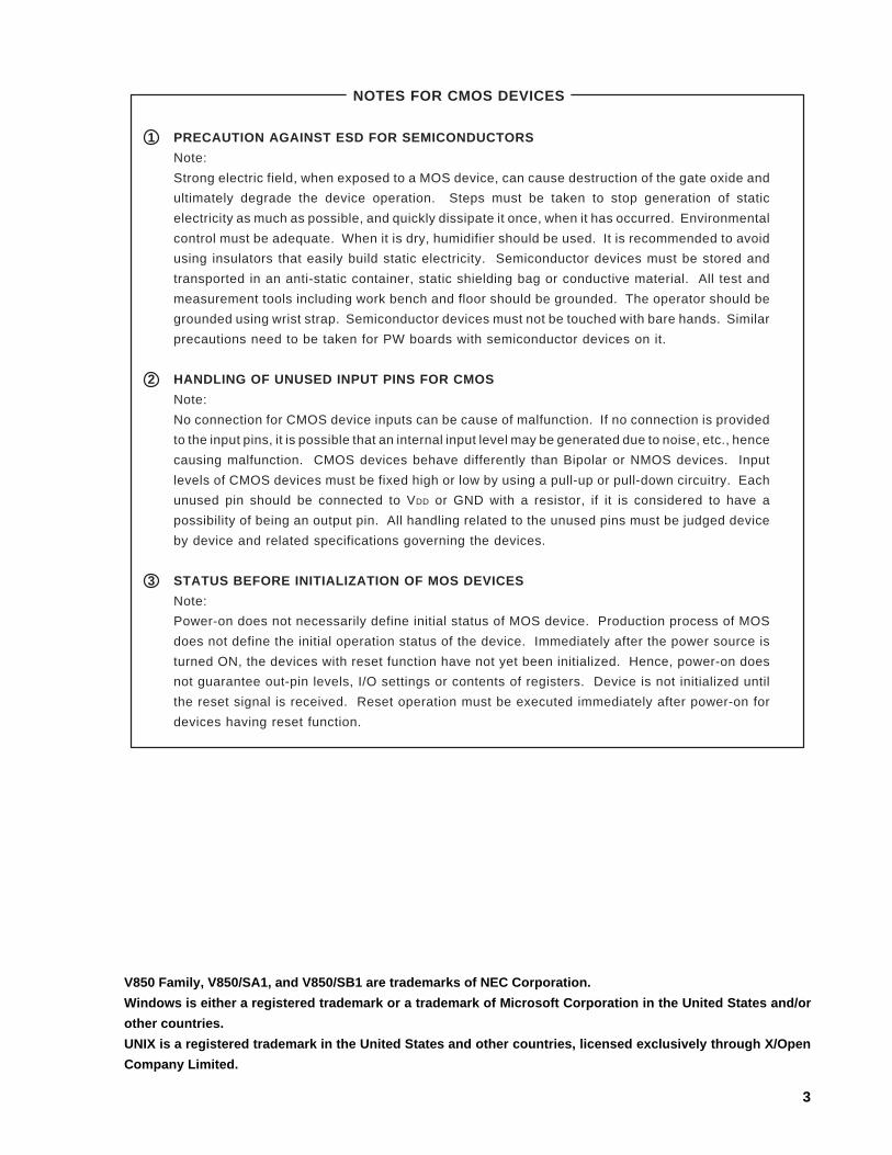
NOTES FOR CMOS DEVICES
1 PRECAUTION AGAINST ESD FOR SEMICONDUCTORS
Note:
Strong electric field, when exposed to a MOS device, can cause destruction of the gate oxide and
ultimately degrade the device operation. Steps must be taken to stop generation of static
electricity as much as possible, and quickly dissipate it once, when it has occurred. Environmental
control must be adequate. When it is dry, humidifier should be used. It is recommended to avoid
using insulators that easily build static electricity. Semiconductor devices must be stored and
transported in an anti-static container, static shielding bag or conductive material. All test and
measurement tools including work bench and floor should be grounded. The operator should be
grounded using wrist strap. Semiconductor devices must not be touched with bare hands. Similar
precautions need to be taken for PW boards with semiconductor devices on it.
2 HANDLING OF UNUSED INPUT PINS FOR CMOS
Note:
No connection for CMOS device inputs can be cause of malfunction. If no connection is provided
to the input pins, it is possible that an internal input level may be generated due to noise, etc., hence
causing malfunction. CMOS devices behave differently than Bipolar or NMOS devices. Input
levels of CMOS devices must be fixed high or low by using a pull-up or pull-down circuitry. Each
unused pin should be connected to VDD or GND with a resistor, if it is considered to have a
possibility of being an output pin. All handling related to the unused pins must be judged device
by device and related specifications governing the devices.
3 STATUS BEFORE INITIALIZATION OF MOS DEVICES
Note:
Power-on does not necessarily define initial status of MOS device. Production process of MOS
does not define the initial operation status of the device. Immediately after the power source is
turned ON, the devices with reset function have not yet been initialized. Hence, power-on does
not guarantee out-pin levels, I/O settings or contents of registers. Device is not initialized until
the reset signal is received. Reset operation must be executed immediately after power-on for
devices having reset function.
V850 Family, V850/SA1, and V850/SB1 are trademarks of NEC Corporation.
Windows is either a registered trademark or a trademark of Microsoft Corporation in the United States and/or
other countries.
UNIX is a registered trademark in the United States and other countries, licensed exclusively through X/Open
Company Limited.

4
Purchase of NEC I2C components conveys a license under the Philips I2C Patent Rights to use these
components in an I2C system, provided that the system conforms to the I2C Standard Specification as defined
by Philips.
The export of these products from Japan is regulated by the Japanese government. The export of some or all of these products may be prohibited without governmental license. To export or re-export some or all of these products from a country other than Japan may also be prohibited without a license from that country. Please call an NEC sales representative.
License not needed: µPD70F3033, 70F3033YThe customer must judge the need for license: µPD703033, 703033Y
The information in this document is subject to change without notice.No part of this document may be copied or reproduced in any form or by any means without the prior writtenconsent of NEC Corporation. NEC Corporation assumes no responsibility for any errors which may appear inthis document.NEC Corporation does not assume any liability for infringement of patents, copyrights or other intellectualproperty rights of third parties by or arising from use of a device described herein or any other liability arisingfrom use of such device. No license, either express, implied or otherwise, is granted under any patents,copyrights or other intellectual property rights of NEC Corporation or others.While NEC Corporation has been making continuous effort to enhance the reliability of its semiconductor devices,the possibility of defects cannot be eliminated entirely. To minimize risks of damage or injury to persons orproperty arising from a defect in an NEC semiconductor device, customers must incorporate sufficient safetymeasures in its design, such as redundancy, fire-containment, and anti-failure features.NEC devices are classified into the following three quality grades:"Standard", "Special", and "Specific". The Specific quality grade applies only to devices developed based ona customer designated "quality assurance program" for a specific application. The recommended applicationsof a device depend on its quality grade, as indicated below. Customers must check the quality grade of eachdevice before using it in a particular application. Standard: Computers, office equipment, communications equipment, test and measurement equipment, audio and visual equipment, home electronic appliances, machine tools, personal electronic equipment and industrial robots Special: Transportation equipment (automobiles, trains, ships, etc.), traffic control systems, anti-disaster systems, anti-crime systems, safety equipment and medical equipment (not specifically designed for life support) Specific: Aircrafts, aerospace equipment, submersible repeaters, nuclear reactor control systems, life support systems or medical equipment for life support, etc.The quality grade of NEC devices is "Standard" unless otherwise specified in NEC's Data Sheets or Data Books.If customers intend to use NEC devices for applications other than those specified for Standard quality grade,they should contact an NEC sales representative in advance.Anti-radioactive design is not implemented in this product.
M7 96. 5

5
Regional Information
Some information contained in this document may vary from country to country. Before using any NECproduct in your application, pIease contact the NEC office in your country to obtain a list of authorizedrepresentatives and distributors. They will verify:
• Device availability
• Ordering information
• Product release schedule
• Availability of related technical literature
• Development environment specifications (for example, specifications for third-party tools and components, host computers, power plugs, AC supply voltages, and so forth)
• Network requirements
In addition, trademarks, registered trademarks, export restrictions, and other legal issues may also varyfrom country to country.
NEC Electronics Inc. (U.S.)Santa Clara, CaliforniaTel: 408-588-6000 800-366-9782Fax: 408-588-6130 800-729-9288
NEC Electronics (Germany) GmbHDuesseldorf, GermanyTel: 0211-65 03 02Fax: 0211-65 03 490
NEC Electronics (UK) Ltd.Milton Keynes, UKTel: 01908-691-133Fax: 01908-670-290
NEC Electronics Italiana s.r.1.Milano, ItalyTel: 02-66 75 41Fax: 02-66 75 42 99
NEC Electronics (Germany) GmbHBenelux OfficeEindhoven, The NetherlandsTel: 040-2445845Fax: 040-2444580
NEC Electronics (France) S.A.Velizy-Villacoublay, FranceTel: 01-30-67 58 00Fax: 01-30-67 58 99
NEC Electronics (France) S.A.Spain OfficeMadrid, SpainTel: 01-504-2787Fax: 01-504-2860
NEC Electronics (Germany) GmbHScandinavia OfficeTaeby, SwedenTel: 08-63 80 820Fax: 08-63 80 388
NEC Electronics Hong Kong Ltd.Hong KongTel: 2886-9318Fax: 2886-9022/9044
NEC Electronics Hong Kong Ltd. Seoul BranchSeoul, KoreaTel: 02-528-0303Fax: 02-528-4411
NEC Electronics Singapore Pte. Ltd.United Square, Singapore 1130Tel: 65-253-8311Fax: 65-250-3583
NEC Electronics Taiwan Ltd.Taipei, TaiwanTel: 02-2719-2377Fax: 02-2719-5951
NEC do Brasil S.A.Electron Devices DivisionRodovia Presidente Dutra, Km 21407210-902-Guarulhos-SP BrasilTel: 55-11-6465-6810Fax: 55-11-6465-6829
J98. 8

6
[MEMO]

7
INTRODUCTION
Readers This manual is intended for users who understand the function of the V850/SB1 (µPD703033,
703033Y, 70F3033, 70F3033Y) and design application system using the V850/SB1.
Purpose This manual is intended for users to understand the hardware functions described in the Organization
below.
Organization The V850/SB1 User’s Manual is divided into two parts: hardware (this manual) and architecture
(V850 FamilyTM User’s Manual Architecture).
Hardware Architecture
• Pin function
• CPU function
• Internal peripheral function
• Flash memory programming
• Data type
• Register set
• Instruction format and instruction set
• Interrupt and exception
• Pipeline operation
How to Read This Manual It is assumed that the reader of this manual has general knowledge in the fields of
electrical engineering , logic circuits, and microcontrollers.
To find out the details of a register whose name is known:
→ Refer to APPENDIX A REGISTER INDEX .
To find out the details of a function, etc., whose name is known:
→ Refer to APPENDIX C INDEX.
To understand the details of a instruction function:
→ Refer to V850 Family User’s Manual Architecture available separately.
How to read register formats:
→ Names of bits whose numbers are enclosed in a square are defined in the device file under
reserved words.
To understand the overall functions of the V850/SB1:
→ Read this manual in accordance with the CONTENTS.
8
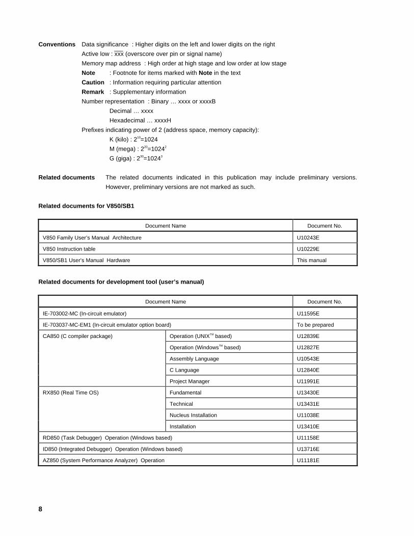
Conventions Data significance : Higher digits on the left and lower digits on the right
Active low : xxx (overscore over pin or signal name)
Memory map address : High order at high stage and low order at low stage
Note : Footnote for items marked with Note in the text
Caution : Information requiring particular attention
Remark : Supplementary information
Number representation : Binary … xxxx or xxxxB
Decimal … xxxx
Hexadecimal … xxxxH
Prefixes indicating power of 2 (address space, memory capacity):
K (kilo) : 210=1024
M (mega) : 220=10242
G (giga) : 230=10243
Related documents The related documents indicated in this publication may include preliminary versions.
However, preliminary versions are not marked as such.
Related documents for V850/SB1
Document Name Document No.
V850 Family User’s Manual Architecture U10243E
V850 Instruction table U10229E
V850/SB1 User’s Manual Hardware This manual
Related documents for development tool (user’s manual)
Document Name Document No.
IE-703002-MC (In-circuit emulator) U11595E
IE-703037-MC-EM1 (In-circuit emulator option board) To be prepared
CA850 (C compiler package) Operation (UNIXTM based) U12839E
Operation (WindowsTM based) U12827E
Assembly Language U10543E
C Language U12840E
Project Manager U11991E
RX850 (Real Time OS) Fundamental U13430E
Technical U13431E
Nucleus Installation U11038E
Installation U13410E
RD850 (Task Debugger) Operation (Windows based) U11158E
ID850 (Integrated Debugger) Operation (Windows based) U13716E
AZ850 (System Performance Analyzer) Operation U11181E
9
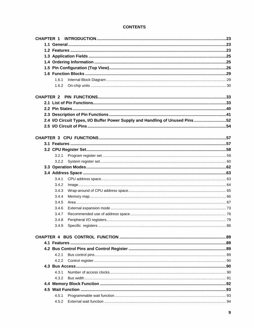
CONTENTS
CHAPTER 1 INTRODUCTION..................................................................................................... ............231.1 General ................................................................................................................... .......................231.2 Features .................................................................................................................. ......................231.3 Application Fields ........................................................................................................ ................251.4 Ordering Information ...................................................................................................... .............251.5 Pin Configuration (Top View).............................................................................................. ........261.6 Function Blocks ........................................................................................................... ................29
1.6.1 Internal Block Diagram .................................................................................................................. 29
1.6.2 On-chip units ................................................................................................................................. 30
CHAPTER 2 PIN FUNCTIONS................................................................................................... .............332.1 List of Pin Functions..................................................................................................... ...............332.2 Pin States................................................................................................................ ......................402.3 Description of Pin Functions .............................................................................................. ........412.4 I/O Circuit Types, I/O Buffer Power Supply and Handling of Unused Pins ............................522.5 I/O Circuit of Pins ....................................................................................................... ..................54
CHAPTER 3 CPU FUNCTIONS.................................................................................................... ...........573.1 Features .................................................................................................................. ......................573.2 CPU Register Set.......................................................................................................... ................58
3.2.1 Program register set ...................................................................................................................... 59
3.2.2 System register set........................................................................................................................ 60
3.3 Operation Modes........................................................................................................... ...............623.4 Address Space ............................................................................................................. ................63
3.4.1 CPU address space....................................................................................................................... 63
3.4.2 Image............................................................................................................................................. 64
3.4.3 Wrap-around of CPU address space............................................................................................. 65
3.4.4 Memory map.................................................................................................................................. 66
3.4.5 Area ............................................................................................................................................... 67
3.4.6 External expansion mode .............................................................................................................. 73
3.4.7 Recommended use of address space .......................................................................................... . 76
3.4.8 Peripheral I/O registers.................................................................................................................. 79
3.4.9 Specific registers .......................................................................................................................... 86
CHAPTER 4 BUS CONTROL FUNCTION ............................................................................................ .894.1 Features .................................................................................................................. ......................894.2 Bus Control Pins and Control Register ..................................................................................... 89
4.2.1 Bus control pins ............................................................................................................................. 89
4.2.2 Control register .............................................................................................................................. 90
4.3 Bus Access................................................................................................................ ...................904.3.1 Number of access clocks............................................................................................................... 90
4.3.2 Bus width ....................................................................................................................................... 91
4.4 Memory Block Function ..................................................................................................... .........924.5 Wait Function ............................................................................................................. ..................93
4.5.1 Programmable wait function .......................................................................................................... 93
4.5.2 External wait function .................................................................................................................... 94

10
4.5.3 Relationship between programmable wait and external wait......................................................... 94
4.6 Idle State Insertion Function ............................................................................................. ......... 954.7 Bus Hold Function ......................................................................................................... ............. 96
4.7.1 Outline of function.......................................................................................................................... 96
4.7.2 Bus hold procedure........................................................................................................................ 97
4.7.3 Operation in power save mode...................................................................................................... 97
4.8 Bus Timing................................................................................................................ ................... 984.9 Bus Priority .............................................................................................................. .................. 1054.10 Memory Boundary Operation Condition............................................................................... 105
4.10.1 Program space ............................................................................................................................ 105
4.10.2 Data space................................................................................................................................... 105
CHAPTER 5 INTERRUPT/EXCEPTION PROCESSING FUNCTION.................................................. 1075.1 Outline ................................................................................................................... ..................... 107
5.1.1 Features....................................................................................................................................... 107
5.2 Non-Maskable Interrupt .................................................................................................... ........ 1105.2.1 Operation ..................................................................................................................................... 111
5.2.2 Restore ........................................................................................................................................ 113
5.2.3 NP flag ......................................................................................................................................... 114
5.2.4 Noise elimination circuit of NMI pin.............................................................................................. 114
5.2.5 Edge detection function of NMI pin.............................................................................................. 115
5.3 Maskable Interrupts....................................................................................................... ............ 1165.3.1 Operation ..................................................................................................................................... 116
5.3.2 Restore ........................................................................................................................................ 118
5.3.3 Priorities of maskable interrupts .................................................................................................. 119
5.3.4 Interrupt control register (xxICn) .................................................................................................. 123
5.3.5 In-service priority register (ISPR)................................................................................................. 125
5.3.6 Maskable interrupt status flag...................................................................................................... 125
5.3.7 Watchdog timer mode register (WDTM) ...................................................................................... 126
5.3.8 Noise elimination ......................................................................................................................... 126
5.3.9 Edge detection function ............................................................................................................... 128
5.4 Software Exception ........................................................................................................ ........... 1295.4.1 Operation ..................................................................................................................................... 129
5.4.2 Restore ........................................................................................................................................ 130
5.4.3 EP flag ......................................................................................................................................... 131
5.5 Exception Trap............................................................................................................ ............... 1315.5.1 Illegal op code definition .............................................................................................................. 131
5.5.2 Operation ..................................................................................................................................... 131
5.5.3 Restore ........................................................................................................................................ 132
5.6 Priority Control .......................................................................................................... ................ 1345.6.1 Priorities of interrupts and exceptions.......................................................................................... 134
5.6.2 Multiple interrupt processing........................................................................................................ 134
5.7 Interrupt Latency Time.................................................................................................... .......... 1375.8 Periods Where Interrupt Is Not Acknowledged ...................................................................... 1375.9 Key Interrupt Function.................................................................................................... .......... 138
11
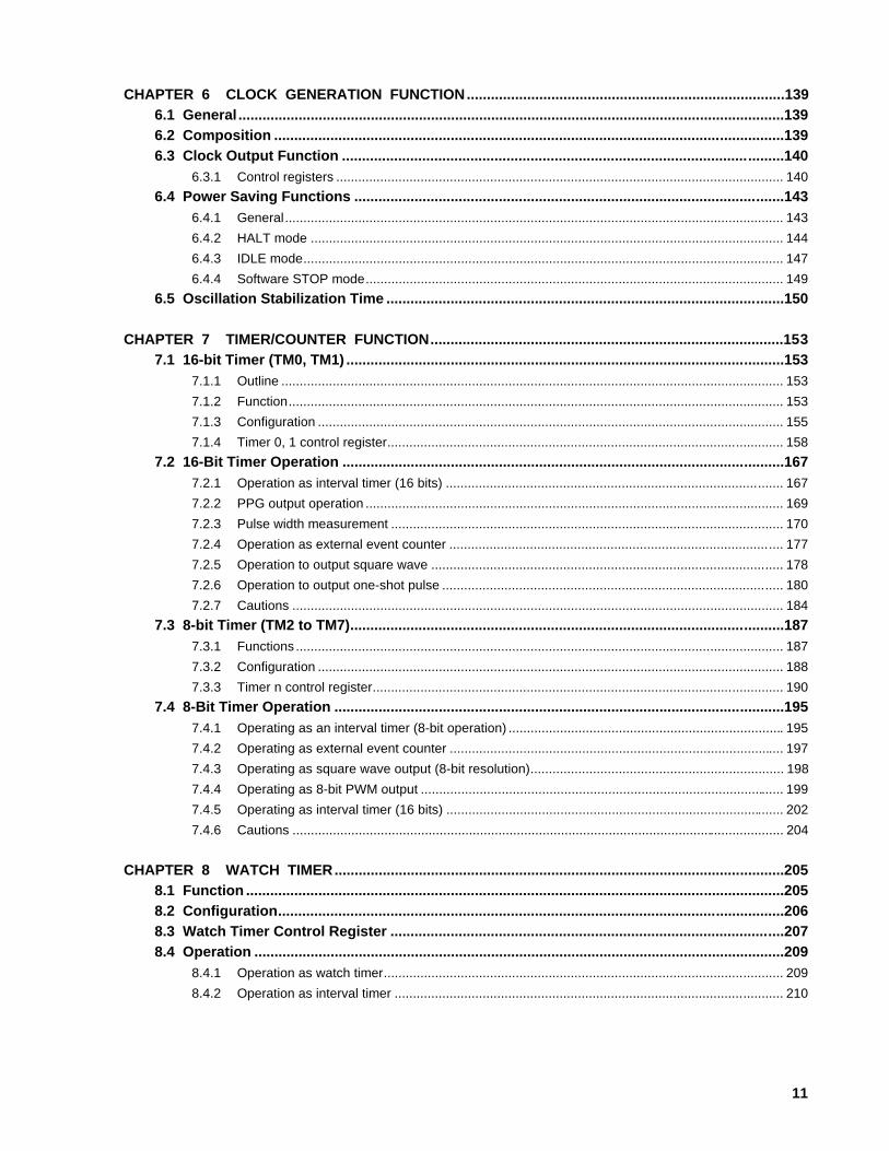
CHAPTER 6 CLOCK GENERATION FUNCTION...............................................................................1396.1 General ................................................................................................................... .....................1396.2 Composition ............................................................................................................... ................1396.3 Clock Output Function ..................................................................................................... .........140
6.3.1 Control registers .......................................................................................................................... 140
6.4 Power Saving Functions .................................................................................................... .......1436.4.1 General........................................................................................................................................ 143
6.4.2 HALT mode ................................................................................................................................. 144
6.4.3 IDLE mode................................................................................................................................... 147
6.4.4 Software STOP mode.................................................................................................................. 149
6.5 Oscillation Stabilization Time ............................................................................................ .......150
CHAPTER 7 TIMER/COUNTER FUNCTION........................................................................................1537.1 16-bit Timer (TM0, TM1) ................................................................................................... ..........153
7.1.1 Outline ......................................................................................................................................... 153
7.1.2 Function....................................................................................................................................... 153
7.1.3 Configuration ............................................................................................................................... 155
7.1.4 Timer 0, 1 control register............................................................................................................ 158
7.2 16-Bit Timer Operation .................................................................................................... ..........1677.2.1 Operation as interval timer (16 bits) ............................................................................................ 167
7.2.2 PPG output operation .................................................................................................................. 169
7.2.3 Pulse width measurement ........................................................................................................... 170
7.2.4 Operation as external event counter ........................................................................................... 177
7.2.5 Operation to output square wave ................................................................................................ 178
7.2.6 Operation to output one-shot pulse ............................................................................................. 180
7.2.7 Cautions ...................................................................................................................................... 184
7.3 8-bit Timer (TM2 to TM7).................................................................................................. ..........1877.3.1 Functions ..................................................................................................................................... 187
7.3.2 Configuration ............................................................................................................................... 188
7.3.3 Timer n control register................................................................................................................ 190
7.4 8-Bit Timer Operation ..................................................................................................... ...........1957.4.1 Operating as an interval timer (8-bit operation) ........................................................................... 195
7.4.2 Operating as external event counter ........................................................................................... 197
7.4.3 Operating as square wave output (8-bit resolution)..................................................................... 198
7.4.4 Operating as 8-bit PWM output ................................................................................................... 199
7.4.5 Operating as interval timer (16 bits) ............................................................................................ 202
7.4.6 Cautions ...................................................................................................................................... 204
CHAPTER 8 WATCH TIMER..................................................................................................... ...........2058.1 Function .................................................................................................................. ....................2058.2 Configuration............................................................................................................. .................2068.3 Watch Timer Control Register .............................................................................................. ....2078.4 Operation ................................................................................................................. ...................209
8.4.1 Operation as watch timer............................................................................................................. 209
8.4.2 Operation as interval timer .......................................................................................................... 210

12
CHAPTER 9 WATCHDOG TIMER.................................................................................................. ..... 2119.1 Functions ................................................................................................................. .................. 2119.2 Configuration............................................................................................................. ................ 2139.3 Watchdog Timer Control Register ........................................................................................... 2139.4 Operation................................................................................................................. ................... 216
9.4.1 Operating as watchdog timer....................................................................................................... 216
9.4.2 Operating as interval timer........................................................................................................... 217
9.5 Standby Function Control Register......................................................................................... 218
CHAPTER 10 SERIAL INTERFACE FUNCTION ............................................................................... 21910.1 Overview................................................................................................................. .................. 21910.2 3-wire Serial I/O (CSI0 to CSI3)......................................................................................... ...... 219
10.2.1 Configuration ............................................................................................................................... 220
10.2.2 CSIn control registers .................................................................................................................. 221
10.2.3 Operations ................................................................................................................................... 223
10.3 I2C Bus ( µPD703033Y, 70F3033Y)........................................................................................... 22710.3.1 Configuration ............................................................................................................................... 230
10.3.2 I2C control register ....................................................................................................................... 232
10.3.3 I2C bus mode functions ................................................................................................................ 242
10.3.4 I2C bus definitions and control methods....................................................................................... 243
10.3.5 I2C interrupt requests (INTIICn).................................................................................................... 250
10.3.6 Interrupt request (INTIICn) generation timing and wait control .................................................... 270
10.3.7 Address match detection method ................................................................................................ 271
10.3.8 Error detection ............................................................................................................................. 271
10.3.9 Extension code ............................................................................................................................ 271
10.3.10Arbitration .................................................................................................................................... 272
10.3.11Wake up function ......................................................................................................................... 274
10.3.12Communication reservation ......................................................................................................... 275
10.3.13Other cautions ............................................................................................................................. 279
10.3.14Communication operations .......................................................................................................... 280
10.3.15Timing of Data Communication.................................................................................................... 282
10.4 Asynchronous Serial Interface (UART0, UART1) ................................................................. 28910.4.1 Configuration ............................................................................................................................... 289
10.4.2 UARTn control registers .............................................................................................................. 291
10.4.3 Operations ................................................................................................................................... 296
10.4.4 Asynchronous serial interface (UARTn) mode............................................................................. 297
10.4.5 Standby function .......................................................................................................................... 309
10.5 3-Wire Variable Serial I/O (CSI4)........................................................................................ ..... 31010.5.1 Configuration ............................................................................................................................... 310
10.5.2 CSI4 control registers .................................................................................................................. 313
10.5.3 Operations ................................................................................................................................... 317
CHAPTER 11 A/D CONVERTER.................................................................................................. ....... 32311.1 Function ................................................................................................................. .................. 32311.2 Configuration............................................................................................................ ............... 32511.3 Control Registers ....................................................................................................... ............ 32711.4 Operation................................................................................................................ .................. 330
11.4.1 Basic operation ............................................................................................................................ 330
13
11.4.2 Input voltage and conversion result............................................................................................. 332
11.4.3 A/D converter operation mode..................................................................................................... 333
11.5 Low Power Consumption Mode .............................................................................................33 511.6 Notes on Using A/D Converter............................................................................................. ...336
CHAPTER 12 DMA FUNCTIONS .................................................................................................. .......34112.1 Functions ................................................................................................................ ..................34112.2 Transfer Completion Interrupt Request .................................................................................34112.3 Control Registers ........................................................................................................ .............341
12.3.1 DMA peripheral I/O address registers 0 to 5 (DIOA0 to DIOA5) ................................................. 341
12.3.2 DMA internal RAM address registers 0 to 5 (DRA0 to DRA5)..................................................... 342
12.3.3 DMA byte count registers 0 to 5 (DBC0 to DBC5)....................................................................... 343
12.3.4 DMA channel control registers 0 to 5 (DCHC0 to DCHC5) ......................................................... 343
CHAPTER 13 REAL-TIME OUTPUT FUNCTION (RTO) ...................................................................34713.1 Function ................................................................................................................. ...................34713.2 Configuration............................................................................................................ ................34813.3 RTO Control Registers .................................................................................................... ........34913.4 Operation ................................................................................................................ ..................35213.5 Usage.................................................................................................................... .....................35313.6 Cautions................................................................................................................. ...................353
CHAPTER 14 PORT FUNCTION.................................................................................................. ........35514.1 Port Configuration ....................................................................................................... ............35514.2 Port Pin Function ........................................................................................................ .............355
14.2.1 Port 0 ........................................................................................................................................... 355
14.2.2 Port 1 ........................................................................................................................................... 360
14.2.3 Port 2 ........................................................................................................................................... 363
14.2.4 Port 3 ........................................................................................................................................... 366
14.2.5 Ports 4 and 5 ............................................................................................................................... 369
14.2.6 Port 6 ........................................................................................................................................... 371
14.2.7 Ports 7 and 8 ............................................................................................................................... 373
14.2.8 Port 9 ........................................................................................................................................... 374
14.2.9 Port 10 ......................................................................................................................................... 376
14.2.10 Port 11 ........................................................................................................................................ 379
14.3 Setting When Port Pin Is Used For Alternate Function........................................................382
CHAPTER 15 RESET FUNCTION................................................................................................. .......38715.1 General .................................................................................................................. ....................38715.2 Pin Operations........................................................................................................... ...............387
CHAPTER 16 REGULATOR........................................................................................................ ...........38916.1 Outline.................................................................................................................. .....................38916.2 Operation ................................................................................................................ ..................389
CHAPTER 17 ROM CORRECTION FUNCTION ....................................................................................39117.1 General .................................................................................................................. ....................39117.2 ROM Correction Peripheral I/O Registers..............................................................................392

14
17.2.1 Correction control register (CORCN) ........................................................................................... 392
17.2.2 Correction request register (CORRQ).......................................................................................... 393
17.2.3 Correction address registers (CORAD0 to CORAD3).................................................................. 393
CHAPTER 18 FLASH MEMORY ( µµµµPD70F3033, 70F3033Y) .............................................................. 39518.1 Features................................................................................................................. ................... 39518.2 Writing by Flash Programmer .............................................................................................. .. 39518.3 Programming Environment .................................................................................................. .. 39618.4 Communication System ..................................................................................................... .... 39618.5 Pin Connection ........................................................................................................... ............. 398
18.5.1 VPP pin ......................................................................................................................................... 398
18.5.2 Serial interface pin ....................................................................................................................... 398
18.5.3 RESET pin ................................................................................................................................... 400
18.5.4 Port pin (including NMI) ............................................................................................................... 400
18.5.5 Other signal pins.......................................................................................................................... 400
18.5.6 Power supply ............................................................................................................................... 400
18.6 Programming Method ....................................................................................................... ...... 40118.6.1 Flash memory control .................................................................................................................. 401
18.6.2 Flash memory programming mode .............................................................................................. 401
18.6.3 Selection of communication mode............................................................................................... 402
18.6.4 Communication command ........................................................................................................... 402
18.6.5 Resources used........................................................................................................................... 403
APPENDIX A REGISTER INDEX................................................................................................. ........ 405
APPENDIX B LIST OF INSTRUCTION SETS .................................................................................... 41 3
APPENDIX C INDEX ............................................................................................................................. 421

15
LIST OF FIGURES (1/6)
Figure No. Title Page
3-1 CPU Address Space............................................................................................................................... 63
3-2 Image on Address Space ....................................................................................................................... 64
3-3 Memory Map........................................................................................................................................... 66
3-4 Internal ROM/Internal Flash Memory Area............................................................................................. 67
3-5 External Memory Area (When Expanded to 64 K, 256 K, or 1 Mbytes) ................................................. 71
3-6 External Memory Area (When Expanded to 4 Mbytes) .......................................................................... 72
3-7 Memory Expansion Mode Register (MM) Format................................................................................... 74
3-8 Memory Address Output Mode Register (MAM) Format ........................................................................ 75
3-9 Recommended Memory Map (Flash Memory Version) .......................................................................... 78
4-1 Example of Inserting Wait States ........................................................................................................... 94
5-1 Non-Maskable Interrupt Servicing .......................................................................................................... 111
5-2 Acknowledging Non-Maskable Interrupt Request .................................................................................. 112
5-3 RETI Instruction Processing................................................................................................................... 113
5-4 Rising Edge Specification Register (EGP0) Format ............................................................................... 115
5-5 Falling Edge Specification Register (EGN0) Format .............................................................................. 115
5-6 Maskable Interrupt Servicing.................................................................................................................. 117
5-7 RETI Instruction Processing................................................................................................................... 118
5-8 Example of Interrupt Nesting Service ..................................................................................................... 120
5-9 Example of Servicing Interrupt Requests Simultaneously Generated.................................................... 122
5-10 Interrupt Control Register (xxICn) Format .............................................................................................. 123
5-11 In-service Priority Register (ISPR) Format ............................................................................................. 125
5-12 Watchdog Timer Mode Register (WDTM) Format .................................................................................. 126
5-13 Noise Elimination Control Register (NCC).............................................................................................. 127
5-14 Software Exception Processing.............................................................................................................. 129
5-15 RETI Instruction Processing................................................................................................................... 130
5-16 Exception Trap Processing .................................................................................................................... 132
5-17 RETI Instruction Processing................................................................................................................... 133
5-18 Pipeline Operation at Interrupt Request Acknowledge........................................................................... 137
5.19 Key Return Mode Register (KRM).......................................................................................................... 138
6-1 Format of Processor Clock Control Register (PCC) ............................................................................... 140
6-2 Format of Power Saving Control Register (PSC) ................................................................................... 142
6-3 Format of Oscillation Stabilization Time Select Register (OSTS)........................................................... 143
7-1 Block Diagram of TM0 and TM1............................................................................................................. 154
7-2 16-Bit Timer Mode Control Registers 0, 1 (TMC0, TMC1) ..................................................................... 159
7-3 Capture/Compare Control Registers 0, 1 (CRC0, CRC1) ...................................................................... 161
7-4 16-Bit Timer Output Control Registers 0, 1 (TOC0, TOC1) .................................................................... 163

16
LIST OF FIGURES (2/6)
Figure No. Title Page
7-5 Prescaler Mode Register 00 (PRM00).................................................................................................... 164
7-6 Prescaler Mode Register 01 (PRM01).................................................................................................... 165
7-7 Prescaler Mode Register 10 (PRM10).................................................................................................... 165
7-8 Prescaler Mode Register 11 (PRM11).................................................................................................... 166
7-9 Control Register Settings When TMn Operates as Interval Timer.......................................................... 167
7-10 Configuration of Interval Timer ............................................................................................................... 168
7-11 Timing of Interval Timer Operation ......................................................................................................... 168
7-12 Control Register Settings in PPG Output Operation............................................................................... 169
7-13 Control Register Settings for Pulse Width Measurement with Free Running Counter and
One Capture Register............................................................................................................................. 170
7-14 Configuration for Pulse Width Measurement with Free Running Counter .............................................. 171
7-15 Timing of Pulse Width Measurement with Free Running Counter and One Capture Register
(with Both Edges Specified).................................................................................................................... 171
7-16 Control Register Settings for Measurement of Two Pulse Widths with Free Running Counter .............. 172
7-17 CRn1 Capture Operation with Rising Edge Specified ............................................................................ 173
7-18 Timing of Pulse Width Measurement with Free Running Counter (with Both Edges Specified)............. 173
7-19 Control Register Settings for Pulse Width Measurement with Free Running Counter and
Two Capture Registers ........................................................................................................................... 174
7-20 Timing of Pulse Width Measurement with Free Running Counter and Two Capture Registers
(with Rising Edge Specified)................................................................................................................... 175
7-21 Control Register Settings for Pulse Width Measurement by Restarting ................................................. 176
7-22 Timing of Pulse Width Measurement by Restarting (with Rising Edge Specified).................................. 176
7-23 Control Register Settings in External Event Counter Mode.................................................................... 177
7-24 Configuration of External Event Counter ................................................................................................ 178
7-25 Timing of External Event Counter Operation (with Rising Edge Specified) ............................................ 178
7-26 Control Register Settings in Square Wave Output Mode ....................................................................... 179
7-27 Timing of Square Wave Output Operation.............................................................................................. 180
7-28 Control Register Settings for One-Shot Pulse Output with Software Trigger.......................................... 181
7-29 Timing of One-Shot Pulse Output Operation with Software Trigger ....................................................... 182
7-30 Control Register Settings for One-Shot Pulse Output with External Trigger........................................... 183
7-31 Timing of One-Shot Pulse Output Operation with External Trigger (with Rising Edge Specified) .......... 184
7-32 Start Timing of 16-Bit Timer Register n .................................................................................................. 184
7-33 Timing After Changing Compare Register During Timer Count Operation............................................. 185
7-34 Data Hold Timing of Capture Register.................................................................................................... 185
7-35 Operation Timing of OVFn Flag.............................................................................................................. 186
7-36 Block Diagram of TM2 to TM7 ................................................................................................................ 188
7-37 TM2, TM3 Timer Clock Selection Registers 20, 21, 30, 31 (TCL20, TCL21, TCL30, and TCL31)......... 190
7-38 TM4, TM5 Timer Clock Selection Registers 40, 41, 50, 51 (TCL40, TCL41, TCL50, and TCL51)......... 191
7-39 TM6, TM7 Timer Clock Selection Registers 60, 61, 70, 71 (TCL60, TCL61, TCL70, and TCL71)......... 192
7-40 8-Bit Timer Mode Control Registers 2 to 7 (TMC2 to TMC7).................................................................. 194
7-41 Timing of Interval Timer Operation ......................................................................................................... 195
7-42 Timing of External Event Counter Operation (When Rising Edge Is Set)............................................... 198
7-43 Timing of PWM Output ........................................................................................................................... 200

17
LIST OF FIGURES (3/6)
Figure No. Title Page
7-44 Timing of Operation Based on CRn0 Transitions ................................................................................... 201
7-45 Cascade Connection Mode with 16-Bit Resolution ................................................................................ 203
7-46 Start Timing of Timer n ........................................................................................................................... 204
7-47 Timing After Compare Register Changes During Timer Counting.......................................................... 204
8-1 Block Diagram of Watch Timer............................................................................................................... 205
8-2 Watch Timer Mode Control Register (WTNM)........................................................................................ 207
8-3 Watch Timer Clock Selection Register (WTNCS) .................................................................................. 208
8-4 Operation Timing of Watch Timer/Interval Timer.................................................................................... 210
9-1 Block Diagram of Watchdog Timer......................................................................................................... 211
9-2 Oscillation Stabilization Time Selection Register (OSTS) ...................................................................... 213
9-3 Watchdog Timer Clock Selection Register (WDCS)............................................................................... 214
9-4 Watchdog Timer Mode Register (WDTM) .............................................................................................. 215
9-5 Oscillation Stabilization Time Selection Register (OSTS) .................................................................... .. 218
10-1 Block Diagram of 3-Wire Serial I/O......................................................................................................... 220
10-2 Serial Operation Mode Registers 0 to 3 (CSIM0 to CSIM3) ................................................................... 221
10-3 Serial Clock Selection Registers 0 to 3 (CSIS0 to CSIS3) ..................................................................... 222
10-4 Serial Operation Mode Registers 0 to 3 (CSIM0 to CSIM3) ................................................................... 223
10-5 Serial Operation Mode Registers 0 to 3 (CSIM0 to CSIM3) ................................................................... 224
10-6 Timing of 3-Wire Serial I/O Mode ........................................................................................................... 225
10-7 Block Diagram of I2Cn............................................................................................................................. 228
10-8 Serial Bus Configuration Example Using I2C Bus................................................................................... 229
10-9 IIC Control Register n (IICCn) ................................................................................................................ 233
10-10 IIC Status Register n (IICSn) .................................................................................................................. 237
10-11 IIC Clock Select Register n (IICCLn) ...................................................................................................... 240
10-12 Pin Configuration Diagram ..................................................................................................................... 242
10-13 I2C Bus’s Serial Data Transfer Timing .................................................................................................... 243
10-14 Start Conditions...................................................................................................................................... 243
10-15 Address .................................................................................................................................................. 244
10-16 Transfer Direction Specification ............................................................................................................. 245
10-17 ACK Signal ............................................................................................................................................. 246
10-18 Stop Condition........................................................................................................................................ 247
10-19 Wait Signal ............................................................................................................................................. 248
10-20 Arbitration Timing Example .................................................................................................................... 273
10-21 Communication Reservation Timing....................................................................................................... 276
10-22 Timing for Accepting Communication Reservations............................................................................... 277
10-23 Communication Reservation Flow Chart ................................................................................................ 278
10-24 Master Operation Flow Chart ................................................................................................................. 280
10-25 Slave Operation Flow Chart ................................................................................................................... 281
10-26 Example of Master to Slave Communication (When 9-Clock Wait Is Selected for Both Master
and Slave) .............................................................................................................................................. 283

18
LIST OF FIGURES (4/6)
Figure No. Title Page
10-27 Example of Slave to Master Communication (When 9-Clock Wait Is Selected for Both Master
and Slave)............................................................................................................................................... 286
10-28 Block Diagram of UARTn........................................................................................................................ 290
10-29 Asynchronous Serial Interface Mode Register 0, 1 (ASIM0, ASIM1)...................................................... 292
10-30 Asynchronous Serial Interface Status Registers 0, 1 (ASIS0, ASIS1).................................................... 293
10-31 Baud Rate Generator Control Registers 0, 1 (BRGC0, BRGC1)............................................................ 294
10-32 Baud Rate Generator Mode Control Registers n0, n1 (BRGMCn0, BRGMCn1) .................................... 295
10-33 Error Tolerance (When k = 0), Including Sampling Errors ...................................................................... 303
10-34 Format of Transmit/Receive Data in Asynchronous Serial Interface ...................................................... 304
10-35 Timing of Asynchronous Serial Interface Transmit Completion Interrupt ............................................... 306
10-36 Timing of Asynchronous Serial Interface Receive Completion Interrupt ................................................ 307
10-37 Receive Error Timing .............................................................................................................................. 308
10-38 Block Diagram of CSI4 ........................................................................................................................... 311
10-39 Veriable Serial I/O Shift Register (SIO4) ................................................................................................ 311
10-40 When Transfer Bit Length Other Than 16 Bits Is Set ............................................................................. 312
10-41 Variable Length Serial Control Register (CSIM4) ................................................................................... 313
10-42 Variable Length Serial Setting Register (CSIB4) .................................................................................... 314
10-43 Baud Rate Generator Source Clock Select Register (BRGCN4)............................................................ 315
10-44 Baud Rate Generator Output Clock Select Register (BRGCK4) ............................................................ 316
10-45 Timing of 3-Wire Variable Serial I/O Mode ............................................................................................. 320
10-46 Timing of 3-Wire Variable Serial I/O Mode (When CSIB4 = 08H)........................................................... 321
11-1 Block Diagram of A/D Converter............................................................................................................. 324
11-2 A/D Converter Mode Register 1 (ADM1) ................................................................................................ 327
11-3 Analog Input Channel Specification Register (ADS)............................................................................... 329
11-4 A/D Converter Mode Register 2 (ADM2) ................................................................................................ 329
11-5 Basic Operation of A/D Converter .......................................................................................................... 331
11-6 Relationship Between Analog Input Voltage and A/D Conversion Result .............................................. 332
11-7 A/D Conversion by Hardware Start (with Falling Edge Specified) .......................................................... 334
11-8 A/D Conversion by Software Start .......................................................................................................... 335
11-9 Handling of Analog Input Pin .................................................................................................................. 337
11-10 A/D Conversion End Interrupt Generation Timing .................................................................................. 338
11-11 Handling of AVDD Pin .............................................................................................................................. 339
12-1 Format of DMA Peripheral I/O Address Registers 0 to 5 (DIOA0 to DIOA5) .......................................... 341
12-2 Format of DMA Internal RAM Address Registers 0 to 5 (DRA0 to DRA5).............................................. 342
12-3 Correspondence Between DRAn Setup Value and Internal RAM Area.................................................. 342
12-4 Format of DMA Byte Count Registers 0 to 5 (DBC0 to DBC5) ............................................................... 343
12-5 Format of DMA Channel Control Registers 0 to 5 (DCHC0 to DCHC5) ................................................. 344
13-1 Block Diagram of RTO............................................................................................................................ 347
13-2 Configuration of Real-Time Output Buffer Registers .............................................................................. 348
13-3 Format of Real-Time Output Port Mode Register (RTPM)...................................................................... 350
19
LIST OF FIGURES (5/6)
Figure No. Title Page
13-4 Format of Real-Time Output Port Control Register (RTPC) ................................................................... 351
13-5 Example of Operation Timing of RTO (When EXTR = 0, BYTE = 0)...................................................... 352
14-1 Format of Port 0 (P0).............................................................................................................................. 355
14-2 Port 0 Mode Register (PM0)................................................................................................................... 358
14-3 Pull-up Resistor Option Register 0 (PU0)............................................................................................... 358
14-4 Rising Edge Specification Register (EGP0) ........................................................................................... 359
14-5 Falling Edge Specification Register (EGN0)........................................................................................... 359
14-6 Port 1 (P1) .............................................................................................................................................. 360
14-7 Port 1 Mode Register (PM1)................................................................................................................... 361
14-8 Pull-up Resistor Option Register 1 (PU1)............................................................................................... 362
14-9 Port 1 Function Register (PF1)............................................................................................................... 362
14-10 Port 2 (P2) .............................................................................................................................................. 363
14-11 Port 2 Mode Register (PM2)................................................................................................................... 364
14-12 Pull-up Resistor Option Register 2 (PU2)............................................................................................... 365
14-13 Port 2 Function Register (PF2)............................................................................................................... 365
14-14 Port 3 (P3) .............................................................................................................................................. 366
14-15 Port 3 Mode Register (PM3)................................................................................................................... 367
14-16 Pull-up Resistor Option Register 3 (PU3)............................................................................................... 367
14-17 Port 3 Function Register (PF3)............................................................................................................... 368
14-18 Ports 4 and 5 (P4 and P5) ...................................................................................................................... 369
14-19 Port 4 Mode Register, Port 5 Mode Register (PM4, PM5)...................................................................... 371
14-20 Port 6 (P6) .............................................................................................................................................. 371
14-21 Port 6 Mode Register (PM6)................................................................................................................... 372
14-22 Ports 7 and 8 (P7 and P8) ...................................................................................................................... 373
14-23 Port 9 (P9) .............................................................................................................................................. 374
14-24 Port 9 Mode Register (PM9)................................................................................................................... 375
14-25 Port 10 (P10) .......................................................................................................................................... 376
14-26 Port 10 Mode Register (PM10)............................................................................................................... 377
14-27 Pull-up Resistance Option Register 10 (PU10) ...................................................................................... 378
14-28 Port 10 Function Register (PF10)........................................................................................................... 378
14-29 Port 11 (P11) .......................................................................................................................................... 379
14-30 Port 11 Mode Register (PM11)............................................................................................................... 380
14-31 Pull-up Resistor Option Register 11 (PU11)........................................................................................... 381
14-32 Port Alternate Resistor-function Control Register (PAC)........................................................................ 381
20
LIST OF FIGURES (6/6)
Figure No. Title Page
15-1 System Reset Timing.............................................................................................................................. 387
16-1 Regulator ................................................................................................................................................ 389
17-1 Block Diagram of ROM Correction.......................................................................................................... 391
17-2 Correction Control Register (CORCN).................................................................................................... 392
17-3 Correction Request Register (CORRQ).................................................................................................. 393
17-4 Correction Address Registers (CORAD0 to CORAD3) .......................................................................... 393
17-5 ROM Correction Operation and Program Flow ...................................................................................... 394

21
LIST OF TABLES (1/2)
Table No. Title Page
1-1 V850/SB1 ............................................................................................................................................... 23
3-1 Program Registers.................................................................................................................................. 593-2 System Register Numbers...................................................................................................................... 603-3 Interrupt/Exception Table ....................................................................................................................... 68
4-1 Bus Priority ............................................................................................................................................. 105
5-1 Interrupt Source List ............................................................................................................................... 1085-2 Description of Key Return Detection Pin ................................................................................................ 138
6-1 Operating Statuses in HALT Mode......................................................................................................... 1456-2 Operating Statuses in IDLE Mode .......................................................................................................... 1476-3 Operating States in Software STOP Mode............................................................................................. 149
7-1 Configuration of Timers 0 and 1 ............................................................................................................. 1557-2 Valid Edge of TIn0 Pin and Capture Trigger of CRn0 ............................................................................ 1567-3 Valid Edge of TIn1 Pin and Capture Trigger of CRn0 ............................................................................ 1567-4 Timers 2 to 7 Configuration .................................................................................................................... 188
8-1 Interval Time of Interval Timer................................................................................................................ 2068-2 Configuration of Watch Timer................................................................................................................. 2068-3 Interval Time of Interval Timer................................................................................................................ 210
9-1 Runaway Detection Time by Watchdog Timer ....................................................................................... 2129-2 Interval Time of Interval Timer............................................................................................................... 2129-3 Watchdog Timer Configuration............................................................................................................... 2139-4 Runaway Detection Time of Watchdog Timer ........................................................................................ 2169-5 Interval Time of Interval Timer................................................................................................................ 217
10-1 Configuration of CSIn ............................................................................................................................. 22010-2 Configuration of I2Cn............................................................................................................................... 23010-3 INTIICn Timing and Wait Control............................................................................................................ 27010-4 Extension Code Bit Definitions ............................................................................................................... 27110-5 Status During Arbitration and Interrupt Request Generation Timing ...................................................... 27310-6 Wait Periods ........................................................................................................................................... 27510-7 Configuration of UARTn ......................................................................................................................... 28910-8 Relationship Between Main Clock and Baud Rate ................................................................................. 30210-9 Receive Error Causes ............................................................................................................................ 30810-10 Configuration of CSI4 ............................................................................................................................. 310
22
LIST OF TABLES (2/2)
Table No. Title Page
11-1 Configuration of A/D Converter............................................................................................................... 325
13-1 Configuration of RTO.............................................................................................................................. 34813-2 Operation When Real-Time Output Buffer Registers Are Manipulated .................................................. 34913-3 Operation Mode and Output Trigger of Real-Time Output Port .............................................................. 351
14-1 Setting When Port Pin Is Used for Alternate Function............................................................................ 382
18-1 List of Communication Systems ............................................................................................................. 402

23
CHAPTER 1 INTRODUCTION
The V850/SB1 is a product in NEC’s V850 Family of single-chip microcontrollers designed for low power
operation.
1.1 General
The V850/SB1 is a 32-/16-bit single-chip microcontroller that includes the V850 Family’s CPU core, and peripheral
functions such as ROM/RAM, a timer/counter, a serial interface, an A/D converter, a timer, and DMA controller.
Based on the V850/SA1™, the V850/SB1 features various additions, including 3-5V I/O interface support, and
ROM correction. In addition to high real-time response characteristics and 1-clock-pitch basic instructions, the
V850/SB1 has multiply, saturation operation, and bit manipulation instructions realized with a hardware multiplier for
digital servo control. Moreover, as a real-time control system, the V850/SB1 enables the realization of extremely high
cost-performance for applications that require low power consumption, such as audio equipment, car audio systems,
and VCRs.
Table 1-1 shows the outlines of the V850/SB1 products.
Table 1-1. V850/SB1
Product Name ROM
Popular
Name
Part Number Type Size RAM Size I2C
µPD703033 Mask ROM
µPD70F3033 Flash memory
None
µPD703033Y Mask ROM
V850/SB1
µPD70F3033Y Flash memory
256 Kbytes 16 Kbytes
I2C equipped
1.2 Features
{ Number of instructions: 74
{ Minimum instruction execution time
50 ns (operating at 20 MHz, external power supply 5 V, regulator output 3.3 V)
{ General registers 32 bits × 32 registers
{ Instruction set Signed multiplication (16 × 16 → 32): 100 ns (operating at 20 MHz)
(able to execute instructions in parallel continuously without creating any register
hazards).
Saturation operations (overflow and underflow detection functions are included)
32-bit shift instruction: 1 clock
Bit manipulation instructions
Load/store instructions with long/short format
{ Memory space 16 Mbytes of linear address space (for programs and data)
External expandability: expandable to 4 Mbytes
Memory block allocation function: 2 Mbytes per block
Programmable wait function
Idle state insertion function
CHAPTER 1 INTRODUCTION
24
{ External bus interface 16-bit data bus (address/data multiplex)
Address bus: separate output enabled
3-V to 5-V interface enabled
Bus hold function
External wait function
{ Internal memory µPD703033, 703033Y (mask ROM: 256 Kbytes/RAM: 16 Kbytes)
µPD70F3033, 70F3033Y (flash memory: 256 Kbytes/RAM: 16 Kbytes)
{ Interrupts and exceptions Non-maskable interrupts: 2 sources
Maskable interrupts: µPD703033, 70F3033 (37 sources)
µPD703033Y, 70F3033Y (38 sources)
Software exceptions: 32 sources
Exception trap: 1 source
{ I/O lines Total: 83 (12 input ports and 71 I/O ports)
3 V to 5 V-interface enabled
{ Timer/counter 16-bit timer: 2 channels (PWM output)
8-bit timer: 6 channels (four PWM outputs, cascade connection enabled)
{ Watch timer When operating under subsystem or main system clock: 1 channel
Operation using the subsystem or main system clock is also possible in the IDLE
mode.
{ Watchdog timer 1 channel
{ Serial interface (SIO) Asynchronous serial interface (UART)
Clock-synchronized serial interface (CSI)
I2C bus interface (I2C) (µPD703033Y and 70F3033Y only)
8-bit/16-bit variable serial interface
CSI/UART: 2 channels
CSI/I2C: 2 channels
CSI (8-bit/16-bit valuable): 1 channel
Dedicated baud rate generator: 3 channels
{ A/D converter 10-bit resolution: 12 channels
{ DMA controller Internal RAM ←→ on-chip peripheral I/O: 6 channels
{ Real-time output port (RTP) 8 bits × 1 channel or 4 bits × 2 channels
{ ROM correction Modifiable 4 points
{ Regulator 4.5 V to 5.5 V input → internal 3.3 V
{ Key return function 4 to 8 selecting enabled, falling edge fixed
{ Clock generator During main system clock or subsystem clock operation
5-level CPU clock (including slew rate and sub operations)
{ Power-saving functions HALT/IDLE/STOP modes
{ Package 100-pin plastic LQFP (fine pitch, 14 × 14 mm)
100-pin plastic QFP (14 × 20 mm)
{ CMOS structure All static circuits

CHAPTER 1 INTRODUCTION
25
1.3 Application Fields
AV equipment
Example : Audio, car audio equipment, VCR, and TV.
1.4 Ordering Information
Part Number Package Internal ROM
µPD703033GC-×××-8EU Note
µPD703033GF-×××-3BA Note
µPD703033YGC-×××-8EU Note
µPD703033YGF-×××-3BA Note
µPD70F3033GC-8EU Note
µPD70F3033GF-3BA Note
µPD70F3033YGC-8EU Note
µPD70F3033YGF-3BA Note
100-pin Plastic LQFP (fine-pitch) (14 × 14 mm)
100-pin Plastic QFP (14 × 20 mm)
100-pin Plastic LQFP (fine-pitch) (14 × 14 mm)
100-pin Plastic QFP (14 × 20 mm)
100-pin Plastic LQFP (fine-pitch) (14 × 14 mm)
100-pin Plastic QFP (14 × 20 mm)
100-pin Plastic LQFP (fine-pitch) (14 × 14 mm)
100-pin Plastic QFP (14 × 20 mm)
Mask ROM
Mask ROM
Mask ROM
Mask ROM
Flash memory
Flash memory
Flash memory
Flash memory
Note Under development
Remarks 1. ××× indicates ROM code suffix.
2. ROM-less devices are not provided.

CHAPTER 1 INTRODUCTION
26
1.5 Pin Configuration (Top View)100-pin plastic LQFP (fine pitch) (14 × 14 mm)
• µPD703033GC-×××-8EU
• µPD703033YGC-×××-8EU
• µPD70F3033GC-8EU
• µPD70F3033YGC-8EU
P20
/SI2
/SD
A1
Not
e 2
P14
/SO
1/T
XD
0P
13/S
I1/R
XD
0
P11
/SO
0P
10/S
I0/S
DA
0 N
ote
2
P07
/INT
P6
P05
/INT
P4/
AD
TR
GP
04/IN
TP
3P
03/IN
TP
2P
02/IN
TP
1P
01/IN
TP
0P
00/N
MI
P83
/AN
I11
P82
/AN
I10
P81
/AN
I9P
80/A
NI8
P77
/AN
I7P
76/A
NI6
P75
/AN
I5P
74/A
NI4
P73
/AN
I3P
72/A
NI2
P10
7/R
TP
7/K
R7/
A12
P11
0/W
AIT
/A1
P11
1/A
2P
112/
A3
P11
3/A
4
XT
1X
T2
RE
GC X2
X1
VS
S
VD
D
P94
/AS
TB
P40
/AD
0P
41/A
D1
P42
/AD
2P
43/A
D3
99 98 97 96 95 94 93 92 91 90 89 88 87 86 85 84 83 82 81 80 79 78 77 76100
27 28 29 30 31 32 33 34 35 36 37 38 39 40 41 42 43 44 45 46 47 48 49 5026
2
3
4
5
6
78
9
10
11
12
13
14
15
16
17
18
19
20
21
22
23
24
25
1
74
73
72
71
70
69
68
67
66
65
64
63
62
61
60
59
58
57
56
55
54
53
52
51
75P21/SO2
P23/RXD1/SI3P24/TXD1/SO3
EVDD
EVSS
P26/TI2/TO2P27/TI3/TO3
P30/TI00P31/TI01
P33/TI11/SO4P34/TO0/A13/SCK4
P35/TO1/A14P36/TI4/TO4/A15
P37/TI5/TO5IC/VPP Note 1
P100/RTP0/KR0/A5P101/RTP1/KR1/A6P102/RTP2/KR2/A7P103/RTP3/KR3/A8P104/RTP4/KR4/A9
P105/RTP5/KR5/A10P106/RTP6/KR6/A11
P71/ANI1P70/ANI0
AVSS
AVREF
AVDD
P65/A21P64/A20P63/A19P62/A18P61/A17P60/A16P57/AD15P56/AD14P55/AD13P54/AD12P53/AD11P52/AD10P51/AD9P50/AD8BVSS
BVDD
P47/AD7P46/AD6P45/AD5P44/AD4
P22/SCK2/SCL1 Note 2
RE
SE
T
CLK
OU
TP
90/L
BE
N/W
RL
P91
/UB
EN
P92
/R/W
/WR
HP
93/D
ST
B/R
D
P95
/HLD
AK
P96
/HLD
RQ
P15
/SC
K1/
AS
CK
0
P12
/SC
K0/
SC
L0 N
ote
2
P25/ASCK1/SCK3
P32/TI10/SI4
P06
/INT
P5/
RT
PT
RG
Notes 1. µPD703033, 703033Y: IC
µPD70F3033, 70F3033Y: VPP (connect directly to VSS in normal operation mode)
2. SCL0, SCL1, SDA0, and SDA1 are available only in the µPD703033Y and 70F3033Y.
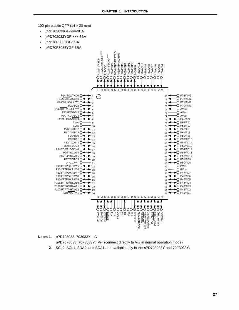
CHAPTER 1 INTRODUCTION
27
100-pin plastic QFP (14 × 20 mm)
• µPD703033GF-×××-3BA
• µPD703033YGF-×××-3BA
• µPD70F3033GF-3BA
• µPD70F3033YGF-3BA
P13
/SI1
/RX
D0
P11
/SO
0P
10/S
I0/S
DA
0 N
ote
2
P07
/INT
P6
P06
/INT
P5/
RT
PT
RG
P05
/INT
P4/
AD
TR
GP
04/IN
TP
3P
03/IN
TP
2P
02/IN
TP
1P
01/IN
TP
0P
00/N
MI
P83
/AN
I11
P82
/AN
I10
P81
/AN
I9P
80/A
NI8
P77
/AN
I7P
76/A
NI6
P75
/AN
I5P
74/A
NI4
P11
1/A
2P
112/
A3
P11
3/A
4
XT
1X
T2
RE
GC X2
X1
VS
S
VD
D
P94
/AS
TB
P40
/AD
0
99 98 97 96 95 94 93 92 91 90 89 88 87 86 85 84 83 82 81100
31 32 33 34 35 36 37 38 39 40 41 42 43 44 45 46 47 48 49 50
2
3
4
5
6
78
9
10
11
12
13
14
15
16
17
18
19
20
21
22
23
24
25
1
74
73
72
71
70
69
68
67
66
65
64
63
62
61
60
59
58
57
56
55
54
53
52
51
75
P21/SO2
P23/RXD1/SI3P24/TXD1/SO3
EVDD
EVSS
P26/TI2/TO2P27/TI3/TO3
P30/TI00P31/TI01
P33/TI11/SO4P34/TO0/A13/SCK4
P35/TO1/A14P36/TI4/TO4/A15
P37/TI5/TO5
IC/VPP Note 1
P100/RTP0/KR0/A5P101/RTP1/KR1/A6P102/RTP2/KR2/A7P103/RTP3/KR3/A8P104/RTP4/KR4/A9
P105/RTP5/KR5/A10P106/RTP6/KR6/A11
P71/ANI1P70/ANI0
AVSS
AVREF
AVDD
P65/A21P64/A20P63/A19P62/A18P61/A17P60/A16P57/AD15P56/AD14P55/AD13P54/AD12P53/AD11P52/AD10P51/AD9P50/AD8BVSS
BVDD
P47/AD7P46/AD6P45/AD5P44/AD4
P22/SCK2/SCL1 Note 2R
ES
ET
CLK
OU
TP
90/L
BE
N/W
RL
P91
/UB
EN
P92
/R/W
/WR
HP
93/D
ST
B/R
D
P95
/HLD
AK
P96
/HLD
RQ
P12
/SC
K0/
SC
L0 N
ote
2
P25/ASCK1/SCK3
P32/TI10/SI4
26
27
28
29
30
P14/SO1/TXD0
P20/SI2/SDA1 Note 2
P107/RTP7/KR7/A12P110/WAIT/A1
P43/AD3P42/AD2P41/AD1
80
79
78
77
76
P73/ANI3P72/ANI2P15/SCK1/ASCK0
Notes 1. µPD703033, 703033Y: IC
µPD70F3033, 70F3033Y: VPP (connect directly to VSS in normal operation mode)
2. SCL0, SCL1, SDA0, and SDA1 are available only in the µPD703033Y and 70F3033Y.
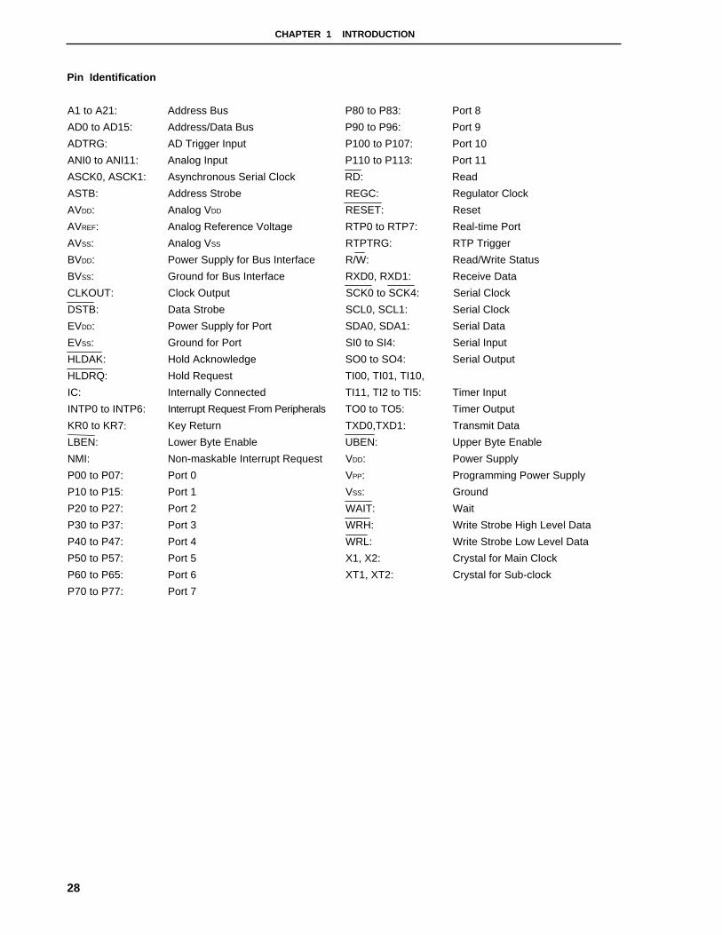
CHAPTER 1 INTRODUCTION
28
Pin Identification
A1 to A21: Address Bus P80 to P83: Port 8
AD0 to AD15: Address/Data Bus P90 to P96: Port 9
ADTRG: AD Trigger Input P100 to P107: Port 10
ANI0 to ANI11: Analog Input P110 to P113: Port 11
ASCK0, ASCK1: Asynchronous Serial Clock RD: Read
ASTB: Address Strobe REGC: Regulator Clock
AVDD: Analog VDD RESET: Reset
AVREF: Analog Reference Voltage RTP0 to RTP7: Real-time Port
AVSS: Analog VSS RTPTRG: RTP Trigger
BVDD: Power Supply for Bus Interface R/W: Read/Write Status
BVSS: Ground for Bus Interface RXD0, RXD1: Receive Data
CLKOUT: Clock Output SCK0 to SCK4: Serial Clock
DSTB: Data Strobe SCL0, SCL1: Serial Clock
EVDD: Power Supply for Port SDA0, SDA1: Serial Data
EVSS: Ground for Port SI0 to SI4: Serial Input
HLDAK: Hold Acknowledge SO0 to SO4: Serial Output
HLDRQ: Hold Request TI00, TI01, TI10,
IC: Internally Connected TI11, TI2 to TI5: Timer Input
INTP0 to INTP6: Interrupt Request From Peripherals TO0 to TO5: Timer Output
KR0 to KR7: Key Return TXD0,TXD1: Transmit Data
LBEN: Lower Byte Enable UBEN: Upper Byte Enable
NMI: Non-maskable Interrupt Request VDD: Power Supply
P00 to P07: Port 0 VPP: Programming Power Supply
P10 to P15: Port 1 VSS: Ground
P20 to P27: Port 2 WAIT: Wait
P30 to P37: Port 3 WRH: Write Strobe High Level Data
P40 to P47: Port 4 WRL: Write Strobe Low Level Data
P50 to P57: Port 5 X1, X2: Crystal for Main Clock
P60 to P65: Port 6 XT1, XT2: Crystal for Sub-clock
P70 to P77: Port 7

CHAPTER 1 INTRODUCTION
29
1.6 Function Blocks
1.6.1 Internal Block Diagram
INTP0 to INTP6
NMIINTC
TI2/TO2TI3/TO3TI4/TO4TI5/TO5
SIO
SO0SI0/SDA0 Note 3
Timer/counterTI00,TI01,TI10,TI11
SO1/TXD0SI1/RXD0
SO4SI4
CSI0/I2C0Note 4
CSI1/UART0
Variablelength CSI4
Watchdogtimer
Note1
ROM CPU
Note2
Multiplier16 ×16→32
RAM
PC
32-bit barrelshifter
Systemregister
General registers32 bits × 32
Instructionqueue
BCU
ASTB(P94)
A16 to A21(P60 to P65)
AD0 to AD15(P40 to P47,P50 to P57)
A/DconverterRTP
Ports
CG
CLKOUT
X1
X2
XT1
VDD
VSS
BVDD
BVSS
EVDD
AN
I0 to
AN
I11
AV
RE
F
AV
SS
AV
DD
AD
TR
G
RT
P0
to R
TP
7
P11
0 to
P11
3
P10
0 to
P10
7
P70
to P
77P
60 to
P65
P50
to P
57P
40 to
P47
P30
to P
37P
20 to
P27
P10
to P
15P
00 to
P07
SCK0/SCL0 Note 3
SCK1/ASCK0
SCK4 RESET
XT2
HLDAK(P95)HLDRQ(P96)
WAIT(P110)
UBEN(P91)
ALU
16-bit timer: TM0, TM18-bit timer: TM2 to TM7
TO0,TO1
DMAC: 6 ch
Watch timer
P80
to P
83P
90 to
P96
EVSS
DSTB/RD(P93)R/W /WRH(P92)
LBEN/WRL(P90)
RT
PT
RG
A13 to A15(P34 to P36)
A1 to A12(P100 to P107,P110 to P113)
SO2SI2/SDA1 Note 3 CSI2/I2C1
Note 4SCK2/SCL1 Note 3
SO3/TXD1SI3/RXD1 CSI3/UART1
SCK3/ASCK1
Key returnKR0 to KR7
ROMcorrection
VPP Note 6
Regulator
RE
GC
IC Note 6
3.3 V
Notes 1. µPD703033, 703033Y: 256 Kbytes (mask ROM)
µPD70F3033, 70F3033Y: 256 Kbytes (flash memory)
2. µPD703033, 703033Y, 70F3033, 70F3033Y: 16 bytes
3. SDA0, SDA1, SCL0, and SCL1 pins are available only in the µPD703033Y and 70F3033Y.
4. I2C function is available only in the µPD703033Y and 70F3033Y.
5. µPD70F3033, 70F3033Y
6. µPD703033, 703033Y

CHAPTER 1 INTRODUCTION
30
1.6.2 On-chip units
(1) CPU
The CPU uses five-stage pipeline control to enable single-clock execution of address calculations, arithmetic
logic operations, data transfers, and almost all other instruction processing.
Other dedicated on-chip hardware, such as the multiplier (16 bits × 16 bits → 32 bits) and the barrel shifter (32
bits) help accelerate processing of complex instructions.
(2) Bus control unit (BCU)
The BCU starts a required external bus cycle based on the physical address obtained by the CPU. When an
instruction is fetched from external memory space and the CPU does not send a bus cycle start request, the
BCU generates a prefetch address and prefetches the instruction code. The prefetched instruction code is
stored in an instruction queue.
(3) ROM
This consists of a 256-Kbyte mask ROM or flash memory mapped to the address space starting at 00000000H.
ROM can be accessed by the CPU in one clock cycle during instruction fetch.
(4) RAM
This consists of a 16-Kbyte RAM mapped to the address space starting at FFFFB000H. RAM can be accessed
by the CPU in one clock cycle during data access.
(5) Interrupt controller (INTC)
This controller handles hardware interrupt requests (NMI, INTP0 to INTP6) from on-chip peripheral hardware and
external hardware. Eight levels of interrupt priorities can be specified for these interrupt requests, and
multiplexed servicing control can be performed for interrupt sources.
(6) Clock generator (CG)
The clock generator includes two types of oscillators, each for main system clock (fXX) and for subsystem clock
(fXT), generates five types of clocks (fXX, fXX/2, fXX/4, fXX/8, and fXT), and supplies one of them as the operating
clock for the CPU (fCPU).
CHAPTER 1 INTRODUCTION
31
(7) Timer/counter
A two-channel 16-bit timer/event counter, a four-channel 8-bit timer/event counter, and a two-channel 8-bit
interval timer are equipped, enabling measurement of pulse intervals and frequency as well as programmable
pulse output.
The two-channel 8-bit timer/event counter can be connected via a cascade connection to enable use as a 16-bit
timer.
The two-channel 8-bit interval timer can be connected via a cascade connection to enable to be used as a 16-bit
timer.
(8) Watch timer
This timer counts the reference time period (0.5 seconds) for counting the clock (the 32.768-kHz subsystem
clock or the 16.777-MHz main system clock). At the same time, the watch timer can be used as an interval timer
for the main system clock.
(9) Watchdog timer
A watchdog timer is equipped to detect runaway programs, system abnormalities, etc.
It can also be used as an interval timer.
When used as a watchdog timer, it generates a non-maskable interrupt request (INTWDT) after an overflow
occurs. When used as an interval timer, it generates a maskable interrupt request (INTWDTM) after an overflow
occurs.
(10) Serial interface (SIO)
The V850/SB1 includes three kinds of serial interfaces: an asynchronous serial interface (UART0, UART1), a
clock-synchronized serial interface (CSI0 to CSI3), and an 8-bit/16-bit variable serial interface (CSI4). These
plus the I2C bus interface (I2C0, I2C1) comprise five channels. Two of these channels are switchable between
the UART and CSI and another two switchable between CSI and I2C.
For UART0 and UART1, data is transferred via the TXD0, TXD1, RXD0, and RXD1 pins.
For CSI0 to CSI3, data is transferred via the SO0 to SO3, SI0 to SI3, and SCK0 to SCK3 pins.
For CSI4, data is transferred via the SO4, SI4, and SCK4 pins.
For I2C0 and I2C1, data is transferred via the SDA0, SDA1, SCL0, and SCL1 pins.
I2C0 and I2C1 are equipped only in the µPD703033Y and 70F3033Y.
For UART and CSI4, a dedicated baud rate generator is equipped.
(11) A/D converter
This high-speed, high-resolution 10-bit A/D converter includes 12 analog input pins. Conversion uses the
successive approximation method.
(12) DMA controller
A six-channel DMA controller is equipped. This controller transfers data between the internal RAM and on-chip
peripheral I/O devices in response to interrupt requests sent by on-chip peripheral I/O.
(13) Real-time output port (RTP)
The RTP is a real-time output function that transfers previously set 8-bit data to an output latch when an
external trigger signal occurs or when there is a coincidence signal in a timer compare register. It can also be
used for 4-bit × 2 channels.
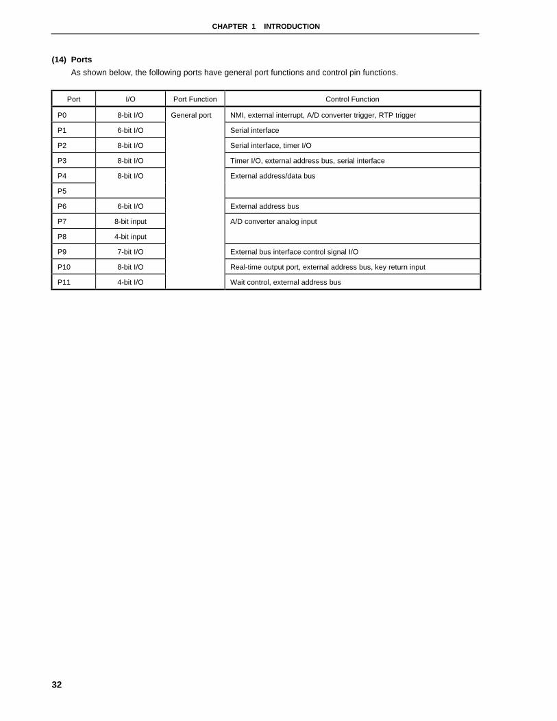
CHAPTER 1 INTRODUCTION
32
(14) Ports
As shown below, the following ports have general port functions and control pin functions.
Port I/O Port Function Control Function
P0 8-bit I/O General port NMI, external interrupt, A/D converter trigger, RTP trigger
P1 6-bit I/O Serial interface
P2 8-bit I/O Serial interface, timer I/O
P3 8-bit I/O Timer I/O, external address bus, serial interface
P4 8-bit I/O External address/data bus
P5
P6 6-bit I/O External address bus
P7 8-bit input A/D converter analog input
P8 4-bit input
P9 7-bit I/O External bus interface control signal I/O
P10 8-bit I/O Real-time output port, external address bus, key return input
P11 4-bit I/O Wait control, external address bus
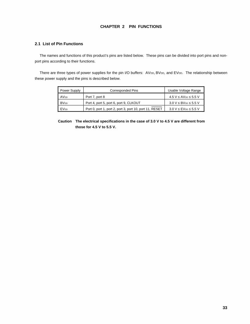
33
CHAPTER 2 PIN FUNCTIONS
2.1 List of Pin Functions
The names and functions of this product’s pins are listed below. These pins can be divided into port pins and non-
port pins according to their functions.
There are three types of power supplies for the pin I/O buffers: AVDD, BVDD, and EVDD. The relationship between
these power supply and the pins is described below.
Power Supply Corresponded Pins Usable Voltage Range
AVDD Port 7, port 8 4.5 V ≤ AVDD ≤ 5.5 V
BVDD Port 4, port 5, port 6, port 9, CLKOUT 3.0 V ≤ BVDD ≤ 5.5 V
EVDD Port 0, port 1, port 2, port 3, port 10, port 11, RESET 3.0 V ≤ EVDD ≤ 5.5 V
Caution The electrical specifications in the case of 3.0 V to 4.5 V are different from
those for 4.5 V to 5.5 V.

CHAPTER 2 PIN FUNCTIONS
34
(1) Port pins
(1/3)
Pin Name I/O PULL Function Alternate Function
P00 NMI
P01 INTP0
P02 INTP1
P03 INTP2
P04 INTP3
P05 INTP4/ADTRG
P06 INTP5/RTPTRG
P07
I/O Yes Port 0
8-bit I/O port
Input/output mode can be specified in 1-bit units.
INTP6
P10 SI0/SDA0
P11 SO0
P12 SCK0/SCL0
P13 SI1/RXD0
P14 SO1/TXD0
P15
I/O Yes Port 1
6-bit I/O port
Input/output mode can be specified in 1-bit units.
SCK1/ASCK0
P20 SI2/SDA1
P21 SO2
P22 SCK2/SCL1
P23 SI3/RXD1
P24 SO3/TXD1
P25 SCK3/ASCK1
P26 TI2/TO2
P27
I/O Yes Port 2
8-bit I/O port
Input/output mode can be specified in 1-bit units.
TI3/TO3
Remark PULL: on-chip pull-up resistor

CHAPTER 2 PIN FUNCTIONS
35
(2/3)
Pin Name I/O PULL Function Alternate Function
P30 TI00
P31 TI01
P32 TI10/SI4
P33 TI11/SO4
P34 TO0/A13/SCK4
P35 TO1/A14
P36 TI4/TO4/A15
P37
I/O Yes Port 3
8-bit I/O port
Input/output mode can be specified in 1-bit units.
TI5/TO5
P40 AD0
P41 AD1
P42 AD2
P43 AD3
P44 AD4
P45 AD5
P46 AD6
P47
I/O No Port 4
8-bit I/O port
Input/output mode can be specified in 1-bit units.
AD7
P50 AD8
P51 AD9
P52 AD10
P53 AD11
P54 AD12
P55 AD13
P56 AD14
P57
I/O No Port 5
8-bit I/O port
Input/output mode can be specified in 1-bit units.
AD15
P60 A16
P61 A17
P62 A18
P63 A19
P64 A20
P65
I/O No Port 6
6-bit I/O port
Input/output mode can be specified in 1-bit units.
A21
Remark PULL: on-chip pull-up resistor
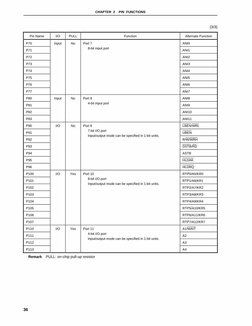
CHAPTER 2 PIN FUNCTIONS
36
(3/3)
Pin Name I/O PULL Function Alternate Function
P70 ANI0
P71 ANI1
P72 ANI2
P73 ANI3
P74 ANI4
P75 ANI5
P76 ANI6
P77
Input No Port 7
8-bit input port
ANI7
P80 ANI8
P81 ANI9
P82 ANI10
P83
Input No Port 8
4-bit input port
ANI11
P90 LBEN/WRL
P91 UBEN
P92 R/W/WRH
P93 DSTB/RD
P94 ASTB
P95 HLDAK
P96
I/O No Port 9
7-bit I/O port
Input/output mode can be specified in 1-bit units.
HLDRQ
P100 RTP0/A5/KR0
P101 RTP1/A6/KR1
P102 RTP2/A7/KR2
P103 RTP3/A8/KR3
P104 RTP4/A9/KR4
P105 RTP5/A10/KR5
P106 RTP6/A11/KR6
P107
I/O Yes Port 10
8-bit I/O port
Input/output mode can be specified in 1-bit units.
RTP7/A12/KR7
P110 A1/WAIT
P111 A2
P112 A3
P113
I/O Yes Port 11
4-bit I/O port
Input/output mode can be specified in 1-bit units.
A4
Remark PULL: on-chip pull-up resistor

CHAPTER 2 PIN FUNCTIONS
37
(2) Non-port pins
(1/3)
Pin Name I/O PULL Function Alternate Function
A1 P110/WAIT
A2 to A4 P111 to P113
A5 to A12 P100/RTP0/KR0 to
P107/RTP7/KR7
A13 P34/TO0/SCK4
A14 P35/TO1
A15
Output Yes Low-order address bus used for external memory expansion
P36/TI4/TO4
A16 to A21 Output No High-order address bus used for external memory expansion P60 to P65
AD0 to AD7 P40 to P47
AD8 to AD15
I/O No 16-bit multiplexed address/data bus used for external memory
expansion P50 to P57
ADTRG Input Yes A/D converter external trigger input P05/INTP4
ANI0 to ANI7 Input No P70 to P77
ANI8 to ANI11 Input No
Analog input to A/D converter
P80 to P83
ASCK0 P15/SCK1
ASCK1
Input Yes Serial clock input for UART0 and UART1
P25/SCK3
ASTB Output No External address strobe signal output P94
AVDD − − Positive power supply for A/D converter and alternate-function port −
AVREF Input − Reference voltage input for A/D converter −
AVSS − − Ground potential for A/D converter and alternate-function port −
BVDD − − Positive power supply for bus interface and alternate-function port −
BVSS − − Ground potential for bus interface and alternate-function port −
CLKOUT Output − Internal system clock output −
DSTB Output No External data strobe signal output P93/RD
EVDD − − Power supply for I/O port and alternate-function pin (except for
bus interface)
−
EVSS − − Ground potential for I/O port and alternate-function pin (except
for bus interface)
−
HLDAK Output No Bus hold acknowledge output P95
HLDRQ Input No Bus hold request input P96
INTP0 to INTP3 External interrupt request input (analog noise elimination) P01 to P04
INTP4 P05/ADTRG
INTP5
External interrupt request input (digital noise elimination)
P06/RTPTRG
INTP6
Input Yes
External interrupt request input (digital noise elimination for
remote control)
P07
KR0 to KR7 Input Yes Key return input P100/A5/RTP0 to
P107/A12/RTP7
LBEN Output No External data bus’s low-order byte enable signal output P90/WRL
IC − − Internally connected (µPD703033 and 703033Y only) −
Remark PULL: on-chip pull-up resistor

CHAPTER 2 PIN FUNCTIONS
38
(2/3)
Pin Name I/O PULL Function Alternate Function
NMI Input Yes Non-maskable interrupt request input P00
RD Output No Read strobe signal output P93/DSTB
REGC − − Capacitor connection for regulator output stabilization −
RESET Input − System reset input −
RTP0 to RTP7 Output Yes Real-time output port P100/A5/KR0 to
P107/A12/KR7
RTPTRG Input Yes RTP external trigger input P06/INTP5
R/W Output No External read/write status output P92/WRH
RXD0 P13/SI1
RXD1
Input Yes Serial receive data input for UART0 and UART1
P23/SI3
SCK0 P12/SCL0
SCK1 P15/ASCK0
SCK2 P22/SCL1
SCK3
Serial clock I/O (3-wire type) for CSI0 to CSI3
P25/ASCK1
SCK4
I/O Yes
Serial clock I/O for variable length CSI4 (3-wire type) P34/TO0/A13
SCL0 P12/SCK0
SCL1
I/O Yes Serial clock I/O for I2C0 and I2C1 (µPD703033Y and 70F3033Y
only)P22/SCK2
SDA0 P10/SI0
SDA1
I/O Yes Serial transmit/receive data I/O for I2C0 and I2C1 (µPD703033Y
and 70F3033Y only)P20/SI2
SI0 P10/SDA0
SI1 P13/RXD0
SI2 P20/SDA1
SI3
Serial receive data input (3-wire type) for CSI0 to CSI3
P23/RXD1
SI4
Input Yes
Serial receive data input (3-wire type) for variable length CSI4 P32/TI10
SO0 P11
SO1 P14/TXD0
SO2 P21
SO3
Serial transmit data output (3-wire type) for CSI0 to CSI3
P24/TXD1
SO4
Output Yes
Serial transmit data output for variable length CSI4 (3-wire type) P33/TI11
TI00 Shared as external capture trigger input and external count
clock input for TM0
P30
TI01 External capture trigger input for TM0 P31
TI10 Shared as external capture trigger input and external count
clock input for TM1
P32/SI4
TI11 External capture trigger input for TM1 P33/SO4
TI2 External count clock input for TM2 P26/TO2
TI3
Input Yes
External count clock input for TM3 P27/TO3
Remark PULL: on-chip pull-up resistor

CHAPTER 2 PIN FUNCTIONS
39
(3/3)
Pin Name I/O PULL Function Alternate Function
TI4 External count clock input for TM4 P36/TO4/A15
TI5
Input Yes
External count clock input for TM5 P37/TO5
TO0, TO1 Pulse signal output for TM0, TM1 P34/A13/SCK4/P35/
A14
TO2 Pulse signal output for TM2 P26/TI2
TO3 Pulse signal output for TM3 P27/TI3
TO4 Pulse signal output for TM4 P36/TI4/A15
TO5
Output Yes
Pulse signal output for TM5 P37/TI5
TXD0 P14/SO1
TXD1
Output Yes Serial transmit data output for UART0 and UART1
P24/SO3
UBEN Output No High-order byte enable signal output for external data bus P91
VDD − − Positive power supply pin −
VPP − − High-voltage apply pin for program write/verify (µPD70F3033
and 70F3033Y only)
−
VSS − − GND potential −
WAIT Input Yes Control signal input for inserting wait in bus cycle P110/A1
WRH High-order byte write strobe signal output for external data bus P92/R/W
WRL
Output No
Low-order byte write strobe signal output for external data bus P90/LBEN
X1 Input −
X2 −
No Resonator connection for main clock
−
XT1 Input −
XT2 −
No Resonator connection for subsystem clock
−
Remark PULL: on-chip pull-up resistor

CHAPTER 2 PIN FUNCTIONS
40
2.2 Pin States
The operating states of various pins are described below with reference to their operating states.
Operating State
PinReset STOP Mode IDLE Mode HALT Mode Bus Hold Idle State
AD0 to AD15 Hi-Z Hi-Z Hi-Z Hi-Z Hi-Z Hi-Z
A1 to A15 Hi-Z Held Held Held Held Held
A16 to A21 Hi-Z Hi-Z Hi-Z Held Hi-Z Held
LBEN, UBEN Hi-Z Hi-Z Hi-Z Held Hi-Z Held
R/W Hi-Z Hi-Z Hi-Z H Hi-Z H
DSTB, WRL, WRH, RD Hi-Z Hi-Z Hi-Z H Hi-Z H
ASTB Hi-Z Hi-Z Hi-Z H Hi-Z H
HLDRQ − − − Operating Operating Operating
HLDAK Hi-Z Hi-Z Hi-Z Operating L Operating
WAIT − − − − − −
CLKOUT Hi-Z L L Operating Note Operating Note Operating Note
Note “L” when in clock output inhibit mode
Remark Hi-Z : High impedance
Held : State is held during previously set external bus cycle
L : Low-level output
H : High-level output
− : Input without sampling sampled

CHAPTER 2 PIN FUNCTIONS
41
2.3 Description of Pin Functions
(1) P00 to P07 (Port 0) ··· 3-state I/O
Port 0 is an 8-bit I/O port that can be set in 1-bit units for input or output.
P00 to P07 can function as I/O port pins and can also function as NMI inputs, external interrupt request inputs,
external triggers for the A/D converter, and external triggers for the real-time output port. Port/control mode can
be selected for each bit, and the pin’s valid edge is specified by the EGP0 and EGN0 registers.
(a) Port mode
P00 to P07 can be set bit-wise as input or output according to the contents of port 0 mode register (PM0).
(b) Control mode
(i) NMI (Non-maskable Interrupt Request) ··· input
This is a non-maskable interrupt request signal input pin.
(ii) INTP0 to INTP6 (Interrupt Request from Peripherals) ··· input
These are external interrupt request input pins.
(iii) ADTRG (AD Trigger Input) ··· input
This is the A/D converter’s external trigger input pin. This pin is controlled with A/D converter mode
register (ADM).
(iv) RTPTRG (Real-Time Port Trigger Input) ··· input
This is the real-time output port’s external trigger input pin. This pin is controlled with real-time output
port control register (RTPC).

CHAPTER 2 PIN FUNCTIONS
42
(2) P10 to P15 (Port 1) ··· 3-state I/O
Port 1 is a 6-bit I/O port in which input and output pins can be specified in 1-bit units.
P10 to P15 can function as I/O port pins and can also operate as input or output pins for the serial interface.
Port/control mode can be selected for each bit.
P10 to P12, P14, and P15 can select normal output and N-ch open-drain output.
(a) Port mode
P10 to P15 can be set in 1-bit units as input or output pins according to the contents of port 1 mode register
(PM1).
(b) Control mode
(i) SI0, SI1 (Serial Input 0, 1) ··· input
These are the serial receive data input pins of CSI0 and CSI1.
(ii) SO0, SO1 (Serial Output 0, 1) ··· output
These are the serial transmit data output pins of CSI0 and CSI1.
(iii) SCK0, SCK1 (Serial Clock 0, 1) ··· 3-state I/O
These are the serial clock I/O pins for CSI0 and CSI1.
(iv) SDA0 (Serial Data 0) ··· I/O
This is the serial transmit/receive data I/O pin for I2C0 (µPD703033Y and 70F3033Y only).
(v) SCL0 (Serial Clock 0) ··· I/O
This is the serial clock I/O pin for I2C0 (µPD703033Y and 70F3033Y only).
(vi) RXD0 (Receive Data 0) ··· input
This is the serial receive data pin of UART0.
(vii) TXD0 (Transmit Data 0) ··· output
This is the serial transmit data pin of UART0.
(viii) ASCK0 (Asynchronous Serial Clock 0) ··· input
This is the serial baud rate clock pin of UART0.

CHAPTER 2 PIN FUNCTIONS
43
(3) P20 to P27 (Port 2) ··· 3-state I/O
Port 2 is an 8-bit I/O port in which input and output pins can be specified in 1-bit units.
P20 to P27 can function as I/O port pins, input or output pins for the serial interface, and input or output for the
timer/counter.
Port/control mode can be selected for each bit.
P20 to P22, P24 and P25 can select normal output and N-ch open-drain output.
(a) Port mode
P20 to P27 can be set in 1-bit units as input or output pins according to the contents of port 2 mode register
(PM2).
(b) Control mode
(i) SI2, SI3 (Serial Input 2, 3) ··· input
These are the serial receive data input pins of CSI2 and 3.
(ii) SO2, SO3 (Serial Output 2, 3) ··· output
These are the serial transmit data output pins of CSI2 and 3.
(iii) SCK2, SCK3 (Serial Clock 2, 3) ··· 3-state I/O
This is the CSI2, 3 serial clock I/O pin.
(iv) SDA1 (Serial Data 1) ... I/O
This is the serial transmit/receive data I/O pin for I2C1 (µPD703033Y and 70F3033Y only).
(v) SCL1 (Serial Clock 1) ... I/O
This is the serial clock I/O pin for I2C1 (µPD703033Y and 70F3033Y only).
(vi) RXD1 (Receive Data 1) ... input
This is the serial receive data input pin of UART1.
(vii) TXD1 (Transmit Data 1) ... output
This is the serial transmit data output pin of UART1.
(viii) ASCK1 (Asynchronous Serial Clock 1) ... input
This is the serial clock input pin of UART1.
(ix) TI2 and TI3 (Timer Input 2, 3) ... input
These are the external counter clock input pins for timer 2 and timer 3.
(x) TO2 and TO3 (Timer Output 2, 3) ... output
These are the external counter clock output pins for timer 2 and timer 3.

CHAPTER 2 PIN FUNCTIONS
44
(4) P30 to P37 (Port 3) ··· 3-state I/O
Port 3 is an 8-bit I/O port in which input and output pins can be specified in 1-bit units.
P30 to P37 can function as I/O port pins, input or output pins for the timer/counter, address buses (A13 to A15)
when memory is expanded externally, and serial interface I/Os.
Port/control mode can be selected for each bit.
P31 and P32 can select normal output and N-ch open-drain output.
(a) Port mode
P30 to P37 can be set in 1-bit units as input or output pins according to the contents of the port 3 mode
register (PM3).
(b) Control mode
(i) TI00, TI01, TI10, TI11, TI4, TI5 (Timer Input 00, 01, 10, 11, 4, 5) ··· input
These pins accept external count clock input from timer 0, timer 1, timer 4, and timer 5.
(ii) TO0, TO1, TO4, TO5 (Timer Output 0, 1, 4, 5) ··· output
These are the pulse signal output pins of timer 0, timer 1, timer 4, and timer 5.
(iii) A13 to A15 (Address 13 to 15) ··· output
These comprise the address bus that is used for external access. These pins operate as A13 to A15 bit
address output pins within a 22-bit address. The output changes in synchronization with the rising edge
of the clock in the T1 state of the bus cycle. When the timing sets the bus cycle as inactive, the
previous bus cycle’s address is retained.
(iv) SI4 (Serial Input 4) ··· input
This is the serial receive data input pin of CSI4.
(v) SO4 (Serial Output 4) ··· output
This is the serial transmit data output pin for CSI4.
(vi) SCK4 (Serial Clock 4) ··· 3-state I/O
This is the I/O pin for CSI4 serial clock.
(5) P40 to P47 (Port 4) ··· 3-state I/O
Port 4 is an 8-bit I/O port in which input and output pins can be specified in 1-bit units.
P40 to P47 can function as I/O port pins and as a time division address/data buses (AD0 to AD7) when memory
is expanded externally.
Port/control mode can be selected for each bit.
The I/O signal level uses the bus interface power supply pins BVDD and BVSS as a reference.
(a) Port mode
P40 to P47 can be set in 1-bit units as input or output pins according to the contents of the port 4 mode
register (PM4).

CHAPTER 2 PIN FUNCTIONS
45
(b) Control mode (external expansion mode)
P40 to P47 can be set as AD0 to AD7 according to the contents of the memory expansion register (MM).
(i) AD0 to AD7 (Address/Data 0 to 7) ··· 3-state I/O
These are multiplexed address/data bus that is used for external access. Under address timing (T1
state), these pins operate as AD0 to AD7 (22-bit address) output pins. Under data timing (T2, TW, T3),
they operate as low-order 8-bit I/O bus pins for 16-bit data. The output changes in synchronization with
the rising edge of the clock in each state within the bus cycle. When the timing sets the bus cycle as
inactive, these pins go into a high-impedance state.
(6) P50 to P57 (Port 5) ··· 3-state I/O
Port 5 is an 8-bit I/O port in which input and output pins can be specified in 1-bit units.
P50 to P57 can function as I/O port pins and as a time division address/data buses (AD8 to AD15) when memory
is expanded externally.
The I/O signal level uses the bus interface power supply pins BVDD and BVSS as reference.
(a) Port mode
P50 to P57 can be set bit-wise as input or output pins according to the contents of the port 5 mode register
(PM5).
(b) Control mode (external expansion mode)
P50 to P57 can be set as AD8 to AD15 according to the contents of the memory expansion register (MM).
(i) AD8 to AD15 (Address/Data 8 to 15) ··· 3-state I/O
These comprise the multiplexed address/data bus that is used for external access. Under address
timing (T1 state), these pins operate as AD8 to AD15 (22-bit address) output pins. Under data timing
(T2, TW, T3), they operate as high-order 8-bit I/O bus pins for 16-bit data. The output changes in
synchronization with the rising edge of the clock in each state within the bus cycle. When the timing
sets the bus cycle as inactive, these pins go into a high-impedance state.
(7) P60 to P65 (Port 6) ··· 3-state I/O
Port 6 is a 6-bit I/O port in which input and output pins can be specified in 1-bit units.
P60 to P65 can function as I/O port pins and as address buses (A16 to A21) when memory is expanded
externally. These pins can be set in 2 bit units to port mode or an external expansion mode.
Port/control mode can be selected for each bit.
The I/O signal level uses the bus interface power supply pins BVDD and BVSS as reference.

CHAPTER 2 PIN FUNCTIONS
46
(a) Port mode
P60 to P65 can be set in 1-bit units as input or output pins according to the contents of the port 6 mode
register (PM6).
(b) Control mode (external expansion mode)
P60 to P65 can be set as A16 to A21 according to the contents of the memory expansion register (MM).
(i) A16 to A21 (Address 16 to 21) ··· output
These comprise an address bus that is used for external access. These pins operate as the high-order
6-bit address output pins within a 22-bit address. The output changes in synchronization with the rising
edge of the clock in the T1 state of the bus cycle. When the timing sets the bus cycle as inactive, the
previous bus cycle’s address is retained.
(8) P70 to P77 (Port 7), P80 to P83 (Port 8) ··· input
Port 7 is an 8-bit input-only port in which all pins are fixed as input pins. Port 8 is a 4-bit input-only port.
P70 to P77 and P80 to P83 can function as input ports and as analog input pins for the A/D converter. However,
they cannot be switched between these input port and analog input pin.
(a) Port mode
P70 to P77 and P80 to P83 are input-only pins.
(b) Control mode (external expansion mode)
P70 to P77 also function as pins ANI0 to ANI7 and P80 to P83 also function as ANI8 to ANI11, but these
alternate functions are not switchable.
(i) ANI0 to ANI11 (Analog Input 0 to 11) ··· input
These are analog input pins for the A/D converter.
Connect a capacitor between these pins and AVSS to prevent noise-related operation faults. Also, do
not apply voltage that is outside the range for AVSS and AVREF to pins that are being used as inputs for
the A/D converter. If it is possible for noise above the AVREF range or below the AVSS to enter, clamp
these pins using a diode that has a small VF value.

CHAPTER 2 PIN FUNCTIONS
47
(9) P90 to P96 (Port 9) ··· 3-state I/O
Port 9 is a 7-bit I/O port in which input and output pins can be specified in 1-bit units.
P90 to P96 can function as I/O port pins, control signal output pins, and bus hold control signal output pins when
memory is expanded externally.
During 8-bit access of port 9, the highest-order bit is ignored during a write operation and is read as a “0” during
a read operation.
Port/control can be selected for each bit.
The I/O signal level uses the bus interface power supply pins BVDD and BVSS as a reference.
(a) Port mode
P90 to P96 can be set in 1-bit units as input or output pins according to the contents of the port 9 mode
register (PM9).
(b) Control mode (external expansion mode)
P90 to P96 can be set to operate as control signal outputs for external memory expansion according to the
contents of the memory expansion register (MM).
(i) LBEN (Lower Byte Enable) ··· output
This is a lower byte enable signal output pin for an external 16-bit data bus. The output changes in
synchronization with the rising edge of the clock in the T1 state of the bus cycle. When the timing sets
the bus cycle as inactive, the previous bus cycle’s address is retained.
(ii) UBEN (Upper Byte Enable) ··· output
This is an upper byte enable signal output pin for an external 16-bit data bus. During byte access of
even-numbered addresses, these pins are set as inactive (high level). The output changes in
synchronization with the rising edge of the clock in the T1 state of the bus cycle. When the timing sets
the bus cycle as inactive, the previous bus cycle’s address is retained.
Access UBEN LBEN A0
Word access 0 0 0
Half word access 0 0 0
Byte access Even-numbered address 1 0 0
Odd-numbered address 0 1 1
CHAPTER 2 PIN FUNCTIONS
48
(iii) R/W (Read/Write Status) ··· output
This is an output pin for the status signal pin that indicates whether the bus cycle is a read cycle or write
cycle during external access. High level is set during the read cycle and low level is set during the write
cycle. The output changes in synchronization with the rising edge of the clock in the T1 state of the bus
cycle. High level is set when the timing sets the bus cycle as inactive.
(iv) DSTB (Data Strobe) ··· output
This is an output pin for the external data bus’s access strobe signal. Output becomes active (low level)
during the T2 and TW states of the bus cycle. Output becomes inactive (high level) when the timing
sets the bus cycle as inactive.
(v) ASTB (Address Strobe) ··· output
This is an output pin for the external address bus’s latch strobe signal. Output becomes active (low
level) in synchronization with the falling edge of the clock during the T1 state of the bus cycle, and
becomes inactive (high level) in synchronization with the falling edge of the clock during the T3 state of
the bus cycle. Output becomes inactive when the timing sets the bus cycle as inactive.
(vi) HLDAK (Hold Acknowledge) ··· output
This is an output pin for the acknowledge signal that indicates high impedance status for the address
bus, data bus, and control bus when the V850/SB1 receives a bus hold request.
The address bus, data bus, and control bus are set to high impedance status when this signal is active.
(vii) HLDRQ (Hold Request) ··· input
This is an input pin by which an external device requests the V850/SB1 to release the address bus,
data bus, and control bus. This pin accepts asynchronous input for CLKOUT. When this pin is active,
the address bus, data bus, and control bus are set to high impedance status. This occurs either when
the V850/SB1 completes execution of the current bus cycle or immediately if no bus cycle is being
executed, then the HLDAK signal is set as active and the bus is released.
(viii) WRL (Write Strobe Low Level Data) ··· output
This is a write strobe signal output pin for the low-order data in an external 16-bit data bus. Output
occurs during the write cycle, similar to DSTB.
CHAPTER 2 PIN FUNCTIONS
49
(ix) WRH (Write Strobe High Level Data) ··· output
This is a write strobe signal output pin for the high-order data in an external 16-bit data bus. Output
occurs during the write cycle, similar to DSTB.
(x) RD (Read) ··· output
This is a read strobe signal output pin for an external 16-bit data bus. Output occurs during the read
cycle, similar to DSTB.
(10) P100 to P107 (Port 10) ··· 3-state I/O
Port 10 is an 8-bit I/O port in which input and output pins can be specified in 1-bit units.
P100 to P107 can function as I/O port pins, a real-time output port, address buses (A5 to A12) when memory is
expanded externally, and a key return input.
P100 to P107 can select normal output and N-ch open-drain output.
(a) Port mode
P100 to P107 can be set bit-wise as input or output pins according to the contents of the port 10 mode
register (PM10).
(b) Control mode
(i) RTP0 to RTP7 (Real-time Port 0 to 7) ··· output
These pins comprise a real-time output port.
(ii) A5 to A12 (Address 5 to 12) ··· output
These comprise the address bus that is used for external access. These pins operate as A5 to A12 bit
address output pins within a 22-bit address. The output changes in synchronization with the rising edge
of the clock in the T1 state of the bus cycle. When the timing sets the bus cycle as inactive, the
previous bus cycle’s address is retained.
(iii) KR0 to KR7 (Key Return 0 to 7) ... input
These are key return input pins. Their operations are specified by the key return mode register (KRM).
(11) P110 to P113 (Port 11) ··· 3-state I/O
Port 11 is a 4-bit I/O port in which input and output pins can be specified in 1-bit units.
(a) Port mode
P110 to P113 can be set bit-wise as inputs or outputs according to the contents of port 11 mode register
(PM11).
P110 to P113 can function as I/O port pins, address buses (A1 to A4) when memory is expanded externally,
and the control signal (WAIT) that inserts waits into the bus cycle.
CHAPTER 2 PIN FUNCTIONS
50
(b) Control mode
(i) A1 to A4 (Address 1 to 4) ··· output
These comprise the address bus that is used for external access. These pins operate as the low-order
4-bit address output pins within a 22-bit address. The output changes in synchronization with the
rising edge of the clock in the T1 state of the bus cycle. When the timing sets the bus cycle as
inactive, the previous bus cycle’s address is retained.
(ii) WAIT (Wait) ··· input
This is an input pin for the control signal used to insert waits into the bus cycle. This pin is sampled at
the falling edge of the clock during the T2 or TW state of the bus cycle.
ON/OFF switching of the wait function is performed by the port alternate function control register
(PAC).
Caution When using the wait function, set BV DD to the same potential as EV DD.
(12) RESET (Reset) ··· input
RESET input is asynchronous input for a signal that has a constant low level width regardless of the operating
clock’s status. When this signal is input, a system reset is executed as the first priority ahead of all other
operations.
In addition to being used for ordinary initialization/start operations, this pin can also be used to cancel a standby
mode (HALT, IDLE, or STOP mode).
(13) REGC (Regulator Control) ... input
This pin is used to connect the regulator-use capacitor.
(14) X1 and X2 (Crystal)
These pins are used to connect the resonator that generates the system clock.
(15) XT1, XT2 (Crystal for Sub-clock)
These pins are used to connect the resonator that generates the subclock.
(16) AVDD (Analog V DD)
This is the analog power supply pin for the A/D converter and alternate-function ports.
(17) AVSS (Analog V SS)
This is the ground pin for the A/D converter and alternate-function ports.
(18) AVREF (Analog Reference Voltage) … input
This is the reference voltage supply pin for the A/D converter.
(19) BVDD (Power Supply for Bus Interface)
This is the positive power supply pin for the bus interface and alternate-function ports.
(20) BVSS (Ground for Bus Interface)
This is the ground pin for the bus interface.

CHAPTER 2 PIN FUNCTIONS
51
(21) EVDD (Power Supply for Port)
This is the positive power supply pin for I/O ports and alternate-function pins (except for the alternate-function
ports of the bus interface).
(22) EVSS (Ground for Port)
This the ground pin for I/O ports and alternate-function pins (except for the alternate-function ports of the bus
interface).
(23) VDD (Power Supply)
These are the positive power supply pins. All VDD pins should be connected to a positive power source.
(24) VSS (Ground)
These are the ground pins. All VSS pins should be grounded.
(25) VPP (Programming Power Supply)
This is the positive power supply pin used for flash memory programming mode.
This pin is used in the µPD70F3033 and 70F3033Y.
(26) IC (Internally Connected)
This is an internally connected pin used in the µPD703033 and 703033Y.
Connect directly to VSS in normal operating mode.

CHAPTER 2 PIN FUNCTIONS
52
2.4 I/O Circuit Types, I/O Buffer Power Supply and Handling of Unused Pins
(1/2)
Pin Alternate Function I/O
Buffer
Power
Supply
I/O Circuit Type Recommended Connection Method
P00 NMI
P01 to P04 INTP0 to INTP3
P05 INTP4/ADTRG
P06 INTP5/RTPTRG
P07 INTP6
EVDD 8-A
P10 SI0/SDA0 10-A
P11 SO0 26
P12 SCK0/SCL0 10-A
P13 SI1/RXD0 8-A
P14 SO1/TXD0 26
P15 SCK1/ASCK0
EVDD
10-A
P20 SI2/SDA1 10-A
P21 SO2 26
P22 SCK2/SCL1
P23 SI3/RXD1
10-A
P24 SO3/TXD1 26
P25 SCK3/ASCK1 10-A
P26, P27 TI2/TO2, TI3/TO3
EVDD
8-A
P30, P31 TI00, TI01
P32, P33 TI10/SI4, TI11/SO4
P34 TO0/A13/SCK4
8-A
P35 TO1/A14 5-A
P36 TI4/TO4/A15
P37 TI5/TO5
EVDD
8-A
For input: Individually connect to EVDD or EVSS via a
resistor
For output: Leave open
P40 to P47 AD0 to AD7
P50 to P57 AD8 to AD15
P60 to P65 A16 to A21
BVDD 5 For input: Individually connect to BVDD or BVSS via a
resistor
For output: Leave open
P70 to P77 ANI0 to ANI7
P80 to P83 ANI8 to ANI11
AVDD 9 Individually connect to AVDD or AVSS via a resistor

CHAPTER 2 PIN FUNCTIONS
53
(2/2)
Pin Alternate Function I/O
Buffer
Power
Supply
I/O Circuit Type Recommended Connection Method
P90 LBEN/WRL
P91 UBEN
P92 R/W/WRH
P93 DSTB/RD
P94 ASTB
5
P95 HLDAK
P96 HLDRQ
BVDD
26
For input: Individually connect to BVDD or BVSS via a
resistor
For output: Leave open
P100 to P107 RTP0/A5/KR0 to
RTP7/A12/KR7
EVDD 10-A
P110 A1/WAIT
P111 to P113 A2 to A4
EVDD 5-A
For input: Individually connect to EVDD or EVSS via a
resistor
For output: Leave open
AVREF − − − Connect to AVSS via a resistor
CLKOUT − BVDD 4 Leave open
RESET − EVDD 2 −
X1 − − − −
X2 − − − −
XT1 − − 16 Connect to VSS via a resistor
XT2 − − 16 Leave open
VPP/IC − − − Connect to VSS via a resistor
VDD − − − −
VSS − − − −
AVDD − − − −
AVSS − − − −
BVDD − − − −
BVSS − − − −
EVDD − − − −
EVSS − − − −

CHAPTER 2 PIN FUNCTIONS
54
2.5 I/O Circuit of Pins
(1/2)
Type 2
Schmitt trigger input having hysteresis characteristics
Type 5-A
Type 4
Push-pull output that can be set for high impedance output
(both P-ch and N-ch off).
Type 8-A
Type 5 Type 9
pullupenable
input enable
IN/OUT
data
outputdisable
N-ch
P-ch
P-ch
VDD
VDD
IN
OUT
output
disableN-ch
dataP-ch
VDD
pullup
enable
IN/OUT
data
output disable N-ch
P-ch
P-chVDD
VDD
output
disable
input enable
IN/OUT
data
N-ch
P-ch
VDD
+-N-ch
P-ch
input enable
VREF (threshold voltage)
comparator

CHAPTER 2 PIN FUNCTIONS
55
(2/2)
Type 10-A Type 26
Type 16
pullup
enable
IN/OUT
data
open drain
output disable N-ch
P-ch
P-ch
VDD
VDD
pullup
enable
IN/OUT
data
open drain
output disable N-ch
P-ch
P-ch
VDD
VDD
P-ch
XT1 XT2
feedback cut-off

56
[MEMO]
57
CHAPTER 3 CPU FUNCTIONS
The CPU of the V850/SB1 is based on the RISC architecture and executes most instructions in one clock cycle by
using a 5-stage pipeline.
3.1 Features
• Minimum instruction execution time: 50 ns (@ 20-MHz operation)
• Address space: 4 M-byte linear
• Thirty-two 32-bit general registers
• Internal 32-bit architecture
• Five-stage pipeline control
• Multiplication/division instructions
• Saturated operation instructions
• One-clock 32-bit shift instruction
• Load/store instruction with long/short format
• Four types of bit manipulation instructions
• Set
• Clear
• Not
• Test

CHAPTER 3 CPU FUNCTIONS
58
3.2 CPU Register Set
The CPU registers of the V850/SB1 can be classified into two categories: a general-purpose program register set
and a dedicated system register set. All the registers are 32 bits width. For details, refer to V850 Family User’s
Manual-Architecture .
r0
r1
r2
r3
r4
r5
r6
r7
r8
r9
r10
r11
r12
r13
r14
r15
r16
r17
r18
r19
r20
r21
r22
r23
r24
r25
r26
r27
r28
r29
r30
r31
Zero Register
Reserved for Address Register
Interrupt Stack Pointer
Stack Pointer (SP)
Global Pointer (GP)
Text Pointer (TP)
Element Pointer (EP)
Link Pointer (LP)
PC Program Counter
PSW Program Status Word
ECR Exception Cause Register
FEPC
FEPSW
Fatal Error PC
Fatal Error PSW
EIPC
EIPSW
Exception/Interrupt PC
Exception/Interrupt PSW
31 0
31 0 31 0
31 0
31 0
31 0
System register setProgram register set
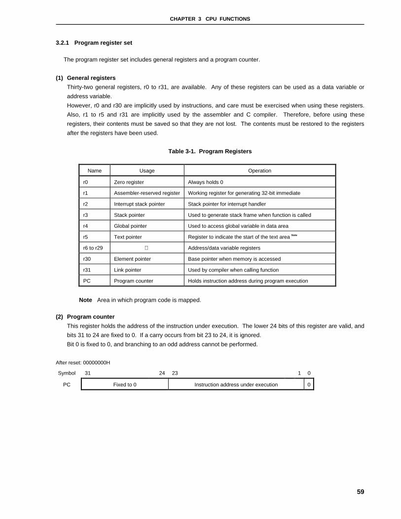
CHAPTER 3 CPU FUNCTIONS
59
3.2.1 Program register set
The program register set includes general registers and a program counter.
(1) General registers
Thirty-two general registers, r0 to r31, are available. Any of these registers can be used as a data variable or
address variable.
However, r0 and r30 are implicitly used by instructions, and care must be exercised when using these registers.
Also, r1 to r5 and r31 are implicitly used by the assembler and C compiler. Therefore, before using these
registers, their contents must be saved so that they are not lost. The contents must be restored to the registers
after the registers have been used.
Table 3-1. Program Registers
Name Usage Operation
r0 Zero register Always holds 0
r1 Assembler-reserved register Working register for generating 32-bit immediate
r2 Interrupt stack pointer Stack pointer for interrupt handler
r3 Stack pointer Used to generate stack frame when function is called
r4 Global pointer Used to access global variable in data area
r5 Text pointer Register to indicate the start of the text area Note
r6 to r29 Address/data variable registers
r30 Element pointer Base pointer when memory is accessed
r31 Link pointer Used by compiler when calling function
PC Program counter Holds instruction address during program execution
Note Area in which program code is mapped.
(2) Program counter
This register holds the address of the instruction under execution. The lower 24 bits of this register are valid, and
bits 31 to 24 are fixed to 0. If a carry occurs from bit 23 to 24, it is ignored.
Bit 0 is fixed to 0, and branching to an odd address cannot be performed.
After reset: 00000000H
Symbol 31 24 23 1 0
PC Fixed to 0 Instruction address under execution 0

CHAPTER 3 CPU FUNCTIONS
60
3.2.2 System register set
System registers control the status of the CPU and hold interrupt information.
Table 3-2. System Register Numbers
No. System Register Name Usage Operation
0 EIPC
1 EIPSW
Interrupt status saving registers These registers save the PC and PSW when an
exception or interrupt occurs. Because only one set of
these registers is available, their contents must be
saved when multiple interrupts are enabled.
2 FEPC
3 FEPSW
NMI status saving registers These registers save PC and PSW when NMI occurs.
4 ECR Interrupt source register If exception, maskable interrupt, or NMI occurs, this
register will contain information referencing the
interrupt source. The high-order 16 bits of this register
are called FECC, to which exception code of NMI is
set. The low-order 16 bits are called EICC, to which
exception code of exception/interrupt is set.
5 PSW Program status word A program status word is a collection of flags that
indicate program status (instruction execution result)
and CPU status.
6 to 31 Reserved
To read/write these system registers, specify a system register number indicated by the system register load/store
instruction (LDSR or STSR instruction).
(1) Interrupt source register (ECR)
After reset: 00000000H
Symbol 31 16 15 0
ECR FECC EICC
FECC Exception code of NMI (For exception code, refer to Table 5-1 .)
EICC Exception code of exception/interrupt

CHAPTER 3 CPU FUNCTIONS
61
(2) Program status word (PSW)
After reset: 00000020H
Symbol 31 8 7 6 5 4 3 2 1 0
PSW RFU NP EP ID SAT CY OV S Z
RFU Reserved field (fixed to 0).
NP Indicates that NMI processing is in progress. This flag is set when NMI is accepted, and
disables multiple interrupts.
EP Indicates that trap processing is in progress. This flag is set when trap is generated.
Moreover, interrupt requests can be accepted when this bit is sets.
ID Indicates that accepting external interrupt request is disabled.
SAT This flag is set if the result of executing saturated operation instruction overflows. If overflow
does not occur, value of previous operation is held.
CY This flag is set if carry or borrow occurs as result of operation. If carry or borrow does not
occur, it is reset.
OV This flag is set if overflow occurs during operation. If overflow does not occur, it is reset.
S This flag is set if the result of operation is negative. It is reset if the result is positive.
Z This flag is set if the result of operation is zero. If the result is not zero, it is reset.
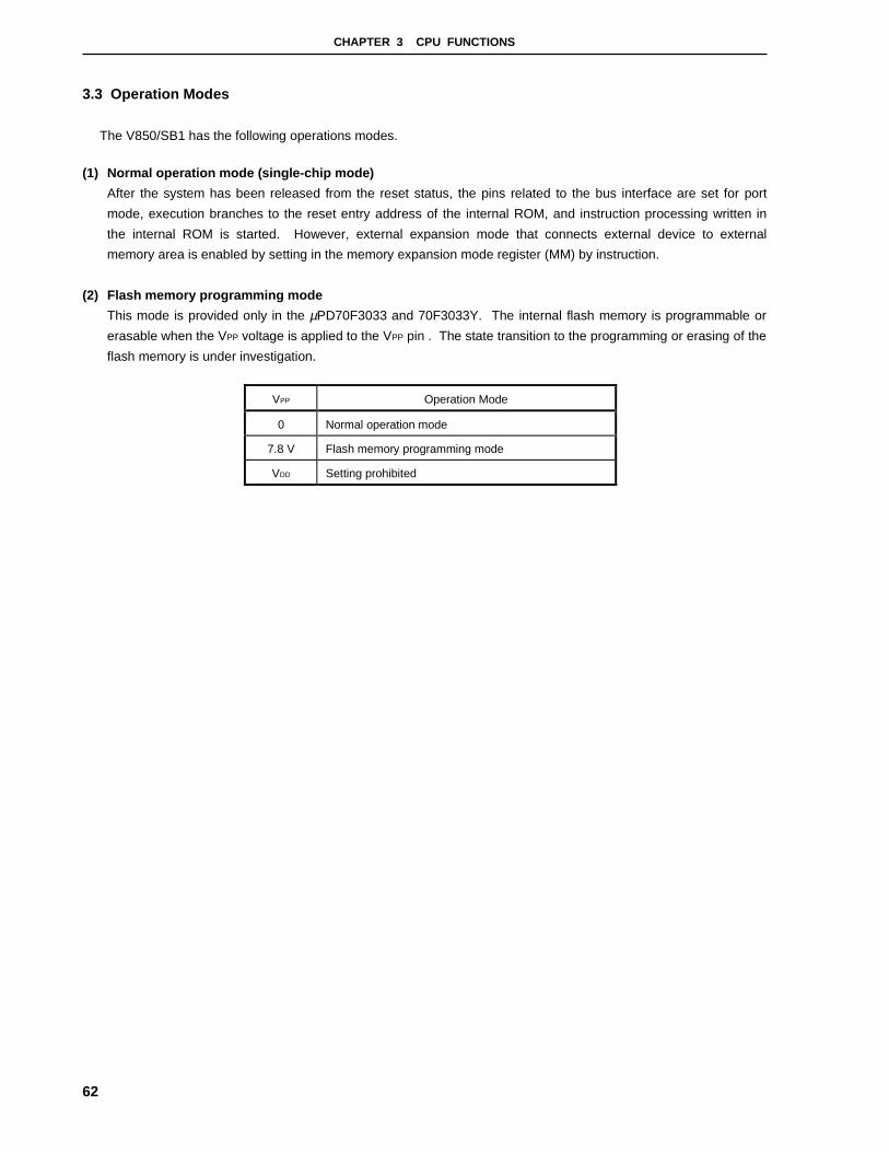
CHAPTER 3 CPU FUNCTIONS
62
3.3 Operation Modes
The V850/SB1 has the following operations modes.
(1) Normal operation mode (single-chip mode)
After the system has been released from the reset status, the pins related to the bus interface are set for port
mode, execution branches to the reset entry address of the internal ROM, and instruction processing written in
the internal ROM is started. However, external expansion mode that connects external device to external
memory area is enabled by setting in the memory expansion mode register (MM) by instruction.
(2) Flash memory programming mode
This mode is provided only in the µPD70F3033 and 70F3033Y. The internal flash memory is programmable or
erasable when the VPP voltage is applied to the VPP pin . The state transition to the programming or erasing of the
flash memory is under investigation.
VPP Operation Mode
0 Normal operation mode
7.8 V Flash memory programming mode
VDD Setting prohibited

CHAPTER 3 CPU FUNCTIONS
63
3.4 Address Space
3.4.1 CPU address space
The CPU of the V850/SB1 is of 32-bit architecture and supports up to 4 Gbytes of linear address space (data
space) during operand addressing (data access). When referencing instruction addresses, linear address space
(program space) of up to 16 Mbytes is supported.
Figure 3-1 shows the CPU address space.
Figure 3-1. CPU Address Space
FFFFFFFFH
CPU address space
Program area (16-Mbyte linear)
Data area (4-Gbyte linear)
01000000H00FFFFFFH
00000000H
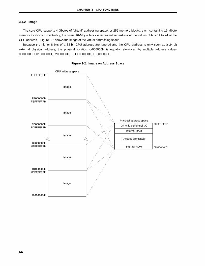
CHAPTER 3 CPU FUNCTIONS
64
3.4.2 Image
The core CPU supports 4 Gbytes of “virtual” addressing space, or 256 memory blocks, each containing 16-Mbyte
memory locations. In actuality, the same 16-Mbyte block is accessed regardless of the values of bits 31 to 24 of the
CPU address. Figure 3-2 shows the image of the virtual addressing space.
Because the higher 8 bits of a 32-bit CPU address are ignored and the CPU address is only seen as a 24-bit
external physical address, the physical location xx000000H is equally referenced by multiple address values
00000000H, 01000000H, 02000000H, ..., FE000000H, FF000000H.
Figure 3-2. Image on Address Space
FFFFFFFFH
FF000000HFEFFFFFFH
Image
CPU address space
Image
Image
Image
Image
FE000000HFDFFFFFFH
02000000H01FFFFFFH
01000000H00FFFFFFH
00000000H
Physical address space
On-chip peripheral I/O
Internal RAM
(Access prohibited)
Internal ROM
xxFFFFFFH
xx000000H

CHAPTER 3 CPU FUNCTIONS
65
3.4.3 Wrap-around of CPU address space
(1) Program space
Of the 32 bits of the PC (program counter), the higher 8 bits are fixed to 0, and only the lower 24 bits are valid.
Even if a carry or borrow occurs from bit 23 to 24 as a result of branch address calculation, the higher 8 bits
ignore the carry or borrow and remain 0.
Therefore, the lower-limit address of the program space, address 00000000H, and the upper-limit address
00FFFFFFH are contiguous addresses, and the program space is wrapped around at the boundary of these
addresses.
Caution No instruction can be fetched from the 4-Kbyte area of 00FFF000H to 00FFFFFFH because
this area is defined as peripheral I/O area. Therefore, do not execute any branch operation
instructions in which the destination address will reside in any part of this area.
00FFFFFEH
00FFFFFFH
00000000H
00000001H
Program space
Program space
(+) direction (–) direction
(2) Data space
The result of operand address calculation that exceeds 32 bits is ignored.
Therefore, the lower-limit address of the program space, address 00000000H, and the upper-limit address
FFFFFFFFH are contiguous addresses, and the data space is wrapped around at the boundary of these
addresses.
FFFFFFFEH
FFFFFFFFH
00000000H
00000001H
Data space
Data space
(+) direction (–) direction

CHAPTER 3 CPU FUNCTIONS
66
3.4.4 Memory map
The V850/SB1 reserves areas as shown below.
Figure 3-3. Memory Map
xxFFFFFFHOn-chip peripheral
I/O area
Internal RAM area
(Reserved)
Internal flash memory/
Internal ROM area
On-chip peripheral
I/O area
Internal RAM area
External memory
area
Internal flash memory/
Internal ROM area
Single-chip mode Single-chip mode(external expansion mode)
16 Mbytes
1 Mbyte
4 Kbytes
xxFFF000HxxFFEFFFH
xx100000Hxx0FFFFFH
xx000000H
xxFF8000HxxFF7FFFH
28 Kbytes

CHAPTER 3 CPU FUNCTIONS
67
3.4.5 Area
(1) Internal ROM/Internal flash memory area
An area of 1-Mbyte maximum is reserved for the internal ROM/internal flash memory area. 256 Kbytes are
provided from 000000H. The V850/SB1 is provided with physical internal ROM as follows:
Physical internal ROM: 000000H to 03FFFFH (256 Kbytes) … Mask ROM version
000000H to 03FFFFH (256 Kbytes) … Flash memory version
The image is seen in the rest of the area.
Figure 3-4. Internal ROM/Internal Flash Memory Area
xx0FFFFFH
xx0C0000H
xx0BFFFFH
xx080000H
xx07FFFFH
xx040000H
xx03FFFFH
xx000000H
Image
Image
Image
Image
Physical internal ROM
Internal ROM/flash memory
03FFFFH
000000HInterrupt/exception table
Interrupt/exception table
The V850/SB1 increases the interrupt response speed by assigning handler addresses corresponding to
interrupts/exceptions.
The collection of these handler addresses is called an interrupt/exception table, which is located in the internal
ROM area. When an interrupt/exception request is granted, execution jumps to the handler address, and the
program written at that memory address is executed. Table 3-3 shows the sources of interrupts/exceptions, and
the corresponding addresses.

CHAPTER 3 CPU FUNCTIONS
68
Table 3-3. Interrupt/Exception Table
Start Address of
Interrupt/Exception TableInterrupt/Exception Source
Start Address of
Interrupt/Exception TableInterrupt/Exception Source
00000000H RESET 000001C0H INTTM5
00000010H NMI 000001D0H INTTM6
00000020H INTWDT 000001E0H INTTM7
00000040H TRAP0n (n = 0 to F) 000001F0H INTIIC0 Note/INTCSI0
00000050H TRAP1n (n = 0 to F) 00000200H INTSER0
00000060H ILGOP 00000210H INTSR0/INTCSI1
00000080H INTWDTM 00000220H INTST0
00000090H INTP0 00000230H INTCSI2
000000A0H INTP1 00000240H INTIIC1 Note
000000B0H INTP2 00000250H INTSER1
000000C0H INTP3 00000260H INTSR1/INTCSI3
000000D0H INTP4 00000270H INTST1
000000E0H INTP5 00000280H INTCSI4
000000F0H INTP6 000002B0H INTAD
00000140H INTWTNI 000002C0H INTDMA0
00000150H INTTM00 000002D0H INTDMA1
00000160H INTTM01 000002E0H INTDMA2
00000170H INTTM10 000002F0H INTDMA3
00000180H INTTM11 00000300H INTDMA4
00000190H INTTM2 00000310H INTDMA5
000001A0H INTTM3 00000320H INTWTN
000001B0H INTTM4 00000330H INTKR
Note Available only for the µPD703033Y and 70F3033Y.
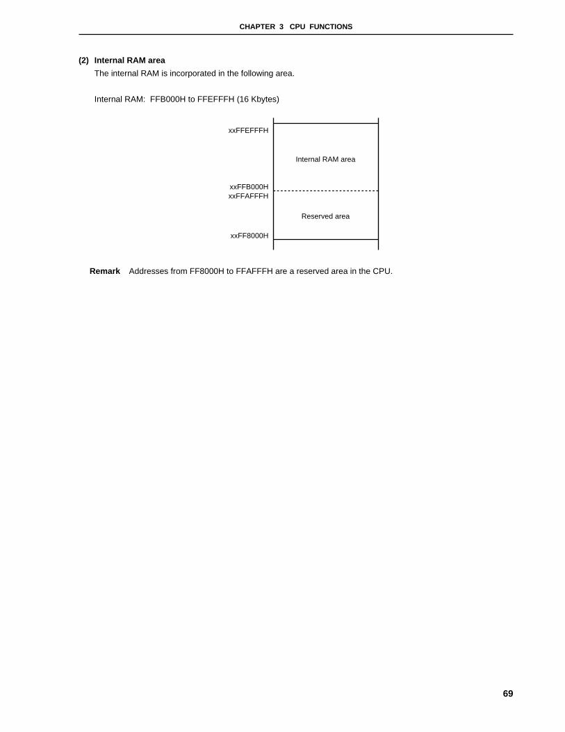
CHAPTER 3 CPU FUNCTIONS
69
(2) Internal RAM area
The internal RAM is incorporated in the following area.
Internal RAM: FFB000H to FFEFFFH (16 Kbytes)
xxFFEFFFH
xxFFB000HxxFFAFFFH
xxFF8000H
Internal RAM area
Reserved area
Remark Addresses from FF8000H to FFAFFFH are a reserved area in the CPU.
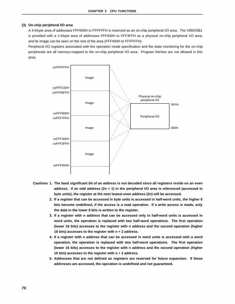
CHAPTER 3 CPU FUNCTIONS
70
(3) On-chip peripheral I/O area
A 4-Kbyte area of addresses FFF000H to FFFFFFH is reserved as an on-chip peripheral I/O area. The V850/SB1
is provided with a 1-Kbyte area of addresses FFF000H to FFF3FFH as a physical on-chip peripheral I/O area,
and its image can be seen on the rest of the area (FFF400H to FFFFFFH).
Peripheral I/O registers associated with the operation mode specification and the state monitoring for the on-chip
peripherals are all memory-mapped to the on-chip peripheral I/O area. Program fetches are not allowed in this
area.
xxFFFFFFH
xxFFFC00H
xxFFFBFFH
xxFFF800H
xxFFF7FFH
xxFFF400H
xxFFF3FFH
xxFFF000H
Image
Image
Image
Physical on-chipperipheral I/O
3FFH
000H
Image
Peripheral I/O
Cautions 1. The least significant bit of an address is not decoded since all registers reside on an even
address. If an odd address (2n + 1) in the peripheral I/O area is referenced (accessed in
byte units), the register at the next lowest even address (2n) will be accessed.
2. If a register that can be accessed in byte units is accessed in half-word units, the higher 8
bits become undefined, if the access is a read operation. If a write access is made, only
the data in the lower 8 bits is written to the register.
3. If a register with n address that can be accessed only in half-word units is accessed in
word units, the operation is replaced with two half-word operations. The first operation
(lower 16 bits) accesses to the register with n address and the second operation (higher
16 bits) accesses to the register with n + 2 address.
4. If a register with n address that can be accessed in word units is accessed with a word
operation, the operation is replaced with two half-word operations. The first operation
(lower 16 bits) accesses to the register with n address and the second operation (higher
16 bits) accesses to the register with n + 2 address.
5. Addresses that are not defined as registers are reserved for future expansion. If these
addresses are accessed, the operation is undefined and not guaranteed.

CHAPTER 3 CPU FUNCTIONS
71
(4) External memory area
The V850/SB1 can use an area of up to 16 Mbytes (xx100000H to xxFF7FFFH) for external memory accesses (in
single-chip mode: external expansion).
64 K, 256 K, 1 M, or 4 Mbytes of physical external memory can be allocated when the external expansion mode is
specified. In the area of other than the physical external memory, the image of the physical external memory can
be seen.
The internal RAM area and on-chip peripheral I/O area are not subject to external memory access.
Figure 3-5. External Memory Area (When Expanded to 64 K, 256 K, or 1 Mbyte)
xxFFFFFFH
xx000000H
Physical external memoryxFFFFH
x0000H
On-chip peripheral I/O
Internal RAM
Image
Image
Image
Internal ROM
xxFF7FFFH
xx100000H
External memory
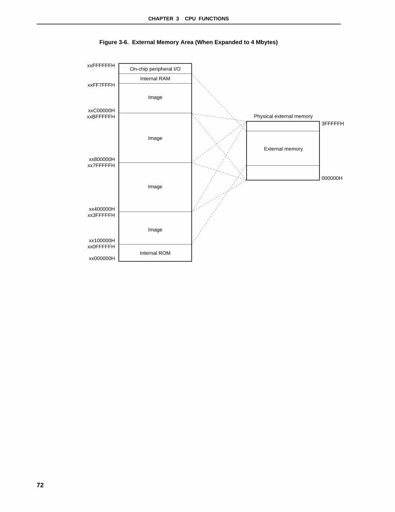
CHAPTER 3 CPU FUNCTIONS
72
Figure 3-6. External Memory Area (When Expanded to 4 Mbytes)
xxFFFFFFH
xxFF7FFFH
Image
On-chip peripheral I/O
Internal RAM
Image
Image
Image
Internal ROM
xxC00000HxxBFFFFFH
xx800000Hxx7FFFFFH
xx100000Hxx0FFFFFH
xx400000Hxx3FFFFFH
xx000000H
Physical external memory
External memory
3FFFFFH
000000H

CHAPTER 3 CPU FUNCTIONS
73
3.4.6 External expansion mode
The V850/SB1 allows external devices to be connected to the external memory space by using the pins of ports 4,
5, 6, and 9. To connect an external device, the port pins must be set in the external expansion mode by using the
memory expansion mode register (MM).
The address bus (A1 to A15) is set to multiplexed output with data bus (D1 to D15), though separate output is also
available by setting the memory address output mode register (MAM) (see the User’s Manual of relevant in-circuit
emulator about debugging when using the separate bus).
Caution Because the A1 pin and WAIT pin are alternate-function pins, the wait function by the WAIT pin
cannot be used when using a separate bus (programmable wait can be used however).
Similarly, a separate bus cannot be used when the wait function by the WAIT pin is being used.
Because the V850/SB1 is fixed to single-chip mode in the normal operation mode, the port alternate pins become
the port mode, thereby the external memory cannot be used. When the external memory is used (external expansion
mode), specify the MM register by the program.
(1) Memory expansion mode register (MM)
This register sets the mode of each pin of ports 4, 5, 6, and 9. In the external expansion mode, an external
device can be connected to the external memory area of up to 4 Mbytes. However, the external device cannot be
connected to the internal RAM area, on-chip peripheral I/O area, and internal ROM area in the single-chip mode
(and even if the external device is connected physically, it cannot be accessed).
The MM register can be read/written in 8- or 1-bit units. However, bits 4 to 7 are fixed to 0.

CHAPTER 3 CPU FUNCTIONS
74
Figure 3-7. Memory Expansion Mode Register (MM) Format
After reset: 00H R/W Address: FFFFF04CH
Symbol 7 6 5 4 3 2 1 0
MM 0 0 0 0 MM3 MM2 MM1 MM0
MM3 P95 and P96 Operation Modes
0 Port mode
1 External expansion mode (HLDAK: P95, HLDRQ: P96)
MM2 MM1 MM0 Address Space Port 4 Port 5 Port 6 Port 9
0 0 0 − Port mode
0 1 1 64 Kbytes AD0 to AD8 to LBEN,
expansion mode AD7 AD15 UBEN,
1 0 0 256 Kbytes A16, R/W, DSTB,
expansion mode A17 ASTB,
1 0 1 1 Mbyte A18, WRL,
expansion mode A19 WRH, RD
1 1 × 4 Mbytes A20,
expansion mode A21
Other than above RFU (reserved)
Remark For the details of the operation of each port pin, refer to 2.3 Description of Pin Functions .
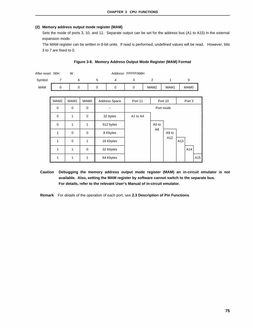
CHAPTER 3 CPU FUNCTIONS
75
(2) Memory address output mode register (MAM)
Sets the mode of ports 3, 10, and 11. Separate output can be set for the address bus (A1 to A15) in the external
expansion mode.
The MAM register can be written in 8-bit units. If read is performed, undefined values will be read. However, bits
3 to 7 are fixed to 0.
Figure 3-8. Memory Address Output Mode Register (MAM) Format
After reset: 00H W Address: FFFFF068H
Symbol 7 6 5 4 3 2 1 0
MAM 0 0 0 0 0 MAM2 MAM1 MAM0
MAM2 MAM1 MAM0 Address Space Port 11 Port 10 Port 3
0 0 0 − Port mode
0 1 0 32 bytes
0 1 1 512 bytes
1 0 0 8 Kbytes
1 0 1 16 Kbytes
1 1 0 32 Kbytes
1 1 1 64 Kbytes
A1 to A4
A5 to
A8A9 to
A12A13
A14
A15
Caution Debugging the memory address output mode register (MAM) an in-circuit emulator is not
available. Also, setting the MAM register by software cannot switch to the separate bus.
For details, refer to the relevant User’s Manual of in-circuit emulator.
Remark For details of the operation of each port, see 2.3 Description of Pin Functions .

CHAPTER 3 CPU FUNCTIONS
76
3.4.7 Recommended use of address space
The architecture of the V850/SB1 requires that a register that serves as a pointer be secured for address
generation in operand data accessing for data space. The address in this pointer register ±32 Kbytes can be
accessed directly from instruction. However, general register used as a pointer register is limited. Therefore, by
minimizing the deterioration of address calculation performance when changing the pointer value, the number of
usable general registers for handling variables is maximized, and the program size can be saved because instructions
for calculating pointer addresses are not required.
To enhance the efficiency of using the pointer in connection with the memory map of the V850/SB1, the following
points are recommended:
(1) Program space
Of the 32 bits of the PC (program counter), the higher 8 bits are fixed to 0, and only the lower 24 bits are valid.
Therefore, a continuous 16-Mbyte space, starting from address 00000000H, unconditionally corresponds to the
memory map of the program space.
(2) Data space
For the efficient use of resources to be performed through the wrap-around feature of the data space, the
continuous 8-Mbyte address spaces 00000000H to 007FFFFFH and FF800000H to FFFFFFFFH of the 4-Gbyte
CPU are used as the data space. With the V850/SB1, 16-Mbyte physical address space is seen as 256 images
in the 4-Gbyte CPU address space. The highest bit (bit 23) of this 24-bit address is assigned as address sign-
extended to 32 bits.
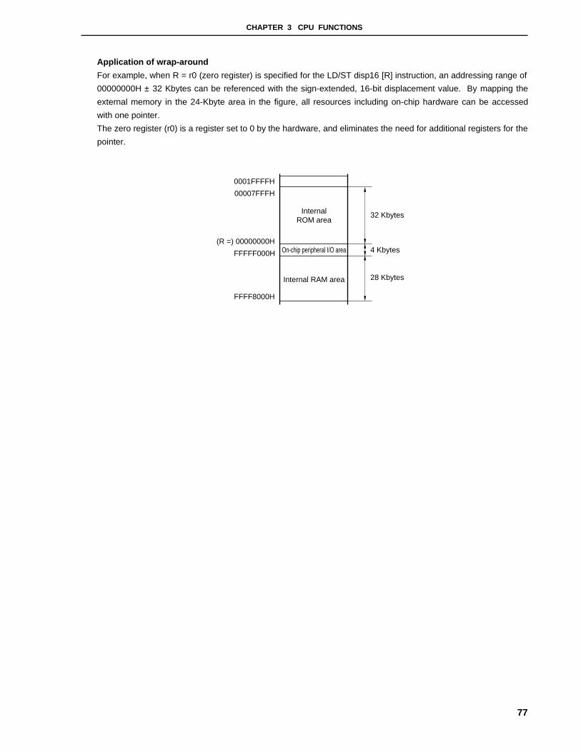
CHAPTER 3 CPU FUNCTIONS
77
Application of wrap-around
For example, when R = r0 (zero register) is specified for the LD/ST disp16 [R] instruction, an addressing range of
00000000H ± 32 Kbytes can be referenced with the sign-extended, 16-bit displacement value. By mapping the
external memory in the 24-Kbyte area in the figure, all resources including on-chip hardware can be accessed
with one pointer.
The zero register (r0) is a register set to 0 by the hardware, and eliminates the need for additional registers for the
pointer.
InternalROM area
On-chip peripheral I/O area
Internal RAM area
4 Kbytes
28 Kbytes
0001FFFFH
00007FFFH
(R =) 00000000H
FFFFF000H
FFFF8000H
32 Kbytes
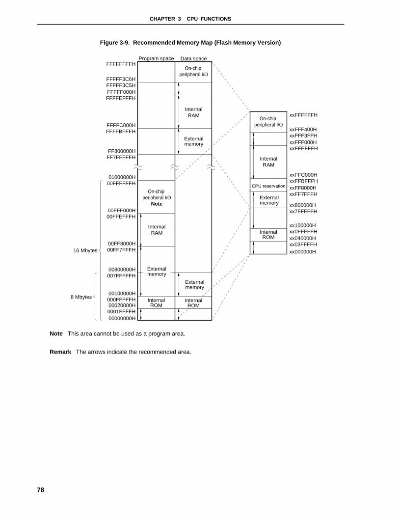
CHAPTER 3 CPU FUNCTIONS
78
Figure 3-9. Recommended Memory Map (Flash Memory Version)
FFFFFFFFH
FFFFF3C6HFFFFF3C5H
00000000H
16 Mbytes
8 MbytesInternalROM
InternalROM
Externalmemory
InternalRAM
On-chip peripheral I/O
Note
Program space Data space
On-chip peripheral I/O
InternalRAM
Externalmemory
On-chip peripheral I/O
InternalRAM
CPU reservation
Externalmemory
Externalmemory
InternalROM
xxFFFFFFH
xxFFF400HxxFFF3FFHxxFFF000HxxFFEFFFH
xxFFC000HxxFFBFFFHxxFF8000HxxFF7FFFH
xx100000Hxx0FFFFFHxx040000Hxx03FFFFH
xx800000Hxx7FFFFFH
xx000000H
FFFFF000HFFFFEFFFH
FFFFC000HFFFFBFFFH
FF800000HFF7FFFFFH
01000000H00FFFFFFH
00FFF000H00FFEFFFH
00FF8000H00FF7FFFH
00800000H007FFFFFH
00100000H000FFFFFH00020000H0001FFFFH
Note This area cannot be used as a program area.
Remark The arrows indicate the recommended area.
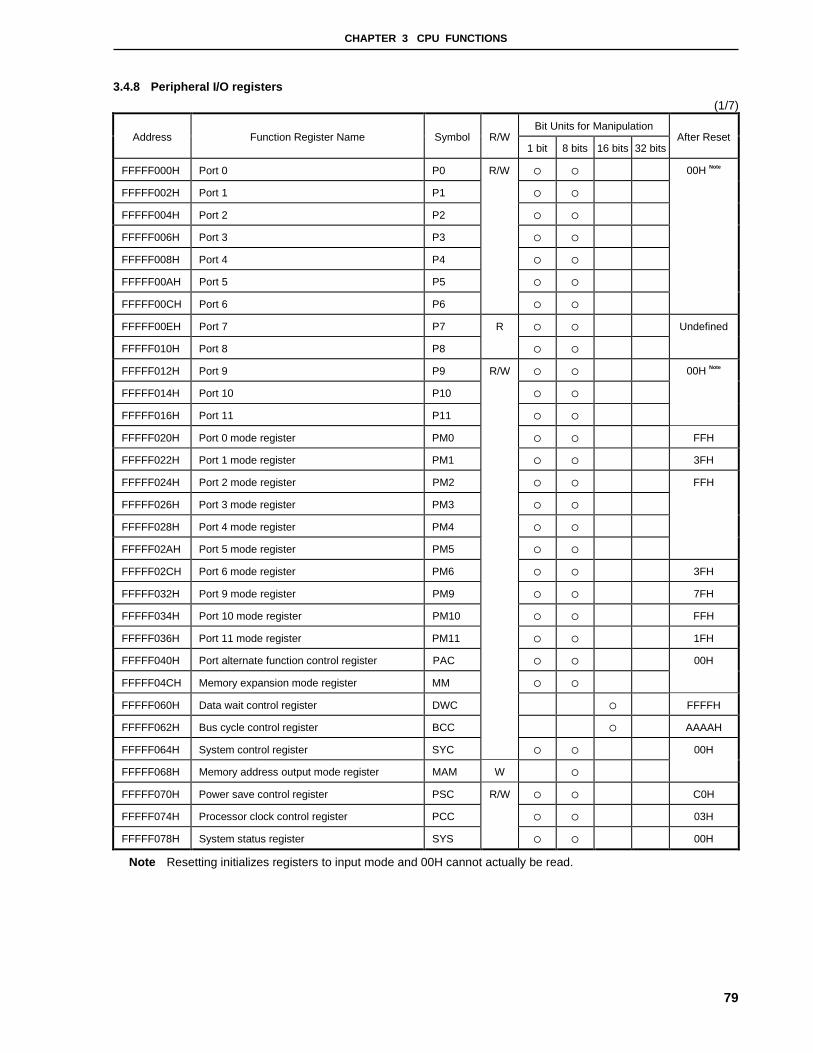
CHAPTER 3 CPU FUNCTIONS
79
3.4.8 Peripheral I/O registers
(1/7)
Bit Units for ManipulationAddress Function Register Name Symbol R/W
1 bit 8 bits 16 bits 32 bitsAfter Reset
FFFFF000H Port 0 P0 { {
FFFFF002H Port 1 P1 { {
FFFFF004H Port 2 P2 { {
FFFFF006H Port 3 P3 { {
FFFFF008H Port 4 P4 { {
FFFFF00AH Port 5 P5 { {
FFFFF00CH Port 6 P6
R/W
{ {
00H Note
FFFFF00EH Port 7 P7 { {
FFFFF010H Port 8 P8
R
{ {
Undefined
FFFFF012H Port 9 P9 { {
FFFFF014H Port 10 P10 { {
FFFFF016H Port 11 P11 { {
00H Note
FFFFF020H Port 0 mode register PM0 { { FFH
FFFFF022H Port 1 mode register PM1 { { 3FH
FFFFF024H Port 2 mode register PM2 { {
FFFFF026H Port 3 mode register PM3 { {
FFFFF028H Port 4 mode register PM4 { {
FFFFF02AH Port 5 mode register PM5 { {
FFH
FFFFF02CH Port 6 mode register PM6 { { 3FH
FFFFF032H Port 9 mode register PM9 { { 7FH
FFFFF034H Port 10 mode register PM10 { { FFH
FFFFF036H Port 11 mode register PM11 { { 1FH
FFFFF040H Port alternate function control register PAC { {
FFFFF04CH Memory expansion mode register MM { {
00H
FFFFF060H Data wait control register DWC { FFFFH
FFFFF062H Bus cycle control register BCC { AAAAH
FFFFF064H System control register SYC
R/W
{ {
FFFFF068H Memory address output mode register MAM W {
00H
FFFFF070H Power save control register PSC { { C0H
FFFFF074H Processor clock control register PCC { { 03H
FFFFF078H System status register SYS
R/W
{ { 00H
Note Resetting initializes registers to input mode and 00H cannot actually be read.

CHAPTER 3 CPU FUNCTIONS
80
(2/7)
Bit Units for ManipulationAddress Function Register Name Symbol R/W
1 bit 8 bits 16 bits 32 bitsAfter Reset
FFFFF080H Pull-up resistor option register 0 PU0 { {
FFFFF082H Pull-up resistor option register 1 PU1 { {
FFFFF084H Pull-up resistor option register 2 PU2 { {
FFFFF086H Pull-up resistor option register 3 PU3 { {
FFFFF094H Pull-up resistor option register 10 PU10 { {
FFFFF096H Pull-up resistor option register 11 PU11 { {
FFFFF0A2H Port 1 function register PF1 { {
FFFFF0A4H Port 2 function register PF2 { {
FFFFF0A6H Port 3 function register PF3 { {
FFFFF0B4H Port 10 function register PF10 { {
FFFFF0C0H Rising edge specification register 0 EGP0 { {
FFFFF0C2H Falling edge specification register 0 EGN0 { {
00H
FFFFF100H Interrupt control register WDTIC { {
FFFFF102H Interrupt control register PIC0 { {
FFFFF104H Interrupt control register PIC1 { {
FFFFF106H Interrupt control register PIC2 { {
FFFFF108H Interrupt control register PIC3 { {
FFFFF10AH Interrupt control register PIC4 { {
FFFFF10CH Interrupt control register PIC5 { {
FFFFF10EH Interrupt control register PIC6 { {
FFFFF118H Interrupt control register WTNIIC { {
FFFFF11AH Interrupt control register TMIC00 { {
FFFFF11CH Interrupt control register TMIC01 { {
FFFFF11EH Interrupt control register TMIC10 { {
FFFFF120H Interrupt control register TMIC11 { {
FFFFF122H Interrupt control register TMIC2 { {
FFFFF124H Interrupt control register TMIC3 { {
FFFFF126H Interrupt control register TMIC4 { {
FFFFF128H Interrupt control register TMIC5 { {
FFFFF12AH Interrupt control register TMIC6 { {
FFFFF12CH Interrupt control register TMIC7 { {
FFFFF12EH Interrupt control register CSIC0
R/W
{ {
47H

CHAPTER 3 CPU FUNCTIONS
81
(3/7)
Bit Units for ManipulationAddress Function Register Name Symbol R/W
1 bit 8 bits 16 bits 32 bitsAfter Reset
FFFFF130H Interrupt control register SERIC0 { {
FFFFF132H Interrupt control register CSIC1 { {
FFFFF134H Interrupt control register STIC0 { {
FFFFF136H Interrupt control register CSIC2 { {
FFFFF138H Interrupt control register Note IICIC1 { {
FFFFF13AH Interrupt control register SERIC1 { {
FFFFF13CH Interrupt control register CSIC3 { {
FFFFF13EH Interrupt control register STIC1 { {
FFFFF140H Interrupt control register CSIC4 { {
FFFFF146H Interrupt control register ADIC { {
FFFFF148H Interrupt control register DMAIC0 { {
FFFFF14AH Interrupt control register DMAIC1 { {
FFFFF14CH Interrupt control register DMAIC2 { {
FFFFF14EH Interrupt control register DMAIC3 { {
FFFFF150H Interrupt control register DMAIC4 { {
FFFFF152H Interrupt control register DMAIC5 { {
FFFFF154H Interrupt control register WTNIC { {
FFFFF156H Interrupt control register KRIC
R/W
{ {
47H
FFFFF166H In-service priority register ISPR R { { 00H
FFFFF170H Command register PRCMD W {
FFFFF180H DMA peripheral I/O address register 0 DIOA0 {
FFFFF182H DMA internal RAM address register 0 DRA0 {
FFFFF184H DMA byte count register 0 DBC0 {
Undefined
FFFFF186H DMA channel control register 0 DCHC0 { { 00H
FFFFF190H DMA peripheral I/O address register 1 DIOA1 {
FFFFF192H DMA internal RAM address register 1 DRA1 {
FFFFF194H DMA byte count register 1 DBC1 {
Undefined
FFFFF196H DMA channel control register 1 DCHC1 { { 00H
FFFFF1A0H DMA peripheral I/O address register 2 DIOA2 {
FFFFF1A2H DMA internal RAM address register 2 DRA2 {
FFFFF1A4H DMA byte count register 2 DBC2 {
Undefined
FFFFF1A6H DMA channel control register 2 DCHC2
R/W
{ { 00H
FFFFF1B0H DMA peripheral I/O address register 3 DIOA3 {
FFFFF1B2H DMA internal RAM address register 3 DRA3 {
FFFFF1B4H DMA byte count register 3 DBC3 {
Undefined
FFFFF1B6H DMA channel control register 3 DCHC3 { { 00H
Note Available only for the µPD703033Y and 70F3033Y
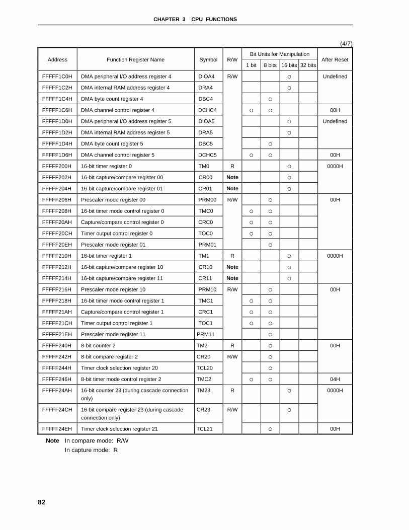
CHAPTER 3 CPU FUNCTIONS
82
(4/7)
Bit Units for ManipulationAddress Function Register Name Symbol R/W
1 bit 8 bits 16 bits 32 bitsAfter Reset
FFFFF1C0H DMA peripheral I/O address register 4 DIOA4 {
FFFFF1C2H DMA internal RAM address register 4 DRA4 {
FFFFF1C4H DMA byte count register 4 DBC4 {
Undefined
FFFFF1C6H DMA channel control register 4 DCHC4 { { 00H
FFFFF1D0H DMA peripheral I/O address register 5 DIOA5 {
FFFFF1D2H DMA internal RAM address register 5 DRA5 {
FFFFF1D4H DMA byte count register 5 DBC5 {
Undefined
FFFFF1D6H DMA channel control register 5 DCHC5
R/W
{ { 00H
FFFFF200H 16-bit timer register 0 TM0 R {
FFFFF202H 16-bit capture/compare register 00 CR00 Note {
FFFFF204H 16-bit capture/compare register 01 CR01 Note {
0000H
FFFFF206H Prescaler mode register 00 PRM00 {
FFFFF208H 16-bit timer mode control register 0 TMC0 { {
FFFFF20AH Capture/compare control register 0 CRC0 { {
FFFFF20CH Timer output control register 0 TOC0 { {
FFFFF20EH Prescaler mode register 01 PRM01
R/W
{
00H
FFFFF210H 16-bit timer register 1 TM1 R {
FFFFF212H 16-bit capture/compare register 10 CR10 Note {
FFFFF214H 16-bit capture/compare register 11 CR11 Note {
0000H
FFFFF216H Prescaler mode register 10 PRM10 {
FFFFF218H 16-bit timer mode control register 1 TMC1 { {
FFFFF21AH Capture/compare control register 1 CRC1 { {
FFFFF21CH Timer output control register 1 TOC1 { {
FFFFF21EH Prescaler mode register 11 PRM11
R/W
{
00H
FFFFF240H 8-bit counter 2 TM2 R {
FFFFF242H 8-bit compare register 2 CR20 {
FFFFF244H Timer clock selection register 20 TCL20 {
00H
FFFFF246H 8-bit timer mode control register 2 TMC2
R/W
{ { 04H
FFFFF24AH 16-bit counter 23 (during cascade connection
only)
TM23 R {
FFFFF24CH 16-bit compare register 23 (during cascade
connection only)
CR23 {
0000H
FFFFF24EH Timer clock selection register 21 TCL21
R/W
{ 00H
Note In compare mode: R/W
In capture mode: R
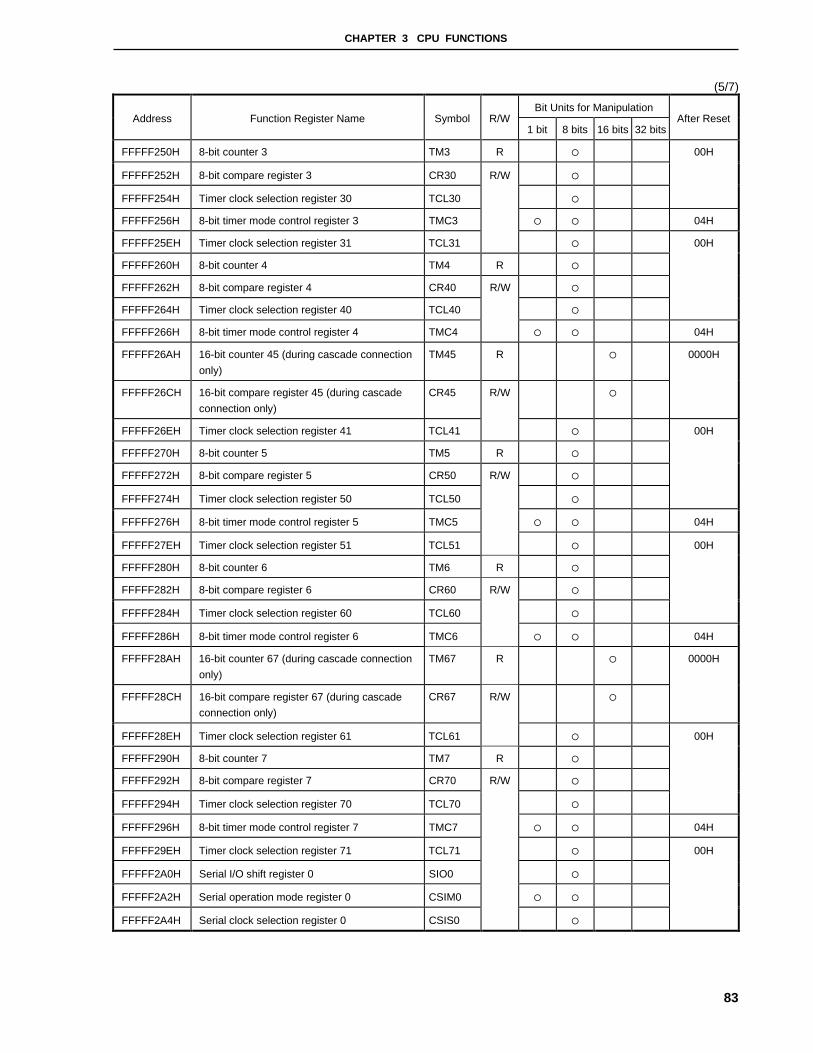
CHAPTER 3 CPU FUNCTIONS
83
(5/7)
Bit Units for ManipulationAddress Function Register Name Symbol R/W
1 bit 8 bits 16 bits 32 bitsAfter Reset
FFFFF250H 8-bit counter 3 TM3 R {
FFFFF252H 8-bit compare register 3 CR30 {
FFFFF254H Timer clock selection register 30 TCL30 {
00H
FFFFF256H 8-bit timer mode control register 3 TMC3 { { 04H
FFFFF25EH Timer clock selection register 31 TCL31
R/W
{
FFFFF260H 8-bit counter 4 TM4 R {
FFFFF262H 8-bit compare register 4 CR40 R/W {
FFFFF264H Timer clock selection register 40 TCL40 {
00H
FFFFF266H 8-bit timer mode control register 4 TMC4 { { 04H
FFFFF26AH 16-bit counter 45 (during cascade connection
only)
TM45 R { 0000H
FFFFF26CH 16-bit compare register 45 (during cascade
connection only)
CR45 {
FFFFF26EH Timer clock selection register 41 TCL41
R/W
{
FFFFF270H 8-bit counter 5 TM5 R {
FFFFF272H 8-bit compare register 5 CR50 {
FFFFF274H Timer clock selection register 50 TCL50 {
00H
FFFFF276H 8-bit timer mode control register 5 TMC5 { { 04H
FFFFF27EH Timer clock selection register 51 TCL51
R/W
{
FFFFF280H 8-bit counter 6 TM6 R {
FFFFF282H 8-bit compare register 6 CR60 {
FFFFF284H Timer clock selection register 60 TCL60 {
00H
FFFFF286H 8-bit timer mode control register 6 TMC6
R/W
{ { 04H
FFFFF28AH 16-bit counter 67 (during cascade connection
only)
TM67 R {
FFFFF28CH 16-bit compare register 67 (during cascade
connection only)
CR67 {
0000H
FFFFF28EH Timer clock selection register 61 TCL61
R/W
{
FFFFF290H 8-bit counter 7 TM7 R {
FFFFF292H 8-bit compare register 7 CR70 {
FFFFF294H Timer clock selection register 70 TCL70 {
00H
FFFFF296H 8-bit timer mode control register 7 TMC7 { { 04H
FFFFF29EH Timer clock selection register 71 TCL71 {
FFFFF2A0H Serial I/O shift register 0 SIO0 {
FFFFF2A2H Serial operation mode register 0 CSIM0 { {
FFFFF2A4H Serial clock selection register 0 CSIS0
R/W
{
00H
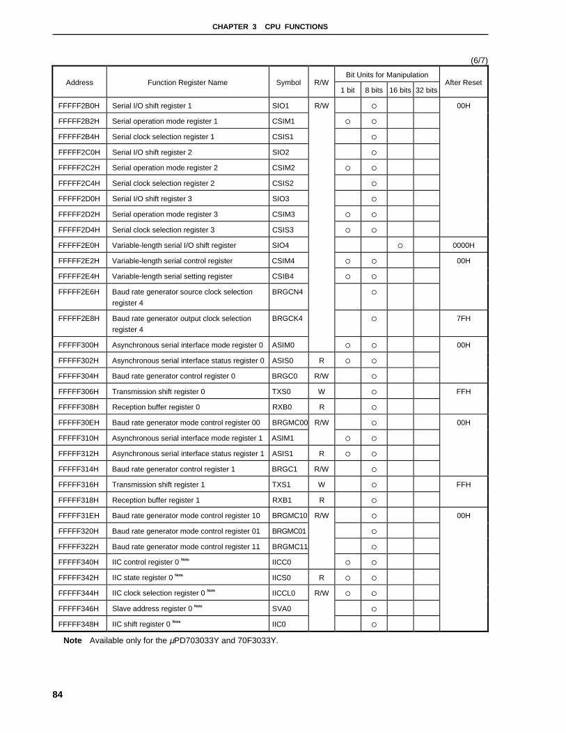
CHAPTER 3 CPU FUNCTIONS
84
(6/7)
Bit Units for ManipulationAddress Function Register Name Symbol R/W
1 bit 8 bits 16 bits 32 bitsAfter Reset
FFFFF2B0H Serial I/O shift register 1 SIO1 {
FFFFF2B2H Serial operation mode register 1 CSIM1 { {
FFFFF2B4H Serial clock selection register 1 CSIS1 {
FFFFF2C0H Serial I/O shift register 2 SIO2 {
FFFFF2C2H Serial operation mode register 2 CSIM2 { {
FFFFF2C4H Serial clock selection register 2 CSIS2 {
FFFFF2D0H Serial I/O shift register 3 SIO3 {
FFFFF2D2H Serial operation mode register 3 CSIM3 { {
FFFFF2D4H Serial clock selection register 3 CSIS3 { {
00H
FFFFF2E0H Variable-length serial I/O shift register SIO4 { 0000H
FFFFF2E2H Variable-length serial control register CSIM4 { {
FFFFF2E4H Variable-length serial setting register CSIB4 { {
FFFFF2E6H Baud rate generator source clock selection
register 4
BRGCN4 {
00H
FFFFF2E8H Baud rate generator output clock selection
register 4
BRGCK4 { 7FH
FFFFF300H Asynchronous serial interface mode register 0 ASIM0
R/W
{ {
FFFFF302H Asynchronous serial interface status register 0 ASIS0 R { {
FFFFF304H Baud rate generator control register 0 BRGC0 R/W {
00H
FFFFF306H Transmission shift register 0 TXS0 W {
FFFFF308H Reception buffer register 0 RXB0 R {
FFH
FFFFF30EH Baud rate generator mode control register 00 BRGMC00 {
FFFFF310H Asynchronous serial interface mode register 1 ASIM1
R/W
{ {
FFFFF312H Asynchronous serial interface status register 1 ASIS1 R { {
FFFFF314H Baud rate generator control register 1 BRGC1 R/W {
00H
FFFFF316H Transmission shift register 1 TXS1 W {
FFFFF318H Reception buffer register 1 RXB1 R {
FFH
FFFFF31EH Baud rate generator mode control register 10 BRGMC10 {
FFFFF320H Baud rate generator mode control register 01 BRGMC01 {
FFFFF322H Baud rate generator mode control register 11 BRGMC11 {
FFFFF340H IIC control register 0 Note IICC0
R/W
{ {
FFFFF342H IIC state register 0 Note IICS0 R { {
FFFFF344H IIC clock selection register 0 Note IICCL0 { {
FFFFF346H Slave address register 0 Note SVA0 {
FFFFF348H IIC shift register 0 Note IIC0
R/W
{
00H
Note Available only for the µPD703033Y and 70F3033Y.

CHAPTER 3 CPU FUNCTIONS
85
(7/7)
Bit Units for ManipulationAddress Function Register Name Symbol R/W
1 bit 8 bits 16 bits 32 bitsAfter Reset
FFFFF350H IIC control register 1 Note IICC1 R/W { {
FFFFF352H IIC state register 1 Note IICS1 R { {
FFFFF354H IIC clock selection register 1 Note IICCL1 R/W { {
FFFFF356H Slave address register 1 Note SVA1 {
FFFFF358H IIC shift register 1 Note IIC1 {
FFFFF360H Watch timer mode register WTNM { {
FFFFF364H Watch timer clock selection register WTNCS {
FFFFF36CH Correction control register CORCN { {
FFFFF36EH Correction request register CORRQ { {
FFFFF370H Correction address register 0 CORAD0 {
FFFFF374H Correction address register 1 CORAD1 {
FFFFF378H Correction address register 2 CORAD2 {
FFFFF37CH Correction address register 3 CORAD3 {
00000000H
FFFFF380H Oscillation stable time selection register OSTS { 04H
FFFFF382H Watchdog timer clock selection register WDCS { 00H
FFFFF384H Watchdog timer mode register WDTM { {
FFFFF3A0H Real-time output buffer register L RTBL {
FFFFF3A2H Real-time output buffer register H RTBH {
FFFFF3A4H Real-time output port mode register RTPM { {
FFFFF3A6H Real-time output port control register RTPC { {
FFFFF3C0H A/D converter mode register 1 ADM1 { {
FFFFF3C2H Analog input channel specification register ADS { {
FFFFF3C4H A/D conversion result register ADCR { 0000H
FFFFF3C6H A/D conversion result register H (higher 8 bits) ADCRH
R
{
FFFFF3C8H A/D converter mode register 2 ADM2 { {
FFFFF3D0H Key return mode register KRM { {
FFFFF3D4H Noise elimination control register NCC
R/W
{
00H
Note Available only for the µPD703033Y and 70F3033Y.
CHAPTER 3 CPU FUNCTIONS
86
3.4.9 Specific registers
Specific registers are registers that are protected from being written with illegal data due to erroneous program
execution, etc. The write access of these specific registers is executed in a specific sequence, and if abnormal store
operations occur, it is notified by the system status register (SYS). The V850/SB1 has two specific registers, the
power save control register (PSC) and processor clock control register (PCC). For details of the PSC register, refer to
6.3.1 (2), and for details of the PCC register, refer to 6.3.1 (1).
The following sequence shows the data setting of the specific registers.
<1> Disable DMA operation.
<2> Set the PSW NP bit to 1 (interrupt disabled).
<3> Write any 8-bit data in the command register (PRCMD).
<4> Write the set data in the specific registers (by the following instructions).
• Store instruction (ST/SST instruction)
• Bit manipulation instruction (SET1/CLR1/NOT1 instruction)
<5> Return the PSW NP bit to 0 (interrupt disable canceled).
<6> Insert the NOP instructions (2 or 5 instructions).
<7> If necessary, enable DMA operation.
No special sequence is required when reading the specific registers.
Cautions 1. If an interrupt request or a DMA request is accepted between the time PRCMD is generated
(<3>) and the specific register write operation (<4>) that follows immediately after, the write
operation to the specific register is not performed and a protection error (PRERR bit of SYS
register is 1) may occur. Therefore, set the NP bit of PSW to 1 (<2>) to disable the acceptance
of INT/NMI or to disable DMA transfer.
The above also applies when a bit manipulation instruction is used to set a specific register.
Moreover, to ensure that the execution routine following release of the STOP/IDLE mode is
performed correctly, insert the NOP instruction as a dummy instruction (<6>). If the value of
the ID bit of PSW does not change as the result of execution of the instruction to return the NP
bit to 0 (<5>), insert two NOP instructions, and if the value of the ID bit of PSW changes, insert
five NOP instructions.

CHAPTER 3 CPU FUNCTIONS
87
A description example is given below.
[Description example]: In case of PSC register
LDSR rX,5 ; NP bit = 1
ST.B r0,PRCMD [r0] ; Write to PRCMD
ST.B rD,PSC [r0] ; PSC register setting
LDSR rY,5 ; NP bit = 0
NOP ; Dummy instruction (2 or 5 instructions)...
NOP
(next instruction) ; Execution routine following cancellation of STOP/IDLE mode...
rX: Value to be written to PSW
rY: Value to be written back to PSW
rD: Value to be set to PSC
When saving the value of PSW, the value of PSW prior to setting the NP bit must be
transferred to the rY register.
Cautions 2. The instructions (<5> interrupt disable cancel, <6> NOP instruction) following the store
instruction for the PSC register for setting the software STOP mode and IDLE mode are
executed before a power save mode is entered.
3. Always stop the DMA prior to accessing special registers.

CHAPTER 3 CPU FUNCTIONS
88
(1) Command register (PRCMD)
The command register (PRCMD) is a register used when write-accessing the specific register to prevent incorrect
writing to the specific registers due to the erroneous program execution.
This register can be written in 8-bit units. It becomes undefined values in a read cycle.
Occurrence of illegal store operations can be checked by the PRERR bit of the SYS register.
After reset: Undefined W Address: FFFFF170H
Symbol 7 6 5 4 3 2 1 0
PRCMD REG7 REG6 REG5 REG4 REG3 REG2 REG1 REG0
REGn Registration Code
0/1 Any 8-bit data
(2) System status register (SYS)
This register is allocated with status flags showing the operating state of the entire system. This register can be
read/written in 8- or 1-bit units.
After reset: 00H R/W Address: FFFFF078H
Symbol 7 6 5 4 3 2 1 0
SYS 0 0 0 PRERR 0 0 0 0
PRERR Detection of Protection Error
0 Protection error does not occur
1 Protection error occurs
Operation conditions of PRERR flag are shown as follows.
(a) Set conditions (PRERR = 1)
(1) When a write operation to the specific register took place in a state where the store instruction operation
for the recent peripheral I/O was not a write operation to the PRCMD register.
(2) When the first store instruction operation following a write operation to the PRCMD register is to any
peripheral I/O register apart from specific registers.
(b) Reset conditions: (PRERR = 0)
(1) When 0 is written to the PRERR flag of the SYS register.
(2) At system reset.

89
CHAPTER 4 BUS CONTROL FUNCTION
The V850/SB1 is provided with an external bus interface function by which external memories such as ROM and
RAM, and I/O can be connected.
4.1 Features
• Address bus (capable of separate output)
• 16-bit data bus
• Able to be connected to external devices via the pins that have alternate-functions as ports
• Wait function
• Programmable wait function, capable of inserting up to 3 wait states per 2 blocks
• External wait control through WAIT input pin
• Idle state insertion function
• Bus mastership arbitration function
• Bus hold function
4.2 Bus Control Pins and Control Register
4.2.1 Bus control pins
The following pins are used for interfacing to external devices:
External Bus Interface Function Corresponding Port (pins)
Address/data bus (AD0 to AD7) Port 4 (P40 to P47)
Address/data bus (AD8 to AD15) Port 5 (P50 to P57)
Address bus (A1 to A4) Port 11 (P110 to P113)
Address bus (A5 to A12) Port 10 (P100 to P107)
Address bus (A13 to A15) Port 3 (P34 to P36)
Address bus (A16 to A21) Port 6 (P60 to P65)
Read/write control (LBEN, UBEN, R/W, DSTB, WRL, WRH, RD) Port 9 (P90 to P93)
Address strobe (ASTB) Port 9 (P94)
Bus hold control (HLDRQ, HLDAK) Port 9 (P95, P96)
External wait control (WAIT) Port 11 (P110)
The bus interface function of each pin is enabled by specifying the memory expansion mode register (MM) or the
memory address output mode register (MAM). For the details of specifying an operation mode of the external bus
interface, refer to 3.4.6 (1) Memory expansion mode register (MM) and for (2) Memory address output mode
register (MAM).
Caution For debugging using the separate bus, refer to the user’s manual of corresponding in-circuit
emulator.
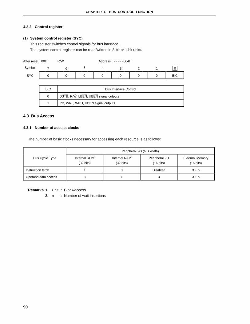
CHAPTER 4 BUS CONTROL FUNCTION
90
4.2.2 Control register
(1) System control register (SYC)
This register switches control signals for bus interface.
The system control register can be read/written in 8-bit or 1-bit units.
After reset: 00H R/W Address: FFFFF064H
Symbol 7 6 5 4 3 2 1 0
SYC 0 0 0 0 0 0 0 BIC
BIC Bus Interface Control
0 DSTB, R/W, LBEN, UBEN signal outputs
1 RD, WRL, WRH, UBEN signal outputs
4.3 Bus Access
4.3.1 Number of access clocks
The number of basic clocks necessary for accessing each resource is as follows:
Peripheral I/O (bus width)
Bus Cycle Type Internal ROM
(32 bits)
Internal RAM
(32 bits)
Peripheral I/O
(16 bits)
External Memory
(16 bits)
Instruction fetch 1 3 Disabled 3 + n
Operand data access 3 1 3 3 + n
Remarks 1. Unit : Clock/access
2. n : Number of wait insertions
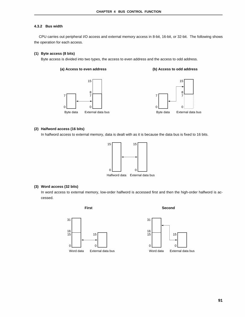
CHAPTER 4 BUS CONTROL FUNCTION
91
4.3.2 Bus width
CPU carries out peripheral I/O access and external memory access in 8-bit, 16-bit, or 32-bit. The following shows
the operation for each access.
(1) Byte access (8 bits)
Byte access is divided into two types, the access to even address and the access to odd address.
0
7
0
78
15
Byte data External data bus
(a) Access to even address
0
7
0
78
15
Byte data External data bus
(b) Access to odd address
(2) Halfword access (16 bits)
In halfword access to external memory, data is dealt with as it is because the data bus is fixed to 16 bits.
0 0
1515
Halfword data External data bus
(3) Word access (32 bits)
In word access to external memory, low-order halfword is accessed first and then the high-order halfword is ac-
cessed.
0
15
0
1516
31
Word data External data bus
First
0
15
0
1516
31
Word data External data bus
Second

CHAPTER 4 BUS CONTROL FUNCTION
92
4.4 Memory Block Function
The 16-Mbyte memory space is divided into memory blocks of 1-Mbyte units. The programmable wait function
and bus cycle operation mode can be independently controlled for every two memory blocks.
Block 15
Block 14
Block 13
Block 12
Block 11
Block 10
Block 9
Block 8
Block 7
Block 6
Block 5
Block 4
Block 3
Block 2
Block 1
Block 0
On-chip peripheral I/O area
Internal RAM area
External memory area
FFFFFFH
F00000HEFFFFFH
E00000HDFFFFFH
D00000HCFFFFFH
C00000HBFFFFFH
B00000HAFFFFFH
A00000H9FFFFFH
900000H8FFFFFH
800000H7FFFFFH
700000H6FFFFFH
600000H5FFFFFH
500000H4FFFFFH
400000H3FFFFFH
300000H2FFFFFH
200000H1FFFFFH
100000H0FFFFFH
000000HInternal ROM area

CHAPTER 4 BUS CONTROL FUNCTION
93
4.5 Wait Function
4.5.1 Programmable wait function
To facilitate interfacing with low-speed memories and I/O devices, up to 3 data wait states can be inserted in a bus
cycle that starts every two memory blocks.
The number of wait states can be programmed by using data wait control register (DWC). Immediately after the
system has been reset, three data wait insertion states are automatically programmed for all memory blocks.
(1) Data wait control register (DWC)
This register can be read/written in 16-bit units.
After reset: FFFFH R/W Address: FFFFF060H
Symbol 15 14 13 12 11 10 9 8 7 6 5 4 3 2 1 0
DWC
Number of Wait States to Be Inserted
0 0 0
0 1 1
1 0 2
1 1 3
n Blocks into Which Wait States Are Inserted
0 Blocks 0/1
1 Blocks 2/3
2 Blocks 4/5
3 Blocks 6/7
4 Blocks 8/9
5 Blocks 10/11
6 Blocks 12/13
7 Blocks 14/15
Block 0 is reserved for the internal ROM area. It is not subject to programmable wait control, regardless of the
setting of DWC, and is always accessed without wait states.
The internal RAM area of block 15 is not subject to programmable wait control and is always accessed without
wait states. The on-chip peripheral I/O area of this block is not subject to programmable wait control, either. The
only wait control is dependent upon the execution of each peripheral function.
DW61 DW00DW01DW10DW11DW20DW21DW30DW31DW40DW41DW50DW51DW60DW70DW71
DWn0DWn1

CHAPTER 4 BUS CONTROL FUNCTION
94
4.5.2 External wait function
When an extremely slow device, I/O, or asynchronous system is connected, any number of wait states can be in-
serted in a bus cycle by sampling the external wait pin (WAIT) to synchronize with the external device.
The external wait signal is data wait only, and does not affect the access times of the internal ROM, internal RAM,
and on-chip peripheral I/O areas, similar to programmable wait.
Input of the external WAIT signal can be done asynchronously to CLKOUT and is sampled at the falling edge of
the clock in the T2 and TW states of a bus cycle. If the setup/hold time at sampling timing is not satisfied, the wait
state may or may not be inserted in the next state.
Caution Because the A1 pin and WAIT pin are alternate-function pins, the wait function by the WAIT pin
cannot be used when using a separate bus (programmable wait can be used, however).
Similarly, a separate bus cannot be used when the wait function by the WAIT pin is being used.
4.5.3 Relationship between programmable wait and external wait
A wait cycle is inserted as a result of an OR operation between the wait cycle specified by the set value of pro-
grammable wait and the wait cycle controlled by the WAIT pin. In other words, the number of wait cycles is deter-
mined by those which have much more cycles than the other.
Wait controlProgrammable wait
Wait by WAIT pin
For example, if the number of programmable wait and the timing of the WAIT pin input signal is as illustrated be-
low, three wait states will be inserted in the bus cycle.
Figure 4-1. Example of Inserting Wait States
CLKOUTT1 T2 TW TW TW T3
WAIT pin
Wait by WAIT pin
Programmable wait
Wait control
Remark {: valid sampling timing

CHAPTER 4 BUS CONTROL FUNCTION
95
4.6 Idle State Insertion Function
To facilitate interfacing with low-speed memory devices and meeting the data output float delay time on memory
read accesses every two blocks, one idle state (TI) can be inserted into the current bus cycle after the T3 state. The
bus cycle following continuous bus cycles starts after one idle state.
Specifying insertion of the idle state is programmable by using the bus cycle control register (BCC).
Immediately after the system has been reset, idle state insertion is automatically programmed for all memory
blocks.
(1) Bus cycle control register (BCC)
This register can be read/written in 16-bit units.
After reset: AAAAH R/W Address: FFFFF062H
Symbol 15 14 13 12 11 10 9 8 7 6 5 4 3 2 1 0
BCC
Idle State Insert Specification
0 Not inserted
1 Inserted
n Blocks into Which Idle State Is Inserted
0 Blocks 0/1
1 Blocks 2/3
2 Blocks 4/5
3 Blocks 6/7
4 Blocks 8/9
5 Blocks 10/11
6 Blocks 12/13
7 Blocks 14/15
Block 0 is reserved for the internal ROM area; therefore, no idle state can be specified.
The internal RAM area and on-chip peripheral I/O area of block 15 are not subject to insertion of the idle state.
Be sure to set bits 0, 2, 4, 6, 8, 10, 12, and 14 to 0. If these bits are set to 1, the operation is not guaranteed.
0BC010BC110BC210BC310BC410BC510BC610BC71
BCn11
CHAPTER 4 BUS CONTROL FUNCTION
96
4.7 Bus Hold Function
4.7.1 Outline of function
When the MM3 bit of the memory expansion mode register (MM) is set (1), the HLDRQ and HLDAK pin functions
of P95 and P96 become valid.
When the HLDRQ pin becomes active (low) indicating that another bus master is requesting acquisition of the bus,
the external address/data bus and strobe pins go into a high-impedance state Note, and the bus is released (bus hold
status). When the HLDRQ pin becomes inactive (high) indicating that the request for the bus is cleared, these pins
are driven again.
During bus hold period, the internal operation continues until the next external memory access.
The bus hold status can be recognized by that the HLDAK pin becomes active (low).
This feature can be used to design a system where two or more bus masters exist, such as when multi-processor
configuration is used and when a DMA controller is connected.
Bus hold request is not acknowledged between the first and the second word access, and not acknowledged be-
tween read access and write access in read modify write access of bit manipulation instruction either.
Note A1 to A15 are retained when a separate bus is used.

CHAPTER 4 BUS CONTROL FUNCTION
97
4.7.2 Bus hold procedure
The procedure of the bus hold function is illustrated below.
HLDRQ
HLDAK
<1> <2> <3><4><5> <7><8><9><6>
<1>HLDRQ = 0 accepted<2>All bus cycle start request pending<3>End of current bus cycle<4>Bus idle status<5>HLDAK = 0
<6>HLDRQ = 1 accepted<7>HLDAK = 1<8>Clears bus cycle start request pending<9>Start of bus cycle
Nomal status
Bus hold status
Normal status
4.7.3 Operation in power save mode
In the STOP or IDLE mode, the system clock is stopped. Consequently, the bus hold status is not set even if the
HLDRQ pin becomes active.
In the HALT mode, the HLDAK pin immediately becomes active when the HLDRQ pin becomes active, and the
bus hold status is set. When the HLDRQ pin becomes inactive, the HLDAK pin becomes inactive. As a result, the
bus hold status is cleared, and the HALT mode is set again.

CHAPTER 4 BUS CONTROL FUNCTION
98
4.8 Bus Timing
The V850/SB1 can execute the read/write control for an external device by the following two modes.
• Mode using DSTB, R/W, LBEN, UBEN, and ASTB signals
• Mode using RD, WRL, WRH, and ASTB signals
Set these modes by using the BIC bit of the system control register (SYC).
(1) Memory read (0 wait)
T1 T2 T3
CLKOUT (input)
A16 to A21 (output)
AD0 to AD15 (input/output)
Address
DataAddress
ASTB (output)
R/W (output)
DSTB, RD (output)
UBEN, LBEN (output)
WAIT (input)
WRH, WRL (output)H
A1 to A15 (output) Address
Remarks 1. { indicates the sampling timing when the number of programmable waits is set to 0.
2. The broken line indicates the high-impedance state.

CHAPTER 4 BUS CONTROL FUNCTION
99
(2) Memory read (1 wait)
T1 T2 TW
CLKOUT (input)
A16 to A21 (output)
AD0 to AD15(input/output)
Address
Address
ASTB (output)
R/W (output)
DSTB, RD (output)
UBEN, LBEN (output)
WAIT (input)
WRH, WRL (output)
T3
Data
H
A1 to A15 (output) Address
Remarks 1. { indicates the sampling timing when the number of programmable waits is set to 0.
2. The broken line indicates the high-impedance state.

CHAPTER 4 BUS CONTROL FUNCTION
100
(3) Memory read (0 wait, idle state)
T1 T2 T3
CLKOUT (input)
A1 to A15 (output)
AD0 to AD15(input/output)
Address
Address
ASTB (output)
R/W (output)
DSTB, RD (output)
UBEN, LBEN (output)
WAIT (input)
WRH, WRL (output)H
TI
Data
A16 to A21 (output) Address
Remarks 1. { indicates the sampling timing when the number of programmable waits is set to 0.
2. The broken line indicates the high-impedance state.
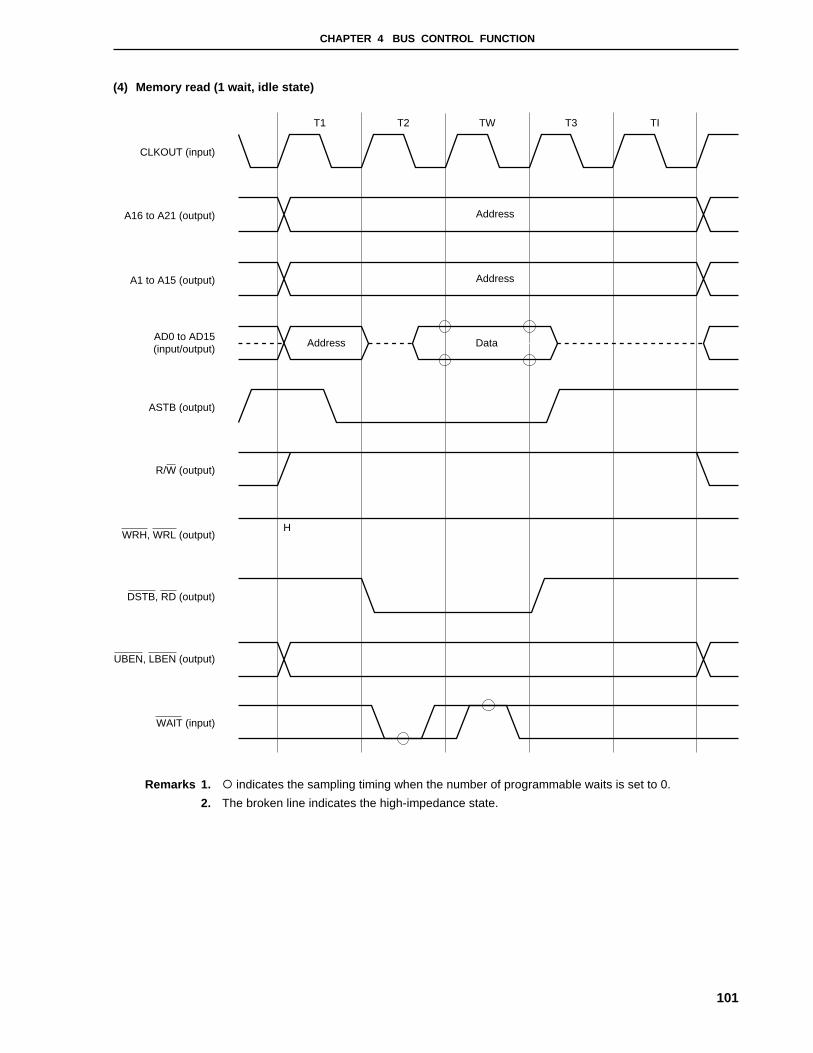
CHAPTER 4 BUS CONTROL FUNCTION
101
(4) Memory read (1 wait, idle state)
T1 T2 TW
CLKOUT (input)
A1 to A15 (output)
AD0 to AD15(input/output)
Address
Address
ASTB (output)
R/W (output)
DSTB, RD (output)
UBEN, LBEN (output)
WAIT (input)
WRH, WRL (output)
T3
Data
TI
H
A16 to A21 (output) Address
Remarks 1. { indicates the sampling timing when the number of programmable waits is set to 0.
2. The broken line indicates the high-impedance state.
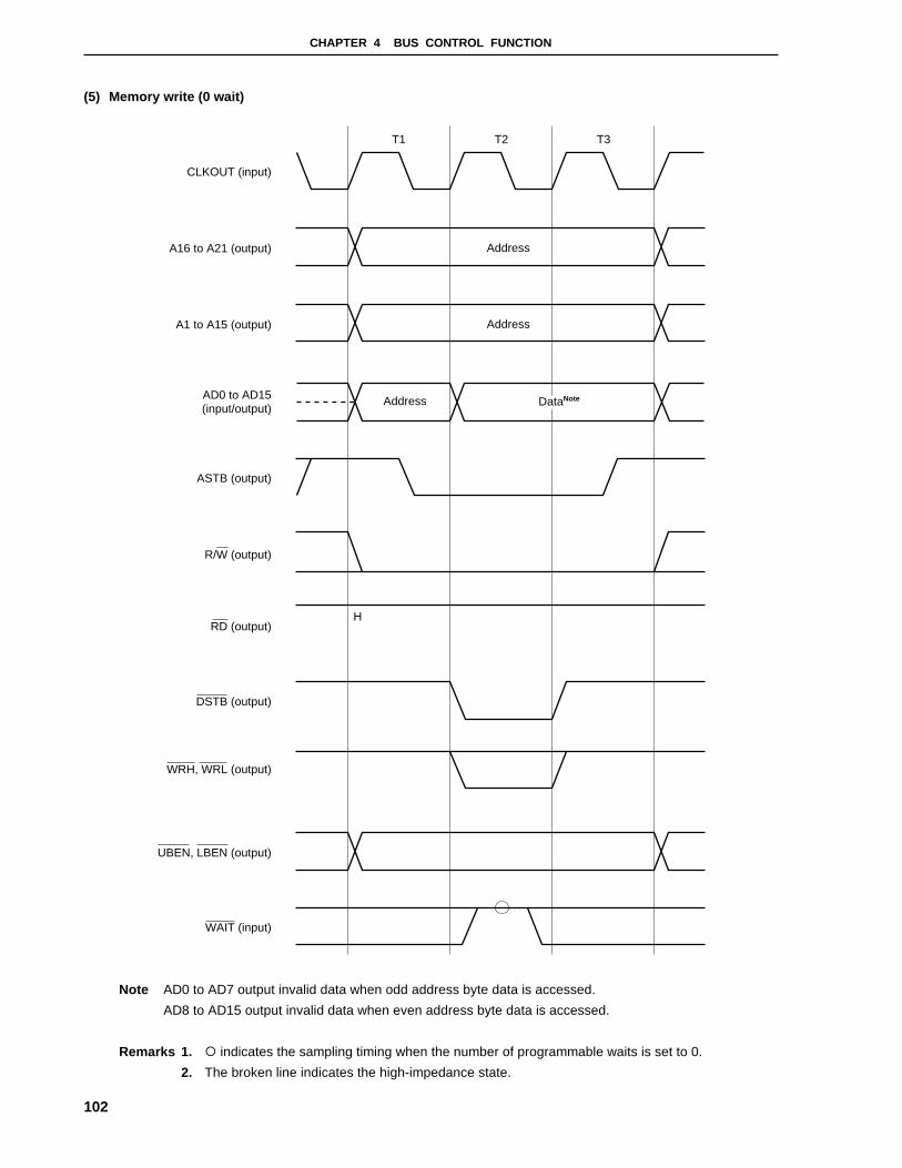
CHAPTER 4 BUS CONTROL FUNCTION
102
(5) Memory write (0 wait)
T1 T2 T3
CLKOUT (input)
A16 to A21 (output)
AD0 to AD15(input/output)
Address
DataNoteAddress
ASTB (output)
R/W (output)
DSTB (output)
UBEN, LBEN (output)
WAIT (input)
RD (output)
WRH, WRL (output)
H
A1 to A15 (output) Address
Note AD0 to AD7 output invalid data when odd address byte data is accessed.
AD8 to AD15 output invalid data when even address byte data is accessed.
Remarks 1. { indicates the sampling timing when the number of programmable waits is set to 0.
2. The broken line indicates the high-impedance state.

CHAPTER 4 BUS CONTROL FUNCTION
103
(6) Memory write (1 wait)
T1 T2 TW
CLKOUT (input)
A16 to A21 (output)
AD0 to AD15(input/output)
Address
ASTB (output)
R/W (output)
DSTB (output)
UBEN, LBEN (output)
WAIT (input)
RD (output)
WRH, WRL (output)
T3
DataNoteAddress
H
A1 to A15 (output) Address
Note AD0 to AD7 output invalid data when odd address byte data is accessed.
AD8 to AD15 output invalid data when even address byte data is accessed.
Remarks 1. { indicates the sampling timing when the number of programmable waits is set to 0.
2. The broken line indicates the high-impedance state.

CHAPTER 4 BUS CONTROL FUNCTION
104
(7) Bus hold timing
CLKOUT (input)
R/W (output)
DSTB, RD,WRH, WRL (output)
UBEN, LBEN (output)
WAIT (input)
HLDRQ (input)
T2 T3 TH TH TH TH TI T1
HLDAK (output)
A16 to A21 (output)
A1 to A15 (output)
AD0 to AD15(input/output)
Address
Address
Address Data
Address
ASTB (output)
Undefined Address
Note 1
Note 2
Notes 1. If HLDRQ signal is inactive (high-level) at this sampling timing, bus hold state is not entered.
2. If transferred to bus hold status after a write cycle, high-level may be output momentarily from the
R/W pin immediately before HLDAK signal changes from high-level to low-level.
Remarks 1. { indicates the sampling timing when the number of programmable waits is set to 0.
2. The broken line indicates the high-impedance state.
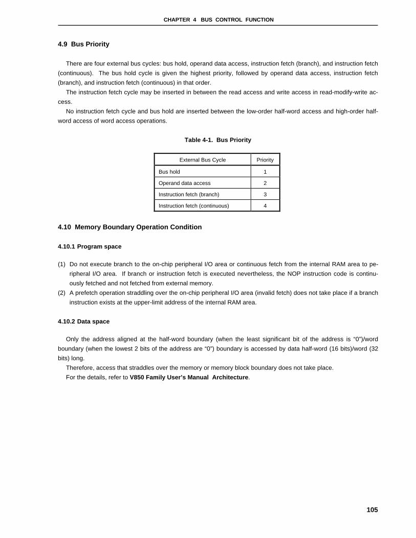
CHAPTER 4 BUS CONTROL FUNCTION
105
4.9 Bus Priority
There are four external bus cycles: bus hold, operand data access, instruction fetch (branch), and instruction fetch
(continuous). The bus hold cycle is given the highest priority, followed by operand data access, instruction fetch
(branch), and instruction fetch (continuous) in that order.
The instruction fetch cycle may be inserted in between the read access and write access in read-modify-write ac-
cess.
No instruction fetch cycle and bus hold are inserted between the low-order half-word access and high-order half-
word access of word access operations.
Table 4-1. Bus Priority
External Bus Cycle Priority
Bus hold 1
Operand data access 2
Instruction fetch (branch) 3
Instruction fetch (continuous) 4
4.10 Memory Boundary Operation Condition
4.10.1 Program space
(1) Do not execute branch to the on-chip peripheral I/O area or continuous fetch from the internal RAM area to pe-
ripheral I/O area. If branch or instruction fetch is executed nevertheless, the NOP instruction code is continu-
ously fetched and not fetched from external memory.
(2) A prefetch operation straddling over the on-chip peripheral I/O area (invalid fetch) does not take place if a branch
instruction exists at the upper-limit address of the internal RAM area.
4.10.2 Data space
Only the address aligned at the half-word boundary (when the least significant bit of the address is “0”)/word
boundary (when the lowest 2 bits of the address are “0”) boundary is accessed by data half-word (16 bits)/word (32
bits) long.
Therefore, access that straddles over the memory or memory block boundary does not take place.
For the details, refer to V850 Family User’s Manual Architecture .

106
[MEMO]
107
CHAPTER 5 INTERRUPT/EXCEPTION PROCESSING FUNCTION
5.1 Outline
The V850/SB1 is provided with a dedicated interrupt controller (INTC) for interrupt servicing and realizes a high-
powered interrupt function that can service interrupt requests from a total of 37 sources for the µPD703033 and
70F3033, and a total of 38 sources for the µPD703033Y and 70F3033Y.
An interrupt is an event that occurs independently of program execution, and an exception is an event that occurs
dependently on program execution. Generally, an exception takes precedence over an interrupt.
The V850/SB1 can process interrupt requests from the internal peripheral hardware and external sources.
Moreover, exception processing can be started (exception trap) by the TRAP instruction (software exception) or by
generation of an exception event (fetching of an illegal op code).
5.1.1 Features
• Interrupts
• Non-maskable interrupt: 2 sources
• Maskable interrupt: (the number of maskable interrupt sources is different depending on the product)
µPD703033, 70F3033: 37 sources µPD703033Y, 70F3033Y: 38 sources
• 8 levels programmable priorities
• Mask specification for the interrupt request according to priority
• Mask can be specified to each maskable interrupt request.
• Noise elimination, edge detection, and valid edge of external interrupt request signal can be specified.
• Exceptions
• Software exceptions: 32 sources
• Exception trap: 1 source (illegal op code exception)
Interrupt/exception sources are listed in Table 5-1.

CHAPTER 5 INTERRUPT/EXCEPTION PROCESSING FUNCTION
108
Table 5-1. Interrupt Source List (1/2)
TypeClassifi-
cation
Default
PriorityName Trigger
Inter-
rupt
Source
Exception
Code
Handler
Address
Restored
PC
Interrupt
Control
Register
Reset Interrupt − RESET Reset input − 0000H 00000000H Unde-
fined
−
Interrupt − NMI NMI pin input − 0010H 00000010H nextPC −Non-
maskableInterrupt − INTWDT WDTOVF non-maskable WDT 0020H 00000020H nextPC −
Exception − TRAP0n Note 1 TRAP instruction − 004nH Note 1 00000040H nextPC −Software
exceptionException − TRAP1n Note 1 TRAP instruction − 005nH Note 1 00000050H nextPC −
Exception
trap
Exception − ILGOP Illegal op code − 0060H 00000060H nextPC −
0 INTWDTM WDTOVF maskable WDT 0080H 00000080H nextPC WDTIC
1 INTP0 INTP0 pin Pin 0090H 00000090H nextPC PIC0
2 INTP1 INTP1 pin Pin 00A0H 000000A0H nextPC PIC1
3 INTP2 INTP2 pin Pin 00B0H 000000B0H nextPC PIC2
4 INTP3 INTP3 pin Pin 00C0H 000000C0H nextPC PIC3
5 INTP4 INTP4 pin Pin 00D0H 000000D0H nextPC PIC4
6 INTP5 INTP5 pin Pin 00E0H 000000E0H nextPC PIC5
7 INTP6 INTP6 pin Pin 00F0H 000000F0H nextPC PIC6
8 INTWTNI Watch timer prescaler WT 0140H 00000140H nextPC WTNIIC
9 INTTM00 INTTM00 TM0 0150H 00000150H nextPC TMIC00
10 INTTM01 INTTM01 TM0 0160H 00000160H nextPC TMIC01
11 INTTM10 INTTM10 TM1 0170H 00000170H nextPC TMIC10
12 INTTM11 INTTM11 TM1 0180H 00000180H nextPC TMIC11
13 INTTM2 TM2 compare match/OVF TM2 0190H 00000190H nextPC TMIC2
14 INTTM3 TM3 compare match/OVF TM3 01A0H 000001A0H nextPC TMIC3
15 INTTM4 TM4 compare match/OVF TM4 01B0H 000001B0H nextPC TMIC4
16 INTTM5 TM5 compare match/OVF TM5 01C0H 000001C0H nextPC TMIC5
17 INTTM6 TM6 compare match/OVF TM6 01D0H 000001D0H nextPC TMIC6
18 INTTM7 TM7 compare match/OVF TM7 01E0H 000001E0H nextPC TMIC7
19 INTIIC0 Note 2/
INTCSI0
I2C interrupt/
CSI0 transmit end
I2C/
CSI0
01F0H 000001F0H nextPC CSIC0
20 INTSER0 UART0 serial error UART0 0200H 00000200H nextPC SERIC0
21 INTSR0/
INTCSI1
UART0 receive end/
CSI1 transmit end
UART0/
CSI1
0210H 00000210H nextPC CSIC1
Maskable Interrupt
22 INTST0 UART0 transmit end UART0 0220H 00000220H nextPC STIC0
Notes 1. n: 0 to FH
2. Available only for the µPD703033Y and 70F3033Y.

CHAPTER 5 INTERRUPT/EXCEPTION PROCESSING FUNCTION
109
Table 5-1. Interrupt Source List (2/2)
TypeClassifi-
cation
Default
PriorityName Trigger
Interrupt
Source
Exception
Code
Handler
Address
Restored
PC
Interrupt
Control
Register
23 INTCSI2 CSI2 transmit end CSI2 0230H 00000230H nextPC CSIC2
24 INTIIC1 Note I2C1 interrupt I2C1 0240H 00000240H nextPC IICIC1
25 INTSER1 UART1 serial error UART1 0250H 00000250H nextPC SERIC1
26 INTSR1/
INTCSI3
UART1 receive end/
CSI3 transmit end
UART1/
CSI3
0260H 00000260H nextPC CSIC3
27 INTST1 UART1 transmit end UART1 0270H 00000270H nextPC STIC1
28 INTCSI4 CSI4 transmit end CSI4 0280H 00000280H nextPC CSIC4
29 INTAD A/D conversion end A/D 02B0H 000002B0H nextPC ADIC
30 INTDMA0 DMA0 transfer end DMA0 02C0H 000002C0H nextPC DMAIC0
31 INTDMA1 DMA1 transfer end DMA1 02D0H 000002D0H nextPC DMAIC1
32 INTDMA2 DMA2 transfer end DMA2 02E0H 000002E0H nextPC DMAIC2
33 INTDMA3 DMA3 transfer end DMA3 02F0H 000002F0H nextPC DMAIC3
34 INTDMA4 DMA4 transfer end DMA4 0300H 00000300H nextPC DMAIC4
35 INTDMA5 DMA5 transfer end DMA5 0310H 00000310H nextPC DMAIC5
36 INTWTN Watch timer OVF WT 0320H 00000320H nextPC WTNIC
Maskable Interrupt
37 INTKR Key return interrupt KR 0330H 00000330H nextPC KRIC
Note Available only for the µPD703033Y and 70F3033Y.
Remarks 1. Default Priority: Priority that takes precedence when two or more maskable interrupt requests
occur at the same time. The highest priority is 0.
Restored PC: The value of the PC saved to EIPC or FEPC when interrupt/exception process-
ing is started. However, the value of the PC saved when an interrupt is granted
during the DIVH (division) instruction execution is the value of the PC of the cur-
rent instruction (DIVH).
2. The execution address of the illegal instruction when an illegal op code exception occurs is calcu-
lated with (Restored PC − 4).
3. A restored PC of interrupt/exception other than RESET is the value of the PC (when an event oc-
curred) + 1.
4. Non-maskable interrupt (INTWDT) and maskable interrupt (INTWDTM) are set by the WDTM4 bit of
the watchdog timer mode register (WDTM).
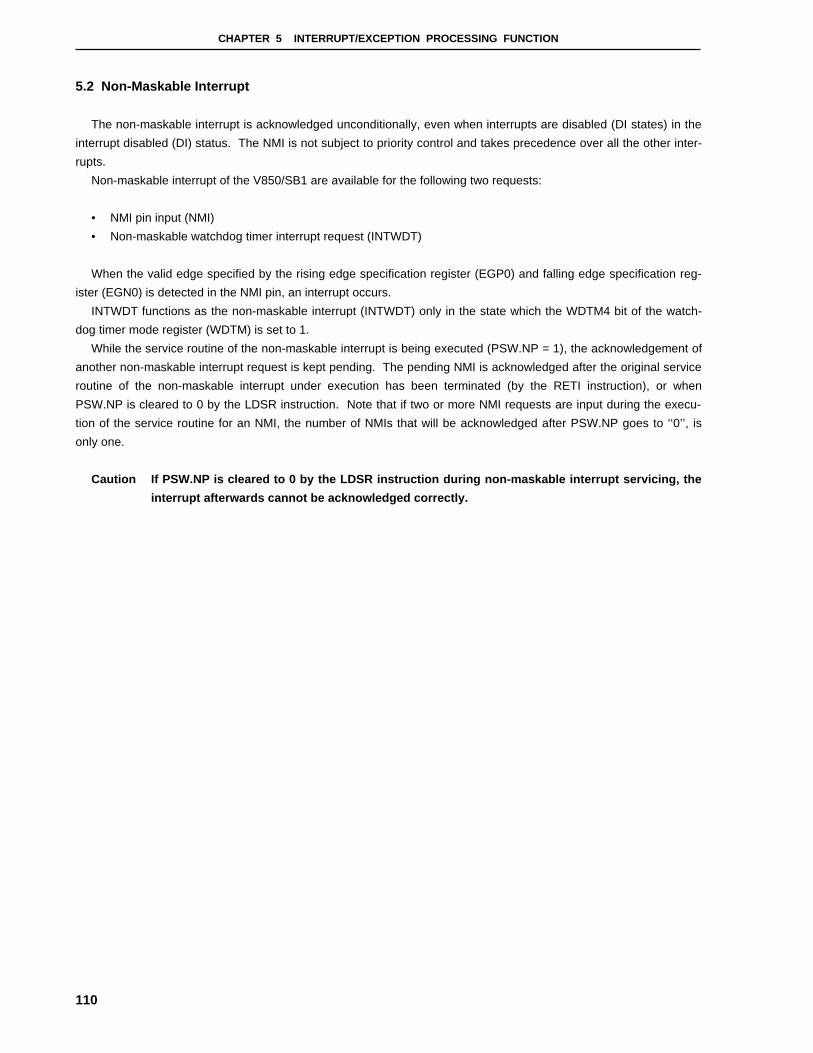
CHAPTER 5 INTERRUPT/EXCEPTION PROCESSING FUNCTION
110
5.2 Non-Maskable Interrupt
The non-maskable interrupt is acknowledged unconditionally, even when interrupts are disabled (DI states) in the
interrupt disabled (DI) status. The NMI is not subject to priority control and takes precedence over all the other inter-
rupts.
Non-maskable interrupt of the V850/SB1 are available for the following two requests:
• NMI pin input (NMI)
• Non-maskable watchdog timer interrupt request (INTWDT)
When the valid edge specified by the rising edge specification register (EGP0) and falling edge specification reg-
ister (EGN0) is detected in the NMI pin, an interrupt occurs.
INTWDT functions as the non-maskable interrupt (INTWDT) only in the state which the WDTM4 bit of the watch-
dog timer mode register (WDTM) is set to 1.
While the service routine of the non-maskable interrupt is being executed (PSW.NP = 1), the acknowledgement of
another non-maskable interrupt request is kept pending. The pending NMI is acknowledged after the original service
routine of the non-maskable interrupt under execution has been terminated (by the RETI instruction), or when
PSW.NP is cleared to 0 by the LDSR instruction. Note that if two or more NMI requests are input during the execu-
tion of the service routine for an NMI, the number of NMIs that will be acknowledged after PSW.NP goes to ‘‘0’’, is
only one.
Caution If PSW.NP is cleared to 0 by the LDSR instruction during non-maskable interrupt servicing, the
interrupt afterwards cannot be acknowledged correctly.
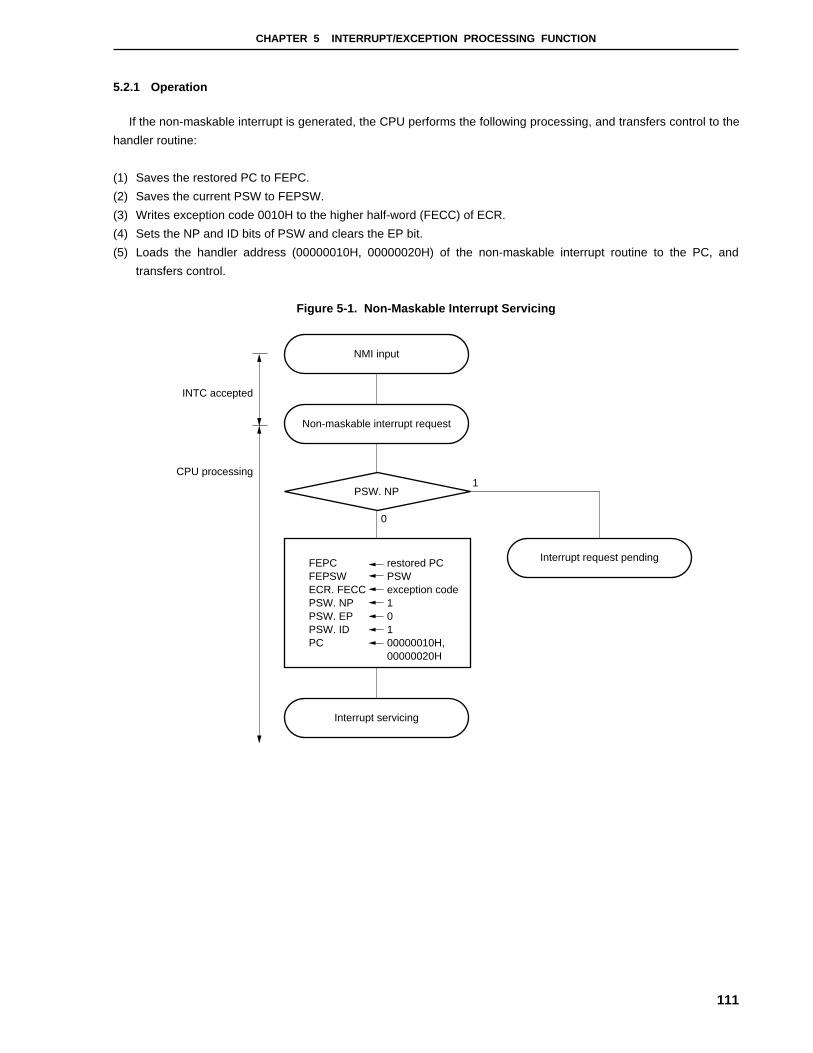
CHAPTER 5 INTERRUPT/EXCEPTION PROCESSING FUNCTION
111
5.2.1 Operation
If the non-maskable interrupt is generated, the CPU performs the following processing, and transfers control to the
handler routine:
(1) Saves the restored PC to FEPC.
(2) Saves the current PSW to FEPSW.
(3) Writes exception code 0010H to the higher half-word (FECC) of ECR.
(4) Sets the NP and ID bits of PSW and clears the EP bit.
(5) Loads the handler address (00000010H, 00000020H) of the non-maskable interrupt routine to the PC, and
transfers control.
Figure 5-1. Non-Maskable Interrupt Servicing
NMI input
Non-maskable interrupt request
Interrupt servicing
Interrupt request pendingFEPCFEPSWECR. FECCPSW. NPPSW. EPPSW. IDPC
restored PCPSWexception code10100000010H,00000020H
INTC accepted
CPU processing
PSW. NP1
0
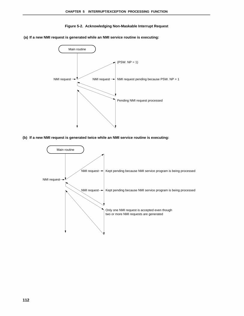
CHAPTER 5 INTERRUPT/EXCEPTION PROCESSING FUNCTION
112
Figure 5-2. Acknowledging Non-Maskable Interrupt Request
(a) If a new NMI request is generated while an NMI service routine is executing:
Main routine
NMI request NMI request
(PSW. NP = 1)
NMI request pending because PSW. NP = 1
Pending NMI request processed
(b) If a new NMI request is generated twice while an NMI service routine is executing:
Main routine
NMI request
NMI request Kept pending because NMI service program is being processed
Kept pending because NMI service program is being processedNMI request
Only one NMI request is accepted even though two or more NMI requests are generated

CHAPTER 5 INTERRUPT/EXCEPTION PROCESSING FUNCTION
113
5.2.2 Restore
Execution is restored from the non-maskable interrupt service by the RETI instruction.
Operation of RETI instruction
When the RETI instruction is executed, the CPU performs the following processing, and transfers control to the
address of the restored PC.
(1) Restores the values of PC and PSW from FEPC and FEPSW, respectively, because the EP bit of PSW is 0
and the NP bit of PSW is 1.
(2) Transfers control back to the address of the restored PC and PSW.
Figure 5-3 illustrates how the RETI instruction is processed.
Figure 5-3. RETI Instruction Processing
PSW.EP
RETI instruction
PCPSW
EIPCEIPSW
PSW.NP
Original processing restored
PCPSW
FEPCFEPSW
1
1
0
0
Caution When the PSW.EP bit and PSW.NP bit are changed by the LDSR instruction during the non-
maskable interrupt service, in order to restore the PC and PSW correctly during recovery by the
RETI instruction, it is necessary to set PSW.EP back to 0 and PSW.NP back to 1 using the LDSR
instruction immediately before the RETI instruction.
Remark The solid line shows the CPU processing flow.
CHAPTER 5 INTERRUPT/EXCEPTION PROCESSING FUNCTION
114
5.2.3 NP flag
The NP flag is a status flag that indicates that non-maskable interrupt (NMI) servicing is under execution. This flag
is set when the NMI interrupt request has been acknowledged, and masks all interrupt requests to prohibit multiple
interrupts from being acknowledged.
After reset: 00000020H
Symbol 31 8 7 6 5 4 3 2 1 0
PSW 0 NP EP ID SAT CY OV S Z
NP NMI Servicing State
0 No NMI interrupt servicing
1 NMI interrupt currently servicing
5.2.4 Noise elimination circuit of NMI pin
NMI pin noise is eliminated by the noise elimination circuit with analog delay. Therefore, a signal input to the NMI
pin is not detected as an edge, unless it maintains its input level for a certain period. The edge is detected after a
certain period has elapsed.
NMI pin is used for canceling the software stop mode. In the software stop mode, noise elimination does not use
system clock for noise elimination because the internal system clock is stopped.
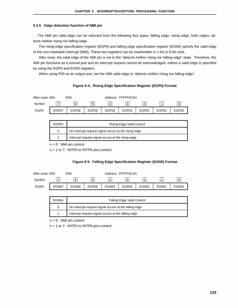
CHAPTER 5 INTERRUPT/EXCEPTION PROCESSING FUNCTION
115
5.2.5 Edge detection function of NMI pin
The NMI pin valid edge can be selected from the following four types: falling edge, rising edge, both edges, de-
tects neither rising nor falling edge.
The rising edge specification register (EGP0) and falling edge specification register (EGN0) specify the valid edge
of the non-maskable interrupt (NMI). These two registers can be read/written in 1-bit or 8-bit units.
After reset, the valid edge of the NMI pin is set to the “detects neither rising nor falling edge” state. Therefore, the
NMI pin functions as a normal port and an interrupt request cannot be acknowledged, unless a valid edge is specified
by using the EGP0 and EGN0 registers.
When using P00 as an output port, set the NMI valid edge to “detects neither rising nor falling edge”.
Figure 5-4. Rising Edge Specification Register (EGP0) Format
After reset: 00H R/W Address: FFFFF0C0H
Symbol 7 6 5 4 3 2 1 0
EGP0 EGP07 EGP06 EGP05 EGP04 EGP03 EGP02 EGP01 EGP00
EGP0n Rising Edge Valid Control
0 No interrupt request signal occurs at the rising edge
1 Interrupt request signal occurs at the rising edge
n = 0: NMI pin control
n = 1 to 7: INTP0 to INTP6 pins control
Figure 5-5. Falling Edge Specification Register (EGN0) Format
After reset: 00H R/W Address: FFFFF0C2H
Symbol 7 6 5 4 3 2 1 0
EGN0 EGN07 EGN06 EGN05 EGN04 EGN03 EGN02 EGN01 EGN00
EGN0n Falling Edge Valid Control
0 No interrupt request signal occurs at the falling edge
1 Interrupt request signal occurs at the falling edge
n = 0: NMI pin control
n = 1 to 7: INTP0 to INTP6 pins control
CHAPTER 5 INTERRUPT/EXCEPTION PROCESSING FUNCTION
116
5.3 Maskable Interrupts
Maskable interrupt requests can be masked by interrupt control registers. The V850/SB1 has 37 maskable inter-
rupt sources for the µPD703033, 70F3033 and 38 maskable interrupt sources for the µPD703033Y, 70F3033Y.
If two or more maskable interrupt requests are generated at the same time, they are acknowledged according to
the default priority. In addition to the default priority, eight levels of priorities can be specified by using the interrupt
control registers, allowing programmable priority control.
When an interrupt request has been acknowledged, the acknowledgement of other maskable interrupts is disabled
and the interrupt disabled (DI) status is set.
When the EI instruction is executed in an interrupt servicing routine, the interrupt enabled (EI) status is set which
enables interrupts having a higher priority to immediately interrupt the current service routine in progress. Note that
only interrupts with a higher priority will have this capability; interrupts with the same priority level cannot be nested.
To use multiple interrupts, it is necessary to save EIPC and EIPSW to memory or a register before executing the
EI instruction, and restore EIPC and EIPSW to the original values by executing the DI instruction before the RETI
instruction.
When the WDTM4 bit of the watchdog timer mode register (WDTM) is set to 0, the watchdog timer overflow inter-
rupt functions as a maskable interrupt (INTWDTM).
5.3.1 Operation
If a maskable interrupt occurs, the CPU performs the following processing, and transfers control to a handler rou-
tine:
(1) Saves the restored PC to EIPC.
(2) Saves the current PSW to EIPSW.
(3) Writes an exception code to the lower half-word of ECR (EICC).
(4) Sets the ID bit of PSW and clears the EP bit.
(5) Loads the corresponding handler address to the PC, and transfers control.
The INT input masked by INTC and the INT input that occurs during the other interrupt servicing (when PSW.NP =
1 or PSW.ID = 1) are internally pended. When the interrupts are unmasked, or when PSW.NP = 0 and PSW.ID = 0
by using the RETI and LDSR instructions, the pending INT is input to start the new maskable interrupt servicing.
Figure 5-6 illustrates how the maskable interrupts are serviced.
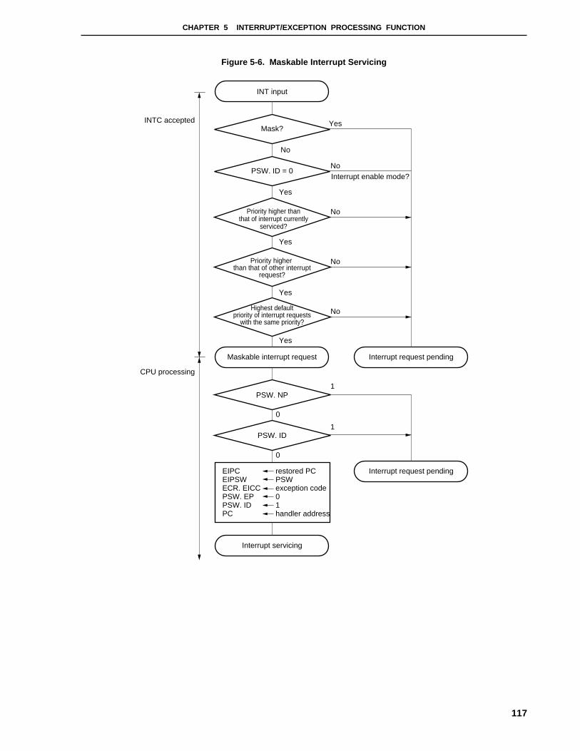
CHAPTER 5 INTERRUPT/EXCEPTION PROCESSING FUNCTION
117
Figure 5-6. Maskable Interrupt Servicing
Maskable interrupt request
Interrupt servicing
EIPCEIPSWECR. EICCPSW. EPPSW. IDPC
INTC accepted
CPU processing
Mask?Yes
No
PSW. ID = 0
Priority higher thanthat of interrupt currently
serviced?
Interrupt request pending
PSW. NP
PSW. ID
Interrupt request pending
No
No
No
No
1
0
1
0
INT input
Yes
Yes
Yes
Yes
Priority higher than that of other interrupt
request?
Highest defaultpriority of interrupt requests
with the same priority?
Interrupt enable mode?
restored PCPSWexception code01handler address
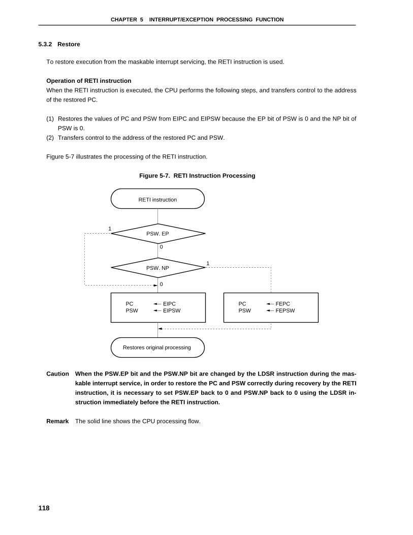
CHAPTER 5 INTERRUPT/EXCEPTION PROCESSING FUNCTION
118
5.3.2 Restore
To restore execution from the maskable interrupt servicing, the RETI instruction is used.
Operation of RETI instruction
When the RETI instruction is executed, the CPU performs the following steps, and transfers control to the address
of the restored PC.
(1) Restores the values of PC and PSW from EIPC and EIPSW because the EP bit of PSW is 0 and the NP bit of
PSW is 0.
(2) Transfers control to the address of the restored PC and PSW.
Figure 5-7 illustrates the processing of the RETI instruction.
Figure 5-7. RETI Instruction Processing
RETI instruction
Restores original processing
PCPSW
EIPCEIPSW
PSW. EP1
0
1
0
PCPSW
FEPCFEPSW
PSW. NP
Caution When the PSW.EP bit and the PSW.NP bit are changed by the LDSR instruction during the mas-
kable interrupt service, in order to restore the PC and PSW correctly during recovery by the RETI
instruction, it is necessary to set PSW.EP back to 0 and PSW.NP back to 0 using the LDSR in-
struction immediately before the RETI instruction.
Remark The solid line shows the CPU processing flow.
CHAPTER 5 INTERRUPT/EXCEPTION PROCESSING FUNCTION
119
5.3.3 Priorities of maskable interrupts
The V850/SB1 provides multiple interrupt service that acknowledges an interrupt while servicing another interrupt.
Multiple interrupts can be controlled by priority levels.
There are two types of priority level control: control based on the default priority levels, and control based on the
programmable priority levels which are specified by interrupt priority level specification bit (xxPRn). When two or
more interrupts having the same priority level specified by xxPRn are generated at the same time, interrupts are
serviced in order depending on the priority level allocated to each interrupt request types (default priority level) be-
forehand. For more information, refer to Table 5-1. The programmable priority control customizes interrupt requests
into eight levels by setting the priority level specification flag.
Note that when an interrupt request is acknowledged, the ID flag of PSW is automatically set to ‘‘1’’. Therefore,
when multiple interrupts are to be used, clear the ID flag to ‘‘0’’ beforehand (for example, by placing the EI instruction
into the interrupt service program) to set the interrupt enable mode.
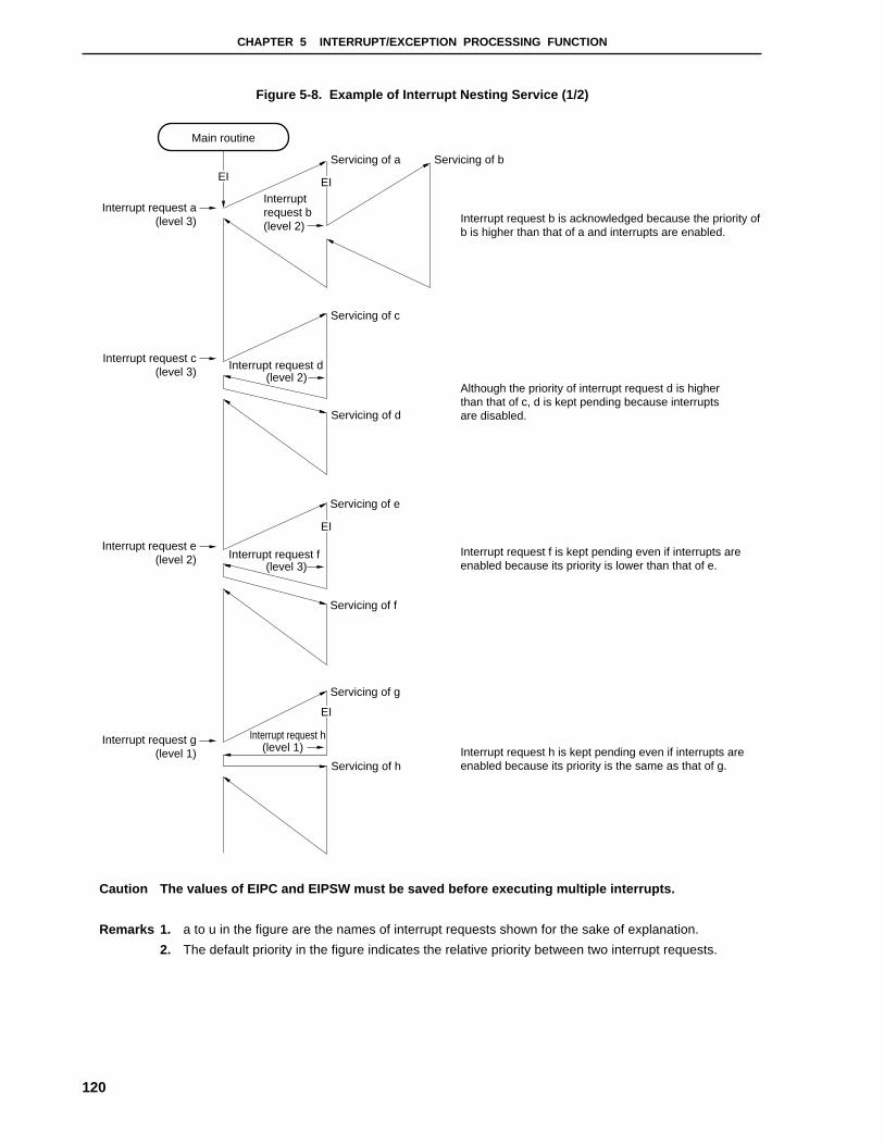
CHAPTER 5 INTERRUPT/EXCEPTION PROCESSING FUNCTION
120
Figure 5-8. Example of Interrupt Nesting Service (1/2)
Main routine
EI EI
Interrupt request a(level 3)
Servicing of a Servicing of b
Interruptrequest b(level 2)
Servicing of c
Interrupt request c(level 3)
Interrupt request d(level 2)
Servicing of d
Servicing of e
EI
Interrupt request e(level 2) Interrupt request f
(level 3)
Servicing of f
EI
Servicing of g
Interrupt request g(level 1)
Interrupt request h(level 1)
Servicing of hInterrupt request h is kept pending even if interrupts areenabled because its priority is the same as that of g.
Interrupt request f is kept pending even if interrupts areenabled because its priority is lower than that of e.
Interrupt request b is acknowledged because the priority ofb is higher than that of a and interrupts are enabled.
Although the priority of interrupt request d is higherthan that of c, d is kept pending because interruptsare disabled.
Caution The values of EIPC and EIPSW must be saved before executing multiple interrupts.
Remarks 1. a to u in the figure are the names of interrupt requests shown for the sake of explanation.
2. The default priority in the figure indicates the relative priority between two interrupt requests.

CHAPTER 5 INTERRUPT/EXCEPTION PROCESSING FUNCTION
121
Figure 5-8. Example of Interrupt Nesting Process (2/2)
Main routine
EI
Interrupt request i(level 2)
Servicing of iProcessing of k
Interruptrequest j(level 3)
Servicing of j
Interrupt request l(level 2)
EIEI
EIEI
Interrupt request o(level 3)
Interrupt request s(level 1)
Interrupt request k (level 1)
Servicing of l
Servicing of n
Servicing of m
Servicing of s
Servicing of u
Servicing of t
Interruptrequest m
(level 3) Interrupt request n (level 1)
Servicing of o
Interruptrequest p
(level 2)Interrupt
request q(level 1)
Interruptrequest r(level 0)
Interrupt request u (level 2) Note 2
Interrupt request t(level 2) Note 1
Servicing of pServicing of q
Servicing of r
EI
If levels 3 to 0 are acknowledged
Interrupt request j is kept pending because its priority is lower than that of i. k that occurs after j is acknowledged because it has the higher priority.
Interrupt requests m and n are kept pending because servicing of l is performed in the interrupt disabled status.
Pending interrupt requests are acknowledged after servicing of interrupt request l.At this time, interrupt requests n is acknowledged first even though m has occurred first because the priority of n is higher than that of m.
Pending interrupt requests t and u are acknowledged after processing of s.Because the priorities of t and u are the same, u is acknowledged first because it has the higher default priority, regardless of the order in which the interrupt requests have been generated.
Notes 1. Lower default priority
2. Higher default priority
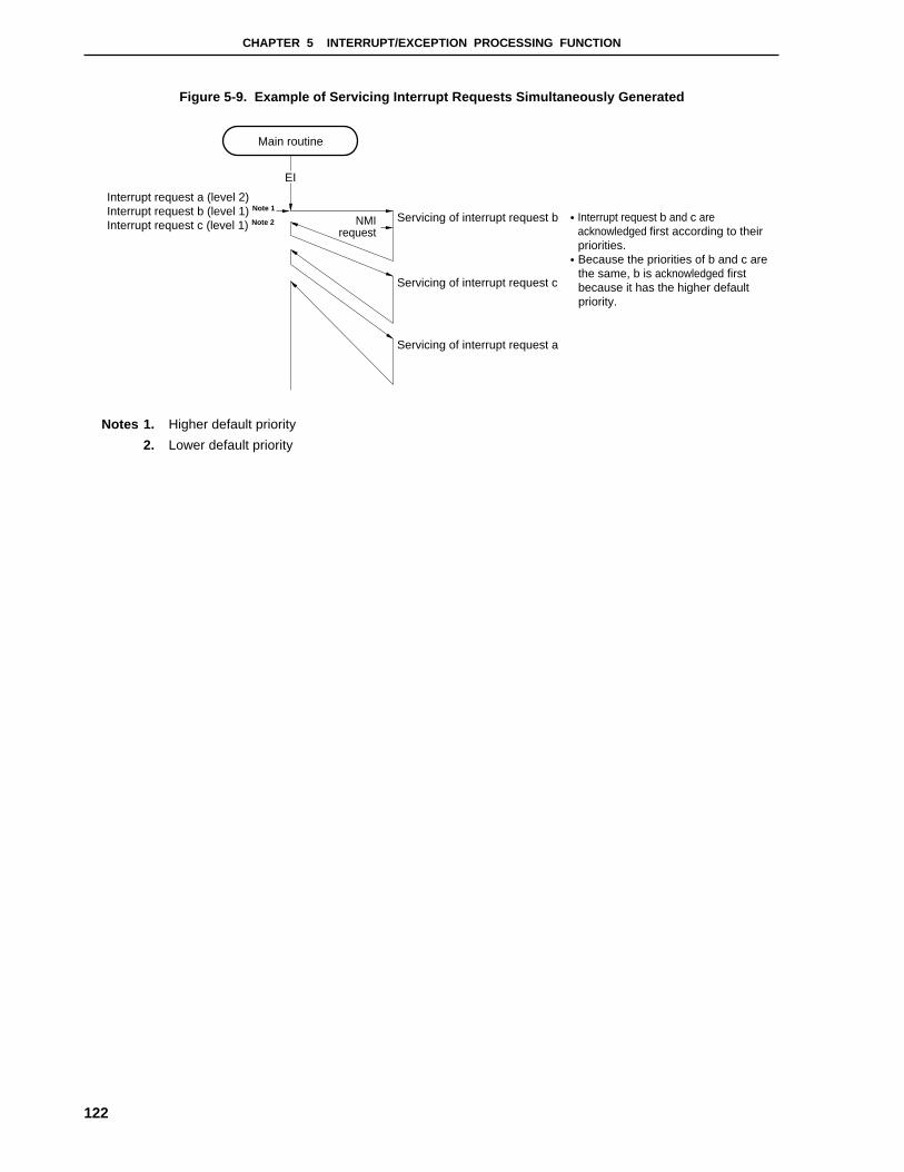
CHAPTER 5 INTERRUPT/EXCEPTION PROCESSING FUNCTION
122
Figure 5-9. Example of Servicing Interrupt Requests Simultaneously Generated
Main routine
EI
Interrupt request a (level 2)Interrupt request b (level 1) Note 1
Interrupt request c (level 1) Note 2 Servicing of interrupt request b •
•
Servicing of interrupt request c
Servicing of interrupt request a
Interrupt request b and c are acknowledged first according to their priorities.Because the priorities of b and c are the same, b is acknowledged first because it has the higher default priority.
NMIrequest
Notes 1. Higher default priority
2. Lower default priority
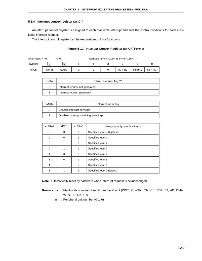
CHAPTER 5 INTERRUPT/EXCEPTION PROCESSING FUNCTION
123
5.3.4 Interrupt control register (xxICn)
An interrupt control register is assigned to each maskable interrupt and sets the control conditions for each mas-
kable interrupt request.
The interrupt control register can be read/written in 8- or 1-bit units.
Figure 5-10. Interrupt Control Register (xxICn) Format
After reset: 47H R/W Address: FFFFF100H to FFFFF156H
Symbol 7 6 5 4 3 2 1 0
xxICn xxIFn xxMKn 0 0 0 xxPRn2 xxPRn1 xxPRn0
xxIFn Interrupt request flag Note
0 Interrupt request not generated
1 Interrupt request generated
xxMKn Interrupt mask flag
0 Enables interrupt servicing
1 Disables interrupt servicing (pending)
xxPRn2 xxPRn1 xxPRn0 Interrupt priority specification bit
0 0 0 Specifies level 0 (highest)
0 0 1 Specifies level 1
0 1 0 Specifies level 2
0 1 1 Specifies level 3
1 0 0 Specifies level 4
1 0 1 Specifies level 5
1 1 0 Specifies level 6
1 1 1 Specifies level 7 (lowest)
Note Automatically reset by hardware when interrupt request is acknowledged.
Remark xx : Identification name of each peripheral unit (WDT, P, WTNI, TM, CS, SER, ST, AD, DMA,
WTN, IIC, C2, KR)
n : Peripheral unit number (0 to 6)

CHAPTER 5 INTERRUPT/EXCEPTION PROCESSING FUNCTION
124
Address and bit of each interrupt control register is as follows:
BitAddress Register
7 6 5 4 3 2 1 0
FFFFF100H WDTIC WDTIF WDTMK 0 0 0 WDTPR2 WDTPR1 WDTPR0
FFFFF102H PIC0 PIF0 PMK0 0 0 0 PPR02 PPR01 PPR00
FFFFF104H PIC1 PIF1 PMK1 0 0 0 PPR12 PPR11 PPR10
FFFFF106H PIC2 PIF2 PMK2 0 0 0 PPR22 PPR21 PPR20
FFFFF108H PIC3 PIF3 PMK3 0 0 0 PPR32 PPR31 PPR30
FFFFF10AH PIC4 PIF4 PMK4 0 0 0 PPR42 PPR41 PPR40
FFFFF10CH PIC5 PIF5 PMK5 0 0 0 PPR52 PPR51 PPR50
FFFFF10EH PIC6 PIF6 PMK6 0 0 0 PPR62 PPR61 PPR60
FFFFF118H WTNIIC WTNIIF WTNIMK 0 0 0 WTNIPR2 WTNIPR1 WTNIPR0
FFFFF11AH TMIC00 TMIF00 TMMK00 0 0 0 TMPR002 TMPR001 TMPR000
FFFFF11CH TMIC01 TMIF01 TMMK01 0 0 0 TMPR012 TMPR011 TMPR010
FFFFF11EH TMIC10 TMIF10 TMMK10 0 0 0 TMPR102 TMPR101 TMPR100
FFFFF120H TMIC11 TMIF11 TMMK11 0 0 0 TMPR112 TMPR111 TMPR110
FFFFF122H TMIC2 TMIF2 TMMK2 0 0 0 TMPR22 TMPR21 TMPR20
FFFFF124H TMIC3 TMIF3 TMMK3 0 0 0 TMPR32 TMPR31 TMPR30
FFFFF126H TMIC4 TMIF4 TMMK4 0 0 0 TMPR42 TMPR41 TMPR40
FFFFF128H TMIC5 TMIF5 TMMK5 0 0 0 TMPR52 TMPR51 TMPR50
FFFFF12AH TMIC6 TMIF6 TMMK6 0 0 0 TMPR62 TMPR61 TMPR60
FFFFF12CH TMIC7 TMIF7 TMMK7 0 0 0 TMPR72 TMPR71 TMPR70
FFFFF12EH CSIC0 CSIF0 CSMK0 0 0 0 CSPR02 CSPR01 CSPR00
FFFFF130H SERIC0 SERIF0 SERMK0 0 0 0 SERPR02 SERPR01 SERPR00
FFFFF132H CSIC1 CSIF1 CSMK1 0 0 0 CSPR12 CSPR11 CSPR10
FFFFF134H STIC0 STIF0 STMK0 0 0 0 STPR02 STPR01 STPR00
FFFFF136H CSIC2 CSIF2 CSMK2 0 0 0 CSPR22 CSPR21 CSPR20
FFFFF138H IICIC1 Note IICIF1 IICMK1 0 0 0 IICPR12 IICPR11 IICPR10
FFFFF13AH SERIC1 SERIF1 SERMK1 0 0 0 SERPR12 SERPR11 SERPR10
FFFFF13CH CSIC3 CSIF3 CSMK3 0 0 0 CSPR32 CSPR31 CSPR30
FFFFF13EH STIC1 STIF1 STMK1 0 0 0 STPR12 STPR11 STPR10
FFFFF140H CSIC4 CSIF4 CSMK4 0 0 0 CSPR42 CSPR41 CSPR40
FFFFF146H ADIC ADIF ADMK 0 0 0 ADPR2 ADPR1 ADPR0
FFFFF148H DMAIC0 DMAIF0 DMAMK0 0 0 0 DMAPR02 DMAPR01 DMAPR00
FFFFF14AH DMAIC1 DMAIF1 DMAMK1 0 0 0 DMAPR12 DMAPR11 DMAPR10
FFFFF14CH DMAIC2 DMAIF2 DMAMK2 0 0 0 DMAPR22 DMAPR21 DMAPR20
FFFFF14EH DMAIC3 DMAIF3 DMAMK3 0 0 0 DMAPR32 DMAPR31 DMAPR30
FFFFF150H DMAIC4 DMAIF4 DMAMK4 0 0 0 DMAPR42 DMAPR41 DMAPR40
FFFFF152H DMAIC5 DMAIF5 DMAMK5 0 0 0 DMAPR52 DMAPR51 DMAPR50
FFFFF154H WTNIC WTNIF WTNMK 0 0 0 WTNPR2 WTNPR1 WTNPR0
FFFFF156H KRIC KRIF KRMK 0 0 0 KRPR2 KRPR1 KRPR0
Note Available only for the µPD703033Y and 70F3033Y.
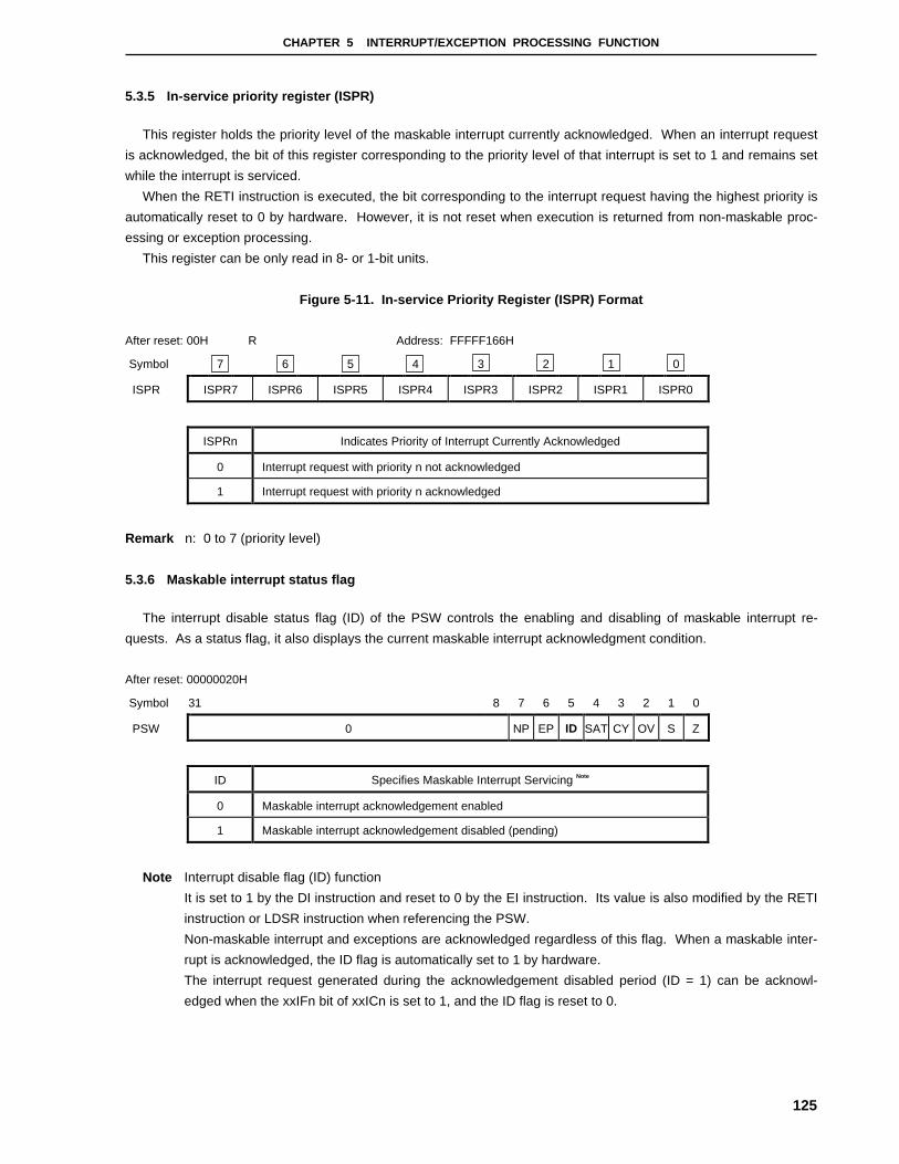
CHAPTER 5 INTERRUPT/EXCEPTION PROCESSING FUNCTION
125
5.3.5 In-service priority register (ISPR)
This register holds the priority level of the maskable interrupt currently acknowledged. When an interrupt request
is acknowledged, the bit of this register corresponding to the priority level of that interrupt is set to 1 and remains set
while the interrupt is serviced.
When the RETI instruction is executed, the bit corresponding to the interrupt request having the highest priority is
automatically reset to 0 by hardware. However, it is not reset when execution is returned from non-maskable proc-
essing or exception processing.
This register can be only read in 8- or 1-bit units.
Figure 5-11. In-service Priority Register (ISPR) Format
After reset: 00H R Address: FFFFF166H
Symbol 7 6 5 4 3 2 1 0
ISPR ISPR7 ISPR6 ISPR5 ISPR4 ISPR3 ISPR2 ISPR1 ISPR0
ISPRn Indicates Priority of Interrupt Currently Acknowledged
0 Interrupt request with priority n not acknowledged
1 Interrupt request with priority n acknowledged
Remark n: 0 to 7 (priority level)
5.3.6 Maskable interrupt status flag
The interrupt disable status flag (ID) of the PSW controls the enabling and disabling of maskable interrupt re-
quests. As a status flag, it also displays the current maskable interrupt acknowledgment condition.
After reset: 00000020H
Symbol 31 8 7 6 5 4 3 2 1 0
PSW 0 NP EP ID SAT CY OV S Z
ID Specifies Maskable Interrupt Servicing Note
0 Maskable interrupt acknowledgement enabled
1 Maskable interrupt acknowledgement disabled (pending)
Note Interrupt disable flag (ID) function
It is set to 1 by the DI instruction and reset to 0 by the EI instruction. Its value is also modified by the RETI
instruction or LDSR instruction when referencing the PSW.
Non-maskable interrupt and exceptions are acknowledged regardless of this flag. When a maskable inter-
rupt is acknowledged, the ID flag is automatically set to 1 by hardware.
The interrupt request generated during the acknowledgement disabled period (ID = 1) can be acknowl-
edged when the xxIFn bit of xxICn is set to 1, and the ID flag is reset to 0.

CHAPTER 5 INTERRUPT/EXCEPTION PROCESSING FUNCTION
126
5.3.7 Watchdog timer mode register (WDTM)
Read/write is available in 8- or 1-bit units (for details, refer to CHAPTER 9 WATCHDOG TIMER ).
Figure 5-12. Watchdog Timer Mode Register (WDTM) Format
After reset: 00H R/W Address: FFFFF384H
Symbol 7 6 5 4 3 2 1 0
WDTM RUN 0 0 WDTM4 0 0 0 0
RUN Watchdog Timer Operation Control
0 Count operation stop
1 Count start after clearing
WDTM4 Timer Mode Selection/Interrupt Control by WDT
0 Interval timer mode
1 WDT mode
Caution If 1 is set to RUN or WDTM4 bit, no operation other than the reset input is available for clearing
this register.
5.3.8 Noise elimination
(1) Noise elimination of INTP0 to INTP3 pins
INTP0 to INTP3 pins incorporate the noise elimination circuit that functions via an analog delay. Therefore, a
signal input to each pin is not detected as an edge, unless it maintains its input level for a certain period.
An edge is detected after a certain period has elapsed.
(2) Noise elimination of INTP4 and INTP5 pins
INTP4 and INTP5 pins incorporate the digital noise elimination circuit. If an input level of the INTP pin is detected
with the sampling clock (fxx) and the same level is not detected three successive times, the input pulse is elimi-
nated as a noise. Note the followings:
• In the case that the input pulse width is between 2 and 3 clocks, whether the input pulse is detected as a
valid edge or eliminated as a noise is indefinite.
• To securely detect the level as a pulse, the same level input of 3 clocks or more is required.
• When a noise is generated in synchronization with a sampling clock, this may not be recognized as a noise.
In this case, eliminate the noise by adding a filter to the input pin.
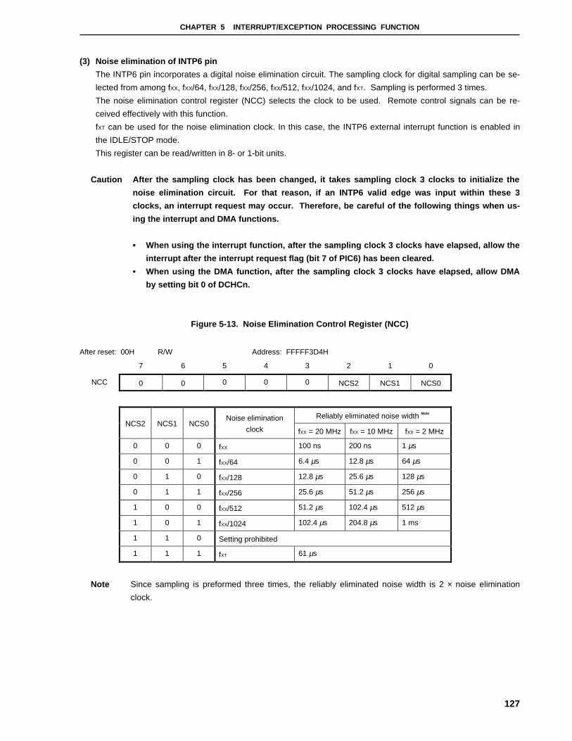
CHAPTER 5 INTERRUPT/EXCEPTION PROCESSING FUNCTION
127
(3) Noise elimination of INTP6 pin
The INTP6 pin incorporates a digital noise elimination circuit. The sampling clock for digital sampling can be se-
lected from among fXX, fXX/64, fXX/128, fXX/256, fXX/512, fXX/1024, and fXT. Sampling is performed 3 times.
The noise elimination control register (NCC) selects the clock to be used. Remote control signals can be re-
ceived effectively with this function.
fXT can be used for the noise elimination clock. In this case, the INTP6 external interrupt function is enabled in
the IDLE/STOP mode.
This register can be read/written in 8- or 1-bit units.
Caution After the sampling clock has been changed, it takes sampling clock 3 clocks to initialize the
noise elimination circuit. For that reason, if an INTP6 valid edge was input within these 3
clocks, an interrupt request may occur. Therefore, be careful of the following things when us-
ing the interrupt and DMA functions.
• When using the interrupt function, after the sampling clock 3 clocks have elapsed, allow the
interrupt after the interrupt request flag (bit 7 of PIC6) has been cleared.
• When using the DMA function, after the sampling clock 3 clocks have elapsed, allow DMA
by setting bit 0 of DCHCn.
Figure 5-13. Noise Elimination Control Register (NCC)
After reset: 00H R/W Address: FFFFF3D4H
7 6 5 4 3 2 1 0
NCC 0 0 0 0 0 NCS2 NCS1 NCS0
Reliably eliminated noise width Note
NCS2 NCS1 NCS0Noise elimination
clock fXX = 20 MHz fXX = 10 MHz fXX = 2 MHz
0 0 0 fXX 100 ns 200 ns 1 µs
0 0 1 fXX/64 6.4 µs 12.8 µs 64 µs
0 1 0 fXX/128 12.8 µs 25.6 µs 128 µs
0 1 1 fXX/256 25.6 µs 51.2 µs 256 µs
1 0 0 fXX/512 51.2 µs 102.4 µs 512 µs
1 0 1 fXX/1024 102.4 µs 204.8 µs 1 ms
1 1 0 Setting prohibited
1 1 1 fXT 61 µs
Note Since sampling is preformed three times, the reliably eliminated noise width is 2 × noise elimination
clock.
CHAPTER 5 INTERRUPT/EXCEPTION PROCESSING FUNCTION
128
5.3.9 Edge detection function
Valid edges of the INTP0 to INTP6 pins can be selected for each pin from the following four types.
• Rising edge
• Falling edge
• Both rising and falling edges
• Detects neither rising nor falling edge
The validity of the rising edge is controlled by the rising edge specification register (EGP0), and the validity of the
falling edge is controlled by the falling edge specification register (EGN0). Refer to Figures 5-4 and 5-5 for details of
EGP0 and EGN0.
After reset, the valid edge of the NMI pin is set to the “detects neither rising nor falling edge” state. Therefore, the
NMI pin functions as a normal port and an interrupt request cannot be acknowledged, unless a valid edge is specified
by using the EGP0 and EGN0 registers.
When using P01 to P07 as output ports, set valid edges of INTP0 to INTP6 to “detects neither rising nor falling
edge” or mask the interrupt request.

CHAPTER 5 INTERRUPT/EXCEPTION PROCESSING FUNCTION
129
5.4 Software Exception
A software exception is generated when the CPU executes the TRAP instruction, and can be always accepted.
• TRAP instruction format: TRAP vector (where vector is 0 to 1FH)
For details of the instruction function, refer to the V850 Family User’s Manual Architecture.
5.4.1 Operation
If a software exception occurs, the CPU performs the following processing, and transfers control to the handler
routine:
(1) Saves the restored PC to EIPC.
(2) Saves the current PSW to EIPSW.
(3) Writes an exception code to the lower 16 bits (EICC) of ECR (interrupt source).
(4) Sets the EP and ID bits of PSW.
(5) Loads the handler address (00000040H or 00000050H) of the software exception routine in the PC, and trans-
fers control.
Figure 5-14 illustrates how a software exception is processed.
Figure 5-14. Software Exception Processing
TRAP instruction
EIPCEIPSWECR.EICCPSW.EPPSW.IDPC
restored PCPSWexception code11handler address
CPU processing
Exception processingHandler address: 00000040H (Vector = 0nH) 00000050H (Vector = 1nH)

CHAPTER 5 INTERRUPT/EXCEPTION PROCESSING FUNCTION
130
5.4.2 Restore
To restore or return execution from the software exception service routine, the RETI instruction is used.
Operation of RETI instruction
When the RETI instruction is executed, the CPU performs the following steps, and transfers control to the address
of the restored PC.
(1) Restores the restored PC and PSW from EIPC and EIPSW because the EP bit of PSW is 1.
(2) Transfers control to the address of the restored PC and PSW.
Figure 5-15 illustrates the processing of the RETI instruction.
Figure 5-15. RETI Instruction Processing
PSW.EP
RETI instruction
PCPSW
EIPCEIPSW
PSW.NP
Original processing restored
PCPSW
FEPCFEPSW
1
1
0
0
Caution When the PSW.EP bit and the PSW.NP bit are changed by the LDSR instruction during the soft-
ware exception process, in order to restore the PC and PSW correctly during recovery by the
RETI instruction, it is necessary to set PSW.EP back to 1 using the LDSR instruction immedi-
ately before the RETI instruction.
Remark The solid line shows the CPU processing flow.

CHAPTER 5 INTERRUPT/EXCEPTION PROCESSING FUNCTION
131
5.4.3 EP flag
The EP flag in PSW is a status flag used to indicate that exception processing is in progress. It is set when on ex-
ception occurs, and the interrupt is disabled.
After reset: 00000020H
Symbol 31 8 7 6 5 4 3 2 1 0
PSW 0 NP EP ID SAT CY OV S Z
EP Exception Processing
0 Exception processing is not in progress
1 Exception processing is in progress
5.5 Exception Trap
The exception trap is an interrupt that is requested when illegal execution of an instruction takes place. In the
V850/SB1, an illegal op code exception (ILGOP: ILeGal OPcode trap) is considered as an exception trap.
• Illegal op code exception: occurs if the sub op code field of an instruction to be executed next is not a valid op
code.
5.5.1 Illegal op code definition
An illegal op code is defined to be a 32-bit word with bits 5 to 10 being 111111B and bits 23 to 26 being 0011B to
1111B.
15 161723 22
x
21
x
20
x x x x xxxxxxxxxxx111111xxxxx
27 263104510111213
1
1
1
1
0 to
1
0
1
x : don’t care
5.5.2 Operation
If an exception trap occurs, the CPU performs the following processing, and transfers control to the handler rou-
tine:
(1) Saves the restored PC to EIPC.
(2) Saves the current PSW to EIPSW.
(3) Writes an exception code (0060H) to the lower 16 bits (EICC) of ECR.
(4) Sets the EP and ID bits of PSW.
(5) Loads the handler address (00000060H) for the exception trap routine to the PC, and transfers control.
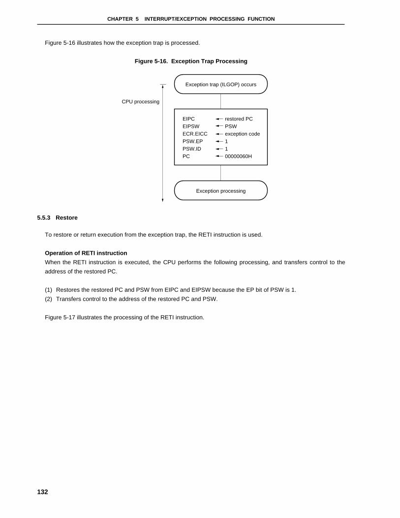
CHAPTER 5 INTERRUPT/EXCEPTION PROCESSING FUNCTION
132
Figure 5-16 illustrates how the exception trap is processed.
Figure 5-16. Exception Trap Processing
Exception trap (ILGOP) occurs
EIPCEIPSWECR.EICCPSW.EPPSW.IDPC
restored PCPSWexception code1100000060H
CPU processing
Exception processing
5.5.3 Restore
To restore or return execution from the exception trap, the RETI instruction is used.
Operation of RETI instruction
When the RETI instruction is executed, the CPU performs the following processing, and transfers control to the
address of the restored PC.
(1) Restores the restored PC and PSW from EIPC and EIPSW because the EP bit of PSW is 1.
(2) Transfers control to the address of the restored PC and PSW.
Figure 5-17 illustrates the processing of the RETI instruction.

CHAPTER 5 INTERRUPT/EXCEPTION PROCESSING FUNCTION
133
Figure 5-17. RETI Instruction Processing
RETI instruction
Jump to PC
PCPSW
EIPCEIPSW
PSW. EP1
0
1
0
PCPSW
FEPCFEPSW
PSW. NP
Caution When the PSW.EP bit and the PSW.NP bit are changed by the LDSR instruction during the ex-
ception trap process, in order to restore the PC and PSW correctly during recovery by the RETI
instruction, it is necessary to set PSW.EP back to 1 using the LDSR instruction immediately be-
fore the RETI instruction.
Remark The solid line shows the CPU processing flow.
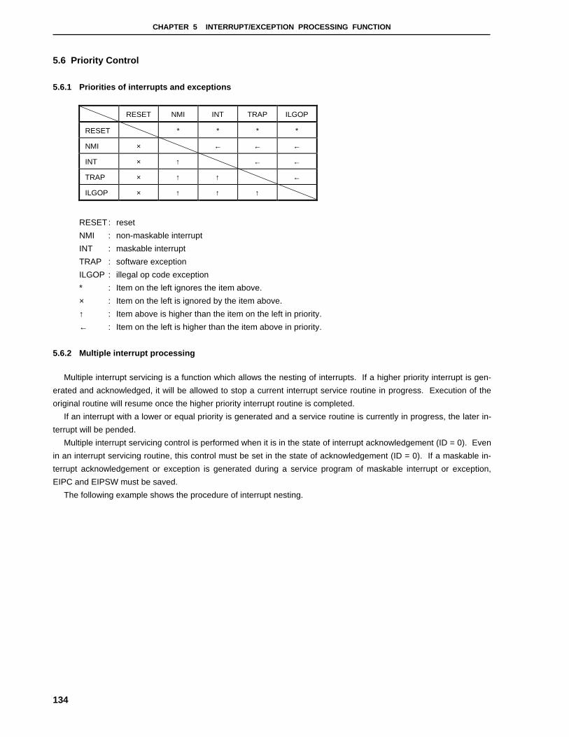
CHAPTER 5 INTERRUPT/EXCEPTION PROCESSING FUNCTION
134
5.6 Priority Control
5.6.1 Priorities of interrupts and exceptions
RESET NMI INT TRAP ILGOP
RESET * * * *
NMI × ← ← ←
INT × ↑ ← ←
TRAP × ↑ ↑ ←
ILGOP × ↑ ↑ ↑
RESET: reset
NMI : non-maskable interrupt
INT : maskable interrupt
TRAP : software exception
ILGOP : illegal op code exception
* : Item on the left ignores the item above.
× : Item on the left is ignored by the item above.
↑ : Item above is higher than the item on the left in priority.
← : Item on the left is higher than the item above in priority.
5.6.2 Multiple interrupt processing
Multiple interrupt servicing is a function which allows the nesting of interrupts. If a higher priority interrupt is gen-
erated and acknowledged, it will be allowed to stop a current interrupt service routine in progress. Execution of the
original routine will resume once the higher priority interrupt routine is completed.
If an interrupt with a lower or equal priority is generated and a service routine is currently in progress, the later in-
terrupt will be pended.
Multiple interrupt servicing control is performed when it is in the state of interrupt acknowledgement (ID = 0). Even
in an interrupt servicing routine, this control must be set in the state of acknowledgement (ID = 0). If a maskable in-
terrupt acknowledgement or exception is generated during a service program of maskable interrupt or exception,
EIPC and EIPSW must be saved.
The following example shows the procedure of interrupt nesting.
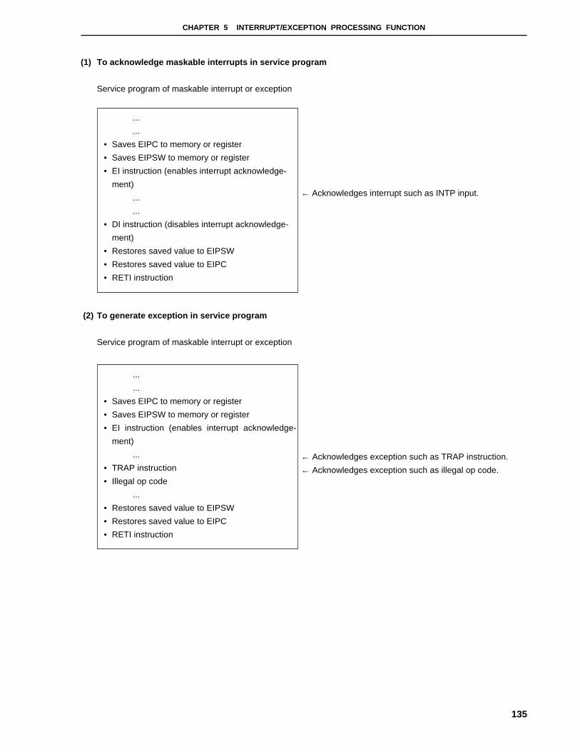
CHAPTER 5 INTERRUPT/EXCEPTION PROCESSING FUNCTION
135
(1) To acknowledge maskable interrupts in service program
Service program of maskable interrupt or exception
(2) To generate exception in service program
Service program of maskable interrupt or exception
...
...
• Saves EIPC to memory or register
• Saves EIPSW to memory or register
• EI instruction (enables interrupt acknowledge-
ment)
...
...
• DI instruction (disables interrupt acknowledge-
ment)
• Restores saved value to EIPSW
• Restores saved value to EIPC
• RETI instruction
...
...
• Saves EIPC to memory or register
• Saves EIPSW to memory or register
• EI instruction (enables interrupt acknowledge-
ment)
...
• TRAP instruction
• Illegal op code
...
• Restores saved value to EIPSW
• Restores saved value to EIPC
• RETI instruction
← Acknowledges interrupt such as INTP input.
← Acknowledges exception such as TRAP instruction.
← Acknowledges exception such as illegal op code.
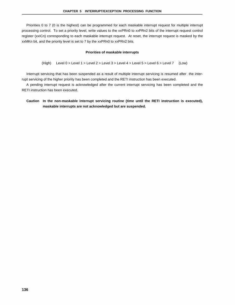
CHAPTER 5 INTERRUPT/EXCEPTION PROCESSING FUNCTION
136
Priorities 0 to 7 (0 is the highest) can be programmed for each maskable interrupt request for multiple interrupt
processing control. To set a priority level, write values to the xxPRn0 to xxPRn2 bits of the interrupt request control
register (xxICn) corresponding to each maskable interrupt request. At reset, the interrupt request is masked by the
xxMKn bit, and the priority level is set to 7 by the xxPRn0 to xxPRn2 bits.
Priorities of maskable interrupts
(High) Level 0 > Level 1 > Level 2 > Level 3 > Level 4 > Level 5 > Level 6 > Level 7 (Low)
Interrupt servicing that has been suspended as a result of multiple interrupt servicing is resumed after the inter-
rupt servicing of the higher priority has been completed and the RETI instruction has been executed.
A pending interrupt request is acknowledged after the current interrupt servicing has been completed and the
RETI instruction has been executed.
Caution In the non-maskable interrupt servicing routine (time until the RETI instruction is executed),
maskable interrupts are not acknowledged but are suspended.

CHAPTER 5 INTERRUPT/EXCEPTION PROCESSING FUNCTION
137
5.7 Interrupt Latency Time
The following table describes the V850/SB1 interrupt latency time (from interrupt request generation to start of in-
terrupt servicing).
Figure 5-18. Pipeline Operation at Interrupt Request Acknowledge
System clock
IF ID
IFX IDX
IFX
EX MEM
INT1 INT2 INT3
IF ID EX MEM WB
INT4
WB
Interrupt request
Instruction 1
Instruction 2
Instruction 3
Interrupt acknowledge operation
Instruction (start instruction ofinterrupt servcing routine)
7 to 14 system clocks 4 system clocks
INT1 to INT4: interrupt acknowledge processing
IFX : invalid instruction fetch
IDX : invalid instruction decode
Interrupt Latency Time (system clock)
Internal interrupt External interruptCondition
Minimum 11 13
Maximum 18 20
Time to eliminate noise (2 system clocks) is also necessary
for external interrupts, except when:
• In IDLE/STOP mode
• External bus is accessed
• Two or more interrupt request non-sample instructions
are executed in succession
• Access to interrupt control register
5.8 Periods Where Interrupt Is Not Acknowledged
An interrupt is acknowledged while an instruction is being executed. However, no interrupt will be acknowledged
between interrupt non-sample instruction and next instruction.
Interrupt request non-sample instruction
• EI instruction
• DI instruction
• LDSR reg2, 0x5 instruction (vs. PSW)
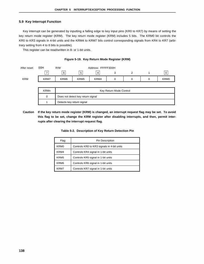
CHAPTER 5 INTERRUPT/EXCEPTION PROCESSING FUNCTION
138
5.9 Key Interrupt Function
Key interrupt can be generated by inputting a falling edge to key input pins (KR0 to KR7) by means of setting the
key return mode register (KRM). The key return mode register (KRM) includes 5 bits. The KRM0 bit controls the
KR0 to KR3 signals in 4-bit units and the KRM4 to KRM7 bits control corresponding signals from KR4 to KR7 (arbi-
trary setting from 4 to 8 bits is possible).
This register can be read/written in 8- or 1-bit units.
Figure 5-19. Key Return Mode Register (KRM)
After reset: 00H R/W Address: FFFFF3D0H
7 6 5 4 3 2 1 0
KRM KRM7 KRM6 KRM5 KRM4 0 0 0 KRM0
KRMn Key Return Mode Control
0 Does not detect key return signal
1 Detects key return signal
Caution If the key return mode register (KRM) is changed, an interrupt request flag may be set. To avoid
this flag to be set, change the KRM register after disabling interrupts, and then, permit inter-
rupts after clearing the interrupt request flag.
Table 5-2. Description of Key Return Detection Pin
Flag Pin Description
KRM0 Controls KR0 to KR3 signals in 4-bit units
KRM4 Controls KR4 signal in 1-bit units
KRM5 Controls KR5 signal in 1-bit units
KRM6 Controls KR6 signal in 1-bit units
KRM7 Controls KR7 signal in 1-bit units

139
CHAPTER 6 CLOCK GENERATION FUNCTION
6.1 General
The clock generator is a circuit that generates the clock pulses that are supplied to the CPU and peripheral
hardware. There are two types of system clock oscillators.
(1) Main system clock oscillator
This oscillator has an oscillation frequency of 2 to 20 MHz. Oscillation can be stopped by executing a STOP
instruction or by setting the processor clock control register (PCC). Oscillation is also stopped during a reset.
In IDLE mode, supplying the peripheral clock to the clock timer only is possible. Therefore, in IDLE mode, it is
possible to operate the clock timer without using the subsystem clock oscillator.
Cautions 1. When the main oscillator is stopped by inputting a reset or executing a STOP instruction,
the oscillation stabilization time is secured after the stop mode is canceled. This
oscillation stabilization time is set via the oscillation stabilization time select register
(OSTS). The watchdog timer is used as the timer that counts the oscillation stabilization
time.
2. If the main system clock halt is released by clearing MCK to 0 after the main system clock
is stopped by setting the MCK bit in the PCC register to 1, the oscillation stabilization time
is not secured.
(2) Subsystem clock oscillator
This circuit has an oscillation frequency of 32.768 kHz. Its oscillation is not stopped when the STOP instruction
is executed, neither is it stopped when a reset is input.
When the subsystem clock oscillator is not used, the FRC bit in the processor clock control register (PCC) can be
set to disable use of the internal feedback resistor. This enables the current consumption to be kept low in the
STOP mode.
6.2 Composition
fXT
fXT
fXX/8
fXX
STOP,MCK
FRC
Prescaler
PrescalerX2
X1
XT2
XT1
IDLE
Main systemclockoscillator
Subsystemclockoscillator
IDLEcontrol
IDLEcontrol
Selector
Clock supplied towatch timer, etc.
Clock supplied toperipheral hardware
HALT
HALTcontrol
CPU clock(fCPU)
CLKOUT
fXX/4fXX/2

CHAPTER 6 CLOCK GENERATION FUNCTION
140
6.3 Clock Output Function
This function outputs the CPU clock via the CLKOUT pin.
When clock output is enabled, the CPU clock is output via the CLKOUT pin. When it is disabled, a low-level signal
is output via the CLKOUT pin.
Output is stopped in the IDLE or STOP mode (fixed to low level).
This function is controlled via the DCLK1 and DCLK0 bits in the PSC register.
The high-impedance status is set during the reset period. After reset is canceled, low level is output.
Caution While CLKOUT is output, changing the CPU clock (CK2 to CK0 bits of PCC register) is disabled.
6.3.1 Control registers
(1) Processor clock control register (PCC)
This is a specific register. It can be written to only when a specified combination of sequences is used (see 3.4.9
Specific registers ). This register can be read/written in 8- or 1-bit units.
Figure 6-1. Format of Processor Clock Control Register (PCC) (1/2)
After reset: 03H R/W Address : FFFFF074H
7 6 5 4 3 2 1 0
PCC FRC MCK 0 0 0 CK2 CK1 CK0
FRC Selection of Internal Feedback Resistor for Sub Clock
0 Use
1 Do not use
MCK Operation of Main Clock (main system clock)
0 Operate
1 Stop
CK2 Note CK1 CK0 Selection of CPU Clock
0 0 0 fXX
0 0 1 fXX/2
0 1 0 fXX/4
0 1 1 fXX/8
1 X X fXT (sub clock)

CHAPTER 6 CLOCK GENERATION FUNCTION
141
Note If manipulating CK2, do so in 1-bit units. In the case of 8-bit manipulation, do not change the values of
CK1 and CK0.
Cautions 1. While CLKOUT is output, do not change the CPU clock (the value of the CK2 to CK0 in the
PCC register).
2. Even if the MCK bit is set to 1 during main clock operation, the main clock is not stopped.
The CPU clock stops after the sub clock is selected.
Remark X: don’t care
(a) Example of main clock operation →→→→ sub clock operation setup
<1> CK2 ← 1 : Bit manipulation instructions are recommended. Do not change CK1 and CK0.
<2> Sub clock operation : The maximum number of the following instructions is required before sub clock
operation after the CK2 bit is set.
(CPU clock frequency before setting / sub clock frequency) × 2
Therefore, insert the wait described above using a program.
<3> MCK ← 1 : Only when the main clock is stopped.
(b) Example of sub clock operation →→→→ main clock operation setup
<1> MCK ← 0 : Main clock oscillation start
<2> Insert wait using a program and wait until the main clock oscillation stabilizing time elapses.
<3> CK2, CK1, CH0 ← CPU clock
<4> Main clock operation : If CK1 and CH0 are not changed from value of the CPU clock selected before
the sub clock operation, a maximum of two instructions is required.
If CK1 and CK0 are changed, a maximum of ten instructions is required
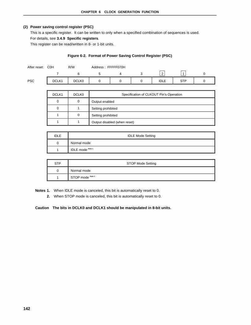
CHAPTER 6 CLOCK GENERATION FUNCTION
142
(2) Power saving control register (PSC)
This is a specific register. It can be written to only when a specified combination of sequences is used.
For details, see 3.4.9 Specific registers .
This register can be read/written in 8- or 1-bit units.
Figure 6-2. Format of Power Saving Control Register (PSC)
After reset: C0H R/W Address : FFFFF070H
7 6 5 4 3 2 1 0
PSC DCLK1 DCLK0 0 0 0 IDLE STP 0
DCLK1 DCLK0 Specification of CLKOUT Pin’s Operation
0 0 Output enabled
0 1 Setting prohibited
1 0 Setting prohibited
1 1 Output disabled (when reset)
IDLE IDLE Mode Setting
0 Normal mode
1 IDLE mode Note 1
STP STOP Mode Setting
0 Normal mode
1 STOP mode Note 2
Notes 1. When IDLE mode is canceled, this bit is automatically reset to 0.
2. When STOP mode is canceled, this bit is automatically reset to 0.
Caution The bits in DCLK0 and DCLK1 should be manipulated in 8-bit units.

CHAPTER 6 CLOCK GENERATION FUNCTION
143
(3) Oscillation stabilization time select register (OSTS)
This register can be read/written in 8-bit units.
Figure 6-3. Format of Oscillation Stabilization Time Select Register (OSTS)
After reset: 04H R/W Address : FFFFF380H
7 6 5 4 3 2 1 0
OSTS 0 0 0 0 0 OSTS2 OSTS1 OSTS0
OSTS2 OSTS1 OSTS0 Selection of Oscillation Stabilization Time Note
0 0 0 214/fXX (819.2 µs)
0 0 1 216/fXX (3.3 ms)
0 1 0 217/fXX (6.6 ms)
0 1 1 218/fXX (13.1 ms)
1 0 0 219/fXX (26.2 ms)
Other than above Setting prohibited
Note The numerical value in parentheses is the value when fXX = 20 MHz.
6.4 Power Saving Functions
6.4.1 General
This product provides the following power saving functions.
These modes can be combined and switched to suit the target application, which enables effective implementation
of low-power systems.
(1) HALT mode
When in this mode, the clock’s oscillator continues to operate but the CPU’s operating clock is stopped. A clock
continues to be supplied for other on-chip peripheral functions to maintain operation of those functions. This
enables the system’s total power consumption to be reduced.
A special-purpose instruction (the HALT instruction) is used to switch to HALT mode.
CHAPTER 6 CLOCK GENERATION FUNCTION
144
(2) IDLE mode
This mode stops the entire system by stopping the CPU’s operating clock as well as the operating clock for on-
chip peripheral functions while the clock oscillator is still operating. However, the sub clock continues to operate
and supplies a clock to the on-chip peripheral functions.
When this mode is canceled, there is no need for the oscillator to wait for the oscillation stabilization time, so
normal operation can be resumed quickly.
When the power saving control register (PSC)’s IDLE bit is set to 1, the system switches to IDLE mode.
(3) Software STOP mode
This mode stops the entire system by stopping a clock oscillator that is not for a sub clock system. The sub
clock continues to be supplied to keep on-chip peripheral functions operating. If a sub clock is not used, ultra low
power consumption mode (leak current only) is set. STOP mode setting is prohibited if the CPU is operating via
the sub clock.
If the PSC register’s STP bit is set to 1, the system enters STOP mode.
(4) Sub clock operation
Under this mode, the CPU clock is set to operate using the sub clock and the PCC register’s MCK bit is set to 1
to set low power consumption mode in which the entire system operates using only the sub clock.
When HALT mode has been set, the CPU’s operating clock is stopped so that power consumption can be
reduced.
When IDLE mode has been set, the CPU’s operating clock and some peripheral functions (DMAC and BCU) are
stopped, so that power consumption can be reduced even lower than when in HALT mode.
6.4.2 HALT mode
(1) Settings and operating states
When in this mode, the clock’s oscillator continues to operate but the CPU’s operating clock is stopped. A clock
continues to be supplied for other on-chip peripheral functions to maintain operation of those functions. When
HALT mode is set while the CPU is idle, it enables the system’s total power consumption to be reduced.
When in HALT mode, execution of programs is stopped but the contents of all registers and on-chip RAM are
retained as they were just before HALT mode was set. In addition, all on-chip peripheral functions that do not
depend on instruction processing by the CPU continue operating.
HALT mode can be set by executing the HALT instruction. It can be set when the CPU is operating via either the
main clock or sub clock.
The operating statuses in the HALT mode are listed in Table 6-1.
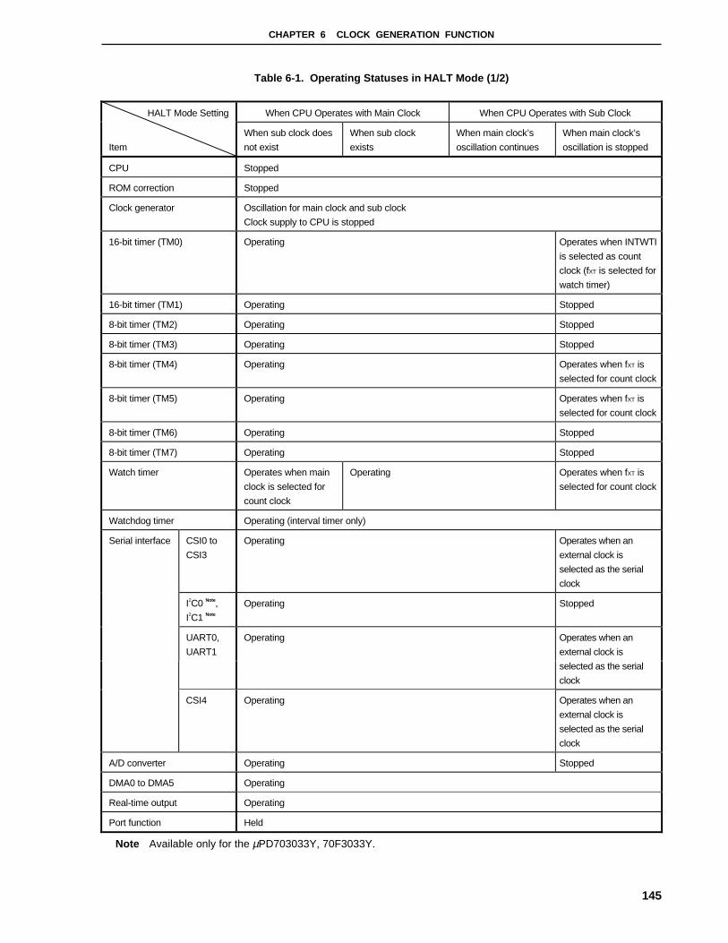
CHAPTER 6 CLOCK GENERATION FUNCTION
145
Table 6-1. Operating Statuses in HALT Mode (1/2)
HALT Mode Setting When CPU Operates with Main Clock When CPU Operates with Sub Clock
Item
When sub clock does
not exist
When sub clock
exists
When main clock’s
oscillation continues
When main clock’s
oscillation is stopped
CPU Stopped
ROM correction Stopped
Clock generator Oscillation for main clock and sub clock
Clock supply to CPU is stopped
16-bit timer (TM0) Operating Operates when INTWTI
is selected as count
clock (fXT is selected for
watch timer)
16-bit timer (TM1) Operating Stopped
8-bit timer (TM2) Operating Stopped
8-bit timer (TM3) Operating Stopped
8-bit timer (TM4) Operating Operates when fXT is
selected for count clock
8-bit timer (TM5) Operating Operates when fXT is
selected for count clock
8-bit timer (TM6) Operating Stopped
8-bit timer (TM7) Operating Stopped
Watch timer Operates when main
clock is selected for
count clock
Operating Operates when fXT is
selected for count clock
Watchdog timer Operating (interval timer only)
CSI0 to
CSI3
Operating Operates when an
external clock is
selected as the serial
clock
I2C0 Note,
I2C1 Note
Operating Stopped
Serial interface
UART0,
UART1
Operating Operates when an
external clock is
selected as the serial
clock
CSI4 Operating Operates when an
external clock is
selected as the serial
clock
A/D converter Operating Stopped
DMA0 to DMA5 Operating
Real-time output Operating
Port function Held
Note Available only for the µPD703033Y, 70F3033Y.

CHAPTER 6 CLOCK GENERATION FUNCTION
146
Table 6-1. Operating Statuses in HALT Mode (2/2)
HALT Mode Setting When CPU Operates with Main Clock When CPU Operates with Sub Clock
Item
When sub clock does
not exist
When sub clock
exists
When main clock’s
oscillation continues
When main clock’s
oscillation is stopped
External bus interface Only bus hold function operates
NMI Operating
INTP0 to INTP3 Operating
INTP4 and INTP5 Operating Stopped
External
interrupt
request
INTP6 Operating Operation when
sampling clock fXT is
selected
Key return function Operating
AD0 to AD15 High impedance Note
A16 to A21
LBEN, UBEN Held Note (high impedance when HLDAK = 0)
R/W High level output Note (high impedance when HLDAK = 0)
DSTB, WRL,
WRH, RD
ASTB
In
external
expansion
mode
HLDAK Operating
Note Even when the HALT instruction has been executed, the instruction fetch operation continues until the
on-chip instruction prefetch queue becomes full. Once it is full, operation stops according to the status
shown in Table 6-1.
(2) Cancellation of HALT mode
HALT mode can be canceled by an NMI request, an unmasked maskable interrupt request, or a RESET input.
(a) Cancellation by interrupt request
HALT mode is canceled regardless of the priority level when an NMI request or an unmasked maskable
interrupt request occurs. However, the following occurs if HALT mode was set as part of an interrupt
servicing routine.
(i) Only HALT mode is canceled when an interrupt request that has a lower priority level than the interrupt
currently being serviced occurs, and the lower-priority interrupt request is not acknowledged. The
interrupt request itself is retained.
(ii) When an interrupt request (including NMI request) that has a higher priority level than the interrupt
currently being serviced occurs, HALT mode is canceled and the interrupt request is acknowledged.
(b) Cancellation by RESET pin input
This is the same as for normal reset operations.
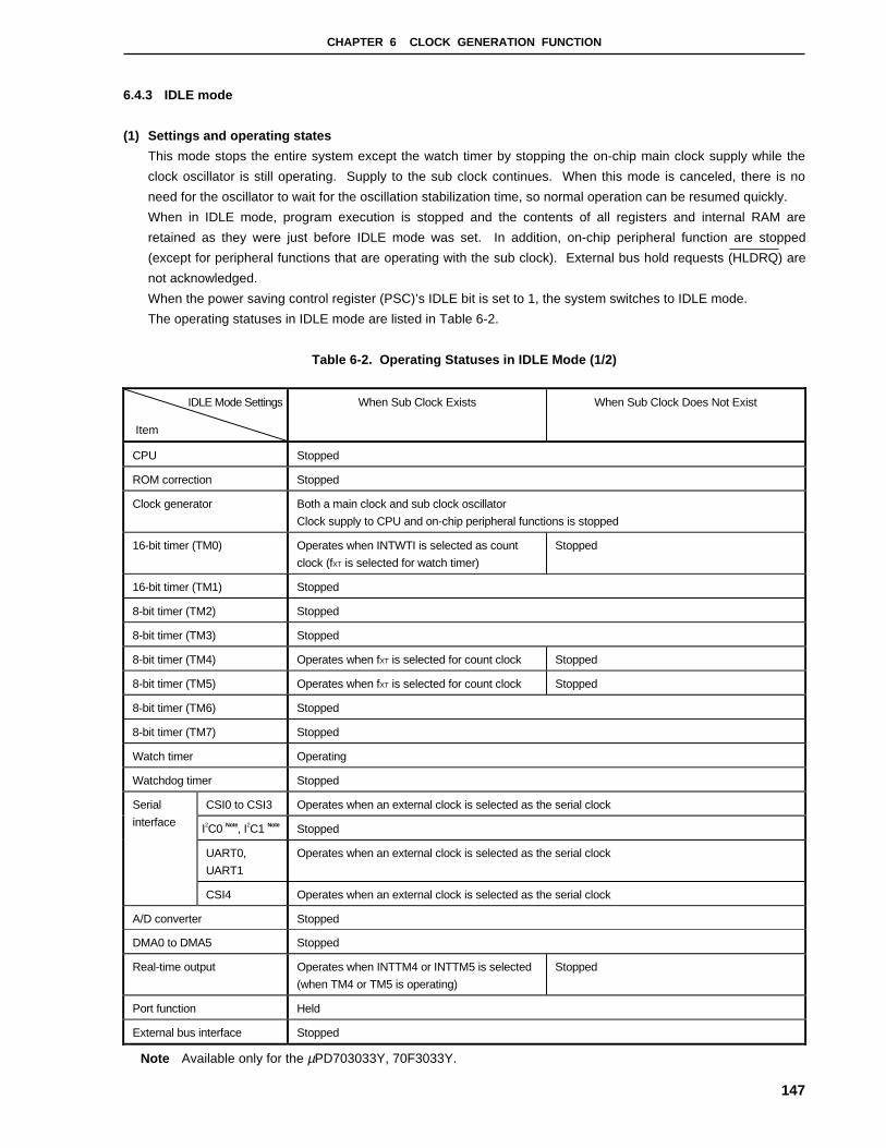
CHAPTER 6 CLOCK GENERATION FUNCTION
147
6.4.3 IDLE mode
(1) Settings and operating states
This mode stops the entire system except the watch timer by stopping the on-chip main clock supply while the
clock oscillator is still operating. Supply to the sub clock continues. When this mode is canceled, there is no
need for the oscillator to wait for the oscillation stabilization time, so normal operation can be resumed quickly.
When in IDLE mode, program execution is stopped and the contents of all registers and internal RAM are
retained as they were just before IDLE mode was set. In addition, on-chip peripheral function are stopped
(except for peripheral functions that are operating with the sub clock). External bus hold requests (HLDRQ) are
not acknowledged.
When the power saving control register (PSC)’s IDLE bit is set to 1, the system switches to IDLE mode.
The operating statuses in IDLE mode are listed in Table 6-2.
Table 6-2. Operating Statuses in IDLE Mode (1/2)
IDLE Mode Settings When Sub Clock Exists When Sub Clock Does Not Exist
CPU Stopped
ROM correction Stopped
Clock generator Both a main clock and sub clock oscillator
Clock supply to CPU and on-chip peripheral functions is stopped
16-bit timer (TM0) Operates when INTWTI is selected as count
clock (fXT is selected for watch timer)
Stopped
16-bit timer (TM1) Stopped
8-bit timer (TM2) Stopped
8-bit timer (TM3) Stopped
8-bit timer (TM4) Operates when fXT is selected for count clock Stopped
8-bit timer (TM5) Operates when fXT is selected for count clock Stopped
8-bit timer (TM6) Stopped
8-bit timer (TM7) Stopped
Watch timer Operating
Watchdog timer Stopped
CSI0 to CSI3 Operates when an external clock is selected as the serial clock
I2C0 Note, I2C1 Note Stopped
UART0,
UART1
Operates when an external clock is selected as the serial clock
Serial
interface
CSI4 Operates when an external clock is selected as the serial clock
A/D converter Stopped
DMA0 to DMA5 Stopped
Real-time output Operates when INTTM4 or INTTM5 is selected
(when TM4 or TM5 is operating)
Stopped
Port function Held
External bus interface Stopped
Note Available only for the µPD703033Y, 70F3033Y.
Item
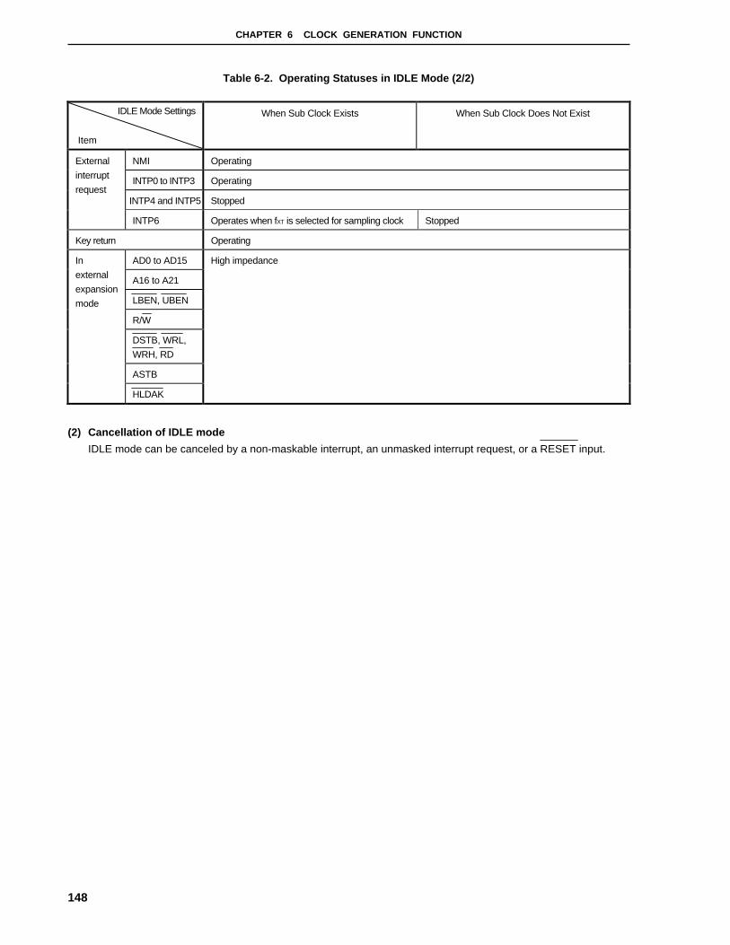
CHAPTER 6 CLOCK GENERATION FUNCTION
148
Table 6-2. Operating Statuses in IDLE Mode (2/2)
IDLE Mode Settings When Sub Clock Exists When Sub Clock Does Not Exist
NMI Operating
INTP0 to INTP3 Operating
INTP4 and INTP5 Stopped
External
interrupt
request
INTP6 Operates when fXT is selected for sampling clock Stopped
Key return Operating
AD0 to AD15
A16 to A21
LBEN, UBEN
R/W
DSTB, WRL,
WRH, RD
ASTB
In
external
expansion
mode
HLDAK
High impedance
(2) Cancellation of IDLE mode
IDLE mode can be canceled by a non-maskable interrupt, an unmasked interrupt request, or a RESET input.
Item

CHAPTER 6 CLOCK GENERATION FUNCTION
149
6.4.4 Software STOP mode
(1) Settings and operating states
This mode stops the entire system by stopping the main clock oscillator to stop supplying the internal main clock.
The sub clock oscillator continues operating and the on-chip sub clock supply is continued. When the FRC bit in
the processor clock control register (PCC) is set to 1, the sub clock oscillator’s on-chip feedback resistor is cut.
This sets ultra low power consumption mode in which the only current is the device’s leak current.
In this mode, program execution is stopped and the contents of all registers and internal RAM are retained as
they were just before software STOP mode was set.
This mode can be set only when the main clock is being used as the CPU clock. This mode is set when the STP
bit in the power saving control register (PSC) has been set to 1.
Do not set this mode when the sub clock has been selected as the CPU clock.
The operating statuses for software STOP mode are listed in Table 6-3.
Table 6-3. Operating Statuses in Software STOP Mode (1/2)
STOP Mode Settings
Item
When Sub Clock Exists When Sub Clock Does Not Exist
CPU Stopped
ROM correction Stopped
Clock generator Oscillation for main clock is stopped and oscillation for sub clock continues
Clock supply to CPU and on-chip peripheral functions is stopped
16-bit timer (TM0) Operates when INTWTI is selected for count
clock (fXT is selected as count clock for watch
timer)
Stopped
16-bit timer (TM1) Stopped
8-bit timer (TM2) Stopped
8-bit timer (TM3) Stopped
8-bit timer (TM4) Operates when fXT is selected for count clock Stopped
8-bit timer (TM5) Operates when fXT is selected for count clock Stopped
8-bit timer (TM6) Stopped
8-bit timer (TM7) Stopped
Watch timer Operates when fXT is selected for count clock Stopped
Watchdog timer Stopped
CSI0 to CSI3 Operates when an external clock is selected as the serial clock
I2C0 Note to
I2C1 Note
Stopped
UART0,
UART1
Operates when an external clock is selected as the serial clock
Serial
interface
CSI4 Operates when an external clock is selected as the serial clock
A/D converter Stopped
DMA0 to DMA5 Stopped
Note Available only for the µPD703033Y and 70F3033Y.

CHAPTER 6 CLOCK GENERATION FUNCTION
150
Table 6-3. Operating Statuses in Software STOP Mode (2/2)
Mode Settings
ItemWhen Sub Clock Exists When Sub Clock Does Not Exist
Real-time output Operates when INTTM4 or INTTM5 has been
selected (when TM4 or TM5 is operating)
Stopped
Port function Held
External bus interface Stopped
NMI Operating
INTP0 to INTP3 Operating
INTP4 and INTP5 Stopped
External
interrupt
request
INTP6 Operates when fXT is selected for the noise
elimination circuit
Stopped
Key return Operating
AD0 to AD15
A16 to A21
LBEN, UBEN
R/W
DSTB, WRL,
WRH, RD
ASTB
In
external
expansion
mode
HLDAK
High impedance
(2) Cancellation of software STOP mode
Software STOP mode can be canceled by an non-maskable interrupt, an unmasked interrupt request, or a
RESET input.
When the STOP mode is canceled, an oscillation stabilization time is secured.
6.5 Oscillation Stabilization Time
The following shows methods for specifying the length of oscillation stabilization time required to stabilize the
oscillator following cancellation of STOP mode.
(1) Cancellation by non-maskable interrupt or by unmasked interrupt request
STOP mode is canceled by a non-maskable interrupt or an unmasked interrupt request. When an inactive edge
is input to this pin, the counter (watchdog timer) starts counting and the count time is the length of time that must
elapse for stabilization of the oscillator’s clock output.
Oscillation stabilization time =·· WDT count time
After the specified amount of time has elapsed, system clock output starts and processing branches to the
interrupt handler address.

CHAPTER 6 CLOCK GENERATION FUNCTION
151
STOP mode is set
Oscillator is stopped
Interrupt input
Oscillation wave
Main clock
STOP status
Count time value of timebase counter
(2) Use of RESET pin to allocate time (RESET pin input)
For allocating time with RESET pin, refer to CHAPTER 15 RESET FUNCTION.

152
[MEMO]

153
CHAPTER 7 TIMER/COUNTER FUNCTION
7.1 16-bit Timer (TM0, TM1)
7.1.1 Outline
• 16-bit capture/compare registers: 2 (CRn0, CRn1)
• Independent capture/trigger inputs: 2 (TIn0, TIn1)
• Support of output of capture/match interrupt request signals (INTTMn0, INTTMn1)
• Event input (shared with TIn0) via digital noise elimination circuit and support of edge specifications
• Timer output operated by match detection: 1/each (TOn)
When using P34/TO0 and P35/TO1 pins as TO0 and TO1 pins (timer output), set the value of port 3 (P3) to 0
(port mode output) and port 3 mode register (PM3) to 0. The ORed value of the output of a port and a timer is
output.
Remark n = 0, 1
7.1.2 Function
TM0 and TM1 have the following functions:
• Interval timer
• PPG output
• Pulse width measurement
• External event counter
• Square wave output
• One-shot pulse output
Figure 7-1 shows the block diagram.

CHAPTER 7 TIMER/COUNTER FUNCTION
154
Figure 7-1. Block Diagram of TM0 and TM1
Internal bus
Internal bus
TIn1Noiseeliminationcircuit
Count clock Note
TIn0
TOEnTOCn1LVRnLVSnTOCn4OSPEnOSPTnOVFnTMCn1TMCn2
Prescaler moderegister n0 (PRMn0)
PRMn1 PRMn0 TMCn3
CRCn0CRCn1CRCn2
Capture/compare controlregister n (CRCn)
16-bit capture/compareregister n0 (CRn0)
Outputcontrolcircuit
16-bit timer register (TMn)
16-bit capture/compareregister n1 (CRn1)
CRCn2
Match
Match
Clear
16-bit timer modecontrol register n(TMCn)
TOn
INTTMn1
INTTMn0
3
Timer output controlregister n (TOCn)
fxx
Selector
Selector
Selector
Selector
PRMn2Prescaler moderegister n1 (PRMn1)
Noiseeliminationcircuit
Noiseeliminationcircuit
Note Count clock is set by the PRMn register.
Remark n = 0, 1
(1) Interval timerGenerate an interrupt at predetermined time intervals.
(2) PPG outputCan output the square wave, whose frequency and output-pulse width can be changed arbitrarily.
(3) Pulse width measurementCan measure the pulse width of a signal input from an external source.
(4) External event counterCan measure the number of pulses of a signal input from an external source.

CHAPTER 7 TIMER/COUNTER FUNCTION
155
(5) Square wave outputCan output a square wave of any frequency.
(6) One-shot pulse outputCan output a one-shot pulse with any output pulse width.
7.1.3 Configuration
Timers 0 and 1 consist of the following hardware:
Table 7-1. Configuration of Timers 0 and 1
Item Configuration
Timer registers 16 bits × 2 (TM0, TM1)
Registers Capture/compare registers: 16 bits × 2 (CRn0, CRn1)
Timer outputs 2 (TO0, TO1)
Control registers 16-bit timer mode control registers 0, 1 (TMC0, TMC1)
Capture/compare control registers 0, 1 (CRC0, CRC1)
16-bit timer output control registers 0, 1 (TOC0, TOC1)
Prescaler mode registers n0, n1 (PRMn0, PRMn1)
(1) 16-bit timer registers 0, 1 (TM0, TM1)
TMn is a 16-bit read-only register that counts count pulses.
The counter is incremented in synchronization with the rising edge of an input clock. If the count value is read
during operation, input of the count clock is temporarily stopped, and the count value at that point is read. The
count value is reset to 0000H in the following cases:
<1> At RESET input
<2> If TMCn3 and TMCn2 are cleared
<3> If valid edge of TIn0 is input in the clear & start mode by inputting valid edge of TIn0
<4> If TMn and CRn0 coincide with each other in the clear & start mode on coincidence between TMn and
CRn0
<5> If OSPTn is set or if the valid edge of TIn0 is input in the one-shot pulse output mode

CHAPTER 7 TIMER/COUNTER FUNCTION
156
(2) Capture/compare registers n0 (CR00, CR10)
CRn0 is a 16-bit register that functions as a capture register and as a compare register. Whether this register
functions as a capture or compare register is specified by using bit 0 (CRCn0) of the CRCn register.
(a) When using CRn0 as compare register
The value set to CRn0 is always compared with the count value of the TMn register. When the values of the
two coincide, an interrupt request (INTTMn0) is generated. When TMn is used as an interval timer, CRn0
can also be used as a register that holds the interval time.
(b) When using CRn0 as capture register
The valid edge of the TIn0 or TIn1 pin can be selected as a capture trigger. The valid edge for TIn0 or TIn1
is set by using the PRMn register.
When the valid edge for TIn0 pin is specified as the capture trigger, refer to Table 7-2. When the valid edge
for TIn1 pin is specified as the capture trigger, refer to Table 7-3.
Table 7-2. Valid Edge of TIn0 Pin and Capture Trigger of CRn0
ESn01 ESn00 Valid Edge of TIn0 Pin CRn0 Capture Trigger
0 0 Falling edge Rising edge
0 1 Rising edge Falling edge
1 0 Setting prohibited Setting prohibited
1 1 Both rising and falling edges No capture operation
Remark n = 0, 1
Table 7-3. Valid Edge of TIn1 Pin and Capture Trigger of CRn0
ESn11 ESn10 Valid Edge of TIn1 Pin CRn0 Capture Trigger
0 0 Falling edge Falling edge
0 1 Rising edge Rising edge
1 0 Setting prohibited Setting prohibited
1 1 Both rising and falling edges Both rising and falling edges
Remark n = 0, 1
CRn0 is set by using a 16-bit memory manipulation instruction.
The value of this register is undefined after the RESET signal is input.
Caution Set a value other than 0000H to CRn0. Consequently, the count operation for one pulse is not
enabled when CRn0 is operated as an event counter. In the free running mode or the TIn0 valid
edge clear mode, however, an interrupt request (INTTMn0) is generated after an overflow
(FFFFH) when 0000H is set to CRn0.

CHAPTER 7 TIMER/COUNTER FUNCTION
157
(3) Capture/compare register n1 (CRn1)
This is a 16-bit register that can be used as a capture register and a compare register. Whether it is used as a
capture register or compare register is specified by bit 2 (CRCn2) of the CRCn register.
(a) When using CRn1 as compare register
The value set to CRn1 is always compared with the count value of TMn. When the values of the two
coincide, an interrupt request (INTTMn1) is generated.
(b) When using CRn1 as capture register
The valid edge of the TIn1 pin can be selected as a capture trigger. The valid edge of TIn1 is specified by
using the PRMn register.
CRn1 is set by using a 16-bit memory manipulation instruction.
The value of this register is undefined after the RESET signal is input.
Caution Set a value other than 0000H to CRn1. Consequently, the count operation for one pulse is not
enabled when CRn1 is operated as an event counter. In the free running mode or the TIn1 valid
edge clear mode, however, an interrupt request (INTTMn1) is generated after an overflow
(FFFFH) when 0000H is set to CRn1.

CHAPTER 7 TIMER/COUNTER FUNCTION
158
7.1.4 Timer 0, 1 control register
The following four types of registers control timer 0, 1.
• 16-bit timer mode control register n (TMCn)
• Capture/compare control register n (CRCn)
• 16-bit timer output control register n (TOCn)
• Prescaler mode registers n0, n1 (PRMn0, PRMn1)
(1) 16-bit timer mode control registers 0, 1 (TMC0, TMC1)
TMCn specifies the operation mode of the 16-bit timer; and the clear mode, output timing, and overflow
detection of the 16-bit timer register n.
TMCn is set by a 1-bit or 8-bit memory manipulation instruction.
RESET input clears TMC0 and TMC1 to 00H.
Caution The 16-bit timer register n starts operating when a value other than 0, 0 (operation stop
mode) is set to TMCn2 and TMCn3. To stop the operation, set 0, 0 to TMCn2 and TMCn3.
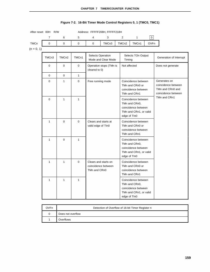
CHAPTER 7 TIMER/COUNTER FUNCTION
159
Figure 7-2. 16-Bit Timer Mode Control Registers 0, 1 (TMC0, TMC1)
After reset: 00H R/W Address: FFFFF208H, FFFFF218H
7 6 5 4 3 2 1 0
TMCn 0 0 0 0 TMCn3 TMCn2 TMCn1 OVFn
(n = 0, 1)
TMCn3 TMCn2 TMCn1Selects Operation
Mode and Clear Mode
Selects TOn Output
TimingGeneration of Interrupt
0 0 0 Operation stops (TMn is
cleared to 0)
Not affected Does not generate
0 0 1
0 1 0 Free running mode Coincidence between
TMn and CRn0 or
coincidence between
TMn and CRn1
0 1 1 Coincidence between
TMn and CRn0,
coincidence between
TMn and CRn1, or valid
edge of TIn0
1 0 0 Clears and starts at
valid edge of TIn0
Coincidence between
TMn and CRn0 or
coincidence between
TMn and CRn1
1 0 1 Coincidence between
TMn and CRn0,
coincidence between
TMn and CRn1, or valid
edge of TIn0
1 1 0 Clears and starts on
coincidence between
TMn and CRn0
Coincidence between
TMn and CRn0 or
coincidence between
TMn and CRn1
1 1 1 Coincidence between
TMn and CRn0,
coincidence between
TMn and CRn1, or valid
edge of TIn0
OVFn Detection of Overflow of 16-bit Timer Register n
0 Does not overflow
1 Overflows
Generates on
coincidence between
TMn and CRn0 and
coincidence between
TMn and CRn1
CHAPTER 7 TIMER/COUNTER FUNCTION
160
Cautions 1. When the bit other than the OVFn flag is written, be sure to stop the timer operation.
2. The valid edge of the TIn0 pin is set by using the prescaler mode register n (PRMn).
3. When a mode in which the timer is cleared and started on coincidence between TMn and
CRn0, the OVFn flag is set to 1 when the count value of TMn changes from FFFFH to 0000H
with CRn0 set to FFFFH.
Remark TOn : Output pin of timer n
TIn0 : Input pin of timer n
TMn : 16-bit timer register n
CRn0 : Compare register n0
CRn1 : Compare register n1

CHAPTER 7 TIMER/COUNTER FUNCTION
161
(2) Capture/compare control registers 0, 1 (CRC0, CRC1)
CRCn controls the operation of the capture/compare register n (CRn0 and CRn1).
CRCn is set by a 1-bit or 8-bit memory manipulation instruction.
RESET input clears CRC0 and CRC1 to 00H.
Figure 7-3. Capture/Compare Control Registers 0, 1 (CRC0, CRC1)
After reset: 00H R/W Address: FFFFF20AH, FFFFF21AH
7 6 5 4 3 2 1 0
CRCn 0 0 0 0 0 CRCn2 CRCn1 CRCn0
(n = 0, 1)
CRCn2 Selects Operation Mode of CRn1
0 Operates as compare register
1 Operates as capture register
CRCn1 Selects Capture Trigger of CRn0
0 Captured at valid edge of TIn1
1 Captured in reverse phase of valid edge of TIn0
CRCn0 Selects Operation Mode of CRn0
0 Operates as compare register
1 Operates as capture register
Cautions 1. Before setting CRCn, be sure to stop the timer operation.
2. When the mode in which the timer is cleared and started on coincidence between TMn
and CRn0 is selected by the 16-bit timer mode control register n (TMCn), do not specify
CRn0 as a capture register.
3. When both the rising edge and falling edge are specified for the TIn0 valid edge, the
capture operation does not work.
CHAPTER 7 TIMER/COUNTER FUNCTION
162
(3) 16-bit timer output control registers 0, 1 (TOC0, TOC1)
TOCn controls the operation of the timer n output control circuit by setting or resetting the R-S flip-flop (LV0),
enabling or disabling reverse output, enabling or disabling output of timer n, enabling or disabling one-shot pulse
output operation, and selecting an output trigger for a one-shot pulse by software.
TOCn is set by a 1-bit or 8-bit memory manipulation instruction.
RESET input clears TOC0 and TOC1 to 00H.

CHAPTER 7 TIMER/COUNTER FUNCTION
163
Figure 7-4. 16-Bit Timer Output Control Registers 0, 1 (TOC0, TOC1)
After reset: 00H R/W Address: FFFFF20CH, FFFFF21CH
7 6 5 4 3 2 1 0
TOCn 0 OSPTn OSPEn TOCn4 LVSn LVRn TOCn1 TOEn
(n = 0, 1)
OSPTn Controls Output Trigger of One-shot Pulse by Software
0 No one-shot pulse trigger
1 Uses one-shot pulse trigger
OSPEn Controls One-shot Pulse Output Operation
0 Successive pulse output
1 One-shot pulse output Note
TOCn4 Controls Timer Output F/F on Coincidence between CRn1 and TMn
0 Disables reverse timer output F/F
1 Enables reverse timer output F/F
LVSn LVRn Sets Status of Timer Output F/F of Timer 0
0 0 Not affected
0 1 Resets timer output F/F (0)
1 0 Sets timer output F/F (1)
1 1 Setting prohibited
TOCn1 Controls Timer Output F/F on Coincidence between CRn0 and TMn and TIn0 Valid Edge
0 Disables reverse timer output F/F
1 Enables reverse timer output F/F
TOEn Controls Output of Timer n
0 Disables output (output is fixed to 0 level)
1 Enables output
Note The one-shot pulse output operates only in the free running mode.
Cautions 1. Before setting TOCn, be sure to stop the timer operation.
2. LVSn and LVRn are 0 when read after data have been set to them.
3. OSPTn is 0 when read because it is automatically cleared after data has been set.
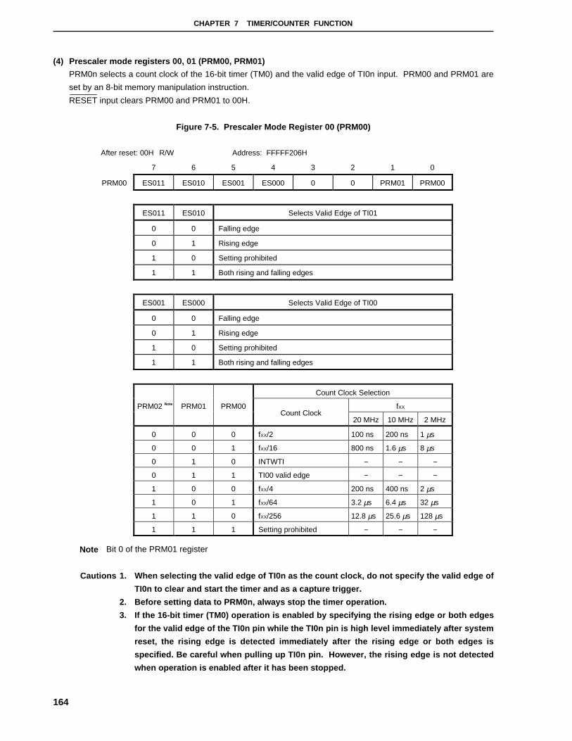
CHAPTER 7 TIMER/COUNTER FUNCTION
164
(4) Prescaler mode registers 00, 01 (PRM00, PRM01)
PRM0n selects a count clock of the 16-bit timer (TM0) and the valid edge of TI0n input. PRM00 and PRM01 are
set by an 8-bit memory manipulation instruction.
RESET input clears PRM00 and PRM01 to 00H.
Figure 7-5. Prescaler Mode Register 00 (PRM00)
After reset: 00H R/W Address: FFFFF206H
7 6 5 4 3 2 1 0
PRM00 ES011 ES010 ES001 ES000 0 0 PRM01 PRM00
ES011 ES010 Selects Valid Edge of TI01
0 0 Falling edge
0 1 Rising edge
1 0 Setting prohibited
1 1 Both rising and falling edges
ES001 ES000 Selects Valid Edge of TI00
0 0 Falling edge
0 1 Rising edge
1 0 Setting prohibited
1 1 Both rising and falling edges
Count Clock Selection
fXXPRM02 Note PRM01 PRM00Count Clock
20 MHz 10 MHz 2 MHz
0 0 0 fXX/2 100 ns 200 ns 1 µs
0 0 1 fXX/16 800 ns 1.6 µs 8 µs
0 1 0 INTWTI − − −
0 1 1 TI00 valid edge − − −
1 0 0 fXX/4 200 ns 400 ns 2 µs
1 0 1 fXX/64 3.2 µs 6.4 µs 32 µs
1 1 0 fXX/256 12.8 µs 25.6 µs 128 µs
1 1 1 Setting prohibited − − −
Note Bit 0 of the PRM01 register
Cautions 1. When selecting the valid edge of TI0n as the count clock, do not specify the valid edge of
TI0n to clear and start the timer and as a capture trigger.
2. Before setting data to PRM0n, always stop the timer operation.
3. If the 16-bit timer (TM0) operation is enabled by specifying the rising edge or both edges
for the valid edge of the TI0n pin while the TI0n pin is high level immediately after system
reset, the rising edge is detected immediately after the rising edge or both edges is
specified. Be careful when pulling up TI0n pin. However, the rising edge is not detected
when operation is enabled after it has been stopped.
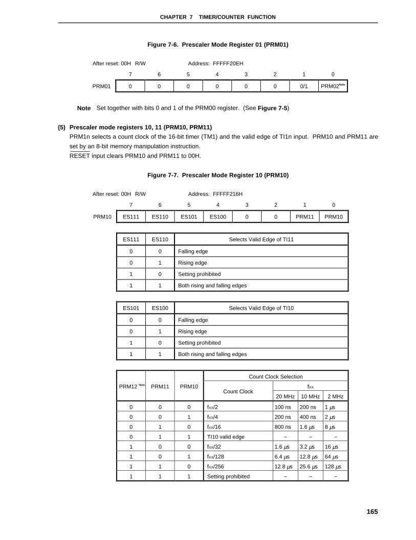
CHAPTER 7 TIMER/COUNTER FUNCTION
165
Figure 7-6. Prescaler Mode Register 01 (PRM01)
After reset: 00H R/W Address: FFFFF20EH
7 6 5 4 3 2 1 0
PRM01 0 0 0 0 0 0 0/1 PRM02Note
Note Set together with bits 0 and 1 of the PRM00 register. (See Figure 7-5 )
(5) Prescaler mode registers 10, 11 (PRM10, PRM11)
PRM1n selects a count clock of the 16-bit timer (TM1) and the valid edge of TI1n input. PRM10 and PRM11 are
set by an 8-bit memory manipulation instruction.
RESET input clears PRM10 and PRM11 to 00H.
Figure 7-7. Prescaler Mode Register 10 (PRM10)
After reset: 00H R/W Address: FFFFF216H
7 6 5 4 3 2 1 0
PRM10 ES111 ES110 ES101 ES100 0 0 PRM11 PRM10
ES111 ES110 Selects Valid Edge of TI11
0 0 Falling edge
0 1 Rising edge
1 0 Setting prohibited
1 1 Both rising and falling edges
ES101 ES100 Selects Valid Edge of TI10
0 0 Falling edge
0 1 Rising edge
1 0 Setting prohibited
1 1 Both rising and falling edges
Count Clock Selection
fXXPRM12 Note PRM11 PRM10Count Clock
20 MHz 10 MHz 2 MHz
0 0 0 fXX/2 100 ns 200 ns 1 µs
0 0 1 fXX/4 200 ns 400 ns 2 µs
0 1 0 fXX/16 800 ns 1.6 µs 8 µs
0 1 1 TI10 valid edge − − −
1 0 0 fXX/32 1.6 µs 3.2 µs 16 µs
1 0 1 fXX/128 6.4 µs 12.8 µs 64 µs
1 1 0 fXX/256 12.8 µs 25.6 µs 128 µs
1 1 1 Setting prohibited − − −
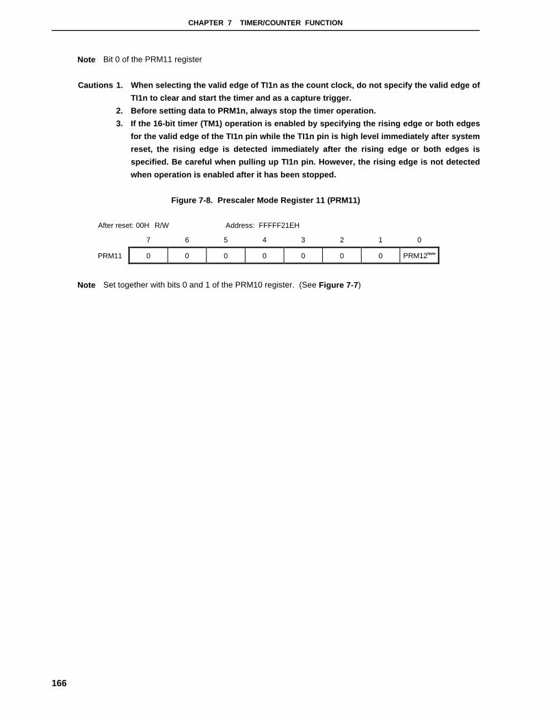
CHAPTER 7 TIMER/COUNTER FUNCTION
166
Note Bit 0 of the PRM11 register
Cautions 1. When selecting the valid edge of TI1n as the count clock, do not specify the valid edge of
TI1n to clear and start the timer and as a capture trigger.
2. Before setting data to PRM1n, always stop the timer operation.
3. If the 16-bit timer (TM1) operation is enabled by specifying the rising edge or both edges
for the valid edge of the TI1n pin while the TI1n pin is high level immediately after system
reset, the rising edge is detected immediately after the rising edge or both edges is
specified. Be careful when pulling up TI1n pin. However, the rising edge is not detected
when operation is enabled after it has been stopped.
Figure 7-8. Prescaler Mode Register 11 (PRM11)
After reset: 00H R/W Address: FFFFF21EH
7 6 5 4 3 2 1 0
PRM11 0 0 0 0 0 0 0 PRM12Note
Note Set together with bits 0 and 1 of the PRM10 register. (See Figure 7-7 )
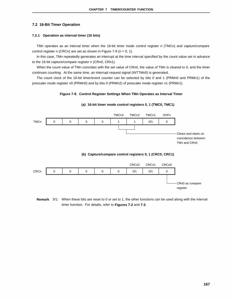
CHAPTER 7 TIMER/COUNTER FUNCTION
167
7.2 16-Bit Timer Operation
7.2.1 Operation as interval timer (16 bits)
TMn operates as an interval timer when the 16-bit timer mode control register n (TMCn) and capture/compare
control register n (CRCn) are set as shown in Figure 7-9 (n = 0, 1).
In this case, TMn repeatedly generates an interrupt at the time interval specified by the count value set in advance
to the 16-bit capture/compare register n (CRn0, CRn1).
When the count value of TMn coincides with the set value of CRn0, the value of TMn is cleared to 0, and the timer
continues counting. At the same time, an interrupt request signal (INTTMn0) is generated.
The count clock of the 16-bit timer/event counter can be selected by bits 0 and 1 (PRMn0 and PRMn1) of the
prescaler mode register n0 (PRMn0) and by bits 0 (PRMn2) of prescaler mode register n1 (PRMn1).
Figure 7-9. Control Register Settings When TMn Operates as Interval Timer
(a) 16-bit timer mode control registers 0, 1 (TMC0, TMC1)
TMCn3 TMCn2 TMCn1 OVFn
TMCn 0 0 0 0 1 1 0/1 0
Clears and starts on
coincidence between
TMn and CRn0.
(b) Capture/compare control registers 0, 1 (CRC0, CRC1)
CRCn2 CRCn1 CRCn0
CRCn 0 0 0 0 0 0/1 0/1 0
CRn0 as compare
register
Remark 0/1: When these bits are reset to 0 or set to 1, the other functions can be used along with the interval
timer function. For details, refer to Figures 7-2 and 7-3.
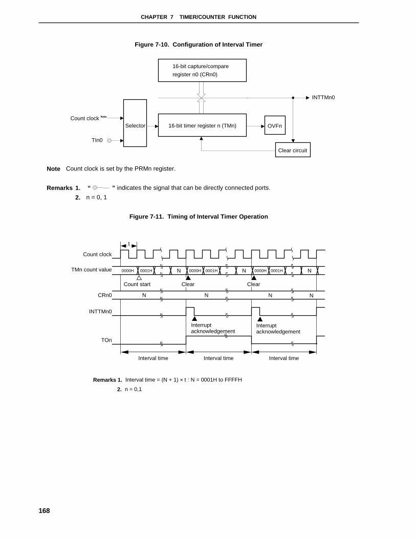
CHAPTER 7 TIMER/COUNTER FUNCTION
168
Figure 7-10. Configuration of Interval Timer
Note Count clock is set by the PRMn register.
Remarks 1. “ ” indicates the signal that can be directly connected ports.
2. n = 0, 1
Figure 7-11. Timing of Interval Timer Operation
Remarks 1. Interval time = (N + 1) × t : N = 0001H to FFFFH
2. n = 0,1
TMn count value
CRn0
0000H 0001H NNN
N NN N
0000H 0001H 0000H 0001H
Count start Clear Clear
Interruptacknowledgement
Interruptacknowledgement
INTTMn0
TOn
Interval time Interval time Interval time
Count clock
t
16-bit capture/compare
register n0 (CRn0)
Count clock Note
TIn0
Selector 16-bit timer register n (TMn) OVFn
Clear circuit
INTTMn0

CHAPTER 7 TIMER/COUNTER FUNCTION
169
7.2.2 PPG output operation
TMn can be used for PPG (Programmable Pulse Generator) output by setting the 16-bit timer mode control
register n (TMCn) and capture/compare control register n (CRCn) as shown in Figure 7-12.
The PPG output function outputs a square wave from the TOn pin with a cycle specified by the count value set in
advance to the 16-bit capture/compare register n0 (CRn0) and a pulse width specified by the count value set in
advance to the 16-bit capture/compare register n1 (CRn1).
Figure 7-12. Control Register Settings in PPG Output Operation
(a) 16-bit timer mode control registers 0, 1 (TMC0, TMC1)
TMCn3 TMCn2 TMCn1 OVFn
TMCn 0 0 0 0 1 1 0 0
Clears and starts on
coincidence between
TMn and CRn0.
(b) Capture/compare control registers 0, 1 (CRC0, CRC1)
CRCn2 CRCn1 CRCn0
CRCn 0 0 0 0 0 0 × 0
CRn0 as compare
register
CRn1 as compare
register
(c) 16-bit timer output control registers 0, 1 (TOC0, TOC1)
OSPTn OSPEn TOCn4 LVSn LVRn TOCn1 TOEn
TOCn 0 0 0 1 0/1 0/1 1 1
Enables TOn output.
Reverses output on
coincidence between
TMn and CRn0.
Specifies initial value of
TOn output F/F.
Reverses output on
coincidence between
TMn and CRn1.
Disables one-shot pulse
output.
Cautions 1. Make sure that 0000H < CRn1 < CRn0 ≤≤≤≤ FFFFH is set to CRn0 and CRn1.
2. PPG output set the pulse cycle to (CRn0 setup value + 1).
Duty factor is (CRn1 setup value + 1)/(CRn0 setup value + 1).
× : don’t care
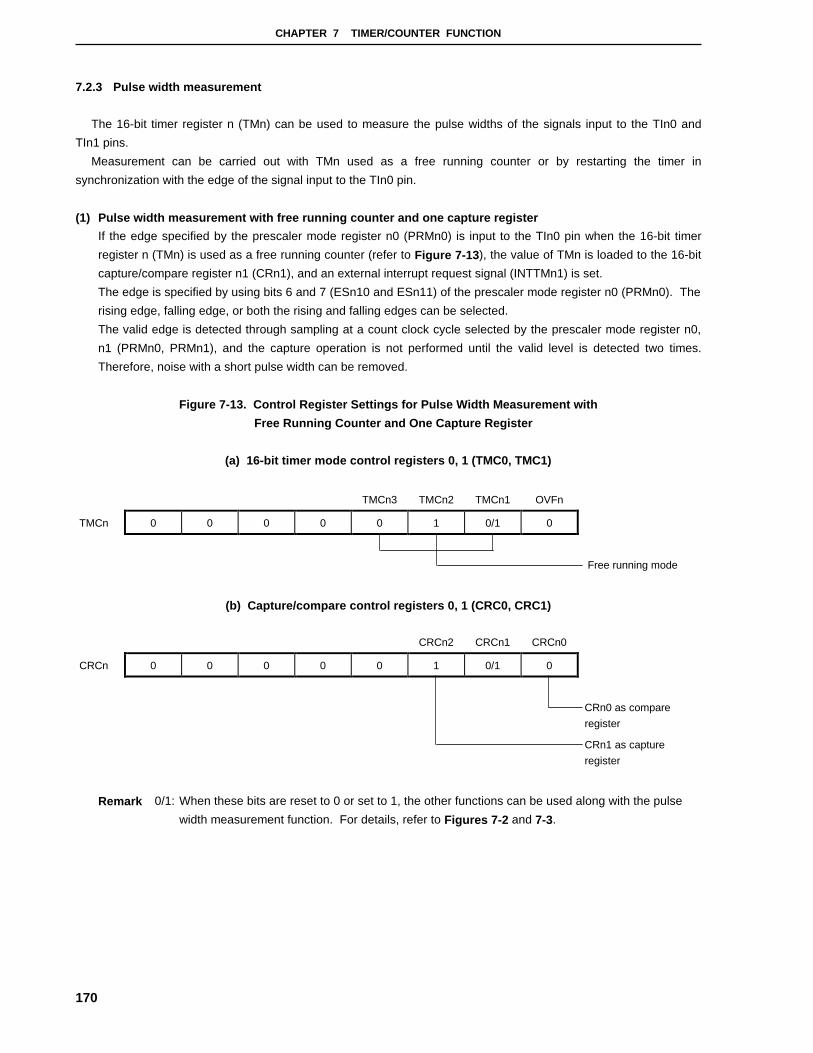
CHAPTER 7 TIMER/COUNTER FUNCTION
170
7.2.3 Pulse width measurement
The 16-bit timer register n (TMn) can be used to measure the pulse widths of the signals input to the TIn0 and
TIn1 pins.
Measurement can be carried out with TMn used as a free running counter or by restarting the timer in
synchronization with the edge of the signal input to the TIn0 pin.
(1) Pulse width measurement with free running counter and one capture register
If the edge specified by the prescaler mode register n0 (PRMn0) is input to the TIn0 pin when the 16-bit timer
register n (TMn) is used as a free running counter (refer to Figure 7-13 ), the value of TMn is loaded to the 16-bit
capture/compare register n1 (CRn1), and an external interrupt request signal (INTTMn1) is set.
The edge is specified by using bits 6 and 7 (ESn10 and ESn11) of the prescaler mode register n0 (PRMn0). The
rising edge, falling edge, or both the rising and falling edges can be selected.
The valid edge is detected through sampling at a count clock cycle selected by the prescaler mode register n0,
n1 (PRMn0, PRMn1), and the capture operation is not performed until the valid level is detected two times.
Therefore, noise with a short pulse width can be removed.
Figure 7-13. Control Register Settings for Pulse Width Measurement with
Free Running Counter and One Capture Register
(a) 16-bit timer mode control registers 0, 1 (TMC0, TMC1)
TMCn3 TMCn2 TMCn1 OVFn
TMCn 0 0 0 0 0 1 0/1 0
Free running mode
(b) Capture/compare control registers 0, 1 (CRC0, CRC1)
CRCn2 CRCn1 CRCn0
CRCn 0 0 0 0 0 1 0/1 0
CRn0 as compare
register
CRn1 as capture
register
Remark 0/1: When these bits are reset to 0 or set to 1, the other functions can be used along with the pulse
width measurement function. For details, refer to Figures 7-2 and 7-3.

CHAPTER 7 TIMER/COUNTER FUNCTION
171
Figure 7-14. Configuration for Pulse Width Measurement with Free Running Counter
Note Count clock is set by the PRMn0 and PRMn1 registers.
Remarks 1. “ ” indicates the signal that can be directly connected ports.
2. n = 0, 1
Figure 7-15. Timing of Pulse Width Measurement with Free Running Counter and
One Capture Register (with Both Edges Specified)
t
Value loadedto CRn1
TIn0 pininput
TMn countvalue 0000H 0001H D0 FFFFHD1 0000H D2 D3
INTTMn1
D0
OVFn
(D1 - D0) × t (10000H - D1 + D2) × t
Count clock
D1 D2 D3
(D3 - D2) × t
D0+1 D1+1
Remark n = 0, 1
16-bit capture/compare register n1
(CRn1)
16-bit timer register n (TMn)
Internal bus
Count clock Note
TIn0
Selector OVFn
INTTMn1

CHAPTER 7 TIMER/COUNTER FUNCTION
172
(2) Measurement of two pulse widths with free running counterThe pulse widths of the two signals respectively input to the TIn0 and TIn1 pins can be measured when the 16-bit timer register n (TMn) is used as a free running counter (refer to Figure 7-16 ).When the edge specified by bits 4 and 5 (ESn00 and ESn01) of the prescaler mode register n (PRMn0) is inputto the TIn0 pin, the value of the TMn is loaded to the 16-bit capture/compare register n1 (CRn1) and an externalinterrupt request signal (INTTMn1) is set.When the edge specified by bits 6 and 7 (ESn10 and ESn11) in PRMn0 is input to the TIn1 pin, the value of TMnis loaded to the 16-bit capture/compare register n0 (CRn0), and an external interrupt request signal (INTTMn0) isset.The edges of the TIn0 and TIn1 pins are specified by bits 4 and 5 (ESn00 and ESn01) and bits 6 and 7 (ESn10and ESn11) of PRMn, respectively. The rising, falling, or both rising and falling edges can be specified.The valid edge is detected through sampling at a count clock cycle selected by the prescaler mode register n0,n1 (PRMn0, PRMn1), and the capture operation is not performed until the valid level is detected two times.Therefore, noise with a short pulse width can be removed.
Figure 7-16. Control Register Settings for Measurement of Two Pulse Widths with Free Running Counter
(a) 16-bit timer mode control registers 0, 1 (TMC0, TMC1)
TMCn3 TMCn2 TMCn1 OVFn
TMCn 0 0 0 0 0 1 0/1 0
Free running mode
(b) Capture/compare control registers 0, 1 (CRC0, CRC1)
CRCn2 CRCn1 CRCn0
CRCn 0 0 0 0 0 1 0 1
CRn0 as capture
register
Captures valid edge of
TIn1 pin to CRn0.
CRn1 as capture
register
Remark 0/1: When these bits are reset to 0 or set to 1, the other functions can be used along with the pulse
width measurement function. For details, refer to Figures 7-2 and 7-3.
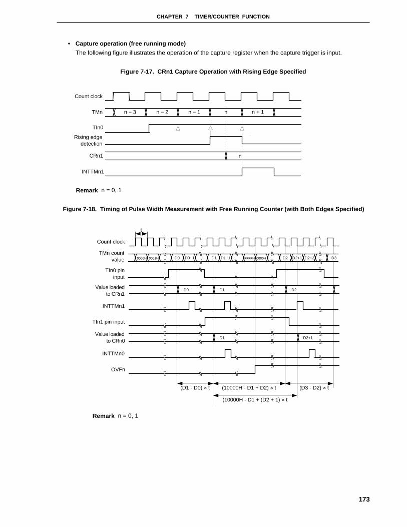
CHAPTER 7 TIMER/COUNTER FUNCTION
173
• Capture operation (free running mode)
The following figure illustrates the operation of the capture register when the capture trigger is input.
Figure 7-17. CRn1 Capture Operation with Rising Edge Specified
Count clock
TMn
TIn0
CRn1
INTTMn1
n + 1nn − 1n − 2n − 3
n
Rising edgedetection
Remark n = 0, 1
Figure 7-18. Timing of Pulse Width Measurement with Free Running Counter (with Both Edges Specified)
t
Value loadedto CRn1
(D1 - D0) × t (10000H - D1 + D2) × t (D3 - D2) × t
(10000H - D1 + (D2 + 1) × t
0000H 0001H D0
Count clock
TMn countvalue
TIn0 pininput
INTTMn1
TIn1 pin input
INTTMn0
OVFn
Value loadedto CRn0
D0+1 D1 D1+1 FFFFH 0000H D2 D2+1 D2+2 D3
D0 D1 D2
D1 D2+1
Remark n = 0, 1

CHAPTER 7 TIMER/COUNTER FUNCTION
174
(3) Pulse width measurement with free running counter and two capture registers
When the 16-bit timer register n (TMn) is used as a free running counter (refer to Figure 7-19 ), the pulse width of
the signal input to the TIn0 pin can be measured.
When the edge specified by bits 4 and 5 (ESn00 and ESn01) of the prescaler mode register n (PRMn0) is input
to the TIn0 pin, the value of TMn is loaded to the 16-bit capture/compare register n1 (CRn1), and an external
interrupt request signal (INTTMn1) is set.
The value of TMn is also loaded to the 16-bit capture/compare register n0 (CRn0) when an edge reverse to the
one that triggers capturing to CRn1 is input.
The edge of the TIn0 pin is specified by bits 4 and 5 (ESn00 and ESn01) of the prescaler mode register n
(PRMn0). The rising or falling edge can be specified.
The valid edge of TIn0 is detected through sampling at a count clock cycle selected by the prescaler mode
register n0, n1 (PRMn0, PRMn1), and the capture operation is not performed until the valid level is detected two
times. Therefore, noise with a short pulse width can be removed.
Caution If the valid edge of the TIn0 pin is specified to be both the rising and falling edges, the
capture/compare register n0 (CRn0) cannot perform its capture operation.
Figure 7-19. Control Register Settings for Pulse Width Measurement
with Free Running Counter and Two Capture Registers
(a) 16-bit timer mode control registers 0, 1 (TMC0, TMC1)
TMCn3 TMCn2 TMCn1 OVFn
TMCn 0 0 0 0 0 1 0/1 0
Free running mode
(b) Capture/compare control registers 0, 1 (CRC0, CRC1)
CRCn2 CRCn1 CRCn0
CRCn 0 0 0 0 0 1 1 1
CRn0 as capture
register
Captures to CRn0 at
edge reverse to valid
edge of TIn0 pin.
CRn1 as capture
register
Remark 0/1: When these bits are reset to 0 or set to 1, the other functions can be used along with the pulse
width measurement function. For details, refer to Figures 7-2 and 7-3.

CHAPTER 7 TIMER/COUNTER FUNCTION
175
Figure 7-20. Timing of Pulse Width Measurement with Free Running Counter and
Two Capture Registers (with Rising Edge Specified)
t
(D1 - D0) × t (10000H - D1 + D2) × t (D3 - D2) × t
OVFn
0001H0000H D0 D1
Count clock
TMn countvalue
TIn0 pin input
INTTMn1
Value loadedto CRn1
Value loadedto CRn0
D0+1 D1+1 0000HFFFFH D2 D2+1 D3
D0
D1
D2
D3
Remark n = 0, 1
(4) Pulse width measurement by restarting
When the valid edge of the TIn0 pin is detected, the pulse width of the signal input to the TIn0 pin can be
measured by clearing the 16-bit timer register n (TMn) once and then resuming counting after loading the count
value of TMn to the 16-bit capture/compare register n1 (CRn1). (See Figure 7-20 )
The edge is specified by bits 4 and 5 (ESn00 and ESn01) of the prescaler mode register n0 (PRMn0). The rising
or falling edge can be specified.
The valid edge is detected through sampling at a count clock cycle selected by prescaler mode register n0, n1
(PRMn0, PRMn1) and the capture operation is not performed until the valid level is detected two times.
Therefore, noise with a short pulse width can be removed.
Caution If the valid edge of the TIn0 pin is specified to be both the rising and falling edges, the
capture/compare register n0 (CRn0) cannot perform its capture operation.

CHAPTER 7 TIMER/COUNTER FUNCTION
176
Figure 7-21. Control Register Settings for Pulse Width Measurement by Restarting
(a) 16-bit timer mode control registers 0, 1 (TMC0, TMC1)
TMCn3 TMCn2 TMCn1 OVFn
TMCn 0 0 0 0 1 0 0/1 0
Clears and starts at
valid edge of TIn0 pin.
(b) Capture/compare control registers 0, 1 (CRC0, CRC1)
CRCn2 CRCn1 CRCn0
CRCn 0 0 0 0 0 1 1 1
CRn0 as capture
register
Captures to CRn0 at
edge reverse to valid
edge of TIn0.
CRn1 as capture
register
Remark 0/1: When these bits are reset to 0 or set to 1, the other functions can be used along with the pulse
width measurement function. For details, refer to Figures 7-2 and 7-3.
Figure 7-22. Timing of Pulse Width Measurement by Restarting (with Rising Edge Specified)
t
(D1 + 1) × t
(D2 + 1) × t
0001H0000H D0 D2D1
Count clock
TMn countvalue
TIn0 pin input
INTTMn1
D0 D2Value loaded to
CRn1
Value loaded toCRn0
D1
0001H0000H 0001H0000H
Remark n = 0, 1

CHAPTER 7 TIMER/COUNTER FUNCTION
177
7.2.4 Operation as external event counter
TMn can be used as an external event counter that counts the number of clock pulses input to the TIn0 pin from
an external source by using the 16-bit timer register n (TMn).
Each time the valid edge specified by the prescaler mode register n0 (PRMn0) has been input, TMn is
incremented.
When the count value of TMn coincides with the value of the 16-bit capture/compare register n0 (CRn0), TMn is
cleared to 0, and an interrupt request signal (INTTMn0) is generated.
The edge is specified by bits 4 and 5 (ESn00 and ESn01) of the prescaler mode register n0 (PRMn0). The rising,
falling, or both the rising and falling edges can be specified.
The valid edge is detected through sampling at a count clock cycle of fxx/2, and the capture operation is not
performed until the valid level is detected two times. Therefore, noise with a short pulse width can be removed.
Figure 7-23. Control Register Settings in External Event Counter Mode
(a) 16-bit timer mode control registers 0, 1 (TMC0, TMC1)
TMCn3 TMCn2 TMCn1 OVFn
TMCn 0 0 0 0 1 1 0/1 0
Clears and starts on
coincidence between
TMn and CRn0.
(b) Capture/compare control registers 0, 1 (CRC0, CRC1)
CRCn2 CRCn1 CRCn0
CRCn 0 0 0 0 0 0/1 0/1 0
CRn0 as compare
register
Remark 0/1: When these bits are reset to 0 or set to 1, the other functions can be used along with the external
event counter function. For details, refer to Figures 7-2 and 7-3.

CHAPTER 7 TIMER/COUNTER FUNCTION
178
Figure 7-24. Configuration of External Event Counter
Internal bus
16-bit capture/compareregister n (CRn0)
16-bit timer/counter n (TMn) OVFnCount clock Note
Selector
INTTMn0
16-bit capture/compareregister n1 (CRn1)
Noise eliminationcircuit
Valid edge of TIn0
fxx/2
Coincidence
Clear
Note Count clock is set by the PRMn0 and PRMn1 registers.
Remarks 1. “ ” indicates the signal that can be directly connected ports.
2. n = 0, 1
Figure 7-25. Timing of External Event Counter Operation (with Rising Edge Specified)
TIn0 pin input
TMn count value
CRn0
INTTMn0
0001H0000H N-1 N
N
0003H0002H 0005H0004H 0001H0000H 0003H0002H
Caution Read TMn when reading the count value of the external event counter.
Remark n = 0, 1
7.2.5 Operation to output square wave
TMn can be used to output a square wave with any frequency at an interval specified by the count value set in
advance to the 16-bit capture/compare register n0 (CRn0).
By setting bits 0 (TOEn) and 1 (TOCn1) of the 16-bit timer output control register n (TOCn) to 1, the output status
of the TOn0 pin is reversed at an interval specified by the count value set in advance to CRn1. In this way, a square
wave of any frequency can be output.

CHAPTER 7 TIMER/COUNTER FUNCTION
179
Figure 7-26. Control Register Settings in Square Wave Output Mode
(a) 16-bit timer mode control registers 0, 1 (TMC0, TMC1)
TMCn3 TMCn2 TMCn1 OVFn
TMCn 0 0 0 0 1 1 0/1 0
Clears and starts on
coincidence between
TMn and CRn0.
(b) Capture/compare control registers 0, 1 (CRC0, CRC1)
CRCn2 CRCn1 CRCn0
CRCn 0 0 0 0 0 0/1 0/1 1
CRn0 as compare
register
(c) 16-bit timer output control registers 0, 1 (TOC0, TOC1)
OSPTn OSPEn TOCn4 LVSn LVRn TOCn1 TOEn
TOCn 0 0 0 0 0/1 0/1 1 1
Enables TOn0 output.
Reverses output on
coincidence between
TMn and CRn0.
Specifies initial value of
TOn0 output F/F.
Does not reverse output
on coincidence between
TMn and CRn1.
Disables one-shot pulse
output.
Remark 0/1: When these bits are reset to 0 or set to 1, the other functions can be used along with the square
wave output function. For details, refer to Figures 7-2 , 7-3, and 7-4.

CHAPTER 7 TIMER/COUNTER FUNCTION
180
Figure 7-27. Timing of Square Wave Output Operation
Count clock
TMn count value
CRn0
INTTMn0
0002H0001H0000H N-1 N
N
N-1 N
TOn0 pin output
0002H0001H0000H 0000H
Remark n = 0, 1
7.2.6 Operation to output one-shot pulse
TMn can output a one-shot pulse in synchronization with a software trigger and an external trigger (TIn0 pin input).
(1) One-shot pulse output with software trigger
A one-shot pulse can be output from the TOn0 pin by setting the 16-bit timer mode control register n (TMCn),
capture/compare control register n (CRCn), and 16-bit timer output control register n (TOCn) as shown in Figure
7-28, and by setting bit 6 (OSPTn) of TOCn by software.
By setting OSPTn to 1, the 16-bit timer/event counter is cleared and started, and its output is asserted active at
the count value set in advance to the 16-bit capture/compare register n1 (CRn1). After that, the output is
deasserted inactive at the count value set in advance to the 16-bit capture/compare register n0 (CRn0).
Even after the one-shot pulse has been output, TMn continues its operation. To stop TMn, TMCn must be reset
to 00H.
Caution Do not set OSPTn to 1 while the one-shot pulse is being output. To output the one-shot
pulse again, wait until INTTMn0, which occurs on coincidence between TMn and CRn0,
occurs.

CHAPTER 7 TIMER/COUNTER FUNCTION
181
Figure 7-28. Control Register Settings for One-Shot Pulse Output with Software Trigger
(a) 16-bit timer mode control registers 0, 1 (TMC0, TMC1)
TMCn3 TMCn2 TMCn1 OVFn
TMCn 0 0 0 0 1 1 0 0
Clears and starts on
coincidence between
TMn and CRn0.
(b) Capture/compare control registers 0, 1 (CRC0, CRC1)
CRCn2 CRCn1 CRCn0
CRCn 0 0 0 0 0 0 0/1 0
CRn0 as compare
register
CRn1 as compare
register
(c) 16-bit timer output control registers 0, 1 (TOC0, TOC1)
OSPTn OSPEn TOCn4 LVSn LVRn TOCn1 TOEn
TOCn 0 0 1 1 0/1 0/1 1 1
Enables TOn0 output.
Reverses output on
coincidence between
TMn and CRn0.
Specifies initial value of
TOn0 output F/F.
Reverses output on
coincidence between
TMn and CRn1.
Sets one-shot pulse
output mode.
Set to 1 for output.
Caution Set a value in the following range to CRn0 and CRn1.
0000H < CRn1 < CRn0 ≤≤≤≤ FFFFH
Remark 0/1: When these bits are reset to 0 or set to 1, the other functions can be used along with the one-
shot pulse output function. For details, refer to Figures 7-2 , 7-3, and 7-4.

CHAPTER 7 TIMER/COUNTER FUNCTION
182
Figure 7-29. Timing of One-Shot Pulse Output Operation with Software Trigger
Count clock
TMn countvalue
0000H 0001H 0000HN+1 N 0001HN-1 M-1 0000HN M
CRn1 setvalue N
CRn0 setvalue
M
OSPTn
INTTMn1
INTTMn0
TOn0 pinoutput
Sets 0CH to TMCn(TMn count starts)
N
M
N
M
N
M
Caution The 16-bit timer register n starts operating as soon as a value other than 0, 0 (operation stop
mode) has been set to TMCn2 and TMCn3.
Remark n = 0, 1
(2) One-shot pulse output with external trigger
A one-shot pulse can be output from the TOn0 pin by setting the 16-bit timer mode control register n (TMCn),
capture/compare control register n (CRCn), and 16-bit timer output control register n (TOCn) as shown in Figure
7-30, and by using the valid edge of the TIn0 pin as an external trigger.
The valid edge of the TIn0 pin is specified by bits 4 and 5 (ESn00 and ESn01) of the prescaler mode register n0
(PRMn0). The rising, falling, or both the rising and falling edges can be specified.
When the valid edge of the TIn0 pin is detected, the 16-bit timer/event counter is cleared and started, and the
output is asserted active at the count value set in advance to the 16-bit capture/compare register n1 (CRn1).
After that, the output is deasserted inactive at the count value set in advance to the 16-bit capture/compare
register n0 (CRn0).
Caution Even if the external trigger is generated again while the one-shot pulse is output, it is
ignored.

CHAPTER 7 TIMER/COUNTER FUNCTION
183
Figure 7-30. Control Register Settings for One-Shot Pulse Output with External Trigger
(a) 16-bit timer mode control registers 0, 1 (TMC0, TMC1)
TMCn3 TMCn2 TMCn1 OVFn
TMCn 0 0 0 0 1 0 0 0
Clears and starts at
valid edge of TIn0 pin.
(b) Capture/compare control registers 0, 1 (CRC0, CRC1)
CRCn2 CRCn1 CRCn0
CRCn 0 0 0 0 0 0 0/1 0
CRn0 as compare
register
CRn1 as compare
register
(c) 16-bit timer output control registers 0, 1 (TOC0, TOC1)
OSPTn OSPEn TOCn4 LVSn LVRn TOCn1 TOEn
TOCn 0 0 1 1 0/1 0/1 1 1
Enables TOn0 output.
Reverses output on
coincidence between
TMn and CRn0.
Specifies initial value of
TOn0 output F/F.
Reverses output on
coincidence between
TMn and CRn1.
Sets one-shot pulse
output mode.
Caution Set a value in the following range to CRn0 and CRn1.
0000H < CRn1 < CRn0 ≤≤≤≤ FFFFH
Remark 0/1: When these bits are reset to 0 or set to 1, the other functions can be used along with the one-
shot pulse output function. For details, refer to Figures 7-2 , 7-3, and 7-4.
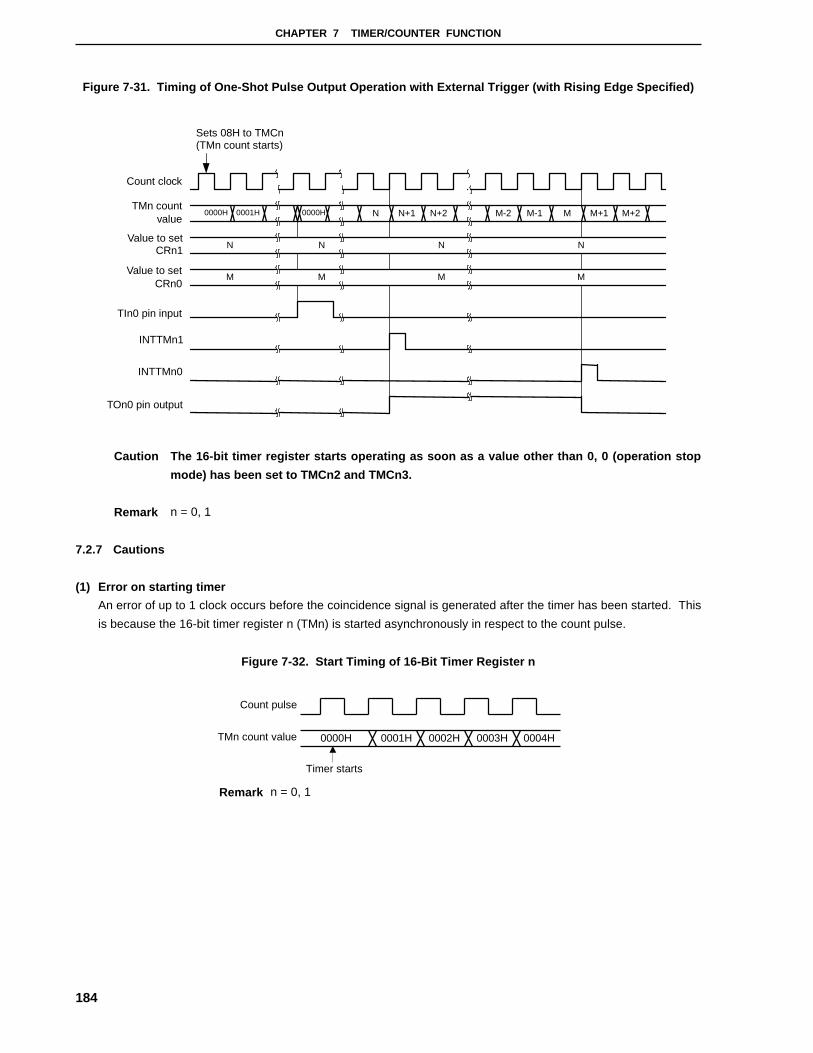
CHAPTER 7 TIMER/COUNTER FUNCTION
184
Figure 7-31. Timing of One-Shot Pulse Output Operation with External Trigger (with Rising Edge Specified)
Count clock
TMn countvalue
0000H 0001H N+1 M+2N+2 M-1 M+1M
Value to setCRn1 N
Value to setCRn0
M
TIn0 pin input
INTTMn1
INTTMn0
TOn0 pin output
Sets 08H to TMCn(TMn count starts)
0000H N M-2
N
M
N
M
N
M
Caution The 16-bit timer register starts operating as soon as a value other than 0, 0 (operation stop
mode) has been set to TMCn2 and TMCn3.
Remark n = 0, 1
7.2.7 Cautions
(1) Error on starting timer
An error of up to 1 clock occurs before the coincidence signal is generated after the timer has been started. This
is because the 16-bit timer register n (TMn) is started asynchronously in respect to the count pulse.
Figure 7-32. Start Timing of 16-Bit Timer Register n
Remark n = 0, 1
Count pulse
TMn count value 0004H0003H0002H0001H0000H
Timer starts
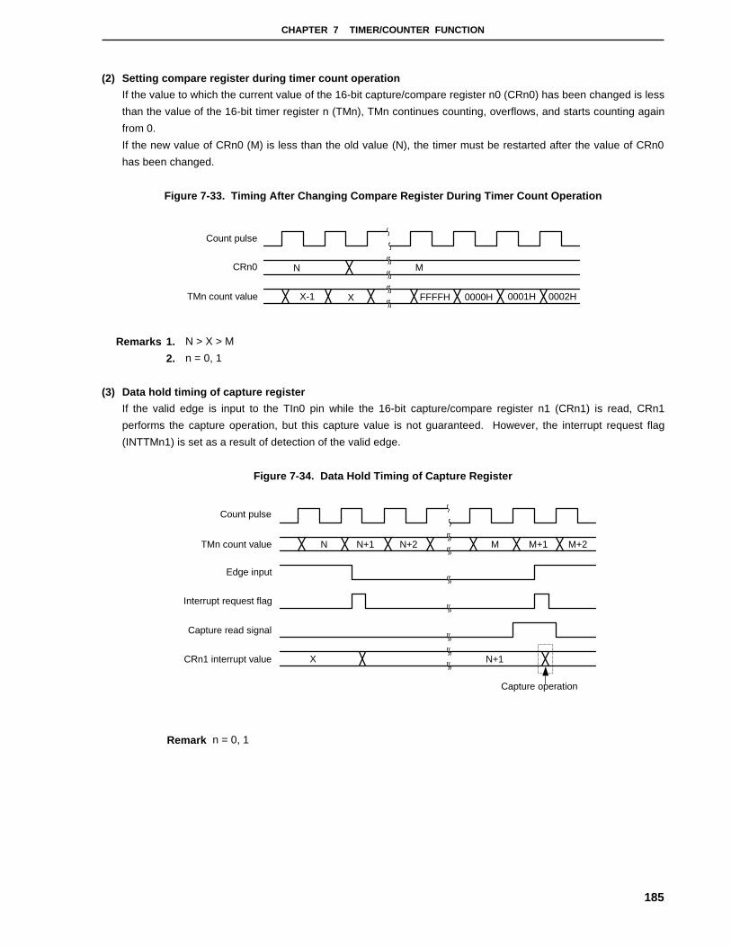
CHAPTER 7 TIMER/COUNTER FUNCTION
185
(2) Setting compare register during timer count operation
If the value to which the current value of the 16-bit capture/compare register n0 (CRn0) has been changed is less
than the value of the 16-bit timer register n (TMn), TMn continues counting, overflows, and starts counting again
from 0.
If the new value of CRn0 (M) is less than the old value (N), the timer must be restarted after the value of CRn0
has been changed.
Figure 7-33. Timing After Changing Compare Register During Timer Count Operation
TMn count value FFFFH 0001H 0002H0000H
Count pulse
X-1
N MCRn0
X
Remarks 1. N > X > M
2. n = 0, 1
(3) Data hold timing of capture register
If the valid edge is input to the TIn0 pin while the 16-bit capture/compare register n1 (CRn1) is read, CRn1
performs the capture operation, but this capture value is not guaranteed. However, the interrupt request flag
(INTTMn1) is set as a result of detection of the valid edge.
Figure 7-34. Data Hold Timing of Capture Register
TMn count value
Count pulse
N+1N N+2 M+2M+1M
X N+1
Capture operation
Edge input
Interrupt request flag
Capture read signal
CRn1 interrupt value
Remark n = 0, 1
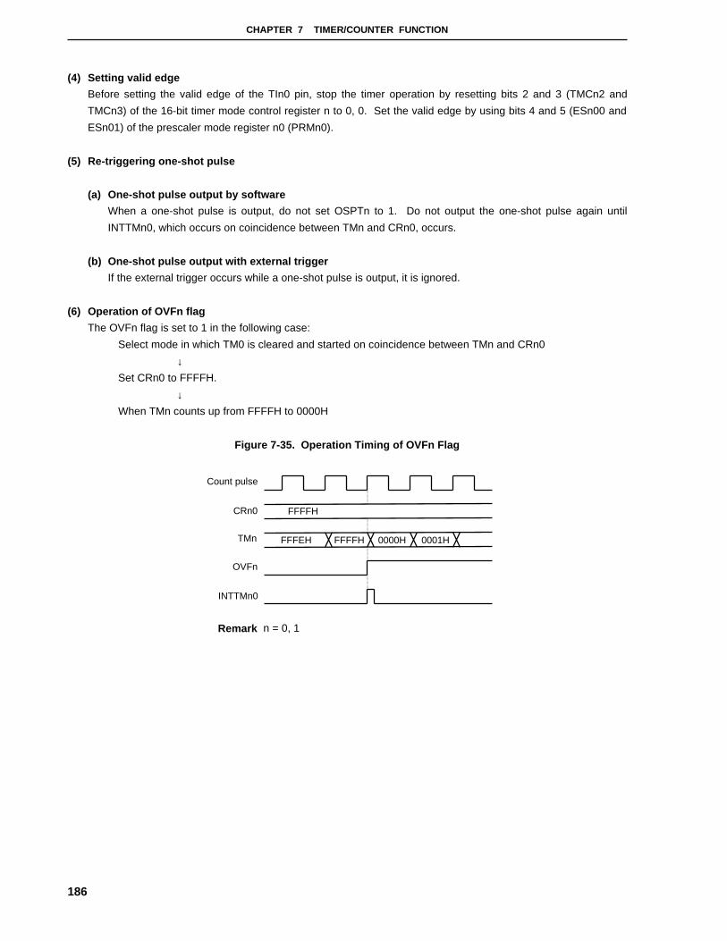
CHAPTER 7 TIMER/COUNTER FUNCTION
186
(4) Setting valid edge
Before setting the valid edge of the TIn0 pin, stop the timer operation by resetting bits 2 and 3 (TMCn2 and
TMCn3) of the 16-bit timer mode control register n to 0, 0. Set the valid edge by using bits 4 and 5 (ESn00 and
ESn01) of the prescaler mode register n0 (PRMn0).
(5) Re-triggering one-shot pulse
(a) One-shot pulse output by software
When a one-shot pulse is output, do not set OSPTn to 1. Do not output the one-shot pulse again until
INTTMn0, which occurs on coincidence between TMn and CRn0, occurs.
(b) One-shot pulse output with external trigger
If the external trigger occurs while a one-shot pulse is output, it is ignored.
(6) Operation of OVFn flag
The OVFn flag is set to 1 in the following case:
Select mode in which TM0 is cleared and started on coincidence between TMn and CRn0
↓Set CRn0 to FFFFH.
↓When TMn counts up from FFFFH to 0000H
Figure 7-35. Operation Timing of OVFn Flag
Remark n = 0, 1
Count pulse
CRn0
0001H0000HFFFFHFFFEH
FFFFH
TMn
OVFn
INTTMn0
CHAPTER 7 TIMER/COUNTER FUNCTION
187
7.3 8-bit Timer (TM2 to TM7)
7.3.1 Functions
8-bit timer n has the following two modes (n = 2 to 7).
• Mode using timer alone (individual mode)
• Mode using the cascade connection (16-bit resolution: cascade connection mode)
These two modes are described next.
(1) Mode using timer alone (individual mode)
The timer operates as an 8-bit timer/event counter.
It can have the following functions.
• Interval timer
• External event counter
• Square wave output
• PWM output
(2) Mode using the cascade connection (16-bit resolution: cascade connection mode)
The timer operates as a 16-bit timer/event counter by connecting TM2 and TM3 or TM4 and TM5 in cascade.
It can have the following functions.
• Interval timer with 16-bit resolution
• External event counter with 16-bit resolution
• Square wave output with 16-bit resolution
The timer operates as a 16-bit timer/event counter by connecting TM6 and TM7 in cascade.
• Interval timer with 16-bit resolution

CHAPTER 7 TIMER/COUNTER FUNCTION
188
Figure 7-36. Block Diagram of TM2 to TM7
Note Count clock is set by the TCLn register.
Remarks 1. “ ]” is a signal that can be directly connected to the port.
2. n = 2 to 7, m = 2 to 5
7.3.2 Configuration
Timer n is constructed from the following hardware.
Table 7-4. Timers 2 to 7 Configuration
Item Configuration
Timer registers 8-bit counters 2 to 7 (TM2 to TM7)
16-bit counters 23, 45, 67 (TM23, TM45, TM67): Only when connecting in cascade
Registers 8-bit compare registers 2 to 7 (CR20 to CR70)
16-bit compare registers 23, 45, 67 (CR23, CR45, CR67): Only when connecting in
cascade
Timer outputs TO2 to TO5
Control registers Timer clock selection registers 20 to 70 and 21 to 71 (TCL20 to TCL70 and TCL21 to
TCL71)
8-bit timer mode control registers 2 to 7 (TMC2 to TMC7)
8-bit compareregister n (CRn0)
8-bit counter n(TMn)
Match
OVF
Maskcircuit
TCEn
Selector
Clear/4
TCLn2 TCLn1 TCLn0
Timer clock selection registern0, n1(TCLn0, TCLn1)
Internal bus
TMCn6 TMCn4 LVSm LVRm TMCm1 TOEm
Timer mode controlregister n (TMCn)
SQ
R
Invertlevel
S
R
INVQ
Selector
INTTMnSelector
TOm
Internal bus
SelectorCount clock Note
TIn
TCLn3

CHAPTER 7 TIMER/COUNTER FUNCTION
189
(1) 8-bit counters 2 to 7 (TM2 to TM7)
TMn is an 8-bit read-only register that counts the count pulses.
The counter is incremented synchronous to the rising edge of the count clock. When the count is read out during
operation, the count clock input temporarily stops and the count is read at that time. In the following cases, the
count becomes 00H.
(1) RESET is input.
(2) TCEn is cleared.
(3) TMn and CRn0 match in the clear and start mode that occurs when TMn and CRn0 match.
Caution When connected in cascade, these registers become 00H even when TCEn in the lowest-
order timer is cleared.
(2) 8-bit compare registers 2 to 7 (CR20 to CR70)
The value set in CRn0 is always compared to the count in the 8-bit counter n (TMn). If the two values match, an
interrupt request (INTTMn) is generated (except in the PWM mode).
The value of CRn0 can be set in the range of 00H to FFH, and can be written during counting.
Caution If data is set in a cascade connection, always set after stopping the timer.

CHAPTER 7 TIMER/COUNTER FUNCTION
190
7.3.3 Timer n control register
The following two types of registers control timer n.
• Timer clock selection registers n0, n1 (TCLn0, TCLn1)
• 8-bit timer mode control register n (TMCn)
(1) Timer clock selection registers 20 to 71 and 21 to 71 (TCL20 to TCL70 and TCL21 to TCL71)
These registers set the count clock of timer n.
TCLn0 and TCLn1 are set by an 8-bit memory manipulation instruction.
RESET input sets these registers to 00H.
Figure 7-37. TM2, TM3 Timer Clock Selection Registers 20, 21, 30, 31 (TCL20, TCL21, TCL30, and TCL31)
After reset: 00H R/W Address: FFFFF244H, FFFFF254H
7 6 5 4 3 2 1 0
TCLn0 0 0 0 0 0 TCLn2 TCLn1 TCLn0
(n = 2, 3)
After reset: 00H R/W Address: FFFFF24EH, FFFFF25EH
7 6 5 4 3 2 1 0
TCLn1 0 0 0 0 0 0 0 TCLn3
(n = 2, 3)
Count Clock Selection
fXXTCLn3 TCLn2 TCLn1 TCLn0Count Clock
20 MHz 10 MHz 2 MHz
0 0 0 0 TIn falling edge − − −
0 0 0 1 TIn rising edge − − −
0 0 1 0 fXX/4 200 ns 400 ns 2 µs
0 0 1 1 fXX/8 400 ns 800 ns 4 µs
0 1 0 0 fXX/16 800 ns 1.6 µs 8 µs
0 1 0 1 fXX/32 1.6 µs 3.2 µs 16 µs
0 1 1 0 fXX/128 6.4 µs 12.8 µs 64 µs
0 1 1 1 fXX/512 25.6 µs 51.2 µs 256 µs
1 0 0 0 Setting prohibited − − −
1 0 0 1 Setting prohibited − − −
1 0 1 0 fXX/64 3.2 µs 6.4 µs 32 µs
1 0 1 1 fXX/256 12.8 µs 25.6 µs 128 µs
1 1 0 0 Setting prohibited − − −
1 1 0 1 Setting prohibited − − −
1 1 1 0 Setting prohibited − − −
1 1 1 1 Setting prohibited − − −

CHAPTER 7 TIMER/COUNTER FUNCTION
191
Cautions 1. When TCLn0 and TCLn1 are overwritten by different data, write after temporarily
stopping the timer.
2. Always set bits 3 to 7 to in TCLn0 to 0, and bits 1 to 7 in TCLn1 to 0.
Remark When connected in cascade, the settings of TCLn3 to TCLn0, except for the lowest-order timer, are
invalid.
Figure 7-38. TM4, TM5 Timer Clock Selection Registers 40, 41, 50, 51 (TCL40, TCL41, TCL50, and TCL51)
After reset: 00H R/W Address: FFFFF264H, FFFFF274H
7 6 5 4 3 2 1 0
TCLn0 0 0 0 0 0 TCLn2 TCLn1 TCLn0
(n = 4, 5)
After reset: 00H R/W Address: FFFFF26EH, FFFFF27EH
7 6 5 4 3 2 1 0
TCLn1 0 0 0 0 0 0 0 TCLn3
(n = 4, 5)
Count Clock Selection
fXXTCLn3 TCLn2 TCLn1 TCLn0Count Clock
20 MHz 10 MHz 2 MHz
0 0 0 0 TIn falling edge − − −
0 0 0 1 TIn rising edge − − −
0 0 1 0 fXX/4 200 ns 400 ns 2 µs
0 0 1 1 fXX/8 400 ns 800 ns 4 µs
0 1 0 0 fXX/16 800 ns 1.6 µs 8 µs
0 1 0 1 fXX/32 1.6 µs 3.2 µs 16 µs
0 1 1 0 fXX/128 6.4 µs 12.8 µs 64 µs
0 1 1 1 fXT (Sub clock) 30.5 µs 30.5 µs 30.5 µs
1 0 0 0 Setting prohibited − − −
1 0 0 1 Setting prohibited − − −
1 0 1 0 fXX/64 3.2 µs 6.4 µs 32 µs
1 0 1 1 fXX/256 12.8 µs 25.6 µs 128 µs
1 1 0 0 Setting prohibited − − −
1 1 0 1 Setting prohibited − − −
1 1 1 0 Setting prohibited − − −
1 1 1 1 Setting prohibited − − −
Cautions 1. When TCLn0 and TCLn1 are overwritten by different data, write after temporarily
stopping the timer.
2. Always set bits 3 to 7 of TCLn0 and bits 1 to 7 of TCLn1 to 0.
Remark When connected in cascade, the settings of TCLn3 to TCLn0, except for the lowest-order timer,
are invalid.
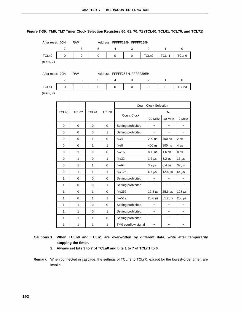
CHAPTER 7 TIMER/COUNTER FUNCTION
192
Figure 7-39. TM6, TM7 Timer Clock Selection Registers 60, 61, 70, 71 (TCL60, TCL61, TCL70, and TCL71)
After reset: 00H R/W Address: FFFFF284H, FFFFF294H
7 6 5 4 3 2 1 0
TCLn0 0 0 0 0 0 TCLn2 TCLn1 TCLn0
(n = 6, 7)
After reset: 00H R/W Address: FFFFF28EH, FFFFF29EH
7 6 5 4 3 2 1 0
TCLn1 0 0 0 0 0 0 0 TCLn3
(n = 6, 7)
Count Clock Selection
fXXTCLn3 TCLn2 TCLn1 TCLn0Count Clock
20 MHz 10 MHz 2 MHz
0 0 0 0 Setting prohibited − − −
0 0 0 1 Setting prohibited − − −
0 0 1 0 fXX/4 200 ns 400 ns 2 µs
0 0 1 1 fXX/8 400 ns 800 ns 4 µs
0 1 0 0 fXX/16 800 ns 1.6 µs 8 µs
0 1 0 1 fXX/32 1.6 µs 3.2 µs 16 µs
0 1 1 0 fXX/64 3.2 µs 6.4 µs 32 µs
0 1 1 1 fXX/128 6.4 µs 12.8 µs 64 µs
1 0 0 0 Setting prohibited − − −
1 0 0 1 Setting prohibited − − −
1 0 1 0 fXX/256 12.8 µs 25.6 µs 128 µs
1 0 1 1 fXX/512 25.6 µs 51.2 µs 256 µs
1 1 0 0 Setting prohibited − − −
1 1 0 1 Setting prohibited − − −
1 1 1 0 Setting prohibited − − −
1 1 1 1 TM0 overflow signal − − −
Cautions 1. When TCLn0 and TCLn1 are overwritten by different data, write after temporarily
stopping the timer.
2. Always set bits 3 to 7 of TCLn0 and bits 1 to 7 of TCLn1 to 0.
Remark When connected in cascade, the settings of TCLn3 to TCLn0, except for the lowest-order timer, are
invalid.
CHAPTER 7 TIMER/COUNTER FUNCTION
193
(2) 8-bit timer mode control registers 2 to 7 (TMC2 to TMC7)
The TMCn register makes the following six settings.
(1) Controls the counting by the 8-bit counter n (TMn)
(2) Selects the operating mode of the 8-bit counter n (TMn)
(3) Selects the individual mode or cascade connection mode
(4) Sets the state of the timer output flip-flop
(5) Controls the timer flip-flop or selects the active level in the PWM (free running) mode
(6) Controls timer output
TMCn is set by a 1-bit or 8-bit memory manipulation instruction.
RESET input sets these registers to 04H.
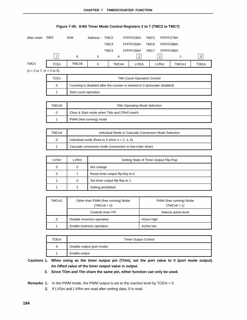
CHAPTER 7 TIMER/COUNTER FUNCTION
194
Figure 7-40. 8-Bit Timer Mode Control Registers 2 to 7 (TMC2 to TMC7)
After reset: 04H R/W Address : TMC2 FFFFF246H TMC5 FFFFF276H
TMC3 FFFFF256H TMC6 FFFFF286H
TMC4 FFFFF266H TMC7 FFFFF296H
7 6 5 4 3 2 1 0
TMCn TCEn TMCn6 0 TMCn4 LVSm LVRm TMCm1 TOEm
(n = 2 to 7, m = 2 to 5)
TCEn TMn Count Operation Control
0 Counting is disabled after the counter is cleared to 0 (prescaler disabled)
1 Start count operation
TMCn6 TMn Operating Mode Selection
0 Clear & Start mode when TMn and CRn0 match
1 PWM (free running) mode
TMCn4 Individual Mode or Cascade Connection Mode Selection
0 Individual mode (fixed to 0 when n = 2, 4, 6)
1 Cascade connection mode (connection to low-order timer)
LVSm LVRm Setting State of Timer Output Flip-Flop
0 0 Not change
0 1 Reset timer output flip-flop to 0
1 0 Set timer output flip-flop to 1
1 1 Setting prohibited
Other than PWM (free running) Mode
(TMCn6 = 0)
PWM (free running) Mode
(TMCn6 = 1)
TMCm1
Controls timer F/F Selects active level
0 Disable inversion operation Active high
1 Enable inversion operation Active low
TOEm Timer Output Control
0 Disable output (port mode)
1 Enable output
Cautions 1. When using as the timer output pin (TOm), set the port value to 0 (port mode output).
An ORed value of the timer output value is output.
2. Since TOm and TIm share the same pin, either function can only be used.
Remarks 1. In the PWM mode, the PWM output is set to the inactive level by TCEm = 0.
2. If LVSm and LVRm are read after setting data, 0 is read.

CHAPTER 7 TIMER/COUNTER FUNCTION
195
7.4 8-Bit Timer Operation
7.4.1 Operating as an interval timer (8-bit operation)
The timer operates as an interval timer that repeatedly generates interrupts at the interval of the preset count in
the 8-bit compare register n (CRn0).
If the count in the 8-bit counter n (TMn) matches the value set in CRn0, simultaneous to clearing the value of
TMn to 0 and continuing the count, the interrupt request signal (INTTMn) is generated.
The TMn count clock can be selected by bits 0 to 2 (TCLn0 to TCLn2) in the timer clock selection register n0
(TCLn0) and by bit 0 (TCLn3) in timer clock selection register n1 (TCLn1) (n = 2 to 7).
Setting method
(1) Set each register.
• TCLn0, TCLn1 : Selects the count clock.
• CRn0 : Compare value
• TMCn : Selects the clear and start mode when TMn and CRn0 match.
(TMCn = 0000xxx0B, x is don’t care)
(2) When TCEn = 1 is set, counting starts.
(3) When the values of TMn and CRn0 match, INTTMn is generated (TMn is cleared to 00H).
(4) Then, INTTMn is repeatedly generated during the same interval. When counting stops, set TCEn = 0.
Figure 7-41. Timing of Interval Timer Operation (1/3)
Basic operation
TMn count value
CRn0
00H 01H N 00H 01H 00H 01H NN
Count start Clear Clear
N N N N
Interrupt acknowledgement Interruptacknowledgement
TCEn
INTTMn
TOn
Interval time Interval time Interval time
Count clock
t
Remarks 1. Interval time = (N + 1) × t; N = 00H to FFH
2. n = 2 to 7
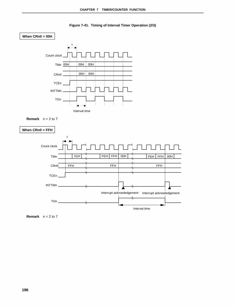
CHAPTER 7 TIMER/COUNTER FUNCTION
196
Figure 7-41. Timing of Interval Timer Operation (2/3)
When CRn0 = 00H
Remark n = 2 to 7
When CRn0 = FFH
01H FEHFFH 00HFEH FFH00H
FFH FFHFFH
Count clock
TMn
CRn0
TCEn
INTTMn
TOn
Interrupt acknowledgement
Interval time
t
Interrupt acknowledgement
Remark n = 2 to 7
Count clock
CRn0
TCEn
INTTMn
TOn
TMn 00H 00H 00H
00H 00H
Interval time
t
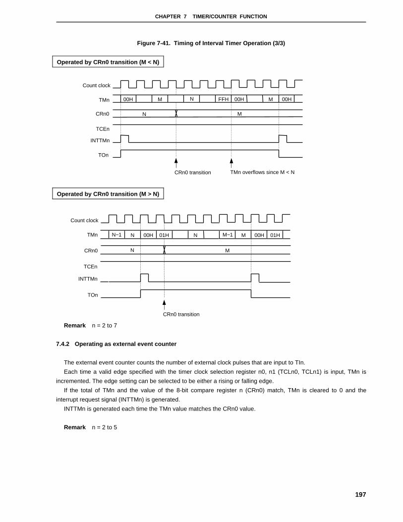
CHAPTER 7 TIMER/COUNTER FUNCTION
197
Figure 7-41. Timing of Interval Timer Operation (3/3)
Operated by CRn0 transition (M < N)
Operated by CRn0 transition (M > N)
Remark n = 2 to 7
7.4.2 Operating as external event counter
The external event counter counts the number of external clock pulses that are input to TIn.
Each time a valid edge specified with the timer clock selection register n0, n1 (TCLn0, TCLn1) is input, TMn is
incremented. The edge setting can be selected to be either a rising or falling edge.
If the total of TMn and the value of the 8-bit compare register n (CRn0) match, TMn is cleared to 0 and the
interrupt request signal (INTTMn) is generated.
INTTMn is generated each time the TMn value matches the CRn0 value.
Remark n = 2 to 5
Count clock
CRn0
TCEn
INTTMn
TOn
TMn 00H FFH MM 00H 00HN
N M
CRn0 transition TMn overflows since M < N
CRn0
TCEn
INTTMn
TOn
TMn
N M
CRn0 transition
M 01H00HM−1N01H00HNN−1
Count clock

CHAPTER 7 TIMER/COUNTER FUNCTION
198
Figure 7-42. Timing of External Event Counter Operation (When Rising Edge Is Set)
TIn
TMn count value 000500040003000200010000 N-1 N
CRn0
INTTMn
N
0000 0001 0002 0003
Remark n = 2 to 5
7.4.3 Operating as square wave output (8-bit resolution)
A square wave having any frequency is output at the interval preset in the 8-bit compare register n (CRn0).
By setting bit 0 (TOEn) of the 8-bit timer mode control register n (TMCn) to 1, the output state of TOn is inverted
with the count preset in CRn0 as the interval. Therefore, a square wave output having any frequency (duty factor =
50%) is possible.
Setting method
(1) Set the registers.
• Sets the port latch and port mode register to 0
• TCLn0, TCLn1 : Selects the count clock
• CRn0 : Compare value
• TMCn : Clear and start mode when TMn and CRn0 match
LVSn LVRn Setting State of Timer Output Flip-flop
1 0 High level output
0 1 Low level output
Inversion of timer output flip-flop enabled
Timer output enabled → TOEn = 1
(2) When TCEn = 1 is set, the counter starts operating.
(3) If the values of TMn and CRn0 match, the timer output flip-flop inverts. Also, INTTMn is generated and
TMn is cleared to 00H.
(4) Then, the timer output flip-flop is inverted for the same interval to output a square wave from TOn.
Remark n = 2 to 5

CHAPTER 7 TIMER/COUNTER FUNCTION
199
7.4.4 Operating as 8-bit PWM output
By setting bit 6 (TMCn6) of the 8-bit timer mode control register n (TMCn) to 1, the timer operates as a PWM
output.
Pulses with the duty factor determined by the value set in the 8-bit compare register n (CRn0) is output from TOn.
Set the width of the active level of the PWM pulse in CRn0. The active level can be selected by bit 1 (TMCn1) in
TMCn.
The count clock can be selected by bits 0 to 2 (TCLn0 to TCLn2) of timer clock selection register n0 (TCLn0) and
by bit 0 (TCLn3) of timer clock selection register n1 (TCLn1).
The PWM output can be enabled and disabled by bit 0 (TOEn) of TMCn.
Caution CRn0 can be rewritten only once in one period while in the PWM mode.
Remark n = 2 to 5
(1) Basic operation of the PWM output
Setting method
(1) Set the port latch and port mode register n to 0.
(2) Set the active level width in the 8-bit compare register n (CRn0).
(3) Select the count clock with the timer clock selection register n0, n1 (TCLn0, TCLn1).
(4) Set the active level in bit 1 (TMCn1) of TMCn.
(5) If bit 7 (TCEn) of TMCn is set to 1. counting starts. When counting stops, set TCEn to 0.
PWM output operation
(1) When counting starts, the PWM output (output from TOn) outputs the inactive level until an overflow
occurs.
(2) When the overflow occurs, the active level specified in step (1) in the setting method is output. The active
level is output until CRn0 and the count of the 8-bit counter n (TMn) match.
(3) The PWM output after CRn0 and the count match is the inactive level until an overflow occurs again.
(4) Steps (2) and (3) repeat until counting stops.
(5) If counting is stopped by TCEn = 0, the PWM output goes to the inactive level.
Remark n = 2 to 5

CHAPTER 7 TIMER/COUNTER FUNCTION
200
(a) Basic operation of PWM output
Figure 7-43. Timing of PWM Output
Basic operation (active level = H)
Count clock
00HTMn
CRn0
TCEn
INTTMn
TOn
Active level Inactive level Active level
01H FFH 00H 01H 02H N N+1 FFH 00H 01H 02H M 00H
N
When CRn0 = 0
Count clock
TMn
CRn0
TCEn
INTTMn
TOn
Inactive level Inactive level
00H 01H FFH 00H 01H 02H N N+1 N+2 FFH 00H 01H 02H M 00H
00H
When CRn0 = FFH
Count clock
TMn
CRn0
TCEn
INTTMn
TOn
Inactive level Inactive levelActive level Active levelInactive level
00H 01H FFH 00H 01H 02H N N+1 N+2 FFH 00H 01H 02H M 00H
FFH
Remark n = 2 to 5
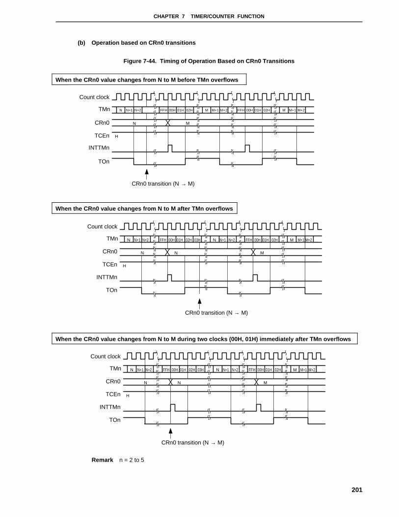
CHAPTER 7 TIMER/COUNTER FUNCTION
201
(b) Operation based on CRn0 transitions
Figure 7-44. Timing of Operation Based on CRn0 Transitions
When the CRn0 value changes from N to M before TMn overflows
INTTMn
N+1 02H01H00HFFHN N+2TMn
CRn0
TCEn
TOn
Count clock
CRn0 transition (N → M)
M+1M
N M
H
M+2 02H01H00HFFH M+1M M+2
When the CRn0 value changes from N to M after TMn overflows
INTTMn
N+1 02H01H00HFFHN N+2TMn
CRn0
TCEn
TOn
Count clock
CRn0 transition (N → M)
N+1N
N M
H
N+2 02H01H00HFFH M+1M M+203H
N
When the CRn0 value changes from N to M during two clocks (00H, 01H) immediately after TMn overflows
INTTMn
N+1 02H01H00HFFHN N+2TMn
CRn0
TCEn
TOn
Count clock
CRn0 transition (N → M)
N+1N
N M
H
N+2 02H01H00HFFH M+1M M+203H
N
Remark n = 2 to 5

CHAPTER 7 TIMER/COUNTER FUNCTION
202
7.4.5 Operating as interval timer (16 bits)
(1) Cascade connection (16-bit timer) mode
The V850/SB1 provides a 16-bit register that can be used when connecting in cascade.
Available registers are as follows.
TM2 to TM3 cascade connection: 16-bit counter TM23 (Address: FFFFF24AH)
16-bit compare register CR23 (Address: FFFFF24CH)
TM4 to TM5 cascade connection: 16-bit counter TM45 (Address: FFFFF26AH)
16-bit compare register CR45 (Address: FFFFF26CH)
TM6 to TM7 cascade connection: 16-bit counter TM67 (Address: FFFFF28AH)
16-bit compare register CR67 (Address: FFFFF28CH)
By setting bit 4 (TMCn4) of the 8-bit timer mode control register n (TMCn) to 1, the timer enters the
timer/counter mode with 16-bit resolution (n = 2 to 7).
With the count preset in the 8-bit compare register n (CRn0) as the interval, the timer operates as an interval
timer by repeatedly generating interrupts (n = 2 to 7).
Setting method
(1) Set each register.
• TCLn0, TCLn1 : The lowest-order timer selects the count clock.
The high-order timers connected in cascade are not used in setting.
• CRn0 : Compare values (Each compare value can be set from 00H to FFH.)
• TMCn : Select the clear and start mode when TMn and CRn0 match.
Lowest-order timer → TMCn = 0000xxx0B, x: don’t care
Other timer → TMCn = 0001xxx0B, x: don’t care
(2) Setting TCEn = 1 for the high-order timer and finally setting TCEn = 1 in the low-order timer starts the
count operation.
(3) If the values of TMn of all timers connected in cascade and CRn0 match, the lowest-order INTTMn is
generated (All TMns are cleared to 00H).
(4) INTTMn are repeatedly generated at the same interval.
Cautions 1. Always set the compare register n (CRn0) after stopping timer operation.
2. If the high-order count matches CRn0 even when used in a cascade connection, the high-
order INTTMn is generated. Always mask the high-order timer in order to disable interrupts.
3. The TCEn setting begins at the high-order timer. Set the lowest-order timer last.
4. Restarting and stopping the count is possible by setting only 1 or 0 in TCEn of the lowest-
order timer to start and stop it.
Remark n = 2 to 7

CHAPTER 7 TIMER/COUNTER FUNCTION
203
Figure 7-45 shows a timing example of the cascade connection mode with 16-bit resolution.
Figure 7-45. Cascade Connection Mode with 16-Bit Resolution
N+1N00H 01HTMn
Count clock
Enable operation starting count
00HFFH FFH 01H00HFFH00H 00HN 01H 00HA
00HTMn+1 01H MM-102H 00H 00HB
CRn0 N
CR(n+1)0 M
TCEn
TCEn+1
INTTMn
TOn Interval time
Operationstopped
Interrupt generation level invertedCounter cleared
Remark n = 2, 4, 6

CHAPTER 7 TIMER/COUNTER FUNCTION
204
7.4.6 Cautions
(1) Error when the timer starts
The time until the coincidence signal is generated after the timer starts has a maximum error of one clock. The
reason is the starting of the 8-bit counter n (TMn) is asynchronous with respect to the count pulse.
Figure 7-46. Start Timing of Timer n
Remark n = 2 to 7
(2) Operation after the compare register is changed while the timer is counting
If the value after the 8-bit compare register n (CRn0) changes is less than the value of the 8-bit timer register
(TMn), counting continues, overflows, and counting starts again from 0. Consequently, when the value (M) after
CRn0 changes is less than the value (N) before the change, the timer must restart after CRn0 changes (n = 2 to
5).
Figure 7-47. Timing After Compare Register Changes During Timer Counting
TMn count value
N
Count pulse
CRn0
X-1 X FFH 00H 01H 02H
M
Remarks 1. N > X > M
2. n = 2 to 5
Caution Except when the TIn input is selected, always set TCEn = 0 before setting the stop state.
(3) TMn read out during timer operation
Since reading out TMn during operation occurs while the selected clock is temporarily stopped, select some high
or low level waveform that is longer than the selected clock (n = 2 to 7).
00H 01H 02H 03H 04H
↑Timer starts
TMn count value
Count pulse

205
CHAPTER 8 WATCH TIMER
8.1 Function
The watch timer has the following functions:
• Watch timer
• Interval timer
The watch timer and interval timer functions can be used at the same time.
Figure 8-1 shows the block diagram of the watch timer.
Figure 8-1. Block Diagram of Watch Timer
fW/29
Sel
ecto
r
11-bit prescaler
fW/28fW/27fW/26fW/25fW/24
5-bit counter INTWTN
INTWTNI
WTNM0WTNM1WTNM3WTNM4WTNM5WTNM6WTNM7
Watch timer mode controlregister (WTNM)
fXX
Internal bus
Clear
Clear
WTNM2
fXT fW/211fW/210
WTNCS1 WTNCS0
Sel
ecto
rS
elec
tor
Sel
ecto
rWatch timer clock selectionregister (WTNCS)
3
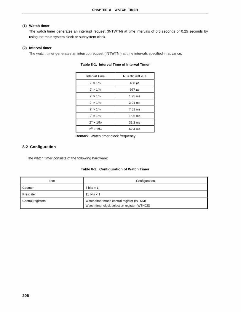
CHAPTER 8 WATCH TIMER
206
(1) Watch timer
The watch timer generates an interrupt request (INTWTN) at time intervals of 0.5 seconds or 0.25 seconds by
using the main system clock or subsystem clock.
(2) Interval timer
The watch timer generates an interrupt request (INTWTNI) at time intervals specified in advance.
Table 8-1. Interval Time of Interval Timer
Interval Time fXT = 32.768 kHz
24 × 1/fW 488 µs
25 × 1/fW 977 µs
26 × 1/fW 1.95 ms
27 × 1/fW 3.91 ms
28 × 1/fW 7.81 ms
29 × 1/fW 15.6 ms
210 × 1/fW 31.2 ms
211 × 1/fW 62.4 ms
Remark Watch timer clock frequency
8.2 Configuration
The watch timer consists of the following hardware:
Table 8-2. Configuration of Watch Timer
Item Configuration
Counter 5 bits × 1
Prescaler 11 bits × 1
Control registers Watch timer mode control register (WTNM)
Watch timer clock selection register (WTNCS)
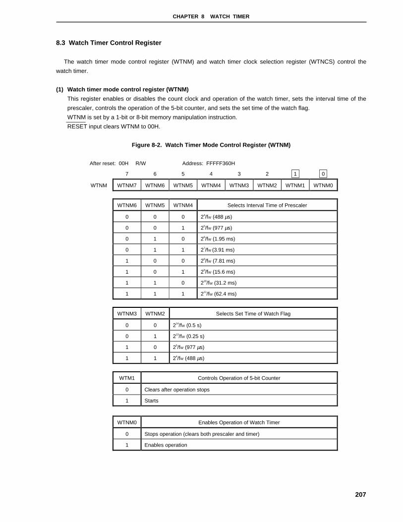
CHAPTER 8 WATCH TIMER
207
8.3 Watch Timer Control Register
The watch timer mode control register (WTNM) and watch timer clock selection register (WTNCS) control the
watch timer.
(1) Watch timer mode control register (WTNM)
This register enables or disables the count clock and operation of the watch timer, sets the interval time of the
prescaler, controls the operation of the 5-bit counter, and sets the set time of the watch flag.
WTNM is set by a 1-bit or 8-bit memory manipulation instruction.
RESET input clears WTNM to 00H.
Figure 8-2. Watch Timer Mode Control Register (WTNM)
After reset: 00H R/W Address: FFFFF360H
7 6 5 4 3 2 1 0
WTNM WTNM7 WTNM6 WTNM5 WTNM4 WTNM3 WTNM2 WTNM1 WTNM0
WTNM6 WTNM5 WTNM4 Selects Interval Time of Prescaler
0 0 0 24/fW (488 µs)
0 0 1 25/fW (977 µs)
0 1 0 26/fW (1.95 ms)
0 1 1 27/fW (3.91 ms)
1 0 0 28/fW (7.81 ms)
1 0 1 29/fW (15.6 ms)
1 1 0 210/fW (31.2 ms)
1 1 1 211/fW (62.4 ms)
WTNM3 WTNM2 Selects Set Time of Watch Flag
0 0 214/fW (0.5 s)
0 1 213/fW (0.25 s)
1 0 25/fW (977 µs)
1 1 24/fW (488 µs)
WTM1 Controls Operation of 5-bit Counter
0 Clears after operation stops
1 Starts
WTNM0 Enables Operation of Watch Timer
0 Stops operation (clears both prescaler and timer)
1 Enables operation

CHAPTER 8 WATCH TIMER
208
Remarks 1. fW: Watch timer clock frequency
2. Values in parentheses apply when fW = 32.768 kHz.
3. For the settings of WTNM7, refer to Figure 8-3 .
(2) Watch Timer Clock Selection Register (WTNCS)
This register selects the count clock of the watch timer.
WTNCS is set using an 8-bit memory manipulation instruction.
RESET input clears WTNCS to 00H.
Figure 8-3. Watch Timer Clock Selection Register (WTNCS)
After reset: 00H R/W Address: FFFFF364H
7 6 5 4 3 2 1 0
WTNCS 0 0 0 0 0 0 WTNCS1 WTNCS0
WTNCS1 WTNCS0 WTNM7Selection of Count
ClockMain Clock Frequency
0 0 0 fXX/27 4.194 MHz
0 0 1 fXT (sub clock) –
0 1 0 fXX/3 × 26 6.291 MHz
0 1 1 fXX/28 8.388 MHz
1 0 0 Setting prohibited –
1 0 1 Setting prohibited –
1 1 0 fXX/3 × 27 12.582 MHz
1 1 1 fXX/29 16.776 MHz
Remark WTNM7 is bit 7 of the WTNM register

CHAPTER 8 WATCH TIMER
209
8.4 Operation
8.4.1 Operation as watch timer
The watch timer operates with time intervals of 0.5 seconds with the subsystem clock (32.768 kHz).
The watch timer generates an interrupt request at fixed time intervals.
The count operation of the watch timer is started when bits 0 (WTNM0) and 1 (WTNM1) of the watch timer mode
control register (WTNM) are set to 1. When these bits are cleared to 0, the 11-bit prescaler and 5-bit counter are
cleared, and the watch timer stops the count operation.
When the interval timer function is started at the same time, the watch timer can be started from 0 second by
resetting WTNM1 to 0. However, an error of up to 0.5 seconds may occur when the watch timer overflows
(INTWTN).

CHAPTER 8 WATCH TIMER
210
8.4.2 Operation as interval timer
The watch timer can also be used as an interval timer that repeatedly generates an interrupt at intervals specified
by a count value set in advance.
The interval time can be selected by bits 4 through 6 (WTNM4 through WTNM6) of the watch timer mode control
register (WTNM).
Table 8-3. Interval Time of Interval Timer
WTNM6 WTNM5 WTNM4 Interval Time fW = 32.768 kHz
0 0 0 24 × 1/fW 488 µs
0 0 1 25 × 1/fW 977 µs
0 1 0 26 × 1/fW 1.95 ms
0 1 1 27 × 1/fW 3.91 ms
1 0 0 28 × 1/fW 7.81 ms
1 0 1 29 × 1/fW 15.6 ms
1 1 0 210 × 1/fW 31.2 ms
1 1 1 211 × 1/fW 62.4 ms
Remark fW : Watch timer clock frequency
Figure 8-4. Operation Timing of Watch Timer/Interval Timer
Start
5-bit counter
OverflowOverflow
0H
Interrupt time of watch timer (0.5 s)Interrupt time of watch timer (0.5 s)
Interval time(T)
Interval time(T)
Count clock fW orfW/29
Watch timerinterrupt INTWTN
Interval timerinterrupt INTWTNI
nTnT
Remark fW : Watch timer clock frequency
( ) : fW = 32.768 kHz
n : Interval timer operation numbers

211
Internal bus
fxx
3RUN
Frequencydivider
Frequencydivision clock
selectioncircuit
Clock inputcontrol circuit
Outputcontrolcircuit
INTWDT Note 1
INTWDTM Note 2
WDT mode signal
WDTM4WDCS2 WDCS1 WDCS0OSTS2 OSTS1 OSTS0
Frequency divisionmode selection circuit
CHAPTER 9 WATCHDOG TIMER
9.1 Functions
The watchdog timer has the following functions. Figure 9-1 shows a block diagram of the watchdog timer.
• Watchdog timer
• Interval timer
• Selecting the oscillation stabilization time
Caution Use the watchdog timer mode register (WDTM) to select the watchdog timer mode or the interval
timer mode.
Figure 9-1. Block Diagram of Watchdog Timer
Notes 1. When watchdog timer mode
2. When interval timer mode
Remark fXX: Main clock frequency

CHAPTER 9 WATCHDOG TIMER
212
(1) Watchdog timer mode
This mode detects program runaway. When runaway is detected, a non-maskable interrupt can be generated.
Table 9-1. Runaway Detection Time by Watchdog Timer
Runaway Detection TimeClock
fXX = 20 MHz fXX = 10 MHz fXX = 2 MHz
214/fxx 819.2 µs 1.6 ms 8.2 ms
215/fxx 1.6 ms 3.2 ms 16.4 ms
216/fxx 3.3 ms 6.6 ms 32.8 ms
217/fxx 6.6 ms 13.1 ms 65.5 ms
218/fxx 13.1 ms 26.2 ms 131.1 ms
219/fxx 26.2 ms 52.4 ms 262.1 ms
220/fxx 52.4 ms 104.9 ms 524.3 ms
222/fxx 209.7 ms 419.4 ms 2.1 s
(2) Interval timer mode
Interrupts are generated at a preset time interval.
Table 9-2. Interval Time of Interval Timer
Runaway Detection TimeClock
fXX = 20 MHz fXX = 10 MHz fXX = 2 MHz
214/fxx 819.2 µs 1.6 ms 8.2 ms
215/fxx 1.6 ms 3.2 ms 16.4 ms
216/fxx 3.3 ms 6.6 ms 32.8 ms
217/fxx 6.6 ms 13.1 ms 65.5 ms
218/fxx 13.1 ms 26.2 ms 131.1 ms
219/fxx 26.2 ms 52.4 ms 262.1 ms
220/fxx 52.4 ms 104.9 ms 524.3 ms
222/fxx 209.7 ms 419.4 ms 2.1 s
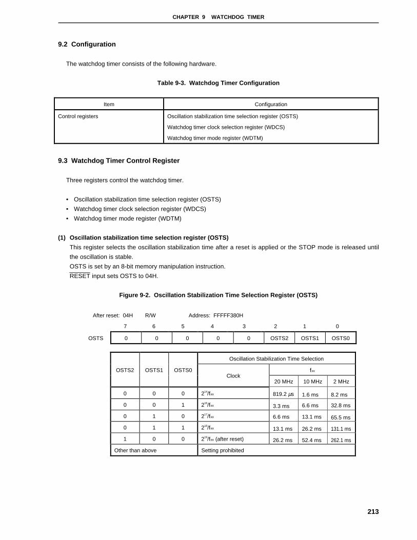
CHAPTER 9 WATCHDOG TIMER
213
9.2 Configuration
The watchdog timer consists of the following hardware.
Table 9-3. Watchdog Timer Configuration
Item Configuration
Control registers Oscillation stabilization time selection register (OSTS)
Watchdog timer clock selection register (WDCS)
Watchdog timer mode register (WDTM)
9.3 Watchdog Timer Control Register
Three registers control the watchdog timer.
• Oscillation stabilization time selection register (OSTS)
• Watchdog timer clock selection register (WDCS)
• Watchdog timer mode register (WDTM)
(1) Oscillation stabilization time selection register (OSTS)
This register selects the oscillation stabilization time after a reset is applied or the STOP mode is released until
the oscillation is stable.
OSTS is set by an 8-bit memory manipulation instruction.
RESET input sets OSTS to 04H.
Figure 9-2. Oscillation Stabilization Time Selection Register (OSTS)
After reset: 04H R/W Address: FFFFF380H
7 6 5 4 3 2 1 0
OSTS 0 0 0 0 0 OSTS2 OSTS1 OSTS0
Oscillation Stabilization Time Selection
fxxOSTS2 OSTS1 OSTS0Clock
20 MHz 10 MHz 2 MHz
0 0 0 214/fxx 819.2 µs 1.6 ms 8.2 ms
0 0 1 216/fxx 3.3 ms 6.6 ms 32.8 ms
0 1 0 217/fxx 6.6 ms 13.1 ms 65.5 ms
0 1 1 218/fxx 13.1 ms 26.2 ms 131.1 ms
1 0 0 219/fxx (after reset) 26.2 ms 52.4 ms 262.1 ms
Other than above Setting prohibited
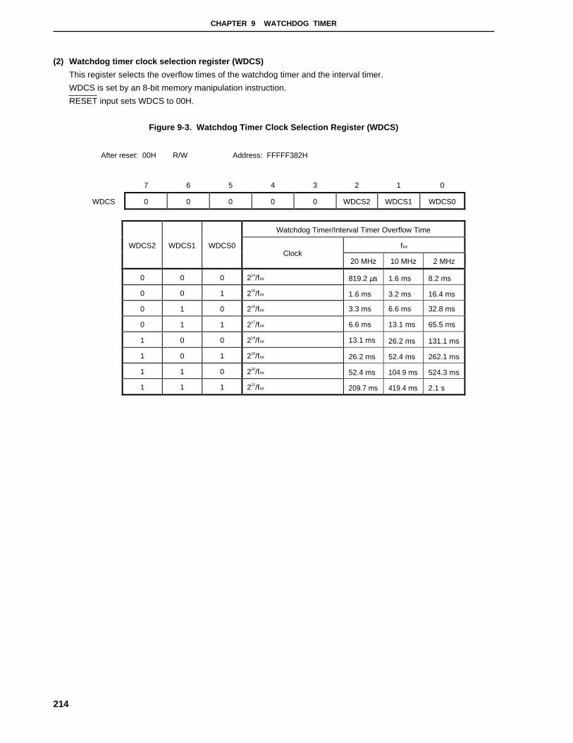
CHAPTER 9 WATCHDOG TIMER
214
(2) Watchdog timer clock selection register (WDCS)
This register selects the overflow times of the watchdog timer and the interval timer.
WDCS is set by an 8-bit memory manipulation instruction.
RESET input sets WDCS to 00H.
Figure 9-3. Watchdog Timer Clock Selection Register (WDCS)
After reset: 00H R/W Address: FFFFF382H
7 6 5 4 3 2 1 0
WDCS 0 0 0 0 0 WDCS2 WDCS1 WDCS0
Watchdog Timer/Interval Timer Overflow Time
fxxWDCS2 WDCS1 WDCS0Clock
20 MHz 10 MHz 2 MHz
0 0 0 214/fxx 819.2 µs 1.6 ms 8.2 ms
0 0 1 215/fxx 1.6 ms 3.2 ms 16.4 ms
0 1 0 216/fxx 3.3 ms 6.6 ms 32.8 ms
0 1 1 217/fxx 6.6 ms 13.1 ms 65.5 ms
1 0 0 218/fxx 13.1 ms 26.2 ms 131.1 ms
1 0 1 219/fxx 26.2 ms 52.4 ms 262.1 ms
1 1 0 220/fxx 52.4 ms 104.9 ms 524.3 ms
1 1 1 222/fxx 209.7 ms 419.4 ms 2.1 s

CHAPTER 9 WATCHDOG TIMER
215
(3) Watchdog timer mode register (WDTM)
This register sets the operating mode of the watchdog timer, and enables and disables counting.
WDTM is set by a 1-bit or 8-bit memory manipulation instruction.
RESET input sets WDTM to 00H.
Figure 9-4. Watchdog Timer Mode Register (WDTM)
After reset: 00H R/W Address: FFFFF384H
7 6 5 4 3 2 1 0
WDTM RUN 0 0 WDTM4 0 0 0 0
RUN Operating Mode Selection for the Watchdog Timer Note 1
0 Disable count
1 Clear count and start counting
WDTM4 Operating Mode Selection for the Watchdog Timer Note 2
0 Interval timer mode
(If an overflow occurs, a maskable interrupt INTWDTM is generated.)
1 Watchdog timer mode 1
(If an overflow occurs, a non-maskable interrupt INTWDT is generated.)
Notes 1. If RUN is set once to 1, the register cannot be cleared to 0 by software. Therefore, when the count
starts, the count cannot be stopped except by RESET input.
2. If WDTM4 is set once to 1, the register cannot be cleared to 0 by software.
Caution If RUN is set to 1 and the watchdog timer is cleared, the actual overflow time is a maximum of
0.5% less than the set time.

CHAPTER 9 WATCHDOG TIMER
216
9.4 Operation
9.4.1 Operating as watchdog timer
Set bit 4 (WDTM4) of the watchdog timer mode register (WDTM) to 1 to operate as a watchdog timer to detect
program runaway.
Setting bit 7 (RUN) of WDTM to 1 starts the count. After counting starts, if RUN is set to 1 again within the set
time interval for runaway detection, the watchdog timer is cleared and counting starts again.
If RUN is not set to 1 and the runaway detection time has elapsed, a non-maskable interrupt (INTWDT) is
generated (no reset functions).
The watchdog timer stops running in the STOP mode and IDLE mode. Consequently, set RUN to 1 and clear the
watchdog timer before entering the STOP mode or IDLE mode. Do not set the watchdog timer when operating the
HALT mode since the watchdog timer running in HALT mode.
Cautions 1. Sometimes, the actual runaway detection time is a maximum of 0.5% less than the set time.
2. When the subclock is selected in a CPU clock, the watchdog timer stops (retains) counting.
Table 9-4. Runaway Detection Time of Watchdog Timer
Runaway Detection TimeClock
fXX = 20 MHz fXX = 10 MHz fXX = 2 MHz
214/fxx 819.2 µs 1.6 ms 8.2 ms
215/fxx 1.6 ms 3.2 ms 16.4 ms
216/fxx 3.3 ms 6.6 ms 32.8 ms
217/fxx 6.6 ms 13.1 ms 65.5 ms
218/fxx 13.1 ms 26.2 ms 131.1 ms
219/fxx 26.2 ms 52.4 ms 262.1 ms
220/fxx 52.4 ms 104.9 ms 524.3 ms
222/fxx 209.7 ms 419.4 ms 2.1 s
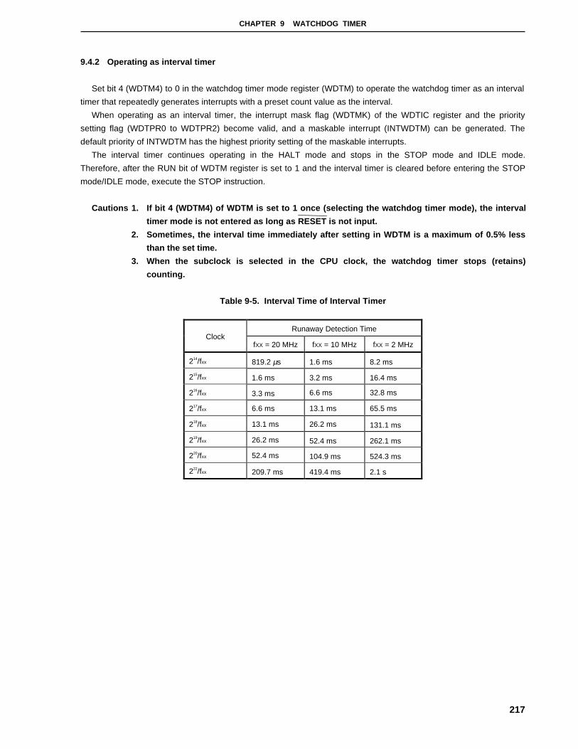
CHAPTER 9 WATCHDOG TIMER
217
9.4.2 Operating as interval timer
Set bit 4 (WDTM4) to 0 in the watchdog timer mode register (WDTM) to operate the watchdog timer as an interval
timer that repeatedly generates interrupts with a preset count value as the interval.
When operating as an interval timer, the interrupt mask flag (WDTMK) of the WDTIC register and the priority
setting flag (WDTPR0 to WDTPR2) become valid, and a maskable interrupt (INTWDTM) can be generated. The
default priority of INTWDTM has the highest priority setting of the maskable interrupts.
The interval timer continues operating in the HALT mode and stops in the STOP mode and IDLE mode.
Therefore, after the RUN bit of WDTM register is set to 1 and the interval timer is cleared before entering the STOP
mode/IDLE mode, execute the STOP instruction.
Cautions 1. If bit 4 (WDTM4) of WDTM is set to 1 once (selecting the watchdog timer mode), the interval
timer mode is not entered as long as RESET is not input.
2. Sometimes, the interval time immediately after setting in WDTM is a maximum of 0.5% less
than the set time.
3. When the subclock is selected in the CPU clock, the watchdog timer stops (retains)
counting.
Table 9-5. Interval Time of Interval Timer
Runaway Detection TimeClock
fXX = 20 MHz fXX = 10 MHz fXX = 2 MHz
214/fxx 819.2 µs 1.6 ms 8.2 ms
215/fxx 1.6 ms 3.2 ms 16.4 ms
216/fxx 3.3 ms 6.6 ms 32.8 ms
217/fxx 6.6 ms 13.1 ms 65.5 ms
218/fxx 13.1 ms 26.2 ms 131.1 ms
219/fxx 26.2 ms 52.4 ms 262.1 ms
220/fxx 52.4 ms 104.9 ms 524.3 ms
222/fxx 209.7 ms 419.4 ms 2.1 s
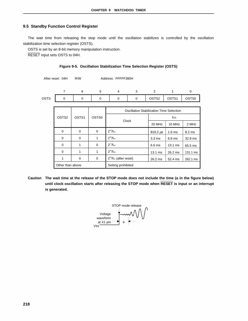
CHAPTER 9 WATCHDOG TIMER
218
9.5 Standby Function Control Register
The wait time from releasing the stop mode until the oscillation stabilizes is controlled by the oscillation
stabilization time selection register (OSTS).
OSTS is set by an 8-bit memory manipulation instruction.
RESET input sets OSTS to 04H.
Figure 9-5. Oscillation Stabilization Time Selection Register (OSTS)
After reset: 04H R/W Address: FFFFF380H
7 6 5 4 3 2 1 0
OSTS 0 0 0 0 0 OSTS2 OSTS1 OSTS0
Oscillation Stabilization Time Selection
fXXOSTS2 OSTS1 OSTS0Clock
20 MHz 10 MHz 2 MHz
0 0 0 214/fxx 819.2 µs 1.6 ms 8.2 ms
0 0 1 216/fxx 3.3 ms 6.6 ms 32.8 ms
0 1 0 217/fxx 6.6 ms 13.1 ms 65.5 ms
0 1 1 218/fxx 13.1 ms 26.2 ms 131.1 ms
1 0 0 219/fxx (after reset) 26.2 ms 52.4 ms 262.1 ms
Other than above Setting prohibited
Caution The wait time at the release of the STOP mode does not include the time (a in the figure below)
until clock oscillation starts after releasing the STOP mode when RESET is input or an interrupt
is generated.
Vss
STOP mode release
a
Voltagewaveformat X1 pin

219
CHAPTER 10 SERIAL INTERFACE FUNCTION
10.1 Overview
The V850/SB1 supports the following on-chip serial interfaces.
• Channel 0: 3-wire serial I/O (CSI0)/I2C0 Note
• Channel 1: 3-wire serial I/O (CSI1)/Asynchronous serial interface (UART0)
• Channel 2: 3-wire serial I/O (CSI2)/I2C1 Note
• Channel 3: 3-wire serial I/O (CSI3)/Asynchronous serial interface (UART1)
• Channel 4: 8 to 16-bit variable 3-wire serial I/O (CSI4)
Note I2C0 and I2C1 support Multi-master (µPD703033Y and 70F3033Y only).
Either 3-wire serial I/O or I2C can be used as a serial interface.
10.2 3-wire Serial I/O (CSI0 to CSI3)
The CSIn (n = 0 to 3) has the following two modes.
(1) Operation stop mode
This mode is used when serial transfers are not performed.
(2) 3-wire serial I/O mode (fixed as MSB first)
This is an 8-bit data transfer mode using three lines: a serial clock line (SCKn), serial output line (SOn), and
serial input line (SIn).
Since simultaneous transmit and receive operations are enabled in 3-wire serial I/O mode, the processing time
for data transfer is reduced.
The first bit in the 8-bit data in serial transfers is fixed as the MSB.
3-wire serial I/O mode is useful for connection to a peripheral I/O device that includes a clock-synchronous serial
interface, a display controller, etc.
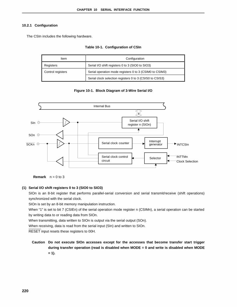
CHAPTER 10 SERIAL INTERFACE FUNCTION
220
10.2.1 Configuration
The CSIn includes the following hardware.
Table 10-1. Configuration of CSIn
Item Configuration
Registers Serial I/O shift registers 0 to 3 (SIO0 to SIO3)
Control registers Serial operation mode registers 0 to 3 (CSIM0 to CSIM3)
Serial clock selection registers 0 to 3 (CSIS0 to CSIS3)
Figure 10-1. Block Diagram of 3-Wire Serial I/O
INTTMn
Clock Selection
SCKn
SOn
SIn
INTCSIn
Internal Bus
Selector
8
Serial clock controlcircuit
Serial clock counter
Serial I/O shiftregister n (SIOn)
Interruptgenerator
Remark n = 0 to 3
(1) Serial I/O shift registers 0 to 3 (SIO0 to SIO3)
SIOn is an 8-bit register that performs parallel-serial conversion and serial transmit/receive (shift operations)
synchronized with the serial clock.
SIOn is set by an 8-bit memory manipulation instruction.
When “1” is set to bit 7 (CSIEn) of the serial operation mode register n (CSIMn), a serial operation can be started
by writing data to or reading data from SIOn.
When transmitting, data written to SIOn is output via the serial output (SOn).
When receiving, data is read from the serial input (SIn) and written to SIOn.
RESET input resets these registers to 00H.
Caution Do not execute SIOn accesses except for the accesses that become transfer start trigger
during transfer operation (read is disabled when MODE = 0 and write is disabled when MODE
= 1).
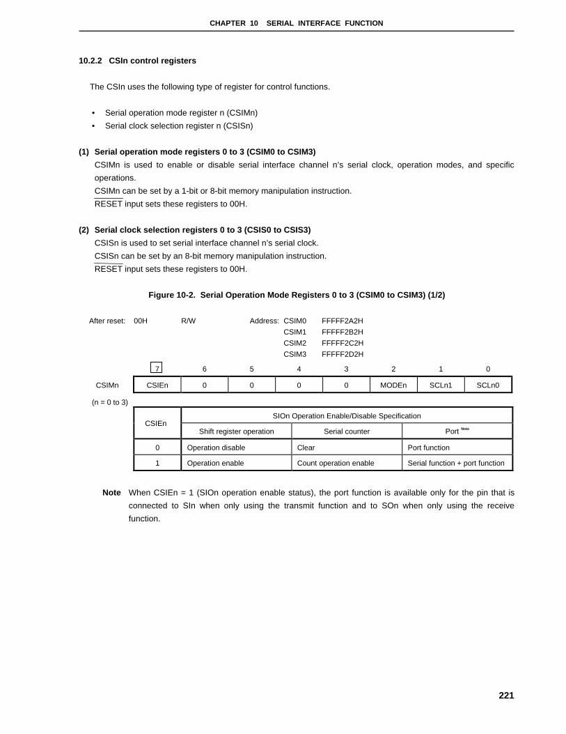
CHAPTER 10 SERIAL INTERFACE FUNCTION
221
10.2.2 CSIn control registers
The CSIn uses the following type of register for control functions.
• Serial operation mode register n (CSIMn)
• Serial clock selection register n (CSISn)
(1) Serial operation mode registers 0 to 3 (CSIM0 to CSIM3)
CSIMn is used to enable or disable serial interface channel n’s serial clock, operation modes, and specific
operations.
CSIMn can be set by a 1-bit or 8-bit memory manipulation instruction.
RESET input sets these registers to 00H.
(2) Serial clock selection registers 0 to 3 (CSIS0 to CSIS3)
CSISn is used to set serial interface channel n’s serial clock.
CSISn can be set by an 8-bit memory manipulation instruction.
RESET input sets these registers to 00H.
Figure 10-2. Serial Operation Mode Registers 0 to 3 (CSIM0 to CSIM3) (1/2)
After reset: 00H R/W Address: CSIM0 FFFFF2A2H
CSIM1 FFFFF2B2H
CSIM2 FFFFF2C2H
CSIM3 FFFFF2D2H
7 6 5 4 3 2 1 0
CSIMn CSIEn 0 0 0 0 MODEn SCLn1 SCLn0
(n = 0 to 3)
SIOn Operation Enable/Disable Specification
Shift register operation Serial counter Port Note
0 Operation disable Clear Port function
1 Operation enable Count operation enable Serial function + port function
Note When CSIEn = 1 (SIOn operation enable status), the port function is available only for the pin that is
connected to SIn when only using the transmit function and to SOn when only using the receive
function.
CSIEn

CHAPTER 10 SERIAL INTERFACE FUNCTION
222
Figure 10-2. Serial Operation Mode Registers 0 to 3 (CSIM0 to CSIM3) (2/2)
Transfer Operation Mode Flag
Operation mode Transfer start trigger SOn output
0 Transmit/receive mode SIOn write Normal output
1 Receive-only mode SIOn read Low level fixed
SCLn2 SCLn1 SCLn0 Clock Selection
0 0 0 External clock input (SCKn)
0 0 1 at n = 0, 3: TO2
at n = 1, 2: TO3
0 1 0 fxx/8
0 1 1 fxx/16
1 0 0 Setting prohibited
1 0 1 Setting prohibited
1 1 0 fxx/32
1 1 1 fxx/64
Caution Do not perform bit manipulation of the SCLn1 and SCLn0.
Remark Refer to Figure 10-3 for the SCLn2 bit.
Figure 10-3. Serial Clock Selection Registers 0 to 3 (CSIS0 to CSIS3)
After reset : 00H R/W Address: CSIS0 FFFFF2A4H
CSIS1 FFFFF2B4H
CSIS2 FFFFF2C4H
CSIS3 FFFFF2D4H
7 6 5 4 3 2 1 0
CSISn 0 0 0 0 0 0 0 SCLn2
(n = 0 to 3)
Remark Refer to Figure 10-2 for the setting of the SCLn2 bit.
MODEn

CHAPTER 10 SERIAL INTERFACE FUNCTION
223
10.2.3 Operations
The CSIn has the following two operation modes.
• Operation stop mode
• 3-wire serial I/O mode
(1) Operation stop mode
This mode does not perform serial transfers and can therefore reduce power consumption.
When in operation stop mode, if SIn, SOn, and the serial clock pin are also used as I/O ports, they can be used
as normal I/O ports as well.
(a) Register settings
Operation stop mode are set via serial operation mode register n (CSIMn).
CSIMn can be set by a 1-bit or 8-bit memory manipulation instruction.
RESET input sets the register to 00H.
Figure 10-4. Serial Operation Mode Registers 0 to 3 (CSIM0 to CSIM3)
After reset : 00H R/W Address: CSIM0 FFFFF2A2H
CSIM1 FFFFF2B2H
CSIM2 FFFFF2C2H
CSIM3 FFFFF2D2H
7 6 5 4 3 2 1 0
CSIMn CSIEn 0 0 0 0 MODEn SCLn1 SCLn0
(n = 0 to 3)
SIOn Operation Enable/Disable Specification
Shift register operation Serial counter Port Note
0 Operation disable Clear Port function
1 Operation enable Count operation enable Serial function + port function
Note When CSIEn = 1 (SIOn operation enable status), the port function is available only for the pin that is
connected to SIn when only using the transmit function and to SOn when only using the receive
function.
CSIEn
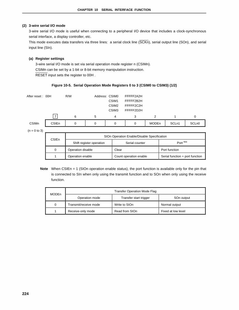
CHAPTER 10 SERIAL INTERFACE FUNCTION
224
(2) 3-wire serial I/O mode
3-wire serial I/O mode is useful when connecting to a peripheral I/O device that includes a clock-synchronous
serial interface, a display controller, etc.
This mode executes data transfers via three lines: a serial clock line (SCKn), serial output line (SOn), and serial
input line (SIn).
(a) Register settings
3-wire serial I/O mode is set via serial operation mode register n (CSIMn).
CSIMn can be set by a 1-bit or 8-bit memory manipulation instruction.
RESET input sets the register to 00H .
Figure 10-5. Serial Operation Mode Registers 0 to 3 (CSIM0 to CSIM3) (1/2)
After reset : 00H R/W Address: CSIM0 FFFFF2A2H
CSIM1 FFFFF2B2H
CSIM2 FFFFF2C2H
CSIM3 FFFFF2D2H
7 6 5 4 3 2 1 0
CSIMn CSIEn 0 0 0 0 MODEn SCLn1 SCLn0
(n = 0 to 3)
SIOn Operation Enable/Disable Specification
Shift register operation Serial counter Port Note
0 Operation disable Clear Port function
1 Operation enable Count operation enable Serial function + port function
Note When CSIEn = 1 (SIOn operation enable status), the port function is available only for the pin that
is connected to SIn when only using the transmit function and to SOn when only using the receive
function.
Transfer Operation Mode Flag
Operation mode Transfer start trigger SOn output
0 Transmit/receive mode Write to SIOn Normal output
1 Receive-only mode Read from SIOn Fixed at low level
CSIEn
MODEn

CHAPTER 10 SERIAL INTERFACE FUNCTION
225
Figure 10-5. Serial Operation Mode Registers 0 to 3 (CSIM0 to CSIM3) (2/2)
SCLn2 SCLn1 SCLn0 Clock Selection
0 0 0 External clock input (SCKn)
0 0 1 when n = 0, 3 : TO2
when n = 1, 2 : TO3
0 1 0 fxx/8
0 1 1 fxx/16
1 0 0 Setting prohibited
1 0 1 Setting prohibited
1 1 0 fxx/32
1 1 1 fxx/64
Remark Refer to Figure 10-3 for the SCLn2 bit.
(b) Communication Operations
In 3-wire serial I/O mode, data is transmitted and received in 8-bit units. Each bit of data is sent or received
in synchronized with the serial clock.
The serial I/O shift register n (SIOn) is shifted in synchronized with the falling edge of the serial clock.
Transmission data is held in the SOn latch and is output from the SOn pin. Data that is received via the SIn
pin in synchronized with the rising edge of the serial clock is latched to SIOn.
Completion of an 8-bit transfer automatically stops operation of SIOn and sets the interrupt request flag
(INTCSIn).
Figure 10-6. Timing of 3-Wire Serial I/O Mode
SI0 DI7 DI6 DI5 DI4 DI3 DI2 DI1 DI0
INTCSIn
Serial clock 1
SO0 DO7 DO6 DO5 DO4 DO3 DO2 DO1 DO0
2 3 4 5 6 7 8
Transfer completion
Transfer starts in synchronized with the serial clock’s falling edge
CHAPTER 10 SERIAL INTERFACE FUNCTION
226
(c) Transfer start
A serial transfer starts when the following two conditions have been satisfied and transfer data has been set
to serial I/O shift register n (SIOn).
• The SIOn operation control bit (CSIEn) = 1
• After an 8-bit serial transfer, the internal serial clock is either stopped or is set to high level.
• Transmit/receive mode
When CSIEn = 1 and MODEn = 0, transfer starts when writing to SIOn.
• Receive-only mode
When CSIEn = 1 and MODEn = 1, transfer starts when reading from SIOn.
Caution After data has been written to SIOn, transfer will not start even if the CSIEn bit value is
set to “1”.
Completion of an 8-bit transfer automatically stops the serial transfer operation and sets the interrupt request
flag (INTCSIn).

CHAPTER 10 SERIAL INTERFACE FUNCTION
227
10.3 I2C Bus ( µPD703033Y, 70F3033Y)
To use the I2C bus function, set the P10/SDA0, P12/SCL0, P20/SDA1, and P22/SCL1 pins to N-ch open
drain output.
The I2C0 and I2C1 have the following two modes.
• Operation stop mode
• I2C (Inter IC) bus mode (multi-master support)
(1) Operation stop mode
This mode is used when serial transfers are not performed. It can therefore be used to reduce power
consumption.
(2) I2C bus mode (multi-master support)
This mode is used for 8-bit data transfers with several devices via two lines: a serial clock (SCLn) line and a
serial data bus (SDAn) line.
This mode complies with the I2C bus format and the master device can output “start condition”, “data”, and “stop
condition” data to the slave device, via the serial data bus. The slave device automatically detects these
received data by hardware. This function can simplify the part of application program that controls the I2C bus.
Since SCLn and SDAn are open drain outputs, the I2Cn requires pull-up resistors for the serial clock line and the
serial data bus line.
Remark n = 0, 1

CHAPTER 10 SERIAL INTERFACE FUNCTION
228
Figure 10-7. Block Diagram of I 2C
Internal bus
IIC status register (IICSn)
IIC control register (IICCn)
Slave addressregister (SVAn)
Noise eliminationcircuit
Noise eliminationcircuit
Coincidencesignal
IIC shift register(IICn)
SO latch
IICE
DQ
SET
CLEAR
CL1,CL0
SDA
SCL
N-ch opendrain output
N-ch opendrain output
Data holdtime correction
circuit
ACK detectioncircuit
Wake up controlcircuit
ACK detection circuit
Stop conditiondetection circuit
Serial clock counterInterrupt requestsignal generator
Serial clock control circuit Serial clock waitcontrol circuit
Prescaler
INTIICn
fxx
TM2 output
CLDIIC clock selectregister (IICCLn)
Internal bus
LREL WREL SPIE WTIM ACKE STT SPT
MSTS ALD EXC COI TRC ACKD STD SPD
Start conditiondetection circuit
DAD SMC DFC CL1 CL0
Remark n = 0, 1

CHAPTER 10 SERIAL INTERFACE FUNCTION
229
Figure 10-8 shows a serial bus configuration example.
Figure 10-8. Serial Bus Configuration Example Using I 2C Bus
SDA
SCL
SDA
+VDD+VDD
SCL
SDA
SCL
Slave CPU3
Address 3
SDA
SCL
Slave IC
Address 4
SDA
SCL
Slave IC
Address N
Master CPU1
Slave CPU1
Address 1
Serial data bus
Serial clock
Master CPU2
Slave CPU2
Address 2

CHAPTER 10 SERIAL INTERFACE FUNCTION
230
10.3.1 Configuration
The I2Cn includes the following hardware (n = 0, 1).
Table 10-2. Configuration of I 2Cn
Item Configuration
Registers IIC shift registers 0 and 1 (IIC0, IIC1)
Slave address registers 0 and 1 (SVA0, SVA1)
Control registers IIC control registers 0 and 1 (IICC0, IICC1)
IIC status registers 0 and 1 (IICS0, IICS1)
IIC clock select registers 0 and 1 (IICCL0, IICCL1)
(1) IIC shift registers 0 and 1 (IIC0, IIC1)
IICn is used to convert 8-bit serial data to 8-bit parallel data and to convert 8-bit parallel data to 8-bit serial data.
IICn can be used for both transmission and reception (n = 0, 1).
Write and read operations to IICn are used to control the actual transmit and receive operations.
IICn is set by an 8-bit memory manipulation instruction.
RESET input sets the IIC0 and IIC1 to 00H.
(2) Slave address registers 0 and 1 (SVA0, SVA1)
SVAn sets local addresses when in slave mode.
SVAn is set by an 8-bit memory manipulation instruction (n = 0, 1).
RESET input sets the SVA0 and SVA1 to 00H.
(3) SO latch
The SO latch is used to retain the SDAn pin’s output level (n = 0, 1).
(4) Wake-up control circuit
This circuit generates an interrupt request when the address received by this register matches the address
value set to the slave address register (SVAn) or when an extension code is received (n = 0, 1).
(5) Clock selector
This selects the sampling clock to be used.
CHAPTER 10 SERIAL INTERFACE FUNCTION
231
(6) Serial clock counter
This counter counts the serial clocks that are output and the serial clocks that are input during transmit/receive
operations and is used to verify that 8-bit data was sent or received.
(7) Interrupt request signal generator
This circuit controls the generation of interrupt request signals.
An I2C interrupt is generated following either of two triggers.
• Eighth or ninth clock of the serial clock (set by WTIMn bit Note)
• Interrupt request generated when a stop condition is detected (set by SPIEn bit Note)
Note WTIMn bit : bit 3 of the IIC control register (IICCn)
SPIEn bit : bit 4 of the IIC control register (IICCn)
Remark n = 0, 1
(8) Serial clock control circuit
In master mode, this circuit generates the clock output via the SCLn pin from a sampling clock (n = 0, 1).
(9) Serial clock wait control circuit
This circuit controls the wait timing.
(10) ACK output circuit, stop condition detection circuit, start condition detection circuit, and ACK detection
circuit
These circuits are used to output and detect various control signals.
(11) Data hold time correction circuit
This circuit generates the hold time for data corresponding to the falling edge of the serial clock.

CHAPTER 10 SERIAL INTERFACE FUNCTION
232
10.3.2 I2C control register
I2C0 and I2C1 are controlled via three types of registers.
• IIC control registers 0, 1 (IICC0, IICC1)
• IIC status registers 0, 1 (IICS0, IICS1)
• IIC clock select registers 0, 1 (IICCL0, IICCL1)
The following registers are also used.
• IIC shift registers 0, 1 (IIC0, IIC1)
• Slave address registers 0, 1 (SVA0, SVA1)
(1) IIC control register 0, 1 (IICC0, IICC1)
IICCn is used to enable/disable I2C operations, set wait timing, and set other I2C operations.
IICCn can be set by a 1-bit or 8-bit memory manipulation instruction (n = 0, 1).
RESET input sets IICCn to 00H.
Caution In I 2C0, I2C1 bus mode, set port 1 mode register (PM1) and port 2 mode register (PM2) as follows. In
addition, set each output latch to 0.
• Set P10 (SDA0) to output mode (PM10 = 0)
• Set P12 (SCL0) to output mode (PM12 = 0)
• Set P20 (SDA1) to output mode (PM20 = 0)
• Set P22 (SCL1) to output mode (PM22 = 0)
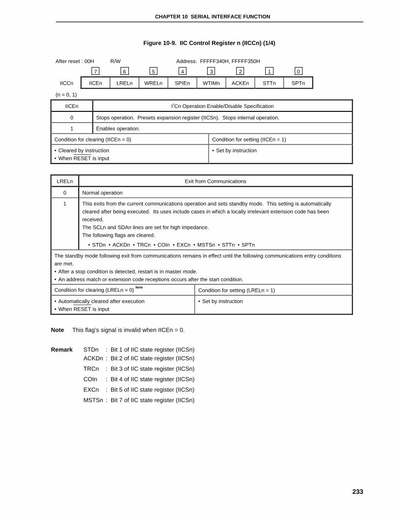
CHAPTER 10 SERIAL INTERFACE FUNCTION
233
Figure 10-9. IIC Control Register n (IICCn) (1/4)
After reset : 00H R/W Address: FFFFF340H, FFFFF350H
7 6 5 4 3 2 1 0
IICCn IICEn LRELn WRELn SPIEn WTIMn ACKEn STTn SPTn
(n = 0, 1)
IICEn I2Cn Operation Enable/Disable Specification
0 Stops operation. Presets expansion register (IICSn). Stops internal operation.
1 Enables operation.
Condition for clearing (IICEn = 0) Condition for setting (IICEn = 1)
• Cleared by instruction
• When RESET is input
• Set by instruction
LRELn Exit from Communications
0 Normal operation
1 This exits from the current communications operation and sets standby mode. This setting is automatically
cleared after being executed. Its uses include cases in which a locally irrelevant extension code has been
received.
The SCLn and SDAn lines are set for high impedance.
The following flags are cleared.
• STDn • ACKDn • TRCn • COIn • EXCn • MSTSn • STTn • SPTn
The standby mode following exit from communications remains in effect until the following communications entry conditions
are met.
• After a stop condition is detected, restart is in master mode.
• An address match or extension code receptions occurs after the start condition.
Condition for clearing (LRELn = 0) Note
Condition for setting (LRELn = 1)
• Automatically cleared after execution
• When RESET is input
• Set by instruction
Note This flag’s signal is invalid when IICEn = 0.
Remark STDn : Bit 1 of IIC state register (IICSn)
ACKDn : Bit 2 of IIC state register (IICSn)
TRCn : Bit 3 of IIC state register (IICSn)
COIn : Bit 4 of IIC state register (IICSn)
EXCn : Bit 5 of IIC state register (IICSn)
MSTSn : Bit 7 of IIC state register (IICSn)

CHAPTER 10 SERIAL INTERFACE FUNCTION
234
Figure 10-9. IIC Control Register n (IICCn) (2/4)
After reset : 00H R/W Address: FFFFF340H, FFFFF350H
7 6 5 4 3 2 1 0
IICCn IICEn LRELn WRELn SPIEn WTIMn ACKEn STTn SPTn
(n = 0, 1)
WRELn Wait Cancellation Control
0 Does not cancel wait
1 Cancels wait. This setting is automatically cleared after wait is canceled.
Condition for clearing (WRELn = 0) Note
Condition for setting (WRELn = 1)
• Automatically cleared after execution
• When RESET is input
• Set by instruction
SPIEn Enable/disable Generation of Interrupt Request when Stop Condition is Detected
0 Disable
1 Enable
Condition for clearing (SPIEn = 0) Note
Condition for setting (SPIEn = 1)
• Cleared by instruction
• When RESET is input
• Set by instruction
WTIMn Control of Wait and Interrupt Request Generation
0 Interrupt request is generated at the eighth clock’s falling edge.
Master mode : After output of eight clocks, clock output is set to low level and wait is set.
Slave mode : After input of eight clocks, the clock is set to low level and wait is set for master device.
1 Interrupt request is generated at the ninth clock’s falling edge.
Master mode : After output of nine clocks, clock output is set to low level and wait is set.
Slave mode : After input of nine clocks, the clock is set to low level and wait is set for master device.
This bit’s setting is invalid during an address transfer and is valid as the transfer is completed. When in master mode,
a wait is inserted at the falling edge of the ninth clock during address transfers. For a slave device that has received a
local address, a wait is inserted at the falling edge of the ninth clock after an ACK signal is issued. When the slave
device has received an extension code, a wait is inserted at the falling edge of the eighth clock.
Condition for clearing (WTIMn = 0) Note
Condition for setting (WTIMn = 1)
• Cleared by instruction
• When RESET is input
• Set by instruction
Note This flag’s signal is invalid when IICEn = 0.
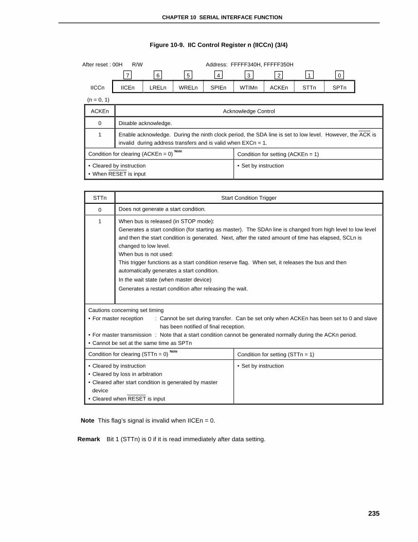
CHAPTER 10 SERIAL INTERFACE FUNCTION
235
Figure 10-9. IIC Control Register n (IICCn) (3/4)
After reset : 00H R/W Address: FFFFF340H, FFFFF350H
7 6 5 4 3 2 1 0
IICCn IICEn LRELn WRELn SPIEn WTIMn ACKEn STTn SPTn
(n = 0, 1)
ACKEn Acknowledge Control
0 Disable acknowledge.
1 Enable acknowledge. During the ninth clock period, the SDA line is set to low level. However, the ACK is
invalid during address transfers and is valid when EXCn = 1.
Condition for clearing (ACKEn = 0) Note
Condition for setting (ACKEn = 1)
• Cleared by instruction
• When RESET is input
• Set by instruction
STTn Start Condition Trigger
0 Does not generate a start condition.
1 When bus is released (in STOP mode):
Generates a start condition (for starting as master). The SDAn line is changed from high level to low level
and then the start condition is generated. Next, after the rated amount of time has elapsed, SCLn is
changed to low level.
When bus is not used:
This trigger functions as a start condition reserve flag. When set, it releases the bus and then
automatically generates a start condition.
In the wait state (when master device)
Generates a restart condition after releasing the wait.
Cautions concerning set timing
• For master reception : Cannot be set during transfer. Can be set only when ACKEn has been set to 0 and slave
has been notified of final reception.
• For master transmission : Note that a start condition cannot be generated normally during the ACKn period.
• Cannot be set at the same time as SPTn
Condition for clearing (STTn = 0) Note
Condition for setting (STTn = 1)
• Cleared by instruction
• Cleared by loss in arbitration
• Cleared after start condition is generated by master
device
• Cleared when RESET is input
• Set by instruction
Note This flag’s signal is invalid when IICEn = 0.
Remark Bit 1 (STTn) is 0 if it is read immediately after data setting.
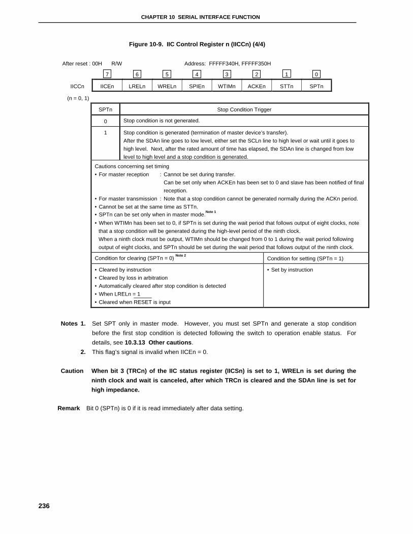
CHAPTER 10 SERIAL INTERFACE FUNCTION
236
Figure 10-9. IIC Control Register n (IICCn) (4/4)
After reset : 00H R/W Address: FFFFF340H, FFFFF350H
7 6 5 4 3 2 1 0
IICCn IICEn LRELn WRELn SPIEn WTIMn ACKEn STTn SPTn
(n = 0, 1)
SPTn Stop Condition Trigger
0 Stop condition is not generated.
1 Stop condition is generated (termination of master device’s transfer).
After the SDAn line goes to low level, either set the SCLn line to high level or wait until it goes to
high level. Next, after the rated amount of time has elapsed, the SDAn line is changed from low
level to high level and a stop condition is generated.
Cautions concerning set timing
• For master reception : Cannot be set during transfer.
Can be set only when ACKEn has been set to 0 and slave has been notified of final
reception.
• For master transmission : Note that a stop condition cannot be generated normally during the ACKn period.
• Cannot be set at the same time as STTn.• SPTn can be set only when in master mode.
Note 1
• When WTIMn has been set to 0, if SPTn is set during the wait period that follows output of eight clocks, note
that a stop condition will be generated during the high-level period of the ninth clock.
When a ninth clock must be output, WTIMn should be changed from 0 to 1 during the wait period following
output of eight clocks, and SPTn should be set during the wait period that follows output of the ninth clock.
Condition for clearing (SPTn = 0) Note 2
Condition for setting (SPTn = 1)
• Cleared by instruction
• Cleared by loss in arbitration
• Automatically cleared after stop condition is detected
• When LRELn = 1
• Cleared when RESET is input
• Set by instruction
Notes 1. Set SPT only in master mode. However, you must set SPTn and generate a stop condition
before the first stop condition is detected following the switch to operation enable status. For
details, see 10.3.13 Other cautions .
2. This flag’s signal is invalid when IICEn = 0.
Caution When bit 3 (TRCn) of the IIC status register (IICSn) is set to 1, WRELn is set during the
ninth clock and wait is canceled, after which TRCn is cleared and the SDAn line is set for
high impedance.
Remark Bit 0 (SPTn) is 0 if it is read immediately after data setting.

CHAPTER 10 SERIAL INTERFACE FUNCTION
237
(2) IIC status registers 0, 1 (IICS0, IICS1)
IICSn indicates the status of the I2Cn bus.
IICSn can be set by a 1-bit or 8-bit memory manipulation instruction. IICSn is a read-only register (n = 0, 1).
RESET input sets IICSn to 00H.
Figure 10-10. IIC Status Register n (IICSn) (1/3)
After reset : 00H R Address: FFFFF342H, FFFFF352H
7 6 5 4 3 2 1 0
IICSn MSTSn ALDn EXCn COIn TRCn ACKDn STDn SPDn
(n = 0, 1)
MSTSn Master Device Status
0 Slave device status or communication standby status
1 Master device communication status
Condition for clearing (MSTSn = 0) Condition for setting (MSTSn = 1)
• When a stop condition is detected
• When ALDn = 1
• Cleared by LRELn = 1
• When IICEn changes from 1 to 0
• When RESET is input
• When a start condition is generated
ALDn Detection of Arbitration Loss
0 This status means either that there was no arbitration or that the arbitration result was a “win”.
1 This status indicates the arbitration result was a “loss”. MSTSn is cleared.
Condition for clearing (ALDn = 0) Condition for setting (ALDn = 1)
• Automatically cleared after IICSn is read Note
• When IICEn changes from 1 to 0
• When RESET is input
• When the arbitration result is a “loss”.
Note This register is also cleared when a bit manipulation instruction is executed for bits other than IICSn.
Remark LRELn : Bit 6 of IIC control register (IICCn)
IICEn : Bit 7 of IIC control register (IICCn)

CHAPTER 10 SERIAL INTERFACE FUNCTION
238
Figure 10-10. IIC Status Register n (IICSn) (2/3)
After reset : 00H R Address: FFFFF342H, FFFFF352H
7 6 5 4 3 2 1 0
IICSn MSTSn ALDn EXCn COIn TRCn ACKDn STDn SPDn
(n = 0, 1)
EXCn Detection of Extension Code Reception
0 Extension code was not received.
1 Extension code was received.
Condition for clearing (EXCn = 0) Condition for setting (EXCn = 1)
• When a start condition is detected
• When a stop condition is detected
• Cleared by LRELn = 1
• When IICEn changes from 1 to 0
• When RESET is input
• When the high-order four bits of the received address
data is either “0000” or “1111” (set at the rising edge of
the eighth clock).
COIn Detection of Matching Addresses
0 Addresses do not match.
1 Addresses match.
Condition for clearing (COIn = 0) Condition for setting (COIn = 1)
• When a start condition is detected
• When a stop condition is detected
• Cleared by LRELn = 1
• When IICEn changes from 1 to 0
• When RESET is input
• When the received address matches the local address
(SVAn) (set at the rising edge of the eighth clock).
TRCn Detection of Transmit/Receive Status
0 Receive status (other than transmit status). The SDAn line is set for high impedance.
1 Transmit status. The value in the SO latch is enabled for output to the SDAn line (valid starting at the
falling edge of the first byte’s ninth clock).
Condition for clearing (TRCn = 0) Condition for setting (TRCn = 1)
• When a stop condition is detected
• Cleared by LRELn = 1
• When IICEn changes from 1 to 0
• Cleared by WRELn = 1
• When ALDn changes from 0 to 1
• When RESET is input
Master
• When “1” is output to the first byte’s LSB (transfer
direction specification bit)
Slave
• When a start condition is detected
When not used for communication
Master
• When a start condition is generated
Slave
• When “1” is input by the first byte’s LSB (transfer
direction specification bit)
Remark LRELn : Bit 6 of IIC control register (IICCn)
IICEn : Bit 7 of IIC control register (IICCn)
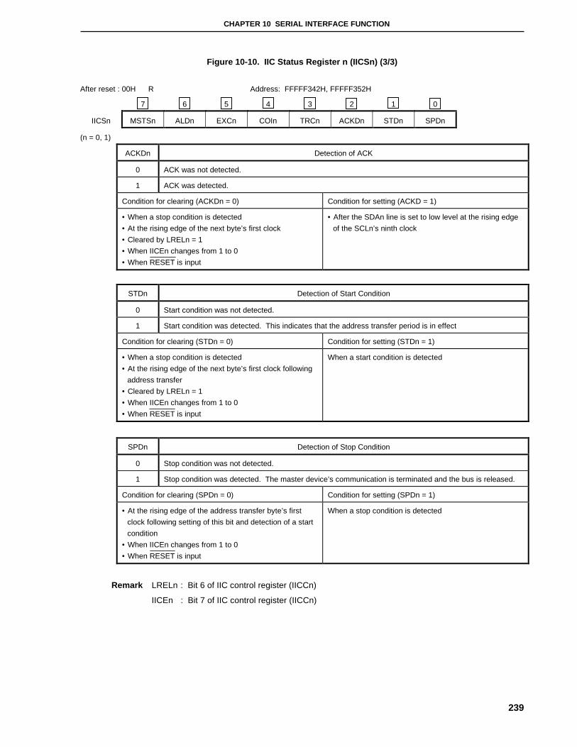
CHAPTER 10 SERIAL INTERFACE FUNCTION
239
Figure 10-10. IIC Status Register n (IICSn) (3/3)
After reset : 00H R Address: FFFFF342H, FFFFF352H
7 6 5 4 3 2 1 0
IICSn MSTSn ALDn EXCn COIn TRCn ACKDn STDn SPDn
(n = 0, 1)
ACKDn Detection of ACK
0 ACK was not detected.
1 ACK was detected.
Condition for clearing (ACKDn = 0) Condition for setting (ACKD = 1)
• When a stop condition is detected
• At the rising edge of the next byte’s first clock
• Cleared by LRELn = 1
• When IICEn changes from 1 to 0
• When RESET is input
• After the SDAn line is set to low level at the rising edge
of the SCLn’s ninth clock
STDn Detection of Start Condition
0 Start condition was not detected.
1 Start condition was detected. This indicates that the address transfer period is in effect
Condition for clearing (STDn = 0) Condition for setting (STDn = 1)
• When a stop condition is detected
• At the rising edge of the next byte’s first clock following
address transfer
• Cleared by LRELn = 1
• When IICEn changes from 1 to 0
• When RESET is input
When a start condition is detected
SPDn Detection of Stop Condition
0 Stop condition was not detected.
1 Stop condition was detected. The master device’s communication is terminated and the bus is released.
Condition for clearing (SPDn = 0) Condition for setting (SPDn = 1)
• At the rising edge of the address transfer byte’s first
clock following setting of this bit and detection of a start
condition
• When IICEn changes from 1 to 0
• When RESET is input
When a stop condition is detected
Remark LRELn : Bit 6 of IIC control register (IICCn)
IICEn : Bit 7 of IIC control register (IICCn)

CHAPTER 10 SERIAL INTERFACE FUNCTION
240
(3) IIC clock select registers 0, 1 (IICCL0, IICCL1)
IICCLn is used to set the transfer clock for the I2Cn bus.
IICCLn can be set by a 1-bit or 8-bit memory manipulation instruction (n = 0, 1).
RESET input sets IICCLn to 00H.
Figure 10-11. IIC Clock Select Register n (IICCLn) (1/2)
After reset : 00H R/W Note
Address: FFFFF344H, FFFFF354H
7 6 5 4 3 2 1 0
IICCLn 0 0 CLDn DADn SMCn DFCn CLn1 CLn0
(n = 0, 1)
CLDn Detection of SCLn Line Level (valid only when IICEn = 1)
0 SCLn line was detected at low level.
1 SCLn line was detected at high level.
Condition for clearing (CLDn = 0) Condition for setting (CLDn = 1)
• When the SCLn line is at low level
• When IICEn = 0
• When RESET is input
• When the SCLn line is at high level
DADn Detection of SDAn Line Level (valid only when IICEn = 1)
0 SDAn line was detected at low level.
1 SDAn line was detected at high level.
Condition for clearing (DADn = 0) Condition for setting (DADn = 1)
• When the SDAn line is at low level
• When IICEn = 0
• When RESET is input
• When the SDAn line is at high level

CHAPTER 10 SERIAL INTERFACE FUNCTION
241
Figure 10-11. IIC Clock Select Register n (IICCLn) (2/2)
After reset : 00H R/W Note
Address: FFFFF344H, FFFFF354H
7 6 5 4 3 2 1 0
IICCLn 0 0 CLDn DADn SMCn DFCn CLn1 CLn0
(n = 0, 1)
SMCn DFCn Note
CLn1 CLn0 Clock Selection Note 3
1 × 0 0 fXX/24
1 × 0 1 fXX/24
4.0 to 8.388 MHz
1 × 1 0 fXX/48 8.0 to 16.776 MHz
1 × 1 1 TM2 output/18 (n = 0), TM3 output/18 (n = 1) −
0 0 0 0 fXX/44
0 0 0 1 fXX/86
2.0 to 8.388 MHz
0 0 1 0 fXX/172 4.0 to 16.776 MHz
0 0 1 1 TM2 output/66 (n = 0), TM3 output/66 (n = 1) −
0 1 0 0 fXX/46
0 1 0 1 fXX/88
2.0 to 8.388 MHz
0 1 1 0 fXX/176 4.0 to 16.776 MHz
0 1 1 1 TM2 output/68 (n = 0), TM3 output/68 (n = 1) −
Notes 1. Bits 4 and 5 are read only bits.
2. Digital filter (DFCn) can be used in high-speed mode. Response time become slow while the digital filter is
used.
3. Setting can be done only when the main clock frequency (fXX) is within the range indicated in this table.
Remarks 1. IICEn: Bit 7 of IIC control register n (IICCn)
2. ×: don’t care
(4) IIC shift registers 0, 1 (IIC0, IIC1)
IICn is used for serial transmission/reception (shift operations) that are synchronized with the serial clock. It can
be read from or written to in 8-bit units, but data should not be written to IICn during a data transfer (n = 0, 1).
After reset : 00H R/W Address: FFFFF348H, FFFFF358H
7 6 5 4 3 2 1 0
IICn
(n = 0, 1)
(5) Slave address registers 0, 1 (SVA0, SVA1)
SVAn holds the I2C bus’s slave addresses.
It can be read from or written to in 8-bit units, but bit 0 should be fixed as 0.
After reset : 00H R/W Address: FFFFF346H, FFFFF356H
7 6 5 4 3 2 1 0
SVAn 0
(n = 0, 1)

CHAPTER 10 SERIAL INTERFACE FUNCTION
242
10.3.3 I2C bus mode functions
(1) Pin configuration
The serial clock pin (SCLn) and serial data bus pin (SDAn) are configured as follows (n = 0, 1).
SCLn .............. This pin is used for serial clock input and output.
This pin is an N-ch open-drain output for both master and slave devices. Input is Schmitt input.
SDAn .............. This pin is used for serial data input and output.
This pin is an N-ch open-drain output for both master and slave devices. Input is Schmitt input.
Since outputs from the serial clock line and the serial data bus line are N-ch open-drain outputs, an external pull-up
resistor is required.
Figure 10-12. Pin Configuration Diagram
VDD
SCLn
SDAn
SCLn
SDAn
VDD
Clock output
Master device
(Clock input)
Data output
Data input
(Clock output)
Clock input
Data output
Data input
Slave device
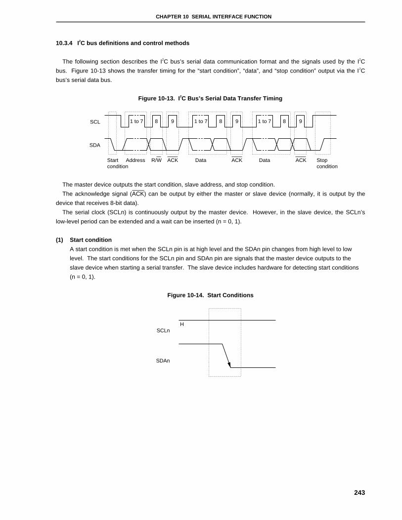
CHAPTER 10 SERIAL INTERFACE FUNCTION
243
10.3.4 I2C bus definitions and control methods
The following section describes the I2C bus’s serial data communication format and the signals used by the I2C
bus. Figure 10-13 shows the transfer timing for the “start condition”, “data”, and “stop condition” output via the I2C
bus’s serial data bus.
Figure 10-13. I 2C Bus’s Serial Data Transfer Timing
1 to 7 8 9 1 to 7 8 9 1 to 7 8 9SCL
SDA
Startcondition
Address R/W ACK Data Data Stop condition
ACK ACK
The master device outputs the start condition, slave address, and stop condition.
The acknowledge signal (ACK) can be output by either the master or slave device (normally, it is output by the
device that receives 8-bit data).
The serial clock (SCLn) is continuously output by the master device. However, in the slave device, the SCLn’s
low-level period can be extended and a wait can be inserted (n = 0, 1).
(1) Start condition
A start condition is met when the SCLn pin is at high level and the SDAn pin changes from high level to low
level. The start conditions for the SCLn pin and SDAn pin are signals that the master device outputs to the
slave device when starting a serial transfer. The slave device includes hardware for detecting start conditions
(n = 0, 1).
Figure 10-14. Start Conditions
HSCLn
SDAn

CHAPTER 10 SERIAL INTERFACE FUNCTION
244
A start condition is output when the IIC control register n (IICCn)’s bit 1 (STTn) is set to 1 after a stop condition
has been detected (SPDn: Bit 0 = 1 in the IIC status register n (IICSn)). When a start condition is detected,
IICSn’s bit 1 (STDn) is set to 1 (n = 0, 1).
(2) Addresses
The 7 bits of data that follow the start condition are defined as an address.
An address is a 7-bit data segment that is output in order to select one of the slave devices that are connected
to the master device via bus lines. Therefore, each slave device connected via the bus lines must have a
unique address.
The slave devices include hardware that detects the start condition and checks whether or not the 7-bit address
data matches the data values stored in the slave address register n (SVAn). If the address data matches the
SVAn values, the slave device is selected and communicates with the master device until the master device
transmits a start condition or stop condition (n = 0, 1).
Figure 10-15. Address
Address
SCLn 1
SDAn
INTIICnNote
2 3 4 5 6 7 8 9
AD6 AD5 AD4 AD3 AD2 AD1 AD0 R/W
Note INTIICn is not generated if data other than a local address or extension code is received during slave
device operation.
Remark n = 0, 1
The slave address and the eighth bit, which specifies the transfer direction as described in (3) Transfer direction
specification below, are together written to the IIC shift register (IICn) and are then output. Received addresses are
written to IICn (n = 0, 1).
The slave address is assigned to the high-order 7 bits of IICn.

CHAPTER 10 SERIAL INTERFACE FUNCTION
245
(3) Transfer direction specification
In addition to the 7-bit address data, the master device sends 1 bit that specifies the transfer direction. When
this transfer direction specification bit has a value of 0, it indicates that the master device is transmitting data to
a slave device. When the transfer direction specification bit has a value of 1, it indicates that the master device
is receiving data from a slave device.
Figure 10-16. Transfer Direction Specification
SCLn 1
SDAn
INTIICn
2 3 4 5 6 7 8 9
AD6 AD5 AD4 AD3 AD2 AD1 AD0 R/W
Transfer direction specification
Note
Note INTIICn is not generated if data other than a local address or extension code is received during slave
device operation.
Remark n = 0, 1
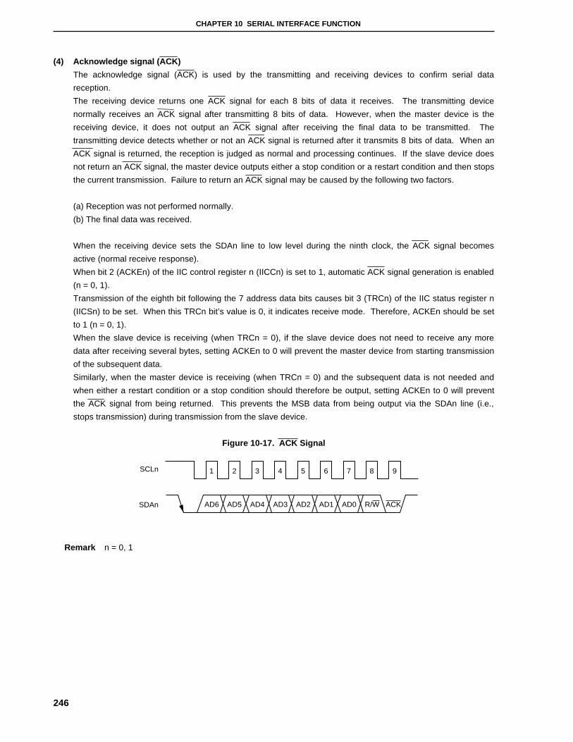
CHAPTER 10 SERIAL INTERFACE FUNCTION
246
(4) Acknowledge signal (ACK)
The acknowledge signal (ACK) is used by the transmitting and receiving devices to confirm serial data
reception.
The receiving device returns one ACK signal for each 8 bits of data it receives. The transmitting device
normally receives an ACK signal after transmitting 8 bits of data. However, when the master device is the
receiving device, it does not output an ACK signal after receiving the final data to be transmitted. The
transmitting device detects whether or not an ACK signal is returned after it transmits 8 bits of data. When an
ACK signal is returned, the reception is judged as normal and processing continues. If the slave device does
not return an ACK signal, the master device outputs either a stop condition or a restart condition and then stops
the current transmission. Failure to return an ACK signal may be caused by the following two factors.
(a) Reception was not performed normally.
(b) The final data was received.
When the receiving device sets the SDAn line to low level during the ninth clock, the ACK signal becomes
active (normal receive response).
When bit 2 (ACKEn) of the IIC control register n (IICCn) is set to 1, automatic ACK signal generation is enabled
(n = 0, 1).
Transmission of the eighth bit following the 7 address data bits causes bit 3 (TRCn) of the IIC status register n
(IICSn) to be set. When this TRCn bit’s value is 0, it indicates receive mode. Therefore, ACKEn should be set
to 1 (n = 0, 1).
When the slave device is receiving (when TRCn = 0), if the slave device does not need to receive any more
data after receiving several bytes, setting ACKEn to 0 will prevent the master device from starting transmission
of the subsequent data.
Similarly, when the master device is receiving (when TRCn = 0) and the subsequent data is not needed and
when either a restart condition or a stop condition should therefore be output, setting ACKEn to 0 will prevent
the ACK signal from being returned. This prevents the MSB data from being output via the SDAn line (i.e.,
stops transmission) during transmission from the slave device.
Figure 10-17. ACK Signal
SCLn 1
SDAn
2 3 4 5 6 7 8 9
AD6 AD5 AD4 AD3 AD2 AD1 AD0 R/W ACK
Remark n = 0, 1

CHAPTER 10 SERIAL INTERFACE FUNCTION
247
When the local address is received, an ACK signal is automatically output in synchronization with the falling edge
of the SCLn’s eighth clock regardless of the ACKEn value. No ACK signal is output if the received address is not a
local address (n = 0, 1).
The ACK signal output method during data reception is based on the wait timing setting, as described below.
When 8-clock wait is selected: ACK signal is output when ACKEn is set to 1 before wait cancellation.
When 9-clock wait is selected: ACK signal is automatically output at the falling edge of the SCLn’s eighth clock if
ACKEn has already been set to 1.
(5) Stop condition
When the SCLn pin is at high level, changing the SDAn pin from low level to high level generates a stop
condition (n = 0, 1).
A stop condition is a signal that the master device outputs to the slave device when serial transfer has been
completed. The slave device includes hardware that detects stop conditions.
Figure 10-18. Stop Condition
HSCLn
SDAn
Remark n = 0, 1
A stop condition is generated when bit 0 (SPTn) of the IIC control register n (IICCn) is set to 1. When the stop
condition is detected, bit 0 (SPDn) of the IIC status register n (IICSn) is set to 1 and INTIICn is generated when
bit 4 (SPIEn) of IICCn is set to 1 (n = 0, 1).
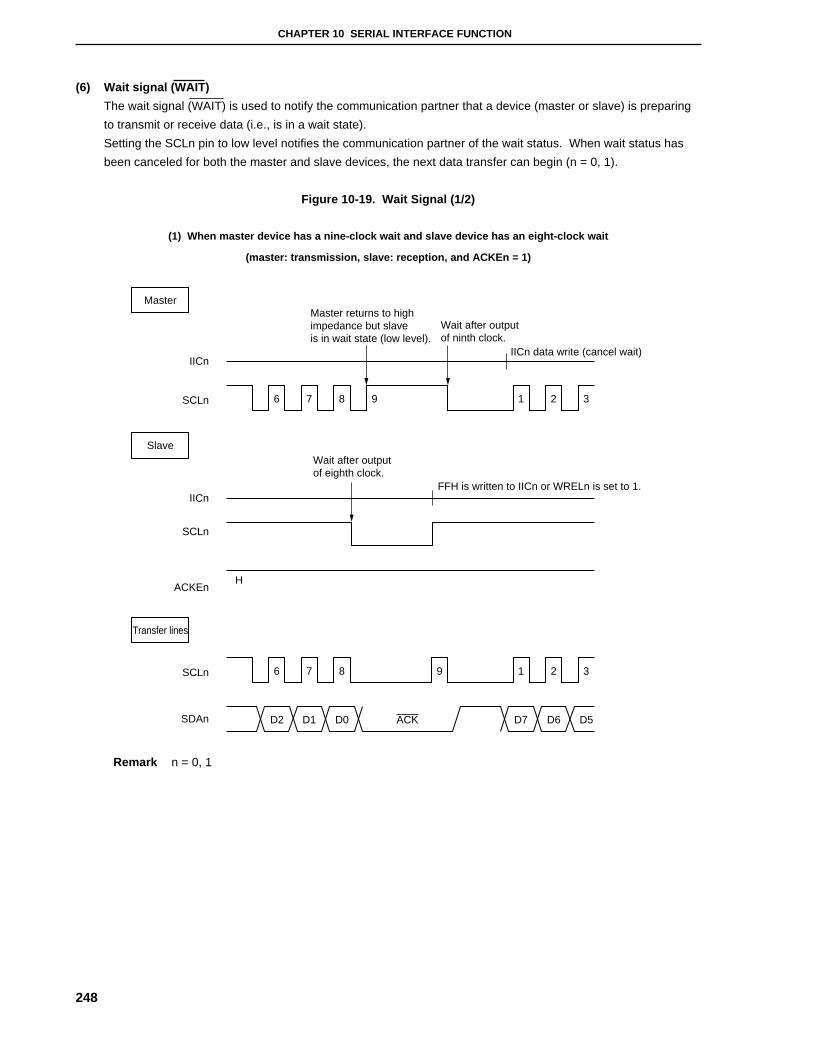
CHAPTER 10 SERIAL INTERFACE FUNCTION
248
(6) Wait signal (WAIT)
The wait signal (WAIT) is used to notify the communication partner that a device (master or slave) is preparing
to transmit or receive data (i.e., is in a wait state).
Setting the SCLn pin to low level notifies the communication partner of the wait status. When wait status has
been canceled for both the master and slave devices, the next data transfer can begin (n = 0, 1).
Figure 10-19. Wait Signal (1/2)
(1) When master device has a nine-clock wait and slave device has an eight-clock wait
(master: transmission, slave: reception, and ACKEn = 1)
SCLn 6
SDAn
7 8 9 1 2 3
SCLn
IICn
6
H
7 8 1 2 3
D2 D1 D0 ACK D7 D6 D5
9
IICn
SCLn
ACKEn
MasterMaster returns to highimpedance but slaveis in wait state (low level).
Wait after outputof ninth clock.
IICn data write (cancel wait)
SlaveWait after outputof eighth clock.
FFH is written to IICn or WRELn is set to 1.
Transfer lines
Remark n = 0, 1

CHAPTER 10 SERIAL INTERFACE FUNCTION
249
Figure 10-19. Wait Signal (2/2)
(2) When master and slave devices both have a nine-clock wait
(master: transmission, slave: reception, and ACKEn = 1)
SCLn 6
SDAn
7 8 9 1 2 3
SCLn
IICn
6
H
7 8 1 2 3
D2 D1 D0 ACK D7 D6 D5
9
IICn
SCLn
ACKEn
Master Master and slave both waitafter output of ninth clock.
IICn data write (cancel wait)
Slave
FFH is written to IICn or WRELn is set to 1.
Output according to previously set ACKEn value
Transfer lines
Remarks 1. ACKEn : Bit 2 of IIC control register n (IICCn)
WRELn : Bit 5 of IIC control register n (IICCn)
2. n = 0, 1
A wait may be automatically generated depending on the setting for bit 3 (WTIMn) of the IIC control register n
(IICCn) (n = 0, 1).
Normally, when bit 5 (WRELn) of IICCn is set to 1 or when FFH is written to the IIC shift register n (IICn), the wait
status is canceled and the transmitting side writes data to IICn to cancel the wait status.
The master device can also cancel the wait status via either of the following methods.
• By setting bit 1 (STTn) of IICCn to 1
• By setting bit 0 (SPTn) of IICCn to 1

CHAPTER 10 SERIAL INTERFACE FUNCTION
250
10.3.5 I2C interrupt requests (INTIICn)
The following shows the value of IIC status register n (IICSn) at the INTIICn interrupt request generation timing and
at the INTIICn interrupt timing (n = 0, 1).
(1) Master device operation
(a) Start ~ Address ~ Data ~ Data ~ Stop (normal transmission/reception)
<1> When WTIMn = 0
ST AD6-AD0 RW AK D7-D0 AK D7-D0 AK SP
▲1 ▲2 ▲3 ∆4
▲1 : IICSn = 10XXX110B
▲2 : IICSn = 10XXX000B
▲3 : IICSn = 10XXX000B
∆ 4 : IICSn = 00000001B
Remark ▲ : Always generated
∆ : Generated only when SPIEn = 1
X : don’t care
n = 0, 1
<2> When WTIMn = 1
ST AD6-AD0 RW AK D7-D0 AK D7-D0 AK SP
▲1 ▲2 ▲3 ∆4
▲1 : IICSn = 10XXX110B
▲2 : IICSn = 10XXX100B
▲3 : IICSn = 10XXXX00B
∆ 4 : IICSn = 00000001B
Remark ▲ : Always generated
∆ : Generated only when SPIEn = 1
X : don’t care
n = 0, 1
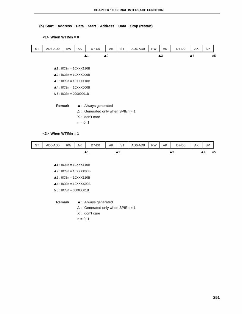
CHAPTER 10 SERIAL INTERFACE FUNCTION
251
(b) Start ~ Address ~ Data ~ Start ~ Address ~ Data ~ Stop (restart)
<1> When WTIMn = 0
ST AD6-AD0 RW AK D7-D0 AK ST AD6-AD0 RW AK D7-D0 AK SP
▲1 ▲2 ▲3 ▲4 ∆5
▲1 : IICSn = 10XXX110B
▲2 : IICSn = 10XXX000B
▲3 : IICSn = 10XXX110B
▲4 : IICSn = 10XXX000B
∆ 5 : IICSn = 00000001B
Remark ▲ : Always generated
∆ : Generated only when SPIEn = 1
X : don’t care
n = 0, 1
<2> When WTIMn = 1
ST AD6-AD0 RW AK D7-D0 AK ST AD6-AD0 RW AK D7-D0 AK SP
▲1 ▲2 ▲3 ▲4 ∆5
▲1 : IICSn = 10XXX110B
▲2 : IICSn = 10XXXX00B
▲3 : IICSn = 10XXX110B
▲4 : IICSn = 10XXXX00B
∆ 5 : IICSn = 00000001B
Remark ▲ : Always generated
∆ : Generated only when SPIEn = 1
X : don’t care
n = 0, 1

CHAPTER 10 SERIAL INTERFACE FUNCTION
252
(c) Start ~ Code ~ Data ~ Data ~ Stop (extension code transmission)
<1> When WTIMn = 0
ST AD6-AD0 RW AK D7-D0 AK D7-D0 AK SP
▲1 ▲2 ▲3 ∆4
▲1 : IICSn = 1010X110B
▲2 : IICSn = 1010X000B
▲3 : IICSn = 1010X000B
∆ 4 : IICSn = 00000001B
Remark ▲ : Always generated
∆ : Generated only when SPIEn = 1
X : don’t care
n = 0, 1
<2> When WTIMn = 1
ST AD6-AD0 RW AK D7-D0 AK D7-D0 AK SP
▲1 ▲2 ▲3 ∆4
▲1 : IICSn = 1010X110B
▲2 : IICSn = 1010X100B
▲3 : IICSn = 1010XX00B
∆ 4 : IICSn = 00000001B
Remark ▲ : Always generated
∆ : Generated only when SPIEn = 1
X : don’t care
n = 0, 1
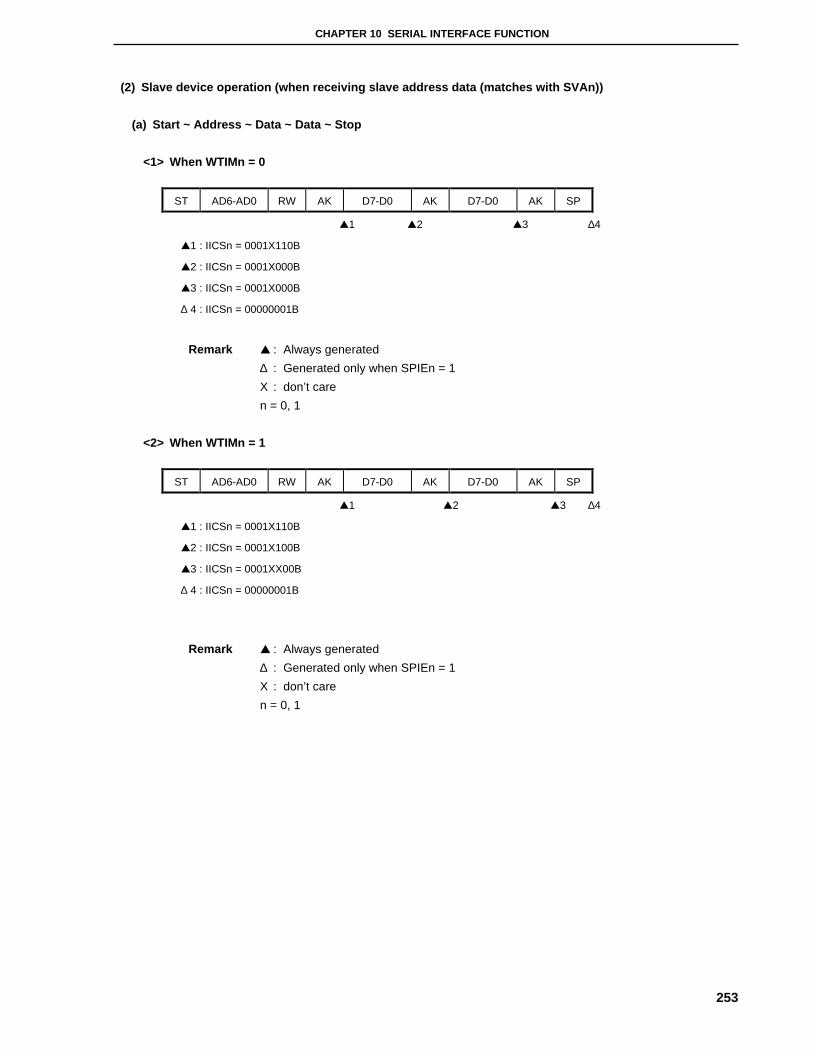
CHAPTER 10 SERIAL INTERFACE FUNCTION
253
(2) Slave device operation (when receiving slave address data (matches with SVAn))
(a) Start ~ Address ~ Data ~ Data ~ Stop
<1> When WTIMn = 0
ST AD6-AD0 RW AK D7-D0 AK D7-D0 AK SP
▲1 ▲2 ▲3 ∆4
▲1 : IICSn = 0001X110B
▲2 : IICSn = 0001X000B
▲3 : IICSn = 0001X000B
∆ 4 : IICSn = 00000001B
Remark ▲ : Always generated
∆ : Generated only when SPIEn = 1
X : don’t care
n = 0, 1
<2> When WTIMn = 1
ST AD6-AD0 RW AK D7-D0 AK D7-D0 AK SP
▲1 ▲2 ▲3 ∆4
▲1 : IICSn = 0001X110B
▲2 : IICSn = 0001X100B
▲3 : IICSn = 0001XX00B
∆ 4 : IICSn = 00000001B
Remark ▲ : Always generated
∆ : Generated only when SPIEn = 1
X : don’t care
n = 0, 1
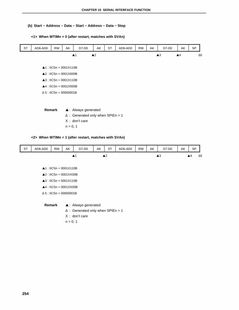
CHAPTER 10 SERIAL INTERFACE FUNCTION
254
(b) Start ~ Address ~ Data ~ Start ~ Address ~ Data ~ Stop
<1> When WTIMn = 0 (after restart, matches with SVAn)
ST AD6-AD0 RW AK D7-D0 AK ST AD6-AD0 RW AK D7-D0 AK SP
▲1 ▲2 ▲3 ▲4 ∆5
▲1 : IICSn = 0001X110B
▲2 : IICSn = 0001X000B
▲3 : IICSn = 0001X110B
▲4 : IICSn = 0001X000B
∆ 5 : IICSn = 00000001B
Remark ▲ : Always generated
∆ : Generated only when SPIEn = 1
X : don’t care
n = 0, 1
<2> When WTIMn = 1 (after restart, matches with SVAn)
ST AD6-AD0 RW AK D7-D0 AK ST AD6-AD0 RW AK D7-D0 AK SP
▲1 ▲2 ▲3 ▲4 ∆5
▲1 : IICSn = 0001X110B
▲2 : IICSn = 0001XX00B
▲3 : IICSn = 0001X110B
▲4 : IICSn = 0001XX00B
∆ 5 : IICSn = 00000001B
Remark ▲ : Always generated
∆ : Generated only when SPIEn = 1
X : don’t care
n = 0, 1
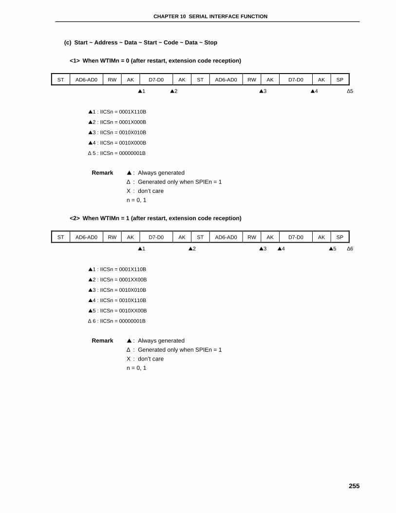
CHAPTER 10 SERIAL INTERFACE FUNCTION
255
(c) Start ~ Address ~ Data ~ Start ~ Code ~ Data ~ Stop
<1> When WTIMn = 0 (after restart, extension code reception)
ST AD6-AD0 RW AK D7-D0 AK ST AD6-AD0 RW AK D7-D0 AK SP
▲1 ▲2 ▲3 ▲4 ∆5
▲1 : IICSn = 0001X110B
▲2 : IICSn = 0001X000B
▲3 : IICSn = 0010X010B
▲4 : IICSn = 0010X000B
∆ 5 : IICSn = 00000001B
Remark ▲ : Always generated
∆ : Generated only when SPIEn = 1
X : don’t care
n = 0, 1
<2> When WTIMn = 1 (after restart, extension code reception)
ST AD6-AD0 RW AK D7-D0 AK ST AD6-AD0 RW AK D7-D0 AK SP
▲1 ▲2 ▲3 ▲4 ▲5 ∆6
▲1 : IICSn = 0001X110B
▲2 : IICSn = 0001XX00B
▲3 : IICSn = 0010X010B
▲4 : IICSn = 0010X110B
▲5 : IICSn = 0010XX00B
∆ 6 : IICSn = 00000001B
Remark ▲ : Always generated
∆ : Generated only when SPIEn = 1
X : don’t care
n = 0, 1

CHAPTER 10 SERIAL INTERFACE FUNCTION
256
(d) Start ~ Address ~ Data ~ Start ~ Address ~ Data ~ Stop
<1> When WTIMn = 0 (after restart, does not match with address (= not extension code))
ST AD6-AD0 RW AK D7-D0 AK ST AD6-AD0 RW AK D7-D0 AK SP
▲1 ▲2 ▲3 ∆4
▲1 : IICSn = 0001X110B
▲2 : IICSn = 0001X000B
▲3 : IICSn = 0000XX10B
∆ 4 : IICSn = 00000001B
Remark ▲ : Always generated
∆ : Generated only when SPIEn = 1
X : don’t care
n = 0, 1
<2> When WTIMn = 1 (after restart, does not match with address (= not extension code))
ST AD6-AD0 RW AK D7-D0 AK ST AD6-AD0 RW AK D7-D0 AK SP
▲1 ▲2 ▲3 ∆4
▲1 : IICSn = 0001X110B
▲2 : IICSn = 0001XX00B
▲3 : IICSn = 0000XX10B
∆ 4 : IICSn = 00000001B
Remark ▲ : Always generated
∆ : Generated only when SPIEn = 1
X : don’t care
n = 0, 1
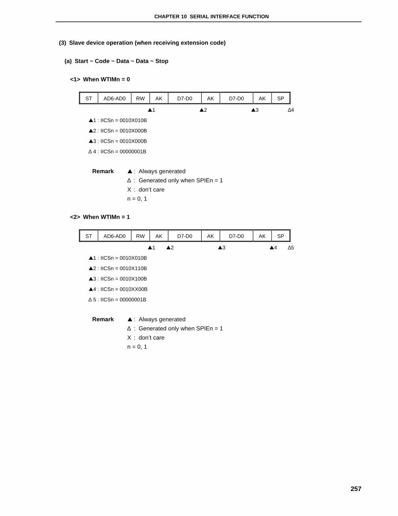
CHAPTER 10 SERIAL INTERFACE FUNCTION
257
(3) Slave device operation (when receiving extension code)
(a) Start ~ Code ~ Data ~ Data ~ Stop
<1> When WTIMn = 0
ST AD6-AD0 RW AK D7-D0 AK D7-D0 AK SP
▲1 ▲2 ▲3 ∆4
▲1 : IICSn = 0010X010B
▲2 : IICSn = 0010X000B
▲3 : IICSn = 0010X000B
∆ 4 : IICSn = 00000001B
Remark ▲ : Always generated
∆ : Generated only when SPIEn = 1
X : don’t care
n = 0, 1
<2> When WTIMn = 1
ST AD6-AD0 RW AK D7-D0 AK D7-D0 AK SP
▲1 ▲2 ▲3 ▲4 ∆5
▲1 : IICSn = 0010X010B
▲2 : IICSn = 0010X110B
▲3 : IICSn = 0010X100B
▲4 : IICSn = 0010XX00B
∆ 5 : IICSn = 00000001B
Remark ▲ : Always generated
∆ : Generated only when SPIEn = 1
X : don’t care
n = 0, 1

CHAPTER 10 SERIAL INTERFACE FUNCTION
258
(b) Start ~ Code ~ Data ~ Start ~ Address ~ Data ~ Stop
<1> When WTIMn = 0 (after restart, matches with SVAn)
ST AD6-AD0 RW AK D7-D0 AK ST AD6-AD0 RW AK D7-D0 AK SP
▲1 ▲2 ▲3 ▲4 ∆5
▲1 : IICSn = 0010X010B
▲2 : IICSn = 0010X000B
▲3 : IICSn = 0001X110B
▲4 : IICSn = 0001X000B
∆ 5 : IICSn = 00000001B
Remark ▲: Always generated
∆ : Generated only when SPIEn = 1
X : don’t care
n = 0, 1
<2> When WTIMn = 1 (after restart, matches with SVAn)
ST AD6-AD0 RW AK D7-D0 AK ST AD6-AD0 RW AK D7-D0 AK SP
▲1 ▲2 ▲3 ▲4 ▲5 ∆6
▲1 : IICSn = 0010X010B
▲2 : IICSn = 0010X110B
▲3 : IICSn = 0010XX00B
▲4 : IICSn = 0001X110B
▲5 : IICSn = 0001XX00B
∆ 6 : IICSn = 00000001B
Remark ▲: Always generated
∆ : Generated only when SPIEn = 1
X : don’t care
n = 0, 1
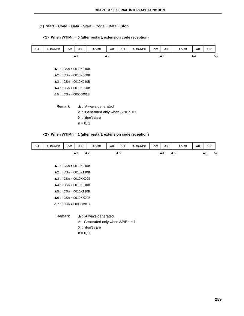
CHAPTER 10 SERIAL INTERFACE FUNCTION
259
(c) Start ~ Code ~ Data ~ Start ~ Code ~ Data ~ Stop
<1> When WTIMn = 0 (after restart, extension code reception)
ST AD6-AD0 RW AK D7-D0 AK ST AD6-AD0 RW AK D7-D0 AK SP
▲1 ▲2 ▲3 ▲4 ∆5
▲1 : IICSn = 0010X010B
▲2 : IICSn = 0010X000B
▲3 : IICSn = 0010X010B
▲4 : IICSn = 0010X000B
∆ 5 : IICSn = 00000001B
Remark ▲ : Always generated
∆ : Generated only when SPIEn = 1
X : don’t care
n = 0, 1
<2> When WTIMn = 1 (after restart, extension code reception)
ST AD6-AD0 RW AK D7-D0 AK ST AD6-AD0 RW AK D7-D0 AK SP
▲1 ▲2 ▲3 ▲4 ▲5 ▲6 ∆7
▲1 : IICSn = 0010X010B
▲2 : IICSn = 0010X110B
▲3 : IICSn = 0010XX00B
▲4 : IICSn = 0010X010B
▲5 : IICSn = 0010X110B
▲6 : IICSn = 0010XX00B
∆ 7 : IICSn = 00000001B
Remark ▲ : Always generated
∆: Generated only when SPIEn = 1
X : don’t care
n = 0, 1

CHAPTER 10 SERIAL INTERFACE FUNCTION
260
(d) Start ~ Code ~ Data ~ Start ~ Address ~ Data ~ Stop
<1> When WTIMn = 0 (after restart, does not match with address (= not extension code))
ST AD6-AD0 RW AK D7-D0 AK ST AD6-AD0 RW AK D7-D0 AK SP
▲1 ▲2 ▲3 ∆4
▲1 : IICSn = 0010X010B
▲2 : IICSn = 0010X000B
▲3 : IICSn = 00000X10B
∆ 4 : IICSn = 00000001B
Remark ▲ : Always generated
∆ : Generated only when SPIEn = 1
X : don’t care
n = 0, 1
<2> When WTIMn = 1 (after restart, does not match with address (= not extension code))
ST AD6-AD0 RW AK D7-D0 AK ST AD6-AD0 RW AK D7-D0 AK SP
▲1 ▲2 ▲3 ▲4 ∆5
▲1 : IICSn = 0010X010B
▲2 : IICSn = 0010X110B
▲3 : IICSn = 0010XX00B
▲4 : IICSn = 00000X10B
∆ 5 : IICSn = 00000001B
Remark ▲ : Always generated
∆ : Generated only when SPIEn = 1
X : don’t care
n = 0, 1

CHAPTER 10 SERIAL INTERFACE FUNCTION
261
(4) Operation without communication
(a) Start ~ Code ~ Data ~ Data ~ Stop
ST AD6-AD0 RW AK D7-D0 AK D7-D0 AK SP
∆1
∆ 1 : IICSn = 00000001B
Remark ∆ : Generated only when SPIEn = 1
n = 0, 1
(5) Arbitration loss operation (operation as slave after arbitration loss)
(a) When arbitration loss occurs during transmission of slave address data
<1> When WTIMn = 0
ST AD6-AD0 RW AK D7-D0 AK D7-D0 AK SP
▲1 ▲2 ▲3 ∆4
▲1 : IICSn = 0101X110B (Example: when ALDn is read during interrupt servicing)
▲2 : IICSn = 0001X000B
▲3 : IICSn = 0001X000B
∆ 4 : IICSn = 00000001B
Remark ▲ : Always generated
∆ : Generated only when SPIEn = 1
X : don’t care
n = 0, 1

CHAPTER 10 SERIAL INTERFACE FUNCTION
262
<2> When WTIMn = 1
ST AD6-AD0 RW AK D7-D0 AK D7-D0 AK SP
▲1 ▲2 ▲3 ∆4
▲1 : IICSn = 0101X110B (Example: when ALDn is read during interrupt servicing)
▲2 : IICSn = 0001X100B
▲3 : IICSn = 0001XX00B
∆ 4 : IICSn = 00000001B
Remark ▲ : Always generated
∆ : Generated only when SPIEn = 1
X : don’t care
n = 0, 1
(b) When arbitration loss occurs during transmission of extension code
<1> When WTIMn = 0
ST AD6-AD0 RW AK D7-D0 AK D7-D0 AK SP
▲1 ▲2 ▲3 ∆4
▲1 : IICSn = 0110X010B (Example: when ALDn is read during interrupt servicing)
▲2 : IICSn = 0010X000B
▲3 : IICSn = 0010X000B
∆ 4 : IICSn = 00000001B
Remark ▲ : Always generated
∆ : Generated only when SPIEn = 1
X : don’t care
n = 0, 1

CHAPTER 10 SERIAL INTERFACE FUNCTION
263
<2> When WTIMn = 1
ST AD6-AD0 RW AK D7-D0 AK D7-D0 AK SP
▲1 ▲2 ▲3 ▲4 ∆5
▲1 : IICSn = 0110X010B (Example: when ALDn is read during interrupt servicing)
▲2 : IICSn = 0010X110B
▲3 : IICSn = 0010X100B
▲4 : IICSn = 0010XX00B
∆ 5 : IICSn = 00000001B
Remark ▲ : Always generated
∆ : Generated only when SPIEn = 1
X : don’t care
n = 0, 1
(6) Operation when arbitration loss occurs (no communication after arbitration loss)
(a) When arbitration loss occurs during transmission of slave address data
ST AD6-AD0 RW AK D7-D0 AK D7-D0 AK SP
▲1 ∆2
▲1 : IICSn = 01000110B (Example: when ALDn is read during interrupt servicing)
∆ 2 : IICSn = 00000001B
Remark ▲ : Always generated
∆ : Generated only when SPIEn = 1
X : don’t care
n = 0, 1
(b) When arbitration loss occurs during transmission of extension code
ST AD6-AD0 RW AK D7-D0 AK D7-D0 AK SP
▲1 ∆2
▲1 : IICSn = 0110X010B (Example: when ALDn is read during interrupt servicing)
LRELn is set to 1 by software
∆ 2 : IICSn = 00000001B
Remark ▲ : Always generated
∆ : Generated only when SPIEn = 1
X : don’t care
n = 0, 1

CHAPTER 10 SERIAL INTERFACE FUNCTION
264
(c) When arbitration loss occurs during data transfer
<1> When WTIMn = 0
ST AD6-AD0 RW AK D7-D0 AK D7-D0 AK SP
▲1 ▲2 ∆3
▲1 : IICSn = 10001110B
▲2 : IICSn = 01000000B (Example: when ALDn is read during interrupt servicing)
∆ 3 : IICSn = 00000001B
Remark ▲ : Always generated
∆ : Generated only when SPIEn = 1
X : don’t care
n = 0, 1
<2> When WTIMn = 1
ST AD6-AD0 RW AK D7-D0 AK D7-D0 AK SP
▲1 ▲2 ∆3
▲1 : IICSn = 10001110B
▲2 : IICSn = 01000100B (Example: when ALDn is read during interrupt servicing)
∆ 3 : IICSn = 00000001B
Remark ▲ : Always generated
∆ : Generated only when SPIEn = 1
X : don’t care
n = 0, 1

CHAPTER 10 SERIAL INTERFACE FUNCTION
265
(d) When loss occurs due to restart condition during data transfer
<1> Not extension code (Example: matches with SVAn)
ST AD6-AD0 RW AK D7-Dn ST AD6-AD0 RW AK D7-D0 AK SP
▲1 ▲2 ∆3
▲1 : IICSn = 1000X110B
▲2 : IICSn = 01000110B (Example: when ALDn is read during interrupt servicing)
∆ 3 : IICSn = 00000001B
Remark ▲ : Always generated
∆ : Generated only when SPIEn = 1
X : don’t care
Dn = D6 to D0
n = 0, 1
<2> Extension code
ST AD6-AD0 RW AK D7-Dn ST AD6-AD0 RW AK D7-D0 AK SP
▲1 ▲2 ∆3
▲1 : IICSn = 1000X110B
▲2 : IICSn = 0110X010B (Example: when ALDn is read during interrupt servicing)
IICCn’s LRELn is set to 1 by software
∆ 3 : IICSn = 00000001B
Remark ▲ : Always generated
∆ : Generated only when SPIEn = 1
X : don’t care
Dn = D6 to D0
n = 0, 1

CHAPTER 10 SERIAL INTERFACE FUNCTION
266
(e) When loss occurs due to stop condition during data transfer
ST AD6-AD0 RW AK D7-Dn SP
▲1 ∆2
▲1 : IICSn = 1000X110B
∆ 2 : IICSn = 01000001B
Remark ▲ : Always generated
∆ : Generated only when SPIEn = 1
X : don’t care
Dn = D6 to D0
n = 0, 1
(f) When arbitration loss occurs due to low-level data when attempting to generate a restart condition
<1> When WTIMn = 0STTn = 1
↓
ST AD6-AD0 RW AK D7-D0 AK D7-D0 AK D7-D0 AK SP
▲1 ▲2 ▲3 ∆4
▲1 : IICSn = 1000X110B
▲2 : IICSn = 1000X000B
▲3 : IICSn = 01000000B (Example: when ALDn is read during interrupt servicing)
∆ 4 : IICSn = 00000001B
Remark ▲ : Always generated
∆ : Generated only when SPIEn = 1
X : don’t care
n = 0, 1

CHAPTER 10 SERIAL INTERFACE FUNCTION
267
<2> When WTIMn = 1STTn = 1
↓
ST AD6-AD0 RW AK D7-D0 AK D7-D0 AK D7-D0 AK SP
▲1 ▲2 ▲3 ∆4
▲1 : IICSn = 1000X110B
▲2 : IICSn = 1000XX00B
▲3 : IICSn = 01000100B (Example: when ALDn is read during interrupt servicing)
∆ 4 : IICSn = 00000001B
Remark ▲ : Always generated
∆ : Generated only when SPIEn = 1
X : don’t care
n = 0, 1
(g) When arbitration loss occurs due to a stop condition when attempting to generate a restart condition
<1> When WTIMn = 0STTn = 1
↓
ST AD6-AD0 RW AK D7-D0 AK SP
▲1 ▲2 ∆3
▲1 : IICSn = 1000X110B
▲2 : IICSn = 1000X000B
∆ 3 : IICSn = 01000001B
Remark ▲ : Always generated
∆ : Generated only when SPIEn = 1
X : don’t care
n = 0, 1

CHAPTER 10 SERIAL INTERFACE FUNCTION
268
<2> When WTIMn = 1STTn = 1
↓
ST AD6-AD0 RW AK D7-D0 AK SP
▲1 ▲2 ∆3
▲1 : IICSn = 1000X110B
▲2 : IICSn = 1000XX00B
∆ 3 : IICSn = 01000001B
Remark ▲ : Always generated
∆ : Generated only when SPIEn = 1
X : don’t care
n = 0, 1
(h) When arbitration loss occurs due to low-level data when attempting to generate a stop condition
<1> When WTIMn = 0SPTn = 1
↓
ST AD6-AD0 RW AK D7-D0 AK D7-D0 AK D7-D0 AK SP
▲1 ▲2 ▲3 ∆4
▲1 : IICSn = 1000X110B
▲2 : IICSn = 1000X000B
▲3 : IICSn = 01000000B (Example: when ALDn is read during interrupt servicing)
∆ 4 : IICSn = 00000001B
Remark ▲ : Always generated
∆ : Generated only when SPIEn = 1
X : don’t care
n = 0, 1
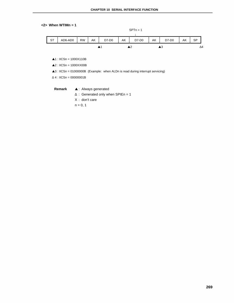
CHAPTER 10 SERIAL INTERFACE FUNCTION
269
<2> When WTIMn = 1SPTn = 1
↓
ST AD6-AD0 RW AK D7-D0 AK D7-D0 AK D7-D0 AK SP
▲1 ▲2 ▲3 ∆4
▲1 : IICSn = 1000X110B
▲2 : IICSn = 1000XX00B
▲3 : IICSn = 01000000B (Example: when ALDn is read during interrupt servicing)
∆ 4 : IICSn = 00000001B
Remark ▲ : Always generated
∆ : Generated only when SPIEn = 1
X : don’t care
n = 0, 1

CHAPTER 10 SERIAL INTERFACE FUNCTION
270
10.3.6 Interrupt request (INTIICn) generation timing and wait control
The setting of bit 3 (WTIMn) in the IIC control register n (IICCn) determines the timing by which INTIICn is
generated and the corresponding wait control, as shown in Table 10-3 (n = 0, 1).
Table 10-3. INTIICn Generation Timing and Wait Control
During slave device operation During master device operationWTIMn
Address Data reception Data transmission Address Data reception Data transmission
0 9 Notes 1, 2
8 Note 2
8 Note 2
9 8 8
1 9 Notes 1, 2
9 Note 2
9 Note 2
9 9 9
Notes 1. The slave device’s INTIICn signal and wait period occurs at the falling edge of the ninth clock only when
there is a match with the address set to the slave address register (SVAn).
At this point, ACK is output regardless of the value set to IICCn’s bit 2 (ACKEn). For a slave device that
has received an extension code, INTIICn occurs at the falling edge of the eighth clock.
2. If the received address does not match the contents of the slave address register (SVAn), neither INTIICn
nor a wait occurs.
Remarks 1. The numbers in the table indicate the number of the serial clock’s clock signals. Interrupt requestsand wait control are both synchronized with the falling edge of these clock signals.
2. n = 0, 1
(1) During address transmission/reception
• Slave device operation : Interrupt and wait timing are determined regardless of the WTIMn bit.
• Master device operation : Interrupt and wait timing occur at the falling edge of the ninth clock regardless of
the WTIMn bit.
(2) During data reception
• Master/slave device operation: Interrupt and wait timing are determined according to the WTIMn bit.
(3) During data transmission
• Master/slave device operation: Interrupt and wait timing are determined according to the WTIMn bit.
(4) Wait cancellation method
The two wait cancellation methods are as follows.
• By setting bit 5 (WRELn) of IIC control register n (IICCn) to 1
• By writing to the IIC shift register n (IICn)
When 8-clock wait has been selected (WTIMn = 0), the output level of ACK must be determined prior to wait
cancellation.
(5) Stop condition detection
INTIICn is generated when a stop condition is detected.
Remark n = 0, 1
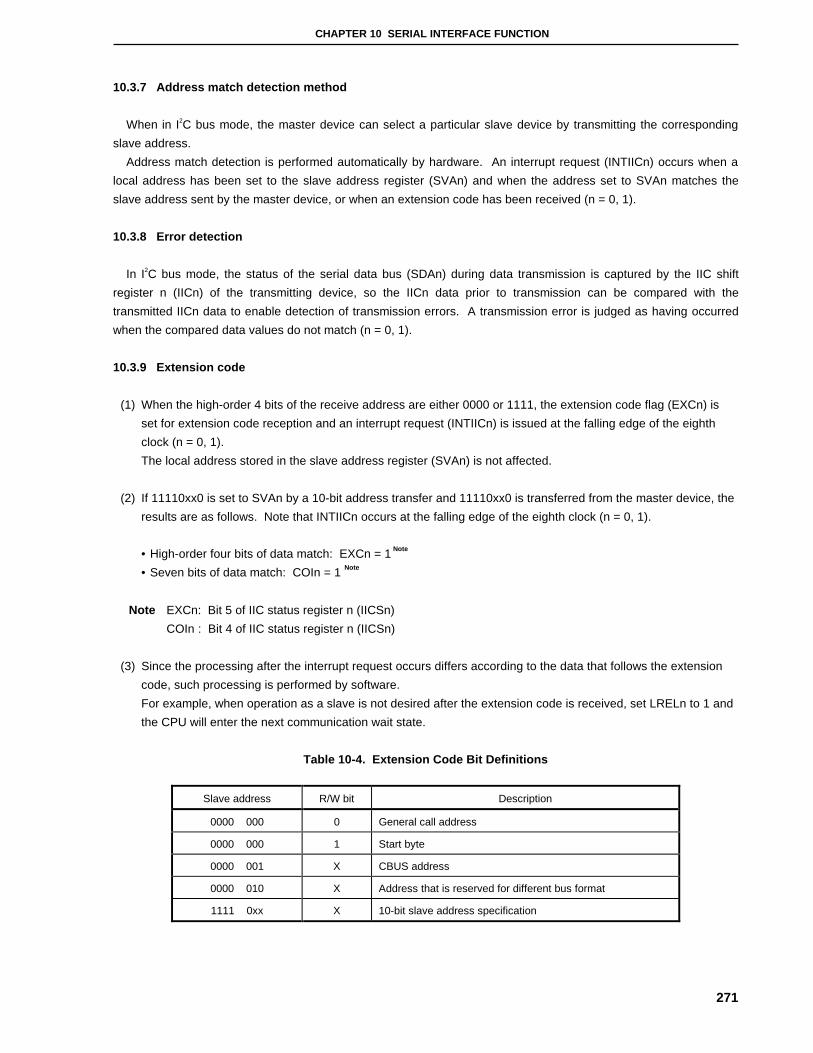
CHAPTER 10 SERIAL INTERFACE FUNCTION
271
10.3.7 Address match detection method
When in I2C bus mode, the master device can select a particular slave device by transmitting the corresponding
slave address.
Address match detection is performed automatically by hardware. An interrupt request (INTIICn) occurs when a
local address has been set to the slave address register (SVAn) and when the address set to SVAn matches the
slave address sent by the master device, or when an extension code has been received (n = 0, 1).
10.3.8 Error detection
In I2C bus mode, the status of the serial data bus (SDAn) during data transmission is captured by the IIC shift
register n (IICn) of the transmitting device, so the IICn data prior to transmission can be compared with the
transmitted IICn data to enable detection of transmission errors. A transmission error is judged as having occurred
when the compared data values do not match (n = 0, 1).
10.3.9 Extension code
(1) When the high-order 4 bits of the receive address are either 0000 or 1111, the extension code flag (EXCn) is
set for extension code reception and an interrupt request (INTIICn) is issued at the falling edge of the eighth
clock (n = 0, 1).
The local address stored in the slave address register (SVAn) is not affected.
(2) If 11110xx0 is set to SVAn by a 10-bit address transfer and 11110xx0 is transferred from the master device, the
results are as follows. Note that INTIICn occurs at the falling edge of the eighth clock (n = 0, 1).
• High-order four bits of data match: EXCn = 1 Note
• Seven bits of data match: COIn = 1 Note
Note EXCn: Bit 5 of IIC status register n (IICSn)
COIn : Bit 4 of IIC status register n (IICSn)
(3) Since the processing after the interrupt request occurs differs according to the data that follows the extension
code, such processing is performed by software.
For example, when operation as a slave is not desired after the extension code is received, set LRELn to 1 and
the CPU will enter the next communication wait state.
Table 10-4. Extension Code Bit Definitions
Slave address R/W bit Description
0000 000 0 General call address
0000 000 1 Start byte
0000 001 X CBUS address
0000 010 X Address that is reserved for different bus format
1111 0xx X 10-bit slave address specification

CHAPTER 10 SERIAL INTERFACE FUNCTION
272
10.3.10 Arbitration
When several master devices simultaneously output a start condition (when STTn is set to 1 before STDn is set to
1Note), communication among the master devices is performed as the number of clocks are adjusted until the data
differs. This kind of operation is called arbitration (n = 0, 1).
When one of the master devices loses in arbitration, an arbitration loss flag (ALDn) in the IIC status register n
(IICSn) is set via the timing by which the arbitration loss occurred, and the SCLn and SDAn lines are both set for high
impedance, which releases the bus (n = 0, 1).
The arbitration loss is detected based on the timing of the next interrupt request (the eighth or ninth clock, when a
stop condition is detected, etc.) and the ALDn = 1 setting that has been made by software (n = 0, 1).
For details of interrupt request timing, see 10.3.5 I2C interrupt requests (INTIICn) .
Note STDn : Bit 1 of IIC status register n (IICSn)
STTn : Bit 1 of IIC control register n (IICCn)

CHAPTER 10 SERIAL INTERFACE FUNCTION
273
Figure 10-20. Arbitration Timing Example
Master 1
Master 2
Transfer lines
SCLn
SDAn
SCLn
SDAn
SCLn
SDAn
Master 1 loses arbitration
Hi-Z
Hi-Z
Remark n = 0, 1
Table 10-5. Status During Arbitration and Interrupt Request Generation Timing
Status During Arbitration Interrupt Request Generation Timing
During address transmission At falling edge of eighth or ninth clock following byte transfer Note 1
Read/write data after address transmission
During extension code transmission
Read/write data after extension code transmission
During data transmission
During ACK signal transfer period after data transmission
When restart condition is detected during data transfer
When stop condition is detected during data transfer When stop condition is output (when SPIEn = 1) Note 2
When data is at low level while attempting to output a
restart condition
At falling edge of eighth or ninth clock following byte transfer Note 1
When stop condition is detected while attempting to
output a restart condition
When stop condition is output (when SPIEn = 1) Note 2
When data is at low level while attempting to output a stop
condition
At falling edge of eighth or ninth clock following byte transfer Note 1
When SCLn is at low level while attempting to output a
restart condition
CHAPTER 10 SERIAL INTERFACE FUNCTION
274
Notes 1. When WTIMn (bit 3 of the IIC control register n (IICCn)) = 1, an interrupt request occurs at the falling
edge of the ninth clock. When WTIMn = 0 and the extension code’s slave address is received, an
interrupt request occurs at the falling edge of the eighth clock (n = 0, 1).
2. When there is a possibility that arbitration will occur, set SPIEn = 1 for master device operation (n = 0,
1).
Remark SPIEn: Bit 5 of the IIC control register n (IICCn)
10.3.11 Wake up function
The I2C bus slave function is a function that generates an interrupt request (INTIICn) when a local address and
extension code have been received.
This function makes processing more efficient by preventing unnecessary interrupt requests from occurring when
addresses do not match.
When a start condition is detected, wake-up standby mode is set. This wake-up standby mode is in effect while
addresses are transmitted due to the possibility that an arbitration loss may change the master device (which has
output a start condition) to a slave device.
However, when a stop condition is detected, bit 5 (SPIEn) of the IIC control register n (IICCn) is set regardless of
the wake up function, and this determines whether interrupt requests are enabled or disabled (n = 0, 1).
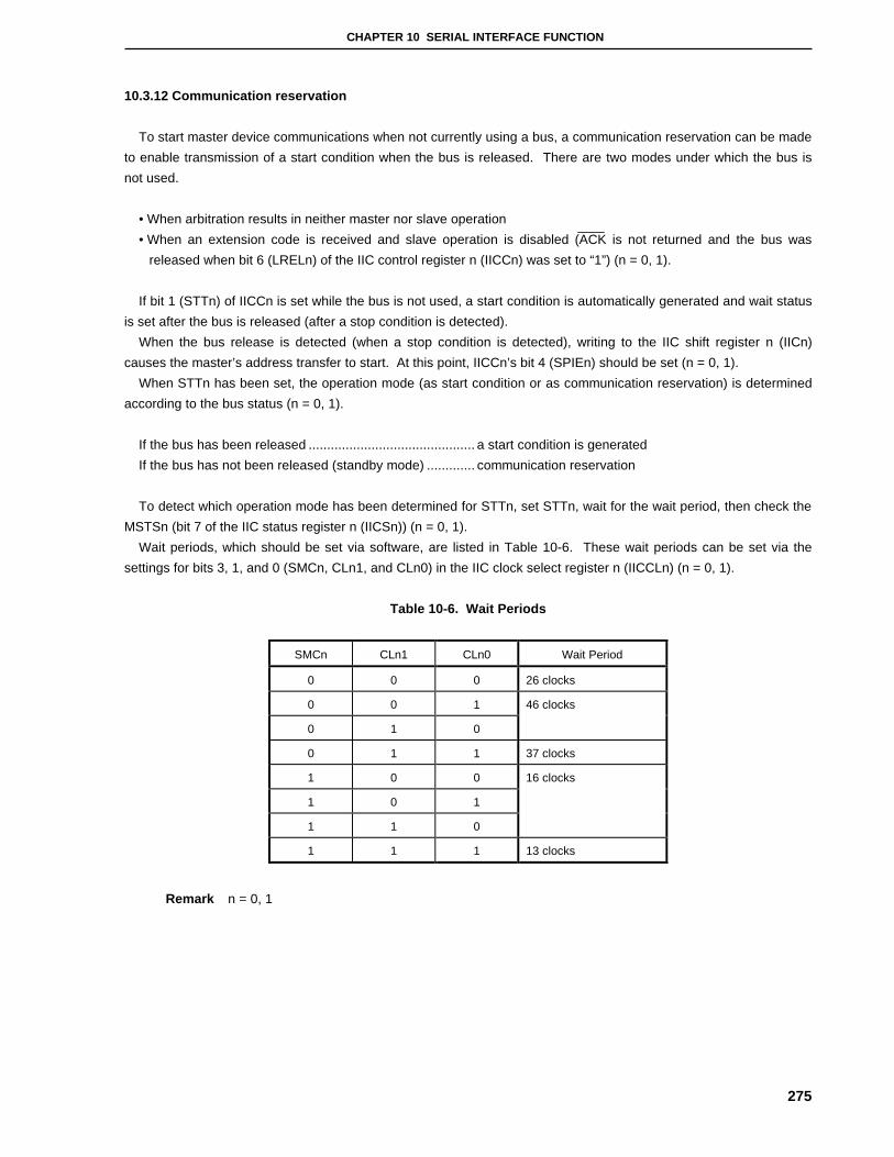
CHAPTER 10 SERIAL INTERFACE FUNCTION
275
10.3.12 Communication reservation
To start master device communications when not currently using a bus, a communication reservation can be made
to enable transmission of a start condition when the bus is released. There are two modes under which the bus is
not used.
• When arbitration results in neither master nor slave operation
• When an extension code is received and slave operation is disabled (ACK is not returned and the bus was
released when bit 6 (LRELn) of the IIC control register n (IICCn) was set to “1”) (n = 0, 1).
If bit 1 (STTn) of IICCn is set while the bus is not used, a start condition is automatically generated and wait status
is set after the bus is released (after a stop condition is detected).
When the bus release is detected (when a stop condition is detected), writing to the IIC shift register n (IICn)
causes the master’s address transfer to start. At this point, IICCn’s bit 4 (SPIEn) should be set (n = 0, 1).
When STTn has been set, the operation mode (as start condition or as communication reservation) is determined
according to the bus status (n = 0, 1).
If the bus has been released ............................................. a start condition is generated
If the bus has not been released (standby mode) ............. communication reservation
To detect which operation mode has been determined for STTn, set STTn, wait for the wait period, then check the
MSTSn (bit 7 of the IIC status register n (IICSn)) (n = 0, 1).
Wait periods, which should be set via software, are listed in Table 10-6. These wait periods can be set via the
settings for bits 3, 1, and 0 (SMCn, CLn1, and CLn0) in the IIC clock select register n (IICCLn) (n = 0, 1).
Table 10-6. Wait Periods
SMCn CLn1 CLn0 Wait Period
0 0 0 26 clocks
0 0 1
0 1 0
46 clocks
0 1 1 37 clocks
1 0 0
1 0 1
1 1 0
16 clocks
1 1 1 13 clocks
Remark n = 0, 1

CHAPTER 10 SERIAL INTERFACE FUNCTION
276
Figure 10-21 shows the communication reservation timing.
Figure 10-21. Communication Reservation Timing
21 3 4 5 6 21 3 4 5 67 8 9SCLn
SDAn
Program processing
Hardware processing
Write toIICn
Set SPDnand INTIICn
STTn=1
Communicationreservation
SetSTDn
Output by master with bus access
IICn : IIC shift register n
STTn : Bit 1 of IIC control register n (IICCn)
STDn : Bit 1 of IIC status register n (IICSn)
SPDn : Bit 0 of IIC status register n (IICSn)
Remark n = 0, 1
Communication reservations are accepted via the following timing. After bit 1 (STDn) of the IIC status register n
(IICSn) is set to “1”, a communication reservation can be made by setting bit 1 (STTn) of the IIC control register n
(IICCn) to “1” before a stop condition is detected (n = 0, 1).

CHAPTER 10 SERIAL INTERFACE FUNCTION
277
Figure 10-22. Timing for Accepting Communication Reservations
SCLn
SDAn
STDn
SPDn
Standby mode
Remark n = 0, 1

CHAPTER 10 SERIAL INTERFACE FUNCTION
278
The communication reservation flow chart is illustrated in Figure 10-23.
Figure 10-23. Communication Reservation Flow Chart
DI
SET1 STT
Define communicationreservation
Wait
Cancel communicationreservation
No
Yes
MOV IIC0, #xxH
EI
STT=1? (Communication reservation)
Note
(Generate start condition)
; Sets STT flag (communication reservation).
; Gets wait period set by software (see Table 10-6 ).
; Confirmation of STT flag
; Clear user flag.
; IIC0 write operation
; Defines that communication reservation is in effect (defines and sets user flag to any part of RAM).
Note The communication reservation operation executes a write to the IIC shift register n (IICn) when a stop
condition interrupt request occurs.
Remark n = 0, 1

CHAPTER 10 SERIAL INTERFACE FUNCTION
279
10.3.13 Other cautions
After a reset, when changing from a mode in which no stop condition has been detected (the bus has not been
released) to a master device communication mode, first generate a stop condition to release the bus, then perform
master device communication.
When using multiple masters, it is not possible to perform master device communication when the bus has not
been released (when a stop condition has not been detected).
Use the following sequence for generating a stop condition.
(a) Set IIC clock select register n (IICCLn).
(b) Set bit 7 (IICEn) of the IIC control register (IICCn).
(c) Set bit 0 of IICCn.
Remark n = 0, 1
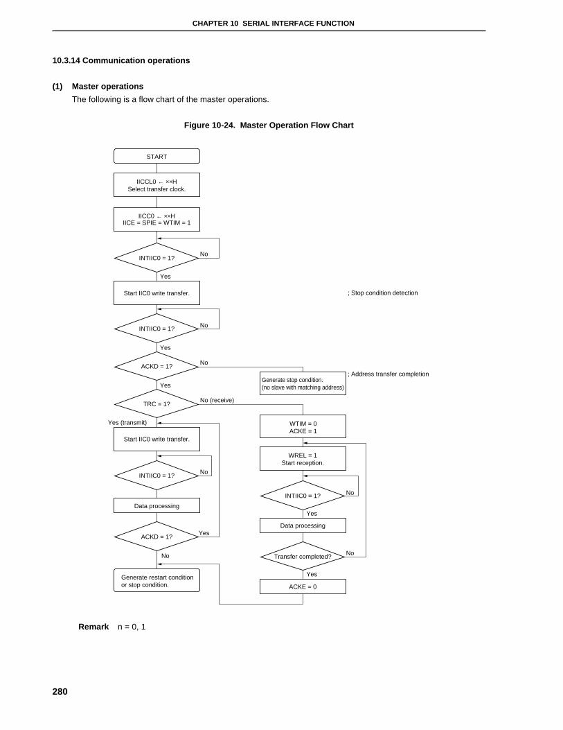
CHAPTER 10 SERIAL INTERFACE FUNCTION
280
10.3.14 Communication operations
(1) Master operations
The following is a flow chart of the master operations.
Figure 10-24. Master Operation Flow Chart
IICCL0 ← ××HSelect transfer clock.
IICC0 ← ××HIICE = SPIE = WTIM = 1
Start IIC0 write transfer.
Start IIC0 write transfer.
WREL = 1Start reception.
Generate stop condition.(no slave with matching address)
Generate restart conditionor stop condition.
START
Data processing
Data processing
ACKE = 0
No
Yes
No
No
No
No No
No
Yes
Yes
Yes
Yes
Yes
INTIIC0 = 1?
WTIM = 0ACKE = 1
INTIIC0 = 1?
Transfer completed?
INTIIC0 = 1?
ACKD = 1?
TRC = 1?
INTIIC0 = 1?
ACKD = 1?
; Stop condition detection
; Address transfer completion
No (receive)
Yes (transmit)
Remark n = 0, 1

CHAPTER 10 SERIAL INTERFACE FUNCTION
281
(2) Slave operation
An example of slave operation is shown below.
Figure 10-25. Slave Operation Flow Chart
IICC0 ← ××HIICE = 1
WREL = 1Start reception.
Detect restart conditionor stop condition.
START
ACKE = 0
Data processing
Data processing
LREL = 1
No
Yes
No
No
No
NoNo
No
No
Yes
No
Yes
Yes
Yes
Yes
Yes
Yes
WTIM = 0ACKE = 1
INTIIC0 = 1?
Yes
Communicate?
Transfer completed?
INTIIC0 = 1?
WTIM = 1Start IIC0 write transfer.
INTIIC0 = 1?
EXC = 1?
COI = 1?
TRC = 1?
ACKD = 1?
Remark n = 0, 1
CHAPTER 10 SERIAL INTERFACE FUNCTION
282
10.3.15 Timing of Data Communication
When using I2C bus mode, the master device outputs an address via the serial bus to select one of several slave
devices as its communication partner.
After outputting the slave address, the master device transmits the TRCn bit (bit 3 of the IIC status register n
(IICSn)) that specifies the data transfer direction and then starts serial communication with the slave device.
Figures 10-26 and 10-27 show timing charts of the data communication.
The IIC bus shift register n (IICn)’s shift operation is synchronized with the falling edge of the serial clock (SCLn).
The transmit data is transferred to the SO latch and is output (MSB first) via the SDAn pin.
Data input via the SDAn pin is captured by IICn at the rising edge of SCLn.
Remark n = 0, 1

CHAPTER 10 SERIAL INTERFACE FUNCTION
283
Figure 10-26. Example of Master to Slave Communication
(When 9-Clock Wait Is Selected for Both Master and Slave) (1/3)
(a) Start condition ~ address
IIC0n
ACKDn
STDn
SPDn
WTIMn
H
H
L
L
L
L
H
H
H
L
L
ACKEn
MSTSn
STTn
SPTn
WRELn
INTIIC0n
TRCn
IIC0n
ACKDn
STDn
SPDn
WTIMn
ACKEn
MSTSn
STTn
SPTn
WRELn
INTIIC0n
TRCn
SCLn
SDAn
Processing by master device
Transfer lines
Processing by slave device
1 2 3 4 5 6 7 8 9 4321
AD6 AD5 AD4 AD3 AD2 AD1 AD0 W ACK D4D5D6D7
IIC0 ← address IIC0 ← data
IIC0 ← FFH
Transmit
Start condition
Receive
(When EXC = 1)
Note
Note
Note To cancel slave wait, write FFH to IICn or set WRELn.
Remark n = 0, 1

CHAPTER 10 SERIAL INTERFACE FUNCTION
284
Figure 10-26. Example of Master to Slave Communication
(When 9-Clock Wait Is Selected for Both Master and Slave) (2/3)
(b) Data
IIC0
ACKD
STD
SPD
WTIM
H
H
L
L
L
L
L
L
H
H
H
H
L
L
L
L
L
ACKE
MSTS
STT
SPT
WREL
INTIIC0
TRC
IIC0
ACKD
STD
SPD
WTIM
ACKE
MSTS
STT
SPT
WREL
INTIIC0
TRC
SCL
SDA
Processing by master device
Transfer lines
Processing by slave device
198 2 3 4 5 6 7 8 9 321
D7D0 D6 D5 D4 D3 D2 D1 D0 D5D6D7
IIC0 ← data
IIC0 ← FFH Note IIC0 ← FFH Note
IIC0 ← data
Transmit
Receive
Note Note
Note To cancel slave wait, write FFH to IICn or set WRELn.
Remark n = 0, 1

CHAPTER 10 SERIAL INTERFACE FUNCTION
285
Figure 10-26. Example of Master to Slave Communication
(When 9-Clock Wait Is Selected for Both Master and Slave) (3/3)
(c) Stop condition
IIC0n
ACKDn
STDn
SPDn
WTIMn
H
H
L
L
L
L
H
H
H
L
ACKEn
MSTSn
STTn
SPTn
WRELn
INTIIC0n
TRCn
IIC0n
ACKDn
STDn
SPDn
WTIMn
ACKEn
MSTSn
STTn
SPTn
WRELn
INTIIC0n
TRCn
SCLn
SDAn
Processing by master device
Transfer lines
Processing by slave device
1 2 3 4 5 6 7 8 9 21
D7 D6 D5 D4 D3 D2 D1 D0 AD5AD6
IIC0 ← data IIC0 ← address
IIC0 ← FFH Note IIC0 ← FFH Note
Stopcondition
Startcondition
Transmit
Note Note
(When SPIE = 1)Receive
(When SPIE = 1)
Note To cancel slave wait, write FFH to IICn or set WRELn.
Remark n = 0, 1

CHAPTER 10 SERIAL INTERFACE FUNCTION
286
Figure 10-27. Example of Slave to Master Communication
(When 9-Clock Wait Is Selected for Both Master and Slave) (1/3)
(a) Start condition ~ address
IIC0n
ACKDn
STDn
SPDn
WTIMn
H
H
L
L
H
H
L
ACKEn
MSTSn
STTn
L
L
SPTn
WRELn
INTIIC0n
TRCn
IIC0n
ACKDn
STDn
SPDn
WTIMn
ACKEn
MSTSn
STTn
SPTn
WRELn
INTIIC0n
TRCn
SCLn
SDAn
Processing by master device
Transfer lines
Processing by slave device
1 2 3 4 5 6 7 8 9 4 5 6321
AD6 AD5 AD4 AD3 AD2 AD1 AD0 R D4 D3 D2D5D6D7
IIC0 ← address IIC0 ← FFH Note
Note
IIC0 ← data
Start condition
Note To cancel slave wait, write FFH to IICn or set WRELn.
Remark n = 0, 1
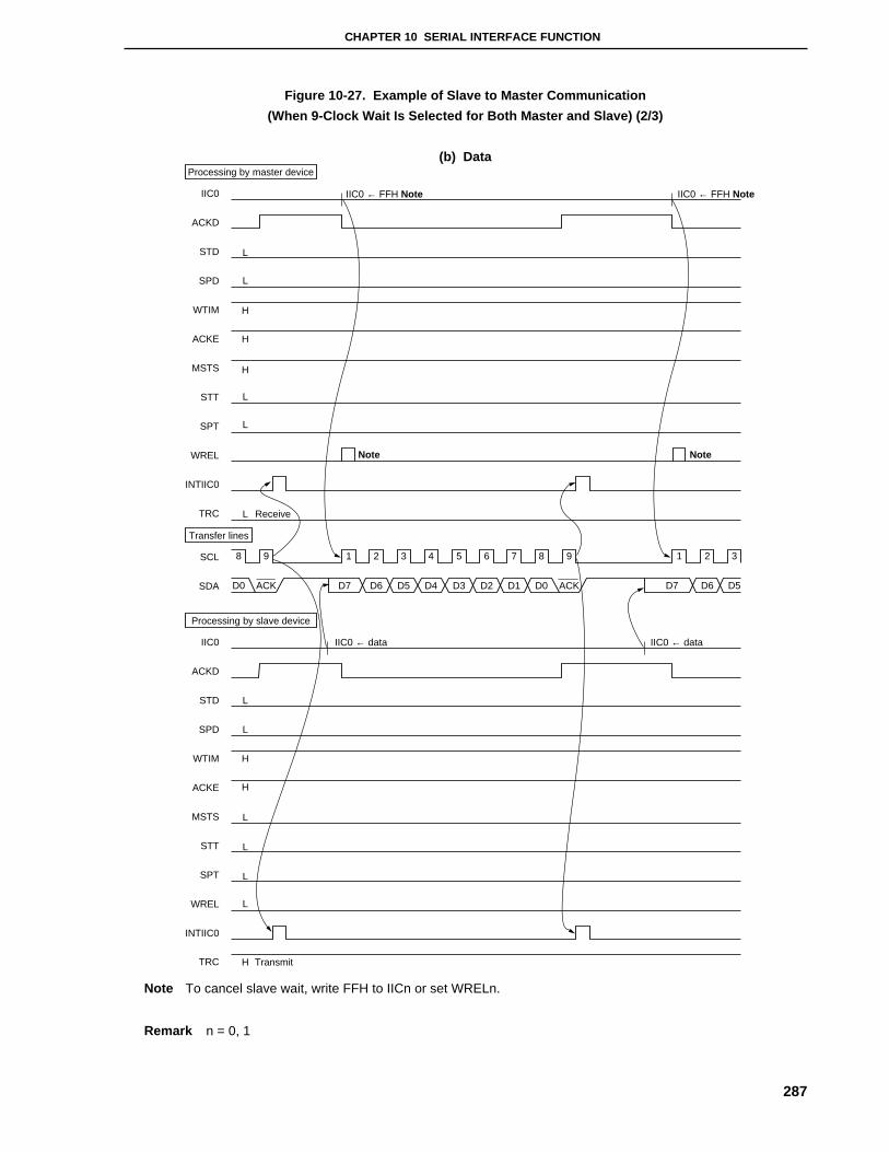
CHAPTER 10 SERIAL INTERFACE FUNCTION
287
Figure 10-27. Example of Slave to Master Communication
(When 9-Clock Wait Is Selected for Both Master and Slave) (2/3)
(b) Data
IIC0
ACKD
STD
SPD
WTIM
H
H
H
L
L
L
L
L
L
H
H
H
L
L
L
L
L
ACKE
MSTS
STT
SPT
WREL
INTIIC0
TRC
IIC0
ACKD
STD
SPD
WTIM
ACKE
MSTS
STT
SPT
WREL
INTIIC0
TRC
SCL
SDA
Processing by master device
Transfer lines
Processing by slave device
18 9 2 3 4 5 6 7 8 9 321
D7D0 ACK D6 D5 D4 D3 D2 D1 D0 ACK D5D6D7
Note Note
Receive
Transmit
IIC0 ← data IIC0 ← data
IIC0 ← FFH Note IIC0 ← FFH Note
Note To cancel slave wait, write FFH to IICn or set WRELn.
Remark n = 0, 1
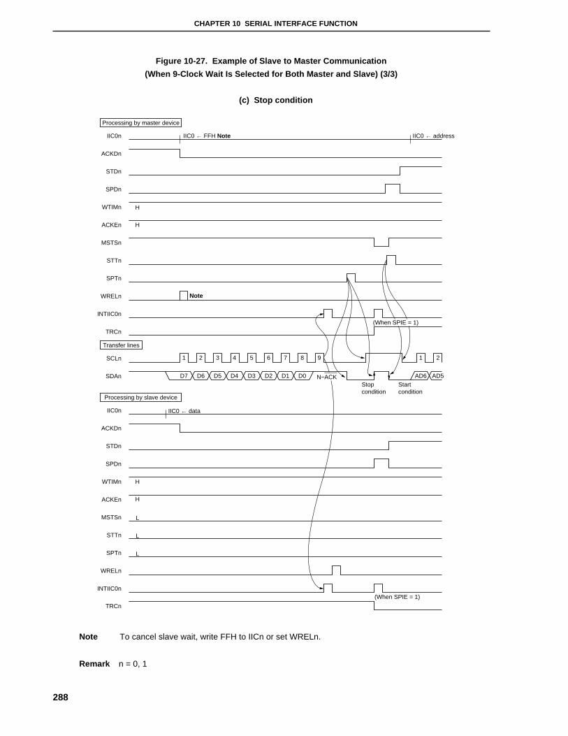
CHAPTER 10 SERIAL INTERFACE FUNCTION
288
Figure 10-27. Example of Slave to Master Communication
(When 9-Clock Wait Is Selected for Both Master and Slave) (3/3)
(c) Stop condition
IIC0n
ACKDn
STDn
SPDn
WTIMn
H
H
L
L
L
H
HACKEn
MSTSn
STTn
SPTn
WRELn
INTIIC0n
TRCn
IIC0n
ACKDn
STDn
SPDn
WTIMn
ACKEn
MSTSn
STTn
SPTn
WRELn
INTIIC0n
TRCn
SCLn
SDAn
Processing by master device
Transfer lines
Processing by slave device
1 2 3 4 5 6 7 8 9 21
D7 D6 D5 D4 D3 D2 D1 D0 AD5AD6
IIC0 ← addressIIC0 ← FFH Note
Note
IIC0 ← data
Stopcondition
Startcondition
(When SPIE = 1)
N−ACK
(When SPIE = 1)
Note To cancel slave wait, write FFH to IICn or set WRELn.
Remark n = 0, 1

CHAPTER 10 SERIAL INTERFACE FUNCTION
289
10.4 Asynchronous Serial Interface (UART0, UART1)
The UARTn (n = 0, 1) has the following two modes.
(1) Operation stop mode
This mode is used when serial transfers are not performed. It can therefore be used to reduce power
consumption.
(2) Asynchronous serial interface (UARTn) mode
This mode enables full-duplex operation which transmits and receives one byte of data after the start bit.
The on-chip dedicated UARTn baud rate generator enables communications using a wide range of selectable
baud rates. In addition, a baud rate based on divided clock input to the ASCKn pin can also be defined.
The UARTn baud rate generator can also be used to generate a MIDI-standard baud rate (31.25 kbps).
10.4.1 Configuration
The UARTn includes the following hardware.
Table 10-7. Configuration of UARTn
Item Configuration
Registers Transmit shift registers 0, 1 (TXS0, TXS1)
Receive buffer registers 0, 1 (RXB0, RXB1)
Control registers Asynchronous serial interface mode registers 0, 1 (ASIM0, ASIM1)
Asynchronous serial interface status registers 0, 1 (ASIS0, ASIS1)
Baud rate generator control registers 0, 1 (BRGC0, BRGC1)
Baud rate generator mode control registers 00, 01 (BRGMC00,
BRGMC01)
Baud rate generator mode control registers 10, 11 (BRGMC10,
BRGMC11)

CHAPTER 10 SERIAL INTERFACE FUNCTION
290
Figure 10-28. Block Diagram of UARTn
Baud rate generator
fxx-fxx/29
TXD0, TXD1
ASCK0, ASCK1
RXD0, RXD1
INTST0,
INTST1
INTSR0,
INTSR1
0, 1 (RX0, RX1)
Internal Bus
Selector
0, 1 (TXS0, TXS1)
8
8
Receive shift registers
Receive buffer registers
0, 1 (RXB0, RXB1)
8
Transmit controlparity addition
Receive controlparity check
Transmit shift registers
(1) Transmit shift registers 0, 1 (TXS0, TXS1)
TXSn is the register for setting transmit data. Data written to TXSn is transmitted as serial data.
When the data length is set as 7 bits, bit 0 to bit 6 of the data written to TXSn is transmitted as serial data.
Writing data to TXSn starts the transmit operation.
TXSn can be written to by an 8-bit memory manipulation instruction. It cannot be read from.
RESET input sets these registers to FFH.
Caution Do not write to TXSn during a transmit operation.
(2) Receive shift registers 0, 1 (RX0, RX1)
RXn register converts serial data input via the RXD0, RXD1 pins to parallel data. When one byte of data is
received at RXn, the received data is transferred to the receive buffer register (RXB0, RXB1).
RX0, RX1 cannot be manipulated directly by a program.
CHAPTER 10 SERIAL INTERFACE FUNCTION
291
(3) Receive buffer registers 0, 1 (RXB0, RXB1)
RXBn is used to hold receive data. When one byte of data is received, one byte of new receive data is
transferred.
When the data length is set as 7 bits, received data is sent to bit 0 to bit 6 of RXBn. In RXBn, the MSB must be
set to “0”.
RXBn can be read by an 8-bit memory manipulation instruction. It cannot be written to.
RESET input sets RXBn to FFH.
(4) Transmission control circuit
The transmission control circuit controls transmit operations, such as adding a start bit, parity bit, and stop bit to
data that is written to the transmit shift register (TXSn), based on the values set to the asynchronous serial
interface mode register (ASIMn).
(5) Reception control circuit
The reception control circuit controls receive operations based on the values set to the asynchronous serial
interface mode register (ASIMn). During a receive operation, it performs error checking, such as for parity errors,
and sets various values to the asynchronous serial interface status register (ASISn) according to the type of error
that is detected.
10.4.2 UARTn control registers
The UARTn uses the following four types of registers for control function (n = 0, 1).
• Asynchronous serial interface mode register (ASIMn)
• Asynchronous serial interface status register (ASISn)
• Baud rate generator control register (BRGCn)
• Baud rate generator mode control registers n0, n1 (BRGMCn0, BRGMCn1)
(1) Asynchronous serial interface mode registers 0, 1 (ASIM0, ASIM1)
ASIMn is an 8-bit register that controls UARTn’s serial transfer operations.
ASIMn can be set by a 1-bit or 8-bit memory manipulation instruction.
RESET input sets these registers to 00H.
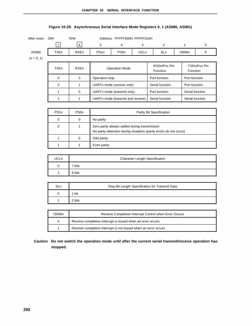
CHAPTER 10 SERIAL INTERFACE FUNCTION
292
Figure 10-29. Asynchronous Serial Interface Mode Registers 0, 1 (ASIM0, ASIM1)
After reset: 00H R/W Address: FFFFF300H, FFFFF310H
7 6 5 4 3 2 1 0
ASIMn TXEn RXEn PS1n PS0n UCLn SLn ISRMn 0
(n = 0, 1)
TXEn RXEn Operation ModeRXDn/Pxx Pin
Function
TXDn/Pxx Pin
Function
0 0 Operation stop Port function Port function
0 1 UARTn mode (receive only) Serial function Port function
1 0 UARTn mode (transmit only) Port function Serial function
1 1 UARTn mode (transmit and receive) Serial function Serial function
PS1n PS0n Parity Bit Specification
0 0 No parity
0 1 Zero parity always added during transmission
No parity detection during reception (parity errors do not occur)
1 0 Odd parity
1 1 Even parity
UCLn Character Length Specification
0 7 bits
1 8 bits
SLn Stop Bit Length Specification for Transmit Data
0 1 bit
1 2 bits
ISRMn Receive Completion Interrupt Control when Error Occurs
0 Receive completion interrupt is issued when an error occurs
1 Receive completion interrupt is not issued when an error occurs
Caution Do not switch the operation mode until after the current serial transmit/receive operation has
stopped.
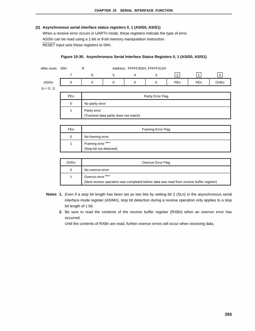
CHAPTER 10 SERIAL INTERFACE FUNCTION
293
(2) Asynchronous serial interface status registers 0, 1 (ASIS0, ASIS1)
When a receive error occurs in UARTn mode, these registers indicate the type of error.
ASISn can be read using a 1-bit or 8-bit memory manipulation instruction.
RESET input sets these registers to 00H.
Figure 10-30. Asynchronous Serial Interface Status Registers 0, 1 (ASIS0, ASIS1)
After reset: 00H R Address: FFFFF302H, FFFFF312H
7 6 5 4 3 2 1 0
ASISn 0 0 0 0 0 PEn FEn OVEn
(n = 0, 1)
PEn Parity Error Flag
0 No parity error
1 Parity error
(Transmit data parity does not match)
FEn Framing Error Flag
0 No framing error
1 Framing error Note 1
(Stop bit not detected)
OVEn Overrun Error Flag
0 No overrun error
1 Overrun error Note 2
(Next receive operation was completed before data was read from receive buffer register)
Notes 1. Even if a stop bit length has been set as two bits by setting bit 2 (SLn) in the asynchronous serial
interface mode register (ASIMn), stop bit detection during a receive operation only applies to a stop
bit length of 1 bit.
2. Be sure to read the contents of the receive buffer register (RXBn) when an overrun error has
occurred.
Until the contents of RXBn are read, further overrun errors will occur when receiving data.
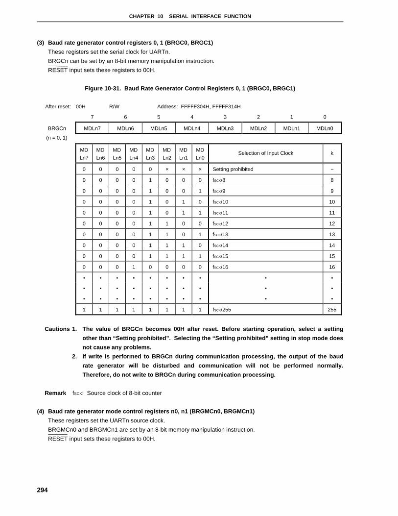
CHAPTER 10 SERIAL INTERFACE FUNCTION
294
(3) Baud rate generator control registers 0, 1 (BRGC0, BRGC1)
These registers set the serial clock for UARTn.
BRGCn can be set by an 8-bit memory manipulation instruction.
RESET input sets these registers to 00H.
Figure 10-31. Baud Rate Generator Control Registers 0, 1 (BRGC0, BRGC1)
After reset: 00H R/W Address: FFFFF304H, FFFFF314H
7 6 5 4 3 2 1 0
BRGCn MDLn7 MDLn6 MDLn5 MDLn4 MDLn3 MDLn2 MDLn1 MDLn0
(n = 0, 1)
MD
Ln7
MD
Ln6
MD
Ln5
MD
Ln4
MD
Ln3
MD
Ln2
MD
Ln1
MD
Ln0Selection of Input Clock k
0 0 0 0 0 × × × Setting prohibited −
0 0 0 0 1 0 0 0 fSCK/8 8
0 0 0 0 1 0 0 1 fSCK/9 9
0 0 0 0 1 0 1 0 fSCK/10 10
0 0 0 0 1 0 1 1 fSCK/11 11
0 0 0 0 1 1 0 0 fSCK/12 12
0 0 0 0 1 1 0 1 fSCK/13 13
0 0 0 0 1 1 1 0 fSCK/14 14
0 0 0 0 1 1 1 1 fSCK/15 15
0 0 0 1 0 0 0 0 fSCK/16 16
• • • • • • • • • •
• • • • • • • • • •
• • • • • • • • • •
1 1 1 1 1 1 1 1 fSCK/255 255
Cautions 1. The value of BRGCn becomes 00H after reset. Before starting operation, select a setting
other than “Setting prohibited”. Selecting the “Setting prohibited” setting in stop mode does
not cause any problems.
2. If write is performed to BRGCn during communication processing, the output of the baud
rate generator will be disturbed and communication will not be performed normally.
Therefore, do not write to BRGCn during communication processing.
Remark fSCK: Source clock of 8-bit counter
(4) Baud rate generator mode control registers n0, n1 (BRGMCn0, BRGMCn1)
These registers set the UARTn source clock.
BRGMCn0 and BRGMCn1 are set by an 8-bit memory manipulation instruction.
RESET input sets these registers to 00H.

CHAPTER 10 SERIAL INTERFACE FUNCTION
295
Figure 10-32. Baud Rate Generator Mode Control Registers n0, n1 (BRGMCn0, BRGMCn1)
After reset: 00H R/W Address: FFFFF30EH, FFFFF31EH
7 6 5 4 3 2 1 0
BRGMCn0 0 0 0 0 0 TPSn2 TPSn1 TPSn0
(n = 0, 1)
After reset: 00H R/W Address: FFFFF320H, FFFFF322H
7 6 5 4 3 2 1 0
BRGMCn1 0 0 0 0 0 0 0 TPSn3
(n = 0, 1)
TPSn3 TPSn2 TPSn1 TPSn0 8-bit Counter Source Clock Selection m
0 0 0 0 External clock (ASCKn) −
0 0 0 1 fxx 0
0 0 1 0 fxx/2 1
0 0 1 1 fxx/4 2
0 1 0 0 fxx/8 3
0 1 0 1 fxx/16 4
0 1 1 0 fxx/32 5
0 1 1 1 at n = 0: TM3 output
at n = 1: TM2 output
−
1 0 0 0 fxx/64 6
1 0 0 1 fxx/128 7
1 0 1 0 fxx/256 8
1 0 1 1 fxx/512 9
1 1 0 0 –
1 1 0 1 –
1 1 1 0 –
1 1 1 1
Setting prohibited
–
Caution If write is performed to BRGMCn0, n1 during communication processing, the output of the baud
rate generator will be disturbed and communication will not be performed normally. Therefore,
do not write to BRGMCn0, n1 during communication processing.
Remark fSCK: Source clock of 8-bit counter

CHAPTER 10 SERIAL INTERFACE FUNCTION
296
10.4.3 Operations
The UARTn has the following two operation modes.
• Operation stop mode
• Asynchronous serial interface (UARTn) mode
(1) Operation stop mode
This mode does not perform serial transfers and can therefore be used to reduce power consumption.
When in operation stop mode, pins can be used as ordinary ports.
(a) Register settings
Operation stop mode settings are made via the asynchronous serial interface mode register (ASIMn).
ASIMn can be set by a 1-bit or 8-bit memory manipulation instruction.
RESET input sets the ASIMn to 00H.
After reset: 00H R/W Address: FFFFF300H, FFFFF310H
7 6 5 4 3 2 1 0
ASIMn TXEn RXEn PS1n PS0n CLn SLn ISRMn 0
(n = 0, 1)
TXEn RXEn Operation ModeRXDn/Pxx Pin
Function
TXDn/Pxx Pin
Function
0 0 Operation stop Port function Port function
0 1 UARTn mode (receive only) Serial function Port function
1 0 UARTn mode (transmit only) Port function Serial function
1 1 UARTn mode (transmit and receive) Serial function Serial function
Caution Do not switch the operation mode until after the current serial transmit/receive
operation has stopped.

CHAPTER 10 SERIAL INTERFACE FUNCTION
297
10.4.4 Asynchronous serial interface (UARTn) mode
This mode enables full-duplex operation which transmits and receives one byte of data after the start bit.
The on-chip dedicated UARTn baud rate generator enables communications using a wide range of selectable
baud rates.
The UARTn baud rate generator can also be used to generate a MIDI-standard baud rate (31.25 kbps).
(1) Register settings
UARTn mode settings are made via the asynchronous serial interface mode register (ASIMn), asynchronous
serial interface status register (ASISn), baud rate generator control register (BRGCn), and the baud rate
generator mode control registers (BRGMCn0, BRGMCn1).
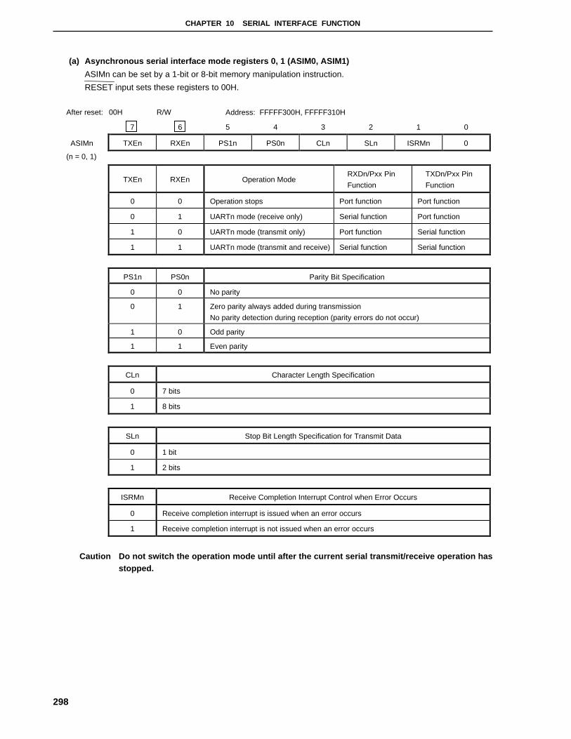
CHAPTER 10 SERIAL INTERFACE FUNCTION
298
(a) Asynchronous serial interface mode registers 0, 1 (ASIM0, ASIM1)
ASIMn can be set by a 1-bit or 8-bit memory manipulation instruction.
RESET input sets these registers to 00H.
After reset: 00H R/W Address: FFFFF300H, FFFFF310H
7 6 5 4 3 2 1 0
ASIMn TXEn RXEn PS1n PS0n CLn SLn ISRMn 0
(n = 0, 1)
TXEn RXEn Operation ModeRXDn/Pxx Pin
Function
TXDn/Pxx Pin
Function
0 0 Operation stops Port function Port function
0 1 UARTn mode (receive only) Serial function Port function
1 0 UARTn mode (transmit only) Port function Serial function
1 1 UARTn mode (transmit and receive) Serial function Serial function
PS1n PS0n Parity Bit Specification
0 0 No parity
0 1 Zero parity always added during transmission
No parity detection during reception (parity errors do not occur)
1 0 Odd parity
1 1 Even parity
CLn Character Length Specification
0 7 bits
1 8 bits
SLn Stop Bit Length Specification for Transmit Data
0 1 bit
1 2 bits
ISRMn Receive Completion Interrupt Control when Error Occurs
0 Receive completion interrupt is issued when an error occurs
1 Receive completion interrupt is not issued when an error occurs
Caution Do not switch the operation mode until after the current serial transmit/receive operation hasstopped.

CHAPTER 10 SERIAL INTERFACE FUNCTION
299
(b) Asynchronous serial interface status registers 0, 1 (ASIS0, ASIS1)
ASISn can be read using a 1-bit or 8-bit memory manipulation instruction.
RESET input sets these registers to 00H.
After reset: 00H R Address: FFFFF302H, FFFFF312H
7 6 5 4 3 2 1 0
ASISn 0 0 0 0 0 PEn FEn OVEn
(n = 0, 1)
PEn Parity Error Flag
0 No parity error
1 Parity error
(Transmit data parity does not match)
FEn Framing Error Flag
0 No framing error
1 Framing error Note 1
(Stop bit not detected)
OVEn Overrun Error Flag
0 No overrun error
1 Overrun error Note 2
(Next receive operation was completed before data was read from receive buffer register)
Notes 1. Even if a stop bit length has been set as two bits by setting bit 2 (SLn) in the asynchronous serial
interface mode register (ASIMn), stop bit detection during a receive operation only applies to a stop
bit length of 1 bit.
2. Be sure to read the contents of the receive buffer register (RXBn) when an overrun error has
occurred.
Until the contents of RXBn are read, further overrun errors will occur when receiving data.
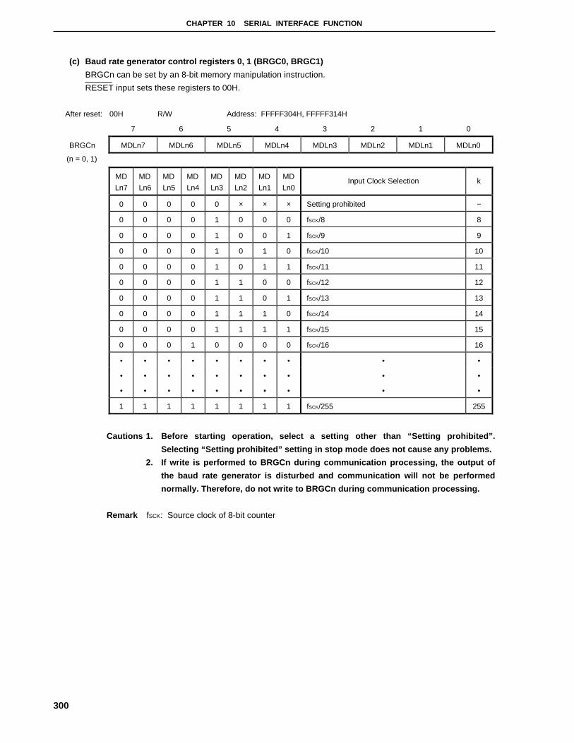
CHAPTER 10 SERIAL INTERFACE FUNCTION
300
(c) Baud rate generator control registers 0, 1 (BRGC0, BRGC1)
BRGCn can be set by an 8-bit memory manipulation instruction.
RESET input sets these registers to 00H.
After reset: 00H R/W Address: FFFFF304H, FFFFF314H
7 6 5 4 3 2 1 0
BRGCn MDLn7 MDLn6 MDLn5 MDLn4 MDLn3 MDLn2 MDLn1 MDLn0
(n = 0, 1)
MD
Ln7
MD
Ln6
MD
Ln5
MD
Ln4
MD
Ln3
MD
Ln2
MD
Ln1
MD
Ln0Input Clock Selection k
0 0 0 0 0 × × × Setting prohibited −
0 0 0 0 1 0 0 0 fSCK/8 8
0 0 0 0 1 0 0 1 fSCK/9 9
0 0 0 0 1 0 1 0 fSCK/10 10
0 0 0 0 1 0 1 1 fSCK/11 11
0 0 0 0 1 1 0 0 fSCK/12 12
0 0 0 0 1 1 0 1 fSCK/13 13
0 0 0 0 1 1 1 0 fSCK/14 14
0 0 0 0 1 1 1 1 fSCK/15 15
0 0 0 1 0 0 0 0 fSCK/16 16
• • • • • • • • • •
• • • • • • • • • •
• • • • • • • • • •
1 1 1 1 1 1 1 1 fSCK/255 255
Cautions 1. Before starting operation, select a setting other than “Setting prohibited”.
Selecting “Setting prohibited” setting in stop mode does not cause any problems.
2. If write is performed to BRGCn during communication processing, the output of
the baud rate generator is disturbed and communication will not be performed
normally. Therefore, do not write to BRGCn during communication processing.
Remark fSCK: Source clock of 8-bit counter

CHAPTER 10 SERIAL INTERFACE FUNCTION
301
(d) Baud rate generator mode control registers 0, 1 (BRGMCn0, BRGMCn1)
BRGMCn0 and BRGMCn1 are set by an 8-bit memory manipulation instruction.
RESET input sets these registers to 00H.
After reset: 00H R/W Address: FFFFF30EH, FFFFF31EH
7 6 5 4 3 2 1 0
BRGMCn0 0 0 0 0 0 TPSn2 TPSn1 TPSn0
(n = 0, 1)
After reset: 00H R/W Address: FFFFF320H, FFFFF322H
7 6 5 4 3 2 1 0
BRGMCn1 0 0 0 0 0 0 0 TPSn3
(n = 0, 1)
TPSn3 TPSn2 TPSn1 TPSn0 8-bit Counter Source Clock Selection m
0 0 0 0 External clock (ASCKn) −
0 0 0 1 fxx 0
0 0 1 0 fxx/2 1
0 0 1 1 fxx/4 2
0 1 0 0 fxx/8 3
0 1 0 1 fxx/16 4
0 1 1 0 fxx/32 5
0 1 1 1 at n = 0 : TM3 output
at n = 1 : TM2 output
−
1 0 0 0 fxx/64 6
1 0 0 1 fxx/128 7
1 0 1 0 fxx/256 8
1 0 1 1 fxx/512 9
1 1 0 0 –
1 1 0 1 –
1 1 1 0 –
1 1 1 1
Setting prohibited
–
Caution If write is performed to BRGMCn0, n1 during communication processing, the output of
the baud rate generator is disturbed and communication will not be performed
normally. Therefore, do not write to BRGMCn0 and BRGMCn1 during communication
processing.
Remark fXX: Main clock oscillation frequency
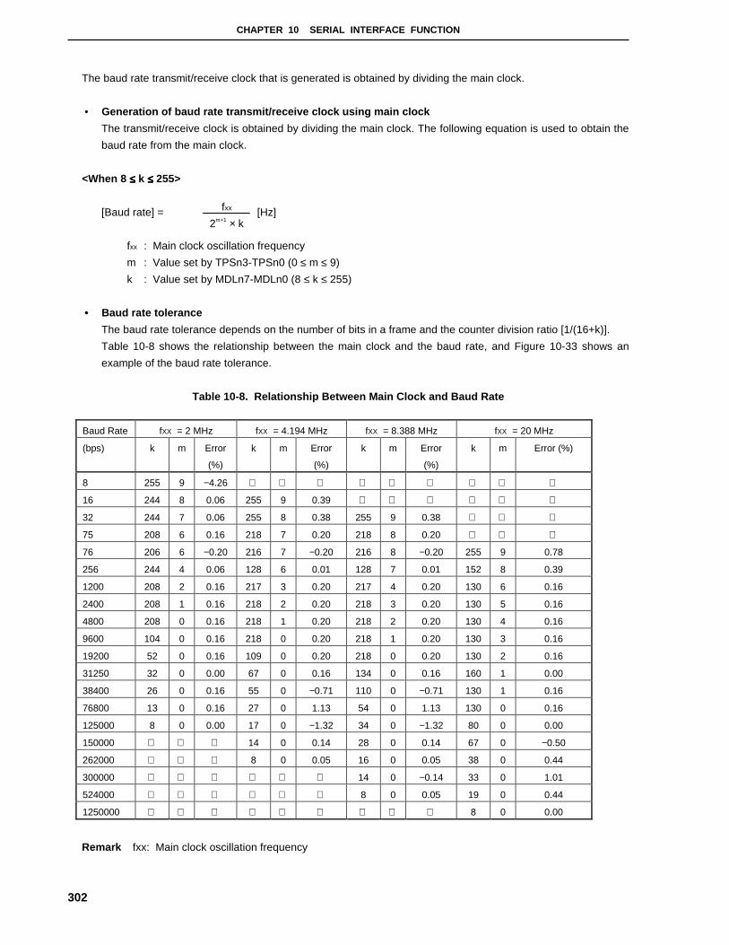
CHAPTER 10 SERIAL INTERFACE FUNCTION
302
The baud rate transmit/receive clock that is generated is obtained by dividing the main clock.
• Generation of baud rate transmit/receive clock using main clock
The transmit/receive clock is obtained by dividing the main clock. The following equation is used to obtain the
baud rate from the main clock.
<When 8 ≤≤≤≤ k ≤≤≤≤ 255>
[Baud rate] = [Hz]
fxx : Main clock oscillation frequency
m : Value set by TPSn3-TPSn0 (0 ≤ m ≤ 9)
k : Value set by MDLn7-MDLn0 (8 ≤ k ≤ 255)
• Baud rate tolerance
The baud rate tolerance depends on the number of bits in a frame and the counter division ratio [1/(16+k)].
Table 10-8 shows the relationship between the main clock and the baud rate, and Figure 10-33 shows an
example of the baud rate tolerance.
Table 10-8. Relationship Between Main Clock and Baud Rate
Baud Rate fXX = 2 MHz fXX = 4.194 MHz fXX = 8.388 MHz fXX = 20 MHz
(bps) k m Error
(%)
k m Error
(%)
k m Error
(%)
k m Error (%)
8 255 9 −4.26
16 244 8 0.06 255 9 0.39
32 244 7 0.06 255 8 0.38 255 9 0.38
75 208 6 0.16 218 7 0.20 218 8 0.20
76 206 6 −0.20 216 7 −0.20 216 8 −0.20 255 9 0.78
256 244 4 0.06 128 6 0.01 128 7 0.01 152 8 0.39
1200 208 2 0.16 217 3 0.20 217 4 0.20 130 6 0.16
2400 208 1 0.16 218 2 0.20 218 3 0.20 130 5 0.16
4800 208 0 0.16 218 1 0.20 218 2 0.20 130 4 0.16
9600 104 0 0.16 218 0 0.20 218 1 0.20 130 3 0.16
19200 52 0 0.16 109 0 0.20 218 0 0.20 130 2 0.16
31250 32 0 0.00 67 0 0.16 134 0 0.16 160 1 0.00
38400 26 0 0.16 55 0 −0.71 110 0 −0.71 130 1 0.16
76800 13 0 0.16 27 0 1.13 54 0 1.13 130 0 0.16
125000 8 0 0.00 17 0 −1.32 34 0 −1.32 80 0 0.00
150000 14 0 0.14 28 0 0.14 67 0 −0.50
262000 8 0 0.05 16 0 0.05 38 0 0.44
300000 14 0 −0.14 33 0 1.01
524000 8 0 0.05 19 0 0.44
1250000 8 0 0.00
Remark fxx: Main clock oscillation frequency
fxx
2m+1 × k
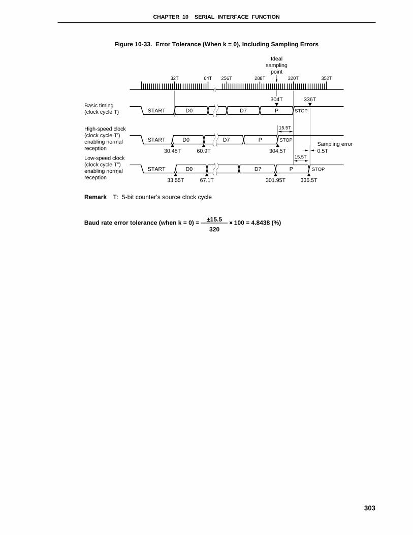
CHAPTER 10 SERIAL INTERFACE FUNCTION
303
Figure 10-33. Error Tolerance (When k = 0), Including Sampling Errors
Basic timing(clock cycle T) START D0 D7 P STOP
High-speed clock(clock cycle T’)enabling normalreception
START D0 D7 P STOP
Low-speed clock(clock cycle T”)enabling normalreception
START D0 D7 P STOP
32T 64T 256T 288T 320T 352T
Idealsampling
point
304T 336T
30.45T 60.9T 304.5T
15.5T
15.5T0.5TSampling error
33.55T 67.1T 301.95T 335.5T
Remark T: 5-bit counter’s source clock cycle
Baud rate error tolerance (when k = 0) = ×××× 100 = 4.8438 (%)±±±±15.5
320

CHAPTER 10 SERIAL INTERFACE FUNCTION
304
(2) Communication operations
(a) Data format
As shown in Figure 10-34, the format of the transmit/receive data consists of a start bit, character bits, a
parity bit, and one or more stop bits.
The asynchronous serial interface mode register (ASIMn) is used to set the character bit length, parity
selection, and stop bit length within each data frame (n = 0, 1).
Figure 10-34. Format of Transmit/Receive Data in Asynchronous Serial Interface
D0 D1 D2 D3 D4 D5 D6 D7Startbit
Paritybit
Stop bit
1 data frame
• Start bit ............. 1 bit
• Character bits ... 7 bits or 8 bits
• Parity bit ........... Even parity, odd parity, zero parity, or no parity
• Stop bit(s) ........ 1 bit or 2 bits
When 7 bits is selected as the number of character bits, only the low-order 7 bits (from bit 0 to bit 6) are
valid, so that during a transmission the highest bit (bit 7) is ignored and during reception the highest bit (bit 7)
must be set to 0.
The asynchronous serial interface mode register (ASIMn) and the baud rate generator control register
(BRGCn) are used to set the serial transfer rate (n = 0, 1).
If a receive error occurs, information about the receive error can be recognized by reading the asynchronous
serial interface status register (ASISn).
CHAPTER 10 SERIAL INTERFACE FUNCTION
305
(b) Parity types and operations
The parity bit is used to detect bit errors in transfer data. Usually, the same type of parity bit is used by the
transmitting and receiving sides. When odd parity or even parity is set, errors in the parity bit (the odd-
number bit) can be detected. When zero parity or no parity is set, errors are not detected.
(i) Even parity
• During transmission
The number of bits in transmit data including a parity bit is controlled so that the number is set an
even number of “1” bits. The value of the parity bit is as follows.
If the transmit data contains an odd number of “1” bits : the parity bit value is “1”
If the transmit data contains an even number of “1” bits : the parity bit value is “0”
• During reception
The number of “1” bits is counted among the receive data including a parity bit, and a parity error is
generated when the result is an odd number.
(ii) Odd parity
• During transmission
The number of bits in transmit data including a parity bit is controlled so that the number is set an
odd number of “1” bits. The value of the parity bit is as follows.
If the transmit data contains an odd number of “1” bits : the parity bit value is “0”
If the transmit data contains an even number of “1” bits : the parity bit value is “1”
• During reception
The number of “1” bits is counted among the receive data including a parity bit, and a parity error is
generated when the result is an even number.
(iii) Zero parity
During transmission, the parity bit is set to “0” regardless of the transmit data.
During reception, the parity bit is not checked. Therefore, no parity errors will be generated regardless
of whether the parity bit is a “0” or a “1”.
(iv) No parity
No parity bit is added to the transmit data.
During reception, receive data is regarded as having no parity bit. Since there is no parity bit, no parity
errors will be generated.

CHAPTER 10 SERIAL INTERFACE FUNCTION
306
(c) Transmission
The transmit operation is started when transmit data is written to the transmit shift register (TXSn). A start
bit, parity bit, and stop bit(s) are automatically added to the data.
Starting the transmit operation shifts out the data in TXSn, thereby emptying TXSn, after which a transmit
completion interrupt (INTSTn) is issued.
The timing of the transmit completion interrupt is shown in Figure 10-35.
Figure 10-35. Timing of Asynchronous Serial Interface Transmit Completion Interrupt
TxDn (output) D0 D1 D2 D6 D7 Parity STOPSTART
INTSTn
(a) Stop bit length: 1
TxDn (output) D0 D1 D2 D6 D7 ParitySTART
INTSTn
(b) Stop bit length: 2
STOP
Caution Do not write to the asynchronous serial interface mode register (ASIMn) during a
transmit operation. Writing to ASIMn during a transmit operation may disable further
transmit operations (in such cases, enter a RESET to restore normal operation).
Whether or not a transmit operation is in progress can be determined via software using
the transmit completion interrupt (INTSTn) or the interrupt request flag (STIFn) that is set
by INTSTn.
Remark n = 0, 1
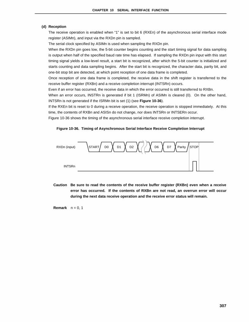
CHAPTER 10 SERIAL INTERFACE FUNCTION
307
(d) Reception
The receive operation is enabled when “1” is set to bit 6 (RXEn) of the asynchronous serial interface mode
register (ASIMn), and input via the RXDn pin is sampled.
The serial clock specified by ASIMn is used when sampling the RXDn pin.
When the RXDn pin goes low, the 5-bit counter begins counting and the start timing signal for data sampling
is output when half of the specified baud rate time has elapsed. If sampling the RXDn pin input with this start
timing signal yields a low-level result, a start bit is recognized, after which the 5-bit counter is initialized and
starts counting and data sampling begins. After the start bit is recognized, the character data, parity bit, and
one-bit stop bit are detected, at which point reception of one data frame is completed.
Once reception of one data frame is completed, the receive data in the shift register is transferred to the
receive buffer register (RXBn) and a receive completion interrupt (INTSRn) occurs.
Even if an error has occurred, the receive data in which the error occurred is still transferred to RXBn.
When an error occurs, INSTRn is generated if bit 1 (ISRMn) of ASIMn is cleared (0). On the other hand,
INTSRn is not generated if the ISRMn bit is set (1) (see Figure 10-36 ).
If the RXEn bit is reset to 0 during a receive operation, the receive operation is stopped immediately. At this
time, the contents of RXBn and ASISn do not change, nor does INTSRn or INTSERn occur.
Figure 10-36 shows the timing of the asynchronous serial interface receive completion interrupt.
Figure 10-36. Timing of Asynchronous Serial Interface Receive Completion Interrupt
Caution Be sure to read the contents of the receive buffer register (RXBn) even when a receive
error has occurred. If the contents of RXBn are not read, an overrun error will occur
during the next data receive operation and the receive error status will remain.
Remark n = 0, 1
RXDn (input) D0 D1 D2 D6 D7 Parity STOPSTART
INTSRn
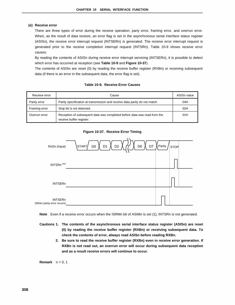
CHAPTER 10 SERIAL INTERFACE FUNCTION
308
(e) Receive error
There are three types of error during the receive operation, pariy error, framing error, and overrun error.
When, as the result of data receive, an error flag is set in the asynchronous serial interface status register
(ASISn), the receive error interrupt request (INTSERn) is generated. The receive error interrupt request is
generated prior to the receive completion interrupt request (INTSRn). Table 10-9 shows receive error
causes.
By reading the contents of ASISn during receive error interrupt servicing (INTSERn), it is possible to detect
which error has occurred at reception (see Table 10-9 and Figure 10-37 ).
The contents of ASISn are reset (0) by reading the receive buffer register (RXBn) or receiving subsequent
data (if there is an error in the subsequent data, the error flag is set).
Table 10-9. Receive Error Causes
Receive error Cause ASISn value
Parity error Parity specification at transmission and receive data parity do not match. 04H
Framing error Stop bit is not detected. 02H
Overrun error Reception of subsequent data was completed before data was read from the
receive buffer register.
01H
Figure 10-37. Receive Error Timing
RxDn (Input)
INTSRn Note
D7D6D2D1D0 Parity STOPSTART
INTSERn
INTSERn(When parity error occurs)
Note Even if a receive error occurs when the ISRMn bit of ASIMn is set (1), INTSRn is not generated.
Cautions 1. The contents of the asynchronous serial interface status register (ASISn) are reset
(0) by reading the receive buffer register (RXBn) or receiving subsequent data. To
check the contents of error, always read ASISn before reading RXBn.
2. Be sure to read the receive buffer register (RXBn) even in receive error generation. If
RXBn is not read out, an overrun error will occur during subsequent data reception
and as a result receive errors will continue to occur.
Remark n = 0, 1

CHAPTER 10 SERIAL INTERFACE FUNCTION
309
10.4.5 Standby function
(1) Operation in HALT mode
Serial transfer operation is performed normally.
(2) Operation in STOP and IDLE modes
(a) When internal clock is selected as serial clock
The operations of asynchronous serial interface mode register n (ASIMn), transmit shift register n (TXSn),
and receive buffer register n (RXBn) are stopped and their values immediately before the clock stopped are
hold.
The TXDn pin output holds the data immediately before the clock is stopped (in STOP mode) during
transmission. When the clock is stopped during reception, the receive data until the clock stopped are stored
and subsequent receive operation is stopped. Reception resumes upon clock restart.
(b) When external clock is selected as serial clock
Serial transfer operation is performed normally.

CHAPTER 10 SERIAL INTERFACE FUNCTION
310
10.5 3-Wire Variable Serial I/O (CSI4)
The CSI4 has the following two modes.
(1) Operation stop mode
This mode is used when serial transfers are not performed.
(2) 3-wire variable serial I/O mode (MSB/LSB first switchable)
This mode transfers variable data of 8 to 16 bits via three lines: serial clock (SCK4), serial output (SO4), and
serial input (SI4).
Since the data can be transmitted and received simultaneously in the 3-wire variable serial I/O mode, the
processing time of data transfer is shortened.
MSB and LSB can be switched for the first bit of data to be transferred in serial.
The 3-wire variable serial I/O mode is useful when connecting to a peripheral I/O device that includes a clock-
synchronous serial interface, a display controller, etc.
Caution The serial clock (SCK4) must be used within the range of SCK4 ≤≤≤≤ 2.5 MHz.
10.5.1 Configuration
The SCI4 includes the following hardware.
Table 10-10. Configuration of CSI4
Item Configuration
Register Variable serial IO shift register (SIO4)
Control registers Variable serial control register (CSIM4)
Variable serial setting register (CSIB4)
Baud rate generator source clock select register 4 (BRGCN4)
Baud rate generator output clock select register 4 (BRGCK4)

CHAPTER 10 SERIAL INTERFACE FUNCTION
311
Figure 10-38. Block Diagram of CSI4
Baud rategenerator
SO4
SI4
INTCSI4
Serial clock controller Selector
Interruptgenerator
Serial clock counter(8-/16-bit switchable)
Variable length I/O shiftregister (8-/16-bit)
SCK4 Selected clock
Direction controller
Internal bus
(1) Variable serial I/O shift register (SIO4)
SIO4 is the 16-bit variable register that performs parallel-serial conversion and transmit/receive (shift operations)
synchronized with the serial clock.
SIO4 is set by a 16-bit memory manipulation instruction.
The serial operation starts when data is written to or read from SIO4, while the bit 7 (CSIE4) of the serial
operation mode register 4 (CSIM4) is 1.
When transmitting, data written to SIO4 is output via the serial output (SO4).
When receiving, data is read from the serial input (SI4) and written to SIO4.
RESET input resets SIO4 to 0000H.
Caution Do not execute SIO4 access except for the accesses that become transfer start trigger during
transfer operation (read is disabled when MODE = 0 and write is disabled when MODE = 1).
Figure 10-39. Variable Serial I/O Shift Register (SIO4)
After reset: 0000H R/W Address: FFFFF2E0H
15 14 13 12 11 10 9 8 7 6 5 4 3 2 1 0
SIO4

CHAPTER 10 SERIAL INTERFACE FUNCTION
312
When transfer bit length is set other than 16 bits no matter which data should be aligned from the lowest bit of the
shift register for setting data, regardless of whether MSB or LSB is set for the transfer first bit. Any data can be set to
the unused high-order bits, however, in this case the received data after a serial transfer operation becomes 0.
Figure 10-40. When Transfer Bit Length Other Than 16 Bits Is Set
(a) When transfer bit length is 10 bits and MSB first
(b) When transfer bit length is 12 bits and LSB first
SI4SO4
15 10 9 0
Fixed to 0
SI4 SO4
Fixed to 0
15 12 11 0

CHAPTER 10 SERIAL INTERFACE FUNCTION
313
10.5.2 CSI4 control registers
The CSI4 uses the following type of registers for control functions.
• Variable length serial control register (CSIM4)
• Variable length serial setting register (CSIB4)
• Baud rate generator source clock select register 4 (BRGCN4)
• Baud rate generator output clock select register 4 (BRGCK4)
(1) Variable length serial control register (CSIM4)
This register is used to enable or disable serial interface channel 4’s serial clock, operation modes, and specific
operations.
CSIM4 can be set by a 1-bit or 8-bit memory manipulation instruction.
RESET input sets CSIM4 to 00H.
Figure 10-41. Variable Length Serial Control Register (CSIM4)
After reset: 00H R/W Address: FFFFF2E2H
7 6 5 4 3 2 1 0
CSIM4 CSIE4 0 0 0 0 MODE4 0 SCL4
SIO4 Operation Enable/Disable Specification
Shift register operation Serial counter Port Note
0 Operation disable Clear Port function
1 Operation enable Count operation enable Serial function + port function
Transfer Operation Mode Flag
Operation mode Transfer start trigger SO4 output
0 Transmit/receive mode SIO4 write Normal output
1 Receive-only mode SIO4 read Low level fixed
SCL4 Clock Selection
0 External clock input (SCK4)
1 BRG (Baud rate generator)
Note When CSIE4 = 1 (SIO4 operation enable status), the port function is available only for the pin that is
connected to SI4 when using the transmit function only and to SO4 when using the receive function.
CSIE4
MODE4

CHAPTER 10 SERIAL INTERFACE FUNCTION
314
(2) Variable length serial setting register (CSIB4)
CSIB4 is used to set the operation format of the serial interface channel 4.
Bit length of a variable register is set by setting bits 3 to 0 (BSEL3 to BSEL0) of this register. Data is transferred
in MSB first while bit 4 (DIR) is 1, and is transferred in LCB first while DIR is 0.
CSIB4 can be set by a 1-bit or 8-bit memory manipulation instruction.
RESET input sets CSIB4 to 00H.
Figure 10-42. Variable Length Serial Setting Register (CSIB4)
After reset : 00H R/W Address: FFFFF2E4H
7 6 5 4 3 2 1 0
CSIB4 0 CMODE DMODE DIR BSEL3 BSEL2 BSEL1 BSEL0
CMODE DMODE SCK4 Active Level SI4 Interrupt Timing SO4 Output Timing
0 0 Low level Rising edge of SCK4 Falling edge of SCK4
0 1 Low level Falling edge of SCK4 Rising edge of SCK4
1 0 High level Rising edge of SCK4 Falling edge of SCK4
1 1 High level Falling edge of SCK4 Rising edge of SCK4
DIR Serial Transfer Direction
0 LSB first
1 MSB first
BSEL3 BSEL2 BSEL1 BSEL0 Bit Length of Serial Register
0 0 0 0 16 bits
1 0 0 0 8 bits
1 0 0 1 9 bits
1 0 1 0 10 bits
1 0 1 1 11 bits
1 1 0 0 12 bits
1 1 0 1 13 bits
1 1 1 0 14 bits
1 1 1 1 15 bits
Other than above Setting prohibited

CHAPTER 10 SERIAL INTERFACE FUNCTION
315
(3) Baud rate generator source clock select register 4 (BRGCN4)
BRGCN4 can be set by an 8-bit memory manipulation instruction.
RESET input sets BRGCN4 to 00H.
Figure 10-43. Baud Rate Generator Source Clock Select Register 4 (BRGCN4)
After reset : 00H R/W Address: FFFFF2E6H
7 6 5 4 3 2 1 0
BRGCN4 0 0 0 0 0 BRGN2 BRGN1 BRGN0
BRGN2 BRGN1 BRGN0 Source Clock (fSCK) n
0 0 1 fXX 0
0 0 0 fXX/2 1
0 1 1 fXX/4 2
0 1 0 fXX/8 3
1 0 1 fXX/16 4
1 0 0 fXX/32 5
1 1 1 fXX/64 6
1 1 0 fXX/128 7
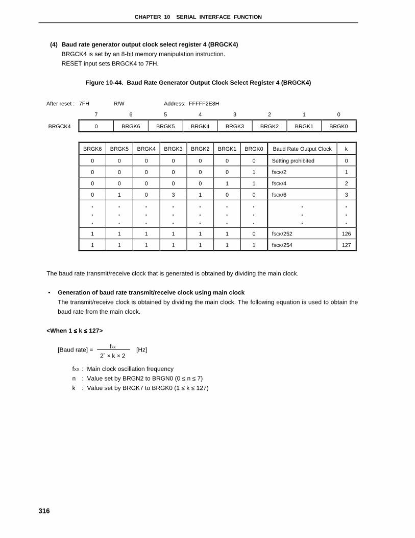
CHAPTER 10 SERIAL INTERFACE FUNCTION
316
(4) Baud rate generator output clock select register 4 (BRGCK4)
BRGCK4 is set by an 8-bit memory manipulation instruction.
RESET input sets BRGCK4 to 7FH.
Figure 10-44. Baud Rate Generator Output Clock Select Register 4 (BRGCK4)
After reset : 7FH R/W Address: FFFFF2E8H
7 6 5 4 3 2 1 0
BRGCK4 0 BRGK6 BRGK5 BRGK4 BRGK3 BRGK2 BRGK1 BRGK0
BRGK6 BRGK5 BRGK4 BRGK3 BRGK2 BRGK1 BRGK0 Baud Rate Output Clock k
0 0 0 0 0 0 0 Setting prohibited 0
0 0 0 0 0 0 1 fSCK/2 1
0 0 0 0 0 1 1 fSCK/4 2
0 1 0 3 1 0 0 fSCK/6 3
•
•
•
•
•
•
•
•
•
•
•
•
•
•
•
•
•
•
•
•
•
•
•
•
•
•
•
1 1 1 1 1 1 0 fSCK/252 126
1 1 1 1 1 1 1 fSCK/254 127
The baud rate transmit/receive clock that is generated is obtained by dividing the main clock.
• Generation of baud rate transmit/receive clock using main clock
The transmit/receive clock is obtained by dividing the main clock. The following equation is used to obtain the
baud rate from the main clock.
<When 1 ≤≤≤≤ k ≤≤≤≤ 127>
[Baud rate] = [Hz]
fXX : Main clock oscillation frequency
n : Value set by BRGN2 to BRGN0 (0 ≤ n ≤ 7)
k : Value set by BRGK7 to BRGK0 (1 ≤ k ≤ 127)
fxx
2n × k × 2

CHAPTER 10 SERIAL INTERFACE FUNCTION
317
10.5.3 Operations
The CSI4 has the following two operation modes.
(1) Operation stop mode
This mode does not perform serial transfers and can therefore reduce power consumption.
When in operation stop mode, SI4, SO4, and SCK4 can be used as normal I/O ports.
(a) Register settings
Operation stop mode is set via the variable length serial control register (CSIM4). While CSIE4 = 0 (SIO4
operation stop state), the pins connected to SI4, SO4, or SCK4 function as port pins.
CSIM4 can be set by a 1-bit or 8-bit memory manipulation instruction.
RESET input sets CSIM4 to 00H.
After reset : 00H R/W Address: FFFFF2E2H
7 6 5 4 3 2 1 0
CSIM4 CSIE4 0 0 0 0 MODE4 0 SCL4
SIO4 Operation Enable/Disable Specification
Shift register operation Serial counter Port Note
0 Operation disable Clear Port function
1 Operation enable Count operation enable Serial function + port function
Note When CSIE4 = 1 (SIO4 operation enable status), the port function is available only for the pin that is
connected to SI4 when using the transmit function only and to SO4 when using the receive function.
CSIE4
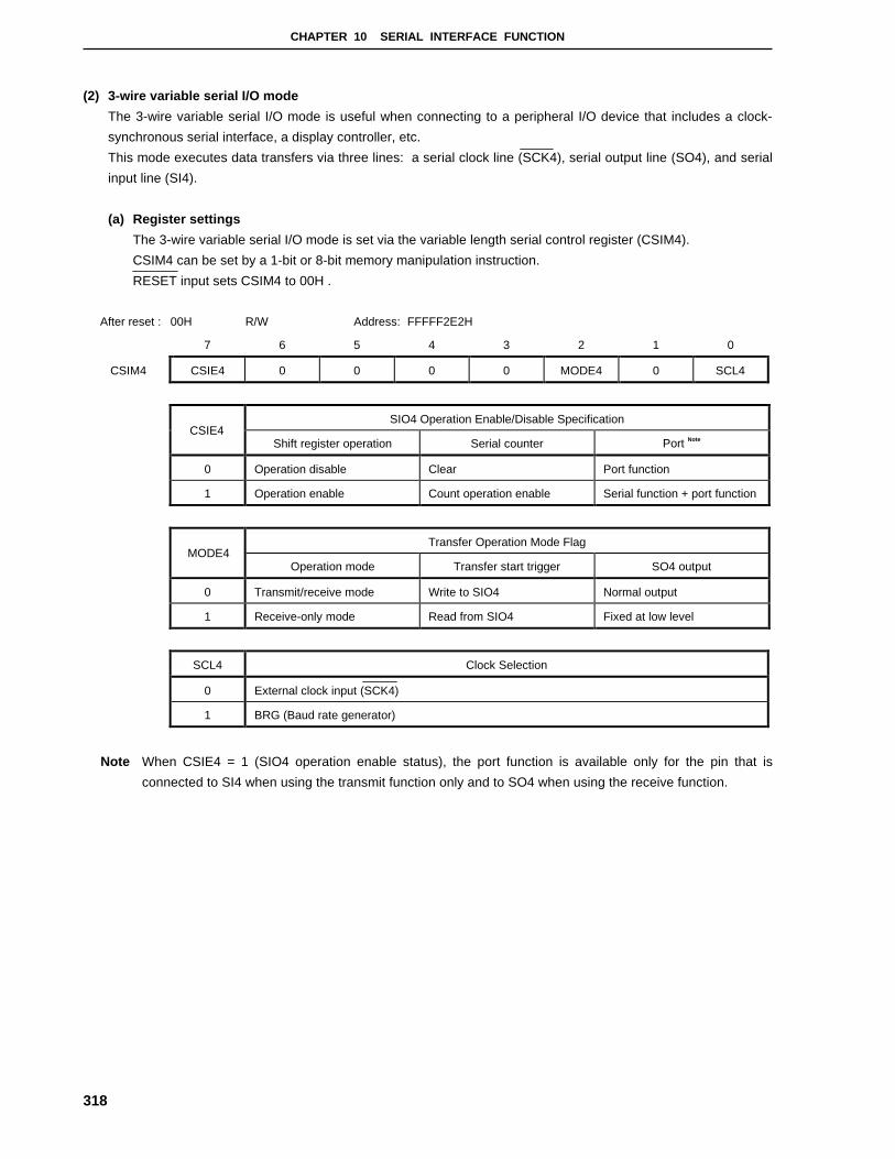
CHAPTER 10 SERIAL INTERFACE FUNCTION
318
(2) 3-wire variable serial I/O mode
The 3-wire variable serial I/O mode is useful when connecting to a peripheral I/O device that includes a clock-
synchronous serial interface, a display controller, etc.
This mode executes data transfers via three lines: a serial clock line (SCK4), serial output line (SO4), and serial
input line (SI4).
(a) Register settings
The 3-wire variable serial I/O mode is set via the variable length serial control register (CSIM4).
CSIM4 can be set by a 1-bit or 8-bit memory manipulation instruction.
RESET input sets CSIM4 to 00H .
After reset : 00H R/W Address: FFFFF2E2H
7 6 5 4 3 2 1 0
CSIM4 CSIE4 0 0 0 0 MODE4 0 SCL4
SIO4 Operation Enable/Disable Specification
Shift register operation Serial counter Port Note
0 Operation disable Clear Port function
1 Operation enable Count operation enable Serial function + port function
Transfer Operation Mode Flag
Operation mode Transfer start trigger SO4 output
0 Transmit/receive mode Write to SIO4 Normal output
1 Receive-only mode Read from SIO4 Fixed at low level
SCL4 Clock Selection
0 External clock input (SCK4)
1 BRG (Baud rate generator)
Note When CSIE4 = 1 (SIO4 operation enable status), the port function is available only for the pin that is
connected to SI4 when using the transmit function only and to SO4 when using the receive function.
CSIE4
MODE4
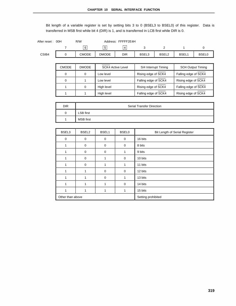
CHAPTER 10 SERIAL INTERFACE FUNCTION
319
Bit length of a variable register is set by setting bits 3 to 0 (BSEL3 to BSEL0) of this register. Data is
transferred in MSB first while bit 4 (DIR) is 1, and is transferred in LCB first while DIR is 0.
After reset : 00H R/W Address: FFFFF2E4H
7 6 5 4 3 2 1 0
CSIB4 0 CMODE DMODE DIR BSEL3 BSEL2 BSEL1 BSEL0
CMODE DMODE SCK4 Active Level SI4 Interrupt Timing SO4 Output Timing
0 0 Low level Rising edge of SCK4 Falling edge of SCK4
0 1 Low level Falling edge of SCK4 Rising edge of SCK4
1 0 High level Rising edge of SCK4 Falling edge of SCK4
1 1 High level Falling edge of SCK4 Rising edge of SCK4
DIR Serial Transfer Direction
0 LSB first
1 MSB first
BSEL3 BSEL2 BSEL1 BSEL0 Bit Length of Serial Register
0 0 0 0 16 bits
1 0 0 0 8 bits
1 0 0 1 9 bits
1 0 1 0 10 bits
1 0 1 1 11 bits
1 1 0 0 12 bits
1 1 0 1 13 bits
1 1 1 0 14 bits
1 1 1 1 15 bits
Other than above Setting prohibited

CHAPTER 10 SERIAL INTERFACE FUNCTION
320
(b) Communication Operations
In the 3-wire serial I/O mode, data is transmitted and received in 8 to 16-bit units, and is specified by setting
bits 3 to 0 (BSEL3 to BSEL0) of the variable length serial setting register (CSIB4). Each bit of data is
transmitted or received in synchronization with the serial clock.
After transfer of all bits is completed, SIC4 stops operation automatically and the interrupt request flag
(INTCSI4) is set.
Bits 6 and 5 (CMODE and DMODE) of the variable length serial setting register (CSIB4) can change the
attribute of the serial clock (SCK4) and the phases of serial data (SI4 and SO4).
Figure 10-45. Timing of 3-Wire Variable Serial I/O Mode
SCK4 (CMODE = 0)
SIO4 (Write)
SO4 (DMODE = 1)
INTCSI4
SCK4 (CMODE = 1)
SO4 (DMODE = 0)
Remark An arrow shows the SI4 data fetch timing.
When CMODE = 0, the serial clock (SCK4) stops at the high level during the operation stop, and outputs the low
level during a data transfer operation. When CMODE = 1, on the other hand, SCK4 stops at the low level during
the operation stop and outputs the high level during a data transfer operation.
The phases of the SO4 output timing and the S14 fetch timing can transit half a clock by setting DMODE.
However, the interrupt signal (INTCSI4) is generated at the final edge of the serial clock (SCK4), regardless the
setting of CSIB4.

CHAPTER 10 SERIAL INTERFACE FUNCTION
321
(c) Transfer start
A serial transfer becomes possible when the following two conditions have been satisfied.
• The SIO4 operation control bit (CSIE4) = 1
• After a serial transfer, the internal serial clock is stopped.
Serial transfer starts when the following operation is performed after the above two conditions have been
satisfied.
• Transmit/transmit and receive mode (MODE4 = 0)
Transfer starts when writing to SIO4.
• Receive-only mode
Transfer starts when reading from SIO4.
Caution After data has been written to SIO4, transfer will not start even if the CSIE4 bit value is
set to “1”.
Completion of the final-bit transfer automatically stops the serial transfer operation and sets the interrupt
request flag (INTCSI4).
Figure 10-46. Timing of 3-Wire Variable Serial I/O Mode (When CSIB4 = 08H)
SCK4 (CMODE = 0)
SI4
INTCSI4
1 2 3 4 5 6 7 8
Transfer end
SO4 (DMODE = 0) MSB LSB
MSB LSB
Remark CSIB4 = 08H (CMODE = 0, DMODE = 0, DIR = 0, BSEL3 to BSEL0 = 1000)

322
[MEMO]
323
CHAPTER 11 A/D CONVERTER
11.1 Function
The A/D converter converts analog input signals into digital values with a resolution of 10 bits, and can handle 12
channels of analog input signals (ANI0 to ANI11).
The V850/SB1 supports the low power consumption mode by low-speed conversion.
(1) Hardware start
Conversion is started by trigger input (ADTRG) (rising edge, falling edge, or both rising and falling edges can be
specified).
(2) Software start
Conversion is started by setting A/D converter mode register 1 (ADM1).
One analog input channel is selected from ANI0 to ANI11, and A/D conversion is performed. If A/D conversion
has been started by means of hardware start, conversion stops once it has been completed, and an interrupt request
(INTAD) is generated. If conversion has been started by means of software start, conversion is performed
repeatedly. Each time conversion has been completed, INTAD is generated.

CHAPTER 11 A/D CONVERTER
324
Figure 11-1 shows the block diagram.
Figure 11-1. Block Diagram of A/D Converter
ANI0ANI1ANI2ANI3ANI4ANI5ANI6ANI7ANI8ANI9
ANI10ANI11
AVREF
AVSS
INTAD
4
ADS3 ADS2 ADS1 ADS0 ADCS TRG FR2 FR1 FR0 EGA1 EGA0 ADPS
Sel
ecto
r
Sample & hold circuit
AVSS
Voltage comparator
Tap
sel
ecto
r
ADTRGEdge detectioncircuit
Control circuit
A/D conversion resultregister (ADCR)
Trigger enable
Analog input channel specification register (ADS)
A/D converter moderegister 1 (ADM1)
Internal bus
IEAD
A/D converter moderegister 2 (ADM2)
Successive approximation register(SAR)
AVDD

CHAPTER 11 A/D CONVERTER
325
11.2 Configuration
The A/D converter consists of the following hardware units.
Table 11-1. Configuration of A/D Converter
Item Configuration
Analog input 12 channels (ANI0 to ANI11)
Registers Successive approximation register (SAR)
A/D conversion result register (ADCR)
A/D conversion result register H (ADCRH): only high-order 8 bits
can be read
Control registers A/D converter mode register 1 (ADM1)
A/D converter mode register 2 (ADM2)
Analog input channel specification register (ADS)
(1) Successive approximation register (SAR)
This register compares the voltage value of the analog input signal with the voltage tap (compare voltage) value
from the series resistor string, and holds the result of the comparison starting from the most significant bit (MSB).
When the comparison result has settled down to the least significant bit (LSB) (i.e., when the A/D conversion has
been completed), the contents of the SAR are transferred to the A/D conversion result register.
(2) A/D conversion result register (ADCR), A/D conversion result register H (ADCRH)
Each time A/D conversion has been completed, the result of the conversion is loaded to this register from the
successive approximation register. The high-order 10 bits of this register holds the result of the A/D conversion
(the low-order 6 bits are fixed to 0). This register is read using a 16-bit memory manipulation instruction. RESET
input sets ADCR to 0000H.
When using only high-order 8 bits of the result of the A/D conversion, ADCRH is read using an 8-bit memory
manipulation instruction.
RESET input sets ADCRH to 00H.
Caution A write operation to A/D converter mode register 1 (ADM1) and analog input channel
specification register (ADS) may cause the ADCR contents to be undefined. After the
conversion, read out the conversion result before the write operation to ADM1 and ADS is
performed. Correct conversion results may not be read if the timing is other than the above.
(3) Sample & hold circuit
The sample & hold circuit samples each of the analog input signals sequentially sent from the input circuit, and
sends the sampled data to the voltage comparator. This circuit also holds the sampled analog input signal
voltage during A/D conversion.
(4) Voltage comparator
The voltage comparator compares the analog input signal with the output voltage of the series resistor string.
(5) Series resistor string
The series resistor string is connected between AVREF and AVSS and generates a voltage for comparison with the
analog input signal.
CHAPTER 11 A/D CONVERTER
326
(6) ANI0 to ANI11 pins
These are analog input pins for the 12 channels of the A/D converter, and are used to input analog signals to be
converted into digital signals. Pins other than ones selected as analog input with the analog input channel
specification register (ADS) can be used as input ports.
Caution Make sure that the voltages input to ANI0 through ANI11 do not exceed the rated values. If a
voltage higher than AV REF or lower than AV SS (even within the range of the absolute maximum
ratings) is input to a channel, the conversion value of the channel is undefined, and the
conversion values of the other channels may also be affected.
(7) AVREF pin
This pin inputs a reference voltage to the A/D converter.
The signals input to the ANI0 through ANI11 pins are converted into digital signals based on the voltage applied
across AVREF and AVSS.
(8) AVSS pin
This is the ground pin of the A/D converter. Always keep the potential at this pin the same as that at the VSS pin
even when the A/D converter is not in use.
(9) AVDD pin
This is the analog power supply pin of the A/D converter. Always keep the potential at this pin the same as that
at the VDD pin even when the A/D converter is not in use.
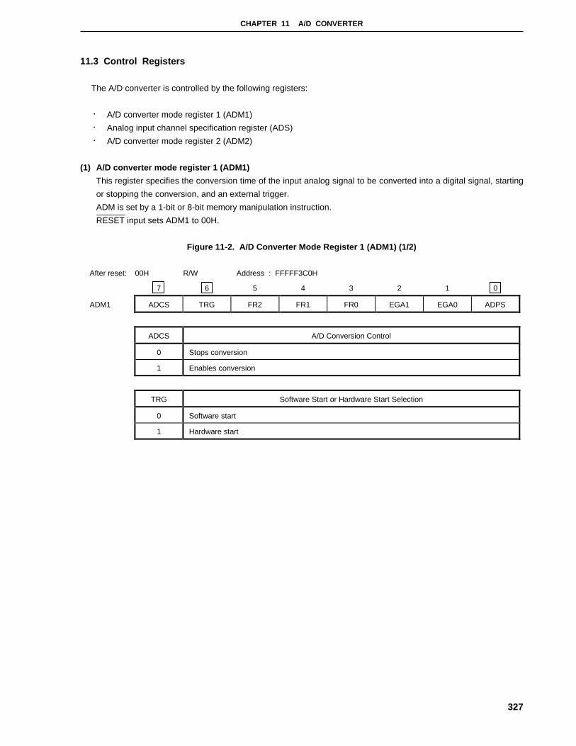
CHAPTER 11 A/D CONVERTER
327
11.3 Control Registers
The A/D converter is controlled by the following registers:
• A/D converter mode register 1 (ADM1)• Analog input channel specification register (ADS)• A/D converter mode register 2 (ADM2)
(1) A/D converter mode register 1 (ADM1)
This register specifies the conversion time of the input analog signal to be converted into a digital signal, starting
or stopping the conversion, and an external trigger.
ADM is set by a 1-bit or 8-bit memory manipulation instruction.
RESET input sets ADM1 to 00H.
Figure 11-2. A/D Converter Mode Register 1 (ADM1) (1/2)
After reset: 00H R/W Address : FFFFF3C0H
7 6 5 4 3 2 1 0
ADM1 ADCS TRG FR2 FR1 FR0 EGA1 EGA0 ADPS
ADCS A/D Conversion Control
0 Stops conversion
1 Enables conversion
TRG Software Start or Hardware Start Selection
0 Software start
1 Hardware start
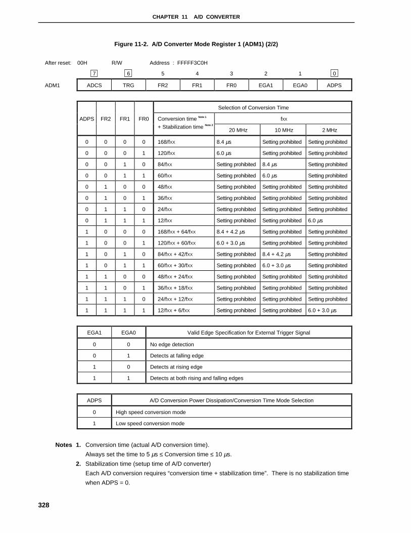
CHAPTER 11 A/D CONVERTER
328
Figure 11-2. A/D Converter Mode Register 1 (ADM1) (2/2)
After reset: 00H R/W Address : FFFFF3C0H
7 6 5 4 3 2 1 0
ADM1 ADCS TRG FR2 FR1 FR0 EGA1 EGA0 ADPS
Selection of Conversion Time
fXXADPS FR2 FR1 FR0 Conversion time Note 1
+ Stabilization time Note 2
20 MHz 10 MHz 2 MHz
0 0 0 0 168/fXX 8.4 µs Setting prohibited Setting prohibited
0 0 0 1 120/fXX 6.0 µs Setting prohibited Setting prohibited
0 0 1 0 84/fXX Setting prohibited 8.4 µs Setting prohibited
0 0 1 1 60/fXX Setting prohibited 6.0 µs Setting prohibited
0 1 0 0 48/fXX Setting prohibited Setting prohibited Setting prohibited
0 1 0 1 36/fXX Setting prohibited Setting prohibited Setting prohibited
0 1 1 0 24/fXX Setting prohibited Setting prohibited Setting prohibited
0 1 1 1 12/fXX Setting prohibited Setting prohibited 6.0 µs
1 0 0 0 168/fXX + 64/fXX 8.4 + 4.2 µs Setting prohibited Setting prohibited
1 0 0 1 120/fXX + 60/fXX 6.0 + 3.0 µs Setting prohibited Setting prohibited
1 0 1 0 84/fXX + 42/fXX Setting prohibited 8.4 + 4.2 µs Setting prohibited
1 0 1 1 60/fXX + 30/fXX Setting prohibited 6.0 + 3.0 µs Setting prohibited
1 1 0 0 48/fXX + 24/fXX Setting prohibited Setting prohibited Setting prohibited
1 1 0 1 36/fXX + 18/fXX Setting prohibited Setting prohibited Setting prohibited
1 1 1 0 24/fXX + 12/fXX Setting prohibited Setting prohibited Setting prohibited
1 1 1 1 12/fXX + 6/fXX Setting prohibited Setting prohibited 6.0 + 3.0 µs
EGA1 EGA0 Valid Edge Specification for External Trigger Signal
0 0 No edge detection
0 1 Detects at falling edge
1 0 Detects at rising edge
1 1 Detects at both rising and falling edges
ADPS A/D Conversion Power Dissipation/Conversion Time Mode Selection
0 High speed conversion mode
1 Low speed conversion mode
Notes 1. Conversion time (actual A/D conversion time).
Always set the time to 5 µs ≤ Conversion time ≤ 10 µs.
2. Stabilization time (setup time of A/D converter)
Each A/D conversion requires “conversion time + stabilization time”. There is no stabilization time
when ADPS = 0.

CHAPTER 11 A/D CONVERTER
329
(2) Analog input channel specification register (ADS)
ADS specifies the port for inputting an analog voltage to be converted into a digital signal.
ADS is set by a 1-bit or 8-bit memory manipulation instruction.
RESET input sets ADS to 00H.
Figure 11-3. Analog Input Channel Specification Register (ADS)
After reset: 00H R/W Address : FFFFF3C2H
7 6 5 4 3 2 1 0
ADS 0 0 0 0 ADS3 ADS2 ADS1 ADS0
ADS3 ADS2 ADS1 ADS0 Analog Input Channel Specification
0 0 0 0 ANI0
0 0 0 1 ANI1
0 0 1 0 ANI2
0 0 1 1 ANI3
0 1 0 0 ANI4
0 1 0 1 ANI5
0 1 1 0 ANI6
0 1 1 1 ANI7
1 0 0 0 ANI8
1 0 0 1 ANI9
1 0 1 0 ANI10
1 0 1 1 ANI11
Other than above Setting prohibited
(3) A/D converter mode register 2 (ADM2)
ADM2 specifies connection/disconnection of AVDD and AVREF.
ADM2 is set by a 1-bit or 8-bit memory manipulation instruction.
RESET input sets ADM2 to 00H.
Figure 11-4. A/D Converter Mode Register 2 (ADM2)
After reset: 00H R/W Address : FFFFF3C8H
7 6 5 4 3 2 1 0
ADM2 0 0 0 0 0 0 0 IEAD
IEAD A/D Current Cut Control
0 Cut between AVDD and AVREF
1 Connect between AVDD and AVREF
CHAPTER 11 A/D CONVERTER
330
11.4 Operation
11.4.1 Basic operation
<1> Select one channel whose analog signal is to be converted into a digital signal by using the analog input
channel specification register (ADS).
<2> The sample & hold circuit samples the voltage input to the selected analog input channel.
<3> After sampling for a specific time, the sample & hold circuit enters the hold status, and holds the input analog
voltage until it has been converted into a digital signal.
<4> Set the bit 9 of the successive approximation register (SAR). The tap selector sets the voltage tap of the
series resistor string to (1/2) AVREF.
<5> The voltage difference between the voltage tap of the series resistor string and the analog input voltage is
compared by the voltage comparator. If the analog input voltage is greater than (1/2) AVREF, the MSB of the
SAR remains set. If the analog input voltage is less than (1/2) AVREF, the MSB is reset.
<6> Next, bit 8 of the SAR is automatically set, and the analog input voltage is compared again. Depending on
the value of bit 9 to which the result of the preceding comparison has been set, the voltage tap of the series
resistor string is selected as follows:• Bit 9 = 1: (3/4) AVREF
• Bit 9 = 0: (1/4) AVREF
The analog input voltage is compared with one of these voltage taps, and bit 8 of the SAR is manipulated as
follows depending on the result of the comparison.• Analog input voltage ≥ voltage tap: bit 8 = 1• Analog input voltage ≤ voltage tap: bit 8 = 0
<7> The above steps are repeated until the bit 0 of the SAR has been manipulated.
<8> When comparison of all the 10 bits of the SAR has been completed, the valid digital value remains in the
SAR, and the value of the SAR is transferred and latched to the A/D conversion result register (ADCR).
At the same time, an A/D conversion end interrupt request (INTAD) can be generated.
Caution The first conversion value immediately after starting the A/D conversion may not satisfy the
ratings.
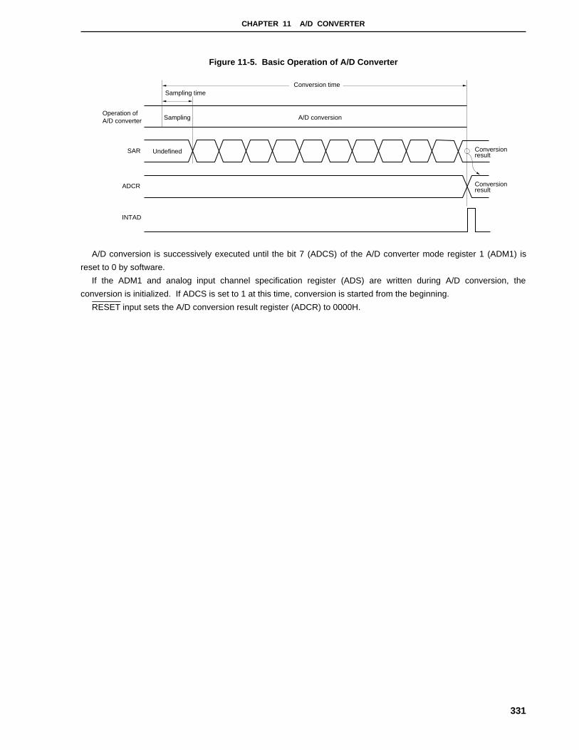
CHAPTER 11 A/D CONVERTER
331
Figure 11-5. Basic Operation of A/D Converter
SAR
ADCR
INTAD
Conversion time Sampling time
Sampling Operation of A/D converter A/D conversion
Undefined Conversion result
Conversion result
A/D conversion is successively executed until the bit 7 (ADCS) of the A/D converter mode register 1 (ADM1) is
reset to 0 by software.
If the ADM1 and analog input channel specification register (ADS) are written during A/D conversion, the
conversion is initialized. If ADCS is set to 1 at this time, conversion is started from the beginning.
RESET input sets the A/D conversion result register (ADCR) to 0000H.
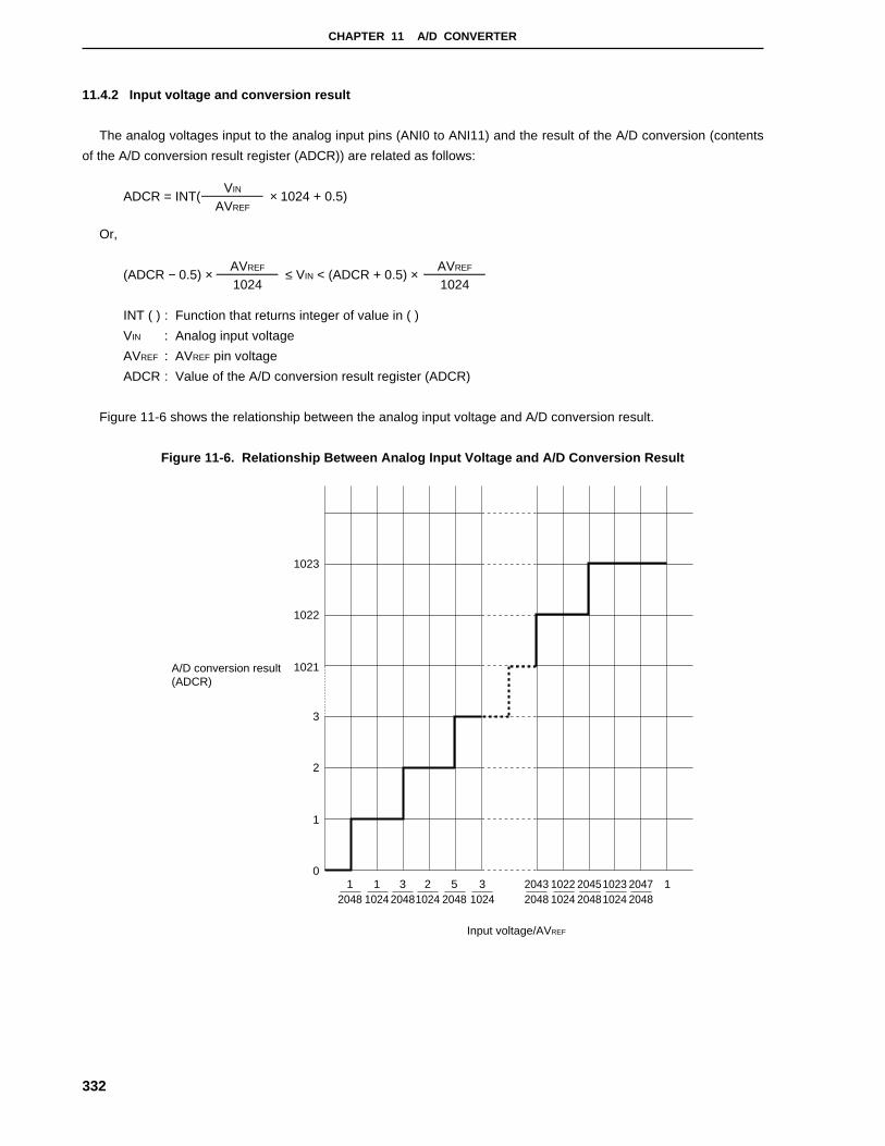
CHAPTER 11 A/D CONVERTER
332
11.4.2 Input voltage and conversion result
The analog voltages input to the analog input pins (ANI0 to ANI11) and the result of the A/D conversion (contents
of the A/D conversion result register (ADCR)) are related as follows:
ADCR = INT( × 1024 + 0.5)
Or,
(ADCR − 0.5) × ≤ VIN < (ADCR + 0.5) ×
INT ( ) : Function that returns integer of value in ( )
VIN : Analog input voltage
AVREF : AVREF pin voltage
ADCR : Value of the A/D conversion result register (ADCR)
Figure 11-6 shows the relationship between the analog input voltage and A/D conversion result.
Figure 11-6. Relationship Between Analog Input Voltage and A/D Conversion Result
1 1 3 2 5 3 2043 1022 20451023 2047 12048 1024 20481024 2048 1024 2048 1024 20481024 2048
0
1
2
3
1021
1022
1023
A/D conversion result(ADCR)
Input voltage/AVREF
VIN
AVREF
AVREF
1024AVREF
1024

CHAPTER 11 A/D CONVERTER
333
11.4.3 A/D converter operation mode
In this mode one of the analog input channels ANI0 to ANI11 is selected by the analog input channel specification
register (ADS) and A/D conversion is executed.
The A/D conversion can be started in the following two ways:
• Hardware start: Started by trigger input (ADTRG) (rising edge, falling edge, or both rising and falling edges
can be specified)• Software start: Started by setting A/D converter mode register 1 (ADM1)
The result of the A/D conversion is stored to the A/D conversion result register (ADCR) and an interrupt request
signal (INTAD) is generated at the same time.

CHAPTER 11 A/D CONVERTER
334
(1) A/D conversion by hardware start
A/D conversion is on standby if bit 6 (TRG) and bit 7 (ADCS) of the A/D converter mode register 1 (ADM1) are
set to 1. When an external trigger signal is input, the A/D converter starts converting the voltage applied to the
analog input pin specified by the analog input channel specification register (ADS) into a digital signal.
When the A/D conversion has been completed, the result of the conversion is stored to the A/D conversion result
register (ADCR), and an interrupt request signal (INTAD) is generated. Once the A/D conversion has been
started and completed, conversion is not started again unless a new external trigger signal is input.
If data with ADCS set to 1 is written to ADM during A/D conversion, the conversion under execution is stopped,
and the A/D converter stands by until a new external trigger signal is input. If the external trigger signal is input,
A/D conversion is executed again from the beginning.
If data with ADCS set to 0 is written to ADM1 during A/D conversion, the conversion is immediately stopped.
Figure 11-7. A/D Conversion by Hardware Start (with Falling Edge Specified)
Rewriting ADSADCS = 1, TRG = 1
Rewriting ADSADCS = 1, TRG = 1
A/D conversion
ADCR
INTAD
ANInStandby status
Standby status
Standby status
ANIn ANIn ANIm ANIm ANIm
ANInANInANIn ANIm ANIm
External trigger input signal
Remarks 1. n = 0, 1, ..., 11
2. m = 0, 1, ..., 11
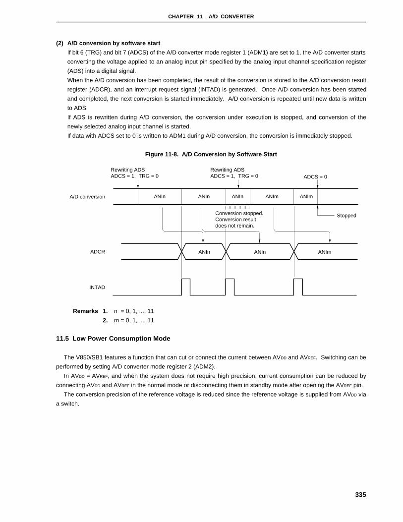
CHAPTER 11 A/D CONVERTER
335
(2) A/D conversion by software start
If bit 6 (TRG) and bit 7 (ADCS) of the A/D converter mode register 1 (ADM1) are set to 1, the A/D converter starts
converting the voltage applied to an analog input pin specified by the analog input channel specification register
(ADS) into a digital signal.
When the A/D conversion has been completed, the result of the conversion is stored to the A/D conversion result
register (ADCR), and an interrupt request signal (INTAD) is generated. Once A/D conversion has been started
and completed, the next conversion is started immediately. A/D conversion is repeated until new data is written
to ADS.
If ADS is rewritten during A/D conversion, the conversion under execution is stopped, and conversion of the
newly selected analog input channel is started.
If data with ADCS set to 0 is written to ADM1 during A/D conversion, the conversion is immediately stopped.
Figure 11-8. A/D Conversion by Software Start
Rewriting ADSADCS = 1, TRG = 0
Rewriting ADSADCS = 1, TRG = 0 ADCS = 0
A/D conversion
ADCR
INTAD
ANIn ANIn ANIn ANIm ANIm
ANInANIn ANIm
Conversion stopped.Conversion result does not remain.
Stopped
Remarks 1. n = 0, 1, ..., 11
2. m = 0, 1, ..., 11
11.5 Low Power Consumption Mode
The V850/SB1 features a function that can cut or connect the current between AVDD and AVREF. Switching can be
performed by setting A/D converter mode register 2 (ADM2).
In AVDD = AVREF, and when the system does not require high precision, current consumption can be reduced by
connecting AVDD and AVREF in the normal mode or disconnecting them in standby mode after opening the AVREF pin.
The conversion precision of the reference voltage is reduced since the reference voltage is supplied from AVDD via
a switch.
CHAPTER 11 A/D CONVERTER
336
11.6 Notes on Using A/D Converter
(1) Current consumption in standby mode
The A/D converter stops operation in the STOP and IDLE modes (operable in the HALT mode). At this time, the
current consumption of the A/D converter can be reduced by stopping the conversion (by resetting the bit 7
(ADCS) of the A/D converter mode register 1 (ADM1) to 0).
To reduce the current consumption in the STOP and IDLE modes, set the AVREF potential in the user circuit to
the same value (0 V) as the AVSS potential.
(2) Input range of ANI0 to ANI11
Keep the input voltage of the ANI0 through ANI11 pins to within the rated range. If a voltage greater than AV REF
or lower than AVSS (even within the range of the absolute maximum ratings) is input to a channel, the converted
value of the channel becomes undefined. Moreover, the values of the other channels may also be affected.
(3) Conflict
<1> Conflict between writing A/D conversion result register (ADCR) and reading ADCR at end of
conversion
Reading ADCR takes precedence. After ADCR has been read, a new conversion result is written to ADCR.
<2> Conflict between writing ADCR and external trigger signal input at end of conversion
The external trigger signal is not input during A/D conversion. Therefore, the external trigger signal is not
accepted during writing of ADCR.
<3> Conflict between writing of ADCR and writing A/D converter mode register 1 (ADM1) or analog input
channel specification register (ADS)
When ADM1 or ADS write is performed immediately after ADCR write following A/D conversion end, the
conversion result is written to the ADCR register, but the timing is such that INTAD is not generated.
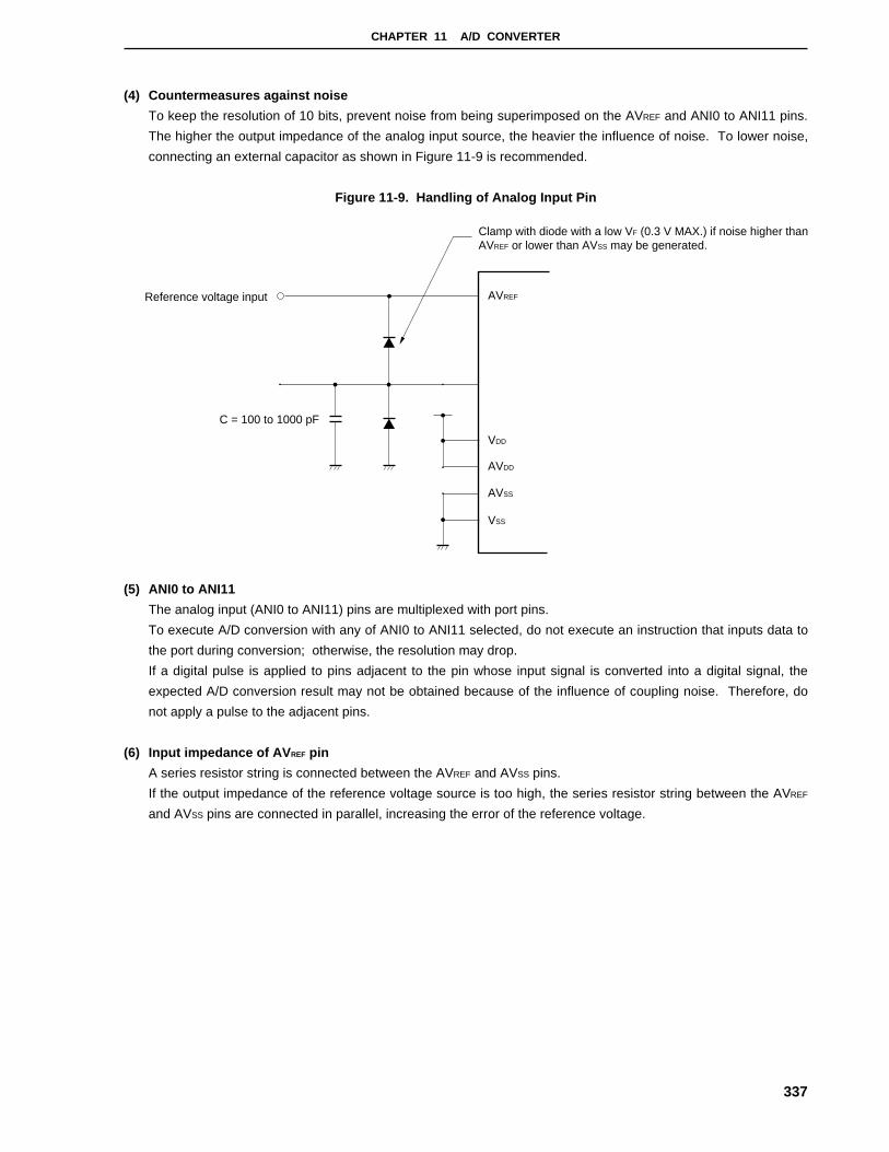
CHAPTER 11 A/D CONVERTER
337
(4) Countermeasures against noise
To keep the resolution of 10 bits, prevent noise from being superimposed on the AVREF and ANI0 to ANI11 pins.
The higher the output impedance of the analog input source, the heavier the influence of noise. To lower noise,
connecting an external capacitor as shown in Figure 11-9 is recommended.
Figure 11-9. Handling of Analog Input Pin
AVREF
VDD
VSS
AVDD
AVSS
Reference voltage input
Clamp with diode with a low VF (0.3 V MAX.) if noise higher than AVREF or lower than AVSS may be generated.
C = 100 to 1000 pF
(5) ANI0 to ANI11
The analog input (ANI0 to ANI11) pins are multiplexed with port pins.
To execute A/D conversion with any of ANI0 to ANI11 selected, do not execute an instruction that inputs data to
the port during conversion; otherwise, the resolution may drop.
If a digital pulse is applied to pins adjacent to the pin whose input signal is converted into a digital signal, the
expected A/D conversion result may not be obtained because of the influence of coupling noise. Therefore, do
not apply a pulse to the adjacent pins.
(6) Input impedance of AV REF pin
A series resistor string is connected between the AVREF and AVSS pins.
If the output impedance of the reference voltage source is too high, the series resistor string between the AVREF
and AVSS pins are connected in parallel, increasing the error of the reference voltage.
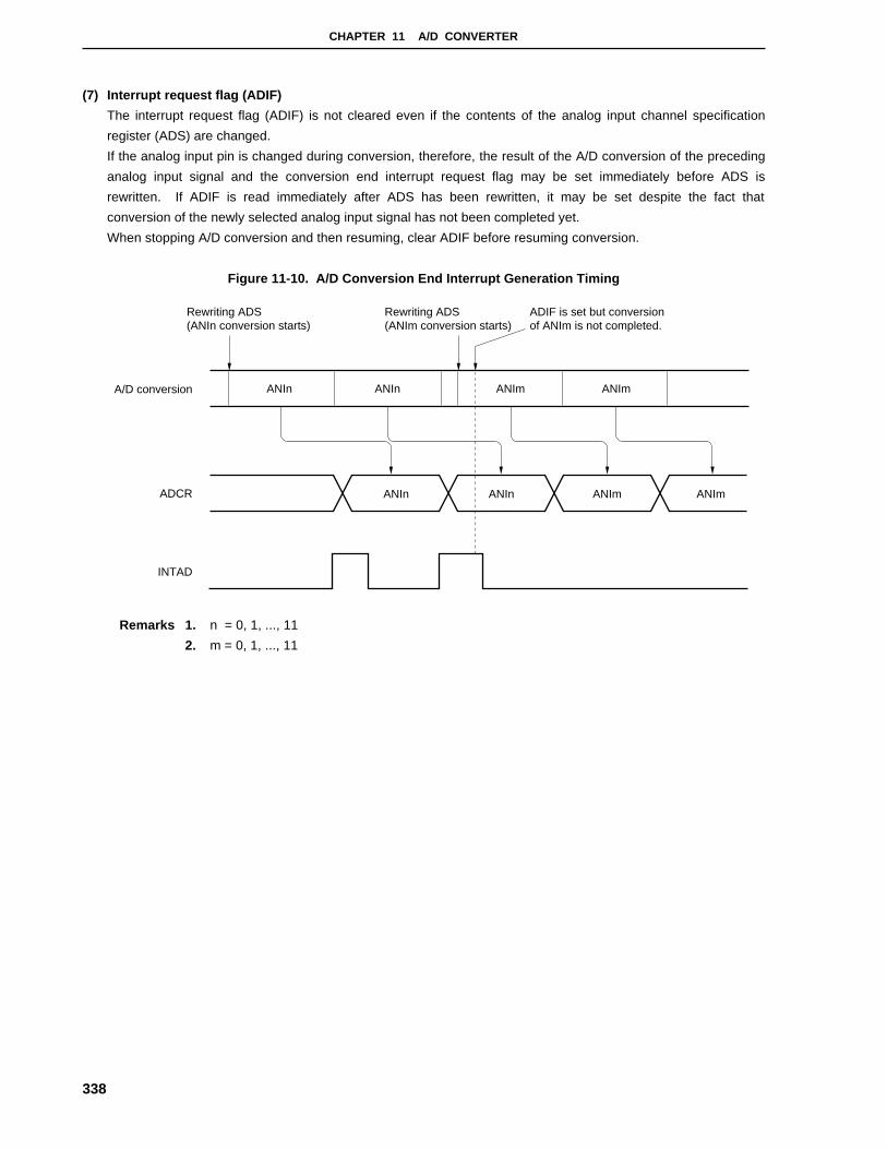
CHAPTER 11 A/D CONVERTER
338
(7) Interrupt request flag (ADIF)
The interrupt request flag (ADIF) is not cleared even if the contents of the analog input channel specification
register (ADS) are changed.
If the analog input pin is changed during conversion, therefore, the result of the A/D conversion of the preceding
analog input signal and the conversion end interrupt request flag may be set immediately before ADS is
rewritten. If ADIF is read immediately after ADS has been rewritten, it may be set despite the fact that
conversion of the newly selected analog input signal has not been completed yet.
When stopping A/D conversion and then resuming, clear ADIF before resuming conversion.
Figure 11-10. A/D Conversion End Interrupt Generation Timing
Rewriting ADS (ANIn conversion starts)
Rewriting ADS (ANIm conversion starts)
ADIF is set but conversion of ANIm is not completed.
A/D conversion
ADCR
INTAD
ANIn ANIn ANIm ANIm
ANImANInANIn ANIm
Remarks 1. n = 0, 1, ..., 11
2. m = 0, 1, ..., 11

CHAPTER 11 A/D CONVERTER
339
(8) AVDD pin
The AVDD pin is the power supply pin of the analog circuit, and also supplies power to the input circuit of ANI0 to
ANI11. Even in an application where a back-up power supply is used, therefore, be sure to apply the same
voltage as the VDD pin to the AVDD pin as shown in Figure 11-11.
Figure 11-11. Handling of AV DD Pin
AVREF
VDD
VSS
AVDD
AVSS
Main power supply Back-up capacitor
(9) Reading out A/D converter result register (ADCR)
A write operation to the A/D converter mode register 1 (ADM1) and analog input channel specification register
(ADS) may cause the ADCR contents to be undefined. After the conversion, read out the conversion result
before the write operation to ADM1 and ADS is performed. Incorrect conversion results may be read out in
timings other than the above.

340
[MEMO]
341
CHAPTER 12 DMA FUNCTIONS
12.1 Functions
The DMA (Direct Memory Access) controller transfers data between memory and peripheral I/Os based on DMA
requests sent from on-chip peripheral hardware (such as the serial interface, timer, or A/D converter).
This product includes six independent DMA channels that can transfer data in 8-bit and 16-bit units. The
maximum number of transfers is 256 (when transferring data in 8-bit units).
After a DMA transfer has occurred a specified number of times, DMA transfer completion interrupt (INTDMA0 to
INTDMA3) requests are output individually from the various channels.
The priority levels of the DMA channels are fixed as follows for simultaneous generation of multiple DMA transfer
requests.
DMA0 > DMA1 > DMA2 > DMA3
12.2 Transfer Completion Interrupt Request
After a DMA transfer has occurred a specified number of times and the TCn bit in the corresponding DMA channel
control register (DCHCn) has been set to 1, a DMA transfer completion interrupt request (INTDMA0 to INTDMA5)
occurs on each channel in relation to the interrupt controller.
12.3 Control Registers
12.3.1 DMA peripheral I/O address registers 0 to 5 (DIOA0 to DIOA5)
These registers are used to set the peripheral I/O register’s address for DMA channel n.
These registers are can be read/written in 16-bit units.
Figure 12-1. Format of DMA Peripheral I/O Address Registers 0 to 5 (DIOA0 to DIOA5)
After reset: Undefined R/W Address : DIOA0 FFFFF180H DIOA3 FFFFF1B0H
DIOA1 FFFFF190H DIOA4 FFFFF1C0H
DIOA2 FFFFF1A0H DIOA5 FFFFF100H
15 14 13 12 11 10 9 1 0
DIOAn 0 0 0 0 0 0 IOAn9 to IOAn1 0
(n = 0 to 5)
Caution The following peripheral I/O registers must not be set.
P4, P5, P6, P9, P11, PM4, PM5, PM6, PM9, PM11, MM, DWC, BCC, SYC, PSC, PCC, SYS,
PRCMD, DIOAn, DRAn, DBCn, DCHCn, CORCN, CORRQ, CORADn

CHAPTER 12 DMA FUNCTIONS
342
12.3.2 DMA internal RAM address registers 0 to 5 (DRA0 to DRA5)
These registers are used to set the on-chip RAM address for DMA channel n. An address is incremented after
each transfer is completed, when the DADn bit of the DCHDn register is 0. The incrementation value is “1”
during 8-bit transfers and “2” during 16-bit transfers (n = 0 to 5).
These registers are can be read/written in 16-bit units.
Figure 12-2. Format of DMA Internal RAM Address Registers 0 to 5 (DRA0 to DRA5)
After reset: Undefined R/W Address : DRA0 FFFFF182H DRA3 FFFFF1B2H
DRA1 FFFFF192H DRA4 FFFFF1C2H
DRA2 FFFFF1A2H DRA5 FFFFF1D2H
15 14 13 0
DRAn 0 0 RAn13 to RAn0
(n = 0 to 5)
Figure 12.3. Correspondence Between DRAn Setup Value and Internal RAM Area
Caution Do not set the odd-number addresses during 16-bit transfer (DS = 1 in DCHCn register).
Peripheral I/O area
Internal RAM area
Expansion ROM area
xxFFFFFFHDRAn Setup value
16 Kbytes
xxFFF000HxxFFEFFFH
xxFFC000HxxFFBFFFH
xxFFB000HxxFFAFFFH
2FFFH
0000H3FFFH
3000H
xxFF8000HxxFF7FFFH

CHAPTER 12 DMA FUNCTIONS
343
12.3.3 DMA byte count registers 0 to 5 (DBC0 to DBC5)
These are 8-bit registers that are used to set the number of transfers for DMA channel n.
The remaining number of transfers is retained during the DMA transfers.
A value of 1 is decremented once per transfer if the transfer is a byte (8-bit) transfer, and a value of 2 is
decremented once per transfer if the transfer is a 16-bit transfer. The transfers are ended when a borrow
operation occurs. Accordingly, “number of transfers − 1” should be set for byte (8-bit) transfers and “(number of
transfers − 1) × 2” should be set for 16-bit transfers.
These registers are can be read/written in 8-bit units.
Figure 12-4. Format of DMA Byte Count Registers 0 to 5 (DBC0 to DBC5)
After reset: Undefined R/W Address : DBC0 FFFFF184H DBC3 FFFFF1B4H
DBC1 FFFFF194H DBC4 FFFFF1C4H
DBC2 FFFFF1A4H DBC5 FFFFF1D4H
7 6 5 4 3 2 1 0
DBCn BCn7 BCn6 BCn5 BCn4 BCn3 BCn2 BCn1 BCn0
(n = 0 to 5)
Caution Values set to bit 0 are ignored during 16-bit transfers.
12.3.4 DMA channel control registers 0 to 5 (DCHC0 to DCHC5)
These registers are used to control the DMA transfer operation mode for DMA channel n.
These registers are can be read/written in 1-bit or 8-bit units.
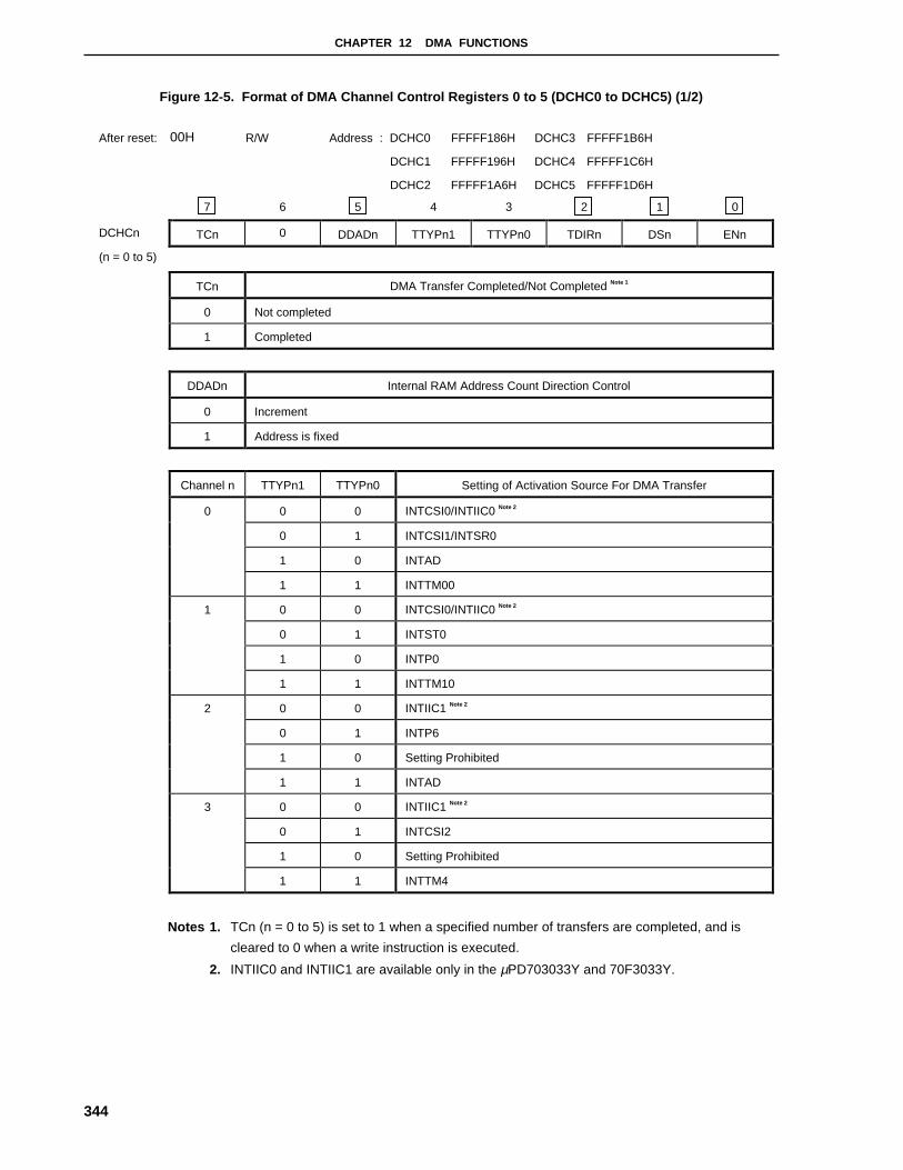
CHAPTER 12 DMA FUNCTIONS
344
Figure 12-5. Format of DMA Channel Control Registers 0 to 5 (DCHC0 to DCHC5) (1/2)
After reset: 00H R/W Address : DCHC0 FFFFF186H DCHC3 FFFFF1B6H
DCHC1 FFFFF196H DCHC4 FFFFF1C6H
DCHC2 FFFFF1A6H DCHC5 FFFFF1D6H
7 6 5 4 3 2 1 0
DCHCn TCn 0 DDADn TTYPn1 TTYPn0 TDIRn DSn ENn
(n = 0 to 5)
TCn DMA Transfer Completed/Not Completed Note 1
0 Not completed
1 Completed
DDADn Internal RAM Address Count Direction Control
0 Increment
1 Address is fixed
Channel n TTYPn1 TTYPn0 Setting of Activation Source For DMA Transfer
0 0 INTCSI0/INTIIC0 Note 2
0 1 INTCSI1/INTSR0
1 0 INTAD
0
1 1 INTTM00
0 0 INTCSI0/INTIIC0 Note 2
0 1 INTST0
1 0 INTP0
1
1 1 INTTM10
0 0 INTIIC1 Note 2
0 1 INTP6
1 0 Setting Prohibited
2
1 1 INTAD
0 0 INTIIC1 Note 2
0 1 INTCSI2
1 0 Setting Prohibited
3
1 1 INTTM4
Notes 1. TCn (n = 0 to 5) is set to 1 when a specified number of transfers are completed, and is
cleared to 0 when a write instruction is executed.
2. INTIIC0 and INTIIC1 are available only in the µPD703033Y and 70F3033Y.
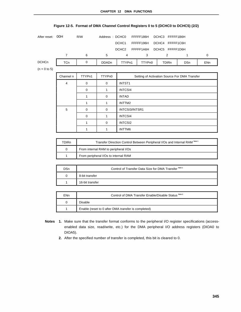
CHAPTER 12 DMA FUNCTIONS
345
Figure 12-5. Format of DMA Channel Control Registers 0 to 5 (DCHC0 to DCHC5) (2/2)
After reset: 00H R/W Address : DCHC0 FFFFF186H DCHC3 FFFFF1B6H
DCHC1 FFFFF196H DCHC4 FFFFF1C6H
DCHC2 FFFFF1A6H DCHC5 FFFFF1D6H
7 6 5 4 3 2 1 0
DCHCn TCn 0 DDADn TTYPn1 TTYPn0 TDIRn DSn ENn
(n = 0 to 5)
Channel n TTYPn1 TTYPn0 Setting of Activation Source For DMA Transfer
0 0 INTST1
0 1 INTCSI4
1 0 INTAD
4
1 1 INTTM2
0 0 INTCSI3/INTSR1
0 1 INTCSI4
1 0 INTCSI2
5
1 1 INTTM6
TDIRn Transfer Direction Control Between Peripheral I/Os and Internal RAM Note 1
0 From internal RAM to peripheral I/Os
1 From peripheral I/Os to internal RAM
DSn Control of Transfer Data Size for DMA Transfer Note 1
0 8-bit transfer
1 16-bit transfer
ENn Control of DMA Transfer Enable/Disable Status Note 2
0 Disable
1 Enable (reset to 0 after DMA transfer is completed)
Notes 1. Make sure that the transfer format conforms to the peripheral I/O register specifications (access-
enabled data size, read/write, etc.) for the DMA peripheral I/O address registers (DIOA0 to
DIOA5).
2. After the specified number of transfer is completed, this bit is cleared to 0.

346
[MEMO]

347
CHAPTER 13 REAL-TIME OUTPUT FUNCTION (RTO)
13.1 Function
The real-time output function transfers pre-set data to real-time output buffer registers (RTBL, RTBH), and then
transfers this data with hardware to an external device via the output latches, upon the occurrence of an external
interrupt or external trigger. The pins through which the data is output to an external device constitute a port called a
real-time output port.
Because RTO can output signals without jitter, it is suitable for controlling a stepping motor.
The real-time output port can be set in port mode or real-time output port mode in 1-bit units.
Figure 13-1 shows the block diagram of RTO.
Figure 13-1. Block Diagram of RTO
Output latch
RT
P7
Real-time output port mode register (RTPM)
Real-time output buffer register, high-order 4 bits (RTBH)
Output trigger control circuit
4
RTPOE RTPEG BYTE EXTR
RTPTRG
Real-time output port control register (RTPC)
Internal bus
Real-time output buffer register, low-order 4 bits (RTBL)
INTTM4
INTTM5
RT
P6
RT
P5
RT
P4
RT
P3
RT
P2
RT
P1
RT
P0
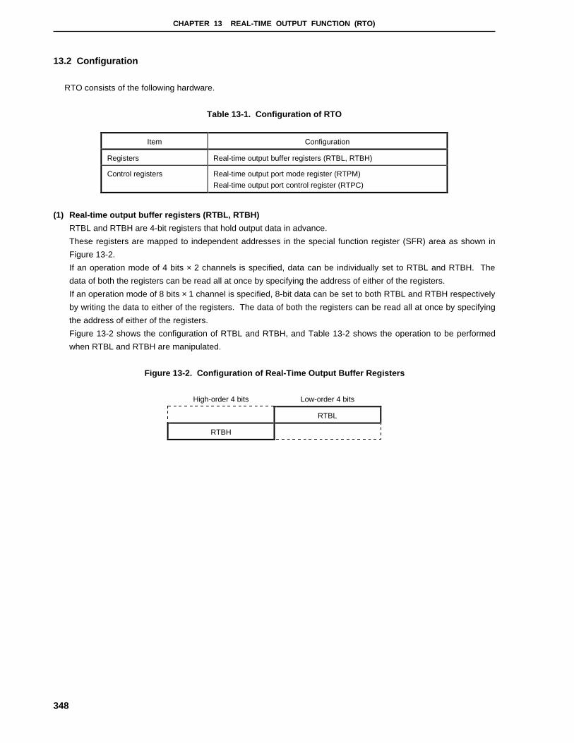
CHAPTER 13 REAL-TIME OUTPUT FUNCTION (RTO)
348
13.2 Configuration
RTO consists of the following hardware.
Table 13-1. Configuration of RTO
Item Configuration
Registers Real-time output buffer registers (RTBL, RTBH)
Control registers Real-time output port mode register (RTPM)
Real-time output port control register (RTPC)
(1) Real-time output buffer registers (RTBL, RTBH)
RTBL and RTBH are 4-bit registers that hold output data in advance.
These registers are mapped to independent addresses in the special function register (SFR) area as shown in
Figure 13-2.
If an operation mode of 4 bits × 2 channels is specified, data can be individually set to RTBL and RTBH. The
data of both the registers can be read all at once by specifying the address of either of the registers.
If an operation mode of 8 bits × 1 channel is specified, 8-bit data can be set to both RTBL and RTBH respectively
by writing the data to either of the registers. The data of both the registers can be read all at once by specifying
the address of either of the registers.
Figure 13-2 shows the configuration of RTBL and RTBH, and Table 13-2 shows the operation to be performed
when RTBL and RTBH are manipulated.
Figure 13-2. Configuration of Real-Time Output Buffer Registers
High-order 4 bits Low-order 4 bits
RTBL
RTBH

CHAPTER 13 REAL-TIME OUTPUT FUNCTION (RTO)
349
Table 13-2. Operation When Real-Time Output Buffer Registers Are Manipulated
Read Note 1
Write Note 2
Operation Mode Register to Be ManipulatedHigh-order 4 bits Low-order 4 bits High-order 4 bits Low-order 4 bits
RTBL RTBH RTBL Invalid RTBL4 bits × 2 channels
RTBH RTBH RTBL RTBH Invalid
RTBL RTBH RTBL RTBH RTBL8 bits × 1 channel
RTBH RTBH RTBL RTBH RTBL
Notes 1. Only the bits set in the real-time output port mode (RTPM) can be read. If a bit set in the port mode is
read, 0 is read.
2. Set output data to RTBL and RTBH after setting the real-time output port until the real-time output
trigger is generated.
13.3 RTO Control Registers
RTO is controlled by using the following two types of registers:
• Real-time output port mode register (RTPM)
• Real-time output port control register (RTPC)

CHAPTER 13 REAL-TIME OUTPUT FUNCTION (RTO)
350
(1) Real-time output port mode register (RTPM)
This register selects real-time output port mode or port mode in 1-bit units.
RTPM is set by a 1-bit or 8-bit memory manipulation instruction.
RESET input sets RTPM to 00H.
Figure 13-3. Format of Real-Time Output Port Mode Register (RTPM)
After reset: 00H R/W Address: FFFFF3A4H
7 6 5 4 3 2 1 0
RTPM RTPM7 RTPM6 RTPM5 RTPM4 RTPM3 RTPM2 RTPM1 RTPM0
RTPMn Selection of Real-Time Output Port (n = 0 to 7)
0 Port mode
1 Real-time output port mode
Cautions 1. Set a port pin to the output mode when it is used as a real-time output port pin.
2. Data cannot be set to the output latch for a port pin set as a real-time output port pin. To set
an initial value, therefore, set the data to the output latch before setting the port pin to the
real-time output port mode.

CHAPTER 13 REAL-TIME OUTPUT FUNCTION (RTO)
351
(2) Real-time output port control register (RTPC)
This register sets the operation mode and output trigger of the real-time output port.
The relationship between the operation mode and output trigger of the real-time output port is as shown in Table 13-
3.
RTPC is set by a 1-bit or 8-bit memory manipulation instruction.
RESET input sets RTPC to 00H.
Figure 13-4. Format of Real-Time Output Port Control Register (RTPC)
After reset: 00H R/W Address: FFFFF3A6H
7 6 5 4 3 2 1 0
RTPC RTPOE RTPEG BYTE EXTR 0 0 0 0
RTPOE Control of Operation of Real-Time Output Port
0 Disables operation Note
1 Enables operation
RTPEG Valid Edge of RTPTRG
0 Falling edge
1 Rising edge
BYTE Operation Mode of Real-Time Output Port
0 4 bits × 2 channels
1 8 bits × 1 channel
EXTR Control of Real-Time Output by RTPTRG Signal
0 Does not use RTPTRG as real-time output trigger
1 Uses RTPTRG as real-time output trigger
Note RTP0 to RTP7 output 0 if the real-time output operation is disabled (RTPOE = 0).
Table 13-3. Operation Mode and Output Trigger of Real-Time Output Port
BYTE EXTR Operation Mode RTBH → Port Output RTBL → Port Output
0 0 4 bits × 2 channels INTTM5 INTTM4
1 INTTM4 RTPTRG
1 0 8 bits × 1 channel INTTM4
1 RTPTRG

CHAPTER 13 REAL-TIME OUTPUT FUNCTION (RTO)
352
13.4 Operation
If the real-time output operation is enabled by setting the bit 7 (RTPOE) of the real-time output port control register
(RTPC) to 1, the data of the real-time output buffer registers (RTBH and RTBL) is transferred to the output latch in
synchronization with the generation of the selected transmit trigger (set by EXTR and BYTE Note). Of the transferred
data, only the data of the bits specified in the real-time output mode by the real-time output port mode register
(RTPM) is output from the bits of RTP0 to RTP7. The bits specified in the port mode by RTPM output 0.
If the real-time output operation is disabled by clearing RTPOE to 0, RTP0 to RTP7 output 0 regardless of the
setting of RTPM.
Note EXTR: Bit 4 of real-time output port control register (RTPC)
BYTE: Bit 5 of real-time output port control register (RTPC)
Figure 13-5. Example of Operation Timing of RTO (When EXTR = 0, BYTE = 0)
INTTM5 (internal)
INTTM4 (internal)
CPU operation
RTBH
RTBL
RT output latch (H)
RT output latch (L)
A B A B A B A B
D01 D02 D03 D04
D11 D12 D13 D14
D01 D02 D03 D04
D11 D12 D13 D14
A: Software processing by interrupt request input to INTTM5 (RTBH write)
B: Software processing by interrupt request input to INTTM4 (RTBL write)
CHAPTER 13 REAL-TIME OUTPUT FUNCTION (RTO)
353
13.5 Usage
(1) Disable the real-time output operation.
Clear bit 7 (RTPOE) of the real-time output port control register (RTPC) to 0.
(2) Initialization
• Set the initial value to the output latch.
• Specify the real-time output port mode or port mode in 1-bit units.
Set the real-time output port mode register (RTPM).
• Selects a trigger and valid edge.
Set bits 4, 5, and 6 (EXTR, BYTE, and RTPEG) of RTPC.
• Set the initial value that is the same as the output latch to the real-time output buffer registers (RTBH and
RTBL).
(3) Enable the real-time output operation.
Set RTPOE to 1.
(4) Set the next output to RTBH and RTBL until the selected transfer trigger is generated.
(5) Set the next real-time output value to RTBH and RTBL by interrupt servicing corresponding to the selected
trigger.
13.6 Cautions
(1) Before performing initialization, disable the real-time output operation by clearing bit 7 (RTPOE) of the real-time
output port control register (RTPC) to 0.
(2) Once the real-time output operation is disabled (RTPOE = 0), be sure to set the initial value that is the same as
the output latch to the real-time output buffer registers (RTBH and RTBL) before enabling the real-time output
operation (RTPOE = 0 → 1).

354
[MEMO]

355
CHAPTER 14 PORT FUNCTION
14.1 Port Configuration
The V850/SB1 includes 83 I/O ports from ports 0 to 11 (12 ports are input only).
There are three port I/O buffer power supplies, AVDD, BVDD, and EVDD that are described below.
Power Supply Corresponded Pins Usable Voltage Range
AVDD Port 7, port 8 4.5 V ≤ AVDD ≤ 5.5 V
BVDD Port 4, port 5, port 6, port 9, CLKOUT 3.0 V ≤ BVDD ≤ 5.5 V
EVDD Port 0, port 1, port 2, port 3, port 10, port 11, RESET 3.0 V ≤ EVDD ≤ 5.5 V
Caution The electrical specifications in the case of 3.0 V to 4.5 V are different from those for
4.5 V to 5.5 V.
14.2 Port Pin Function
14.2.1 Port 0
Port 0 is an 8-bit I/O port for which I/O settings can be controlled in 1-bit units.
A pull-up resistor can be connected in 1-bit units (software pull-up function).
Figure 14-1. Format of Port 0 (P0)
After reset: 00H R/W Address: FFFFF000H
7 6 5 4 3 2 1 0
P0 P07 P06 P05 P04 P03 P02 P01 P00
P0n Control of Output Data (in output mode) (n = 0, 1)
0 Outputs 0
1 Outputs 1
Remark In input mode: When the P0 register is read, the pin levels at that time are read. Writing to P0
writes the values to that register. This does not affect the input pins.
In output mode: When the P0 register is read, the P0 register’s values are read. Writing to P0
writes values to that register, and those values are immediately output.

CHAPTER 14 PORT FUNCTION
356
Port 0 includes the following alternate functions.
Pin Name Alternate Function I/O PULLNote Remark
P00 NMI
P01 INTP0
P02 INTP1
P03 INTP2
P04 INTP3
Analog noise elimination
P05 INTP4/ADTRG
P06 INTP5/RTPTRG
Port 0
P07 INTP6
I/O Yes
Digital noise elimination
Note Software pull-up function
(1) Function of P0 pins
Port 0 is an 8-bit I/O port for which I/O settings can be controlled in 1-bit units. I/O settings are controlled via the
port 0 mode register (PM0).
In output mode, the values set to each bit are output to the port 0 register (P0). When using this port in output
mode, either the valid edge of each interrupt request should be made invalid or each interrupt request should be
masked (except for NMI requests).
When using this port in input mode, the pin statuses can be read by reading the P0 register. Also, the P0
register (output latch) values can be read by reading the P0 register while in output mode.
The valid edge of NMI and INTP0 to INTP6 are specified via the external interrupt rising edge specification
register (EGP0) and the external interrupt falling edge specification register (EGN0).
A pull-up resistor can be connected in 1-bit units when specified via the pull-up resistor option register (PU0).
When a reset is input, the settings are initialized to input mode. Also, the valid edge of each interrupt request
becomes invalid (NMI and INTP0 to INTP6 do not function immediately after reset).
(2) Noise elimination
(a) Elimination of noise from NMI and INTP0 to INTP3 pins
An on-chip noise elimination circuit uses analog delay to eliminate noise. Consequently, if a signal having a
constant level is input for longer than a specified time to these pins, it is detected as a valid edge. Such
edge detection occurs after the specified amount of time.
(b) Elimination of noise from INTP4 to INTP6, ADTRG, and RTPTRG pins
A digital noise elimination circuit is provided on chip.
This circuit uses digital sampling. A pin’s input level is detected using a sampling clock (fxx), and noise
elimination is performed for the INTP4, INTP5, ADTRG, and RTPTRG pins if the same level is not detected
three times consecutively. The noise-elimination width can be changed for the INTP6 pin (see 5.3.8 (3)
Noise elimination of INTP6 pin ).

CHAPTER 14 PORT FUNCTION
357
Cautions 1. If the input pulse width is 2 or 3 clock, whether it will be detected as a valid edge or
eliminated as noise is undefined.
2. To ensure correct detection of pulses as pulses, constant-level input is required for 3
clocks or more.
3. If noise is occurring in synchronization with the sampling clock, it may not be
recognized as noise. In such cases, attach a filter to the input pins to eliminate the
noise.
4. Noise elimination is not performed when these pins are used as an ordinary input
port.

CHAPTER 14 PORT FUNCTION
358
(3) Control registers
(a) Port 0 mode register (PM0)
PM0 can be read/written in 1-bit or 8-bit units.
Figure 14-2. Port 0 Mode Register (PM0)
After reset: FFH R/W Address: FFFFF020H
7 6 5 4 3 2 1 0
PM0 PM07 PM06 PM05 PM04 PM03 PM02 PM01 PM00
PM0n Control of I/O Mode (n = 0 to 7)
0 Output mode
1 Input mode
(b) Pull-up resistor option register 0 (PU0)
PU0 can be read/written in 1-bit or 8-bit units.
Figure 14-3. Pull-up Resistor Option Register 0 (PU0)
After reset: 00H R/W Address: FFFFF080H
7 6 5 4 3 2 1 0
PU0 PU07 PU06 PU05 PU04 PU03 PU02 PU01 PU00
PU0n Control of On-Chip Pull-Up Resistor Connection (n = 0 to 7)
0 Do not connect
1 Connect

CHAPTER 14 PORT FUNCTION
359
(c) Rising edge specification register (EGP0)
EGP0 can be read/written in 1-bit or 8-bit units.
Figure 14-4. Rising Edge Specification Register (EGP0)
After reset: 00H R/W Address: FFFFF0C0H
7 6 5 4 3 2 1 0
EGP0 EGP07 EGP06 EGP05 EGP04 EGP03 EGP02 EGP01 EGP00
EGP0n Control of Rising Edge Detection (n = 0 to 7)
0 Interrupt request signal does not occur at rising edge
1 Interrupt request signal occurs at rising edge
Remark n = 0: Control of NMI pin
n = 1 to 7: Control of INTP0 to INTP6 pins
(d) Falling edge specification register (EGN0)
EGN0 can be read/written in 1-bit or 8-bit units.
Figure 14-5. Falling Edge Specification Register (EGN0)
After reset: 00H R/W Address: FFFFF0C2H
7 6 5 4 3 2 1 0
EGN0 EGN07 EGN06 EGN05 EGN04 EGN03 EGN02 EGN01 EGN00
EGN0n Control of Falling Edge Detection (n = 0 to 7)
0 Interrupt request signal does not occur at falling edge
1 Interrupt request signal occurs at falling edge
Remark n = 0: Control of NMI pin
n = 1 to 7: Control of INTP0 to INTP6 pins
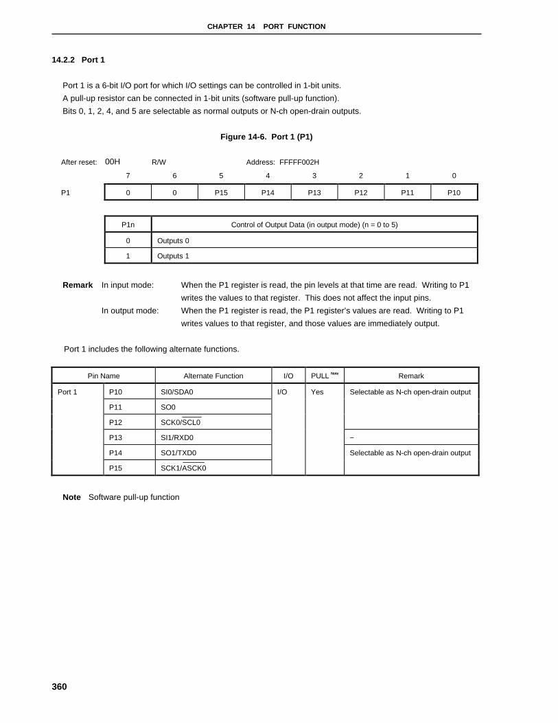
CHAPTER 14 PORT FUNCTION
360
14.2.2 Port 1
Port 1 is a 6-bit I/O port for which I/O settings can be controlled in 1-bit units.
A pull-up resistor can be connected in 1-bit units (software pull-up function).
Bits 0, 1, 2, 4, and 5 are selectable as normal outputs or N-ch open-drain outputs.
Figure 14-6. Port 1 (P1)
After reset: 00H R/W Address: FFFFF002H
7 6 5 4 3 2 1 0
P1 0 0 P15 P14 P13 P12 P11 P10
P1n Control of Output Data (in output mode) (n = 0 to 5)
0 Outputs 0
1 Outputs 1
Remark In input mode: When the P1 register is read, the pin levels at that time are read. Writing to P1
writes the values to that register. This does not affect the input pins.
In output mode: When the P1 register is read, the P1 register’s values are read. Writing to P1
writes values to that register, and those values are immediately output.
Port 1 includes the following alternate functions.
Pin Name Alternate Function I/O PULL Note Remark
Port 1 P10 SI0/SDA0 I/O Yes Selectable as N-ch open-drain output
P11 SO0
P12 SCK0/SCL0
P13 SI1/RXD0 −
P14 SO1/TXD0 Selectable as N-ch open-drain output
P15 SCK1/ASCK0
Note Software pull-up function

CHAPTER 14 PORT FUNCTION
361
(1) Function of P1 pins
Port 1 is a 6-bit I/O port for which I/O settings can be controlled in 1-bit units. I/O settings are controlled via the
port 1 mode register (PM1).
In output mode, the values set to each bit are output to the port 1 register (P1). The port 1 function register (PF1)
can be used to specify whether P10 to P12, P14, and P15 are normal outputs or N-ch open-drain outputs.
When using this port in input mode, the pin statuses can be read by reading the P1 register. Also, the P1
register (output latch) values can be read by reading the P1 register while in output mode.
A pull-up resistor can be connected in 1-bit units when specified via the pull-up resistor option register 1 (PU1).
Clear the P1 and PM1 registers to 0 when using alternate-function pins as outputs. The ORed result of the port
output and the alternate-function pin is output from the pins.
When a reset is input, the settings are initialized to input mode.
(2) Control registers
(a) Port 1 mode register (PM1)
PM1 can be read/written in 1-bit or 8-bit units.
Figure 14-7. Port 1 Mode Register (PM1)
After reset: 3FH R/W Address: FFFFF022H
7 6 5 4 3 2 1 0
PM1 0 0 PM15 PM14 PM13 PM12 PM11 PM10
PM1n Control of I/O Mode (n = 0 to 5)
0 Output mode
1 Input mode
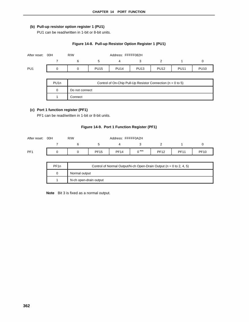
CHAPTER 14 PORT FUNCTION
362
(b) Pull-up resistor option register 1 (PU1)
PU1 can be read/written in 1-bit or 8-bit units.
Figure 14-8. Pull-up Resistor Option Register 1 (PU1)
After reset: 00H R/W Address: FFFFF082H
7 6 5 4 3 2 1 0
PU1 0 0 PU15 PU14 PU13 PU12 PU11 PU10
PU1n Control of On-Chip Pull-Up Resistor Connection (n = 0 to 5)
0 Do not connect
1 Connect
(c) Port 1 function register (PF1)
PF1 can be read/written in 1-bit or 8-bit units.
Figure 14-9. Port 1 Function Register (PF1)
After reset: 00H R/W Address: FFFFF0A2H
7 6 5 4 3 2 1 0
PF1 0 0 PF15 PF14 0 Note PF12 PF11 PF10
PF1n Control of Normal Output/N-ch Open-Drain Output (n = 0 to 2, 4, 5)
0 Normal output
1 N-ch open-drain output
Note Bit 3 is fixed as a normal output.

CHAPTER 14 PORT FUNCTION
363
14.2.3 Port 2
Port 2 is an 8-bit I/O port for which I/O settings can be controlled in 1-bit units.
A pull-up resistor can be connected in 1-bit units (software pull-up function).
P20, P21, P22, P24 and P25 are selectable as normal outputs or N-ch open-drain outputs.
When P26 and P27 are used as TI2/TI3 pins, noise is eliminated from these pins by a digital noise elimination
circuit.
Figure 14-10. Port 2 (P2)
After reset: 00H R/W Address: FFFFF004H
7 6 5 4 3 2 1 0
P2 P27 P26 P25 P24 P23 P22 P21 P20
P2n Control of Output Data (in output mode) (n = 0 to 7)
0 Outputs 0
1 Outputs 1
Remark In input mode : When the P2 register is read, the pin levels at that time are read. Writing to P2
writes the values to that register. This does not affect the input pins.
In output mode : When the P2 register is read, the P2 register’s values are read. Writing to P2
writes values to that register, and those values are immediately output.
Port 2 includes the following alternate functions. SDA1 and SCL1 are available only in the µPD703033Y and
70F3033Y.
Pin Name Alternate Function I/O PULL Note Remark
Port 2 P20 SI2/SDA1
P21 SO2
P22 SCK2/SCL1
Selectable as N-ch open-drain output
P23 SI3/RXD1 −
P24 SO3/TXD1
P25 SCK3/ASCK1
Selectable as N-ch open-drain output
P26 TI2/TO2
P27 TI3/TO3
I/O Yes
Digital noise elimination
Note Software pull-up function
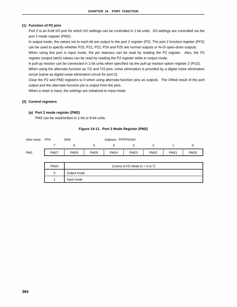
CHAPTER 14 PORT FUNCTION
364
(1) Function of P2 pins
Port 2 is an 8-bit I/O port for which I/O settings can be controlled in 1-bit units. I/O settings are controlled via the
port 2 mode register (PM2).
In output mode, the values set to each bit are output to the port 2 register (P2). The port 2 function register (PF2)
can be used to specify whether P20, P21, P22, P24 and P25 are normal outputs or N-ch open-drain outputs.
When using this port in input mode, the pin statuses can be read by reading the P2 register. Also, the P2
register (output latch) values can be read by reading the P2 register while in output mode.
A pull-up resistor can be connected in 1-bit units when specified via the pull-up resistor option register 2 (PU2).
When using the alternate function as TI2 and TI3 pins, noise elimination is provided by a digital noise elimination
circuit (same as digital noise elimination circuit for port 0).
Clear the P2 and PM2 registers to 0 when using alternate-function pins as outputs. The ORed result of the port
output and the alternate-function pin is output from the pins.
When a reset is input, the settings are initialized to input mode.
(2) Control registers
(a) Port 2 mode register (PM2)
PM2 can be read/written in 1-bit or 8-bit units.
Figure 14-11. Port 2 Mode Register (PM2)
After reset: FFH R/W Address: FFFFF024H
7 6 5 4 3 2 1 0
PM2 PM27 PM26 PM25 PM24 PM23 PM22 PM21 PM20
PM2n Control of I/O Mode (n = 0 to 7)
0 Output mode
1 Input mode

CHAPTER 14 PORT FUNCTION
365
(b) Pull-up resistor option register 2 (PU2)
PU2 can be read/written in 1-bit or 8-bit units.
Figure 14-12. Pull-up Resistor Option Register 2 (PU2)
After reset: 00H R/W Address: FFFFF084H
7 6 5 4 3 2 1 0
PU2 PU27 PU26 PU25 PU24 PU23 PU22 PU21 PU20
PU2n Control of On-Chip Pull-Up Resistor Connection (n = 0 to 7)
0 Do not connect
1 Connect
(c) Port 2 function register (PF2)
PF2 can be read/written in 1-bit or 8-bit units.
Figure 14-13. Port 2 Function Register (PF2)
After reset: 00H R/W Address: FFFFF0A4H
7 6 5 4 3 2 1 0
PF2 0 0 PF25 PF24 0 PF22 PF21 PF20
PF2n Control of Normal Output/N-ch Open-Drain Output (n = 0 to 2, 4, 5)
0 Normal output
1 N-ch open-drain output

CHAPTER 14 PORT FUNCTION
366
14.2.4 Port 3
Port 3 is an 8-bit I/O port for which I/O settings can be controlled in 1-bit units.
A pull-up resistor can be connected in 1-bit units (software pull-up function).
Either a normal output or N-ch open-drain out can be selected for P33 and P34.
Figure 14-14. Port 3 (P3)
After reset: 00H R/W Address: FFFFF006H
7 6 5 4 3 2 1 0
P3 P37 P36 P35 P34 P33 P32 P31 P30
P3n Control of Output Data (In Output Mode) (n = 0 to 7)
0 Outputs 0
1 Outputs 1
Remark In input mode : When the P3 register is read, the pin levels at that time are read. Writing to P3
writes the values to that register. This does not affect the input pins.
In output mode : When the P3 register is read, the P3 register’s values are read. Writing to P3
writes values to that register, and those values are immediately output.
Port 3 includes the following alternate functions.
Pin Name Alternate Function I/O PULL Note Remark
P30 TI00
P31 TI01
P32 TI10/SI4
−
P33 TI11/SO4
P34 TO0/A13/SCK4
Selectable as N-ch open-drain output.
P35 TO1/A14 –
P36 TI4/TO4/A15
Port 3
P37 TI5/TO5
I/O Yes
Digital noise elimination
Note Software pull-up function

CHAPTER 14 PORT FUNCTION
367
(1) Function of P3 pins
Port 3 is an 8-bit I/O port for which I/O settings can be controlled in 1-bit units. I/O settings are controlled via the
port 3 mode register (PM3).
In output mode, the values set to each bit are output to the port register (P3). The port 3 function register (PF3)
can be used to specify whether P33 and P34 are normal outputs or N-ch open-drain outputs.
When using this port in input mode, the pin statuses can be read by reading the P3 register. Also, the P3
register (output latch) values can be read by reading the P3 register while in output mode.
A pull-up resistor can be connected in 1-bit units when specified via the pull-up resistor option register 3 (PU3).
When using the alternate function as TI4 and TI5 pins, noise elimination is provided by a digital noise elimination
circuit (same as digital noise elimination circuit for port 0).
When using the alternate function as A13 to A15 pins, set the pin functions via the memory address output mode
register (MAM). At this time, be sure to set the PM3 registers (PM34, PM35, PM36) and the P3 registers (P34,
P35, P36) to 0.
Clear the P3 and PM3 registers to 0 when using alternate-function pins as outputs. The ORed result of the port
output and the alternate-function pin is output from the pins.
When a reset is input, the settings are initialized to input mode.
(2) Control registers
(a) Port 3 mode register (PM3)
PM3 can be read/written in 1-bit or 8-bit units.
Figure 14-15. Port 3 Mode Register (PM3)
After reset: FFH R/W Address: FFFFF026H
7 6 5 4 3 2 1 0
PM3 PM37 PM36 PM35 PM34 PM33 PM32 PM31 PM30
PM3n Control of I/O Mode (n = 0 to 7)
0 Output mode
1 Input mode
(b) Pull-up resistor option register 3 (PU3)
PU3 can be read/written in 1-bit or 8-bit units.
Figure 14-16. Pull-up Resistor Option Register 3 (PU3)
After reset: 00H R/W Address: FFFFF086H
7 6 5 4 3 2 1 0
PU3 PU37 PU36 PU35 PU34 PU33 PU32 PU31 PU30
PU3n Control of On-Chip Pull-Up Resistor Connection (n = 0 to 7)
0 Do not connect
1 Connect
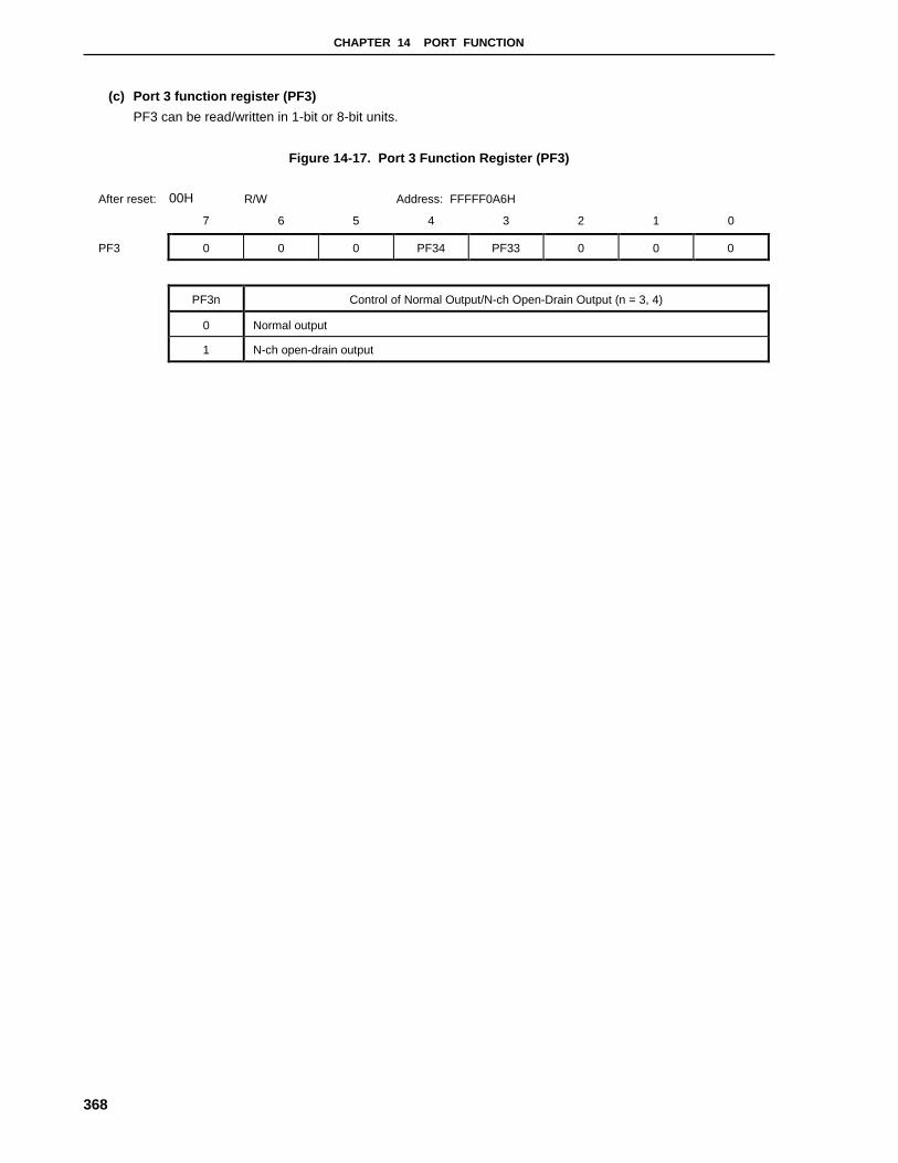
CHAPTER 14 PORT FUNCTION
368
(c) Port 3 function register (PF3)
PF3 can be read/written in 1-bit or 8-bit units.
Figure 14-17. Port 3 Function Register (PF3)
After reset: 00H R/W Address: FFFFF0A6H
7 6 5 4 3 2 1 0
PF3 0 0 0 PF34 PF33 0 0 0
PF3n Control of Normal Output/N-ch Open-Drain Output (n = 3, 4)
0 Normal output
1 N-ch open-drain output

CHAPTER 14 PORT FUNCTION
369
14.2.5 Ports 4 and 5
Ports 4 and 5 are 8-bit I/O ports for which I/O settings can be controlled in 1-bit units.
Figure 14-18. Ports 4 and 5 (P4 and P5)
After reset: 00H R/W Address: FFFFF008H, FFFFF00AH
7 6 5 4 3 2 1 0
Pn Pn7 Pn6 Pn5 Pn4 Pn3 Pn2 Pn1 Pn0
Pnx Control of Output Data (in output mode) (n = 4, 5)
0 Outputs 0
1 Outputs 1
Remarks 1. In input mode: When the P4 and P5 registers are read, the pin levels at that time are read.
Writing to P4 and P5 writes the values to those registers. This does
not affect the input pins.
In output mode: When the P4 and P5 registers are read, their values are read. Writing to P4
and P5 writes values to those registers, and those values are immediately
output.
2. x = 0 to 7
Ports 4 and 5 include the following alternate functions.
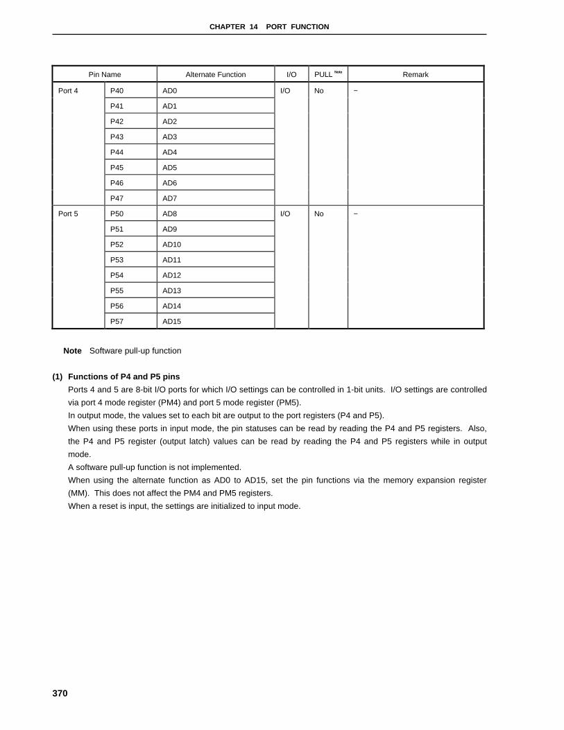
CHAPTER 14 PORT FUNCTION
370
Pin Name Alternate Function I/O PULL Note Remark
Port 4 P40 AD0 I/O No −
P41 AD1
P42 AD2
P43 AD3
P44 AD4
P45 AD5
P46 AD6
P47 AD7
Port 5 P50 AD8 I/O No −
P51 AD9
P52 AD10
P53 AD11
P54 AD12
P55 AD13
P56 AD14
P57 AD15
Note Software pull-up function
(1) Functions of P4 and P5 pins
Ports 4 and 5 are 8-bit I/O ports for which I/O settings can be controlled in 1-bit units. I/O settings are controlled
via port 4 mode register (PM4) and port 5 mode register (PM5).
In output mode, the values set to each bit are output to the port registers (P4 and P5).
When using these ports in input mode, the pin statuses can be read by reading the P4 and P5 registers. Also,
the P4 and P5 register (output latch) values can be read by reading the P4 and P5 registers while in output
mode.
A software pull-up function is not implemented.
When using the alternate function as AD0 to AD15, set the pin functions via the memory expansion register
(MM). This does not affect the PM4 and PM5 registers.
When a reset is input, the settings are initialized to input mode.
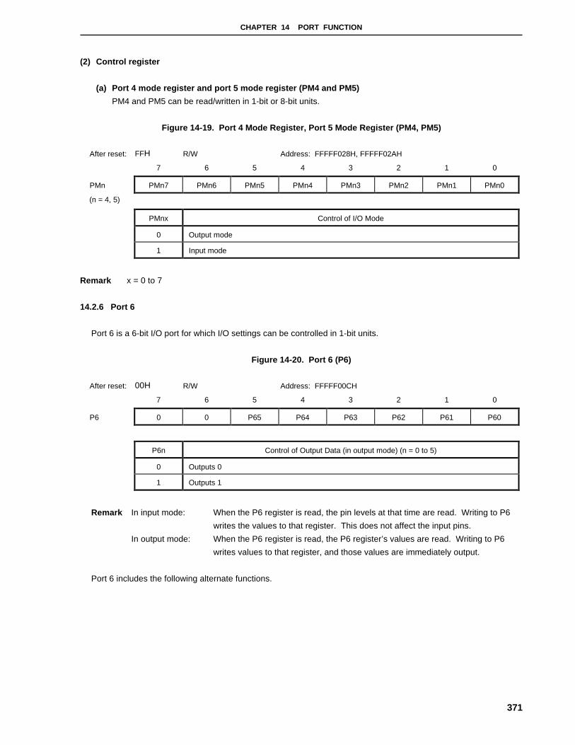
CHAPTER 14 PORT FUNCTION
371
(2) Control register
(a) Port 4 mode register and port 5 mode register (PM4 and PM5)
PM4 and PM5 can be read/written in 1-bit or 8-bit units.
Figure 14-19. Port 4 Mode Register, Port 5 Mode Register (PM4, PM5)
After reset: FFH R/W Address: FFFFF028H, FFFFF02AH
7 6 5 4 3 2 1 0
PMn PMn7 PMn6 PMn5 PMn4 PMn3 PMn2 PMn1 PMn0
(n = 4, 5)
PMnx Control of I/O Mode
0 Output mode
1 Input mode
Remark x = 0 to 7
14.2.6 Port 6
Port 6 is a 6-bit I/O port for which I/O settings can be controlled in 1-bit units.
Figure 14-20. Port 6 (P6)
After reset: 00H R/W Address: FFFFF00CH
7 6 5 4 3 2 1 0
P6 0 0 P65 P64 P63 P62 P61 P60
P6n Control of Output Data (in output mode) (n = 0 to 5)
0 Outputs 0
1 Outputs 1
Remark In input mode: When the P6 register is read, the pin levels at that time are read. Writing to P6
writes the values to that register. This does not affect the input pins.
In output mode: When the P6 register is read, the P6 register’s values are read. Writing to P6
writes values to that register, and those values are immediately output.
Port 6 includes the following alternate functions.

CHAPTER 14 PORT FUNCTION
372
Pin Name Alternate Function I/O PULL Note Remark
Port 6 P60 A16 I/O No −
P61 A17
P62 A18
P63 A19
P64 A20
P65 A21
Note Software pull-up function
(1) Function of P6 pins
Port 6 is a 6-bit I/O port for which I/O settings can be controlled in 1-bit units. I/O settings are controlled via the
port 6 mode register (PM6).
In output mode, the values set to each bit are output to the port register (P6).
When using this port in input mode, the pin statuses can be read by reading the P6 register. Also, the P6
register (output latch) values can be read by reading the P6 register while in output mode.
A software pull-up function is not implemented.
When using the alternate function as A16 to A21, set the pin functions via the memory expansion register (MM).
This does not affect the PM6 register.
When a reset is input, the settings are initialized to input mode.
(2) Control register
(a) Port 6 mode register (PM6)
PM6 can be read/written in 1-bit or 8-bit units.
Figure 14-21. Port 6 Mode Register (PM6)
After reset: 3FH R/W Address: FFFFF02CH
7 6 5 4 3 2 1 0
PM6 0 0 PM65 PM64 PM63 PM62 PM61 PM60
PM6n Control of I/O Mode (n = 0 to 5)
0 Output mode
1 Input mode

CHAPTER 14 PORT FUNCTION
373
14.2.7 Ports 7 and 8
Port 7 is an 8-bit input port and port 8 is a 4-bit input port. Both ports are read-only and are accessible in 8-bit
units or in 1-bit units.
Figure 14-22. Ports 7 and 8 (P7 and P8)
After reset: Undefined R Address: FFFFF00EH
7 6 5 4 3 2 1 0
P7 P77 P76 P75 P74 P73 P72 P71 P70
P7n Pin Level (n = 0 to 7)
0/1 Read pin level of bit n
After reset: Undefined R Address: FFFFF010H
7 6 5 4 3 2 1 0
P8 0 0 0 0 P83 P82 P81 P80
P8n Pin Level (n = 0 to 3)
0/1 Read pin level of bit n
Ports 7 and 8 include the following alternate functions.
Pin Name Alternate Function I/O PULL Note Remark
Port 7 P70 ANI0 Input No −
P71 ANI1
P72 ANI2
P73 ANI3
P74 ANI4
P75 ANI5
P76 ANI6
P77 ANI7
Port 8 P80 ANI8 Input No −
P81 ANI9
P82 ANI10
P83 ANI11
Note Software pull-up function
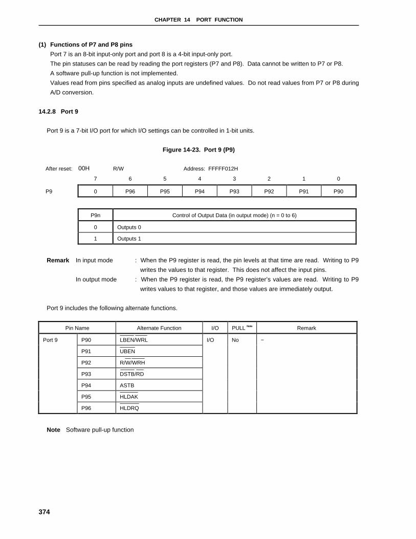
CHAPTER 14 PORT FUNCTION
374
(1) Functions of P7 and P8 pins
Port 7 is an 8-bit input-only port and port 8 is a 4-bit input-only port.
The pin statuses can be read by reading the port registers (P7 and P8). Data cannot be written to P7 or P8.
A software pull-up function is not implemented.
Values read from pins specified as analog inputs are undefined values. Do not read values from P7 or P8 during
A/D conversion.
14.2.8 Port 9
Port 9 is a 7-bit I/O port for which I/O settings can be controlled in 1-bit units.
Figure 14-23. Port 9 (P9)
After reset: 00H R/W Address: FFFFF012H
7 6 5 4 3 2 1 0
P9 0 P96 P95 P94 P93 P92 P91 P90
P9n Control of Output Data (in output mode) (n = 0 to 6)
0 Outputs 0
1 Outputs 1
Remark In input mode : When the P9 register is read, the pin levels at that time are read. Writing to P9
writes the values to that register. This does not affect the input pins.
In output mode : When the P9 register is read, the P9 register’s values are read. Writing to P9
writes values to that register, and those values are immediately output.
Port 9 includes the following alternate functions.
Pin Name Alternate Function I/O PULL Note Remark
P90 LBEN/WRL
P91 UBEN
P92 R/W/WRH
P93 DSTB/RD
P94 ASTB
P95 HLDAK
Port 9
P96 HLDRQ
I/O No −
Note Software pull-up function
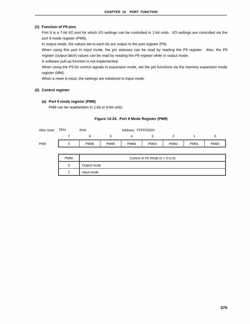
CHAPTER 14 PORT FUNCTION
375
(1) Function of P9 pins
Port 9 is a 7-bit I/O port for which I/O settings can be controlled in 1-bit units. I/O settings are controlled via the
port 9 mode register (PM9).
In output mode, the values set to each bit are output to the port register (P9).
When using this port in input mode, the pin statuses can be read by reading the P9 register. Also, the P9
register (output latch) values can be read by reading the P9 register while in output mode.
A software pull-up function is not implemented.
When using the P9 for control signals in expansion mode, set the pin functions via the memory expansion mode
register (MM).
When a reset is input, the settings are initialized to input mode.
(2) Control register
(a) Port 9 mode register (PM9)
PM9 can be read/written in 1-bit or 8-bit units.
Figure 14-24. Port 9 Mode Register (PM9)
After reset: 7FH R/W Address: FFFFF032H
7 6 5 4 3 2 1 0
PM9 0 PM96 PM95 PM94 PM93 PM92 PM91 PM90
PM9n Control of I/O Mode (n = 0 to 6)
0 Output mode
1 Input mode

CHAPTER 14 PORT FUNCTION
376
14.2.9 Port 10
Port 10 is an 8-bit I/O port for which I/O settings can be controlled in 1-bit units.
A pull-up resistor can be connected in 1-bit units (software pull-up function).
The pins in this port are selectable as normal outputs or N-ch open-drain outputs.
Figure 14-25. Port 10 (P10)
After reset: 00H R/W Address: FFFFF014H
7 6 5 4 3 2 1 0
P10 P107 P106 P105 P104 P103 P102 P101 P100
P10n Control of Output Data (in output mode) (n = 0 to 7)
0 Outputs 0
1 Outputs 1
Remark In input mode: When the P10 register is read, the pin levels at that time are read. Writing to P10
writes the values to that register. This does not affect the input pins.
In output mode: When the P10 register is read, the P10 register’s values are read. Writing to P10
writes values to that register, and those values are immediately output.
Port 10 includes the following alternate functions.
Pin Name Alternate Function I/O PULL Note Remark
Port 10 P100 RTP0/A5/KR0 I/O Yes Selectable as N-ch open-drain outputs
P101 RTP1/A6/KR1
P102 RTP2/A7/KR2
P103 RTP3/A8/KR3
P104 RTP4/A9/KR4
P105 RTP5/A10/KR5
P106 RTP6/A11/KR6
P107 RTP7/A12/KR7
Note Software pull-up function

CHAPTER 14 PORT FUNCTION
377
(1) Function of P10 pins
Port 10 is an 8-bit I/O port for which I/O settings can be controlled in 1-bit units. I/O settings are controlled via
the port 10 mode register (PM10).
In output mode, the values set to each bit are output to the port register (P10). The port 10 function register
(PF10) can be used to specify whether outputs are normal outputs or N-ch open-drain outputs.
When using this port in input mode, the pin statuses can be read by reading the P10 register. Also, the P10
register (output latch) values can be read by reading the P10 register while in output mode.
A pull-up resistor can be connected in 1-bit units when specified via pull-up resistor option register 10 (PU10).
When using the alternate function as A5 to A12 pins, see the pin functions via the memory address output mode
register (MAM). At this time, be sure to set PM10 to 0.
When used as KR0 to KR7 pins, noise is eliminated by the analog noise elimination circuit.
Clear the P10 and PM10 registers to 0 when using alternate-function pins as outputs. The ORed result of the
port output and the alternate-function pin is output from the pins.
When a reset is input, the settings are initialized to input mode.
(2) Control register
(a) Port 10 mode register (PM10)
PM10 can be read/written in 1-bit or 8-bit units.
Figure 14-26. Port 10 Mode Register (PM10)
After reset: FFH R/W Address: FFFFF034H
7 6 5 4 3 2 1 0
PM10 PM107 PM106 PM105 PM104 PM103 PM102 PM101 PM100
PM10n Control of I/O Mode (n = 0 to 7)
0 Output mode
1 Input mode
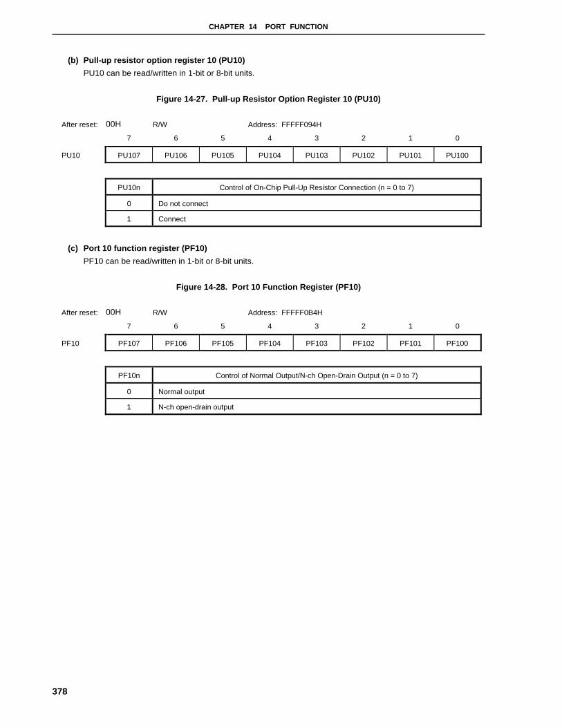
CHAPTER 14 PORT FUNCTION
378
(b) Pull-up resistor option register 10 (PU10)
PU10 can be read/written in 1-bit or 8-bit units.
Figure 14-27. Pull-up Resistor Option Register 10 (PU10)
After reset: 00H R/W Address: FFFFF094H
7 6 5 4 3 2 1 0
PU10 PU107 PU106 PU105 PU104 PU103 PU102 PU101 PU100
PU10n Control of On-Chip Pull-Up Resistor Connection (n = 0 to 7)
0 Do not connect
1 Connect
(c) Port 10 function register (PF10)
PF10 can be read/written in 1-bit or 8-bit units.
Figure 14-28. Port 10 Function Register (PF10)
After reset: 00H R/W Address: FFFFF0B4H
7 6 5 4 3 2 1 0
PF10 PF107 PF106 PF105 PF104 PF103 PF102 PF101 PF100
PF10n Control of Normal Output/N-ch Open-Drain Output (n = 0 to 7)
0 Normal output
1 N-ch open-drain output
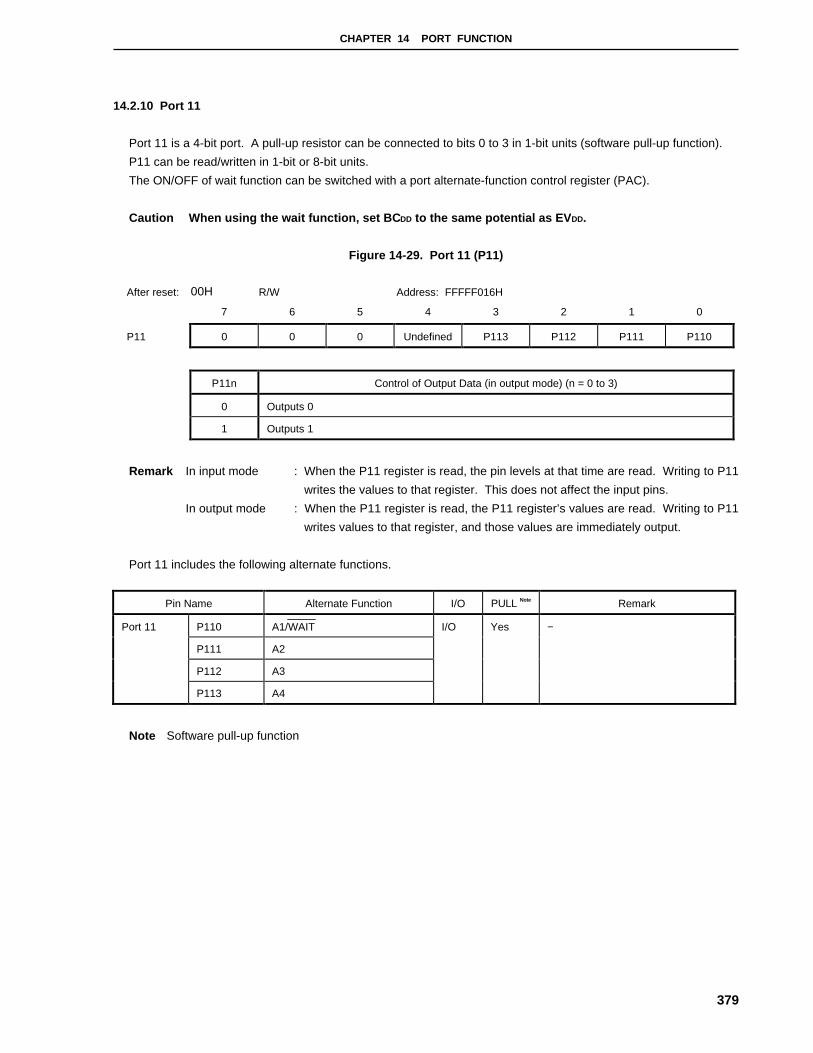
CHAPTER 14 PORT FUNCTION
379
14.2.10 Port 11
Port 11 is a 4-bit port. A pull-up resistor can be connected to bits 0 to 3 in 1-bit units (software pull-up function).
P11 can be read/written in 1-bit or 8-bit units.
The ON/OFF of wait function can be switched with a port alternate-function control register (PAC).
Caution When using the wait function, set BC DD to the same potential as EV DD.
Figure 14-29. Port 11 (P11)
After reset: 00H R/W Address: FFFFF016H
7 6 5 4 3 2 1 0
P11 0 0 0 Undefined P113 P112 P111 P110
P11n Control of Output Data (in output mode) (n = 0 to 3)
0 Outputs 0
1 Outputs 1
Remark In input mode : When the P11 register is read, the pin levels at that time are read. Writing to P11
writes the values to that register. This does not affect the input pins.
In output mode : When the P11 register is read, the P11 register’s values are read. Writing to P11
writes values to that register, and those values are immediately output.
Port 11 includes the following alternate functions.
Pin Name Alternate Function I/O PULL Note Remark
Port 11 P110 A1/WAIT I/O Yes −
P111 A2
P112 A3
P113 A4
Note Software pull-up function
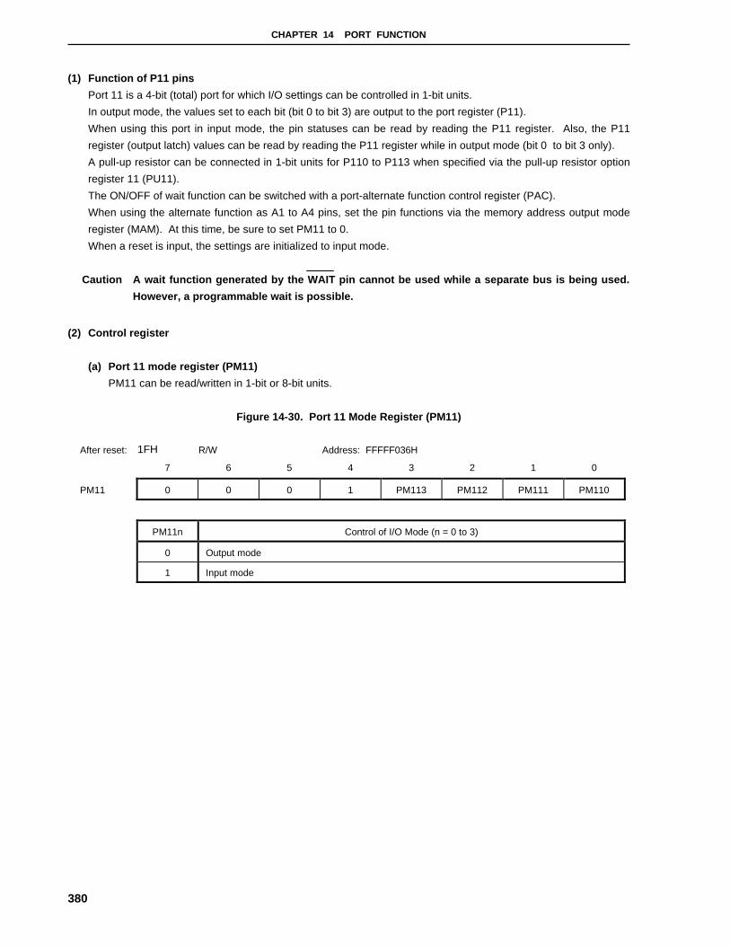
CHAPTER 14 PORT FUNCTION
380
(1) Function of P11 pins
Port 11 is a 4-bit (total) port for which I/O settings can be controlled in 1-bit units.
In output mode, the values set to each bit (bit 0 to bit 3) are output to the port register (P11).
When using this port in input mode, the pin statuses can be read by reading the P11 register. Also, the P11
register (output latch) values can be read by reading the P11 register while in output mode (bit 0 to bit 3 only).
A pull-up resistor can be connected in 1-bit units for P110 to P113 when specified via the pull-up resistor option
register 11 (PU11).
The ON/OFF of wait function can be switched with a port-alternate function control register (PAC).
When using the alternate function as A1 to A4 pins, set the pin functions via the memory address output mode
register (MAM). At this time, be sure to set PM11 to 0.
When a reset is input, the settings are initialized to input mode.
Caution A wait function generated by the WAIT pin cannot be used while a separate bus is being used.
However, a programmable wait is possible.
(2) Control register
(a) Port 11 mode register (PM11)
PM11 can be read/written in 1-bit or 8-bit units.
Figure 14-30. Port 11 Mode Register (PM11)
After reset: 1FH R/W Address: FFFFF036H
7 6 5 4 3 2 1 0
PM11 0 0 0 1 PM113 PM112 PM111 PM110
PM11n Control of I/O Mode (n = 0 to 3)
0 Output mode
1 Input mode

CHAPTER 14 PORT FUNCTION
381
(b) Pull-up resistor option register 11 (PU11)
PU11 can be read/written in 1-bit or 8-bit units.
Figure 14-31. Pull-up Resistor Option Register 11 (PU11)
After reset: 00H R/W Address: FFFFF096H
7 6 5 4 3 2 1 0
PU11 0 0 0 0 PU113 PU112 PU111 PU110
PU11n Control of On-Chip Pull-Up Resistor Connection (n = 0 to 3)
0 Do not connect
1 Connect
(c) Port alternate function register (PAC)
PAC can be read/written in 1-bit or 8-bit units.
Figure 14-32. Port Alternate-function Control Register (PAC)
After reset: 00H R/W Address: FFFFF040H
7 6 5 4 3 2 1 0
PAC 0 0 0 0 0 0 0 WAC
P120 Control of Output Data (in output mode)
0 Wait function OFF
1 Wait function ON

CHAPTER 14 PORT FUNCTION
382
14.3 Setting When Port Pin Is Used For Alternate Function
When a port pin is used for an alternate function, set the port n mode register (PM0 to PM6 and PM9 to PM11)
and output latch as shown in Table 14-1 below.
Table 14-1. Setting When Port Pin Is Used for Alternate Function (1/4)
Alternate FunctionPin Name
Function Name I/O
PMnx Bit of
PMn Register
Pnx Bit of
Pn Register
Other Bits
(Register)
P00 NMI Input PM00 = 1 Setting not needed
for P00
P01 INTP0 I/O PM01 = 1 Setting not needed
for P01
P02 INTP1 I/O PM02 = 1 Setting not needed
for P02
P03 INTP2 I/O PM03 = 1 Setting not needed
for P03
P04 INTP3 I/O PM04 = 1 Setting not needed
for P04
INTP4 I/OP05
ADTRG Input
PM05 = 1 Setting not needed
for P05
INTP5 I/OP06
RTPTRG Input
PM06 = 1 Setting not needed
for P06
P07 INTP6 I/O PM07 = 1 Setting not needed
for P07
SI0 Input PM10 = 1 Setting not needed
for P10
P10
SDA0 Note I/O PM10 = 0 P10 = 0
P11 SO0 Output PM11 = 0 P11 = 0
Input PM12 = 1 Setting not needed
for P12
SCK0
Output
P12
SCL0 Note I/O
PM12 = 0 P12 = 0
SI1 InputP13
RXD0 Input
PM13 = 1 Setting not needed
for P13
SO1 OutputP14
TXD0 Output
PM14 = 0 P14 = 0
Input PM15 = 1 Setting not needed
for P15
SCK1
Output PM15 = 0 P12 = 0
P15
ASCK0 Input PM15 = 1 Setting not needed
for P15
Note Provided for the µPD703033Y and 70F3033Y only.

CHAPTER 14 PORT FUNCTION
383
Table 14-1. Setting When Port Pin Is Used for Alternate Function (2/4)
Alternate FunctionPin Name
Function Name I/O
PMnx Bit of
PMn Register
Pnx Bit of
Pn Register
Other Bits
(Register)
SI2 Input PM20 = 1 Setting not needed
for P20
P20
SDA1 Note I/O PM20 = 0 P20 = 0
P21 SO2 Output PM21 = 0 P21 = 0
Input PM22 = 1 Setting not needed
for P22
SCK2
Output
P22
SCL1 Note I/O
PM22 = 0 P22 = 0
SI3 InputP23
RXD1 Input
PM23 = 1 Setting not needed
for P23
SO3 OutputP24
TXD1 Output
PM24 = 0 P24 = 0
Input PM25 = 1 Setting not needed
for P25
SCK3
Output PM25 = 0 P25 = 0
P25
ASCK1 Input PM25 = 1 Setting not needed
for P25
TI2 Input PM26 = 1 Setting not needed
for P26
P26
TO2 Output PM26 = 0 P26 = 0
TI3 Input PM27 = 1 Setting not needed
for P27
P27
TO3 Output PM27 = 0 P27 = 0
P30 TI00 Input PM30 = 1 Setting not needed
for P30
P31 TI01 Input PM31 = 1 Setting not needed
for P31
TI10 InputP32
SI4 Input
PM32 = 1 Setting not needed
for P32
TI11 Input PM33 = 1 Setting not needed
for P33
P33
SO4 Output PM33 = 0 P33 = 0
TO0 Output
A13 Output
PM34 = 0 P34 = 0
Refer to Figure 3-8 (MAM)
Input PM34 = 1 Setting not needed
for P34
P34
SCK4
Output PM34 = 0 P34 = 0
Note Provided for the µPD703033Y and 70F3033Y only.
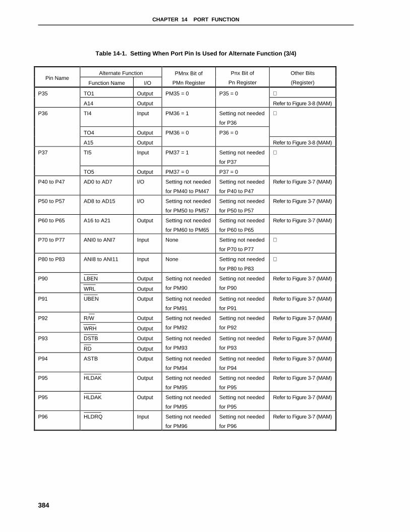
CHAPTER 14 PORT FUNCTION
384
Table 14-1. Setting When Port Pin Is Used for Alternate Function (3/4)
Alternate FunctionPin Name
Function Name I/O
PMnx Bit of
PMn Register
Pnx Bit of
Pn Register
Other Bits
(Register)
TO1 Output P35
A14 Output
PM35 = 0 P35 = 0
Refer to Figure 3-8 (MAM)
TI4 Input PM36 = 1 Setting not needed
for P36
TO4 Output
P36
A15 Output
PM36 = 0 P36 = 0
Refer to Figure 3-8 (MAM)
TI5 Input PM37 = 1 Setting not needed
for P37
P37
TO5 Output PM37 = 0 P37 = 0
P40 to P47 AD0 to AD7 I/O Setting not needed
for PM40 to PM47
Setting not needed
for P40 to P47
Refer to Figure 3-7 (MAM)
P50 to P57 AD8 to AD15 I/O Setting not needed
for PM50 to PM57
Setting not needed
for P50 to P57
Refer to Figure 3-7 (MAM)
P60 to P65 A16 to A21 Output Setting not needed
for PM60 to PM65
Setting not needed
for P60 to P65
Refer to Figure 3-7 (MAM)
P70 to P77 ANI0 to ANI7 Input None Setting not needed
for P70 to P77
P80 to P83 ANI8 to ANI11 Input None Setting not needed
for P80 to P83
LBEN OutputP90
WRL Output
Setting not needed
for PM90
Setting not needed
for P90
Refer to Figure 3-7 (MAM)
P91 UBEN Output Setting not needed
for PM91
Setting not needed
for P91
Refer to Figure 3-7 (MAM)
R/W OutputP92
WRH Output
Setting not needed
for PM92
Setting not needed
for P92
Refer to Figure 3-7 (MAM)
DSTB OutputP93
RD Output
Setting not needed
for PM93
Setting not needed
for P93
Refer to Figure 3-7 (MAM)
P94 ASTB Output Setting not needed
for PM94
Setting not needed
for P94
Refer to Figure 3-7 (MAM)
P95 HLDAK Output Setting not needed
for PM95
Setting not needed
for P95
Refer to Figure 3-7 (MAM)
P95 HLDAK Output Setting not needed
for PM95
Setting not needed
for P95
Refer to Figure 3-7 (MAM)
P96 HLDRQ Input Setting not needed
for PM96
Setting not needed
for P96
Refer to Figure 3-7 (MAM)
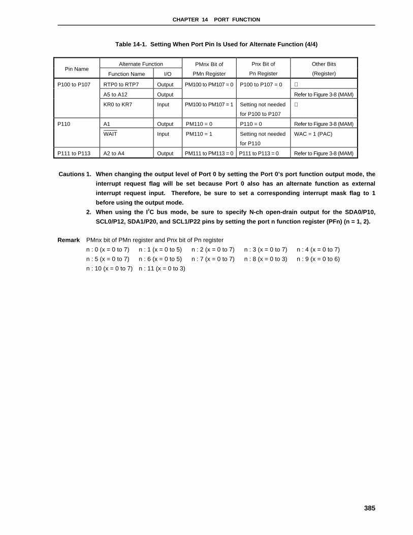
CHAPTER 14 PORT FUNCTION
385
Table 14-1. Setting When Port Pin Is Used for Alternate Function (4/4)
Alternate FunctionPin Name
Function Name I/O
PMnx Bit of
PMn Register
Pnx Bit of
Pn Register
Other Bits
(Register)
RTP0 to RTP7 Output
A5 to A12 Output
PM100 to PM107 = 0 P100 to P107 = 0
Refer to Figure 3-8 (MAM)
P100 to P107
KR0 to KR7 Input PM100 to PM107 = 1 Setting not needed
for P100 to P107
A1 Output PM110 = 0 P110 = 0 Refer to Figure 3-8 (MAM)P110
WAIT Input PM110 = 1 Setting not needed
for P110
WAC = 1 (PAC)
P111 to P113 A2 to A4 Output PM111 to PM113 = 0 P111 to P113 = 0 Refer to Figure 3-8 (MAM)
Cautions 1. When changing the output level of Port 0 by setting the Port 0’s port function output mode, the
interrupt request flag will be set because Port 0 also has an alternate function as external
interrupt request input. Therefore, be sure to set a corresponding interrupt mask flag to 1
before using the output mode.
2. When using the I 2C bus mode, be sure to specify N-ch open-drain output for the SDA0/P10,
SCL0/P12, SDA1/P20, and SCL1/P22 pins by setting the port n function register (PFn) (n = 1, 2).
Remark PMnx bit of PMn register and Pnx bit of Pn register
n : 0 (x = 0 to 7) n : 1 (x = 0 to 5) n : 2 (x = 0 to 7) n : 3 (x = 0 to 7) n : 4 (x = 0 to 7)
n : 5 (x = 0 to 7) n : 6 (x = 0 to 5) n : 7 (x = 0 to 7) n : 8 (x = 0 to 3) n : 9 (x = 0 to 6)
n : 10 (x = 0 to 7) n : 11 (x = 0 to 3)

386
[MEMO]

387
CHAPTER 15 RESET FUNCTION
15.1 General
When low-level input occurs at the RESET pin, a system reset is performed and the various on-chip hardware
devices are reset to their initial settings. In addition, oscillation of the main clock is stopped during the reset period,
although oscillation of the sub clock continues.
When the input at the RESET pin changes from low level to high level, the reset status is canceled and the CPU
resumes program execution. The contents of the various registers should be initialized within the program as
necessary.
An on-chip noise elimination circuit uses analog delay to prevent noise-related malfunction of the RESET pin.
15.2 Pin Operations
During the system reset period, high impedance is set at almost all pins (all pins except for RESET, X2, XT2,
REGC, AVREF, VDD, VSS, AVDD, AVSS, BVDD, BVSS, EVDD, EVSS, and VPP/IC).
Accordingly, if connected to an external memory device, be sure to attach a pull-up (or pull-down) resistor for each
pin. If such a resistor is not attached, high impedance will be set for these pins, which could damage the data in
memory devices. Likewise, make sure the pins are handled so as to prevent such effects at the signal outputs by on-
chip peripheral I/O functions and output ports.
Figure 15-1. System Reset Timing
Analogdelay
Eliminated as noise
Hi-ZX1
Analog delay
20.2 ms (during 20 MHz)
RESET
Internal systemreset signal
Reset is accepted Reset is canceled
Oscillation stabilization time
Analog delay

388
[MEMO]
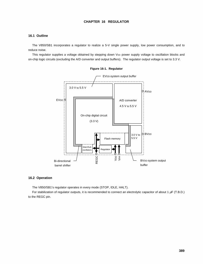
389
CHAPTER 16 REGULATOR
16.1 Outline
The V850/SB1 incorporates a regulator to realize a 5-V single power supply, low power consumption, and to
reduce noise.
This regulator supplies a voltage obtained by stepping down VDD power supply voltage to oscillation blocks and
on-chip logic circuits (excluding the A/D converter and output buffers). The regulator output voltage is set to 3.3 V.
Figure 16-1. Regulator
A/D converter
4.5 V to 5.5 V
AVDD
Main/Suboscillators
On-chip digital circuit
(3.3 V)
Regulator
VD
D
BVDD
EVDD
Flash memory
3.0 V to 5.5 V
3.0 V to5.5 V
Bi-directional
barrel shifter
EVDD-system output buffer
BVDD-system output
buffer
VP
P
RE
GC
16.2 Operation
The V850/SB1’s regulator operates in every mode (STOP, IDLE, HALT).
For stabilization of regulator outputs, it is recommended to connect an electrolytic capacitor of about 1 µF (T.B.D.)
to the REGC pin.

390
[MEMO]

391
CHAPTER 17 ROM CORRECTION FUNCTION
17.1 General
The ROM correction function provided in the V850/SB1 is a function that replaces part of a program in the mask
ROM with a program in the internal RAM.
First, the instruction of the address where the program replacement should start is replaced with the JMP r0
instruction and instructed to jump to 00000000H. The correction request register (CORRQ) is then checked. At this
time, if the CORRQn flag is set to 1, program control shifts to the internal RAM after jumping to the internal ROM area
by an instruction such as a jump instruction.
Instruction bugs found in the mask ROM can be avoided, and program flow can be changed by using the ROM
correction function.
Up to four correction addresses can be specified.
Caution The ROM correction function cannot be used for the data in the internal ROM; it can only be
used for instruction codes. If the ROM correction is carried out on data, that data will replace
the instruction code of the JMP r0 instruction.
Figure 17-1. Block Diagram of ROM Correction
ROM
(1-Mbyte area)
Instruction address bus
S Q
R
Correction address
register (CORADn)
Comparator
Correction control register
(CORCNn bit)
JMP r0 instruction
generation
Instruction
replacement
Instruction data
bus
Correction request
register (CORRQn bit)0 Clear instruction
Remark n = 0 to 3
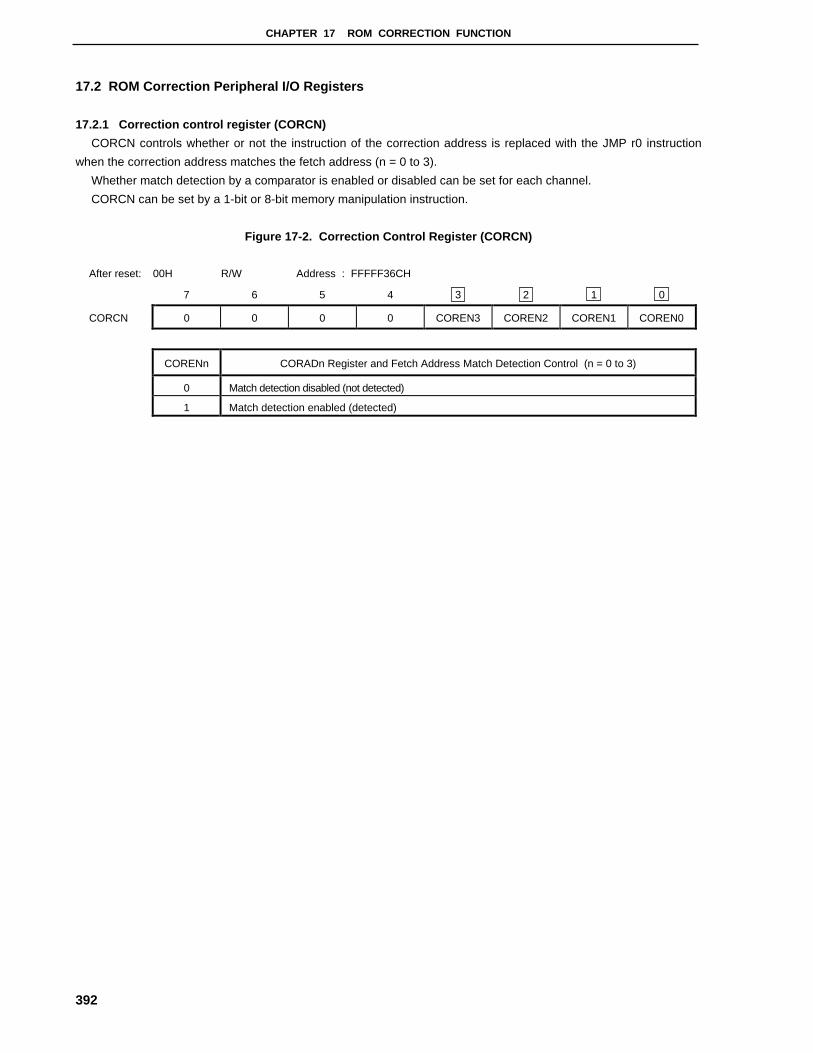
CHAPTER 17 ROM CORRECTION FUNCTION
392
17.2 ROM Correction Peripheral I/O Registers
17.2.1 Correction control register (CORCN)
CORCN controls whether or not the instruction of the correction address is replaced with the JMP r0 instruction
when the correction address matches the fetch address (n = 0 to 3).
Whether match detection by a comparator is enabled or disabled can be set for each channel.
CORCN can be set by a 1-bit or 8-bit memory manipulation instruction.
Figure 17-2. Correction Control Register (CORCN)
After reset: 00H R/W Address : FFFFF36CH
7 6 5 4 3 2 1 0
CORCN 0 0 0 0 COREN3 COREN2 COREN1 COREN0
CORENn CORADn Register and Fetch Address Match Detection Control (n = 0 to 3)
0 Match detection disabled (not detected)
1 Match detection enabled (detected)
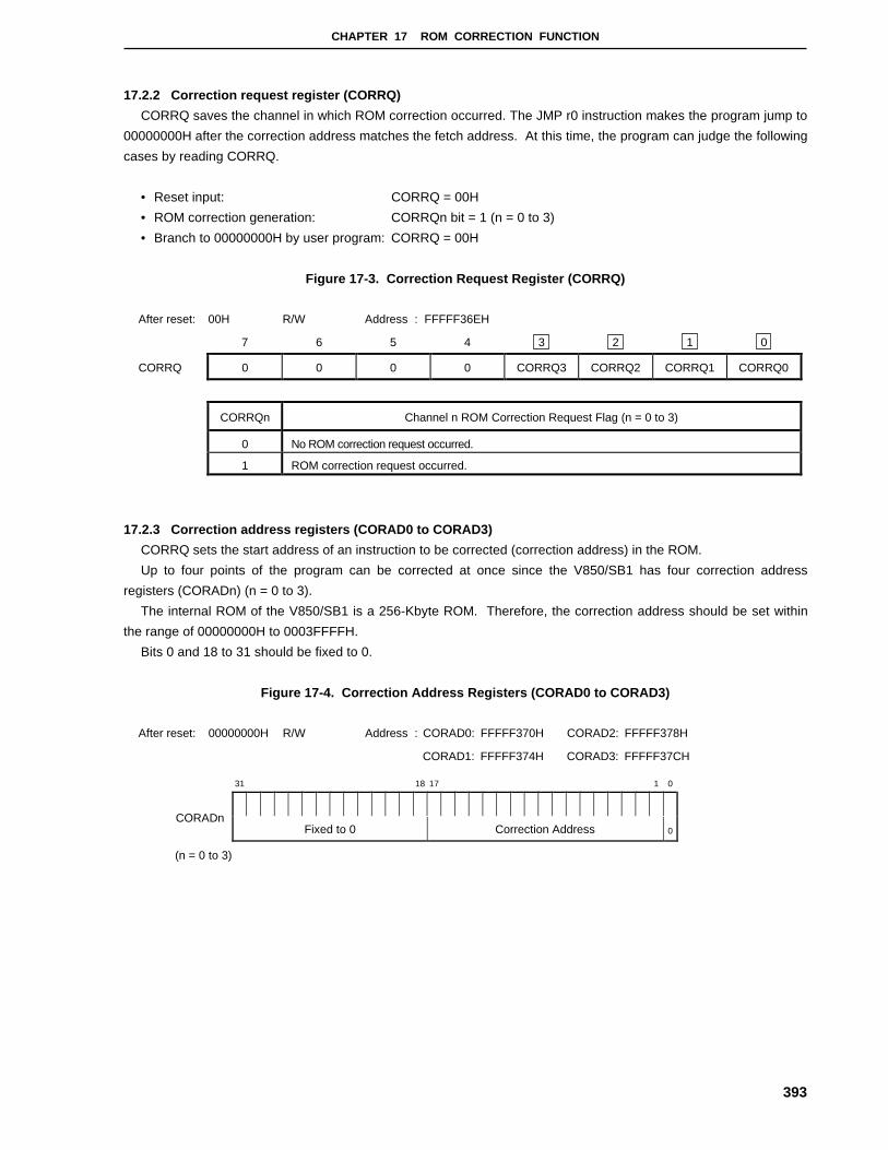
CHAPTER 17 ROM CORRECTION FUNCTION
393
17.2.2 Correction request register (CORRQ)
CORRQ saves the channel in which ROM correction occurred. The JMP r0 instruction makes the program jump to
00000000H after the correction address matches the fetch address. At this time, the program can judge the following
cases by reading CORRQ.
• Reset input: CORRQ = 00H
• ROM correction generation: CORRQn bit = 1 (n = 0 to 3)
• Branch to 00000000H by user program: CORRQ = 00H
Figure 17-3. Correction Request Register (CORRQ)
After reset: 00H R/W Address : FFFFF36EH
7 6 5 4 3 2 1 0
CORRQ 0 0 0 0 CORRQ3 CORRQ2 CORRQ1 CORRQ0
CORRQn Channel n ROM Correction Request Flag (n = 0 to 3)
0 No ROM correction request occurred.
1 ROM correction request occurred.
17.2.3 Correction address registers (CORAD0 to CORAD3)
CORRQ sets the start address of an instruction to be corrected (correction address) in the ROM.
Up to four points of the program can be corrected at once since the V850/SB1 has four correction address
registers (CORADn) (n = 0 to 3).
The internal ROM of the V850/SB1 is a 256-Kbyte ROM. Therefore, the correction address should be set within
the range of 00000000H to 0003FFFFH.
Bits 0 and 18 to 31 should be fixed to 0.
Figure 17-4. Correction Address Registers (CORAD0 to CORAD3)
After reset: 00000000H R/W Address : CORAD0: FFFFF370H CORAD2: FFFFF378H
CORAD1: FFFFF374H CORAD3: FFFFF37CH
31 18 17 1 0
CORADnFixed to 0 Correction Address 0
(n = 0 to 3)

CHAPTER 17 ROM CORRECTION FUNCTION
394
Figure 17-5. ROM Correction Operation and Program Flow
START(reset vector)
Correction address?
CORENn = 1?
CORRQn = 0?
Yes
No
Data for ROM correction setting is loaded
from an external memory into the internal
RAM to initialize ROM correction function.
If there is a correction code, it is loaded in
the internal RAM.
Microcontroller initializationClears CORRQn flag.JMP channel n correct code address
Executes internal ROM program
Executes correction program code
Jumps to internal ROM
Yes
No
Yes
No
CORRQn flag set
JMP r0
The address of the internal RAM that
stores the correction code of channel n
should be preset before the instruction
that makes the program jump to this
address is stored in the internal ROM.
: Executed by a program stored in the internal ROM
: Executed by a program stored in the internal RAM
Remark n = 0 to 3
: Executed by the ROM correction function

395
CHAPTER 18 FLASH MEMORY ( µµµµPD70F3033, 70F3033Y)
The µPD70F3033 and 70F3033Y are flash memory versions of the V850/SB1 Series and are provided with a 256-
Kbyte flash memory. In the instruction fetch to this flash memory, 4 bytes can be accessed by a single clock as well
as the mask ROM version.
Writing to a flash memory can be performed with memory mounted on the target system (on board). The
dedicated flash programmer is connected to the target system to perform writing.
The followings can be considered as the development environment and the applications using a flash memory.
• Software can be altered after the V850/SB1 is solder mounted on the target system.
• Small scale production of various models is made easier by differentiating software.
• Data adjustment in starting mass production is made easier.
18.1 Features
• 4-byte/1-clock access (in instruction fetch access)
• All area one-shot erase
• Communication via serial interface with the dedicated flash programmer
• Erase/write voltage: VPP = 7.8 V
• On-board programming
• Number of rewrite: 100 times (target)
18.2 Writing by Flash Programmer
Writing can be performed either on-board or off-board by the dedicated flash programmer.
(1) On-board programming
The contents of the flash memory is rewritten after the V850/SB1 is mounted on the target system. Mount
connectors, etc., on the target system to connect the dedicated flash programmer.
(2) Off-board programming
Writing to a flash memory is performed by the dedicated program adapter (FA Series), etc., before mounting the
V850/SB1 on the target system.
Remark FA Series is a product of Naito Densei Machidaseisakusho Co., Ltd.

CHAPTER 18 FLASH MEMORY ( µµµµPD70F3033, 70F3033Y)
396
18.3 Programming Environment
The following shows the environment required for writing programs to the flash memory of the V850/SB1.
RS-232-C
Host machine
V850/SB1Dedicated flash programmer
VSS
VPP
VDD
RESETUART0/CSI0
A host machine is required for controlling the dedicated flash programmer.
UART0 or CSI0 is used for the interface between the dedicated flash programmer and the V850/SB1 to perform
writing, erasing, etc. A dedicated program adaptor (FA Series) required for off-board writing.
18.4 Communication System
The communication between the dedicated flash programmer and the V850/SB1 is performed by serial
communication using UART0 or CSI0.
(1) UART0
Transfer rate: 4800 to 76800 bps
V850/SB1
RESET
VSS
VDD
VPP
Dedicated flashprogrammer
TXD0
RXD0
Clock
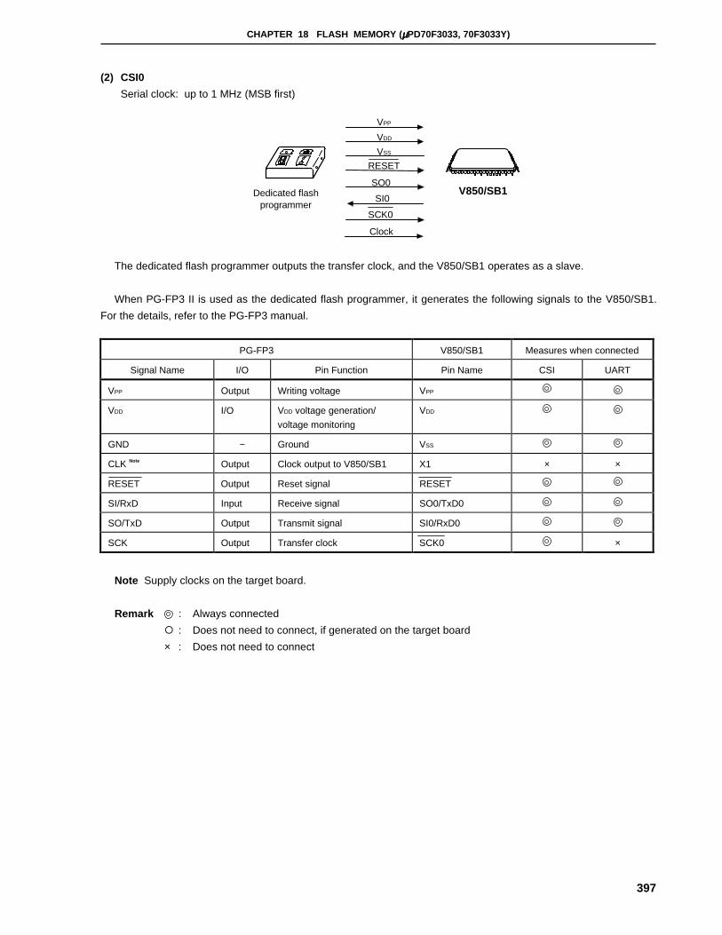
CHAPTER 18 FLASH MEMORY ( µµµµPD70F3033, 70F3033Y)
397
(2) CSI0
Serial clock: up to 1 MHz (MSB first)
V850/SB1
VSS
VDD
VPP
Dedicated flashprogrammer
SO0
SI0
Clock
RESET
SCK0
The dedicated flash programmer outputs the transfer clock, and the V850/SB1 operates as a slave.
When PG-FP3 II is used as the dedicated flash programmer, it generates the following signals to the V850/SB1.
For the details, refer to the PG-FP3 manual.
PG-FP3 V850/SB1 Measures when connected
Signal Name I/O Pin Function Pin Name CSI UART
VPP Output Writing voltage VPP
VDD I/O VDD voltage generation/
voltage monitoring
VDD
GND − Ground VSS
CLK Note Output Clock output to V850/SB1 X1 × ×
RESET Output Reset signal RESET
SI/RxD Input Receive signal SO0/TxD0
SO/TxD Output Transmit signal SI0/RxD0
SCK Output Transfer clock SCK0 ×
Note Supply clocks on the target board.
Remark : Always connected
{ : Does not need to connect, if generated on the target board
× : Does not need to connect
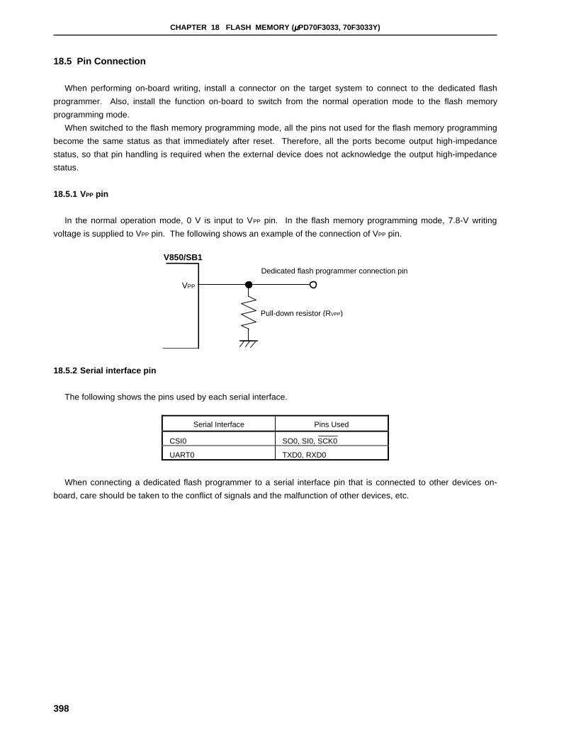
CHAPTER 18 FLASH MEMORY ( µµµµPD70F3033, 70F3033Y)
398
18.5 Pin Connection
When performing on-board writing, install a connector on the target system to connect to the dedicated flash
programmer. Also, install the function on-board to switch from the normal operation mode to the flash memory
programming mode.
When switched to the flash memory programming mode, all the pins not used for the flash memory programming
become the same status as that immediately after reset. Therefore, all the ports become output high-impedance
status, so that pin handling is required when the external device does not acknowledge the output high-impedance
status.
18.5.1 VPP pin
In the normal operation mode, 0 V is input to VPP pin. In the flash memory programming mode, 7.8-V writing
voltage is supplied to VPP pin. The following shows an example of the connection of VPP pin.
VPP
Dedicated flash programmer connection pin
Pull-down resistor (RVPP)
V850/SB1
18.5.2 Serial interface pin
The following shows the pins used by each serial interface.
Serial Interface Pins Used
CSI0 SO0, SI0, SCK0
UART0 TXD0, RXD0
When connecting a dedicated flash programmer to a serial interface pin that is connected to other devices on-
board, care should be taken to the conflict of signals and the malfunction of other devices, etc.

CHAPTER 18 FLASH MEMORY ( µµµµPD70F3033, 70F3033Y)
399
(1) Conflict of signals
When connecting a dedicated flash programmer (output) to a serial interface pin (input) that is connected to
another device (output), conflict of signals occurs. To avoid the conflict of signals, isolate the connection to the
other device or set the other device to the output high-impedance status.
V850/SB1
The other device
Output pin
Conflict of signals
Input pin
In the flash memory programming mode, the signal that thededicated flash programmer sends out conflicts with signalsthe other device outputs. Therefore, isolate the signals on theother device side.
Dedicated flash programmer connection
(2) Malfunction of the other device
When connecting a dedicated flash programmer (output or input) to a serial interface pin (input or output) that is
connected to another device (input), the signal output to the other device may cause the device to malfunction.
To avoid this, isolate the connection to the other device or make the setting so that the input signal to the other
device is ignored.
V850/SB1
Pin
In the flash memory programming mode, if thesignal the V850/SB1 outputs affects the other device,isolate the signal on the other device side.
The other device
Input pin
Dedicated flash programmer connection pin
V850/SB1
Pin
In the flash memory programming mode, if thesignal the dedicated flash programmer outputsaffects the other device, isolate the signal on theother device side.
The other device
Input pin
Dedicated flash programmer connection pin

CHAPTER 18 FLASH MEMORY ( µµµµPD70F3033, 70F3033Y)
400
18.5.3 RESET pin
When connecting the reset signals of the dedicated flash programmer to the RESET pin that is connected to the
reset signal generation circuit on-board, conflict of signals occurs. To avoid the conflict of signals, isolate the
connection to the reset signal generation circuit.
When a reset signal is input from the user system in the flash memory programming mode, programming
operation will not be performed correctly. Therefore, do not input signals other than the reset signals from the
dedicated flash programmer.
RESET
V850/SB1
Reset signal generation circuit
Output pin
Conflict of signals
In the flash memory programming mode, thesignal the reset signal generation circuit outputsconflicts with the signal the dedicated flashprogrammer outputs. Therefore, isolate thesignals on the reset signal generation circuitid
Dedicated flash programmer connection pin
18.5.4 Port pin (including NMI)
When the flash memory programming mode is set, all the port pins except the pins that communicate with the
dedicated flash programmer become output high-impedance status. If problems such as disabling output high-
impedance status should occur to the external devices connected to the port, connect them to VDD or VSS through
resistors.
18.5.5 Other signal pins
Connect X1, X2, XT2, and AVREF to the same status as that in the normal operation mode.
18.5.6 Power supply
Supply the power supply as follows:
VDD = EVDD
Supply the power supply (AVDD, AVSS, BVDD, BVSS) the same as when in normal operation mode.

CHAPTER 18 FLASH MEMORY ( µµµµPD70F3033, 70F3033Y)
401
18.6 Programming Method
18.6.1 Flash memory control
The following shows the procedure for manipulating the flash memory.
Supplies RESET pulse Switches to flash memory programming mode
Selects communication system
Manipulates flash memory
Ends?No
Yes
Ends
Starts
18.6.2 Flash memory programming mode
When rewriting the contents of a flash memory using the dedicated flash programmer, set the V850/SB1 in the
flash memory programming mode. When switching to modes, set VPP pin before releasing reset.
When performing on-board writing, change modes using a jumper, etc.
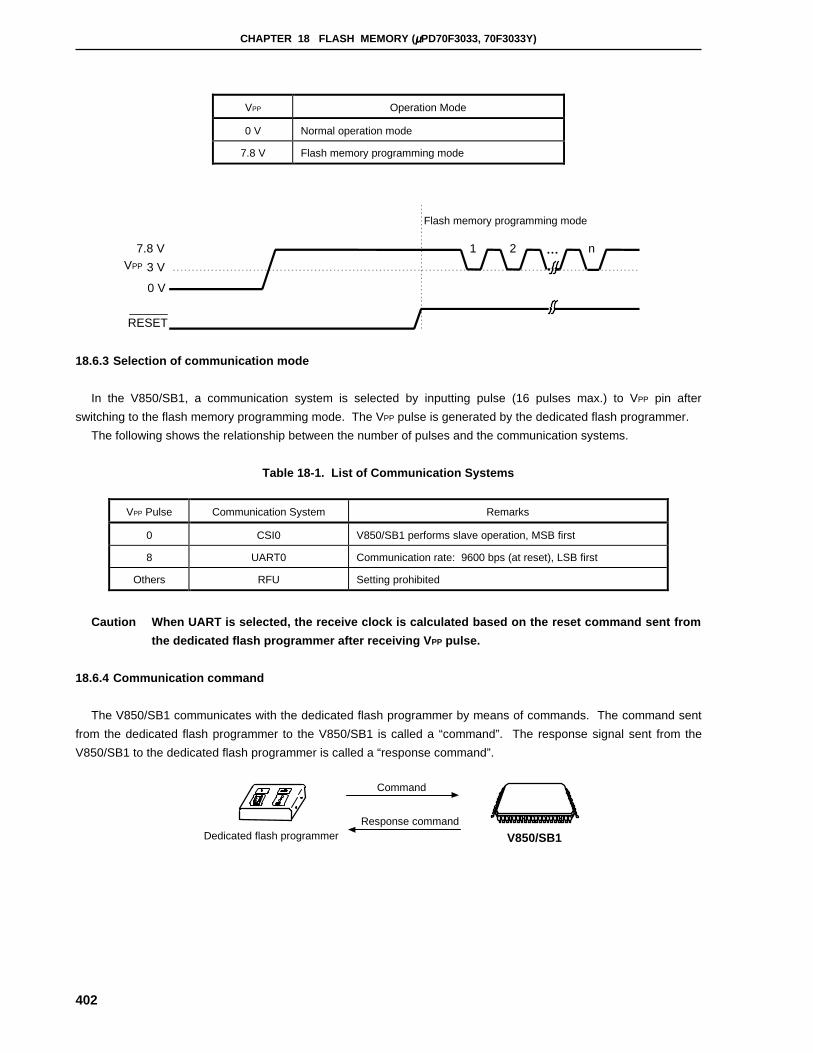
CHAPTER 18 FLASH MEMORY ( µµµµPD70F3033, 70F3033Y)
402
VPP Operation Mode
0 V Normal operation mode
7.8 V Flash memory programming mode
VPP
RESET
Flash memory programming mode
7.8 V
3 V
0 V
1 2 … n
18.6.3 Selection of communication mode
In the V850/SB1, a communication system is selected by inputting pulse (16 pulses max.) to VPP pin after
switching to the flash memory programming mode. The VPP pulse is generated by the dedicated flash programmer.
The following shows the relationship between the number of pulses and the communication systems.
Table 18-1. List of Communication Systems
VPP Pulse Communication System Remarks
0 CSI0 V850/SB1 performs slave operation, MSB first
8 UART0 Communication rate: 9600 bps (at reset), LSB first
Others RFU Setting prohibited
Caution When UART is selected, the receive clock is calculated based on the reset command sent from
the dedicated flash programmer after receiving V PP pulse.
18.6.4 Communication command
The V850/SB1 communicates with the dedicated flash programmer by means of commands. The command sent
from the dedicated flash programmer to the V850/SB1 is called a “command”. The response signal sent from the
V850/SB1 to the dedicated flash programmer is called a “response command”.
V850/SB1
Command
Dedicated flash programmerResponse command
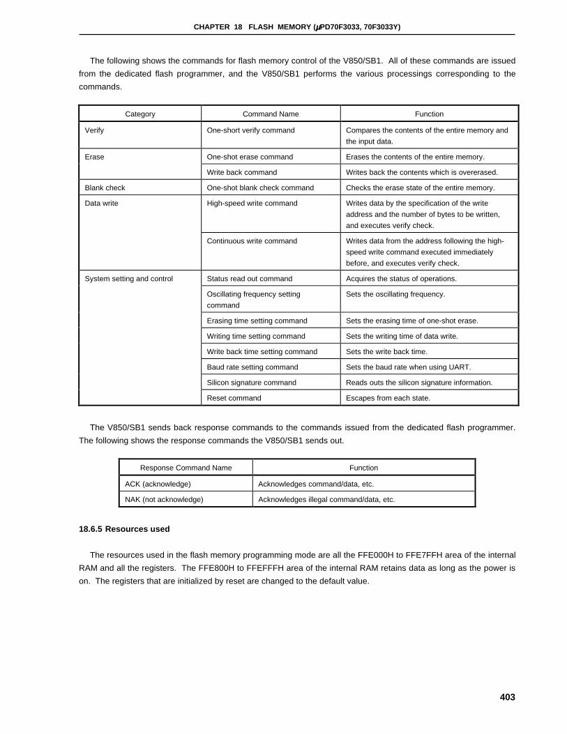
CHAPTER 18 FLASH MEMORY ( µµµµPD70F3033, 70F3033Y)
403
The following shows the commands for flash memory control of the V850/SB1. All of these commands are issued
from the dedicated flash programmer, and the V850/SB1 performs the various processings corresponding to the
commands.
Category Command Name Function
Verify One-short verify command Compares the contents of the entire memory and
the input data.
Erase One-shot erase command Erases the contents of the entire memory.
Write back command Writes back the contents which is overerased.
Blank check One-shot blank check command Checks the erase state of the entire memory.
Data write High-speed write command Writes data by the specification of the write
address and the number of bytes to be written,
and executes verify check.
Continuous write command Writes data from the address following the high-
speed write command executed immediately
before, and executes verify check.
System setting and control Status read out command Acquires the status of operations.
Oscillating frequency setting
command
Sets the oscillating frequency.
Erasing time setting command Sets the erasing time of one-shot erase.
Writing time setting command Sets the writing time of data write.
Write back time setting command Sets the write back time.
Baud rate setting command Sets the baud rate when using UART.
Silicon signature command Reads outs the silicon signature information.
Reset command Escapes from each state.
The V850/SB1 sends back response commands to the commands issued from the dedicated flash programmer.
The following shows the response commands the V850/SB1 sends out.
Response Command Name Function
ACK (acknowledge) Acknowledges command/data, etc.
NAK (not acknowledge) Acknowledges illegal command/data, etc.
18.6.5 Resources used
The resources used in the flash memory programming mode are all the FFE000H to FFE7FFH area of the internal
RAM and all the registers. The FFE800H to FFEFFFH area of the internal RAM retains data as long as the power is
on. The registers that are initialized by reset are changed to the default value.

404
[MEMO]

405
APPENDIX A REGISTER INDEX
(1/7)
Symbol Name Unit Page
ADCR A/D conversion result register ADC 325
ADCRH A/D conversion result register H ADC 325
ADIC Interrupt control register INTC 123, 124
ADM1 A/D converter mode register 1 ADC 327
ADM2 A/D converter mode register 2 ADC 329
ADS Analog input channel specification register ADC 329
ASIM0 Asynchronous serial interface mode register 0 UART 291
ASIM1 Asynchronous serial interface mode register 1 UART 291
ASIS0 Asynchronous serial interface status register 0 UART 293
ASIS1 Asynchronous serial interface status register 1 UART 293
BCC Bus cycle control register BCU 95
BRGC0 Baud rate generator control register 0 BRG 294
BRGC1 Baud rate generator control register 1 BRG 294
BRGCK4 Baud rate output clock selection register 4 BRG 316
BRGCN4 Baud rate generator source clock selection register 4 BRG 315
BRGMC00 Baud rate generator mode control register 00 BRG 294
BRGMC01 Baud rate generator mode control register 01 BRG 294
BRGMC10 Baud rate generator mode control register 10 BRG 294
BRGMC11 Baud rate generator mode control register 11 BRG 294
CORAD0 Correction address register 0 CPU 393
CORAD1 Correction address register 1 CPU 393
CORAD2 Correction address register 2 CPU 393
CORAD3 Correction address register 3 CPU 393
CORCN Correction control register CPU 392
CORRQ Correction request register CPU 393
CR00 Capture/Compare register 00 RPU 156
CR01 Capture/Compare register 01 RPU 157
CR10 Capture/Compare register 10 RPU 156
CR11 Capture/Compare register 11 RPU 157
CR20 8-bit compare register 2 RPU 189
CR23 16-bit compare register 23 (when connected to TM2,TM3 cascade) RPU 202
CR30 8-bit compare register 3 RPU 189
CR40 8-bit compare register 4 RPU 189
CR45 16-bit compare register 45 (when connected to TM4,TM5 cascade) RPU 202

APPENDIX A REGISTER INDEX
406
(2/7)
Symbol Name Unit Page
CR50 8-bit compare register 5 RPU 189
CR60 8-bit compare register 6 RPU 189
CR67 16-bit compare register 67 (when connected to TM6,TM7 cascade) RPU 202
CR70 8-bit compare register 7 RPU 189
CRC0 Capture/compare control register 0 RPU 161
CRC1 Capture/compare control register 1 RPU 161
CSIB4 Variable length serial setting register CSI 314
CSIC0 Interrupt control register INTC 123, 124
CSIC1 Interrupt control register INTC 123, 124
CSIC2 Interrupt control register INTC 123, 124
CSIC3 Interrupt control register INTC 123, 124
CSIC4 Interrupt control register INTC 123, 124
CSIM0 Serial operation mode register 0 CSI 221
CSIM1 Serial operation mode register 1 CSI 221
CSIM2 Serial operation mode register 2 CSI 221
CSIM3 Serial operation mode register 3 CSI 221
CSIM4 Serial operation mode register 4 CSI 313
CSIS0 Serial clock selection register 0 CSI 221
CSIS1 Serial clock selection register 1 CSI 221
CSIS2 Serial clock selection register 2 CSI 221
CSIS3 Serial clock selection register 3 CSI 221
DBC0 DMA byte counter register 0 DMAC 343
DBC1 DMA byte counter register 1 DMAC 343
DBC2 DMA byte counter register 2 DMAC 343
DBC3 DMA byte counter register 3 DMAC 343
DBC4 DMA byte counter register 4 DMAC 343
DBC5 DMA byte counter register 5 DMAC 343
DCHC0 DMA channel control register 0 DMAC 343
DCHC1 DMA channel control register 1 DMAC 343
DCHC2 DMA channel control register 2 DMAC 343
DCHC3 DMA channel control register 3 DMAC 343
DCHC4 DMA channel control register 4 DMAC 343
DCHC5 DMA channel control register 5 DMAC 343
DIOA0 DMA peripheral I/O address register 0 DMAC 341
DIOA1 DMA peripheral I/O address register 1 DMAC 341
DIOA2 DMA peripheral I/O address register 2 DMAC 341
DIOA3 DMA peripheral I/O address register 3 DMAC 341
DIOA4 DMA peripheral I/O address register 4 DMAC 341

APPENDIX A REGISTER INDEX
407
(3/7)
Symbol Name Unit Page
DIOA5 DMA peripheral I/O address register 5 DMAC 341
DMAIC0 Interrupt control register INTC 123, 124
DMAIC1 Interrupt control register INTC 123, 124
DMAIC2 Interrupt control register INTC 123, 124
DMAIC3 Interrupt control register INTC 123, 124
DMAIC4 Interrupt control register INTC 123, 124
DMAIC5 Interrupt control register INTC 123, 124
DRA0 DMA internal RAM address register 0 DMAC 342
DRA1 DMA internal RAM address register 1 DMAC 342
DRA2 DMA internal RAM address register 2 DMAC 342
DRA3 DMA internal RAM address register 3 DMAC 342
DRA4 DMA internal RAM address register 4 DMAC 342
DRA5 DMA internal RAM address register 5 DMAC 342
DWC Data wait control register BCU 93
ECR Interrupt source register CPU 60
EGN0 Falling edge specification register INTC 115, 359
EGP0 Rising edge specification register INTC 115, 359
EIPC Status saving register during interrupt CPU 60
EIPSW Status saving register during interrupt CPU 60
FEPC Status saving registers for NMI CPU 60
FEPSW Status saving registers for NMI CPU 60
IIC0 IIC shift register 0 I2C 230, 241
IIC1 IIC shift register 1 I2C 230, 241
IICC0 IIC control register 0 I2C 232
IICC1 IIC control register 1 I2C 232
IICCL0 IIC clock selection register 0 I2C 240
IICCL1 IIC clock selection register 1 I2C 240
IICIC1 Interrupt control register I2C 123, 124
IICS0 IIC status register 0 I2C 237
IICS1 IIC status register 1 I2C 237
ISPR In-service priority register INTC 125
KRIC Interrupt control register KR 123, 124
KRM Key return mode register KR 138
MAM Memory address output mode register Port 75
MM Memory expansion mode register Port 73
NCC Noise elimination control register INTC 127
OSTS Oscillation stabilization time selection register WDT 213

APPENDIX A REGISTER INDEX
408
(4/7)
Symbol Name Unit Page
P0 Port 0 Port 355
P1 Port 1 Port 360
P2 Port 2 Port 363
P3 Port 3 Port 366
P4 Port 4 Port 369
P5 Port 5 Port 369
P6 Port 6 Port 371
P7 Port 7 Port 373
P8 Port 8 Port 373
P9 Port 9 Port 374
P10 Port 10 Port 376
P11 Port 11 Port 379
PAC Port alternate function control register Port 381
PCC Processor clock control register CG 140
PF1 Port 1 function register Port 362
PF2 Port 2 function register Port 365
PF3 Port 3 function register Port 368
PF10 Port 10 function register Port 378
PIC0 Interrupt control register INTC 123, 124
PIC1 Interrupt control register INTC 123, 124
PIC2 Interrupt control register INTC 123, 124
PIC3 Interrupt control register INTC 123, 124
PIC4 Interrupt control register INYC 123, 124
PIC5 Interrupt control register INTC 123, 124
PIC6 Interrupt control register INTC 123, 124
PM0 Port 0 mode register Port 358
PM1 Port 1 mode register Port 361
PM2 Port 2 mode register Port 364
PM3 Port 3 mode register Port 367
PM4 Port 4 mode register Port 371
PM5 Port 5 mode register Port 371
PM6 Port 6 mode register Port 372
PM9 Port 9 mode register Port 375
PM10 Port 10 mode register Port 377
PM11 Port 11 mode register Port 380
PRCMD Command register CG 88

APPENDIX A REGISTER INDEX
409
(5/7)
Symbol Name Unit Page
PRM00 Prescaler mode register 00 RPU 164
PRM01 Prescaler mode register 01 RPU 164
PRM10 Prescaler mode register 10 RPU 165
PRM11 Prescaler mode register 11 RPU 165
PSC Power save control register CG 142
PSW Program status word CPU 60
PU0 Pull-up resistor option register 0 Port 358
PU1 Pull-up resistor option register 1 Port 362
PU2 Pull-up resistor option register 2 Port 365
PU3 Pull-up resistor option register 3 Port 367
PU10 Pull-up resistor option register 10 Port 378
PU11 Pull-up resistor option register 11 Port 381
RTBH Real time output buffer register H RPU 348
RTBL Real time output buffer register L RPU 348
RTPC Real time output port control register RPU 351
RTPM Real time output port mode register RPU 350
RX0 Receive shift register 0 UART 290
RX1 Receive shift register 1 UART 290
RXB0 Receive buffer register 0 UART 291
RXB1 Receive buffer register 1 UART 291
SERIC0 Interrupt control register INTC 123, 124
SERIC1 Interrupt control register INTC 123, 124
SIO0 Serial I/O shift register 0 CSI 220
SIO1 Serial I/O shift register 1 CSI 220
SIO2 Serial I/O shift register 2 CSI 220
SIO3 Serial I/O shift register 3 CSI 220
SIO4 Variable length serial I/O shift register 4 CSI 311
STIC0 Interrupt control register INTC 123, 124
STIC1 Interrupt control register INTC 123, 124
SVA0 Slave address register 0 I2C 230, 241
SVA1 Slave address register 1 I2C 230, 241
SYC System control register CG 90
SYS System status register CG 88
TCL20 Timer clock selection register 20 RPU 190
TCL21 Timer clock selection register 21 RPU 190
TCL30 Timer clock selection register 30 RPU 190
TCL31 Timer clock selection register 31 RPU 190
APPENDIX A REGISTER INDEX
410
(6/7)
Symbol Name Unit Page
TCL40 Timer clock selection register 40 RPU 190
TCL41 Timer clock selection register 41 RPU 190
TCL50 Timer clock selection register 50 RPU 190
TCL51 Timer clock selection register 51 RPU 190
TCL60 Timer clock selection register 60 RPU 190
TCL61 Timer clock selection register 61 RPU 190
TCL70 Timer clock selection register 70 RPU 190
TCL71 Timer clock selection register 71 RPU 190
TM0 16-bit timer register 0 RPU 155
TM1 16-bit timer register 1 RPU 155
TM2 8-bit counter 2 RPU 189
TM23 16-bit counter 23 (When connected to TM2,TM3 cascade) RPU 202
TM3 8-bit counter 3 RPU 189
TM4 8-bit counter 4 RPU 189
TM45 16-bit counter 45 (When connected to TM4,TM5 cascade) RPU 202
TM5 8-bit counter 5 RPU 189
TM6 8-bit counter 6 RPU 189
TM67 16-bit counter 67 (When connected to TM6,TM7 cascade) RPU 202
TM7 8-bit counter 7 RPU 189
TMC0 16-bit timer mode control register 0 RPU 158
TMC1 16-bit timer mode control register 1 RPU 158
TMC2 8-bit timer mode control register 2 RPU 193
TMC3 8-bit timer mode control register 3 RPU 193
TMC4 8-bit timer mode control register 4 RPU 193
TMC5 8-bit timer mode control register 5 RPU 193
TMC6 8-bit timer mode control register 6 RPU 193
TMC7 8-bit timer mode control register 7 RPU 193
TMIC00 Interrupt control register INTC 123, 124
TMIC01 Interrupt control register INTC 123, 124
TMIC10 Interrupt control register INTC 123, 124
TMIC11 Interrupt control register INTC 123, 124
TMIC2 Interrupt control register INTC 123, 124
TMIC3 Interrupt control register INTC 123, 124
TMIC4 Interrupt control register INTC 123, 124
TMIC5 Interrupt control register INTC 123, 124
TMIC6 Interrupt control register INTC 123, 124
TMIC7 Interrupt control register INTC 123, 124

APPENDIX A REGISTER INDEX
411
(7/7)
Symbol Name Unit Page
TOC0 16-bit timer output control register 0 RPU 162
TOC1 16-bit timer output control register 1 RPU 162
TXS0 Transmit shift register 0 UART 290
TXS1 Transmit shift register 1 UART 290
WDCS Watchdog timer clock selection register WDT 214
WDTIC Interrupt control register INTC 123, 124
WDTM Watchdog timer mode register WDT 126, 215
WTNCS Watch timer clock selection register WT 208
WTNIC Interrupt control register INTC 123, 124
WTNIIC Interrupt control register INTC 123, 124
WTNM Watch timer mode control register WT 207

412
[MEMO]
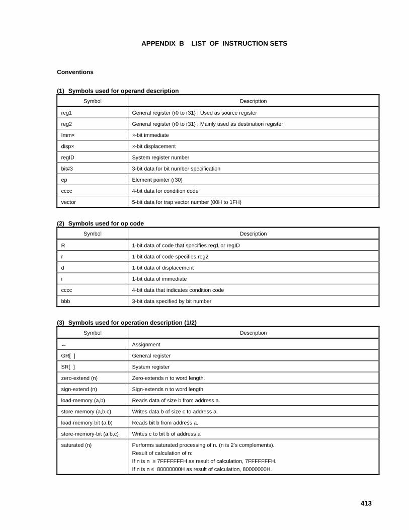
413
APPENDIX B LIST OF INSTRUCTION SETS
Conventions
(1) Symbols used for operand description
Symbol Description
reg1 General register (r0 to r31) : Used as source register
reg2 General register (r0 to r31) : Mainly used as destination register
Imm× ×-bit immediate
disp× ×-bit displacement
regID System register number
bit#3 3-bit data for bit number specification
ep Element pointer (r30)
cccc 4-bit data for condition code
vector 5-bit data for trap vector number (00H to 1FH)
(2) Symbols used for op code
Symbol Description
R 1-bit data of code that specifies reg1 or regID
r 1-bit data of code specifies reg2
d 1-bit data of displacement
i 1-bit data of immediate
cccc 4-bit data that indicates condition code
bbb 3-bit data specified by bit number
(3) Symbols used for operation description (1/2)
Symbol Description
← Assignment
GR[ ] General register
SR[ ] System register
zero-extend (n) Zero-extends n to word length.
sign-extend (n) Sign-extends n to word length.
load-memory (a,b) Reads data of size b from address a.
store-memory (a,b,c) Writes data b of size c to address a.
load-memory-bit (a,b) Reads bit b from address a.
store-memory-bit (a,b,c) Writes c to bit b of address a
saturated (n) Performs saturated processing of n. (n is 2’s complements).
Result of calculation of n:
If n is n ≥ 7FFFFFFFH as result of calculation, 7FFFFFFFH.
If n is n ≤ 80000000H as result of calculation, 80000000H.
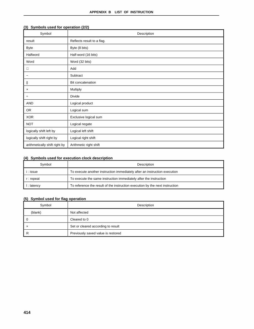
APPENDIX B LIST OF INSTRUCTION
414
(3) Symbols used for operation (2/2)
Symbol Description
result Reflects result to a flag.
Byte Byte (8 bits)
Halfword Half-word (16 bits)
Word Word (32 bits)
+ Add
− Subtract
|| Bit concatenation
× Multiply
÷ Divide
AND Logical product
OR Logical sum
XOR Exclusive logical sum
NOT Logical negate
logically shift left by Logical left shift
logically shift right by Logical right shift
arithmetically shift right by Arithmetic right shift
(4) Symbols used for execution clock description
Symbol Description
i : issue To execute another instruction immediately after an instruction execution
r : repeat To execute the same instruction immediately after the instruction
l : latency To reference the result of the instruction execution by the next instruction
(5) Symbol used for flag operation
Symbol Description
(blank) Not affected
0 Cleared to 0
× Set or cleared according to result
R Previously saved value is restored

APPENDIX B LIST OF INSTRUCTION SET
415
Condition Codes
Condition Name
(cond)
Condition Code
(cccc)
V 0000 OV = 1 Overflow
NV 1000 OV = 0 No overflow
C/L 0001 CY = 1 Carry
Lower (Less than)
NC/NL 1001 CY = 0 No carry
No lower (Greater than or equal)
Z/E 0010 Z = 1 Zero
Equal
NZ/NE 1010 Z = 0 Not zero
Not equal
NH 0011 (CY or Z) = 1 Not higher (Less than or equal)
H 1011 (CY or Z) = 0 Higher (Greater than)
N 0100 S = 1 Negative
P 1100 S = 0 Positive
T 0101 − Always (unconditional)
SA 1101 SAT = 1 Saturated
LT 1101 (S xor OV) = 1 Less than signed
GE 1110 (S xor OV) = 0 Greater than or equal signed
LE 0111 ( (S xor OV) or Z) = 1 Less than or equal signed
GT 1111 ( (S xor OV) or Z) = 0 Greater than signed
DescriptionCondition Expression
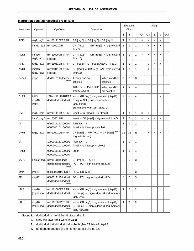
APPENDIX B LIST OF INSTRUCTION
416
Instruction Sets (alphabetical order) (1/4)
Mnemonic Operand Op Code Operation
Execution
Clock
Flag
i r l CY OV S Z SAT
ADD reg1, reg2 rrrrr001110RRRRR GR [reg2] ← GR [reg2] + GR [reg1] 1 1 1 × × × ×
imm5, reg2 rrrrr010010iiiii GR [reg2] ← GR [reg2] + sign-extend
(imm5)
1 1 1 × × × ×
ADDI imm16,
reg1, reg2
rrrrr110000RRRRR
iiiiiiiiiiiiiiii
GR [reg2] ← GR [reg1] + sign-extend
(imm16)
1 1 1 × × × ×
AND reg1, reg2 rrrrr110110RRRRR GR [reg2] ← GR [reg2] AND GR [reg1] 1 1 1 0 × ×
ANDI imm16,
reg1, reg2
rrrrr110110RRRRR
iiiiiiiiiiiiiiii
GR [reg2] ← GR [reg1] AND zero-extend
(imm16)
1 1 1 0 0 ×
Bcond disp9 ddddd1011dddccccNote 1
if conditions are
satisfied
When condition
satisfied
3 3 3
then PC ← PC + sign-
extend (disp9)When condition
not satisfied
1 1 1
CLR1 bit#3,
disp16
[regf1]
10bbb111110RRRRR
dddddddddddddddd
adr ← GR [reg1] + sign-extend (disp16)
Z flag ← Not (Load-memory-bit
(adr, bit#3))
Store memory-bit (adr, bit#3, 0)
4 4 4 ×
CMP reg1, reg2 rrrrr001111RRRRR result ← GR [reg2] − GR [reg1] 1 1 1 × × × ×
imm5, reg2 rrrrr010011iiiii result ← GR [reg2] − sign-extend (imm5) 1 1 1 × × × ×
DI 0000011111100000
0000000101100000
PSW.ID ← 1
(Maskable interrupt disabled)
1 1 1
DIVH reg1, reg2 rrrrr000010RRRRR GR [reg2] ← GR [reg2] ÷ GR [reg2] Note 2
(signed division)
36 36 36 × × ×
EI 1000011111100000
0000000101100000
PSW.ID ← 0
(Maskable interrupt enabled)
1 1 1
HALT 0000011111100000
0000000100100000
Stops 1 1 1
JARL disp22, reg2 rrrrr11110dddddd
ddddddddddddddd0Note 3
GR [reg2] ← PC + 4
PC ← PC + sign-extend (disp22)
3 3 3
JMP [reg1] 00000000011RRRRR PC ← GR [reg1] 3 3 3
JR disp22 0000011110dddddd
ddddddddddddddd0Note 3
PC ← PC + sign-extend (disp22) 3 3 3
LD.B disp16
[reg1], reg2
rrrrr111000RRRRR
dddddddddddddddd
adr ← GR [reg1] + sign-extend (disp16)
GR [reg2] ← sign-extend (Load-memory
(adr, Byte))
1 1 2
LD.H disp16
[reg1], reg2
rrrrr111001RRRRR
ddddddddddddddd0Note 4
adr ← GR [reg1] + sign-extend (disp16)
GR [reg2] ← sign-extend (Load-memory
(adr, Halfword))
1 1 2
Notes 1. dddddddd is the higher 8 bits of disp9.
2. Only the lower half-word is valid.
3. ddddddddddddddddddddd is the higher 21 bits of disp22.
4. ddddddddddddddd is the higher 15 bits of disp 16.

APPENDIX B LIST OF INSTRUCTION SET
417
Instruction Set (alphabetical order) (2/4)
Mnemonic Operand Op Code Operation
Execution
Clock
Flag
i r l CY OV S Z SAT
LD.W disp16
[reg1], reg2
rrrrr111001RRRRR
ddddddddddddddd1Note 1
adr ← GR [reg1] + sign-extend (disp16)
GR [reg2] ← Load-memory (adr, Wortd))
1 1 2
LDSR reg2, regID rrrrr111001RRRRR SR [regID] regID = EIPC, FEPC 1 1 3
ddddddddddddddd1 ← GR [reg2] regID = EIPSW, FEPSW 1Note 2
regID = PSW 1 × × × × ×
MOV reg1, reg2 rrrrr000000RRRRR GR [reg2] ← GR [reg1] 1 1 1
imm5, reg2 rrrrr010000iiiii GR [reg2] ← sign-extend (imm5) 1 1 1
MOVEA imm16,
reg1, reg2
rrrrr110001RRRRR
iiiiiiiiiiiiiiii
GR [reg2] ← GR [reg1] + sign-extend
(imm16)
1 1 1
MOVHI imm16,
reg1, reg2
rrrrr110010RRRRR
iiiiiiiiiiiiiiii
GR [reg2] ← GR [reg1] + (imm16 || 016) 1 1 1
MULH reg1,reg2 rrrrr000111RRRRR GR [reg2] ← GR [reg2] Note 3
× GR [reg1] Note 3
(Signed multiplication)
1 1 2
imm5, reg2 rrrrr010111iiiii GR [reg2] ← GR [reg2] Note 3
× sign-extend
(imm5) (Signed multiplication)
1 1 2
MULHI imm16,
reg1, reg2
rrrrr110111RRRRR
iiiiiiiiiiiiiiii
GR [reg2] ← GR [reg1] Note 3
× imm16
(Signed multiplication)
1 1 2
NOP 0000000000000000 Uses 1 clock cycle without doing anything 1 1 1
NOT reg1, reg2 rrrrr000001RRRRR GR [reg2] ← NOT (GR [reg1]) 1 1 1 0 × ×
NOT1 bit#3,
disp16 [reg1]
01bbb111110RRRRR
dddddddddddddddd
adr ← GR [reg1] + sign-extend (disp16)
Z flag ← Not (Load-memory-bit
(adr, bit#3))
Store-memory-bit (adr, bit#3, Z flag)
4 4 4 ×
OR reg1, reg2 rrrrr001000RRRRR GR [reg2] ← GR [reg2] OR GR [reg1] 1 1 1 0 × ×
ORI imm16,
reg1, reg2
rrrrr110100RRRRR
iiiiiiiiiiiiiiii
GR [reg2] ← GR [reg2] OR zero-extend
(imm16)
1 1 1 0 × ×
RETI 0000011111100000
0000000101000000
if PSW.EP = 1
then PC ← EIPC
PSW ← EIPSW
eise if PSW.NP = 1
then PC ← FEPC
PSW ← FEPSW
eise PC ← EIPC
PSW ← EIPSW
4 4 4 R R R R R
Notes 1. ddddddddddddddd is the higher 15 bits of disp 16.
2. The op code of this instruction uses the field of reg1 through the source register is shown as reg2 in
the above table. Therefore, the meaning of register specification for mnemonic description and op code
is different from that of the other instructions.
rrr = regID specification
RRRRR = reg2 specification
3. Only the lower half-word data is valid.

APPENDIX B LIST OF INSTRUCTION
418
Instruction Set (alphabetical order) (3/4)
Mnemonic Operand Op Code Operation
Execution
Clock
Flag
i r l CY OV S Z SAT
SAR reg1, reg2 rrrrr111111RRRRR
0000000010100000
GR [reg2] ← GR [reg2] arithmetically shift
right
by GR [reg1]
1 1 1 × 0 × ×
imm5, reg2 rrrrr010101iiiii GR [reg2] ← GR [reg2] arithmetically shift
right
by zero-extend (imm5)
1 1 1 × 0 × ×
SATADD reg1, reg2 rrrrr000110RRRRR GR [reg2] ← saturated (GR [reg2] − GR
[reg1])
1 1 1 × × × × ×
imm5, reg2 rrrrr010101iiiii GR [reg2] ← saturated (GR [reg2] + sign-
extend (imm5))
1 1 1 × × × × ×
SATSUB reg1, reg2 rrrrr000101RRRRR GR [reg2] ← saturated (GR [reg2] − GR
[reg1])
1 1 1 × × × × ×
SATSUBI imm16,
reg1, reg2
rrrrr110011RRRRR
iiiiiiiiiiiiiiii
GR [reg2] ← saturated (GR [reg1] − sign-
extend (imm16))
1 1 1 × × × × ×
SATSUBR reg1, reg2 rrrrr000100RRRRR GR [reg2] ← saturated (GR [reg1] + GR
[reg2])
1 1 1 × × × × ×
SETF cccc, reg2 rrrrr1111110cccc
0000000000000000
if conditions are satisfied
then GR [reg2] ← 00000001H
eise GR [reg2] ← 00000000H
1 1 1
SET1 bit#3,
disp16 [reg1]
00bbb111110RRRRR
dddddddddddddddd
adr ← GR [reg1] + sign-extend (disp16)
Z flag ← Not (Load-memory-bit
(adr, bit#3)
Store memory-bit (adr, bit#3, 1)
4 4 4 ×
SHL reg1, reg2 rrrrr111111RRRRR
0000000011000000
GR [reg2] ← GR [reg2] logically shift left
by GR [reg1])
1 1 1 × 0 × ×
imm5, reg2 rrrrr010110iiiii GR [reg2] ← GR [reg2] logically shift left
by zero-extend (imm5)
1 1 1 × 0 × ×
SHR reg1, reg2 rrrrr1111111cccc
0000000000000000
GR [reg2] ← GR [reg2] logically shift right
by GR [reg1]
1 1 1 × 0 × ×
imm5, reg2 rrrrr010100iiiii GR [reg2] ← GR [reg2] logically shift right
by zero-extend (imm5)
1 1 1 × 0 × ×
SLD.B disp7 [ep],
reg2
rrrrr0110ddddddd adr ← ep + zero-extend (disp7)
GR [reg2] ← sign-extend (Load-memory
(adr, Byte))
1 1 2
SLD.H disp8 [ep],
reg2
rrrrr1000dddddddNote 1
adr ← ep + zero-extend (disp7)
GR [reg2] ← sign-extend (Load-memory
(adr, Byte))
1 1 2
SLD.W disp8 [ep],
reg2
rrrrr1010dddddddNote 2
adr ← ep + zero-extend (disp7)
GR [reg2] ← Load-memory (adr, Word)
1 1 2
Notes 1. ddddddd is the higher 7 bits of dip8.
2. dddddd is the higher 6 bits of disp8.
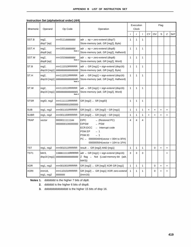
APPENDIX B LIST OF INSTRUCTION SET
419
Instruction Set (alphabetical order) (4/4)
Mnemonic Operand Op Code Operation
Execution
Clock
Flag
i r l CY OV S Z SAT
SST.B reg2,
disp7 [ep]
rrrrr0111ddddddd adr ← ep + zero-extend (disp7)
Store-memory (adr, GR [reg2], Byte)
1 1 1
SST.H reg2,
disp8 [ep]
rrrrr1001dddddddNote 1
adr ← ep + zero-extend (disp8)
Store-memory (adr, GR [reg2], Halfword)
1 1 1
SST.W reg2,
disp8 [ep]
rrrrr1010dddddddNote 2
adr ← ep + zero-extend (disp8)
Store-memory (adr, GR [reg2], Word)
1 1 1
ST.B reg2,
disp16 [reg1]
rrrrr111010RRRRR
dddddddddddddddd
adr ← GR [reg1] + sign-extend (disp16)
Store-memory (adr, GR [reg2], Byte)
1 1 1
ST.H reg2,
disp16 [reg1]
rrrrr111011RRRRR
ddddddddddddddd0Note 3
adr ← GR [reg1] + sign-extend (disp16)
Store-memory (adr, GR [reg2], Halfword)
1 1 1
ST.W reg2,
disp16 [reg1]
rrrrr111011RRRRR
ddddddddddddddd1Note 3
adr ← GR [reg1] + sign-extend (disp16)
Store-memory (adr, GR [reg2], Word)
1 1 1
STSR regID, reg2 rrrrr111111RRRRR
0000000001000000
GR [reg2] ← SR [regID] 1 1 1
SUB reg1, reg2 rrrrr001101RRRRR GR [reg2] ← GR [reg2] − GR [reg1] 1 1 1 × × × ×
SUBR reg1, reg2 rrrrr001100RRRRR GR [reg2] ← GR [reg2] − GR [reg1] 1 1 1 × × × ×
TRAP vector 00000111111iiiii
0000000100000000
EIPC ← (Restored PC)
EIPSW ← PSW
ECR.EICC ← Interrupt code
PSW.EP ← 1
PSW.ID ← 1
PC ← 00000040H(vector = 00H to 0FH)
00000050H(vector = 10H to 1FH)
4 4 4
TST reg1, reg2 rrrrr001011RRRRR result ← GR [reg2] AND [reg1] 1 1 1 0 × ×
TST1 bit#3,
disp16 [reg1]
11bbb111110RRRRR
dddddddddddddddd
adr ← GR [reg1] + sign-extend (disp16)
Z flag ← Not (Load-memory-bit (adr,
bit#3))
3 3 3 ×
XOR reg1, reg2 rrrrr001001RRRRR GR [reg2] ← GR [reg2] XOR GR [reg1] 1 1 1 0 × ×
XORI imm16,
reg1, reg2
rrrrr110101RRRRR
iiiiiiiiiiiiiiii
GR [reg2] ← GR [reg1] XOR zero-extend
(imm16)
1 1 1 0 × ×
Notes 1. ddddddd is the higher 7 bits of dip8.
2. dddddd is the higher 6 bits of disp8.
3. ddddddddddddddd is the higher 15 bits of disp 16.

420
[MEMO]

421
APPENDIX C INDEX
[Number]16-bit compare register 23 ----------------------------- 202
16-bit compare register 45 ------------------------------ 202
16-bit compare register 67 ------------------------------ 202
16-bit couner 23 ------------------------------------------- 202
16-bit couner 45 ------------------------------------------- 202
16-bit couner 67 ------------------------------------------- 202
16-bit timer -------------------------------------------------- 153
16-bit timer mode control registers 0, 1 -------------- 158
16-bit timer output control registers 0, 1 ------------- 162
16-bit timer registers 0, 1 -------------------------------- 155
3-wire serial I/O -------------------------------------------- 219
3-wire variable serial I/O --------------------------------- 310
8-bit compare registers 2 to 7 --------------------------- 189
8-bit counters 2 to 7 --------------------------------------- 189
8-bit timer----------------------------------------------------- 187
8-bit timer mode control registers 2 to 7-------------- 193
[A]A/D conversion result register -------------------------- 325
A/D conversion result register H ----------------------- 325
A/D converter ----------------------------------------------- 323
A/D converter mode register 1 ------------------------- 327
A/D converter mode register 2 ------------------------- 329
A1 to A4 -------------------------------------------------------- 50
A13 to A15 ---------------------------------------------------- 44
A16 to A21 ---------------------------------------------------- 46
A5 to A12 ------------------------------------------------------ 49
Access clock counts ---------------------------------------- 90
AD0 to AD7 --------------------------------------------------- 45
AD8 to AD15 -------------------------------------------------- 45
ADCR --------------------------------------------------------- 325
ADCRH ------------------------------------------------------- 325
Address match detection method --------------------- 271
Address space ----------------------------------------------- 63
ADIC ----------------------------------------------------123, 124
ADM1 --------------------------------------------------------- 327
ADM2 --------------------------------------------------------- 329
ADS ----------------------------------------------------------- 329
ADTRG --------------------------------------------------------- 41
Analog input channel specification register --------- 329
ANI0 to ANI11 ------------------------------------------------ 46
Arbitration ---------------------------------------------------- 272
ASCK0 --------------------------------------------------------- 42
ASCK1 --------------------------------------------------------- 43
ASIM0, ASIM1 ----------------------------------------------291
ASIS0, ASIS1 -----------------------------------------------293
ASTB ----------------------------------------------------------- 48
Asynchronous serial interface --------------------------289
Asynchronous serial interface mode
registers 0, 1 ------------------------------------------------291
Asynchronous serial interface status
registers 0, 1 ------------------------------------------------293
AVDD ------------------------------------------------------------ 50
AVREF ----------------------------------------------------------- 50
AVSS ------------------------------------------------------------ 50
[B]Baud rate generator control registers 0, 1 -----------294
Baud rate generator mode control
registers n0, n1 ---------------------------------------------294
Baud rate generator source clock select
register 4 -----------------------------------------------------315
Baud rate output clock selection register 4 ----------316
BCC ------------------------------------------------------------- 95
BCU ------------------------------------------------------------- 30
BRGC0, BRGC1 --------------------------------------------294
BRGCK4 ------------------------------------------------------316
BRGCN4 -----------------------------------------------------315
BRGMCn0, BRGMCn1 -----------------------------------294
Bus control function ---------------------------------------- 89
Bus control pin ----------------------------------------------- 89
Bus control unit ---------------------------------------------- 30
Bus cycle control register --------------------------------- 95
Bus hold function -------------------------------------------- 96
Bus priority ---------------------------------------------------105
Bus timing ----------------------------------------------------- 98
Bus width ------------------------------------------------------ 91
BVDD ------------------------------------------------------------ 50
BVSS ------------------------------------------------------------ 50
Byte access --------------------------------------------------- 91
[C]Capture/compare control registers 0, 1 --------------161
Capture/compare register n0 ---------------------------156
Capture/compare register n1 ---------------------------157
CG -------------------------------------------------------------- 30
CLKOUT ------------------------------------------------------- 37
Clock generation function --------------------------------139

APPENDIX C INDEX
422
Clock generator (CG) ---------------------------------------30
Clock output function --------------------------------------140
Command register -------------------------------------------88
Communication command -------------------------------402
Communication reservation -----------------------------275
Communication system ----------------------------------396
CORAD0 to CORAD3 -------------------------------------393
CORCN -------------------------------------------------------392
Correction address registers 0 to 3 -------------------393
Correction control register -------------------------------392
Correction request register ------------------------------393
CORRQ -------------------------------------------------------393
CPU -------------------------------------------------------------30
CPU address space -----------------------------------------63
CPU register set ----------------------------------------------58
CR20 to CR70 ----------------------------------------------189
CR23, CR45, CR67 ---------------------------------------202
CRC0, CRC1 ------------------------------------------------161
CRn0 ----------------------------------------------------------156
CRn1 ----------------------------------------------------------157
CSI0 to CSI3 ------------------------------------------------219
CSI4 -----------------------------------------------------------310
CSIB4 ---------------------------------------------------------314
CSIC0 to CSIC4 ------------------------------------- 123, 124
CSIM0 to CSIM3 -------------------------------------------221
CSIM4 ---------------------------------------------------------313
CSIS0 to CSIS3 --------------------------------------------221
[D]Data wait control register ----------------------------------93
DBC0 to DBC5 ----------------------------------------------343
DCHC0 to DCHC5 -----------------------------------------343
DIOA0 to DIOA5 --------------------------------------------341
DMA function -----------------------------------------------341
DMA byte count registers 0 to 5 -----------------------343
DMA channel control registers 0 to 5 -----------------343
DMA internal RAM address registers 0 to 5 --------342
DMA peripheral I/O address registers 0 to 5 --------341
DMAIC0 to DMAIC5 -------------------------------- 123, 124
DRA0 to DRA5 ----------------------------------------------342
DSTB ------------------------------------------------------------48
DWC -------------------------------------------------------------93
[E]ECR -------------------------------------------------------------60
EGN0 --------------------------------------------------- 115, 359
EGP0 --------------------------------------------------- 115, 359
EIPC -------------------------------------------------------------60
EIPSW --------------------------------------------------------- 60
Error detection ---------------------------------------------- 271
EVDD ------------------------------------------------------------ 51
EVSS ------------------------------------------------------------- 51
Exception trap ---------------------------------------------- 131
Extension code --------------------------------------------- 271
External expansion mode --------------------------------- 73
External memory --------------------------------------------- 71
External wait function --------------------------------------- 94
[F]Falling edge specification register --------------115, 359
FEPC ----------------------------------------------------------- 60
FEPSW --------------------------------------------------------- 60
Flash memory ---------------------------------------------- 395
Flash memory control ------------------------------------ 401
Flash memory programming mode -------------- 62, 401
[G]General register ---------------------------------------------- 59
[H]Half-word access -------------------------------------------- 91
HALT mode ------------------------------------------------- 144
Handling of unused pins ----------------------------------- 52
Hardware start ---------------------------------------------- 323
HLDAK --------------------------------------------------------- 48
HLDRQ --------------------------------------------------------- 48
[I]I2C bus ------------------------------------------------------- 227
I2C bus mode -----------------------------------------227, 242
I2C interrupt request --------------------------------------- 250
IC ---------------------------------------------------------------- 51
IDLE mode -------------------------------------------------- 147
Idle state insertion function ------------------------------- 95
IIC clock select registers 0, 1 --------------------------- 240
IIC control registers 0, 1 --------------------------------- 232
IIC shift registers 0, 1 -------------------------------230, 241
IIC status registers 0, 1 ---------------------------------- 237
IIC0, IIC1 -----------------------------------------------230, 241
IICC0, IICC1 ------------------------------------------------ 232
IICCL0, IICCL1 --------------------------------------------- 240
IICIC1 ---------------------------------------------------123, 124
IICS0, IICS1 ------------------------------------------------- 237
Illegal op code ---------------------------------------------- 131
Image ----------------------------------------------------------- 64
In-service priority register ------------------------------- 125

APPENDIX C INDEX
423
INTC ----------------------------------------------------------- 30
Internal RAM area ------------------------------------------- 69
Internal ROM area ------------------------------------------- 67
Interrupt control register ---------------------------123, 124
Interrupt controller ------------------------------------------- 30
Interrupt latency time ------------------------------------- 137
Interrupt request signal generator --------------------- 231
Interrupt source register ----------------------------------- 60
Interrupt status saving register --------------------------- 60
Interrupt/exception processing function ------------- 107
Interval timer mode ---------------------------------------- 212
INTP0 to INTP6 ---------------------------------------------- 41
ISPR ---------------------------------------------------------- 125
[K]Key interrupt function ------------------------------------- 138
Key return mode register -------------------------------- 138
KR0 to KR7 --------------------------------------------------- 49
KRIC ----------------------------------------------------123, 124
KRM ----------------------------------------------------------- 138
[L]LBEN ----------------------------------------------------------- 47
Low power consumption mode ------------------------ 335
[M]Main system clock oscillation circuit ------------------ 139
MAM ------------------------------------------------------------ 75
Maskable interrupt ---------------------------------------- 116
Memory address output mode register ---------------- 75
Memory block function ------------------------------------- 92
Memory boundary operation condition --------------- 105
Memory expansion mode register ----------------------- 73
Memory map -------------------------------------------------- 66
MM -------------------------------------------------------------- 73
Multiple interrupt ------------------------------------------- 134
[N]NCC ----------------------------------------------------------- 127
NMI -------------------------------------------------------------- 41
NMI status saving register -------------------------------- 60
Noise elimination control register --------------------- 127
Non-maskable interrupt ---------------------------------- 110
Normal operation mode ------------------------------------ 62
[O]Off-board programming ---------------------------------- 395
On-board programming ---------------------------------- 395
On-chip peripheral I/O area ------------------------------ 70
Operation mode --------------------------------------------- 62
Oscillation stabilization time -----------------------------150
Oscillation stabilization time selection register -----213
OSTS ----------------------------------------------------------213
[P]P0 --------------------------------------------------------------355
P00 to P07 ---------------------------------------------------- 41
P1 --------------------------------------------------------------360
P10 -------------------------------------------------------------376
P10 to P15 ---------------------------------------------------- 42
P100 to P107 ------------------------------------------------- 49
P11 -------------------------------------------------------------379
P110 to P113 ------------------------------------------------- 49
P2 --------------------------------------------------------------363
P20 to P27 ---------------------------------------------------- 43
P3 --------------------------------------------------------------366
P30 to P37 ---------------------------------------------------- 44
P4 --------------------------------------------------------------369
P40 to P47 ---------------------------------------------------- 44
P5 --------------------------------------------------------------369
P50 to P57 ---------------------------------------------------- 45
P6 --------------------------------------------------------------371
P60 to P65 ---------------------------------------------------- 45
P7 --------------------------------------------------------------373
P70 to P77 ---------------------------------------------------- 46
P8 --------------------------------------------------------------373
P80 to P83 ---------------------------------------------------- 46
P9 --------------------------------------------------------------374
P90 to P96 ---------------------------------------------------- 47
PAC ------------------------------------------------------------381
PCC ------------------------------------------------------------140
Peripheral I/O registers ------------------------------------ 79
PF1 ------------------------------------------------------------362
PF10 -----------------------------------------------------------378
PF2 ------------------------------------------------------------365
PF3 ------------------------------------------------------------368
PIC0 to PIC6 ----------------------------------------- 123, 124
Pin function --------------------------------------------------- 33
Pin I/O buffer power supply ------------------------------ 52
Pin I/O circuit type ------------------------------------------ 52
PM0 ------------------------------------------------------------358
PM1 ------------------------------------------------------------361
PM10 ----------------------------------------------------------377
PM11 ----------------------------------------------------------380
PM2 ------------------------------------------------------------364
PM3 ------------------------------------------------------------367
APPENDIX C INDEX
424
PM4 ------------------------------------------------------------371
PM5 ------------------------------------------------------------371
PM6 ------------------------------------------------------------372
PM9 ------------------------------------------------------------375
Port ------------------------------------------------------------355
Port 0 ----------------------------------------------------------355
Port 0 mode register --------------------------------------358
Port 1 ----------------------------------------------------------360
Port 1 function register -----------------------------------362
Port 1 mode register --------------------------------------361
Port 10 --------------------------------------------------------376
Port 10 function register ----------------------------------378
Port 10 mode register -------------------------------------377
Port 11 --------------------------------------------------------379
Port 11 mode register -------------------------------------380
Port 2 ----------------------------------------------------------363
Port 2 function register -----------------------------------365
Port 2 mode register --------------------------------------364
Port 3 ----------------------------------------------------------366
Port 3 function register -----------------------------------368
Port 3 mode register --------------------------------------367
Port 4 ----------------------------------------------------------369
Port 4 mode register --------------------------------------371
Port 5 ----------------------------------------------------------369
Port 5 mode register --------------------------------------371
Port 6 ----------------------------------------------------------371
Port 6 mode register --------------------------------------372
Port 7 ----------------------------------------------------------373
Port 8 ----------------------------------------------------------373
Port 9 ----------------------------------------------------------374
Port 9 mode register --------------------------------------375
Port alternate function control register ---------------381
Power save control register -----------------------------142
Power save function ---------------------------------------143
PRCMD ---------------------------------------------------------88
Prescaler mode register 0n ------------------------------164
Prescaler mode register 1n ------------------------------165
Priority control ----------------------------------------------134
PRM0n --------------------------------------------------------164
PRM1n --------------------------------------------------------165
Processor clock control register ------------------------141
Program counter ---------------------------------------------59
Program register set ----------------------------------------59
Program status word ----------------------------------------60
Programmable wait function ------------------------------93
Programming environment ------------------------------396
Programming method -------------------------------------401
PSC ------------------------------------------------------------142
PSW ----------------------------------------------------------- 60
PU0 ----------------------------------------------------------- 358
PU1 ----------------------------------------------------------- 362
PU10 ---------------------------------------------------------- 378
PU11 ---------------------------------------------------------- 381
PU2 ----------------------------------------------------------- 365
PU3 ----------------------------------------------------------- 367
Pull-up resistor option register 0 ----------------------- 358
Pull-up resistor option register 1 ----------------------- 362
Pull-up resistor option register 10 --------------------- 378
Pull-up resistor option register 11 --------------------- 381
Pull-up resistor option register 2 ----------------------- 365
Pull-up resistor option register 3 ----------------------- 367
[R]R/W ------------------------------------------------------------- 48
RAM ------------------------------------------------------------- 30
RD --------------------------------------------------------------- 49
Real-time output buffer register H --------------------- 348
Real-time output buffer register L --------------------- 348
Real-time output function -------------------------------- 347
Real-time output port control register ---------------- 351
Real-time output port mode register ------------------ 350
Receive buffer registers 0, 1 ---------------------------- 291
Receive shift registers 0, 1 ------------------------------ 290
Recommended use of address space ----------------- 76
REGC ----------------------------------------------------------- 50
Regulator ---------------------------------------------------- 389
RESET --------------------------------------------------------- 50
Reset function ---------------------------------------------- 387
Rising edge specification register ---------------115, 359
ROM ------------------------------------------------------------ 30
ROM correction function --------------------------------- 391
RTBH --------------------------------------------------------- 348
RTBL ---------------------------------------------------------- 348
RTO ----------------------------------------------------------- 347
RTP ------------------------------------------------------------- 49
RTP0 to RTP7 ------------------------------------------------ 49
RTPC --------------------------------------------------------- 351
RTPM --------------------------------------------------------- 350
RTPTRG ------------------------------------------------------- 41
RX0, RX1 ---------------------------------------------------- 290
RXB0, RXB1 ------------------------------------------------ 291
RXD0 ----------------------------------------------------------- 42
RXD1 ----------------------------------------------------------- 43
[S]SAR ----------------------------------------------------------- 325

APPENDIX C INDEX
425
SCK0, SCK1 -------------------------------------------------- 42
SCK2, SCK3 -------------------------------------------------- 43
SCK4 ----------------------------------------------------------- 44
SCL0 ------------------------------------------------------------ 42
SCL1 ------------------------------------------------------------ 43
SDA0 ----------------------------------------------------------- 42
SDA1 ----------------------------------------------------------- 43
Serial clock counter --------------------------------------- 231
Serial clock selection registers 0 to 3 ---------------- 221
Serial I/O shift registers 0 to 3 -------------------------- 220
Serial interface function ---------------------------------- 219
Serial operation mode registers 0 to 3 --------------- 221
Serial operation mode register 4 ----------------------- 313
SERIC0, SERIC1 ------------------------------------123, 124
SI0, SI1 --------------------------------------------------------- 42
SI2, SI3 --------------------------------------------------------- 43
SI4 --------------------------------------------------------------- 44
Single-chip mode -------------------------------------------- 62
SIO0 to SIO3 ----------------------------------------------- 220
SIO4 ---------------------------------------------------------- 311
Slave address registers 0, 1 ----------------------230, 241
SO latch ------------------------------------------------------ 230
SO0, SO1 ------------------------------------------------------ 42
SO2, SO3 ------------------------------------------------------ 43
SO4 ------------------------------------------------------------- 44
Software exception ---------------------------------------- 129
Software start ----------------------------------------------- 323
Software STOP mode ------------------------------------ 149
Specific register ---------------------------------------------- 86
Stand-by function ------------------------------------------ 309
Start condition ---------------------------------------------- 243
STIC0, STIC1 -----------------------------------------123, 124
Stop condition ---------------------------------------------- 247
Subsystem clock oscillator ------------------------------ 139
Successive approximation register ------------------- 325
SVA0, SVA1 ------------------------------------------230, 241
SYC ------------------------------------------------------------- 90
SYS ------------------------------------------------------------- 88
System control register ------------------------------------ 90
System register set ----------------------------------------- 60
System status register ------------------------------------- 88
[T]TCL20 to TCL70 ------------------------------------------- 190
TCL21 to TCL71 ------------------------------------------- 190
TI00, TI01, TI10, TI11, TI4, TI5 -------------------------- 44
TI2, TI3 --------------------------------------------------------- 43
Timer clock selection registers 20 to 70 ------------- 190
Timer clock selection registers 21 to 71 -------------190
Timer/counter function ------------------------------------153
TM0, TM1 ----------------------------------------------------155
TM2 to TM7 --------------------------------------------------189
TM23, TM45, TM67 ---------------------------------------202
TMC0, TMC1 ------------------------------------------------158
TMC2 to TMC7 ---------------------------------------------193
TMIC00 ------------------------------------------------ 123, 124
TMIC01 ------------------------------------------------ 123, 124
TMIC10 ------------------------------------------------ 123, 124
TMIC11 ------------------------------------------------ 123, 124
TMIC2 to TMIC7 ------------------------------------- 123, 124
TO0, TO1, TO4, TO5 -------------------------------------- 44
TO2, TO3 ------------------------------------------------------ 43
TOC0, TOC1 ------------------------------------------------162
Transfer completion interrupt request ----------------341
Transmit shift registers 0, 1 -----------------------------290
TXD0 ----------------------------------------------------------- 42
TXD1 ----------------------------------------------------------- 43
TXS0, TXS1 -------------------------------------------------290
[U]UART0, UART1 ---------------------------------------------289
UBEN ----------------------------------------------------------- 47
[V]Variable length serial control register -----------------313
Variable length serial I/O shift register 4--------------311
Variable length serial setting register -----------------314
VDD -------------------------------------------------------------- 51
VPP -------------------------------------------------------------- 51
VSS -------------------------------------------------------------- 51
[W]WAIT ----------------------------------------------------------- 50
Wait function ------------------------------------------------- 93
Wake-up control circuit -----------------------------------230
Wake-up function ------------------------------------------274
Watch timer clock selection register ------------------208
Watch timer function --------------------------------------205
Watch timer mode control register ---------------------207
Watchdog timer clock selection register -------------214
Watchdog timer function ---------------------------------211
Watchdog timer mode ------------------------------------212
Watchdog timer mode register ------------------ 126, 215
WDCS ---------------------------------------------------------214
WDTIC ------------------------------------------------- 123, 124
WDTM -------------------------------------------------- 126, 215

APPENDIX C INDEX
426
Word access --------------------------------------------------91
Wrap-around of CPU address space -------------------65
WRH -------------------------------------------------------------49
Writing by flash programmer ----------------------------395
WRL -------------------------------------------------------------48
WTNCS -------------------------------------------------------208
WTNIC ------------------------------------------------- 123, 124
WTNIIC ------------------------------------------------ 123, 124
WTNM --------------------------------------------------------207
[X]X1 ----------------------------------------------------------------50
X2 ----------------------------------------------------------------50
XT1 --------------------------------------------------------------50
XT2 --------------------------------------------------------------50

Although NEC has taken all possible stepsto ensure that the documentation suppliedto our customers is complete, bug freeand up-to-date, we readily accept thaterrors may occur. Despite all the care andprecautions we've taken, you mayencounter problems in the documentation.Please complete this form wheneveryou'd like to report errors or suggestimprovements to us.
Hong Kong, Philippines, OceaniaNEC Electronics Hong Kong Ltd.Fax: +852-2886-9022/9044
KoreaNEC Electronics Hong Kong Ltd.Seoul BranchFax: 02-528-4411
TaiwanNEC Electronics Taiwan Ltd.Fax: 02-2719-5951
Address
North AmericaNEC Electronics Inc.Corporate Communications Dept.Fax: 1-800-729-9288
1-408-588-6130
EuropeNEC Electronics (Europe) GmbHTechnical Documentation Dept.Fax: +49-211-6503-274
South AmericaNEC do Brasil S.A.Fax: +55-11-6465-6829
Asian Nations except PhilippinesNEC Electronics Singapore Pte. Ltd.Fax: +65-250-3583
JapanNEC Semiconductor Technical HotlineFax: 044-548-7900
I would like to report the following error/make the following suggestion:
Document title:
Document number: Page number:
Thank you for your kind support.
If possible, please fax the referenced page or drawing.
Excellent Good Acceptable PoorDocument Rating
Clarity
Technical Accuracy
Organization
CS 98.8
Name
Company
From:
Tel. FAX
Facsimile Message