80c51 high performance rom 8-bit microcontroller
TRANSCRIPT
80C51 High Performance ROM 8-bit Microcontroller
AT80C51RD2
Features• 80C52 Compatible
– Four 8-bit I/O Ports– Three 16-bit Timer/Counters– 256 Bytes Scratch Pad RAM– 8 Interrupt Sources with 4 Priority Levels– Dual Data Pointer
• Variable Length MOVX for Slow RAM/Peripherals• High-speed Architecture
– 10 to 40 MHz in Standard Mode• 16K/32K Bytes On-Chip ROM Program• AT80C51RD2 ROMless Versions • On-Chip 1024 bytes Expanded RAM (XRAM)
– Software Selectable Size (0, 256, 512, 768, 1024 bytes)– 256 Bytes Selected at Reset
• Keyboard Interrupt Interface on Port P1• 8-bit Clock Prescaler• 64K Program and Data Memory Spaces• Improved X2 Mode with Independant Selection for CPU and Each Peripheral• Programmable Counter Array 5 Channels with:
– High-speed Output– Compare/Capture– Pulse Width Modulator– Watchdog Timer Capabilities
• Asynchronous Port Reset• Full Duplex Enhanced UART• Dedicated Baud Rate Generator for UART• Low EMI (Inhibit ALE)• Hardware Watchdog Timer (One-time Enabled with Reset-out)• Power Control Modes
– Idle Mode– Power-down Mode – Power-off Flag
• Power Supply: 2.7V to 5.5V • Temperature Ranges: Commercial (0 to +70°C) and Industrial (-40°C to +85°C)• Packages: PDIL40, PLCC44, VQFP44
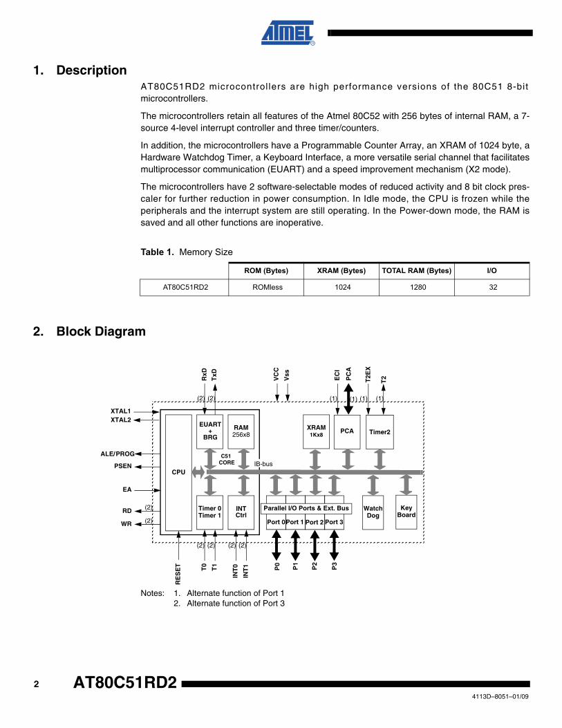
1. DescriptionAT80C51RD2 microcontrol lers are high performance versions of the 80C51 8-bitmicrocontrollers.
The microcontrollers retain all features of the Atmel 80C52 with 256 bytes of internal RAM, a 7-source 4-level interrupt controller and three timer/counters.
In addition, the microcontrollers have a Programmable Counter Array, an XRAM of 1024 byte, aHardware Watchdog Timer, a Keyboard Interface, a more versatile serial channel that facilitatesmultiprocessor communication (EUART) and a speed improvement mechanism (X2 mode).
The microcontrollers have 2 software-selectable modes of reduced activity and 8 bit clock pres-caler for further reduction in power consumption. In Idle mode, the CPU is frozen while theperipherals and the interrupt system are still operating. In the Power-down mode, the RAM issaved and all other functions are inoperative.
Table 1. Memory Size
2. Block Diagram
Notes: 1. Alternate function of Port 12. Alternate function of Port 3
ROM (Bytes) XRAM (Bytes) TOTAL RAM (Bytes) I/O
AT80C51RD2 ROMless 1024 1280 32
Timer 0 INT
RAM256x8
T0
T1
RxD
TxD
WR
RD
EA
PSEN
ALE/
XTAL2XTAL1
EUART
CPU
Timer 1
INT
1
Ctrl
INT
0
(2)
(2)
C51 CORE
(2) (2) (2) (2)
Port 0
P0
Port 1 Port 2 Port 3
Parallel I/O Ports & Ext. Bus
P1
P2
P3
XRAM1Kx8
IB-bus
PCA
RE
SE
T
PROG
WatchDog
PC
A
EC
I
Vss
VC
C
(2)(2) (1)(1)
Timer2
T2E
X
T2
(1) (1)
KeyBoard
+BRG
24113D–8051–01/09
AT80C51RD2
AT80C51RD2
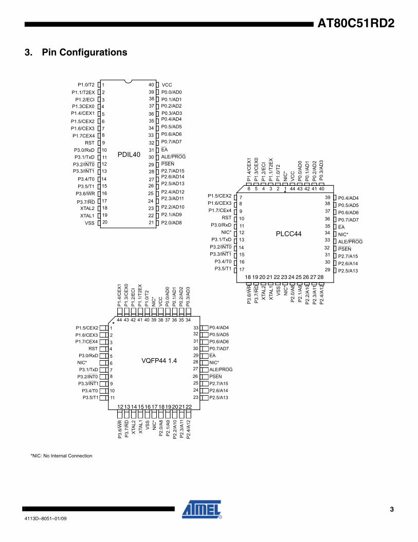
3. Pin Configurations
P1.7CEX4
P1.4/CEX1
RSTP3.0/RxDP3.1/TxD
P1.3CEX0
1
P1.5/CEX2P1.6/CEX3
P3.2/INT0P3.3/INT1
P3.4/T0P3.5/T1
P3.6/WR
P3.7/RDXTAL2XTAL1
VSS P2.0/AD8
P2.1/AD9P2.2/AD10
P2.3/AD11P2.4/AD12
P0.4/AD4
P0.6/AD6P0.5/AD5
P0.7/AD7
ALE/PROGPSEN
EA
P2.7/AD15
P2.5/AD13P2.6/AD14
P1.0/T2
P1.2/ECIP1.1/T2EX
VCC P0.0/AD0 P0.1/AD1 P0.2/AD2 P0.3/AD3
PDIL40
2 3 4 56 78 9 10 1112 1314 15 16 17181920
40393837
3635343332
31 30292827
2625
24232221
43 42 41 40 3944 38 37 36 35 34
P1.
4/C
EX
1
P1.
0/T2
P1.
1/T2
EX
P1.
3/C
EX
0P
1.2/
EC
I
NIC
*V
CC
P0.
0/A
D0
P0.
2/A
D2
P0.
3/A
D3
P0.
1/A
D1
P0.4/AD4
P0.6/AD6P0.5/AD5
P0.7/AD7
ALE/PROGPSEN
EANIC*
P2.7/A15
P2.5/A13P2.6/A14
P1.5/CEX2P1.6/CEX3P1.7/CEX4
RSTP3.0/RxD
NIC*P3.1/TxD
P3.2/INT0P3.3/INT1
P3.4/T0P3.5/T1
P3.
6/W
RP
3.7/
RD
XTA
L2X
TAL1
VS
S
P2.
0/A
8P
2.1/
A9
P2.
2/A
10P
2.3/
A11
P2.
4/A
12
NIC
*
1213 17161514 201918 2122
3332 31 30 2928 2726 25 24 23
VQFP44 1.4
1 2
3 4 56 78 9 10 11
18 19 23222120 262524 27 28
5 4 3 2 1 6 44 43 42 41 40
P1.4
/CE
X1
P1.0
/T2
P1.1
/T2E
X
P1.3
/CE
X0P1
.2/E
CI
NIC
*VC
CP0
.0/A
D0
P0.2
/AD
2P0
.1/A
D1
P0.4/AD4
P0.6/AD6P0.5/AD5
P0.7/AD7
ALE/PROGPSEN
EANIC*
P2.7/A15
P2.5/A13P2.6/A14
P3.
6/W
RP3
.7/R
DX
TAL2
XTA
L1V
SS
P2.0
/A8
P2.1
/A9
P2.
2/A
10P
2.3/
A11
P2.
4/A
12
P1.5/CEX2P1.6/CEX3P1.7/CEx4
RSTP3.0/RxD
NIC*P3.1/TxD
P3.2/INT0P3.3/INT1
P3.4/T0P3.5/T1
P0.3
/AD
3
NIC
*
78 9 10 1112 1314 15 16 17
3938 37 36 3534 3332 31 30 29
PLCC44
*NIC: No Internal Connection
34113D–8051–01/09
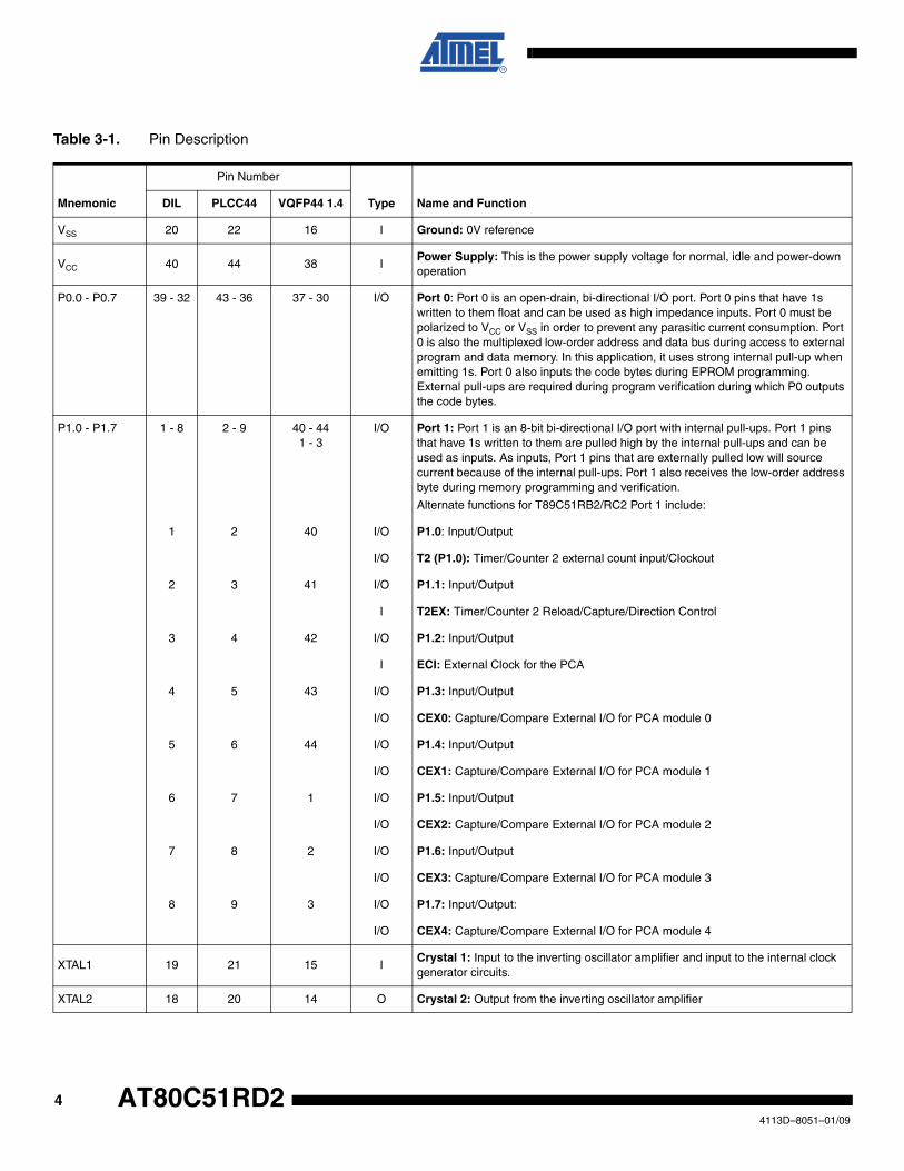
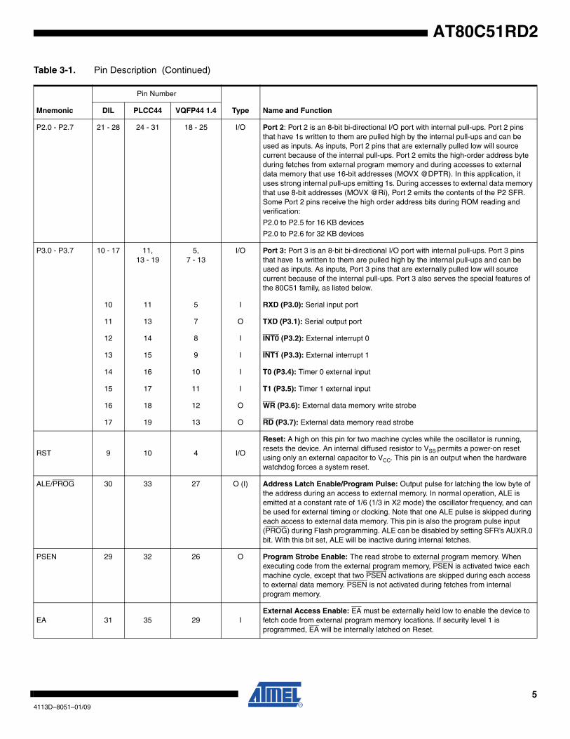
Table 3-1. Pin Description
Mnemonic
Pin Number
Type Name and FunctionDIL PLCC44 VQFP44 1.4
VSS 20 22 16 I Ground: 0V reference
VCC 40 44 38 IPower Supply: This is the power supply voltage for normal, idle and power-down operation
P0.0 - P0.7 39 - 32 43 - 36 37 - 30 I/O Port 0: Port 0 is an open-drain, bi-directional I/O port. Port 0 pins that have 1s written to them float and can be used as high impedance inputs. Port 0 must be polarized to VCC or VSS in order to prevent any parasitic current consumption. Port 0 is also the multiplexed low-order address and data bus during access to external program and data memory. In this application, it uses strong internal pull-up when emitting 1s. Port 0 also inputs the code bytes during EPROM programming. External pull-ups are required during program verification during which P0 outputs the code bytes.
P1.0 - P1.7 1 - 8 2 - 9 40 - 441 - 3
I/O Port 1: Port 1 is an 8-bit bi-directional I/O port with internal pull-ups. Port 1 pins that have 1s written to them are pulled high by the internal pull-ups and can be used as inputs. As inputs, Port 1 pins that are externally pulled low will source current because of the internal pull-ups. Port 1 also receives the low-order address byte during memory programming and verification.
Alternate functions for T89C51RB2/RC2 Port 1 include:
1 2 40 I/O P1.0: Input/Output
I/O T2 (P1.0): Timer/Counter 2 external count input/Clockout
2 3 41 I/O P1.1: Input/Output
I T2EX: Timer/Counter 2 Reload/Capture/Direction Control
3 4 42 I/O P1.2: Input/Output
I ECI: External Clock for the PCA
4 5 43 I/O P1.3: Input/Output
I/O CEX0: Capture/Compare External I/O for PCA module 0
5 6 44 I/O P1.4: Input/Output
I/O CEX1: Capture/Compare External I/O for PCA module 1
6 7 1 I/O P1.5: Input/Output
I/O CEX2: Capture/Compare External I/O for PCA module 2
7 8 2 I/O P1.6: Input/Output
I/O CEX3: Capture/Compare External I/O for PCA module 3
8 9 3 I/O P1.7: Input/Output:
I/O CEX4: Capture/Compare External I/O for PCA module 4
XTAL1 19 21 15 ICrystal 1: Input to the inverting oscillator amplifier and input to the internal clock generator circuits.
XTAL2 18 20 14 O Crystal 2: Output from the inverting oscillator amplifier
44113D–8051–01/09
AT80C51RD2
AT80C51RD2
P2.0 - P2.7 21 - 28 24 - 31 18 - 25 I/O Port 2: Port 2 is an 8-bit bi-directional I/O port with internal pull-ups. Port 2 pins that have 1s written to them are pulled high by the internal pull-ups and can be used as inputs. As inputs, Port 2 pins that are externally pulled low will source current because of the internal pull-ups. Port 2 emits the high-order address byte during fetches from external program memory and during accesses to external data memory that use 16-bit addresses (MOVX @DPTR). In this application, it uses strong internal pull-ups emitting 1s. During accesses to external data memory that use 8-bit addresses (MOVX @Ri), Port 2 emits the contents of the P2 SFR. Some Port 2 pins receive the high order address bits during ROM reading and verification:
P2.0 to P2.5 for 16 KB devices
P2.0 to P2.6 for 32 KB devices
P3.0 - P3.7 10 - 17 11,13 - 19
5,7 - 13
I/O Port 3: Port 3 is an 8-bit bi-directional I/O port with internal pull-ups. Port 3 pins that have 1s written to them are pulled high by the internal pull-ups and can be used as inputs. As inputs, Port 3 pins that are externally pulled low will source current because of the internal pull-ups. Port 3 also serves the special features of the 80C51 family, as listed below.
10 11 5 I RXD (P3.0): Serial input port
11 13 7 O TXD (P3.1): Serial output port
12 14 8 I INT0 (P3.2): External interrupt 0
13 15 9 I INT1 (P3.3): External interrupt 1
14 16 10 I T0 (P3.4): Timer 0 external input
15 17 11 I T1 (P3.5): Timer 1 external input
16 18 12 O WR (P3.6): External data memory write strobe
17 19 13 O RD (P3.7): External data memory read strobe
RST 9 10 4 I/O
Reset: A high on this pin for two machine cycles while the oscillator is running, resets the device. An internal diffused resistor to VSS permits a power-on reset using only an external capacitor to VCC. This pin is an output when the hardware watchdog forces a system reset.
ALE/PROG 30 33 27 O (I) Address Latch Enable/Program Pulse: Output pulse for latching the low byte of the address during an access to external memory. In normal operation, ALE is emitted at a constant rate of 1/6 (1/3 in X2 mode) the oscillator frequency, and can be used for external timing or clocking. Note that one ALE pulse is skipped during each access to external data memory. This pin is also the program pulse input (PROG) during Flash programming. ALE can be disabled by setting SFR’s AUXR.0 bit. With this bit set, ALE will be inactive during internal fetches.
PSEN 29 32 26 O Program Strobe Enable: The read strobe to external program memory. When executing code from the external program memory, PSEN is activated twice each machine cycle, except that two PSEN activations are skipped during each access to external data memory. PSEN is not activated during fetches from internal program memory.
EA 31 35 29 IExternal Access Enable: EA must be externally held low to enable the device to fetch code from external program memory locations. If security level 1 is programmed, EA will be internally latched on Reset.
Table 3-1. Pin Description (Continued)
Mnemonic
Pin Number
Type Name and FunctionDIL PLCC44 VQFP44 1.4
54113D–8051–01/09
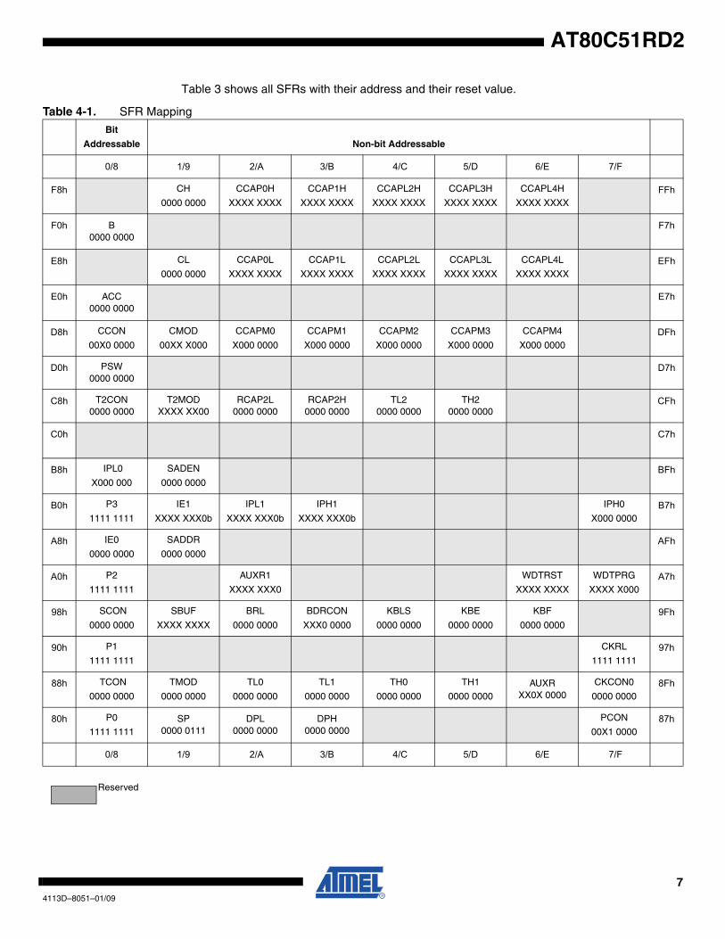
4. SFR MappingThe Special Function Registers (SFRs) of the microcontroller fall into the following categories:
• C51 core registers: ACC, B, DPH, DPL, PSW, SP
• I/O port registers: P0, P1, P2, P3
• Timer registers: T2CON, T2MOD, TCON, TH0, TH1, TH2, TMOD, TL0, TL1, TL2, RCAP2L, RCAP2H
• Serial I/O port registers: SADDR, SADEN, SBUF, SCON
• PCA (Programmable Counter Array) registers: CCON, CCAPMx, CL, CH, CCAPxH, CCAPxL (x: 0 to 4)
• Power and clock control registers: PCON
• Hardware Watchdog Timer registers: WDTRST, WDTPRG
• Interrupt system registers: IE0, IPL0, IPH0, IE1, IPL1, IPH1
• Keyboard Interface registers: KBE, KBF, KBLS
• BRG (Baud Rate Generator) registers: BRL, BDRCON
• Clock Prescaler register: CKRL
• Others: AUXR, AUXR1, CKCON0, CKCON1
64113D–8051–01/09
AT80C51RD2
AT80C51RD2
Table 3 shows all SFRs with their address and their reset value.
Table 4-1. SFR Mapping
Bit
Addressable Non-bit Addressable
0/8 1/9 2/A 3/B 4/C 5/D 6/E 7/F
F8h CH
0000 0000
CCAP0H
XXXX XXXX
CCAP1H
XXXX XXXX
CCAPL2H
XXXX XXXX
CCAPL3H
XXXX XXXX
CCAPL4H
XXXX XXXXFFh
F0h B0000 0000
F7h
E8h CL
0000 0000
CCAP0L
XXXX XXXX
CCAP1L
XXXX XXXX
CCAPL2L
XXXX XXXX
CCAPL3L
XXXX XXXX
CCAPL4L
XXXX XXXXEFh
E0h ACC0000 0000
E7h
D8h CCON
00X0 0000
CMOD
00XX X000
CCAPM0
X000 0000
CCAPM1
X000 0000
CCAPM2
X000 0000
CCAPM3
X000 0000
CCAPM4
X000 0000DFh
D0h PSW0000 0000
D7h
C8h T2CON0000 0000
T2MODXXXX XX00
RCAP2L0000 0000
RCAP2H0000 0000
TL20000 0000
TH20000 0000
CFh
C0h C7h
B8h IPL0
X000 000
SADEN
0000 0000BFh
B0h P3
1111 1111
IE1
XXXX XXX0b
IPL1
XXXX XXX0b
IPH1
XXXX XXX0b
IPH0
X000 0000B7h
A8h IE0
0000 0000
SADDR
0000 0000AFh
A0h P2
1111 1111
AUXR1
XXXX XXX0
WDTRST
XXXX XXXX
WDTPRG
XXXX X000A7h
98h SCON
0000 0000
SBUF
XXXX XXXX
BRL
0000 0000
BDRCON
XXX0 0000
KBLS
0000 0000
KBE
0000 0000
KBF
0000 00009Fh
90h P1
1111 1111
CKRL
1111 111197h
88h TCON
0000 0000
TMOD
0000 0000
TL0
0000 0000
TL1
0000 0000
TH0
0000 0000
TH1
0000 0000AUXR
XX0X 0000CKCON0
0000 00008Fh
80h P0
1111 1111SP
0000 0111DPL
0000 0000DPH
0000 0000PCON
00X1 000087h
0/8 1/9 2/A 3/B 4/C 5/D 6/E 7/F
Reserved
74113D–8051–01/09
84113D–8051–01/09
AT80C51RD2
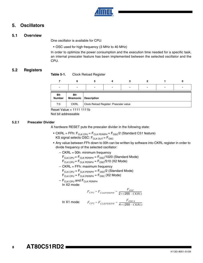
5. Oscillators
5.1 Overview One oscillator is available for CPU:
• OSC used for high frequency (3 MHz to 40 MHz)
In order to optimize the power consumption and the execution time needed for a specific task,an internal prescaler feature has been implemented between the selected oscillator and theCPU.
5.2 RegistersTable 5-1. Clock Reload Register
Reset Value = 1111 1111bNot bit addressable
5.2.1 Prescaler DividerA hardware RESET puts the prescaler divider in the following state:
• CKRL = FFh: FCLK CPU = FCLK PERIPH = FOSC/2 (Standard C51 feature)KS signal selects OSC: FCLK OUT = FOSC
• Any value between FFh down to 00h can be written by software into CKRL register in order to divide frequency of the selected oscillator:
– CKRL = 00h: minimum frequency FCLK CPU = FCLK PERIPH = FOSC/1020 (Standard Mode) FCLK CPU = FCLK PERIPH = FOSC/510 (X2 Mode)
– CKRL = FFh: maximum frequencyFCLK CPU = FCLK PERIPH = FOSC/2 (Standard Mode) FCLK CPU = FCLK PERIPH = FOSC (X2 Mode)
– FCLK CPU and FCLK PERIPH
In X2 mode:
In X1 mode:
7 6 5 4 3 2 1 0
- - - - - - - -
Bit Number
Bit Mnemonic Description
7:0 CKRL Clock Reload Register: Prescaler value
FCPU F= CLKPERIPHFOSC
2 255 CKRL–( )×----------------------------------------------=
FCPU F= CLKPERIPHFOSCA
4 255 CKRL–( )×----------------------------------------------=
AT80C51RD2
6. Enhanced FeaturesIn comparison to the original 80C52, the microcontrollers implement the following new features:
• X2 option
• Dual Data Pointer
• Extended RAM
• Programmable Counter Array (PCA)
• Hardware Watchdog
• 4-level Interrupt Priority System
• Power-off Flag
• Power On Reset
• ONCE mode
• ALE disabling
• Some enhanced features are also located in the UART and the Timer 2
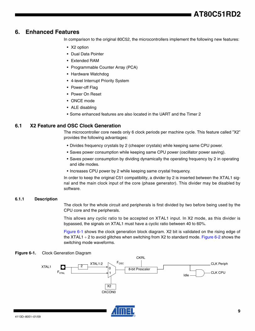
6.1 X2 Feature and OSC Clock GenerationThe microcontroller core needs only 6 clock periods per machine cycle. This feature called ”X2”provides the following advantages:
• Divides frequency crystals by 2 (cheaper crystals) while keeping same CPU power.
• Saves power consumption while keeping same CPU power (oscillator power saving).
• Saves power consumption by dividing dynamically the operating frequency by 2 in operating and idle modes.
• Increases CPU power by 2 while keeping same crystal frequency.
In order to keep the original C51 compatibility, a divider by 2 is inserted between the XTAL1 sig-nal and the main clock input of the core (phase generator). This divider may be disabled bysoftware.
6.1.1 DescriptionThe clock for the whole circuit and peripherals is first divided by two before being used by theCPU core and the peripherals.
This allows any cyclic ratio to be accepted on XTAL1 input. In X2 mode, as this divider isbypassed, the signals on XTAL1 must have a cyclic ratio between 40 to 60%.
Figure 6-1 shows the clock generation block diagram. X2 bit is validated on the rising edge ofthe XTAL1 ÷ 2 to avoid glitches when switching from X2 to standard mode. Figure 6-2 shows theswitching mode waveforms.
Figure 6-1. Clock Generation Diagram
XTAL1 2
CKCON0
X2
8-bit Prescaler
FOSC
FXTAL
01
XTAL1:2
CKRL
CLK Periph
CLK CPUIdle
94113D–8051–01/09
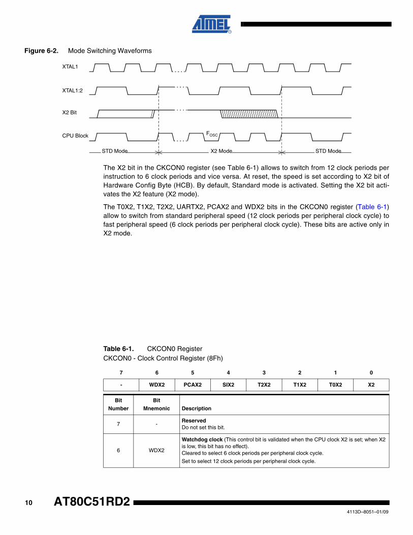
Figure 6-2. Mode Switching Waveforms
The X2 bit in the CKCON0 register (see Table 6-1) allows to switch from 12 clock periods perinstruction to 6 clock periods and vice versa. At reset, the speed is set according to X2 bit ofHardware Config Byte (HCB). By default, Standard mode is activated. Setting the X2 bit acti-vates the X2 feature (X2 mode).
The T0X2, T1X2, T2X2, UARTX2, PCAX2 and WDX2 bits in the CKCON0 register (Table 6-1)allow to switch from standard peripheral speed (12 clock periods per peripheral clock cycle) tofast peripheral speed (6 clock periods per peripheral clock cycle). These bits are active only inX2 mode.
Table 6-1. CKCON0 RegisterCKCON0 - Clock Control Register (8Fh)
XTAL1:2
CPU Block
X2 Bit
X2 ModeSTD Mode STD Mode
FOSC
XTAL1
7 6 5 4 3 2 1 0
- WDX2 PCAX2 SIX2 T2X2 T1X2 T0X2 X2
Bit
Number
Bit
Mnemonic Description
7 -ReservedDo not set this bit.
6 WDX2
Watchdog clock (This control bit is validated when the CPU clock X2 is set; when X2 is low, this bit has no effect).Cleared to select 6 clock periods per peripheral clock cycle.
Set to select 12 clock periods per peripheral clock cycle.
104113D–8051–01/09
AT80C51RD2
AT80C51RD2
Reset Value = 0000 000’HCB.X2’b (see Hardware Config Byte)Not bit addressable
5 PCAX2
Programmable Counter Array clock (This control bit is validated when the CPU clock X2 is set; when X2 is low, this bit has no effect).Cleared to select 6 clock periods per peripheral clock cycle.
Set to select 12 clock periods per peripheral clock cycle.
4 SIX2
Enhanced UART clock (Mode 0 and 2) (This control bit is validated when the CPU clock X2 is set; when X2 is low, this bit has no effect).Cleared to select 6 clock periods per peripheral clock cycle.
Set to select 12 clock periods per peripheral clock cycle.
3 T2X2
Timer 2 clock (This control bit is validated when the CPU clock X2 is set; when X2 is low, this bit has no effect).Cleared to select 6 clock periods per peripheral clock cycle.
Set to select 12 clock periods per peripheral clock cycle.
2 T1X2
Timer 1 clock (This control bit is validated when the CPU clock X2 is set; when X2 is low, this bit has no effect).Cleared to select 6 clock periods per peripheral clock cycle.
Set to select 12 clock periods per peripheral clock cycle
1 T0X2
Timer 0 clock (This control bit is validated when the CPU clock X2 is set; when X2 is low, this bit has no effect).Cleared to select 6 clock periods per peripheral clock cycle.
Set to select 12 clock periods per peripheral clock cycle
0 X2
CPU clock
Cleared to select 12 clock periods per machine cycle (STD mode) for CPU and all the peripherals.
Set to select 6clock periods per machine cycle (X2 mode) and to enable the individual peripherals "X2" bits.
Programmed by hardware after Power-up regarding Hardware Config Byte (HCB).
Bit
Number
Bit
Mnemonic Description
114113D–8051–01/09
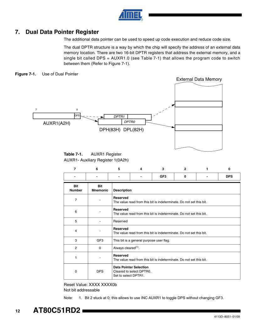
7. Dual Data Pointer RegisterThe additional data pointer can be used to speed up code execution and reduce code size.
The dual DPTR structure is a way by which the chip will specify the address of an external datamemory location. There are two 16-bit DPTR registers that address the external memory, and asingle bit called DPS = AUXR1.0 (see Table 7-1) that allows the program code to switchbetween them (Refer to Figure 7-1).
Figure 7-1. Use of Dual Pointer
Table 7-1. AUXR1 RegisterAUXR1- Auxiliary Register 1(0A2h)
Reset Value: XXXX XXXX0bNot bit addressable
Note: 1. Bit 2 stuck at 0; this allows to use INC AUXR1 to toggle DPS without changing GF3.
External Data Memory
AUXR1(A2H)
DPS
DPH(83H) DPL(82H)
07
DPTR0
DPTR1
7 6 5 4 3 2 1 0
- - - - GF3 0 - DPS
Bit Number
Bit Mnemonic Description
7 -ReservedThe value read from this bit is indeterminate. Do not set this bit.
6 -ReservedThe value read from this bit is indeterminate. Do not set this bit.
5 - Reserved
4 -ReservedThe value read from this bit is indeterminate. Do not set this bit.
3 GF3 This bit is a general purpose user flag.
2 0 Always cleared(1).
1 -ReservedThe value read from this bit is indeterminate. Do not set this bit.
0 DPSData Pointer SelectionCleared to select DPTR0.Set to select DPTR1.
124113D–8051–01/09
AT80C51RD2
AT80C51RD2
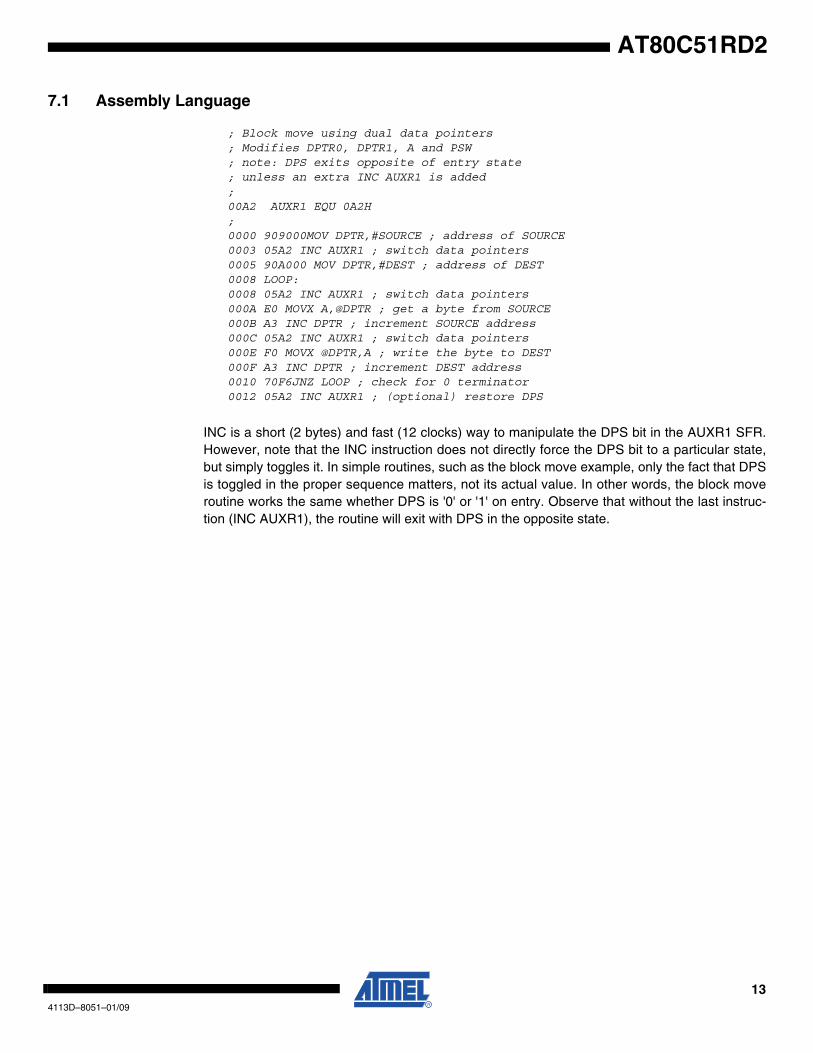
7.1 Assembly Language
; Block move using dual data pointers ; Modifies DPTR0, DPTR1, A and PSW ; note: DPS exits opposite of entry state ; unless an extra INC AUXR1 is added ; 00A2 AUXR1 EQU 0A2H ; 0000 909000MOV DPTR,#SOURCE ; address of SOURCE 0003 05A2 INC AUXR1 ; switch data pointers 0005 90A000 MOV DPTR,#DEST ; address of DEST 0008 LOOP: 0008 05A2 INC AUXR1 ; switch data pointers 000A E0 MOVX A,@DPTR ; get a byte from SOURCE 000B A3 INC DPTR ; increment SOURCE address 000C 05A2 INC AUXR1 ; switch data pointers 000E F0 MOVX @DPTR,A ; write the byte to DEST 000F A3 INC DPTR ; increment DEST address 0010 70F6JNZ LOOP ; check for 0 terminator 0012 05A2 INC AUXR1 ; (optional) restore DPS
INC is a short (2 bytes) and fast (12 clocks) way to manipulate the DPS bit in the AUXR1 SFR.However, note that the INC instruction does not directly force the DPS bit to a particular state,but simply toggles it. In simple routines, such as the block move example, only the fact that DPSis toggled in the proper sequence matters, not its actual value. In other words, the block moveroutine works the same whether DPS is '0' or '1' on entry. Observe that without the last instruc-tion (INC AUXR1), the routine will exit with DPS in the opposite state.
134113D–8051–01/09
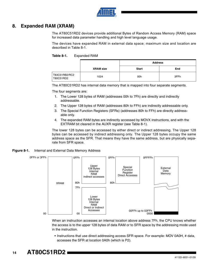
8. Expanded RAM (XRAM)The AT80C51RD2 devices provide additional Bytes of Random Access Memory (RAM) spacefor increased data parameter handling and high level language usage.
The devices have expanded RAM in external data space; maximum size and location aredescribed in Table 8-1.
Table 8-1. Expanded RAM
The AT80C51RD2 has internal data memory that is mapped into four separate segments.
The four segments are: 1. The Lower 128 bytes of RAM (addresses 00h to 7Fh) are directly and indirectly
addressable.
2. The Upper 128 bytes of RAM (addresses 80h to FFh) are indirectly addressable only.
3. The Special Function Registers (SFRs) (addresses 80h to FFh) are directly address-able only.
4. The expanded RAM bytes are indirectly accessed by MOVX instructions, and with the EXTRAM bit cleared in the AUXR register (see Table 8-1).
The lower 128 bytes can be accessed by either direct or indirect addressing. The Upper 128bytes can be accessed by indirect addressing only. The Upper 128 bytes occupy the sameaddress space as the SFR. That means they have the same address, but are physically sepa-rate from SFR space.
Figure 8-1. Internal and External Data Memory Address
When an instruction accesses an internal location above address 7Fh, the CPU knows whetherthe access is to the upper 128 bytes of data RAM or to SFR space by the addressing mode usedin the instruction.
• Instructions that use direct addressing access SFR space. For example: MOV 0A0H, # data, accesses the SFR at location 0A0h (which is P2).
XRAM size
Address
Start End
T83C51RB2/RC2 T80C51RD2
1024 00h 3FFh
XRAM
Upper128 Bytes
InternalRAM
Lower128 Bytes
InternalRAM
SpecialFunctionRegister
80h 80h
00
0FFh or 3FFh 0FFh
00
0FFh
ExternalData
Memory
000000FFh up to 03FFh
0FFFFh
indirect accesses Direct Accesses
Direct or IndirectAccesses
7Fh
144113D–8051–01/09
AT80C51RD2
AT80C51RD2
• Instructions that use indirect addressing access the Upper 128 bytes of data RAM. For example: MOV @R0, # data where R0 contains 0A0h, accesses the data byte at address 0A0h, rather than P2 (whose address is 0A0h).
• The XRAM bytes can be accessed by indirect addressing, with EXTRAM bit cleared and MOVX instructions. This part of memory which is physically located on-chip, logically occupies the first bytes of external data memory. The bits XRS0 and XRS1 are used to hide a part of the available XRAM as explained in Table 8-1. This can be useful if external peripherals are mapped at addresses already used by the internal XRAM.
• With EXTRAM = 0, the XRAM is indirectly addressed, using the MOVX instruction in combination with any of the registers R0, R1 of the selected bank or DPTR. An access to XRAM will not affect ports P0, P2, P3.6 (WR) and P3.7 (RD). For example, with EXTRAM = 0, MOVX @R0, # data where R0 contains 0A0H, accesses the XRAM at address 0A0H rather than external memory. An access to external data memory locations higher than the accessible size of the XRAM will be performed with the MOVX DPTR instructions in the same way as in the standard 80C51, with P0 and P2 as data/address busses, and P3.6 and P3.7 as write and read timing signals. Accesses to XRAM above 0FFH can only be done by the use of DPTR.
• With EXTRAM = 1, MOVX @Ri and MOVX @DPTR will be similar to the standard 80C51. MOVX @ Ri will provide an eight-bit address multiplexed with data on Port 0 and any output port pins can be used to output higher order address bits. This is to provide the external paging capability. MOVX @DPTR will generate a sixteen-bit address. Port2 outputs the high-order eight address bits (the contents of DPH) while Port0 multiplexes the low-order eight address bits (DPL) with data. MOVX @ Ri and MOVX @DPTR will generate either read or write signals on P3.6 (WR) and P3.7 (RD).
The stack pointer (SP) may be located anywhere in the 256 bytes RAM (lower and upper RAM)internal data memory. The stack may not be located in the XRAM.
The M0 bit allows to stretch the XRAM timings; if M0 is set, the read and write pulses areextended from 6 to 30 clock periods. This is useful to access external slow peripherals.
Table 8-2. AUXR RegisterAUXR - Auxiliary Register (8Eh)
7 6 5 4 3 2 1 0
- - M0 - XRS1 XRS0 EXTRAM AO
Bit
Number
Bit
Mnemonic Description
7 -Reserved
The value read from this bit is indeterminate. Do not set this bit
6 -Reserved
The value read from this bit is indeterminate. Do not set this bit
5 M0
Pulse length
Cleared to stretch MOVX control: the RD and the WR pulse length is 6 clock periods (default).
Set to stretch MOVX control: the RD and the WR pulse length is 30 clock periods.
4 -Reserved
The value read from this bit is indeterminate. Do not set this bit
154113D–8051–01/09
Reset Value = XX0X 00’HSB.XRAM’0b (see Table 8-1)Not bit addressable
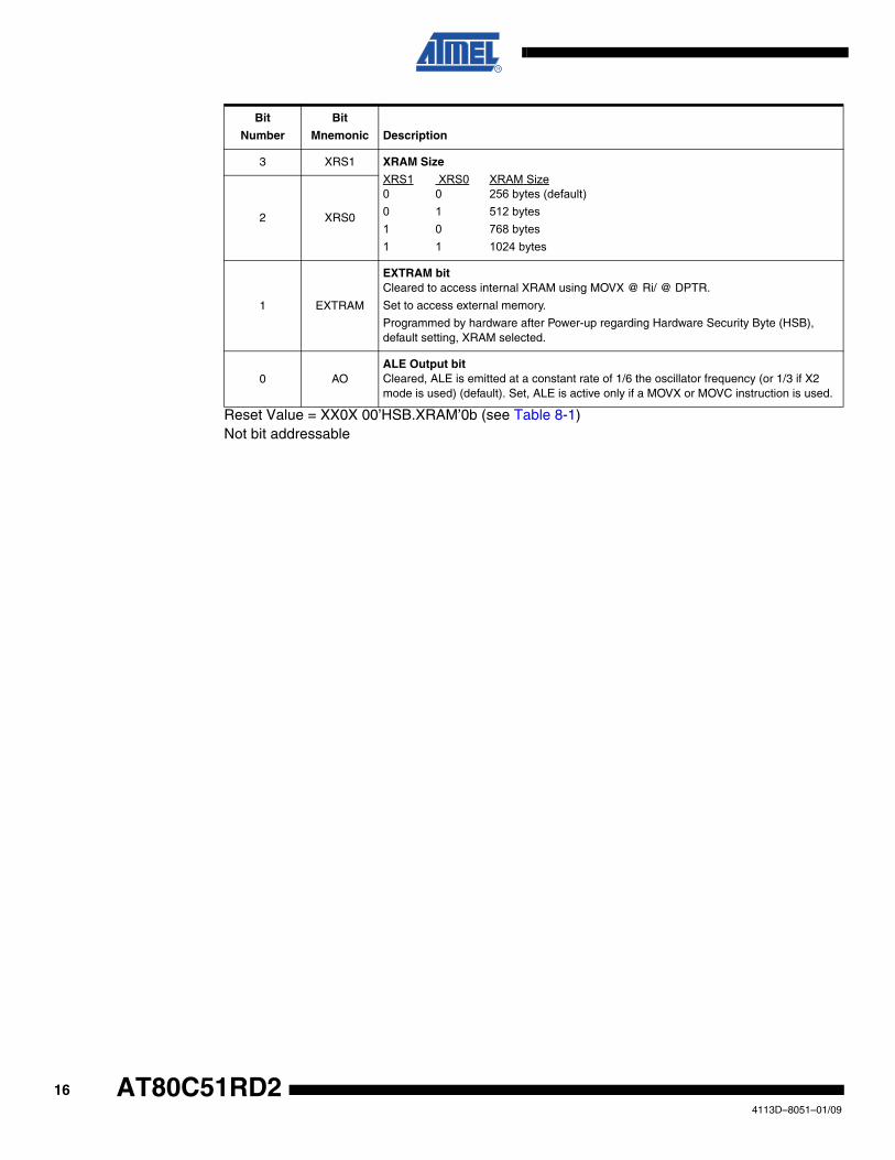
3 XRS1 XRAM Size
XRS1 XRS0 XRAM Size0 0 256 bytes (default)0 1 512 bytes1 0 768 bytes1 1 1024 bytes
2 XRS0
1 EXTRAM
EXTRAM bitCleared to access internal XRAM using MOVX @ Ri/ @ DPTR.
Set to access external memory.
Programmed by hardware after Power-up regarding Hardware Security Byte (HSB), default setting, XRAM selected.
0 AOALE Output bitCleared, ALE is emitted at a constant rate of 1/6 the oscillator frequency (or 1/3 if X2 mode is used) (default). Set, ALE is active only if a MOVX or MOVC instruction is used.
Bit
Number
Bit
Mnemonic Description
164113D–8051–01/09
AT80C51RD2
AT80C51RD2
9. Timer 2The Timer 2 in the AT80C51RD2 is the standard C52 Timer 2. It is a 16-bit timer/counter: the count is maintained by two eight-bit timer registers, TH2 and TL2are cascaded. It is controlled by T2CON (Table 9-1) and T2MOD (Table 9-2) registers. Timer 2operation is similar to Timer 0 and Timer 1. C/T2 selects FOSC/12 (timer operation) or externalpin T2 (counter operation) as the timer clock input. Setting TR2 allows TL2 to be incremented bythe selected input.
Timer 2 has 3 operating modes: capture, auto-reload and Baud Rate Generator. These modesare selected by the combination of RCLK, TCLK and CP/RL2 (T2CON).
Refer to the Atmel 8-bit Microcontroller Hardware description for Capture and Baud Rate Gen-erator Modes.
Timer 2 includes the following enhancements:
• Auto-reload mode with up or down counter
• Programmable clock-output
9.1 Auto-reload ModeThe auto-reload mode configures Timer 2 as a 16-bit timer or event counter with automaticreload. If DCEN bit in T2MOD is cleared, Timer 2 behaves as in 80C52 (refer to the Atmel 8-bitMicrocontroller Hardware description). If DCEN bit is set, Timer 2 acts as an Up/downtimer/counter as shown in Figure 9-1. In this mode the T2EX pin controls the direction of count.
When T2EX is high, Timer 2 counts up. Timer overflow occurs at FFFFh which sets the TF2 flagand generates an interrupt request. The overflow also causes the 16-bit value in RCAP2H andRCAP2L registers to be loaded into the timer registers TH2 and TL2.
When T2EX is low, Timer 2 counts down. Timer underflow occurs when the count in the timerregisters TH2 and TL2 equals the value stored in RCAP2H and RCAP2L registers. The under-flow sets TF2 flag and reloads FFFFh into the timer registers.
The EXF2 bit toggles when Timer 2 overflows or underflows according to the direction of thecount. EXF2 does not generate any interrupt. This bit can be used to provide 17-bit resolution.
174113D–8051–01/09
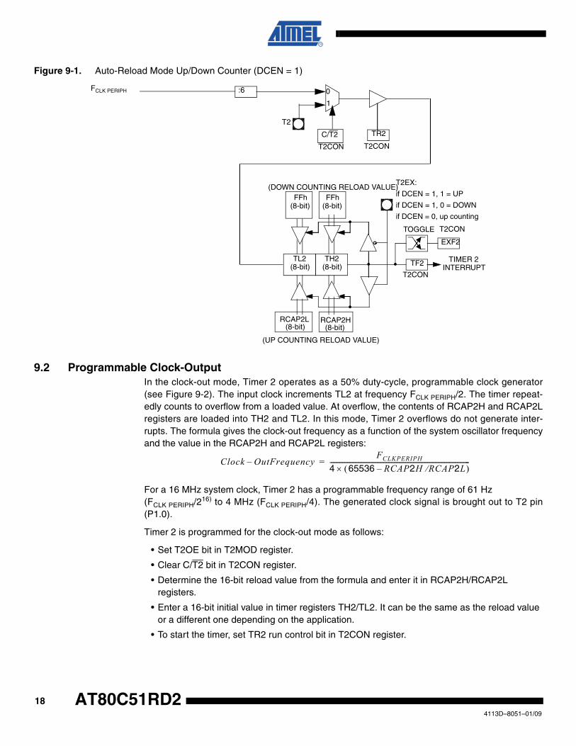
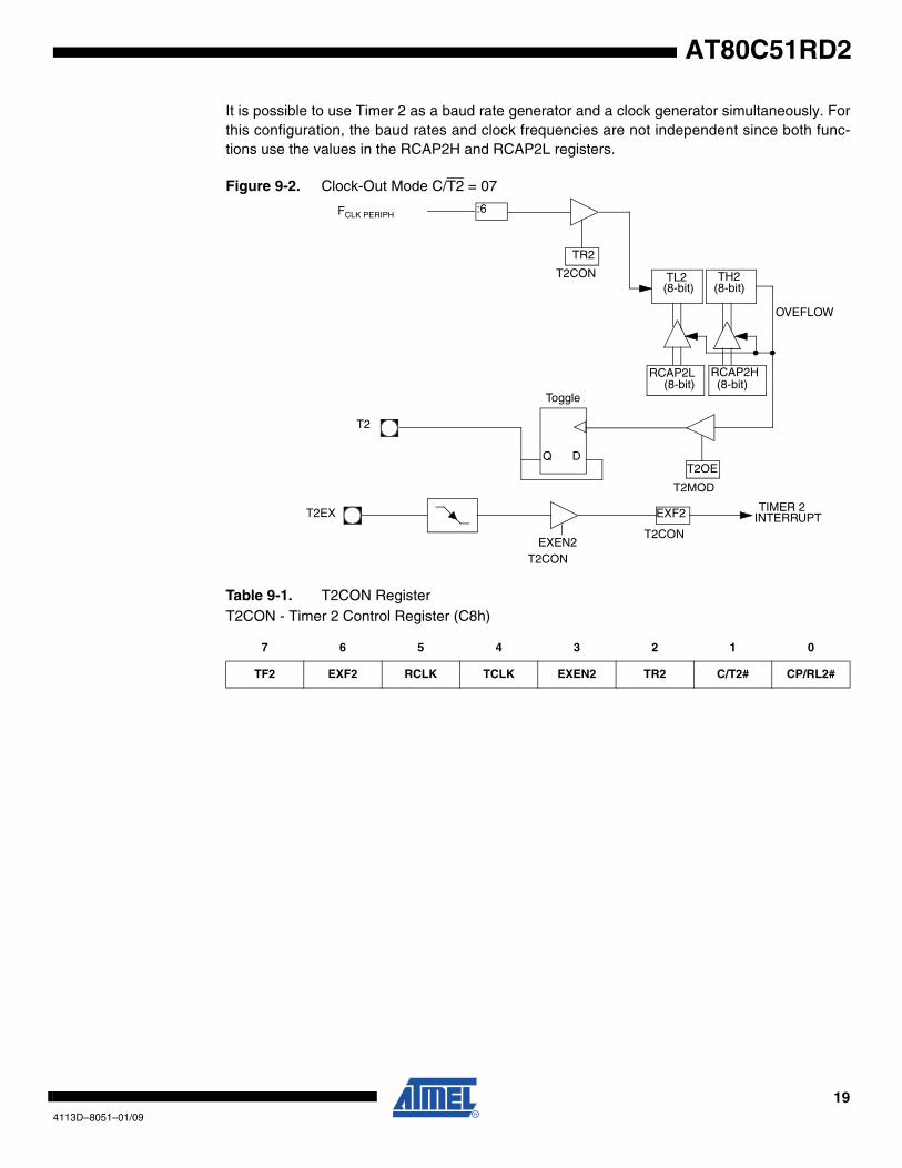
Figure 9-1. Auto-Reload Mode Up/Down Counter (DCEN = 1)
9.2 Programmable Clock-OutputIn the clock-out mode, Timer 2 operates as a 50% duty-cycle, programmable clock generator(see Figure 9-2). The input clock increments TL2 at frequency FCLK PERIPH/2. The timer repeat-edly counts to overflow from a loaded value. At overflow, the contents of RCAP2H and RCAP2Lregisters are loaded into TH2 and TL2. In this mode, Timer 2 overflows do not generate inter-rupts. The formula gives the clock-out frequency as a function of the system oscillator frequencyand the value in the RCAP2H and RCAP2L registers:
For a 16 MHz system clock, Timer 2 has a programmable frequency range of 61 Hz (FCLK PERIPH/216) to 4 MHz (FCLK PERIPH/4). The generated clock signal is brought out to T2 pin(P1.0).
Timer 2 is programmed for the clock-out mode as follows:
• Set T2OE bit in T2MOD register.
• Clear C/T2 bit in T2CON register.
• Determine the 16-bit reload value from the formula and enter it in RCAP2H/RCAP2L registers.
• Enter a 16-bit initial value in timer registers TH2/TL2. It can be the same as the reload value or a different one depending on the application.
• To start the timer, set TR2 run control bit in T2CON register.
(DOWN COUNTING RELOAD VALUE)
C/T2
TF2
TR2
T2
EXF2
TH2(8-bit)
TL2(8-bit)
RCAP2H(8-bit)
RCAP2L(8-bit)
FFh(8-bit)
FFh(8-bit)
TOGGLE
(UP COUNTING RELOAD VALUE)
TIMER 2INTERRUPT
FCLK PERIPH 0
1
T2CON T2CON
T2CON
T2CON
T2EX:
if DCEN = 1, 1 = UP
if DCEN = 1, 0 = DOWN
if DCEN = 0, up counting
:6
Clock OutFrequency–FCLKPERIPH
4 65536 RCAP2H– RCAP2L⁄( )×-----------------------------------------------------------------------------------------=
184113D–8051–01/09
AT80C51RD2
AT80C51RD2
It is possible to use Timer 2 as a baud rate generator and a clock generator simultaneously. Forthis configuration, the baud rates and clock frequencies are not independent since both func-tions use the values in the RCAP2H and RCAP2L registers.
Figure 9-2. Clock-Out Mode C/T2 = 07
Table 9-1. T2CON RegisterT2CON - Timer 2 Control Register (C8h)
7 6 5 4 3 2 1 0
TF2 EXF2 RCLK TCLK EXEN2 TR2 C/T2# CP/RL2#
:6
EXF2
TR2
OVEFLOW
T2EX
TH2(8-bit)
TL2(8-bit)
TIMER 2
RCAP2H(8-bit)
RCAP2L(8-bit)
T2OE
T2
FCLK PERIPH
T2CON
T2CON
T2CON
T2MOD
INTERRUPT
Q D
Toggle
EXEN2
194113D–8051–01/09
Reset Value = 0000 0000bBit addressable
Bit
Number
Bit
Mnemonic Description
7 TF2Timer 2 overflow FlagMust be cleared by software.Set by hardware on Timer 2 overflow, if RCLK = 0 and TCLK = 0.
6 EXF2
Timer 2 External FlagSet when a capture or a reload is caused by a negative transition on T2EX pin if EXEN2 = 1.When set, causes the CPU to vector to Timer 2 interrupt routine when Timer 2 interrupt is enabled.Must be cleared by software. EXF2 doesn’t cause an interrupt in Up/down counter mode (DCEN = 1)
5 RCLKReceive Clock bitCleared to use timer 1 overflow as receive clock for serial port in mode 1 or 3.Set to use Timer 2 overflow as receive clock for serial port in mode 1 or 3.
4 TCLKTransmit Clock bitCleared to use timer 1 overflow as transmit clock for serial port in mode 1 or 3.Set to use Timer 2 overflow as transmit clock for serial port in mode 1 or 3.
3 EXEN2
Timer 2 External Enable bitCleared to ignore events on T2EX pin for Timer 2 operation.Set to cause a capture or reload when a negative transition on T2EX pin is detected, if Timer 2 is not used to clock the serial port.
2 TR2Timer 2 Run control bitCleared to turn off Timer 2.Set to turn on Timer 2.
1 C/T2#
Timer/Counter 2 select bitCleared for timer operation (input from internal clock system: FCLK PERIPH).Set for counter operation (input from T2 input pin, falling edge trigger). Must be 0 for clock out mode.
0 CP/RL2#
Timer 2 Capture/Reload bitIf RCLK = 1 or TCLK = 1, CP/RL2# is ignored and timer is forced to auto-reload on Timer 2 overflow.Cleared to auto-reload on Timer 2 overflows or negative transitions on T2EX pin if EXEN2 = 1.Set to capture on negative transitions on T2EX pin if EXEN2 = 1.
204113D–8051–01/09
AT80C51RD2
AT80C51RD2
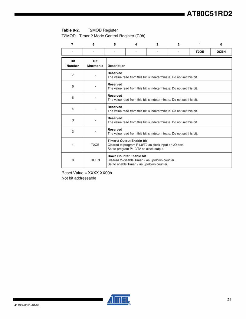
Table 9-2. T2MOD RegisterT2MOD - Timer 2 Mode Control Register (C9h)
Reset Value = XXXX XX00bNot bit addressable
7 6 5 4 3 2 1 0
- - - - - - T2OE DCEN
Bit
Number
Bit
Mnemonic Description
7 -ReservedThe value read from this bit is indeterminate. Do not set this bit.
6 -ReservedThe value read from this bit is indeterminate. Do not set this bit.
5 -ReservedThe value read from this bit is indeterminate. Do not set this bit.
4 -ReservedThe value read from this bit is indeterminate. Do not set this bit.
3 -ReservedThe value read from this bit is indeterminate. Do not set this bit.
2 -ReservedThe value read from this bit is indeterminate. Do not set this bit.
1 T2OETimer 2 Output Enable bitCleared to program P1.0/T2 as clock input or I/O port.Set to program P1.0/T2 as clock output.
0 DCENDown Counter Enable bitCleared to disable Timer 2 as up/down counter.Set to enable Timer 2 as up/down counter.
214113D–8051–01/09
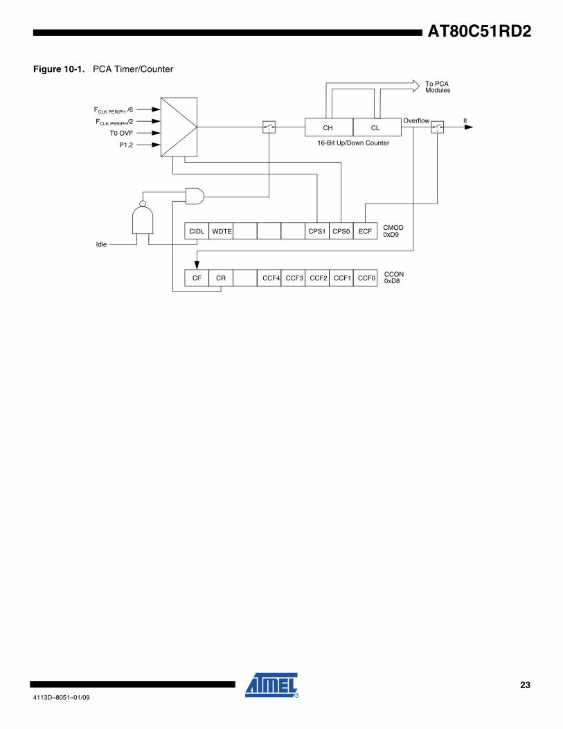
10. Programmable Counter Array (PCA)The PCA provides more timing capabilities with less CPU intervention than the standardtimer/counters. Its advantages include reduced software overhead and improved accuracy. ThePCA consists of a dedicated timer/counter which serves as the time base for an array of fivecompare/capture modules. Its clock input can be programmed to count any one of the followingsignals:
• Peripheral clock frequency (FCLK PERIPH) ÷ 6
• Peripheral clock frequency (FCLK PERIPH) ÷ 2
• Timer 0 overflow
• External input on ECI (P1.2)
Each compare/capture modules can be programmed in any one of the following modes:
• Rising and/or falling edge capture
• Software timer
• High-speed output
• Pulse width modulator
Module 4 can also be programmed as a Watchdog Timer (see Section "PCA Watchdog Timer",page 33).
When the compare/capture modules are programmed in the capture mode, software timer, orhigh-speed output mode, an interrupt can be generated when the module executes its function.All five modules plus the PCA timer overflow share one interrupt vector.
The PCA timer/counter and compare/capture modules share Port 1 for external I/O. These pinsare listed below. If the port is not used for the PCA, it can still be used for standard I/O.
The PCA timer is a common time base for all five modules (see Figure 10-1). The timer countsource is determined from the CPS1 and CPS0 bits in the CMOD register (Table 10-1) and canbe programmed to run at:
• 1/6 the peripheral clock frequency (FCLK PERIPH)
• 1/2 the peripheral clock frequency (FCLK PERIPH)
• The Timer 0 overflow
• The input on the ECI pin (P1.2)
PCA Component External I/O Pin
16-bit Counter P1.2/ECI
16-bit Module 0 P1.3/CEX0
16-bit Module 1 P1.4/CEX1
16-bit Module 2 P1.5/CEX2
16-bit Module 3 P1.6/CEX3
224113D–8051–01/09
AT80C51RD2
AT80C51RD2
Figure 10-1. PCA Timer/Counter
CIDL CPS1 CPS0 ECF
ItCH CL
16-Bit Up/Down Counter
To PCAModules
FCLK PERIPH /6
FCLK PERIPH/2
T0 OVF
P1.2
Idle
CMOD0xD9WDTE
CF CR CCON0xD8CCF4 CCF3 CCF2 CCF1 CCF0
Overflow
234113D–8051–01/09
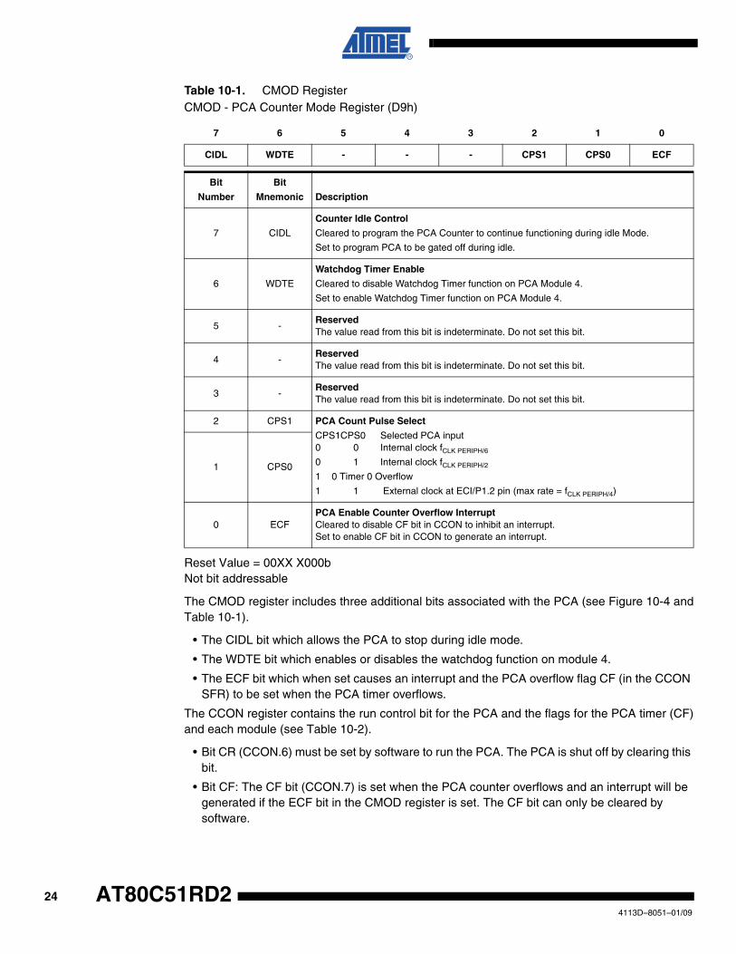
Table 10-1. CMOD RegisterCMOD - PCA Counter Mode Register (D9h)
Reset Value = 00XX X000bNot bit addressable
The CMOD register includes three additional bits associated with the PCA (see Figure 10-4 andTable 10-1).
• The CIDL bit which allows the PCA to stop during idle mode.
• The WDTE bit which enables or disables the watchdog function on module 4.
• The ECF bit which when set causes an interrupt and the PCA overflow flag CF (in the CCON SFR) to be set when the PCA timer overflows.
The CCON register contains the run control bit for the PCA and the flags for the PCA timer (CF)and each module (see Table 10-2).
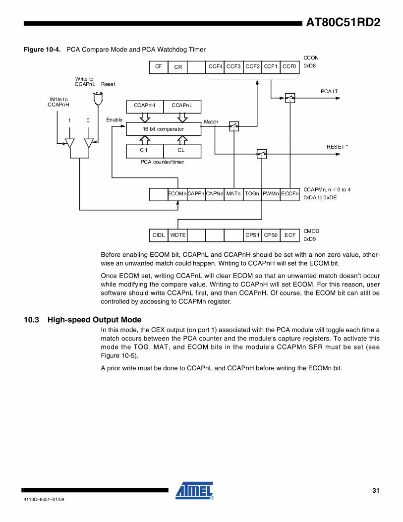
• Bit CR (CCON.6) must be set by software to run the PCA. The PCA is shut off by clearing this bit.
• Bit CF: The CF bit (CCON.7) is set when the PCA counter overflows and an interrupt will be generated if the ECF bit in the CMOD register is set. The CF bit can only be cleared by software.
7 6 5 4 3 2 1 0
CIDL WDTE - - - CPS1 CPS0 ECF
Bit
Number
Bit
Mnemonic Description
7 CIDL
Counter Idle Control
Cleared to program the PCA Counter to continue functioning during idle Mode.
Set to program PCA to be gated off during idle.
6 WDTE
Watchdog Timer Enable
Cleared to disable Watchdog Timer function on PCA Module 4.
Set to enable Watchdog Timer function on PCA Module 4.
5 -ReservedThe value read from this bit is indeterminate. Do not set this bit.
4 -ReservedThe value read from this bit is indeterminate. Do not set this bit.
3 -ReservedThe value read from this bit is indeterminate. Do not set this bit.
2 CPS1 PCA Count Pulse Select
CPS1CPS0 Selected PCA input0 0 Internal clock fCLK PERIPH/6
0 1 Internal clock fCLK PERIPH/2
1 0 Timer 0 Overflow
1 1 External clock at ECI/P1.2 pin (max rate = fCLK PERIPH/4)
1 CPS0
0 ECFPCA Enable Counter Overflow InterruptCleared to disable CF bit in CCON to inhibit an interrupt.Set to enable CF bit in CCON to generate an interrupt.
244113D–8051–01/09
AT80C51RD2
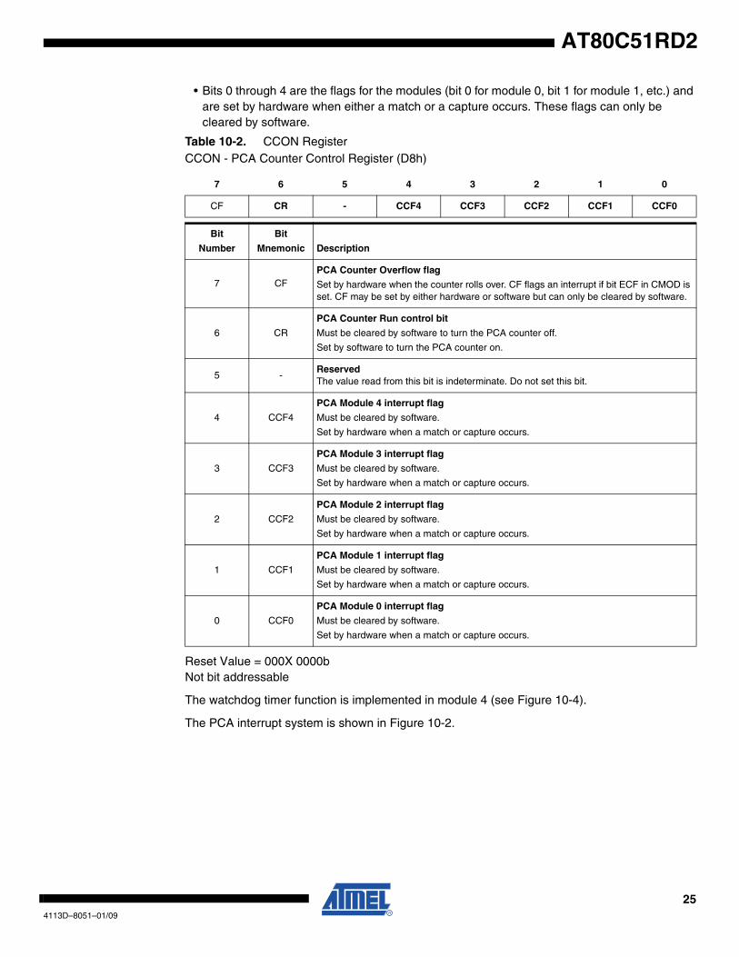
AT80C51RD2
• Bits 0 through 4 are the flags for the modules (bit 0 for module 0, bit 1 for module 1, etc.) and are set by hardware when either a match or a capture occurs. These flags can only be cleared by software.
Table 10-2. CCON RegisterCCON - PCA Counter Control Register (D8h)
Reset Value = 000X 0000bNot bit addressable
The watchdog timer function is implemented in module 4 (see Figure 10-4).
The PCA interrupt system is shown in Figure 10-2.
7 6 5 4 3 2 1 0
CF CR - CCF4 CCF3 CCF2 CCF1 CCF0
Bit
Number
Bit
Mnemonic Description
7 CFPCA Counter Overflow flag
Set by hardware when the counter rolls over. CF flags an interrupt if bit ECF in CMOD is set. CF may be set by either hardware or software but can only be cleared by software.
6 CR
PCA Counter Run control bit
Must be cleared by software to turn the PCA counter off.
Set by software to turn the PCA counter on.
5 -ReservedThe value read from this bit is indeterminate. Do not set this bit.
4 CCF4
PCA Module 4 interrupt flag
Must be cleared by software.
Set by hardware when a match or capture occurs.
3 CCF3
PCA Module 3 interrupt flag
Must be cleared by software.
Set by hardware when a match or capture occurs.
2 CCF2
PCA Module 2 interrupt flag
Must be cleared by software.
Set by hardware when a match or capture occurs.
1 CCF1
PCA Module 1 interrupt flag
Must be cleared by software.
Set by hardware when a match or capture occurs.
0 CCF0
PCA Module 0 interrupt flag
Must be cleared by software.
Set by hardware when a match or capture occurs.
254113D–8051–01/09
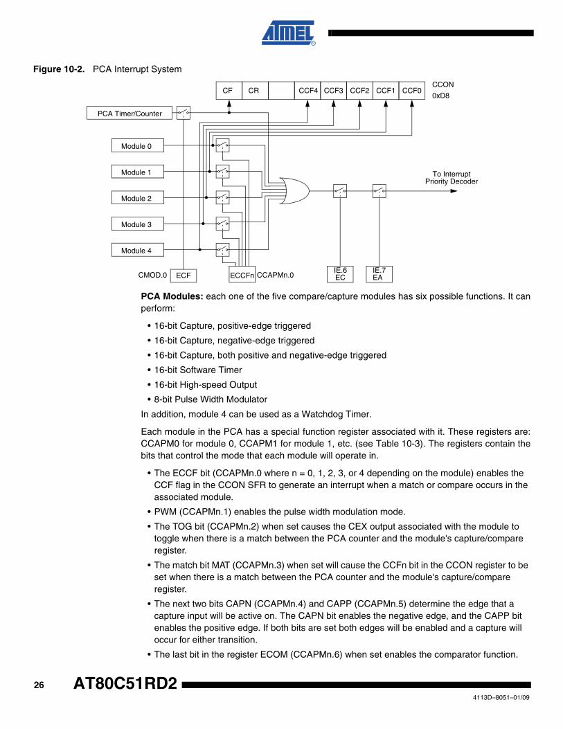
Figure 10-2. PCA Interrupt System
PCA Modules: each one of the five compare/capture modules has six possible functions. It canperform:
• 16-bit Capture, positive-edge triggered
• 16-bit Capture, negative-edge triggered
• 16-bit Capture, both positive and negative-edge triggered
• 16-bit Software Timer
• 16-bit High-speed Output
• 8-bit Pulse Width Modulator
In addition, module 4 can be used as a Watchdog Timer.
Each module in the PCA has a special function register associated with it. These registers are:CCAPM0 for module 0, CCAPM1 for module 1, etc. (see Table 10-3). The registers contain thebits that control the mode that each module will operate in.
• The ECCF bit (CCAPMn.0 where n = 0, 1, 2, 3, or 4 depending on the module) enables the CCF flag in the CCON SFR to generate an interrupt when a match or compare occurs in the associated module.
• PWM (CCAPMn.1) enables the pulse width modulation mode.
• The TOG bit (CCAPMn.2) when set causes the CEX output associated with the module to toggle when there is a match between the PCA counter and the module's capture/compare register.
• The match bit MAT (CCAPMn.3) when set will cause the CCFn bit in the CCON register to be set when there is a match between the PCA counter and the module's capture/compare register.
• The next two bits CAPN (CCAPMn.4) and CAPP (CCAPMn.5) determine the edge that a capture input will be active on. The CAPN bit enables the negative edge, and the CAPP bit enables the positive edge. If both bits are set both edges will be enabled and a capture will occur for either transition.
• The last bit in the register ECOM (CCAPMn.6) when set enables the comparator function.
CF CRCCON
0xD8CCF4 CCF3 CCF2 CCF1 CCF0
Module 4
Module 3
Module 2
Module 1
Module 0
ECF
PCA Timer/Counter
ECCFn CCAPMn.0CMOD.0IE.6 IE.7
To InterruptPriority Decoder
EC EA
264113D–8051–01/09
AT80C51RD2
AT80C51RD2
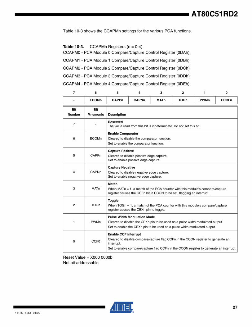
Table 10-3 shows the CCAPMn settings for the various PCA functions.
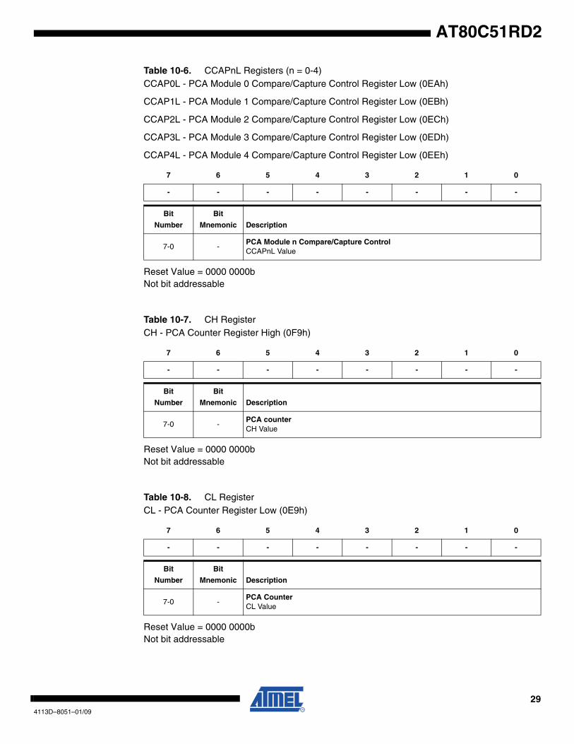
Table 10-3. CCAPMn Registers (n = 0-4)CCAPM0 - PCA Module 0 Compare/Capture Control Register (0DAh)
CCAPM1 - PCA Module 1 Compare/Capture Control Register (0DBh)
CCAPM2 - PCA Module 2 Compare/Capture Control Register (0DCh)
CCAPM3 - PCA Module 3 Compare/Capture Control Register (0DDh)
CCAPM4 - PCA Module 4 Compare/Capture Control Register (0DEh)
Reset Value = X000 0000bNot bit addressable
7 6 5 4 3 2 1 0
- ECOMn CAPPn CAPNn MATn TOGn PWMn ECCFn
Bit
Number
Bit
Mnemonic Description
7 -ReservedThe value read from this bit is indeterminate. Do not set this bit.
6 ECOMn
Enable Comparator
Cleared to disable the comparator function.
Set to enable the comparator function.
5 CAPPnCapture Positive
Cleared to disable positive edge capture.Set to enable positive edge capture.
4 CAPNnCapture Negative
Cleared to disable negative edge capture.Set to enable negative edge capture.
3 MATnMatch
When MATn = 1, a match of the PCA counter with this module's compare/capture register causes the CCFn bit in CCON to be set, flagging an interrupt.
2 TOGnToggle
When TOGn = 1, a match of the PCA counter with this module's compare/capture register causes the CEXn pin to toggle.
1 PWMn
Pulse Width Modulation Mode
Cleared to disable the CEXn pin to be used as a pulse width modulated output.
Set to enable the CEXn pin to be used as a pulse width modulated output.
0 CCF0
Enable CCF interrupt
Cleared to disable compare/capture flag CCFn in the CCON register to generate an interrupt.
Set to enable compare/capture flag CCFn in the CCON register to generate an interrupt.
274113D–8051–01/09
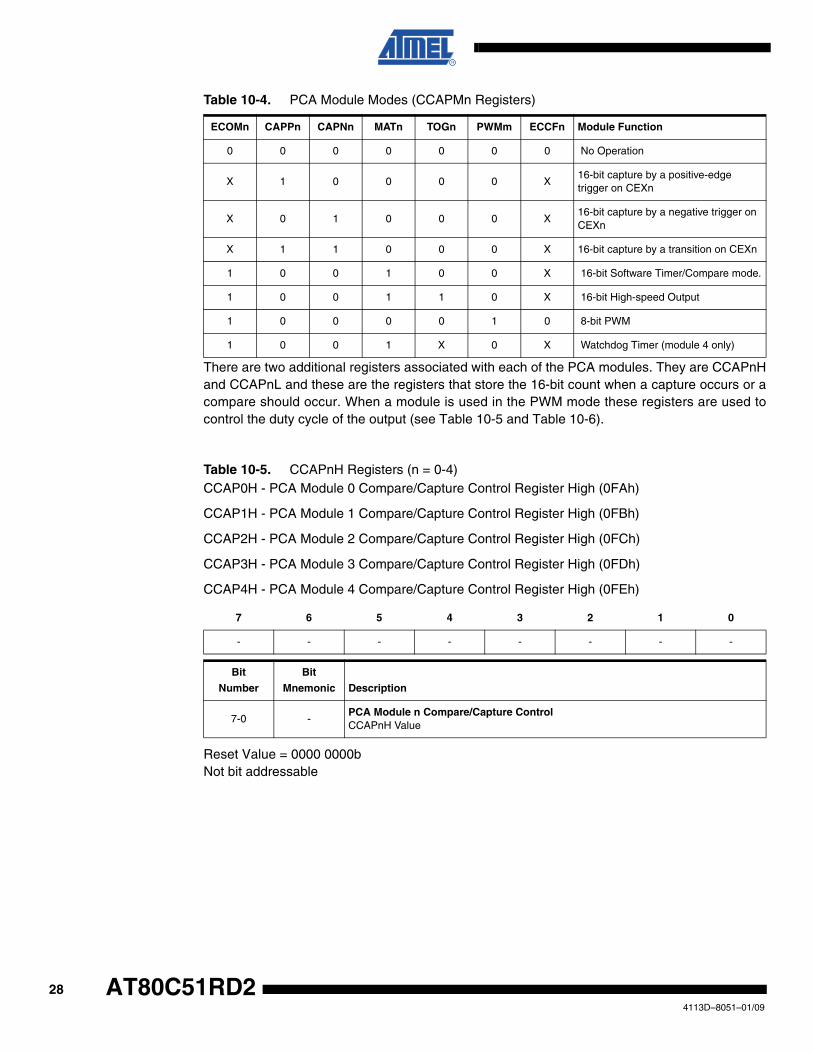
Table 10-4. PCA Module Modes (CCAPMn Registers)
There are two additional registers associated with each of the PCA modules. They are CCAPnHand CCAPnL and these are the registers that store the 16-bit count when a capture occurs or acompare should occur. When a module is used in the PWM mode these registers are used tocontrol the duty cycle of the output (see Table 10-5 and Table 10-6).
Table 10-5. CCAPnH Registers (n = 0-4)CCAP0H - PCA Module 0 Compare/Capture Control Register High (0FAh)
CCAP1H - PCA Module 1 Compare/Capture Control Register High (0FBh)
CCAP2H - PCA Module 2 Compare/Capture Control Register High (0FCh)
CCAP3H - PCA Module 3 Compare/Capture Control Register High (0FDh)
CCAP4H - PCA Module 4 Compare/Capture Control Register High (0FEh)
Reset Value = 0000 0000bNot bit addressable
ECOMn CAPPn CAPNn MATn TOGn PWMm ECCFn Module Function
0 0 0 0 0 0 0 No Operation
X 1 0 0 0 0 X16-bit capture by a positive-edge trigger on CEXn
X 0 1 0 0 0 X16-bit capture by a negative trigger on CEXn
X 1 1 0 0 0 X 16-bit capture by a transition on CEXn
1 0 0 1 0 0 X 16-bit Software Timer/Compare mode.
1 0 0 1 1 0 X 16-bit High-speed Output
1 0 0 0 0 1 0 8-bit PWM
1 0 0 1 X 0 X Watchdog Timer (module 4 only)
7 6 5 4 3 2 1 0
- - - - - - - -
Bit
Number
Bit
Mnemonic Description
7-0 -PCA Module n Compare/Capture ControlCCAPnH Value
284113D–8051–01/09
AT80C51RD2
AT80C51RD2
Table 10-6. CCAPnL Registers (n = 0-4)CCAP0L - PCA Module 0 Compare/Capture Control Register Low (0EAh)
CCAP1L - PCA Module 1 Compare/Capture Control Register Low (0EBh)
CCAP2L - PCA Module 2 Compare/Capture Control Register Low (0ECh)
CCAP3L - PCA Module 3 Compare/Capture Control Register Low (0EDh)
CCAP4L - PCA Module 4 Compare/Capture Control Register Low (0EEh)
Reset Value = 0000 0000bNot bit addressable
Table 10-7. CH RegisterCH - PCA Counter Register High (0F9h)
Reset Value = 0000 0000bNot bit addressable
Table 10-8. CL RegisterCL - PCA Counter Register Low (0E9h)
Reset Value = 0000 0000bNot bit addressable
7 6 5 4 3 2 1 0
- - - - - - - -
Bit
Number
Bit
Mnemonic Description
7-0 -PCA Module n Compare/Capture ControlCCAPnL Value
7 6 5 4 3 2 1 0
- - - - - - - -
Bit
Number
Bit
Mnemonic Description
7-0 -PCA counterCH Value
7 6 5 4 3 2 1 0
- - - - - - - -
Bit
Number
Bit
Mnemonic Description
7-0 -PCA CounterCL Value
294113D–8051–01/09
10.1 PCA Capture ModeTo use one of the PCA modules in the capture mode either one or both of the CCAPM bitsCAPN and CAPP for that module must be set. The external CEX input for the module (on port 1)is sampled for a transition. When a valid transition occurs the PCA hardware loads the value ofthe PCA counter registers (CH and CL) into the module's capture registers (CCAPnL and CCA-PnH). If the CCFn bit for the module in the CCON SFR and the ECCFn bit in the CCAPMn SFRare set then an interrupt will be generated (see Figure 10-3).
Figure 10-3. PCA Capture Mode
10.2 16-bit Software Timer/ Compare ModeThe PCA modules can be used as software timers by setting both the ECOM and MAT bits inthe modules CCAPMn register. The PCA timer will be compared to the module's capture regis-ters and when a match occurs an interrupt will occur if the CCFn (CCON SFR) and the ECCFn(CCAPMn SFR) bits for the module are both set (see Figure 10-4).
CF CR CCON0xD8
CH CL
CCAPnH CCAPnL
CCF4 CCF3 CCF2 CCF1 CCF0
PCA IT
PCA Counter/Timer
ECOMn CCAPMn, n= 0 to 40xDA to 0xDE
CAPNn MATn TOGn PWMn ECCFnCAPPn
Cex.n
Capture
304113D–8051–01/09
AT80C51RD2
AT80C51RD2
Figure 10-4. PCA Compare Mode and PCA Watchdog Timer
Before enabling ECOM bit, CCAPnL and CCAPnH should be set with a non zero value, other-wise an unwanted match could happen. Writing to CCAPnH will set the ECOM bit.
Once ECOM set, writing CCAPnL will clear ECOM so that an unwanted match doesn’t occurwhile modifying the compare value. Writing to CCAPnH will set ECOM. For this reason, usersoftware should write CCAPnL first, and then CCAPnH. Of course, the ECOM bit can still becontrolled by accessing to CCAPMn register.
10.3 High-speed Output ModeIn this mode, the CEX output (on port 1) associated with the PCA module will toggle each time amatch occurs between the PCA counter and the module's capture registers. To activate thismode the TOG, MAT, and ECOM bits in the module's CCAPMn SFR must be set (seeFigure 10-5).
A prior write must be done to CCAPnL and CCAPnH before writing the ECOMn bit.
CH CL
CCAPnH CCAPnL
ECOMnCCAPMn, n = 0 to 40xDA to 0xDE
CAPNn MATn TOGn PWMn ECCFnCAPPn
16 bit comparatorMatch
CCON0xD8
PCA IT
Enable
PCA counter/ timer
RESET *
CIDL CPS1 CPS0 ECFCMOD0xD9
WDTE
ResetWrite toCCAPnL
Write toCCAPnH
CF CCF2 CCF1 CCF0CR CCF3CCF4
1 0
314113D–8051–01/09
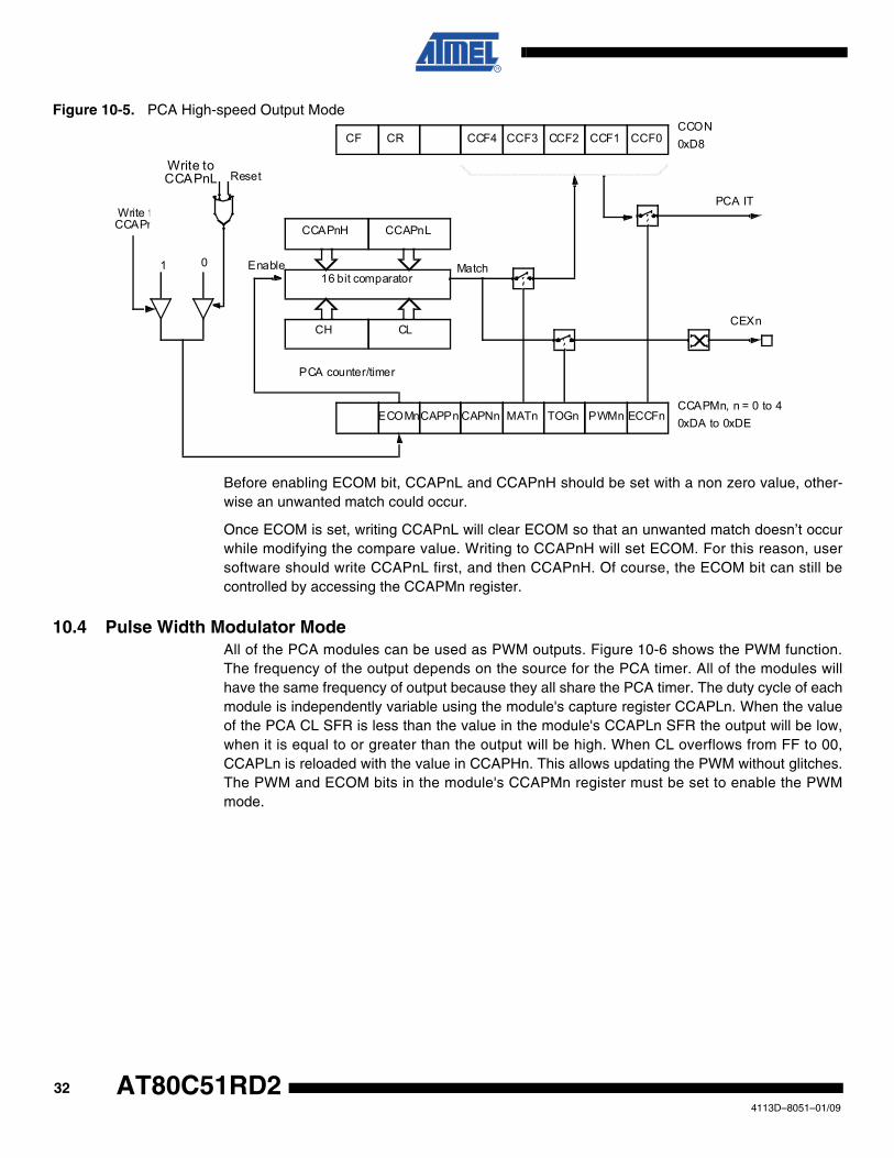
Figure 10-5. PCA High-speed Output Mode
Before enabling ECOM bit, CCAPnL and CCAPnH should be set with a non zero value, other-wise an unwanted match could occur.
Once ECOM is set, writing CCAPnL will clear ECOM so that an unwanted match doesn’t occurwhile modifying the compare value. Writing to CCAPnH will set ECOM. For this reason, usersoftware should write CCAPnL first, and then CCAPnH. Of course, the ECOM bit can still becontrolled by accessing the CCAPMn register.
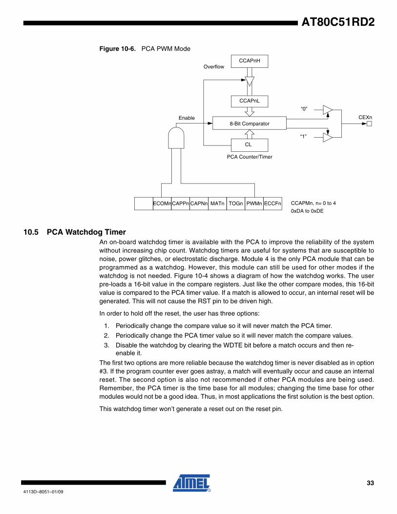
10.4 Pulse Width Modulator ModeAll of the PCA modules can be used as PWM outputs. Figure 10-6 shows the PWM function.The frequency of the output depends on the source for the PCA timer. All of the modules willhave the same frequency of output because they all share the PCA timer. The duty cycle of eachmodule is independently variable using the module's capture register CCAPLn. When the valueof the PCA CL SFR is less than the value in the module's CCAPLn SFR the output will be low,when it is equal to or greater than the output will be high. When CL overflows from FF to 00,CCAPLn is reloaded with the value in CCAPHn. This allows updating the PWM without glitches.The PWM and ECOM bits in the module's CCAPMn register must be set to enable the PWMmode.
CH CL
CCAPnH CCAPnL
ECOMnCCAPMn, n = 0 to 40xDA to 0xDECAPNn MATn TOGn PWMn ECCFnCAPPn
16 bit comparatorMatch
CF CRCCON0xD8CCF4 CCF3 CCF2 CCF1 CCF0
PCA IT
Enable
CEXn
PCA counter/timer
Write toCCAPnH
ResetWrite toCCAPnL
1 0
324113D–8051–01/09
AT80C51RD2
AT80C51RD2
Figure 10-6. PCA PWM Mode
10.5 PCA Watchdog Timer An on-board watchdog timer is available with the PCA to improve the reliability of the systemwithout increasing chip count. Watchdog timers are useful for systems that are susceptible tonoise, power glitches, or electrostatic discharge. Module 4 is the only PCA module that can beprogrammed as a watchdog. However, this module can still be used for other modes if thewatchdog is not needed. Figure 10-4 shows a diagram of how the watchdog works. The userpre-loads a 16-bit value in the compare registers. Just like the other compare modes, this 16-bitvalue is compared to the PCA timer value. If a match is allowed to occur, an internal reset will begenerated. This will not cause the RST pin to be driven high.
In order to hold off the reset, the user has three options:
1. Periodically change the compare value so it will never match the PCA timer.
2. Periodically change the PCA timer value so it will never match the compare values.
3. Disable the watchdog by clearing the WDTE bit before a match occurs and then re-enable it.
The first two options are more reliable because the watchdog timer is never disabled as in option#3. If the program counter ever goes astray, a match will eventually occur and cause an internalreset. The second option is also not recommended if other PCA modules are being used.Remember, the PCA timer is the time base for all modules; changing the time base for othermodules would not be a good idea. Thus, in most applications the first solution is the best option.
This watchdog timer won’t generate a reset out on the reset pin.
CL
CCAPnH
CCAPnL
ECOMn CCAPMn, n= 0 to 4
0xDA to 0xDECAPNn MATn TOGn PWMn ECCFnCAPPn
8-Bit ComparatorCEXn
“0”
“1”
Enable
PCA Counter/Timer
Overflow
334113D–8051–01/09
11. Serial I/O PortThe serial I/O port in the AT80C51RD2 is compatible with the serial I/O port in the 80C52.It provides both synchronous and asynchronous communication modes. It operates as a Univer-sal Asynchronous Receiver and Transmitter (UART) in three full-duplex modes (Modes 1, 2 and3). Asynchronous transmission and reception can occur simultaneously and at different baudrates
Serial I/O port includes the following enhancements:
• Framing error detection
• Automatic address recognition
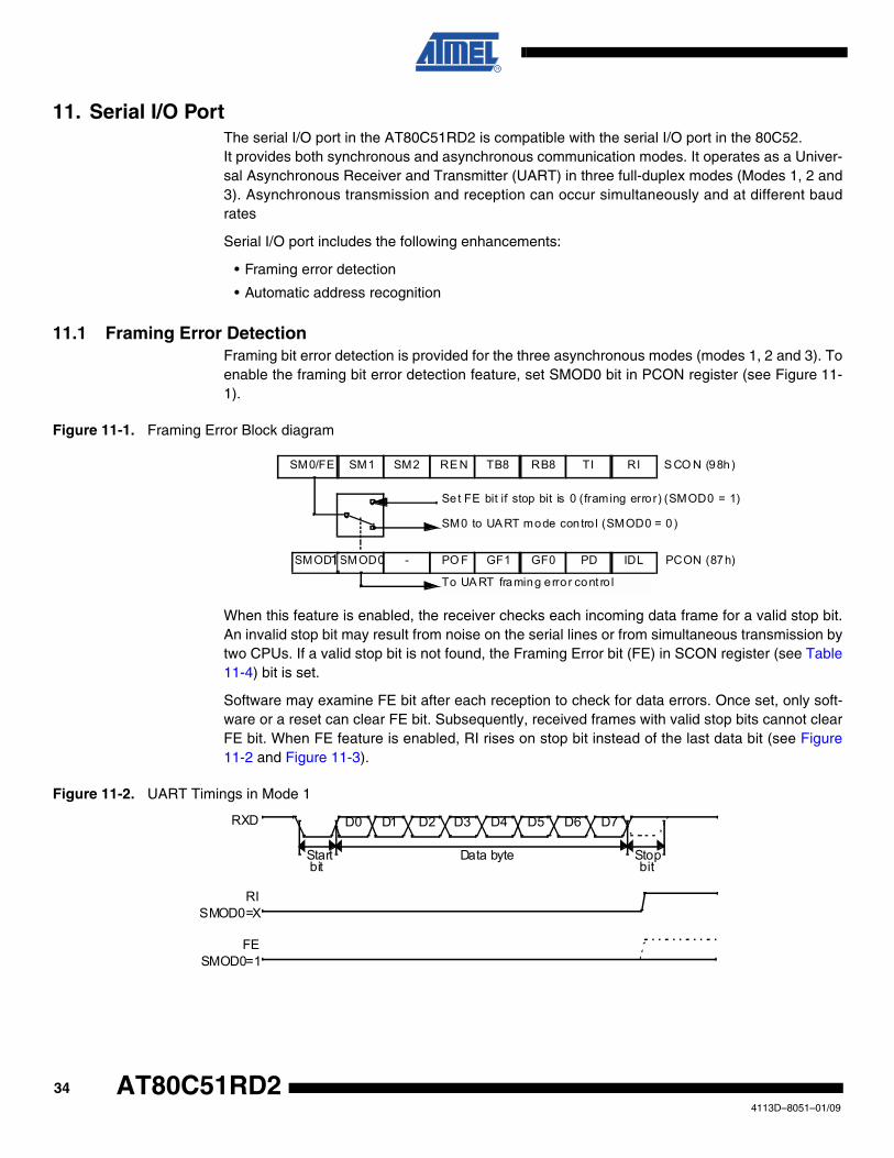
11.1 Framing Error DetectionFraming bit error detection is provided for the three asynchronous modes (modes 1, 2 and 3). Toenable the framing bit error detection feature, set SMOD0 bit in PCON register (see Figure 11-1).
Figure 11-1. Framing Error Block diagram
When this feature is enabled, the receiver checks each incoming data frame for a valid stop bit.An invalid stop bit may result from noise on the serial lines or from simultaneous transmission bytwo CPUs. If a valid stop bit is not found, the Framing Error bit (FE) in SCON register (see Table11-4) bit is set.
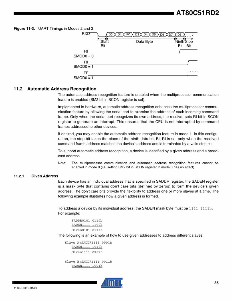
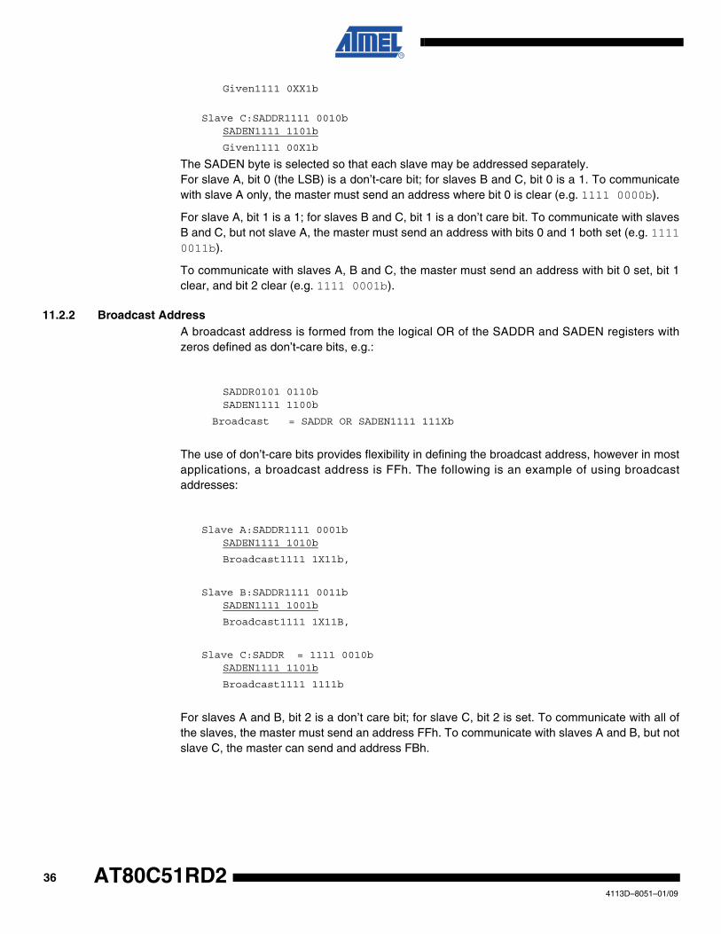
Software may examine FE bit after each reception to check for data errors. Once set, only soft-ware or a reset can clear FE bit. Subsequently, received frames with valid stop bits cannot clearFE bit. When FE feature is enabled, RI rises on stop bit instead of the last data bit (see Figure11-2 and Figure 11-3).
Figure 11-2. UART Timings in Mode 1
RITIRB8TB8RE NSM2SM1SM0/FE
IDLPDGF0GF1PO F-SMOD0SMOD1
To UA RT framing e rro r cont ro l
SM0 to UA RT mode con tro l (SMOD0 = 0 )
Se t FE bit if stop bit is 0 (framing erro r) (SMOD0 = 1)
S CO N (98h)
PCON (87h)1
Data byte
RISMOD0=X
Stopbit
Startbit
RXD D7D6D5D4D3D2D1D0
FESMOD0=1
344113D–8051–01/09
AT80C51RD2
AT80C51RD2
Figure 11-3. UART Timings in Modes 2 and 3
11.2 Automatic Address Recognition The automatic address recognition feature is enabled when the multiprocessor communicationfeature is enabled (SM2 bit in SCON register is set).
Implemented in hardware, automatic address recognition enhances the multiprocessor commu-nication feature by allowing the serial port to examine the address of each incoming commandframe. Only when the serial port recognizes its own address, the receiver sets RI bit in SCONregister to generate an interrupt. This ensures that the CPU is not interrupted by commandframes addressed to other devices.
If desired, you may enable the automatic address recognition feature in mode 1. In this configu-ration, the stop bit takes the place of the ninth data bit. Bit RI is set only when the receivedcommand frame address matches the device’s address and is terminated by a valid stop bit.
To support automatic address recognition, a device is identified by a given address and a broad-cast address.
Note: The multiprocessor communication and automatic address recognition features cannot beenabled in mode 0 (i.e. setting SM2 bit in SCON register in mode 0 has no effect).
11.2.1 Given AddressEach device has an individual address that is specified in SADDR register; the SADEN registeris a mask byte that contains don’t care bits (defined by zeros) to form the device’s givenaddress. The don’t care bits provide the flexibility to address one or more slaves at a time. Thefollowing example illustrates how a given address is formed.
To address a device by its individual address, the SADEN mask byte must be 1111 1111b.For example:
SADDR0101 0110bSADEN1111 1100b
Given0101 01XXb
The following is an example of how to use given addresses to address different slaves:
Slave A:SADDR1111 0001bSADEN1111 1010b
Given1111 0X0Xb
Slave B:SADDR1111 0011bSADEN1111 1001b
RISMOD0 = 0
Data Byte NinthBit
StopBit
.StartBit
RXD D8D7D6D5D4D3D2D1D0
RISMOD0 = 1
FESMOD0 = 1
354113D–8051–01/09
Given1111 0XX1b
Slave C:SADDR1111 0010bSADEN1111 1101b
Given1111 00X1b
The SADEN byte is selected so that each slave may be addressed separately.For slave A, bit 0 (the LSB) is a don’t-care bit; for slaves B and C, bit 0 is a 1. To communicatewith slave A only, the master must send an address where bit 0 is clear (e.g. 1111 0000b).
For slave A, bit 1 is a 1; for slaves B and C, bit 1 is a don’t care bit. To communicate with slavesB and C, but not slave A, the master must send an address with bits 0 and 1 both set (e.g. 11110011b).
To communicate with slaves A, B and C, the master must send an address with bit 0 set, bit 1clear, and bit 2 clear (e.g. 1111 0001b).
11.2.2 Broadcast AddressA broadcast address is formed from the logical OR of the SADDR and SADEN registers withzeros defined as don’t-care bits, e.g.:
SADDR0101 0110bSADEN1111 1100b
Broadcast = SADDR OR SADEN1111 111Xb
The use of don’t-care bits provides flexibility in defining the broadcast address, however in mostapplications, a broadcast address is FFh. The following is an example of using broadcastaddresses:
Slave A:SADDR1111 0001bSADEN1111 1010b
Broadcast1111 1X11b,
Slave B:SADDR1111 0011bSADEN1111 1001b
Broadcast1111 1X11B,
Slave C:SADDR = 1111 0010bSADEN1111 1101b
Broadcast1111 1111b
For slaves A and B, bit 2 is a don’t care bit; for slave C, bit 2 is set. To communicate with all ofthe slaves, the master must send an address FFh. To communicate with slaves A and B, but notslave C, the master can send and address FBh.
364113D–8051–01/09
AT80C51RD2
AT80C51RD2
11.2.3 Reset AddressesOn reset, the SADDR and SADEN registers are initialized to 00h, i.e. the given and broadcastaddresses are XXXX XXXXb (all don’t-care bits). This ensures that the serial port will reply to anyaddress, and so, that it is backwards compatible with the 80C51 microcontrollers that do notsupport automatic address recognition.
Table 11-1. SADEN RegisterSADEN - Slave Address Mask Register (B9h)
Reset Value = 0000 0000bNot bit addressable
Table 11-2. SADDR RegisterSADDR - Slave Address Register (A9h)
Reset Value = 0000 0000bNot bit addressable
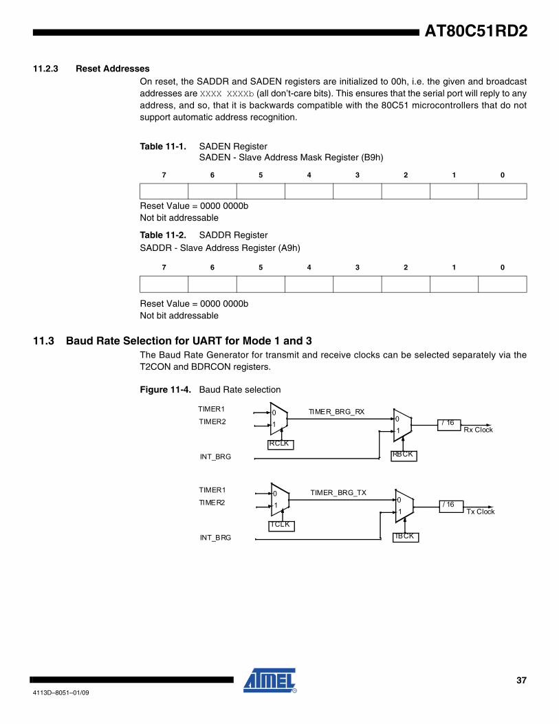
11.3 Baud Rate Selection for UART for Mode 1 and 3The Baud Rate Generator for transmit and receive clocks can be selected separately via theT2CON and BDRCON registers.
Figure 11-4. Baud Rate selection
7 6 5 4 3 2 1 0
7 6 5 4 3 2 1 0
RCLK
/ 16
RBCKINT_BRG
01
TIMER1
01
01
TIMER2
INT_BRG
TIMER1
TIMER2
TIMER_BRG_RX
Rx Clock
/ 1601
TIMER_BRG_TX
Tx Clock
TBCKTCLK
374113D–8051–01/09
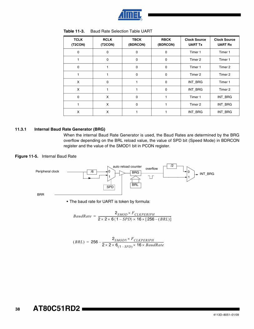
Table 11-3. Baud Rate Selection Table UART
11.3.1 Internal Baud Rate Generator (BRG)When the internal Baud Rate Generator is used, the Baud Rates are determined by the BRGoverflow depending on the BRL reload value, the value of SPD bit (Speed Mode) in BDRCONregister and the value of the SMOD1 bit in PCON register.
Figure 11-5. Internal Baud Rate
• The baud rate for UART is token by formula:
TCLK
(T2CON)
RCLK
(T2CON)
TBCK
(BDRCON)
RBCK
(BDRCON)
Clock Source
UART Tx
Clock Source
UART Rx
0 0 0 0 Timer 1 Timer 1
1 0 0 0 Timer 2 Timer 1
0 1 0 0 Timer 1 Timer 2
1 1 0 0 Timer 2 Timer 2
X 0 1 0 INT_BRG Timer 1
X 1 1 0 INT_BRG Timer 2
0 X 0 1 Timer 1 INT_BRG
1 X 0 1 Timer 2 INT_BRG
X X 1 1 INT_BRG INT_BRG
Peripheral clock BRG0
1
/6
BRL
/2
0
1INT_BRG
BRR
auto reload counteroverflow
SPD
BaudRate2SMOD FCLKPERIPH×
2 2 6×× 1 SPD–⟨ ⟩ 16× 256 BRL( )–[ ]×----------------------------------------------------------------------------------------------------------=
BRL( ) 2562SMOD1 FCLKPERIPH×
2 2 6×× 1 SPD–( ) 16× BaudRate×-----------------------------------------------------------------------------------------–=
384113D–8051–01/09
AT80C51RD2
AT80C51RD2
Table 11-4. SCON RegisterSCON - Serial Control Register (98h)
Reset Value = 0000 0000b
Bit addressable
7 6 5 4 3 2 1 0
FE/SM0 SM1 SM2 REN TB8 RB8 TI RI
Bit
Number
Bit
Mnemonic Description
7 FE
Framing Error bit (SMOD0 = 1)
Clear to reset the error state, not cleared by a valid stop bit.Set by hardware when an invalid stop bit is detected.
SMOD0 must be set to enable access to the FE bit
SM0Serial port Mode bit 0Refer to SM1 for serial port mode selection.
SMOD0 must be cleared to enable access to the SM0 bit
6 SM1
Serial port Mode bit 1
SM1ModeDescriptionBaud Rate
0 0Shift RegisterfCPU PERIPH/6
1 18-bit UARTVariable
0 29-bit UARTfCPU PERIPH /32 or /16
1 39-bit UARTVariable
5 SM2
Serial port Mode 2 bit/Multiprocessor Communication Enable bit
Clear to disable multiprocessor communication feature.
Set to enable multiprocessor communication feature in mode 2 and 3, and eventually mode 1. This bit should be cleared in mode 0.
4 RENReception Enable bitClear to disable serial reception.Set to enable serial reception.
3 TB8Transmitter Bit 8/Ninth bit to transmit in modes 2 and 3
o transmit a logic 0 in the 9th bit.Set to transmit a logic 1 in the 9th bit.
2 RB8
Receiver Bit 8/Ninth bit received in modes 2 and 3Cleared by hardware if 9th bit received is a logic 0.Set by hardware if 9th bit received is a logic 1.
In mode 1, if SM2=0, RB8 is the received stop bit. In mode 0 RB8 is not used.
1 TI
Transmit Interrupt flagClear to acknowledge interrupt.Set by hardware at the end of the 8th bit time in mode 0 or at the beginning of the stop bit in the other modes.
0 RI
Receive Interrupt flagClear to acknowledge interrupt.Set by hardware at the end of the 8th bit time in mode 0, see Figure 11-2. and Figure 11-3. in the other modes.
394113D–8051–01/09
Table 11-5. Example of Computed Value when X2 = 1, SMOD1 = 1, SPD = 1
Table 11-6. Example of Computed Value when X2 = 0, SMOD1 = 0, SPD = 0
The baud rate generator can be used for mode 1 or 3 (see Figure 11-4.), but also for mode 0 forUART, thanks to the bit SRC located in BDRCON register (Table 11-13.)
11.4 UART RegistersTable 11-7. SADEN RegisterSADEN - Slave Address Mask Register for UART (B9h)
Reset Value = 0000 0000b
Table 11-8. SADDR RegisterSADDR - Slave Address Register for UART (A9h)
Reset Value = 0000 0000b
Baud Rates FOSC=16.384 MHz FOSC=24 MHz
BRL Error (%) BRL Error (%)
115200 247 1.23 243 0.16
57600 238 1.23 230 0.16
38400 229 1.23 217 0.16
28800 220 1.23 204 0.16
19200 203 0.63 178 0.16
9600 149 0.31 100 0.16
4800 43 1.23 - -
Baud Rates FOSC=16.384 MHz FOSC=24 MHz
BRL Error (%) BRL Error (%)
4800 247 1.23 243 0.16
2400 238 1.23 230 0.16
1200 220 1.23 202 3.55
600 185 0.16 152 0.16
7 6 5 4 3 2 1 0
7 6 5 4 3 2 1 0
404113D–8051–01/09
AT80C51RD2
AT80C51RD2
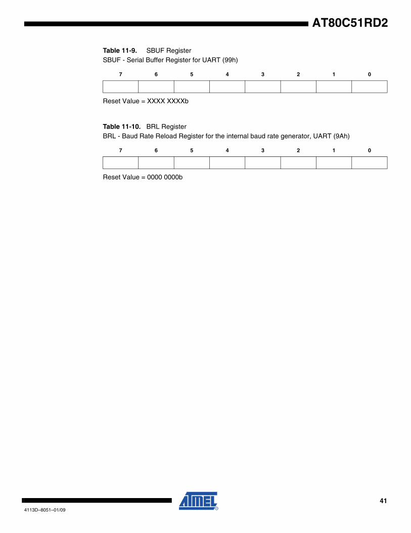
Table 11-9. SBUF RegisterSBUF - Serial Buffer Register for UART (99h)
Reset Value = XXXX XXXXb
Table 11-10. BRL RegisterBRL - Baud Rate Reload Register for the internal baud rate generator, UART (9Ah)
Reset Value = 0000 0000b
7 6 5 4 3 2 1 0
7 6 5 4 3 2 1 0
414113D–8051–01/09
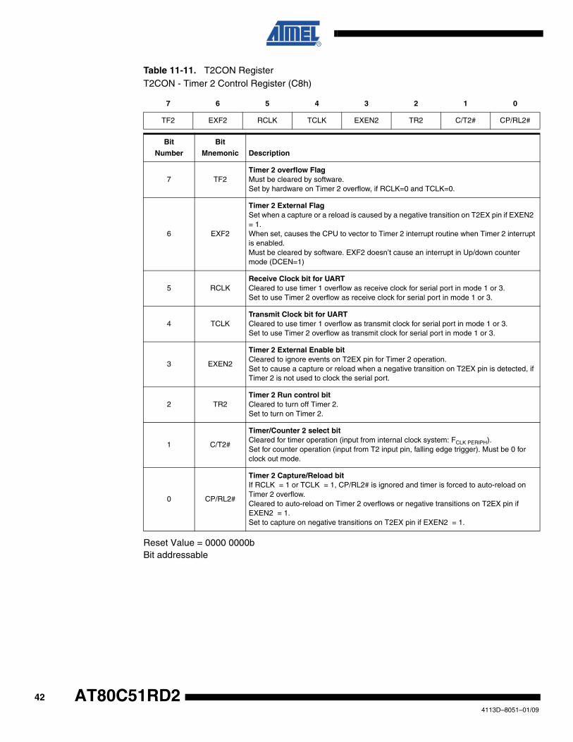
Table 11-11. T2CON RegisterT2CON - Timer 2 Control Register (C8h)
Reset Value = 0000 0000bBit addressable
7 6 5 4 3 2 1 0
TF2 EXF2 RCLK TCLK EXEN2 TR2 C/T2# CP/RL2#
Bit
Number
Bit
Mnemonic Description
7 TF2Timer 2 overflow FlagMust be cleared by software.Set by hardware on Timer 2 overflow, if RCLK=0 and TCLK=0.
6 EXF2
Timer 2 External FlagSet when a capture or a reload is caused by a negative transition on T2EX pin if EXEN2 = 1.When set, causes the CPU to vector to Timer 2 interrupt routine when Timer 2 interrupt is enabled.Must be cleared by software. EXF2 doesn’t cause an interrupt in Up/down counter mode (DCEN=1)
5 RCLKReceive Clock bit for UARTCleared to use timer 1 overflow as receive clock for serial port in mode 1 or 3.Set to use Timer 2 overflow as receive clock for serial port in mode 1 or 3.
4 TCLKTransmit Clock bit for UARTCleared to use timer 1 overflow as transmit clock for serial port in mode 1 or 3.Set to use Timer 2 overflow as transmit clock for serial port in mode 1 or 3.
3 EXEN2
Timer 2 External Enable bitCleared to ignore events on T2EX pin for Timer 2 operation.Set to cause a capture or reload when a negative transition on T2EX pin is detected, if Timer 2 is not used to clock the serial port.
2 TR2Timer 2 Run control bitCleared to turn off Timer 2.Set to turn on Timer 2.
1 C/T2#
Timer/Counter 2 select bitCleared for timer operation (input from internal clock system: FCLK PERIPH).Set for counter operation (input from T2 input pin, falling edge trigger). Must be 0 for clock out mode.
0 CP/RL2#
Timer 2 Capture/Reload bitIf RCLK = 1 or TCLK = 1, CP/RL2# is ignored and timer is forced to auto-reload on Timer 2 overflow.Cleared to auto-reload on Timer 2 overflows or negative transitions on T2EX pin if EXEN2 = 1.Set to capture on negative transitions on T2EX pin if EXEN2 = 1.
424113D–8051–01/09
AT80C51RD2
AT80C51RD2
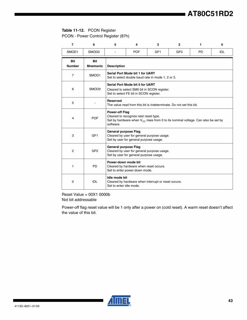
Table 11-12. PCON RegisterPCON - Power Control Register (87h)
Reset Value = 00X1 0000bNot bit addressable
Power-off flag reset value will be 1 only after a power on (cold reset). A warm reset doesn’t affectthe value of this bit.
7 6 5 4 3 2 1 0
SMOD1 SMOD0 - POF GF1 GF0 PD IDL
Bit
Number
Bit
Mnemonic Description
7 SMOD1Serial Port Mode bit 1 for UARTSet to select double baud rate in mode 1, 2 or 3.
6 SMOD0Serial Port Mode bit 0 for UART
Cleared to select SM0 bit in SCON register.Set to select FE bit in SCON register.
5 -ReservedThe value read from this bit is indeterminate. Do not set this bit.
4 POF
Power-off FlagCleared to recognize next reset type.Set by hardware when VCC rises from 0 to its nominal voltage. Can also be set by software.
3 GF1General purpose FlagCleared by user for general purpose usage.Set by user for general purpose usage.
2 GF0General purpose FlagCleared by user for general purpose usage.Set by user for general purpose usage.
1 PDPower-down mode bitCleared by hardware when reset occurs.Set to enter power-down mode.
0 IDLIdle mode bitCleared by hardware when interrupt or reset occurs.Set to enter idle mode.
434113D–8051–01/09
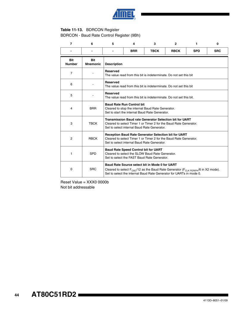
Table 11-13. BDRCON RegisterBDRCON - Baud Rate Control Register (9Bh)
Reset Value = XXX0 0000bNot bit addressable
7 6 5 4 3 2 1 0
- - - BRR TBCK RBCK SPD SRC
Bit Number
Bit Mnemonic Description
7 -ReservedThe value read from this bit is indeterminate. Do not set this bit
6 -ReservedThe value read from this bit is indeterminate. Do not set this bit
5 -ReservedThe value read from this bit is indeterminate. Do not set this bit.
4 BRRBaud Rate Run Control bitCleared to stop the internal Baud Rate Generator.Set to start the internal Baud Rate Generator.
3 TBCKTransmission Baud rate Generator Selection bit for UARTCleared to select Timer 1 or Timer 2 for the Baud Rate Generator.Set to select internal Baud Rate Generator.
2 RBCKReception Baud Rate Generator Selection bit for UARTCleared to select Timer 1 or Timer 2 for the Baud Rate Generator.Set to select internal Baud Rate Generator.
1 SPDBaud Rate Speed Control bit for UARTCleared to select the SLOW Baud Rate Generator.Set to select the FAST Baud Rate Generator.
0 SRCBaud Rate Source select bit in Mode 0 for UART
Cleared to select FOSC/12 as the Baud Rate Generator (FCLK PERIPH/6 in X2 mode).Set to select the internal Baud Rate Generator for UARTs in mode 0.
444113D–8051–01/09
AT80C51RD2
AT80C51RD2
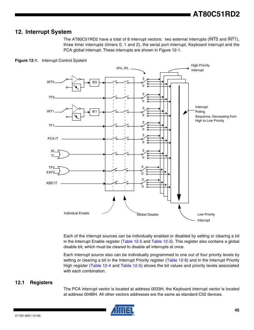
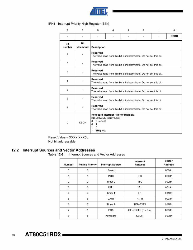
12. Interrupt SystemThe AT80C51RD2 have a total of 8 interrupt vectors: two external interrupts (INT0 and INT1),three timer interrupts (timers 0, 1 and 2), the serial port interrupt, Keyboard interrupt and thePCA global interrupt. These interrupts are shown in Figure 12-1.
Figure 12-1. Interrupt Control System
Each of the interrupt sources can be individually enabled or disabled by setting or clearing a bitin the Interrupt Enable register (Table 12-5 and Table 12-3). This register also contains a globaldisable bit, which must be cleared to disable all interrupts at once.
Each interrupt source also can be individually programmed to one out of four priority levels bysetting or clearing a bit in the Interrupt Priority register (Table 12-6) and in the Interrupt PriorityHigh register (Table 12-4 and Table 12-5) shows the bit values and priority levels associatedwith each combination.
12.1 RegistersThe PCA interrupt vector is located at address 0033H, the Keyboard interrupt vector is locatedat address 004BH. All other vectors addresses are the same as standard C52 devices.
IE1
0
3
High PriorityInterrupt
InterruptPollingSequence, Decreasing from High to Low Priority
Low Priority
Interrupt
Global DisableIndividual Enable
EXF2TF2
TIRI
TF0
INT0
INT1
TF1
IPH, IPL
IE0
0
3
0
3
0
3
0
3
0
3
0
3
PCA IT
KBD IT0
3
454113D–8051–01/09
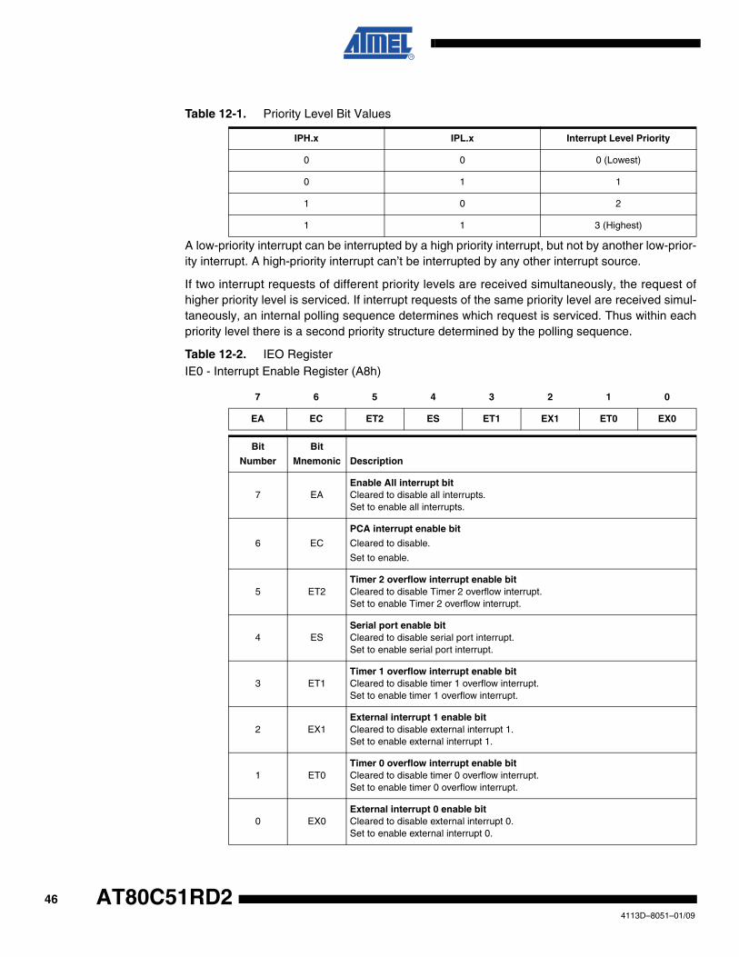
Table 12-1. Priority Level Bit Values
A low-priority interrupt can be interrupted by a high priority interrupt, but not by another low-prior-ity interrupt. A high-priority interrupt can’t be interrupted by any other interrupt source.
If two interrupt requests of different priority levels are received simultaneously, the request ofhigher priority level is serviced. If interrupt requests of the same priority level are received simul-taneously, an internal polling sequence determines which request is serviced. Thus within eachpriority level there is a second priority structure determined by the polling sequence.
Table 12-2. IEO RegisterIE0 - Interrupt Enable Register (A8h)
IPH.x IPL.x Interrupt Level Priority
0 0 0 (Lowest)
0 1 1
1 0 2
1 1 3 (Highest)
7 6 5 4 3 2 1 0
EA EC ET2 ES ET1 EX1 ET0 EX0
Bit
Number
Bit
Mnemonic Description
7 EAEnable All interrupt bitCleared to disable all interrupts. Set to enable all interrupts.
6 EC
PCA interrupt enable bit
Cleared to disable.
Set to enable.
5 ET2Timer 2 overflow interrupt enable bitCleared to disable Timer 2 overflow interrupt. Set to enable Timer 2 overflow interrupt.
4 ESSerial port enable bitCleared to disable serial port interrupt. Set to enable serial port interrupt.
3 ET1Timer 1 overflow interrupt enable bitCleared to disable timer 1 overflow interrupt. Set to enable timer 1 overflow interrupt.
2 EX1External interrupt 1 enable bitCleared to disable external interrupt 1.Set to enable external interrupt 1.
1 ET0Timer 0 overflow interrupt enable bitCleared to disable timer 0 overflow interrupt. Set to enable timer 0 overflow interrupt.
0 EX0External interrupt 0 enable bitCleared to disable external interrupt 0.Set to enable external interrupt 0.
464113D–8051–01/09
AT80C51RD2
AT80C51RD2
Reset Value = 0000 0000bBit addressable
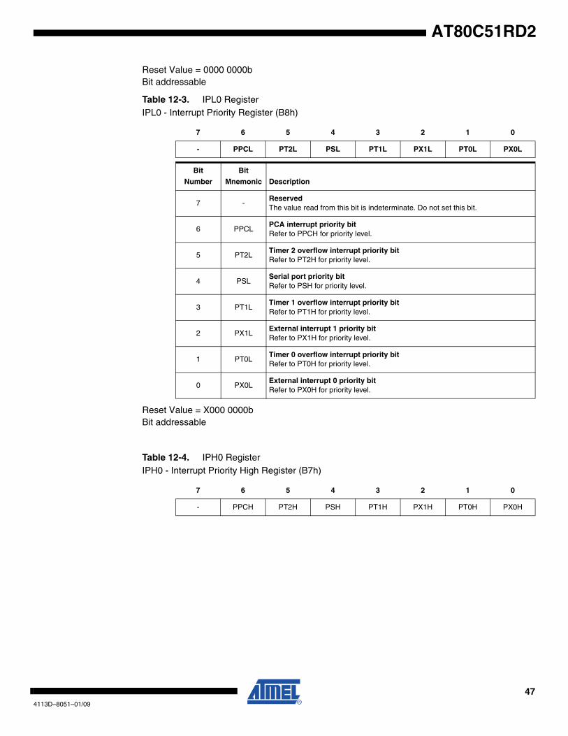
Table 12-3. IPL0 RegisterIPL0 - Interrupt Priority Register (B8h)
Reset Value = X000 0000bBit addressable
Table 12-4. IPH0 RegisterIPH0 - Interrupt Priority High Register (B7h)
7 6 5 4 3 2 1 0
- PPCL PT2L PSL PT1L PX1L PT0L PX0L
Bit
Number
Bit
Mnemonic Description
7 -ReservedThe value read from this bit is indeterminate. Do not set this bit.
6 PPCLPCA interrupt priority bitRefer to PPCH for priority level.
5 PT2LTimer 2 overflow interrupt priority bitRefer to PT2H for priority level.
4 PSLSerial port priority bitRefer to PSH for priority level.
3 PT1LTimer 1 overflow interrupt priority bitRefer to PT1H for priority level.
2 PX1LExternal interrupt 1 priority bitRefer to PX1H for priority level.
1 PT0LTimer 0 overflow interrupt priority bitRefer to PT0H for priority level.
0 PX0LExternal interrupt 0 priority bitRefer to PX0H for priority level.
7 6 5 4 3 2 1 0
- PPCH PT2H PSH PT1H PX1H PT0H PX0H
474113D–8051–01/09
Reset Value = X000 0000bNot bit addressable
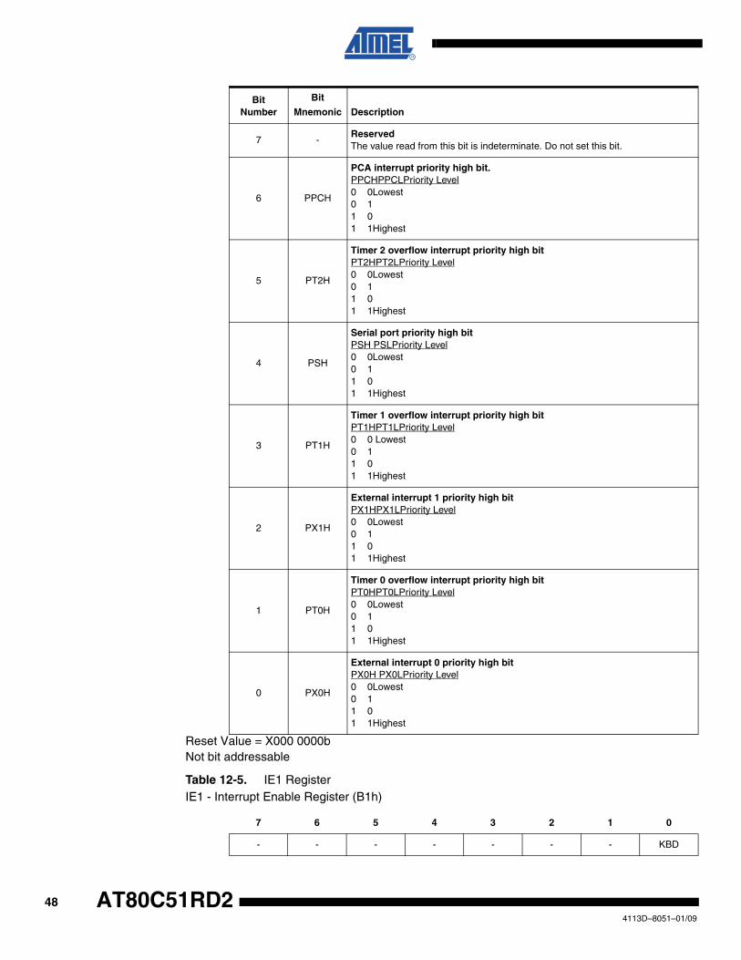
Table 12-5. IE1 RegisterIE1 - Interrupt Enable Register (B1h)
Bit Number
Bit
Mnemonic Description
7 -ReservedThe value read from this bit is indeterminate. Do not set this bit.
6 PPCH
PCA interrupt priority high bit. PPCHPPCLPriority Level0 0Lowest0 11 01 1Highest
5 PT2H
Timer 2 overflow interrupt priority high bitPT2HPT2LPriority Level0 0Lowest0 11 01 1Highest
4 PSH
Serial port priority high bitPSH PSLPriority Level0 0Lowest0 11 01 1Highest
3 PT1H
Timer 1 overflow interrupt priority high bitPT1HPT1LPriority Level0 0 Lowest0 11 01 1 Highest
2 PX1H
External interrupt 1 priority high bitPX1HPX1LPriority Level0 0Lowest0 11 01 1Highest
1 PT0H
Timer 0 overflow interrupt priority high bitPT0HPT0LPriority Level0 0Lowest0 11 01 1Highest
0 PX0H
External interrupt 0 priority high bitPX0H PX0LPriority Level0 0Lowest0 11 01 1Highest
7 6 5 4 3 2 1 0
- - - - - - - KBD
484113D–8051–01/09
AT80C51RD2
AT80C51RD2
Reset Value = XXXX XXX0bBit addressable
Table 12-6. IPL1 RegisterIPL1 - Interrupt Priority Register (B2h)
Reset Value = XXXX XXX0bBit addressable
Table 12-7. IPH1 Register
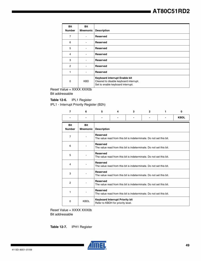
Bit
Number
Bit
Mnemonic Description
7 - Reserved
6 - Reserved
5 - Reserved
4 - Reserved
3 - Reserved
2 - Reserved
1 - Reserved
0 KBDKeyboard interrupt Enable bitCleared to disable keyboard interrupt. Set to enable keyboard interrupt.
7 6 5 4 3 2 1 0
- - - - - - - KBDL
Bit
Number
Bit
Mnemonic Description
7 -ReservedThe value read from this bit is indeterminate. Do not set this bit.
6 -ReservedThe value read from this bit is indeterminate. Do not set this bit.
5 -ReservedThe value read from this bit is indeterminate. Do not set this bit.
4 -ReservedThe value read from this bit is indeterminate. Do not set this bit.
3 -ReservedThe value read from this bit is indeterminate. Do not set this bit.
2 -ReservedThe value read from this bit is indeterminate. Do not set this bit.
1 -ReservedThe value read from this bit is indeterminate. Do not set this bit.
0 KBDLKeyboard Interrupt Priority bitRefer to KBDH for priority level.
494113D–8051–01/09
IPH1 - Interrupt Priority High Register (B3h)
Reset Value = XXXX XXX0bNot bit addressable
12.2 Interrupt Sources and Vector AddressesTable 12-8. Interrupt Sources and Vector Addresses
7 6 5 4 3 2 1 0
- - - - - - - KBDH
Bit Number
Bit
Mnemonic Description
7 -ReservedThe value read from this bit is indeterminate. Do not set this bit.
6 -ReservedThe value read from this bit is indeterminate. Do not set this bit.
5 -ReservedThe value read from this bit is indeterminate. Do not set this bit.
4 -ReservedThe value read from this bit is indeterminate. Do not set this bit.
3 -ReservedThe value read from this bit is indeterminate. Do not set this bit.
2 -ReservedThe value read from this bit is indeterminate. Do not set this bit.
1 -ReservedThe value read from this bit is indeterminate. Do not set this bit.
0 KBDH
Keyboard interrupt Priority High bitKB DHKBDLPriority Level0 0 Lowest0 11 01 1 Highest
Number Polling Priority Interrupt SourceInterruptRequest
Vector
Address
0 0 Reset 0000h
1 1 INT0 IE0 0003h
2 2 Timer 0 TF0 000Bh
3 3 INT1 IE1 0013h
4 4 Timer 1 IF1 001Bh
5 6 UART RI+TI 0023h
6 7 Timer 2 TF2+EXF2 002Bh
7 5 PCA CF + CCFn (n = 0-4) 0033h
8 8 Keyboard KBDIT 003Bh
504113D–8051–01/09
AT80C51RD2

AT80C51RD2
514113D–8051–01/09
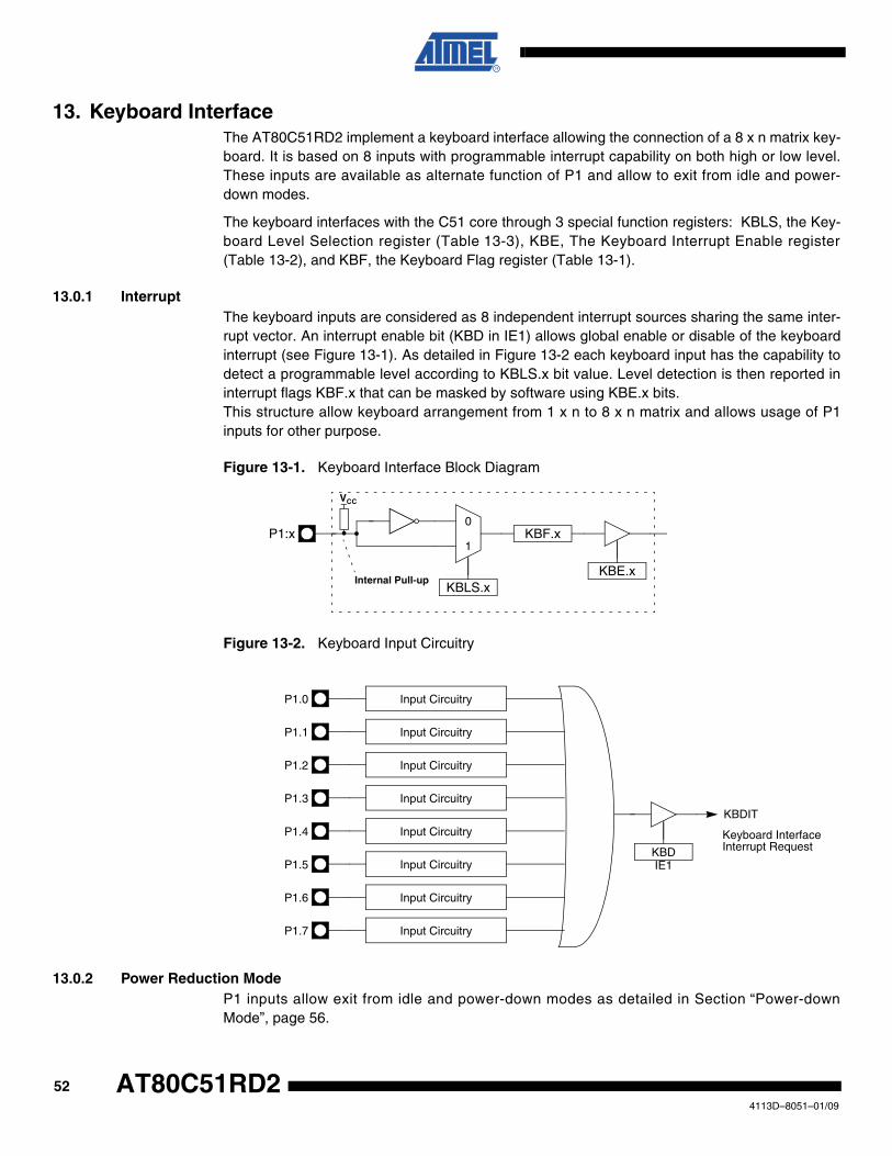
13. Keyboard InterfaceThe AT80C51RD2 implement a keyboard interface allowing the connection of a 8 x n matrix key-board. It is based on 8 inputs with programmable interrupt capability on both high or low level.These inputs are available as alternate function of P1 and allow to exit from idle and power-down modes.
The keyboard interfaces with the C51 core through 3 special function registers: KBLS, the Key-board Level Selection register (Table 13-3), KBE, The Keyboard Interrupt Enable register(Table 13-2), and KBF, the Keyboard Flag register (Table 13-1).
13.0.1 Interrupt The keyboard inputs are considered as 8 independent interrupt sources sharing the same inter-rupt vector. An interrupt enable bit (KBD in IE1) allows global enable or disable of the keyboardinterrupt (see Figure 13-1). As detailed in Figure 13-2 each keyboard input has the capability todetect a programmable level according to KBLS.x bit value. Level detection is then reported ininterrupt flags KBF.x that can be masked by software using KBE.x bits. This structure allow keyboard arrangement from 1 x n to 8 x n matrix and allows usage of P1inputs for other purpose.
Figure 13-1. Keyboard Interface Block Diagram
Figure 13-2. Keyboard Input Circuitry
13.0.2 Power Reduction ModeP1 inputs allow exit from idle and power-down modes as detailed in Section “Power-downMode”, page 56.
P1:x
KBE.x
KBF.x
KBLS.x
0
1
VCC
Internal Pull-up
P1.0
Keyboard InterfaceInterrupt RequestKBD
IE1
Input Circuitry
P1.1 Input Circuitry
P1.2 Input Circuitry
P1.3 Input Circuitry
P1.4 Input Circuitry
P1.5 Input Circuitry
P1.6 Input Circuitry
P1.7 Input Circuitry
KBDIT
524113D–8051–01/09
AT80C51RD2
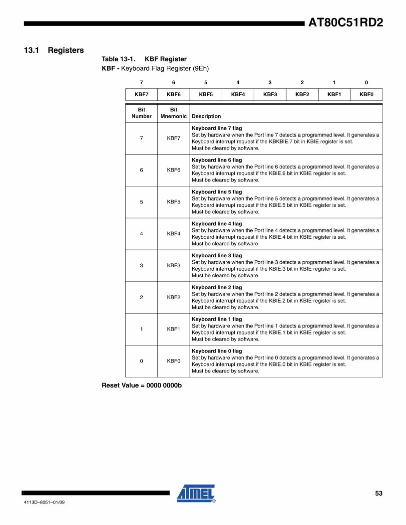
AT80C51RD2
13.1 RegistersTable 13-1. KBF RegisterKBF - Keyboard Flag Register (9Eh)
Reset Value = 0000 0000b
7 6 5 4 3 2 1 0
KBF7 KBF6 KBF5 KBF4 KBF3 KBF2 KBF1 KBF0
Bit Number
Bit Mnemonic Description
7 KBF7
Keyboard line 7 flagSet by hardware when the Port line 7 detects a programmed level. It generates a Keyboard interrupt request if the KBKBIE.7 bit in KBIE register is set. Must be cleared by software.
6 KBF6
Keyboard line 6 flag Set by hardware when the Port line 6 detects a programmed level. It generates a Keyboard interrupt request if the KBIE.6 bit in KBIE register is set. Must be cleared by software.
5 KBF5
Keyboard line 5 flag Set by hardware when the Port line 5 detects a programmed level. It generates a Keyboard interrupt request if the KBIE.5 bit in KBIE register is set. Must be cleared by software.
4 KBF4
Keyboard line 4 flag Set by hardware when the Port line 4 detects a programmed level. It generates a Keyboard interrupt request if the KBIE.4 bit in KBIE register is set. Must be cleared by software.
3 KBF3
Keyboard line 3 flagSet by hardware when the Port line 3 detects a programmed level. It generates a Keyboard interrupt request if the KBIE.3 bit in KBIE register is set. Must be cleared by software.
2 KBF2
Keyboard line 2 flagSet by hardware when the Port line 2 detects a programmed level. It generates a Keyboard interrupt request if the KBIE.2 bit in KBIE register is set. Must be cleared by software.
1 KBF1
Keyboard line 1 flag Set by hardware when the Port line 1 detects a programmed level. It generates a Keyboard interrupt request if the KBIE.1 bit in KBIE register is set. Must be cleared by software.
0 KBF0
Keyboard line 0 flag Set by hardware when the Port line 0 detects a programmed level. It generates a Keyboard interrupt request if the KBIE.0 bit in KBIE register is set. Must be cleared by software.
534113D–8051–01/09
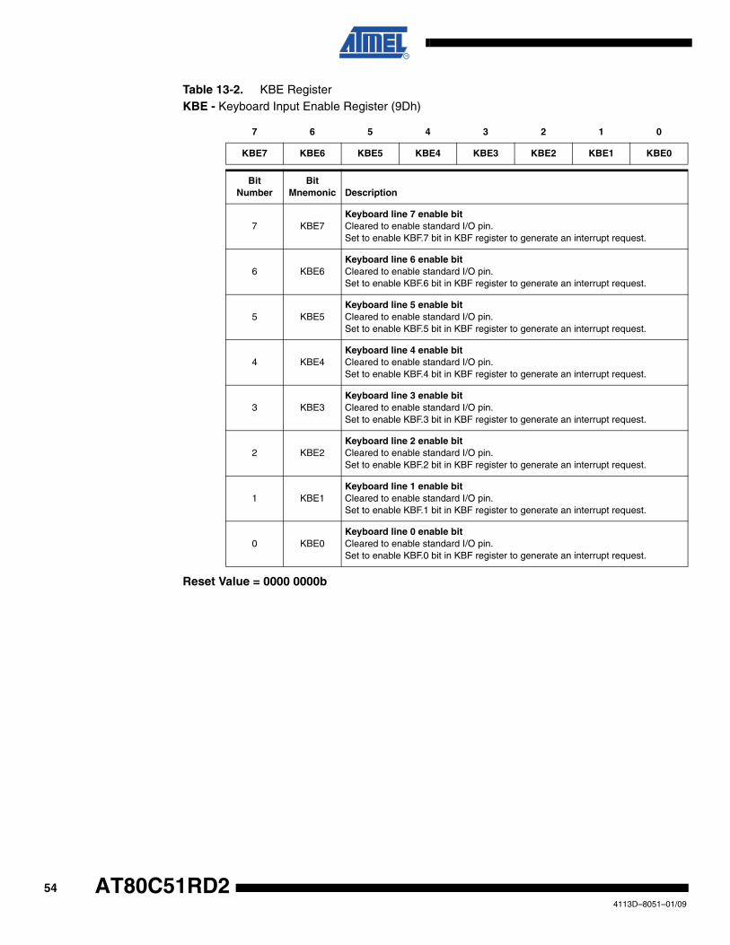
Table 13-2. KBE RegisterKBE - Keyboard Input Enable Register (9Dh)
Reset Value = 0000 0000b
7 6 5 4 3 2 1 0
KBE7 KBE6 KBE5 KBE4 KBE3 KBE2 KBE1 KBE0
BitNumber
BitMnemonic Description
7 KBE7Keyboard line 7 enable bitCleared to enable standard I/O pin. Set to enable KBF.7 bit in KBF register to generate an interrupt request.
6 KBE6Keyboard line 6 enable bitCleared to enable standard I/O pin. Set to enable KBF.6 bit in KBF register to generate an interrupt request.
5 KBE5Keyboard line 5 enable bitCleared to enable standard I/O pin. Set to enable KBF.5 bit in KBF register to generate an interrupt request.
4 KBE4Keyboard line 4 enable bitCleared to enable standard I/O pin. Set to enable KBF.4 bit in KBF register to generate an interrupt request.
3 KBE3Keyboard line 3 enable bitCleared to enable standard I/O pin. Set to enable KBF.3 bit in KBF register to generate an interrupt request.
2 KBE2Keyboard line 2 enable bitCleared to enable standard I/O pin. Set to enable KBF.2 bit in KBF register to generate an interrupt request.
1 KBE1Keyboard line 1 enable bitCleared to enable standard I/O pin. Set to enable KBF.1 bit in KBF register to generate an interrupt request.
0 KBE0Keyboard line 0 enable bitCleared to enable standard I/O pin. Set to enable KBF.0 bit in KBF register to generate an interrupt request.
544113D–8051–01/09
AT80C51RD2
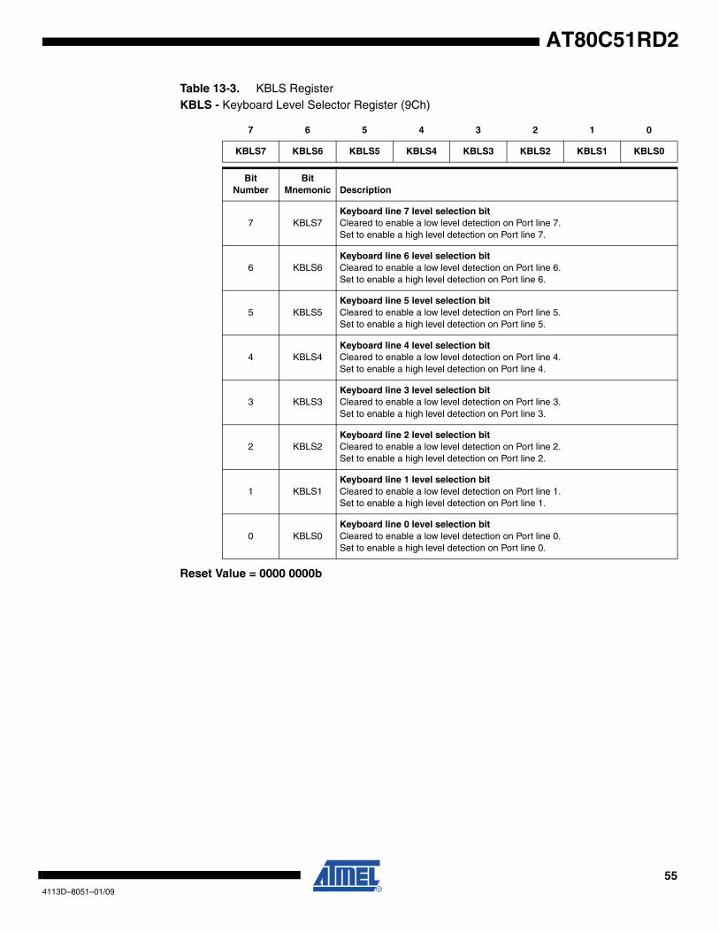
AT80C51RD2
Table 13-3. KBLS RegisterKBLS - Keyboard Level Selector Register (9Ch)
Reset Value = 0000 0000b
7 6 5 4 3 2 1 0
KBLS7 KBLS6 KBLS5 KBLS4 KBLS3 KBLS2 KBLS1 KBLS0
Bit Number
Bit Mnemonic Description
7 KBLS7Keyboard line 7 level selection bitCleared to enable a low level detection on Port line 7. Set to enable a high level detection on Port line 7.
6 KBLS6Keyboard line 6 level selection bitCleared to enable a low level detection on Port line 6. Set to enable a high level detection on Port line 6.
5 KBLS5Keyboard line 5 level selection bitCleared to enable a low level detection on Port line 5. Set to enable a high level detection on Port line 5.
4 KBLS4Keyboard line 4 level selection bitCleared to enable a low level detection on Port line 4. Set to enable a high level detection on Port line 4.
3 KBLS3Keyboard line 3 level selection bitCleared to enable a low level detection on Port line 3.Set to enable a high level detection on Port line 3.
2 KBLS2Keyboard line 2 level selection bitCleared to enable a low level detection on Port line 2.Set to enable a high level detection on Port line 2.
1 KBLS1Keyboard line 1 level selection bitCleared to enable a low level detection on Port line 1.Set to enable a high level detection on Port line 1.
0 KBLS0Keyboard line 0 level selection bitCleared to enable a low level detection on Port line 0.Set to enable a high level detection on Port line 0.
554113D–8051–01/09
14. Power Management
14.1 Idle ModeAn instruction that sets PCON.0 indicates that it is the last instruction to be executed beforegoing into Idle mode. In Idle mode, the internal clock signal is gated off to the CPU, but not to theinterrupt, Timer, and Serial Port functions. The CPU status is preserved in its entirety: the StackPointer, Program Counter, Program Status Word, Accumulator and all other registers maintaintheir data during idle. The port pins hold the logical states they had at the time Idle was acti-vated. ALE and PSEN hold at logic high level.
There are two ways to terminate the Idle mode. Activation of any enabled interrupt will causePCON.0 to be cleared by hardware, terminating the Idle mode. The interrupt will be serviced,and following RETI the next instruction to be executed will be the one following the instructionthat put the device into idle.
The flag bits GF0 and GF1 can be used to give an indication if an interrupt occurred during nor-mal operation or during idle. For example, an instruction that activates idle can also set one orboth flag bits. When idle is terminated by an interrupt, the interrupt service routine can examinethe flag bits.
The other way of terminating the Idle mode is with a hardware reset. Since the clock oscillator isstill running, the hardware reset needs to be held active for only two machine cycles (24 oscilla-tor periods) to complete the reset.
14.2 Power-down ModeTo save maximum power, a power-down mode can be invoked by software (refer to Table 11-12, PCON register).
In power-down mode, the oscillator is stopped and the instruction that invoked power-downmode is the last instruction executed. The internal RAM and SFRs retain their value until thepower-down mode is terminated. VCC can be lowered to save further power. Either a hardwarereset or an external interrupt can cause an exit from power-down. To properly terminate power-down, the reset or external interrupt should not be executed before VCC is restored to its normaloperating level and must be held active long enough for the oscillator to restart and stabilize.
Only external interrupts INT0, INT1 and Keyboard Interrupts are useful to exit from power-down.Thus, the interrupt must be enabled and configured as level - or edge - sensitive interrupt input.When Keyboard Interrupt occurs after a power-down mode, 1024 clocks are necessary to exit topower-down mode and enter in operating mode.
Holding the pin low restarts the oscillator but bringing the pin high completes the exit as detailedin Figure 14-1. When both interrupts are enabled, the oscillator restarts as soon as one of thetwo inputs is held low and power-down exit will be completed when the first input is released. Inthis case, the higher priority interrupt service routine is executed. Once the interrupt is serviced,the next instruction to be executed after RETI will be the one following the instruction that putAT80C51RD2 into power-down mode.
564113D–8051–01/09
AT80C51RD2
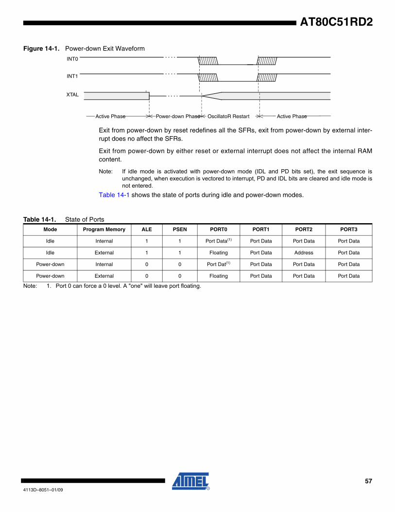
AT80C51RD2
Figure 14-1. Power-down Exit Waveform
Exit from power-down by reset redefines all the SFRs, exit from power-down by external inter-rupt does no affect the SFRs.
Exit from power-down by either reset or external interrupt does not affect the internal RAMcontent.
Note: If idle mode is activated with power-down mode (IDL and PD bits set), the exit sequence isunchanged, when execution is vectored to interrupt, PD and IDL bits are cleared and idle mode isnot entered.
Table 14-1 shows the state of ports during idle and power-down modes.
Note: 1. Port 0 can force a 0 level. A "one" will leave port floating.
INT1
INT0
XTAL
Power-down Phase OscillatoR Restart Active PhaseActive Phase
Table 14-1. State of Ports
Mode Program Memory ALE PSEN PORT0 PORT1 PORT2 PORT3
Idle Internal 1 1 Port Data(1) Port Data Port Data Port Data
Idle External 1 1 Floating Port Data Address Port Data
Power-down Internal 0 0 Port Dat(1) Port Data Port Data Port Data
Power-down External 0 0 Floating Port Data Port Data Port Data
574113D–8051–01/09
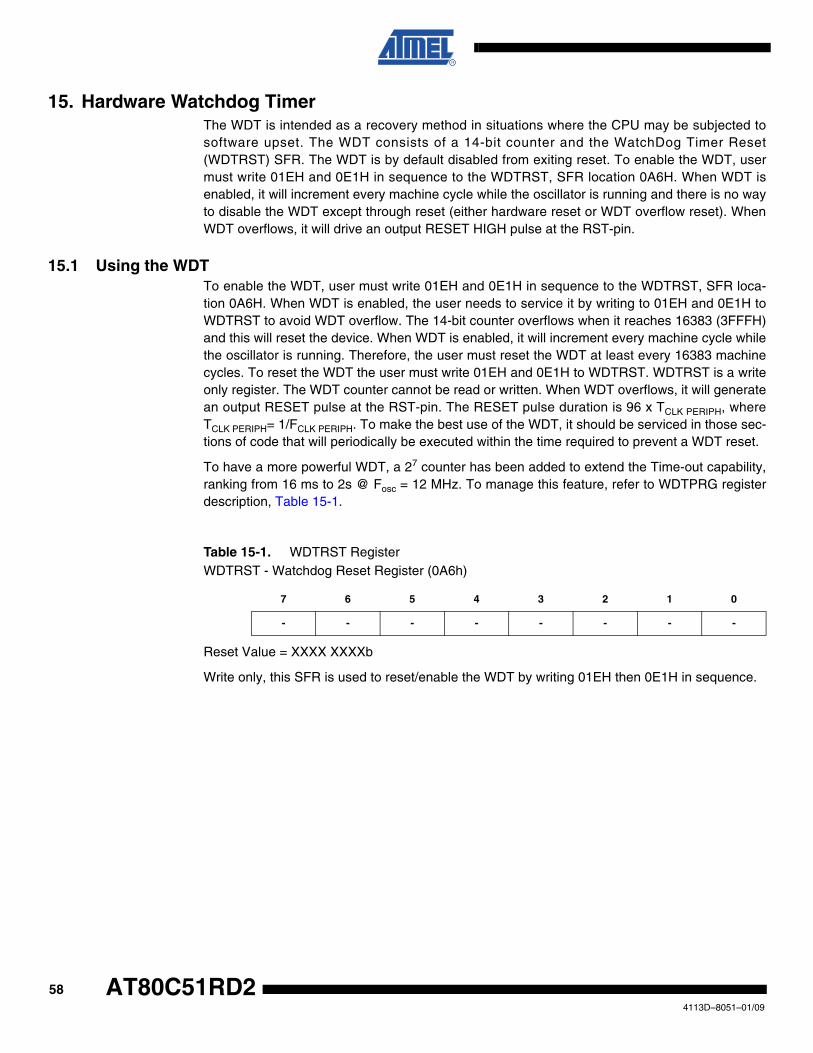
15. Hardware Watchdog TimerThe WDT is intended as a recovery method in situations where the CPU may be subjected tosoftware upset. The WDT consists of a 14-bit counter and the WatchDog Timer Reset(WDTRST) SFR. The WDT is by default disabled from exiting reset. To enable the WDT, usermust write 01EH and 0E1H in sequence to the WDTRST, SFR location 0A6H. When WDT isenabled, it will increment every machine cycle while the oscillator is running and there is no wayto disable the WDT except through reset (either hardware reset or WDT overflow reset). WhenWDT overflows, it will drive an output RESET HIGH pulse at the RST-pin.
15.1 Using the WDTTo enable the WDT, user must write 01EH and 0E1H in sequence to the WDTRST, SFR loca-tion 0A6H. When WDT is enabled, the user needs to service it by writing to 01EH and 0E1H toWDTRST to avoid WDT overflow. The 14-bit counter overflows when it reaches 16383 (3FFFH)and this will reset the device. When WDT is enabled, it will increment every machine cycle whilethe oscillator is running. Therefore, the user must reset the WDT at least every 16383 machinecycles. To reset the WDT the user must write 01EH and 0E1H to WDTRST. WDTRST is a writeonly register. The WDT counter cannot be read or written. When WDT overflows, it will generatean output RESET pulse at the RST-pin. The RESET pulse duration is 96 x TCLK PERIPH, whereTCLK PERIPH= 1/FCLK PERIPH. To make the best use of the WDT, it should be serviced in those sec-tions of code that will periodically be executed within the time required to prevent a WDT reset.
To have a more powerful WDT, a 27 counter has been added to extend the Time-out capability,ranking from 16 ms to 2s @ Fosc = 12 MHz. To manage this feature, refer to WDTPRG registerdescription, Table 15-1.
Table 15-1. WDTRST RegisterWDTRST - Watchdog Reset Register (0A6h)
Reset Value = XXXX XXXXb
Write only, this SFR is used to reset/enable the WDT by writing 01EH then 0E1H in sequence.
7 6 5 4 3 2 1 0
- - - - - - - -
584113D–8051–01/09
AT80C51RD2
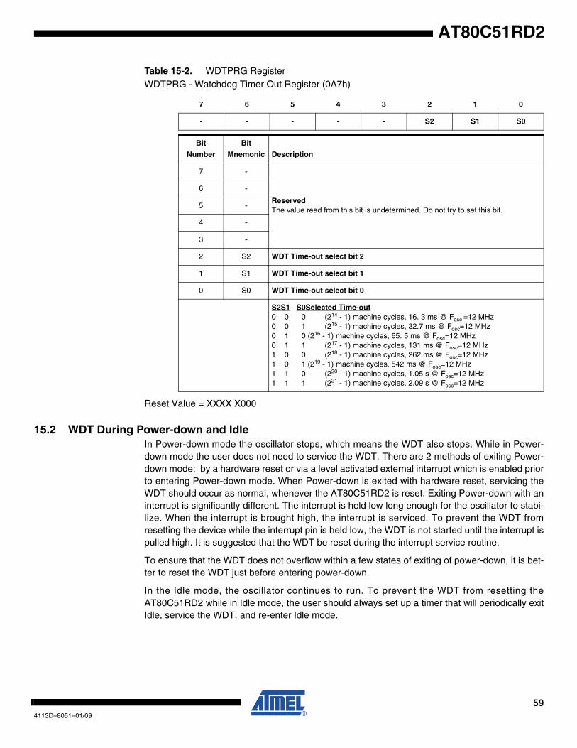
AT80C51RD2
Table 15-2. WDTPRG RegisterWDTPRG - Watchdog Timer Out Register (0A7h)
Reset Value = XXXX X000
15.2 WDT During Power-down and IdleIn Power-down mode the oscillator stops, which means the WDT also stops. While in Power-down mode the user does not need to service the WDT. There are 2 methods of exiting Power-down mode: by a hardware reset or via a level activated external interrupt which is enabled priorto entering Power-down mode. When Power-down is exited with hardware reset, servicing theWDT should occur as normal, whenever the AT80C51RD2 is reset. Exiting Power-down with aninterrupt is significantly different. The interrupt is held low long enough for the oscillator to stabi-lize. When the interrupt is brought high, the interrupt is serviced. To prevent the WDT fromresetting the device while the interrupt pin is held low, the WDT is not started until the interrupt ispulled high. It is suggested that the WDT be reset during the interrupt service routine.
To ensure that the WDT does not overflow within a few states of exiting of power-down, it is bet-ter to reset the WDT just before entering power-down.
In the Idle mode, the oscillator continues to run. To prevent the WDT from resetting theAT80C51RD2 while in Idle mode, the user should always set up a timer that will periodically exitIdle, service the WDT, and re-enter Idle mode.
7 6 5 4 3 2 1 0
- - - - - S2 S1 S0
Bit
Number
Bit
Mnemonic Description
7 -
ReservedThe value read from this bit is undetermined. Do not try to set this bit.
6 -
5 -
4 -
3 -
2 S2 WDT Time-out select bit 2
1 S1 WDT Time-out select bit 1
0 S0 WDT Time-out select bit 0
S2S1 S0Selected Time-out0 0 0 (214 - 1) machine cycles, 16. 3 ms @ Fosc =12 MHz0 0 1 (215 - 1) machine cycles, 32.7 ms @ Fosc=12 MHz0 1 0 (216 - 1) machine cycles, 65. 5 ms @ Fosc=12 MHz0 1 1 (217 - 1) machine cycles, 131 ms @ Fosc=12 MHz1 0 0 (218 - 1) machine cycles, 262 ms @ Fosc=12 MHz1 0 1 (219 - 1) machine cycles, 542 ms @ Fosc=12 MHz1 1 0 (220 - 1) machine cycles, 1.05 s @ Fosc=12 MHz1 1 1 (221 - 1) machine cycles, 2.09 s @ Fosc=12 MHz
594113D–8051–01/09
604113D–8051–01/09
AT80C51RD2
16. Power-off FlagThe Power-off flag allows the user to distinguish between a “cold start” reset and a “warm start”reset.
A cold start reset is the one induced by VCC switch-on. A warm start reset occurs while VCC is stillapplied to the device and could be generated for example by an exit from power-down.
The Power-off flag (POF) is located in PCON register (Table 16-1). POF is set by hardwarewhen VCC rises from 0 to its nominal voltage. The POF can be set or cleared by software allow-ing the user to determine the type of reset.
Table 16-1. PCON RegisterPCON - Power Control Register (87h)
Reset Value = 00X1 0000bNot bit addressable
7 6 5 4 3 2 1 0
SMOD1 SMOD0 - POF GF1 GF0 PD IDL
Bit
Number
Bit
Mnemonic Description
7 SMOD1Serial port Mode bit 1Set to select double baud rate in mode 1, 2 or 3.
6 SMOD0Serial port Mode bit 0Cleared to select SM0 bit in SCON register. Set to select FE bit in SCON register.
5 -ReservedThe value read from this bit is indeterminate. Do not set this bit.
4 POF
Power-off FlagCleared to recognize next reset type. Set by hardware when VCC rises from 0 to its nominal voltage. Can also be set by software.
3 GF1General purpose FlagCleared by user for general purpose usage. Set by user for general purpose usage.
2 GF0General purpose FlagCleared by user for general purpose usage. Set by user for general purpose usage.
1 PDPower-down mode bitCleared by hardware when reset occurs. Set to enter power-down mode.
0 IDLIdle mode bitCleared by hardware when interrupt or reset occurs. Set to enter idle mode.
AT80C51RD2
17. Reduced EMI ModeThe ALE signal is used to demultiplex address and data buses on port 0 when used with exter-nal program or data memory. Nevertheless, during internal code execution, ALE signal is stillgenerated. In order to reduce EMI, ALE signal can be disabled by setting AO bit.
The AO bit is located in AUXR register at bit location 0. As soon as AO is set, ALE is no longeroutput but remains active during MOVX and MOVC instructions and external fetches. DuringALE disabling, ALE pin is weakly pulled high.
Table 17-1. AUXR RegisterAUXR - Auxiliary Register (8Eh)
7 6 5 4 3 2 1 0
- - M0 - XRS1 XRS0 EXTRAM AO
Bit
Number
Bit
Mnemonic Description
7 -Reserved
The value read from this bit is indeterminate. Do not set this bit
6 -Reserved
The value read from this bit is indeterminate. Do not set this bit
5 M0
Pulse length
Cleared to stretch MOVX control: the RD and the WR pulse length is 6 clock periods (default).
Set to stretch MOVX control: the RD and the WR pulse length is 30 clock periods.
4 -Reserved
The value read from this bit is indeterminate. Do not set this bit
3 XRS1 XRAM Size
XRS1XRS0XRAM Size0 0256 bytes (default)
0 1512 bytes
1 0768 bytes
1 11024 bytes
2 XRS0
1 EXTRAM
EXTRAM bitCleared to access internal XRAM using movx @ Ri/ @ DPTR.
Set to access external memory.
Programmed by hardware after Power-up regarding Hardware Security Byte (HSB), default setting, XRAM selected.
0 AO
ALE Output bitCleared, ALE is emitted at a constant rate of 1/6 the oscillator frequency (or 1/3 if X2 mode is used) (default). Set, ALE is active only during a MOVX or MOVC instructione is used.
614113D–8051–01/09

624113D–8051–01/09
AT80C51RD2
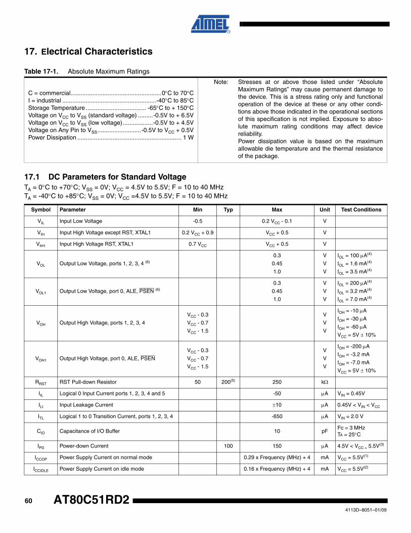
17. Electrical Characteristics
17.1 DC Parameters for Standard VoltageTA = 0°C to +70°C; VSS = 0V; VCC = 4.5V to 5.5V; F = 10 to 40 MHzTA = -40°C to +85°C; VSS = 0V; VCC =4.5V to 5.5V; F = 10 to 40 MHz
Table 17-1. Absolute Maximum Ratings
C = commercial......................................................0°C to 70°CI = industrial ........................................................-40°C to 85°CStorage Temperature .................................... -65°C to + 150°CVoltage on VCC to VSS (standard voltage) .........-0.5V to + 6.5VVoltage on VCC to VSS (low voltage)..................-0.5V to + 4.5VVoltage on Any Pin to VSS..........................-0.5V to VCC + 0.5VPower Dissipation .............................................................. 1 W
Note: Stresses at or above those listed under “AbsoluteMaximum Ratings” may cause permanent damage tothe device. This is a stress rating only and functionaloperation of the device at these or any other condi-tions above those indicated in the operational sectionsof this specification is not implied. Exposure to abso-lute maximum rating conditions may affect devicereliability.Power dissipation value is based on the maximumallowable die temperature and the thermal resistanceof the package.
Symbol Parameter Min Typ Max Unit Test Conditions
VIL Input Low Voltage -0.5 0.2 VCC - 0.1 V
VIH Input High Voltage except RST, XTAL1 0.2 VCC + 0.9 VCC + 0.5 V
VIH1 Input High Voltage RST, XTAL1 0.7 VCC VCC + 0.5 V
VOL Output Low Voltage, ports 1, 2, 3, 4 (6)
0.3
0.45
1.0
V
V
V
IOL = 100 μA(4)
IOL = 1.6 mA(4)
IOL = 3.5 mA(4)
VOL1 Output Low Voltage, port 0, ALE, PSEN (6)
0.3
0.45
1.0
V
V
V
IOL = 200 μA(4)
IOL = 3.2 mA(4)
IOL = 7.0 mA(4)
VOH Output High Voltage, ports 1, 2, 3, 4
VCC - 0.3
VCC - 0.7
VCC - 1.5
V
V
V
IOH = -10 μA
IOH = -30 μA
IOH = -60 μA
VCC = 5V ± 10%
VOH1 Output High Voltage, port 0, ALE, PSEN
VCC - 0.3
VCC - 0.7
VCC - 1.5
V
V
V
IOH = -200 μA
IOH = -3.2 mA
IOH = -7.0 mA
VCC = 5V ± 10%
RRST RST Pull-down Resistor 50 200(5) 250 kΩ
IIL Logical 0 Input Current ports 1, 2, 3, 4 and 5 -50 μA VIN = 0.45V
ILI Input Leakage Current ±10 μA 0.45V < VIN < VCC
ITL Logical 1 to 0 Transition Current, ports 1, 2, 3, 4 -650 μA VIN = 2.0 V
CIO Capacitance of I/O Buffer 10 pFFc = 3 MHzTA = 25°C
IPD Power-down Current 100 150 μA 4.5V < VCC < 5.5V(3)
ICCOP Power Supply Current on normal mode 0.29 x Frequency (MHz) + 4 mA VCC = 5.5V(1)
ICCIDLE Power Supply Current on idle mode 0.16 x Frequency (MHz) + 4 mA VCC = 5.5V(2)
604113D–8051–01/09
AT80C51RD2
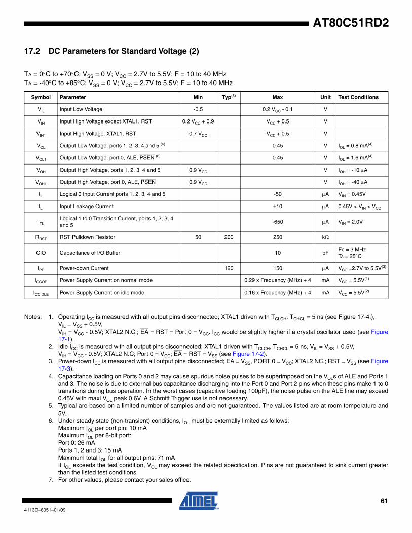
AT80C51RD2
17.2 DC Parameters for Standard Voltage (2)
TA = 0°C to +70°C; VSS = 0 V; VCC = 2.7V to 5.5V; F = 10 to 40 MHzTA = -40°C to +85°C; VSS = 0 V; VCC = 2.7V to 5.5V; F = 10 to 40 MHz
Notes: 1. Operating ICC is measured with all output pins disconnected; XTAL1 driven with TCLCH, TCHCL = 5 ns (see Figure 17-4.), VIL = VSS + 0.5V,VIH = VCC - 0.5V; XTAL2 N.C.; EA = RST = Port 0 = VCC. ICC would be slightly higher if a crystal oscillator used (see Figure17-1).
2. Idle ICC is measured with all output pins disconnected; XTAL1 driven with TCLCH, TCHCL = 5 ns, VIL = VSS + 0.5V, VIH = VCC - 0.5V; XTAL2 N.C; Port 0 = VCC; EA = RST = VSS (see Figure 17-2).
3. Power-down ICC is measured with all output pins disconnected; EA = VSS, PORT 0 = VCC; XTAL2 NC.; RST = VSS (see Figure17-3).
4. Capacitance loading on Ports 0 and 2 may cause spurious noise pulses to be superimposed on the VOLs of ALE and Ports 1and 3. The noise is due to external bus capacitance discharging into the Port 0 and Port 2 pins when these pins make 1 to 0transitions during bus operation. In the worst cases (capacitive loading 100pF), the noise pulse on the ALE line may exceed0.45V with maxi VOL peak 0.6V. A Schmitt Trigger use is not necessary.
5. Typical are based on a limited number of samples and are not guaranteed. The values listed are at room temperature and5V.
6. Under steady state (non-transient) conditions, IOL must be externally limited as follows:Maximum IOL per port pin: 10 mAMaximum IOL per 8-bit port:Port 0: 26 mAPorts 1, 2 and 3: 15 mAMaximum total IOL for all output pins: 71 mAIf IOL exceeds the test condition, VOL may exceed the related specification. Pins are not guaranteed to sink current greaterthan the listed test conditions.
7. For other values, please contact your sales office.
Symbol Parameter Min Typ(5) Max Unit Test Conditions
VIL Input Low Voltage -0.5 0.2 VCC - 0.1 V
VIH Input High Voltage except XTAL1, RST 0.2 VCC + 0.9 VCC + 0.5 V
VIH1 Input High Voltage, XTAL1, RST 0.7 VCC VCC + 0.5 V
VOL Output Low Voltage, ports 1, 2, 3, 4 and 5 (6) 0.45 V IOL = 0.8 mA(4)
VOL1 Output Low Voltage, port 0, ALE, PSEN (6) 0.45 V IOL = 1.6 mA(4)
VOH Output High Voltage, ports 1, 2, 3, 4 and 5 0.9 VCC V IOH = -10 μA
VOH1 Output High Voltage, port 0, ALE, PSEN 0.9 VCC V IOH = -40 μA
IIL Logical 0 Input Current ports 1, 2, 3, 4 and 5 -50 μA VIN = 0.45V
ILI Input Leakage Current ±10 μA 0.45V < VIN < VCC
ITLLogical 1 to 0 Transition Current, ports 1, 2, 3, 4 and 5
-650 μA VIN = 2.0V
RRST RST Pulldown Resistor 50 200 250 kΩ
CIO Capacitance of I/O Buffer 10 pFFc = 3 MHzTA = 25°C
IPD Power-down Current 120 150 μA VCC =2.7V to 5.5V(3)
ICCOP Power Supply Current on normal mode 0.29 x Frequency (MHz) + 4 mA VCC = 5.5V(1)
ICCIDLE Power Supply Current on idle mode 0.16 x Frequency (MHz) + 4 mA VCC = 5.5V(2)
614113D–8051–01/09
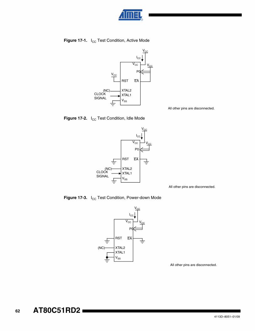
Figure 17-1. ICC Test Condition, Active Mode
Figure 17-2. ICC Test Condition, Idle Mode
Figure 17-3. ICC Test Condition, Power-down Mode
EA
VCC
VCC
ICC
(NC)CLOCK SIGNAL
VCC
All other pins are disconnected.
RST
XTAL2XTAL1
VSS
VCC
P0
RST EA
XTAL2XTAL1
VSS
VCC
VCC
ICC
(NC)
P0
VCC
All other pins are disconnected.
CLOCK SIGNAL
RST EA
XTAL2XTAL1
VSS
VCC
VCC
ICC
(NC)
P0
VCC
All other pins are disconnected.
624113D–8051–01/09
AT80C51RD2
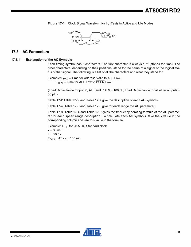
AT80C51RD2
Figure 17-4. Clock Signal Waveform for ICC Tests in Active and Idle Modes
17.3 AC Parameters
17.3.1 Explanation of the AC SymbolsEach timing symbol has 5 characters. The first character is always a “t” (stands for time). Theother characters, depending on their positions, stand for the name of a signal or the logical sta-tus of that signal. The following is a list of all the characters and what they stand for.
Example:TAVLL = Time for Address Valid to ALE Low.TLLPL = Time for ALE Low to PSEN Low.
(Load Capacitance for port 0, ALE and PSEN = 100 pF; Load Capacitance for all other outputs =80 pF.)
Table 17-2 Table 17-5, and Table 17-7 give the description of each AC symbols.
Table 17-4, Table 17-6 and Table 17-8 give for each range the AC parameter.
Table 17-3, Table 17-4 and Table 17-9 gives the frequency derating formula of the AC parame-ter for each speed range description. To calculate each AC symbols. take the x value in thecorreponding column and use this value in the formula.
Example: TLLIU for 20 MHz, Standard clock.x = 35 nsT = 50 nsTCCIV = 4T - x = 165 ns
VCC-0.5V
0.45V
0.7VCC0.2VCC-0.1
TCLCHTCHCL
TCLCH = TCHCL = 5ns.
634113D–8051–01/09
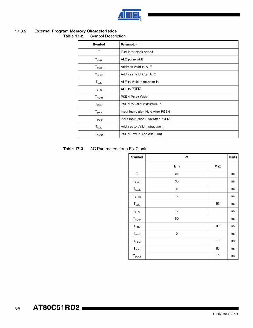
17.3.2 External Program Memory CharacteristicsTable 17-2. Symbol Description
Table 17-3. AC Parameters for a Fix Clock
Symbol Parameter
T Oscillator clock period
TLHLL ALE pulse width
TAVLL Address Valid to ALE
TLLAX Address Hold After ALE
TLLIV ALE to Valid Instruction In
TLLPL ALE to PSEN
TPLPH PSEN Pulse Width
TPLIV PSEN to Valid Instruction In
TPXIX Input Instruction Hold After PSEN
TPXIZ Input Instruction FloatAfter PSEN
TAVIV Address to Valid Instruction In
TPLAZ PSEN Low to Address Float
Symbol -M Units
Min Max
T 25 ns
TLHLL 35 ns
TAVLL 5 ns
TLLAX 5 ns
TLLIV 65 ns
TLLPL 5 ns
TPLPH 50 ns
TPLIV 30 ns
TPXIX 0 ns
TPXIZ 10 ns
TAVIV 80 ns
TPLAZ 10 ns
644113D–8051–01/09
AT80C51RD2
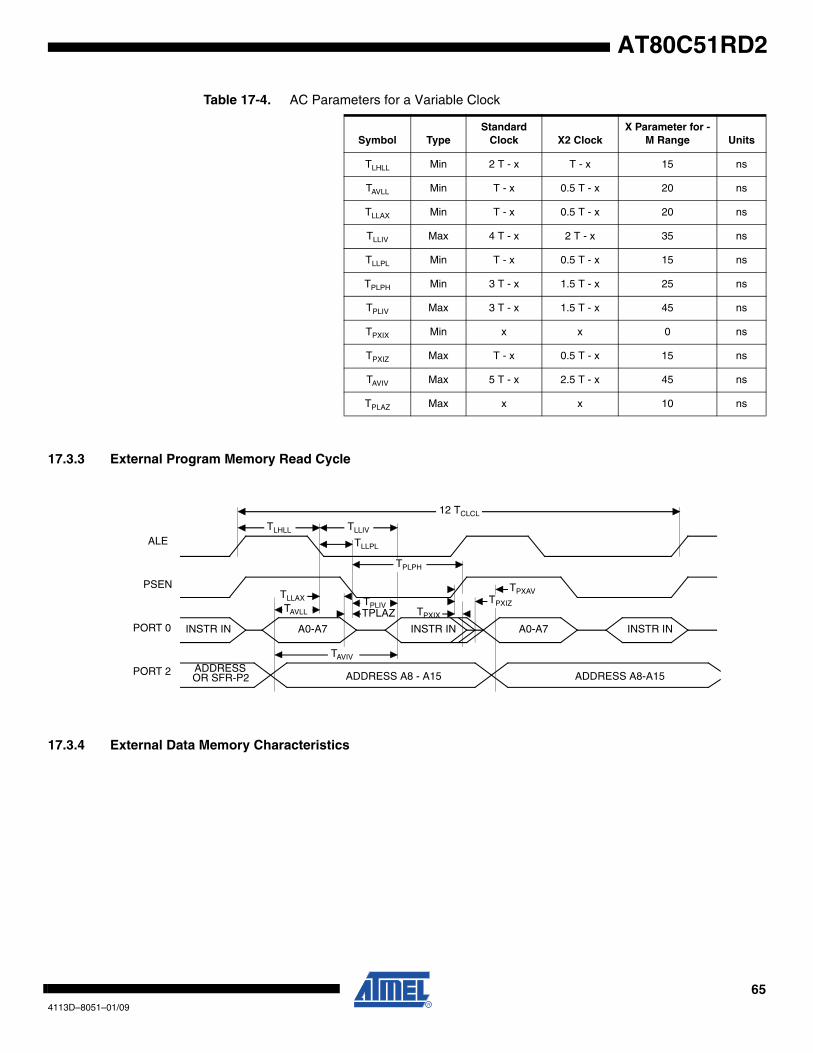
AT80C51RD2
Table 17-4. AC Parameters for a Variable Clock
17.3.3 External Program Memory Read Cycle
17.3.4 External Data Memory Characteristics
Symbol TypeStandard
Clock X2 Clock X Parameter for -
M Range Units
TLHLL Min 2 T - x T - x 15 ns
TAVLL Min T - x 0.5 T - x 20 ns
TLLAX Min T - x 0.5 T - x 20 ns
TLLIV Max 4 T - x 2 T - x 35 ns
TLLPL Min T - x 0.5 T - x 15 ns
TPLPH Min 3 T - x 1.5 T - x 25 ns
TPLIV Max 3 T - x 1.5 T - x 45 ns
TPXIX Min x x 0 ns
TPXIZ Max T - x 0.5 T - x 15 ns
TAVIV Max 5 T - x 2.5 T - x 45 ns
TPLAZ Max x x 10 ns
TPLIVTPLAZ
ALE
PSEN
PORT 0
PORT 2
A0-A7A0-A7 INSTR ININSTR IN INSTR IN
ADDRESSOR SFR-P2 ADDRESS A8-A15ADDRESS A8 - A15
12 TCLCL
TAVIV
TLHLL
TAVLL
TLLIV
TLLPL
TPLPH
TPXAV
TPXIX
TPXIZTLLAX
654113D–8051–01/09
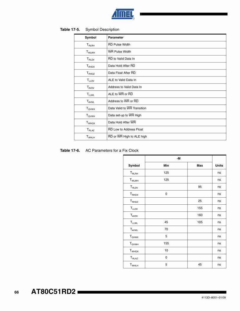
Table 17-5. Symbol Description
Table 17-6. AC Parameters for a Fix Clock
Symbol Parameter
TRLRH RD Pulse Width
TWLWH WR Pulse Width
TRLDV RD to Valid Data In
TRHDX Data Hold After RD
TRHDZ Data Float After RD
TLLDV ALE to Valid Data In
TAVDV Address to Valid Data In
TLLWL ALE to WR or RD
TAVWL Address to WR or RD
TQVWX Data Valid to WR Transition
TQVWH Data set-up to WR High
TWHQX Data Hold After WR
TRLAZ RD Low to Address Float
TWHLH RD or WR High to ALE high
Symbol
-M
UnitsMin Max
TRLRH 125 ns
TWLWH 125 ns
TRLDV 95 ns
TRHDX 0 ns
TRHDZ 25 ns
TLLDV 155 ns
TAVDV 160 ns
TLLWL 45 105 ns
TAVWL 70 ns
TQVWX 5 ns
TQVWH 155 ns
TWHQX 10 ns
TRLAZ 0 ns
TWHLH 5 45 ns
664113D–8051–01/09
AT80C51RD2
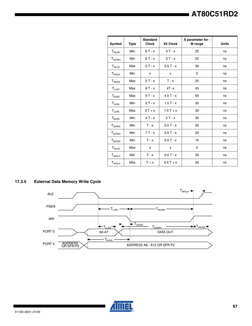
AT80C51RD2
17.3.5 External Data Memory Write Cycle
Symbol TypeStandard
Clock X2 ClockX parameter for -
M range Units
TRLRH Min 6 T - x 3 T - x 25 ns
TWLWH Min 6 T - x 3 T - x 25 ns
TRLDV Max 5 T - x 2.5 T - x 30 ns
TRHDX Min x x 0 ns
TRHDZ Max 2 T - x T - x 25 ns
TLLDV Max 8 T - x 4T -x 45 ns
TAVDV Max 9 T - x 4.5 T - x 65 ns
TLLWL Min 3 T - x 1.5 T - x 30 ns
TLLWL Max 3 T + x 1.5 T + x 30 ns
TAVWL Min 4 T - x 2 T - x 30 ns
TQVWX Min T - x 0.5 T - x 20 ns
TQVWH Min 7 T - x 3.5 T - x 20 ns
TWHQX Min T - x 0.5 T - x 15 ns
TRLAZ Max x x 0 ns
TWHLH Min T - x 0.5 T - x 20 ns
TWHLH Max T + x 0.5 T + x 20 ns
TQVWHTLLAX
ALE
PSEN
WR
PORT 0
PORT 2
A0-A7 DATA OUT
ADDRESSOR SFR-P2
TAVWL
TLLWL
TQVWX
ADDRESS A8 - A15 OR SFR P2
TWHQX
TWHLH
TWLWH
674113D–8051–01/09
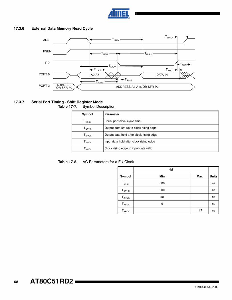
17.3.6 External Data Memory Read Cycle
17.3.7 Serial Port Timing - Shift Register ModeTable 17-7. Symbol Description
Table 17-8. AC Parameters for a Fix Clock
ALE
PSEN
RD
PORT 0
PORT 2
A0-A7 DATA IN
ADDRESSOR SFR-P2
TAVWL
TLLWL
TRLAZ
ADDRESS A8-A15 OR SFR P2
TRHDZ
TWHLH
TRLRH
TLLDV
TRHDXTLLAX
TAVDV
Symbol Parameter
TXLXL Serial port clock cycle time
TQVHX Output data set-up to clock rising edge
TXHQX Output data hold after clock rising edge
TXHDX Input data hold after clock rising edge
TXHDV Clock rising edge to input data valid
Symbol
-M
UnitsMin Max
TXLXL 300 ns
TQVHX 200 ns
TXHQX 30 ns
TXHDX 0 ns
TXHDV 117 ns
684113D–8051–01/09
AT80C51RD2
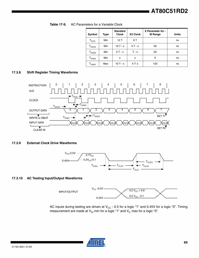
AT80C51RD2
Table 17-9. AC Parameters for a Variable Clock
17.3.8 Shift Register Timing Waveforms
17.3.9 External Clock Drive Waveforms
17.3.10 AC Testing Input/Output Waveforms
AC inputs during testing are driven at VCC - 0.5 for a logic “1” and 0.45V for a logic “0”. Timingmeasurement are made at VIH min for a logic “1” and VIL max for a logic “0”.
Symbol TypeStandard
Clock X2 ClockX Parameter for -
M Range Units
TXLXL Min 12 T 6 T ns
TQVHX Min 10 T - x 5 T - x 50 ns
TXHQX Min 2 T - x T - x 20 ns
TXHDX Min x x 0 ns
TXHDV Max 10 T - x 5 T- x 133 ns
INPUT DATA VALIDVALID VALID VALID
0 1 2 3 4 5 6 87
ALE
CLOCK
OUTPUT DATA
WRITE to SBUF
CLEAR RI
TXLXL
TQVXHTXHQX
TXHDVTXHDX SET TI
SET RI
INSTRUCTION
0 1 2 3 4 5 6 7
VALID VALID VALID VALID
VCC-0.5V
0.45V
0.7VCC
0.2VCC-0.1
TCHCL TCLCX
TCLCL
TCLCH
TCHCX
INPUT/OUTPUT 0.2 VCC + 0.9
0.2 VCC - 0.1
VCC -0.5V
0.45V
694113D–8051–01/09
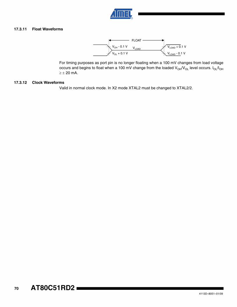
17.3.11 Float Waveforms
For timing purposes as port pin is no longer floating when a 100 mV changes from load voltageoccurs and begins to float when a 100 mV change from the loaded VOH/VOL level occurs. IOL/IOH
≥ ± 20 mA.
17.3.12 Clock WaveformsValid in normal clock mode. In X2 mode XTAL2 must be changed to XTAL2/2.
FLOAT
VOH - 0.1 V
VOL + 0.1 V
VLOADVLOAD + 0.1 V
VLOAD - 0.1 V
704113D–8051–01/09
AT80C51RD2
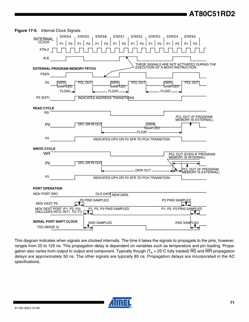
AT80C51RD2
Figure 17-5. Internal Clock Signals
This diagram indicates when signals are clocked internally. The time it takes the signals to propagate to the pins, however,ranges from 25 to 125 ns. This propagation delay is dependent on variables such as temperature and pin loading. Propa-gation also varies from output to output and component. Typically though (TA = 25°C fully loaded) RD and WR propagationdelays are approximately 50 ns. The other signals are typically 85 ns. Propagation delays are incorporated in the ACspecifications.
P2
P2
DATA PCL OUT DATA PCL OUT DATA PCL OUT SAMPLED SAMPLED SAMPLED
STATE4 STATE5 STATE6 STATE1 STATE2 STATE3 STATE4 STATE5
P1 P2 P1 P2 P1 P2 P1 P2 P1 P2 P1 P2 P1 P2 P1 P2
FLOAT FLOAT FLOAT
THESE SIGNALS ARE NOT ACTIVATED DURING THEEXECUTION OF A MOVX INSTRUCTION
INDICATES ADDRESS TRANSITIONS
EXTERNAL PROGRAM MEMORY FETCH
FLOAT
DATASAMPLED
DPL OR Rt OUT
INDICATES DPH OR P2 SFR TO PCH TRANSITION
PCL OUT (IF PROGRAMMEMORY IS EXTERNAL)
PCL OUT (EVEN IF PROGRAMMEMORY IS INTERNAL)
PCL OUT (IF PROGRAMMEMORY IS EXTERNAL)
OLD DATA NEW DATA
P0 PINS SAMPLED
P1, P2, P3 PINS SAMPLED P1, P2, P3 PINS SAMPLED
P0 PINS SAMPLED
RXD SAMPLED
INTERNALCLOCK
XTAL2
ALE
PSEN
P0
P2 (EXT)
READ CYCLE
WRITE CYCLE
RD
P0
WR
PORT OPERATION
MOV PORT SRC
MOV DEST P0
MOV DEST PORT (P1. P2. P3)(INCLUDES INTO. INT1. TO T1)
SERIAL PORT SHIFT CLOCK
TXD (MODE 0)
DATA OUT
DPL OR Rt OUT
INDICATES DPH OR P2 SFR TO PCH TRANSITION
P0
RXD SAMPLED
714113D–8051–01/09
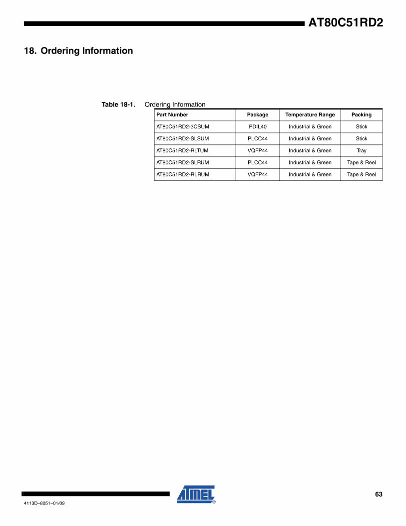
AT80C51RD2
18. Ordering Information
Table 18-1. Ordering Information
Part Number Package Temperature Range Packing
AT80C51RD2-3CSUM PDIL40 Industrial & Green Stick
AT80C51RD2-SLSUM PLCC44 Industrial & Green Stick
AT80C51RD2-RLTUM VQFP44 Industrial & Green Tray
AT80C51RD2-SLRUM PLCC44 Industrial & Green Tape & Reel
AT80C51RD2-RLRUM VQFP44 Industrial & Green Tape & Reel
634113D–8051–01/09
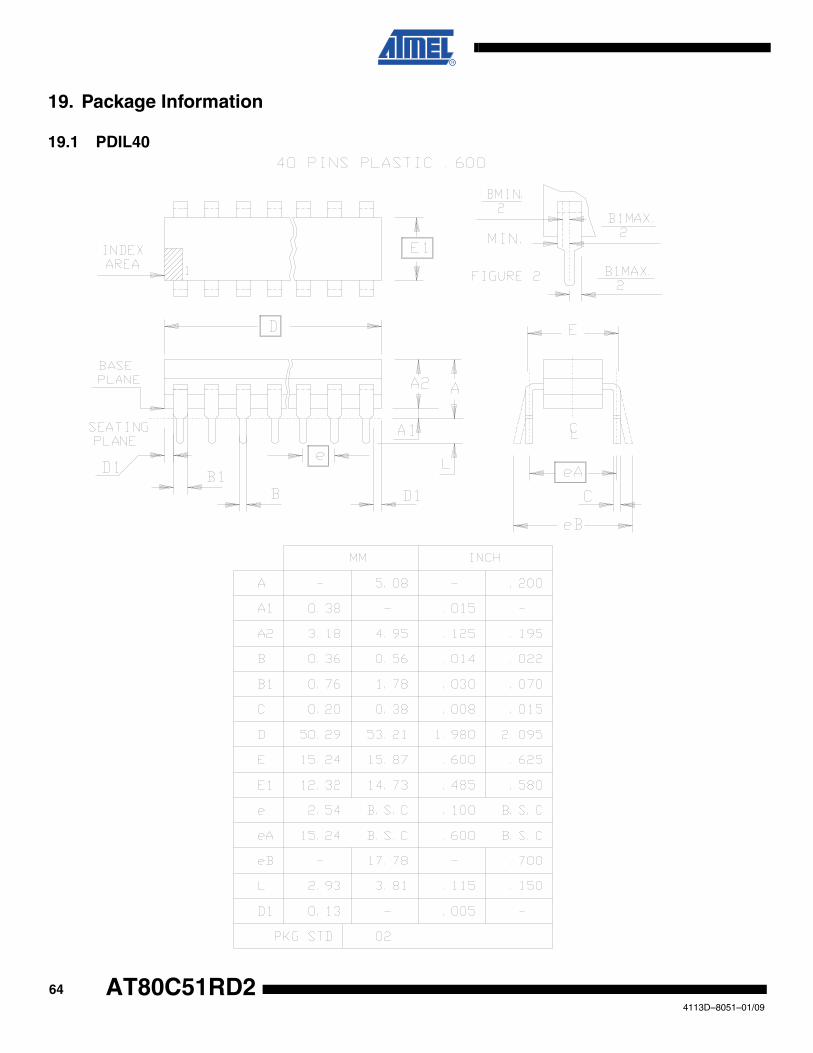
19. Package Information
19.1 PDIL40
644113D–8051–01/09
AT80C51RD2
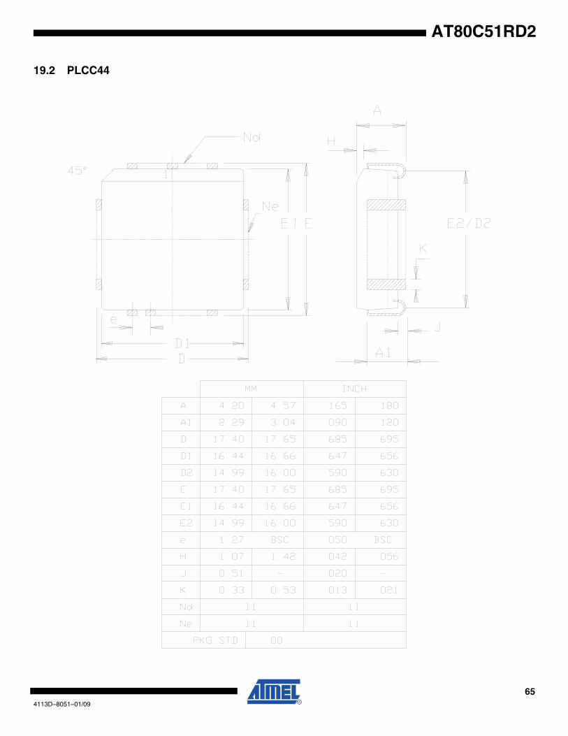
AT80C51RD2
19.2 PLCC44
654113D–8051–01/09
STANDARD NOTES FOR PLCC
1/ CONTROLLING DIMENSIONS : INCHES
2/ DIMENSIONING AND TOLERANCING PER ANSI Y 14.5M - 1982.
3/ "D" AND "E1" DIMENSIONS DO NOT INCLUDE MOLD FLASH OR PROTUSIONS.MOLD FLASH OR PROTUSIONS SHALL NOT EXCEED 0.20 mm (.008 INCH) PER
SIDE.
664113D–8051–01/09
AT80C51RD2
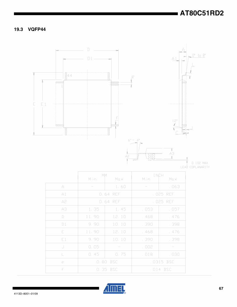
AT80C51RD2
19.3 VQFP44
674113D–8051–01/09

STANDARD NOTES FOR PQFP/ VQFP / TQFP / DQFP
1/ CONTROLLING DIMENSIONS : INCHES
2/ ALL DIMENSIONING AND TOLERANCING CONFORM TO ANSI Y 14.5M -1982.
3/ "D1 AND E1" DIMENSIONS DO NOT INCLUDE MOLD PROTUSIONS. MOLD PROTUSIONS SHALL NOT EXCEED 0.25 mm (0.010 INCH).THE TOP PACKAGE BODY SIZE MAY BE SMALLER THAN THE BOTTOM PACKAGE BODY SIZE BY AS MUCH AS 0.15 mm.
4/ DATUM PLANE "H" LOCATED AT MOLD PARTING LINE ANDCOINCIDENT WITH LEAD, WHERE LEAD EXITS PLASTIC BODY AT BOTTOM OF PARTING LINE.
5/ DATUM "A" AND "D" TO BE DETERMINED AT DATUM PLANE H.
6/ DIMENSION " f " DOES NOT INCLUDE DAMBAR PROTUSION ALLOWABLE DAMBAR PROTUSION SHALL BE 0.08mm/.003" TOTAL IN EXCESS OF THE" f " DIMENSION AT MAXIMUM MATERIAL CONDITION .DAMBAR CANNOT BE LOCATED ON THE LOWER RADIUS OR THE FOOT.
684113D–8051–01/09
AT80C51RD2
AT80C51RD2
20. Datasheet Change Log
20.1 Changes from 4113A - 09/02 to 4113B -03/051. Added Green product ordering information.
20.2 Changes from 4113B -03/05 to 4113C -01/081. Removed AT80C51RD2 product offering Table 18-1 on page 63.
2. Updated Package Drawings.
20.3 Changes from 4113C -01/08 to 4113D -01/091. Removed AT83C51RD2 product offering
694113D–8051–01/09