usb 2.0 oscilloscope project
TRANSCRIPT

USB 2.0Oscilloscope ProjectBy Geoffrey M. Phillips22nd October 2001 – 19th July 2002
Project supervisor: Dr. T. J. W. Clarke
A report presented to the Science, Engineering and TechnologyStudent of the Year Awards in relation to the author’s final year
undergraduate university project conducted atImperial College of the University of London
© Geoffrey Phillips 2002
2
1. AbstractThis report details the design and development of a digital oscilloscope
incorporating the Universal Serial Bus (USB) 2.0 standard, named the ‘USB2Scope’. The author was awarded the Sir Bruce White Prize for the best undergraduate project of 2002 by the Electrical and Electronic Engineering Department of Imperial College.
The functionality of the instrument is illustrated in the following diagram:
USB2Scope
Test Circuit
USB 2.0480Mbps
Host Computer
Figure 1.1 A functional diagram of the USB2Scope
The USB2Scope system is composed of an external measurement unit with two 1MΩ oscilloscope probe inputs and one USB 2.0 compatible connection to a host computer. The user tests signals using the probes and views the results via the host computer’s display. This system architecture has the benefit of low component costs for the external measurement unit, compared with traditional ‘one-box’ instruments, and the ease of use gained from using a ‘Plug-and-Play’ interface technology such as USB 2.0.
The USB 2.0 standard allows for a maximum data rate of 480Mbps (Mega bits per second). This is 40 times faster than the 12Mbps data rate of USB 1.1 and 17% faster than the 400Mbps of IEEE 1394a, also known as Firewire. The USB2Scope system uses this increased data rate to improve on the performance available from currently available computer-based oscilloscopes.
The system incorporates several novel design features. Firstly the ‘triggering’process is performed using software, as opposed to the conventional hardware method. This process was named ‘Software Triggering’. The system also employs a non-uniform sampling process to ‘under-sample’ a periodic input signal without suffering the detrimental effect of signal aliasing.
The project was conducted by the author at the Electrical and Electronic Engineering Department of Imperial College London in association with IFR Aeroflex UK Ltd., formerly known as Marconi Instruments.
This report describes the design process undertaken, including: market research, concept development, device specification, project planning, hardware design techniques and decisions, prototyping and testing, and the software development.
A prototype of the instrument was built, tested and evaluated, leading to conclusions on the viability of the proposed system, and proposed work for further development of the system.

3
2. Preface and AcknowledgementsThroughout my university career the emphasis has always been put on the
learning the theory behind engineering. This project has been an excellent opportunity to put this theory into unrestricted and independent practice, and has been a fantastic way to finish my undergraduate degree course.
It would be fair to say that this has been the largest and most wide-ranging project that I have completed so far. The project has encompassed system design, radio-frequency and digital electronic design, in conjunction with software design for both the device firmware and the host application.
Trying to fit all of this into an eight month period, along with normal university study has been hard work, but definitely worth it!
I have had a lot of help and advice along the way, especially from Tom Clarke and Steve Wilkinson. I would also like to thank IFR Aeroflex UK Ltd., my sponsoring company through university, for all their help and generosity, and without whose assistance many parts of this project would have been a lot harder to accomplish.
Geoffrey Phillips19th July 2002

4
3. Table of Contents1. Abstract ......................................................................................................22. Preface and Acknowledgements ................................................................33. Table of Contents .......................................................................................44. List of Figures ............................................................................................65. Introduction ................................................................................................9
5.1 Motivation ..........................................................................................95.2 Aim.....................................................................................................95.3 Structure of the Report .......................................................................95.4 Conventions Used ............................................................................10
6. Task ..........................................................................................................116.1 Task Expansion ................................................................................11
7. Preliminary Research ...............................................................................127.1 A Brief History of the Oscilloscope.................................................127.2 Digital Oscilloscope Architecture ....................................................127.3 Product Analysis ..............................................................................147.4 Market Analysis ...............................................................................177.5 Preliminary Research Conclusions...................................................18
8. Initial Concepts ........................................................................................198.1 Top-Level Concept...........................................................................198.2 System-Level Concepts....................................................................19
9. Concept Directed Research ......................................................................219.1 Data Transfer Technology................................................................219.2 Microsoft Windows USB Driver Architecture.................................269.3 The Theory of Non-Uniform Sampling ...........................................289.4 Software Triggering .........................................................................319.5 Additive Dither Theory ....................................................................329.6 Concept Directed Research Conclusions .........................................39
10. Concept Development ..........................................................................4010.1 Top-Level Concept Development ....................................................4010.2 System-Level Concept Development...............................................4010.3 Concept Selection.............................................................................41
11. Hardware Specification ........................................................................4211.1 Performance Decisions.....................................................................4211.2 Cost and Power Budgeting...............................................................44
12. Software Specification .........................................................................4613. Project Planning ...................................................................................4814. System-Level Design ...........................................................................5114.1 Initial System Design .......................................................................5114.2 System Design Review.....................................................................5514.3 Final System Design.........................................................................56
15. Front-End Design .................................................................................5815.1 Block Level Design..........................................................................5815.2 Attenuator Design ............................................................................6115.3 Front-End Buffer Design..................................................................6215.4 Amplification Stage Design .............................................................6415.5 Anti-Alias Filter Design ...................................................................6615.6 ADC Driver Stage Design................................................................68
5
15.7 ADC Stage Design ...........................................................................6915.8 LVDS Output Stage Design .............................................................7115.9 Switched Gain Driver Design ..........................................................71
16. Digital-Stage Design ............................................................................7317. Design Review .....................................................................................7517.1 Necessary Specification Changes.....................................................7517.2 Final USB2Scope Cost and Power Budget ......................................7517.3 Design Review Conclusions.............................................................7517.4 Final USB2Scope Hardware Specification ......................................77
18. Prototyping ...........................................................................................7818.1 Front-End Board...............................................................................7818.2 Digital-Stage Board..........................................................................7918.3 The Final Prototype..........................................................................8018.4 Photograph of the USB2Scope Prototype ........................................82
19. Introduction to the Testing Procedure ..................................................8320. Front-End Testing ................................................................................8320.1 AA filter analysis .............................................................................8420.2 Front-End Buffer Measurements......................................................8520.3 Amplifier Measurements..................................................................8720.4 Buffer and Amplifier Measurements................................................8820.5 The Test Setup Using the IFR 2319E Radio Frequency Digitiser and
the ‘FAT’ Software ..........................................................................8920.6 Photographs of the Front-End and 2319E Setup:.............................9120.7 ADC Frequency Response ...............................................................9220.8 ADC Level Linearity........................................................................9320.9 Dither Evaluation .............................................................................9320.10 Total Front-End Response................................................................9520.11 Front-End Testing Conclusions........................................................97
21. Digital-Stage Testing............................................................................9822. Front-End Improvement .......................................................................9923. Software Development .......................................................................10423.1 The Device Firmware.....................................................................10423.2 The Host Application .....................................................................109
24. Device Integration ..............................................................................11024.1 Screenshots of the USB2Scope Application ..................................111
25. Project Evaluation ..............................................................................11226. Conclusion..........................................................................................11327. Appendicies ........................................................................................11427.1 Appendix I – Proof of the Non-Uniform Sampling Theorem........11427.2 Appendix II – Derivation of the Second Moment of a Uniformly
Distributed Random Variable.........................................................11527.3 Appendix III – Derivation of the Maximum Signal to Noise Ratio of
an ADC...........................................................................................11627.4 Appendix IV – Device Schematics ................................................117
28. Glossary..............................................................................................12829. Bibliography.......................................................................................12930. References ..........................................................................................130

6
4. List of FiguresFigure 1.1 A functional diagram of the USB2Scope .....................................................2Figure 7.1 Transient Digitisation .................................................................................13Figure 7.2 RIS Digitisation ..........................................................................................13Figure 7.3 Sampling Digitisation .................................................................................14Figure 7.4 Agilent Technologies 54622A....................................................................15Figure 7.5 Tektronix TDS220 ......................................................................................15Figure 7.6 Pico Technolog ...........................................................................................16Figure 7.7 The Soft DSP .............................................................................................16Figure 7.8 The Agilent Technologies share price for the last two years (dark), and its
200 day moving average (light). ................................................................18Figure 8.1 The ‘High-Speed Capture – Low -Speed Transfer’ system........................19Figure 8.2 The ‘Continuously Streaming – Software Triggering’ system...................20Figure 9.1 A sketch of the simplest means of constructing an IEEE 1394 or USB 2.0
compatible peripheral .................................................................................24Figure 9.2 The USB software architecture of the Microsoft Win32 API. The names in
double quotation marks are the file names of the relevant drivers.............27Figure 9.3 The probability density of the sampling instants of periodic sampling with
jitter ............................................................................................................28Figure 9.4 An illustration of an additive- random process...........................................29Figure 9.5 Direct DFT of a discrete-random sampled signal with components at 20, 50
and 80MHz. The effective sample rate is 200MHz, but with an average sample rate of only 20MHz........................................................................31
Figure 9.6 Sketch of the extrapolation of a trigger point (X) from a positive movement through a threshold level (Thick line) to a given sample number Dashed line). The original sample points are notated with circles, and the interpolated signal is the dotted line...........................................................32
Figure 9.7 The ‘staircase’ formation of the quantisation function...............................33Figure 9.8 Quantisation error as a function of input ....................................................34Figure 9.9 A sinusoidal signal subject to quantisation.................................................34Figure 9.10 The quantisation error of the quantised sinusoid ......................................34Figure 9.11 Frequency components of the quantised sinusoid ....................................35Figure 9.12 The probability density function of a uniformly distributed random
process ........................................................................................................35Figure 9.13 Subtractively and Non-Subtractively Dithered Systems ..........................36Figure 9.14 The graphical illustration of the mean quantisation error having equality
to zero under the affect of a uniform dither signal. ....................................37Figure 10.1 The proposed appearance of the USB2Scope...........................................40Figure 11.1 The Top-Level Block diagram for the system ..........................................42Figure 12.1 The overall software architecture of the USB2Scope system...................47Figure 14.1 The Initial System-Level Design ..............................................................51Figure 14.2 The Common Serial Bus Interface............................................................52Figure 14.3 The Front-End Common Serial Bus Decoder Circuit...............................53Figure 14.4 The Final System-Level Design ...............................................................56Figure 14.5 The class-A amplifier design used to convert a bipolar input to a CMOS
compatible output.......................................................................................57Figure 15.1 The chosen block-level architecture of the Front-End Stage....................59
7
Figure 15.2 The incorrect model of a oscilloscope probe on x1 setting, illustrating the expected 1MΩ source resistance..............................................................60
Figure 15.3 The Attenuator Circuit ..............................................................................61Figure 15.4 The maximum peak amplitude for a slew-rate limited device of 390V/µs
..................................................................................................................63Figure 15.5 The Front-End Buffer Circuit ...................................................................64Figure 15.6 The Amplification Stage with the Gain-Switches ....................................65Figure 15.7 Eagleware derived 7th order elliptic filter – 90MHz cut-off, -60dB
from110MHz............................................................................................66Figure 15.8 Eagleware derived 7th order elliptic filter – 81MHz cut-off, -70dB from
119MHz....................................................................................................67Figure 15.9 Eagleware derived 9th order elliptic filter – 92MHz cut-off, -70dB from
108MHz....................................................................................................67Figure 15.10 The synthesised 9th order minimal-inductor elliptic low-pass filter .......68Figure 15.11 The Anti-Alias Filter schematic..............................................................68Figure 15.12 The ADC Driver Stage, including the Dither conditioning circuitry .....69Figure 15.13 The ADC Stage.......................................................................................70Figure 15.14 The LVDS Line Drivers and the common-mode filters .........................71Figure 15.15 The Attenuator driving circuit (Left) and the Gain-Switch driver circuit
(Right) ......................................................................................................72Figure 18.1 A block diagram of the Front-End PCB layout ........................................79Figure 18.2 A block diagram of the Digital-Stage PCB Layout ..................................80Figure 18.3 A photograph of the final USB2Scope prototype.....................................82Figure 20.1 A plot of the Anti-Alias Filter frequency response (S21).........................84Figure 20.2 The Front-End Buffer test setup ...............................................................85Figure 20.3 A plot of the frequency response of the Front-End Buffer for the different
Attenuator settings (pre-improvement) ....................................................85Figure 20.4 The incorrect model of a 1MΩ oscilloscope probe setup .........................86Figure 20.5 The Amplification test setup.....................................................................87Figure 20.6 A plot of the Amplifier Stage frequency response for the different
switched gain settings (pre-improvement) ...............................................87Figure 20.7 A plot of the total frequency response of the Front-End Buffer and the
Amplifier stage with the Attenuator set to 0dB for the different switched gain settings (pre-improvement) ..............................................................88
Figure 20.8 The Flashlite Automatic Test (FAT) system ...........................................89Figure 20.9 A close up photograph of the FAT setup, showing from top to bottom the
Front-End Stage, the IFR 2319E and the IFR 2026 signal generator ......91Figure 20.10 A photograph showing the whole test area.............................................91Figure 20.11 The frequency response of the ADC Stage, measured using the FAT
system.......................................................................................................92Figure 20.12 The level linearity of the ADC Stage using the FAT measurement
system.......................................................................................................94Figure 20.13 A sketch of the various unwanted frequency components generated
during two-tone intermodulation..............................................................94Figure 20.14 The SFDR of the ADC Stage with and without dither, measured using
the FAT system ........................................................................................95Figure 20.15 The Front-End Stage frequency response, measured using the FAT
system.......................................................................................................96Figure 20.16 The Front-End Stage level linearity, measured using the FAT system ..96Figure 22.1 A plot of the output of the Front-End Buffer with the Attenuator set on
0dB for the x1 and x10 settings of the oscilloscope probe.......................99
8
Figure 22.2 The improved Front-End Buffer frequency response using a probe on x10 with most of the input capacitance removed for each Attenuator setting................................................................................................................100
Figure 22.3 A plot of the frequency response of Gain Stage 2, for without a Gain Switch and with a ADG 702 Gain Switch, in ‘On’ and ‘Off’ states ......101
Figure 22.4 A plot of the frequency response of Gain Stage 2, for without a Gain Switch and with a AF002 Gain Switch, in ‘On’ and ‘Off’ states...........101
Figure 22.5 The improved Gain Stage frequency response using the AF002 GaAsFET gain switches for each gain setting.........................................................102
Figure 22.6 The improved total frequency response of the Front-End Buffer and the Amplification Stage, with the Attenuator on 0dB, for each gain setting................................................................................................................102
Figure 22.7 The improved total frequency response of the gain stages and the Anti-Alias Filter, with the Attenuator on 0dB, for each gain setting .............103
Figure 24.1 Screenshot of the oscilloscope application. Note the fine dots marking out the sample points of a sinusoid .............................................................111
Figure 24.2 Screenshot of the DFT analyser..............................................................111
9
5. IntroductionComputer performance has increased at an immense rate over the last twenty
years. Processors run more than 2000 times faster, and the amount of data that can be stored on today’s average desktop computer is more than ten times that stored in the main-frames of the 1980s. With such amazing computing power available, new ideas for its application are constantly being developed in every conceivable field.
The test and measurement business is a vital sector of the engineering industry. Without their equipment, companies producing the computers and mobile phones of tomorrow could not operate. With the increasing demand for higher performing test and measurement equipment, the use of modern computing technology has become fundamental to the operation of the latest instruments.
An important decision in test equipment design is the method of interface between the measurement circuitry and the instrument’s computer. If a proprietary interface is used it becomes very difficult to upgrade the computational hardware.
This report proposes that there are significant advantages in using a standardised interface to external computing hardware. It would enable the straightforward upgrading of the measurement system as and when higher performance computing technology becomes available.
5.1 MotivationThe author’s motivation for the project was two-fold. Firstly it would be a
unique opportunity to put engineering theory into practice. Secondly, since the author had been sponsored through university by the test and measurement company IFR Aeroflex UK Ltd., it would provide an excellent opportunity to further the knowledge of this discipline.
5.2 AimThe main aim of this project was to become experienced in the practical
application of as wide variety of engineering theory as possible.
5.3 Structure of the ReportThe emphasis throughout this report is on detailing the evolution of the design
process. Each design decision is justified by supporting information and the conclusions drawn from it.
The report begins with a clear statement of the project’s specified task, and its analysis. This is followed by a preliminary research chapter to examine existing technology and propose areas of possible development. Initial system concepts are developed, leading to the concept directed research chapter whose results are used as the basis for the final concept. A clear specification of the proposed system is given, before embarking on the central design chapters, which detail the design decisions made. It should be noted that as a lot of the design decisions were made in parallel, the design chapters do not document an exact series of sequential decisions. Instead the design work is divided into a section on system-level decisions, and then sections documenting the decisions made within each system block. The design chapters are followed by a design review giving a summary of the final design, and the final device specification. The next chapter briefly documents the prototyping work, including the PCB design and manufacture process. The following two chapters cover
10
the initial prototype testing procedure, which concludes that further testing in one area of the design is required. This is covered in the subsequent chapter. The software design chapter covers all software related design work and gives details of the results. The report’s culmination is the device integration chapter which evaluates the performance of the system as a whole. The report finally draws conclusions from the system results as to the viability of the overall system concept, and proposes work for its further development.
5.4 Conventions UsedDecibels (dB) will always be used to describe the ratio of two powers 1 2P P ,
unless otherwise specified. I.e. ( )10 1 210 log P P⋅ , or equivalently ( )10 1 220 log V V⋅
where 1V and 2V are the voltages relating to the powers 1P and 2P respectively.When abbreviations are stated, the relevant capital letters are capitalised, and
the abbreviation follows in curved brackets, e.g. Printed Circuit Board (PCB).When unusual expressions are used for the first time they will be quoted in
italics, e.g. this amazing new standard was named as ‘USB 2.0’.All numbers are positive unless denoted with a ‘-’ sign.When stating the size of binary data, the usual convention will be to give it in
Bytes (B), equivalent to 8 binary digits. The following two prefixes will be used as a multiplication factors: Kilo (K) meaning 102 and Mega (M) meaning 202 . E.g. 1MB =
201 2 8 8388608× × = binary digits.Power will sometimes be specified in ‘dBm’. This is the ratio of the specified
power to a power of 1mW.
11
6. TaskThe fourth year of the undergraduate course in electrical and electronic
engineering at Imperial College requires each student to carry out a ‘final year project’. The allocations of the final year project tasks were made on the 21st October 2001. The task set for the author’s project was:
“The design of a high quality PC-based oscilloscope using USB 2.0”The task’s expanded description elaborated that:
“This project will be to design and possibly construct a USB peripheral that will turn a PC into a high-quality oscilloscope and spectrum analyser”During early October 2001 initial project meetings with the author’s
supervisor concluded that preliminary courses of action should concentrate ondefining the scope of the project. Depending on the results of this initial research, the project would then be steered towards either a “design-and-simulate” or “design-and-build” strategy. It was also stated that the project would be focused on the development of hardware rather than software, and that the aim of the project was to design a system that would compete with currently available oscilloscope systems in terms of cost. An initial component cost budget was set at £100.
6.1 Task ExpansionThe philosophy of questioning ‘Why’ a task should be solved before turning to
‘How’ it can be solved was followed. Although the title of the project did indeed suggest a hardware design project incorporating USB 2.0, there was no initial evidence that this was in any way feasible. The decision was made to start the design process right from the beginning rather than from half way through. The aim would be to head towards the goal of developing a USB 2.0 computer based oscilloscope but, could be changed if the objective was not viable.
It was decided that if the project did evolve into a design-and-build approach there would be two main goals:
i) Try to get a “Sine-wave on the screen”, i.e. aim to get the basic system working before starting on more ambitious tasks.
ii) The aim of any hardware design would be to develop a “Proposed Solution” rather than a final product design, i.e. more of a working concept, than a product ready for sale.
Throughout the project, the emphasis would be on learning about the practicalities of following the design process from start to end.
12
7. Preliminary ResearchThe first stage of the design process was to develop a concept for the product,
through research into the test-and-measurement market, and into the potential technology and techniques that could be employed in the design. This chapter covers the findings of this research, and the conclusions drawn from it.
7.1 A Brief History of the OscilloscopeThe oscilloscope was invented in 1897 by Karl Ferdinand Braun who was
developing wireless telegraphy and needed to examine high frequency alternating currents. This first instrument was named the ‘Braun Tube’, and was composed of a cathode-ray tube (CRT) and sweep-generator.
The first digital-oscilloscope, the HP54100, was produced in 1984 by Hewlett-Packard. The reason for converting an input into a digital representation is to ease the storage of the signal for further analysis. This meant infrequently occurring signals could be ‘captured’ and viewed for as long as desired. Earlier analogue oscilloscopes attempted this using a more persistent phosphor in the CRT. Digital oscilloscopes are often referred to as Digital Storage Oscilloscopes or DSOs.
7.2 Digital Oscilloscope ArchitectureThe fundamental operation performed by an oscilloscope is to capture time-
domain voltage information from a signal source, and display this information for analysis by the user. In digital oscilloscopes the information is represented as discrete time samples acquired by an analogue-to-digital converter (ADC).
Choosing the points in time at which the oscilloscope’s input signal should be sampled is less than straightforward. The signal could be continuously sampled and all of the data could be stored in memory. Although very appealing in terms of potential for data-logging, such a system would be hard to conceive as the amount of memory required to store all of the captured data would have to be very large.
In general an oscilloscope user is uninterested in viewing all of the information contained within in a signal, they are more concerned with examining smaller extracts of the signal data in relation to certain events. The events may be defined by the behaviour of the signal itself or that of another signal. Examples of such events are the signal value increasing through a given ‘threshold’, or the signal exhibiting more complex behaviour such as protocol implementation. These events are known as ‘triggers’ as conventionally it was at these points that the electron beam was triggered to start the sweep across the CRT screen.
Once the process of identifying the points of interest within the signal has been accomplished, the method of digitising the signal must be chosen. The three main methods used by today’s digital oscilloscopes are:
13
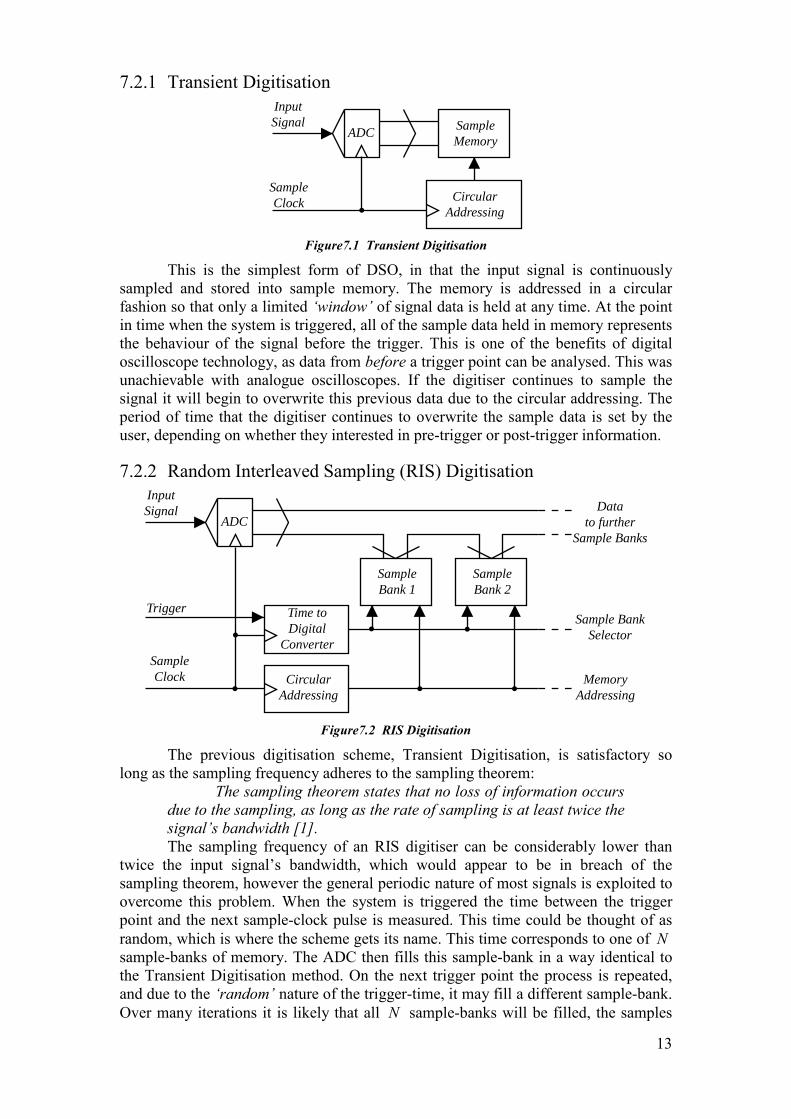
7.2.1 Transient Digitisation
SampleMemory
CircularAddressing
SampleClock
ADC
InputSignal
Figure 7.1 Transient Digitisation
This is the simplest form of DSO, in that the input signal is continuously sampled and stored into sample memory. The memory is addressed in a circular fashion so that only a limited ‘window’ of signal data is held at any time. At the point in time when the system is triggered, all of the sample data held in memory represents the behaviour of the signal before the trigger. This is one of the benefits of digital oscilloscope technology, as data from before a trigger point can be analysed. This was unachievable with analogue oscilloscopes. If the digitiser continues to sample the signal it will begin to overwrite this previous data due to the circular addressing. The period of time that the digitiser continues to overwrite the sample data is set by the user, depending on whether they interested in pre-trigger or post-trigger information.
7.2.2 Random Interleaved Sampling (RIS) Digitisation
SampleBank 1
CircularAddressing
SampleClock
ADC
InputSignal
SampleBank 2
Trigger Time toDigital
Converter
Datato further
Sample Banks
Sample BankSelector
MemoryAddressing
Figure 7.2 RIS Digitisation
The previous digitisation scheme, Transient Digitisation, is satisfactory so long as the sampling frequency adheres to the sampling theorem:
The sampling theorem states that no loss of information occurs due to the sampling, as long as the rate of sampling is at least twice the signal’s bandwidth [1].The sampling frequency of an RIS digitiser can be considerably lower than
twice the input signal’s bandwidth, which would appear to be in breach of the sampling theorem, however the general periodic nature of most signals is exploited to overcome this problem. When the system is triggered the time between the trigger point and the next sample-clock pulse is measured. This time could be thought of as random, which is where the scheme gets its name. This time corresponds to one of Nsample-banks of memory. The ADC then fills this sample-bank in a way identical to the Transient Digitisation method. On the next trigger point the process is repeated, and due to the ‘random’ nature of the trigger-time, it may fill a different sample-bank. Over many iterations it is likely that all N sample-banks will be filled, the samples
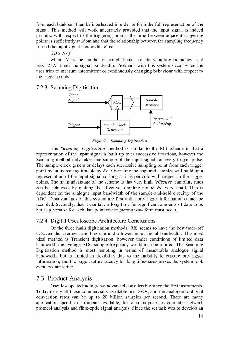
14
from each bank can then be interleaved in order to form the full representation of the signal. This method will work adequately provided that the input signal is indeed periodic with respect to the triggering points, the time between adjacent triggering points is sufficiently random and that the relationship between the sampling frequency f and the input signal bandwidth B is:
2B N f≤ ⋅where N is the number of sample-banks, i.e. the sampling frequency is at
least 2 / N times the signal bandwidth. Problems with this system occur when the user tries to measure intermittent or continuously changing behaviour with respect to the trigger points.
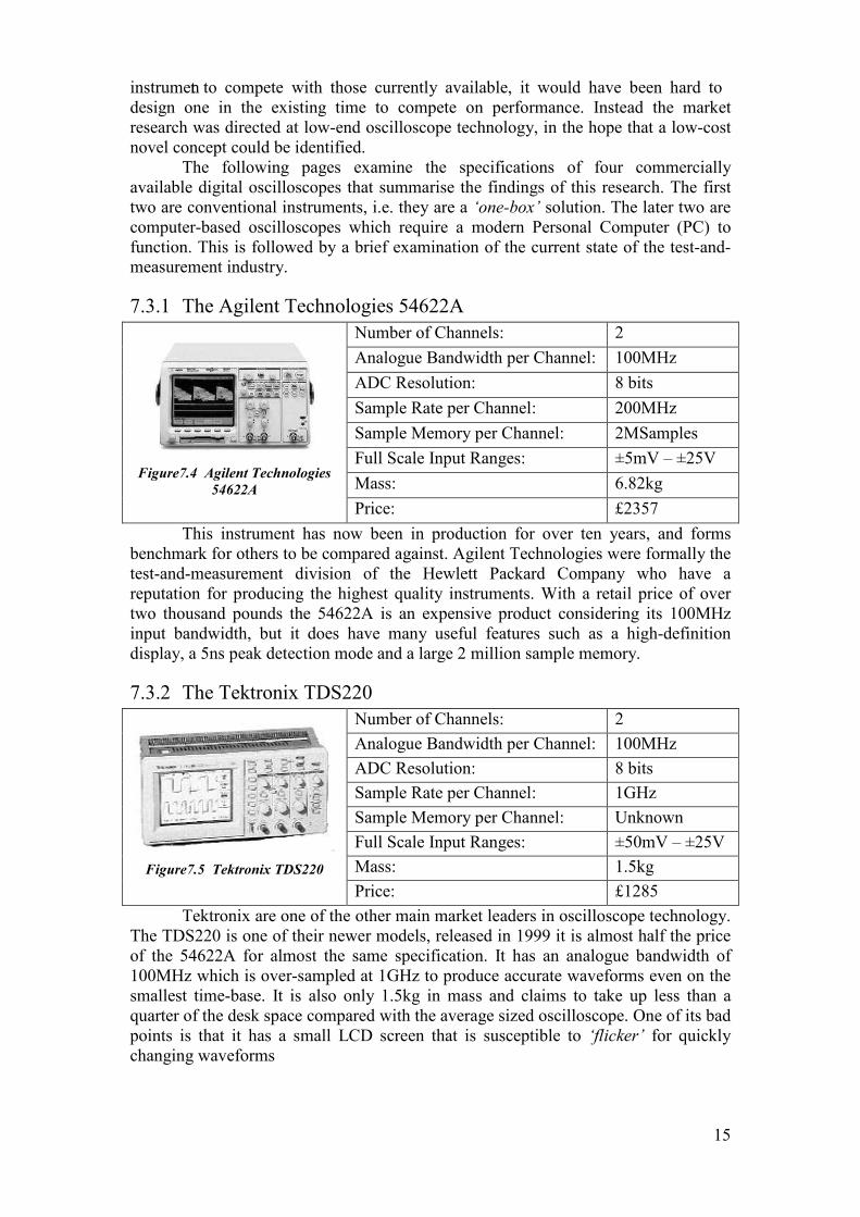
7.2.3 Scanning Digitisation
SampleMemoryADC
InputSignal
Sample ClockGenerator
TriggerIncrementalAddressing
Figure 7.3 Sampling Digitisation
The ‘Scanning Digitisation’ method is similar to the RIS scheme in that a representation of the input signal is built up over successive iterations, however the Scanning method only takes one sample of the input signal for every trigger pulse. The sample clock generator delays each successive sampling point from each trigger point by an increasing time delay tδ . Over time the captured samples will build up a representation of the input signal so long as it is periodic with respect to the trigger points. The main advantage of the scheme is that very high ‘effective’ sampling rates can be achieved, by making the effective sampling period tδ very small. This is dependent on the analogue input bandwidth of the sample-and-hold circuitry of the ADC. Disadvantages of this system are firstly that pre-trigger information cannot be recorded. Secondly, that it can take a long time for significant amounts of data to be built up because for each data point one triggering waveform must occur.
7.2.4 Digital Oscilloscope Architecture ConclusionsOf the three main digitisation methods, RIS seems to have the best trade-off
between the average sampling-rate and allowed input signal bandwidth. The most ideal method is Transient digitisation, however under conditions of limited data bandwidth the average ADC sample frequency would also be limited. The Scanning Digitisation method is most tempting in terms of measurable analogue signal bandwidth, but is limited in flexibility due to the inability to capture pre-trigger information, and the large capture latency for long time-bases makes the system look even less attractive.
7.3 Product AnalysisOscilloscope technology has advanced considerably since the first instruments.
Today nearly all those commercially available are DSOs, and the analogue-to-digitalconversion rates can be up to 20 billion samples per second. There are many application specific instruments available, for such purposes as computer network protocol analysis and fibre-optic signal analysis. Since the set task was to develop an
15
instrument to compete with those currently available, it would have been hard to design one in the existing time to compete on performance. Instead the market research was directed at low-end oscilloscope technology, in the hope that a low-cost novel concept could be identified.
The following pages examine the specifications of four commercially available digital oscilloscopes that summarise the findings of this research. The first two are conventional instruments, i.e. they are a ‘one-box’ solution. The later two are computer-based oscilloscopes which require a modern Personal Computer (PC) to function. This is followed by a brief examination of the current state of the test-and-measurement industry.
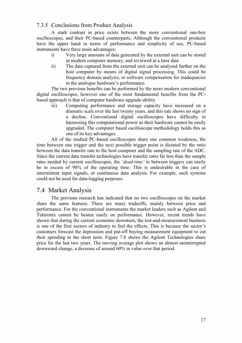
7.3.1 The Agilent Technologies 54622ANumber of Channels: 2Analogue Bandwidth per Channel: 100MHzADC Resolution: 8 bitsSample Rate per Channel: 200MHzSample Memory per Channel: 2MSamplesFull Scale Input Ranges: ±5mV – ±25VMass: 6.82kgFigure 7.4 Agilent Technologies
54622APrice: £2357
This instrument has now been in production for over ten years, and forms benchmark for others to be compared against. Agilent Technologies were formally the test-and-measurement division of the Hewlett Packard Company who have a reputation for producing the highest quality instruments. With a retail price of over two thousand pounds the 54622A is an expensive product considering its 100MHz input bandwidth, but it does have many useful features such as a high-definition display, a 5ns peak detection mode and a large 2 million sample memory.
7.3.2 The Tektronix TDS220Number of Channels: 2Analogue Bandwidth per Channel: 100MHzADC Resolution: 8 bitsSample Rate per Channel: 1GHzSample Memory per Channel: UnknownFull Scale Input Ranges: ±50mV – ±25VMass: 1.5kgFigure 7.5 Tektronix TDS220Price: £1285
Tektronix are one of the other main market leaders in oscilloscope technology. The TDS220 is one of their newer models, released in 1999 it is almost half the price of the 54622A for almost the same specification. It has an analogue bandwidth of 100MHz which is over-sampled at 1GHz to produce accurate waveforms even on the smallest time-base. It is also only 1.5kg in mass and claims to take up less than a quarter of the desk space compared with the average sized oscilloscope. One of its bad points is that it has a small LCD screen that is susceptible to ‘flicker’ for quickly changing waveforms

16
7.3.3 The Pico Technology ADC-200/100Number of Channels: 2
Analogue Bandwidth per Channel: 50MHz
ADC Resolution: 8 bits
Sample Rate per Channel: 50MHz
Sample Memory per Channel: 32kSamples
Full Scale Input Ranges: ±5mV – ±25VFigure 7.6 Pico Technolog
ADC-200/100 Price: £500
The ADC-200 is a PC-based oscilloscope that connects via the ‘parallel- port’. Pico Technology have specialised in low-cost PC-based oscilloscopes and data logging devices since 1991. This is a very low-cost solution in comparison to the previous conventional models. However it will suffer from ‘aliasing’ when used in two- channel mode as the sample frequency is not greater than or equal to twice the analogue bandwidth. In one channel mode the sampling frequency is doubled to 100MHz resolving this issue. The bottle-neck in the system will be at the data transfer point from the device to the computer via the parallel port interface. The Enhanced Parallel Port (EPP) on most PCs has a maximum transfer rate of 2MB per second. Therefore the device cannot be actively sample the input signal for more than 1/50th of the operating time in two channel mode without using data compression ( 2 8 / 2 50 8M M× × × ), as each capture of sample data has to be transferred to the host before further sampling.
7.3.4 The Soft DSP SDS-200Number of Channels: 2Analogue Bandwidth per Channel: 200MHzADC Resolution: 9 bitsSample Rate per Channel: 50MHzSample Memory per Channel: 10kSamplesFull Scale Input Ranges: ±50mV – ±50V
Figure 7.7 The Soft DSP
SDS-200Price: £570
The SDS-200 is a USB 1.1 compliant PC-based oscilloscope, built by Korean based Soft DSP. The instrument incorporates the RIS digitisation scheme to sample a 200MHz input bandwidth at 50MHz sample frequency. This is a very novel concept as it benefits from all of the features of the USB standard, including not requiring an external power supply and being ‘Plug-and-Play’ conformant. This device also suffers from the same problem exhibited by the ADC-200, in that the bottleneck in the system will exist at the data transfer stage. USB 1.1 has a maximum transfer rate of 12Mbps, that means that again the device cannot actively sample the input signal for more than 1/75th of the operating time in two-channel mode without data compression(12 / 2 50 9M M× × ).
17
7.3.5 Conclusions from Product AnalysisA stark contrast in price exists between the more conventional one-box
oscilloscopes, and their PC-based counterparts. Although the conventional products have the upper hand in terms of performance and simplicity of use, PC-based instruments have three main advantages:
i) Very large amounts of data generated by the external unit can be stored in modern computer memory, and reviewed at a later date
ii) The data captured from the external unit can be analysed further on the host computer by means of digital signal processing. This could be frequency domain analysis, or software compensation for inadequacies in the analogue hardware’s performance.
The two previous benefits can be performed by the more modern conventional digital oscilloscopes, however one of the most fundamental benefits from the PC-based approach is that of computer hardware upgrade-ability
iii) Computing performance and storage capacity have increased on a dramatic scale over the last twenty years, and this rate shows no sign of a decline. Conventional digital oscilloscopes have difficulty in harnessing this computational power as their hardware cannot be easily upgraded. The computer based oscilloscope methodology holds this as one of its key advantages.
All of the studied PC-based oscilloscopes share one common weakness, the time between one trigger and the next possible trigger point is dictated by the ratio between the data transfer rate to the host computer and the sampling rate of the ADC. Since the current data transfer technologies have transfer rates far less than the sample rates needed by current oscilloscopes, the ‘dead-time’ in between triggers can easily be in excess of 98% of the operating time. This is undesirable in the case of intermittent input signals, or continuous data analysis. For example, such systems could not be used for data-logging purposes.
7.4 Market AnalysisThe previous research has indicated that no two oscilloscopes on the market
share the same features. There are many tradeoffs, mainly between price and performance. For the conventional instruments the market leaders such as Agilent and Tektronix cannot be beaten easily on performance. However, recent trends have shown that during the current economic downturn, the test-and-measurement business is one of the first sectors of industry to feel the effects. This is because the sector’s customers forecast the depression and put-off buying measurement equipment to cut their spending in the short term. Figure 7.8 shows the Agilent Technologies share price for the last two years. The moving average plot shows an almost uninterrupted downward change, a decrease of around 60% in value over that period.

18
Figure 7.8 The Agilent Technologies share price for the last two years (dark), and its 200 day moving average (light).
The test-and-measurement industry’s customers are clearly concerned about spending large amounts of capital on expensive new test equipment during the current economic climate. This may explain the increase in the market for cheaper more low-end computer based oscilloscopes such as the SDS-200, or the ADC-200.
7.5 Preliminary Research ConclusionsThe conclusions from the preliminary research were as follows:i) There has been an increase in the market for cheaper, computer-based
digital oscilloscopes.ii) Computer based instruments have the advantage of being upgraded
with both newer computing hardware and software with far more ease than conventional oscilloscopes.
iii) The flexibility and ease of use of modern plug-and-play technology, such as the USB 1.1 standard, can be incorporated into digital oscilloscopes.
iv) Existing computer based oscilloscopes pay the price of their limited data transfer rate, by exhibiting a very large proportion of dead-time in between consecutive trigger points.
v) The RIS digitisation method has been used successfully in commercially available instruments to reconstruct a representation of the original input signal using successive signal measurement sweeps, even though the ADC sample rate is far lower than double the input signal bandwidth.

19
8. Initial ConceptsAfter conducting preliminary research into the area of digital oscilloscope
technology and the test-and-measurement market, it was time to use the findings to develop initial concepts for further investigation.
8.1 Top-Level ConceptTime was spent developing ideas for the top-level functionality and user
operation of the proposed instrument. It had been noted that the SDS-200 digital oscilloscope had many advantages over its other PC-based competitors, owing to the use of the USB 1.1 standard as its means of connecting with the host computer. USB 1.1 is known as a ‘Plug-and-Play’ technology, meaning that a compliant device can simply be plugged into the host machine in order to operate it. It can also have the convenience of only having one physical connection between the computer and the peripheral. It was decided that these benefits, in combination with the other advantages noted of computer based oscilloscopes, that all further research would be aimed at developing a low-cost, computer-based, Plug-and-Play oscilloscope.
8.2 System-Level ConceptsSystem-level operation of digital oscilloscopes is based around picking
windows of signal data exhibiting behaviour matching the triggering criteria, and displaying this data on a video screen. In conventional ‘one-box’ oscilloscopes there is no one defining factor that slows the transfer of information between the input signal and the video display.
In computer-based instruments, the main limiting factor is undoubtedly the transfer of information between the peripheral and the host computer. (A method of reducing this effect is to connect the device via the PCI bus, which has a data transfer rate of 33MHz * 32bits =1.056Gbps. However products employing this method prove to be costly. For example the ‘Gage Applied Sciences - Comuscope 12100’ card, with 12bit ADC resolution, 1M sample capture memory and a 100MSPS sampling rate, has a retail price of £4,100). The limitation of the data transfer rate leads to the following system architecture:
SignalMemory
HardwareTrigger Generator
DataTransferInterface
HostComputer
VideoDisplay
ADC
InputSignal
Oscilloscope Peripheral
Figure 8.1 The ‘High-Speed Capture – Low-Speed Transfer’ system
Only the data for display is transferred to the host, to minimise the amount of data transfer. To do this, the triggering system that identifies the windows of input data of interest must be realised in hardware. This system has shown to work in practice by several instruments on the market, and shall be called the ‘High-Speed Capture – Low-Speed Transfer’ solution.
The new system concept developed in this project is illustrated below:
20
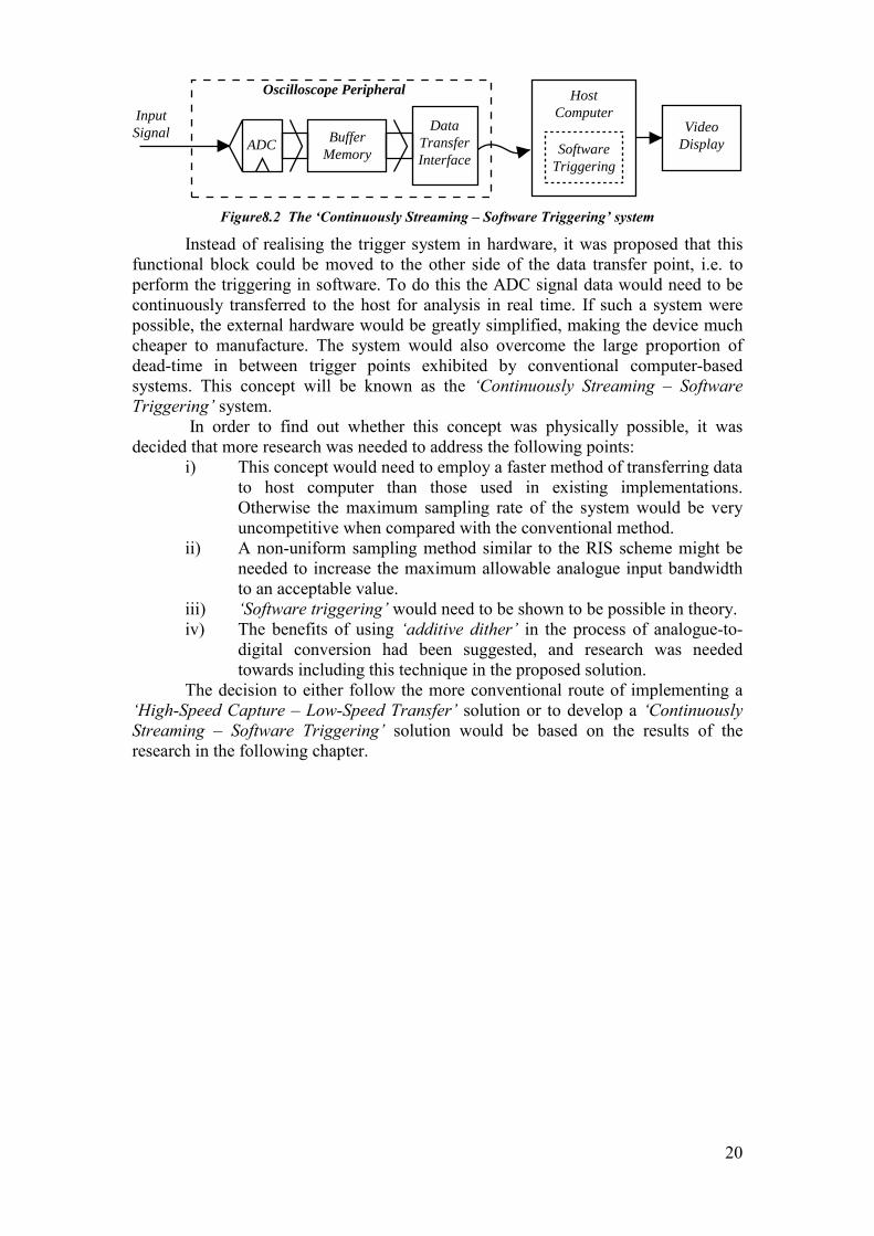
BufferMemory Software
Triggering
DataTransferInterface
HostComputer
VideoDisplayADC
InputSignal
Oscilloscope Peripheral
Figure 8.2 The ‘Continuously Streaming – Software Triggering’ system
Instead of realising the trigger system in hardware, it was proposed that this functional block could be moved to the other side of the data transfer point, i.e. to perform the triggering in software. To do this the ADC signal data would need to be continuously transferred to the host for analysis in real time. If such a system were possible, the external hardware would be greatly simplified, making the device much cheaper to manufacture. The system would also overcome the large proportion of dead-time in between trigger points exhibited by conventional computer-based systems. This concept will be known as the ‘Continuously Streaming – Software Triggering’ system.
In order to find out whether this concept was physically possible, it was decided that more research was needed to address the following points:
i) This concept would need to employ a faster method of transferring data to host computer than those used in existing implementations. Otherwise the maximum sampling rate of the system would be very uncompetitive when compared with the conventional method.
ii) A non-uniform sampling method similar to the RIS scheme might be needed to increase the maximum allowable analogue input bandwidth to an acceptable value.
iii) ‘Software triggering’ would need to be shown to be possible in theory.iv) The benefits of using ‘additive dither’ in the process of analogue-to-
digital conversion had been suggested, and research was needed towards including this technique in the proposed solution.
The decision to either follow the more conventional route of implementing a ‘High-Speed Capture – Low-Speed Transfer’ solution or to develop a ‘Continuously Streaming – Software Triggering’ solution would be based on the results of the research in the following chapter.
21
9. Concept Directed ResearchWith two possible system concepts identified for further development, the next
stage was to conduct further research aimed at solving the issues raised in the previous chapter.
It was decided that if the proposed solution would incorporate a plug-and-play data-transfer technology, more research was required into the strengths and weaknesses of available types.
Once the method of data transfer had been chosen, there would be implications on the software used to communicate with the instrument in relation to the selected standard. Research was needed to discover just what implications these would be, and to understand the fundamental principles behind the software implementation of the standard.
The RIS digitisation scheme used in existing instruments is based on the theory of Non Uniform Sampling (NUS). If the proposed solution were to feature a similar technique, further research into this area would be needed.
The proposal to implement the triggering process in software rather than hardware needed to be examined further, especially in relation to the use of NUS.
The benefits of using ‘additive dither’ in the process of analogue-to-digital conversion had been suggested, and it was decided that research into the theory of this phenomenon should be conducted, as towards using this method in the proposed solution.
9.1 Data Transfer TechnologyThis section examines the currently existing data-transfer standards between a
peripheral and a personal computer. The aim of this research was to identify the preferred method of transferring the data obtained from a PC-based digital oscilloscope to the host computer for display. The standards were compared at a very high level, without going in to the low-level operation of the technologies.
9.1.1 Pre-1995 Peripheral Interface TechnologyLooking back to the early 1990s, someone fortunate enough to afford one of
the first ‘multi-media’ computers may have encountered the following situation:They opened up the parcel containing their brand new IBM-compatible 486
DX2-66 PC with 16MB of RAM and 512MB hard-disk-drive, and with much glee and anticipation plugged it into the wall, switched it on and sat back ready for the mind-blowing graphics and program loading speeds they had been promised. Half an hour later, and after only one system crash, they had written their first word processed document ready to be printed. They plugged in their fabulous new colour dot-matrix printer, and clicked on the ‘print’ button. Nothing happened. On consulting the printer manual, it turned out they first needed to install a ‘driver’ for the printer. They did so, and were told that it was necessary to ‘reboot’ their beloved machine, which promptly destroyed the letter they had just written. Half an hour later after needing to reboot further times and re-writing their letter, they finally managed to print the document. Ready for their next multi-media experience, they unpacked their speedy 14.4Kbps modem. This time they were prepared for the demand for the modem’s driver, and the incessant rebooting that followed it, but were unprepared for the message notifying them that there was an ‘IRQ Conflict’ between the sound-card and the modem. After a call to the manufacturer it turned out they should have known to change one of the

22
‘jumpers’ on the modem before plugging it in. Getting quickly bored with the less than exhilarating bulletin-board service, they decided to try out their mono picture scanner. Immediately they came across two problems, firstly that their computer only had one ‘parallel port’ for which now the printer and scanner both jostled for use. Secondly their four-way power socket was already full with other plugs, and had no room for the scanner’s power supply. With a sigh, they thought that surely there must be a better way to connect a computer system together.
The main deficiencies encountered with the myriad of different interface standards of yesteryear are as follows:
i) A software driver for a peripheral had to be installed, and typically involved rebooting the computer after installation.
ii) The computer usually had to be switched off during device attachment / detachment.
iii) The computer must have an available interface of the right type.iv) Hardware conflicts between IRQ / DMA / I/O addresses needed to be
resolved.v) The peripheral generally required a separate power supply.An interface technology to resolve these issues would have to allow the user to
simply ‘plug in’ the peripheral using only one common connection, and use it without needing to install any additional software. This concept is known as ‘Plug-and-Play’.
9.1.2 A History of Plug-and-Play Interface StandardsWork began on designing a Plug-and-Play standard as long ago as 1986 by
Apple Computers. It was originally designed as a high-speed serial replacement for the Small Computer System Interface (SCSI) standard used for connecting hard disk drives to the host computer. The standard featured a ‘Hot-Swap’ capability, meaning a peripheral could be attached or removed whilst the host computer was running, and a 100Mbps data transfer rate. It also eliminated the need for external power supplies for individual peripherals by being able to supply up to 12W through the same cable as the data transfer wires. This standard was brand named ‘Firewire’ by Apple. It was later ratified in 1995 by the Institute of Electrical and Electronic Engineers (IEEE) and given the standard number of 1394. It sounds like an amazing idea, but even today the standard is only used in the minority of peripherals. The question must be asked as to why the standard has not been as widely adopted is it might have been.
The answer is that Apple Computers, who foresaw the enormous potential market for the technology, were rumoured to be thinking of charging a royalty fee of 1 US$ for each IEEE 1394 ‘port’ manufactured. This was not appreciated by the computing industry, which perceived this as if Apple were holding the industry hostage. In response a group of leading technology companies, Compaq, DEC, IBM, Intel, Microsoft, NEC and Northern Telecom, decided to develop their own standard, which had a far lower data transfer rate but was much cheaper to implement.
The new standard was called the Universal Serial Bus (USB) version 1.0. USB 1.0 got off to a shaky start in that misconceptions occurred whilst interpreting the standard which lead the hardware and software developers to produce incompatible products. These issues were resolved in the USB 1.1 standard released in 1995. The five years that followed saw a dramatic increase in the numbers of commercially available USB 1.1 peripherals. Today almost every type of PC peripheral is available with a USB 1.1 interface.
USB 1.1 is lacking in one major property, data transfer bandwidth. Its 12Mbps bandwidth is more than adequate for use with keyboards and mice, however it becomes noticeably slow when used with data transfer intensive devices such as picture scanners or printers. The network topology of USB also leads to bandwidth

23
deficiencies when many devices share the same connection to the host computer –known as a ‘root hub’. USB’s developers had foreseen this problem, and were already developing a new version of the Universal Serial Bus that was 40 times faster in transfer rate than the original, yet backwards compatible with USB 1.1. This standard was released in 1999 and imaginatively named USB 2.0.
Not to be outdone the developers of IEEE 1394 released a faster version in 2000, named 1394a with a transfer rate of 400Mbps, but still 17% slower than USB 2.0. As of the time of writing the group is currently developing a further IEEE 1394 standard with a maximum specified transfer rate of 800Mbps over copper wire or 3.2Gbps over an optical-fibre. This is due to be ratified by the IEEE in August 2002 and is likely to be named IEEE 1394b. Table 9.1 summarises the technologies.
IEEE1394-1995
USB 1.1 USB 2.0 IEEE 1394a 1394b
Standard Ratified 1995 1995 1999 2000 Unratified
Maximum Data Transfer Rate 200Mbps 12Mbps 480Mbps 400Mb
ps 3.2Gbps
Maximum Device Power 12W 2.5W 2.5W 12W 12W
Table 9.1 A chronological table of Plug-and-Play interface technologies
Further information regarding the proposed 1394b standard may be found at:http://www.zayante.com/p1394b/For a rather crude estimation of the popularity of IEEE 1394 against USB, the
following internet search was made using the Google search engine (http://www.google.com):
Approximate number of pages containing “1394”or “Firewire”
Approximate number of pages containing “USB”
1,849,000 6,130,000(N.B.: The Google database covers approximately two billion internet pages)
Table 9.2 Results returned from the Google search engine, for IEEE 1394 and USB
The same searches were made again using Google, this time specifying that results should only be returned from specific internet domains, namely: microsoft.com for the Microsoft Corporation, ibm.com for IBM and apple.com for Apple Computers.Internet Domain Searched Approximate number of
pages containing “1394”or “Firewire”
Approximate number of pages containing “USB”
microsoft.com 3,300 11,000ibm.com 1,700 16,600apple.com 5,800 5,100
Table 9.3 Results returned from the Google search engine, for IEEE 1394 and USB, for specific internet domains.
It is interesting to note that the total number of results from the Google database and the results from the microsoft.com domain revealed that the word “USB” is around three times more frequent than both “Firewire” and “1394”. Whereas the results from ibm.com and apple.com are biased further towards their own interface technologies, USB and 1394 respectively. This might suggest that the USB standard carries more weight within the computing community.
24
The main two standards that exist for the Plug-and-Play interface between peripherals and personal computers are IEEE 1394 and the Universal Serial Bus. They are both very similar in concept, but on stated performance alone IEEE 1394 has the most promise in its 1394b version. Ideas and theory illustrated on paper alone are not enough to be of any use for practical development purposes. With the knowledge gained from reviewing the existing standards, it was time to investigate the availablehardware and software for the two competitors.
9.1.3 Currently Available Hardware and SoftwareThe research conducted into available data transfer hardware and software was
aimed at searching for devices that would be of use in a PC-based digital oscilloscope. The findings relate to either the IEEE 1394 or the USB standard. It was noted from the examination of existing PC-based oscilloscopes in chapter 7 that USB 1.1 was lacking in transfer bandwidth. Therefore it was decided that this research should be directed at only version 2.0 of the USB standard.
The minimum amount of hardware needed to form either an IEEE 1394 or USB data link is the same:
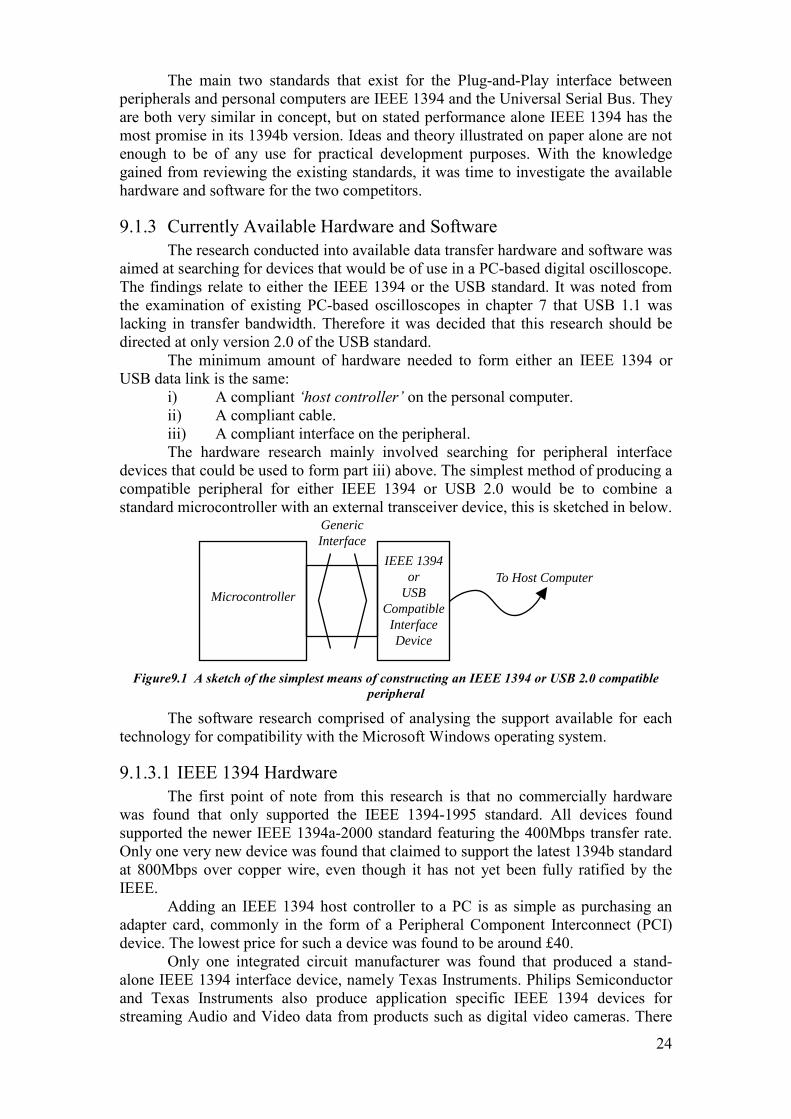
i) A compliant ‘host controller’ on the personal computer.ii) A compliant cable.iii) A compliant interface on the peripheral.The hardware research mainly involved searching for peripheral interface
devices that could be used to form part iii) above. The simplest method of producing a compatible peripheral for either IEEE 1394 or USB 2.0 would be to combine a standard microcontroller with an external transceiver device, this is sketched in below.
Microcontroller
IEEE 1394or
USBCompatible
InterfaceDevice
GenericInterface
To Host Computer
Figure 9.1 A sketch of the simplest means of constructing an IEEE 1394 or USB 2.0 compatible
peripheral
The software research comprised of analysing the support available for each technology for compatibility with the Microsoft Windows operating system.
9.1.3.1 IEEE 1394 HardwareThe first point of note from this research is that no commercially hardware
was found that only supported the IEEE 1394-1995 standard. All devices found supported the newer IEEE 1394a-2000 standard featuring the 400Mbps transfer rate. Only one very new device was found that claimed to support the latest 1394b standard at 800Mbps over copper wire, even though it has not yet been fully ratified by the IEEE.
Adding an IEEE 1394 host controller to a PC is as simple as purchasing an adapter card, commonly in the form of a Peripheral Component Interconnect (PCI) device. The lowest price for such a device was found to be around £40.
Only one integrated circuit manufacturer was found that produced a stand-alone IEEE 1394 interface device, namely Texas Instruments. Philips Semiconductor and Texas Instruments also produce application specific IEEE 1394 devices for streaming Audio and Video data from products such as digital video cameras. There
25
are many small integrated circuit design companies such as ISI (http://www.isi96.com) who develop IEEE 1394 ‘cores’ in Hardware Description Language (HDL), and licence their designs to System On Chip (SOC) designers who produce a compliant device by simply including the HDL within their own design.
A summary of devices produced by TI is shown below.Model Compatible
StandardFeatures
TSB43AA82A IEEE 1394a This device has a generic interface to an external microcontroller and 4728 bytes of FIFO memory, into which data can be transferred directly to the host controller.
TSB82AA2 1394b(Not yet ratified)
This is the first 1394b compliant device to have been constructed by any manufacturer. Its specification is unclear, but was demonstrated in August 2001 to transfer hard disk data at 800Mbps.
Table 9.4 Texas Instruments IEEE 1394 devices.
9.1.3.2 IEEE 1394 SoftwareAll currently available IEEE 1394a compliant host controllers and devices are
compatible with Microsoft ‘Windows XP’ and ‘Windows Me’. Microsoft ‘Windows 2000’ and ‘Windows 98 Second Edition’ support the standard in a more basic form that may require additional software to be installed for unsupported devices.
9.1.3.3 USB 2.0 HardwareThe lowest price found for a USB 2.0 PCI host controller card was found to be
around £40. Several integrated circuit manufacturers found to be producing USB 2.0 compatible devices. Netchip (http://www.netchip.com) were the first to demonstrate a compliant device in February 2000. Philips Semiconductor (http://www.philips.com) and Cypress Semiconductor (http://www.cypress.com) are two other companies who have produced USB 2.0 devices. The following table details the three devices that were under most consideration.Manufacturer Model FeaturesNetchip NET2270 Netchip were one of the first companies to produce
USB 2.0 compliant devices. The NET2270 has two 1kB FIFO memory banks, and three configurable USB endpoints. An external microprocessor is required to use this device.
Philips ISP1581 Philips’ ISP1581 is another microprocessor dependent USB 2.0 solution. It has 8kB of FIFO memory and up to 14 programmable USBendpoints.
Cypress CY7C68013 ‘EZ- USB FX2’
This device contains an 8051 microcontroller as well as a USB 2.0 transceiver. It has 8 configurable endpoints and an integrated 4kB FIFO memory. Has the ability to download its own firmware from the host machine via USB. An ANSI ‘C’ compiler is available for developing device firmware, which features extensive debugging facilities, along with an example device driver for Microsoft Windows.
Table 9.5 USB 2.0 Compliant Interface Devices
26
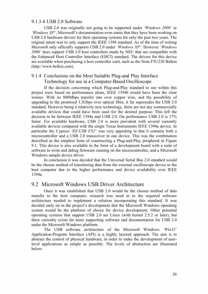
9.1.3.4 USB 2.0 SoftwareUSB 2.0 was originally not going to be supported under ‘Windows 2000’ or
‘Windows XP’, Microsoft’s documentation even states that they have been working on USB 2.0 hardware drivers for their operating systems for only the past two years. The original intent was to only support the IEEE 1394 standard. As of the time of writing Microsoft only officially supports USB 2.0 under ‘Windows XP’. However ‘Windows 2000’ does support USB 2.0 host controllers made by NEC that are compatible with the Enhanced Host Controller Interface (EHCI) standard. The drivers for this device are available when purchasing a host controller card, such as the from F5U220 Belkin (http://www.belkin.com).
9.1.4 Conclusions on the Most Suitable Plug-and- Play Interface Technology for use in a Computer-Based OscilloscopeIf the decision concerning which Plug-and-Play standard to use within this
project were based on performance alone, IEEE 1394b would have been the clear winner. With its 800Mbps transfer rate over copper wire, and the possibility of upgrading to the promised 3.2Gbps over optical fibre, it far supersedes the USB 2.0 standard. However being a relatively new technology, there are not any commercially available devices that could have been used for the desired purpose. This left the decision to be between IEEE 1394a and USB 2.0. On performance USB 2.0 is 17% faster. For available hardware, USB 2.0 is more prevalent with several currently available devices compared with the single Texas Instruments IEEE 1394a device. In particular the Cypress ‘EZ-USB FX2’ was very appealing in that it contains both a microcontroller and a USB 2.0 transceiver in one device. This was the combination described as the simplest form of constructing a Plug-and-Play peripheral in Figure 9.1. This device is also available in the form of a development board with a suite of software to write and debug firmware running on the microcontroller, and a Microsoft Windows sample device driver.
In conclusion it was decided that the Universal Serial Bus 2.0 standard would be the chosen method of transferring data from the external oscilloscope device to the host computer due to the higher performance and device availability over IEEE 1394a.
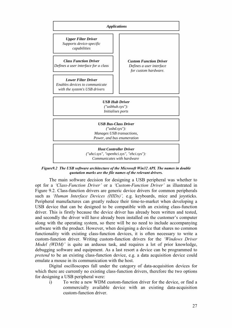
9.2 Microsoft Windows USB Driver ArchitectureOnce it was established that USB 2.0 would be the chosen method of data
transfer to the host computer, research was need in to the required software architecture needed to implement a solution incorporating this standard. It was decided early on in the project’s development that the Microsoft Windows operating system would be the platform of choice for device development. Other potential operating systems that support USB 2.0 are Linux (with kernel 2.5.2 or later), but there currently exists far more supporting software and documentation for USB 2.0 under the Microsoft Windows platform.
The USB software architecture of the Microsoft Windows ‘Win32’Application-Program Interface (API) is a highly layered approach. The aim is to abstract the control of physical hardware, in order to make the development of user-level applications as simple as possible. The levels of abstraction are illustrated below:
27
Applications
Upper Filter DriverSupports device-specific
capabilities
Class Function DriverDefines a user interface for a class
Lower Filter DriverEnables devices to communicate
with the system's USB drivers
USB Hub Driver("usbhub.sys"):Initialises ports
USB Bus-Class Driver("usbd.sys"):
Manages USB transactions,Power, and bus enumeration
Host Controller Driver("uhci.sys", "openhci.sys", "ehci.sys"):
Communicates with hardware
Custom Function DriverDefines a user interfacefor custom hardware.
Figure 9.2 The USB software architecture of the Microsoft Win32 API. The names in double quotation marks are the file names of the relevant drivers.
The main software decision for designing a USB peripheral was whether to opt for a ‘Class-Function Driver’ or a ‘Custom-Function Driver’ as illustrated in Figure 9.2. Class-function drivers are generic device drivers for common peripherals such as ‘Human Interface Devices (HIDs)’, e.g. keyboards, mice and joysticks. Peripheral manufactures can greatly reduce their time-to-market when developing a USB device that can be designed to be compatible with an existing class-function driver. This is firstly because the device driver has already been written and tested, and secondly the driver will have already been installed on the customer’s computer along with the operating system, so there will be no need to include accompanying software with the product. However, when designing a device that shares no common functionality with existing class-function devices, it is often necessary to write a custom-function driver. Writing custom-function drivers for the ‘Windows Driver Model (WDM)’ is quite an arduous task, and requires a lot of prior knowledge, debugging software and equipment. As a last resort a device can be programmed to pretend to be an existing class-function device, e.g. a data acquisition device could emulate a mouse in its communication with the host.
Digital oscilloscopes fall under the category of data-acquisition devices for which there are currently no existing class-function drivers, therefore the two options for designing a USB peripheral were:
i) To write a new WDM custom-function driver for the device, or find a commercially available device with an existing data-acquisition custom-function driver.

28
ii) Design the digital oscilloscope to be compatible with an existing class-function driver.
The research into existing USB 2.0 hardware in Section 9.1.3.3 revealed that the Cypress Semiconductor EZ-USB FX2 device was available with a sample custom-function driver, so a solution incorporating this device would not require any WDM driver writing, and would not need to be made compatible with an existing class-function driver. It was it this point in the project’s evolution, that the Cypress Semiconductor EZ -USB FX2 was chosen as the device of choice for implementing the USB 2.0 data interface.
9.3 The Theory of Non-Uniform SamplingThe sampling theorem [1] is well known. It states that unless a continuous
signal is sampled at a rate of at least twice the signal’s bandwidth ‘aliasing’ will occur. Aliasing is defined as the inability to distinguish between a signal component of frequency ω and one of frequency sn ω ω⋅ ± where n is a non-zero integer. This phenomenon can be seen as the images of a true frequency component within the Discrete Fourier Transform (DFT) of a signal.
However, there exists a theory that suggests that if a periodic signal was sampled randomly rather than periodically with respect to time, such that the instants at which sampling occurs has a uniform distribution, then the following is true:
The expectation of the spectrum of a randomly sampled signal coincides with that of the original signal. [2] This suggests that the statistical mean sampling rate of the random sampling
process can actually become lower than twice the bandwidth of the sampled signal without suffering excessive loss of information. The random sampling process has the effect of suppressing the periodic aliases in the frequency domain, by converting them into ‘white-noise’ instead. This is proved in Appendix I.
9.3.1 Random Sampling ProcessesIn order for the points in time at which a signal is sampled to be uniformly
distributed, the probability of a sample occurring at any given time must be the same. Producing such a random sampling process is a non-trivial exercise. For example, sampling processes that do not achieve this goal include periodic sampling with ‘jitter’. Using this technique involves sampling the signal at a periodic rate but each sample point deviates from the expected sampling point by a random amount known as jitter. For example if the sampling period was 10 and the distribution of the jitter was Normal with standard deviation 1, the probability density of the sampling points in time would be as sketched below:
0 10 20 30 400
0.02
0.04
0.06
0.08
t
f(t)
Figure 9.3 The probability density of the sampling instants of periodic sampling with jitter
29
Looking at Figure 9.3, it is obvious to see that the probability of a sample point occurring at any given instant in time is not the same. This exception to this rule is when the jitter is distributed uniformly in the range [ 2 2]T T− + where T is the sampling period. However such a method would be hard to use in practice as the time in between sample points could be vanishingly small, which would put significant requirements on ADC.
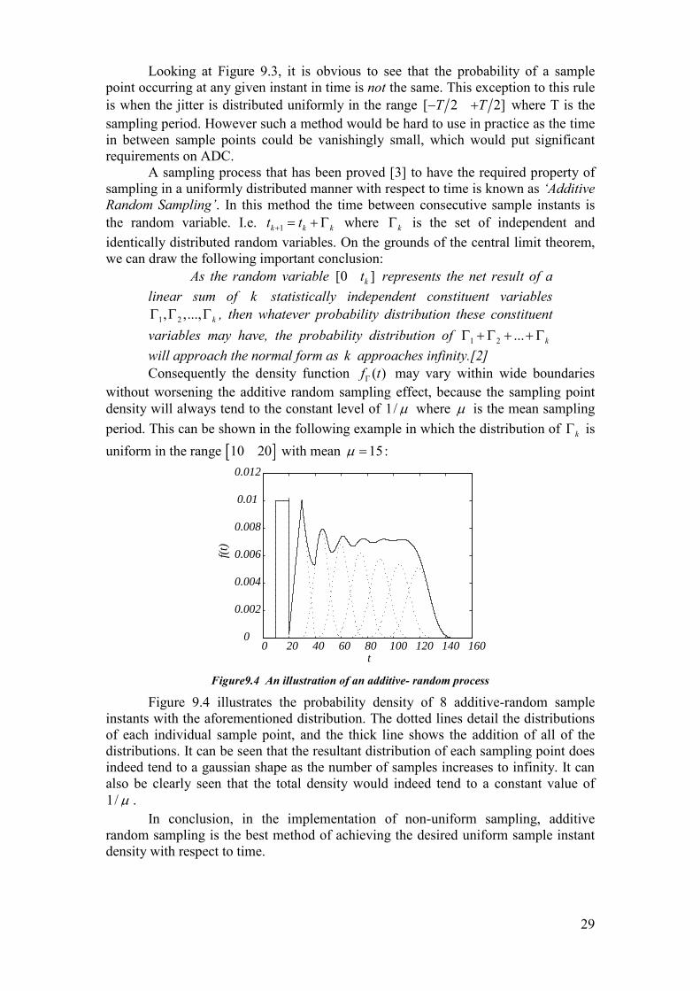
A sampling process that has been proved [3] to have the required property of sampling in a uniformly distributed manner with respect to time is known as ‘Additive Random Sampling’. In this method the time between consecutive sample instants is the random variable. I.e. 1k k kt t+ = + Γ where kΓ is the set of independent and identically distributed random variables. On the grounds of the central limit theorem, we can draw the following important conclusion:
As the random variable [0 ]kt represents the net result of a linear sum of k statistically independent constituent variables
1 2, ,..., kΓ Γ Γ , then whatever probability distribution these constituent variables may have, the probability distribution of 1 2 ... kΓ +Γ + +Γwill approach the normal form as k approaches infinity.[2] Consequently the density function ( )f tΓ may vary within wide boundaries
without worsening the additive random sampling effect, because the sampling point density will always tend to the constant level of 1/ µ where µ is the mean sampling period. This can be shown in the following example in which the distribution of kΓ is uniform in the range [ ]10 20 with mean 15µ = :
0 20 40 60 80 100 120 140 1600
0.002
0.004
0.006
0.008
0.01
0.012
t
f(t)
Figure 9.4 An illustration of an additive- random process
Figure 9.4 illustrates the probability density of 8 additive-random sample instants with the aforementioned distribution. The dotted lines detail the distributions of each individual sample point, and the thick line shows the addition of all of the distributions. It can be seen that the resultant distribution of each sampling point does indeed tend to a gaussian shape as the number of samples increases to infinity. It can also be clearly seen that the total density would indeed tend to a constant value of 1/ µ .
In conclusion, in the implementation of non-uniform sampling, additive random sampling is the best method of achieving the desired uniform sample instant density with respect to time.
30
9.3.2 Discrete-Random SamplingIt has been shown that non-uniform sampling can, in theory, be used to
analyse any frequency component far in excess of the Nyquist frequency. However this is dependent on the random variable separating consecutive sample points being truly continuous. As the points in time at which the samples were taken have to be known for further signal analysis, it is necessary to store their values in some kind of memory. In practice this will involve using a digital memory. Therefore it is not possible to accurately store a continuous sample instant, instead the points in time at which the signal can next be sampled is limited to a set of discrete points that can be stored in digital memory. When the minimum distance in time between two possible sample instants is made to be tδ , the relation between successive sample points is given by:
1k k kt t tδ+ = + ⋅Γwhere kΓ is now a discrete random variable that takes only integer values.It has been shown [4] that whilst using this sampling method, the effective
periodic sample rate is 1effectivef tδ= , I.e. for unaliased signal detection the sample rate must be at least twice the signal bandwidth in accordance with the sampling theorem:
2effectivef B≥ ⋅ (1) This is an important result as in practice non-uniform sampling has to be
implemented in this manner. It implies that the input signal must be band-limited to an upper frequency of half the effective sample rate.
9.3.3 Random Sample AnalysisOnce a signal has been randomly sampled, interpreting the resultant data is not
a simple matter. The two domains commonly used for analysing signal data are the time and frequency domains. In the time domain the difficulty in analysing randomly sampled data is that it needs to be ‘reconstructed’ in order to reveal the high frequency characteristics of the signal. There exist several papers [2] [5] [6] that describe various methods of reconstructing randomly sampled signals:
i) Signal Reconstruction using non-orthogonal transformsii) Signal Reconstruction by filtersiii) Iterative Reconstruction using Low Pass FiltersNone of these methods can theoretically produce an exact replication of the
sampled signal, unlike the interpolation method used in periodic sampling. However results have been shown [2] to give close approximations to the original signal.
There are also several methods for the frequency analysis of randomly sampled signals [2] [4]:
i) Direct discrete Fourier transform analysisii) Frequency analysis using non-orthogonal transformsOf these two the direct discrete Fourier transform method is the simplest, it
involves replacing all of the points in the discretely sampled signal that were not sampled with zeros, then performing the Discrete Fourier Transform (DFT) on the resultant signal.
To evaluate the effectiveness of this technique such a system was simulated. An effective sample rate of 200MHz was chosen, i.e. 1 200t Mδ = , with an additive-random sampling distribution taking the integer values 5,6,…,15 with equal probability, i.e. the mean sampling period was 10 tδ⋅ making the average sampling frequency 20MHz. An input signal was created with frequency components at 20, 50 and 80MHz. The direct DFT method was performed on 16384 randomly sampled data
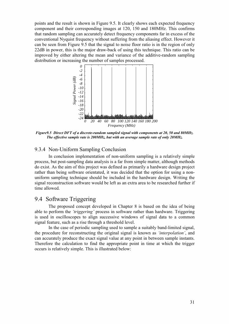
31
points and the result is shown in Figure 9.5. It clearly shows each expected frequency component and their corresponding images at 120, 150 and 180MHz. This confirms that random sampling can accurately detect frequency components far in excess of the conventional Nyquist frequency without suffering from the aliasing effect. However it can be seen from Figure 9.5 that the signal to noise floor ratio is in the region of only 22dB in power, this is the major draw-back of using this technique. This ratio can be improved by either altering the mean and variance of the additive-random sampling distribution or increasing the number of samples processed.
0 20 40 60 80 100 120 140 160 180 200-24-22-20-18-16-14-12-10-8-6-4-20
Frequency (MHz)
Sign
al P
ower
(dB)
Figure 9.5 Direct DFT of a discrete-random sampled signal with components at 20, 50 and 80MHz. The effective sample rate is 200MHz, but with an average sample rate of only 20MHz.
9.3.4 Non-Uniform Sampling ConclusionIn conclusion implementation of non-uniform sampling is a relatively simple
process, but post-sampling data analysis is a far from simple matter, although methods do exist. As the aim of this project was defined as primarily a hardware design project rather than being software orientated, it was decided that the option for using a non-uniform sampling technique should be included in the hardware design. Writing the signal reconstruction software would be left as an extra area to be researched further if time allowed.
9.4 Software TriggeringThe proposed concept developed in Chapter 8 is based on the idea of being
able to perform the ‘triggering’ process in software rather than hardware. Triggering is used in oscilloscopes to align successive windows of signal data to a common signal feature, such as a rise through a threshold level.
In the case of periodic sampling used to sample a suitably band-limited signal, the procedure for reconstructing the original signal is known as ‘interpolation’, and can accurately produce the exact signal value at any point in between sample instants. Therefore the calculation to find the appropriate point in time at which the trigger occurs is relatively simple. This is illustrated below:
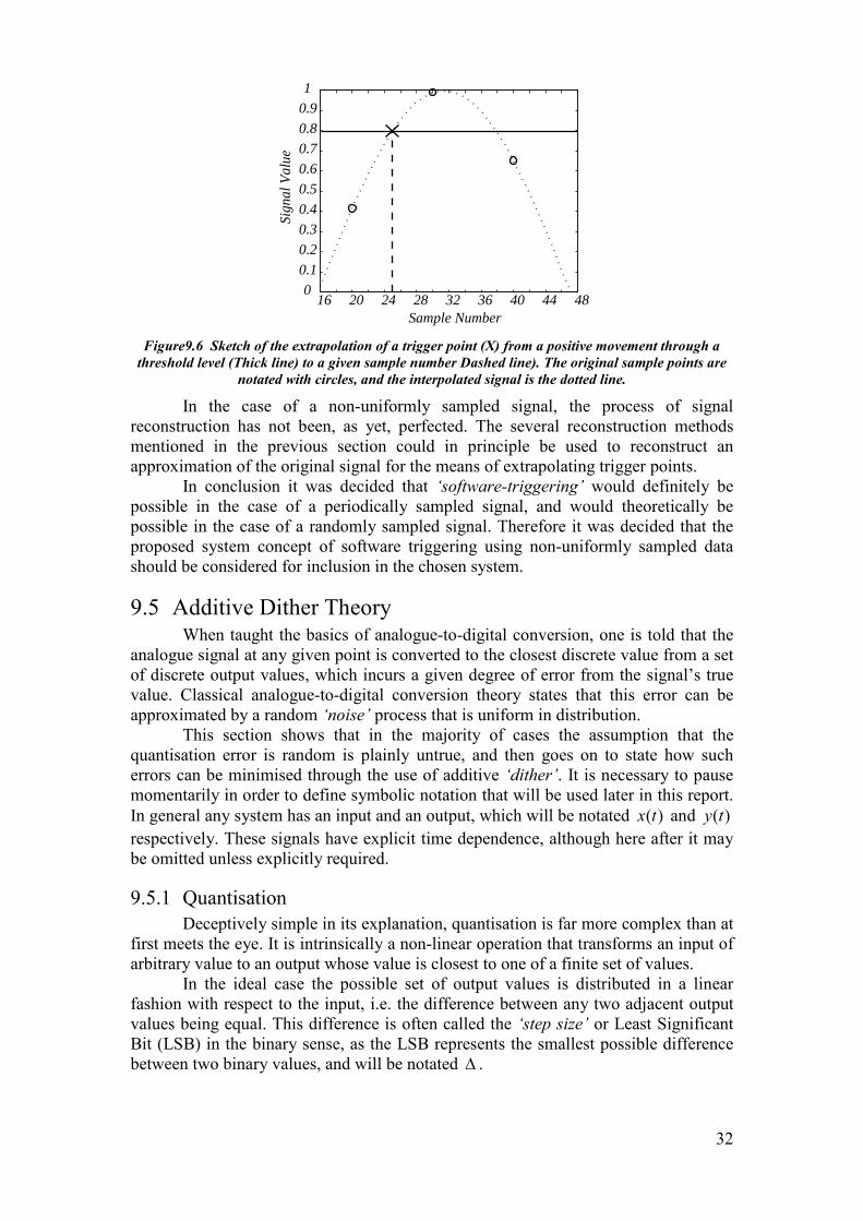
32
16 20 24 28 32 36 40 44 480
0.10.20.30.40.50.60.70.80.91
Sign
al V
alue
Sample Number
Figure 9.6 Sketch of the extrapolation of a trigger point (X) from a positive movement through a threshold level (Thick line) to a given sample number Dashed line). The original sample points are
notated with circles, and the interpolated signal is the dotted line.
In the case of a non-uniformly sampled signal, the process of signal reconstruction has not been, as yet, perfected. The several reconstruction methods mentioned in the previous section could in principle be used to reconstruct an approximation of the original signal for the means of extrapolating trigger points.
In conclusion it was decided that ‘software-triggering’ would definitely be possible in the case of a periodically sampled signal, and would theoretically be possible in the case of a randomly sampled signal. Therefore it was decided that the proposed system concept of software triggering using non-uniformly sampled data should be considered for inclusion in the chosen system.
9.5 Additive Dither TheoryWhen taught the basics of analogue-to-digital conversion, one is told that the
analogue signal at any given point is converted to the closest discrete value from a set of discrete output values, which incurs a given degree of error from the signal’s true value. Classical analogue-to-digital conversion theory states that this error can be approximated by a random ‘noise’ process that is uniform in distribution.
This section shows that in the majority of cases the assumption that the quantisation error is random is plainly untrue, and then goes on to state how such errors can be minimised through the use of additive ‘dither’. It is necessary to pause momentarily in order to define symbolic notation that will be used later in this report. In general any system has an input and an output, which will be notated ( )x t and ( )y trespectively. These signals have explicit time dependence, although here after it may be omitted unless explicitly required.
9.5.1 QuantisationDeceptively simple in its explanation, quantisation is far more complex than at
first meets the eye. It is intrinsically a non-linear operation that transforms an input of arbitrary value to an output whose value is closest to one of a finite set of values.
In the ideal case the possible set of output values is distributed in a linear fashion with respect to the input, i.e. the difference between any two adjacent outputvalues being equal. This difference is often called the ‘step size’ or Least Significant Bit (LSB) in the binary sense, as the LSB represents the smallest possible difference between two binary values, and will be notated ∆ .
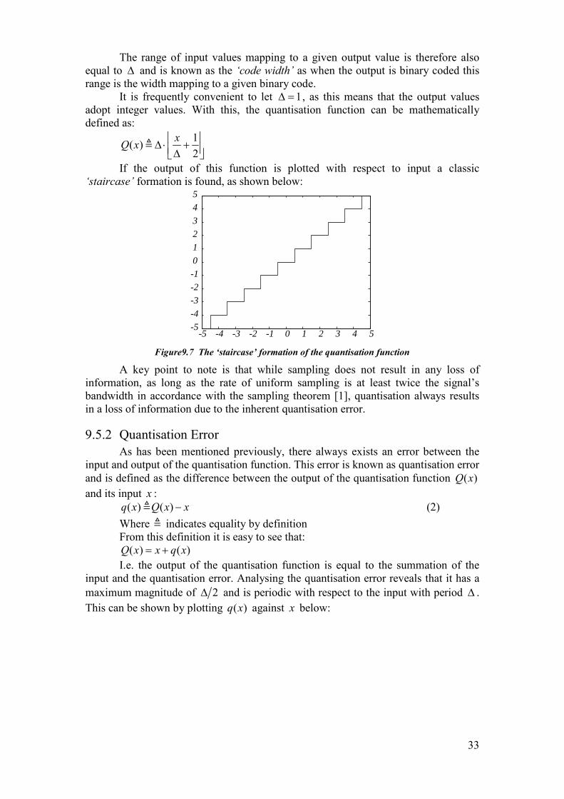
33
The range of input values mapping to a given output value is therefore also equal to ∆ and is known as the ‘code width’ as when the output is binary coded this range is the width mapping to a given binary code.
It is frequently convenient to let 1∆ = , as this means that the output values adopt integer values. With this, the quantisation function can be mathematically defined as:
1( )2
xQ x ∆ ⋅ + ∆
If the output of this function is plotted with respect to input a classic ‘staircase’ formation is found, as shown below:
-5 -4 -3 -2 -1 0 1 2 3 4 5-5-4-3-2-1012345
Figure 9.7 The ‘staircase’ formation of the quantisation function
A key point to note is that while sampling does not result in any loss of information, as long as the rate of uniform sampling is at least twice the signal’s bandwidth in accordance with the sampling theorem [1], quantisation always results in a loss of information due to the inherent quantisation error.
9.5.2 Quantisation ErrorAs has been mentioned previously, there always exists an error between the
input and output of the quantisation function. This error is known as quantisation error and is defined as the difference between the output of the quantisation function ( )Q xand its input x :
( ) ( )q x Q x x− (2) Where indicates equality by definitionFrom this definition it is easy to see that:( ) ( )Q x x q x= +
I.e. the output of the quantisation function is equal to the summation of the input and the quantisation error. Analysing the quantisation error reveals that it has a maximum magnitude of 2∆ and is periodic with respect to the input with period ∆ . This can be shown by plotting ( )q x against x below:
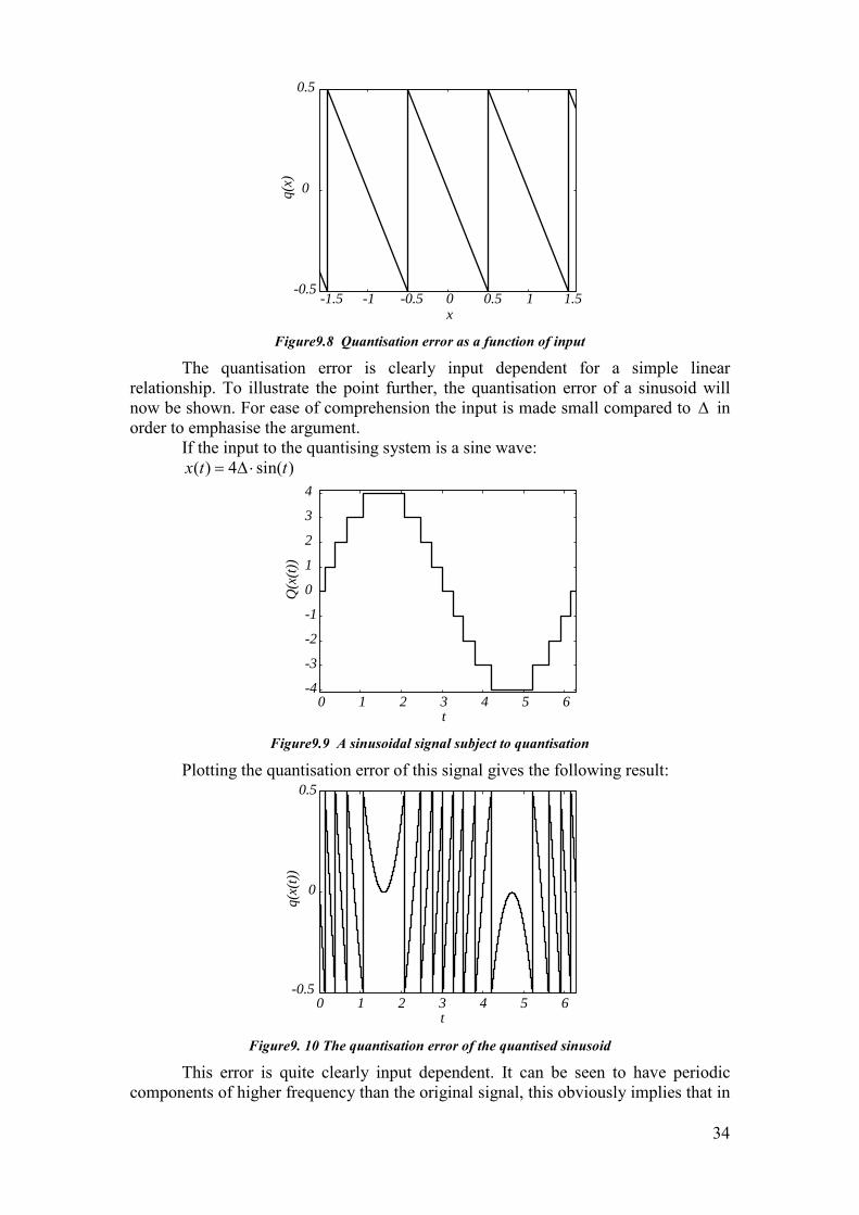
34
-1.5 -1 -0.5 0 0.5 1 1.5-0.5
0
0.5
x
q(x)
Figure 9.8 Quantisation error as a function of input
The quantisation error is clearly input dependent for a simple linear relationship. To illustrate the point further, the quantisation error of a sinusoid will now be shown. For ease of comprehension the input is made small compared to ∆ in order to emphasise the argument.
If the input to the quantising system is a sine wave:( ) 4 sin( )x t t= ∆ ⋅
0 1 2 3 4 5 6-4
-3
-2
-1
0
1
2
3
4
t
Q(x
(t))
Figure 9.9 A sinusoidal signal subject to quantisation
Plotting the quantisation error of this signal gives the following result:
0 1 2 3 4 5 6t
0.5
-0.5
0
q(x(
t))
Figure 9. 10 The quantisation error of the quantised sinusoid
This error is quite clearly input dependent. It can be seen to have periodic components of higher frequency than the original signal, this obviously implies that in

35
the frequency domain there will be higher order frequency components due to the quantisation error. The power spectrum of the quantised signal is shown below:
1 3 5 7 9 11 13 15 17 19-120
-100
-80
-60
-40
-20
0
Relative Frequency
Pow
er R
elat
ive
to F
unda
men
tal (
dB)
Figure 9.11 Frequency components of the quantised sinusoid
It should be concluded that the quantisation error is in fact heavily dependent on the properties of the input signal.
9.5.3 Quantisation ‘Noise’It has previously been mentioned that quantisation error has often been
approximated as a ‘noise-like’ signal. A noise-like signal implies one that possesses the properties of a stationary random process1. Often this noise is modelled as a uniformly distributed error between 2+∆ and 2−∆ . In other words, the error is equally likely to take the value of any point within this range. This distribution has the probability density function (PDF) as shown in Figure 9.12. Statistical analysis shows that (see Appendix I) the mean of the quantisation noise is 0 and the mean squared of the noise is 12∆ . These are known respectively as the first and second moments of the quantisation noise. The second moment of a signal is of interest as it is proportional to the signal’s average power.
1/∆
Pr(q(ω))
q(ω)0−∆/2 +∆/2
Figure 9. 12 The probability density function of a uniformly distributed random process
Widrow [7] showed that the minimum loss of statistical data due to the quantising operation occurs when the quantisation error is independent of the input signal, therefore the approximation that the quantisation error is random and independent of the input signal is in fact the best case scenario, i.e. at best the mean squared error due to quantisation will be 12∆ . This situation can be shown to arise when the input signal exhibits a smooth PDF and is large relative to ∆ , but it was also suggested by Widrow that if the quantisation error could be made to be independent of the input then this would also be a situation under which information loss is at a minimum. This is the main aim of the use of dither in analogue-to- digital conversion.
1 A stationary random process is one who’s statistical properties are time invariant
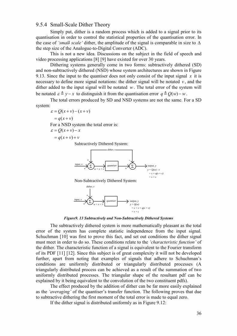
36
9.5.4 Small-Scale Dither TheorySimply put, dither is a random process which is added to a signal prior to its
quantisation in order to control the statistical properties of the quantisation error. In the case of ‘small- scale’ dither, the amplitude of the signal is comparable in size to ∆the step size of the Analogue-to-Digital Converter (ADC).
This is not a new idea. Discussions on the subject in the field of speech and video processing applications [8] [9] have existed for over 30 years.
Dithering systems generally come in two forms: subtractively dithered (SD) and non-subtractively dithered (NSD) whose system architectures are shown in Figure 9.13. Since the input to the quantiser does not only consist of the input signal x it is necessary to define more signal notations: the dither signal will be notated v , and the dither added to the input signal will be notated w . The total error of the system will be notated y xε − to distinguish it from the quantisation error ( )q Q w w− .
The total errors produced by SD and NSD systems are not the same. For a SD system:
( ) ( )( )
Q x v x vq x v
ε = + − += +
For a NSD system the total error is:( )( )
Q x v xq x v v
ε = + −= + +
input, x
dither, v
output, yquantiser
Subtractively Dithered System:
Non-Subtractively Dithered System:
Σ Σ+
+ +
-
w = x + v y = Q(w) - v= x + q(x + v)= x + ε
input, x
dither, v
output, yquantiserΣ+
+ w = x + v y = Q(w)= x + v + q(x + v)= x + ε
Figure 9. 13 Subtractively and Non-Subtractively Dithered Systems
The subtractively dithered system is more mathematically pleasant as the total error of the system has complete statistic independence from the input signal. Schuchman [10] was first to prove this fact, and set out conditions the dither signal must meet in order to do so. These conditions relate to the ‘characteristic function’ of the dither. The characteristic function of a signal is equivalent to the Fourier transform of its PDF [11] [12]. Since this subject is of great complexity it will not be developed further, apart from noting that examples of signals that adhere to Schuchman’s conditions are uniformly distributed or triangularly distributed processes (A triangularly distributed process can be achieved as a result of the summation of two uniformly distributed processes. The triangular shape of the resultant pdf can be explained by it being equivalent to the convolution of the two constituent pdfs).
The effect produced by the addition of dither can be far more easily explained as the ‘averaging’ of the quantiser’s transfer function. The following proves that due to subtractive dithering the first moment of the total error is made to equal zero.
If the dither signal is distributed uniformly as in Figure 9.12:
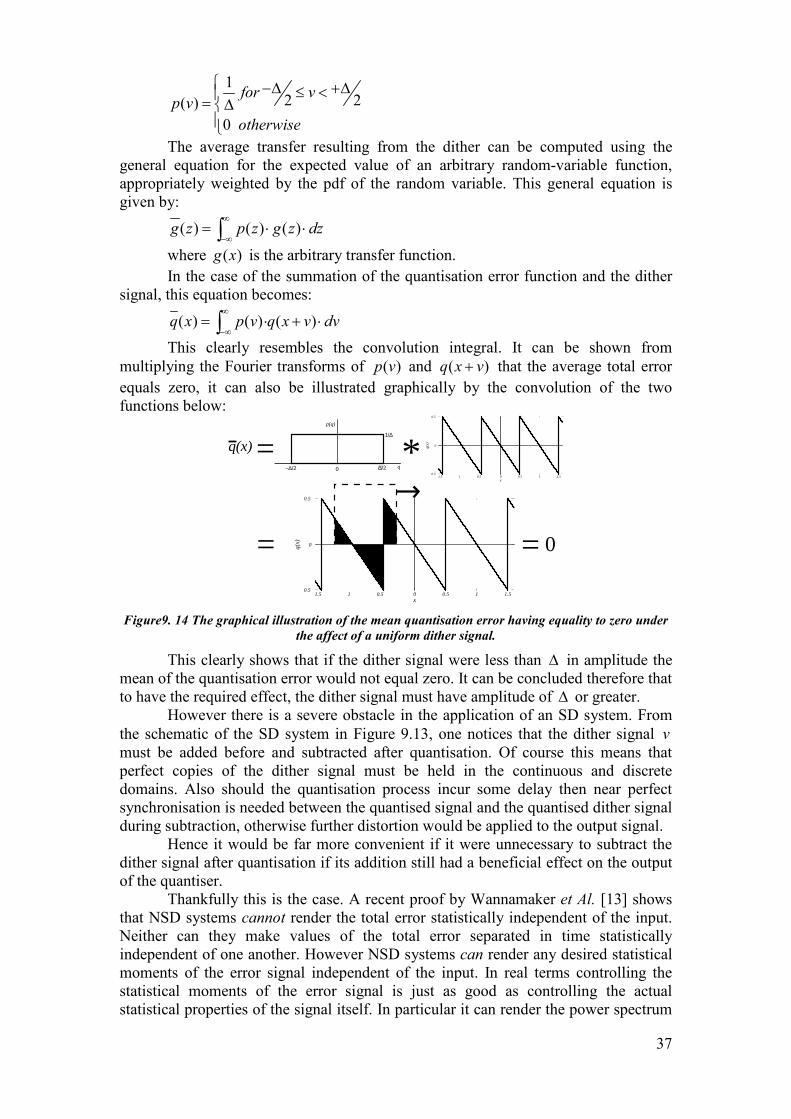
37
12 2( )
0
for vp v
otherwise
−∆ +∆≤ <= ∆
The average transfer resulting from the dither can be computed using the general equation for the expected value of an arbitrary random-variable function, appropriately weighted by the pdf of the random variable. This general equation is given by:
( ) ( ) ( )g z p z g z dz∞
−∞= ⋅ ⋅∫
where ( )g x is the arbitrary transfer function.In the case of the summation of the quantisation error function and the dither
signal, this equation becomes:
( ) ( ) ( )q x p v q x v dv∞
−∞= ⋅ + ⋅∫
This clearly resembles the convolution integral. It can be shown from multiplying the Fourier transforms of ( )p v and ( )q x v+ that the average total error equals zero, it can also be illustrated graphically by the convolution of the two functions below:
+∆/2−∆/2 0
1/∆
p(q)
q
1.5 1 0.5 0 0.5 1 1.50.5
0
0.5
x
q(x)
q(x) =
=
1.5 1 0.5 0 0.5 1 1.50.5
0
0.5
x
q(x)*
= 0
Figure 9. 14 The graphical illustration of the mean quantisation error having equality to zero under the affect of a uniform dither signal.
This clearly shows that if the dither signal were less than ∆ in amplitude the mean of the quantisation error would not equal zero. It can be concluded therefore that to have the required effect, the dither signal must have amplitude of ∆ or greater.
However there is a severe obstacle in the application of an SD system. From the schematic of the SD system in Figure 9.13, one notices that the dither signal vmust be added before and subtracted after quantisation. Of course this means that perfect copies of the dither signal must be held in the continuous and discrete domains. Also should the quantisation process incur some delay then near perfect synchronisation is needed between the quantised signal and the quantised dither signal during subtraction, otherwise further distortion would be applied to the output signal.
Hence it would be far more convenient if it were unnecessary to subtract the dither signal after quantisation if its addition still had a beneficial effect on the output of the quantiser.
Thankfully this is the case. A recent proof by Wannamaker et Al. [13] shows that NSD systems cannot render the total error statistically independent of the input. Neither can they make values of the total error separated in time statistically independent of one another. However NSD systems can render any desired statistical moments of the error signal independent of the input. In real terms controlling the statistical moments of the error signal is just as good as controlling the actual statistical properties of the signal itself. In particular it can render the power spectrum

38
of the total error signal equal to the power spectrum of dither signal plus a white ‘quantisation noise’ component. The paper also conducts an analysis of band-limited dither, i.e. a dither signal limited in its spectral occupancy, in particular “high-pass” random noise for use in dither applications. It was found to meet the necessary conditions to leave the total error statistically stationary and independent of the system input. This is an encouraging revelation as it implies that the complicated issue of dither subtraction is unnecessary and also brings the possibility of using band-limited dither to the fore.
There is also a method known as ‘large-scale’ dithering for which, as one might expect, the amplitude is much larger than ∆ . This method is used has the effect of not only averaging the quantisation error, but also has the effect of averaging non-linearities in the ADC’s transfer function. It has been found [14] that large scale dither has a beneficial effect in conjunction with ADCs that exhibit moderately high levels of non-linearity in their transfer function. However large-scale dither was found to have a no more beneficial effect than small-scale dither when used with highly linear modern ADCs (such as the Analog Devices AD6644) that employ digital error correction in conversion.
9.5.5 Small-Scale Dither ConclusionThe addition of small-scale dither in the process of analogue-to-digital
conversion has been shown to theoretically have the beneficial effect of suppressing the coherent spurious components generated due to the quantisation process. Small-scale band-limited non-subtracted dither has been found to work in practice [14] byimproving the Spurious Free Dynamic Range of ADCs, therefore it was decided that the option of using small-scale dither should be included in the specification for the proposed device.
39
9.6 Concept Directed Research ConclusionsThe conclusions drawn from the research detailed in this chapter is as follows:i) USB 2.0 would be the chosen method of data transfer from the digital-
oscilloscope peripheral to the host computer.ii) It was noted from the currently available hardware research that the
Cypress Semiconductor EZ-USB FX2 device had the advantage of incorporating a microcontroller and USB 2.0 transceiver. It also had the added functionality of being able to download its own firmware, was available as a development board and came with a suite of development software.
iii) The USB 2.0 software research revealed that it would be too time consuming to write a WDM custom-function driver and that designing a data-acquisition device to be compatible with an existing class-function driver would be impractical. This was the final reason for choosing the Cypress EZ-USB FX2 as the device to implement the USB 2.0 data interface, as a pre-written sample device driver is available for it.
iv) The Non-Uniform Sampling (NUS) research concluded that in principle the technique could indeed be used to sample signal bandwidths far greater than those possible with conventional uniform sampling.
v) In the analysis of software triggering, it was found that it would be relatively easy to implement in the case of periodically sampled signals, and would be theoretically possible in the case of non-uniformly sampled signals.
vi) The theory of additive dither was examined, and it was shown that a dither signal of around 1LSB in magnitude used in a Non-Subtractive Dither (NSD) system should have beneficial effects in suppressing the spurious components due to quantisation error.
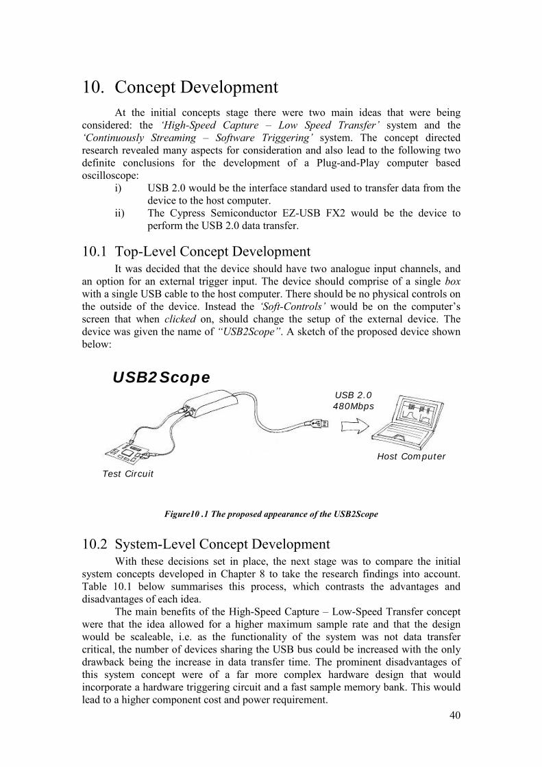
40
10. Concept DevelopmentAt the initial concepts stage there were two main ideas that were being
considered: the ‘High-Speed Capture – Low Speed Transfer’ system and the ‘Continuously Streaming – Software Triggering’ system. The concept directed research revealed many aspects for consideration and also lead to the following two definite conclusions for the development of a Plug-and-Play computer based oscilloscope:
i) USB 2.0 would be the interface standard used to transfer data from the device to the host computer.
ii) The Cypress Semiconductor EZ-USB FX2 would be the device to perform the USB 2.0 data transfer.
10.1 Top-Level Concept DevelopmentIt was decided that the device should have two analogue input channels, and
an option for an external trigger input. The device should comprise of a single boxwith a single USB cable to the host computer. There should be no physical controls on the outside of the device. Instead the ‘Soft-Controls’ would be on the computer’s screen that when clicked on, should change the setup of the external device. The device was given the name of “USB2Scope”. A sketch of the proposed device shown below:
USB2Scope
Test Circuit
USB 2.0480Mbps
Host Computer
Figure 10 .1 The proposed appearance of the USB2Scope
10.2 System-Level Concept DevelopmentWith these decisions set in place, the next stage was to compare the initial
system concepts developed in Chapter 8 to take the research findings into account. Table 10.1 below summarises this process, which contrasts the advantages and disadvantages of each idea.
The main benefits of the High-Speed Capture – Low-Speed Transfer concept were that the idea allowed for a higher maximum sample rate and that the design would be scaleable, i.e. as the functionality of the system was not data transfer critical, the number of devices sharing the USB bus could be increased with the only drawback being the increase in data transfer time. The prominent disadvantages of this system concept were of a far more complex hardware design that would incorporate a hardware triggering circuit and a fast sample memory bank. This would lead to a higher component cost and power requirement.

41
The principle advantages of the Continuously Streaming – Software Triggering concept were its basic hardware requirements, therefore being cheaper to construct and requiring less power, and the potential ease of software upgrade for increased performance. The main disadvantages would be the need for a reliable data transfer bandwidth or the data streaming could be stalled and the need for an extensive software application for a fully working system.
High-Speed Capture – Low-Speed Transfer Continuously Streaming – Software TriggeringAdvantages Disadvantages Advantages Disadvantages
Highest sampling rate possible
More complex hardware design Simpler Construction
The device would rely a given data transfer rate to work correctly
Device would still function if the USB bandwidth was limited
Hardware triggering required
No need for Hardware for triggering
Average sampling rate dependent on the maximum data transfer rate
Large proportion of ‘dead-time’ in between sampling windows, due to transfer time to host.
Theoretically no ‘dead-time’, as the trigger detection rate is host computer dependent.
The system would be incomplete without an extensive software application to perform software triggering
Higher Power Lower PowerHigher Cost CheaperLarge proportion of ‘dead-time’ in between sampling windows, due to transfer time to host.
Theoretically no ‘dead-time’, as the trigger detection rate is host computer dependent.
Trade off between sampling rate and sampling timeframe, as memory size limited.
Could be used for data logging.
Table 10.1 A comparison of the two initial system concepts
10.3 Concept SelectionThe concept selection was not an easy process as both concepts had their
advantages and disadvantages. One main point of concern was for the time scale of the project. Being a university project done by one person there was a limit to the pure amount of man-hours that could be put in along with normal study, so it was decided that a simple hardware design that could be completed on time would be far more favourable than a complex hardware design that would probably not be completed on schedule.
It was for this reason and the advantages mentioned previously that the Continuously Streaming – Software Triggering system concept was chosen.
With the system concept selected, the next stage in the design process was to devise a top-level specification for the device.
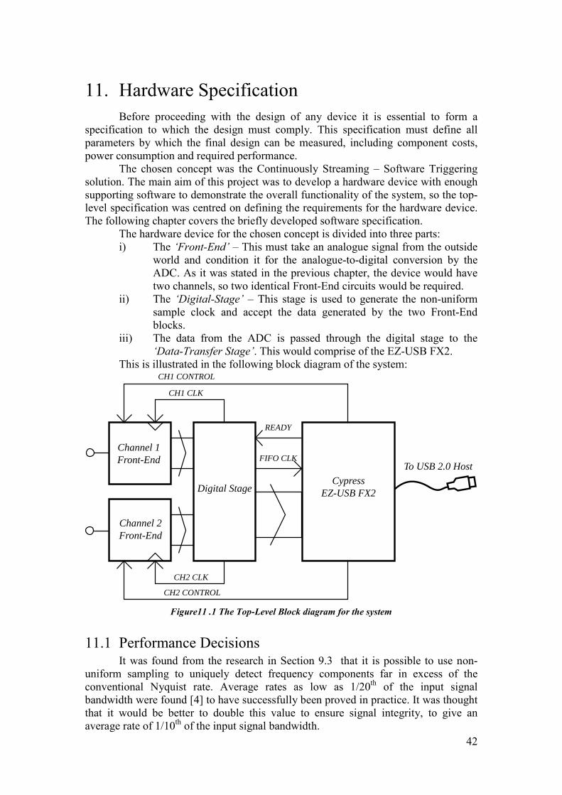
42
11. Hardware SpecificationBefore proceeding with the design of any device it is essential to form a
specification to which the design must comply. This specification must define all parameters by which the final design can be measured, including component costs, power consumption and required performance.
The chosen concept was the Continuously Streaming – Software Triggering solution. The main aim of this project was to develop a hardware device with enough supporting software to demonstrate the overall functionality of the system, so the top-level specification was centred on defining the requirements for the hardware device. The following chapter covers the briefly developed software specification.
The hardware device for the chosen concept is divided into three parts:i) The ‘Front-End’ – This must take an analogue signal from the outside
world and condition it for the analogue-to-digital conversion by the ADC. As it was stated in the previous chapter, the device would have two channels, so two identical Front-End circuits would be required.
ii) The ‘Digital-Stage’ – This stage is used to generate the non-uniform sample clock and accept the data generated by the two Front-End blocks.
iii) The data from the ADC is passed through the digital stage to the ‘Data-Transfer Stage’. This would comprise of the EZ-USB FX2.
This is illustrated in the following block diagram of the system:
Channel 1Front-End
Channel 2Front-End
Digital StageCypress
EZ-USB FX2
To USB 2.0 Host
READY
FIFO CLK
CH1 CONTROL
CH1 CLK
CH2 CONTROL
CH2 CLK
Figure 11 .1 The Top-Level Block diagram for the system
11.1 Performance DecisionsIt was found from the research in Section 9.3 that it is possible to use non-
uniform sampling to uniquely detect frequency components far in excess of the conventional Nyquist rate. Average rates as low as 1/20th of the input signal bandwidth were found [4] to have successfully been proved in practice. It was thought that it would be better to double this value to ensure signal integrity, to give an average rate of 1/10th of the input signal bandwidth.
43
It was decided that as the EZ-USB FX2’s FIFO memory allowed an input data width of 16 bits, that the ADC should have a resolution of 10 bits, leaving 6 bits to code the additive-random sampling time stamp for each sample. This would allow a wide distribution for the non-uniform sampling process and would also give an ADC resolution better than the currently available computer-based oscilloscopes. If it was found that more bits per sample where needed to encode the additive-random time stamps, lower bits of the ADCs’ output could be discarded inside the digital-stage block.
The choice of using USB 2.0 allows a theoretical data maximum data rate of 480Mbps, in reality it was estimated that the figure for the true data transfer rate would be more in the region of 80% of the maximum value due to protocol overheads (It was necessary to make this estimate early in the design process as no EZ-USB FX2 device was available for testing, and the Front-End design process needed to be started).
The points detailed in the previous three paragraphs lead to the following main decision for the specified performance of the instrument. The maximum average sampling rate was predicted to be around 400Mbps/(2*16bits)=12.5MSPS per channel. It was decided to err on the side of caution and settle on an expected transfer rate of 10MSPS per channel. This lead to the decision to settle on an analogue input bandwidth of 10MSPS*10=100MHz for both channels using the 1/10th input bandwidth non-uniform sampling rate for both of the input channels. The maximum sampling rate of each ADC would be 20MSPS, to allow for fast capture from a single channel.
The effective sampling rate required for an input signal bandwidth of 100MHz sampled using a discrete non-uniform sampling process was 100MHz*2=200MHz (As shown in Section 9.3.2). I.e. the 10MSPS additive-random sample clock would be derived from a high frequency 200MHz uniform clock.
The decision to use a 10bit ADC meant that a maximum Signal to Noise Ratio (SNR) due to the quantisation errors of around 10*6.02+1.78=62dB (For a derivation of this value, please refer to Appendix IV). Therefore it was decided that the analogue front-end circuitry should have a SIgnal to Noise And Distortion (SINAD) ratio of at least -60dB lower than a full-scale signal to make the most of the ADC’s dynamic range. Later research found that distortion increases drastically with frequency whilst using typical devices, and that a value of 60dB SINAD was a reasonable value for a frequency of 1MHz, so this was set as the specification.
The research into small-scale dither revealed that small-scale dither can have a beneficial effect [15] in the range of ±0.1LSB to ±32LSB, therefore it was decided that a dither generation system capable of producing this range of dither would be designed. The probability distribution of the dither signal is not critical [16] as long as its magnitude satisfies the need to average the quantisation noise. A method noted for generating an adequate dither signal [14] is to generate a pseudo-random pulse-width modulated digital signal in a digital-logic device, then process this signal by means of filtering and amplitude limitation, to achieve the desired probability distribution. It was decided that the digital stage should generate this pseudo-random pulse-width modulated signal, and that each front end stage should low pass filter and attenuate this signal to the desired magnitude for addition to the input signal prior to digitisation.
From the research into existing oscilloscope products in Section 0 it was found that most oscilloscopes work on full-scale ranges in 1,2,5,10 format, i.e. in a roughly logarithmic fashion to cover a wide dynamic range of input signals. It decided that the device should follow this scheme and have the following full-scale DC ranges:

44
10mVp.p. (±5mV DC) 20mVp.p. (±10mV DC) 50mVp.p (±25mV DC)100mVp.p. (±50mV DC) 200mVp.p. (±100mV DC) 500mVp.p. (±250mV DC)1Vp.p. (±500mV DC) 2Vp.p. (±1V DC) 5Vp.p. (±2.5V DC)10Vp.p. (±5V DC) 20Vp.p. (±10V DC) 50Vp.p. (±25V DC)100Vp.p. (±50V DC)
Table 11.1 The specified full-scale input ranges
A common value for voltage linearity specified by low-end oscilloscope manufacturers is 3%. This means that when the oscilloscope displays a certain voltage value on the display, it should be correct to within ±3%. It was decided that this accuracy would also be specified for the USB2Scope.
In Figure 11.1 the reader will notice the signals labelled ‘CH0’ and ‘CH1 Control’. These signals represent the means of controlling the front-end full-scale input range settings. It was decided that these would take the form of a common serial bus between each of the front-ends and one of the two free 8 bit output ports on the EZ-USB FX2 microcontroller. There was not time to rigorously define the bus’ communication protocol during the specification but, it was later fully specified during the system design stage in Chapter 14.
11.2 Cost and Power BudgetingA USB root-hub can supply to 2.5W of power to all peripherals sharing the
same bus (500mA at 5V DC). However the minimum quoted supply voltage is 4.65V DC, therefore the figure for maximum power consumption used in the power budget was 4.65V*500mA=2.325W. At this point in the design process the only confirmed power consumption was the EZ-USB FX2, whose datasheet quotes a value of around 600mW as the maximum power consumption (177mA at 3.3V). Rough estimates were made to specify the power consumption of both the front-ends and the digital-stage. These values were reviewed later in the Design Review, detailed in Chapter 17.
At the beginning of the project it was stated that a component cost of around £100 should be aimed for in batches of 1000 units (1KU). The only known significant component cost was the EZ-USB FX2, at around £20 per device, so again rough estimates were made to work with during the design process.
The following table summarises these initial cost and power budget values:
StageMaximum Power Consumption Price
Channel 0 Front-End 500mW £20.00Channel 1 Front-End 500mW £20.00Digital Stage 400mW £10.00EZ-USB FX2 600mW £20.00TOTAL: 2W £70.00
Table 11.2 The initial cost and power budget
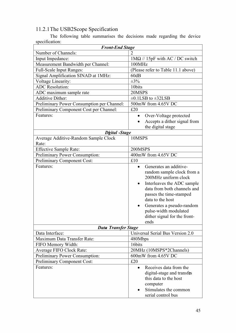
45
11.2.1The USB2Scope SpecificationThe following table summarises the decisions made regarding the device
specification:Front-End Stage
Number of Channels: 2Input Impedance: 1MΩ // 15pF with AC / DC switchMeasurement Bandwidth per Channel: 100MHzFull-Scale Input Ranges: (Please refer to Table 11.1 above)Signal Amplification SINAD at 1MHz: 60dBVoltage Linearity: ±3%ADC Resolution: 10bitsADC maximum sample rate 20MSPSAdditive Dither: ±0.1LSB to ±32LSBPreliminary Power Consumption per Channel: 500mW from 4.65V DCPreliminary Component Cost per Channel: £20Features: • Over-Voltage protected
• Accepts a dither signal from the digital stage
Digital -StageAverage Additive-Random Sample Clock Rate:
10MSPS
Effective Sample Rate: 200MSPSPreliminary Power Consumption: 400mW from 4.65V DCPreliminary Component Cost: £10Features: • Generates an additive-
random sample clock from a 200MHz uniform clock
• Interleaves the ADC sample data from both channels and passes the time-stamped data to the host
• Generates a pseudo-random pulse-width modulated dither signal for the front-ends
Data- Transfer StageData Interface: Universal Serial Bus Version 2.0Maximum Data Transfer Rate: 480MbpsFIFO Memory Width: 16bitsAverage FIFO Clock Rate: 20MHz (10MSPS*2Channels)Preliminary Power Consumption: 600mW from 4.65V DCPreliminary Component Cost: £20Features: • Receives data from the
digital-stage and transfers this data to the host computer
• Stimulates the common serial control bus

46
12. Software SpecificationFor a complete USB2Scope system a large amount of software would be required. This would be comprised firstly of device firmware, and secondly a Windows application.The device firmware would run on the EZ-USB FX2’s 8051 microcontroller, with the following required functionality:
i) Firstly it should setup the device’s control registers that configure the FIFO memory, I/O ports, timers and USB device descriptor tables.
ii) Once the device has been numerated by the host, the firmware has only a few tasks to complete, including ‘Housekeeping’ functions such as responding to new setup data from the host, and driving the common serial bus with data received from the soft-controls in the Windows Application.
The proposed Windows application was subdivided into the following three programs: i) An oscilloscope program that would display time domain data in a
triggered fashion.ii) A Discrete Fourier Transform analyser that would transform the input data
to the discrete frequency domain.iii) An automatic test program that could perform automatic capture and
measurement functions using script files.All three programs would be started as separate processes from a single Graphical User Interface (GUI) program that would perform housekeeping commands such as sending Front-End control data to the device. Communication between the main program and the three different program processes would be by means of event flags. Only one program would be allowed to run at a time.The oscilloscope program would need the following two processes to be run simultaneously:i) One process known as the ‘Scanning Process’ would be used to
continuously fill a circular buffer with input data, whilst searching the data for the triggering behaviour. To do this it would need to perform the ‘Software triggering’ operation described in Section 9.4 .
ii) A second process, used to plot the data on the video display, would be started by the buffering process when a trigger point was discovered. Event flags would be used to communicate between the processes to ensure that the data currently being displayed was not overwritten by the circular buffering process.
The DFT analyser program would be called on a regular time basis. Each time the program is run it firstly captures data from the device, windows the data, and then performs the DFT. The spectrum would then be then plotted to the screen.The automatic test program would follow instructions from a given input file. Example uses of this program would include frequency response sweeps, consisting of the following series of events:i) An external signal source, under General Peripheral Interface Port (GPIB)
control, would be set to each level and frequency specified by the input file. This signal would be used as the input to the USB2Scope.
ii) Data would then be captured from the device and transformed to the frequency domain. Frequency points specified in the input file would be recorded in an output file, before the procedure was repeated again.
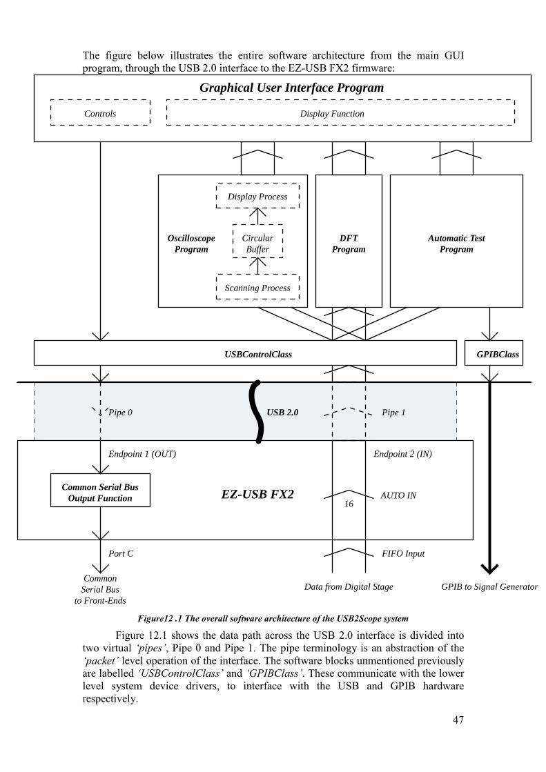
47
The figure below illustrates the entire software architecture from the main GUI program, through the USB 2.0 interface to the EZ-USB FX2 firmware:
Graphical User Interface Program
USBControlClass
OscilloscopeProgram
DFTProgram
Automatic TestProgram
Scanning Process
CircularBuffer
Display Process
Pipe 0 USB 2.0 Pipe 1
Endpoint 1 (OUT) Endpoint 2 (IN)
Common Serial BusOutput Function
Port C FIFO Input
16AUTO IN
CommonSerial Bus
to Front-EndsData from Digital Stage
GPIBClass
Display FunctionControls
EZ-USB FX2
GPIB to Signal Generator
Figure 12 .1 The overall software architecture of the USB2Scope system
Figure 12.1 shows the data path across the USB 2.0 interface is divided into two virtual ‘pipes’, Pipe 0 and Pipe 1. The pipe terminology is an abstraction of the ‘packet’ level operation of the interface. The software blocks unmentioned previously are labelled ‘USBControlClass’ and ‘GPIBClass’. These communicate with the lower level system device drivers, to interface with the USB and GPIB hardware respectively.
48
13. Project PlanningProject planning was one aspect that was of more than average importance in
comparison to the author’s previous experience in project work. This project took many man-hours to complete, and a substantial amount of time was spent planning to insure that the available time was put towards obtaining the set goals.
Up until this point this project was still purely a hardware design project, the decision to move to a hardware design and build project was not taken lightly. There were many logistical questions that had to be asked, and solved:
i) “Would the required materials, equipment, development systems be available on time when they are needed?”
ii) “Would there be the support, documentation and professional advice available when problems arise?”
iii) “How much of the proposed specification would physically be possible to design, build and test within the timeframe of this project?”
Almost the single reason why the project developed to a design-and-build approach was because of the project’s sponsorship by IFR Aeroflex UK Ltd., the author’s sponsor through university. IFR Aeroflex UK offered the following facilities and materials for the project’s development:
i) Regular consultation with design staffii) Unlimited use of the company’s PCB design software (The Mentor
Graphics 2000 Suite)iii) The in-house fabrication of the PCBs designediv) All components needed to populate the PCBsv) Use of test equipment, including development model instruments for
modification purposes.With such a generous offer of sponsorship that would answer the first two
questions asked above, it was decided to start planning for a design-and-build project.The main strategy was one of least risk, so that each system block could be
tested independently without system block inter-dependence, i.e. if one part of the project isn’t available / doesn’t work / goes terribly wrong etc. the rest of the project could still tested and written up.
Since the system level architecture was already neatly divided into three different blocks (Front-End, Digital-Stage and EZ-USB FX2), it was decided to separate the risk of failure along the points of interface between the blocks by making each a self-functioning unit.
The most significant contingency plan revolved around the need to be able to test and evaluate the Front-End stage’s performance, even if both the digital-stage and EZ-USB stage were unavailable. The chosen solution was to standardise the interface between the front-ends and the digital-stage to one used in the IFR Aeroflex 2319E radio frequency digitiser. This instrument has an ADC sample rate of 65.28MSPS, which can be altered internally, and can transfer captured data to a host computer using an interface card sold by National Instruments (NI-DAQ). The author had had previous experience in working with this instrument, so relatively little research was required to show that this would definitely be possible. The 2319E’s ADC interface uses a 16bit Low Voltage Differential Signal (LVDS) interface, which could easily be incorporated into both the design of the front-end stages and the digital-stage.
With this uncertainty solved, the largest remaining point of concern was that of constructing a stage incorporating the EZ-USB FX2 device. The device’s datasheet
49
explains clearly that the PCB layout around the device is critical to conform to the USB 2.0 standard. Since a development board containing the device was available, there seemed to be little point in spending time and effort constructing a PCB with the possibility of it not functioning correctly. This choice did however come at a high price of £420. Another reason the development board approach was taken was that it had been advised that a USB protocol analyser was “Invaluable” in the development of USB devices. USB 2.0 protocol analysers are currently very expensive, and since a USB 2.0 data connection was guaranteed with the use of the development board, the need for a USB protocol analyser seemed remote. Once the decision to use the EZ-USB FX2 development board had been made an order was placed, and the quoted lead time was around 6 weeks, although this was in no way guaranteed. This made the strategy of designing the Front-End and Digital-Stage boards to function independently of this development board look even more justified.
It was also initially decided that the interface between the Digital-Stage and the EZ-USB FX2 stage should also be a 2319E compatible LVDS interface, as this would allow the Digital Stage testing without the reliance on the EZ-USB FX2 development board arriving from the supplier on schedule.
It was concluded that there was no advantage in laying out both of the Front-Ends on a single board in the PCB design package, this would waste time and double the work. Therefore the decision was made to build two identical Front-End boards with a means of setting the Channel address for the Common Serial Bus on each board.
The method of planning the oncoming design, prototyping and testing parts of the project was to make a list of all conceivable tasks, identifying milestones in the project’s development. Please refer to the following page for the Gantt chart of the project plan.
A point of interest is that due to the extended lead time in the ordering of some components, samples of most devices were ordered almost at the time of their discovery rather than when the devices were confirmed as being included in the design. In fact several of the choices made for components used in the final design were due to the fact that samples of the devices had arrived from the suppliers whilst the some of the preferred devices had not!
The following milestones were set to keep the hardware development on schedule:
Date Milestone7th December 2001 Specification Completed4th January 2002 Hardware Design Phase Completed8th February 2002 PCB Layout Submitted for Manufacture1st March 2002 Prototype Built22nd March 2002 Prototype Tested
The critical path through the hardware design process was estimated to be the design, fabrication and testing of the Front-End stage, so this chain of tasks was made the highest priority for completion.
With the specification set and the initial project planning completed it was now time to start the hardware design.

50
Task NameFinal Year Project
Preliminary ResearchEvaluation of Current Oscilloscopes
Evaluation of High-Speed Serial Technology
Cost & Power Budget Analysis
Solution DevelopmentRequirement Specification DevelopmentRequirement Specification Completed
Solution Development
Solution Chosen
Block-Level SpecificationFront-End SpecificationDither Generator Specification
Digital Stage Specification
Power Supply SpecificationTop-Level Specification Completed
Front-End DesignEvaluation of Available Technology
Sub-Block Definition
Initial Front-End DesignFront-End Deisgn Appraisal
Front-End Design Finalisation
Dither Generator DesignResearch into the Use of Additive Dither
Initial Dither Generator DesignDither Generator Deisgn Appraisal
Dither Generator Design Finalisation
Digital-Stage DesignResearch into Non-Uniform Sampling Methods
Evaluation of Available FPGA TechnologyInitial Digital-Stage Design
Digital-Stage Deisgn AppraisalDigital-Stage Design Finalisation
Device PrototypingOrder ComponentLead Time for Ordered Component
PCB LayoutSubmit PCB Design for Manufacture
PCB Lead Time
Build PrototypePrototype Built
Device TestingFront-End Testing
Digital Stage Testing
Hardware Tested
Software DevelopmentMicrosoft Windows Driver Model ResearchSoftware Architecture Specification Development
Software Architecture Specification Completed
Software Development Using Keil EmulatorOrder Development Board
Development Board Lead TimeSoftware Development using Development Board
Software Written
Exam Period
Interim Report WritingInterim Report WritingInterim Report Deadline
Final Report WritingFinal Report WritingFinal Report Deadline
02/11
23/11
07/12
04/01
04/01
04/01
11/01
08/02
01/03
22/03
28/12
09/01
23/03
22/01
08 15 22 29 05 12 19 26 03 10 17 24 31 07 14 21 28 04 11 18 25 04 11 18 25 01 08 15 22 29 06 13 20 27 03 10Nov '01 Dec '01 Jan '02 Feb '02 Mar '02 Apr '02 May '02 Jun '02

51
14. System-Level DesignThe decision to design and prototype each system stage separately on different
PCBs had several implications on the overall system design. Firstly each board would require its own power regulation circuitry. Secondly the additional interface circuitry required for the proposed LVDS interfaces would require additional power that would not be a considered factor in a final product design. This meant that due to the extra power consumption, it would not be possible to power the device from the USB bus, therefore the decision to use an external power supply for the Front-End and Digital-Stages was an obvious one. Since the project was not really an exercise in power supply design, it was decided that the power regulation circuitry should be designed as simply as possible, rather than trying to optimise the efficiency of the regulation. However the system would still be designed with the aim being powered directly from the USB 5V supply.
During the specification process there had to be a compromise between the time spent rigorously defining the interfaces between system-level blocks, and the point at which the hardware design work could begin. It had been decided that the interfaces would be roughly defined during the specification, and properly defined during the system design process itself. Any necessary design changes would be evaluated during the Design Review stage.
14.1 Initial System DesignThis section documents the initial design of the system-level interfaces and the
design of the system’s power supply. The following diagram illustrates the initial system design.
Channel 0Front-End Board
Channel 1Front-End Board
Digital-StageBoard
LVDS ReceiverDaughter Board
LVDS
LVDS
DitherIn
ClockIn
Power In
Power In
1MΩ Signal Input
1MΩ Signal Input
EZ-USB FX2Development Board
LVDS
To Host Computer
ClocksOut
DitherOut
Clock Generator
DitherIn
ClockIn
Power In
CommonSerial Bus
Out
CommonSerial Bus
In
CommonSerial Bus
In
Figure 14.1 The Initial System-Level Design
As can be seen from the diagram the initial design had the two identical Front-End stages joined via the 2319E compatible LVDS interfaces to the Digital-Stage, as planned in the previous Chapter. The EZ-USB FX2 development board provides access to the device’s pins in the form of PCB headers. A daughter board is supplied with the development kit that plugs directly on to the development board’s headers.
52
The Digital-Stage would be connected to the daughter board by another LVDS interface as stated in the project planning chapter.
14.1.1Common Serial Control BusThe common serial bus was defined in the specification as a common interface
between the two front end boards and one of the free Input / Output (I/O) ports on theEZ-USB FX2 microcontroller. The data width of the I/O ports is 8 bits, so the common serial bus width was chosen to be 10way. The port would be directly connected to the first 8 bits leaving bus-wire 9 unconnected, followed by a common ground. The interface was developed in parallel with the Front-End design in order to accommodate the developed control requirements. The interface is illustrated in the following figure:
SCLK
CH_SEL
DCLK
DATA
Reserved
Reserved
Reserved
Reserved
N.C.
Ground
1 (Brown):
2 (Red):
3 (Orange):
4 (Yellow):
5 (Green):
6 (Blue):
7 (Purple):
8 (Grey):
9 (White):
10 (Black):
EZ-USB FX2I/O Port
Front-EndChannel 0
Front-EndChannel 1
Bus-Line Filtering
Front-EndCommon Serial Bus
Input Pin
100Ω
10nF
To Front-EndSerial Decoder
Bus Assignments
Figure 14 .2 The Common Serial Bus Interface
The inputs to the Front-End boards would be filtered using an RC filter with a cut-off frequency of around 150kHz ( 91 2 1 2 100 10 159RC kHzπ π −= ⋅ ⋅ ≈ ) to suppress any digital noise from the EZ-USB FX2 board interfering with the Front-End analogue circuitry.
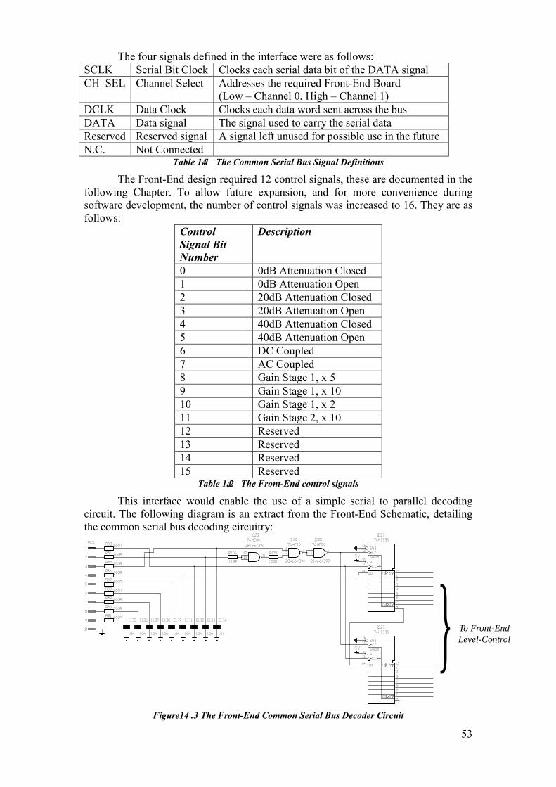
53
The four signals defined in the interface were as follows:SCLK Serial Bit Clock Clocks each serial data bit of the DATA signalCH_SEL Channel Select Addresses the required Front-End Board
(Low – Channel 0, High – Channel 1)DCLK Data Clock Clocks each data word sent across the busDATA Data signal The signal used to carry the serial dataReserved Reserved signal A signal left unused for possible use in the futureN.C. Not Connected
Table 14.1 The Common Serial Bus Signal Definitions
The Front-End design required 12 control signals, these are documented in the following Chapter. To allow future expansion, and for more convenience during software development, the number of control signals was increased to 16. They are as follows:
Control Signal Bit Number
Description
0 0dB Attenuation Closed1 0dB Attenuation Open2 20dB Attenuation Closed3 20dB Attenuation Open4 40dB Attenuation Closed5 40dB Attenuation Open6 DC Coupled7 AC Coupled8 Gain Stage 1, x 59 Gain Stage 1, x 1010 Gain Stage 1, x 211 Gain Stage 2, x 1012 Reserved13 Reserved14 Reserved15 Reserved
Table 14.2 The Front-End control signals
This interface would enable the use of a simple serial to parallel decoding circuit. The following diagram is an extract from the Front-End Schematic, detailing the common serial bus decoding circuitry:
To Front-EndLevel-Control
Figure 14 .3 The Front-End Common Serial Bus Decoder Circuit

54
The circuit consists of two cascaded 74HC595 8 bit shift registers driven by the common serial bus on PL5. The NAND logic gates are used to enable or disable the Data Clock Signal depending on the Channel Select signal. The channel number is set by either wiring in, or wiring out the inverter-connected NAND gate between the two dummy resistors R105 and R106.
14.1.2The 200MHz Fast ClockThe specification defined that the system should perform the sampling in an
additive-random manner derived from a high frequency 200MHz clock. Initially it was decided that this 200MHz clock signal should be generated on the digital-stage board. Research was conducted into simple clock generating chips, and the Cypress Semiconductor CYC22393 device was identified as a simple solution to the issue. The device’s data sheet specified that the device could generate up to 6 CMOS compatible clock signal outputs ranging from 8 to 200MHz, derived from a reference clock or an external crystal. The device’s non-volatile flash memory would need to be programmed using its proprietary serial interface, in order to set up the internal Phase-Locked Loops (PLLs) and clock dividers.
14.1.3The LVDS InterfaceIn the project planning chapter the interface between the Front-End and the
Digital-Stage had been chosen to be compatible the LVDS interface used inside the IFR Aeroflex 2319E radio frequency digitiser. This would enable the testing of the Front-End board without waiting for the development board to arrive and or building the digital-stage board. The interface standard uses a 50-way 0.05 pitch ribbon cable with a SCSI D-type connector with the following signal connections:
Pin Numbers Signal2, 26 +CLK, -CLK28, 3 Reserved, Reserved5, 29 +Bit 13, -Bit 13 (MSB)31, 6 +Bit 12, -Bit 128, 32 +Bit 12, -Bit 1134, 9 +Bit 12, -Bit 1011, 35 +Bit 12, -Bit 937, 12 +Bit 12, -Bit 814, 38 +Bit 12, -Bit 740, 15 +Bit 12, -Bit 617, 41 +Bit 12, -Bit 543, 18 +Bit 12, -Bit 420, 44 +Bit 12, -Bit 346, 21 +Bit 12, -Bit 223, 47 +Bit 12, -Bit 149, 24 +Bit 12, -Bit 0 (LSB)1, 27, 4, 30, 7, 33, 10, 36, 13, 39, 16, 42, 19, 45, 22, 48, 25, 50
GND
Table 14.3 The LVDS standard used to interface the Front-End boards to the 2319E digitiser and the Digital-Stage.
This allows for the transfer of 14bit data using the LVDS standard. The reader may notice that the order of signals in the ribbon cable is +SIGNAL,-SIGNAL, GND,+SIGNAL,-SIGNAL, GND,… etc. in order to provide isolation between adjacent signal pairs. Note that pin numbers 2 and 26 are used to supply the sample clock to
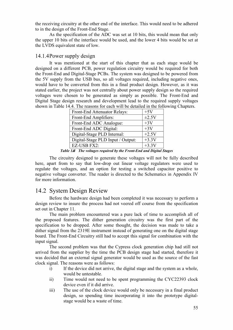
55
the receiving circuitry at the other end of the interface. This would need to be adhered to in the design of the Front-End Stage.
As the specification of the ADC was set at 10 bits, this would mean that only the upper 10 bits of the interface would be used, and the lower 4 bits would be set at the LVDS equivalent state of low.
14.1.4Power supply designIt was mentioned at the start of this chapter that as each stage would be
designed on a different PCB, power regulation circuitry would be required for both the Front-End and Digital-Stage PCBs. The system was designed to be powered from the 5V supply from the USB bus, so all voltages required, including negative ones, would have to be converted from this in a final product design. However, as it was stated earlier, the project was not centrally about power supply design so the required voltages were chosen to be generated as simply as possible. The Front-End and Digital Stage design research and development lead to the required supply voltages shown in Table 14.4. The reasons for each will be detailed in the following Chapters.
Front-End Attenuator Relays: +5VFront-End Amplifiers: ±2.5VFront-End ADC Analogue: +3VFront-End ADC Digital: +3VDigital-Stage PLD Internal: +2.5VDigital-Stage PLD Input / Output: +3.3VEZ-USB FX2: +3.3V
Table 14.4 The voltages required by the Front-End and Digital Stages
The circuitry designed to generate these voltages will not be fully described here, apart from to say that low-drop out linear voltage regulators were used to regulate the voltages, and an option for testing a switched capacitor positive to negative voltage converter. The reader is directed to the Schematics in Appendix IV for more information.
14.2 System Design ReviewBefore the hardware design had been completed it was necessary to perform a
design review to insure the process had not veered off course from the specification set out in Chapter 11.
The main problem encountered was a pure lack of time to accomplish all of the proposed features. The dither generation circuitry was the first part of the specification to be dropped. After some thought, the decision was made to take a dither signal from the 2319E instrument instead of generating one on the digital stage board. The Front-End Circuitry still had to accept this signal for combination with the input signal.
The second problem was that the Cypress clock generation chip had still not arrived from the supplier by the time the PCB design stage had started, therefore it was decided that an external signal generator would be used as the source of the fast clock signal. The reasons were as follows:
i) If the device did not arrive, the digital stage and the system as a whole, would be untestable.
ii) Time would not need to be spent programming the CYC22393 clock device even if it did arrive.
iii) The use of the clock device would only be necessary in a final product design, so spending time incorporating it into the prototype digital-stage would be a waste of time.
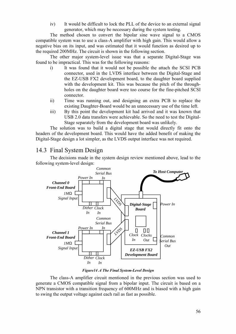
56
iv) It would be difficult to lock the PLL of the device to an external signal generator, which may be necessary during the system testing.
The method chosen to convert the bipolar sine wave signal to a CMOS compatible system was to use a class-A amplifier with high gain. This would allow a negative bias on its input, and was estimated that it would function as desired up to the required 200MHz. The circuit is shown in the following section.
The other major system-level issue was that a separate Digital-Stage was found to be impractical. This was for the following reasons:
i) It was found that it would not be possible the attach the SCSI PCB connector, used in the LVDS interface between the Digital-Stage and the EZ-USB FX2 development board, to the daughter board supplied with the development kit. This was because the pitch of the through-holes on the daughter board were too course for the fine-pitched SCSI connector.
ii) Time was running out, and designing an extra PCB to replace the existing Daughter-Board would be an unnecessary use of the time left.
iii) By this point the development kit had arrived and it was known that USB 2.0 data transfers were achievable. So the need to test the Digital-Stage separately from the development board was unlikely.
The solution was to build a digital stage that would directly fit onto the headers of the development board. This would have the added benefit of making the Digital-Stage design a lot simpler, as the LVDS output interface was not required.
14.3 Final System DesignThe decisions made in the system design review mentioned above, lead to the
following system-level design:
Channel 0Front-End Board
Channel 1Front-End Board
Digital-StageBoardDither
InClock
In
Power In
Power In
1MΩ Signal Input
1MΩ Signal Input EZ-USB FX2
Development Board
To Host Computer
ClocksOut
DitherIn
ClockIn
Power In
CommonSerial Bus
Out
CommonSerial Bus
In
CommonSerial Bus
In
LVDS
LVDSClock
In
Figure 14 .4 The Final System-Level Design
The class-A amplifier circuit mentioned in the previous section was used to generate a CMOS compatible signal from a bipolar input. The circuit is based on a NPN transistor with a transition frequency of 600MHz and is biased with a high gain to swing the output voltage against each rail as fast as possible.
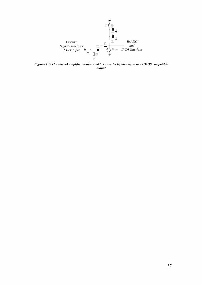
57
ExternalSignal Generator
Clock Input
To ADCand
LVDS Interface
Figure 14 .5 The class-A amplifier design used to convert a bipolar input to a CMOS compatible output
58
15. Front-End DesignThe largest proportion of the time spent on designing hardware, was used to
design the Front-End Stage. It proved to be a very educational experience, as the trade-offs between many real-world factors had to be undertaken. The design process needed to be iterative in nature, in order to analyse the many interdependent system relationships. When a proposed block-level concept was developed, the next stage was to perform market research to identify potential devices that would accomplish the concept. Many devices were disregarded almost immediately due to factors such as their required supply voltage being higher than the USB bus’ +5V, even though their performance was more than satisfactory. The research would form a proposed design which could then be matched against the required specification. More often than not, factors such as the power consumption and cost ruled the proposed design unviable. The procedure would then have to either start again, or the proposed design could be modified to trade-off surplus performance in one area with under-performance in another.
This Chapter documents the Block-Level decisions made, and then goes through the design work undertaken for each Front-End block.
15.1 Block Level DesignThe required specification for each Front-End board was as follows:
Input Impedance: 1MΩ // 15pF with AC / DC switchMeasurement Bandwidth per Channel: 100MHzFull-Scale Input Ranges: See Table 15.2 belowSignal Amplification SINAD at 1MHz: 60dBVoltage Linearity: ±3%ADC Resolution: 10bitsMaximum ADC sampling rate: 20MSPSAdditive Dither: ±0.1LSB to ±32LSBPreliminary Power Consumption per Channel: 500mW from 4.65V DCPreliminary Component Cost per Channel: £20Features: • Over-Voltage protected
• Accepts a dither signal from the digital stage
Table 15.1 The specification of the Front-End board
10mVp.p. (±5mV DC) 20mVp.p. (±10mV DC) 50mVp.p (±25mV DC)100mVp.p. (±50mV DC) 200mVp.p. (±100mV DC) 500mVp.p. (±250mV DC)1Vp.p. (±500mV DC) 2Vp.p. (±1V DC) 5Vp.p. (±2.5V DC)10Vp.p. (±5V DC) 20Vp.p. (±10V DC) 50Vp.p. (±25V DC)100Vp.p. (±50V DC)
Table 15.2 The specified full-scale input ranges
Two concepts were developed for the block-level solution of this specification.i) One was based on a ‘single-ended’ approach, in the sense that the
signal path would pass from one block to the next in the form of a single conductor, whose signal value was relative to its voltage with respect to the common ground reference.
ii) The second was to use a fully differential system, i.e. the signal passes from one block to the next in the form of two conductors, where the
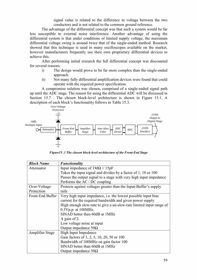
59
signal value is related to the difference in voltage between the two conductors and is not related to the common ground reference.
The advantage of the differential concept was that such a system would be far less susceptible to external noise interference. Another advantage of using the differential system is that under conditions of limited supply voltage, the maximum differential voltage swing is around twice that of the single-ended method. Research showed that this technique is used in many oscilloscopes available on the market, however manufacturers frequently use their own proprietary differential devices to achieve this.
After performing initial research the full differential concept was discounted for several reasons:
i) The design would prove to be far more complex than the single-ended approach.
ii) Not many fully differential amplification devices were found that could operate with the required power specification.
A compromise solution was chosen, comprised of a single-ended signal path up until the ADC stage. The reason for using the differential ADC will be discussed in Section 15.7 . The chosen block-level architecture is shown in Figure 15.1. A description of each block’s functionality follows in Table 15.3.
Attenuator
Over-VoltageProtection
Front-EndBuffer
AmplifierStage
Anti-AliasFilter
ADCDriver
ADC LVDSInterface
+V
-V
1MΩAnalogue Input
LVDSOutput to
Digital-Stage
Figure 15 .1 The chosen block-level architecture of the Front-End Stage
Block Name FunctionalityAttenuator Input impedance of 1MΩ // 15pF
Takes the input signal and divides by a factor of 1, 10 or 100Passes the output signal to a stage with very high input impedancePerforms the AC / DC coupling
Over-Voltage Protection
Protects against voltages greater than the Input-Buffer’s supply rails
Front-End Buffer Very high input impedance, i.e. the lowest possible input bias current for the required bandwidth and given power supplyHigh enough slew-rate to give a un-slew-rate limited input range of 0.5Vp.p. at 100MHz.SINAD better then 60dB at 1MHzA gain of 2.Low voltage noise at inputOutput impedance 50Ω
Amplifier Stage High Input ImpedanceGain factors of 1, 2, 5, 10, 20, 50 or 100Bandwidth of 100MHz on gain factor 100SINAD better than 60dB at 1MHzOutput impedance 50Ω

60
Anti-Alias Filter Characteristic impedance 50ΩCut-off frequency of around 100MHzStop-band attenuation of at least -60dBPass-band return loss (S11) of at least -16dBAs steep a transition as possible to maximise measurement bandwidth
ADC Driver Two 50Ω impedance inputsThe two inputs should be combined, and converted from single-ended to differential signal format with a gain of 2.It should also perform a level shifting process from a bipolar signal to one biased around 1.5VLow output impedance
ADC Stage High input impedanceThe input should be low-pass filtered, before digitisationUnsigned binary 10 bit outputMaximum sample rate of around 20MSPSCMOS outputs
LVDS Interface CMOS inputsLVDS compatible outputsCommon mode filtering of the LVDS output to stop unwanted digital noise coming in the opposite direction from the digital stageOutput to 50-way IFR 2319E compatible SCSI connector
Table 15.3 The functional specification of the sub-blocks within the Front-End Stage
More information about the contents of Table 15.3 is given in the following sections of this chapter.
Table 15.4 details the full-scale voltage ranges between each block of the Front-End Stage for both the minimum and maximum specified full-scale input ranges. The minimum full-scale range is when the attenuator is set to divide by 1 (0dB) and the amplifier is set to multiply by 100 (+40dB). The maximum full-scale input ranges is when the attenuator is set to divide by 100 (-40dB) and the amplifier is set to unity gain (0dB). Note that the calculation does not take the pass-band insertion loss of the Anti-Alias Filter into account, which is usually in the order of around -1dB. This would have the desirable effect of slightly reducing the full-scale range seen at the ADC, therefore reducing the likelihood of clipping.
It is worth mentioning here that a rather fundamental mistake was made during the initial Front-End design work, which was not discovered until well into the testing stage. It was thought that as the probes for oscilloscopes are 1MΩ in characteristic impedance, that the probe contained a 1MΩ source resistor on x1 mode, as illustrated below:
RR
1MΩ
1MΩ ImpedanceTransmission Line
approx. 1.5meters long
1MΩSignalSource
Oscilloscope Probe
InputTermination
of Oscilloscope
Figure 15 .2 The incorrect model of a oscilloscope probe on x1 setting, illustrating the expected 1MΩ source resistance
In fact x1 oscilloscope probes have no source resistor, and are effectively an unmatched transmission line, which can have very undesirable effects at high frequencies. This was discovered during the testing process. The assumption that
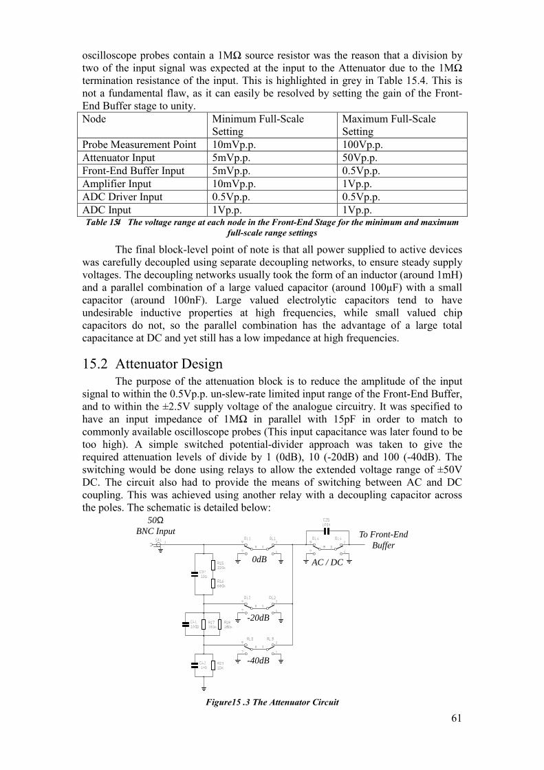
61
oscilloscope probes contain a 1MΩ source resistor was the reason that a division by two of the input signal was expected at the input to the Attenuator due to the 1MΩ termination resistance of the input. This is highlighted in grey in Table 15.4. This is not a fundamental flaw, as it can easily be resolved by setting the gain of the Front-End Buffer stage to unity.Node Minimum Full-Scale
SettingMaximum Full-Scale Setting
Probe Measurement Point 10mVp.p. 100Vp.p.Attenuator Input 5mVp.p. 50Vp.p.Front-End Buffer Input 5mVp.p. 0.5Vp.p.Amplifier Input 10mVp.p. 1Vp.p.ADC Driver Input 0.5Vp.p. 0.5Vp.p.ADC Input 1Vp.p. 1Vp.p.Table 15.4 The voltage range at each node in the Front-End Stage for the minimum and maximum
full-scale range settings
The final block-level point of note is that all power supplied to active devices was carefully decoupled using separate decoupling networks, to ensure steady supply voltages. The decoupling networks usually took the form of an inductor (around 1mH) and a parallel combination of a large valued capacitor (around 100µF) with a small capacitor (around 100nF). Large valued electrolytic capacitors tend to have undesirable inductive properties at high frequencies, while small valued chip capacitors do not, so the parallel combination has the advantage of a large total capacitance at DC and yet still has a low impedance at high frequencies.
15.2 Attenuator DesignThe purpose of the attenuation block is to reduce the amplitude of the input
signal to within the 0.5Vp.p. un-slew-rate limited input range of the Front-End Buffer, and to within the ±2.5V supply voltage of the analogue circuitry. It was specified to have an input impedance of 1MΩ in parallel with 15pF in order to match to commonly available oscilloscope probes (This input capacitance was later found to be too high). A simple switched potential-divider approach was taken to give the required attenuation levels of divide by 1 (0dB), 10 (-20dB) and 100 (-40dB). The switching would be done using relays to allow the extended voltage range of ±50V DC. The circuit also had to provide the means of switching between AC and DC coupling. This was achieved using another relay with a decoupling capacitor across the poles. The schematic is detailed below:
50Ω BNC Input
0dB
-20dB
-40dB
AC / DC
To Front-EndBuffer
Figure 15 .3 The Attenuator Circuit

62
Research was put into finding the most suitable relays for the task, they would have to be small, cheap, low in power consumption, have a good insertion loss over the required 100MHz bandwidth, and good isolation between poles when in their open position.
All of the suitable relays found during the research were found to be of the Double-Pole, Double-Throw variety. A solution for the use of the unutilised pole was to form a ‘back-to-back’ double switched junction, with both the unused contacts connected to ground as shown in Figure 15.3. This formation would have the added benefit of greatly increasing the isolation between the input and output contacts in the open position, due to the grounded bridge between the two. The relays put under most consideration are detailed in the table below:
Teledyne RF100
Teledyne RF300
Matsushita TQ2
Switching Voltage (V) 5 5 5Coil Power (mW) 450 450 140Contact Resistance (mΩ)
100 100 20
Contact Voltage Rating(V DC)
28 28 125
Bandwidth with insertion loss < 0.5dB
2GHz 3GHz 1GHz
Off Isolation at 100MHz (dB)
50 65 40
Latching Version? No No YesSingle Unit Price (£) 23.94 27.16 2.38
Table 15.5 The relays found during the research
The Teledyne relays are very high performance devices, capable of switching very high frequency signals. However they are not very well suited to the required specification of switching up to 50V DC. They are also very expensive! (Although the prices quoted are for one-off quantities). The decision to use the TQ2 variety of Matsushita relays was further ensured when it was revealed that the manufacturer produced small surface mount versions with latching capability. Up until this point in the design process the power budgeting was very tight because a lot of power was required to hold the relay contacts in place. The prospect of using latching devices with switching times of as little as 3ms, allowed a considerable amount of the power budget to be better used elsewhere.
The current supplied to the TQ2SA-L2-5V relays was not allowed to exceed 10mA per channel in the worst case, assuming all relay coils were powered at the same time, in order to reduce the possibility of exceeding the allowed USB supply current. This was achieved by powering them from a large 1000µF capacitor charged up through a 470Ω resistor. This did mean that a charge time of around half a second was required in between switching.
15.3 Front-End Buffer DesignThe choice of device for accomplishing the buffering stage was very limited.
Research into the buffering methods used by oscilloscope manufacturers revealed that from about 1980 onwards custom ICs were used to perform the operation, often converting from the single-ended input to a differential signal. The research into possible Front-End buffering devices centred on the wideband video operational amplifier market. The possibility of designing a custom buffer stage out of discretecomponents was considered, but this was discounted as it would have been a project

63
in itself. Only two commercially available devices were found that were within the required specification, both made by Burr-Brown, now a subsidiary of Texas Instruments:
OPA655 OPA355Minimum supply voltage (V) ±4.75 2.5Maximum supply current (mA) 29 11Input impedance (GΩ) 10 10Gain bandwidth product (MHz) 240 200Slew- rate (V/µs) 290 360Noise (nV/√Hz) at 1MHz 20 5.8SINAD (dB) at 1MHz 90 80
Table 15.6 Burr-Brown very high input impedance operational-amplifiers
Looking at the table the reader will see that the only advantage of the OPA655 device is the better distortion ratio of 90dB at 1MHz. The OPA355 device is superior in all other characteristics, so it was chosen as the device of choice for the Front-End Buffer.
The only problem with the OPA355 device is its low slew-rate. It was found that due to this value being around 360V/µs that the un-slew-rate limited bandwidth is reduced to around 60MHz. For a 100MHz undistorted bandwidth, the output signal would need to be limited to around 0.6Vp.p. This was calculated as follows:
For a given sinusoid of peak amplitude A and radial frequency ω , the derivative of the sinusoid is equal to A ω⋅ , since this equates to the constant known as the slew-rate for the upper bound of performance, there is an inverse relationship between the maximum peak amplitude of the output signal for a given frequency. This relationship is shown in the following figure for a slew- rate of 390V/µs:
0.6
10 6 10 7 10 8 10 60
0.2
0.4
0.8
1
Frequency (Hz)
Peak
Am
plitu
de (V
)W
ithou
t Sle
w-R
ate
Dis
tort
ion
Figure 15 .4 The maximum peak amplitude for a slew-rate limited device of 390V/µs
It was thought that as no other suitable devices had been found that this performance limitation was unavoidable.
The input bias current of the OPA355 is around 3pA, therefore voltage-protection diodes with equally low reverse bias current diodes were chosen. These were Philips Semiconductor standard BAS116 devices, with a typical reverse bias current of 3pA, supplied by On Semiconductor. The only point of concern was that the switching time of these devices is as high as 800ns, therefore leaving the buffer unprotected for a larger than average period of time. But it was thought that the low-leakage current requirement was of higher importance.

64
The following diagram shows the schematic of the Front-End Buffer, notice the gain setting of 2 as specified earlier in the block level design:
From AttenuatorCircuit
To GainStage
Figure 15 .5 The Front-End Buffer Circuit
15.4 Amplification Stage DesignThe required specification for the amplification stage was as follows:
• High input impedance• Gain factors of 1, 2, 5, 10, 20, 50 or 100• Bandwidth of 100MHz on gain factor 100• SINAD better than 60dB at 1MHz• Output impedance 50Ω
The requirement of at least a 100MHz bandwidth for a gain factor of 100, meant that it would definitely not be possible to achieve this easily using one device, as it would need a gain-bandwidth product of 10GHz! With two identical stages this product could be reduced to 1GHz as each stage would have an amplification factor of 10. Again the decision was made not to design a custom amplification stage using discrete components, as this would be too time consuming. Instead research was conducted in to high-speed video frequency operational-amplifier market.
An almost ideal device was found for the purpose, the Analog Devices AD8009, its specification is shown below:
AD8009Minimum supply voltage (V) +5VMaximum supply current (mA) 14Large signal bandwidth (MHz) Gain=10 320Unity gain bandwidth (MHz) 1000Slew-rate (V/µs) 5500Noise (nV/√Hz) at 1MHz 1.9SINAD (dB) at 5MHz 74SINAD (dB) at 150MHz 44
Table 15.7 The Analogue Devices AD8009 specification
With a unity gain bandwidth of 1GHz and satisfactory performance whilst supplying a gain factor of 10, it satisfied all of the specification requirements. The trade-off in performance was that its supply voltage requirement was of a minimum of 5V. This was the reason why ±2.5V was chosen as the supply voltage to the analogue circuitry.

65
The specification stated that the gain must be able to switch between factors of 1 (+0dB), 2 (+6dB), 5 (+14dB), 10 (+20dB), 20 (+26dB), 50 (+34dB) or 100 (+40dB). This could easily be accomplished using two gain stages, with the first stage providing gain factors of 1, 5 and 10, and the second providing 1, 2 and 10.
The method of switching between the different gain settings was chosen as being to use only one AD8009 device per gain stage, each with a fixed feedback resistor. To alter the gain from unity, a gain resistor could be ‘switched in’ from the inverting input to ground. This is shown in the schematic of the final design (Please do not examine the method of switching too carefully yet!):
FromFront-End
Buffer
To Anti-AliasFilter
Gain Stage 1 Gain Stage 2
Gain Stage 1, 14dB (x 5)
Gain Stage 1, 20dB (x 10)
Gain Stage 2, 6dB (x 2)
Gain Stage 2, 20dB (x 10)
Figure 15 .6 The Amplification Stage with the Gain-Switches
Possible methods of switching in each gain resistor are summarised in the following qualitative table:
Gain Switching Method
Reliability Isolation Insertion Loss
Distortion Economical
Relays 710≈ operations Excellent Excellent Excellent GoodCMOS Switches →∞ operations Medium Excellent Medium ExcellentGaAsFET Switches →∞ operations Good Medium Good ExcellentPin Diodes →∞ operations Excellent Good Good Good
Table 15.8 Different radio frequency signal switching technologies
The research into the different switching methods was somewhat rushed, and not enough time for proper market analysis could be scheduled. The decision was made to use the ADG702 CMOS switches made by Analog Devices, as it was thought that low ‘on-resistance’ was of the highest importance to preserve the expected gain

66
(Later during the testing stage it was found that GaAsFET switches would have been a more appropriate choice).
15.5 Anti-Alias Filter DesignThe specification stated that the analogue input bandwidth should be 100MHz.
The Amplification stage has a bandwidth exceeding this when set to any gain factor other than 100. However the effective sample rate of the non-uniform sampling system is always 200MHz, therefore the output of the amplification stage must be band-limited to below 100MHz to prevent the effect of aliasing. This process is carried out by the Anti-Alias Filter.
It was decided that in order to have the steepest possible transition between pass and stop bands, an elliptic filter would be used. Elliptic filters have ripples in both their pass band due to poles and in their stop band due to zeros within the elliptic transfer function. They are notoriously hard to design, so the ‘Eagleware’ Computer Aided Design (CAD) package was used to synthesise the required specification.
Firstly a 7th order minimal inductor low-pass elliptic filter, with a characteristic of 50Ω was synthesised. With a cut-off frequency of 90MHz and 60dB stop-band attenuation above 110MHz it can be seen from Figure 15.7 that the match is poor as the input and output return loss (S11 and S22 respectively) is around 10dB in the pass-band. This was because the pass-band ripple had been set high (0.5dB) in order to obtain the steep transition.
Figure 15 .7 Eagleware derived 7th order elliptic filter – 90MHz cut-off, -60dB from110MHz
Next, the aim was to try another 7th order filter to get the required return loss of 16dB in the pass-band, and also improve the stop-band attenuation. This was achieved with a cut-off frequency of 81MHz. The stop-band attenuation was 70dB from 119MHz upwards.
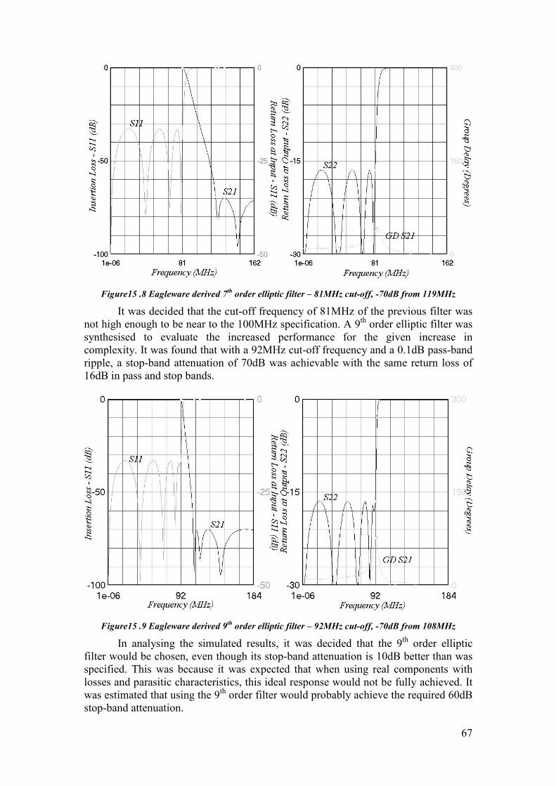
67
Figure 15 .8 Eagleware derived 7th order elliptic filter – 81MHz cut-off, -70dB from 119MHz
It was decided that the cut-off frequency of 81MHz of the previous filter was not high enough to be near to the 100MHz specification. A 9th order elliptic filter was synthesised to evaluate the increased performance for the given increase in complexity. It was found that with a 92MHz cut-off frequency and a 0.1dB pass-band ripple, a stop-band attenuation of 70dB was achievable with the same return loss of 16dB in pass and stop bands.
Figure 15 .9 Eagleware derived 9th order elliptic filter – 92MHz cut-off, -70dB from 108MHz
In analysing the simulated results, it was decided that the 9th order elliptic filter would be chosen, even though its stop-band attenuation is 10dB better than was specified. This was because it was expected that when using real components with losses and parasitic characteristics, this ideal response would not be fully achieved. It was estimated that using the 9th order filter would probably achieve the required 60dB stop-band attenuation.

68
The selected minimal-inductor elliptic low-pass filter was composed of the following network:
Figure 15 .10 The synthesised 9th order minimal-inductor elliptic low-pass filter
The filter’s response has four zeros in the stop band these correspond to the resonant frequency of each parallel inductor and capacitor pair. In left to right order from Figure 15.10, the frequencies of these zeros are at:
1. 243.37MHz2. 116.57MHz3. 108.63MHz4. 142.50MHzThese frequencies would be used later in the construction phase to help tune
the filter’s response.The actual component values used are as shown in the following schematic:
From AmplifierStage
To ADC DriverStage
Figure 15 .11 The Anti-Alias Filter schematic
15.6 ADC Driver Stage DesignThe signal passing through the Front-End stage has been bipolar and single-
ended up until this block. The ADC Driver’s functional tasks were to level-shift this single-ended signal, whilst combining it with a dither signal injected from the IFR Aeroflex 2319E, and convert it to the differential signal needed by the single supply ADC. The reason that a differential ADC was chosen will be covered in the following section. The only device found during the market research that would perform the required tasks given the limited supply voltage was the Analog Devices AD8138, whose specification is as follows:
AD8138Minimum supply voltage (V) ±1.4Maximum supply current (mA) 23Large signal bandwidth (MHz) Output 2Vp.p. 265Unity gain bandwidth (MHz) 320Slew- rate (V/µs) 1150Noise (nV/√Hz) at 40MHz 5SINAD (dB) at 5MHz 94SINAD (dB) at 70MHz 62
Table 15.9 The Analog Devices AD8138 specification
The device easily meets the specification requirements. The schematic for the circuit is shown below. Notice the 51Ω termination resistors to terminate the transmission line from the Anti-Alias Filter, and from the dither signal path. The gain

69
setting is for a single-ended gain of 2 (This is a differential gain of 4, but the inverting input is connected to ground). Notice that the parallel combination of the 8.2kΩ and 560Ω resistors forms a resistance of 524Ω at the inverting input, which was as close to 525Ω as standard resistor values allowed. The reason for this value is to make the impedance seen at the input pins the same, i.e. the same as the 500Ω + 50Ω // 50Ω impedance on the non-inverting input pin.
Dither FilterDither SignalInput
From Anti-Alias Filter
DitherAttenuator
To ADC
ADC Driver
Figure 15 .12 The ADC Driver Stage, including the Dither conditioning circuitry
The Dither conditioning network on the lower half of Figure 15.12 shows the input signal passing through a low-pass filter and an attenuator before being combined with the input signal using another 500Ω resistor. The dither signal was chosen to be band-limited to below 10MHz using a 4th order low- pass Butterworth filter, in order to cut-off any high frequency coherent signals from the digital circuit generating the source of the dither. The dither signal is attenuated with a ‘T’ attenuator formation, whose values were to be set during the testing of the stage. This attenuator must reduce the level of dither to the required amplitude within the specified amount of ±0.1LSB to ±32LSB. As the original level of the dither generated by the IFR Aeroflex 2319E was unknown, the amount of attenuation performed by this attenuator was left unspecified at the time of design. Note the use of low-pass filtering on the output to the ADC stage, as stated in the specification. The cut-off frequency of these filters was set to be around 140MHz (1 2 51 22 142p MHzπ ⋅ ⋅ ≈ ) to definitely allow the full input signal bandwidth through.
15.7 ADC Stage DesignAt heart of each Front-End Stage is an analogue-to- digital converter. The
specification defined this as: a 10 bit ADC with a maximum sample rate of 20MSPS. A lot of market research was done in examining the available converters on the market. Six ADCs were identified as potential candidates and a detailed comparison of the group was undertaken. The specification of each is summarised in the following table:

70
Texas InstrumentsADS901
Texas Instruments THS1040
Analog Devices AD9200
Analog Devices AD9203
National Semi. ADC10D020
Maxim / Dallas MAX1184
Resolution (Bits) 10 10 10 10 10 10Devices in One Package 1 1 1 1 2 2Single-Ended or Differential Single Single Single Diff. Single Diff.Maximum Sampling Rate (MSPS)
20 40 20 40 20 20
Analogue Input Bandwidth (MHz)
100 900 300 390 140 400
SINAD (dB) 54 60 54 59 56 59Supply Voltage (V) 3 3 3 3 3 3Maximum Power Consumption (mW)
60 120 100 84 169 150
1KU Price (£) 1.91 3.46 2.31 4.53 4.11 3.54Table 15. 10 The specification of the six ADC finalists
In the end the Analog Devices AD9203 was selected as the winner for these two reasons:
i) It had the best trade-off between sample rate, analogue bandwidth and SINAD ratio, for the given power consumption
ii) The sample rate was double that needed. Since this ADC would be working with the 2319E system, it was thought that it may need this extra performance to be closer to the instrument’s 65.28MSPS sample rate.
The AD9203 is a differential input ADC that uses a single 3V supply, so a method was required to convert from the bipolar signal format of the output of the Anti-Alias filter to the differential input format. The AD9203 directly recommends the use of the AD8318 for this purpose. The reader will remember that this was indeed the device used in the ADC Driver Block.
The ADC schematic is shown below. Notice that the output named OTR is also passed to the LVDS stage. This signal displays whether the input signal is out of allowed 1Vp.p. input amplitude range centred at 1.5V DC:
To LVDSOutput Stage
From ADC DriverStage
Sample Clock
Figure 15 .13 The ADC Stage
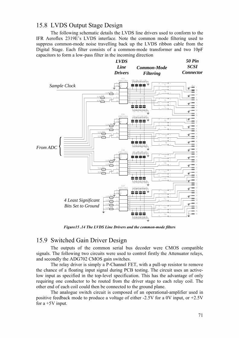
71
15.8 LVDS Output Stage DesignThe following schematic details the LVDS line drivers used to conform to the
IFR Aeroflex 2319E’s LVDS interface. Note the common mode filtering used to suppress common-mode noise travelling back up the LVDS ribbon cable from the Digital Stage. Each filter consists of a common-mode transformer and two 10pF capacitors to form a low-pass filter in the incoming direction
50 PinSCSI
ConnectorCommon-Mode
Filtering
LVDSLine
Drivers
4 Least SignificantBits Set to Ground
From ADC
Sample Clock
Figure 15 .14 The LVDS Line Drivers and the common-mode filters
15.9 Switched Gain Driver DesignThe outputs of the common serial bus decoder were CMOS compatible
signals. The following two circuits were used to control firstly the Attenuator relays, and secondly the ADG702 CMOS gain switches.
The relay driver is simply a P-Channel FET, with a pull-up resistor to remove the chance of a floating input signal during PCB testing. The circuit uses an active-low input as specified in the top-level specification. This has the advantage of only requiring one conductor to be routed from the driver stage to each relay coil. The other end of each coil could then be connected to the ground plane.
The analogue switch circuit is composed of an operational-amplifier used in positive feedback mode to produce a voltage of either -2.5V for a 0V input, or +2.5V for a +5V input.

72
FromCommon
Serial BusDecoder
FromCommon
Serial BusDecoder
Example Relay Circuit
Example Gain Switch Driver
To Gain Switch
Figure 15 .15 The Attenuator driving circuit (Left) and the Gain-Switch driver circuit (Right)

73
16. Digital-Stage DesignThe required specification for the digital stage is shown below:
Average Additive-Random Sample Clock Rate:
10MSPS
Effective Sample Rate: 200MSPSPreliminary Power Consumption:
400mW from 4.65V DC
Features: • Generates an additive-random sample clock from a 200MHz uniform clock
• Interleaves the ADC sample data from both channels and passes the time-stamped data to the host
Table 16.1 The post-system design review digital-stage specification
In order to produce the required non-uniform sampling signal this stage would undoubtedly be based on a Programmable Logic Device (PLD). Research was conducted into the different types of PLD available on the market. The hardest specification to meet was the required clock frequency of 200MHz. Since the 200MHz fast clock would be ‘divided down’ to produce the lower rate sample clock, the device would also need to produce counter circuitry that could also cope with a 200MHz clock. Only one device family was found to easily cover the required maximum clock and counter frequencies, this was Altera’s MAX7000B series of CMOS EEPROM based PLDs. They are a high-performance family that run on a 2.5V core voltage, with the ability to interface to 5V and 3.3V CMOS logic by means of a separate power supply for the I/O pins. The series comes in a variety of sizes, with a trade-off in performance with increased size. The following table summarises this relationship:
Device Name: EPM7032B EPM7064B EPM7128B EPM7256B EPM7512BUsable Gates: 600 1,250 2,500 5,000 10,000Macrocells: 32 64 128 256 512Maximum I/O pins:
36 68 100 164 212
Maximum Counter Frequency (MHz):
303 303 243.9 188.7 163.9
Table 16.2 Specification of the Altera MAX7000B series of CPLD
From the table it is clear that the largest number of Macrocells for a counter frequency of 200MHz is the EPM128B device. By a strange twist of fate this happened to be the exact device which Altera had recently sent to our department for use as samples. With a ready supply of a device meeting the specification, there was no reason to spend time continuing with the CPLD research.
The interconnections on the digital stage were left vague during the design process, as they would be highly layout dependent. Therefore the process of assigning device pins to interface pins was left until the prototyping stage. However the overall connections would be:
i) 2 x 10bit ADC Data inputsii) 1 x 16bit output to the EZ-USB FX2 FIFO memoryiii) Outputs to the Read / Write strobes of the EZ-USB FX2 FIFOiv) 2 x LED outputs

74
v) 2 x Sample clock outputsvi) 200MHz clock inputAs was mentioned during the project planning section the critical path of the
project was identified as the design, prototyping and testing of the Front-End Stage. This was because one of the original aims stated at the start of the project was to achieve the basic system functionality before developing the more advanced features. Because of this, developing the non-uniform sampling system was one of the lower priorities. As to date there has not been time to implement any form of non-uniform clock generation.

75
17. Design ReviewThroughout the hardware design process, the evolving design was
continuously compared with the specification set at the start. Once that majority of the design for each stage had been completed, it was necessary to rigorously check that the specification had indeed been met, and that the cost and power consumption were within the set budget.
17.1 Necessary Specification ChangesSome changes to the original specification were found to be necessary during
the design process. These have been documented in the previous chapters, and will now be summarised here:
i) Dither generation on the Digital-Stage was not includedii) The 200MHz clock generation chip was not included, instead a circuit
was devised to generate the clock signal from a sine wave obtained from an external signal generator:
iii) The Anti-Alias Filter specification was not rigorously defined in the initial specification. Final solution had a cut-off of 92MHz.
Other changes to the original intent were the dropping of the proposed separate Digital-Stage board. Instead the circuit was designed to interface directly to the EZ-USB FX2 development board. This was achieved during the PCB layout of the Digital-Stage in the Prototyping phase of the project.
The final USB2Scope specification is given on Page 75.The final device schematics can be viewed in Appendix IV.
17.2 Final USB2Scope Cost and Power BudgetThe final cost and power budget is on the following page. This budget was
developed alongside the design of the hardware, and was often used a tool to evaluate the viability of devices and concepts. It is documented in this part of the report to reside next to the Final USB2Scope specification. It can be seen that the final component cost and maximum expected device power consumption (excluding the LVDS interface circuitry) is 1.96W, well within the required maximum operating power of 2.5W of the USB specification. The component costs came to US$73.84 or £53.45, almost half of the cost set at the start of the project.
17.3 Design Review ConclusionsThe design review had revealed some shortcomings in the original
specification, that were then resolved and a second version of the specification was defined.
At the end of the hardware design process, a potentially fully functioning system design had been completed. At this point the majority of the components had arrived from their respective suppliers, and the prototyping work could be started in earnest.

76
USB2Scope Budget
Front End:
Component Manufacturer Device
S upp ly Voltage
(V) Supply Power (mW) Load Power (mW) Total Power (mW) 1KUMin Typ Max Min Typ Max Min Typ Max Price (US$) Supplier
0dB Attenuator Relay Matsushita (Aromat) TQ2SA-L2-5V 5 0 0 0 0 0 0 0 0 0 1.8 Avnet Website20dB Attenuator Relay Matsushita (Aromat) TQ2SA-L2-5V 5 0 0 0 0 0 0 0 0 0 1.8 Avnet Website40dB Attenuator Relay Matsushita (Aromat) TQ2SA-L2-5V 5 0 0 0 0 0 0 0 0 0 1.8 Avnet WebsiteAC / DC Relay Matsushita (Aromat) TQ2SA-L2-5V 5 0 0 0 0 0 0 0 0 0 1.8 Avnet WebsiteFront End Buffer TI (Burr Brown) OPA355 ±2.5 41.5 41. 5 55 0 2.8 5 .6 41.5 44.3 60. 6 1 .25 TI WebsiteVariable Gain Stage 1 Analog Devices AD8009 ±2.5 70 70 80 0 12.8 25. 6 70 82.8 105. 6 1 .87 Analog Devices WebsiteVariable Gain Switches 1 Analog Devices ADG702 ±2.5 0 0 0 0 0 0 0 0 0 1.02 Analog Devices WebsiteVariable Gain Stage 2 Analog Devices AD8009 ±2.5 70 70 80 0 44.1 88. 1 70 114.1 168. 1 1 .87 Analog Devices WebsiteVariable Gain Switches 2 Analog Devices ADG702 ±2.5 0 0 0 0 0 0 0 0 0 1.02 Analog Devices WebsiteADC Driver Analog Devices AD8138 3 54 60 69 0 0 0 54 60 69 4.25 Analog Devices WebsiteADC Analog Devices AD9203 3 60.3 60. 3 66 13.2 13. 2 18 73.5 73. 5 84 6 .34 Analog Devices Website
296 302 350 13.2 72.9 137 309 374.7 487.3 $24.8 2
Single Channel Front End Power Consumption (mW) Price (US$)Min Typ Max
309 374.7 487.3 $24.82
Dual Channel Front End Power Consumption (mW) Price (US$)Min Typ Max
618 749.4 974.6 $49.64
Digital:
Component Manufacturer Device
Supply Voltage
(V) Supply Power (mW) Load Power (mW) Total Power (mW) 1KUMin Typ Max Min Typ Max Min Typ Max Price (US$) Supplier
FPGA Altera EPM7064B 2.5 188 188 188 65.5 65.5 130.7 253.5 253.5 318. 7 5 Avnet WebsiteUSB 2.0 Microcontroller Cypress CY7C68013 3.3 422.4 422.4 422. 4 92 92 165 514.4 514.4 587.4 16.28 Avnet WebsiteProgramable Clock Cypress CY22393 3.3 39.6 79.2 79. 2 0 0 0 39.6 79.2 79. 2 2 .92 Avnet Website
650 690 690 158 158 296 807.5 847.1 985.3 $24.2 0
Digital Stage Power Consumption (mW) Price (US$)Min Typ Max
807.5 847.1 985.3 $24.20
Device Total Power Consumption (mW) Price (US$)Min Typ Max
1426 1597 1960 $73.84

77
17.4 Final USB2Scope Hardware SpecificationFront-End Stage
Number of Channels: 2Input Impedance: 1MΩ // 15pF with AC / DC switchMeasurement Bandwidth per Channel: 92MHzFull-Scale Input Ranges: (Please refer to Table 17.2 below)Signal Amplification SINAD at 1MHz: 60dBVoltage Linearity: ±3%ADC Resolution: 10bitsADC maximum sample rate 40MSPSAdditive Dither: ±0.1LSB to ±32LSBPower Consumption per Channel (Maximum): 500mW from 4.65V DCComponent Cost per Channel: £17.73Features: • Over-Voltage protected
• Accepts a dither signal from IFR Aeroflex 2319E
Digital-StageAverage Additive-Random Sample Clock Rate:
10MSPS
Effective Sample Rate: 200MSPSPower Consumption (Maximum): 400mW from 4.65V DCComponent Cost: £5.66Features: • Generates an additive-
random sample clock from a 200MHz uniform clock
• Interleaves the ADC sample data from both channels and passes the time-stamped data to the host
Data- Transfer StageData Interface: Universal Serial Bus Version 2.0Maximum Data Transfer Rate: 480MbpsFIFO Memory Width: 16bitsAverage FIFO Clock Rate: 20MHz (10MSPS*2Channels)Power Consumption (Maximum): 600mW from 4.65V DCComponent Cost: £11.62Features: • Receives data from the
digital-stage and transfers this data to the host computer
• Stimulates the common serial control bus
Table 17.1 The final USB2Scope specification
10mVp.p. (±5mV DC) 20mVp.p. (±10mV DC) 50mVp.p (±25mV DC)100mVp.p. (±50mV DC) 200mVp.p. (±100mV DC) 500mVp.p. (±250mV DC)1Vp.p. (±500mV DC) 2Vp.p. (±1V DC) 5Vp.p. (±2.5V DC)10Vp.p. (±5V DC) 20Vp.p. (±10V DC) 50Vp.p. (±25V DC)100Vp.p. (±50V DC)
Table 17.2 The final full-scale input ranges
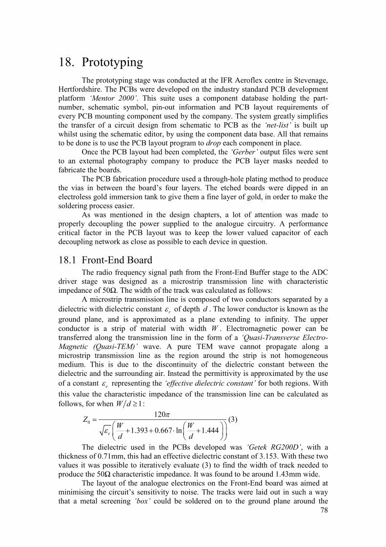
78
18. PrototypingThe prototyping stage was conducted at the IFR Aeroflex centre in Stevenage,
Hertfordshire. The PCBs were developed on the industry standard PCB development platform ‘Mentor 2000’. This suite uses a component database holding the part-number, schematic symbol, pin-out information and PCB layout requirements of every PCB mounting component used by the company. The system greatly simplifies the transfer of a circuit design from schematic to PCB as the ‘net-list’ is built up whilst using the schematic editor, by using the component data base. All that remainsto be done is to use the PCB layout program to drop each component in place.
Once the PCB layout had been completed, the ‘Gerber’ output files were sent to an external photography company to produce the PCB layer masks needed to fabricate the boards.
The PCB fabrication procedure used a through-hole plating method to produce the vias in between the board’s four layers. The etched boards were dipped in an electroless gold immersion tank to give them a fine layer of gold, in order to make the soldering process easier.
As was mentioned in the design chapters, a lot of attention was made to properly decoupling the power supplied to the analogue circuitry. A performance critical factor in the PCB layout was to keep the lower valued capacitor of each decoupling network as close as possible to each device in question.
18.1 Front-End BoardThe radio frequency signal path from the Front-End Buffer stage to the ADC
driver stage was designed as a microstrip transmission line with characteristic impedance of 50Ω. The width of the track was calculated as follows:
A microstrip transmission line is composed of two conductors separated by a dielectric with dielectric constant rε of depth d . The lower conductor is known as the ground plane, and is approximated as a plane extending to infinity. The upper conductor is a strip of material with width W . Electromagnetic power can be transferred along the transmission line in the form of a ‘Quasi-Transverse Electro-Magnetic (Quasi-TEM)’ wave. A pure TEM wave cannot propagate along a microstrip transmission line as the region around the strip is not homogeneous medium. This is due to the discontinuity of the dielectric constant between the dielectric and the surrounding air. Instead the permittivity is approximated by the use of a constant eε representing the ‘effective dielectric constant’ for both regions. With this value the characteristic impedance of the transmission line can be calculated as follows, for when 1W d ≥ :
0120
1.393 0.667 ln 1.444e
ZW Wd d
π
ε=
+ + ⋅ +
(3)
The dielectric used in the PCBs developed was ‘Getek RG200D’, with a thickness of 0.71mm, this had an effective dielectric constant of 3.153. With these two values it was possible to iteratively evaluate (3) to find the width of track needed to produce the 50Ω characteristic impedance. It was found to be around 1.43mm wide.
The layout of the analogue electronics on the Front-End board was aimed at minimising the circuit’s sensitivity to noise. The tracks were laid out in such a way that a metal screening ‘box’ could be soldered on to the ground plane around the

79
circuitry without shorting any signals, i.e. all tracks passing into the analogue compartment were on either layer 3 or 4.
A block diagram of the Front-End PCB layout is shown on the following page. The reader will notice the grey folded signal path from the input through the attenuation, amplification and filtering stages, where it is combined with the conditioned dither signal before passing through the ADC driver stage to the ADC. After digitisation the LVDS line drivers pass the signals through to the SCSI connector on the underside of the board. The connector is positioned in this manner to allow the analogue circuitry on the upper side of the board to be fully encased within metal screening box, without passing the LVDS cable through the side of it.
50WBNC Input Power
Input
Atte
nuat
orAC /
DC
Switc
h
Fron
t-End
Buffe
r
GainStage 1
GainStage 2
Anti-Alias Filter
DitherInput
DitherFilter
DitherAttenuator
ADCDriver
ADC
LVDS Line Drivers
LVDS Common-ModeFiltering
ADC PowerRegulation
Com
mon
Ser
ial-B
usD
ecod
erRelay
Drivers
GainSwitchDrivers
AnaloguePower
Regulation
ClockInput
CommonSerial-Bus
Input
50-Way SCSI Connector
Figure 18 .1 A block diagram of the Front-End PCB layout
18.2 Digital-Stage BoardThe decisions of exactly which pins to connect together on the digital stage
were made during the PCB layout process in order to make the layout as simple as possible. Figure 18.2 shows a sketch of the signal paths between the LVDS receiver stages and the EZ-USB FX2 development board PCB headers to the EPM7128B PLD device’s pins. For exact details of the interconnections, please refer to the Digital-Stage schematics in Appendix IV.
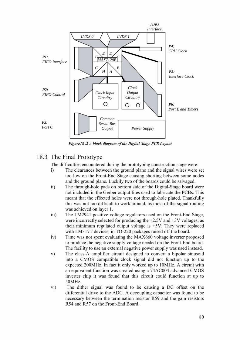
80
LVDS 0 LVDS 1
E
AB
CD
F
GH
MAX7128BP1:FIFO Interface
P2:FIFO Control
P3:Port C
P6:Port E and Timers
P5:Interface Clock
P4:CPU Clock
CommonSerial Bus
Output
Clock InputCircuitry
ClockOutput
Circuitry
Power Supply
JTAGInterface
Figure 18 .2 A block diagram of the Digital-Stage PCB Layout
18.3 The Final PrototypeThe difficulties encountered during the prototyping construction stage were:i) The clearances between the ground plane and the signal wires were set
too low on the Front-End Stage causing shorting between some nodes and the ground plane. Luckily two of the boards could be salvaged.
ii) The through-hole pads on bottom side of the Digital-Stage board were not included in the Gerber output files used to fabricate the PCBs. This meant that the effected holes were not through-hole plated. Thankfully this was not too difficult to work around, as most of the signal routing was achieved on layer 1.
iii) The LM2941 positive voltage regulators used on the Front-End Stage, were incorrectly selected for producing the +2.5V and +3V voltages, as their minimum regulated output voltage is +5V. They were replaced with LM317T devices, in TO-220 packages raised off the board.
iv) Time was not spent evaluating the MAX660 voltage inverter proposed to produce the negative supply voltage needed on the Front-End board. The facility to use an external negative power supply was used instead.
v) The class-A amplifier circuit designed to convert a bipolar sinusoid into a CMOS compatible clock signal did not function up to the expected 200MHz. In fact it only worked up to 10MHz. A circuit with an equivalent function was created using a 74AC004 advanced CMOS inverter chip it was found that this circuit could function at up to 50MHz.
vi) The dither signal was found to be causing a DC offset on the differential drive to the ADC. A decoupling capacitor was found to be necessary between the termination resistor R59 and the gain resistors R54 and R57 on the Front-End Board.
81
vii) The voltage input to each gain-switch-controlling operational-amplifier (IC20 and IC24) was changed from +2.5 to +1.25V to bring it within the device’s power supply range. This was simply done by changing the ratio of R69 and R71, and R73 and R75.
viii) The allowance for testing the single-chip switch mode power regulators on the digital stage was not used. Instead LM317T linear regulator devices were used.
ix) Learning from the lesson of the ill-fated class-A amplifier design used in both the Front-End Stage and the Digital-Stages, an AD8611 100MHz fast comparator was ordered in advance from Analog Devices for the Digital-Stage testing. The device worked as expected, however it did mean that the required 200MHz system clock speed, defined in the final specification for the Digital-Stage, could not be evaluated. Unfortunately the project ran out of time before the non-uniform sampling method could be developed, so the 100MHz clock signal was more than adequate for uniform sampling purposes.
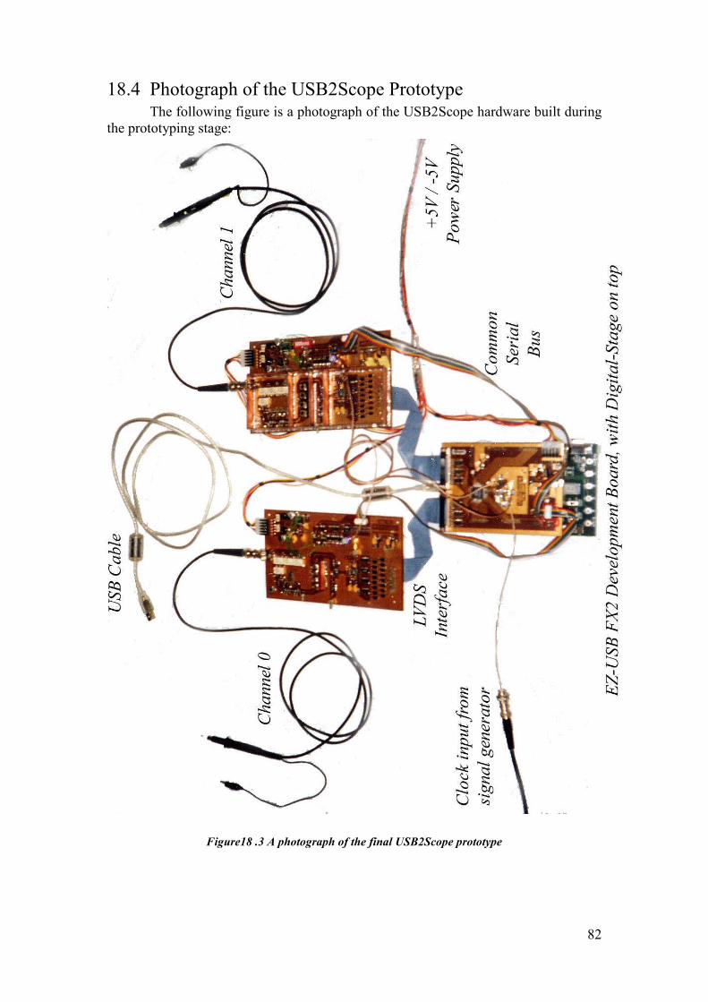
82
18.4 Photograph of the USB2Scope PrototypeThe following figure is a photograph of the USB2Scope hardware built during
the prototyping stage:
Figure 18 .3 A photograph of the final USB2Scope prototype

83
19. Introduction to the Testing ProcedureThe next stage of the project was to test the USB2Scope prototype. The testing
procedure actually ran in parallel with the construction of the device. Each Stage was built block, by block, testing each one in the process. The testing procedure is documented in three separate chapters in order to give a chronological order of the testing process:
Chapter 20 – Front-End TestingChapter 21 – Digital-Stage TestingChapter 22 – Front-End ImprovementChapter 23 covers the software development undertaken during the project,
followed by the Device Integration Chapter 24 which contains the final test results for the whole USB2Scope system.
The aim of the first round of testing was to gain an initial indication of the Front-End Stage’s performance. This testing was completed by the 23rd March 2002, a project break of eight weeks then proceeded during the author’s final year exam period. Testing restarted on the 16th May 2002, which consisted of firstly testing the Digital-Stage, then a decision was made to try and improve the performance of the Front-End Stage, the reason for this will be explained in the following chapters. This work was completed by the 22nd May 2002.
20. Front-End TestingThis chapter documents the results of the initial Front-End Stage testing. It
starts with an analysis of the Anti-Alias filter, buffer and amplification stages using a spectrum analyser with tracking generator. It then moves on to explaining the test setup used to test the Front-End Stage using the IFR 2319E instrument. The test results obtained from using the IFR 2319E instrument are analysed, before a concluding section summarising the findings of the test exercise.
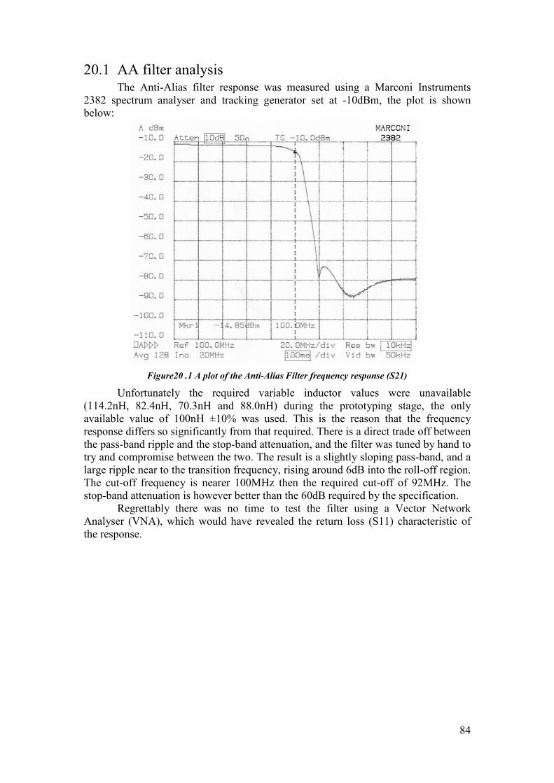
84
20.1 AA filter analysisThe Anti-Alias filter response was measured using a Marconi Instruments
2382 spectrum analyser and tracking generator set at -10dBm, the plot is shown below:
Figure 20 .1 A plot of the Anti-Alias Filter frequency response (S21)
Unfortunately the required variable inductor values were unavailable (114.2nH, 82.4nH, 70.3nH and 88.0nH) during the prototyping stage, the only available value of 100nH ±10% was used. This is the reason that the frequency response differs so significantly from that required. There is a direct trade off between the pass-band ripple and the stop-band attenuation, and the filter was tuned by hand to try and compromise between the two. The result is a slightly sloping pass-band, and a large ripple near to the transition frequency, rising around 6dB into the roll-off region. The cut-off frequency is nearer 100MHz then the required cut-off of 92MHz. The stop-band attenuation is however better than the 60dB required by the specification.
Regrettably there was no time to test the filter using a Vector Network Analyser (VNA), which would have revealed the return loss (S11) characteristic of the response.

85
20.2 Front-End Buffer MeasurementsThe spectrum analyser’s built in tracking generator was used to produce
frequency response plots of the Front-End Buffer performance. The tracking generator was set to -10dBm, and was terminated on the front of the instrument with a probe-measurable termination. An oscilloscope probe set on x1 was inserted into this termination and connected to the Front-End Stage. The output of the buffer was connected to a 50Ω cable back to the spectrum analyser, with a 50Ω source resistor.
Marconi 2382
RF Input
TerminatedTracking Generator
50Ω OutputMeasured withOscilloscopeProbe on x1
50Ω
Buffer Stage
Spectrum Analyser
50Ω
AttenuatorStage
Figure 20 .2 The Front-End Buffer test setup
Each attenuation setting was tested and plotted on the same graph. The results are shown below:
Figure 20 .3 A plot of the frequency response of the Front-End Buffer for the different Attenuator settings (pre-improvement)
The performance is far from ideal, which would be constant horizontal lines at each attenuation level. The 0dBm attenuation plot shows a very steep roll-off, which is -23dB down from the -10dBm input at 100MHz. The plot continues to roll-off

86
across the entire 200MHz measured bandwidth. The -20dB attenuator setting sees the same effect up until around 160MHz, where suddenly it starts to increase again. It climbs around 6dB up from its minimum value by 200MHz. The -40dB attenuation setting results in a far less steep roll-off than that of the 0dB or -20dB setting, it drops about 15dB up until around 140MHz then the same increase in magnitude is seen as the -20dB setting, although on a smaller scale. It rises about 2dB by 200MHz.
Initially it was thought that these results were due to the poor performance of the Front-End buffer. Time was spent trying to compensate for this misdiagnosed effect by placing capacitance around the buffer’s feedback resistors. This was to no avail.
As time was limited in the testing schedule, it was decided not to dwell on the deficient results for long at that point, as the higher priority was to get the whole system working to some extent first.
Later, after the first round of testing had been finished, it was discovered that the model used for measurement using an oscilloscope probe on the x1 setting was incorrect. It had been assumed that as the impedance of standard oscilloscope probes are 1MΩ, that there was a 1MΩ source resistor inside the probe:
RR
1MΩ
1MΩ ImpedanceTransmission Line
approx. 1.5meters long
1MΩSignalSource
Oscilloscope Probe
InputTermination
of Oscilloscope
Figure 20 .4 The incorrect model of a 1MΩ oscilloscope probe setup
In fact no source resistor is used. This explains why the roll off, and then subsequent increase in gain was seen in the buffer’s results. It is due to the unmatched, approximately 1.5 meter long length of transmission line formed by the cable from the probe to the 1MΩ input termination of the device. This forms a reactive impedance that varies cyclically with frequency due to the variation of the standing waves set up in the line. This is why the magnitude of the gain is seen to increase again after falling to a minimum. If the stop-frequency used in the tests had been moved above 200MHz, the increase in gain seen towards 200MHz would have continued to increase to a peak before rolling-off gain.
To counteract this effect the x10 setting of the probe can be used, this places a 9MΩ source resistance in series with the probe’s cable. As this was unfortunately discovered after the first round of tests, it was decided that if more tests were carried out, the tests should be repeated using the x10 probe setting.
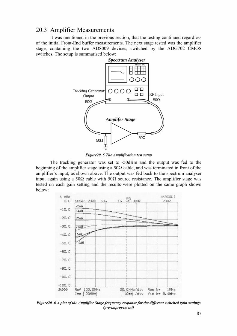
87
20.3 Amplifier MeasurementsIt was mentioned in the previous section, that the testing continued regardless
of the initial Front-End buffer measurements. The next stage tested was the amplifier stage, containing the two AD8009 devices, switched by the ADG702 CMOS switches. The setup is summarised below:
Marconi 2382
RF InputTracking Generator
Output
50Ω50Ω
Amplifer Stage
Spectrum Analyser
50Ω 50Ω
Figure 20 .5 The Amplification test setup
The tracking generator was set to -50dBm and the output was fed to the beginning of the amplifier stage using a 50Ω cable, and was terminated in front of theamplifier’s input, as shown above. The output was fed back to the spectrum analyser input again using a 50Ω cable with 50Ω source resistance. The amplifier stage was tested on each gain setting and the results were plotted on the same graph shown below:
Figure 20 .6 A plot of the Amplifier Stage frequency response for the different switched gain settings (pre-improvement)

88
As can be seen the results are far from ideal. At DC the gains are roughly correct, however as the frequency is increased, the 0dB, 6dB and 14dB gain setting curve upwards, whilst the 40dB, 34dB and 26dB curve downwards. The 26dB setting is the most flat of the six settings, but they all tend to the same gain value of around 33dB.
After thinking for some time why this effect was seen, it was hypothesised that the input capacitance of the ADG702 CMOS switches played a significant factor in the total frequency response of the circuit. It was suggested that their input capacitance was high enough to make every switch look ‘On’ above a given frequency. This hypothesis was tested in the later Chapter on Front-End improvement.
20.4 Buffer and Amplifier MeasurementsThe Buffer and amplifier stages were tested together using the spectrum
analyser and tracking generator set to -50dBm, and terminated in front of the instrument using a probe-measurable terminator. The input was measured from the termination using an oscilloscope probe set to x1, and the Attenuator was set to 0dB. Each setting of the amplifier stage was plotted on the same graph below:
Figure 20 .7 A plot of the total frequency response of the Front-End Buffer and the Amplifier stage with the Attenuator set to 0dB for the different switched gain settings (pre-improvement)
Again a far from ideal response was achieved. There was a subtle combination of effects from the roll-off of the Front-End Buffer and the converging characteristic seen in the amplifier stage.
With some initial spectrum analyser plots of the analogue stages taken, the next step was to test the ADC stage and then the entire Front-End. As the Digital-Stage had not been built and the EZ-USB FX2 development board had not been fully
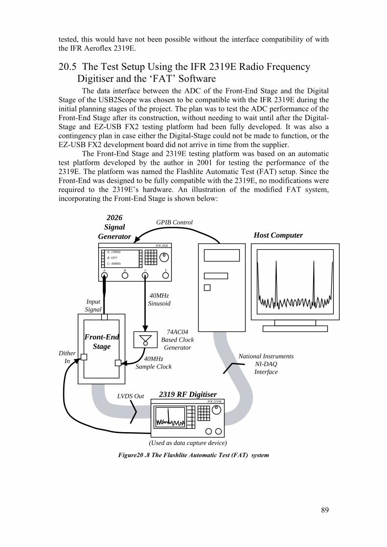
89
tested, this would have not been possible without the interface compatibility of with the IFR Aeroflex 2319E.
20.5 The Test Setup Using the IFR 2319E Radio Frequency Digitiser and the ‘FAT’ SoftwareThe data interface between the ADC of the Front-End Stage and the Digital
Stage of the USB2Scope was chosen to be compatible with the IFR 2319E during the initial planning stages of the project. The plan was to test the ADC performance of the Front-End Stage after its construction, without needing to wait until after the Digital-Stage and EZ-USB FX2 testing platform had been fully developed. It was also a contingency plan in case either the Digital-Stage could not be made to function, or the EZ-USB FX2 development board did not arrive in time from the supplier.
The Front-End Stage and 2319E testing platform was based on an automatic test platform developed by the author in 2001 for testing the performance of the 2319E. The platform was named the Flashlite Automatic Test (FAT) setup. Since the Front-End was designed to be fully compatible with the 2319E, no modifications were required to the 2319E’s hardware. An illustration of the modified FAT system, incorporating the Front-End Stage is shown below:
IFR 2026
A: 10MHz
B: OFF
C: 40MHz
A B C Σ
74AC04Based ClockGenerator
Front-EndStage
IFR 2319ELVDS Out
DitherIn
2026Signal
Generator
2319 RF Digitiser
(Used as data capture device)
National InstrumentsNI-DAQInterface
Host Computer
InputSignal
40MHzSinusoid
40MHzSample Clock
GPIB Control
Figure 20 .8 The Flashlite Automatic Test (FAT) system
90
As can be seen from Figure 20.8 the system consists of the following items:i) A signal generator, ideally an IFR 2026 multi-source signal generator.
This instrument can produce up to three different sinusoids, and can combine them into a single signal.
ii) An IBM compatible PC, used to run the FAT software.iii) An IFR 2319E RF Digitiser. This instrument is used solely as a data
capture interface between the LVDS interface and the NI-DAQ interface card in the PC.
iv) The Front-End is connected to the 2319E via the LVDS interface. It can also take a dither signal from the 2319E. The board is clocked by a signal generated by an external 74AC04 based sinusoid-to-clock generator (This circuit was described in the prototyping chapter). The input signal is taken from the IFR 2026, whose output is under GPIB control by the FAT software running on the PC.
When the FAT program is run, it reads in setups files describing ‘setups’which must be tested, and ‘markers’ that define the frequencies to be measured during each setup. The program repeats the following process until all of the setups have been tested:
i) The required input signal frequency and level is sent to the signal generator using the GPIB interface.
ii) Data is captured from the 2319E using the NI-DAQ interface.iii) The data is transformed to the frequency domain and the required
frequency markers are measured, and recorded to an output file.The following measurements were carried out using the FAT system:i) The frequency response of the ADC Stage, including 2nd and 3rd order
harmonic distortion, and noise floor.ii) The level linearity of the ADC Stage, including 2nd and 3rd order
harmonic distortion, and noise floor.iii) The 2nd and 3rd order intermodulation distortion of the ADC Stage with
respect to a two-tone input level, with and without dither.iv) The frequency response of the whole Front-End Stage, including 2nd
and 3rd order harmonic distortion, and noise floor.v) The level linearity of the whole Front-End Stage, including 2nd and 3rd
order harmonic distortion, and noise floor.The frequency range measured was 100kHz – 200MHz, and the input level
range measured was -90dBm – +8dBm. The next page shows two photographs of the FAT setup, and the subsequent five sections detail the results of the experiments.

91
20.6 Photographs of the Front-End and 2319E Setup:
Figure 20 .9 A close up photograph of the FAT setup, showing from top to bottom the Front-End Stage, the IFR 2319E and the IFR 2026 signal generator
Figure 20 .10 A photograph showing the whole test area

92
20.7 ADC Frequency ResponseThe frequency response of the AD8138 and AD9203, a.k.a. the ADC Stage,
was measured using the FAT setup. The fundamental frequency, the 2nd and 3rdharmonics and the noise floor were measured from 100kHz to 200MHz with an ADC sample rate of 40MHz. The input level of the tone was -10dBm. 100 averages were taken of each measurement. The figure below is the data returned from the test:
0 20 40 60 80 100 120 140 160 180 200-100
-90
-80
-70
-60
-50
-40
-30
-20
-10
Mea
sure
d Le
vel (
dBm
)
Input Frequency (MHz)
Fundamental
Third Harmonic
SecondHarmonic
Noise Floor (32768 Sample DFTs)
Figure 20 .11 The frequency response of the ADC Stage, measured using the FAT system
The frequency response of the ADC Stage shows a -3dB bandwidth of around 100MHz, with a smooth roll-off, which is down by 15dB by 200MHz. The analogue input bandwidth of the ADC is 390MHz, therefore the roll-off is likely to be due to the AD8138 ADC driver. This is confirmed by examining the quoted frequency response in the device’s data sheet for a gain of 4. The bandwidth was specified by the USB2Scope specification as 100MHz, therefore this result is in accordance with it.
The 2nd and 3rd order harmonic distortion is nearly all 60dB down from the signal level within the -3dB bandwidth. This signal to distortion ratio is also in accordance with the specified 60dB SINAD of the Front-End Stage.
The noise floor is around -96dBm for the 32768 point DFTs. The full-scale level of the ADC was later found out to be a convenient level of 0dBm, therefore the noise floor was measured at -96dBFS (dB Full-Scale). The bandwidth that the DFT measures at a given point in the spectrum is far less than the whole of the Nyquist bandwidth. This bandwidth is known as the Noise Band-Width or NBW, and is proportional to the Resolution Band-Width or RBW ( sf N ). Its coefficient relates to the window used on the data before transformation known as the ‘window coefficient’notated windowk :
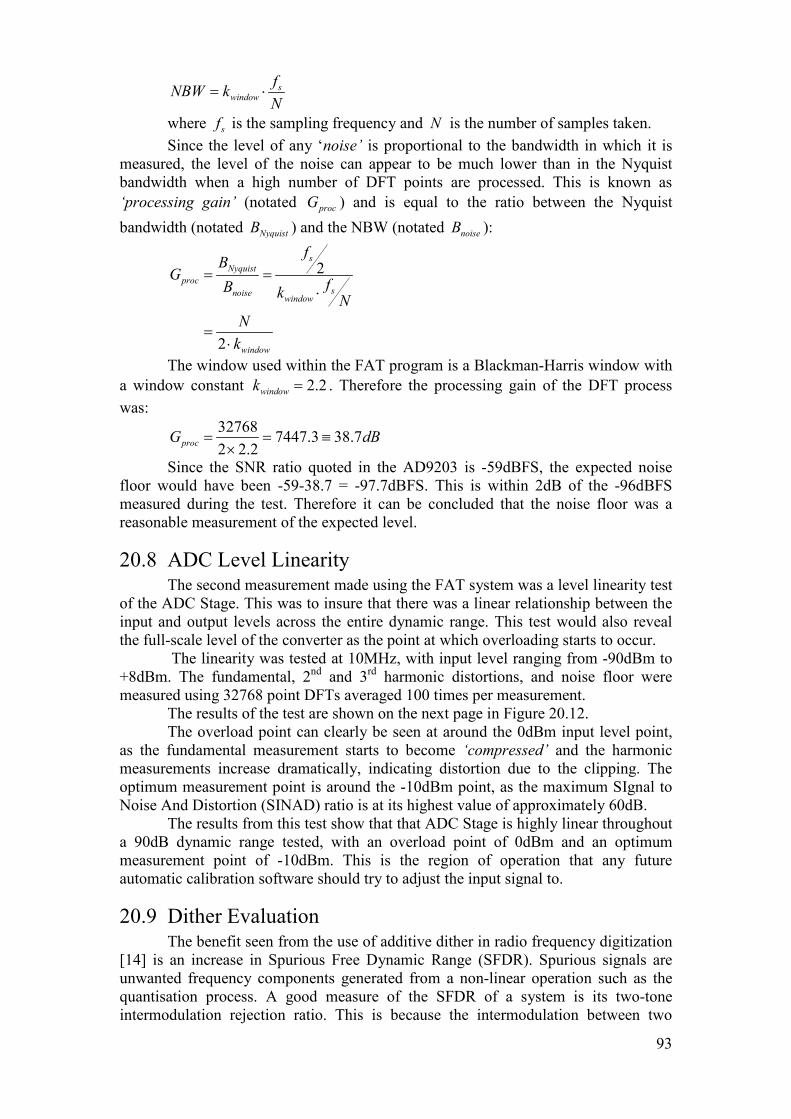
93
swindow
fNBW kN
= ⋅
where sf is the sampling frequency and N is the number of samples taken.Since the level of any ‘noise’ is proportional to the bandwidth in which it is
measured, the level of the noise can appear to be much lower than in the Nyquist bandwidth when a high number of DFT points are processed. This is known as ‘processing gain’ (notated procG ) and is equal to the ratio between the Nyquist bandwidth (notated NyquistB ) and the NBW (notated noiseB ):
2
2
sNyquist
procsnoise window
window
fBG fB k N
Nk
= =⋅
=⋅
The window used within the FAT program is a Blackman-Harris window with a window constant 2.2windowk = . Therefore the processing gain of the DFT process was:
32768 7447.3 38.72 2.2procG dB= = ≡×
Since the SNR ratio quoted in the AD9203 is -59dBFS, the expected noise floor would have been -59-38.7 = -97.7dBFS. This is within 2dB of the -96dBFS measured during the test. Therefore it can be concluded that the noise floor was a reasonable measurement of the expected level.
20.8 ADC Level LinearityThe second measurement made using the FAT system was a level linearity test
of the ADC Stage. This was to insure that there was a linear relationship between the input and output levels across the entire dynamic range. This test would also reveal the full-scale level of the converter as the point at which overloading starts to occur.
The linearity was tested at 10MHz, with input level ranging from -90dBm to +8dBm. The fundamental, 2nd and 3rd harmonic distortions, and noise floor were measured using 32768 point DFTs averaged 100 times per measurement.
The results of the test are shown on the next page in Figure 20.12.The overload point can clearly be seen at around the 0dBm input level point,
as the fundamental measurement starts to become ‘compressed’ and the harmonic measurements increase dramatically, indicating distortion due to the clipping. The optimum measurement point is around the -10dBm point, as the maximum SIgnal to Noise And Distortion (SINAD) ratio is at its highest value of approximately 60dB.
The results from this test show that that ADC Stage is highly linear throughout a 90dB dynamic range tested, with an overload point of 0dBm and an optimum measurement point of -10dBm. This is the region of operation that any future automatic calibration software should try to adjust the input signal to.
20.9 Dither EvaluationThe benefit seen from the use of additive dither in radio frequency digitization
[14] is an increase in Spurious Free Dynamic Range (SFDR). Spurious signals are unwanted frequency components generated from a non-linear operation such as the quantisation process. A good measure of the SFDR of a system is its two-tone intermodulation rejection ratio. This is because the intermodulation between two
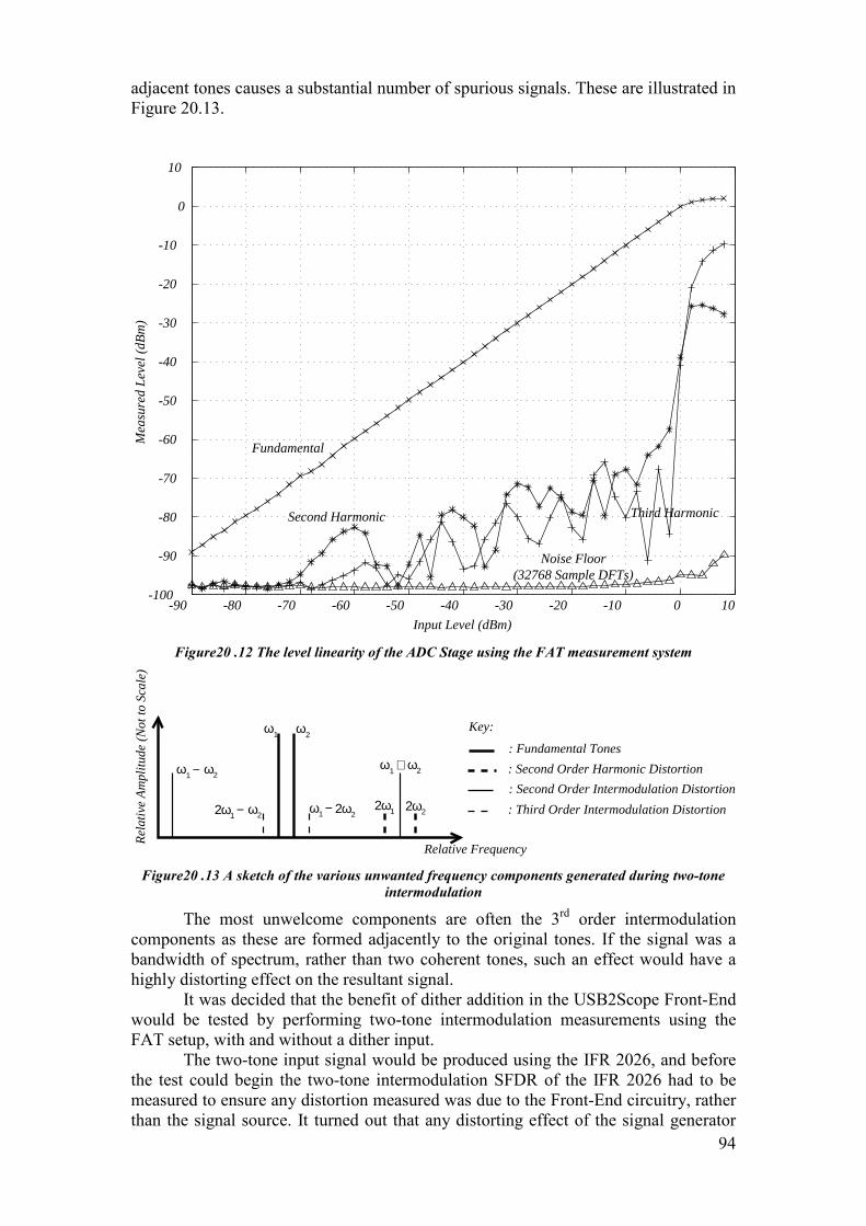
94
adjacent tones causes a substantial number of spurious signals. These are illustrated in Figure 20.13.
-90 -80 -70 -60 -50 -40 -30 -20 -10 0 10-100
-90
-80
-70
-60
-50
-40
-30
-20
-10
0
10
Mea
sure
d Le
vel (
dBm
)
Input Level (dBm)
Fundamental
Second Harmonic Third Harmonic
Noise Floor(32768 Sample DFTs)
Figure 20 .12 The level linearity of the ADC Stage using the FAT measurement system
ω1 ω2
ω1 2ω2−
ω1 ω2−
2ω1 ω2−
ω1 ω2+
2ω22ω1
Rela
tive
Ampl
itude
(Not
to S
cale
)
Relative Frequency
Key:
: Fundamental Tones: Second Order Harmonic Distortion: Second Order Intermodulation Distortion: Third Order Intermodulation Distortion
Figure 20 .13 A sketch of the various unwanted frequency components generated during two-tone intermodulation
The most unwelcome components are often the 3rd order intermodulation components as these are formed adjacently to the original tones. If the signal was a bandwidth of spectrum, rather than two coherent tones, such an effect would have a highly distorting effect on the resultant signal.
It was decided that the benefit of dither addition in the USB2Scope Front-End would be tested by performing two-tone intermodulation measurements using the FAT setup, with and without a dither input.
The two-tone input signal would be produced using the IFR 2026, and before the test could begin the two-tone intermodulation SFDR of the IFR 2026 had to be measured to ensure any distortion measured was due to the Front-End circuitry, rather than the signal source. It turned out that any distorting effect of the signal generator
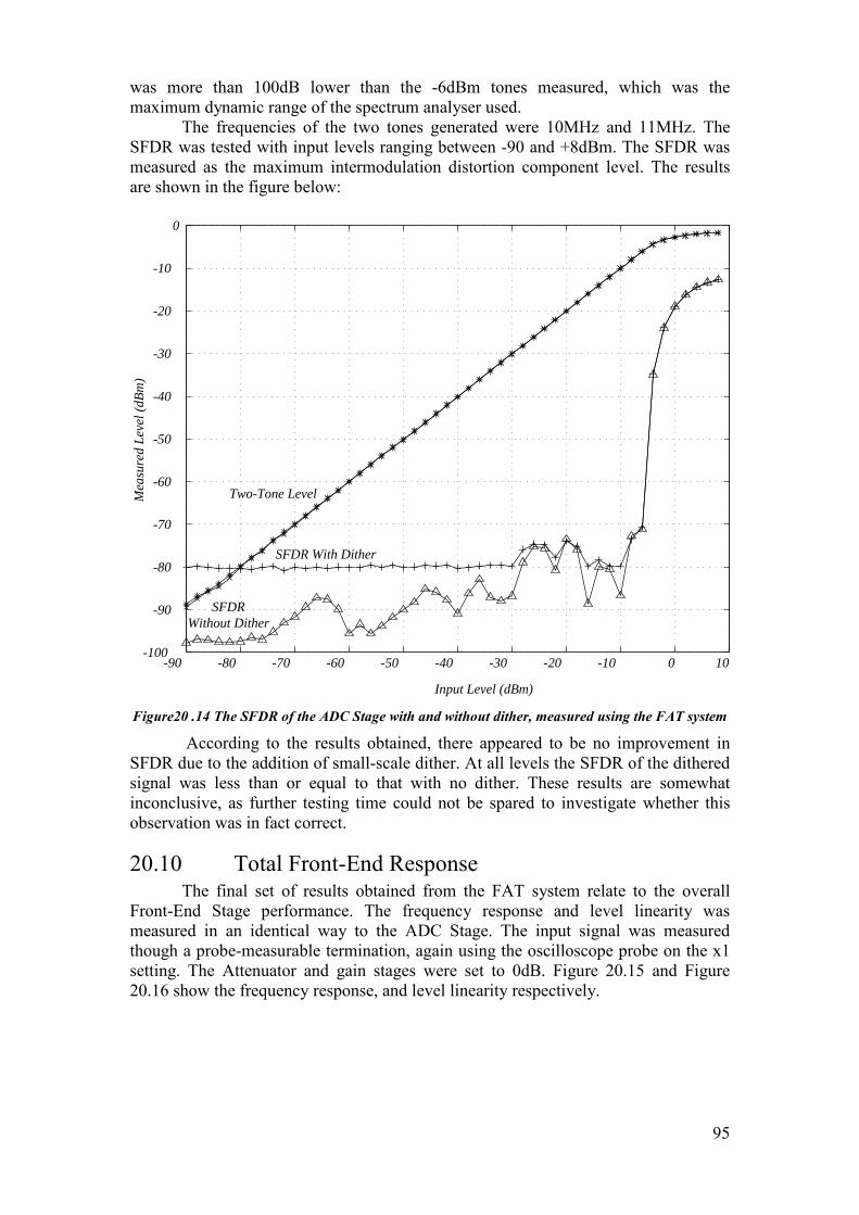
95
was more than 100dB lower than the -6dBm tones measured, which was the maximum dynamic range of the spectrum analyser used.
The frequencies of the two tones generated were 10MHz and 11MHz. The SFDR was tested with input levels ranging between -90 and +8dBm. The SFDR was measured as the maximum intermodulation distortion component level. The results are shown in the figure below:
-90 -80 -70 -60 -50 -40 -30 -20 -10 0 10-100
-90
-80
-70
-60
-50
-40
-30
-20
-10
0
Input Level (dBm)
Mea
sure
d Le
vel (
dBm
)
Two-Tone Level
SFDR With Dither
SFDRWithout Dither
Figure 20 .14 The SFDR of the ADC Stage with and without dither, measured using the FAT system
According to the results obtained, there appeared to be no improvement in SFDR due to the addition of small-scale dither. At all levels the SFDR of the dithered signal was less than or equal to that with no dither. These results are somewhat inconclusive, as further testing time could not be spared to investigate whether this observation was in fact correct.
20.10 Total Front-End ResponseThe final set of results obtained from the FAT system relate to the overall
Front-End Stage performance. The frequency response and level linearity was measured in an identical way to the ADC Stage. The input signal was measured though a probe-measurable termination, again using the oscilloscope probe on the x1 setting. The Attenuator and gain stages were set to 0dB. Figure 20.15 and Figure 20.16 show the frequency response, and level linearity respectively.
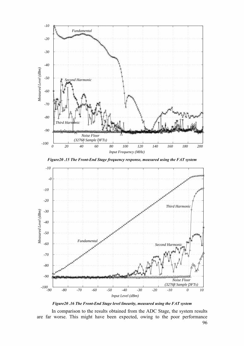
96
0 20 40 60 80 100 120 140 160 180 200-100
-90
-80
-70
-60
-50
-40
-30
-20
-10
Mea
sure
d Le
vel (
dBm
)
Input Frequency (MHz)
Fundamental
Second Harmonic
Third Harmonic
Noise Floor(32768 Sample DFTs)
Figure 20 .15 The Front-End Stage frequency response, measured using the FAT system
-90 -80 -70 -60 -50 -40 -30 -20 -10 0 10-100
-90
-80
-70
-60
-50
-40
-30
-20
-10
-0
-10
Input Level (dBm)
Mea
sure
d Le
vel (
dBm
)
FundamentalSecond Harmonic
Third Harmonic
Noise Floor(32768 Sample DFTs)
Figure 20 .16 The Front-End Stage level linearity, measured using the FAT system
In comparison to the results obtained from the ADC Stage, the system results are far worse. This might have been expected, owing to the poor performance

97
measured previously using the spectrum analyser. A pass-band can clearly be seen between DC and 100MHz in the frequency response, however the response is highly frequency dependent, exhibiting large ripples due to the Front-End buffer and amplifier characteristics. The Noise floor is measured at an almost constant value of -90dBm, which as found previously, equates to -90dBFS. This shows that the peak signal to noise ratio for the whole Front-End is around 6dB worse than with just the ADC Stage. The noise is therefore conclusively generated by the buffer and amplification circuitry. The second and third order harmonic distortion is also considerably worse due to this circuitry, lowering the SINAD ratio to as low as 30dB at around 20MHz. These results had not been measured during the earlier spectrum analyser tests, and could now be listed along with the other shortcomings of the stages.
The level linearity results were more encouraging. The same noise level of -90dBm was measured, but the linearity of the circuitry is shown to be constant over the 90dB measured range. The levels were measured a frequency of 10MHz, which explains why the harmonic distortion is fairly good. This corresponds to the low distortion seen before the large peak seen at 20MHz seen in the previous graph.
20.11 Front-End Testing ConclusionsThe results from the first round of Front-End testing were very far from ideal,
although the principle operation of the system had been shown to be working.A summary of the measurements found is shown below:
ADC Bandwidth (MHz) 100ADC SNR (dB) 57.3ADC SINAD (dB) 60Front-End Stage Bandwidth (MHz) N/A (Very large ripples in pass-band)Front-End Stage SNR (dB) 51.3Front-End Stage SINAD (dB) 30 (Worst case)
Table 20.1 The overall performance of the Front-End Stage (pre-improvement)
The main conclusion was that more work was required to discover why there were such inadequacies in the stage’s performance. Two hypotheses for some of the poor reading measured had been developed:
i) The oscilloscope probes setting of x1 was causing a low pass filtering effect within the circuit’s 100MHz bandwidth.
ii) The input capacitance of the ADG702 CMOS gain switches was thought to be high enough to make each switch look on at high frequency.
The highest priority after the exam break was decided to be to fabricate and test the Digital-Stage board. If this went without problem, it was decided that the remaining time would be spent trying to improve the Front-End Stage’s performance.
98
21. Digital-Stage TestingFabricating the digital stage involved soldering the 100-pin 0.5mm pitch
device onto the PCB by hand, which took specialised equipment to do correctly. A stereoscopic microscope and a fine pitch soldering iron tip ensured that this was done properly.
With the board built, the first test was to program the device. The software package used was Altera’s Maxplus II package, version 10.12, that also contains device simulation software. Programming the device required that a ‘ByteblasterMV’compatible cable was constructed, and used to connect from the parallel port of the PC to the JTAG header on the Digital-Stage.
It was mentioned in the prototyping chapter that the class-A amplifier design, that was going to be used to generate the clock signal, could not run fast enough. Instead an Analog Devices AD8611 100MHz fast comparator was used. To verify that the circuit function correctly a 810 divider was designed in Maxplus II and wired to on of the LEDs, to produce a 1Hz flashing light. The circuit worked as expected.
As there was not time to start on the implementation of the non-uniform sample clock generator, the remaining work done on the Digital-Stage revolved around designing a circuit to multiplex data from both channels into one stream for the FIFO memory input.
This work was completed ahead of schedule, which gave more time to improve the performance of the Front-End Stage.
99
22. Front-End ImprovementIt was hypothesised that the strange phenomenon seen in the plot of Figure
20.6, was likely to be due to the un-source terminated transmission line effect of the probe. It was suggested the Front-End Buffer tests should be repeated again using the probe on the x10 setting, in order to reduce this effect. To confirm this, the following plot was taken with the spectrum analyser and tracking generator set to -10dBm. The attenuator was set to 0dB and each probe setting was recorded:
Figure 22 .1 A plot of the output of the Front-End Buffer with the Attenuator set on 0dB for the x1 and x10 settings of the oscilloscope probe.
This clearly shows that the x10 setting does not have the steep low-pass effect seen by the x1 setting. The x10 setting did have a slight roll-off but was still a significant improvement in measurement performance over the x1 setting.
To evaluate the performance of the x10 setting, each attenuator level was tested and is shown in the following figure using the tracking generator set to -30dBm:
100
Figure 22 .2 The improved Front-End Buffer frequency response using a probe on x10 with most of the input capacitance removed for each Attenuator setting
The response still has about a 10dB roll-off over 200MHz for the 0dB setting, and the attenuation settings are equally spaced, but this is still a massive improvement from the initial x1 measurements.
It was also hypothesised in the first round of Front-End tests that the ADG702s used as gain switches effectively looked as if they were switched ‘On’ above a given frequency due to the significant input capacitance. It was decided that further investigation should done into revealing whether this was indeed the cause of the poor performance of the amplifier stage during the earlier tests.
The following plot illustrates clearly that that the hypothesis was true. It shows the gain of the 6dB amplifier with and without the gain switch in place, for both the on and off settings. The response of the off state does indeed tend to the response of the on state as the frequency is increased. Another point of note is that the gain of the amplifier with no gain switch in place has an increase for high frequencies. This would imply that there is still some parasitic capacitance to ground on the feedback path of the amplifier.

101
Figure 22 .3 A plot of the frequency response of Gain Stage 2, for without a Gain Switch and with a ADG 702 Gain Switch, in ‘On’ and ‘Off’ states
The ADG702 was replaced with an Alpha AF002 GaAsFET switch, and the process was repeated:
Figure 22 .4 A plot of the frequency response of Gain Stage 2, for without a Gain Switch and with a AF002 Gain Switch, in ‘On’ and ‘Off’ states
The Alpha switches show a very clear improvement over the ADG702 CMOS switches. The gain still increases by about 2dB over 200MHz from the curve of the gain without the gain switch, but is still a significant improvement from the ADG702 response.
All of the gain switches were replaced with AF002 devices, and every gain setting was tested to reveal the following plot of the amplifier stage for a tracking generator input of -50dBm:

102
Figure 22 .5 The improved Gain Stage frequency response using the AF002 GaAsFET gain switches for each gain setting
The convergence of the gain levels, seen with the initial results, can hardly be seen. Each gain level is clearly distinguishable. ‘Humping’ in all of the gain settings occurs at around 200MHz, but on the whole this response is a drastic improvement over the previously obtained results.
The following two figures show plots of the Front-End Buffer and Amplifier stages, and the entire analogue signal path response (including Anti-Alias filter):
Figure 22 .6 The improved total frequency response of the Front-End Buffer and the Amplification Stage, with the Attenuator on 0dB, for each gain setting
103
Figure 22 .7 The improved total frequency response of the gain stages and the Anti-Alias Filter, with the Attenuator on 0dB, for each gain setting
The Front-End Buffer and Amplifier stage plot shows that the combination of the two circuits produces a response with far more ripples in each curve in Figure 22.6. This effect occurs most above 100MHz, which can be seen to be masked by the Anti-Alias filter’s repose in Figure 22.7. This final frequency response for each amplification setting, using a x10 probe and a 0dBm Attenuator setting, can be seen to have a very uniform shape, albeit a 4dB ramp in gain, but still an enormous improvement over the original readings.

104
23. Software DevelopmentThroughout the hardware design, prototyping and testing stages, the software
for the USB2Scope system was continuously developed. The USB2Scope software comprises of two separate programs, the device firmware and the host application.
The device firmware runs on the 8051 microcontroller on the EZ-USB FX2. Its task is to firstly configure the device’s control registers to automatically transfer data from the Digital-Stage to the host, and then perform a ‘housekeeping’ function to administer the device.
The host application continuously reads data from the device, processes it and displays the data according to the user’s requirements.
Relevant portions of the source code will be included in the following text, if the reader would like an electronic copy of the full source code listings please visit:
http://geoff.phillips.fm
23.1 The Device FirmwareThe firmware run on the EZ-USB FX2’s 8051 microprocessor was written
using a modified version of the ‘frame-work’ program supplied by Cypress Semiconductor. The program is written in ANSI ‘C’ and complied using the Keil 8051 Micro-Vision suite.
The main function within the frame-work is summarised below. ‘... ’ indicates missing code with little relevance here.
void main(void) ... // Initialize user device
TD_Init(&pollStatus); ... // Task Dispatcher while(TRUE) // Main Loop if(GotSUD) // Wait for SUDAV SetupCommand(); // Implem ent setup command GotSUD = FALSE; // Clear SUDAV flag
// Poll User Device if (Sleep) if(TD_Suspend()) Sleep = FALSE; do EZUSB_Susp(); // Plac e processor in idle mode. while(!Rwuen && EZUSB_EXTWAKEUP()); // 8051 activity will resume here due to USB bus or // Wakeup# pin activity. EZUSB_Resume(); // If source is the Wakeup# pin,
// signal the host to Resume. TD_Resume();
TD_Poll(&pollStatus);

105
The program firstly runs a function called TD_Init() which initialises the device’s configuration registers and sets up the common serial bus interface. After this it enters an infinite loop in which it continuously checks for setup data from the host (if (GotSUD) ), then checks whether it should place the processor into its idle state (if (Sleep) ), if not then it runs the housekeeping function TD_Poll() . The structure status of type TPollStatus is used to hold the current state of the common serial bus for the transmission function. It is defined as follows:
struct TPollStatus // Boolean value denoting whether the TD_Poll() function is // currently sending data across the common serial bus:
BYTE bSendingData; // The channel to which the data is currently being sent: // (Either 0 or 1)
BYTE channel; // The data being sent a bit at a time acros s the bus:
WORD serialData; // The current bit being sent:
WORD currentBit;;
The TD_Init() function is listed below:
void TD_Init(struct TPollStatus *status)
// S et the CPU clock to 48MHzCPUCS = (( CPUCS & ~bmCLKSPD) | bmCLKSPD1) ;
// Set up the strobes and flags for active high:FIFOPINPOLAR = 0x3F; SYNCDELAY;PINFLAGSAB = 0x00; SYNCDELAY;PINFLAGSCD = 0x40; SYNCDELAY;
// Set up the FIFO interface for an external clock:IFCONFIG = bmIFCFG0 | bmIFCFG1; SYNCDELAY;
// Set u p EP2 FIFO:EP2FIFOCFG = bmAUTOIN | bmZEROLENIN | bmWORDWIDE; SYNCDELAY;
// Configure EP2 (IN, BULK, 1024)EP2CFG = 0xE8; SYNCDELAY;
// Set up EP2 FIFO for 1024 byte packets:EP2AUTOINLENH = 0x04; SYNCDELAY;EP2AUTOINLENL = 0x00; SYNCDELAY;
// Configure EP1OUT (OUT, BULK, 512)EP1OUTCFG = 0xA0; SYNCDELAY;
// Reset the FIFO s: FIFORESET = 0x80; SYNCDELAY;
FIFORESET = 0x02; SYNCDELAY;FIFORESET = 0x00; SYNCDELAY;
// Arm EP1OUT:EP1OUTBC = 0x00; SYNCDELAY;
// Enable remote - wakeupRwuen = TRUE;
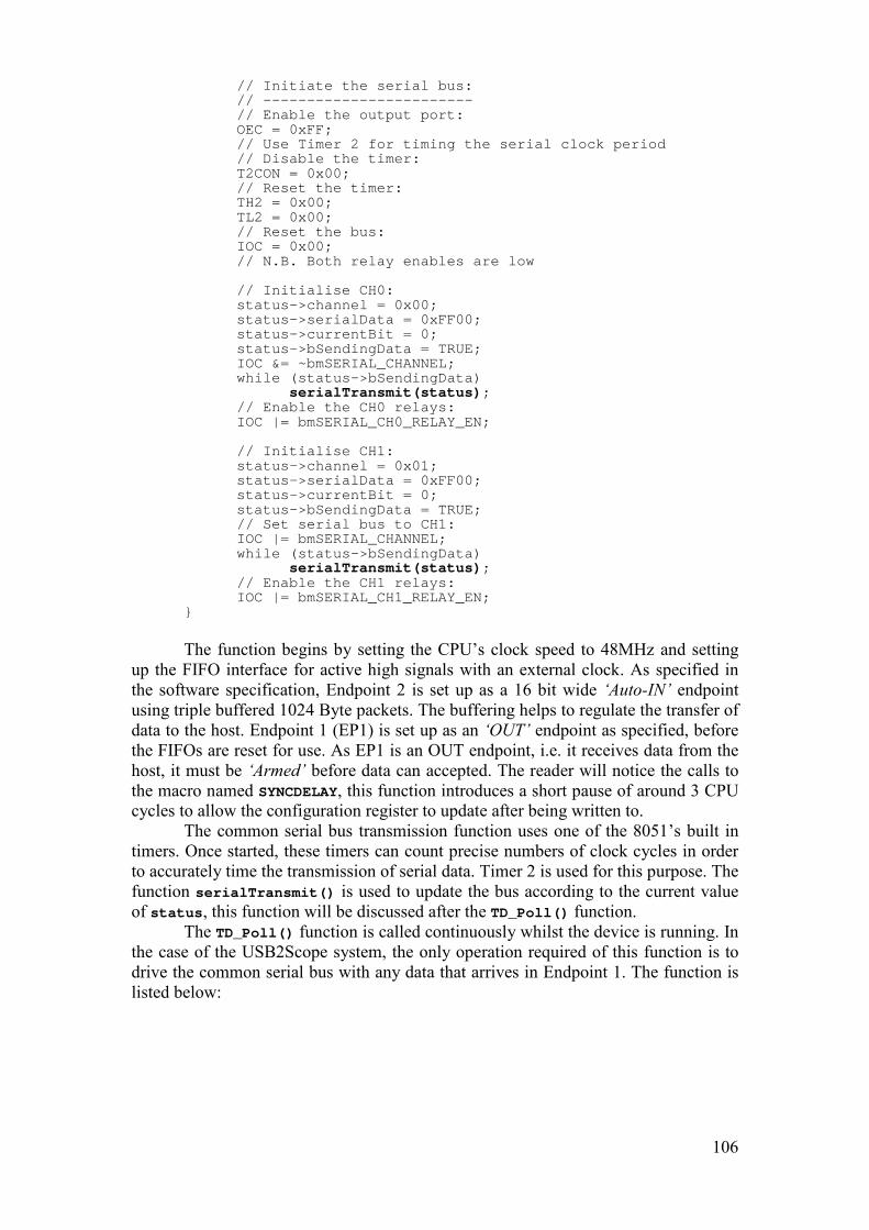
106
// Initiate the serial bus:// ------------------------// Enable the output port:OEC = 0xFF;// U se Timer 2 for timing the serial clock period// Disable the timer:T2CON = 0x00;// Reset the timer:TH2 = 0x 00;TL2 = 0x00;// Reset the bus:IOC = 0x00;// N.B. Both relay enables are low
// Initialise CH0:status - >channel = 0x00;status - >serialData = 0xFF00;status - >currentBit = 0;status - >bSendingData = TRUE;IOC &= ~bmSERIAL_CHANNEL;while (stat us - >bSendingData)
serialTransmit(status) ;// Enable the CH0 relays:IOC |= bmSERIAL_CH0_RELAY_EN;
// Initialise CH1:status - >channel = 0x01;status - >serialData = 0xFF00;status - >currentBit = 0;status - >bSendingData = TRUE;// Set serial bus to CH1:IOC |= bmSERIAL_CHANNEL;while (status - >bSendingData)
serialTransmit(status) ;// Enable the CH1 relays:IOC |= bmSERIAL_CH1_RELAY_EN;
The function begins by setting the CPU’s clock speed to 48MHz and setting up the FIFO interface for active high signals with an external clock. As specified in the software specification, Endpoint 2 is set up as a 16 bit wide ‘Auto-IN’ endpointusing triple buffered 1024 Byte packets. The buffering helps to regulate the transfer of data to the host. Endpoint 1 (EP1) is set up as an ‘OUT’ endpoint as specified, before the FIFOs are reset for use. As EP1 is an OUT endpoint, i.e. it receives data from the host, it must be ‘Armed’ before data can accepted. The reader will notice the calls to the macro named SYNCDELAY, this function introduces a short pause of around 3 CPU cycles to allow the configuration register to update after being written to.
The common serial bus transmission function uses one of the 8051’s built in timers. Once started, these timers can count precise numbers of clock cycles in order to accurately time the transmission of serial data. Timer 2 is used for this purpose. The function serialTransmit() is used to update the bus according to the current value of status , this function will be discussed after the TD_Poll() function.
The TD_Poll() function is called continuously whilst the device is running. In the case of the USB2Scope system, the only operation required of this function is to drive the common serial bus with any data that arrives in Endpoint 1. The function is listed below:
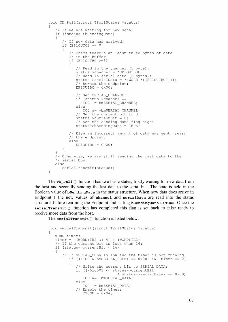
107
void TD_Poll(struct TPollStatus *status)
// If we are waiting for new data:if (!status - >bSendingData)
// If new data has arrived:if (EP1OUTCS == 0)
// Check there's at least thr ee bytes of data // in the buffer:
if ( EP1OUTBC >=3)
// Read in the channel (1 byte):status - >channel = *EP1OUTBUF;// Read in serial data (2 bytes):status - >serialData = *(WORD *)(EP1OUTBUF+1);// Re - arm the endpoint:EP1OUTBC = 0x00;
// Set SERIAL_CHANNEL:if (status - >channel == 1)
IOC |= bmSERIAL_CHANNEL;else
IOC &= ~bmSERIAL_CHANNEL;// Set the current bit to 0:status - >currentBit = 0;// Set the sending data flag high:status - >bSendingData = TRUE;
// Else an incorrect amount of data was sent, rearm
// the endpoint:else
EP1OUTBC = 0x00;
// Otherwise, we are still sending the last data to the // serial bus:
elseserialTransmit(status);
The TD_Poll() function has two basic states, firstly waiting for new data from the host and secondly sending the last data to the serial bus. The state is held in the Boolean value of bSendingData in the status structure. When new data does arrive in Endpoint 1 the new values of channel and serialData are read into the statusstructure, before rearming the Endpoint and setting bSendingData to TRUE. Once the serialTransmit () function has completed this flag is set back to false ready to receive more data from the host.
The serialTransmit () function is listed below:
void serialTransmit(struct TPollStatus *status) WORD timer; timer = ((WORD)TH2 << 4) | (WORD)TL2; // If the current bit is less than 16: if (status - >currentBit < 16)
// If SERIAL_SCLK i s low and the timer is not running: if (((IOC & bmSERIAL_SCLK) == 0x00) && (timer == 0))
// Write the current bit to SERIAL_DATA:if (((0x0001 << status - >currentBit)
& status - >serialData) == 0x00) IOC &= ~bmSERIAL_DATA;else IOC |= bmSERIAL_DATA;// Enable the timer: T2CON = 0x04;
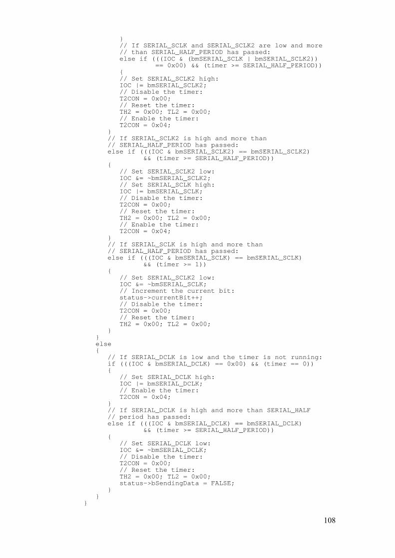
108
// If SERIAL_SCLK and SERIAL_SCLK2 are low and more // than SERIAL_HALF_PERIOD has passed: else if (((IOC & (bmSERIAL_SCLK | bmSERIAL_SCLK2))
== 0x00) && (timer >= SERIAL_HALF_ PERIOD)) // Set SERIAL_SCLK2 high: IOC |= bmSERIAL_SCLK2; // Disable the timer: T2CON = 0x00; // Reset the timer: TH2 = 0x00; TL2 = 0x00; // Enable the timer: T2CON = 0x04;// If SERIAL_SCLK2 is high and more than // SERIAL_HALF_PERIOD has passed:else if (((IOC & bmSERIAL_SCLK2) == bmSERIAL_SCLK2)
&& (timer >= SERIAL_HALF_PERIOD)) // Set SERIAL_SCLK2 low: IOC &= ~bmSERIAL_SCLK2; // Set SERIAL_SCLK high: IOC |= bmSERIAL_SCLK; // Disabl e the timer: T2CON = 0x00; // Reset the timer: TH2 = 0x00; TL2 = 0x00; // Enable the timer: T2CON = 0x04;// If SERIAL_SCLK is high and more than // SERIAL_HALF_PERIOD has passed:else if (((IOC & b mSERIAL_SCLK) == bmSERIAL_SCLK)
&& (timer >= 1))
// Set SERIAL_SCLK2 low:IOC &= ~bmSERIAL_SCLK;// Increment the current bit:status - >currentBit++;// Disable the timer:T2CON = 0x00;// Reset the timer:TH2 = 0x00; TL2 = 0x00;
else
// If SERIAL_DCLK is low and the timer is not running:if (((IOC & bmSERIAL_DCLK) == 0x00) && (timer == 0))
// Set SERIAL_DCLK high:IOC |= bmSERIAL_DCLK;// Enable the timer:T2CON = 0x04;
// If SERIAL_DCLK is high and more tha n SERIAL_HALF // period has passed:else if (((IOC & b mSERIAL_DCLK) == bmSERIAL_DCLK)
&& (timer >= SERIAL_HALF_PERIOD))
// Set SERIAL_DCLK low:IOC &= ~bmSERIAL_DCLK;// Disable the timer:T2CON = 0x00;// Reset the timer:TH2 = 0x00; TL2 = 0x00;status - >bSendingData = FALSE;
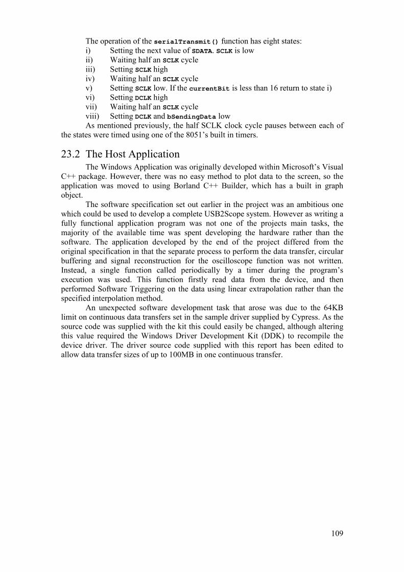
109
The operation of the serialTransmit () function has eight states:i) Setting the next value of SDATA. SCLK is lowii) Waiting half an SCLK cycleiii) Setting SCLK highiv) Waiting half an SCLK cyclev) Setting SCLK low. If the currentBit is less than 16 return to state i)vi) Setting DCLK highvii) Waiting half an SCLK cycleviii) Setting DCLK and bSendingData lowAs mentioned previously, the half SCLK clock cycle pauses between each of
the states were timed using one of the 8051’s built in timers.
23.2 The Host ApplicationThe Windows Application was originally developed within Microsoft’s Visual
C++ package. However, there was no easy method to plot data to the screen, so the application was moved to using Borland C++ Builder, which has a built in graph object.
The software specification set out earlier in the project was an ambitious one which could be used to develop a complete USB2Scope system. However as writing a fully functional application program was not one of the projects main tasks, the majority of the available time was spent developing the hardware rather than the software. The application developed by the end of the project differed from the original specification in that the separate process to perform the data transfer, circular buffering and signal reconstruction for the oscilloscope function was not written. Instead, a single function called periodically by a timer during the program’s execution was used. This function firstly read data from the device, and thenperformed Software Triggering on the data using linear extrapolation rather than the specified interpolation method.
An unexpected software development task that arose was due to the 64KB limit on continuous data transfers set in the sample driver supplied by Cypress. As the source code was supplied with the kit this could easily be changed, although altering this value required the Windows Driver Development Kit (DDK) to recompile the device driver. The driver source code supplied with this report has been edited to allow data transfer sizes of up to 100MB in one continuous transfer.
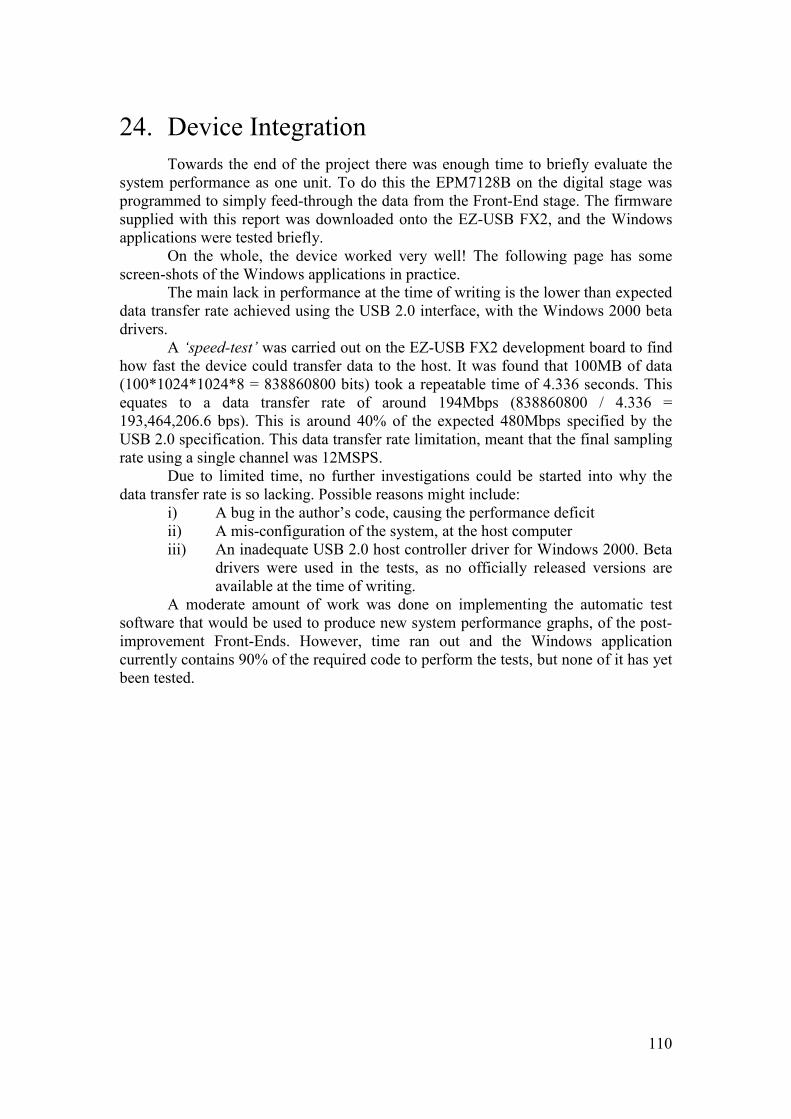
110
24. Device IntegrationTowards the end of the project there was enough time to briefly evaluate the
system performance as one unit. To do this the EPM7128B on the digital stage was programmed to simply feed-through the data from the Front-End stage. The firmware supplied with this report was downloaded onto the EZ-USB FX2, and the Windows applications were tested briefly.
On the whole, the device worked very well! The following page has some screen-shots of the Windows applications in practice.
The main lack in performance at the time of writing is the lower than expected data transfer rate achieved using the USB 2.0 interface, with the Windows 2000 beta drivers.
A ‘speed-test’ was carried out on the EZ-USB FX2 development board to find how fast the device could transfer data to the host. It was found that 100MB of data (100*1024*1024*8 = 838860800 bits) took a repeatable time of 4.336 seconds. This equates to a data transfer rate of around 194Mbps (838860800 / 4.336 = 193,464,206.6 bps). This is around 40% of the expected 480Mbps specified by the USB 2.0 specification. This data transfer rate limitation, meant that the final sampling rate using a single channel was 12MSPS.
Due to limited time, no further investigations could be started into why the data transfer rate is so lacking. Possible reasons might include:
i) A bug in the author’s code, causing the performance deficitii) A mis-configuration of the system, at the host computeriii) An inadequate USB 2.0 host controller driver for Windows 2000. Beta
drivers were used in the tests, as no officially released versions are available at the time of writing.
A moderate amount of work was done on implementing the automatic test software that would be used to produce new system performance graphs, of the post-improvement Front-Ends. However, time ran out and the Windows application currently contains 90% of the required code to perform the tests, but none of it has yet been tested.
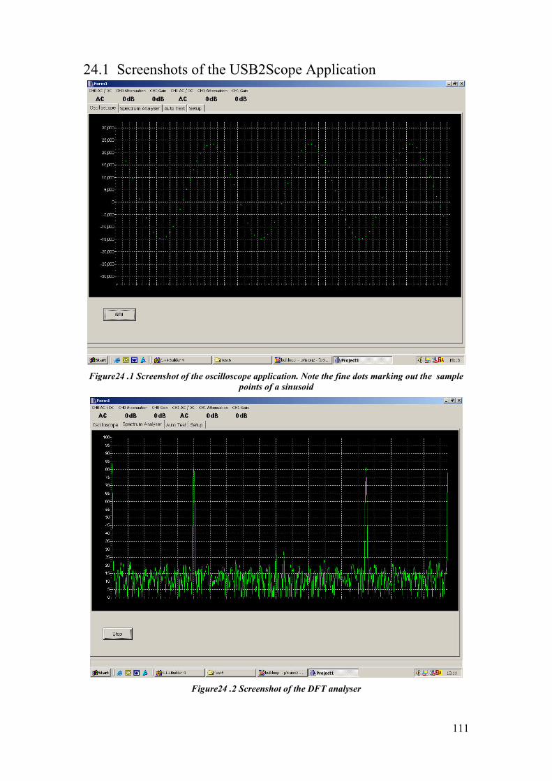
111
24.1 Screenshots of the USB2Scope Application
Figure 24 .1 Screenshot of the oscilloscope application. Note the fine dots marking out the sample points of a sinusoid
Figure 24 .2 Screenshot of the DFT analyser
112
25. Project EvaluationOnce the end of a project has been reached, it is important to look back and
reflect on how the project progressed, what went well, what did not, and what can still be done in the future.
Overall the project progressed very well indeed. What turned out to be a very ambitious specification was set at the start of the design process, which took a lot of time and hard work to accomplish. The aim of getting a ‘sine wave on the screen’ was achieved, and a lot was learnt along the way. The project covered many new practical fields of engineering that were new to the author, including:
i) PCB design using surface mount componentsii) System design and the trade-off processiii) Firmware designiv) Device driver usagev) Practical programmable logic device experiencevi) Filter designvii) Practical project planningSome of the best aspects to come out of the project have included:i) The author’s increased self-confidence in his own practical engineering
ability.ii) A lot of very useful practical experience that will be of great use in the
future.iii) Further experience in the professional engineering environment.Aspects of the project that could have been improved upon include:i) The project planning should have been based on more achievable
goals.ii) More foresight should have been put into the testing procedure to
identify the required tests way in advance.iii) Timekeeping and the meeting of important deadlines should have been
of a higher priority.The finished prototype and accompanying software conformed to a lot of the
specification that was set. There were some parts of the original idea which were not started or uncompleted at the end of the project. These aspects could be developed if further time were available:
i) The automatic test software for the USB 2.0 platform could be finished to give the final system results, similar to those gained from the FAT system
ii) The application of dither in the analogue-to-digital conversion process could be analysed further, to find why it was not found to improve the SFDR of the device.
iii) The non-uniform sampling method could be implementediv) Calibration Digital to Analogue Converters could be used to
tweak unwanted DC offsets at given nodes in the network. Automatic calibration would then be possible

113
26. ConclusionThe project’s task stated at the start of the design process was:
“The design of a high quality PC-based oscilloscope using USB 2.0”The design process was started from first principles, with the aim of following
a path to the set aim, however the scope of the project was left undefined to allow flexibility from the set task if it had become unachievable.
Preliminary research revealed that there was definitely an increase in the market for low-cost computer based test equipment. Advantages of using a standardised interface include ease of upgrade, reduced component costs and ease of use.
An initial concept was developed and areas for further research were identified as: data transfer technology, the theory of non-uniform sampling and additive dither theory.
The initial concepts were compared taking the findings of the concept directed research into consideration, and a final concept was chosen for design. Firstly a detailed specification of the proposed device was defined, giving reasoning for each decision made. Then project planning was used to minimise the risk of total-system failure due to one system component.
The design process started with system-level design, followed by the design of each sub-block. Throughout the hardware design process full explanations of each important decision made was given, including if any changes had to be made to the original specification. The hardware design culminated in a system design review that ensured that the overall design would meet the specified requirements.
The prototyping and testing stages were accomplished in parallel to insure proper functionality of the device.
The initial test results from the Front-End Stage concluded that the response was far from ideal. The factors thought to be to blame were the use of the oscilloscope probe on the x1 setting and the high input capacitance of the gain switches.
In the second round of testing these factors were indeed shown to adversely affect the device’s performance. To improve the performance the x10 setting on the probe was used, and the CMOS gain switches were replaced by GaAsFET switches, and final performance results were taken using the spectrum analyser. There was no time available to develop the automatic test software required to collect final overall system performance data.
The software used in the project is explained, before a brief chapter covers the performance of the system as a whole, which concluded that it was limited by the unexpectedly low USB 2.0 bandwidth of 193Mbps, rather than the expected 480Mbps.
The project’s evaluation concluded that the project has been an overwhelming success, in that the main aim of achieving a simple functioning device setup has been achieved. A lot of good experience has been gained from the project, but project planning and timekeeping should be made a higher priority. Possible future expansion for the project includes the implementation of the non-uniform sampling method specified, and the completion of the automatic test platform incorporating the USB 2.0 interface.

114
27. Appendicies
27.1 Appendix I – Proof of the Non-Uniform Sampling TheoremThe Dirac ‘delta’ function is defined in the continuous case as:
0
1 0( )
0limx
xotherwise
δ∆→
∆ ≤ < ∆
In the generalised case a sampling point process can be defined as:
( ) ( )kk
u t t tδ+∞
=−∞
= −∑where kt are the discrete points in time at which a signal is sampled.Given a time dependent periodic signal ( )x t , resulting function of time due to
the sampling process ( )x t′ is given by:( ) ( ) ( )
( ) ( )kk
x t x t u t
x t t tδ+∞
=−∞
′ = ⋅
= ⋅ −∑The spectrum of the sampled signal is therefore given by its Fourier transform:
( ) ( )
( ) ( )
j t
j t
X x t e dt
x t u t e dt
ω
ω
ω+∞ −
−∞
+∞ −
−∞
′ ′= ⋅ ⋅
= ⋅ ⋅ ⋅
∫∫
(4)
When the difference between successive sampling instants is uniform, i.e. 1k kt t T+ = + where T is the sampling period, then the function ( )u t is periodic and
can be expressed as the Fourier series expansion:
1
1
1 2 2( ) cos
1 1r
j r t j r t
r
ru t tT T T
e eT T
ω ω
π+∞
=
+∞⋅ ⋅ − ⋅ ⋅
=
= + ⋅
= + +
∑
∑(5)
given that 2 2T t T− ≤ ≤ + , and where 2Tπω = is the frequency of sampling.
Substituting (5) into (4) leads to:
( )
( )
2
21
2 2 (1 ) (1 )
2 21
*
1
1 1( ) ( )
1 1( ) ( )
( ) [ (1 )] [ (1 )]
T j r t j r t j t
Tr
T Tj t j t r j t r
T Tr
r
X x t e e e dtT T
x t e x t e e dtT T
X X r X r
ω ω ω
ω ω ω
ω
ω ω ω
+∞+ ⋅ ⋅ − ⋅ ⋅ −
−=
+∞+ −− − ⋅ ⋅ + − ⋅ ⋅ −
− −=
+∞
=
′ = ⋅ + + ⋅ ⋅
= ⋅ + ⋅ + ⋅
= + ⋅ + + ⋅ −
∑∫
∑∫ ∫
∑where ( )X ω is the Fourier transform of ( )x t and *( )X ω is its complex
conjugate. It can be seen that ( )X ω′ is periodic in frequency with period ω - the sampling frequency. This explains the periodic nature of uniformly sampled signal spectra.
115
However if the distance in time between consecutive sample points kt and 1kt +
were formed as follows:1k k kt t+ = + Γ
where kΓ is a set of i.i.d. random variables (RVs), with probability density function ( )f t . The probability distribution of each value of kt , ( )kf t , is the successive convolution of ( )f t :
1 0
2 1
( ) ( )( ) ( )* ( )( ) ( )* ( )
...
of t f tf t f t f tf t f t f t
==
=
The spectrum of the randomly sampled signal, is therefore equal to:( ) ( ) ( )
( ) k
j t
j tk
k
X x t u t e dt
x t e
ω
ω
ω+∞ −
−∞
+∞−
=−∞
′ = ⋅ ⋅ ⋅
= ⋅
∫
∑The definition of expectation [ ( )]E φ Γ is given by:
[ ( )] ( ) ( )E t f t dtφ φ+∞
−∞Γ = ⋅ ⋅∫
where ( )φ Γ is an arbitrary function of the random variable Γ .Therefore the expectation of the spectrum of a randomly sampled signal is:
[ ( )] ( ) ( )
( ) ( )
j tk
k
j tk
k
E X x t e f t dt
x t e f t dt
ω
ω
ω+∞+∞ −
−∞=−∞
+∞+∞ −
−∞=−∞
′ = ⋅ ⋅ ⋅
= ⋅ ⋅ ⋅
∑∫
∑∫where ( )kf t is the probability density function of kΓ .It has been shown in Section 9.3.1 that:
( )kk
f t constant+∞
=−∞
=∑Therefore:[ ( )] ( )E X constant Xω ω′ = ⋅
27.2 Appendix II – Derivation of the Second Moment of a Uniformly Distributed Random VariableDefinition of mean squared signal:
2 2 ( )x x p x dx∞
−∞
⋅ ⋅∫Mean Squared deviation, assuming the RV is uniformly distributed
between +∆/2 and -∆/2:
12121
83831
311)(
23332
2
32
2
222 ∆=
∆⋅
∆=
⋅∆−
−⋅∆
∆=
∆
=⋅∆⋅=⋅⋅=
∆+
∆−
∆+
∆−
∞
∞−∫∫
qdqqdqqpqq

116
27.3 Appendix III – Derivation of the Maximum Signal to Noise Ratio of an ADC
Definition of signal to quantisation noise ratio:2
2
signal
quantisation noise
P xSQNRP q
= =
Mean square of a sin wave in relation to an M bit quantiser with quantisation
step 22 1M∆ =
−:
( )2 2 2 2
2 2 2 2max
1 1 1 (2 1) 2(1) 2 2 2 12 2 2 2 8 8
M MM Mx x
− ∆ ⋅∆= ⋅ = ⋅ = ⋅ ⋅∆ = ⋅ − ⋅ + ≈
Signal to quantisation noise ratio for an M bit quantiser:
2 2 22
22
2 12 3( ) 28 2
MMxSQNR M
q⋅∆
= ≈ ⋅ = ⋅∆
3( ) 10 log 10 log(2) 2 1.761 6.0202dBSQNR M M M ≈ ⋅ + ⋅ ⋅ = + ⋅

117
27.4 Appendix IV – Device SchematicsThe following nine pages are the prototype schematics generated during the
PCB design process. The table below gives descriptions of each pages’ contents.
1. The Power Supply of the Front-End Stage2. The Attenuator, Buffer, Amplification and Anti-Alias Filter Stages of the Front-End3. The ADC Driver, ADC and LVDS Line-Driver Stages of the Front-End4. The Common Serial Bus Decoder and Gain Switch Drivers of the Front-End5. The Power Supply of the Digital-Stage6. The global connections to the EPM7128B device of the Digital Stage7. The I/O banks of pins on the EPM7128B device of the Digital Stage8. The LVDS receiver, and FIFO data output connections of the Digital-Stage9. The remainder of the Digital Stage connections

118

119
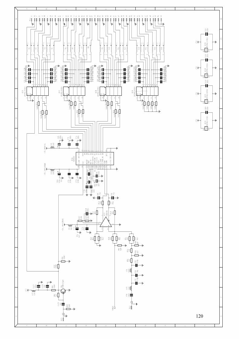
120
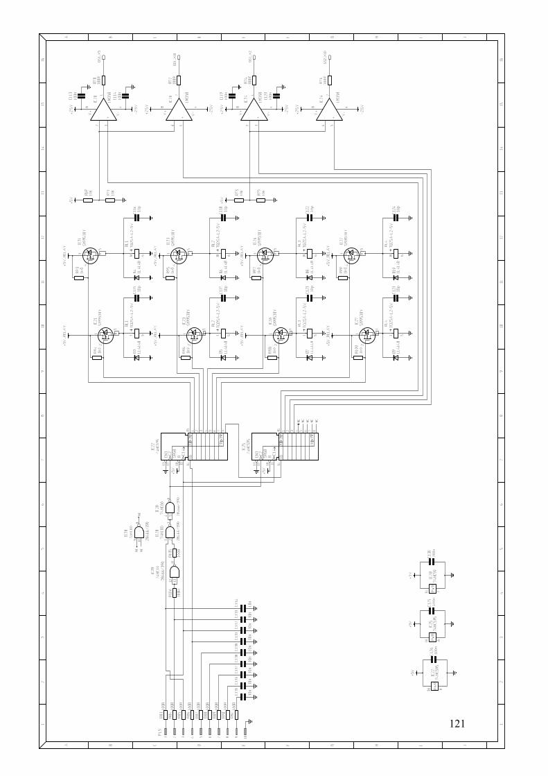
121

122
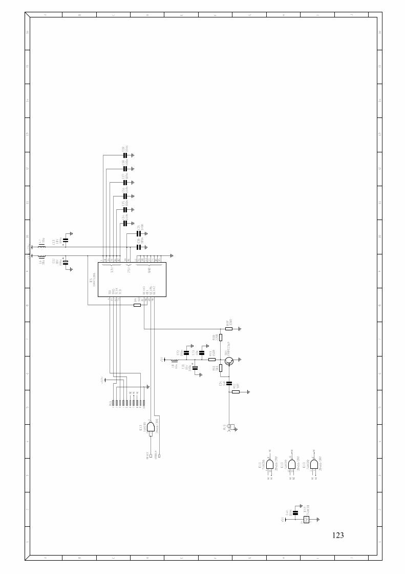
123
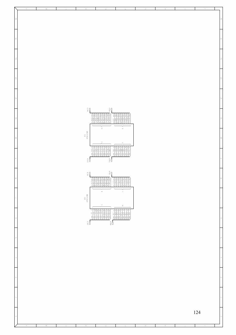
124

125
126


128
28. GlossaryAPI Application-Program Interface - A defined standard of
communication between application-level programs and lower-level system programs.
bps bits per secondBps Bytes per second (8 * bits per second)Elephant A big animalFIFO First In First OutFirmware Software run on a device, who's main function is not to
perform a computational role. E.g. peripherals.GaAsFET Gallium Arsenide Field Effect TransistorHot-Swap An interface system which can allow devices to be
attached and removed whilst the system is running.LSB Least Significant Bit - The difference between two
adjacent quantisation levels in an ADCMSPS Mega Samples Per SecondPCB Printed Circuit BoardPlug-and-Play A concept for modern peripheral design. Such devices
can simply be plugged into a compliant host computer. The host can automatically detect the new device and install a relevant device driver if it has an appropriate one.
RC Resistor-CapacitorRF Radio FrequencySINAD SIgnal to Noise And Distortion ratio

129
29. BibliographyJ. Axelson, “USB Complete,” Labview Research, Madison, USA, 2 nd Edition.
J. Hyde, “USB Design by Example,” Intel University Press, Wiley Comp. Pub., 1999.
Cypress Semi. Corp., “EZ-USB FX2 technical reference manual,” Revision 2.1, 2001.
A. S. Sedra and K. C. Smith, “Microelectronic Circuits,” Oxford University Press, 1998.
S. K. Mitra, “Digital Signal Processing, a computer based approach,” McGraw-Hill Int., 2001.
I. D. Robertson and S. Lucyszyn, “RFIC and MMIC design and technology,” IEE circuits, devices and systems, Series 13, 2001.
D. M. Pozar, “Microwave Engineering,” John Wiley & sons inc., 2nd Ed., 1998.
J. G. Proakis and D. G. Manolakis, “Digital Signal Processing, Principles, algorithms and applications,” Prentice Hall Int. Editions, 3rd Ed., 1996.
R. E. Walpole, R. H. Myers and S. L. Myers, “Probability and Statistics for Engineers and Scientists,” Prentice Hall Int., 6th Ed., 1998.
T. M. Cover and J. A. Thomas, “Elements of Information Theory,” Wiley series in telecommunications, 1991.
J. L. Hennessy and D. A. Patterson, “Computer Architecture a Quantitative Approach,” Morgan Kaufmann Pub. Inc., 2nd Ed., 1996.

130
30. References
[1] E. T. Whittaker, “On the functions which are represented by the expansions of the interpolation theory,” Proc. R. Soc. Edinburgh, vol. 35, pp. 181-194, 1915.
[2] I. Bilinskis and A. Mikelsons, “Randomized Signal Processing,” Prentice Hall Int. Series in Accoustics, Speech and Signal Proc., 1992.
[3] H. S. Shapiro and R. A. Silverman, “Alias-free sampling of random noise,” IRE Trans. Inf. Theory, IT-8 145-54, 1960.
[4] I. Mednieks, “Methods for spectral analysis of nonuniformly sampled signals,” Institute of Electronics and Computer Science, Latvia.
[5] H.G. Feichtinger, C.Cenker, and M.Herrmann, “Reconstruction algorithms for discrete non-uniform sampled band-limited signals,” 15.ÖAGM Conf., ÖCG, volume 56, pages 51-61, May 1991.
[6] H.G.Feichtinger, C.Cenker, and H.Steier, “Fast iterative and non-iterative reconstruction methods in irregular sampling,” Conf. ICASSP`91, May, Toronto, p.p. 1773-1776, 1991.
[7] B. Widrow, “Statistical analysis of amplitude-quantized sample-data systems,” Trans. AIEE (Applications and Industry), vol. 79, 1960 (Jan ’61 section), pp 555-568.
[8] N. S. Jayant and L. R. Rabiner, “The application of dither to the quantization of speech signals,” Bell Syst. Tech. J., vol. 51 pp. 1293-1304, July-Aug. 1972.
[9] L. G. Roberts, “Picture coding using pseudo-random noise,” IRE Trans. Inform. Theory, vol. IT-8, pp. 145-154, Feb. 1962.
[10] L. Schuchman, “Dither signals and their effect on quantization noise,” IEEE Trans. Commun. Technol., vol. COMM-12, pp. 162-165, Dec. 1964.
[11] E. Lukacs, “Characteristic Functions,” Griffin, London, U.K., 1960.
[12] T. Kawata, “Fourier Analysis in Probability Theory,” Academic, New York, N.Y., 1972.
[13] R. A. Wannamaker, S. P. Lipshitz, J. Vanderkooy, and J. Nelson Wright, “A theory of nonsubtractive dither,” IEEE Trans. on Signal Proc., vol. 48, no. 2, Feb. 2000.
[14] G. M. Phillips, “The theory and application of dither in radio frequency digitisation,” Unpublished university paper, Sept. 2001.

131
[15] C. J. Kikkert, “Improving ADC performance by adding dither,” Unpublished paper, Dept. Elec. and Computer Eng., James Cook Univ. of North Queensland, Australia.
[16] R. A. Wannamaker, “The theory of dithered quantization,” Ph.D. dissertation, Dept. Appl. Math., Univ. Waterloo, Waterloo, Ont., Canada, June 1997.