\u003ctitle\u003emems raster correction scanner for sxga resolution retinal scanning...
TRANSCRIPT

MEMS Raster Correction Scanner for SXGA resolution Retinal Scanning Display
Hakan Urey*, Frank DeWitt IV, Peggy Lopez, Jason Tauscher
*KOÇ University, Optoelectronics Research Center, Sariyer, 34450 Istanbul, TURKEY Phone: +90-212-338-1474, E-mail: [email protected]
Microvision Inc., 19910 North Creek Pkwy, Bothell, WA 98011
ABSTRACT A high-frequency resonant horizontal scanner and a linearly driven vertical scanner at display frame rates can create a 2-D raster for video display. The combined motion of the two scanners forms a sinusoidal raster in the vertical direction where the raster line spacing is uniform only at the center and becomes progressively nonuniform towards the left and right edges of the display screen. Nonuniformities degrade the image quality and can be corrected by the addition of a third scanner to the system. Last year we reported the requirements and some of the early results in our MEMS-based raster correction scanner development effort. Since then, a lot of progress was made and the scanner was successfully incorporated into an SXGA resolution helmet-mounted display system. In this paper we report the results of thick copper coil development, new coil and magnet design for electromagnetic actuator, thermal flatness testing, new mounting design, and finally the performance measurements for the HMD system with a raster correction scanner. Keywords: MEMS scanner, raster scanning, electromagnetic actuators, copper plating, RSD
1. INTRODUCTION In this section we discuss the need for a raster correction scanner (RCS), RCS specifications, and why MEMS
technology was selected for the implementation. In the following sections, we discuss the scanner mechanical design, thermal and mounting issues and test results, novel electromagnetic actuator design, and the test results of the HMD system incorporating the RCS.
Retinal Scanning Displays typically employ two uniaxial or one biaxial scanner where the horizontal scanner is
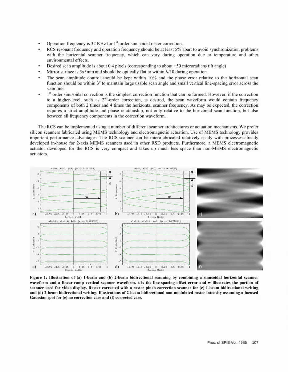
operated at resonance, and the vertical scanner is driven by a linear ramp waveform1,2,3. The primary reason for the resonant sinusoidal operation of the horizontal scanner is to take advantage of the high mechanical gain (Q-factor) of the scanner at resonance. As illustrated in Figure 1.a, the combined motions of the two scanners create a 2-D sinusoidal raster pattern where line-to-line spacing is uniform at the center of the screen and becomes non-uniform for points away from the center of the screen. As shown in Figure 1.b and 1.e, the effect is worse when two-beams are scanning in parallel as in the case of our SXGA-resolution HMD systems.
An ideal raster pattern with equal raster line spacing can be obtained using a vertical scanner that creates a stairstep
waveform instead of the linear ramp waveform. However, such a scanner requires large mechanical bandwidth (i.e., low-Q), high frequency and non-resonant operation, and large scan angle. It is not possible to meet all these requirements with one scanner at reasonable power levels. A better approach is to split the required stair step motion of the vertical scanner into combination of a linear-ramp at display refresh rate (60Hz) and a small amplitude triangular wave at exactly twice the frequency of the horizontal scanner, and to implement each waveform with separate scanners. The small triangular wave is approximated with a sinusoidal wave and implemented by adding a raster correction scanner or RCS to the system. It was shown that even the simple sinusoidal correction provides very good raster correction4.
An SXGA (1280x1024) resolution Helmet Mounted Display (HMD) system is implemented using 2-beam
bidirectional scanning architecture and horizontal and vertical scanners operating at 16KHz and 60Hz (see Figures 1.c, 1.d, and 1.f). RCS specifications can be summarized as below:5
MOEMS Display and Imaging Systems, Hakan Urey, Editor,Proceedings of SPIE Vol. 4985 (2003) © 2003 SPIE · 0277-786X/03/$15.00
106
• Operation frequency is 32 KHz for 1st-order sinusoidal raster correction. • RCS resonant frequency and operation frequency should be at least 5% apart to avoid synchronization problems
with the horizontal scanner frequency, which can vary during operation due to temperature and other environmental effects.
• Desired scan amplitude is about 0.4 pixels (corresponding to about ±50 microradians tilt angle) • Mirror surface is 5x5mm and should be optically flat to within λ/10 during operation. • The scan amplitude control should be kept within 10% and the phase error relative to the horizontal scan
function should be within 3o to maintain large usable scan angle and small vertical line-spacing error across the scan line.
• 1st order sinusoidal correction is the simplest correction function that can be formed. However, if the correction to a higher-level, such as 2nd-order correction, is desired, the scan waveform would contain frequency components of both 2 times and 4 times the horizontal scanner frequency. As may be expected, the correction requires a strict amplitude and phase relationship, not only relative to the horizontal scan function, but also between all frequency components in the correction waveform.
The RCS can be implemented using a number of different scanner architectures or actuation mechanisms. We prefer
silicon scanners fabricated using MEMS technology and electromagnetic actuation. Use of MEMS technology provides important performance advantages. The RCS scanner can be microfabricated relatively easily with processes already developed in-house for 2-axis MEMS scanners used in other RSD products. Furthermore, a MEMS electromagnetic actuator developed for the RCS is very compact and takes up much less space than non-MEMS electromagnetic actuators.
a) b)
w
ε
w
ε
c) d)
e)
f)
a) b)
w
ε
w
ε
a) b)
www
ε
www
ε
c) d)c) d)
e)
f)
e)
f)
Figure 1: Illustration of (a) 1-beam and (b) 2-beam bidirectional scanning by combining a sinusoidal horizontal scanner waveform and a linear-ramp vertical scanner waveform. ε ε ε ε is the line-spacing offset error and w illustrates the portion of scanner used for video display. Raster corrected with a raster pinch correction scanner for (c) 1-beam bidirectional writing and (d) 2-beam bidirectional writing. Illustrations of 2-beam bidirectional non-modulated raster intensity assuming a focused Gaussian spot for (e) no correction case and (f) corrected case.
Proc. of SPIE Vol. 4985 107

2. RASTER CORRECTION SCANNER DESIGN
2.1. Fabrication Scanner fabrication steps are relatively simple. The starting substrate is a double-side polished silicon wafer. The
mirror side is protected during the processing to maintain optical quality. The mirror and the flexures are formed using DRIE as opposed to KOH etch to maintain better tolerances while etching through the relatively thick wafer. A thin Al film forms a highly reflective mirror surface and the coils are deposited at the back surface (see figure 5.b for illustration). The coils can be gold or copper. Copper has better electrical properties and weighs less, but gold adheres better to the substrate. First generation devices used gold and 2nd generation devices use copper coils. Copper coil development is discussed in detail in Section 3.
2.2. Scanner natural-frequency selection One can design the RCS to have a natural frequency above or below the nominal operation frequency of 32 KHz,
but the two should be sufficiently far apart for good controllability and synchronization between RCS and the system clock. If the natural frequency is above the operation frequency (fn>f), the torsional stiffness, and, thus, torque and power requirements would be higher compared to the fn<f case. If the resonant frequency is too low, f/fn ratio becomes large and the drop in the scanner response amplitude offsets the gain due to the reduced stiffness. It is best to keep the resonant frequency close to the operating frequency to take advantage of the rapid increase in the mechanical gain factor near the resonant frequency, but not too close to avoid exceeding the phase and amplitude tolerances during operation as specified above. Assuming the operating frequency changes less than 100Hz during operation (i.e., horizontal scanner frequency changes less than 50Hz), the optimal choice for the natural frequency that minimizes the torque requirements is calculated to be around 31 kHz.
2.3. Wafer thickness and thermal considerations The scanners are produced using DRIE etch through the entire wafer thickness. Our first generation devices used
300um wafers. For a scan mirror diameter of 5mm, frequencies in the 30 KHz range required the flexures had to be very wide (>2mm), which caused some of the bending to take place at the mirror surface, resulting in optical aberrations. The temperature of the mirror can change during operation due to ambient changes and also due to the heat dissipated on the coils. Figure 2.a shows the experimental verification of the linear power relationship. The data were taken at room temperature using a thermocouple. Using the slope of the figure, the temperature rise coefficient is calculated as 0.190°C/mW.
In addition, the variations on the mirror temperature resulted in large deformations on the scanner surface due to thermal mismatch between the silicon, the coil material (gold in our first generation devices), and the top surface Al layer. Figure 2.b illustrates the thermal deformation caused by 25oC change in temperature for the 300um and 600um wafers. Thermal deformation problem in 2nd generation scanners was minimal due to thicker Al layer and thicker substrate. Zero deformation can be attained when the coil thickness is adequate to cancel the bending caused by the 2um Al on the opposite side. To completely cancel the thermal deformation caused by the top and the bottom metals, the following relationship need to be satisfied:
Al
coil
Al
coil
Al
coil
coil
Al
EE
AA
CTECTE
tt = ,
where t is the mirror thickness, CTE is the coefficient of thermal expansion, A is the surface area covered by the metal, and E is the Young’s modulus of the material for the coil metal and the mirror metal (Aluminum in this case).
Figure 3 shows the FEA thermal deformation results for gold coils. In 2nd generation scanners, an important
improvement in thermal deformation was obtained by switching to copper coils.
108 Proc. of SPIE Vol. 4985

Temperature rise Vs. Input Power
20.0
30.0
40.0
50.0
60.0
70.0
80.0
0.0 50.0 100.0 150.0 200.0 250.0 300.0
Im \nput Power (m W)
Tem
pera
ture
(C)
Deformation for 25C change
0
50
100
150
200
250
300
350
400
0 5 10 15 20 25
Gold Coil thickness um
P-V
Def
orm
atio
n nm
300 um Si Edge 600 um edge Figure 2: (a) Experimental results for temperature rise as a function of dissipated power on the coils. (b)Thermally induced peak-to-valley surface deformation as a function of bottom surface soil thickness for 300um and 600um thick silicon scanners. The top surface is coated with a 2um Al layer.
Figure 3: COSMOS/M FEA was used to model the deformation due to temperature changes. Shell elements were used to model the thin silicon wafer and very thin gold coil. ∆T of model set to +25°°°° C. Pinch scanner design 2 with 6µµµµm gold coil, 300µµµµm silicon, and 0.2µµµµm aluminum mirror for 25°°°° C temperature rise. Displacement over mirror is 290nm.
Proc. of SPIE Vol. 4985 109
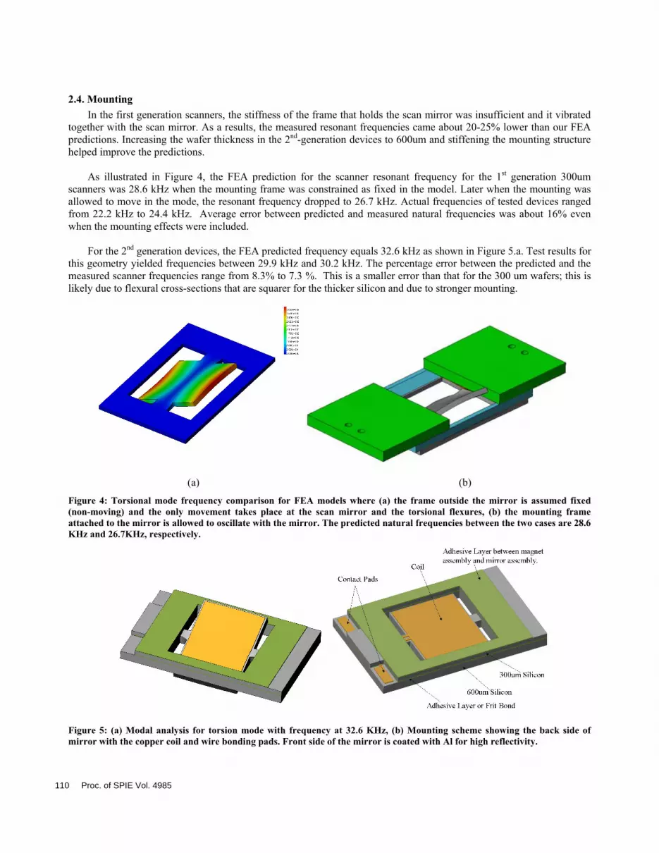
2.4. Mounting In the first generation scanners, the stiffness of the frame that holds the scan mirror was insufficient and it vibrated
together with the scan mirror. As a results, the measured resonant frequencies came about 20-25% lower than our FEA predictions. Increasing the wafer thickness in the 2nd-generation devices to 600um and stiffening the mounting structure helped improve the predictions.
As illustrated in Figure 4, the FEA prediction for the scanner resonant frequency for the 1st generation 300um scanners was 28.6 kHz when the mounting frame was constrained as fixed in the model. Later when the mounting was allowed to move in the mode, the resonant frequency dropped to 26.7 kHz. Actual frequencies of tested devices ranged from 22.2 kHz to 24.4 kHz. Average error between predicted and measured natural frequencies was about 16% even when the mounting effects were included.
For the 2nd generation devices, the FEA predicted frequency equals 32.6 kHz as shown in Figure 5.a. Test results for this geometry yielded frequencies between 29.9 kHz and 30.2 kHz. The percentage error between the predicted and the measured scanner frequencies range from 8.3% to 7.3 %. This is a smaller error than that for the 300 um wafers; this is likely due to flexural cross-sections that are squarer for the thicker silicon and due to stronger mounting.
(a) (b)
Figure 4: Torsional mode frequency comparison for FEA models where (a) the frame outside the mirror is assumed fixed (non-moving) and the only movement takes place at the scan mirror and the torsional flexures, (b) the mounting frame attached to the mirror is allowed to oscillate with the mirror. The predicted natural frequencies between the two cases are 28.6 KHz and 26.7KHz, respectively.
Figure 5: (a) Modal analysis for torsion mode with frequency at 32.6 KHz, (b) Mounting scheme showing the back side of mirror with the copper coil and wire bonding pads. Front side of the mirror is coated with Al for high reflectivity.
110 Proc. of SPIE Vol. 4985

3. ELECTROMAGNETIC ACTUATOR
3.1. Design A moving coil electromagnetic actuator uses Lorentz force to move the mirror. Another paper in this proceeding discusses electromagnetic actuators for MEMS scanners in more detail6. The coil is deposited at the backside of the surface as described in Section 3.2. First generation scanners, shown in Figure 6.b, used a single coil that covers the entire back surface of the mirror and two large magnets on either side of the scanner. Second generation scanners employed novel two-coil architecture, illustrated in Figure 6.a, and novel magnet design that is placed underneath the coil, illustrated in Figure 6.a and Figure 7. The new magnet design takes advantage of the fringing fields and the magnets are substantially smaller than the 1st generation magnets. The 2nd generation electromagnetic architecture has significantly smaller volume and larger torque compared to the 1st generation scanners. The assembly of the magnets requires a special fixture.
Figure 6: Side by side comparison of the (a) 2nd generation design: two-coil and small bottom magnet design and (b) 1st generation design: one-coil and two side magnets.
3.2. Coil plating First generation RCS used gold coils that were about 6um thick. As given in the table below, gold has higher
resistivity, and is heavier than copper. Further, the CTE mismatch between gold and aluminum is worse than that of copper and aluminum, resulting in larger thermal deformation of the mirror. The resistance of the coil is inversely proportional to the coil thickness, thus power dissipated at the coil can be reduced if the thickness of the coil can be increased. Coils also add weight to the structure. We calculated the optimum coil thickness to be in the range 10-20µm for different designs. In our 2nd generation scanners we developed a thick copper plating process to reduce power requirements.
CTE (m/m/°C) Density (kg/m3) Resistivity (ohm.m)
Gold 14.0x10⁻⁶ 19,300 2.04x10⁻⁸ Copper 16.9x10⁻⁶ 8,960 1.67x10⁻⁸
Aluminum 24.0x10⁻⁶ Silicon 2.6x10⁻⁶ 2,330
Proc. of SPIE Vol. 4985 111

Copper plating is a well-established process and has been used extensively outside of the MEMS arena for years.
The chemistry is well understood and the formulations used in these traditional bulk-plating methods are readily applicable for use in the formation of MEMS devices. However, the plating methods commonly used, even in somewhat closely related industries such as printed circuit boards, do not generally provide the precise control and uniformity that may be required for precision MEMS designs. To bring up a useful copper process for this application, the primary focus was on issues relating to uniformity of plating across four inch wafers: wafer fixturing, bath/flow control, and electrical field optimization.
Figure 7 (a) Bottom view of the two-coil design, (b) magnetic field lines for the novel magnet design. B-field along the direction perperndicular to the coil current is 0.5-0.7 Tesla range.
A standard sulfamate copper solution was selected. The anode is a 99.99% pure copper rod custom formed to
minimize interaction with the fluid flow in the bath. The bath and wafer fixture was designed to provide uniform even flow with minimal interference to the flow around the wafer. The wafer jig (holder) was custom designed and built to provide even 4-point contact to the wafer with little to no loss of current at the contact points. The wafer is firmly held in place in a vertical orientation to allow for even extreme flow or agitation as needed. Baffling in the bath was designed to be modular to allow for easy experimentation with flow rates at the wafer surface.
Copper plating solutions have high efficiency and throwing power. This allows for easy coverage of odd features and deep cavities, but also has the negative effect of enhancing non-uniformities in the electrical field. When plating copper onto a four-inch wafer, the outer edges of the wafer tend to plate thicker than the center. This can be attributed to decrease in the potential as from the edges to the center of the wafer. For many other metal systems, this can be offset by introducing “thief” structures to take advantage of these lower efficiency solutions and create a current “shadow” to balance out the effect. For copper, the near 100% efficiency makes it much more difficult to take advantage of this shadow effect.
In this effort, a good deal of time was optimizing a thief structure for maximum uniformity across the wafer. Everything from a simple ring to an elaborate basket structure was used and the edge to center uniformity measured. The ratio of the current split between the wafer and the thief was also controlled, as were the total current and duty cycle. Some improvement was noted with the more elaborate configurations, but was not significant enough to overcome the added difficulty associated with using them. In the end a simple ring was chosen to give the most improvement with the least complication. Even so, the edge to center non-uniformity was not completely eliminated.
112 Proc. of SPIE Vol. 4985

The standard resist coat was modified to be approximately 30% greater than the target metal thickness. Based on the plating rates of the earlier work and rough estimates of the relative area of the final mask to the test mask, the plating time was adjusted to give the desired result. Lastly, to reduce any remaining nonuniformity that could be attributed to flow variations in the tank, the wafers were periodically rotated in the jig to normalize the inconsistencies. In the end, the final wafers were plated with 10 microns of copper with better than ±0.75 micron uniformity, which was good enough uniformity for this project.
4. SUMMARY REMARKS AND SYSTEM RESULTS A thick copper plating process, 600um thick DRIE process, novel 2-coil architecture, and novel compact magnet
design that utilized fringing magnetic fields were developed within the scope of the RCS project. The 2nd generation RCS with 10um thick dual copper coils and the new magnet design is integrated into an SXGA-resolution HMD system delivered to the US Army and the RCS project came to a successful completion.
Our initial target for power dissipation was to stay below 100mW. The system-integrated scanner has a resonant frequency of about 31 KHz, meets all the thermal, mirror flatness, scan-angle, and frequency requirements, and it dissipates only about 20mW of power. Figure 8 shows that the text readability is vastly improved by having a raster correction scanner in the system. Even 8pt text is easily readable even near the edges of the display screen. Figure 9 shows the improvement in the contrast modulation when the raster correction scanner was on for various line-on/line-off type images.
(a) (b)
Figure 8: HMD system with SXGA resolution displaying Helvetica 8 pt font at 70% of way from the center of the screen to the left edge of the screen. (a) Raster pinch correction scanner turned off, (b) RPC scanner turned on.
ACKNOWLEDGMENTS
We thank US Army for the financial support for this research. We are grateful to Billy Johnson, Mircea Bayer, and Karlton Powell, and Mark Holton for their support and invaluable contributions at different parts of this project.
Proc. of SPIE Vol. 4985 113

AIHS - 69 Left
0.0
10.0
20.0
30.0
40.0
50.0
60.0
70.0
80.0
90.0
100.0
0.00 2.00 4.00 6.00 8.00 10.00 12.00 14.00 16.00 18.00 20.00
Frequency (cyc/deg)
Mic
hels
on C
ontra
st (%
)
Pinch Correction ON Pinch Correction OFF
Figure 9: Michelson contrast at 70% of the way from center to the edge of the screen. Pinch scanner improves the contrast modulation for high-frequency features.
REFERENCES
1. H. Urey, D. Wine, and T. Osborn, "Optical performance requirements for MEMS-scanner based microdisplays," Conf. on MOEMS and Miniaturized Systems, SPIE Vol. 4178, pp. 176-185, Santa Clara, California (2000)
2. D. W. Wine, M. P. Helsel, L. Jenkins, H. Urey, T. D. Osborn, “Performance of a Biaxial MEMS-Based Scanner for Microdisplay Applications,” Conf. on MOEMS and Miniaturized Systems, SPIE Vol. 4178, pp. 186-196, Santa Clara, California (2000)
3. H. Urey, N. Nestorovic, B. Ng, A. Gross, “Optics designs and system MTF for laser scanning displays,” Helmet and Head-Mounted Display IV, Proc. SPIE Vol. 3689, pp. 238-248, Orlando, Florida, March (1999)
4. US Patent 6,140,979, “Scanned display with pinch timing, and distortion correction” 5. H. Urey, F. DeWitt, K. Powell, and M. Bayer, "High-Frequency Raster Pinch Correction Scanner for Retinal Scanning Displays,"
Conf. on MOEMS and Miniaturized Systems, SPIE Vol. 4561, San Francisco, California October (2001) 6. J. Yan, S. Luanava, F. DeWitt, V. Casasanta, H. Urey, “Magnetic Actuation for MEMS Scanners for Retinal Scanning Displays,”
MOEMS Display and Imaging Systems, Proc. SPIE, Vol. 4985, San Jose, CA, January (2003)
114 Proc. of SPIE Vol. 4985