transistors, matched dual, pnpbased on type
TRANSCRIPT
TRANSISTORS, MATCHED DUAL, PNP
BASED ON TYPE 2N3810
ESCC Detail Specification No. 5207/005
Issue 7 May 2019
Document Custodian: European Space Agency – see https://escies.org
Page 1 of 20
ESCC Detail Specification
No. 5207/005
PAGE 2
ISSUE 7
LEGAL DISCLAIMER AND COPYRIGHT
European Space Agency, Copyright © 2019. All rights reserved.
The European Space Agency disclaims any liability or responsibility, to any person or entity, with respect to any loss or damage caused, or alleged to be caused, directly or indirectly by the use and application of this ESCC publication.
This publication, without the prior permission of the European Space Agency and provided that it is not used for a commercial purpose, may be:
− copied in whole, in any medium, without alteration or modification. − copied in part, in any medium, provided that the ESCC document identification, comprising the
ESCC symbol, document number and document issue, is removed.
ESCC Detail Specification
No. 5207/005
PAGE 3
ISSUE 7
DOCUMENTATION CHANGE NOTICE
(Refer to https://escies.org for ESCC DCR content)
DCR No. CHANGE DESCRIPTION
1185, 1220 Specification upissued to incorporate changes per DCR.
ESCC Detail Specification
No. 5207/005
PAGE 4
ISSUE 7
TABLE OF CONTENTS
1 GENERAL 5
1.1 SCOPE 5
1.2 APPLICABLE DOCUMENTS 5
1.3 TERMS, DEFINITIONS, ABBREVIATIONS, SYMBOLS AND UNITS 5
1.4 THE ESCC COMPONENT NUMBER AND COMPONENT TYPE VARIANTS 5
1.4.1 The ESCC Component Number 5
1.4.2 Component Type Variants 6
1.5 MAXIMUM RATINGS 7
1.6 PHYSICAL DIMENSIONS AND TERMINAL IDENTIFICATION 8
1.6.1 Metal Can Package (TO-78) - 6 lead 8
1.6.2 Chip Carrier Package (CCP) - 6 terminal 9
1.6.3 Flat package (FP) – 8 Pin 10
1.6.4 Die (Variant 12) 11
1.7 FUNCTIONAL DIAGRAM 12
1.8 MATERIALS AND FINISHES 12
1.8.1 Materials and Finishes of Packaged Components 12
1.8.2 Materials and Finishes of Die Components 12
2 REQUIREMENTS 12
2.1 GENERAL 12
2.1.1 Deviations from the Generic Specification 13
2.1.1.1 Deviation from Production Control – Chart F2 13
2.2 MARKING 13
2.3 TERMINAL STRENGTH 13
2.4 ELECTRICAL MEASUREMENTS AT ROOM, HIGH AND LOW TEMPERATURES 13
2.4.1 Room Temperature Electrical Measurements 13
2.4.2 High and Low Temperatures Electrical Measurements 16
2.5 PARAMETER DRIFT VALUES 16
2.6 INTERMEDIATE AND END-POINT ELECTRICAL MEASUREMENTS 17
2.7 HIGH TEMPERATURE REVERSE BIAS BURN-IN CONDITIONS 17
2.8 POWER BURN-IN CONDITIONS 17
2.9 OPERATING LIFE CONDITIONS 18
2.10 TOTAL DOSE RADIATION TESTING 18
2.10.1 Bias Conditions and Total Dose Level for Total dose Radiation Testing 18
2.10.2 Electrical Measurements for Radiation Testing 19
APPENDIX ‘A’ 20
ESCC Detail Specification
No. 5207/005
PAGE 5
ISSUE 7
1 GENERAL
1.1 SCOPE This specification details the ratings, physical and electrical characteristics and test and inspection data for the component type variants and/or the range of components specified below. It supplements the requirements of, and shall be read in conjunction with, the ESCC Generic Specification listed under Applicable Documents.
1.2 APPLICABLE DOCUMENTS The following documents form part of this specification and shall be read in conjunction with it:
(a) ESCC Generic Specification No. 5000 (b) MIL-STD-750, Test Methods and Procedures for Semiconductor Devices
1.3 TERMS, DEFINITIONS, ABBREVIATIONS, SYMBOLS AND UNITS For the purpose of this specification, the terms, definitions, abbreviations, symbols and units specified in ESCC Basic Specification No. 21300 shall apply.
1.4 THE ESCC COMPONENT NUMBER AND COMPONENT TYPE VARIANTS
1.4.1 The ESCC Component Number The ESCC Component Number shall be constituted as follows:
Example: 520700501R
• Detail Specification Reference: 5207005 • Component Type Variant Number: 01 (as required) • Total Dose Radiation Level Letter: R (as required)
ESCC Detail Specification
No. 5207/005
PAGE 6
ISSUE 7
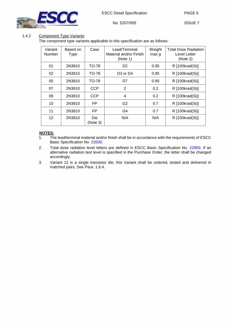
1.4.2 Component Type Variants
The component type variants applicable to this specification are as follows:
Variant Number
Based on Type
Case Lead/Terminal Material and/or Finish
(Note 1)
Weight max g
Total Dose Radiation Level Letter
(Note 2)
01 2N3810 TO-78 D2 0.95 R [100krad(Si)]
02 2N3810 TO-78 D3 or D4 0.95 R [100krad(Si)]
05 2N3810 TO-78 D7 0.95 R [100krad(Si)]
07 2N3810 CCP 2 0.2 R [100krad(Si)]
09 2N3810 CCP 4 0.2 R [100krad(Si)]
10 2N3810 FP G2 0.7 R [100krad(Si)]
11 2N3810 FP G4 0.7 R [100krad(Si)]
12 2N3810 Die (Note 3)
N/A N/A R [100krad(Si)]
NOTES: 1. The lead/terminal material and/or finish shall be in accordance with the requirements of ESCC
Basic Specification No. 23500. 2. Total dose radiation level letters are defined in ESCC Basic Specification No. 22900. If an
alternative radiation test level is specified in the Purchase Order, the letter shall be changed accordingly.
3. Variant 12 is a single transistor die; this Variant shall be ordered, tested and delivered in matched pairs. See Para. 1.6.4.
ESCC Detail Specification
No. 5207/005
PAGE 7
ISSUE 7
1.5 MAXIMUM RATINGS
The maximum ratings shall not be exceeded at any time during use or storage.
Maximum ratings shall only be exceeded during testing to the extent specified in this specification and when stipulated in Test Methods and Procedures of the ESCC Generic Specification.
Characteristics Symbols Maximum Ratings Unit Remarks
Collector-Base Voltage VCBO -60 V Over entire operating
temperature range
Collector-Emitter Voltage VCEO -60 V
Emitter-Base Voltage VEBO -5 V
Collector Current IC 50 mA Continuous
Power Dissipation (One Section) For TO-78, CCP and FP For TO-78
PtotO1 PtotO2
0.5 0.5
W W
At Tamb ≤ +25°C At Tcase ≤ +25°C
Power Dissipation (Both Sections) For TO-78, CCP and FP For TO-78
PtotB1 PtotB2
0.6 0.6
W W
At Tamb ≤ +25°C At Tcase ≤ +25°C
Thermal Resistance, Junction-to-Ambient
Rth(j-a) 350
291.7
°C/W
For one section
For both sections
Thermal Resistance, Junction-to-Case
Rth(j-c) 350
291.7
°C/W
For one section
For both sections Note 1
Operating Temperature Range Top -55 to +200 °C Note 2
Storage Temperature Range Tstg -65 to +200 °C Note 2
Soldering Temperature For FP For TO-78 For CCP
Tsol +265 +260 +245
°C Note 3 Note 3 Note 4
NOTES: 1. Thermal Resistance, Junction-to-Case only applies to TO-78 packaged Variants. 2. For Variants with tin-lead plating or hot solder dip lead finish all testing, and any handling,
performed at Tamb > +125°C shall be carried out in a 100% inert atmosphere. 3. Duration 10 seconds maximum at a distance of not less than 1.5mm from the device body and
the same lead shall not be resoldered until 3 minutes have elapsed. 4. Duration 5 seconds maximum and the same terminal shall not be resoldered until 3 minutes
have elapsed.
ESCC Detail Specification
No. 5207/005
PAGE 8
ISSUE 7
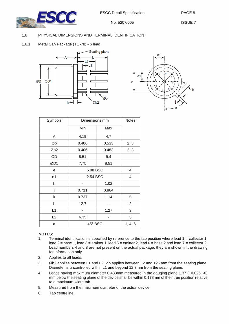
1.6 PHYSICAL DIMENSIONS AND TERMINAL IDENTIFICATION
1.6.1 Metal Can Package (TO-78) - 6 lead
Symbols Dimensions mm Notes
Min Max
A 4.19 4.7
Øb 0.406 0.533 2, 3
Øb2 0.406 0.483 2, 3
ØD 8.51 9.4
ØD1 7.75 8.51
e 5.08 BSC 4
e1 2.54 BSC 4
h - 1.02
j 0.711 0.864
k 0.737 1.14 5
L 12.7 - 2
L1 - 1.27 3
L2 6.35 - 3
α 45° BSC 1, 4, 6
NOTES: 1. Terminal identification is specified by reference to the tab position where lead 1 = collector 1,
lead 2 = base 1, lead 3 = emitter 1, lead 5 = emitter 2, lead 6 = base 2 and lead 7 = collector 2. Lead numbers 4 and 8 are not present on the actual package; they are shown in the drawing for information only.
2. Applies to all leads. 3. Øb2 applies between L1 and L2. Øb applies between L2 and 12.7mm from the seating plane.
Diameter is uncontrolled within L1 and beyond 12.7mm from the seating plane. 4. Leads having maximum diameter 0.483mm measured in the gauging plane 1.37 (+0.025, -0)
mm below the seating plane of the device shall be within 0.178mm of their true position relative to a maximum-width-tab.
5. Measured from the maximum diameter of the actual device. 6. Tab centreline.
ESCC Detail Specification
No. 5207/005
PAGE 9
ISSUE 7
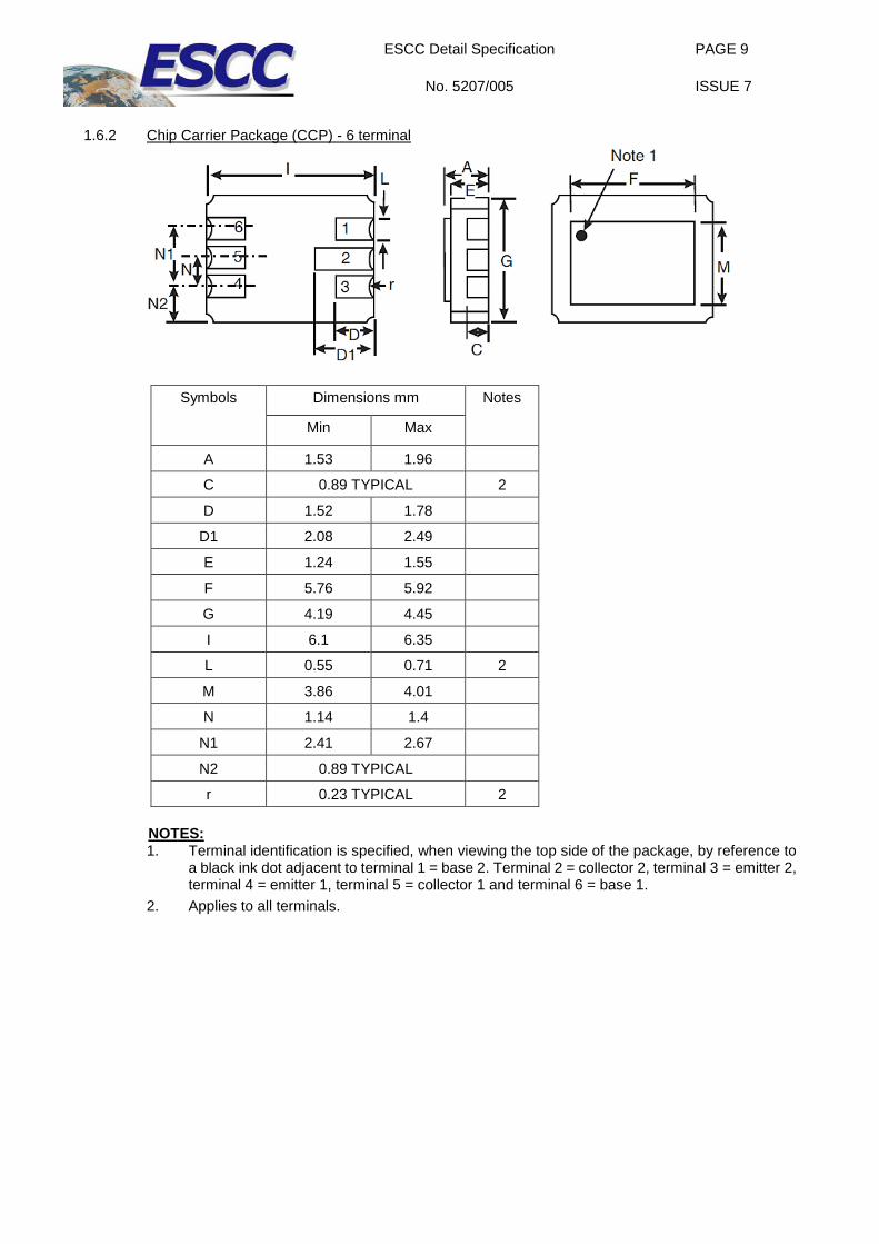
1.6.2 Chip Carrier Package (CCP) - 6 terminal
Symbols Dimensions mm Notes
Min Max
A 1.53 1.96
C 0.89 TYPICAL 2
D 1.52 1.78
D1 2.08 2.49
E 1.24 1.55
F 5.76 5.92
G 4.19 4.45
I 6.1 6.35
L 0.55 0.71 2
M 3.86 4.01
N 1.14 1.4
N1 2.41 2.67
N2 0.89 TYPICAL
r 0.23 TYPICAL 2
NOTES: 1. Terminal identification is specified, when viewing the top side of the package, by reference to
a black ink dot adjacent to terminal 1 = base 2. Terminal 2 = collector 2, terminal 3 = emitter 2, terminal 4 = emitter 1, terminal 5 = collector 1 and terminal 6 = base 1.
2. Applies to all terminals.
ESCC Detail Specification
No. 5207/005
PAGE 10
ISSUE 7
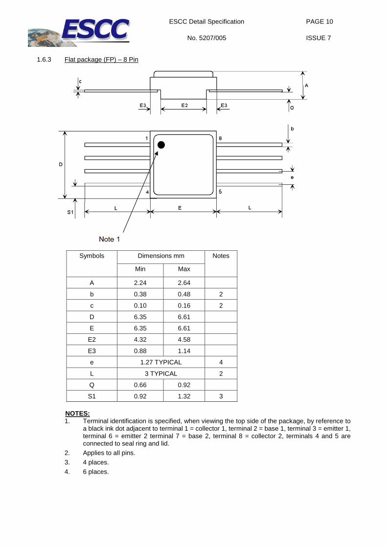
1.6.3 Flat package (FP) – 8 Pin
Symbols Dimensions mm Notes
Min Max
A 2.24 2.64
b 0.38 0.48 2
c 0.10 0.16 2
D 6.35 6.61
E 6.35 6.61
E2 4.32 4.58
E3 0.88 1.14
e 1.27 TYPICAL 4
L 3 TYPICAL 2
Q 0.66 0.92
S1 0.92 1.32 3
NOTES: 1. Terminal identification is specified, when viewing the top side of the package, by reference to
a black ink dot adjacent to terminal 1 = collector 1, terminal 2 = base 1, terminal 3 = emitter 1, terminal 6 = emitter 2 terminal 7 = base 2, terminal 8 = collector 2, terminals 4 and 5 are connected to seal ring and lid.
2. Applies to all pins. 3. 4 places. 4. 6 places.
ESCC Detail Specification
No. 5207/005
PAGE 11
ISSUE 7
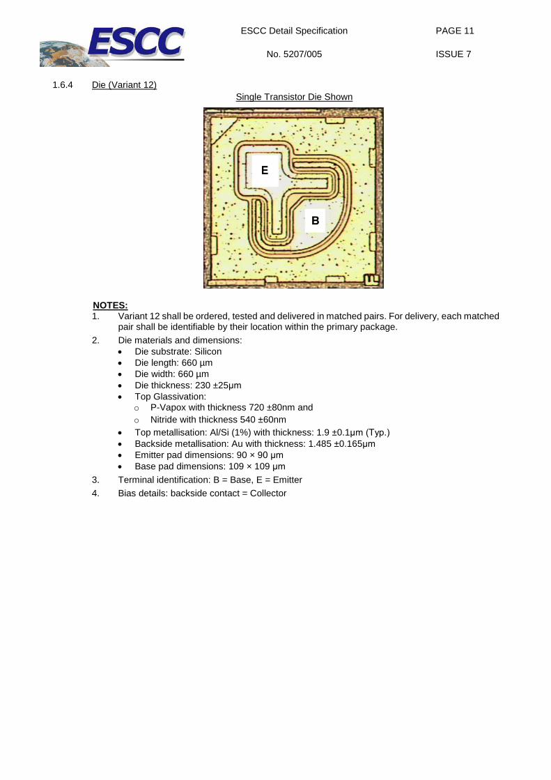
1.6.4 Die (Variant 12)
Single Transistor Die Shown
NOTES: 1. Variant 12 shall be ordered, tested and delivered in matched pairs. For delivery, each matched
pair shall be identifiable by their location within the primary package. 2. Die materials and dimensions:
• Die substrate: Silicon • Die length: 660 µm • Die width: 660 µm • Die thickness: 230 ±25μm • Top Glassivation:
o P-Vapox with thickness 720 ±80nm and o Nitride with thickness 540 ±60nm
• Top metallisation: Al/Si (1%) with thickness: 1.9 ±0.1μm (Typ.) • Backside metallisation: Au with thickness: 1.485 ±0.165μm • Emitter pad dimensions: 90 × 90 μm • Base pad dimensions: 109 × 109 μm
3. Terminal identification: B = Base, E = Emitter 4. Bias details: backside contact = Collector
ESCC Detail Specification
No. 5207/005
PAGE 12
ISSUE 7
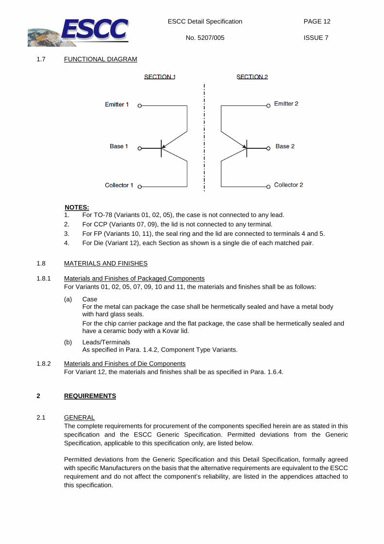
1.7 FUNCTIONAL DIAGRAM
NOTES: 1. For TO-78 (Variants 01, 02, 05), the case is not connected to any lead. 2. For CCP (Variants 07, 09), the lid is not connected to any terminal. 3. For FP (Variants 10, 11), the seal ring and the lid are connected to terminals 4 and 5. 4. For Die (Variant 12), each Section as shown is a single die of each matched pair.
1.8 MATERIALS AND FINISHES
1.8.1 Materials and Finishes of Packaged Components For Variants 01, 02, 05, 07, 09, 10 and 11, the materials and finishes shall be as follows:
(a) Case For the metal can package the case shall be hermetically sealed and have a metal body with hard glass seals. For the chip carrier package and the flat package, the case shall be hermetically sealed and have a ceramic body with a Kovar lid.
(b) Leads/Terminals As specified in Para. 1.4.2, Component Type Variants.
1.8.2 Materials and Finishes of Die Components For Variant 12, the materials and finishes shall be as specified in Para. 1.6.4.
2 REQUIREMENTS
2.1 GENERAL The complete requirements for procurement of the components specified herein are as stated in this specification and the ESCC Generic Specification. Permitted deviations from the Generic Specification, applicable to this specification only, are listed below.
Permitted deviations from the Generic Specification and this Detail Specification, formally agreed with specific Manufacturers on the basis that the alternative requirements are equivalent to the ESCC requirement and do not affect the component’s reliability, are listed in the appendices attached to this specification.
ESCC Detail Specification
No. 5207/005
PAGE 13
ISSUE 7
2.1.1 Deviations from the Generic Specification
2.1.1.1 Deviation from Production Control – Chart F2 Special in-process controls – assembly of the packaged test sublot: For Variant 12, each packaged test sublot sample shall contain two dice in a matched pair.
For procurement, the quantity of matched pairs of dice to be assembled, n, shall be selected at the Manufacturer’s discretion from one of the four specified sampling plans (a), (b), (c) or (d).
For qualification and maintenance of qualification, the quantity of matched pairs of dice to be assembled, n, shall be selected at the Manufacturer’s discretion from one of the specified sampling plans (c) or (d).
2.2 MARKING The marking shall be in accordance with the requirements of ESCC Basic Specification No. 21700 and as follows.
The information to be marked on the component or its primary package shall be:
(a) Terminal identification (see Para. 1.6; applies to CCP and FP packages only). (b) The ESCC qualified components symbol (for ESCC qualified components only). (c) The ESCC Component Number (see Para. 1.4.1). (d) Traceability information.
2.3 TERMINAL STRENGTH The test conditions for terminal strength, tested as specified in the ESCC Generic Specification, shall be as follows:
• For TO-78, Test Condition: E, lead fatigue. • For FP, Test Condition: E, lead fatigue. The applied weight shall be 3 ounces (85g), with three
bends of 15°.
2.4 ELECTRICAL MEASUREMENTS AT ROOM, HIGH AND LOW TEMPERATURES Electrical measurements shall be performed at room, high and low temperatures.
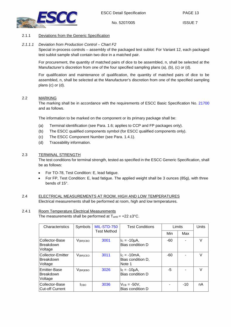
2.4.1 Room Temperature Electrical Measurements The measurements shall be performed at Tamb = +22 ±3°C.
Characteristics Symbols MIL-STD-750 Test Method
Test Conditions Limits Units
Min Max
Collector-Base Breakdown Voltage
V(BR)CBO 3001 IC = -10µA, Bias condition D
-60 - V
Collector-Emitter Breakdown Voltage
V(BR)CEO 3011 IC = -10mA, Bias condition D, Note 1
-60 - V
Emitter-Base Breakdown Voltage
V(BR)EBO 3026 IE = -10µA, Bias condition D
-5 - V
Collector-Base Cut-off Current
ICBO 3036 VCB = -50V, Bias condition D
- -10 nA
ESCC Detail Specification
No. 5207/005
PAGE 14
ISSUE 7
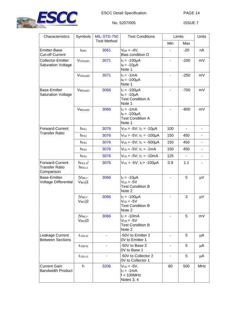
Characteristics Symbols MIL-STD-750
Test Method Test Conditions Limits Units
Min Max
Emitter-Base Cut-off Current
IEBO 3061 VEB = -4V, Bias condition D
- -20 nA
Collector-Emitter Saturation Voltage
VCE(sat)1 3071 IC = -100µA IB = -10µA Note 1
- -200 mV
VCE(sat)2 3071 IC = -1mA IB = -100µA Note 1
- -250 mV
Base-Emitter Saturation Voltage
VBE(sat)1 3066 IC = -100µA IB = -10µA Test Condition A Note 1
- -700 mV
VBE(sat)2 3066 IC = -1mA IB = -100µA Test Condition A Note 1
- -800 mV
Forward-Current Transfer Ratio
hFE1 3076 VCE = -5V; IC = -10µA 100 - -
hFE2 3076 VCE = -5V; IC = -100µA 150 450 -
hFE3 3076 VCE = -5V; IC = -500µA 150 450 -
hFE4 3076 VCE = -5V; IC = -1mA 150 450 -
hFE5 3076 VCE = -5V; IC = -10mA 125 - -
Forward-Current Transfer Ratio Comparison
hFE2-1/ hFE2-2
3076 VCE = -5V; IC= -100µA 0.9 1.1 -
Base-Emitter Voltage Differential
|VBE1-VBE2|1
3066 IC = -10µA VCE = -5V Test Condition B Note 2
- 5 µV
|VBE1-VBE2|2
3066 IC = -100µA VCE = -5V Test Condition B Note 2
- 3 µV
|VBE1-VBE2|3
3066 IC = -10mA VCE = -5V Test Condition B Note 2
- 5 mV
Leakage Current Between Sections
ILS(e-e) - -50V to Emitter 2 0V to Emitter 1
- 5 µA
ILS(b-b) - -50V to Base 2 0V to Base 1
- 5 µA
ILS(c-c) - -50V to Collector 2 0V to Collector 1
- 5 µA
Current Gain Bandwidth Product
fT 3206 VCE = -5V, IC = -1mA f = 100MHz Notes 3, 4
80 500 MHz
ESCC Detail Specification
No. 5207/005
PAGE 15
ISSUE 7
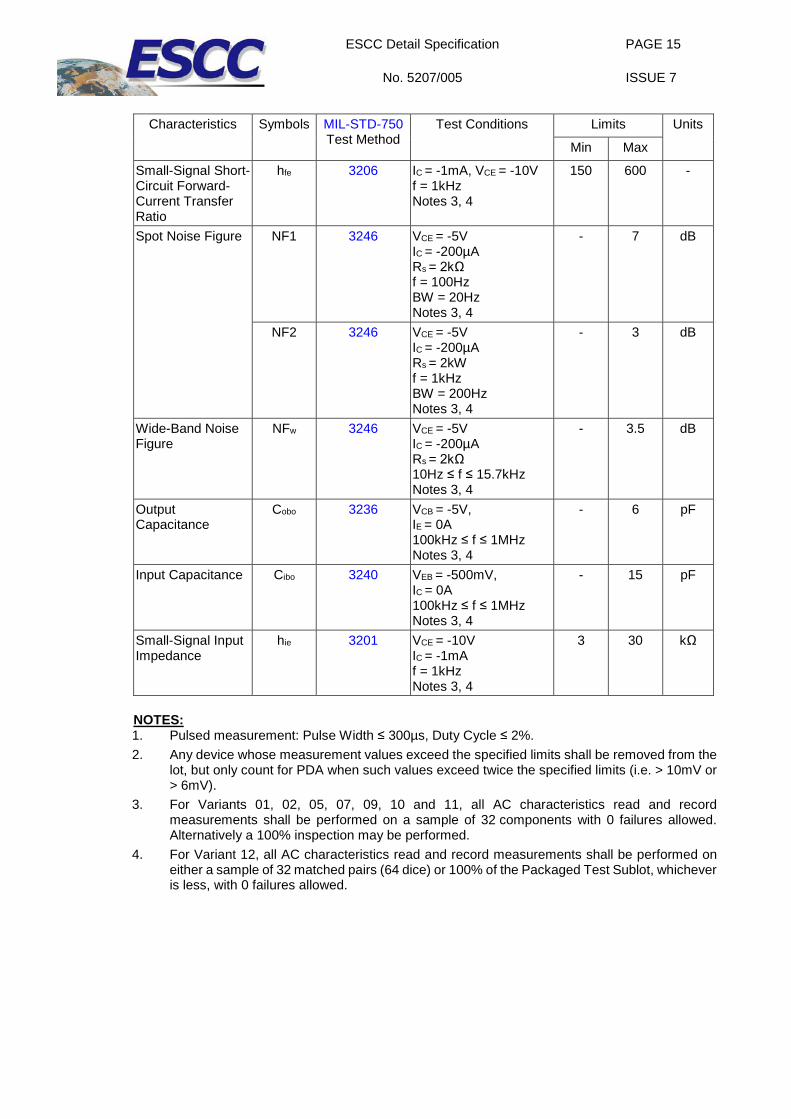
Characteristics Symbols MIL-STD-750
Test Method Test Conditions Limits Units
Min Max
Small-Signal Short-Circuit Forward-Current Transfer Ratio
hfe 3206 IC = -1mA, VCE = -10V f = 1kHz Notes 3, 4
150 600
-
Spot Noise Figure NF1 3246 VCE = -5V IC = -200µA Rs = 2kΩ f = 100Hz BW = 20Hz Notes 3, 4
-
7
dB
NF2 3246 VCE = -5V IC = -200µA Rs = 2kW f = 1kHz BW = 200Hz Notes 3, 4
- 3 dB
Wide-Band Noise Figure
NFw 3246 VCE = -5V IC = -200µA Rs = 2kΩ 10Hz ≤ f ≤ 15.7kHz Notes 3, 4
- 3.5 dB
Output Capacitance
Cobo 3236 VCB = -5V, IE = 0A 100kHz ≤ f ≤ 1MHz Notes 3, 4
- 6 pF
Input Capacitance Cibo 3240 VEB = -500mV, IC = 0A 100kHz ≤ f ≤ 1MHz Notes 3, 4
- 15 pF
Small-Signal Input Impedance
hie 3201 VCE = -10V IC = -1mA f = 1kHz Notes 3, 4
3 30 kΩ
NOTES: 1. Pulsed measurement: Pulse Width ≤ 300µs, Duty Cycle ≤ 2%. 2. Any device whose measurement values exceed the specified limits shall be removed from the
lot, but only count for PDA when such values exceed twice the specified limits (i.e. > 10mV or > 6mV).
3. For Variants 01, 02, 05, 07, 09, 10 and 11, all AC characteristics read and record measurements shall be performed on a sample of 32 components with 0 failures allowed. Alternatively a 100% inspection may be performed.
4. For Variant 12, all AC characteristics read and record measurements shall be performed on either a sample of 32 matched pairs (64 dice) or 100% of the Packaged Test Sublot, whichever is less, with 0 failures allowed.
ESCC Detail Specification
No. 5207/005
PAGE 16
ISSUE 7
2.4.2 High and Low Temperatures Electrical Measurements
Characteristics Symbols MIL-STD-750 Test Method
Test Conditions Note 1
Limits Units
Min Max
Collector-Base Cut-off Current
ICBO 3036 Tamb = +150 (+0 -5)°C VCB = -50V, Bias Condition D
- -10 µA
Forward-Current Transfer Ratio 2
hFE2 3076 Tamb = -55 (+5 -0)°C VCE = -5V IC = -100µA
60 - -
Forward-Current Transfer Ratio Comparison
hFE2-1/hFE2-2 3076 Tamb = -55 to +125°C VCE = -5V, IC = -100µA
0.85 1.18 -
Base-Emitter Voltage Differential Change
|Δ(VBE1-VBE2)ΔTamb|1
3066 Tamb = -55 (+5 -0)°C to +25 ±3°C VCE = -5V IC = -100µA Test condition B
-
800 µV
|Δ(VBE1-VBE2)ΔTamb|2
3066 Tamb = +25 ±3°C to +125 (+0 -5) °C VCE = -5V IC = -100µA Test condition B
- 1000 µV
NOTES: 1. Measurements shall be performed on a sample basis as specified in the Generic Specification.
2.5 PARAMETER DRIFT VALUES Unless otherwise specified, the measurements shall be performed at Tamb = +22 ±3°C.
The test methods and test conditions shall be as per the corresponding test defined in Para. 2.4.1, Room Temperature Electrical Measurements.
The drift values (Δ) shall not be exceeded for each characteristic specified. The corresponding absolute limit values for each characteristic shall not be exceeded.
Characteristics Symbols Limits Units
Drift Value
Δ
Absolute
Min Max
Collector-Base Cut-off Current ICBO ±2 or (1)
±100%
- -10 nA
Collector-Emitter Saturation Voltage 2 VCE(sat)2 ±15 or (1) ±10%
- -250 mV
Forward-Current Transfer Ratio 2 hFE2 ±15% 150 450 -
NOTES: 1. Whichever is the greater referred to the initial value.
ESCC Detail Specification
No. 5207/005
PAGE 17
ISSUE 7
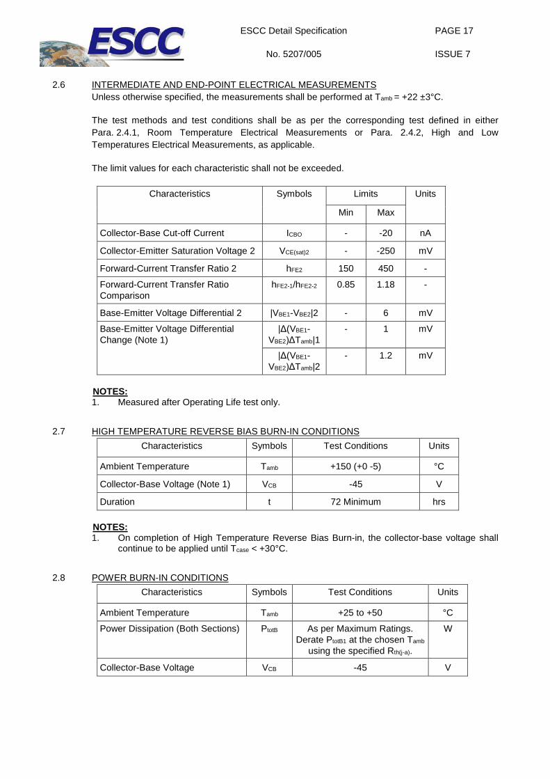
2.6 INTERMEDIATE AND END-POINT ELECTRICAL MEASUREMENTS
Unless otherwise specified, the measurements shall be performed at Tamb = +22 ±3°C.
The test methods and test conditions shall be as per the corresponding test defined in either Para. 2.4.1, Room Temperature Electrical Measurements or Para. 2.4.2, High and Low Temperatures Electrical Measurements, as applicable.
The limit values for each characteristic shall not be exceeded.
Characteristics Symbols Limits Units
Min Max
Collector-Base Cut-off Current ICBO - -20 nA
Collector-Emitter Saturation Voltage 2 VCE(sat)2 - -250 mV
Forward-Current Transfer Ratio 2 hFE2 150 450 -
Forward-Current Transfer Ratio Comparison
hFE2-1/hFE2-2 0.85 1.18 -
Base-Emitter Voltage Differential 2 |VBE1-VBE2|2 - 6 mV
Base-Emitter Voltage Differential Change (Note 1)
|Δ(VBE1-VBE2)ΔTamb|1
- 1 mV
|Δ(VBE1-VBE2)ΔTamb|2
- 1.2 mV
NOTES: 1. Measured after Operating Life test only.
2.7 HIGH TEMPERATURE REVERSE BIAS BURN-IN CONDITIONS Characteristics Symbols Test Conditions Units
Ambient Temperature Tamb +150 (+0 -5) °C
Collector-Base Voltage (Note 1) VCB -45 V
Duration t 72 Minimum hrs
NOTES: 1. On completion of High Temperature Reverse Bias Burn-in, the collector-base voltage shall
continue to be applied until Tcase < +30°C.
2.8 POWER BURN-IN CONDITIONS Characteristics Symbols Test Conditions Units
Ambient Temperature Tamb +25 to +50 °C
Power Dissipation (Both Sections) PtotB As per Maximum Ratings. Derate PtotB1 at the chosen Tamb
using the specified Rth(j-a).
W
Collector-Base Voltage VCB -45 V
ESCC Detail Specification
No. 5207/005
PAGE 18
ISSUE 7
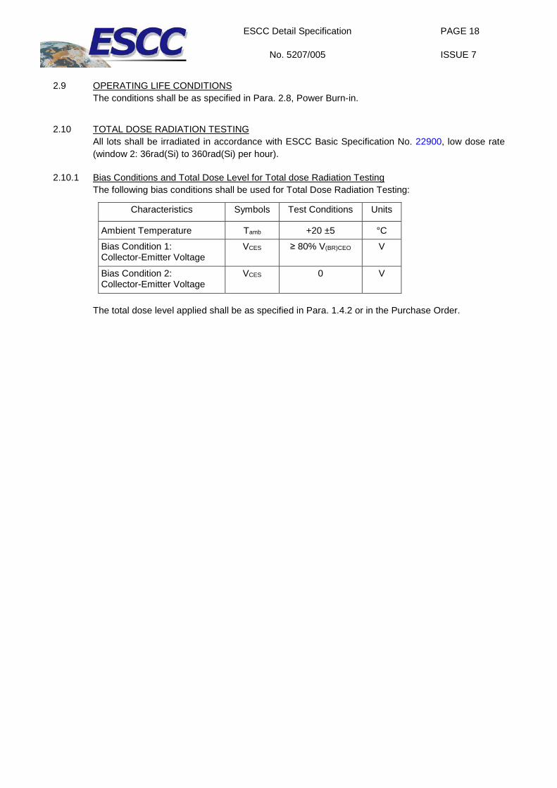
2.9 OPERATING LIFE CONDITIONS
The conditions shall be as specified in Para. 2.8, Power Burn-in.
2.10 TOTAL DOSE RADIATION TESTING All lots shall be irradiated in accordance with ESCC Basic Specification No. 22900, low dose rate (window 2: 36rad(Si) to 360rad(Si) per hour).
2.10.1 Bias Conditions and Total Dose Level for Total dose Radiation Testing The following bias conditions shall be used for Total Dose Radiation Testing:
Characteristics Symbols Test Conditions Units
Ambient Temperature Tamb +20 ±5 °C Bias Condition 1: Collector-Emitter Voltage
VCES ≥ 80% V(BR)CEO V
Bias Condition 2: Collector-Emitter Voltage
VCES 0 V
The total dose level applied shall be as specified in Para. 1.4.2 or in the Purchase Order.
ESCC Detail Specification
No. 5207/005
PAGE 19
ISSUE 7
2.10.2 Electrical Measurements for Radiation Testing
Prior to irradiation testing the devices shall have successfully met Room Temperature Electrical Measurements specified in Para. 2.4.1.
Unless otherwise stated the measurements shall be performed at Tamb = +22 ±3°C.
Unless otherwise specified the test methods and test conditions shall be as per the corresponding test defined in Para. 2.4.1, Room Temperature Electrical Measurements.
The parameters to be measured during and on completion of irradiation testing are shown below.
Characteristics Symbols MIL-STD-750 Test Method
Test Conditions Limits Units
Min Max
Collector-Base Breakdown Voltage
V(BR)CBO Para. 2.4.1 Para. 2.4.1 -60 - V
Collector-Emitter Breakdown Voltage
V(BR)CEO Para. 2.4.1 Para. 2.4.1 -60 - V
Emitter-Base Breakdown Voltage
V(BR)EBO Para. 2.4.1 Para. 2.4.1 -5 - V
Collector-Base Cut-off Current
ICBO Para. 2.4.1 Para. 2.4.1 - -10
nA
Emitter-Base Cut-off Current
IEBO Para. 2.4.1 Para. 2.4.1 - -20
nA
Collector-Emitter Saturation Voltage
VCE(sat)1 Para. 2.4.1 Para. 2.4.1 - -200 mV
VCE(sat)2 - -250 mV
Base-Emitter Saturation Voltage
VBE(sat)1 Para. 2.4.1 Para. 2.4.1 - -700 mV
VBE(sat)2 - -800 mV
Forward-Current Transfer Ratio (post irradiation gain calculation) (Note 1)
[hFE1] 3076 VCE = -5V, IC = -10µA [50] - -
[hFE2] VCE = -5V, IC = -100µA [75] 450 -
[hFE3] VCE = -5V, IC = -500µA [75] 450 -
[hFE4] VCE = -5V, IC = -1mA [75] 450 -
[hFE5] VCE = -5V, IC = -10mA [65] - -
NOTES: 1. The post-irradiation gain calculation of [hFE], made using hFE measurements from prior to and
on completion of irradiation testing and after each annealing step if any, shall be as specified in MIL-STD-750 Method 1019.
ESCC Detail Specification
No. 5207/005
PAGE 20
ISSUE 7
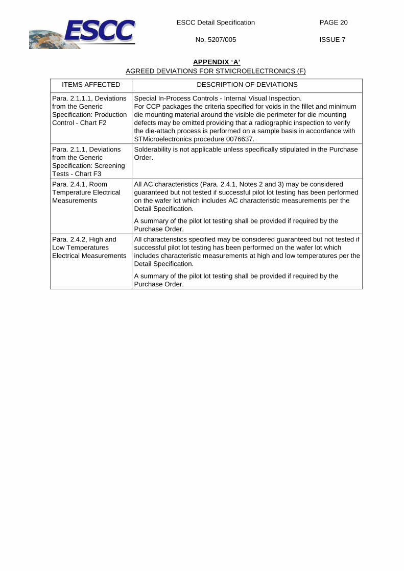
APPENDIX ‘A’
AGREED DEVIATIONS FOR STMICROELECTRONICS (F)
ITEMS AFFECTED DESCRIPTION OF DEVIATIONS
Para. 2.1.1.1, Deviations from the Generic Specification: Production Control - Chart F2
Special In-Process Controls - Internal Visual Inspection. For CCP packages the criteria specified for voids in the fillet and minimum die mounting material around the visible die perimeter for die mounting defects may be omitted providing that a radiographic inspection to verify the die-attach process is performed on a sample basis in accordance with STMicroelectronics procedure 0076637.
Para. 2.1.1, Deviations from the Generic Specification: Screening Tests - Chart F3
Solderability is not applicable unless specifically stipulated in the Purchase Order.
Para. 2.4.1, Room Temperature Electrical Measurements
All AC characteristics (Para. 2.4.1, Notes 2 and 3) may be considered guaranteed but not tested if successful pilot lot testing has been performed on the wafer lot which includes AC characteristic measurements per the Detail Specification.
A summary of the pilot lot testing shall be provided if required by the Purchase Order.
Para. 2.4.2, High and Low Temperatures Electrical Measurements
All characteristics specified may be considered guaranteed but not tested if successful pilot lot testing has been performed on the wafer lot which includes characteristic measurements at high and low temperatures per the Detail Specification.
A summary of the pilot lot testing shall be provided if required by the Purchase Order.