chapter 6: field-effect transistors
TRANSCRIPT
Chapter 6:Field-Effect Transistors
www.getmyuni.com
FETs vs BJTsFETs vs BJTs
Similarities:Similarities:
FETs vs. BJTsFETs vs. BJTs
Similarities: Similarities: • Amplifiers• Switching devices • Impedance matching circuits Impedance matching circuits
Differences:Differences:• FETs are voltage controlled devices BJTs are current controlled FETs are voltage controlled devices. BJTs are current controlled
devices.• FETs have a higher input impedance. BJTs have higher gains.• FETs are less sensitive to temperature variations and are more easily FETs are less sensitive to temperature variations and are more easily
integrated on ICs. • FETs are generally more static sensitive than BJTs.
Electronic Devices and Circuit Theory, 10/eRobert L. Boylestad and Louis Nashelsky
22
www.getmyuni.com
FET TypesFET TypesFET TypesFET Types
••JFET: JFET: Junction FET
••MOSFET: MOSFET: Metal–Oxide–Semiconductor FET
DD MOSFETMOSFET D l ti MOSFETDD--MOSFET:MOSFET: Depletion MOSFETEE--MOSFET:MOSFET: Enhancement MOSFET
Electronic Devices and Circuit Theory, 10/eRobert L. Boylestad and Louis Nashelsky
33
www.getmyuni.com

JFET ConstructionJFET ConstructionThere are two types of JFETs
••nn--channelchannel••pp--channelchannel
Th h l i id l dThe n-channel is more widely used.
There are three terminals:There are three terminals:
••Drain Drain (D) and SourceSource (S) are connected to the n-channel••GateGate (G) is connected to the p-type material••GateGate (G) is connected to the p-type material
Electronic Devices and Circuit Theory, 10/eRobert L. Boylestad and Louis Nashelsky
44
www.getmyuni.com
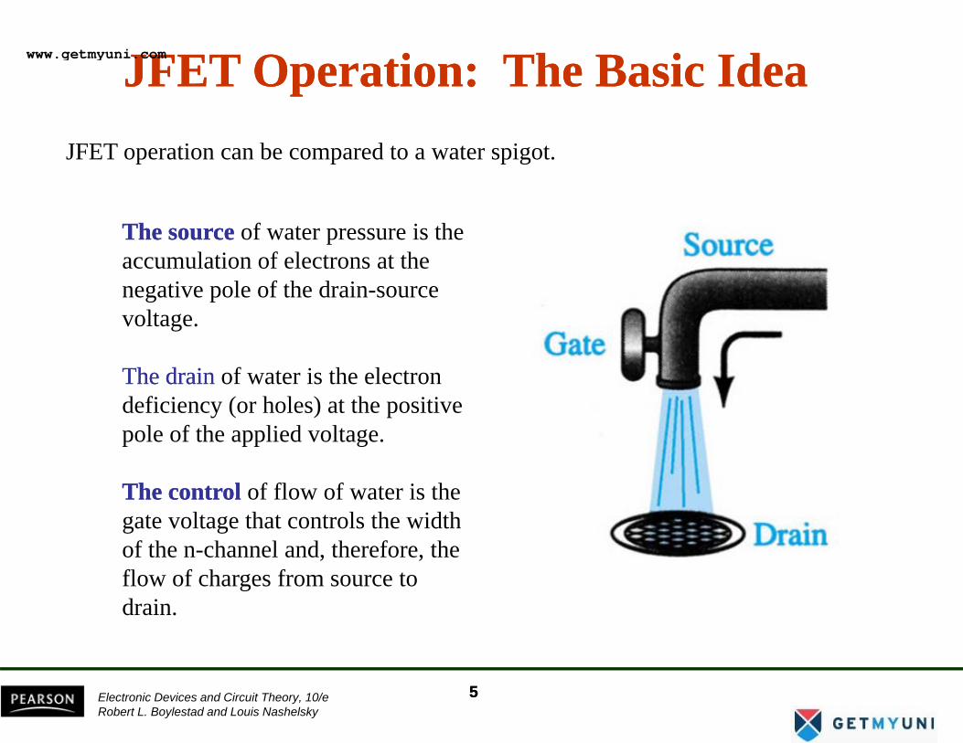
JFET Operation: The Basic IdeaJFET Operation: The Basic IdeaJFET operation can be compared to a water spigot.
The sourceThe source of water pressure is the accumulation of electrons at the
i l f h d inegative pole of the drain-source voltage.
Th d iTh d i f t i th l tThe drainThe drain of water is the electron deficiency (or holes) at the positive pole of the applied voltage.
The controlThe control of flow of water is the gate voltage that controls the width of the n-channel and therefore theof the n-channel and, therefore, the flow of charges from source to drain.
Electronic Devices and Circuit Theory, 10/eRobert L. Boylestad and Louis Nashelsky
55
www.getmyuni.com
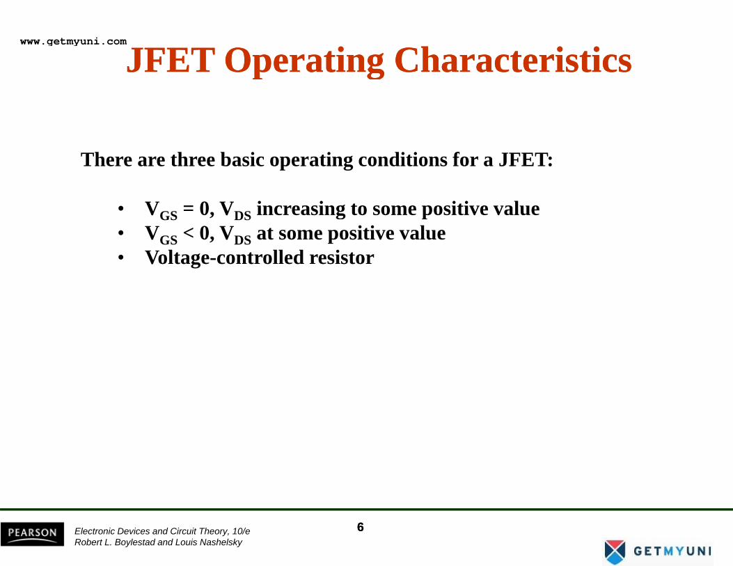
JFET Operating CharacteristicsJFET Operating Characteristicsp gp g
There are three basic operating conditions for a JFET:
• VGS = 0, VDS increasing to some positive valueVGS 0, VDS increasing to some positive value• VGS < 0, VDS at some positive value• Voltage-controlled resistor
Electronic Devices and Circuit Theory, 10/eRobert L. Boylestad and Louis Nashelsky
66
www.getmyuni.com
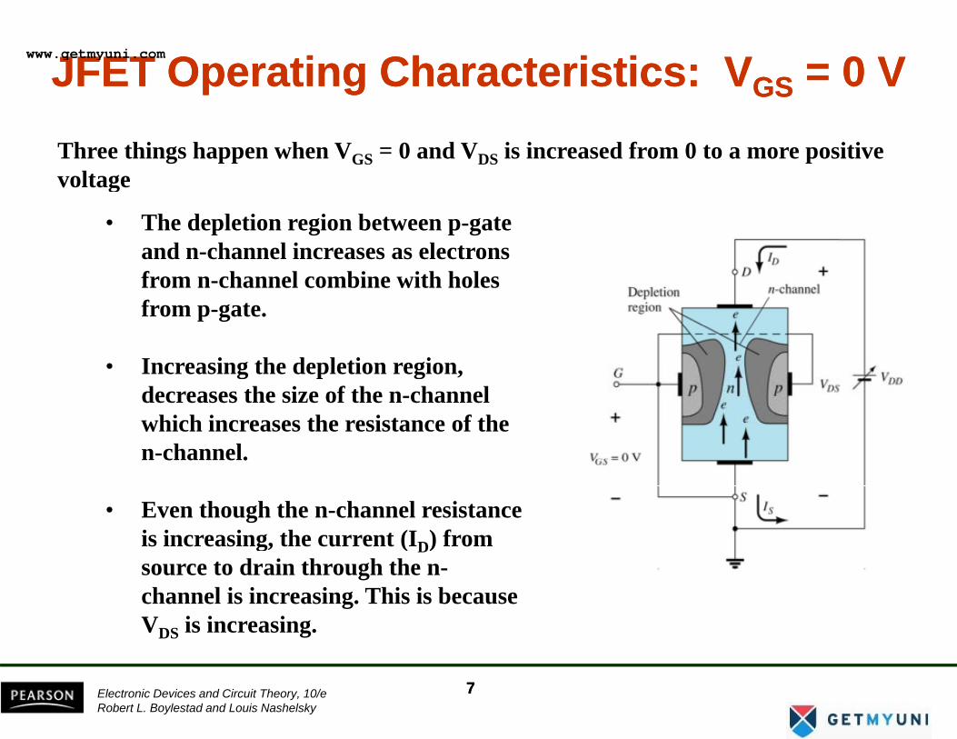
JFET Operating Characteristics: VJFET Operating Characteristics: VGSGS = 0 V= 0 VThree things happen when VGS = 0 and VDS is increased from 0 to a more positive voltage
• The depletion region between p-gate and n-channel increases as electrons from n channel combine with holes
g
from n-channel combine with holes from p-gate.
• Increasing the depletion regionIncreasing the depletion region, decreases the size of the n-channel which increases the resistance of the n-channel.n channel.
• Even though the n-channel resistance is increasing, the current (ID) from g, ( D)source to drain through the n-channel is increasing. This is because VDS is increasing.
Electronic Devices and Circuit Theory, 10/eRobert L. Boylestad and Louis Nashelsky
77
www.getmyuni.com
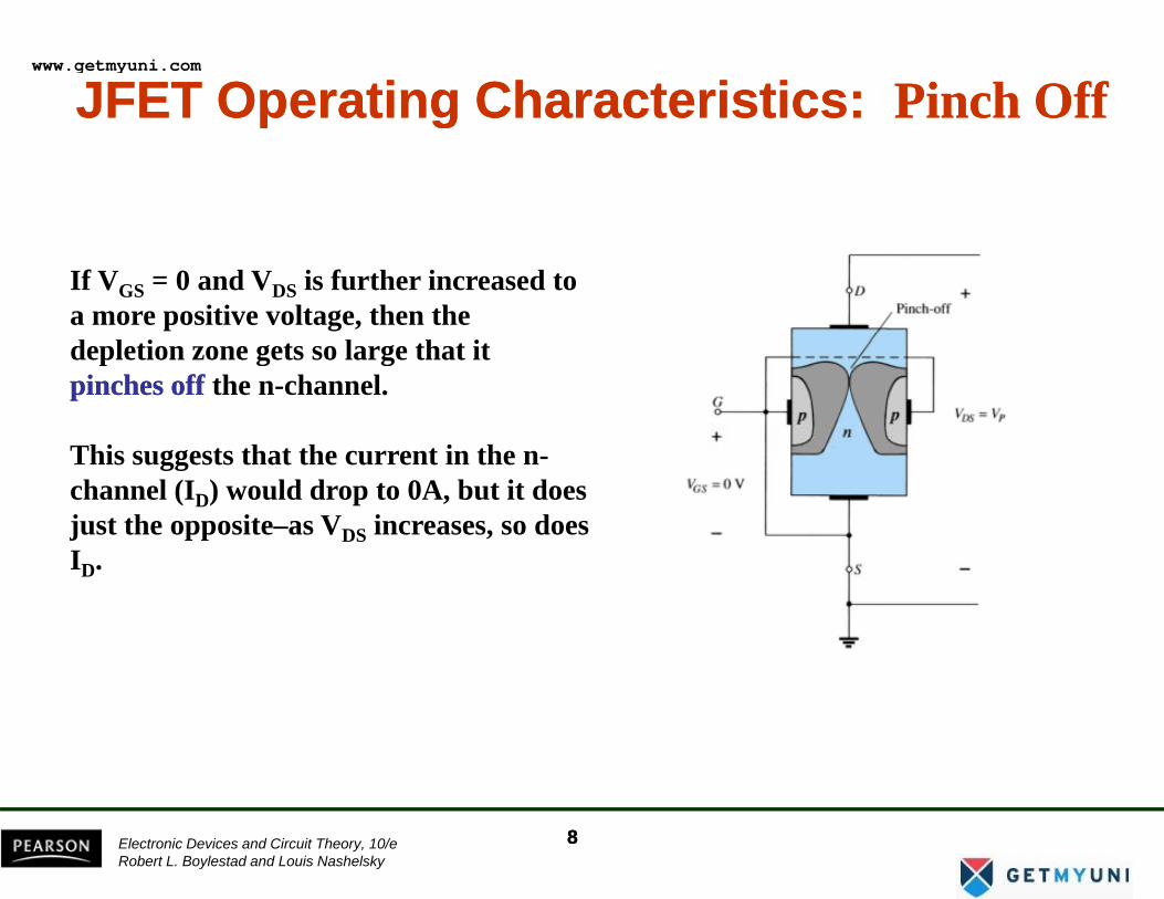
JFET Operating Characteristics: JFET Operating Characteristics: Pinch OffPinch Offp gp g
If VGS = 0 and VDS is further increased to a more positive voltage, then the d l i l h idepletion zone gets so large that it pinches offpinches off the n-channel.
Thi t th t th t i thThis suggests that the current in the n-channel (ID) would drop to 0A, but it does just the opposite–as VDS increases, so does IID.
Electronic Devices and Circuit Theory, 10/eRobert L. Boylestad and Louis Nashelsky
88
www.getmyuni.com
JFET Operating CharacteristicsJFET Operating Characteristics: Saturation: Saturationp gp g
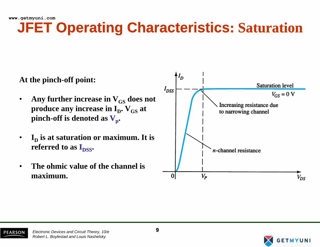
At the pinch-off point:
• Any further increase in VGS does not produce any increase in ID. VGS at pinch-off is denoted as VVpp.pp
• ID is at saturation or maximum. It is referred to as IIDSSDSS.
• The ohmic value of the channel is maximum.
Electronic Devices and Circuit Theory, 10/eRobert L. Boylestad and Louis Nashelsky
99
www.getmyuni.com
JFET Operating CharacteristicsJFET Operating Characteristicsp gp g
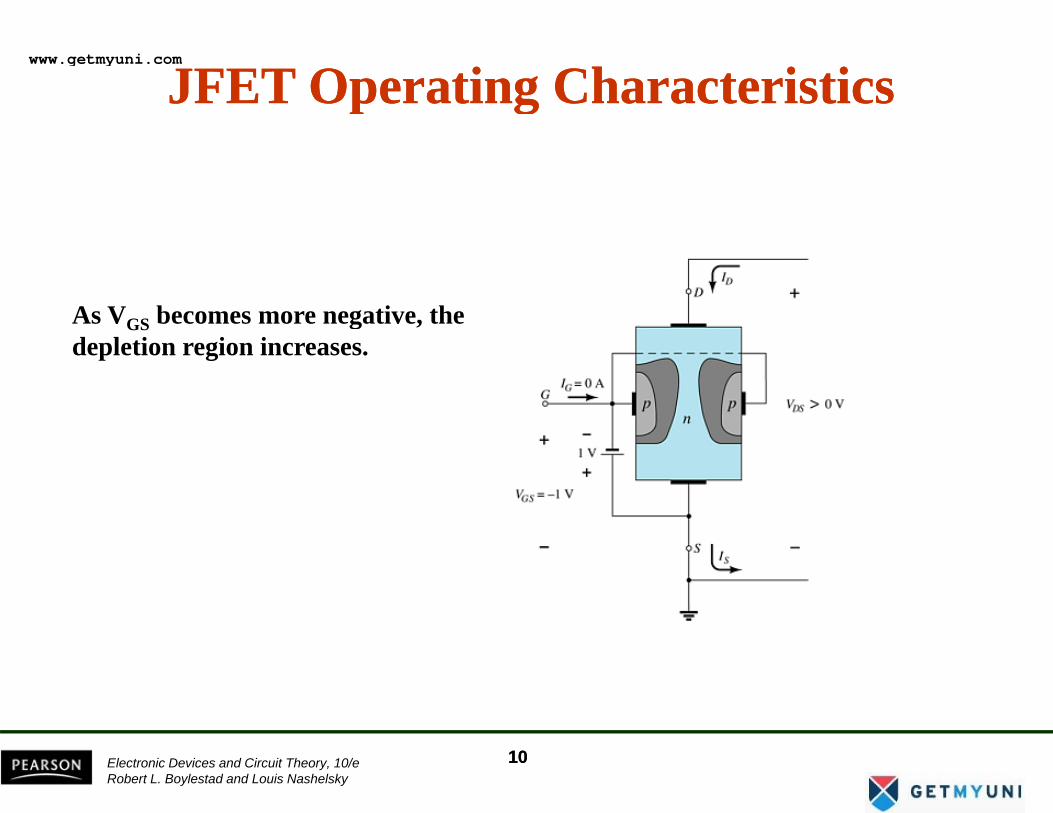
A V b ti thAs VGS becomes more negative, the depletion region increases.
Electronic Devices and Circuit Theory, 10/eRobert L. Boylestad and Louis Nashelsky
1010
www.getmyuni.com
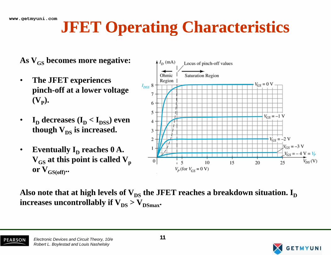
JFET Operating CharacteristicsJFET Operating Characteristics
As VGS becomes more negative:
p gp g
• The JFET experiences pinch-off at a lower voltage (VP).
• ID decreases (ID < IDSS) even th h V i i dthough VDS is increased.
• Eventually ID reaches 0 A. V at this point is called VVGS at this point is called Vpor VGS(off)..
A i f i iAlso note that at high levels of VDS the JFET reaches a breakdown situation. IDincreases uncontrollably if VDS > VDSmax.
Electronic Devices and Circuit Theory, 10/eRobert L. Boylestad and Louis Nashelsky
1111
www.getmyuni.com
JFET Operating Characteristics:JFET Operating Characteristics:p gp gVoltageVoltage--Controlled ResistorControlled Resistor
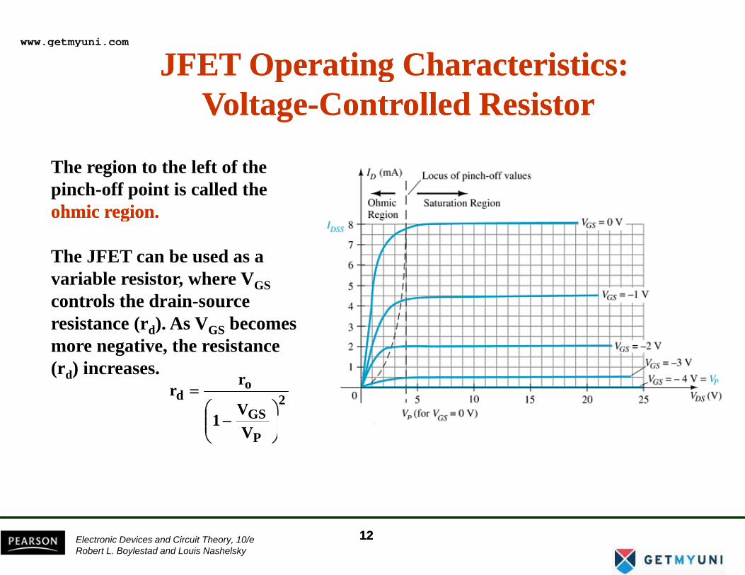
The region to the left of the pinch-off point is called the ohmic region.ohmic region.o c eg o .o c eg o .
The JFET can be used as a variable resistor, where VGS, GScontrols the drain-source resistance (rd). As VGS becomes more negative, the resistance
2GS
od
VV
1
rr
⎟⎟⎠
⎞⎜⎜⎝
⎛−
=(rd) increases.
PV ⎟⎠
⎜⎝
Electronic Devices and Circuit Theory, 10/eRobert L. Boylestad and Louis Nashelsky
1212
www.getmyuni.com
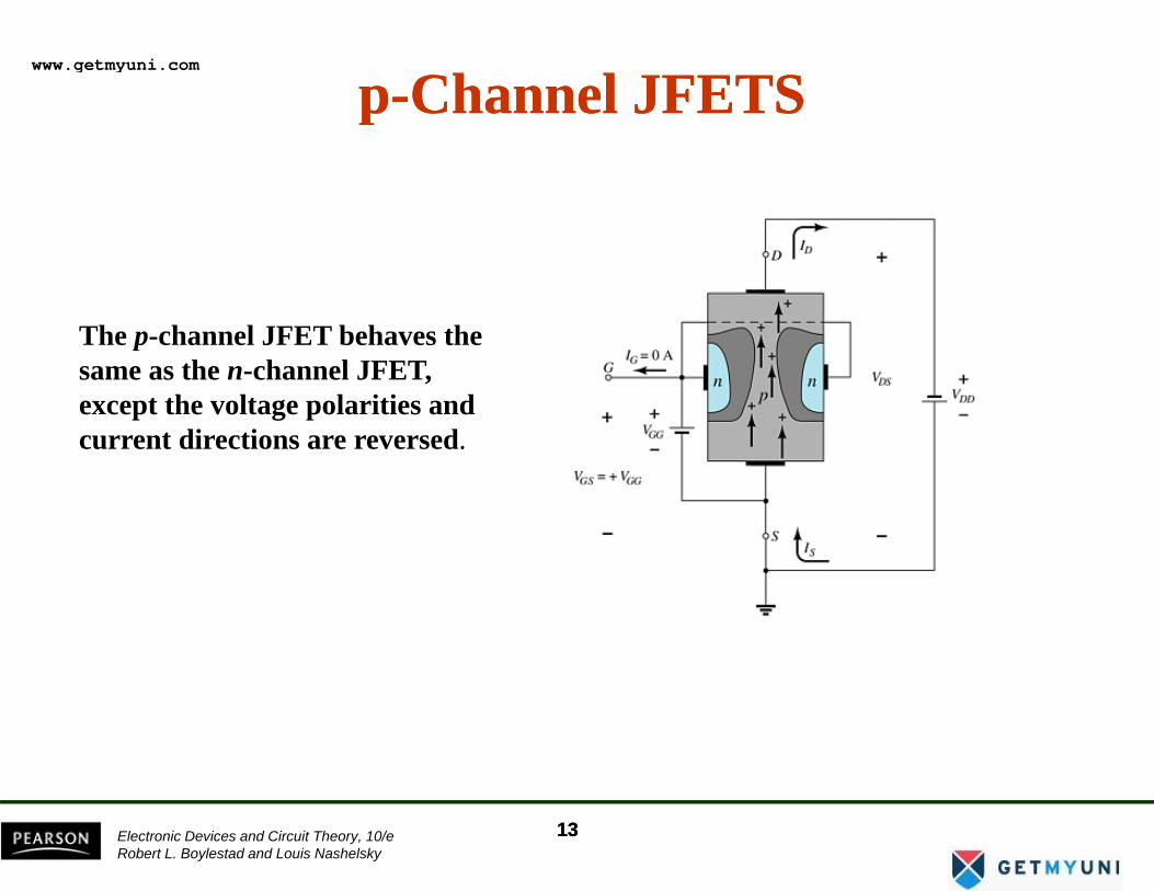
pp--Channel JFETSChannel JFETSpp
The p-channel JFET behaves theThe p-channel JFET behaves the same as the n-channel JFET, except the voltage polarities and current directions are reversedcurrent directions are reversed.
Electronic Devices and Circuit Theory, 10/eRobert L. Boylestad and Louis Nashelsky
1313
www.getmyuni.com
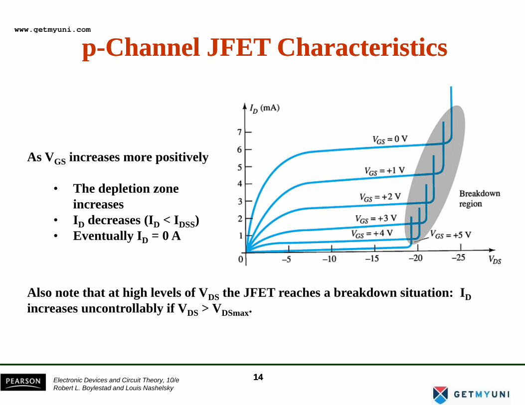
pp--Channel JFET CharacteristicsChannel JFET Characteristicspp Channel JFET CharacteristicsChannel JFET Characteristics
A V i iti lAs VGS increases more positively
• The depletion zone increasesincreases
• ID decreases (ID < IDSS)• Eventually ID = 0 A
Also note that at high levels of VDS the JFET reaches a breakdown situation: IDincreases uncontrollably if VDS > VDSmax.
Electronic Devices and Circuit Theory, 10/eRobert L. Boylestad and Louis Nashelsky
1414
www.getmyuni.com
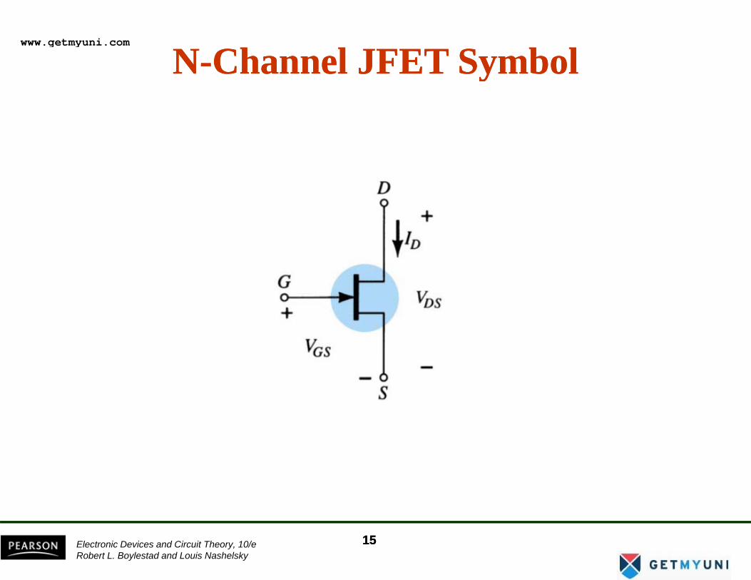
NN--Channel JFET SymbolChannel JFET Symbolyy
Electronic Devices and Circuit Theory, 10/eRobert L. Boylestad and Louis Nashelsky
1515
www.getmyuni.com
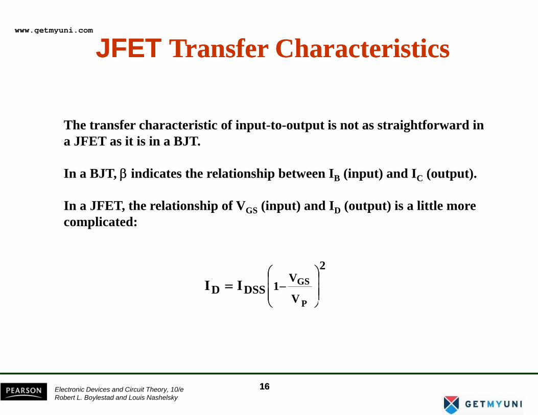
JFETJFET Transfer CharacteristicsTransfer CharacteristicsJFETJFET Transfer CharacteristicsTransfer Characteristics
The transfer characteristic of input-to-output is not as straightforward in a JFET as it is in a BJT.
In a BJT, β indicates the relationship between IB (input) and IC (output).
In a JFET the relationship of VGS (input) and ID (output) is a little moreIn a JFET, the relationship of VGS (input) and ID (output) is a little more complicated:
2
V
V1DSSD
P
GSII⎟⎟⎟
⎠
⎞
⎜⎜⎜
⎝
⎛−=
Electronic Devices and Circuit Theory, 10/eRobert L. Boylestad and Louis Nashelsky
1616
www.getmyuni.com
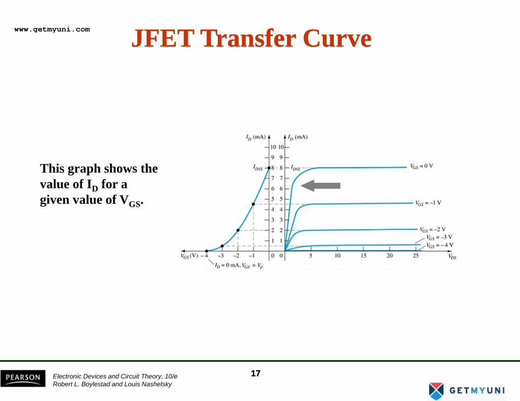
JFET Transfer CurveJFET Transfer Curve
This graph shows the value of ID for a given value of Vgiven value of VGS.
Electronic Devices and Circuit Theory, 10/eRobert L. Boylestad and Louis Nashelsky
1717
www.getmyuni.com
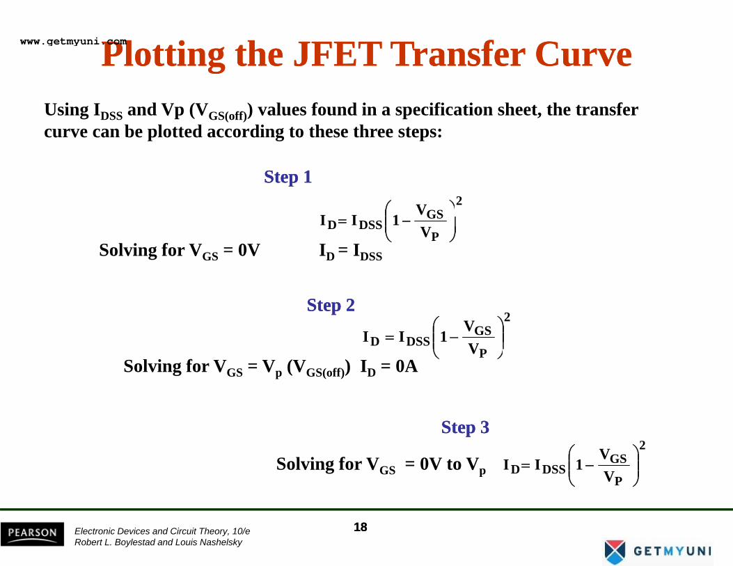
Plotting the JFET Transfer CurvePlotting the JFET Transfer CurveUsing IDSS and Vp (VGS(off)) values found in a specification sheet, the transfer curve can be plotted according to these three steps:
2GSV
⎟⎞
⎜⎛
Step 1Step 1
Solving for VGS = 0V ID = IDSSP
GSDSSD V
V1II ⎟⎟
⎠
⎞⎜⎜⎝
⎛−=
2
P
GSDSSD V
V1II ⎟⎟
⎠
⎞⎜⎜⎝
⎛−=
Step 2Step 2
Solving for VGS = Vp (VGS(off)) ID = 0APV ⎠⎝
S 3S 3
Solving for VGS = 0V to Vp
2
P
GSDSSD V
V1II ⎟⎟
⎠
⎞⎜⎜⎝
⎛−=
Step 3Step 3
Electronic Devices and Circuit Theory, 10/eRobert L. Boylestad and Louis Nashelsky
1818
www.getmyuni.com
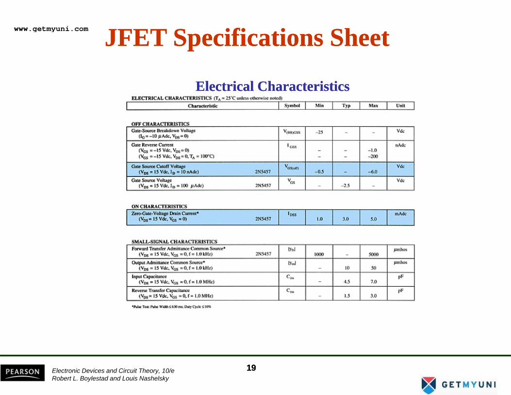
JFET Specifications SheetJFET Specifications Sheet
Electrical CharacteristicsElectrical Characteristics
Electronic Devices and Circuit Theory, 10/eRobert L. Boylestad and Louis Nashelsky
1919
www.getmyuni.com
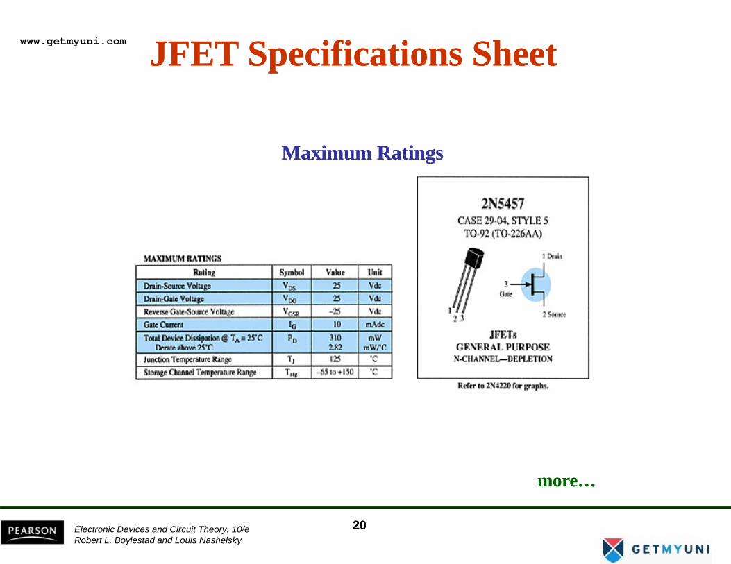
JFET Specifications SheetJFET Specifications Sheet
Maximum RatingsMaximum Ratings
more…more…
Electronic Devices and Circuit Theory, 10/eRobert L. Boylestad and Louis Nashelsky
2020
www.getmyuni.com
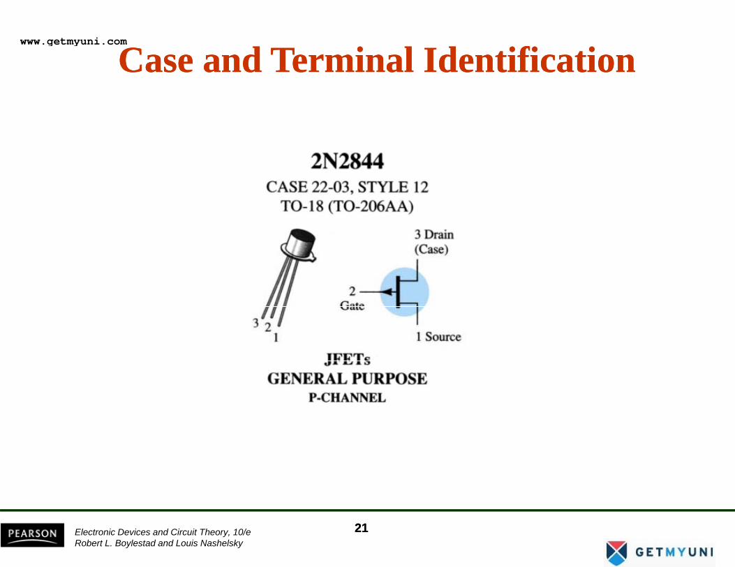
Case and Terminal IdentificationCase and Terminal Identification
Electronic Devices and Circuit Theory, 10/eRobert L. Boylestad and Louis Nashelsky
2121
www.getmyuni.com

Testing JFETsTesting JFETsgg
•• Curve TracerCurve TracerA curve tracer displays the ID versus VDS graph for various levels of VGS.various levels of VGS.
•• Specialized FET TestersSpecialized FET TestersThese testers show I for the JFET under testThese testers show IDSS for the JFET under test.
Electronic Devices and Circuit Theory, 10/eRobert L. Boylestad and Louis Nashelsky
2222
www.getmyuni.com

MOSFETsMOSFETsMOSFETsMOSFETsMOSFETs have characteristics similar to JFETs and additional characteristics that make then very useful
There are two types of MOSFETs:
characteristics that make then very useful.
•• DepletionDepletion--TypeType•• EnhancementEnhancement--TypeType
Electronic Devices and Circuit Theory, 10/eRobert L. Boylestad and Louis Nashelsky
2323
www.getmyuni.com
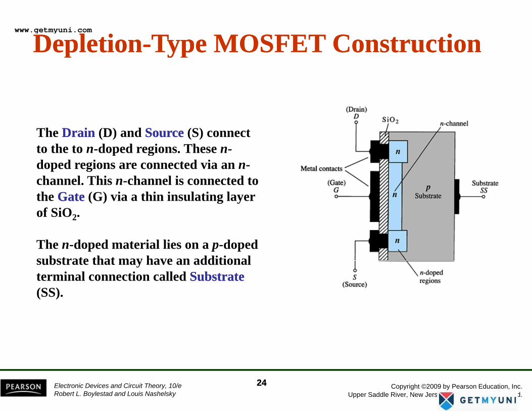
DepletionDepletion--Type MOSFET ConstructionType MOSFET Constructionpp ypyp
The DrainDrain (D) and SourceSource (S) connect to the to n-doped regions. These n-p gdoped regions are connected via an n-channel. This n-channel is connected to the Gate Gate (G) via a thin insulating layer of SiO2.
The n-doped material lies on a p-doped substrate that may have an additional terminal connection called SubstrateSubstrate(SS).
Electronic Devices and Circuit Theory, 10/eRobert L. Boylestad and Louis Nashelsky
2424 Copyright ©2009 by Pearson Education, Inc.Upper Saddle River, New Jersey 0745 • All rights reserved.
www.getmyuni.com

Basic MOSFET OperationBasic MOSFET Operation
A depletion type MOSFET can operate in two modes:A depletion-type MOSFET can operate in two modes:
•• Depletion modeDepletion mode•• Enhancement modeEnhancement modeEnhancement modeEnhancement mode
Electronic Devices and Circuit Theory, 10/eRobert L. Boylestad and Louis Nashelsky
2525
www.getmyuni.com
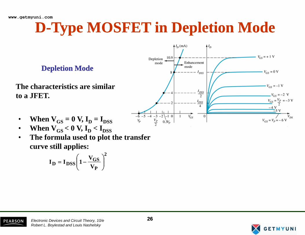
DD--Type MOSFET in Depletion ModeType MOSFET in Depletion ModeDD Type MOSFET in Depletion ModeType MOSFET in Depletion Mode
Depletion ModeDepletion Mode
The characteristics are similar
Wh V 0 V I I
e c c e s cs e sto a JFET.
• When VGS = 0 V, ID = IDSS• When VGS < 0 V, ID < IDSS• The formula used to plot the transfer
curve still applies:curve still applies: 2
P
GSDSSD V
V1II ⎟⎟
⎠
⎞⎜⎜⎝
⎛−=
Electronic Devices and Circuit Theory, 10/eRobert L. Boylestad and Louis Nashelsky
2626
www.getmyuni.com
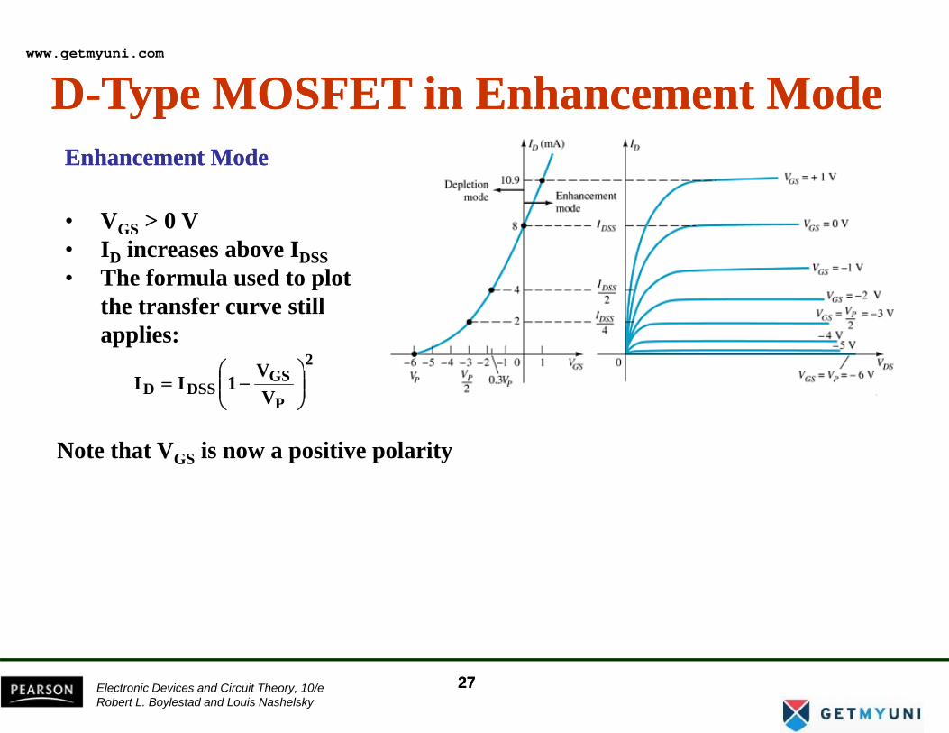
DD--Type MOSFET in Enhancement ModeType MOSFET in Enhancement ModeDD--Type MOSFET in Enhancement ModeType MOSFET in Enhancement ModeEnhancement ModeEnhancement Mode
• VGS > 0 V• ID increases above IDSS• The formula used to plot• The formula used to plot
the transfer curve still applies:
2V ⎞⎛
P
GSDSSD V
V1II ⎟⎟
⎠
⎞⎜⎜⎝
⎛−=
Note that VGS is now a positive polarityNote that VGS is now a positive polarity
Electronic Devices and Circuit Theory, 10/eRobert L. Boylestad and Louis Nashelsky
2727
www.getmyuni.com
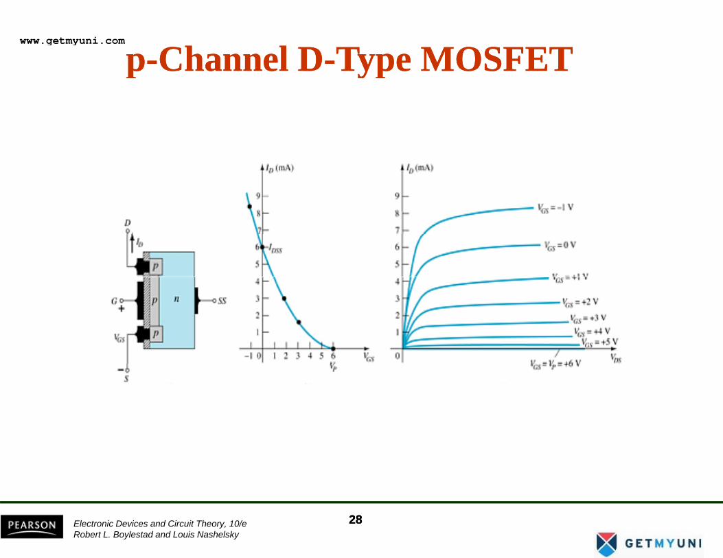
pp--Channel DChannel D--Type MOSFETType MOSFETpp ypyp
Electronic Devices and Circuit Theory, 10/eRobert L. Boylestad and Louis Nashelsky
2828
www.getmyuni.com
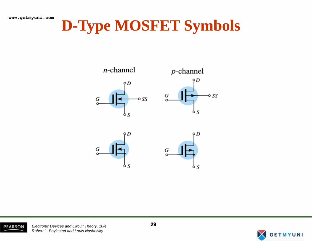
DD--Type MOSFET SymbolsType MOSFET Symbolsyp yyp y
Electronic Devices and Circuit Theory, 10/eRobert L. Boylestad and Louis Nashelsky
2929
www.getmyuni.com
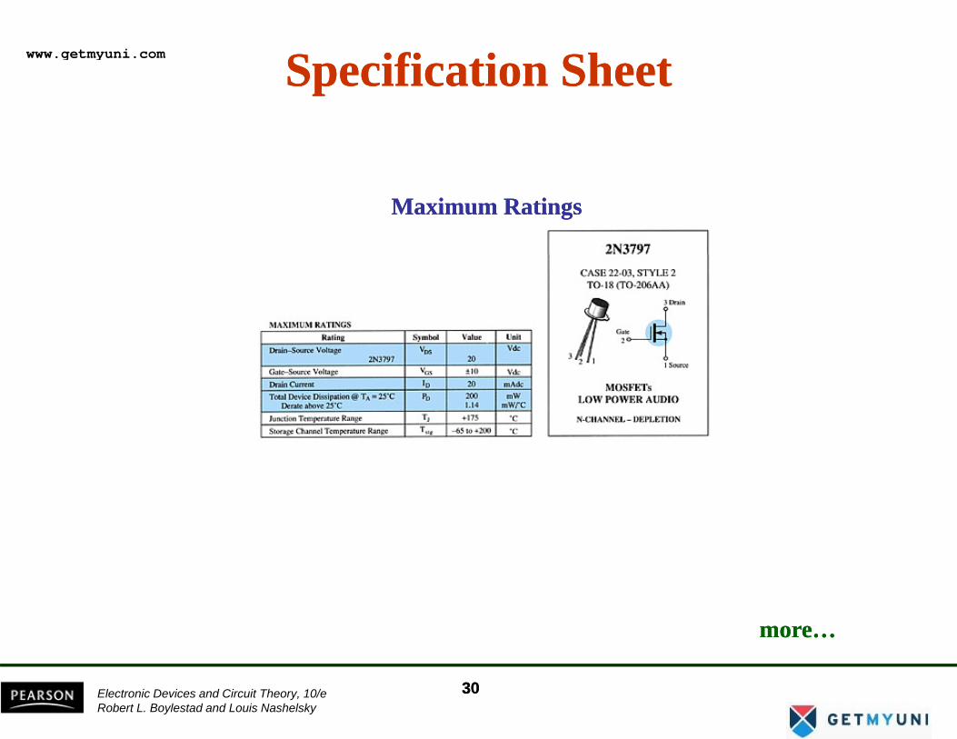
Specification SheetSpecification Sheet
Maximum RatingsMaximum Ratings
more…more…
Electronic Devices and Circuit Theory, 10/eRobert L. Boylestad and Louis Nashelsky
3030
www.getmyuni.com
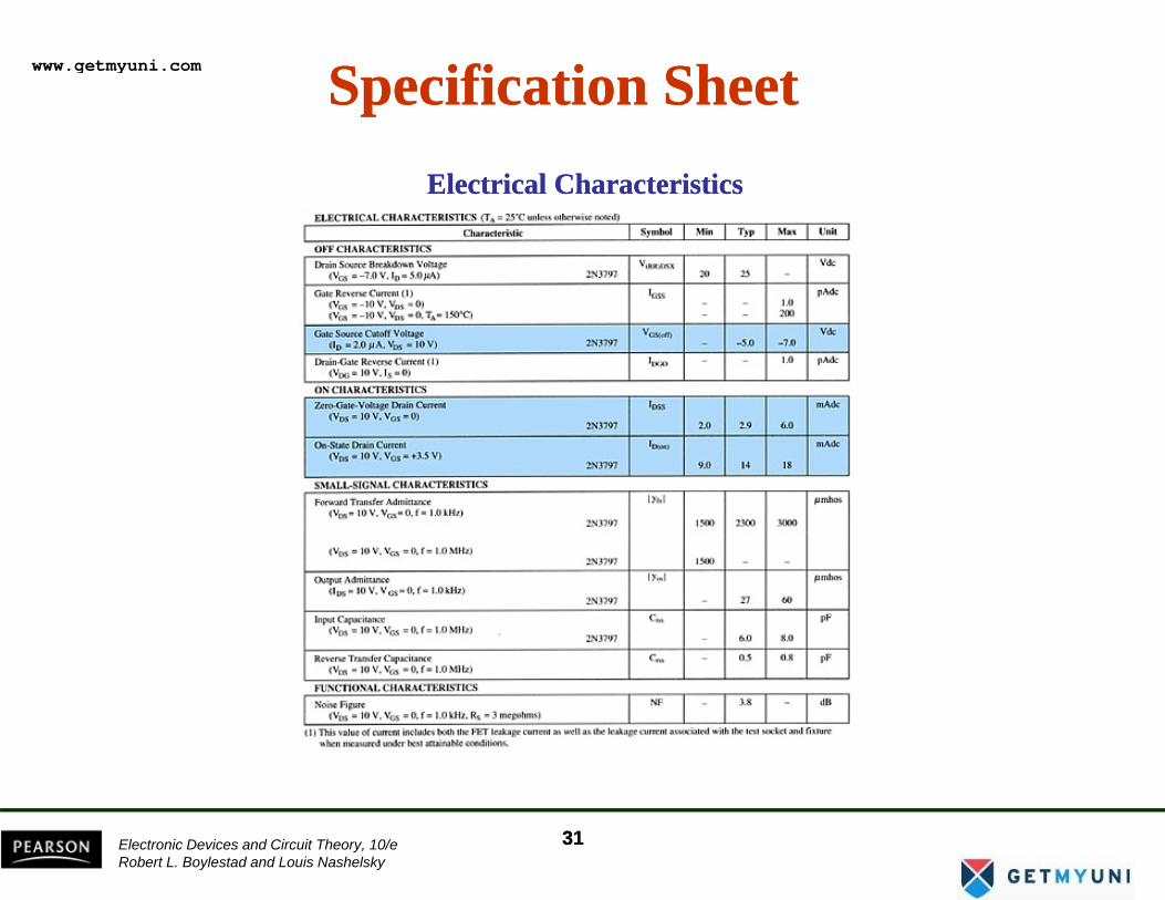
Specification SheetSpecification SheetElectrical CharacteristicsElectrical Characteristics
Electronic Devices and Circuit Theory, 10/eRobert L. Boylestad and Louis Nashelsky
3131
www.getmyuni.com
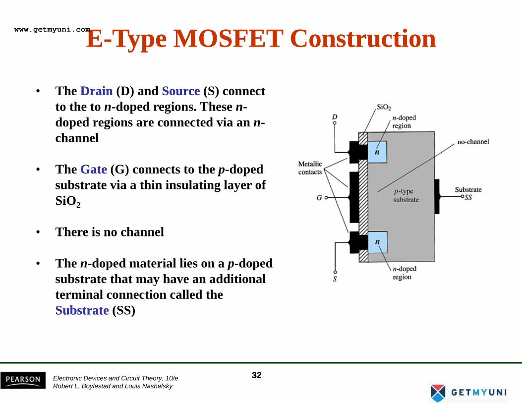
EE--Type MOSFET ConstructionType MOSFET Construction
• The DrainDrain (D) and SourceSource (S) connect t th t d d i Thto the to n-doped regions. These n-doped regions are connected via an n-channel
• The GateGate (G) connects to the p-doped substrate via a thin insulating layer of SiOSiO2
• There is no channel
• The n-doped material lies on a p-doped substrate that may have an additional terminal connection called the SubstrateSubstrate (SS)
Electronic Devices and Circuit Theory, 10/eRobert L. Boylestad and Louis Nashelsky
3232
www.getmyuni.com

Basic Operation of the EBasic Operation of the E--Type MOSFETType MOSFETpp ypyp
The enhancementThe enhancement type MOSFET operates only in the enhancement modetype MOSFET operates only in the enhancement mode
• VGS is always positive
The enhancementThe enhancement--type MOSFET operates only in the enhancement mode.type MOSFET operates only in the enhancement mode.
• As VGS increases, IDincreases
• As VGS is kept constant and VDS is increased, th I t t (I )then ID saturates (IDSS) and the saturation level, VDSsat is reached
Electronic Devices and Circuit Theory, 10/eRobert L. Boylestad and Louis Nashelsky
3333
www.getmyuni.com
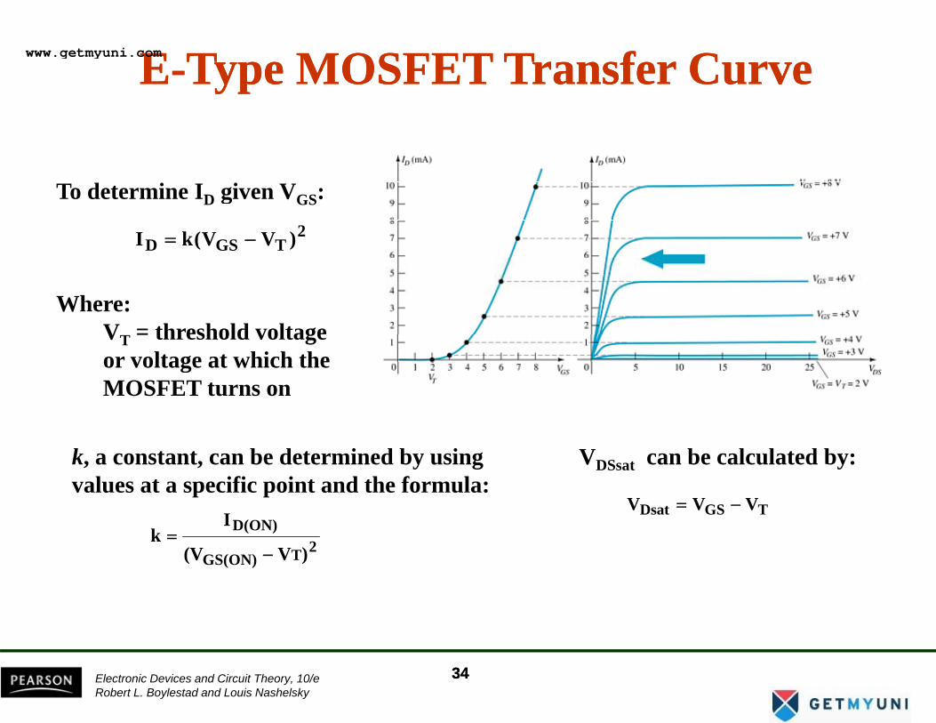
EE--Type MOSFET Transfer CurveType MOSFET Transfer Curve
T d t i I i VTo determine ID given VGS:2
TGSD )VV(kI −=
Where: VT = threshold voltage or voltage at which theor voltage at which the MOSFET turns on
k b d i d b i V b l l d bk, a constant, can be determined by using values at a specific point and the formula:
D(ON)Ik =
VDSsat can be calculated by:
TGSDsat VVV −=
2TGS(ON) )V(Vk
−=
Electronic Devices and Circuit Theory, 10/eRobert L. Boylestad and Louis Nashelsky
3434
www.getmyuni.com
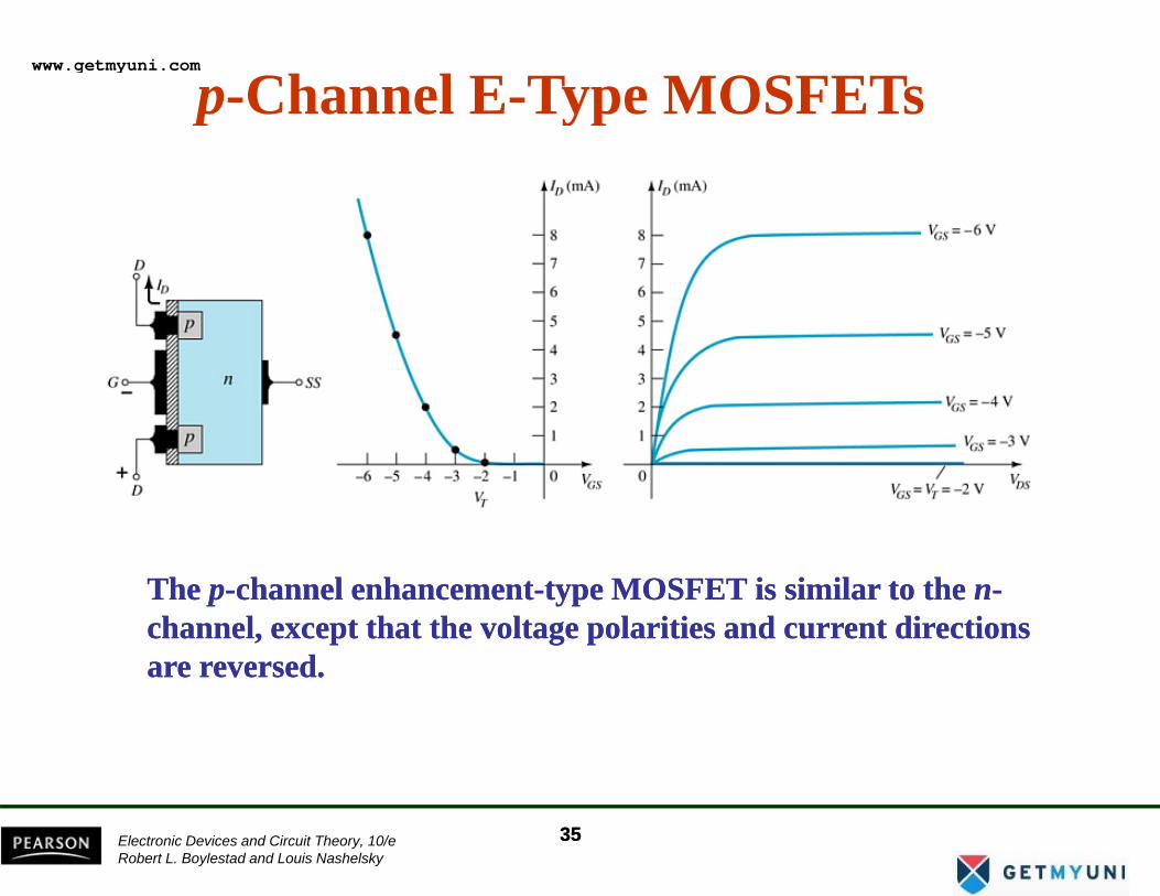
p-Channel E-Type MOSFETsp yp
The The pp--channel enhancementchannel enhancement--type MOSFET is similar to the type MOSFET is similar to the nn--channel, except that the voltage polarities and current directions channel, except that the voltage polarities and current directions are reversedare reversedare reversed.are reversed.
Electronic Devices and Circuit Theory, 10/eRobert L. Boylestad and Louis Nashelsky
3535
www.getmyuni.com
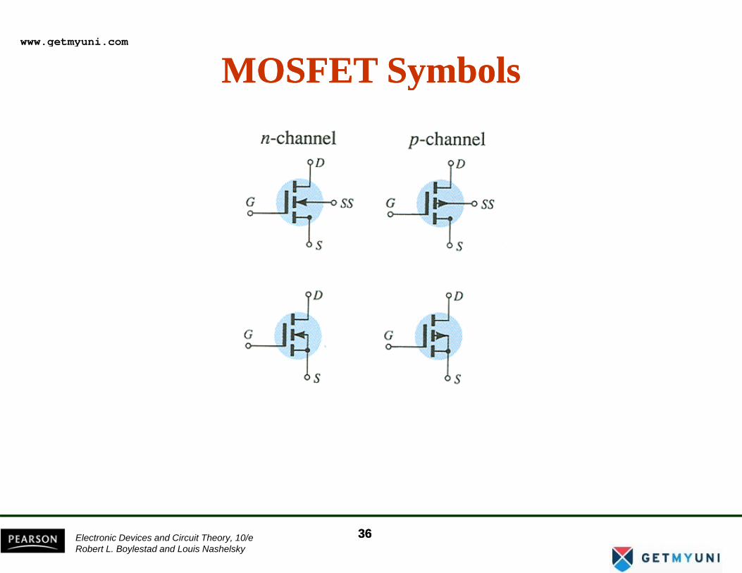
MOSFET SymbolsMOSFET SymbolsMOSFET SymbolsMOSFET Symbols
Electronic Devices and Circuit Theory, 10/eRobert L. Boylestad and Louis Nashelsky
3636
www.getmyuni.com
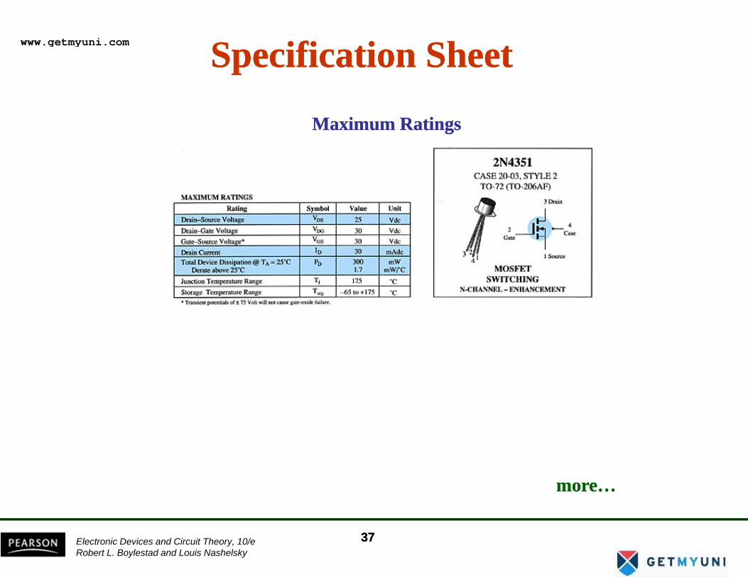
Specification SheetSpecification Sheet
Maximum RatingsMaximum Ratings
more…more…
Electronic Devices and Circuit Theory, 10/eRobert L. Boylestad and Louis Nashelsky
3737
www.getmyuni.com
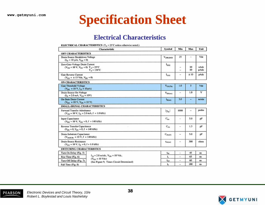
Specification SheetSpecification SheetElectrical CharacteristicsElectrical Characteristics
Electronic Devices and Circuit Theory, 10/eRobert L. Boylestad and Louis Nashelsky
3838
www.getmyuni.com
Handling MOSFETsHandling MOSFETsMOSFETs are very sensitive to static electricity. Because of the very thin
SiO2 layer between the external terminals and the layers of the device, any small electrical discharge can create an unwanted conduction.
P iP iProtectionProtection
• Always transport in a static sensitive bag
• Always wear a static strap when handling MOSFETS•
A l lt li iti d i b t th t d h• Apply voltage limiting devices between the gate and source, such as back-to-back Zeners to limit any transient voltage.
Electronic Devices and Circuit Theory, 10/eRobert L. Boylestad and Louis Nashelsky
3939
www.getmyuni.com
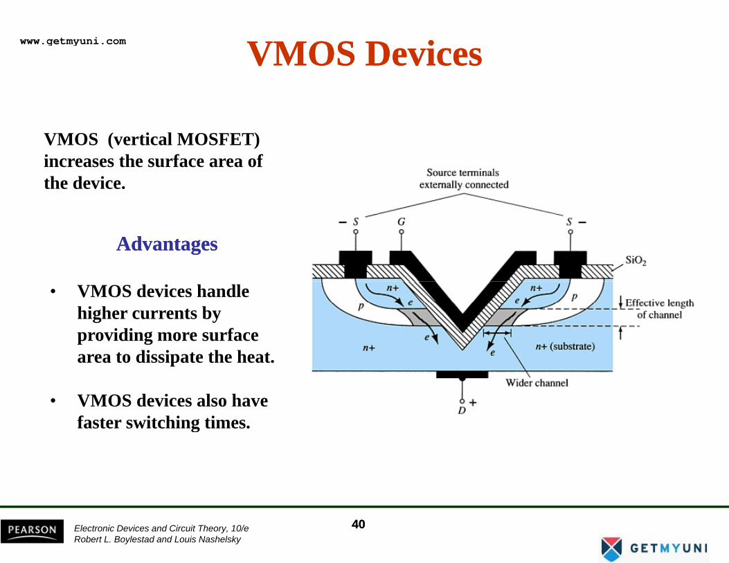
VMOS DevicesVMOS Devices
VMOS (vertical MOSFET)VMOS (vertical MOSFET) increases the surface area of the device.
AdvantagesAdvantages
• VMOS devices handle higher currents by providing more surface area to dissipate the heat.
• VMOS devices also have f t it hi tifaster switching times.
Electronic Devices and Circuit Theory, 10/eRobert L. Boylestad and Louis Nashelsky
4040
www.getmyuni.com
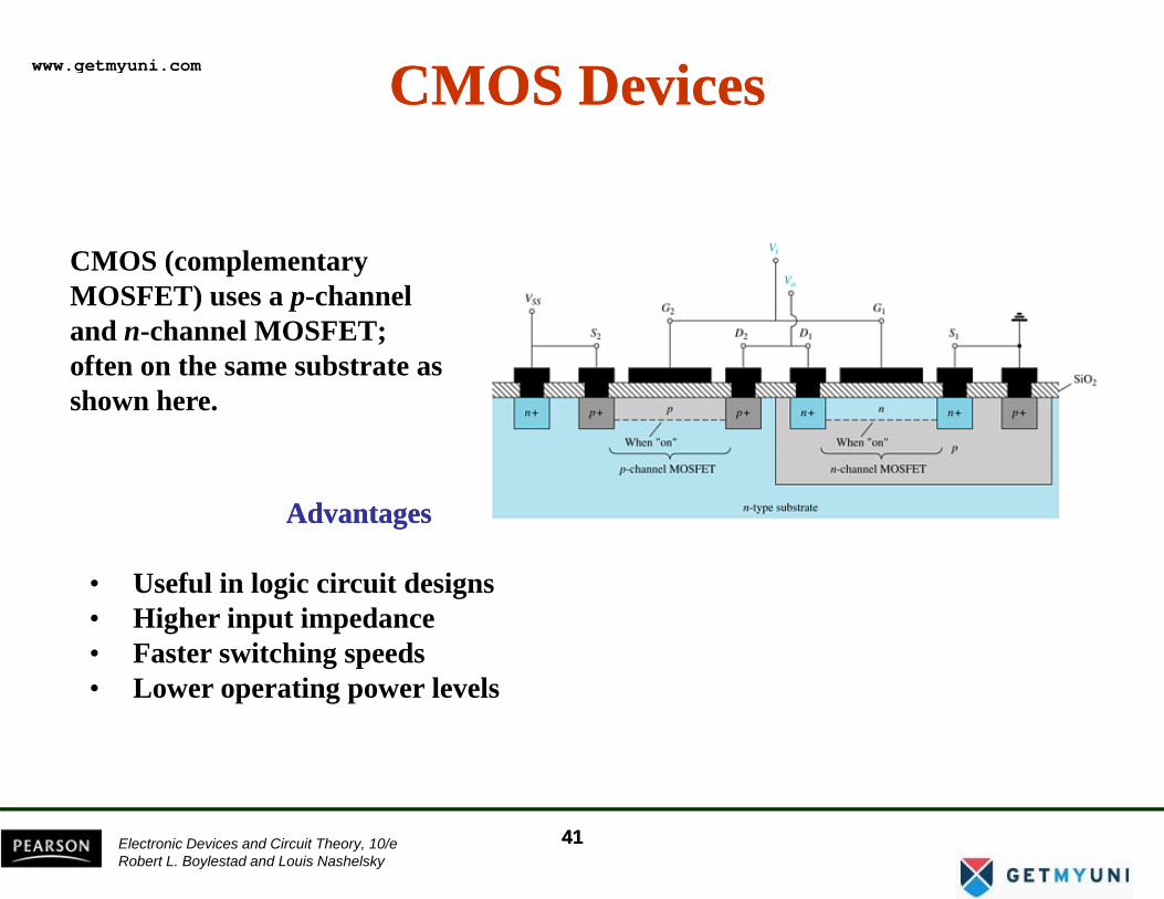
CMOS DevicesCMOS Devices
CMOS (complementary MOSFET) uses a p-channel and n-channel MOSFET; d c e OS ;often on the same substrate as shown here.
AdvantagesAdvantages
• Useful in logic circuit designs• Higher input impedance• Faster switching speedsg p• Lower operating power levels
Electronic Devices and Circuit Theory, 10/eRobert L. Boylestad and Louis Nashelsky
4141
www.getmyuni.com
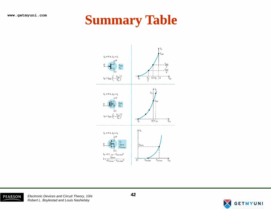
Summary TableSummary Table
Electronic Devices and Circuit Theory, 10/eRobert L. Boylestad and Louis Nashelsky
4242
www.getmyuni.com