black phosphorus radio-frequency transistors
TRANSCRIPT
1
Black Phosphorus Radio-Frequency Transistors
Han Wang1 Xiaomu Wang2 Fengnian Xia2 Luhao Wang1 Hao Jiang3
Qiangfei Xia3 Matthew L Chin4 Madan Dubey4 Shu-jen Han5
1Ming Hsieh Department of Electrical Engineering University of Southern California
Los Angeles CA 90089
2Department of Electrical Engineering Yale University New Haven CT 06511
3Department of Electrical amp Computer Engineering University of Massachusetts
Amherst MA 01003
4 Sensors and Electron Devices Directorate US Army Research Laboratory
Adelphi MD 20723
5IBM T J Watson Research Center Yorktown Heights NY 10598
Abstract Few-layer and thin film forms of layered black phosphorus (BP) have recently
emerged as a promising material for applications in high performance nanoelectronics
and infrared optoelectronics Layered BP thin film offers a moderate bandgap of around
03 eV and high carrier mobility leading to transistors with decent on-off ratio and high
on-state current density Here we demonstrate the gigahertz frequency operation of black
phosphorus field-effect transistors for the first time The BP transistors demonstrated here
show excellent current saturation with an on-off ratio exceeding 2times103 We achieved a
current density in excess of 270 mAmm and DC transconductance above 180 mSmm
for hole conduction Using standard high frequency characterization techniques we
measured a short-circuit current-gain cut-off frequency fT of 12 GHz and a maximum
oscillation frequency fmax of 20 GHz in 300 nm channel length devices BP devices may
offer advantages over graphene transistors for high frequency electronics in terms of
voltage and power gain due to the good current saturation properties arising from their
finite bandgap thus enabling the future ubiquitous transistor technology that can operate
in the multi-GHz frequency range and beyond
Email hanwang4uscedu fengnianxiayaleedu
2
Introduction
Typical channel materials in thin film electronics include amorphous or
polycrystalline silicon1-3 organic compounds45 and oxides67 These materials usually
exhibit a sizable bandgap but compromised carrier mobility making them undesirable for
radio-frequency (RF) electronics Early interests in using two-dimensional materials for
RF thin film electronics focused mainly on graphene Since the first demonstration of
high frequency current gain in graphene field-effect transistors (FETs) in 20078 graphene
has inspired great interests for RF applications due to its high mobility high carrier
velocity and long mean free path9-14 However several years of intensive research has
revealed that graphene transistors might suffer from a few fundamental limitations that
will restrict its high frequency performance The key shortcoming of graphene RF
transistors is their lack of current saturation as a result of graphenersquos zero-bandgap nature
that can lead to reduced voltage and power gains1516 and to a lesser extent the current
gain 17 As a result most graphene RF FETs may have relatively high short-circuit
current-gain cut-off frequency (fT) but significantly lower maximum oscillation
frequency (fmax) which benchmarks the power gain of the transistor On the other hand
transistors based on transition metal dichalcogenides such as molybdenum disulfide
(MoS2) and tungsten diselenide (WSe2) only showed limited potential for high frequency
applications because of their relatively low mobility 18 19 Recently layered black
phosphorus (BP) thin film has emerged as a promising candidate for high performance
thin film electronics due to its moderate bandgap of 03 eV and high carrier mobility The
recent experiment has shown hole mobility exceeding 650 cm2 V-1 s-1 at room
temperature and above 1000 cm2 V-1 s-1 at 120 K along the light effective mass (x)
3
direction20 While in bulk black phosphorus mobilities exceeding 1000 cm2 V-1s-1 at
room temperature for both electrons and holes and exceeding 50000 cm2 V-1s-1 at 30 K
have been demonstrated21 In this work we demonstrate for the first time the operation of
black phosphorus FETs in the gigahertz frequency range Future ubiquitous transistor
technologies using this novel layered material with high mobility and highly desirable
current saturation property may revolutionize the electronic systems for many civilian
and defense applications
Results
Device fabrication
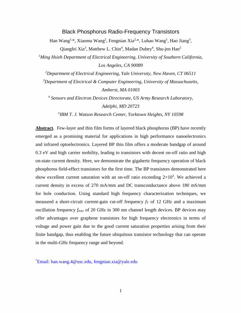
Orthorhombic bulk black phosphorus is an elemental layered material with D2h
point group symmetry as shown in Fig 1a It is the most stable allotrope of phosphorus
and the electronic properties of bulk BP have been studied several decades ago22-26
Recently BP in its few-layer and thin-film form has inspired renewed interests among
physicists and engineers due to its promising potential for application in thin film
electronics and infrared optoelectronics2027-29 The layered nature of BP crystals allows
single- and multi-layer atomic crystals to be obtained through mechanical exfoliation
techniques In our experiments multi-layer BP was first exfoliated using the standard
micromechanical cleavage method from a bulk BP crystal then transferred onto 300 nm
thick silicon dioxide thermally grown on highly resistive silicon (gt104 Ωmiddotcm) Atomic
force microscope (AFM) can be used to determine the number of atomic layers in a BP
flake which has a layer-to-layer spacing of 053 nm2021 The x- y- and z-directions of
the crystal lattice are indicated in Fig 1a In a series of recent publications the mobility
4
and the on-off current ratio of BP FETs have been studied with respect to the thickness
and layer number in the BP channel202728 In this work BP thin films with thicknesses
around 6-10 nm were selected for the best balanced mobility and on-off properties for RF
applications Transistors using thinner BP films exhibit an on-off current ratio as high as
2times105 but low mobility of below 100 cm2 V-1 s-1 due to the scattering from the external
environment Utilization of excessively thick BP films can lead to higher mobility but a
reduced on-off ratio and less pronounced current saturation The inset of Fig 1b shows
the optical micrograph of a typical BP flake used for device fabrication AFM
measurements indicate a thickness of 85 nm in this flake (Fig 1b) To enhance the
channel mobility crystal orientations of the flakes were first identified using either
Raman spectroscopy or infrared spectroscopy techniques and the transistors were built
along the light effective mass (x-) direction of the BP lattice Fig 1c shows the Raman
spectrum of the BP flake with the excitation laser polarized along the x-direction The
characteristic peaks at 470 440 and 365 cm-1 correspond to 2gA B2g and
1gA modes
respectively2030 The 2gA mode has higher intensity compared to B2g and
1gA modes with
this particular excitation laser polarization Fig 1d shows the polarization-resolved
infrared spectra of the flake and the x-direction can be clearly identified as the direction
with the highest optical conductivity around the band edge2021 The source and drain
electrodes were formed with 1 nm Ti20 nm Pd 30 nm Au metal stack which favors p-
type carrier injection into the channel owing to the large work-function (~522 eV) of Pd
The gate dielectric was made with 21 nm of HfO2 deposited by atomic layer deposition
(ALD) technique at a temperature of 150 C The typical dielectric constant is around 13
determined by ellipsometric measurement on a control sample Finally the gate electrode
5
was defined by electron-beam lithography to form transistors with sub-micrometer
channel lengths The fabrication process is described in more detail in Supporting
Information Fig 2b shows the optical micrograph of the full layout of the device The
standard ground-signal-ground (GSG) pads were fabricated to realize signal transition
from microwave coax cables to on-chip coplanar waveguide electrodes
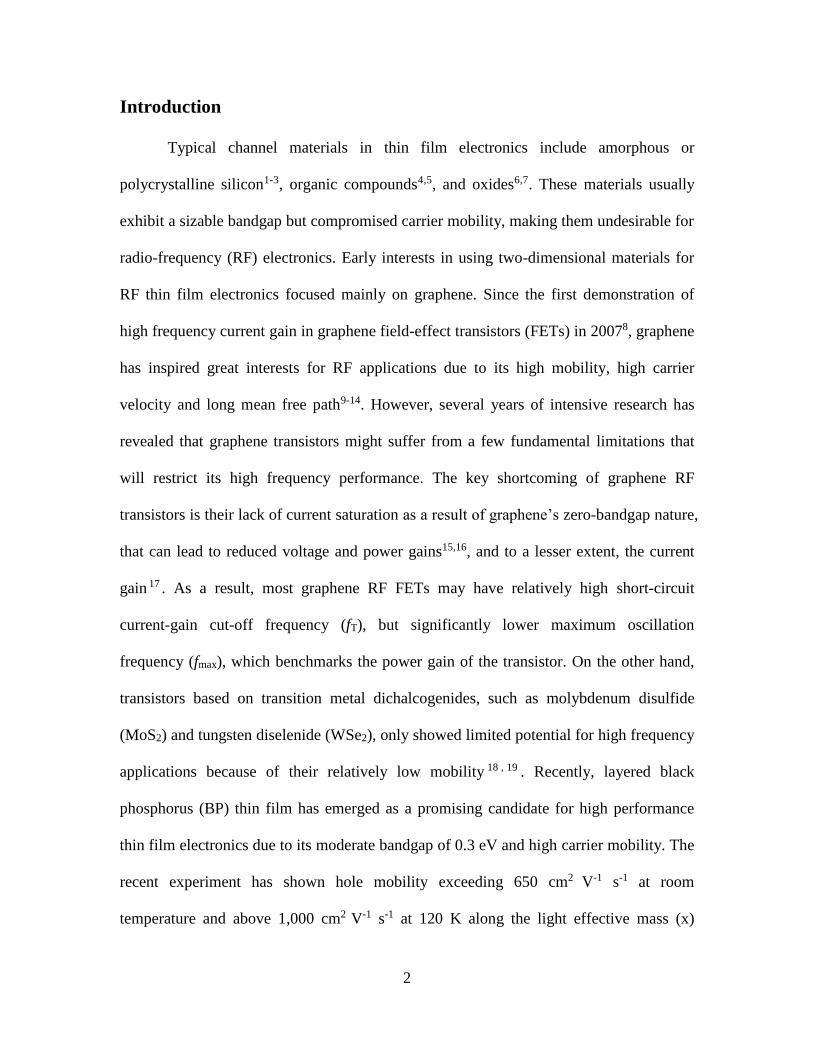
DC Characterization
Fig 2a shows the schematic of the transistor structure Fig 2c and 2d display the
DC characteristics of a top-gated BP FET with a 300 nm channel length (LG) The device
was built along the x-direction of the 85 nm thick flake shown in Fig 1 Fig 2c shows
the measured drain current (IDS) as a function of drain-source bias voltage (VDS) at gate
bias (VGS) from 0 V to -2 V in steps of -05 V The current saturation in the BP transistor
is clearly visible and significantly improved from that in most graphene FETs due to the
finite bandgap in BP thin film This is typical for a BP device with ~85 nm channel
thickness and agrees well with previous demonstrations20 Good current saturation
characteristics will lead to low output conductance defined as 1198920 =d119868DS
d119881DS|
119881GS=constant which
is the differential drain current change with respect to the variation in drain voltage bias
Low output conductance is critical for improving voltage and power gains and to a lesser
extent the current gain in RF transistors As reported in our previous work20 typical Hall
mobility along x-direction of BP flakes with thickness around 8 nm is above 400 cm2 V-
1s-1 at room temperature Fig 2d shows IDS as a function of VGS at VDS=-2 V where on-
off current ratio over 2times103 is achieved The as-fabricated device shows p-type
conduction with threshold voltage around -07 V A key factor influencing the high-
6
frequency small signal response of a transistor is its transconductance (119892m) defined as the
first derivative of the transfer characteristics ie 119892m =d119868DS
d119881GS|
119881DS=constant The inset of Fig 2d
shows the measured 119892m as a function of the gate voltage at VDS=-2 V The peak value of
this extrinsic 119892m exceeds 180 mSmm at VG=-175 V while the peak on-state current
density measured exceeds 270 mAmm at VDS=-2 V and VGS=-25 V Fig 2d also shows
IDS as a function of top-gate voltage VGS at a drain bias of VDS=-2 V with the current
plotted in logarithmic scale The on-off current ratio of the device exceeds 2times103 Hence
the BP transistor demonstrated here shows significant advantages over graphene
transistors in terms of its current saturation properties and on-off current ratio Typical
monolayer graphene devices have on-off current ratio less than 10 at room temperature
In bilayer graphene devices the on-off current ratio only reaches around 100 even with
bandgap opening induced by a strong external electrical field31
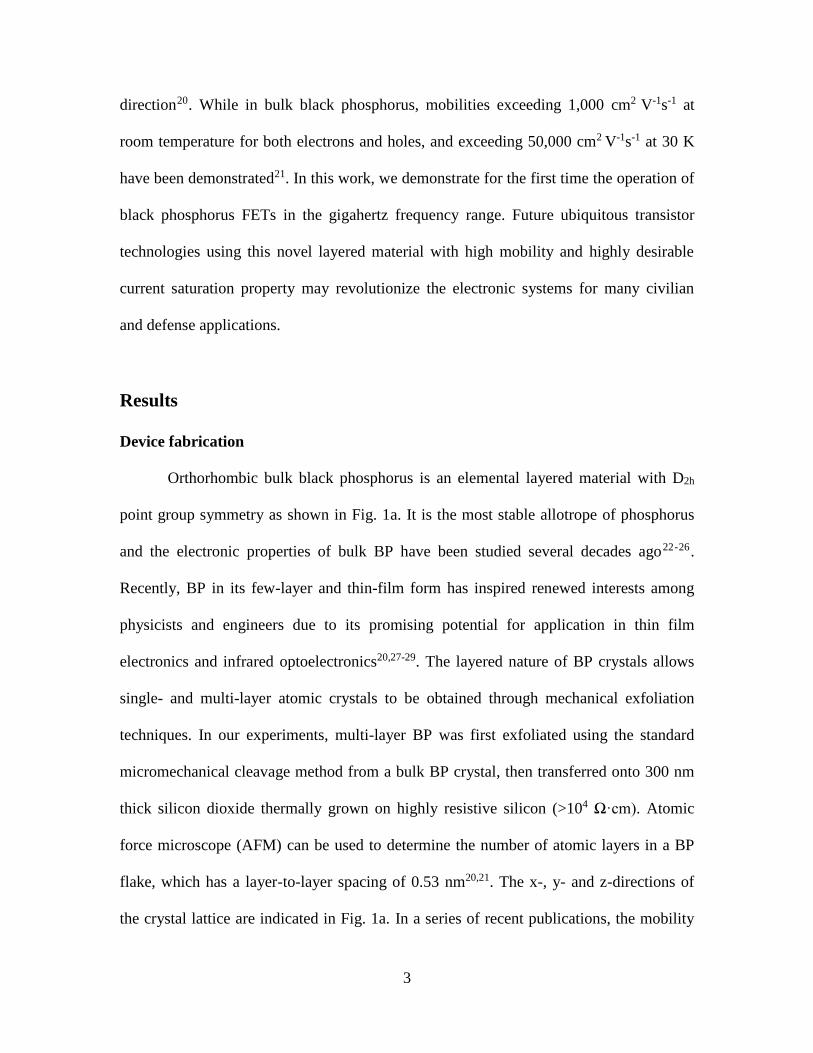
RF Characterization
To characterize the high frequency performance of BP RF transistors we used the
standard S-parameter measurement with on-chip probing utilizing GSG probes and
Agilent N5230 vector network analyzer up to 50 GHz Key figures of merit for
microwave transistors can then be obtained for the BP devices The network analyzer and
the entire testing fixture were first calibrated using standard open short and load
calibrations Standard open and short structures were then used to de-embed the signals
of the parallel and series parasitics associated with the measurement pads and
connections1532-34 The measurement procedure used in this work followed strictly the
standard calibration and de-embedding processes widely accepted in the semiconductor
7
industry where the calibration step moves the reference plane to the tips of the GSG
probes and the de-embedding step gives access to the performance of the active device
region
Fig 3a and 3b plot the short-circuit current gain (h21) the unilateral power gain
(U) and maximum stable gain (MSG)maximum available gain (MAG) extracted from S-
parameters before and after de-embedding respectively measured at VDS=-20 V and
VGS=-17 V for the device with LG=300 nm The plot of |h21|2 follows the characteristic 1f
relation with respect to frequency at a 20 dBdec slope16 Fig 3a and 3b show that the
300 nm channel length device has a fT of 78 GHz before de-embedding and 12 GHz after
de-embedding as extracted from the frequencies at which |h21| reaches unity Gummelrsquos
method provides another way of extracting the cut-off frequency35 where fT is extracted
from the reciprocal of the initial slope in the imaginary part of 1h21 vs frequency plot
The values of fT obtained by both 1f extraction and Gummelrsquos method match closely for
both 300 nm (Fig 3c and 3d) and 1 m (see Fig S1 in the Supporting Information)
channel length devices before and after de-embedding
While fT is an important figure of merit related to the intrinsic speed of the BP
transistor another key figure of merit for analog application is the maximum oscillation
frequency It is the highest possible operating frequency at which a transistor can still
amplify power fmax can be extracted from U or MSGMAG of the device1636 The
unilateral power gain U also known more generally as Masonrsquos U invariant is a key
parameter for any general two-port network It carries great significance as an invariant
parameter of the system under linear lossless and reciprocal transformations In Masonrsquos
classic work3738 the rich physical meaning of U was interpreted in three different ways
8
as a maximum power gain as a device activity measure and as an invariant under a class
of bilinear Moumlbius transformations In transistor characterizations U is the power gain
under the condition of (1) Unilateralization and (2) Conjugate matched load for
maximum power transfer In Fig 3a and 3b the plots of U follow a 20 dBdec slope and
both U and MSGMAG plots give similar fmax of 12 GHz before de-embedding and 20
GHz after de-embedding respectively
The 300 nm channel length device has an extrinsic fTmiddotLG product of 36 GHz m
Using a slightly different design of the open pattern where the gate electrode in the ldquoopenrdquo
structure extends into the spacing between the source and drain electrodes15 we can
eliminate most of the gate-source and gate-drain parasitic capacitances Cgs and Cgd This
will allow the extraction of a new fT value that reflects the more intrinsic property of the
BP channel and an intrinsic fT value (fTint) close to 51 GHz is obtained for the same
device which corresponds to the average saturation velocity in the channel
approximately equal to vsat=2fTLG ~ 96times106 cms However we would like to
emphasize that fTint only represents the upper limit of the possible frequency spectrum for
this transistor In any practical applications the Cgs and Cgd of the device always
significantly affect the device performance As a result we report fT=12 GHz and fmax=20
GHz in Fig 3 as the practically operable cut-off frequencies of the active device
region1533 which are extracted based on standard characterization techniques commonly
used for the characterization in silicon and III-V high frequency transistors The intrinsic
cut-off frequency of 51 GHz is extracted only as a way to approximately estimate the
saturation velocity and it may not be appropriate for technology benchmarking The RF
characteristics for a device with 1 m channel length are also reported in the Supporting
9
Information The 1 m channel length device has peak fT=28 GHz and fmax=51 GHz
before de-embedding and fT=33 GHz and fmax=56 GHz after de-embedding (see Fig S1
in the Supporting Information)
The intrinsic limit of the cut-off frequency can be estimated using 119891119879 =119892119898
2120587119862119892119904
Assuming the same gm and gate dielectrics property from the measured data an fT above
100 GHz may be reached if the channel length reduces to 30 nm On the other hand fmax
depends on both the current and voltage gains It is related to fT following 119891119898119886119909 =119891119879
2 radic1199030
119877119892+119877119894
We can see that a high fT will enhance fmax and good current saturation ie high output
resistance (r0) low gate resistance (Rg) and low input resistance (Ri) are critical for
improving fmax of the device
Fig 4 shows the magnitude of the small-signal open-circuit voltage gain |z21z11|
as a function of frequency before and after de-embedding An open-circuit voltage gain
refers to the voltage gain subject to infinitely high load impedance Here the voltage gain
is obtained from the ratio between the open circuit forward transfer impedance z21 and the
open circuit input impedance z11 Since 11991111 =1199071
1198941|
1198942=0 and 11991121 =
1199072
1198941|
1198942=0 the ratio z21z11 is
equal to 1199072
1199071|
1198942=0 ie the voltage gain with the output port in open condition v1 and v2
refer to the voltages at the input and output ports respectively In transistors v1 is the
small-signal input voltage at the gate and the v2 is the small-signal output voltage at the
drain Based on the definition of gm and g0 discussed earlier we can see that the voltage
gain |z21z11| is closely related to the ratio gmg0 Devices with good current saturation and
high transcondutance are hence expected to have high voltage gains The BP transistors
show good voltage gain characteristics As shown in Fig 4 the before-de-embedding
10
voltage gain stays above unity (0 dB) up to 13 GHz The after-de-embedding voltage gain
is close to 20 dB at 2 GHz and stays above unity (0 dB) for the entire frequency range
measured up to 50 GHz For a longer channel length (1 m) device (see Fig S2 in the
Supporting Information) the before-de-embedding voltage gain is above unity (0 dB) up
to 10 GHz The after-de-embedding voltage gain is above 15 dB at 1 GHz and stays
above unity (0 dB) up to 30 GHz
Summary
In this work we investigated the high frequency characteristics of black
phosphorus field effect transistors whose channels were fabricated along the light
effective mass (x-) direction The device operates well into the GHz frequency range of
the radio frequency spectrum We carried out standard S-parameter measurements to
characterize the high frequency response of these top-gated BP transistors The short-
circuit current gain maximum stable gainmaximum available gain unilateral power gain
and voltage gain of the devices were carefully extracted The short-circuit current gain of
BP transistors shows the 20 dBdec 1f frequency dependence at high frequency We
measured a peak short-circuit current gain cutoff frequency fT of 12 GHz and maximum
oscillation frequency fmax of 20 GHz for a 300 nm channel length BP transistor
demonstrating the GHz operation of BP devices for the first time These results clearly
reveal the potentials of BP transistors to function as power and voltage amplifiers in
multi-GHz frequency analogue and digital electronics demanded by many emerging
civilian and military applications
11
References
1 Powell M J The physics of amorphous-silicon thin-film transistors IEEE Trans
Electron Devices 36 2753-2763 (1989)
2 Street R A Thin-Film Transistors Adv Mater 21 2007-2022 (2009)
3 Hawkins W G Polycrystalline-silicon device technology for large-area electronics
IEEE Trans Electron Devices 33 477-481 (1986)
4 Forrest S R The path to ubiquitous and low-cost organic electronic appliances on
plastic Nature 428 911-918 (2004)
5 Dimitrakopoulos C D Mascaro D J Organic thin-film transistors A review of
recent advances IBM J Res Dev 45 11-27 (2004)
6 Nomura K et al Amorphous Oxide Semiconductors for High-Performance Flexible
Thin-Film Transistors Japanese Journal of Applied Physics 45 4303 (2006)
7 Carcia P F McLean R S Reilly M H amp Nunes G Jr Transparent ZnO thin-film
transistor fabricated by RF magnetron sputtering Appl Phys Lett 82 1117 (2003)
8 Meric I Baklitskaya N Kim P amp Shepard K L RF performance of top-gated
zero-bandgap graphene field-effect transistors IEEE IEDM Tech Digest 2008
9 Lin Y-M Dimitrakopoulos C D Jenkins K A Farmer D B Chiu H-Y Grill
A amp Avouris P 100-GHz Transistors from Wafer-Scale Epitaxial Graphene Science
327 662 (2010)
10 Wu Y Lin Y Bol A A Jenkins K A Xia F Farmer D B Zhu Y amp
Avouris P High-frequency scaled graphene transistors on diamond-like carbon Nature
472 74-78 (2011)
11 Liao L et al High-speed graphene transistors with a self-aligned nanowire gate
Nature 467 305ndash308 (2010)
12 Wang H Nezich D Kong J amp Palacios T Graphene frequency multipliers IEEE
Elec Dev Lett 30 547-549 (2009)
13 Wang H Hsu A Wu J Kong J amp Palacios T Graphene-based ambipolar RF
mixers IEEE Elec Dev Lett 31 906-908 (2010)
12
14 Han S-J Valdes-Garcia A Oida S Jenkins K A amp Haensch W Graphene radio
frequency receiver integrated circuit Nat Commun 53086 doi101038ncomms4086
(2014)
15 Wang H Chapter 4 In Two-Dimensional Materials for Electronic Applications Ph
D Thesis Massachusetts Institute of Technology Cambridge MA USA 2014
httpdspacemiteduhandle1721184899
16 Schwierz F amp Liou J J Modern Microwave Transistors Theory Design and
Performance Wiley-Interscience 1st edition 2002
17 Tasker P J amp Hughes B Importance of source and drain resistance to the maximum
f T of millimeter-wave MODFETs IEEE Elec Dev Lett 10 291-293 (1989)
18 Zhu W Low T Lee Y-H Wang H Farmer D B Kong J Xia F amp Avouris
P Electronic transport and device prospects of monolayer molybdenum disulphide grown
by chemical vapour deposition Nat Commun 53087 doi101038ncomms4087 (2014)
19 Huang J-K et al Large-Area Synthesis of Highly Crystalline WSe2 Monolayers and
Device Applications ACS Nano 8 923-930 (2014)
20 Xia F Wang H amp Jia Y Rediscovering black phosphorus as an anisotropic layered
material for optoelectronics and electronics Nat Commun 54458
doi101038ncomms5458 (2014)
21 Morita A Semiconducting black phosphorus Appl Phys A 39 227-242 1986
22 Keyes R The electrical properties of black phosphorus Phys Rev 92 580-584
(1953)
23 Warschauer D Electrical and optical properties of crystalline black phosphorus J
Appl Phys 34 1853-1860 (1963)
24 Jamieson J Crystal structures adopted by black phosphorus at high pressures
Science 139 1291-1292 (1963)
25 Wittig J amp Matthias B T Superconducting phosphorus Science 160 994-995
(1968)
26 Maruyama Y Suzuki S Kobayashi K amp Tanuma S Synthesis and some
properties of black phosphorus single crystals Physica 105B 99-102 (1981)
13
27 Li L et al Black phosphorus field-effect transistors Nat Nanotechnol 9 372-377
(2014)
28 Liu H et al Phosphorene an unexplored 2D semiconductor with a high hole
mobility ACS Nano 8 4033-4041 (2014)
29 Koenig S Doganov R Schmidt H Castro Neto A amp Ozyilmaz B Electric field
effect in ultrathin black phosphorus Appl Phys Lett 104 103106 (2014)
30 Akahama Y Kobayashi M amp Kawamura H Raman study of black phosphorus up
to 13 GPa Solid State Comm 104 311-315 (1997)
31 Xia F Farmer D B Lin Y-M Avouris P Graphene field-effect transistors with
high onoff current ratio and large transport band gap at room temperature Nano Lett 10
715-718 (2010)
32 R J Collier and A D Skinner Microwave Measurements 3rd Edition the
Institution of Engineering and Technology 2007
33 Koolen M C A Geelen J A amp Versleijen M P J An improved de-embedding
technique for on-wafer high-frequency characterization Proceedings of the Bipolar
Circuits and Technology Meeting 1991 188ndash191 (1991)
34 Kim J-Y Choi M-K amp Lee S-H A lsquoThru-Short-Openrsquo De-embedding Method
for Accurate On-Wafer RF Measurements of Nano-Scale MOSFETs JSTSJournal of
Semiconductor Technology and Science 12 53ndash58 (2012)
35 Gummel H K On the definition of the cutoff frequency fT Proceedings of the IEEE
57 12 2159ndash2159 (1969)
36 S-Parameter Techniques HP Application Note 95-1
httpwwwhparchivecomApplication_NotesHP-AN-95-1pdf
37 Mason S J Power gain in feedback amplifiers Trans IRE Professional Group on
Circuit Theory CT-1 20-25 (1954) (This work was previously reported in Tech Rep
No 257 Research Laboratory of Electronics MIT Cambridge MA 1953
38 Gupta M S Power Gain in Feedback Amplifiers a Classic Revisited IEEE Trans
Microwave Theory and Techniques 40 5 (1992)
14
Competing financial interests
Authors declare no competing financial interests
Supporting Information
Information on the device fabrication process and characterization method additional
high frequency characterization data are included in the Supporting Information This
material is available free of charge via the Internet at httppubsacsorg
Additional information
Correspondence and requests for materials should be addressed to HW
(hanwang4uscedu) and F X (fengnianxiayaleedu)
Figure Captions
Figure 1 Characterization of the black phosphorus (BP) thin film
(a) Layered crystal structure of black phosphorus The spacing between adjacent layers is
53 Aring (b) atomic force microscope (AFM) data showing the thickness of a BP flake The
inset shows the optical micrograph of the BP flake with thickness around 85 nm (c)
Raman spectrum of the BP flake along x-direction (d) Polarization-resolved infrared
spectra of a BP flake
Figure 2 DC characteristics of BP transistors
(a) Schematic of the BP transistor device structure (b) Optical micrograph of the
fabricated device (c) Output characteristics of the BP transistor LG= 300 nm (d)
Transfer characteristics of the same BP transistor plotted in both linear and logarithmic
15
scale VDS=-2 V The device has an on-off current ratio exceeding 2times103 The inset shows
the transconductance gm of the device
Figure 3 Current and power gain in BP transistors at GHz frequency
(a) and (b) the short-circuit current gain h21 the maximum stable gain and maximum
available gain MSGMAG and the unilateral power gain U of the 300 nm channel length
device before and after de-embedding respectively The device has fT=78 GHz fmax=12
GHz before de-embedding and fT=12 GHz fmax=20 GHz after de-embedding (c) and (d)
the imaginary part of 1h21 as a function of frequency before and after de-embedding
respectively Based on Gummelrsquos method the initial slope of the curve is equal to 1fT
Figure 4 Open-circuit voltage gain in BP transistors at GHz frequency
The open-circuit voltage gain (z21z11) before and after de-embedding is shown as a
function of the frequency After de-embedding the voltage gain stays close to 20 dB up
to 2 GHz and is above unity (0 dB) in the entire measurement range up to 50 GHz The
grey dashed line is a guide to the eyes
0 1 2 3 40
2
4
6
8
10
12
He
igh
t (n
m)
Distance (m)
85 nm10 m
b
c d
a
53 Aring
300 350 400 450 500
00
03
06
09
12
15
B2g
A2
g
Inte
nsity (
au
)
Raman Shift (cm-1)
A1
g
Excitation light polarized
along x-direction
x
y z
Figure 1 Characterization of the black phosphorus (BP) thin film
2000 3000 4000-005
000
005
010
015
1-T
T0
Wavenumber (cm-1)
x
y
Figure 2 DC characteristics of BP transistors
-20 -15 -10 -05 000
-50
-100
-150
-200
-250 V
G=-20 V
VG=-15 V
VG=-10 V
VG=-05 V
VG= 0 V
I DS (
mA
mm
)
VDS
(V)
S
D
G
SiO2
BP
x
S
b a
d c
-2 -1 0 1 2 30
-50
-100
-150
-200
-250
-300
-350
|ID
S| (m
Am
m)
VG (V)
I DS (
mA
mm
)
01
1
10
100
onoff ~2times103
-2 -1 0 10
40
80
120
160
200
gm (
mS
mm
)V
G (V)
S
G D
S
LG = 300 nm
t ~ 85 nm
tox ~ 21 nm HfO2
50 m
BP
Figure 3 Current and power gain in BP transistors at
GHz frequency
1 100
5
10
15
20
25
30
35
Frequency (GHz)
Gain
(dB
)Before De-embedding
LG=300 nm
|h21|2
MSGMAG
U
fmax
=12 GHz
fT=8 GHz
1 100
5
10
15
20
25
30
35
fmax
=20 GHz
Frequency (GHz)
Gain
(dB
)
fT=12 GHz
LG=300 nm
|h21|2
MSGMAG
U
After De-embedding
0 2 4 6 8 1000
02
04
06
08
10
12
Im (1h21
(f))=ffT
Before De-embedding
fT=76 GHz
Slope=fT
-1
Frequency (GHz)
Im (
1h
21)
0 2 4 6 8 1000
02
04
06
08
10
12
Im (1h21
(f))=ffT
After De-embedding
Frequency (GHz)
fT=119 GHz
Slope=fT
-1Im (
1h
21)
a b
c d
Figure 4 Open-circuit voltage gain in BP transistors at
GHz frequency
1 10 1000
5
10
15
20
25
30
35
Frequency (GHz)
Vo
lta
ge
Ga
in |z
21z
11| (d
B)
LG=300 nm
|z21
z11
| before de-embedding
|z21
z11
| after de-embedding
1
Supporting Information for
Black Phosphorus Radio-Frequency Transistors
Han Wang1 Xiaomu Wang2 Fengnian Xia2 Luhao Wang1 Hao Jiang3
Qiangfei Xia3 Matthew L Chin4 Madan Dubey4 Shu-jen Han5
1Ming Hsieh Department of Electrical Engineering University of Southern California
Los Angeles CA 90089
2Department of Electrical Engineering Yale University New Haven CT 06511
3Department of Electrical amp Computer Engineering University of Massachusetts
Amherst MA 01003
4 Sensors and Electron Devices Directorate US Army Research Laboratory
Adelphi MD 20723
5IBM T J Watson Research Center Yorktown Heights NY 10598
Email hanwang4uscedu fengnianxiayaleedu
Methods
Top-gated transistor fabrication The fabrication of our devices starts with the
exfoliation of BP thin films from bulk BP crystals onto 300 nm SiO2 on a Si substrate
which has pre-patterned alignment grids using the micro-mechanical cleavage technique
The thickness of the SiO2 was selected to provide the optimal optical contrast for locating
BP flakes relative to the alignment grids The thickness of BP layers was measured by
atomic force microscopy (AFM) The next step was to pattern the resist layer for
metallization using a Vistec 100 kV electron-beam lithography system based on poly
(methyl methacrylate) (950k MW PMMA) PMMA A3 was spun on wafer at a speed of
3000 rpm for 1 minute and was then bakes at 175 degrees for 3 minutes The dose for
exposure is 1100 microC cm-2 Development was performed in 13 MIBK IPA (Methyl
isobutyl ketone Isopropanol) for 90 s We then evaporated 1 nm Ti20 nm Pd30 nm Au
2
followed by lift-off in acetone to form the contacts The HfO2 gate dielectric is deposited
using atomic layer deposition (ALD) at 150 C The gate electrode is also patterned using
Vistec 100 kV electron-beam lithography system
AFM Atomic force microscopy (AFM) for identifying the thin film thickness was
performed on a Digital InstrumentsVeeco Dimension 3000 system
IR spectroscopy Bruker Optics Fourier Transfer Infrared spectrometer (Vertex 70)
integrated with a Hyperion 2000 microscope system was used to measure the infrared
spectroscopy of the BP flakes in the 800 cm-1 to 4000 cm-1 range The linear polarization
of the incident light was achieved using an infrared polarizer
Electrical characterization DC electrical characterizations were performed using an
Agilent B1500 semiconductor parameter analyzer and a Lakeshore cryogenic probe station
with micromanipulation probes The high frequency characterizations were performed
using an Agilent N5230A Vector Network Analyzer
High frequency characterization of BP transistor with 1 m channel length
The short-circuit current and power gain of a BP transistor with 1 m channel length are
shown in Fig S1 The open-circuit voltage gain z21z11 both before and after de-embedding
are shown in Fig S2 The device has fT=28 GHz fmax=51 GHz before de-embedding and
fT=33 GHz fmax=56 GHz after de-embedding After de-embedding the voltage gain stays
above 15 dB up around 1 GHz and is above unity (0 dB) up to 30 GHz
3
Fig S1 (a) and (b) the short-circuit current gain h21 the maximum stable gain and maximum available gain
MSGMAG and the unilateral power gain U of the device with 1 m channel length before and after de-
embedding respectively The device has fT=28 GHz fmax=51 GHz before de-embedding and fT=33 GHz
fmax=56 GHz after de-embedding (c) and (d) the imaginary part of 1h21 as a function of frequency before
and after de-embedding respectively Based on Gummelrsquos method the initial slope of the curve is equal to
1fT
Fig S2 the open-circuit voltage gain (z21z11) before and after de-embedding is shown as a function of the
frequency After de-embedding the voltage gain stays above 15 dB up to around 1 GHz and is above unity
(0 dB) up to 30 GHz
01 1 100
5
10
15
20
25
30
35
Frequency (GHz)
Gain
(dB
)
Before De-embedding
LG=1 m
|h21|2
MSGMAG
U
fmax
=51 GHz
fT=28 GHz
a
b
c
0 1 2 3 400
02
04
06
08
10
12
Im (1h21
(f))=ffT
Before De-embedding
fT=28 GHz
Slope=fT
-1
Frequency (GHz)
Im (
1h
21)
d
0 1 2 3 400
02
04
06
08
10
12
Im (1h21
(f))=ffT
After De-embedding
Frequency (GHz)
fT=35 GHz
Slope=fT
-1Im (
1h
21)
01 1 100
5
10
15
20
25
30
35
fmax
=56 GHz
Frequency (GHz)
Gain
(dB
)
fT=33 GHz
LG=1 m
|h21|2
MSGMAG
U
After De-embedding
1 100
5
10
15
20
25
30
35
Frequency (GHz)
Voltage G
ain
z21z
11 (
dB
)
LG=1 m
|z21
z11
| before de-embedding
|z21
z11
| after de-embedding
- Main_text_arXiv
- Figure 21
- Supporting_Information_arXiv
-
2
Introduction
Typical channel materials in thin film electronics include amorphous or
polycrystalline silicon1-3 organic compounds45 and oxides67 These materials usually
exhibit a sizable bandgap but compromised carrier mobility making them undesirable for
radio-frequency (RF) electronics Early interests in using two-dimensional materials for
RF thin film electronics focused mainly on graphene Since the first demonstration of
high frequency current gain in graphene field-effect transistors (FETs) in 20078 graphene
has inspired great interests for RF applications due to its high mobility high carrier
velocity and long mean free path9-14 However several years of intensive research has
revealed that graphene transistors might suffer from a few fundamental limitations that
will restrict its high frequency performance The key shortcoming of graphene RF
transistors is their lack of current saturation as a result of graphenersquos zero-bandgap nature
that can lead to reduced voltage and power gains1516 and to a lesser extent the current
gain 17 As a result most graphene RF FETs may have relatively high short-circuit
current-gain cut-off frequency (fT) but significantly lower maximum oscillation
frequency (fmax) which benchmarks the power gain of the transistor On the other hand
transistors based on transition metal dichalcogenides such as molybdenum disulfide
(MoS2) and tungsten diselenide (WSe2) only showed limited potential for high frequency
applications because of their relatively low mobility 18 19 Recently layered black
phosphorus (BP) thin film has emerged as a promising candidate for high performance
thin film electronics due to its moderate bandgap of 03 eV and high carrier mobility The
recent experiment has shown hole mobility exceeding 650 cm2 V-1 s-1 at room
temperature and above 1000 cm2 V-1 s-1 at 120 K along the light effective mass (x)
3
direction20 While in bulk black phosphorus mobilities exceeding 1000 cm2 V-1s-1 at
room temperature for both electrons and holes and exceeding 50000 cm2 V-1s-1 at 30 K
have been demonstrated21 In this work we demonstrate for the first time the operation of
black phosphorus FETs in the gigahertz frequency range Future ubiquitous transistor
technologies using this novel layered material with high mobility and highly desirable
current saturation property may revolutionize the electronic systems for many civilian
and defense applications
Results
Device fabrication
Orthorhombic bulk black phosphorus is an elemental layered material with D2h
point group symmetry as shown in Fig 1a It is the most stable allotrope of phosphorus
and the electronic properties of bulk BP have been studied several decades ago22-26
Recently BP in its few-layer and thin-film form has inspired renewed interests among
physicists and engineers due to its promising potential for application in thin film
electronics and infrared optoelectronics2027-29 The layered nature of BP crystals allows
single- and multi-layer atomic crystals to be obtained through mechanical exfoliation
techniques In our experiments multi-layer BP was first exfoliated using the standard
micromechanical cleavage method from a bulk BP crystal then transferred onto 300 nm
thick silicon dioxide thermally grown on highly resistive silicon (gt104 Ωmiddotcm) Atomic
force microscope (AFM) can be used to determine the number of atomic layers in a BP
flake which has a layer-to-layer spacing of 053 nm2021 The x- y- and z-directions of
the crystal lattice are indicated in Fig 1a In a series of recent publications the mobility
4
and the on-off current ratio of BP FETs have been studied with respect to the thickness
and layer number in the BP channel202728 In this work BP thin films with thicknesses
around 6-10 nm were selected for the best balanced mobility and on-off properties for RF
applications Transistors using thinner BP films exhibit an on-off current ratio as high as
2times105 but low mobility of below 100 cm2 V-1 s-1 due to the scattering from the external
environment Utilization of excessively thick BP films can lead to higher mobility but a
reduced on-off ratio and less pronounced current saturation The inset of Fig 1b shows
the optical micrograph of a typical BP flake used for device fabrication AFM
measurements indicate a thickness of 85 nm in this flake (Fig 1b) To enhance the
channel mobility crystal orientations of the flakes were first identified using either
Raman spectroscopy or infrared spectroscopy techniques and the transistors were built
along the light effective mass (x-) direction of the BP lattice Fig 1c shows the Raman
spectrum of the BP flake with the excitation laser polarized along the x-direction The
characteristic peaks at 470 440 and 365 cm-1 correspond to 2gA B2g and
1gA modes
respectively2030 The 2gA mode has higher intensity compared to B2g and
1gA modes with
this particular excitation laser polarization Fig 1d shows the polarization-resolved
infrared spectra of the flake and the x-direction can be clearly identified as the direction
with the highest optical conductivity around the band edge2021 The source and drain
electrodes were formed with 1 nm Ti20 nm Pd 30 nm Au metal stack which favors p-
type carrier injection into the channel owing to the large work-function (~522 eV) of Pd
The gate dielectric was made with 21 nm of HfO2 deposited by atomic layer deposition
(ALD) technique at a temperature of 150 C The typical dielectric constant is around 13
determined by ellipsometric measurement on a control sample Finally the gate electrode
5
was defined by electron-beam lithography to form transistors with sub-micrometer
channel lengths The fabrication process is described in more detail in Supporting
Information Fig 2b shows the optical micrograph of the full layout of the device The
standard ground-signal-ground (GSG) pads were fabricated to realize signal transition
from microwave coax cables to on-chip coplanar waveguide electrodes
DC Characterization
Fig 2a shows the schematic of the transistor structure Fig 2c and 2d display the
DC characteristics of a top-gated BP FET with a 300 nm channel length (LG) The device
was built along the x-direction of the 85 nm thick flake shown in Fig 1 Fig 2c shows
the measured drain current (IDS) as a function of drain-source bias voltage (VDS) at gate
bias (VGS) from 0 V to -2 V in steps of -05 V The current saturation in the BP transistor
is clearly visible and significantly improved from that in most graphene FETs due to the
finite bandgap in BP thin film This is typical for a BP device with ~85 nm channel
thickness and agrees well with previous demonstrations20 Good current saturation
characteristics will lead to low output conductance defined as 1198920 =d119868DS
d119881DS|
119881GS=constant which
is the differential drain current change with respect to the variation in drain voltage bias
Low output conductance is critical for improving voltage and power gains and to a lesser
extent the current gain in RF transistors As reported in our previous work20 typical Hall
mobility along x-direction of BP flakes with thickness around 8 nm is above 400 cm2 V-
1s-1 at room temperature Fig 2d shows IDS as a function of VGS at VDS=-2 V where on-
off current ratio over 2times103 is achieved The as-fabricated device shows p-type
conduction with threshold voltage around -07 V A key factor influencing the high-
6
frequency small signal response of a transistor is its transconductance (119892m) defined as the
first derivative of the transfer characteristics ie 119892m =d119868DS
d119881GS|
119881DS=constant The inset of Fig 2d
shows the measured 119892m as a function of the gate voltage at VDS=-2 V The peak value of
this extrinsic 119892m exceeds 180 mSmm at VG=-175 V while the peak on-state current
density measured exceeds 270 mAmm at VDS=-2 V and VGS=-25 V Fig 2d also shows
IDS as a function of top-gate voltage VGS at a drain bias of VDS=-2 V with the current
plotted in logarithmic scale The on-off current ratio of the device exceeds 2times103 Hence
the BP transistor demonstrated here shows significant advantages over graphene
transistors in terms of its current saturation properties and on-off current ratio Typical
monolayer graphene devices have on-off current ratio less than 10 at room temperature
In bilayer graphene devices the on-off current ratio only reaches around 100 even with
bandgap opening induced by a strong external electrical field31
RF Characterization
To characterize the high frequency performance of BP RF transistors we used the
standard S-parameter measurement with on-chip probing utilizing GSG probes and
Agilent N5230 vector network analyzer up to 50 GHz Key figures of merit for
microwave transistors can then be obtained for the BP devices The network analyzer and
the entire testing fixture were first calibrated using standard open short and load
calibrations Standard open and short structures were then used to de-embed the signals
of the parallel and series parasitics associated with the measurement pads and
connections1532-34 The measurement procedure used in this work followed strictly the
standard calibration and de-embedding processes widely accepted in the semiconductor
7
industry where the calibration step moves the reference plane to the tips of the GSG
probes and the de-embedding step gives access to the performance of the active device
region
Fig 3a and 3b plot the short-circuit current gain (h21) the unilateral power gain
(U) and maximum stable gain (MSG)maximum available gain (MAG) extracted from S-
parameters before and after de-embedding respectively measured at VDS=-20 V and
VGS=-17 V for the device with LG=300 nm The plot of |h21|2 follows the characteristic 1f
relation with respect to frequency at a 20 dBdec slope16 Fig 3a and 3b show that the
300 nm channel length device has a fT of 78 GHz before de-embedding and 12 GHz after
de-embedding as extracted from the frequencies at which |h21| reaches unity Gummelrsquos
method provides another way of extracting the cut-off frequency35 where fT is extracted
from the reciprocal of the initial slope in the imaginary part of 1h21 vs frequency plot
The values of fT obtained by both 1f extraction and Gummelrsquos method match closely for
both 300 nm (Fig 3c and 3d) and 1 m (see Fig S1 in the Supporting Information)
channel length devices before and after de-embedding
While fT is an important figure of merit related to the intrinsic speed of the BP
transistor another key figure of merit for analog application is the maximum oscillation
frequency It is the highest possible operating frequency at which a transistor can still
amplify power fmax can be extracted from U or MSGMAG of the device1636 The
unilateral power gain U also known more generally as Masonrsquos U invariant is a key
parameter for any general two-port network It carries great significance as an invariant
parameter of the system under linear lossless and reciprocal transformations In Masonrsquos
classic work3738 the rich physical meaning of U was interpreted in three different ways
8
as a maximum power gain as a device activity measure and as an invariant under a class
of bilinear Moumlbius transformations In transistor characterizations U is the power gain
under the condition of (1) Unilateralization and (2) Conjugate matched load for
maximum power transfer In Fig 3a and 3b the plots of U follow a 20 dBdec slope and
both U and MSGMAG plots give similar fmax of 12 GHz before de-embedding and 20
GHz after de-embedding respectively
The 300 nm channel length device has an extrinsic fTmiddotLG product of 36 GHz m
Using a slightly different design of the open pattern where the gate electrode in the ldquoopenrdquo
structure extends into the spacing between the source and drain electrodes15 we can
eliminate most of the gate-source and gate-drain parasitic capacitances Cgs and Cgd This
will allow the extraction of a new fT value that reflects the more intrinsic property of the
BP channel and an intrinsic fT value (fTint) close to 51 GHz is obtained for the same
device which corresponds to the average saturation velocity in the channel
approximately equal to vsat=2fTLG ~ 96times106 cms However we would like to
emphasize that fTint only represents the upper limit of the possible frequency spectrum for
this transistor In any practical applications the Cgs and Cgd of the device always
significantly affect the device performance As a result we report fT=12 GHz and fmax=20
GHz in Fig 3 as the practically operable cut-off frequencies of the active device
region1533 which are extracted based on standard characterization techniques commonly
used for the characterization in silicon and III-V high frequency transistors The intrinsic
cut-off frequency of 51 GHz is extracted only as a way to approximately estimate the
saturation velocity and it may not be appropriate for technology benchmarking The RF
characteristics for a device with 1 m channel length are also reported in the Supporting
9
Information The 1 m channel length device has peak fT=28 GHz and fmax=51 GHz
before de-embedding and fT=33 GHz and fmax=56 GHz after de-embedding (see Fig S1
in the Supporting Information)
The intrinsic limit of the cut-off frequency can be estimated using 119891119879 =119892119898
2120587119862119892119904
Assuming the same gm and gate dielectrics property from the measured data an fT above
100 GHz may be reached if the channel length reduces to 30 nm On the other hand fmax
depends on both the current and voltage gains It is related to fT following 119891119898119886119909 =119891119879
2 radic1199030
119877119892+119877119894
We can see that a high fT will enhance fmax and good current saturation ie high output
resistance (r0) low gate resistance (Rg) and low input resistance (Ri) are critical for
improving fmax of the device
Fig 4 shows the magnitude of the small-signal open-circuit voltage gain |z21z11|
as a function of frequency before and after de-embedding An open-circuit voltage gain
refers to the voltage gain subject to infinitely high load impedance Here the voltage gain
is obtained from the ratio between the open circuit forward transfer impedance z21 and the
open circuit input impedance z11 Since 11991111 =1199071
1198941|
1198942=0 and 11991121 =
1199072
1198941|
1198942=0 the ratio z21z11 is
equal to 1199072
1199071|
1198942=0 ie the voltage gain with the output port in open condition v1 and v2
refer to the voltages at the input and output ports respectively In transistors v1 is the
small-signal input voltage at the gate and the v2 is the small-signal output voltage at the
drain Based on the definition of gm and g0 discussed earlier we can see that the voltage
gain |z21z11| is closely related to the ratio gmg0 Devices with good current saturation and
high transcondutance are hence expected to have high voltage gains The BP transistors
show good voltage gain characteristics As shown in Fig 4 the before-de-embedding
10
voltage gain stays above unity (0 dB) up to 13 GHz The after-de-embedding voltage gain
is close to 20 dB at 2 GHz and stays above unity (0 dB) for the entire frequency range
measured up to 50 GHz For a longer channel length (1 m) device (see Fig S2 in the
Supporting Information) the before-de-embedding voltage gain is above unity (0 dB) up
to 10 GHz The after-de-embedding voltage gain is above 15 dB at 1 GHz and stays
above unity (0 dB) up to 30 GHz
Summary
In this work we investigated the high frequency characteristics of black
phosphorus field effect transistors whose channels were fabricated along the light
effective mass (x-) direction The device operates well into the GHz frequency range of
the radio frequency spectrum We carried out standard S-parameter measurements to
characterize the high frequency response of these top-gated BP transistors The short-
circuit current gain maximum stable gainmaximum available gain unilateral power gain
and voltage gain of the devices were carefully extracted The short-circuit current gain of
BP transistors shows the 20 dBdec 1f frequency dependence at high frequency We
measured a peak short-circuit current gain cutoff frequency fT of 12 GHz and maximum
oscillation frequency fmax of 20 GHz for a 300 nm channel length BP transistor
demonstrating the GHz operation of BP devices for the first time These results clearly
reveal the potentials of BP transistors to function as power and voltage amplifiers in
multi-GHz frequency analogue and digital electronics demanded by many emerging
civilian and military applications
11
References
1 Powell M J The physics of amorphous-silicon thin-film transistors IEEE Trans
Electron Devices 36 2753-2763 (1989)
2 Street R A Thin-Film Transistors Adv Mater 21 2007-2022 (2009)
3 Hawkins W G Polycrystalline-silicon device technology for large-area electronics
IEEE Trans Electron Devices 33 477-481 (1986)
4 Forrest S R The path to ubiquitous and low-cost organic electronic appliances on
plastic Nature 428 911-918 (2004)
5 Dimitrakopoulos C D Mascaro D J Organic thin-film transistors A review of
recent advances IBM J Res Dev 45 11-27 (2004)
6 Nomura K et al Amorphous Oxide Semiconductors for High-Performance Flexible
Thin-Film Transistors Japanese Journal of Applied Physics 45 4303 (2006)
7 Carcia P F McLean R S Reilly M H amp Nunes G Jr Transparent ZnO thin-film
transistor fabricated by RF magnetron sputtering Appl Phys Lett 82 1117 (2003)
8 Meric I Baklitskaya N Kim P amp Shepard K L RF performance of top-gated
zero-bandgap graphene field-effect transistors IEEE IEDM Tech Digest 2008
9 Lin Y-M Dimitrakopoulos C D Jenkins K A Farmer D B Chiu H-Y Grill
A amp Avouris P 100-GHz Transistors from Wafer-Scale Epitaxial Graphene Science
327 662 (2010)
10 Wu Y Lin Y Bol A A Jenkins K A Xia F Farmer D B Zhu Y amp
Avouris P High-frequency scaled graphene transistors on diamond-like carbon Nature
472 74-78 (2011)
11 Liao L et al High-speed graphene transistors with a self-aligned nanowire gate
Nature 467 305ndash308 (2010)
12 Wang H Nezich D Kong J amp Palacios T Graphene frequency multipliers IEEE
Elec Dev Lett 30 547-549 (2009)
13 Wang H Hsu A Wu J Kong J amp Palacios T Graphene-based ambipolar RF
mixers IEEE Elec Dev Lett 31 906-908 (2010)
12
14 Han S-J Valdes-Garcia A Oida S Jenkins K A amp Haensch W Graphene radio
frequency receiver integrated circuit Nat Commun 53086 doi101038ncomms4086
(2014)
15 Wang H Chapter 4 In Two-Dimensional Materials for Electronic Applications Ph
D Thesis Massachusetts Institute of Technology Cambridge MA USA 2014
httpdspacemiteduhandle1721184899
16 Schwierz F amp Liou J J Modern Microwave Transistors Theory Design and
Performance Wiley-Interscience 1st edition 2002
17 Tasker P J amp Hughes B Importance of source and drain resistance to the maximum
f T of millimeter-wave MODFETs IEEE Elec Dev Lett 10 291-293 (1989)
18 Zhu W Low T Lee Y-H Wang H Farmer D B Kong J Xia F amp Avouris
P Electronic transport and device prospects of monolayer molybdenum disulphide grown
by chemical vapour deposition Nat Commun 53087 doi101038ncomms4087 (2014)
19 Huang J-K et al Large-Area Synthesis of Highly Crystalline WSe2 Monolayers and
Device Applications ACS Nano 8 923-930 (2014)
20 Xia F Wang H amp Jia Y Rediscovering black phosphorus as an anisotropic layered
material for optoelectronics and electronics Nat Commun 54458
doi101038ncomms5458 (2014)
21 Morita A Semiconducting black phosphorus Appl Phys A 39 227-242 1986
22 Keyes R The electrical properties of black phosphorus Phys Rev 92 580-584
(1953)
23 Warschauer D Electrical and optical properties of crystalline black phosphorus J
Appl Phys 34 1853-1860 (1963)
24 Jamieson J Crystal structures adopted by black phosphorus at high pressures
Science 139 1291-1292 (1963)
25 Wittig J amp Matthias B T Superconducting phosphorus Science 160 994-995
(1968)
26 Maruyama Y Suzuki S Kobayashi K amp Tanuma S Synthesis and some
properties of black phosphorus single crystals Physica 105B 99-102 (1981)
13
27 Li L et al Black phosphorus field-effect transistors Nat Nanotechnol 9 372-377
(2014)
28 Liu H et al Phosphorene an unexplored 2D semiconductor with a high hole
mobility ACS Nano 8 4033-4041 (2014)
29 Koenig S Doganov R Schmidt H Castro Neto A amp Ozyilmaz B Electric field
effect in ultrathin black phosphorus Appl Phys Lett 104 103106 (2014)
30 Akahama Y Kobayashi M amp Kawamura H Raman study of black phosphorus up
to 13 GPa Solid State Comm 104 311-315 (1997)
31 Xia F Farmer D B Lin Y-M Avouris P Graphene field-effect transistors with
high onoff current ratio and large transport band gap at room temperature Nano Lett 10
715-718 (2010)
32 R J Collier and A D Skinner Microwave Measurements 3rd Edition the
Institution of Engineering and Technology 2007
33 Koolen M C A Geelen J A amp Versleijen M P J An improved de-embedding
technique for on-wafer high-frequency characterization Proceedings of the Bipolar
Circuits and Technology Meeting 1991 188ndash191 (1991)
34 Kim J-Y Choi M-K amp Lee S-H A lsquoThru-Short-Openrsquo De-embedding Method
for Accurate On-Wafer RF Measurements of Nano-Scale MOSFETs JSTSJournal of
Semiconductor Technology and Science 12 53ndash58 (2012)
35 Gummel H K On the definition of the cutoff frequency fT Proceedings of the IEEE
57 12 2159ndash2159 (1969)
36 S-Parameter Techniques HP Application Note 95-1
httpwwwhparchivecomApplication_NotesHP-AN-95-1pdf
37 Mason S J Power gain in feedback amplifiers Trans IRE Professional Group on
Circuit Theory CT-1 20-25 (1954) (This work was previously reported in Tech Rep
No 257 Research Laboratory of Electronics MIT Cambridge MA 1953
38 Gupta M S Power Gain in Feedback Amplifiers a Classic Revisited IEEE Trans
Microwave Theory and Techniques 40 5 (1992)
14
Competing financial interests
Authors declare no competing financial interests
Supporting Information
Information on the device fabrication process and characterization method additional
high frequency characterization data are included in the Supporting Information This
material is available free of charge via the Internet at httppubsacsorg
Additional information
Correspondence and requests for materials should be addressed to HW
(hanwang4uscedu) and F X (fengnianxiayaleedu)
Figure Captions
Figure 1 Characterization of the black phosphorus (BP) thin film
(a) Layered crystal structure of black phosphorus The spacing between adjacent layers is
53 Aring (b) atomic force microscope (AFM) data showing the thickness of a BP flake The
inset shows the optical micrograph of the BP flake with thickness around 85 nm (c)
Raman spectrum of the BP flake along x-direction (d) Polarization-resolved infrared
spectra of a BP flake
Figure 2 DC characteristics of BP transistors
(a) Schematic of the BP transistor device structure (b) Optical micrograph of the
fabricated device (c) Output characteristics of the BP transistor LG= 300 nm (d)
Transfer characteristics of the same BP transistor plotted in both linear and logarithmic
15
scale VDS=-2 V The device has an on-off current ratio exceeding 2times103 The inset shows
the transconductance gm of the device
Figure 3 Current and power gain in BP transistors at GHz frequency
(a) and (b) the short-circuit current gain h21 the maximum stable gain and maximum
available gain MSGMAG and the unilateral power gain U of the 300 nm channel length
device before and after de-embedding respectively The device has fT=78 GHz fmax=12
GHz before de-embedding and fT=12 GHz fmax=20 GHz after de-embedding (c) and (d)
the imaginary part of 1h21 as a function of frequency before and after de-embedding
respectively Based on Gummelrsquos method the initial slope of the curve is equal to 1fT
Figure 4 Open-circuit voltage gain in BP transistors at GHz frequency
The open-circuit voltage gain (z21z11) before and after de-embedding is shown as a
function of the frequency After de-embedding the voltage gain stays close to 20 dB up
to 2 GHz and is above unity (0 dB) in the entire measurement range up to 50 GHz The
grey dashed line is a guide to the eyes
0 1 2 3 40
2
4
6
8
10
12
He
igh
t (n
m)
Distance (m)
85 nm10 m
b
c d
a
53 Aring
300 350 400 450 500
00
03
06
09
12
15
B2g
A2
g
Inte
nsity (
au
)
Raman Shift (cm-1)
A1
g
Excitation light polarized
along x-direction
x
y z
Figure 1 Characterization of the black phosphorus (BP) thin film
2000 3000 4000-005
000
005
010
015
1-T
T0
Wavenumber (cm-1)
x
y
Figure 2 DC characteristics of BP transistors
-20 -15 -10 -05 000
-50
-100
-150
-200
-250 V
G=-20 V
VG=-15 V
VG=-10 V
VG=-05 V
VG= 0 V
I DS (
mA
mm
)
VDS
(V)
S
D
G
SiO2
BP
x
S
b a
d c
-2 -1 0 1 2 30
-50
-100
-150
-200
-250
-300
-350
|ID
S| (m
Am
m)
VG (V)
I DS (
mA
mm
)
01
1
10
100
onoff ~2times103
-2 -1 0 10
40
80
120
160
200
gm (
mS
mm
)V
G (V)
S
G D
S
LG = 300 nm
t ~ 85 nm
tox ~ 21 nm HfO2
50 m
BP
Figure 3 Current and power gain in BP transistors at
GHz frequency
1 100
5
10
15
20
25
30
35
Frequency (GHz)
Gain
(dB
)Before De-embedding
LG=300 nm
|h21|2
MSGMAG
U
fmax
=12 GHz
fT=8 GHz
1 100
5
10
15
20
25
30
35
fmax
=20 GHz
Frequency (GHz)
Gain
(dB
)
fT=12 GHz
LG=300 nm
|h21|2
MSGMAG
U
After De-embedding
0 2 4 6 8 1000
02
04
06
08
10
12
Im (1h21
(f))=ffT
Before De-embedding
fT=76 GHz
Slope=fT
-1
Frequency (GHz)
Im (
1h
21)
0 2 4 6 8 1000
02
04
06
08
10
12
Im (1h21
(f))=ffT
After De-embedding
Frequency (GHz)
fT=119 GHz
Slope=fT
-1Im (
1h
21)
a b
c d
Figure 4 Open-circuit voltage gain in BP transistors at
GHz frequency
1 10 1000
5
10
15
20
25
30
35
Frequency (GHz)
Vo
lta
ge
Ga
in |z
21z
11| (d
B)
LG=300 nm
|z21
z11
| before de-embedding
|z21
z11
| after de-embedding
1
Supporting Information for
Black Phosphorus Radio-Frequency Transistors
Han Wang1 Xiaomu Wang2 Fengnian Xia2 Luhao Wang1 Hao Jiang3
Qiangfei Xia3 Matthew L Chin4 Madan Dubey4 Shu-jen Han5
1Ming Hsieh Department of Electrical Engineering University of Southern California
Los Angeles CA 90089
2Department of Electrical Engineering Yale University New Haven CT 06511
3Department of Electrical amp Computer Engineering University of Massachusetts
Amherst MA 01003
4 Sensors and Electron Devices Directorate US Army Research Laboratory
Adelphi MD 20723
5IBM T J Watson Research Center Yorktown Heights NY 10598
Email hanwang4uscedu fengnianxiayaleedu
Methods
Top-gated transistor fabrication The fabrication of our devices starts with the
exfoliation of BP thin films from bulk BP crystals onto 300 nm SiO2 on a Si substrate
which has pre-patterned alignment grids using the micro-mechanical cleavage technique
The thickness of the SiO2 was selected to provide the optimal optical contrast for locating
BP flakes relative to the alignment grids The thickness of BP layers was measured by
atomic force microscopy (AFM) The next step was to pattern the resist layer for
metallization using a Vistec 100 kV electron-beam lithography system based on poly
(methyl methacrylate) (950k MW PMMA) PMMA A3 was spun on wafer at a speed of
3000 rpm for 1 minute and was then bakes at 175 degrees for 3 minutes The dose for
exposure is 1100 microC cm-2 Development was performed in 13 MIBK IPA (Methyl
isobutyl ketone Isopropanol) for 90 s We then evaporated 1 nm Ti20 nm Pd30 nm Au
2
followed by lift-off in acetone to form the contacts The HfO2 gate dielectric is deposited
using atomic layer deposition (ALD) at 150 C The gate electrode is also patterned using
Vistec 100 kV electron-beam lithography system
AFM Atomic force microscopy (AFM) for identifying the thin film thickness was
performed on a Digital InstrumentsVeeco Dimension 3000 system
IR spectroscopy Bruker Optics Fourier Transfer Infrared spectrometer (Vertex 70)
integrated with a Hyperion 2000 microscope system was used to measure the infrared
spectroscopy of the BP flakes in the 800 cm-1 to 4000 cm-1 range The linear polarization
of the incident light was achieved using an infrared polarizer
Electrical characterization DC electrical characterizations were performed using an
Agilent B1500 semiconductor parameter analyzer and a Lakeshore cryogenic probe station
with micromanipulation probes The high frequency characterizations were performed
using an Agilent N5230A Vector Network Analyzer
High frequency characterization of BP transistor with 1 m channel length
The short-circuit current and power gain of a BP transistor with 1 m channel length are
shown in Fig S1 The open-circuit voltage gain z21z11 both before and after de-embedding
are shown in Fig S2 The device has fT=28 GHz fmax=51 GHz before de-embedding and
fT=33 GHz fmax=56 GHz after de-embedding After de-embedding the voltage gain stays
above 15 dB up around 1 GHz and is above unity (0 dB) up to 30 GHz
3
Fig S1 (a) and (b) the short-circuit current gain h21 the maximum stable gain and maximum available gain
MSGMAG and the unilateral power gain U of the device with 1 m channel length before and after de-
embedding respectively The device has fT=28 GHz fmax=51 GHz before de-embedding and fT=33 GHz
fmax=56 GHz after de-embedding (c) and (d) the imaginary part of 1h21 as a function of frequency before
and after de-embedding respectively Based on Gummelrsquos method the initial slope of the curve is equal to
1fT
Fig S2 the open-circuit voltage gain (z21z11) before and after de-embedding is shown as a function of the
frequency After de-embedding the voltage gain stays above 15 dB up to around 1 GHz and is above unity
(0 dB) up to 30 GHz
01 1 100
5
10
15
20
25
30
35
Frequency (GHz)
Gain
(dB
)
Before De-embedding
LG=1 m
|h21|2
MSGMAG
U
fmax
=51 GHz
fT=28 GHz
a
b
c
0 1 2 3 400
02
04
06
08
10
12
Im (1h21
(f))=ffT
Before De-embedding
fT=28 GHz
Slope=fT
-1
Frequency (GHz)
Im (
1h
21)
d
0 1 2 3 400
02
04
06
08
10
12
Im (1h21
(f))=ffT
After De-embedding
Frequency (GHz)
fT=35 GHz
Slope=fT
-1Im (
1h
21)
01 1 100
5
10
15
20
25
30
35
fmax
=56 GHz
Frequency (GHz)
Gain
(dB
)
fT=33 GHz
LG=1 m
|h21|2
MSGMAG
U
After De-embedding
1 100
5
10
15
20
25
30
35
Frequency (GHz)
Voltage G
ain
z21z
11 (
dB
)
LG=1 m
|z21
z11
| before de-embedding
|z21
z11
| after de-embedding
- Main_text_arXiv
- Figure 21
- Supporting_Information_arXiv
-
3
direction20 While in bulk black phosphorus mobilities exceeding 1000 cm2 V-1s-1 at
room temperature for both electrons and holes and exceeding 50000 cm2 V-1s-1 at 30 K
have been demonstrated21 In this work we demonstrate for the first time the operation of
black phosphorus FETs in the gigahertz frequency range Future ubiquitous transistor
technologies using this novel layered material with high mobility and highly desirable
current saturation property may revolutionize the electronic systems for many civilian
and defense applications
Results
Device fabrication
Orthorhombic bulk black phosphorus is an elemental layered material with D2h
point group symmetry as shown in Fig 1a It is the most stable allotrope of phosphorus
and the electronic properties of bulk BP have been studied several decades ago22-26
Recently BP in its few-layer and thin-film form has inspired renewed interests among
physicists and engineers due to its promising potential for application in thin film
electronics and infrared optoelectronics2027-29 The layered nature of BP crystals allows
single- and multi-layer atomic crystals to be obtained through mechanical exfoliation
techniques In our experiments multi-layer BP was first exfoliated using the standard
micromechanical cleavage method from a bulk BP crystal then transferred onto 300 nm
thick silicon dioxide thermally grown on highly resistive silicon (gt104 Ωmiddotcm) Atomic
force microscope (AFM) can be used to determine the number of atomic layers in a BP
flake which has a layer-to-layer spacing of 053 nm2021 The x- y- and z-directions of
the crystal lattice are indicated in Fig 1a In a series of recent publications the mobility
4
and the on-off current ratio of BP FETs have been studied with respect to the thickness
and layer number in the BP channel202728 In this work BP thin films with thicknesses
around 6-10 nm were selected for the best balanced mobility and on-off properties for RF
applications Transistors using thinner BP films exhibit an on-off current ratio as high as
2times105 but low mobility of below 100 cm2 V-1 s-1 due to the scattering from the external
environment Utilization of excessively thick BP films can lead to higher mobility but a
reduced on-off ratio and less pronounced current saturation The inset of Fig 1b shows
the optical micrograph of a typical BP flake used for device fabrication AFM
measurements indicate a thickness of 85 nm in this flake (Fig 1b) To enhance the
channel mobility crystal orientations of the flakes were first identified using either
Raman spectroscopy or infrared spectroscopy techniques and the transistors were built
along the light effective mass (x-) direction of the BP lattice Fig 1c shows the Raman
spectrum of the BP flake with the excitation laser polarized along the x-direction The
characteristic peaks at 470 440 and 365 cm-1 correspond to 2gA B2g and
1gA modes
respectively2030 The 2gA mode has higher intensity compared to B2g and
1gA modes with
this particular excitation laser polarization Fig 1d shows the polarization-resolved
infrared spectra of the flake and the x-direction can be clearly identified as the direction
with the highest optical conductivity around the band edge2021 The source and drain
electrodes were formed with 1 nm Ti20 nm Pd 30 nm Au metal stack which favors p-
type carrier injection into the channel owing to the large work-function (~522 eV) of Pd
The gate dielectric was made with 21 nm of HfO2 deposited by atomic layer deposition
(ALD) technique at a temperature of 150 C The typical dielectric constant is around 13
determined by ellipsometric measurement on a control sample Finally the gate electrode
5
was defined by electron-beam lithography to form transistors with sub-micrometer
channel lengths The fabrication process is described in more detail in Supporting
Information Fig 2b shows the optical micrograph of the full layout of the device The
standard ground-signal-ground (GSG) pads were fabricated to realize signal transition
from microwave coax cables to on-chip coplanar waveguide electrodes
DC Characterization
Fig 2a shows the schematic of the transistor structure Fig 2c and 2d display the
DC characteristics of a top-gated BP FET with a 300 nm channel length (LG) The device
was built along the x-direction of the 85 nm thick flake shown in Fig 1 Fig 2c shows
the measured drain current (IDS) as a function of drain-source bias voltage (VDS) at gate
bias (VGS) from 0 V to -2 V in steps of -05 V The current saturation in the BP transistor
is clearly visible and significantly improved from that in most graphene FETs due to the
finite bandgap in BP thin film This is typical for a BP device with ~85 nm channel
thickness and agrees well with previous demonstrations20 Good current saturation
characteristics will lead to low output conductance defined as 1198920 =d119868DS
d119881DS|
119881GS=constant which
is the differential drain current change with respect to the variation in drain voltage bias
Low output conductance is critical for improving voltage and power gains and to a lesser
extent the current gain in RF transistors As reported in our previous work20 typical Hall
mobility along x-direction of BP flakes with thickness around 8 nm is above 400 cm2 V-
1s-1 at room temperature Fig 2d shows IDS as a function of VGS at VDS=-2 V where on-
off current ratio over 2times103 is achieved The as-fabricated device shows p-type
conduction with threshold voltage around -07 V A key factor influencing the high-
6
frequency small signal response of a transistor is its transconductance (119892m) defined as the
first derivative of the transfer characteristics ie 119892m =d119868DS
d119881GS|
119881DS=constant The inset of Fig 2d
shows the measured 119892m as a function of the gate voltage at VDS=-2 V The peak value of
this extrinsic 119892m exceeds 180 mSmm at VG=-175 V while the peak on-state current
density measured exceeds 270 mAmm at VDS=-2 V and VGS=-25 V Fig 2d also shows
IDS as a function of top-gate voltage VGS at a drain bias of VDS=-2 V with the current
plotted in logarithmic scale The on-off current ratio of the device exceeds 2times103 Hence
the BP transistor demonstrated here shows significant advantages over graphene
transistors in terms of its current saturation properties and on-off current ratio Typical
monolayer graphene devices have on-off current ratio less than 10 at room temperature
In bilayer graphene devices the on-off current ratio only reaches around 100 even with
bandgap opening induced by a strong external electrical field31
RF Characterization
To characterize the high frequency performance of BP RF transistors we used the
standard S-parameter measurement with on-chip probing utilizing GSG probes and
Agilent N5230 vector network analyzer up to 50 GHz Key figures of merit for
microwave transistors can then be obtained for the BP devices The network analyzer and
the entire testing fixture were first calibrated using standard open short and load
calibrations Standard open and short structures were then used to de-embed the signals
of the parallel and series parasitics associated with the measurement pads and
connections1532-34 The measurement procedure used in this work followed strictly the
standard calibration and de-embedding processes widely accepted in the semiconductor
7
industry where the calibration step moves the reference plane to the tips of the GSG
probes and the de-embedding step gives access to the performance of the active device
region
Fig 3a and 3b plot the short-circuit current gain (h21) the unilateral power gain
(U) and maximum stable gain (MSG)maximum available gain (MAG) extracted from S-
parameters before and after de-embedding respectively measured at VDS=-20 V and
VGS=-17 V for the device with LG=300 nm The plot of |h21|2 follows the characteristic 1f
relation with respect to frequency at a 20 dBdec slope16 Fig 3a and 3b show that the
300 nm channel length device has a fT of 78 GHz before de-embedding and 12 GHz after
de-embedding as extracted from the frequencies at which |h21| reaches unity Gummelrsquos
method provides another way of extracting the cut-off frequency35 where fT is extracted
from the reciprocal of the initial slope in the imaginary part of 1h21 vs frequency plot
The values of fT obtained by both 1f extraction and Gummelrsquos method match closely for
both 300 nm (Fig 3c and 3d) and 1 m (see Fig S1 in the Supporting Information)
channel length devices before and after de-embedding
While fT is an important figure of merit related to the intrinsic speed of the BP
transistor another key figure of merit for analog application is the maximum oscillation
frequency It is the highest possible operating frequency at which a transistor can still
amplify power fmax can be extracted from U or MSGMAG of the device1636 The
unilateral power gain U also known more generally as Masonrsquos U invariant is a key
parameter for any general two-port network It carries great significance as an invariant
parameter of the system under linear lossless and reciprocal transformations In Masonrsquos
classic work3738 the rich physical meaning of U was interpreted in three different ways
8
as a maximum power gain as a device activity measure and as an invariant under a class
of bilinear Moumlbius transformations In transistor characterizations U is the power gain
under the condition of (1) Unilateralization and (2) Conjugate matched load for
maximum power transfer In Fig 3a and 3b the plots of U follow a 20 dBdec slope and
both U and MSGMAG plots give similar fmax of 12 GHz before de-embedding and 20
GHz after de-embedding respectively
The 300 nm channel length device has an extrinsic fTmiddotLG product of 36 GHz m
Using a slightly different design of the open pattern where the gate electrode in the ldquoopenrdquo
structure extends into the spacing between the source and drain electrodes15 we can
eliminate most of the gate-source and gate-drain parasitic capacitances Cgs and Cgd This
will allow the extraction of a new fT value that reflects the more intrinsic property of the
BP channel and an intrinsic fT value (fTint) close to 51 GHz is obtained for the same
device which corresponds to the average saturation velocity in the channel
approximately equal to vsat=2fTLG ~ 96times106 cms However we would like to
emphasize that fTint only represents the upper limit of the possible frequency spectrum for
this transistor In any practical applications the Cgs and Cgd of the device always
significantly affect the device performance As a result we report fT=12 GHz and fmax=20
GHz in Fig 3 as the practically operable cut-off frequencies of the active device
region1533 which are extracted based on standard characterization techniques commonly
used for the characterization in silicon and III-V high frequency transistors The intrinsic
cut-off frequency of 51 GHz is extracted only as a way to approximately estimate the
saturation velocity and it may not be appropriate for technology benchmarking The RF
characteristics for a device with 1 m channel length are also reported in the Supporting
9
Information The 1 m channel length device has peak fT=28 GHz and fmax=51 GHz
before de-embedding and fT=33 GHz and fmax=56 GHz after de-embedding (see Fig S1
in the Supporting Information)
The intrinsic limit of the cut-off frequency can be estimated using 119891119879 =119892119898
2120587119862119892119904
Assuming the same gm and gate dielectrics property from the measured data an fT above
100 GHz may be reached if the channel length reduces to 30 nm On the other hand fmax
depends on both the current and voltage gains It is related to fT following 119891119898119886119909 =119891119879
2 radic1199030
119877119892+119877119894
We can see that a high fT will enhance fmax and good current saturation ie high output
resistance (r0) low gate resistance (Rg) and low input resistance (Ri) are critical for
improving fmax of the device
Fig 4 shows the magnitude of the small-signal open-circuit voltage gain |z21z11|
as a function of frequency before and after de-embedding An open-circuit voltage gain
refers to the voltage gain subject to infinitely high load impedance Here the voltage gain
is obtained from the ratio between the open circuit forward transfer impedance z21 and the
open circuit input impedance z11 Since 11991111 =1199071
1198941|
1198942=0 and 11991121 =
1199072
1198941|
1198942=0 the ratio z21z11 is
equal to 1199072
1199071|
1198942=0 ie the voltage gain with the output port in open condition v1 and v2
refer to the voltages at the input and output ports respectively In transistors v1 is the
small-signal input voltage at the gate and the v2 is the small-signal output voltage at the
drain Based on the definition of gm and g0 discussed earlier we can see that the voltage
gain |z21z11| is closely related to the ratio gmg0 Devices with good current saturation and
high transcondutance are hence expected to have high voltage gains The BP transistors
show good voltage gain characteristics As shown in Fig 4 the before-de-embedding
10
voltage gain stays above unity (0 dB) up to 13 GHz The after-de-embedding voltage gain
is close to 20 dB at 2 GHz and stays above unity (0 dB) for the entire frequency range
measured up to 50 GHz For a longer channel length (1 m) device (see Fig S2 in the
Supporting Information) the before-de-embedding voltage gain is above unity (0 dB) up
to 10 GHz The after-de-embedding voltage gain is above 15 dB at 1 GHz and stays
above unity (0 dB) up to 30 GHz
Summary
In this work we investigated the high frequency characteristics of black
phosphorus field effect transistors whose channels were fabricated along the light
effective mass (x-) direction The device operates well into the GHz frequency range of
the radio frequency spectrum We carried out standard S-parameter measurements to
characterize the high frequency response of these top-gated BP transistors The short-
circuit current gain maximum stable gainmaximum available gain unilateral power gain
and voltage gain of the devices were carefully extracted The short-circuit current gain of
BP transistors shows the 20 dBdec 1f frequency dependence at high frequency We
measured a peak short-circuit current gain cutoff frequency fT of 12 GHz and maximum
oscillation frequency fmax of 20 GHz for a 300 nm channel length BP transistor
demonstrating the GHz operation of BP devices for the first time These results clearly
reveal the potentials of BP transistors to function as power and voltage amplifiers in
multi-GHz frequency analogue and digital electronics demanded by many emerging
civilian and military applications
11
References
1 Powell M J The physics of amorphous-silicon thin-film transistors IEEE Trans
Electron Devices 36 2753-2763 (1989)
2 Street R A Thin-Film Transistors Adv Mater 21 2007-2022 (2009)
3 Hawkins W G Polycrystalline-silicon device technology for large-area electronics
IEEE Trans Electron Devices 33 477-481 (1986)
4 Forrest S R The path to ubiquitous and low-cost organic electronic appliances on
plastic Nature 428 911-918 (2004)
5 Dimitrakopoulos C D Mascaro D J Organic thin-film transistors A review of
recent advances IBM J Res Dev 45 11-27 (2004)
6 Nomura K et al Amorphous Oxide Semiconductors for High-Performance Flexible
Thin-Film Transistors Japanese Journal of Applied Physics 45 4303 (2006)
7 Carcia P F McLean R S Reilly M H amp Nunes G Jr Transparent ZnO thin-film
transistor fabricated by RF magnetron sputtering Appl Phys Lett 82 1117 (2003)
8 Meric I Baklitskaya N Kim P amp Shepard K L RF performance of top-gated
zero-bandgap graphene field-effect transistors IEEE IEDM Tech Digest 2008
9 Lin Y-M Dimitrakopoulos C D Jenkins K A Farmer D B Chiu H-Y Grill
A amp Avouris P 100-GHz Transistors from Wafer-Scale Epitaxial Graphene Science
327 662 (2010)
10 Wu Y Lin Y Bol A A Jenkins K A Xia F Farmer D B Zhu Y amp
Avouris P High-frequency scaled graphene transistors on diamond-like carbon Nature
472 74-78 (2011)
11 Liao L et al High-speed graphene transistors with a self-aligned nanowire gate
Nature 467 305ndash308 (2010)
12 Wang H Nezich D Kong J amp Palacios T Graphene frequency multipliers IEEE
Elec Dev Lett 30 547-549 (2009)
13 Wang H Hsu A Wu J Kong J amp Palacios T Graphene-based ambipolar RF
mixers IEEE Elec Dev Lett 31 906-908 (2010)
12
14 Han S-J Valdes-Garcia A Oida S Jenkins K A amp Haensch W Graphene radio
frequency receiver integrated circuit Nat Commun 53086 doi101038ncomms4086
(2014)
15 Wang H Chapter 4 In Two-Dimensional Materials for Electronic Applications Ph
D Thesis Massachusetts Institute of Technology Cambridge MA USA 2014
httpdspacemiteduhandle1721184899
16 Schwierz F amp Liou J J Modern Microwave Transistors Theory Design and
Performance Wiley-Interscience 1st edition 2002
17 Tasker P J amp Hughes B Importance of source and drain resistance to the maximum
f T of millimeter-wave MODFETs IEEE Elec Dev Lett 10 291-293 (1989)
18 Zhu W Low T Lee Y-H Wang H Farmer D B Kong J Xia F amp Avouris
P Electronic transport and device prospects of monolayer molybdenum disulphide grown
by chemical vapour deposition Nat Commun 53087 doi101038ncomms4087 (2014)
19 Huang J-K et al Large-Area Synthesis of Highly Crystalline WSe2 Monolayers and
Device Applications ACS Nano 8 923-930 (2014)
20 Xia F Wang H amp Jia Y Rediscovering black phosphorus as an anisotropic layered
material for optoelectronics and electronics Nat Commun 54458
doi101038ncomms5458 (2014)
21 Morita A Semiconducting black phosphorus Appl Phys A 39 227-242 1986
22 Keyes R The electrical properties of black phosphorus Phys Rev 92 580-584
(1953)
23 Warschauer D Electrical and optical properties of crystalline black phosphorus J
Appl Phys 34 1853-1860 (1963)
24 Jamieson J Crystal structures adopted by black phosphorus at high pressures
Science 139 1291-1292 (1963)
25 Wittig J amp Matthias B T Superconducting phosphorus Science 160 994-995
(1968)
26 Maruyama Y Suzuki S Kobayashi K amp Tanuma S Synthesis and some
properties of black phosphorus single crystals Physica 105B 99-102 (1981)
13
27 Li L et al Black phosphorus field-effect transistors Nat Nanotechnol 9 372-377
(2014)
28 Liu H et al Phosphorene an unexplored 2D semiconductor with a high hole
mobility ACS Nano 8 4033-4041 (2014)
29 Koenig S Doganov R Schmidt H Castro Neto A amp Ozyilmaz B Electric field
effect in ultrathin black phosphorus Appl Phys Lett 104 103106 (2014)
30 Akahama Y Kobayashi M amp Kawamura H Raman study of black phosphorus up
to 13 GPa Solid State Comm 104 311-315 (1997)
31 Xia F Farmer D B Lin Y-M Avouris P Graphene field-effect transistors with
high onoff current ratio and large transport band gap at room temperature Nano Lett 10
715-718 (2010)
32 R J Collier and A D Skinner Microwave Measurements 3rd Edition the
Institution of Engineering and Technology 2007
33 Koolen M C A Geelen J A amp Versleijen M P J An improved de-embedding
technique for on-wafer high-frequency characterization Proceedings of the Bipolar
Circuits and Technology Meeting 1991 188ndash191 (1991)
34 Kim J-Y Choi M-K amp Lee S-H A lsquoThru-Short-Openrsquo De-embedding Method
for Accurate On-Wafer RF Measurements of Nano-Scale MOSFETs JSTSJournal of
Semiconductor Technology and Science 12 53ndash58 (2012)
35 Gummel H K On the definition of the cutoff frequency fT Proceedings of the IEEE
57 12 2159ndash2159 (1969)
36 S-Parameter Techniques HP Application Note 95-1
httpwwwhparchivecomApplication_NotesHP-AN-95-1pdf
37 Mason S J Power gain in feedback amplifiers Trans IRE Professional Group on
Circuit Theory CT-1 20-25 (1954) (This work was previously reported in Tech Rep
No 257 Research Laboratory of Electronics MIT Cambridge MA 1953
38 Gupta M S Power Gain in Feedback Amplifiers a Classic Revisited IEEE Trans
Microwave Theory and Techniques 40 5 (1992)
14
Competing financial interests
Authors declare no competing financial interests
Supporting Information
Information on the device fabrication process and characterization method additional
high frequency characterization data are included in the Supporting Information This
material is available free of charge via the Internet at httppubsacsorg
Additional information
Correspondence and requests for materials should be addressed to HW
(hanwang4uscedu) and F X (fengnianxiayaleedu)
Figure Captions
Figure 1 Characterization of the black phosphorus (BP) thin film
(a) Layered crystal structure of black phosphorus The spacing between adjacent layers is
53 Aring (b) atomic force microscope (AFM) data showing the thickness of a BP flake The
inset shows the optical micrograph of the BP flake with thickness around 85 nm (c)
Raman spectrum of the BP flake along x-direction (d) Polarization-resolved infrared
spectra of a BP flake
Figure 2 DC characteristics of BP transistors
(a) Schematic of the BP transistor device structure (b) Optical micrograph of the
fabricated device (c) Output characteristics of the BP transistor LG= 300 nm (d)
Transfer characteristics of the same BP transistor plotted in both linear and logarithmic
15
scale VDS=-2 V The device has an on-off current ratio exceeding 2times103 The inset shows
the transconductance gm of the device
Figure 3 Current and power gain in BP transistors at GHz frequency
(a) and (b) the short-circuit current gain h21 the maximum stable gain and maximum
available gain MSGMAG and the unilateral power gain U of the 300 nm channel length
device before and after de-embedding respectively The device has fT=78 GHz fmax=12
GHz before de-embedding and fT=12 GHz fmax=20 GHz after de-embedding (c) and (d)
the imaginary part of 1h21 as a function of frequency before and after de-embedding
respectively Based on Gummelrsquos method the initial slope of the curve is equal to 1fT
Figure 4 Open-circuit voltage gain in BP transistors at GHz frequency
The open-circuit voltage gain (z21z11) before and after de-embedding is shown as a
function of the frequency After de-embedding the voltage gain stays close to 20 dB up
to 2 GHz and is above unity (0 dB) in the entire measurement range up to 50 GHz The
grey dashed line is a guide to the eyes
0 1 2 3 40
2
4
6
8
10
12
He
igh
t (n
m)
Distance (m)
85 nm10 m
b
c d
a
53 Aring
300 350 400 450 500
00
03
06
09
12
15
B2g
A2
g
Inte
nsity (
au
)
Raman Shift (cm-1)
A1
g
Excitation light polarized
along x-direction
x
y z
Figure 1 Characterization of the black phosphorus (BP) thin film
2000 3000 4000-005
000
005
010
015
1-T
T0
Wavenumber (cm-1)
x
y
Figure 2 DC characteristics of BP transistors
-20 -15 -10 -05 000
-50
-100
-150
-200
-250 V
G=-20 V
VG=-15 V
VG=-10 V
VG=-05 V
VG= 0 V
I DS (
mA
mm
)
VDS
(V)
S
D
G
SiO2
BP
x
S
b a
d c
-2 -1 0 1 2 30
-50
-100
-150
-200
-250
-300
-350
|ID
S| (m
Am
m)
VG (V)
I DS (
mA
mm
)
01
1
10
100
onoff ~2times103
-2 -1 0 10
40
80
120
160
200
gm (
mS
mm
)V
G (V)
S
G D
S
LG = 300 nm
t ~ 85 nm
tox ~ 21 nm HfO2
50 m
BP
Figure 3 Current and power gain in BP transistors at
GHz frequency
1 100
5
10
15
20
25
30
35
Frequency (GHz)
Gain
(dB
)Before De-embedding
LG=300 nm
|h21|2
MSGMAG
U
fmax
=12 GHz
fT=8 GHz
1 100
5
10
15
20
25
30
35
fmax
=20 GHz
Frequency (GHz)
Gain
(dB
)
fT=12 GHz
LG=300 nm
|h21|2
MSGMAG
U
After De-embedding
0 2 4 6 8 1000
02
04
06
08
10
12
Im (1h21
(f))=ffT
Before De-embedding
fT=76 GHz
Slope=fT
-1
Frequency (GHz)
Im (
1h
21)
0 2 4 6 8 1000
02
04
06
08
10
12
Im (1h21
(f))=ffT
After De-embedding
Frequency (GHz)
fT=119 GHz
Slope=fT
-1Im (
1h
21)
a b
c d
Figure 4 Open-circuit voltage gain in BP transistors at
GHz frequency
1 10 1000
5
10
15
20
25
30
35
Frequency (GHz)
Vo
lta
ge
Ga
in |z
21z
11| (d
B)
LG=300 nm
|z21
z11
| before de-embedding
|z21
z11
| after de-embedding
1
Supporting Information for
Black Phosphorus Radio-Frequency Transistors
Han Wang1 Xiaomu Wang2 Fengnian Xia2 Luhao Wang1 Hao Jiang3
Qiangfei Xia3 Matthew L Chin4 Madan Dubey4 Shu-jen Han5
1Ming Hsieh Department of Electrical Engineering University of Southern California
Los Angeles CA 90089
2Department of Electrical Engineering Yale University New Haven CT 06511
3Department of Electrical amp Computer Engineering University of Massachusetts
Amherst MA 01003
4 Sensors and Electron Devices Directorate US Army Research Laboratory
Adelphi MD 20723
5IBM T J Watson Research Center Yorktown Heights NY 10598
Email hanwang4uscedu fengnianxiayaleedu
Methods
Top-gated transistor fabrication The fabrication of our devices starts with the
exfoliation of BP thin films from bulk BP crystals onto 300 nm SiO2 on a Si substrate
which has pre-patterned alignment grids using the micro-mechanical cleavage technique
The thickness of the SiO2 was selected to provide the optimal optical contrast for locating
BP flakes relative to the alignment grids The thickness of BP layers was measured by
atomic force microscopy (AFM) The next step was to pattern the resist layer for
metallization using a Vistec 100 kV electron-beam lithography system based on poly
(methyl methacrylate) (950k MW PMMA) PMMA A3 was spun on wafer at a speed of
3000 rpm for 1 minute and was then bakes at 175 degrees for 3 minutes The dose for
exposure is 1100 microC cm-2 Development was performed in 13 MIBK IPA (Methyl
isobutyl ketone Isopropanol) for 90 s We then evaporated 1 nm Ti20 nm Pd30 nm Au
2
followed by lift-off in acetone to form the contacts The HfO2 gate dielectric is deposited
using atomic layer deposition (ALD) at 150 C The gate electrode is also patterned using
Vistec 100 kV electron-beam lithography system
AFM Atomic force microscopy (AFM) for identifying the thin film thickness was
performed on a Digital InstrumentsVeeco Dimension 3000 system
IR spectroscopy Bruker Optics Fourier Transfer Infrared spectrometer (Vertex 70)
integrated with a Hyperion 2000 microscope system was used to measure the infrared
spectroscopy of the BP flakes in the 800 cm-1 to 4000 cm-1 range The linear polarization
of the incident light was achieved using an infrared polarizer
Electrical characterization DC electrical characterizations were performed using an
Agilent B1500 semiconductor parameter analyzer and a Lakeshore cryogenic probe station
with micromanipulation probes The high frequency characterizations were performed
using an Agilent N5230A Vector Network Analyzer
High frequency characterization of BP transistor with 1 m channel length
The short-circuit current and power gain of a BP transistor with 1 m channel length are
shown in Fig S1 The open-circuit voltage gain z21z11 both before and after de-embedding
are shown in Fig S2 The device has fT=28 GHz fmax=51 GHz before de-embedding and
fT=33 GHz fmax=56 GHz after de-embedding After de-embedding the voltage gain stays
above 15 dB up around 1 GHz and is above unity (0 dB) up to 30 GHz
3
Fig S1 (a) and (b) the short-circuit current gain h21 the maximum stable gain and maximum available gain
MSGMAG and the unilateral power gain U of the device with 1 m channel length before and after de-
embedding respectively The device has fT=28 GHz fmax=51 GHz before de-embedding and fT=33 GHz
fmax=56 GHz after de-embedding (c) and (d) the imaginary part of 1h21 as a function of frequency before
and after de-embedding respectively Based on Gummelrsquos method the initial slope of the curve is equal to
1fT
Fig S2 the open-circuit voltage gain (z21z11) before and after de-embedding is shown as a function of the
frequency After de-embedding the voltage gain stays above 15 dB up to around 1 GHz and is above unity
(0 dB) up to 30 GHz
01 1 100
5
10
15
20
25
30
35
Frequency (GHz)
Gain
(dB
)
Before De-embedding
LG=1 m
|h21|2
MSGMAG
U
fmax
=51 GHz
fT=28 GHz
a
b
c
0 1 2 3 400
02
04
06
08
10
12
Im (1h21
(f))=ffT
Before De-embedding
fT=28 GHz
Slope=fT
-1
Frequency (GHz)
Im (
1h
21)
d
0 1 2 3 400
02
04
06
08
10
12
Im (1h21
(f))=ffT
After De-embedding
Frequency (GHz)
fT=35 GHz
Slope=fT
-1Im (
1h
21)
01 1 100
5
10
15
20
25
30
35
fmax
=56 GHz
Frequency (GHz)
Gain
(dB
)
fT=33 GHz
LG=1 m
|h21|2
MSGMAG
U
After De-embedding
1 100
5
10
15
20
25
30
35
Frequency (GHz)
Voltage G
ain
z21z
11 (
dB
)
LG=1 m
|z21
z11
| before de-embedding
|z21
z11
| after de-embedding
- Main_text_arXiv
- Figure 21
- Supporting_Information_arXiv
-
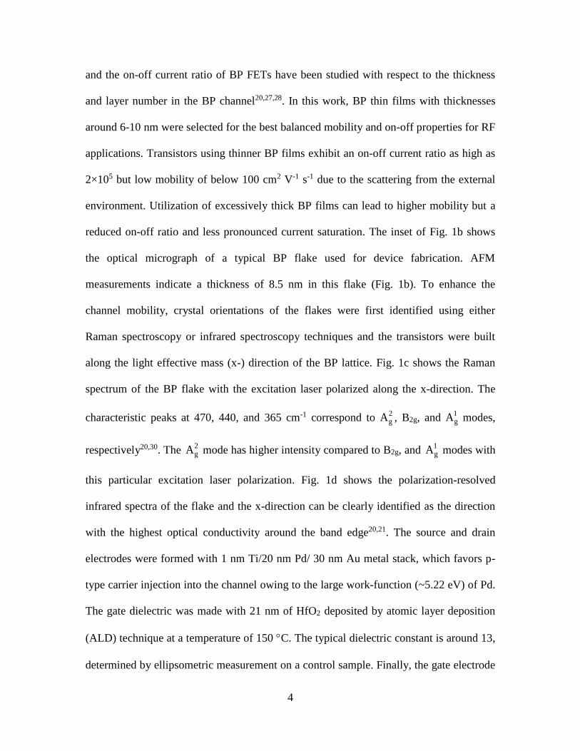
4
and the on-off current ratio of BP FETs have been studied with respect to the thickness
and layer number in the BP channel202728 In this work BP thin films with thicknesses
around 6-10 nm were selected for the best balanced mobility and on-off properties for RF
applications Transistors using thinner BP films exhibit an on-off current ratio as high as
2times105 but low mobility of below 100 cm2 V-1 s-1 due to the scattering from the external
environment Utilization of excessively thick BP films can lead to higher mobility but a
reduced on-off ratio and less pronounced current saturation The inset of Fig 1b shows
the optical micrograph of a typical BP flake used for device fabrication AFM
measurements indicate a thickness of 85 nm in this flake (Fig 1b) To enhance the
channel mobility crystal orientations of the flakes were first identified using either
Raman spectroscopy or infrared spectroscopy techniques and the transistors were built
along the light effective mass (x-) direction of the BP lattice Fig 1c shows the Raman
spectrum of the BP flake with the excitation laser polarized along the x-direction The
characteristic peaks at 470 440 and 365 cm-1 correspond to 2gA B2g and
1gA modes
respectively2030 The 2gA mode has higher intensity compared to B2g and
1gA modes with
this particular excitation laser polarization Fig 1d shows the polarization-resolved
infrared spectra of the flake and the x-direction can be clearly identified as the direction
with the highest optical conductivity around the band edge2021 The source and drain
electrodes were formed with 1 nm Ti20 nm Pd 30 nm Au metal stack which favors p-
type carrier injection into the channel owing to the large work-function (~522 eV) of Pd
The gate dielectric was made with 21 nm of HfO2 deposited by atomic layer deposition
(ALD) technique at a temperature of 150 C The typical dielectric constant is around 13
determined by ellipsometric measurement on a control sample Finally the gate electrode
5
was defined by electron-beam lithography to form transistors with sub-micrometer
channel lengths The fabrication process is described in more detail in Supporting
Information Fig 2b shows the optical micrograph of the full layout of the device The
standard ground-signal-ground (GSG) pads were fabricated to realize signal transition
from microwave coax cables to on-chip coplanar waveguide electrodes
DC Characterization
Fig 2a shows the schematic of the transistor structure Fig 2c and 2d display the
DC characteristics of a top-gated BP FET with a 300 nm channel length (LG) The device
was built along the x-direction of the 85 nm thick flake shown in Fig 1 Fig 2c shows
the measured drain current (IDS) as a function of drain-source bias voltage (VDS) at gate
bias (VGS) from 0 V to -2 V in steps of -05 V The current saturation in the BP transistor
is clearly visible and significantly improved from that in most graphene FETs due to the
finite bandgap in BP thin film This is typical for a BP device with ~85 nm channel
thickness and agrees well with previous demonstrations20 Good current saturation
characteristics will lead to low output conductance defined as 1198920 =d119868DS
d119881DS|
119881GS=constant which
is the differential drain current change with respect to the variation in drain voltage bias
Low output conductance is critical for improving voltage and power gains and to a lesser
extent the current gain in RF transistors As reported in our previous work20 typical Hall
mobility along x-direction of BP flakes with thickness around 8 nm is above 400 cm2 V-
1s-1 at room temperature Fig 2d shows IDS as a function of VGS at VDS=-2 V where on-
off current ratio over 2times103 is achieved The as-fabricated device shows p-type
conduction with threshold voltage around -07 V A key factor influencing the high-
6
frequency small signal response of a transistor is its transconductance (119892m) defined as the
first derivative of the transfer characteristics ie 119892m =d119868DS
d119881GS|
119881DS=constant The inset of Fig 2d
shows the measured 119892m as a function of the gate voltage at VDS=-2 V The peak value of
this extrinsic 119892m exceeds 180 mSmm at VG=-175 V while the peak on-state current
density measured exceeds 270 mAmm at VDS=-2 V and VGS=-25 V Fig 2d also shows
IDS as a function of top-gate voltage VGS at a drain bias of VDS=-2 V with the current
plotted in logarithmic scale The on-off current ratio of the device exceeds 2times103 Hence
the BP transistor demonstrated here shows significant advantages over graphene
transistors in terms of its current saturation properties and on-off current ratio Typical
monolayer graphene devices have on-off current ratio less than 10 at room temperature
In bilayer graphene devices the on-off current ratio only reaches around 100 even with
bandgap opening induced by a strong external electrical field31
RF Characterization
To characterize the high frequency performance of BP RF transistors we used the
standard S-parameter measurement with on-chip probing utilizing GSG probes and
Agilent N5230 vector network analyzer up to 50 GHz Key figures of merit for
microwave transistors can then be obtained for the BP devices The network analyzer and
the entire testing fixture were first calibrated using standard open short and load
calibrations Standard open and short structures were then used to de-embed the signals
of the parallel and series parasitics associated with the measurement pads and
connections1532-34 The measurement procedure used in this work followed strictly the
standard calibration and de-embedding processes widely accepted in the semiconductor
7
industry where the calibration step moves the reference plane to the tips of the GSG
probes and the de-embedding step gives access to the performance of the active device
region
Fig 3a and 3b plot the short-circuit current gain (h21) the unilateral power gain
(U) and maximum stable gain (MSG)maximum available gain (MAG) extracted from S-
parameters before and after de-embedding respectively measured at VDS=-20 V and
VGS=-17 V for the device with LG=300 nm The plot of |h21|2 follows the characteristic 1f
relation with respect to frequency at a 20 dBdec slope16 Fig 3a and 3b show that the
300 nm channel length device has a fT of 78 GHz before de-embedding and 12 GHz after
de-embedding as extracted from the frequencies at which |h21| reaches unity Gummelrsquos
method provides another way of extracting the cut-off frequency35 where fT is extracted
from the reciprocal of the initial slope in the imaginary part of 1h21 vs frequency plot
The values of fT obtained by both 1f extraction and Gummelrsquos method match closely for
both 300 nm (Fig 3c and 3d) and 1 m (see Fig S1 in the Supporting Information)
channel length devices before and after de-embedding
While fT is an important figure of merit related to the intrinsic speed of the BP
transistor another key figure of merit for analog application is the maximum oscillation
frequency It is the highest possible operating frequency at which a transistor can still
amplify power fmax can be extracted from U or MSGMAG of the device1636 The
unilateral power gain U also known more generally as Masonrsquos U invariant is a key
parameter for any general two-port network It carries great significance as an invariant
parameter of the system under linear lossless and reciprocal transformations In Masonrsquos
classic work3738 the rich physical meaning of U was interpreted in three different ways
8
as a maximum power gain as a device activity measure and as an invariant under a class
of bilinear Moumlbius transformations In transistor characterizations U is the power gain
under the condition of (1) Unilateralization and (2) Conjugate matched load for
maximum power transfer In Fig 3a and 3b the plots of U follow a 20 dBdec slope and
both U and MSGMAG plots give similar fmax of 12 GHz before de-embedding and 20
GHz after de-embedding respectively
The 300 nm channel length device has an extrinsic fTmiddotLG product of 36 GHz m
Using a slightly different design of the open pattern where the gate electrode in the ldquoopenrdquo
structure extends into the spacing between the source and drain electrodes15 we can
eliminate most of the gate-source and gate-drain parasitic capacitances Cgs and Cgd This
will allow the extraction of a new fT value that reflects the more intrinsic property of the
BP channel and an intrinsic fT value (fTint) close to 51 GHz is obtained for the same
device which corresponds to the average saturation velocity in the channel
approximately equal to vsat=2fTLG ~ 96times106 cms However we would like to
emphasize that fTint only represents the upper limit of the possible frequency spectrum for
this transistor In any practical applications the Cgs and Cgd of the device always
significantly affect the device performance As a result we report fT=12 GHz and fmax=20
GHz in Fig 3 as the practically operable cut-off frequencies of the active device
region1533 which are extracted based on standard characterization techniques commonly
used for the characterization in silicon and III-V high frequency transistors The intrinsic
cut-off frequency of 51 GHz is extracted only as a way to approximately estimate the
saturation velocity and it may not be appropriate for technology benchmarking The RF
characteristics for a device with 1 m channel length are also reported in the Supporting
9
Information The 1 m channel length device has peak fT=28 GHz and fmax=51 GHz
before de-embedding and fT=33 GHz and fmax=56 GHz after de-embedding (see Fig S1
in the Supporting Information)
The intrinsic limit of the cut-off frequency can be estimated using 119891119879 =119892119898
2120587119862119892119904
Assuming the same gm and gate dielectrics property from the measured data an fT above
100 GHz may be reached if the channel length reduces to 30 nm On the other hand fmax
depends on both the current and voltage gains It is related to fT following 119891119898119886119909 =119891119879
2 radic1199030
119877119892+119877119894
We can see that a high fT will enhance fmax and good current saturation ie high output
resistance (r0) low gate resistance (Rg) and low input resistance (Ri) are critical for
improving fmax of the device
Fig 4 shows the magnitude of the small-signal open-circuit voltage gain |z21z11|
as a function of frequency before and after de-embedding An open-circuit voltage gain
refers to the voltage gain subject to infinitely high load impedance Here the voltage gain
is obtained from the ratio between the open circuit forward transfer impedance z21 and the
open circuit input impedance z11 Since 11991111 =1199071
1198941|
1198942=0 and 11991121 =
1199072
1198941|
1198942=0 the ratio z21z11 is
equal to 1199072
1199071|
1198942=0 ie the voltage gain with the output port in open condition v1 and v2
refer to the voltages at the input and output ports respectively In transistors v1 is the
small-signal input voltage at the gate and the v2 is the small-signal output voltage at the
drain Based on the definition of gm and g0 discussed earlier we can see that the voltage
gain |z21z11| is closely related to the ratio gmg0 Devices with good current saturation and
high transcondutance are hence expected to have high voltage gains The BP transistors
show good voltage gain characteristics As shown in Fig 4 the before-de-embedding
10
voltage gain stays above unity (0 dB) up to 13 GHz The after-de-embedding voltage gain
is close to 20 dB at 2 GHz and stays above unity (0 dB) for the entire frequency range
measured up to 50 GHz For a longer channel length (1 m) device (see Fig S2 in the
Supporting Information) the before-de-embedding voltage gain is above unity (0 dB) up
to 10 GHz The after-de-embedding voltage gain is above 15 dB at 1 GHz and stays
above unity (0 dB) up to 30 GHz
Summary
In this work we investigated the high frequency characteristics of black
phosphorus field effect transistors whose channels were fabricated along the light
effective mass (x-) direction The device operates well into the GHz frequency range of
the radio frequency spectrum We carried out standard S-parameter measurements to
characterize the high frequency response of these top-gated BP transistors The short-
circuit current gain maximum stable gainmaximum available gain unilateral power gain
and voltage gain of the devices were carefully extracted The short-circuit current gain of
BP transistors shows the 20 dBdec 1f frequency dependence at high frequency We
measured a peak short-circuit current gain cutoff frequency fT of 12 GHz and maximum
oscillation frequency fmax of 20 GHz for a 300 nm channel length BP transistor
demonstrating the GHz operation of BP devices for the first time These results clearly
reveal the potentials of BP transistors to function as power and voltage amplifiers in
multi-GHz frequency analogue and digital electronics demanded by many emerging
civilian and military applications
11
References
1 Powell M J The physics of amorphous-silicon thin-film transistors IEEE Trans
Electron Devices 36 2753-2763 (1989)
2 Street R A Thin-Film Transistors Adv Mater 21 2007-2022 (2009)
3 Hawkins W G Polycrystalline-silicon device technology for large-area electronics
IEEE Trans Electron Devices 33 477-481 (1986)
4 Forrest S R The path to ubiquitous and low-cost organic electronic appliances on
plastic Nature 428 911-918 (2004)
5 Dimitrakopoulos C D Mascaro D J Organic thin-film transistors A review of
recent advances IBM J Res Dev 45 11-27 (2004)
6 Nomura K et al Amorphous Oxide Semiconductors for High-Performance Flexible
Thin-Film Transistors Japanese Journal of Applied Physics 45 4303 (2006)
7 Carcia P F McLean R S Reilly M H amp Nunes G Jr Transparent ZnO thin-film
transistor fabricated by RF magnetron sputtering Appl Phys Lett 82 1117 (2003)
8 Meric I Baklitskaya N Kim P amp Shepard K L RF performance of top-gated
zero-bandgap graphene field-effect transistors IEEE IEDM Tech Digest 2008
9 Lin Y-M Dimitrakopoulos C D Jenkins K A Farmer D B Chiu H-Y Grill
A amp Avouris P 100-GHz Transistors from Wafer-Scale Epitaxial Graphene Science
327 662 (2010)
10 Wu Y Lin Y Bol A A Jenkins K A Xia F Farmer D B Zhu Y amp
Avouris P High-frequency scaled graphene transistors on diamond-like carbon Nature
472 74-78 (2011)
11 Liao L et al High-speed graphene transistors with a self-aligned nanowire gate
Nature 467 305ndash308 (2010)
12 Wang H Nezich D Kong J amp Palacios T Graphene frequency multipliers IEEE
Elec Dev Lett 30 547-549 (2009)
13 Wang H Hsu A Wu J Kong J amp Palacios T Graphene-based ambipolar RF
mixers IEEE Elec Dev Lett 31 906-908 (2010)
12
14 Han S-J Valdes-Garcia A Oida S Jenkins K A amp Haensch W Graphene radio
frequency receiver integrated circuit Nat Commun 53086 doi101038ncomms4086
(2014)
15 Wang H Chapter 4 In Two-Dimensional Materials for Electronic Applications Ph
D Thesis Massachusetts Institute of Technology Cambridge MA USA 2014
httpdspacemiteduhandle1721184899
16 Schwierz F amp Liou J J Modern Microwave Transistors Theory Design and
Performance Wiley-Interscience 1st edition 2002
17 Tasker P J amp Hughes B Importance of source and drain resistance to the maximum
f T of millimeter-wave MODFETs IEEE Elec Dev Lett 10 291-293 (1989)
18 Zhu W Low T Lee Y-H Wang H Farmer D B Kong J Xia F amp Avouris
P Electronic transport and device prospects of monolayer molybdenum disulphide grown
by chemical vapour deposition Nat Commun 53087 doi101038ncomms4087 (2014)
19 Huang J-K et al Large-Area Synthesis of Highly Crystalline WSe2 Monolayers and
Device Applications ACS Nano 8 923-930 (2014)
20 Xia F Wang H amp Jia Y Rediscovering black phosphorus as an anisotropic layered
material for optoelectronics and electronics Nat Commun 54458
doi101038ncomms5458 (2014)
21 Morita A Semiconducting black phosphorus Appl Phys A 39 227-242 1986
22 Keyes R The electrical properties of black phosphorus Phys Rev 92 580-584
(1953)
23 Warschauer D Electrical and optical properties of crystalline black phosphorus J
Appl Phys 34 1853-1860 (1963)
24 Jamieson J Crystal structures adopted by black phosphorus at high pressures
Science 139 1291-1292 (1963)
25 Wittig J amp Matthias B T Superconducting phosphorus Science 160 994-995
(1968)
26 Maruyama Y Suzuki S Kobayashi K amp Tanuma S Synthesis and some
properties of black phosphorus single crystals Physica 105B 99-102 (1981)
13
27 Li L et al Black phosphorus field-effect transistors Nat Nanotechnol 9 372-377
(2014)
28 Liu H et al Phosphorene an unexplored 2D semiconductor with a high hole
mobility ACS Nano 8 4033-4041 (2014)
29 Koenig S Doganov R Schmidt H Castro Neto A amp Ozyilmaz B Electric field
effect in ultrathin black phosphorus Appl Phys Lett 104 103106 (2014)
30 Akahama Y Kobayashi M amp Kawamura H Raman study of black phosphorus up
to 13 GPa Solid State Comm 104 311-315 (1997)
31 Xia F Farmer D B Lin Y-M Avouris P Graphene field-effect transistors with
high onoff current ratio and large transport band gap at room temperature Nano Lett 10
715-718 (2010)
32 R J Collier and A D Skinner Microwave Measurements 3rd Edition the
Institution of Engineering and Technology 2007
33 Koolen M C A Geelen J A amp Versleijen M P J An improved de-embedding
technique for on-wafer high-frequency characterization Proceedings of the Bipolar
Circuits and Technology Meeting 1991 188ndash191 (1991)
34 Kim J-Y Choi M-K amp Lee S-H A lsquoThru-Short-Openrsquo De-embedding Method
for Accurate On-Wafer RF Measurements of Nano-Scale MOSFETs JSTSJournal of
Semiconductor Technology and Science 12 53ndash58 (2012)
35 Gummel H K On the definition of the cutoff frequency fT Proceedings of the IEEE
57 12 2159ndash2159 (1969)
36 S-Parameter Techniques HP Application Note 95-1
httpwwwhparchivecomApplication_NotesHP-AN-95-1pdf
37 Mason S J Power gain in feedback amplifiers Trans IRE Professional Group on
Circuit Theory CT-1 20-25 (1954) (This work was previously reported in Tech Rep
No 257 Research Laboratory of Electronics MIT Cambridge MA 1953
38 Gupta M S Power Gain in Feedback Amplifiers a Classic Revisited IEEE Trans
Microwave Theory and Techniques 40 5 (1992)
14
Competing financial interests
Authors declare no competing financial interests
Supporting Information
Information on the device fabrication process and characterization method additional
high frequency characterization data are included in the Supporting Information This
material is available free of charge via the Internet at httppubsacsorg
Additional information
Correspondence and requests for materials should be addressed to HW
(hanwang4uscedu) and F X (fengnianxiayaleedu)
Figure Captions
Figure 1 Characterization of the black phosphorus (BP) thin film
(a) Layered crystal structure of black phosphorus The spacing between adjacent layers is
53 Aring (b) atomic force microscope (AFM) data showing the thickness of a BP flake The
inset shows the optical micrograph of the BP flake with thickness around 85 nm (c)
Raman spectrum of the BP flake along x-direction (d) Polarization-resolved infrared
spectra of a BP flake
Figure 2 DC characteristics of BP transistors
(a) Schematic of the BP transistor device structure (b) Optical micrograph of the
fabricated device (c) Output characteristics of the BP transistor LG= 300 nm (d)
Transfer characteristics of the same BP transistor plotted in both linear and logarithmic
15
scale VDS=-2 V The device has an on-off current ratio exceeding 2times103 The inset shows
the transconductance gm of the device
Figure 3 Current and power gain in BP transistors at GHz frequency
(a) and (b) the short-circuit current gain h21 the maximum stable gain and maximum
available gain MSGMAG and the unilateral power gain U of the 300 nm channel length
device before and after de-embedding respectively The device has fT=78 GHz fmax=12
GHz before de-embedding and fT=12 GHz fmax=20 GHz after de-embedding (c) and (d)
the imaginary part of 1h21 as a function of frequency before and after de-embedding
respectively Based on Gummelrsquos method the initial slope of the curve is equal to 1fT
Figure 4 Open-circuit voltage gain in BP transistors at GHz frequency
The open-circuit voltage gain (z21z11) before and after de-embedding is shown as a
function of the frequency After de-embedding the voltage gain stays close to 20 dB up
to 2 GHz and is above unity (0 dB) in the entire measurement range up to 50 GHz The
grey dashed line is a guide to the eyes
0 1 2 3 40
2
4
6
8
10
12
He
igh
t (n
m)
Distance (m)
85 nm10 m
b
c d
a
53 Aring
300 350 400 450 500
00
03
06
09
12
15
B2g
A2
g
Inte
nsity (
au
)
Raman Shift (cm-1)
A1
g
Excitation light polarized
along x-direction
x
y z
Figure 1 Characterization of the black phosphorus (BP) thin film
2000 3000 4000-005
000
005
010
015
1-T
T0
Wavenumber (cm-1)
x
y
Figure 2 DC characteristics of BP transistors
-20 -15 -10 -05 000
-50
-100
-150
-200
-250 V
G=-20 V
VG=-15 V
VG=-10 V
VG=-05 V
VG= 0 V
I DS (
mA
mm
)
VDS
(V)
S
D
G
SiO2
BP
x
S
b a
d c
-2 -1 0 1 2 30
-50
-100
-150
-200
-250
-300
-350
|ID
S| (m
Am
m)
VG (V)
I DS (
mA
mm
)
01
1
10
100
onoff ~2times103
-2 -1 0 10
40
80
120
160
200
gm (
mS
mm
)V
G (V)
S
G D
S
LG = 300 nm
t ~ 85 nm
tox ~ 21 nm HfO2
50 m
BP
Figure 3 Current and power gain in BP transistors at
GHz frequency
1 100
5
10
15
20
25
30
35
Frequency (GHz)
Gain
(dB
)Before De-embedding
LG=300 nm
|h21|2
MSGMAG
U
fmax
=12 GHz
fT=8 GHz
1 100
5
10
15
20
25
30
35
fmax
=20 GHz
Frequency (GHz)
Gain
(dB
)
fT=12 GHz
LG=300 nm
|h21|2
MSGMAG
U
After De-embedding
0 2 4 6 8 1000
02
04
06
08
10
12
Im (1h21
(f))=ffT
Before De-embedding
fT=76 GHz
Slope=fT
-1
Frequency (GHz)
Im (
1h
21)
0 2 4 6 8 1000
02
04
06
08
10
12
Im (1h21
(f))=ffT
After De-embedding
Frequency (GHz)
fT=119 GHz
Slope=fT
-1Im (
1h
21)
a b
c d
Figure 4 Open-circuit voltage gain in BP transistors at
GHz frequency
1 10 1000
5
10
15
20
25
30
35
Frequency (GHz)
Vo
lta
ge
Ga
in |z
21z
11| (d
B)
LG=300 nm
|z21
z11
| before de-embedding
|z21
z11
| after de-embedding
1
Supporting Information for
Black Phosphorus Radio-Frequency Transistors
Han Wang1 Xiaomu Wang2 Fengnian Xia2 Luhao Wang1 Hao Jiang3
Qiangfei Xia3 Matthew L Chin4 Madan Dubey4 Shu-jen Han5
1Ming Hsieh Department of Electrical Engineering University of Southern California
Los Angeles CA 90089
2Department of Electrical Engineering Yale University New Haven CT 06511
3Department of Electrical amp Computer Engineering University of Massachusetts
Amherst MA 01003
4 Sensors and Electron Devices Directorate US Army Research Laboratory
Adelphi MD 20723
5IBM T J Watson Research Center Yorktown Heights NY 10598
Email hanwang4uscedu fengnianxiayaleedu
Methods
Top-gated transistor fabrication The fabrication of our devices starts with the
exfoliation of BP thin films from bulk BP crystals onto 300 nm SiO2 on a Si substrate
which has pre-patterned alignment grids using the micro-mechanical cleavage technique
The thickness of the SiO2 was selected to provide the optimal optical contrast for locating
BP flakes relative to the alignment grids The thickness of BP layers was measured by
atomic force microscopy (AFM) The next step was to pattern the resist layer for
metallization using a Vistec 100 kV electron-beam lithography system based on poly
(methyl methacrylate) (950k MW PMMA) PMMA A3 was spun on wafer at a speed of
3000 rpm for 1 minute and was then bakes at 175 degrees for 3 minutes The dose for
exposure is 1100 microC cm-2 Development was performed in 13 MIBK IPA (Methyl
isobutyl ketone Isopropanol) for 90 s We then evaporated 1 nm Ti20 nm Pd30 nm Au
2
followed by lift-off in acetone to form the contacts The HfO2 gate dielectric is deposited
using atomic layer deposition (ALD) at 150 C The gate electrode is also patterned using
Vistec 100 kV electron-beam lithography system
AFM Atomic force microscopy (AFM) for identifying the thin film thickness was
performed on a Digital InstrumentsVeeco Dimension 3000 system
IR spectroscopy Bruker Optics Fourier Transfer Infrared spectrometer (Vertex 70)
integrated with a Hyperion 2000 microscope system was used to measure the infrared
spectroscopy of the BP flakes in the 800 cm-1 to 4000 cm-1 range The linear polarization
of the incident light was achieved using an infrared polarizer
Electrical characterization DC electrical characterizations were performed using an
Agilent B1500 semiconductor parameter analyzer and a Lakeshore cryogenic probe station
with micromanipulation probes The high frequency characterizations were performed
using an Agilent N5230A Vector Network Analyzer
High frequency characterization of BP transistor with 1 m channel length
The short-circuit current and power gain of a BP transistor with 1 m channel length are
shown in Fig S1 The open-circuit voltage gain z21z11 both before and after de-embedding
are shown in Fig S2 The device has fT=28 GHz fmax=51 GHz before de-embedding and
fT=33 GHz fmax=56 GHz after de-embedding After de-embedding the voltage gain stays
above 15 dB up around 1 GHz and is above unity (0 dB) up to 30 GHz
3
Fig S1 (a) and (b) the short-circuit current gain h21 the maximum stable gain and maximum available gain
MSGMAG and the unilateral power gain U of the device with 1 m channel length before and after de-
embedding respectively The device has fT=28 GHz fmax=51 GHz before de-embedding and fT=33 GHz
fmax=56 GHz after de-embedding (c) and (d) the imaginary part of 1h21 as a function of frequency before
and after de-embedding respectively Based on Gummelrsquos method the initial slope of the curve is equal to
1fT
Fig S2 the open-circuit voltage gain (z21z11) before and after de-embedding is shown as a function of the
frequency After de-embedding the voltage gain stays above 15 dB up to around 1 GHz and is above unity
(0 dB) up to 30 GHz
01 1 100
5
10
15
20
25
30
35
Frequency (GHz)
Gain
(dB
)
Before De-embedding
LG=1 m
|h21|2
MSGMAG
U
fmax
=51 GHz
fT=28 GHz
a
b
c
0 1 2 3 400
02
04
06
08
10
12
Im (1h21
(f))=ffT
Before De-embedding
fT=28 GHz
Slope=fT
-1
Frequency (GHz)
Im (
1h
21)
d
0 1 2 3 400
02
04
06
08
10
12
Im (1h21
(f))=ffT
After De-embedding
Frequency (GHz)
fT=35 GHz
Slope=fT
-1Im (
1h
21)
01 1 100
5
10
15
20
25
30
35
fmax
=56 GHz
Frequency (GHz)
Gain
(dB
)
fT=33 GHz
LG=1 m
|h21|2
MSGMAG
U
After De-embedding
1 100
5
10
15
20
25
30
35
Frequency (GHz)
Voltage G
ain
z21z
11 (
dB
)
LG=1 m
|z21
z11
| before de-embedding
|z21
z11
| after de-embedding
- Main_text_arXiv
- Figure 21
- Supporting_Information_arXiv
-
5
was defined by electron-beam lithography to form transistors with sub-micrometer
channel lengths The fabrication process is described in more detail in Supporting
Information Fig 2b shows the optical micrograph of the full layout of the device The
standard ground-signal-ground (GSG) pads were fabricated to realize signal transition
from microwave coax cables to on-chip coplanar waveguide electrodes
DC Characterization
Fig 2a shows the schematic of the transistor structure Fig 2c and 2d display the
DC characteristics of a top-gated BP FET with a 300 nm channel length (LG) The device
was built along the x-direction of the 85 nm thick flake shown in Fig 1 Fig 2c shows
the measured drain current (IDS) as a function of drain-source bias voltage (VDS) at gate
bias (VGS) from 0 V to -2 V in steps of -05 V The current saturation in the BP transistor
is clearly visible and significantly improved from that in most graphene FETs due to the
finite bandgap in BP thin film This is typical for a BP device with ~85 nm channel
thickness and agrees well with previous demonstrations20 Good current saturation
characteristics will lead to low output conductance defined as 1198920 =d119868DS
d119881DS|
119881GS=constant which
is the differential drain current change with respect to the variation in drain voltage bias
Low output conductance is critical for improving voltage and power gains and to a lesser
extent the current gain in RF transistors As reported in our previous work20 typical Hall
mobility along x-direction of BP flakes with thickness around 8 nm is above 400 cm2 V-
1s-1 at room temperature Fig 2d shows IDS as a function of VGS at VDS=-2 V where on-
off current ratio over 2times103 is achieved The as-fabricated device shows p-type
conduction with threshold voltage around -07 V A key factor influencing the high-
6
frequency small signal response of a transistor is its transconductance (119892m) defined as the
first derivative of the transfer characteristics ie 119892m =d119868DS
d119881GS|
119881DS=constant The inset of Fig 2d
shows the measured 119892m as a function of the gate voltage at VDS=-2 V The peak value of
this extrinsic 119892m exceeds 180 mSmm at VG=-175 V while the peak on-state current
density measured exceeds 270 mAmm at VDS=-2 V and VGS=-25 V Fig 2d also shows
IDS as a function of top-gate voltage VGS at a drain bias of VDS=-2 V with the current
plotted in logarithmic scale The on-off current ratio of the device exceeds 2times103 Hence
the BP transistor demonstrated here shows significant advantages over graphene
transistors in terms of its current saturation properties and on-off current ratio Typical
monolayer graphene devices have on-off current ratio less than 10 at room temperature
In bilayer graphene devices the on-off current ratio only reaches around 100 even with
bandgap opening induced by a strong external electrical field31
RF Characterization
To characterize the high frequency performance of BP RF transistors we used the
standard S-parameter measurement with on-chip probing utilizing GSG probes and
Agilent N5230 vector network analyzer up to 50 GHz Key figures of merit for
microwave transistors can then be obtained for the BP devices The network analyzer and
the entire testing fixture were first calibrated using standard open short and load
calibrations Standard open and short structures were then used to de-embed the signals
of the parallel and series parasitics associated with the measurement pads and
connections1532-34 The measurement procedure used in this work followed strictly the
standard calibration and de-embedding processes widely accepted in the semiconductor
7
industry where the calibration step moves the reference plane to the tips of the GSG
probes and the de-embedding step gives access to the performance of the active device
region
Fig 3a and 3b plot the short-circuit current gain (h21) the unilateral power gain
(U) and maximum stable gain (MSG)maximum available gain (MAG) extracted from S-
parameters before and after de-embedding respectively measured at VDS=-20 V and
VGS=-17 V for the device with LG=300 nm The plot of |h21|2 follows the characteristic 1f
relation with respect to frequency at a 20 dBdec slope16 Fig 3a and 3b show that the
300 nm channel length device has a fT of 78 GHz before de-embedding and 12 GHz after
de-embedding as extracted from the frequencies at which |h21| reaches unity Gummelrsquos
method provides another way of extracting the cut-off frequency35 where fT is extracted
from the reciprocal of the initial slope in the imaginary part of 1h21 vs frequency plot
The values of fT obtained by both 1f extraction and Gummelrsquos method match closely for
both 300 nm (Fig 3c and 3d) and 1 m (see Fig S1 in the Supporting Information)
channel length devices before and after de-embedding
While fT is an important figure of merit related to the intrinsic speed of the BP
transistor another key figure of merit for analog application is the maximum oscillation
frequency It is the highest possible operating frequency at which a transistor can still
amplify power fmax can be extracted from U or MSGMAG of the device1636 The
unilateral power gain U also known more generally as Masonrsquos U invariant is a key
parameter for any general two-port network It carries great significance as an invariant
parameter of the system under linear lossless and reciprocal transformations In Masonrsquos
classic work3738 the rich physical meaning of U was interpreted in three different ways
8
as a maximum power gain as a device activity measure and as an invariant under a class
of bilinear Moumlbius transformations In transistor characterizations U is the power gain
under the condition of (1) Unilateralization and (2) Conjugate matched load for
maximum power transfer In Fig 3a and 3b the plots of U follow a 20 dBdec slope and
both U and MSGMAG plots give similar fmax of 12 GHz before de-embedding and 20
GHz after de-embedding respectively
The 300 nm channel length device has an extrinsic fTmiddotLG product of 36 GHz m
Using a slightly different design of the open pattern where the gate electrode in the ldquoopenrdquo
structure extends into the spacing between the source and drain electrodes15 we can
eliminate most of the gate-source and gate-drain parasitic capacitances Cgs and Cgd This
will allow the extraction of a new fT value that reflects the more intrinsic property of the
BP channel and an intrinsic fT value (fTint) close to 51 GHz is obtained for the same
device which corresponds to the average saturation velocity in the channel
approximately equal to vsat=2fTLG ~ 96times106 cms However we would like to
emphasize that fTint only represents the upper limit of the possible frequency spectrum for
this transistor In any practical applications the Cgs and Cgd of the device always
significantly affect the device performance As a result we report fT=12 GHz and fmax=20
GHz in Fig 3 as the practically operable cut-off frequencies of the active device
region1533 which are extracted based on standard characterization techniques commonly
used for the characterization in silicon and III-V high frequency transistors The intrinsic
cut-off frequency of 51 GHz is extracted only as a way to approximately estimate the
saturation velocity and it may not be appropriate for technology benchmarking The RF
characteristics for a device with 1 m channel length are also reported in the Supporting
9
Information The 1 m channel length device has peak fT=28 GHz and fmax=51 GHz
before de-embedding and fT=33 GHz and fmax=56 GHz after de-embedding (see Fig S1
in the Supporting Information)
The intrinsic limit of the cut-off frequency can be estimated using 119891119879 =119892119898
2120587119862119892119904
Assuming the same gm and gate dielectrics property from the measured data an fT above
100 GHz may be reached if the channel length reduces to 30 nm On the other hand fmax
depends on both the current and voltage gains It is related to fT following 119891119898119886119909 =119891119879
2 radic1199030
119877119892+119877119894
We can see that a high fT will enhance fmax and good current saturation ie high output
resistance (r0) low gate resistance (Rg) and low input resistance (Ri) are critical for
improving fmax of the device
Fig 4 shows the magnitude of the small-signal open-circuit voltage gain |z21z11|
as a function of frequency before and after de-embedding An open-circuit voltage gain
refers to the voltage gain subject to infinitely high load impedance Here the voltage gain
is obtained from the ratio between the open circuit forward transfer impedance z21 and the
open circuit input impedance z11 Since 11991111 =1199071
1198941|
1198942=0 and 11991121 =
1199072
1198941|
1198942=0 the ratio z21z11 is
equal to 1199072
1199071|
1198942=0 ie the voltage gain with the output port in open condition v1 and v2
refer to the voltages at the input and output ports respectively In transistors v1 is the
small-signal input voltage at the gate and the v2 is the small-signal output voltage at the
drain Based on the definition of gm and g0 discussed earlier we can see that the voltage
gain |z21z11| is closely related to the ratio gmg0 Devices with good current saturation and
high transcondutance are hence expected to have high voltage gains The BP transistors
show good voltage gain characteristics As shown in Fig 4 the before-de-embedding
10
voltage gain stays above unity (0 dB) up to 13 GHz The after-de-embedding voltage gain
is close to 20 dB at 2 GHz and stays above unity (0 dB) for the entire frequency range
measured up to 50 GHz For a longer channel length (1 m) device (see Fig S2 in the
Supporting Information) the before-de-embedding voltage gain is above unity (0 dB) up
to 10 GHz The after-de-embedding voltage gain is above 15 dB at 1 GHz and stays
above unity (0 dB) up to 30 GHz
Summary
In this work we investigated the high frequency characteristics of black
phosphorus field effect transistors whose channels were fabricated along the light
effective mass (x-) direction The device operates well into the GHz frequency range of
the radio frequency spectrum We carried out standard S-parameter measurements to
characterize the high frequency response of these top-gated BP transistors The short-
circuit current gain maximum stable gainmaximum available gain unilateral power gain
and voltage gain of the devices were carefully extracted The short-circuit current gain of
BP transistors shows the 20 dBdec 1f frequency dependence at high frequency We
measured a peak short-circuit current gain cutoff frequency fT of 12 GHz and maximum
oscillation frequency fmax of 20 GHz for a 300 nm channel length BP transistor
demonstrating the GHz operation of BP devices for the first time These results clearly
reveal the potentials of BP transistors to function as power and voltage amplifiers in
multi-GHz frequency analogue and digital electronics demanded by many emerging
civilian and military applications
11
References
1 Powell M J The physics of amorphous-silicon thin-film transistors IEEE Trans
Electron Devices 36 2753-2763 (1989)
2 Street R A Thin-Film Transistors Adv Mater 21 2007-2022 (2009)
3 Hawkins W G Polycrystalline-silicon device technology for large-area electronics
IEEE Trans Electron Devices 33 477-481 (1986)
4 Forrest S R The path to ubiquitous and low-cost organic electronic appliances on
plastic Nature 428 911-918 (2004)
5 Dimitrakopoulos C D Mascaro D J Organic thin-film transistors A review of
recent advances IBM J Res Dev 45 11-27 (2004)
6 Nomura K et al Amorphous Oxide Semiconductors for High-Performance Flexible
Thin-Film Transistors Japanese Journal of Applied Physics 45 4303 (2006)
7 Carcia P F McLean R S Reilly M H amp Nunes G Jr Transparent ZnO thin-film
transistor fabricated by RF magnetron sputtering Appl Phys Lett 82 1117 (2003)
8 Meric I Baklitskaya N Kim P amp Shepard K L RF performance of top-gated
zero-bandgap graphene field-effect transistors IEEE IEDM Tech Digest 2008
9 Lin Y-M Dimitrakopoulos C D Jenkins K A Farmer D B Chiu H-Y Grill
A amp Avouris P 100-GHz Transistors from Wafer-Scale Epitaxial Graphene Science
327 662 (2010)
10 Wu Y Lin Y Bol A A Jenkins K A Xia F Farmer D B Zhu Y amp
Avouris P High-frequency scaled graphene transistors on diamond-like carbon Nature
472 74-78 (2011)
11 Liao L et al High-speed graphene transistors with a self-aligned nanowire gate
Nature 467 305ndash308 (2010)
12 Wang H Nezich D Kong J amp Palacios T Graphene frequency multipliers IEEE
Elec Dev Lett 30 547-549 (2009)
13 Wang H Hsu A Wu J Kong J amp Palacios T Graphene-based ambipolar RF
mixers IEEE Elec Dev Lett 31 906-908 (2010)
12
14 Han S-J Valdes-Garcia A Oida S Jenkins K A amp Haensch W Graphene radio
frequency receiver integrated circuit Nat Commun 53086 doi101038ncomms4086
(2014)
15 Wang H Chapter 4 In Two-Dimensional Materials for Electronic Applications Ph
D Thesis Massachusetts Institute of Technology Cambridge MA USA 2014
httpdspacemiteduhandle1721184899
16 Schwierz F amp Liou J J Modern Microwave Transistors Theory Design and
Performance Wiley-Interscience 1st edition 2002
17 Tasker P J amp Hughes B Importance of source and drain resistance to the maximum
f T of millimeter-wave MODFETs IEEE Elec Dev Lett 10 291-293 (1989)
18 Zhu W Low T Lee Y-H Wang H Farmer D B Kong J Xia F amp Avouris
P Electronic transport and device prospects of monolayer molybdenum disulphide grown
by chemical vapour deposition Nat Commun 53087 doi101038ncomms4087 (2014)
19 Huang J-K et al Large-Area Synthesis of Highly Crystalline WSe2 Monolayers and
Device Applications ACS Nano 8 923-930 (2014)
20 Xia F Wang H amp Jia Y Rediscovering black phosphorus as an anisotropic layered
material for optoelectronics and electronics Nat Commun 54458
doi101038ncomms5458 (2014)
21 Morita A Semiconducting black phosphorus Appl Phys A 39 227-242 1986
22 Keyes R The electrical properties of black phosphorus Phys Rev 92 580-584
(1953)
23 Warschauer D Electrical and optical properties of crystalline black phosphorus J
Appl Phys 34 1853-1860 (1963)
24 Jamieson J Crystal structures adopted by black phosphorus at high pressures
Science 139 1291-1292 (1963)
25 Wittig J amp Matthias B T Superconducting phosphorus Science 160 994-995
(1968)
26 Maruyama Y Suzuki S Kobayashi K amp Tanuma S Synthesis and some
properties of black phosphorus single crystals Physica 105B 99-102 (1981)
13
27 Li L et al Black phosphorus field-effect transistors Nat Nanotechnol 9 372-377
(2014)
28 Liu H et al Phosphorene an unexplored 2D semiconductor with a high hole
mobility ACS Nano 8 4033-4041 (2014)
29 Koenig S Doganov R Schmidt H Castro Neto A amp Ozyilmaz B Electric field
effect in ultrathin black phosphorus Appl Phys Lett 104 103106 (2014)
30 Akahama Y Kobayashi M amp Kawamura H Raman study of black phosphorus up
to 13 GPa Solid State Comm 104 311-315 (1997)
31 Xia F Farmer D B Lin Y-M Avouris P Graphene field-effect transistors with
high onoff current ratio and large transport band gap at room temperature Nano Lett 10
715-718 (2010)
32 R J Collier and A D Skinner Microwave Measurements 3rd Edition the
Institution of Engineering and Technology 2007
33 Koolen M C A Geelen J A amp Versleijen M P J An improved de-embedding
technique for on-wafer high-frequency characterization Proceedings of the Bipolar
Circuits and Technology Meeting 1991 188ndash191 (1991)
34 Kim J-Y Choi M-K amp Lee S-H A lsquoThru-Short-Openrsquo De-embedding Method
for Accurate On-Wafer RF Measurements of Nano-Scale MOSFETs JSTSJournal of
Semiconductor Technology and Science 12 53ndash58 (2012)
35 Gummel H K On the definition of the cutoff frequency fT Proceedings of the IEEE
57 12 2159ndash2159 (1969)
36 S-Parameter Techniques HP Application Note 95-1
httpwwwhparchivecomApplication_NotesHP-AN-95-1pdf
37 Mason S J Power gain in feedback amplifiers Trans IRE Professional Group on
Circuit Theory CT-1 20-25 (1954) (This work was previously reported in Tech Rep
No 257 Research Laboratory of Electronics MIT Cambridge MA 1953
38 Gupta M S Power Gain in Feedback Amplifiers a Classic Revisited IEEE Trans
Microwave Theory and Techniques 40 5 (1992)
14
Competing financial interests
Authors declare no competing financial interests
Supporting Information
Information on the device fabrication process and characterization method additional
high frequency characterization data are included in the Supporting Information This
material is available free of charge via the Internet at httppubsacsorg
Additional information
Correspondence and requests for materials should be addressed to HW
(hanwang4uscedu) and F X (fengnianxiayaleedu)
Figure Captions
Figure 1 Characterization of the black phosphorus (BP) thin film
(a) Layered crystal structure of black phosphorus The spacing between adjacent layers is
53 Aring (b) atomic force microscope (AFM) data showing the thickness of a BP flake The
inset shows the optical micrograph of the BP flake with thickness around 85 nm (c)
Raman spectrum of the BP flake along x-direction (d) Polarization-resolved infrared
spectra of a BP flake
Figure 2 DC characteristics of BP transistors
(a) Schematic of the BP transistor device structure (b) Optical micrograph of the
fabricated device (c) Output characteristics of the BP transistor LG= 300 nm (d)
Transfer characteristics of the same BP transistor plotted in both linear and logarithmic
15
scale VDS=-2 V The device has an on-off current ratio exceeding 2times103 The inset shows
the transconductance gm of the device
Figure 3 Current and power gain in BP transistors at GHz frequency
(a) and (b) the short-circuit current gain h21 the maximum stable gain and maximum
available gain MSGMAG and the unilateral power gain U of the 300 nm channel length
device before and after de-embedding respectively The device has fT=78 GHz fmax=12
GHz before de-embedding and fT=12 GHz fmax=20 GHz after de-embedding (c) and (d)
the imaginary part of 1h21 as a function of frequency before and after de-embedding
respectively Based on Gummelrsquos method the initial slope of the curve is equal to 1fT
Figure 4 Open-circuit voltage gain in BP transistors at GHz frequency
The open-circuit voltage gain (z21z11) before and after de-embedding is shown as a
function of the frequency After de-embedding the voltage gain stays close to 20 dB up
to 2 GHz and is above unity (0 dB) in the entire measurement range up to 50 GHz The
grey dashed line is a guide to the eyes
0 1 2 3 40
2
4
6
8
10
12
He
igh
t (n
m)
Distance (m)
85 nm10 m
b
c d
a
53 Aring
300 350 400 450 500
00
03
06
09
12
15
B2g
A2
g
Inte
nsity (
au
)
Raman Shift (cm-1)
A1
g
Excitation light polarized
along x-direction
x
y z
Figure 1 Characterization of the black phosphorus (BP) thin film
2000 3000 4000-005
000
005
010
015
1-T
T0
Wavenumber (cm-1)
x
y
Figure 2 DC characteristics of BP transistors
-20 -15 -10 -05 000
-50
-100
-150
-200
-250 V
G=-20 V
VG=-15 V
VG=-10 V
VG=-05 V
VG= 0 V
I DS (
mA
mm
)
VDS
(V)
S
D
G
SiO2
BP
x
S
b a
d c
-2 -1 0 1 2 30
-50
-100
-150
-200
-250
-300
-350
|ID
S| (m
Am
m)
VG (V)
I DS (
mA
mm
)
01
1
10
100
onoff ~2times103
-2 -1 0 10
40
80
120
160
200
gm (
mS
mm
)V
G (V)
S
G D
S
LG = 300 nm
t ~ 85 nm
tox ~ 21 nm HfO2
50 m
BP
Figure 3 Current and power gain in BP transistors at
GHz frequency
1 100
5
10
15
20
25
30
35
Frequency (GHz)
Gain
(dB
)Before De-embedding
LG=300 nm
|h21|2
MSGMAG
U
fmax
=12 GHz
fT=8 GHz
1 100
5
10
15
20
25
30
35
fmax
=20 GHz
Frequency (GHz)
Gain
(dB
)
fT=12 GHz
LG=300 nm
|h21|2
MSGMAG
U
After De-embedding
0 2 4 6 8 1000
02
04
06
08
10
12
Im (1h21
(f))=ffT
Before De-embedding
fT=76 GHz
Slope=fT
-1
Frequency (GHz)
Im (
1h
21)
0 2 4 6 8 1000
02
04
06
08
10
12
Im (1h21
(f))=ffT
After De-embedding
Frequency (GHz)
fT=119 GHz
Slope=fT
-1Im (
1h
21)
a b
c d
Figure 4 Open-circuit voltage gain in BP transistors at
GHz frequency
1 10 1000
5
10
15
20
25
30
35
Frequency (GHz)
Vo
lta
ge
Ga
in |z
21z
11| (d
B)
LG=300 nm
|z21
z11
| before de-embedding
|z21
z11
| after de-embedding
1
Supporting Information for
Black Phosphorus Radio-Frequency Transistors
Han Wang1 Xiaomu Wang2 Fengnian Xia2 Luhao Wang1 Hao Jiang3
Qiangfei Xia3 Matthew L Chin4 Madan Dubey4 Shu-jen Han5
1Ming Hsieh Department of Electrical Engineering University of Southern California
Los Angeles CA 90089
2Department of Electrical Engineering Yale University New Haven CT 06511
3Department of Electrical amp Computer Engineering University of Massachusetts
Amherst MA 01003
4 Sensors and Electron Devices Directorate US Army Research Laboratory
Adelphi MD 20723
5IBM T J Watson Research Center Yorktown Heights NY 10598
Email hanwang4uscedu fengnianxiayaleedu
Methods
Top-gated transistor fabrication The fabrication of our devices starts with the
exfoliation of BP thin films from bulk BP crystals onto 300 nm SiO2 on a Si substrate
which has pre-patterned alignment grids using the micro-mechanical cleavage technique
The thickness of the SiO2 was selected to provide the optimal optical contrast for locating
BP flakes relative to the alignment grids The thickness of BP layers was measured by
atomic force microscopy (AFM) The next step was to pattern the resist layer for
metallization using a Vistec 100 kV electron-beam lithography system based on poly
(methyl methacrylate) (950k MW PMMA) PMMA A3 was spun on wafer at a speed of
3000 rpm for 1 minute and was then bakes at 175 degrees for 3 minutes The dose for
exposure is 1100 microC cm-2 Development was performed in 13 MIBK IPA (Methyl
isobutyl ketone Isopropanol) for 90 s We then evaporated 1 nm Ti20 nm Pd30 nm Au
2
followed by lift-off in acetone to form the contacts The HfO2 gate dielectric is deposited
using atomic layer deposition (ALD) at 150 C The gate electrode is also patterned using
Vistec 100 kV electron-beam lithography system
AFM Atomic force microscopy (AFM) for identifying the thin film thickness was
performed on a Digital InstrumentsVeeco Dimension 3000 system
IR spectroscopy Bruker Optics Fourier Transfer Infrared spectrometer (Vertex 70)
integrated with a Hyperion 2000 microscope system was used to measure the infrared
spectroscopy of the BP flakes in the 800 cm-1 to 4000 cm-1 range The linear polarization
of the incident light was achieved using an infrared polarizer
Electrical characterization DC electrical characterizations were performed using an
Agilent B1500 semiconductor parameter analyzer and a Lakeshore cryogenic probe station
with micromanipulation probes The high frequency characterizations were performed
using an Agilent N5230A Vector Network Analyzer
High frequency characterization of BP transistor with 1 m channel length
The short-circuit current and power gain of a BP transistor with 1 m channel length are
shown in Fig S1 The open-circuit voltage gain z21z11 both before and after de-embedding
are shown in Fig S2 The device has fT=28 GHz fmax=51 GHz before de-embedding and
fT=33 GHz fmax=56 GHz after de-embedding After de-embedding the voltage gain stays
above 15 dB up around 1 GHz and is above unity (0 dB) up to 30 GHz
3
Fig S1 (a) and (b) the short-circuit current gain h21 the maximum stable gain and maximum available gain
MSGMAG and the unilateral power gain U of the device with 1 m channel length before and after de-
embedding respectively The device has fT=28 GHz fmax=51 GHz before de-embedding and fT=33 GHz
fmax=56 GHz after de-embedding (c) and (d) the imaginary part of 1h21 as a function of frequency before
and after de-embedding respectively Based on Gummelrsquos method the initial slope of the curve is equal to
1fT
Fig S2 the open-circuit voltage gain (z21z11) before and after de-embedding is shown as a function of the
frequency After de-embedding the voltage gain stays above 15 dB up to around 1 GHz and is above unity
(0 dB) up to 30 GHz
01 1 100
5
10
15
20
25
30
35
Frequency (GHz)
Gain
(dB
)
Before De-embedding
LG=1 m
|h21|2
MSGMAG
U
fmax
=51 GHz
fT=28 GHz
a
b
c
0 1 2 3 400
02
04
06
08
10
12
Im (1h21
(f))=ffT
Before De-embedding
fT=28 GHz
Slope=fT
-1
Frequency (GHz)
Im (
1h
21)
d
0 1 2 3 400
02
04
06
08
10
12
Im (1h21
(f))=ffT
After De-embedding
Frequency (GHz)
fT=35 GHz
Slope=fT
-1Im (
1h
21)
01 1 100
5
10
15
20
25
30
35
fmax
=56 GHz
Frequency (GHz)
Gain
(dB
)
fT=33 GHz
LG=1 m
|h21|2
MSGMAG
U
After De-embedding
1 100
5
10
15
20
25
30
35
Frequency (GHz)
Voltage G
ain
z21z
11 (
dB
)
LG=1 m
|z21
z11
| before de-embedding
|z21
z11
| after de-embedding
- Main_text_arXiv
- Figure 21
- Supporting_Information_arXiv
-
6
frequency small signal response of a transistor is its transconductance (119892m) defined as the
first derivative of the transfer characteristics ie 119892m =d119868DS
d119881GS|
119881DS=constant The inset of Fig 2d
shows the measured 119892m as a function of the gate voltage at VDS=-2 V The peak value of
this extrinsic 119892m exceeds 180 mSmm at VG=-175 V while the peak on-state current
density measured exceeds 270 mAmm at VDS=-2 V and VGS=-25 V Fig 2d also shows
IDS as a function of top-gate voltage VGS at a drain bias of VDS=-2 V with the current
plotted in logarithmic scale The on-off current ratio of the device exceeds 2times103 Hence
the BP transistor demonstrated here shows significant advantages over graphene
transistors in terms of its current saturation properties and on-off current ratio Typical
monolayer graphene devices have on-off current ratio less than 10 at room temperature
In bilayer graphene devices the on-off current ratio only reaches around 100 even with
bandgap opening induced by a strong external electrical field31
RF Characterization
To characterize the high frequency performance of BP RF transistors we used the
standard S-parameter measurement with on-chip probing utilizing GSG probes and
Agilent N5230 vector network analyzer up to 50 GHz Key figures of merit for
microwave transistors can then be obtained for the BP devices The network analyzer and
the entire testing fixture were first calibrated using standard open short and load
calibrations Standard open and short structures were then used to de-embed the signals
of the parallel and series parasitics associated with the measurement pads and
connections1532-34 The measurement procedure used in this work followed strictly the
standard calibration and de-embedding processes widely accepted in the semiconductor
7
industry where the calibration step moves the reference plane to the tips of the GSG
probes and the de-embedding step gives access to the performance of the active device
region
Fig 3a and 3b plot the short-circuit current gain (h21) the unilateral power gain
(U) and maximum stable gain (MSG)maximum available gain (MAG) extracted from S-
parameters before and after de-embedding respectively measured at VDS=-20 V and
VGS=-17 V for the device with LG=300 nm The plot of |h21|2 follows the characteristic 1f
relation with respect to frequency at a 20 dBdec slope16 Fig 3a and 3b show that the
300 nm channel length device has a fT of 78 GHz before de-embedding and 12 GHz after
de-embedding as extracted from the frequencies at which |h21| reaches unity Gummelrsquos
method provides another way of extracting the cut-off frequency35 where fT is extracted
from the reciprocal of the initial slope in the imaginary part of 1h21 vs frequency plot
The values of fT obtained by both 1f extraction and Gummelrsquos method match closely for
both 300 nm (Fig 3c and 3d) and 1 m (see Fig S1 in the Supporting Information)
channel length devices before and after de-embedding
While fT is an important figure of merit related to the intrinsic speed of the BP
transistor another key figure of merit for analog application is the maximum oscillation
frequency It is the highest possible operating frequency at which a transistor can still
amplify power fmax can be extracted from U or MSGMAG of the device1636 The
unilateral power gain U also known more generally as Masonrsquos U invariant is a key
parameter for any general two-port network It carries great significance as an invariant
parameter of the system under linear lossless and reciprocal transformations In Masonrsquos
classic work3738 the rich physical meaning of U was interpreted in three different ways
8
as a maximum power gain as a device activity measure and as an invariant under a class
of bilinear Moumlbius transformations In transistor characterizations U is the power gain
under the condition of (1) Unilateralization and (2) Conjugate matched load for
maximum power transfer In Fig 3a and 3b the plots of U follow a 20 dBdec slope and
both U and MSGMAG plots give similar fmax of 12 GHz before de-embedding and 20
GHz after de-embedding respectively
The 300 nm channel length device has an extrinsic fTmiddotLG product of 36 GHz m
Using a slightly different design of the open pattern where the gate electrode in the ldquoopenrdquo
structure extends into the spacing between the source and drain electrodes15 we can
eliminate most of the gate-source and gate-drain parasitic capacitances Cgs and Cgd This
will allow the extraction of a new fT value that reflects the more intrinsic property of the
BP channel and an intrinsic fT value (fTint) close to 51 GHz is obtained for the same
device which corresponds to the average saturation velocity in the channel
approximately equal to vsat=2fTLG ~ 96times106 cms However we would like to
emphasize that fTint only represents the upper limit of the possible frequency spectrum for
this transistor In any practical applications the Cgs and Cgd of the device always
significantly affect the device performance As a result we report fT=12 GHz and fmax=20
GHz in Fig 3 as the practically operable cut-off frequencies of the active device
region1533 which are extracted based on standard characterization techniques commonly
used for the characterization in silicon and III-V high frequency transistors The intrinsic
cut-off frequency of 51 GHz is extracted only as a way to approximately estimate the
saturation velocity and it may not be appropriate for technology benchmarking The RF
characteristics for a device with 1 m channel length are also reported in the Supporting
9
Information The 1 m channel length device has peak fT=28 GHz and fmax=51 GHz
before de-embedding and fT=33 GHz and fmax=56 GHz after de-embedding (see Fig S1
in the Supporting Information)
The intrinsic limit of the cut-off frequency can be estimated using 119891119879 =119892119898
2120587119862119892119904
Assuming the same gm and gate dielectrics property from the measured data an fT above
100 GHz may be reached if the channel length reduces to 30 nm On the other hand fmax
depends on both the current and voltage gains It is related to fT following 119891119898119886119909 =119891119879
2 radic1199030
119877119892+119877119894
We can see that a high fT will enhance fmax and good current saturation ie high output
resistance (r0) low gate resistance (Rg) and low input resistance (Ri) are critical for
improving fmax of the device
Fig 4 shows the magnitude of the small-signal open-circuit voltage gain |z21z11|
as a function of frequency before and after de-embedding An open-circuit voltage gain
refers to the voltage gain subject to infinitely high load impedance Here the voltage gain
is obtained from the ratio between the open circuit forward transfer impedance z21 and the
open circuit input impedance z11 Since 11991111 =1199071
1198941|
1198942=0 and 11991121 =
1199072
1198941|
1198942=0 the ratio z21z11 is
equal to 1199072
1199071|
1198942=0 ie the voltage gain with the output port in open condition v1 and v2
refer to the voltages at the input and output ports respectively In transistors v1 is the
small-signal input voltage at the gate and the v2 is the small-signal output voltage at the
drain Based on the definition of gm and g0 discussed earlier we can see that the voltage
gain |z21z11| is closely related to the ratio gmg0 Devices with good current saturation and
high transcondutance are hence expected to have high voltage gains The BP transistors
show good voltage gain characteristics As shown in Fig 4 the before-de-embedding
10
voltage gain stays above unity (0 dB) up to 13 GHz The after-de-embedding voltage gain
is close to 20 dB at 2 GHz and stays above unity (0 dB) for the entire frequency range
measured up to 50 GHz For a longer channel length (1 m) device (see Fig S2 in the
Supporting Information) the before-de-embedding voltage gain is above unity (0 dB) up
to 10 GHz The after-de-embedding voltage gain is above 15 dB at 1 GHz and stays
above unity (0 dB) up to 30 GHz
Summary
In this work we investigated the high frequency characteristics of black
phosphorus field effect transistors whose channels were fabricated along the light
effective mass (x-) direction The device operates well into the GHz frequency range of
the radio frequency spectrum We carried out standard S-parameter measurements to
characterize the high frequency response of these top-gated BP transistors The short-
circuit current gain maximum stable gainmaximum available gain unilateral power gain
and voltage gain of the devices were carefully extracted The short-circuit current gain of
BP transistors shows the 20 dBdec 1f frequency dependence at high frequency We
measured a peak short-circuit current gain cutoff frequency fT of 12 GHz and maximum
oscillation frequency fmax of 20 GHz for a 300 nm channel length BP transistor
demonstrating the GHz operation of BP devices for the first time These results clearly
reveal the potentials of BP transistors to function as power and voltage amplifiers in
multi-GHz frequency analogue and digital electronics demanded by many emerging
civilian and military applications
11
References
1 Powell M J The physics of amorphous-silicon thin-film transistors IEEE Trans
Electron Devices 36 2753-2763 (1989)
2 Street R A Thin-Film Transistors Adv Mater 21 2007-2022 (2009)
3 Hawkins W G Polycrystalline-silicon device technology for large-area electronics
IEEE Trans Electron Devices 33 477-481 (1986)
4 Forrest S R The path to ubiquitous and low-cost organic electronic appliances on
plastic Nature 428 911-918 (2004)
5 Dimitrakopoulos C D Mascaro D J Organic thin-film transistors A review of
recent advances IBM J Res Dev 45 11-27 (2004)
6 Nomura K et al Amorphous Oxide Semiconductors for High-Performance Flexible
Thin-Film Transistors Japanese Journal of Applied Physics 45 4303 (2006)
7 Carcia P F McLean R S Reilly M H amp Nunes G Jr Transparent ZnO thin-film
transistor fabricated by RF magnetron sputtering Appl Phys Lett 82 1117 (2003)
8 Meric I Baklitskaya N Kim P amp Shepard K L RF performance of top-gated
zero-bandgap graphene field-effect transistors IEEE IEDM Tech Digest 2008
9 Lin Y-M Dimitrakopoulos C D Jenkins K A Farmer D B Chiu H-Y Grill
A amp Avouris P 100-GHz Transistors from Wafer-Scale Epitaxial Graphene Science
327 662 (2010)
10 Wu Y Lin Y Bol A A Jenkins K A Xia F Farmer D B Zhu Y amp
Avouris P High-frequency scaled graphene transistors on diamond-like carbon Nature
472 74-78 (2011)
11 Liao L et al High-speed graphene transistors with a self-aligned nanowire gate
Nature 467 305ndash308 (2010)
12 Wang H Nezich D Kong J amp Palacios T Graphene frequency multipliers IEEE
Elec Dev Lett 30 547-549 (2009)
13 Wang H Hsu A Wu J Kong J amp Palacios T Graphene-based ambipolar RF
mixers IEEE Elec Dev Lett 31 906-908 (2010)
12
14 Han S-J Valdes-Garcia A Oida S Jenkins K A amp Haensch W Graphene radio
frequency receiver integrated circuit Nat Commun 53086 doi101038ncomms4086
(2014)
15 Wang H Chapter 4 In Two-Dimensional Materials for Electronic Applications Ph
D Thesis Massachusetts Institute of Technology Cambridge MA USA 2014
httpdspacemiteduhandle1721184899
16 Schwierz F amp Liou J J Modern Microwave Transistors Theory Design and
Performance Wiley-Interscience 1st edition 2002
17 Tasker P J amp Hughes B Importance of source and drain resistance to the maximum
f T of millimeter-wave MODFETs IEEE Elec Dev Lett 10 291-293 (1989)
18 Zhu W Low T Lee Y-H Wang H Farmer D B Kong J Xia F amp Avouris
P Electronic transport and device prospects of monolayer molybdenum disulphide grown
by chemical vapour deposition Nat Commun 53087 doi101038ncomms4087 (2014)
19 Huang J-K et al Large-Area Synthesis of Highly Crystalline WSe2 Monolayers and
Device Applications ACS Nano 8 923-930 (2014)
20 Xia F Wang H amp Jia Y Rediscovering black phosphorus as an anisotropic layered
material for optoelectronics and electronics Nat Commun 54458
doi101038ncomms5458 (2014)
21 Morita A Semiconducting black phosphorus Appl Phys A 39 227-242 1986
22 Keyes R The electrical properties of black phosphorus Phys Rev 92 580-584
(1953)
23 Warschauer D Electrical and optical properties of crystalline black phosphorus J
Appl Phys 34 1853-1860 (1963)
24 Jamieson J Crystal structures adopted by black phosphorus at high pressures
Science 139 1291-1292 (1963)
25 Wittig J amp Matthias B T Superconducting phosphorus Science 160 994-995
(1968)
26 Maruyama Y Suzuki S Kobayashi K amp Tanuma S Synthesis and some
properties of black phosphorus single crystals Physica 105B 99-102 (1981)
13
27 Li L et al Black phosphorus field-effect transistors Nat Nanotechnol 9 372-377
(2014)
28 Liu H et al Phosphorene an unexplored 2D semiconductor with a high hole
mobility ACS Nano 8 4033-4041 (2014)
29 Koenig S Doganov R Schmidt H Castro Neto A amp Ozyilmaz B Electric field
effect in ultrathin black phosphorus Appl Phys Lett 104 103106 (2014)
30 Akahama Y Kobayashi M amp Kawamura H Raman study of black phosphorus up
to 13 GPa Solid State Comm 104 311-315 (1997)
31 Xia F Farmer D B Lin Y-M Avouris P Graphene field-effect transistors with
high onoff current ratio and large transport band gap at room temperature Nano Lett 10
715-718 (2010)
32 R J Collier and A D Skinner Microwave Measurements 3rd Edition the
Institution of Engineering and Technology 2007
33 Koolen M C A Geelen J A amp Versleijen M P J An improved de-embedding
technique for on-wafer high-frequency characterization Proceedings of the Bipolar
Circuits and Technology Meeting 1991 188ndash191 (1991)
34 Kim J-Y Choi M-K amp Lee S-H A lsquoThru-Short-Openrsquo De-embedding Method
for Accurate On-Wafer RF Measurements of Nano-Scale MOSFETs JSTSJournal of
Semiconductor Technology and Science 12 53ndash58 (2012)
35 Gummel H K On the definition of the cutoff frequency fT Proceedings of the IEEE
57 12 2159ndash2159 (1969)
36 S-Parameter Techniques HP Application Note 95-1
httpwwwhparchivecomApplication_NotesHP-AN-95-1pdf
37 Mason S J Power gain in feedback amplifiers Trans IRE Professional Group on
Circuit Theory CT-1 20-25 (1954) (This work was previously reported in Tech Rep
No 257 Research Laboratory of Electronics MIT Cambridge MA 1953
38 Gupta M S Power Gain in Feedback Amplifiers a Classic Revisited IEEE Trans
Microwave Theory and Techniques 40 5 (1992)
14
Competing financial interests
Authors declare no competing financial interests
Supporting Information
Information on the device fabrication process and characterization method additional
high frequency characterization data are included in the Supporting Information This
material is available free of charge via the Internet at httppubsacsorg
Additional information
Correspondence and requests for materials should be addressed to HW
(hanwang4uscedu) and F X (fengnianxiayaleedu)
Figure Captions
Figure 1 Characterization of the black phosphorus (BP) thin film
(a) Layered crystal structure of black phosphorus The spacing between adjacent layers is
53 Aring (b) atomic force microscope (AFM) data showing the thickness of a BP flake The
inset shows the optical micrograph of the BP flake with thickness around 85 nm (c)
Raman spectrum of the BP flake along x-direction (d) Polarization-resolved infrared
spectra of a BP flake
Figure 2 DC characteristics of BP transistors
(a) Schematic of the BP transistor device structure (b) Optical micrograph of the
fabricated device (c) Output characteristics of the BP transistor LG= 300 nm (d)
Transfer characteristics of the same BP transistor plotted in both linear and logarithmic
15
scale VDS=-2 V The device has an on-off current ratio exceeding 2times103 The inset shows
the transconductance gm of the device
Figure 3 Current and power gain in BP transistors at GHz frequency
(a) and (b) the short-circuit current gain h21 the maximum stable gain and maximum
available gain MSGMAG and the unilateral power gain U of the 300 nm channel length
device before and after de-embedding respectively The device has fT=78 GHz fmax=12
GHz before de-embedding and fT=12 GHz fmax=20 GHz after de-embedding (c) and (d)
the imaginary part of 1h21 as a function of frequency before and after de-embedding
respectively Based on Gummelrsquos method the initial slope of the curve is equal to 1fT
Figure 4 Open-circuit voltage gain in BP transistors at GHz frequency
The open-circuit voltage gain (z21z11) before and after de-embedding is shown as a
function of the frequency After de-embedding the voltage gain stays close to 20 dB up
to 2 GHz and is above unity (0 dB) in the entire measurement range up to 50 GHz The
grey dashed line is a guide to the eyes
0 1 2 3 40
2
4
6
8
10
12
He
igh
t (n
m)
Distance (m)
85 nm10 m
b
c d
a
53 Aring
300 350 400 450 500
00
03
06
09
12
15
B2g
A2
g
Inte
nsity (
au
)
Raman Shift (cm-1)
A1
g
Excitation light polarized
along x-direction
x
y z
Figure 1 Characterization of the black phosphorus (BP) thin film
2000 3000 4000-005
000
005
010
015
1-T
T0
Wavenumber (cm-1)
x
y
Figure 2 DC characteristics of BP transistors
-20 -15 -10 -05 000
-50
-100
-150
-200
-250 V
G=-20 V
VG=-15 V
VG=-10 V
VG=-05 V
VG= 0 V
I DS (
mA
mm
)
VDS
(V)
S
D
G
SiO2
BP
x
S
b a
d c
-2 -1 0 1 2 30
-50
-100
-150
-200
-250
-300
-350
|ID
S| (m
Am
m)
VG (V)
I DS (
mA
mm
)
01
1
10
100
onoff ~2times103
-2 -1 0 10
40
80
120
160
200
gm (
mS
mm
)V
G (V)
S
G D
S
LG = 300 nm
t ~ 85 nm
tox ~ 21 nm HfO2
50 m
BP
Figure 3 Current and power gain in BP transistors at
GHz frequency
1 100
5
10
15
20
25
30
35
Frequency (GHz)
Gain
(dB
)Before De-embedding
LG=300 nm
|h21|2
MSGMAG
U
fmax
=12 GHz
fT=8 GHz
1 100
5
10
15
20
25
30
35
fmax
=20 GHz
Frequency (GHz)
Gain
(dB
)
fT=12 GHz
LG=300 nm
|h21|2
MSGMAG
U
After De-embedding
0 2 4 6 8 1000
02
04
06
08
10
12
Im (1h21
(f))=ffT
Before De-embedding
fT=76 GHz
Slope=fT
-1
Frequency (GHz)
Im (
1h
21)
0 2 4 6 8 1000
02
04
06
08
10
12
Im (1h21
(f))=ffT
After De-embedding
Frequency (GHz)
fT=119 GHz
Slope=fT
-1Im (
1h
21)
a b
c d
Figure 4 Open-circuit voltage gain in BP transistors at
GHz frequency
1 10 1000
5
10
15
20
25
30
35
Frequency (GHz)
Vo
lta
ge
Ga
in |z
21z
11| (d
B)
LG=300 nm
|z21
z11
| before de-embedding
|z21
z11
| after de-embedding
1
Supporting Information for
Black Phosphorus Radio-Frequency Transistors
Han Wang1 Xiaomu Wang2 Fengnian Xia2 Luhao Wang1 Hao Jiang3
Qiangfei Xia3 Matthew L Chin4 Madan Dubey4 Shu-jen Han5
1Ming Hsieh Department of Electrical Engineering University of Southern California
Los Angeles CA 90089
2Department of Electrical Engineering Yale University New Haven CT 06511
3Department of Electrical amp Computer Engineering University of Massachusetts
Amherst MA 01003
4 Sensors and Electron Devices Directorate US Army Research Laboratory
Adelphi MD 20723
5IBM T J Watson Research Center Yorktown Heights NY 10598
Email hanwang4uscedu fengnianxiayaleedu
Methods
Top-gated transistor fabrication The fabrication of our devices starts with the
exfoliation of BP thin films from bulk BP crystals onto 300 nm SiO2 on a Si substrate
which has pre-patterned alignment grids using the micro-mechanical cleavage technique
The thickness of the SiO2 was selected to provide the optimal optical contrast for locating
BP flakes relative to the alignment grids The thickness of BP layers was measured by
atomic force microscopy (AFM) The next step was to pattern the resist layer for
metallization using a Vistec 100 kV electron-beam lithography system based on poly
(methyl methacrylate) (950k MW PMMA) PMMA A3 was spun on wafer at a speed of
3000 rpm for 1 minute and was then bakes at 175 degrees for 3 minutes The dose for
exposure is 1100 microC cm-2 Development was performed in 13 MIBK IPA (Methyl
isobutyl ketone Isopropanol) for 90 s We then evaporated 1 nm Ti20 nm Pd30 nm Au
2
followed by lift-off in acetone to form the contacts The HfO2 gate dielectric is deposited
using atomic layer deposition (ALD) at 150 C The gate electrode is also patterned using
Vistec 100 kV electron-beam lithography system
AFM Atomic force microscopy (AFM) for identifying the thin film thickness was
performed on a Digital InstrumentsVeeco Dimension 3000 system
IR spectroscopy Bruker Optics Fourier Transfer Infrared spectrometer (Vertex 70)
integrated with a Hyperion 2000 microscope system was used to measure the infrared
spectroscopy of the BP flakes in the 800 cm-1 to 4000 cm-1 range The linear polarization
of the incident light was achieved using an infrared polarizer
Electrical characterization DC electrical characterizations were performed using an
Agilent B1500 semiconductor parameter analyzer and a Lakeshore cryogenic probe station
with micromanipulation probes The high frequency characterizations were performed
using an Agilent N5230A Vector Network Analyzer
High frequency characterization of BP transistor with 1 m channel length
The short-circuit current and power gain of a BP transistor with 1 m channel length are
shown in Fig S1 The open-circuit voltage gain z21z11 both before and after de-embedding
are shown in Fig S2 The device has fT=28 GHz fmax=51 GHz before de-embedding and
fT=33 GHz fmax=56 GHz after de-embedding After de-embedding the voltage gain stays
above 15 dB up around 1 GHz and is above unity (0 dB) up to 30 GHz
3
Fig S1 (a) and (b) the short-circuit current gain h21 the maximum stable gain and maximum available gain
MSGMAG and the unilateral power gain U of the device with 1 m channel length before and after de-
embedding respectively The device has fT=28 GHz fmax=51 GHz before de-embedding and fT=33 GHz
fmax=56 GHz after de-embedding (c) and (d) the imaginary part of 1h21 as a function of frequency before
and after de-embedding respectively Based on Gummelrsquos method the initial slope of the curve is equal to
1fT
Fig S2 the open-circuit voltage gain (z21z11) before and after de-embedding is shown as a function of the
frequency After de-embedding the voltage gain stays above 15 dB up to around 1 GHz and is above unity
(0 dB) up to 30 GHz
01 1 100
5
10
15
20
25
30
35
Frequency (GHz)
Gain
(dB
)
Before De-embedding
LG=1 m
|h21|2
MSGMAG
U
fmax
=51 GHz
fT=28 GHz
a
b
c
0 1 2 3 400
02
04
06
08
10
12
Im (1h21
(f))=ffT
Before De-embedding
fT=28 GHz
Slope=fT
-1
Frequency (GHz)
Im (
1h
21)
d
0 1 2 3 400
02
04
06
08
10
12
Im (1h21
(f))=ffT
After De-embedding
Frequency (GHz)
fT=35 GHz
Slope=fT
-1Im (
1h
21)
01 1 100
5
10
15
20
25
30
35
fmax
=56 GHz
Frequency (GHz)
Gain
(dB
)
fT=33 GHz
LG=1 m
|h21|2
MSGMAG
U
After De-embedding
1 100
5
10
15
20
25
30
35
Frequency (GHz)
Voltage G
ain
z21z
11 (
dB
)
LG=1 m
|z21
z11
| before de-embedding
|z21
z11
| after de-embedding
- Main_text_arXiv
- Figure 21
- Supporting_Information_arXiv
-
8
as a maximum power gain as a device activity measure and as an invariant under a class
of bilinear Moumlbius transformations In transistor characterizations U is the power gain
under the condition of (1) Unilateralization and (2) Conjugate matched load for
maximum power transfer In Fig 3a and 3b the plots of U follow a 20 dBdec slope and
both U and MSGMAG plots give similar fmax of 12 GHz before de-embedding and 20
GHz after de-embedding respectively
The 300 nm channel length device has an extrinsic fTmiddotLG product of 36 GHz m
Using a slightly different design of the open pattern where the gate electrode in the ldquoopenrdquo
structure extends into the spacing between the source and drain electrodes15 we can
eliminate most of the gate-source and gate-drain parasitic capacitances Cgs and Cgd This
will allow the extraction of a new fT value that reflects the more intrinsic property of the
BP channel and an intrinsic fT value (fTint) close to 51 GHz is obtained for the same
device which corresponds to the average saturation velocity in the channel
approximately equal to vsat=2fTLG ~ 96times106 cms However we would like to
emphasize that fTint only represents the upper limit of the possible frequency spectrum for
this transistor In any practical applications the Cgs and Cgd of the device always
significantly affect the device performance As a result we report fT=12 GHz and fmax=20
GHz in Fig 3 as the practically operable cut-off frequencies of the active device
region1533 which are extracted based on standard characterization techniques commonly
used for the characterization in silicon and III-V high frequency transistors The intrinsic
cut-off frequency of 51 GHz is extracted only as a way to approximately estimate the
saturation velocity and it may not be appropriate for technology benchmarking The RF
characteristics for a device with 1 m channel length are also reported in the Supporting
9
Information The 1 m channel length device has peak fT=28 GHz and fmax=51 GHz
before de-embedding and fT=33 GHz and fmax=56 GHz after de-embedding (see Fig S1
in the Supporting Information)
The intrinsic limit of the cut-off frequency can be estimated using 119891119879 =119892119898
2120587119862119892119904
Assuming the same gm and gate dielectrics property from the measured data an fT above
100 GHz may be reached if the channel length reduces to 30 nm On the other hand fmax
depends on both the current and voltage gains It is related to fT following 119891119898119886119909 =119891119879
2 radic1199030
119877119892+119877119894
We can see that a high fT will enhance fmax and good current saturation ie high output
resistance (r0) low gate resistance (Rg) and low input resistance (Ri) are critical for
improving fmax of the device
Fig 4 shows the magnitude of the small-signal open-circuit voltage gain |z21z11|
as a function of frequency before and after de-embedding An open-circuit voltage gain
refers to the voltage gain subject to infinitely high load impedance Here the voltage gain
is obtained from the ratio between the open circuit forward transfer impedance z21 and the
open circuit input impedance z11 Since 11991111 =1199071
1198941|
1198942=0 and 11991121 =
1199072
1198941|
1198942=0 the ratio z21z11 is
equal to 1199072
1199071|
1198942=0 ie the voltage gain with the output port in open condition v1 and v2
refer to the voltages at the input and output ports respectively In transistors v1 is the
small-signal input voltage at the gate and the v2 is the small-signal output voltage at the
drain Based on the definition of gm and g0 discussed earlier we can see that the voltage
gain |z21z11| is closely related to the ratio gmg0 Devices with good current saturation and
high transcondutance are hence expected to have high voltage gains The BP transistors
show good voltage gain characteristics As shown in Fig 4 the before-de-embedding
10
voltage gain stays above unity (0 dB) up to 13 GHz The after-de-embedding voltage gain
is close to 20 dB at 2 GHz and stays above unity (0 dB) for the entire frequency range
measured up to 50 GHz For a longer channel length (1 m) device (see Fig S2 in the
Supporting Information) the before-de-embedding voltage gain is above unity (0 dB) up
to 10 GHz The after-de-embedding voltage gain is above 15 dB at 1 GHz and stays
above unity (0 dB) up to 30 GHz
Summary
In this work we investigated the high frequency characteristics of black
phosphorus field effect transistors whose channels were fabricated along the light
effective mass (x-) direction The device operates well into the GHz frequency range of
the radio frequency spectrum We carried out standard S-parameter measurements to
characterize the high frequency response of these top-gated BP transistors The short-
circuit current gain maximum stable gainmaximum available gain unilateral power gain
and voltage gain of the devices were carefully extracted The short-circuit current gain of
BP transistors shows the 20 dBdec 1f frequency dependence at high frequency We
measured a peak short-circuit current gain cutoff frequency fT of 12 GHz and maximum
oscillation frequency fmax of 20 GHz for a 300 nm channel length BP transistor
demonstrating the GHz operation of BP devices for the first time These results clearly
reveal the potentials of BP transistors to function as power and voltage amplifiers in
multi-GHz frequency analogue and digital electronics demanded by many emerging
civilian and military applications
11
References
1 Powell M J The physics of amorphous-silicon thin-film transistors IEEE Trans
Electron Devices 36 2753-2763 (1989)
2 Street R A Thin-Film Transistors Adv Mater 21 2007-2022 (2009)
3 Hawkins W G Polycrystalline-silicon device technology for large-area electronics
IEEE Trans Electron Devices 33 477-481 (1986)
4 Forrest S R The path to ubiquitous and low-cost organic electronic appliances on
plastic Nature 428 911-918 (2004)
5 Dimitrakopoulos C D Mascaro D J Organic thin-film transistors A review of
recent advances IBM J Res Dev 45 11-27 (2004)
6 Nomura K et al Amorphous Oxide Semiconductors for High-Performance Flexible
Thin-Film Transistors Japanese Journal of Applied Physics 45 4303 (2006)
7 Carcia P F McLean R S Reilly M H amp Nunes G Jr Transparent ZnO thin-film
transistor fabricated by RF magnetron sputtering Appl Phys Lett 82 1117 (2003)
8 Meric I Baklitskaya N Kim P amp Shepard K L RF performance of top-gated
zero-bandgap graphene field-effect transistors IEEE IEDM Tech Digest 2008
9 Lin Y-M Dimitrakopoulos C D Jenkins K A Farmer D B Chiu H-Y Grill
A amp Avouris P 100-GHz Transistors from Wafer-Scale Epitaxial Graphene Science
327 662 (2010)
10 Wu Y Lin Y Bol A A Jenkins K A Xia F Farmer D B Zhu Y amp
Avouris P High-frequency scaled graphene transistors on diamond-like carbon Nature
472 74-78 (2011)
11 Liao L et al High-speed graphene transistors with a self-aligned nanowire gate
Nature 467 305ndash308 (2010)
12 Wang H Nezich D Kong J amp Palacios T Graphene frequency multipliers IEEE
Elec Dev Lett 30 547-549 (2009)
13 Wang H Hsu A Wu J Kong J amp Palacios T Graphene-based ambipolar RF
mixers IEEE Elec Dev Lett 31 906-908 (2010)
12
14 Han S-J Valdes-Garcia A Oida S Jenkins K A amp Haensch W Graphene radio
frequency receiver integrated circuit Nat Commun 53086 doi101038ncomms4086
(2014)
15 Wang H Chapter 4 In Two-Dimensional Materials for Electronic Applications Ph
D Thesis Massachusetts Institute of Technology Cambridge MA USA 2014
httpdspacemiteduhandle1721184899
16 Schwierz F amp Liou J J Modern Microwave Transistors Theory Design and
Performance Wiley-Interscience 1st edition 2002
17 Tasker P J amp Hughes B Importance of source and drain resistance to the maximum
f T of millimeter-wave MODFETs IEEE Elec Dev Lett 10 291-293 (1989)
18 Zhu W Low T Lee Y-H Wang H Farmer D B Kong J Xia F amp Avouris
P Electronic transport and device prospects of monolayer molybdenum disulphide grown
by chemical vapour deposition Nat Commun 53087 doi101038ncomms4087 (2014)
19 Huang J-K et al Large-Area Synthesis of Highly Crystalline WSe2 Monolayers and
Device Applications ACS Nano 8 923-930 (2014)
20 Xia F Wang H amp Jia Y Rediscovering black phosphorus as an anisotropic layered
material for optoelectronics and electronics Nat Commun 54458
doi101038ncomms5458 (2014)
21 Morita A Semiconducting black phosphorus Appl Phys A 39 227-242 1986
22 Keyes R The electrical properties of black phosphorus Phys Rev 92 580-584
(1953)
23 Warschauer D Electrical and optical properties of crystalline black phosphorus J
Appl Phys 34 1853-1860 (1963)
24 Jamieson J Crystal structures adopted by black phosphorus at high pressures
Science 139 1291-1292 (1963)
25 Wittig J amp Matthias B T Superconducting phosphorus Science 160 994-995
(1968)
26 Maruyama Y Suzuki S Kobayashi K amp Tanuma S Synthesis and some
properties of black phosphorus single crystals Physica 105B 99-102 (1981)
13
27 Li L et al Black phosphorus field-effect transistors Nat Nanotechnol 9 372-377
(2014)
28 Liu H et al Phosphorene an unexplored 2D semiconductor with a high hole
mobility ACS Nano 8 4033-4041 (2014)
29 Koenig S Doganov R Schmidt H Castro Neto A amp Ozyilmaz B Electric field
effect in ultrathin black phosphorus Appl Phys Lett 104 103106 (2014)
30 Akahama Y Kobayashi M amp Kawamura H Raman study of black phosphorus up
to 13 GPa Solid State Comm 104 311-315 (1997)
31 Xia F Farmer D B Lin Y-M Avouris P Graphene field-effect transistors with
high onoff current ratio and large transport band gap at room temperature Nano Lett 10
715-718 (2010)
32 R J Collier and A D Skinner Microwave Measurements 3rd Edition the
Institution of Engineering and Technology 2007
33 Koolen M C A Geelen J A amp Versleijen M P J An improved de-embedding
technique for on-wafer high-frequency characterization Proceedings of the Bipolar
Circuits and Technology Meeting 1991 188ndash191 (1991)
34 Kim J-Y Choi M-K amp Lee S-H A lsquoThru-Short-Openrsquo De-embedding Method
for Accurate On-Wafer RF Measurements of Nano-Scale MOSFETs JSTSJournal of
Semiconductor Technology and Science 12 53ndash58 (2012)
35 Gummel H K On the definition of the cutoff frequency fT Proceedings of the IEEE
57 12 2159ndash2159 (1969)
36 S-Parameter Techniques HP Application Note 95-1
httpwwwhparchivecomApplication_NotesHP-AN-95-1pdf
37 Mason S J Power gain in feedback amplifiers Trans IRE Professional Group on
Circuit Theory CT-1 20-25 (1954) (This work was previously reported in Tech Rep
No 257 Research Laboratory of Electronics MIT Cambridge MA 1953
38 Gupta M S Power Gain in Feedback Amplifiers a Classic Revisited IEEE Trans
Microwave Theory and Techniques 40 5 (1992)
14
Competing financial interests
Authors declare no competing financial interests
Supporting Information
Information on the device fabrication process and characterization method additional
high frequency characterization data are included in the Supporting Information This
material is available free of charge via the Internet at httppubsacsorg
Additional information
Correspondence and requests for materials should be addressed to HW
(hanwang4uscedu) and F X (fengnianxiayaleedu)
Figure Captions
Figure 1 Characterization of the black phosphorus (BP) thin film
(a) Layered crystal structure of black phosphorus The spacing between adjacent layers is
53 Aring (b) atomic force microscope (AFM) data showing the thickness of a BP flake The
inset shows the optical micrograph of the BP flake with thickness around 85 nm (c)
Raman spectrum of the BP flake along x-direction (d) Polarization-resolved infrared
spectra of a BP flake
Figure 2 DC characteristics of BP transistors
(a) Schematic of the BP transistor device structure (b) Optical micrograph of the
fabricated device (c) Output characteristics of the BP transistor LG= 300 nm (d)
Transfer characteristics of the same BP transistor plotted in both linear and logarithmic
15
scale VDS=-2 V The device has an on-off current ratio exceeding 2times103 The inset shows
the transconductance gm of the device
Figure 3 Current and power gain in BP transistors at GHz frequency
(a) and (b) the short-circuit current gain h21 the maximum stable gain and maximum
available gain MSGMAG and the unilateral power gain U of the 300 nm channel length
device before and after de-embedding respectively The device has fT=78 GHz fmax=12
GHz before de-embedding and fT=12 GHz fmax=20 GHz after de-embedding (c) and (d)
the imaginary part of 1h21 as a function of frequency before and after de-embedding
respectively Based on Gummelrsquos method the initial slope of the curve is equal to 1fT
Figure 4 Open-circuit voltage gain in BP transistors at GHz frequency
The open-circuit voltage gain (z21z11) before and after de-embedding is shown as a
function of the frequency After de-embedding the voltage gain stays close to 20 dB up
to 2 GHz and is above unity (0 dB) in the entire measurement range up to 50 GHz The
grey dashed line is a guide to the eyes
0 1 2 3 40
2
4
6
8
10
12
He
igh
t (n
m)
Distance (m)
85 nm10 m
b
c d
a
53 Aring
300 350 400 450 500
00
03
06
09
12
15
B2g
A2
g
Inte
nsity (
au
)
Raman Shift (cm-1)
A1
g
Excitation light polarized
along x-direction
x
y z
Figure 1 Characterization of the black phosphorus (BP) thin film
2000 3000 4000-005
000
005
010
015
1-T
T0
Wavenumber (cm-1)
x
y
Figure 2 DC characteristics of BP transistors
-20 -15 -10 -05 000
-50
-100
-150
-200
-250 V
G=-20 V
VG=-15 V
VG=-10 V
VG=-05 V
VG= 0 V
I DS (
mA
mm
)
VDS
(V)
S
D
G
SiO2
BP
x
S
b a
d c
-2 -1 0 1 2 30
-50
-100
-150
-200
-250
-300
-350
|ID
S| (m
Am
m)
VG (V)
I DS (
mA
mm
)
01
1
10
100
onoff ~2times103
-2 -1 0 10
40
80
120
160
200
gm (
mS
mm
)V
G (V)
S
G D
S
LG = 300 nm
t ~ 85 nm
tox ~ 21 nm HfO2
50 m
BP
Figure 3 Current and power gain in BP transistors at
GHz frequency
1 100
5
10
15
20
25
30
35
Frequency (GHz)
Gain
(dB
)Before De-embedding
LG=300 nm
|h21|2
MSGMAG
U
fmax
=12 GHz
fT=8 GHz
1 100
5
10
15
20
25
30
35
fmax
=20 GHz
Frequency (GHz)
Gain
(dB
)
fT=12 GHz
LG=300 nm
|h21|2
MSGMAG
U
After De-embedding
0 2 4 6 8 1000
02
04
06
08
10
12
Im (1h21
(f))=ffT
Before De-embedding
fT=76 GHz
Slope=fT
-1
Frequency (GHz)
Im (
1h
21)
0 2 4 6 8 1000
02
04
06
08
10
12
Im (1h21
(f))=ffT
After De-embedding
Frequency (GHz)
fT=119 GHz
Slope=fT
-1Im (
1h
21)
a b
c d
Figure 4 Open-circuit voltage gain in BP transistors at
GHz frequency
1 10 1000
5
10
15
20
25
30
35
Frequency (GHz)
Vo
lta
ge
Ga
in |z
21z
11| (d
B)
LG=300 nm
|z21
z11
| before de-embedding
|z21
z11
| after de-embedding
1
Supporting Information for
Black Phosphorus Radio-Frequency Transistors
Han Wang1 Xiaomu Wang2 Fengnian Xia2 Luhao Wang1 Hao Jiang3
Qiangfei Xia3 Matthew L Chin4 Madan Dubey4 Shu-jen Han5
1Ming Hsieh Department of Electrical Engineering University of Southern California
Los Angeles CA 90089
2Department of Electrical Engineering Yale University New Haven CT 06511
3Department of Electrical amp Computer Engineering University of Massachusetts
Amherst MA 01003
4 Sensors and Electron Devices Directorate US Army Research Laboratory
Adelphi MD 20723
5IBM T J Watson Research Center Yorktown Heights NY 10598
Email hanwang4uscedu fengnianxiayaleedu
Methods
Top-gated transistor fabrication The fabrication of our devices starts with the
exfoliation of BP thin films from bulk BP crystals onto 300 nm SiO2 on a Si substrate
which has pre-patterned alignment grids using the micro-mechanical cleavage technique
The thickness of the SiO2 was selected to provide the optimal optical contrast for locating
BP flakes relative to the alignment grids The thickness of BP layers was measured by
atomic force microscopy (AFM) The next step was to pattern the resist layer for
metallization using a Vistec 100 kV electron-beam lithography system based on poly
(methyl methacrylate) (950k MW PMMA) PMMA A3 was spun on wafer at a speed of
3000 rpm for 1 minute and was then bakes at 175 degrees for 3 minutes The dose for
exposure is 1100 microC cm-2 Development was performed in 13 MIBK IPA (Methyl
isobutyl ketone Isopropanol) for 90 s We then evaporated 1 nm Ti20 nm Pd30 nm Au
2
followed by lift-off in acetone to form the contacts The HfO2 gate dielectric is deposited
using atomic layer deposition (ALD) at 150 C The gate electrode is also patterned using
Vistec 100 kV electron-beam lithography system
AFM Atomic force microscopy (AFM) for identifying the thin film thickness was
performed on a Digital InstrumentsVeeco Dimension 3000 system
IR spectroscopy Bruker Optics Fourier Transfer Infrared spectrometer (Vertex 70)
integrated with a Hyperion 2000 microscope system was used to measure the infrared
spectroscopy of the BP flakes in the 800 cm-1 to 4000 cm-1 range The linear polarization
of the incident light was achieved using an infrared polarizer
Electrical characterization DC electrical characterizations were performed using an
Agilent B1500 semiconductor parameter analyzer and a Lakeshore cryogenic probe station
with micromanipulation probes The high frequency characterizations were performed
using an Agilent N5230A Vector Network Analyzer
High frequency characterization of BP transistor with 1 m channel length
The short-circuit current and power gain of a BP transistor with 1 m channel length are
shown in Fig S1 The open-circuit voltage gain z21z11 both before and after de-embedding
are shown in Fig S2 The device has fT=28 GHz fmax=51 GHz before de-embedding and
fT=33 GHz fmax=56 GHz after de-embedding After de-embedding the voltage gain stays
above 15 dB up around 1 GHz and is above unity (0 dB) up to 30 GHz
3
Fig S1 (a) and (b) the short-circuit current gain h21 the maximum stable gain and maximum available gain
MSGMAG and the unilateral power gain U of the device with 1 m channel length before and after de-
embedding respectively The device has fT=28 GHz fmax=51 GHz before de-embedding and fT=33 GHz
fmax=56 GHz after de-embedding (c) and (d) the imaginary part of 1h21 as a function of frequency before
and after de-embedding respectively Based on Gummelrsquos method the initial slope of the curve is equal to
1fT
Fig S2 the open-circuit voltage gain (z21z11) before and after de-embedding is shown as a function of the
frequency After de-embedding the voltage gain stays above 15 dB up to around 1 GHz and is above unity
(0 dB) up to 30 GHz
01 1 100
5
10
15
20
25
30
35
Frequency (GHz)
Gain
(dB
)
Before De-embedding
LG=1 m
|h21|2
MSGMAG
U
fmax
=51 GHz
fT=28 GHz
a
b
c
0 1 2 3 400
02
04
06
08
10
12
Im (1h21
(f))=ffT
Before De-embedding
fT=28 GHz
Slope=fT
-1
Frequency (GHz)
Im (
1h
21)
d
0 1 2 3 400
02
04
06
08
10
12
Im (1h21
(f))=ffT
After De-embedding
Frequency (GHz)
fT=35 GHz
Slope=fT
-1Im (
1h
21)
01 1 100
5
10
15
20
25
30
35
fmax
=56 GHz
Frequency (GHz)
Gain
(dB
)
fT=33 GHz
LG=1 m
|h21|2
MSGMAG
U
After De-embedding
1 100
5
10
15
20
25
30
35
Frequency (GHz)
Voltage G
ain
z21z
11 (
dB
)
LG=1 m
|z21
z11
| before de-embedding
|z21
z11
| after de-embedding
- Main_text_arXiv
- Figure 21
- Supporting_Information_arXiv
-
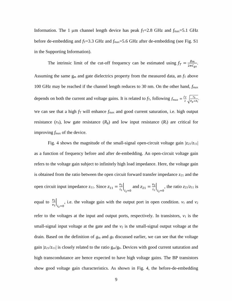
10
voltage gain stays above unity (0 dB) up to 13 GHz The after-de-embedding voltage gain
is close to 20 dB at 2 GHz and stays above unity (0 dB) for the entire frequency range
measured up to 50 GHz For a longer channel length (1 m) device (see Fig S2 in the
Supporting Information) the before-de-embedding voltage gain is above unity (0 dB) up
to 10 GHz The after-de-embedding voltage gain is above 15 dB at 1 GHz and stays
above unity (0 dB) up to 30 GHz
Summary
In this work we investigated the high frequency characteristics of black
phosphorus field effect transistors whose channels were fabricated along the light
effective mass (x-) direction The device operates well into the GHz frequency range of
the radio frequency spectrum We carried out standard S-parameter measurements to
characterize the high frequency response of these top-gated BP transistors The short-
circuit current gain maximum stable gainmaximum available gain unilateral power gain
and voltage gain of the devices were carefully extracted The short-circuit current gain of
BP transistors shows the 20 dBdec 1f frequency dependence at high frequency We
measured a peak short-circuit current gain cutoff frequency fT of 12 GHz and maximum
oscillation frequency fmax of 20 GHz for a 300 nm channel length BP transistor
demonstrating the GHz operation of BP devices for the first time These results clearly
reveal the potentials of BP transistors to function as power and voltage amplifiers in
multi-GHz frequency analogue and digital electronics demanded by many emerging
civilian and military applications
11
References
1 Powell M J The physics of amorphous-silicon thin-film transistors IEEE Trans
Electron Devices 36 2753-2763 (1989)
2 Street R A Thin-Film Transistors Adv Mater 21 2007-2022 (2009)
3 Hawkins W G Polycrystalline-silicon device technology for large-area electronics
IEEE Trans Electron Devices 33 477-481 (1986)
4 Forrest S R The path to ubiquitous and low-cost organic electronic appliances on
plastic Nature 428 911-918 (2004)
5 Dimitrakopoulos C D Mascaro D J Organic thin-film transistors A review of
recent advances IBM J Res Dev 45 11-27 (2004)
6 Nomura K et al Amorphous Oxide Semiconductors for High-Performance Flexible
Thin-Film Transistors Japanese Journal of Applied Physics 45 4303 (2006)
7 Carcia P F McLean R S Reilly M H amp Nunes G Jr Transparent ZnO thin-film
transistor fabricated by RF magnetron sputtering Appl Phys Lett 82 1117 (2003)
8 Meric I Baklitskaya N Kim P amp Shepard K L RF performance of top-gated
zero-bandgap graphene field-effect transistors IEEE IEDM Tech Digest 2008
9 Lin Y-M Dimitrakopoulos C D Jenkins K A Farmer D B Chiu H-Y Grill
A amp Avouris P 100-GHz Transistors from Wafer-Scale Epitaxial Graphene Science
327 662 (2010)
10 Wu Y Lin Y Bol A A Jenkins K A Xia F Farmer D B Zhu Y amp
Avouris P High-frequency scaled graphene transistors on diamond-like carbon Nature
472 74-78 (2011)
11 Liao L et al High-speed graphene transistors with a self-aligned nanowire gate
Nature 467 305ndash308 (2010)
12 Wang H Nezich D Kong J amp Palacios T Graphene frequency multipliers IEEE
Elec Dev Lett 30 547-549 (2009)
13 Wang H Hsu A Wu J Kong J amp Palacios T Graphene-based ambipolar RF
mixers IEEE Elec Dev Lett 31 906-908 (2010)
12
14 Han S-J Valdes-Garcia A Oida S Jenkins K A amp Haensch W Graphene radio
frequency receiver integrated circuit Nat Commun 53086 doi101038ncomms4086
(2014)
15 Wang H Chapter 4 In Two-Dimensional Materials for Electronic Applications Ph
D Thesis Massachusetts Institute of Technology Cambridge MA USA 2014
httpdspacemiteduhandle1721184899
16 Schwierz F amp Liou J J Modern Microwave Transistors Theory Design and
Performance Wiley-Interscience 1st edition 2002
17 Tasker P J amp Hughes B Importance of source and drain resistance to the maximum
f T of millimeter-wave MODFETs IEEE Elec Dev Lett 10 291-293 (1989)
18 Zhu W Low T Lee Y-H Wang H Farmer D B Kong J Xia F amp Avouris
P Electronic transport and device prospects of monolayer molybdenum disulphide grown
by chemical vapour deposition Nat Commun 53087 doi101038ncomms4087 (2014)
19 Huang J-K et al Large-Area Synthesis of Highly Crystalline WSe2 Monolayers and
Device Applications ACS Nano 8 923-930 (2014)
20 Xia F Wang H amp Jia Y Rediscovering black phosphorus as an anisotropic layered
material for optoelectronics and electronics Nat Commun 54458
doi101038ncomms5458 (2014)
21 Morita A Semiconducting black phosphorus Appl Phys A 39 227-242 1986
22 Keyes R The electrical properties of black phosphorus Phys Rev 92 580-584
(1953)
23 Warschauer D Electrical and optical properties of crystalline black phosphorus J
Appl Phys 34 1853-1860 (1963)
24 Jamieson J Crystal structures adopted by black phosphorus at high pressures
Science 139 1291-1292 (1963)
25 Wittig J amp Matthias B T Superconducting phosphorus Science 160 994-995
(1968)
26 Maruyama Y Suzuki S Kobayashi K amp Tanuma S Synthesis and some
properties of black phosphorus single crystals Physica 105B 99-102 (1981)
13
27 Li L et al Black phosphorus field-effect transistors Nat Nanotechnol 9 372-377
(2014)
28 Liu H et al Phosphorene an unexplored 2D semiconductor with a high hole
mobility ACS Nano 8 4033-4041 (2014)
29 Koenig S Doganov R Schmidt H Castro Neto A amp Ozyilmaz B Electric field
effect in ultrathin black phosphorus Appl Phys Lett 104 103106 (2014)
30 Akahama Y Kobayashi M amp Kawamura H Raman study of black phosphorus up
to 13 GPa Solid State Comm 104 311-315 (1997)
31 Xia F Farmer D B Lin Y-M Avouris P Graphene field-effect transistors with
high onoff current ratio and large transport band gap at room temperature Nano Lett 10
715-718 (2010)
32 R J Collier and A D Skinner Microwave Measurements 3rd Edition the
Institution of Engineering and Technology 2007
33 Koolen M C A Geelen J A amp Versleijen M P J An improved de-embedding
technique for on-wafer high-frequency characterization Proceedings of the Bipolar
Circuits and Technology Meeting 1991 188ndash191 (1991)
34 Kim J-Y Choi M-K amp Lee S-H A lsquoThru-Short-Openrsquo De-embedding Method
for Accurate On-Wafer RF Measurements of Nano-Scale MOSFETs JSTSJournal of
Semiconductor Technology and Science 12 53ndash58 (2012)
35 Gummel H K On the definition of the cutoff frequency fT Proceedings of the IEEE
57 12 2159ndash2159 (1969)
36 S-Parameter Techniques HP Application Note 95-1
httpwwwhparchivecomApplication_NotesHP-AN-95-1pdf
37 Mason S J Power gain in feedback amplifiers Trans IRE Professional Group on
Circuit Theory CT-1 20-25 (1954) (This work was previously reported in Tech Rep
No 257 Research Laboratory of Electronics MIT Cambridge MA 1953
38 Gupta M S Power Gain in Feedback Amplifiers a Classic Revisited IEEE Trans
Microwave Theory and Techniques 40 5 (1992)
14
Competing financial interests
Authors declare no competing financial interests
Supporting Information
Information on the device fabrication process and characterization method additional
high frequency characterization data are included in the Supporting Information This
material is available free of charge via the Internet at httppubsacsorg
Additional information
Correspondence and requests for materials should be addressed to HW
(hanwang4uscedu) and F X (fengnianxiayaleedu)
Figure Captions
Figure 1 Characterization of the black phosphorus (BP) thin film
(a) Layered crystal structure of black phosphorus The spacing between adjacent layers is
53 Aring (b) atomic force microscope (AFM) data showing the thickness of a BP flake The
inset shows the optical micrograph of the BP flake with thickness around 85 nm (c)
Raman spectrum of the BP flake along x-direction (d) Polarization-resolved infrared
spectra of a BP flake
Figure 2 DC characteristics of BP transistors
(a) Schematic of the BP transistor device structure (b) Optical micrograph of the
fabricated device (c) Output characteristics of the BP transistor LG= 300 nm (d)
Transfer characteristics of the same BP transistor plotted in both linear and logarithmic
15
scale VDS=-2 V The device has an on-off current ratio exceeding 2times103 The inset shows
the transconductance gm of the device
Figure 3 Current and power gain in BP transistors at GHz frequency
(a) and (b) the short-circuit current gain h21 the maximum stable gain and maximum
available gain MSGMAG and the unilateral power gain U of the 300 nm channel length
device before and after de-embedding respectively The device has fT=78 GHz fmax=12
GHz before de-embedding and fT=12 GHz fmax=20 GHz after de-embedding (c) and (d)
the imaginary part of 1h21 as a function of frequency before and after de-embedding
respectively Based on Gummelrsquos method the initial slope of the curve is equal to 1fT
Figure 4 Open-circuit voltage gain in BP transistors at GHz frequency
The open-circuit voltage gain (z21z11) before and after de-embedding is shown as a
function of the frequency After de-embedding the voltage gain stays close to 20 dB up
to 2 GHz and is above unity (0 dB) in the entire measurement range up to 50 GHz The
grey dashed line is a guide to the eyes
0 1 2 3 40
2
4
6
8
10
12
He
igh
t (n
m)
Distance (m)
85 nm10 m
b
c d
a
53 Aring
300 350 400 450 500
00
03
06
09
12
15
B2g
A2
g
Inte
nsity (
au
)
Raman Shift (cm-1)
A1
g
Excitation light polarized
along x-direction
x
y z
Figure 1 Characterization of the black phosphorus (BP) thin film
2000 3000 4000-005
000
005
010
015
1-T
T0
Wavenumber (cm-1)
x
y
Figure 2 DC characteristics of BP transistors
-20 -15 -10 -05 000
-50
-100
-150
-200
-250 V
G=-20 V
VG=-15 V
VG=-10 V
VG=-05 V
VG= 0 V
I DS (
mA
mm
)
VDS
(V)
S
D
G
SiO2
BP
x
S
b a
d c
-2 -1 0 1 2 30
-50
-100
-150
-200
-250
-300
-350
|ID
S| (m
Am
m)
VG (V)
I DS (
mA
mm
)
01
1
10
100
onoff ~2times103
-2 -1 0 10
40
80
120
160
200
gm (
mS
mm
)V
G (V)
S
G D
S
LG = 300 nm
t ~ 85 nm
tox ~ 21 nm HfO2
50 m
BP
Figure 3 Current and power gain in BP transistors at
GHz frequency
1 100
5
10
15
20
25
30
35
Frequency (GHz)
Gain
(dB
)Before De-embedding
LG=300 nm
|h21|2
MSGMAG
U
fmax
=12 GHz
fT=8 GHz
1 100
5
10
15
20
25
30
35
fmax
=20 GHz
Frequency (GHz)
Gain
(dB
)
fT=12 GHz
LG=300 nm
|h21|2
MSGMAG
U
After De-embedding
0 2 4 6 8 1000
02
04
06
08
10
12
Im (1h21
(f))=ffT
Before De-embedding
fT=76 GHz
Slope=fT
-1
Frequency (GHz)
Im (
1h
21)
0 2 4 6 8 1000
02
04
06
08
10
12
Im (1h21
(f))=ffT
After De-embedding
Frequency (GHz)
fT=119 GHz
Slope=fT
-1Im (
1h
21)
a b
c d
Figure 4 Open-circuit voltage gain in BP transistors at
GHz frequency
1 10 1000
5
10
15
20
25
30
35
Frequency (GHz)
Vo
lta
ge
Ga
in |z
21z
11| (d
B)
LG=300 nm
|z21
z11
| before de-embedding
|z21
z11
| after de-embedding
1
Supporting Information for
Black Phosphorus Radio-Frequency Transistors
Han Wang1 Xiaomu Wang2 Fengnian Xia2 Luhao Wang1 Hao Jiang3
Qiangfei Xia3 Matthew L Chin4 Madan Dubey4 Shu-jen Han5
1Ming Hsieh Department of Electrical Engineering University of Southern California
Los Angeles CA 90089
2Department of Electrical Engineering Yale University New Haven CT 06511
3Department of Electrical amp Computer Engineering University of Massachusetts
Amherst MA 01003
4 Sensors and Electron Devices Directorate US Army Research Laboratory
Adelphi MD 20723
5IBM T J Watson Research Center Yorktown Heights NY 10598
Email hanwang4uscedu fengnianxiayaleedu
Methods
Top-gated transistor fabrication The fabrication of our devices starts with the
exfoliation of BP thin films from bulk BP crystals onto 300 nm SiO2 on a Si substrate
which has pre-patterned alignment grids using the micro-mechanical cleavage technique
The thickness of the SiO2 was selected to provide the optimal optical contrast for locating
BP flakes relative to the alignment grids The thickness of BP layers was measured by
atomic force microscopy (AFM) The next step was to pattern the resist layer for
metallization using a Vistec 100 kV electron-beam lithography system based on poly
(methyl methacrylate) (950k MW PMMA) PMMA A3 was spun on wafer at a speed of
3000 rpm for 1 minute and was then bakes at 175 degrees for 3 minutes The dose for
exposure is 1100 microC cm-2 Development was performed in 13 MIBK IPA (Methyl
isobutyl ketone Isopropanol) for 90 s We then evaporated 1 nm Ti20 nm Pd30 nm Au
2
followed by lift-off in acetone to form the contacts The HfO2 gate dielectric is deposited
using atomic layer deposition (ALD) at 150 C The gate electrode is also patterned using
Vistec 100 kV electron-beam lithography system
AFM Atomic force microscopy (AFM) for identifying the thin film thickness was
performed on a Digital InstrumentsVeeco Dimension 3000 system
IR spectroscopy Bruker Optics Fourier Transfer Infrared spectrometer (Vertex 70)
integrated with a Hyperion 2000 microscope system was used to measure the infrared
spectroscopy of the BP flakes in the 800 cm-1 to 4000 cm-1 range The linear polarization
of the incident light was achieved using an infrared polarizer
Electrical characterization DC electrical characterizations were performed using an
Agilent B1500 semiconductor parameter analyzer and a Lakeshore cryogenic probe station
with micromanipulation probes The high frequency characterizations were performed
using an Agilent N5230A Vector Network Analyzer
High frequency characterization of BP transistor with 1 m channel length
The short-circuit current and power gain of a BP transistor with 1 m channel length are
shown in Fig S1 The open-circuit voltage gain z21z11 both before and after de-embedding
are shown in Fig S2 The device has fT=28 GHz fmax=51 GHz before de-embedding and
fT=33 GHz fmax=56 GHz after de-embedding After de-embedding the voltage gain stays
above 15 dB up around 1 GHz and is above unity (0 dB) up to 30 GHz
3
Fig S1 (a) and (b) the short-circuit current gain h21 the maximum stable gain and maximum available gain
MSGMAG and the unilateral power gain U of the device with 1 m channel length before and after de-
embedding respectively The device has fT=28 GHz fmax=51 GHz before de-embedding and fT=33 GHz
fmax=56 GHz after de-embedding (c) and (d) the imaginary part of 1h21 as a function of frequency before
and after de-embedding respectively Based on Gummelrsquos method the initial slope of the curve is equal to
1fT
Fig S2 the open-circuit voltage gain (z21z11) before and after de-embedding is shown as a function of the
frequency After de-embedding the voltage gain stays above 15 dB up to around 1 GHz and is above unity
(0 dB) up to 30 GHz
01 1 100
5
10
15
20
25
30
35
Frequency (GHz)
Gain
(dB
)
Before De-embedding
LG=1 m
|h21|2
MSGMAG
U
fmax
=51 GHz
fT=28 GHz
a
b
c
0 1 2 3 400
02
04
06
08
10
12
Im (1h21
(f))=ffT
Before De-embedding
fT=28 GHz
Slope=fT
-1
Frequency (GHz)
Im (
1h
21)
d
0 1 2 3 400
02
04
06
08
10
12
Im (1h21
(f))=ffT
After De-embedding
Frequency (GHz)
fT=35 GHz
Slope=fT
-1Im (
1h
21)
01 1 100
5
10
15
20
25
30
35
fmax
=56 GHz
Frequency (GHz)
Gain
(dB
)
fT=33 GHz
LG=1 m
|h21|2
MSGMAG
U
After De-embedding
1 100
5
10
15
20
25
30
35
Frequency (GHz)
Voltage G
ain
z21z
11 (
dB
)
LG=1 m
|z21
z11
| before de-embedding
|z21
z11
| after de-embedding
- Main_text_arXiv
- Figure 21
- Supporting_Information_arXiv
-
12
14 Han S-J Valdes-Garcia A Oida S Jenkins K A amp Haensch W Graphene radio
frequency receiver integrated circuit Nat Commun 53086 doi101038ncomms4086
(2014)
15 Wang H Chapter 4 In Two-Dimensional Materials for Electronic Applications Ph
D Thesis Massachusetts Institute of Technology Cambridge MA USA 2014
httpdspacemiteduhandle1721184899
16 Schwierz F amp Liou J J Modern Microwave Transistors Theory Design and
Performance Wiley-Interscience 1st edition 2002
17 Tasker P J amp Hughes B Importance of source and drain resistance to the maximum
f T of millimeter-wave MODFETs IEEE Elec Dev Lett 10 291-293 (1989)
18 Zhu W Low T Lee Y-H Wang H Farmer D B Kong J Xia F amp Avouris
P Electronic transport and device prospects of monolayer molybdenum disulphide grown
by chemical vapour deposition Nat Commun 53087 doi101038ncomms4087 (2014)
19 Huang J-K et al Large-Area Synthesis of Highly Crystalline WSe2 Monolayers and
Device Applications ACS Nano 8 923-930 (2014)
20 Xia F Wang H amp Jia Y Rediscovering black phosphorus as an anisotropic layered
material for optoelectronics and electronics Nat Commun 54458
doi101038ncomms5458 (2014)
21 Morita A Semiconducting black phosphorus Appl Phys A 39 227-242 1986
22 Keyes R The electrical properties of black phosphorus Phys Rev 92 580-584
(1953)
23 Warschauer D Electrical and optical properties of crystalline black phosphorus J
Appl Phys 34 1853-1860 (1963)
24 Jamieson J Crystal structures adopted by black phosphorus at high pressures
Science 139 1291-1292 (1963)
25 Wittig J amp Matthias B T Superconducting phosphorus Science 160 994-995
(1968)
26 Maruyama Y Suzuki S Kobayashi K amp Tanuma S Synthesis and some
properties of black phosphorus single crystals Physica 105B 99-102 (1981)
13
27 Li L et al Black phosphorus field-effect transistors Nat Nanotechnol 9 372-377
(2014)
28 Liu H et al Phosphorene an unexplored 2D semiconductor with a high hole
mobility ACS Nano 8 4033-4041 (2014)
29 Koenig S Doganov R Schmidt H Castro Neto A amp Ozyilmaz B Electric field
effect in ultrathin black phosphorus Appl Phys Lett 104 103106 (2014)
30 Akahama Y Kobayashi M amp Kawamura H Raman study of black phosphorus up
to 13 GPa Solid State Comm 104 311-315 (1997)
31 Xia F Farmer D B Lin Y-M Avouris P Graphene field-effect transistors with
high onoff current ratio and large transport band gap at room temperature Nano Lett 10
715-718 (2010)
32 R J Collier and A D Skinner Microwave Measurements 3rd Edition the
Institution of Engineering and Technology 2007
33 Koolen M C A Geelen J A amp Versleijen M P J An improved de-embedding
technique for on-wafer high-frequency characterization Proceedings of the Bipolar
Circuits and Technology Meeting 1991 188ndash191 (1991)
34 Kim J-Y Choi M-K amp Lee S-H A lsquoThru-Short-Openrsquo De-embedding Method
for Accurate On-Wafer RF Measurements of Nano-Scale MOSFETs JSTSJournal of
Semiconductor Technology and Science 12 53ndash58 (2012)
35 Gummel H K On the definition of the cutoff frequency fT Proceedings of the IEEE
57 12 2159ndash2159 (1969)
36 S-Parameter Techniques HP Application Note 95-1
httpwwwhparchivecomApplication_NotesHP-AN-95-1pdf
37 Mason S J Power gain in feedback amplifiers Trans IRE Professional Group on
Circuit Theory CT-1 20-25 (1954) (This work was previously reported in Tech Rep
No 257 Research Laboratory of Electronics MIT Cambridge MA 1953
38 Gupta M S Power Gain in Feedback Amplifiers a Classic Revisited IEEE Trans
Microwave Theory and Techniques 40 5 (1992)
14
Competing financial interests
Authors declare no competing financial interests
Supporting Information
Information on the device fabrication process and characterization method additional
high frequency characterization data are included in the Supporting Information This
material is available free of charge via the Internet at httppubsacsorg
Additional information
Correspondence and requests for materials should be addressed to HW
(hanwang4uscedu) and F X (fengnianxiayaleedu)
Figure Captions
Figure 1 Characterization of the black phosphorus (BP) thin film
(a) Layered crystal structure of black phosphorus The spacing between adjacent layers is
53 Aring (b) atomic force microscope (AFM) data showing the thickness of a BP flake The
inset shows the optical micrograph of the BP flake with thickness around 85 nm (c)
Raman spectrum of the BP flake along x-direction (d) Polarization-resolved infrared
spectra of a BP flake
Figure 2 DC characteristics of BP transistors
(a) Schematic of the BP transistor device structure (b) Optical micrograph of the
fabricated device (c) Output characteristics of the BP transistor LG= 300 nm (d)
Transfer characteristics of the same BP transistor plotted in both linear and logarithmic
15
scale VDS=-2 V The device has an on-off current ratio exceeding 2times103 The inset shows
the transconductance gm of the device
Figure 3 Current and power gain in BP transistors at GHz frequency
(a) and (b) the short-circuit current gain h21 the maximum stable gain and maximum
available gain MSGMAG and the unilateral power gain U of the 300 nm channel length
device before and after de-embedding respectively The device has fT=78 GHz fmax=12
GHz before de-embedding and fT=12 GHz fmax=20 GHz after de-embedding (c) and (d)
the imaginary part of 1h21 as a function of frequency before and after de-embedding
respectively Based on Gummelrsquos method the initial slope of the curve is equal to 1fT
Figure 4 Open-circuit voltage gain in BP transistors at GHz frequency
The open-circuit voltage gain (z21z11) before and after de-embedding is shown as a
function of the frequency After de-embedding the voltage gain stays close to 20 dB up
to 2 GHz and is above unity (0 dB) in the entire measurement range up to 50 GHz The
grey dashed line is a guide to the eyes
0 1 2 3 40
2
4
6
8
10
12
He
igh
t (n
m)
Distance (m)
85 nm10 m
b
c d
a
53 Aring
300 350 400 450 500
00
03
06
09
12
15
B2g
A2
g
Inte
nsity (
au
)
Raman Shift (cm-1)
A1
g
Excitation light polarized
along x-direction
x
y z
Figure 1 Characterization of the black phosphorus (BP) thin film
2000 3000 4000-005
000
005
010
015
1-T
T0
Wavenumber (cm-1)
x
y
Figure 2 DC characteristics of BP transistors
-20 -15 -10 -05 000
-50
-100
-150
-200
-250 V
G=-20 V
VG=-15 V
VG=-10 V
VG=-05 V
VG= 0 V
I DS (
mA
mm
)
VDS
(V)
S
D
G
SiO2
BP
x
S
b a
d c
-2 -1 0 1 2 30
-50
-100
-150
-200
-250
-300
-350
|ID
S| (m
Am
m)
VG (V)
I DS (
mA
mm
)
01
1
10
100
onoff ~2times103
-2 -1 0 10
40
80
120
160
200
gm (
mS
mm
)V
G (V)
S
G D
S
LG = 300 nm
t ~ 85 nm
tox ~ 21 nm HfO2
50 m
BP
Figure 3 Current and power gain in BP transistors at
GHz frequency
1 100
5
10
15
20
25
30
35
Frequency (GHz)
Gain
(dB
)Before De-embedding
LG=300 nm
|h21|2
MSGMAG
U
fmax
=12 GHz
fT=8 GHz
1 100
5
10
15
20
25
30
35
fmax
=20 GHz
Frequency (GHz)
Gain
(dB
)
fT=12 GHz
LG=300 nm
|h21|2
MSGMAG
U
After De-embedding
0 2 4 6 8 1000
02
04
06
08
10
12
Im (1h21
(f))=ffT
Before De-embedding
fT=76 GHz
Slope=fT
-1
Frequency (GHz)
Im (
1h
21)
0 2 4 6 8 1000
02
04
06
08
10
12
Im (1h21
(f))=ffT
After De-embedding
Frequency (GHz)
fT=119 GHz
Slope=fT
-1Im (
1h
21)
a b
c d
Figure 4 Open-circuit voltage gain in BP transistors at
GHz frequency
1 10 1000
5
10
15
20
25
30
35
Frequency (GHz)
Vo
lta
ge
Ga
in |z
21z
11| (d
B)
LG=300 nm
|z21
z11
| before de-embedding
|z21
z11
| after de-embedding
1
Supporting Information for
Black Phosphorus Radio-Frequency Transistors
Han Wang1 Xiaomu Wang2 Fengnian Xia2 Luhao Wang1 Hao Jiang3
Qiangfei Xia3 Matthew L Chin4 Madan Dubey4 Shu-jen Han5
1Ming Hsieh Department of Electrical Engineering University of Southern California
Los Angeles CA 90089
2Department of Electrical Engineering Yale University New Haven CT 06511
3Department of Electrical amp Computer Engineering University of Massachusetts
Amherst MA 01003
4 Sensors and Electron Devices Directorate US Army Research Laboratory
Adelphi MD 20723
5IBM T J Watson Research Center Yorktown Heights NY 10598
Email hanwang4uscedu fengnianxiayaleedu
Methods
Top-gated transistor fabrication The fabrication of our devices starts with the
exfoliation of BP thin films from bulk BP crystals onto 300 nm SiO2 on a Si substrate
which has pre-patterned alignment grids using the micro-mechanical cleavage technique
The thickness of the SiO2 was selected to provide the optimal optical contrast for locating
BP flakes relative to the alignment grids The thickness of BP layers was measured by
atomic force microscopy (AFM) The next step was to pattern the resist layer for
metallization using a Vistec 100 kV electron-beam lithography system based on poly
(methyl methacrylate) (950k MW PMMA) PMMA A3 was spun on wafer at a speed of
3000 rpm for 1 minute and was then bakes at 175 degrees for 3 minutes The dose for
exposure is 1100 microC cm-2 Development was performed in 13 MIBK IPA (Methyl
isobutyl ketone Isopropanol) for 90 s We then evaporated 1 nm Ti20 nm Pd30 nm Au
2
followed by lift-off in acetone to form the contacts The HfO2 gate dielectric is deposited
using atomic layer deposition (ALD) at 150 C The gate electrode is also patterned using
Vistec 100 kV electron-beam lithography system
AFM Atomic force microscopy (AFM) for identifying the thin film thickness was
performed on a Digital InstrumentsVeeco Dimension 3000 system
IR spectroscopy Bruker Optics Fourier Transfer Infrared spectrometer (Vertex 70)
integrated with a Hyperion 2000 microscope system was used to measure the infrared
spectroscopy of the BP flakes in the 800 cm-1 to 4000 cm-1 range The linear polarization
of the incident light was achieved using an infrared polarizer
Electrical characterization DC electrical characterizations were performed using an
Agilent B1500 semiconductor parameter analyzer and a Lakeshore cryogenic probe station
with micromanipulation probes The high frequency characterizations were performed
using an Agilent N5230A Vector Network Analyzer
High frequency characterization of BP transistor with 1 m channel length
The short-circuit current and power gain of a BP transistor with 1 m channel length are
shown in Fig S1 The open-circuit voltage gain z21z11 both before and after de-embedding
are shown in Fig S2 The device has fT=28 GHz fmax=51 GHz before de-embedding and
fT=33 GHz fmax=56 GHz after de-embedding After de-embedding the voltage gain stays
above 15 dB up around 1 GHz and is above unity (0 dB) up to 30 GHz
3
Fig S1 (a) and (b) the short-circuit current gain h21 the maximum stable gain and maximum available gain
MSGMAG and the unilateral power gain U of the device with 1 m channel length before and after de-
embedding respectively The device has fT=28 GHz fmax=51 GHz before de-embedding and fT=33 GHz
fmax=56 GHz after de-embedding (c) and (d) the imaginary part of 1h21 as a function of frequency before
and after de-embedding respectively Based on Gummelrsquos method the initial slope of the curve is equal to
1fT
Fig S2 the open-circuit voltage gain (z21z11) before and after de-embedding is shown as a function of the
frequency After de-embedding the voltage gain stays above 15 dB up to around 1 GHz and is above unity
(0 dB) up to 30 GHz
01 1 100
5
10
15
20
25
30
35
Frequency (GHz)
Gain
(dB
)
Before De-embedding
LG=1 m
|h21|2
MSGMAG
U
fmax
=51 GHz
fT=28 GHz
a
b
c
0 1 2 3 400
02
04
06
08
10
12
Im (1h21
(f))=ffT
Before De-embedding
fT=28 GHz
Slope=fT
-1
Frequency (GHz)
Im (
1h
21)
d
0 1 2 3 400
02
04
06
08
10
12
Im (1h21
(f))=ffT
After De-embedding
Frequency (GHz)
fT=35 GHz
Slope=fT
-1Im (
1h
21)
01 1 100
5
10
15
20
25
30
35
fmax
=56 GHz
Frequency (GHz)
Gain
(dB
)
fT=33 GHz
LG=1 m
|h21|2
MSGMAG
U
After De-embedding
1 100
5
10
15
20
25
30
35
Frequency (GHz)
Voltage G
ain
z21z
11 (
dB
)
LG=1 m
|z21
z11
| before de-embedding
|z21
z11
| after de-embedding
- Main_text_arXiv
- Figure 21
- Supporting_Information_arXiv
-
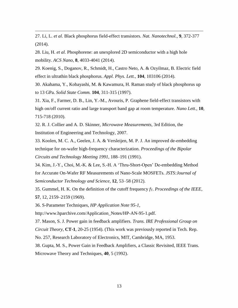
15
scale VDS=-2 V The device has an on-off current ratio exceeding 2times103 The inset shows
the transconductance gm of the device
Figure 3 Current and power gain in BP transistors at GHz frequency
(a) and (b) the short-circuit current gain h21 the maximum stable gain and maximum
available gain MSGMAG and the unilateral power gain U of the 300 nm channel length
device before and after de-embedding respectively The device has fT=78 GHz fmax=12
GHz before de-embedding and fT=12 GHz fmax=20 GHz after de-embedding (c) and (d)
the imaginary part of 1h21 as a function of frequency before and after de-embedding
respectively Based on Gummelrsquos method the initial slope of the curve is equal to 1fT
Figure 4 Open-circuit voltage gain in BP transistors at GHz frequency
The open-circuit voltage gain (z21z11) before and after de-embedding is shown as a
function of the frequency After de-embedding the voltage gain stays close to 20 dB up
to 2 GHz and is above unity (0 dB) in the entire measurement range up to 50 GHz The
grey dashed line is a guide to the eyes
0 1 2 3 40
2
4
6
8
10
12
He
igh
t (n
m)
Distance (m)
85 nm10 m
b
c d
a
53 Aring
300 350 400 450 500
00
03
06
09
12
15
B2g
A2
g
Inte
nsity (
au
)
Raman Shift (cm-1)
A1
g
Excitation light polarized
along x-direction
x
y z
Figure 1 Characterization of the black phosphorus (BP) thin film
2000 3000 4000-005
000
005
010
015
1-T
T0
Wavenumber (cm-1)
x
y
Figure 2 DC characteristics of BP transistors
-20 -15 -10 -05 000
-50
-100
-150
-200
-250 V
G=-20 V
VG=-15 V
VG=-10 V
VG=-05 V
VG= 0 V
I DS (
mA
mm
)
VDS
(V)
S
D
G
SiO2
BP
x
S
b a
d c
-2 -1 0 1 2 30
-50
-100
-150
-200
-250
-300
-350
|ID
S| (m
Am
m)
VG (V)
I DS (
mA
mm
)
01
1
10
100
onoff ~2times103
-2 -1 0 10
40
80
120
160
200
gm (
mS
mm
)V
G (V)
S
G D
S
LG = 300 nm
t ~ 85 nm
tox ~ 21 nm HfO2
50 m
BP
Figure 3 Current and power gain in BP transistors at
GHz frequency
1 100
5
10
15
20
25
30
35
Frequency (GHz)
Gain
(dB
)Before De-embedding
LG=300 nm
|h21|2
MSGMAG
U
fmax
=12 GHz
fT=8 GHz
1 100
5
10
15
20
25
30
35
fmax
=20 GHz
Frequency (GHz)
Gain
(dB
)
fT=12 GHz
LG=300 nm
|h21|2
MSGMAG
U
After De-embedding
0 2 4 6 8 1000
02
04
06
08
10
12
Im (1h21
(f))=ffT
Before De-embedding
fT=76 GHz
Slope=fT
-1
Frequency (GHz)
Im (
1h
21)
0 2 4 6 8 1000
02
04
06
08
10
12
Im (1h21
(f))=ffT
After De-embedding
Frequency (GHz)
fT=119 GHz
Slope=fT
-1Im (
1h
21)
a b
c d
Figure 4 Open-circuit voltage gain in BP transistors at
GHz frequency
1 10 1000
5
10
15
20
25
30
35
Frequency (GHz)
Vo
lta
ge
Ga
in |z
21z
11| (d
B)
LG=300 nm
|z21
z11
| before de-embedding
|z21
z11
| after de-embedding
1
Supporting Information for
Black Phosphorus Radio-Frequency Transistors
Han Wang1 Xiaomu Wang2 Fengnian Xia2 Luhao Wang1 Hao Jiang3
Qiangfei Xia3 Matthew L Chin4 Madan Dubey4 Shu-jen Han5
1Ming Hsieh Department of Electrical Engineering University of Southern California
Los Angeles CA 90089
2Department of Electrical Engineering Yale University New Haven CT 06511
3Department of Electrical amp Computer Engineering University of Massachusetts
Amherst MA 01003
4 Sensors and Electron Devices Directorate US Army Research Laboratory
Adelphi MD 20723
5IBM T J Watson Research Center Yorktown Heights NY 10598
Email hanwang4uscedu fengnianxiayaleedu
Methods
Top-gated transistor fabrication The fabrication of our devices starts with the
exfoliation of BP thin films from bulk BP crystals onto 300 nm SiO2 on a Si substrate
which has pre-patterned alignment grids using the micro-mechanical cleavage technique
The thickness of the SiO2 was selected to provide the optimal optical contrast for locating
BP flakes relative to the alignment grids The thickness of BP layers was measured by
atomic force microscopy (AFM) The next step was to pattern the resist layer for
metallization using a Vistec 100 kV electron-beam lithography system based on poly
(methyl methacrylate) (950k MW PMMA) PMMA A3 was spun on wafer at a speed of
3000 rpm for 1 minute and was then bakes at 175 degrees for 3 minutes The dose for
exposure is 1100 microC cm-2 Development was performed in 13 MIBK IPA (Methyl
isobutyl ketone Isopropanol) for 90 s We then evaporated 1 nm Ti20 nm Pd30 nm Au
2
followed by lift-off in acetone to form the contacts The HfO2 gate dielectric is deposited
using atomic layer deposition (ALD) at 150 C The gate electrode is also patterned using
Vistec 100 kV electron-beam lithography system
AFM Atomic force microscopy (AFM) for identifying the thin film thickness was
performed on a Digital InstrumentsVeeco Dimension 3000 system
IR spectroscopy Bruker Optics Fourier Transfer Infrared spectrometer (Vertex 70)
integrated with a Hyperion 2000 microscope system was used to measure the infrared
spectroscopy of the BP flakes in the 800 cm-1 to 4000 cm-1 range The linear polarization
of the incident light was achieved using an infrared polarizer
Electrical characterization DC electrical characterizations were performed using an
Agilent B1500 semiconductor parameter analyzer and a Lakeshore cryogenic probe station
with micromanipulation probes The high frequency characterizations were performed
using an Agilent N5230A Vector Network Analyzer
High frequency characterization of BP transistor with 1 m channel length
The short-circuit current and power gain of a BP transistor with 1 m channel length are
shown in Fig S1 The open-circuit voltage gain z21z11 both before and after de-embedding
are shown in Fig S2 The device has fT=28 GHz fmax=51 GHz before de-embedding and
fT=33 GHz fmax=56 GHz after de-embedding After de-embedding the voltage gain stays
above 15 dB up around 1 GHz and is above unity (0 dB) up to 30 GHz
3
Fig S1 (a) and (b) the short-circuit current gain h21 the maximum stable gain and maximum available gain
MSGMAG and the unilateral power gain U of the device with 1 m channel length before and after de-
embedding respectively The device has fT=28 GHz fmax=51 GHz before de-embedding and fT=33 GHz
fmax=56 GHz after de-embedding (c) and (d) the imaginary part of 1h21 as a function of frequency before
and after de-embedding respectively Based on Gummelrsquos method the initial slope of the curve is equal to
1fT
Fig S2 the open-circuit voltage gain (z21z11) before and after de-embedding is shown as a function of the
frequency After de-embedding the voltage gain stays above 15 dB up to around 1 GHz and is above unity
(0 dB) up to 30 GHz
01 1 100
5
10
15
20
25
30
35
Frequency (GHz)
Gain
(dB
)
Before De-embedding
LG=1 m
|h21|2
MSGMAG
U
fmax
=51 GHz
fT=28 GHz
a
b
c
0 1 2 3 400
02
04
06
08
10
12
Im (1h21
(f))=ffT
Before De-embedding
fT=28 GHz
Slope=fT
-1
Frequency (GHz)
Im (
1h
21)
d
0 1 2 3 400
02
04
06
08
10
12
Im (1h21
(f))=ffT
After De-embedding
Frequency (GHz)
fT=35 GHz
Slope=fT
-1Im (
1h
21)
01 1 100
5
10
15
20
25
30
35
fmax
=56 GHz
Frequency (GHz)
Gain
(dB
)
fT=33 GHz
LG=1 m
|h21|2
MSGMAG
U
After De-embedding
1 100
5
10
15
20
25
30
35
Frequency (GHz)
Voltage G
ain
z21z
11 (
dB
)
LG=1 m
|z21
z11
| before de-embedding
|z21
z11
| after de-embedding
- Main_text_arXiv
- Figure 21
- Supporting_Information_arXiv
-
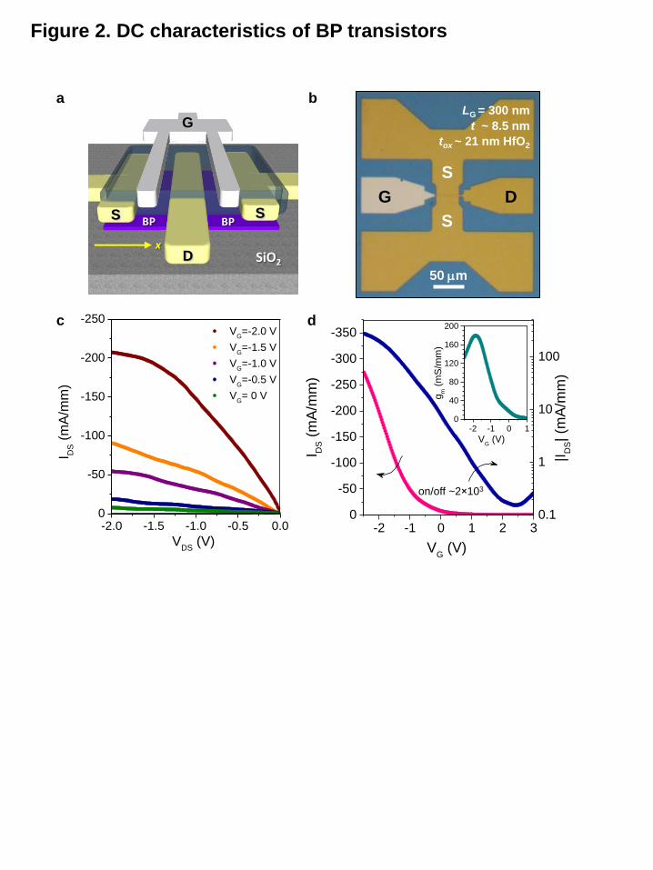
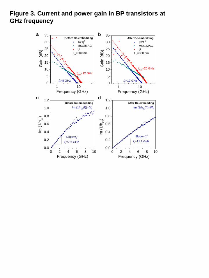
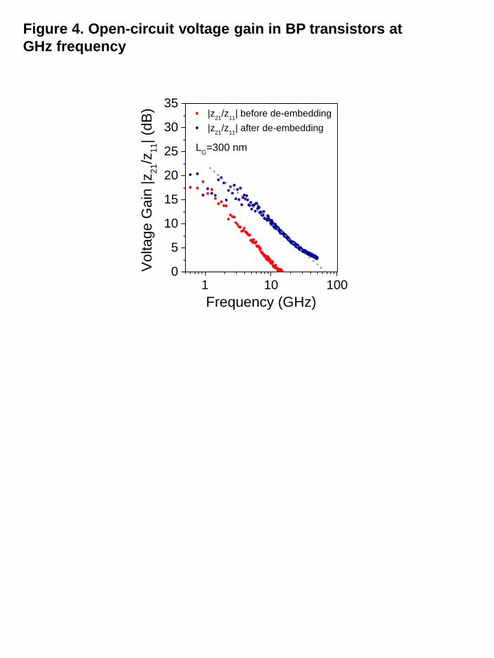
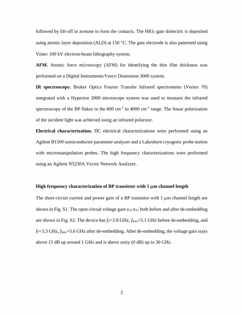
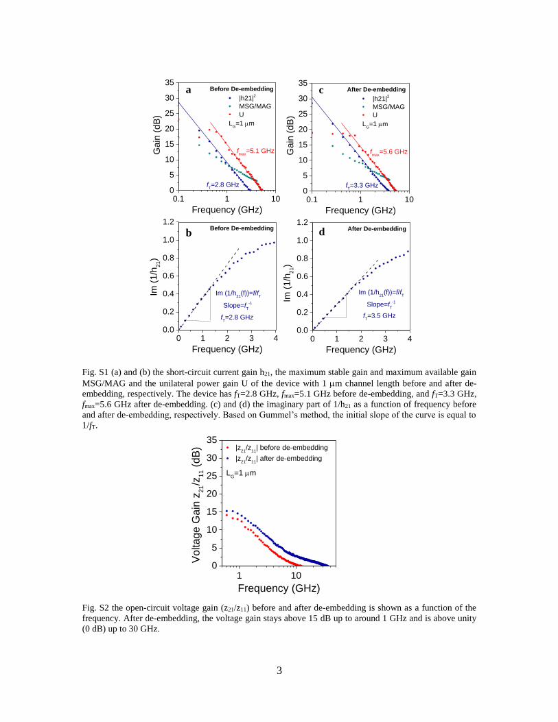