towards specifications of n-type silicon purified via the metallurgical route
TRANSCRIPT
Available online at www.sciencedirect.com
SiliconPV: 17-20 April 2011, Freiburg, Germany
Towards Specifications of n-type Silicon Purified via the Metallurgical Route
Thomas Schutz-Kuchlya*b, Vincent Sanzonea , Olivier Palaisb, Jed Kraiemc, Yannick Veschettia
aCEA, LITEN, INES, 50 Avenue du Lac Léman, 73377 Le Bourget du Lac, France bIM2NP, Faculté des Sciences et Techniques, Avenue Escadrille Normandie Niemen, Service 231, 13397 Marseille Cedex 20,
France cAPOLLON SOLAR, 23 rue Claudius Collonge, 69002 Lyon, France
Abstract
This study focuses on the fabrication and the characterization of solar cells using highly doped boron-phosphorus compensated n-type multicrystalline silicon. Two ingots were used and compared for this study. One ingot was crystallized from a silicon feedstock purified via the metallurgical route. The second ingot was crystallized from an electronic grade silicon feedstock in order to be metallic impurity free. Both ingots were intentionally compensated with a similar boron and phosphorus amount in the initial feedstock. Chemical and electrical characterizations were carried out on each ingot and similar carrier lifetimes were reported. Large area solar cells were fabricated on wafers selected at different positions along both ingots with a reference fabrication process leading to 18.4% efficiency on FZ material. No differences in terms of cells performances were observed between both ingots. Efficiencies between 13.5% and 15.0% were reported and were found to be limited by the low resistivity values of this material. This is consistent with the carrier lifetime previously measured which underlines the weak influence of the metallic impurities initially present in the wafers. Some perspectives are given in terms of feedstock specifications to exploit the potential of this material. © 2011 Published by Elsevier Ltd. Selection and/or peer-review under responsibility of SiliconPV 2011. Keywords: n-type silicon ; compensation ; boron ; phosphorus ; solar-grade silicon ; solar cells ; electrical properties
* Corresponding author. Tel.: +33 (0)4 79 44 52 37; fax: +33 (0)4 79 60 69 01. E-mail address: [email protected].
1876–6102 © 2011 Published by Elsevier Ltd. Selection and/or peer-review under responsibility of SiliconPV 2011.doi:10.1016/j.egypro.2011.06.098
Energy Procedia 8 (2011) 35–40
© 2011 Published by Elsevier Ltd. Selection and/or peer-review under responsibility of SiliconPV 2011.
36 Thomas Schutz-Kuchly et al. / Energy Procedia 8 (2011) 35–40
1. Introduction
The silicon (Si) feedstock, the ingot growth and the wafering steps represent between 30% and 50% of the overall photovoltaic (PV) module cost [1]. The use of Solar-Grade Si (SoG-Si) produced with simplified purification process [2] represents an issue to reduce the fabrication costs of the PV module. SoG-Si purified via the metallurgical route (SoGM-Si) will contain more impurities than Electronic-Grade Si (EG-Si). Most studies in this field are based on p-type Si due to the possibility of using the current industrial cell fabrication process. Nevertheless, n-type SoGM-Si could be a potential candidate for several reasons: Very weak Light-Induced-Degradation (LID) effect was reported [3, 4]. This is mainly related to a
higher capture cross section for electrons than for holes [5] when BOi2 complexes are involved [6, 7, 8]. n-type Si also shows a reduced sensitivity to several metallic impurities [9, 10] such as iron, titanium or
vanadium. Therefore, n-type SoGM-Si could be a potential candidate for the fabrication of efficient and stable
solar cells. However, very few investigations were carried out on this material. The purpose of this study is to analyse the potential of n-type multicrystalline Si (mc-Si) purified via
the metallurgical route and to define the required specifications to fabricate efficient solar cells assuming a low-cost scenario in terms of purification process. This leads to a limitation in terms of dopant impurities concentration in the initial feedstock ([B] > 1.5ppmw, [P] > 10ppmw). Indeed, for p-type Si, a boron concentration of 0.3 - 0.4 ppmw in the initial feedstock is required to reach acceptable and stable efficiencies (> 16.0%) [11]. Nevertheless, the purification process for such specification remains more complex and is as a consequence more expensive.
2. Experimental details
Two 8 kg B-P compensated n-type mc-Si ingots were grown for this study. One ingot was crystallized from an EG-Si feedstock and the other from a SoGM-Si feedstock, containing a similar amount of B and P (see Table 1). There was no addition of doping species during crystallization. The SoGM-Si feedstock was purified using several steps of directional solidification steps for metallic impurities and P removal plus a plasma torch for the B removal. More details on the purification and the crystallization process are given in [12]. The ingots were sliced into 125 × 125 mm² wafers at a thickness of 200 µm.
Table 1. Boron and Phosphorus concentrations (ppmw) in the melt of the crystallized SoGM-Si and EG-Si ingots.
Ingot [B] (ppmw) [P] (ppmw)
SoGM-Si 1.6 11.5
EG-Si 1.5 11.0
For chemical characterization, several wafers were selected along the ingot height and Glow Discharge
Mass Spectroscopy (GDMS) measurements were carried out. The wafers’ resistivity ( ) along the ingot was measured using the four point-probes measurement
technique. The carriers’ lifetime ( ) was measured with the Quasi-Steady-State-Photoconductivity (QssPC) method at an injection level p = 1.1015 cm-3. This method also requires the knowledge of the electron (µe) and hole (µh) carrier mobilities. The effects of compensation on µe and µh were – at least partially – taken into account using Arora’s mobility model [13] based on the GDMS results for [B] and [P]. For the carrier lifetime measurements, the wafers were first chemically polished in order to remove
Thomas Schutz-Kuchly et al. / Energy Procedia 8 (2011) 35–40 37
the saw damaged layers and then electrical passivation of the surfaces was achieved with plasma-enhanced-chemical-vapor-deposited (PECVD) hydrogenated Si Nitride (SiN:H) layers on both sides.
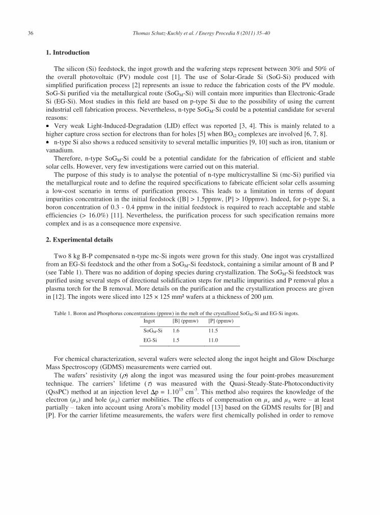
The solar cells were fabricated on wafers selected at different positions along the ingot’s height. The main fabrication steps are given in Fig 1. The boron diffusion was achieved at 925°C, and the thermal oxide for emitter passivation was 10 nm thick.
The fabricated solar cells were then measured in terms of short circuit current (Jsc), open circuit voltage (Voc), fill factor (FF) and energy conversion efficiency ( ) by standard I-V measurements (AM 1.5 at 25 °C).
Fig. 1. Schematic flow chart for the fabrication of solar cells (left) and cell architecture (right).
3. Results and discussion
3.1. Chemical characterization of the ingots
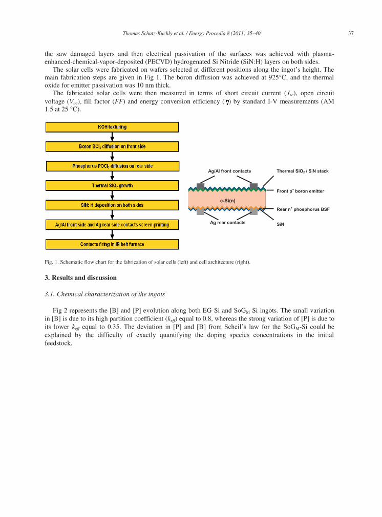
Fig 2 represents the [B] and [P] evolution along both EG-Si and SoGM-Si ingots. The small variation in [B] is due to its high partition coefficient (keff) equal to 0.8, whereas the strong variation of [P] is due to its lower keff equal to 0.35. The deviation in [P] and [B] from Scheil’s law for the SoGM-Si could be explained by the difficulty of exactly quantifying the doping species concentrations in the initial feedstock.
Ag rear contacts
Ag/Al front contacts
Front p+ boron emitter
Thermal SiO2 / SiN stack
Rear n+ phosphorus BSF
SiN
c-Si(n)
38 Thomas Schutz-Kuchly et al. / Energy Procedia 8 (2011) 35–40
Fig. 2. Variation of [B] and [P] along the EG-Si ingot (left) and the SoGM-Si ingot (right). The solid lines correspond to the fit using Scheil’s law. 0 % corresponds to the first crystallized part and 100 % corresponds to the last crystallized part.
3.2. Electrical characterization of the ingots
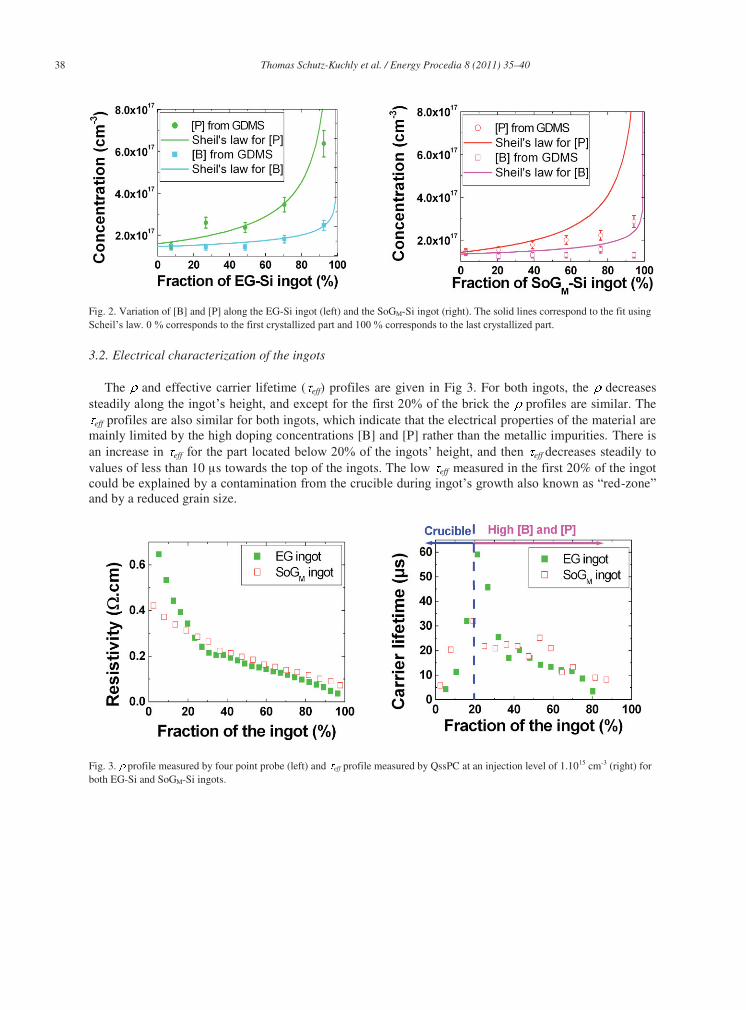
The and effective carrier lifetime ( eff) profiles are given in Fig 3. For both ingots, the decreases steadily along the ingot’s height, and except for the first 20% of the brick the profiles are similar. The
eff profiles are also similar for both ingots, which indicate that the electrical properties of the material are mainly limited by the high doping concentrations [B] and [P] rather than the metallic impurities. There is an increase in eff for the part located below 20% of the ingots’ height, and then eff decreases steadily to values of less than 10 µs towards the top of the ingots. The low eff measured in the first 20% of the ingot could be explained by a contamination from the crucible during ingot’s growth also known as “red-zone” and by a reduced grain size.
Fig. 3. profile measured by four point probe (left) and eff profile measured by QssPC at an injection level of 1.1015 cm-3 (right) for both EG-Si and SoGM-Si ingots.
Thomas Schutz-Kuchly et al. / Energy Procedia 8 (2011) 35–40 39
3.3. Solar cells results
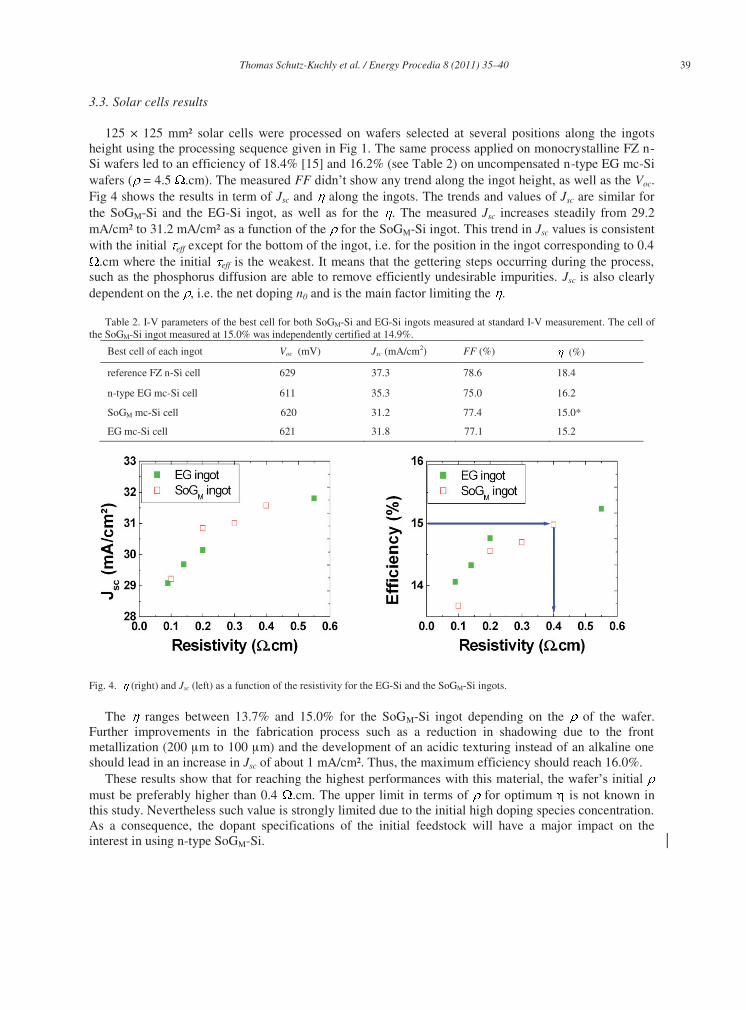
125 × 125 mm² solar cells were processed on wafers selected at several positions along the ingots height using the processing sequence given in Fig 1. The same process applied on monocrystalline FZ n-Si wafers led to an efficiency of 18.4% [15] and 16.2% (see Table 2) on uncompensated n-type EG mc-Si wafers ( = 4.5 .cm). The measured FF didn’t show any trend along the ingot height, as well as the Voc. Fig 4 shows the results in term of Jsc and along the ingots. The trends and values of Jsc are similar for the SoGM-Si and the EG-Si ingot, as well as for the . The measured Jsc increases steadily from 29.2 mA/cm² to 31.2 mA/cm² as a function of the for the SoGM-Si ingot. This trend in Jsc values is consistent with the initial eff except for the bottom of the ingot, i.e. for the position in the ingot corresponding to 0.4
.cm where the initial eff is the weakest. It means that the gettering steps occurring during the process, such as the phosphorus diffusion are able to remove efficiently undesirable impurities. Jsc is also clearly dependent on the , i.e. the net doping n0 and is the main factor limiting the .
Table 2. I-V parameters of the best cell for both SoGM-Si and EG-Si ingots measured at standard I-V measurement. The cell of
the SoGM-Si ingot measured at 15.0% was independently certified at 14.9%.
Best cell of each ingot Voc (mV) Jsc (mA/cm2) FF (%) (%)
reference FZ n-Si cell 629 37.3 78.6 18.4
n-type EG mc-Si cell 611 35.3 75.0 16.2
SoGM mc-Si cell 620 31.2 77.4 15.0*
EG mc-Si cell 621 31.8 77.1 15.2
Fig. 4. (right) and Jsc (left) as a function of the resistivity for the EG-Si and the SoGM-Si ingots.
The ranges between 13.7% and 15.0% for the SoGM-Si ingot depending on the of the wafer. Further improvements in the fabrication process such as a reduction in shadowing due to the front metallization (200 µm to 100 µm) and the development of an acidic texturing instead of an alkaline one should lead in an increase in Jsc of about 1 mA/cm². Thus, the maximum efficiency should reach 16.0%.
These results show that for reaching the highest performances with this material, the wafer’s initial must be preferably higher than 0.4 .cm. The upper limit in terms of for optimum is not known in this study. Nevertheless such value is strongly limited due to the initial high doping species concentration. As a consequence, the dopant specifications of the initial feedstock will have a major impact on the interest in using n-type SoGM-Si.
40 Thomas Schutz-Kuchly et al. / Energy Procedia 8 (2011) 35–40
4. Conclusion
In this study, we investigated the potential of n-type SoGM-Si for fabricating solar cells via a direct comparison with an intentionally B-P compensated EG-Si ingot. The objective was to select a silicon feedstock with relatively high doping concentrations ([B] = 1.5ppmw, [P] =11ppmw) in order to consider a low-cost scenario in terms of purification process. It was showed that n-type industrial process including high temperature boron diffusion and thermal oxidation was compatible with such material. Efficiency between 13.5% up to 15.0% was obtained on large area solar cells. A strong correlation of the cell performances with the material’s resistivity was highlighted. More precisely, the electrical quality of the material seems to be limited by the resistivity. Due to the low segregation coefficient of phosphorus into silicon, a large fraction of the ingot presents a range of resistivity too low to expect the fabrication of highly efficient solar cells. In terms of material’s specifications, a minimum value of resistivity of 0.4
.cm is required to expect an efficiency of 16.0 %. As a consequence, this study shows that n-type SoGM-Si is a very promising candidate for next generation of solar cells as condition issues can be solved in terms of doping engineering to fabricate ingots with homogeneous resistivity values above 0.4 .cm.
5. Acknowledgments
The authors would like to thank the CEA, the French National Research Agency (ANR) for financing the MULTIXEN project and the French environment and energy management agency ADEME for financial support.
6. References
[1] C. del Cañizo, G. del Coso and W.C. Sinke, “Crystalline Silicon Solar Module Technology: Towards the 1 € Per Watt-Peak Goal”, Prog. Photovolt: Res. Appl., 17:199-209, 2009.
[2] J. Kraiem, R. Einhaus, F. Lissalde, S. Dubois, N. Enjalbert, B. Drevet, F. Servant, and D. Camel, “Innovative Crystallisation of Multi-Crystalline Silicon Ingots from different types of Silicon Feedstock”, Proceedings of the 23rd PVSEC European Conference, pp. 1071-1074, Valencia, 2008.
[3] T. Schutz-Kuchly, S. Dubois, J. Veirman, Y. Veschetti, D. Heslinga, and O. Palais, “Light-Induced-Degradation in compensated n-type Czochralski silicon solar cells”, Phys. Status Solidi A (in press).
[4] Y. Veschetti, T. Schutz-Kuchly, V. Sanzone, and D. Heslinga, “Electrical properties of n-type solar grade silicon fabrication of solar cells and investigation of LID effect”, proceedings of the 24th EU-PVSEC Hamburg, 2009.
[5] S. Rein and S. W. Glunz, Appl. Phys. Lett. 82, 1054 (2003). [6] J. Schmidt, A. G. Aberle, and R. Hezel, Proceedings of the 26th IEEE Photovoltaic Specialists Conference, Anaheim, 1997
(IEEE, New York, 1997), p. 13. [7] J. Schmidt, and K. Bothe, Phys. Rev. B 69, 024107 (2004). [8] V. V. Voronkov, and R. Falster, J. Appl. Phys. 107, 053509 (2010). [9] S. Martinuzzi, I. Périchaud, C. Trassy, and J. Degoulange, Prog. Photovoltaics 17, 297, 2009. [10] D. Macdonald, and L. J. Geerligs, Appl. Phys. Lett. 85, 4061, 2004. [11] A. Halm, J. Jourdan, S. Nichol, B. Ryningen, H. Tathgar, R. Kopecek, “DETAILED STUDY ON LARGE AREA 100%
SOG SILICON MC SOLAR CELLS WITH EFFICIENCIES EXCEEDING 16%”, 25th European Photovoltaic Solar Energy Conference, 6-10 September 2010, Valencia, Spain.
[12] R. Einhaus, J. Kraiem, F. Cocco, Y. Caratini, D. Bernou, D. Sarti, G. Rey, R. Monna, C. Trassy, J. Degoulange, Y. Delannoy, S. Martinuzzi, I. Périchaud, M. C. Record, P. Rivat. “PHOTOSIL – Simplified Production of Solar Silicon from Metallurgical Silicon”. 21st PVSEC European Conference, Dresden, 2006.
[13] Arora ND, Hauser JR, Roulston DJ., Electron and hole mobility in silicon as a function of concentration and temperature. IEEE 1982;29:292–5.
[14] N. Enjalbert, and R.A. Sinton. Proceedings of the 31st IEEE Photovoltaic Specialists Conference, Orlando. 3-7 Jan. 2005. [15] Y. Veschetti, V. Sanzone, F. Diagne, N. Auriac, D. Heslinga, “HIGH EFFICIENCY N-TYPE SILICON SOLAR CELLS
WITH NOVEL DIFFUSION TECHNIQUE FOR EMITTER FORMATION”, 25th European Photovoltaic Solar Energy Conference, 6-10 September 2010, Valencia, Spain.