the logic analyzer: a new instrument for observing logic
TRANSCRIPT
OCTOBER 1973
© Copr. 1949-1998 Hewlett-Packard Co.
The Logic Analyzer: A New Instrument for Observing Logic Signals Des igned spec i f i ca l l y to so lve d ig i ta l des ign and t roub le shooting problems, this new instrument provides a digi tal d isp lay w i th s torage, pos i t i ve and negat ive d ig i ta l de lay , combinator ia l t r igger ing, and dig i ta l sequence compar ison.
by Robin Adler , Mark Baker , and Howard D . Marsha l l
DIGITAL CIRCUITS confront designers and troubleshooters with measurement problems
that differ in many ways from those in analog cir cuits. As a result, instruments developed for analog measurements are often less than optimum for the new digital measurements, so there is a need for new kinds of instruments designed specifically to solve digital problems.
Model 5000A Logic Analyzer, Fig. 1, is just that. An entirely digital instrument for displaying logic signals, it has a digital display, digital functions, and digital controls, and it operates in a manner that is intuitive to digitally oriented users.
A good example of the kind of problem that is easily solved by the Logic Analyzer is observation of long and infrequent logic sequences in calcula tors and other ROM-controlled systems. With conventional instruments, seeing these sequences is quite difficult and identifying individual bits is virtually impossible. With the Logic Analyzer and its digital storage, once-per-keystroke calculator sequences are easily captured. The Analyzer's dig ital delay makes it possible to observe any section of a thousand-bit sequence with no uncertainty as to which bits are displayed and no need to count clock pulses. These abilities also make it easy to see and analyze the long, non-repetitive signal se quences that occur in serial data transmission, such as between remote terminals and a computer.
Another problem arises in disc drives and other motor-driven computer peripherals. Continuous variations in drive-motor speed may cause so much jitter in the data waveforms that they are impos sible to interpret when observed by conventional means. The Logic Analyzer's digital delay removes the jitter, so the display is stable and easily inter preted.
Other Logic Analyzer features are useful in a variety of digital applications. In its SPIKE mode, the Analyzer captures and stores the short, ran domly occurring noise pulses that often cripple en tire systems while escaping detection by conven tional means. Negative delay helps the user analyze causes of errors in single-shot data sequences by displaying data that occurred prior to a trigger point. And a trigger point need not be defined simply as an edge occurring at a single node; the Analyzer can be set to trigger on coincidences of logic HIGH's or LOW's at two or three nodes.
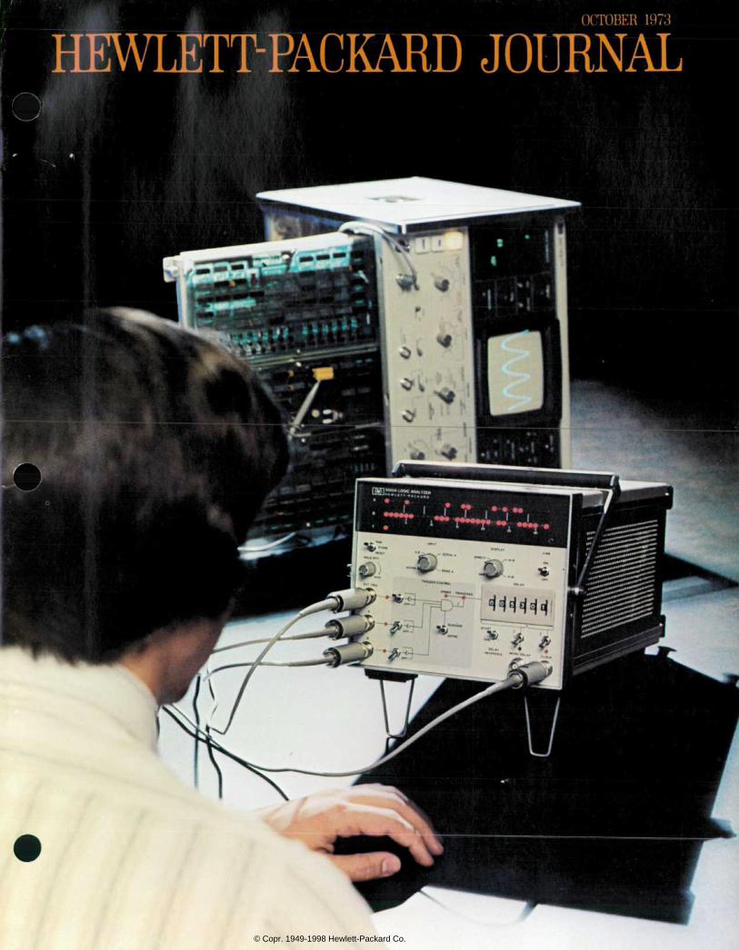
C o v e r : M o d e l 5 0 0 0 A L o g i c Analyzer 's two rows of 32 red l i gh t -em i t t i ng d iodes d i sp lay dig i ta l data occurr ing at the A a n d B i n p u t s . A l i g h t e d L E D ind ica tes a log ic HIGH leve l . Other LED's ind ica te the t r ig g e r p o i n t , i n p u t c o n d i t i o n s , a r m i n g , a n d t r i g g e r i n g . D e
s igned speci f ica l ly for d ig i ta l des ign and t rouble shoot ing, the Logic Analyzer s impl i f ies many d i f f icul t measurements.
In this Issue:
The Logic Analyzer : A New Kind of In strument for Observing Logic Signals, b y R o b i n A d l e r , M a r k B a k e r , a n d H o w a r d D . M a r s h a l l . page 2
A Pulse Generator fo r Today 's D ig i ta l Ci rcui ts , by Reinhard Falke and Horst L ink. . page 17
P R I N T E D I N U . S . A . t H E W L E T T - P A C K A R D C O M P A N Y , 1 9 7 3
© Copr. 1949-1998 Hewlett-Packard Co.
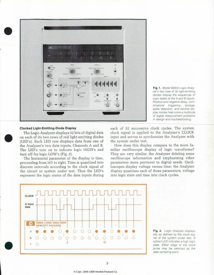
Fig. 1 . Model 5000 A Logic Analy zer 's two rows of 32 l ight-emit t ing d iodes d i sp lay t he sequences o f logic states at the A and B inputs. Pos i t i ve and negat ive de lay , com b i n a t o r i a l t r i g g e r i n g , s t o r a g e , sp i ke de tec t i on , and seve ra l d i s play modes help solve a mult i tude o f d ig i ta l measurement p rob lems in des ign and t roubleshoot ing.
Clocked Light-Emitt ing-Diode Display The Logic Analyzer displays 32 bits of digital data
on each of its two rows of red light-emitting diodes (LED's). Each LED row displays data from one of the Analyzer's two data inputs, Channels A and B. The LED's turn on to indicate logic HIGH's and turn off for logic LOW's (Fig. 2).
The horizontal parameter of the display is time, proceeding from left to right. Time is quantized into discrete intervals according to the clock signal of the circuit or system under test. Thus the LED's represent the logic states of the data inputs during
each of 32 successive clock cycles. The system clock signal is applied to the Analyzer's CLOCK input and serves to synchronize the Analyzer with the system under test.
How does this display compare to the more fa miliar oscilloscope display of logic waveforms? They are very similar, the Analyzer deleting some oscilloscope information and emphasizing other parameters more pertinent to digital needs. Oscil loscopes display voltage versus time; the Analyzer display quantizes each of these parameters, voltage into logic state and time into clock cycles.
F l g . 2 . L o g ; c A n a l y z e r d i s p l a y s b i t s a s d e f i n e d b y t h e c l o c k s i g n a l o f t h e s y s t e m u n d e r t e s t . A l ighted LED indicates a h igh logic s t a t e . E i t h e r e d g e o f t h e c l o c k p u l s e m a y b e s e l e c t e d a s t h e data sampl ing point .
© Copr. 1949-1998 Hewlett-Packard Co.
Omitted from the Analyzer's display is analog voltage and timing information. These of course, are the signal parameters over which the digital de signer has least control. Once he has selected a particular 1C family, he cannot, for example, adjust high-state output levels or propagation delays be yond the limits specified on data sheets.
What the user does control is what the Analyzer is designed to display, that is, the procession of logic states as a function of clock cycle, or in other words, the function of the circuit. On and off LED's correspond naturally and intuitively to HIGH and LOW logic states. Using the test system's clock for the horizontal quantization means the data is dis played in terms of bits — just the information the user needs to compare circuit response to device truth tables or system timing diagrams.
Oscilloscopes, on the other hand, force the user to make the quantization into bits. To do this, he must display the clock along with the data and vis ually divide the continuous data stream into the bits of interest. At the same time the user must mentally impress the threshold voltage of the logic family on the waveforms to make decisions about HIGH's and LOW's.
This is not to say that either instrument precludes use of the other. Both are essential, although for different things. The oscilloscope is most important early in the design cycle, when questions about ringing, race conditions, fan-outs, and power dis tribution are important. These are questions that need to be answered before the system begins to run. Later in the design cycle, when the sequences of logic states are most important, and in produc tion test and field service, the Logic Analyzer is likely to be more useful. There are also many measurements (often involving the Analyzer's digi tal delay) that can be made only by using both in struments together.
Digi ta l Combinator ia l Tr igger ing Triggering begins the Analyzer's data input and
display processes. The trigger point is the reference point to which all following events are related.
The Analyzer's controls provide for triggering on either single events or multiple events occurring simultaneously. This capability is necessary in di gital applications because digital systems commonly function in response to parallel data patterns oc curring simultaneously on several circuit nodes. A device, for example, might be designed to accept data only when two control lines are HIGH con currently. Therefore, synchronizing a measurement with the start of a process often requires the ability to recognize multiple simultaneous events. This the
Analyzer can do. It triggers on an AND combination of up to three signals or their complements.
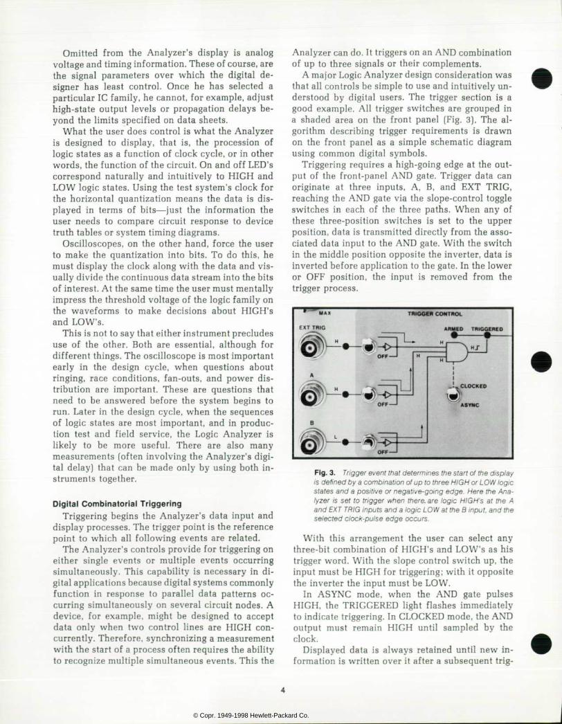
A major Logic Analyzer design consideration was that all controls be simple to use and intuitively un derstood by digital users. The trigger section is a good example. All trigger switches are grouped in a shaded area on the front panel (Fig. 3). The al gorithm describing trigger requirements is drawn on the front panel as a simple schematic diagram using common digital symbols.
Triggering requires a high-going edge at the out put of the front-panel AND gate. Trigger data can originate at three inputs, A, B, and EXT TRIG, reaching the AND gate via the slope-control toggle switches in each of the three paths. When any of these three-position switches is set to the upper position, data is transmitted directly from the asso ciated data input to the AND gate. With the switch in the middle position opposite the inverter, data is inverted before application to the gate. In the lower or OFF position, the input is removed from the trigger process.
Fig. 3 . Tr igger event that determines the s tar t o f the d isp lay is def ined by a combinat ion of up to three HIGH or LOW logic s ta tes and a pos i t i ve o r negat ive-go ing edge. Here the Ana lyzer i s se t to t r igger when there , a re log ic HIGH's a t the A and EXT TRIG inputs and a logic LOW at the B input, and the se lec ted c lock-pu lse edge occurs .
With this arrangement the user can select any three-bit combination of HIGH's and LOW's as his trigger word. With the slope control switch up, the input must be HIGH for triggering; with it opposite the inverter the input must be LOW.
In ASYNC mode, when the AND gate pulses HIGH, the TRIGGERED light flashes immediately to indicate triggering. In CLOCKED mode, the AND output must remain HIGH until sampled by the clock.
Displayed data is always retained until new in formation is written over it after a subsequent trig-
© Copr. 1949-1998 Hewlett-Packard Co.
Logic Analyzer Applications in Digital System Waveform Measurements
W h e r e v e r o s c i l l o s c o p e s a r e u s e d t o d i s p l a y d i g i t a l i n f o r mat ion , the Log ic Ana lyzer w i l l be a va luab le add i t ion to the u s e r ' s t e s t e q u i p m e n t . S p e c i f i c a r e a s i n c l u d e c o m p u t e r s , m a g n e t i c t a p e a n d d i s c d r i v e s , c a r d r e a d e r s , t e l e p r i n t e r s , p a p e r t a p e r e a d e r s , p o i n t - o f - s a l e r e a d e r s a n d t e r m i n a l s , c a l c u l a t o r s , d i g i t a l d a t a t r a n s m i s s i o n , R O M - c o n t r o l l e d i n s t ruments , and o thers .
Disc Drives M a g n e t i c d i s c d r i v e s a r e f a s t - a c c e s s , m a s s s t o r a g e d e
v i ces t ha t r eco rd i n f o rma t i on on ro ta t i ng magne t i c p l a t t e r s o r d i s c s . D a t a i s s t o r e d a n d r e a d s e r i a l l y . T h e a d d r e s s o f e a c h d a t a r e c o r d o n t h e d i s c i s c o n t a i n e d i n a p r e a m b l e t h a t p r e c e d e s t h e r e c o r d a n d i s p a r t o f t h e s e r i a l d a t a s t r e a m . W h e n t h e c o n t e n t s o f a g i v e n r e c o r d a r e d e s i r e d , i t s add ress i s en te red and the da ta s t ream i s mon i to red fo r t ha t add ress . When t he add ress i s de tec ted , a compa r i son c i r c u i t g e n e r a t e s a p u l s e a n d d a t a t r a n s m i s s i o n b e g i n s . I f t h i s p u l s e i s u s e d t o t r i g g e r a n o s c i l l o s c o p e o r L o g i c A n a l yze r , subsequen t da ta i s v i ewab le . However , t he p reamb le d a t a h a s a l r e a d y p a s s e d b y ; s e e i n g i t r e q u i r e s a n e g a t i v e de lay . The SOOOA's END mode prov ides negat ive de lay and makes i t poss ib le t o see the add ress and o the r i n fo rma t ion s tored in the preamble .
Look ing fa r the r i n to t he da ta reco rd f o l l ow ing the t r i gge r c r e a t e s o t h e r d i f f i c u l t i e s . T h e t i m i n g o f t h e w a v e f o r m s d e pends on the ro ta t iona l speed o f the d isc , wh ich con t inua l l y var ies. Hence the waveforms j i t ter wi th respect to the t r igger . J i t t e r i s c u m u l a t i v e a n d b e c o m e s q u i t e l a r g e s e v e r a l t h o u sand data into the record. Stable presentat ion of j i t ter ing data requ i res d ig i t a l de lay . A pa r t i cu la r da ta b i t a lways occu rs a f i x e d n u m b e r o f c l o c k c y c l e s i n t o t h e r e c o r d , e v e n t h o u g h t h e t i m e d e l a y b e t w e e n t h e t r i g g e r a n d t h e b i t o f i n t e r e s t v a r i e s w i d e l y . D i a l i n g t h i s d e l a y i n t o t h e L o g i c A n a l y z e r ' s t h u m b w h e e l r e g i s t e r w i l l p r o d u c e a s t a b l e d i s p l a y o f a n y desired bi t .
T h e L o g i c A n a l y z e r ' s s i n g l e - s h o t s t o r a g e s i m p l i f i e s f i n d i ng and ana l yz i ng i n te rm i t t en t f au l t s , wh i ch a re common i n d i s c d r i v e s a n d o t h e r c o m p u t e r s y s t e m s . W h e n a s y s t e m fa i l s once per hour o r even less o f ten , the 5000A w i l l , when e v e r t h e e r r o r o c c u r s , c a p t u r e a s w e e p o f d a t a a n d h o l d i t i n d e f i n i t e l y . W i t h n e g a t i v e d e l a y , d a t a t h a t p r e c e d e d t h e e r r o r c a n b e d i s p l a y e d s o t h e c a u s e o f t h e e r r o r c a n b e analyzed.
Microprogrammed Devices Mic rop rog rammed , r ead -on l y -memory - con t ro l l ed dev i ces
commonly genera te long non- repe t i t i ve da ta sequences tha t a r e d i f f i c u l t t o a n a l y z e . C a l c u l a t o r s a r e a g o o d e x a m p l e o f s u c h d e v i c e s . A p r o g r a m t o c a l c u l a t e t h e s q u a r e r o o t o f a n u m b e r m i g h t c o n t a i n o v e r t e n t h o u s a n d b i t s a n d r e p e a t on ly as o f ten as the square- roo t key i s p ressed.
I n t r o u b l e s h o o t i n g a R O M - c o n t r o l l e d i n s t r u m e n t , i t m a y b e p o s s i b l e t o s i n g l e - s t e p t h r o u g h l o n g s e q u e n c e s . H o w e v e r , t h i s i s o f t e n i n c o n v e n i e n t , a n d t h e p r o b l e m m a y g o away a t s low speeds . The Log ic Ana lyzer a l lows the sys tem to run a t i t s norma l ra te wh i le the tes t i s be ing made. I t can d i s p l a y n o t o n l y d a t a s e q u e n c e s b u t a l s o s p i k e s o r t r a n s ients on c r i t i ca l cont ro l l ines . In cases where ROMs cont ro l a r i t h m e t i c o p e r a t i o n s i n v o l v i n g s e v e r a l s h i f t r e g i s t e r s , t h e A n a l y z e r c a n b e u s e d t o d i s p l a y i n d e t a i l t h e c o m p l e x o p erat ions that take p lace in these shi f t reg is ters. This analys is
capab i l i t y goes fa r beyond mere ly observ ing the f i na l resu l t o f a comp lex opera t ion .
T h e L o g i c A n a l y z e r ' s d i g i t a l d i s p l a y , d i g i t a l d e l a y , a n d s ing le -sho t s to rage a l so s imp l i f y ca l cu la to r measu remen ts . T h e d i g i t a l c l o c k e d d i s p l a y p r e s e n t s d a t a a n d p r o g r a m i n s t ruc t i ons i n t he fo rm o f b i t s , j us t as they appear on t im ing d i a g r a m s o r R O M t r u t h t a b l e s . S t o r a g e c a p t u r e s t h e t r a n s i e n t w a v e f o r m s . I f R Z ( r e t u r n - t o - z e r o ) e n c o d i n g i s u s e d , S P I K E A m o d e w i l l p r o d u c e t h e d e s i r e d d i s p l a y .
Because the ser ia l inst ruct ions or data are usual ly grouped i n t o w o r d s , d i g i t a l d e l a y b y b o t h b i t s a n d w o r d s i s u s e f u l . W i th once -pe r -word pu lses app l i ed to the Ana lyze r ' s WORD D E L A Y i n p u t , a n y w o r d c a n b e d i s p l a y e d w i t h o u t c o u n t i n g pu lses to f ind i t . B i t de lay wi th in the se lec ted word is he lp fu l w h e n w o r d l e n g t h e x c e e d s t h e d i s p l a y c a p a c i t y .
Digital Data Transmission In d ig i ta l data t ransmiss ion, characters , words, and b locks
o f da ta take the fo rm o f f as t s ing le -sho t bu rs t s o f ones and z e r o s . T h i s i s t r u e w h e t h e r t h e d a t a i s b e i n g t r a n s m i t t e d between a termina l and a computer , between two data banks v i a m o d e m s a n d t e l e p h o n e l i n e s , o r b e t w e e n a f r e q u e n c y c o u n t e r a n d a c a l c u l a t o r i n a s m a l l a u t o m a t i c t e s t s y s t e m . T h e L o g i c A n a l y z e r e a s i l y d i s p l a y s t h e s e b u r s t s . T h e A n a l y z e r d i s p l a y i s l o c k e d t o t h e d a t a b y t h e c l o c k a n d t h e A n a l y z e r t r i g g e r s o n l y w h e n d a t a i s r e c e i v e d . S u c c e s s i v e c h a r a c t e r s c a n b e d i s p l a y e d o n e a f t e r a n o t h e r a n d s t o r e d as long as desired.
T o a c c e s s a s p e c i f i c p a r t o f a d a t a b l o c k , s u c h a s a p r e amble, a postamble, a control bi t , or a par i ty bi t , the Analyzer 's posi t ive and negat ive digi tal delay can be used. I f a tr igger can on ly be found a t the end o f the p reamble , engag ing nega t i ve de lay by se lect ing DELAY REFERENCE "END" wi l l d isp lay the da ta tha t l eads up to the t r i gge r , name ly the p reamb le . Wi th exac t l y the same t r igger po in t , the end o f the da ta b lock can be observed by d ia l ing in the correct amount o f pos i t ive de lay and retransmit t ing the data.
Analyzer and Osci l loscope The synerg ism that ex is ts between the Log ic Ana lyzer and
t h e o s c i l l o s c o p e i s m o s t e v i d e n t w h e n e i t h e r i n s t r u m e n t i s used as a t r i gge r sou rce fo r t he o the r . When the Ana lyze r ' s coun tdown o f b i t and wo rd de lays i s comp le te , a pu l se t ha t c a n b e u s e d t o t r i g g e r a n o s c i l l o s c o p e i s g e n e r a t e d a t t h e r e a r p a n e l T R I G O U T c o n n e c t o r . T h e S O O O A ' s c o m b i n a t o r i a l t r i g g e r i n g a n d d i g i t a l d e l a y c o m b i n e w i t h t h e o s c i l l o s c o p e ' s v o l t a g e a n d t i m i n g i n f o r m a t i o n t o d i s p l a y a n a l o g pa ramete rs o f ha rd - to - l oca te da ta b i t s . S tab le osc i l l oscope d i s p l a y s o f d i s c d a t a o r c a l c u l a t o r p r o g r a m w o r d s a r e p o s s ib le w i th th is techn ique .
W i t h a de layed -sweep osc i l l o scope , t he r eve rse a r range m e n t i s o f t e n f r u i t f u l . T r i g g e r i n g t h e A n a l y z e r f r o m t h e d e layed ga te ou tpu t o f the osc i l loscope beg ins the 5000A da ta input a t the s tar t o f the in tens i f ied region on the osc i l loscope C R T . T h e o s c i l l o s c o p e d e l a y v e r n i e r c a n b e u s e d t o s c a n r a p i d l y t h r o u g h t h e w a v e f o r m s e a r c h i n g f o r s u s p e c t d a t a . T h e A n a l y z e r s i m u l t a n e o u s l y d i s p l a y s t h e p r e c i s e b i t s t r u c t u r e o f t h e s c a n n e d d a t a a n d i n d i c a t e s a n y s p i k e s t h a t a r e p r e s e n t . S e a r c h i n g f o r a p a r t i c u l a r c o n t r o l c h a r a c t e r i n a s e r i a l t r a n s m i s s i o n t o o r f r o m a d a t a t e r m i n a l i s a g o o d e x a m p l e o f t h e t y p e o f p r o b l e m t h a t c a n b e s o l v e d u s i n g th is technique.
(Cont inued on page 6)
© Copr. 1949-1998 Hewlett-Packard Co.
(Cont inued f rom page 5 )
Everyday Uses W h i l e t h e e x a m p l e s g i v e n s o f a r h a v e c o n c e n t r a t e d o n
d r a m a t i c a p p l i c a t i o n s o f t h e L o g i c A n a l y z e r i n d i f f i c u l t s y s t e m m e a s u r e m e n t s , t h e A n a l y z e r w i l l p r o b a b l y b e u s e d m o s t o f t e n a s a g e n e r a l - p u r p o s e b e n c h i n s t r u m e n t i n c o m m o n d i g i t a l t r o u b l e s h o o t i n g s i t u a t i o n s . F o r e x a m - pie: • With the CLOCK input connected to the c lock l ine of a f l ip-
f l op and the channe l A i npu t connec ted to t he Q ou tpu t o f the f l ip - f lop , the f l ip - f lop can be checked for p roper d iv ide- by - two ope ra t i on , i nd i ca ted by a d i sp lay o f a l t e rna te l y o f f and on LED'S.
• An AND gate has pulses at i ts two inputs but the output re ma ins LOW. Comb ina to r ia l t r i gge r ing can de te rm ine i f t he inputs are ever HIGH s imul taneously .
• Wi th d ig i ta l de lay determin ing the number o f c lock pu lses between over f lows, proper d iv is ion ra t io in a programmable f requency div ider is easi ly ver i f ied.
• The output pu lse of a monostable mul t iv ibrator (one-shot) may be v i ewed us ing asynch ronous t r i gge r i ng and SP IKE mode, no mat ter what the pu lse re la t ionsh ip o f the c lock to the one-shot output .
• Data b i t s d ropped in a rec i rcu la t ing sh i f t reg is te r can be d e t e c t e d b y c o m p a r i n g t h e c i r c u l a t i n g d a t a w i t h a s t o r e d reference.
ger. If only a single trigger occurs, the data is held indefinitely. The result is automatic, single-shot storage. There is no need to realize beforehand that data is non-recurring and engage special storage controls.
Even if a data sequence is repetitive, the Analyzer can be commanded to store it by placing a front- panel switch in the STORE position. With this same switch in the RUN position the display will change each time a trigger occurs. An adjustable HOLDOFF control prevents triggering for up to five seconds in the RUN mode so new data can be displayed at a convenient rate. At the end of the holdoff period an ARMED light on the front panel turns on to in dicate that the Analyzer is ready to trigger.
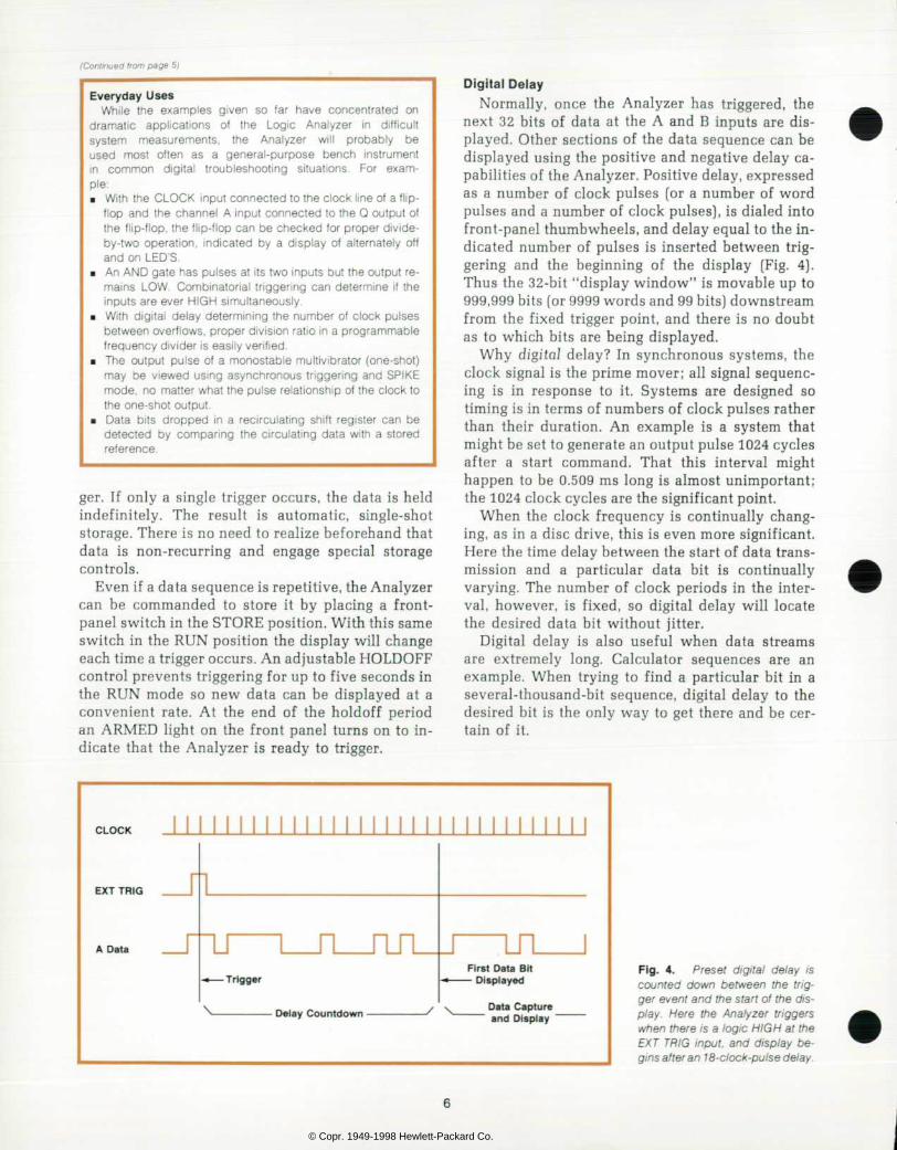
Digital Delay Normally, once the Analyzer has triggered, the
next 32 bits of data at the A and B inputs are dis played. Other sections of the data sequence can be displayed using the positive and negative delay ca pabilities of the Analyzer. Positive delay, expressed as a number of clock pulses (or a number of word pulses and a number of clock pulses), is dialed into front-panel thumbwheels, and delay equal to the in dicated number of pulses is inserted between trig gering and the beginning of the display (Fig. 4). Thus the 32-bit "display window" is movable up to 999,999 bits (or 9999 words and 99 bits) downstream from the fixed trigger point, and there is no doubt as to which bits are being displayed.
Why digital delay? In synchronous systems, the clock signal is the prime mover; all signal sequenc ing is in response to it. Systems are designed so timing is in terms of numbers of clock pulses rather than their duration. An example is a system that might be set to generate an output pulse 1024 cycles after a start command. That this interval might happen to be 0.509 ms long is almost unimportant; the 1024 clock cycles are the significant point.
When the clock frequency is continually chang ing, as in a disc drive, this is even more significant. Here the time delay between the start of data trans mission and a particular data bit is continually varying. The number of clock periods in the inter val, however, is fixed, so digital delay will locate the desired data bit without jitter.
Digital delay is also useful when data streams are extremely long. Calculator sequences are an example. When trying to find a particular bit in a several-thousand-bit sequence, digital delay to the desired bit is the only way to get there and be cer tain of it.
CLOCK
EXT TRIG
A Da ta _ru Trigger
Delay Countdown -
First Data Bit — Displayed
Data Capture and Display
F i g . 4 . P r e s e t d i g i t a l d e l a y i s c o u n t e d d o w n b e t w e e n t h e t r i g ger event and the s tar t o f the d is p l a y . H e r e t h e A n a l y z e r t r i g g e r s when there is a log ic HIGH at the E X T T R I G i n p u t , a n d d i s p l a y b e gins after an 18-clock-pulse delay-
© Copr. 1949-1998 Hewlett-Packard Co.
Negat ive Delay Some oscilloscopes use an analog delay line to
preserve information close to the trigger long enough for the CRT to display it. The 5000A extends this concept using digital storage to permit display of events up to 32 clock cycles before the trigger.
Negative delay is engaged by setting the DELAY REFERENCE switch to the END position. The trig ger then occurs at the end of the display registers and the data displayed is the data that occurred on the 32 clock cycles prior to the trigger.
Uses of negative delay are numerous. For ex ample, when analyzing serial trigger circuits in disc drives or data terminals, the serial word leading up to and causing the trigger can be displayed. Or, triggering from an error condition, the pre-error data may be examined to locate the cause of the error.
Input and Display Modes In its most common mode of operation the Logic
Analyzer is a two-channel device with a row of LED's for each channel. The various INPUT and DISPLAY modes use the two inputs and displays in other ways to perform additional functions. SERIAL A mode, for example, cascades the B display regis ter onto the end of the A display. The result is a single 64-bit display loaded from the A input, and a single-channel 64-bit negative delay capability, as well. STORE B provides selective use of the Analyzer's storage. B-channel data is stored while the A display reloads with each trigger.
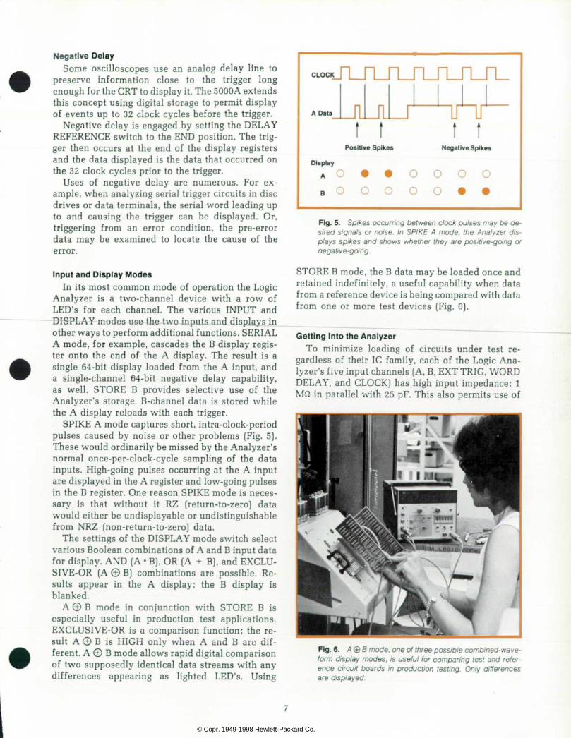
SPIKE A mode captures short, intra-clock-period pulses caused by noise or other problems (Fig. 5). These would ordinarily be missed by the Analyzer's normal once-per-clock-cycle sampling of the data inputs. High-going pulses occurring at the A input are displayed in the A register and low-going pulses in the B register. One reason SPIKE mode is neces sary is that without it RZ (return-to-zero) data would either be undisplayable or undistinguishable from NRZ (non-return-to-zero) data.
The settings of the DISPLAY mode switch select various Boolean combinations of A and B input data for display. AND [A • B), OR (A + B), and EXCLU- SIVE-OR (A © B) combinations are possible. Re sults appear in the A display; the B display is blanked.
A © B mode in conjunction with STORE B is especially useful in production test applications. EXCLUSIVE-OR is a comparison function; the re sult A © B is HIGH only when A and B are dif ferent. A © B mode allows rapid digital comparison of two supposedly identical data streams with any differences appearing as lighted LED's. Using
CLOCK
A Data ÃILJ t t
Posit ive Spikes
t t Negative Spikes
Display
A O O O O O
F l g . 5 . S p i k e s o c c u r r i n g b e t w e e n c l o c k p u l s e s m a y b e d e s i r ed s i gna l s o r no i se . I n SP IKE A mode , t he Ana l yze r d i s p lays sp ikes and shows whe ther they a re pos i t i ve -go ing o r negat ive-going.
STORE B mode, the B data may be loaded once and retained indefinitely, a useful capability when data from a reference device is being compared with data from one or more test devices (Fig. 6).
Getting Into the Analyzer To minimize loading of circuits under test re
gardless of their 1C family, each of the Logic Ana lyzer's five input channels (A, B, EXT TRIG, WORD DELAY, and CLOCK) has high input impedance: 1
in parallel with 25 pF. This also permits use of
Fig . 6 . A © B mode, one o f th ree poss ib le combined-wave fo rm d i sp lay modes , i s use fu l f o r compar ing tes t and re fe r ence c i r cu i t boards in p roduc t ion tes t ing . On ly d i f f e rences are displayed.
© Copr. 1949-1998 Hewlett-Packard Co.
the Analyzer with standard Hewlett-Packard high- impedance probes and their accessories to further minimize circuit loading and to maximize probing flexibility.
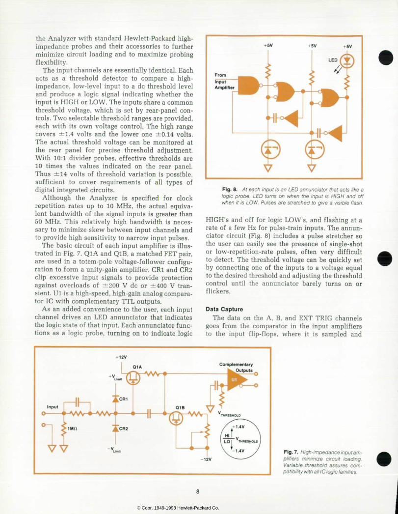
The input channels are essentially identical. Each acts as a threshold detector to compare a high- impedance, low-level input to a dc threshold level and produce a logic signal indicating whether the input is HIGH or LOW. The inputs share a common threshold voltage, which is set by rear-panel con trols. Two selectable threshold ranges are provided, each with its own voltage control. The high range covers ±1.4 volts and the lower one ±0.14 volts. The actual threshold voltage can be monitored at the rear panel for precise threshold adjustment. With 10:1 divider probes, effective thresholds are 10 times the values indicated on the rear panel. Thus ±14 volts of threshold variation is possible, sufficient to cover requirements of all types of digital integrated circuits.
Although the Analyzer is specified for clock repetition rates up to 10 MHz, the actual equiva lent bandwidth of the signal inputs is greater than 50 MHz. This relatively high bandwidth is neces sary to minimize skew between input channels and to provide high sensitivity to narrow input pulses.
The basic circuit of each input amplifier is illus trated in Fig. 7. Q1A and QlB, a matched FET pair, are used in a totem-pole voltage-follower configu ration to form a unity-gain amplifier. CRl and CR2 clip excessive input signals to provide protection against overloads of ±200 V dc or ±400 V tran sient. Ul is a high-speed, high-gain analog compara tor 1C with complementary TTL outputs.
As an added convenience to the user, each input channel drives an LED annunciator that indicates the logic state of that input. Each annunciator func tions as a logic probe, turning on to indicate logic
+ 5V + 5V +5V
Fig . 8 . A t each inpu t i s an LED annunc ia to r tha t ac ts l i ke a l o g i c p r o b e . L E D t u r n s o n w h e n t h e i n p u t i s H I G H a n d o f f when i t is LOW. Pulses are s t re tched to g ive a v is ib le f lash.
HIGH's and off for logic LOW's, and flashing at a rate of a few Hz for pulse-train inputs. The annun ciator circuit (Fig. 8) includes a pulse stretcher so the user can easily see the presence of single-shot or low-repetition-rate pulses, often very difficult to detect. The threshold voltage can be quickly set by connecting one of the inputs to a voltage equal to the desired threshold and adjusting the threshold control until the annunciator barely turns on or flickers.
Data Capture The data on the A, B, and EXT TRIG channels
goes from the comparator in the input amplifiers to the input flip-flops, where it is sampled and
+ 12V Complementary
Outputs
- 1 2 V Fig . 7 . H igh- impedance inpu t am p l i f i e r s m in im ize c i r cu i t l oad ing . V a r i a b l e t h r e s h o l d a s s u r e s c o m patibility with all I C logic families .
© Copr. 1949-1998 Hewlett-Packard Co.
quantized into bits. Data at the inputs to these flip- flops is transferred to their outputs at the clock pulse edge selected by the slope control on the front panel. This takes place whenever there is a clock signal present. However, the display is not loaded until the Analyzer is triggered and all digital delay is counted to zero. When this occurs, data is trans ferred to the input registers a short time (50 ns) after it is loaded into the sampler flip-flops. (See block diagram, Fig. 9.)
For easier use and interpretation of the Analyzer and its display, the first bit in each display row represents the data at the A or B input when the trigger event occurs. It is also necessary that these first and subsequent bits be displayed immediately, as soon as they are sampled, without waiting (e.g., for the next clock pulse). To accomplish this the contents of the input samplers are continuously monitored for the trigger event. When it occurs, a delayed version of the input clock is gated to the input registers to load the contents of the samplers for display. On each succeeding clock pulse data is loaded into the samplers and 50 ns later is trans ferred to the input registers by the delayed clock. Loading continues in this way until the two 32-bit channels are filled.
Meanwhile, data has also been flowing from the input registers to the display registers. Details of this process are described in the section headed "Display Considerations."
Once loaded, data is frozen for a minimum of 50
ms before a new trigger and input sequence can begin. This guarantees that even an intermittent bit is displayed long enough to be recognized.
Triggering One of the most difficult problems to overcome
in the display of any waveform is the definition of a trigger or sync point to which the data can be ref erenced. It is necessary that the trigger, however defined, be a unique event, one that occurs only once in the cycle of the machine whose waveforms are being analyzed. When signals are repetitive, this guarantees that triggering always occurs at the same point in the sequence and, most importantly, that the display will be stable.
Examination of trigger requirements in synchro nous systems reveals several possibilities. First, the trigger may be well defined as an event on a single line — for example, start-program pulses, reset pulses, or gating signals. In this case, the familiar single-channel, edge-sensitive triggering is suffi cient and the positive or negative edge of the pulse provides a unique data reference. It is crucial that an edge rather than a level serve as the trigger since the pulse may extend over many clock periods. The edges are unique; the level is not.
If the trigger cannot be derived from a single line, several signals can be ANDed together to provide the unique reference. This is controlled using the Analyzer's three trigger control switches.
N e g a t i v e D e l a y R e g i s t e r 3 2 B i t s E N D
E X T T R I G
C L O C K
I n p u t y C l o c k / S a m p l e r s : , .
. ASYNC & CLOCKED Trtwertno,
C l o c k G a t e a n d N Â « o a t , v . [ M a y
â € ¢ D a t a S w e e p a n d D i s p l a y -
F i g . 9 . L o g i c A n a l y z e r b l o c k d i a g r a m .
© Copr. 1949-1998 Hewlett-Packard Co.
Edge sensitivity of the Analyzer's trigger is achieved by an algorithm performed in the blocks labeled "Previous Trigger Storage" in Fig. 9. In words, the algorithm is simply that for a given event to trigger the Analyzer, the previous clock cycle must not have contained a trigger event. Thus the Analyzer does not trigger, for example, if its inputs are such that the front panel AND gate output is continuously HIGH.
In many cases it is desirable to ignore spikes and transients when triggering. This can be done by selecting the CLOCKED mode of operation, in which the inputs are monitored for the trigger con dition only at the selected clock edge (Fig. 10). The converse is also possible, in case the desired trigger is a spike. When this happens — that is, trigger in formation exists only between sampling points — ASYNC mode should be selected. The spike will be captured and stored until the clock occurs to enter it as a trigger condition. Both of these situations are common in digital testing.
Dig i ta l De lay Countdown Once the Analyzer has been triggered, it counts
down any digital delay that has been entered in the thumbwheel switch register. The contents of the thumbwheel switches are loaded into six down counters, which are then decremented.
The chain of six down counters may be decre mented solely by clock pulses or by a combination of clock pulses and WORD DELAY pulses. When the word delay function is engaged, the left four decades of the thumbwheel switch register are
CLOCK
T r i g g e r C o n t r o l T r i g g e r S e t t i n g s P o i n t s : A S Y N C C L O C K E D
F i g . 1 0 . I n C L O C K E D m o d e , t h e L o g i c A n a l y z e r m o n i t o r s i t s inputs fo r the t r igger cond i t ion on ly a t the se lec ted c lock edge. In ASYNC mode, t r igger ing occurs as soon as the t r ig g e r c o n d i t i o n a p p e a r s a t t h e i n p u t s . T r i g g e r i n g i s a l w a y s edge-sensi t ive.
counted down by pulses of lower repetition rate than the clock. These might correspond, for ex ample, to pulses that occur once per serial word in a calculator program. The four digits of word delay in combination with the remaining two digits of clock delay provide coarse and fine digital delays between the trigger and the start of the display.
The Analyzer's negative delay is implemented by running all incoming data through 32-bit digital delay lines (shift registers) prior to loading it into the input registers. When a trigger occurs, there fore, the data that is displayed actually occurred 32 clock periods earlier and has spent the interim trav eling through the shift register. The result is a dis play whose trigger event appears displayed at the right side, or end, of the display. Hence the START and END positions of the DELAY REFERENCE switch.
In END mode the thumbwheels still cause delay in the positive sense. The display ends the indicated number of pulses after the trigger. By selecting the END mode and less than 32 bits of positive delay, pre-trigger and post-trigger events can be seen in the same display.
Display Considerations In addition to the input registers, which provide
the sixty-four bits of information storage, there is also a second set of shift registers that provide an interface to the LED display. The function of these display registers is threefold.
First, the display registers are necessary to po sition the displayed data bits in the proper place. It was desired that data should always be displayed with the oldest data on the left and the newest data on the right, just as on an oscilloscope display.
The input shift register places each new bit in the rightmost position and pushes older data to the left. Thus if the contents of the input register were displayed directly, data would shift in from the right. To prevent this, as each new bit is entered, the contents of the input register are loaded in parallel into the display register. The display regis ter then quickly shifts so the oldest bit always ap pears at the left side of the display. This occurs on each clock cycle (Fig. 11). With 32-bit displays, the number of bits that data must be shifted on each clock cycle is thirty two minus the number of bits entered since the start of display.
This data positioning circuitry is required only for low-frequency data, because the movement of data apparent at slow rates cannot be seen above about 1 kHz. Therefore the data positioning circuit is disabled above 1 kHz and data is transferred to the display registers only after all 32 bits of the
10
© Copr. 1949-1998 Hewlett-Packard Co.
Left Shift
( 2 )
Parallel D i s p l a y R e g i s t e r 3 2 B i t s
I n p u t R e g i s t e r 3 2 B i t s Data In
(From Sampler )
F i g . 1 1 . L o g i c A n a l y z e r d i s p l a y s d a t a w i t h o l d e s t i n f o r m a t i on a t t he l e f t . A t c lock ra tes be low 1 kHz the th ree s teps shown occur on each c lock cyc le . The resu l t is that each b i t i s d i sp layed , p roper l y pos i t i oned , as soon as i t i s en te red . Data does not appear to shi f t in and is v iewable whi le the dis p lay is be ing loaded.
input register have been reloaded. The advantage is that no high-speed circuitry is needed in the dis play register.
The second purpose of the display register is to perform the multiplexing function necessary for transferring the data to the scanned display. After the display register is loaded and the data is po sitioned in the correct orientation, each 32-bit shift register is broken into four eight-bit closed loops. The data in each loop is circulated and one bit of the eight is monitored for the multiplexed data sig nal. The eight lines corresponding to the eight closed loops of circulating data in the two channels supply the drive (through buffers] to the anodes of the
LED's in the 8 X 8 scanned matrix. To properly decode the multiplexed data, the cathodes of the LED's are scanned in synchronism with the shifting of data in the eight-bit loops.
The third function of the display registers is as a source of data to the circuits that perform the Boolean operations (A + B, A • B, A © B) on the A and B inputs. These Boolean operations take place as the data is scanned into the LED matrix and therefore do not affect the data that is stored in the input registers. This means that any Boolean function can be performed without disturbing the stored data. Thus if it is desired to see this data in its original form it is readily available.
Spike Detect ion Selection of the SPIKE A mode makes possible
the detection of asynchronous events occurring be tween clock pulses. A spike is detected whenever more than one logic transition occurs within a single clock period. If the positive-going transition occurs first, the spike is defined as positive and is dis played on the A channel; conversely, negative spikes are displayed on the B channel.
The spike detector consists of two flip-flops (Fig. 12). One is sensitive to the positive-going edge of the data input and the other is sensitive to the negative-going edge. If during any given clock pe riod both flip-flops are set, a spike has occurred. The detected spike is entered into the input register by the next clock pulse.
A positive spike is differentiated from a negative one by a detector and a latch which determine which of the two flip-flops was set first. At the
A Data Positive Spike
Mult iple Edge Detect
Polarity Detect
Fig . 12 . Sp ike detec t ion c i rcu i t ry d e t e c t s m u l t i p l e e d g e s w i t h i n a c lock cyc le.
11
© Copr. 1949-1998 Hewlett-Packard Co.
The 1C Troubleshooters
Logic tes t ing needs s imi la r to those for wh ich the 5000A Lo g i c A n a l y z e r w a s d e v e l o p e d h a d e a r l i e r p r o m p t e d d e v e l o p m e n t o f a g r o u p o f h a n d h e l d i n s t r u m e n t s t h a t w e r e f o r e r u n ners o f the 5000A. Beg inn ing in 1968 wi th the now ub iqu i tous Logic Probe, th is fami ly o f ins t ruments has grown to inc lude a T T L / D T L L o g i c P r o b e , a L o g i c C l i p , a L o g i c P u l s e r , a L o g i c Compara to r , and Log ic Probes fo r tes t ing ECL and HTL/MOS circuits.
Logic Probe The Log ic Probe was the f i rs t tes t ins t rument des igned and
opt im ized s t r i c t l y fo r d ig i ta l app l ica t ions . I t has a d ig i ta l read ou t , a l amp near the p robe t i p , tha t d i sp lays log ic l eve ls and pu lses occu r r i ng on the c i r cu i t node be ing p robed . The lamp g l o w s b r i g h t l y t o i n d i c a t e l o g i c H I G H ' s , g o e s o f f f o r l o g i c LOW'S and g lows at ha l f br i l l iance to ind icate open c i rcu i ts or v o l t a g e s b e t w e e n t h e p r e s e t l o g i c t h r e s h o l d s . C o n t i n u o u s pulse t ra ins cause b l ink ing of the lamp at a 10 Hz rate and s in g l e p u l s e s a r e s t r e t c h e d t o p r o v i d e a v i s i b l e f l a s h o f t h e lamp: on for HIGH-going pulses and off for LOW-going ones.
Log ic Probes a re the qu ickes t , su res t way o f de tec t ing the presence or absence o f s ing le or in f requent pu lses. No ad jus t ments a re needed, and s igna ls can be rap id ly t raced th rough c i rcu i t s by mon i to r ing on ly two po in ts : the schemat ic and the probe t ip . There is no chance the probe wi l l s l ip o f f the in tend ed node whi le the user turns his head to read a remote display.
T h e P r o b e ' s v a l u e d e r i v e s f r o m t h e g r e a t e r s p e e d w i t h w h i c h d e s i g n a n d t r o u b l e s h o o t i n g f a u l t s t h a t r e s u l t i n b a d nodes can be found. In these cases the Probe by i tse l f w i l l ra p i d l y i s o l a t e t h e f a i l u r e . W h e n m o r e d e t a i l e d a n a l y s i s i s r e qu i red , such as tha t o f a Log ic Ana lyze r o r osc i l l oscope , t he Probe is a usefu l ad junc t . When the user i s unab le to ident i fy t he spec i f i c cause o f a f au l t , t he P robe can usua l l y l oca l i ze t h e s e a r c h t o a s m a l l g r o u p o f s u s p e c t I C ' s a n d t h u s m o r e qu ick ly focus the power o f the analyzer or osc i l loscope on the prob lem.
The 5 vo l t p robe, Model 10525T for TTL and DTL in tegra ted c i r c u i t s , h a s n o w b e e n j o i n e d b y t w o o t h e r m o d e l s . M o d e l 10525E has ECL log ic th resho lds and a -5 .2 vo l t power inpu t vo l t age f o r compa t i b i l i t y w i t h a l l t ypes o f em i t t e r - coup led l o g ic . i s a lso the fas tes t o f the th ree probes : pu lse de tec t ion is guaran teed down to 5 ns . Mode l 10525H is des igned fo r h igh vo l tage log ic fami l ies such as HTL and HiNIL. A bu i l t - in power supp ly vo l tage regu la to r accep ts inpu t vo l tages anywhere be t w e e n + 1 2 a n d + 2 5 v o l t s . L o g i c t h r e s h o l d s a r e p r e s e t t o +2 .5 vo l t s and +9 .5 vo l t s . The "H " p robe i s a l so use fu l w i t h many t ypes o f MOS, d isc re te componen t , and re lay log ic sys tems.
Logic Cl ip T h e s e c o n d h a n d h e l d l o g i c t e s t e r , i n t r o d u c e d i n 1 9 7 0 , i s
Model 1 0528A Logic Cl ip. IC's are mult i -pin devices, and i t 's of ten o f i n te res t to see in fo rmat ion a t severa l p ins a t the same t ime. The Logic Cl ip was deve loped to d isp lay the log ic s ta tes o f a l l 1 4 o r 1 6 p i n s o f a D I P 1 C s i m u l t a n e o u s l y . T h e C l i p a t taches d i rec t l y to TTL /DTL IC 's , au tomat i ca l l y seeks the Vcc and ground p ins , and connects i ts power and ground buses to t he p rope r p i ns . The C l i p ' s 16 l i gh t -em i t t i ng d i odes t hen d i s p lay the log ic s tates of a l l p ins of the 1C, one LED correspond ing to each pin. The LED's l ight to indicate logic HIGH's and re main of f for logic LOW'S.
The C l i p i s handy when ana lyz ing sequen t ia l c i r cu i t s such as those con ta in ing 1C coun te rs o r sh i f t reg ise rs . These typ i
ca l l y have four o r more ou tpu ts . Wi th a s low s t imu lus (abou t 1 Hz) the p rogress ion o f l og ic s ta tes can be fo l l owed on the C l i p . o f app l i ca t i ons i nc lude mon i to r i ng the ou tpu t s ta tes o f a ROM or d isp lay ing s ta t i c i npu t -ou tpu t re la t ionsh ips in com binator ia l IC 's such as inver ters or NAND gates.
Logic Pulser The Log ic Pu lse r , Mode l 10526T , was the fou r th o f t he 1C
Troub leshoo te rs to be deve loped . The Probe and C l ip a re re sponse moni tors ; they depend on the c i rcu i t under tes t to sup p ly s t imu lus to IC 's wh i le they d isp lay the responses. The Lo g i c P u l s e r c o n t r i b u t e s i n - c i r c u i t s t i m u l u s , t h e r e b y m a k i n g poss ib le the same k ind o f s t imu lus- response tes t ing tha t has long been inva luable in analog t roubleshoot ing.
The p rob lem o f s t imu la t i ng d ig i ta l IC ' s i n a c i r cu i t i s more d i f f icu l t than i t might a t f i rs t appear . Dig i ta l outputs have very low output impedances ( less than 5 ohms). They are designed th is way to p rov ide w ide immuni ty to spur ious no ise . Connec t e d i n c i r c u i t s , e a c h r e l a t i v e l y h i g h - i m p e d a n c e 1 C i n p u t i s d r i ven by a low- impedance ou tpu t tha t c lamps i t e i ther HIGH o r L O W a t a l l t i m e s . S t i m u l u s i s p o s s i b l e b y o v e r r i d i n g t h e dr iv ing 1C output w i th la rge amounts o f cur rent , bu t then des t ruct ion of the dr iv ing stage is a real possib i l i ty .
The Log ic Pu lser so lves th is p rob lem by genera t ing a very narrow pulse, br ie f ly overr id ing the dr iv ing output . The Pulser wi l l source or s ink up to 0 .65 amperes each t ime i ts pu lse but ton i s p ressed. Nar row pu lse w id th o f 0 .3 mic roseconds , cou p l e d w i t h t h e m a n u a l a c t i v a t i o n , m a k e t h e d u t y c y c l e v e r y sma l l , so t he re i s neg l i g i b l e added power d i ss i pa t i on i n t he driving 1C and no danger of damage. Automatic select ion of the po lar i ty o f the output pu lse geat ly s impl i f ies opera t ion ; HIGH nodes a re pu lsed LOW, and LOW nodes HIGH w i th no ad jus t ments required.
The Pulser prov ides s t imulus a t ra tes appropr ia te for moni -
Clockwise f rom lower le f t : 705267 Logic Pulser , 10529A Logic C o m p a r a t o r , 1 0 5 2 8 A L o g i c C l i p , 5 0 0 0 A L o g i c A n a l y z e r , 7 0 5 2 5 7 " L o g i c P r o b e , W 5 2 5 E L o g i c P r o b e , 1 0 5 2 5 H L o g i c Probe.
12
© Copr. 1949-1998 Hewlett-Packard Co.
tor ing responses wi th the Logic Cl ip . For example, the proper progression of logic states in an 1C counter may be ver i f ied us i ng Pu l se r and C l i p as a s t imu lus / response t eam The Log i c P robe , w i th i t s pu l se s t re t che r , i s a good compan ion fo r t he Pu lser when tes t ing combinator ia l log ic such as gates and in ver ters . The Logic Pu lser 's 0 .3 us pu lse, in jec ted a t a gate in p u t , s h o u l d a p p e a r a t t h e g a t e o u t p u t a n d b e d i s p l a y e d b y the Probe. I f i t doesn' t , the gate is defect ive
The Log ic Probe, Pu lser , and C l ip a re ava i lab le in a s ing le package as the 50 1ST Logic Troubleshoot ing Ki t .
Logic Comparator The Pulser , Cl ip and Probe leave most of the task of analyz
i n g r e s u l t s t o t h e u s e r , w h o m u s t i n t e r p r e t t h e c i r c u i t r e s p o n s e s t h a t t h e i n s t r u m e n t s d i s p l a y f o r h i m . T h r o u g h h i s knowledge of c i rcu i t operat ion he dec ides i f h is new design is func t ion ing the way he in tended or i f a par t icu lar 1C in the in st rument he is t roubleshoot ing has fa i led.
M o d e l 1 0 5 2 9 A L o g i c C o m p a r a t o r , a n i n - c i r c u i t 1 C t e s t e r , goes fur ther , analyz ing the detected s ignals to d isp lay log ica l f a u l t s r a t h e r t h a n H I G H ' s a n d L O W ' S . T h e c o m p a r a t o r f u n c t i o n a l l y t e s t s T T L a n d D T L I C ' s i n t h e i r n o r m a l c i r c u i t e n v i r o n m e n t w i t h o u t r e m o v i n g t h e m f r o m t h e i r p r i n t e d c i r c u i t boards. Fa i lures o f the tes t 1C are d isp layed on the Compara tor 's 16 LED's , each of which cor responds to a p in o f the tes t device.
The 10529A compares the operat ion of the test 1C to a refer ence 1C o f the same type tha t i s inser ted in the Compara tor . Power and inpu t s igna ls a re bo r rowed f rom the tes t 1C . Ou t puts of the two IC 's are compared and whenever a log ic d i f fer ence ex is ts the LED corresponding to the d i f fer ing p in is l ight ed Br ie f o r in te rmi t ten t e r ro rs a re s t re tched to p rov ide a v is i b le f lash of the LED.
B lank re fe rence boards a re supp l ied w i th the Compara to r , ready for the user to load with the IC's he wants to test. After in s e r t i n g t h e 1 C i n t o t h e b o a r d t h e u s e r b e n d s p o w e r a n d g r o u n d p i n s t o c o n t a c t t h e b u s e s t h a t s u p p l y t h e C o m p a r a t o r ' s p o w e r , a n d s o l d e r s t h e 1 C i n t o p l a c e . T h e u s e r t h e n breaks a t race on the re ference board to ident i fy each output
p i n ; i n p e r m i t s t h e C o m p a r a t o r t o d i f f e r e n t i a t e b e t w e e n i n pu ts and ou tpu ts . The re fe rence board i s then ready fo r use A n a c c e s s o r y k i t o f r e f e r e n c e b o a r d s p r e - p r o g r a m m e d w i t h 20 commonly used TTL IC 's is ava i lab le .
In a t roub leshoot ing s i tua t ion , a suspect 1C is se lec ted for t e s t i n g a n d t h e c o r r e s p o n d i n g r e f e r e n c e b o a r d i s p l a c e d i n the Compara to r ' s d rawer The Compara to r i s then c l i pped on to the se lec ted tes t 1C and the d isp lay is checked for l igh ted LED's.
The Log ic Probe , Pu lser , and C l ip a lso complement the Lo g i c Compara to r i n t r oub leshoo t i ng app l i ca t i ons . Many va r i a t ions are poss ib le . For example, the Probe can be used to iso la te the fa i lu re to a spec i f i c board o r g roup o f IC 's . Then the Compara to r can be b rough t i n t o t es t t he sma l l e r number o f poss ib i l i t i es . Once a bad node has been loca ted by the Com para to r , t he P robe and Pu lse r can ana lyze the cause . S imu l taneously probing and puls ing the suspect node wi l l ident i fy a shor t to ground or to the power supply : the Pulser can ' t pu lse i t s o w n s u p p l y b u s e s , s o i f n o s i g n a l i s r e g i s t e r e d o n t h e Probe a solder short is l ikely.
The Pulser is handy when the Comparator is used to test se quent ia l log ic . I f the reference 1C turns on to a d i f ferent s tate than the test 1C, an er ror may be ind icated. Puls ing the reset input the the test 1C synchronizes test and reference IC's to the same s ta te and the tes t becomes va l i d . Th i s ex te rna l synch ron izat ion is necessary whenever i t is not per formed automat i ca l ly by the c i rcu i t or by a manual reset cont ro l .
Mode l 501 1T Log ic T roub leshoo t ing K i t comb ines a l l f ou r T T L a n d D T L f a u l t - f i n d e r s : P r o b e , C l i p , P u l s e r , a n d C o m parator
References 1 . R. Adler and J. Hof land, "Logic Pulser and Probe: A New Di g i t a l T roub leshoo t i ng Team, " Hew le t t -Packa rd Jou rna l , Sep tember 1972. 2 . M. Baker and J . P ipk in , "C l ip and Read Compara tor F inds 1C Fai lures," Hewlet t -Packard Journal , January 1972. 3 G . B . G o r d o n , " 1 C L o g i c C h e c k o u t S i m p l i f i e d , " H e w l e t t - Packard Journa l , June 1969
end of each clock period, the contents of the spike circuit are cleared. To assure that there are no dead times for spike detection, two identical spike de tection circuits have been included. Each is active on alternate clock cycles. Thus even when the spike detector is being cleared, a new spike can be de tected.
Special Appl icat ions Additional capabilities built into the Logic Ana
lyzer greatly extend its flexibility in certain appli cations.
First, external access is provided to the data stored in the A and B registers. This data is valuable when using the Analyzer as a serial-to-parallel con verter or whenever computer analysis of displayed data is desired. Computer-aided fault isolation in production test is one example.
The top edges of the two register boards that store displayed information are designed to mate
with flat-cable connectors. Holes and trace patterns already exist on the boards for IC's to interface the Analyzer's TTL levels to those of other logic fami lies. Layout is for the 7404 pin configuration, and any similar devices (7405, 7407, etc.) may be used to tailor the outputs to specific requirements. Once interface devices are selected and soldered in place, data is available at the connectors at the top of the card. A rear-panel signal, TRIG OUT, functions as the strobing command, signaling with a logic LOW when data is valid.
Second, if it is desired to use the 5000A as a digital trigger and delay generator for an oscillo scope, the 50 ms data hold time (during which the display is frozen) may be reduced to 3/is. To do this one simply moves the programming plug on the Control A board to the TEST position. The Analyzer is then retriggerable 3,"S after a display sweep is completed. The 50 ms delay is necessary for proper operation of the Analyzer's display section, so all
13
© Copr. 1949-1998 Hewlett-Packard Co.
displayed information must be ignored with the plug in the TEST position. Data at the top of the register boards, however, is still valid.
Finally, if special triggering capability beyond that provided by the Logic Analyzer is required, inclusion of user-designed add-ons has been facili tated. All necessary data and trigger control signals in addition to +5V power are available at the top of the Trigger Board, which also mates with a card- edge connector. Serial triggering, the ability to trig ger when a particular serial bit pattern occurs, could be added in this manner, for example.
Mechanica l Des ign The 5000A Logic Analyzer is the first instrument
to be packaged in the new HP cabinet system. This system features die-cast front and rear frames and removable aluminum side rails that connect the front and rear frames. With top, bottom, and both side covers removed, access to all sides of the in strument is possible (Fig. 13). The covers slide into slots on the frame; each is quickly removed by loosening only a single screw.
The internal design of the Logic Analyzer em phasizes ease of assembly from both manufacturing and service viewpoints. Its chassis is a single printed-circuit mother board containing a series of card-edge connectors. All electronic components are mounted on printed-circuit modules that plug into the mother board, which contains all inter-
assembly connections. The printed-circuit modules are easily extendible or removable for trouble shooting purposes, and hand wiring is kept to a minimum. Even the front and rear-panel controls are printed-circuit mounted; the only hand wiring in the instrument is the IEC-required power and transformer wiring.
The Logic Analyzer cabinet is a standard half- rack module, 15 inches deep. Its handle, 15 pound weight, and form factor make it light and convenient to carry (Fig. 14).
Acknowledgments The authors wish to acknowledge the following
people whose help was greatly appreciated through out the design and production introduction phases: Jim Marrocco for mechanical design, Jack Nilsson for his inputs on serviceability, Chuck Taubman and Gary Gordon for their guidance and manage ment, Roy Criswell for a smooth, on-time produc tion introduction, and Jesse Pipkin for his constant efforts to configure an instrument in concert with market needs. S
F i g . 1 3 . L o g i c A n a l y z e r i s m e c h an i ca l l y des igned fo r ease o f as s e m b l y a n d r e p a i r . T o p , b o t t o m , and s i des a re eas i l y r emoved t o ga in access to a l l s ides o f the in strument.
14
© Copr. 1949-1998 Hewlett-Packard Co.
Fig. 14. Light weight, handle, and form factor make the Logic Analyzer sui table for f ie ld serv ice appl icat ions.
Howard D. Marshal l Howard Marshal l received his BS degree in engineering from California Institute of Technology in 1 970, and came to HP the same year. After a brief exploration into high-speed test sys tems, he he lped invent the 10526T Log ic Pu lser and made major contributions to the design of the 5000A Logic Analyzer. He's now a project leader in the logic test labora tory. A native of Nampa, Idaho who now lives in Woodside, Cal i forn ia, Howard enjoys backpacking, b icyc l ing, and mak ing h is own wine
Mark Baker Logic tes t product market ing eng ineer Mark Baker assumed h is present pos i t ion af ter serv ing as engineer ing pro ject leader for the 5000A Logic Analyzer. A native of Oklahoma, Mark received his BS degree in electr ical engineering from Oklahoma State University in 1 969 and his MSEE degree from Stanford University in 1 970. His first product for HP was the 1 0528A Logic Cl ip, which he designed during the sum mer of 1 969. He's also contributed to the design of the 5525A Laser Interferometer and the 1 0529A Logic Comparator. For recreation, Mark l ikes water skiing, tennis, and tinkering with cars. He and his wi fe l ive in Cupert ino, Cal i forn ia.
Robin Adler Robin Adler joined HP in 1 970 after receiving his BS degree in e lect r ica l engineer ing f rom Cal i forn ia Inst i tu te o f tech nology. After two years of digital design he became project leader for the 1 0526T Logic Pulser. When that project was completed in 1 972 he moved into logic test marketing and now has marketing responsibi l i ty for the 5000A Logic Analyzer. Robin spends a good deal of his spare t ime restoring old cars, mostly foreign ones. Weekends and vacations he's l ikely to spend in the mountains, camping or ski ing, depending on the season
© Copr. 1949-1998 Hewlett-Packard Co.
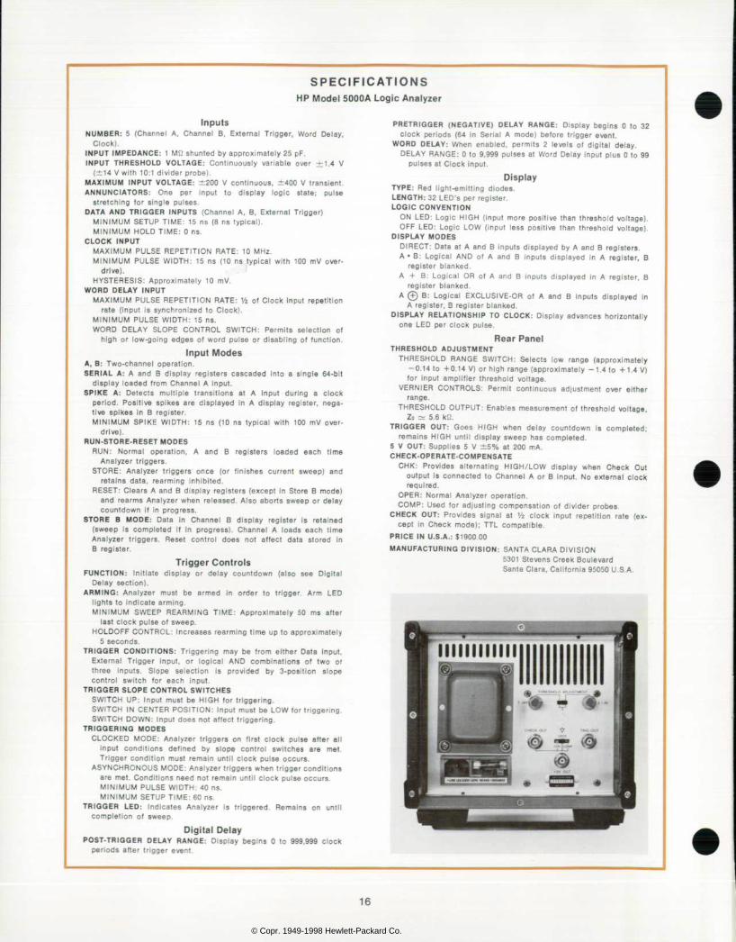
S P E C I F I C A T I O N S HP Model 5000A Logic Analyzer
Inputs NUMBER: 5 (Channe l A , Channe l B , Ex te rna l T r igge r , Word De lay ,
Clock). INPUT IMPEDANCE: 1 Mi! shunted by approximately 25 pF. INPUT THRESHOLD VOLTAGE: Cont inuous ly var iab le over ±1.4 V
(±14 V with 10:1 divider probe). MAXIMUM INPUT VOLTAGE: ±200 V cont inuous, ±400 V transient. A N N U N C I A T O R S : O n e p e r i n p u t t o d i s p l a y l o g i c s t a t e ; p u l s e
s t re tch ing for s ing le pu lses. DATA AND TRIGGER INPUTS (Channe l A , B , Ex terna l Tr igger )
MINIMUM SETUP TIME: 15 ns (8 ns typ ica l ) . MINIMUM HOLD TIME: 0 ns .
CLOCK INPUT MAXIMUM PULSE REPETITION RATE: 10 MHz. M IN IMUM PULSE WIDTH: 15 ns (10 ns t yp i ca l w i th 100 mV ove r
drive). HYSTERESIS: Approx imate ly 10 mV.
WORD DELAY INPUT MAXIMUM PULSE REPETITION RATE: V i o f C lock input repet i t ion
ra te ( input is synchronized to Clock) . MINIMUM PULSE WIDTH: 15 ns. W O R D D E L A Y S L O P E C O N T R O L S W I T C H : P e r m i t s s e l e c t i o n o f
h igh o r low-go ing edges o f word pu lse o r d isab l ing o f func t ion . Input Modes
A, B: Two-channel operat ion. SERIAL A : A and B d i sp lay reg i s te rs cascaded i n to a s i ng le 64 -b i t
d isp lay loaded f rom Channel A input . S P I K E A : D e t e c t s m u l t i p l e t r a n s i t i o n s a t A I n p u t d u r i n g a c l o c k
pe r i od . Pos i t i ve sp i kes a re d i sp layed i n A d i sp lay reg i s te r , nega t i ve sp ikes In B reg is te r . M IN IMUM SP IKE WIDTH: 15 ns ( 10 ns t yp i ca l w i t h 100 mV ove r
drive). RUN-STORE-RESET MODES
R U N : N o r m a l o p e r a t i o n , A a n d B r e g i s t e r s l o a d e d e a c h t i m e Analyzer t r iggers.
S T O R E : A n a l y z e r t r i g g e r s o n c e ( o r f i n i s h e s c u r r e n t s w e e p ) a n d re ta ins data, rearming inh ib i ted.
RESET: Clears A and B d isp lay reg is ters (except in Store B mode) and rearms Analyzer when re leased. A lso abor ts sweep or de lay countdown i f in progress.
S T O R E B M O D E : D a t a i n C h a n n e l B d i s p l a y r e g i s t e r i s r e t a i n e d ( sweep i s comp le ted i f i n p rog ress ) . Channe l A l oads each t ime A n a l y z e r t r i g g e r s . R e s e t c o n t r o l d o e s n o t a f f e c t d a t a s t o r e d I n B register.
Trigger Controls F U N C T I O N : I n i t i a t e d i s p l a y o r d e l a y c o u n t d o w n ( a l s o s e e D i g i t a l
Delay sect ion). A R M I N G : A n a l y z e r m u s t b e a r m e d i n o r d e r t o t r i g g e r . A r m L E D
l ights to indicate arming. M IN IMUM SWEEP REARMING T IME : App rox ima te l y 50 ms a f t e r
last c lock pulse of sweep. HOLDOFF CONTROL: increases rearming t ime up to approximately
5 seconds. TRIGGER CONDIT IONS: T r igger ing may be f rom e i the r Da ta inpu t ,
E x t e r n a l T r i g g e r i n p u t , o r l o g i c a l A N D c o m b i n a t i o n s o f t w o o r t h r e e i n p u t s . S l o p e s e l e c t i o n i s p r o v i d e d b y 3 - p o s i t i o n s l o p e c o n t r o l s w i t c h f o r e a c h i n p u t .
TRIGGER SLOPE CONTROL SWITCHES SWITCH UP: Input must be HIGH for t r igger ing . SWITCH IN CENTER POSITION: Input must be LOW for t r igger ing. SWITCH DOWN: Input does not af fect t r igger ing.
TRIGGERING MODES CLOCKED MODE: Ana lyze r t r i gge rs on f i r s t c l ock pu l se a f te r a l l
I n p u t c o n d i t i o n s d e f i n e d b y s l o p e c o n t r o l s w i t c h e s a r e m e t . Tr igger cond i t ion must remain unt i l c lock pu lse occurs .
ASYNCHRONOUS MODE: Analyzer t r iggers when tr igger condi t ions are met. Condi t ions need not remain unt i l c lock pulse occurs. MINIMUM PULSE WIDTH: 40 ns. MINIMUM SETUP TIME: 60 ns.
T R I G G E R L E D : I n d i c a t e s A n a l y z e r i s t r i g g e r e d . R e m a i n s o n u n t i l comple t ion o f sweep.
Digital Delay POST-TRIGGER DELAY RANGE: D isp lay beg ins 0 to 999 ,999 c lock
per iods af ter t r igger event .
PRETRIGGER (NEGATIVE) DELAY RANGE: D isp lay beg ins 0 to 32 c lock per iods (64 in Ser ia l A mode) be fore t r igger event .
WORD DELAY: When enab led , permi ts 2 leve ls o f d ig i ta l de lay . DELAY RANGE: 0 to 9,999 pulses at Word Delay input p lus 0 to 99
pulses at Clock input. Display
TYPE: Red l ight-emit t ing d iodes. LENGTH: 32 LED's per register. LOGIC CONVENTION
ON LED: Logic HIGH ( input more posi t ive than threshold vol tage) . OFF LED: Logic LOW ( input less pos i t ive than threshold vo l tage) .
DISPLAY MODES DIRECT: Data at A and B inputs d isp layed by A and B reg is ters . A - B : L o g i c a l A N D o f A a n d B i n p u t s d i s p l a y e d i n A r e g i s t e r , B
register blanked. A + B : L o g i c a l O R o f A a n d B i n p u t s d i s p l a y e d i n A r e g i s t e r , B
register blanked. A (+ ) B : Log i ca l EXCLUSIVE-OR o f A and B I npu t s d i sp l ayed i n
A register, B register blanked. DISPLAY RELATIONSHIP TO CLOCK: Disp lay advances hor izonta l ly
one LED per c lock pulse. Rear Panel
T H R E S H O L D A D J U S T M E N T THRESHOLD RANGE SWITCH: Se lec ts low range (approx imate ly
-0 .14 to +0 .14 V) o r h igh range (approx imate ly -1 .4 to +1 .4 V) for input ampl i f ie r threshold vo l tage.
VERNIER CONTROLS: Permi t con t inuous ad jus tment over e i ther range.
THRESHOLD OUTPUT: Enables measurement of threshold vol tage, Zo ~ 5.6 kiJ.
T R I G G E R O U T : G o e s H I G H w h e n d e l a y c o u n t d o w n i s c o m p l e t e d ; remains HIGH unt i l d isp lay sweep has completed.
5 V OUT: Suppl ies 5 V ±5% at 200 mA. CHECK-OPERATE-COMPENSATE
C H K : P r o v i d e s a l t e r n a t i n g H I G H / L O W d i s p l a y w h e n C h e c k O u t ou tpu t i s connec ted to Channe l A o r B Input . No ex te rna l c lock required.
OPER: Normal Analyzer operat ion. COMP: Used for adjust ing compensat ion of d iv ider probes.
C H E C K O U T : P r o v i d e s s i g n a l a t V i c l o c k i n p u t r e p e t i t i o n r a t e ( e x cep t in Check mode) ; TTL compat ib le .
PRICE IN U.S.A.: $1900 00 MANUFACTURING DIVISION: SANTA CLARA DIVISION
5301 Stevens Creek Boulevard Santa Clara, California 95050 U.S.A.
16
© Copr. 1949-1998 Hewlett-Packard Co.
A Pulse Generator for Today's Digital Circuits This new dual-output Pulse Generator produces 16V pulses at high repetit ion rates, and with as much as 16V o f fse t . A new cont ro l a r range ment makes pulse set -up much s impler .
by Reinhard Falke and Horst Link
BECAUSE OF THE rapidly expanding role that digital circuits play in present-day technology,
pulse generators introduced recently by Hewlett- Packard were designed to drive integrated circuits. The main emphasis with these instruments was to provide high repetition rates, 50 MHz and higher, as well as to produce well-defined pulse shapes. In tended as test signal sources for TTL and ECL cir cuits, these instruments had maximum output lev els of ±5 V (into 50f2) with a baseline offset range of ±2 V or so.
MOS integrated circuits and high-threshold "noise immune" circuits, however, require higher
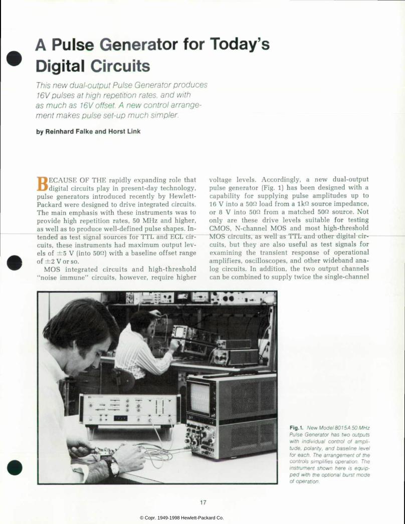
voltage levels. Accordingly, a new dual-output pulse generator (Fig. 1) has been designed with a capability for supplying pulse amplitudes up to 16 V into a 50n load from a Ikn source impedance, or 8 V into 50n from a matched 50Q source. Not only are these drive levels suitable for testing CMOS, N-channel MOS and most high-threshold MOS circuits, as well as TTL and other digital cir cuits, but they are also useful as test signals for examining the transient response of operational amplifiers, oscilloscopes, and other wideband ana log circuits. In addition, the two output channels can be combined to supply twice the single-channel
Fig.1. New Model 801 5A 50 MHz Pu lse Genera tor has two ou tpu ts w i t h i n d i v i d u a l c o n t r o l o f a m p l i tude , po la r i t y , and base l ine leve l fo r each. The ar rangement o f the contro ls s impl i f ies operat ion. The i n s t r u m e n t s h o w n h e r e i s e q u i p ped w i th the op t iona l burs t mode of operation.
17
© Copr. 1949-1998 Hewlett-Packard Co.
output current, especially useful when the genera tor is used to drive magnetic devices. The doubled current capability enables pulse swings of up to 30 V anywhere within a +16 V to —16 V window.
The maximum repetition rate of this instrument depends on the pulse amplitude selected (and, of course, on the characteristics of the load). With the internal 50Q source impedance switched in, the repetition rate can go as high as 50 MHz up to the maximum amplitude (8 V) obtainable in this mode. Without the internal 50Q, pulses up to 16 V can be generated at repetition rates up to 40 MHz.
Two-Phase Genera t ion With its two output channels the new pulse gen
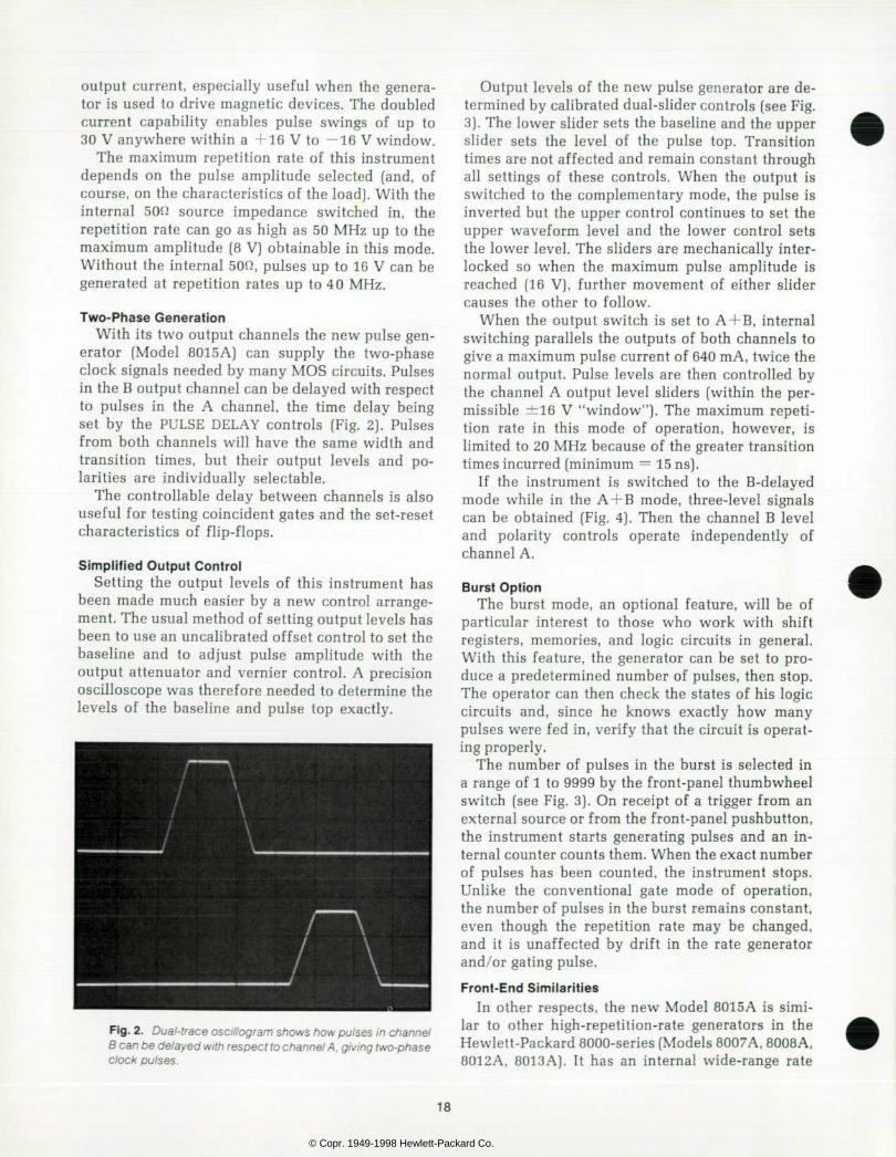
erator (Model 8015A] can supply the two-phase clock signals needed by many MOS circuits. Pulses in the B output channel can be delayed with respect to pulses in the A channel, the time delay being set by the PULSE DELAY controls (Fig. 2). Pulses from both channels will have the same width and transition times, but their output levels and po larities are individually selectable.
The controllable delay between channels is also useful for testing coincident gates and the set-reset characteristics of flip-flops.
Simpl i f ied Output Control Setting the output levels of this instrument has
been made much easier by a new control arrange ment. The usual method of setting output levels has been to use an uncalibrated offset control to set the baseline and to adjust pulse amplitude with the output attenuator and vernier control. A precision oscilloscope was therefore needed to determine the levels of the baseline and pulse top exactly.
Fig . 2 . Dua l - t race osc i / logram shows how pu lses in channe l B can be delayed wi th respect to channel A, g iv ing two-phase c lock pulses.
Output levels of the new pulse generator are de termined by calibrated dual-slider controls (see Fig. 3). The lower slider sets the baseline and the upper slider sets the level of the pulse top. Transition times are not affected and remain constant through all settings of these controls. When the output is switched to the complementary mode, the pulse is inverted but the upper control continues to set the upper waveform level and the lower control sets the lower level. The sliders are mechanically inter locked so when the maximum pulse amplitude is reached (16 V), further movement of either slider causes the other to follow.
When the output switch is set to A + B, internal switching parallels the outputs of both channels to give a maximum pulse current of 640 mA, twice the normal output. Pulse levels are then controlled by the channel A output level sliders (within the per missible ±16 V "window"). The maximum repeti tion rate in this mode of operation, however, is limited to 20 MHz because of the greater transition times incurred (minimum = 15 ns).
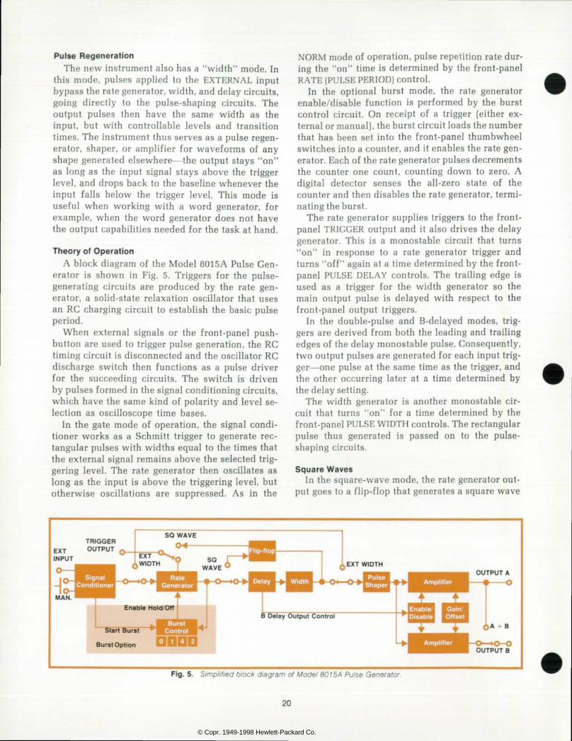
If the instrument is switched to the B-delayed mode while in the A + B mode, three-level signals can be obtained (Fig. 4). Then the channel B level and polarity controls operate independently of channel A.
Burst Option The burst mode, an optional feature, will be of
particular interest to those who work with shift registers, memories, and logic circuits in general. With this feature, the generator can be set to pro duce a predetermined number of pulses, then stop. The operator can then check the states of his logic circuits and, since he knows exactly how many pulses were fed in, verify that the circuit is operat ing properly.
The number of pulses in the burst is selected in a range of 1 to 9999 by the front-panel thumbwheel switch (see Fig. 3). On receipt of a trigger from an external source or from the front-panel pushbutton, the instrument starts generating pulses and an in ternal counter counts them. When the exact number of pulses has been counted, the instrument stops. Unlike the conventional gate mode of operation, the number of pulses in the burst remains constant, even though the repetition rate may be changed, and it is unaffected by drift in the rate generator and/or gating pulse.
Front-End Similarit ies In other respects, the new Model 8015A is simi
lar to other high-repetition-rate generators in the Hewlett-Packard 8000-series (Models 8007A, 8008A, 8012A, 8013A). It has an internal wide-range rate
18
© Copr. 1949-1998 Hewlett-Packard Co.
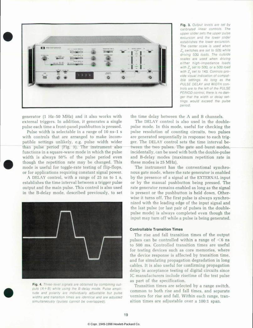
F i g . 3 . O u t p u t l e v e l s a r e s e t b y c a l i b r a t e d l i n e a r c o n t r o l s . T h e upper s l ider sets the upper pu lse e x c u r s i o n a n d t h e l o w e r s l i d e r es tab l i shes the lower excurs ion . T h e c e n t e r s c a l e i s u s e d w h e n Zs switches are set to 51X1 whi le d r i v i ng 50Ã2 loads . The ou ts ide s c a l e s a r e u s e d w h e n d r i v i n g e i t h e r h i g h - i m p e d a n c e l o a d s with Zs set to 50ÃJ, or a 50Ã2 load w i th Zs se t t o 1k i l . Con t ro l s p ro v i de v i sua l i nd i ca t i on o t compa t i b l e s e t t i n g s . A s l o n g a s t h e P U L S E D E L A Y a n d W I D T H c o n t ro ls are to the le f t o t the PULSE PERIOD con t ro l , the re i s no dan g e r t h a t t h e w i d t h o r d e l a y s e t t i n g s w o u l d e x c e e d t h e p u l s e per iod.
generator (1 Hz-50 MHz) and it also works with external triggers. In addition, it generates a single pulse each time a front-panel pushbutton is pressed.
Pulse width is selectable in a range of 10 ns-1 s with controls that are arranged to make incom patible settings unlikely, e.g. pulse width wider than pulse period (Fig. 3). The instrument also functions in a square-wave mode in which the pulse width is always 50% of the pulse period even though the repetition rate may be changed. This mode is useful for toggle-rate testing of flip-flops, or for applications requiring constant signal power.
A DELAY control, with a range of 25 ns to 1 s, establishes the time interval between a trigger pulse output and the main pulse. This control is also used in the B-delay mode, described previously, to set
F ig . 4 . Th ree - l eve l s i gna l s a re ob ta ined by comb in ing ou t p u t s ( A + B ) w h i l e u s i n g t h e B - d e l a y m o d e . P u l s e a m p l i t u d e a n d p o l a r i t y a r e i n d i v i d u a l l y a d j u s t a b l e b u t p u l s e w id ths and t rans i t i on t imes a re i den t i ca l and a re ad jus ted s imu l t aneous l y ( pu l ses canno t be ove r l apped ) .
the time delay between the A and B channels. The DELAY control is also used in the double-
pulse mode. In this mode, useful for checking the pulse resolution of counting circuits, two pulses are generated sequentially in response to each trig ger. The DELAY control sets the time interval be tween the two pulses. The gate and burst modes, incidentally, can be used with both the double-pulse and B-delay modes (maximum repetition rate in these modes is 25 MHz).
The instrument has the conventional synchro nous gate mode, where the rate generator is enabled by the presence of a signal at the EXTERNAL input or by the manual pushbutton being pressed. The rate generator remains enabled as long as the signal is present or the pushbutton is held down. Other wise it turns off. The first pulse is always synchro nized with the leading edge of the input signal and the last pulse (or last pair of pulses in the double- pulse mode) is always completed even though the input may turn off while a pulse is being generated.
Control lable Transit ion Times The rise and fall transition times of the output
pulses can be controlled within a range of <6 ns to 500 ms. Controlled transition times are useful for testing devices such as core memories, where the device response is affected by transition time, and for simulating propagation degradation in long cables. It is also useful for confirming propagation delay in acceptance testing of digital circuits since 1C manufacturers include risetime of the test pulse as part of the specification.
Transition times are selected by a range switch, common to both rise and fall times, and separate verniers for rise and fall. Within each range, tran sition times are adjustable over a 100:1 span.
19
© Copr. 1949-1998 Hewlett-Packard Co.
Pulse Regenerat ion The new instrument also has a "width" mode. In
this mode, pulses applied to the EXTERNAL input bypass the rate generator, width, and delay circuits, going directly to the pulse-shaping circuits. The output pulses then have the same width as the input, but with controllable levels and transition times. The instrument thus serves as a pulse regen erator, shaper, or amplifier for waveforms of any shape generated elsewhere — the output stays "on" as long as the input signal stays above the trigger level, and drops back to the baseline whenever the input falls below the trigger level. This mode is useful when working with a word generator, for example, when the word generator does not have the output capabilities needed for the task at hand.
Theory of Operat ion A block diagram of the Model 8015A Pulse Gen
erator is shown in Fig. 5. Triggers for the pulse- generating circuits are produced by the rate gen erator, a solid-state relaxation oscillator that uses an RC charging circuit to establish the basic pulse period.
When external signals or the front-panel push button are used to trigger pulse generation, the RC timing circuit is disconnected and the oscillator RC discharge switch then functions as a pulse driver for the succeeding circuits. The switch is driven by pulses formed in the signal conditioning circuits, which have the same kind of polarity and level se lection as oscilloscope time bases.
In the gate mode of operation, the signal condi tioner works as a Schmitt trigger to generate rec tangular pulses with widths equal to the times that the external signal remains above the selected trig gering level. The rate generator then oscillates as long as the input is above the triggering level, but otherwise oscillations are suppressed. As in the
NORM mode of operation, pulse repetition rate dur ing the "on" time is determined by the front-panel RATE (PULSE PERIOD) control.
In the optional burst mode, the rate generator enable/disable function is performed by the burst control circuit. On receipt of a trigger (either ex ternal or manual), the burst circuit loads the number that has been set into the front-panel thumbwheel switches into a counter, and it enables the rate gen erator. Each of the rate generator pulses decrements the counter one count, counting down to zero. A digital detector senses the all-zero state of the counter and then disables the rate generator, termi nating the burst.
The rate generator supplies triggers to the front- panel TRIGGER output and it also drives the delay generator. This is a monostable circuit that turns "on" in response to a rate generator trigger and turns "off" again at a time determined by the front- panel PULSE DELAY controls. The trailing edge is used as a trigger for the width generator so the main output pulse is delayed with respect to the front-panel output triggers.
In the double-pulse and B-delayed modes, trig gers are derived from both the leading and trailing edges of the delay monostable pulse. Consequently, two output pulses are generated for each input trig ger — one pulse at the same time as the trigger, and the other occurring later at a time determined by the delay setting.
The width generator is another monostable cir cuit that turns "on" for a time determined by the front-panel PULSE WIDTH controls. The rectangular pulse thus generated is passed on to the pulse- shaping circuits.
Square Waves In the square-wave mode, the rate generator out
put goes to a flip-flop that generates a square wave
TRIGGER EXT INPUT
Fig . 5 . S impl i f ied b lock d iagram of Mode l 801 5 A Pu lse Genera tor .
20
© Copr. 1949-1998 Hewlett-Packard Co.
with a repetition rate one-half that of the rate gen erator. The flip-flop also generates triggers at the half rate. This square wave goes directly to the pulse-shaping circuits, bypassing the delay and width circuits.
The square-wave function can also be used with the gate and burst modes but in this case, the num ber of square-wave cycles in the burst is only one- half the number of triggers counted. Accordingly, to return the output at the end of the burst to the same level as the start, the gate or burst should be set so that an even number of triggers is counted.
Transit ion-Time Control The pulse shaper consists essentially of two
switched current sources and two clamps. On a positive-going transition, the "positive" current source is switched on, linearly charging a capacitor. When the capacitor voltage reaches the upper clamp level, the clamp absorbs the output of the current source, preventing any further charge of the capac itor. The current magnitude is adjustable so the slope of the transition can be varied.
On a negative-going transition, the "positive" current source switches off and the "negative" cur rent source switches on. The capacitor then charges in the opposite direction until its voltage reaches the lower clamp level where it remains until the next positive-going transition. The result is a trape
zoidal-shaped waveform. The upper and lower current sources are adjust
able separately over a 100:1 range, so the slopes of the leading and trailing edges can be adjusted in dividually. The range of adjustment is determined by the capacitor, which can be changed by the front- panel TRANSITION TIME range switch.
Because of the relatively large amplitude of the pulses generated by this instrument, the speed of the fastest transition is limited by the output cir cuits, and this limit depends on the output con figuration and the nature of the load. The fastest transition (<6 ns) is obtained when driving a 50Q load with the 50Q internal source impedance switched in. With the IkO internal source imped ance, the fastest transition is 8 ns into a 50n load. In the A + B mode, fastest transition is 15 ns with or without the internal 50O. With loads other than a well-matched 50O, the maximum speed attainable depends on the load capacitance.
Output Stages At first glance it would seem that control of the
output levels could be a simple matter of using ad justable clamp circuits, one to set the baseline level and the other to set the pulse top. This method is not applicable, however, because the transition times would not remain constant as either clamp level were changed.
From Pulse Shaper
Duty Cycle Error Signal
VA «
To Channe l B To Channel B From Output B
S w i t c h
F ig . 6 . Ou tpu t s tages fo r Channe l A . Channe l B i s iden t i ca l .
21
© Copr. 1949-1998 Hewlett-Packard Co.
Actually, the operation of the Model 8015A's out put amplifier is similar to earlier pulse generators: peak-to-peak amplitude is determined by ampli fier gain and the baseline is set by a dc offset voltage added to the output waveform.
As shown in Fig. 6, the pulse upper and lower levels are selected by sliders on the OUTPUT LEVEL potentiometer. The difference between the slider voltages is used to control pulse amplitude, since the peak-to-peak amplitude is proportional to this difference. The sum of the slider voltages is used to generate a current that is proportional to the desired offset. This is added to the pulse waveform at the output through a decoupling network that prevents the capacitance of the offset circuits from slowing the pulse transition times.
This method of setting pulse levels requires elec tronic control of the pulse amplitude. Accordingly, active attenuators1 of the type shown in Fig. 7 are used. One pair of these attenuators, in a push-pull configuration, is used between stages 1 and 2 of the output chain (Fig. 6) and a second pair is between stages 2 and 3. Each attenuator has a range of 2.75 to 1, giving an overall attenuation range of about 8 to 1.
The difference voltage also adjusts the bias levels of the third amplifier stage so the pulses will be centered in the linear range of this amplifier re gardless of amplitude.
Complementary Output The NORM/COMP switch selects either the non-
inverted or the inverted output of the differential amplifier chain for presentation to the power output stage.
The output stage normally has a source impe dance of IkO. A 50n source impedance is obtained by switching in a 50n resistor. This absorbs any signal reflections from impedance mismatches in the external system so there will be no re-reflec tions to distort the primary pulse. When reflections are not a problem, maximum signal drive can be obtained by switching out the 50O.
Delayed Pulses In the B-delayed mode, an enable/disable circuit
is activated under control of the pulse delay genera tor. When the delay monostable circuit is "on," the channel B output amplifier is disabled, so the first pulse appears only in the channel A output. When the delay monostable goes "off," channel A is dis abled and channel B is then enabled. In effect, the instrument is functioning in the double-pulse mode, but the first pulse of each pair is processed through channel A and the second pulse goes through channel B.
Gain
Fig. two Electronic attenuator spl i ts the signal current into two pa ths . The p ropor t i on tha t goes to 03 depends on 03 b ias . 02 s inks the remainder .
Combined Outputs In the A + B mode, the switch in the channel B
output places the outputs in parallel and relay Kl gives control of pulse levels in both channels to the channel A OUTPUT LEVEL controls. To prevent both source impedance resistors from being placed in parallel, the channel A 50O source impedance re sistor is automatically disconnected so output im pedance is established by the channel B switch.
When the B-delayed mode is used at the same time as A + B, the outputs are in parallel but Kl is opened. The two pulses generated separately in channels A and B are then combined at the channel A output. It should be noted that the offsets are added too, so the pulse baseline will be at a level corresponding to the algebraic sum of the output level sliders that set the baseline in each channel.
Acknowledgments Among those who worked on the design of the
Model 8015A Pulse Generator, and who deserve spe cial thanks for their contributions, are Winfred Freihoff, Theo Papatheodorou, Michael Wollgast, Gert Globas, and Giinter Zieher (Pulse Generator Group Leader). S
References 1. ]. Riggen and D. Fogg, 'An Agile Graphic Display De vice,' Hewlett-Packard Journal, April 1972.
22
© Copr. 1949-1998 Hewlett-Packard Co.
S P E C I F I C A T I O N S HP Model 8015A Pulse Generator
Pulse Characteristics T R A N S I T I O N T I M E S : F r o m m i n i m u m ( s e e T a b l e ) t o 0 . 5 s i n f o u r
r a n g e s . R a n g e s a r e c o m m o n f o r b o t h t r a n s i t i o n s w i t h l e a d i n g - t o - t r a i l i n g e d g e r a t i o s w i t h i n e a c h r a n g e c o n t i n u o u s l y v a r i a b l e f r o m 1 0 0 : 1 t o 1 : 1 0 0 .
T R A N S I T I O N L I N E A R I T Y : F o r t r a n s i t i o n t i m e s > 3 0 n s , d e v i a t i o n f r o m s t r a i g h t l i n e b e t w e e n 1 0 % a n d 9 0 % p o i n t s i s l e s s t h a n 5 % o f p u l s e a m p l i t u d e .
O V E R S H O O T A N D R I N G I N G : Â ± 5 % o f p u l s e a m p l i t u d e , p o s s i b l y i n c r e a s i n g t o < Â ± 1 0 % a t m i n i m u m a m p l i t u d e .
P R E - S H O O T : < 5 % o f p u l s e a m p l i t u d e . P U L S E T O P D R O O P : < 5 % o f p u l s e a m p l i t u d e . P U L S E W I D T H : < 1 0 n s t o 1 s i n f o u r r a n g e s . V e r n i e r p r o v i d e s c o n
t i n u o u s a d j u s t m e n t w i t h i n e a c h r a n g e . W I D T H J I T T E R : < 0 . 1 % + 5 0 p s .
M A X D U T Y C Y C L E : > 7 5 % f r o m 1 H z t o 1 M H z , d e c r e a s i n g t o 5 0 % a t 5 0 M H z . S w i t c h i n g o u t p u t t o C O M P m o d e g i v e s e q u i v a l e n t o f 5 0 t o 1 0 0 % d u t y c y c l e .
S Q U A R E W A V E S Y M M E T R Y :  ± 5 % f r o m 1 H z t o 1 M H z , g o i n g t o  ± 1 5 % a t 2 5 M H z ( i n t e r n a l m o d e s o n l y ) .
P U L S E D E L A Y : 2 0 n s ( + 2 5 n s f i x e d ) t o 1 s w i t h r e s p e c t t o t r i g g e r o u t p u t . F o u r r a n g e s w i t h v e r n i e r f o r c o n t i n u o u s a d j u s t m e n t w i t h i n e a c h r a n g e . D E L A Y J I T T E R : < 0 . 1 % + 5 0 p s .
P U L S E O U T P U T S : T w o o u t p u t s w i t h i n d e p e n d e n t c o n t r o l o f p u l s e u p p e r a n d l o w e r l e v e l s , s o u r c e i m p e d a n c e , a n d n o r m a l o r c o m p l e m e n t e d o u t p u t ( s e e T a b l e ) . A + B : O u t p u t c h a n n e l s c o m b i n e d t h r o u g h c h a n n e l A o u t p u t ( w i t h n o l o a d c o n n e c t e d t o c h a n n e l B o u t p u t ) . I n N O R M a n d D O U B L E P U L S E m o d e s , p u l s e l e v e l s a n d n o r m / c o m p i e m e n t s e l e c t i o n a r e c o n t r o l l e d b y c h a n n e l A ( c h a n n e l B c o n t r o l s a r e d i s a b l e d ) . I n B D E L A Y m o d e , b o t h c h a n n e l A a n d c h a n n e l B c o n t r o l s a r e e n a b l e d f o r i n d e p e n d e n t c o n t r o l o f f i r s t a n d s e c o n d p u l s e s i n e a c h p a i r . O u t p u t l e v e l s i n e a c h p a r t o f c o m b i n e d w a v e f o r m t h e n e q u a l a l g e b r a i c s u m o f c h a n n e l A a n d c h a n n e l B l e v e l s .
Repetit ion Rate and Trigger R E P E T I T I O N R A T E : 1 H z t o 5 0 M H z ( s e e T a b l e ) i n f o u r r a n g e s . V e r
n i e r p r o v i d e s c o n t i n u o u s a d j u s t m e n t w i t h i n e a c h r a n g e . P E R I O D J I T T E R : < 0 . 1 % + 5 0 p s .
S Q U A R E W A V E : 0 . 5 H z t o 2 5 M H z ( 1 / 2 o f r e p e t i t i o n r a t e ) . D O U B L E P U L S E : 1 H z t o 2 5 M H z . S p a c i n g b e t w e e n p u l s e s i n e a c h
p a i r d e f i n e d b y d e l a y c o n t r o l s . B D E L A Y : 1 H z t o 2 5 M H z . C h a n n e l B p u l s e d e l a y e d w i t h r e s p e c t t o
c h a n n e l A p u l s e , a s d e f i n e d b y d e l a y c o n t r o l s . T R I G G E R O U T P U T : > 1 V i n t o 5 0 S l o a d , d c c o u p l e d . 5 0 Â £ 2 t y p i c a l
s o u r c e i m p e d a n c e . T R I G G E R P U L S E W I D T H : 9 n s  ± 5 n s .
Externally-Control led Operation R E P E T I T I O N R A T E : 0 t o 5 0 M H z . F o r s q u a r e - w a v e o u t p u t , V t o f r e p e
t i t i o n r a t e . T R I G G E R I N G :
DELAY: <50 ns between input and output t r iggers. MANUAL: Fron t -pane l pushbut ton genera tes one input t r igger each
t ime i t is pressed. GATE genera Externa l input tu rns on in terna l repet i t ion ra te genera
to r . de lay pu l se occu rs a f t e r s ta r t o f ga te s igna l w i th t ime de lay d e f i n e d b y d e l a y c o n t r o l s . L a s t p u l s e i s a l w a y s c o m p l e t e d r e ga rd less o f phas ing be tween end o f ga te and pu lse ou tpu t . Max i mum repeti t ion rate: 40 MHz. MANUAL: Fron t -pane l pushbut ton genera tes ga te s igna l equa l to t ime i t i s he ld down.
EXTERNAL WIDTH: Each inpu t pu lse resu l ts in one ou tpu t pu lse o f same t imes. but wi th control lable pulse levels and transi t ion t imes. In th i s mode , repe t i t i on - ra te genera to r runs independen t l y a t se lec ted ra te , produc ing t r iggers independent o f main output . MANUAL: Press ing f ron t -pane l pushbu t ton sw i tches ou tpu t l eve l for t ime equal to t ime that pushbutton is held down.
BURST MODE (opt ional) : Preselected number of pulses generated in response to each i npu t t r i gge r o r pushbu t ton ac tua t i on . Number o f pu lses : 0 to 9999. Max imum repet i t ion ra te : 40 MHz. Min imum time between bursts: 200 ns.
General O P E R A T I N G T E M P E R A T U R E R A N G E : O t o 5 5 Â ° C . P O W E R : 1 0 0 , 1 2 0 , 2 2 0 , o r 2 4 0 V ( + 5 % . - 1 0 % ) , 4 8 t o 4 4 0 H z , 1 8 0 V A
m a x . D I M E N S I O N S : 1 6 % i n . W x 5 Â ¥ t i n . H x 1 5 i n . D ( 4 2 6 x 1 4 5 x 3 8 0 m m ) . W E I G H T : 2 4 ' / 4 I b s . ( 1 1 k g ) . P R I C E I N U . S . A . : M o d e l 8 0 1 5 A , $ 1 7 5 0 . B u r s t O p t i o n ( 0 0 2 ) , a d d $ 3 5 0 .
S i n g l e o u t p u t v e r s i o n ( o p t i o n 0 0 1 ) , $ 1 3 5 0 . M A N U F A C T U R I N G D I V I S I O N : H e w l e t t - P a c k a r d G m b H
H e r r e n b e r g e r S t r a s s e 1 1 0 D-7030 Bòb l ingen , Wür t temberg G e r m a n y
' Source capac i tance = 30 pF. t A t 8 V; may increase to 6 .5 ns a t 4 V.
23
© Copr. 1949-1998 Hewlett-Packard Co.
Reinhard Falke Graduating from Karlsruhe Universi ty (Germany) three years ago with a Diplom Ingenieur, Reinhard Falke went to work for Hewlet t -Packard designing logar i thmic ampl i f iers and rms- to-dB converters for real- t ime spectrum analyzers. A year later, he switched to pulse generators and then became Pro ject Leader for the Model 801 5A. For fun, he plays soccer wi th the HP GmbH Research and Development department 's team, l ikes cars, and l ikes l istening to contemporary popular music (known in the U.S. as rock-and-roll). He is married and has a two-year -o ld daughter and a th ree-month-o ld son.
Horst Link Also a sometime member of the R and D soccer team, Horst Link spends his free t ime snorkel diving and taking photo graphs. Before joining Hewlett-Packard in 1970, he was with a f irm making educational construction kits. Since being with HP, he contr ibuted to the mechanical design of tape punches and tape readers for calculators and data acquisi t ion sys tems before joining the 801 5A team. He is married and has a 5-month-o ld daughter .
H e w l e t t - P a c k a r d C o m p a n y . 1 5 0 1 P a g e M i R o a d . P a l o A l t o . C a l i f o r n i a 9 4 3 0 4
5CTOBER1973 Vo lume 25 • Number 2
T e c h n i c a l I n f o r m a t i o n f r o m t h e L a b o r a t o r i e s o f H e w l e t t - P a c k a r d C o m p a n y
H e w l e t t - P a c k a r d S . A . , C H - 1 2 1 7 M e y n n 2 G e n e v a . S w i t z e r l a n d
Y o k a g a w a - H e w l e t t - P a c k a r d L t d . , S h i b u y a - K u T o k y o 1 5 1 J a p a n
E d i t o r i a l D i r e c t o r * H o w a r d L . R o b e r t s M a n a g i n g E d i t o r â € ¢ R i c h a r d P . D o l a n
Cont r ibut ing Ed i tors • Ross H . Snyder , L a u r e n c e D . S h e r g a l i s
t D i r e c t o r , P h o t o g r a p h e r â € ¢ A r v i d A . D a n i e l s o n Ar t Ass is tan t • Sue M . Re inhe imer
A d m i n i s t r a t i v e S e r v i c e s * A n n e S . L o P r e s t i E u r o p e a n P r o d u c t i o n M a n a g e r * K u r t H u n g e r b u h l e r
B u l k R a t e U .S . Pos tage
Paid H e w l e t t - P a c k a r d
C o m p a n y
C H A N G E p l e a s e o l d T o c h a n g e y o u r a d d r e s s o r d e l e t e y o u r n a m e f r o m o u r m a i l i n g l i s t p l e a s e s e n d u s y o u r o l d a d d r e s s l a b e l ( i t p e e l s o f f ) . S e n d c h a n g e s t o H e w l e t t - P a c k a r d J o u r n a l , 1 5 0 1 P a g e M i l l R o a d , P a l o A l t o , C a l i f o r n i a 9 4 3 0 4 U . S . A . A l l o w 6 0 d a y s .
© Copr. 1949-1998 Hewlett-Packard Co.