synchrotron tests of a 3d medipix2 x-ray detector
TRANSCRIPT
research papers
Journal of Synchrotron Radiation
ISSN 0909-0495
Received 0 XXXXXXX 0000Accepted 0 XXXXXXX 0000Online 0 XXXXXXX 0000
c© 2008 International Union of CrystallographyPrinted in Singapore – all rights reserved
Synchrotron tests of a 3D Medipix2 X-ray detectorDavid Pennicard,a* Julien Marchal,b Celeste Fleta,a Giulio Pellegrini,cManuel Lozano,c Chris Parkes,a Nicola Tartoni,b Damien Barnett,b Igor Dolb-nya,b Kawal Sawhney,b Richard Bates,a Val O’Sheaa and Victoria Wrighta
aUniversity of Glasgow, Department of Physics and Astronomy, Glasgow, UK, bDiamond Light SourceLtd, Harwell Science and Innovation Campus, Oxfordshire, UK, cInstituto de Microelectronica de Barcelona,IMB-CNM-CSIC, 08193 Bellaterra, Barcelona, Spain, and dScience and Technology Facilities Council, PolarisHouse, North Star Ave., Swindon, UK. Correspondence e-mail: [email protected]
Three-dimensional (3D) photodiode detectors offer advantages over standard pla-nar photodiodes in a range of applications, including X-ray detection for syn-chrotrons and medical imaging. The principal advantage of these sensors for X-ray imaging is their low charge sharing between adjacent pixels, which improvesspatial and spectral resolution.A ‘double-sided’ 3D detector has been bonded to a Medipix2 single-photon-counting readout chip, and tested in a monochromatic X-ray beam at the Diamondsynchrotron. Tests of the 3D detector’s response spectrum and its Line SpreadFunction have shown that it has substantially lower charge sharing than a standardplanar Medipix2 sensor. Additionally, the 3D detector was used to image diffrac-tion rings produced by a powdered silicon sample, demonstrating the detector’suse in a standard synchrotron experiment.
1. IntroductionThe high-intensity X-ray beams produced by new synchrotronssuch as Diamond Light Source can be used to improve the speedand quality of X-ray diffraction experiments. However, in orderto fully exploit these new light sources, high-performance X-raydetectors are also needed (Westbrook, 1999). New X-ray detec-tors can also be applied to other important applications, such asmedical imaging.
In many of these applications, high-resolution X-ray imagesare required. However, X-ray detectors with small pixel sizessuffer from charge-sharing effects, which tend to blur the imageand reduce spectral resolution (Chmeissani & Mikulec, 2001).3D detectors, proposed by Parker et al. (1997), can potentiallyimprove X-ray imaging by reducing these effects.
1.1. 3D detectorsA 3D detector is a specialised variety of silicon photodiode
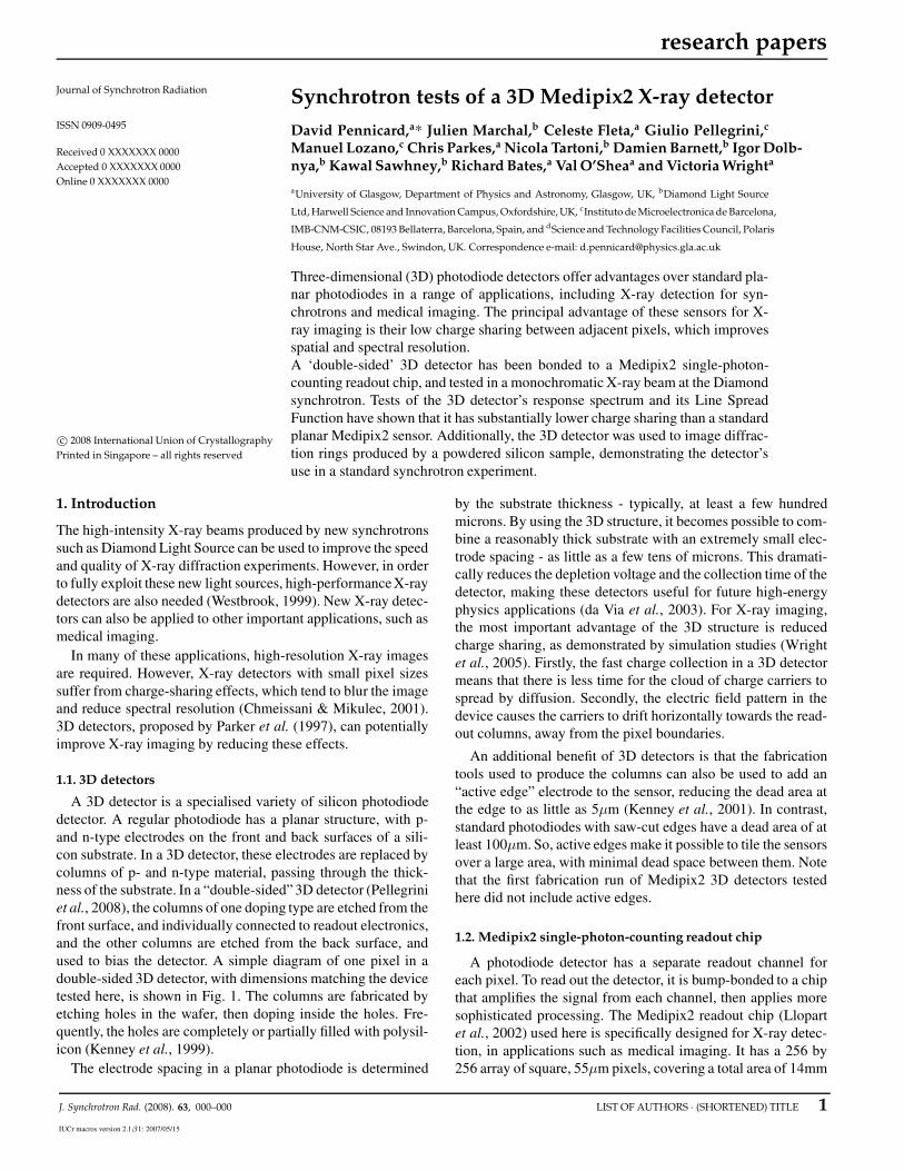
detector. A regular photodiode has a planar structure, with p-and n-type electrodes on the front and back surfaces of a sili-con substrate. In a 3D detector, these electrodes are replaced bycolumns of p- and n-type material, passing through the thick-ness of the substrate. In a “double-sided” 3D detector (Pellegriniet al., 2008), the columns of one doping type are etched from thefront surface, and individually connected to readout electronics,and the other columns are etched from the back surface, andused to bias the detector. A simple diagram of one pixel in adouble-sided 3D detector, with dimensions matching the devicetested here, is shown in Fig. 1. The columns are fabricated byetching holes in the wafer, then doping inside the holes. Fre-quently, the holes are completely or partially filled with polysil-icon (Kenney et al., 1999).
The electrode spacing in a planar photodiode is determined
by the substrate thickness - typically, at least a few hundredmicrons. By using the 3D structure, it becomes possible to com-bine a reasonably thick substrate with an extremely small elec-trode spacing - as little as a few tens of microns. This dramati-cally reduces the depletion voltage and the collection time of thedetector, making these detectors useful for future high-energyphysics applications (da Via et al., 2003). For X-ray imaging,the most important advantage of the 3D structure is reducedcharge sharing, as demonstrated by simulation studies (Wrightet al., 2005). Firstly, the fast charge collection in a 3D detectormeans that there is less time for the cloud of charge carriers tospread by diffusion. Secondly, the electric field pattern in thedevice causes the carriers to drift horizontally towards the read-out columns, away from the pixel boundaries.
An additional benefit of 3D detectors is that the fabricationtools used to produce the columns can also be used to add an“active edge” electrode to the sensor, reducing the dead area atthe edge to as little as 5µm (Kenney et al., 2001). In contrast,standard photodiodes with saw-cut edges have a dead area of atleast 100µm. So, active edges make it possible to tile the sensorsover a large area, with minimal dead space between them. Notethat the first fabrication run of Medipix2 3D detectors testedhere did not include active edges.
1.2. Medipix2 single-photon-counting readout chip
A photodiode detector has a separate readout channel foreach pixel. To read out the detector, it is bump-bonded to a chipthat amplifies the signal from each channel, then applies moresophisticated processing. The Medipix2 readout chip (Llopartet al., 2002) used here is specifically designed for X-ray detec-tion, in applications such as medical imaging. It has a 256 by256 array of square, 55µm pixels, covering a total area of 14mm
J. Synchrotron Rad. (2008). 63, 000–000 LIST OF AUTHORS · (SHORTENED) TITLE 1IUCr macros version 2.1β1: 2007/05/15
research papersby 14mm.
Whenever a hit occurs on a Medipix pixel, the signal is com-pared to high and low signal thresholds set by the user. If thesignal falls between the two thresholds, a counter within thepixel is incremented. This allows the chip to count the indi-vidual X-ray photons hitting each pixel during an exposure. Asa result, the detector has a high count rate and a large, lineardynamic range, and it is also largely unaffected by electronicnoise. These advantages are useful for synchrotron diffractionexperiments, because the brightest diffraction spots in an imagemay have extremely high count rates but the rate in the weakestspots may be orders of magnitude lower.
In a single-photon-counting detector, charge-sharing canreduce the image quality in various ways. Firstly, depending onthe threshold setting, charge-shared events can either be missed(reducing the signal) or produce hits in more than one pixel(blurring the image). If the incident beam contains a wide spec-trum, both these effects may occur. Additionally, charge-sharingreduces the detector’s ability to distinguish between photons ofdifferent energy - for example, to reject Compton scattering orfluorescence from a sample (Chmeissani & Mikulec, 2001).
2. Detectors, apparatus and preliminary tests
2.1. DetectorsThe 3D detector tested here is a double-sided 3D detec-
tor, fabricated by IMB-CNM as described by Pellegrini et al.(2008)—see Fig. 1. The detector has a 300µm-thick n-typesubstrate. The columns fabricated in the substrate are 250µmlong (i.e. they do not pass through the full substrate thickness)and are 10µm in diameter. Boron-doped p-type columns extendfrom the front surface into the bulk silicon, and have individ-ual bump-bond pads. The phosphorus-doped n-type columnsextending from the back surface are connected together by lay-ers of polysilicon and metal, and are used for biasing. The pitchbetween adjacent columns of the same type is 55µm, to matchthe pixel size of Medipix2. After fabrication, the sensor wasbump-bonded to a Medipix2 chip by VTT, and mounted on achipboard. VTT have previous experience of producing sim-pler “semi-3D” sensors and bonding them to Medipix2 (Tlustoset al., 2007).
For comparison, a standard 300µm-thick p-on-n planar detec-tor was also tested.
2.2. Data acquisitionThe Medipix2 chipboards were read out using Medipix2
USB interfaces, produced by IEAP, Czech Technical Univer-sity, Prague (Vykydal et al., 2006). This interface powers thechipboard and reads out the detector using a USB connection.It also has a built-in high voltage source for biasing the detector.During the beam test, the detectors inside the beam area wereconnected to a PC outside via a USB extender.
2.3. Beamline and test setupThe X-ray tests were done at beamline B16 at the Dia-
mond Light Source, which is specifically designed to test new
detectors and experimental techniques. The beamline can pro-vide white or monochromatic beam; during the tests, only themonochromatic beam was used, in the range 12-20keV.
The Medipix2 detectors were each mounted in an aluminiumtest box with a 50µm-thick aluminized Mylar window in frontof the detector active area. During the tests, they were mountedon a remotely-controlled XY stage, allowing them to be movedin and out of the beam without having to re-open the beam area.
2.4. Preparation for testsDuring all the tests, the 3D detector was biased to 21.5V and
the planar detector was biased to 100V, ensuring that both werefully depleted.
Before testing the detectors, it was necessary to performthreshold equalisation. Medipix2 uses a global low threshold(THL) to determine whether or not a hit is registered. Eachindividual pixel has three THL adjust bits which are used toimprove the uniformity of the threshold across the detector(Llopart et al., 2002). Because the Medipix2 chip is bipolar, thenoise level lies in the middle of the chip’s dynamic range, and sothe thresholds could be equalised using the centroid of the noiseon each channel. This process also produced a histogram of thecentroid position for each pixel after equalisation; the peak ofthis histogram gave the THL value corresponding to zero sig-nal. Although the chip also has a high threshold, only the lowthreshold was used.
Since the beam profile was non-uniform, shutters were usedto give a square beam spot, slightly smaller than the area ofthe detector. This ensured that we consistently imaged the samearea of the beam when switching between the two detectors.
2.5. Electronic noise, pixel masking, and radiation damageSince it counts individual photons, rather than integrating the
signal detected over the acquisition time, the Medipix2 chip isnot affected by electronic noise in a conventional way. However,if the noise fluctuations are large enough, a pixel can registerfalse hits. This will of course depend on the threshold setting.
As a test of detector noise, the low threshold was scannedthrough a range of values without any beam present, with 0.1sacquisitions at each setting. At each setting, the 3D detectortended to show more noisy pixels. As a representative exam-ple, the threshold was set to 6keV, i.e. half the energy of thelowest-energy beam used in the tests. (Section 3 describes howthe energy calibrations were found.) The 3D detector had 4 pix-els with extremely high noise counts of over 10,000, and 66moderately noisy pixels with over 100 counts. In contrast, theplanar detector had only 1 pixel with more than 100 counts.The increased noise on the 3D detector may be related to itsrelatively high capacitance per pixel (Pennicard et al., 2007).However, the noise can also depend on the individual Medipix2readout chip. During the data analysis, noisy pixels were appro-priately masked.
After making the spectra measurements, but before the LineSpread Function and diffraction experiments, both Medipix2readout chips showed signs of radiation damage. Firstly, thenumber of noisy pixels had increased, and secondly, when the
2 LIST OF AUTHORS · (SHORTENED) TITLE J. Synchrotron Rad. (2008). 63, 000–000IUCr macros version 2.1β1: 2007/05/15
research papersthreshold equalisations were repeated, the THL adjust valueshad changed for some of the pixels. The pixels which hadn’tbeen exposed to the beam were unaffected. This damage willbe due to the production of fixed charges in the gate oxides onthe readout chip, which alters the behaviour of some of the tran-sistors. The damage was unexpectedly high, and may have beencaused by accidentally exposing the detectors to the direct X-ray beam when changing attenuators.
3. Beam spectra measurements with Medipix2After setting the X-ray beam to 15keV, the response spectrumof each detector was tested. This was done by taking images at aseries of consecutive low threshold (THL) values ranging fromabove the beam energy down to the noise level. An acquisitiontime of 0.5s was used at each step - this was chosen to ensure ahigh count in each pixel, without reaching the maximum countof 11810. As mentioned previously, the 3D and planar detectorswere biased to 21.5V and 100V.
Then, the total number of counts was calculated for eachimage (excluding noisy pixels), producing an integral spectrumof counts vs threshold setting. This was then differentiated tofind the differential spectrum measured by each detector. Thisspectral measurement was repeated a total of 10 times, and themean spectrum found. The standard error on each point in thespectrum was also calculated.
At this point, the spectrum simply gave the signal at eachTHL setting. In order to calibrate the detector, the tests wererepeated at 12keV and 20keV. The peak in each spectrum wasfound by using a Gaussian fit. Having obtained the THL valuescorresponding to these energies, and also the “zero signal” THLvalue from the threshold equalisation, a linear least-squares fitwas made to these points to find the calibration for each detec-tor. This was then applied to the spectra. The change in energycorresponding to a step in THL was very similar on the twodetectors, but the “zero signal” THL levels were different. Thiseffect has been seen previously on other Medipix2 sensors.
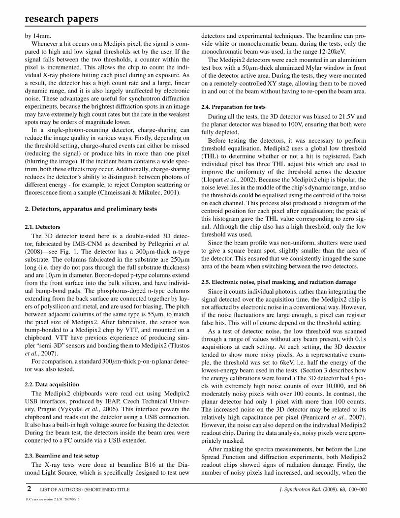
Figure 2 shows the spectrum obtained from the 3D detectorwith the 15keV beam, including the Gaussian peak fit and thestandard error on each data point. In addition to the peak, lowerenergy “hits” can be seen, due to some X-rays being charge-shared between pixels. Before fitting the Gaussian to the peak,the steepest point on the low-energy edge was found, and the fitwas only applied to the data at higher energies. This preventedthe charge-shared signal from affecting the fit.
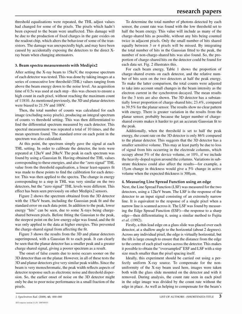
Figure 3 shows the results from the 3D and planar detectorssuperimposed, with a Gaussian fit to each peak. It can clearlybe seen that the planar detector has a smaller peak and a greatercharge shared signal, giving a poorer spectrum as a result.
The onset of false counts due to noise occurs sooner on the3D detector than on the planar. However, in all of these tests the3D and planar detectors give very similar peak widths. Since thebeam is very monochromatic, the peak width reflects aspects ofdetector response such as electronic noise and threshold disper-sion. So, the earlier onset of noise on the 3D detector mightonly be due to poor noise performance in a small fraction of thepixels.
To determine the total number of photons detected by eachsensor, the count rate was found with the low threshold set tohalf the beam energy. This value will include as many of thecharge-shared hits as possible, without any hits being countedtwice in adjacent pixels. Only the small number of hits sharedequally between 3 or 4 pixels will be missed. By integratingthe total number of hits in the Gaussian fitted to the peak, thenumber of non-charge-shared hits was also found. So, the pro-portion of charge-shared hits on the detector could be found foreach data set. Fig. 2 illustrates this.
For each beam energy, Table 1 shows the proportion ofcharge-shared events on each detector, and the relative num-ber of hits seen on the two detectors at half the peak energy.To make the latter comparison, the total counts were adjustedto take into account small changes in the beam intensity as theelectron current in the synchrotron decayed. The mean resultsfor the 3 tests are also shown. The 3D detector has a substan-tially lower proportion of charge-shared hits; 23.4%, comparedto 39.5% for the planar sensor. The results show no clear patternwith energy. There is greater variation in the results from theplanar sensor, probably because the larger number of charge-shared events makes it harder to get an accurate Gaussian fit tothe peak.
Additionally, when the threshold is set to half the peakenergy, the count rate on the 3D detector is only 86% comparedto the planar detector. This suggests that the 3D detector has asmaller sensitive volume. This may at least partly be due to lossof signal from hits occurring in the electrode columns, whichoccupy about 5% of the device volume, or 10%, if we includethe heavily-doped region around the columns. Variations in sub-strate thickness could also affect the results—for example, a15µm change in thickness would give a 5% change in activevolume when the expected thickness is 300µm.
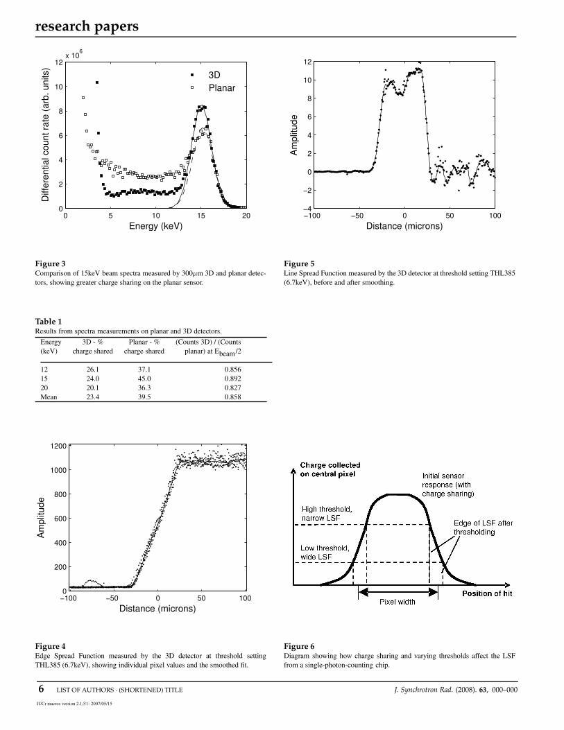
4. Measuring Line Spread Function using an edgeNext, the Line Spread Function (LSF) was measured for the twodetectors, using a 12keV beam. The LSF is the response of thedetector to an input signal consisting of an extremely narrowline. It is equivalent to the response of a single pixel when anarrow line is scanned across it. The LSF was found by measur-ing the Edge Spread Function (ESF)—the response to a sharpedge—then differentiating it, using a similar method to Fujitaet al. (1992).
Firstly, a thin lead edge on a glass slide was placed over eachdetector, at a shallow angle to the horizontal (about 2 degrees).Across any individual pixel, the edge is virtually horizontal, butthe tilt is large enough to ensure that the distance from the edgeto the centre of each pixel varies across the detector. This makesit possible to obtain the “oversampled” ESF and LSF with a stepsize much smaller than the pixel spacing itself.
Ideally, this experiment should be carried out using a per-fectly uniform X-ray source. To compensate for the non-uniformity of the X-ray beam used here, images were takenboth with the glass slide mounted on the detector and with itremoved. During analysis, the count rate seen in each pixelin the edge image was divided by the count rate without theedge in place. As well as helping to compensate for the beam’s
J. Synchrotron Rad. (2008). 63, 000–000 LIST OF AUTHORS · (SHORTENED) TITLE 3IUCr macros version 2.1β1: 2007/05/15
research papersnon-uniformity, this will also compensate for variations inthe response of individual pixels (flat-field correction). Theseimages were taken for both the 3D and planar detectors at arange of different threshold settings. Each measurement con-sisted of 100 images taken with a 2.5s acquisition time, whichwere then averaged.
Firstly, the position of the edge in the image was found. Thiswas done by looking at each column of pixels in the imageand finding the Y-position where the count rate was halfwaybetween the maximum and minimum signal level, using inter-polation to get sub-pixel precision. Then, a linear fit was madeto the resulting data points.
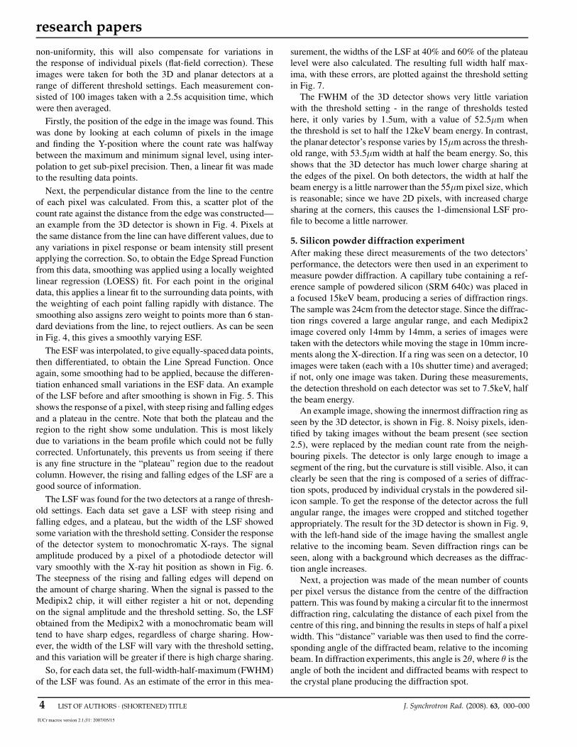
Next, the perpendicular distance from the line to the centreof each pixel was calculated. From this, a scatter plot of thecount rate against the distance from the edge was constructed—an example from the 3D detector is shown in Fig. 4. Pixels atthe same distance from the line can have different values, due toany variations in pixel response or beam intensity still presentapplying the correction. So, to obtain the Edge Spread Functionfrom this data, smoothing was applied using a locally weightedlinear regression (LOESS) fit. For each point in the originaldata, this applies a linear fit to the surrounding data points, withthe weighting of each point falling rapidly with distance. Thesmoothing also assigns zero weight to points more than 6 stan-dard deviations from the line, to reject outliers. As can be seenin Fig. 4, this gives a smoothly varying ESF.
The ESF was interpolated, to give equally-spaced data points,then differentiated, to obtain the Line Spread Function. Onceagain, some smoothing had to be applied, because the differen-tiation enhanced small variations in the ESF data. An exampleof the LSF before and after smoothing is shown in Fig. 5. Thisshows the response of a pixel, with steep rising and falling edgesand a plateau in the centre. Note that both the plateau and theregion to the right show some undulation. This is most likelydue to variations in the beam profile which could not be fullycorrected. Unfortunately, this prevents us from seeing if thereis any fine structure in the “plateau” region due to the readoutcolumn. However, the rising and falling edges of the LSF are agood source of information.
The LSF was found for the two detectors at a range of thresh-old settings. Each data set gave a LSF with steep rising andfalling edges, and a plateau, but the width of the LSF showedsome variation with the threshold setting. Consider the responseof the detector system to monochromatic X-rays. The signalamplitude produced by a pixel of a photodiode detector willvary smoothly with the X-ray hit position as shown in Fig. 6.The steepness of the rising and falling edges will depend onthe amount of charge sharing. When the signal is passed to theMedipix2 chip, it will either register a hit or not, dependingon the signal amplitude and the threshold setting. So, the LSFobtained from the Medipix2 with a monochromatic beam willtend to have sharp edges, regardless of charge sharing. How-ever, the width of the LSF will vary with the threshold setting,and this variation will be greater if there is high charge sharing.
So, for each data set, the full-width-half-maximum (FWHM)of the LSF was found. As an estimate of the error in this mea-
surement, the widths of the LSF at 40% and 60% of the plateaulevel were also calculated. The resulting full width half max-ima, with these errors, are plotted against the threshold settingin Fig. 7.
The FWHM of the 3D detector shows very little variationwith the threshold setting - in the range of thresholds testedhere, it only varies by 1.5um, with a value of 52.5µm whenthe threshold is set to half the 12keV beam energy. In contrast,the planar detector’s response varies by 15µm across the thresh-old range, with 53.5µm width at half the beam energy. So, thisshows that the 3D detector has much lower charge sharing atthe edges of the pixel. On both detectors, the width at half thebeam energy is a little narrower than the 55µm pixel size, whichis reasonable; since we have 2D pixels, with increased chargesharing at the corners, this causes the 1-dimensional LSF pro-file to become a little narrower.
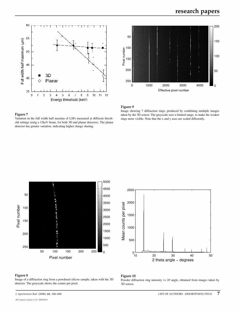
5. Silicon powder diffraction experimentAfter making these direct measurements of the two detectors’performance, the detectors were then used in an experiment tomeasure powder diffraction. A capillary tube containing a ref-erence sample of powdered silicon (SRM 640c) was placed ina focused 15keV beam, producing a series of diffraction rings.The sample was 24cm from the detector stage. Since the diffrac-tion rings covered a large angular range, and each Medipix2image covered only 14mm by 14mm, a series of images weretaken with the detectors while moving the stage in 10mm incre-ments along the X-direction. If a ring was seen on a detector, 10images were taken (each with a 10s shutter time) and averaged;if not, only one image was taken. During these measurements,the detection threshold on each detector was set to 7.5keV, halfthe beam energy.
An example image, showing the innermost diffraction ring asseen by the 3D detector, is shown in Fig. 8. Noisy pixels, iden-tified by taking images without the beam present (see section2.5), were replaced by the median count rate from the neigh-bouring pixels. The detector is only large enough to image asegment of the ring, but the curvature is still visible. Also, it canclearly be seen that the ring is composed of a series of diffrac-tion spots, produced by individual crystals in the powdered sil-icon sample. To get the response of the detector across the fullangular range, the images were cropped and stitched togetherappropriately. The result for the 3D detector is shown in Fig. 9,with the left-hand side of the image having the smallest anglerelative to the incoming beam. Seven diffraction rings can beseen, along with a background which decreases as the diffrac-tion angle increases.
Next, a projection was made of the mean number of countsper pixel versus the distance from the centre of the diffractionpattern. This was found by making a circular fit to the innermostdiffraction ring, calculating the distance of each pixel from thecentre of this ring, and binning the results in steps of half a pixelwidth. This “distance” variable was then used to find the corre-sponding angle of the diffracted beam, relative to the incomingbeam. In diffraction experiments, this angle is 2θ, where θ is theangle of both the incident and diffracted beams with respect tothe crystal plane producing the diffraction spot.
4 LIST OF AUTHORS · (SHORTENED) TITLE J. Synchrotron Rad. (2008). 63, 000–000IUCr macros version 2.1β1: 2007/05/15
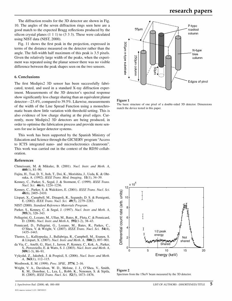
research papersThe diffraction results for the 3D detector are shown in Fig.
10. The angles of the seven diffraction rings seen here are agood match to the expected Bragg reflections produced by thesilicon crystal planes (1 1 1) to (3 3 3). These were calculatedusing NIST data (NIST, 2000).
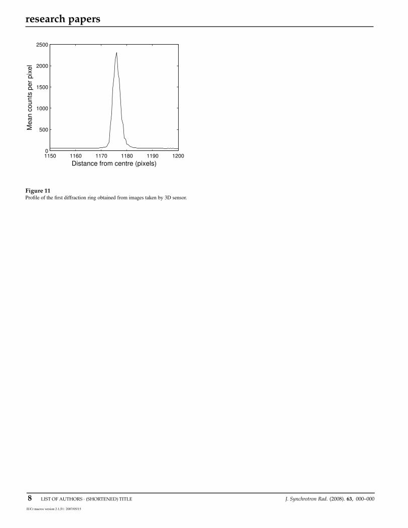
Fig. 11 shows the first peak in the projection, expressed interms of the distance measured on the detector rather than theangle. The full-width half maximum of this peak is 3.5 pixels.Given the relatively large width of the peaks, when the experi-ment was repeated using the planar sensor there was no visibledifference between the peak shapes seen on the two sensors.
6. ConclusionsThe first Medipix2 3D sensor has been successfully fabri-cated, tested, and used in a standard X-ray diffraction exper-iment. Measurements of the 3D detector’s spectral responseshow significantly less charge sharing than an equivalent planardetector—23.4%, compared to 39.5%. Likewise, measurementsof the width of the Line Spread Function using a monochro-matic beam show little variation with threshold setting. This isalso evidence of low charge sharing at the pixel edges. Cur-rently, more Medipix2 3D detectors are being produced, inorder to optimise the fabrication process and provide more sen-sors for use in larger detector systems.
This work has been supported by the Spanish Ministry ofEducation and Science through the GICSERV program “Accessto ICTS integrated nano- and microelectronics cleanroom”.This work was carried out in the context of the RD50 collab-oration.
ReferencesChmeissani, M. & Mikulec, B. (2001). Nucl. Instr. and Meth. A,
460(1), 81–90.Fujita, H., Tsai, D. Y., Itoh, T., Doi, K., Morishita, J., Ueda, K. & Oht-
suka, A. (1992). IEEE Trans. Med. Imaging, 11(1), 34–39.Kenney, C., Parker, S., Segal, J. & Storment, C. (1999). IEEE Trans.
Nucl. Sci. 46(4), 1224–1236.Kenney, C., Parker, S. & Walckiers, E. (2001). IEEE Trans. Nucl. Sci.
48(6), 2405–2410.Llopart, X., Campbell, M., Dinapoli, R., Segundo, D. S. & Pernigotti,
E. (2002). IEEE Trans. Nucl. Sci. 49(5), 2279–2283.NIST (2000). Standard Reference Materials Program.Parker, S., Kenney, C. & Segal, J. (1997). Nucl. Instr. and Meth. A,
395(3), 328–343.Pellegrini, G., Lozano, M., Ullan, M., Bates, R., Fleta, C. & Pennicard,
D. (2008). Nucl. Instr. and Meth A, 592(1-2), 38–43.Pennicard, D., Pellegrini, G., Lozano, M., Bates, R., Parkes, C.,
O’Shea, V. & Wright, V. (2007). IEEE Trans. Nucl. Sci. 54(4),1435–1443.
Tlustos, L., Kalliopuska, J., Ballabriga, R., Campbell, M., Eranen, S.& Llopart, X. (2007). Nucl. Instr. and Meth. A, 580(2), 897–901.
da Via, C., Anelli, G., Hasi, J., Jarron, P., Kenney, C., Kok, A., Parker,S., Perozziello, E. & Watts, S. J. (2003). Nucl. Instr. and Meth. A,509(1-3), 86–91.
Vykydal, Z., Jakubek, J. & Pospisil, S. (2006). Nucl. Instr. and Meth.A, 563(1), 112–115.
Westbrook, E. M. (1999). Proc. SPIE, 3774, 2–16.Wright, V. A., Davidson, W. D., Melone, J. J., O’Shea, V., Smith,
K. M., Donohue, L., Lea, L., Robb, K., Nenonen, S. & Sipila,H. (2005). IEEE Trans. Nucl. Sci. 52(5), 1873–1876.
Figure 1The basic structure of one pixel of a double-sided 3D detector. Dimensionsmatch the device tested in this paper.
0 5 10 15 200
2
4
6
8
10
12x 106
Energy (keV)
Diffe
rent
ial c
ount
rate
(arb
. uni
ts)
Notshared
1/2 peak energy
Shared
Figure 2Spectrum from the 15keV beam measured by the 3D detector.
J. Synchrotron Rad. (2008). 63, 000–000 LIST OF AUTHORS · (SHORTENED) TITLE 5IUCr macros version 2.1β1: 2007/05/15
research papers
0 5 10 15 200
2
4
6
8
10
12x 106
Energy (keV)
Diffe
rent
ial c
ount
rate
(arb
. uni
ts)
3D Planar
Figure 3Comparison of 15keV beam spectra measured by 300µm 3D and planar detec-tors, showing greater charge sharing on the planar sensor.
Table 1Results from spectra measurements on planar and 3D detectors.
Energy 3D - % Planar - % (Counts 3D) / (Counts(keV) charge shared charge shared planar) at Ebeam/2
12 26.1 37.1 0.85615 24.0 45.0 0.89220 20.1 36.3 0.827Mean 23.4 39.5 0.858
−100 −50 0 50 1000
200
400
600
800
1000
1200
Distance (microns)
Ampl
itude
Figure 4Edge Spread Function measured by the 3D detector at threshold settingTHL385 (6.7keV), showing individual pixel values and the smoothed fit.
−100 −50 0 50 100−4
−2
0
2
4
6
8
10
12
Distance (microns)
Ampl
itude
Figure 5Line Spread Function measured by the 3D detector at threshold setting THL385(6.7keV), before and after smoothing.
Figure 6Diagram showing how charge sharing and varying thresholds affect the LSFfrom a single-photon-counting chip.
6 LIST OF AUTHORS · (SHORTENED) TITLE J. Synchrotron Rad. (2008). 63, 000–000IUCr macros version 2.1β1: 2007/05/15
research papers
Figure 7Variation in the full width half maxima of LSFs measured at different thresh-old settings using a 12keV beam, for both 3D and planar detectors. The planardetector has greater variation, indicating higher charge sharing.
50 100 150 200 250
50
100
150
200
250
Pixel number
Pixe
l num
ber
0
500
1000
1500
2000
2500
3000
3500
4000
4500
5000
Figure 8Image of a diffraction ring from a powdered silicon sample, taken with the 3Ddetector. The greyscale shows the counts per pixel.
0 1000 2000 3000 4000
50
100
150
200
250
Effective pixel number
Pixe
l num
ber
0
50
100
150
200
Figure 9Image showing 7 diffraction rings, produced by combining multiple imagestaken by the 3D sensor. The greyscale uses a limited range, to make the weakerrings more visible. Note that the x and y axes are scaled differently.
10 20 30 40 500
500
1000
1500
2000
2500
2 theta angle − degrees
Mea
n co
unts
per
pixe
l
Figure 10Powder diffraction ring intensity vs 2θ angle, obtained from images taken by3D sensor.
J. Synchrotron Rad. (2008). 63, 000–000 LIST OF AUTHORS · (SHORTENED) TITLE 7IUCr macros version 2.1β1: 2007/05/15
research papers
1150 1160 1170 1180 1190 12000
500
1000
1500
2000
2500
Distance from centre (pixels)
Mea
n co
unts
per
pixe
l
Figure 11Profile of the first diffraction ring obtained from images taken by 3D sensor.
8 LIST OF AUTHORS · (SHORTENED) TITLE J. Synchrotron Rad. (2008). 63, 000–000IUCr macros version 2.1β1: 2007/05/15