spf band 345 signal function design document
TRANSCRIPT
Name Designation Affiliation Signature and Date
Submitted by:
J. Leech SPF Band 345 Lead Engineer
University of Oxford
Approved by:
A. C. Taylor SPF Band
345 Project Manager
University of Oxford
A. Born SPF Band
345 System Engineer
UKATC
I. P. Theron SPF Lead Engineer
EMSS
SPF BAND 345 SIGNAL FUNCTION DESIGN DOCUMENT
Document Number..................................................................................317-030000-008 Revision ........................................................................................................................... A Author ... J. Leech, L. Liu, A. Hector, W. Yang, D. Biao, R. Watson, A. Pollak, D. Banda, T. Ghigna, M. Jones, A. Born, A. Taylor, A. Aminaei Date ................................................................................................................. 2019-02-28 Status ......................................................................................................................... Draft

Document No.: Revision: Date:
317-030000-008 A 2019-02-28
Author: J. Leech et. al. Page 2 of 131
DOCUMENT HISTORY Revision Date of Issue Engineering Change
Number Comments
A 2019-02-28 - First draft for Band 345 DDR
DOCUMENT SOFTWARE Package Version Filename
Wordprocessor MsWord Word 2016 317-030000-008_RevA_SPFB345_SignalFunctionDesign.docx
Block diagrams
Other
ORGANISATION DETAILS Name SKA Organisation
Registered Address Jodrell Bank Observatory
Lower Withington
Macclesfield
Cheshire
SK11 9DL
United Kingdom
Registered in England & Wales Company Number: 07881918
Fax. +44 (0)161 306 9600
Website www.skatelescope.org

Document No.: Revision: Date:
317-030000-008 A 2019-02-28
Author: J. Leech et. al. Page 3 of 131
TABLE OF CONTENTS
1 SCOPE OF DOCUMENT ................................................................................. 11
1.1 Applicable Documents ...........................................................................................................11
1.2 Reference Documents ...........................................................................................................11
2 DESIGN DESCRIPTION .................................................................................. 13
2.1 Context ...................................................................................................................................13
2.2 Feed requirements ................................................................................................................13
3 MAJOR COMPONENT DESIGN ........................................................................ 16
3.1 Summary of the SKA dish design ...........................................................................................16
3.2 Feed horns .............................................................................................................................16
3.3 Orthomode transducers (OMTs) ...........................................................................................24
3.3.1 Band 5a OMT simulated and measured results ............................................................24
3.3.2 Band 5b OMT simulated and measured results ............................................................25
3.4 Interaction of the feed horn and cryostat window ...............................................................28
3.5 Simulated optical performance of the full optics ..................................................................34
3.5.1 Beam Patterns for the full optics ...................................................................................38
3.6 Projected feed sensitivities, antenna and system temperatures ..........................................95
3.7 Noise Calibration Signal Injection ........................................................................................104
3.7.1 Noise Source ................................................................................................................104
3.7.2 Coupling of noise probe to cylindrical waveguide.......................................................105
3.7.3 Radiation of the calibration signal ...............................................................................106
4 RF SIGNAL CHAIN ..................................................................................... 107
4.1 Coaxial cables and Interconnections ...................................................................................108
4.1.1 OMT to LNA..................................................................................................................108
4.1.2 LNA to SMA bulkhead feedthrough .............................................................................109
4.1.3 SMA bulkhead feedthrough to warm RF chain ...........................................................110
4.1.4 Warm RF chain to hermetic vacuum feedthrough ......................................................111
4.1.5 Hermetic SMA feedthrough .........................................................................................111
4.2 Low Noise Amplifier .............................................................................................................111
4.3 Warm RF chain .....................................................................................................................114
4.3.1 Warm amplifiers ..........................................................................................................115
4.3.2 Bandpass filters ............................................................................................................116
4.3.3 Warm RF chain experimental tests..............................................................................117
4.3.4 Warm RF chain: temperature control scheme ............................................................120
5 RECEIVER NOISE TEMPERATURE MODEL ......................................................... 122
Document No.: Revision: Date:
317-030000-008 A 2019-02-28
Author: J. Leech et. al. Page 4 of 131
5.1 Summary of previous PDR noise model ..............................................................................122
5.2 Updated (DDR) noise model. ...............................................................................................123
6 CONCLUSION AND FURTHER WORK ................................................................ 125
APPENDIX A: AN ALTERNATIVE FINLINE BAND 5B OMT DESIGN ................................. 126
LIST OF FIGURES
Figure 1: SPF Band 345 diagram showing the main path components. ...............................................13
Figure 2: FEKO model of the shaped offset Gregorian reflector system and the horn and the coordinate system in which the z-axis is parallel to the optical axis. .........................................16
Figure 3: Prototype Band 5a (left) and Band 5b (right) feed horns fabricated by JLRAT. ....................17
Figure 4: Simulated and measured radiation patterns (Left: amplitude, Right: phase) for the Band 5a horn at 4.6 GHz. ...........................................................................................................................17
Figure 5: Simulated and measured radiation patterns (Left: amplitude, Right: phase) for the Band 5a horn at 5.5 GHz. ...........................................................................................................................18
Figure 6: Simulated and measured radiation patterns (Left: amplitude, Right: phase) for the Band 5a horn at 6.5 GHz. ...........................................................................................................................18
Figure 7: Simulated and measured radiation patterns (Left: amplitude, Right: phase) for the Band 5a horn at 7.5 GHz. ...........................................................................................................................19
Figure 8: Simulated and measured radiation patterns (Left: amplitude, Right: phase) for the Band 5a horn at 8.51 GHz. .........................................................................................................................19
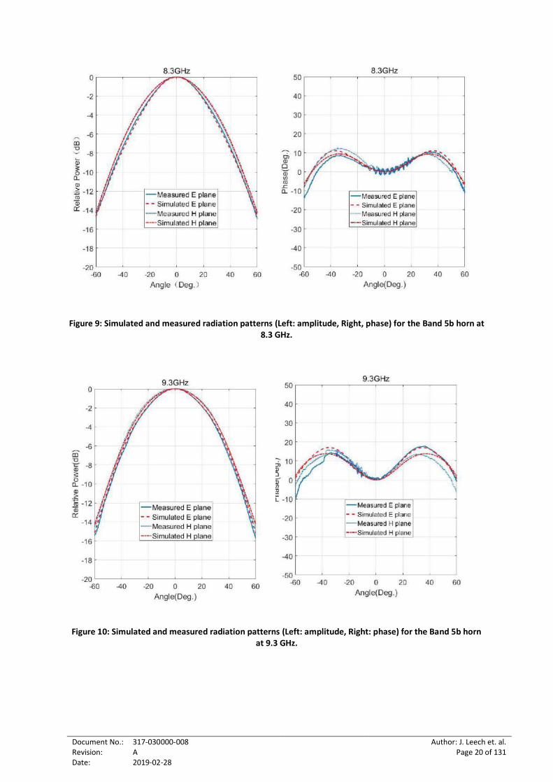
Figure 9: Simulated and measured radiation patterns (Left: amplitude, Right, phase) for the Band 5b horn at 8.3 GHz. ...........................................................................................................................20
Figure 10: Simulated and measured radiation patterns (Left: amplitude, Right: phase) for the Band 5b horn at 9.3 GHz. ...........................................................................................................................20
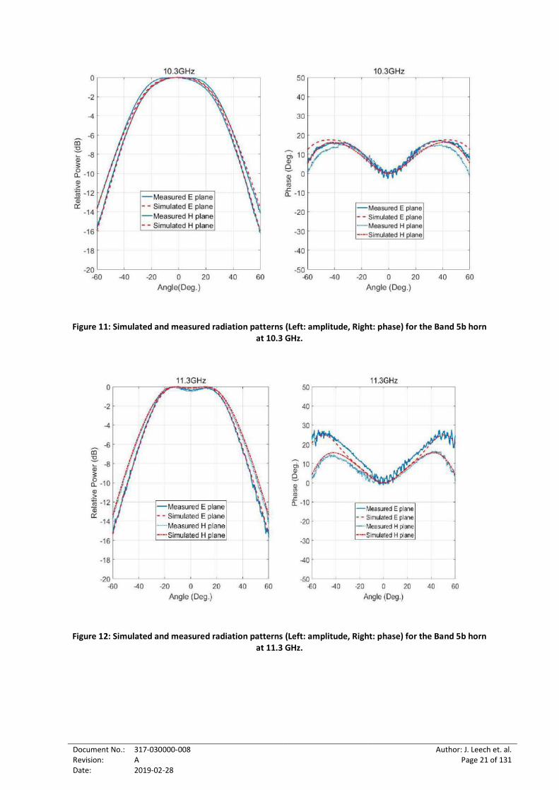
Figure 11: Simulated and measured radiation patterns (Left: amplitude, Right: phase) for the Band 5b horn at 10.3 GHz. .........................................................................................................................21
Figure 12: Simulated and measured radiation patterns (Left: amplitude, Right: phase) for the Band 5b horn at 11.3 GHz. .........................................................................................................................21
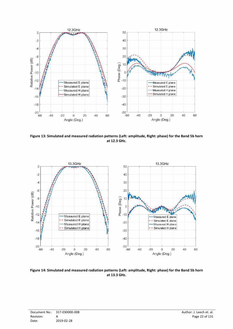
Figure 13: Simulated and measured radiation patterns (Left: amplitude, Right: phase) for the Band 5b horn at 12.3 GHz. .........................................................................................................................22
Figure 14: Simulated and measured radiation patterns (Left: amplitude, Right: phase) for the Band 5b horn at 13.3 GHz. .........................................................................................................................22
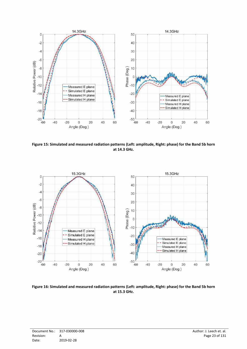
Figure 15: Simulated and measured radiation patterns (Left: amplitude, Right: phase) for the Band 5b horn at 14.3 GHz. .........................................................................................................................23
Figure 16: Simulated and measured radiation patterns (Left: amplitude, Right: phase) for the Band 5b horn at 15.3 GHz. .........................................................................................................................23
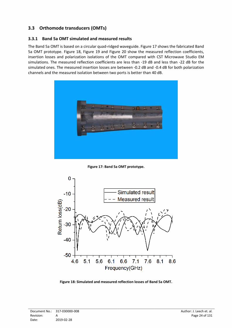
Figure 17: Band 5a OMT prototype. ......................................................................................................24
Figure 18: Simulated and measured reflection losses of Band 5a OMT. ..............................................24
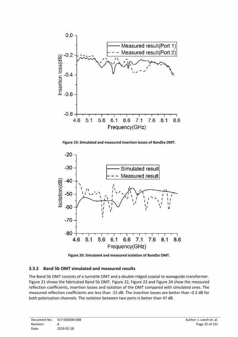
Figure 19: Simulated and measured insertion losses of Band5a OMT..................................................25
Figure 20: Simulated and measured isolation of Band5a OMT. ............................................................25
Document No.: Revision: Date:
317-030000-008 A 2019-02-28
Author: J. Leech et. al. Page 5 of 131
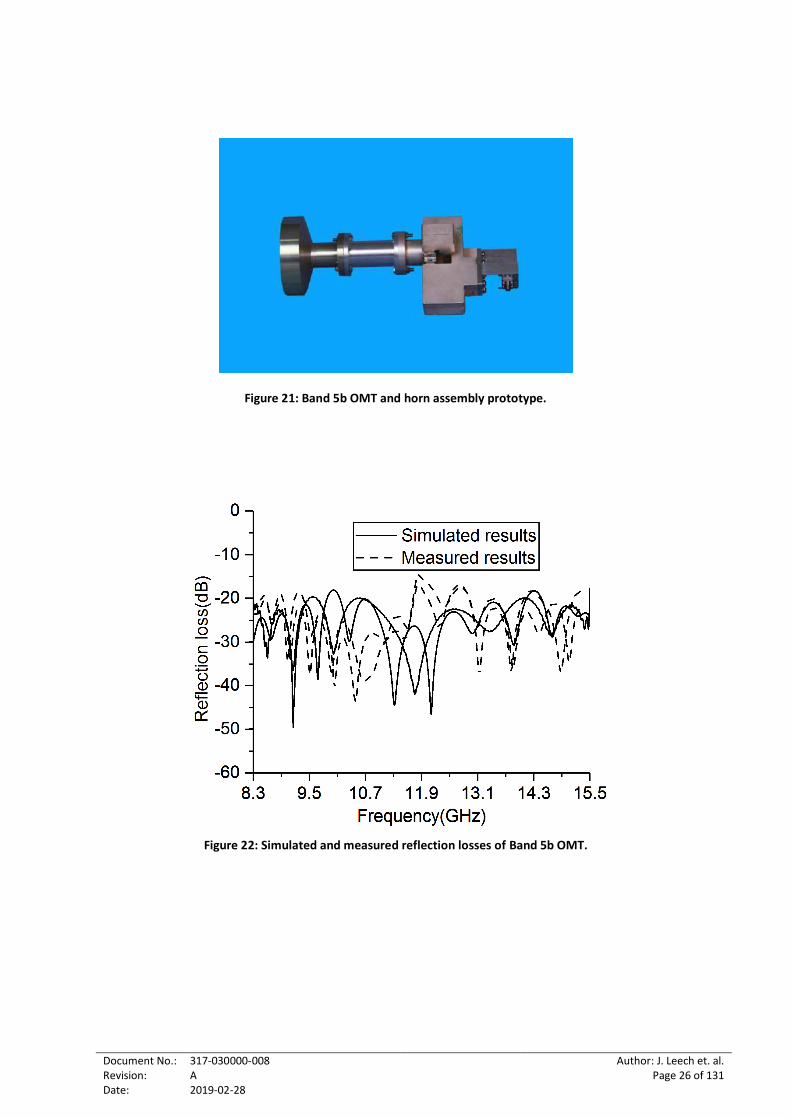
Figure 21: Band 5b OMT and horn assembly prototype. ......................................................................26
Figure 22: Simulated and measured reflection losses of Band 5b OMT. ..............................................26
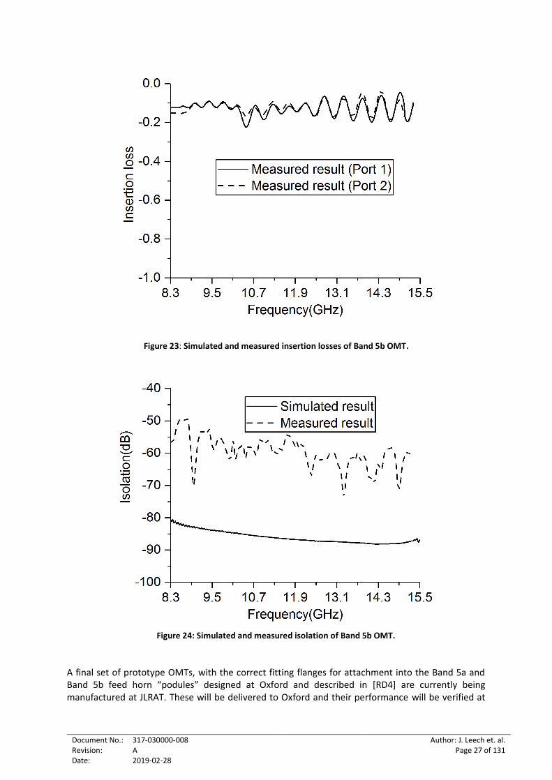
Figure 23: Simulated and measured insertion losses of Band 5b OMT. ...............................................27
Figure 24: Simulated and measured isolation of Band 5b OMT. ...........................................................27
Figure 25: Side view of a Band 5a horn & cryostat window. .................................................................28
Figure 26: Near field distribution for Band 5a window and horn at 4.6 GHz (side view). ....................29
Figure 27: Near field distribution for Band 5a window and horn at 6.5 GHz (side view). ....................30
Figure 28: Near field distribution for Band 5a window and horn at 8.5 GHz (side view). ....................30
Figure 29: Near field distribution for Band 5a window and horn at 4.6 GHz (top view). .....................31
Figure 30: Near field distribution for Band 5a window and horn at 6.5 GHz (top view). .....................31
Figure 31: Near field distribution for Band 5a window and horn at 8.5 GHz (top view). .....................31
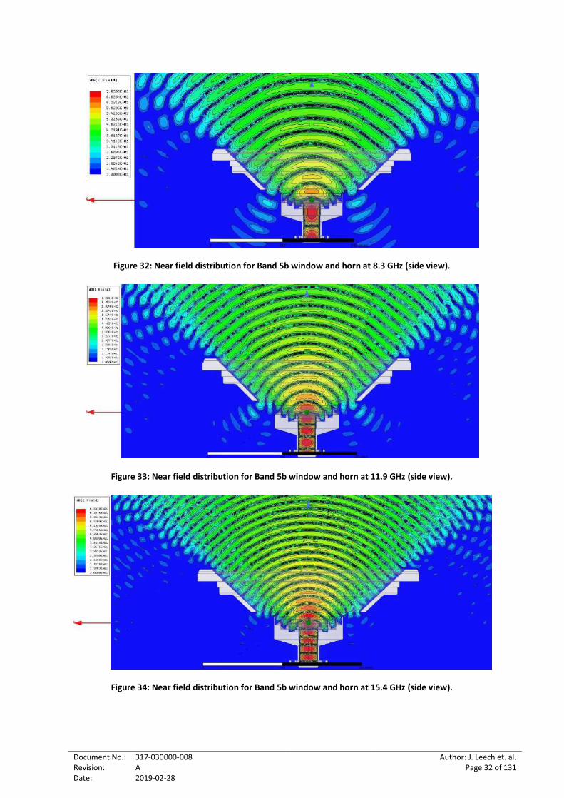
Figure 32: Near field distribution for Band 5b window and horn at 8.3 GHz (side view). ....................32
Figure 33: Near field distribution for Band 5b window and horn at 11.9 GHz (side view). ..................32
Figure 34: Near field distribution for Band 5b window and horn at 15.4 GHz (side view). ..................32
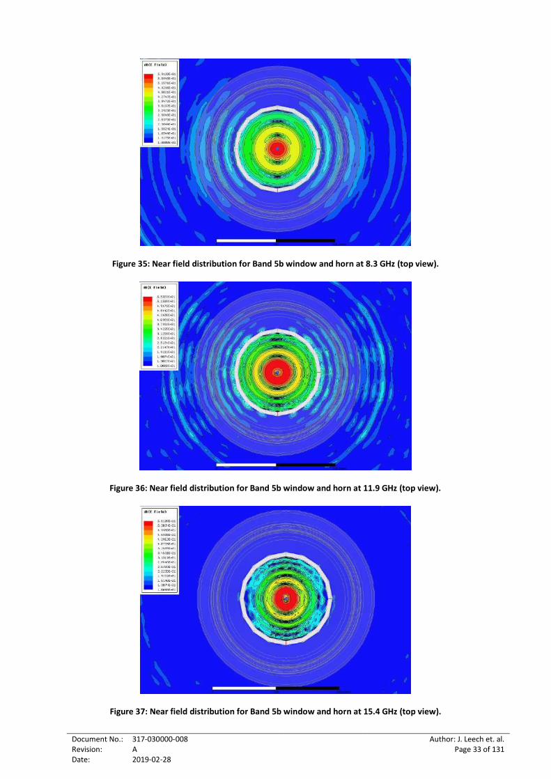
Figure 35: Near field distribution for Band 5b window and horn at 8.3 GHz (top view). .....................33
Figure 36: Near field distribution for Band 5b window and horn at 11.9 GHz (top view). ...................33
Figure 37: Near field distribution for Band 5b window and horn at 15.4 GHz (top view). ...................33
Figure 38: The peak antenna directivity for the full optics with no window and with our baseline window for Band 5a calculated in GRASP for both polarizations. ..............................................34
Figure 39: The peak antenna directivity for the full optics with no window and with our baseline window for Band 5b calculated in GRASP for both polarizations. ..............................................35
Figure 40: The aperture efficiency for the full optics with no window and with our baseline window for Band 5a calculated in GRASP for both polarizations. ............................................................35
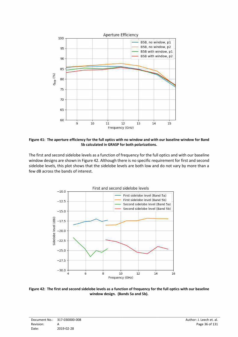
Figure 41: The aperture efficiency for the full optics with no window and with our baseline window for Band 5b calculated in GRASP for both polarizations. ............................................................36
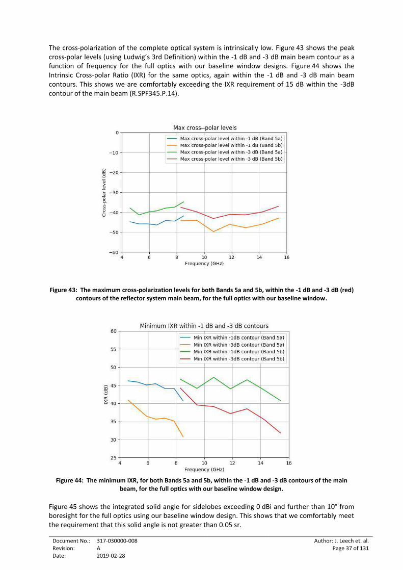
Figure 42: The first and second sidelobe levels as a function of frequency for the full optics with our baseline window design. (Bands 5a and 5b). .............................................................................36
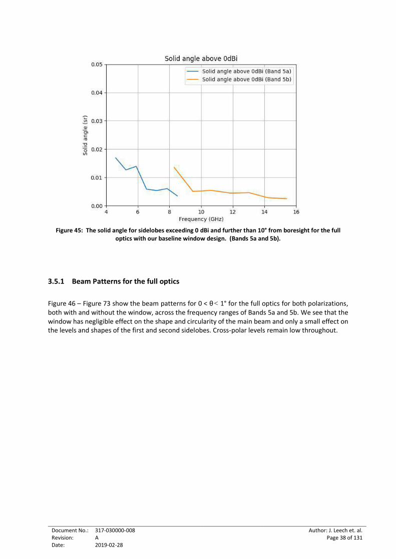
Figure 43: The maximum cross-polarization levels for both Bands 5a and 5b, within the -1 dB and -3 dB (red) contours of the reflector system main beam, for the full optics with our baseline window. .......................................................................................................................................37
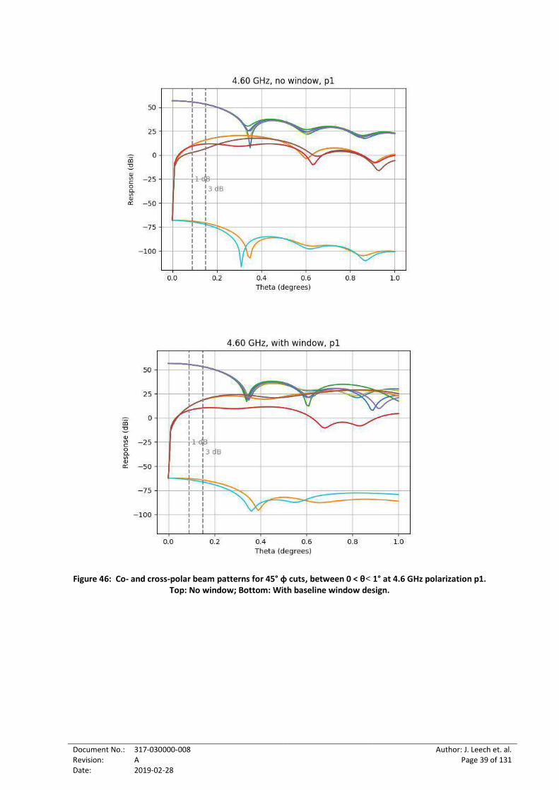
Figure 44: The minimum IXR, for both Bands 5a and 5b, within the -1 dB and -3 dB contours of the main beam, for the full optics with our baseline window design. ..............................................37
Figure 45: The solid angle for sidelobes exceeding 0 dBi and further than 10° from boresight for the full optics with our baseline window design. (Bands 5a and 5b). ..............................................38
Figure 46: Co- and cross-polar beam patterns for 45° φ cuts, between 0 < θ< 1° at 4.6 GHz polarization p1. Top: No window; Bottom: With baseline window design. ...................................................39
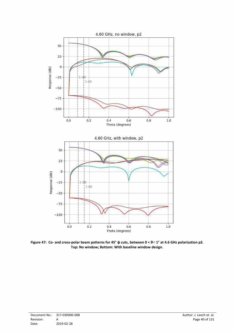
Figure 47: Co- and cross-polar beam patterns for 45° φ cuts, between 0 < θ< 1° at 4.6 GHz polarization p2. Top: No window; Bottom: With baseline window design. ...................................................40
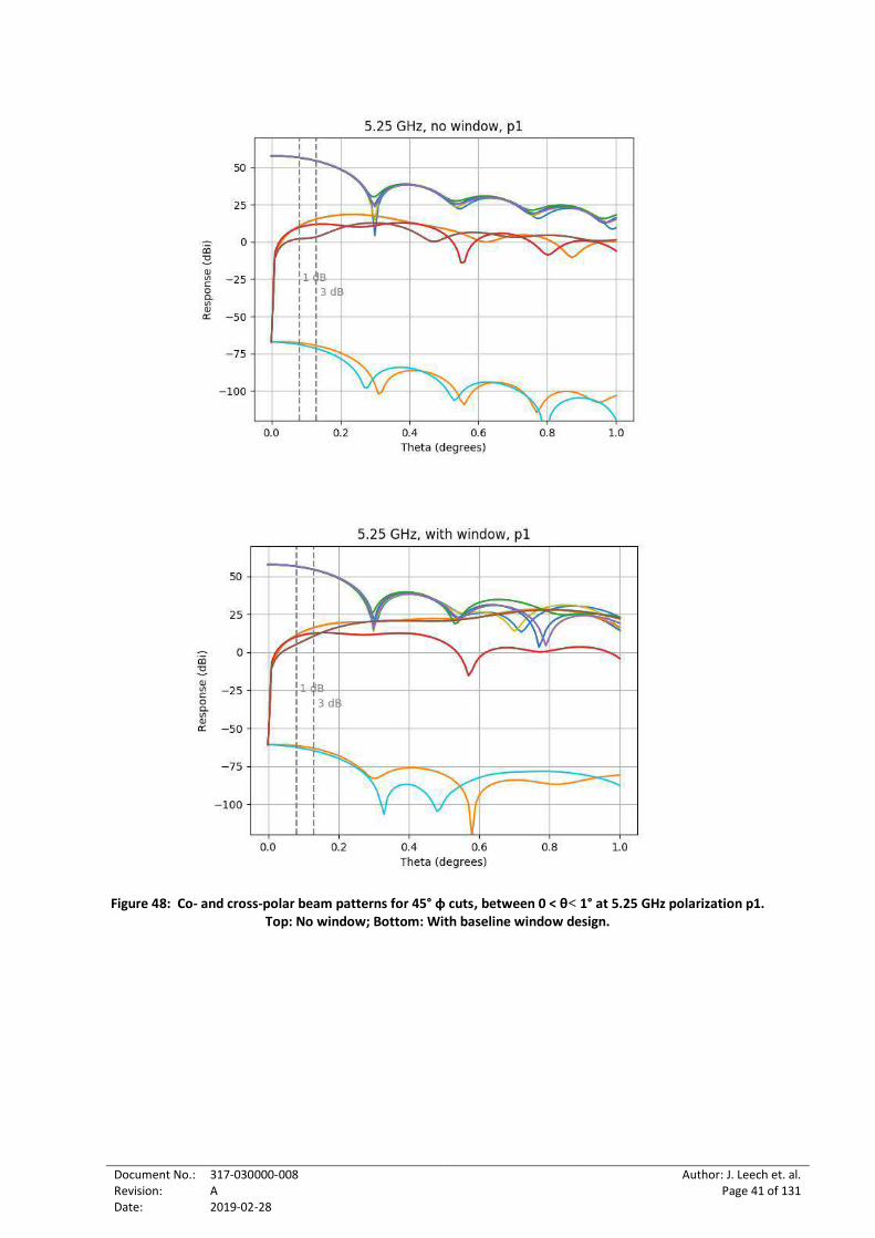
Figure 48: Co- and cross-polar beam patterns for 45° φ cuts, between 0 < θ< 1° at 5.25 GHz polarization p1. Top: No window; Bottom: With baseline window design. ...............................41
Document No.: Revision: Date:
317-030000-008 A 2019-02-28
Author: J. Leech et. al. Page 6 of 131
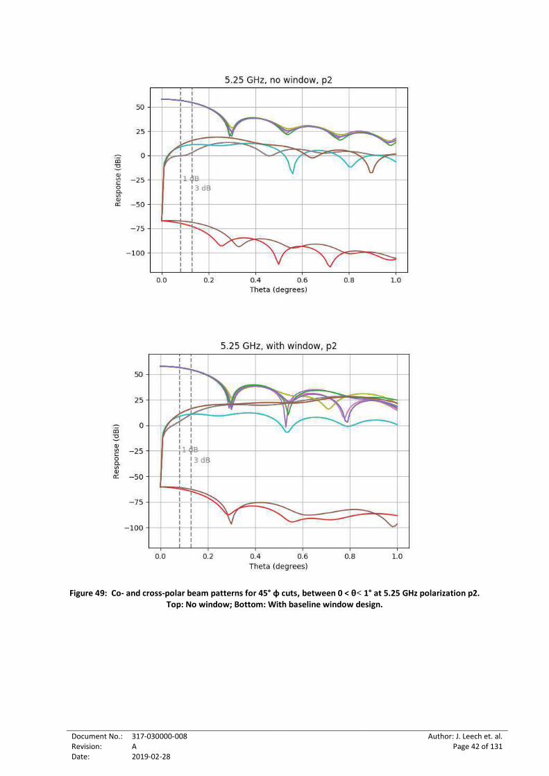
Figure 49: Co- and cross-polar beam patterns for 45° φ cuts, between 0 < θ< 1° at 5.25 GHz polarization p2. Top: No window; Bottom: With baseline window design. ...............................42
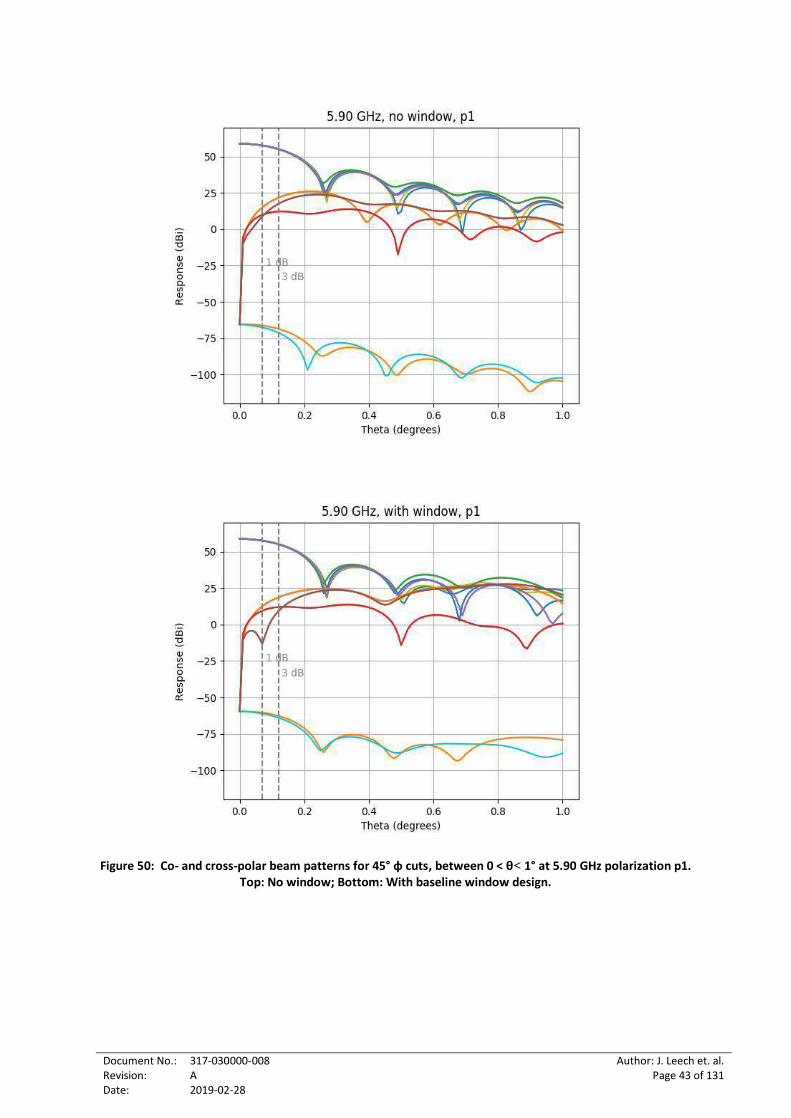
Figure 50: Co- and cross-polar beam patterns for 45° φ cuts, between 0 < θ< 1° at 5.90 GHz polarization p1. Top: No window; Bottom: With baseline window design. ...............................43
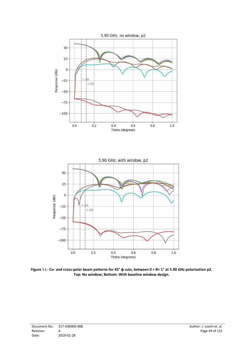
Figure 51: Co- and cross-polar beam patterns for 45° φ cuts, between 0 < θ< 1° at 5.90 GHz polarization p2. Top: No window; Bottom: With baseline window design. ...............................44
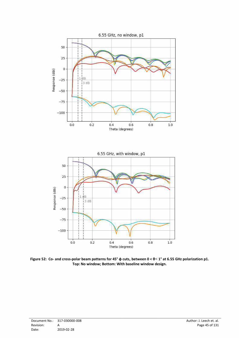
Figure 52: Co- and cross-polar beam patterns for 45° φ cuts, between 0 < θ< 1° at 6.55 GHz polarization p1. Top: No window; Bottom: With baseline window design. ...............................45
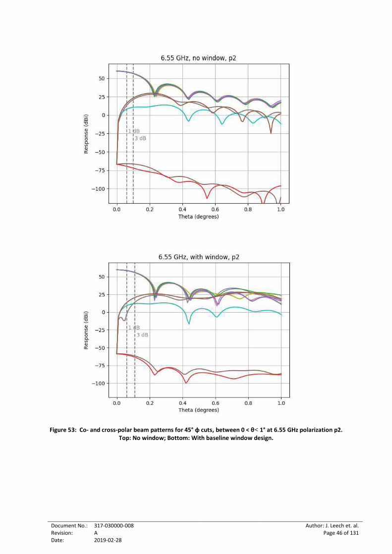
Figure 53: Co- and cross-polar beam patterns for 45° φ cuts, between 0 < θ< 1° at 6.55 GHz polarization p2. Top: No window; Bottom: With baseline window design. ...............................46
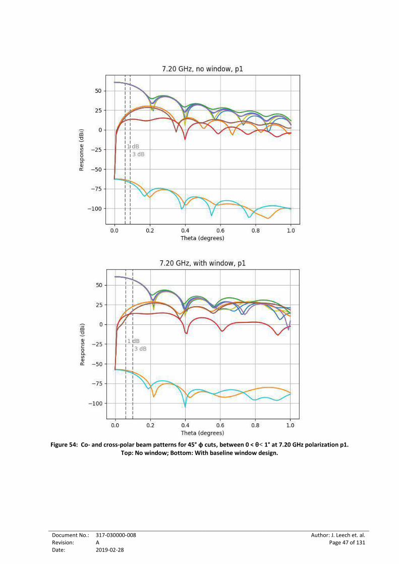
Figure 54: Co- and cross-polar beam patterns for 45° φ cuts, between 0 < θ< 1° at 7.20 GHz polarization p1. Top: No window; Bottom: With baseline window design. ...............................47
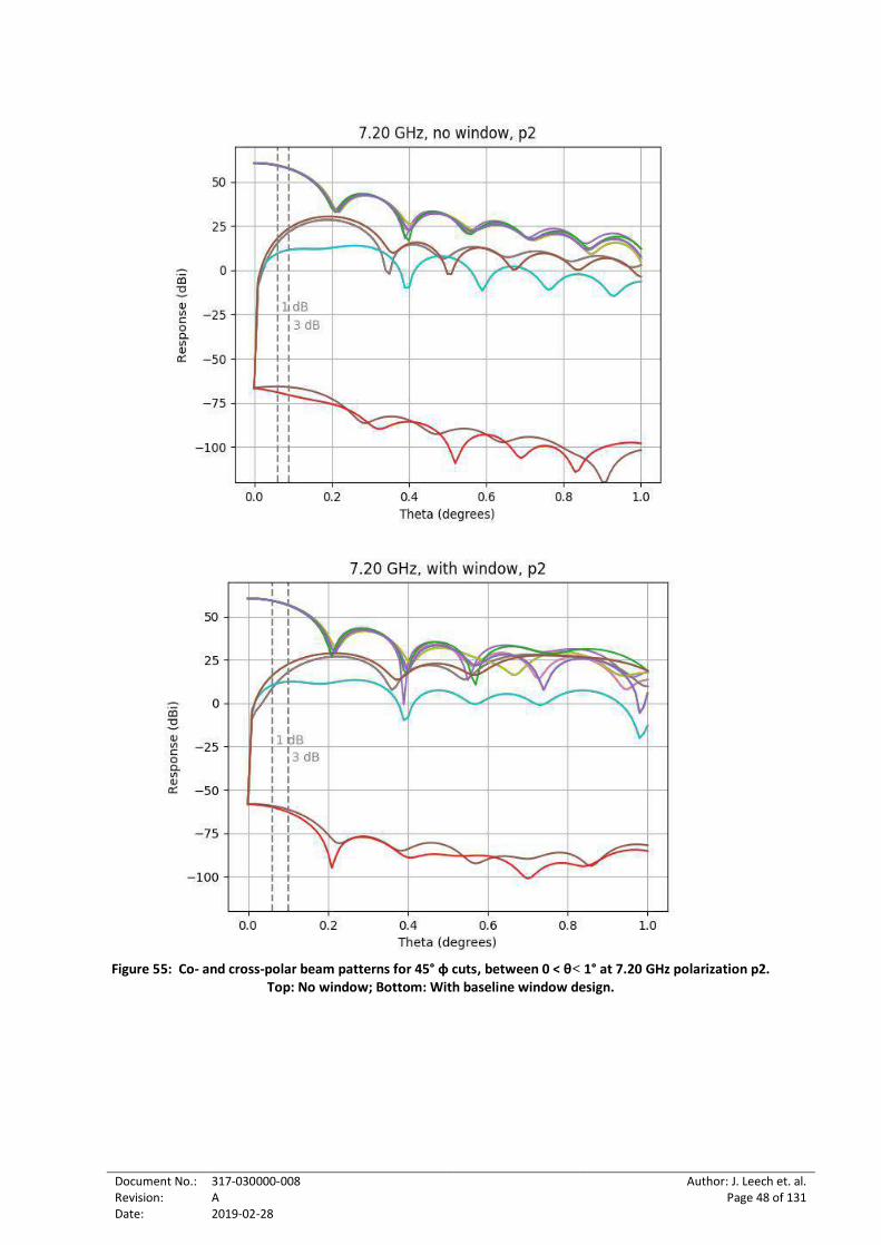
Figure 55: Co- and cross-polar beam patterns for 45° φ cuts, between 0 < θ< 1° at 7.20 GHz polarization p2. Top: No window; Bottom: With baseline window design. ...............................48
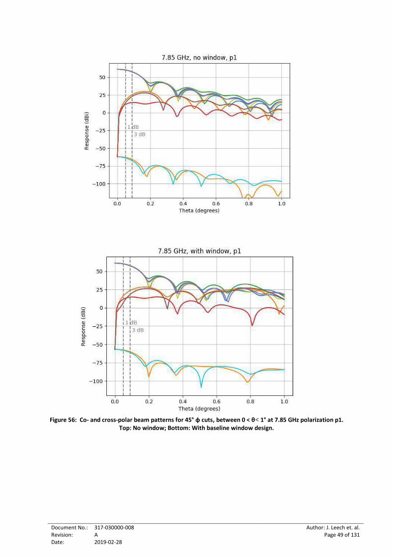
Figure 56: Co- and cross-polar beam patterns for 45° φ cuts, between 0 < θ< 1° at 7.85 GHz polarization p1. Top: No window; Bottom: With baseline window design. ...............................49
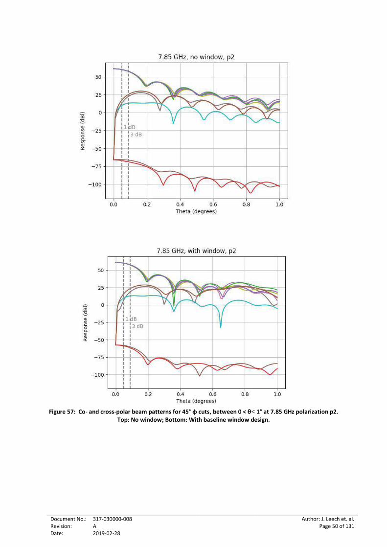
Figure 57: Co- and cross-polar beam patterns for 45° φ cuts, between 0 < θ< 1° at 7.85 GHz polarization p2. Top: No window; Bottom: With baseline window design. ...............................50
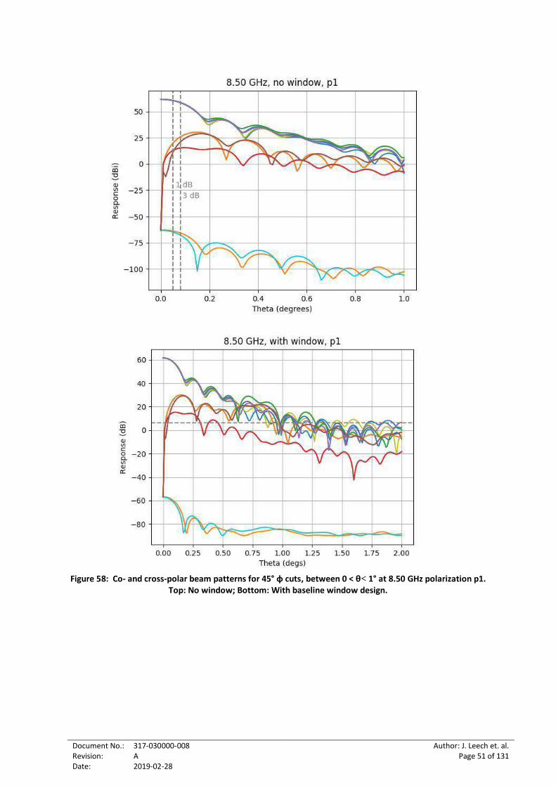
Figure 58: Co- and cross-polar beam patterns for 45° φ cuts, between 0 < θ< 1° at 8.50 GHz polarization p1. Top: No window; Bottom: With baseline window design. ...............................51
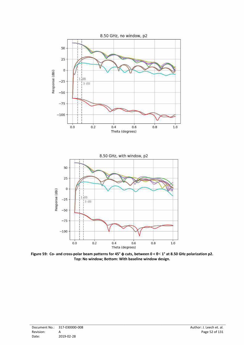
Figure 59: Co- and cross-polar beam patterns for 45° φ cuts, between 0 < θ< 1° at 8.50 GHz polarization p2. Top: No window; Bottom: With baseline window design. ...............................52
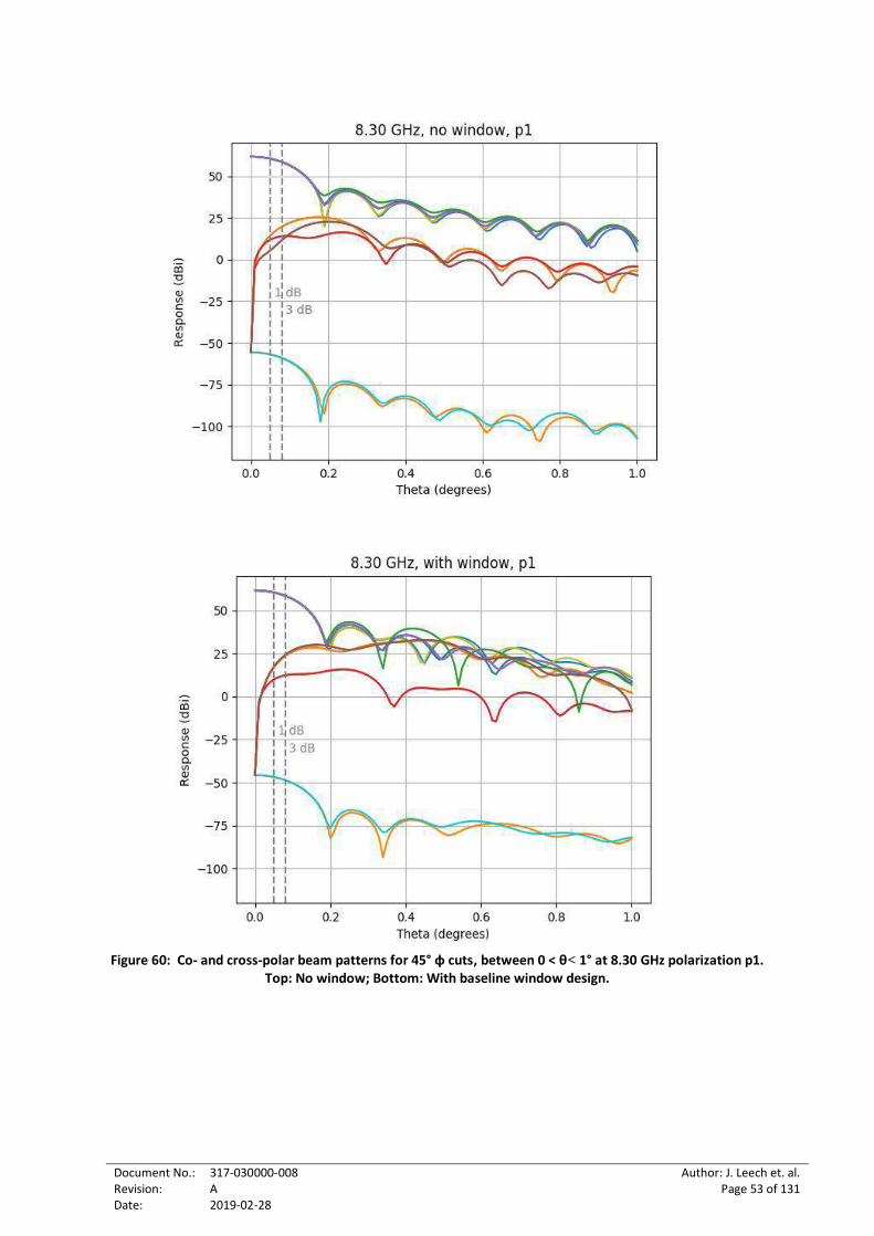
Figure 60: Co- and cross-polar beam patterns for 45° φ cuts, between 0 < θ< 1° at 8.30 GHz polarization p1. Top: No window; Bottom: With baseline window design. ...............................53
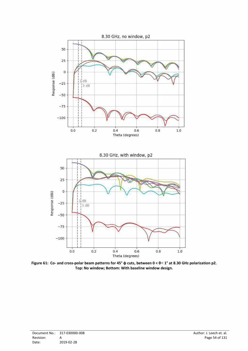
Figure 61: Co- and cross-polar beam patterns for 45° φ cuts, between 0 < θ< 1° at 8.30 GHz polarization p2. Top: No window; Bottom: With baseline window design. ...............................54
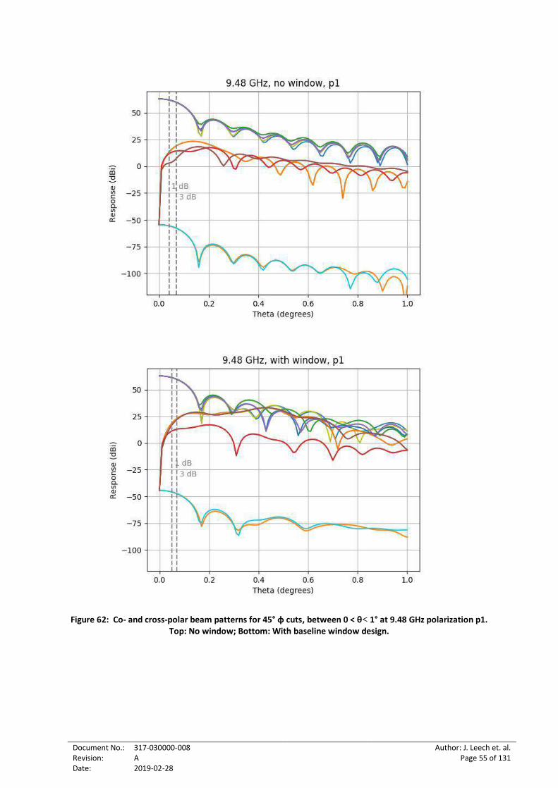
Figure 62: Co- and cross-polar beam patterns for 45° φ cuts, between 0 < θ< 1° at 9.48 GHz polarization p1. Top: No window; Bottom: With baseline window design. ...............................55
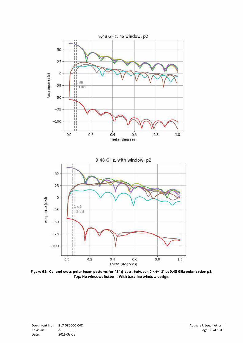
Figure 63: Co- and cross-polar beam patterns for 45° φ cuts, between 0 < θ< 1° at 9.48 GHz polarization p2. Top: No window; Bottom: With baseline window design. ...............................56
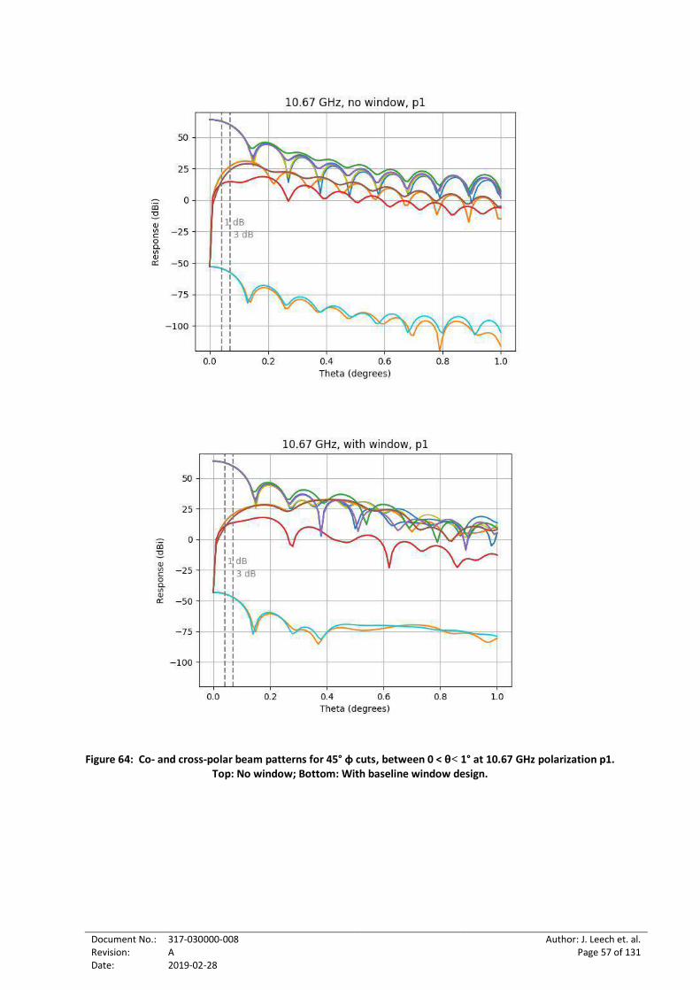
Figure 64: Co- and cross-polar beam patterns for 45° φ cuts, between 0 < θ< 1° at 10.67 GHz polarization p1. Top: No window; Bottom: With baseline window design. ...............................57
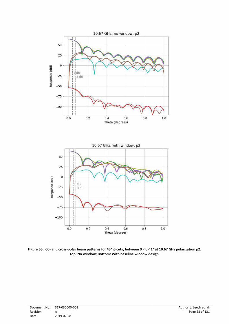
Figure 65: Co- and cross-polar beam patterns for 45° φ cuts, between 0 < θ< 1° at 10.67 GHz polarization p2. Top: No window; Bottom: With baseline window design. ...............................58
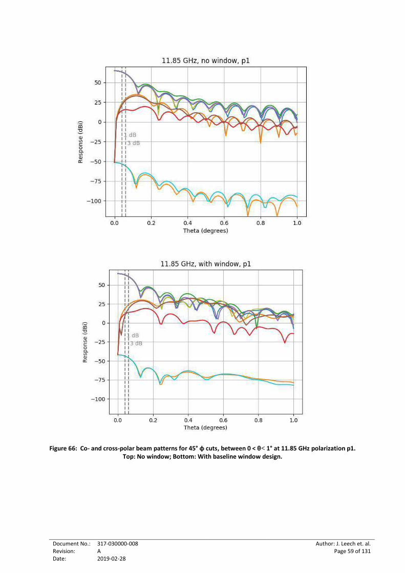
Figure 66: Co- and cross-polar beam patterns for 45° φ cuts, between 0 < θ< 1° at 11.85 GHz polarization p1. Top: No window; Bottom: With baseline window design. ...............................59
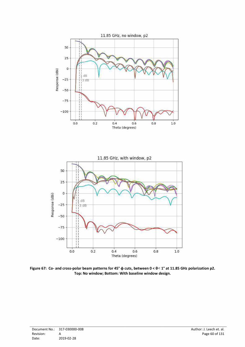
Figure 67: Co- and cross-polar beam patterns for 45° φ cuts, between 0 < θ< 1° at 11.85 GHz polarization p2. Top: No window; Bottom: With baseline window design. ...............................60
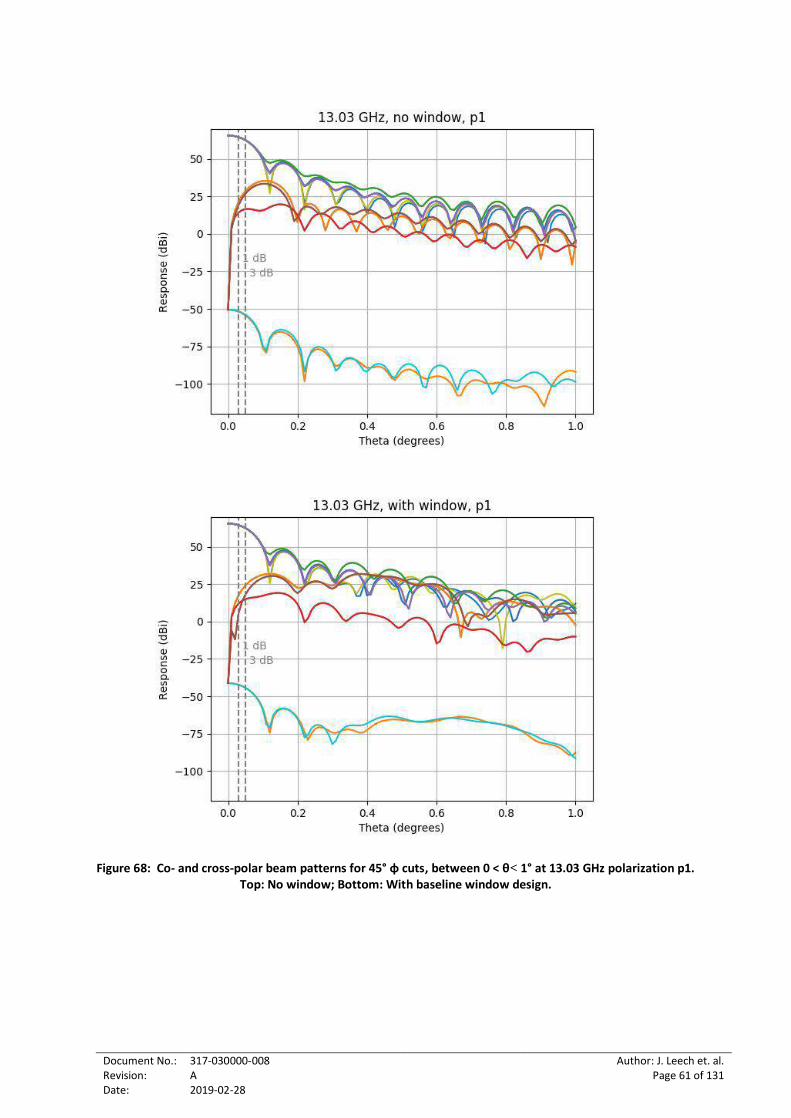
Figure 68: Co- and cross-polar beam patterns for 45° φ cuts, between 0 < θ< 1° at 13.03 GHz polarization p1. Top: No window; Bottom: With baseline window design. ...............................61
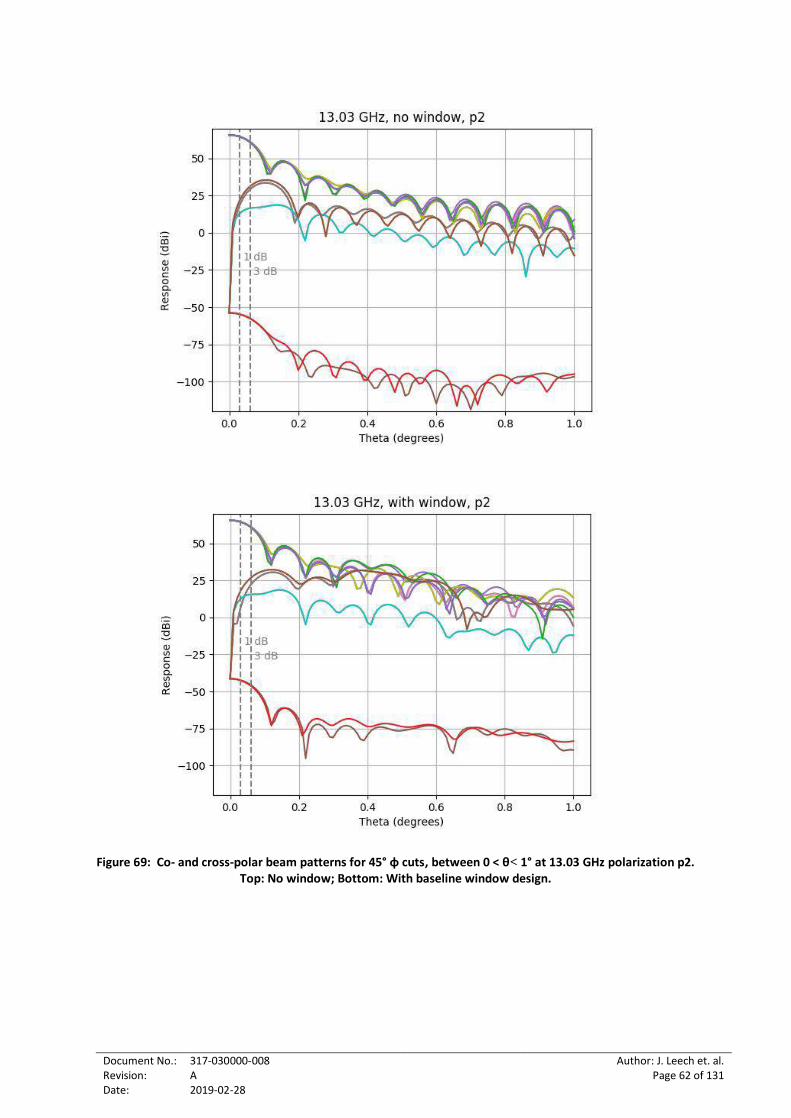
Figure 69: Co- and cross-polar beam patterns for 45° φ cuts, between 0 < θ< 1° at 13.03 GHz polarization p2. Top: No window; Bottom: With baseline window design. ...............................62
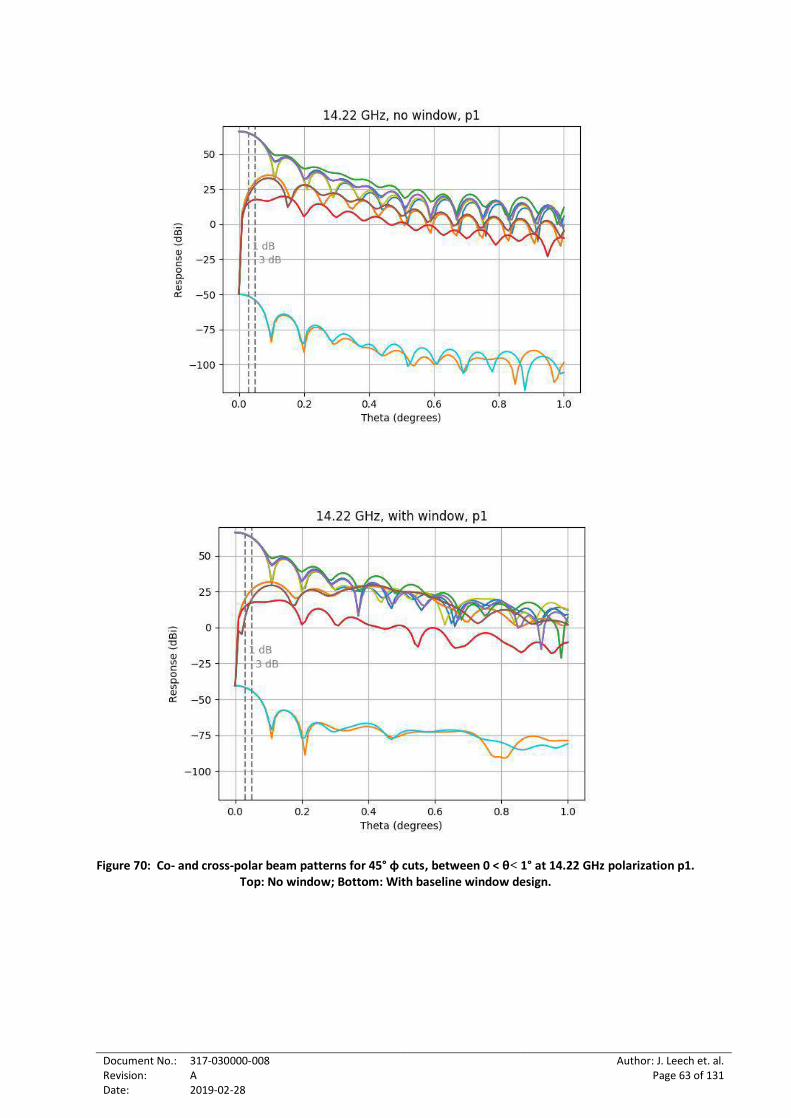
Figure 70: Co- and cross-polar beam patterns for 45° φ cuts, between 0 < θ< 1° at 14.22 GHz polarization p1. Top: No window; Bottom: With baseline window design. ...............................63

Document No.: Revision: Date:
317-030000-008 A 2019-02-28
Author: J. Leech et. al. Page 7 of 131
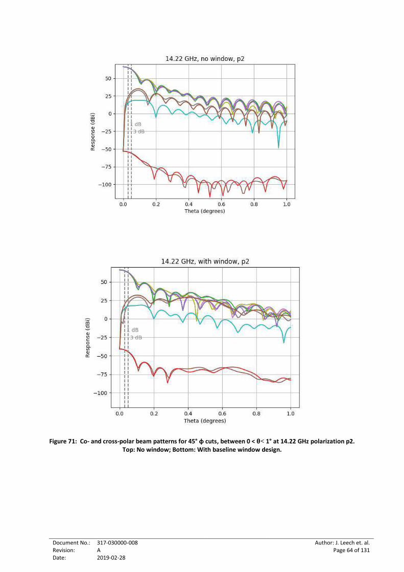
Figure 71: Co- and cross-polar beam patterns for 45° φ cuts, between 0 < θ< 1° at 14.22 GHz polarization p2. Top: No window; Bottom: With baseline window design. ...............................64
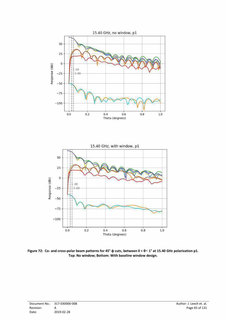
Figure 72: Co- and cross-polar beam patterns for 45° φ cuts, between 0 < θ< 1° at 15.40 GHz polarization p1. Top: No window; Bottom: With baseline window design. ...............................65
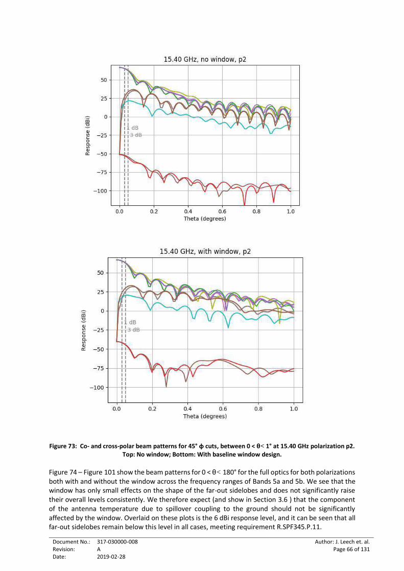
Figure 73: Co- and cross-polar beam patterns for 45° φ cuts, between 0 < θ< 1° at 15.40 GHz polarization p2. Top: No window; Bottom: With baseline window design. ...............................66
Figure 74: Co- and cross-polar beam patterns for 45° φ cuts, between 0 < θ< 180° at 4.6 GHz polarization p1. Top: No window; Bottom: With baseline window design. ...............................67
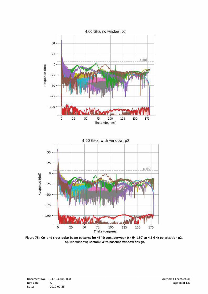
Figure 75: Co- and cross-polar beam patterns for 45° φ cuts, between 0 < θ< 180° at 4.6 GHz polarization p2. Top: No window; Bottom: With baseline window design. ...............................68
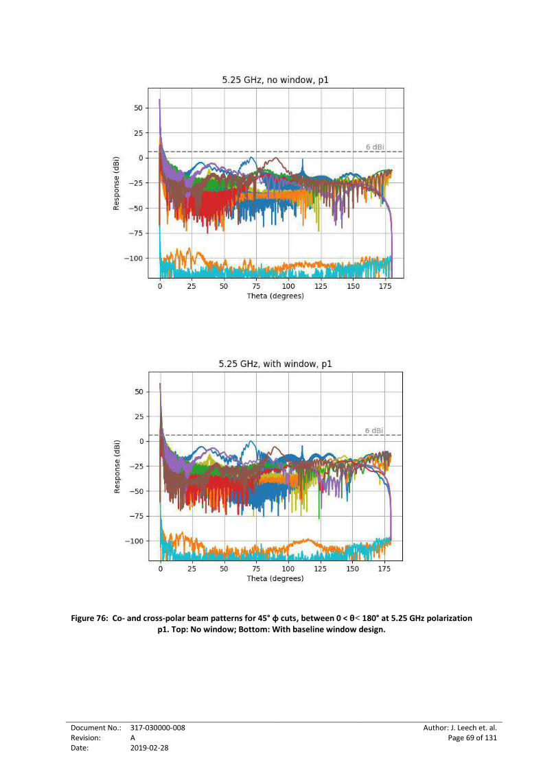
Figure 76: Co- and cross-polar beam patterns for 45° φ cuts, between 0 < θ< 180° at 5.25 GHz polarization p1. Top: No window; Bottom: With baseline window design. ...............................69
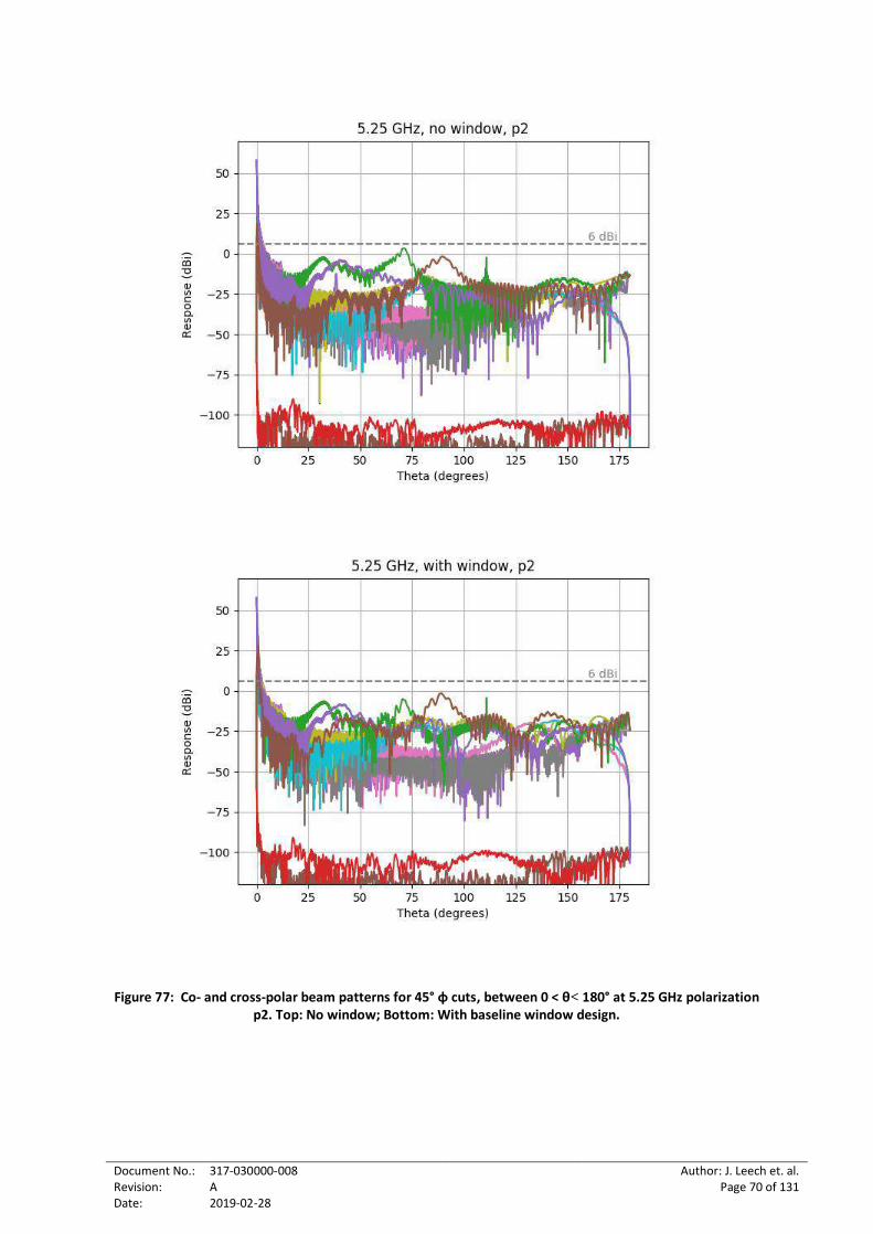
Figure 77: Co- and cross-polar beam patterns for 45° φ cuts, between 0 < θ< 180° at 5.25 GHz polarization p2. Top: No window; Bottom: With baseline window design. ...............................70
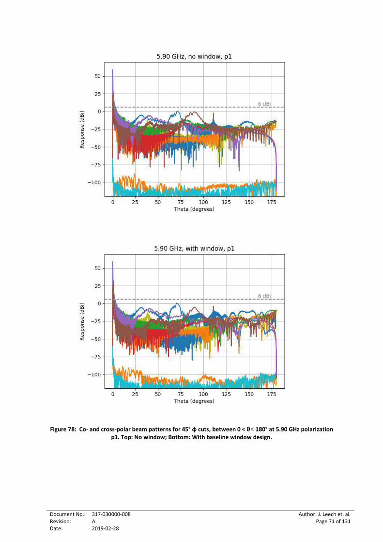
Figure 78: Co- and cross-polar beam patterns for 45° φ cuts, between 0 < θ< 180° at 5.90 GHz polarization p1. Top: No window; Bottom: With baseline window design. ...............................71
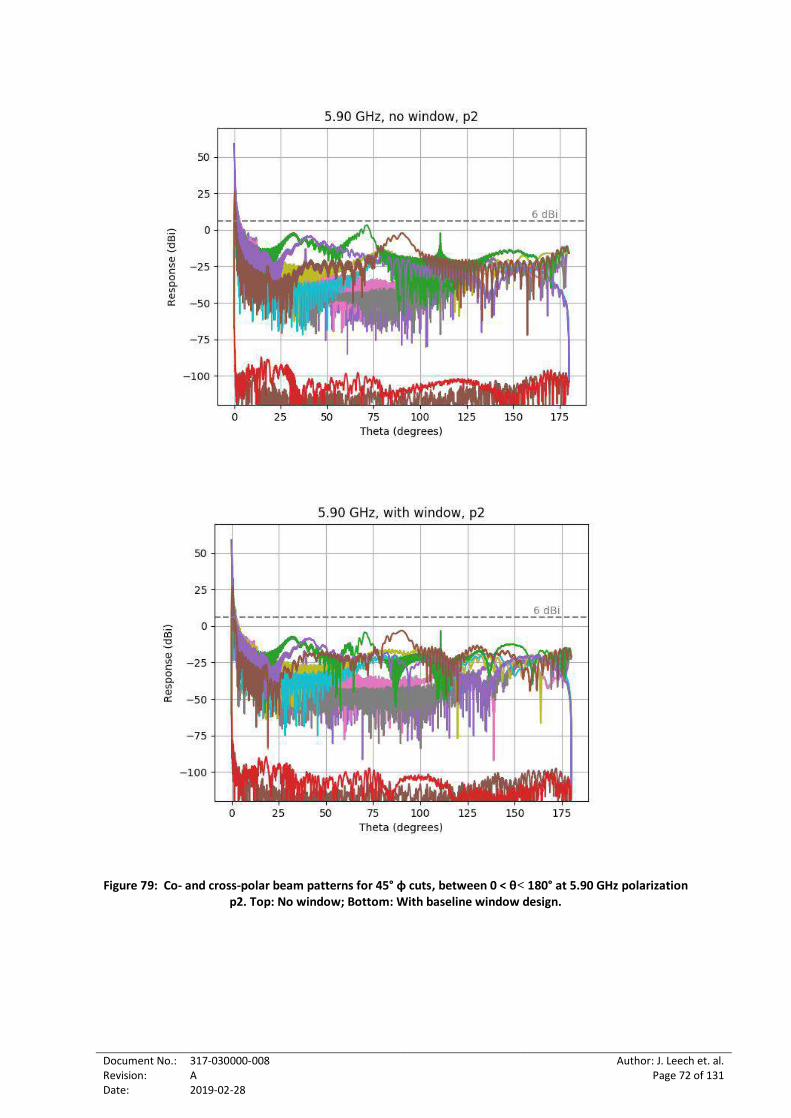
Figure 79: Co- and cross-polar beam patterns for 45° φ cuts, between 0 < θ< 180° at 5.90 GHz polarization p2. Top: No window; Bottom: With baseline window design. ...............................72
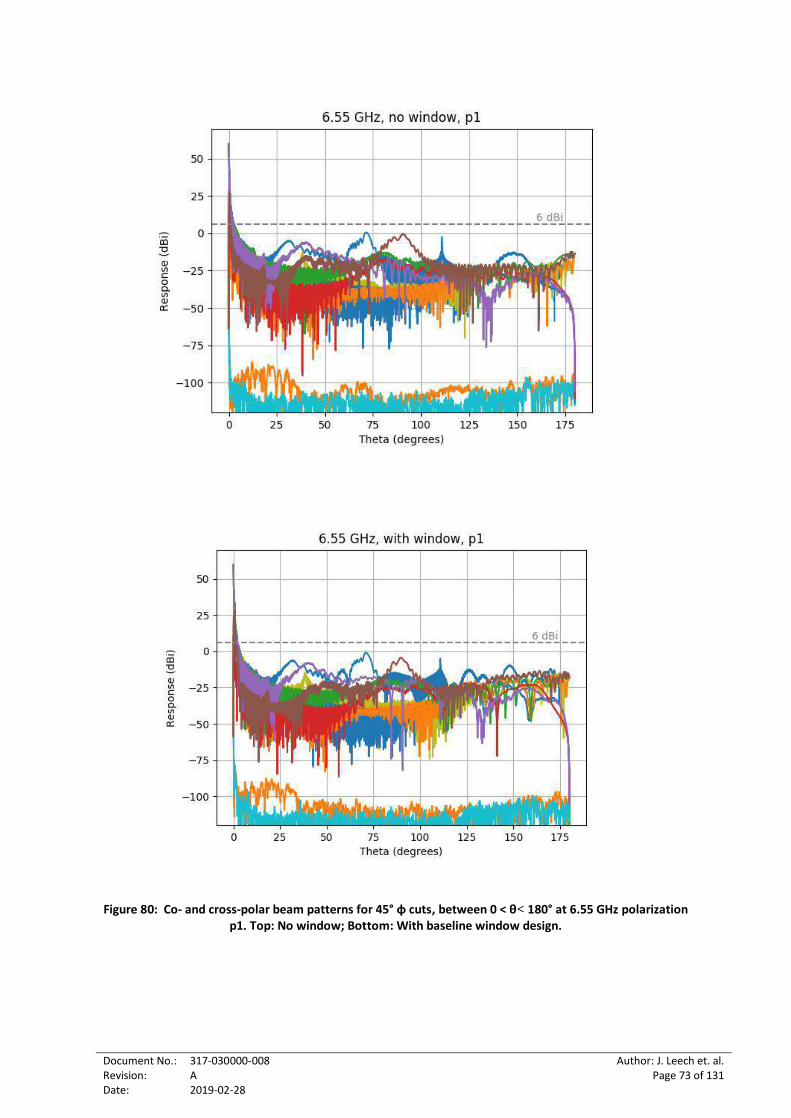
Figure 80: Co- and cross-polar beam patterns for 45° φ cuts, between 0 < θ< 180° at 6.55 GHz polarization p1. Top: No window; Bottom: With baseline window design. ...............................73
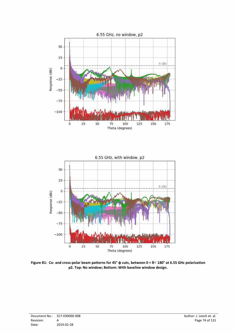
Figure 81: Co- and cross-polar beam patterns for 45° φ cuts, between 0 < θ< 180° at 6.55 GHz polarization p2. Top: No window; Bottom: With baseline window design. ...............................74
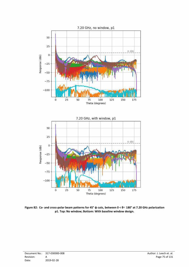
Figure 82: Co- and cross-polar beam patterns for 45° φ cuts, between 0 < θ< 180° at 7.20 GHz polarization p1. Top: No window; Bottom: With baseline window design. ...............................75
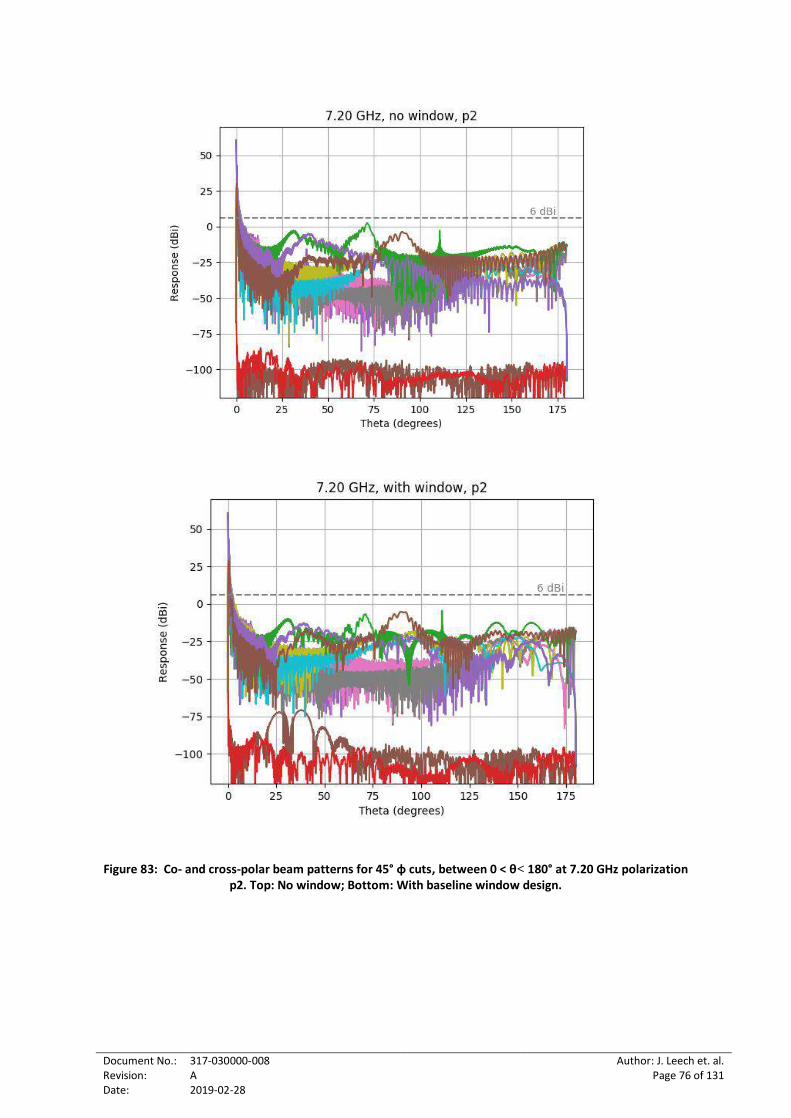
Figure 83: Co- and cross-polar beam patterns for 45° φ cuts, between 0 < θ< 180° at 7.20 GHz polarization p2. Top: No window; Bottom: With baseline window design. ...............................76
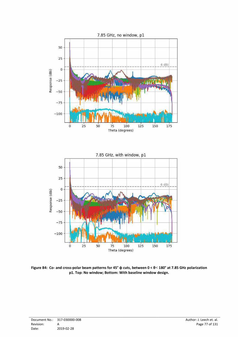
Figure 84: Co- and cross-polar beam patterns for 45° φ cuts, between 0 < θ< 180° at 7.85 GHz polarization p1. Top: No window; Bottom: With baseline window design. ...............................77
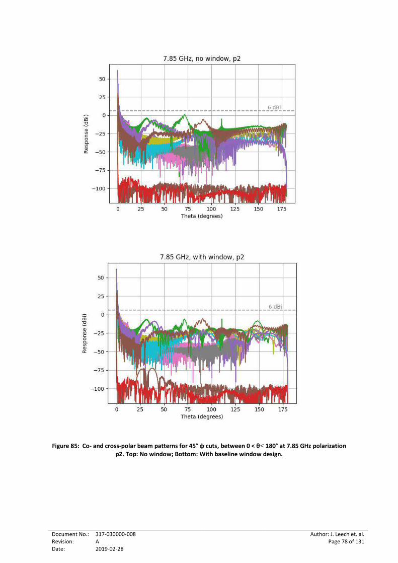
Figure 85: Co- and cross-polar beam patterns for 45° φ cuts, between 0 < θ< 180° at 7.85 GHz polarization p2. Top: No window; Bottom: With baseline window design. ...............................78
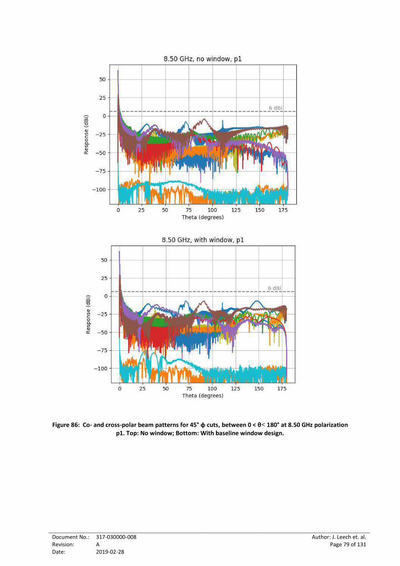
Figure 86: Co- and cross-polar beam patterns for 45° φ cuts, between 0 < θ< 180° at 8.50 GHz polarization p1. Top: No window; Bottom: With baseline window design. ...............................79
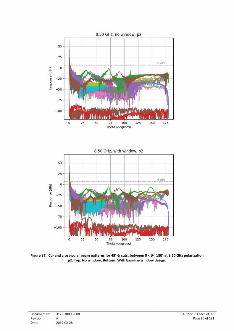
Figure 87: Co- and cross-polar beam patterns for 45° φ cuts, between 0 < θ< 180° at 8.50 GHz polarization p2. Top: No window; Bottom: With baseline window design. ...............................80
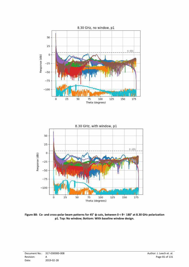
Figure 88: Co- and cross-polar beam patterns for 45° φ cuts, between 0 < θ< 180° at 8.30 GHz polarization p1. Top: No window; Bottom: With baseline window design. ...............................81
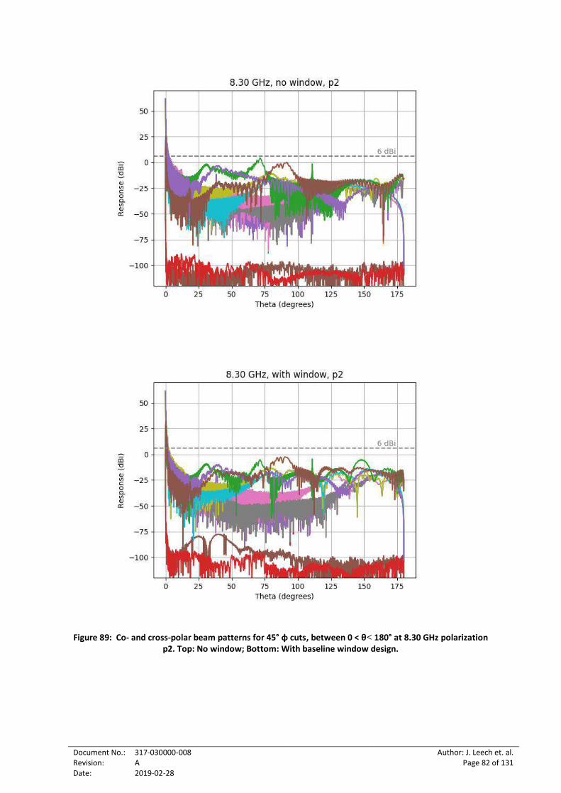
Figure 89: Co- and cross-polar beam patterns for 45° φ cuts, between 0 < θ< 180° at 8.30 GHz polarization p2. Top: No window; Bottom: With baseline window design. ...............................82
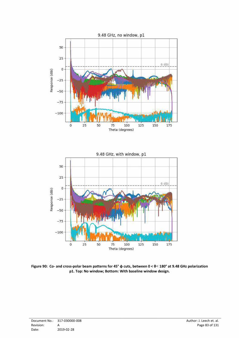
Figure 90: Co- and cross-polar beam patterns for 45° φ cuts, between 0 < θ< 180° at 9.48 GHz polarization p1. Top: No window; Bottom: With baseline window design. ...............................83
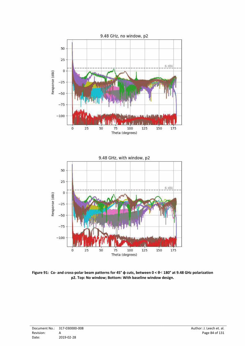
Figure 91: Co- and cross-polar beam patterns for 45° φ cuts, between 0 < θ< 180° at 9.48 GHz polarization p2. Top: No window; Bottom: With baseline window design. ...............................84
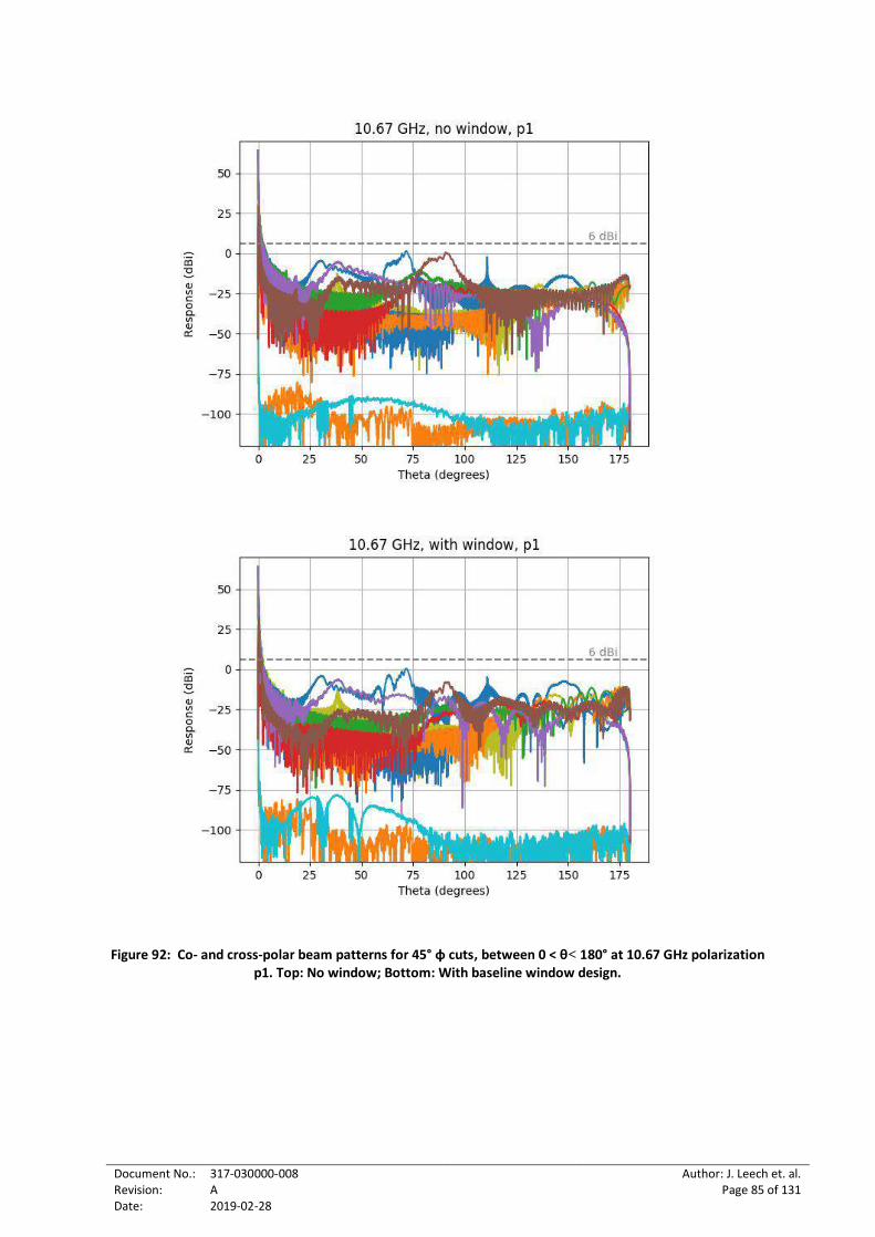
Figure 92: Co- and cross-polar beam patterns for 45° φ cuts, between 0 < θ< 180° at 10.67 GHz polarization p1. Top: No window; Bottom: With baseline window design. ...............................85
Document No.: Revision: Date:
317-030000-008 A 2019-02-28
Author: J. Leech et. al. Page 8 of 131
Figure 93: Co- and cross-polar beam patterns for 45° φ cuts, between 0 < θ< 180° at 10.67 GHz polarization p2. Top: No window; Bottom: With baseline window design. ...............................86
Figure 94: Co- and cross-polar beam patterns for 45° φ cuts, between 0 < θ< 180° at 11.85 GHz polarization p1. Top: No window; Bottom: With baseline window design. ...............................87
Figure 95: Co- and cross-polar beam patterns for 45° φ cuts, between 0 < θ< 180° at 11.85 GHz polarization p2. Top: No window; Bottom: With baseline window design. ...............................88
Figure 96: Co- and cross-polar beam patterns for 45° φ cuts, between 0 < θ< 180° at 13.03 GHz polarization p1. Top: No window; Bottom: With baseline window design. ...............................89
Figure 97: Co- and cross-polar beam patterns for 45° φ cuts, between 0 < θ< 180° at 13.03 GHz polarization p1. Top: No window; Bottom: With baseline window design. ...............................90
Figure 98: Co- and cross-polar beam patterns for 45° φ cuts, between 0 < θ< 180° at 14.22 GHz polarization p1. Top: No window; Bottom: With baseline window design. ...............................91
Figure 99: Co- and cross-polar beam patterns for 45° φ cuts, between 0 < θ< 180° at 14.22 GHz polarization p2. Top: No window; Bottom: With baseline window design. ...............................92
Figure 100: Co- and cross-polar beam patterns for 45° φ cuts, between 0 < θ< 180° at 15.40 GHz polarization p1. Top: No window; Bottom: With baseline window design. ...............................93
Figure 101: Co- and cross-polar beam patterns for 45° φ cuts, between 0 < θ< 180° at 15.40 GHz polarization p2. Top: No window; Bottom: With baseline window design. ...............................94
Figure 102: The sky brightness temperature according to the model given in [RD5], which includes the cosmic microwave background and atmospheric absorption. ...................................................95
Figure 103: A/Tsys for the full optics for Band 5a at zenith angle = 0 degrees. Both polarizations and the cases with no window and the baseline window design are shown. .........................................96
Figure 104: Antenna temperature TA for the full optics for Band 5a at zenith angle = 0 degrees. Both polarizations and the cases with no window and the baseline window design are shown. ......96
Figure 105: System temperature Tsys for the full optics for Band 5a at zenith angle = 0 degrees. Both polarizations and the cases with no window and the baseline window design are shown. ......97
Figure 106: A/Tsys for the full optics for Band 5a at zenith angle = 60 degrees. Both polarizations and the cases with no window and the baseline window design are shown. ...................................97
Figure 107: Antenna temperature TA for the full optics for Band 5a at zenith angle = 60 degrees. Both polarizations and the cases with no window and the baseline window design are shown. ......98
Figure 108: System temperature Tsys for the full optics for Band 5a at zenith angle = 60 degrees. Both polarizations and the cases with no window and the baseline window design are shown. ......98
Figure 109: A/Tsys for the full optics for Band 5b at zenith angle = 0 degrees. Both polarizations and the cases with no window and the baseline window design are shown. ...................................99
Figure 110: Antenna temperature TA for the full optics for Band 5b at zenith angle = 0 degrees. Both polarizations and the cases with no window and the baseline window design are shown. ......99
Figure 111: Antenna temperature TSYS for the full optics for Band 5b at zenith angle = 0 degrees. Both polarizations and the cases with no window and the baseline window design are shown. ....100
Figure 112: A/Tsys for the full optics for Band 5b at zenith angle = 60 degrees. Both polarizations and the cases with no window and the baseline window design are shown. .................................100
Figure 113: Antenna temperature TA for the full optics for Band 5b at zenith angle = 0 degrees. Both polarizations and the cases with no window and the baseline window design are shown (note that the yellow B5B, no window, p2 line is partially obscured by the equivalent line with a window (red)). ...........................................................................................................................101
Document No.: Revision: Date:
317-030000-008 A 2019-02-28
Author: J. Leech et. al. Page 9 of 131
Figure 114: System a temperature TSYS for the full optics for Band 5b at zenith angle = 60 degrees. Both polarizations and the cases with no window and the baseline window design are shown (note that the yellow B5B, no window, p2 line is partially obscured by the equivalent line with a window (red)). ...........................................................................................................................101
Figure 115: The feed sensitivity (with the baseline window design) for both polarizations (p1, upper, p2 lower) as a function of zenith angle and frequency calculated for Band 5a........................102
Figure 116: The feed sensitivity (with the baseline window design) for both polarizations (p1, upper, p2 lower) as a function of zenith angle and frequency calculated for Band 5b. ......................103
Figure 117: HFSS model of a cylindrical waveguide with noise inject probe oriented at 45° with respect to the vertical and horizontal OMT positions. ..........................................................................105
Figure 118: HFSS simulated insertion loss for the Band 5a noise injection probe. .............................106
Figure 119: HFSS simulated insertion loss for the Band 5b noise injection probe. ............................106
Figure 120: Basic diagram of the RF signal chain in the cryostat and control assembly. ...................107
Figure 121: Schematic diagram of the RF chain. ................................................................................108
Figure 122: Semi-rigid coaxial cable used to connect the OMT to the LNA. ......................................109
Figure 123: Stainless-Steel semi-rigid coaxial cable used to connect the SMA bulkhead feedthrough to the warm RF amplification chain. ..............................................................................................110
Figure 124: Hermetic SMA feedthrough from TE Connectivity. ..........................................................111
Figure 125: Gain and noise characteristics of the Band 5a LNA - Low Noise Factory LNF-LNC4_8C (Rev. Sept. 2018). Data courtesy of Low Noise Factory. ....................................................................112
Figure 126: Gain and noise characteristics of the proposed Band 5b LNA - Low Noise Factory LNF-LNC4_16B (Rev May. 2018). Data courtesy of Low Noise Factory. ...........................................113
Figure 127: Band 5a (left) and 5b (right) LNA assemblies installed in the prototype receiver cryostat. The heater resistor and temperature sensors can also be seen on the side of the aluminium bracket. ......................................................................................................................................113
Figure 128: An image of the warm RF chain components mounted on a prototype aluminium L-bracket. ......................................................................................................................................114
Figure 129: Second-stage, warm RF amplifiers from AtlanTecRF. ......................................................116
Figure 130: Band 5a (left) and Band 5b (right) defining filters. ...........................................................116
Figure 131: Measured gain of a typical, warm amplifier between 1 - 20 GHz that will be used in the warm RF amplification chain. ....................................................................................................117
Figure 132: Measured S21 transmission of a typical Band 5a defining filter. ....................................118
Figure 133: Measured S21 transmission of a typical Band 5b defining filter. .....................................118
Figure 134: Measured gain of a warm, slope compensating amplifier between 1 - 20 GHz. .............119
Figure 135: Measured gain response for the Band 5a warm RF amplification chain. ........................119
Figure 136: Measured gain response for the Band 5b warm RF amplification chain. ........................120
Figure 137: Circuit diagram showing the temperature stabilisation scheme employed for the warm RF chain. .........................................................................................................................................121
Figure 138: Circuit diagram for the power supply used to power the warm RF electronics temperature stabilisation board. ....................................................................................................................122
Figure 139: Front and back views of the PCB that will be used to temperature stabilise the warm RF electronics. ................................................................................................................................122
Document No.: Revision: Date:
317-030000-008 A 2019-02-28
Author: J. Leech et. al. Page 10 of 131
Figure 140: Measured insertion loss for a representative cable of a suitable length for connecting the OMT output to the LNA. ............................................................................................................124
Figure 141: The new receiver temperature noise model used in this DDR document. The previous noise model used in the PDR is also shown for comparison. .............................................................125
Figure 142: Solid model of the 5b finline OMT, showing the interior quad-ridge structure. .............126
Figure 143: Cross-section of the 5b OMT, showing the coaxial to quad-ridge transition and the transition from quad-ridge to unloaded waveguide. ................................................................127
Figure 144: Photograph of the 5b OMT, showing detail of the coaxial to quad-ridge transition. ......127
Figure 145: Photograph of the prototype OMT 5b OMT split into its four component sections. ......128
Figure 146: Photograph of the experiment setup for measurements of the prototype 5b OMT. .....128
Figure 147: Measured and simulated return loss for the OMT. ..........................................................129
Figure 148: Measured and simulated insertion loss for the OMT.......................................................129
Figure 149: Measured and simulated cross-polar isolation for the OMT. ..........................................130
LIST OF TABLES
Table 1: Estimated feed sensitivities averaged over the frequency bands and solid angle (between
zenith and zenith angle = 60). The sensitivity requirements are shown for comparison. ......104
Table 2: Baseline RF chain component list with nominal gains, from the OMT output to the RF vacuum feedthrough. ..............................................................................................................................108
Table 3: AtlanTecRF ASR Series 0.141 Reformable Aluminium semi-rigid coaxial cable properties. .109
Table 4: AtlanTecRF AS5266 Series 0.086 Reformable Stainless-Steel semi-rigid coaxial cable properties ..................................................................................................................................110
Table 5: Key parameters of the Low Noise Factory LNAs selected as the baseline LNAs for Bands 5a and 5b. .......................................................................................................................................112
Table 6: Summary of the DDR noise models. The elements which have a strong frequency dependence are labelled “Freq. Dep.”. The other elements are unchanged since the PDR noise model. ...123
Document No.: Revision: Date:
317-030000-008 A 2019-02-28
Author: J. Leech et. al. Page 11 of 131
LIST OF ABBREVIATIONS
CNC ....................................Computer Numerical Control CW .....................................Continuous Wave EM .....................................Electromagnetic ENR ....................................Excess Noise Ratio GM .....................................Gifford-McMahon IXR .....................................Intrinsic Cross-Polarisation Ratio LNA ....................................Low Noise Amplifier OMT ...................................Orthogonal Mode Transducer PCB ....................................Printed Circuit Board RBW ...................................Resolution Bandwidth RF .......................................Radio Frequency SKA.....................................Square Kilometre Array SPF .....................................Single Pixel Feed
1 Scope of Document
This document outlines the signal chain design of the Band 345 feed for the SKA single pixel feed (SPF) that forms part of the SKA_MID dish element. The feed collects the electromagnetic (EM) radiation concentrated at the focus of the reflector system and transforms it into electric signals for both of the received (linear) orthogonal polarizations. The Band 345 feed package is designed to be modular, with Bands 5a and 5b being initially installed, and the population of the Bands 3,4 and possibly 6 (up to 24 GHz) occurring at a later date. This document will restrict itself to the design description, EM modelling and experimental verification of the Band 5a and 5b signal chains. Each signal chain consists of a wide-flare-angle corrugated horn (behind a cryostat window), an orthomode transducer, a low-noise amplifier (cooled to 15 K), and a warm RF chain comprising room temperature amplifiers, band-pass filters and matching attenuators. In addition, there is provision for the injection of a calibration noise signal from a diode noise source. Full physical optics simulations (made with TICRA GRASP) of the feed horns, cryostat windows and the Gregorian telescope reflector system are presented, and projected telescope sensitivities are calculated.
1.1 Applicable Documents
The following documents are applicable to the extent stated herein. In the event of conflict between the contents of the applicable documents and this document, the applicable documents shall take precedence. Unless specifically stated, latest revisions shall apply.
[AD1] A. Born, “SPF Band 345 Development Specification” SKA-TEL-DSH-0000085 Rev 1, 2018‑09‑25.
1.2 Reference Documents
The following works are referenced in this document. In the event of conflict between the contents of the referenced documents and this document, this document shall take precedence.
[RD1] J. Leech et. al., “SPF B345 Preliminary Design Document”, SKA-TEL-DSH-0000118, Rev. 3, 2018-07-16.
[RD2] R. Lehmensiek, “Shaping the SKA optics”, SKA-TEL-DSH-0000034, Rev 1, 4 Mar 2015.
[RD3] I. P. Theron, “SKA Dish Optics Selection”, SKA-TEL-DSH-0000018, Rev 2, 4 Nov 2015.
[RD4] J. Leech et. al., “SPF Band 345 Cryogenic Function Design Document”, 317-030000-006, Draft A, 2019-02-28.
[RD5] G. Medellin, “SKA Memo 95: Antenna Noise Temperature Calculation”, July 2007.
Document No.: Revision: Date:
317-030000-008 A 2019-02-28
Author: J. Leech et. al. Page 12 of 131
[RD6] M. Jones et. al., “SPF Band 345 Control Function Design Document”, 317-030000-007, Draft A, 2019-02-28.
[RD7] de Villiers, D. I., Meyer, P., & Palmer, K. D. (2009, September). Design of a wideband orthomode transducer. In AFRICON, 2009. AFRICON'09. (pp. 1-6). IEEE.
[RD8] Pollak, A. W., & Jones, M. E. (2018). A Compact Quad-Ridge Orthogonal Mode Transducer With Wide Operational Bandwidth. IEEE Antennas and Wireless Propagation Letters, 17(3), 422-425.
[RD9] Lauria, E. (1999). Trap issue in reference to the L-band receiver. National Astronomy and Ionosphere Center, Tech. Rep.
[RD10] Coutts, G. M., Dinwiddie, H., & Lilie, P. (2009, June). S-band octave-bandwidth orthomode transducer for the expanded very large array. In Antennas and Propagation Society International Symposium, 2009. APSURSI'09. IEEE (pp. 1-4). IEEE.
[RD11] I.P. Theron et al., “SPF Sub-Element Qualification Plan”, SKA-TEL-DSH-0000117, Rev 2A, 2019-02-28.
Document No.: Revision: Date:
317-030000-008 A 2019-02-28
Author: J. Leech et. al. Page 13 of 131
2 Design Description
2.1 Context
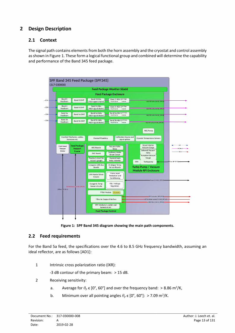
The signal path contains elements from both the horn assembly and the cryostat and control assembly as shown in Figure 1. These form a logical functional group and combined will determine the capability and performance of the Band 345 feed package.
Figure 1: SPF Band 345 diagram showing the main path components.
2.2 Feed requirements
For the Band 5a feed, the specifications over the 4.6 to 8.5 GHz frequency bandwidth, assuming an ideal reflector, are as follows [AD1]:
1 Intrinsic cross polarization ratio (IXR):
-3 dB contour of the primary beam: > 15 dB.
2 Receiving sensitivity:
a. Average for θp ϵ [0°, 60°] and over the frequency band: > 8.86 m2/K,
b. Minimum over all pointing angles θp ϵ [0°, 60°]: > 7.09 m2/K.
Document No.: Revision: Date:
317-030000-008 A 2019-02-28
Author: J. Leech et. al. Page 14 of 131
3 Beam smoothness:
The on-diagonal Mueller matrix patterns shall not vary by more than 3 % relative to the peak gain along any 5° of rotation around the optical axis down to the -20 dB contour, assuming an ideal reflector, 5 mm indexer positioning error as well as the feed mounting structure positioning error (both translation and rotation) after correcting for pointing error.
4 Sidelobe levels outside the 10° from boresight region:
a. Total solid angle over which the sidelobe level exceeds 0 dBi shall be less than 0.05 sr,
b. Peak level: < 6 dBi.
5 RF signal amplification:
a. Nominal gain: 56 ± 3 dB,
b. Variation of the magnitude of the output power spectrum: ≤ 2 dBp-p across any 2.5 GHz interval
c. 3rd order intercept (referred to the input): ≥ -43 dBm,
d. Survival input levels: -2 dBm continuous input power,
e. Saturated output level: ≤ 14 dBm,
f. Output reflection coefficient (50 Ω system impedance): < -16 dB,
g. Gain stability over 5 s, when averaged over the central 500 MHz of the band and sampled with 20 ms intervals: ≤ 0.08% RMS,
h. Phase stability over 5 minutes when sampled with 5 s intervals: ≤ 1° peak to peak,
i. Phase stability over 5 minutes after subtracting a linear fit when sampled with 5 s intervals: ≤ 0.5° RMS.
6 Calibration signals:
a. The calibration signal shall be coupled into both polarization channels (i.e. one signal into both channels), at the earliest possible point preceding the LNA,
b. The power spectral density of the calibration signal shall be equivalent to 5% - 13% of Tsys, averaged over any 1 MHz bandwidth across the frequency range and with Tsys computed for cold sky at θp = 60°,
c. The calibration signal shall be coupled into the signal path with phase imbalance of < 1.5° between the coupling points,
d. Under normal operating conditions the phase difference with which the calibration noise signal is injected into the two signal paths shall remain stable to < 0.3°RMS.
For the Band 5b feed the specifications over the 8.3 to 15.4 GHz frequency bandwidth, assuming an ideal reflector, are as follows [AD1]:
1 Intrinsic cross polarization ratio (IXR):
-3 dB contour of the primary beam: > 15 dB.
2 Receiving sensitivity:
a. Average for θp ϵ [0°, 60°] and over the frequency band: > 6.74 m2/K,
b. Minimum over all pointing angles θp ϵ [0°, 60°]: > 5.05 m2/K.
Document No.: Revision: Date:
317-030000-008 A 2019-02-28
Author: J. Leech et. al. Page 15 of 131
3 Beam smoothness:
The on-diagonal Mueller matrix patterns shall not vary by more than 3 % relative to the peak gain along any 5° of rotation around the optical axis down to the -20 dB contour, assuming an ideal reflector, 5 mm indexer positioning error as well as the feed mounting structure positioning error (both translation and rotation) after correcting for pointing error.
4 Sidelobe levels outside the 10° from boresight region:
a. Total solid angle over which the sidelobe level exceeds 0 dBi shall be less than 0.05 sr,
b. Peak level: < 6 dBi.
5 RF signal amplification:
a. Nominal gain: 56 ± 3 dB,
b. Variation of the magnitude of the output power spectrum: ≤ 2 dBp-p across any 2.5 GHz interval
c. 3rd order intercept (referred to the input): ≥ -43 dBm,
d. Survival input levels: -2 dBm continuous input power,
e. Saturated output level: ≤ 14 dBm,
f. Output reflection coefficient (50 Ω system impedance): < -16 dB,
g. Gain stability over 5 s, when averaged over the central 500 MHz of the band and sampled with 20 ms intervals: ≤ 0.08% RMS,
h. Phase stability over 5 minutes when sampled with 5 s intervals: ≤ 1° peak to peak,
i. Phase stability over 5 minutes after subtracting a linear fit when sampled with 5 s intervals: ≤ 0.5° RMS.
6 Calibration signals:
a. The calibration signal shall be coupled into both polarization channels (i.e. one signal into both channels), at the earliest possible point preceding the LNA,
b. The power spectral density of the calibration signal shall be equivalent to 5% - 13% of Tsys, averaged over any 1 MHz bandwidth across the frequency range and with Tsys computed for cold sky at θp = 60°,
c. The calibration signal shall be coupled into the signal path with phase imbalance of < 1.5° between the coupling points,
d. Under normal operating conditions the phase difference with which the calibration noise signal is injected into the two signal paths shall remain stable to < 0.3°RMS.
Document No.: Revision: Date:
317-030000-008 A 2019-02-28
Author: J. Leech et. al. Page 16 of 131
3 Major Component Design
3.1 Summary of the SKA dish design
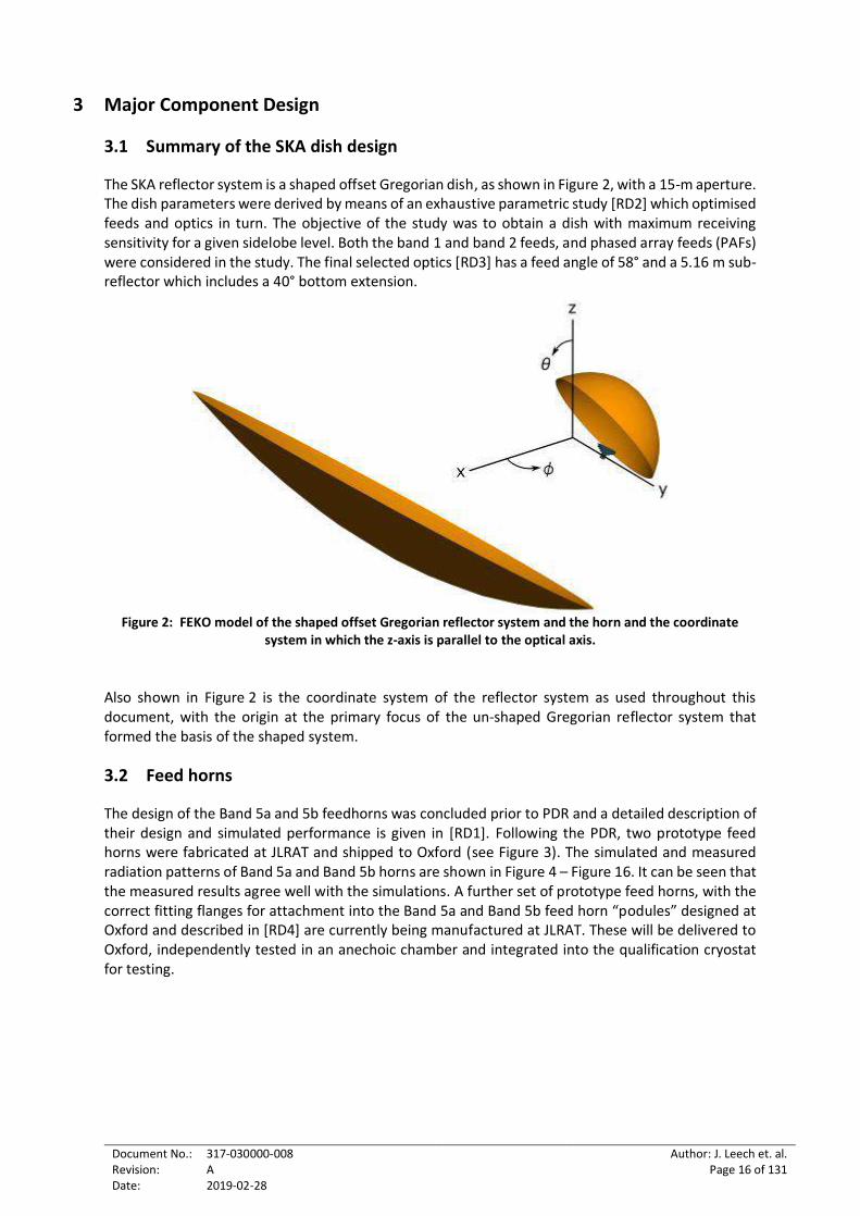
The SKA reflector system is a shaped offset Gregorian dish, as shown in Figure 2, with a 15-m aperture. The dish parameters were derived by means of an exhaustive parametric study [RD2] which optimised feeds and optics in turn. The objective of the study was to obtain a dish with maximum receiving sensitivity for a given sidelobe level. Both the band 1 and band 2 feeds, and phased array feeds (PAFs) were considered in the study. The final selected optics [RD3] has a feed angle of 58° and a 5.16 m sub-reflector which includes a 40° bottom extension.
Figure 2: FEKO model of the shaped offset Gregorian reflector system and the horn and the coordinate system in which the z-axis is parallel to the optical axis.
Also shown in Figure 2 is the coordinate system of the reflector system as used throughout this document, with the origin at the primary focus of the un-shaped Gregorian reflector system that formed the basis of the shaped system.
3.2 Feed horns
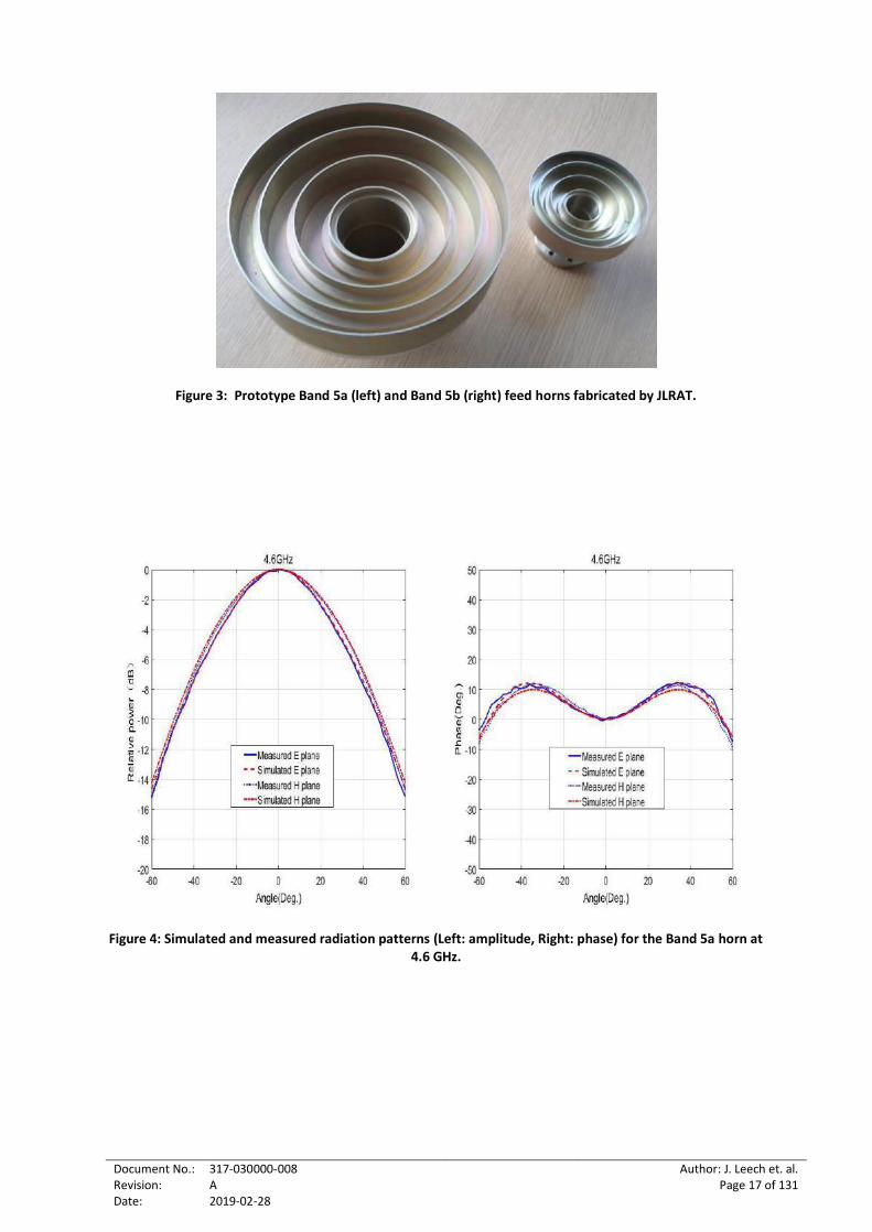
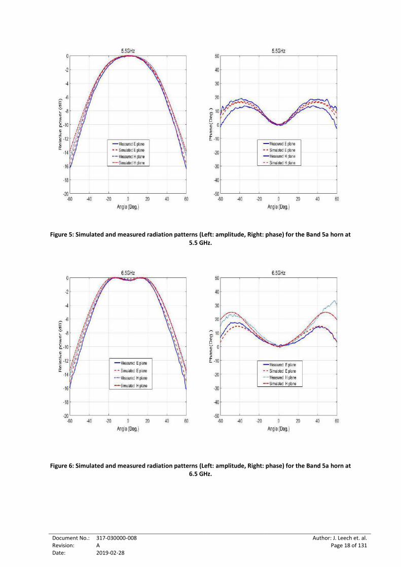
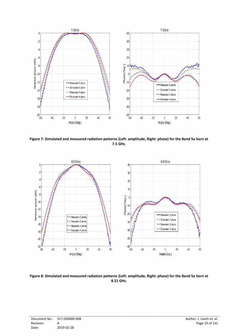
The design of the Band 5a and 5b feedhorns was concluded prior to PDR and a detailed description of their design and simulated performance is given in [RD1]. Following the PDR, two prototype feed horns were fabricated at JLRAT and shipped to Oxford (see Figure 3). The simulated and measured radiation patterns of Band 5a and Band 5b horns are shown in Figure 4 – Figure 16. It can be seen that the measured results agree well with the simulations. A further set of prototype feed horns, with the correct fitting flanges for attachment into the Band 5a and Band 5b feed horn “podules” designed at Oxford and described in [RD4] are currently being manufactured at JLRAT. These will be delivered to Oxford, independently tested in an anechoic chamber and integrated into the qualification cryostat for testing.
Document No.: Revision: Date:
317-030000-008 A 2019-02-28
Author: J. Leech et. al. Page 17 of 131
Figure 3: Prototype Band 5a (left) and Band 5b (right) feed horns fabricated by JLRAT.
Figure 4: Simulated and measured radiation patterns (Left: amplitude, Right: phase) for the Band 5a horn at 4.6 GHz.
Document No.: Revision: Date:
317-030000-008 A 2019-02-28
Author: J. Leech et. al. Page 18 of 131
Figure 5: Simulated and measured radiation patterns (Left: amplitude, Right: phase) for the Band 5a horn at
5.5 GHz.
Figure 6: Simulated and measured radiation patterns (Left: amplitude, Right: phase) for the Band 5a horn at
6.5 GHz.
Document No.: Revision: Date:
317-030000-008 A 2019-02-28
Author: J. Leech et. al. Page 19 of 131
Figure 7: Simulated and measured radiation patterns (Left: amplitude, Right: phase) for the Band 5a horn at
7.5 GHz.
Figure 8: Simulated and measured radiation patterns (Left: amplitude, Right: phase) for the Band 5a horn at 8.51 GHz.
Document No.: Revision: Date:
317-030000-008 A 2019-02-28
Author: J. Leech et. al. Page 20 of 131
Figure 9: Simulated and measured radiation patterns (Left: amplitude, Right, phase) for the Band 5b horn at 8.3 GHz.
Figure 10: Simulated and measured radiation patterns (Left: amplitude, Right: phase) for the Band 5b horn
at 9.3 GHz.
Document No.: Revision: Date:
317-030000-008 A 2019-02-28
Author: J. Leech et. al. Page 21 of 131
Figure 11: Simulated and measured radiation patterns (Left: amplitude, Right: phase) for the Band 5b horn at 10.3 GHz.
Figure 12: Simulated and measured radiation patterns (Left: amplitude, Right: phase) for the Band 5b horn at 11.3 GHz.
Document No.: Revision: Date:
317-030000-008 A 2019-02-28
Author: J. Leech et. al. Page 22 of 131
Figure 13: Simulated and measured radiation patterns (Left: amplitude, Right: phase) for the Band 5b horn
at 12.3 GHz.
Figure 14: Simulated and measured radiation patterns (Left: amplitude, Right: phase) for the Band 5b horn at 13.3 GHz.
Document No.: Revision: Date:
317-030000-008 A 2019-02-28
Author: J. Leech et. al. Page 23 of 131
Figure 15: Simulated and measured radiation patterns (Left: amplitude, Right: phase) for the Band 5b horn at 14.3 GHz.
Figure 16: Simulated and measured radiation patterns (Left: amplitude, Right: phase) for the Band 5b horn at 15.3 GHz.
Document No.: Revision: Date:
317-030000-008 A 2019-02-28
Author: J. Leech et. al. Page 24 of 131
3.3 Orthomode transducers (OMTs)
3.3.1 Band 5a OMT simulated and measured results
The Band 5a OMT is based on a circular quad-ridged waveguide. Figure 17 shows the fabricated Band 5a OMT prototype. Figure 18, Figure 19 and Figure 20 show the measured reflection coefficients, insertion losses and polarization isolations of the OMT compared with CST Microwave Studio EM simulations. The measured reflection coefficients are less than -19 dB and less than -22 dB for the simulated ones. The measured insertion losses are between -0.2 dB and -0.4 dB for both polarization channels and the measured isolation between two ports is better than 40 dB.
Figure 17: Band 5a OMT prototype.
Figure 18: Simulated and measured reflection losses of Band 5a OMT.
Document No.: Revision: Date:
317-030000-008 A 2019-02-28
Author: J. Leech et. al. Page 25 of 131
Figure 19: Simulated and measured insertion losses of Band5a OMT.
Figure 20: Simulated and measured isolation of Band5a OMT.
3.3.2 Band 5b OMT simulated and measured results
The Band 5b OMT consists of a turnstile OMT and a double-ridged coaxial to waveguide transformer. Figure 21 shows the fabricated Band 5b OMT. Figure 22, Figure 23 and Figure 24 show the measured reflection coefficients, insertion losses and isolation of the OMT compared with simulated ones. The measured reflection coefficients are less than -15 dB. The insertion losses are better than -0.2 dB for both polarization channels. The isolation between two ports is better than 47 dB.
Document No.: Revision: Date:
317-030000-008 A 2019-02-28
Author: J. Leech et. al. Page 26 of 131
Figure 21: Band 5b OMT and horn assembly prototype.
Figure 22: Simulated and measured reflection losses of Band 5b OMT.
Document No.: Revision: Date:
317-030000-008 A 2019-02-28
Author: J. Leech et. al. Page 27 of 131
Figure 23: Simulated and measured insertion losses of Band 5b OMT.
Figure 24: Simulated and measured isolation of Band 5b OMT.
A final set of prototype OMTs, with the correct fitting flanges for attachment into the Band 5a and Band 5b feed horn “podules” designed at Oxford and described in [RD4] are currently being manufactured at JLRAT. These will be delivered to Oxford and their performance will be verified at
Document No.: Revision: Date:
317-030000-008 A 2019-02-28
Author: J. Leech et. al. Page 28 of 131
both ambient and at cryogenic temperatures. Following these tests, they will be integrated into the qualification model receiver cryostat.
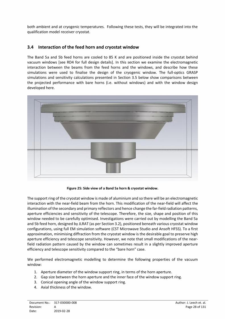
3.4 Interaction of the feed horn and cryostat window
The Band 5a and 5b feed horns are cooled to 85 K and are positioned inside the cryostat behind vacuum windows [see RD4 for full design details]. In this section we examine the electromagnetic interaction between the beams from the feed horns and the windows, and describe how these simulations were used to finalise the design of the cryogenic window. The full-optics GRASP simulations and sensitivity calculations presented in Section 3.5 below show comparisons between the projected performance with bare horns (i.e. without windows) and with the window design developed here.
Figure 25: Side view of a Band 5a horn & cryostat window.
The support ring of the cryostat window is made of aluminium and so there will be an electromagnetic interaction with the near-field beam from the horn. This modification of the near-field will affect the illumination of the secondary and primary reflectors and hence change the far-field radiation patterns, aperture efficiencies and sensitivity of the telescope. Therefore, the size, shape and position of this window needed to be carefully optimised. Investigations were carried out by modelling the Band 5a and 5b feed horn, designed by JLRAT (as per Section 3.2), positioned beneath various cryostat window configurations, using full EM simulation software (CST Microwave Studio and Ansoft HFSS). To a first approximation, minimising diffraction from the cryostat window is the desirable goal to preserve high aperture efficiency and telescope sensitivity. However, we note that small modifications of the near-field radiation pattern caused by the window can sometimes result in a slightly improved aperture efficiency and telescope sensitivity compared to the “bare horn” case. We performed electromagnetic modelling to determine the following properties of the vacuum window:
1. Aperture diameter of the window support ring, in terms of the horn aperture. 2. Gap size between the horn aperture and the inner face of the window support ring. 3. Conical opening angle of the window support ring. 4. Axial thickness of the window.
Document No.: Revision: Date:
317-030000-008 A 2019-02-28
Author: J. Leech et. al. Page 29 of 131
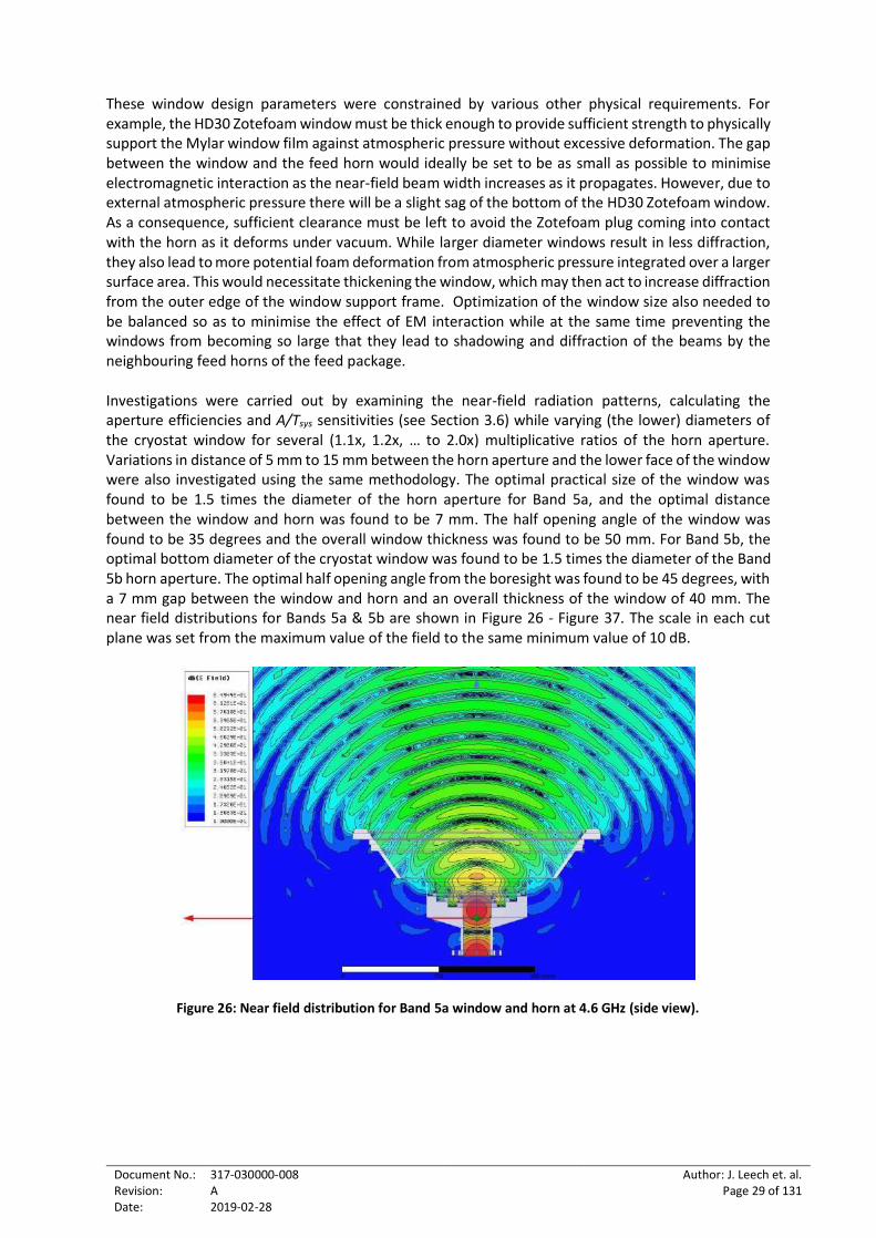
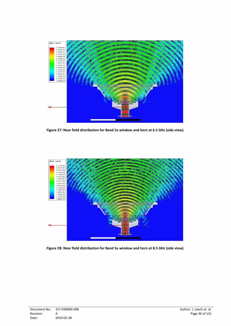
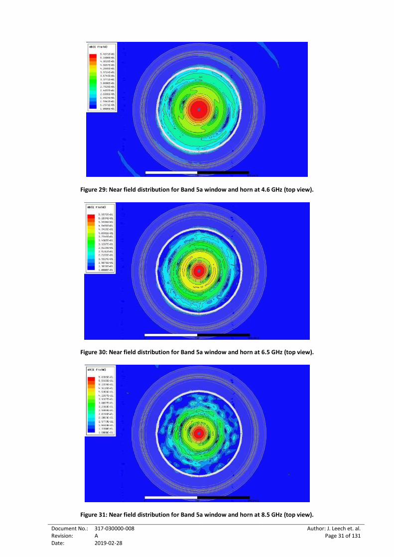
These window design parameters were constrained by various other physical requirements. For example, the HD30 Zotefoam window must be thick enough to provide sufficient strength to physically support the Mylar window film against atmospheric pressure without excessive deformation. The gap between the window and the feed horn would ideally be set to be as small as possible to minimise electromagnetic interaction as the near-field beam width increases as it propagates. However, due to external atmospheric pressure there will be a slight sag of the bottom of the HD30 Zotefoam window. As a consequence, sufficient clearance must be left to avoid the Zotefoam plug coming into contact with the horn as it deforms under vacuum. While larger diameter windows result in less diffraction, they also lead to more potential foam deformation from atmospheric pressure integrated over a larger surface area. This would necessitate thickening the window, which may then act to increase diffraction from the outer edge of the window support frame. Optimization of the window size also needed to be balanced so as to minimise the effect of EM interaction while at the same time preventing the windows from becoming so large that they lead to shadowing and diffraction of the beams by the neighbouring feed horns of the feed package. Investigations were carried out by examining the near-field radiation patterns, calculating the aperture efficiencies and A/Tsys sensitivities (see Section 3.6) while varying (the lower) diameters of the cryostat window for several (1.1x, 1.2x, … to 2.0x) multiplicative ratios of the horn aperture. Variations in distance of 5 mm to 15 mm between the horn aperture and the lower face of the window were also investigated using the same methodology. The optimal practical size of the window was found to be 1.5 times the diameter of the horn aperture for Band 5a, and the optimal distance between the window and horn was found to be 7 mm. The half opening angle of the window was found to be 35 degrees and the overall window thickness was found to be 50 mm. For Band 5b, the optimal bottom diameter of the cryostat window was found to be 1.5 times the diameter of the Band 5b horn aperture. The optimal half opening angle from the boresight was found to be 45 degrees, with a 7 mm gap between the window and horn and an overall thickness of the window of 40 mm. The near field distributions for Bands 5a & 5b are shown in Figure 26 - Figure 37. The scale in each cut plane was set from the maximum value of the field to the same minimum value of 10 dB.
Figure 26: Near field distribution for Band 5a window and horn at 4.6 GHz (side view).
Document No.: Revision: Date:
317-030000-008 A 2019-02-28
Author: J. Leech et. al. Page 30 of 131
Figure 27: Near field distribution for Band 5a window and horn at 6.5 GHz (side view).
Figure 28: Near field distribution for Band 5a window and horn at 8.5 GHz (side view).
Document No.: Revision: Date:
317-030000-008 A 2019-02-28
Author: J. Leech et. al. Page 31 of 131
Figure 29: Near field distribution for Band 5a window and horn at 4.6 GHz (top view).
Figure 30: Near field distribution for Band 5a window and horn at 6.5 GHz (top view).
Figure 31: Near field distribution for Band 5a window and horn at 8.5 GHz (top view).
Document No.: Revision: Date:
317-030000-008 A 2019-02-28
Author: J. Leech et. al. Page 32 of 131
Figure 32: Near field distribution for Band 5b window and horn at 8.3 GHz (side view).
Figure 33: Near field distribution for Band 5b window and horn at 11.9 GHz (side view).
Figure 34: Near field distribution for Band 5b window and horn at 15.4 GHz (side view).
Document No.: Revision: Date:
317-030000-008 A 2019-02-28
Author: J. Leech et. al. Page 33 of 131
Figure 35: Near field distribution for Band 5b window and horn at 8.3 GHz (top view).
Figure 36: Near field distribution for Band 5b window and horn at 11.9 GHz (top view).
Figure 37: Near field distribution for Band 5b window and horn at 15.4 GHz (top view).
Document No.: Revision: Date:
317-030000-008 A 2019-02-28
Author: J. Leech et. al. Page 34 of 131
3.5 Simulated optical performance of the full optics
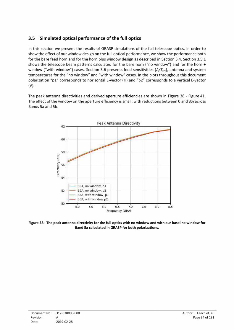
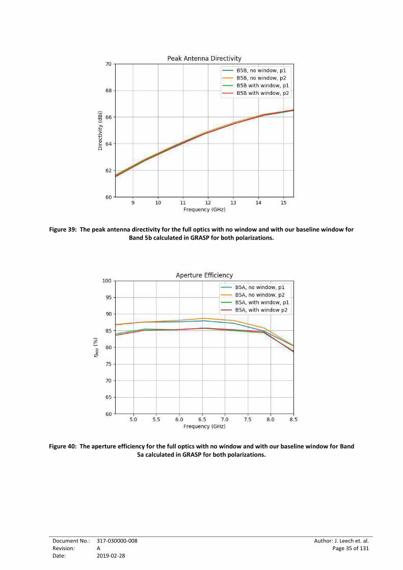
In this section we present the results of GRASP simulations of the full telescope optics. In order to show the effect of our window design on the full optical performance, we show the performance both for the bare feed horn and for the horn plus window design as described in Section 3.4. Section 3.5.1 shows the telescope beam patterns calculated for the bare horn (“no window”) and for the horn + window (“with window”) cases. Section 3.6 presents feed sensitivities (A/Tsys), antenna and system temperatures for the “no window” and “with window” cases. In the plots throughout this document polarization “p1” corresponds to horizontal E-vector (H) and “p2” corresponds to a vertical E-vector (V). The peak antenna directivities and derived aperture efficiencies are shown in Figure 38 - Figure 41. The effect of the window on the aperture efficiency is small, with reductions between 0 and 3% across Bands 5a and 5b.
Figure 38: The peak antenna directivity for the full optics with no window and with our baseline window for Band 5a calculated in GRASP for both polarizations.
Document No.: Revision: Date:
317-030000-008 A 2019-02-28
Author: J. Leech et. al. Page 35 of 131
Figure 39: The peak antenna directivity for the full optics with no window and with our baseline window for Band 5b calculated in GRASP for both polarizations.
Figure 40: The aperture efficiency for the full optics with no window and with our baseline window for Band 5a calculated in GRASP for both polarizations.
Document No.: Revision: Date:
317-030000-008 A 2019-02-28
Author: J. Leech et. al. Page 36 of 131
Figure 41: The aperture efficiency for the full optics with no window and with our baseline window for Band 5b calculated in GRASP for both polarizations.
The first and second sidelobe levels as a function of frequency for the full optics and with our baseline window designs are shown in Figure 42. Although there is no specific requirement for first and second sidelobe levels, this plot shows that the sidelobe levels are both low and do not vary by more than a few dB across the bands of interest.
Figure 42: The first and second sidelobe levels as a function of frequency for the full optics with our baseline window design. (Bands 5a and 5b).
Document No.: Revision: Date:
317-030000-008 A 2019-02-28
Author: J. Leech et. al. Page 37 of 131
The cross-polarization of the complete optical system is intrinsically low. Figure 43 shows the peak cross-polar levels (using Ludwig’s 3rd Definition) within the -1 dB and -3 dB main beam contour as a function of frequency for the full optics with our baseline window designs. Figure 44 shows the Intrinsic Cross-polar Ratio (IXR) for the same optics, again within the -1 dB and -3 dB main beam contours. This shows we are comfortably exceeding the IXR requirement of 15 dB within the -3dB contour of the main beam (R.SPF345.P.14).
Figure 43: The maximum cross-polarization levels for both Bands 5a and 5b, within the -1 dB and -3 dB (red) contours of the reflector system main beam, for the full optics with our baseline window.
Figure 44: The minimum IXR, for both Bands 5a and 5b, within the -1 dB and -3 dB contours of the main
beam, for the full optics with our baseline window design.
Figure 45 shows the integrated solid angle for sidelobes exceeding 0 dBi and further than 10° from boresight for the full optics using our baseline window design. This shows that we comfortably meet the requirement that this solid angle is not greater than 0.05 sr.
Document No.: Revision: Date:
317-030000-008 A 2019-02-28
Author: J. Leech et. al. Page 38 of 131
Figure 45: The solid angle for sidelobes exceeding 0 dBi and further than 10° from boresight for the full
optics with our baseline window design. (Bands 5a and 5b).
3.5.1 Beam Patterns for the full optics
Figure 46 – Figure 73 show the beam patterns for 0 < θ< 1° for the full optics for both polarizations, both with and without the window, across the frequency ranges of Bands 5a and 5b. We see that the window has negligible effect on the shape and circularity of the main beam and only a small effect on the levels and shapes of the first and second sidelobes. Cross-polar levels remain low throughout.
Document No.: Revision: Date:
317-030000-008 A 2019-02-28
Author: J. Leech et. al. Page 39 of 131
Figure 46: Co- and cross-polar beam patterns for 45° φ cuts, between 0 < θ< 1° at 4.6 GHz polarization p1. Top: No window; Bottom: With baseline window design.
Document No.: Revision: Date:
317-030000-008 A 2019-02-28
Author: J. Leech et. al. Page 40 of 131
Figure 47: Co- and cross-polar beam patterns for 45° φ cuts, between 0 < θ< 1° at 4.6 GHz polarization p2. Top: No window; Bottom: With baseline window design.
Document No.: Revision: Date:
317-030000-008 A 2019-02-28
Author: J. Leech et. al. Page 41 of 131
Figure 48: Co- and cross-polar beam patterns for 45° φ cuts, between 0 < θ< 1° at 5.25 GHz polarization p1. Top: No window; Bottom: With baseline window design.
Document No.: Revision: Date:
317-030000-008 A 2019-02-28
Author: J. Leech et. al. Page 42 of 131
Figure 49: Co- and cross-polar beam patterns for 45° φ cuts, between 0 < θ< 1° at 5.25 GHz polarization p2. Top: No window; Bottom: With baseline window design.
Document No.: Revision: Date:
317-030000-008 A 2019-02-28
Author: J. Leech et. al. Page 43 of 131
Figure 50: Co- and cross-polar beam patterns for 45° φ cuts, between 0 < θ< 1° at 5.90 GHz polarization p1. Top: No window; Bottom: With baseline window design.
Document No.: Revision: Date:
317-030000-008 A 2019-02-28
Author: J. Leech et. al. Page 44 of 131
Figure 51: Co- and cross-polar beam patterns for 45° φ cuts, between 0 < θ< 1° at 5.90 GHz polarization p2. Top: No window; Bottom: With baseline window design.
Document No.: Revision: Date:
317-030000-008 A 2019-02-28
Author: J. Leech et. al. Page 45 of 131
Figure 52: Co- and cross-polar beam patterns for 45° φ cuts, between 0 < θ< 1° at 6.55 GHz polarization p1.
Top: No window; Bottom: With baseline window design.
Document No.: Revision: Date:
317-030000-008 A 2019-02-28
Author: J. Leech et. al. Page 46 of 131
Figure 53: Co- and cross-polar beam patterns for 45° φ cuts, between 0 < θ< 1° at 6.55 GHz polarization p2. Top: No window; Bottom: With baseline window design.
Document No.: Revision: Date:
317-030000-008 A 2019-02-28
Author: J. Leech et. al. Page 47 of 131
Figure 54: Co- and cross-polar beam patterns for 45° φ cuts, between 0 < θ< 1° at 7.20 GHz polarization p1.
Top: No window; Bottom: With baseline window design.
Document No.: Revision: Date:
317-030000-008 A 2019-02-28
Author: J. Leech et. al. Page 48 of 131
Figure 55: Co- and cross-polar beam patterns for 45° φ cuts, between 0 < θ< 1° at 7.20 GHz polarization p2.
Top: No window; Bottom: With baseline window design.
Document No.: Revision: Date:
317-030000-008 A 2019-02-28
Author: J. Leech et. al. Page 49 of 131
Figure 56: Co- and cross-polar beam patterns for 45° φ cuts, between 0 < θ< 1° at 7.85 GHz polarization p1.
Top: No window; Bottom: With baseline window design.
Document No.: Revision: Date:
317-030000-008 A 2019-02-28
Author: J. Leech et. al. Page 50 of 131
Figure 57: Co- and cross-polar beam patterns for 45° φ cuts, between 0 < θ< 1° at 7.85 GHz polarization p2.
Top: No window; Bottom: With baseline window design.
Document No.: Revision: Date:
317-030000-008 A 2019-02-28
Author: J. Leech et. al. Page 51 of 131
Figure 58: Co- and cross-polar beam patterns for 45° φ cuts, between 0 < θ< 1° at 8.50 GHz polarization p1.
Top: No window; Bottom: With baseline window design.
Document No.: Revision: Date:
317-030000-008 A 2019-02-28
Author: J. Leech et. al. Page 52 of 131
Figure 59: Co- and cross-polar beam patterns for 45° φ cuts, between 0 < θ< 1° at 8.50 GHz polarization p2.
Top: No window; Bottom: With baseline window design.
Document No.: Revision: Date:
317-030000-008 A 2019-02-28
Author: J. Leech et. al. Page 53 of 131
Figure 60: Co- and cross-polar beam patterns for 45° φ cuts, between 0 < θ< 1° at 8.30 GHz polarization p1.
Top: No window; Bottom: With baseline window design.
Document No.: Revision: Date:
317-030000-008 A 2019-02-28
Author: J. Leech et. al. Page 54 of 131
Figure 61: Co- and cross-polar beam patterns for 45° φ cuts, between 0 < θ< 1° at 8.30 GHz polarization p2.
Top: No window; Bottom: With baseline window design.
Document No.: Revision: Date:
317-030000-008 A 2019-02-28
Author: J. Leech et. al. Page 55 of 131
Figure 62: Co- and cross-polar beam patterns for 45° φ cuts, between 0 < θ< 1° at 9.48 GHz polarization p1. Top: No window; Bottom: With baseline window design.
Document No.: Revision: Date:
317-030000-008 A 2019-02-28
Author: J. Leech et. al. Page 56 of 131
Figure 63: Co- and cross-polar beam patterns for 45° φ cuts, between 0 < θ< 1° at 9.48 GHz polarization p2.
Top: No window; Bottom: With baseline window design.
Document No.: Revision: Date:
317-030000-008 A 2019-02-28
Author: J. Leech et. al. Page 57 of 131
Figure 64: Co- and cross-polar beam patterns for 45° φ cuts, between 0 < θ< 1° at 10.67 GHz polarization p1. Top: No window; Bottom: With baseline window design.
Document No.: Revision: Date:
317-030000-008 A 2019-02-28
Author: J. Leech et. al. Page 58 of 131
Figure 65: Co- and cross-polar beam patterns for 45° φ cuts, between 0 < θ< 1° at 10.67 GHz polarization p2. Top: No window; Bottom: With baseline window design.
Document No.: Revision: Date:
317-030000-008 A 2019-02-28
Author: J. Leech et. al. Page 59 of 131
Figure 66: Co- and cross-polar beam patterns for 45° φ cuts, between 0 < θ< 1° at 11.85 GHz polarization p1. Top: No window; Bottom: With baseline window design.
Document No.: Revision: Date:
317-030000-008 A 2019-02-28
Author: J. Leech et. al. Page 60 of 131
Figure 67: Co- and cross-polar beam patterns for 45° φ cuts, between 0 < θ< 1° at 11.85 GHz polarization p2. Top: No window; Bottom: With baseline window design.
Document No.: Revision: Date:
317-030000-008 A 2019-02-28
Author: J. Leech et. al. Page 61 of 131
Figure 68: Co- and cross-polar beam patterns for 45° φ cuts, between 0 < θ< 1° at 13.03 GHz polarization p1. Top: No window; Bottom: With baseline window design.
Document No.: Revision: Date:
317-030000-008 A 2019-02-28
Author: J. Leech et. al. Page 62 of 131
Figure 69: Co- and cross-polar beam patterns for 45° φ cuts, between 0 < θ< 1° at 13.03 GHz polarization p2. Top: No window; Bottom: With baseline window design.
Document No.: Revision: Date:
317-030000-008 A 2019-02-28
Author: J. Leech et. al. Page 63 of 131
Figure 70: Co- and cross-polar beam patterns for 45° φ cuts, between 0 < θ< 1° at 14.22 GHz polarization p1. Top: No window; Bottom: With baseline window design.
Document No.: Revision: Date:
317-030000-008 A 2019-02-28
Author: J. Leech et. al. Page 64 of 131
Figure 71: Co- and cross-polar beam patterns for 45° φ cuts, between 0 < θ< 1° at 14.22 GHz polarization p2. Top: No window; Bottom: With baseline window design.
Document No.: Revision: Date:
317-030000-008 A 2019-02-28
Author: J. Leech et. al. Page 65 of 131
Figure 72: Co- and cross-polar beam patterns for 45° φ cuts, between 0 < θ< 1° at 15.40 GHz polarization p1. Top: No window; Bottom: With baseline window design.
Document No.: Revision: Date:
317-030000-008 A 2019-02-28
Author: J. Leech et. al. Page 66 of 131
Figure 73: Co- and cross-polar beam patterns for 45° φ cuts, between 0 < θ< 1° at 15.40 GHz polarization p2. Top: No window; Bottom: With baseline window design.
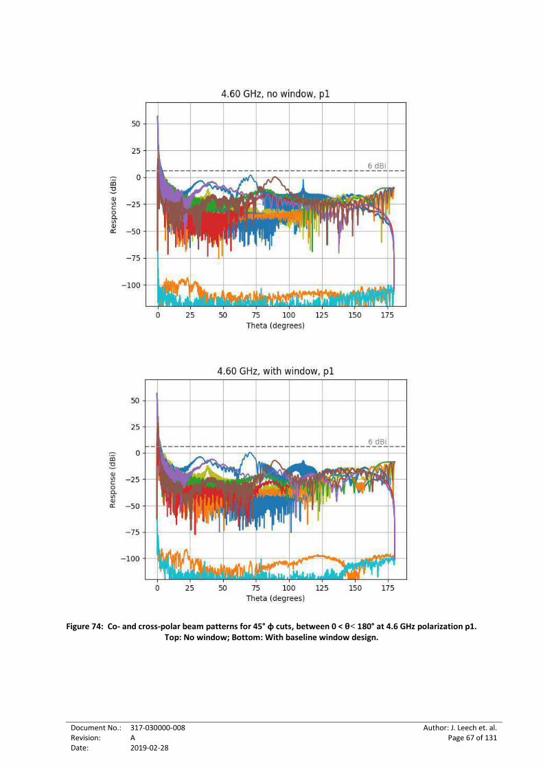
Figure 74 – Figure 101 show the beam patterns for 0 < θ< 180° for the full optics for both polarizations both with and without the window across the frequency ranges of Bands 5a and 5b. We see that the window has only small effects on the shape of the far-out sidelobes and does not significantly raise their overall levels consistently. We therefore expect (and show in Section 3.6 ) that the component of the antenna temperature due to spillover coupling to the ground should not be significantly affected by the window. Overlaid on these plots is the 6 dBi response level, and it can be seen that all far-out sidelobes remain below this level in all cases, meeting requirement R.SPF345.P.11.
Document No.: Revision: Date:
317-030000-008 A 2019-02-28
Author: J. Leech et. al. Page 67 of 131
Figure 74: Co- and cross-polar beam patterns for 45° φ cuts, between 0 < θ< 180° at 4.6 GHz polarization p1. Top: No window; Bottom: With baseline window design.
Document No.: Revision: Date:
317-030000-008 A 2019-02-28
Author: J. Leech et. al. Page 68 of 131
Figure 75: Co- and cross-polar beam patterns for 45° φ cuts, between 0 < θ< 180° at 4.6 GHz polarization p2.
Top: No window; Bottom: With baseline window design.
Document No.: Revision: Date:
317-030000-008 A 2019-02-28
Author: J. Leech et. al. Page 69 of 131
Figure 76: Co- and cross-polar beam patterns for 45° φ cuts, between 0 < θ< 180° at 5.25 GHz polarization p1. Top: No window; Bottom: With baseline window design.
Document No.: Revision: Date:
317-030000-008 A 2019-02-28
Author: J. Leech et. al. Page 70 of 131
Figure 77: Co- and cross-polar beam patterns for 45° φ cuts, between 0 < θ< 180° at 5.25 GHz polarization p2. Top: No window; Bottom: With baseline window design.
Document No.: Revision: Date:
317-030000-008 A 2019-02-28
Author: J. Leech et. al. Page 71 of 131
Figure 78: Co- and cross-polar beam patterns for 45° φ cuts, between 0 < θ< 180° at 5.90 GHz polarization p1. Top: No window; Bottom: With baseline window design.
Document No.: Revision: Date:
317-030000-008 A 2019-02-28
Author: J. Leech et. al. Page 72 of 131
Figure 79: Co- and cross-polar beam patterns for 45° φ cuts, between 0 < θ< 180° at 5.90 GHz polarization p2. Top: No window; Bottom: With baseline window design.
Document No.: Revision: Date:
317-030000-008 A 2019-02-28
Author: J. Leech et. al. Page 73 of 131
Figure 80: Co- and cross-polar beam patterns for 45° φ cuts, between 0 < θ< 180° at 6.55 GHz polarization p1. Top: No window; Bottom: With baseline window design.
Document No.: Revision: Date:
317-030000-008 A 2019-02-28
Author: J. Leech et. al. Page 74 of 131
Figure 81: Co- and cross-polar beam patterns for 45° φ cuts, between 0 < θ< 180° at 6.55 GHz polarization p2. Top: No window; Bottom: With baseline window design.
Document No.: Revision: Date:
317-030000-008 A 2019-02-28
Author: J. Leech et. al. Page 75 of 131
Figure 82: Co- and cross-polar beam patterns for 45° φ cuts, between 0 < θ< 180° at 7.20 GHz polarization p1. Top: No window; Bottom: With baseline window design.
Document No.: Revision: Date:
317-030000-008 A 2019-02-28
Author: J. Leech et. al. Page 76 of 131
Figure 83: Co- and cross-polar beam patterns for 45° φ cuts, between 0 < θ< 180° at 7.20 GHz polarization p2. Top: No window; Bottom: With baseline window design.
Document No.: Revision: Date:
317-030000-008 A 2019-02-28
Author: J. Leech et. al. Page 77 of 131
Figure 84: Co- and cross-polar beam patterns for 45° φ cuts, between 0 < θ< 180° at 7.85 GHz polarization p1. Top: No window; Bottom: With baseline window design.
Document No.: Revision: Date:
317-030000-008 A 2019-02-28
Author: J. Leech et. al. Page 78 of 131
Figure 85: Co- and cross-polar beam patterns for 45° φ cuts, between 0 < θ< 180° at 7.85 GHz polarization p2. Top: No window; Bottom: With baseline window design.
Document No.: Revision: Date:
317-030000-008 A 2019-02-28
Author: J. Leech et. al. Page 79 of 131
Figure 86: Co- and cross-polar beam patterns for 45° φ cuts, between 0 < θ< 180° at 8.50 GHz polarization
p1. Top: No window; Bottom: With baseline window design.
Document No.: Revision: Date:
317-030000-008 A 2019-02-28
Author: J. Leech et. al. Page 80 of 131
Figure 87: Co- and cross-polar beam patterns for 45° φ cuts, between 0 < θ< 180° at 8.50 GHz polarization p2. Top: No window; Bottom: With baseline window design.
Document No.: Revision: Date:
317-030000-008 A 2019-02-28
Author: J. Leech et. al. Page 81 of 131
Figure 88: Co- and cross-polar beam patterns for 45° φ cuts, between 0 < θ< 180° at 8.30 GHz polarization p1. Top: No window; Bottom: With baseline window design.
Document No.: Revision: Date:
317-030000-008 A 2019-02-28
Author: J. Leech et. al. Page 82 of 131
Figure 89: Co- and cross-polar beam patterns for 45° φ cuts, between 0 < θ< 180° at 8.30 GHz polarization p2. Top: No window; Bottom: With baseline window design.
Document No.: Revision: Date:
317-030000-008 A 2019-02-28
Author: J. Leech et. al. Page 83 of 131
Figure 90: Co- and cross-polar beam patterns for 45° φ cuts, between 0 < θ< 180° at 9.48 GHz polarization p1. Top: No window; Bottom: With baseline window design.
Document No.: Revision: Date:
317-030000-008 A 2019-02-28
Author: J. Leech et. al. Page 84 of 131
Figure 91: Co- and cross-polar beam patterns for 45° φ cuts, between 0 < θ< 180° at 9.48 GHz polarization p2. Top: No window; Bottom: With baseline window design.
Document No.: Revision: Date:
317-030000-008 A 2019-02-28
Author: J. Leech et. al. Page 85 of 131
Figure 92: Co- and cross-polar beam patterns for 45° φ cuts, between 0 < θ< 180° at 10.67 GHz polarization p1. Top: No window; Bottom: With baseline window design.
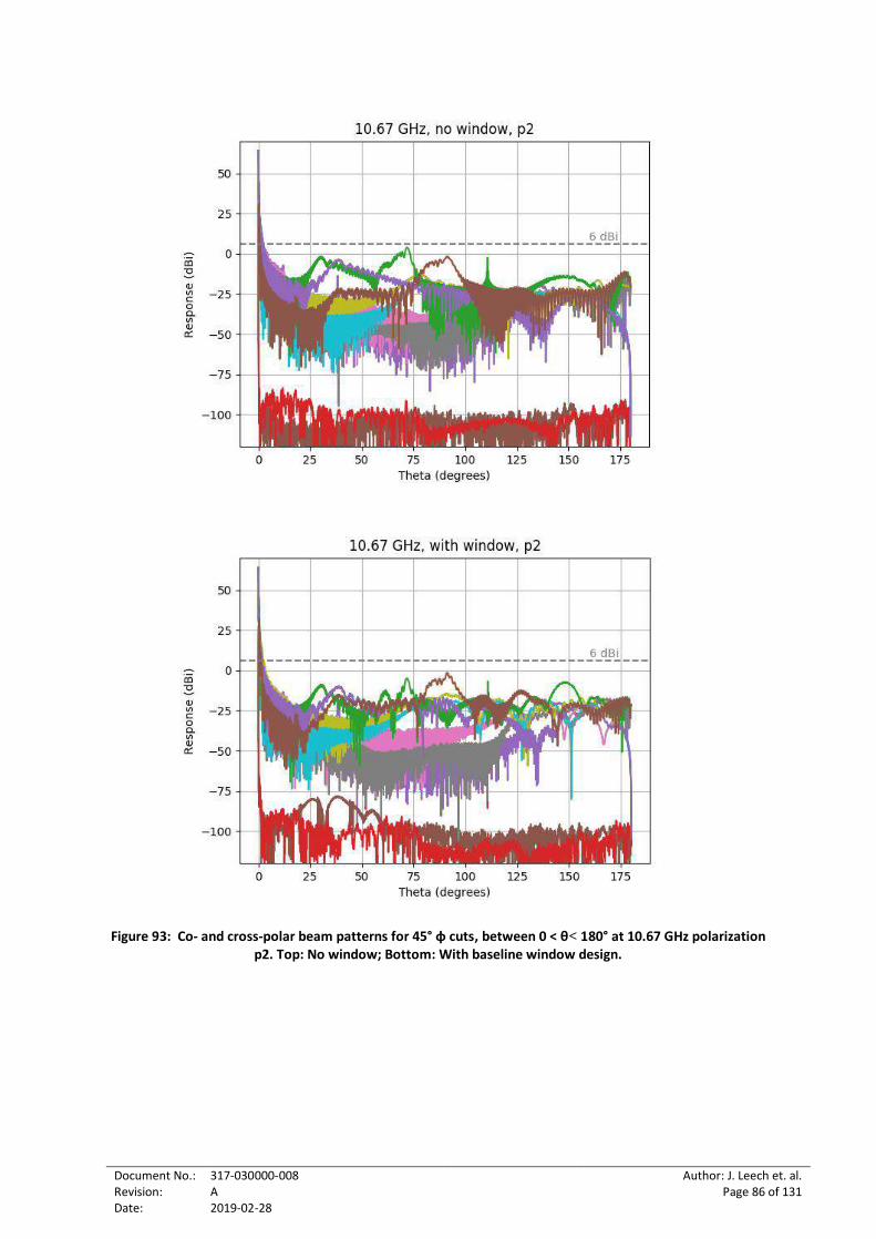
Document No.: Revision: Date:
317-030000-008 A 2019-02-28
Author: J. Leech et. al. Page 86 of 131
Figure 93: Co- and cross-polar beam patterns for 45° φ cuts, between 0 < θ< 180° at 10.67 GHz polarization p2. Top: No window; Bottom: With baseline window design.
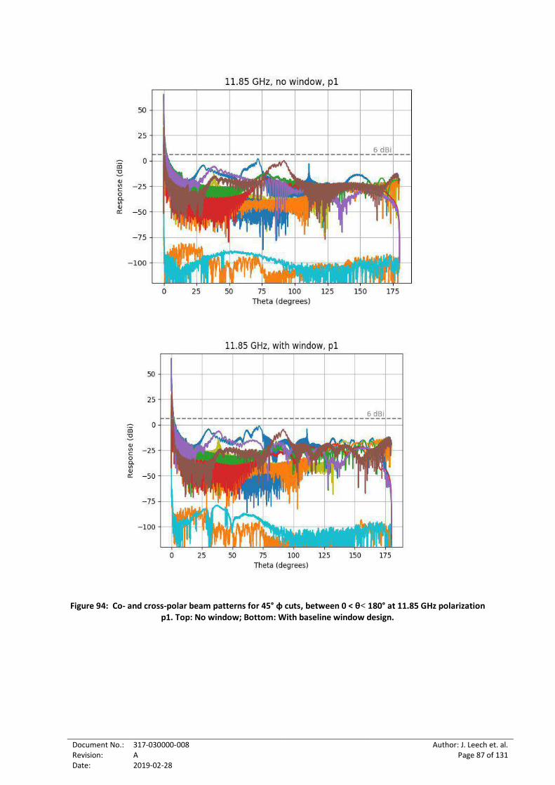
Document No.: Revision: Date:
317-030000-008 A 2019-02-28
Author: J. Leech et. al. Page 87 of 131
Figure 94: Co- and cross-polar beam patterns for 45° φ cuts, between 0 < θ< 180° at 11.85 GHz polarization p1. Top: No window; Bottom: With baseline window design.
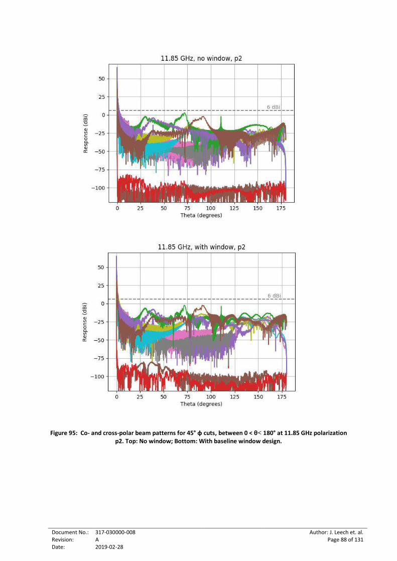
Document No.: Revision: Date:
317-030000-008 A 2019-02-28
Author: J. Leech et. al. Page 88 of 131
Figure 95: Co- and cross-polar beam patterns for 45° φ cuts, between 0 < θ< 180° at 11.85 GHz polarization p2. Top: No window; Bottom: With baseline window design.
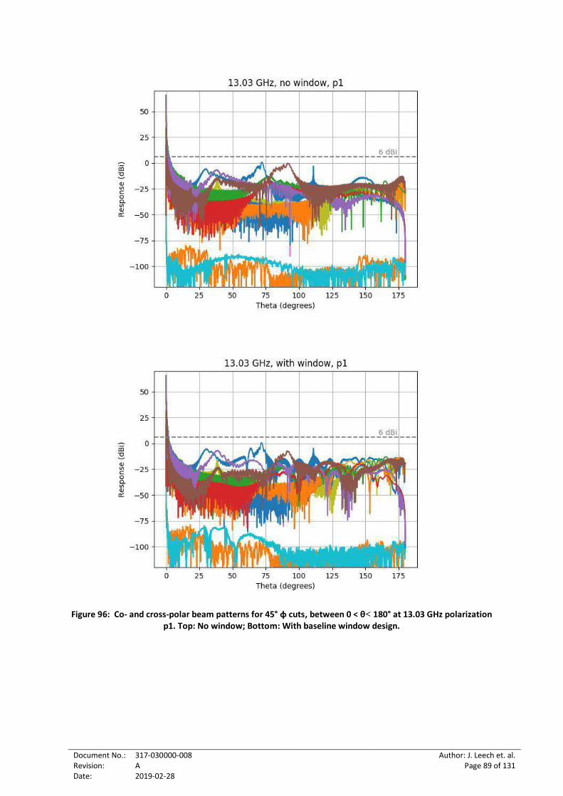
Document No.: Revision: Date:
317-030000-008 A 2019-02-28
Author: J. Leech et. al. Page 89 of 131
Figure 96: Co- and cross-polar beam patterns for 45° φ cuts, between 0 < θ< 180° at 13.03 GHz polarization p1. Top: No window; Bottom: With baseline window design.
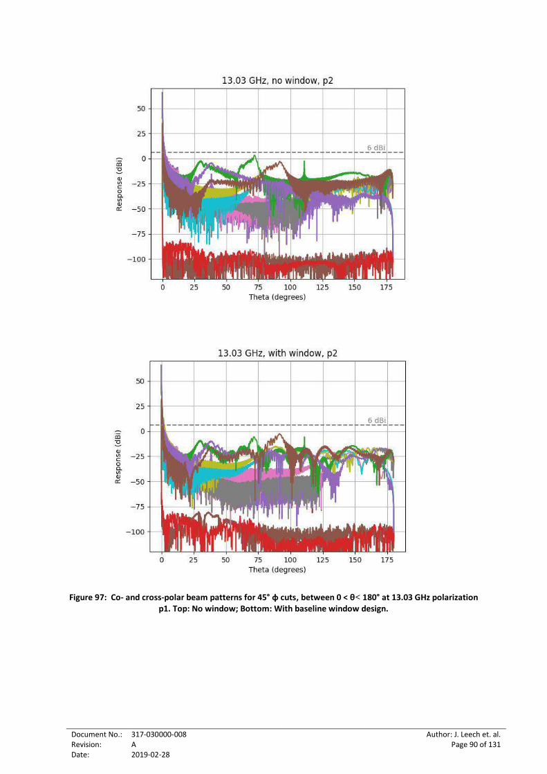
Document No.: Revision: Date:
317-030000-008 A 2019-02-28
Author: J. Leech et. al. Page 90 of 131
Figure 97: Co- and cross-polar beam patterns for 45° φ cuts, between 0 < θ< 180° at 13.03 GHz polarization p1. Top: No window; Bottom: With baseline window design.
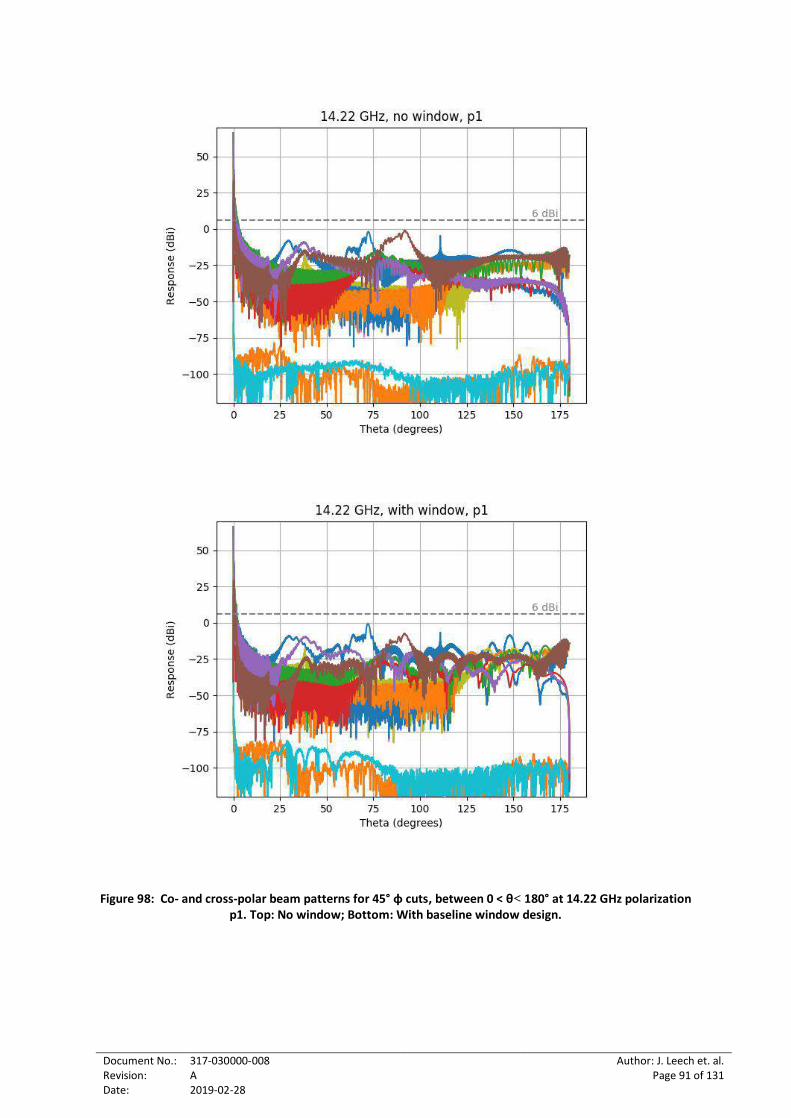
Document No.: Revision: Date:
317-030000-008 A 2019-02-28
Author: J. Leech et. al. Page 91 of 131
Figure 98: Co- and cross-polar beam patterns for 45° φ cuts, between 0 < θ< 180° at 14.22 GHz polarization p1. Top: No window; Bottom: With baseline window design.
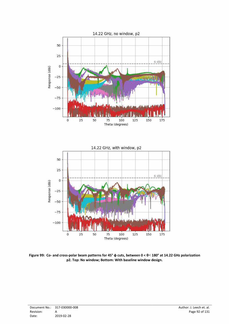
Document No.: Revision: Date:
317-030000-008 A 2019-02-28
Author: J. Leech et. al. Page 92 of 131
Figure 99: Co- and cross-polar beam patterns for 45° φ cuts, between 0 < θ< 180° at 14.22 GHz polarization p2. Top: No window; Bottom: With baseline window design.
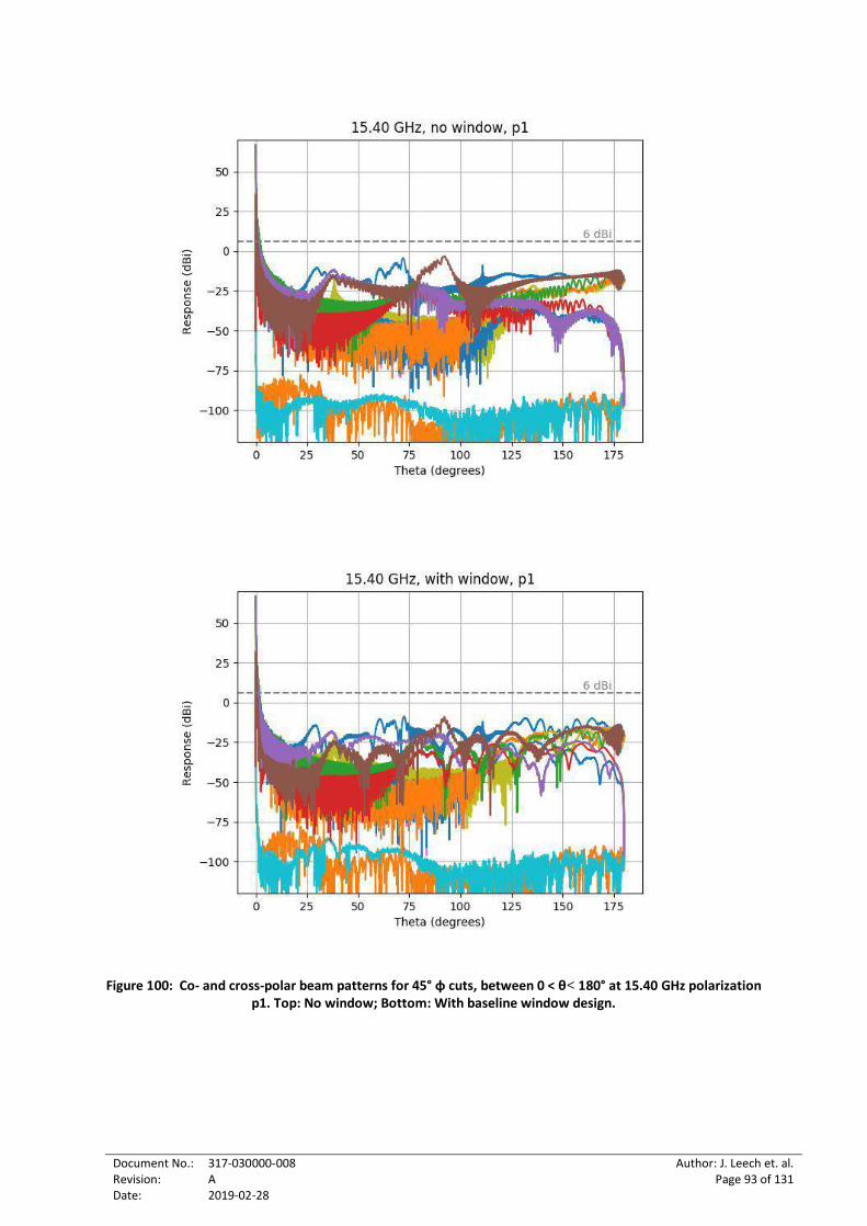
Document No.: Revision: Date:
317-030000-008 A 2019-02-28
Author: J. Leech et. al. Page 93 of 131
Figure 100: Co- and cross-polar beam patterns for 45° φ cuts, between 0 < θ< 180° at 15.40 GHz polarization p1. Top: No window; Bottom: With baseline window design.
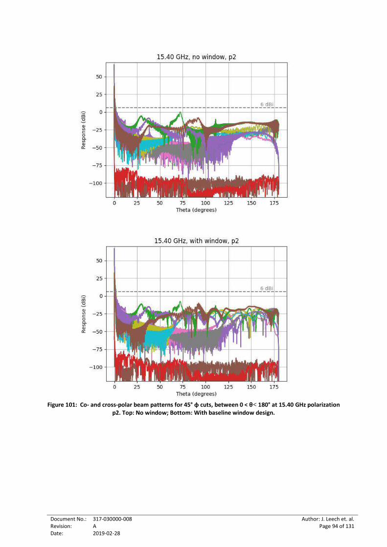
Document No.: Revision: Date:
317-030000-008 A 2019-02-28
Author: J. Leech et. al. Page 94 of 131
Figure 101: Co- and cross-polar beam patterns for 45° φ cuts, between 0 < θ< 180° at 15.40 GHz polarization
p2. Top: No window; Bottom: With baseline window design.
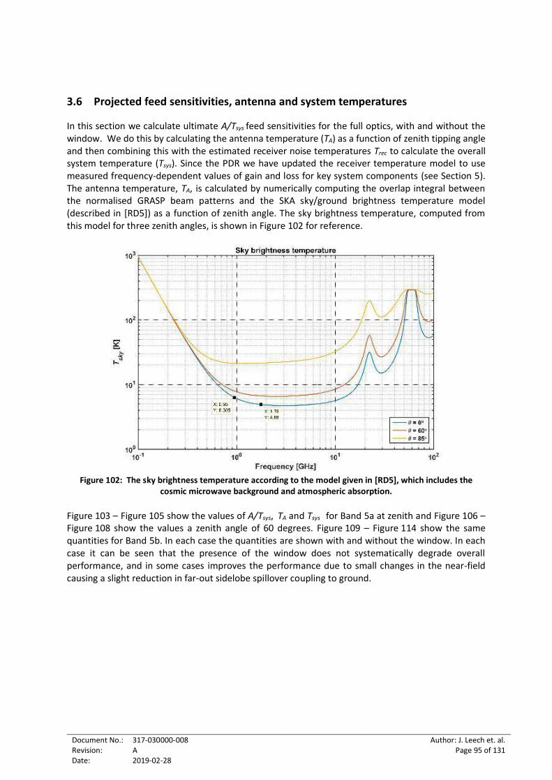
Document No.: Revision: Date:
317-030000-008 A 2019-02-28
Author: J. Leech et. al. Page 95 of 131
3.6 Projected feed sensitivities, antenna and system temperatures
In this section we calculate ultimate A/Tsys feed sensitivities for the full optics, with and without the window. We do this by calculating the antenna temperature (TA) as a function of zenith tipping angle and then combining this with the estimated receiver noise temperatures Trec to calculate the overall system temperature (Tsys). Since the PDR we have updated the receiver temperature model to use measured frequency-dependent values of gain and loss for key system components (see Section 5). The antenna temperature, TA, is calculated by numerically computing the overlap integral between the normalised GRASP beam patterns and the SKA sky/ground brightness temperature model (described in [RD5]) as a function of zenith angle. The sky brightness temperature, computed from this model for three zenith angles, is shown in Figure 102 for reference.
Figure 102: The sky brightness temperature according to the model given in [RD5], which includes the
cosmic microwave background and atmospheric absorption.
Figure 103 – Figure 105 show the values of A/Tsys, TA and Tsys for Band 5a at zenith and Figure 106 – Figure 108 show the values a zenith angle of 60 degrees. Figure 109 – Figure 114 show the same quantities for Band 5b. In each case the quantities are shown with and without the window. In each case it can be seen that the presence of the window does not systematically degrade overall performance, and in some cases improves the performance due to small changes in the near-field causing a slight reduction in far-out sidelobe spillover coupling to ground.
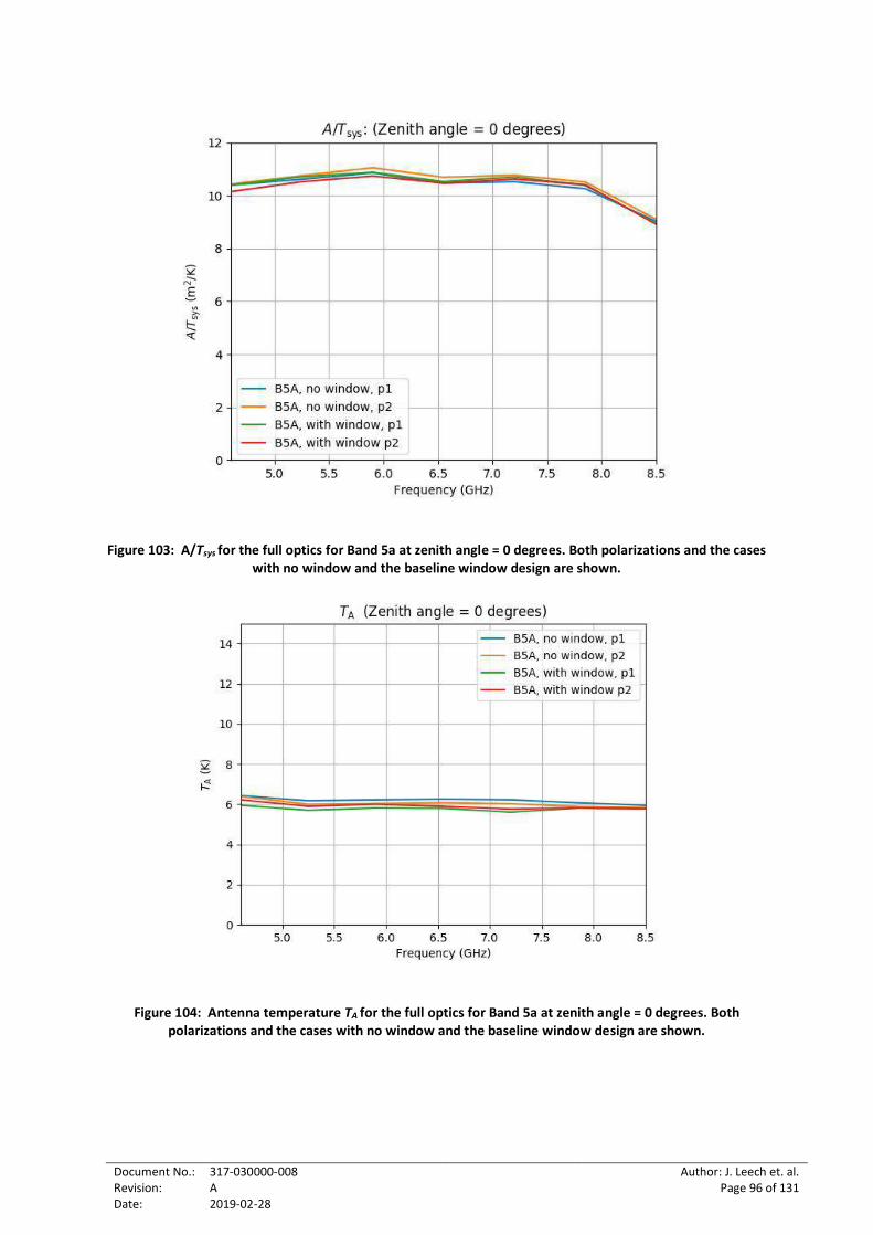
Document No.: Revision: Date:
317-030000-008 A 2019-02-28
Author: J. Leech et. al. Page 96 of 131
Figure 103: A/Tsys for the full optics for Band 5a at zenith angle = 0 degrees. Both polarizations and the cases with no window and the baseline window design are shown.
Figure 104: Antenna temperature TA for the full optics for Band 5a at zenith angle = 0 degrees. Both polarizations and the cases with no window and the baseline window design are shown.
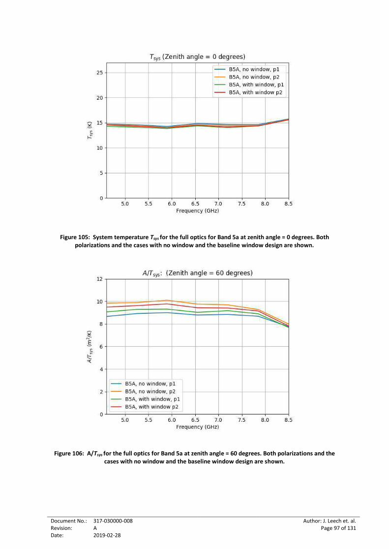
Document No.: Revision: Date:
317-030000-008 A 2019-02-28
Author: J. Leech et. al. Page 97 of 131
Figure 105: System temperature Tsys for the full optics for Band 5a at zenith angle = 0 degrees. Both polarizations and the cases with no window and the baseline window design are shown.
Figure 106: A/Tsys for the full optics for Band 5a at zenith angle = 60 degrees. Both polarizations and the cases with no window and the baseline window design are shown.
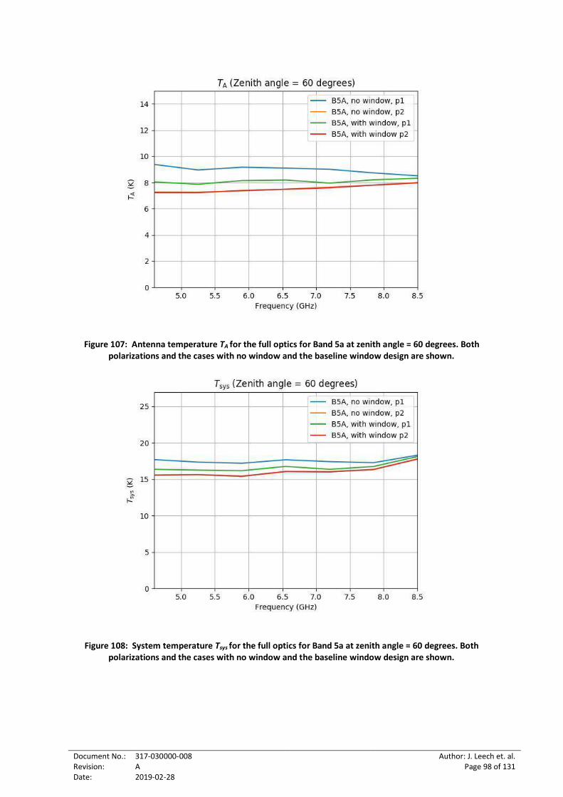
Document No.: Revision: Date:
317-030000-008 A 2019-02-28
Author: J. Leech et. al. Page 98 of 131
Figure 107: Antenna temperature TA for the full optics for Band 5a at zenith angle = 60 degrees. Both polarizations and the cases with no window and the baseline window design are shown.
Figure 108: System temperature Tsys for the full optics for Band 5a at zenith angle = 60 degrees. Both polarizations and the cases with no window and the baseline window design are shown.
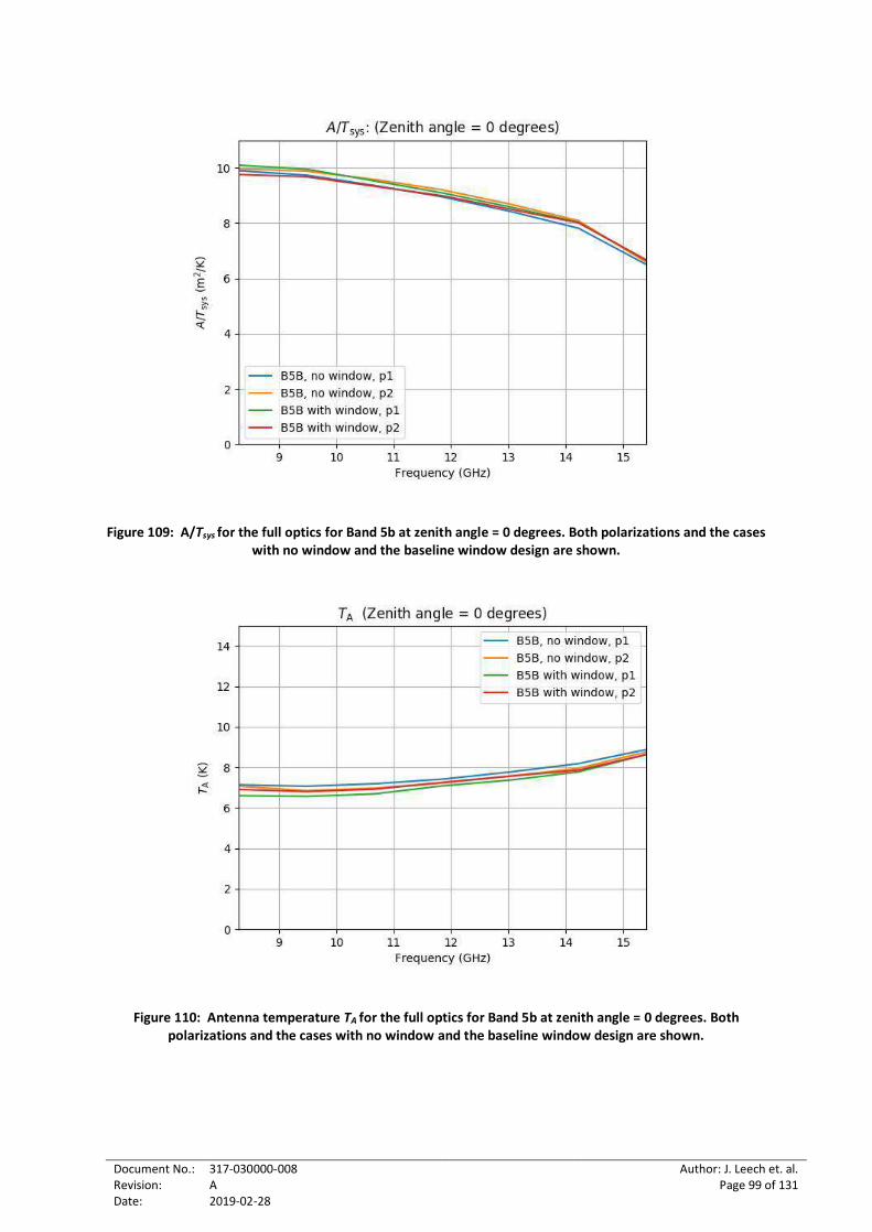
Document No.: Revision: Date:
317-030000-008 A 2019-02-28
Author: J. Leech et. al. Page 99 of 131
Figure 109: A/Tsys for the full optics for Band 5b at zenith angle = 0 degrees. Both polarizations and the cases with no window and the baseline window design are shown.
Figure 110: Antenna temperature TA for the full optics for Band 5b at zenith angle = 0 degrees. Both polarizations and the cases with no window and the baseline window design are shown.
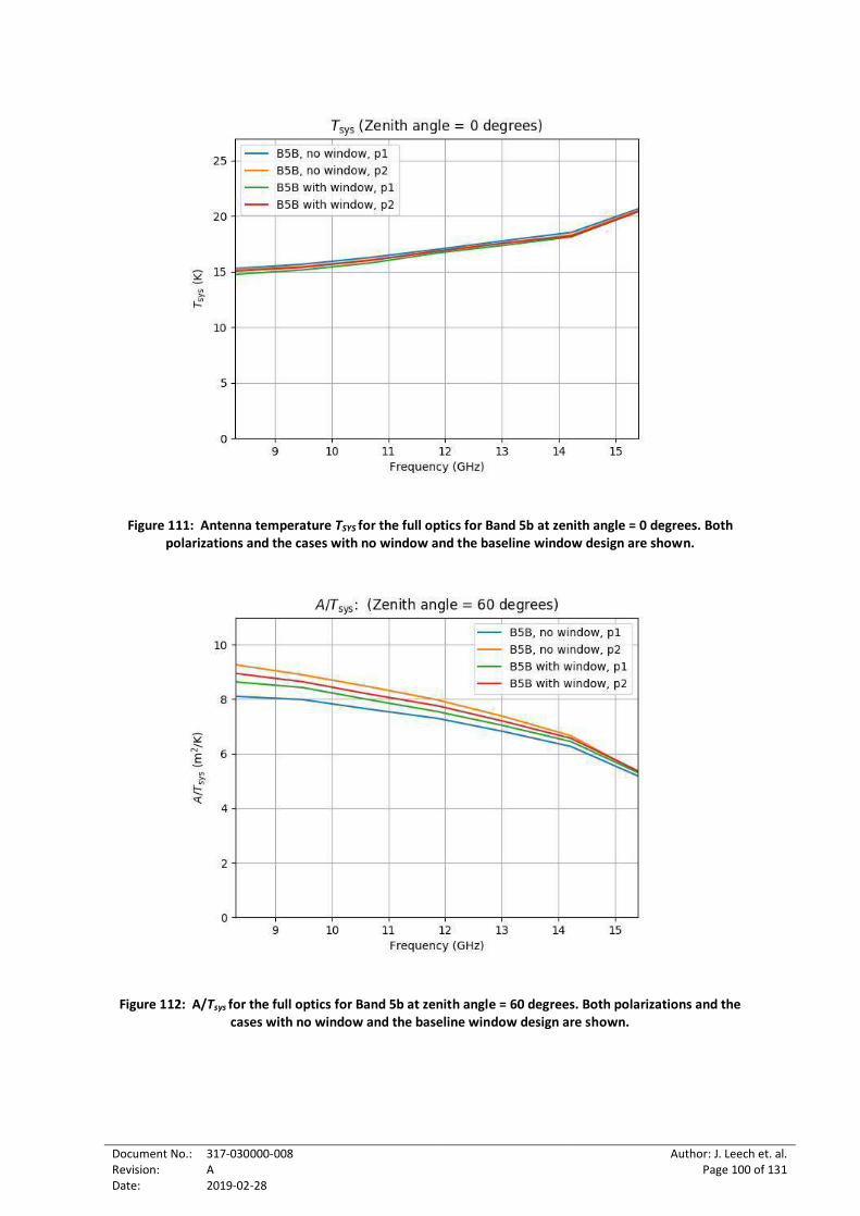
Document No.: Revision: Date:
317-030000-008 A 2019-02-28
Author: J. Leech et. al. Page 100 of 131
Figure 111: Antenna temperature TSYS for the full optics for Band 5b at zenith angle = 0 degrees. Both polarizations and the cases with no window and the baseline window design are shown.
Figure 112: A/Tsys for the full optics for Band 5b at zenith angle = 60 degrees. Both polarizations and the cases with no window and the baseline window design are shown.
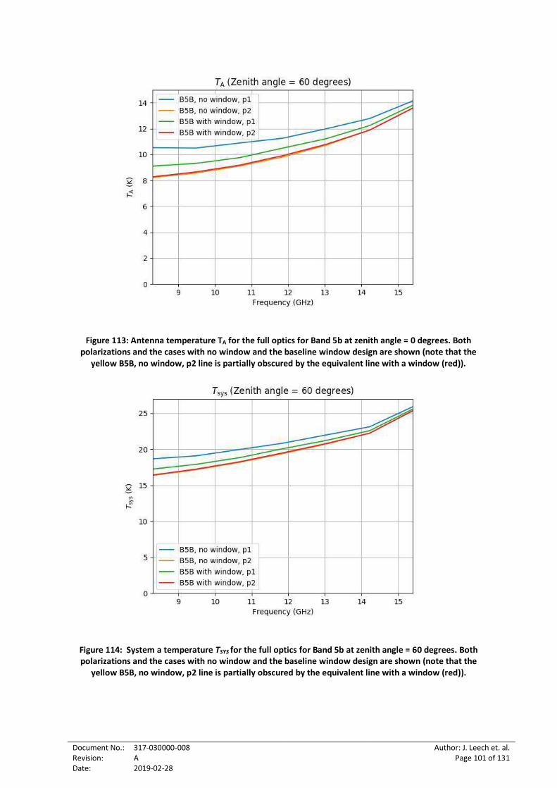
Document No.: Revision: Date:
317-030000-008 A 2019-02-28
Author: J. Leech et. al. Page 101 of 131
Figure 113: Antenna temperature TA for the full optics for Band 5b at zenith angle = 0 degrees. Both polarizations and the cases with no window and the baseline window design are shown (note that the
yellow B5B, no window, p2 line is partially obscured by the equivalent line with a window (red)).
Figure 114: System a temperature TSYS for the full optics for Band 5b at zenith angle = 60 degrees. Both polarizations and the cases with no window and the baseline window design are shown (note that the
yellow B5B, no window, p2 line is partially obscured by the equivalent line with a window (red)).
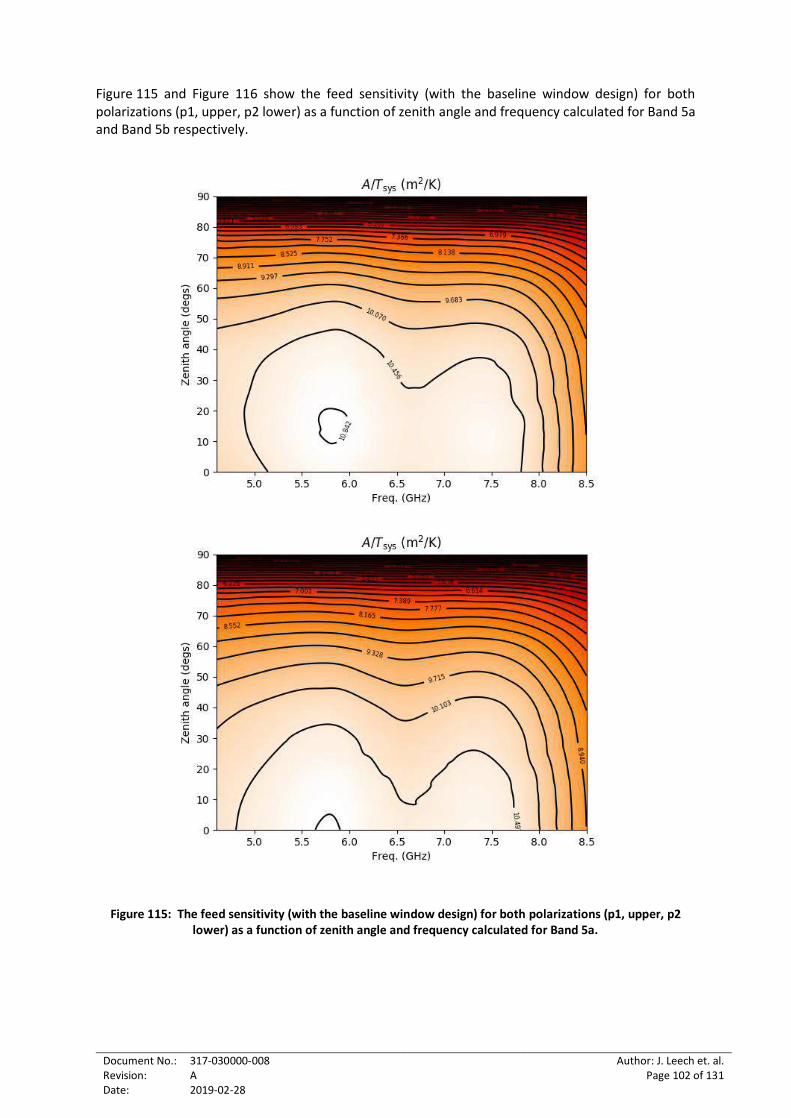
Document No.: Revision: Date:
317-030000-008 A 2019-02-28
Author: J. Leech et. al. Page 102 of 131
Figure 115 and Figure 116 show the feed sensitivity (with the baseline window design) for both polarizations (p1, upper, p2 lower) as a function of zenith angle and frequency calculated for Band 5a and Band 5b respectively.
Figure 115: The feed sensitivity (with the baseline window design) for both polarizations (p1, upper, p2
lower) as a function of zenith angle and frequency calculated for Band 5a.
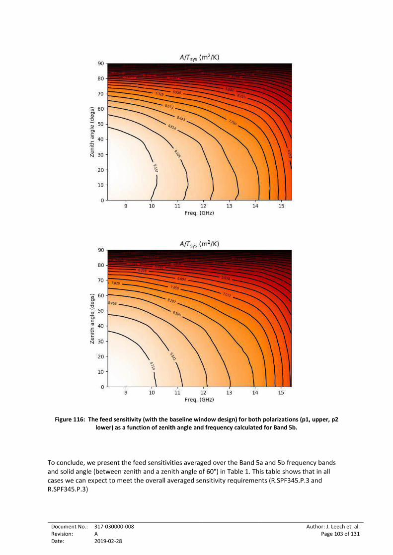
Document No.: Revision: Date:
317-030000-008 A 2019-02-28
Author: J. Leech et. al. Page 103 of 131
Figure 116: The feed sensitivity (with the baseline window design) for both polarizations (p1, upper, p2 lower) as a function of zenith angle and frequency calculated for Band 5b.
To conclude, we present the feed sensitivities averaged over the Band 5a and 5b frequency bands and solid angle (between zenith and a zenith angle of 60°) in Table 1. This table shows that in all cases we can expect to meet the overall averaged sensitivity requirements (R.SPF345.P.3 and R.SPF345.P.3)
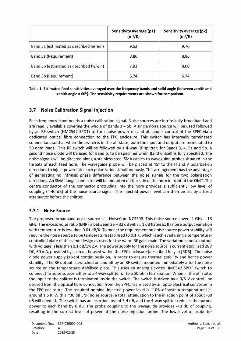
Document No.: Revision: Date:
317-030000-008 A 2019-02-28
Author: J. Leech et. al. Page 104 of 131
Sensitivity average (p1) (m2/K)
Sensitivity average (p2) (m2/K)
Band 5a (estimated as described herein) 9.52 9.70
Band 5a (Requirement) 8.86 8.86
Band 5b (estimated as described herein) 7.93 8.00
Band 5b (Requirement) 6.74 6.74
Table 1: Estimated feed sensitivities averaged over the frequency bands and solid angle (between zenith and
zenith angle = 60). The sensitivity requirements are shown for comparison.
3.7 Noise Calibration Signal Injection
Each frequency band needs a noise calibration signal. Noise sources are intrinsically broadband and are readily available covering the whole of Bands 3 – 5b. A single noise source will be used followed by an RF switch (HMC547 SPDT) to turn noise power on and off under control of the SPFC via a dedicated optical fibre connection to the FPC enclosure. This switch has internally terminated connections so that when the switch is in the off state, both the input and output are terminated to 50 ohm loads. This RF switch will be followed by a 4-way RF splitter, for Bands 3, 4, 5a and 5b. A second noise diode will be used for Band 6, to be specified when Band 6 itself is fully specified. The noise signals will be directed along a stainless steel SMA cables to waveguide probes situated in the throats of each feed horn. The waveguide probe will be placed at 45° to the H and V polarization directions to inject power into each polarization simultaneously. This arrangement has the advantage of generating no intrinsic phase difference between the noise signals for the two polarization directions. An SMA flange connector will be mounted on the side of the horn in front of the OMT. The centre conductor of the connector protruding into the horn provides a sufficiently low level of coupling (~-40 dB) of the noise source signal. The injected power level can then be set by a fixed attenuator before the splitter.
3.7.1 Noise Source
The proposed broadband noise source is a NoiseCom NC3208. This noise source covers 1 GHz – 18
GHz. The excess noise ratio (ENR) is between 26 – 32 dB with 1 dB flatness. Its noise output variation with temperature is less than 0.01 dB/K. To meet the requirement on noise source power stability will require the noise source to be temperature stabilized to 0.1 K, which is achieved using a temperature-controlled plate of the same design as used for the warm RF gain chain. The variation in noise output with voltage is less than 0.1 dB/1% ΔV. The power supply for the noise source is current-stabilised 28V DC, 60 mA, provided by a circuit housed within the FPC enclosure (described fully in [RD6]). The noise diode power supply is kept continuously on, in order to ensure thermal stability and hence power stability. The RF output is switched on and off by an RF switch mounted immediately after the noise source on the temperature-stabilised plate. This uses an Analog Devices HMC547 SPDT switch to connect the noise source either to a 4-way splitter or to a 50-ohm termination. When in the off state, the input to the splitter is terminated inside the switch. The switch is driven by a 0/5 V control line derived from the optical fibre connection from the SPFC, translated by an opto-electrical converter in the FPC enclosure. The required nominal injected power level is ~10% of system temperature i.e. around 1.5 K. With a ~30 dB ENR noise source, a total attenuation to the injection point of about -50 dB will needed. The switch has an insertion loss of 3-4 dB, and the 4-way splitter reduces the output power to each band by 6 dB. The probe coupling to the waveguide provides -40 dB of coupling, resulting in the correct level of power at the noise injection probe. The low level of probe-to-
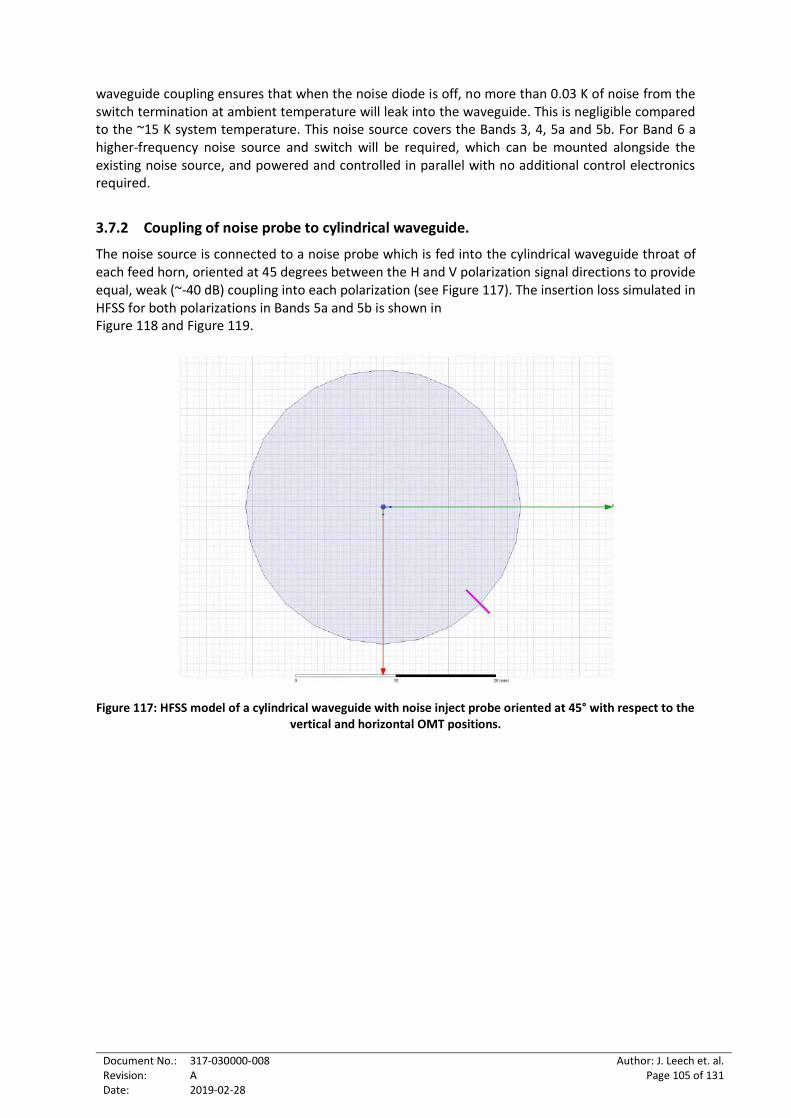
Document No.: Revision: Date:
317-030000-008 A 2019-02-28
Author: J. Leech et. al. Page 105 of 131
waveguide coupling ensures that when the noise diode is off, no more than 0.03 K of noise from the switch termination at ambient temperature will leak into the waveguide. This is negligible compared to the ~15 K system temperature. This noise source covers the Bands 3, 4, 5a and 5b. For Band 6 a higher-frequency noise source and switch will be required, which can be mounted alongside the existing noise source, and powered and controlled in parallel with no additional control electronics required.
3.7.2 Coupling of noise probe to cylindrical waveguide.
The noise source is connected to a noise probe which is fed into the cylindrical waveguide throat of each feed horn, oriented at 45 degrees between the H and V polarization signal directions to provide equal, weak (~-40 dB) coupling into each polarization (see Figure 117). The insertion loss simulated in HFSS for both polarizations in Bands 5a and 5b is shown in Figure 118 and Figure 119.
Figure 117: HFSS model of a cylindrical waveguide with noise inject probe oriented at 45° with respect to the vertical and horizontal OMT positions.
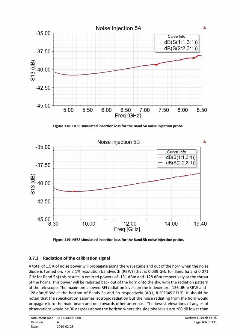
Document No.: Revision: Date:
317-030000-008 A 2019-02-28
Author: J. Leech et. al. Page 106 of 131
Figure 118: HFSS simulated insertion loss for the Band 5a noise injection probe.
Figure 119: HFSS simulated insertion loss for the Band 5b noise injection probe.
3.7.3 Radiation of the calibration signal
A total of 1.5 K of noise power will propagate along the waveguide and out of the horn when the noise diode is turned on. For a 1% resolution bandwidth (RBW) (that is 0.039 GHz for Band 5a and 0.071 GHz for Band 5b) this results in emitted powers of -131 dBm and -128 dBm respectively at the throat of the horns. This power will be radiated back out of the horn onto the sky, with the radiation pattern of the telescope. The maximum allowed RFI radiation levels on the indexer are -136 dBm/RBW and -128 dBm/RBW at the bottom of Bands 5a and 5b respectively [AD1, R.SPF345.RFI.3]. It should be noted that the specification assumes isotropic radiation but the noise radiating from the horn would propagate into the main beam and not towards other antennas. The lowest elevations of angles of observations would be 30 degrees above the horizon where the sidelobe levels are ~60 dB lower than
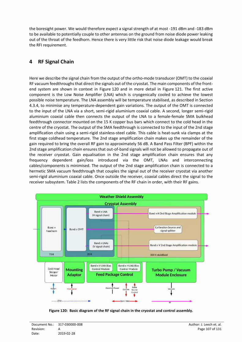
Document No.: Revision: Date:
317-030000-008 A 2019-02-28
Author: J. Leech et. al. Page 107 of 131
the boresight power. We would therefore expect a signal strength of at most -191 dBm and -183 dBm to be available to potentially couple to other antennas on the ground from noise diode power leaking out of the throat of the feedhorn. Hence there is very little risk that noise diode leakage would break the RFI requirement.
4 RF Signal Chain
Here we describe the signal chain from the output of the ortho-mode transducer (OMT) to the coaxial RF vacuum feedthroughs that direct the signals out of the cryostat. The main components of the front-end system are shown in context in Figure 120 and in more detail in Figure 121. The first active component is the Low Noise Amplifier (LNA) which is cryogenically cooled to achieve the lowest possible noise temperature. The LNA assembly will be temperature stabilised, as described in Section 4.3.4, to minimise any temperature-dependent gain variations. The output of the OMT is connected to the input of the LNA via a short, semi-rigid aluminium coaxial cable. A second, longer semi-rigid aluminium coaxial cable then connects the output of the LNA to a female-female SMA bulkhead feedthrough connector mounted on the 15 K copper bus bars which connect to the cold head in the centre of the cryostat. The output of the SMA feedthrough is connected to the input of the 2nd stage amplification chain using a semi-rigid stainless-steel cable. This cable is heat-sunk via clamps at the first stage coldhead temperature. The 2nd stage amplification chain makes up the remainder of the gain required to bring the overall RF gain to approximately 56 dB. A Band Pass Filter (BPF) within the 2nd stage amplification chain ensures that out-of-band signals will not be allowed to propagate out of the receiver cryostat. Gain equalisation in the 2nd stage amplification chain ensures that any frequency dependent gain/loss introduced via the OMT, LNAs and interconnecting cables/components is minimised. The output of the 2nd stage amplification chain is connected to a hermetic SMA vacuum feedthrough that couples the signal out of the receiver cryostat via another semi-rigid aluminium coaxial cable. Once outside the receiver, coaxial cables direct the signal to the receiver subsystem. Table 2 lists the components of the RF chain in order, with their RF gains.
Figure 120: Basic diagram of the RF signal chain in the cryostat and control assembly.
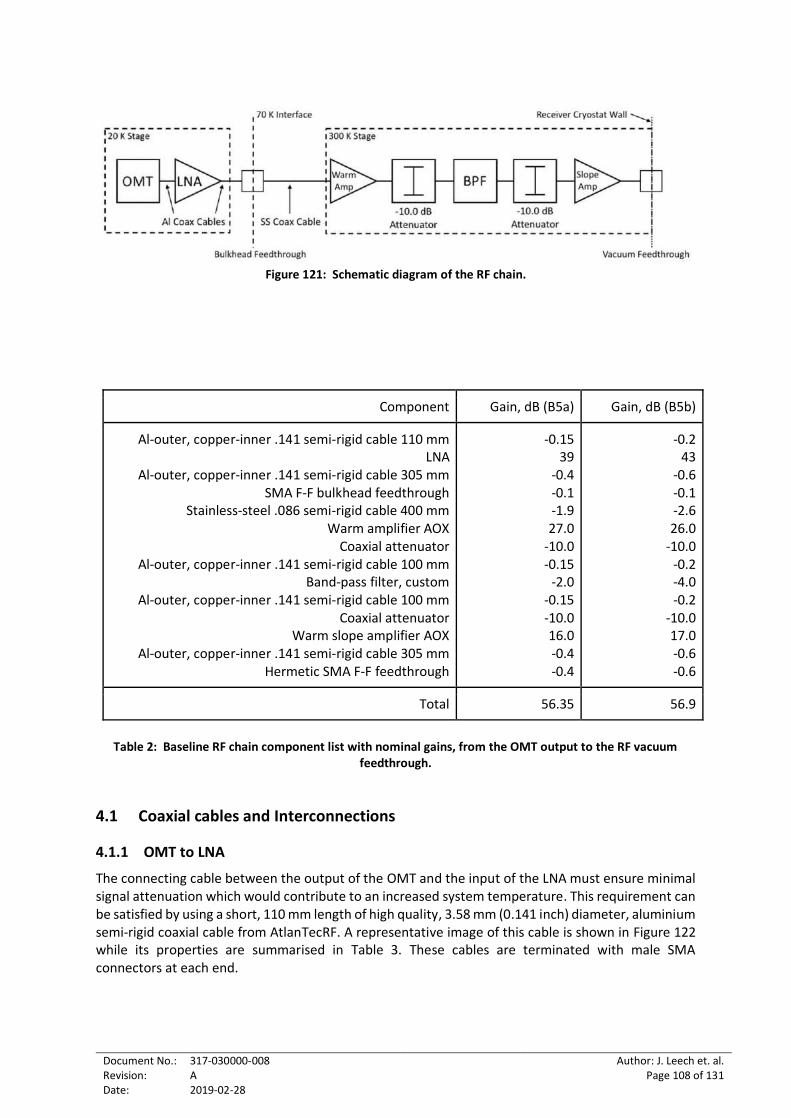
Document No.: Revision: Date:
317-030000-008 A 2019-02-28
Author: J. Leech et. al. Page 108 of 131
Figure 121: Schematic diagram of the RF chain.
Component Gain, dB (B5a) Gain, dB (B5b)
Al-outer, copper-inner .141 semi-rigid cable 110 mm LNA
Al-outer, copper-inner .141 semi-rigid cable 305 mm SMA F-F bulkhead feedthrough
Stainless-steel .086 semi-rigid cable 400 mm Warm amplifier AOX
Coaxial attenuator Al-outer, copper-inner .141 semi-rigid cable 100 mm
Band-pass filter, custom Al-outer, copper-inner .141 semi-rigid cable 100 mm
Coaxial attenuator Warm slope amplifier AOX
Al-outer, copper-inner .141 semi-rigid cable 305 mm Hermetic SMA F-F feedthrough
-0.15 39
-0.4 -0.1 -1.9 27.0
-10.0 -0.15
-2.0 -0.15 -10.0 16.0 -0.4 -0.4
-0.2 43
-0.6 -0.1 -2.6 26.0
-10.0 -0.2 -4.0 -0.2
-10.0 17.0 -0.6 -0.6
Total 56.35 56.9
Table 2: Baseline RF chain component list with nominal gains, from the OMT output to the RF vacuum
feedthrough.
4.1 Coaxial cables and Interconnections
4.1.1 OMT to LNA
The connecting cable between the output of the OMT and the input of the LNA must ensure minimal signal attenuation which would contribute to an increased system temperature. This requirement can be satisfied by using a short, 110 mm length of high quality, 3.58 mm (0.141 inch) diameter, aluminium semi-rigid coaxial cable from AtlanTecRF. A representative image of this cable is shown in Figure 122 while its properties are summarised in Table 3. These cables are terminated with male SMA connectors at each end.
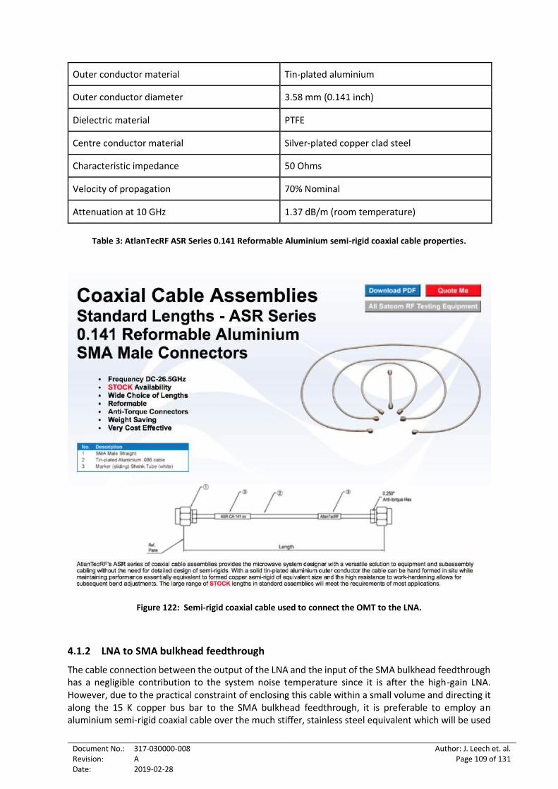
Document No.: Revision: Date:
317-030000-008 A 2019-02-28
Author: J. Leech et. al. Page 109 of 131
Table 3: AtlanTecRF ASR Series 0.141 Reformable Aluminium semi-rigid coaxial cable properties.
Figure 122: Semi-rigid coaxial cable used to connect the OMT to the LNA.
4.1.2 LNA to SMA bulkhead feedthrough
The cable connection between the output of the LNA and the input of the SMA bulkhead feedthrough has a negligible contribution to the system noise temperature since it is after the high-gain LNA. However, due to the practical constraint of enclosing this cable within a small volume and directing it along the 15 K copper bus bar to the SMA bulkhead feedthrough, it is preferable to employ an aluminium semi-rigid coaxial cable over the much stiffer, stainless steel equivalent which will be used
Outer conductor material Tin-plated aluminium
Outer conductor diameter 3.58 mm (0.141 inch)
Dielectric material PTFE
Centre conductor material Silver-plated copper clad steel
Characteristic impedance 50 Ohms
Velocity of propagation 70% Nominal
Attenuation at 10 GHz 1.37 dB/m (room temperature)
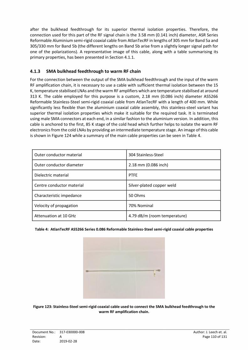
Document No.: Revision: Date:
317-030000-008 A 2019-02-28
Author: J. Leech et. al. Page 110 of 131
after the bulkhead feedthrough for its superior thermal isolation properties. Therefore, the connection used for this part of the RF signal chain is the 3.58 mm (0.141 inch) diameter, ASR Series Reformable Aluminium semi-rigid coaxial cable from AtlanTecRF in lengths of 305 mm for Band 5a and 305/330 mm for Band 5b (the different lengths on Band 5b arise from a slightly longer signal path for one of the polarizations). A representative image of this cable, along with a table summarising its primary properties, has been presented in Section 4.1.1.
4.1.3 SMA bulkhead feedthrough to warm RF chain
For the connection between the output of the SMA bulkhead feedthrough and the input of the warm RF amplification chain, it is necessary to use a cable with sufficient thermal isolation between the 15 K, temperature stabilised LNAs and the warm RF amplifiers which are temperature stabilised at around 313 K. The cable employed for this purpose is a custom, 2.18 mm (0.086 inch) diameter AS5266 Reformable Stainless-Steel semi-rigid coaxial cable from AtlanTecRF with a length of 400 mm. While significantly less flexible than the aluminium coaxial cable assembly, this stainless-steel variant has superior thermal isolation properties which make it suitable for the required task. It is terminated using male SMA connectors at each end, in a similar fashion to the aluminium version. In addition, this cable is anchored to the first, 85 K stage of the cold head which further helps to isolate the warm RF electronics from the cold LNAs by providing an intermediate temperature stage. An image of this cable is shown in Figure 124 while a summary of the main cable properties can be seen in Table 4.
Outer conductor material 304 Stainless-Steel
Outer conductor diameter 2.18 mm (0.086 inch)
Dielectric material PTFE
Centre conductor material Silver-plated copper weld
Characteristic impedance 50 Ohms
Velocity of propagation 70% Nominal
Attenuation at 10 GHz 4.79 dB/m (room temperature)
Table 4: AtlanTecRF AS5266 Series 0.086 Reformable Stainless-Steel semi-rigid coaxial cable properties
Figure 123: Stainless-Steel semi-rigid coaxial cable used to connect the SMA bulkhead feedthrough to the warm RF amplification chain.
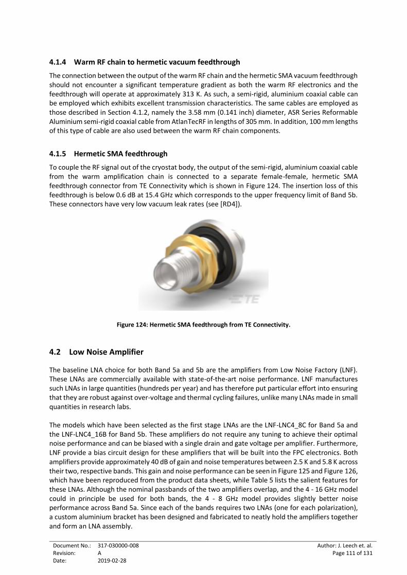
Document No.: Revision: Date:
317-030000-008 A 2019-02-28
Author: J. Leech et. al. Page 111 of 131
4.1.4 Warm RF chain to hermetic vacuum feedthrough
The connection between the output of the warm RF chain and the hermetic SMA vacuum feedthrough should not encounter a significant temperature gradient as both the warm RF electronics and the feedthrough will operate at approximately 313 K. As such, a semi-rigid, aluminium coaxial cable can be employed which exhibits excellent transmission characteristics. The same cables are employed as those described in Section 4.1.2, namely the 3.58 mm (0.141 inch) diameter, ASR Series Reformable Aluminium semi-rigid coaxial cable from AtlanTecRF in lengths of 305 mm. In addition, 100 mm lengths of this type of cable are also used between the warm RF chain components.
4.1.5 Hermetic SMA feedthrough
To couple the RF signal out of the cryostat body, the output of the semi-rigid, aluminium coaxial cable from the warm amplification chain is connected to a separate female-female, hermetic SMA feedthrough connector from TE Connectivity which is shown in Figure 124. The insertion loss of this feedthrough is below 0.6 dB at 15.4 GHz which corresponds to the upper frequency limit of Band 5b. These connectors have very low vacuum leak rates (see [RD4]).
Figure 124: Hermetic SMA feedthrough from TE Connectivity.
4.2 Low Noise Amplifier
The baseline LNA choice for both Band 5a and 5b are the amplifiers from Low Noise Factory (LNF). These LNAs are commercially available with state-of-the-art noise performance. LNF manufactures such LNAs in large quantities (hundreds per year) and has therefore put particular effort into ensuring that they are robust against over-voltage and thermal cycling failures, unlike many LNAs made in small quantities in research labs. The models which have been selected as the first stage LNAs are the LNF-LNC4_8C for Band 5a and the LNF-LNC4_16B for Band 5b. These amplifiers do not require any tuning to achieve their optimal noise performance and can be biased with a single drain and gate voltage per amplifier. Furthermore, LNF provide a bias circuit design for these amplifiers that will be built into the FPC electronics. Both amplifiers provide approximately 40 dB of gain and noise temperatures between 2.5 K and 5.8 K across their two, respective bands. This gain and noise performance can be seen in Figure 125 and Figure 126, which have been reproduced from the product data sheets, while Table 5 lists the salient features for these LNAs. Although the nominal passbands of the two amplifiers overlap, and the 4 - 16 GHz model could in principle be used for both bands, the 4 - 8 GHz model provides slightly better noise performance across Band 5a. Since each of the bands requires two LNAs (one for each polarization), a custom aluminium bracket has been designed and fabricated to neatly hold the amplifiers together and form an LNA assembly.
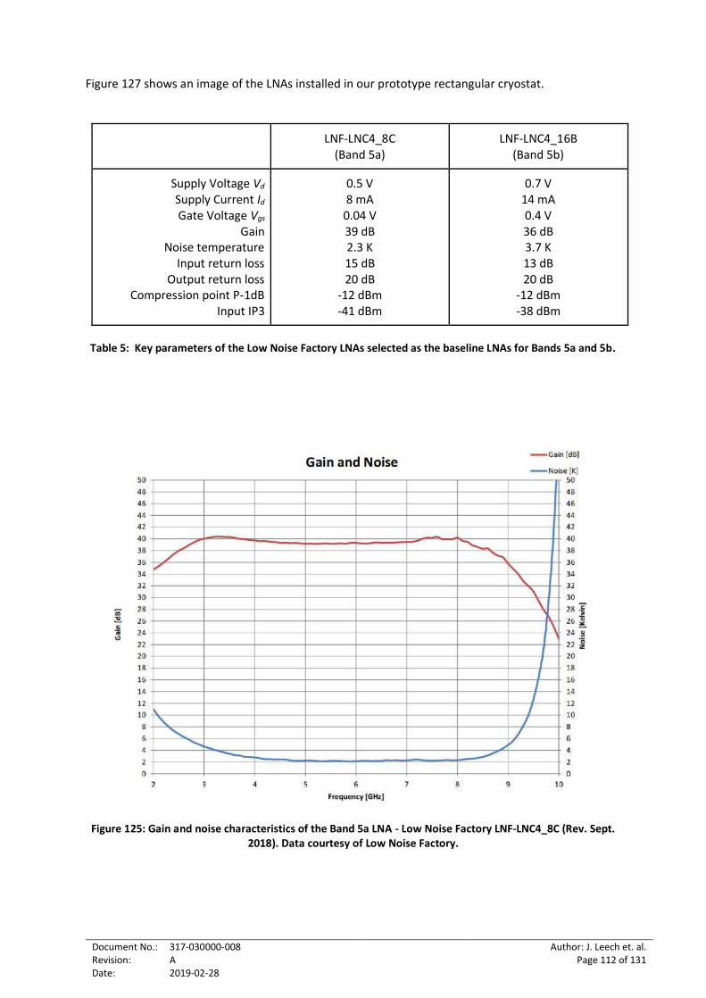
Document No.: Revision: Date:
317-030000-008 A 2019-02-28
Author: J. Leech et. al. Page 112 of 131
Figure 127 shows an image of the LNAs installed in our prototype rectangular cryostat.
LNF-LNC4_8C (Band 5a)
LNF-LNC4_16B (Band 5b)
Supply Voltage Vd
Supply Current Id
Gate Voltage Vgs Gain
Noise temperature Input return loss
Output return loss Compression point P-1dB
Input IP3
0.5 V 8 mA
0.04 V 39 dB 2.3 K 15 dB 20 dB
-12 dBm -41 dBm
0.7 V 14 mA 0.4 V 36 dB 3.7 K 13 dB 20 dB
-12 dBm -38 dBm
Table 5: Key parameters of the Low Noise Factory LNAs selected as the baseline LNAs for Bands 5a and 5b.
Figure 125: Gain and noise characteristics of the Band 5a LNA - Low Noise Factory LNF-LNC4_8C (Rev. Sept. 2018). Data courtesy of Low Noise Factory.
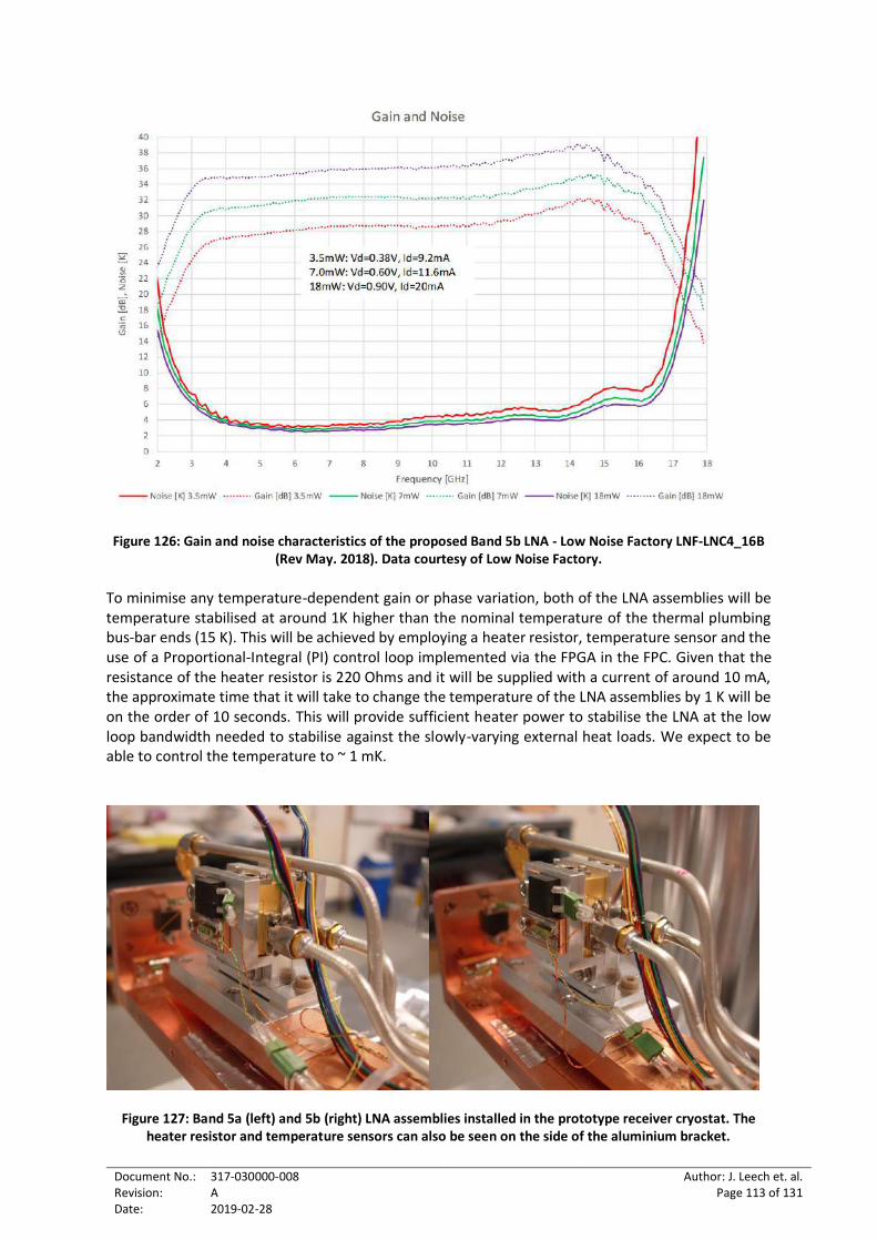
Document No.: Revision: Date:
317-030000-008 A 2019-02-28
Author: J. Leech et. al. Page 113 of 131
Figure 126: Gain and noise characteristics of the proposed Band 5b LNA - Low Noise Factory LNF-LNC4_16B (Rev May. 2018). Data courtesy of Low Noise Factory.
To minimise any temperature-dependent gain or phase variation, both of the LNA assemblies will be temperature stabilised at around 1K higher than the nominal temperature of the thermal plumbing bus-bar ends (15 K). This will be achieved by employing a heater resistor, temperature sensor and the use of a Proportional-Integral (PI) control loop implemented via the FPGA in the FPC. Given that the resistance of the heater resistor is 220 Ohms and it will be supplied with a current of around 10 mA, the approximate time that it will take to change the temperature of the LNA assemblies by 1 K will be on the order of 10 seconds. This will provide sufficient heater power to stabilise the LNA at the low loop bandwidth needed to stabilise against the slowly-varying external heat loads. We expect to be able to control the temperature to ~ 1 mK.
Figure 127: Band 5a (left) and 5b (right) LNA assemblies installed in the prototype receiver cryostat. The heater resistor and temperature sensors can also be seen on the side of the aluminium bracket.
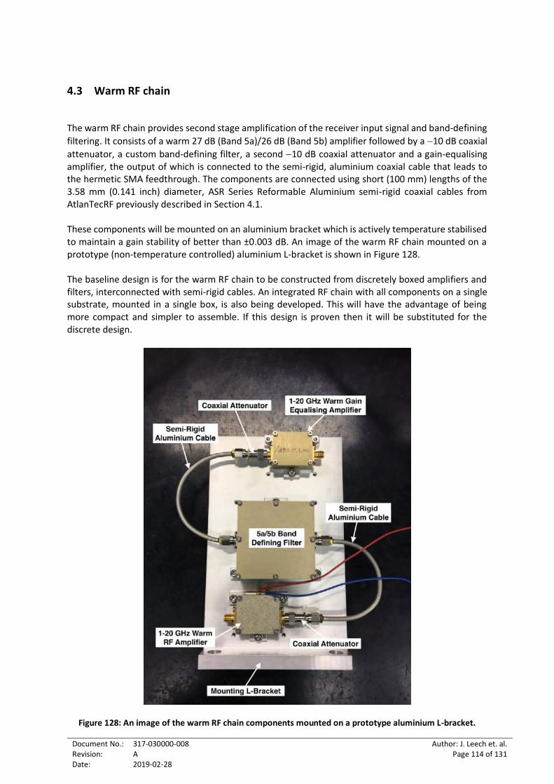
Document No.: Revision: Date:
317-030000-008 A 2019-02-28
Author: J. Leech et. al. Page 114 of 131
4.3 Warm RF chain
The warm RF chain provides second stage amplification of the receiver input signal and band-defining
filtering. It consists of a warm 27 dB (Band 5a)/26 dB (Band 5b) amplifier followed by a −10 dB coaxial
attenuator, a custom band-defining filter, a second −10 dB coaxial attenuator and a gain-equalising amplifier, the output of which is connected to the semi-rigid, aluminium coaxial cable that leads to the hermetic SMA feedthrough. The components are connected using short (100 mm) lengths of the 3.58 mm (0.141 inch) diameter, ASR Series Reformable Aluminium semi-rigid coaxial cables from AtlanTecRF previously described in Section 4.1. These components will be mounted on an aluminium bracket which is actively temperature stabilised to maintain a gain stability of better than ±0.003 dB. An image of the warm RF chain mounted on a prototype (non-temperature controlled) aluminium L-bracket is shown in Figure 128. The baseline design is for the warm RF chain to be constructed from discretely boxed amplifiers and filters, interconnected with semi-rigid cables. An integrated RF chain with all components on a single substrate, mounted in a single box, is also being developed. This will have the advantage of being more compact and simpler to assemble. If this design is proven then it will be substituted for the discrete design.
Figure 128: An image of the warm RF chain components mounted on a prototype aluminium L-bracket.
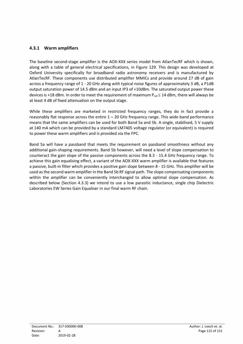
Document No.: Revision: Date:
317-030000-008 A 2019-02-28
Author: J. Leech et. al. Page 115 of 131
4.3.1 Warm amplifiers
The baseline second-stage amplifier is the AOX-XXX series model from AtlanTecRF which is shown, along with a table of general electrical specifications, in Figure 129. This design was developed at Oxford University specifically for broadband radio astronomy receivers and is manufactured by AtlanTecRF. These components use distributed amplifier MMICs and provide around 27 dB of gain across a frequency range of 1 - 20 GHz along with typical noise figures of approximately 3 dB, a P1dB output saturation power of 14.5 dBm and an input IP3 of +10dBm. The saturated output power these
devices is +18 dBm. In order to meet the requirement of maximum Psat 14 dBm, there will always be at least 4 dB of fixed attenuation on the output stage. While these amplifiers are marketed in restricted frequency ranges, they do in fact provide a reasonably flat response across the entire 1 – 20 GHz frequency range. This wide-band performance means that the same amplifiers can be used for both Band 5a and 5b. A single, stabilised, 5 V supply at 140 mA which can be provided by a standard LM7405 voltage regulator (or equivalent) is required to power these warm amplifiers and is provided via the FPC. Band 5a will have a passband that meets the requirement on passband smoothness without any additional gain-shaping requirements. Band 5b however, will need a level of slope compensation to counteract the gain slope of the passive components across the 8.3 - 15.4 GHz frequency range. To achieve this gain equalising effect, a variant of the AOX-XXX warm amplifier is available that features a passive, built-in filter which provides a positive gain slope between 8 - 15 GHz. This amplifier will be used as the second warm amplifier in the Band 5b RF signal path. The slope compensating components within the amplifier can be conveniently interchanged to allow optimal slope compensation. As described below (Section 4.3.3) we intend to use a low parasitic inductance, single chip Dielectric Laboratories EW Series Gain Equaliser in our final warm RF chain.
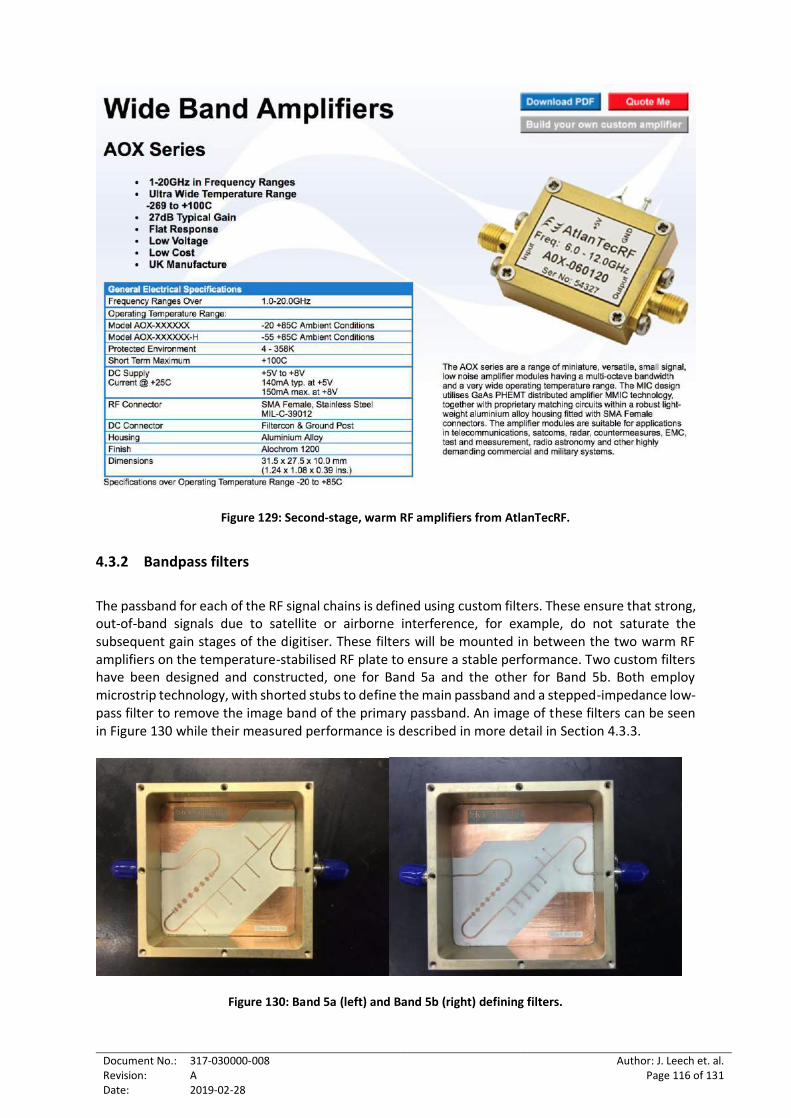
Document No.: Revision: Date:
317-030000-008 A 2019-02-28
Author: J. Leech et. al. Page 116 of 131
Figure 129: Second-stage, warm RF amplifiers from AtlanTecRF.
4.3.2 Bandpass filters
The passband for each of the RF signal chains is defined using custom filters. These ensure that strong, out-of-band signals due to satellite or airborne interference, for example, do not saturate the subsequent gain stages of the digitiser. These filters will be mounted in between the two warm RF amplifiers on the temperature-stabilised RF plate to ensure a stable performance. Two custom filters have been designed and constructed, one for Band 5a and the other for Band 5b. Both employ microstrip technology, with shorted stubs to define the main passband and a stepped-impedance low-pass filter to remove the image band of the primary passband. An image of these filters can be seen in Figure 130 while their measured performance is described in more detail in Section 4.3.3.
Figure 130: Band 5a (left) and Band 5b (right) defining filters.
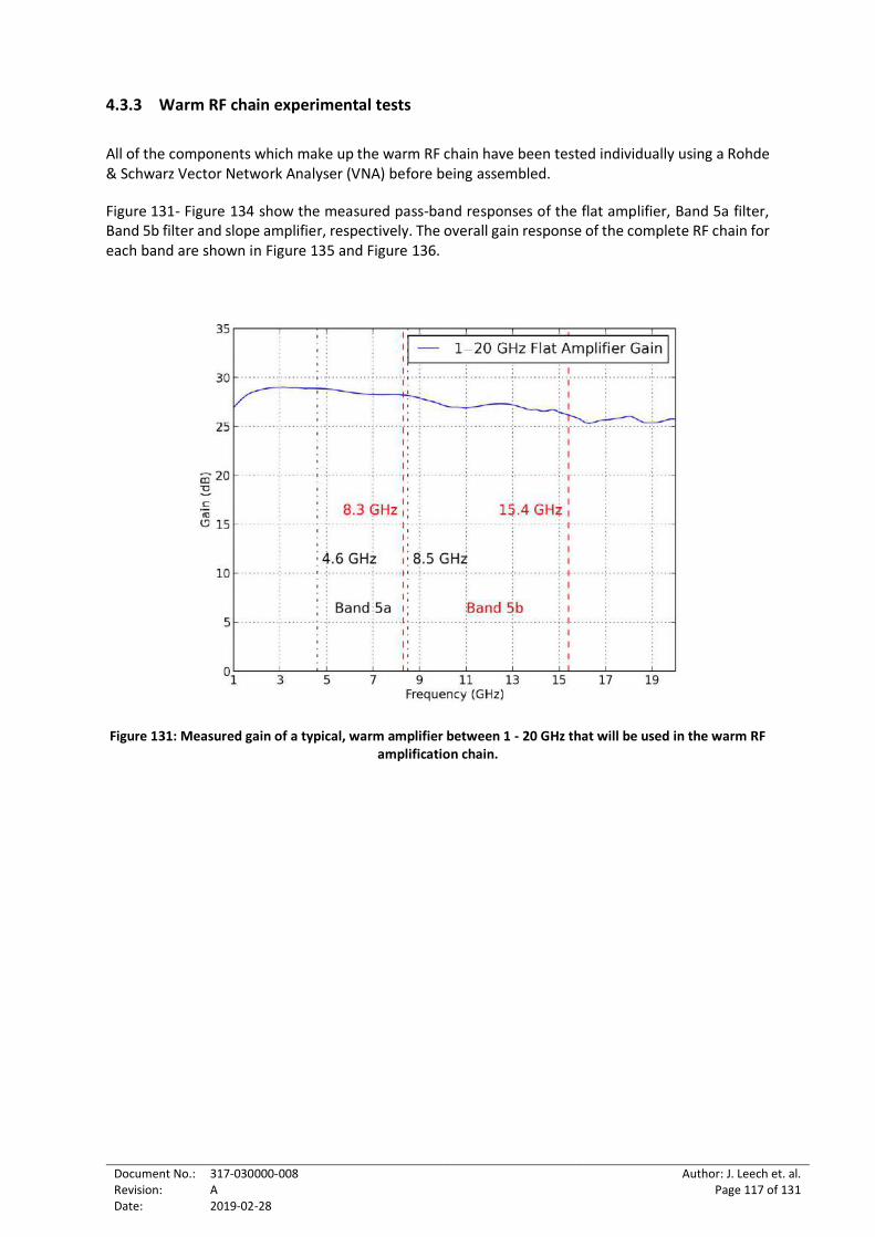
Document No.: Revision: Date:
317-030000-008 A 2019-02-28
Author: J. Leech et. al. Page 117 of 131
4.3.3 Warm RF chain experimental tests
All of the components which make up the warm RF chain have been tested individually using a Rohde & Schwarz Vector Network Analyser (VNA) before being assembled.
Figure 131- Figure 134 show the measured pass-band responses of the flat amplifier, Band 5a filter, Band 5b filter and slope amplifier, respectively. The overall gain response of the complete RF chain for each band are shown in Figure 135 and Figure 136.
Figure 131: Measured gain of a typical, warm amplifier between 1 - 20 GHz that will be used in the warm RF amplification chain.
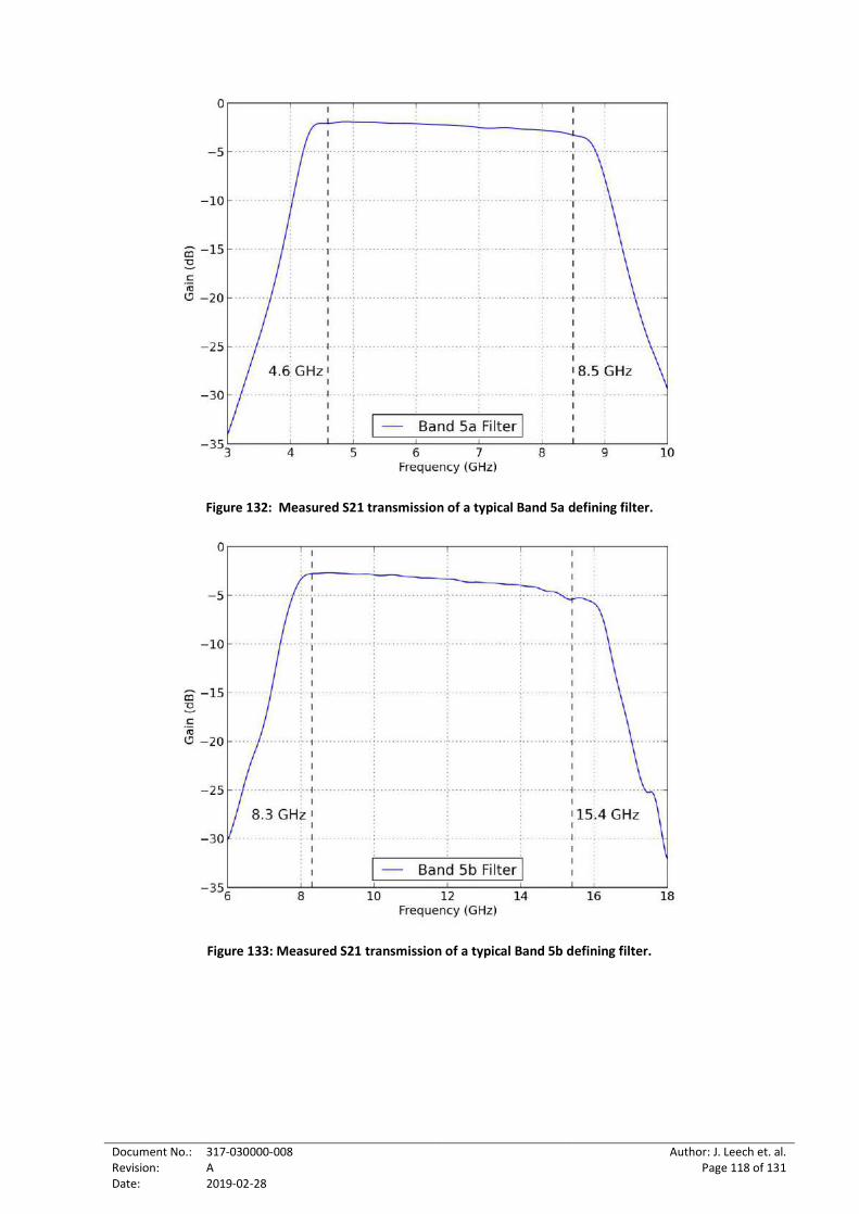
Document No.: Revision: Date:
317-030000-008 A 2019-02-28
Author: J. Leech et. al. Page 118 of 131
Figure 132: Measured S21 transmission of a typical Band 5a defining filter.
Figure 133: Measured S21 transmission of a typical Band 5b defining filter.
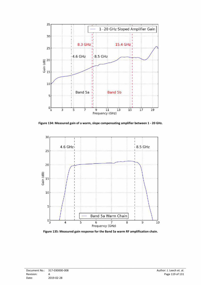
Document No.: Revision: Date:
317-030000-008 A 2019-02-28
Author: J. Leech et. al. Page 119 of 131
Figure 134: Measured gain of a warm, slope compensating amplifier between 1 - 20 GHz.
Figure 135: Measured gain response for the Band 5a warm RF amplification chain.
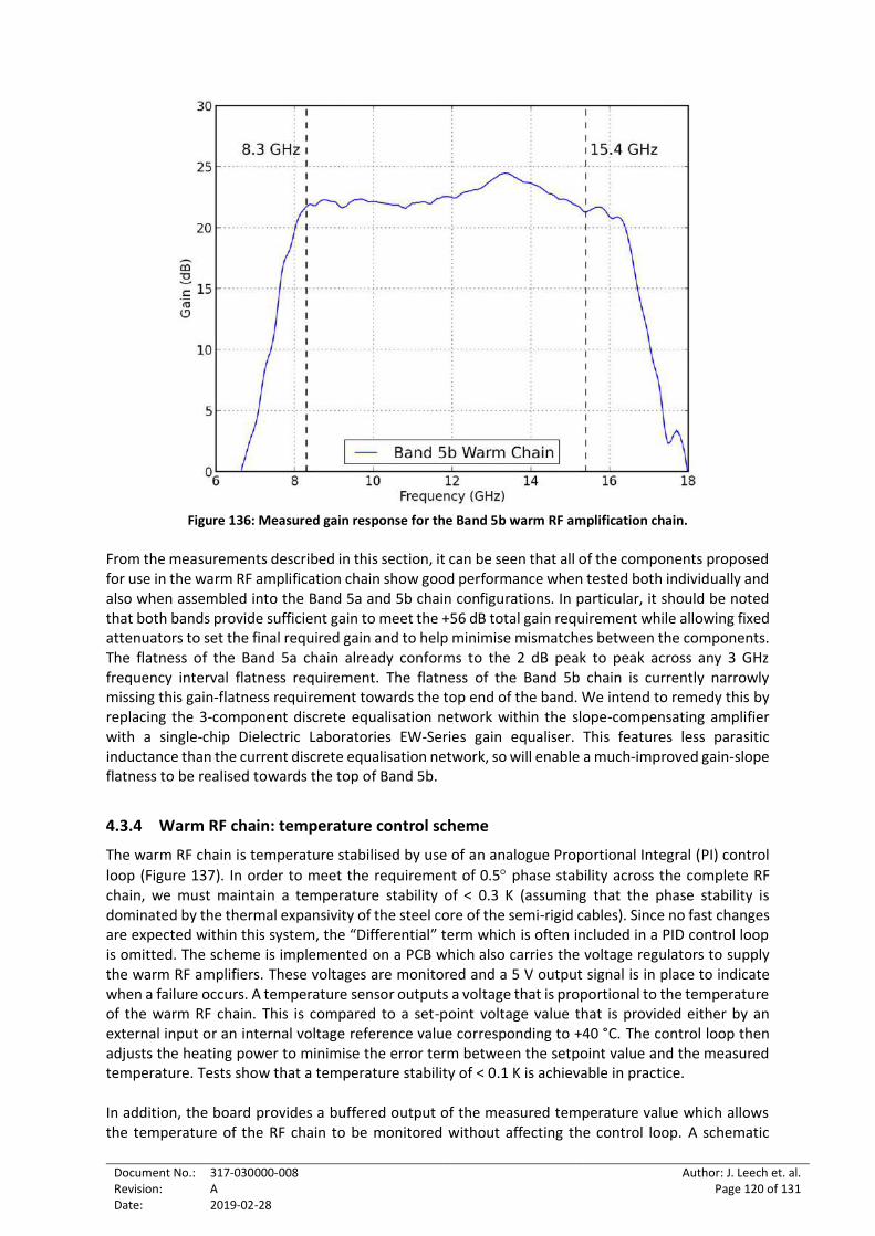
Document No.: Revision: Date:
317-030000-008 A 2019-02-28
Author: J. Leech et. al. Page 120 of 131
Figure 136: Measured gain response for the Band 5b warm RF amplification chain.
From the measurements described in this section, it can be seen that all of the components proposed for use in the warm RF amplification chain show good performance when tested both individually and also when assembled into the Band 5a and 5b chain configurations. In particular, it should be noted that both bands provide sufficient gain to meet the +56 dB total gain requirement while allowing fixed attenuators to set the final required gain and to help minimise mismatches between the components. The flatness of the Band 5a chain already conforms to the 2 dB peak to peak across any 3 GHz frequency interval flatness requirement. The flatness of the Band 5b chain is currently narrowly missing this gain-flatness requirement towards the top end of the band. We intend to remedy this by replacing the 3-component discrete equalisation network within the slope-compensating amplifier with a single-chip Dielectric Laboratories EW-Series gain equaliser. This features less parasitic inductance than the current discrete equalisation network, so will enable a much-improved gain-slope flatness to be realised towards the top of Band 5b.
4.3.4 Warm RF chain: temperature control scheme
The warm RF chain is temperature stabilised by use of an analogue Proportional Integral (PI) control
loop (Figure 137). In order to meet the requirement of 0.5 phase stability across the complete RF chain, we must maintain a temperature stability of < 0.3 K (assuming that the phase stability is dominated by the thermal expansivity of the steel core of the semi-rigid cables). Since no fast changes are expected within this system, the “Differential” term which is often included in a PID control loop is omitted. The scheme is implemented on a PCB which also carries the voltage regulators to supply the warm RF amplifiers. These voltages are monitored and a 5 V output signal is in place to indicate when a failure occurs. A temperature sensor outputs a voltage that is proportional to the temperature of the warm RF chain. This is compared to a set-point voltage value that is provided either by an external input or an internal voltage reference value corresponding to +40 °C. The control loop then adjusts the heating power to minimise the error term between the setpoint value and the measured temperature. Tests show that a temperature stability of < 0.1 K is achievable in practice. In addition, the board provides a buffered output of the measured temperature value which allows the temperature of the RF chain to be monitored without affecting the control loop. A schematic
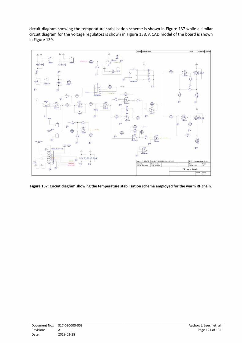
Document No.: Revision: Date:
317-030000-008 A 2019-02-28
Author: J. Leech et. al. Page 121 of 131
circuit diagram showing the temperature stabilisation scheme is shown in Figure 137 while a similar circuit diagram for the voltage regulators is shown in Figure 138. A CAD model of the board is shown in Figure 139.
Figure 137: Circuit diagram showing the temperature stabilisation scheme employed for the warm RF chain.
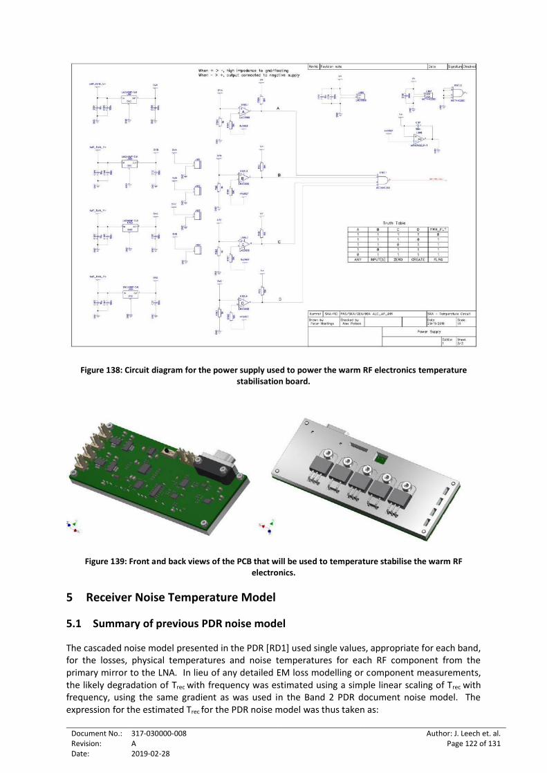
Document No.: Revision: Date:
317-030000-008 A 2019-02-28
Author: J. Leech et. al. Page 122 of 131
Figure 138: Circuit diagram for the power supply used to power the warm RF electronics temperature stabilisation board.
Figure 139: Front and back views of the PCB that will be used to temperature stabilise the warm RF electronics.
5 Receiver Noise Temperature Model
5.1 Summary of previous PDR noise model
The cascaded noise model presented in the PDR [RD1] used single values, appropriate for each band, for the losses, physical temperatures and noise temperatures for each RF component from the primary mirror to the LNA. In lieu of any detailed EM loss modelling or component measurements, the likely degradation of Trec with frequency was estimated using a simple linear scaling of Trec with frequency, using the same gradient as was used in the Band 2 PDR document noise model. The expression for the estimated Trec for the PDR noise model was thus taken as:
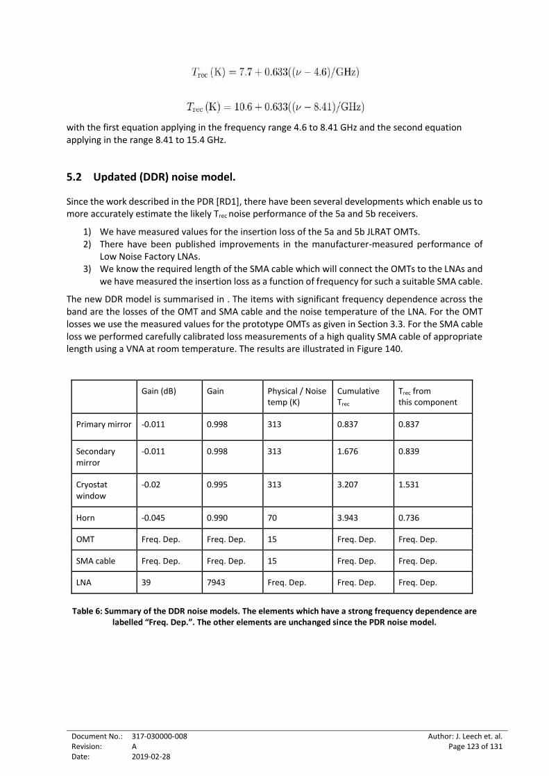
Document No.: Revision: Date:
317-030000-008 A 2019-02-28
Author: J. Leech et. al. Page 123 of 131
with the first equation applying in the frequency range 4.6 to 8.41 GHz and the second equation applying in the range 8.41 to 15.4 GHz.
5.2 Updated (DDR) noise model.
Since the work described in the PDR [RD1], there have been several developments which enable us to more accurately estimate the likely Trec noise performance of the 5a and 5b receivers.
1) We have measured values for the insertion loss of the 5a and 5b JLRAT OMTs. 2) There have been published improvements in the manufacturer-measured performance of
Low Noise Factory LNAs. 3) We know the required length of the SMA cable which will connect the OMTs to the LNAs and
we have measured the insertion loss as a function of frequency for such a suitable SMA cable.
The new DDR model is summarised in . The items with significant frequency dependence across the band are the losses of the OMT and SMA cable and the noise temperature of the LNA. For the OMT losses we use the measured values for the prototype OMTs as given in Section 3.3. For the SMA cable loss we performed carefully calibrated loss measurements of a high quality SMA cable of appropriate length using a VNA at room temperature. The results are illustrated in Figure 140.
Gain (dB) Gain Physical / Noise temp (K)
Cumulative Trec
Trec from this component
Primary mirror -0.011 0.998 313 0.837 0.837
Secondary mirror
-0.011 0.998 313 1.676 0.839
Cryostat window
-0.02 0.995 313 3.207 1.531
Horn -0.045 0.990 70 3.943 0.736
OMT Freq. Dep. Freq. Dep. 15 Freq. Dep. Freq. Dep.
SMA cable Freq. Dep. Freq. Dep. 15 Freq. Dep. Freq. Dep.
LNA 39 7943 Freq. Dep. Freq. Dep. Freq. Dep.
Table 6: Summary of the DDR noise models. The elements which have a strong frequency dependence are
labelled “Freq. Dep.”. The other elements are unchanged since the PDR noise model.
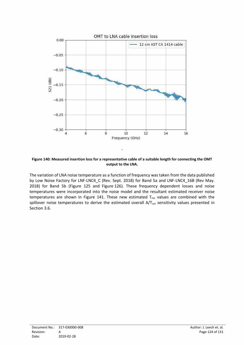
Document No.: Revision: Date:
317-030000-008 A 2019-02-28
Author: J. Leech et. al. Page 124 of 131
.
Figure 140: Measured insertion loss for a representative cable of a suitable length for connecting the OMT
output to the LNA.
The variation of LNA noise temperature as a function of frequency was taken from the data published by Low Noise Factory for LNF-LNC4_C (Rev. Sept. 2018) for Band 5a and LNF-LNC4_16B (Rev May. 2018) for Band 5b (Figure 125 and Figure 126). These frequency dependent losses and noise temperatures were incorporated into the noise model and the resultant estimated receiver noise temperatures are shown in Figure 141. These new estimated Trec values are combined with the spillover noise temperatures to derive the estimated overall A/Tsys sensitivity values presented in Section 3.6.
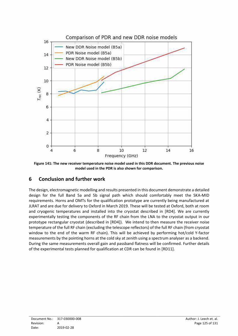
Document No.: Revision: Date:
317-030000-008 A 2019-02-28
Author: J. Leech et. al. Page 125 of 131
Figure 141: The new receiver temperature noise model used in this DDR document. The previous noise
model used in the PDR is also shown for comparison.
6 Conclusion and further work
The design, electromagnetic modelling and results presented in this document demonstrate a detailed design for the full Band 5a and 5b signal path which should comfortably meet the SKA-MID requirements. Horns and OMTs for the qualification prototype are currently being manufactured at JLRAT and are due for delivery to Oxford in March 2019. These will be tested at Oxford, both at room and cryogenic temperatures and installed into the cryostat described in [RD4]. We are currently experimentally testing the components of the RF chain from the LNA to the cryostat output in our prototype rectangular cryostat (described in [RD4]). We intend to then measure the receiver noise temperature of the full RF chain (excluding the telescope reflectors) of the full RF chain (from cryostat window to the end of the warm RF chain). This will be achieved by performing hot/cold Y-factor measurements by the pointing horns at the cold sky at zenith using a spectrum analyser as a backend. During the same measurements overall gain and passband flatness will be confirmed. Further details of the experimental tests planned for qualification at CDR can be found in [RD11].
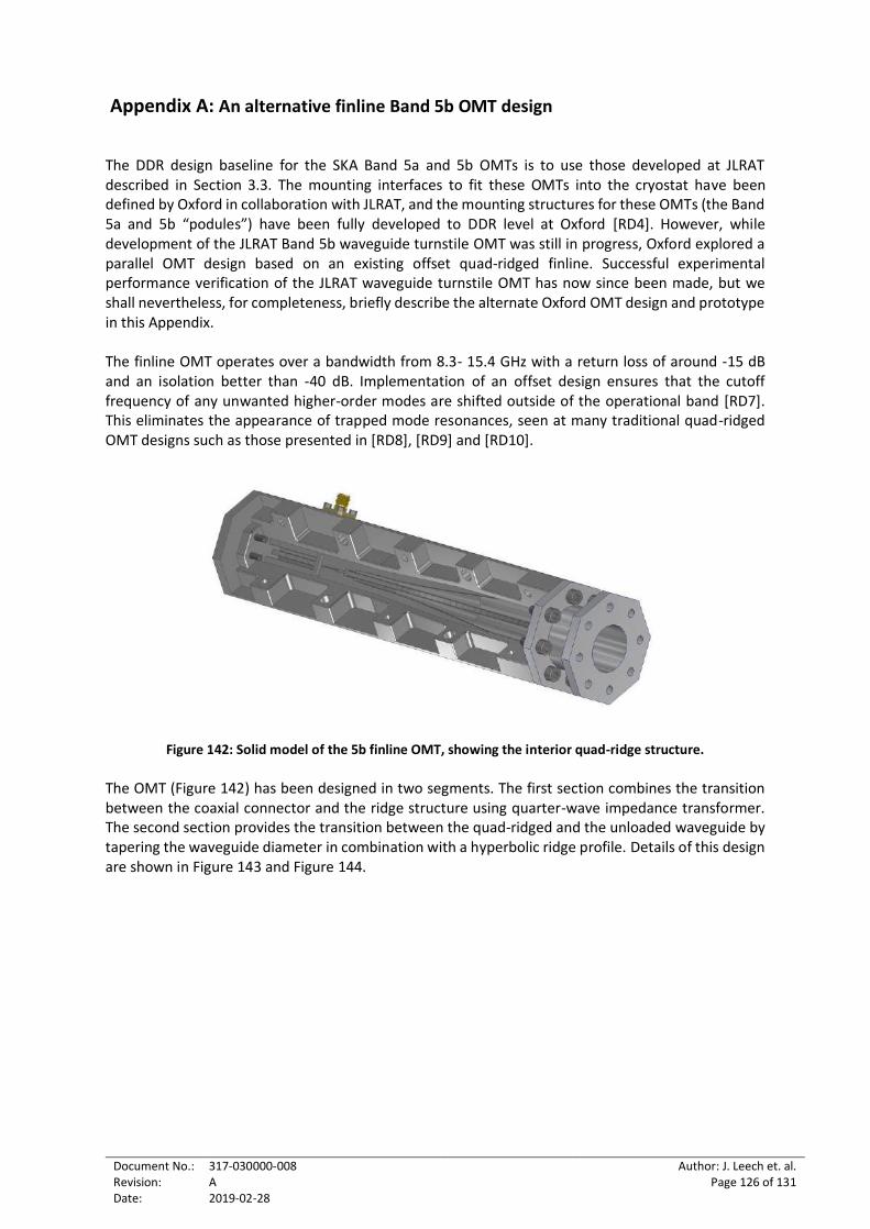
Document No.: Revision: Date:
317-030000-008 A 2019-02-28
Author: J. Leech et. al. Page 126 of 131
Appendix A: An alternative finline Band 5b OMT design
The DDR design baseline for the SKA Band 5a and 5b OMTs is to use those developed at JLRAT described in Section 3.3. The mounting interfaces to fit these OMTs into the cryostat have been defined by Oxford in collaboration with JLRAT, and the mounting structures for these OMTs (the Band 5a and 5b “podules”) have been fully developed to DDR level at Oxford [RD4]. However, while development of the JLRAT Band 5b waveguide turnstile OMT was still in progress, Oxford explored a parallel OMT design based on an existing offset quad-ridged finline. Successful experimental performance verification of the JLRAT waveguide turnstile OMT has now since been made, but we shall nevertheless, for completeness, briefly describe the alternate Oxford OMT design and prototype in this Appendix. The finline OMT operates over a bandwidth from 8.3- 15.4 GHz with a return loss of around -15 dB and an isolation better than -40 dB. Implementation of an offset design ensures that the cutoff frequency of any unwanted higher-order modes are shifted outside of the operational band [RD7]. This eliminates the appearance of trapped mode resonances, seen at many traditional quad-ridged OMT designs such as those presented in [RD8], [RD9] and [RD10].
Figure 142: Solid model of the 5b finline OMT, showing the interior quad-ridge structure.
The OMT (Figure 142) has been designed in two segments. The first section combines the transition between the coaxial connector and the ridge structure using quarter-wave impedance transformer. The second section provides the transition between the quad-ridged and the unloaded waveguide by tapering the waveguide diameter in combination with a hyperbolic ridge profile. Details of this design are shown in Figure 143 and Figure 144.
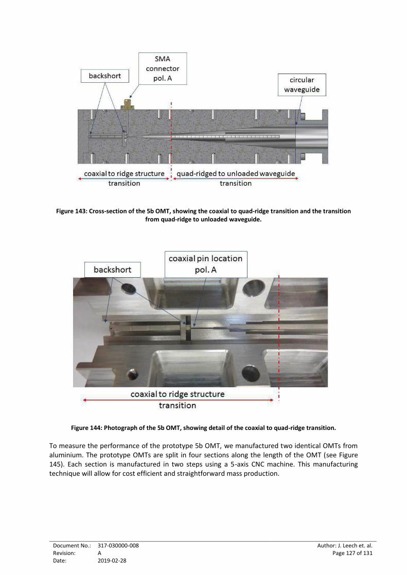
Document No.: Revision: Date:
317-030000-008 A 2019-02-28
Author: J. Leech et. al. Page 127 of 131
Figure 143: Cross-section of the 5b OMT, showing the coaxial to quad-ridge transition and the transition
from quad-ridge to unloaded waveguide.
Figure 144: Photograph of the 5b OMT, showing detail of the coaxial to quad-ridge transition.
To measure the performance of the prototype 5b OMT, we manufactured two identical OMTs from aluminium. The prototype OMTs are split in four sections along the length of the OMT (see Figure 145). Each section is manufactured in two steps using a 5-axis CNC machine. This manufacturing technique will allow for cost efficient and straightforward mass production.
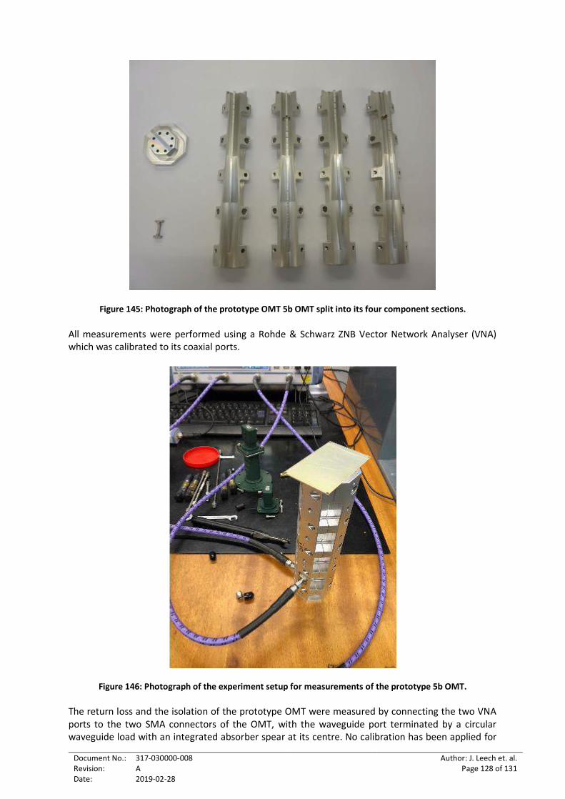
Document No.: Revision: Date:
317-030000-008 A 2019-02-28
Author: J. Leech et. al. Page 128 of 131
Figure 145: Photograph of the prototype OMT 5b OMT split into its four component sections.
All measurements were performed using a Rohde & Schwarz ZNB Vector Network Analyser (VNA) which was calibrated to its coaxial ports.
Figure 146: Photograph of the experiment setup for measurements of the prototype 5b OMT.
The return loss and the isolation of the prototype OMT were measured by connecting the two VNA ports to the two SMA connectors of the OMT, with the waveguide port terminated by a circular waveguide load with an integrated absorber spear at its centre. No calibration has been applied for
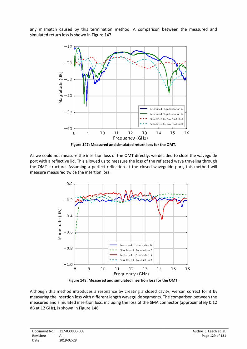
Document No.: Revision: Date:
317-030000-008 A 2019-02-28
Author: J. Leech et. al. Page 129 of 131
any mismatch caused by this termination method. A comparison between the measured and simulated return loss is shown in Figure 147.
Figure 147: Measured and simulated return loss for the OMT.
As we could not measure the insertion loss of the OMT directly, we decided to close the waveguide port with a reflective lid. This allowed us to measure the loss of the reflected wave traveling through the OMT structure. Assuming a perfect reflection at the closed waveguide port, this method will measure measured twice the insertion loss.
Figure 148: Measured and simulated insertion loss for the OMT.
Although this method introduces a resonance by creating a closed cavity, we can correct for it by measuring the insertion loss with different length waveguide segments. The comparison between the measured and simulated insertion loss, including the loss of the SMA connector (approximately 0.12 dB at 12 GHz), is shown in Figure 148.
Document No.: Revision: Date:
317-030000-008 A 2019-02-28
Author: J. Leech et. al. Page 130 of 131
The cross-polarization of the OMT has been measured using the same technique as applied to measure the insertion loss. However, for this measurement we measured the transmission between the two polarizations, thereby measuring the cross-coupling between the different polarizations. The comparison between the measured and simulated cross-polarization is shown in Figure 149.
Figure 149: Measured and simulated cross-polar isolation for the OMT.
The presented design of an offset quad-ridge OMT developed for the SKA 5b band shows good performance with respect to the measured return loss, insertion loss and cross- polarization.

Document No.: Revision: Date:
317-030000-008 A 2019-02-28
Author: J. Leech et. al. Page 131 of 131