scanning tunneling microscopy/spectroscopy of titanium dioxide nanoparticulate film on au() surface
TRANSCRIPT

Scanning tunneling microscopy/spectroscopy of picene thin films formed on Ag(111)Yasuo Yoshida, Hung-Hsiang Yang, Hsu-Sheng Huang, Shu-You Guan, Susumu Yanagisawa, Takuya
Yokosuka, Minn-Tsong Lin, Wei-Bin Su, Chia-Seng Chang, Germar Hoffmann, and Yukio Hasegawa
Citation: The Journal of Chemical Physics 141, 114701 (2014); doi: 10.1063/1.4894439 View online: http://dx.doi.org/10.1063/1.4894439 View Table of Contents: http://scitation.aip.org/content/aip/journal/jcp/141/11?ver=pdfcov Published by the AIP Publishing Articles you may be interested in C58 on Au(111): A scanning tunneling microscopy study J. Chem. Phys. 138, 104703 (2013); 10.1063/1.4793761 Characterization of thiol-functionalized oligo(phenylene-ethynylene)-protected Au nanoparticles by scanningtunneling microscopy and spectroscopy Appl. Phys. Lett. 101, 083115 (2012); 10.1063/1.4747720 Scanning tunneling microscopy/spectroscopy study of atomic and electronic structures of In 2 O on InAs and In0.53 Ga 0.47 As ( 001 ) - ( 4 × 2 ) surfaces J. Chem. Phys. 133, 164704 (2010); 10.1063/1.3497040 Modification of Ag(111) surface electronic structure via weak molecular adsorption of adenine measured with lowtemperature scanning tunneling microscopy and spectroscopy J. Chem. Phys. 132, 214701 (2010); 10.1063/1.3427248 Rectifying behavior of silicon–phthalocyanine junctions investigated with scanning tunnelingmicroscopy/spectroscopy J. Vac. Sci. Technol. A 15, 1014 (1997); 10.1116/1.580508
This article is copyrighted as indicated in the article. Reuse of AIP content is subject to the terms at: http://scitation.aip.org/termsconditions. Downloaded to IP:
140.114.82.58 On: Wed, 17 Sep 2014 01:48:03

THE JOURNAL OF CHEMICAL PHYSICS 141, 114701 (2014)
Scanning tunneling microscopy/spectroscopy of picene thin films formedon Ag(111)
Yasuo Yoshida,1,a) Hung-Hsiang Yang,2 Hsu-Sheng Huang,3 Shu-You Guan,3
Susumu Yanagisawa,4 Takuya Yokosuka,1 Minn-Tsong Lin,2,5 Wei-Bin Su,3
Chia-Seng Chang,3 Germar Hoffmann,1,6 and Yukio Hasegawa1,b)
1The Institute of Solid State Physics, The University of Tokyo, Kashiwa 277-8581, Japan2Department of Physics, National Taiwan University, Taipei 106, Taiwan3Institute of Physics, Academia Sinica, Nankang, Taipei 11529, Taiwan4Department of Physics and Earth Science Department, University of the Ryukyus, 1 Nishihara,Okinawa 903-0213, Japan5Institute of Atomic and Molecular Sciences, Academia Sinica, Taipei 10617, Taiwan6Department of Physics, National Tsing Hua University, Hsinchu 30013, Taiwan
(Received 13 June 2014; accepted 15 August 2014; published online 16 September 2014)
Using ultrahigh-vacuum low-temperature scanning tunneling microscopy and spectroscopy com-bined with first principles density functional theory calculations, we have investigated structuraland electronic properties of pristine and potassium (K)-deposited picene thin films formed in situon a Ag(111) substrate. At low coverages, the molecules are uniformly distributed with the longaxis aligned along the [112̄] direction of the substrate. At higher coverages, ordered structurescomposed of monolayer molecules are observed, one of which is a monolayer with tilted and flat-lying molecules resembling a (11̄0) plane of the bulk crystalline picene. Between the moleculesand the substrate, the van der Waals interaction is dominant with negligible hybridization be-tween their electronic states; a conclusion that contrasts with the chemisorption exhibited by pen-tacene molecules on the same substrate. We also observed a monolayer picene thin film in whichall molecules were standing to form an intermolecular π stacking. Two-dimensional delocalizedelectronic states are found on the K-deposited π stacking structure. © 2014 AIP Publishing LLC.[http://dx.doi.org/10.1063/1.4894439]
I. INTRODUCTION
Picene (C22H14), its chemical structure depicted inFig. 1(c), is a simple aromatic compound composed of fivefused benzene rings with an arm-chair edge. Thin films ofone of its isomers, pentacene, possessing instead a zigzagedge, have been studied extensively because their high car-rier mobility makes them a promising candidate for molecu-lar electronic device applications such as organic field effecttransistors1–3 and photovoltaic cells.4, 5 However, instabilityor degradation of the molecule under atmospheric conditionsremains a fundamental limitation to the pursuit of these prac-tical applications.6 Picene is chemically stable due to the largeenergy band gap (3.3 eV), compared with pentacene (1.8 eV),but has delocalized π -electrons in thin films and high carriermobility under oxygen exposure,6 a combination of the prop-erties making it a promising post-pentacene candidate ma-terial for molecular electronics. Very recently, the moleculehas attracted tremendous attention for an entirely differentproperty, namely, the discovery of superconductivity in potas-sium (K)-doped picene with the critical temperature of 19 K,7
followed by discoveries of similar aromatic compound-basedsuperconductors with even higher transition temperatures upto 30 K.8, 9 In spite of this surprisingly high transition tem-perature, high reactivity in the air limits experimental access
a)E-mail: [email protected])Author to whom correspondence should be addressed. Electronic mail:
to K-doped picene, and therefore, molecular level details ofgrowth, structural, and electronic properties have remainedelusive.
The properties of the molecular thin films depend onthe nature of the interfaces between the molecules and thesubstrate.10 Understanding the contacts is a major motiva-tion behind a study of molecular layer formation on surfaces.The performance of molecular devices also depends on therelative alignment of energy levels in the molecules, whichmay be strongly modified by the interaction of substrateelectronic states with molecular orbitals.11 Here, in order tounderstand structural and electronic properties of the molecu-lar layer and their interactions with the substrate, we investi-gated ultrathin films of picene formed on a Ag(111) substratein situ under ultrahigh vacuum (UHV) conditions by low-temperature scanning tunneling microscopy and spectroscopy(STM/STS) combined with first principles density functionaltheory (DFT) calculations. The obtained results indicate thatthe molecule has a weak van der Waals (vdW) interactionwith the substrate (in contrast with pentacene on Ag(111)),and thus exhibits a growth mode different from that of thesister molecule.
II. METHODS
A. STM experiment
The experiments were performed using an ultrahigh vac-uum STM setup (USM-1300, Unisoku, and SPM-1000, RHK)
0021-9606/2014/141(11)/114701/8/$30.00 © 2014 AIP Publishing LLC141, 114701-1
This article is copyrighted as indicated in the article. Reuse of AIP content is subject to the terms at: http://scitation.aip.org/termsconditions. Downloaded to IP:
140.114.82.58 On: Wed, 17 Sep 2014 01:48:03
114701-2 Yoshida et al. J. Chem. Phys. 141, 114701 (2014)
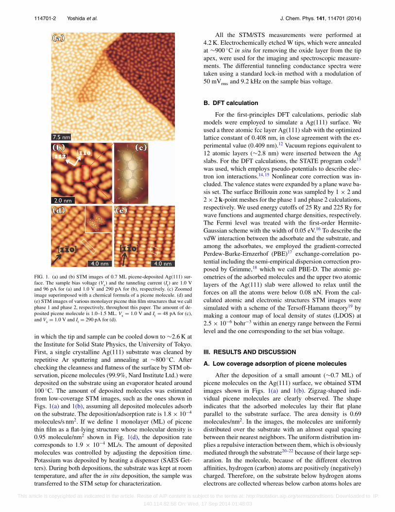
FIG. 1. (a) and (b) STM images of 0.7 ML picene-deposited Ag(111) sur-face. The sample bias voltage (Vs) and the tunneling current (It) are 1.0 Vand 96 pA for (a) and 1.0 V and 290 pA for (b), respectively. (c) Zoomedimage superimposed with a chemical formula of a picene molecule. (d) and(e) STM images of various monolayer picene thin film structures that we callphase 1 and phase 2, respectively, throughout this paper. The amount of de-posited picene molecule is 1.0–1.5 ML. Vs = 1.0 V and It = 48 pA for (c),and Vs = 1.0 V and It = 290 pA for (d).
in which the tip and sample can be cooled down to ∼2.6 K atthe Institute for Solid State Physics, the University of Tokyo.First, a single crystalline Ag(111) substrate was cleaned byrepetitive Ar sputtering and annealing at ∼800 ◦C. Afterchecking the cleanness and flatness of the surface by STM ob-servation, picene molecules (99.9%, Nard Institute Ltd.) weredeposited on the substrate using an evaporator heated around100 ◦C. The amount of deposited molecules was estimatedfrom low-coverage STM images, such as the ones shown inFigs. 1(a) and 1(b), assuming all deposited molecules adsorbon the substrate. The deposition/adsorption rate is 1.8 × 10⁻⁴
molecules/s nm2. If we define 1 monolayer (ML) of picenethin film as a flat-lying structure whose molecular density is0.95 molecule/nm2 shown in Fig. 1(d), the deposition ratecorresponds to 1.9 × 10⁻⁴ ML/s. The amount of depositedmolecules was controlled by adjusting the deposition time.Potassium was deposited by heating a dispenser (SAES Get-ters). During both depositions, the substrate was kept at roomtemperature, and after the in situ deposition, the sample wastransferred to the STM setup for characterization.
All the STM/STS measurements were performed at4.2 K. Electrochemically etched W tips, which were annealedat ∼900 ◦C in situ for removing the oxide layer from the tipapex, were used for the imaging and spectroscopic measure-ments. The differential tunneling conductance spectra weretaken using a standard lock-in method with a modulation of50 mVrms and 9.2 kHz on the sample bias voltage.
B. DFT calculation
For the first-principles DFT calculations, periodic slabmodels were employed to simulate a Ag(111) surface. Weused a three atomic fcc layer Ag(111) slab with the optimizedlattice constant of 0.408 nm, in close agreement with the ex-perimental value (0.409 nm).12 Vacuum regions equivalent to12 atomic layers (∼2.8 nm) were inserted between the Agslabs. For the DFT calculations, the STATE program code13
was used, which employs pseudo-potentials to describe elec-tron ion interactions.14, 15 Nonlinear core correction was in-cluded. The valence states were expanded by a plane wave ba-sis set. The surface Brillouin zone was sampled by 1 × 2 and2 × 2 k-point meshes for the phase 1 and phase 2 calculations,respectively. We used energy cutoffs of 25 Ry and 225 Ry forwave functions and augmented charge densities, respectively.The Fermi level was treated with the first-order Hermite-Gaussian scheme with the width of 0.05 eV.16 To describe thevdW interaction between the adsorbate and the substrate, andamong the adsorbates, we employed the gradient-correctedPerdew-Burke-Ernzerhof (PBE)17 exchange-correlation po-tential including the semi-empirical dispersion correction pro-posed by Grimme,18 which we call PBE-D. The atomic ge-ometries of the adsorbed molecules and the upper two atomiclayers of the Ag(111) slab were allowed to relax until theforces on all the atoms were below 0.08 nN. From the cal-culated atomic and electronic structures STM images weresimulated with a scheme of the Tersoff-Hamann theory19 bymaking a contour map of local density of states (LDOS) at2.5 × 10−6 bohr−3 within an energy range between the Fermilevel and the one corresponding to the set bias voltage.
III. RESULTS AND DISCUSSION
A. Low coverage adsorption of picene molecules
After the deposition of a small amount (∼0.7 ML) ofpicene molecules on the Ag(111) surface, we obtained STMimages shown in Figs. 1(a) and 1(b). Zigzag-shaped indi-vidual picene molecules are clearly observed. The shapeindicates that the adsorbed molecules lay their flat planeparallel to the substrate surface. The area density is 0.69molecules/nm2. In the images, the molecules are uniformlydistributed over the substrate with an almost equal spacingbetween their nearest neighbors. The uniform distribution im-plies a repulsive interaction between them, which is obviouslymediated through the substrate20–22 because of their large sep-aration. In the molecule, because of the different electronaffinities, hydrogen (carbon) atoms are positively (negatively)charged. Therefore, on the substrate below hydrogen atomselectrons are collected whereas below carbon atoms holes are
This article is copyrighted as indicated in the article. Reuse of AIP content is subject to the terms at: http://scitation.aip.org/termsconditions. Downloaded to IP:
140.114.82.58 On: Wed, 17 Sep 2014 01:48:03
114701-3 Yoshida et al. J. Chem. Phys. 141, 114701 (2014)
collected. Since the edge of molecules is completely occupiedby hydrogen atoms, the electron clouds below the moleculesrepel each other and contribute to the repulsive interactionamong the adsorbed molecules. No bright protrusions arefound at the ends of the molecules, indicating no bending, un-like the case of pentacene molecules deposited on Cu(111).23
All picene molecules align their long axis along the [112̄]direction of the substrate. The orientation is also differentfrom that of pentacene molecules adsorbed on Cu(111)23 andAg(111),24 where the long axis of the adsorbed moleculesalign to the close-packed [11̄0] directions.
B. Monolayer coverage structuresof picene molecules
Further molecular deposition (1.0–1.5 ML) makes vari-ous ordered structures of the adsorbed molecules, as shownin Figs. 1(d) and 1(e), and 6(a) in a sequence of themolecular density. In the lowest-density structure shown inFig. 1(d), which we call phase 1 hereafter, the molecules makerows along the [11̄0] direction of the Ag substrate with theirlong axis aligned to the [112̄] direction. Judging from the ob-served bright protrusions similar in size to that of the isolatedmolecules, as demonstrated with a superimposed structuralformula in an inset of Fig. 1(d), the molecules are most likelylaid flat parallel to the substrate surface. Despite random ori-entations of the zigzag shape of the molecule, translationalperiodicities of the center of the molecules are obvious in therow and inter-row directions. The two-dimensionally (2D) or-dered molecular structure has a centered rectangular unit cell,depicted with a white box in Fig. 1(d), with a space group ofcm whose lengths are 0.75 ± 0.05 nm and 2.8 ± 0.2 nm. Thedensity of the molecule is 0.95 ± 0.06 molecules/nm2. Theunit length along the close-packed direction is ∼2.5 timesthe Ag(111) atomic distance (0.298 nm); 2 intermolecularspacings correspond to 5 atom spacings of the substrate. Thestructure is symmetric with respect to the (11̄0) and (1̄1̄2)planes of the substrate except for the randomness of the zigzagorientation and slight meanderings of the molecular rows.
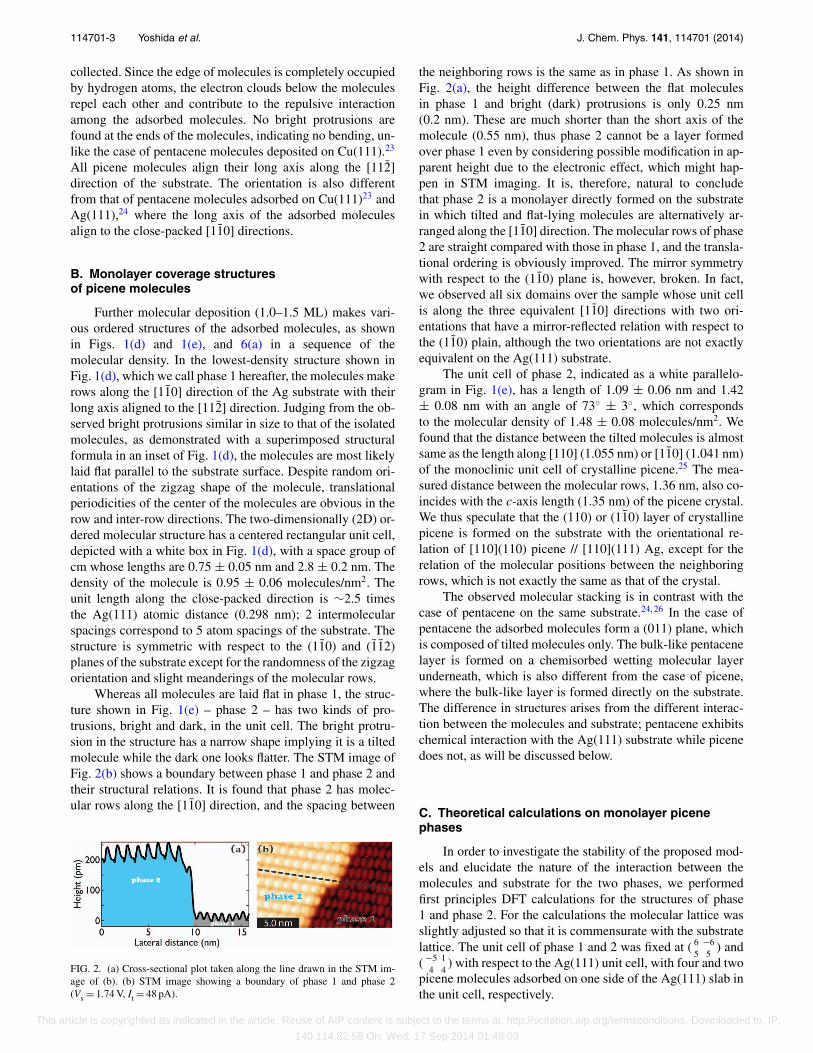
Whereas all molecules are laid flat in phase 1, the struc-ture shown in Fig. 1(e) – phase 2 – has two kinds of pro-trusions, bright and dark, in the unit cell. The bright protru-sion in the structure has a narrow shape implying it is a tiltedmolecule while the dark one looks flatter. The STM image ofFig. 2(b) shows a boundary between phase 1 and phase 2 andtheir structural relations. It is found that phase 2 has molec-ular rows along the [11̄0] direction, and the spacing between
FIG. 2. (a) Cross-sectional plot taken along the line drawn in the STM im-age of (b). (b) STM image showing a boundary of phase 1 and phase 2(Vs = 1.74 V, It = 48 pA).
the neighboring rows is the same as in phase 1. As shown inFig. 2(a), the height difference between the flat moleculesin phase 1 and bright (dark) protrusions is only 0.25 nm(0.2 nm). These are much shorter than the short axis of themolecule (0.55 nm), thus phase 2 cannot be a layer formedover phase 1 even by considering possible modification in ap-parent height due to the electronic effect, which might hap-pen in STM imaging. It is, therefore, natural to concludethat phase 2 is a monolayer directly formed on the substratein which tilted and flat-lying molecules are alternatively ar-ranged along the [11̄0] direction. The molecular rows of phase2 are straight compared with those in phase 1, and the transla-tional ordering is obviously improved. The mirror symmetrywith respect to the (11̄0) plane is, however, broken. In fact,we observed all six domains over the sample whose unit cellis along the three equivalent [11̄0] directions with two ori-entations that have a mirror-reflected relation with respect tothe (11̄0) plain, although the two orientations are not exactlyequivalent on the Ag(111) substrate.
The unit cell of phase 2, indicated as a white parallelo-gram in Fig. 1(e), has a length of 1.09 ± 0.06 nm and 1.42± 0.08 nm with an angle of 73◦ ± 3◦, which correspondsto the molecular density of 1.48 ± 0.08 molecules/nm2. Wefound that the distance between the tilted molecules is almostsame as the length along [110] (1.055 nm) or [11̄0] (1.041 nm)of the monoclinic unit cell of crystalline picene.25 The mea-sured distance between the molecular rows, 1.36 nm, also co-incides with the c-axis length (1.35 nm) of the picene crystal.We thus speculate that the (110) or (11̄0) layer of crystallinepicene is formed on the substrate with the orientational re-lation of [110](110) picene // [110](111) Ag, except for therelation of the molecular positions between the neighboringrows, which is not exactly the same as that of the crystal.
The observed molecular stacking is in contrast with thecase of pentacene on the same substrate.24, 26 In the case ofpentacene the adsorbed molecules form a (011) plane, whichis composed of tilted molecules only. The bulk-like pentacenelayer is formed on a chemisorbed wetting molecular layerunderneath, which is also different from the case of picene,where the bulk-like layer is formed directly on the substrate.The difference in structures arises from the different interac-tion between the molecules and substrate; pentacene exhibitschemical interaction with the Ag(111) substrate while picenedoes not, as will be discussed below.
C. Theoretical calculations on monolayer picenephases
In order to investigate the stability of the proposed mod-els and elucidate the nature of the interaction between themolecules and substrate for the two phases, we performedfirst principles DFT calculations for the structures of phase1 and phase 2. For the calculations the molecular lattice wasslightly adjusted so that it is commensurate with the substratelattice. The unit cell of phase 1 and 2 was fixed at ( 6 −6
5 5) and
( −5 14 4
) with respect to the Ag(111) unit cell, with four and twopicene molecules adsorbed on one side of the Ag(111) slab inthe unit cell, respectively.
This article is copyrighted as indicated in the article. Reuse of AIP content is subject to the terms at: http://scitation.aip.org/termsconditions. Downloaded to IP:
140.114.82.58 On: Wed, 17 Sep 2014 01:48:03
114701-4 Yoshida et al. J. Chem. Phys. 141, 114701 (2014)
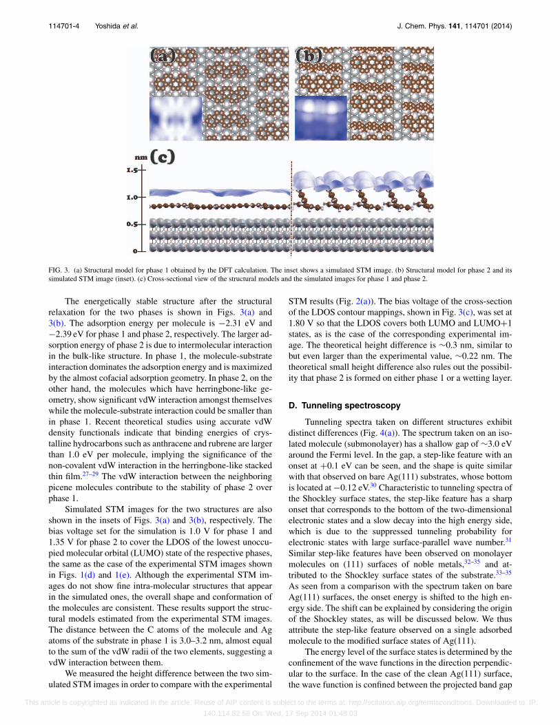
FIG. 3. (a) Structural model for phase 1 obtained by the DFT calculation. The inset shows a simulated STM image. (b) Structural model for phase 2 and itssimulated STM image (inset). (c) Cross-sectional view of the structural models and the simulated images for phase 1 and phase 2.
The energetically stable structure after the structuralrelaxation for the two phases is shown in Figs. 3(a) and3(b). The adsorption energy per molecule is −2.31 eV and−2.39 eV for phase 1 and phase 2, respectively. The larger ad-sorption energy of phase 2 is due to intermolecular interactionin the bulk-like structure. In phase 1, the molecule-substrateinteraction dominates the adsorption energy and is maximizedby the almost cofacial adsorption geometry. In phase 2, on theother hand, the molecules which have herringbone-like ge-ometry, show significant vdW interaction amongst themselveswhile the molecule-substrate interaction could be smaller thanin phase 1. Recent theoretical studies using accurate vdWdensity functionals indicate that binding energies of crys-talline hydrocarbons such as anthracene and rubrene are largerthan 1.0 eV per molecule, implying the significance of thenon-covalent vdW interaction in the herringbone-like stackedthin film.27–29 The vdW interaction between the neighboringpicene molecules contribute to the stability of phase 2 overphase 1.
Simulated STM images for the two structures are alsoshown in the insets of Figs. 3(a) and 3(b), respectively. Thebias voltage set for the simulation is 1.0 V for phase 1 and1.35 V for phase 2 to cover the LDOS of the lowest unoccu-pied molecular orbital (LUMO) state of the respective phases,the same as the case of the experimental STM images shownin Figs. 1(d) and 1(e). Although the experimental STM im-ages do not show fine intra-molecular structures that appearin the simulated ones, the overall shape and conformation ofthe molecules are consistent. These results support the struc-tural models estimated from the experimental STM images.The distance between the C atoms of the molecule and Agatoms of the substrate in phase 1 is 3.0–3.2 nm, almost equalto the sum of the vdW radii of the two elements, suggesting avdW interaction between them.
We measured the height difference between the two sim-ulated STM images in order to compare with the experimental
STM results (Fig. 2(a)). The bias voltage of the cross-sectionof the LDOS contour mappings, shown in Fig. 3(c), was set at1.80 V so that the LDOS covers both LUMO and LUMO+1states, as is the case of the corresponding experimental im-age. The theoretical height difference is ∼0.3 nm, similar tobut even larger than the experimental value, ∼0.22 nm. Thetheoretical small height difference also rules out the possibil-ity that phase 2 is formed on either phase 1 or a wetting layer.
D. Tunneling spectroscopy
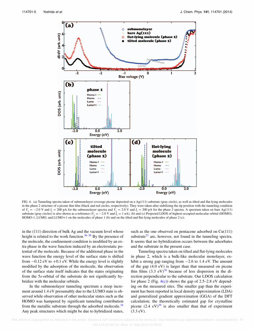
Tunneling spectra taken on different structures exhibitdistinct differences (Fig. 4(a)). The spectrum taken on an iso-lated molecule (submonolayer) has a shallow gap of ∼3.0 eVaround the Fermi level. In the gap, a step-like feature with anonset at +0.1 eV can be seen, and the shape is quite similarwith that observed on bare Ag(111) substrates, whose bottomis located at −0.12 eV.30 Characteristic to tunneling spectra ofthe Shockley surface states, the step-like feature has a sharponset that corresponds to the bottom of the two-dimensionalelectronic states and a slow decay into the high energy side,which is due to the suppressed tunneling probability forelectronic states with large surface-parallel wave number.31
Similar step-like features have been observed on monolayermolecules on (111) surfaces of noble metals,32–35 and at-tributed to the Shockley surface states of the substrate.33–35
As seen from a comparison with the spectrum taken on bareAg(111) surfaces, the onset energy is shifted to the high en-ergy side. The shift can be explained by considering the originof the Shockley states, as will be discussed below. We thusattribute the step-like feature observed on a single adsorbedmolecule to the modified surface states of Ag(111).
The energy level of the surface states is determined by theconfinement of the wave functions in the direction perpendic-ular to the surface. In the case of the clean Ag(111) surface,the wave function is confined between the projected band gap
This article is copyrighted as indicated in the article. Reuse of AIP content is subject to the terms at: http://scitation.aip.org/termsconditions. Downloaded to IP:
140.114.82.58 On: Wed, 17 Sep 2014 01:48:03
114701-5 Yoshida et al. J. Chem. Phys. 141, 114701 (2014)
FIG. 4. (a) Tunneling spectra taken of submonolayer coverage picene deposited on a Ag(111) substrate (gray circle), as well as tilted and flat-lying moleculesin the phase 2 structure of a picene thin film (black and red circles, respectively). They were taken after stabilizing the tip position with the tunneling conditionof Vs = −2.0 V and It = 200 pA for the submonolayer spectra and Vs = 2.0 V and It = 200 pA for the phase 2 spectra. A spectrum taken on bare Ag(111)substrate (gray circles) is also shown as a reference (Vs = −2.0 V and It = 1 nA). (b) and (c) Projected LDOS of highest occupied molecular orbital (HOMO),HOMO-1, LUMO, and LUMO+1 on the molecules of phase 1 (b) and on the tilted and flat-lying molecules of phase 2 (c).
in the (111) direction of bulk Ag and the vacuum level whoseheight is related to the work function.36–38 By the presence ofthe molecule, the confinement condition is modified by an ex-tra phase in the wave function induced by an electrostatic po-tential of the molecule. Because of the additional phase in thewave function the energy level of the surface state is shiftedfrom −0.12 eV to +0.1 eV. While the energy level is slightlymodified by the adsorption of the molecule, the observationof the surface state itself indicates that the states originatingfrom the 5s-orbital of the substrate do not significantly hy-bridize with the molecular orbitals.
In the submonolayer tunneling spectrum a steep incre-ment around 1.4 eV presumably due to the LUMO state is ob-served while observation of other molecular states such as theHOMO was hampered by significant tunneling contributionfrom the metallic substrate through the adsorbed molecule.34
Any peak structures which might be due to hybridized states,
such as the one observed on pentacene adsorbed on Cu(111)substrate23 are, however, not found in the tunneling spectra.It seems that no hybridization occurs between the adsorbatesand the substrate in the present case.
Tunneling spectra taken on tilted and flat-lying moleculesin phase 2, which is a bulk-like molecular monolayer, ex-hibit a strong gap ranging from −2.6 to 1.4 eV. The amountof the gap (4.0 eV) is larger than that measured on picenethin films (3.3 eV)39 because of less dispersion in the di-rection perpendicular to the substrate. Our LDOS calculationfor phase 2 (Fig. 4(c)) shows the gap of 2.5–2.8 eV depend-ing on the measured sites. The smaller gap than the experi-ment has been reported in local density approximation (LDA)and generalized gradient approximation (GGA) of the DFTcalculation; the theoretically estimated gap for crystallinepicene (2.4 eV)39 is also smaller than that of experiment(3.3 eV).
This article is copyrighted as indicated in the article. Reuse of AIP content is subject to the terms at: http://scitation.aip.org/termsconditions. Downloaded to IP:
140.114.82.58 On: Wed, 17 Sep 2014 01:48:03
114701-6 Yoshida et al. J. Chem. Phys. 141, 114701 (2014)
The spectrum taken on tilted (flat-lying) moleculesshown in Fig. 4(a) exhibits peaks at −3.0, 1.7, and 1.9 eV(−3.0, −1.8, and −2.0 eV), although we found that the peakenergy differences between the two molecules fluctuate by∼0.15 eV probably due to variation in the local intermolecu-lar configuration. While the energy levels of the HOMO stateof the two molecules do not differ, the energy levels of theLUMO and LUMO+1 states taken on flat-lying moleculesare in general higher than those of tilted molecules. Whenthe intermolecular distance is small, the Pauli repulsion in-duces charge redistribution in the molecules and substrate,modifying the electrostatic potential of the relevant moleculesand their electronic states.11 The peak energies of LUMO andLUMO+1 states obtained by our first principles calculationshown in Fig. 4(c) are almost same between the tilted andflat-lying molecules. The same calculation performed witha unit cell smaller in size by 82%, however, showed higherLUMO and LUMO+1 states on flat-lying molecules thantilted ones by 0.2 eV. This indicates that local variation inthe intermolecular distance modifies the local potential of themolecules and induces the peak energy differences betweenthe two molecules.
The calculated spectra exhibit several peaks with smallenergy dispersion, as shown in Figs. 4(c) and 4(d). Both theexperimental and theoretical tunneling spectra on phase 2 donot show any features in the gap, which indicates negligiblehybridization between the orbitals of the adsorbed moleculesand the electronic states of the substrate in the phase. Sev-eral very tiny peaks can be found in the theoretical results,but these peaks are not large enough to produce peak struc-tures in tunneling spectra like the ones observed by Smer-don et al.23 on pentacene/Cu(111) and Gonzalez-Lakunzaet al.33 According to the Mulliken population analysis theamount of charge transfer from the substrate to the LUMOand LUMO+1 states of the tilted and flat-lying moleculesdue to the gap states is only 0.02e and 0.04e, respectively,where e is the electron charge. It is not reasonable to claimchemisorption from such small amounts of charge transfer.Note that the tip-sample distance during our tunneling con-ductance measurements is similar to or even smaller than thatof Gonzalez-Lakunza et al.,33 who observed peaks due to hy-bridized states at the TCNQ/Au(111) interface, judged from acomparison of the two stabilization conditions. We thus do notthink our tip-sample distance was too far to detect hybridizedstates. A theoretical tunneling spectrum of phase 1 (Fig. 4(b))does not show peaks in the gap either. All these results leadus to conclude that the interaction between the molecule andthe substrate is dominated by the vdW interaction and that thecontribution of the chemical interaction is negligibly small.
The weak interaction and the vdW binding nature of themolecule to the substrate are quite different from the caseof the sister molecule, pentacene. The straight 5-benzene-ring molecule is known to chemisorb on Cu(111)40–42 andAg(111)24, 26 surfaces; the hybridized states between themolecular orbitals and substrate states and their energy disper-sions have been observed experimentally by angle-resolvedphotoemission spectroscopy,41 and reproduced theoreticallyby first principles calculations.42 We attribute the difference inthe bonding nature between the two 5-benzene-ring molecules
to the difference in their band gap; picene has wider bandgap than pentacene, and therefore the energy levels of themolecular states of picene are far from the Fermi level. Largeenergy differences between the molecular orbitals and therelevant electronic states of the substrate suppress hybridiza-tion between them. As a consequence of the different bond-ing nature, the growth modes of the thin films of the twomolecules are quite different; Thayer et al.43 reported thatpentacene molecules form a flat-lying layer on strongly inter-acting metallic substrates, while on weakly-bound semi-metalBi substrates bulk-like structures are formed directly on thesurface. The bulk-like structure in phase 2 directly bound tothe substrate is attributed to the weak physisorbed interactionbetween the picene molecules and the Ag(111) substrate.
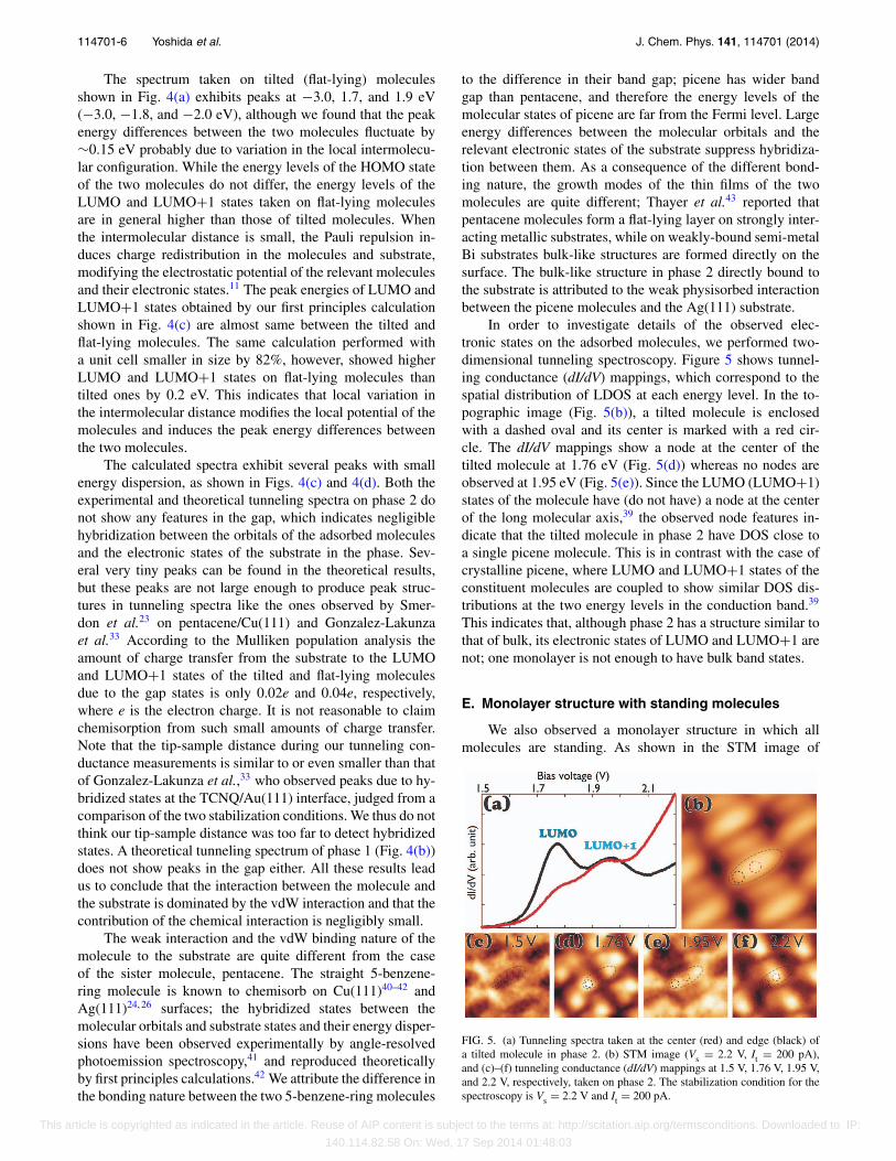
In order to investigate details of the observed elec-tronic states on the adsorbed molecules, we performed two-dimensional tunneling spectroscopy. Figure 5 shows tunnel-ing conductance (dI/dV) mappings, which correspond to thespatial distribution of LDOS at each energy level. In the to-pographic image (Fig. 5(b)), a tilted molecule is enclosedwith a dashed oval and its center is marked with a red cir-cle. The dI/dV mappings show a node at the center of thetilted molecule at 1.76 eV (Fig. 5(d)) whereas no nodes areobserved at 1.95 eV (Fig. 5(e)). Since the LUMO (LUMO+1)states of the molecule have (do not have) a node at the centerof the long molecular axis,39 the observed node features in-dicate that the tilted molecule in phase 2 have DOS close toa single picene molecule. This is in contrast with the case ofcrystalline picene, where LUMO and LUMO+1 states of theconstituent molecules are coupled to show similar DOS dis-tributions at the two energy levels in the conduction band.39
This indicates that, although phase 2 has a structure similar tothat of bulk, its electronic states of LUMO and LUMO+1 arenot; one monolayer is not enough to have bulk band states.
E. Monolayer structure with standing molecules
We also observed a monolayer structure in which allmolecules are standing. As shown in the STM image of
FIG. 5. (a) Tunneling spectra taken at the center (red) and edge (black) ofa tilted molecule in phase 2. (b) STM image (Vs = 2.2 V, It = 200 pA),and (c)–(f) tunneling conductance (dI/dV) mappings at 1.5 V, 1.76 V, 1.95 V,and 2.2 V, respectively, taken on phase 2. The stabilization condition for thespectroscopy is Vs = 2.2 V and It = 200 pA.
This article is copyrighted as indicated in the article. Reuse of AIP content is subject to the terms at: http://scitation.aip.org/termsconditions. Downloaded to IP:
140.114.82.58 On: Wed, 17 Sep 2014 01:48:03
114701-7 Yoshida et al. J. Chem. Phys. 141, 114701 (2014)
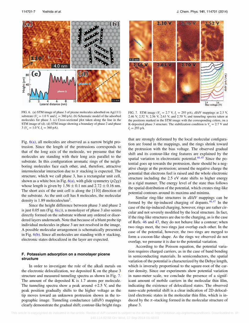
FIG. 6. (a) STM image of phase 3 of picene molecules adsorbed on Ag(111)substrate (Vs = 1.0 V and It = 360 pA). (b) Schematic model of the adsorbedmolecules for phase 3. (c) Cross-sectional plot taken along the line in theSTM image of (d). (d) STM image showing a boundary of phase 2 and phase3 (Vs = 1.0 V, It = 360 pA).
Fig. 6(a), all molecules are observed as a narrow bright pro-trusion. Since the length of the protrusions corresponds tothat of the long axis of the molecule, we presume that themolecules are standing with their long axis parallel to thesubstrate. In this configuration aromatic rings of the neigh-boring molecules face each other, and, therefore, attractiveintermolecular interaction due to π stacking is expected. Thestructure, which we call phase 3, has a rectangular unit cell,shown as a white box in Fig. 6(a), with glide symmetry (p2gg)whose length is given by 1.56 ± 0.1 nm and 2.72 ± 0.16 nm.The short axis of the unit cell is along the [11̄0] direction ofthe substrate. As the unit cell has 8 molecules, the moleculardensity is 1.89 molecules/nm2.
Since the height difference between phase 3 and phase 2is just 0.05 nm (Fig. 6(c)), a monolayer of phase 3 also seemsdirectly formed on the substrate without any ordered or disor-dered layers underneath. Note that because of a blunt probe tipindividual molecules in phase 3 are not resolved in the image.A possible molecular arrangement is schematically presentedin Fig. 6(b). Since all molecules are standing with π stacking,electronic states delocalized in the layer are expected.
F. Potassium adsorption on a monolayer picenestructure
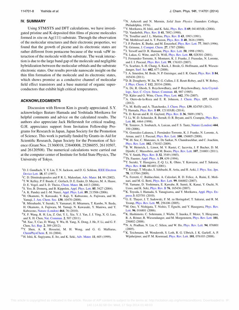
In order to investigate the role of the alkali metals onthe electronic delocalization, we deposited K on the phase 3structure and measured tunneling spectra as shown in Fig. 7.The amount of the deposited K is 1.7 atoms per molecule.The tunneling spectra show a peak around +2.5 V, and thepeak position gradually shifts to the higher voltage as thetip moves toward an unknown protrusion shown in the to-pographic image. Tunneling conductance (dI/dV) mappingsclearly demonstrate the gradual shift; contour-like bright rings
FIG. 7. STM image (Vs = 2.7 V, It = 293 pA), dI/dV mappings at 2.3 V,2.46 V, 2.52 V, 2.56 V, 2.63 V, and 2.70 V, and tunneling spectra taken atthe positions marked in the STM image with the corresponding colors, on aK-deposited phase 3 structure. The stabilization condition is Vs = 2.7 V andIt = 293 pA.
that are strongly deformed by the local molecular configura-tion are found in the mappings, and the rings shrink towardthe protrusion with the bias voltage. The observed gradualshift and its contour-like ring features are explained by thespatial variation in electrostatic potential.44, 45 Since the po-tential goes up towards the protrusion, there should be a neg-ative charge at the protrusion; around the negative charge thepotential that electrons feel is raised and the whole electronicstructure including the 2.5 eV state shifts to higher energyin a rigid manner. The energy level of the state thus followsthe spatial distribution of the potential, which creates ring-likepotential contours around its maxima and minima.
Similar ring-like structures in dI/dV mappings can beformed by the tip-induced charging of dopants.46, 47 In thecase of the tip-induced charging, however, rings are rather cir-cular and not severely modified by the local structure. In fact,if the ring-like structures are due to the charging, as is the caseof Refs. 46 and 47, they do not behave like a contour; whentwo rings meet, the two rings just overlap each other. In thecase of the potential, however, the two rings are merged toform a cocoon-like shape. As the rings we observed do notoverlap, we presume it is due to the potential variation.
According to the Poisson equation, the potential varia-tion requires charged carriers, as in the case of band bendingin semiconducting materials. In semiconductors, the spatialvariation of the potential is characterized by the Debye length,which is inversely proportional to the square-root of the car-rier density. Since our experiments show potential variationin nano-meter scale, we conclude the presence of a signif-icant amount of mobile carriers in the molecular thin film,indicating the existence of delocalized states. The observednano-scale potential shift is a clear indication of 2D delocal-ized electronic states in the molecular thin film, which is in-duced by the π -stacking formed in the molecular structure ofphase 3.
This article is copyrighted as indicated in the article. Reuse of AIP content is subject to the terms at: http://scitation.aip.org/termsconditions. Downloaded to IP:
140.114.82.58 On: Wed, 17 Sep 2014 01:48:03
114701-8 Yoshida et al. J. Chem. Phys. 141, 114701 (2014)
IV. SUMMARY
Using STM/STS and DFT calculations, we have investi-gated pristine and K-deposited thin films of picene moleculesformed in situ on Ag(111) substrate. Through the observationof the molecular structures and their electronic properties, wefound that the growth of picene and its electronic states arerather different from pentacene because of the weak vdW in-teraction of the molecule with the substrate. The weak interac-tion is due to the large band gap of the molecule and negligiblehybridization between the molecular orbitals and the substrateelectronic states. Our results provide nanoscale insight on thethin film formation of the molecule and its electronic states,which shows promise as a conductive channel of molecularfield effect transistors and a base material of organic super-conductors that exhibit high critical temperatures.
ACKNOWLEDGMENTS
Discussion with Howon Kim is greatly appreciated. S.Y.acknowledges Ikutaro Hamada and Yoshitada Morikawa forhelpful comments and advice on the calculated results. Theauthors also appreciate Jack Hellerstedt for critical reading.G.H. appreciates support from Invitation Fellowship Pro-grams for Research in Japan, Japan Society for the Promotionof Science. This work is partially funded by Grants-in-Aid forScientific Research, Japan Society for the Promotion of Sci-ence (Grant Nos. 21360018, 23840008, 25286055, 26110507,and 26120508). The numerical calculations were carried outat the computer center of Institute for Solid State Physics, TheUniversity of Tokyo.
1D. J. Gundlach, Y. Y. Lin, T. N. Jackson, and D. G. Schlom, IEEE ElectronDevice Lett. 18, 87 (1997).
2C. D. Dimitrakopoulos and P. R. L. Malenfant, Adv. Mater. 14, 99 (2002).3T. W. Kelley, P. F. Baude, C. Gerlach, D. E. Ender, D. Muyres, M. A. Haase,D. E. Vogel, and S. D. Theiss, Chem. Mater. 16, 4413 (2004).
4S. Yoo, B. Domerq, and B. Kippelen, Appl. Phys. Lett. 85, 5427 (2004).5A. K. Pandey and J.-M. Nunzi, Appl. Phys. Lett. 89, 213506 (2006).6H. Okamoto, N. Kawasaki, Y. Kaji, Y. Kubozono, A. Fujiwara, and M.Yamaji, J. Am. Chem. Soc. 130, 10470 (2008).
7R. Mitsuhashi, Y. Suzuki, Y. Yamanari, H. Mitamura, T. Kambe, N. Ikeda,H. Okamoto, A. Fujiwara, M. Yamaji, N. Kawasaki, Y. Maniwa, and Y.Kubozono, Nature (London) 464, 76 (2010).
8X. F. Wang, R. H. Liu, Z. Gui, Y. L. Xie, Y. J. Yan, J. J. Ying, X. G. Luo,and X. H. Chen, Nat. Commun. 2, 507 (2011).
9M. Xue, T. Cao, D. Wang, Y. Wu, H. Yang, X. Dong, J. He, F. Li, and G. F.Chen, Sci. Rep. 2, 389 (2012).
10Y. Shen, A. R. Hosseini, M. H. Wong, and G. G. Malliaras,ChemPhysChem. 5, 16 (2004).
11H. Ishii, K. Sugiyama, E. Ito, and K. Seki, Adv. Mater. 11, 605 (1999).
12N. Ashcroft and N. Mermin, Solid State Physics (Saunders College,Philadelphia, 1976).
13Y. Morikawa, H. Ishii, and K. Seki, Phys. Rev. B 69, 041403(R) (2004).14D. Vanderbilt, Phys. Rev. B 41, 7892 (1990).15N. Troullier and J. L. Martins, Phys. Rev. B 43, 1993 (1991).16M. Methfessel and A. T. Paxton, Phys. Rev. B 40, 3616 (1989).17J. P. Perdew, K. Burke, and M. Ernzerhof, Phys. Rev. Lett. 77, 3865 (1996).18S. Grimme, J. Comput. Chem. 27, 1787 (2006).19J. Tersoff and D. R. Hamann, Phys. Rev. Lett. 50, 1998 (1983).20S. Lukas, G. Witte, and Ch. Wöll, Phys. Rev. Lett. 88, 028301 (2001).21I. Fernandez-Torrente, S. Monturet, K. J. Franke, J. Fraxedas, N. Lorente,
and J. I. Pascual, Phys. Rev. Lett. 99, 176103 (2007).22A. Scarfato, S.-H. Chang, S. Kuck, J. Brede, G. Hoffmann, and R. Wiesen-
danger, Surf. Sci. 602, 677 (2008).23J. A. Smerdon, M. Bode, N. P. Guisinger, and J. R. Guest, Phys. Rev. B 84,
165436 (2011).24D. B. Dougherty, W. Jin, W. G. Cullen, J. E. Reutt-Robey, and S. W. Robey,
J. Phys. Chem. C 112, 20334 (2008).25A. De, R. Ghosh, S. Roychowdhury, and P. Roychowdhury, Acta Crystal-
logr., Sect. C: Cryst. Struct. Commun. 41, 907 (1985).26D. Käfer and G. Witte, Chem. Phys. Lett. 442, 376 (2007).27A. Otero-de-la-Roza and E. R. Johnson, J. Chem. Phys. 137, 054103
(2012).28A. M. Reilly and A. Tkatchenko, J. Chem. Phys. 139, 024705 (2013).29I. Hamada, Phys. Rev. B 89, 121103(R) (2014).30S. D. Kevan and R. H. Gaylord, Phys. Rev. B 36, 5809 (1987).31J. Li, W.-D. Schneider, R. Berndt, O. R. Bryant, and S. Crampin, Phys. Rev.
Lett. 81, 4464 (1998).32R. Temirov, S. Soubatch, A. Luican, and F. S. Tautz, Nature (London) 444,
350 (2006).33N. Gonzalez-Lakunza, I. Fernández-Torrente, K. J. Franke, N. Lorente, A.
Arnau, and J. I. Pascual, Phys. Rev. Lett. 100, 156805 (2008).34W.-H. Soe, C. Manzano, A. De Sarkar, N. Chandrasekhar, and C. Joachim,
Phys. Rev. Lett. 102, 176102 (2009).35B. W. Heinrich, L. Limot, M. V. Rastei, C. Iacovita, J. P. Bucher, D. M.
Djimbi, C. Massobrio, and M. Boero, Phys. Rev. Lett. 107, 216801 (2011).36N. V. Smith, Phys. Rev. B 32, 3549 (1985).37Th. Fauster, Appl. Phys. A 59, 639 (1994).38T. Suzuki, Y. Hasegawa, Z.-Q. Li, K. Ohno, Y. Kawazoe, and T. Sakurai,
Phys. Rev. B 64, 081403 (2001).39T. Kosugi, T. Miyake, S. Ishibashi, R. Arita, and H. Aoki, J. Phys. Soc. Jpn.
78, 113704 (2009).40A. Ferretti, C. Baldacchini, A. Calzolari, R. D. Felice, A. Ruini, E. Moli-
nari, and M. G. Betti, Phys. Rev. Lett. 99, 046802 (2007).41H. Yamane, D. Yoshimura, E. Kawabe, R. Sumii, K. Kanai, Y. Ouchi, N.
Ueno, and K. Seki, Phys. Rev. B 76, 165436 (2007).42K. Toyoda, I. Hamada, S. Yanagisawa, and Y. Morikawa, Appl. Phys. Ex-
press 3, 025701 (2010).43G. E. Thayer, J. T. Sadowski, F. M. zu Heringdorf, T. Sakurai, and R. M.
Tromp, Phys. Rev. Lett. 95, 256106 (2005).44M. Ono, Y. Nishigata, T. Nishio, T. Eguchi, and Y. Hasegawa, Phys. Rev.
Lett. 96, 016801 (2006).45K. Hashimoto, C. Sohrmann, J. Wiebe, T. Inaoka, F. Meier, Y. Hirayama,
R. A. Römer, R. Wiesendanger, and M. Morgenstern, Phys. Rev. Lett. 101,256802 (2008).
46N. A. Pradhan, N. Liu, C. Silien, and W. Ho, Phys. Rev. Lett. 94, 076801(2005).
47K. Teichmann, M. Wenderoth, S. Loth, R. G. Ulbrich, J. K. Garleff, A. P.Wijnheijmer, and P. M. Koenraad, Phys. Rev. Lett. 101, 076103 (2008).
This article is copyrighted as indicated in the article. Reuse of AIP content is subject to the terms at: http://scitation.aip.org/termsconditions. Downloaded to IP:
140.114.82.58 On: Wed, 17 Sep 2014 01:48:03