tunneling spectroscopy of the andreev ... - archives-ouvertes.fr
TRANSCRIPT

HAL Id: tel-00833472https://tel.archives-ouvertes.fr/tel-00833472
Submitted on 12 Jun 2013
HAL is a multi-disciplinary open accessarchive for the deposit and dissemination of sci-entific research documents, whether they are pub-lished or not. The documents may come fromteaching and research institutions in France orabroad, or from public or private research centers.
L’archive ouverte pluridisciplinaire HAL, estdestinée au dépôt et à la diffusion de documentsscientifiques de niveau recherche, publiés ou non,émanant des établissements d’enseignement et derecherche français ou étrangers, des laboratoirespublics ou privés.
Tunneling spectroscopy of the Andreev Bound States ina Carbon Nanotube
Jean-Damien Pillet
To cite this version:Jean-Damien Pillet. Tunneling spectroscopy of the Andreev Bound States in a Carbon Nanotube.Mesoscopic Systems and Quantum Hall Effect [cond-mat.mes-hall]. Université Pierre et Marie Curie- Paris VI, 2011. English. tel-00833472

2011Jean
-Dam
ienP
illetT
un
nelin
g sp
ectrosco
py o
f the
An
dreev B
ou
nd
States in
a Carb
on
Nan
otu
be
Jean-Damien PilletQuantronics GroupSPEC - CEA Saclay
Tunneling spectroscopy ofthe Andreev Bound States
in a Carbon Nanotube
Superconductivity is a fascinating electronic order in which electronspair up due to an attractive interaction and condense in amacroscopic quantum state that can carry dissipationless currents,i.e. supercurrents. In hybrid structures where superconductors (S)are put in contact with non-superconducting material (X), electronicpairs propagating from the superconductor “contaminate” the non-superconducting material conferring it superconducting-likeproperties close to the interface, among which the ability to carrysupercurrent. This “contamination”, known as the superconductingproximity effect is a truly generic phenomenon.The transmission of a supercurrent through any S-X-S structure isexplained by the constructive interference of pairs of electronstraversing X. Indeed, much as in an optical Fabry-Perot resonator,such constructive interference of electronic pairs occurs only forspecial resonant electronic states in X, known as the AndreevBound States (ABS). In the recent years it has been possible tofabricate a variety of nanostructures in which X could be for instancenanowires, carbon nanotubes or even molecules. Such deviceshave in common that their X contains only few conduction electronswhich implies that ABS are also in small number. In this case, if onewants to quantitatively understand proximity effect in these systems,it is necessary to understand in detail how individual ABS form. Thiscan be seen as a central question in the development of nanoscalesuperconducting electronics.In this thesis, we observed individual ABS by tunnelingspectroscopy in a carbon nanotube.

THÈSE DE DOCTORAT DE
L’UNIVERSITÉ PARIS VI – PIERRE ET MARIE CURIE
ÉCOLE DOCTORALE DE PHYSIQUE DE LA REGION PARISIENNE - ED107
Spécialité :
Physique de la matière condensée
Présentée par Jean-Damien Pillet
Pour obtenir le grade de
DOCTEUR de l’UNIVERSITÉ PIERRE ET MARIE CURIE
Sujet de la thèse :
SPECTROSCOPIE TUNNEL DES ETATS LIES D’ANDREEV
DANS UN NANOTUBE DE CARBONE
soutenue le 14 décembre 2011
devant un jury composé de :
Vincent Bouchiat (Rapporteur)
Juan Carlos Cuevas (Rapporteur)
Benoit Douçot (Président du jury)
Silvano de Franceschi
Francesco Giazotto
Philippe Joyez (Directeur de thèse)
Thèse préparée au sein du Service de Physique de l’Etat Condensé,
CEA-Saclay


Remerciements
N’étant pas de nature particulièrement éloquente, l’écriture de ces remer-ciements représente pour moi un exercice difficile. Néanmoins, je sais à quelpoint ils sont importants car je dois beaucoup aux personnes qui apparaissentdans ces quelques lignes, et je souhaite leur témoigner la reconnaissance quej’ai pour elles.
La première d’entre elles est bien sûr Philippe. Merci de m’avoir pris enthèse, de m’avoir encadré avec patience et de m’avoir tant appris. Je mesurela chance que j’ai eu de travailler avec un physicien aussi talentueux et pas-sionné. Tu m’as donné l’opportunité de participer à une manip magnifique,et j’ai adoré. Je dois également une fière chandelle à Charis. Ses éclatsde rire, sa bonne humeur, sa pêche ont énormément contribué à notre bontravail. Je me rappelle avec beaucoup de plaisir ces longues heures de salleblanche où tu m’expliquais avec pédagogie tes astuces de nano-fabrication.Je m’amusais bien, et je t’en remercie. Lors de ma dernière année de thèse,Marcelo s’est aussi beaucoup occupé de moi, en chantant, en jurant (¡QuéBoludo!), et c’était cool. Tes futur(e)s thésard(e)s ont beaucoup de chance.
Le groupe Quantronique est une grande famille et tous ses membres ontparticipé à l’agréable déroulement de cette thèse. Je veux les remercier égale-ment. Daniel, tu as toujours su me rappeler avec beaucoup de tact qu’il fallaitbosser lors d’une thèse, et ce dès le premier jour (ce qui n’avait pas man-qué de m’intimider, mais fut certainement pour le mieux). Merci égalementà Hugues dont le second degré m’a souvent décontenancé et également faitbeaucoup rire. Ton honnêteté intellectuelle, ta clarté m’ont impressionnéet guidé dans ma manière d’aborder la physique. Merci à Cristian qui aplusieurs fois su me redonner du peps à certains moments où je perdais con-fiance, c’était important pour moi et je t’en remercie. Merci à Denis pourton enthousiasme extrêmement communicatif, et pour tout le temps que tuvoulais bien passer avec moi quand je sollicitais ton aide, merci pour ta gen-tillesse. Merci à Patrice (Bertet) pour tes conseils et ton aide. Merci à Pief,pour avoir toujours répondu avec bienveillance à mes questions. Merci àPascal pour les agréables brins de causette que l’on avait parfois. Merci à
3

4
Thomas pour ces moments sympas passés autour d’un café.Merci aux post-docs du groupe Quantronique que j’ai croisés pendant
cette belle aventure doctorale. Francois (Mallet) que j’ai rencontré au débutde ma thèse et que j’ai appris à mieux connaitre depuis, avec beaucoup deplaisir. Maciej, you make me discover polish cheese and sausage, I will neverforget it. Yui, merci pour les excellents sakés que tu nous ramenais du Japon.Merci Florian, pour toutes ces fois où tu m’as épargné de traverser la forêtpour rejoindre le RER et pour cette sympathique soirée à Dallas. MerciMax de t’être moqué de moi après chaque pot de thèse pour me rappelerla bonne conduite à suivre. Merci Carles, pour ta manière si singulière deparler bonne bouffe et le jabugo de mon pot de thèse. Merci Çağlar pourta gnac lors de nos parties de foot. Merci également à Romain et Michael.Merci aux thésards avec qui c’était vraiment chouette de vivre cette aventurecommune: François (Nguyen), Quentin, Augustin, Andreas, Vivien, Cécile,Olivier... Merci Hélène, tu m’avais transmis l’envie de prendre ta suite lorsde ma première visite du SPEC, quel beau cadeau! Landry, tu es bien sûr àpart dans cette catégorie puisqu’on est ami depuis longtemps. Je ne sauraispas exprimer ici à quel point j’étais content de te voir arriver dans le groupe.Aussi, j’écrirais simplement que partager avec toi cet intérêt pour la physiquec’est énorme.
J’aimerais ajouter à cette liste Fabien pour toutes les heures de StevieWonder que j’écoute maintenant grâce à toi, Patrice (Roche) pour m’avoirdit un jour que je n’avais du con que l’air. Thank you Alfredo and Cristina,not only for what you brought to my thesis as theorists, but also becauseit was really nice learning some physics with you. Thank you Juan Carlosfor making us discover, with Landry, the best places to have some tapas inMadrid.
Je remercie aussi tous les autres membres du SPEC qui ont contribué deprès ou de loin à cette thèse. Mentionnons Eric Vincent pour son accueil ausein du service, Nathalie Royer, Corinne Kopec-Coelho pour leur aide dansles démarches administratives, et Jean-Michel Richomme pour avoir sauvémon parquet grâce à sa cire d’abeille.
I would like also to thank the members of my thesis comitee: BenoitDouçot, Vincent Bouchiat, Juan Carlos Cuevas, Silvano de Franceschi andFrancesco Giazotto.
Merci aux membres du groupe Qélec du LPA de m’avoir accueilli dansleur groupe après cette thèse pour mon premier post-doc : Philippe, Manu,Nico, François, Benjamin et Michel. C’est une expérience géniale de faire dela physique avec vous, et les lundredi n’ont rien gâché.
Merci à mes potes rencontrés pendant la période de Master car, d’unecertaine manière, j’ai fait cette thèse avec eux. Merci Xavier pour ces heures

5
passées au soleil autour d’une bière, David pour ta méchanceté et ton hu-mour qui ne font qu’un, Philippe d’être un écureuil et pour ces matchs avecle Dynam’eaux, Ludivine pour ces apéros magiques dans ton ancien studiobancale, Loïg d’avoir souffert avec moi aux Buttes et ailleurs, Juliana d’avoiramené la chaleur colombienne à Paris, Yannis de m’avoir emmené parfois aubout de la nuit, Keyan pour ces discussions nocturnes autour d’un bon verrede Bordeaux. Merci à mes potes de l’ENS trop nombreux pour être tousmentionnés mais que je porte dans mon cœur et qui ont vécu cette thèse parprocuration : Jérem hockeyeur acquatique, Raph mentor footbalistique, Yocamarade de traquenard, Laura qui illumina la yourte, Romain victime del’ours blanc, Elsa neo-californienne, Sarah reine du Requin Chagrin, Françoisle petit et le grand, Hélène globe-trotteuse, Oskar toujours chaud pour le ski,Sylvain éleveur d’escargot dans l’âme...
Pour finir, je veux remercier les membres de ma famille. En particulier,mes parents, mon frère et mes deux sœurs, mes grands-parents parce queleur soutien permanent et leur compréhension n’avaient pas de prix. Mercià Jacqueline Campagne pour ton aide lors de la préparation du pot, et pourtes tricots magnifiques. Merci à Cécile parce que tu partages ma vie et quetu me rends heureux.

6

Contents
1 Introduction 131.1 Observation of the ABSs . . . . . . . . . . . . . . . . . . . . . 141.2 ABSs in Quantum Dots . . . . . . . . . . . . . . . . . . . . . 151.3 Perspectives . . . . . . . . . . . . . . . . . . . . . . . . . . . . 18
I Andreev Bound States in Quantum Dots 21
2 Scattering description of the proximity effect 252.1 Andreev reflection . . . . . . . . . . . . . . . . . . . . . . . . . 25
2.1.1 Scattering description of AR . . . . . . . . . . . . . . . 282.1.2 Case of non ideal materials and interfaces . . . . . . . 28
2.2 ABS in S-X-S systems . . . . . . . . . . . . . . . . . . . . . . 292.2.1 Normal state scattering matrices . . . . . . . . . . . . 292.2.2 Andreev scattering . . . . . . . . . . . . . . . . . . . . 312.2.3 Resonant bound states : Andreev Bound States . . . . 312.2.4 Supercurrent in S-X-S junctions: contribution of ABSs 32
2.3 ABS in S-QD-S system from the scattering description . . . . 332.3.1 Non-interacting dot . . . . . . . . . . . . . . . . . . . . 332.3.2 Weakly-coupled interacting dot: simple effective model 342.3.3 Meaning of the sign of the eigenenergies; arbitrariness
of the description . . . . . . . . . . . . . . . . . . . . . 36
3 Proximity effects in QD in terms of Greens functions 393.1 Effective description of the S-QD-S junction . . . . . . . . . . 40
3.1.1 Green’s function of a QD connected to superconduct-ing leads . . . . . . . . . . . . . . . . . . . . . . . . . . 403.1.1.1 Effective Hamiltonian of a S-QD-S junction . 403.1.1.2 Green’s function of the Quantum Dot . . . . 42
3.1.2 Tunneling spectroscopy of a QD in terms of GF . . . . 453.1.2.1 Definition of the QD’s DOS . . . . . . . . . . 45
7

8 CONTENTS
3.1.2.2 Comparison with other type of QD spectroscopy 463.1.2.3 Tunneling into ABSs . . . . . . . . . . . . . . 47
3.1.3 Asymmetric QD . . . . . . . . . . . . . . . . . . . . . . 503.1.4 Extension of the effective model to a double QD . . . . 513.1.5 Supercurrent within the effective model . . . . . . . . . 53
3.1.5.1 Calculation of the supercurrent . . . . . . . . 533.1.5.2 Singlet-doublet transition . . . . . . . . . . . 563.1.5.3 Reversal of supercurrent (0 − π transition)
in a S-QD-S junction: description with ourphenomenological approach . . . . . . . . . . 57
3.2 Exact treatment of the Quantum Dot with superconductingleads: the Numerical Renormalization Group . . . . . . . . . . 603.2.1 Anderson impurity model in NRG . . . . . . . . . . . . 603.2.2 Zero vs finite superconducting phase difference across
the QD . . . . . . . . . . . . . . . . . . . . . . . . . . 623.3 Predictions for the DOS of a QD connected to superconductors 63
3.3.1 Modification of the spectral density of a QD upon cou-pling to superconducting contacts . . . . . . . . . . . . 63
3.3.2 Influence of the parameters on ABSs . . . . . . . . . . 663.3.2.1 Tunable parameters . . . . . . . . . . . . . . 663.3.2.2 Phase dependence: signature of the ABSs . . 663.3.2.3 Influence of ΓL, ΓR and U on ABSs “gate
dependence” . . . . . . . . . . . . . . . . . . 68
II Experimental observation of the Andreev BoundStates 79
4 Description of the samples and measurement setup 834.1 Samples description and role of controllable parameters . . . . 834.2 Measurement setup . . . . . . . . . . . . . . . . . . . . . . . . 86
5 Tunneling spectroscopy of the Andreev Bound States 895.1 Paper “Andreev bound states in supercurrent-carrying carbon
nanotubes revealed” . . . . . . . . . . . . . . . . . . . . . . . 895.2 Singlet-doublet transition observed in the TDOS . . . . . . . . 114
6 Measurement of the flux sensitivity of our devices 1196.1 Principle of detection . . . . . . . . . . . . . . . . . . . . . . . 1196.2 Definition of the flux sensitivity . . . . . . . . . . . . . . . . . 1216.3 Setup . . . . . . . . . . . . . . . . . . . . . . . . . . . . . . . . 121

CONTENTS 9
6.4 Maximization of the flux-tunnel current transfer function dIdΦ . 122
6.5 Flux noise measurements . . . . . . . . . . . . . . . . . . . . . 123
III Second experiment: exploring Kondo and An-dreev Bound States in a Double Quantum Dot 129
7 Proof of Double Quantum Dot behaviour 1337.1 Charge stability diagram of a DQD . . . . . . . . . . . . . . . 1357.2 Description of the avoided crossings in the stability diagram . 137
7.2.1 Mean-field approximation on the Coulomb repulsion . . 1377.2.2 Interdot couplings . . . . . . . . . . . . . . . . . . . . . 138
8 Kondo vs superconductivity in single QD 1418.1 TDOS of an effective single QD . . . . . . . . . . . . . . . . . 142
8.1.1 Comparison between measurements in the Normal andSuperconducting state . . . . . . . . . . . . . . . . . . 1428.1.1.1 N state measurements . . . . . . . . . . . . . 1428.1.1.2 S state measurements . . . . . . . . . . . . . 147
8.1.2 Kondo temperatures . . . . . . . . . . . . . . . . . . . 1478.2 Comparison of the data with NRG calculations . . . . . . . . 148
9 Specific Double Quantum Dot features 1559.1 Conventional and split Kondo (CK and SK) in a single effec-
tive QD . . . . . . . . . . . . . . . . . . . . . . . . . . . . . . 1559.2 Strongly coupled QDs: transition from CK to SK . . . . . . . 159
9.2.1 Gate-controlled transition . . . . . . . . . . . . . . . . 1599.2.2 Temperature dependences . . . . . . . . . . . . . . . . 164
9.3 Weakly coupled QDs: hybridization of two Kondo resonances . 166
IV Samples fabrication 173
10 Fabrication of a sample 17510.1 Lithography techniques . . . . . . . . . . . . . . . . . . . . . . 175
10.1.1 Coating the substrate with resist . . . . . . . . . . . . 17510.1.2 Exposure . . . . . . . . . . . . . . . . . . . . . . . . . 17610.1.3 Development . . . . . . . . . . . . . . . . . . . . . . . 178
10.2 Nanotubes growth on Si substrate . . . . . . . . . . . . . . . . 17810.2.1 Substrate characteristics . . . . . . . . . . . . . . . . . 17810.2.2 CNT grown by Chemical Vapor Deposition (CVD) . . 178
10.3 Localizing nanotubes . . . . . . . . . . . . . . . . . . . . . . . 181

10 CONTENTS
10.4 Contacting nanotubes with metallic leads . . . . . . . . . . . . 18310.4.1 Mask fabrication to contact CNTs . . . . . . . . . . . . 18310.4.2 Metal deposition . . . . . . . . . . . . . . . . . . . . . 183
10.5 Room temperature characterization . . . . . . . . . . . . . . . 189
11 Parameters and techniques for fabrication 19311.1 Preparation of the resist layers or bilayers . . . . . . . . . . . 19311.2 Exposure : parameters and resulting masks after development 193
11.2.1 Parameters of exposure . . . . . . . . . . . . . . . . . . 19311.2.2 Resulting masks after development . . . . . . . . . . . 195
11.3 Catalyst preparation and deposition . . . . . . . . . . . . . . . 19611.3.1 Catalyst suspension preparation . . . . . . . . . . . . . 19611.3.2 Catalyst deposition . . . . . . . . . . . . . . . . . . . . 197
11.4 Metal deposition and lift-off . . . . . . . . . . . . . . . . . . . 19711.4.1 Description of the electron gun evaporator . . . . . . . 19711.4.2 Lift off . . . . . . . . . . . . . . . . . . . . . . . . . . . 199
V Appendices 201
A Introduction to Quantum dots 203A.1 Energy quantization in QDs . . . . . . . . . . . . . . . . . . . 203A.2 Hamiltonian description of the system . . . . . . . . . . . . . 205A.3 Weakly coupled QDs . . . . . . . . . . . . . . . . . . . . . . . 206
A.3.1 Sequential filling . . . . . . . . . . . . . . . . . . . . . 207A.3.2 Coulomb spectroscopy and Coulomb diamonds . . . . . 207
A.4 Weakly coupled QDs in a coherent regime : a phenomenolog-ical approach . . . . . . . . . . . . . . . . . . . . . . . . . . . 211A.4.1 A phenomenological approach . . . . . . . . . . . . . . 211A.4.2 Limits of this effective non-interacting model . . . . . . 213
A.5 QDs with stronger coupling . . . . . . . . . . . . . . . . . . . 213A.5.1 Spin-1/2 Kondo effect in nanostructures . . . . . . . . 214A.5.2 Variety and universality of the Kondo effect . . . . . . 215
B Quantum dot Green’s function 217B.1 Definitions of the QD’s GFs and TDOS . . . . . . . . . . . . . 217
B.1.1 Green’s functions in real time . . . . . . . . . . . . . . 217B.1.2 Retarded and advanced Green’s function in real time . 218
B.2 Matsubara formalism and equation of motion . . . . . . . . . 219B.2.1 Notation in Matsubara imaginary time . . . . . . . . . 219B.2.2 Fourier transform of the Matsubara GF . . . . . . . . . 219
CONTENTS 11
B.2.3 Equation of motion . . . . . . . . . . . . . . . . . . . . 220B.3 Calculation of the QD’s GF by resolution of the EOM . . . . . 220
B.3.1 Resolution of the EOM . . . . . . . . . . . . . . . . . . 221B.3.2 Calculation of the QD’s self-energy . . . . . . . . . . . 222B.3.3 Comment on the temperature dependence of the QD’s
GF . . . . . . . . . . . . . . . . . . . . . . . . . . . . . 223B.3.4 Poles as roots of the inverse GF’s determinant . . . . . 223B.3.5 Physical signification of a GF . . . . . . . . . . . . . . 223
B.4 Useful identities for calculation of the tunnel Density of statesand supercurrent . . . . . . . . . . . . . . . . . . . . . . . . . 225B.4.1 Lehmann representation . . . . . . . . . . . . . . . . . 225B.4.2 Relation between lesser, greater, advanced and retarded
GFs at equilibrium . . . . . . . . . . . . . . . . . . . . 226
C Relation between ABS’s energies and Josephson current 229C.1 Josephson current carried by a S-QD-S junction . . . . . . . . 229
C.1.1 Symmetrization of the current GF . . . . . . . . . . . . 230C.1.2 Expression of the current GF . . . . . . . . . . . . . . 231
C.2 Supercurrent carried by the ABSs . . . . . . . . . . . . . . . . 233C.3 Supercurrent carried by the continuum . . . . . . . . . . . . . 235
D Tunneling spectroscopy 239D.1 The tunnel current and tunnel density of states . . . . . . . . 240
D.1.1 Description of the system and tunneling Hamiltonian . 240D.1.2 Calculation of the tunnel current . . . . . . . . . . . . 241
D.1.2.1 Definition of the tunnel current operator . . . 241D.1.2.2 Calculation of the tunnel current using the
Kubo formula . . . . . . . . . . . . . . . . . . 242D.1.2.3 Tunnel differential conductance . . . . . . . . 244
D.2 Broadening of the ABSs due to the coupling to the tunnel probe244D.2.1 ABSs coupled to a normal tunnel probe . . . . . . . . . 244D.2.2 ABSs coupled to a superconducting tunnel probe . . . 246
D.3 Extracting the Density of States (DOS) from the differentialconductance . . . . . . . . . . . . . . . . . . . . . . . . . . . . 247D.3.1 Principle of the deconvolution procedure . . . . . . . . 248D.3.2 Introduction of a Dynes parameter . . . . . . . . . . . 250D.3.3 Influence of the finite measurement range . . . . . . . . 250
E Calculation of Coulomb blockade peaks for a DQD 251E.1 GF of an interacting DQD connected to normal leads . . . . . 252
E.1.1 DQD Anderson-type Hamiltonian . . . . . . . . . . . . 252

12 CONTENTS
E.1.2 Interacting DQD’s GF calculation . . . . . . . . . . . . 253E.2 Self-consistent calculation of the DQD’s occupancy and TDOS 255
E.2.1 Self-consistency . . . . . . . . . . . . . . . . . . . . . . 255E.2.2 DQD’s TDOS . . . . . . . . . . . . . . . . . . . . . . . 256
F Bogoliubov de Gennes equations formalism 259F.1 Inhomogeneous superconductivity . . . . . . . . . . . . . . . . 259
F.1.1 Effective Hamiltonian describing an inhomogeneous su-perconductors . . . . . . . . . . . . . . . . . . . . . . . 259
F.1.2 Bogoliubov-de Gennes equations . . . . . . . . . . . . . 260F.1.3 Interpretation of the BdG equations as ’one-particle’
wave equations . . . . . . . . . . . . . . . . . . . . . . 261F.1.4 Arbitrariness of the description and diagonalization with
a different spinor . . . . . . . . . . . . . . . . . . . . . 262F.1.4.1 Arbitrariness of the description . . . . . . . . 262F.1.4.2 Same physics described . . . . . . . . . . . . 263F.1.4.3 Diagonalization using a spinor with equiva-
lence between the spins . . . . . . . . . . . . 264F.1.4.4 Excitation picture . . . . . . . . . . . . . . . 266
F.2 States in gap . . . . . . . . . . . . . . . . . . . . . . . . . . . 267
G Andreev Bound States in a well-known system 269G.1 ABSs in an infinitely short perfectly transmitted one dimen-
sional single channel . . . . . . . . . . . . . . . . . . . . . . . 269G.2 ABSs in an infinitely short one dimensional single channel with
finite transmission . . . . . . . . . . . . . . . . . . . . . . . . . 270

Chapter 1
Introduction
Superconductivity is a fascinating electronic order in which electrons pairup due to an effective attractive interaction and condense into a state, char-acterized by a macroscopic phase, that can carry dissipationless currents,i.e. supercurrents. It was observed and understood for a long time that inhybrid structures where superconductors (S) are put in contact with non-superconducting materials (X), electronic pairs propagating from the su-perconductor “contaminate” the non-superconducting material conferring itsuperconducting-like properties close to the interface, among which notablythe ability to transmit supercurrent. This “contamination”, known as the su-perconducting proximity effect was gradually understood to be truly generic:whatever the electronics properties of X, proximity effect will occur, albeitpossibly only on a range of the order of the interatomic distance in unfavor-able cases.
The transmission of a supercurrent through any S-X-S hybrid structure isexplained by the constructive interference of pairs of electrons traversing X.Indeed, much as in an optical Fabry-Perot resonator, such constructive inter-ference of electronic pairs occurs only for special resonant electronic statesconfined inside X, known as the Andreev Bound States (ABS). Reciprocally,knowing the properties of the ABS is enough to characterize the supercon-ducting properties of the S-X-S structure.
In hybrid nanostructures containing many ABSs, a statistical knowledgeabout the ABSs provided by quasiclassical theories suffices to predict the su-percurrent in the structure. This is the case for instance in Superconductor-Normal metal-Superconductor (S-N-S) microbridges. However, in the recentyears its has been possible to fabricate a variety of hybrid nanostructuresin which X could be for instance semiconducting nanowires [1, 2, 3], carbonnanotubes [4, 5, 6, 7, 8, 9, 10, 11], aggregates [12, 13, 14] or even molecules[15]. Such devices have in common that their X contains only few conduction
13
14 1. Introduction
electrons which implies that ABS are also in small number. In this case, ifone wants to quantitatively understand proximity effect in these systems, it isnecessary to understand in detail how the individual ABS form in such devicefor which quasiclassical methods are ineffective. This can be seen as a cen-tral question in the development of nanoscale or molecular superconductingelectronics.
In a first step to address this question, the initial goal of this thesis workwas to observe individual ABSs in a system expected to contain only a fewof them. To do so, we have set up an experiment with an hybrid device inwhich X was a carbon nanotube (CNT). In such a structure, it was indeedexpected that there would be only a small number of ABS that one couldresolve individually by performing tunneling spectroscopy directly on theCNT.
When wanting to understand the formation of ABS in systems with fewelectrons, one is rapidly faced with the question of Coulomb interaction: incontrast to the (quasi-)electrons of the superconductor that experience aneffective attractive interaction, in a nanoscale X with few electrons, Coulom-bian repulsion is expected to play a large role. Hence a second question onehas to address is: how do ABSs form in a system with Coulomb repulsion(obviously opposing superconducting pairing)? Prior to this thesis work,many theoretical works had addressed this point, but there had been no ex-perimental counterpart taking the point of view of the ABS formation. Ourexperimental results shed light on the effect of Coulomb repulsion on ABSs.
1.1 Observation of the ABSsThe concept of ABSs has been widely used to understand a large panel ofexperiments in hybrid nanostructures. Yet, no experiment had so far alloweda detailed and direct spectroscopy of the ABSs. In this thesis work, we reportthe first spectroscopy of individually resolved ABSs, in a CNT-based hybriddevice.
CNTs are suitable to perform the spectroscopy of ABSs, first, because asalready mentioned they should host only a reduced number of ABSs whencontacted to Ss. Also, establishing good contacts to superconducting leadshas already been demonstrated [4, 7, 8], and they have a favorable elongatedgeometry providing an easy access to a tunnel probe. In our setup the CNTis contacted to aluminum electrodes distant of 0.7 µm. These electrodesbecome superconducting below ∼ 1K and “contaminate” the CNT. As elec-trodes are reconnected, they form a loop. This geometry permits to imposea superconducting phase difference δ across the CNT by threading a mag-

1.2. ABSs in Quantum Dots 15
-Π 0 Π
-D
0
D
0 1
∆
En
erg
yHm
eV
L
0
1.5
3
D.O
.S.Ha
.u.L
D.O.S.
Spectroscopy of the Andreev Bound StatesFigure 1.1: Colorplot of the density of states (D.O.S.) of a CNT measuredas a function of the superconducting phase difference δ between electrodes.Andreev Bound States appear as resonances (bright lines on this graph)whose energies depend periodically on δ. The solid trace corresponds to across-section of the data at the phase indicated by the dashed line.
netic flux in the loop. In between these electrodes, a tunnel probe is weaklycontacted to the CNT in order to measure its density of states by tunnel-ing spectroscopy. The detailed description of our process of fabrication isexposed in part IV.
In part II, we present a first experiment realized on such structure in whichwe have successfully observed individual ABSs in the CNT. They appear asresonances in the density of states of the CNT within a gap of width 2∆ where∆ is the amplitude of the order parameter of the superconducting electrodes(see Fig. 1.1). We were also able to measure the 2π-periodic dependence withδ of the ABSs’ energies. This phase dependence is a signature of the ABSsand is intimately related to their role in the transport of supercurrent in theCNT, even though that current was not actually measured in the experiment.The supercurrent carried by an ABS is indeed given by the derivative if itsenergy with respect to δ. In chapter 6, based on this behaviour, we evaluatethe performance of our device as a SQUID-magnetometer.
1.2 ABSs in Quantum DotsTrying to interpret this first experiment has led us to address the questionof the formation of ABSs in Quantum Dots (QDs). This is because, mostexperiments involving electronic transport through CNTs can be interpreted

16 1. Introduction
-11.7 -11.4 -11.1
-D
0
D
Vbg HVL
En
erg
yHm
eV
L
0
3
6
D.O
.S.Ha
.u.L
-11.7 -11.4 -11.1
-D
0
D
Vbg HVL
En
erg
yHm
eV
L
0
1
2
D.O
.S.Ha
.u.L
Figure 1.2: Experimental (upper graph) and theoretical (lower graph) de-pendence of the Andreev Bound States spectra with the voltage applied ona back gate. Comparison of our experimental results and calculations per-formed within the phenomenological approach of Ref. [16] yields a very goodagreement. In this model, ABSs appear as facing bell-shaped resonanceswith their bases resting against opposite edges of the superconducting gap.For large enough Coulomb repulsion these resonances may form a loop. Thefeatures observed in experimental data can be identified as such bell-shapedresonances corresponding thus to different orbitals in the nanotube. Closerinspection reveals however that adjacent resonances are sometimes coupled,forming avoided crossings, so that we need to consider the case where twoorbitals contribute simultaneously to the spectral properties within the su-perconducting gap. For this, we extend the model to two serially-connectedQD each containing an orbital, with a significant hopping term in between.This model is fairly natural, given that the centre tunnel probe electrode islikely to act as an efficient scatterer.

1.2. ABSs in Quantum Dots 17
in terms of QD, and ours in no exception. In QDs, the electronic structure,prior to the connection to superconducting leads, is quantized in orbitals thatcan each contain two electrons of opposite spin, and a gate electrode allowsto control the filling of these orbitals. Moreover, due to Coulomb repulsion,the energy necessary to add an electron to the QD - the charging energy -is one of the biggest energy scale of the system. In our experiments it is tentimes larger than the characteristic energy of superconductivity ∆.
Our experiment showed that by applying a voltage on a capacitively cou-pled gate, one can tune the ABSs’ energies. The observations were consistentwith ABSs arising from the hybridization of levels of opposite spin belong-ing to orbitals of the CNT behaving as a double quantum dot. In part I,we introduce the theoretical approaches which allow to describe these ex-perimental results. A first approach is based on an effective non-interactingmodel developed in Ref. [16] by Vecino et al. It consists in a phenomenolog-ical treatment - Hartree-Fock like - of the Coulomb repulsion in the CNT.Though based on rough approximations, this approach yields a rather goodagreement with experimental results (see Fig. 1.2) allowing to extract de-tailed information on our sample: couplings between CNT and the leads orstrength of Coulomb repulsion. Spectra of ABSs constitute thus a powerfulspectroscopic tool for QDs. We validate this phenomenological approach, forthe parameters range of our experiment, by comparison with exact numericalrenormalization group (NRG) calculations.
In part III, we report on a second experiment that aimed at filling thegaps left in the analysis of the first experiment. In particular we wantedto check the double-dot analysis that we had used for the first experiment.A second goal of this experiment was to investigate the possible interplaybetween the PE in a QD and the Kondo effect. The Kondo effect is complexmany-body phenomenon which arises in a QD connected to normal leads (i.e.non superconducting). When the QD contains, in its last occupied orbital,a single electron, its spin degree of freedom interacts with conduction seasof the electrodes. Virtual charge fluctuations, in which an electron brieflymigrates off, or into the QD lead to spin-exchange between the local momentand the conduction sea [17]. This spin-exchange gives rise to the formationof a many-body spin-singlet state characterized by an energy scale TK : itsKondo temperature. This state manifests by a peak at the Fermi level inthe density of states of the CNT. Its interplay with superconductivity hasbeen the subject of numerous experimental [5, 9, 14, 18, 19, 20, 21] andtheoretical works (see for example [22, 23, 24, 25]). There are however stillfew quantitative experimental investigations leaving many open questions,like: is there an interplay between Kondo effect and superconductivity ruledby the ratio TK/∆? We explored this interplay through the spectroscopy of

18 1. Introduction
ABSs by comparing normal state and superconducting state measurementsof the CNT’s density of states (see Fig. 1.3). Our experimental results showthat, within the parameters range of our experiment, Kondo effect observedin the normal state induces no qualitative change in the behaviour of ABSs.The behaviour that we observe experimentally is well described by NRGcalculations which can capture both the Kondo effect and the formationof ABSs in QDs, as is shown in Fig. 1.3. We also discuss the quantumtransition between a spin-singlet and a spin-1/2 ground state of the QD in thesuperconducting state when the gate voltage is varied. The most spectaculareffect of such transition is the reversal of the supercurrent by adding a singleextra electron in the QD. This is directly visible in our spectroscopy by anABS that crosses the Fermi level in forming a loop pattern as a function of thegate voltage in an odd valley of the QD. A second signature of this transitionis a phase shift of π in the phase-dependence of the ABSs, indicating thatthe CNT goes from a zero to a pi-junction behaviour. Finally in this secondexperiment we show some spectroscopic features that are specific of double-QD physics.
1.3 PerspectivesOur observation of the ABSs in a CNT constitutes an important step forwardin the exploration of PE in nanostructure. This experiment is not just theconfirmation of a fifty years old prediction [26, 27, 28], but is at the heartof modern issues on hybrid nanostructure with superconducting leads. Thisfield is presently very active. People are considering all sorts of S-X-S de-vices with all possible electronic properties for X, and some of them are verypromising. For instance, if X is a topological insulator (or a semiconductorwith strong spin-orbit coupling and Zeeman splitting), it is predicted that -under appropriate circumstances - some ABSs should take the appearance ofMajorana fermions which could be a basis for the implementation of topolog-ical quantum information processing. But so far, only a limited number ofpredictions have considered the effect of interactions [29]. Our work shouldgive some insight in order to picture the influence of interaction on the for-mation of Majorana fermions. Apart from this exciting perspective, othercornerstone experiments could extend the present work.
Semiconducting nanowires (NW) are characterized by a large spin-orbitinteraction and can be contacted to Ss. Since they share similar geometrythan CNTs, the spectroscopy of ABSs could, in principle, be realized in thesame way than in our experiment. Such spectroscopy would open excitingperspective for the understanding of the interplay between superconductivity

1.3. Perspectives 19
ì ì ì
13 13.1 13.2
-2
-1
0
1
2
Vbg HVL
VHm
VL
0
2.5
5
dId
VHµ
SLA B C
10
0
-2
-1
1
2
-Ε0U
En
erg
yHD
L
0
0.5
1
D.O
.S.Ha
.u.L
13 13.1 13.2
-D
D
-2
-1
1
2
Vbg HVL
En
erg
yHm
eV
L
0
2.5
5
D.O
.S.Ha
.u.L
10
0
-2
-1
1
2
-Ε0U
En
erg
yHD
L
0
0.5
1
D.O
.S.Ha
.u.L
Figure 1.3: On the left: densities of states of the CNT measured as a functionof the gate voltage Vbg when the leads are driven into their normal state witha magnetic field (upper graph), and when they are in their superconductingstate (lower graph). In normal state measurements, Kondo peaks (indicatedby black diamond) appear at the Fermi level. In the superconducting state,these peaks disappear because of the opening of a superconducting gap be-tween −∆ and +∆. Within this gap, ABSs appear because of proximityeffect. They form loop when we tune the gate voltage Vbg. All these be-haviours are nicely captured by NRG approach, as shown by the matchinggraphs on the right.

20 1. Introduction
and spin orbit interaction.Some two-dimensional electron gases (2DEG) in semiconductor heterostruc-
tures are also characterized by a strong spin orbit [30, 31]. Hence, they werealso proposed as candidate for the observation of Majorana fermions [32].Moreover, the possibility of patterning the 2DEG and introducing lateralgates offer an even richer degree of control than CNTs or NWs: couplingsto the leads as well as charging energies would be tunable parameters, incontrast to our experiment where they are essentially imposed during fabri-cation of the device. Moreover, as coupling between the tunnel probe and theQD could also be tuned, it would make possible to limit the broadening ofABSs due to the coupling to the probe, thereby increasing the resolution ofAndreev Bound States spectra as a spectroscopic tool. We could also, as inRef. [33], realize this spectroscopy through an extra QD acting as an energyfilter and reach an even better resolution.

Part I
Andreev Bound States inQuantum Dots
21


23
Superconducting proximity effect and Josephson effect Close to aninterface with a superconductor (denoted by S), materials that are not in-trinsic superconductors (hereafter called normal materials and denoted byX) acquire some characteristic properties of the superconductor. This effect,generically known as “the proximity effect”, is of wide generality although itsstrength and length-scale depend on the electronic properties of the normalmaterial and on the quality of the interface.
A striking manifestation of this proximity effect can be observed in S-X-S junctions: if X is thin enough and the temperature low enough, such ajunction can sustain a supercurrent. Such phenomenon constitutes a general-ization of the supercurrent flow through an insulating barrier (S-I-S junction)described by B. Josephson, and, by extension, it is also called Josephson ef-fect.
The physics of the proximity effect was investigated and understood soonafter the discovery of the BCS theory. The group led by de Gennes in Orsaynotably contributed to this work [27, 34, 35].
With the advent of mesoscopic physics there was a renewed interest onthe proximity effect that started in the 90’s. This revival was pushed both bythe development of microfabrication techniques that allowed to make elabo-rate heterostructures at the scales relevant for the proximity effect, but alsoby the emergence of new ideas in the domain of mesoscopic physics, suchas the Landauer-Büttiker scattering formalism [36], Random matrices [37],Nazarov’s circuit theory [38], etc...
This has led to consider proximity and Josephson effects in countlessstructures, where X could be anything among molecules (graphene, carbonnanotube, fullerene), diffusive normal metals, ferromagnetic materials, semi-conductors (two dimensional electron gas or nanowires) and atomic contacts.In the recent years the introduction of new materials has made the field ofproximity effect richer with for instance the observation of a striking µm-range proximity effect though ferromagnetic layers presumably due to equal-spin Cooper pairs (a.k.a. “spin-triplet”) [39, 40, 41], or predictions of thepresence of composite “Majorana fermions” in exotic proximity structuresinvolving topological insulators or semiconductors with strong spin-orbit cou-pling [42].
The behaviour of all the above mentioned structures, despite their verydifferent electronic properties, can be qualitatively understood within a re-markably uniform language based on key concepts of the superconductingproximity effect: Andreev reflections and Andreev bound states [26, 28,43]. These two concepts are easily understood and depicted in the com-bined framework of the Landauer-Büttiker scattering formalism and theBogoliubov-de Gennes formulation [44] of the BCS theory [45, 46, 47]. We

24
first introduce them below.Then we will restrict the topic to proximity effect in Quantum dots (a
general introduction to Quantum Dots is provided in appendix A). Manyexperiments have already reported the measurement of a Josephson super-current through QDs [48], but the link between these observations and theunderlying phenomena remained rather qualitative. By addressing the DOSof the QD in proximity effect, we reach a deeper understanding of theseexperiments.
In chapter 2, we will introduce the concepts of Andreev reflection andAndreev Bound States with scattering formalism which provides intuitivepictures of those notions. Afterward, in chapter 3, we will introduce a Green’sfunction description of the superconducting proximity effect in QD. Thisformal tool affords a handy and straightforward way to calculate observablesin a QD. In this part of the thesis, we will first focus on not too stronglycoupled QD in which effective non-interacting models are appropriate. Lateron, we will address the case of QD displaying Kondo effect [49].

Chapter 2
Scattering description of theproximity effect
In the present chapter, we adopt the scattering approach to describe generalproperties of the proximity effect. This approach, pioneered by C. Lambert[50] and C. Beenakker [51], allows to obtain the quasiparticle excitation spec-trum of a Josephson junction including the Andreev Bound States. From thisspectrum can be deduced various observables such as the supercurrent.
Here, we follow closely Beenakker’s method and notations to introducethe process of Andreev reflections and the formation of Andreev Bound Statesin S-X-S junctions. Finally, since the experiments we performed use a carbonnanotubes as a QD, we eventually apply this description to a quantum dotin which interactions are treated in a minimal fashion.
2.1 Andreev reflectionAndreev reflection is the process by which charge carriers from a normalmetal (X) can enter a superconductor (S). Addressing this problem amountsto solve the Bogoliubov-de Gennes equations at an X-S interface, and this is adifficult problem since one should in principle determine the superconductingorder parameter ∆ (see appendix F for definition) self-consistently whilesolving the equations. Fortunately, in many experimental situations wherea weak link is connected to much more massive superconducting electrodes,approximating the order parameter as a step function at the interface yields asimple and yet very good approximation. In this case, the Andreev reflectionamplitude can be obtained by simply matching wave functions of the normalmetal with those of the bulk superconductor.
Let us consider an electron in the normal metal (x < 0) at an energy
25

26 2. Scattering description of the proximity effect
E
Δ
- Δ
xx = 0
DOS of the S part
EFE < Δ
X Sxx = 0
Cooper pairSpin up electronSpin down hole
Andreev Reflection of an electron into its time-reversedconjugated hole at a X-S interface
Figure 2.1: Schematic representation (bottom diagram) of the Andreev re-flection of an electron into its time-reversed conjugated hole at a X-S in-terface. The latter is represented in the top diagram with the X part onthe left and the S part on the right. When a right-moving spin up electronin the X part, with an energy E smaller than the superconducting gap ∆,reaches the interface with a S part (represented by its density of states inblue) at x = 0, it cannot enter by itself the superconductor. It may be eithernormally reflected (if the interface is not perfect) or Andreev reflected intoits time-reversed conjugated hole (left-moving and spin down). In the lattercase, a Cooper pair is transferred to the superconductor S.
2.1. Andreev reflection 27
(defined with respect to the Fermi level EF ) lower than the superconductinggap |ϵ| < ∆ propagating toward the superconducting part (x > 0). Sincethe solutions to the BdG equation in the superconductor (equivalent of theSchrödinger’s equation in normal materials) are in the Nambu space, we alsodescribe the normal metal states in this space. The incident electron is thena state: [
10
]eikx
that we need to match to states in the S region (see Eq. F.7 of section F.2in appendix F) at the interface (x = 0 see Fig. 2.1). For matching the holepart, it is necessary to introduce a reflected hole component on the N side(l.h.s.): [
10
]eikx + λ
[01
]eikx = µ
[1
a(
ϵ|∆|
)e−iϕ
]eik+(ϵ)x
where λ and µ are coefficients to be determined (one rapidly sees that µ = 1)and a is a function of the energy given by the ratio of the coherence factors(see appendix F). Since |ϵ| < ∆, the wavevectors are imaginary on the Sside (r.h.s.) and only the evanescent wave (Im [k+(ϵ)] > 0) is an acceptablephysical solution. The hole reflection amplitude is simply:
λ = a
(ϵ
|∆|
)e−iϕ
For |ϵ| < ∆, one has |a|2 = 1 so that, the electron is reflected as a hole withunit probability (|λ|2 = 1). Note that the phase of reflected hole relative tothat of the incident electron depends both on energy (through arg(a)) and onthe phase ϕ of the order parameter of the superconductor (see Fig. F.3). Ahole in X incident on S is conversely reflected as an electron. However, a holepropagating to the right has a negative wave vector and has to be matchedwith a −k−(E) solution. The reflection coefficient is then a
(ϵ
|∆|
)e+iϕ, where
ϵ is the energy of the reflected electron.This is the Andreev reflection process that explains how charges pass
from N to S: the right-propagating incident electron carries a charge −e,and it is reflected as a left-propagating hole of charge +e. By conservation, acharge −2e has to enter the superconductor as a Cooper pair, in the so-called"superconducting condensate".
The Andreev process is not restricted to |ϵ| < ∆; the same reasoning canbe made at all energies in exactly the same way, with the same formal result:the a function correctly gives the probability amplitude for the hole reflection

28 2. Scattering description of the proximity effect
process at all energies. Thus the a function is generally called the Andreevreflection amplitude. As shown in appendix F (Fig. F.3), for |ϵ| > ∆, theAndreev reflection probability is less than unity, falling off rapidly away fromthe gap edge.
2.1.1 Scattering description of ARFrom the point of view of electrons and holes in the normal metal, onecan describe the Andreev reflection process using a scattering matrix, thatrelates the amplitudes of the incoming states on the NS interface and outgoing(reflected) states:(
eouthout
)= a
(ϵ
|∆|
)(0 e−iϕ
eiϕ 0
)(einhin
)
This scattering matrix is unitary (i.e. particle-number conserving) onlyfor energies |ϵ| < ∆. At larger energies, propagating quasiparticles can enterthe superconductor and Andreev reflection is only partial.
2.1.2 Case of non ideal materials and interfacesThe above description of plane wave matching to describe the Andreev re-flection is not essential. The process also occurs in diffusive materials, andthe Andreev reflection amplitude is exactly the same for diffusive states, aslong as the inverse proximity effect can be neglected.
In cases where the inverse proximity effect cannot be neglected, the or-der parameter has a spatial dependence different from a step function atthe interface. Then one cannot simply match the wave functions of the Nside with the bulk superconductor wave functions. However the fact thatno propagating states exist in S at energies |ϵ| < ∆ is still true, so thatfull Andreev reflection remains exactly valid. The only change will be thatthe detailed energy dependence of the AR amplitude will be quantitativelydifferent from that given above, but not qualitatively. Hence, whatever theinterface, whatever the materials, AR remains perfect and can be seen as aspectral property of NS interfaces.
For interfaces with imperfect transparency, a normal (non-Andreev) scat-tering also occurs at the interface, partly reflecting electrons as electrons andholes as holes, in addition of the AR process. Both these processes can becast into a single scattering matrix that remains unitary at energies belowthe gap. The normal scattering process can also be formally separated fromthe pure AR process. This is what we do in the following.

2.2. ABS in S-X-S systems 29
2.2 ABS in S-X-S systems
The Landauer description of coherent conductors [36] (Fig. 2.2) in the nor-mal state allows to describe transport in terms of independent channels, theLandauer channels. This picture, valid in absence of electron-electron andinelastic interactions inside the device, elegantly deals with interferences inquantum devices and yields a powerful and intuitive description of such sys-tems. This approach can be adapted to describe systems with superconduct-ing reservoirs provided we can neglect the pairing interaction in the centralpart of the device, that is, when the scattering of electrons and of holes can beconsidered separately. This assumption is justified if either the central partis not intrinsically superconducting (the pairing interaction is zero inside thecentral part), or the central part is much shorter than the coherence lengthof superconductor so that the pairing interaction has a negligible weight inthat part compared to the reservoirs. Moreover, as in Ref. [51], we assumethat the only scattering in the superconductors consists of Andreev reflectionat the SN interfaces, i.e. normal scattering happens only within the centralpart of the device.
We first write the scattering matrix for electrons and holes in this systemin the normal state.
2.2.1 Normal state scattering matrices
For electrons in the central part, the vectors of incident (a) and reflected(b) electronic modes in the left (n1 modes) and right (n2 modes) leads arerelated by the scattering matrix according to:
(ben1ben2
)= Se.
(aen1aen2
)
where Se, the scattering matrix, a priori depends on energy and has the blockstructure:
Se = Se(ϵ) =(r(ϵ) t(ϵ)t′(ϵ) r′(ϵ)
)
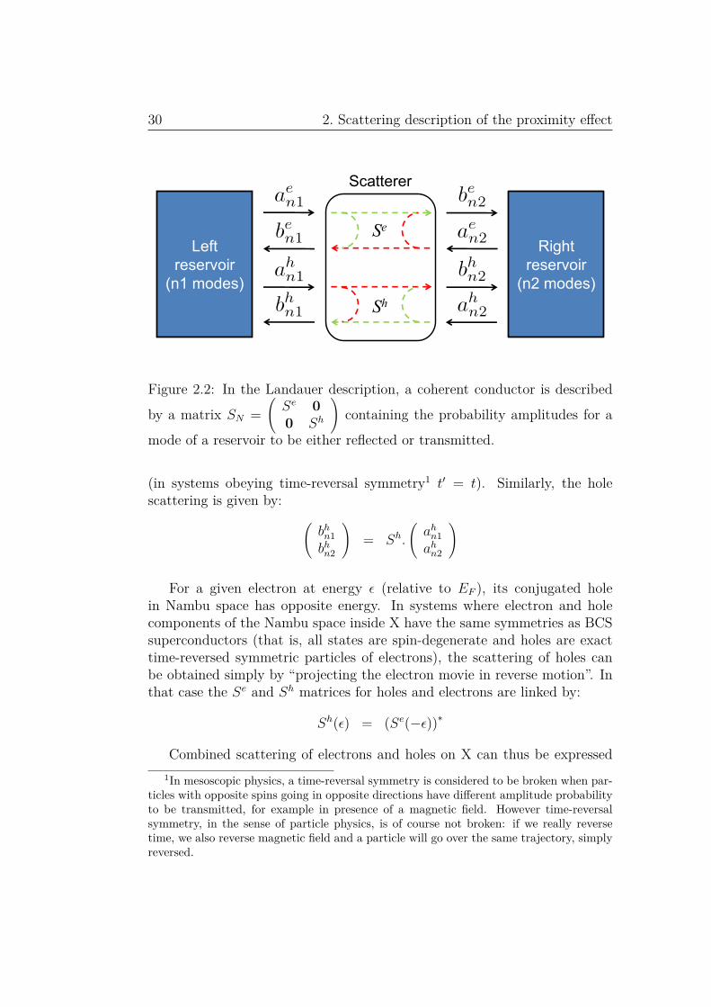
30 2. Scattering description of the proximity effect
Left reservoir
(n1 modes)
Right reservoir
(n2 modes)
Se
Sh
Scatterer
Figure 2.2: In the Landauer description, a coherent conductor is described
by a matrix SN =(Se 00 Sh
)containing the probability amplitudes for a
mode of a reservoir to be either reflected or transmitted.
(in systems obeying time-reversal symmetry1 t′ = t). Similarly, the holescattering is given by: (
bhn1bhn2
)= Sh.
(ahn1ahn2
)
For a given electron at energy ϵ (relative to EF ), its conjugated holein Nambu space has opposite energy. In systems where electron and holecomponents of the Nambu space inside X have the same symmetries as BCSsuperconductors (that is, all states are spin-degenerate and holes are exacttime-reversed symmetric particles of electrons), the scattering of holes canbe obtained simply by “projecting the electron movie in reverse motion”. Inthat case the Se and Sh matrices for holes and electrons are linked by:
Sh(ϵ) = (Se(−ϵ))∗
Combined scattering of electrons and holes on X can thus be expressed1In mesoscopic physics, a time-reversal symmetry is considered to be broken when par-
ticles with opposite spins going in opposite directions have different amplitude probabilityto be transmitted, for example in presence of a magnetic field. However time-reversalsymmetry, in the sense of particle physics, is of course not broken: if we really reversetime, we also reverse magnetic field and a particle will go over the same trajectory, simplyreversed.

2.2. ABS in S-X-S systems 31
as: ben1ben2bhn1bhn2
= SN .
aen1aen2ahn1ahn2
where SN can be cast as a block matrix:
SN =(Se 00 Sh
)
with 0 a matrix with all its entries equal to 0.
2.2.2 Andreev scatteringAs shown above in section 2.1.1, the Andreev reflection can be described asa scattering process for which the b states become incident and the a areemergent:
aen1aen2ahn1ahn2
= SA.
ben1ben2bhn1bhn2
where SA can also be cast as a block matrix:
SA = a
(ϵ
|∆|
)0 In1e
−iϕ1 00 In2e
−iϕ2
In1eiϕ1 0
0 In2eiϕ2 0
where In is a n × n identity matrix and ϕ1 and ϕ2 are the superconductingphases of the two reservoirs.
2.2.3 Resonant bound states : Andreev Bound StatesCascading the above SN and SA matrices, an incident state ain =
(aen1a
en2a
hn1a
hn2
)is stationary and bound inside X (with only evanescent tails into the su-perconductors) whenever ain = SA.SNain. This condition implies that theenergies which give the roots of the equation2:
Det [I − SA.SN ] = 0 (2.1)2I is a (n1 + n2) × (n1 + n2) identity matrix.

32 2. Scattering description of the proximity effect
are the energies of these bound states. These states mediated by the An-dreev reflection are the so-called ABSs. Therefore, if X is described by anappropriate scattering matrix SN , the ABSs energies can always be foundwith relation 2.1. The existence of Andreev Bound States is thus a universalfeature of hybrid S-X-S junction3.
Beenakker and van Houten pointed out [52] that this situation was analo-gous to a Fabry-Perot optical resonator with phase-conjugating mirrors. Therole of the optical cavity is played by the coherent conductor, a CNT in ourexperiment, and its interfaces with superconducting leads play the role ofthe mirrors. Andreev reflection is analogous to optical phase conjugation:an electron in the nanostructure with energy below the superconducting gapis reflected as its time-reverse conjugated hole. This hole can be subse-quently reflected as an electron, and if the phase acquired during this cyclefulfils a resonant condition, ABSs form. ABSs thus correspond to opticalresonant standing waves, being however electronic excitations constitutedby a superposition of time-reversed states with opposite spins. Within thesuperconducting gap, ABS form a discrete spectrum which depends on thesuperconducting phase difference δ = ϕ1 − ϕ2 between the left and rightsuperconducting electrodes, as we can see by rewriting Eq. 2.1 in the form:
Det
I − a
(ϵ
|∆|
)2 (e−i δ
2 00 ei
δ2
)Se (ϵ)
(ei
δ2 0
0 e−i δ2
)Sh (ϵ)
= 0
This phase dependence is the manifestation of the fact that in each AR theelectron (resp. hole) acquires a phase4 ϕ1 or ϕ2 (resp. −ϕ1 or −ϕ2), such thatafter a cycle the phase acquired depends on δ. The phase difference is thusanalogous to the length of the optical Fabry-Perot. This phase dependenceis a characteristic signature of the ABSs in S-X-S structures and the proofthat they carry supercurrent (see 3.1.5, appendix C and Ref. [51, 53, 54]).
In appendix F, we discuss the well-known case of an infinitely short singlechannel with perfect and finite transmission.
2.2.4 Supercurrent in S-X-S junctions: contribution ofABSs
The scattering formalism is not restricted to the extraction of the ABSs’spectrum. Beenakker has indeed shown in Ref. [54] the link between the
3It is also true for S-X structures where bound states can form at interfaces. In thiscase the ABSs’s energies don’t depend on the phase.
4Not only, as it also acquires an energy-dependent phase arg(a(
E|∆|
))in each AR,
and also a phase due to propagation and scattering in the coherent conductor.

2.3. ABS in S-QD-S system from the scattering description 33
spectrum of a S-X-S junction and the supercurrent flowing through it. Hedecomposes the latter in two parts:
• the contribution of the ABSs which is related to the derivative of theirenergies with respect to δ,
• and the contribution of the continuum (for |E| > ∆).
He shows in particular that for the case of a quantum point contact, thesecond contribution is negligible and all the supercurrent is carried by theABSs.
In appendix C, we give an alternative demonstration, for the case of aQuantum Dot, of these physical properties using Green’s function techniques.
2.3 ABS in S-QD-S system from the scatter-ing description
We now consider the case where the central scatterer is a quantum dot (QD).In a QD, scattering occurs via resonant tunneling through discrete states.
2.3.1 Non-interacting dotIf we consider, as a first approach, that electrons do not to interact in theQD, the lead-QD-lead structure can be modelled as a double barrier system.The energy levels are then discrete spin-degenerate states given by the ladderof waves-in-a-box solutions to the Schrödinger equation.
Let ϵr be the energy of one of these resonant levels, relative to the Fermienergy EF in the reservoirs, and let ΓL/~ and ΓR/~ be the tunnel ratesthrough the left and right barriers. We denote Γ = ΓL+ΓR. If Γ ≪ ∆E (with∆E the level spacing in the quantum dot) and T ≪ Γ/kB, we can assume thattransport through the QD occurs exclusively via resonant tunneling throughthe spin degenerate level of energy ϵr. The conductance G of the QD hasthus the form[55, 56, 57]:
G = 2e2
h
4ΓLΓRϵ2
r + Γ2 = 2e2
hTBW (2.2)
where TBW is the Breit-Wigner transmission probability at the Fermi level.Assuming the resonance couples to a single mode in the reservoirs (general-ization to many modes is straightforward, see Ref. [58]), the normal-state

34 2. Scattering description of the proximity effect
Breit-Wigner scattering matrix sϵr(ϵ) which yields this conductance has theform [56]:
sϵr(ϵ) =
(1 − i2ΓL
ϵ−ϵr+iΓ
)ei2δL − i
√4ΓLΓR
ϵ−ϵr+iΓ ei(δL+δR)
− i√
4ΓLΓR
ϵ−ϵr+iΓ ei(δL+δR)(1 − i2ΓR
ϵ−ϵr+iΓ
)ei2δR
(2.3)
Note that since the reflection phases δL and δR later vanish in the determi-nation of the energies of the ABS, we do not need to specify them. Büttikerhas shown how the conductance, given by Eq. 2.2, follows, via the Landauerformula (see Ref. [36]), from the Breit-Wigner scattering matrix 2.3.
As we are able to describe a non-interacting QD by scattering matrix, wecan perfectly describe the superconducting proximity effect in QDs in termof ABSs and find their energies with relation 2.1. Beenakker and van Houten[59] have considered the ABSs occurring through such spin-degenerate reso-nance, that is when both spin components of the ABS are parts of the sameresonant level. They found results for the supercurrent in agreement withthe perturbative approach of Glazman and Matveev [22], validating theirscattering approaches for description of the superconducting proximity effectin QDs with small charging energies.
2.3.2 Weakly-coupled interacting dot: simple effectivemodel
However, in real QDs, in addition to the confinement energy mentionedabove, Coulomb repulsion has to be taken into account. In simplest situa-tions one can nevertheless recover a simple effective non-interacting picture,in which each time an electron is added to the QD one merely pays a charg-ing energy and possibly the configuration energy necessary to access the nextfree orbital (see the appendix A for a more detailed discussion of QDs).
When the coupling to the leads is weak, one needs to invoke states ofopposite spin to build an ABS. In a dot where time-reversal symmetry is notbroken, the most favorable states for making an ABS correspond to a pair ofstate arising from a single orbital of the dot, that is a singly-occupied orbital(odd electron number in the dot) followed by the doubly occupied orbital(even electron number). Such a pair of states are the closest in energy, onlyseparated by the effective charging energy of the dot, and the two electronsinvolved in these states have opposite spin by virtue of the Pauli exclusionprinciple. Moreover these states are coupled in an identical manner to thereservoirs since this coupling arises from properties of the orbital. Neverthe-less taking into account this interaction together with the coupling to the

2.3. ABS in S-QD-S system from the scattering description 35
0 Π 2 Π-D
0
D
∆
Ε-
Ε+
ABSs energies ϵ− and ϵ+ from scattering description
Figure 2.3: In solid lines, we have represented ϵ− and ϵ+ as a function of δobtained from Eq. 2.4 with ϵ↑ = −2.5∆, ϵ↓ = 2.5∆, ΓL = 2∆, ΓR = ∆. Indashed lines, we have represented the ABSs for the same parameters exceptthat we have inverted spin up and spin down.
electrodes terribly complicates the problem and no fully analytic results ex-ists (See appendix A). Yet, within some range of parameters, most of theeffect of Coulomb interaction of the electrons in the dot can be mimickedby introducing a phenomenological breaking of the spin degeneracy of thesestates (see Appendix A, and Refs [16]). Such a "caricature" of the problemyields a tractable non-interacting effective model that still contains a gooddeal of the interesting physics of this system. Discussing or justifying thisapproximation is beyond the scope of this experimental thesis, but in chapter3 we will show how the results of this phenomenological model compare withexact numerical results.
We thus consider a pair of levels:
ϵ↑ = ϵ0 + U/2ϵ↓ = ϵ0 − U/2
where ϵ0 is the mean position of the levels (we will see in part II, that thisparameter can be controlled experimentally by a gate voltage), and U =|ϵ↑ − ϵ↓| is the effective charging energy (which of the spin up or down stateis highest in energy will turn out to be unimportant, we will discuss it later).

36 2. Scattering description of the proximity effect
The scattering matrix SN then takes the form:
SN =(sϵ↑(ϵ) 0
0 sϵ↓(−ϵ)∗
)
With this scattering matrix, Eq. 2.1 giving the positions of the ABSyields the equation in ϵ:
Det
I2 − a
(ϵ
|∆|
)2 (e−iδ 0
0 eiδ
)sϵ↑(ϵ)
(eiδ 00 e−iδ
)sϵ↓(−ϵ)∗
= 0 (2.4)
where δ = ϕ1 − ϕ2 is the superconducting phase difference between the tworeservoirs.
Expending the determinant, this equation takes the algebraic form5:
D (ϵ) 4 (∆2 − ϵ2)∆2 (ϵ− ϵ↑ + iΓ) (−ϵ− ϵr − iΓ)
a
(ϵ
|∆|
)2
= 0
with:
D (ϵ) =[ϵ+ U
2− Γg (ϵ)
]2− ϵ2
0 − Γ2[1 +
(1 − δΓ2
Γ2
)sin2
(δ
2
)]f (ϵ)2 (2.5)
where δΓ = ΓL − ΓR, g (ϵ) = −ϵ√∆2−ϵ2 and f (ϵ) = ∆√
∆2−ϵ2 . Roots of Eq. 2.5give the energy of the ABSs. As shown in Fig. 2.3, within the gap of thesuperconductors, there are 2 solutions ϵ+, ϵ− to the equation D (ϵ) = 0, suchthat −∆ < ϵ−, ϵ+ < ∆.
2.3.3 Meaning of the sign of the eigenenergies; arbi-trariness of the description
In the previous section, we arbitrarily assumed that the spin up electron statehas an energy lower by U than the spin down electron state. This choice ledto get two eigenenergies ϵ+ and ϵ− that are not symmetric with respect tothe Fermi level. Making the opposite choice (or equivalently chosen U < 0),the sign of the eigen-energies would have been reversed (dashed lines in Fig.
5To reach this expression we use the fact that sϵ↓(−ϵ)∗ is unitary
(i.e. sϵ↓(−ϵ)†sϵ↓(−ϵ) = I2) to transform Eq. 2.4 into:a(
ϵ|∆|
)2
Det[sϵ↓ (−ϵ)] ×
Det
[a(
ϵ|∆|
)∗sϵ↓(−ϵ)
(e−iδ 0
0 eiδ
)− a
(ϵ
|∆|
)( e−iδ 00 eiδ
)sϵ↑(ϵ)
]= 0 and we
use the relation sϵ↓(−ϵ) =(sϵ↑(ϵ) − 1
)× ϵ−ϵ↑+iΓ
−ϵ−ϵ↓+iΓ + 1.

2.3. ABS in S-QD-S system from the scattering description 37
2.3). However, physical observables, such as the Josephson current or thetunnel density of states will end to be the same whether we choose, in ourmodel, U to be positive (spin up lower in energy) or negative (spin up higherin energy).
This is related to the fact that signs of the energies, that are roots of Eq.2.5, have no real physical meaning and are just conventional features relatedto the Nambu space. This is discussed in section F.1.

38 2. Scattering description of the proximity effect

Chapter 3
Proximity effects in QD interms of Greens functions
The scattering formalism described above offers a clear physical picture tounderstand how ABSs form in general, and in a QD, in particular. Howevera Green’s functions (GF) description of the proximity effect in QD is a morestraightforward technique to calculate physical observables of the system,such as the Josephson current carried by the QD or its DOS. We stress thatthe two formalisms are rigorously equivalent (see for example [60, 61, 62] orAppendix A of Ref. [49]), and thus observables could also be computed inthe scattering approach. In this chapter divided in three sections, we tacklethe problem of a S-QD-S junction using GF techniques.
To calculate the GFs that will allow us to obtain these observables, weneed to write down the Hamiltonian of the S-QD-S system. The latter can becorrectly described by a single-level Anderson model (introduced in detail inappendix A) but where normal leads are replaced by BCS superconductors.There are, however, no exact analytical solution for this model. Therefore,following Ref. [16], we first use an approximation (see also section A.4.1)which gives rise to an effective non-interacting model that we can solve.Then, we will use Numerical Renormalization Group (NRG) technique, whichallows an exact numerical treatment of the QD with superconducting leads,in order to validate the phenomenological model and to find out its region ofapplicability.
In the first section 3.1, we use the effective model of Ref. [16] in whichCoulomb repulsion in the QD is addressed phenomenologically in the samenon-interacting picture than in section 2.3. In order to calculate the TDOSand the supercurrent through the QD, we express the Green’s functions whichwill be introduced in subsection 3.1.1. General properties of GFs like self-energy and poles will be included in this subsection in order to gain a physical
39

40 3. Proximity effects in QD in terms of Greens functions
insight on this formalism. Next in subsection 3.1.2, we explain how to ex-tract from QD’s GF a first observable: the QD’s density of states. Then weanalyze the GF’s expression for an asymmetric QD in section 3.1.3, and weextend our model to a double QD in which two QDs are connected in seriesbetween two superconducting electrodes in section 3.1.4. In section 3.1.5,we explain how to calculate, from QD’s GFs a second observable: the super-current flowing through the QD. We also discuss how the phenomenologicalmodel describes the singlet-doublet transition of the device and the resultingreversal of supercurrent (the so-called 0 − π transition) [3, 48].
In section 3.2, we briefly introduced the NRG technique. We will discusshow one can used NRG calculations to obtain exact numerical results on theproximity effect in QD.
Finally in section 3.3, we analyze the influence of the physical ingre-dients of the model on the QD’s DOS and particularly on the ABSs. Inparallel to this analysis, we carry out a comparison between NRG and thesimplified non-interacting treatment in order to understand the limits of thephenomenological approach.
3.1 Effective description of the S-QD-S junc-tion
3.1.1 Green’s function of a QD connected to supercon-ducting leads
We use here exactly the same effective non-interacting picture of a QD cou-pled to superconducting leads (see section A.4.1 appendix A) as in the scat-tering description of section 2.3. However, in contrast with the scatteringapproach where we used known results without making explicit the Hamil-tonian of the system, here we write down this Hamiltonian, as we will needit to express the GF.
3.1.1.1 Effective Hamiltonian of a S-QD-S junction
As in section 2.3, we restrict to a single orbital of the QD, as most of therelevant physics is captured in this simple case. There are at most twoelectrons in the dot, which then are necessarily of opposite spin, due tothe Pauli principle. We also adopt the same approximate treatment of theCoulomb interaction by introducing a phenomenological breaking of the spin

3.1. Effective description of the S-QD-S junction 41
degeneracy of this single level1 (See Appendix A). The QD is thus describedby a spin up level of energy ϵ↑ = ϵ0 + U/2 and a spin down level of energyϵ↓ = ϵ0 − U/2, with U the effective charging energy. Hence the QD itself issimply described by:
HQD =∑σ=↑,↓
ϵσd†σdσ
where dσ is the annihilation operator of an electron in the QD of energy ϵσwith a spin σ.
The left and right superconducting electrodes are described by the BCSHamiltonian:
HL = ∑l,σ ϵlc
†lσclσ +∑
l
(∆eiϕLc†
l↑c†−l↓ + ∆e−iϕLc−l↓cl↑
)HR = ∑
r,σ ϵrc†rσcrσ +∑
r
(∆eiϕRc†
r↑c†−r↓ + ∆e−iϕRc−r↓cr↑
)Here cl(r)σ is the annihilation operator of an electron of the left (resp. right)electrode in state l (r) with an energy ϵl (ϵr), and spin σ. In this notation, land r represent a synthetic index for all the quantum numbers of the electronsin electrodes, except their spin, and such that c−l−σ is the time reversed-state of clσ. ∆eiϕL(R) is the complex order parameter in electrode L(R) withmodulus ∆ (also known as the gap energy) and phase ϕL(R).
Finally, the coupling of the dot to the leads is described by a hoppingterm:
HTL= ∑
l,σ
(tLd
†σclσ + t∗Lc
†lσdσ
)HTR
= ∑r,σ
(tRd
†σcrσ + t∗Rc
†rσdσ
)where tL(R) is the energy associated to the transfer of an electron betweenleft (right) electrode and the dot. We assume these couplings to be energy-independent as in Refs. [63, 64]. The whole system is schematized in Fig.3.1.
Electron-hole spinor field operator in Nambu space As supercon-ductivity induces correlations between electrons and holes of opposite spins,we will need to express GF with electron-hole spinor field operators in Nambu
space, ψl(r) =(
cl(r)↑c†
−l(−r)↓
)and ψd =
(d↑
d†↓
).
1This lift of degeneracy used to model phenomenologically the Coulomb interaction isnot a real Zeeman splitting: there are no magnetic field and the axis of spin quantizationis not even specified.

42 3. Proximity effects in QD in terms of Greens functions
S SQD
tL tRU
QD connected to superconducting leads
Figure 3.1: In our model, the QD is characterized by three parameters: thecoupling to the left (resp. right) lead tL (resp. tR) and the effective chargingenergy U .
In this spinor basis, the Hamiltonian can be written as a matrix expres-sion2:
H =∑i=l,r
ψ†iEiψi + ψ†
dEQDψd +∑l
[ψ†dETL
ψl + h.c.]
+∑r
[ψ†dETR
ψr + h.c.]
where:
EQD =(ϵ↑ 00 −ϵ↓
), El(r) =
(ϵl(r) ∆eiϕL(R)
∆e−iϕL(R) −ϵl(r)
), and ETL(R) =
(tL(R) 0
0 −t∗L(R)
)
that will be useful to write GF in a simple and compact matrix form.
3.1.1.2 Green’s function of the Quantum Dot
As discussed in introduction of this chapter, properties of the QD are encodedin the QD’s GF. In this section, we define the QD’s GF in Nambu space andgive its expression (the detailed derivations are given in appendix B).
Definition of the QD Green’s function In Nambu notation and in timedomain, the QD GF takes the form3:
Gdd (t) = −i⟨Ttψd (t)ψ†d (0)⟩
= −i(
⟨Ttd↑ (t) d†↑ (0)⟩ ⟨Ttd↑ (t) d↓ (0)⟩
⟨Ttd†↓ (t) d†
↑ (0)⟩ ⟨Ttd†↓ (t) d↓ (0)⟩
) (3.1)
2In this writing we have dropped an unimportant constant equal to∑
l ϵl +∑
r ϵr + ϵ↓that does not change the physics.
3The symbolˆis here to distinguish the 2×2 matrix in Nambu space from its coefficients.
3.1. Effective description of the S-QD-S junction 43
where Tt is the time-ordering operator:
Ttψd (t)ψ†d (0) = θ (t)ψd (t)ψ†
d (0) − θ (−t)ψ†d (0)ψd (t)
which preserves GF causality, and ⟨A⟩ represents the expectation value ofoperator A (defined by Eq. B.1).
Diagonal elements of Gdd (t) give the temporal evolution of a bare elec-tron or hole injected in the QD4, in this respect they are also called propa-gators. We will see that this is directly linked to the QD’s density of states.Non-diagonal parts of Gdd (t), also called “anomalous” GFs, indicate paircorrelations amplitude in the QD and are equal to zero in absence of super-conductivity.
Expression for the QD GF In section B.3, we carry out the full deriva-tion of the GF from its equation of motion (EOM) in the Matsubara formal-ism. Below we simply present and use the result of this derivation.
A convenient way to express the GF is to introduce the analytic contin-uation Gdd (z) of the Fourier transform of Gdd (t), where z has the dimensionof an energy and can take values in the entire complex plane. The resolutionof the EOM yields5:
Gdd (z) =[z − EQD − Σ (z)
]−1(3.2)
in which the QD’s self-energy:
Σ (z) = ΣL (z) + ΣR (z)
ΣL (z) =∑l
ETL[z − El]−1 E†
TL
ΣR (z) =∑r
ETR[z − Er]−1 E†
TR
is due to the connection to superconducting leads. After summation overindexes l and r, Σ (z) becomes:
Σ (z) =∑i=L,R
Γi(
g (z) −f (z) eiϕi
−f (z) e−iϕi g (z)
)
4This point is discussed in section B.3.5.5Here and in the following, we don’t write explicitly matrices proportional to the 2 ×
2 unit matrix I2, but replace them for convenience by a scalar factor. For example,(z 00 z
)= z × I2 is noted z.

44 3. Proximity effects in QD in terms of Greens functions
where we have introduced functions g (z) = −z√∆2−z2 and f (z) = ∆√
∆2−z2 , butalso exchange rates between the QD and the leads Γi = πρF |ti|2 with ρF thedensity of states at the Fermi level of the electrodes in their normal state.These rates are the same that those of matrix 2.3.
Properties of the GF The QD’s GF contains the local properties ofthe QD. In particular, eigenstates appear as isolated poles of the diagonalelements of Gdd (z) on the real axis, or as a branch cut in the real axis fora continuum of states. If the GF has complex poles, they correspond toquasiparticle states of finite lifetime. From Gdd (z), we define the retardedand advanced GF that are the value of Gdd (z) approaching the real axis fromthe upper and lower half of the complex plane [65], respectively (here ω andη are real and η → 0+):
GRdd (ω) = Gdd (ω + iη)
GAdd (ω) = Gdd (ω − iη)
and from which we will obtain the density of states of the QD.
ABS as real poles and decaying states as complex poles To illustratethe two types of poles that we have mentioned above, let us look at threepeculiar cases: an isolated QD, a QD connected to normal leads and a QDconnected to superconducting leads.
• The GF describing the isolated QD is given by [z − EQD]−1. As ex-pected, diagonal elements of the GF have only real poles ϵ↑ and ϵ↓that correspond to energies of the QD’s eigenstates which have infinitelifetime. This is characteristic of an eigenstates.
• For a QD connected to normal leads (∆ = 0), the retarded GF ischanged in: [
ω + iη − EQD + i
(ΓL + ΓR 0
0 ΓL + ΓR
)]−1
In that case, the poles take complex values ϵ↑ − i (ΓL + ΓR) and ϵ↑ −i (ΓL + ΓR). As a consequence, when t > 0, the propagator is an expo-nentially decaying function of the time:
Gdd (t > 0) = −iθ (t) e−iEQDte−(ΓL+ΓR)t
which means that an electron or a hole injected in the QD has a char-acteristic lifetime ~/(ΓL+ΓR), given by the imaginary part of the polesfor escaping to the leads.

3.1. Effective description of the S-QD-S junction 45
• As discussed in section B.3.4, when the leads are superconducting, thepoles of the GF are the roots of equationD (z) = Det
(z − EQD − Σ (z)
)=
0 (or equivalently Det(GRdd (z)−1
)= 0). On the real axis and when
|ω| < ∆, D (ω) has two poles ϵ+ and ϵ− defined by the equality:[ϵ± + U
2− Γg (ϵ±)
]2− ϵ2
0 − Γ2[1 +
(1 − δΓ2
Γ2
)sin2
(δ
2
)]f (ϵ±)2 = 0
(3.3)where Γ = ΓL + ΓR, δΓ = ΓL − ΓR and δ = ϕL −ϕR. Eq. 3.3 is exactlythe same as 2.5. Hence, these poles coincide with the ABSs calculatedin the scattering approach of section 2.3 illustrating the equivalence ofthe two approaches.
3.1.2 Tunneling spectroscopy of a QD in terms of GFTo observe the ABS, we have chosen to explore our system by tunnelingspectroscopy. This technique consists to inject or extract, with a well char-acterized tunnel probe under a given voltage bias, electrons in the QD andat well defined energies. By measuring the differential conductance betweenthe probe and the QD we have rather direct access to the spectral functionof the QD. In this section we give the link between the spectral function ofthe QD and its GF and we will discuss what would be this link for othertypes of spectroscopy. We also discuss how the ABSs appear in a tunnelingspectroscopy, in particular the fact that each of them appear twice in thespectrum.
3.1.2.1 Definition of the QD’s DOS
The spectral function of the QD is defined by the equality (see for examplethe textbook [65]):
Add (ω) = − 1π
Im[TrN
(GRdd (ω)
)]where TrN is the trace in Nambu space:
TrN(GRdd (ω)
)= GR11
dd (ω) + GR22dd (−ω)
We can show, that, when a voltage V is applied to the tunnel probe,the tunnel current through the QD is given by (a demonstration is given inappendix D):
⟨I (V )⟩ = 2e~
|tprobe|2׈ +∞
−∞Aprobe (ω + eV ) Add (ω) [fFD (ω) − fFD (ω + eV )] dω

46 3. Proximity effects in QD in terms of Greens functions
where fFD (ω) is the Fermi-Dirac distribution, tprobe the coupling to the probeand Aprobe (ω) the spectral function of the probe. The differential conduc-tance, which is the quantity that we measure experimentally, is thus givenby:
G (V ) = 2e~
|tprobe|2׈ +∞
−∞Add (ω) ∂
∂V[Aprobe (ω + eV ) (fFD (ω) − fFD (ω + eV ))] dω
In our experiments Aprobe (ω) is given by the well known BCS DOS (see Fig.2.1 and Ref. [47]). The differential conductance gives thus a direct access tothe spectral density of the quantum dot.
We can show that the QD’s spectral density take the form6 (see textbook[65]):
Add (ω) =∑α,σ
∣∣∣⟨α ∣∣∣d†σ
∣∣∣ψ0⟩∣∣∣2 δ (ω − Eα) + |⟨α |dσ|ψ0⟩|2 δ (ω + Eα)
(3.4)
where |ψ0⟩ is the system ground state, |α⟩ are all the possible states of thesystem (QD plus superconducting leads) and Eα their energies with respectto the ground state energy. In this writing, the left term in the sum canbe interpreted as the probability to inject an electron in the QD creating anexcitation of energy Eα, and the right one as the probability to extract anelectron from the QD creating an excitation of energy Eα.
The spectral density we obtained is local as we inject electrons in thesystem only into the QD, and is usually called the tunnel DOS or TDOS.
3.1.2.2 Comparison with other type of QD spectroscopy
The TDOS spectroscopy allows to explore the excitations of a system bycreation or annihilation of an electron. This technique, like in the case ofARPES measurements [66], does not conserve the number of quasiparticlesof the system under test.
However in ARPES, the system is excited by a photon of several tensof eV which expels an electron collected by a detector. As a result, since aphoton cannot expel a hole from the system, the DOS obtained is limited toω < 0 and we only have access to the second part of the sum in 3.4.
There are other types of spectroscopies to probe the QD density of statesthat conserve the number of electrons in the system. For example by sendingoptical photons on the system and measuring the absorption spectra, we
6There is a more general temperature-dependent form of the TDOS. But in the effectiveapproach, the TDOS does not depend on temperature.

3.1. Effective description of the S-QD-S junction 47
would have access to another type of quantity such as:∑i,f
∣∣∣⟨αN ∣∣∣d†2σd1σ
∣∣∣ψ0N⟩∣∣∣2 δ (ω − EαN + E0N)
where |ψ0N⟩ is the system ground state (energy E0N) with N electrons and|αN⟩ are the excited states of the system with the same number of electrons(energy EαN). Operator d†
2σd1σ is an “exciton” operator which creates anelectron-hole pair in the QD by exciting an electron with a spin σ from anorbital labelled 1 to an orbital labelled7 2. This process conserves the numberof electron in the system and is always associated to a positive ω becauseEαN > E0N by definition of the ground state. We then have ω = ~ν with νthe frequency of absorption.
In the rest of the manuscript, the denomination “DOS” will only concernTDOS as we are only dealing with tunnel spectroscopy.
3.1.2.3 Tunneling into ABSs
Width of ABSs: phenomenological inelastic loss ηinel The abovetheoretical treatment of ABSs predicts they are infinitely thin peaks in thespectral density. Even if this description was correct, in an actual tunnelingspectroscopy experiment however, the energy resolution would be limited forexample by temperature, voltage noise or coupling to the probe. In order tomimic this effect we include a depairing Dynes parameter [67] in g (ω) andf (ω), replacing ω by ω + iηinel. This gives a width to ABSs, allowing us toreproduce qualitatively the observed linewidth (see article in part II).
The origin of the measured linewidth is discussed in section D.2 appendixD, where we show that the main contribution is probably due to the couplingto the probe.
Double observation of the ABSs In tunneling spectroscopy measure-ments, ABSs appear twice in the DOS as is illustrated in Fig. 3.2. Thesestates (like all Bogoliubons as explained in appendix F) have a hole partand an electron part and there is, as a consequence, a finite probability toinject an electron or a hole into an ABS. The injection of an electron (resp.hole) occurs when we apply a negative (resp. positive) voltage V on thetunnel probe. When performing the tunneling spectroscopy of ABSs, theywill thus appear both at positive voltage and negative voltage. Therefore, we
7We precise here, to avoid confusion, that |ψ0N ⟩ and |αN ⟩ are many-body states ofthe system whereas d†
2σ and d1σ are creation and annihilation operators of single particlestates.
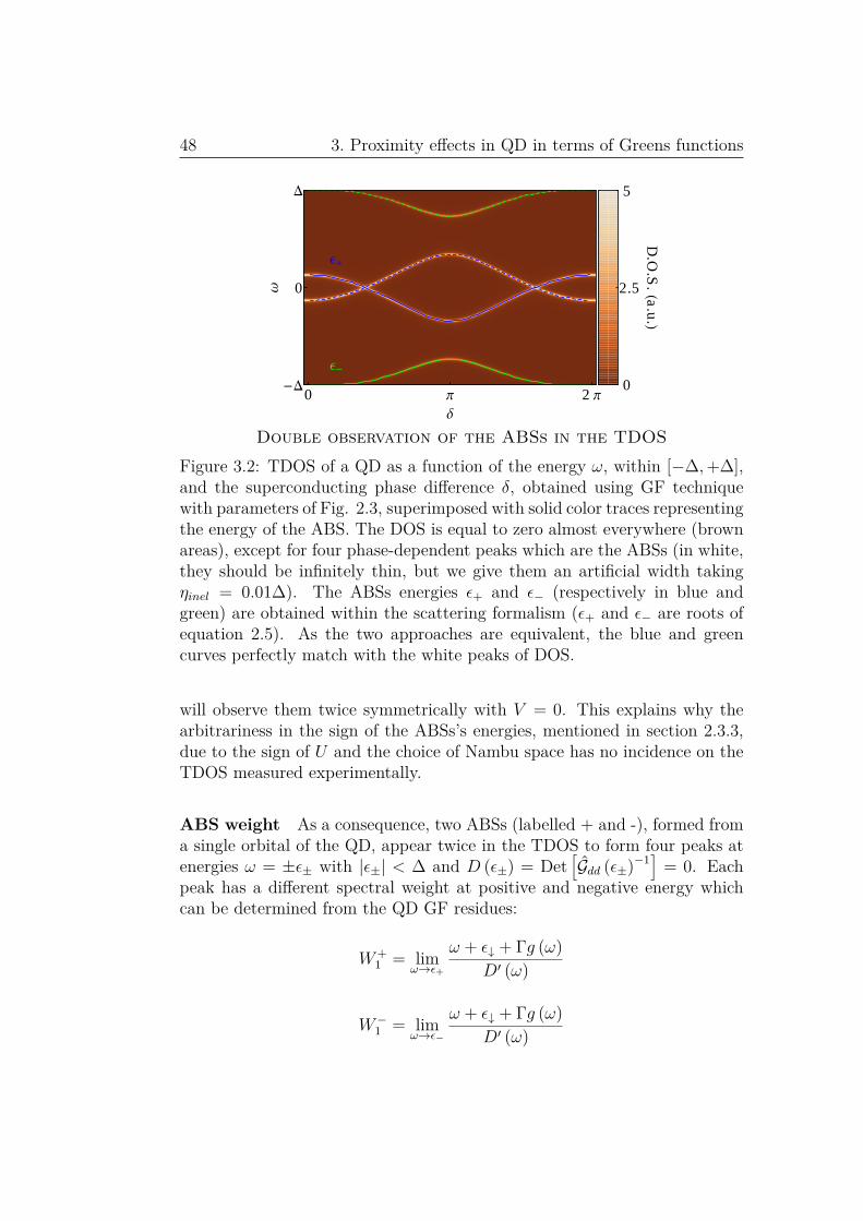
48 3. Proximity effects in QD in terms of Greens functions
0 Π 2 Π-D
0
D
∆
Ω
0
2.5
5
D.O
.S.Ha
.u.L
Ε-
Ε+
Double observation of the ABSs in the TDOSFigure 3.2: TDOS of a QD as a function of the energy ω, within [−∆,+∆],and the superconducting phase difference δ, obtained using GF techniquewith parameters of Fig. 2.3, superimposed with solid color traces representingthe energy of the ABS. The DOS is equal to zero almost everywhere (brownareas), except for four phase-dependent peaks which are the ABSs (in white,they should be infinitely thin, but we give them an artificial width takingηinel = 0.01∆). The ABSs energies ϵ+ and ϵ− (respectively in blue andgreen) are obtained within the scattering formalism (ϵ+ and ϵ− are roots ofequation 2.5). As the two approaches are equivalent, the blue and greencurves perfectly match with the white peaks of DOS.
will observe them twice symmetrically with V = 0. This explains why thearbitrariness in the sign of the ABSs’s energies, mentioned in section 2.3.3,due to the sign of U and the choice of Nambu space has no incidence on theTDOS measured experimentally.
ABS weight As a consequence, two ABSs (labelled + and -), formed froma single orbital of the QD, appear twice in the TDOS to form four peaks atenergies ω = ±ϵ± with |ϵ±| < ∆ and D (ϵ±) = Det
[Gdd (ϵ±)−1
]= 0. Each
peak has a different spectral weight at positive and negative energy whichcan be determined from the QD GF residues:
W+1 = lim
ω→ϵ+
ω + ϵ↓ + Γg (ω)D′ (ω)
W−1 = lim
ω→ϵ−
ω + ϵ↓ + Γg (ω)D′ (ω)

3.1. Effective description of the S-QD-S junction 49
00
0.1
0.2
0.3(a.u.)
ABSs have different weightsFigure 3.3: TDOS of a QD connected to superconducting leads as a functionof the energy ω. In [−∆,+∆], ABSs are infinitely thin and are representedby vertical lines whose heights represent their weights. Parameters of theplot: Γ = 2∆, ϵ↑ = ∆, ϵ↓ = 2∆, δΓ = 0 , and δ = π
2 .
W+2 = lim
ω→ϵ+
ω − ϵ↑ + Γg (ω)D′ (ω)
W−2 = lim
ω→ϵ−
ω − ϵ↑ + Γg (ω)D′ (ω)
where W±1 and W±
2 represent respectively the spin ↑ electron and spin ↓ holeparts of ABS ±.For |ω| < ∆, the TDOS thus reads:
Add (ω) = W+1 δ (ω − ϵ+) +W−
1 δ (ω − ϵ−) +W+2 δ (ω + ϵ+) +W−
2 δ (ω + ϵ−)
The latter, plotted on Fig. 3.3 with parameters indicated in the caption,exhibits then two peaks at ϵ± with weights W±
1 and two others at −ϵ± withweights W±
2 .
ABSs spins As mentioned above, each ABS has a spin ↑ and a spin ↓part that can be deduced from weights W±
1(2). The spin S± of ABS ± can besimply defined as:
S± = 12(W±
1 −W±2
)For the parameters of Fig. 3.3, ABSs have their spin in opposite directionswith S+ ≈ −0.104 and S− ≈ 0.101. The orientation of these spins is ofcourse relative as the quantization axis is not defined.
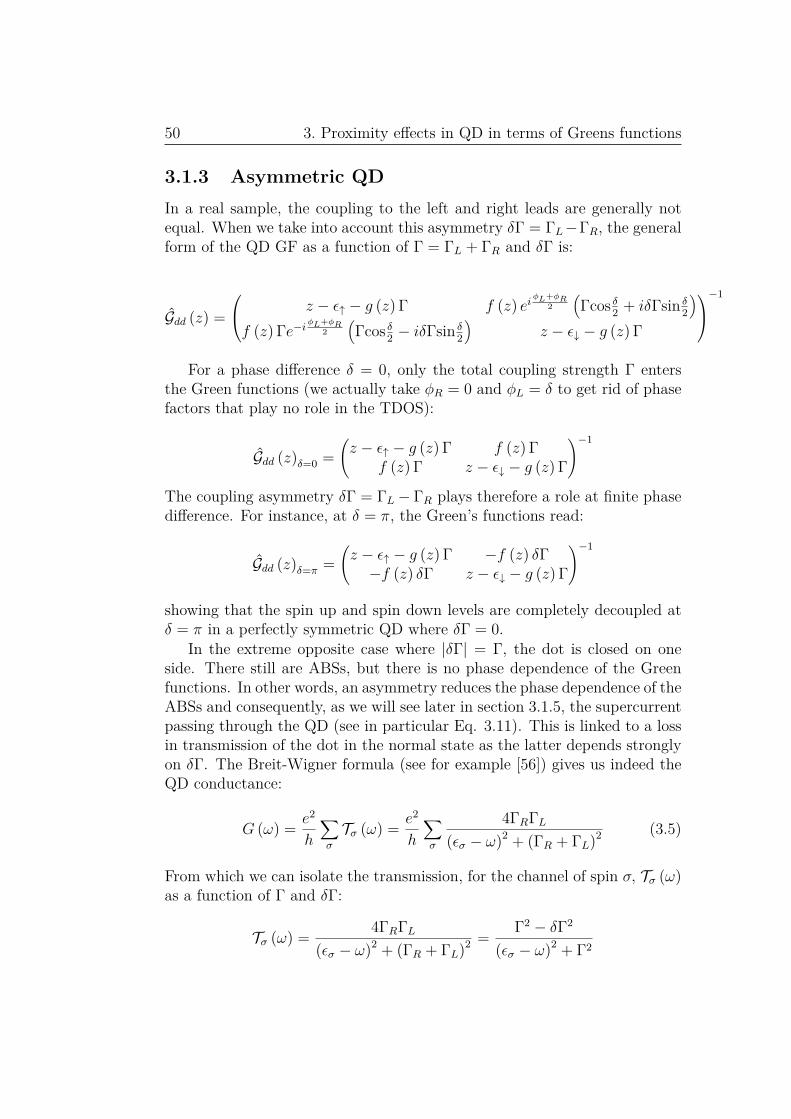
50 3. Proximity effects in QD in terms of Greens functions
3.1.3 Asymmetric QDIn a real sample, the coupling to the left and right leads are generally notequal. When we take into account this asymmetry δΓ = ΓL−ΓR, the generalform of the QD GF as a function of Γ = ΓL + ΓR and δΓ is:
Gdd (z) =
z − ϵ↑ − g (z) Γ f (z) eiϕL+ϕR
2
(Γcos δ2 + iδΓsin δ
2
)f (z) Γe−iϕL+ϕR
2
(Γcos δ2 − iδΓsin δ
2
)z − ϵ↓ − g (z) Γ
−1
For a phase difference δ = 0, only the total coupling strength Γ entersthe Green functions (we actually take ϕR = 0 and ϕL = δ to get rid of phasefactors that play no role in the TDOS):
Gdd (z)δ=0 =(z − ϵ↑ − g (z) Γ f (z) Γ
f (z) Γ z − ϵ↓ − g (z) Γ
)−1
The coupling asymmetry δΓ = ΓL − ΓR plays therefore a role at finite phasedifference. For instance, at δ = π, the Green’s functions read:
Gdd (z)δ=π =(z − ϵ↑ − g (z) Γ −f (z) δΓ
−f (z) δΓ z − ϵ↓ − g (z) Γ
)−1
showing that the spin up and spin down levels are completely decoupled atδ = π in a perfectly symmetric QD where δΓ = 0.
In the extreme opposite case where |δΓ| = Γ, the dot is closed on oneside. There still are ABSs, but there is no phase dependence of the Greenfunctions. In other words, an asymmetry reduces the phase dependence of theABSs and consequently, as we will see later in section 3.1.5, the supercurrentpassing through the QD (see in particular Eq. 3.11). This is linked to a lossin transmission of the dot in the normal state as the latter depends stronglyon δΓ. The Breit-Wigner formula (see for example [56]) gives us indeed theQD conductance:
G (ω) = e2
h
∑σ
Tσ (ω) = e2
h
∑σ
4ΓRΓL(ϵσ − ω)2 + (ΓR + ΓL)2 (3.5)
From which we can isolate the transmission, for the channel of spin σ, Tσ (ω)as a function of Γ and δΓ:
Tσ (ω) = 4ΓRΓL(ϵσ − ω)2 + (ΓR + ΓL)2 = Γ2 − δΓ2
(ϵσ − ω)2 + Γ2

3.1. Effective description of the S-QD-S junction 51
We see that for a maximum asymmetry Γ = δΓ the transmission is equal tozero, this situation corresponding to an open circuit (ΓL or ΓR equal to zero).It is interesting to notice that this transmission takes a particularly simpleexpression when the level ϵσ is at resonances with the electrodes Fermi level(ω = ϵσ = 0):
Tσ,ω=ϵσ=0 = 1 −(δΓΓ
)2
As a consequence, whereas the lifetime of a charge in the QD is limited bythe bigger coupling because this charge sees the two contacts in parallel, thetransmission in series is rather limited by the smallest coupling. Indeed whena charge is going in the QD through the more open contact, it will go backwhere it comes from rather than going through the less transmitted contact.
3.1.4 Extension of the effective model to a double QD
In this section we explain how to apply this formalism to the case of a doubleQD (DQD) in which two QDs are in series between the superconducting leads.
In our experiments, the CNT behaves as a DQD because of the influenceof the probe. The latter acts as a scatterer which separates the CNT in twoQDs which are strongly coupled together. Further in the manuscript (seepart III), measurement which proves this interpretation will be shown andcompared to other experiments with similar geometry.
S SQDL QDR
tL tRt’
Figure 3.4: Our DQD model consists of two coupled QDs in series, QDLbeing connected to the left lead and QDR to the right lead.

52 3. Proximity effects in QD in terms of Greens functions
DQD Hamiltonian To modify our model to a DQD, we need to replacefirst, in H, HQD by HDQD:
HDQD =∑
σ,α=L,Rϵασd
†ασdασ +
∑σ
(t′d†
LσdRσ + t′∗d†RσdLσ
)with indexes L and R referring to the QDL or QDR (cf Fig. 3.4), σ the spin,and t the interdot coupling. The second modification consists in changingHTi
:HTL
= ∑l,σ
(tLd
†Lσclσ + t∗Lc
†lσdLσ
)HTR
= ∑r,σ
(tRd
†Rσcrσ + t∗Rc
†lσdRσ
)This is a crude approach missing a lot of important physics, such as
interdot electrostatic interaction (UmnL↑nR↓), exchange (−JSL.SR)... But itcontains the essential ingredients to understand how ABSs form over the allDQD.
DQD spinors, Green functions and spectral density By introducingnew spinors ψd and ψe
8:
ψd =
dL↑
d†L↓dR↑
d†R↓
and ψe =
cl↑c†
−l↓cr↑c†
−r↓
we can give to H the form;
H =∑e
ψ†eEeψe + ψ†
dEDQDψd +∑e
[ψ†dETψe + h.c.
]where Ee, EDQD and ET are 4 × 4 matrices with block structures:
Ee =(
El 0202 Er
)EDQD =
(EQDL ETID
ETIDEQDR
)ET =
(ETL
0202 ETR
)
with EQDL =(ϵL↑ 00 −ϵL↓
), EQDR =
(ϵR↑ 00 −ϵR↓
)and ETID
=(t′ 00 −t′∗
)Replicating exactly the single QD approach, we can calculate the DQD Greenfunctions and obtain:
Gdd (z) = 1z − EDQD − ΣDQD (z)
8The index e designates pairs of index l, r chosen such that they appear in only onepair.

3.1. Effective description of the S-QD-S junction 53
where ΣDQD (z) is the self-energy due to the superconducting leads:
ΣDQD (z) = ∑e ET [z − Ee]−1 E†
T
=(
ΣL (z) 02
02 ΣR (z)
)
The total DQD spectral density is obtain similarly than before:
Add (ω) = − 1π
Im[TrDQD
(GRdd (ω)
)]TrDQD is the trace in Nambu space over the two QDs9:
TrDQD(GRdd (ω)
)= GR11
dd (ω) + GR22dd (−ω) + GR33
dd (ω) + GR44dd (−ω)
3.1.5 Supercurrent within the effective modelThe supercurrent flowing through the QD can be calculated, as the TDOS,with GFs. We will show in this section that it can be directly related tothe QD density of states that we measure10. Unfortunately, this supercur-rent is not measurable experimentally in our present setup. Nevertheless,the following explains how we can have indirect access to the magnitude ofsupercurrents in our samples from the measured spectra. Note that this eval-uation of the QD supercurrent might be checked in the future, using a moreelaborate setup giving direct access to the loop supercurrent, as was done foratomic contacts [68, 69] (see Fig. 3.5).
Using the expression of the supercurrent we obtained from the QD’s GF,we discuss how our model describe the so-called 0 − π transition.
3.1.5.1 Calculation of the supercurrent
Supercurrent definition Since number of particles and phase are conju-gated quantum variable, the equilibrium supercurrent IJ flowing through aJosephson junction is given by the fundamental relation [43, 53, 54]:
IJ = 2e~
⟨dH
dδ
⟩9Tunneling rates between the tunnel probe and the two sides of the DQD may be
different. For fitting of experimental TDOS, we may thus introduce a factor of relativeintensity α: TrN
(GR
dd (ω))
= α×(
GR11dd (ω) + GR22
dd (−ω))
+(
GR33dd (ω) + GR44
dd (−ω))
10The system being at equilibrium, there is no quasiparticle current through the QD,but just a DC supercurrent.

54 3. Proximity effects in QD in terms of Greens functions
Breakjunction
Josephsonjunction
5µm
rC
CHIP
RV
⊗
T=20mK
IbU
Figure 3.5: Diagram of the experimental setup and a SEM picture of thesample used to measure the current-phase relation of an atomic contact (Fig.from Ref. [69]). The atomic contact is obtained within the break junction bybending of the sample and forms in parallel with a large Josephson junctionan atomic SQUID. The current-phase relation is extracted from the switchingcurrent of the atomic SQUID.
where H is the Hamiltonian of the junction and δ the superconducting phasedifference across the junction11.
In a QD described by the effective Hamiltonian given in section 3.1.1.1,a convenient form of this relation can be obtained by performing a gaugetransformation on the operators of the leads:
cl(r)σ → cl(r)σei
ϕL(R)2
which transfers the phase into the tunnel matrix elements tL(R) → tL(R)ei
ϕL(R)2 .
Then it can be shown that the Josephson current carried by the QD from
11If we want to relate this current with the time-derivative of the charge in the leftlead, we can write IJ = e d
dt
⟨NL (t)
⟩= e d
dt
⟨ei H
~ tNLe−i H
~ t⟩
= ie~
⟨[H, NL (t)
]⟩. But the
commutator of NL (t) with the full Hamiltonian introduces spurious terms of the type⟨c†
kL↑c†−kL↓
⟩because of charge fluctuations within the lead. These fluctuations appear
because the mean-field BCS Hamiltonian doesn’t conserve the charge:[HBCS−MF , NL
]=
0. This is not the case for the Hamiltonian on which has not been performed a mean-fieldapproximation, so we can consider that these terms are not relevant for current calculationthrough the system. For a more detailed discussion see Ref. [70].

3.1. Effective description of the S-QD-S junction 55
the left to the right takes the simple expression12:
IJ = ie
~⟨[HT , NL]⟩ (3.6)
where NL(R) is the number operator of the left (right) electrode13:
NL(R) =∑l(r),σ
c†l(r)σcl(r)σ
From expression 3.6, we can relate the current to correlation functionsbetween the QD and the left lead:
IJ = ie
~∑l,σ
tL⟨d†σclσ
⟩− tL
⟨c†lσdσ
⟩(3.7)
that we can calculate with GF techniques.
Lesser and greater GF Correlation functions in expression 3.7 are slightlydifferent from those defined in Eq. 3.1. They are linked to the QD greaterGreen functions (taking t → 0):
G>ld (t) = −i
⟨ψl (t)ψ†
d (0)⟩
(3.8)
At equilibrium, one can show that its Fourier transform is simply relatedto Fermi-Dirac distribution fFD, the retarded and the advanced GFs whichboth contain the equilibrium properties of the system:
G>ld (ω) = fFD (−ω)
[GRld (ω) − GA
ld (ω)]
(3.9)
(a demonstration of this relation is given in section B.4).
Expression of the current as a function of the QD Green’s functionsBy combining Eq. 3.7, 3.8 and 3.9, we get, after some algebra, the followingintermediate expression for IJ :
IJ = −2e~
ˆfFD (−ω)
∑l
ReTrN
[ETL
(GRld (ω) − GA
ld (ω))] dω
2π
12We take here the example ϕL = δ and ϕR = 0 without any loss of generality.13Because of charge conservation, IJ could also be written IJ = − ie
~ ⟨[HT , NR]⟩, seeappendix C for demonstration
56 3. Proximity effects in QD in terms of Greens functions
which is actually a Fourier transform taken at t = 0. The GF of the QDdoes not appear explicitly in this expression. However, since Gld (z) obeysthe Schrödinger-like equation14:
z × Gld (z) = ElGld (z) + E†TL
Gdd (z)
we have:Gld (z) = [z − EL]−1 E†
TLGdd (z)
with notations of section 3.1.1.1. From this expression, we can write a verycompact formula for the current that is only function of the known QD’s GFand self energy of the left lead:
IJ = 2e~
´fFD (ω) Re TrN [ΣL (−ω − iη) Gdd (−ω − iη)
−ΣL (−ω + iη) Gdd (−ω + iη)]dω2π(3.10)
In appendix C, we show how equation 3.10 is equivalent to Beenakker’sformula of Ref. [51, 58] giving the supercurrent carried by the ABSs:
IABS = − e
~∑±
tanh(βϵ±
2
)∂ϵ±
∂δ(3.11)
and discuss the contribution of the continuum.
Supercurrent in DQDs
To obtain the supercurrent carried by a DQD between two superconductingleads, one can generalize Eq. 3.10 simply replacing ΣL (z) by ΣL
DQD (z) with:
ΣLDQD (z) =
(ΣL (z) 02
02 02
)
3.1.5.2 Singlet-doublet transition
The singlet-doublet transition is a quantum transition between two groundstates of the QD with different spins: a spin-singlet state (S=0) and a mag-netic doublet (S=1/2) [24, 71]. In the TDOS, this transition is directly visiblethrough the progressive intercrossing, inside the superconducting gap, of the
14This is actually an Equation of Motion (EOM), see Eq. B.7 in section B.3.

3.1. Effective description of the S-QD-S junction 57
two inner resonances15 [16]. In other words, this means that an ABS thatis above the Fermi level (or below depending on the chosen point of view,as discussed in section 2.3.3) crosses the latter. Hence this ABS, which wasinitially empty, suddenly becomes filled. This induces a change of groundstates. We will see, in section 3.3.2 (see in particular Fig. 3.14), how thistransition is described by the phenomenological model and the NumericalRenormalization group (introduced briefly in section 3.2).
3.1.5.3 Reversal of supercurrent (0 − π transition) in a S-QD-S junction: description with our phenomenological ap-proach
One of the manifestation of the singlet-doublet transition is the so called 0−πtransition [72, 73, 74]. The 0 − π transition is a sign reversal of the current-phase relation induced by a change of a parameter in the system. Thisphenomenon has been observed in a wide variety of controllable Josephsonjunctions [3, 73, 74, 75], including CNT based junctions [8, 20, 76] where theparameter of control is the CNT’s chemical potential that is tuned with aback gate voltage. In those experiments, the observation of the 0 − π tran-sition is performed through measurement of the critical current. During thetransition, the latter decreases, cancels and then increases again indicatingits change of sign. Such junctions are suggested as potential element in thearchitecture of novel quantum devices [48]. Here, we give a brief illustration,based on our phenomenological model, of the 0−π transition and discuss therole of the Coulomb repulsion. Despite the rough approximations we havemade in this model, the predicted behaviour of the system is consistent withthe observation realized in the references mentioned above.
Reversal of the current changing ϵ In a QD, the 0−π transition appearswhen the Coulomb repulsion inside the QD is sufficiently high such that asingle electron may be localized in the QD, the latter being as a consequencein its magnetic ground state S=1/2. In Ref. [72], Spivak et al. showed thatthe transfer of a Cooper pair through the dot may be then accompanied byan exchange of spin between electrons of the pair which translates into anegative contribution in the supercurrent. When this contribution is higherthan the direct transfer of Cooper pairs from one electrode to the other, thesupercurrent reverses its sign.
15ABSs we see in the TDOS are excitations which correspond to transitions betweenthese two states (S=0 and S=1/2). At the quantum transition, these two states aredegenerate and ABSs are thus zero energy excitations. That’s why a progressive changeof ground states coincides with the crossing of an ABS with the Fermi level.
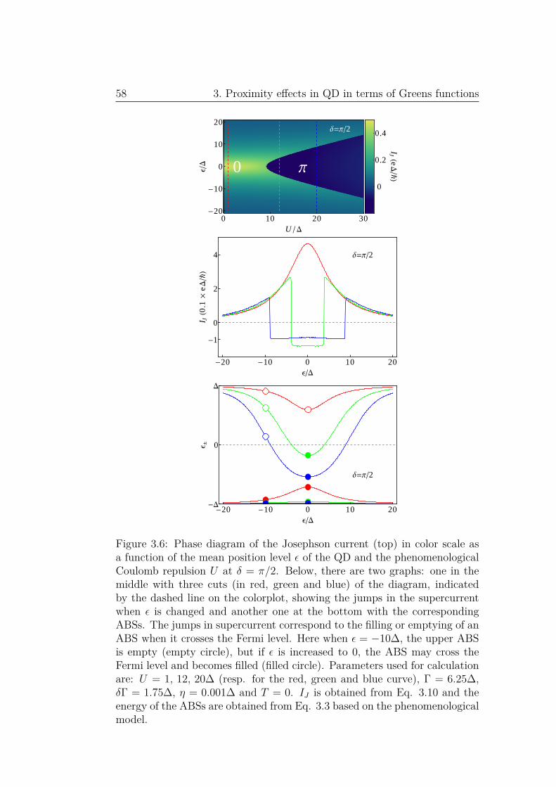
58 3. Proximity effects in QD in terms of Greens functions
0 10 20 30
0
-10
10
-20
20
U D
ΕD
0
0.2
0.4
IJ He
DÑL
0 Π
∆=Π2
0 10 20-10-20
0
2
4
-1
ΕD
IJ
H0.1
´e
DÑ
L
∆=Π2
0 10 20-10-20
0
D
-D
ΕD
Ε ±
∆=Π2
Figure 3.6: Phase diagram of the Josephson current (top) in color scale asa function of the mean position level ϵ of the QD and the phenomenologicalCoulomb repulsion U at δ = π/2. Below, there are two graphs: one in themiddle with three cuts (in red, green and blue) of the diagram, indicatedby the dashed line on the colorplot, showing the jumps in the supercurrentwhen ϵ is changed and another one at the bottom with the correspondingABSs. The jumps in supercurrent correspond to the filling or emptying of anABS when it crosses the Fermi level. Here when ϵ = −10∆, the upper ABSis empty (empty circle), but if ϵ is increased to 0, the ABS may cross theFermi level and becomes filled (filled circle). Parameters used for calculationare: U = 1, 12, 20∆ (resp. for the red, green and blue curve), Γ = 6.25∆,δΓ = 1.75∆, η = 0.001∆ and T = 0. IJ is obtained from Eq. 3.10 and theenergy of the ABSs are obtained from Eq. 3.3 based on the phenomenologicalmodel.
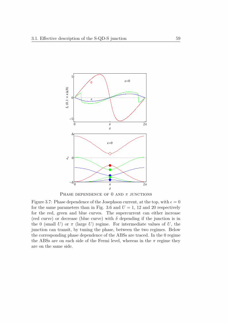
3.1. Effective description of the S-QD-S junction 59
0 Π 2Π
0
5
-5
∆
IJ
H0.1
´e
DÑ
L
Ε=00
Π
0 Π 2Π
0
D
-D
∆
Ε ±
Ε=0
Phase dependence of 0 and π junctionsFigure 3.7: Phase dependence of the Josephson current, at the top, with ϵ = 0for the same parameters than in Fig. 3.6 and U = 1, 12 and 20 respectivelyfor the red, green and blue curves. The supercurrent can either increase(red curve) or decrease (blue curve) with δ depending if the junction is inthe 0 (small U) or π (large U) regime. For intermediate values of U , thejunction can transit, by tuning the phase, between the two regimes. Belowthe corresponding phase dependence of the ABSs are traced. In the 0 regimethe ABSs are on each side of the Fermi level, whereas in the π regime theyare on the same side.

60 3. Proximity effects in QD in terms of Greens functions
This can be seen in the colorplot of Fig. 3.6 where we have representedcalculation of the Josephson current carried by a QD connected between twosuperconducting leads, at a superconducting phase difference δ = π/2, as afunction of the mean position level, noted here ϵ, and the Coulomb repulsioninside the QD U normalized with the superconducting gap ∆. IJ is obtainedfrom Eq. 3.10 (or Eq. C.10) based on the phenomenological model.
In this diagram, there are two areas: one of positive Josephson currentthat appears in green and yellow and one where the current is negative andwhich is blue (they are respectively labelled 0 and π on the graph). Below,we have chosen to trace three cuts of this diagram: the current is plotted as afunction of ϵ (controlled experimentally with gates) and shows, for sufficientlyhigh U , abrupt transitions from positive to negative current. Comparing thisgraph with the one below, we can see that these sudden jumps correspondexactly to the crossing of an ABS with the Fermi level.
Phase dependence The phase dependence of these ABSs is representedin Fig. 3.7 as well as the supercurrent carried by the QD. For small U ,the junction is in its ground state for δ = 0, where its energy reaches itsminimum. The S-QD-S junction is then in its 0-state. However if U is large,the junction is in its lower energy state for δ = π, the supercurrent flowsthen in opposite direction than in the previous case. The junction is, thistime, in its π-state. For intermediate values of U , variation of δ may causethe crossing of one ABS with the Fermi level inducing jumps in the current-phase relation. When the junction is in this regime, it is conventionally called0′ or π′ junction depending if the system is more stable at δ = 0 or δ = π.
3.2 Exact treatment of the Quantum Dot withsuperconducting leads: the Numerical Renor-malization Group
In this section we briefly discuss how one can used NRG calculations to obtainexact numerical results on the proximity effect in QD. The comparison of thistechnique with the simplified non-interacting treatment made in the previoussections will be carried out in the next section.
3.2.1 Anderson impurity model in NRGLike before we consider a single orbital of the quantum dot, but in contrastto the simplified approach, the NRG approach yields the exact solutions of

3.2. Exact treatment of the Quantum Dot with superconducting leads: theNumerical Renormalization Group 61
the system, taking into account the Coulomb interaction in the dot. Thisproblem is exactly the Anderson impurity model (AIM) with superconductingleads, described by the Hamiltonian:
H = HQD +HL +HR +HTL+HTR
with:
HQD = ϵorb (n↑ + n↓) + Ecn↑n↓ with nσ = d†σdσ
HL =∑l,σ
ϵlc†lσclσ +
∑l
(∆eiϕLc†
l↑c†−l↓ + ∆e−iϕLc−l↓cl↑
)HR =
∑r,σ
ϵrc†rσcrσ +
∑l
(∆eiϕRc†
r↑c†−r↓ + ∆e−iϕRc−r↓cr↑
)
HTL=∑l,σ
(tLd
†σclσ + t∗Lc
†lσdσ
)HTR
=∑r,σ
(tRd
†σcrσ + t∗Rc
†rσdσ
)
Here, dσ is the annihilation operator of an electron with a spin σ in theorbital of energy ϵorb and Ec is the charging energy due to the repulsionbetween two electrons occupying the QD. Operator cl(r)σ annihilates, in theleft (resp. right) electrode, an electron of spin σ in state l (r) with an energyϵl(r). In this notation, l and r represent a synthetic index for all the quantumnumbers of the electrons in electrodes, except their spin, and such that c−l−σis the time reversed-state of clσ. ∆eiϕL(R) is the complex order parameter inelectrode L(R) with modulus ∆ (also known as the gap energy) and phaseϕL(R). tL(R) is the energy associated to the transfer of an electron betweenleft (right) electrode and the dot.
In the resolution of the problem, the method takes into account all fourstates of the uncoupled orbital, with their spin degeneracy:
EcS = 0 (singlet)
S = 1/2 (doublet)
Energy
S = 0 (singlet)

62 3. Proximity effects in QD in terms of Greens functions
For the numerical calculations we have used the “NRG Ljubjana” open-source code written by Rok Zitko16. We gratefully acknowledge extendedhelp from the author.
For any given set of parameters of the Hamiltonian, the NRG calculationyields the quasi-exact17 complete low energy spectrum of a discretized system.In particular it determines the ground state, and the subgap excitations(the ABSs) giving their total spin and degeneracies. NRG can also providearbitrary spectral functions of operators, and in particular, the tunnelingdensity of states into the dot. Since NRG calculation is performed for adiscretized Hamiltonian, the spectral function is represented in form of aweighted set of delta peaks. For the sub-gap part this is, in fact, an exactrepresentation of the ABSs. For the continuum, however, in order to obtain asmooth plot, one has to do spectral averaging (over several NRG calculationswith different discretizations) together with some broadening.
3.2.2 Zero vs finite superconducting phase differenceacross the QD
In principle, the AIM with an arbitrary number of identical leads (normal orsuperconducting) remains a “single-channel” problem, since one can performa suitable Gram-Schmidt orthogonalization to a single effective channel, whileall other states fully decouple.
In practice however, in the case of two superconducting channels withdifferent SC amplitude and/or phase the results of such a transformation isdifficult to use in NRG. In that case, in order to circumvent this difficulty,one has rather recourse to a “two channels” NRG calculations (one channelfor each lead), which is unfortunately much more demanding in terms ofcomputational power. Indeed, compared to the zero phase difference case,an NRG calculation of a QD at finite phase difference is slower by aboutthree orders of magnitude. This explains why in the following we give onlyresults of NRG calculations at zero phase difference.
16See http://nrgljubljana.ijs.si/ for an introduction to quantum impurity problems, anexplanation of the NRG method, downloadable number-crunching NRG code, documen-tation and examples.
17It is not formally exact because the resolution is performed with discrete states insteadof a continuum, but we can control the precision of the results.

3.3. Predictions for the DOS of a QD connected to superconductors 63
3.3 Predictions for the DOS of a QD con-nected to superconductors
In this section we look how the DOS of the QD, and in particular the ABSs,depends on the parameters of the effective model we have used to obtain theGreen’s functions. To better grasp the limitations of this effective model, wecompare its results with those of the exact NRG solution of the Andersonimpurity model. We introduce the following correspondence between thenotations of the NRG (see section 3.2.1) and those of the effective model (seesection 3.1.1.1):
ϵorb ↔ ϵ0 − U/2Ec ↔ U
in order to compare their respective results. In the following, we will call ϵ0the “mean position level” and U the “charging energy” for both approaches.Concerning the coupling to the leads ΓL and ΓR, they are defined in the sameway in both approaches.
Among the parameters of the models we discuss here, we will distin-guish those that are tunable parameters (that we can tune during the exper-iment18): the mean position level ϵ0 and phase dependence δ, and others thatwill be considered as fixed sample-dependent, or setup-dependent parame-ters: the couplings to the leads Γ = ΓL + ΓR, its asymmetry δΓ = ΓL − ΓRand the charging energy U .
3.3.1 Modification of the spectral density of a QD uponcoupling to superconducting contacts
Superconducting proximity effect in QD modifies its TDOS in a characteristicway. In order to identify signatures that are peculiar to this effect, we firstlook how the connection to normal leads modifies the QD’s spectral densityand then we turn them superconducting. Experimentally the latter transitioncan be achieved by lowering a magnetic field or the temperature.
Spectral density of a QD connected to normal leads An isolatedQD has a very simple spectral density composed of two Dirac peaks spacedof the charging energy at ω = ϵ0 − U/2 and ϵ0 + U/2. They correspond toeigenstates of the isolated QD and have, as a consequence, infinite lifetime.
18We need to mention that there are other parameters that we can control experimentallyand are not in the model as the temperature, the magnetic field or the current flowingthrough the sample.

64 3. Proximity effects in QD in terms of Greens functions
That’s why they are infinitely thin. As we can see in Fig. 3.8, NRG and theeffective approach give the same TDOS (plotted in dashed gray in the firstline of graphs) for this elementary case.
When we couple the QD to two normal leads, the levels of the dots are notanymore eigenstates: an electron placed into the QD can escape to the leadsin a finite time. Hence, the levels are broaden in a Lorentzian shape. In theeffective approach, their half-width at half-maximum are given by ΓL + ΓR(see Fig. 3.8, first graph from the top of the central column), whereas NRGshows levels that are sensitively wider for the chosen set of parameters. Themost striking difference, between NRG and the effective approach, is theformation of a Kondo peak19 at the Fermi level that is not captured at allby the effective approach but only by NRG (a brief discussion about thisparticularity of the effective non-interacting model can be found in sectionA.4.2 appendix A). Because the Kondo peak gets wider with increasing Γ,the comparison between the two approaches become completely inaccuratefor large coupling to the leads.
Since this effect essentially disappears of the TDOS when the leads areturned superconducting, we will ignore Kondo effect in this chapter, but thisphenomenon will be tackled in details in part III.
Spectral density of a QD connected to superconducting leads: for-mation of ABSs When the leads connected to the QD are turned super-conducting (Fig. 3.8 second line of graphs from the top), a superconductinggap is induced in the dot around the Fermi level and ABSs appear in it. Asthey are eigenstates, they have infinite lifetime and appear as infinitely thinpeaks.
Taking ηinel = 0, we increase their linewidth such that they become vis-ible in the DOS. We can then compare results of the effective model withexact NRG calculations (in which the ABSs’ linewidth is added artificially).In the third line of graphs of Fig. 3.8, we can see that the TDOS obtainedfrom the two different approaches are qualitatively similar. ABSs are locatedapproximately at the same energies and continuums outside of the gap arecomparable. This similarity between approaches hold only for large charg-ing energy and small or moderate coupling to the leads compared to thesuperconducting gap. For large Γ, the effective model breaks down and givesTDOS which shows large discrepancy with exact NRG calculations.
19See appendix A.

3.3. Predictions for the DOS of a QD connected to superconductors 65
NR
GEff
ectiv
em
odel
0
1(a.u.)
-U/2
+U/2
Kon
do p
eak
0
1(a.u.)
-U/2
+U/2
QD
NN
U
0
1(a.u.)
-U/2
+U/2
QD
SS
U
0
1(a.u.)
-U/2
+U/2
0
1(a.u.)
-U/2
+U/2
Probe
QD
SS
U
TD
OS
ofa
QD
whe
nco
nnec
ted
toel
ectr
odes
Figu
re3.
8:T
hele
ftan
dce
ntra
lcol
umns
repr
esen
tsT
DO
Sof
aQ
Das
afu
nctio
nof
thee
nerg
yω
,res
pect
ivel
yob
tain
edw
ithN
RG
and
the
effec
tive
mod
el,i
ndi
ffere
ntsit
uatio
ns.
From
top
tobo
ttom
:sp
ectr
alde
nsity
inar
bitr
ary
unit
ofa
QD
conn
ecte
dto
norm
alle
ads
(inda
shed
gray
,we
have
trac
edth
eT
DO
Sof
the
isola
ted
QD
),a
QD
conn
ecte
dto
supe
rcon
duct
ing
lead
s(ju
stfo
rth
eeff
ectiv
em
odel
)an
dth
esa
me
thin
gbu
tw
itha
linew
idth
adde
dto
the
AB
Ss.
Inth
eth
irdlin
eof
grap
hs,w
ega
veth
elin
ewid
thto
the
AB
Ssta
king
η inel
=0.
03∆
inth
eeff
ectiv
em
odel
and
adde
dar
tifici
ally
inN
RG
.The
finite
linew
idth
can
mod
elth
ere
duct
ion
ofth
eA
BSs
lifet
ime
due
toth
eco
nnec
tion
toan
exte
rnal
tunn
elpr
obe.
Para
met
ers
for
the
figur
esar
e:ϵ 0
=1,
Γ=
0.2∆
,U=
3∆an
dδ
=0.

66 3. Proximity effects in QD in terms of Greens functions
Right lead DOSLeft lead DOS
EF EF
EE Increasing Vg
S SQD
Figure 3.9: Energies of the QD levels can be tuned with a back gate voltagecoupled capacitively to the sample.
3.3.2 Influence of the parameters on ABSs
3.3.2.1 Tunable parameters
In our experiment, we control the superconducting phase difference δ betweenthe superconducting electrodes connected to the QD with a magnetic field.With a gate voltage, we can tune the energy level of the QD’s orbital whichis equivalent, in the model, to control ϵ0 (see Fig. 3.9). Experimental detailson how we control these parameters are given in part II.
3.3.2.2 Phase dependence: signature of the ABSs
As mentioned above (section 3.2.2), calculations of the TDOS at δ = 0 isa too much time-demanding process in NRG. In this respect, the effectivemodel provides the interesting possibility to access the phase-dependence ofthe TDOS. In Fig. 3.10, we have represented, for three different values of δ (ingreen, blue and red), the TDOS of a QD connected to two superconductingleads. Below, is plotted the phase dependence of the ABSs (degenerate forthe chosen parameters) which are 2π-periodic. This phase dependence is asignature of the ABSs and an indirect evidence that they carry supercurrent(see section 3.1.5 above).

3.3. Predictions for the DOS of a QD connected to superconductors 67
(a.u.)
EABSFigure 3.10: Plot of the spectral density of a QD connected to supercon-ducting leads (top) as a function of the energy ω obtained with the effectivemodel for three different phases and energies of the ABSs (bottom) as a func-tion of δ. The ABS are 2π-periodic with δ (not shown). Parameters takenfor these plots: U = 0, ϵ0 = 0, ΓL = 10∆, ΓR = 8∆, η = 0.00001∆, andδ = π/3 (red) , 2π/3 (green) and π (blue) .
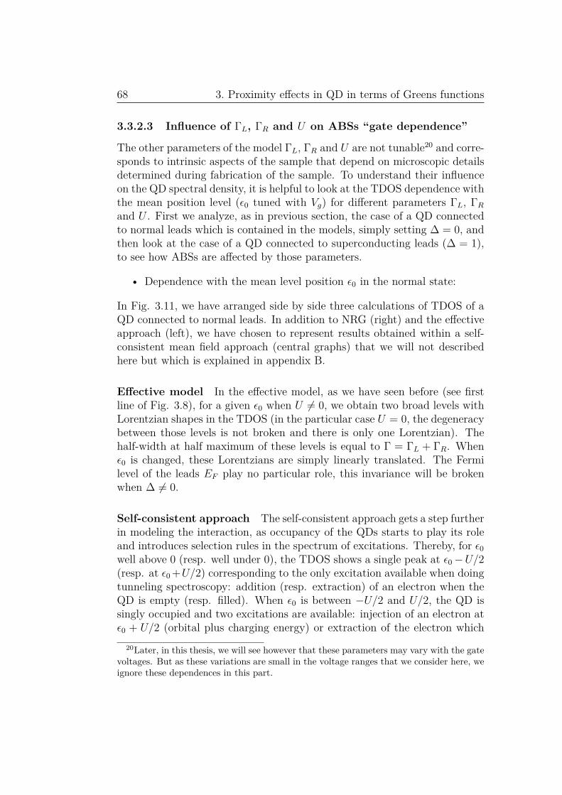
68 3. Proximity effects in QD in terms of Greens functions
3.3.2.3 Influence of ΓL, ΓR and U on ABSs “gate dependence”
The other parameters of the model ΓL, ΓR and U are not tunable20 and corre-sponds to intrinsic aspects of the sample that depend on microscopic detailsdetermined during fabrication of the sample. To understand their influenceon the QD spectral density, it is helpful to look at the TDOS dependence withthe mean position level (ϵ0 tuned with Vg) for different parameters ΓL, ΓRand U . First we analyze, as in previous section, the case of a QD connectedto normal leads which is contained in the models, simply setting ∆ = 0, andthen look at the case of a QD connected to superconducting leads (∆ = 1),to see how ABSs are affected by those parameters.
• Dependence with the mean level position ϵ0 in the normal state:
In Fig. 3.11, we have arranged side by side three calculations of TDOS of aQD connected to normal leads. In addition to NRG (right) and the effectiveapproach (left), we have chosen to represent results obtained within a self-consistent mean field approach (central graphs) that we will not describedhere but which is explained in appendix B.
Effective model In the effective model, as we have seen before (see firstline of Fig. 3.8), for a given ϵ0 when U = 0, we obtain two broad levels withLorentzian shapes in the TDOS (in the particular case U = 0, the degeneracybetween those levels is not broken and there is only one Lorentzian). Thehalf-width at half maximum of these levels is equal to Γ = ΓL + ΓR. Whenϵ0 is changed, these Lorentzians are simply linearly translated. The Fermilevel of the leads EF play no particular role, this invariance will be brokenwhen ∆ = 0.
Self-consistent approach The self-consistent approach gets a step furtherin modeling the interaction, as occupancy of the QDs starts to play its roleand introduces selection rules in the spectrum of excitations. Thereby, for ϵ0well above 0 (resp. well under 0), the TDOS shows a single peak at ϵ0 −U/2(resp. at ϵ0 +U/2) corresponding to the only excitation available when doingtunneling spectroscopy: addition (resp. extraction) of an electron when theQD is empty (resp. filled). When ϵ0 is between −U/2 and U/2, the QD issingly occupied and two excitations are available: injection of an electron atϵ0 + U/2 (orbital plus charging energy) or extraction of the electron which
20Later, in this thesis, we will see however that these parameters may vary with the gatevoltages. But as these variations are small in the voltage ranges that we consider here, weignore these dependences in this part.
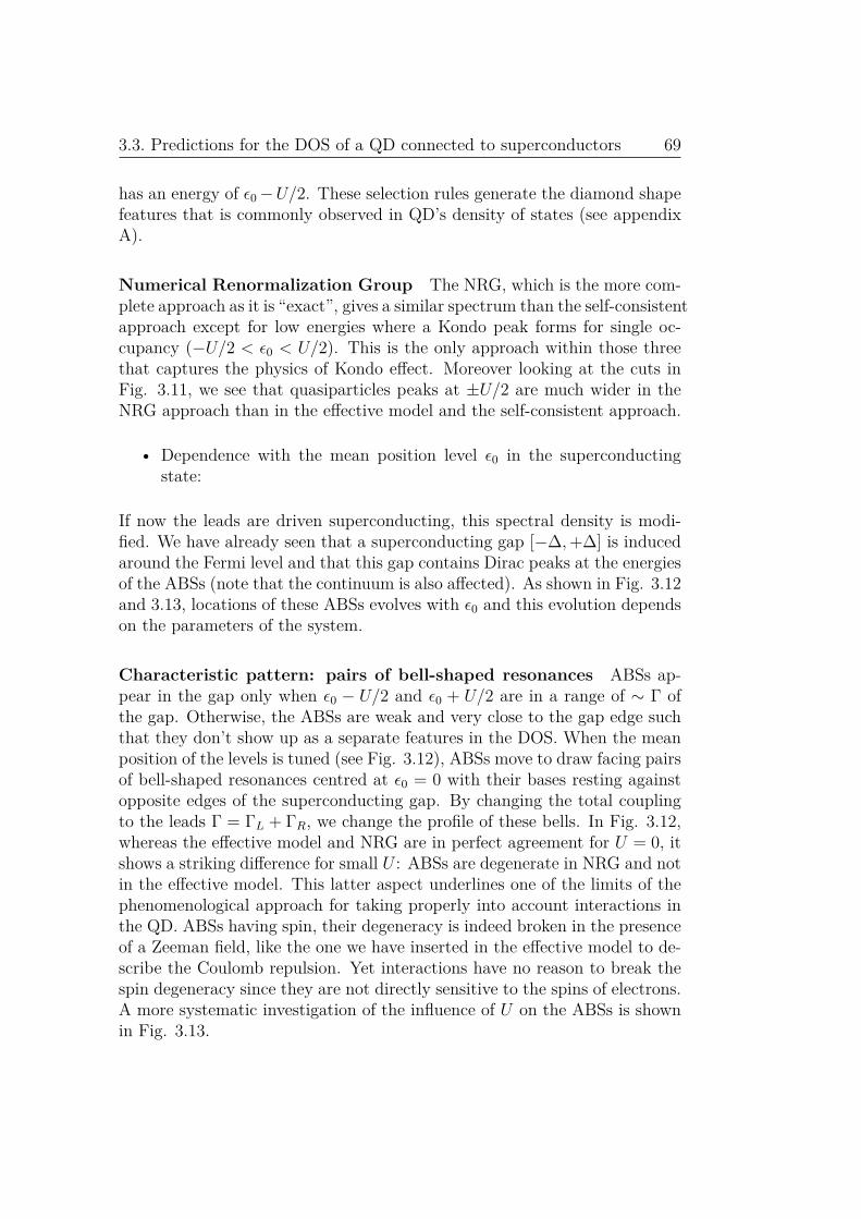
3.3. Predictions for the DOS of a QD connected to superconductors 69
has an energy of ϵ0 −U/2. These selection rules generate the diamond shapefeatures that is commonly observed in QD’s density of states (see appendixA).
Numerical Renormalization Group The NRG, which is the more com-plete approach as it is “exact”, gives a similar spectrum than the self-consistentapproach except for low energies where a Kondo peak forms for single oc-cupancy (−U/2 < ϵ0 < U/2). This is the only approach within those threethat captures the physics of Kondo effect. Moreover looking at the cuts inFig. 3.11, we see that quasiparticles peaks at ±U/2 are much wider in theNRG approach than in the effective model and the self-consistent approach.
• Dependence with the mean position level ϵ0 in the superconductingstate:
If now the leads are driven superconducting, this spectral density is modi-fied. We have already seen that a superconducting gap [−∆,+∆] is inducedaround the Fermi level and that this gap contains Dirac peaks at the energiesof the ABSs (note that the continuum is also affected). As shown in Fig. 3.12and 3.13, locations of these ABSs evolves with ϵ0 and this evolution dependson the parameters of the system.
Characteristic pattern: pairs of bell-shaped resonances ABSs ap-pear in the gap only when ϵ0 − U/2 and ϵ0 + U/2 are in a range of ∼ Γ ofthe gap. Otherwise, the ABSs are weak and very close to the gap edge suchthat they don’t show up as a separate features in the DOS. When the meanposition of the levels is tuned (see Fig. 3.12), ABSs move to draw facing pairsof bell-shaped resonances centred at ϵ0 = 0 with their bases resting againstopposite edges of the superconducting gap. By changing the total couplingto the leads Γ = ΓL + ΓR, we change the profile of these bells. In Fig. 3.12,whereas the effective model and NRG are in perfect agreement for U = 0, itshows a striking difference for small U : ABSs are degenerate in NRG and notin the effective model. This latter aspect underlines one of the limits of thephenomenological approach for taking properly into account interactions inthe QD. ABSs having spin, their degeneracy is indeed broken in the presenceof a Zeeman field, like the one we have inserted in the effective model to de-scribe the Coulomb repulsion. Yet interactions have no reason to break thespin degeneracy since they are not directly sensitive to the spins of electrons.A more systematic investigation of the influence of U on the ABSs is shownin Fig. 3.13.

70 3. Proximity effects in QD in terms of Greens functions
QD
NN
U
Effective
model
Self-consistentN
RG
-4
-2
04
2
-3
-1 0 31
Ε0
Ω
0 2.5
5
D.O.S.Ha.u.L
-4
-2
04
2
-3
-1 0 31
Ε0
Ω
0 2.5
5
D.O.S.Ha.u.L
-4
-2
04
2
-3
-1 0 31
Ε0
Ω
0 2.5
5D.O.S.Ha.u.L
02
24
4
1 (a.u.)
02
24
4
1 (a.u.)
02
24
4
1 (a.u.)
Figure3.11:
Colorplots
(left)and
cuts(right)
ofcalculated
spectraldensityfor
aQ
Dconnected
tonorm
alleadsas
afunction
ofthe
energyω
andthe
levelsm
eanposition
ϵ0w
ithinthree
differentapproaches:
effectivem
odel,self-consistentm
eanfield
approximation
andN
RG
.QD
levelsarebroaden
ina
Lorentzianshape
dueto
thecouplings
tothe
leadsΓ
=ΓL
+ΓR
andsplitted
becauseofthe
chargingenergy
U.
Self-consistentapproach
andN
RG
includeselection
rulesrelated
tothe
occupancyofthe
dot(responsibleofthe
diamond-shape
pattern),whereas
theeffective
modelis
notsensitive
tothis
aspect.N
RG
isthe
onlyapproach
within
thosethree
thatcaptures
theK
ondoeffect
occurringat
lowenergies.
Parameters
takenfor
thesecalculations
areΓ
=0.2,and
U=
3in
arbitraryunit.

3.3. Predictions for the DOS of a QD connected to superconductors 71
Effective model
-4D -2D 0 4D2D
-3D
-D
0
3D
D
Ε0
Ω
0
2.5
5
D.O
.S.Ha
.u.L
-4D -2D 0 4D2D
-3D
-D
0
3D
D
Ε0
Ω0
2.5
5
D.O
.S.Ha
.u.L
-4D -2D 0 4D2D
-3D
-D
0
3D
D
Ε0
Ω
0
2.5
5
D.O
.S.Ha
.u.L
-4D -2D 0 4D2D
-3D
-D
0
3D
D
Ε0
Ω
0
2.5
5
D.O
.S.Ha
.u.L
-4D -2D 0 4D2D
-3D
-D
0
3D
D
Ε0
Ω
0
2.5
5
D.O
.S.Ha
.u.L
-4D -2D 0 4D2D
-3D
-D
0
3D
D
Ε0
Ω
0
2.5
5
D.O
.S.Ha
.u.L
NRG
-4D -2D 0 4D2D
-3D
-D
0
3D
D
Ε0
Ω
0
2.5
5
D.O
.S.Ha
.u.L
-4D -2D 0 4D2D
-3D
-D
0
3D
D
Ε0
Ω
0
2.5
5
D.O
.S.Ha
.u.L
-4D -2D 0 4D2D
-3D
-D
0
3D
D
Ε0
Ω
0
2.5
5
D.O
.S.Ha
.u.L
-4D -2D 0 4D2D
-3D
-D
0
3D
D
Ε0
Ω
0
2.5
5
D.O
.S.Ha
.u.L
-4D -2D 0 4D2D
-3D
-D
0
3D
D
Ε0
Ω
0
2.5
5
D.O
.S.Ha
.u.L
-4D -2D 0 4D2D
-3D
-D
0
3D
D
Ε0
Ω
0
2.5
5
D.O
.S.Ha
.u.L
S SQD Decreasing
Figure 3.12: DOS as a function of the energy ω and the levels mean positionϵ0 calculated within the effective model (6 upper graphs) and using NRG (6lower graphs) for decreasing Γ from the left to the right for U = 0 (first andthird lines) and U = 0.6∆ (second and fourth lines). The coupling to theleads influences strongly the ABSs dependence with ϵ0. Parameters: δ = 0,ΓL = ΓR = 0.7, 0.5, and 0.3∆, and ηinel = 0.01∆.
72 3. Proximity effects in QD in terms of Greens functions
Influence of the strength of U It shows that, as just mentioned, for smallU (left graphs) the phenomenological approach fails to describe correctly thisinfluence because ABSs are predicted to be degenerate by the NRG whereasthe effective non-interacting model predicts that this degeneracy is broken.
For U ∼ ∆ (central graphs), the degeneracy between ABS is broken inboth approaches and four resonances corresponding to two ABSs may appearwithin the gap. However in NRG, this happens only when one of the ABS hascrossed the Fermi level, i.e. after the singlet-doublet transition mentionedin section 3.1.5.2. It results in a “hanging” ABS for a reduced region of ϵ0.This feature is missed by the phenomenological approach because it is dueto selection rules related to QD’s occupancy[77], not taken into account inthis approach. Indeed, in the ground state, the QD is either occupied by anodd number of electron or by an even number of electron (superconductingsinglet-states): the spin S of the dot is thus either equal to 1/2 or 0. Astunneling spectroscopy explores excitations of the system through injectionof electrons, it allows only to see transitions that do not conserve the spinof the dot. In Fig. 3.14, we have plotted the energies of the different statesavailable for the system21 as a function of ϵ0. There are four of them: twoS = 0 states with one that is always higher in energy and two degenerateS = 1/2 states. For ϵ0 far from 0, the ground state is a S = 0 state andtunneling spectroscopy allows to explore only the degenerate S = 1/2 dou-blet, resulting in a single resonance between 0 and ∆ in the TDOS. Aftercrossing of an ABS with the Fermi level, the ground state is the degeneratedoublet S = 1/2, and transition toward S = 0 states can be seen by tunnel-ing spectroscopy, resulting in two resonances between 0 and ∆ in the TDOS.As the effective approach ignores selection rules due to QD occupancy, allthe possible transitions are seen in the spectrum and ABSs are never “inter-rupted” this way. It can be noticed that it is not because states cannot beseen through transition authorized by tunneling spectroscopy that they donot exist. Besides, performing a spectroscopy through microwave irradiation,we would obtained transition between S = 0 states, completing the wholespectrum.
For large U , the calculated TDOS are in satisfying agreement between thetwo approaches (at least concerning the ABSs). The two central bells crossto form a loop, and the external states merge into the continuum beyond ±∆(see Fig. 3.13). At some point only one ABS appears in the spectral density(but twice, at ω > 0 and ω < 0), the other one being stuck to the edge. Thisis the most common situation in our measurements.
21Be careful that we distinguish states of the whole system and excitations of the system(which are transitions between states).

3.3. Predictions for the DOS of a QD connected to superconductors 73
-2
D0
2D
-3
D
-D0
3D D
Ε0
Ω
02.55
D.O.S. Ha.u.L
-2
D0
2D
-3
D
-D0
3D D
Ε0
Ω
02.55
D.O.S. Ha.u.L
-4
D-
2D
04
D2
D
-3
D
-D0
3D D
Ε0
Ω
02.55
D.O.S. Ha.u.L
-2
D0
2D
-3
D
-D0
3D D
Ε0
Ω
02.55
D.O.S. Ha.u.L
-2
D0
2D
-3
D
-D0
3D D
Ε0
Ω
02.55
D.O.S. Ha.u.L
-4
D-
2D
04
D2
D
-3
D
-D0
3D D
Ε0
Ω
02.55
D.O.S. Ha.u.L
Increasing
U
Infl
uenc
eof
the
char
ging
ener
gyin
the
phen
omen
olog
ical
mod
el(u
pper
grap
hs)
and
inN
RG
(low
ergr
aphs
)
Figu
re3.
13:
Col
orsc
aled
repr
esen
tatio
nsof
TD
OS
ofa
QD
conn
ecte
dto
supe
rcon
duct
ing
lead
sas
afu
nctio
nofϵ 0
.T
heth
ree
uppe
rgra
phsa
reob
tain
edw
ithin
the
effec
tive
non-
inte
ract
ing
appr
oach
and
the
lowe
rgra
phsa
reob
tain
edby
NR
Gca
lcul
atio
ns.
Inth
eeff
ectiv
em
odel
,we
see
that
incr
easin
gU
split
sth
eA
BSs
until
alo
opis
form
edin
the
spec
tral
dens
ityan
don
eof
the
AB
Ssm
erge
into
the
cont
inuu
m.
Ifwe
com
pare
with
the
exac
tre
sults
obta
ined
inN
RG
,we
see
that
the
effec
tive
mod
elca
ptur
em
any
feat
ures
ofth
eA
BSs
that
deve
lop
inan
inte
ract
ing
QD
.T
here
are
howe
vers
ome
diffe
renc
es.
Fore
xam
ple,
whe
nU
issm
allc
ompa
red
to∆
,we
see
that
,in
oppo
sitio
nto
the
effec
tive
mod
el,i
nN
RG
calc
ulat
ions
the
dege
nera
cybe
twee
nA
BSs
isno
tbr
oken
.Fo
rU
clos
eto
∆,N
RG
pred
icts
that
ther
eis
a“h
angi
ng”
exci
tatio
nth
atap
pear
sw
henϵ 0
iscl
ose
toth
eFe
rmil
evel
.T
his
isdu
eto
sele
ctio
nru
le(s
eeFi
g.3.
14)
that
are
com
plet
ely
igno
red
inth
eeff
ectiv
em
odel
.H
owev
erfo
rla
rgeU
,the
effec
tive
mod
elis
ingo
odag
reem
ent
with
NR
Gco
ncer
ning
the
AB
Ss.
Para
met
ers
used
for
calc
ulat
ions
:δ
=0,η inel
=0.
01∆
(onl
yfo
rth
eeff
ectiv
em
odel
),Γ
=0.
2∆,U
=0.
25,
1an
d3∆
.

74 3. Proximity effects in QD in terms of Greens functions
S = 0
S = 0
S = 1/2 (doublet)
E
continuum
0
0
Ene
rgy
ofab
sorp
tion
0
0
Energy of the ground state and singlet-doublet transitionFigure 3.14: On the top, is represented a spectrum calculated in NRG of Fig.3.13, where a “hanging” ABS appear around ϵ0 = 0. Below, we have plottedenergies of the four lowest states (in energy) of the system as a function ofϵ0 (the ground state is always chosen as the origin). The blue lines indicateenergies of S = 0 states, whereas energies of degenerate S = 1/2 states aretraced in pink. As measuring the TDOS, we do not conserve the spin of thedot (one electron is added or extracted) we cannot see transitions betweenS = 0 states (red arrow), but only transition between S = 0 and S = 1/2states (green arrows). The inversion of ground state, or singlet-doublet tran-sition, occurring at the crossing of an ABS with the Fermi level induces alift of degeneracy between excitations of the system. As a consequence, anabrupt transition between two and four resonances in the gap happens in theTDOS. The lower graph shows what we should obtain by microwave spec-troscopy as a function of the frequency and ϵ0: we would explore transitionsfrom S = 0 ground states to S = 0 excited states.

3.3. Predictions for the DOS of a QD connected to superconductors 75
0 Π 2 Π
-D
0
D
∆
Ω
∆G = 0
0
2.5
5
D.O
.S.Ha
.u.L
0 Π 2 Π
-D
0
D
∆
Ω
∆G = 0.2D
0
2.5
5
D.O
.S.Ha
.u.L
Effect of the contact asymmetry on the ABSsFigure 3.15: DOS obtained from the phenomenological approach for symmet-ric (top) and asymmetric (right) contacts connected to the QD. On the leftδΓ = 0 and on the right δΓ = 0.2∆. The contact asymmetry δΓ introducesa coupling between the ABSs which form an avoided crossing at δ = π whenδΓ = 0. For both DOS, we used Γ = 1.8∆, ϵ0 = 0, Eex = 0 and ηinel = 0.01∆in the calculation.
Role of the coupling asymmetry δΓ = ΓL − ΓR in the phase depen-dence As we explain previously, in section 3.1.3, the coupling asymmetryto the electrodes δΓ = ΓL − ΓR only plays a role at finite δ. In figures 3.12and 3.13, the TDOS is always calculated at a phase difference δ = 0, so thatonly the total coupling strength Γ enters the Green’s functions and δΓ hasno influence.
However, we can then see the influence of the coupling asymmetry δΓin the phase dependence of the spectral density. Figure 3.15 represents twocolorplots of the spectral density phase dependence for δΓ = 0 and δΓ = 0but with a similar Γ. The asymmetry introduces a coupling between ABSswhich anticross at δ = π only when δΓ = 0.

76 3. Proximity effects in QD in terms of Greens functions
Role of the interdot coupling t′ Compared to a single QD, the DQDnature of the CNT introduces new physics which is governed by the strengthof the interdot coupling t′. In chapter 7 of part III, we will see how it affectsthe electronic structure of the CNT within a self-consistent approach (NRGfor DQD is not done here as it is more complicated and time-demanding thanfor single QD).
Here, we analyze its influence on the ABSs formation within our crudeapproach and particularly their phase dependence. When t′ = 0, the electri-cal circuit is open between the two superconducting leads: no supercurrentcan flow and there is thus no phase dependence of the DOS. Yet ABSs doform in both QDs, they just do not carry supercurrent and are not coupledwith each others. In Fig. 3.16, the gate dependence of the DQD densityof states exhibit the characteristic “bells” within [−∆,+∆] which appearindependently.
If now t′ = 0, the electrical circuit is closed and can sustain supercurrent.The “bells” are now interacting because of the interdot coupling and form ananticrossing where ABSs cross each other as on Fig. 3.16. At this anticrossingABSs get their maximum phase dependence and it remains essentially phaseindependent elsewhere.

3.3. Predictions for the DOS of a QD connected to superconductors 77
-6 -4 -2 0 2 4 6
-D
0
D
Ε0
Ω
t' = 0
0
2.5
5
D.O
.S.Ha
.u.L
L L¯ R R¯
-6 -4 -2 0 2 4 6
-D
0
D
Ε0
Ω
t' = 0.5D
0
2.5
5
D.O
.S.Ha
.u.L
ì
S SQDL QDR
t'
L
L
RR
Avoided crossings of the ABSs due to interdot couplingFigure 3.16: Colorplots of the QD’s TDOS as a function of the energy ω andthe mean position of the levels (ϵL↑, ϵL↓, ϵR↑ and ϵR↓) noted ϵ0. When ABSsof QDL and QDR cross each other they may couple if t′ = 0 and form anavoided crossing, as for example where indicated by the diamond. At theseavoided crossing, the flux dependence is maximum. On the left graph, dashedlines labelled L ↑ and L ↓ (resp. R ↑ and R ↓) are inserted to indicate whereare, for each value of ϵ0, levels of spin up and down of the left (resp. right)QD. Parameters are: ϵL↑ = ϵ0 + 2, 5∆, ϵL↓ = ϵ0 + 0, 5∆, ϵR↑ = ϵ0 − 0, 5∆,ϵR↓ = ϵ0 − 2, 5∆, ΓL = ΓR = 1, 2∆, ηinel = 0, 01∆ and δ = π.

78 3. Proximity effects in QD in terms of Greens functions

Part II
Experimental observation ofthe Andreev Bound States
79


81
Andreev Bound States concept has led to many successful interpretationsfor experiments on mesoscopic superconductivity [69, 78, 79, 80, 81], andexotic or high-Tc superconductors [82, 83, 84, 85, 86]. Moreover they arenow inspiring possible experimental realizations in mesoscopic circuits forthe observation of Majorana Bound States [32, 42, 87, 88], which suppos-edly behave as non-abelian anyons [89]. Despite the fundamental interestthey arouse and though there have been already some strong indications oftheir existence [69], no direct observation of individually resolved ABSs wereperformed so far. In this chapter we present the first observation of ABSsrealized by tunneling spectroscopy in a supercurrent-carrying CNT.
For the purpose of probing the ABSs, we have fabricated samples withopen superconducting loops closed by a CNT in order to form S-CNT-Sstructures with a tunable superconducting phase difference δ. Additionally,in the middle of these structure, a superconducting tunnel probe is connectedto the CNT in order to measure its DOS.
With such devices, we observed individually resolved ABSs and theirδ-dependence, which is the ABSs’s main signature and is related to theirsupercurrent-carrying nature. Moreover thanks to external gate voltagesand by confronting our experimental results with the phenomenological DQDmodel described in previous part, we were able to link ABSs with the elec-tronic structure of the CNT and to extract information on parameters of thesystem such as the coupling to the leads and the charging energy of the QDs.
In this part of the thesis, we first describe the samples and the mea-surement setup. Then we present the ABSs tunneling spectroscopy that wehave realized in a CNT connected to superconducting leads, and discuss theobservation of the 0 − π transition in the TDOS of our device. Finally, wediscuss the performance of our device as a magnetic flux sensor using theδ-dependence of the ABSs.

82
Chapter 4
Description of the samples andmeasurement setup
In this section, we describe the samples we measured and discuss the roleof controllable parameters of the experiment: gate voltages, bias voltage,magnetic field, temperature. We also describe the measurement setup whichis connected to these samples in order to measure CNTs’ DOS.
4.1 Samples description and role of control-lable parameters
Samples geometry Samples we used to perform ABSs spectroscopy arecomposed of several metallic structures connected to CNTs (see part IV).These structures are constituted by a superconducting “fork” and a super-conducting tunnel probe connected to a single CNT, as depicted on Fig.4.1.
Within this geometry, we create two QDs (QDL and QDR in Fig. 4.1)localized between the two arms of the fork and on each side of the tunnelprobe.
Voltage bias V The fork, which is well connected to the CNT, is grounded,whereas the tunnel probe, which is weakly coupled to the CNT, is biased witha voltage V . By tuning this voltage we control the energies at which we probethe TDOS of the CNT (see appendix D). This TDOS is extracted from lock-in measurements of the differential conductance G (V ) between the tunnelprobe and the fork (see subsection 4.2).
83

84 4. Description of the samples and measurement setup
dIdV NT(E)
VLg
nT=35 mK
S S
Good contacts
Tunnel electrode
Lateral gate
SiO2 substrate
QDR
VbgVLg V
I
Vbg
QDL
QDRQDL
Diagram of the structures and connection to control devicesFigure 4.1: Each structure is connected to two (or three) DC voltage sources:a back gate voltage Vbg which controls the CNTs’ electro-chemical potential(some structures have an additional lateral gate voltage VLg which allowsto tune locally the electro-chemical potential) and a voltage bias V that weapply on the tunnel probe in order to measure the differential conductanceG (V ). From G (V ), we extract the CNT’s DOS (see appendix D). Addition-ally, we can generate, perpendicularly to the sample, a magnetic field that weuse either to tune the magnetic flux Φ in order to produce a superconductingphase bias δ = ϕL − ϕR across the CNT (low magnetic field ≤ 50 Gauss),or to drive the electrodes in their normal state (high magnetic field ≥ 500Gauss.).

4.1. Samples description and role of controllable parameters 85
Gate voltages Each sample is capacitively coupled to a back gate voltageVbg, and some structures (but not all) have an additional lateral gate coupledto the left part of the CNT1 biased with a voltage VLg. When biased, the backgate voltage Vbg shift the electro-chemical potential of CNTs homogeneously,thereby accumulating electrons or holes in the CNT, whereas VLg has just alocal influence and allows to change the number of charge carriers only onone side of the CNT (in QDL).
Magnetic flux Φ In our experiment the two superconducting contacts areconnected to the CNT on one side and shorted together on the other side,thereby forming a loop with the CNT. In this geometry, with the magneticflux Φ enclosed by the loop, we control the superconducting phase differenceδ = ϕL − ϕR between the two superconducting electrodes connected to theQD.
As the total magnetic flux threading the loop determines the integralof the phase gradient around the complete loop [47], the flux Φ and thesuperconducting phase difference δ are related through the relation:
Φ = Φ0
2π(δ + δAl) − Φscreen
where Φ0 = h/2e is the flux quantum, δAl is the phase difference accumulatedalong the aluminum part of the loop and Φscreen is a screening flux createdby the current Iloop that develops in the loop. This two contributions arerespectively proportional to the kinetic inductance LAl
K of the aluminum partof the loop (δAl = 2π
Φ0LAlK Iloop) and the geometric inductance LG of the loop
(Φscreen = LGIloop).However, as LAl
K and LG are negligible compared to the kinetic inductanceLCNTK of the CNT2, the magnetic flux threading the loop essentially imposes
a phase difference δ across the CNT. The latter is thus simply given by:
δ = 2π ΦΦ0
across the CNT (see Ref. [90] for a detail discussion on how to achieve agood phase bias).
The magnetic field is generated with a current circulating in a supercon-ducting coil below the sample. When we want to generate a magnetic fieldin order to tune the superconducting phase difference, we use magnetic fieldlower than 50 Gauss. But we can also generate a higher magnetic field (of
1A right lateral gate was also coupled to the sample but floating.2We have indeed LG < LAl
K ≪ LCNTK , as LG ≈ 1pH, LAl
K ≈ 10pH and LCNTK > 10nH.

86 4. Description of the samples and measurement setup
the order of 500 Gauss) in order to drive the aluminum electrodes in theirnormal state.
Temperature Measurements presented in chapter 5 and 7 were performedat fixed temperature, in a dilution fridge with a base temperature of 35 mK.
In chapter 9 of part III, we also performed temperature dependence mea-surements. This is performed heating up the sample between 35 mK and ∼ 1K increasing the temperature of the dilution fridge.
4.2 Measurement setupThe measurement setup is similar to the one of Ref. [90] where the readercan find all the details. Here we just describe the basic principles of mea-surements.
The measurement setup is sketched in Fig. 4.2. Voltages are applied onthe samples with Yokogawa 7651 DC generators and the differential conduc-tance is measured using standard lock-in techniques with a SR830 Lock InAmplifier (LIA).
A small AC voltage excitation, (sinusoidal with a 0.3 Vrms amplitudeand a frequency ranging between 150 and 200 Hz) generated by the LIA,is divided by 100 and combined with a DC signal (delivered by a voltagesource) in a low noise summing amplifier. This signal is then divided by1000 and applied on the tunnel probe. The resulting current I is convertedto a voltage by a home-made current to voltage converter (CVC), describedin Ref. [91], with a gain of 107 (determined by a feedback resistance R of 10MΩ) and then measured by the LIA. This measurement gives us access tothe differential conductance G (V ) = dI
dV.
To reduce as much as possible the amount of noise, all the amplifiers arebattery powered in order to decouple the experiment from the rest of theelectronics, and contained in an Electro-Magnetic Interference (EMI) shield-ing in order to isolate the measurement setup from ambient electromagneticnoise. Furthermore, the voltage is applied on the sample through the CVC(mounted right at the output connector of the refrigerator in order to avoidfor extra noise) in order to obtain a differential sensing of the voltage appliedon the sample with respect to a well-referenced cold ground. And finallythere is an additional home made amplifier with unit gain at the output,decoupling the experiment from the LIA in order to avoid ground loops.

4.2. Measurement setup 87
+ Summing differential amplifier
GPIBComputer
control
DC sourceYokogawa 7651
Lock-in amplifierSR380
Stanford research
DC sourceYokogawa 7651
DC sourceYokogawa 7651
Current tovoltage
converter +
Vout=RI
VAC
VDC
I
Cold ground
Frid
geEMI shielding
100
VLg
Vbg
in
out
10 M
Ω
V
1 2 34
5
Measurement setup
Vout=RI
+
‐
Differentialamplifier
1 kΩ
1 Ω
+
‐
I V
1 2 3
5
4
V
Current to voltage converter
Simplified diagram of the current to voltage converterFigure 4.2: Diagram (top) of the measurement setup and simplified schematic(bottom) of the current to voltage converter (CVC). Measured structures arecooled down on top of a Sionludi dilution fridge at a base temperature of 35mK. Their back gate and lateral gate are connected to DC generators throughfilters (not represented). A voltage V , including a DC part and an AC exci-tation, is applied on the tunnel probe. The resulting current is amplified andconverted into a voltage by the CVC, it is then measured with the Lock-InAmplifier (AC coupled). From this measurement, we deduce the differentialconductance G = dI
dV. All low levels signals amplifiers are battery-powered
and contained in an Electro-Magnetic Interference (EMI) shielding in orderto isolate the measurement setup from ambient electromagnetic noise. Thesignal VOUT (see bottom diagram) is measured through a home made ampli-fier with unit gain (not represented) that decouples the experiment groundfrom the rest of the electronics in order to avoid the so-called ground loops.

88 4. Description of the samples and measurement setup

Chapter 5
Tunneling spectroscopy of theAndreev Bound States
In this chapter which is the heart of the thesis, we first reproduce our articlepublished in Ref. [92] and its supplementary information on the observationof the ABSs by tunneling spectroscopy of a CNT connected to superconduct-ing leads. Then we discuss the singlet-doublet transition that we do observein Ref. [92] but that we didn’t mention.
5.1 Paper “Andreev bound states in supercurrent-carrying carbon nanotubes revealed”
89

arX
iv:1
005.
0443
v3 [
cond
-mat
.mes
-hal
l] 2
Aug
201
0
Revealing the electronic structure of a carbon nanotube carrying a
supercurrent
J.-D. Pilleta, C. H. L. Quaya, P. Morfinb, C. Benac,d, A. Levy Yeyatie and P. Joyeza
aQuantronics Group,
Service de Physique de l’Etat Condensé,
CNRS URA 2426, IRAMIS, CEA
F-91191 Gif-sur-Yvette, France
bLaboratoire Pierre Aigrain (LPA), CNRS UMR 8551,
Université Pierre et Marie Curie (Paris VI) - Université Denis
Diderot (Paris VII) - Ecole Normale Supérieure de Paris (ENS Paris)
cLaboratoire de Physique des Solides, CNRS UMR 8502,
Université Paris-Sud, Bât. 510, F-91405 Orsay, France
dInstitut de Physique Théorique, CEA/Saclay,
CNRS URA 2306, Orme des Merisiers,
F-91191 Gif-sur-Yvette, France and
eDepartamento de Física Téorica de la Materia Condensada C-V,
Universidad Autónoma de Madrid, E-28049 Madrid, Spain.
1

Carbon nanotubes (CNTs) are not intrinsically superconducting but they can
carry a supercurrent when connected to superconducting electrodes [1–4]. This
supercurrent is mainly transmitted by discrete entangled electron-hole states
confined to the nanotube, called Andreev Bound States (ABS). These states
are a key concept in mesoscopic superconductivity as they provide a universal
description of Josephson-like effects in quantum-coherent nanostructures (e.g.
molecules, nanowires, magnetic or normal metallic layers) connected to super-
conducting leads [5]. We report here the first tunneling spectroscopy of indi-
vidually resolved ABS, in a nanotube-superconductor device. Analyzing the
evolution of the ABS spectrum with a gate voltage, we show that the ABS arise
from the discrete electronic levels of the molecule and that they reveal detailed
information about the energies of these levels, their relative spin orientation
and the coupling to the leads. Such measurements hence constitute a power-
ful new spectroscopic technique capable of elucidating the electronic structure
of CNT-based devices, including those with well-coupled leads. This is rele-
vant for conventional applications (e.g. superconducting or normal transistors,
SQUIDs [3]) and quantum information processing (e.g. entangled electron pairs
generation [6, 7], ABS-based qubits [8] ). Finally, our device is a new type of
dc-measurable SQUID.
First envisioned four decades ago [9], ABS are electronic analogues of the resonant states
in a Fabry-Pérot resonator. The cavity is here a nanostructure and its interfaces with super-
conducting leads play the role of the mirrors. Furthermore, these “mirrors” behave similarly
to optical phase-conjugate mirrors: because of the superconducting pairing, electrons in
the nanostructure with energies below the superconducting gap are reflected as their time-
reversed particle – a process known as Andreev Reflection (AR). As a result, the resonant
standing waves – the ABS – are entangled pair of time-reversed electronic states which have
opposite spins (Fig. 1a); they form a set of discrete levels within the superconducting gap
(Fig. 1b) and have fermionic character. Changing the superconducting phase difference ϕ
between the leads is analoguous to moving the mirrors and changes the energies En(ϕ) of
the ABS. In response, a populated ABS carries a supercurrent 2eh
∂En(ϕ)∂ϕ
through the device,
while states in the continuous spectrum (outside the superconducting gap) have negligible
or minor contributions in most common cases [5]. Therefore, the finite set of ABS gener-
2

ically determines Josephson-like effects in such systems. As such, ABS play a central role
in mesoscopic superconductivity and can be seen as the superconducting counterpart of the
Landauer channels for the normal state: in both cases, only a handful of them suffices to
account for all the transport properties of complex many-electron systems such as atomic
contacts or CNTs. In effect, the ABS concept quantitatively explains the Josephson effect
in atomic contacts [10]; it also explains tunneling spectroscopy of vortex cores and surface
states in some superconductors [11]. However, there has been to date no detailed direct
spectroscopic observation of individual ABS. Interest in such spectroscopy has increased
with recent proposals for using ABS as quantum bits [8], and AR as a source of entangled
spin states [6].
Nanotubes are particularly good candidates for the observation of ABS. First, CNT-
superconductor hybrid systems are expected to show a small number of ABS, and the typical
meV energy scales involved in nanotube devices are comparable with conventional supercon-
ducting gaps. These are favourable conditions for a well-resolved spectroscopy experiment.
Second, given the length of CNTs, it is possible to introduce an additional tunnel probe which
enables straightforward tunneling spectroscopy [12]. Furthermore, CNTs are of fundamental
interest as nearly ideal, tunable one-dimensional systems in which a wealth of phenomena
(e.g. Luttinger-liquid behavior [13], Kondo effects [3, 14] and spin-orbit coupling [15]) has
been observed, whose rich interplay with superconducting coupling has attracted a lot of
interest [16–22].
Our sample is described in Figure 1. A CNT is well connected to two superconducting
metallic contacts 0.7 µm apart, leaving enough space to place a weakly-coupled tunnel
electrode in between. The electrodes are made of aluminum with a few nm of titanium as a
sticking layer (see SI for details); they become superconducting below ∼ 1K. The two outer
contacts are reconnected, forming a loop. A magnetic flux Φ threaded through the loop
produces a superconducting phase difference ϕ = 2ehΦ across the tube. By measuring the
differential conductance of the tunnel contact at low temperature (T ∼ 40mK) we observe
(see Fig. 2a, 3a) well-defined resonances inside the superconducting gap. The energies of
these resonances strongly depend on the voltage applied on the back-gate of the device,
and vary periodically with the phase difference accross the CNT, a signature of ABS. From
the raw measurement of the differential conductance between the tunnel probe and the
loop we can extract the density of states (DOS) in the tube (see e.g. fig. 2b) through a
3

Lead 1
a
↓ ↑ ↓ ↑
Nanostructure
Energy
Lead 2
DOS
Nanostructure
b
↑
↓
Figure 1: a : Generic schematic for an Andreev Bound State (ABS) in a nanostructure between two super-
conducting leads, which have Densities of States (DOS) with a gap ∆, and with respective superconducting
phases ϕ1,2. At energies within the superconducting gap (grey band) the Andreev reflection process (which
reflects an electron (e) as a hole (h) – its time-reversed particle – and vice versa) leads to the formation of
discrete resonant states of entangled e − h pairs confined between the superconductors. These states –the
ABS– are electronic analogues to the resonances in an optical Fabry-Pérot cavity. b : The local DOS in
the nanostructure is thus expected to display a set of resonances in the gap at the energies of the ABS.
The energies of the ABS should depend periodically on the superconducting phase difference ϕ = ϕ1 − ϕ2
which is analogous to the optical cavity length. c : Color-enhanced scanning electron micrograph of a device
fabricated for the spectroscopy of ABS in a CNT which appears here as the thin vertical grey line. The
substrate consists of highly doped silicon serving as a back gate (figured here in violet), with a 1µm-thick
surface oxide layer. A grounded superconducting fork (green) is well connected to the tube, forming a loop.
The measurement of the differential conductance ∂I/∂V of a superconducting tunnel probe (red) weakly
connected to the tube gives acces to the density of states in the CNT, where ABS are confined. The energies
of the ABS can be tuned by varying the gate voltage Vg and the magnetic flux Φ threading the loop.4

b DOS
a dI/dV
Figure 2: a: Differential conductance of the tunnel probe at a fixed gate voltageVg = −0.5V as a function of
the bias voltage V of the probe junction (vertical axis) and of the current in a coil (top axis) which controls
the flux Φ through the loop. The sharp resonances are the signature of the ABS, and the periodicity of
the pattern demonstrates that ABS coherently connect the two end contacts and are sensitive to their
superconducting phase difference ϕ (bottom axis). The solid color traces correspond to cross sections of the
data at the flux indicated by the dashed line. G0 = 2e²/h denotes the conductance quantum. b DOS in
the CNT as deconvolved from the data in panel a, assuming BCS DOS in the tunnel probe. The device
can be operated as a dc-current SQUID magnetometer by biasing it at a point which maximize ∂I/∂Φ, as
indicated by a red circle. The fact that the phase is not zero at zero current in the coil is due to a residual
magnetic field in our setup.
straightforward deconvolution procedure (see SI). Figure 2 shows the dependence of the ABS
spectrum on the flux in the loop at a fixed gate voltage. By dc-biasing this device at a point
which maximizes ∂I/∂Φ (see Fig. 2a), it can be used as a SQUID magnetometer which
combines the advantages of Refs [23] and [3]. Being nanotube-based, our SQUID should be
5

a dI/dV
b DOS
c
DOS Thy.
Figure 3: Note: These color plots display well on computer screens. However, the printed
appearance might be too dark depending on the printer used.
a Gate dependence of the differential conductance of the tunnel probe. b DOS in the CNT as deconvolved
from the data in panel a, after correcting for the gating effect of the probe junction which appears as a
slight horizontal shear in panel a. The ABS form an intricate pattern of intertwined lines. Predicted from a
basic quantum-dot model for the CNT, the green dotted bell-shaped lines are the positions of ABS arising
from a single Spin-Split Pair of Levels (SSPL - white dashed lines) crossing the gap as the gate voltage is
increased. The spin labelling indicates only the relative orientations of the spins in these levels. Most of the
resonances observed in this panel have similar shapes and can be attributed to different SSPL. However, some
resonances corresponding to two different SSPL are connected together where indicated by the diamonds. c
Calculated DOS involving several coupled SSPL in a double quantum dot model. Here a SSPL is represented
by a pair of dashed lines of the same color. The positions of the levels and their coupling to the electrodes
were adjusted to provide best overall agreement with 2b. This simple model captures many of the observed
features and shows how ABS spectroscopy allows the identification of the dot levels, and in particular of
their relative spin, without applying any magnetic field.
6

Exp.
Exp.Exp.
Model
Model Model
Figure 4: top panels: experimental deconvolved DOS as a function of Vg and predictions of our double
quantum dot model, at phase ϕ = 0. Bottom pannels: experimental phase dependence taken at gate
voltages indicated by the plain coloured lines in the top panels, and corresponding predictions of the model.
All theoretical panels use the same set of parameters; the corresponding level positions are indicated by the
dashed lines in the second pannel. The spin labelling indicates only the relative orientations of the spins in
these coupled levels.
able to detect the reversal of magnetic moments of only a few Bohr magnetons[3]. At the
same time, the present device can be read out with a dc current measurement (similar to
[23]) and requires a single gate voltage, making it easier to operate than Ref. [3]. The gate
voltage dependence of the DOS shows a pattern of resonance lines (Fig. 3b) which is more
or less intricate depending on the strength of the coupling to the leads (see SI).
We now show that the ABS observed in this device arise from the discrete molecular levels
7

in the CNT. For this we describe phenomenologically our nanotube as a Quantum Dot (QD)
coupled to superconducting leads (See the SI for a detailed discussion of the model). The
essential physics of ABS in this system is already captured when one considers a single orbital
of the QD filled with either one or two electrons. Due to the Pauli exclusion principle, these
two electrons have opposite spins and can thus be coupled by Andreev Reflection. Also, the
doubly occupied state is higher in energy by an effective charging energy U which can be
determined from the experimental data. Hence, the minimal effective model consists of a
Spin-Split Pair of Levels (SSPL) whose parameters are the splitting U , the mean position
E of the SSPL relative to the Fermi level (which is controlled by the gate voltage Vg), and
the coupling to the leads (see Fig. S1a in SI). Previous theoretical work [24, 25] has shown
that there can be up to four ABS, symmetric (in position, but not in intensity) about the
Fermi Level. For sufficiently large U (respectively, E), however, the two outer (respectively,
all) ABS merge with the continuum and are no longer visible in the spectrum [24–26].
We now discuss the dependence of the ABS energies on the gate voltage Vg. The ABS
appear as facing pairs of bell-shaped resonances centred at E(Vg) = 0 and with their bases
resting against opposite edges of the superconducting gap (see green dashed curves in Fig.
3b.). For large enough U the inner resonances cross at the Fermi energy, forming a loop
(Fig. 3b.). Such loops are a distinct signature of SSPL in this model (spin-degenerate levels
(U = 0) cannot give loops). Most of the features observed in Fig. 3b can be identified as
such pairs of bell-shaped resonances corresponding thus to different SSPL in the nanotube.
Closer inspection reveals however that adjacent resonances are sometimes coupled, form-
ing avoided crossings (as indicated by ♦ symbols in Fig. 3b, 4), so that we need to consider
the case where two SSPL contribute simultaneously to the spectral properties within the
superconducting gap. For this, we extend the model to two serially-connected QD each
containing a SSPL, with a significant hopping term in between. This model is fairly natural,
given that the centre tunnel probe electrode is likely to act as an efficient scatterer. The
full description of the model, the derivation of the retarded Green function from which we
obtain the spectral properties, and the parameters used to produce the theoretical panels
in Figures 3&4 are detailed in the SI. Assuming for simplicity that all states in the two
dots are identically capacitively coupled to the gate and that the couplings to the leads are
independent of Vg, we can locally reproduce most features of the gate-voltage dependence
of the DOS, and simultaneously the flux dependence at fixed Vg (see fig. 4). By summing
8

contributions of independent SSPLs and pairs of coupled SSPLs, (i.e. isolated orbitals and
coupled pairs of QD orbitals) we can also reproduce the observed dependence on an extended
Vg range (See Fig. 3 b & c, and discussion in the SI).
Note that a single superconducting terminal is sufficient to induce ABS in a QD (in which
case, of course, there can be no supercurrent) (see Refs. [27, 28]). Given this, and in light
of our analysis, we think that some features observed in Refs [29, 30] which were tentatively
explained as out-of-equilibrium second order AR can now be reinterpreted as equilibrium
ABS spectroscopy on a QD well connected to one superconducting lead, as in Refs. [27, 28],
with the second lead acting as a superconducting tunnel probe.
The agreement between experiment and theory in Figs. 3 and 4 shows that ABS spectra
constitute an entirely new spectroscopic tool for QDs and CNTs. This spectroscopy provides
extremely detailed information, in particular about the relative spin state of the nanotube
levels without requiring high magnetic fields. Note that, in contrast to the usual Coulomb
blockade spectroscopy of QDs, the energy resolution is here essentially independent of the
temperature (as long as kBT ≪ ∆) and of the strength of the coupling to the leads. It
should therefore allow the exploration of the transition between the Fabry-Pérot (where
the Luttinger-Liquid physics is expected to play a role [18, 19]) and the Coulomb blockade
regimes in CNT. We also expect this new technique to be able to provide key insights in cases
where simple charge transport measurements are not sufficient to fully probe the physics at
work. In particular, it should allow detailed investigation of the competition between super-
conductivity and the Kondo effect [16] which arise for stronger couplings to the leads. Also,
used in combination with an in-plane magnetic field, it could also probe spin-orbit interac-
tions [20–22]. Finally it should be emphasized that even while our phenomenological model
successfully describes the observed experimental data further theoretical work is needed in
order to establish a truly microscopic theory which should predict the level splittings from
the bare many-body Hamiltonian.
The information extracted from such spectroscopy may also help to optimize Field Effect
Transistors, SQUIDs or even Nano Electromechanical devices based on nanotubes, by better
understanding how current is carried through the device. It could also be used for evaluating
recently proposed devices for quantum information processing such as entangled electron pair
generation by crossed Andreev reflection [6] or ABS-based quantum bits [8]. Regarding the
latter, our observation of tunable ABS is heartening even though the measured spectroscopic
9
linewidth (30 − 40 µeV FWHM) seems to question the feasability of such qubits (if it were
intrinsic to the sample, it would correspond to sub-ns coherence time). The present linewidth
is however likely to be caused simply by spurious noise in the experimental setup. More
investigations are needed in order to assess the potential of nanotube ABS as qubits.
To summarize, we have performed the first tunneling spectroscopy of individually resolved
ABS which provide a universal description for the Josephson effect in weak links. The
analysis of the ABS spectrum constitutes a powerful and promising spectroscopic technique
capable of elucidating the electronic structure of CNT-based devices, including those with
well-coupled leads.
Acknowledgments
This work was partially supported by ANR project SEMAFAET, C’Nano projet
SPLONA, Spanish MICINN under contracts NAN2007-29366 and FIS2008-04209.
The authors gratefully acknowledge discussions with the Quantronics group, Ophir Aus-
lander, Juan Carlos Cuevas, Reinhold Egger, Milena Grifoni, Takis Kontos, Hélène le Sueur,
Alvaro Martín-Rodero, Pascal Simon and Christoph Strunk.
References
[1] Kasumov, A. Y. et al. Supercurrents through Single-Walled carbon nanotubes. Science 284,
1508–1511 (1999).
[2] Jarillo-Herrero, P., van Dam, J. A. & Kouwenhoven, L. P. Quantum supercurrent transistors
in carbon nanotubes. Nature 439, 953–956 (2006).
[3] Cleuziou, J. P., Wernsdorfer, W., Bouchiat, V., Ondarcuhu, T. & Monthioux, M. Carbon nan-
otube superconducting quantum interference device. Nature Nanotechnology 1, 53–59 (2006).
[4] Pallecchi, E., Gaass, M., Ryndyk, D. A. & Strunk, C. Carbon nanotube Josephson junctions
with Nb contacts. Applied Physics Letters 93, 072501–3 (2008).
10

[5] Beenakker, C. W. J. Three "universal" mesoscopic Josephson effects. cond-mat/0406127
(2004). Transport Phenomena in Mesoscopic Systems, edited by H. Fukuyama and T. Ando
(Springer, Berlin, 1992).
[6] Recher, P., Sukhorukov, E. V. & Loss, D. Andreev tunneling, Coulomb blockade, and resonant
transport of nonlocal spin-entangled electrons. Physical Review B 63, 165314 (2001).
[7] Herrmann, L. G. et al. Carbon nanotubes as Cooper-Pair beam splitters. Physical Review
Letters 104, 026801 (2010).
[8] Zazunov, A., Shumeiko, V., Bratus’, E., Lantz, J. & Wendin, G. Andreev level qubit. Physical
Review Letters 90 (2003).
[9] Kulik, I. Macroscopic quantization and proximity effect in S-N-S junctions. Soviet Physics
JETP-USSR 30, 944–& (1970).
[10] Della Rocca, M. L. et al. Measurement of the Current-Phase relation of superconducting
atomic contacts. Physical Review Letters 99, 127005 (2007).
[11] Fischer, Ø., Kugler, M., Maggio-Aprile, I., Berthod, C. & Renner, C. Scanning tunneling
spectroscopy of high-temperature superconductors. Reviews of Modern Physics 79, 353 (2007).
[12] Chen, Y., Dirks, T., Al-Zoubi, G., Birge, N. O. & Mason, N. Nonequilibrium tunneling
spectroscopy in carbon nanotubes. Physical Review Letters 102, 036804 (2009).
[13] Bockrath, M. et al. Luttinger-liquid behaviour in carbon nanotubes. Nature 397, 598–601
(1999).
[14] Buitelaar, M. R., Nussbaumer, T. & Schönenberger, C. Quantum dot in the Kondo regime
coupled to superconductors. Physical Review Letters 89, 256801 (2002).
[15] Kuemmeth, F., Ilani, S., Ralph, D. C. & McEuen, P. L. Coupling of spin and orbital motion
of electrons in carbon nanotubes. Nature 452, 448–452 (2008).
[16] Glazman, L. I. & Matveev, K. A. Resonant Josephson current through Kondo impurities in a
tunnel barrier. JETP Letters 49, 659–662 (1989).
[17] Spivak, B. I. & Kivelson, S. A. Negative local superfluid densities: The difference between
dirty superconductors and dirty Bose liquids. Physical Review B 43, 3740 (1991).
[18] Fazio, R., Hekking, F. W. J. & Odintsov, A. A. Josephson current through a Luttinger liquid.
Physical Review Letters 74, 1843 (1995).
[19] Caux, J., Saleur, H. & Siano, F. Josephson current in Luttinger Liquid-Superconductor junc-
tions. Physical Review Letters 88, 106402 (2002).
11

[20] Dell’Anna, L., Zazunov, A., Egger, R. & Martin, T. Josephson current through a quantum
dot with spin-orbit coupling. Physical Review B 75, 085305 (2007).
[21] Dolcini, F. & Dell’Anna, L. Multiple Andreev reflections in a quantum dot coupled to super-
conducting leads: Effect of spin-orbit coupling. Physical Review B 78, 024518 (2008).
[22] Zazunov, A., Egger, R., Jonckheere, T. & Martin, T. Anomalous Josephson current through
a Spin-Orbit coupled quantum dot. Physical Review Letters 103, 147004 (2009).
[23] Giazotto, F., Peltonen, J. T., Meschke, M. & Pekola, J. P. Superconducting quantum inter-
ference proximity transistor. Nature Physics 6, 254–259 (2010).
[24] Yoshioka, T. & Ohashi, Y. Numerical renormalization group studies on single impurity An-
derson model in superconductivity: A unified treatment of magnetic, nonmagnetic impurities,
and resonance scattering. Journal of the Physical Society of Japan 69, 1812–1823 (2000).
[25] Vecino, E., Martín-Rodero, A. & Levy Yeyati, A. Josephson current through a correlated
quantum level: Andreev states and pi junction behavior. Physical Review B 68, 035105
(2003).
[26] Meng, T., Florens, S. & Simon, P. Self-consistent description of Andreev bound states in
Josephson quantum dot devices. Physical Review B (Condensed Matter and Materials Physics)
79, 224521–10 (2009).
[27] Deacon, R. S. et al. Tunneling spectroscopy of Andreev energy levels in a quantum dot coupled
to a superconductor. Physical Review Letters 104, 076805 (2010).
[28] Dirks, T. et al. Andreev bound state spectroscopy in a graphene quantum dot. arXiv:1005.2749
(2010). URL http://arxiv.org/abs/1005.2749.
[29] Eichler, A. et al. Even-Odd effect in Andreev transport through a carbon nanotube quantum
dot. Physical Review Letters 99, 126602–4 (2007).
[30] Grove-Rasmussen, K. et al. Superconductivity-enhanced bias spectroscopy in carbon nanotube
quantum dots. Physical Review B (Condensed Matter and Materials Physics) 79, 134518–5
(2009).
12

SUPPLEMENTARY INFORMATIONDOI: 10.1038/NPHYS1811
NATURE PHYSICS | www.nature.com/naturephysics 1
SUPPLEMENTARY INFORMATION FOR:
ANDREEV BOUND STATES IN SUPERCURRENT-CARRYING CARBON NANOTUBES REVEALED
J-D. Pillet, C. H. L. Quay, P. Morfin, C. Bena, A. Levy Yeyati and P. Joyez

Sample fabrication
Carbon nanotubes were grown by chemical vapor deposition from catalyst grains de-
posited on a 1 µm SiO2 insulating layer atop a highly doped Si substrate used as a back
gate. As measured with an atomic force microscope, the tubes have diameters of 1-3 nm
and are thus expected to be single-walled carbon nanotubes (SWNT). The SWNTs are then
located with respect to gold alignment marks using Scanning Electron Microscopy (SEM)
and electron-beam lithography of a MAA-PMMA bilayer is used to form a suspended mask
through which we deposit the electrodes. The electrodes consist of 3 nm Ti/100 nm Al for the
loop and 1 nm Ti/40 nm Al for the tunnel probe; they are deposited through the suspended
mask at dierent angles in a single pump-down. The loop, which is well-connected to the
CNT was deposited rst after 2 hours of heating at 110°C in a vacuum of ∼ 10−7mb followed
by rapid quenching down to -80°C. Evaporation is started when the temperature is around
0°C. The tunnel contact is then evaporated at another angle. This process yields quite
frequently contact resistances measured at room temperature of 15 − 25 kΩ and ∼ 100 kΩ
respectively which depend weakly on back gate voltage. Room temperature conductance
measurements between two well-connected electrodes on either side of such tunnel probes
indicate that the latter does not cut the tube. After lift-o, the sample was wire-bonded
and cooled down in a dilution refrigerator equiped with carefully ltered lines.
Measurements
The dierential conductance of the tunnel probe was measured using standard lock-in
techniques at frequencies ∼ 200Hz and an ac excitation of 2 µV. All electrical lines are
shielded and ltered and we use a room temperature amplier with a low back action on
the tunnel contact to ensure a low electronic temperature. In previous experiments a very
similar setup was shown to have a tunneling spectroscopy resolution of ∼ 15µeV [1].
Extracting the Density of States (DOS) from the dierential conductance
Assuming thermal equilibrium and energy-independent transmission between the probe
and the tube, the tunnel current is expressed as
2

I(V ) ∝
ˆ
(nTP (ε− eV)− nNT (ε)) ρNT (ε)ρTP (ε− eV)dε
where ni are Fermi functions and ρi are DOSs, withNT (TP ) standing for Nanotube (Tunnel
probe). In the present experiment, the tunnel probe is superconducting. We assume that its
DOS is nearly BCS, with a phenomenological Dynes depairing imaginary part iγ∆ added
to the energy, to smooth out the BCS singularity (here γ is a dimensionless parameter) [2]:
ρTP (ε) = Re|ε|
√
(ε+ iγ∆)2 −∆2
The dierential conductance can be expressed as a convolution product (⊗)
∂I
∂V(V ) ∝ (g ⊗ ρNT ) (eV ) =
ˆ
g(eV − ε, V )ρNT (ε)dε
of the unknown tube DOS ρNT with the xed function
g(E, V ) = (nNT (E − eV )− nTP (E)) ρ′TP (E)− n′
TP (E)ρTP (E),
with respect to E.
Since convolution is a linear operation, its implementation on a discretized set of data[
∂I∂V
]
can be expressed as a matrix operation :
[
∂I
∂V
]
∝Mg. [ρNT ]
where Mg is a matrix appropriately sampling g over its two variables. We obtain the least-
square error estimate of the DOS in the nanotube by left-multiplying the latter equation
by the Moore-Penrose pseudo-inverse [3] of Mg. The dierential conductance can thus be
deconvolved to get ρNT simply by multiplying it by a xed matrix. We have checked that
edge eects due to the nite measurement range are negligible. The adjustable parameters
in this deconvolution process are the probe gap ∆, the depairing amplitude γ, and the
temperature. However, variations of the temperature within a reasonable range have a
negligible eect; thus, the Fermi functions can eectively be replaced by step functions. The
values of γ providing adequate deconvolution (i.e. artefact-free, positive DOS) depend on
the data sampling; they were determined empirically and found to fall in the 0.5%-2% range.
The value of ∆ = 152 ± 5µeV was determined to provide best overall consistency and is
compatible with the estimated gap of our Ti/Al bilayer.
3
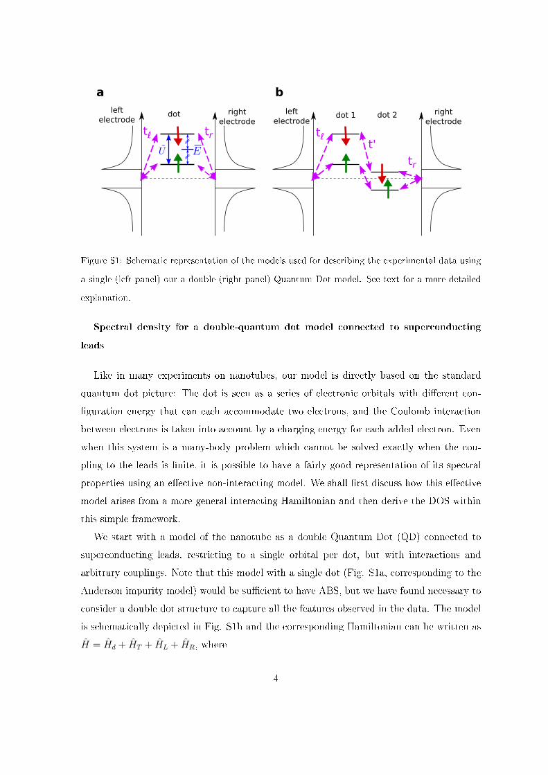
tℓ tr tℓ
tr
t'
left
electrodeleft
electroderight
electrode
right
electrodedot dot 1 dot 2
a b
Figure S1: Schematic representation of the models used for describing the experimental data using
a single (left panel) our a double (right panel) Quantum Dot model. See text for a more detailed
explanation.
Spectral density for a double-quantum dot model connected to superconducting
leads
Like in many experiments on nanotubes, our model is directly based on the standard
quantum dot picture: The dot is seen as a series of electronic orbitals with dierent con-
guration energy that can each accommodate two electrons, and the Coulomb interaction
between electrons is taken into account by a charging energy for each added electron. Even
when this system is a many-body problem which cannot be solved exactly when the cou-
pling to the leads is nite, it is possible to have a fairly good representation of its spectral
properties using an eective non-interacting model. We shall rst discuss how this eective
model arises from a more general interacting Hamiltonian and then derive the DOS within
this simple framework.
We start with a model of the nanotube as a double Quantum Dot (QD) connected to
superconducting leads, restricting to a single orbital per dot, but with interactions and
arbitrary couplings. Note that this model with a single dot (Fig. S1a, corresponding to the
Anderson impurity model) would be sucient to have ABS, but we have found necessary to
consider a double dot structure to capture all the features observed in the data. The model
is schematically depicted in Fig. S1b and the corresponding Hamiltonian can be written as
H = Hd + HT + HL + HR, where
4

Hd =∑
α,σ
εαd†ασdασ +
∑
α
Uαnα↑nα↓ +∑
σ
t′d†1σd2σ + h.c.,
describe the electronic states and their Coulomb interactions in the central region. Here d†ασ
creates an electron in dot α = 1, 2 with spin σ =↑, ↓ and nασ = d†ασdασ. The interactions are
reduced to the local charging energies Uα on each dot. For the sake of simplicity we neglect
the interdot Coulomb interaction which was found to be negligible in experiments on double
QD systems based on CNTs [4]. The term in t′ corresponds to the interdot tunneling.
On the other hand the leads are described as ideal conductors accomodating one spin-
degenerate channel with BCS pairing:
Hj =∑
kσ
ξkc†jkσcjkσ +
∑
k
(
∆eiϕjc†jk↑c†j,−k,↓ + h.c.
)
,
where c†jk,σ creates an electron with wavevectork in lead j = L/R, ξk and∆ are the single-
particle energy and the gap parameter respectively (assumed to be equal for j = L/R) while
in the main text ϕ = ϕL − ϕR denotes the superconducting phase dierence between the
leads. The leads are also characterized by a normal density of states ρn. Finally, the spin-
conserving tunneling Hamiltonian can be written as HT =∑
jkσ tjc†jkσdαjσ + h.c., where
αj = 1(2) for j = L(R) and tj denote the hopping elements t`,r illustrated in the right panel
of Fig. S1. For simplicity we take tj and t′ to be real quantities.
Finding the spectral properties of this model in the general case, including the eects of
electron correlations, is a formidable task. For the case of the Anderson impurity model with
superconducting leads several techniques have been applied, including Hartree-Fock approx-
imation (HFA) [5], perturbation theory in U [6], Quantum Monte Carlo [7] and Numerical
Renormalization Group (NRG) [8, 9]. In brief these works demonstrate that the system ex-
hibits a magnetic S=1/2 ground state for ∆ > kBTK , where TK is the Kondo temperature.
In this regime the Andreev states spectrum predicted by the more sophisticated numerical
techniques (NRG) [9] can be mimicked by a those of a simple non-interacting HFA [5] in
which the level splitting between the two spin orientations is simply the charging energy
times the dierence in their population. We expect that other eects such as spin-orbit or
exchange interactions (that the Anderson model cannot handle) could also modify the level
splitting.
5

To describe in a simple way the behavior of the Andreev states spectrum in the dif-
ferent regimes, in the present work we thus adopt a phenomenological non-interacting
approach similar to HFA but with eective parameters. For this, we replace Hd by
Heffd =
∑
α,σ εασd†ασdασ +
∑
σ t′d†1σd2σ + h.c., where εα↓ = εα↑ + Uα. In this way the model
describes both the case of nearly degenerate spin states (for Uα ∆) and well resolved spin
states (for Uα ∆). The eective charging energy Uα is then a parameter which has to be
determined by tting the experiment. Notice that the ordering of the spin states implied
by εα↓ = εα↑ + Uα is conventional. We cannot tell which spin direction is populated rst in
a given dot but once a spin orientation is selected for the rst electron, the second electron
should have the opposite. It should be emphasized that spin symmetry is not broken on
average.
We can then obtain the spectral properties of this model from the retarded Green function
in the orbital-Nambu space dened as Gσ(t, t′) = −iθ(t, t′) <
[
ψσ(t), ψ†σ(t
′)]
+>, where
ψσ = (d1,σ, d2,σ, d†1,−σ, d
†2,−σ). In the frequency representation this quantity adopts the form
Gσ(ω) =[
ω − hσ − Σ(ω)]−1
, where
hσ =
ε1,σ t′ 0 0
t′ ε2,σ 0 0
0 0 −ε1,−σ −t′
0 0 −t′ −ε2,−σ
and
Σ(ω) =
Σee1 0 Σeh
1 0
0 Σee2 0 Σeh
2
Σhe1 0 Σhh
1 0
0 Σhe2 0 Σhh
2
,
with Σeeαj
= Σhhαj
= Γjg(ω) and Σeh,heαj
= −Γje±iϕjf(ω). In these expressions f(ω) =
∆/√
∆2 − (ω + iη)2 and g(ω) = −(ω + iη)f(ω)/∆ are the dimensionless BCS green func-
tions of the uncoupled leads (where we have included a nite inelastic relaxation rate η as
a phenomenological parameter) and Γj = πρnt2j are the so-called normal tunneling rates to
the leads. Obtaining Gσ(ω) thus corresponds to the inversion of a 4 × 4 matrix which we
perform numerically. From this quantity one can directly express the spectral densities as
ρασ(ω) = −1
πIm
[
Gσ(ω)]
α,α.
6

Note that in the ts of the dierential conductance we allow for dierent tunneling rates,
Γpα between the probe electrode and the two sides of the double-QD. This is justied by the
broken symmetry which is expected between the two quantum dots. Figures 3c and 4 thus
show the quantity∑
α,σ Γpαρασ(ω). We do not t the total intensity but rather x the relative
visibility Γp1/Γ
p2 (the complete list of parameters for the ts of Figs. 3c and 4 is given below).
Parameters used for the theoretical gures
The parameters used in gure 3c of the article are:
group 1 2 3 4 5 6 7
V 0n (V) -10.12 -10.08 -10.33 -9.84 -9.49 -9.25 -9.045 -8.807 -8.08 -7.95 -7.84 -7.43 -6.739 -6.408 -6.65 -6.65 -6.00 -5.77 -5.48 -5.19
spin ↑ ↓ ↑ ↓ ↑ ↓ ↑ ↓ ↑ ↓ ↑ ↓ ↑ ↓ ↑ ↓ ↑ ↓ ↑ ↓
Γ`,r/∆ 0.90 0.81 1.21 1.0 0.81 1.96 1.21 2.10 0.75 2.40
t′/∆ - 1.25 - 0.8 - - 1.1
visibility 0.5 1 0.5 1 1 0.5 1 0.5 1 0.5
and those in gure 4 of the article are:
group 1
V 0n (V) -11.65 -11.53 -11.382 -11.085
spin ↑ ↓ ↑ ↓
Γ`,r/∆ 2.10 1.11
t′/∆ 1.0
visibility 0.5 1
In these tables, V 0n is the gate voltage at which the given level crosses the Fermi level. The
spin orientation shown here only indicate the relative spin orientation within a given group.
We have assumed that all levels have identical capacitances to the gate. Their respective
energies as a function of the gate voltage are thus given by εn(Vg) = λ∆ × (Vg − V 0n ), with
a value of λ = +12V −1 determined in data where the Coulomb diamonds are most visible.
For groups of levels involving two SSPL, one of them is coupled to the left lead with Γ`, the
other one to the right lead with Γr, and they are coupled together with a hopping term t′, as
show on the right panel of Figure S1. For single SSPLs Γ`,r denotes either the left or right
coupling. The visibility gives the relative weight of a pair of levels in the measurement of
7

dot 1 dot 2
Figure S2: Possible arrangement of the levels of Fig. 3c in the two dots. In this picture, each color
corresponds to a pair of levels extracted from the ABS spectroscopy and given in the table (we
use the same colors as the lines in Fig. 3c). The various orbitals were assigned to either dot to
yield the most uniform level spacing in each dot, which is of course an "aesthetic" and arbitrary
assumption we cast on the system. The boxes represent the pairs of levels for which we needed to
take into account inter-dot coupling, to reproduce avoided crossing. In each pair the electrons are
of opposite spin, but there is no preferred overall orientation. Hence, the arrows shown here only
indicate the relative spin orientation of the levels, as obtained from ABS spectroscopy.
the DOS by the tunnel probe (see previous section).
From these parameters we can give a tentative picture of the ladder of levels in the two
dots, as shown in Fig S2. Such a level representation is easier to apprehend than the set of
apparently random lines shown in Fig 3c.
Quantum dot vs. Fabry-Pérot description
We also measured a device, shown in Fig. S3, which was better coupled to the leads
than the sample analyzed in the main text (for which we had coupling Γ in the range
0.8−2.4×∆). The DOS at energies |E| ≥ ∆ (the continuum) shows weak modulations with
the gate voltage rather than sharp features. These modulations can arise in two dierent
regimes.
8

Figure S3: Top panel : Deconvolved DOS data from a dierent device than the one shown in the
main text. We see almost everywhere more ABS in the gap, each extending on larger Vg range and
overlapping with others. This indicates that the nanotube in this device was better coupled to the
leads than the one in the main article. Bottom panel: ux dependence at Vg = −6.02V .
In the rst regime, the nanotube is characterized by a continuum of states (this would
be true for nanotube devices in which nite-size eects are negligible). In this situation
the weak modulations of the DOS at energies above the gap are generated by Fabry-Perot
9

interference due to weak backscattering at the two contacts. Moreover, for energies below
the gap, this model predicts continuous bands of ABSs.
The second situation that can give rise to weak modulations of the DOS above the gap
is that of a nanotube exhibiting discrete levels that are well separated in energy (i.e. a
short nanotube behaving as a quantum dot), but also well coupled to the leads. This is the
model discussed in the previous two sections. Above the gap, this model shows that the
good coupling with the leads gives rise to weak modulations of the DOS: the stronger the
coupling, the smoother the uctuations in the DOS. However, inside the gap, one should see
discrete Andreev levels that are not broadened by the coupling with the leads. Nevertheless,
the good coupling makes the variation of the ABS energies with the gate voltage slower
than in the weak coupling situation, thus the observed ABS remain within the gap for larger
intervals of gate voltages and, consequently, a larger number of ABS resonances are observed
at a given gate voltage.
Thus we see that, while two possible models for the nanotube can give rise to the same
type of features in the spectroscopic features above the gap, inside the gap the two models
give rise to very distinct features, as long as one can resolve discrete ABS. In particular,
since our experimental data shows distinct ABS inside the gap, it suggests that the studied
nanotube behaves as a discrete quantum dot rather than as a plain continuum of states.
On the other hand, a continuum model properly including all the eects of backscattering
should also be able to account for the observed features.
Our results indicate that for nanotube devices with good coupling to the leads, quantum
dot models may be more broadly applicable than previously thought. This also underlines
that in eorts to reveal Luttinger Liquid physics in nanotube devices, it is important to take
nite-size eects and in particular discrete energy spectra into account.
Width of the resonances - Lifetime of the ABS
The analysis of the ABS linewidth in the deconvolved DOS gives a FWHM of 30-40 µeV,
independent of gate voltage and ux. If this linewidth is intrinsic, it would correspond to a
sub-ns coherence time of the ABS. Possible extrinsic sources for this linewidth are
Charge or ux noise. These cannot be the dominant contribution to the linewidth
since the latter is essentially independant of the ux and of the gate voltage.
10
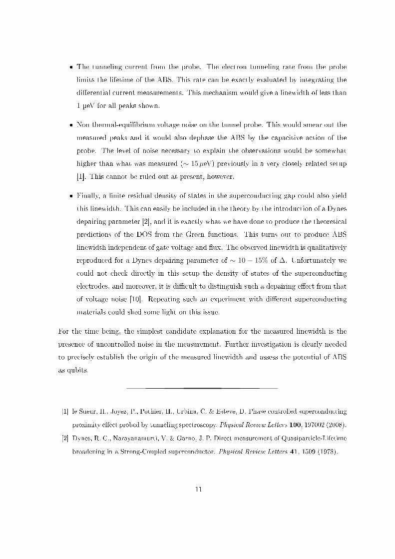
The tunneling current from the probe. The electron tunneling rate from the probe
limits the lifetime of the ABS. This rate can be exactly evaluated by integrating the
dierential current measurements. This mechanism would give a linewidth of less than
1 µeV for all peaks shown.
Non thermal-equilibrium voltage noise on the tunnel probe. This would smear out the
measured peaks and it would also dephase the ABS by the capacitive action of the
probe. The level of noise necessary to explain the observations would be somewhat
higher than what was measured (∼ 15µeV) previously in a very closely related setup
[1]. This cannot be ruled out at present, however.
Finally, a nite residual density of states in the superconducting gap could also yield
this linewidth. This can easily be included in the theory by the introduction of a Dynes
depairing parameter [2], and it is exactly what we have done to produce the theoretical
predictions of the DOS from the Green functions. This turns out to produce ABS
linewidth independent of gate voltage and ux. The observed linewidth is qualitatively
reproduced for a Dynes depairing parameter of ∼ 10 − 15% of ∆. Unfortunately we
could not check directly in this setup the density of states of the superconducting
electrodes, and moreover, it is dicult to distinguish such a depairing eect from that
of voltage noise [10]. Repeating such an experiment with dierent superconducting
materials could shed some light on this issue.
For the time being, the simplest candidate explanation for the measured linewidth is the
presence of uncontrolled noise in the measurement. Further investigation is clearly needed
to precisely establish the origin of the measured linewidth and assess the potential of ABS
as qubits.
[1] le Sueur, H., Joyez, P., Pothier, H., Urbina, C. & Esteve, D. Phase controlled superconducting
proximity eect probed by tunneling spectroscopy. Physical Review Letters 100, 197002 (2008).
[2] Dynes, R. C., Narayanamurti, V. & Garno, J. P. Direct measurement of Quasiparticle-Lifetime
broadening in a Strong-Coupled superconductor. Physical Review Letters 41, 1509 (1978).
11

[3] Wikipedia. MoorePenrose pseudoinverse. http://en.wikipedia.org/wiki/Moore-
Penrose_pseudoinverse (2010).
[4] Gräber, M. R. et al. Molecular states in carbon nanotube double quantum dots. Physical
Review B 74, 075427 (2006).
[5] Rozhkov, A. V. & Arovas, D. P. Josephson coupling through a magnetic impurity. Physical
Review Letters 82, 2788 (1999).
[6] Vecino, E., Martín-Rodero, A. & Levy Yeyati, A. Josephson current through a correlated
quantum level: Andreev states and pi junction behavior. Physical Review B 68, 035105
(2003).
[7] Siano, F. & Egger, R. Josephson current through a nanoscale magnetic quantum dot. Physical
Review Letters 93, 047002 (2004).
[8] Tanaka, Y., Oguri, A. & Hewson, A. C. Kondo eect in asymmetric Josephson couplings
through a quantum dot. New Journal of Physics 9, 115115 (2007).
[9] Lim, J. S. & Choi, M. Andreev bound states in the Kondo quantum dots coupled to super-
conducting leads. Journal of Physics: Condensed Matter 20, 415225 (2008).
[10] Pekola, J. P. et al. Environment-assisted tunneling as an origin of the dynes density of states.
Phys. Rev. Lett. 105, 026803 (2010).
12

114 5. Tunneling spectroscopy of the Andreev Bound States
5.2 Singlet-doublet transition observed in theTDOS
In the experimental data presented in Fig. 4 of Ref. [92], we observe thecrossing of an ABS with the Fermi level around Vbg = −11.35 V. At thispoint, the system undergoes a singlet-doublet transition. This means thatthe ground state of the system changes, for increasing gate voltage, froma spin-singlet ground state (S=0) to a degenerate magnetic ground state(S=1/2) (see section 3.1.5.2). When the ground state is a singlet, the energyof the system is minimized for a superconducting phase difference betweenthe leads δ equal to 0, whereas in the magnetic ground state the energy isminimized for δ = π [16, 71]. This induces a π phase shift in the phasedependence of the ABSs’ energies and, as a consequence, a reversal of thesupercurrent.
Reversal of supercurrent (0 − π transition) In Fig. 5.1, we have rep-resented, on the top, the TDOS of the device measured as a function of thegate voltage for δ = π. Below, we show two graphs of the TDOS and thesupercurrent calculated, using the phenomenological model (see section 3.1of chapter 3), with parameters1 used in Fig. 4 of Ref. [92], for the samegate voltage range but for δ = π/2 (the supercurrent is equal to 0 at δ = 0).These calculations confirm that the crossing of an ABS with the Fermi levelcoincides with a brutal transition of the supercurrent from positive to nega-tive values. This behaviour is called 0 − π transition and has inspired somepotential applications, such as a transistor in which the direction of a su-percurrent can be reversed by adding just one electron to a quantum dot[48].
The order of magnitude obtained for the supercurrent, from our phe-nomenological approach, is smaller from what would be expected from theAmbegaokar and Baratoff formula2 [93] which rather predicts 10 nA for ajunction such as ours. It is however in good agreement with experimentalresults of Ref. [7, 8, 9, 20] where the critical currents measured are of theorder of the nA.
1There is a mistake in Fig. 4 of Ref. [92]: in the top panel the experimental andpredicted DOS as a function of Vg are respectively measured and calculated at φ = π andnot φ = 0. Moreover the φ axis in the bottom panel is shifted of π.
2This formula gives the critical current Ic as a function of the normal state resistanceRN of a tunnel junction and the superconducting gap Ic = ∆π
2RN.

5.2. Singlet-doublet transition observed in the TDOS 115
-11.7 -11.4 -11.1
-D
0
D
jihgfedcba
Vbg HVL
En
erg
yHm
eV
L
0
2.5
5
D.O
.S.Ha
.u.L
∆=Π
-11.7 -11.4 -11.1
-D
0
D
Vbg HVL
En
erg
yHm
eV
L
0
2.5
5
D.O
.S.Ha
.u.L
∆=Π2 and Ηinel=0.1D
ì
-11.8 -11.4 -11
-2
2
4
0
-1
-0.5
0
0.5
1
1.5
Vbg HVL
I JH0
.01
´e
DÑ
L
IJ Hn
AL
∆=Π2
ì
0 − π transition of a DQD with parameters of Ref. [92]
Figure 5.1: The top graph represent the TDOS of the CNT plotted as a func-tion of the gate voltage and the energy for a superconducting phase differenceacross the junction δ = π. Below, we show the TDOS of a DQD connectedto superconducting leads as a function of the back gate voltage obtainedfrom the phenomenological approach of Ref. [16] with parameters used inFig. 4 of Ref. [92]. At the bottom, we have traced the Josephson currentcalculated with the same parameters. Parameters are: δ = π/2, ΓL = 2.10∆,ΓR = 1.11∆, t′ = ∆ and ϵ↑(↓)L(R) = λ∆
(Vbg − Vbg↑(↓)L(R)
)with Vbg↑L = 11.65
V, Vbg↓L = 11.53 V, Vbg↑R = 11.382 V, Vbg↓R = 11.085 V and λ = 12 V−1.We see that the crossing of the inner ABS with the Fermi level coincideswith a brutal transition of the supercurrent from positive to negative values(magenta diamond). This transition is smoothed if we add a phenomenolog-ical broadening ηinel to the ABSs, the supercurrent magnitude remaining ofthe same order of magnitude though slightly reduced (this reduction has alsobeen predicted in Ref. [94] for the case of a ballistic S-N-S junction coupledto a normal side probe).

116 5. Tunneling spectroscopy of the Andreev Bound States
π phase shift in the δ-dependence of the ABSs In Ref. [92], we didnot performed supercurrent measurements and were thus not able to observereversals of the supercurrent. These measurements were not possible in oursetup3. However, we did see, in the TDOS of the CNT, the π phase shift inthe δ-dependence of the ABS’s energies.
This is what we show in Fig. 5.2. We have represented measurements ofthe TDOS as a function of the energy and the superconducting phase differ-ence δ across the CNT. They are taken at different gate voltages indicated bythe white dashed lines in Fig. 5.1. We observe up to four resonances insidethe gap corresponding to two ABSs of different energy (two orbitals, eachone belonging to a different QD, are involved in their formation). The outerABS has a smaller phase dependence and merge into the continuum duringthe transition. The inner one has a larger δ-dependence meaning that it iscarrying more supercurrent. Its energy increases when we tune δ from 0 toπ and hence we have a 0-junction which means that the ground state is aspin-singlet.
Across the singlet-doublet transition, we observe the progressive inter-crossing of the two inner resonances inside the gap. Eventually, when thisintercrossing is complete the whole δ-dependence of the TDOS has acquireda π phase shift. We have thus a π junction. The ground state is hencea degenerate magnetic doublet. For the states in the intermediate region,conventionally designed as 0’ or π’ [16], the ground state depends on thesuperconducting phase difference δ we impose across the junction.
3As mentioned in section 3.1.5, evaluation of the QD supercurrent might be checked inthe future, using a more elaborate setup giving direct access to the loop supercurrent, aswas done for atomic contacts [68, 69]).
5.2. Singlet-doublet transition observed in the TDOS 117
ab
cd
e
fg
hi
j
0sta
te
Πsta
te
∆=
0
∆=
Π
Energy Energy
D
-D D
-D
0Π
0Π
0Π
0Π
0Π
∆∆
∆∆
∆
Pha
sede
pend
ence
acro
ssth
esi
ngle
t-do
uble
ttr
ansi
tion
Figu
re5.
2:T
DO
Sof
the
CN
Tpl
otte
das
afu
nctio
nof
the
ener
gyan
dth
esu
perc
ondu
ctin
gph
ase
diffe
renc
eδ
impo
sed
acro
ssth
eS-
CN
T-S
junc
tion.
The
yar
eta
ken,
acro
ssth
esin
glet
-dou
blet
tran
sitio
n,at
diffe
rent
gate
volta
ges
(indi
cate
dby
the
whi
teda
shed
line
ofFi
g.5.
1).
We
obse
rve
that
the
syst
em,i
nitia
llyin
a0
stat
e,en
dsin
toaπ
stat
eaf
ter
the
prog
ress
ive
cros
sing
ofan
AB
Sw
ithth
eFe
rmil
evel
.Fr
omth
ese
spec
tra,
weca
nse
eth
at,
whe
nth
esy
stem
isin
asin
glet
grou
ndst
ate
(a),
itis
mor
est
able
whe
nδ
=0
beca
use
the
inne
rA
BS
islo
wer
inen
ergy
(as
indi
cate
dby
the
whi
tear
row
in(a
)).
Inco
ntra
st,w
hen
the
syst
emis
ina
mag
netic
grou
ndst
ate
(j),t
hesy
stem
ism
ore
stab
lefo
rδ
=π
(see
whi
tear
row
in(j)
).

118 5. Tunneling spectroscopy of the Andreev Bound States
Chapter 6
Measurement of the fluxsensitivity of our devices
In this chapter of the thesis, we study the magnetic flux sensitivity of ourdevices. The latter have indeed current-voltage characteristics that dependon the flux enclosed inside their loops, these behaviours relying on the phase-dependence of the ABSs’ energies.
Our devices work thus as flux-tunnel current transducers showing fluxnoise down to 5.10−5ϕ0/
√Hz. As in Ref. [8], thanks to CNTs’ aspect ratios,
such device should be able to detect the reversal of the magnetic momentof single nanometer-sized particles or single molecules. They are moreovereasier to operate than devices of Ref. [8] since they can be read through asimple DC measurements of the current, as in Ref. [95].
Here, we discuss the principle of detection of a small signal generated byvariation of the magnetic field. Then we present our measurement techniqueto evaluate the devices’ flux noise. Finally we explain how we optimize, withgates, the operation point of our devices and discuss their performances aswell as the limiting sources of noise of our CNT-based magnetometer.
6.1 Principle of detectionThe detection principle of our CNT device is based on the flux dependenceof ABSs’ energy. As previously explained (see section 4.1), the flux Φ en-closed by the superconducting loop imposes a superconducting phase dif-ference across the CNT. Since the phase difference determines the energyposition of ABS, a flux variation will modify the CNT TDOS. In this senseour device constitutes a flux-tunnel current transducer.
In Fig. 6.1, we show two current-voltage characteristics measured at
119

120 6. Measurement of the flux sensitivity of our devices
00.5
0.5
0
1.5
1.5
I = 0.27 nA
V = 0.18575 mV
V (m
V)
I (nA)
V
Vbg
I
Vbg
CN
T
B
I-Vcharacteristics
fordifferent
fluxFigure
6.1:In
redand
greenare
shown
I-Vcharacteristics
ofour
devicerespectively
fora
fluxinside
theloop
Φequalto
−ϕ
0 /2and
0.A
tvoltage
biasV
=0.1875
mV
,thevariation
oftunnelcurrent
reaches0.27
nA.O
nthe
right,aschem
aticofthe
CN
T-based
deviceis
representedw
iththe
DC
sourcesconnected
thetunnelprobe
andthe
gates.O
rientationofthe
magnetic
fieldB
isindicated.

6.2. Definition of the flux sensitivity 121
35 mK for different values of the applied flux. At given voltage bias V , acurrent variation ∆I is induced when Φ is changed of half a flux quantum.The detection of a variation of the magnetic field relies on this property ofthe device.
6.2 Definition of the flux sensitivityWe define the flux sensitivity of our device as the smallest signal (generatedby a magnetic flux variation) we can detect within a bandwidth δf . Thislimit is given by the flux noise SΦδf , expressed in ϕ2
0, where SX is the powerspectrum of the noise on X. It constitutes thereby the relevant figure ofmerit to characterize performances of our device as a flux sensor.
If IN is the intrinsic current-noise of the device in the bandwidth δf , theequivalent flux noise is given by:
SΦδf = ϕ20SIN
×(dI
dΦ
)−2
The flux sensitivity is therefore optimum when the flux-tunnel current trans-fer function dI
dΦ is maximum and the current noise is minimum.In the following, we describe the setup we use for measurements of the
transfer function dIdΦ . Then we explain how we maximize the latter. And
finally we evaluate the flux noise of our device SΦ and discuss its performanceas a magnetic flux sensor.
6.3 SetupIn order to measure the differential flux-tunnel current transfer function, weuse Lock-In measurement techniques described in section 4.2. The setup,represented in Fig. 6.2, combined dI
dΦ and G = dIdV
measurements.For G and dI
dΦ measurements, two Lock-In Amplifiers (LIA), operatingat different frequencies, generate two AC excitations (respectively VAC andV
′AC), each one being subsequently combined with a DC voltage (respectivelyVDC and V
′DC) generated with a programmable DC source 7651 from Yoko-
gawa. One of the composite signal is applied on the tunnel probe for Gmeasurement, whereas the other is applied, through a 200 Ω resistor, on asuperconducting coil, inside the fridge and underneath the sample, for dI
dΦmeasurements.
The resulting current flowing through the sample is amplified by the cur-rent to voltage converter (see Fig. 4.2) and the output signal is then fed to

122 6. Measurement of the flux sensitivity of our devices
GPIBComputer
control
Current tovoltage
converter
+
+200 Ω
VLgVbg
~134 Hz
~193.29 Hz
VAC
VDC
VDC’
’VAC
10 MΩin
inV
I
FRIDGE
: Summing differential amplifier+
Vout = RI
100
1
2
3 4
5
Figure 6.2: Schematic of the measurement setup
the inputs of the two LIAs for independent narrow band measurements of dIdΦ
and G, respectively at 134 Hz and 193.29 Hz.
6.4 Maximization of the flux-tunnel currenttransfer function dI
dΦ
As mentioned in section 6.2, the flux sensitivity of our device is optimizedwhen the flux-tunnel current transfer function dI
dΦ is maximized. Similarlyto the differential conductance G, it depends on the bias voltage V appliedacross the device, the flux Φ enclosed inside its loop, and the gate voltagesVbg and VLg. In order to find the optimum operating point, one has thusto measure dI
dΦ as a function of these four parameters at the same time, aprocedure which is highly time-demanding.
We can however find a quicker method. In our sample, at a fixed Vg, theflux variation of an ABS is maximum around ϕ0/3. At this magnetic flux,the position in energy of an ABS is generally around ∆/2. So, to roughlymap regions with high flux sensitivity in the (Vbg, VLg) plane, we DC biasedthe device at Φ ≈ ϕ0/3 and V ≈ 3
2e∆ (voltage corresponding to ∆/2 of thedeconvoluted DOS) and sweep Vbg and VLg. Thereafter, we fixed Vbg and VLgat the highest dI
dΦ and we measured the flux-tunnel current transfer functionas a function of V and Φ in order to find the the best operating point.
In Fig. 6.3, we show measurements of the differential conductance G andthe flux-tunnel current transfer function dI
dΦ (respectively the upper and lowergraphics). They are taken in the superconducting state, at low magnetic fieldand at 35 mK, as functions of Vbg and VLg at V = 0.2 mV and Φ ≈ ϕ0/3.
In differential conductance measurements, areas of low conductance ap-pear in violet, areas of negative conductance in dark violet and areas of high

6.5. Flux noise measurements 123
conductance in white. These measurements resemble those obtained in thenormal state (see chapter 7) except that ABSs appear much thinner thannormal resonant levels of the CNT. In the inset with the thick orange frame,we have zoomed on the area indicated by the dashed orange frame whereABSs of the left and right QD meet each other to form avoided crossings.Such pattern is a manifestation of the coupling between the left and right QDwhich happens when they are both in resonance. This situation is favorablefor the flow of supercurrent between the left and right electrodes of the fork,and therefore for a large Φ-dependence. However, we do observe also largeflux dependence, though smaller, in situations where one of the dot in notnecessarily at resonance.
Below, flux-tunnel current transfer function measurements show that, inthis situation, the tunnel current variation induced by the flux excitation ismaximum. This is the expression of a large flux-dependence of the ABSs, orequivalently a large supercurrent circulating in the loop formed by the forkand the CNT. In the thick yellow frame, we have represented a zoom on thesame area than before but for the dI
dΦ measurements. The large yellow pointindicates where we have chosen to optimize dI
dΦ adjusting V and Φ: at theavoided crossings formed by the ABSs (Vbg = 10.96 V and VLg = −2 V).
In Fig. 6.4, we have represented the dependence with V and Φ of thedifferential conductance and flux-tunnel current transfer function measure-ments at this operating point. As expected, we see that dI
dΦ is close to zerowhere the ABSs have no flux dependence and is maximum where the ABSsenergies are strongly phase dependent. A maximum value of dI
dΦ is obtainedat Φ = 0.32ϕ0 and V = −0.1875 mV and reaches 1.6 nA/ϕ0.
In the following, we evaluate the flux sensitivity of our device at thisoptimal point by measurement of the flux noise with a spectrum analyzer.
6.5 Flux noise measurementsIn Fig. 6.5, we show the noise spectrum from 10 to 1610 Hz of the outputsignal of the current to voltage converter (CVC, see Fig. 6.2), measured atthe operating point indicated by the brown dot in Fig. 6.4 (Vbg = 10.96 V,VLg = −2 V, Φ ≈ 0.32ϕ0 and V = −0.1875 mV). The AC flux excitation,controlled with V
′AC , is taken with an amplitude equal to 0.01 × ϕ0 with a
frequency equal to 134 Hz. Yet, we don’t send any AC excitation directly onthe tunnel probe (i.e. VAC = 0).
On the tunnel current noise spectrum, we observe a peak at 134 Hz cor-responding to the AC flux excitation we send to the coil, and a noise floorbetween ∼ 10−12 and ∼ 10−11 V2/Hz. This noise floor is partly due to intrin-

124 6. Measurement of the flux sensitivity of our devices
8 9 10 11 12-4
-2
0
2
4
Vbg HVL
VL
gHV
L
-0.2
0
1
2G
H10
-5SL
ææ
8 9 10 11 12-4
-2
0
2
4
Vbg HVL
VL
gHV
L
0
-1.6
1.6
dId
FHn
AΦ0 L
Figure 6.3: Colorplots of the differential conductance (upper graphic) andflux-tunnel current transfer function (lower graphic) measured as functions ofVbg and VLg, with V = 0.2 mV and Φ ≈ 1
3ϕ0. In orange and yellow frames, wehave zoomed on a region where ABSs of the left and right QDs of the devicemeet and form an avoided crossing. This yields a high flux dependence of thetunnel current and is favorable for detection of small magnetic flux variationinside the loop of the device. The yellow point indicates the operating pointwhere measurements of Fig. 6.4 were taken.

6.5. Flux noise measurements 125
G H10-5
SL G H10-5
SL
-Π 0 Π
0
-0.5
0.5
eD
-eD
2eD
-2eD
0 1 0 1
2ΠFΦ0
VHm
VL
-0.2
0
1
2
GH1
0-
5SL
ææ
-Π 0 Π
0
-0.5
0.5
eD
-eD
2eD
-2eD
0 0.5
2ΠFΦ0
VHm
VL
dIdF HnAΦ0L
0
-1.6
1.6
dId
FHn
AΦ0 L
Figure 6.4: Colorplots of the differential conductance (upper graphic) andflux-tunnel current transfer function (lower graphic) measured as functionsof the voltage bias across the device V and the flux inside the loop Φ. Indifferential conductance measurements, two cuts are represented at Φ = 0and Φ = −ϕ0/2 where the ABSs’ energies reach their extreme positions. Influx-tunnel current transfer function measurement, a cut is represented atΦ ≈ 0.32 × ϕ0 where we obtain our largest dI
dΦ . The brown point indicateswhere the spectrum of Fig. 6.5 was taken.

126 6. Measurement of the flux sensitivity of our devices
AC flux excitation
10 20 50 100 200 500 1000
10-8
10-9
10-10
10-11
134
f HHzL
SV
HV²H
zL
Spectrum analyzer measurement of the output signalFigure 6.5: Graph representing the density of noise of the output signal ofthe CVC, when an AC excitation at 134 Hz with an amplitude correspondingto 0.01×ϕ0 is send to the coil below the sample and generating the magneticfield. A peak is clearly visible at 134 Hz and there is a noise floor between10−11 and 10−12 V2/Hz. This noise floor gives the limit of flux sensitivity SΦof our device.
sic charge noise of the device which depends experimentally on gate voltages,but the principal source of noise in our device is the shot noise [36]. Indeed,when biased, the device carries a current of quasiparticle which induces noise(because of the discrete charge of the carriers) proportional to the currentamplitude. Therefore, as can be seen in Fig. 6.6, this noise increases withthe bias voltage applied across the device.
In Fig. 6.5, at the bottom of the AC flux excitation peak, this noise floorreaches SV = 3.10−12 V2/Hz. As we know that the peak is induced by anexcitation with a RMS amplitude corresponding to 0.01 × ϕ0, it gives us abenchmark to convert this voltage noise in its equivalent flux noise. Theintegral below the peak being equal to 10−7 V2, the flux noise at 134 Hz ofour device S1/2
Φ is equal to:
S1/2Φ =
√√√√(0.01 × ϕ0)2
⟨Vex⟩2 SV = 5.10−5ϕ0/√
Hz

6.5. Flux noise measurements 127
V=0.75 mV
V=0.4025 mV
V=0 mV
10 20 50 100 200 500 1000
10-10
10-11
10-12
10-13
f HHzL
SV
HV²H
zL
Voltage dependence of the noise floorFigure 6.6: Noise floor of the device measured with a spectrum analyzerfor different voltage bias applied between the tunnel probe and the groundedsuperconducting loop. The fact that the noise increases with the quasiparticlecurrent carried by the device is an indication that the noise floor may bepartly due to shot noise.

128 6. Measurement of the flux sensitivity of our devices
Our flux sensitivity is therefore low enough to detect in less than 1 s a fluxvariation of 10−4ϕ0.

Part III
Second experiment: exploringKondo and Andreev BoundStates in a Double Quantum
Dot
129


131
In confined quantum conductors, Coulomb repulsion between electronsmay lead to the localization of one or several electrons and consequently toa many-body effect called the Kondo effect (see appendix A). It occurs whenthese localized electrons, forming an artificial magnetic impurity, are coupledto electrodes with continuous density of states. Through cotunneling spin-flipprocesses, conduction electrons of the leads screen the spin of the localizedelectrons resulting in a many-body singlet state. When the impurity has a 1/2spin, the Kondo effect manifests by a peak at the Fermi level in the densityof states (DOS) of the QD. The most spectacular experimental consequenceof this effect is the opening (for symmetrically contacted QD) of a perfectlytransmitted conduction channel at the Fermi level (with a conductance of2e2/h) for temperature well below the so-called Kondo temperature TK .
Carbon nanotube-based electronic devices generally exhibit Kondo effectwhen cooled down at temperatures reached in a cryogenic fridge [96, 97]. Likesemiconductor heterostructures, nanowires or molecular devices, these coher-ent quantum conductors have thereby offered the opportunity to explore, ina controlled way, various type of Kondo effects1 with electronic transportexperiments. As spins of electrons play an important role in these phenom-ena, they are strongly affected by an eventual spin ordering inherent to theelectrodes or the quantum conductor. The various nature of the electrodesthat can be contacted to carbon nanotubes (CNT) or nanowires has therebymotivated many experimental realizations aiming to explore the interplaybetween Kondo effect and ferromagnetism [98, 99] or BCS superconductivity[5, 9, 10, 14, 18, 19, 20, 21, 100]. Otherwise, in certain situations, a local spinordering takes place directly in the QD by formations, for example, of singletor triplet states between electrons belonging to different orbitals [101, 102], ordifferent part of the conductor when the latter behaves as a double quantumdot (DQD). This second situation can be achieved either by defining severalcoupled quantum dots during fabrication [103, 104, 105, 106, 107, 108] or inpresence of a parasitic magnetic impurity [11, 109]. Whether the spin order-ing forms in the leads or the QD, the Kondo effect is modified compared tothe spin-1/2 Kondo state and, sometimes, even suppressed.
In this part of the thesis, we present tunneling spectroscopy measure-ments, in the normal and superconducting states, performed on a CNT-baseddevice with several gates coupled to the sample. This experiment was follow-ing the one presented in part II and realized for two different purposes. First,we were able to verify the DQD behaviour of our device using external gateswhich were lacking in the previous experiment. Secondly, as parameters ex-tracted from measurements of part II suggested that our sample should have
1See for example references indicated in section A.5.2.

132
Kondo temperature (between 0.5 and 2K) higher than the base temperatureof our fridge (35 mK), we took measurements in the normal state in order toobserve how Kondo effect develops in our samples. The results we obtainedshed light on the interplay between Kondo effect and two phenomena thatlead to different type of spin orderings: exchange between two QDs and BCSsuperconductivity induced in the CNT by proximity effect.
In chapter 7, we show experimental results proving the DQD behaviour ofour sample and comment the role of microscopic parameters. Then in chap-ter 8, we analyze the interplay between Kondo effect and superconductivitywithin a single effective QD. Finally in chapter 9, we focus on effects thatare inherent to the DQD behaviour of our device and discuss in particularsplittings of the Kondo resonance that we observe in our sample.

Chapter 7
Proof of Double Quantum Dotbehaviour
In the previous part, interpretation of our measurements was based on thesupposition that our CNT-based device behaves as a double quantum dot(DQD). We supposed that the tunnel probe splits the CNT into two coupledQDs. Other experiments realized on three terminals devices based on a singleCNT [105, 108] have already shown the DQD behaviour of such structuresand motivated a theoretical proposal of a scheme for a spin quantum bitbased on a DQD contacted with ferromagnetic leads [110].
In this chapter, we present TDOS measurements, taken in the normalstate and at 35 mK, of a CNT-based device with multiple gates (see Fig.7.1). A single and a double QD show qualitatively distinct behaviour. Ina DQD, if the gates are coupled differently to the two dots, the stabilitydiagram shows two families of parallel lines, each one reflecting the additionof electrons in one of the QD. Therefore, measuring the TDOS as a functionof the gate voltages, we can demonstrate the DQD behaviour of our device.
In section 7.1, we first show the charge stability diagram of the device andexplain why the different features we observe are consistent with a system oftwo coupled QDs. We will discuss the role of each parameter characterizingour device (see Fig. 7.1). Then in section 7.2, we show that we obtaina satisfactory agreement between our measurements and TDOS of a DQDobtained within a self-consistent mean-field approximation on the intradotCoulomb repulsion. It yields, in particular, a correct description of the role ofthe interdot coupling in contrast to the phenomenological approach presentedin chapter 2.
133

134 7. Proof of Double Quantum Dot behaviour
Vbg
S QDL
UL EL
S
VLg
R L t’
ΓL ΓR
V
probe
QDR
UR ER
300 nm
Figure 7.1: Schematic representation of the system with its parameters (left)and SEM picture with false colors of a typical sample (right). The behaviourof the device can be characterized by exchange rates with the left (resp.right) leads ΓL(R), charging energies UL(R), energy difference between orbitals∆EL(R) and the coupling t′ between the left and right dots (QDL and QDR).These parameters are orbital dependent and vary with the gate voltages. Wemeasure the TDOS of the CNT with a tunnel probe (in red) that is weaklycoupled to the device.
7.1. Charge stability diagram of a DQD 135
7.1 Charge stability diagram of a DQDIn Fig. 7.2, we have represented the charge stability diagram of the device.It maps the CNT’s TDOS measured at the Fermi level of the electrodes (i.e.V = 0 on the probe) as a function of VLg and Vbg. Here, we discuss in detailthe pattern we observe.
Electronic levels of the left and right dot In the upper graph thatshows the raw data, we see that the TDOS resembles a diamond patternwith pairs of bright lines running mainly in two directions and formingavoided crossings. Below, in the lower graph, we have superimposed thesame data with two sets of orange and green parallel lines. The latter cor-respond schematically to a typical TDOS we expect in absence of couplingbetween the dots (coupling by exchange of electrons, or capacitive coupling),whether they are in sequential [111, 112] or coherent [107, 108] regime. Whenan electronic level of one of the dots is at resonance with the Fermi level ofthe electrodes, a current can flow between the probe and the fork giving riseto a peak of conductance. As the right dot is more weakly influenced by VLgthan Vbg and the left QD is more evenly affected by VLg and Vbg, slopes ofthe lines allow to identify that green lines correspond to electronic levels ofthe right dot, whereas orange lines to those of the left dot.
Even-odd alternation These lines are separated by Coulomb blockadedareas, or valleys, in blue. In this regions, none of the dots are at resonance butrather at a stable charge state. As distances between these lines are relatedto addition energies of the dots (see section A.3), we can identify the parity ofthese valleys. For an odd occupancy, addition of an electron costs a chargingenergy UL(R) due to repulsion between electrons. For an even occupancy, asthe last occupied orbital is already filled, the addition energy is given by thecharging energy plus the energy difference between orbitals UL(R) + ∆EL(R).In Fig. 7.2, two levels with opposite spins belonging to same orbital appeartherefore as a neighboring pair. The large blue pockets between pairs of linesdefine regions where dots are in an even-even configuration, whereas a pairof lines delimits regions where occupancy of the corresponding dot is odd (asindicated in the lower graph of Fig. 7.2).
Levels width When the temperature kBT is negligible compared to thecoupling to the leads ΓL(R) (as in our experiment, see next chapter), thesharpness of the resonances emphasized, for each orbitals, the strength ofthe coupling to the electrodes [56, 113]. Thin sharp lines correspond to
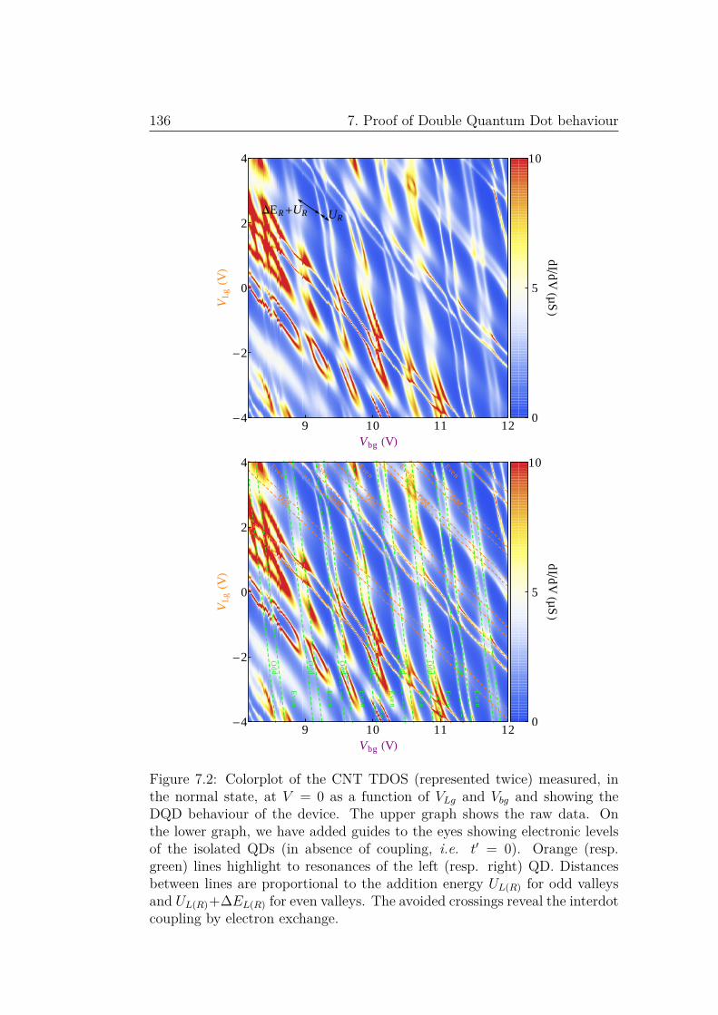
136 7. Proof of Double Quantum Dot behaviour
9 10 11 12-4
-2
0
2
4
Vbg HVL
VL
gHV
L
0
5
10d
IdV
HµSL
DER+UR UR
Even
Even
Even
Even
Even
Odd
Odd
Odd
Odd
Odd
Even
Even
Even
Even
Even
Even
Even
Odd
Odd
Odd
Odd
Odd
Odd
Odd
9 10 11 12-4
-2
0
2
4
Vbg HVL
VL
gHV
L
0
5
10
dId
VHµ
SL
Figure 7.2: Colorplot of the CNT TDOS (represented twice) measured, inthe normal state, at V = 0 as a function of VLg and Vbg and showing theDQD behaviour of the device. The upper graph shows the raw data. Onthe lower graph, we have added guides to the eyes showing electronic levelsof the isolated QDs (in absence of coupling, i.e. t′ = 0). Orange (resp.green) lines highlight to resonances of the left (resp. right) QD. Distancesbetween lines are proportional to the addition energy UL(R) for odd valleysand UL(R)+∆EL(R) for even valleys. The avoided crossings reveal the interdotcoupling by electron exchange.

7.2. Description of the avoided crossings in the stability diagram 137
weaker coupling and large fuzzy lines to strong coupling. We also observethat two levels of a pair sometimes connect forming a wide single band. Thismay be due to a Kondo resonance. We will not discuss Kondo effect, here,but it will be addressed in the next chapter.
Avoided crossings When electronic levels of two different orbitals meet,in the (Vbg, VLg) plane, they generally (but not always) form an avoidedcrossing. This behaviour underlines the coupling between the dots. The usualelectrostatic approach1 [111, 112] or the phenomenological model presented inchapter 2 fail to describe all the features of the avoided crossings we observe.In the next section, we propose another approach based on a self-consistentmean-field approximation on the intradot Coulomb repulsion.
7.2 Description of the avoided crossings inthe stability diagram
7.2.1 Mean-field approximation on the Coulomb re-pulsion
The phenomenological approach of section 3.1.4 does not capture the ap-pearance of avoided crossings because the Coulomb repulsion was taken intoaccount with a phenomenological splitting that forbids spin fluctuations ofelectrons in QDs. Levels of opposite spin, belonging to different QDs, re-mains thus uncoupled when electrodes are in their normal state (they arehowever coupled by superconductivity). As a consequence, they simply crosseach other in the stability diagram whatever the value of t′.
Following Bruus and Flensberg [65], we can take into account correla-tions, due to Coulomb repulsion inside the DQD performing a self-consistentcalculation of the DQD occupancy within a mean-field approximation. Wedo not describe in detail this approximation here but send the reader toappendix E.
This approach renders correctly the pattern observed (see Fig. E.2 ofannex E). Like in the electrostatic classical approach, regions corresponding
1Actually, the electrostatic approach does predict avoided crossing for capacitive cou-pling between dots (the honeycomb lattice). However, the latter is a priori small comparedto the other parameters in our device [105]. Moreover, it is predicted to give rise to angularavoided crossings whereas they are rather smooth in our data. Furthermore, the hoppingbetween dots is necessary in the model to interpret the phase dependence of the ABSsshown in previous chapter; if t′ = 0 the loop is open and there is no phase dependence.

138 7. Proof of Double Quantum Dot behaviour
to different charge states are separated by frontiers corresponding to con-ductance peaks. However this coherent approach allows to understand thewidth of these frontiers and the fact that the latter are rounded rather thanangular as in an electrostatic approach [111, 112] (see Fig. E.1 and E.2 ofannex E).
7.2.2 Interdot couplingsThis approach confirms that the avoided crossings we observe are indeedinduced by the interdot coupling. They occur near points where the levelswould cross in absence of interdot coupling t′, that is to say where the orangeand green dashed lines cross in the lower graph of Fig. 7.2. Because ofinterdot coupling t′, the levels hybridize to form bonding and antibondingenergy levels.
In Fig. 7.3, we have shown a zoom of Fig. 7.2 on a particular avoidedcrossings. These data can be reproduced using the theoretical approach de-veloped in annex E. As shown in Fig. 7.3, results obtained theoreticallyare in reasonable agreement with experiment for an interdot coupling ap-proximately equal to t′ ≈ 0.5 meV. To extract this value, we have actuallyanticipated on next chapter where we explain how to convert gate voltagesin energy thanks to measurements of the Coulomb diamonds (see Fig 8.4below).
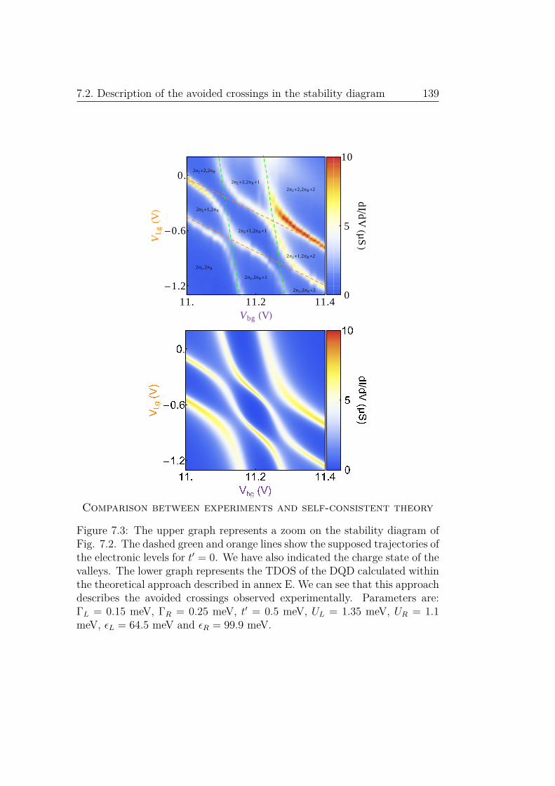
7.2. Description of the avoided crossings in the stability diagram 139
11. 11.2 11.4
-1.2
-0.6
0.
Vbg HVL
VL
gHV
L
0
5
10
dId
VHµ
SL
2nL,2nR
2nL,2nR+1
2nL+1,2nR+1
2nL,2nR+2
2nL+1,2nR
2nL+2,2nR
2nL+2,2nR+1
2nL+2,2nR+2
2nL+1,2nR+2
Comparison between experiments and self-consistent theory
Figure 7.3: The upper graph represents a zoom on the stability diagram ofFig. 7.2. The dashed green and orange lines show the supposed trajectories ofthe electronic levels for t′ = 0. We have also indicated the charge state of thevalleys. The lower graph represents the TDOS of the DQD calculated withinthe theoretical approach described in annex E. We can see that this approachdescribes the avoided crossings observed experimentally. Parameters are:ΓL = 0.15 meV, ΓR = 0.25 meV, t′ = 0.5 meV, UL = 1.35 meV, UR = 1.1meV, ϵL = 64.5 meV and ϵR = 99.9 meV.

140 7. Proof of Double Quantum Dot behaviour

Chapter 8
Kondo vs superconductivity insingle QD
Kondo effect and superconductivity are often argued to develop a delicateinterplay (and sometimes a competition) in QDs [22, 23, 24, 25, 114, 115].This is because the conduction electrons of the leads are condensed intospin-singlet Cooper pairs (S=0) which cannot participate to spin-flip pro-cesses responsible of the Kondo effect (see section A.5), and also because thesuperconducting gap induced by the leads in the QD suppresses the Kondopeak. This interplay was explored in several experiments performed on S-QD-S junctions, with visible Kondo effect when the leads are driven into theirnormal state. They consisted either in electronic transport (for example withnanotubes, nanowires, etc...)[5, 9, 10, 14, 18, 19, 116], or in tunneling spec-troscopy experiments (molecules adsorbed on superconducting surface)[21].Interpretations of these experiments are not direct: the former are realized farfrom equilibrium and the latter suffer from a lack of controllable parameters(the chemical potential, for example, cannot be controlled).
In this chapter, we analyze the interplay between superconductivity andKondo effect through the tunneling spectroscopy of the Andreev BoundStates (ABSs) in a CNT. We measured the TDOS of our DQD-device main-taining one of the QD in an even charge state. This way, we obtain theTDOS of an (effective) single QD isolated from the other one. Comparingmeasurements taken in the normal (N) and superconducting (S) state, we geta direct observation of the interplay between superconductivity and Kondoeffect. This observation leads however to the conclusion that Kondo effectdoesn’t change qualitatively the formation of the ABSs in our range of param-eters neither determine whether the system’s ground state is a spin-singletor a magnetic state (see section 3.1.5.2).
141
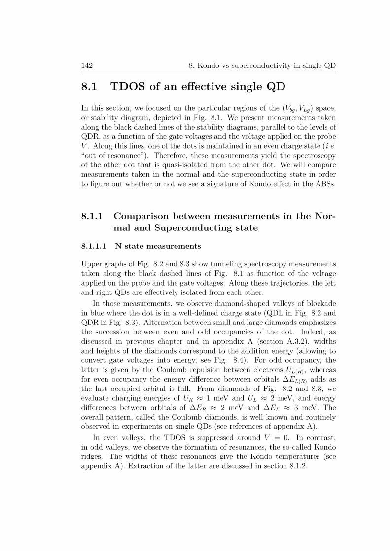
142 8. Kondo vs superconductivity in single QD
8.1 TDOS of an effective single QD
In this section, we focused on the particular regions of the (Vbg, VLg) space,or stability diagram, depicted in Fig. 8.1. We present measurements takenalong the black dashed lines of the stability diagrams, parallel to the levels ofQDR, as a function of the gate voltages and the voltage applied on the probeV . Along this lines, one of the dots is maintained in an even charge state (i.e.“out of resonance”). Therefore, these measurements yield the spectroscopyof the other dot that is quasi-isolated from the other dot. We will comparemeasurements taken in the normal and the superconducting state in orderto figure out whether or not we see a signature of Kondo effect in the ABSs.
8.1.1 Comparison between measurements in the Nor-mal and Superconducting state
8.1.1.1 N state measurements
Upper graphs of Fig. 8.2 and 8.3 show tunneling spectroscopy measurementstaken along the black dashed lines of Fig. 8.1 as function of the voltageapplied on the probe and the gate voltages. Along these trajectories, the leftand right QDs are effectively isolated from each other.
In those measurements, we observe diamond-shaped valleys of blockadein blue where the dot is in a well-defined charge state (QDL in Fig. 8.2 andQDR in Fig. 8.3). Alternation between small and large diamonds emphasizesthe succession between even and odd occupancies of the dot. Indeed, asdiscussed in previous chapter and in appendix A (section A.3.2), widthsand heights of the diamonds correspond to the addition energy (allowing toconvert gate voltages into energy, see Fig. 8.4). For odd occupancy, thelatter is given by the Coulomb repulsion between electrons UL(R), whereasfor even occupancy the energy difference between orbitals ∆EL(R) adds asthe last occupied orbital is full. From diamonds of Fig. 8.2 and 8.3, weevaluate charging energies of UR ≈ 1 meV and UL ≈ 2 meV, and energydifferences between orbitals of ∆ER ≈ 2 meV and ∆EL ≈ 3 meV. Theoverall pattern, called the Coulomb diamonds, is well known and routinelyobserved in experiments on single QDs (see references of appendix A).
In even valleys, the TDOS is suppressed around V = 0. In contrast,in odd valleys, we observe the formation of resonances, the so-called Kondoridges. The widths of these resonances give the Kondo temperatures (seeappendix A). Extraction of the latter are discussed in section 8.1.2.

8.1. TDOS of an effective single QD 143
12.6 13. 13.4
1.9
3.9
5.9
Vbg HVL
VL
gHV
L
0
5
10
dId
VHµ
SL
A
B
C
7.6 8.2 8.8
0.5
1.5
2.5
Vbg HVL
VL
gHV
L
0
5
10
dId
VHµ
SL
D
E
F
Stability diagramsFigure 8.1: Color scaled measurements of the TDOS in the N state in twodifferent regions of the (Vbg, VLg) plane. The black dashed lines indicate thetrajectories followed in Fig. 8.2 and 8.3. Along them the right and left dotare maintained in an even charge state in order to perform the spectroscopyof effective single QDs. A, B, C, D, E and F are Kondo ridges we will analyzein the following.

144 8. Kondo vs superconductivity in single QD
ì ì ì
13 13.1 13.2
-2
-1
0
1
2
246
Vbg HVL
VHm
VL
VLg HVL
0
2.5
5
dId
VHµ
SL
A B C
UA
UB UC
13 13.1 13.2
-2
-1
D
-D
1
2
246
Vbg HVL
En
erg
yHm
eV
L
VLg HVL
0
2.5
5
D.O
.S.Ha
.u.L
Coulomb diamonds of QDL in the N and S states
Figure 8.2: The upper graph shows differential conductance measurementstaken in the normal (N) state as a function of V and the gate voltages ofour CNT-based device. These measurements are performed on an effectivesingle dot (the left one) while the other dot is maintained out of resonancewith an even occupancy. The measurements show the development of Kondoridges in diamonds where the dot has an odd occupancy. Double arrowsindicate the charging energy of each diamond in odd valleys which is givenby their half height (here UA = 1.8 ± 0.2 meV, UB = 2.2 ± 0.1 meV andUC = 2.05 ± 0.1 meV). Dashed lines show two edges of each diamond: theirslopes give the factor of proportionality to convert gate voltages in energy.Below, we show the same measurements but taken in the superconducting(S) state. We see that ABSs have formed in odd valleys suggesting that theycome from the hybridization, through Andreev reflections, of two levels ofopposite spin belonging to the same orbital. The discontinuity at Vbg = 13 Vis a jump of offset charge.

8.1. TDOS of an effective single QD 145
ì ì ì
7.6 8. 8.4 8.8
-2
-1
0
1
2
2.5 1.5 0.5
Vbg HVL
VHm
VL
VLg HVL
0
2.5
5
dId
VHµ
SL
D E FUD
UD
DED
UE UF
7.6 8. 8.4 8.8
-D
0
D
2.5 1.5 0.5
Vbg HVL
En
erg
yHm
eV
L
VLg HVL
0
2.5
5
D.O
.S.Ha
.u.L
Coulomb diamonds of QDR in the N and S states
Figure 8.3: Similar measurements than in Fig. 8.2 but for the right dot.The energy difference between orbitals is extracted from the size of the largediamond between D and E. From sizes of diamonds D, E and F, we getUD = 1 ± 0.15 meV, UE = 1.2 ± 0.15 meV and UF = 0.95 ± 0.15 meV.

146 8. Kondo vs superconductivity in single QD
QDL QDR
Vbg
N N
VLg
Lg L
bg L bg
R
Lg R
Influence of the gates on the QDs
Figure 8.4: The QDs’ electro-chemical potentials are controlled linearly bythe back and lateral gates through conversion factors κL(R)
bg and κL(R)Lg . A
variation of gate voltage ∆Vg = (∆Vbg,∆VLg) induces an electro-chemicalpotential variation ∆µ = (∆µL,∆µR) through the linear relation (this rela-tion is not always linear but this assumption is justified experimentally in
our case, see [117]) ∆Vg = κ∆µ where κ =(κbgL κbgRκLgL κLgR
). From the aspect
ratio of the diamonds and the slopes observed in Fig. 7.2, we can extract:κRLg ≈ −0.5±0.1 meV.V−1, κRbg ≈ −9±1 meV.V−1, κLLg ≈ −3±0.3 meV.V−1
and κLbg ≈ −6 ± 0.6 meV.V−1.

8.1. TDOS of an effective single QD 147
8.1.1.2 S state measurements
The lower graphs of Fig. 8.2 and 8.3 show TDOS measurements, of the samediamonds but with the leads in their S state (obtained after deconvolutionof the differential conductance, see section D.3).
Between + and −∆, we observe the opening of a superconducting gapinduced by proximity effect. Within this gap, ABSs appear as bright andthin lines which form loops of different size. In diamond B, the loop is aslarge as the gap, whereas in diamond F, the loop is almost closed. ABSsappear in odd valleys (just like the Kondo ridges) showing that they form byhybridization, through Andreev reflections, of two levels with opposite spinand belonging to the same orbital. This is expected as we know from NRG(see Fig. 3.14 of section 3.3 in chapter 3) that the formation of a loop occursonly for odd occupancy as it is related to a change of ground state froma spin-singlet S = 0 (even number of electrons) to a S = 1/2 doublet (oddnumber of electrons). In even valleys, ABSs have merged with the continuumand stay at the edge of the superconducting gap that can then be estimated.
Yet, the behaviour of the ABS does not seem to be impacted whether ornot there is Kondo effect. Indeed, we know that we are able to predict (atleast qualitatively) the formation of loops from the phenomenological model(see part I), even if the latter completely ignores Kondo effect (see sectionA.4.2). We will see in section 8.2 that NRG predicts the formation of a loopwhen TK becomes smaller than ∆ but only in the regime U ≫ Γ ≫ ∆.However, in our experiment we rather have U > Γ ∼ ∆ (see below) and therole of Kondo effect remains rather limited.
8.1.2 Kondo temperaturesThe Kondo temperature TK can be estimated from the shape of the Kondoridges. For this, we fit the latter with Lorentzian curves whose half widths athalf maximum (HWHM) give the order of magnitude of TK , provided thatT ≪ TK , through the relation e × HWHM/kB ∼ TK (see appendix A andRef. [101, 118, 119]). This is what we have done, for example, in Fig. 8.5for the ridge A.
The obtained Kondo temperatures, for our sample, is generally around∼ 0.5 K which means that they are all smaller than the superconductinggap (∆ = 0.15 meV or 1.74 K). These values are in agreement with Kondotemperatures obtained by fitting the temperature dependences of the heightsof the ridges [120]. We did not measure systematically these dependences forpractical reasons, but some of them are presented and commented in nextchapter.

148 8. Kondo vs superconductivity in single QD
æ
ææ
æ
æ
ææ
ææ
æ
æ
æ
æ
ææ
ææ
ææ
æ
æ
æ
æææ
ææ
ææ
æ
æ
ææææ
ææ
ææ
æ
æ
æ
æ
æ
æ
æ
æ
æ
æ
ææ
æ
æ
æ
æ
æ
æ
æ
æ
ææ
ææ
ææææ
æææ
æææ
ææ
æ
ææ
æ
ææ
æ
ææ
æ
æ
ææ
ææ
æ
æ
æ
æææ
ææ
æ
æ
-0.4 0. 0.4
0.6
1.1
1.6
V HmVL
dId
VHµ
SL
A TK=0.46 K=0.26 D
Figure 8.5: Kondo resonance measured in the middle of diamond A repre-sented in Fig. 8.2. The resonance is fitted by a Lorentzian function (fullline) whose HWHM give the order of magnitude of the Kondo temperatureTK ∼ e × HWHM/kB. In our sample, TK generally lies around 0.5 K. Thecorresponding ΓL and ΓR extracted using Eq. 8.1 are approximately equalto 1 or 2∆ (with ∆ = 0.15 meV).
From the known form of the Kondo temperature in the middle of theridge1 [49, 115, 119, 121]:
TK =√
ΓU2
exp(
−πU
8Γ
)(8.1)
we can then estimate the couplings to the leads ΓL ≈ ΓR ≈ 0.3 meV. Wecan notice that we have ΓL and ΓR ≫ kBT (kBT ≈ 3 µeV). As mentioned insection 7.1, the widths of the electronic levels in the normal state are thusindeed given by ΓL,R rather than kBT .
8.2 Comparison of the data with NRG calcu-lations
In Fig. 8.6 and 8.7, we present superconducting states TDOS measurementsof diamonds A from F (on the left) and TDOS calculated with NRG (on theright). In our NRG calculations, the parameters are:
• the charging energies U , obtained from the size of the diamonds (seeFig. 8.2 and 8.3),
1We need to mention that, in this definition of the Kondo temperature, Γ is the HWHMof the electronic levels of the QD. This is the convention we use everywhere in this thesis.
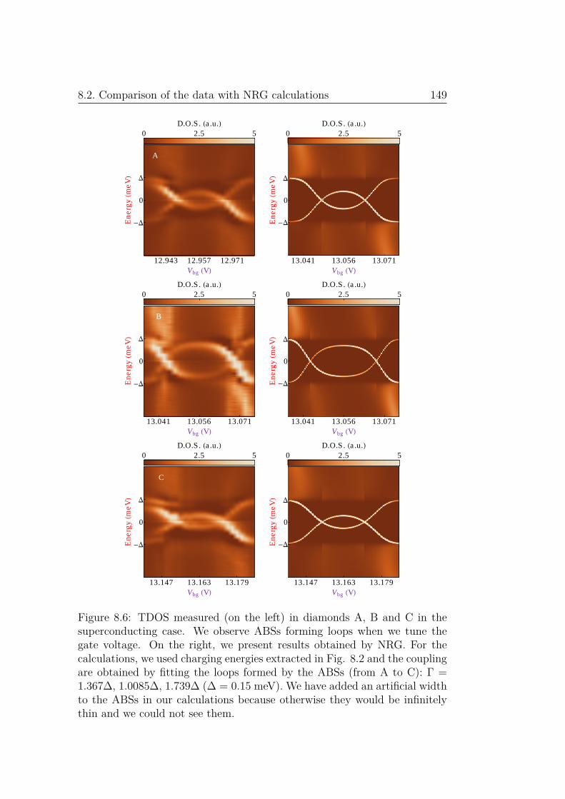
8.2. Comparison of the data with NRG calculations 149
12.97112.95712.943
-D
0
D
Vbg HVL
En
erg
yHm
eV
L0 2.5 5
D.O.S. Ha.u.L
A
13.07113.05613.041
-D
0
D
Vbg HVLE
ne
rgy
Hme
VL
0 2.5 5
D.O.S. Ha.u.L
13.07113.05613.041
-D
0
D
Vbg HVL
En
erg
yHm
eV
L
0 2.5 5
D.O.S. Ha.u.L
B
13.07113.05613.041
-D
0
D
Vbg HVL
En
erg
yHm
eV
L
0 2.5 5
D.O.S. Ha.u.L
13.17913.16313.147
-D
0
D
Vbg HVL
En
erg
yHm
eV
L
0 2.5 5
D.O.S. Ha.u.L
C
13.17913.16313.147
-D
0
D
Vbg HVL
En
erg
yHm
eV
L
0 2.5 5
D.O.S. Ha.u.L
Figure 8.6: TDOS measured (on the left) in diamonds A, B and C in thesuperconducting case. We observe ABSs forming loops when we tune thegate voltage. On the right, we present results obtained by NRG. For thecalculations, we used charging energies extracted in Fig. 8.2 and the couplingare obtained by fitting the loops formed by the ABSs (from A to C): Γ =1.367∆, 1.0085∆, 1.739∆ (∆ = 0.15 meV). We have added an artificial widthto the ABSs in our calculations because otherwise they would be infinitelythin and we could not see them.

150 8. Kondo vs superconductivity in single QD
7.8847.777.656
-D
0
D
Vbg HVL
En
erg
yHm
eV
L
0 2.5 5
D.O.S. Ha.u.L
D
7.8847.777.656
-D
0
D
Vbg HVL
En
erg
yHm
eV
L
0 2.5 5
D.O.S. Ha.u.L
8.3318.2098.087
-D
0
D
Vbg HVL
En
erg
yHm
eV
L
0 2.5 5
D.O.S. Ha.u.L
E
8.3318.2098.087
-D
0
D
Vbg HVL
En
erg
yHm
eV
L0 2.5 5
D.O.S. Ha.u.L
8.8168.78.584
-D
0
D
Vbg HVL
En
erg
yHm
eV
L
0 2.5 5
D.O.S. Ha.u.L
F
8.8168.78.584
-D
0
D
Vbg HVL
En
erg
yHm
eV
L
0 2.5 5
D.O.S. Ha.u.L
Figure 8.7: Graphs similar to those of Fig. 8.6 but for diamonds D, E andF. Couplings obtained with NRG are (from D to F): Γ = 1.01∆, 1.163∆,1.152∆.

8.2. Comparison of the data with NRG calculations 151
• the superconducting gap ∆ that can directly be read in TDOS mea-surements,
• the conversion factor from gate voltages to energy which is given bythe aspect ratio of the diamonds,
• and the couplings to the lead Γ (only one lead is relevant in thesemeasurements: the left for A, B and C, and the right for D, E and F)that are fit parameters obtained from the size of the loop.
With the single fit parameter Γ, we obtain a very satisfying agreement be-tween NRG and the experimental results.
A new spectroscopic tool As explained in Ref. [92], this good agreementshows that ABSs spectra constitute an entirely new spectroscopic tool forquantum dots and CNTs. Fits shown in Fig. 8.6 and 8.7 give a directmeasurements of the coupling to the leads Γ. The energy resolution, incontrast to the usual Coulomb spectroscopy, is essentially independent of thetemperature (as long as kBT ≪ ∆). In our experiment, the resolution israther limited by the coupling between the CNT and the tunnel probe (seeappendix D). This parameter could, in principle, be improved, by reducingit, in a subsequent experiment. The sharpness of the ABSs (which are muchthinner than the electronic levels of the QD in the normal state) shouldyield a better precision than the Coulomb spectroscopy in regime of strongcoupling to the leads Γ ∼ U . Sensitivity of this procedure is illustrated inFig. 8.8. Provided that U is measured with enough precision (i.e. more thanΓ), the size of the loop yields a value of Γ with less than 10% of uncertainty.
Influence of the Kondo effect Results of Fig. 8.6 and 8.7 also showsthat in our range of parameters (U > Γ ∼ ∆), Kondo effect seems to playno particular role concerning the formation of ABSs in our experiment. Thisexplains why the phenomenological model, described in section 3.1, quali-tatively captures how ABSs form in QDs even though it completely ignoresKondo effect (see section A.4.2).
In Ref. [24], NRG calculations of Bauer et al. predict that the crossing ofABSs with the Fermi level, i.e. the singlet-doublet transition in single QD,follows a universal behaviour with TK/∆ but only in the regime U ≫ Γ ≫ ∆.This could be realized fabricating samples where the leads are more stronglycoupled and define smaller QDs. However, to really state that Kondo effectarises in S-QD-S device, a more straightforward proof could be, for example,the direct detection of a Kondo cloud. The latter is a cloud of electrons which
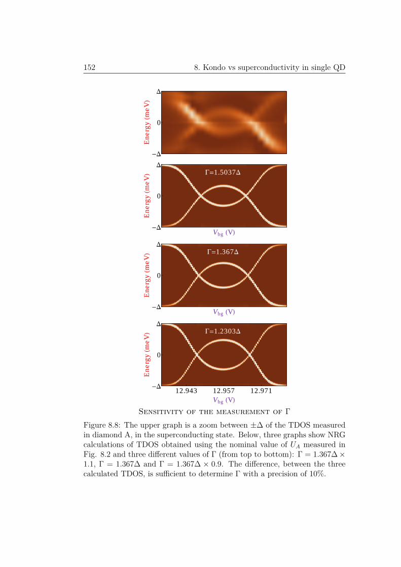
152 8. Kondo vs superconductivity in single QD
-D
0
D
En
erg
yHm
eV
L
-D
0
D
Vbg HVL
En
erg
yHm
eV
L G=1.5037D
-D
0
D
Vbg HVL
En
erg
yHm
eV
L G=1.367D
12.97112.95712.943-D
0
D
Vbg HVL
En
erg
yHm
eV
L G=1.2303D
Sensitivity of the measurement of ΓFigure 8.8: The upper graph is a zoom between ±∆ of the TDOS measuredin diamond A, in the superconducting state. Below, three graphs show NRGcalculations of TDOS obtained using the nominal value of UA measured inFig. 8.2 and three different values of Γ (from top to bottom): Γ = 1.367∆ ×1.1, Γ = 1.367∆ and Γ = 1.367∆ × 0.9. The difference, between the threecalculated TDOS, is sufficient to determine Γ with a precision of 10%.

8.2. Comparison of the data with NRG calculations 153
is predicted to form over a mesoscopic distance from the QD when thereis Kondo effect. Several experimental realizations were already proposedfor detection of this cloud in the normal state: for example by tunnelingspectroscopy measurements on adatoms adsorbed on a metallic surface [122],or by measurements of persistent currents in quantum wires [123].

154 8. Kondo vs superconductivity in single QD

Chapter 9
Specific Double Quantum Dotfeatures
In chapter 7, we proved, with measurements of the stability diagram, theDQD behaviour of our device. Afterward, we analyzed the interplay betweenKondo effect and superconductivity along lines of the (Vbg, VLg) plane wherethe device behaves as an effective single QD (the other dot being maintainedout of resonance in an even charge state). Here, we will focus on specificeffects that we observe in TDOS measurements of the device which cannotbe interpreted by a single dot behaviour.
In a first section, we present measurements of the TDOS of an effectivesingle QD (taken as in previous chapter with the other dot in an even chargestate) where we observe, beside conventional Kondo (CK) effect, split Kondo(SK) resonances. These split resonances are not predicted to occur in singleQD [49]. In section 9.2, we will analyze in details a transition between CKand SK occurring in a region of the stability diagram where the couplingbetween the two dots t′ is so large (t′ ≫ Γ, U) that they can be regarded asa single one. Finally, in section 9.3, we discuss the hybridization of Kondoresonances in two weakly coupled QDs (t′ < Γ, U).
9.1 Conventional and split Kondo (CK andSK) in a single effective QD
Charge stability diagram In Fig. 9.1, we show a stability diagram ofour device measured at V = 0 as a function of the gate voltages. It is verysimilar to the one presented in chapter 7, but with a richer variety of interdotcouplings. Widths of the avoided crossings emphasize interdot couplings fromvery weak (t′ ≪ Γ, U as in rectangle α of Fig. 9.1) to very strong (t′ ≫ Γ, U
155

156 9. Specific Double Quantum Dot features
89
10
-4
-2 0 2 4
Vb
g HVL
VLg HVL
0 2.5
5 7.5
dIdVHµSL
ì
ô
Α
Γ
DQ
Dbehaviour
ofthe
CN
T
Figure9.1:
Color
scaledgraph
ofthe
differentialconductanceof
ourdevice,
similar
tothe
oneof
Fig.7.2.
Itis
measured
atV
=0
asa
functionofthe
backgate
voltageVbg
andthe
leftside
gatevoltage
VLg .
The
dataare
takenat
35m
Kbetween
thetunnelprobe
andthe
aluminum
forkdriven
intheir
normalstate
with
am
agneticfield.
The
blackdiam
ondindicates
apoint
where
aK
ondoridge
connectstwo
electroniclevelofthe
same
orbital,whereas
theblack
triangleshow
san
orbitalwith
noridge
ofconductancebetween
itslevels.

9.1. Conventional and split Kondo (CK and SK) in a single effective QD157
as in rectangle γ of Fig. 9.1).As discussed in chapter 7, when two levels of the same orbital appear as
a single wide stripe (as indicated by the small black diamond in Fig. 9.1)rather than two peaks, it is a manifestation of CK effect (a Kondo resonanceconnects these two levels). In contrast, when two levels of the same orbitalappear as two distinct peaks (see the point indicated by the black triangle),it shows the absence of Kondo resonance.
Coulomb diamonds in normal (N) state In the upper graph of Fig.9.2, we show the Coulomb diamonds of the right QD, taken in the N state,following the black dashed line of Fig. 9.1 where the left dot is maintainedin an even charge state. We observe 15 Coulomb diamonds. Even diamonds(i.e. corresponding to an even charge state of the DQD) are featurelessaround V = 0, whereas odd diamonds present characteristic features of theKondo effect around V = 0. Some of them are CK resonances but others areSK resonances.
TDOS in the superconducting (S) state of the ABSs In the lowergraph of Fig. 9.2, the TDOS are taken in the S state. It shows that thebehaviour of the ABSs is qualitatively the same whether the Kondo ridge issplit or not. The loops formed by ABSs are slightly larger in diamonds withSK ridges. This is presumably due to larger charging energies in diamondswhere SK ridge have formed. It corresponds then to diamonds where TKshould be smaller implying a weaker Kondo effect.
Origin of the SK effect The origin of this SK effect is at present notknown with certainty, but could be due to exchange with the other QD1.SK effect has already been seen in other experiments performed on CNTs[10, 11, 98, 109], semi-conductor QDs [103, 106] or gold nanoparticles in theKondo regime [125]. In Ref. [103, 106], SK was only observed (in contrastto us) for even occupancy (each QD in odd occupancy) and was interpretedas spin entanglement between the excess electrons on each dot. In Ref.[10, 11], it was explained by the probable coupling via exchange interactionto a localized electron trapped in the gate oxide close to the nanotube. Itwas suggested, in Ref. [109], that the interaction with magnetic particles of
1Recent theoretical works based on NRG calculations [124] shows that a splitting ofKondo ridges could happen for odd occupancy of the DQD provided that there is a non-negligible interdot coupling together with an interdot Coulomb repulsion comparable tothe intradot Coulomb repulsion. Interdot Coulomb repulsion is however generally smallerthan Coulomb repulsion in DQD CNTs [105].

158 9. Specific Double Quantum Dot features
00
.5-
0.5
0 4
VHmVL
dIdV HµSL
00
.5-
0.5
0 4
VHmVL
dIdV HµSL
-2
-1 0 1 2
20
-2
VHmVL
VL
g HVL
0 2.5
5 7.5
dIdVHµSL
No
rma
l
ab
ab
89
10
-D D0
Vb
g HVL
Energy HmeVL
0 2.5
5
D.O.SHa.u.L
D=
15
0µ
eV
Su
pe
rco
nd
uctin
g
Figure9.2:
Color
scaledgraph
ofthe
TD
OS
measured
alongthe
blackdashed
lineof
Fig.9.1
inthe
normal(in
blue,yellow
andred)
andsuperconducting
state(in
white
andbrow
n).In
thenorm
alstate,
weobserve
aclear
even-oddalternation
with
Kondo
resonancesaround
V=
0for
oddoccupancy.
Inblack,we
haveplotted
cutofthe
conductancefor
voltagesapplied
onthe
probebetween
-0.5and
0.5m
Vfor
thefirst
andthird
diamond
onthe
left(a
andb).
We
cansee
twotypes
ofKondo
resonances:conventionaland
split.W
hetherthe
Kondo
resonancesis
splitor
notin
thenorm
alstate,AB
Ssspectra,m
easuredin
thesuperconducting
case,donot
showany
qualitativedifference
intheir
behaviour:they
formloops
ofdifferentsize
when
wetune
thegate
voltages.T
hediscontinuity
which
appearsaround
Vbg =
10V
inthe
normalstate
isa
jump
ofoffsetcharge

9.2. Strongly coupled QDs: transition from CK to SK 159
the catalyst pads used for CNTs’ growth (see part IV) could be responsible ofthis split Kondo. However, this should not be the case in our sample as theseparticles should remain far from the QDs. In Ref. [125], the authors showedthat the split Kondo they observed was caused by the RKKY interactionbetween a single electron localized in a gold QD and magnetic impuritiesdeposited deliberately on the electrodes. This splitting could also be causedby a magnetic field [11, 98, 126]. This is however excluded in our experimentas we apply magnetic fields which should induce Zeeman splitting of only 3µeV, below our experimental resolution.
More investigation is needed to understand the origin of these SK ridges.
9.2 Strongly coupled QDs: transition fromCK to SK
Here, we focus on the transition between CK and SK resonance, in a regionof the stability diagram where the coupling between the two dots t′ is solarge that they can be regarded as a single one. In section 9.2.1, we willshow that we can drive the system across this transition with gate voltages.Afterward, in section 9.2.2, we will see that we can extract two characteristicKondo energy scales from the temperature dependence of the CK and SKresonances.
9.2.1 Gate-controlled transitionGate driven transition In Fig. 9.3, we show a color scaled measurementof the differential conductance taken at V = 0 as a function of the gatevoltages. We observe two pairs of two lines moving in parallel with a slopethat is intermediate between those of the independent QDs (given by theorange and green dashed line for the left and right QD). The coupling betweenthe two dots t′ is actually so large that they can be regarded as a singlecomposite QD. The coupled QDs form bonding and antibonding orbitals thatwe can fill sequentially from 2n (empty orbitals) to 2n + 4 (filled orbitals)electrons tuning the gate voltages. We recognize even and odd valleys ofthe large effective dot, with more or less developed Kondo effect in the oddvalleys.
Measurements of Fig. 9.4 show differential conductance measurements asa function of V following the red dashed arrow along the center of the 2n+ 1valley of the composite dot in the N (upper graph) and S (lower graph) state.
On this trajectory, N state measurements (upper graph) clearly show atransition from a CK peak to a SK peak. This transition is continuous:

160 9. Specific Double Quantum Dot features
10.1 10.6-4
-2
0
Vbg HVL
VL
gHV
L
0
5
10
dId
VHµ
SL
KR1
KR2
2n
2n+2
2n+4ì
ì
ì
Β
Figure 9.3: Color scaled graph of differential conductance measurementstaken at V = 0 as a function of the gate voltages in the dashed-dotted rect-angle of Fig. 9.1. Along the red arrow, the coupling between the two dotsis so strong that they almost merge into a single one. The green and orangedashed lines show the respective slopes of the right and left QD when theyare isolated from each other. Some valleys of even occupancies are indicated(2n, 2n+ 2 and 2n+ 4). A fuzzy Kondo resonance follow the orange dashedline and hybridize with an orbital of the right dot at the point indicated bya red diamond.

9.2. Strongly coupled QDs: transition from CK to SK 161
-3.4 -2.3 -1.2-1
-0.5
0
0.5
1
0 4 0 4
VLg HVL
VHm
VL
0
2.5
5
7.5
dId
VHµ
SL
dIdV HµSLdIdV HµSL
-3.4 -2.3 -1.2
0
D
-D
0.3
-0.3
0 4 0 4
VLg HVL
En
erg
yHm
eV
L
0
2.5
5
7.5
D.O
.S.Ha
.u.L
D.O.S. Ha.u.LD.O.S. Ha.u.L
Figure 9.4: Two graphs of TDOS measured along the red dashed arrow inthe stability diagram of Fig. 9.3. The upper diagram is measured in theN state and the lower one in the S state. In the upper graph, we observea CK peak for gate voltages above VLg ≈ −2.9 V. It evolves into a SKresonance below −2.9 V. In dark blue and green, we have plotted cuts atpoints indicated by blue and green diamonds in the stability diagram ofFig. 9.3. In the S case, the Kondo peaks have disappeared because of theopening of a superconducting gap. They are replaced by an ABS whoseenergy changes with the gate voltage. They get closer to the edge of the gapwhere there is a SK resonance in the N state.

162 9. Specific Double Quantum Dot features
the splitting of the resonance decreases, for increasing gate voltage, until itcompletely closes. Interpretation of the transition observed in Fig. 9.3 and9.4 is not straightforward, as, by changing the electrostatic environment ofthe CNT with the gates, several internal parameters of the system may bemodified. For example, the left (resp. right) charging energies UL (resp. UR)can change as the effective size of the QD depends on gate voltages. Thetunneling rates ΓL(R) may also depend strongly on the gate voltages as thelatter will distort the internal electrostatic barriers that control the transit ofelectrons. Finally, the interdot coupling t′ or the interdot Coulomb repulsionUID (we ignore this parameter in the model developed in section 3.1.4) mayalso be modified by the gates and change the properties of the compositeQD. All of these parameters influence the formation of a Kondo state: it isnot possible to identify which one changes and is responsible of this splitting.
In the S state, CK and SK resonances disappear with the opening of theinduced S gap. They are replaced by an ABS whose energy is changing withthe gate voltage. In Fig. 9.2, the loops formed by these ABSs seem biggerfor orbitals where SK ridge appears in the normal state suggesting a smallercoupling to the leads.
ABSs in diamonds with CK or SK ridge In Fig. 9.5, we have rep-resented TDOS measured, in the N and S state, along two cuts (KR1 andKR2) of the Kondo ridge of the 2n+ 1 valley (see Fig. 9.3).
In N state measurements, we observe Coulomb diamonds with differenttype of Kondo effect: a CK resonance for KR1 and a SK resonance for KR2.When the leads are driven in their S state, the TDOS measured along KR1and KR2 becomes very similar. Kondo ridges are replaced by ABSs which,as usual, form loops when we tune the gate.
We observe however a more important difference between KR1 and KR2if we measure the S state TDOS as a function of the superconducting phasedifference δ between the leads. In Fig. 9.5, we show such δ-dependences takenin the middle of the Kondo ridges (two lower graphs). While ABS of KR1is almost insensitive to the phase, ABS of KR2 shows a large δ-dependencewith an amplitude that is roughly half the gap. The supercurrent flowing inthe loop formed by our device is thus higher when the working point is themiddle of KR2 (where there is a SK ridge in the N state), than the middleof KR1 (where the ridge is conventional in the N state). In both cases, thephase dependence shows that the device is in a π state. This is expectedas this δ-dependences are measured in the middle of the loops where thesystem’s ground state is a magnetic doublet (see section 3.1.5.2).

9.2. Strongly coupled QDs: transition from CK to SK 163
0 0.2-0.2
2
4
V HmVL
dId
VHµ
SL
TK=0.93 K
-2.1 -1.85 -1.6
-2
2
-1
0
1
0 6
VLg HVL
VHm
VL
0
2.5
5
7.5
dId
VHµ
SL
dIdV HµSLKR1
-3.1-3.35-3.6
-2
2
-1
0
1
0 6
VLg HVL
VHm
VL
0
2.5
5
7.5
dId
VHµ
SLdIdV HµSL
KR2
-2.1 -1.85 -1.6
-2
2
-1
D
-D
1
0 6
VLg HVL
En
erg
yHm
eV
L
0
2.5
5
7.5
D.O
.S.Ha
.u.L
KR1D.O.S Ha.u.L
-3.1-3.35-3.6
-2
2
-1
D
-D
1
0 6
VLg HVL
En
erg
yHm
eV
L
0
2.5
5
7.5
D.O
.S.Ha
.u.L
D.O.S Ha.u.LKR2
0 Π2 Π
0
D
-D
∆
En
erg
yHm
eV
L
0
1.5
3
D.O
.S.Ha
.u.L
0 Π2 Π
0
D
-D
∆
En
erg
yHm
eV
L
0
1.5
3
D.O
.S.Ha
.u.L
Figure 9.5: The four upper graphs show color scaled differential conductancemeasurements of the device taken along black dashed lines of Fig. 9.3 (KR1and KR2) as a function of V , in the N (graph in blue, yellow and red) andS state (graph in white and brown). In the N case, we observe Coulombdiamonds with Kondo resonances: CK ridge for KR1 and SK ridge for KR2.Cuts taken in the middle of the diamonds are plotted in black. For KR1,a fit with a Lorentzian function of the CK resonance is plotted in the insetand allows to extract a Kondo temperature TK = 0.93 K. In the S case,the TDOS measured as a function of Vbg are very similar: we observe ABSsforming loop. In the middle of the diamonds, we measured dependence withthe difference of superconducting phase δ between the leads. We observe amuch larger dependence of the ABS’s energy for KR2 suggesting a highersupercurrent circulating in the loop.

164 9. Specific Double Quantum Dot features
0-0.4 0.40
2.5
5
V HmVL
dId
VHµ
SL
42 mK
77 mK
118 mK
224 mK
400 mK
585 mK
805 mK
KR1
0-0.4 0.40
2.5
5
V HmVL
dId
VHµ
SL
32 mK
40 mK
77 mK
130 mK
224 mK
370 mK
608 mK
800 mK
KR2
Figure 9.6: Temperature evolution of the CK ridge KR1 and the SK ridgeKR2. For increasing temperature, KR1 follows the usual logarithmic decreaseof spin 1/2 Kondo resonances. The SK resonance KR2 first merges into asingle resonance which then decreases until it vanishes.
9.2.2 Temperature dependences
In Fig. 9.6, we show the temperature dependence of the differential conduc-tance measured in the middle of Kondo ridges KR1 and KR2. We observethat the amplitude of the CK ridge KR1 decreases with increasing tempera-ture. This is the expected behaviour for CK effect. For KR2, the differentialconductance shows two peaks around V = 0 distant of 120 µV. When weincrease the temperature, these two peaks merge into a single one above athreshold temperature T ∗. Beyond T ∗, this single peak subsequently de-creases in amplitude.
As shown in Fig. 9.7, the conductance at V = 0 of the CK resonance(where the Kondo peak is maximum) has the usual logarithmic decrease ofspin-1/2 Kondo resonances [119, 120]. We can extract TK from this temper-ature dependence using the empirical formula for the conductance G (T ) ofRef. [120]:
G (T ) = GT=0(1 + (21/0.22 − 1)
(TTK
)2)0.22
which is widely used to fit experimental data in experiments on the Kondoeffect (see for example Ref. [5, 10, 14]). We obtain reasonable fits for valuesof the Kondo temperatures TK = 800 ± 50 mK. These values are comparableto those obtained in other experiments performed on CNTs [9, 96, 97].
As was done in section 8.1.2, we can also evaluate the Kondo temperaturefrom the shape of the KR1 Kondo ridge measured as a function of V . In orderto do so, we fit the ridge with a Lorentzian function with a half width at half

9.2. Strongly coupled QDs: transition from CK to SK 165
æ
æ
æ
æ
æ
æ
æ
à
à
à
à
à
à
à
à
KR1
KR2
TK=800 mK and GT=0=4.5 µS
TK=950 mK and GT=0=3.6 µS
T*
» 220 mK
50 100 200 400 7002
3
4
5
T HmKL
dId
Va
tV
=0
HµS
L
Figure 9.7: Temperature dependences in logarithmic scale of the Kondo res-onances amplitude at V = 0. We see that the conventional Kondo resonanceKR1 follows the usual logarithmic decrease, whereas the split Kondo reso-nance KR2 has a non-monotonic temperature dependence with a maximumaround T = 220 mK. A fit is plotted in cyan for KR1 with the empiricalformula of Ref. [120]. They give Kondo temperatures around 0.8 K in agree-ment with those obtain from fits of the Kondo ridge (see Fig. 9.5). In dashedgray, we have plotted a fit, using the same formula, for the SK ridge KR2that matches with point above T ∗. It yields a Kondo temperature of 950mK.

166 9. Specific Double Quantum Dot features
maximum HWHM given by:
HWHM ∼ kBTKe
where e is the charge of the electron, kB the Boltzmann constant and TK theKondo temperature. As shown in the inset of Fig. 9.5 (N state of KR1), thisfit gives a Kondo temperature slightly different than those obtained from thetemperature dependence. This procedure can therefore gives a good order ofmagnitude for TK but the only reliable method to measure precisely TK isthe temperature dependence.
In contrast to KR1, for KR2 the temperature dependence of the conduc-tance measured at V = 0, is non monotonic. As shown in Fig. 9.7, theconductance increases until T ∗, around 220 mK, and then decreases until thepeak has completely vanished.
Such non-monotonic temperature dependence has also been observed inRef. [125] and was interpreted as the manifestation of the competition be-tween the Kondo effect and RKKY interaction. In our sample, the originof the suppression of CK effect for T < T ∗ is not clearly identified. It maybe due to the interaction with another QD [127] or with a parasitic spinthat could be localized in a neighboring impurity (for example another CNTor a charge trapped in the gate oxide). They would form a non-degenerateground state, and, therefore, suppress the Kondo effect which happens onlyfor degenerate ground states of the QD (spin up and spin down). The Kondoresonance would be replaced in the Coulomb diamond by finite bias cotun-neling features at voltages corresponding to transition between the groundstate and an excited state (as appear in Ref. [101, 102, 128]). This wouldlook like two symmetric peaks centered around V = 0. Note that in the caseof an antiferromagnetic coupling due to superexchange [129], these peakswould be distant of 2J ≈ 8t2p/U with tp the coupling to the impurity [130].Unfortunately, it is not possible for us to identify experimentally the realreason of this splitting.
More investigation on DQD physics is needed to understand these results.
9.3 Weakly coupled QDs: hybridization oftwo Kondo resonances
In this section we discuss, the influence of a weak interdot coupling (t′ < U,Γ)when two Kondo resonances meet in the (Vbg, VLg) plane, that is to say whenthe two last occupied orbital of the two QDs are degenerate and both halfoccupied.

9.3. Weakly coupled QDs: hybridization of two Kondo resonances 167
This situation occurs in the stability diagram of Fig. 9.3. Indeed, follow-ing the orange dashed line, a fuzzy Kondo resonances of the left dot meetsan orbital of the right dot. At the point of meeting (red diamonds of Fig.9.3), the two orbitals form an avoided crossing. Its width is smaller thanthe width of the Kondo resonance underlining a small interdot coupling (i.e.t′ < U,Γ). Far from the point of meeting, the two levels of the right dotorbital are connected by a ridge of conductance but remains distinguishable.However, they completely reconnect when they start to hybridize with theKondo resonance of the left dot.
This weak avoided crossing is an intermediate situation between weakcoupling (t′ ≪ U,Γ) and strong coupling t′ ≫ U,Γ. In Fig. 9.8, we illustratethese three situations showing cuts of avoided crossings (labelled α, β andγ) in the stability diagram. These cuts are measured along the dotted linesof Fig. 9.1 and Fig. 9.3. In these three situations, the interdot coupling t′plays a predominant role. Let’s discuss them separately.
Very weak interdot coupling When the QDs are almost uncoupled (aswe suppose along α), each QD is independently in the Kondo regime whensingly occupied. They develop their own single dot Kondo resonance at theFermi level (see diagram (a) of Fig. 9.9). We thus observe, in the (Vbg, VLg)plane, two conventional Kondo resonances that simply add their DOS, andapparently cross each other. Therefore, if we measure the TDOS of the DQDmaintaining the two orbitals of the two QDs in a degenerate situation (thetwo orbitals are maintained at equal energy following the dotted black line inrectangle α of Fig. 9.1), we observe, as shown in Fig. 9.8, a single peak thatis just the sum of the two Kondo resonances of the two independent QDs.
Very strong interdot coupling In the extreme opposite case, that is tosay if t′ is the biggest energy scale of the system (and is in particular biggerthan TK), orbitals of the left and right QDs hybridize to form bonding andantibonding orbitals delocalized over the DQD. The two QDs actually mergeto form an effective single QD. As explained in section 9.2, the slope of thisnew single dot is roughly the average one of the left and right dot. In therectangle γ of Fig. 9.1, we thus see two wide parallel stripes which simplyshow the area where the bonding and antibonding orbitals are successivelysingly occupied and develop Kondo effect (see Fig. 9.10). As shown in Fig.9.8, following the black dotted line in rectangle γ of Fig. 9.1 we thus observetwo successive conventional Kondo resonances as we would expect with twoorbitals of a single QD.
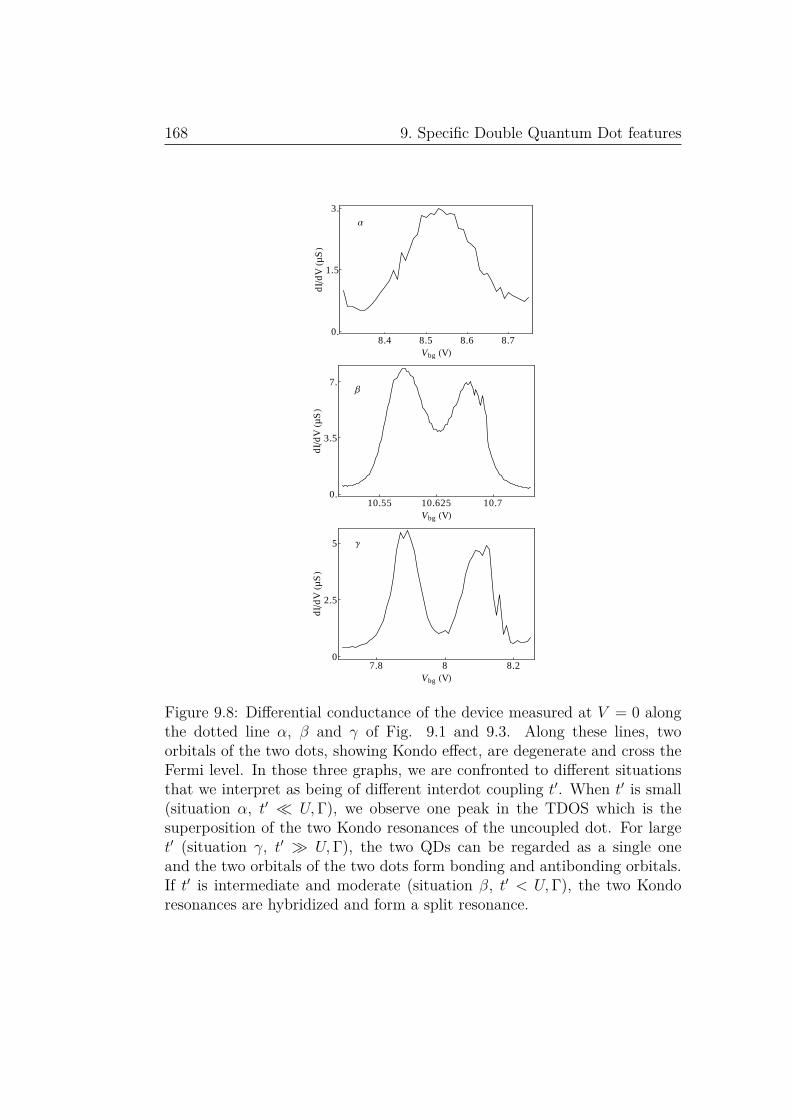
168 9. Specific Double Quantum Dot features
8.4 8.5 8.6 8.70.
1.5
3.
Vbg HVL
dId
VHµ
SL
Α
10.55 10.625 10.70.
3.5
7.
Vbg HVL
dId
VHµ
SL
Β
7.8 8 8.20
2.5
5
Vbg HVL
dId
VHµ
SL
Γ
Figure 9.8: Differential conductance of the device measured at V = 0 alongthe dotted line α, β and γ of Fig. 9.1 and 9.3. Along these lines, twoorbitals of the two dots, showing Kondo effect, are degenerate and cross theFermi level. In those three graphs, we are confronted to different situationsthat we interpret as being of different interdot coupling t′. When t′ is small(situation α, t′ ≪ U,Γ), we observe one peak in the TDOS which is thesuperposition of the two Kondo resonances of the uncoupled dot. For larget′ (situation γ, t′ ≫ U,Γ), the two QDs can be regarded as a single oneand the two orbitals of the two dots form bonding and antibonding orbitals.If t′ is intermediate and moderate (situation β, t′ < U,Γ), the two Kondoresonances are hybridized and form a split resonance.

9.3. Weakly coupled QDs: hybridization of two Kondo resonances 169
Kondo state Kondo state
QDL QDR Right electrode Left electrode
TK t’,T
a)
Formation of two independent Kondo singlet states
Singlet state
QDL QDR Right electrode Left electrode
t’ TK ,T
b)
Formation of a local singlet state preventing Kondo effect
(i)
QDL QDR Right electrode Left electrode
(ii)
(iii)
Singlet state
Superexchange => Antiferromagnetic coupling c)
Antiferromagnetic coupling through superexchange
Figure 9.9: The upper diagram (a) shows what happens for strong couplingto the leads and vanishing interdot coupling (TK ≫ t′): two independentKondo states form between dots and leads. In the Kondo state, electrons aredelocalized between leads and dots (see the simplified wave function of Ref.[131]). In the second diagram (b), the coupling between the dots favors theformation of a local singlet state which prevents Kondo effect (TK ≪ t′). Inthis singlet state, electrons are localized and could be described by the simplevector |↑↓⟩−|↓↑⟩√
2 . The formation of this singlet state is due to an effective ferro-magnetic interaction between the dots illustrated by the sequence (c). Whenthe last orbital of each dot is singly occupied (i), an effective antiferromag-netic coupling may arise by superexchange through an intermediate virtualstate of double occupancy (ii). This leads to the formation of a spin-singletstate delocalized over the two dots (iii).
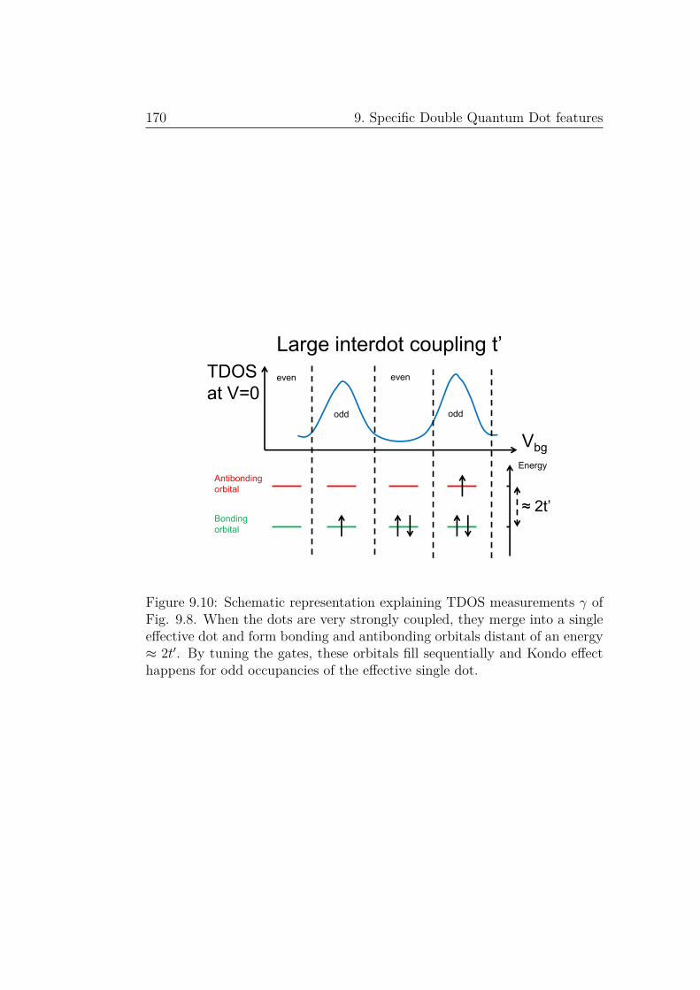
170 9. Specific Double Quantum Dot features
Bonding
orbital
Antibonding
orbital
Vbg
TDOS
at V=0 even even
odd odd
Energy
≈ 2t’
Large interdot coupling t’
Figure 9.10: Schematic representation explaining TDOS measurements γ ofFig. 9.8. When the dots are very strongly coupled, they merge into a singleeffective dot and form bonding and antibonding orbitals distant of an energy≈ 2t′. By tuning the gates, these orbitals fill sequentially and Kondo effecthappens for odd occupancies of the effective single dot.
9.3. Weakly coupled QDs: hybridization of two Kondo resonances 171
Intermediate interdot coupling If the coupling between the QDs is in-termediate between the two previous situation (as we suppose along β), singledot Kondo effect develops independently in the two QDs if their last occupiedorbitals are not degenerate. However, when the two Kondo ridges meet eachother in the (Vbg, VLg) plane (i.e. when orbitals of the QDs are degenerate),we can see “an avoided Kondo ridge crossing” forming with a non-zero con-ductance minimum in-between. If we measure the TDOS as a function ofthe gate voltages following the black dotted line β (along which the orbitalsare roughly maintained degenerate), we thus observe two peaks symmetricalwith the point of meeting (see Fig. 9.8). The transition between the pre-vious case (γ) and this one is actually continuous for decreasing t′ with theconductance at V = 0 falling to zero when the two ridges move away fromeach other. This case is of particular interest because, in contrast with thetwo others, it leads to specific physics of the DQD as we will explain in thefollowing.
In Fig. 9.11, we have represents the TDOS of the DQD measured alongthe dotted line β and as a function of V . We recognize, on the left and theright, two blue areas of blockade where the occupancy of the DQD is evenwith no feature around V = 0. In between these two regions, we observe alarge region of conductance, that resembles an odd diamond of a single QDwith a Kondo ridge (see N state measurements of KR1 in Fig. 9.5, or forexample Ref. [96]). However, in contrast to single QD, the Kondo ridge ofFig. 9.11 is interrupted between VLg =-1.2 and -1.45 V. This part is replacedby an asymmetric split Kondo resonance, as can be seen in the inset.
This “avoided Kondo ridge crossing” can be interpreted in terms of com-petition between formation of a singlet state in the DQD and independentKondo effect between the two dots (see the two upper diagrams of Fig. 9.9).When the coupling between QDs, characterized by t′, is absent, we are inthe α case and QDs develop Kondo effect independently. If t′ gets a bitlarger, an effective antiferromagnetic exchange between the dots is generatedby superexchange [129, 132] (see lower diagram of Fig. 9.9), characterized bythe energy scale J ∼ 4t′2/U . If J gets of the order of magnitude of TK , thisantiferromagnetic exchange favors the formation of a non-degenerate singletstate within the DQD. This state prevents the development of singlet Kondostate as the latter is based on the degeneracy of two spin states. The Kondopeak is then split into two peaks distant of an energy 2J [130] that are inter-preted in some theoretical works as molecular levels between Kondo resonantstates [133, 134].
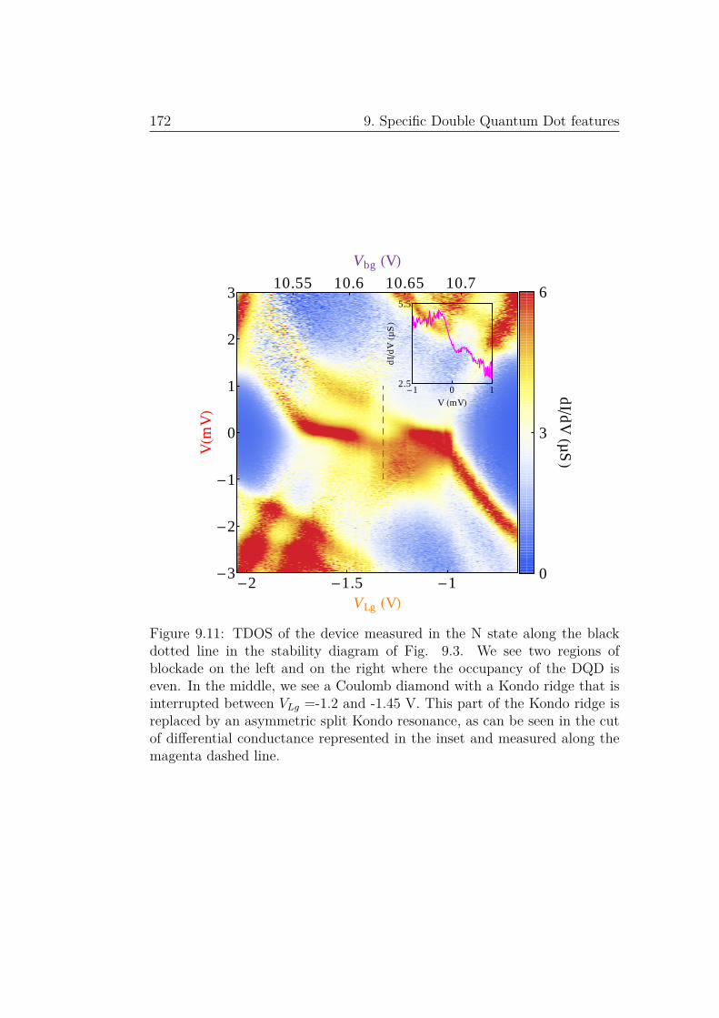
172 9. Specific Double Quantum Dot features
-1 0 12.5
5.5
V HmVLd
IdV
HµS
L
-2 -1.5 -1-3
-2
-1
0
1
2
310.55 10.6 10.65 10.7
VLg HVL
VHm
VL
Vbg HVL
0
3
6
dId
VHµ
SL
Figure 9.11: TDOS of the device measured in the N state along the blackdotted line in the stability diagram of Fig. 9.3. We see two regions ofblockade on the left and on the right where the occupancy of the DQD iseven. In the middle, we see a Coulomb diamond with a Kondo ridge that isinterrupted between VLg =-1.2 and -1.45 V. This part of the Kondo ridge isreplaced by an asymmetric split Kondo resonance, as can be seen in the cutof differential conductance represented in the inset and measured along themagenta dashed line.

Part IV
Samples fabrication
173


Chapter 10
Fabrication of a sample
In order to perform the spectroscopy of ABSs in carbon nanotubes (CNTs),it is necessary to well connect an individual CNT with two superconductingelectrodes less than a µm apart and place a weakly coupled tunnel electrodein between. The fabrication of this superconducting CNT-based circuit con-cerns three steps:
• on chip CNTs growth,
• localization of CNTs,
• nanofabrication of superconducting CNT-based circuit.All these steps rely on the use of standard e-beam lithography technique thatwe describe in detail in the following section. In section 10.2, we explain howwe synthesized on chip high quality CNTs, sufficiently long and isolated tobe contacted individually. Then in section 10.3 and 10.4, we present thetechniques used to localize and fabricate on such CNTs the circuits designedto observe the ABS by tunneling spectroscopy. The last section is devotedto room temperature characterization of samples in their final form.
10.1 Lithography techniquesAlong our fabrication scheme, we use electron lithography three times inorder to fabricate resist masks, as depicted on Fig. 10.1 and 10.2, withpatterns smaller than 100 nm.
10.1.1 Coating the substrate with resistMask fabrication starts by coating the substrate with an electro-sensitiveresist single layer of polymethyl-meta-acrylate (PMMA) for the case depicted
175

176 10. Fabrication of a sample
Resist SiO2 Si
(a) Resist deposition (b) Spinning and baking
Electron beam
(c) Exposure (d) After development
Figure 10.1: Typical procedure of electronic lithography
in Fig. 10.1 or a bilayer of polymethyl-meta-acrylate/meta-acrylate acid(PMMA/MAA) for the case depicted in Fig. 10.2. Parameters used aredetailed in subsection 11.1.
10.1.2 ExposureOnce substrate is coated, we expose the resist with the electron beam ofa SEM Philips XL30 fitted with Elphy Quantum lithography system fromRaith. The Elphy Quantum software (EQ) controls the exposure of patternsdefined in a GDSII file (for example see Fig. 10.9).
These patterns are divided by the software when needed into rectanglesand triangles that are scanned step by step in meander. The electron beamstays at each step during a time called dwell time until the programmedcharge dose is reached. With a positive resist, polymer chains are locallybroken in these exposed areas which will be removed during the development.
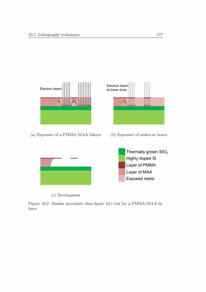
10.1. Lithography techniques 177
Electron beamElectron beamat lower dose
(a) Exposure of a PMMA/MAA bilayer (b) Exposure of undercut boxes
Thermally grown SiO2
Highly doped Si
Layer of PMMA
Layer of MAA
Exposed resist
(c) Development
Figure 10.2: Similar procedure than figure 10.1 but for a PMMA/MAA bi-layer

178 10. Fabrication of a sample
We choose the appropriate exposure dose depending on the resist de-posited on the chip (see subsection 11.2.1 in chapter 11) and the pattern wewant to obtain. If the coating is a bilayer, we expose generally undercutboxes at low doses (see Fig. 10.2 (b)) in order to have a larger undercut, re-quired to perform a subsequent angle evaporation. Doses for undercut boxesare high enough to get rid of MAA during development but not of PMMA,getting part of the mask suspended.
10.1.3 DevelopmentAfter exposition, we develop the resist in methyl-isobutyl ketone (MIBK)diluted 1:3 in volume with isopropanol (IPA) for 45 s. We subsequently rinsethe chip in IPA to stop development and dry it under N2 flow. MIBK dissolvethe exposed resist yielding the designed patterns (see in section 11.2.2).
10.2 Nanotubes growth on Si substrateIn this section we describe the method to obtain CNTs on an insulating layerof thermally grown silica (SiO2) atop highly doped silicium (Si) substrate.As we want in the end to perform transport experiments, we need CNTs withcoherence lengths greater than 1 µm. This is provided by a chemical vapordeposition technique which yields CNTs with a low defect concentration [135]in comparison for example to arc discharge technique [136, 137].
10.2.1 Substrate characteristicsWe use commercial 4-inch wafers constituted by a 1 µm thick insulating layerof SiO2 atop a Si substrate. The SiO2 layer is obtained by oxidation of a Sicrystal. Si is heavily doped (typically 5 mΩ/cm) remaining conducting evenat very low temperature. We use it as a back gate capacitively coupled tothe sample.
Such commercial wafers provide us a sufficiently flat surface to fabricateelectrical circuits with elements of the order of the nanometer like CNT. Wecut up these wafers with a diamond tip in chips of 1 × 1 cm2 and we processthem individually (see Fig. 10.3).
10.2.2 CNT grown by Chemical Vapor Deposition (CVD)To obtain CNTs we choose the CVD technique. It provides individual CNTswith low defect density, single wall, with diameters of 1-3 nm and lengths of

10.2. Nanotubes growth on Si substrate 179
(a) Si Wafer (b) 1 × 1 cm2 chip
Figure 10.3 – Samples are fabricated on a chip cut out from a highly dopedSi wafer with a 1µm thick oxide layer.
up to tens of micrometres.
Catalyst deposition In this method CNTs grow from catalyst pads de-posited on the substrate as depicted in Fig. 10.4. In order to isolate a singleCNT and have zones free of catalyst for circuit fabrication, we prepare cat-alyst pads of 1 × 1 or 2 × 2 µm2 sufficiently far from each other to get a lowCNT density (see Fig. 10.4).
We obtain catalyst pads by dispensing, through a resist mask made froma single layer of PMMA (see table 11.1), a few drops of a suspension ofthe catalyst in methanol (see recipe in subsection 11.3.1 and [135]). Afterevaporation of the methanol and lift off of the resist (see for details subsection11.3.2), only catalyst pads networks patterned on the mask remain on thechip (see Fig. 10.4 (d)).
The chip is then divided into four parts that will give four different sam-ples. Each one has a network of 30 catalyst pads distant of 40 µm
Nanotubes growth by chemical vapor deposition (CVD) After cat-alyst deposition, the chip is placed in a quartz tube. This quartz tube lies ina furnace1 (see Fig. 10.5) which can heat up to 900C. It is linked by pipeson one end to gas cylinders of Ar, H2 and CH4, and on the other end to anexhaust pipe.
The growth starts by heating up the quartz tube to 900C with a flowof Ar (1500 ml/min) passing through the tube. Then, during 8 minutes aH2 flow (200 ml/min) cleans the chip. The growth is then performed by
1We used the furnace of LPA Mesoscopic Physics group at ENS Paris.
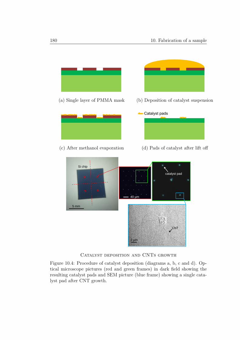
180 10. Fabrication of a sample
(a) Single layer of PMMA mask (b) Deposition of catalyst suspension
Catalyst pads
(c) After methanol evaporation (d) Pads of catalyst after lift off
5 mm
40 µm
catalyst pad
Si chip
CNT
2 µm
Catalyst deposition and CNTs growthFigure 10.4: Procedure of catalyst deposition (diagrams a, b, c and d). Op-tical microscope pictures (red and green frames) in dark field showing theresulting catalyst pads and SEM picture (blue frame) showing a single cata-lyst pad after CNT growth.

10.3. Localizing nanotubes 181
quartz tube
heated to 900°C
gases inlet
to exhaust
Figure 10.5: Picture of the ENS CVD furnace.
injecting an additional flow of CH4 during 10 minutes (1000 ml/min) afterthat the furnace slowly cools down to room temperature in an Ar flow.
10.3 Localizing nanotubes
To locate nanotubes, we first add gold alignment marks on the chip by per-forming standard e-beam lithography on a MAA-PMMA bilayer (see table11.1). These gold alignment marks include 7 large crosses of 200 µm (distantof 1392.5 µm) on the edge of the chip and a grid of 12 × 12 small labelledcrosses inside a 150 µm2 box in the center of the chip (see Fig. 10.6), whereCNTs were grown.
We locate CNTs on the chip using our SEM Philips XL30 working inUltra High Resolution mode with accelerating voltages that ranges over 0.5and 1.5 kV. In order to minimize carbon contamination and possible damageof CNTs, we imaged them quickly. We take pictures of approximately 25×35µm in 1 minute.
In the SEM we find the central region where we grew CNT, using largecrosses. CNTs are located with respect to the labelled crosses (see Fig. 10.7a)by taking pictures.

182 10. Fabrication of a sample
15 µm
2 µm 1 mm
Gold alignment marks for CNTs localization and forfabrication
Figure 10.6: The central area where CNTs are grown is located thanks tolarge crosses (optical microscope picture on the top right). Small crosses areused to define a coordinate system for lithography alignment of the contactson the CNTs (SEM pictures with red and green frames).

10.4. Contacting nanotubes with metallic leads 183
10.4 Contacting nanotubes with metallic leadsThe sample we want to obtain includes a superconducting fork well connectedto a CNT and at the same time a superconducting tunnel probe weaklycoupled to its central part in order to measure the density of states (seesection “experimental measurement of the TDOS” and Fig. 10.8). In thissection we explain how we obtain these two types of contact in a singlelithography step.
10.4.1 Mask fabrication to contact CNTsDrawing the circuits for e-beam lithography Once CNTs are located,we draw (see Figs. 10.7a and 10.9) a circuit to connect them (our drawingsare encoded in standard GDSII database file format). The drawing is donein layer in which SEM pictures of labelled crosses and CNTs are inserted.On Fig. 10.7a, we have represented, in dark red and on top of such a picture,several structures constituted by a fork and a tunnel probe. These structuresare linked to pads of 300 µm2 (see Fig. 10.9), that will subsequently serveto bond the sample with aluminum wires of 25µm and connect it to themeasurement circuit (see Fig. 10.10).
Alignment procedure Prior to the exposure step, we perform a threesteps alignment. On the first step we focus on the surface of the sample atthree different places on three scratches at corners of the chip. EQ softwarewill use these data to interpolate the correct focus at the position where theexposure is performed in case the sample is not laid down flat on the sampleholder. On the second step, we define the chip coordinate system thanks tolarge crosses. And on the last step, we used small crosses to fine-tune thegeometry of the exposed field.
We performed this exposure on a bilayer of PMMA-MAA (see section11.1). This gives a suspended mask that will allow us to perform metal angleevaporation (see below).
10.4.2 Metal depositionIn order to obtain the two required types of superconducting contact onthe CNT in a single step (well connected electrodes and tunnel contacts),we evaporate the metal (as described in subsection 11.4.1) at two differentangles (see Fig. 10.11). We evaporate all the contacts in a single pumpdown instead of fabricating the good contacts and the tunnel contacts in

184 10. Fabrication of a sample
(a) Drawing in GDSII format of the circuits in Elphy Quantumon top of a SEM picture showing the CNT used to make thesample of Ref. [92] and gold alignment marks labelled 53 and63. In green are represented undercut boxes and in orangereplica of the labelled crosses we use to align the drawing.
(b) SEM picture of the sample T9 (left) fabricated on this CNT
Figure 10.7: Pictures of the sample of Ref. [92]. Differential conductancemeasurement of the structure on the left are presented in the supplementaryinformation of Ref. [92].

10.4. Contacting nanotubes with metallic leads 185
CNT
Fork (good contacts)
Tunnelprobe
Figure 10.8: SEM picture of the sample of Ref. [92]
Figure 10.9: Drawing in a GDSII file and picture taken after angle evapora-tion with an optical microscope of the sample of Ref. [92]

186 10. Fabrication of a sample
(a) Sample D03 on a 5 mm chip glued by silver paint on the metallicpart of a sample holder. On this metallic part can be applied a back gatevoltage to tune the chemical potential of the CNT. The sample is bondedto contacts for transport measurements.
(b) SEM picture of sample D03 with aluminum bonding wires
Figure 10.10: Picture of the sample of Ref. [92] after measurements

10.4. Contacting nanotubes with metallic leads 187
two consecutive processes because reprocessing killed the contacts previouslymade each time we tried.
Electrodes composition We choose Aluminum (Al) to fabricate thesesuperconducting contacts because of its well-known superconducting BCSbehaviour below 1.2 K. However Al directly evaporated on CNT doesn’tprovide measurable contacts [138]. In order to obtain good electrical contacts,we thus need to add, between CNTs and Al, a sticking layer of Palladium(Pd) or Titanium (Ti) thin enough for Al to induce superconductivity inCNTs.
Contacting a single wall CNT is generally achieved with Pd electrodesbecause it affords statistically the best contacts [139]. Also efficient thoughless reliable than Pd, other materials such as Ti or Platinum (Pt) providesas well transparent contacts. We chose a sticking layer of Ti as we did nothave Pd in our evaporator2.
A thin layer of Ti (3 nm thick) proves to be enough to obtain well con-nected contacts. To obtain tunnel contacts, we evaporate only 1 nm of Ti. Itgives us contacts which are on average ten times more resistive than contactswith 3 nm of Ti (see section 10.5). We evaporate on top of these Ti layer100 nm of Al for the fork and 40 nm of Al for the tunnel probe.
We need to mention that Ti is actually superconducting below 400 mKand one can imagine that we could have simply evaporate only Ti instead ofa Ti/Al bilayer. However the temperature of the fridge (35 mK) is not neg-ligible compare to the Ti superconducting gap and temperature could excitequasiparticles which would limit our spectroscopic resolution. With a Ti/Albilayer we get superconducting electrodes with a superconducting gap whichcan be three times higher. The resulting gap decreases exponentially withthe Ti thickness [140], we choose then a thickness of Ti negligible compareto the Al thickness (1 or 3 nm compared to 40 or 100 nm).
Evaporation Before evaporation the sample is heated up to 110C for twohours. It is subsequently cool down to -80C, evaporation being started at0C (see Fig. 10.12). We choose to perform this temperature cycling for tworeasons:
1. we expect to get rid of the residual water on the chip surface duringheating up,
2Actually we had at our disposal two evaporators. One of them could evaporate Pd butit was not possible to cool down the sample holder at liquid N2 temperature. Furthermoreits loadlock pressure was higher of one order of magnitude.

188 10. Fabrication of a sample
Figure 10.11: Well connected and tunnel contacts are evaporated in a singlepump down at different angles.
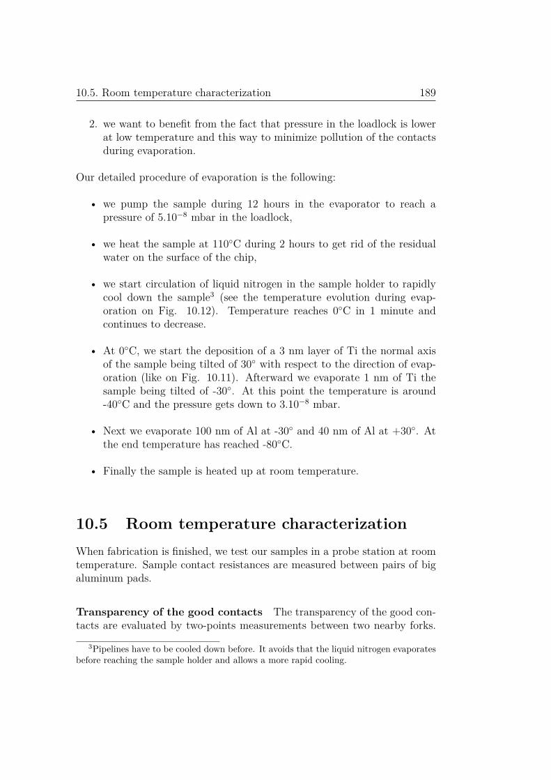
10.5. Room temperature characterization 189
2. we want to benefit from the fact that pressure in the loadlock is lowerat low temperature and this way to minimize pollution of the contactsduring evaporation.
Our detailed procedure of evaporation is the following:
• we pump the sample during 12 hours in the evaporator to reach apressure of 5.10−8 mbar in the loadlock,
• we heat the sample at 110C during 2 hours to get rid of the residualwater on the surface of the chip,
• we start circulation of liquid nitrogen in the sample holder to rapidlycool down the sample3 (see the temperature evolution during evap-oration on Fig. 10.12). Temperature reaches 0C in 1 minute andcontinues to decrease.
• At 0C, we start the deposition of a 3 nm layer of Ti the normal axisof the sample being tilted of 30 with respect to the direction of evap-oration (like on Fig. 10.11). Afterward we evaporate 1 nm of Ti thesample being tilted of -30. At this point the temperature is around-40C and the pressure gets down to 3.10−8 mbar.
• Next we evaporate 100 nm of Al at -30 and 40 nm of Al at +30. Atthe end temperature has reached -80C.
• Finally the sample is heated up at room temperature.
10.5 Room temperature characterizationWhen fabrication is finished, we test our samples in a probe station at roomtemperature. Sample contact resistances are measured between pairs of bigaluminum pads.
Transparency of the good contacts The transparency of the good con-tacts are evaluated by two-points measurements between two nearby forks.
3Pipelines have to be cooled down before. It avoids that the liquid nitrogen evaporatesbefore reaching the sample holder and allows a more rapid cooling.

190 10. Fabrication of a sample
Cooling down
Start heating
Temperature (°C)
timehh:mm:ss
0:00:00 1:00:00 2:00:00 3:00:00
-50
0
50
100 Heating at 110°C (2 hours)
Starting evaporation
Warming up
Figure 10.12: Evolution of temperature in the loadlock during our evapora-tion procedure
This measurement gives, for roughly one third of the samples, contact resis-tances between 11 and 50 kΩ4. This result has to be compared to the maxi-mum resistance expected for a ballistic CNT which corresponds to about 6.5kΩ [141]. Transmissions of devices are then included between 0.5 and 0.15.
If this first test is conclusive, we test resistances between tunnel probesand their corresponding forks.
Tunnel contacts characterization To be in the tunneling regime, theresistance between a tunnel probe and its corresponding fork has to be 10times higher than quantum of resistance RK = h/e2. At room temperature,this two-points measurement gives generally on a given sample very hetero-geneous results between 80 kΩ and 10 MΩ or even more. They could thusnot all be selected to perform the spectroscopy of ABS.
We found out experimentally that, once cooled down, a sample is indeed4The rest of the samples were either not showing measurable contacts or contacts up
to several MΩ.5The criterion to know if contacts are good enough for us is not simple. But we knew
from theoretical estimation that if the transmission was lower than 0.1, we expected theABS to have an energy dependence with the phase smaller than 5% of |∆|. This has to becompared with the ABS full width at half maximum (FWHM) which gives approximatelyour limit of resolution. The ABS we have observed have a FWHM of roughly 10% of |∆|.

10.5. Room temperature characterization 191
in the tunnel regime if its room temperature tunnel contact is above 150 kΩ.At 35 mK such resistances increase to reach values above 200 kΩ.
Our procedure of fabrication gives us about 10% of samples with well con-nected electrodes and tunnel electrodes with appropriate contact resistancesat the same time. It yields well connected electrode 30% of the time. Butwhen we obtain good contacts, tunnel contacts are in the required range only20-30% of the time. The efficiency of this fabrication process is only 10% inthe end.
Influence of the probe We have checked if the tunnel probe did notcut electrically the CNT by measuring the two-points resistance at roomtemperature between pairs of good contacts that are separated by a tunnelprobe (see Fig. 10.13). This indicates that tunnel probes don’t cut electri-cally CNT. However this test has not been done systematically on our sampleas it requires a specific geometry which was not needed for the experimentwe wanted to perform.

192 10. Fabrication of a sample
E1 E2
T2
CNT
T1
E3
Ei=1,2,3 = good contacts
Ti=1,2 = tunnel contacts
Pairs of electrode Resistance value between them
E1-E2 14 kȍ
E2-E3 34 kȍ
T1-E1 750 kȍ
T1-E2 720 kȍ
T2-E2 500 kȍ
T2-E3 480 kȍ
Influence of the tunnel probe on the conductance betweengood contacts
Figure 10.13: SEM picture and two-points resistance values of a test sampleused to prove that tunnel probes don’t cut electrically CNT between twogood contacts.

Chapter 11
Parameters and techniques forfabrication
11.1 Preparation of the resist layers or bilay-ers
To coat the substrates, we deposit on it drops of resist diluted in solvent. Wethen spin it at 4000 revolutions per minute (rpm) to form an homogeneouslayer. Next we bake it on a hot plate at 170C. This procedure can berepeated to form a thicker layer of resist or a bilayer of distinct resists. Thebaking at 170C evaporates the solvent and avoids the mixing of the differentlayers on the chip.
We use two different kinds of masks that are obtained by different recipesgiven in table 11.1. They differ by the type of resist layer coated on thesubstrate. This is either a single layer of polymethyl-meta-acrylate (PMMA)or a bilayer of polymethyl-meta-acrylate/meta-acrylate acid (PMMA/MAA).MAA being more electro-sensitive than PMMA, a bilayer of PMMA/MAAgives suspended masks after development.
11.2 Exposure: parameters and resulting masksafter development
11.2.1 Parameters of exposure
In this table are detailed parameters used during exposure in the SEM foreach type of mask.
193

194 11. Parameters and techniques for fabrication
Mask for the catalyst pads (thick PMMA single layer):1. Spin 950K A6 PMMAa at 4000 rpm for 1 minute,
2. bake at 170C for 1 minute,
3. spin another identical layer,
4. bake at 170C for 10 minutes.
This first recipe gives a thick single layer of PMMA which is sufficient forcatalyst deposition.
Mask for the alignment marks (PMMA/MAA bilayer):
1. Spin MAA 8.5 EL10b at 4000 rpm for 1 minute,
2. bake at 170C for 10 minutes,
3. spin 950K PMMA A3c at 4000 rpm for 1 minute,
4. bake at 170C for 15 minutes.
This second recipe gives a bilayer of PMMA/MAA which makes the lift offeasier after metal deposition.
Mask for the contacts to the nanotube (PMMA/thick MAA bi-layer):
1. Spin MAA 8.5 EL10 at 4000 rpm for 1 minute,
2. bake at 170C for 1 minute,
3. Spin MAA 8.5 EL10 at 4000 rpm for 1 minute,
4. bake at 170C for 10 minutes,
5. spin 950K PMMA A3 at 4000 rpm for 1 minute,
6. bake at 170C for 15 minutes.
This third recipe gives a bilayer of PMMA/MAA with a thick layer of MAA.For a given shift between metal evaporations (see Fig. 10.11), this thicknesswill allow us to perform angle evaporations with smaller angle than with athinner layer of MAA.
aPMMA of molecular weight 950000 diluted at 6% in anisole from MicroChembMAA of molecular weight 8500 diluted at 10% in ethyl-lactate from MicroChemcPMMA of molecular weight 950000 diluted at 3% in anisole from MicroChem
Table 11.1: Recipes to obtain an homogeneous layer of PMMA or bilayers ofPMMA/MAA.

11.2. Exposure: parameters and resulting masks after development 195
pattern exposed Dose and parameterscatalyst pads 350µC/cm2 at 25 kV spot 11
alignment marks 4000µC/cm at 10 kV spot 5contacts to the nanotubes 250µC/cm2 (×1.4 for small structures) at 25 kV spot 1
undercut boxes 25µC/cm2 at 25 kV spot 1
When we want to expose an area, we have to choose a dose defined inµC/cm2. But for patterns defined by lines, the dose is defined in µC/cm andthe width of the obtained patterned line depends on the magnitude of thedose.
The chosen step of exposure is 2 nm for the small structures to obtain ahigh enough resolution. We choose several µm for large structure.
Once we have chosen the current of exposure and the step, EQ calculateautomatically the dwell time given by:
tdwell time = Dose× step2
current
11.2.2 Resulting masks after development• Development for a PMMA single layer:
Development of a 950K A6 PMMA single layer gives an non suspended mask.If we wanted to evaporate metal, a suspended mask would be preferable (seebelow). But when we want to deposit catalyst, a single thick layer is sufficientto obtain well defined patterns that will give compact and dense catalyst padsyielding an efficient and controlled growth of CNT (see Fig. 11.1).
Figure 11.1: CNT growth obtained from well defined catalyst pads.
1Spot 1 corresponds typically to 20 pA and spot 5 to 2 nA of current for the electronbeam.

196 11. Parameters and techniques for fabrication
Before lift off
After lift off
Evaporated metalSilicaHighly doped SiLayer of PMMALayer of MAAExposed resist
Figure 11.2: With a single layer of PMMA and after a metal evaporation,the mask may not lift properly or not at all if the resist cannot be reachedby its solvent.
• Development for PMMA/MAA bilayer:
Development of a PMMA/MAA bilayer gives suspended masks of PMMAsupported by MAA (see Fig. 10.2). We perform angle evaporation usingthis kind of mask. It can be also useful to make the lift off easier for smallstructures which may not lift properly otherwise (see Fig. 11.2).
With such mask, because of proximity effect, represented by a zigzagarrow in Fig. 10.2 (a), we need several iterations to obtain a correct mask.
Once a mask is done, we deposit either catalyst for CNTs growth, ormetals with an electron beam evaporator for alignment marks and electrodesconnecting CNTs. After deposition, the mask is removed by lift off in ace-tone. Technique of catalyst deposition and principle of metal evaporationare described respectively in section 11.3 and 11.4.
11.3 Catalyst preparation and deposition
11.3.1 Catalyst suspension preparationThe catalyst suspension is obtained by dispersion of the following ingredientsin 15 ml of methanol:
• 20mg iron nonahydrate powder,

11.4. Metal deposition and lift-off 197
• 15mg aluminum oxide powder,
• 1mg bis(acetylaceto)-dioxomolybdenum (VI) powder.
The solution is sonicated during 15 minutes to homogenise suspension. Thesonication has also to be performed 10 minutes before each deposition.
11.3.2 Catalyst depositionDisposition of the catalyst on the chip influences dramatically the concen-tration of CNT grown on the substrate (see Fig. 11.1). We have determinedempirically that we obtain the appropriate concentration by having on thechip 4 networks of 30 pads. Pads are distant of 40 µm from each other. The4 networks will give 4 different potential samples after the 1×1 cm2 chip hasbeen cut up in four 5 × 5 mm2 chips (see Fig. 10.4).
To obtain such networks, we dispense on the chip on the mask 2 drops ofthe catalyst suspension which has been freshly sonicated during 10 minutes.The methanol is evaporated from the chip slowly under a petri dish slightlytilted so that the vapor can escape. This process lets a thin layer of catalyst.After a lift off of 10 minutes in acetone at 65C, only catalyst remains inthe lithographically defined pads. The chip is then rinsed with acetone andisopropanol.
11.4 Metal deposition and lift-off
11.4.1 Description of the electron gun evaporatorWe deposit gold (Au), titanium (Ti) and aluminum (Al) on our samples intwo similar electron gun evaporators2 . They are divided in two chambers:a loadlock and a main chamber (see Fig. 11.3).
In the main chamber are located crucibles in which are positioned thedifferent available metals. Deposition is realized by heating the desired targetwith an electron beam gun. Deposition rate, typically between 0.1 and 1nm/s, is computer controlled through a quartz microbalance.
In the loadlock, a sample holder is attached to an arm which can betilted between - and +90 for angle evaporation. This sample holder can beheated by an electrical heater to 400C, or cooled down to nearly -200C bycirculation of liquid nitrogen. Pressure in this chamber3 is lower than 10−6
mbar after 30 minutes of pumping and reaches 3.10−8 mbar after one night.2Electron gun evaporator fabricated by PLASSYS3Pressure in the lower chamber is slightly lower.

198 11. Parameters and techniques for fabrication
loadlock
main chamber
High voltage
sample holder
sample pneumatic shutter
valve
electron beam magnetic focus
crucible
vapor of metal
metal
control computer
pumping
pumping
Figure 11.3: Schematic and picture of a PLASSYS e-gun

11.4. Metal deposition and lift-off 199
When we vent the loadlock, the main chamber remains isolated thanks toa valve to maintain its pressure low. Repumping after venting is then fasterand there are less risks of pollution of the main chamber. This low pressureenvironment is crucial to obtain good metallic contacts by evaporation onnanotube.
11.4.2 Lift offThe last step of fabrication is the lift off. The resist on the chip is dissolvedduring 10 minutes in acetone heated on a hot plate at 65C. Afterward, onlymetallic patterns and CNT remain on the chip (see Fig. 11.4).
Metal
Figure 11.4: After metal deposition, the resist is removed by lift off and justmetal and CNTs remain on the chip.

200 11. Parameters and techniques for fabrication

Part V
Appendices
201


Appendix A
Introduction to Quantum dots
The term of Quantum Dot (QD) designates systems such as molecules, smallaggregates of semiconducting or metallic materials which are semi-isolatedfrom bulk conducting materials and in which few-electron effects play a largerole. The ab-initio physics of QD is a complicated many-body problem thatcannot be solved exactly. However in some ranges of parameters, QD maybe described by some fairly simple effective models, such as a independentparticle-in-a-box model with interactions accounted for simply by a chargingenergy. In this case, when the dot is weakly connected to electrodes, one dealswith simple Coulomb blockade physics, electrons being added one by one tothe dot. On the other hand, when the dot is well coupled to some conductingreservoirs, many-body interaction effects lead to a variety of Kondo effectsthat require elaborate theoretical methods to capture them.
A.1 Energy quantization in QDsConfined systems or QDs, such as those mentioned above, are first of allboxes or “pools” of electrons [17] whose electronic structures are quantizedin discrete quantum states like in atoms. For that matter, they are oftenregarded as artificial atoms [142].
If we ignore for the moment Coulomb interactions, this quantization arisesfrom boundary conditions of the box and, therefore, depends only on its ge-ometry. For example, in nanopillars of semiconductor, the cylindrical geom-etry leads to orbital states with quantized radial and angular components[143]. When, as in our experiment, the QD is a quasi one-dimensional singlewalled CNT whose boundaries are marked by the leads, the system can beregarded as a quasi one-dimensional box. The CNT acquires thus a sim-ple electronic structure whose levels form a ladder of discrete energies [144],
203

204 A. Introduction to Quantum dots
L R QD
Gate
Figure A.1: Illustration of a QD connected to left (L) and right (R) elec-trodes through tunneling processes. An additional electrode called the gateis capacitively coupled to the QD in order to control its electro-chemicalpotential with a voltage. In such geometry, one can perform an electronictransport experiment which gives access to the energy spectrum of the latterin the weak coupling limit (see section A.3).
each of these levels being moreover fourfold degenerate [128, 145] becauseof the spin and the quantized orbital momentum1 symmetries [146]. In ab-sence of interaction, a QD can thus be adequately described by the followingHamiltonian:
HD0 =∑n,σ
ϵnσd†nσdnσ
where dnσ is a fermionic annihilation operator associated to a QD’s eigenstateof energy ϵnσ, orbital state n and spin σ.
To explore the energy spectrum of a QD, one can perform electronictransport experiments between a source and a drain, with an additionalcapacitively coupled gate electrode controlling the electro-chemical potentialof the dot. The system is illustrated in Fig. A.1 with a left and right electrodethat we respectively call from now on the source and the drain.
It is, however, crucial in this case to understand how the coupling tometallic electrodes affects the system and what will be the influence ofCoulomb repulsion between electrons. In the following, we discuss theseaspects in regimes of weak coupling to the leads and strong coupling to theleads. In QDs, the physics is actually dominated by these essential ingredi-ents. But first, we explain how to describe the system of an interacting QD
1In dirty CNTs the orbital symmetry is generally broken and this fourfold degeneracyis lost.
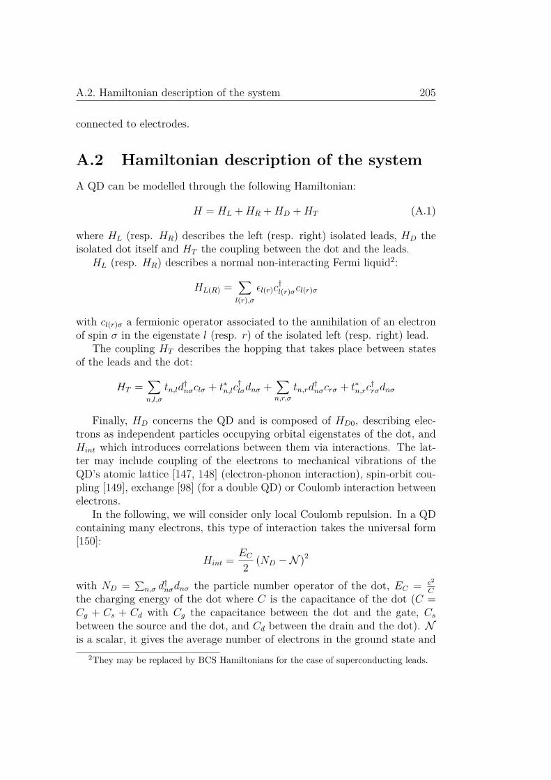
A.2. Hamiltonian description of the system 205
connected to electrodes.
A.2 Hamiltonian description of the systemA QD can be modelled through the following Hamiltonian:
H = HL +HR +HD +HT (A.1)
where HL (resp. HR) describes the left (resp. right) isolated leads, HD theisolated dot itself and HT the coupling between the dot and the leads.
HL (resp. HR) describes a normal non-interacting Fermi liquid2:
HL(R) =∑l(r),σ
ϵl(r)c†l(r)σcl(r)σ
with cl(r)σ a fermionic operator associated to the annihilation of an electronof spin σ in the eigenstate l (resp. r) of the isolated left (resp. right) lead.
The coupling HT describes the hopping that takes place between statesof the leads and the dot:
HT =∑n,l,σ
tn,ld†nσclσ + t∗n,lc
†lσdnσ +
∑n,r,σ
tn,rd†nσcrσ + t∗n,rc
†rσdnσ
Finally, HD concerns the QD and is composed of HD0, describing elec-trons as independent particles occupying orbital eigenstates of the dot, andHint which introduces correlations between them via interactions. The lat-ter may include coupling of the electrons to mechanical vibrations of theQD’s atomic lattice [147, 148] (electron-phonon interaction), spin-orbit cou-pling [149], exchange [98] (for a double QD) or Coulomb interaction betweenelectrons.
In the following, we will consider only local Coulomb repulsion. In a QDcontaining many electrons, this type of interaction takes the universal form[150]:
Hint = EC2
(ND − N )2
with ND = ∑n,σ d
†nσdnσ the particle number operator of the dot, EC = e2
C
the charging energy of the dot where C is the capacitance of the dot (C =Cg + Cs + Cd with Cg the capacitance between the dot and the gate, Csbetween the source and the dot, and Cd between the drain and the dot). Nis a scalar, it gives the average number of electrons in the ground state and
2They may be replaced by BCS Hamiltonians for the case of superconducting leads.

206 A. Introduction to Quantum dots
depends on voltages applied on the gate and the source. This description, inwhich we parametrize the Coulomb interaction by a constant capacitor C, isactually fully justified only for large dots in which N ≫ 1. Validity of thisapproach is discussed in great details in Ref. [151, 152].
Physics of such system is governed by the interplay between the couplingof the QD to the leads which allows current to flow between L and R, and Hint
which tends either to limit this flow, or to localize a spin in the QD driving theground state in a highly correlated Kondo state. In the following discussion,we will distinguish two cases: weakly coupled QDs (⟨HT ⟩ ≪ ⟨Hint⟩) andstrongly coupled QDs (⟨HT ⟩ ≫ or ≈ ⟨Hint⟩).
A.3 Weakly coupled QDs
For an interacting QD weakly coupled to its leads (⟨HT ⟩ ≪ ⟨Hint⟩), we canaddress interactions in an essentially classical way (see for example Ref. [113])where the physics is governed by the quantization of the charge. Indeed, inthis case, the dot can be considered as isolated (H ≈ HD) and eigenstates ofthe system are given by the familiar classical state: one charge in the dot,two charges in the dot, etc... The number of charge can be regarded as aclassical variable. This assumption is completely valid if the time spent byan electron in the dot is the largest time scale of the system including thecoherence time: we will say that the system is in the classical regime.
In this regime and provided that energies ϵnσ are unaffected by interac-tions, the ground state energy of the system containing N electrons is givenby [117]:
U (N) = 12C
[e (N −N0) − CgVg − CsV ]2 +∑N
ϵnσ
where Vg is the voltage applied on the gate, V the voltage applied on thesource (the drain is grounded), N0 the number of electrons3 in the dot whenV = Vg = 0, and the sum in the last term runs over all the occupied state.
From U (N), we can deduce the electronic transport properties of thesystem. In particular, we can describe how the QD is sequentially filledwhen tuning the backgate, and also the so-called Coulomb blockade.
3We need to mention that in systems with a large number of electrons, we do not knowN0. We use as a variable the number of electrons in excess (N −N0).

A.3. Weakly coupled QDs 207
A.3.1 Sequential fillingIn this regime, we can perform a sequential filling of the QD, electron byelectron and orbital after orbital. Indeed, if µ is the common electrochemical-potential of the left and right leads, the condition for the QD to contain Nelectrons is:
µ (N + 1) > µ > µ (N)
with µ (N) the electro-chemical potential of the dot when it contains Nelectrons:
µ (N) = U (N + 1) − U (N)
Thereby, increasing the gate voltage, we can bring µ (N + 1) below µ andadd an extra electron in the dot.
This is illustrated in Fig. A.2 (adapted from figure 2. (b) of Ref. [117])where orbitals are represented by black circles (whose radii indicate the rel-ative magnitude of the orbital energies), electrons by blue dots, and the reddot symbolizes the center of the QD. At the beginning of this sequence, theQD is singly occupied with, in the lower orbital, an electron that is free tochoose its spin. Increasing Vg, we add, in the same orbital, a second electronthat, due to the Pauli principle, must be of exactly opposite spin. Despitethe degeneracy of these two states, this process can only happen if the systemis sufficiently lowered in energy (with the gate) to compensate the chargingenergy EC . If we continue to increase Vg, we will add a third electron in thesystem but in the next orbital. The addition energy includes this time thecharging energy plus the energy difference between orbitals ∆E = ϵn+1σ−ϵnσ.The fourth electron will end in the same orbital but with a spin that is theexact opposite of the third one.
Note that this simple sequential filling of the orbitals is not always ob-served. For instance, in QDs with a reduced number of electrons [143], andwith a shell of degenerate orbitals, this shell is first filled, by virtue of Hundsrule, with electrons of parallel spins until the shell is half full. After that, thefilling continues with anti-parallel spins. Also, in QDs with reduced numberof electrons, the charging energy may vary from one orbital to another.
A.3.2 Coulomb spectroscopy and Coulomb diamondsThe fact that the QD fills sequentially allows to perform a Coulomb spec-troscopy of the QD. It can be realized through measurements of the differ-ential conductance between the left source and the right drain at V = 0.Each time the QD’s electro-chemical potential is equal to those of the leftand right electrodes µ, electrons can flow through the QD and a peak of

208 A. Introduction to Quantum dots
Increasing Vg
EC EC EC+ǻE
Schematic representation of electron additions in orbitals ofa QD
Figure A.2: When a first electron is occupying an orbital, addition of asecond electron costs an extra energy EC = e2/C. As the orbital can holdonly two electrons, the second one is necessarily of opposite spin (by virtueof the Pauli principle), moreover addition of a third electron will take placein the next orbital and will cost EC + ∆E with ∆E = ϵn+1σ − ϵnσ the energydifference between orbitals.

A.3. Weakly coupled QDs 209
conductance develops whose width ∼ kBT is imposed, in this regime, bythe temperature (T is the temperature and kB is the Boltzmann constant)[113]. As a consequence, provided that the charging energy EC is constantand kBT < EC , we have a direct measurement of the relative orbital energiesϵnσ. For example, in the sequence pictured in Fig. A.2, by increasing Vgwe would observe three consecutive peaks of differential conductance withdistance between them corresponding to ∆Vg = EC+∆E
Cg/Cbetween the first two
peaks and only ∆Vg = EC
Cg/Cbetween the second and the third.
Extending this Coulomb spectroscopy to finite voltage bias, we obtain theso-called Coulomb diamonds. Indeed, when a voltage V is applied betweenthe left and right leads, the condition for the QD to carry electrons from theleft to right electrode (resp. from the right to left electrode) is µL ≥ µ (N) ≥µR (resp. µL ≤ µ (N) ≤ µR) with µL and µR the electrochemical potentialsof the left and right leads (with µL − µR = −eV ). These conditions definein the (Vg, V ) plane, areas of blockade for each N , which take the shape ofdiamonds and where the charge in the QD is well defined.
In Fig. A.3, we have represented these diamonds for N = 2n+ 1, 2n+ 2,2n + 3 and 2n + 4 (n is an arbitrary integer). Widths and heights of thesediamonds are directly related to their corresponding addition energies. Evendiamonds (i.e. areas where the QD contains an even number of charge) arethus larger than odd diamonds: when N is even, addition of an electronnecessarily takes place in the next orbital and the addition energy includesthe charging energy plus the energy difference between orbital ∆E.
The Coulomb blockade has been observed extensively in CNTs and hasallowed, for example, to observe the fourfold degeneracy through periodicityof the diamonds [153, 154, 145], electron-hole symmetry in semiconductingCNT [155], or spin-orbit coupling [149, 128]. Note that in these two last ref-erences the spectroscopy, though based on the same principle, was performeddifferently: in Ref. [149], the Coulomb spectroscopy was performed at fixedVg and tuning V , whereas in Ref. [128] the spectroscopy was performed inthe inelastic cotunneling regime (in this appendix, we will not address co-tunneling events that are exchange of electrons occurring between the sourceand the drain at finite V through second order coherent tunneling processes).
Whereas the classical description we have presented so far is sufficientto understand physics related to the charge quantization, it cannot howeverdescribe phenomena that are of coherent nature like coherent exchange ofelectrons between the QD and its leads. It is indeed only valid under theassumptions that ⟨HT ⟩ ≪ ⟨Hint⟩ but also if particles systematically lose theircoherence during the time spent in the QD. In the following, we present aphenomenological approach, from Ref. [16], which allows to address coherent

210 A. Introduction to Quantum dots
V
Vg
µ(N) = µR µ(N) = µL
Blockade regions
g
S
C
C
g
g d
C
C C
E
e
CE
e
2n+1 2n+3 2n+4 2n+2
/C
g
E E
C C
Coulomb diamondsFigure A.3: Schematic representation of four Coulomb diamonds in the(Vg, V ) plane. In regions of blockade (in violet), the charge in the QD iswell defined and takes values N = 2n + 1, 2n + 2, 2n + 3 and 2n + 4 (n isan arbitrary integer). Borders of this violet areas are defined by the con-ditions µ (N) = µL (in blue) or µ (N) = µL (in red) and, as indicated onthe diagram, slopes of these borders are related to the capacitive couplingsbetween the dot and the electrodes (including the gate). The height andthe width of a diamond is related to the addition energy which is equal tothe charging energy EC for odd diamonds and the charging energy plus theenergy difference between orbitals EC + ∆E for even diamonds.

A.4. Weakly coupled QDs in a coherent regime: a phenomenologicalapproach 211
exchange of electrons between the QD and its leads in the weakly coupledregime.
A.4 Weakly coupled QDs in a coherent regime:a phenomenological approach
Whereas coherence of electrons in non-interacting QDs can be elegantly ad-dressed with the scattering approach of Büttiker [56], and the interplay be-tween charge and energy quantization can be correctly described with a semi-classical constant interaction model [113, 117], the simplest available modelwhich brings together all these ingredients is the Anderson impurity model[63]. Unfortunately, and as mentioned before, there has been so far no exactsolution found for this model. It has been yet analyzed using various approx-imations such as mean-field theory, perturbation expansion in the Coulombinteraction or in the tunnel coupling, but also exact numerical simulationsbased on the numerical renormalization group (NRG) (an exhaustive list ofthese methods can be found in Ref. [49] for the case of a QD connected tonormal electrodes and Ref. [16, 71] and references therein for superconduct-ing electrodes). However, all these methods either suffer of inaccuracy or aresimply too much time-demanding.
A.4.1 A phenomenological approachIn Ref. [16], Vecino et al. have developed an effective and exactly solvablemodel which can correctly describe, for weakly coupled QDs, the coherentexchange of electrons between an interacting QD and its leads (in their work,the leads are actually superconducting and exchange electrons with the QDthrough Andreev reflections, but here we will only consider the case of normalelectrodes in order to focus on the way they addressed interaction). Thisapproach is based on a Hartree-Fock approximation. They describe the QDconnected to its electrodes by means of a single-orbital Anderson model [63]:
H = HL +HR +∑σ=↑,↓
ϵ0d†σdσ + ECn↑n↓ +
∑σ=↑,↓
(tLd
†σclσ + tRd
†σcrσ + h.c.
)
where ϵ0 is the energy of the single orbital and nσ = d†σdσ. Then, the central
approximation consists in replacing phenomenologically the repulsive inter-action inside the QD by a local exchange field in such a way that:
ϵ↑ = ϵ0 − U
2

212 A. Introduction to Quantum dots
ϵ↓ = ϵ0 + U
2with U a constant and ϵ↑ (resp. ϵ↓) the energy of a spin up (resp. down)electron in the QD. In absence of bias voltage between the leads, these ener-gies can be related to the gate voltage as we have (with notations of previoussection):
ϵ0 = µ− eCgCVg
We end up with an effective (non-interacting) Hamiltonian describing thesystem:
Heff = HL +HR +∑σ=↑,↓
ϵσd†σdσ +
∑σ=↑,↓
(tLd
†σclσ + tRd
†σcrσ + h.c.
)
where dσ is an annihilation operator for an electron of spin σ and the lastterm describes the coupling with the leads.
This model is formally equivalent to a mean field solution of HamiltonianA.1, with the prescription U = EC
⟨n↓−n↑⟩2 , except that here we will choose
that U is a constant instead of calculating it self-consistently. It should benoted that, whereas in the classical approach of section A.3 spins of electronswere only taken into account through Pauli principle, here, an arbitraryspin is attributed to each level of the QD. If this can appear as an abusivesymmetry breaking4 introduced in the model, one has to keep in mind thatthe spin axis of quantization is actually not even specified. This choice justimplies that if a second electron is added in the QD, it must have a spinopposite to that of the first one.
In the end, this model combines the advantages of a complete Hamiltoniantreatment which allows to take into account the coherence of the system, andthe ingredients of the classical approach: electrons take opposite spins withinan orbital and fill sequentially the QD when increasing the gate. Except, here,the energies of the addition spectrum are replaced by single particle energylevels with the correspondence:
µ (1) ↔ ϵ↑ and µ (2) ↔ ϵ↓
In this thesis, we extensively used this phenomenological approach of Ve-cino et al., to explain the formation of Andreev bound States in an interactingQD connected to superconducting leads.
4Broken symmetry is possible when the object that breaks the symmetry involves amacroscopic number of degrees of freedom, but here, we are dealing with a single spin.

A.5. QDs with stronger coupling 213
A.4.2 Limits of this effective non-interacting modelThis effective non-interacting model provides correct descriptions for mech-anism based on single particle phenomena. It captures, for example, thebroadening of the QD’s levels caused by the coupling to leads with a con-tinuum of states (reduction of quasiparticles’ lifetime), or some aspects ofthe formation of Andreev Bound States when the leads are superconduct-ing (see chapter 3 for comparison between exact NRG and phenomenologicalapproach calculations).
There are however some shortcomings related to the fact that this ap-proximation by essence completely ignores effects due to correlations betweenelectrons. For example, as the spin operator:
S = d†↑d↑ − d†
↓d↓ +∑l
c†l↑cl↑ − c†
l↓cl↓ +∑r
c†r↑cr↑ − c†
r↓cr↓
commute with Heff , spins of electrons are completely frozen and cannotfluctuate. Yet, in presence of interactions, electrons localized in the dotalways have a certain quantum mechanical amplitude for their spin to flipby inversion with an electron of opposite spin from the electrodes. Thecorresponding spin flip rate τsf defines a temperature scale [17]:
kBTK = ~τsp
called the Kondo temperature above which these fluctuations are driven bythermal activation rather than quantum correlations. However for T < TK ,these fluctuations are quantum and lead to the formation of a many-bodyKondo singlet state in which electrons of the leads screen the magnetic mo-ment formed by electrons localized in the dot. In the following section, wediscuss this phenomenon which arises when an interacting QD is stronglycoupled to its leads
A.5 QDs with stronger couplingFor QDs which are more strongly coupled to their leads, the picture of a se-quential filling with single electrons is generally not correct. One can mentionthe particular case of electronic devices made with single nanotubes whichare so strongly coupled to their leads that charging effect becomes negligible.The CNTs thus act as coherent electron waveguides [7, 141] and electronictransport measurements can be understood within the Landauer-Büttikerformalism. This is called the Fabry-Perot regime. In this section, we focus

214 A. Introduction to Quantum dots
on an intermediate case in which the coupling to the leads is strong andthe Coulomb repulsion plays an important role driving the system into theKondo regime in which electrons are highly correlated.
A.5.1 Spin-1/2 Kondo effect in nanostructuresThe concept of Kondo state was originally introduced by Kondo to explain ananomalous increase of resistance which occurs in some metals at low temper-ature [49]. This phenomenon arises because of the formation, around residualmagnetic impurities, of clouds of conduction electrons which scatter chargecarriers near the Fermi level. In the ground state of the system, the magneticmoment and the conduction electrons form then a many-body singlet state.
The recent possibility to fabricate confined conductors has allowed toobserve the Kondo effect on artificial magnetic impurities constituted bylocalized electrons [118, 126] and study this many-body phenomenon in acontrolled way. The competition between coherent exchange of electronswith the leads and Coulomb repulsion inside the QD may indeed drive thesystem into a Kondo state. Because of Coulomb repulsion, a single electroncan be trapped in the dot and form a localized magnetic moment. If thecoupling to the leads is strong enough, the conduction electrons of the leadstends to screen this artificial magnetic impurity. This can be formally seenperforming a Schrieffer-Wolff transformation on the Anderson Hamiltonian[65] which changes HT+Hint into an antiferromagnetic interaction of the formJ × Scond.SQD between the localized electron and the conduction electrons(SQD is the spin of the QD, Scond is the sum of the spins of the conductionelectrons and J is the strength of the antiferromagnetic interaction).
In nanostructures, the Kondo effect manifests by the apparition of a peakof density of states at the Fermi level (or an enhancement of the conductiv-ity, up to perfect transmission, at zero voltage bias in electronic transportexperiment) for temperature below the so-called Kondo temperature. Asa consequence, differential conductance measurements show, as in previoussection, a Coulomb blockade pattern with Kondo ridge around V = 0 inareas of blockade corresponding to an odd number of charge in the QD (seeFig.A.4).
The Kondo temperature depends both on the strength of the Coulombrepulsion U and the coupling to the leads Γ = πρ0 (t2L + t2R) and takes thefollowing form [49, 115, 119, 121]:
kBTK =√
ΓU2
exp(πϵ0 (ϵ0 − U)
2ΓU
)
A.5. QDs with stronger coupling 215
V
Vg
µ(N) = µR µ(N) = µL
Blockade regions
2n+1 2n+3 2n+4 2n+2
Kondo ridge
0
Figure A.4: Schematic representation of differential conductance measure-ments for a QD in the Kondo regime. The pattern is similar to the oneof Fig. A.3 except that peaks of conductance, also called Kondo ridges, hasappeared around V = 0 in diamonds corresponding to an odd number of elec-trons in the QD. These ridges appear at low temperature and their width isgiven by the Kondo temperature.
Note that since there is no analytic solution to the Kondo problem, thisformula derived by Haldane is not expected to be exact. For increasingtemperature, the zero-bias conductance amplitude in a quantum dot obeysa logarithmic dependence with T/TK and completely disappears when T isfar above TK . When T ≪ TK , this energy scale also gives the HWHM of theconductance peaks through the relation:
HWHM ∼ kBTKe
A.5.2 Variety and universality of the Kondo effectThe Kondo effect has now been observed in a wide variety of man-madenanostructures: carbon nanotubes connected to normal [96], ferromagnetic[98] or superconducting contacts [9], molecular devices (see the review [119]and references therein) including fullerene [101] or adatoms deposited on ametallic surface [21, 156].
Moreover, it has also been seen in various type of situations: in doubleQDs [103], in systems with two degenerate orbitals [97], or in which the arti-ficial magnetic impurities is not constituted by the spin of a single localized

216 A. Introduction to Quantum dots
electron but rather by its orbital momentum [157] or the spins of two local-ized electrons in a triplet-state (S = 1). In the latter case, a major changewith the spin-1/2 Kondo effect comes from the fact that the spin-1 Kondoeffect happens for an even number of electrons localized in the QD [102] andinvolves two channels of screening.
In all these experiments, the various kind of many-body Kondo statesdiffer in the details of their manifestation (double peak structure in doubleQDs, nonmonotonic temperature dependence of the Kondo ridge amplitudefor S = 1 with much weaker Kondo temperature than for S = 1/2...), butshare common robust universal features [158]: peaks of density of states atlow energy, reduction of the zero-bias conductance with temperature, maxi-mum transmission at V = 0, universal scaling with T/TK ...

Appendix B
Quantum dot Green’s function
In this appendix we give some general definitions on Green’s functions forsystem at equilibrium (section B.1 and B.2) and explain how to calculatethe quantum dot’s (QD) Green’s function (GF) using equation of motiontechniques (section B.3). In the last section, we show useful identities forcalculation of the supercurrent and tunnel current, between lesser, greater,retarded and advanced GFs.
In all this appendix, Hamiltonian H is time-independent. In the particu-lar case of a QD connected to superconducting electrodes, this supposes thatnone of the electrodes are voltage biased.
B.1 Definitions of the QD’s GFs and TDOS
B.1.1 Green’s functions in real timeThe QD’s GF is a causal correlation function from which can be calculatedphysical observables of the QD. In Nambu notation and time domain, it takesthe form1:
Gdd (t) = −i⟨Ttψd (t)ψ†d (0)⟩
= −i(
⟨Ttd↑ (t) d†↑ (0)⟩ ⟨Ttd↑ (t) d↓ (0)⟩
⟨Ttd†↓ (t) d†
↑ (0)⟩ ⟨Ttd†↓ (t) d↓ (0)⟩
)
with t a time variable, ψd (t) = eiHtψde−iHt the Heisenberg notation for the
QD spinor field operator taking ~ = 1 (we choose this convention for the1We consider a problem with a time-independent Hamiltonian (or in other words a
system invariant by translation in time) such that ⟨Ttψd (t− t′)ψ†d (0)⟩ = ⟨Ttψd (t)ψ†
d (t′)⟩.We can thus only consider correlation functions of the form ⟨Ttψd (t)ψ†
d (0)⟩.
217

218 B. Quantum dot Green’s function
all appendix) and H the Hamiltonian. Tt is the time-ordering operator, itpreserves causality of the Green’s functions and is defined by:
Ttψd (t)ψ†d (0) = θ (t)ψd (t)ψ†
d (0) − θ (−t)ψ†d (0)ψd (t)
with θ (t) the Heavyside function, and the brackets ⟨A⟩ symbolizes a thermalaverage of the quantum operator A. It can be expressed with the densitymatrix operator ρ:
ρ ≡ e−βH
Z= 1Z
∑α
|α⟩e−βEα⟨α|
with |α⟩ a complete basis set of the system, Eα the energy of state |α⟩,β = 1/kBT (with kB the Boltzmann constant and T the temperature) andZ = Tr
[e−βH
]is the partition function. With this definition we have:
⟨A⟩ = Tr [ρA] = 1Z
∑α
⟨α |A|α⟩e−βEα (B.1)
At T = 0, this thermal average becomes an expectation value of A in thesystem ground state |ψ0⟩: ⟨ψ0 |A|ψ0⟩.
B.1.2 Retarded and advanced Green’s function in realtime
We can also define the retarded and advanced GF of the QD by:
GRdd (t) = −iθ (t) ⟨
ψd (t) , ψ†
d (0)⟩ (B.2)
GAdd (t) = iθ (−t) ⟨
ψd (t) , ψ†
d (0)⟩ (B.3)
with: ψd (t) , ψ†
d (0)
=
d↑ (t) , d†↑ (0)
d↑ (t) , d↓ (0)
d†↓ (t) , d†
↑ (0)
d†↓ (t) , d↓ (0)
and A,B = AB + BA the anticommutator. They are useful for TDOScomputation of the QD.
For supercurrent and tunnel current calculation, we need also to introducethe greater and lesser GF:
G>id (t) = −i⟨ψi (t)ψ†
d (0)⟩
G<id (t) = i⟨ψd (0)† ψi (t)⟩
where i = l or r are index for the states of the left and right leads.

B.2. Matsubara formalism and equation of motion 219
B.2 Matsubara formalism and equation of mo-tion
The QD GF can be obtained by resolution of the equation of motion (EOM),a Heisenberg-like equation for GFs. This resolution is particularly simple inMatsubara formalism.
Here we introduce GFs in the Matsubara formalism and their EOM.
B.2.1 Notation in Matsubara imaginary timeFor calculation of the QD’s GF, it is convenient to introduce GFs in Matsub-ara formalism in which time and frequency arguments are imaginary quan-tities. They are defined by:
Gdd (τ) = −⟨Tτψd (τ)ψ†d (0)⟩
= −(
⟨Tτd↑ (τ) d†↑ (0)⟩ ⟨Tτd↑ (τ) d↓ (0)⟩
⟨Tτd†↓ (τ) d†
↑ (0)⟩ ⟨Tτd†↓ (τ) d↓ (0)⟩
) (B.4)
with τ real, ψd (τ) = eHτψde−Hτ (the Heisenberg notation in imaginary time
for the QD spinor field operator) and Tτ is a time-ordering operator actingon variable τ :
Tτψd (τ)ψ†d (0) = θ (τ)ψd (τ)ψ†
d (0) − θ (−τ)ψ†d (0)ψd (τ)
B.2.2 Fourier transform of the Matsubara GFThe imaginary time QD’s GF can be expressed in frequency domain byFourier transformation. And as we have the property Gdd (τ + β) = −Gdd (τ)(this can be shown from expression − 1
ZTr
[e−βHTτψd (τ)ψ†
d (0)]
of the GF,see for example [65]), the QD’s GF Gdd (iωn) is then defined only on Matsub-ara frequencies ωn taking discrete values:
ωn = 2n+ 1β
π with n ∈ Z and β = kBT
with:
Gdd (τ) = 1β
+∞∑n=−∞
e−iωnτ Gdd (iωn) and Gdd (iωn) =ˆ β
0eiωnτ Gdd (τ) dτ
The Fourier transform Gdd (iωn) can be extended by analytical continuationeverywhere in the complex plane into Gdd (z).
220 B. Quantum dot Green’s function
The retarded and advanced GFs’ Fourier transform are given by the valueof this analytical continuation approaching the real axis from the upper andlower half of the complex plane (see section B.4), respectively2 (here ω andη are real, and η → 0+):
GRdd (ω) = Gdd (ω + iη)
GAdd (ω) = Gdd (ω − iη)
They give access to every observable of the system at equilibrium [159].
B.2.3 Equation of motionGFs can be calculated by resolution of the equation of motion (EOM). Thelatter is obtained by derivation of matrix B.4 with respect to time:
∂Gdd (τ)∂τ
= −∂θ (τ)∂τ
⟨ψd (τ)ψ†
d (0)⟩+∂θ (−τ)
∂τ
⟨ψ†d (0)ψd (τ)
⟩−⟨Tτ
∂ψd (τ)∂τ
ψ†d (0)⟩
from which we can deduce the final form of the EOM:
∂Gdd (τ)∂τ
= −δ (τ)⟨ψd (0) , ψ†
d (0)⟩
− ⟨Tτ∂ψd (τ)∂τ
ψ†d (0)⟩ (B.5)
In the following section, we solve this equation for a QD connected to super-conducting leads.
B.3 Calculation of the QD’s GF by resolutionof the EOM
Here we calculate the QD’s GF by resolution of the EOM.We recall from section 3.1.1 that the QD is described by the following
Hamiltonian:
H =∑i=l,r
ψ†iEiψi + ψ†
dEQDψd +∑l
[ψ†dETL
ψl + h.c.]
+∑r
[ψ†dETR
ψr + h.c.]
with EQD =(ϵ↑ 00 −ϵ↓
), El(r) =
(ϵl(r) ∆eiϕL(R)
∆e−iϕL(R) −ϵl(r)
), and ETL(R) =
(tL(R) 0
0 −t∗L(R)
).
2These expressions in the frequency domain are of course consistent with Eq. B.2 andB.3 where retarded and advanced GF are expressed in time-domain (see Ref. [65]).

B.3. Calculation of the QD’s GF by resolution of the EOM 221
B.3.1 Resolution of the EOMThe GF, that will give us access to the spectral density of the dot, Gdd (τ) isobtained by resolution of the EOM B.5. The latter starts by calculating theanticommutators
ψd (0) , ψ†
d (0)
and the derivative ∂ψd(τ)∂τ
:
⟨ψd (0) , ψ†
d (0)⟩
=
⟨d↑, d†↑
⟩⟨d↑, d↓⟩⟨
d†↓, d
†↑
⟩ ⟨d†
↓, d↓⟩ =
(1 00 1
)= 1
∂ψd (τ)∂τ
=(
[H, d↑ (τ)][H, d†
↓ (τ)] ) = −EQDψd (τ) −
∑l
ETLψl (τ) −
∑r
ETRψr (τ)
It can then be written in a Schrödinger like form:
∂Gdd (τ)∂τ
= −δ (τ) 1 − EQDGdd (τ) −∑l
ETLGld (τ) −
∑r
ETRGrd (τ)
With the same method, we can also write the equations of motion followedby Gl(r)d (τ):
∂Gl(r)d (τ)∂τ
= −El(r)Gl(r)d (τ) − ETL(R)Gdd (τ)
Fourier transformations in Matsubara frequency of these equations providesthe central linear system whose solutions are our quantities of interest:−iωnGdd (iωn) = −1 − EQDGdd (iωn) −∑
l ETLGld (iωn) −∑
r ETRGrd (iωn)
−iωnGl(r)d (iωn) = −El(r)Gl(r)d (iωn) − E†TL(R)
Gdd (iωn)(B.6)
The second equation of B.6 gives the expression of Gl(r)d (iωn) as a functionof Gdd (iωn):
Gl(r)d (iωn) =[iωn − El(r)
]−1E†TL(R)
Gdd (iωn) (B.7)This matrix is useful for Josephson current calculation. But for the momentby combining it with first equation of B.6 we can solve the system and extendthe GF to all the complex plane by replacing iωn by z, where z can take anyvalue in the complex plane:
Gdd (z) =[z − EQD − Σ (z)
]−1(B.8)
with:Σ (z) = ΣL (z) + ΣR (z)
ΣL (z) =∑l
ETL[z − El]−1 E†
TL

222 B. Quantum dot Green’s function
ΣR (z) =∑r
ETR[z − Er]−1 E†
TR
To make this expression usable for further spectral density calculation,we need in a last step to evaluate the self-energy due to the coupling to theleads Σ (z).
B.3.2 Calculation of the QD’s self-energyThe self-energy takes the form of two discrete sums over l and r:
ΣL(R) (z) =∑l(r)
|tl(r)|2
z2 − ϵ2l(r) − ∆2
(z + ϵl(r) ∆eiϕL(R)
∆e−iϕL(R) z − ϵl(r)
)
To get rid of the discrete sum we need to make some assumptions, in orderto replace it by an integral. As the superconducting gap ∆ is generally ordersof magnitude smaller than the bandwidth D (∆ ≪ D: ∆ of aluminum is 210µeV when bandwidth D is several eV large), we can reasonably approximateD as infinite and that the bands are flat. Within these assumptions, theself-energy becomes:
ΣL(R) (z) =ˆ +∞
−∞ρF
|tL(R)|2
z2 − ϵ2 − ∆2
(z + ϵ ∆eiϕL(R)
∆e−iϕL(R) z − ϵ
)dϵ
with ρF the density of states for each spin population at the Fermi energy(in fact at any energies within our approximations) of the electrodes in theirnormal state.
Because ϵz2−ϵ2−|∆|2 is an odd function with respect to ϵ, its integration
from −∞ to +∞ is equal to zero and gives no contribution to Σ (z).By performing the variable change x = ϵ√
∆2−(iωn)2 , we obtain the final
expression for Σ (z):
Σ (z) =∑i=L,R
− ρF |ti|2√∆2 − z2
(z ∆eiϕi
∆e−iϕi z
)ˆ +∞
−∞
11 + x2dx
=∑i=L,R
πρF |ti|2√∆2 − z2
(−z −∆eiϕi
−∆e−iϕi −z
)
With the introduction of functions g (ω) = −ω√|∆|2−ω2
and f (ω) = ∆√∆2−ω2 ,
the self-energy adopts then the compact form:
Σ (z) =∑i=L,R
Γi(
g (z) −f (z) eiϕi
−f (z) e−iϕi g (z)
)
where ΓL(R) = πρF∣∣∣tL(R)
∣∣∣2.

B.3. Calculation of the QD’s GF by resolution of the EOM 223
B.3.3 Comment on the temperature dependence of theQD’s GF
According to the final expression of Gdd (z) and Σ (z), there is no temperaturedependence of the TDOS Add (ω), given by the imaginary part of the retardedGF (see section 3.1.2 in chapter 3). Even if nowhere in the calculation we havespecified at which temperature we calculate expectation values of operators.
The reason is that ∆ and U are considered, in our model, as fixed phe-nomenological parameters. They should however be calculated self-consistently,and in this case they would exhibit a temperature dependence (see for ex-ample [63] or [65]). A temperature variation would cause a redistribution ofAdd (ω) over the energy spectrum. This is actually a general property of thestrongly correlated system, but in our case we use an effective model of freequasiparticles, that’s why there is no temperature dependence (the spectraldensity of a Fermi liquid for example has also no temperature dependence).
Yet, there are a temperature dependence of the tunnel current. Indeedthe latter depends not only on the spectral density of the probe and thesample, but also on their thermal distributions (see appendix D).
B.3.4 Poles as roots of the inverse GF’s determinantThe poles of the GF’s diagonal elements are also the roots of the inverse GF’sdeterminant.
Indeed, equation B.8 can also be written:
Gdd (z) = 1Det
(z − EQD − Σ (z)
) tcom[z − EQD − Σ (z)
]
where tcom[z − EQD − Σ (z)
]is the transposed comatrix of
[z − EQD − Σ (z)
].
As elements of tcom[z − EQD − Σ (z)
]have no pole except at ±∆, poles of
the diagonal element of Gdd (z) are given by the roots ofD (z) = Det(z − EQD − Σ (z)
)or equivalently by Det
(Gdd (z)−1
)= 0.
B.3.5 Physical signification of a GFDue to its physical signification, a GF is also called a propagator. Indeed, itsdiagonal elements contain information about the evolution of a bare particle(electron or hole) injected in the system, and its antidiagonal elements aboutthe tendency for electrons to exist in pair in the ground state.

224 B. Quantum dot Green’s function
If we consider, for example, the case t > 0, the spin up diagonal elementsof the GF is proportional to:
⟨ψ0|eiHtd↑e−iHtd†
↑|ψ0⟩ (B.9)
This function is the recovering between states:
e−iHtd†↑|ψ0⟩
and:
d†↑e
−iHt|ψ0⟩
The first one gives the dynamic of a spin up electron injected in the groundstate, through the QD, that we let evolve under H during a time t, whereasthe second corresponds to a spin up electron injected in the system at t.Function B.9 compares this two states to test how much the injected elec-tron has changed, and gives through its decaying time information on theelectron’s lifetime (infinite if the injected particle corresponds to an eigen-state of the system). For t < 0, the diagonal spin up element of the GF fulfilsthe same role but for a hole injected in the QD.
The non diagonal terms of the GF (or anomalous correlation functions),they contain information about pairing between electrons of opposite spin inthe QD. For example:
⟨ψ0|eiHtd†↓e
−iHtd†↑|ψ0⟩
is the recovering product between states:
e−iHtd†↑|ψ0⟩
and:
d↓e−iHt|ψ0⟩
It gives therefore the probability amplitude to find, after a lapse time t, thetime-reverse conjugated hole of an electron injected in the QD. In absenceof induced superconductivity, these correlations functions would be equalto zero for charge conservation consideration. However, superconductivityauthorizes charge fluctuations and these anomalous correlation functions canbe different from zero.

B.4. Useful identities for calculation of the tunnel Density of states andsupercurrent 225
B.4 Useful identities for calculation of thetunnel Density of states and supercur-rent
In this section, we give demonstrations of the following relations (valid forany time-independent Hamiltonian):
fFD (−ω)[GRld (ω) − GA
ld (ω)]
= G>ld (ω) and −fFD (ω)
[GRld (ω) − GA
ld (ω)]
= G<ld (ω)
(B.10)where fFD (ω) is the Fermi-Dirac distribution. These relations are useful forcalculation of the supercurrent (see section 3.1.5) and the tunnel current (itis done in section D.1.2.2).
First, we need to introduce the Lehmann representation of the advancedand retarded GF.
B.4.1 Lehmann representationThe Lehmann representation of a GF function is a decomposition on theeigenstates basis of H, noted |α⟩. To illustrate it, we consider a GF in realtime:
G (t) = −i ⟨Tta (t) b⟩ = −iZ
∑α
e−βEα (θ (t) ⟨α |a (t) b|α⟩ − θ (−t) ⟨α |ba (t)|α⟩)
where a and b are two operators creation or annihilation.Using the property3 ∑
α′ |α′⟩⟨α′| = I, we can write these GF:
G (t) = − iZ
∑α,α′ e−βEα(θ (t)
⟨α∣∣∣eiHtae−iHt |α′⟩⟨α′| b
∣∣∣α⟩−θ (−t)
⟨α∣∣∣b |α′⟩⟨α′| eiHtae−iHt
∣∣∣α⟩)and as we have H|α⟩ = Eα|α⟩, it becomes:
G (t) = − iZ
∑α,α′ e−βEα(θ (t) ei(Eα−Eα′ )t ⟨α |a |α′⟩⟨α′| b|α⟩
−θ (−t) ei(Eα′ −Eα)t ⟨α |b |α′⟩⟨α′| a|α⟩)
After Fourier transform, we end up with the Lehmann representation ofG (t):
G (ω) = 1Z
∑α,α′
e−βEα
(⟨α |a |α′⟩⟨α′| b|α⟩ω + iη + Eα − Eα′
+ ⟨α |b |α′⟩⟨α′| a|α⟩ω − iη − Eα + Eα′
)
3I is the identity operator.

226 B. Quantum dot Green’s function
where the inverse and direct Fourier transform a of function h are respectivelygiven by:
h (t) =ˆh (ω) e−iωtdω
2πand h (ω) =
ˆh (t) eiωtdt
and the Heaviside function Fourier transform (with η → 0+)4:ˆθ (t) eiωtdt = i
1ω + iη
andˆθ (−t) eiωtdt = −i 1
ω − iη
Following the same reasoning, we can find the Lehmann representationof the retarded (GR (ω)) and advanced (GA (ω)) GF:
GR (ω) = 1Z
∑α,α′
e−βEα
(⟨α |a |α′⟩⟨α′| b|α⟩ω + iη + Eα − Eα′
+ ⟨α |b |α′⟩⟨α′| a|α⟩ω + iη − Eα + Eα′
)(B.11)
GA (ω) = 1Z
∑α,α′
e−βEα
(⟨α |a |α′⟩⟨α′| b|α⟩ω − iη + Eα − Eα′
+ ⟨α |b |α′⟩⟨α′| a|α⟩ω − iη − Eα + Eα′
)(B.12)
B.4.2 Relation between lesser, greater, advanced andretarded GFs at equilibrium
Using Lehmann representations B.11 and B.12, we can find an expression forthe greater and lesser GFs as a function of the retarded and advanced GFs.For this, we consider a greater GF with a general form (here again |α⟩ isthe eigenstates basis of H):
G> (t) = −i ⟨a (t) b⟩ = −iZ
∑α
e−βEα ⟨α |a (t) b|α⟩
where a and b are two creation or annihilation operators. Using the property∑α′ |α′⟩⟨α′| = I, we can write:
G> (t) = − i
Z
∑α,α′
⟨α |a |α′⟩⟨α′| b|α⟩ ei(Eα−Eα′ )te−βEα
After Fourier transform we find:
G> (ω) = −2iπ 1Z
∑α,α′
⟨α |a |α′⟩⟨α′| b|α⟩ δ (ω + Eα − Eα′) e−βEα (B.13)
4This can be shown using residues theorem.

B.4. Useful identities for calculation of the tunnel Density of states andsupercurrent 227
or thanks to the Dirac function:
G> (ω) = −2iπ 1Z
∑α,α′
⟨α |a |α′⟩⟨α′| b|α⟩ δ (ω + Eα − Eα′) e−βEα′eβω (B.14)
Moreover, as we have the equality 1x+iη − 1
x−iη = −2πiδ (x), the differencebetween the retarded (B.11) and advanced (B.12) GFs gives:
GR (ω)−GA (ω) = −2iπ 1Z
∑α,α′
⟨α|a|α′⟩⟨α′|b|α⟩δ (ω + Eα − Eα′)(e−βEα + e−βEα′
)This expression is actually also equal to the sum of Eq. B.13 and Eq. B.14multiplied by e−βω.
Therefore, we have the following relation between greater, advanced andretarded GF:
GR (ω) − GA (ω) = G> (ω)(1 + e−βω
)or by introducing the Fermi-Dirac distribution fFD (ω), we end up with arelation between the greater, retarded and advanced GFs:
fFD (−ω)[GR (ω) − GA (ω)
]= G> (ω) (B.15)
With the same method, we could also show:
− fFD (ω)[GR (ω) − GA (ω)
]= G< (ω) (B.16)
Note that in an out-of-equilibrium situation, H would depend on time and thedistribution would be different from the Fermi-Dirac distribution function.
Replacing a and b, by the appropriate operators we find indeed equationsB.10, useful for calculations of the Josephson current flowing through a QD.
A particular case In the particular case b = a† (useful for calculation ofthe tunnel current in section D.1.2.2), we have the relation GA (ω) = GR (ω)∗.Equations B.15 and B.16 thus becomes:
2 (1 − fFD (ω)) iIm[GR (ω)
]= G> (ω)
−2fFD (ω) iIm[GR (ω)
]= G< (ω)
or if we introduce the TDOS A (ω) = −πIm[GR (ω)
]:
− 2iπ (1 − fFD (ω)) A (ω) = G> (ω) (B.17)
2iπfFD (ω) A (ω) = G< (ω) (B.18)In appendix D, we will use Eq. B.17 and B.18 to calculate the tunnel
current flowing between the tunnel probe and the QD in our experiment.

228 B. Quantum dot Green’s function

Appendix C
Relation between ABS’senergies and Josephson current
In section 3.1.5, we have demonstrated that the Josephson current carriedby a QD connected to two superconducting leads is equal to:
IJ = 2e~
ˆfFD (ω) Re
[TrN
(IL (−ω − iη) − IL (−ω + iη)
)] dω2π
(C.1)
with:IL (z) = ΣL (z) Gdd (z)
We will call matrix IL (z) the “current GF” in the following, −e is the chargeof electron, ~ the reduced Planck constant, fFD (ω) the Fermi-Dirac distri-bution, TrN the trace in Nambu space, ΣL (z) the self-energy of the left leadand Gdd (z) the QD’s GF.
Here we show how to relate this definition of the Josephson current withthe phase derivative of the ABS’s energies ϵ±. For this we first derive anexpression of the Josephson current GF in terms of the parameters of thesystem Γ, U , etc... Then we separate this current in two contributions, onecarried by the ABSs and the other by the continuum of the QD’s TDOS. Wewill see that the first contribution is given by the phase derivative of ϵ±.
C.1 Josephson current carried by a S-QD-Sjunction
In this section, we derive an expression of the Josephson current expressed interms of the system’s parameters. For this, we first perform a symmetriza-tion, based on current conservation, of the current GF with respect to the
229

230 C. Relation between ABS’s energies and Josephson current
left and right leads. We take afterward its trace in Nambu space to end upwith a simple form for the Josephson current.
C.1.1 Symmetrization of the current GF
Current conservation Expression C.1 was originally obtained in section3.1.5 from:
IJ = ie
~⟨[HT , NL]⟩ (C.2)
We can however find a symmetric expression of the Josephson current withoperator NR. For this we start with an argument of current conservation:at equilibrium the charge in the QD, given by operator ND = ∑
σ d†σdσ,
remains constant in average1. Therefore, if we write ND in its Heisenbergrepresentation we have: ⟨
dND
dt
⟩= 0 (C.3)
Then, using the fact that the QD’s charge variation is given by⟨dND
dt
⟩=
i~ ⟨[H,ND]⟩, we also have2:
⟨dND
dt
⟩= − i
~⟨[HT , NL]⟩ − i
~⟨[HT , NR]⟩ (C.4)
Combining Eq. C.2, C.3 and C.4, we can finally write an expression of theJospehson current with operator NR:
IJ = −ie
~⟨[HT , NR]⟩ (C.5)
In the following, we will use both Eq. C.2 and C.5 to express the current,so we note for convenience IJL = ie
~ ⟨[HT , NL]⟩ and IJR = ie~ ⟨[HT , NR]⟩, where
IJL (resp. IJR) is the current going out of the left (resp. right) electrode.It is interesting to note that, combining Eq. C.3 and C.4, we can show thatIJL = −IJR and thus that the current is conserved along the circuit.
1In a real closed system, the charge is of course always constant. But in our model, itis only true in average as we describe the leads with mean-field BCS Hamiltonians whichdo not conserve the charge and induce fluctuations.
2This comes from the fact that, for our Hamiltonian: [H,ND] = − [HT , NL]− [HT , NR]which can be straightforwardly shown by calculating the commutators.

C.1. Josephson current carried by a S-QD-S junction 231
Symmetrization Using the relation between the Josephson current goingout of the left and right electrode IJL = −IJR, we can write a more symmetricexpression of the Josephson current IJ . Indeed, for any constant x, we have3:
IJ = xIJL − (1 − x) IJR
If we choose x = ΓR
ΓL+ΓR, this expression becomes:
IJ = 2e~
ˆfFD (ω) Re
[TrN
(I (−ω − iη) − I (−ω + iη)
)] dω2π
(C.6)
with the following definition of symmetric current GF I (z):
I (z) = ΓRΓL + ΓR
ΣL (z) Gdd (z) − ΓLΓL + ΓR
ΣR (z) Gdd (z) (C.7)
This expression is more symmetric and will naturally simplify the followingcalculations.
C.1.2 Expression of the current GFIn order to express the current GF in terms of the parameters of the sys-tem, we need first to express ΣL (z) Gdd (z) (and by deduction ΣR (z) Gdd (z))explicitly.
The starting expression of the current GF is:
ΣL (z) Gdd (z) =[
g (z) ΓL f (z) ΓLeiϕL
f (z) ΓLe−iϕL g (z) ΓL
] [z − ϵ↑ − g (z) Γ f (z)∑i Γieiϕi
f (z)∑i Γie−iϕi z + ϵ↓ − g (z) Γ
]−1
where we remind that:
g (z) = − z√∆2 − z2
and f (z) = ∆√∆2 − z2
After inversion of the second matrix, it becomes:
ΣL (z) Gdd (z) =[
g (z) ΓL f (z) ΓLeiϕL
f (z) ΓLe−iϕL g (z) ΓL
]
× 1D(z)
[z + ϵ↓ − g (z) Γ −f (z)∑i Γieiϕi
−f (z)∑i Γie−iϕi z − ϵ↑ − g (z) Γ
] (C.8)
3Indeed, as IJL = −IJR, then xIJL − (1 − x) IJR = (x+ 1 − x) IJL = IJL = IJ .

232 C. Relation between ABS’s energies and Josephson current
with D (z) the determinant of the QD’s GF inverse:
D (z) = Det(Gdd (z)−1
)= (z − ϵ↑ − g (z) Γ) (z + ϵ↓ − g (z) Γ)−f (z)2
∣∣∣∣∣∑i
Γieiϕi
∣∣∣∣∣2
From expression C.8 of ΣL (z) Gdd (z) (and the equivalent expression ofΣR (z) Gdd (z)) and Eq. C.7, we can calculate the symmetric current GF (wetake ϕL = −ϕR = δ/2 in the following to get rid of a phase factor withoutany loss of generality):
I (z) = iΓLΓR
ΓL + ΓRf (z)2 sin
(δ
2
)1
D (z)
−∑i Γieiϕi
(z−ϵ↑−g(z)Γ)f(z)
(−z−ϵ↓+g(z)Γ)f(z)
∑i Γie−iϕi
At this stage, it is more convenient to express I (z) as a function of
Γ = ΓL + ΓR and δΓ = ΓL − ΓR rather than ΓL and ΓR. As we haveΓLeiϕL + ΓReiϕR = Γcos
(δ2
)+ iδΓsin
(δ2
)and ΓLΓR
ΓL+ΓR= 1
2Γ2−δΓ2
Γ , we can write:
I (z) = i2
Γ2−δΓ2
Γ f (z)2 sin(δ2
)× 1D(z)
−Γcos(δ2
)+ iδΓsin
(δ2
) (z−ϵ↑−g(z)Γ)f(z)
(−z−ϵ↓+g(z)Γ)f(z) Γcos
(δ2
)+ iδΓsin
(δ2
)
and by taking the trace in Nambu space, we obtain:
TrN(I (ω + iη)
)= ∑
σi2 (Γ2 − δΓ2) f (σω + iη)2
× 1D(σω+iη)
(−σ sin(δ)
2 + i δΓΓ1−cos(δ)
2
) (C.9)
with σ = ±1 respectively for the spin up part and the spin down part of I (z)(i.e. I11 (ω + iη) and I22 (−ω + iη)).
Final expression of the Josephson current Now by inserting expres-sion C.9 in C.6, IJ becomes:
IJ = −2e~
ˆdω
2πfFD (ω) 1
2(Γ2 − δΓ2
)∑σ
Im[F (ω)
(−σ sin (δ)
2+ i
δΓΓ
1 − cos (δ)2
)]
where the factor F (ω):
F (ω) =(f (−σω − iη)2 1
D (−σω − iη)− f (−σω + iη)2 1
D (−σω + iη)
)

C.2. Supercurrent carried by the ABSs 233
is purely imaginary because[f(−ω−iη)2
D(−ω−iη)
]∗= f(−ω+iη)2
D(−ω+iη) .This allows a simplification of the previous expression to:
IJ = e~
´fFD (ω)
×∑σ Im
[(Γ2 − δΓ2)
(∆2
∆2−(−σω+iη)21
D(−σω+iη)
)(−σsin (δ))
]dω2π(C.10)
This expression is the one we use to compute the Josephson current in thefollowing and the rest of this thesis.
C.2 Supercurrent carried by the ABSsWe can distinguish two contributions in the Josephson current (or supercur-rent): one carried by the ABSs (IABS) which corresponds to |ω| < ∆, andanother one carried by the continuum (Icont) which corresponds to |ω| > ∆:
ˆ→ˆ ∆
−∆+ˆθ (∆ − |ω|)
In this section we express the first contribution in terms of the phasederivative of the ABSs’s energies E±
ABS. We only treat the case ηinel = 0 forsimplicity.
Evaluation of the integral with the residue theorem As D (ϵ±) = 0,for η → 0 the integral in IABS has two real poles ϵ+ and ϵ− correspondingto the energies of the ABSs. We can thus evaluate IABS by applying, on thisintegral, the residue theorem.
The latter tells us that:
ˆθ (|ω| − ∆) fFD (ω)
(∆2
∆2 − ω21
D (ω)
)dω
2π= 1
2∑±fFD (ϵ±) ∆2
∆2 − ϵ2±
Im
i 1D′ (ϵ±)︸ ︷︷ ︸purely real
so that the current carried by the ABSs becomes:
IABS = e
~12∑σ
∑±fFD (−σϵ±)
(Γ2 − δΓ2
)(−σsin (δ)) ∆2
∆2 − ϵ2±
1D′ (ϵ±)
(C.11)

234 C. Relation between ABS’s energies and Josephson current
Expression of ∂ϵ±∂δ
as a function of D′ (ϵ±) The final step consists inexpressing ∂ϵ±
∂δas a function of D′ (ϵ±). For this we take the derivative of the
following equation (corresponding to D (ϵ±) = 0):
(ϵ± − ϵ↑ − g (ϵ±) Γ) (ϵ± + ϵ↓ − g (ϵ±) Γ)−f (ϵ±)2 12[Γ2 + δΓ2 +
(Γ2 − δΓ2
)cos (δ)
]= 0
with respect to the superconducting phase difference δ, and obtain:
∂ϵ±
∂δ= −
f (ϵ±)2 (Γ2−δΓ2)2 sin (δ)
D′ (ϵ±)(C.12)
Current carried by the ABSs If now we use relations C.12 to transformexpression C.11, we end up with the final result:
IABS = e
~∑σ
∑±fFD (−σϵ±)
(σ∂ϵ±
∂δ
)
or:
IABS = − e
~∑±
tanh(βϵ±
2
)∂ϵ±
∂δ
This result is in agreement with Ref. [51] of Beenakker who treats the casewhere the two ABS are degenerated4 and thus ϵ+ = −ϵ−.
It is interesting to note that this expression doesn’t depend on the heightsof the ABSs in the TDOS, and that both ABSs + and − carry supercurrentwhatever the temperature consistent with the fact that their position aboveor below the Fermi level is arbitrary.
Furthermore if we consider the case where the spin degeneracy has notbeen broken (U = 0 in our phenomenological model), for a system at zerotemperature, we recover the well-known formula:
IABS = − e
~∑±
sign (ϵ±) ∂ϵ±
∂δ= IABS = 2e
~∂ϵ−
∂δ
The presence of a single ABS in this latter expression is due to the peculiarsymmetry of the system.
4For us, this is only true when ϵ↑ = ϵ↓ or equivalently when U = 0.

C.3. Supercurrent carried by the continuum 235
C.3 Supercurrent carried by the continuumIn the general case, the continuum carries supercurrent that is not alwaysnegligible compared to the contribution of the ABSs. We can say however,from Eq. C.10, that for large ω the continuum contribution decreases as1ω4 . Therefore, the part of the continuum that may carry significantly su-percurrent is around ω ≈ ±∆. Moreover, because of the factor ∆2
∆2−ω2 , thesupercurrent carried by the continuum (|ω| > ∆) may flow in opposite direc-tion than the one carried by the ABS (|ω| > ∆).
In this section, we compare the contribution of the continuum and theABSs for three cases:
• non-interacting resonant QD with highly coupled symmetric contact(U = 0, ϵ = 0, δΓ = 0 and Γ ≫ ∆),
• non-interacting out-of-resonance QD with weakly coupled symmetriccontact (U = 0, ϵ = 0, δΓ = 0 and Γ ≈ ∆),
• interacting resonant QD with weakly coupled symmetric contact (U ≈∆, ϵ = 0, δΓ = 0 and Γ ≈ ∆).
In Fig. C.1, we have represented the phase dependence of the supercurrent IJseparating contributions of the ABSs (in red) and the continuum (in green)for these three different cases.
The first case, that concerns an experimental situation where the weaklink connecting the two superconducting reservoirs is an atomic contact withperfect transmission, shows a completely negligible contribution of the con-tinuum. The latter can thus be ignored to interpret experimental resultsobtained with an atomic contact. This is actually a general property of weaklinks where Γ is the largest characteristic energy of the system.
In the second case, the QD is driven out of resonance. This reduces thetransmission of the weak link and suppresses the abrupt change at δ = πwhich occurs in the previous case (introducing an asymmetry δΓ would havethe same effect). Furthermore we have drastically reduced the coupling tothe leads in order to raise the contribution of the continuum. Besides, thelatter becomes comparable to the contribution of the ABSs and is in oppositedirection. Therefore, if one wants to describe an experimental situation wherea QD is coupled to the leads with a characteristic energy comparable to ∆(as it is typically the case for CNTs), the current carried by the continuumcannot be ignored.
The third case is interesting because, around δ = π, it is an extremecase where the contribution of the ABSs becomes negligible compared to the

236 C. Relation between ABS’s energies and Josephson current
supercurrent carried by the continuum. This is actually quite rare and mayonly happen when the system is in between a 0 state and a π state (seesection 3.1.5.3).

C.3. Supercurrent carried by the continuum 237
0 Π 2 Π
0
eD
Ñ
-eD
Ñ
∆
IJ
Continuum
ABS
0 Π 2 Π
0
eD
Ñ
-eD
Ñ
∆
IJ
0 Π 2 Π
0
eD
Ñ
-eD
Ñ
∆
IJ
Comparison between contributions to the supercurrent ofthe ABSs (red) and the continuum (green)
Figure C.1: Josephson current IJ carried by the ABSs (red) and the con-tinuum (green) respectively from top to bottom for the following param-eters: U = 0, 0, and 2∆, Γ = 20000∆, 2∆, and 2∆, δΓ = 0, 0, and 0,ηinel = 0, 0, and 0 and ϵ = 0, −∆, and 0.

238 C. Relation between ABS’s energies and Josephson current

Appendix D
Tunneling spectroscopy
The tunneling spectroscopy is a technique aiming to explore the DOS of asample by injecting or extracting electrons from a well characterized probe(we therefore talk about tunneling DOS (TDOS)). For this purpose, thesample is separated from the probe by a thin barrier which can be for examplea few nanometers of vacuum or insulator. In this configuration, electrons cantunnel through the insulator (see Fig. D.1). If the probe and the sample arecoupled weakly enough to be described by two independent sets of states,they are said to be in the tunnel regime. We can consider henceforth thatthe probe and the sample both remain at equilibrium.
In this regime, and provided that we know the probe DOS, measurementsof the tunnel current flowing between the probe and the sample I (V ) , withV the voltage applied on the probe, gives a direct access to the sample DOS.Indeed, under some hypotheses that we will detail below, the tunnel currentis proportional to the following product of convolution:
I(V ) ∝ˆ
Aprobe(ω + eV )Asample(ω) (fsample(ω) − fprobe(ω + eV )) dω (D.1)
with e = 1.6×10⁻¹⁹C the charge of an electron, Aprobe(ω) and Asample(ω) theTDOS of the probe and the sample at energy ω, and fsample(ω) = fprobe(ω) =fFD (ω) the Fermi-Dirac distribution. With a deconvolution procedure thatwe describe in section D.3, we can thus extract Asample(ω) from the tunnelcurrent.
In the following, we first show how Eq. D.1 which relates tunnel currentand TDOS can be obtained by a perturbative approach. Afterward we discussthe impact of the tunnel probe on the ABSs linewidth, for the cases of anormal and a superconducting probe. In the last section, we explain how toperform the deconvolution procedure.
239

240 D. Tunneling spectroscopy
Ele
ctro
n w
ave
func
tion
mod
ulus
x
Probe Sample
Insu
latin
g ba
rrie
r Electron tunneling
V
Figure D.1: The wave function of an electron in the left part decreases ex-ponentially in the barrier and reach the right part. If the barrier is not toothick, the probability for an electron to “jump” from an electronic state ofthe left part to one of the right part is not negligible and a current can flow.
D.1 The tunnel current and tunnel density ofstates
In this section, we define the tunnel current and the tunnel density of states,and show how the latter is related to the imaginary part of the Green’sfunction.
For this purpose, we introduce the Hamiltonian H describing the ex-change of electrons between a tunnel probe biased with a voltage V and asample connected to the ground. It contains in particular the “tunnelingHamiltonian” HT of Ref. [70, 160]. Then we calculate the tunnel current, tothe lowest order in HT , by mean of a generalized Kubo formula [161], whena voltage V is applied on the probe.
D.1.1 Description of the system and tunneling Hamil-tonian
Tunneling Hamiltonian To describe the coupling between a tunnel probe(L) and a sample (R), weakly connected together, we need to introduce, inaddition to their respective Hamiltonian HL and HR, an Hamiltonian HT sothat the complete Hamiltonian H describing the system reads:
H = HL +HR +HT
D.1. The tunnel current and tunnel density of states 241
with the tunneling Hamiltonian:
HT =∑l,r
tlrc†l cr + t∗lrc
†rcl
and HL (resp. HR) represents the Hamiltonian of the isolated probe L (resp.sample R) on the left (resp. right), as in Fig. D.1.
Operators c†l and c†
r are creation operators of single-electron states of Land R. These states |l⟩ and |r⟩ constitute complete sets of eigenstates forL and R. The coupling HT describes thus exchange of normal electrons be-tween L and R (even if one of them is a BCS superconductor), by a hoppingterm like in a tight-binding model. The tunnel matrix elements tlr repre-sent overlap integrals of electronic wave functions between states |l⟩ and |r⟩,belonging respectively to L and R. In the following we will consider thatmatrix elements tlr are energy independent and all equal to a constant tprobe(in Ref. [64], Bardeen showed that this assumption is plausible).
Voltage in the phase of the tunneling amplitude When a voltage isapplied on the probe, the tunneling Hamiltonian becomes time-dependent(see Ref. [162]) and takes the form:
HT (t) = T † (t) + T (t) (D.2)
where:T † (t) =
∑l,r
tprobee−i eV
~ tc†l cr
This time-dependence makes the problem very difficult to solve, but thisdifficulty can be circumvented by performing a perturbative calculation of thetunnel current to the first order in HT (t). This is explained in the following.
D.1.2 Calculation of the tunnel currentIn this section, we briefly explain how to calculate the tunnel current follow-ing Ref. [65] where the readers can find all the details.
D.1.2.1 Definition of the tunnel current operator
In order to obtain the tunnel current, we need to define a tunnel currentoperator I (t) as the time derivative of the number of particles operator ofthe probe:
I (t) = dNL (t)dt

242 D. Tunneling spectroscopy
where NL (t) is in Heisenberg representation:NL (t) = eiHt
∑l
c†l cle
−iHt
From this definition, we can show the following equality:
I (t) = ie
~[HT (t) , NL (t)] = ie
~(T † (t) − T (t)
)(D.3)
The average value of this operator gives the current flowing between theprobe and the sample. In the following, we calculate ⟨I (t)⟩ perturbatively bymeans of the Kubo formula which gives the expectation value of the currentup to linear order in HT (t).
D.1.2.2 Calculation of the tunnel current using the Kubo formula
According to the Kubo formula (see chapter 8 of Ref. [65]), the tunnel currentto first order in HT (t) is given by:
⟨I (t)⟩ = − i
~
ˆ +∞
−∞θ (t− t′) ⟨[I (t) , HT (t′)]⟩0 dt
′ (D.4)
where ⟨.⟩0 is the thermal average in absence of tunnel coupling, i.e. withHT (t) = 0.
Inserting equations D.3 and D.2 in the Kubo formula D.4, we get twoterms and their complex conjugates so that the current reads:
⟨I (t)⟩ = 2e~2 × Re
[ˆ +∞
−∞θ (t− t′)
(⟨[T † (t) , T (t′)
]⟩0
− ⟨[T (t) , T (t′)]⟩0
)dt′]
The term ⟨[T (t) , T (t′)]⟩0, involving the creation of an electron pair in R andthe annihilation of another one in L, concerns the flow of Josephson currentbetween L and R. In our experiment, we don’t see this contribution. Indeed,at finite V , this current is oscillating at GHz frequency, whereas we performexperimentally DC measurements, and at V = 0, the branch of supercurrentis too small to be measured. We will therefore neglect this term from nowon.
Expectation values are evaluated for operators governed by H0 = HL +HR. As a consequence L and R are completely independent, and we canwrite
⟨[T † (t) , T (t′)
]⟩0
as the product of two correlation functions calculatedrespectively over states of L and R in such a way that ⟨I (t)⟩ becomes:
⟨I (t)⟩ = 2e~2 |tprobe|2 × Re[
ˆ +∞
−∞e−i eV
~ (t−t′)θ (t− t′)
×∑l,r,l′,r′
(⟨c†l (t) cl′ (t′)
⟩0
⟨cr (t) c†
r′ (t′)⟩
0−⟨cl′ (t′) c†
l (t)⟩
0
⟨c†r′ (t′) cr (t)
⟩0
)dt′]

D.1. The tunnel current and tunnel density of states 243
For simplicity, we choose a basis set |l⟩, |r⟩ in which H0 is diagonal, suchthat those correlation functions are different from 0 only if r = r′ and l = l′.After the variable change t′ → t′ + t and thanks to the fact that thesecorrelation functions are invariant by time-translation1, we can express thetunnel current with lesser and greater Green’s functions of L and R (seesection B.1 appendix B for definitions):
⟨I (t)⟩ = 2e~2 |tprobe|2
×Re[´ +∞
−∞ e−i eV~ (−t′)θ (−t′)∑l,r (G<
ll (t′) G>rr (−t′) − G>
ll (t′) G<rr (−t′)) dt′
]which is equal to2:
⟨I (t)⟩ = e
~|tprobe|2×
ˆ +∞
−∞
∑l,r
(G<ll (ω + eV ) G>
rr (ω) − G>ll (ω + eV ) G<
rr (ω)) dω2π
As shown in section B.4, these lesser and greater GFs for a time-independentHamiltonian can be related to the TDOS and the Fermi-Dirac distributionin the following way:
2 (1 − fFD (ω)) iIm[GRll (ω)
]= G>
ll (ω)
−2fFD (ω) iIm[GRll (ω)
]= G<
ld (ω)
We thus end up with formula D.1:
⟨I (t)⟩ = 2e~
|tprobe|2׈ +∞
−∞Aprobe (ω + eV ) Asample (ω) [fFD (ω) − fFD (ω + eV )] dω
(D.5)where:
Aprobe (ω) = −π∑l
Im[GRll (ω)
]and Asample (ω) = −π
∑r
Im[GRrr (ω)
]At this point, we see that the tunnel current doesn’t depend on time, asthe time-variable does not appear in expression D.5. This formula can beinterpreted as a balance of electrons exchange between L and R as it involvesthe product between the availability of states and the TDOS of the probeand the sample. By sweeping V and as we know the TDOS of the probe, wecan explore the TDOS of the sample.
1This is true because H0 does not depend on time.2Here we have used the fact that the lesser and greater GFs are purely imaginary, see
Eq. B.17 and B.18.

244 D. Tunneling spectroscopy
D.1.2.3 Tunnel differential conductance
Derivation with respect to V of equation D.5 gives access to the differentialconductance G (V ), the quantity that we measure experimentally:
G (V ) = 2e~ |tprobe|2
×´ +∞
−∞ Asample (ω) ∂∂V
[Aprobe (ω + eV ) (fFD (ω) − fFD (ω + eV ))] dω(D.6)
D.2 Broadening of the ABSs due to the cou-pling to the tunnel probe
Theory predicts ABSs as infinitely thin peaks in the spectral density. Inexperiments however, we expect measurements to be smeared either by tem-perature or voltage fluctuations of the bias on the tunnel probe. These peaksshould then appear experimentally as bell-shaped function with a character-istic width of kBTeff , with Teff =
√T 2 + 3 (eVrms/kBπ) [163] where T is the
temperature and Vrms is the rms amplitude of the voltage noise. Our appa-ratus was characterized in a previous experiment [79] and expected to havea limiting resolution of ∼ 15 µeV. However we observe experimentally thatABSs are bell-shaped with a full-width at half-maximum between 30 and 40µeV.
Here we show that broadening due to the coupling to the probe is sufficientto understand this experimental linewidth.
D.2.1 ABSs coupled to a normal tunnel probeSelf-energy of the normal probe If we take into account the couplingof the QD to a normal tunnel probe into the retarded GF GR
dd (ω), we simplyhave to add the self-energy of the probe:
ΣP (ω + iη) =[
−iΓP 00 −iΓP
]
into the QD GF. Here ΓP = πρF |tP |2 is the strength of this coupling to theprobe, with tP the hopping term between the latter and the QD. The QDGF, initially given by Eq. 3.2 in chapter 3, thus becomes:
GRdd (ω) =
[ω + iη − EQD − Σ (ω + iη) − ΣP (ω + iη)
]−1

D.2. Broadening of the ABSs due to the coupling to the tunnel probe 245
Consequence on the ABSs When the QD is not coupled to the tunnelprobe, the ABSs are real poles of the QD GF and consequently appear asinfinitely thin peaks in the TDOS. If the QD is coupled to a continuumspectrum of energy (for example the normal tunnel probe), a quasiparticlelying in an ABS may escape from the QD and acquires thus a finite lifetime.It becomes a complex pole because of the imaginary part iΓP and appearsas a broaden peak in the QD TDOS3.
In Fig. D.2, we show the TDOS of a QD in three cases:
• the QD is not coupled to the probe and there is no phenomenologicalloss introduced,
• the QD is not coupled to the probe and there is a phenomenologicalloss introduced,
• the QD is coupled to the probe and there is no phenomenological lossintroduced.
We can see that the coupling to a normal tunnel probe has a very similareffect than the phenomenological inelastic loss.
There are however some differences. Whereas ηinel seems to give a Lorentzianshape to the ABSs, ΣP gives them a bell-shaped which cannot be fitted bya Lorentzian. Furthermore the TDOS cancels to zero at ±∆ whatever thevalue of ΓP , but takes a finite value as soon as ηinel = 0.
Conductance between the tunnel probe and the superconductingloop The maximum conductance Gp between the tunnel probe and thesuperconducting loop (when ϵd = 0∆) is of the order of4:
Gp = 2 × 4ΓΓP[U2
4 + (Γ + ΓP )2] e2
h
where we have supposed that the tunnel probe sees the left and right electrodein parallel and the factor 2 takes into account the spin. For typical parameters(those of Fig. D.2), Gp is of the order of 0.1 e2
h. This corresponds to a tunnel
resistance of about 250 kΩ in adequacy to our experimental values (see forexample part IV).
3In Ref. [94], Chang and Bagwell demonstrate that ABSs also acquire a finite linewidth,in the case of a ballistic S-N-S junction where the N part is coupled to a normal side probe.This width increases with the coupling to the probe.
4We use here the Breit-Wigner formula (see for example [56] or Eq. 3.5 from chapter3).

246 D. Tunneling spectroscopy
Probe
QD SSU
-10 -5 0 5 10-2
-1
0
1
2
ΕD
ED
Ηinel = 0 and GP
= 0
-10 -5 0 5 10-2
-1
0
1
2
ΕD
ED
Ηinel = 0.09D and GP
= 0
-10 -5 0 5 10-2
-1
0
1
2
ΕD
ED
Ηinel = 0 and GP
= 0.3D
0
2.5
5
D.O
.S.Ha
.u.L
Effect of the coupling to a normal tunnel probe on theABSs width
Figure D.2: TDOS of a QD connected to superconducting leads for threedifferent cases. Common parameters are Γ = 2∆, δΓ = 0, U = 6∆ andδ = 0. As they are not visible for ηinel = ΓP = 0, the ABSs are indicated inwhite dashed line on the left.
D.2.2 ABSs coupled to a superconducting tunnel probeWhen a system is coupled to a biased electrode, out-of-equilibrium processes(quasiparticle current, inelastic tunneling of Cooper pairs [164], multiple An-dreev reflection (MAR) current [68]...) may happen such that the systemcannot be described anymore by a thermal distribution function.
Here we suppose that the current between the tunnel probe and the leftand right superconducting electrodes is sufficiently low to maintain them atthermal equilibrium. Under such approximations the tunnel probe can betaken into account in the QD GF by adding the self-energy ΣSP (z):
ΣSP (z) =∑p
[ √ΓP 00 −
√ΓP
] [ϵp − eVbias ∆P
∆P −ϵp − eVbias
]−1 [ √ΓP 00 −
√ΓP
]
ΣSP (z) =(
ΓPgP (z) −ΓPfP (z)−ΓPfP (z) ΓPgP (z)
)
with gP (z) = −(z−eVbias)√∆2
P −(z−eVbias)2 and fP (z) = ∆P√∆2
P −(z−eVbias)2 . Here ΓP is the

D.3. Extracting the Density of States (DOS) from the differentialconductance 247coupling strength between the QD and the probe and ∆P is the supercon-ducting gap of the probe.
We have set the superconducting phase of the probe ϕP to zero, throwingaway all the dynamics induced by the time-dependent nature of the Hamilto-nian. Indeed, when the tunnel probe is biased, ϕP is actually equal to 2eVbiast
~ .This phase is generally important as it is the cause of the MAR processes(see [165, 166]). However as we are in the tunnel regime, these processesare negligible and we can neglect them by taking ϕP = 0 (as in [167] forexample).
Consequence on the ABSs If the QD is coupled to a superconductingprobe, the latter doesn’t broaden the ABSs when at equilibrium. Indeedwhen the voltage on the probe Vbias is equal to zero, the ABSs see onlythe superconducting gap of the tunnel probe and not its continuum. Asa consequence quasiparticles lying in an ABS cannot escape and the ABSconserves its infinite lifetime. However, when the superconducting tunnelprobe is biased, ABSs see the continuum spectrum of the tunnel probe andacquire a finite lifetime (see Fig. D.3).
-5 0 5-2
-1
0
1
2
ΕD
ED
eVbias = 0
-5 0 5-2
-1
0
1
2
ΕD
ED
eVbias = D
-5 0 5-2
-1
0
1
2
ΕD
ED
eVbias = 10D
0
2.5
5
D.O
.S.Ha
.u.L
Evolution of the QD TDOS with the voltage applied on thesuperconducting tunnel probe
Figure D.3: TDOS of a QD connected to superconducting leads for differentVbias applied on the superconducting tunnel probe. Common parameters areΓ = 2∆, δΓ = 0, U = 3∆, ΓP = 0.3∆, ηinel = 0 and δ = 0.
D.3 Extracting the Density of States (DOS)from the differential conductance
In our experiment we measure the tunnel differential conductance between aBCS probe and a CNT. This differential conductance is given by expression

248 D. Tunneling spectroscopy
(see Eq. D.6):
G (V ) = 2e~ |tprobe|2
×´ +∞
−∞ Asample (ω) ∂∂V
[Aprobe (ω + eV ) (fFD (ω) − fFD (ω + eV ))] dω
where Asample (ω) is the CNT TDOS. We note this TDOS A (ω) in the fol-lowing for compactness. To extract A (ω) from G (V ) we need to perform adeconvolution procedure. Here we described this technique.
D.3.1 Principle of the deconvolution procedureDiscretization of the integral The normalized differential conductance:
g (V ) = G (V ) 1|tprobe|2
~2e2
can be expressed as the integral of convolution:
g (V ) =ˆ +∞
−∞h (ω, V ) A (ω) dω (D.7)
where h (ω, V ) is defined as:
h (ω, V ) = ∂∂V
[Aprobe (ω + eV )] (fFD (ω) − fFD (ω + eV ))+Aprobe (ω + eV ) ∂
∂V[fFD (ω + eV )]
with Aprobe (ω) the TDOS of the tunnel probe and fFD (ω) the Fermi-Diracdistribution function.
Since convolution is a linear operation, its implementation on a discretizedset of data [g (V )] can be expressed as a matrix operation:
[g (V )] = M. [A (ω)] (D.8)
with [A (ω)] a discretized DOS.Here, [g (V )] is a vector containing 2N + 1 experimental points of differ-
ential conductance measured between −V0 and V0 with a step s = V0N
:
[g (V )] =
g (−V0)g (−V0 + s)g (−V0 + 2s)
...g (V0)

D.3. Extracting the Density of States (DOS) from the differentialconductance 249[A (ω)] is a vector of 2P + 1 points of the CNT TDOS from energy −P × sto P × s expressed in eV:
[A (ω)] =
A(− PN
× V0)
A(− PN
× V0 − +s)
...A (0)
...
...A(PN
× V0)
M is thus a matrix of dimensions (2N + 1) × (2P + 1) just depending on
Aprobe and fFD, with its coefficients given by:
Mij = h(
(j − 1) × s− P
N× V0, (i− 1) × s− V0
)× s
Equation D.8 then reads:
[g (V )]i =∑j
h(
(j − 1) × s− P
N× V0, (i− 1) × s− V0
)[A (ω)]j × s
which corresponds indeed to the discretization of integral D.7, except thatboundaries of the integral ±∞ are replaced by finite boundaries ± P
N×V0 for
pratical purpose.
Deconvolution by multiplication to a fixed matrix [A (ω)] is obtainedby multiplying [g (V )] by the “inverse” of M . Yet M is not necessarily aninversible matrix, and is generally not even a square matrix.
There exists though a unique Moore-Penrose pseudo-inverse (see Wikipedia)M−1 so that, for any vector b with the appropriate length, the vector x =M−1.b gives the minimum of:
∥Mx− b∥2
This pseudoinverse can be obtained in Mathematica with the command:"M−1"=Pseudoinverse[M], or in MatLab with the command: "M−1"=M\I2N+1.
We obtain the least-square error estimate of the DOS in the nanotube byleft-multiplying the measured differential conductance [g (V )] by the Moore-Penrose pseudo-inverse of M . The differential conductance can thus be de-convolved to get CNT DOS simply by multiplying it by a fixed matrix.

250 D. Tunneling spectroscopy
D.3.2 Introduction of a Dynes parameterTo smooth the BCS singularity that may be responsible of divergences in thenumerical calculation of M , we assume that the probe have a BCS DOS witha Dynes “depairing” imaginary part iγ∆p (γ is a dimensionless parameter and∆p the superconducting gap of the probe) added to ω:
Aprobe (ω) = nLFRe
|ω|√(ω + iγ∆p)2 − ∆2
p
with nF the DOS of the probe in its normal state at the Fermi level. Thisavoids to obtain unphysical TDOS after deconvolution (negative TDOS, os-cillations, divergences...), but also to take into account the finite differentialconductance measured, in the energy range [−∆p,∆p], that should be equalto zero for a perfect BCS tunnel probe.
During data treatments, we chose Dynes parameters lying between 0.5and 2% of the superconducting gap. A value of about 150 eV for ∆p gave usgenerally the best overall consistency and was compatible with the estimatedgap of our Ti/Al bilayers.
D.3.3 Influence of the finite measurement rangeThe integration bounds of integral D.7 are infinite. We should thereforemeasure g (V ) between −∞ and +∞ in order to perform the deconvolutionprocedure properly. Similarly P should be also infinite (as it corresponds tothe integration bounds) and we should pseudo-inverse an infinite matrix.
However as we are almost at zero temperature, fFD becomes a step func-tion and the bounds are effectively 0 and −eV . Therefore in Eq. D.7, ω takesvalues only in the interval [−eV0, eV0] and the knowledge of g (V ) in this in-terval is sufficient to deduce A (ω) for the interval [−e (V0 − ∆) , e (V0 − ∆)].The latter is smaller because, within the gap of the tunnel probe, we do notextract information about the TDOS.

Appendix E
Calculation of Coulombblockade peaks for a DQD
In this thesis, we model the DQD structure of our sample’s CNTs withan Anderson-type Hamiltonian where Coulomb interaction has been phe-nomenologically replaced by a Zeeman splitting. The latter mimics indeedquite reasonably the effect of repulsion between electrons which compels topay a charging energy to add a second electron of opposite spin in an orbital.This allows us to understand in detail how ABSs form in our system and tofit our data with a good qualitative agreement.
However, we are experimentally confronted to some situations (not tomention the Kondo effect) where this approach completely falls apart. Forexample, in Fig. 7.3, we can observe experimental data taken in the normalstate in which four levels of two different orbitals, each one belonging to adifferent QD, form avoided crossings. This four avoided crossings cannot berendered by our phenomenological approach as we have assigned a spin toeach level and levels of opposite spin are not coupled together.
Here we adopt a slightly different approach, based on self-consistent cal-culation of the DQD occupancy. We use the Anderson model’s equations ofmotion (EOM) in which we neglect terms responsible of the Kondo effect.With this approach, we can describe patterns such as the one of Fig. 7.3missed by the phenomenological approach. The method we present in thisappendix is an extension of the Coulomb blockade peaks calculation in QDexplained in chapter 10 of Ref. [65] but for a DQD connected to normalleads.
251

252 E. Calculation of Coulomb blockade peaks for a DQD
E.1 GF of an interacting DQD connected tonormal leads
E.1.1 DQD Anderson-type HamiltonianHere we consider an Anderson-type Hamiltonian with a left and right QDs,in series, that have on site Coulomb repulsion (we neglect interdot Coulombrepulsion) and a hopping term that couples them together:
H intDQD =
∑σ,α=L,R
ϵαd†ασdασ +
∑α=L,R
Uαnα↑nα↓ +∑σ
(t′d†
LσdRσ + t′d†RσdLσ
)with nασ = d†
ασdασ and with notation of section 3.1.4. This DQD is coupledto normal electrodes described by:
HL = ∑l
∑σ ϵlc
†lσclσ
HR = ∑r
∑σ ϵrc
†rσcrσ
through the terms1:
HTL= ∑
l,σ
(tLd
†Lσclσ + tLc
†lσdLσ
)HTR
= ∑r,σ
(tRd
†Rσcrσ + tRc
†lσdRσ
)The complete Hamiltonian is thus equal to:
H = HL +HR +H intDQD +HTL
+HTR
To calculate the DQD’s TDOS ADQD (ω), we need to find the DQD’s GF.As in this model there are no superconducting correlations and no breakingof spin degeneracy, we just need to calculate the normal spin up GFs of eachQD:
GL↑L↑ (τ) = −⟨TτdL↑ (τ) d†
L↑
⟩and GR↑R↑ (τ) = −
⟨TτdR↑ (τ) d†
R↑
⟩from which we can deduce the spin down GFs by symmetry:
GL↑L↑ (τ) = GL↓L↓ (τ) and GR↑R↑ (τ) = GR↓R↓ (τ) (E.1)
The DQD’s TDOS is obtained just by taking the imaginary part of thoseGFs’s Fourier transform:
ADQD (ω) = − 1π
Im[GRL↑L↑ (ω) + GR
R↑R↑ (ω) + GRL↓L↓ (ω) + GR
R↓R↓ (ω)]
where the superscript R means that these GFs are the retarded ones.1Note that we have considered t′, tL and tR real for simplicity.

E.1. GF of an interacting DQD connected to normal leads 253
E.1.2 Interacting DQD’s GF calculationThose GFs in Matsubara frequencies are obtained by resolution of the EOMas done in appendix B:
∂
∂τGασασ (τ) = −δ (τ)
⟨dασ, d
†ασ
⟩−⟨Tτ [H, dασ (τ)] d†
ασ
⟩where α = L or R and σ =↑ or ↓.
EOM for the left QD For the left QD and after Fourier transform inMatsubara frequency and extension to all the complex plane, these equationsread:− (z − ϵL) GL↑L↑ (z) = −1 − t′GR↑L↑ (z) −∑
l tLGl↑L↑ (z) − UDL↑L↑ (z)−zGl↑L↑ (z) = −ϵlGl↑L↑ (z) − tLGL↑L↑ (z)
(E.2)where we have introduced the Fourier transform of additional GFs:
GR↑L↑ (τ) = −⟨TτdR↑ (τ) d†
L↑
⟩Gl↑L↑ (τ) = −
⟨Tτcl (τ) d†
L↑
⟩and a two-particles correlation function due to the Coulomb repulsion:
DL↑L↑ (τ) = −⟨TτnL↓ (τ) dL↑ (τ) d†
L↑
⟩(E.3)
related to the evolution of a spin up electron in the left QD already occupiedby a spin down electron.
Higher order correlation functions This function is also solution of itsown equation of motion that we obtain by deriving Eq. E.3 with respect tothe time variable (in the same way than in section B.2.3):
∂
∂τDL↑L↑ (τ) = −δ (τ)
⟨nL↓d↑, d
†↑
⟩−⟨Tτ [H,nL↓ (τ) dL↑ (τ)] d†
↑
⟩(E.4)
The anti-commutator introduces the mean value of the left QD spin upoccupancy that we will evaluate self-consistently:⟨
nL↓d↑, d†↑
⟩= ⟨nL↓⟩
whereas the commutator is equal to:
[H,nL↓dL↑] = −ϵLnL↓dL↑ − UnL↓dL↑ − t′nL↓dR↑ −∑l tLnL↓cl↑
−[t′d†
L↓dR↓dL↑ −∑l tLd
†L↓cl↓dL↑
] (E.5)
254 E. Calculation of Coulomb blockade peaks for a DQD
where we have used the fact that (nL↓)2 = nL↓.The first two terms of Eq. E.5 just give correlation functions proportional
to DL↑L↑ (τ). The third and fourth term give correlation functions related tothe possibility for an interacting electron of the left QD to go respectively inthe right QD or the left electrode and come back in the left QD. The lastterms in brackets introduce higher order correlations where the spin of theleft QD flips by exchange with an electron of the right QD or the left lead.These processes are responsible for the Kondo effect. Our first approximationis to ignore them in the following, but they should be taken into account ifone wants to see all the effects of on-site Coulomb interaction.
After Fourier transform Eq. E.4 becomes:
(−z + ϵL + U) DL↑L↑ (z) = − ⟨nL↓⟩ − t′DR↑L↑ (z) −∑l
tLDl↑L↑ (z) (E.6)
where we have defined:
Dl↑L↑ (τ) = −⟨TτnL↓ (τ) cl↑ (τ) d†
L↑
⟩and:
DR↑L↑ (τ) = −⟨TτnL↓ (τ) dR↑ (τ) d†
L↑
⟩Using the same method that we have used for DL↑L↑ (τ) (EOM with omis-
sion of terms responsible for the Kondo effect), we can evaluate Dl↑L↑ (τ) andfind its Fourier transform:
(z − ϵl) Dl↑L↑ (z) = tLDL↑L↑ (z)
On DR↑L↑ (τ) we perform a Hartree-Fock approximation, this avoids tointroduce higher order correlation functions with six fermions operators:
DR↑L↑ (τ) = ⟨nL↓⟩ GR↑L↑ (τ)
This is our second approximation.
GF of the left QD If we introduce the left electrode self-energy that wecalculate with the same approximation than in section B.3.2:
ΣL (z) =∑l
t2L(z − ϵl)
= −iΓsign [Im (z)]
we can rewrite system E.2 and Eq. E.6 in the following form:(z − ϵL + ΣL (z)) GL↑L↑ (z) = 1 + t′GR↑L↑ (z) + UDL↑L↑ (z)(z − ϵL − U + ΣL (z)) DL↑L↑ (z) = ⟨nL↓⟩ + t′ ⟨nL↓⟩ GR↑L↑ (τ) (z)

E.2. Self-consistent calculation of the DQD’s occupancy and TDOS 255
And by combining them we find:
GL↑L↑ (z) = Gt′=0L↑L↑ (z) (1 + t′GR↑L↑ (z))
with Gt′=0L↑L↑ (z) the GF of the left QD for t′ = 0:
Gt′=0L↑L↑ (z) =
[1 − ⟨nL↓⟩
(z − ϵL + ΣL (z))+ ⟨nL↓⟩
(z − ϵL − U + ΣL (z))
]
And following exactly the same calculations (from the beginning) for GR↑L↑ (z),we end up with:
GR↑L↑ (z) = Gt′=0R↑R↑ (z) t′GL↑L↑ (z)
As a conclusion of this calculation, we obtain the left QD’s GF for spinup:
GL↑L↑ (z) =Gt′=0L↑L↑ (z)
1 − t′2Gt′=0L↑L↑ (z) Gt′=0
R↑R↑ (z)and by symmetry the right QD’s GF for spin up:
GR↑R↑ (z) =Gt′=0R↑R↑ (z)
1 − t′2Gt′=0R↑R↑ (z) Gt′=0
L↑L↑ (z)
Again using an argument of symmetry we can deduce the spin down GFsusing Eq. E.1.
E.2 Self-consistent calculation of the DQD’soccupancy and TDOS
E.2.1 Self-consistencyOnce we have the DQD’s GF, its imaginary part gives us the DQD’s TDOS.From now on, we can define the left QD’s TDOS:
ALQD (ω) = − 1π
Im [GL↑L↑ (ω) + GL↓L↓ (ω)] = − 2π
Im [GL↑L↑ (ω)]
the right QD’s TDOS:
ARQD (ω) = − 2π
Im [GR↑R↑ (ω)]
and the DQD’s TDOS:
ADQD (ω) = ALQD (ω) + ARQD (ω)

256 E. Calculation of Coulomb blockade peaks for a DQD
These TDOS depend on the DQD’s occupancy numbers ⟨nL⟩ = ⟨nL↑⟩+⟨nL↓⟩and ⟨nR⟩ = ⟨nR↑⟩ + ⟨nR↓⟩ which themselves depend on these TDOS as wehave:
⟨nL⟩ =ˆfFD (ω) ALQD (ω) dω (E.7)
⟨nR⟩ =ˆfFD (ω) ARQD (ω) dω (E.8)
where fFD (ω) is the Fermi-Dirac distribution. occupancies ⟨nL⟩ and ⟨nR⟩depend thus on temperature. However, in the following, we take the temper-ature equal to zero for simplicity.
Eq. E.7 and E.8 constitute a self-consistent system that we can easilysolve numerically and from which we can deduce the DQD’s TDOS.
E.2.2 DQD’s TDOSHere we show some results of calculation based on the self-consistent sys-tem defined above. We show that we have indeed obtained as expected theavoided crossings that were missing in our previous model where the Coulombrepulsion was replaced by a Zeeman splitting.
DQD’s occupancy In Fig. E.1, we have plotted in three dimensions theDQD’s occupancy as a function of ϵL and ϵR for a set of parameters thatare given in the figure’s legend. We can see that when we increase ϵL andϵR the occupancy number decreases taking the shape of a staircase. Eachintermediate plateau has a width approximately equal to the charging energyof the DQD but limited by the coupling to the leads which rounds this plateauon the edge.
DQD’s TDOS and avoided crossings If we compare the DQD’s occu-pancy with its TDOS represented in Fig. E.2, we see that there is a completecorrespondence between occupancy and TDOS. This is expected as a peakin the TDOS corresponds to a configuration where it is possible to inject orextract an electron in the system (see appendix D).
We see that we obtain, with these calculations, the four avoided crossingswhich appear experimentally when four levels of two orbitals meet each other,contrary to the phenomenological model. This allows us to make a betterestimation of parameter t′ which couples the two QDs.
Another interesting aspect of this approach is that the coupling t′ in-troduces some asymmetry in the peaks of the TDOS in the vicinity of the

E.2. Self-consistent calculation of the DQD’s occupancy and TDOS 257
-10 -5 0 5-10
-5
0
5
ΕL
HmeVL
ΕL
Hme
VL
0
2.0
4.0
DQ
D's
Occu
pa
ncy
DQD’s occupancy
Figure E.1: Color plot of the DQD’s occupancy (left) calculated withinthe approach described in this appendix. Parameters: UL = UR = 5meV,ΓL = ΓR = 1 meV, t′ = 1.75 meV. For comparison, we also show on the righta figure from Ref. [112] which represents a DQD’s occupancy calculatedwithin an electrostatic approach as a function of the gate voltages appliedon the two dots. We can see that the boundaries between areas of differ-ent occupancies are rather smooth in our approach and angular within theelectrostatic approach.
avoided crossings (see cuts of Fig. E.2), this may explain some asymmetriesthat we observe sometimes experimentally for certain Coulomb peaks.

258 E. Calculation of Coulomb blockade peaks for a DQD
-10 -5 0 5-10
-5
0
5
ΕL
HmeVL
ΕL
Hme
VL
0
0.4
0.8
D.O
.S.Ha
.u.L
0 5-5-100
0.2
0.4
0.6
ΕL
HmeVL
D.O
.SHa
.u.L
Figure E.2: Colorplot and cuts (shifted for clarity) of the TDOS calculatedwithin the approach explained in this appendix. Parameters: UL = UR =5meV, ΓL = ΓR = 1 meV, t′ = 1.75 meV

Appendix F
Bogoliubov de Gennesequations formalism
The Bogoliubov-de Gennes (BdG) equations formalism provides a compacttheoretical description of mesoscopic systems with inhomogeneous supercon-ductivity.
In this appendix, we first introduce the basic principles of this formalismand explain how it can be interpreted as “one particle” wave equations (seealso Ref. [168] for more details). We also discuss why this description con-tains some arbitrariness that does not however change the physics described.Then we will see that these equations have evanescent solutions with energiessmaller than the superconducting gap. These evanescent waves form boundstates in presence of an interface with a non-superconducting material. Inthe next appendix, we will study a simple case where hybridization of suchevanescent states allows the formation of the ABSs: the infinitely short onedimensional single channel.
F.1 Inhomogeneous superconductivity
F.1.1 Effective Hamiltonian describing an inhomoge-neous superconductors
A system with inhomogeneous superconductivity can be described by aneffective HamiltonianHeff obtained by mean-field approximation on the BCSHamiltonian1. This Hamiltonian is composed of a “normal” term HN and a
1We consider a problem in one dimension along x for simplicity. Furthermore a constantterm
´ |∆|2
g dr +´
U2
4g dr (−g is the interaction constant of the BCS theory of supercon-ductivity and U a Zeeman energy) that plays no role in the discussion has been dropped
259
260 F. Bogoliubov de Gennes equations formalism
pairing interaction HS, source of superconductivity through the formation ofCooper pairs. They read [44, 47]:
HN =∑
k,σ=↑,↓ξkσc
†kσckσ
HS =∑k
∆kc†k↑c
†−k↓ + ∆∗
kc−k↓ck↑
where k, σ constitutes a complete states basis in which HN is diagonal withσ the spin and k a quantum number that we do not need to specify here.ckσ (resp. c†
kσ) is an annihilation (resp. creation) operator for an electronin state (k, σ). The latter has a kinetic energy2 ξkσ and is paired with itstime-reverse conjugated state (−k,−σ). The strength of this pairing is givenby the potential ∆k:
∆k =ˆϕk↑ (x)∗ ∆ (x)ϕ−k↓ (x)∗ dx
with ∆ (x) = |∆ (x)| eiϕ(x) the inhomogeneous superconducting complex or-der parameter and ϕk↑ (x) (resp. ϕ−k↓ (x)) the wave function of state (k, ↑)(resp. (−k, ↓)).
For a system with inhomogeneous superconductivity, HS contains nor-mally terms of pairing between states that are not time-reverse conjugated(for example ∆pqc
†pσc
†qσ with q = −p). However as they are generally smaller,
and to simplify the discussion, we drop them in this appendix.
F.1.2 Bogoliubov-de Gennes equationsThe BdG equations are obtained by diagonalization of Heff in Nambu spacein which eigenstates of the system are expressed in term of electron-holesuperposition.
In order to perform this diagonalization, we introduce spinors ψk thathave two components: a spin up k-electron component and spin down (−k)-hole component:
ψk =(
ck↑
c†−k↓
)
(see Ref. [54, 168]). It appears when one does the mean field approximation on the BCSHamiltonian [47]. Without this term the interaction energy is counted twice and thereforethe condensation energy is wrong, but the physics we are looking here does not dependon this condensation energy.
2For a Fermi liquid in presence of a magnetic field, we would have ξkσ = ~2k2/2m −EF + ϵσU/2 with ~ the Planck constant, m the electron effective mass, EF the Fermilevel and U the Zeeman energy. This term can also contain a contribution due to a staticpotential caused by disorder.

F.1. Inhomogeneous superconductivity 261
Hamiltonian Heff can hence be written:
Heff =∑k
ψ†k
(ξk↑ ∆k
∆∗k −ξ−k↓
)ψk +
∑k
ξ−k↓ (F.1)
and its diagonalization reduces to the diagonalization of 2 × 2 matrices ofthe first term. We thus have to solve the following system, with uk and vkunknown variables that are known as the “coherence factors”:(
ξk↑ ∆k
∆∗k −ξ−k↓
)(ukvk
)= E
(ukvk
)(F.2)
System F.2 constitutes the BdG equations of the system. It has two
eigenvectors, that we can note |k+⟩ =(uk+vk+
)and |k−⟩ =
(uk−vk−
), with
eigenenergies ϵk+ and ϵk−. Factor uk± (resp. vk±) represents the electron(resp. hole) part of state |k±⟩ and energies ϵk± may be positive or negative.
F.1.3 Interpretation of the BdG equations as ’one-particle’wave equations
Equations F.2 can be interpreted as ’one-particle’ wave equations, as theSchrödinger equation of a normal metal. In this interpretation, eigenstates(or Bogoliubons) fill a “vacuum” |V ⟩, very much like the electrons of a normalmetal fill the vacuum of electron |0⟩ until the Fermi level.
Bogoliubons |k+⟩ and |k−⟩ can thus be seen as “particles” to which wecan associate creation operators γ†
k+ and γ†k−:
γ†k+ = uk+c
†k↑ + vk+c−k↓ and γ†
k− = uk−c†k↑ + vk−c−k↓ (F.3)
These “particles” may have positive or negative energy, as electrons in anormal metal. To simplify the discussion with no loss of generality, let’sconsider a particular case where, for all k, ϵk+ ≥ 0 and ϵk− ≤ 0 (this is truefor example in a spin degenerate system, and, for the case of a QD, in absenceof local Coulomb repulsion).
Within the new algebra F.3, we can write Heff :
Heff =∑k
ϵk+γ†k+γk+ + ϵk−γ
†k−γk− +
∑k
ξk↓︸ ︷︷ ︸energy of the vacuum |V ⟩
In this form, the Hamiltonian is made of three terms: the first and sec-ond terms concern respectively Bogoliubons of positive and negative energy,

262 F. Bogoliubov de Gennes equations formalism
whereas the third concerns the energy of the “vacuum” |V ⟩, mentioned above,constituted by an empty band of spin up and a full band of spin down (seeFig. F.1 (a)):
|V ⟩ =∏k
c†−k↓|0⟩
The term ∑k ξk↓ comes from the anti-commutation rule for fermions: we
have replaced c†−k↓c−k↓ by 1 − c−k↓c
†−k↓, an operation which corresponds to
the inversion of the spin down band.Eigenstates |k+⟩ and |k−⟩ can thus be seen as “particles” of wave func-
tions: (uk+ϕk↑ (x)vk+ϕ−k↓ (x)∗
)and
(uk−ϕk↑ (x)vk−ϕ−k↓ (x)∗
)that propagates into |V ⟩.
In this context, the ground state of the system |G⟩ is obtained by popu-lating this “vacuum” with Bogoliubons of negative energies3:
|G⟩ =∏k
γ†k−|V ⟩ =
∏k
(vk− + uk−c
†k↑c
†−k↓
)|0⟩
whereas the excitations γk−|G⟩ and γ†k+|G⟩ , that have always positive ener-
gies |ϵk−| and |ϵk+|, correspond to the creation of a quasi-hole with operatorγk− and the creation of a quasi-electron with operator γ†
k+ (in complete anal-ogy with the normal metal which has hole or electron excitations of positiveenergy respectively below an above the Fermi level).
F.1.4 Arbitrariness of the description and diagonaliza-tion with a different spinor
F.1.4.1 Arbitrariness of the description
This description contains some arbitrariness due to the choice of the spinor.Indeed, if we diagonalize the Hamiltonian, for example, using spinor ψk =(
c†k↑
c−k↓
), we can show that equation F.1 becomes:
Heff =∑k
ψk†(
−ξk↑ −∆∗k
−∆k ξ−k↓
)ψk +
∑k
ξk↑ (F.4)
3In particular, in a system with homogeneous superconductivity |G⟩ corresponds tothe well-known BCS ground state |G⟩ = |ψBCS⟩ =
∏k(uk − v∗
kc†k↑c
†−k↓)|0⟩ with the
“coherence factors” uk = 1√2
√1 + ξk
Ekand vk = e−iϕ
√2
√1 − ξk
Ek, where ξk = ξk↑ =
ξ−k↓, Ek =√ξ2
k + |∆|2 and ϕ is the phase of the superconducting order parameter.

F.1. Inhomogeneous superconductivity 263
and after diagonalization Heff reads:
Heff =∑k
−ϵk+γ†k+γk+ − ϵk−γ
†k−γk− +
∑k
ξk↑
with4:γ†k+ = γk+ and γ†
k− = γk− (F.5)and energies ϵk± are the same than before.
We see that we have inverted the role of spin up and down, the “vacuum”|V ⟩ in particular is now constituted by a full band of spin up and an emptyband of spin down (as can be seen with the third term giving the energy of thevacuum). Moreover the new “particles” |k+⟩ and |k−⟩ are the “antiparticles”of |k+⟩ and |k−⟩, and therefore have the opposite energies −ϵk+ and −ϵk−.
The signs of these energies is thus arbitrary and depend on the spinorchosen.
F.1.4.2 Same physics described
However, despite the apparent differences with the description of sectionF.1.3, the physics described is the same, i.e. the ground state and its exci-tations have not changed.
Indeed, the new ground state |G⟩ is:
|G⟩ =∏k
γ†k+|V ⟩ =
∏k
(u∗k+ − v∗
k+c†k↑c
†−k↓
)|0⟩
but, as |k+⟩ and |k−⟩ are orthogonal, we have u∗k+ = vk− and −v∗
k+ = uk−,so that5:
|G⟩ = |G⟩ (F.6)The ground states are the same whatever the choice of the spinor, and thisis expected as we start from exactly the same Hamiltonian.
Concerning the new excitations, they include the quasiholes γk+|G⟩ ofenergy |ϵk+| and the quasielectrons γ†
k−|G⟩ of energy |ϵk−|. They are thesame than in section F.1.3, as we can show the following equalities:
γk+|G⟩ = γ†k+|G⟩ and γ†
k−|G⟩ = γk−|G⟩
combining equations F.6 and F.5.4This comes simply from the fact that the 2 × 2 matrix in F.4 is the opposite of the
complex conjugate of the matrix in F.1: −(
−ξk↑ −∆∗k
−∆k ξ−k↓
)∗
=(ξk↑ ∆k
∆∗k −ξ−k↓
).
5To obtain u∗k+ = vk− and −v∗
k+ = uk−, we actually use the orthogonality ⟨k+|k−⟩ =u∗
k+uk− + v∗k+vk− = 0, but also the normalizations |uk±|2 + |vk±|2 = 1 of the vectors.

264 F. Bogoliubov de Gennes equations formalism
F.1.4.3 Diagonalization using a spinor with equivalence betweenthe spins
The spinor used to diagonalize Heff can be adapted to the symmetry of thesystem. A clever choice provides solutions with clearer physical meanings.For example in graphene a four-dimensional spinor [169] is suitable to solveBdG equations because of the spin and valley degeneracies. The two valleysare indeed time-reversal conjugated and thus coupled by superconductivity.
The spinor ψk, that we chose above for diagonalization of Heff , is aninteresting option when the spin symmetry is broken. Otherwise this choiceremains purely arbitrary and another one can be made leading to a differentvacuum and different solutions to fill it. The previous “vacuum” |V ⟩ (resp.|V ⟩) contains a distinction between spins because we choose to diagonalizeHeff in Nambu space in which solutions are described in terms of electrons(resp. holes) of spin up and holes (resp. electrons) of spin down.
However, to diagonalize Heff , we could perfectly choose a spinor withequivalence between spins. For example if k is the momentum, we can con-
sider a spinor ψkσ =(
ckσc†
−k−σ
)with k > 0, and write Heff differently than
F.1 and F.4:
Heff =∑σ
∑k>0
ψ†kσ
(ξkσ ϵσ∆k
ϵσ∆∗k −ξ−k−σ
)ψkσ +
∑σ
∑k>0
ξ−kσ
with ϵσ = 1 (resp. −1) for σ =↑ (resp. ↓).Within the Nambu space defined by ψkσ, excitations are described in
terms of electron of positive momentum and hole of negative momentum,propagating in a new vacuum |V ⟩:
|V ⟩ =∏σ
∏k>0
c†−k−σ|0⟩
This vacuum corresponds to an empty band of k > 0 and a full band of k < 0(see Fig. F.1 (b)) and Bogoliubons are described in terms of electron withpositive momentum and hole with negative momentum.
But in the end, as we start from the same Hamiltonian than in sectionF.1.3, this description with no spin symmetry breaking will bring the samephysics than a diagonalization of Heff with ψk or ψk. The broken spinsymmetry, introduced when we use spinor ψk or ψk is thus purely apparentand has no influence on the physics described.

F.1. Inhomogeneous superconductivity 265
Empty band of spin up Full band of spin down
E E
k k
(a) Vacuum after inversion of a spin down band
Full band for k<0
Empty band for k>0
E E
k k
(b) Vacuum after inversion of the k < 0 band
Figure F.1: Depending on the choice of the spinor used to diagonalize theHamiltonian, solutions of the BdG equations fill different kinds of vacuum.When solutions of the BdG equations are expressed in terms of electron ofspin up and holes of spin down, the vacuum is constituted by an empty bandof spin up and a full band of spin down because of a spin down band inversion.But if they are expressed in terms of electron of positive momentum and holeof negative momentum, the vacuum is an empty band for positive momentumand a full band for negative momentum.

266 F. Bogoliubov de Gennes equations formalism
F.1.4.4 Excitation picture
The excitation picture (see Ref. [168]) provides a different way (but com-pletely equivalent) to describe a system with superconductivity. In this pic-ture, we arrange the states of the system according to their total energy.From the ground state, one can only create positive-energy excitations (seeFig. F.2 on the left). Our system has thus excitations at energy |ϵ+| and |ϵ−|which correspond to emptying a negative-energy ABS or filling a positive-energy ABS (see Fig. F.2 on the right). However, the energies of theseexcitations do not depend on the initial convention regarding electrons andholes.
Ground state
EF
EF
Excitations
filled level empty level
Representation of the system’s excitations with twodifferent conventions
Figure F.2: Diagrammatic representation of system’s excitations from theground state, for two different conventions: description in terms of electron ofspin up and hole of spin down (top diagram with dotted frame), or descriptionin terms of electron of spin down and hole of spin up (bottom diagram withdashed-dotted frame). Depending on the chosen convention, excitation ofenergy |ϵ+| (thick red arrows) corresponds either to emptying an ABS ofenergy − |ϵ+| below the Fermi level EF or filling one of energy |ϵ+| above EF ,whereas excitation of energy |ϵ−| (thick green arrows) corresponds either toemptying an ABS of energy − |ϵ−| below the Fermi level or filling one ofenergy of energy |ϵ−| above the Fermi level.
The fact that we talk about positive and negative energies is just a con-venient way to describe BCS superconductor’s eigenstates, it corresponds tothe so-called semiconductor model [47, 167, 168]. But, contrarily to a realsemiconductor, it is impossible to distinguish states of positive and nega-tive energies, as they depend of an arbitrary choice made when defining theNambu space.

F.2. States in gap 267
F.2 States in gapIn section F.1, we have expressed the eigenenergies and eigenvectors of themean field BCS Hamiltonian using a parametrization of the states in k, andintroducing the “coherence factors” uk± and vk±. If we parametrize theseeigenstates by their energy, we can see that some of these solutions areevanescent waves with energy smaller than the superconducting gap (in abulk superconductor there are no quasiparticle state between − |∆| and |∆|,see Ref. [47]).
Let’s consider the case of an homogeneous spin degenerate BCS supercon-ductor [47] (ξk↑ = ξ−k↓ = ξk = ~2k2
2m − µ with ~ the reduced Planck constant,m the mass of electron and EF the Fermi level) with a superconducting orderparameter ∆ = |∆| eiϕ. We have the eigenstates:(
ukvk
)and
(−v∗
k
uk
)
with:
uk = 1√2
√√√√1 + ξk√ξ2k + |∆|2
and vk = e−iϕ√
2
√√√√1 − ξk√ξ2k + |∆|2
that have eigenenergies ϵk± = ±√ξ2k + |∆|2 roots of the equation in ϵ:
Det(ξk − ϵ ∆
∆∗ −ξk − ϵ
)= 0
The kinetic energy ξk reads then:
ξ2k = ϵ2 − |∆|2
and can take real or complex values:
ξk =
±√ϵ2 − |∆|2 for |ϵ| > |∆|
±i√
|∆|2 − ϵ2 for |ϵ| < |∆|
Therefore, as around the Fermi level ξk ≃ 2EF ( kkF
− 1), eigenstates’ momen-tum are given by:
k±(ϵ) =
kF
(1 ±
√ϵ2−|∆|22EF
)for |ϵ| > |∆|
kF
(1 ± i
√|∆|2−ϵ22EF
)for |ϵ| < |∆|

268 F. Bogoliubov de Gennes equations formalism
We hence have solutions corresponding to waves that decay or rise slowly(|Im [k±]| ≪ Re [k±] = kF ) while propagating. They must necessarily bebounded in space on the side where they grow (for instance by reaching aninterface), otherwise the wavefunction is not normalized.
In this parametrization, the eigenvectors6 can be written as:
eik+(ϵ)x√1 +
∣∣∣a ( ϵ|∆|
)∣∣∣2[
1a(
ϵ|∆|
)e−iϕ
]; eik−(ϵ)r√
1 +∣∣∣a ( ϵ
|∆|
)∣∣∣2[a(
ϵ|∆|
)e+iϕ
1
](F.7)
where a (ε) is given by the ratio between the coherence factor parametrizedin energy:
a(ε) =
sign(ε)
∣∣∣ε−√ε2 − 1
∣∣∣ for |ε| > 1
ε− i√
1 − ε2 = e−i arccos(ε) for |ε| < 1
The function a (ε) has the properties:
∀ε − a(−ε) = (a(ε))∗ (for |ε| > 1, a is real and thus simply odd)
|ε| < 1 1a(ε)
= (a(ε))∗ ⇔ |a(ε)| = 1
and is represented in Fig. F.3.
0.5
-3 -2 -1 1 2 3
-1.0
-0.5
-1 1
-1
1.0
Figure F.3: Plot of the modulus, real part and imaginary part (l.h.s.), andparametric plot in the complex plan (r.h.s.) of the function a (ε) as a functionof ε.
6Note that these vectors are orthogonal because of their different k vectors, not theire-h components.

Appendix G
Andreev Bound States in awell-known system
In this appendix, we analyze the formation of Andreev Bound States (ABSs)in well-known model systems. We address cases where the weak link con-necting two superconducting reservoirs is an infinitely short one dimensionalsingle channel (achievable experimentally in a superconducting atomic-sizequantum point contact). It has been proposed [170] for the realization of anew type of superconducting qubit where a two-level system is constitutedby the ABS.
We analyze first a system with a weak link of perfect transmission, andthen a system with a weak link of finite transmission.
G.1 ABSs in an infinitely short perfectly trans-mitted one dimensional single channel
In Fig. G.1, we have sketched an infinitely short single channel in one dimen-sion with a perfect transmission connected on both side to superconductingleads. In such system, for electrons with an energy smaller than the super-conducting gap ∆, superconducting electrodes act as perfect mirrors whereelectrons are reflected as their time reversal conjugated holes propagatingin opposite direction. This constitutes therefore a kind of Fabry-Perot forelectrons with infinite finesse and phase-conjugated mirrors [52].
In this “Fabry-Perot”, a right moving electron, with energy |ϵ| < ∆, isreflected on the right mirror as a left moving hole with opposite spin, while aCooper pair of charge 2e is transferred in the superconductor. The reflectedhole acquired a phase arg[a(ϵ/∆)e−iϕR ] with respect to the electron, thisphase depending on the energy of the electron and the superconducting phase
269

270 G. Andreev Bound States in a well-known system
S
Electron
Hole
L=0+
S φL φR
Figure G.1: Schematic representation of a S-N-S junction based on an in-finitely short unidimensional single channel. A S-N-S junction acts as Fabry-Perot resonator with phase-conjugating mirrors for electrons and holes.
of the lead ϕR (see section F.2). As it propagates in opposite direction, thishole is reflected on the left mirror as right moving electron, while a Cooperpair is extracted from the left superconductor. The electron acquires anadditional phase of arg[a(ϵ/∆)eiϕL ] with respect to the hole.
The resonant condition of this Fabry-Perot is reached if the total phaseacquired is a multiple of 2π. Or in other words if:
a(ϵ/∆)2ei(ϕL−ϕR) = 1
two ABSs, responsible of the supercurrent flow, form with energies, repre-sented in Fig. G.2), that are 2π periodic:
ϵ± = ∓∆cos(δ
2
)sign
[sin
(δ
2
)]
where δ = ϕL − ϕR.Each of these two states carry supercurrent in opposite direction. As
explained in Ref. [171], the latter is given by the following current-phaserelationship:
I± = 1ϕ0
∂ϵ±
∂ϕ= ±2e∆
2~
∣∣∣∣∣sin(δ
2
)∣∣∣∣∣where ϕ0 is the flux quantum.
G.2 ABSs in an infinitely short one dimen-sional single channel with finite trans-mission
If the weak link connecting the superconducting reservoirs has a finite trans-mission, these two ABSs are hybridized and form an avoided crossing around

G.2. ABSs in an infinitely short one dimensional single channel with finitetransmission 271
0 Π 2 Π-D
D
0
∆
Ε- Ε+
Figure G.2: Energies of the two Andreev Bound States ϵ±, as a functionof the superconducting phase difference δ, in an infinitely short perfectlytransmitted weak link with a single channel.
δ = π. Describing the weak link by the following scattering matrix for elec-trons (with r and t real numbers):
Se =(
−ir tt −ir
)
ABSs’ energies can be found using Eq. 2.1. This leads the expression:
ϵ± = ±∆
√√√√1 − τ sin2(δ
2
)(G.1)
where τ = |t|2 = 1 − |r|2 is the transmission probability of the weak link. Agap is thus open around δ = π, and increases with a decreasing transmissionof the weak link.
In Fig. G.3, we have traced, in red, ϵ+ and ϵ− for τ = 1, 0.8 and 0.6 usingexpressions G.1. The dashed green lines are also ϵ+ and ϵ− but obtained fromthe GF formalism (chapter 3) for a single non-interacting QD (U = 0), highlycoupled to its leads (Γ ≫ ∆), at resonance with the Fermi level (ϵ0 = 0) andwith δΓ chosen in such way that the QD transmission obtained from theBreit-Wigner formula [56]:
τ = 1 −(δΓΓ
)2
is equal to 1, 0.8 and 0.6. Let’s point out that we could have decrease thetransmission of the QD, keeping δΓ = 0, but driving the QD out of resonance(ϵ0 = 0). We can see that the two formalisms yield completely equivalentresults.

272 G. Andreev Bound States in a well-known system
0 Π 2 Π-D
D
0
∆
Ε±
Τ
1
0.8
0.6
Figure G.3: Energies of the two Andreev Bound States ϵ±, as a function ofthe superconducting phase difference δ, in an infinitely short weak link witha single channel with transmission τ = 1, 0.8 and 0.6, calculated from thescattering formalism of chapter 2 (red). In green, ϵ± are calculated, withinthe GF formalism of chapter 3, for a QD with transmission 1, 0.8 and 0.6obtained respectively with ΓR = 100∆, ∼ 38.2∆, ∼ 22.5∆ and the followingcommon parameters: ΓL = 100∆, U = 0 and ϵ0 = 0. The two formalismsyields completely equivalent results.

Bibliography
[1] Y-J. Doh, J. A. van Dam, A. L. Roest, E. P. A. M. Bakkers, L. P.Kouwenhoven, and S. De Franceschi. Tunable Supercurrent ThroughSemiconductor Nanowires. Science, 309(5732):272 –275, July 2005. 13
[2] J. Xiang, A. Vidan, M. Tinkham, R. M. Westervelt, and C. M. Lieber.Ge/Si nanowire mesoscopic Josephson junctions. Nat Nano, 1(3):208–213, December 2006. 13
[3] J. A. van Dam, Y. V. Nazarov, E. P. A. M. Bakkers, S. De Franceschi,and L. P. Kouwenhoven. Supercurrent reversal in quantum dots. Na-ture, 442(7103):667–670, 2006. 13, 40, 57
[4] A. Y. Kasumov, R. Deblock, M. Kociak, B. Reulet, H. Bouchiat, I. I.Khodos, Y. B. Gorbatov, V. T. Volkov, C. Journet, and M. Burghard.Supercurrents Through Single-Walled Carbon Nanotubes. Science,284(5419):1508–1511, 1999. 13, 14
[5] M. R. Buitelaar, T. Nussbaumer, and C. Schönenberger. Quantum Dotin the Kondo Regime Coupled to Superconductors. Physical ReviewLetters, 89(25):256801, December 2002. 13, 17, 131, 141, 164
[6] M. Buitelaar, W. Belzig, T. Nussbaumer, B. Babić, C. Bruder, andC. Schönenberger. Multiple Andreev Reflections in a Carbon NanotubeQuantum Dot. Physical Review Letters, 91(5):1–4, August 2003. 13
[7] P. Jarillo-Herrero, J. A. van Dam, and L. P. Kouwenhoven. Quantumsupercurrent transistors in carbon nanotubes. Nature, 439(7079):953–956, February 2006. 13, 14, 114, 213
[8] J-P. Cleuziou, W. Wernsdorfer, V. Bouchiat, T. Ondarçuhu, andM. Monthioux. Carbon nanotube superconducting quantum interfer-ence device. Nature nanotechnology, 1(1):53–9, October 2006. 13, 14,57, 114, 119
273

274 BIBLIOGRAPHY
[9] A. Eichler, R. Deblock, M. Weiss, C. Karrasch, V. Meden, C. Schö-nenberger, and H Bouchiat. Tuning the Josephson current in carbonnanotubes with the Kondo effect. Physical Review B, 79(16):161407,2009. 13, 17, 114, 131, 141, 164, 215
[10] A. Eichler, M. Weiss, S. Oberholzer, C. Schönenberger, A. Levy Yey-ati, J. C. Cuevas, and A. Martín-Rodero. Even-odd effect in Andreevtransport through a carbon nanotube quantum dot. Physical reviewletters, 99(12):126602, 2007. 13, 131, 141, 157, 164
[11] A. Eichler, M. Weiss, and C. Schönenberger. Gate-tunable split Kondoeffect in a carbon nanotube quantum dot. Nanotechnology, 22:265204,July 2011. 13, 131, 157, 159
[12] D. C. Ralph, C. T. Black, and M. Tinkham. Spectroscopic Measure-ments of Discrete Electronic States in Single Metal Particles. PhysicalReview Letters, 74(16):3241–3244, April 1995. 13
[13] C. T. Black, D. C. Ralph, and M. Tinkham. Spectroscopy of the Super-conducting Gap in Individual Nanometer-Scale Aluminum Particles.Physical Review Letters, 76(4):688–691, January 1996. 13
[14] C. Buizert, A. Oiwa, K. Shibata, K. Hirakawa, and S. Tarucha. Kondouniversal scaling for a quantum dot coupled to superconducting leads.Physical review letters, 99(13):136806, 2007. 13, 17, 131, 141, 164
[15] C. B. Winkelmann, N. Roch, W. Wernsdorfer, V. Bouchiat, andF. Balestro. Superconductivity in a single-C60 transistor. Nat Phys,5(12):876–879, December 2009. 13
[16] E. Vecino, A. Martín-Rodero, and A. Levy Yeyati. Josephson currentthrough a correlated quantum level: Andreev states and pi junctionbehavior. Physical Review B, 68(3):035105, July 2003. 16, 17, 35, 39,57, 114, 115, 116, 209, 211
[17] P. Coleman. Local moment physics in heavy electron systems.arXiv:cond-mat/0206003, May 2002. 17, 203, 213
[18] T. Sand-Jespersen, J. Paaske, B. M. Andersen, K. Grove-Rasmussen,H. I. Jørgensen, M. Aagesen, C. B. Sørensen, P. E. Lindelof, K. Flens-berg, and J. Nygård. Kondo-Enhanced Andreev Tunneling in InAsNanowire Quantum Dots. Physical Review Letters, 99(12):126603,2007. 17, 131, 141

BIBLIOGRAPHY 275
[19] K. Grove-Rasmussen, H. Ingerslev Jørgensen, and P. E. Lindelof.Kondo resonance enhanced supercurrent in single wall carbon nanotubeJosephson junctions. New Journal of Physics, 9:124–124, May 2007.17, 131, 141
[20] R. Maurand. Carbon nanotube based nanoSQUIDs : quantum dotJosephson Pi-junction, Kondo effect, and magnetic detection of molec-ular nanomagnets. PhD thesis, February 2011. 17, 57, 114, 131
[21] K. J. Franke, G. Schulze, and J. I. Pascual. Competition of Supercon-ducting Phenomena and Kondo Screening at the Nanoscale. Science,332(6032):940, 2011. 17, 131, 141, 215
[22] L. I. Glazman and K. A. Matveev. Resonant Josephson current throughKondo impurities in a tunnel barrier. JETP LETTERS, 49(10):659–662, May 1989. 17, 34, 141
[23] M-S. Choi, M. Lee, K. Kang, and W. Belzig. Kondo effect and Joseph-son current through a quantum dot between two superconductors.Physical Review B, 70(2):020502, July 2004. 17, 141
[24] J. Bauer, A. Oguri, and A. C. Hewson. Spectral properties of locallycorrelated electrons in a Bardeen Cooper Schrieffer superconductor.Journal of Physics: Condensed Matter, 19:486211, December 2007. 17,56, 141, 151
[25] R. Žitko, M. Lee, R. López, R. Aguado, and M-S. Choi. JosephsonCurrent in Strongly Correlated Double Quantum Dots. Physical ReviewLetters, 105(11):116803, September 2010. 17, 141
[26] A. F. Andreev. Thermal conductivity of the intermediate state of su-perconductors. Sov. Phys. JETP, 19:1228, 1964. 18, 23
[27] D. Saint-James. Elementary excitations in the vicinity of the surfaceseparating a normal metal and a superconducting metal. Excitationsélémentaires au voisinage de la surface de séparation d’un métal normalet d’un métal supraconducteur. Journal de Physique, 25(10):7, 1964.18, 23
[28] A. F. Andreev. Electron spectrum of the intermediate state of super-conductors. Sov. Phys. JETP, 22:455, 1966. 18, 23

276 BIBLIOGRAPHY
[29] A. Golub, I. Kuzmenko, and Y. Avishai. Kondo Correlations andMajorana Bound States in a Metal to Quantum-Dot to Topological-Superconductor Junction. Physical Review Letters, 107(17):176802,October 2011. 18
[30] F. Deon, V. Pellegrini, F. Giazotto, G. Biasiol, L. Sorba, and F. Bel-tram. Quantum dot spectroscopy of proximity-induced superconduc-tivity in a two-dimensional electron gas. Applied Physics Letters,98:132101, 2011. 20
[31] F. Deon, V. Pellegrini, F. Giazotto, G. Biasiol, L. Sorba, and F. Bel-tram. Proximity effect in a two-dimensional electron gas probed witha lateral quantum dot. Physical Review B, 84(10):100506, 2011. 20
[32] J. Alicea. Majorana fermions in a tunable semiconductor device. Phys-ical Review B, 81(12):125318, March 2010. 20, 81
[33] C. Altimiras, H. le Sueur, U. Gennser, A. Cavanna, D. Mailly, andF. Pierre. Non-equilibrium edge-channel spectroscopy in the integerquantum Hall regime. Nat Phys, 6(1):34–39, January 2010. 20
[34] P. G. de Gennes and D. Saint-James. Elementary excitations in thevicinity of a normal metal-superconducting metal contact. PhysicsLetters, 4(2):151–152, March 1963. 23
[35] P. G. de Gennes. Boundary Effects in Superconductors. Reviews ofModern Physics, 36(1):225, January 1964. 23
[36] Y. M. Blanter and M. Büttiker. Shot Noise in Mesoscopic Conductors.Physics Reports, 336(1-2):1–166, 2000. 23, 29, 34, 126
[37] C. W. J. Beenakker. Random-matrix theory of quantum transport.Reviews of Modern Physics, 69(3):731, July 1997. 23
[38] Y. V. Nazarov. Circuit Theory of Andreev Conductance. PhysicalReview Letters, 73(10):1420, 1994. 23
[39] R. S. Keizer, S. T. B. Goennenwein, T. M. Klapwijk, G. Miao, G. Xiao,and A. Gupta. A spin triplet supercurrent through the half-metallicferromagnet CrO2. Nature, 439(7078):825–7, February 2006. 23
[40] T. S. Khaire, M. A. Khasawneh, W. P. Pratt, and N. O. Birge. Obser-vation of Spin-Triplet Superconductivity in Co-Based Josephson Junc-tions. Physical Review Letters, 104(13):137002, March 2010. 23
BIBLIOGRAPHY 277
[41] F. Bergeret, A. Volkov, and K. Efetov. Long-Range Proximity Effectsin Superconductor-Ferromagnet Structures. Physical Review Letters,86(18):4096–4099, April 2001. 23
[42] L. Fu and C. L. Kane. Superconducting Proximity Effect and MajoranaFermions at the Surface of a Topological Insulator. Physical ReviewLetters, 100(9):096407, March 2008. 23, 81
[43] I. O. Kulik. Macroscopic quantization and the proximity effect in SNSjunctions. Soviet Journal of Experimental and Theoretical Physics,30(5):944, 1969. 23, 53
[44] P. G. de Gennes. Superconductivity of Metals and Alloys. Addison-Wesley, New York, 1989. 23, 260
[45] J. Bardeen, L. N. Cooper, and J. R. Schrieffer. Microscopic theory ofsuperconductivity. Physical Review, 106(1):162–164, April 1957. 23
[46] J. Bardeen, L. N. Cooper, and J. R. Schrieffer. Theory of supercon-ductivity. Physical Review, 108(5):1175, December 1957. 23
[47] M. Tinkham. Introduction to superconductivity (Second Edition).Dover Publications, Inc. Mineola, NY, 1996. 23, 46, 85, 260, 266,267
[48] S. De Franceschi, L. Kouwenhoven, C. Schonenberger, and W. Werns-dorfer. Hybrid superconductor-quantum dot devices. Nat Nano,5(10):703–711, October 2010. 24, 40, 57, 114
[49] A. C. Hewson. The Kondo Problem to Heavy Fermions. CambridgeUniversity Press, April 1997. 24, 39, 148, 155, 211, 214
[50] C. J. Lambert. Generalized Landauer formulae for quasi-particle trans-port in disordered superconductors. Journal of Physics: CondensedMatter, 3(34):6579–6587, August 1991. 25
[51] C. W. J. Beenakker. Universal limit of critical-current fluctuations inmesoscopic Josephson junctions. Physical review letters, 67(27):3836,December 1991. 25, 29, 32, 56, 234
[52] H. van Houten and C. W. J. Beenakker. Andreev reflection and theJosephson effect in a quantum point contact: An analogy with phase-conjugating resonators. Physica B: Condensed Matter, 175(1-3):187–197, December 1991. 32, 269

278 BIBLIOGRAPHY
[53] P. W. Anderson. Special effects in superconductivity. In ER Caianiello,editor, Ravello Lectures on the Many-Body Problem, volume 2, pages113–135. Academic Press, New York, 1964. 32, 53
[54] C. W. J. Beenakker and H. van Houten. The Superconducting Quan-tum Point Contact. cond-mat/0512610, December 2005. 32, 53, 260
[55] G. Breit and E. Wigner. Capture of Slow Neutrons. Physical Review,49(7):519, April 1936. 33
[56] M. Buttiker. Coherent and sequential tunneling in series barriers. IBMJournal of Research and Development, 32(1):63–75, January 1988. 33,34, 50, 135, 211, 245, 271
[57] N. R. Claughton, M. Leadbeater, and C. J. Lambert. Theory of An-dreev resonances in quantum dots. Journal of Physics: CondensedMatter, 7(46):8757–8784, November 1995. 33
[58] C. W. J. Beenakker. Three "universal" mesoscopic Josephson effects.Arxiv preprint cond-mat/0406127, June 2004. 33, 56
[59] C. W. J. Beenakker and H. Van Houten. Resonant Josephson currentthrough a quantum dot. Arxiv preprint cond-mat/0111505, November2001. 34
[60] D. Fisher and P. Lee. Relation between conductivity and transmissionmatrix. Physical Review B, 23(12):6851–6854, June 1981. 39
[61] A. Levy Yeyati and M. Büttiker. Scattering phases in quantum dots:An analysis based on lattice models. Physical Review B, 62(11):7307–7315, September 2000. 39
[62] L. Szunyogh. Introduction to Multiple Scattering Theory. 39
[63] P. W. Anderson. Localized Magnetic States in Metals. Physical Review,124(1):41, October 1961. 41, 211, 223
[64] J. Bardeen. Tunnelling from a Many-Particle Point of View. PhysicalReview Letters, 6(2):57–59, January 1961. 41, 241
[65] H. Bruus and K. Flensberg. Many-Body Quantum Theory in CondensedMatter Physics: An Introduction. OUP Oxford, September 2004. 44,45, 46, 137, 214, 219, 220, 223, 241, 242, 251

BIBLIOGRAPHY 279
[66] A. Damascelli, Z-X. Shen, and Z. Hussain. Angle-resolved photoe-mission studies of the cuprate superconductors. Reviews of ModernPhysics, 75(2):473–541, April 2003. 46
[67] R. C. Dynes, V. Narayanamurti, and J. P. Garno. Direct Measurementof Quasiparticle-Lifetime Broadening in a Strong-Coupled Supercon-ductor. Physical Review Letters, 41(21):1509, November 1978. 47
[68] M. Chauvin. Effet Josephson dans les contacts atomiques / TheJosephson Effect in Atomic Contacts. PhD thesis, November 2005.53, 116, 246
[69] M. L. Della Rocca, M. Chauvin, B. Huard, H. Pothier, D. Esteve,C. Urbina, and M. Della Rocca. Measurement of the Current-PhaseRelation of Superconducting Atomic Contacts. Physical Review Letters,99(12):1–4, September 2007. 53, 54, 81, 116
[70] M. H. Cohen, L. M. Falicov, and J. C. Phillips. Superconductive Tun-neling. Physical Review Letters, 8(8):316, April 1962. 54, 240
[71] T. Meng, S. Florens, and P. Simon. Self-consistent description of An-dreev bound states in Josephson quantum dot devices. Physical ReviewB, 79(22), June 2009. 56, 114, 211
[72] B. I. Spivak and S. A. Kivelson. Negative local superfluid densities:The difference between dirty superconductors and dirty Bose liquids.Physical Review B, 43(4):3740, February 1991. 57
[73] V. Ryazanov, V. Oboznov, A. Rusanov, A. Veretennikov, A. Golubov,and J. Aarts. Coupling of Two Superconductors through a Ferromag-net: Evidence for a π Junction. Physical Review Letters, 86(11):2427–2430, March 2001. 57
[74] T. Kontos, M. Aprili, J. Lesueur, F. Genêt, B. Stephanidis, andR. Boursier. Josephson Junction through a Thin Ferromagnetic Layer:Negative Coupling. Physical Review Letters, 89(13):1–4, September2002. 57
[75] J. J. A. Baselmans, A. F. Morpurgo, B. J. van Wees, and T. M. Klap-wijk. Reversing the direction of the supercurrent in a controllableJosephson junction. Nature, 397(6714):43–45, January 1999. 57
280 BIBLIOGRAPHY
[76] H. Ingerslev Jorgensen, T. Novotny, K. Grove-Rasmussen, K. Flens-berg, and P.E. E. Lindelof. Critical Current 0-Pi Transition in De-signed Josephson Quantum Dot Junctions. Nano Letters, 7(8):2441–2445, 2007. 57
[77] A. Martin-Rodero and A. Levy Yeyati. The Andreev states of a su-perconducting quantum dot: mean field versus exact numerical results.Journal of Physics: Condensed Matter, 24:385303, 2012. 72
[78] M. F. Goffman, R. Cron, A. Levy Yeyati, P. Joyez, M. H. Devoret,D. Esteve, and C. Urbina. Supercurrent in Atomic Point Contacts andAndreev States. Physical Review Letters, 85(1):170, July 2000. 81
[79] H. Le Sueur, P. Joyez, H. Pothier, C. Urbina, and D. Esteve. PhaseControlled Superconducting Proximity Effect Probed by TunnelingSpectroscopy. Physical Review Letters, 100(19):1–4, May 2008. 81,244
[80] Travis Dirks, Yung-fu Chen, Norman O Birge, and Nadya Mason. NoTitle. pages 1–12. 81
[81] M. Zgirski, L. Bretheau, Q. Le Masne, H. Pothier, D. Esteve, andC. Urbina. Evidence for long-lived quasiparticles trapped in supercon-ducting point contacts. Physical Review Letters, 106(25):257003, June2011. 81
[82] M. Covington, M. Aprili, E. Paraoanu, L. H. Greene, F. Xu, J. Zhu, andC. A. Mirkin. Observation of Surface-Induced Broken Time-ReversalSymmetry in YBa_2Cu_3O_7 Tunnel Junctions. Physical Re-view Letters, 79(2):277, July 1997. 81
[83] A. Yazdani, C. M. Howald, C. P. Lutz, A. Kapitulnik, and D. M.Eigler. Impurity-Induced Bound Excitations on the Surface ofBi2Sr2CaCu2O8. Physical Review Letters, 83(1):176, July 1999. 81
[84] L. Alff, A. Beck, R. Gross, A. Marx, S. Kleefisch, Th. Bauch, H. Sato,M. Naito, and G. Koren. Observation of bound surface states in grain-boundary junctions of high-temperature superconductors. Physical Re-view B, 58(17):11197, November 1998. 81
[85] Z. Q. Mao, K. D. Nelson, R. Jin, Y. Liu, and Y. Maeno. Observation ofAndreev Surface Bound States in the 3-K Phase Region of Sr2RuO4.Physical Review Letters, 87(3):037003, June 2001. 81
BIBLIOGRAPHY 281
[86] L. Shan, Y. L. Wang, B. Shen, B. Zeng, and Y. Huang. Observationof ordered vortices with Andreev bound states in Ba0.6K0.4Fe2As2.Nature Physics, 7(4):325–331, April 2011. 81
[87] J. Nilsson, A. R. Akhmerov, and C. W. J. Beenakker. Splitting of aCooper Pair by a Pair of Majorana Bound States. Physical ReviewLetters, 101(12):120403, 2008. 81
[88] A. R Akhmerov, J. P Dahlhaus, F. Hassler, M. Wimmer, and C. W. JBeenakker. Quantized conductance at the Majorana phase transitionin a disordered superconducting wire. 1009.5542, September 2010. 81
[89] J. C. Y. Teo and C. L. Kane. Majorana Fermions and Non-AbelianStatistics in Three Dimensions. Physical Review Letters, 104(4):046401,January 2010. 81
[90] H. Le Sueur. Cryogenic AFM-STM for mesoscopic physics. PhD thesis,2007. 85, 86
[91] H. Le Sueur. Microfabricated electromagnetic filters for millikelvinexperiments. Review of scientific instruments, 77(11):115102–115102,2006. 86
[92] J-D. Pillet, C. H. L. Quay, P. Morfin, C. Bena, A. Levy Yeyati, andP. Joyez. Andreev bound states in supercurrent-carrying carbon nan-otubes revealed. Nature Physics, 6(12):965–969, November 2010. 89,114, 115, 116, 151, 184, 185, 186
[93] V. Ambegaokar and A. Baratoff. Tunneling Between Superconductors.Physical Review Letters, 10(11):486–489, June 1963. 114
[94] L. F. Chang and P. F. Bagwell. Control of Andreev-level occupationin a Josephson junction by a normal-metal probe. Physical Review B,55(18):12678, 1997. 115, 245
[95] F. Giazotto, J. T. Peltonen, and M. Meschke. Superconducting quan-tum interference proximity transistor. Nature Physics, 6(4):254–259,April 2010. 119
[96] J. Nygård, D. H. Cobden, and P. E. Lindelof. Kondo physics in carbonnanotubes. Nature, 408(6810):342–346, November 2000. 131, 164, 171,215

282 BIBLIOGRAPHY
[97] T. Delattre, C. Feuillet-Palma, L. G. Herrmann, P. Morfin, J.-M.Berroir, G. Fève, B. Plaçais, D. C. Glattli, M.-S. Choi, C. Mora, andT. Kontos. Noisy Kondo impurities. Nature Physics, 5(3):208–212,January 2009. 131, 164, 215
[98] J. R. Hauptmann, J. Paaske, and P. E. Lindelof. Electric-field-controlled spin reversal in a quantum dot with ferromagnetic contacts.Nat Phys, 4(5):373–376, May 2008. 131, 157, 159, 205, 215
[99] L. Hofstetter, A. Geresdi, M. Aagesen, J. Nygård, C. Schönen-berger, and S. Csonka. Ferromagnetic Proximity Effect in aFerromagnetQuantum-DotSuperconductor Device. Physical ReviewLetters, 104(24):246804, June 2010. 131
[100] F. Wu, R. Danneau, P. Queipo, E. Kauppinen, T. Tsuneta, and P. J.Hakonen. Single-walled carbon nanotube weak links: from Fabry-Pťerot to Kondo regime. Nature, 1:2–5, 2009. 131
[101] N. Roch, S. Florens, V. Bouchiat, W. Wernsdorfer, and F. Balestro.Quantum phase transition in a single-molecule quantum dot. Nature,453(7195):633–637, May 2008. 131, 147, 166, 215
[102] S. Florens, A. Freyn, N. Roch, W. Wernsdorfer, F. Balestro, P. Roura-Bas, and A. A. Aligia. Universal transport signatures in two-electronmolecular quantum dots: gate-tunable Hunds rule, underscreenedKondo effect and quantum phase transitions. Journal of Physics: Con-densed Matter, 23:243202, June 2011. 131, 166, 216
[103] H. Jeong, A.M. Chang, and M.R. Melloch. The Kondo effect in anartificial quantum dot molecule. Science, 293(5538):2221, 2001. 131,157, 215
[104] A. W. Holleitner, R. H. Blick, A. K. Hüttel, K. Eberl, and J. P. Kot-thaus. Probing and Controlling the Bonds of an Artificial Molecule.Science, 297(5578):70 –72, July 2002. 131
[105] N. Mason, M. J. Biercuk, and C. M. Marcus. Local Gate Control of aCarbon Nanotube Double Quantum Dot. Science, 303(5658):655 –658,January 2004. 131, 133, 137, 157
[106] J. C. Chen, A. M. Chang, and M. R. Melloch. Transition betweenQuantum States in a Parallel-Coupled Double Quantum Dot. PhysicalReview Letters, 92(17):176801, April 2004. 131, 157

BIBLIOGRAPHY 283
[107] G. A. Steele, G. Gotz, and L. P. Kouwenhoven. Tunable few-electrondouble quantum dots and Klein tunnelling in ultraclean carbon nan-otubes. Nature Nanotechnology, 4(6):363–367, April 2009. 131, 135
[108] L. G. Herrmann, F. Portier, P. Roche, A. Levy Yeyati, T. Kontos, andC. Strunk. Carbon Nanotubes as Cooper Pair Beam Splitters. PhysicalReview Letters, 104(2):026801. 131, 133, 135
[109] J. Nygård, W. F Koehl, N. Mason, L. DiCarlo, and C. M Marcus. Zero-field splitting of Kondo resonances in a carbon nanotube quantum dot.arXiv:cond-mat/0410467, October 2004. 131, 157
[110] A. Cottet and T. Kontos. Spin Quantum Bit with Ferromagnetic Con-tacts for Circuit QED. Physical Review Letters, 105(16):160502, Octo-ber 2010. 133
[111] H. Pothier, P. Lafarge, C. Urbina, D. Esteve, and M. H. Devoret.Single-Electron Pump Based on Charging Effects. Europhysics Letters(EPL), 17(3):249–254, January 1992. 135, 137, 138
[112] W. van der Wiel, S. De Franceschi, J. Elzerman, T. Fujisawa,S. Tarucha, and L. Kouwenhoven. Electron transport through dou-ble quantum dots. Reviews of Modern Physics, 75(1):1–22, December2002. 135, 137, 138, 257
[113] C. W. J. Beenakker. Theory of Coulomb-blockade oscillations in theconductance of a quantum dot. Physical Review B, 44(4):1646, July1991. 135, 206, 209, 211
[114] J. S. Lim and M-S. Choi. Andreev bound states in the Kondo quantumdots coupled to superconducting leads. Journal of Physics: CondensedMatter, 20:415225, October 2008. 141
[115] A. Martín-Rodero and A. Levy Yeyati. Josephson and Andreev trans-port through quantum dots. Advances in Physics, 60:899–958, Decem-ber 2011. 141, 148, 214
[116] H. Jørgensen, K. Grove-Rasmussen, T. Novotný, K. Flensberg, andP. Lindelof. Electron Transport in Single-Wall Carbon NanotubeWeak Links in the Fabry-Perot Regime. Physical Review Letters,96(20):207003, May 2006. 141
[117] L. P. Kouwenhoven, D. G. Austing, and S. Tarucha. Few-electronquantum dots. Reports on Progress in Physics, 64(6):701–736, June2001. 146, 206, 207, 211

284 BIBLIOGRAPHY
[118] W. G. van der Wiel, S. De Franceschi, T. Fujisawa, J. M. Elzerman,S. Tarucha, and L. P. Kouwenhoven. The Kondo Effect in the UnitaryLimit. Science, 289(5487):2105 –2108, 2000. 147, 214
[119] G. D. Scott and D. Natelson. Kondo Resonances in Molecular Devices.ACS Nano, 4(7):3560–3579, September 2011. 147, 148, 164, 214, 215
[120] D. Goldhaber-Gordon, J. Göres, M. A. Kastner, Hadas Shtrikman,D. Mahalu, and U. Meirav. From the Kondo Regime to the Mixed-Valence Regime in a Single-Electron Transistor. Physical Review Let-ters, 81(23):5225, December 1998. 147, 164, 165
[121] F. D. M. Haldane. Scaling Theory of the Asymmetric Anderson Model.Physical Review Letters, 40(6):416, February 1978. 148, 214
[122] J. Simonin. Looking for the Kondo cloud. arXiv:0708.3604, August2007. 153
[123] I. Affleck and P. Simon. Detecting the Kondo Screening Cloud Arounda Quantum Dot. Physical Review Letters, 86(13):2854, March 2001.153
[124] J. Mravlje, A. Ramšak, and T. Rejec. Kondo effect in double quantumdots with interdot repulsion. Physical Review B, 73(24):241305, June2006. 157
[125] H. B. Heersche, Z. de Groot, J. A. Folk, L. P. Kouwenhoven, H. S. J.van der Zant, A. A. Houck, J. Labaziewicz, and I. L. Chuang. KondoEffect in the Presence of Magnetic Impurities. Physical Review Letters,96(1):017205, January 2006. 157, 159, 166
[126] D. Goldhaber-Gordon, Hadas Shtrikman, D. Mahalu, David Abusch-Magder, U. Meirav, and M. A. Kastner. Kondo effect in a single-electron transistor. Nature, 391(6663):156–159, January 1998. 159,214
[127] L. Vaugier, A. A. Aligia, and A. M. Lobos. Spectral density of aninteracting dot coupled indirectly to conducting leads. Physical ReviewB, 76(16):165112, October 2007. 166
[128] T. S. Jespersen, K. Grove-Rasmussen, and J. Paaske. Gate-dependentspin-orbit coupling in multielectron carbon nanotubes. Nature Physics,7(4):348–353, 2011. 166, 204, 209

BIBLIOGRAPHY 285
[129] M. Lee, M.S. Choi, R. López, R. Aguado, and J. Martinek. Two-impurity Anderson model revisited: Competition between Kondo ef-fect and reservoir-mediated superexchange in double quantum dots.Physical Review B, 81(12):121311, 2010. 166, 171
[130] R. López, R. Aguado, and G. Platero. Nonequilibrium Transportthrough Double Quantum Dots: Kondo Effect versus Antiferromag-netic Coupling. Physical Review Letters, 89(13):136802, 2002. 166,171
[131] C. M. Varma and Y. Yafet. Magnetic susceptibility of mixed-valencerare-earth compounds. Physical Review B, 13(7):2950, April 1976. 169
[132] A. Georges and Y. Meir. Electronic Correlations in Transport throughCoupled Quantum Dots. Physical Review Letters, 82(17):3508, April1999. 171
[133] R. Aguado and D. C. Langreth. Out-of-Equilibrium Kondo Effect inDouble Quantum Dots. Physical Review Letters, 85(9):1946, 2000. 171
[134] T. Aono and M. Eto. Kondo resonant spectra in coupled quantum dots.Physical Review B, 63(12):125327, 2001. 171
[135] J. Kong, H. T. Soh, A. M. Cassell, C. F. Quate, and H. Dai. Synthesis ofindividual single-walled carbon nanotubes on patterned silicon wafers.Nature, 395(6705):878–881, October 1998. 178, 179
[136] C-H. Kiang, W. A. III Goddard, R. Beyers, J. R. Salem, and D. S.Bethune. Catalytic Synthesis of Single-Layer Carbon Nanotubes witha Wide Range of Diameters. The Journal of Physical Chemistry,98:6612–6618, June 1994. 178
[137] X. Lin, X. K. Wang, V. P. Dravid, R. P. H. Chang, and J. B. Ketterson.Large scale synthesis of single-shell carbon nanotubes. Applied PhysicsLetters, 64:181, 1994. 178
[138] V. Krstic, G. T. Kim, J. G. Park, D. S. Suh, Y. W. Park, S. Roth,and M. Burghard. Role of the metal in contacting Single-Walled Car-bon Nanotubes. In Electronic Properties of Novel Materials - Molec-ular Nanostructures. 14th International Winterschool/EuroconferenceKirchberg, Austria, 4-11 March 2000, volume 544, pages 367–370. AIP,USA, 2000. 187

286 BIBLIOGRAPHY
[139] D. Mann, A. Javey, J. Kong, Q. Wang, and H. Dai. Ballistic Transportin Metallic Nanotubes with Reliable Pd Ohmic Contacts. Nano Letters,3(11):1541–1544, November 2003. 187
[140] S. Gueron. Quasiparticles in a diffusive conductor: Interactions andpairing. PhD thesis, 1997. 187
[141] W. Liang, M. Bockrath, D. Bozovic, J. H. Hafner, M. Tinkham, andH. Park. Fabry - Perot interference in a nanotube electron waveguide.Nature, 411(6838):665–9, June 2001. 190, 213
[142] M. R. Delbecq, V. Schmitt, F. D. Parmentier, N. Roch, J. J. Vien-not, G. Fève, B. Huard, C. Mora, A. Cottet, and T. Kontos. Cou-pling a quantum dot, fermionic leads and a microwave cavity on-chip.arXiv:1108.4371, August 2011. 203
[143] L. P. Kouwenhoven, T. H. Oosterkamp, M. W. S. Danoesastro, M. Eto,D. G. Austing, T. Honda, and S. Tarucha. Excitation Spectra of Cir-cular, Few-Electron Quantum Dots. Science, 278(5344):1788 –1792,December 1997. 203, 207
[144] C. Cohen-Tannoudji, B. Diu, and F. Laloë. Quantum mechanics. Wiley,1977. 203
[145] R. Leturcq, C. Stampfer, K. Inderbitzin, L. Durrer, C. Hierold, E. Mar-iani, M. G. Schultz, F. von Oppen, and K. Ensslin. Franck-Condonblockade in suspended carbon nanotube quantum dots. Nat Phys,5(5):327–331, May 2009. 204, 209
[146] H. Ajiki and T. Ando. Electronic States of Carbon Nanotubes. Journalof the Physical Society of Japan, 62:1255–1266, 1993. 204
[147] G. A. Steele, A. K. Hüttel, B. Witkamp, M. Poot, H. B. Meerwaldt,L. P. Kouwenhoven, and H. S. J. van der Zant. Strong coupling betweensingle-electron tunneling and nanomechanical motion. Science (NewYork, N.Y.), 325(5944):1103–1107, August 2009. 205
[148] B. Lassagne, Y. Tarakanov, J. Kinaret, D. Garcia-Sanchez, andA. Bachtold. Coupling Mechanics to Charge Transport in Carbon Nan-otube Mechanical Resonators. Science, 325(5944):1107 –1110, 2009.205
[149] F. Kuemmeth, S. Ilani, D. C. Ralph, and P. L. McEuen. Couplingof spin and orbital motion of electrons in carbon nanotubes. Nature,452(7186):448–52, March 2008. 205, 209

BIBLIOGRAPHY 287
[150] M. Pustilnik and L. I. Glazman. Kondo Effect in Real Quantum Dots.Physical Review Letters, 87(21):216601, November 2001. 205
[151] I. L. Aleiner, P. W. Brouwer, and L. I. Glazman. Quantum effects inCoulomb blockade. Physics Reports, 358(5-6):309–440, March 2002.206
[152] M. Pustilnik and L. Glazman. Kondo effect in quantum dots. Journalof Physics: Condensed Matter, 16:R513–R537, April 2004. 206
[153] W. Liang, M. Bockrath, and H. Park. Shell Filling and Exchange Cou-pling in Metallic Single-Walled Carbon Nanotubes. Physical ReviewLetters, 88(12):126801, March 2002. 209
[154] D. H. Cobden and J. Nygård. Shell Filling in Closed Single-Wall Car-bon Nanotube Quantum Dots. Physical Review Letters, 89(4):046803,July 2002. 209
[155] P. Jarillo-Herrero, S. Sapmaz, C. Dekker, L. P. Kouwenhoven, andH. S. J. Van Der Zant. Electron-hole symmetry in a semiconductingcarbon nanotube quantum dot. Nature, 429(6990):389–92, May 2004.209
[156] H. C. Manoharan, C. P. Lutz, and D. M. Eigler. Quantum mi-rages formed by coherent projection of electronic structure. Nature,403(6769):512–515, February 2000. 215
[157] P. Jarillo-Herrero, J. Kong, H.S.J. Van Der Zant, C. Dekker, L.P.Kouwenhoven, S. De Franceschi, and T V Superfluid. Orbital Kondoeffect in carbon nanotubes. Nature, 434(7032):484–488, 2005. 216
[158] L. Kouwenhoven and L. Glazman. Revival of the Kondo effect.arXiv:cond-mat/0104100, April 2001. 216
[159] A. L. Fetter and J. D. Walecka. Quantum Theory of Many-ParticleSystems. Dover Publications, June 2003. 220
[160] J. Bardeen. Tunneling Into Superconductors. Physical Review Letters,9(4):147, 1962. 240
[161] R. Kubo. Statistical-Mechanical Theory of Irreversible Processes. I.General Theory and Simple Applications to Magnetic and ConductionProblems. Journal of the Physical Society of Japan, 12:570–586, 1957.240

288 BIBLIOGRAPHY
[162] H. Grabert and M. H. Devoret. Single Charge Tunneling: CoulombBlockade Phenomena in Nanostructures. Springer, 1 edition, June1992. 241
[163] H. Le Sueur and P. Joyez. Room-temperature tunnel current ampli-fier and experimental setup for high resolution electronic spectroscopyin millikelvin scanning tunneling microscope experiments. Review ofscientific instruments, 77(12):123701, 2006. 244
[164] M. Hofheinz, F. Portier, Q. Baudouin, P. Joyez, D. Vion, P. Bertet,P. Roche, and D. Esteve. Bright Side of the Coulomb Blockade. Phys-ical Review Letters, 106(21):217005, May 2011. 246
[165] J. C. Cuevas, A. Martín-Rodero, A. Levy Yeyati, and A. López-Dávalos. Resonant tunneling through a small quantum dot coupledto superconducting leads. Physical Review B, 55(10):R6137, March1997. 247
[166] J. C. Cuevas, A. Martín-Rodero, and A. Levy Yeyati. Hamiltonian ap-proach to the transport properties of superconducting quantum pointcontacts. Physical review. B, Condensed matter, 54(10):7366–7379,September 1996. 247
[167] G. E. Blonder, M. Tinkham, and T. M. Klapwijk. Transition frommetallic to tunneling regimes in superconducting microconstrictions:Excess current, charge imbalance, and supercurrent conversion. Phys-ical Review B, 25(7):4515, April 1982. 247, 266
[168] S. Datta and Philip F. Bagwell. Can the Bogoliubov-de Gennes equa-tion be interpreted as a ’one-particle’ wave equation? Superlattices andMicrostructures, 25(5-6):1233–1250, May 1999. 259, 260, 266
[169] C. W. J. Beenakker. Specular Andreev Reflection in Graphene. PhysicalReview Letters, 97(6):067007, April 2006. 264
[170] A. Zazunov, V. S. Shumeiko, E. N. Bratus’, J. Lantz, G. Wendin, andE. N Bratus\char39. Andreev Level Qubit. Physical Review Letters,90(8):087003, February 2003. 269
[171] C. W. J. Beenakker and H. van Houten. Josephson current througha superconducting quantum point contact shorter than the coherencelength. Physical Review Letters, 66(23):3056, June 1991. 270