scanning probe microscopy beyond imaging. a general tool for quantitativa analysis
TRANSCRIPT
DOI: 10.1002/cphc.201200880
Scanning Probe Microscopy beyond Imaging: A GeneralTool for Quantitative AnalysisAndrea Liscio*[a]
1. Introduction
Advances in nanotechnology in the past two decades haveplaced scanning probe microscopy (SPM)[1] among the mostcommon and powerful techniques in surface science for analy-sing and manipulating a wide range of nanomaterials. SPMallows materials to be characterised with high resolution,which reaches single-atom spatial resolution in atomic forcemicroscopy (AFM) images[2] or single-electron resolution inelectrostatic measurements by electrostatic force microscopy(EFM).[3] SPM is extremely versatile, as it can be employed ina wide range of environments (vacuum, air and liquid), on alltype of materials and allows structural evolution and dynamicprocesses to be investigated in real time.[4]
These techniques can be utilized for simple imaging and fora quantitative analysis of a given property. The latter aspect,which includes interpretation of the chemicophysical proper-ties of the sample by using the acquired SPM data, can berather complicated due to the complex interaction betweenthe scanning probe and the sample. In general, SPM data arecollected as a matrix of M � N pixels forming the image, inwhich each data point z is linked to the corresponding posi-tion (x,y) on the surface. A wide range of mathematical tools(FFT analysis, autocorrelation functions)[5–8] can be successfullyapplied to study systems with an irregular surface morphology,such as interfaces grown under nonequilibrium conditions.These tools reveal that irregularities are only apparent, andthat they can be discussed in terms of the scaling properties
of the surface fluctuations.[8–10] Greater attention has been de-voted to the statistical distribution of the acquired data z. Thisis typically employed to quantify the surface roughness in min-eralogy and metallurgy[6] by using histogram analysis (alsoknown as frequency count Fc) for a qualitative description ofthe acquired topographical images. In particular, Fc is reportedin all SPM manuals as one of the most suitable tools for z-cali-bration algorithms, and it is also exploited by several imageanalysis software, such as Spip, Gwyddion and NT-MDT IA, as“an important analytical tool that provides important informa-tion about the height distribution”.[11] The frequency count isthe best indicator of the flatness of a surface while performinga slope correction, since plane surfaces are characterized byhigh and narrow histogram peaks. Several works in the litera-ture exploit quantitative Fc analysis with dedicated assump-tions,[12, 13] but a comprehensive study or a systematic analysisis still lacking.
Since the SPM image is a 2D collection of the measured sig-nals, usually a rough analysis is performed by studying a set ofarbitrarily chosen 1D arrays (i.e. SPM profiles). However, what isthe minimum number of traced profiles which is sufficient todescribe the entire image? Very large numbers can, in fact, bedrawn in an SPM image, and they can often vary widely.
This paper presents a systematic approach allowing the SPMimage to be described in terms of 1D functions consisting ofthe sum of all traced profiles. For this reason a simple mathe-matical tool based on Fc, which can be employed to performa quantitative analysis of the z data in images acquired bySPM-based techniques exploiting mechanical, electrical ormagnetic interactions to probe the sample, is used. In particu-lar, the validity of this approach is demonstrated by analysingthe three most relevant properties 1) the surface topography,2) the electrical characteristics and 3) the surface electric po-
A simple, fast and general approach for quantitative analysis ofscanning probe microscopy (SPM) images is reported. Asa proof of concept it is used to determine with a high degreeof precision the value of observables such as 1) the height,2) the flowing current and 3) the corresponding surface poten-tial (SP) of flat nanostructures such as gold electrodes, organicsemiconductor architectures and graphenic sheets. Despite his-togram analysis, or frequency count (Fc), being the mostcommon mathematical tool used to analyse SPM images, theanalytical approach is still lacking. By using the mathematical
relationship between Fc and the collected data, the proposedmethod allows quantitative information on observable valuesclose to the noise level to be gained. For instance, the thick-ness of nanostructures deposited on very rough substrates canbe quantified, and this makes it possible to distinguish thecontribution of an adsorbed nanostructure from that of theunderlying substrate. Being non-numerical, this versatile ana-lytical approach is a useful and general tool for quantitativeanalysis of the Fc that enables all signals acquired and record-ed by an SPM data array to be studied with high precision.
[a] Dr. A. LiscioConsiglio Nazionale delle Ricerche—CNRIstituto per la Sintesi Organica e la Fotoreattivit� (ISOF-CNR)via Gobetti 101, 40129 Bologna (Italy)E-mail : [email protected]
Supporting information for this article is available on the WWW underhttp://dx.doi.org/10.1002/cphc.201200880.
� 2013 Wiley-VCH Verlag GmbH & Co. KGaA, Weinheim ChemPhysChem 0000, 00, 1 – 11 &1&
These are not the final page numbers! ��
CHEMPHYSCHEMARTICLES
tential, measured by AFM, conductive AFM (C-AFM)[14] andKelvin probe force microscopy (KPFM),[15, 16] respectively.
As proof of concept the presented tool is built by analysingincreasingly complex images, and most of the analytical andmathematical considerations are reported in the Supporting In-formation. It is noteworthy that the presented tool 1) is notsimply a fitting method, as it represents the simplest analyticaldescription of the histogram distribution, and 2) it does not re-quire homogeneity and uniformity of the sample except forthe scale of the image. This analysis allows one to extract thechemicophysical information (e.g. surface roughness, height,current, and surface potential, as well as the correspondingvariances) contained in a SPM image of nanosized architec-tures with statistical methods.
2. Results and Discussion
In a SPM image, Fc is a discrete 1D function whose domain isdefined within the minimum and the maximum values of theacquired signal (z value). Here, the case of discrete functionswith a low number of data points will not be considered, sincethe typical SPM image consists of a large number of pixels (>512 � 512). Hence, the discrete functions Fc(z) can be regardedas continuous, derivable and integrable. Also, the presentmodel is based on the assumption that systematic errors, forexample, morphological artefacts in AFM images due to piezoscanning, have already been corrected (i.e. the surface de-scribed by the (x,y,z) piezo scanning is considered totally cor-rected into a plane;[17, 18] see the Supporting Information formore details). Under these hypotheses, the measured SPMimage corresponds to an (x,y) plane in which Fc describes therelative frequency of the acquired data. In the presence of stat-istical noise, whereby data points randomly scatter arounda mean value, Fc can be described by a Gaussian function G)[19]
This is the case for AFM images acquired in air on an atomical-ly flat Si(100) sample with a native oxide layer (Si-Mat, SiliconMaterials). Here, the typical mechanical noise of the cantileveramounts to a few angstroms[20] and is thus on the same orderof magnitude as the atomic dislocation fluctuations of thenative SiOx surface.[21] In a more general description, the intrin-sic data point distribution can be modelled with non-Gaussianfunctions (e.g. Beta or Weibull functions),[6] even though themathematical formalism is the same as that of the presentedGaussian case. Since the Gaussian noise distribution is one ofthe most common cases observed in AFM measurements, thiswork deals only with a randomly scattered distribution and thecorresponding G function.
With zero noise (and a spatial resolution insufficient to re-solve single atoms), the intrinsic distribution Fc0 correspondsto a single point function well described by a Dirac delta func-tion dDirac(z0), where z0 is the surface height referred to theprobe. In general, the effect of the experimental noise on themeasured Fc can be described as a convolution of the intrinsicdistribution Fc0 and a G function. In the case of a flat siliconplane, the measured Fc can be simply written as Equation (1):
Fc¼Zþ1
�1
Fc0 sð Þ � G z � sð Þds
¼Zþ1
�1
dDirac s� z0ð Þ � G z � sð Þds ¼ G z � z0ð Þ
ð1Þ
in which G zð Þ ¼ A
sffiffiffiffi2pp exp � z
s
� �2� �, s is the variable of the con-
volution, A the peak area and s the variance, which corre-sponds to the root mean square roughness Rrms of the mea-sured surface.
The main scope of this paper is to exploit this convolutionformalism for modelling of the histogram analysis in more gen-eral cases, for example, if the sample is not a flat surface ortwo different materials are present. This is the case for self-as-sembled monolayers on silicon or gold and for nanostructureshaving a defined thickness on an otherwise flat surface, forwhich Fc is widely used to calculate the structure heights. Inthe simplest case, the nanostructures form well-defined islandshaving a constant height that cover most of the substrate sur-face. Analytically, in this case Fc consists of two Gaussiancurves, one for each flat region, the substrate (1) and the ad-sorbate (2), and the island height is given by D ¼ z2 � z1. Theheight variance is calculated as the square root of the sum ofthe squared variance of the two peaks: sD ¼
ffiffiffiffiffiffiffiffiffiffiffiffiffiffiffiffis2
1 þ s22
p. If A1
(A2) is an area value proportional to the substrate (adsorbate)coverage, then covi=% ¼ Ai
A1þA2� 100. In general, the morpholo-
gy of structures adsorbed on a surface is strongly affected bythe surface roughness.[22] Thus, the measured Rrms value of theadsorbed structure is the intrinsic roughness of the materialplus that of the substrate over which the material is deposited.By using the convolution theorems,[23] the intrinsic Rrms of a de-posited island results:
ffiffiffiffiffiffiffiffiffiffiffiffiffiffiffiffis2
2 � s21
p. This description cannot be
applied for membranes or thin films having a mechanical stiff-ness greater than that of the substrate. In these cases, the filmsurface does not follow the substrate morphology and its Rrms
value is totally decoupled from that of the substrate, so thatRrms = s2
[24] (see the Supporting Information for more details).When estimating sD, it is assumed that all the pixels of theAFM image belong either to the substrate or to the adsorbedarchitectures. Analytically, this assumption leads to a descrip-tion of the height profile at the island boundary as a step func-tion.
As an example of studying Fc by using the two-Gaussian de-scription, Figure 1 shows the AFM image of a graphene oxide(GO) single sheet deposited on an atomically flat silicon sub-strate (Si) and the corresponding height histogram distributionfitted with two Gaussian functions (blue and red peaks for thecontribution of substrate and adsorbed sheet). The inset dis-plays the height profile (squares) across the red horizontal linetraced in the AFM image, fitted with a step function (red line).
The good agreement between fitting curve and experimen-tal data is attributed to the shape of the edge, which, beingvery sharp, allows the boundaries to be described with a fewpixels. In the case of sharp edges, the domain boundary contri-bution can be simply neglected. Hence, the height of the GOsheet as calculated from the fitting function is 1.02�0.28 nm,
� 2013 Wiley-VCH Verlag GmbH & Co. KGaA, Weinheim ChemPhysChem 0000, 00, 1 – 11 &2&
These are not the final page numbers! ��
CHEMPHYSCHEMARTICLES www.chemphyschem.org
in accordance with the values reported in the literature.[25–27]
Moreover, the widths of the Gaussian peaks corresponding tothe substrate and GO of 0.1872�0.0004 and 0.210�0.001 nm,respectively, are in good agreement with the roughness valuesdirectly calculated on the AFM image by considering the areasmarked by squares (0.4 � 0.4 mm) in Figure 1 a (Rrms = 0.196 and0.205 nm). Notably, peak widths are obtained by a fitting pro-cedure, so that the corresponding variances can be smallerthan the noise level. In general, the smaller the fitting varian-ces, the greater the robustness of the fit, as well as the good-ness of the proposed model. This picture can be denoted asa two-Gaussian (2G) approximation, because the two G func-tions totally describe the measured Fc.
2.1. GS Model (Theory and Testing)
If the structures deposited on the substrate have smoother (i.e.less-defined) boundaries, the step function cannot reproducecorrectly the edges, and hence the 2G approximation cannotbe applied. This approach would fail because it does not takeinto account the contribution of the boundaries, that is, itcannot reproduce correctly the obtained Fc, because thecounts in the region between the two main peaks are not zero
(or negligible). To improve this description and avoid artifactsin thickness determination, a more detailed analysis of theboundaries should be used. To reproduce the Fc function,island boundaries must be treated separately. Now, three ele-ments contribute to the measured AFM image: 1) substrate,2) island and 3) boundaries. Thus, the measured Fc can be writ-ten as the sum of three terms: Fc = Fcsubstrate + Fcisland +
Fcboundaries.The key point of the proposed model is to exploit the ana-
lytical correlation between the measured z data and the corre-sponding Fc. This allows one to build an analytical function toreproduce the Fc distribution using the smallest possiblenumber of parameters which are clearly related to the mainproperties of the measured profile, such as slope, broadeningand asymmetry.
Although Fc is usually calculated numerically from the SPMimage, it is analytically correlated to the collected z values. Infact, Fc can be written in terms of a probability density func-tion (PDF),[28] as per the theory of random process analysis,which is well established in the field of metrology.[5] Here, alldata points of the SPM images are treated as independentand, for the sake of simplicity, the SPM image is considered asan ensemble of 1D arrays. Then, the acquired image can bedescribed as a 1D function given by the collection of all f pro-files having the form f ¼ f0 þ n, consisting of the uncorrelatedsum of the intrinsic profile f0 and the random noise n. Withthis description, the analytical correlation with Fc is completelylinked to the intrinsic profile, while the noise contribution istaken into account by the convolution shown in Equation (1).
The random process analysis theory defines Fc0 as the prob-ability that a random variable z adopts a value in a givenrange [a,b] of possible values. This definition allows Fc0 to bedescribed in terms of the profile f0 (see the Supporting Infor-mation for more details). Given a height value z2[a,b] , Fc0 iswritten as Equation (2):[7, 29]
Fc0 ¼d
dzf�1
0 zð Þ ð2Þ
In this work only continuous, invertible and derivable func-tions are used, to bypass all the mathematical problems relat-ed to the function domain. In principle, the analytical functionsshould not necessarily be used to describe exactly the mea-sured profiles, also by decoupling the noise level. For thisreason, this work demonstrates an operative step-by-step pro-tocol by distinguishing three main aspects of a typical profileof the measured boundaries (the slope, the broadening andthe asymmetry) and by using the simplest analytical functions.
The simplest function used to reproduce the slope ofa height profile at the boundaries is the trapezoidal function T,which, after decoupling the noise contribution, describes thethree components of the AFM image just by using three lines:two horizontals and one oblique. The first two describe themeasured surface heights of the substrate and the island, andthe third represents the island edge (boundary slope: m). Thecorresponding Fc0 function, calculated by using Equation (2), isstill divided into three components: two d-Dirac functions cen-
Figure 1. a) AFM image of GO sheet on silicon substrate and b) the corre-sponding height histogram distribution fitted with two Gaussians (red andblue for the substrate and adsorbate). The height profile across the red hori-zontal line in (b) is shown in the top right inset, and it is fitted with a stepfunction (inset, red line). z range: 2 nm.
� 2013 Wiley-VCH Verlag GmbH & Co. KGaA, Weinheim ChemPhysChem 0000, 00, 1 – 11 &3&
These are not the final page numbers! ��
CHEMPHYSCHEMARTICLES www.chemphyschem.org
tred at the two measured heights of the two planes (z1 and z2)and a box function which corresponds to contribution of theboundaries. The random noise is simulated by convolving theobtained Fc0 and a Gaussian function [Eq. (1)] . Thus, Fc takesthe analytical form [Eq. (3)]:
Fc ¼ G z1ð Þ þ G z2ð Þ þ a0 � gbound with
gbound ¼ 1þ erf z � z2ð Þ=s2f g½ � � 1þ erf z1 � zð Þ=s1f g½ �ð3Þ
where the heights of the two planes are described by twoGaussians G, and the boundary term gbound is a broadened boxfunction written in terms of erf functions and weighted bya scale factor a0. In Equation (3) the possibility of having a dif-ferent roughness for substrate and island is taken into accountby using different variances s1 and s2.
The weight of the box function in Equation (3) is inverselyproportional to the boundary slope: a0/m�1. Thus, in the caseof well-defined structures in which the corresponding profilecan be described by a step (m!1), the boundary contribu-tion goes to zero (a0!0) and Fc is then described by the 2Gapproximation.
A more realistic approximation to represent the boundaryprofile must take into account the broadening of the edges,and it is obtained by using a symmetrical sigmoid function S(also known as a Boltzmann function) instead of a trapezoidalone. The S function takes into account the broadening due tothe finite size of the tip in the case of AFM images, as well asall effects due to long-range tip–sample interactions, which aretypical of non-contact techniques as in the case of KPFMimages. Even though the S function satisfies the conditions tobe applied to Equation (2), the convolution with the Gaussianfunction does not permit exact analytical solutions like in thecase of a T function. This problem can be circumvented by de-fining the distorted trapezoidal function (dT), a piecewise func-tion defined by polynomial subfunctions which reproduces Swithin the range defined by the noise level. By using this ap-proximation, for a given data range [z1,z2] and in the limit
dT � Sj j=S� 1, the Gaussian convolution of S can be solved inthe sense of perturbation theory.This provides a description of Fcas a sum of analytical functions,as previously shown for the Tfunction.
The dT function is a piecewisefunction defined by three sub-functions that describe island,substrate and boundaries, re-spectively. A simple scheme isshown in Figure 2. Both islandand substrate components, rep-resented by the two asymptoticparts of the S function, are de-fined as constant subfunctionsamounting to the correspondingasymptotic value (dT1,2 = z1,2),
and the central part, corresponding to the profile boundaries,is expanded in terms of Taylor series [Eq. (4)]:
S¼ z2 �D
1þ exp k x � x0ð Þf g
� dT ¼
z1
P1n¼0
z2
SðnÞ x0ð Þn!
x � x0ð Þ n
8>><>>:
; �1; x1ð Þ; x1; x2½ �; x2;1ð Þ
ð4Þ
where D= z2�z1 is the step height, and S(n) represents the nthderivative of S raised to the flex point x0. The abscissa values x1
and x2 correspond to the following conditions:S x1;2
� �¼ z1;2 � s
ffiffiffi2p
, in which the scale factorffiffiffi2p
takes intoaccount that the three subfunctions are independent.
Each order of the Taylor expansion corresponds to a differentapproximation: the zeroth order describes a step function, thefirst order is simply the trapezoidal profile, the second-orderterm takes into account the asymmetries (i.e. it amounts tozero only in the case of a symmetric S function) and the thirdorder reproduces the non-linearity of the measured profiles. Byincreasing the order of the Taylor expansion, the calculated dTfunction converges to S. The sum is truncated when the differ-ence between the two functions, calculated at x1 and at x2, issmaller than the noise value: dT x1;2
� �� z1;2
�� �� < sffiffiffi2p
.In general, the distorted trapezoidal function expanded to
the third-order Taylor series is a suitable approximation. Allterms can be easily inverted, differentiated and convolved withGaussian functions. The calculated histogram distribution canbe written as Equation (5):
Fc ¼ G z1ð Þ þ G z2ð Þ þ a0 þ a1 z � z0ð Þ þ a2 z � z0ð Þ2½ � � gbound
ð5Þ
This form is similar to that reported in Equation (3), in whichthe Gaussian peaks correspond to the substrate and the island,and the boundaries are represented as a box function weight-ed by the parabola given by the Equation (2) and described byfour parameters: the centre z0 and three coefficients a0, a1 and
Figure 2. S and dT functions. Both curves are divided into three parts defined by the experimental noise level s. Sis a piecewise function described as the sum of polynomial subfunctions plotted in false-colour scale: blue, greenand red.
� 2013 Wiley-VCH Verlag GmbH & Co. KGaA, Weinheim ChemPhysChem 0000, 00, 1 – 11 &4&
These are not the final page numbers! ��
CHEMPHYSCHEMARTICLES www.chemphyschem.org
a2. Notably, the coefficient of the linear term a1 takes into ac-count the asymmetry of the broadened profile and amountszero (a1 = 0) in the case of an S function which is symmetricalwith respect to the point z0. The proposed model is known asthe GS approximation because two generator functions areused to describe the surfaces and the boundary regions: Gaus-sian and sigmoid functions, as shown in the simple schemes inFigures 2 and 3. Clearly, the 2G model is only a particular caseof the GS model that corresponds to the mathematical condi-tion achieved when all three coefficients a0, a1 and a2 tend tozero and Equation (5) can be written as a simple sum of twoGaussians.
If the measured profile is adequately described by the sig-moid function, the z0 value corresponds to the mean value be-tween z1 and z2 : z0 ¼ z1 þ z2ð Þ=2. In AFM images, this approxi-mation is often wrong, because the finite size and cone aper-ture of the tip asymmetrically modify the profile, causinga shift of the parabola along the z axis with z0 placed in therange [z1,z2] . Similarly, this problem also affects KPFM images,in which the z0 point shift can be mainly ascribed to differentcontributions made by the substrate and the island within thearea of the sample that interacts with the tip (i.e. effectivearea).
Thus, the asymmetric sigmoid function, approximated to thepiecewise qT function, is a useful approximation for a widerange of systems, since it can be used to reproduce the mea-sured observables and to take into account the experimentalartefacts due to the finite size of the tip. These artefactsstrongly affect SPM images on a scale smaller than 100 nm, es-pecially on rough surfaces and with SPM techniques exploitinglong-range interactions.
A double check for the robustness of the proposed GSmodel was performed: 1) an internal check of the mathemati-cal procedure by studying test functions with different noiselevels and 2) direct application of the fitting function shown inEquation (3) to reproduce the Fc distributions obtained fromAFM images of well-defined nanostructures.
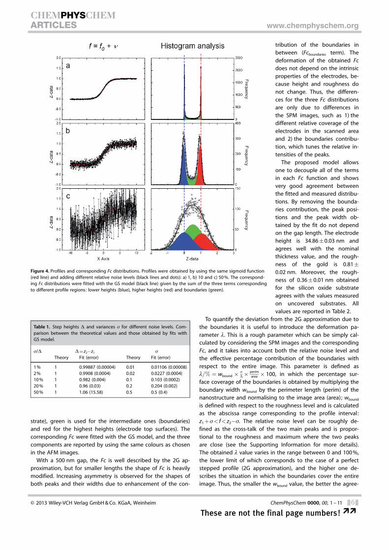
In the first case, the test functions were built starting fromthe same intrinsic profile f0, defined as a symmetrical sigmoidfunction with a given slope and D= z2�z1, and adding an in-creasing Gaussian noise level (i.e. s variance). Figure 4 displaysthe simulated profiles (left) and the corresponding Fc distribu-tions (right) for three cases with relative noise levels s/D of 1,10 and 50 %. Each Fc (empty squares) was fitted with the func-tion shown in Equation (5) and represented by separating thethree terms: peak with centroid z1 (blue), peak with centroid z2
(red) and boundaries (green). In all cases, the fitted functionsshow excellent agreement with the test ones, and the valuepairs obtained by the fit (Dfit,sfit) are equal to the theoreticalones within 5 % error. All values obtained by the fit for differ-ent s are reported in Table 1. The GS model can be applied inthe range of relative noise between 0 and 50 %. In the case of50 %, the fitting function allows the peak position to be repro-duced even if the centroid values are only qualitative becausethe variances are one order of magnitude larger.
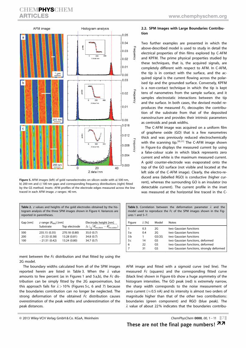
In the second case, the GS model was applied to reproduceFc distributions obtained from AFM images of interdigitatedgold electrodes deposited on a silicon oxide substrate with35 nm thickness and different gaps. Figure 5 shows the AFMimages and corresponding Fc of electrodes having spacings of500, 200 and 100 nm. The images are displayed in a high-con-trast scale in which blue represents the lowest heights (sub-
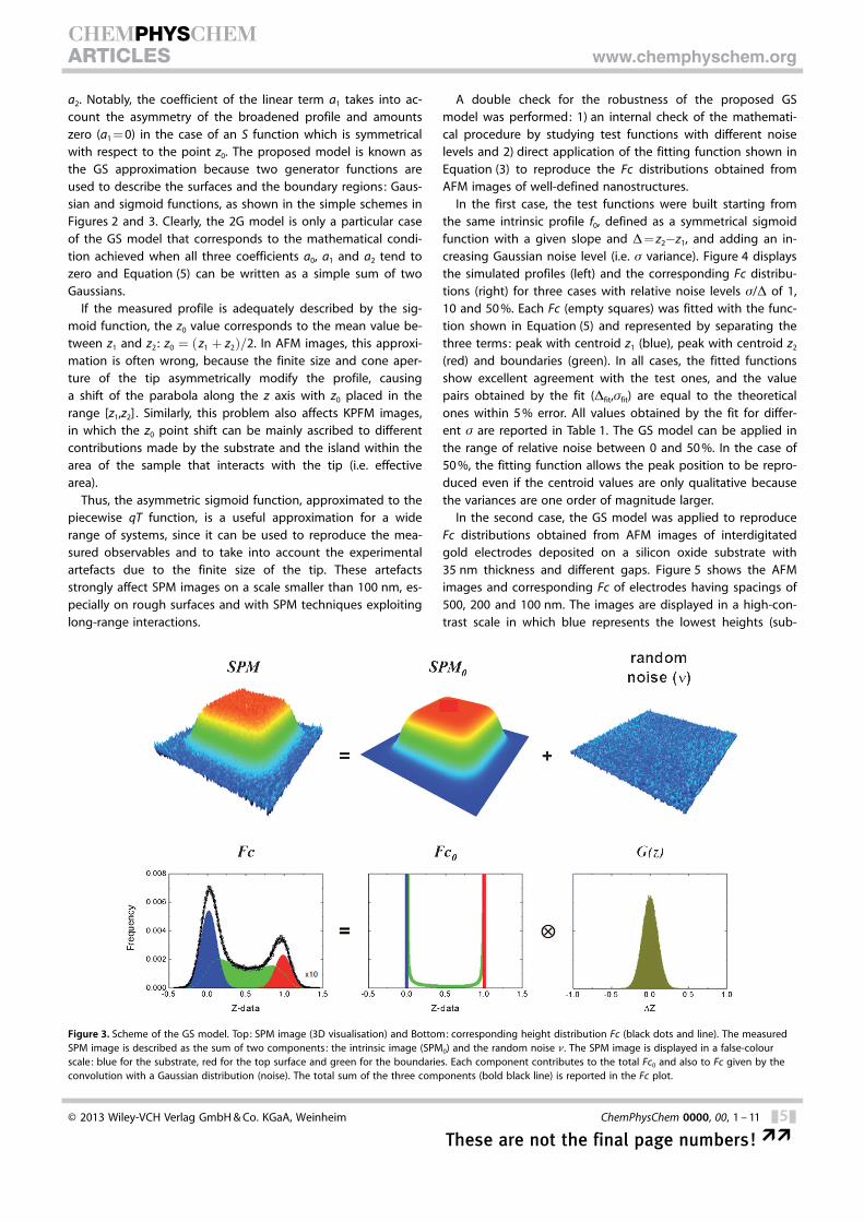
Figure 3. Scheme of the GS model. Top: SPM image (3D visualisation) and Bottom: corresponding height distribution Fc (black dots and line). The measuredSPM image is described as the sum of two components: the intrinsic image (SPM0) and the random noise n. The SPM image is displayed in a false-colourscale: blue for the substrate, red for the top surface and green for the boundaries. Each component contributes to the total Fc0 and also to Fc given by theconvolution with a Gaussian distribution (noise). The total sum of the three components (bold black line) is reported in the Fc plot.
� 2013 Wiley-VCH Verlag GmbH & Co. KGaA, Weinheim ChemPhysChem 0000, 00, 1 – 11 &5&
These are not the final page numbers! ��
CHEMPHYSCHEMARTICLES www.chemphyschem.org
strate), green is used for the intermediate ones (boundaries)and red for the highest heights (electrode top surfaces). Thecorresponding Fc were fitted with the GS model, and the threecomponents are reported by using the same colours as chosenin the AFM images.
With a 500 nm gap, the Fc is well described by the 2G ap-proximation, but for smaller lengths the shape of Fc is heavilymodified. Increasing asymmetry is observed for the shapes ofboth peaks and their widths due to enhancement of the con-
tribution of the boundaries inbetween (Fcboundaries term). Thedeformation of the obtained Fcdoes not depend on the intrinsicproperties of the electrodes, be-cause height and roughness donot change. Thus, the differen-ces for the three Fc distributionsare only due to differences inthe SPM images, such as 1) thedifferent relative coverage of theelectrodes in the scanned areaand 2) the boundaries contribu-tion, which tunes the relative in-tensities of the peaks.
The proposed model allowsone to decouple all of the termsin each Fc function and showsvery good agreement betweenthe fitted and measured distribu-tions. By removing the bounda-ries contribution, the peak posi-tions and the peak width ob-tained by the fit do not dependon the gap length. The electrodeheight is 34.86�0.03 nm andagrees well with the nominalthickness value, and the rough-ness of the gold is 0.81�0.02 nm. Moreover, the rough-ness of 0.36�0.01 nm obtainedfor the silicon oxide substrateagrees with the values measuredon uncovered substrates. Allvalues are reported in Table 2.
To quantify the deviation from the 2G approximation due tothe boundaries it is useful to introduce the deformation pa-rameter l. This is a rough parameter which can be simply cal-culated by considering the SPM images and the correspondingFc, and it takes into account both the relative noise level andthe effective percentage contribution of the boundaries withrespect to the entire image. This parameter is defined asl=% ¼ wbound � s
D�perimarea � 100, in which the percentage sur-
face coverage of the boundaries is obtained by multiplying theboundary width wbound by the perimeter length (perim) of thenanostructure and normalising to the image area (area); wbound
is defined with respect to the roughness level and is calculatedas the abscissa range corresponding to the profile interval :z1 +s< f<z2�s. The relative noise level can be roughly de-fined as the cross-talk of the two main peaks and is propor-tional to the roughness and maximum where the two peaksare close (see the Supporting Information for more details).The obtained l value varies in the range between 0 and 100 %,the lower limit of which corresponds to the case of a perfectstepped profile (2G approximation), and the higher one de-scribes the situation in which the boundaries cover the entireimage. Thus, the smaller the wbound value, the better the agree-
Figure 4. Profiles and corresponding Fc distributions. Profiles were obtained by using the same sigmoid function(red line) and adding different relative noise levels (black lines and dots): a) 1, b) 10 and c) 50 %. The correspond-ing Fc distributions were fitted with the GS model (black line) given by the sum of the three terms correspondingto different profile regions: lower heights (blue), higher heights (red) and boundaries (green).
Table 1. Step heights D and variances s for different noise levels. Com-parison between the theoretical values and those obtained by fits withGS model.
s/D D= z2�z1 s
Theory Fit (error) Theory Fit (error)
1 % 1 0.99887 (0.00004) 0.01 0.01106 (0.00008)2 % 1 0.9908 (0.0004) 0.02 0.0227 (0.0004)10 % 1 0.982 (0.004) 0.1 0.103 (0.0002)20 % 1 0.96 (0.03) 0.2 0.204 (0.002)50 % 1 1.06 (15.58) 0.5 0.5 (0.4)
� 2013 Wiley-VCH Verlag GmbH & Co. KGaA, Weinheim ChemPhysChem 0000, 00, 1 – 11 &6&
These are not the final page numbers! ��
CHEMPHYSCHEMARTICLES www.chemphyschem.org
ment between the Fc distribution and that fitted by using the2G model.
The boundary widths calculated from all of the SPM imagesreported herein are listed in Table 3. When the l valueamounts to few percent (as in Figures 1 and 5 a,b), the Fc dis-tribution can be simply fitted by the 2G aaproximation, butthis approach fails for l>10 % (Figures 5 c, 6 and 7) becausethe boundaries contribution can no longer be neglected. Thestrong deformation of the obtained Fc distribution causesoverestimation of the peak widths and underestimation of thepeak distances.
2.2. SPM Images with Large Boundaries Contribu-tion
Two further examples are presented in which theabove-described model is used to study in detail theelectrical properties of thin films explored by C-AFMand KPFM. The prime physical properties studied bythese techniques, that is, the acquired signals, arecompletely different with respect to AFM. In C-AFM,the tip is in contact with the surface, and the ac-quired signal is the current flowing across the polar-ised tip and the grounded surface. Conversely, KPFMis a non-contact technique in which the tip is kepttens of nanometres from the sample surface, and itsamples electrostatic interactions between the tipand the surface. In both cases, the devised model re-produces the measured Fc, decouples the contribu-tion of the substrate from that of the depositednanostructure and provides their intrinsic parametersas centroids and peak widths.
The C-AFM image was acquired on a uniform filmof graphene oxide (GO) that is a few nanometresthick and was previously reduced electrochemicallywith the scanning tip.[30, 31] The C-AFM image shownin Figure 6 a displays the measured current by usinga false-colour scale in which black represents zerocurrent and white is the maximum measured current.A gold counter-electrode was evaporated onto thetop of the GO surface (not visible and located at theleft side of the C-AFM image). Clearly, the electro-re-duced area (labelled RGO) is conductive (higher cur-rent), whereas the surrounding GO is an insulator (nodetectable current). The current profile in the insetwas measured at the horizontal line traced in the C-
AFM image and fitted with a sigmoid curve (red line). Themeasured Fc (squares) and the corresponding fitted curve(black line) shown in Figure 6 b show a huge asymmetry of thehistogram intensities. The GO peak (red) is extremely narrow,the sharp width corresponds to the noise measurement ofzero current (�0.5 nA) and its intensity is almost two orders ofmagnitude higher than that of the other two contributions:boundaries (green component) and RGO (blue peak). Thel value of about 22 % indicates that the boundaries contribu-
Figure 5. AFM images (left) of gold nanoelectrodes on silicon oxide with a) 500 nm,b) 200 nm and c) 100 nm gaps and corresponding frequency distributions (right) fittedby the GS method. Insets : AFM profiles of the electrode edges measured across the linetraced in each AFM image. z ranges: 40 nm.
Table 2. z values and heights of the gold electrodes obtained by the his-togram analysis of the three SPM images shown in Figure 4. Variances arereported in parentheses.
Gap [nm] z range (RRMS) [nm] Electrode height [nm]Substrate Top electrode D ð
ffiffiffiffiffiffiffiffiffiffiffiffiffiffiffiffiffiffiffiffiffiffiffiffiffiffiffiffiffiffiffiffiffiffiffiffiffiffiR2
rms;electr � R2rms;substr
qÞ
500 235.15 (0.35) 270.18 (0.80) 35.0 (0.7)200 �21.53 (0.38) 13.28 (0.81) 34.8 (0.7)100 �21.51 (0.42) 13.24 (0.80) 34.7 (0.7)
Table 3. Correlation between the deformation parameter l and themodel used to reproduce the Fc of the SPM images shown in the Fig-ures 1 and 5–7.
Figure l [%] Model Notes
1 0.3 2G two Gaussian functions5 a 0.4 2G two Gaussian functions5 b 1 GS/2G two Gaussian functions5 c 14 GS two Gaussian functions, deformed6 22 GS two Gaussian functions, deformed7 31 GS two Gaussian functions, strongly deformed
� 2013 Wiley-VCH Verlag GmbH & Co. KGaA, Weinheim ChemPhysChem 0000, 00, 1 – 11 &7&
These are not the final page numbers! ��
CHEMPHYSCHEMARTICLES www.chemphyschem.org
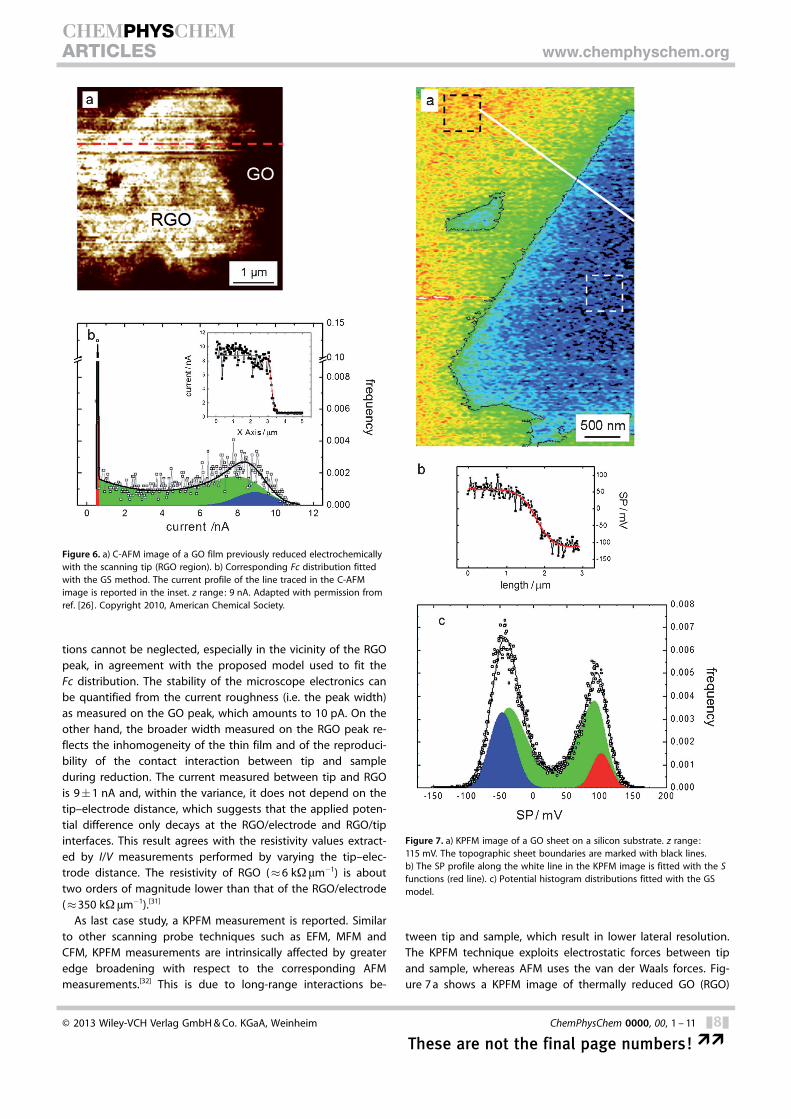
tions cannot be neglected, especially in the vicinity of the RGOpeak, in agreement with the proposed model used to fit theFc distribution. The stability of the microscope electronics canbe quantified from the current roughness (i.e. the peak width)as measured on the GO peak, which amounts to 10 pA. On theother hand, the broader width measured on the RGO peak re-flects the inhomogeneity of the thin film and of the reproduci-bility of the contact interaction between tip and sampleduring reduction. The current measured between tip and RGOis 9�1 nA and, within the variance, it does not depend on thetip–electrode distance, which suggests that the applied poten-tial difference only decays at the RGO/electrode and RGO/tipinterfaces. This result agrees with the resistivity values extract-ed by I/V measurements performed by varying the tip–elec-trode distance. The resistivity of RGO (�6 kW mm�1) is abouttwo orders of magnitude lower than that of the RGO/electrode(�350 kW mm�1).[31]
As last case study, a KPFM measurement is reported. Similarto other scanning probe techniques such as EFM, MFM andCFM, KPFM measurements are intrinsically affected by greateredge broadening with respect to the corresponding AFMmeasurements.[32] This is due to long-range interactions be-
tween tip and sample, which result in lower lateral resolution.The KPFM technique exploits electrostatic forces between tipand sample, whereas AFM uses the van der Waals forces. Fig-ure 7 a shows a KPFM image of thermally reduced GO (RGO)
Figure 6. a) C-AFM image of a GO film previously reduced electrochemicallywith the scanning tip (RGO region). b) Corresponding Fc distribution fittedwith the GS method. The current profile of the line traced in the C-AFMimage is reported in the inset. z range: 9 nA. Adapted with permission fromref. [26] . Copyright 2010, American Chemical Society.
Figure 7. a) KPFM image of a GO sheet on a silicon substrate. z range:115 mV. The topographic sheet boundaries are marked with black lines.b) The SP profile along the white line in the KPFM image is fitted with the Sfunctions (red line). c) Potential histogram distributions fitted with the GSmodel.
� 2013 Wiley-VCH Verlag GmbH & Co. KGaA, Weinheim ChemPhysChem 0000, 00, 1 – 11 &8&
These are not the final page numbers! ��
CHEMPHYSCHEMARTICLES www.chemphyschem.org
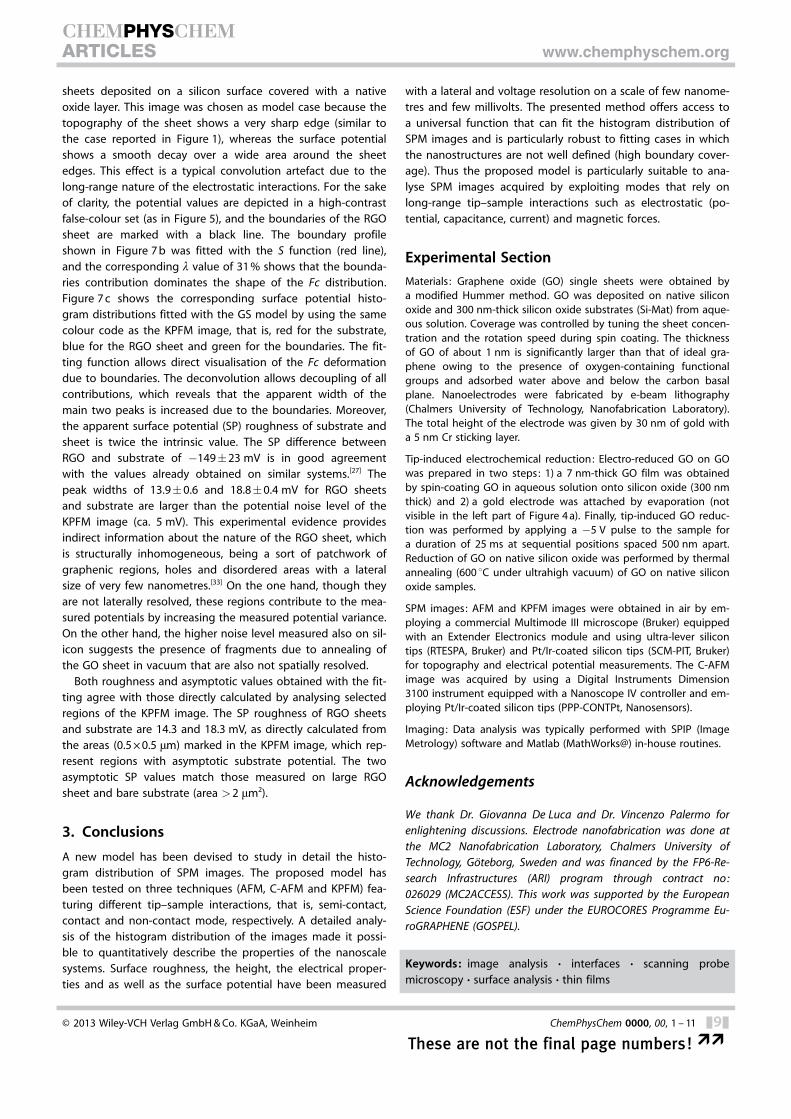
sheets deposited on a silicon surface covered with a nativeoxide layer. This image was chosen as model case because thetopography of the sheet shows a very sharp edge (similar tothe case reported in Figure 1), whereas the surface potentialshows a smooth decay over a wide area around the sheetedges. This effect is a typical convolution artefact due to thelong-range nature of the electrostatic interactions. For the sakeof clarity, the potential values are depicted in a high-contrastfalse-colour set (as in Figure 5), and the boundaries of the RGOsheet are marked with a black line. The boundary profileshown in Figure 7 b was fitted with the S function (red line),and the corresponding l value of 31 % shows that the bounda-ries contribution dominates the shape of the Fc distribution.Figure 7 c shows the corresponding surface potential histo-gram distributions fitted with the GS model by using the samecolour code as the KPFM image, that is, red for the substrate,blue for the RGO sheet and green for the boundaries. The fit-ting function allows direct visualisation of the Fc deformationdue to boundaries. The deconvolution allows decoupling of allcontributions, which reveals that the apparent width of themain two peaks is increased due to the boundaries. Moreover,the apparent surface potential (SP) roughness of substrate andsheet is twice the intrinsic value. The SP difference betweenRGO and substrate of �149�23 mV is in good agreementwith the values already obtained on similar systems.[27] Thepeak widths of 13.9�0.6 and 18.8�0.4 mV for RGO sheetsand substrate are larger than the potential noise level of theKPFM image (ca. 5 mV). This experimental evidence providesindirect information about the nature of the RGO sheet, whichis structurally inhomogeneous, being a sort of patchwork ofgraphenic regions, holes and disordered areas with a lateralsize of very few nanometres.[33] On the one hand, though theyare not laterally resolved, these regions contribute to the mea-sured potentials by increasing the measured potential variance.On the other hand, the higher noise level measured also on sil-icon suggests the presence of fragments due to annealing ofthe GO sheet in vacuum that are also not spatially resolved.
Both roughness and asymptotic values obtained with the fit-ting agree with those directly calculated by analysing selectedregions of the KPFM image. The SP roughness of RGO sheetsand substrate are 14.3 and 18.3 mV, as directly calculated fromthe areas (0.5 � 0.5 mm) marked in the KPFM image, which rep-resent regions with asymptotic substrate potential. The twoasymptotic SP values match those measured on large RGOsheet and bare substrate (area >2 mm2).
3. Conclusions
A new model has been devised to study in detail the histo-gram distribution of SPM images. The proposed model hasbeen tested on three techniques (AFM, C-AFM and KPFM) fea-turing different tip–sample interactions, that is, semi-contact,contact and non-contact mode, respectively. A detailed analy-sis of the histogram distribution of the images made it possi-ble to quantitatively describe the properties of the nanoscalesystems. Surface roughness, the height, the electrical proper-ties and as well as the surface potential have been measured
with a lateral and voltage resolution on a scale of few nanome-tres and few millivolts. The presented method offers access toa universal function that can fit the histogram distribution ofSPM images and is particularly robust to fitting cases in whichthe nanostructures are not well defined (high boundary cover-age). Thus the proposed model is particularly suitable to ana-lyse SPM images acquired by exploiting modes that rely onlong-range tip–sample interactions such as electrostatic (po-tential, capacitance, current) and magnetic forces.
Experimental Section
Materials : Graphene oxide (GO) single sheets were obtained bya modified Hummer method. GO was deposited on native siliconoxide and 300 nm-thick silicon oxide substrates (Si-Mat) from aque-ous solution. Coverage was controlled by tuning the sheet concen-tration and the rotation speed during spin coating. The thicknessof GO of about 1 nm is significantly larger than that of ideal gra-phene owing to the presence of oxygen-containing functionalgroups and adsorbed water above and below the carbon basalplane. Nanoelectrodes were fabricated by e-beam lithography(Chalmers University of Technology, Nanofabrication Laboratory).The total height of the electrode was given by 30 nm of gold witha 5 nm Cr sticking layer.
Tip-induced electrochemical reduction: Electro-reduced GO on GOwas prepared in two steps: 1) a 7 nm-thick GO film was obtainedby spin-coating GO in aqueous solution onto silicon oxide (300 nmthick) and 2) a gold electrode was attached by evaporation (notvisible in the left part of Figure 4 a). Finally, tip-induced GO reduc-tion was performed by applying a �5 V pulse to the sample fora duration of 25 ms at sequential positions spaced 500 nm apart.Reduction of GO on native silicon oxide was performed by thermalannealing (600 8C under ultrahigh vacuum) of GO on native siliconoxide samples.
SPM images: AFM and KPFM images were obtained in air by em-ploying a commercial Multimode III microscope (Bruker) equippedwith an Extender Electronics module and using ultra-lever silicontips (RTESPA, Bruker) and Pt/Ir-coated silicon tips (SCM-PIT, Bruker)for topography and electrical potential measurements. The C-AFMimage was acquired by using a Digital Instruments Dimension3100 instrument equipped with a Nanoscope IV controller and em-ploying Pt/Ir-coated silicon tips (PPP-CONTPt, Nanosensors).
Imaging: Data analysis was typically performed with SPIP (ImageMetrology) software and Matlab (MathWorks@) in-house routines.
Acknowledgements
We thank Dr. Giovanna De Luca and Dr. Vincenzo Palermo forenlightening discussions. Electrode nanofabrication was done atthe MC2 Nanofabrication Laboratory, Chalmers University ofTechnology, Gçteborg, Sweden and was financed by the FP6-Re-search Infrastructures (ARI) program through contract no:026029 (MC2ACCESS). This work was supported by the EuropeanScience Foundation (ESF) under the EUROCORES Programme Eu-roGRAPHENE (GOSPEL).
Keywords: image analysis · interfaces · scanning probemicroscopy · surface analysis · thin films
� 2013 Wiley-VCH Verlag GmbH & Co. KGaA, Weinheim ChemPhysChem 0000, 00, 1 – 11 &9&
These are not the final page numbers! ��
CHEMPHYSCHEMARTICLES www.chemphyschem.org

[1] D. Sarid, Scanning Force Microscopy : With Applications to Electric, Mag-netic and Atomic Forces, Oxford University Press, New York, 1994.
[2] F. J. Giessibl, Science 1995, 267, 68 – 71.[3] C. Schçnenberger, S. F. Alvarado, Phys. Rev. Lett. 1990, 65, 3162 – 3164.[4] P. Samor�, J. Mater. Chem. 2004, 14, 1353 – 1366.[5] D. J. Whitehouse, Handbook of Surface and Nanometrology, CRC, Boca
Raton, 2011.[6] K. J. Stout, L. Blunt, W. P. Dong, E. Mainsah, N. Luo, T. Mathia, P. J. Sulli-
van, H. Zahouani, Development of Methods for Characterisation ofRoughness in Three Dimensions, Penton Press, London, 2000.
[7] J. S. Bendat, A. G. Piersol, Engineering Applications of Correlation andSpectral Analysis, Wiley, New York, 1993.
[8] A.-L. Barab�si, H. E. Stanley, Fractal Concepts in Surface Growth, Cam-bridge University Press, New York, 1995.
[9] F. Biscarini, P. Samori, O. Greco, R. Zamboni, Phys. Rev. Lett. 1997, 78,2389 – 2392.
[10] T. Halpin-Healy, Y.-C. Zhang, Phys. Rep. 1995, 254, 215 – 415.[11] SPIP, The Scanning Probe Image Processor for MS Windows 95/98/NT/
2K/Me/XP Version 2.3232 by Image Metrology ApS, City.[12] J. L. Luria, N. Hoepker, R. Bruce, A. R. Jacobs, C. Groves, J. A. Marohn,
ACS Nano 2012, 6, 9392 – 9401.[13] M. E. McConney, S. Singamaneni, V. V. Tsukruk, Polym. Rev. 2010, 50,
235 – 286.[14] V. Palermo, A. Liscio, M. Palma, M. Surin, R. Lazzaroni, P. Samor�, Chem.
Commun. 2007, 3326 – 3337.[15] A. Liscio, V. Palermo, P. Samori, Acc. Chem. Res. 2010, 43, 541 – 550.[16] M. Nonnenmacher, M. P. Oboyle, H. K. Wickramasinghe, Appl. Phys. Lett.
1991, 58, 2921 – 2923.[17] P. J. Eaton, P. West, Atomic Force Microscopy, Oxford University Press,
New York, 2010.[18] V. W. Tsai, T. Vorburger, R. Dixson, J. Fu, R. Koning, R. Silver, E. D. Williams
in AIP Conference Proceedings, Vol. 449 (Eds. : D. G. Seiler, A. C. Diebold,W. M. Bullis, T. J. Shaffner, R. McDonald, E. J. Walters), American Instituteof Physics, Melville, 1998, pp. 839 – 842.
[19] P. R�fr�gier, Noise Theory and Application to Physics : From Fluctuationsto Information, Springer, New York, 2004.
[20] H. J. Butt, M. Jaschke, Nanotechnology 1995, 6, 1 – 7.[21] M. Morita, T. Ohmi, E. Hasegawa, M. Kawakami, M. Ohwada, J. Appl.
Phys. 1990, 68, 1272 – 1281.[22] R. Castro-Rodr�guez, A. I. Oliva, V. Sosa, F. Caballero-Briones, J. L. Pena,
Appl. Surf. Sci. 2000, 161, 340 – 346.[23] G. B. Arfken, H.-J. Weber, Mathematical Methods for Physicists, Elsevier,
Boston, 2005.[24] J. C. Meyer, A. K. Geim, M. I. Katsnelson, K. S. Novoselov, D. Obergfell, S.
Roth, C. Girit, A. Zettl, Solid State Commun. 2007, 143, 101 – 109.[25] J. I. Paredes, S. Villar-Rodil, A. Martinez-Alonso, J. M. D. Tascon, Langmuir
2008, 24, 10560 – 10564.[26] N. R. Wilson, P. A. Pandey, R. Beanland, R. J. Young, I. A. Kinloch, L. Gong,
z. Liu, K. Suenaga, J. P. Rourke, S. J. York, J. Sloan, ACS Nano 2009, 3,2547 – 2556.
[27] A. Liscio, G. P. Veronese, E. Treossi, F. Suriano, F. Rossella, V. Bellani, R.Rizzoli, P. Samori, V. Palermo, J. Mater. Chem. 2011, 21, 2924 – 2931.
[28] D. Sen, S. K. Pal, Image Vision Comput. 2010, 28, 677 – 695.[29] C. D. McGillem, G. R. Cooper, Continuous and Discrete Signal and System
Analysis, Saunders College, Philadelphia, 1991.[30] J. M. Mativetsky, A. Liscio, E. Treossi, E. Orgiu, A. Zanelli, P. Samori, V. Pa-
lermo, J Am Chem. Soc. 2011, 133, 14320 – 14326.[31] J. M. Mativetsky, E. Treossi, E. Orgiu, M. Melucci, G. P. Veronese, P.
Samori, V. Palermo, J. Am. Chem. Soc. 2010, 132, 14130 – 14136.[32] A. Liscio, V. Palermo, P. Samor�, Adv. Funct. Mater. 2008, 18, 907 – 914.[33] K. Erickson, R. Erni, z. Lee, N. Alem, W. Gannett, A. Zettl, Adv. Mater.
2010, 22, 4467 – 4472.
Received: October 23, 2012
Revised: January 23, 2013
Published online on && &&, 2013
� 2013 Wiley-VCH Verlag GmbH & Co. KGaA, Weinheim ChemPhysChem 0000, 00, 1 – 11 &10&
These are not the final page numbers! ��
CHEMPHYSCHEMARTICLES www.chemphyschem.org

ARTICLES
A. Liscio*
&& –&&
Scanning Probe Microscopy beyondImaging: A General Tool forQuantitative Analysis
Precise estimates of properties such assurface roughness, height, electricalcharacteristics and surface potential areobtained from scanning probe micros-copy images by means of a quantitativeapproach based on histogram analysis(see picture).
� 2013 Wiley-VCH Verlag GmbH & Co. KGaA, Weinheim ChemPhysChem 0000, 00, 1 – 11 &11&
These are not the final page numbers! ��