atomic structure and electrical properties of in(te) nanocontacts on cdznte(110) by scanning probe...
TRANSCRIPT
FULLPAPER
www.MaterialsViews.comwww.afm-journal.de
Atomic Structure and Electrical Properties of In(Te)Nanocontacts on CdZnTe(110) by Scanning ProbeMicroscopy
By Gili Cohen-Taguri, Ori Sinkevich, Mario Levinshtein, Arie Ruzin* and Ilan Goldfarb*
[*] Prof. A. Ruzin, O. SinkevichSchool of Electrical EngineeringFaculty of EngineeringTel Aviv UniversityTel Aviv 69978 (Israel)E-mail: [email protected]
Prof. I. Goldfarb, G. Cohen-Taguri, M. LevinshteinSchool of Mechanical Engineering and Materials &Nanotechnologies ProgramFaculty of EngineeringTel Aviv UniversityTel Aviv 69978 (Israel)E-mail: [email protected]
Prof. A. Ruzin, Prof. I. GoldfarbResearch Center for Nanoscience and NanotechnologyTel Aviv UniversityTel Aviv 69978 (Israel)
DOI: 10.1002/adfm.200900812
Understanding complex correlations between the macroscopic device
performance (largely dependent on the character of the metal–semiconductor
contact) and the metallurgy of contact formation on the atomic level in
cadmium zinc telluride (CdZnTe) radiation detectors remains a formidable
challenge. In this work, an effort towards bridging that macro–nano
knowledge gap is made by conducting a series of controlled experiments
aimed at correlating electrical properties of the In contact to n-type
CdZnTe(110) surface with the step-by-step process of contact formation. This
can only be achieved by using high spatial resolution techniques, capable of
conducting highly localized measurements on the nano- and sub-nanoscale,
such as scanning probe microscopy. Scanning tunneling microscopy is used
in situ to monitor the behavior of various In atom coverages on an atomically
flat and ordered CdZnTe surface under well-controlled molecular beam
epitaxial conditions in ultra-high vacuum. Electrical derivatives of atomic
force microscopy are used to measure the electrical contact properties, such
as contact potential difference and spreading resistance in torsion resonance
tunneling mode. It is concluded that In atoms preferentially reacted with Te
atomic-rows already at room temperature, forming nanometric patches of
indium–telluride Schottky-type contacts. The methods developed in this
study, in terms of both nanocontact fabrication and characterization
(especially in terms of electrical properties) should benefit basic and applied
research of any metal–semiconductor system.
Adv. Funct. Mater. 2010, 20, 215–223 � 2010 WILEY-VCH Verlag GmbH & Co. KGaA, Weinh
1. Introduction
Cadmium zinc telluride (Cd1–xZnxTe orCdZnTe), as well as other II–VI semicon-ductor compounds, exhibits a high gamma-ray absorption coefficient and high elec-trical resistivity (governed by high atomicnumber and wide bandgap, respectively).These properties explain its importance inscientific and technological applications,including medical imaging, homelandsecurity, and spaceborne X-ray andgamma-ray astronomy.[1–3] Single-crystalCdZnTe is particularly attractive for roomtemperature (RT) radiation detection[1,3–5]
and iswidelyusedas a substrate for epitaxialgrowth of lattice-matched Hg1–yCdyTe thinfilms for infrared detectors.[6,7] Thus, it issurprising that amid such a large body ofwork the surface science of CdZnTe devicesremains relatively virgin ground.
The development of CdZnTe as a nuclearradiation detectormaterial has significantlyprogressed with advances in the CdZnTecrystal growth methods, which minimizedbulk defects andprecipitates.[4,8] At present,two primary methods are used to growCdZnTe crystals, the modified high-pres-sure Bridgman (MHB) and the high-
pressure Bridgman (HPB) processes. In this work, MHB-grownn-type CdZnTe substrates from Orbotech Medical Solutions Ltd.(Israel)were employed.MHBproducesuniformsubstrates at highyields and thusmodest costs, though its bulk resistivity of 109V cmis slightly lower than the 1010V cm obtained with a moreconventional HPB process, which may result in higher leakagecurrents and, in turn, inferior energy resolution in the low-energygamma range (<100 keV).[9]
The most common configuration of a CdZnTe-based radiationdetector is ametal–semiconductor–metal (MSM) structure, ratherthan a p–n junction. The nature of themetal–semiconductor (MS)interface depends to a large extent not only on defects, such asdislocations, twins, sub grain boundaries and precipitates, but alsoon the atomistic and electronic surface properties in the form ofreconstructions and relaxations, density of steps, surface states,and position of the Fermi level. Since the latter sensitively dependson the surface-preparation procedures, the performance of suchMSM devices is a strong function of surface preparation,[10,11]
eim 215
FULLPAPER
www.afm-journal.dewww.MaterialsViews.com
216
metallization methods,[12,13] heat treatments,[2] and the contactmetal itself. Furthermore, interfacial reactions (leading to anintermediate phase formation) between themetal and theCdZnTesurfacemay facilitate an intimate contact with superior properties,or degrade the contact region with a detrimental effect on thedevice performance.
Metal contact to a semiconductor can be either rectifying(Schottky) or ohmic, that is, with linear current–voltage (I–V)characteristics. Generally speaking, the former is desirable forachieving lower dark currents (and thus lower electronic noise) forX-ray spectroscopy, and in the latter a more uniform voltage dropover the entire semiconductor crystal may be favorable for largeractive volume (and thus higher-energy g-ray absorption). It hasbeen suggested that the merit of ohmic-type electrodes is thereduction of the hole-tailing effect through the replacement of thetrapped carriers with injected charge carriers from the contacts,though it may be less effective in suppressing leakage currents.[14]
In practice, since CdZnTe crystals used for detector fabrication arehighly resistive (typically 107–1011V cm), the Schottky barrier canbe masked by the high serial resistance of the CdZnTe bulk.[15]
Theoretically speaking, for ‘‘real’’ ohmic contacts to a p-type(n-type) material, the metal has to have a higher (lower) workfunction then the semiconductor, fm > fsðfm < fsÞ. For thisreason only fewmetals, such as Pt and Au,meet the conditions forohmic contact to a higher resistivity p-type CdZnTe (fs � 5:1 eV),whereasmostmetals (e.g., In andAl) satisfy thefm < fs conditionfor ohmic contacts to the lower resistivity n-typeCdZnTe.[16]Oneofthe main challenges in the formation of Schottky contacts isavoiding charge injection, which, due to the high initial bulkresistivity, can dramatically modify the device performance. Allthings considered,modernCdZnTe detectors with ohmic contactsyield some of the best spectroscopic results for high-energy g-raysat room temperature. In reality, thework function difference is notthe only parameter determining the contact electrical behavior:often the influence of the surface states (mostly originating fromatomic and morphological surface structure) prevails. Surfaceorientation, morphology, stoichiometry (of both the substrate andthe contact phase), and reconstruction (determined by surfacethermodynamics, yet sensitive to the preparation procedures)maysignificantly influence the electron affinity in the contact region,and thus play an important role in the contact properties andbehavior. Substrate temperature (in the course of deposition andsubsequent heat treatments) is also among the preparationparameters that may strongly affect the electrical contact proper-ties, via some critical interface processes, such as i) diffusion ofmetal andCdZnTe atoms, ii)metal�Cd�Zn�Tephase formation,iii) oxide removal, and iv) adhesion force.[13,16–19] Surfacestoichiometry and polarity[20–22] may affect the contact properties(such as Schottky barrier height (SBH)), by modifying thepathways of interfacial reactions. With such a large set ofparameters, it is scarcely surprising that the measurements ofthe electrical-contact properties are often difficult to reproduce notonly between various groups, but even within the same set ofexperiments.[20]
The above arguments emphasize the need for a detailedunderstanding of the contact formation mechanisms, if onewishes to fully understand and control the contact (and thus theentire device) performance. Many years of intense research haveyielded such understanding of contacts to Si- and GaAs-based
� 2010 WILEY-VCH Verlag GmbH &
devices. However in II–IV compound semiconductors, and inCdZnTe in particular, the knowledge is far from sufficient. Onlyfew have attempted to correlate electrical characteristics of variousmetal contacts toCdTeor toCdZnTewith thepre-deposited surfaceproperties, e.g.,Au/CdTe{111},[23]Au,In/Cd0.8Zn0.2Te,
[24] andNd/n�CdZnTe.[25] Our previous work was focused on rigorousinvestigation of a bare cleaved CdZnTe(110) surface. First, atomicforce microscopy (AFM), electric force microscopy (EFM), andtunneling current AFM (TUNA) were used for a preliminarycharacterization of the surface as is, after cleavage in air.[26] Then,after developing a repeatable and reproducible preparation routinefor obtaining atomically flat and ordered CdZnTe(110) surfaces inultra-high vacuum (UHV), surface science techniques (mostlyatomic-resolution scanning tunneling microscopy (STM) andreflection high energy electron diffraction (RHEED)) wereemployed to provide a detailed picture of the surface atomicstructure and topography.[27]
The goal of the present work was to study the formation andelectrical properties of In contacts to a Cd0.9Zn0.1Te(110) surface,in a manner that allows for a structure–property correlation.Quaternary metal�Cd�Zn�Te phase equilibrium and thereaction kinetics are of fundamental importance to understandingthe mechanisms of contact formation and the resulting electricalproperties of the contact. For this study, indium was chosen as acontact metal because it is a popular contact material, especially toan n-type CdZnTe, where it can form an ohmic contact. Whileinvestigations into reactions and phase formation between certainmetals andCdZnTe,mostly betweenCu,Ag, Au, andNi andp-typeCd0.95Zn0.05Te,
[28] have been conducted (using indirect methodsrather than real-space atomic resolution imaging), little is knownabout the In/n-type CdZnTe system, and in particular aboutIn�Cd�Zn�Te reactions and their effect on the contact formationand properties. Our AES chemical analysis clearly detectedcompositional changes at the CdZnTe surface upon In deposition,indicating the formation of an intermediate phase already at roomtemperature. Atomic-resolution STM and reciprocal space map-ping by RHEED identified that phase as indium telluride,isomorphic with zinc-blend CdZnTe substrate, and with welldefined epitaxial orientation relations in spite of a large latticemismatchbetween the two. In order tomeasure electrical behaviorof ametallic contact, physical contact between the STM tip and themetal surface is required to avoid the vacuum barrier. That wouldrequire crashing the tip onto the surface, which we did not wish todo.On the other hand, direct contact AFM,which isusually used toprobe such junctions, is too crude andwas noted tomove the ultra-thin In deposits during the scan. Therefore, the more subtle,torsion resonance tunneling atomic forcemicroscopy (TR-TUNA),wasusedex situ to test the contact electrical properties, and showedSchottky-type behavior (in spite of the disadvantage of removingthe sample from UHV, and so inevitably slightly varying thesurface conditions).
2. Results and Discussion
2.1. In situ Experiments
High-resolution filled-states STM images of Cd0.9Zn0.1Te(110)surface, before and after In deposition (very low coverage), are
Co. KGaA, Weinheim Adv. Funct. Mater. 2010, 20, 215–223
FULLPAPER
www.MaterialsViews.comwww.afm-journal.de
shown in Figure 1a and b, respectively. The periodicities along thetwo principle CdZnTe{110} surface directions, namely ½001� and½110�, extracted from the two-dimensional fast Fourier transform(2D-FFT) power spectra shown in the inset, are 0.766 nm and0.540 nm, respectively. Deviation of these periodicities from theideal bulk values of 0.644 nm and 0.456 nm, respectively, alongwith the 91.88 angle between them (rather than the ideal 908), ismost likely due to surface relaxation. The non-polar, electricallyneutral (110) surface of II–VI (e.g., CdTe[29,30] and CdZnTe[27]) andIII–V[31,32] zinc-blend semiconductors is known to retainprimitive(1� 1) periodicity, but exhibits a very well-known pattern ofrelaxation: the surface-layer anionsmove out of the surface in favorof an s2p3 bonding with three neighboring cations, resulting in apyramidal geometry. The cations on the surface move inward thebulk in favor of sp2 bonding with three neighboring anions,
Figure 1. High-resolution filled-states STM images of a) a CdZnTe(110)
surface, and b) low coverage of In on a CdZnTe(110) surface. Tunneling
conditions: a) V¼�4.4 V, I¼ 0.22 nA, b) V¼�3.2 V, I¼ 0.20 nA.
Adv. Funct. Mater. 2010, 20, 215–223 � 2010 WILEY-VCH Verl
resulting in a planar geometry. This can be characterized by arotation angle,v, of about 308 for CdTe(110) surfaces.[30] This typeof relaxation (surfacebuckling), actually serves to conserve thebulkbond lengths to within a few percent. For Cd(Zn)Te(110), suchsurface relaxation results in the filled electron states localizedprimarily on the Te sites with the empty states localized onCd (Zn)sites. Thus, tunneling out of filled states yields maximacorresponding to the Te atoms, as shown in Figures 1a and 2a,while Cd (Zn) sub-lattice emerges under tunneling into emptysubstrate states. In Figure 1a, a schematic top view of the atomicpositions is superimposed on the image, where empty circlesrepresent Te atoms and the filled circles represent Cd (Zn) atoms,and the rectangle indicates the (1� 1) surface unit cell of anunreconstructed CdZnTe(110) surface. The very smooth (110)surface shown contrasts with the apparently atomically rougherIII–V compound (110) surfaces (cf. Ref [33]). While it has beensuggested that high ionicity of the II–VI compounds (more thantwice that of the III–Vs)[34] may be the reason, experimentalmeasurements and calculations show that relaxation hardly
Figure 2. a) current and d) topography STM image of a bare CdZnTe(110)
surface, and after b,e) 2 sec and c,f) 5 s of In evaporation. a,d) �4.2 V,
0.22 nA, b,e) �4.0 V, 0.20 nA, and c,f) �5.0 V, 0.16 nA, respectively. (a–c)
Current (I images), (d–f) topography (z images). Characteristic RHEED
patterns along the h001i and h110i directions are shown in each inset.
Black circle in (c) outlines dislocated region.
ag GmbH & Co. KGaA, Weinheim 217
FULLPAPER
www.afm-journal.dewww.MaterialsViews.com
218
dependson thedegreeof ionicity.[35]Nonetheless, it is possible thata different ionicity and charge transfer upon bonding inthe II–VIs is such that empty states, primarily located at thecation sites, that is, Cd(Zn), move further away from the Fermilevel, making them less accessible to tunneling—which mayexplain why our best-quality STM images are those of thefilled states.
Lower-magnification STM of the CdZnTe(110) surface,prior to In deposition, revealed a multilevel stacking of smallterraces (Fig. 2a and d). Manifestation of such morphology inthe reciprocal space takes the form of continuous intensitydistribution along theRHEED reflections (rel-rods), also known as‘‘streaking’’, as was also the case here (see the inset in Fig. 2a). Thiswas the best possible surface quality under restrictions to theannealing treatments imposed by a desire to avoid significantcompositional changes, as has been discussed in our previouswork.[27]
While only highly ordered clean and pristine Te rows showed inthe filled-states STM images of the CdZnTe(110) surface prior toindium deposition (Fig. 1a and Fig. 2a and d), sparse brightprotrusions on top of the Te rows appeared after only 2 s of indiumevaporation at room temperature (Fig. 1b and Fig. 2b and e). Inspite of such low protrusion density (certainly below the detectionlimit of ourAuger spectrometer), an immediate anddrastic changein the corresponding RHEED patterns took place (see inset inFig. 2b).Tomakesure that theobservedprotrusionswere indeed Inislands, two higher In coverages were evaporated in a sequence.Figure 2c and f show the surface after 5 s of In evaporation: acorresponding increase in the protrusion density is obvious.Moreover, after even longer evaporation, where the entire surfacewas so covered that underlying Te rows could no longer beobserved (not shown), a clear and strong In peak appeared in theAES spectrum shown in Figure 3, undoubtedly assigning thebright protrusions to indium islands. Comparison of the upperspectrum in Figure 3 (prior to In deposition) to the lower one (afterIn deposition) reveals a drastic reduction of Cd concentration(related to peak-to-peak intensity, ICd), with the Te content (relatedto ITe) roughly unchanged. Such a decreasing ICd/ITe ratio wasevident even at sub-monolayer coverages: after 2 s In evaporationthe CCd/CTe ratio decreased by 35%, from CCd/CTe¼ 1.11 (theoriginal value after sputter–anneal surface preparation cycles) to0.72 (the value after 2 s In evaporation), and after 5 s In evaporation
Figure 3. AES spectra: before any treatment (top) and immediately after a
7 s In evaporation (at a k-cell temperature of 808 8C) on CdZnTe(110)
(bottom).
� 2010 WILEY-VCH Verlag GmbH &
the ratio was further reduced by more than 50%, from 1.11 to 0.5!This phenomenon can be explained, for example, by the formationof a binary indium–telluride compound at the interface betweenthe In layer and the CdZnTe’s surface, by In substitutions for Cdatoms in the CdZnTe lattice.
The growth mode of In on the CdZnTe(110) surface can beinferred from high-resolution STM study of surface evolution atvarious coverages. In the low In coverage (hereafter referred to asLIC sample) case, namely 2 s evaporation, the STM images inFigure 2b and e consist primarily of short row (‘‘finger’’) segmentsof bright protrusions, and by inspecting an even higher resolutionimage (Fig. 1b) it canbe inferred that these shortfingersare formedby coalescence of what appear to be compact round-shape nuclei.Further In deposition of 5 s in total (hereafter referred to as ‘‘highIn coverage (HIC)’’ sample), results in even longer, well developedIn fingers, parallel to the substrate’s Te rows, as shown inFigure 2cand f. The location of the compact In nuclei and the fingers theyform appears to be between the pairs of adjacent Te rows of atoms,close to the mid-point position, along the CdZnTeh110i direction,implying bonding between the In adatoms and the Te substrateatoms.However, since the In fingers are about twice as wide as theunderlying Te rows, every two In fingers occupy four Te rows,separated by about double interatomic Te�Te distance along theCdZnTe(110)h001i direction, theoretically around 12.88 A. Henceboth LIC and HIC STM images and the above mentioned AESmeasurements indicate In�Te bonding and epitaxial growth ofindium–telluride on the CdZnTe(110) surface. Formation ofinterfacial binary indium–telluride between the sputtered In layerand CdTe substrate, prior to the formation of ternary Cd�In�Tecompounds, has been inferred before;[36] however, this is the firsttime the formation and evolution of such an interfacial compoundhave been atomically resolved in real space. The non-uniformappearance of the In fingers and their meandering, along withsomedislocation-type kinkingof theunderlyingTe rows (encircledin Fig. 2c), indicated the epitaxy was by nomeans straightforward.The fact that every azimuth 2D streak pattern remainedunobstructed in RHEED, even after being overlapped by the In-induced 3D spot pattern, allowed for exact determination of theIn�Te/CdZnTe epitaxial orientation relations by multi-azimuthalRHEED, as explained below.
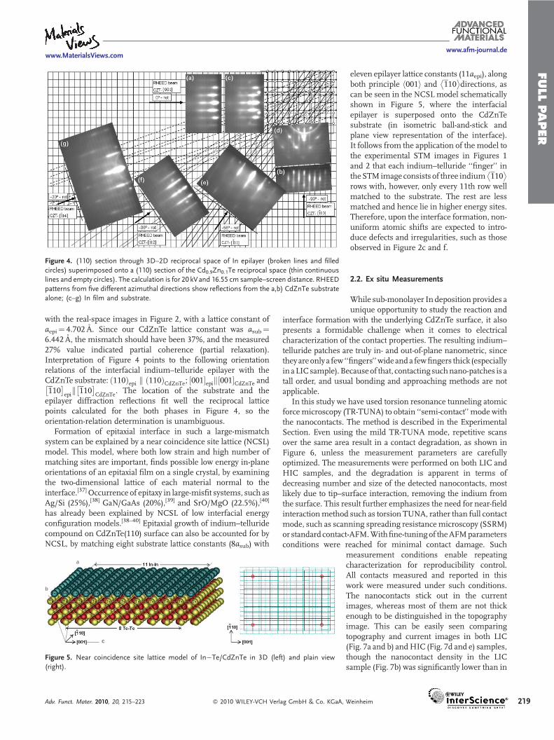
Figure 4 is a complex representation of the reciprocal spaceassociatedwith the sample surface (calculatedusing the reciprocitydefinitions and relations between the reciprocal space vectors andthe geometry of the RHEED apparatus) superimposed ontoexperimental RHEED patterns acquired along five differentazimuths in the 908-rotation diapason. These five azimuths (zoneaxes) were acquired after In deposition to ensure rigorousdetermination of the orientation relations between the interfacialtelluride and the substrate with a high degree of accuracy, with thetwo principle ones, 001h i and 110
� �, shown both before (Fig. 4a
and b) and after (Fig. 4c and d) In evaporation. Dot–streakseparation in all the azimuths indicated a relatively largemismatch(�27%) between the two lattices. Since 3D spot patterns emergedue to transmission of the electron beam through asperities, theywere solved the same way the transmission electron diffractionpatterns are solved in transmission electron microscopy. Thegeometry and the symmetry of the five-zone-axes transmissionpatterns could only be consistent with a zinc-blend crystalstructure, isomorphic and epitaxial with the substrate, in accord
Co. KGaA, Weinheim Adv. Funct. Mater. 2010, 20, 215–223
FULLPAPER
www.MaterialsViews.comwww.afm-journal.de
Figure 4. (110) section through 3D–2D reciprocal space of In epilayer (broken lines and filled
circles) superimposed onto a (110) section of the Cd0.9Zn0.1Te reciprocal space (thin continuous
lines and empty circles). The calculation is for 20 kVand 16.55 cm sample–screen distance. RHEED
patterns from five different azimuthal directions show reflections from the a,b) CdZnTe substrate
alone; (c–g) In film and substrate.
with the real-space images in Figure 2, with a lattice constant ofaepi¼ 4.702 A. Since our CdZnTe lattice constant was asub¼6.442 A, the mismatch should have been 37%, and the measured27% value indicated partial coherence (partial relaxation).Interpretation of Figure 4 points to the following orientationrelations of the interfacial indium–telluride epilayer with theCdZnTe substrate: 110ð Þepi k 110ð ÞCdZnTe; 001½ �epik 001½ �CdZnTe and110� �
epik 110� �
CdZnTe. The location of the substrate and the
epilayer diffraction reflections fit well the reciprocal latticepoints calculated for the both phases in Figure 4, so theorientation-relation determination is unambiguous.
Formation of epitaxial interface in such a large-mismatchsystem can be explained by a near coincidence site lattice (NCSL)model. This model, where both low strain and high number ofmatching sites are important, finds possible low energy in-planeorientations of an epitaxial film on a single crystal, by examiningthe two-dimensional lattice of each material normal to theinterface.[37] Occurrence of epitaxy in large-misfit systems, such asAg/Si (25%),[38] GaN/GaAs (20%),[39] and SrO/MgO (22.5%),[40]
has already been explained by NCSL of low interfacial energyconfiguration models.[38–40] Epitaxial growth of indium–telluridecompound on CdZnTe(110) surface can also be accounted for byNCSL, by matching eight substrate lattice constants (8asub) with
Figure 5. Near coincidence site lattice model of In�Te/CdZnTe in 3D (left) and plain view
(right).
Adv. Funct. Mater. 2010, 20, 215–223 � 2010 WILEY-VCH Verlag GmbH & Co. KGaA, W
eleven epilayer lattice constants (11aepi), alongboth principle 001h i and 110
� �directions, as
can be seen in the NCSL model schematicallyshown in Figure 5, where the interfacialepilayer is superposed onto the CdZnTesubstrate (in isometric ball-and-stick andplane view representation of the interface).It follows from the application of the model tothe experimental STM images in Figures 1and 2 that each indium–telluride ‘‘finger’’ intheSTMimage consists of three indium 110
� �
rows with, however, only every 11th row wellmatched to the substrate. The rest are lessmatched and hence lie in higher energy sites.Therefore, upon the interface formation, non-uniform atomic shifts are expected to intro-duce defects and irregularities, such as thoseobserved in Figure 2c and f.
2.2. Ex situ Measurements
While sub-monolayer In deposition provides aunique opportunity to study the reaction and
interface formation with the underlying CdZnTe surface, it alsopresents a formidable challenge when it comes to electricalcharacterization of the contact properties. The resulting indium–telluride patches are truly in- and out-of-plane nanometric, sincethey areonly a few ‘‘fingers’’wideanda fewfingers thick (especiallyin aLICsample).Becauseof that, contacting suchnano-patches is atall order, and usual bonding and approaching methods are notapplicable.
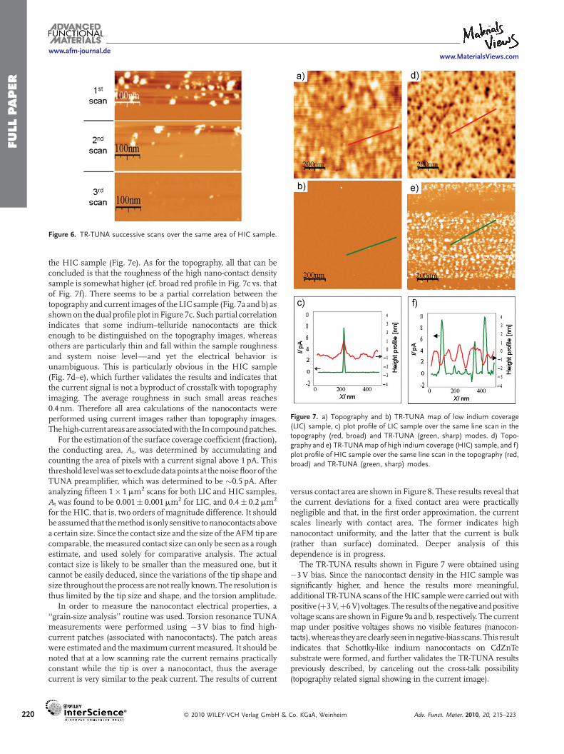
In this study we have used torsion resonance tunneling atomicforcemicroscopy (TR-TUNA) to obtain ‘‘semi-contact’’ mode withthe nanocontacts. The method is described in the ExperimentalSection. Even using the mild TR-TUNA mode, repetitive scansover the same area result in a contact degradation, as shown inFigure 6, unless the measurement parameters are carefullyoptimized. The measurements were performed on both LIC andHIC samples, and the degradation is apparent in terms ofdecreasing number and size of the detected nanocontacts, mostlikely due to tip–surface interaction, removing the indium fromthe surface. This result further emphasizes the need for near-fieldinteractionmethod such as torsion TUNA, rather than full contactmode, such as scanning spreading resistancemicroscopy (SSRM)or standard contact-AFM.Withfine-tuning of theAFMparametersconditions were reached for minimal contact damage. Such
measurement conditions enable repeatingcharacterization for reproducibility control.All contacts measured and reported in thiswork were measured under such conditions.The nanocontacts stick out in the currentimages, whereas most of them are not thickenough to be distinguished in the topographyimage. This can be easily seen comparingtopography and current images in both LIC(Fig. 7a and b) andHIC (Fig. 7d and e) samples,though the nanocontact density in the LICsample (Fig. 7b) was significantly lower than in
einheim 219
FULLPAPER
www.afm-journal.dewww.MaterialsViews.com
Figure 6. TR-TUNA successive scans over the same area of HIC sample.
Figure 7. a) Topography and b) TR-TUNA map of low indium coverage
(LIC) sample, c) plot profile of LIC sample over the same line scan in the
topography (red, broad) and TR-TUNA (green, sharp) modes. d) Topo-
graphy and e) TR-TUNAmap of high indium coverage (HIC) sample, and f)
plot profile of HIC sample over the same line scan in the topography (red,
broad) and TR-TUNA (green, sharp) modes.
220
the HIC sample (Fig. 7e). As for the topography, all that can beconcluded is that the roughness of the high nano-contact densitysample is somewhat higher (cf. broad red profile in Fig. 7c vs. thatof Fig. 7f). There seems to be a partial correlation between thetopography and current images of the LIC sample (Fig. 7a and b) asshownon the dual profile plot in Figure 7c. Suchpartial correlationindicates that some indium–telluride nanocontacts are thickenough to be distinguished on the topography images, whereasothers are particularly thin and fall within the sample roughnessand system noise level—and yet the electrical behavior isunambiguous. This is particularly obvious in the HIC sample(Fig. 7d–e), which further validates the results and indicates thatthe current signal is not a byproduct of crosstalk with topographyimaging. The average roughness in such small areas reaches0.4 nm. Therefore all area calculations of the nanocontacts wereperformed using current images rather than topography images.Thehigh-currentareasareassociatedwith the Incompoundpatches.
For the estimation of the surface coverage coefficient (fraction),the conducting area, At, was determined by accumulating andcounting the area of pixels with a current signal above 1 pA. Thisthreshold levelwas set to excludedatapoints at thenoisefloorof theTUNA preamplifier, which was determined to be �0.5 pA. Afteranalyzing fifteen 1� 1mm2 scans for both LIC and HIC samples,At was found to be 0.001� 0.001mm2 for LIC, and 0.4� 0.2mm2
for the HIC, that is, two orders of magnitude difference. It shouldbeassumed that themethod is only sensitive tonanocontacts abovea certain size. Since the contact size and the size of the AFM tip arecomparable, themeasured contact size can only be seen as a roughestimate, and used solely for comparative analysis. The actualcontact size is likely to be smaller than the measured one, but itcannot be easily deduced, since the variations of the tip shape andsize throughout the process are not really known. The resolution isthus limited by the tip size and shape, and the torsion amplitude.
In order to measure the nanocontact electrical properties, a‘‘grain-size analysis’’ routine was used. Torsion resonance TUNAmeasurements were performed using �3V bias to find high-current patches (associated with nanocontacts). The patch areaswere estimated and themaximum current measured. It should benoted that at a low scanning rate the current remains practicallyconstant while the tip is over a nanocontact, thus the averagecurrent is very similar to the peak current. The results of current
� 2010 WILEY-VCH Verlag GmbH &
versus contact area are shown in Figure 8. These results reveal thatthe current deviations for a fixed contact area were practicallynegligible and that, in the first order approximation, the currentscales linearly with contact area. The former indicates highnanocontact uniformity, and the latter that the current is bulk(rather than surface) dominated. Deeper analysis of thisdependence is in progress.
The TR-TUNA results shown in Figure 7 were obtained using�3V bias. Since the nanocontact density in the HIC sample wassignificantly higher, and hence the results more meaningful,additional TR-TUNA scans of theHIC sample were carried out withpositive (þ3V,þ6V)voltages.Theresultsof thenegativeandpositivevoltage scans are shown in Figure 9a and b, respectively. The currentmap under positive voltages shows no visible features (nanocon-tacts),whereas theyareclearly seen innegative-biasscans.This resultindicates that Schottky-like indium nanocontacts on CdZnTesubstrate were formed, and further validates the TR-TUNA resultspreviously described, by canceling out the cross-talk possibility(topography related signal showing in the current image).
Co. KGaA, Weinheim Adv. Funct. Mater. 2010, 20, 215–223

FULLPAPER
www.MaterialsViews.comwww.afm-journal.de
Figure 9. TR-TUNA scan images under a) negative bias of V¼�3V;
b) positive bias of V¼þ3V.
Figure 8. Typical current versus area curve for HIC sample. Area threshold
was set to 400 nm2 based on AFM probe radius.
Adv. Funct. Mater. 2010, 20, 215–223 � 2010 WILEY-VCH Verl
Additionalmethods to study theelectricalnanocontact behavior,such as high-resolution secondary electron imaging in SEM, andcontact potential difference (CPD) in AFM, were employed.However, the contrast obtained was too poor to yield sufficientlyconclusive results. It thus seems that so far TR-TUNA offers thebest opportunity to measure electrical behavior of such tinynanocontacts.
3. Conclusions
In conclusion, combination of real-space atomic resolutiontechnique of STM, with additional surface-sensitive techniques,such asRHEEDandAES, revealed epitaxial growth of In on a bulk-terminated CdZnTe(110) surface at RT (MBE under UHVconditions), in the form of indium-telluride fingers growingalong the h110i direction of the CdZnTe(110) substrate. AESanalysis implied an immediate In�Te reaction at room tempera-ture, resulting in the formation of epitaxial indium–telluride at theIn/CdZnTe interface, in a zinc-blend crystal structurewith a latticeconstant of aepi¼ 4.702 A. Epitaxial orientation relations wereunambiguously determined using multiple-azimuth RHEEDacquisition, as 110ð Þepi k 110ð ÞCdZnTe, 001½ �epi k 001½ �CdZnTe and110� �
epik 110� �
CdZnTe. These epitaxial relations and partial
coherence, in spite of a massive nominal lattice mismatch, wereexplained on the basis of a near coincidence site lattice (NCSL)model for the In�Te/CdZnTe interface, where excellent coin-cidence is achieved along the two principle orthogonal 001h i and110� �
directions between every 11 indium and 8CdZnTe’s Terows. This model is well supported by STM imaging, where eachindium–telluride finger consists of three In rows roughlymatchedto two CdZnTe’s Te rows, which would correspond to 12 indiumrows on 8CdZnTe’s Te rows (rather than NCSL’s 11 indium and8CdZnTe’s Te rows). The difference is most likely accommodatedby defects, such as meandering, kinking, dislocations, and so on,clearly observed in the high-resolution STM images.
Electrical characterization of contact properties was carried outex situ in an ambient AFM, where torsion resonance tunnelingAFM (TR-TUNA) was found as the most promising method formeasuring contact characteristics of tiny and sparse indium–telluride nanopatches. TR-TUNAmeasurements indicated i) highuniformity of the nanocontacts, especially in the higher-coveragesample, ii) bulk-dominated current, and iii) Schottky-type contactbehavior of the indium–telluride/CdZnTe nano-contacts.
This particular work deals with In contacts to CdZnTe-baseddevices. However, in the age of continuous miniaturization trendandever shrinkingdevice dimensions, everymonolayer and, soon,even a single atom become increasingly important, facilitating theneed for developing fabrication methods and analytical toolscapable of operation on such a tiny scale. Hence the methodsdeveloped here for producing and characterizing nanocontacts—most notably their electrical behavior and properties with highspatial and depth resolution—should be useful for exploration ofany metal–semiconductor system.
4. Experimental
The experimental apparatus for in situ experiments consists of two UHVchambers evacuated to a base pressure of 1.3� 10�8 Pa. The analysischamber contains a multi-purpose variable-temperature (VT) (25–1 500 K)
ag GmbH & Co. KGaA, Weinheim 221
FULLPAPER
www.afm-journal.dewww.MaterialsViews.com
222
UHV SPM (Omicron GmbH AFM-25), which can be operated in STM andAFMmodes, capable of time-resolved monitoring of epitaxial growth froma microprocessor-controlled, precise three-pocket e-beam evaporator.Additional analytical tools available in the analysis chamber are LEED/AES4-grid analyzer and quadrupole residual gas spectrometer. The preparationchamber is equipped with facilities for gas dosing, ion sputtering, RHEED,and In Knudsen cell. These facilities were used for both sputter–annealsurface preparation and in situ monitoring, and for deposition of the Innanocontacts.
High-resistivity 10% Zn n-type semiconductor crystals from OrbotechMedical Solutions Ltd. were used. The samples preparation procedure isdescribed in details in our previous work [27]. The contact metal, indium,has a low melting point (157 8C) and relatively low vapor pressure(�6� 10�1 Pa at 800 8C), and was thus conveniently evaporated from aneffusion cell (a commercial, water cooled k-cell from Karl Eberl GmbH,Germany) onto the sputtered–annealed CdZnTe(110) surfaces. Prior to Inevaporation, those CdZnTe samples had to be PBN heated to �100 8C inthe STM stage to attain the state of sufficient conductivity for tunneling(I¼ 0.32 nA). No heating was required, however, after indium evaporation,indicating an expected formation of a conductive layer. The substrate washeld at room temperature during the evaporation. The In deposition ratewas estimated using the data of the k-cell and time estimation, andcorrelated with the sub-monolayer STM images: a typical operatingtemperature of the k-cell source (PBN crucible) for In growth rates in the0.1–10 As�1 range is � 742 8C. We kept the In source temperature at�700 8C for both low (LIC, two seconds) and high In (HIC, five seconds)coverage, and the pressures below 2.3� 10�7 Pa during evaporation. Theevolution in surface crystallography and morphology with indium coveragewas monitored in real-time with RHEED at room temperature. Azimuthalrotation of the sample stage within 908-rotation diapason allowedinvestigation of a sufficient range of diffraction angles and henceunambiguous identification of the grown In/CdZnTe crystallography andorientation relations.
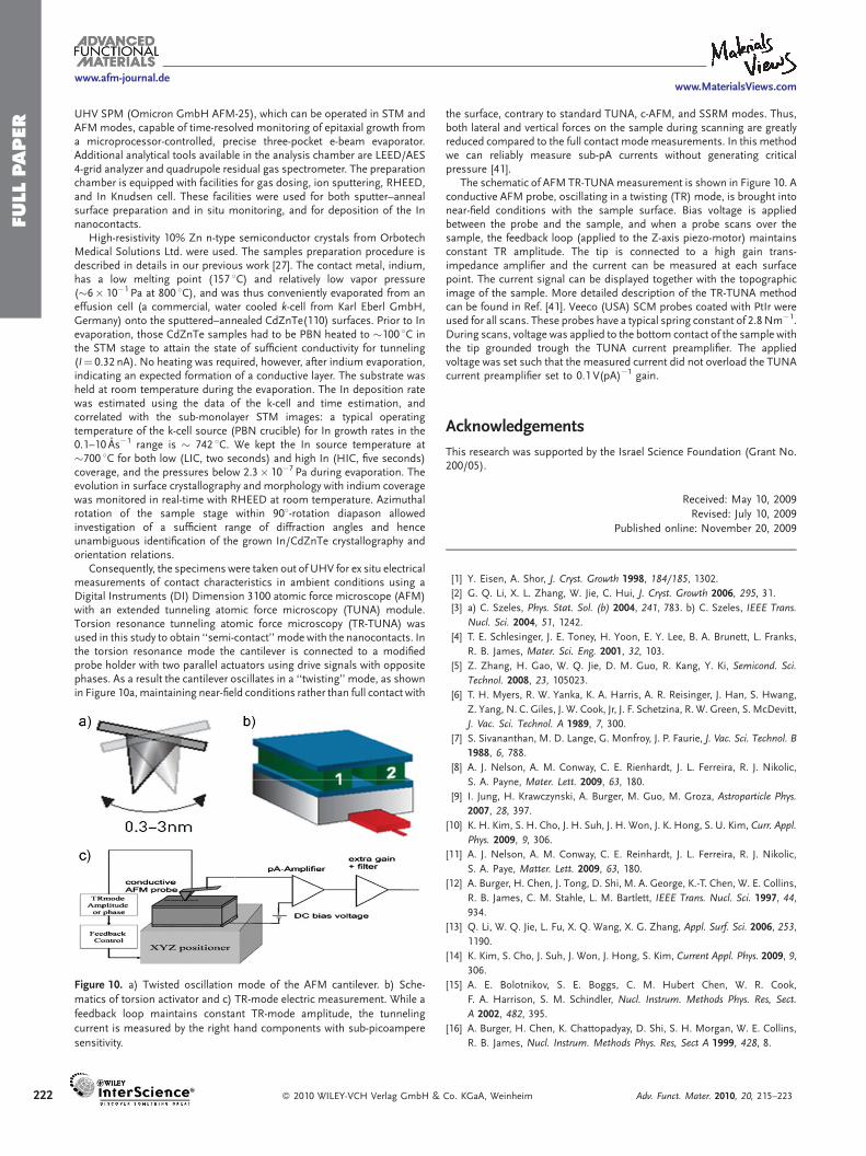
Consequently, the specimens were taken out of UHV for ex situ electricalmeasurements of contact characteristics in ambient conditions using aDigital Instruments (DI) Dimension 3100 atomic force microscope (AFM)with an extended tunneling atomic force microscopy (TUNA) module.Torsion resonance tunneling atomic force microscopy (TR-TUNA) wasused in this study to obtain ‘‘semi-contact’’ mode with the nanocontacts. Inthe torsion resonance mode the cantilever is connected to a modifiedprobe holder with two parallel actuators using drive signals with oppositephases. As a result the cantilever oscillates in a ‘‘twisting’’ mode, as shownin Figure 10a, maintaining near-field conditions rather than full contact with
Figure 10. a) Twisted oscillation mode of the AFM cantilever. b) Sche-
matics of torsion activator and c) TR-mode electric measurement. While a
feedback loop maintains constant TR-mode amplitude, the tunneling
current is measured by the right hand components with sub-picoampere
sensitivity.
� 2010 WILEY-VCH Verlag GmbH &
the surface, contrary to standard TUNA, c-AFM, and SSRM modes. Thus,both lateral and vertical forces on the sample during scanning are greatlyreduced compared to the full contact modemeasurements. In this methodwe can reliably measure sub-pA currents without generating criticalpressure [41].
The schematic of AFM TR-TUNAmeasurement is shown in Figure 10. Aconductive AFM probe, oscillating in a twisting (TR) mode, is brought intonear-field conditions with the sample surface. Bias voltage is appliedbetween the probe and the sample, and when a probe scans over thesample, the feedback loop (applied to the Z-axis piezo-motor) maintainsconstant TR amplitude. The tip is connected to a high gain trans-impedance amplifier and the current can be measured at each surfacepoint. The current signal can be displayed together with the topographicimage of the sample. More detailed description of the TR-TUNA methodcan be found in Ref. [41]. Veeco (USA) SCM probes coated with PtIr wereused for all scans. These probes have a typical spring constant of 2.8Nm�1.During scans, voltage was applied to the bottom contact of the sample withthe tip grounded trough the TUNA current preamplifier. The appliedvoltage was set such that the measured current did not overload the TUNAcurrent preamplifier set to 0.1 V(pA)�1 gain.
Acknowledgements
This research was supported by the Israel Science Foundation (Grant No.200/05).
Received: May 10, 2009
Revised: July 10, 2009
Published online: November 20, 2009
[1] Y. Eisen, A. Shor, J. Cryst. Growth 1998, 184/185, 1302.
[2] G. Q. Li, X. L. Zhang, W. Jie, C. Hui, J. Cryst. Growth 2006, 295, 31.
[3] a) C. Szeles, Phys. Stat. Sol. (b) 2004, 241, 783. b) C. Szeles, IEEE Trans.
Nucl. Sci. 2004, 51, 1242.
[4] T. E. Schlesinger, J. E. Toney, H. Yoon, E. Y. Lee, B. A. Brunett, L. Franks,
R. B. James, Mater. Sci. Eng. 2001, 32, 103.
[5] Z. Zhang, H. Gao, W. Q. Jie, D. M. Guo, R. Kang, Y. Ki, Semicond. Sci.
Technol. 2008, 23, 105023.
[6] T. H. Myers, R. W. Yanka, K. A. Harris, A. R. Reisinger, J. Han, S. Hwang,
Z. Yang, N. C. Giles, J. W. Cook, Jr, J. F. Schetzina, R. W. Green, S. McDevitt,
J. Vac. Sci. Technol. A 1989, 7, 300.
[7] S. Sivananthan, M. D. Lange, G. Monfroy, J. P. Faurie, J. Vac. Sci. Technol. B
1988, 6, 788.
[8] A. J. Nelson, A. M. Conway, C. E. Rienhardt, J. L. Ferreira, R. J. Nikolic,
S. A. Payne, Mater. Lett. 2009, 63, 180.
[9] I. Jung, H. Krawczynski, A. Burger, M. Guo, M. Groza, Astroparticle Phys.
2007, 28, 397.
[10] K. H. Kim, S. H. Cho, J. H. Suh, J. H. Won, J. K. Hong, S. U. Kim, Curr. Appl.
Phys. 2009, 9, 306.
[11] A. J. Nelson, A. M. Conway, C. E. Reinhardt, J. L. Ferreira, R. J. Nikolic,
S. A. Paye, Matter. Lett. 2009, 63, 180.
[12] A. Burger, H. Chen, J. Tong, D. Shi, M. A. George, K.-T. Chen, W. E. Collins,
R. B. James, C. M. Stahle, L. M. Bartlett, IEEE Trans. Nucl. Sci. 1997, 44,
934.
[13] Q. Li, W. Q. Jie, L. Fu, X. Q. Wang, X. G. Zhang, Appl. Surf. Sci. 2006, 253,
1190.
[14] K. Kim, S. Cho, J. Suh, J. Won, J. Hong, S. Kim, Current Appl. Phys. 2009, 9,
306.
[15] A. E. Bolotnikov, S. E. Boggs, C. M. Hubert Chen, W. R. Cook,
F. A. Harrison, S. M. Schindler, Nucl. Instrum. Methods Phys. Res, Sect.
A 2002, 482, 395.
[16] A. Burger, H. Chen, K. Chattopadyay, D. Shi, S. H. Morgan, W. E. Collins,
R. B. James, Nucl. Instrum. Methods Phys. Res, Sect A 1999, 428, 8.
Co. KGaA, Weinheim Adv. Funct. Mater. 2010, 20, 215–223

FULLPAPER
www.MaterialsViews.comwww.afm-journal.de
[17] Wang, W. Sang, W. Shi, Y. Qian, J. Min, D. Liu, Y. Xia, Nucl. Instrum.
Methods Phys. Res, Sect. A 2000, 448, 581.
[18] X. Wang, W. Jie, H. Li, Q. Li, Z. Wang, Nucl. Instrum. Methods Phys. Res,
Sect. A 2006, 560, 409.
[19] H. Corder, R. Schmid-Fetzer, Semicond. Sci. Technol. 1995, 10, 77.
[20] G. Q. Zha, W. Q. Jie, T. T. Tan, W. H. Zhang, F. Q. Xu, J. Phys. Chem. C 2007,
111, 12834.
[21] T. Takeuchi, T. Kore-eda, A. Ebina, Appl. Surf. Sci. 1996, 100/101, 596.
[22] G. Q. Zha, W. Q. Jie, D. M. Zeng, Y. D. Xu, W. H. Zhang, F. Q. Xu, Surf. Sci.
2006, 600, 2629.
[23] T. Takeuchi, T. Kore-eda, A. Ebina, Appl. Surf. Sci. 1996, 100/101, 596.
[24] L. Wang, W. Sang, W. Shi, Y. Qian, J. Min, D. Liu, Y. Xia, Nucl. Instrum.
Methods Phys. Res, Sect. A 2000, 448, 581.
[25] D. Brun-Le Cunff, B. Daudin, J. L. Rouviere, Appl. Phys. Lett. 1996, 69, 514.
[26] A. Ruzin, I. Torchinski, I. Goldfarb, Semicond. Sci. Technol. 2004, 19,
644.
[27] G. Cohen Taguri, M. Levinshtein, A. Ruzin, I. Goldfarb, Surf. Sci. 2008, 602,
712.
[28] H. Corder, R. Schmid-Fetzer, Semicond. Sci. Technol. 1995, 10, 77.
[29] C. B. Duke, A. Paton, W. K. Ford, A. Kahn, G. Scott, Phys. Rev. B 1981, 24,
3310.
Adv. Funct. Mater. 2010, 20, 215–223 � 2010 WILEY-VCH Verl
[30] K. Watari, J. L. A. Alves, A. C. Ferraz, Brazilian J. Phys. 1996, 26, 271.
[31] C. B. Duke, A. Paton, A. Kahn, Phys. Rev. B 1983, 27, 3436.
[32] D. A. Bonnell, Scanning Tunneling Microscopy and Spectroscopy: Theory,
Techniques, and Applications, VCH Publishers, Inc, Weinheim, Germany
1993, pp, 43–44.
[33] K.-J. Chao, C.-K. Shih, D. W. Gotthold, B. G. Streetman, Phys. Rev. Lett.
1997, 79, 4822.
[34] V. Kumar, B. S. R. Sastry, Phys. Stat. Sol. (b) 2005, 242, 869.
[35] T. Kendelewics, J. E. Klepeis, J. C. Woicik, S. H. Southworth, C. Mailhiot,
M. van Schilfgaarde, M. Methfessel, A. Herrera-Gomez, K. E. Miyano, Phys.
Rev. B 1995, 51, 10774.
[36] R. Ramırez-Bon, R. Nunez-Lopez, F. J. Espinoza-Beltran, O. Zelaya-Angle,
J. Gonzales-Hernandez, J. Phys. Chem. Solids 1997, 58, 807.
[37] N. A. Rutter, B. A. Glowack, J. Mater. Sci. Lett. 1999, 18, 1661.
[38] B. Sundaravel, A. K. Das, S. K. Ghose, K. Sekar, B. M. Dev, Appl. Surf. Sci.
1999, 137, 11.
[39] A. Trampert, K. H. Ploog, Cryst. Res. Technol. 2000, 35, 793.
[40] P. A. Langhahr, T. Wagner, F. F. Lange, M. Ruhle, J. Crys. Growth 2003, 256,
162.
[41] B. Bhushan, H. Fuchs, S. Kawata, Applied Scanning Probe Methods V,
Springer-Verlag, Berlin 2007.
ag GmbH & Co. KGaA, Weinheim 223