sa-vk72dgcs sa-vk72dgs - index of
TRANSCRIPT
AMPLIFIER SECTIONRMS Output Power: Dolby Digital Mode
Main
70 W per channel (6 Ω), 1 kHz, 10% THD
Surround Ch
55 W per channel (6 Ω), 1 kHz, 10% THD
Center Ch
70 W per channel (6 Ω), 1 kHz, 10% THD
Total RMS Dolby Digital mode power
320 W
PMPO output power 4000 W
FM/AM TUNER, TERMINALS SECTIONPreset station FM 15 stations
AM 15 stations
Frequency Modulation (FM)
Frequency range 87.50 - 108.00 MHz (50 kHz step)
Sensitivity 2.5 µV (IHF)
S/N 26dB 2.2 µV
Antenna terminals 75 Ω (unbalanced)
Amplitude Modulation (AM)
Frequency range 522 - 1629 kHz (9 kHz step)
520 - 1630 kHz (10 kHz step)
AM Sensitivity S/N 20dB at 999 kHz
560 µV/m
Audio performance (Amplifier)
© 2005 Matsushita Electric Industrial Co. Ltd.. Allrights reserved. Unauthorized copying anddistribution is a violation of law.
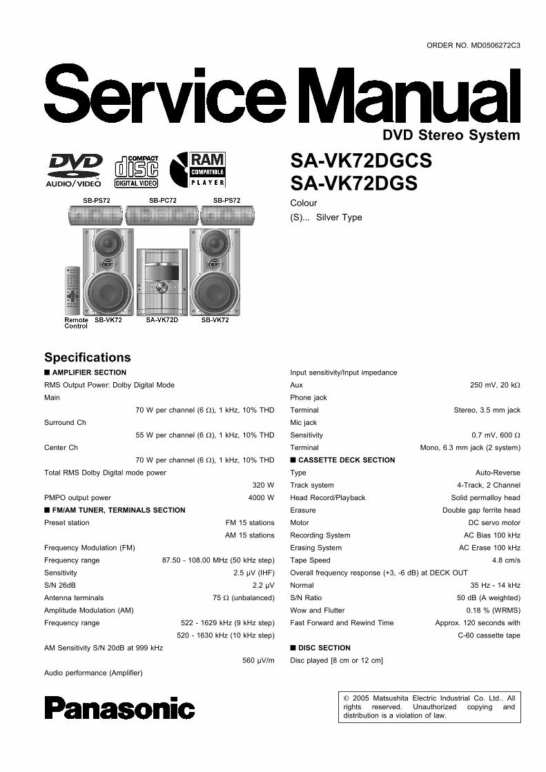
SA-VK72DGCSSA-VK72DGSColour(S)... Silver Type
Input sensitivity/Input impedance
Aux 250 mV, 20 kΩ
Phone jack
Terminal Stereo, 3.5 mm jack
Mic jack
Sensitivity 0.7 mV, 600 Ω
Terminal Mono, 6.3 mm jack (2 system)
CASSETTE DECK SECTIONType Auto-Reverse
Track system 4-Track, 2 Channel
Head Record/Playback Solid permalloy head
Erasure Double gap ferrite head
Motor DC servo motor
Recording System AC Bias 100 kHz
Erasing System AC Erase 100 kHz
Tape Speed 4.8 cm/s
Overall frequency response (+3, -6 dB) at DECK OUT
Normal 35 Hz - 14 kHz
S/N Ratio 50 dB (A weighted)
Wow and Flutter 0.18 % (WRMS)
Fast Forward and Rewind Time Approx. 120 seconds with
C-60 cassette tape
DISC SECTIONDisc played [8 cm or 12 cm]
DVD Stereo System
Specifications
ORDER NO. MD0506272C3
(1) DVD (DVD-Video, DVD-Audio)
(2) DVD-RAM (DVD-VR, JPEG* 4,*5)
(3) DVD-R (DVD-Video)
(4) DVD-RW (DVD-Video)
+ R/RW (Video)
(5) CD,CD-R/RW [CD-DA, Video CD, SVCD* 1, MP3* 2,* 5, WMA* 3,* 5,JPEG* 4,* 5, HighMAT Level 2 (Audio and Image)]* 1 Conforming to IEC62107* 2 MPEG-1 Layer 3, MPEG-2 Layer 3* 3 Windows Media Audio Ver.9.0. Class 2A
Not compatible with Multiple Bit Rate (MBR)* 4 Exif Ver 2.1 JPEG Baseline files
Picture resolution: between 160 x 120 and 6144 x 4096 pixels (Subsampling is 4:2:2 or 4:2:0)* 5 The total combined maximum number of recognizable audio andpicture contents and groups: 4000 audio and picture contents and400 groups.
Pick up
Wavelength
CD 785 nm
DVD 662 nm
Audio output (Disc)
Number of channels 5.1 ch (FL,FR,C,SL,SR,SW)
Audio performance (measurement at: Line out terminal)
Frequency response
CD-Audio 4 Hz to 20 kHz (+1 dB,-2 dB)
VIDEO SECTION
Video system
Signal system PAL625/50, PAL525/60, NTSC
Composite video output
Output level 1 Vp-p (75 Ω)
Terminal Pin jack (1 system)
S-video output
Y output level 1 Vp-p (75 Ω)
C output level 0.3 Vp-p (75 Ω) (PAL)
0.286 Vp-p (75 Ω) (NTSC)
Terminal S terminal (1 system)
Component video output
[NTSC: 525 (480)p/525 (480)i, PAL: 625 (576)p/625 (576)i]
Y output level 1 Vp-p (75 Ω)
PB output level 0.7 Vp-p (75 Ω)
PR output level 0.7 Vp-p (75 Ω)
Terminal
Pin jack (Y: green, PB: blue, PR: red) (1 system)
GENERAL
Power supply
AC 110 to 127V/220 to 240 V, 50/60Hz
Power consumption 300 W
Power consumption in standby mode:
0.8 W (approximate)
Dimensions (W x H x D) 250 x 330 x 348 mm
Mass 8.8 kg
Operating temperature range +5°C to +35°C
Operating humidity range 5% to 90% RH (no condensation)
SYSTEM
SC-VK72D (GCS) Music System: SA-VK72D (GCS)
Front Speakers: SB-VK72 (GC)
Satelite Speakers: SB-PT72 (GC)
SC-VK72D (GS) Music System: SA-VK72D (GS)
Front Speakers: SB-VK72 (GC)
Satelite Speakers: SB-PT72 (GC)
Notes:
1. Specifications are subject to change without notice. Mass anddimensions are approximate.
2. Total harmonic distortion is measured by the digital spectrumanalyzer.
2
SA-VK72DGCS / SA-VK72DGS
1 Safety precautions for AC Cord (For GS only) 5 2 Before Use (Caution) 5 3 Before Repair and Adjustment 5 4 Protection Circuitry 5 5 Safety Precautions 6
5.1. General Guidelines 6
6 Prevention of Electro Static Discharge (ESD) toElectrostatically Sensitive (ES) Devices 7
7 Handling the Lead-free Solder 7 7.1. About lead free solder (PbF) 7
8 Precaution of Laser Diode 8 9 Cautions to be taken when handling Optical Pickup 9
9.1. Handling Optical Pickup 9
9.2. Replacing Precautions for Optical Pickup Unit 9
9.3. Grounding for Preventing Electrostatic Destruction 9
10 Accessories 10 11 Operation Procedures 11 12 Disc information 13 13 About HighMAT 15
13.1. What痴 HighMAT? 15
13.2. Why take advantage of HighMAT? 15
13.3. Benefits of HighMAT? 16
14 Optical Pickup Self-Diagnosis and Replacement Procedure 19 14.1. Optical Pickup Breakdown diagnosis 19
15 Self-Diagnosis Function 20 15.1. Entering into Self-Diagnostic Mode 20
15.2. Automatic Displayed Error Codes 20
15.3. Memorized Error Codes 20
15.4. Service Mode Table 1 21
15.5. DVD/CD Self-Diagnosis Error Code Description 21
15.6. Mode Table 2 21
15.7. CR16 Mechanism Ageing Mode 24
15.8. Operation Lock Function 24
15.9. Things to Do After Repair 25
16 Cautions To Be Taken During Servicing 25 16.1. Recovery after the dvd player is repaired 25
16.2. DVD Player Firmware Version Upgrade Process 25
16.3. Firmware Version Upgrade Process by Using Disc and
Recovery Process 25
16.4. Using Recovery Disc 26
16.5. Total Usage Time Display 26
16.6. After replacement of DVD Module 26
17 Disassembly and Assembly of Main Component 27 17.1. Disassembly steps 27
17.2. Disassembly flow chart 28
17.3. Disassembly of Top Cabinet 29
17.4. Disassembly of Rear Panel 29
17.5. Disassembly of DVD Changer Unit 29
17.6. Disassembly of Main P.C.B. 31
17.7. Disassembly of Power Amp P.C.B. 31
17.8. Disassembly of Power P.C.B. 32
17.9. Disassembly of Transformer P.C.B. & Voltage Selector 33
17.10. Disassembly of Front Panel Unit 33
17.11. Disassembly for Mic P.C.B. & Panel P.C.B. 35
17.12. Disassembly of Deck Mechanism Unit 36
17.13. Replacement for Deck P.C.B. 36
17.14. Replacement for Traverse Deck 36
17.15. Replacement for Optical Pickup Unit (DVD mechanism) 37
17.16. Procedure for removing CD loading mechanism 40
17.17. CR16 mechanism disassembly procedure 40
17.18. CR16 mechanism assembly procedure 46
17.19. Disassembly for Traverse Unit 58
17.20. Replacement for cassette lid 59
17.21. Rectification for tape jam problem 60
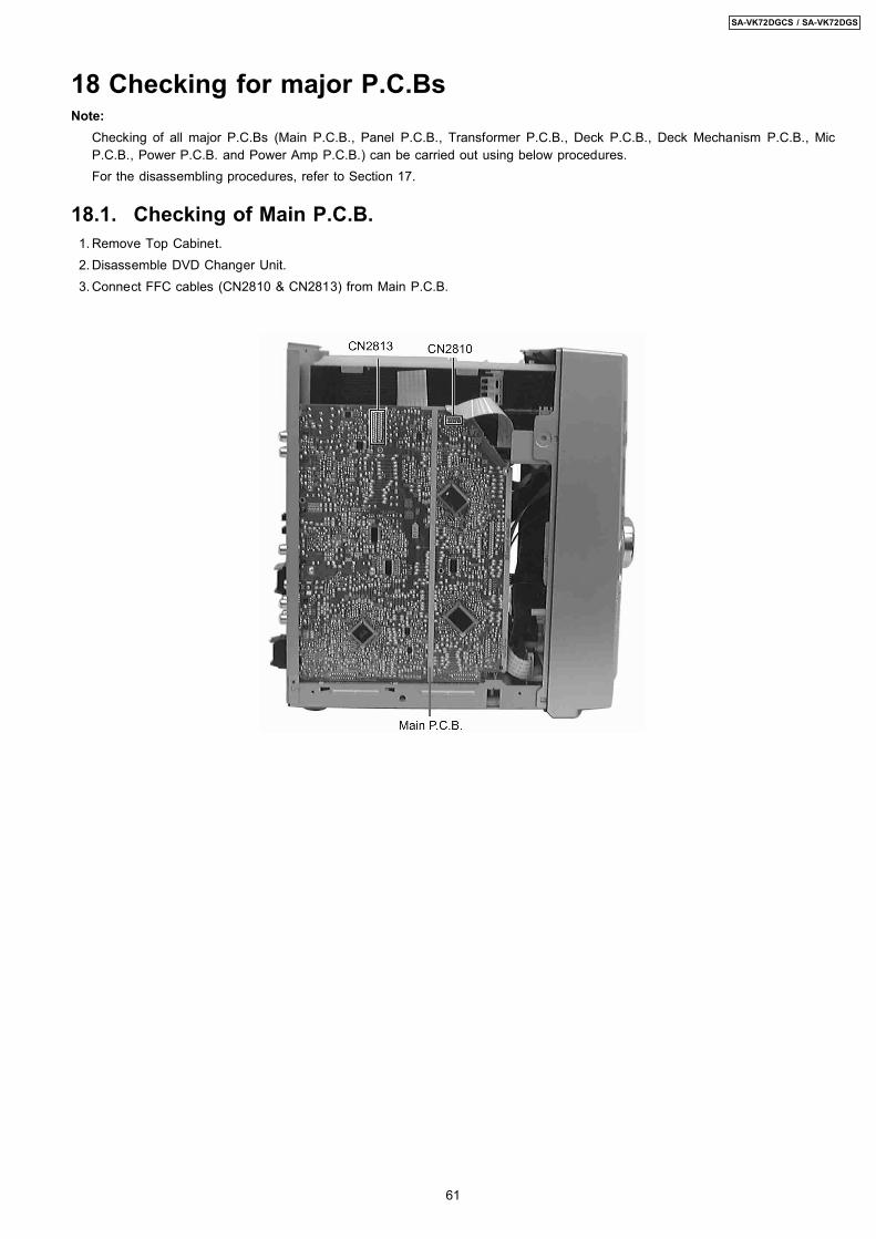
18 Checking for major P.C.Bs 61 18.1. Checking of Main P.C.B. 61
18.2. Checking of Transformer P.C.B. 62
18.3. Checking of Panel, Deck & Deck Mechanism P.C.B. 63
18.4. Checking of Power P.C.B. 64
19 Measurements and Adjustments 65 19.1. Cassette Deck Section 65
19.2. Tuner Section 66
19.3. Alignment Points 67
20 Block Diagram 68 21 Voltage Measurement 79 22 Schematic Diagram 80
22.1. Optical Pickup Unit Circuit 81
22.2. (A) DVD Module Circuit 82
22.3. (B) Main (Tuner) Circuit 89
22.4. (B) Main Circuit 90
22.5. (C) Panel Circuit & (D) Mic Circuit 99
22.6. (E) Deck Circuit & (F) Deck Mechanism Circuit 101
22.7. (G) Power Circuit 103
22.8. (H) Power Amp Circuit 104
22.9. (I) Transformer Circuit 105
22.10. (J) CD Loading Circuit 106
23 Printed Circuit Board 107 23.1. (A) DVD Module P.C.B. (Side: A & B ) 107
23.2. (B) Main P.C.B. 109
23.3. (C) Panel P.C.B. 111
23.4. (D) Mic P.C.B. & (K) Tuner Pack P.C.B. 113
23.5. (E) Deck P.C.B. & (F) Deck Mechanism P.C.B. 114
23.6. (G) Power P.C.B. & (H) Power Amp P.C.B. 115
23.7. (I) Transformer P.C.B. 117
23.8. (J) CD Loading P.C.B. 118
24 Wiring Connection Diagram 119 25 Illustration of ICs, Transistors and Diodes 121 26 Terminal Function of IC 123
26.1. IC2818 (C2CBJG000653) System Microprocessor 123
27 Parts Location and Replacement Parts List 125 27.1. Deck Mechanism (RAA3413-S) 126
27.2. DVD Loading Mechanism 129
CONTENTS Page Page
3
SA-VK72DGCS / SA-VK72DGS

27.3. Cabinet 132
27.4. Electrical Parts List 135
27.5. Packing Materials & Accessories Parts List 148
27.6. Packaging 149
4
SA-VK72DGCS / SA-VK72DGS
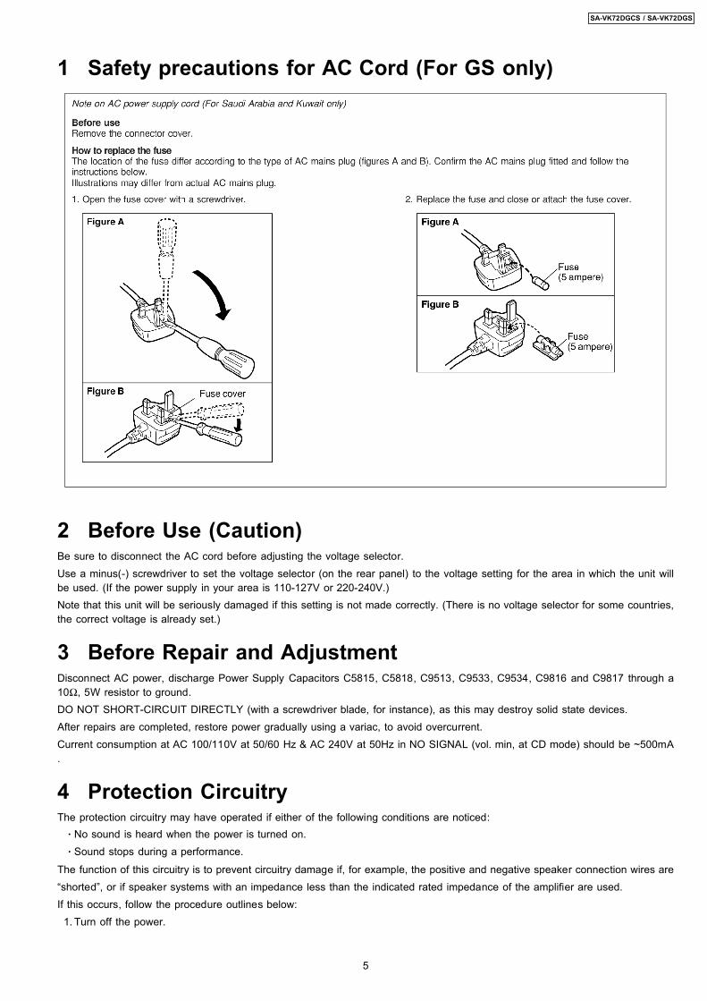
1 Safety precautions for AC Cord (For GS only)
2 Before Use (Caution)Be sure to disconnect the AC cord before adjusting the voltage selector.Use a minus(-) screwdriver to set the voltage selector (on the rear panel) to the voltage setting for the area in which the unit willbe used. (If the power supply in your area is 110-127V or 220-240V.)Note that this unit will be seriously damaged if this setting is not made correctly. (There is no voltage selector for some countries,the correct voltage is already set.)
3 Before Repair and AdjustmentDisconnect AC power, discharge Power Supply Capacitors C5815, C5818, C9513, C9533, C9534, C9816 and C9817 through a10Ω, 5W resistor to ground.DO NOT SHORT-CIRCUIT DIRECTLY (with a screwdriver blade, for instance), as this may destroy solid state devices.After repairs are completed, restore power gradually using a variac, to avoid overcurrent.Current consumption at AC 100/110V at 50/60 Hz & AC 240V at 50Hz in NO SIGNAL (vol. min, at CD mode) should be ~500mA.
4 Protection CircuitryThe protection circuitry may have operated if either of the following conditions are noticed: · No sound is heard when the power is turned on. · Sound stops during a performance.
The function of this circuitry is to prevent circuitry damage if, for example, the positive and negative speaker connection wires are“shorted”, or if speaker systems with an impedance less than the indicated rated impedance of the amplifier are used.If this occurs, follow the procedure outlines below: 1. Turn off the power.
5
SA-VK72DGCS / SA-VK72DGS
2. Determine the cause of the problem and correct it. 3. Turn on the power once again after one minute.Note :When the protection circuitry functions, the unit will not operate unless the power is first turned off and then on again.
5 Safety Precautions5.1. General Guidelines 1. When servicing, observe the original lead dress. If a short circuit is found, replace all parts which have been overheated or
damaged by the short circuit. 2. After servicing, see to it that all the protective devices such as insulation barriers, insulation papers shields are properly
installed. 3. After servicing, make the following leakage current checks to prevent the customer from being exposed to shock hazards.
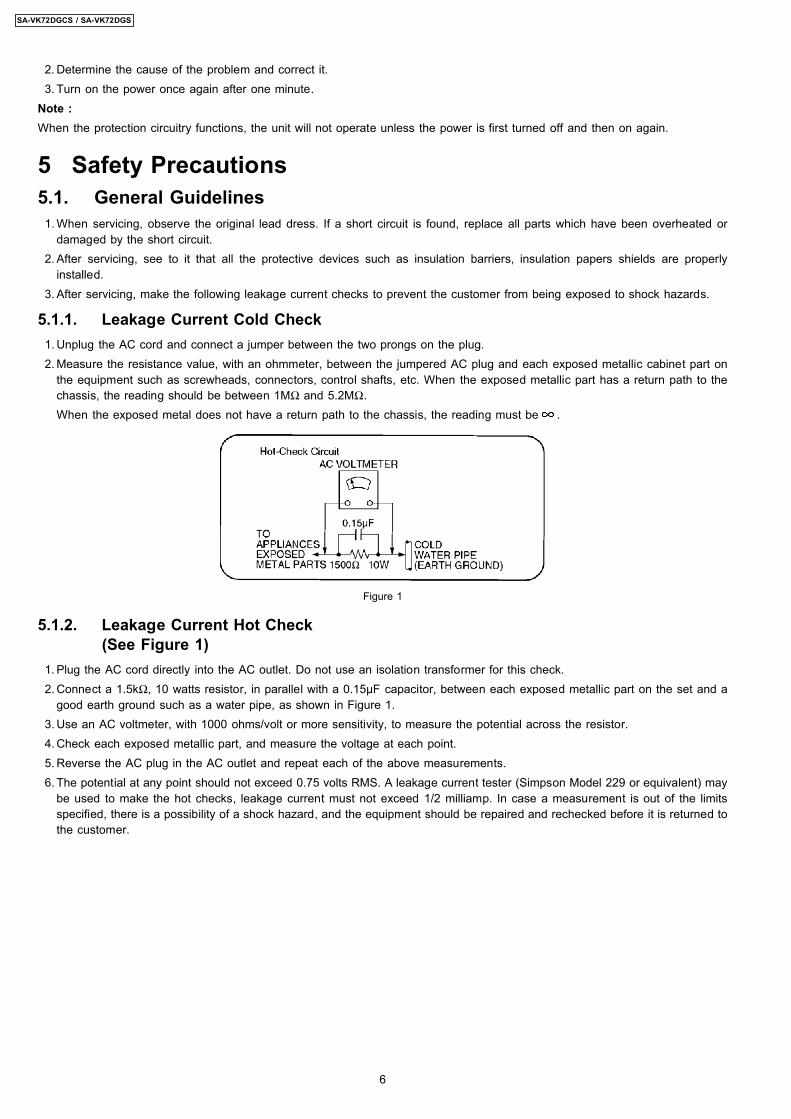
5.1.1. Leakage Current Cold Check 1. Unplug the AC cord and connect a jumper between the two prongs on the plug. 2. Measure the resistance value, with an ohmmeter, between the jumpered AC plug and each exposed metallic cabinet part on
the equipment such as screwheads, connectors, control shafts, etc. When the exposed metallic part has a return path to thechassis, the reading should be between 1MΩ and 5.2MΩ.When the exposed metal does not have a return path to the chassis, the reading must be .
Figure 1
5.1.2. Leakage Current Hot Check(See Figure 1)
1. Plug the AC cord directly into the AC outlet. Do not use an isolation transformer for this check. 2. Connect a 1.5kΩ, 10 watts resistor, in parallel with a 0.15µF capacitor, between each exposed metallic part on the set and a
good earth ground such as a water pipe, as shown in Figure 1. 3. Use an AC voltmeter, with 1000 ohms/volt or more sensitivity, to measure the potential across the resistor. 4. Check each exposed metallic part, and measure the voltage at each point. 5. Reverse the AC plug in the AC outlet and repeat each of the above measurements. 6. The potential at any point should not exceed 0.75 volts RMS. A leakage current tester (Simpson Model 229 or equivalent) may
be used to make the hot checks, leakage current must not exceed 1/2 milliamp. In case a measurement is out of the limitsspecified, there is a possibility of a shock hazard, and the equipment should be repaired and rechecked before it is returned tothe customer.
6
SA-VK72DGCS / SA-VK72DGS

6 Prevention of Electro Static Discharge (ESD) toElectrostatically Sensitive (ES) Devices
Some semiconductor (solid state) devices can be damaged easily by electricity. Such components commonly are calledElectrostatically Sensitive (ES) Devices. Examples of typical ES devices are integrated circuits and some field-effect transistors andsemiconductor “chip” components. The following techniques should be used to help reduce the incidence of component damagecaused by electro static discharge (ESD). 1. Immediately before handling any semiconductor component or semiconductor-equipped assembly, drain off any ESD on your
body by touching a known earth ground. Alternatively, obtain and wear a commercially available discharging ESD wrist strap,which should be removed for potential shock reasons prior to applying power to the unit under test.
2. After removing an electrical assembly equipped with ES devices, place the assembly on a conductive surface such asaluminium foil, to prevent electrostatic charge build up or exposure of the assembly.
3. Use only a grounded-tip soldering iron to solder or unsolder ES devices. 4. Use only an anti-static solder remover device. Some solder removal devices not classified as “anti-static (ESD protected)” can
generate electrical charge to damage ES devices. 5. Do not use freon-propelled chemicals. These can generate electrical charges sufficient to damage ES devices. 6. Do not remove a replacement ES device from its protective package until immediately before you are ready to install it. (Most
replacement ES devices are packaged with leads electrically shorted together by conductive foam, aluminium foil orcomparable conductive material).
7. Immediately before removing the protective material from the leads of a replacement ES device, touch the protective materialto the chassis or circuit assembly into which the device will be installed.Caution
Be sure no power is applied to the chassis or circuit, and observe all other safety precautions. 8. Minimize body motions when handling unpackaged replacement ES devices. (Otherwise harmless motion such as the brushing
together of your clothes fabric or the lifting of your foot from a carpeted floor can generate static electricity (ESD) sufficient todamage an ES device).
7 Handling the Lead-free Solder7.1. About lead free solder (PbF)Distinction of PbF P.C.B.:P.C.B.s (manufactured) using lead free solder will have a PbF stamp on the P.C.B.Caution: · Pb free solder has a higher melting point than standard solder; Typically the melting point is 50 - 70°F (30 - 40°C) higher. Please
use a high temperature soldering iron. In case of soldering iron with temperature control, please set it to 700 ± 20°F (370 ±10°C).
· Pb free solder will tend to splash when heated too high (about 1100°F/600°C). · When soldering or unsoldering, please completely remove all of the solder on the pins or solder area, and be sure to heat the
soldering points with the Pb free solder until it melts enough.
7
SA-VK72DGCS / SA-VK72DGS
8 Precaution of Laser Diode
Caution :This product utilizes a laser diode with the unit turned "ON", invisible laser radiation is emitted from the pick up lens.Wavelength : 785 nm(CD)/662 nm(DVD)Maximum output radiation power from pick up : 100 µW/VDELaser radiation from pick up unit is safety level, but be sure the followings: 1. Do not disassemble the optical pick up unit, since radiation from exposed laser diode is dangerous. 2. Do not adjust the variable resistor on the pick up unit. It was already adjusted. 3. Do not look at the focus lens using optical instruments. 4. Recommend not to look at pick up lens for a long time.
CAUTION!THIS PRODUCT UTILIZES A LASER.USE OF CONTROLS OR ADJUSTMENTS OR PERFORMANCE OF PROCEDURES OTHER THAN THOSE SPECIFIED HEREIN MAY RESULTIN HAZARDOUS RADIATION EXPOSURE.
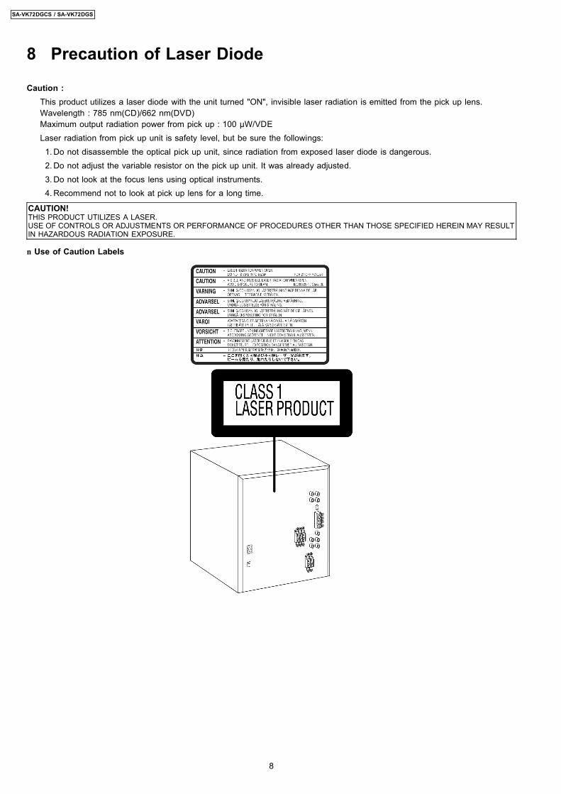
n Use of Caution Labels
8
SA-VK72DGCS / SA-VK72DGS
9 Cautions to be taken when handling Optical PickupThe laser diode used inside optical pickup could be destroyed due to static electricity as a potential difference is caused byelectrostatic load discharged from clothes or human body. Handling the parts carefully to avoid electrostatic destruction duringrepair.
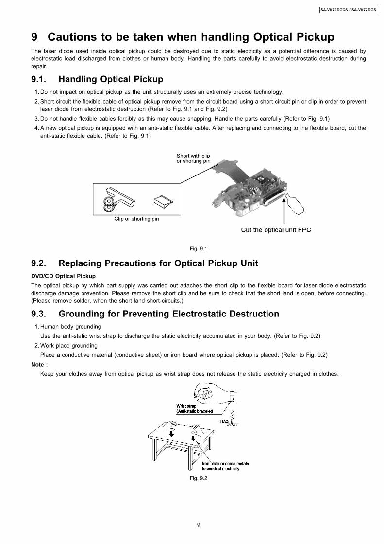
9.1. Handling Optical Pickup 1. Do not impact on optical pickup as the unit structurally uses an extremely precise technology. 2. Short-circuit the flexible cable of optical pickup remove from the circuit board using a short-circuit pin or clip in order to prevent
laser diode from electrostatic destruction (Refer to Fig. 9.1 and Fig. 9.2) 3. Do not handle flexible cables forcibly as this may cause snapping. Handle the parts carefully (Refer to Fig. 9.1) 4. A new optical pickup is equipped with an anti-static flexible cable. After replacing and connecting to the flexible board, cut the
anti-static flexible cable. (Refer to Fig. 9.1)
Fig. 9.1
9.2. Replacing Precautions for Optical Pickup UnitDVD/CD Optical PickupThe optical pickup by which part supply was carried out attaches the short clip to the flexible board for laser diode electrostaticdischarge damage prevention. Please remove the short clip and be sure to check that the short land is open, before connecting.(Please remove solder, when the short land short-circuits.)
9.3. Grounding for Preventing Electrostatic Destruction 1. Human body grounding
Use the anti-static wrist strap to discharge the static electricity accumulated in your body. (Refer to Fig. 9.2) 2. Work place grounding
Place a conductive material (conductive sheet) or iron board where optical pickup is placed. (Refer to Fig. 9.2)Note :
Keep your clothes away from optical pickup as wrist strap does not release the static electricity charged in clothes.
Fig. 9.2
9
SA-VK72DGCS / SA-VK72DGS
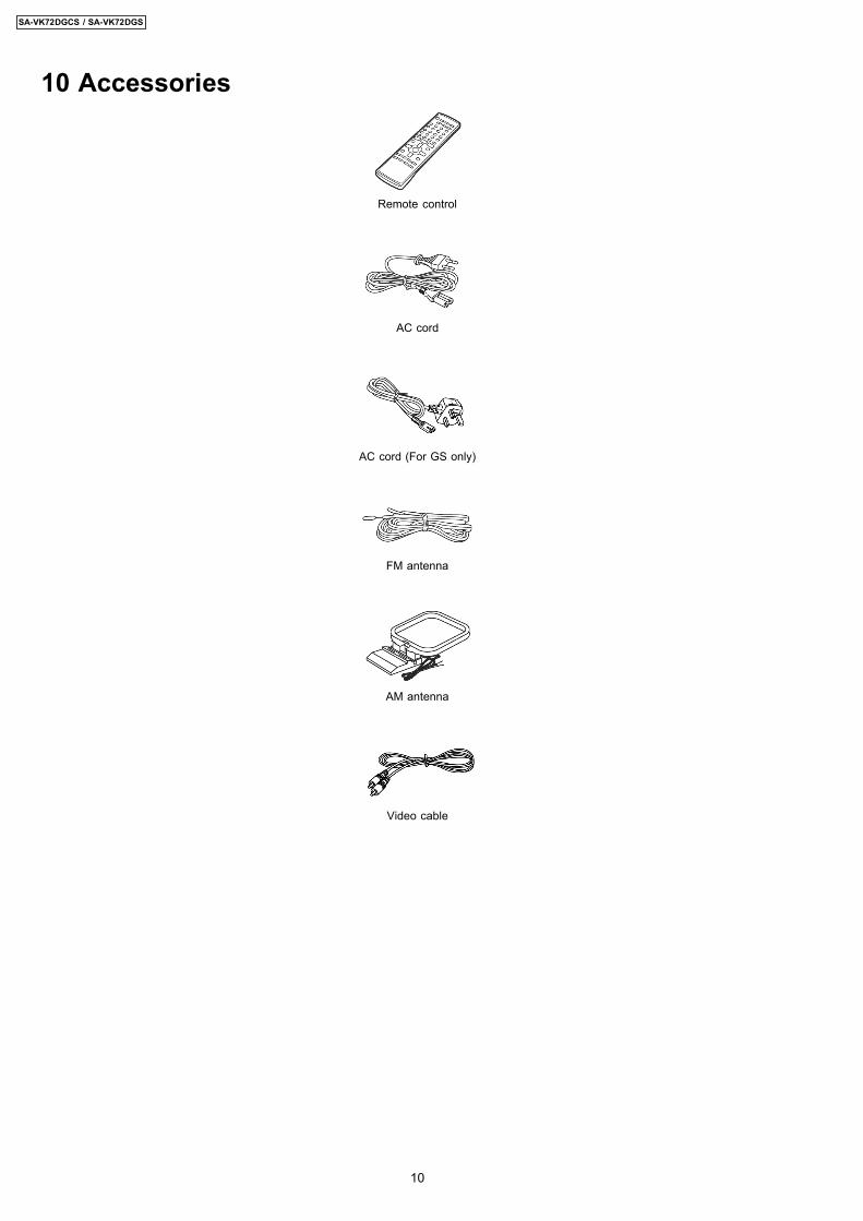
10 Accessories
Remote control
AC cord
AC cord (For GS only)
FM antenna
AM antenna
Video cable
10
SA-VK72DGCS / SA-VK72DGS
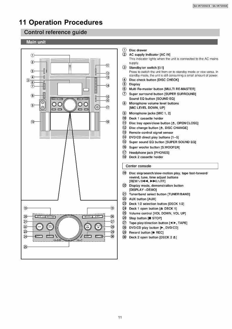
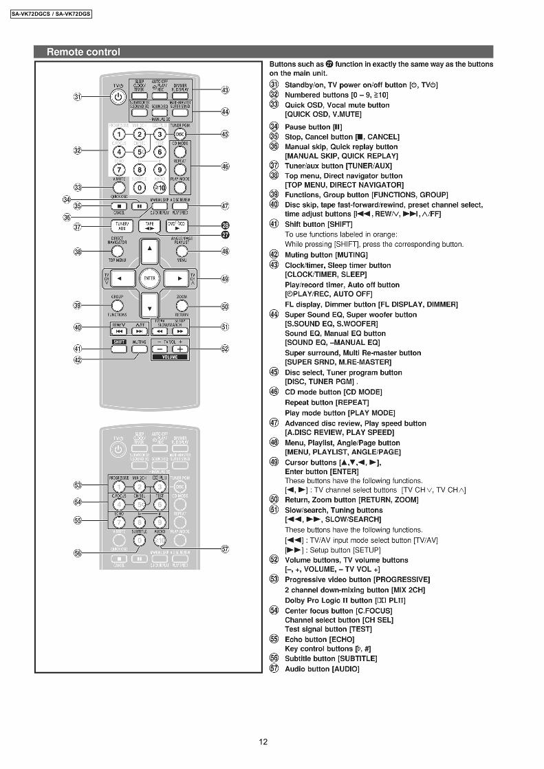
11 Operation Procedures
11
SA-VK72DGCS / SA-VK72DGS
12
SA-VK72DGCS / SA-VK72DGS
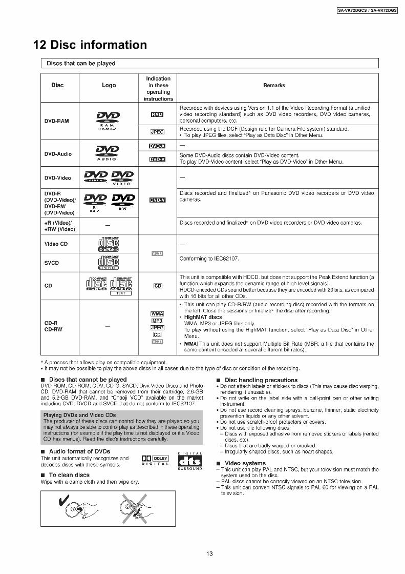
12 Disc information
13
SA-VK72DGCS / SA-VK72DGS
14
SA-VK72DGCS / SA-VK72DGS

13 About HighMAT13.1. What’s HighMAT?Consumers worldwide are using PCs to create their own collections of music, photos and even video by burning them onto CDs.But how these collections can be experienced across different devices can be confusing to navigate, time consuming to access fora DVD player, and be incomplete in terms of music information available to the customer.
HighMAT offers a solution to this growing consumer problem. HighMAT dramatically improves the digital media experience onconsumer electronic devices by delivering a simple, standardized approach that allows consumers who have created personalcollections of digital music, photography and video on their PC to:
>> Create a HighMAT CD or DVD which can be easily played back on consumer electronics devices such as CD and DVD players,and car stereos.>> Move digital media files (using recordable media such as CD-R and CD-RW) between the PC and various playback devicessuch as CD and DVD players.
A new standard for creating personal media on consumer electronic devices, HighMAT enable easier and more seamlessinteroperability between Windows PCs and devices designed for your living room, or the car.
13.2. Why take advantage of HighMAT?A Problem Defined:Today, when consumers create their own digital audio, video or photo collections on CD-R or other physicalformats, there are numerous, inconsistent ways that devices read the data. For the consumer, the playback experience can beconfusing:
15
SA-VK72DGCS / SA-VK72DGS
A Solution Created: HighMAT delivers a better digital media access experience by creating a standard approach for PCs tostructure digital media on various physical formats and for playback devices to read the data.
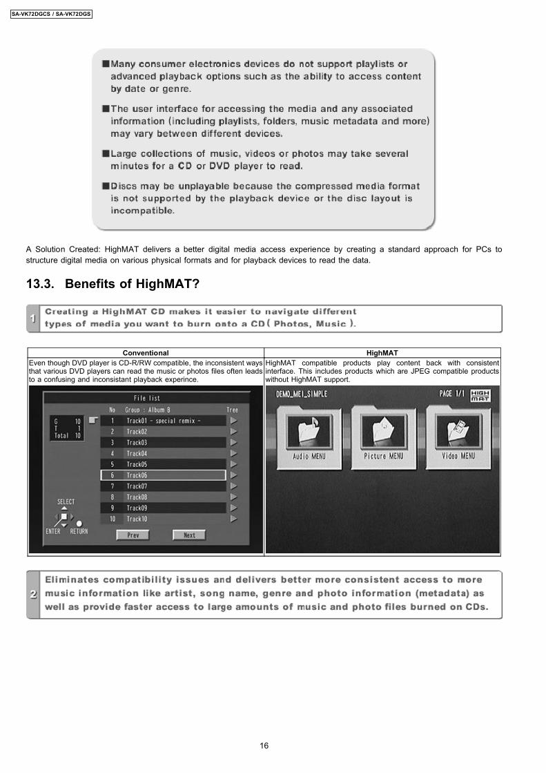
13.3. Benefits of HighMAT?
Conventional HighMATEven though DVD player is CD-R/RW compatible, the inconsistent waysthat various DVD players can read the music or photos files often leadsto a confusing and inconsistant playback experince.
HighMAT compatible products play content back with consistentinterface. This includes products which are JPEG compatible productswithout HighMAT support.
16
SA-VK72DGCS / SA-VK72DGS
17
SA-VK72DGCS / SA-VK72DGS
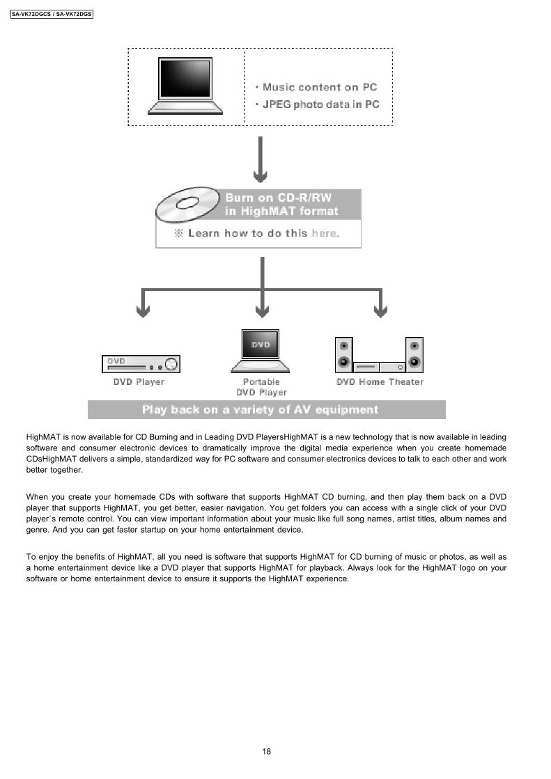
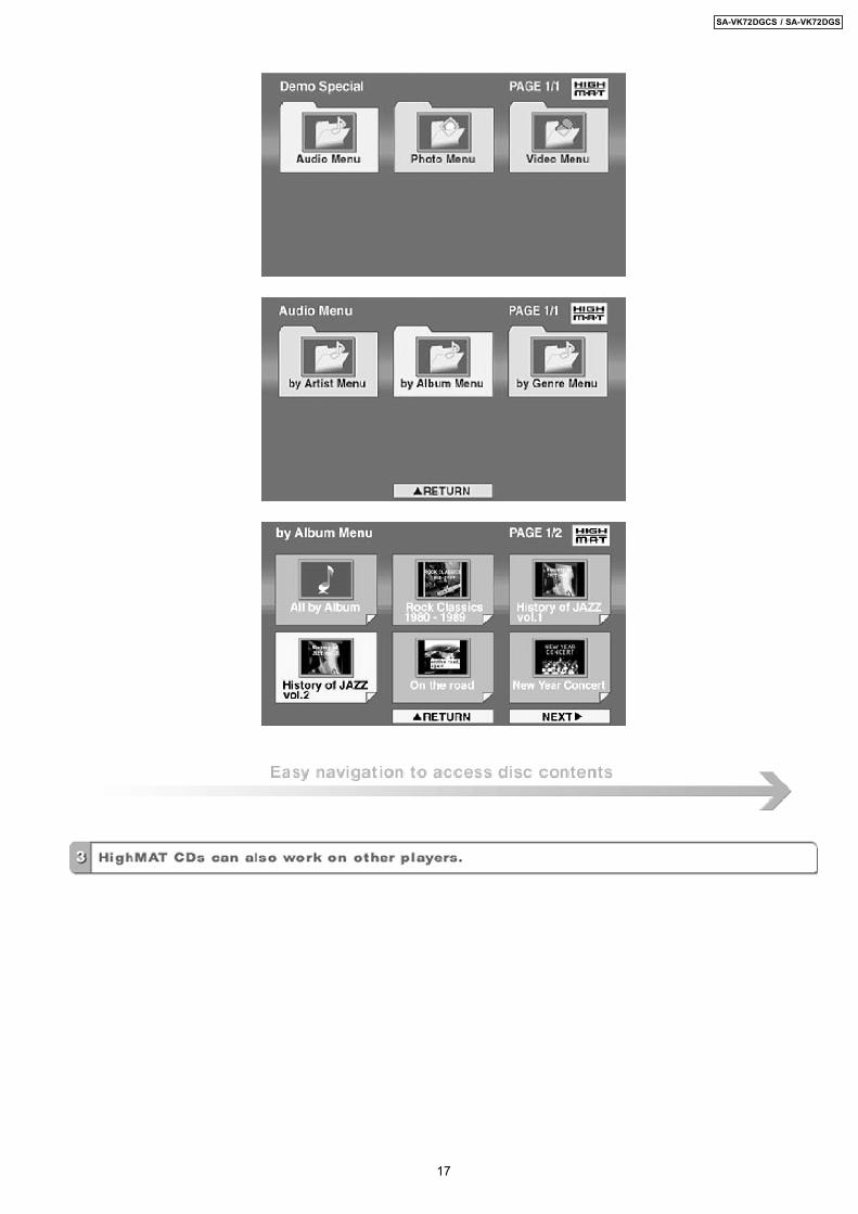
HighMAT is now available for CD Burning and in Leading DVD PlayersHighMAT is a new technology that is now available in leadingsoftware and consumer electronic devices to dramatically improve the digital media experience when you create homemadeCDsHighMAT delivers a simple, standardized way for PC software and consumer electronics devices to talk to each other and workbetter together.
When you create your homemade CDs with software that supports HighMAT CD burning, and then play them back on a DVDplayer that supports HighMAT, you get better, easier navigation. You get folders you can access with a single click of your DVDplayer´s remote control. You can view important information about your music like full song names, artist titles, album names andgenre. And you can get faster startup on your home entertainment device.
To enjoy the benefits of HighMAT, all you need is software that supports HighMAT for CD burning of music or photos, as well asa home entertainment device like a DVD player that supports HighMAT for playback. Always look for the HighMAT logo on yoursoftware or home entertainment device to ensure it supports the HighMAT experience.
18
SA-VK72DGCS / SA-VK72DGS
14 Optical Pickup Self-Diagnosis and ReplacementProcedure
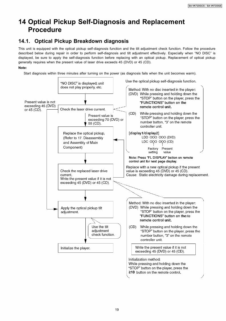
14.1. Optical Pickup Breakdown diagnosisThis unit is equipped with the optical pickup self-diagnosis function and the tilt adjustment check function. Follow the proceduredescribed below during repair in order to perform self-diagnosis and tilt adjustment effectively. Especially when “NO DISC” isdisplayed, be sure to apply the self-diagnosis function before replacing with an optical pickup. Replacement of optical pickupgenerally requires when the present value of laser drive exceeds 45 (DVD) or 45 (CD).Note:
Start diagnosis within three minutes after turning on the power (as diagnosis fails when the unit becomes warm).
19
SA-VK72DGCS / SA-VK72DGS
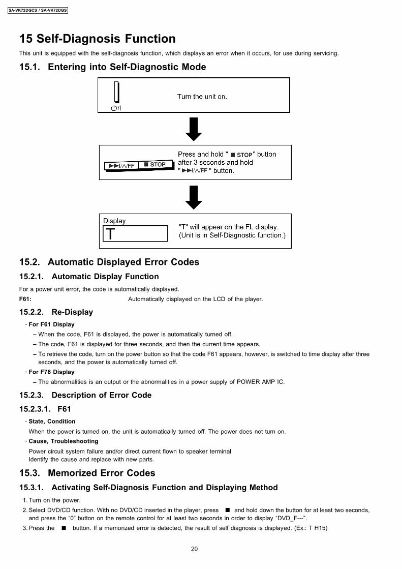
15 Self-Diagnosis FunctionThis unit is equipped with the self-diagnosis function, which displays an error when it occurs, for use during servicing.
15.1. Entering into Self-Diagnostic Mode
15.2. Automatic Displayed Error Codes15.2.1. Automatic Display FunctionFor a power unit error, the code is automatically displayed.F61: Automatically displayed on the LCD of the player.
15.2.2. Re-Display · For F61 Display
− − − − When the code, F61 is displayed, the power is automatically turned off. − − − − The code, F61 is displayed for three seconds, and then the current time appears. − − − − To retrieve the code, turn on the power button so that the code F61 appears, however, is switched to time display after three
seconds, and the power is automatically turned off. · For F76 Display
− − − − The abnormalities is an output or the abnormalities in a power supply of POWER AMP IC.
15.2.3. Description of Error Code15.2.3.1. F61 · State, Condition
When the power is turned on, the unit is automatically turned off. The power does not turn on. · Cause, Troubleshooting
Power circuit system failure and/or direct current flown to speaker terminalIdentify the cause and replace with new parts.
15.3. Memorized Error Codes15.3.1. Activating Self-Diagnosis Function and Displaying Method 1. Turn on the power. 2. Select DVD/CD function. With no DVD/CD inserted in the player, press and hold down the button for at least two seconds,
and press the “0” button on the remote control for at least two seconds in order to display “DVD_F---”. 3. Press the button. If a memorized error is detected, the result of self diagnosis is displayed. (Ex.: T H15)
20
SA-VK72DGCS / SA-VK72DGS
If several errors are detected, press the button to display each.
15.3.2. Re-Display · Press the power button to turn off the power, and then turn on the power. · The details of self diagnosis are stored in the unit memory.
To retrieve them, follow the procedure described the above, “Activating Self-Diagnosis Function and Displaying Method”.
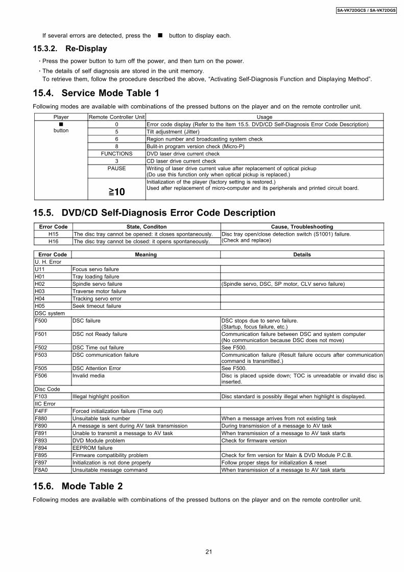
15.4. Service Mode Table 1Following modes are available with combinations of the pressed buttons on the player and on the remote controller unit.
Player Remote Controller Unit Usage
button0 Error code display (Refer to the Item 15.5. DVD/CD Self-Diagnosis Error Code Description)5 Tilt adjustment (Jitter)6 Region number and broadcasting system check8 Bulit-in program version check (Micro-P)
FUNCTIONS DVD laser drive current check3 CD laser drive current check
PAUSE Writing of laser drive current value after replacement of optical pickup(Do use this function only when optical pickup is replaced.)Initialization of the player (factory setting is restored.)Used after replacement of micro-computer and its peripherals and printed circuit board.
15.5. DVD/CD Self-Diagnosis Error Code DescriptionError Code State, Conditon Cause, Troubleshooting
H15 The disc tray cannot be opened: it closes spontaneously. Disc tray open/close detection switch (S1001) failure.(Check and replace)H16 The disc tray cannot be closed: it opens spontaneously.
Error Code Meaning DetailsU. H. ErrorU11 Focus servo failureH01 Tray loading failureH02 Spindle servo failure (Spindle servo, DSC, SP motor, CLV servo failure)H03 Traverse motor failureH04 Tracking servo errorH05 Seek timeout failureDSC systemF500 DSC failure DSC stops due to servo failure.
(Startup, focus failure, etc.)F501 DSC not Ready failure Communication failure between DSC and system computer
(No communication because DSC does not move)F502 DSC Time out failure See F500.F503 DSC communication failure Communication failure (Result failure occurs after communication
command is transmitted.)F505 DSC Attention Error See F500.F506 Invalid media Disc is placed upside down; TOC is unreadable or invalid disc is
inserted.Disc CodeF103 IIlegal highlight position Disc standard is possibly illegal when highlight is displayed.IIC ErrorF4FF Forced initialization failure (Time out)F880 Unsuitable task number When a message arrives from not existing taskF890 A message is sent during AV task transmission During transmission of a message to AV taskF891 Unable to transmit a message to AV task When transmission of a message to AV task startsF893 DVD Module problem Check for firmware versionF894 EEPROM failureF895 Firmware compatibility problem Check for firm version for Main & DVD Module P.C.B.F897 Initialization is not done properly Follow proper steps for initialization & resetF8A0 Unsuitable message command When transmission of a message to AV task starts
15.6. Mode Table 2Following modes are available with combinations of the pressed buttons on the player and on the remote controller unit.
21
SA-VK72DGCS / SA-VK72DGS
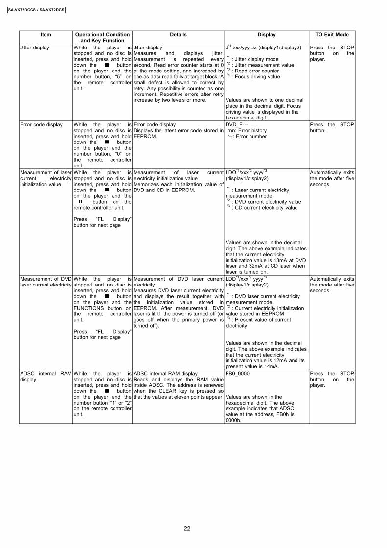
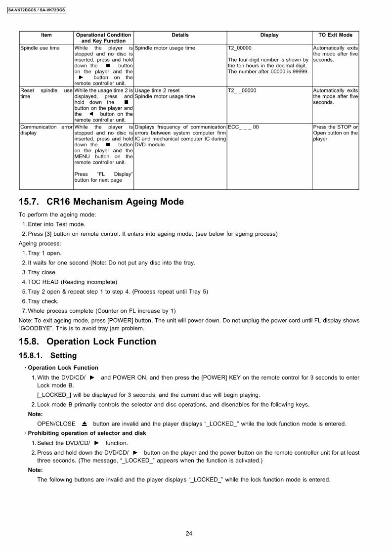
Item Operational Conditionand Key Function
Details Display TO Exit Mode
Jitter display While the player isstopped and no disc isinserted, press and holddown the buttonon the player and thenumber button, “5” onthe remote controllerunit.
Jitter displayMeasures and displays jitter.Measurement is repeated everysecond. Read error counter starts at 0at the mode setting, and increased byone as data read fails at target block. Asmall defect is allowed to correct byretry. Any possibility is counted as oneincrement. Repetitive errors after retryincrease by two levels or more.
J*1 xxx/yyy zz (display1/display2)
*1 : Jitter display mode*2 : Jitter measurement value*3 : Read error counter*4 : Focus driving value
Values are shown to one decimalplace in the decimal digit. Focusdriving value is displayed in thehexadecimal digit.
Press the STOPbutton on theplayer.
Error code display While the player isstopped and no disc isinserted, press and holddown the buttonon the player and thenumber button, “0” onthe remote controllerunit.
Error code displayDisplays the latest error code stored inEEPROM.
DVD_F---*nn: Error history*--: Error number
Press the STOPbutton.
Measurement of lasercurrent electricityinitialization value
While the player isstopped and no disc isinserted, press and holddown the buttonon the player and the
button on theremote controller unit.
Press “FL Display”button for next page
Measurement of laser currentelectricity initialization valueMemorizes each initialization value ofDVD and CD in EEPROM.
LDO*1/xxx*2 yyyy*3
(display1/display2)
*1 : Laser current electricitymeasurement mode*2 : DVD current electricity value*3 : CD current electricity value
Values are shown in the decimaldigit. The above example indicatesthat the current electricityinitialization value is 13mA at DVDlaser and 32mA at CD laser whenlaser is turned on.
Automatically exitsthe mode after fiveseconds.
Measurement of DVDlaser current electricity
While the player isstopped and no disc isinserted, press and holddown the buttonon the player and theFUNCTIONS button onthe remote controllerunit.
Press “FL Display”button for next page
Measurement of DVD laser currentelectricityMeasures DVD laser current electricityand displays the result together withthe initialization value stored inEEPROM. After measurement, DVDlaser is lit till the power is turned off (orgoes off when the primary power isturned off).
LDD*1/xxx*2 yyyy*3
(display1/display2)
*1 : DVD laser current electricitymeasurement mode*2 : Current electricity initializationvalue stored in EEPROM*3 : Present value of currentelectricity
Values are shown in the decimaldigit. The above example indicatesthat the current electricityinitialization value is 12mA and itspresent value is 14mA.
Automatically exitsthe mode after fiveseconds.
ADSC internal RAMdisplay
While the player isstopped and no disc isinserted, press and holddown the buttonon the player and thenumber button “1” or “2”on the remote controllerunit.
ADSC internal RAM displayReads and displays the RAM valueinside ADSC. The address is renewedwhen the CLEAR key is pressed sothat the values at eleven points appear.
FB0_0000
Values are shown in thehexadecimal digit. The aboveexample indicates that ADSCvalue at the address, FB0h is0000h.
Press the STOPbutton on theplayer.
22
SA-VK72DGCS / SA-VK72DGS
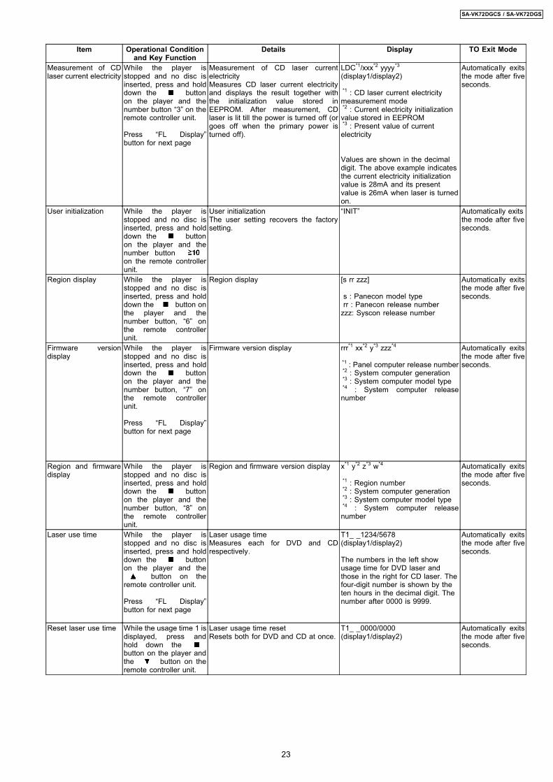
Item Operational Conditionand Key Function
Details Display TO Exit Mode
Measurement of CDlaser current electricity
While the player isstopped and no disc isinserted, press and holddown the buttonon the player and thenumber button “3” on theremote controller unit.
Press “FL Display”button for next page
Measurement of CD laser currentelectricityMeasures CD laser current electricityand displays the result together withthe initialization value stored inEEPROM. After measurement, CDlaser is lit till the power is turned off (orgoes off when the primary power isturned off).
LDC*1/xxx*2 yyyy*3
(display1/display2)
*1 : CD laser current electricitymeasurement mode*2 : Current electricity initializationvalue stored in EEPROM*3 : Present value of currentelectricity
Values are shown in the decimaldigit. The above example indicatesthe current electricity initializationvalue is 28mA and its presentvalue is 26mA when laser is turnedon.
Automatically exitsthe mode after fiveseconds.
User initialization While the player isstopped and no disc isinserted, press and holddown the buttonon the player and thenumber buttonon the remote controllerunit.
User initializationThe user setting recovers the factorysetting.
“INIT” Automatically exitsthe mode after fiveseconds.
Region display While the player isstopped and no disc isinserted, press and holddown the button onthe player and thenumber button, “6” onthe remote controllerunit.
Region display [s rr zzz]
s : Panecon model typerr : Panecon release number
zzz: Syscon release number
Automatically exitsthe mode after fiveseconds.
Firmware versiondisplay
While the player isstopped and no disc isinserted, press and holddown the buttonon the player and thenumber button, “7” onthe remote controllerunit.
Press “FL Display”button for next page
Firmware version display rrr*1 xx*2 y*3 zzz*4
*1 : Panel computer release number*2 : System computer generation*3 : System computer model type*4 : System computer releasenumber
Automatically exitsthe mode after fiveseconds.
Region and firmwaredisplay
While the player isstopped and no disc isinserted, press and holddown the buttonon the player and thenumber button, “8” onthe remote controllerunit.
Region and firmware version display x*1 y*2 z*3 w*4
*1 : Region number*2 : System computer generation*3 : System computer model type*4 : System computer releasenumber
Automatically exitsthe mode after fiveseconds.
Laser use time While the player isstopped and no disc isinserted, press and holddown the buttonon the player and the
button on theremote controller unit.
Press “FL Display”button for next page
Laser usage timeMeasures each for DVD and CDrespectively.
T1_ _1234/5678(display1/display2)
The numbers in the left showusage time for DVD laser andthose in the right for CD laser. Thefour-digit number is shown by theten hours in the decimal digit. Thenumber after 0000 is 9999.
Automatically exitsthe mode after fiveseconds.
Reset laser use time While the usage time 1 isdisplayed, press andhold down thebutton on the player andthe button on theremote controller unit.
Laser usage time resetResets both for DVD and CD at once.
T1_ _0000/0000(display1/display2)
Automatically exitsthe mode after fiveseconds.
23
SA-VK72DGCS / SA-VK72DGS
Item Operational Conditionand Key Function
Details Display TO Exit Mode
Spindle use time While the player isstopped and no disc isinserted, press and holddown the buttonon the player and the
button on theremote controller unit.
Spindle motor usage time T2_00000
The four-digit number is shown bythe ten hours in the decimal digit.The number after 00000 is 99999.
Automatically exitsthe mode after fiveseconds.
Reset spindle usetime
While the usage time 2 isdisplayed, press andhold down thebutton on the player andthe button on theremote controller unit.
Usage time 2 resetSpindle motor usage time
T2_ _00000 Automatically exitsthe mode after fiveseconds.
Communication errordisplay
While the player isstopped and no disc isinserted, press and holddown the buttonon the player and theMENU button on theremote controller unit.
Press “FL Display”button for next page
Displays frequency of communicationerrors between system computer firmIC and mechanical computer IC duringDVD module.
ECC_ _ _ 00 Press the STOP orOpen button on theplayer.
15.7. CR16 Mechanism Ageing ModeTo perform the ageing mode: 1. Enter into Test mode. 2. Press [3] button on remote control. It enters into ageing mode. (see below for ageing process)Ageing process: 1. Tray 1 open. 2. It waits for one second (Note: Do not put any disc into the tray. 3. Tray close. 4. TOC READ (Reading incomplete) 5. Tray 2 open & repeat step 1 to step 4. (Process repeat until Tray 5) 6. Tray check. 7. Whole process complete (Counter on FL increase by 1)Note: To exit ageing mode, press [POWER] button. The unit will power down. Do not unplug the power cord until FL display shows“GOODBYE”. This is to avoid tray jam problem.
15.8. Operation Lock Function15.8.1. Setting · Operation Lock Function
1. With the DVD/CD/ and POWER ON, and then press the [POWER] KEY on the remote control for 3 seconds to enterLock mode B.[_LOCKED_] will be displayed for 3 seconds, and the current disc will begin playing.
2. Lock mode B primarily controls the selector and disc operations, and disenables for the following keys.Note:
OPEN/CLOSE button are invalid and the player displays “_LOCKED_” while the lock function mode is entered. · Prohibiting operation of selector and disk
1. Select the DVD/CD/ function. 2. Press and hold down the DVD/CD/ button on the player and the power button on the remote controller unit for at least
three seconds. (The message, “_LOCKED_” appears when the function is activated.)Note:
The following buttons are invalid and the player displays “_LOCKED_” while the lock function mode is entered.
24
SA-VK72DGCS / SA-VK72DGS
15.9. Things to Do After RepairFollow the procedure described below after repair. 1. While the power is on, press the button to close the tray. 2. Press the power button to turn off the power. 3. Unplug the power cable.Note:
It is prohibited to unplug the power cable while the tray is opened and to close the tray manually.
16 Cautions To Be Taken During Servicing16.1. Recovery after the dvd player is repaired · When Flash ROM or DVD Module P.C.B. is replaced, carry out the recovery processing to optimize the drive. Playback the
recovery disc to process the recovery automatically. · Recovery disc (Product number=RFKZD03R005) · Performing recovery
1. Load the recovery disc (Product number: RFKZD03R005) to the player and run it. 2. Recovery is performed automatically. When it is finished, a message appears on the screen. 3. Remove the recovery disc. 4. Turn off the power.
16.2. DVD Player Firmware Version Upgrade ProcessFirmware of DVD player may upgrade to conform to improvement of its performance and quality including operational range,playability of non-standardized discs, etc. The version upgrade disc contains the recovery function, and the recovery disc is notnecessary.Note:
Version upgrade process cannot be complete if the AC power is cut off due to power failure and other occasions during theprocess. If this occurs, replace FLASH ROM IC and restart version upgrade. Version upgrade disc number is informed whenordered.
16.3. Firmware Version Upgrade Process by Using Disc and RecoveryProcess
· Recovery process · Firmware version upgrade process
Both of the above procedures automatically start when the recovery disc is replayed.General CD-R disc allows version upgradeprocess and recovery process, making version upgrade through disc simple.Recovery process: Optimization process of player after replacement of FLASH ROM, EEPROM, or module circuit board
25
SA-VK72DGCS / SA-VK72DGS
Version upgrade process: Renewal of firmware for improvement of operational range and performance
16.4. Using Recovery Disc16.4.1. Recovery Process 1. Insert the recovery disc (RFKZD03R005) to the player to replay. 2. The recovery process automatically starts, and a message of completion prompts on the screen. 3. Remove the disc. 4. Turn off the power.
16.4.2. Version Upgrade Process 1. Insert the recovery disc to the player to replay. 2. The version of player is automatically checked and prompts if necessary. 3. Select version upgrade process using the cursor keys on the remote controller unit. (Select YES or NO) 4. a. If YES is selected, the process starts.
b. If NO is selected, only the recovery process is applied. 5. a. When the version upgrade process is complete, a message of completion appears on the screen. Remove the disc.
b. Follow the instruction appearing on the screen, and remove the disc. 6. Turn off the power.
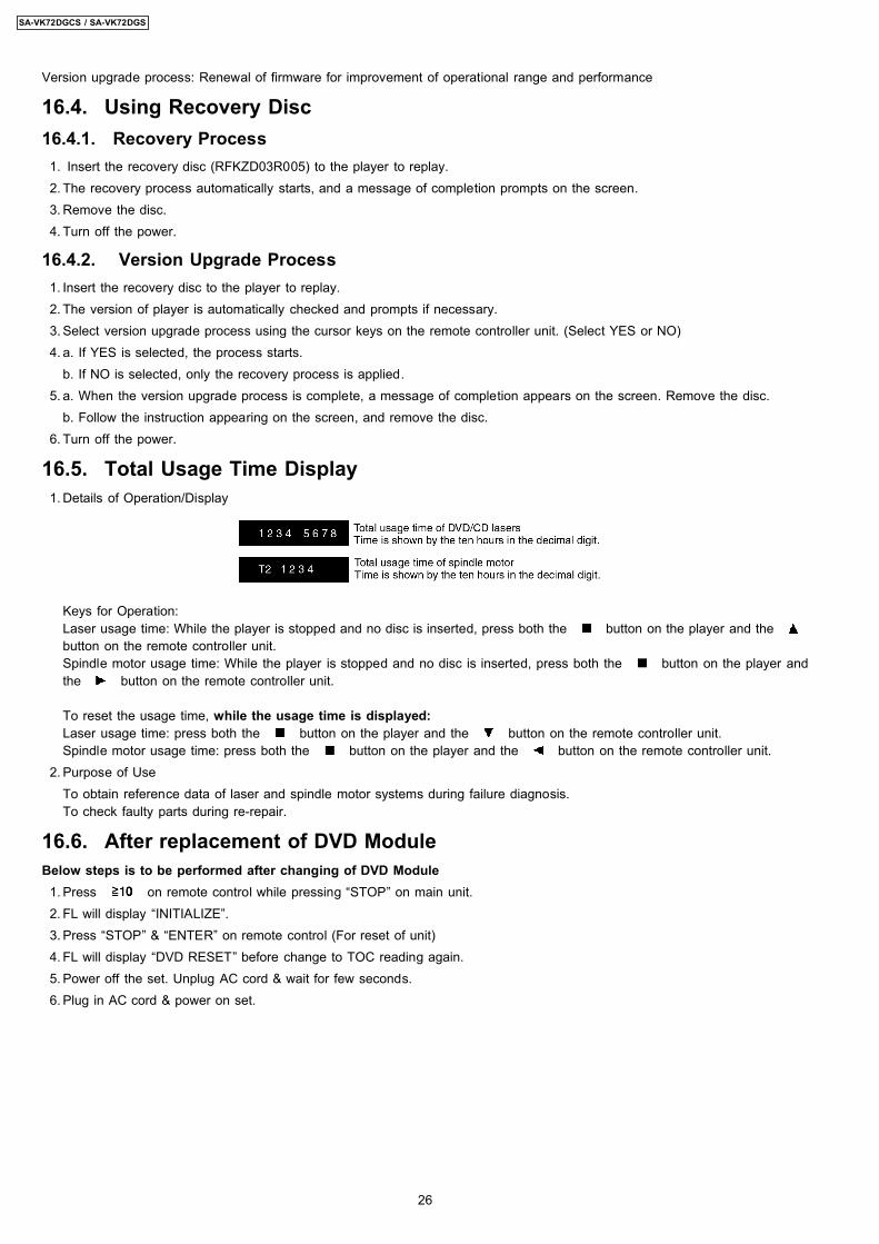
16.5. Total Usage Time Display 1. Details of Operation/Display
Keys for Operation:Laser usage time: While the player is stopped and no disc is inserted, press both the button on the player and thebutton on the remote controller unit.Spindle motor usage time: While the player is stopped and no disc is inserted, press both the button on the player andthe button on the remote controller unit.
To reset the usage time, while the usage time is displayed:Laser usage time: press both the button on the player and the button on the remote controller unit.Spindle motor usage time: press both the button on the player and the button on the remote controller unit.
2. Purpose of UseTo obtain reference data of laser and spindle motor systems during failure diagnosis.To check faulty parts during re-repair.
16.6. After replacement of DVD ModuleBelow steps is to be performed after changing of DVD Module 1. Press on remote control while pressing “STOP” on main unit. 2. FL will display “INITIALIZE”. 3. Press “STOP” & “ENTER” on remote control (For reset of unit) 4. FL will display “DVD RESET” before change to TOC reading again. 5. Power off the set. Unplug AC cord & wait for few seconds. 6. Plug in AC cord & power on set.
26
SA-VK72DGCS / SA-VK72DGS
17.1. Disassembly steps
17 Disassembly and Assembly of Main Component“ATTENTION SERVICER”
Some chassis components may have sharp edges. Be careful when disassembling and servicing. 1. This section describes procedures for checking the operation of the major printed circuit boards and replacing the main
components. 2. For reassembly after operation checks or replacement, reverse the respective procedures.
Special reassembly procedures are described only when required. 3. Select items from the following index when checks or replacement are required. 4. Refer to the Parts No. on the page of “Parts Location and Replacement Parts List” (Section 27), if necessary.
· Disassembly of Top Cabinet · Disassembly of Rear Panel · Disassembly of DVD Changer Unit · Disassembly of Main P.C.B. · Disassembly of Power Amp P.C.B. · Disassembly of Power P.C.B. · Disassembly of Transformer P.C.B. & Voltage Selector · Disassembly of Front Panel Unit · Disassembly of Mic P.C.B. & Panel P.C.B. · Disassembly of Deck Mechanism Unit · Replacement for Deck P.C.B. · Replacement for Traverse Deck · Replacement for Optical Pickup Unit (DVD Mechanism) · Procedure for removing CD loading mechanism · CR16 mechanism disassembly procedure · CR16 mechanism assembly procedure · Disassembly for Traverse Unit · Replacement for cassette lid · Rectification for tape jam problem
27
SA-VK72DGCS / SA-VK72DGS
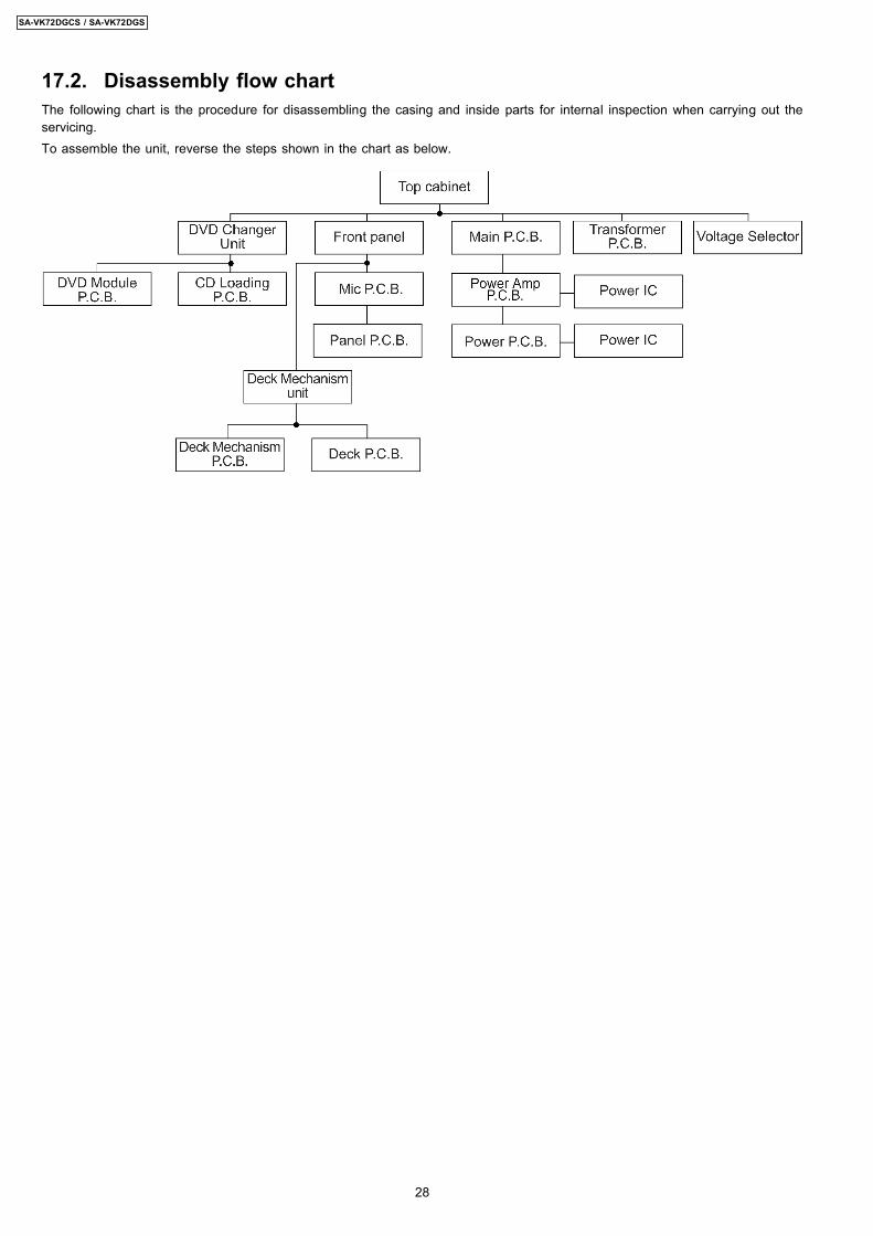
17.2. Disassembly flow chartThe following chart is the procedure for disassembling the casing and inside parts for internal inspection when carrying out theservicing.To assemble the unit, reverse the steps shown in the chart as below.
28
SA-VK72DGCS / SA-VK72DGS
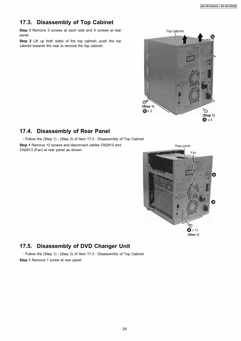
Step 1 Remove 3 screws at each side and 5 screws at rearpanel.Step 2 Lift up both sides of the top cabinet, push the topcabinet towards the rear to remove the top cabinet.
Step 1 Remove 12 screws and disconnect cables CN2810 andCN2813 (Fan) at rear panel as shown.
Step 1 Remove 1 screw at rear panel.
17.3. Disassembly of Top Cabinet
17.4. Disassembly of Rear Panel · Follow the (Step 1) - (Step 2) of Item 17.3 - Disassembly of Top Cabinet
17.5. Disassembly of DVD Changer Unit · Follow the (Step 1) - (Step 2) of Item 17.3 - Disassembly of Top Cabinet
29
SA-VK72DGCS / SA-VK72DGS
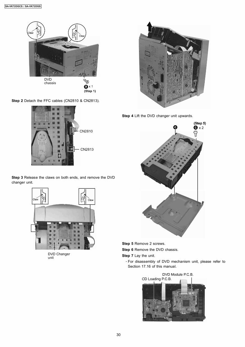
Step 2 Detach the FFC cables (CN2810 & CN2813).
Step 3 Release the claws on both ends, and remove the DVDchanger unit.
Step 4 Lift the DVD changer unit upwards.
Step 5 Remove 2 screws.Step 6 Remove the DVD chassis.Step 7 Lay the unit. · For disassembly of DVD mechanism unit, please refer to
Section 17.16 of this manual.
30
SA-VK72DGCS / SA-VK72DGS
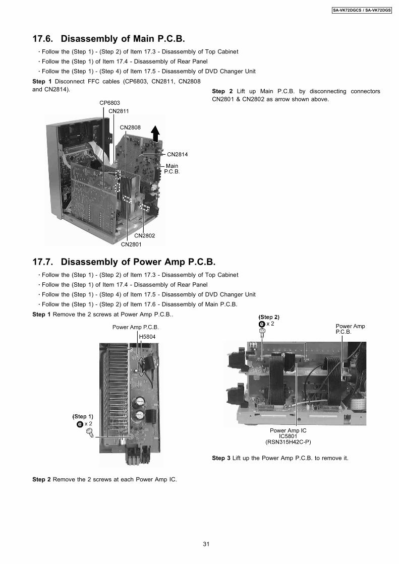
Step 1 Disconnect FFC cables (CP6803, CN2811, CN2808and CN2814).
Step 1 Remove the 2 screws at Power Amp P.C.B..
Step 2 Remove the 2 screws at each Power Amp IC.
Step 2 Lift up Main P.C.B. by disconnecting connectorsCN2801 & CN2802 as arrow shown above.
Step 3 Lift up the Power Amp P.C.B. to remove it.
17.6. Disassembly of Main P.C.B. · Follow the (Step 1) - (Step 2) of Item 17.3 - Disassembly of Top Cabinet · Follow the (Step 1) of Item 17.4 - Disassembly of Rear Panel · Follow the (Step 1) - (Step 4) of Item 17.5 - Disassembly of DVD Changer Unit
17.7. Disassembly of Power Amp P.C.B. · Follow the (Step 1) - (Step 2) of Item 17.3 - Disassembly of Top Cabinet · Follow the (Step 1) of Item 17.4 - Disassembly of Rear Panel · Follow the (Step 1) - (Step 4) of Item 17.5 - Disassembly of DVD Changer Unit · Follow the (Step 1) - (Step 2) of Item 17.6 - Disassembly of Main P.C.B.
31
SA-VK72DGCS / SA-VK72DGS
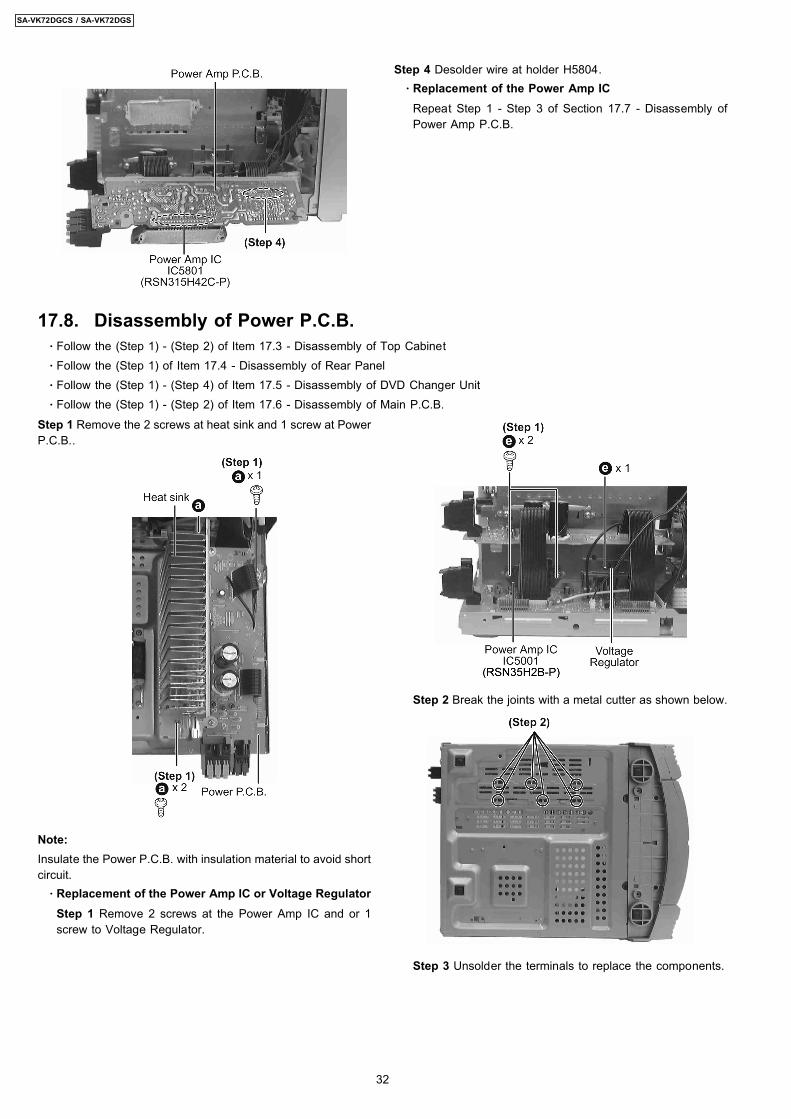
Step 1 Remove the 2 screws at heat sink and 1 screw at PowerP.C.B..
Note:Insulate the Power P.C.B. with insulation material to avoid shortcircuit. · Replacement of the Power Amp IC or Voltage Regulator
Step 1 Remove 2 screws at the Power Amp IC and or 1screw to Voltage Regulator.
Step 4 Desolder wire at holder H5804. · Replacement of the Power Amp IC
Repeat Step 1 - Step 3 of Section 17.7 - Disassembly ofPower Amp P.C.B.
Step 2 Break the joints with a metal cutter as shown below.
Step 3 Unsolder the terminals to replace the components.
17.8. Disassembly of Power P.C.B. · Follow the (Step 1) - (Step 2) of Item 17.3 - Disassembly of Top Cabinet · Follow the (Step 1) of Item 17.4 - Disassembly of Rear Panel · Follow the (Step 1) - (Step 4) of Item 17.5 - Disassembly of DVD Changer Unit · Follow the (Step 1) - (Step 2) of Item 17.6 - Disassembly of Main P.C.B.
32
SA-VK72DGCS / SA-VK72DGS
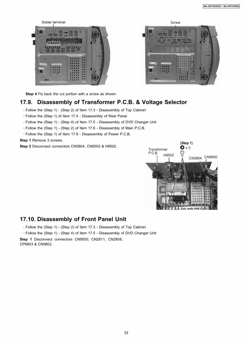
Step 4 Fix back the cut portion with a screw as shown.
Step 1 Remove 3 screws.Step 2 Disconnect connectors CN5804, CN9500 & H9502.
Step 1 Disconnect connectors CN9500, CN2811, CN2808,CP6803 & CN5802.
17.9. Disassembly of Transformer P.C.B. & Voltage Selector · Follow the (Step 1) - (Step 2) of Item 17.3 - Disassembly of Top Cabinet · Follow the (Step 1) of Item 17.4 - Disassembly of Rear Panel · Follow the (Step 1) - (Step 4) of Item 17.5 - Disassembly of DVD Changer Unit · Follow the (Step 1) - (Step 2) of Item 17.6 - Disassembly of Main P.C.B. · Follow the (Step 1) of Item 17.8 - Disassembly of Power P.C.B.
17.10. Disassembly of Front Panel Unit · Follow the (Step 1) - (Step 2) of Item 17.3 - Disassembly of Top Cabinet · Follow the (Step 1) - (Step 4) of Item 17.5 - Disassembly of DVD Changer Unit
33
SA-VK72DGCS / SA-VK72DGS
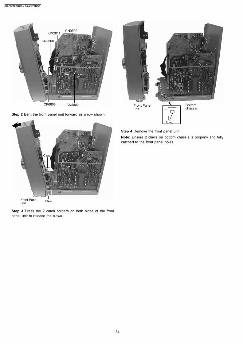
Step 2 Bent the front panel unit forward as arrow shown.
Step 3 Press the 2 catch holders on both sides of the frontpanel unit to release the claws.
Step 4 Remove the front panel unit.Note: Ensure 2 claws on bottom chassis is properly and fullycatched to the front panel holes.
34
SA-VK72DGCS / SA-VK72DGS
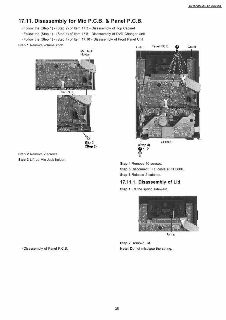
Step 1 Remove volume knob.
Step 2 Remove 2 screws.Step 3 Lift up Mic Jack holder.
· Disassembly of Panel P.C.B.
Step 4 Remove 10 screws.Step 5 Disconnect FFC cable at CP6800.Step 6 Release 2 catches.
17.11.1. Disassembly of LidStep 1 Lift the spring sideward.
Step 2 Remove Lid.Note: Do not misplace the spring.
17.11. Disassembly for Mic P.C.B. & Panel P.C.B. · Follow the (Step 1) - (Step 2) of Item 17.3 - Disassembly of Top Cabinet · Follow the (Step 1) - (Step 4) of Item 17.5 - Disassembly of DVD Changer Unit · Follow the (Step 1) - (Step 4) of Item 17.10 - Disassembly of Front Panel Unit
35
SA-VK72DGCS / SA-VK72DGS
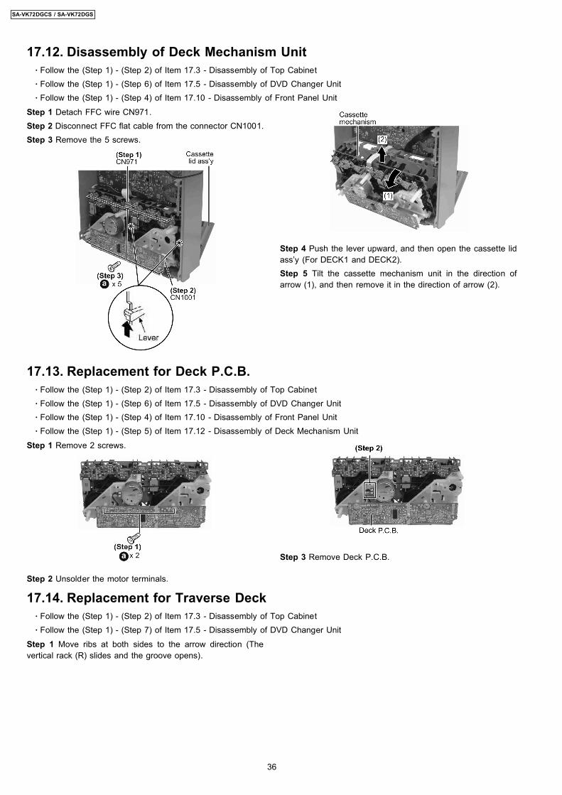
Step 1 Detach FFC wire CN971.Step 2 Disconnect FFC flat cable from the connector CN1001.Step 3 Remove the 5 screws.
Step 1 Remove 2 screws.
Step 2 Unsolder the motor terminals.
Step 1 Move ribs at both sides to the arrow direction (Thevertical rack (R) slides and the groove opens).
Step 4 Push the lever upward, and then open the cassette lidass’y (For DECK1 and DECK2).Step 5 Tilt the cassette mechanism unit in the direction ofarrow (1), and then remove it in the direction of arrow (2).
Step 3 Remove Deck P.C.B.
17.12. Disassembly of Deck Mechanism Unit · Follow the (Step 1) - (Step 2) of Item 17.3 - Disassembly of Top Cabinet · Follow the (Step 1) - (Step 6) of Item 17.5 - Disassembly of DVD Changer Unit · Follow the (Step 1) - (Step 4) of Item 17.10 - Disassembly of Front Panel Unit
17.13. Replacement for Deck P.C.B. · Follow the (Step 1) - (Step 2) of Item 17.3 - Disassembly of Top Cabinet · Follow the (Step 1) - (Step 6) of Item 17.5 - Disassembly of DVD Changer Unit · Follow the (Step 1) - (Step 4) of Item 17.10 - Disassembly of Front Panel Unit · Follow the (Step 1) - (Step 5) of Item 17.12 - Disassembly of Deck Mechanism Unit
17.14. Replacement for Traverse Deck · Follow the (Step 1) - (Step 2) of Item 17.3 - Disassembly of Top Cabinet · Follow the (Step 1) - (Step 7) of Item 17.5 - Disassembly of DVD Changer Unit
36
SA-VK72DGCS / SA-VK72DGS
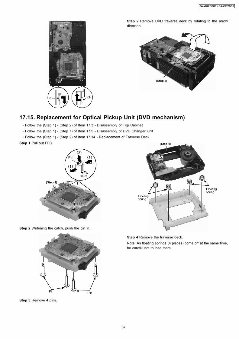
Step 1 Pull out FFC.
Step 2 Widening the catch, push the pin in.
Step 3 Remove 4 pins.
Step 2 Remove DVD traverse deck by rotating to the arrowdirection.
Step 4 Remove the traverse deck.Note: As floating springs (4 pieces) come off at the same time,be careful not to lose them.
17.15. Replacement for Optical Pickup Unit (DVD mechanism) · Follow the (Step 1) - (Step 2) of Item 17.3 - Disassembly of Top Cabinet · Follow the (Step 1) - (Step 7) of Item 17.5 - Disassembly of DVD Changer Unit · Follow the (Step 1) - (Step 2) of Item 17.14 - Replacement of Traverse Deck
37
SA-VK72DGCS / SA-VK72DGS
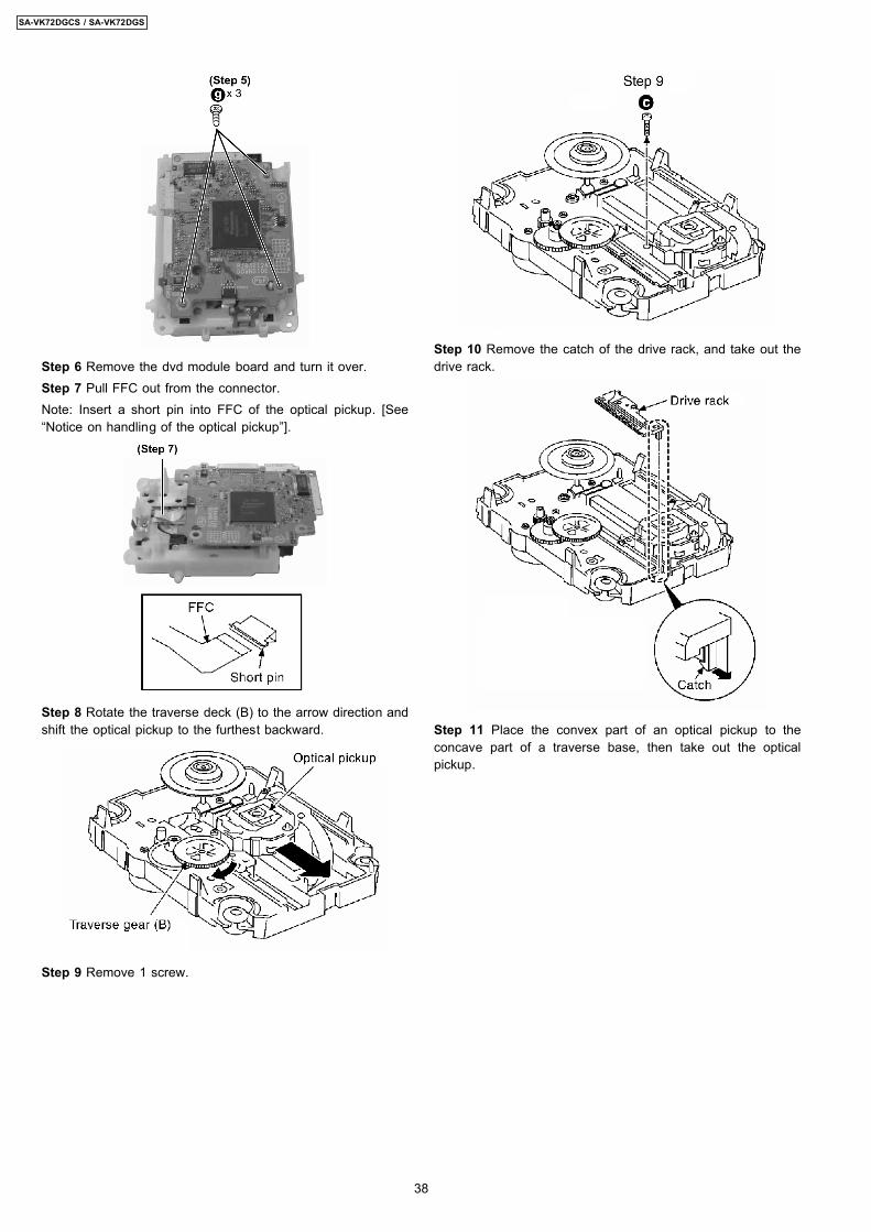
Step 6 Remove the dvd module board and turn it over.Step 7 Pull FFC out from the connector.Note: Insert a short pin into FFC of the optical pickup. [See“Notice on handling of the optical pickup”].
Step 8 Rotate the traverse deck (B) to the arrow direction andshift the optical pickup to the furthest backward.
Step 9 Remove 1 screw.
Step 10 Remove the catch of the drive rack, and take out thedrive rack.
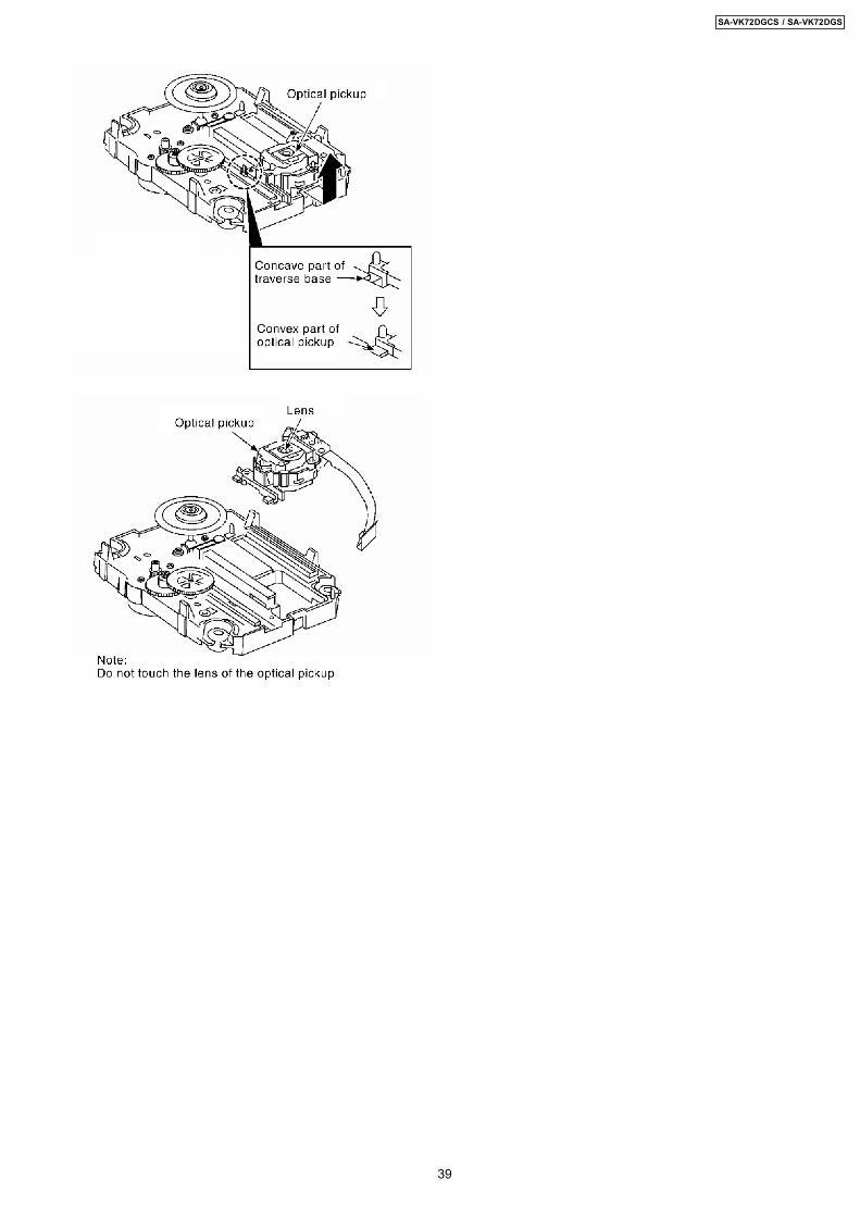
Step 11 Place the convex part of an optical pickup to theconcave part of a traverse base, then take out the opticalpickup.
38
SA-VK72DGCS / SA-VK72DGS
39
SA-VK72DGCS / SA-VK72DGS

17.17.1. Gear for servicing information · This unit has a gear which used for checking items
(open/close of disc tray, up/down operation of traverse unitby manually) when servicing. (For gear information, that isdescribed on the items for disassembly procedures.)
· For preparation of gear (for servicing), perform theprocedures as follows.
· In case of re-servicing the same set, the “gear for servicing”may be took off because it had been used. So, the “gear forservicing” must be stored.
1. Remove the gear attached to top cover of CD loadingmechanism.
2. Insert the hexagonal wrench (2.5mm) into the gear.
17.17.2. Replacement for the disc tray
17.16. Procedure for removing CD loading mechanism 1. Turn off by pressing power SW in the body. 2. Unplug AC power cord after the indication of [GOOD-BYE], then disassemble the body. 3. Disassemble the body, and take out CD loading mechanism. 4. Perform disassembly according to the following procedure for disassembly.
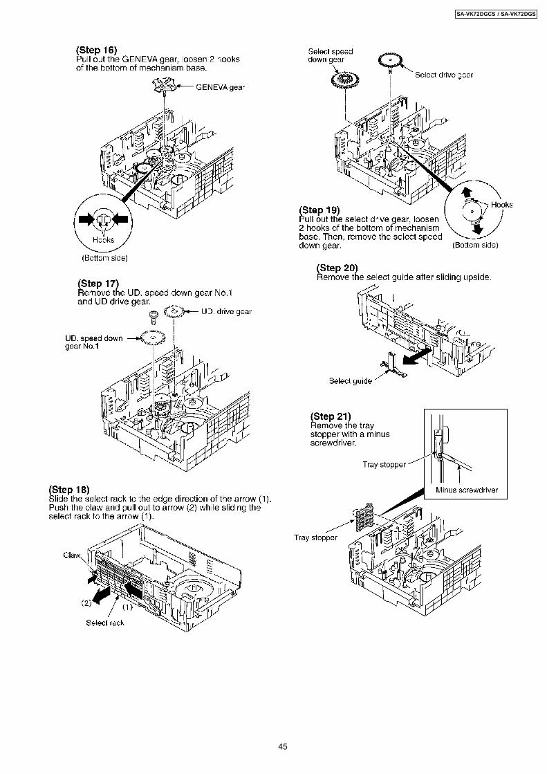
17.17. CR16 mechanism disassembly procedure
40
SA-VK72DGCS / SA-VK72DGS
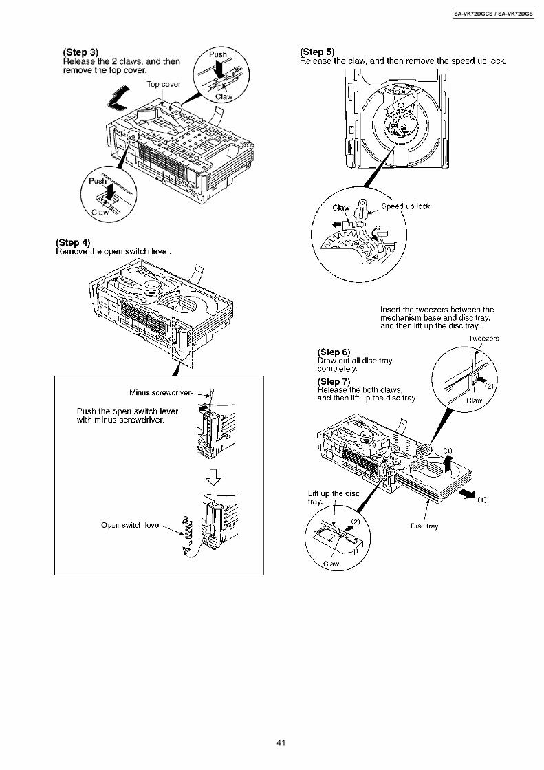
41
SA-VK72DGCS / SA-VK72DGS
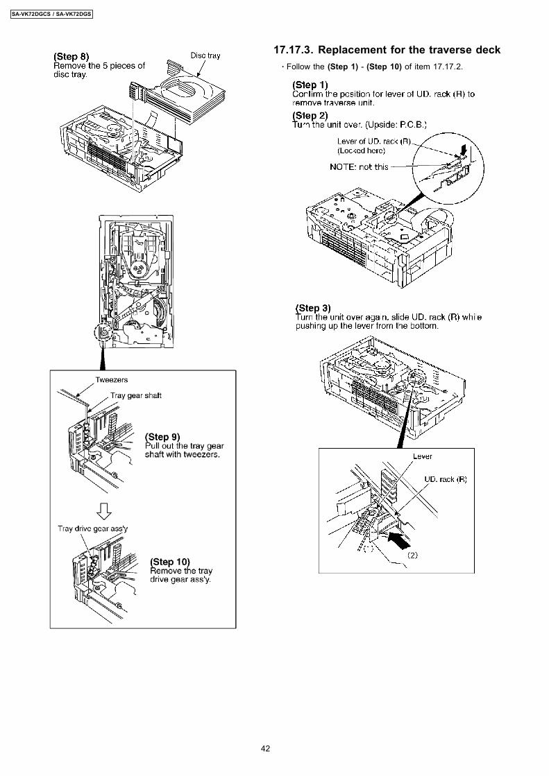
17.17.3. Replacement for the traverse deck · Follow the (Step 1) - (Step 10) of item 17.17.2.
42
SA-VK72DGCS / SA-VK72DGS
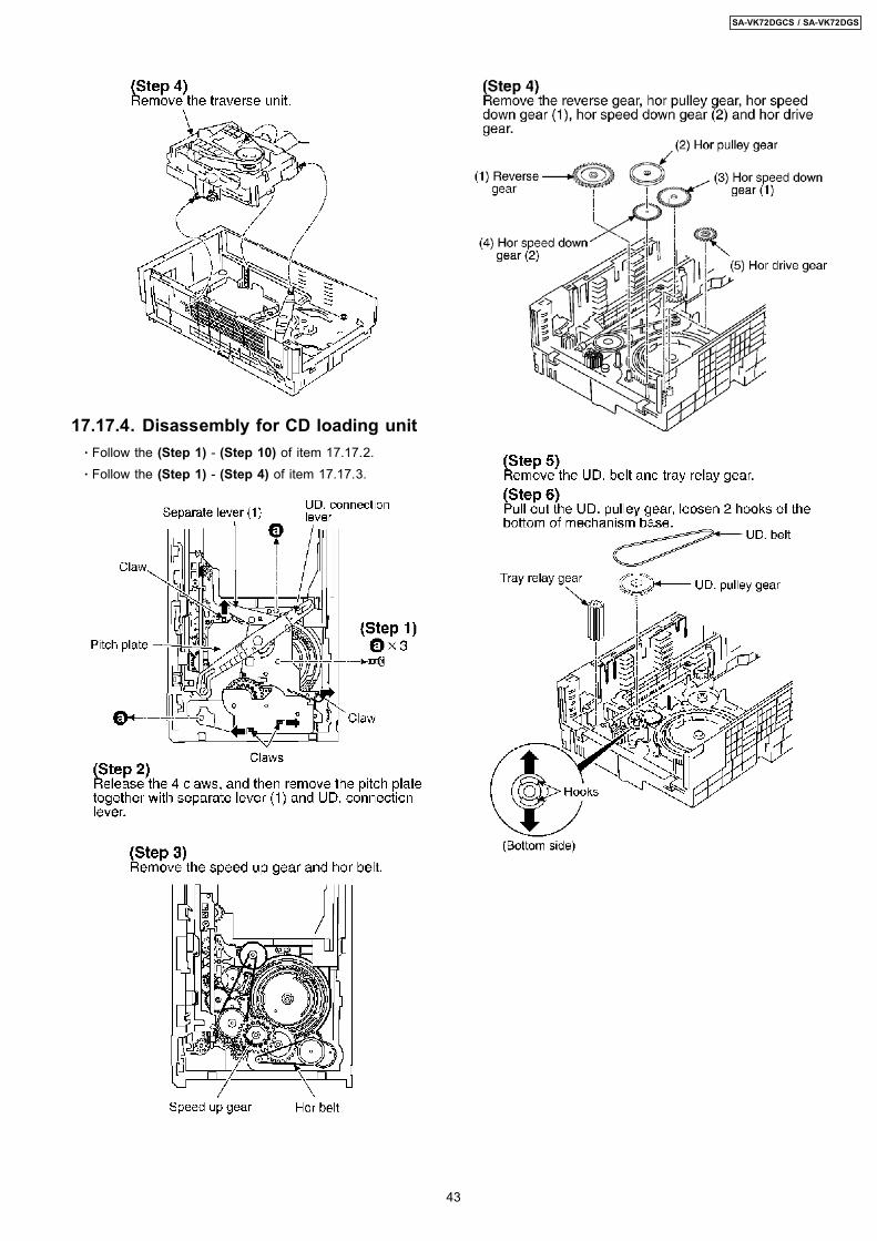
17.17.4. Disassembly for CD loading unit · Follow the (Step 1) - (Step 10) of item 17.17.2. · Follow the (Step 1) - (Step 4) of item 17.17.3.
43
SA-VK72DGCS / SA-VK72DGS
44
SA-VK72DGCS / SA-VK72DGS
45
SA-VK72DGCS / SA-VK72DGS
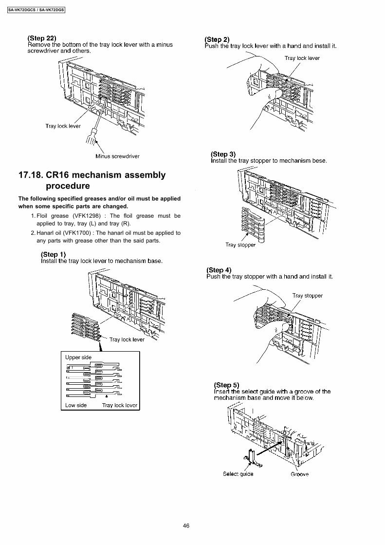
17.18. CR16 mechanism assemblyprocedure
The following specified greases and/or oil must be appliedwhen some specific parts are changed.
1. Floil grease (VFK1298) : The floil grease must beapplied to tray, tray (L) and tray (R).
2. Hanarl oil (VFK1700) : The hanarl oil must be applied toany parts with grease other than the said parts.
46
SA-VK72DGCS / SA-VK72DGS
47
SA-VK72DGCS / SA-VK72DGS
48
SA-VK72DGCS / SA-VK72DGS
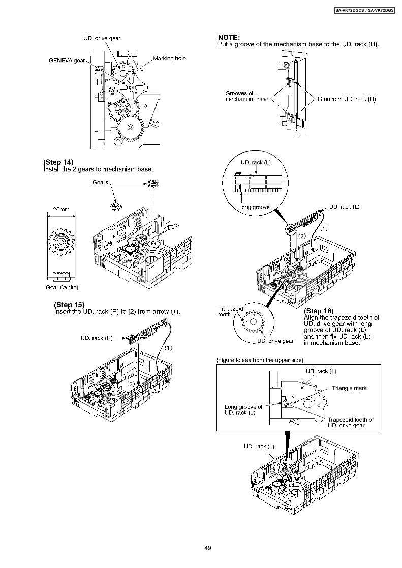
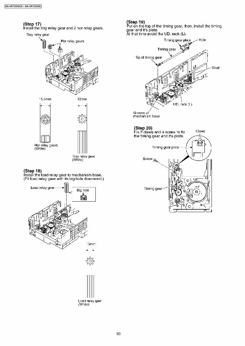
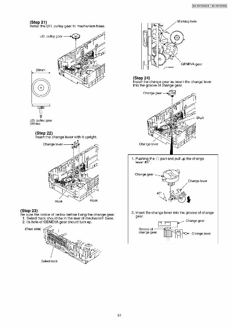
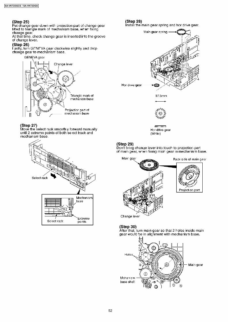
49
SA-VK72DGCS / SA-VK72DGS
50
SA-VK72DGCS / SA-VK72DGS
51
SA-VK72DGCS / SA-VK72DGS
52
SA-VK72DGCS / SA-VK72DGS
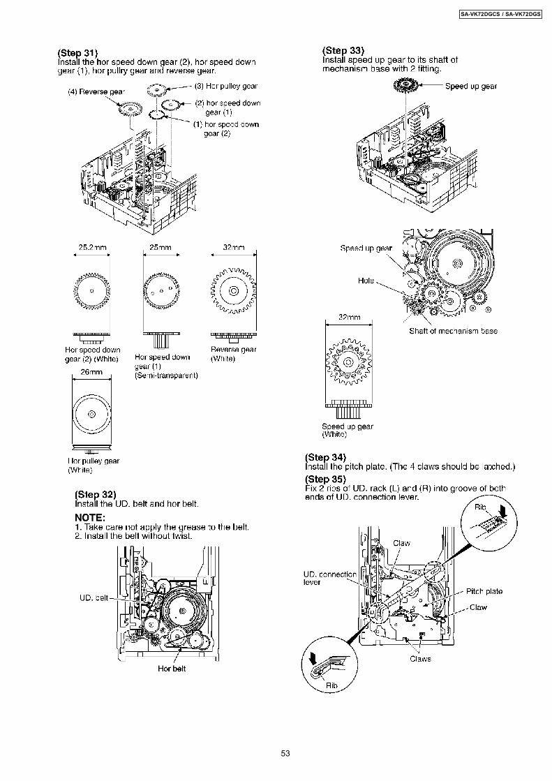
53
SA-VK72DGCS / SA-VK72DGS
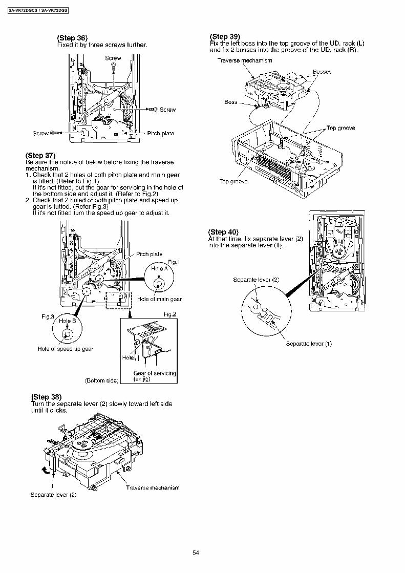
54
SA-VK72DGCS / SA-VK72DGS
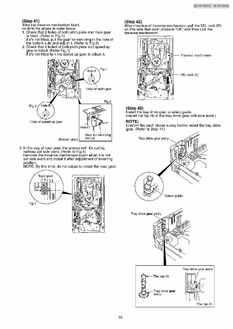
55
SA-VK72DGCS / SA-VK72DGS
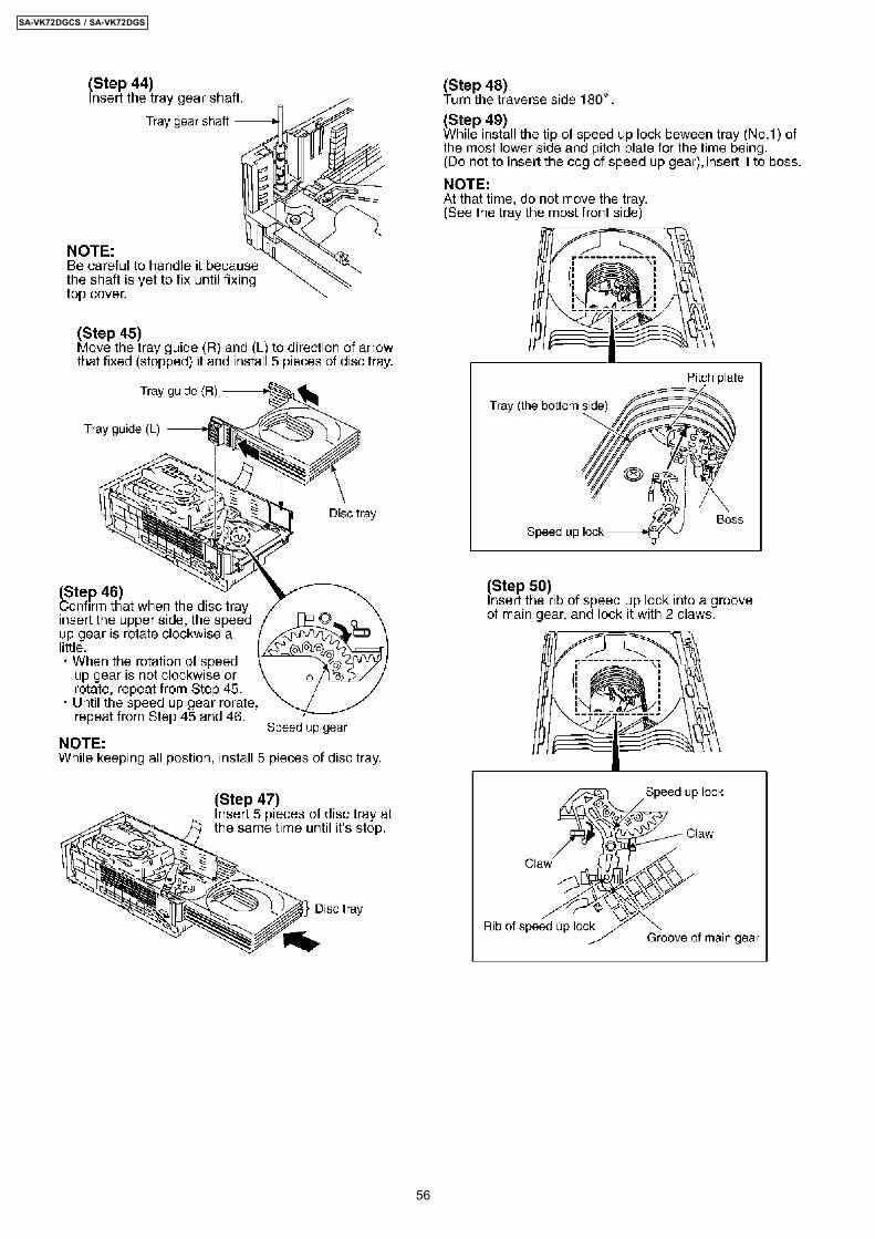
56
SA-VK72DGCS / SA-VK72DGS
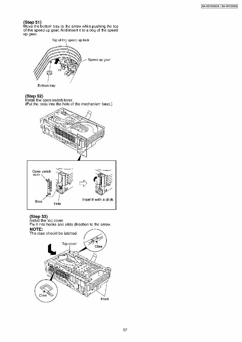
57
SA-VK72DGCS / SA-VK72DGS
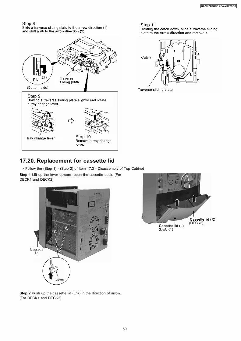
· Follow the (Step 1) - (Step 10) of item 17.17.2 · Follow the (Step 1) - (Step 4) of item 17.17.3
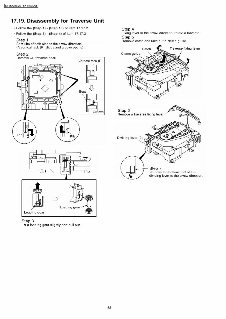
17.19. Disassembly for Traverse Unit
58
SA-VK72DGCS / SA-VK72DGS
Step 1 Lift up the lever upward, open the cassette deck. (ForDECK1 and DECK2)
Step 2 Push up the cassette lid (L/R) in the direction of arrow.(For DECK1 and DECK2).
17.20. Replacement for cassette lid · Follow the (Step 1) - (Step 2) of Item 17.3 - Disassembly of Top Cabinet
59
SA-VK72DGCS / SA-VK72DGS
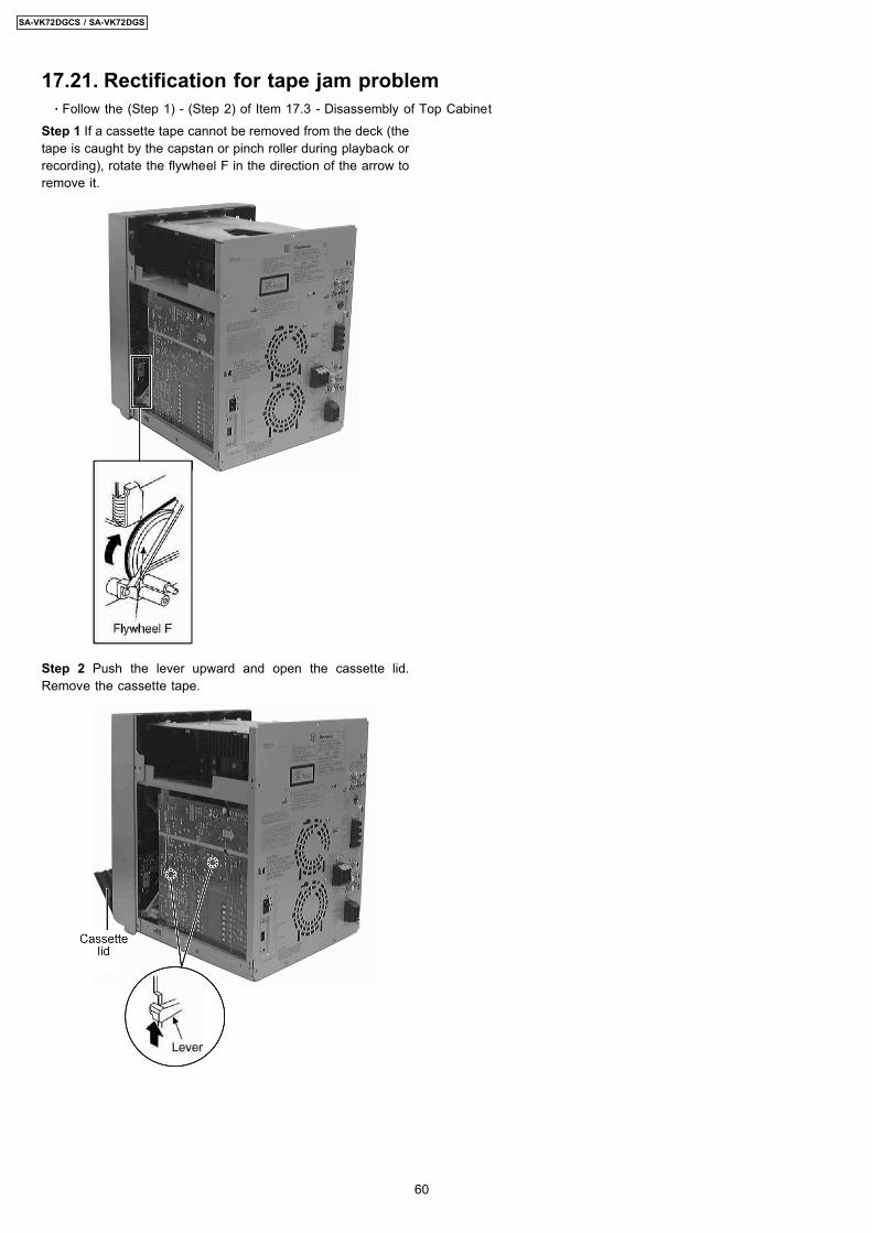
Step 1 If a cassette tape cannot be removed from the deck (thetape is caught by the capstan or pinch roller during playback orrecording), rotate the flywheel F in the direction of the arrow toremove it.
Step 2 Push the lever upward and open the cassette lid.Remove the cassette tape.
17.21. Rectification for tape jam problem · Follow the (Step 1) - (Step 2) of Item 17.3 - Disassembly of Top Cabinet
60
SA-VK72DGCS / SA-VK72DGS
18 Checking for major P.C.BsNote:
Checking of all major P.C.Bs (Main P.C.B., Panel P.C.B., Transformer P.C.B., Deck P.C.B., Deck Mechanism P.C.B., MicP.C.B., Power P.C.B. and Power Amp P.C.B.) can be carried out using below procedures.For the disassembling procedures, refer to Section 17.
18.1. Checking of Main P.C.B. 1. Remove Top Cabinet. 2. Disassemble DVD Changer Unit. 3. Connect FFC cables (CN2810 & CN2813) from Main P.C.B.
61
SA-VK72DGCS / SA-VK72DGS
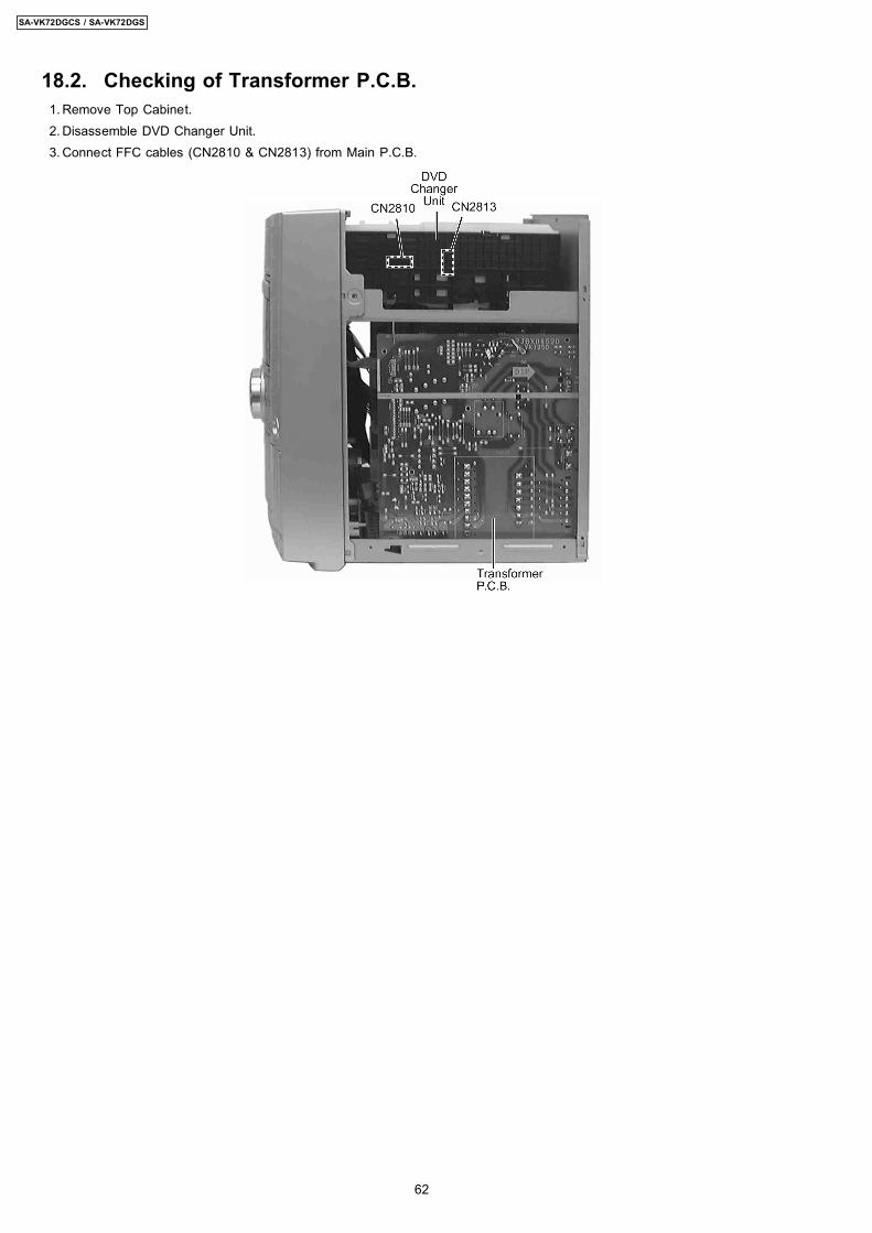
18.2. Checking of Transformer P.C.B. 1. Remove Top Cabinet. 2. Disassemble DVD Changer Unit. 3. Connect FFC cables (CN2810 & CN2813) from Main P.C.B.
62
SA-VK72DGCS / SA-VK72DGS
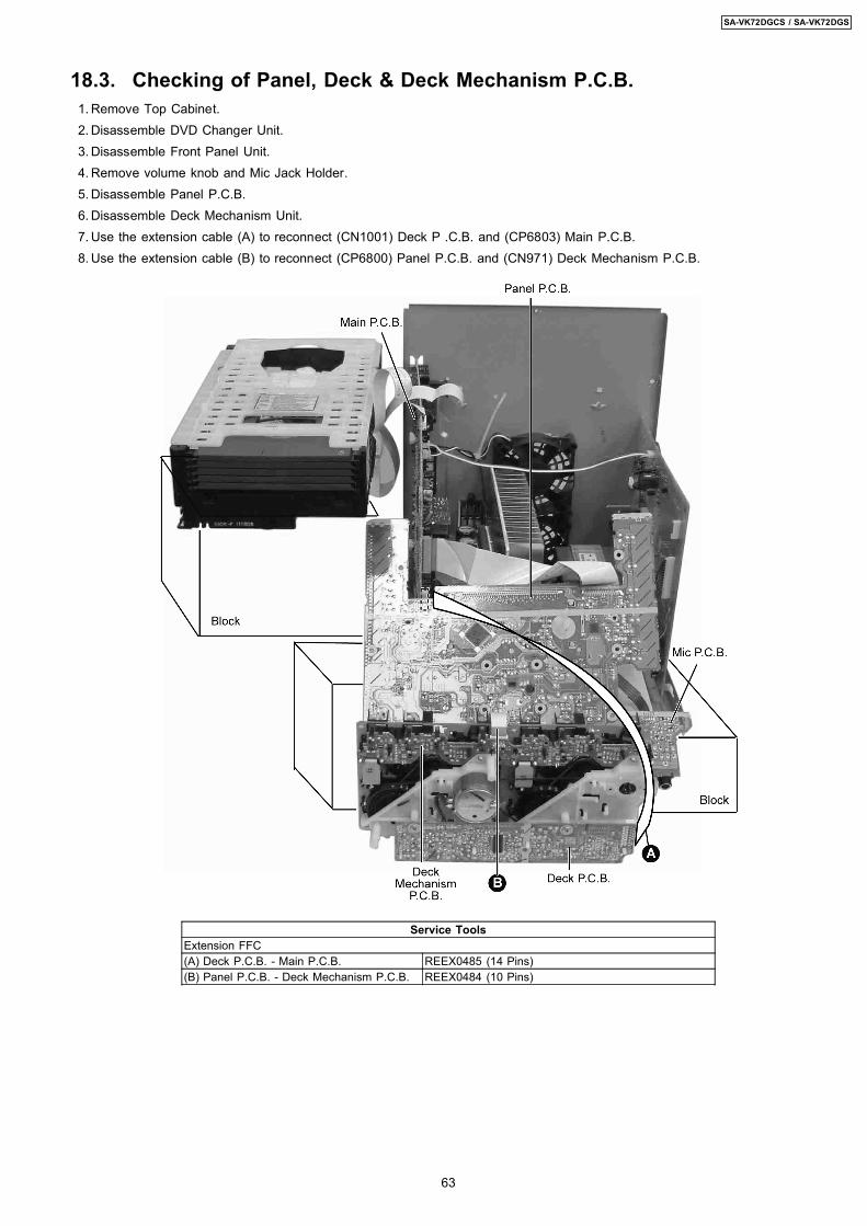
18.3. Checking of Panel, Deck & Deck Mechanism P.C.B. 1. Remove Top Cabinet. 2. Disassemble DVD Changer Unit. 3. Disassemble Front Panel Unit. 4. Remove volume knob and Mic Jack Holder. 5. Disassemble Panel P.C.B. 6. Disassemble Deck Mechanism Unit. 7. Use the extension cable (A) to reconnect (CN1001) Deck P .C.B. and (CP6803) Main P.C.B. 8. Use the extension cable (B) to reconnect (CP6800) Panel P.C.B. and (CN971) Deck Mechanism P.C.B.
Service ToolsExtension FFC(A) Deck P.C.B. - Main P.C.B. REEX0485 (14 Pins)(B) Panel P.C.B. - Deck Mechanism P.C.B. REEX0484 (10 Pins)
63
SA-VK72DGCS / SA-VK72DGS
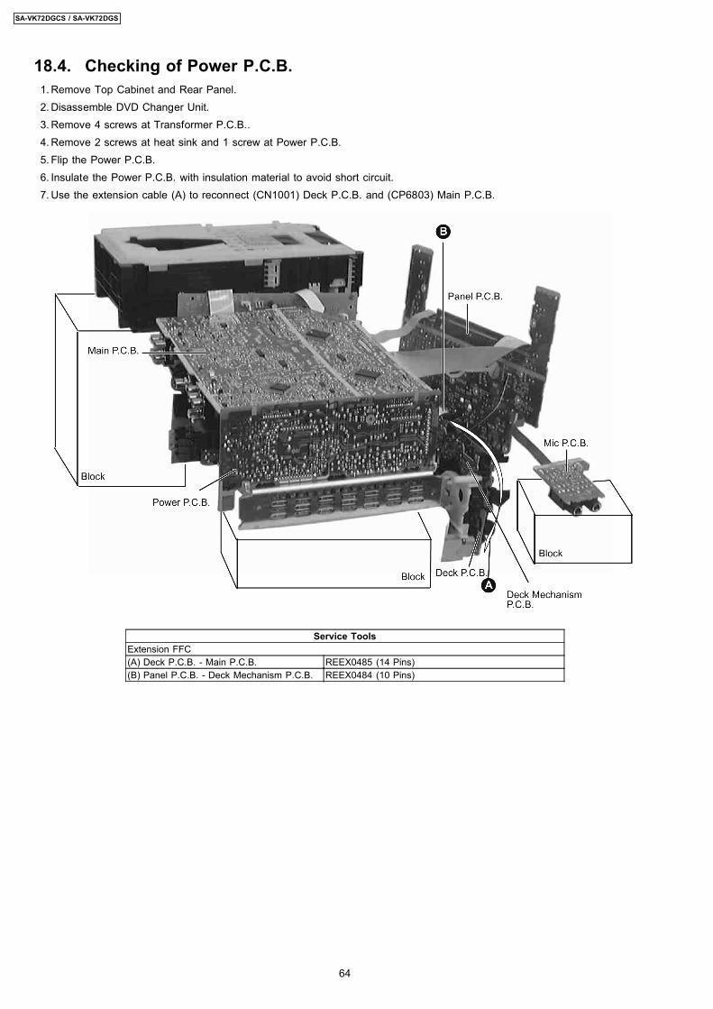
18.4. Checking of Power P.C.B. 1. Remove Top Cabinet and Rear Panel. 2. Disassemble DVD Changer Unit. 3. Remove 4 screws at Transformer P.C.B.. 4. Remove 2 screws at heat sink and 1 screw at Power P.C.B. 5. Flip the Power P.C.B. 6. Insulate the Power P.C.B. with insulation material to avoid short circuit. 7. Use the extension cable (A) to reconnect (CN1001) Deck P.C.B. and (CP6803) Main P.C.B.
Service ToolsExtension FFC(A) Deck P.C.B. - Main P.C.B. REEX0485 (14 Pins)(B) Panel P.C.B. - Deck Mechanism P.C.B. REEX0484 (10 Pins)
64
SA-VK72DGCS / SA-VK72DGS
19.1. Cassette Deck Section · Measurement Condition
− − − − Reverse-mode selector switch: − − − − Tape edit: NORMAL − − − − Make sure head, capstan and press roller are clean. − − − − Judgeable room temperature 20 ± 5 °C (68 ± 9°F)
· Measuring instrument − − − − EVM (DC Electronic voltmeter) − − − − Digital frequency counter
· Test Tape − − − − Tape speed gain adjustment (3 kHz, -10 dB);
QZZCWAT
19.1.1. Head Azimuth Adjustment (Deck1/2)
Caution: · Please replace both azimuth adjustment screw and springs
simultaneously when readjusting the head azimuth. (shownin Fig. 2) Even if you wish to readjust the head azimuthwithout replacing the acrews and springs, a fine adjustmentto the azimuth screw and spring.
· Please remove the screw-locking bond left on the headbase when replacing the azimuth screw.
· If you wish to readjust the head azimuth, be sure to adjustwith adhering the cassette tape closely to the mechanismby pushing the center of cassette tape with your finger.(shown in Fig. 3)
1. Playback the azimuth adjustment portion (8 kHz, -20dB) ofthe test tape (QZZCFM) in the forward play mode. Vary theazimuth adjustment screw until the output of the R-CH (PBOUT-R) are maximized.
2. Perform the same adjustment in the reverse play mode. 3. After the adjustment, apply screwlock to the azimuth
adjusting screw.
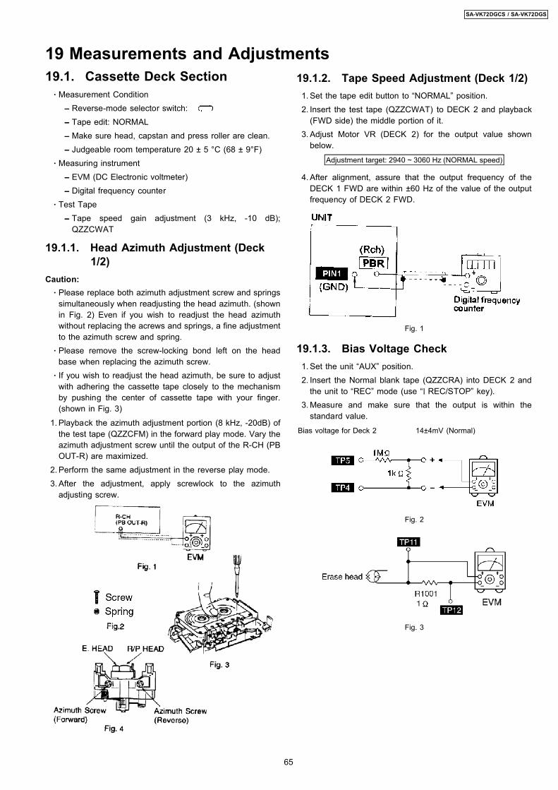
19.1.2. Tape Speed Adjustment (Deck 1/2) 1. Set the tape edit button to “NORMAL” position. 2. Insert the test tape (QZZCWAT) to DECK 2 and playback
(FWD side) the middle portion of it. 3. Adjust Motor VR (DECK 2) for the output value shown
below.
Adjustment target: 2940 ~ 3060 Hz (NORMAL speed)
4. After alignment, assure that the output frequency of theDECK 1 FWD are within ±60 Hz of the value of the outputfrequency of DECK 2 FWD.
Fig. 1
19.1.3. Bias Voltage Check 1. Set the unit “AUX” position. 2. Insert the Normal blank tape (QZZCRA) into DECK 2 and
the unit to “REC” mode (use “l REC/STOP” key). 3. Measure and make sure that the output is within the
standard value.
Bias voltage for Deck 2 14±4mV (Normal)
Fig. 2
Fig. 3
19 Measurements and Adjustments
65
SA-VK72DGCS / SA-VK72DGS
19.1.4. Bias Frequency Adjustment (Deck1/2)
1. Set the unit to “AUX” position. 2. Insert the Normal blank tape (QZZCRA) into DECK 2 and
set the unit to “REC” mode (l use “REC/STOP” key). 3. Adjust L1002 so that the output frequency is within the
standard value.
Standard Value: 89 ~ 110 kHz
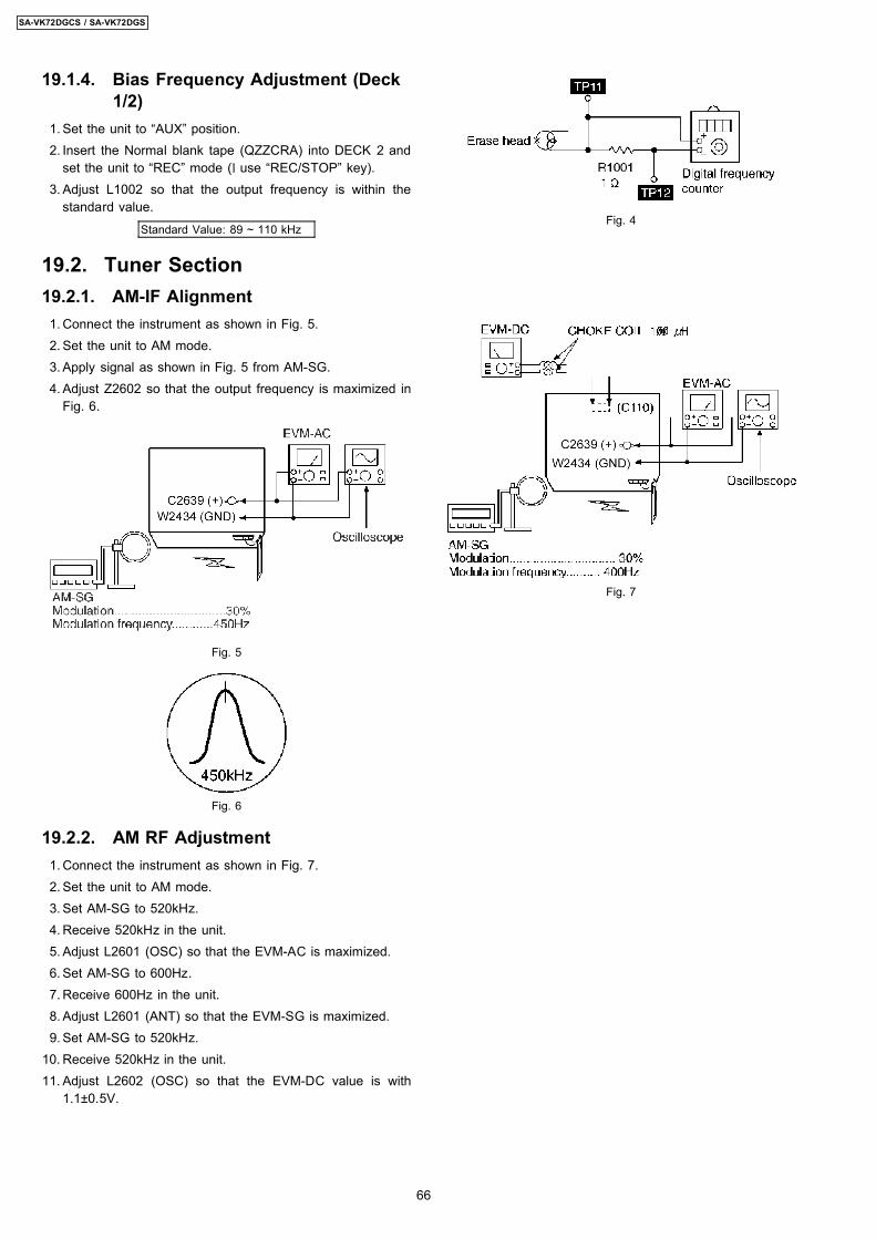
1. Connect the instrument as shown in Fig. 5. 2. Set the unit to AM mode. 3. Apply signal as shown in Fig. 5 from AM-SG. 4. Adjust Z2602 so that the output frequency is maximized in
Fig. 6.
Fig. 5
Fig. 6
19.2.2. AM RF Adjustment 1. Connect the instrument as shown in Fig. 7. 2. Set the unit to AM mode. 3. Set AM-SG to 520kHz. 4. Receive 520kHz in the unit. 5. Adjust L2601 (OSC) so that the EVM-AC is maximized. 6. Set AM-SG to 600Hz. 7. Receive 600Hz in the unit. 8. Adjust L2601 (ANT) so that the EVM-SG is maximized. 9. Set AM-SG to 520kHz. 10. Receive 520kHz in the unit. 11. Adjust L2602 (OSC) so that the EVM-DC value is with
1.1±0.5V.
Fig. 4
Fig. 7
19.2. Tuner Section19.2.1. AM-IF Alignment
66
SA-VK72DGCS / SA-VK72DGS

19.3.1. Cassette Deck Section
19.3.2. Adjustment Point
19.3. Alignment Points
67
SA-VK72DGCS / SA-VK72DGS
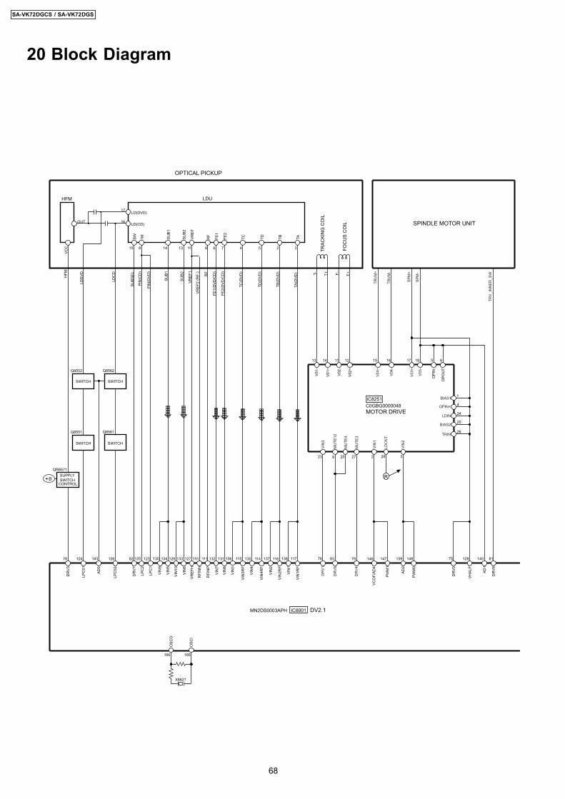
20 Block Diagram
B
LDUHFM
125
LPC
2
82
DR
V7
127
VREF
H
110
RFI
NN
111
RFI
NP
132
VIN
7
131
VIN
8
136
VIN
3
115
VIN
3RF
135
VIN
4
114
VIN
4RF
137
VIN
2
116
VIN
2RF
138
VIN
1
117
VIN
1RF
13
V01-
11
V02-
12
V02+
14
V01+
17 18 5
OPI
N-
6
OPO
UT
1
4
24
25
26
23 9
76
20
83
2
146
VCO
F/AD
4
3
139
AD2
147
PWM
1
148
PWM
0
128
VHAL
F
75
DR
V0
81
DR
V6
140
AD1
1615
T+ F+F-T-
TA(D
VD)
TB(D
VD)
TD(D
VD)
TC(D
VD)
FE2(
DVD
/CD
)
FE1(
DVD
/CD
)
RF
VREF
2 (R
F-)
VREF
1
PIN
(CD
)
SUBS
EL
TRAC
KIN
G C
OIL
FOC
US
CO
IL
124
LPC
01
Q8551
SWITCH
Q8552
SWITCH
126
LPC
02
Q8561
SWITCH
Q8562
SWITCH
143
AD0
LDC
D
LDD
VD
78
DR
V3
QR8571SUPPLYSWITCH
CONTROL
HFM
VCC
OUT
130
VIN
9
134
VIN
5
129
VIN
10
133
VIN
6SU
B2
SUB1
123
LPC
1PI
N(D
VD)
SW
15
1M
8
SUB1
14
SUB2
13
VREF
11
RF
9
FE1
6
FE2
7TC
4
OPTICAL PICKUP
SPINDLE MOTOR UNIT
TD
5
TB
2
TA
3
LD(DVD)17
LD(CD)16
28
R
IC8001 DV2.1
MOTOR DRIVE
IC8251C0GBG0000048
OSC
O
166
OSC
I
165
X8621
TRVM
+
TRVM
-
SPM
+
SPM
-
TRV_
INN
ER_S
W
BIAS1
V03+
V03-
V04+
DR
V8
DR
V1
V04-
OPIN+
LDIN
BIAS2
TRIN
MU
TE12
VIN
3
27
79
DR
V4M
UTE
3
MU
TE4
VIN
1
LDC
NT
VIN
2
MN2DS0003APH
68
SA-VK72DGCS / SA-VK72DGS
1,2,4,5,7,8,10,11,13-15,17,18,
252,254,256
MD
Q0
MD
Q15
A0
1-8,18-25
A15
A16
9,10,16,17,48
A20
DQ
039-36, 38-45
DQ
15
217,220,221,223224,226-228,230,
233,237,238
MA0
MA1
1
21,30,31,43,45
EXAD
R16
EXAD
R20
23-25,27,32,33,36,37,39-42,
46,47,50,51
EXAD
T0
EXAD
T15
192-195,197-200,203,204,206-208
210-212
MD
Q16
MD
Q31
B
DQ
0
2,4,5,7,8,10,11,13,42,44,45,47,
48,50,51,53
DQ
15
BA0
20
232
BA0
BA1
21
234
BA1
LDQ
M
15
249
DQ
M0
UD
QM
39
251
DQ
M1
/CS
19
240
NC
SM
CLK
38
243
MC
K
241
MC
KI
/RAS
18
244
NR
AS
/CAS
17
245
NC
AS
/WE
16
248
NW
E
XWE
11
XCE
26
XOE
28
12XRESET
Q8607
SWITCH
Q8606
SWITCH
Q8560
SWITCH
Q8550
SWITCH
R
IC8001 DV2.1MN2DS0003APH
64 SDRAM
IC8051C3ABPG000133
16M FLASH ROM
IC8651RFKWMH82J160(GCS)RFKWMH82H160(GS)
RESET IC
IC8601C0EBE0000384
RESET IC
IC8606C0EBA0000031
16M EEPROM IC
IC8611C3EBGC000055
22
NEX
WE
38
NEX
CE
52
NEX
OE
73
NR
ST
59
P9
60
6 5
P8
SCL
SDA
VCC
D8550
A0
22-26,29-35
A11
B
69
SA-VK72DGCS / SA-VK72DGS
B
27(26)
VOU
T1(2
)
22(21)
VOU
T3(4
)
20(19)
VOU
T5(6
)
16
VOU
T7
15
VOU
T8
DVD
_MIX
L(R
)
DVD
FL(R
)
DVD
SL(R
)
DVD
CN
T
SUBW
DAT
A2
11~13
DAT
A4
ADO
UT0
ADO
UT2
174~176
DVD
_CM
D
DVD
_STA
T
169
LRC
K
171
ADO
UT3
SRC
K
170 163
DAC
CK
57 56
P12
P11
53
P15
28
55
P13
149
DAC
1OU
T
151
DAC
2OU
T
QR8420
MUTINGSWITCH
152
DAC
3OU
T
156
DAC
4OU
T
158
DAC
5OU
T
70
P1
69
P2
21
68
P3
21
5 5
8
5
4 4
A
AUDIO DAC
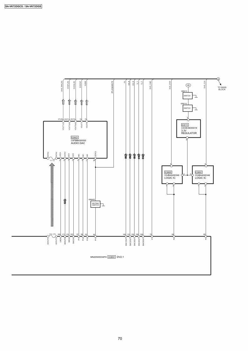
IC8421C0FBBK000050
IC8001 DV2.1MN2DS0003APH
LOGIC IC
IC8695C0JBAA000346
LOGIC IC
IC8691C0JBAA000346
3.3VREGULATOR
IC8111C0CBCBD00018
QR8112
SWITCH
QR8111
SWITCH
DVD
_CLK
TO MAINBLOCK
ZER
O2
MS
MC
MD
ZFLA
G&A
MU
TE
234
SCK
5
BCK
7
DAT
A1
6
LRC
K
8
S_Y
S_C
CR
_R
CB_
BPY
70
SA-VK72DGCS / SA-VK72DGS
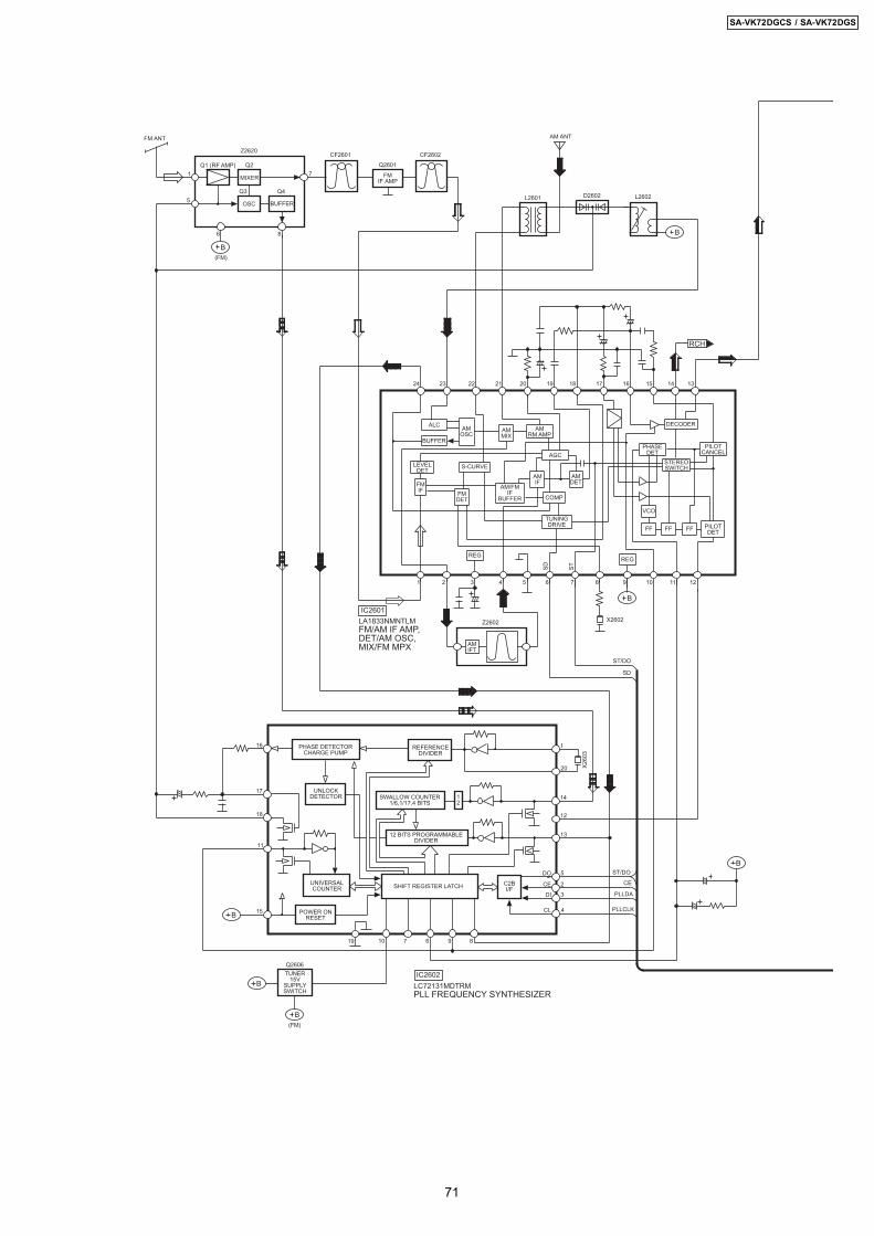
IC2601LA1833NMNTLMFM/AM IF AMP,DET/AM OSC,MIX/FM MPX
SD ST
SHIFT REGISTER LATCH
12
SWALLOW COUNTER1/6,1/17,4 BITS
12 BITS PROGRAMMABLEDIVIDER
REFERENCEDIVIDER
C2BI/F
PLLCLK
PLLDA
ST/DO
CE
X260
3
ST/DO
SD
S-CURVE
REG
FMIF FM
DET
AMOSC
LEVELDET
BUFFER
ALC DECODER
STEREOSWITCH
AMDET
AMIF
TUNINGDRIVE
AM/FMIF
BUFFER COMP
FF FF
VCO
AMMIX
AMRM AMP
AGCPHASE
DET
PILOTDETFF
PILOTCANCEL
(FM)
TUNER15V
SUPPLYSWITCH
Q2606
POWER ONRESET
UNIVERSALCOUNTER
UNLOCKDETECTOR
PHASE DETECTORCHARGE PUMP
LC72131MDTRMPLL FREQUENCY SYNTHESIZER
IC2602
X2602
16
17
18
11
15
19 10 7 6 9 8
4CL
3DI
2CE
5DO
13
12
14
20
1
L2602D2602L2601
2324 22 21 20 19 18 17 16 1415 13
1 2 3 4 65 7 8 9 10 11 12
FMIF AMP
Q2601
REG
B
B
B
B
B
RCH
B
CF2601 CF2602
B
FM ANT
Z2620
8
(FM)
MIXER
OSC BUFFER
Q1 (RF AMP)
6
5
1 7Q2
Q3 Q4
AMIFT
Z2602
AM ANT
71
SA-VK72DGCS / SA-VK72DGS
CE
SD
PLLCLK
ST/DO
PLLDA
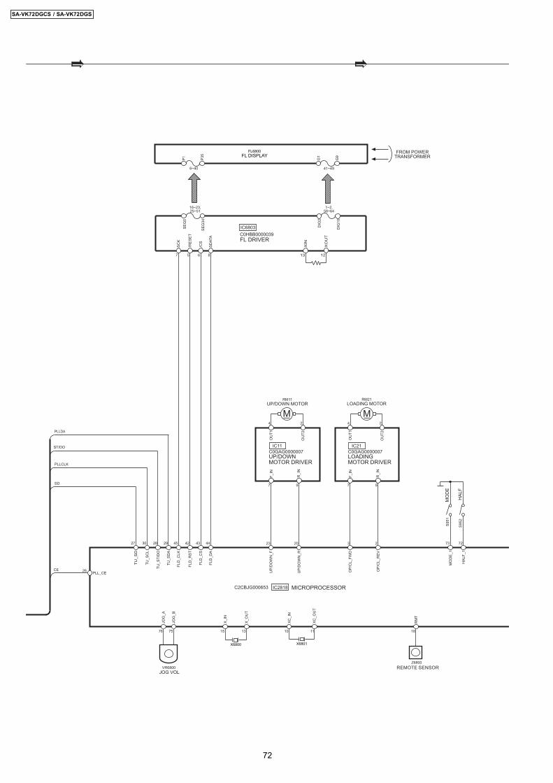
C0HBB0000039FL DRIVER
IC6803
/RES
ET
5
42
FLD
_RST
/CS
6
43
FLD
_CS
45
FLD
_CLK
SCK
7
SDAT
A
8
44
FLD
_DA
XIN
13
XO
UT
12
RM
T
18
27
TU
_SD
28
TU_S
T/D
O
PLL_CE26
30
TU_S
CL
29
TU_S
DA
X_IN
15
X_O
UT
13
JOG
_A
76
JOG
_B
75
S951
M
OD
E
72
HAL
F_1
73
MO
DE_
1
S952
HAL
F
X6800
XC_I
N
10
XC_O
UT
11
X6801
P1
6~40
P35
G1
41~49
G9
SEG
34
FL6800FL DISPLAY
REMOTE SENSORZ6800
JOG VOLVR6800
FROM POWERTRANSFORMER
1~2,58~64
16~23,25~51
SEG
0
DIG
2
DIG
10
23
UP/
DO
WN
_F
20
UP/
DO
WN
_R
3
OP/
CL_
FWD
2
OP/
CL_
REV
OU
T2
2
OU
T1
4
RM11UP/DOWN MOTOR
9
R_I
N
7
F_IN
OU
T2
2
OU
T1
4
RM21LOADING MOTOR
9
R_I
N
7
F_IN
IC11C0GAG0000007UP/DOWNMOTOR DRIVER
IC2818C2CBJG000653 MICROPROCESSOR
M M
IC21C0GAG0000007LOADINGMOTOR DRIVER
72
SA-VK72DGCS / SA-VK72DGS
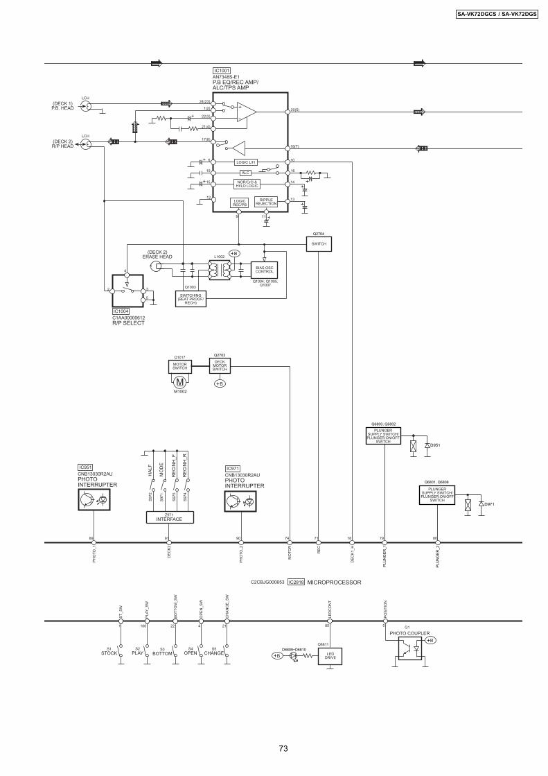
AN7348S-E1P.B EQ/REC AMP/ALC/TPS AMP
IC1001
C1AA00000612R/P SELECT
IC1004
IC971CNB13030R2AUPHOTOINTERRUPTER
Q1003
SWITCHING(BEAT PROOF/
RECH)
L1002
BIAS OSCCONTROL
Q1004, Q1005,Q1007
NOR/CrO &HI/LO LOGIC
LOGICREC/PB
RIPPLEREJECTION
LOGIC L/H
ALC
Q2704
Q6800, Q6802
D951
SWITCH
PLUNGERSUPPLY SWITCH/PLUNGER:ON/OFF
SWITCH
PLUNGERSUPPLY SWITCH/PLUNGER:ON/OFF
SWITCH
90
PHO
TO_2
IC951CNB13030R2AUPHOTOINTERRUPTER
89
PHO
TO_1
79
PLU
NG
ER_1
Q6801, Q6808
80
PLU
NG
ER_2
78
DEC
K1_H
10
16
14
13
11
6
19
15
12
21(4)
22(3)
17(8)
1(2)
24(23)
18(7)
9
3
5
2
4
71
REC
Q2703
DECKMOTORSWITCH
74
MO
TOR
20(5)
M1002
Z971INTERFACE
91
DEC
K2
S972
H
ALF
S975
R
ECIN
H_F
S971
M
OD
E
D971
(DECK 2)R/P HEAD
LCH
Q6811
LEDDRIVE
D6809~D6810
S974
R
ECIN
H_R
B
B
Q1017
MOTORSWITCH
M
(DECK 2)ERASE HEAD
(DECK 1)P.B. HEAD
LCH
B
5
POSI
TIO
N
22
BOTT
OM
_SW
4
OPE
N_S
W
1
ST_S
W
100
PLAY
_SW
21
CH
ANG
E_SW
S4OPEN
S1STOCK
S2PLAY
S3BOTTOM
S5CHANGE
85
LED
CO
NT
IC2818C2CBJG000653 MICROPROCESSOR
B
Q1
PHOTO COUPLER
73
SA-VK72DGCS / SA-VK72DGS
TO DVDBLOCK
A
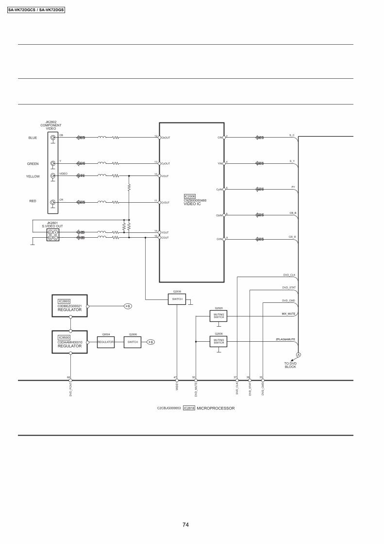
12 CbOUT
13 CyOUT
16 COUT
11CrOUT
15VOUT
14 YOUT
2CIN
4YIN
6CyIN
8CbIN
CrIN 9
S_C
S_Y
PY
CB_B
CR_R
ZFLAG&AMUTE
47
WID
E1
Q2838
SWITCH
37
DVD
_CLK
36
DVD
_STA
T
35
DVD
_CM
D
50
DVD
_MU
TE
Q2806
MUTINGSWITCH
JK2802COMPONENT
VIDEO
CB
Y
CR
68
DVD
_PC
NT
JK2801S.VIDEO OUT
IC2006C9ZB00000466VIDEO IC
IC9500C0DAAMH00010REGULATOR
G YCG
VIDEO
B
RED
BLUE
GREEN
Q9504
REGULATOR
Q2906
SWITCH
YELLOW
MIX_MUTE
Q2920
MUTINGSWITCH
DVD_CMD
DVD_STAT
DVD_CLK
IC2803C0DBEZG00021REGULATOR
B
IC2818C2CBJG000653 MICROPROCESSOR
74
SA-VK72DGCS / SA-VK72DGS
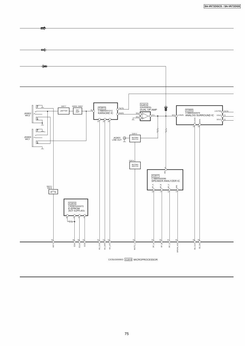
C3EBDG000072E-EPROM(NOT SUPPLIED)
IC2816
5 4 3
38
EDA
39
ECLK
40
ECS
6
Q6806, Q6807
MICAMP
JK6800MIC1
JK6802MIC2
Q6817
LIMITTER
52
KA_L
AT
53
KA_D
AT
54
KA_C
LK
C1BB00001012KARAOKE IC
IC2813
33 32 34
78
64(63)
IC2814KIA4558FELDUAL OP-AMP
C1BB00000979ANALOG SURROUND IC
IC2800
6(7)
67
SP_C
66
SP_B
65
SP_A
C1BB00000086SPEAKER ANALYZER IC
IC2817
10 11 12
8
AIN
SP_A
SP_B
SP_C
95
SPEA
N_A
/D
17
SPE
76(75)
55
MU
TE_L
JK2803LINE OUT
S6810~S6818
92
KEY1
5(3)7(1)
6(2)
15(14)
LCIN(R)
LOUT(R)
25
SS_D
AD
ATA
18
24
SS_C
LKC
LOC
K
19
13COUT
12SOUT
Q2814
MUTINGSWITCH
Q2813
MUTINGSWITCH
IC2818C2CBJG000653 MICROPROCESSOR
Z
75
SA-VK72DGCS / SA-VK72DGS
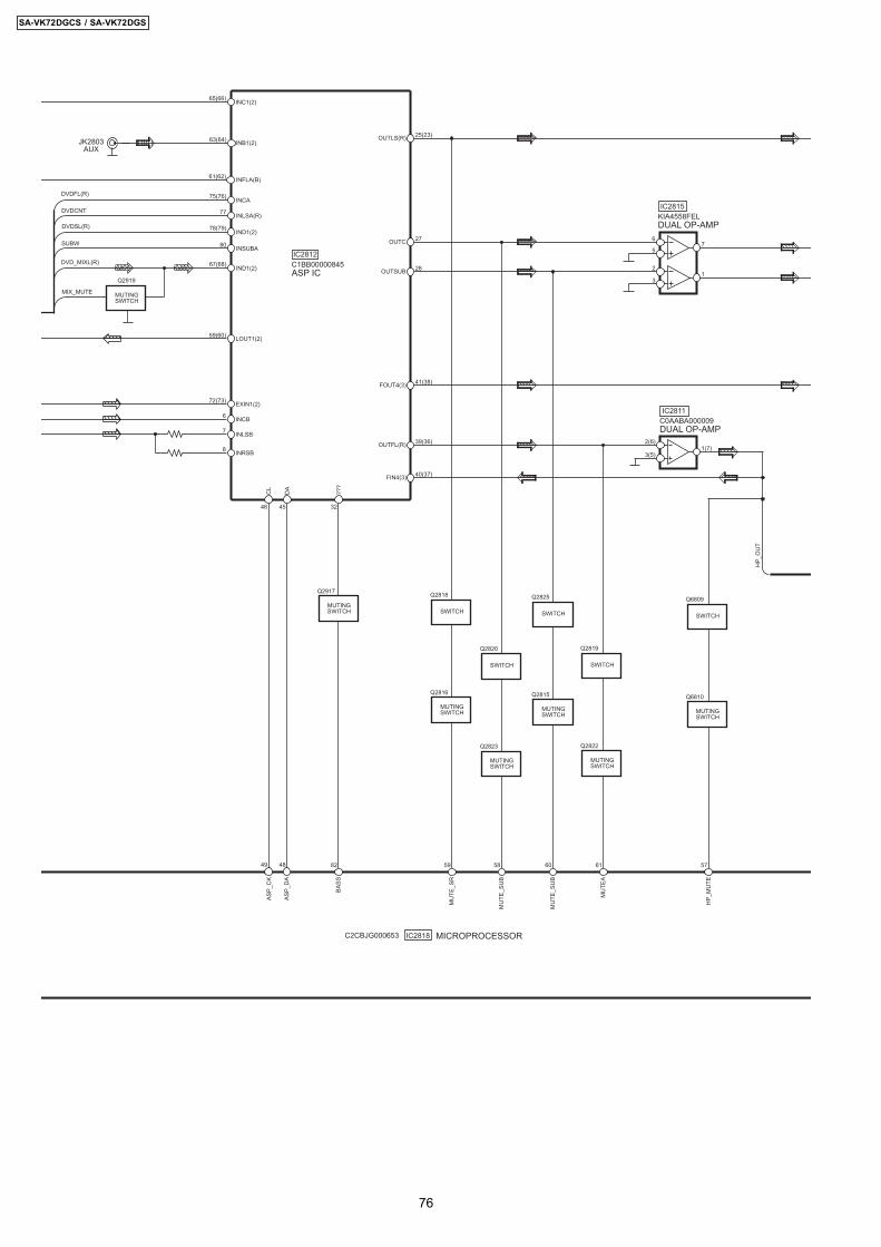
3
7
12
6
5
JK2803AUX
INFLA(B)61(62)
INC1(2)65(66)
INB1(2)63(64)
IND1(2)67(68)IC2812C1BB00000845ASP IC
INSUBA80
IND1(2)78(79)
INCA75(76)
INLSA(R)77IC2815
KIA4558FELDUAL OP-AMP
IC2811C0AABA000009DUAL OP-AMP
82
BASS
HP_
OU
T
MIX_MUTE
Q2919
MUTINGSWITCH
EXIN1(2)72(73)
CL
46
DA
45
???
32
28OUTSUB
INCB6
INLSB7
INRSB8
LOUT1(2)59(60)
48
ASP_
DA
49
ASP_
CK
DVD_MIXL(R)
DVDFL(R)
DVDSL(R)
SUBW
DVDCNT
27OUTC
39(36)OUTFL(R) 2(6)1(7)
3(5)
40(37)FIN4(3)
Q2917
MUTINGSWITCH
25(23)OUTLS(R)
41(38)FOUT4(3)
IC2818C2CBJG000653 MICROPROCESSOR
58
MU
TE_S
UB
Q2823
MUTINGSWITCH
Q2820
SWITCH
59
MU
TE_S
R
Q2818
SWITCH
Q2816
MUTINGSWITCH
61
MU
TEA
Q2822
MUTINGSWITCH
Q2819
SWITCH
60
MU
TE_S
UB
Q2815
MUTINGSWITCH
Q2825
SWITCH
57
HP_
MU
TE
Q6810
MUTINGSWITCH
Q6809
SWITCH
76
SA-VK72DGCS / SA-VK72DGS
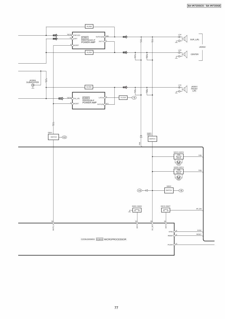
S6819~S6827
69
DC
_DET
19SYNC
70PCONT
SWITCH
Q6820
SYNC
FAN
HP_SW
RSN315H42C-PPOWER AMP
IC5801
OUT11 7-IN1113
-IN21(22)16(15)OUT21(22) 3(6)
RSN35H2B-PPOWER AMP
IC5001-IN_L(R)10(14)
56
MU
TE_H
94
KEY3
S6800~S6809
93
KEY2
B
FAN
SWITCH
Q5801,Q5810
12RESETRESET
OUTL(R) 4(1)
JK9502
CENTER
SUR_L(R)
FRONTL(R)
ACDET8
ACDET6
FAN
B
JK9501
JK2804SUBWOOFER
Q2913~Q2916
FANMOTORDRIVE
M
B
Q2909~Q2912
FANMOTORDRIVE
M
5LATCH
LCH
LCH
FILTERLCH
B
FILTER
Q5811
SWITCH
IC2818C2CBJG000653 MICROPROCESSOR
FILTER
FILTER
77
SA-VK72DGCS / SA-VK72DGS
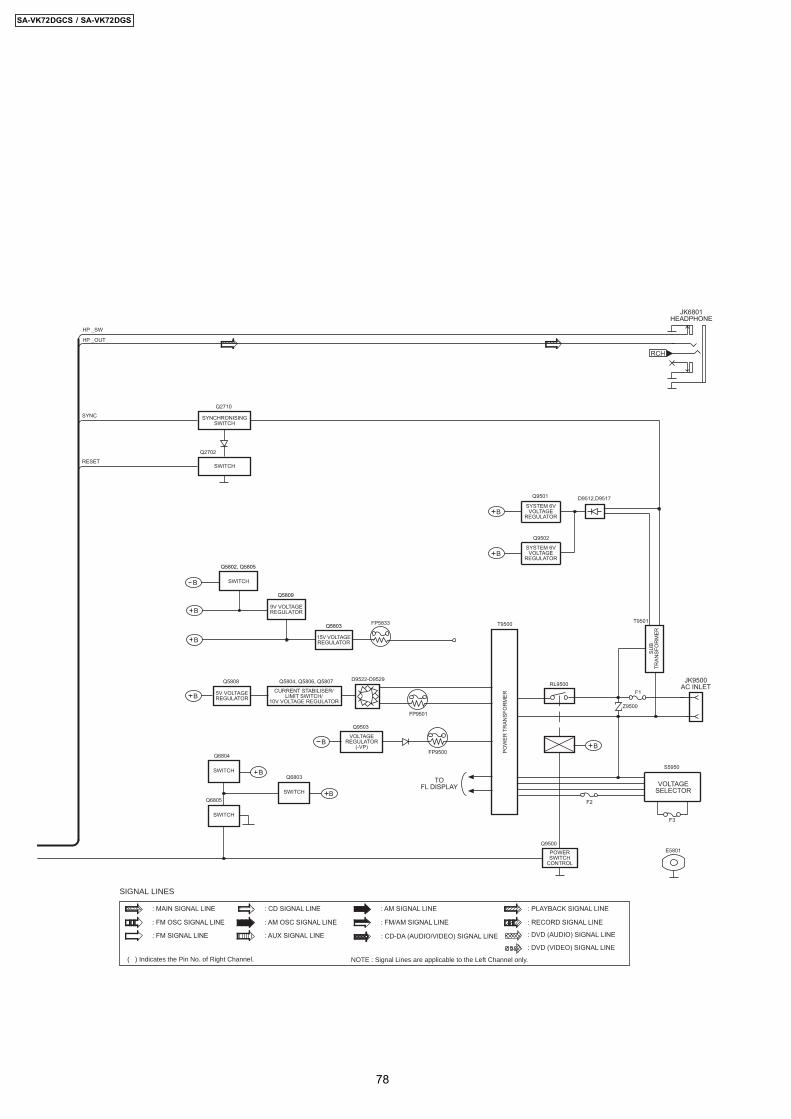
: MAIN SIGNAL LINE
: FM OSC SIGNAL LINE
: FM SIGNAL LINE
: CD SIGNAL LINE
: AM OSC SIGNAL LINE
: AUX SIGNAL LINE
: AM SIGNAL LINE
: FM/AM SIGNAL LINE
: CD-DA (AUDIO/VIDEO) SIGNAL LINE
: PLAYBACK SIGNAL LINE
: RECORD SIGNAL LINE
E5801
T9500
SYNC
HP _SW
JK6801HEADPHONE
VOLTAGEREGULATOR
(-VP)
Q9503
POW
ER T
RAN
SFO
RM
ER
T9501
POWERSWITCH
CONTROL
F1
Q9500
9V VOLTAGEREGULATOR
15V VOLTAGEREGULATOR
5V VOLTAGEREGULATOR
CURRENT STABILISER/LIMIT SWITCH/
10V VOLTAGE REGULATOR
Q2710
D9512,D9517Q9501
SYSTEM 6VVOLTAGE
REGULATOR
JK9500AC INLET
FP9500
FP9501
FP5833
SUB
TRAN
SFO
RM
ER
D9522-D9529Q5804, Q5806, Q5807Q5808
Q5803
Q5809
B
SYNCHRONISINGSWITCH
Z9500
Q9502
: DVD (VIDEO) SIGNAL LINE
: DVD (AUDIO) SIGNAL LINE
Q6805
SWITCH
Q6804
SWITCHQ6803
SWITCH
HP _OUT
SYSTEM 6VVOLTAGE
REGULATOR
SWITCH
Q5802, Q5805
RESET
Q2702
SWITCH
F2
B
B
B
B
RL9500
RCH
TOFL DISPLAY
SIGNAL LINES
( ) Indicates the Pin No. of Right Channel. NOTE : Signal Lines are applicable to the Left Channel only.
S5950
VOLTAGESELECTOR
F3
B
B
B
B
B
78
SA-VK72DGCS / SA-VK72DGS

21 Voltage MeasurementThis section is not available at time of issue.
79
SA-VK72DGCS / SA-VK72DGS
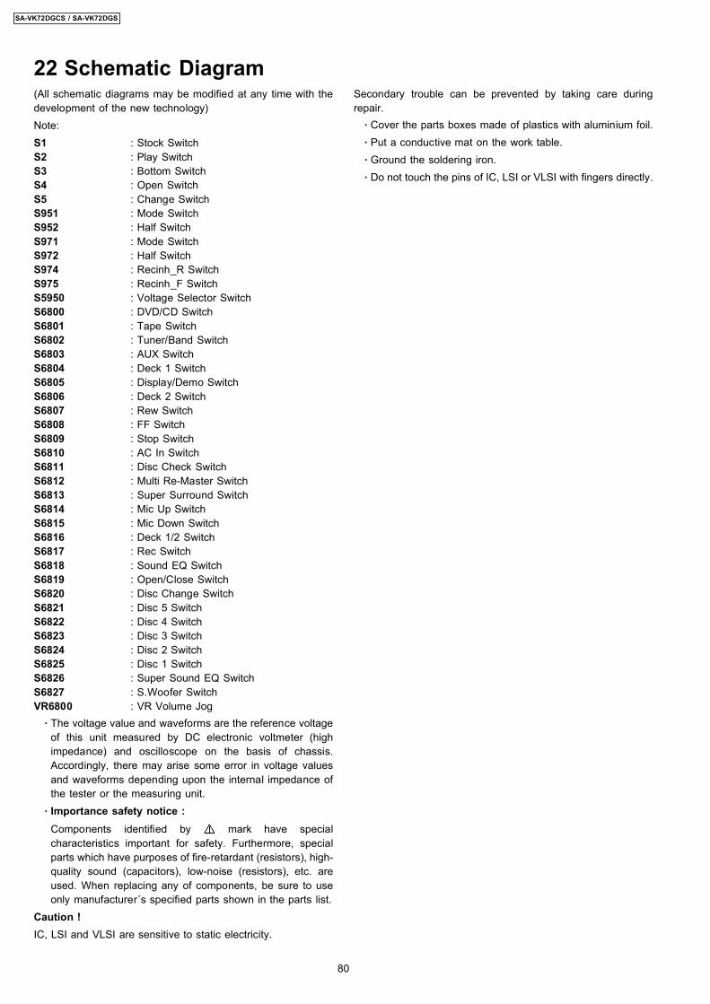
(All schematic diagrams may be modified at any time with thedevelopment of the new technology)Note:S1 : Stock SwitchS2 : Play SwitchS3 : Bottom SwitchS4 : Open SwitchS5 : Change SwitchS951 : Mode SwitchS952 : Half SwitchS971 : Mode SwitchS972 : Half SwitchS974 : Recinh_R SwitchS975 : Recinh_F SwitchS5950 : Voltage Selector SwitchS6800 : DVD/CD SwitchS6801 : Tape SwitchS6802 : Tuner/Band SwitchS6803 : AUX SwitchS6804 : Deck 1 SwitchS6805 : Display/Demo SwitchS6806 : Deck 2 SwitchS6807 : Rew SwitchS6808 : FF SwitchS6809 : Stop SwitchS6810 : AC In SwitchS6811 : Disc Check SwitchS6812 : Multi Re-Master SwitchS6813 : Super Surround SwitchS6814 : Mic Up SwitchS6815 : Mic Down SwitchS6816 : Deck 1/2 SwitchS6817 : Rec SwitchS6818 : Sound EQ SwitchS6819 : Open/Close SwitchS6820 : Disc Change SwitchS6821 : Disc 5 SwitchS6822 : Disc 4 SwitchS6823 : Disc 3 SwitchS6824 : Disc 2 SwitchS6825 : Disc 1 SwitchS6826 : Super Sound EQ SwitchS6827 : S.Woofer SwitchVR6800 : VR Volume Jog · The voltage value and waveforms are the reference voltage
of this unit measured by DC electronic voltmeter (highimpedance) and oscilloscope on the basis of chassis.Accordingly, there may arise some error in voltage valuesand waveforms depending upon the internal impedance ofthe tester or the measuring unit.
· Importance safety notice :Components identified by mark have specialcharacteristics important for safety. Furthermore, specialparts which have purposes of fire-retardant (resistors), high-quality sound (capacitors), low-noise (resistors), etc. areused. When replacing any of components, be sure to useonly manufacturer´s specified parts shown in the parts list.
Caution !IC, LSI and VLSI are sensitive to static electricity.
Secondary trouble can be prevented by taking care duringrepair. · Cover the parts boxes made of plastics with aluminium foil. · Put a conductive mat on the work table. · Ground the soldering iron. · Do not touch the pins of IC, LSI or VLSI with fingers directly.
22 Schematic Diagram
80
SA-VK72DGCS / SA-VK72DGS
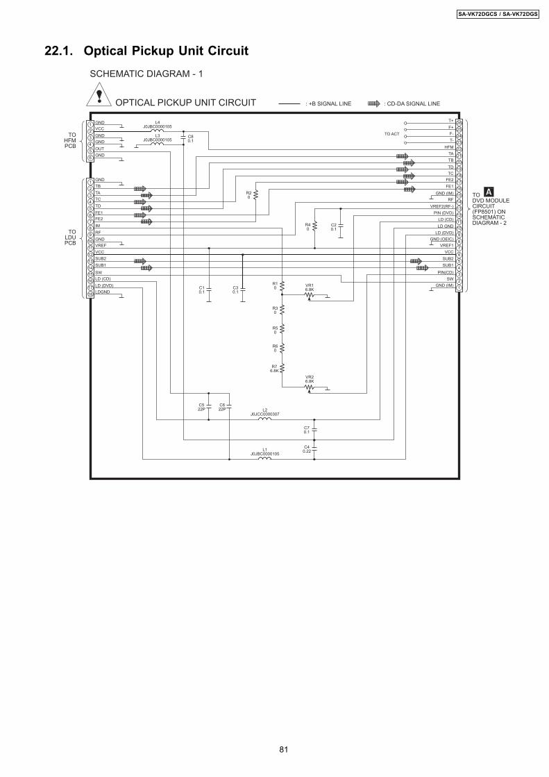
22.1. Optical Pickup Unit Circuit
2
4
65
3
1
151413121110
2
4
6
89
7
5
3
1
1718
16
161718192021
25
2322
24
26
123456
14
12
10
87
9
11
13
15
TO ACT
TODVD MODULECIRCUIT(FP8501) ONSCHEMATICDIAGRAM - 2
TOHFMPCB
TOLDUPCB
L4J0JBC0000105
L1J0JBC0000105
L2J0JCC0000307
C522P
C622P
C10.1
C30.1
C20.1
R10
R40
R20
C80.1
R30
R50
R60
R76.8K
C70.1
VR26.8K
VR16.8K
C40.22
L3J0JBC0000105
T+F+F-T-
HFMTATBTDTC
FE2FE1
GND (IM)RF
VREF2(RF-)PIN (DVD)
LD (CD)LD GND
LD (DVD)GND (OEIC)
VREF1VCC
SUB2SUB1
PIN(CD)SW
GND (IM)
GNDVCCGNDGNDOUTGND
GNDTBTATCTDFE1FE2IMRFGNDVREFVCCSUB2SUB1
SWLD (CD)LD (DVD)LDGND
SCHEMATIC DIAGRAM - 1
OPTICAL PICKUP UNIT CIRCUIT : +B SIGNAL LINE : CD-DA SIGNAL LINE
81
SA-VK72DGCS / SA-VK72DGS
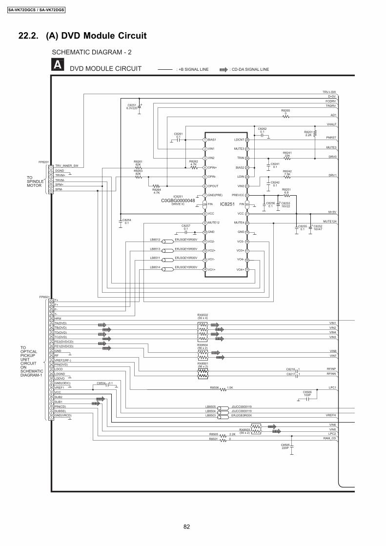
22.2. (A) DVD Module Circuit
2
4
65
3
1
161718192021
25
2322
24
26
123456
14
12
10
87
9
11
13
15
SCHEMATIC DIAGRAM - 2
DVD MODULE CIRCUIT : +B SIGNAL LINE : CD-DA SIGNAL LINE
T+F+F-T-HFMTA(DVD)TB(DVD)TD(DVD)TC(DVD)FE2(DVD/CD)FE1(DVD/CD)GNDRFVREF2(RF-)PIN(DVD)LDCDLDGNDLDDVDGND(OEIC)VREF1VCCSUB2SUB1PIN(CD)SUBSELGND(VRCD)
FP8501
LDCNT
MUTE3
TRIN
BIAS2
LDIN
VIN3
PREVCC
FIN
VCC
MUTE4
GND
VO3-
VO3+
VO4-
VO4+
BIAS1
VIN1
VIN2
OPIN+
OPIN-
OPOUT
GND(PRE)
FIN
VCC
MUTE12
GND
VO2-
VO2+
VO1-
VO1+
VIN1VIN2VIN4VIN3
VIN8VIN7
RFINPRFINN
LPC1
VREFH
VIN6VIN5
LPC2RAM_CD
PNRST
LB8512 ERJ3GEY0R00V
LB8513 ERJ3GEY0R00V
LB8511 ERJ3GEY0R00V
LB8514 ERJ3GEY0R00V
LB8505 J0JCC0000119LB8504 J0JCC0000119LB8503 ERJ2GE0R00X
R8501 0
R8506 1.5KC8504 0.1
C82560.1
C82570.1
R82516.8
RX8502(56 x 4)
RX8504(56 x 2)
RX8503(56 x 2)
C8506100P
C8505220P
RX8501(56 x 2)
IC8251C0GBG0000048
DRIVE IC IC8251
TOOPTICALPICKUPUNITCIRCUITONSCHEMATICDIAGRAM-1
C825316V22
C82550.1
C825216V47
R8505 2.2K
MUTE124
C82620.1
C82610.1
R82624.7K
R826182K
R826382K
R82644.7K
R82650
R824122K
R82012.2K
C82410.1
DRV0
R82427.5K
C82420.1
DRV1
C82540.1
C82516.3V220
D+5V
TOSPINDLEMOTOR
FP8201
SPM-SPM+TRVM-TRVM+DGNDTRV_INNER_SW
M+9V
MUTE3
AD1
TRDRVFODRV
VHALF
TRV-I-SW
C8218 1C8217 1
3029
15
16
1712
13
14
1811
1910
209
218
227
236
245
254
263
272
281
82
SA-VK72DGCS / SA-VK72DGS
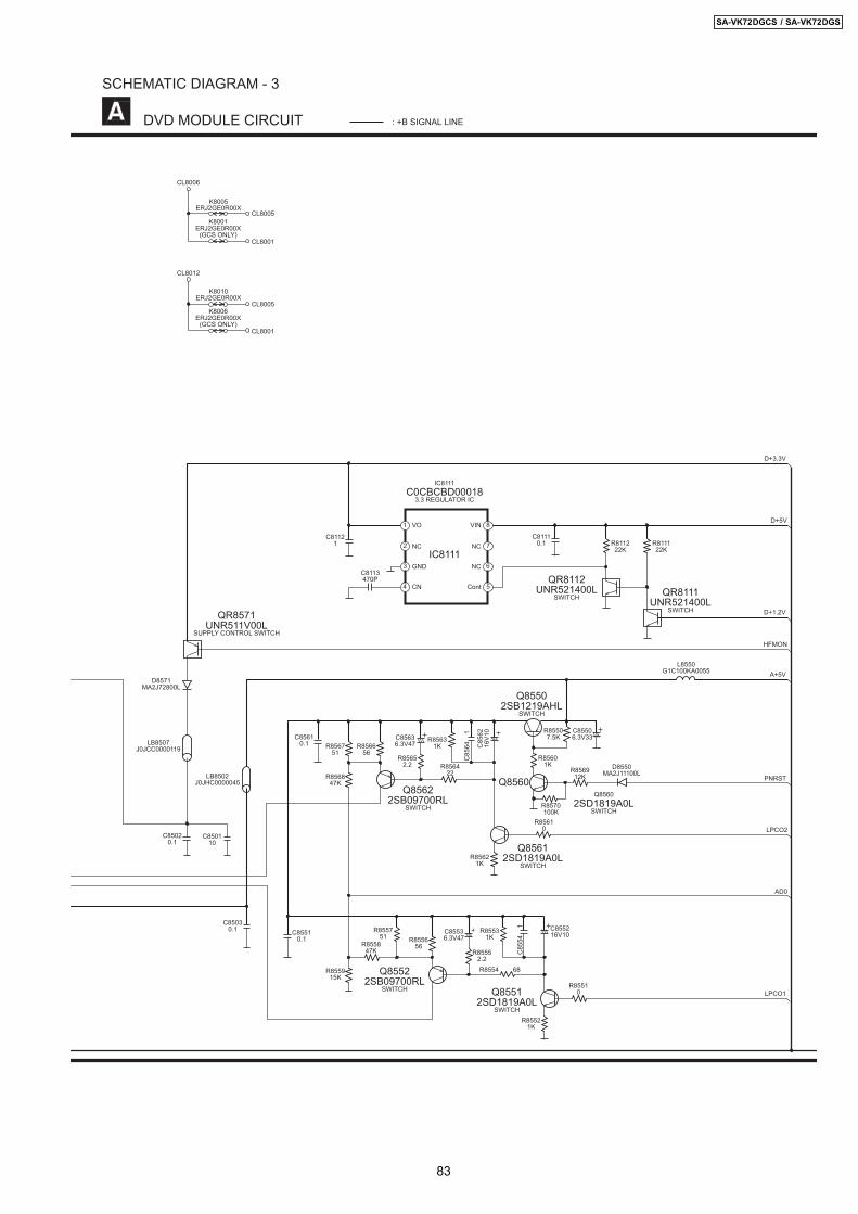
SCHEMATIC DIAGRAM - 3
DVD MODULE CIRCUIT : +B SIGNAL LINE
D+5VVO
NC
GND
CN
VIN
NC
NC
Cont
D+3.3V
HFMON
AD0
LPCO2
LPCO1
A+5V
D+1.2V
LB8507J0JCC0000119
LB8502J0JHC0000045
C85020.1
C850110
D8571MA2J72800L
C81121
C8113470P
C81110.1
L8550G1C100KA0055
C85610.1
C85510.1
C85030.1
R855915K
R855847K
R855751 R8556
56
C85536.3V47
R85552.2
R85531K
R85521K
R85510
R8554 68
C855216V10
R856751
R856847K
R856656
C85636.3V47
R85652.2
R85631K
C85
64
1
C85
6216
V10
R856422
R85621K
R85610
R85601K
R856912K
R8570100K
R85507.5K
C85506.3V33
D8550MA2J11100L
C85
54
1
QR8571UNR511V00L
SUPPLY CONTROL SWITCH
Q85502SB1219AHL
SWITCH
Q85622SB09700RL
SWITCH
Q85522SB09700RL
SWITCH
Q85602SD1819A0L
SWITCH
Q8560
Q85612SD1819A0L
SWITCH
Q85512SD1819A0L
SWITCH
IC8111C0CBCBD00018
3.3 REGULATOR IC
IC8111
PNRST
R811222K
QR8112UNR521400L
SWITCH QR8111UNR521400L
SWITCH
R811122K
K8001ERJ2GE0R00X
(GCS ONLY)CL8001
CL8006
K8005ERJ2GE0R00X
CL8005
K8006ERJ2GE0R00X
(GCS ONLY)CL8001
CL8012
K8010ERJ2GE0R00X
CL8005
1
2
3 6
7
8
4 5
83
SA-VK72DGCS / SA-VK72DGS
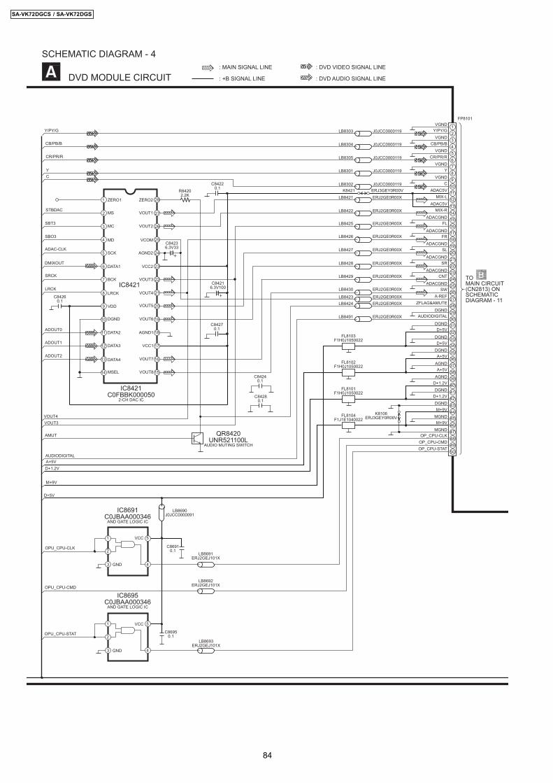
151413121110
2
4
6
89
7
5
3
1
302928272625
17
19
21
2324
22
20
18
16
363534333231
5049484746
38
40
42
4445
43
41
39
37
SCHEMATIC DIAGRAM - 4
DVD MODULE CIRCUIT
TOMAIN CIRCUIT(CN2813) ONSCHEMATICDIAGRAM - 11
FP8101
Y/PY/GVGND
VGND
VGND
VGND
VGND
ADAC5V
ADAC5V
ADACGND
ADACGND
ADACGND
ADACGND
ADACGND
ADACGND
DGND
DGNDD+5V
D+5V
D+5V
A+5V
A+5V
A+5V
AGND
AGNDD+1.2V
D+1.2VDGND
DGNDM+9V
M+9VMGND
MGND
DGND
DGND
LB8303 J0JCC0000119
CB/PB/BLB8304 J0JCC0000119
CR/PR/RLB8305 J0JCC0000119
YLB8301 J0JCC0000119
CLB8302K8421 ERJ3GEY0R00V
J0JCC0000119
MIX-LLB8421 ERJ2GE0R00X
MIX-RLB8422 ERJ2GE0R00X
OP_CPU-CLK
LB8691ERJ2GEJ101X
FL
FR
SL
SR
CNT
SWA-REFLB8423 ERJ2GE0R00X
ZFLAG&AMUTELB8424 ERJ2GE0R00X
AUDIODIGITALLB8491 ERJ2GE0R00X
OP_CPU-CMD
LB8692ERJ2GEJ101X
OP_CPU-STAT
LB8693ERJ2GEJ101X
FL8103F1H0J1050022
FL8102F1H0J1050022
FL8101F1H0J1050022
FL8104F1J1E1040022
VCC
GND
GND
VCC
OPU_CPU-CLK
OPU_CPU-CMD
OPU_CPU-STAT
Y/PY/G
CB/PB/B
CR/PR/R
YC
D+1.2V
C86950.1
C86910.1
LB8690J0JCC0000091
IC8421
IC8691C0JBAA000346
AND GATE LOGIC IC
IC8421C0FBBK000050
2-CH DAC IC
QR8420UNR521100L
AUDIO MUTING SWITCH
IC8695C0JBAA000346
AND GATE LOGIC IC
M+9V
ZERO2
VOUT1
VOUT2
VCOM
AGND2
VCC2
VOUT3
VOUT3VOUT4
VOUT4
ZERO1
MS
MC
MD
SCK
DATA1
BCK
LRCK
C84236.3V33
C84240.1
C84280.1
C84220.1
R84202.2K
C84216.3V100
AUDIODIGITAL
SBT3
STBDAC
SBO3
AMUT
ADAC-CLK
DMIXOUT
SRCK
LRCK
K8106ERJ3GEY0R00V
: +B SIGNAL LINE
: MAIN SIGNAL LINE
: DVD AUDIO SIGNAL LINE
: DVD VIDEO SIGNAL LINE
C84270.1
C84260.1
ADOUT0
ADOUT1
ADOUT2
VDD
DGND
DATA2
DATA3
DATA4
MSEL
VOUT5
VOUT6
AGND1
VCC1
VOUT7
VOUT8
LB8425 ERJ2GE0R00X
LB8426 ERJ2GE0R00X
LB8427 ERJ2GE0R00X
LB8428 ERJ2GE0R00X
LB8429 ERJ2GE0R00X
LB8430 ERJ2GE0R00X
4
51
2
3
4
51
2
3
1
2 27
28
3 26
4 25
5 24
6 23
7 22
8 21
9 20
10 19
11 18
12 17
13 16
14 15
84
SA-VK72DGCS / SA-VK72DGS
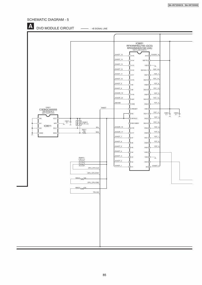
SCHEMATIC DIAGRAM - 5
DVD MODULE CIRCUIT : +B SIGNAL LINE
RX8611(4.7K x 2)
C86110.1
R8611100
R8022 10K
R8023 47K
RX8021(10K x 2)
C86510.1
C86520.1
A0
A1
A2
GND
VCC
WP
SCL
SDA
A15
A14
A13
A12
A11
A10
A9
A8
A19
A20
XWE
XRESET
NC
WP/ACC
RDY/XBSY
A18
A17
A7
A6
A5
A4
A3
A2
A1
A16
XBYTE
VSS
DQ15/A-1
DQ7
DQ14
DQ6
DQ13
DQ5
DQ12
DQ4
VDD
DQ11
DQ3
DQ10
DQ2
DQ9
DQ1
DQ8
DQ0
XOE
VSS
XCE
A0
FDT_15
FDT_7
FDT_14
FDT_6
FDT_13
FDT_5
FDT_12
FDT_4
FDT_11
FDT_3
FDT_10
FDT_2
FDT_9
FDT_1
FDT_8
FDT_0
EXADT_15 EXADR_16
EXADT_14
EXADT_13
EXADT_12
EXADT_11
EXADT_10
EXADT_9
EXADT_8
EXADR_19
EXADR_20
NEXWE
EXADR_18
EXADR_17
EXADT_7
EXADT_6
EXADT_5
EXADT_4
EXADT_3
EXADT_2
EXADT_1 EXADT_0
PNRST
SCL
SDA
OPU_CPU-CLK
OPU_CPU-STAT
OPU_CPU-CMD
TRV-SW
IC8611C3EBGC000055
16M EEPROM IC(NOT SUPPLIED)
IC8611
IC8651RFKWMH82J160 (GCS)RFKWMH82H160 (GS)
16M FLASH ROM IC
8
72
1
63
54
1
2
3 46
47
48
4 45
5 44
6 43
7 42
8 41
9 40
10 39
11 38
12 37
13 36
14 35
15 34
16 33
17 32
18 31
19 30
20 29
21 28
22 27
23 26
24 25
85
SA-VK72DGCS / SA-VK72DGS
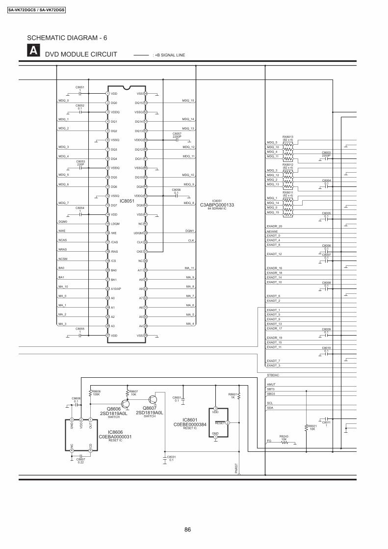
SCHEMATIC DIAGRAM - 6
DVD MODULE CIRCUIT : +B SIGNAL LINE
C80310.1
VDD
DQ0
VDDQ
DQ1
DQ2
VSSQ
DQ3
DQ4
VDDQ
DQ5
DQ6
VSSQ
DQ7
VDD
LDQM
/WE
/CAS
/RAS
/CS
BA0
BA1
A10/AP
A0
A1
A2
A3
VDD
VSS
DQ15
VSSQ
DQ14
DQ13
VDDQ
DQ12
DQ11
VSSQ
DQ10
DQ9
VDDQ
DQ8
VSS
NC
UDQM
CLK
CKE
NC
A11
A9
A8
A7
A6
A5
A4
VSS
SDASCL
SBO3SBT3AMUT
STBDAC
EXADT_3EXADT_7
EXADT_11EXADT_15EXADR_19
EXADR_17EXADT_13EXADT_9EXADT_5EXADT_1
EXADT_2EXADT_6
EXADT_10EXADT_14EXADR_18EXADR_16
EXADT_12
EXADT_8EXADT_4EXADT_0NEXWE
EXADR_20
MDQ_15MDQ_0MDQ_14MDQ_1
MDQ_13MDQ_2MDQ_12MDQ_3
MDQ_11MDQ_4MDQ_10MDQ_5
MDQ_15
MDQ_14
MDQ_13
MDQ_12
MDQ_11
MDQ_10
MDQ_9
MDQ_8
DQM1
CLK
MA_11
MA_9
MA_8
MA_7
MA_6
MA_5
MA_4
MDQ_0
MDQ_1
MDQ_2
MDQ_3
MDQ_4
MDQ_5
MDQ_6
MDQ_7
DQM0
NWE
NCAS
NRAS
NCSM
BA0
BA1
MA_10
MA_0
MA_1
MA_2
MA_3
FG
C80511
C80520.1
C8053220P
C80541
C80551
C80560.1
C80572200P
C80111
C80100.1
C80080.1
C80070.1
C80050.1
C80090.1
C80040.1
C80032200P
RX8011(82 x 4)
RX8012(82 x 4)
RX8013(82 x 4)
IC8051 IC8051C3ABPG000133
64 SDRAM IC
GN
D
VDD
OU
T
NC
CD
VDD
GND
RESET
PNR
ST
C86060.1
C86070.22
R8606100K
R860710K R8601
1KC86010.1
IC8606C0EBA0000031
RESET IC
Q86062SD1819A0L
SWITCH
Q86072SD1819A0L
SWITCHIC8601
C0EBE0000384RESET IC
R824310K
C80060.1
R802110K
4 5
123
1
2
3
1
2
3 52
53
54
4 51
5 50
6 49
7 48
8 47
9 46
10 45
11 44
12 43
13 42
14 41
15 40
16 39
17 38
18 37
19 36
20 35
21 34
22 33
23 32
24 31
25 30
26 29
27 28
86
SA-VK72DGCS / SA-VK72DGS
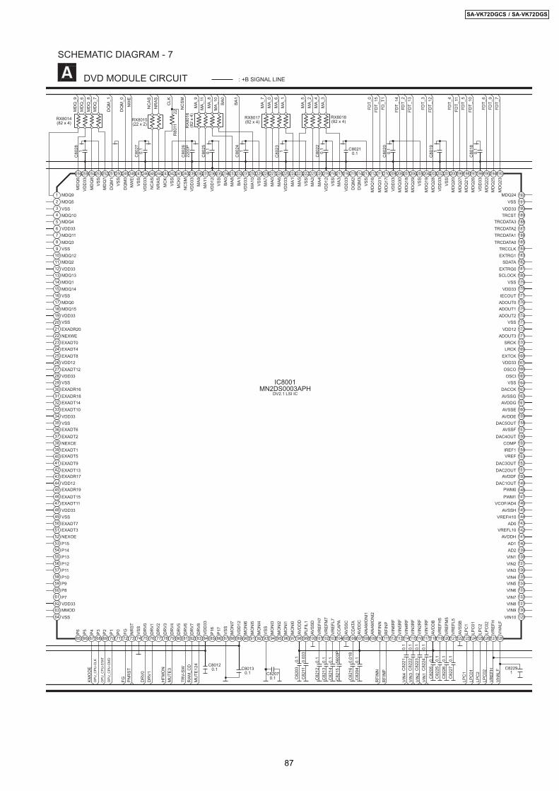
C80
250.
1
C80
220.
1
C80
23 1
C80
24 1
C80
2622
00P
C80
270.
1
C80
28 1
C80130.1
C80120.1
SCHEMATIC DIAGRAM - 7
DVD MODULE CIRCUIT : +B SIGNAL LINE
MDQ9MDQ5VSSMDQ10MDQ4VDD33MDQ11MDQ3VSSMDQ12MDQ2VDD33MDQ13MDQ1MDQ14VSSMDQ0MDQ15VDD33VSSEXADR20NEXWEEXADT0EXADT4EXADT8VDD12EXADT12VDD33VSSEXADR16EXADR18EXADT14EXADT10VDD33VSSEXADT6EXADT2NEXCEEXADT1EXADT5
EXADT9EXADT13EXADR17VDD12EXADR19
EXADT15EXADT11VDD33VSSEXADT7EXADT3NEXOEP15P14P13P12P11P10P9P8P7VDD33MMODVSS
MDQ24VSS
VDD33TRCST
TRCDATA3TRCDATA2TRCDATA1TRCDATA0
TRCCLKEXTRG1
SDATAEXTRG0SCLOCK
VSSVDD33
IECOUTADOUT0ADOUT1ADOUT2
VSSVDD12
ADOUT3SRCKLRCK
EXTCKVDD33OSCOOSCIVSS
DACCKAVSSGAVDDGAVSSEAVDDE
DAC5OUTAVSSF
DAC4OUTCOMPIREF1VREF
DAC3OUTDAC2OUT
AVDDFDAC1OUT
PWM0
PWM1VCOF/AD4
AVSSHVREFH10
AD0VREFL10
AVDDHAD1AD2VIN1VIN2VIN3VIN4VIN5VIN6VIN7VIN8VIN9
VIN10
P6 P5 P4 P3 P2 P1 P0 FG NR
STVS
SD
RV0
DR
V1D
RV2
DR
V3D
RV4
DR
V5D
RV6
DR
V7D
RV8
VDD
33P1
6P1
7VS
SM
ON
I7VD
D12
MO
NI6
MO
NI5
MO
NI4
VSS
MO
NI3
MO
NI2
MO
NI1
MO
NI0
AVD
DD
PLFI
L1AV
SSD
VREF
H7
VREF
M7
VREF
L7C
CAP
A
AVSS
CC
DAT
AAV
DD
CAN
AMO
NI1
ANAM
ON
I2
RFI
NN
RFI
NP
VIN
6RF
VIN
5RF
VIN
4RF
VIN
3RF
VIN
2RF
VIN
1RF
AVD
DB
VREF
H5
VREF
M5
VREF
L5AV
SSB
LPC
1LP
C01
LPC
2LP
C02
VREF
HVH
ALF
MD
Q6
VDD
33M
DQ
8VS
SM
DQ
7D
QM
1VS
SD
QM
0N
WE
VSS
VDD
33N
CAS
NR
ASM
CK
VSS
MC
KIN
CSM
VDD
33M
A9M
A11
VDD
12VS
SBA
0M
A8 BA1
VDD
33M
A10
VSS
MA7
MA0
MA6
VDD
33M
A1M
A5VS
SM
A2M
A4VD
D12
VSS
MA3
VDD
33D
QM
2D
QM
3VS
SM
DQ
16
MD
Q31
MD
Q17
VDD
33M
DQ
30M
DQ
18M
DQ
29VS
SM
DQ
19M
DQ
28VD
D33
VSS
MD
Q20
MD
Q27
MD
Q21
MD
Q26
VDD
33M
DQ
22M
DQ
25M
DQ
23VH
ALF
VREF
HLP
C02
LPC
2LP
C01
LPC
1
VIN
1VI
N2
VIN
3VI
N4
RFI
NP
RFI
NN
MU
TE12
4R
AM_C
DTR
V-SW
MU
TE3
HFM
ON
DR
V1D
RV0
PNR
STFGO
PU_C
PU-C
MD
OPU
_CPU
-STA
T
OPU
_CPU
-CLK
KMO
DE
MD
Q_9
MD
Q_6
MD
Q_8
MD
Q_7
DQ
M_1
DQ
M_0
NW
E
NC
ASN
RAS
NC
SMCLK
MA_
9M
A_11
MA_
8M
A_10
BA0
BA1
MA_
7M
A_0
MA_
6M
A_1
MA_
5M
A_2
MA_
4M
A_3
FDT_
0FD
T_15
FD_T
1
FDT_
14FD
T_2
FDT_
13
FDT_
3FD
T_12
FDT_
4FD
T_11
FDT_
5FD
T_10
FDT_
6FD
T_9
FDT_
7
C82
03
0.1
C82
11
0.0
33
C82
12
0.1
C82
13
0.1
C82
14
0.1
C82
15
560
0P
C82
16
0.0
18C
8204
0
.1
C82
05
0.1
C82
25
0.1
C82
26
0.1
C82
27
0.1
C82
21
0
.1C
8222
0.1
C82
23
0
.1C
8224
0.1
C82291
RX8014(82 x 4)
RX8015(22 x 2) R
X801
6(8
2 x
4) RX8017(82 x 4)
RX8018(82 x 4)
C80210.1
R80
11
2
2
C80
200.
1
C80
19 1
C80
180.
1
IC8001MN2DS0003APH
DV2.1 LSI IC
C82070.1
123456789
65 66 67 68 69 70 71 72 73
185186187188189190191192
248249250251252253254255256
10184
74
247
11183
75
246
12182
13181
76
245
77
244
14180
15179
16178
78
243
79
242
80
241
17177
18176
19175
20174
81
240
82
239
83
238
84
237
21173
22172
23171
24170
25169
85
236
86
235
87
234
88
233
89
232
26168
27167
28166
29165
30164
31163
32162
90
231
91
230
92
229
93
228
94
227
95
226
96
225
33161
3435
159
36158
97
224
98
223
99
222
100
221
37157
38156
39155
40154
41153
42152
43151
44150
101
220
102
219
103
218
104
217
105
216
106
215
107
214
108
213
160
45149
46148
47147
48146
49145
50144
51143
52142
109
212
110
211
111
210
112
209
113
208
114
207
115
206
116
205
53141
54140
55 13856 13757 13658 13559 13460 13361 13262 13163 13064 129
117
204
118
203
119
202
120
201
121
200
122
199
123
198
124
197
125
196
126
195
127
194
128
193
139
87
SA-VK72DGCS / SA-VK72DGS
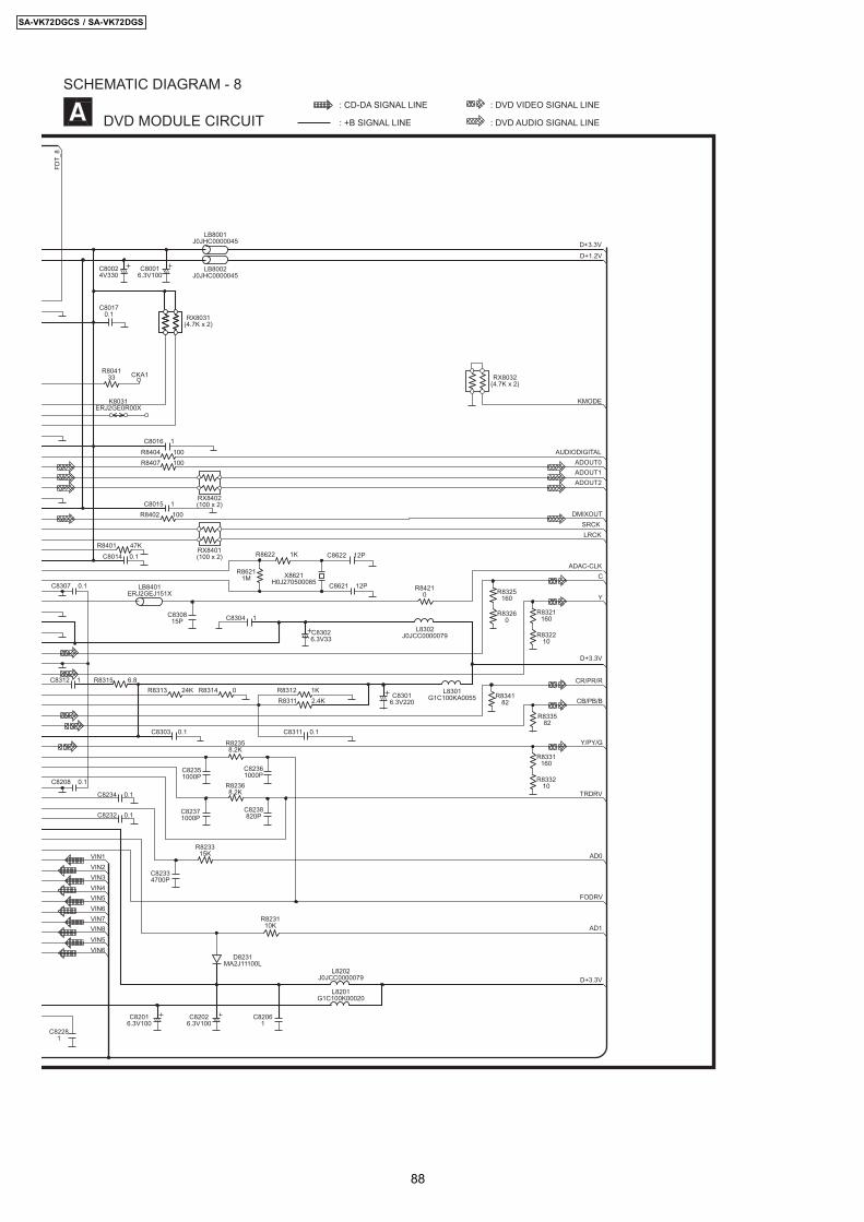
D8231MA2J11100L
SCHEMATIC DIAGRAM - 8
DVD MODULE CIRCUIT : +B SIGNAL LINE
: CD-DA SIGNAL LINE
: DVD AUDIO SIGNAL LINE
: DVD VIDEO SIGNAL LINE
D+1.2V
AUDIODIGITAL
DMIXOUT
C
Y
CR/PR/R
CB/PB/B
Y/PY/G
SRCKLRCK
ADAC-CLK
FODRV
TRDRV
AD0
KMODE
RX8032(4.7K x 2)
RX8031(4.7K x 2)
L8302J0JCC0000079
L8301G1C100KA0055
C83026.3V33
C83016.3V220
R8325160
R83260
R8321160
R832210
R834182
R833582
R8331160
R833210
VIN1VIN2VIN3VIN4VIN5VIN6VIN7VIN8VIN5VIN6
FDT_
8
C82281
C82016.3V100
C82026.3V100
C82061
L8201G1C100K00020
L8202J0JCC0000079
R823110K
C82334700P
C82371000P
C8238820P
C82361000P
C82351000P
R823315K
R82368.2K
R82358.2K
C8232 0.1
C8234 0.1
C8303 0.1
C8312 1
C8304 1
C8311 0.1
R8311 2.4KR8312 1KR8313 24K R8314 0
LB8401ERJ2GEJ151X
C830815P
R86211M
R8622 C8622 12P
C8621 12P
1K
X8621H0J270500085
C8014 0.1R8401 47K
RX8401(100 x 2)
R8402 100
R8404 100
R804133
C8015 1
C8016 1
C80170.1
CKA1
C80024V330
C80016.3V100
LB8002J0JHC0000045
LB8001J0JHC0000045
R8315 6.8
C8208 0.1
C8307 0.1
D+3.3V
AD1
D+3.3V
D+3.3V
R84210
K8031ERJ2GE0R00X
ADOUT0ADOUT1ADOUT2
RX8402(100 x 2)
R8407 100
88
SA-VK72DGCS / SA-VK72DGS
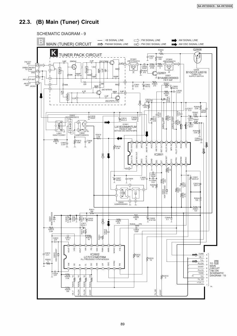
22.3. (B) Main (Tuner) Circuit
3 1
2
1 3
2
1
2
3
5 6
4
MAIN (TUNER) CIRCUIT
SCHEMATIC DIAGRAM - 9
C26471000P
JK2601
IC2602LC72131MDTRM
PLL FREQUENCY SYNTHESIZER
IC2601LA1833NMNTLM
FM/AM IF AMPDET/AM OSC MIX/FM MPX
CF2601J0B1075AA014
X260
3H
0H72
0400
007
D26
01B0
BC5R
0000
09Q2606
Q2606B1GCCFJJ0016
TUNER 15VSUPPLY SWITCH
R26
34
4
70
R26
35
1
K
Q2601Q2601
B1AABC000003FM IF AMP
+7.5V_T
TU_SD
DO/ST
15V
TGNDPLLCK
PLLDA
TUL
CE_T
TUNR
DO
/ST
CE_
T
PLLD
A
PLLC
K
DO
/ST
TU_S
D
C36030.01
C36041000P
R36041K
R3606470K
R3607330
R36010
R3605470
C26010.01
C360216V10
R3603270
TUNER PACK CIRCUIT
C36070.047
R36101K
R3612100K
C36088P
C26361000P
R36145.6K
R26520
C36100.01
R26383.3K
R263010K
C263427P
C263327P
C26120.01
R36
1556
0
R36161K
C361150V4.7
R36
1310
K C262516V22C
2632
1000
P
C26
306.
3V10
0
R26
5182
C26
1310
00P
R36193.3K
R3611390
R262882
R361747K
R36183.3K
C262716V22
Z2602G2BAD0000003
C26261
C36060.01
C261450V3.3
C36091000P
C26
1550
V4.7 C
2616
0.03
3
R362047K
R264322K
C26380.01
R36
2368
K
C262016V10
R2621
22K
R36
024.
7KC
2639
50V4
.7
C2619680P
C26
180.
01
C26170.01
C264250V1
R26426.8K
C264150V1
R26416.8K
R26261K
R36
2547
0
R2629 27K
R26
2747
0
C2624100P
R263210K
C26480.01
R36
2433
X260
2H
3F10
65A0
002 C26
2250
V1R
3622
2.7K
C262150V0.47
R2631120
R2644120
R26331K
C26296.3V100
C26490.1
C262350V1
R26455.6K
C26436800P
C26446800P
R26465.6K
TOMAINCIRCUIT(1B) ONSCHEMATICDIAGRAM - 15
1A
1
2
3
4
CF2602J0B1075AA014
R26
36
1
K
R26
37
1
K
L2601G2A411C00001
L2602G2BPC0000016
D2602B0CDBB000015
: +B SIGNAL LINE
STR
Q
SDC
LW
AIN
PD
AOU
T
VDD
FMIN
AMIN
IFIN
MO
NO
FMAMCE
DI
CL
DO
VSS
XOU
TXI
N
IC2601 PILO
T O
UT
MPX
IN
PILO
T IN
DET
OU
TST
AM O
UT
RC
H
LCH
MO
NO
FM/A
M
OSC AF
C
AM R
F IN
AGC
AM M
IX O
UT
REG
AM IF
IN
GN
D
SD FM D
ET
VCC
STR
Q
OSC
OU
TFM
IF IN
AM LOOP ANT
AM EXTANT
UNBALANCED75 OHM
FM EXT ANT
GND
C26
37
330
0P
C26
31
150
P
: FM/AM SIGNAL LINE: FM SIGNAL LINE: FM OSC SIGNAL LINE
: AM SIGNAL LINE: AM OSC SIGNAL LINE
A
BC
D
E
FG
H
I
J
W29190
1
2
34
6
1
2
3
4
5
7
6
8
5.6P 2SK544
100K 1000P
220
100K180P
2.2P
1.2U
680K
3.3P
18P
2SC2786M
390
0.47U
1000P
390
680K 5.6P
2SC2787FL1TA
2SC1675l1l2
2.2P
390560K
4.7P
2.2P
2.7K
100K
1 2 3 4
21222324
5
20
6
19
7
18
8
17
9
16
10
15
11
14
12
13
1 2
1920
3
18
4
17
5
16
6
15
7
14
8
13
9
12
10
11
89
SA-VK72DGCS / SA-VK72DGS
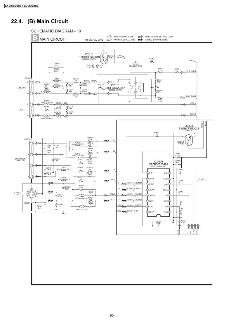
22.4. (B) Main Circuit
N
14
23 C Y
G
5
123
654
AUX
LINE OUT
D+5
V
Y
Y
COUT
CR
CB
VOUT
YOUT
COUT
VOUT
CB_
B
WID
E_1
CR
_R
PYS_C
S_Y
LINE_ROUT
LINE_LOUT
MUTE_L
AUX_L
AUX_R
CB
CR
YOUT
CrIN
GND2
CrOUT
CbOUT MUTE
CbIN
CYIN
GND1
VCC2COUT
BIAS
YIN
CINVOUT
YOUT
CYOUT
C244410V220
C24410.01
R20960
R2803100K
C2851100P
L2812J0JCC0000120
C28420.1
L2816J0JCC0000120
C24
42
5
0V22
C27580.1
Q2838B1GBCFJN0033
SWITCH
R2831100K
C24361
IC2006C9ZB00000498
VIDEO BUFFER IC
C2975 6.3V1000
C2847100P
R282475
R282375
C2846100P
R28202.2K
R2832100K
R281675
C28430.1
R282575
L2813J0JCC0000120
L2811J0JCC0000120
C2046 6.3V1000
C2848100P
R282675
C24430.01
JK2802
L2814J0JCC0000120
C2974 6.3V1000
C2849100P
C2039 0.01
C2850100P
L2815J0JCC0000120
C24371
C2047 6.3V1000
R2834100K
C24400.1
R282275
JK2801
C27590.01
C2434 6.3V1000
R2830100K
R281010K
R2807100K
D2909B0ACCK000005
R28491K
R29592.2
C29650.22u
R2112100K
R28280
R284656K
R2237100
C2110 50V47u
R211447K
L2810J0JBC0000041
R2135 27K
C285550V4.7
C22361000P
C21111000P
R22112.7K
Q2814B1GDCFGA0018
MUTING SWITCH
R2212100K
C21361000P
R22365.6K
L2808J0JBC0000019
L2809J0JBC0000041
L2806J0JBC0000041
R221447K
R28381K
C29700.22u
JK2803
Q2813B1GFGCAA0001
MUTING SWITCH
R2137100
C22111000P
L2807J0JBC0000041
R21112.7K
R22355.6K
R2136 27K
C2210 50V47u
R29582.2
R28391K
R
L
R
L
R
L
R
L
MAIN CIRCUIT
SCHEMATIC DIAGRAM - 10
: +B SIGNAL LINE : MAIN SIGNAL LINE: AUX SIGNAL LINE
: VIDEO SIGNAL LINE: DVD VIDEO SIGNAL LINE
C36230.1 W3011
0
R28990
S-VIDEOOUT
COMPONENTVIDEO OUT
W21260
1
215
16
314
413
512
611
710
89
90
SA-VK72DGCS / SA-VK72DGS
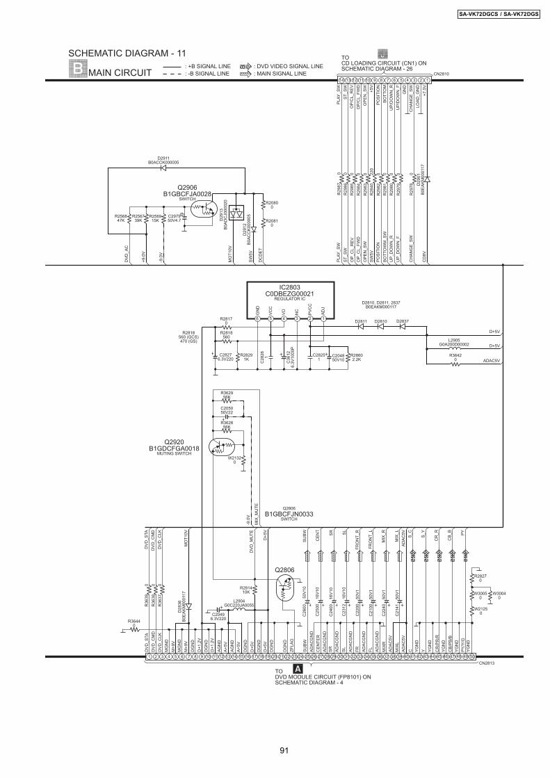
N
36 37 38 39 40 41 4947454342 44 46 48 5021 22 23 24 25 26 3432302827 29 31 33 3515 16 17 18 19 201 2 3 4 5 1311976 8 10 12 14
14 13 12 11 10 24689 7 5 3 1
OP/
CL_
REV
OP/
CL_
FWD
POSI
TIO
N+5
VO
PEN
_SW
BOTT
OM
PLAY
_SW
ST_S
W
CH
ANG
E_SWGN
D
+7.5
VLO
AD_G
ND
UP/
DO
WN
_RU
P/D
OW
N_F
D+5VPL
AY_S
W
CD
8V
CH
ANG
E_SW
UP_
DO
WN
_FU
P_D
OW
N_R
BOTT
OW
M_S
WPO
SITI
ON
OP_
CL_
REV
ST_S
W
OPE
N_S
WSW
5V
OP_
CL_
FWD
NC
VCC
GN
D
VO PVC
C
ADJ
R28602.2K
C204850V10
D2837
C28276.3V220
R28291K
D2810
IC2803C0DBEZG00021
REGULATOR IC
C28251
R2818560
R28170 D2811
C28
26 1
R29
79
0
D29
01B0
EAKM
0001
17
R29
80
0
R29
85
0
R29
87
0
R29
84
0
R29
82
0
R28
40
2
20
R29
86
0
R29
81
0
R29
83
0
R29
78
0
CN2810
D2810, D2811, 2837B0EAKM000117
M+9
V
M+9
V
A+5V
MG
ND
DG
ND
AGN
DD
+1.2
V
DG
ND
D+1
.2V
DVD
_STA
MG
ND
DVD
_CM
DD
VD_C
LK
FL C YMIX
LAD
AC5V
ADAC
5V
ADAC
GN
D
ADAC
GN
DM
IXR
YGN
D
YGN
D
YGN
DC
B/PB
/B
PY/Y
/G
YGN
D
YGN
DC
R/P
R/R
SLD+5
V
SUBW
D+5
V
FRADAC
GN
D
ZFLA
G
ADAC
GN
D
SR ADAC
GN
D
DG
ND
DG
ND
A+5V
AGN
D
DG
ND
DG
ND
CEN
TER
ADAC
GN
D
D+5
V
MO
T10V
DVD
_STA
DVD
_CM
DD
VD_C
LK
FRO
NT_
R
FRO
NT_
LSL
S_C
S_Y
CR
_R
CB_
B
PY
ADAC
5V
CEN
T
SUBW SR
MIX
_R
MIX
_L
Q2806
D28
36B0
EAKM
0001
17
R281410K
C25
00
16V
10
C22
00
50V
1
C21
00
50V
1
C23
12
16V
10
R28270
CN2813
C26
00
50V
10
C24
00
16V
10
TOCD LOADING CIRCUIT (CN1) ONSCHEMATIC DIAGRAM - 26
+9.0
V
SW5V
DC
DET
-9.0
V
DVD
_AC
MO
T10V
D2911B0ACCK000005
R256847K
R256915K
C297950V4.7 R2081
0
Q2906B1GBCFJA0028
SWITCH
R256739K
D29
12B0
ACC
K000
005
D29
13B0
ADC
J000
020 R2080
0
MAIN CIRCUIT
SCHEMATIC DIAGRAM - 11
TODVD MODULE CIRCUIT (FP8101) ONSCHEMATIC DIAGRAM - 4
DVD
_MU
TE
: -B SIGNAL LINE: +B SIGNAL LINE
: MAIN SIGNAL LINE: DVD VIDEO SIGNAL LINE
Q2806B1GBCFJN0033
SWITCH
C22
40
50V
1
C21
41
50V
1
C205050V22
R362956K
R362856K
Q2920B1GDCFGA0018
MUTING SWITCH
-9.0
V
MIX
_MU
TE
L2904G0C220JA0055
C20496.3V220
C36
126.
3V10
00P
L2905G0A200D00002
R36
39
0
R36
38
0
R36
37
0
W21320
ADAC5V
W30050
W30040
W21250
R2818560 (GCS)470 (GS)
D+5V
R36420
R36440
6 5 4 3 2 1
91
SA-VK72DGCS / SA-VK72DGS
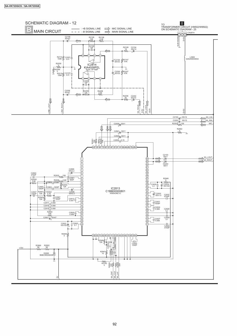
21 3
KA_C
LKKA
_LAT
+15V
5V
MIC
KA_ROUT
KA_D
AT
KA_RIN
KA_LIN
KA_LOUT
R2935 15K
C29290.1
C2901560P
C2939 50V1
R29480
C2941 50V1
C2918 0.068
C29
42
100
0P
R29
5522
0
C293416V100
R294710
C29300.068
R294612K
C29270.068
C2938 0.15
R29395.6K
R294110K
C29280.1
C29004700P
C2940 50V1
R29
5110
K
C292216V100
C2917 0.068
C29
240.
1
C220350V1
C29120.047
R296968
R21620
C2919 0.068
C29350.1
R294310K
C29324700P
C2902 1000P
R29
4910
K
C2921 16V47
IC2813C1BB00000801
KARAOKE IC
C29
4310
00P
C293650V2.2
C29071800P
R295268
C29230.1
R294415K
C29264700P
D2900B0BC5R000009
C29051000P
R294012K
C293350V1.0
C29251000P
C289950V2.2
C29373300P
C29200.068
R29450
C210350V1
R29
5622
0
C29311000P
R29424.7K
C2904 2700PR2938 3.9K
C2202 16V10
C2102 16V10
R28630
R2553 100
-9.0
V
KA_R
OU
T
+9.0
V
KA_L
OU
T
LIN
E_LO
UT
LIN
E_R
OU
TR2059
0
R220912K
R210747K
R2210100K
R2110100K
C210450V10
C210610P
R220747KC2107
0.01
C220610P
C220550V33
R210912K
R21083.3K
R22083.3K
C220450V10
R21061K
C220850V47
C210850V47
R22061K
IC2814KIA4558FEL
DUAL OP AMP
C210550V33
C22070.01
MAIN CIRCUIT
SCHEMATIC DIAGRAM - 12
: -B SIGNAL LINE: +B SIGNAL LINE
: MAIN SIGNAL LINE: MIC SIGNAL LINE
SUB+
BGN
D
D+5
VD
+5V
CN2814
TOTRANSFORMER CIRCUIT (H9502/W9502)ON SCHEMATIC DIAGRAM - 25
W20940
L2906G0A200D00002
1 2
78
3
6
4
5
123456789
25 26 27 28 29 30 31 32 33
565758596061626364
727374757677787980
10 55
34
71
11 54
35
70
12 5313 52
36
69
37
68
14 5115 5016 49
38
67
39
66
40
65
17 4818 4719 4620 4521 4422 4323 4224 41
92
SA-VK72DGCS / SA-VK72DGS
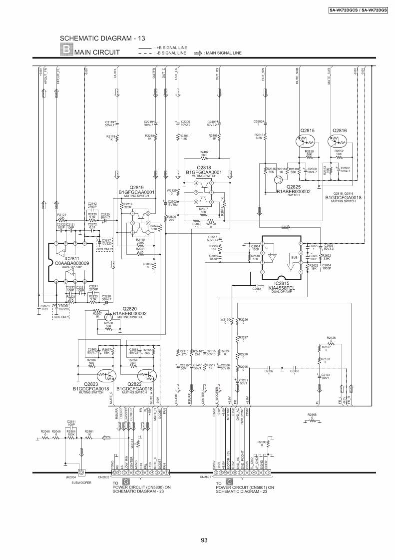
12 11 10 24689 7 5 3 1 12 11 10 24689 7 5 3 1
1
2
3
6
5
4
1
2
3
6
5
4
uP_G
ND
MO
TOR
_10V
+9.0
V-9
.0V
DVD
_PC
ON
T
TL_G
ND
DVD
_AC
GN
D2
DG
ND
CD
8V
D+5
V
SW5V
FAN
+15V
CEN
TER
LOW
_RIN
LSRS
TGN
D
MU
TE_H
DC
DET
AGN
DFR
RFR
LFLFR
MU
TE_A
FAN
S_W
OO
FER
OU
TFL
+9.0
V
-9.0
V
MU
TE_S
UR
MU
TE_S
UB
MU
TE_C
S_W
OO
FER
RSU
RR
+9.0
V
FLFRCEN
TER
-9.0
V
RSU
RR
LSU
RR
D+5
V
LSU
RR
DVD
_PC
NT
CD
8V
DVD
_AC
MO
T10V
+9.0
V-9
.0V
SW5V
+15V
CEN
TER
DC
DET
MU
TE_H
OU
TFR
OU
T_LS
OU
T_R
S
OU
T_SW
OU
T_C
-9.0
V
R28620
R26240
C260650V10
R21181K
C211950V4.7
R250910K
R22181K
Q2818B1GFGCAA0001
MUTING SWITCH
R285756K
R28423.3K
CN2801
C29681
C286050V4.7
R23061.8K
C23321
C28751
R26181K
C251550V10
R25111K
C250216V10u
R22260
R26223.9K
R28
5356
K C286250V4.7
C251750V0.47
C221950V4.7
R2219220K
Q2819B1GFGCAA0001
MUTING SWITCH
C241050V1
R20900
C2605100P
R285656K
C286550V4.7
R29213.3K
C23351
R20950
C29691000P
R25071K
R22270
C213150V1
Q2822B1GDCFGA0018
MUTING SWITCH
IC2815KIA4558FEL
DUAL OP AMP
R251018K
R285556K R2310
270
R240756K
Q2825B1ABEB000002
SWITCH
R22280
C286450V22
R262318K
R21280
Q2823B1GDCFGA0018
MUTING SWITCH
R2410270
R21260
R262056K
C231050V1
R230756K
R26156.8K
C260350V3.3
R24061.8K
R250856K
CN2802
Q2820B1ABEB000002
MUTING SWITCH
C26041000P
R261956K
R2506270
C240650V2.2
R285456K
C230650V2.2
R28
41
1
K
R2119220K
R285256K
R21270
Q2815
C223150V1
C2964100P
C26021
R261656K
R28481K
C
SUB
FR_L
FR_R
HPO
UT_
FL
HPO
UT_
FR
R222127K
C2221100P
C28730.01
R22203.3K
IC2811C0AABA000009
DUAL OP AMP
C2121100P
C28720.01
C222050V4.7
C212050V4.7
R21203.3K
C2222100P
C2122100P
R212122K
+9.0
V
-9.0
V
-9.0
V
MAIN CIRCUIT
SCHEMATIC DIAGRAM - 13
Q2815, Q2816B1GDCFGA0018
MUTING SWITCH
Q2816
TOPOWER CIRCUIT (CN5801) ONSCHEMATIC DIAGRAM - 23
TOPOWER CIRCUIT (CN5800) ONSCHEMATIC DIAGRAM - 23
: -B SIGNAL LINE: +B SIGNAL LINE
: MAIN SIGNAL LINE
R28650
C361710V220
C361810V220
W21270
W21280
W21300
W21
310
C21422700P
C22412700P
R28811K
C2611100P
R2564100K
R20490
R20480
JK2804
SUBWOOFER
GCS ONLY
GCS ONLY
1
27
8
36
451 2
78
3
6
4
5
93
SA-VK72DGCS / SA-VK72DGS
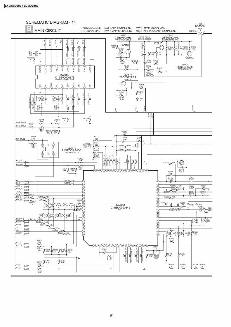
N
1 2
1 2 3
6 5 4
R20550
MIX_MUTE
MIX_LMIX_R
KA_LIN
KA_RIN
TUN_RTUN_LAUX_RAUX_LPBRPBL
+7.5
V
FRONT_RFRONT_L
-7.5
V
SRSLCENT
EXT_LEXT_R
SS_C
SS_S
SUBW
IC2812C1BB00000845
ASP IC
R36303.3K
R36313.3K Q2919
B1GFGCAA0001MUTING SWITCH
R22046.8K
R21046.8K
R22033.3K
R21033.3K
R21
308.
2K
R22
308.
2K
R2213 10KR2113 10K
R20560
R29
98 0
R2200 1.8K
R2100 1.8K
C21
17
0.1
5
R2608 10K
R2400 12K
R21
0118
K
C295450V10
R2609220K
C2225 0.047
R2300 12K
R24
0468
K
R260310K
R250210K
C29
440.
01
C23
0410
P
C26
08
50V
0.47
C21182700P
C25
09
50V
0.47
C29530.22
R25033.3K
R20570
R255847K
R20520
R2124 12K
R2600 10K
C22
16
0.1
5
C22182700P
R20540
C24
0410
P
R220518K
C22
150.
47
R25
014.
7K
R222268K
R2223 47K
R24
014.
7K
R212268K
R26
016.
8K
R22
0118
K
C21
16
0.1
5
R250510K
C291650V10
R261110K
C23
11
50V
0.47
R260433KR2202
15K
C21230.047
C22230.047
C22
17
0.1
5
C296310V47
C2947 1000P
R20580
R23031.5K
C24
11
50V
0.47
C21
150.
47
R20530
R210215K
C2948 1000P
R230210K
C25
1610
P
R21176.8K
R23
014.
7K
R20840
R2614 47K
R230510K
R23
0468
K
R260210KC2201
220P
C2915 0.22
R25
0433
K
C21240.039
R22176.8K
C29140.22
C26101000P
C296210V47
R210518K
C2101220P
R2224 12K
R2612 8.2K
R26053.3K
R2500 12K
R240510K
SS_D
AT
SS_C
LK
+7.5
V
-7.5
V
LINE_ROUT
LINE_LOUT
EXT_
L
EXT_
R
SS_S
SS_C
LIN
MIC
IN
LF RSI
N
LSIN
RC
IN
LCIN
SFRIN
RF
DG
ND
AGN
D
SOU
T
RO
UT
CO
UT
VCC
VEE
CLO
CK
LOU
T
DAT
A
IC2800C1BB00000979ANALOG SURROUND IC
C21
14
10V
1
C28
5716
V10
R20910
C21
40
0.0
82
C21
38
16V
10
C22
38
16V
10
R21
3912
K
C22
37
0.0
22C
2320
1
0V0.
1
R211518K
R22
3912
K
C22
130.
15
C21
12
50V
1
C22
12
50V
1
C25
22
10V
0.1
C21
37
0.0
22
C22
3933
00P
R221518K
C28
5816
V10
C21
3933
00P
C22
14
10V
1
C21
130.
15
R211622K
R221622K
SW5V
-9.0
V
DC
DET
FAN
C299116V10
R20690
D29
18B0
ACC
K000
005
CN2816
Q2915
C299210V10
R2595100K
R24593.3K
Q29142SD0592ARA
SWITCH
R2599120KD
2919
R259410 R2067
0
C29880.01
R24602.2M
Q2913
R259810K
R24564.7K
R24551K
C29890.01
R2597220K
R24574.7K
R2454100K
R20700
D29
17
Q2916R25961.2K
C299016V100
R2453100
D2917, D2919B0ACCK000005
MAIN CIRCUIT
SCHEMATIC DIAGRAM - 14 TOBOTTOM
FAN: -B SIGNAL LINE: +B SIGNAL LINE
: MAIN SIGNAL LINE: AUX SIGNAL LINE
: TAPE PLAYBACK SIGNAL LINE: FM/AM SIGNAL LINE
Q29132SD0601AHL
DETECT SWITCH
Q29152SB0709AHLFAN MOTOR DRIVE
Q29162SB0709AHLFAN MOTOR DRIVE
R215512K
R225412K
R36261K
R36271K
R36
40
0
R36
41
0
W20990
W20960
W20950
W2091 0W2090 0
C36210.056
C36220.056
R22176.8K (GCS)2.2K (GS)
1 2
1920
3
18
4
17
5
16
6
15
7
14
8
13
9
12
10
11
1 2 3 4 5 6 7 8 9
212223242526272829
525354555657585960
727374757677787980
10
51
3071
11
50
3170
12
49
13
48
32693368
14
47
15
46
16
45
346735663665
17
44
18
43
19
42
20
41
3764386339624061
94
SA-VK72DGCS / SA-VK72DGS
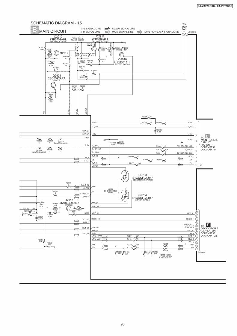
N
1 2
1413121110
2
4
6
89
7
5
3
1
Q2917B1ABEB000002
SWITCH
CE
RCH
LCH
TU_SCL (PLL_CK)
TU_SDA (PLL_DA)
TU_SD
+15V
TU_ST/DO
+7.5V
SUB+BGND
OUT_LS
OUTFR
OUTFL
BASS
RECHPOUT_FL
PBLPBRPBR
+7.5V
TU_SDA
+15V
AGND
ASP_CKASP_DA
TU_SCL
CEFR_R
FL_LTUN_R
+9.0V
TU_ST_DO
HPOUT_FR
TUN_L
OUT_RS
DECK1_H
MOT_01
MOT10VMOT10VREC_01REC_01
+15V+15VREC_RREC_L
5V
MOT_01
REC_01
MOTOR
LINE_LOUT
LINE_ROUT
OUT_SWOUT_C
-9.0V
DECK1_H
MOT_01
R2098 0
R26911K
R269210K
C2913 0.1uR2610 1.8K
C260950V10
R20970
R2233 0
R213833K
R2232470
C29030.01
R2678 10K
R2133 10K
R2613 47K
C21341000P
R2132470
R260710K
R2062 0
D2818B0ACCK000005
R2060 0
W30090
L2804G0C101JA0052
R2131 33K
R2065 0
Q2703B1GDCFJJ0047DECK MOTOR SWITCH
D2809B0ACCK000005
C26070.018
R2061 0
CP6803
R2229 100
R223833K
R2231 33K
Q2704B1GDCFJJ0047
MOTOR SWITCH
R2064 0
R260610K
R2066 0
R2129 100
C22341000P
PBL
-9.0
V
DC
DET
FAN
R25900
R20680
C298616V10
Q29112SB0709AHLFAN MOTOR DRIVE
R25872.2M
R25811.2K
Q29102SD0601AHL
DETECT SWITCH
R2592100K
D29
14
CN2815
R25884.7K
R2582100K
Q29092SD0592ARA
SWITCH
R25934.7K
C29830.01
R25893.3K
R2583220K
R2585120K
C298710V10
C29840.01
D29
16
Q2912 R2584100
R258610K
R258010
C298516V100
R25911K
D29
15B0
ACC
K000
005
D2914, D2916B0ACCK000005
SW5V
MAIN CIRCUIT
SCHEMATIC DIAGRAM - 15 TOTOPFAN
TOMAIN (TUNER)CIRCUIT(1A) ONSCHEMATICDIAGRAM - 9
TODECK CIRCUIT(CN1001) ONSCHEMATICDIAGRAM - 22
TU_SD
1B
J
I
H
G
F
E
D
A
B
C
TGND
: -B SIGNAL LINE: +B SIGNAL LINE
: MAIN SIGNAL LINE: FM/AM SIGNAL LINE
: TAPE PLAYBACK SIGNAL LINE
Q29122SB0709AHLFAN MOTOR DRIVE
Q2911
C26500.47
R269310K
K2905
K2906
K2905, K2906ERJ3GEY0R00V
W30080
W30060
W30070
W20870
W21040
W21030 W2101
0
95
SA-VK72DGCS / SA-VK72DGS
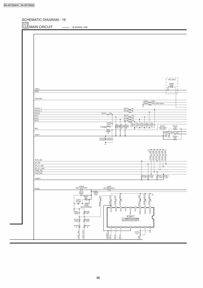
VCC
RR
EFC
VREF
C
BIAS
C
DIF
OU
T
CIN NC
NC
AIN
BASS
LIN
E_R
OU
T
LIN
E_LO
UT
KEY1
OPEN_SW
KEY2KEY3
SPE
PLAY_SW
ST_SW
OP_CL_REV
OP_CL_FWD
POSITION
DVREF+
SYS6V
VREF+
VREF+
DECK2PHOTO_2PHOTO_1
SP_C
SP_B
SP_A
DVR
EF+
SPE
C27521000P
R26581K C2719 0.01
R2797 100
R26
6110
K
IC2817C1BB00000086SPEAKER ANALYZER IC
C27
45
0.0
1
R2708 100
C27
5147
0P
R26
7510
K
C27
26
100
P
R29
24
1
00K
R2253330K
R2672 100
R2791 1K
R2086 0
C272210V22u
R2688100K
C29611000P
C27
25
100
P
R28
4710
K
R291147K
R2957680
C27
46
0.0
1
R27233.3K
C27431000P
R29
26
1
00
C27
24
100
P
R299010K
R2798 100
C27
49
50V
0.1
C29
7747
0P
R2685 100K (GCS ONLY)
C297316V100
C27
28
100
P
D2910B0ACCE000003
R2792 1K
C29
8147
0P
R291247K
C27
23
100
P
C27440.01
C27
47
50V
0.1
C27
48
50V
0.1
C27210.01
L2802G0C3R3JA0030
R26624.7K
D2908B0ACCK000005
R29104.7K
C27
2047
0P
R28504.7K
C29
8247
0P
R20780
R2683 100K
C2718470P
R2154330K
C27
27
100
P
R20790
MAIN CIRCUIT
SCHEMATIC DIAGRAM - 16
: +B SIGNAL LINE
R363410K
LEDCONT
GCS ONLY
R27233.3K (GCS)10K (GS)
12
17 18
3
16
4
15
5
14
6
13
7
12
8
11
9
10
96
SA-VK72DGCS / SA-VK72DGS
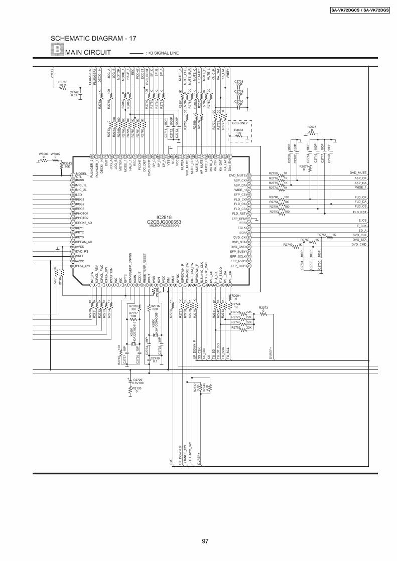
Div
x_EN
LEDMIC_2LMIC_1L
BASS
NC
NC
EFP_TxD1EFP_RxD1EFP_SCLKEFP_BUSY
DM
T
DVD_MUTE
EFP_CE
PLL_
DA
PLL_
CK
PLL_
CE
UP/
DO
WN
_F
DVD_RS
SPEAN_AD
KEY2KEY1
KEY3
DECK2_ADPHOTO2PHOTO1REG3REG2REG1
MODEL_CTL PL
UN
GER
_1D
ECK1
_H
MO
DE_
1H
ALF_
1
DC
_DET N
C
FLD_CKFLD_DA
TU_S
T/D
O
S.Su
rr IC
_CLK
PCO
NT
REC
MO
TOR
JOG
_B
DVD
_PC
NT
SP_B
SP_C
CN
VSS/
EFP_
CN
VSS
RES
ET/E
RP_
RES
ETXO
UT
XCO
UT
XCIN
BYTE
VSS
XIN
JOG
_APO
SITI
ON
VREF
ST_S
W
PLAY_SWAVCC
OPE
N_S
W
OP/
CL_
REV
OP/
CL_
FWD
PLU
NG
ER_2
AVSS
HP_
MU
TE
VCC
SUB_
MU
TEM
UTE
AU
P/D
OW
N_R
SYN
C
CH
ANG
E_SW
VCC
SP_A
RM
TN
MI
VSS
BOTT
OM
_SW
MU
TE_C
MU
TE_S
R
KA_L
ATKA
_DAT
DVD_CMD
DVD_CKDVD_STA
FLD_CS
ECLKEDA
EFP_EPM
FLD_RST
ECS
ASP_CKASP_DAWIDE_1
TU_S
DM
UTE
_LM
UTE
_H
KA_C
LK
VREF
+KA
_LAT
MU
TE_C
MU
TE_A
HP_
MU
TE
MO
DE_
1H
ALF_
1
MU
TE_S
UB
DVR
EF+
DC
DET
FLD_CK
TU_S
DA
TU_S
CL
TU_S
T_D
O
CE
UP_
DO
WN
_F
FLD_DA
PLU
NG
ER1
PLU
NG
ER2
ED_A
DEC
K1_H
REC
PCO
NT
MO
TOR
JOG
_BJO
G_A
SS_D
ATSS
_CLK
DVR
EF+
BOTT
OW
M_S
WC
HAN
GE_
SWU
P_D
OW
N_R
RM
T
DVD
_PC
NT
DVD_MUTE
SP_C
E_CLK
E_CS
MU
TE_L
SP_A
MU
TE_H
KA_C
LK
DVD_STA
TU_S
D
SP_B
WIDE_1M
UTE
_SU
R
DVD_CLK
DVD_CMD
ASP_CKASP_DA
FLD_CS
FLD_RST
KA_D
AT
R3633100
R20730
R27
43
1
K
R20940
R27441K
C27
06
100
P
R2790 1K
R27
38
1
K
C27
50
100
P
R2776 1K
R27
33
1
K
C27
05
100
P
C27
11
100
P
R27
37
1
K
R291710M
C2710100P
R28
64
0
X680
1H
0A32
7200
115
C27
13
100
0P
C27
34
39P
R27
474.
7K
C27
14
100
P
C27
37
15P
C27
12
100
0P
R2793 100
R20
89
0
C29
78
100
P
C27
04
100
P
R27
42
1
K
C27
16
100
P
R20
88
0
R2788100K
R27
78
1
00
R27
52
1
00
R27
35
1
0K
X680
0H
2A10
05A0
005
R27
32
1
K
R2750 1K
R20
77
0
R27
84
1
00
R27
82
1
K
R27
39
1
K
R27
89
1
00
IC2818C2CBJG000653
MICROPROCESSOR
R29
88
1
K
C27
36
15P
R2751 1K
R27
34
1
K
R27
36
1
K
R27
55
1
00
R2728 22K
R2796 100
R2749 1K
R27
53
1
00
R27
77
1
00
R2775 1K
R27
79
1
00
C27
17
100
PR2729 22K
R27
86
1
K
C27300.1
R2745 22K
R2774 1K
R27
58
1
K
R28
51
1
K
R27
464.
7K
R2916680
R27
31
1
K
R27
59
1
KR
2780
100
R27
60
1
K
R27
41
1
K
R2754 100
R27
83
1
K
R26
73
1
K
R28
59
0
R27
13
0
C27420.01
R2794 100
R2918330
C27
07
100
P
R20
76
0
R27
81
1
K
R27
85
1
00
R27
61
1
KC
2735
3
9P
R27
26
1
00
C2709100P
R27
56
1
00
C2708100P
R20750
R20740
C27296.3V100
R27
30
1
K
R27
40
1
K
R27
02
0
MAIN CIRCUIT
SCHEMATIC DIAGRAM - 17
VREF
+: +B SIGNAL LINE
R2762 22K
W21330
W29
990
S.Su
rr IC
_DAT
R364310K
GCS ONLY
W30020
W30030
1 2 3 4 5 6 7 8 9
313233343536373839
727374757677787980
9293949596979899
100
10
71
4091
11
70
4190
12
69
13
68
42894388
14
67
15
66
16
65
448745864685
17
64
18
63
19
62
20
61
4784488349825081
21
60
22
59
23
58
24
57
25
56
26
55
27
54
28
53
29
52
30
51
97
SA-VK72DGCS / SA-VK72DGS
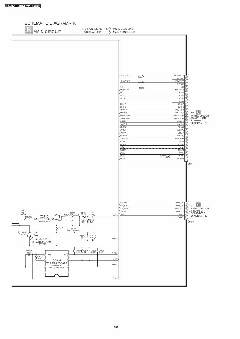
161718192021
29
27
25
2322
24
26
28
30
123456
14
12
10
87
9
11
13
15
123456
SW5V
PCONTSYNC
DCDET
SYS6V+9.0V
-9.0V
HPOUT_FRHPGND
MICGNDMIC
HPOUT_FL
FLD_RSTFLD_CS
FLD_DAFLD_CK
RMTDGND
KEY1HP_MUTE
JOG_BPHOTO_1
KEY3GND2
KEY2
JOG_A
DVREF+DECK2
MOT10VVREF+
PLUNGER2MODE_1HALF_1
PHOTO_2PLUNGER1
RMTFLD_CSFLD_RSTFLD_CKFLD_DA
LEDCONT LEDCONT
SYNC
MIC
KEY1
DCDET-9.0V
+9.0V
SW5V
PCONT
SYS6V
HPOUT_FL
HPOUT_FR
MOT10VVREF+DVREF+DECK2HALF_1MODE_1PLUNGER2PLUNGER1PHOTO_2PHOTO_1
HP_MUTE
JOG_BJOG_A
KEY3KEY2
ED_A
E_CLK
E_CS
VREF+
VREF+
SYNC
DATA CLK
R2999 0
D2905B0ACCK000005
Q2702B1GBCFJJ0051
SWITCH
R20720
C27320.01
R292222K
R292010K
IC2816C3EBEG000072
EEPROM IC(NOT SUPPLIED)
C273350V2.2
R291310K
C27380.022
R266722K
Q2710B1GBCFJJ0051
SYNC SWITCH
C2739330P
D2906B0ACCK000005
R29144.7K
C274135V4.7
CN2811
C2740330P
R29232.2K
R267022K
C273150V0.1
MAIN CIRCUIT
SCHEMATIC DIAGRAM - 18
CN2808
TOPANEL CIRCUIT(CN6811) ONSCHEMATICDIAGRAM - 20
TOPANEL CIRCUIT(H6807) ONSCHEMATICDIAGRAM - 20
: -B SIGNAL LINE: +B SIGNAL LINE
: MAIN SIGNAL LINE: MIC SIGNAL LINE
C27540.01
1
27
8
36
45
98
SA-VK72DGCS / SA-VK72DGS
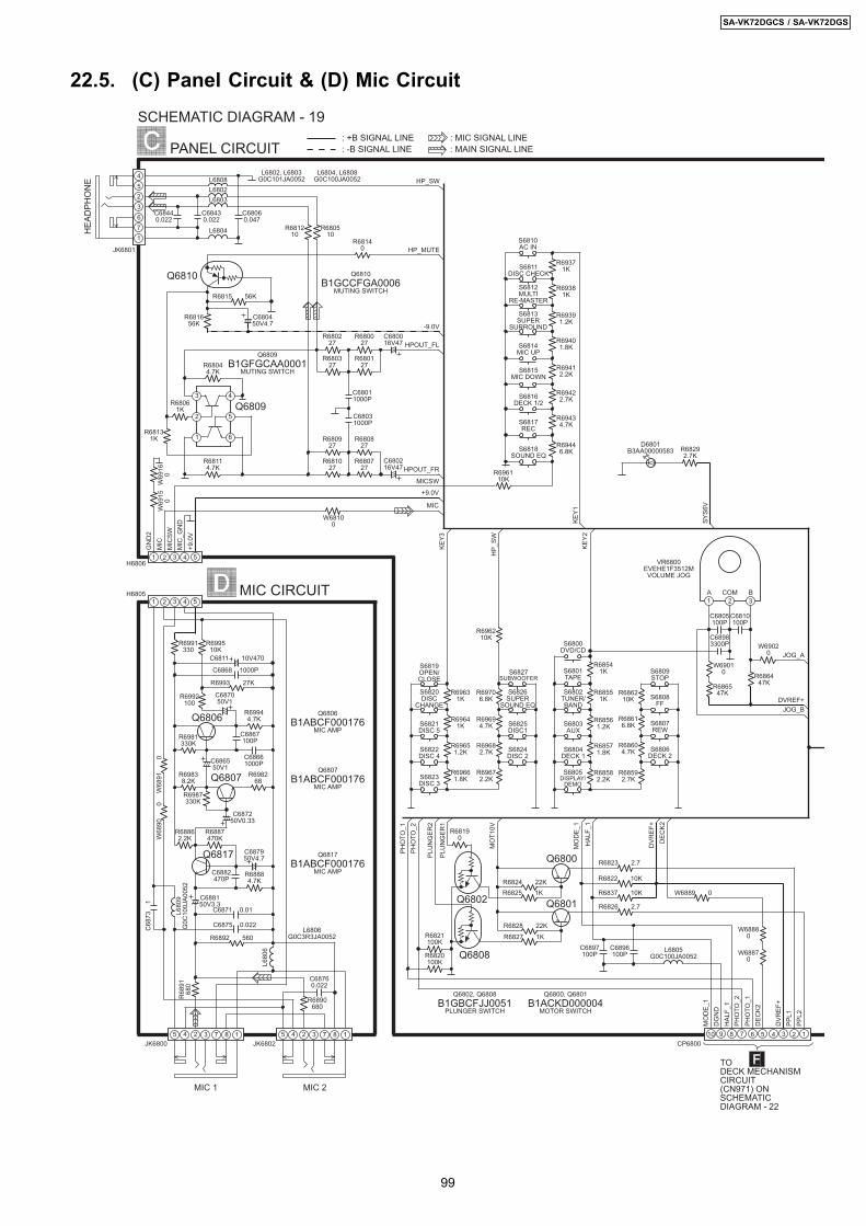
22.5. (C) Panel Circuit & (D) Mic Circuit
10 9 8 7 6 5 134 224 7 85 3 124 7 85 3 1
1 532 4
1 532 4
1 2 3COM BA
67
25
1
3
4
PANEL CIRCUIT
SCHEMATIC DIAGRAM - 19
: -B SIGNAL LINE: +B SIGNAL LINE
: MAIN SIGNAL LINE: MIC SIGNAL LINE
L6808L6802L6803
L6804
C68060.047
C68430.022
C68440.022
R681210
R680510
R68140
R6815 56K
R681656K
C680450V4.7
R680227
R680027
R680327
R680127
C680016V47
C68011000P
C68031000P
R680927
R680827
R681027
R680727
C680216V47
R68114.7K
R68131K
R68061K
R68044.7K
R6991330
R699510KC6811 10V470
C6868 1000P
R6992100
R6981330K
R69838.2K
C687050V1
C6867100P
C68661000P
R6987330K
R68862.2K
C687250V0.33
R6887470K
C687950V4.7
R68884.7K
C6882470P
C688150V3.3
C6871 0.01
C6875 0.022
R6892 560
R68
9168
0
L680
6
L680
9G
0C10
0JA0
052
C68
73
1
Q6806B1ABCF000176
MIC AMP
Q6806
Q6807
Q6817
Q6807B1ABCF000176
MIC AMP
Q6817B1ABCF000176
MIC AMP
R69371K
R69381K
R69391.2K
R69401.8K
R69412.2K
R69422.7K
R69434.7K
R69446.8K
S6810AC IN
S6811DISC CHECK
S6812MULTI
RE-MASTER
S6813SUPER
SURROUND
S6814MIC UP
S6815MIC DOWN
S6816DECK 1/2
S6817REC
S6818SOUND EQ
C6805100P
C6810100P
C68983300P
R686547K
R686447K
R686210K
R68616.8K
R68604.7K
R68592.7K
S6809STOP
S6808FF
S6807REW
S6806DECK 2
R68541K
R68551K
R68561.2K
R68582.2K
R68571.8K
S6800DVD/CD
S6801TAPE
S6802TUNER/BAND
S6803AUX
S6804DECK 1
S6805DISPLAY/
DEMO
R69706.8K
R69694.7K
R69682.7K
R69672.2K
R69631K
R69641K
R69651.2K
R69661.8K
S6827SUBWOOFER
S6826SUPER
SOUND EQ
S6825DISC1
S6824DISC 2
S6819OPEN/CLOSE
S6820DISC
CHANGE
S6821DISC 5
S6822DISC 4
S6823DISC 3
R6824 22KR6825 1K
R6828 22KR6827 1K
R6823 2.7
R6822 10K
R6837 10K
R6826 2.7
C6897100P
C6896100P L6805
G0C100JA0052
R6821100K
R6820100K
Q6808
Q6802 Q6801
Q6800
Q6802, Q6808B1GBCFJJ0051
PLUNGER SWITCH
Q6800, Q6801B1ACKD000004
MOTOR SWITCH
Q6810B1GCCFGA0006
MUTING SWITCH
Q6810
Q6809B1GFGCAA0001
MUTING SWITCH
Q6809
JK6801
HEA
DPH
ON
E
H6806
H6805
JK6800 JK6802
MIC 1 MIC 2
CP6800
MO
DE_
1
PHO
TO_1
PHO
TO_2
PLU
NG
ER2
PLU
NG
ER1
R68190
MO
T10V
MO
DE_
1
HAL
F_1
DVR
EF+
DEC
K2
DG
ND
HAL
F_1
PHO
TO_2
PHO
TO_1
DEC
K2
DVR
EF+
PPL1
PPL2
JOG_A
DVREF+JOG_B
KEY3
HP_
SW
KEY2
KEY1
MIC
+9.0V
MICSW
HPOUT_FR
HPOUT_FL
-9.0V
HP_MUTE
HP_SW
GN
D2
MIC
SW
+9.0
V
MIC
MIC
_GN
D
TODECK MECHANISMCIRCUIT(CN971) ONSCHEMATICDIAGRAM - 22
MIC CIRCUIT
R68292.7K
D6801B3AA00000583
SYS6
V
R6890680
C68760.022
C686550V1
L6802, L6803G0C101JA0052
L6804, L6808G0C100JA0052
L6806G0C3R3JA0052
R698268
R6993 27K
R69944.7K
VR6800EVEHE1F3512MVOLUME JOG
R696110K
R696210K
W68100
W69
160
W69
150
W68
91
0
W68
90
0
W69010
W69020
W6889 0
W68880
W68870
3
2
1
4
5
6
99
SA-VK72DGCS / SA-VK72DGS
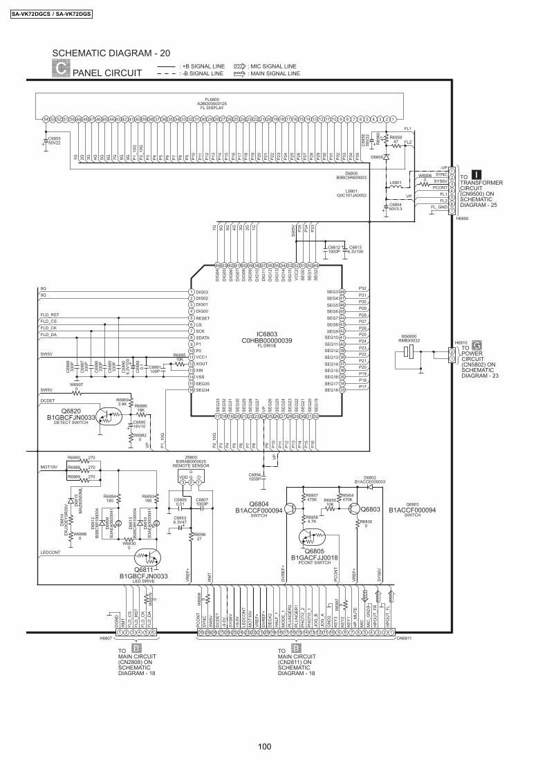
2
4
67
5
3
1
54 53 52 51 50 49 48 47 46 45 44 43 42 41 40 39 38 37 36 35 34 33 32 31 30 29 28 27 26 25 24 23 22 21 20 19 18 17 16 15 14 13 12 11 10 9 8 7 6 5 4 3 2 1
GVDD O3 2 1
21
15 14 13 12 11 10 24689 7 5 3 130 29 28 27 26 25 1719212324 22 20 18 16
TOTRANSFORMERCIRCUIT(CN9500) ONSCHEMATICDIAGRAM - 25
PANEL CIRCUIT
SCHEMATIC DIAGRAM - 20
R6893180
R6894180
D68
10B3
AEA0
0000
41
D68
09B3
AEA0
0000
41
R688510K
C6891100PC
6889
0.1
C68
906.
3V10
0
C68
8533
0P
C68
8633
0P
C68
8733
0P
C68
8833
0P
R68693.9K R6889
18K
C689516V10
Q6820B1GBCFJN0033
DETECT SWITCH
C68941000P
C68071000P
C68090.01
C68536.3V47
R699627
R6957470K
R69564.7K
R695010K
R6954470K
R68300
Q6804B1ACCF000094
SWITCH
Q6805B1GACFJJ0018
PCONT SWITCH
Q6803B1ACCF000094
SWITCHQ6803
D6802B1ACCE000003
C68121000P
C68136.3V100
C685450V3.3
L6801
D6800
C68
5650
V22
R69
6047 R6959
47C685550V22
H6807 CN6811
H6800
-VPSYNC
SYS6VPCONT
FL1FL2
FL_GND
FL1
FL2
VP
7G 6G 5G 4G 3G 2G 1G
SW5V P3
5P3
4P3
3
P32P31P30P29P28P27P26P25P24P23P22P21P20P19P18P17
P1_1
0G
P2_1
0GP3 P4 P5 P6 P7 P8 P9 P1
1P1
2P1
3P1
4P1
5P1
6
P10
VP
DCDET
SW5V
SW5V
FLD_DAFLD_CKFLD_CSFLD_RST
9G8G
1G 2G 3G 4G 5G 6G 7G 8G 9G P1_1
0GP2
_10G
P3 P4 P5 P6 P7 P8 P9 P10
P11
P12
P13
P14
P15
P16
P17
P18
P19
P20
P21
P22
P23
P24
P25
P26
P27
P28
P29
P30
P31
P32
P33
P34
P35
VREF
+
RM
T
DVR
EF+
PCO
NT
VREF
+
SYS6
V
Z6800B3RAB0000025
REMOTE SENSOR
DG
ND
RM
TFL
D_C
SFL
D_R
STFL
D_C
KFL
D_D
A
PCO
NT
SYN
CSW
5VD
CD
ET-9
.0V
SYS6
V+9
.0V
MO
T10V
VREF
+D
VREF
+D
ECK2
HAL
F_1
MO
DE_
1PL
UN
GER
2PL
UN
GER
1PH
OTO
_2PH
OTO
_1JO
G_B
JOG
_AG
ND
2KE
Y3KE
Y2KE
Y1H
P_M
UTE
MIC
MIC
_GN
DH
POU
T_FR
HPO
UT_
FL
TOMAIN CIRCUIT(CN2811) ONSCHEMATICDIAGRAM - 18
TOMAIN CIRCUIT(CN2808) ONSCHEMATICDIAGRAM - 18
DIG03DIG02DIG01DIG00
RESETCSSCKSDATAP1P0VCC1XOUTXINVSSSEG35SEG34
SEG
33SE
G32
SEG
31
SEG
30SE
G29
SEG
28SE
G27
VP SEG
26
SEG
25SE
G24
SEG
23SE
G22
SEG
21SE
G20
SEG
19
SEG17SEG18
SEG16SEG15SEG14SEG13SEG12SEG11SEG10
SEG9SEG8SEG7SEG6SEG5SEG4SEG3
SEG
1SE
G2
SEG
0VC
C2
DIG
15D
IG14
DIG
13D
IG12
DIG
11D
IG10
DIG
09D
IG08
DIG
07D
IG06
DIG
05D
IG04
IC6803C0HBB00000039
FL DRIVE
FL6800A2BD00000125
FL DISPLAY
VP
: -B SIGNAL LINE: +B SIGNAL LINE
: MAIN SIGNAL LINE: MIC SIGNAL LINE
D6800B0BC5R600003
L6801G0C101JA0052
MOT10V
LEDCONT
D68
13B0
BC8R
1000
04
D68
12B0
BC8R
1000
04
Q6811B1GBCFJN0033
LED DRIVE
BS6800RMBX0032 H6810
TOPOWERCIRCUIT(CN5802) ONSCHEMATICDIAGRAM - 23
R69
97 0
R6990 270
R6988 270
R6989 270
D68
14ER
J3G
EY0R
00V D
6815
MAZ
8056
0ML
W69060
W69070
W68820
W68860
W68300
W69
190
W69
080
LED
CO
NT
123456789
17 18 19 20 21 22 23 24 25
404142434445464748
565758596061626364
10 39
26
55
11 38
27
54
12 3713 36
28
53
29
52
14 3515 3416 33
30
51
31
50
32
49
1 2 3 4 5 6
100
SA-VK72DGCS / SA-VK72DGS
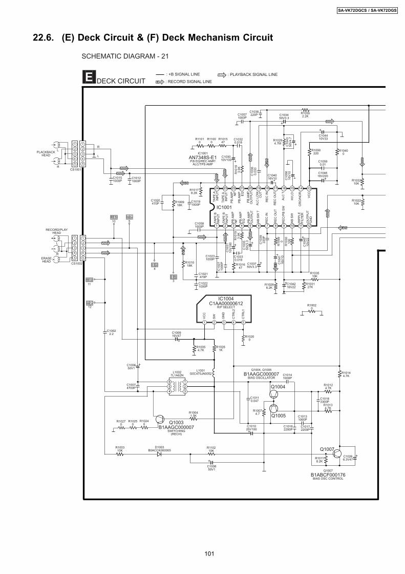
22.6. (E) Deck Circuit & (F) Deck Mechanism Circuit
654 3
21
2
45
3
1L
RERASEHEAD
RECORD/PLAYHEAD
2
45
3
1
LPLACKBACKHEAD
R
2
45
3
1
2
45
3
1
CS1001
SCHEMATIC DIAGRAM - 21
DECK CIRCUIT
CS1002
L10027L1A62N
IC1001AN7348S-E1P.B EQ/REC AMP/
ALC/TPS AMP
IC1004C1AA00000612
R/P SELECT
VCC
L
R
C103010V100
R101547
R10
183.
9K
C10320.018
C10
360.
033
R10294.7M
C10
4350
V4.7
C10
5616
V10
C10
3110
V100
R101647
C10
2710
00P
C10231000P
C10330.018
R10
193.
9K
C10
3550
V3.3
C103750V3.3
C10
3922
0P
C10
4510
V22
R10288.2K
C10
4116
V10
C1021470P
C10221000P
R10178.2K
R100918K
C1020470P C1019
1000P
C104016V10C1012
1000PC10151000P
R101018K
R10261K
R10054.7K
C100916V47
4
L1001G0C470JA0052
C100650V1
C10022.2
C10074700P
R100310K
D1003B0ACCK000005
Q1003B1AAGC000007
SWITCHING(RECH)
Q1007
R1090220
C104616V220
R10400
C104410V33
R10041.5K
Q1004
Q1005
Q1004, Q1005B1AAGC000007
BIAS OSCILLATOR
C10131000P
C10141000P
C101025V100
R10074.7
C10162200P
C10172200P
R10118.2K
Q1007B1ABCF000176
BIAS OSC CONTROL
C10266.3V47
R10134.7K
R10124.7K
C10183300P
R10144.7K
C10110.047
C100850V1
C103450V3.3
R103210K
R10552.2K
C1038220P
C104216V22
R103127K
R103510K
R10
3010
0
5
11
12
TAPE
BIN
PUT
TAPE
BIN
PUT
TAPE
AIN
PUT
TAPE
AIN
PUT
PB A
MP
NF
PB A
MP NF
PB A
MP
EQPB
AM
PEQ
PB A
MP
OU
TPU
TPB
AM
PO
UTP
UT
AB S
W T
REC
INR
EC IN
REC
OU
TR
EC O
UT
REC
/PB
SW
AB S
W
RIP
PLE
FILT
ER
OU
TPU
TG
ND
VCC
CR
O/N
OR
HI/L
O
ALC
T
ALC
LO
WC
UT
IC1001SW G
ND
CTR
L2
CTR
L1
3
C10581000P
R11000
R11010
C10571000P
C10590.01
R10
99 0
R10020
R10240
R10250
R10270
R10200
R102210K
: PLAYBACK SIGNAL LINE
: RECORD SIGNAL LINE
: +B SIGNAL LINE
10
R110210K
1 2 3 4 5
1 2 3 4
21222324
5
20
6
19
7
18
8
17
9
16
10
15
11
14
12
13
101
SA-VK72DGCS / SA-VK72DGS
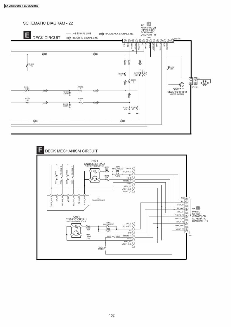
M
1234567
10
1
2
4
6
8
9
7
5
3
1011121314 124689 7 5 3
1
2
1
2
SCHEMATIC DIAGRAM - 22
DECK CIRCUIT
TOMAIN CIRCUIT(CP6803) ONSCHEMATICDIAGRAM - 15
R10842.2K
R10862.2K
R10490
R10910
R10500
R10920
R108747K
R108547K
R10572.2K
R1060390
PBL
PBR
AFG
ND
REC
INL
REC
INR +B
REC
_H
MO
+B
MO
GN
D
DM
T
DEC
K1_H BP
1M
OTO
R
Q1017B1AARC000003
MOTOR SWITCH
W1002
CN1001
R10
9710
K
: RECORD SIGNAL LINE
: +B SIGNAL LINE
IC951CNB13030R2AUPHOTO INTERRUPTER
IC971CNB13030R2AUPHOTO INTERRUPTER
Z971RGSD12A1445T
MODE
PLGND
HALFSTBY_5V
VREF_GND
PHOTO_T
D1_CRO2
TOPANELCIRCUIT(CP6800) ONSCHEMATICDIAGRAM - 19
MODE
PLGND
HALF
PHOTO_S
STBY_5VVREF_GND
PHOTO_T
D1_CRO2
DECK MECHANISM CIRCUIT
CN971
PL1
PL2
STBY_5V
PL_GND
AD_OUT
PHOTO_PB
PHOTO_RP
HALF_PB
VREF_GND
MODE_PB
R972820
R97339K
PL971
R952820
R95339K
D951MA2C16500E
D971MA2C16500E
PL970
S952 HALF
S951MODE
S972
H
ALF
S971
M
OD
E
S975
R
ECIN
H_F
HAL
F
REC
INH
_R
MO
DE
REC
INH
_F
AD_O
UT
VREF
_GN
D
STBY
_5V
-
+
S974
R
ECIN
H_R
C10493300P
C10503300P
R109810K
: PLAYBACK SIGNAL LINE
102
SA-VK72DGCS / SA-VK72DGS
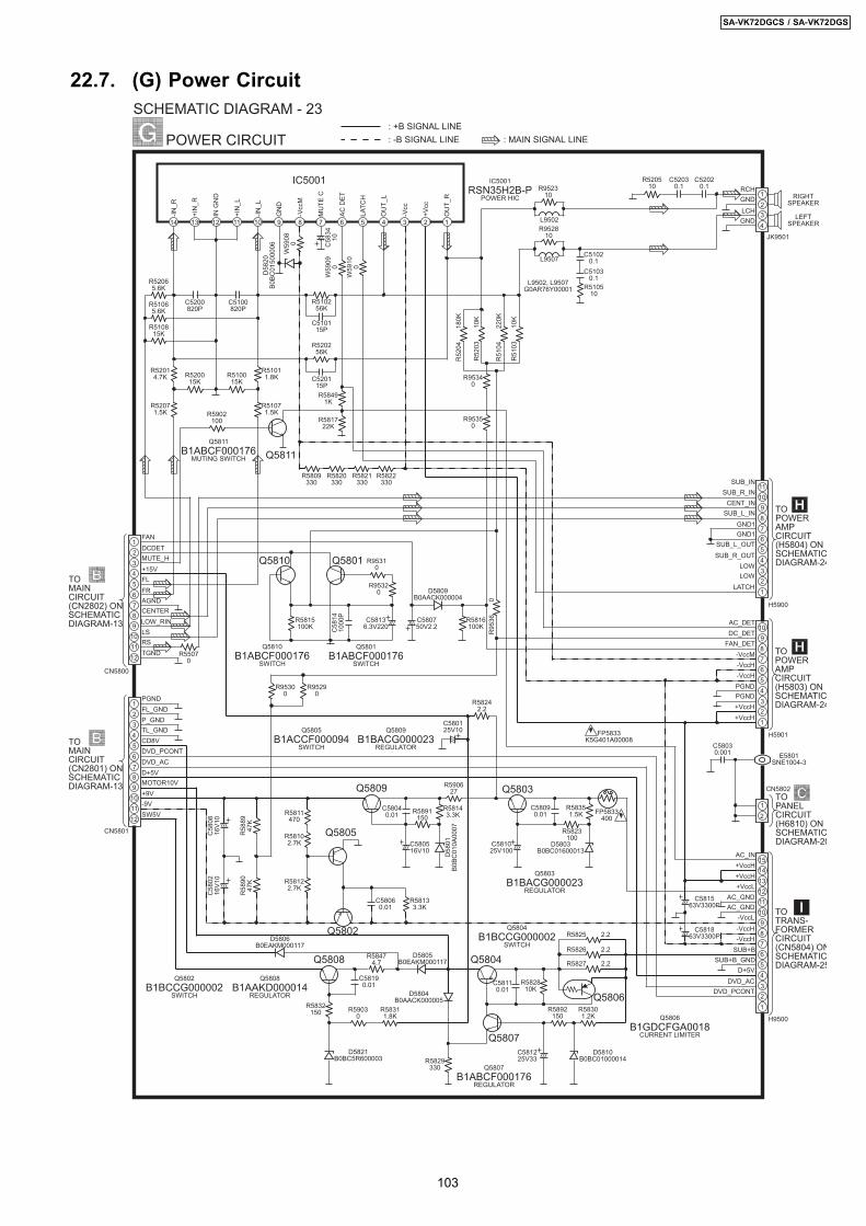
22.7. (G) Power Circuit
121110
2
4
6
89
7
5
3
1
121110
2
4
6
89
7
5
3
1
123456
10
87
9
123456
14
12
10
87
9
11
13
15
POWER CIRCUIT
SCHEMATIC DIAGRAM - 23
: -B SIGNAL LINE: +B SIGNAL LINE
: MAIN SIGNAL LINE
123456
10
87
9
11
4321
FANDCDETMUTE_H+15VFLFRAGNDCENTERLOW_RINLSRSTGND
PGNDFL_GNDP_GNDTL_GNDCD8VDVD_PCONTDVD_ACD+5VMOTOR10V+9V-9VSW5V
TOTRANS-FORMERCIRCUIT(CN5804) ONSCHEMATICDIAGRAM-25
TOPOWERAMPCIRCUIT(H5803) ONSCHEMATICDIAGRAM-24
TOPOWERAMPCIRCUIT(H5804) ONSCHEMATICDIAGRAM-24
DVD_PCONTDVD_AC
D+5VSUB+B_GND
SUB+B-VccH-VccH-VccL
AC_GNDAC_GND
+VccL+VccH+VccHAC_IN
+VccH+VccHPGNDPGND-VccH-VccH-VccM
FAN_DETDC_DETAC_DET
LATCHLOWLOW
SUB_R_OUTSUB_L_OUT
SUB_L_INCENT_IN
SUB_R_INSUB_IN
TOMAINCIRCUIT(CN2801) ONSCHEMATICDIAGRAM-13
TOMAINCIRCUIT(CN2802) ONSCHEMATICDIAGRAM-13
CN5800
CN5801
H9500
CN5802
E5801SNE1004-3
H5901
H5900
C5200820P
C5100820P
R520015K
R510015K
R51011.8K
R52014.7K
C58
3410
R510256K
C510115P
R520256K
C520115PR5849
1K
R581722K
R5902100
R5809330
R5820330
R5821330
R5822330
R95340
R95350
R52
04
1
80K
R52
03
1
0K
R51
04
2
20K
R51
03
1
0K
R952310
R952810
L9502
L9507C5102
0.1C5103
0.1R5105
10
C52020.1
C52030.1
R520510
R95
36
0
R5816100K
C580750V2.2
D5809B0AACK000004
R95310
R95320
C58136.3V220C
5814
1000
P
R5815100K
R95290
R95300
R58242.2
C580125V10
C58
0216
V10
C58
0816
V10
R58
9047
KR
5889
47K
R5811470
R58102.7K
R58122.7K
C58060.01
C580516V10
R58143.3K
C58040.01
R590627
C581025V100
C58090.01
R58351.5K
R5823100
D5803B0BC01600013
FP5833400
C58030.001
C581563V3300P
C581863V3300PD5806
B0EAKM000117R5847
4.7D5805
B0EAKM000117
C58190.01
D5804B0AACK000005
R59030
R58311.8K
R5832150
D5821B0BC5R600003 R5829
330
C581225V33
D5810B0BC01000014
R58301.2K
R582810K
C58110.01
R5825 2.2
R5826 2.2
R5827 2.2
-IN_R
+IN
_R
IN G
ND
+IN
_L
-IN_L
GN
D
-Vcc
M
MU
TE C
AC D
ET
LATC
H
OU
T_L
-Vcc
+Vcc
OU
T_R
IC5001 IC5001RSN35H2B-P
POWER HIC
Q5811
Q5810 Q5801
Q5809
Q5805
Q5802
Q5808 Q5804
Q5807
Q5806
Q5803
R58133.3K
Q5811B1ABCF000176
MUTING SWITCH
Q5801B1ABCF000176
SWITCH
Q5810B1ABCF000176
SWITCH
Q5809B1BACG000023
REGULATOR
R55070
D58
20B0
BC01
5000
06
FP5833K5G401A00008
L9502, L9507G0AR76Y00001
Q5806B1GDCFGA0018
CURRENT LIMITER
Q5807B1ABCF000176
REGULATOR
Q5804B1BCCG000002
SWITCH
Q5803B1BACG000023
REGULATOR
Q5808B1AAKD000014
REGULATOR
Q5805B1ACCF000094
SWITCH
Q5802B1BCCG000002
SWITCH
TOPANELCIRCUIT(H6810) ONSCHEMATICDIAGRAM-20
R51071.5K
R52071.5K
R5891150
R5892150
GND1GND1
W59
080
W59
100
W59
090
D58
01B0
BC01
0A00
07
RCHGND
LCHGND
RIGHTSPEAKER
LEFTSPEAKER
JK9501
R52065.6K
R51065.6K
R510815K
14 13 12 11 10 9 8 7 6 5 4 3 2 1
21
103
SA-VK72DGCS / SA-VK72DGS
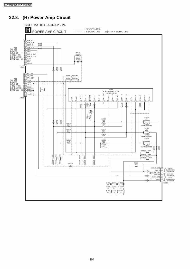
22.8. (H) Power Amp Circuit
123456
10
87
9
123456
POWER AMP CIRCUIT
SCHEMATIC DIAGRAM - 24
: -B SIGNAL LINE: +B SIGNAL LINE
: MAIN SIGNAL LINE
123456
10
87
9
11SUB_INSUR_R_INCENT_INSUR_L_IN
SUR_L_OUTSUR_R_OUTLOW
LATCH
AC_DETDC_DETFAN_DET-VccM-VccH-VccHPGNDPGND+VccH+VccH
TOPOWERCIRCUIT(H5900) ONSCHEMATICDIAGRAM - 23
TOPOWERCIRCUIT(H5901) ONSCHEMATICDIAGRAM - 23
H5804
H5803
SUR_R_GNDSUR_R
CENTER_GNDCENTER
SUR_L_GNDSUR_L
-VD
+VD
-IN 2
1
-IN 2
2
IN G
ND
-IN 1
1
-IN 1
2
OU
T G
ND
OU
T 1
2
AC D
ET
OU
T 1
1
OU
T 2
2
-Vcc
1
+Vcc
1
+Vcc
1
-Vcc
M
+Vcc
2
-Vcc
2
IC5801RSN315H42C-P
POWER AMP IC
R5819330K
C583610V100
R55013.9K
R54012.7K
R53012.7K
R53
00
1
5K
R54
00
1
5K
R55
00
1
5K
C53
03
820
P
C54
03
820
P
C55
00
820
P
R550256K
C550115P
R540256K
C540015P
R530256K
C530015P
L5404G0AR76Y00001
R540410
L5405G0AR76Y00001
R540510
L5406G0AR76Y00001
R540610
R5866 68K
R5898 68K
R5504 100K
R550522K
C53020.1
C53010.1
R530310
C55030.1
C55020.1
R550310
C54020.1
C54010.1
R540310
JK9502
C9533 63V2200
C9534 63V2200
GNDGND
LOW
W59
150
W59140
W59
060
RIGHTSURROUNDSPEAKER
CENTERSPEAKER
LEFTSURROUNDSPEAKER
W59
070
W59
050
18 17 16 15 14 13 12 11 10 9 8 7 6 5 4 3 2 1
104
SA-VK72DGCS / SA-VK72DGS
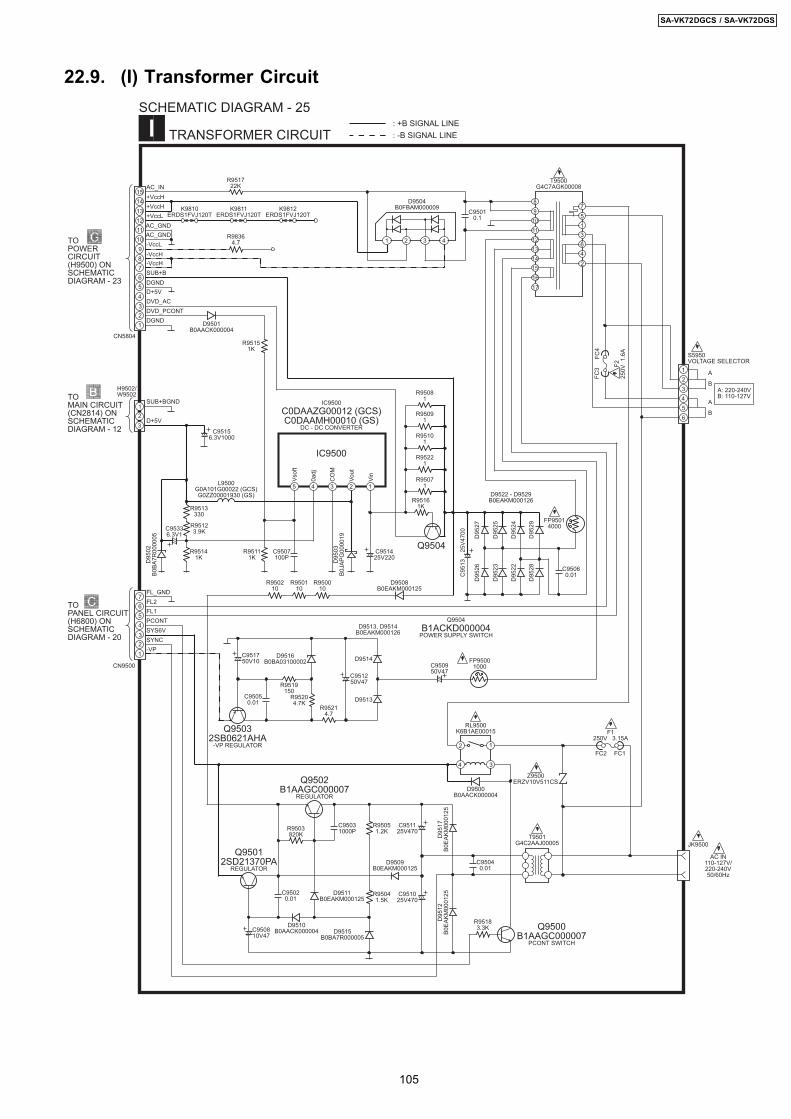
22.9. (I) Transformer Circuit
123456
14
12
10
87
9
11
13
15
1234567
1 2 3 4
7513642
171615141312111098
4 3
2 1
: -B SIGNAL LINE: +B SIGNAL LINE
321
A: 220-240VB: 110-127V
2
4
65
3
1 A
B
A
B
R951722K
R98364.7
C95010.1
R95151K
D9501B0AACK000004
C95336.3V1
R95123.9K
R9513330
L9500G0A101G00022 (GCS)G0ZZ00001930 (GS)
R95141KD
9502
B0BA
7R00
0005
R95111K
C9507100P
C951425V220D
9503
B0JA
PG00
0019
R95081
R95091
R95101
R95221
R95071
R95161K
R950210
R950110
R950010
D9508B0EAKM000125
C95
13
25V
4700 D95
27D
9526
D95
25D
9523
D95
24D
9522
D95
29D
9528 C9506
0.01
FP95014000
T9500G4C7AGK00008
C951750V10
D9516B0BA03100002
C95050.01
R9519150
R95204.7K
R95214.7
C951250V47
D9514
D9513
D9513, D9514B0EAKM000126
C950950V47
D9522 - D9529B0EAKM000126
RL9500K6B1AE00015
T9501G4C2AAJ00005
D9500B0AACK000004
C95040.01
R95183.3K
D95
12B0
EAKM
0001
25D
9517
B0EA
KM00
0125
C951025V470
C951125V470
D9509B0EAKM000125
R95041.5K
R95051.2K
C95031000PR9503
820K
D9510B0AACK000004
D9511B0EAKM000125
C95020.01
D9515B0BA7R000005
F1250V 3.15A
FC2 FC1
Z9500ERZV10V511CS
TOPOWERCIRCUIT(H9500) ONSCHEMATICDIAGRAM - 23
FL_GNDFL2FL1PCONTSYS6VSYNC-VP
DGNDDVD_PCONTDVD_ACD+5VDGNDSUB+B-VccH-VccH-VccLAC_GNDAC_GND+VccL+VccH+VccHAC_IN
TRANSFORMER CIRCUIT
SCHEMATIC DIAGRAM - 25
CN5804
CN9500
TOPANEL CIRCUIT(H6800) ONSCHEMATICDIAGRAM - 20
JK9500
D9504B0FBAM000009
Vsof
t
0adj
CO
M
Vout
Vin
IC9500C0DAAZG00012 (GCS)C0DAAMH00010 (GS)
DC - DC CONVERTER
Q9504
Q95032SB0621AHA
-VP REGULATOR
Q9502B1AAGC000007
REGULATOR
Q95012SD21370PA
REGULATOR
Q9500B1AAGC000007
PCONT SWITCH
Q9504B1ACKD000004
POWER SUPPLY SWITCH
AC IN110-127V/220-240V50/60Hz
FP95001000
C950810V47
SUB+BGND
D+5V
H9502/W9502TO
MAIN CIRCUIT(CN2814) ONSCHEMATICDIAGRAM - 12
K9810ERDS1FVJ120T
K9811ERDS1FVJ120T
K9812ERDS1FVJ120T
IC9500
F225
0V 1
.6A
FC4
FC3
S5950VOLTAGE SELECTOR
C95156.3V1000
5 4 3 2 1
105
SA-VK72DGCS / SA-VK72DGS
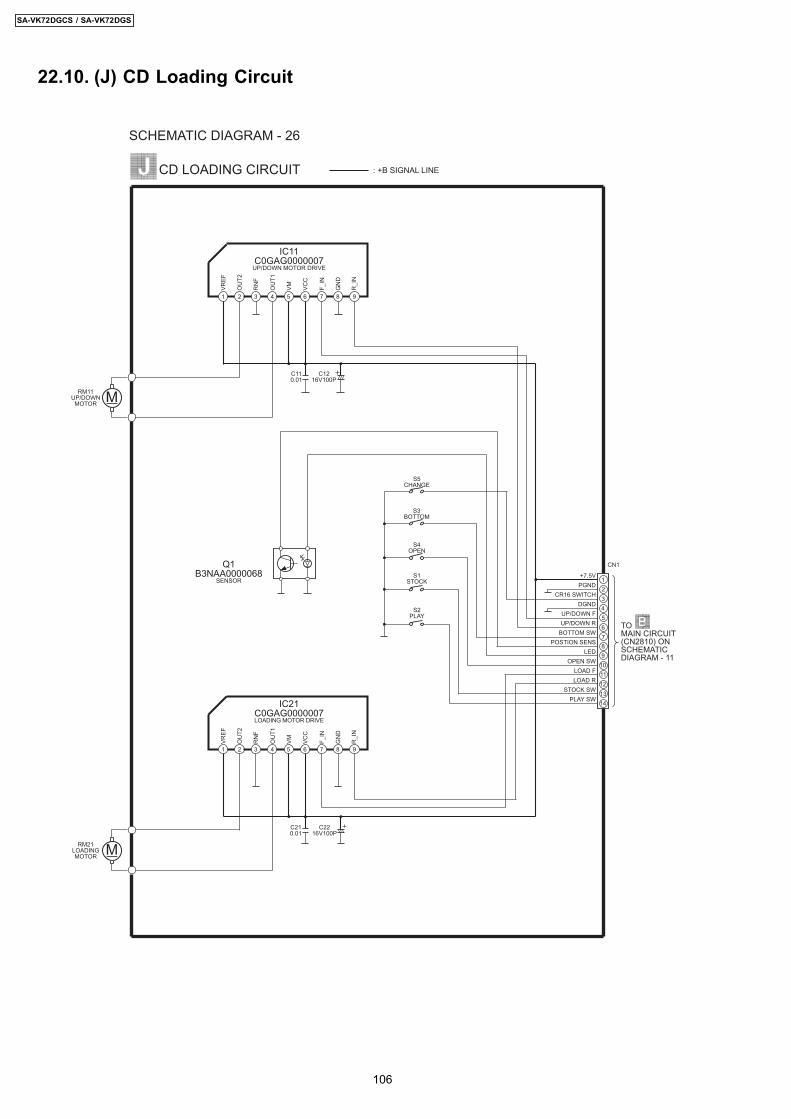
22.10. (J) CD Loading Circuit
M
M
1413121110
2
4
6
89
7
5
3
1
CD LOADING CIRCUIT
SCHEMATIC DIAGRAM - 26
RM11UP/DOWN
MOTOR
RM21LOADINGMOTOR
C110.01
C1216V100P
C210.01
C2216V100P
Q1B3NAA0000068
SENSOR
VREF
OU
T2
RN
F
OU
T1
VM VCC
F_IN
GN
D
R_I
N
VREF
OU
T2
RN
F
OU
T1
VM VCC
F_IN
GN
D
R_I
N
IC11C0GAG0000007
UP/DOWN MOTOR DRIVE
IC21C0GAG0000007LOADING MOTOR DRIVE
S3BOTTOM
S4OPEN
S1STOCK
S2PLAY
: +B SIGNAL LINE
TOMAIN CIRCUIT(CN2810) ONSCHEMATICDIAGRAM - 11
CN1
S5CHANGE
+7.5VPGND
CR16 SWITCHDGND
UP/DOWN FUP/DOWN R
BOTTOM SWPOSTION SENS
LEDOPEN SW
LOAD FLOAD R
STOCK SWPLAY SW
1 2 3 4 5 6 7 8 9
1 2 3 4 5 6 7 8 9
106
SA-VK72DGCS / SA-VK72DGS
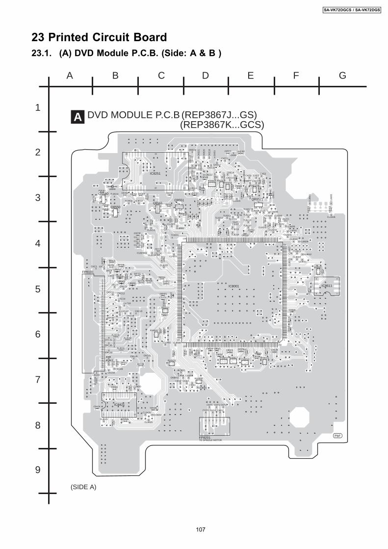
23 Printed Circuit Board23.1. (A) DVD Module P.C.B. (Side: A & B )
A B C D E F G
1
2
3
4
5
6
7
8
9
DVD MODULE P.C.B (REP3867J...GS) (REP3867K...GCS)
A
PbF
C8012
C8013
C80
18
C80
19
C82
03
C82
04
C82
05
C82
21
C82
22
C82
23
C82
24C
8225
C82
26
C82
27
C82
29
C8233
C8234
C8235
C8236
C8237
C8238
C82
41
C82
42
C8254C8261
C8308
C8312
C8422
C85
01
C8502
D8550
D85
71
FL8101
FL8102FL8103
FL8
104
FP8101
IC8001
IC8251
K8106
LB86
91
LB8692
LB86
93
LB8401
LB8302LB8301
LB83
03
LB8304
LB8305
LB8507
Q8550
Q8551Q8561
QR8571
R80
41
R8201
R82
31
R82
33
R82
35R
8236
R82
41
R82
42
R8262 R8264
R8315
R8321
R83
22
R8325 R8326
R8331
R8332 R8335
R83
41
R84
01
R8402
R84
04
R84
07
R84
21
R8550
R85
51
R8552
R8560
R85
61
R8562
R8569
R85
70
RX8401
RX8402
IC8421
Q8560
LB8514LB
8512
LB85
13
LB85
11
RX8018 RX8016RX8017
C8023
C8022
C8021C8020
C80
25
R8011
RX8015
C80
27 C8028
C8426
C82
17
C82
18
RX8502 RX8504
RX8503RX8501
R85
06
R85
05
R85
01
LB85
05 LB85
04LB
8503
LB8502
C8506
C85
05
C85
04
C8503
C80
03C
8004
C8005C
8611
FP8201TO SPINDLE MOTOR
IC8611
R86
11
RX8031
RX8032
RX8611
C8424C8428
K80
31
R82
65
C84
27
C82
32
C8207
C8026
C8024
C83
07
(SIDE A)
X
X
TL8513
TL8522X
TL8512
XX
XTL8201
CL8551
CL8561
XCL8233
X XCL8234
CL8236
X
XCL8231
CL8235
X XCKC1 CKC2
X
X
XX
CKC8CKC10
CKC4
CKC6
X X
X
X
CKC11 CKC12
CKC14
CKC16
XXXX
X
CKC15
CKC18
CKC20
CK
C22
CKC24
X
X
X
X
CKC32
CKC36 CK
C37
CKC40
X
XX
XCKC44
CK
C48
CKC49
CKC50
X X
XCL8430
XCL8421
X X
X
CL8424
CL8425
CL8426
CKC41CKC45
X XCL8040CL8491
CKB1
CKB2
CKB3
CKB4
CKB6
CKB8
CKB9
CL8034X
XXX
X X X
X
XCKF1
CKF2
CKF3
CKF4
CKF5
CKF6X X
X X X
CL8021
CL8022
CL8
023
CL8
027
CL8611CL8612X X X
X X X
CL8028CL8029
CL8031
CL8032
X X
X
X
CL8030X
CL8033X
XCL8241
XCL8243
TL8211TL8212
TL8213
TL8214
TL8215
TL8216
TL8217
TL8218
TL8219
TL8220
CL8242
CL8571CL8036
CL8244XX
XXX CL8035X
X
X
X
XX X
X
X
X CL8006X
CL8201
CKE4X X
CKE2CKE3
CKE5CKE7
CKE9
X
X XX
X
CKE23
CKE25
CKE22
CKE19
CK
E18
CK
E21
CKE12
CKE13
CKE14
CK
E16
CK
E17
CKE24
CK
E1
CK
E20
CKE11
X
X
X
X
X X X X
XX
X
X XX
X
CKE6X
CL8
001
X
K80
01
K80
05C
L800
5
X
50
45
40
35
30
25
20
15
10
5
1
1
64129
192
65128
193256
28 15
141
14
1528
1
123456
1
45
8
234
9
678
11121314
16171819
21222324
26272829
31323334
36373839
41424344
46474849
30
29
B
EC
B
EC
B
EC
B E
C
B E
C
107
SA-VK72DGCS / SA-VK72DGS
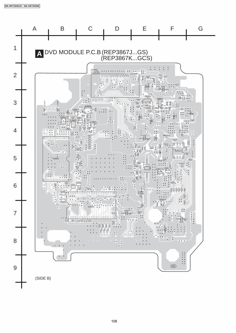
A B C D E F G
1
2
3
4
5
6
7
8
9
A DVD MODULE P.C.B (REP3867J...GS) (REP3867K...GCS)
PbF
C80
01
C8002
C80
11
C8014
C80
15C
8016
C8017
C8031
C8111
C81
12
C8113
C8201C8202
C82
06C
8208
C8211
C8212
C8213
C8214
C8215
C8216
C82
28
C8252
C82
53
C8255
C82
56
C8257
C8262
C83
01
C8302
C83
03
C83
04
C8421
C84
23
C8550C8551
C85
52
C85
53
C8554
C8561
C85
62
C85
63
C8564
C8601
C86
06
C86
07
C8621
C86
22
C86
91
C8695
D82
31
IC8111
IC8601
IC8606
K8421L8
201
L8202
L830
1
L830
2
L8550
LB80
01
LB8002
LB8421
LB8422
LB84
23
LB84
24
LB84
25LB
8426
LB84
27
LB84
28
LB84
29
LB84
30
LB8491
LB86
90
Q8552Q8562
Q8606
Q8607
QR8420
R80
21
R80
22
R8023
R82
43
R82
51 R8261
R8263
R83
13
R83
14
R84
20
R8553
R8554
R85
55
R85
56
R85
57
R8558
R8559 R8563 R8564 R8565
R85
66
R85
67R
8568
R8601
R86
06R8607
R86
21R
8622
X86
21
QR8112QR8111R
8112
R81
11
RX8014
RX8013
C8057 C8056
C80
55
C8054C8053C8052C8051
IC8051
FP8501TO OPTICALPICKUP UNIT
C80
06
C80
07
C80
08
C8009C80
10
C86
51
C8652
IC8651
RX8011
RX8012
RX8021
R8312
R83
11
C83
11
C8251
IC8691
IC8695
(SIDE B)
CK
A5
CK
A6
CK
A2
CK
A4
CK
A3
CK
A1
CK
A7
TL8111
CL8012
CL8002
CL8003
CL8
007
CL8
011
K80
06G
CS
K80
10
XX
1234
5 6 7 8
5
4
1
2
3
1 27
2854
2520
1510
5126
124
25 48
1 2 3
45
1 2 3
45
23
4 67
89 11
1213
1419
1617
18 242321
22
C
E BC
E
B
CE
B
BE
C1
23
C
E B
C
E B
CE
B
XXXX
XXX
X
X
X
X
108
SA-VK72DGCS / SA-VK72DGS
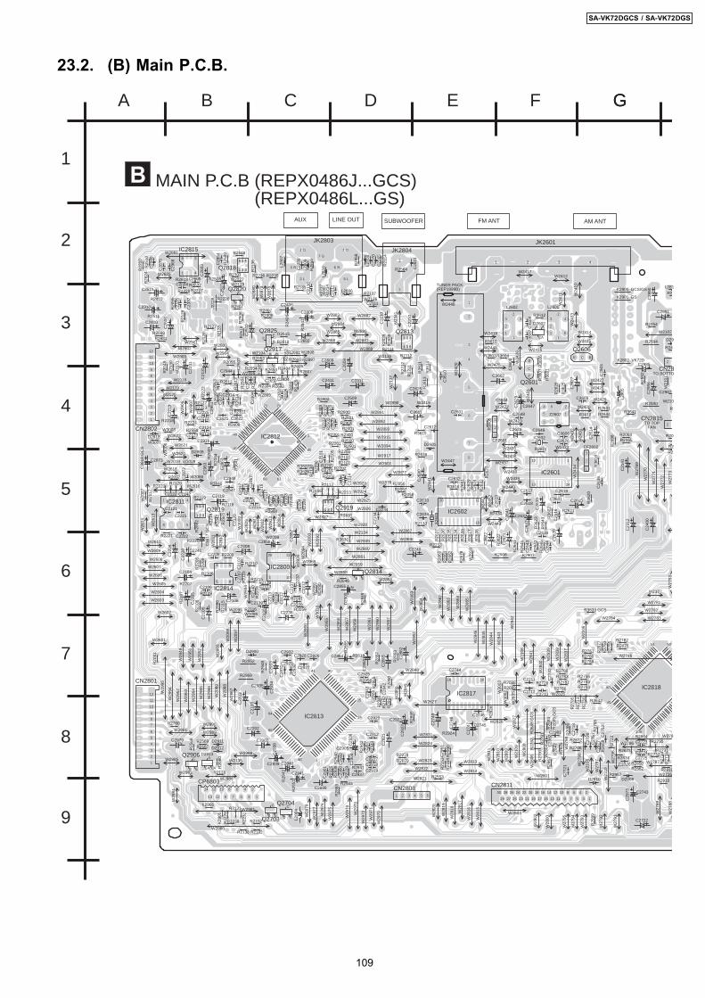
23.2. (B) Main P.C.B.
A B C D E F G
1
2
3
4
5
6
7
8
9
G
B MAIN P.C.B (REPX0486J...GCS) (REPX0486L...GS)
RIG
HT
B
C
E
BC
E
E
C
B
B
C
E CA
A
CA
B
C
E B
C
E
B
C
E
E
C
B
A
CA
A
BCE
N
N
N
SUBWOOFER
C3606
R2631
C26
44R
2646
R26
42
C26
43R
2645
R26
41
R26
38
R36
17
R26
33
R26
34
R26
35
R26
36
R26
37
R36
22C2633
C2634
C2632
R3616
R26
51
R26
29C
2624
R26
32R
2627
R26
52
C26
13
R2630
C2617
C2618
C2637
C2638R
3623
R26
43
R36
02
C26
16
C2631
R2621
R36
20
C26
36R
3619
C2626
C2649
R3624
C2612
R3615
C2601
R36
13
C3604
C2647
C2648
R26
26
R36
25
C3609
R3618
R36
06
R36
01
R36
07
C36
03
R3604R3603
R2628
R36
05
C36
10R36
14
R36
11
IC2601
IC2602
R2644
TUNER PACK(REP1999B)
W29
19
D2602
C36
08C
3607
R3612
R3610
D2601
R24
R2454
L281
R2
R20
98
R25
92
R
R20R2064R2065
IC2818
R2783R2781
R2786
R2756
R27
58
R27
13R
2785
R2789R2784
D2910R2957
C2743
D2908
R29
99
R2730R2864C2723
R2731C2724R2732C2725
R27
33R
2734
R2673
C2726R2911
R2910
R2850R2662
R26
83R
2685
GC
S
R26
88 G
CS
R27
91
R27
92
R27
97
C29
82
C2981
R28
47R
2675
R26
61
R27
23
C27
52R
2658
C29
77C27
51C
2720
R27
98
R2672
R2708
R20
86C
2718
C27
21
R2088R2089
C2746 R29
26
R2782
R27
55R
2753
R2761R2760R2759
R2788
C27
42
R2076
C2711
C2712 C2713
R2726
R20
77
R2619
R28
53
R28
57
R28
55
R2078R2079
R20
80
R25
68
R28
63
D2912
D2911C2979
R2567R2569
Q2704
Q2703
D2900
C2925
R21
62
R29
45
C2923
R2944
C2920
C2919C2918C2917
C2912
R29
43C
2907
C2937R29
39C
2904
C29
02R
2940
C29
00R
2938
R29
35
C29
01
C2905
R2941
R29
42
R29
51R29
49
C29
38
R29
48
C2935
C2932
C29
31
C29
30
C2929
C2928
C2927
C2926
R29
47
R29
46C
2924
R29
55
C29
42
R2956
C29
43
IC2813
R29
90
C29
61R
2154
R22
53
C2744
C2745
D2913Q2906
R2138
R2238
R2129
R2132
R2232
R2131
R22
31
R22
29
R2924
IC2817
R28
41
R24
06
R2056R2057
R2058
R2120
C2947
C2948
R2507
R2508
Q2813
C2139 C22
13
C21
37 C22
37
C29
13
C23
20C
2522
C22
14C
2114
C2239
R26
78
R20
62R
2061
R20
95C
2335
C23
32
C2122
R2121
C2121
C28
72
C2873
C2222R2221
C2221
R2220
L2806
R29
58
L280
8C
2970
L281
0 C29
65
R21
14
R22
14
R22
37
C22
11
C2111
R2137
L280
9
C22
36
R2236
R29
59C
2136
L280
7
R21
36
R2135
R2235
R28
39R
2838
R2112
R2111
R22
12
R22
11
R21
08
R2109
C2106
R21
07
R2207
R22
06
C21
07C
2207
R21
10
R2210
C2206 R2209
IC2800
C21
40 C2113R2139
Q2819
R2119
R28
42R
2921
R2218
R22
19
R2118
Q2818R2307
R2306
R2848
R2407
IC2814
R2127
R2227
R2226
R21
26
R2622
R25
09
C29
69R
2510
C29
64
C2605C2604R2623
IC2815
C28
75
C29
68
R26
16 Q2825
R2618
R2615
R2601
R2401
R2501
R2301
R2201
R2101R2100
R2200
R2300R2500
R2400
R2600
R21
03R
2203
R22
04R
2104
R21
17R
2217
C21
18C
2218
C22
16C22
17C
2116
C21
17
C2115
C2215
R20
84
D2809
D2818
W3008
W2622
W2019
W2621
R26
09
R2558
R2607
R2606
R2124
R2605
C2123
C2124R2224
C2223C2225
R2223R2122
R22
22
R2608
C29
15R
2610 C2914
R2611C29
53
R2612
R26
13R
2614
C26
07
C2944
R25
04C
2516
R25
05C
2304
R2304
R23
05
C2404
R2404
R26
03R
2405
C26
10
R26
04
R2602
R23
02R
2502
R25
03R
2303
C2201R2205
R21
05
IC2812
R25
06
R21
28
R2410
R23
10
Q2820
R22
08
R2106
R2228
R2511
R20
52
R2053
R2054
R2055
R20
90
R21
15
R2116
R2215
R22
16
R22
39
R2091
R2780
R20
81
C21
01
R2059
R2846
Q2814
D29
09
R28
49
C29
03
C2234
C21
34
R2233
R2133
R20
60
R26
24
R2553
R2
R2202
R2102
R2213R2155
R21
30R
2230
R2998
R2
W2104
R28
62
R20
96
R2097
Q2917R2691
R2692
R2113
R2254
Q2919
R3630
R3631
R3634
W21
31
W21
30
R3633 GCS
W210
W21
01
W2126
R3627R3626
W2127W2128
K2906
K29
05
W2099
W2096W2095
W20
94
W20
91W
2090
R2693
C2650
W20
87
R3640
R36
41
R3642
D29
W30
02W30
03
C26
20
C26
21
C26
22
W2443X26
03
C26
30
W24
41
W24
42W2440
W2439
W2438
C26
41
C26
42
C26
39
C2619
C2615
W24
34
W2433
W24
32
C26
14
W2430
W2429
X2602
W2436
W2435
C2623
W2423
W2422 C26
29 W24
24
C3611
W2419
C2625
W24
20 W2425
C3602
W2448
W2418
Q2601
W24
26
W2416
W2428
W2427
C26
27
Q2606
W2415
W2414
W24
13
W24
11 W24
10
W2412W2417
W2446
W2447
W24
31
W2437
Z2602
JK2601
CF2602
CF2601
L2602 L2601C2991
C29
90
C2985
C2987C29
86
R2594
R2580
W27
70
C23
12
C24
00
W27
69
W27
71
W27
72
W27
91
W27
92
W27
94
W27
95 C2722
W2787
C29
73
C27
47
W28
10
W28
06 W28
04
W28
16
W28
08
W28
11
W28
15
W28
00
W28
02
W2803
W278
W2786
W28
27
W28
09
W27
99
W27
96
W2801
W27
97
W27
98
W2826
W27
93
W2735W2814
W27
88
W27
89
W28
40
W2783
W2782
W2746
W28
38
W28
39
W28
37
W2848
C28
65 C28
62
C2864
W28
49
C28
60
W29
55
W29
67
W29
66
W29
65
W29
95
W2991
W29
94
W29
62
W2985
W29
84
W29
64
W2990
W2989
W2988
W2983W2986
L280
4
W28
51
W2831
W29
78
W29
77
W29
76
W29
75
W29
70
W29
71
W29
72W29
73
W29
74
W28
50
R2952
R2969
C29
22
C29
21
C29
36
C2899
C2941
C2940C2939
C2202
C2102
C22
03
C21
03
C29
34C
2933
W2627
W2822
W2823
W2824
W2821
CN2801
CN2808CP6803
C27
48
C27
49
W2981
W2980
W28
20
W28
19
W28
18
W28
17
W2877
W2925
W2882
W2890
W2883
W2904
W2897
W2889
C21
20
C2306
W2900
W2903
W23
41
W28
78
W28
79
W2867
C21
38 C2238
C29
63
W2866
W2881
C26
06
W28
80
C22
20
JK2803
C21
10
C22
10
C2108
C21
05
C2104
C22
05
C22
04 C2208C2858 C
2857
CN2802
C2406
J212
8
J222
8
C26
03
C25
17
C2602
C29
62
C2916
C29
54
C26
08
C2411 C2311
C2509
C25
02
C21
31
C2410
C2310
C22
31
C2515
W2813
C2609
W2893
W2917
W2928
W2923
W29
07
W3007
W30
06
W2620
C22
19
C2119
W2086
W2616
W26
13
W2609
W2608
W2607
W2606
W2605
W2604
W2603
W29
63
W29
14
W26
12
W29
52
W29
49
W29
34
C22
12
C21
12
W2781
W27
53
W2784
W29
61
W28
54W28
53
W29
51
W2927
W2860
W28
62
W28
63
W28
64
W28
65
W28
46
W28
45
W28
44
W28
43
W28
35
C2855
W29
29
CN2811
W2626
IC2811
W29
06
W29
30
W29
58
W29
57
W29
56
W2859
W29
60
W28
57
W2876
W2924
W2888
W2898
W2885
W2884
W2887
W2891
W2892
W2915
W2894
W2501
W2926
W2134
W2861
W2858
W2939
W27
73
W2618
W29
13
W29
12
W29
11
W26
14
W2601
W2602
W2610
W26
11W
2968
W2886
W2895
W2896
W2901
W2902
W2856
W28
42
W28
41
W2828
C2240
C21
41
W29
50
W2120
W2119
W2118
W21
17
W21
10
W21
09
W21
08W2107
W21
06
W21
05
W2102
W2135
W2136
W21
37
W20
98
W20
97
W20
92
W20
93
W20
89
W20
88
C36
18 G
CS
C36
17 G
CS
W3009
L290
5
W30
10
W2959
W30
00
AM ANTFM ANT
AMT
GND
GND
V+
B+
IF
OSC
AUX LINE OUT
CN28TO BOTTO
CN2815TO TOP
FAN
K2907K2908
K2802 VK72D
K2900 GCS/GS
C26
11
R2564
JK2804
R2049R2881
R20
48
C3622C3621
C2142
C2241
K2901 GS
R3643
12
1
4-2
301
2
12
1
4
1 2 3
456
1 4
58
12
10
1120
51
64
1
1018
1 10
1120
4
20
2
-1
3
2
1 6
4-2
-1
3
2
1 6
4 5 6
123
1
80
21
40
41
60 61
4
58
1 2 3
456
1
5 8
11
10
9
8
7
6
5
4
3
2
1
11
10
9
8
7
6
5
4
3
2
1
468101214
135791113
41
1
24
40
25
65
80
2 3 4 5 6
9
1 2 3
456
1
1
13 24
5
3
6 2
1
1
2
3
1
2
3
2
2
50
80
81
100 1
28 26
29
24 22 20 18 16 14 12 10 8 6 4 2
27 25 23 21 19 17 15 13 11 9 7 5 3 1
1 2 3 4
3
4
5
6
7
8
1-G
6-R
5-L
3-R
2-L
4-G
7-G2
1
109
SA-VK72DGCS / SA-VK72DGS
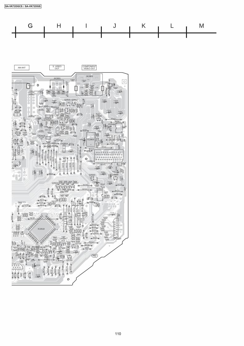
GG H I J K L M
BCE
PbF
N
N
B
C
E
B
C
E
B
C
E
E
C
B
BC
E
B
C
E
E
C
B
BC
E
B
C
E
B
C
E
B
C
EB
CE
B
C
E B
C
E B
C
E B
C
E
B
C
E
6
R2631
621
R36
20
C26
36R
3619
6
C3609
R3618 R2644
Q2806
R2828R2823L2
813
R28
03R2816L2811
C24
36
C24
37
C27
58
IC2006
R2810
Q2838
R28
20
C24
41 C2443
C2039
C2759
C24
40
IC2803
C28
25
R28
60
C2826
R28
18R
2829
R24
57R
2456
R2455
Q2916
C29
88
C2989R2460
R25
96R
2595
R25
97R
2453
Q2915
R25
99
R2454
Q2913
R25
98
R2814
C28
43
R2807 R2832
R2834
R28
26
L2816
R28
30 R28
22L2
812
L2815
R2825 C2850R2824L2814C2851
C2842
C2847C2846
C2848C2849
R20
98
R28
27
R2817
R25
86
Q2910
R25
92
R25
85
Q2911
R25
84R
2583
R25
82R
2581
R2587C2984
C29
83
Q2912
R2591 R2593R2588
R2459
R20
67
R2068
R20
70
R20
66
R20
69
R2064R2065
IC2818
R27
35
R29
17
R2918
C27
36
C2737
R2916
C27
34C
2730
C27
35 R2736R2913Q2710R2667
D2906
R2914
R2737R2738
R2739R2740
R2742
R2744R2743
R2741 R27
29
R27
45R
2728
R2749
C2704
R2750
C27
50
1R2756
R27
58
R27
13R
2785
R2789R2784
R2912D2910R2957
C2743
D2908
R2747R2746
Q2702
D29
05
R29
99
R2987
R2986
R2985
R2984
R2983R2840
R2982
R2981R2980
R2979
R2978
L280
2
D29
01
R2730R2864C2723
R2731C2724R2732C2725
R27
33R
2734
C27
27 C27
28
R2673
C2726R2911
R2910
R2850R2662
R27
23
C27
52R
2658
C29
77C27
51C
2720
R27
98
R2672
R2708
R20
86C
2718
R2094
C2732
R2920
R2072
R2073
R2751
C2705
IC2816
C27
39
C2738
R26
70R
2922
C27
40
R29
23
R27
94
C2978
C27
16C
2717
R27
96
R20
74
C27
14
R20
75
R2790
R27
76R
2775
R27
74
C2707
C27
08
C27
09
R27
77R
2778
R27
79
C27
10
R27
52
R2782
R27
55R
2753
R2761R2760R2759
R2076
C2706
R20
77
Q2823 Q2816 Q2815 Q2822R2854R2620R2852R2856
C29
03
R2702
R2988R2859
R2851
R2589R2590
Q2920
R36
28
R3629
R3634
W2132
R3633 GCS
C27
19W
2133
W2103
W21
01
R27
62
C27
54
R36
37R
3639
R3638
C3623
R3642
D29
15
D29
14
D29
16
D2917
D29
18D29
19
K99
99
W29
99
W3011
W2125
W30
05W
3004
R27
54R
2793
C2615
W24
34
3
W24
32
C26
14
W2430
W2429
W2428
W2427
C26
27
Q2606
W2415
W2414
W24
13W
2410
W24
31
CF2602
W2760
W2762
C2100
C2200
C2975
C2974
C2046
C2047
C2442
C24
44
D28
10D
2811
D28
37
C28
27C2991
C2992
Q2914
C29
90
D28
36
JK2802JK2801
W2703
W27
04
CN2813
C2434
W27
02
W27
01
W2706
W2707
W2705
C2985
Q2909
C2987C29
86
R2594
R2580
W2765
C2600
C25
00
W27
70
W2767
W27
61
W27
54
C23
12
C24
00
W27
69
W27
71
W27
72
W27
76
W2768
W27
91
W27
92
W27
94
W27
32
W27
33
W27
34
CN2810
X68
01
X6800
C2722
W2787
C29
73
C2729
C27
31
C2733
W27
43
W27
44
CN2814
W2785
W2786
W27
99
W27
96
W27
97
W27
98W
2793
W2735
W27
88
W27
28
W2721
W2722
W2724
W2723
W2719
W2717
W2718
C2741
W2720
W27
26
W27
25
W27
38W
2739
W27
40
W27
41
W27
42
W27
45
W27
89
W2712
W27
47
W2748W2783
W2782
W2746
W28
37
W27
55
W27
80
W27
79
W27
78
W27
77
W2781
W2749
W2750
W27
52
W27
53
W2784
W2751
W2763
W2764
W27
66
W27
75
W27
74
W27
73
W2709
W2710
C21
41
C2050
C36
12
W2124
C20
49
W27
27
W21
23
W2122
W21
21
W2116
L2904
W2115
W2114
W2113
W2112
W2111
W21
10W21
08
C2048
W2107
W21
05
W2102
W2100
W21
29
L290
5
W30
01
AM ANTS. VIDEO
OUTCOMPONENTVIDEO OUT
CN2816TO BOTTOM FAN
CN2815TO TOP
FAN
R2899
L2906
R36
44
K2802 VK72D
K2900 GCS/GS
K2901 GS
R3643
R2831
1
1
1
2
1
1
1 8
916
5
6
51
4
1
4
1
2
3
2
2
2
3
1
50
31
3080
81
100 1
3
5
7
9
11
1314
12
10
8
6
4
2
1
85
3
4812162024283236404448
61014182226303438424650
711151923273135394347
5917 132125293337414549
8 6 4 2
7 5 3 1
4
2-G 1-G5-G
3-C 4-Y
1-G
6-V
5-PB
3-Y
2-PR
4-G
7-G
110
SA-VK72DGCS / SA-VK72DGS
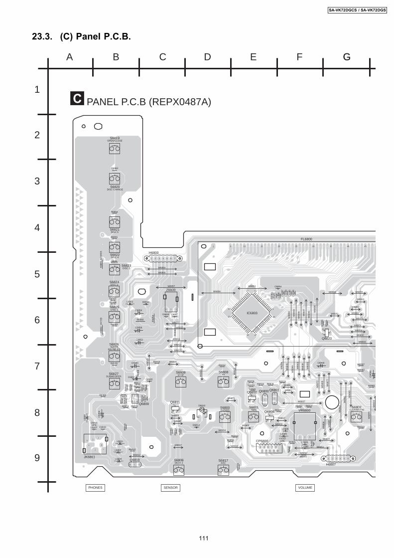
23.3. (C) Panel P.C.B.
A B C D E F G
1
2
3
4
5
6
7
8
9
G
C PANEL P.C.B (REPX0487A)
B
C
E
B
C
E
BC
E
B C E
B
C
E
B
C
E
B
C
E
1
2
9
10
4
5
6
7
1
1
1
13
6 4
31
2 3 4 5 6 7
2
5
2
3
4
5
6
7
8
2 3 4 5 6
2
31
17 16
31 2
132
33
48 49
64
45403530252015106
VR6800
CP6800
S6819OPEN/CLOSE
S6820DISC CHANGE
S6821DISC 5
S6822DISC 4
S6823DISC 3
S6824DISC 2
S6825DISC 1
S6826SUPER
SOUND EQ
S6808FF
S6809STOP
S6806DECK 2
JK6801S6817
REC
S6801TAPE
S6800DVD/CD
S6802TUNER/BAND
S6827SUBWOOFER
H6800
FL6800
C6890
W6804
W68
35
W68
36
W6853
C68
95
W68
06
H6807
W6837
W6809
W68
38
W68
39
W68
40
W68
41
W68
42
W68
43
W68
44
W68
45
W68
24
W68
46
W68
47
W68
48
W68
49
W68
50
Q6801Q6800
L680
8
L6803
L6802
L6804 Q6810
W6854
W6855
C6800
C6802
W6825
C6853
Z6800
W6811
W6826
W6827
W6812
C68
04
W6856
C6856
W6813
W6814
W68
15
R6960
R69
59
L6801
C6854
W6857
W6816
L6805
W6852
W6862
W6801
W6802
W6832
W6833
W6820
W6834
W6866
W6822
W6871
W6851
W68
72
W6874
W6875
W68
77
W6878
W6881
W6900
W68
23
W69
03
W69
04
W69
05
W69
12
W6913
K68
04
W6917 W6918
W6817
D6810
W6885
R6970
R6969
R6968
R6967
R6966
R6965
R6964
R6963
R68
54
R6855
R68
59
R68
60
R6861
R6862
C6805
C68
10
C6898
R68
85C
6891
C68
89
C68
87
C68
88
C68
85
C68
86
C6894
R68
69
R68
89
R6826R6828
R6827
R6823
R6825
R6824R6819
R68
20
R6821
C6896
C6897
R6822 R6837
C6844 C6843
C6806
Q6809
R6805
R68
12
R68
04
R6811
R6802
R6803
C68
01R
6800
R68
01
R68
08
R6807
C6803
R68
10
R68
09
R68
06
R6813
R69
96
C6809 C6807
R6814
R6815
R68
16
D6800
Q6802
Q6808
Q6820
R6962
Q6811
W6907
W6882
W6901
W6919
W69
16
D6813
W6830
IC6803
PHONES VOLUMESENSOR
GC
S/G
SK
6802
VK
72D
111
SA-VK72DGCS / SA-VK72DGS
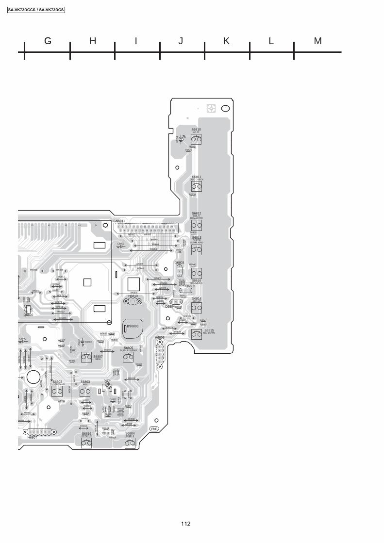
GG H I J K L M
12
BC
E
B C E
B C E
B
C
E
PbF
1
1
2
29
30
54
1 2 3 4 5 6
2
3
4
5
3
4
5
6
7
8
9
10
27
28
25
26
23
24
21
22
19
20
17
18
15
16
13
14
11
12
49454035
H6806
CN6811
S6810AC IN
S6811DISC CHECK
S6812MULTI
REMASTER
S6813SUPER
SURROUND
S6818SOUND EQ
S6814MIC UP
S6807REW
S6815MIC DOWN
S6805DISPLAY-DEMO
D68
01
S6802TUNER/BAND
S6803AUX
S6816DECK 1/2
S6804DECK 1
C6890
W6865
W6867
W6858
C68
95
W6805
W68
06
W6807
H6807
W6863
W6808
W68
39
W68
40
W68
41
W68
42
W6860
Q6804
Q6805
Q6803
W6828
W68
29
W6861
W6862
W6818
W6803
W6831
W6819
W6832
W6833
W6820
W6834
C68
13
C6855
W6866
W6821
W6822
W6870
W6851
W68
72
W6874
W6864
W6876W6875
W68
77
W6878
W6879
W6880
W6881
BS6800
H6810
W68
23
W69
04
W69
05
W6909
W6910
W6911
W6913
W6914
D6809
W68
83
W68
84
R6937
R6938
R6939
R6940
R6941
R6942
R6943
R6944
R6829
R6856
R6857
R6858
R6861
R68
93
R68
94
R68
64
R68
65
R68
69
R68
89
R69
56
R6957
R69
50
R69
54
R6830
Q6820
R6997
C6812
R69
61
W68
86D6812
W6907
W69
06
W6915
W69
08
W6882
D6802
W6902W6889
W6888W6887
W6919
W6810
R6990R6988R6989
D6815
D68
14
112
SA-VK72DGCS / SA-VK72DGS
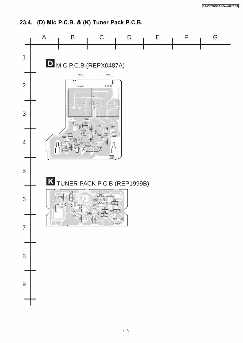
23.4. (D) Mic P.C.B. & (K) Tuner Pack P.C.B.
A B C D E F G
1
2
3
4
5
6
7
8
9
MIC P.C.B (REPX0487A)D
TUNER PACK P.C.B (REP1999B)K
B
C
E
B
C
E
BC
E
PbF
2
1
3
4 5
6
78
92
1
3
4 5
6
78
9
12345
A CA A
G
S
D
A CA AA CA A
B C E
B C E
B C E
JK6802JK6800C
6879
C68
65
R68
92
R68
88
R6981
C6871
C68
73
C6875
R6891
R69
87
C6872
C68
82
R6886
R69
94
C68
81
R6982
C6866
C68
67
W68
00
C68
76
R6890
R69
83
C6811
L680
9
H6805
R68
87
C68
70
L680
6K6806
C68
68
Q6806
Q6807
Q6817
R6991
R69
93 R6992
W6890
W6891
R6995
MIC1 MIC2
PbF
D1
R1
C1
Q1
R4
Q2
L1
R6
R5
D2
C3
C4
C5
C6
C7
C8
C9
C10
C11
R7
R8
R9
R10
Q3
Q4
D3
R11L2C2
R3
R2
J1
J2J3
J4
113
SA-VK72DGCS / SA-VK72DGS
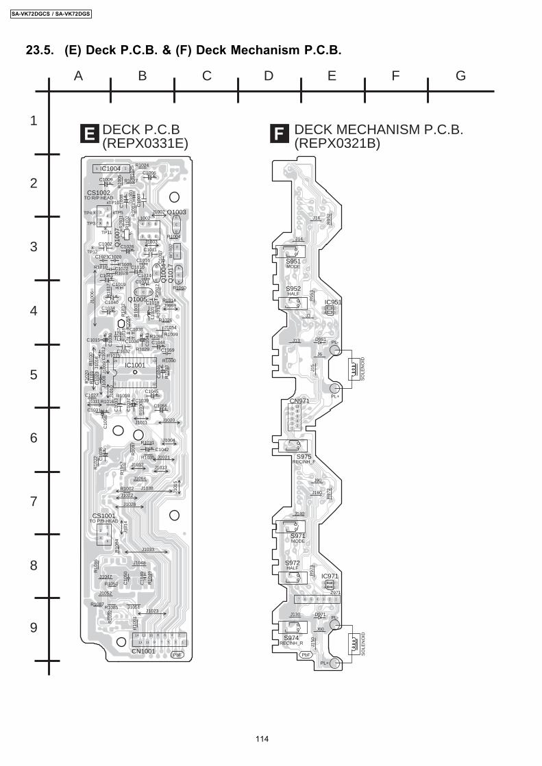
23.5. (E) Deck P.C.B. & (F) Deck Mechanism P.C.B.
A B C D E F G
1
2
3
4
5
6
7
8
9
DECK P.C.B(REPX0331E)
DECK MECHANISM P.C.B.(REPX0321B)FE
BC
EB
C
E
B
C
EB
C
E
BCE
CN971
S971MODE
S972HALF
D971J130
PL+
PL-
S975RECINH_F
Z971
J60
J140
R97
3
J90
R97
2
J150
IC971
J160
321
4
J13
PL+
PL-
J6
J14
R95
2
J3J1
5
S951MODE
R95
3S952HALF
D951
IC951
J16
1
423
12
34
56
78
910
1234567
SO
LEN
OID
SO
LEN
OID
PbF PbF
1 12
1324
15
1
5
2
43
1
5
2
43
1
2
3
4
5
6
7
8
913
14 12
11
10
123
4 5 6
1
2
C1006
C1009
C10
08
Q1003J1002
C10
07
C1002 C1026J1003
C1011
C1040C1034
Q10
17
C1044C10
43
J101
6
J100
8J1
009
C1010
J1111
J1011 J1020
J1012J1013
J1022
J1028
J1038
J101
4
J1033
J1023
J1021
J101
5
C10
46
Q1005
R10
07
W10
02
CS1002TO R/P HEAD
CS1001TO P/B HEAD
L1002
IC1004
C1041
CN1001
J101
0
J1004
C10
30
C1032
C1045
C10
33
C10
37
C1056C1031
C10
35 C1042
J1064
J1051
L100
1
Q10
04
J100
6
J9999
R10
05
R10
03
C1021
R1010
R10
97
R1004
C1016
R1060
C10
17
C1020
R1009
C1014C1013
C1019
R10
18C
1057 C1038
C1036
R10
32R
1055
R1098
R1026
R10
13
C1018 R1014
R10
12
C10
23
C1027 R1019R1016 C1039
R10
30
C1015
C10
12C
1058
R1035
R10
57
R10
22
C10
50
C10
49
R10
49
R10
11Q
1007
R10
92
R10
91
R1087R1085
R1050
R10
84
R10
86
R1031
R1090
R10
17
C1022R1028
D10
03
R10
40
R1029
IC1001
R1015
R1002
R10
20
R1027
R10
25
C1059
R1024
R11
00R
1101
R1099
R11
02
S974RECINH_R
TP10x
TP5x
TP11x
TP12x
TP3 x
TP4 x
J1054
J1047
J1048
J1052
114
SA-VK72DGCS / SA-VK72DGS
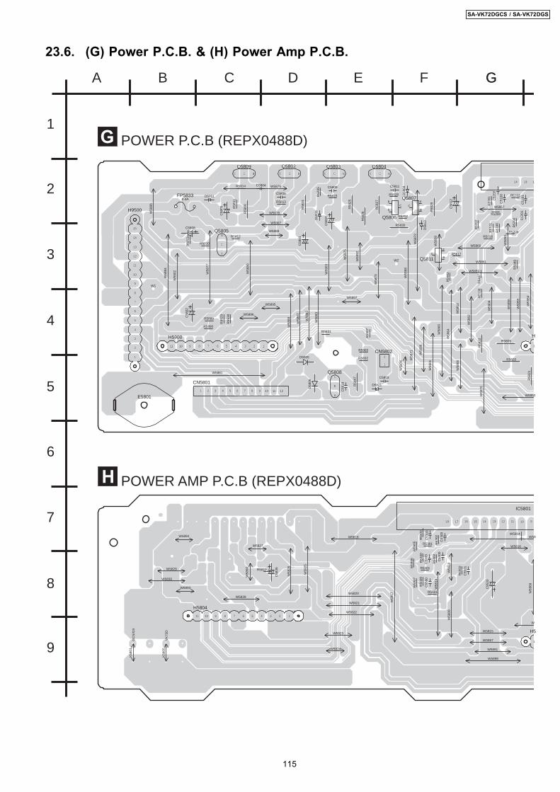
23.6. (G) Power P.C.B. & (H) Power Amp P.C.B.
A B C D E F G
1
2
3
4
5
6
7
8
9
G
POWER P.C.B (REPX0488D)G
POWER AMP P.C.B (REPX0488D)H
BC
E BC
E
BC
E
E C B E C B E C B E C B
E
B
C
E
C
B
121
1
1
1
1
11314
234567891011
2
2 3 4 5 6 7 8 9 1110
2
3
4
5
6
7
8
9
10
11
12
13
14
15
9101112131415161718
1234567891011
1
C52
00
C51
00
R52
01
R5200
R51
01
R5100
R5102
C51
01C
5201
R52
02
C5804R5814
R5813
C5806R5823
C5809
R58
35D
5803
R5828
C5811
Q5806
Q5807
D58
10
D58
04
D5801
R5812
R5810R58
11
C58
19
R5832
R5903
R5831
R5890
R5889
R95
30
R95
29
R5817
R58
49
Q5811
R59
02
R55
07
R52
07R
5107
C5803
R58
91
R5892
D5821
Q5803Q5802Q5809
CN5801
H
H9500 R58
25
W5857
R58
21
R5820
R5809
R58
22
R59
06
W5879
C58
10
FP58330.4A
R58
26
R58
27
R5830
C58
12
W58
72
R58
29
C58
05
Q5805C5808
C58
02
R58
47
W5878
W5887
W58
86
W58
80
W58
85
W58
75
R58
24C
5801
D58
06
D5805
W58
83
W58
84
W58
58
W58
82
W5860
W5861
W5859
W58
54
W58
55
W58
56
W58
62
W58
50
W58
76
W58
88
W58
70
W58
71
W58
66
W58
73
W58
65
W58
64
W58
63
W58
68
W58
36
W59
03
W59
02
W59
01
W59
04
Q5804
W58
77
Q5808
W5853
H5900
CN5802
E5801
W5881
W5889
W58
92
W5897
W5895
W5896
R53
00
R5301
C53
03C
5403
R5401
R54
00R
5500
C55
00
R5501
C55
01
R55
02
R54
02
C54
00C
5300
R53
02
W59
05W
5906
W59
07
R5819
W5914
H5
H5804
W5829
W5830
W58
25
W58
26
W5828
W5827
W58
W58
09W
5810
W5818
W58
17
W5822
W5823
W5821
W5820
W5824
W
W5816
K58
01
W58
69
C58
36
W58
90
C95
33
W5867
W5891
W58
14
W5898
IC5801
W5894
W5893
W5815
GC
S/G
S
W1
W2
K58
05V
K72
D
R51
08
R5206R51
06
115
SA-VK72DGCS / SA-VK72DGS
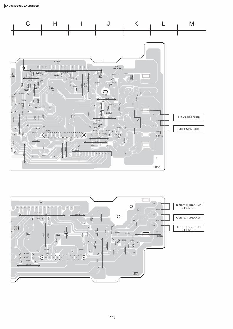
GG H I J K L M
IC5801
BC
E
BC
E
PbF
PbF
121
10 1
19 23456781011121314
23456789
2 3 4 5 6 7 8 9 1110
19 23456781011121314151617
9 1234567810
4-GND
2-GND
3-L
1-R
2-SLG
4-CG
6-SRG
1-SL
3-C
5-SR
C52
00
C51
00
R52
01
R5200
R51
01
R5100
R5102
C51
01C
5201
R52
02
D5820
R5817
R58
49
C52
03
C5202
C5102
C51
03
R52
04
R52
03
R51
03
R51
04
R9531
Q5810
Q5801
R5816
R9532
C5814
R5815
D58
09
R95
36
R95
34
R9535
R52
07R
5107
W59
08
W59
10W
5909
CN5800
H5901
W58
45
W58
46
W5847
W5857
R58
21
R5820
R5809
R58
22
C58
12
W5849
W5860
W5861
W5859
R9523
R5105R9528
R5205
L9502
L9507
C5813
W58
52
W58
51
W58
32
W58
39
C5807
C5834W
5840
W5833
W5835
W5837
W5834
W58
54
W58
55
W58
56
W58
62
W58
50
W58
70
W58
66W
5863
W5844
W5843
W5842
W5841
W5838
W59
04
W5853
C58
15
C58
18
IC5001
JK9501W
5831
RIGHT SPEAKER
LEFT SPEAKER
C55
01
R55
02
R55
05
R5898R5866
R5504 C55
03 C5502
C54
01
C54
02
C53
02
C53
01
W59
15
W5914
JK9502
H5803
W5807
W58
08
W5804
W58
06
W5805
R5503
R54
03
R53
03
R54
06
W5812
W58
01
W58
03
L540
6
R54
04
W5816
R54
05
L540
5
W58
02
W58
69
W58
19
L540
4
C95
33
C95
34
W58
11
W5867
W5891
W58
13
W5898
IC5801
W5815
CENTER SPEAKER
RIGHT SURROUNDSPEAKER
LEFT SURROUNDSPEAKER
W1
K58
05
K58
74
R51
08
R5206R51
06
116
SA-VK72DGCS / SA-VK72DGS
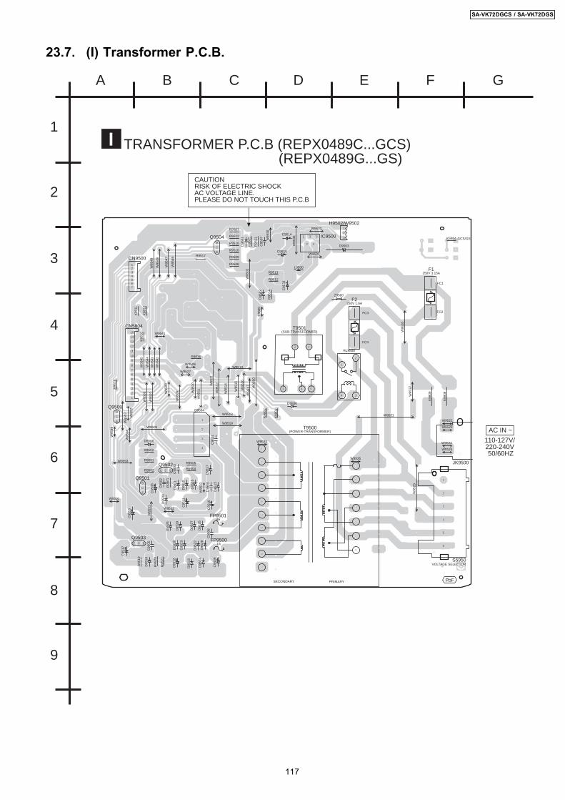
23.7. (I) Transformer P.C.B.
A B C D E F G
1
2
3
4
5
6
7
8
9
TRANSFORMER P.C.B (REPX0489C...GCS) (REPX0489G...GS)
I
CAUTIONRISK OF ELECTRIC SHOCKAC VOLTAGE LINE.PLEASE DO NOT TOUCH THIS P.C.B
E
C
B
E C B
E
C
B
E C B
4 3
2
1
E
C
B
PbF
15
1
1
1
1
4
2
3
3
1
4 5
2
2
3
4
5
6
234567
2 4
53
14
13
12
11
10
9
8
7
6
5
4
3
2
1
1
7
6
5
4
3
2
PRIMARYSECONDARY
8
9
10
11
12
13
14
15
16
17
AC IN ~
110-127V/220-240V 50/60HZ
F2250V 1.6A
F1250V 3.15A
JK9500
T9501(SUB-TRANSFORMER)
CN5804
W9523
W9524
W9525
W9522
D95
12
D95
17C
9504
C95
11
C95
10D95
09
R9505
R9504Q9502
R95
03
D95
10
D95
11
D95
15
Q9501
RL9500
C95
03
C95
02
R9502
R9501
W95
33
C95
08
W9532
W95
29
Z9500
W9521
W95
20
R9500
D9508
D95
14
C95
09
D95
13
C95
12
R95
21
FP95001A
R95
20
R95
19
D95
16
C95
17
Q9503
C95
05
FP95014A
C95
06
C95
13
D9504
W9519
W95
11
W95
14
W95
15
W95
10
W95
09
C95
01
W95
17W95
16
D9500
W9518
Q9500
R95
18
W95
06
W95
07 W95
08
W9513
R9516
R95
15
R9507
R9512
R95
14R9513
R9509R
9511
R9522
R9510
IC9500
L9500
C9515
D9503
D95
02C
9507
D95
01
W95
02
Q9504C9514
R9508
CN9500R9517
W95
03
W95
31
W95
04
W9505
W95
12
W95
30
FC2
FC1C
9533
W95
40
W9541
W9553
D95
29
D95
24
D95
25
D95
27
D95
28
D95
22
D95
23
D95
26
W95
47
W95
48
W95
49
W95
46
W95
45
W95
44
W95
43
W95
42
W95
51
K98
01
K98
02
W95
52
W95
50
W9500
W9501
K98
09
K98
08
R9836
W9528
W9527
W95
37
K98
11
K98
12K
9810
W9600
W95
36
FC4
FC3
S5950
K5804 GCS/GS
1
2
3
H9502/W9502
T9500(POWER-TRANSFORMER)
W9535
W9534
K98
05
VOLTAGE SELECTOR
117
SA-VK72DGCS / SA-VK72DGS
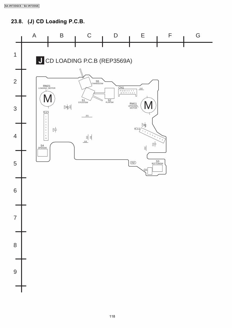
23.8. (J) CD Loading P.C.B.
CD LOADING P.C.B (REP3569A)
A B C D E F G
1
2
3
4
5
6
7
8
9
J
PbF
CN1RM21
IC21
C22
C21
LOADING_MOTOR
OPENSW
STOCKSWS1
PLAYSWS2
RM11UP/DOWN_
MOTOR
IC11
C12
C11
Q1
BOTTOMSW
S4
J21
J11
J13
J14
J12
S3
J15
J16
CHANGESWS5
MM
14
9
1
2
3
4
5
6
7
8
9
10
11
12
13
87
65
43
21
1
2
3
4
5
6
7
8
9
118
SA-VK72DGCS / SA-VK72DGS
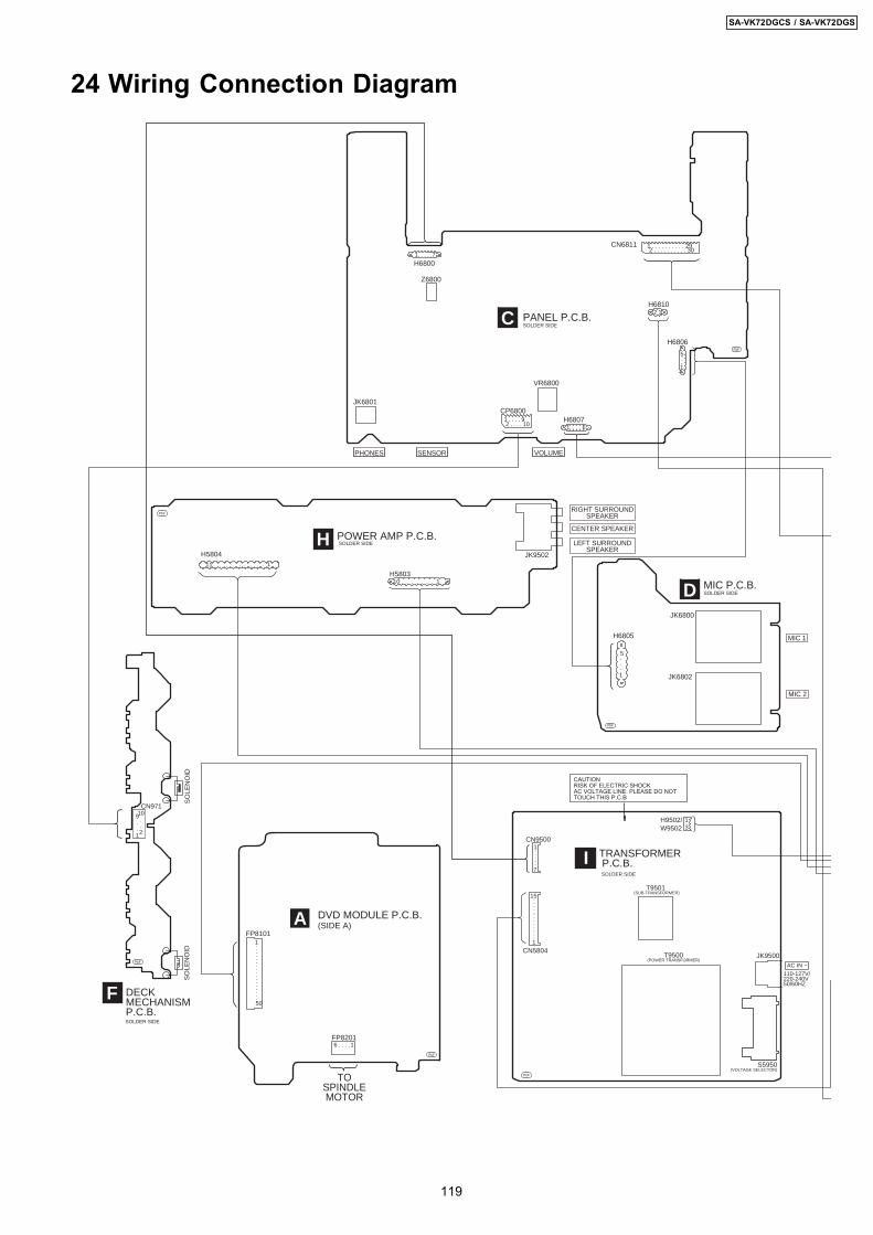
24 Wiring Connection Diagram
2 . . . . . . . . . . 301 . . . . . . . . . . 29
1 . . . . 92 . . . . 10
JK6801CP6800
H6807
H6810
CN6811
VR6800
Z6800
1. . . . .7
1. . . . 6
2 1
H6800
PHONES SENSOR VOLUME
C PANEL P.C.B.SOLDER SIDE
SO
LEN
OID
SO
LEN
OID
CN97110..2
9..1
DECK MECHANISMP.C.B.SOLDER SIDE
F
TRANSFORMER P.C.B.SOLDER SIDE
I
AC IN ~
110-127V/220-240V50/60HZ
CAUTIONRISK OF ELECTRIC SHOCKAC VOLTAGE LINE. PLEASE DO NOTTOUCH THIS P.C.B
T9501 (SUB-TRANSFORMER)
T9500(POWER TRANSFORMER)
JK9500
S5950(VOLTAGE SELECTOR)
7
CN9500
CN5804
1. . . . .
PbF
A DVD MODULE P.C.B.(SIDE A)
PbF
PbF
PbF
FP81011
50
. . . . . . . . . . . . . . . . .
FP82016 . . . .1
TOSPINDLEMOTOR
MIC P.C.B.SOLDER SIDED
MIC 2
MIC 1H6805
JK6800
JK6802
5
1
. . .
PbF
PbF
H6806
5
1
. . .
H580411 . . . . . . . . . 1
H580310 . . . . . . . 1
JK9502
RIGHT SURROUNDSPEAKER
CENTER SPEAKER
LEFT SURROUNDSPEAKER
15
1
. . . . .. . . . . . . .
3H9502/W9502
1.
SOLDER SIDEH POWER AMP P.C.B.
119
SA-VK72DGCS / SA-VK72DGS
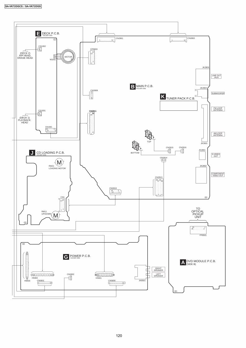
B MAIN P.C.B.SOLDER SIDE
K TUNER PACK P.C.B.
LINE OUT/AUX
SUBWOOFER
FM LOOPANTENNA
AM LOOPANTENNA
COMPONENTVIDEO OUT
S-VIDEOOUT
CN28021. . . . . . . . . . . . 12
CN28011. . . . . . . . . . . . 12
CP6803
13
1
. . . . . . . . .. . . . . . . . .
14
2
CN281130
2
. . . . . . . . . . . . . . . . . .
CN2811
CN2808
30
1
6
2
29
1
. . . . . . . . . . . . . . . . . .. . . . . . . . . . . . . . . . . .
. . . .
JK2803
JK2804
JK2601
JK2801
JK2802
CN281349
1
. . . . . . . . . . . . . . .
47
3
. . . . . . . . . . . . .
50
2
. . . . . . . . . . . . . . .
48
4
. . . . . . . . . . . . .
CN281014 . . . . . 213 . . . . . 1
CN28143 . 1
A DVD MODULE P.C.B.(SIDE B)
TOOPTICAL PICKUP
UNIT
FP8501
25 . . . . . . . . . . .126 . . . . . . . . . . .2
E DECK P.C.B.SOLDER SIDE
SOLDER SIDEG POWER P.C.B.
CN5801H5900
1 . . . . . . . . . . . 12
11 . . . . . . . . . 1
H5901
10 . . . . . . . 1
CN58001 . . . . . . . 12
J CD LOADING P.C.B.SOLDER SIDE
PbF
PbF
PbF
PbF
PbF
RM21LOADING MOTOR
RM11UP/DOWN
M
M
CN1
13
1
. . . . . . . .
14
2
. . . . . . . .
W100212
MOTOR-+
CS1002
(DECK 2)R/P HEAD,
ERASE HEAD
12 .54
CS1001
(DECK 1)PLAYBACK
HEAD
12 .54
CN100114 . . . . . . 213 . . . . . . 1
JK9501
RIGHTSPEAKER
LEFTSPEAKER
H9500
15
1
. . . . . . . . . . . . . CN580221
CN2815
TOP
BOTTOM
CN281621
21
120
SA-VK72DGCS / SA-VK72DGS
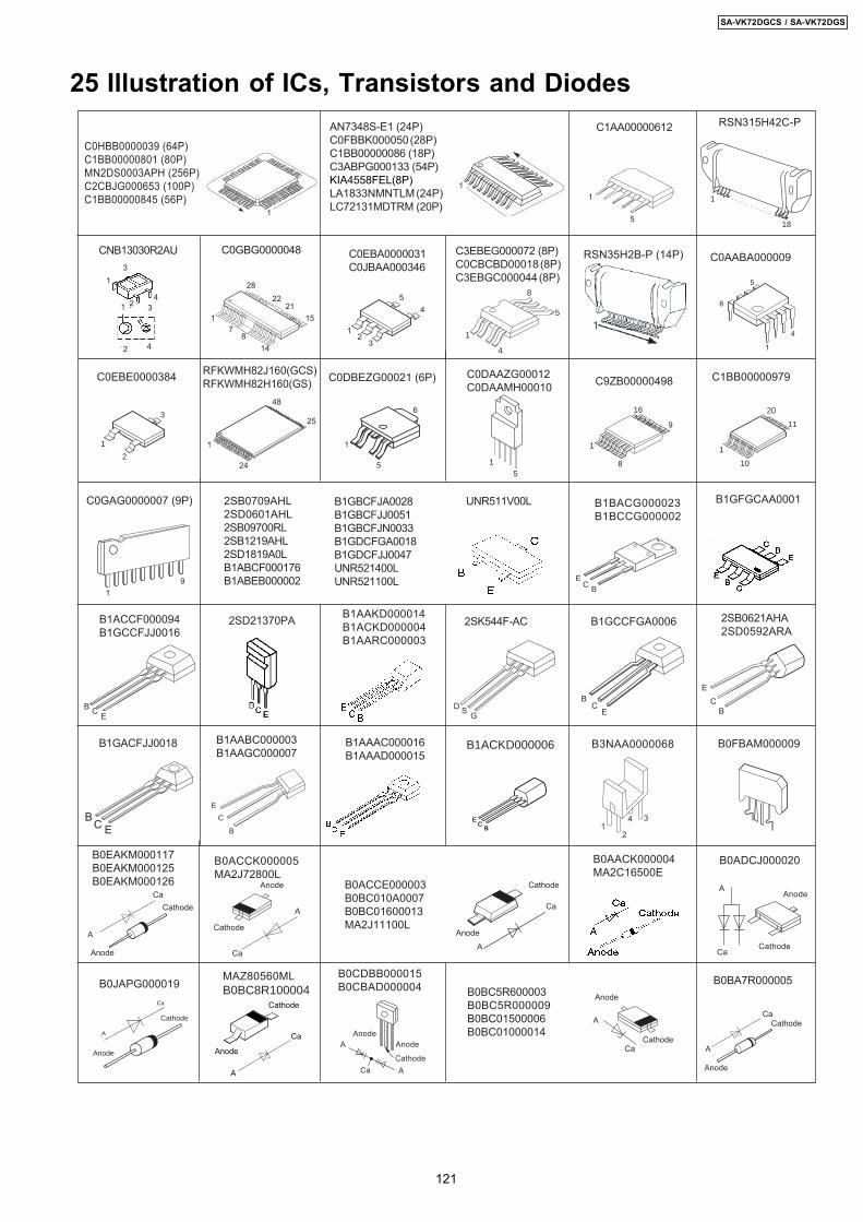
25 Illustration of ICs, Transistors and Diodes
31
1 24
3
2 4
CNB13030R2AU C0GBG0000048 C0EBA0000031C0JBAA000346
B1AAKD000014B1ACKD000004B1AARC000003
B1AAAC000016B1AAAD000015
2SB0621AHA2SD0592ARA
1
14
1
28
157
2122
8
A
CaCathode
Anode
B0EAKM000117B0EAKM000125B0EAKM000126
C3EBEG000072 (8P)C0CBCBD00018 (8P)C3EBGC000044 (8P)
B0CDBB000015B0CBAD000004 B0BC5R600003
B0BC5R000009B0BC01500006B0BC01000014
E
C
B
B1BACG000023B1BCCG000002
BC
E
RSN35H2B-P (14P)
2SB0709AHL2SD0601AHL2SB09700RL2SB1219AHL2SD1819A0LB1ABCF000176B1ABEB000002
BC
E
13
45
2
B1GBCFJA0028B1GBCFJJ0051B1GBCFJN0033B1GDCFGA0018B1GDCFJJ0047UNR521400LUNR521100L
1
24
25
48
1
5
6
C0DBEZG00021 (6P)
B1GFGCAA0001
B0ACCE000003B0BC010A0007B0BC01600013MA2J11100L
RSN315H42C-P
1
2
3
C0EBE0000384 RFKWMH82J160(GCS)RFKWMH82H160(GS)
1
4
8
5
C0AABA000009
C1AA00000612
1
5
1
C0HBB0000039 (64P)C1BB00000801 (80P)MN2DS0003APH (256P)C2CBJG000653 (100P)C1BB00000845 (56P)
AN7348S-E1 (24P)C0FBBK000050 (28P)C1BB00000086 (18P)C3ABPG000133 (54P)KIA4558FEL(8P)LA1833NMNTLM (24P)LC72131MDTRM (20P)
B1ACCF000094B1GCCFJJ0016
B1GCCFGA0006
C9ZB00000498
CathodeCa
A
Anode
B0ADCJ000020
Ca
A
Cathode
Anode
B0BA7R000005
A
CaCathode
Anode
B0AACK000004MA2C16500E
B0FBAM000009
Ca
Cathode
Anode
A
2SD21370PA
C0DAAZG00012C0DAAMH00010
15
2SK544F-AC
A
Ca
Anode
Cathode
MAZ80560MLB0BC8R100004
C1BB00000979
BC E
B1GACFJJ0018
1
10
20
11
1
4
8
5
1
8
16
9
UNR511V00L
1
18
. . . . . . . . . . . . .
ECBGSD
EC
B
B1ACKD000006
EC
BE
CB
B0ACCK000005MA2J72800L
Cathode
Anode
Ca
A
B0JAPG000019
A
Ca
Cathode
Anode
19
C0GAG0000007 (9P)
12
4 3
B3NAA0000068B1AABC000003B1AAGC000007
121
SA-VK72DGCS / SA-VK72DGS
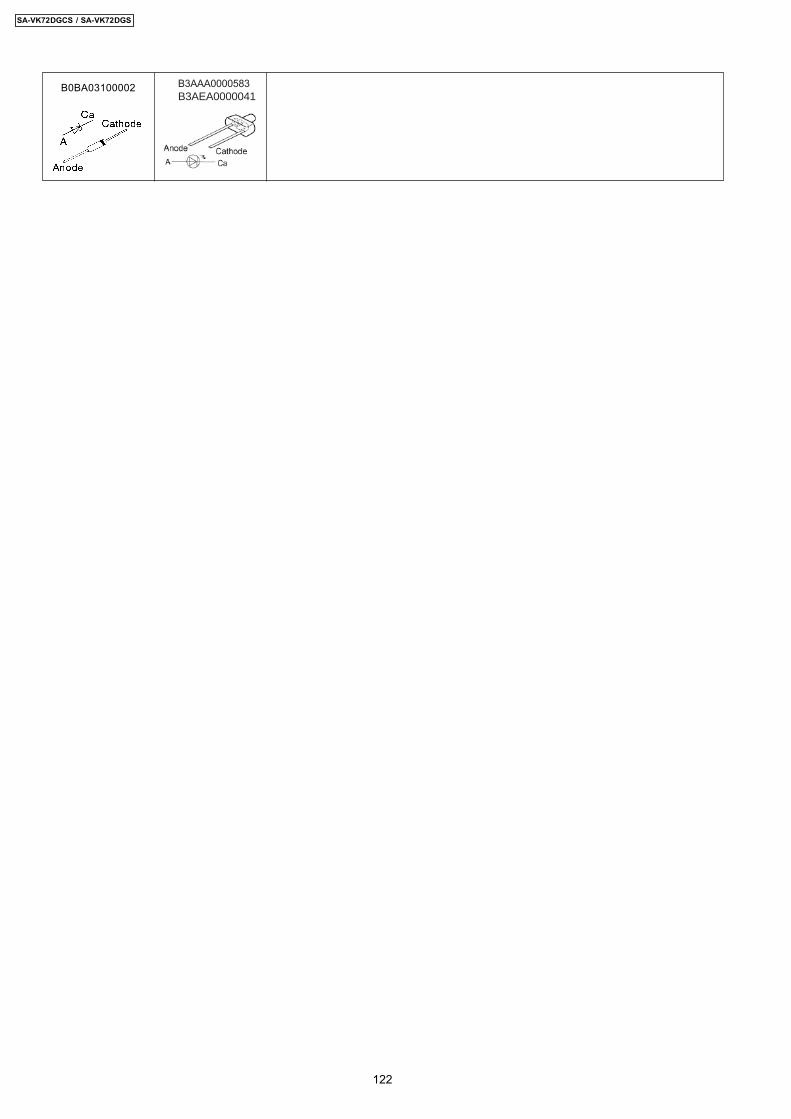
B3AAA0000583B3AEA0000041
B0BA03100002
122
SA-VK72DGCS / SA-VK72DGS
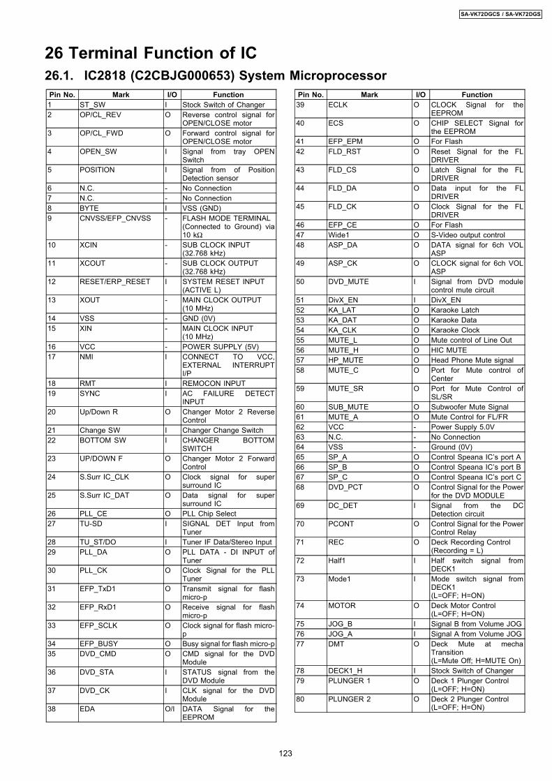
Pin No. Mark I/O Function1 ST_SW I Stock Switch of Changer2 OP/CL_REV O Reverse control signal for
OPEN/CLOSE motor3 OP/CL_FWD O Forward control signal for
OPEN/CLOSE motor4 OPEN_SW I Signal from tray OPEN
Switch5 POSITION I Signal from of Position
Detection sensor6 N.C. - No Connection7 N.C. - No Connection8 BYTE I VSS (GND)9 CNVSS/EFP_CNVSS - FLASH MODE TERMINAL
(Connected to Ground) via10 kΩ
10 XCIN - SUB CLOCK INPUT(32.768 kHz)
11 XCOUT - SUB CLOCK OUTPUT(32.768 kHz)
12 RESET/ERP_RESET I SYSTEM RESET INPUT(ACTIVE L)
13 XOUT - MAIN CLOCK OUTPUT(10 MHz)
14 VSS - GND (0V)15 XIN - MAIN CLOCK INPUT
(10 MHz)16 VCC - POWER SUPPLY (5V)17 NMI I CONNECT TO VCC,
EXTERNAL INTERRUPTI/P
18 RMT I REMOCON INPUT19 SYNC I AC FAILURE DETECT
INPUT20 Up/Down R O Changer Motor 2 Reverse
Control21 Change SW I Changer Change Switch22 BOTTOM SW I CHANGER BOTTOM
SWITCH23 UP/DOWN F O Changer Motor 2 Forward
Control24 S.Surr IC_CLK O Clock signal for super
surround IC25 S.Surr IC_DAT O Data signal for super
surround IC26 PLL_CE O PLL Chip Select27 TU-SD I SIGNAL DET Input from
Tuner28 TU_ST/DO I Tuner IF Data/Stereo Input29 PLL_DA O PLL DATA - DI INPUT of
Tuner30 PLL_CK O Clock Signal for the PLL
Tuner31 EFP_TxD1 O Transmit signal for flash
micro-p32 EFP_RxD1 O Receive signal for flash
micro-p33 EFP_SCLK O Clock signal for flash micro-
p34 EFP_BUSY O Busy signal for flash micro-p35 DVD_CMD O CMD signal for the DVD
Module36 DVD_STA I STATUS signal from the
DVD Module37 DVD_CK I CLK signal for the DVD
Module38 EDA O/I DATA Signal for the
EEPROM
Pin No. Mark I/O Function39 ECLK O CLOCK Signal for the
EEPROM40 ECS O CHIP SELECT Signal for
the EEPROM41 EFP_EPM O For Flash42 FLD_RST O Reset Signal for the FL
DRIVER43 FLD_CS O Latch Signal for the FL
DRIVER44 FLD_DA O Data input for the FL
DRIVER45 FLD_CK O Clock Signal for the FL
DRIVER46 EFP_CE O For Flash47 Wide1 O S-Video output control48 ASP_DA O DATA signal for 6ch VOL
ASP49 ASP_CK O CLOCK signal for 6ch VOL
ASP50 DVD_MUTE I Signal from DVD module
control mute circuit51 DivX_EN I DivX_EN52 KA_LAT O Karaoke Latch53 KA_DAT O Karaoke Data54 KA_CLK O Karaoke Clock55 MUTE_L O Mute control of Line Out56 MUTE_H O HIC MUTE57 HP_MUTE O Head Phone Mute signal58 MUTE_C O Port for Mute control of
Center59 MUTE_SR O Port for Mute Control of
SL/SR60 SUB_MUTE O Subwoofer Mute Signal61 MUTE_A O Mute Control for FL/FR62 VCC - Power Supply 5.0V63 N.C. - No Connection64 VSS - Ground (0V)65 SP_A O Control Speana IC’s port A66 SP_B O Control Speana IC’s port B67 SP_C O Control Speana IC’s port C68 DVD_PCT O Control Signal for the Power
for the DVD MODULE69 DC_DET I Signal from the DC
Detection circuit70 PCONT O Control Signal for the Power
Control Relay71 REC O Deck Recording Control
(Recording = L)72 Half1 I Half switch signal from
DECK173 Mode1 I Mode switch signal from
DECK1(L=OFF; H=ON)
74 MOTOR O Deck Motor Control(L=OFF; H=ON)
75 JOG_B I Signal B from Volume JOG76 JOG_A I Signal A from Volume JOG77 DMT O Deck Mute at mecha
Transition(L=Mute Off; H=MUTE On)
78 DECK1_H I Stock Switch of Changer79 PLUNGER 1 O Deck 1 Plunger Control
(L=OFF; H=ON)80 PLUNGER 2 O Deck 2 Plunger Control
(L=OFF; H=ON)
26 Terminal Function of IC26.1. IC2818 (C2CBJG000653) System Microprocessor
123
SA-VK72DGCS / SA-VK72DGS
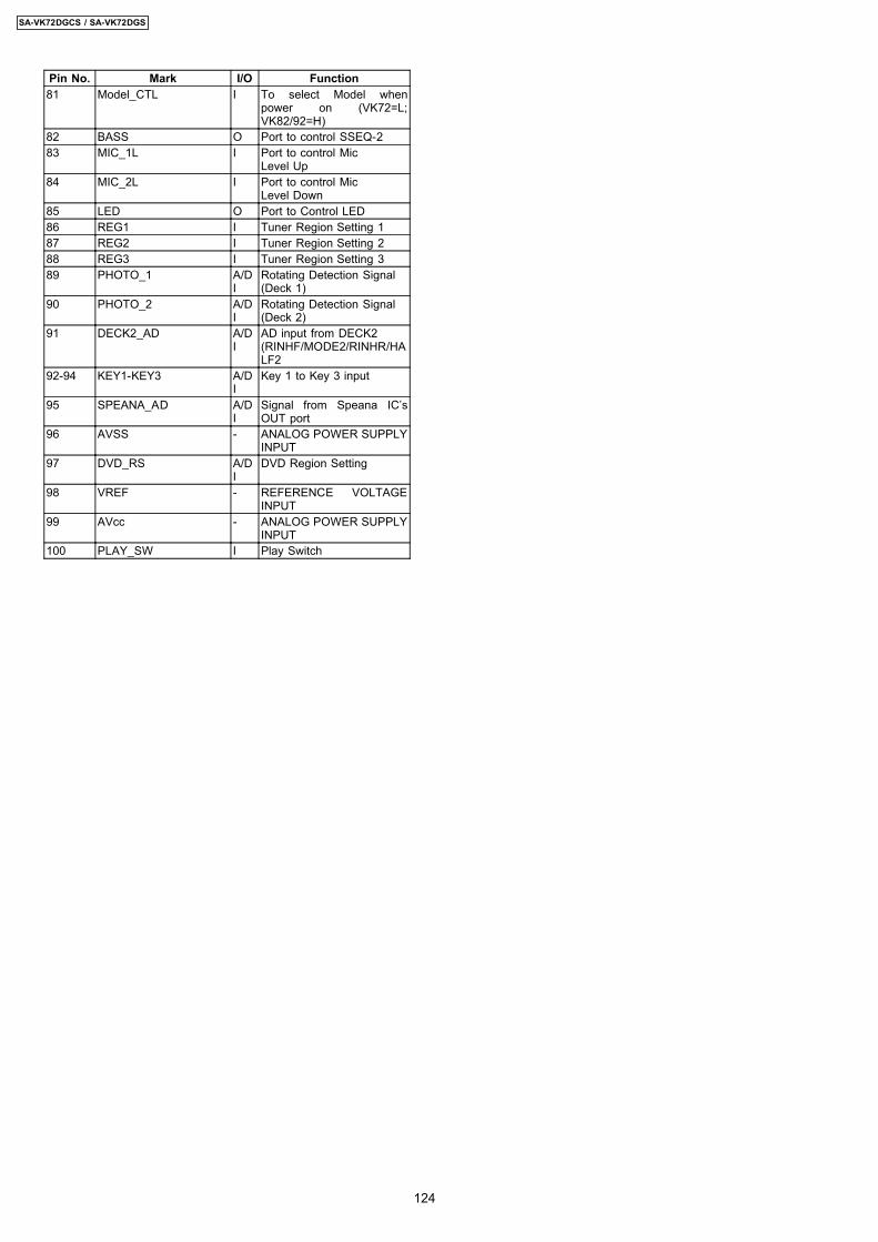
Pin No. Mark I/O Function81 Model_CTL I To select Model when
power on (VK72=L;VK82/92=H)
82 BASS O Port to control SSEQ-283 MIC_1L I Port to control Mic
Level Up84 MIC_2L I Port to control Mic
Level Down85 LED O Port to Control LED86 REG1 I Tuner Region Setting 187 REG2 I Tuner Region Setting 288 REG3 I Tuner Region Setting 389 PHOTO_1 A/D
IRotating Detection Signal(Deck 1)
90 PHOTO_2 A/DI
Rotating Detection Signal(Deck 2)
91 DECK2_AD A/DI
AD input from DECK2(RINHF/MODE2/RINHR/HALF2
92-94 KEY1-KEY3 A/DI
Key 1 to Key 3 input
95 SPEANA_AD A/DI
Signal from Speana IC’sOUT port
96 AVSS - ANALOG POWER SUPPLYINPUT
97 DVD_RS A/DI
DVD Region Setting
98 VREF - REFERENCE VOLTAGEINPUT
99 AVcc - ANALOG POWER SUPPLYINPUT
100 PLAY_SW I Play Switch
124
SA-VK72DGCS / SA-VK72DGS
Notes:
27 Parts Location and Replacement Parts List
· Important safety notice:
Components identified by mark have special characteristics important for safety.Furthermore, special parts which have purposes of fire-retardent (resistors), high-quality sound (capacitors), low noise(resistors), etc are used.When replacing any of these components, be sure to use only manufacturer’s specified parts shown in the parts list.
· The parenthesized indications in the Remarks columns specify the areas or colour. (Refer to the cover page for area or colour)
Parts without these indications can be used for all areas. · Warning: This product uses a laser diode. Refer to caution statements on “Precaution of Laser Diode”. · Capacitor values are in microfarads (µF) unless specified otherwise, P= Pico-farads (pF), F= Farads. · Resistance values are in ohms, unless specified otherwise, 1K=1,000 (OHM). · The marking (RTL) indicates that the Retention Time is limited for this items. After the discontinuation of this assembly in
production, the item will continue to be available for a specific period of time. The retention period of a availability is dependenton the type of assembly, and in accordance with the laws governing part and product retention. After the end of this period, theassembly will no longer be available.
· [M] markings in the Remarks columns indicates parts supplied by PAVCSG. · [SPG] markings in the Remarks columns indicates parts that are supplied by PAVC. · Reference for O/I book languages are as follows:
Ar: Arabic Du: Dutch It: Italian Sp SpanishCf: Canadian French En: English Ko: Korean Sw: SwedishCz: Czech Fr: French Po: Polish Co: Traditional ChineseDa: Danish Ge: German Ru: Russian Cn: Simplified ChinesePe: Persian Ur: Ukraine
125
SA-VK72DGCS / SA-VK72DGS
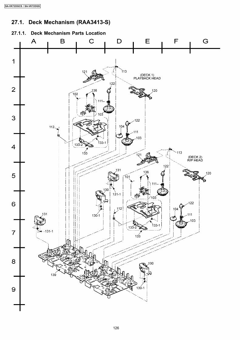
27.1. Deck Mechanism (RAA3413-S)
27.1.1. Deck Mechanism Parts Location
126
SA-VK72DGCS / SA-VK72DGS
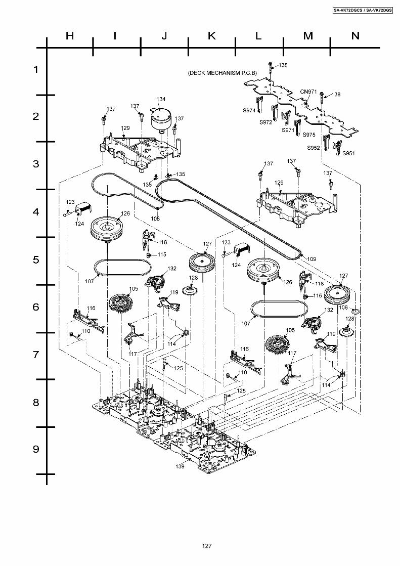
127
SA-VK72DGCS / SA-VK72DGS
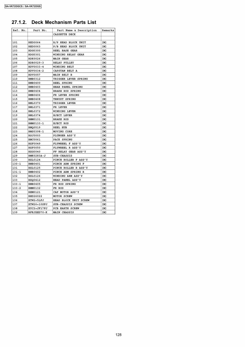
27.1.2. Deck Mechanism Parts ListRef. No. Part No. Part Name & Description Remarks
CASSETTE DECK
101 RED0064 R/P HEAD BLOCK UNIT [M]
102 RED0063 P/B HEAD BLOCK UNIT [M]
103 RDG0300 REEL BASE GEAR [M]
104 RDG0301 WINDING RELAY GEAR [M]
105 RDK0026 MAIN GEAR [M]
106 RDR0029-3 RELAY PULLEY [M]
107 RDV0033-4 WINDING BELT [M]
108 RDV0034-2 CAPSTAN BELT A [M]
109 RDV0057 MAIN BELT B [M]
110 RMB0312 TRIGGER LEVER SPRING [M]
111 RMB0400 REEL SPRING [M]
112 RMB0403 HEAB PANEL SPRING [M]
113 RMB0404 BRAKE ROD SPRING [M]
114 RMB0406 FR LEVER SPRING [M]
115 RMB0408 THRUST SPRING [M]
116 RML0370 TRIGGER LEVER [M]
117 RML0371 FR LEVER [M]
118 RML0372 WINDING LEVER [M]
119 RML0374 EJECT LEVER [M]
120 RMM0131 BRAKE ROD [M]
121 RMM0133-1 EJECT ROD [M]
122 RMQ0519 REEL HUB [M]
123 RMS0398-1 MOVING CORE [M]
124 RSJ0003 PLUNGER ASS’Y [M]
125 RMC0061 PACK SPRING [M]
126 RXF0049 FLYWHEEL F ASS’Y [M]
127 RXF0050 FLYWHEEL R ASS’Y [M]
128 RXG0040 FF RELAY GEAR ASS’Y [M]
129 RMK0283A-J SUB-CHASSIS [M]
130 RXL0124 PINCH ROLLER F ASS’Y [M]
130-1 RMB0401 PINCH ARM SPRING F [M]
131 RXL0125 PINCH ROLLER R ASS’Y [M]
131-1 RMB0402 PINCH ARM SPRING R [M]
132 RXL0126 WINDING ARM ASS’Y [M]
133 RXQ0412 HEAD PANEL ASS’Y [M]
133-1 RMB0405 FR ROD SPRING [M]
133-2 RMM0132 FR ROD [M]
134 REM0121 CAP MOTOR ASS’Y [M]
135 RHD26022 MOTOR SCREW [M]
136 XTW2+5LFJ HEAD BLOCK UNIT SCREW [M]
137 XTW26+10SFJ SUB-CHASSIS SCREW [M]
138 XYC2+JF17FJ PCB EARTH SCREW [M]
139 RFKJXED70-K MAIN CHASSIS [M]
128
SA-VK72DGCS / SA-VK72DGS
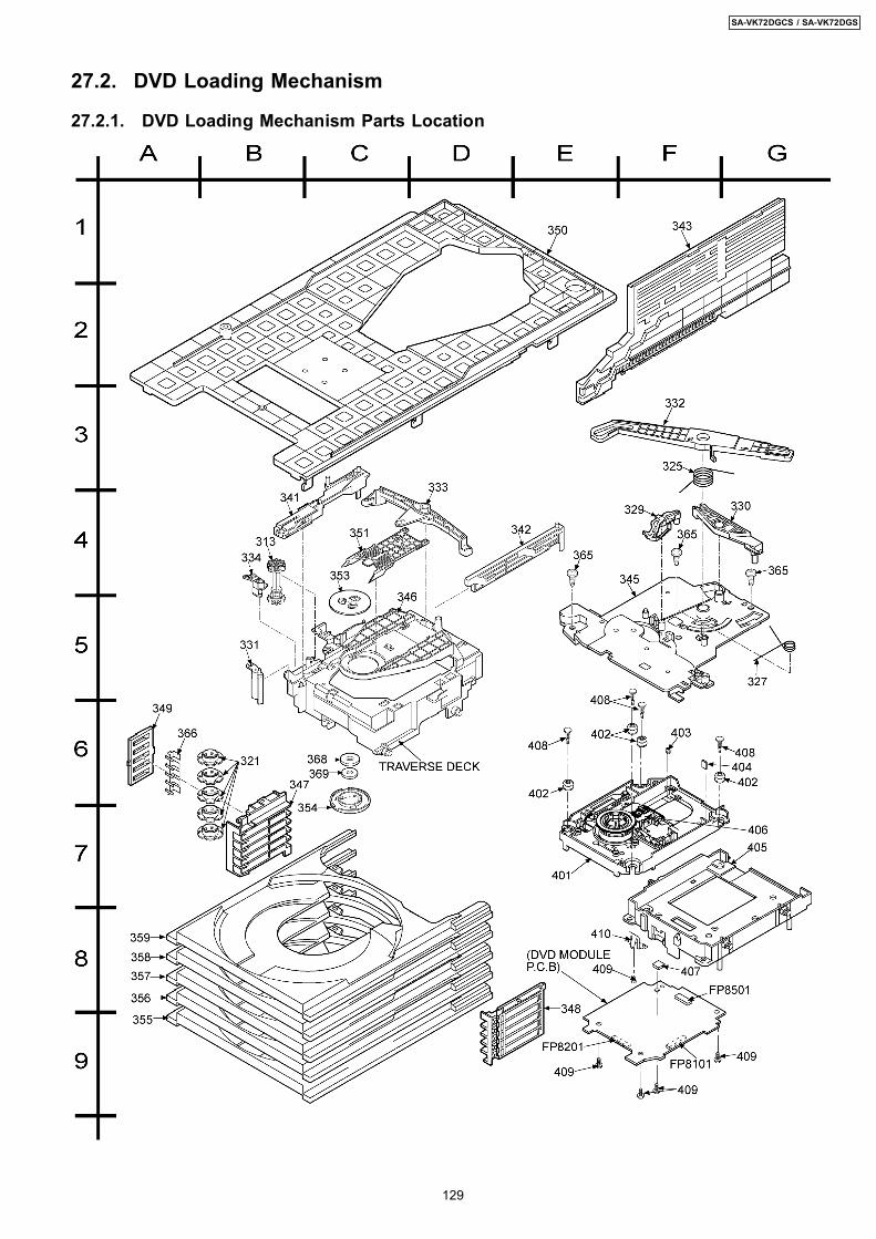
27.2. DVD Loading Mechanism
27.2.1. DVD Loading Mechanism Parts Location
129
SA-VK72DGCS / SA-VK72DGS
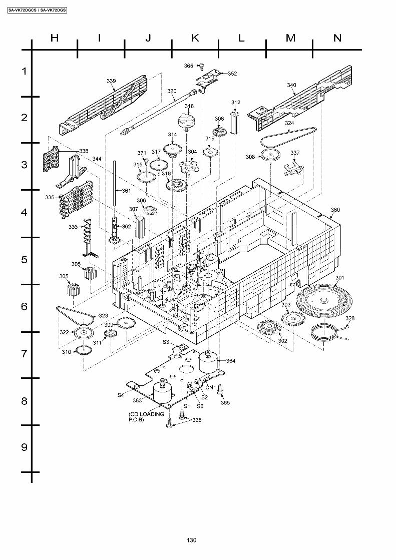
130
SA-VK72DGCS / SA-VK72DGS
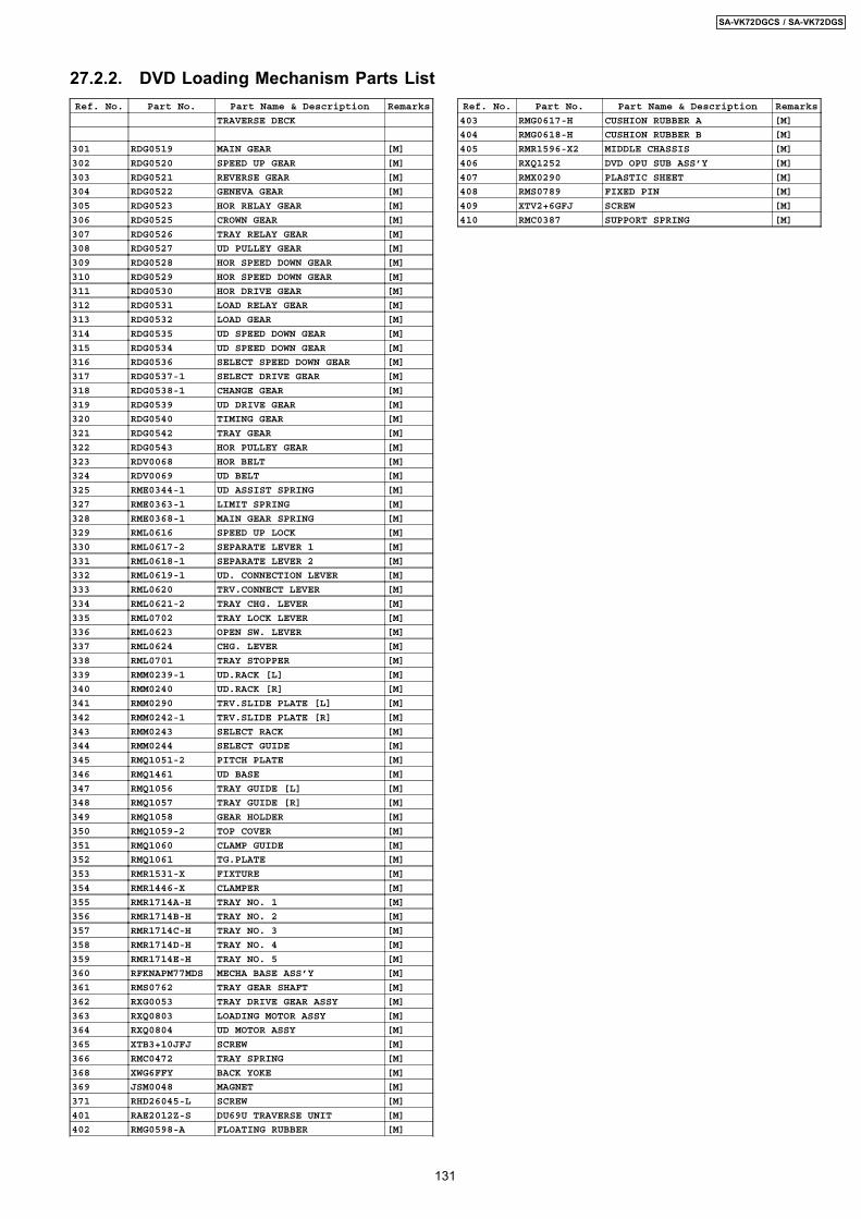
Ref. No. Part No. Part Name & Description Remarks
TRAVERSE DECK
301 RDG0519 MAIN GEAR [M]
302 RDG0520 SPEED UP GEAR [M]
303 RDG0521 REVERSE GEAR [M]
304 RDG0522 GENEVA GEAR [M]
305 RDG0523 HOR RELAY GEAR [M]
306 RDG0525 CROWN GEAR [M]
307 RDG0526 TRAY RELAY GEAR [M]
308 RDG0527 UD PULLEY GEAR [M]
309 RDG0528 HOR SPEED DOWN GEAR [M]
310 RDG0529 HOR SPEED DOWN GEAR [M]
311 RDG0530 HOR DRIVE GEAR [M]
312 RDG0531 LOAD RELAY GEAR [M]
313 RDG0532 LOAD GEAR [M]
314 RDG0535 UD SPEED DOWN GEAR [M]
315 RDG0534 UD SPEED DOWN GEAR [M]
316 RDG0536 SELECT SPEED DOWN GEAR [M]
317 RDG0537-1 SELECT DRIVE GEAR [M]
318 RDG0538-1 CHANGE GEAR [M]
319 RDG0539 UD DRIVE GEAR [M]
320 RDG0540 TIMING GEAR [M]
321 RDG0542 TRAY GEAR [M]
322 RDG0543 HOR PULLEY GEAR [M]
323 RDV0068 HOR BELT [M]
324 RDV0069 UD BELT [M]
325 RME0344-1 UD ASSIST SPRING [M]
327 RME0363-1 LIMIT SPRING [M]
328 RME0368-1 MAIN GEAR SPRING [M]
329 RML0616 SPEED UP LOCK [M]
330 RML0617-2 SEPARATE LEVER 1 [M]
331 RML0618-1 SEPARATE LEVER 2 [M]
332 RML0619-1 UD. CONNECTION LEVER [M]
333 RML0620 TRV.CONNECT LEVER [M]
334 RML0621-2 TRAY CHG. LEVER [M]
335 RML0702 TRAY LOCK LEVER [M]
336 RML0623 OPEN SW. LEVER [M]
337 RML0624 CHG. LEVER [M]
338 RML0701 TRAY STOPPER [M]
339 RMM0239-1 UD.RACK [L] [M]
340 RMM0240 UD.RACK [R] [M]
341 RMM0290 TRV.SLIDE PLATE [L] [M]
342 RMM0242-1 TRV.SLIDE PLATE [R] [M]
343 RMM0243 SELECT RACK [M]
344 RMM0244 SELECT GUIDE [M]
345 RMQ1051-2 PITCH PLATE [M]
346 RMQ1461 UD BASE [M]
347 RMQ1056 TRAY GUIDE [L] [M]
348 RMQ1057 TRAY GUIDE [R] [M]
349 RMQ1058 GEAR HOLDER [M]
350 RMQ1059-2 TOP COVER [M]
351 RMQ1060 CLAMP GUIDE [M]
352 RMQ1061 TG.PLATE [M]
353 RMR1531-X FIXTURE [M]
354 RMR1446-X CLAMPER [M]
355 RMR1714A-H TRAY NO. 1 [M]
356 RMR1714B-H TRAY NO. 2 [M]
357 RMR1714C-H TRAY NO. 3 [M]
358 RMR1714D-H TRAY NO. 4 [M]
359 RMR1714E-H TRAY NO. 5 [M]
360 RFKNAPM77MDS MECHA BASE ASS’Y [M]
361 RMS0762 TRAY GEAR SHAFT [M]
362 RXG0053 TRAY DRIVE GEAR ASSY [M]
363 RXQ0803 LOADING MOTOR ASSY [M]
364 RXQ0804 UD MOTOR ASSY [M]
365 XTB3+10JFJ SCREW [M]
366 RMC0472 TRAY SPRING [M]
368 XWG6FFY BACK YOKE [M]
369 JSM0048 MAGNET [M]
371 RHD26045-L SCREW [M]
401 RAE2012Z-S DU69U TRAVERSE UNIT [M]
402 RMG0598-A FLOATING RUBBER [M]
Ref. No. Part No. Part Name & Description Remarks
403 RMG0617-H CUSHION RUBBER A [M]
404 RMG0618-H CUSHION RUBBER B [M]
405 RMR1596-X2 MIDDLE CHASSIS [M]
406 RXQ1252 DVD OPU SUB ASS’Y [M]
407 RMX0290 PLASTIC SHEET [M]
408 RMS0789 FIXED PIN [M]
409 XTV2+6GFJ SCREW [M]
410 RMC0387 SUPPORT SPRING [M]
27.2.2. DVD Loading Mechanism Parts List
131
SA-VK72DGCS / SA-VK72DGS
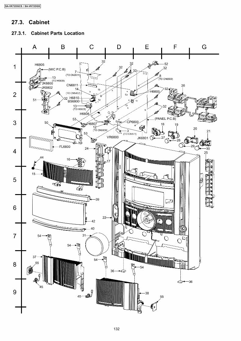
27.3. Cabinet
27.3.1. Cabinet Parts Location
132
SA-VK72DGCS / SA-VK72DGS
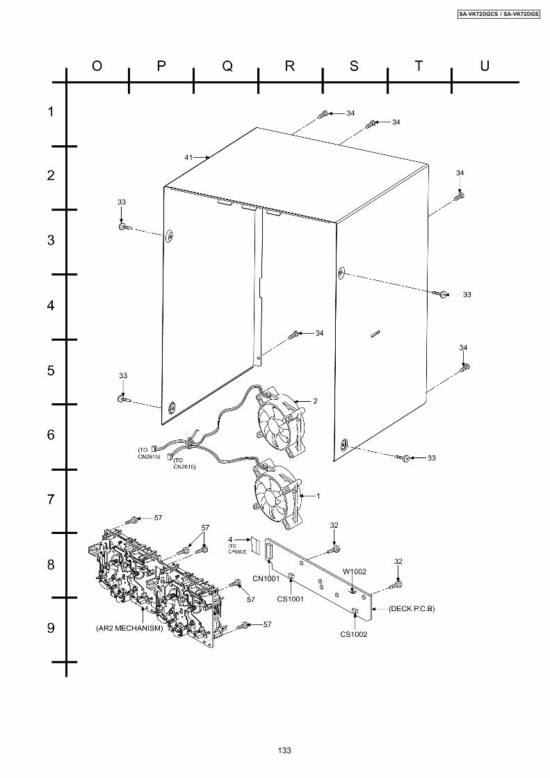
133
SA-VK72DGCS / SA-VK72DGS
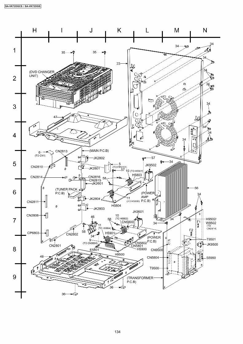
134
SA-VK72DGCS / SA-VK72DGS
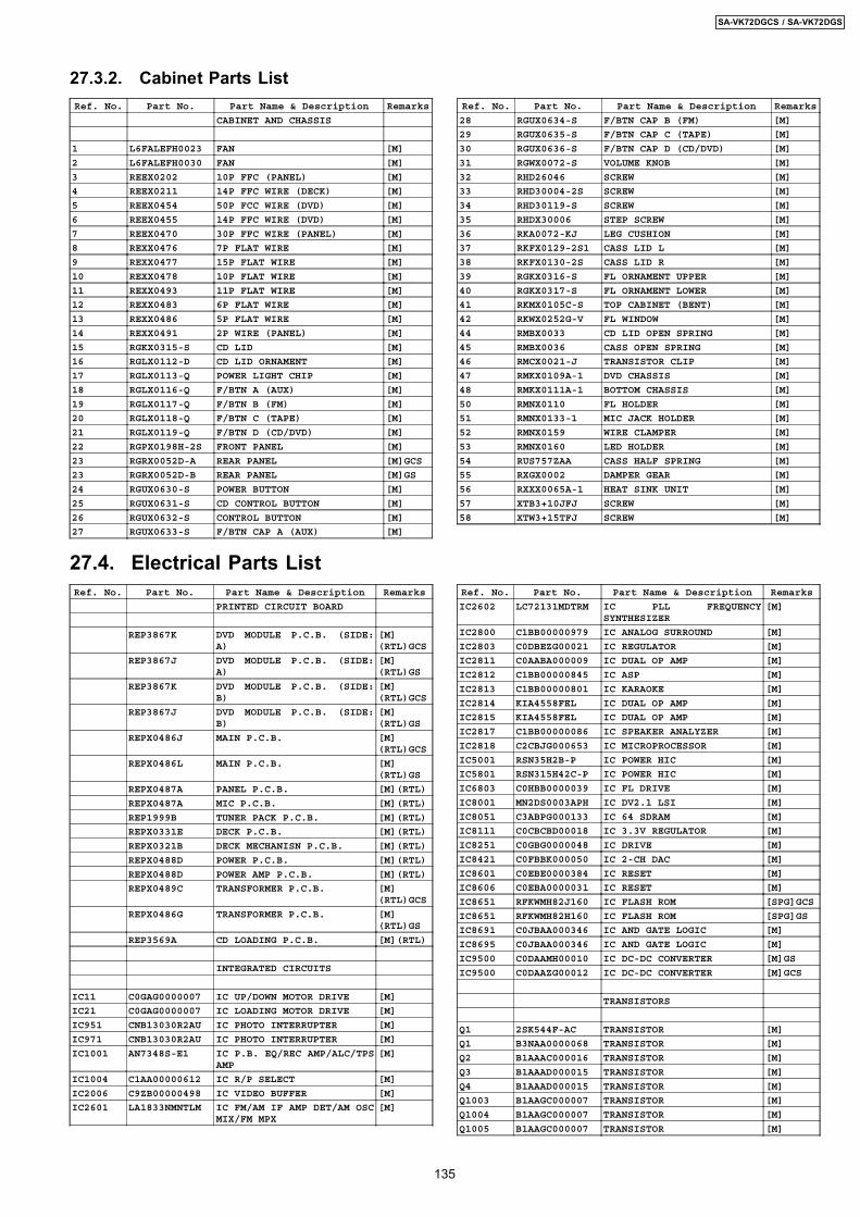
Ref. No. Part No. Part Name & Description Remarks
CABINET AND CHASSIS
1 L6FALEFH0023 FAN [M]
2 L6FALEFH0030 FAN [M]
3 REEX0202 10P FFC (PANEL) [M]
4 REEX0211 14P FFC WIRE (DECK) [M]
5 REEX0454 50P FCC WIRE (DVD) [M]
6 REEX0455 14P FFC WIRE (DVD) [M]
7 REEX0470 30P FFC WIRE (PANEL) [M]
8 REXX0476 7P FLAT WIRE [M]
9 REXX0477 15P FLAT WIRE [M]
10 REXX0478 10P FLAT WIRE [M]
11 REXX0493 11P FLAT WIRE [M]
12 REXX0483 6P FLAT WIRE [M]
13 REXX0486 5P FLAT WIRE [M]
14 REXX0491 2P WIRE (PANEL) [M]
15 RGKX0315-S CD LID [M]
16 RGLX0112-D CD LID ORNAMENT [M]
17 RGLX0113-Q POWER LIGHT CHIP [M]
18 RGLX0116-Q F/BTN A (AUX) [M]
19 RGLX0117-Q F/BTN B (FM) [M]
20 RGLX0118-Q F/BTN C (TAPE) [M]
21 RGLX0119-Q F/BTN D (CD/DVD) [M]
22 RGPX0198H-2S FRONT PANEL [M]
23 RGRX0052D-A REAR PANEL [M]GCS
23 RGRX0052D-B REAR PANEL [M]GS
24 RGUX0630-S POWER BUTTON [M]
25 RGUX0631-S CD CONTROL BUTTON [M]
26 RGUX0632-S CONTROL BUTTON [M]
27 RGUX0633-S F/BTN CAP A (AUX) [M]
Ref. No. Part No. Part Name & Description Remarks
PRINTED CIRCUIT BOARD
REP3867K DVD MODULE P.C.B. (SIDE:A)
[M](RTL)GCS
REP3867J DVD MODULE P.C.B. (SIDE:A)
[M](RTL)GS
REP3867K DVD MODULE P.C.B. (SIDE:B)
[M](RTL)GCS
REP3867J DVD MODULE P.C.B. (SIDE:B)
[M](RTL)GS
REPX0486J MAIN P.C.B. [M](RTL)GCS
REPX0486L MAIN P.C.B. [M](RTL)GS
REPX0487A PANEL P.C.B. [M](RTL)
REPX0487A MIC P.C.B. [M](RTL)
REP1999B TUNER PACK P.C.B. [M](RTL)
REPX0331E DECK P.C.B. [M](RTL)
REPX0321B DECK MECHANISN P.C.B. [M](RTL)
REPX0488D POWER P.C.B. [M](RTL)
REPX0488D POWER AMP P.C.B. [M](RTL)
REPX0489C TRANSFORMER P.C.B. [M](RTL)GCS
REPX0486G TRANSFORMER P.C.B. [M](RTL)GS
REP3569A CD LOADING P.C.B. [M](RTL)
INTEGRATED CIRCUITS
IC11 C0GAG0000007 IC UP/DOWN MOTOR DRIVE [M]
IC21 C0GAG0000007 IC LOADING MOTOR DRIVE [M]
IC951 CNB13030R2AU IC PHOTO INTERRUPTER [M]
IC971 CNB13030R2AU IC PHOTO INTERRUPTER [M]
IC1001 AN7348S-E1 IC P.B. EQ/REC AMP/ALC/TPSAMP
[M]
IC1004 C1AA00000612 IC R/P SELECT [M]
IC2006 C9ZB00000498 IC VIDEO BUFFER [M]
IC2601 LA1833NMNTLM IC FM/AM IF AMP DET/AM OSCMIX/FM MPX
[M]
Ref. No. Part No. Part Name & Description Remarks
28 RGUX0634-S F/BTN CAP B (FM) [M]
29 RGUX0635-S F/BTN CAP C (TAPE) [M]
30 RGUX0636-S F/BTN CAP D (CD/DVD) [M]
31 RGWX0072-S VOLUME KNOB [M]
32 RHD26046 SCREW [M]
33 RHD30004-2S SCREW [M]
34 RHD30119-S SCREW [M]
35 RHDX30006 STEP SCREW [M]
36 RKA0072-KJ LEG CUSHION [M]
37 RKFX0129-2S1 CASS LID L [M]
38 RKFX0130-2S CASS LID R [M]
39 RGKX0316-S FL ORNAMENT UPPER [M]
40 RGKX0317-S FL ORNAMENT LOWER [M]
41 RKMX0105C-S TOP CABINET (BENT) [M]
42 RKWX0252G-V FL WINDOW [M]
44 RMBX0033 CD LID OPEN SPRING [M]
45 RMBX0036 CASS OPEN SPRING [M]
46 RMCX0021-J TRANSISTOR CLIP [M]
47 RMKX0109A-1 DVD CHASSIS [M]
48 RMKX0111A-1 BOTTOM CHASSIS [M]
50 RMNX0110 FL HOLDER [M]
51 RMNX0133-1 MIC JACK HOLDER [M]
52 RMNX0159 WIRE CLAMPER [M]
53 RMNX0160 LED HOLDER [M]
54 RUS757ZAA CASS HALF SPRING [M]
55 RXGX0002 DAMPER GEAR [M]
56 RXXX0065A-1 HEAT SINK UNIT [M]
57 XTB3+10JFJ SCREW [M]
58 XTW3+15TFJ SCREW [M]
Ref. No. Part No. Part Name & Description Remarks
IC2602 LC72131MDTRM IC PLL FREQUENCYSYNTHESIZER
[M]
IC2800 C1BB00000979 IC ANALOG SURROUND [M]
IC2803 C0DBEZG00021 IC REGULATOR [M]
IC2811 C0AABA000009 IC DUAL OP AMP [M]
IC2812 C1BB00000845 IC ASP [M]
IC2813 C1BB00000801 IC KARAOKE [M]
IC2814 KIA4558FEL IC DUAL OP AMP [M]
IC2815 KIA4558FEL IC DUAL OP AMP [M]
IC2817 C1BB00000086 IC SPEAKER ANALYZER [M]
IC2818 C2CBJG000653 IC MICROPROCESSOR [M]
IC5001 RSN35H2B-P IC POWER HIC [M]
IC5801 RSN315H42C-P IC POWER HIC [M]
IC6803 C0HBB0000039 IC FL DRIVE [M]
IC8001 MN2DS0003APH IC DV2.1 LSI [M]
IC8051 C3ABPG000133 IC 64 SDRAM [M]
IC8111 C0CBCBD00018 IC 3.3V REGULATOR [M]
IC8251 C0GBG0000048 IC DRIVE [M]
IC8421 C0FBBK000050 IC 2-CH DAC [M]
IC8601 C0EBE0000384 IC RESET [M]
IC8606 C0EBA0000031 IC RESET [M]
IC8651 RFKWMH82J160 IC FLASH ROM [SPG]GCS
IC8651 RFKWMH82H160 IC FLASH ROM [SPG]GS
IC8691 C0JBAA000346 IC AND GATE LOGIC [M]
IC8695 C0JBAA000346 IC AND GATE LOGIC [M]
IC9500 C0DAAMH00010 IC DC-DC CONVERTER [M]GS
IC9500 C0DAAZG00012 IC DC-DC CONVERTER [M]GCS
TRANSISTORS
Q1 2SK544F-AC TRANSISTOR [M]
Q1 B3NAA0000068 TRANSISTOR [M]
Q2 B1AAAC000016 TRANSISTOR [M]
Q3 B1AAAD000015 TRANSISTOR [M]
Q4 B1AAAD000015 TRANSISTOR [M]
Q1003 B1AAGC000007 TRANSISTOR [M]
Q1004 B1AAGC000007 TRANSISTOR [M]
Q1005 B1AAGC000007 TRANSISTOR [M]
27.3.2. Cabinet Parts List
27.4. Electrical Parts List
135
SA-VK72DGCS / SA-VK72DGS
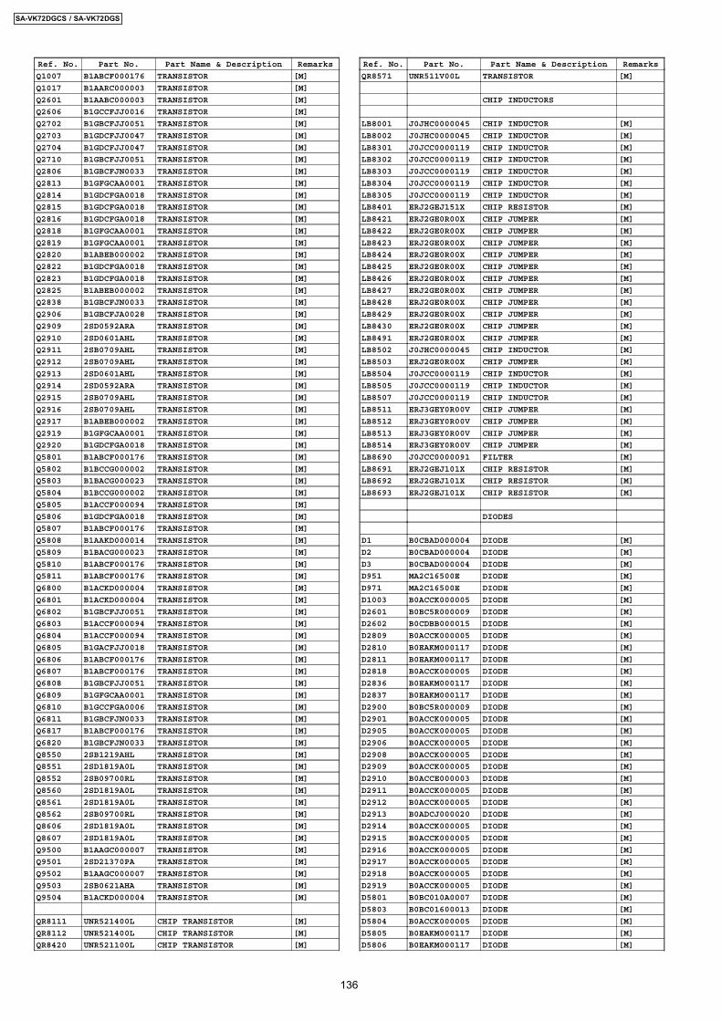
Ref. No. Part No. Part Name & Description Remarks
Q1007 B1ABCF000176 TRANSISTOR [M]
Q1017 B1AARC000003 TRANSISTOR [M]
Q2601 B1AABC000003 TRANSISTOR [M]
Q2606 B1GCCFJJ0016 TRANSISTOR [M]
Q2702 B1GBCFJJ0051 TRANSISTOR [M]
Q2703 B1GDCFJJ0047 TRANSISTOR [M]
Q2704 B1GDCFJJ0047 TRANSISTOR [M]
Q2710 B1GBCFJJ0051 TRANSISTOR [M]
Q2806 B1GBCFJN0033 TRANSISTOR [M]
Q2813 B1GFGCAA0001 TRANSISTOR [M]
Q2814 B1GDCFGA0018 TRANSISTOR [M]
Q2815 B1GDCFGA0018 TRANSISTOR [M]
Q2816 B1GDCFGA0018 TRANSISTOR [M]
Q2818 B1GFGCAA0001 TRANSISTOR [M]
Q2819 B1GFGCAA0001 TRANSISTOR [M]
Q2820 B1ABEB000002 TRANSISTOR [M]
Q2822 B1GDCFGA0018 TRANSISTOR [M]
Q2823 B1GDCFGA0018 TRANSISTOR [M]
Q2825 B1ABEB000002 TRANSISTOR [M]
Q2838 B1GBCFJN0033 TRANSISTOR [M]
Q2906 B1GBCFJA0028 TRANSISTOR [M]
Q2909 2SD0592ARA TRANSISTOR [M]
Q2910 2SD0601AHL TRANSISTOR [M]
Q2911 2SB0709AHL TRANSISTOR [M]
Q2912 2SB0709AHL TRANSISTOR [M]
Q2913 2SD0601AHL TRANSISTOR [M]
Q2914 2SD0592ARA TRANSISTOR [M]
Q2915 2SB0709AHL TRANSISTOR [M]
Q2916 2SB0709AHL TRANSISTOR [M]
Q2917 B1ABEB000002 TRANSISTOR [M]
Q2919 B1GFGCAA0001 TRANSISTOR [M]
Q2920 B1GDCFGA0018 TRANSISTOR [M]
Q5801 B1ABCF000176 TRANSISTOR [M]
Q5802 B1BCCG000002 TRANSISTOR [M]
Q5803 B1BACG000023 TRANSISTOR [M]
Q5804 B1BCCG000002 TRANSISTOR [M]
Q5805 B1ACCF000094 TRANSISTOR [M]
Q5806 B1GDCFGA0018 TRANSISTOR [M]
Q5807 B1ABCF000176 TRANSISTOR [M]
Q5808 B1AAKD000014 TRANSISTOR [M]
Q5809 B1BACG000023 TRANSISTOR [M]
Q5810 B1ABCF000176 TRANSISTOR [M]
Q5811 B1ABCF000176 TRANSISTOR [M]
Q6800 B1ACKD000004 TRANSISTOR [M]
Q6801 B1ACKD000004 TRANSISTOR [M]
Q6802 B1GBCFJJ0051 TRANSISTOR [M]
Q6803 B1ACCF000094 TRANSISTOR [M]
Q6804 B1ACCF000094 TRANSISTOR [M]
Q6805 B1GACFJJ0018 TRANSISTOR [M]
Q6806 B1ABCF000176 TRANSISTOR [M]
Q6807 B1ABCF000176 TRANSISTOR [M]
Q6808 B1GBCFJJ0051 TRANSISTOR [M]
Q6809 B1GFGCAA0001 TRANSISTOR [M]
Q6810 B1GCCFGA0006 TRANSISTOR [M]
Q6811 B1GBCFJN0033 TRANSISTOR [M]
Q6817 B1ABCF000176 TRANSISTOR [M]
Q6820 B1GBCFJN0033 TRANSISTOR [M]
Q8550 2SB1219AHL TRANSISTOR [M]
Q8551 2SD1819A0L TRANSISTOR [M]
Q8552 2SB09700RL TRANSISTOR [M]
Q8560 2SD1819A0L TRANSISTOR [M]
Q8561 2SD1819A0L TRANSISTOR [M]
Q8562 2SB09700RL TRANSISTOR [M]
Q8606 2SD1819A0L TRANSISTOR [M]
Q8607 2SD1819A0L TRANSISTOR [M]
Q9500 B1AAGC000007 TRANSISTOR [M]
Q9501 2SD21370PA TRANSISTOR [M]
Q9502 B1AAGC000007 TRANSISTOR [M]
Q9503 2SB0621AHA TRANSISTOR [M]
Q9504 B1ACKD000004 TRANSISTOR [M]
QR8111 UNR521400L CHIP TRANSISTOR [M]
QR8112 UNR521400L CHIP TRANSISTOR [M]
QR8420 UNR521100L CHIP TRANSISTOR [M]
Ref. No. Part No. Part Name & Description Remarks
QR8571 UNR511V00L TRANSISTOR [M]
CHIP INDUCTORS
LB8001 J0JHC0000045 CHIP INDUCTOR [M]
LB8002 J0JHC0000045 CHIP INDUCTOR [M]
LB8301 J0JCC0000119 CHIP INDUCTOR [M]
LB8302 J0JCC0000119 CHIP INDUCTOR [M]
LB8303 J0JCC0000119 CHIP INDUCTOR [M]
LB8304 J0JCC0000119 CHIP INDUCTOR [M]
LB8305 J0JCC0000119 CHIP INDUCTOR [M]
LB8401 ERJ2GEJ151X CHIP RESISTOR [M]
LB8421 ERJ2GE0R00X CHIP JUMPER [M]
LB8422 ERJ2GE0R00X CHIP JUMPER [M]
LB8423 ERJ2GE0R00X CHIP JUMPER [M]
LB8424 ERJ2GE0R00X CHIP JUMPER [M]
LB8425 ERJ2GE0R00X CHIP JUMPER [M]
LB8426 ERJ2GE0R00X CHIP JUMPER [M]
LB8427 ERJ2GE0R00X CHIP JUMPER [M]
LB8428 ERJ2GE0R00X CHIP JUMPER [M]
LB8429 ERJ2GE0R00X CHIP JUMPER [M]
LB8430 ERJ2GE0R00X CHIP JUMPER [M]
LB8491 ERJ2GE0R00X CHIP JUMPER [M]
LB8502 J0JHC0000045 CHIP INDUCTOR [M]
LB8503 ERJ2GE0R00X CHIP JUMPER [M]
LB8504 J0JCC0000119 CHIP INDUCTOR [M]
LB8505 J0JCC0000119 CHIP INDUCTOR [M]
LB8507 J0JCC0000119 CHIP INDUCTOR [M]
LB8511 ERJ3GEY0R00V CHIP JUMPER [M]
LB8512 ERJ3GEY0R00V CHIP JUMPER [M]
LB8513 ERJ3GEY0R00V CHIP JUMPER [M]
LB8514 ERJ3GEY0R00V CHIP JUMPER [M]
LB8690 J0JCC0000091 FILTER [M]
LB8691 ERJ2GEJ101X CHIP RESISTOR [M]
LB8692 ERJ2GEJ101X CHIP RESISTOR [M]
LB8693 ERJ2GEJ101X CHIP RESISTOR [M]
DIODES
D1 B0CBAD000004 DIODE [M]
D2 B0CBAD000004 DIODE [M]
D3 B0CBAD000004 DIODE [M]
D951 MA2C16500E DIODE [M]
D971 MA2C16500E DIODE [M]
D1003 B0ACCK000005 DIODE [M]
D2601 B0BC5R000009 DIODE [M]
D2602 B0CDBB000015 DIODE [M]
D2809 B0ACCK000005 DIODE [M]
D2810 B0EAKM000117 DIODE [M]
D2811 B0EAKM000117 DIODE [M]
D2818 B0ACCK000005 DIODE [M]
D2836 B0EAKM000117 DIODE [M]
D2837 B0EAKM000117 DIODE [M]
D2900 B0BC5R000009 DIODE [M]
D2901 B0ACCK000005 DIODE [M]
D2905 B0ACCK000005 DIODE [M]
D2906 B0ACCK000005 DIODE [M]
D2908 B0ACCK000005 DIODE [M]
D2909 B0ACCK000005 DIODE [M]
D2910 B0ACCE000003 DIODE [M]
D2911 B0ACCK000005 DIODE [M]
D2912 B0ACCK000005 DIODE [M]
D2913 B0ADCJ000020 DIODE [M]
D2914 B0ACCK000005 DIODE [M]
D2915 B0ACCK000005 DIODE [M]
D2916 B0ACCK000005 DIODE [M]
D2917 B0ACCK000005 DIODE [M]
D2918 B0ACCK000005 DIODE [M]
D2919 B0ACCK000005 DIODE [M]
D5801 B0BC010A0007 DIODE [M]
D5803 B0BC01600013 DIODE [M]
D5804 B0ACCK000005 DIODE [M]
D5805 B0EAKM000117 DIODE [M]
D5806 B0EAKM000117 DIODE [M]
136
SA-VK72DGCS / SA-VK72DGS
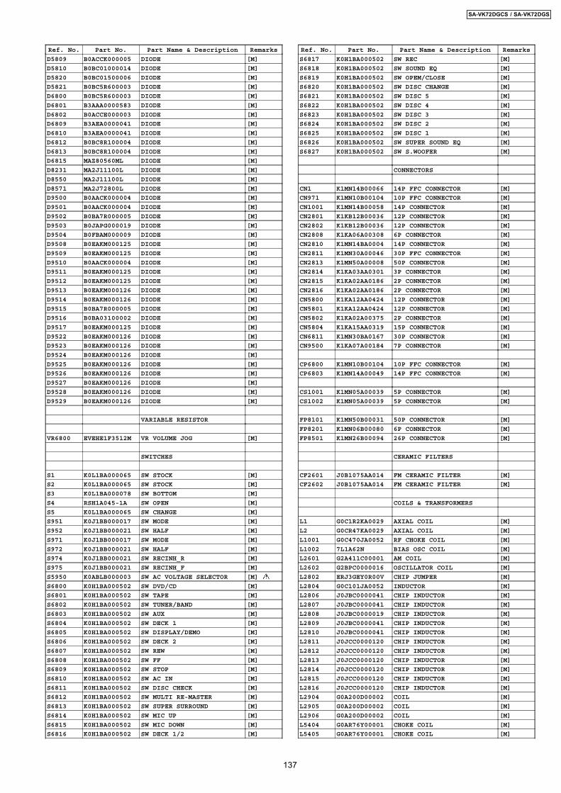
Ref. No. Part No. Part Name & Description Remarks
D5809 B0ACCK000005 DIODE [M]
D5810 B0BC01000014 DIODE [M]
D5820 B0BC01500006 DIODE [M]
D5821 B0BC5R600003 DIODE [M]
D6800 B0BC5R600003 DIODE [M]
D6801 B3AAA0000583 DIODE [M]
D6802 B0ACCE000003 DIODE [M]
D6809 B3AEA0000041 DIODE [M]
D6810 B3AEA0000041 DIODE [M]
D6812 B0BC8R100004 DIODE [M]
D6813 B0BC8R100004 DIODE [M]
D6815 MAZ80560ML DIODE [M]
D8231 MA2J11100L DIODE [M]
D8550 MA2J11100L DIODE [M]
D8571 MA2J72800L DIODE [M]
D9500 B0AACK000004 DIODE [M]
D9501 B0AACK000004 DIODE [M]
D9502 B0BA7R000005 DIODE [M]
D9503 B0JAPG000019 DIODE [M]
D9504 B0FBAM000009 DIODE [M]
D9508 B0EAKM000125 DIODE [M]
D9509 B0EAKM000125 DIODE [M]
D9510 B0AACK000004 DIODE [M]
D9511 B0EAKM000125 DIODE [M]
D9512 B0EAKM000125 DIODE [M]
D9513 B0EAKM000126 DIODE [M]
D9514 B0EAKM000126 DIODE [M]
D9515 B0BA7R000005 DIODE [M]
D9516 B0BA03100002 DIODE [M]
D9517 B0EAKM000125 DIODE [M]
D9522 B0EAKM000126 DIODE [M]
D9523 B0EAKM000126 DIODE [M]
D9524 B0EAKM000126 DIODE [M]
D9525 B0EAKM000126 DIODE [M]
D9526 B0EAKM000126 DIODE [M]
D9527 B0EAKM000126 DIODE [M]
D9528 B0EAKM000126 DIODE [M]
D9529 B0EAKM000126 DIODE [M]
VARIABLE RESISTOR
VR6800 EVEHE1F3512M VR VOLUME JOG [M]
SWITCHES
S1 K0L1BA000065 SW STOCK [M]
S2 K0L1BA000065 SW STOCK [M]
S3 K0L1BA000078 SW BOTTOM [M]
S4 RSH1A045-1A SW OPEN [M]
S5 K0L1BA000065 SW CHANGE [M]
S951 K0J1BB000017 SW MODE [M]
S952 K0J1BB000021 SW HALF [M]
S971 K0J1BB000017 SW MODE [M]
S972 K0J1BB000021 SW HALF [M]
S974 K0J1BB000021 SW RECINH_R [M]
S975 K0J1BB000021 SW RECINH_F [M]
S5950 K0ABLB000003 SW AC VOLTAGE SELECTOR [M]
S6800 K0H1BA000502 SW DVD/CD [M]
S6801 K0H1BA000502 SW TAPE [M]
S6802 K0H1BA000502 SW TUNER/BAND [M]
S6803 K0H1BA000502 SW AUX [M]
S6804 K0H1BA000502 SW DECK 1 [M]
S6805 K0H1BA000502 SW DISPLAY/DEMO [M]
S6806 K0H1BA000502 SW DECK 2 [M]
S6807 K0H1BA000502 SW REW [M]
S6808 K0H1BA000502 SW FF [M]
S6809 K0H1BA000502 SW STOP [M]
S6810 K0H1BA000502 SW AC IN [M]
S6811 K0H1BA000502 SW DISC CHECK [M]
S6812 K0H1BA000502 SW MULTI RE-MASTER [M]
S6813 K0H1BA000502 SW SUPER SURROUND [M]
S6814 K0H1BA000502 SW MIC UP [M]
S6815 K0H1BA000502 SW MIC DOWN [M]
S6816 K0H1BA000502 SW DECK 1/2 [M]
Ref. No. Part No. Part Name & Description Remarks
S6817 K0H1BA000502 SW REC [M]
S6818 K0H1BA000502 SW SOUND EQ [M]
S6819 K0H1BA000502 SW OPEM/CLOSE [M]
S6820 K0H1BA000502 SW DISC CHANGE [M]
S6821 K0H1BA000502 SW DISC 5 [M]
S6822 K0H1BA000502 SW DISC 4 [M]
S6823 K0H1BA000502 SW DISC 3 [M]
S6824 K0H1BA000502 SW DISC 2 [M]
S6825 K0H1BA000502 SW DISC 1 [M]
S6826 K0H1BA000502 SW SUPER SOUND EQ [M]
S6827 K0H1BA000502 SW S.WOOFER [M]
CONNECTORS
CN1 K1MN14B00066 14P FFC CONNECTOR [M]
CN971 K1MN10B00104 10P FFC CONNECTOR [M]
CN1001 K1MN14B00058 14P CONNECTOR [M]
CN2801 K1KB12B00036 12P CONNECTOR [M]
CN2802 K1KB12B00036 12P CONNECTOR [M]
CN2808 K1KA06A00308 6P CONNECTOR [M]
CN2810 K1MN14BA0004 14P CONNECTOR [M]
CN2811 K1MN30A00046 30P FFC CONNECTOR [M]
CN2813 K1MN50A00008 50P CONNECTOR [M]
CN2814 K1KA03AA0301 3P CONNECTOR [M]
CN2815 K1KA02AA0186 2P CONNECTOR [M]
CN2816 K1KA02AA0186 2P CONNECTOR [M]
CN5800 K1KA12AA0424 12P CONNECTOR [M]
CN5801 K1KA12AA0424 12P CONNECTOR [M]
CN5802 K1KA02A00375 2P CONNECTOR [M]
CN5804 K1KA15AA0319 15P CONNECTOR [M]
CN6811 K1MN30BA0167 30P CONNECTOR [M]
CN9500 K1KA07A00184 7P CONNECTOR [M]
CP6800 K1MN10B00104 10P FFC CONNECTOR [M]
CP6803 K1MN14A00049 14P FFC CONNECTOR [M]
CS1001 K1MN05A00039 5P CONNECTOR [M]
CS1002 K1MN05A00039 5P CONNECTOR [M]
FP8101 K1MN50B00031 50P CONNECTOR [M]
FP8201 K1MN06B00080 6P CONNECTOR [M]
FP8501 K1MN26B00094 26P CONNECTOR [M]
CERAMIC FILTERS
CF2601 J0B1075AA014 FM CERAMIC FILTER [M]
CF2602 J0B1075AA014 FM CERAMIC FILTER [M]
COILS & TRANSFORMERS
L1 G0C1R2KA0029 AXIAL COIL [M]
L2 G0CR47KA0029 AXIAL COIL [M]
L1001 G0C470JA0052 RF CHOKE COIL [M]
L1002 7L1A62N BIAS OSC COIL [M]
L2601 G2A411C00001 AM COIL [M]
L2602 G2BPC0000016 OSCILLATOR COIL [M]
L2802 ERJ3GEY0R00V CHIP JUMPER [M]
L2804 G0C101JA0052 INDUCTOR [M]
L2806 J0JBC0000041 CHIP INDUCTOR [M]
L2807 J0JBC0000041 CHIP INDUCTOR [M]
L2808 J0JBC0000019 CHIP INDUCTOR [M]
L2809 J0JBC0000041 CHIP INDUCTOR [M]
L2810 J0JBC0000041 CHIP INDUCTOR [M]
L2811 J0JCC0000120 CHIP INDUCTOR [M]
L2812 J0JCC0000120 CHIP INDUCTOR [M]
L2813 J0JCC0000120 CHIP INDUCTOR [M]
L2814 J0JCC0000120 CHIP INDUCTOR [M]
L2815 J0JCC0000120 CHIP INDUCTOR [M]
L2816 J0JCC0000120 CHIP INDUCTOR [M]
L2904 G0A200D00002 COIL [M]
L2905 G0A200D00002 COIL [M]
L2906 G0A200D00002 COIL [M]
L5404 G0AR76Y00001 CHOKE COIL [M]
L5405 G0AR76Y00001 CHOKE COIL [M]
137
SA-VK72DGCS / SA-VK72DGS
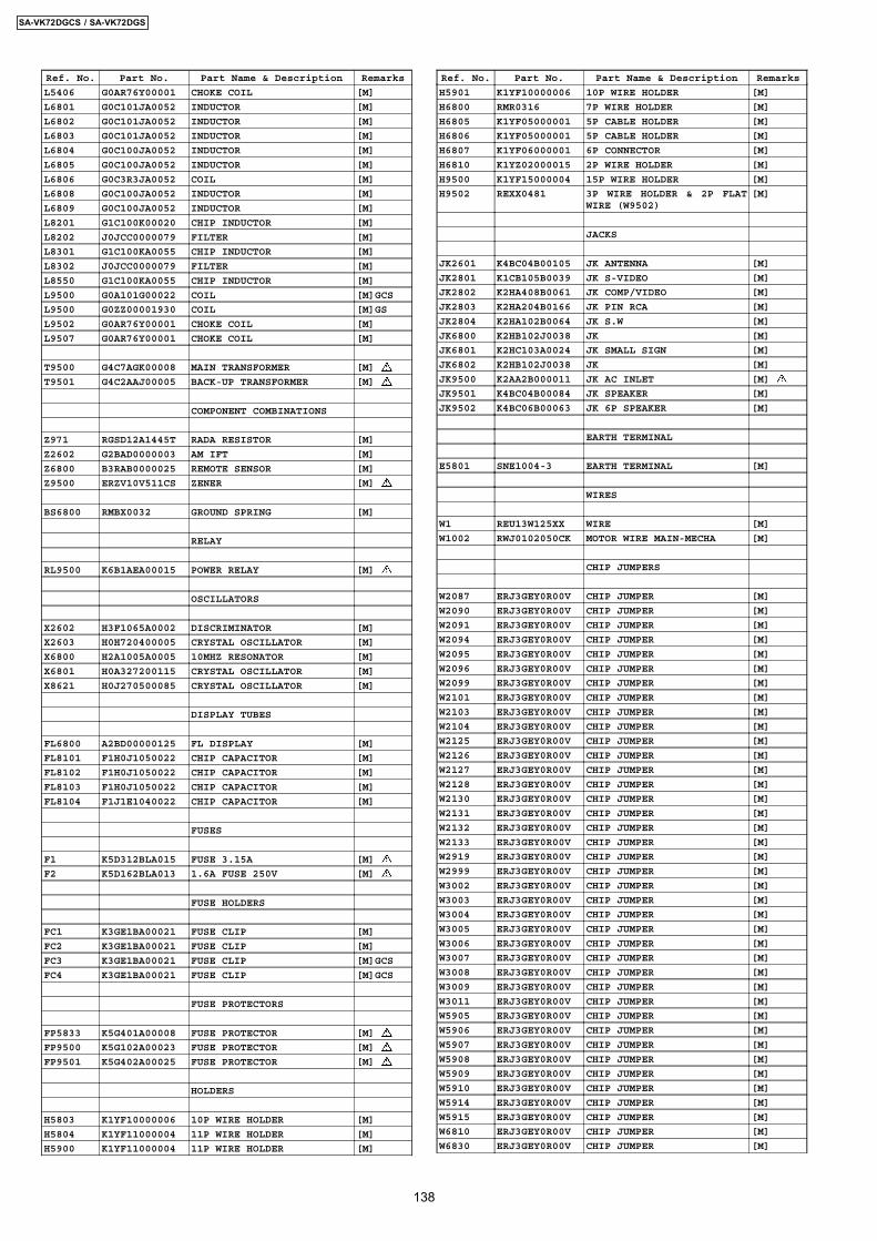
Ref. No. Part No. Part Name & Description Remarks
L5406 G0AR76Y00001 CHOKE COIL [M]
L6801 G0C101JA0052 INDUCTOR [M]
L6802 G0C101JA0052 INDUCTOR [M]
L6803 G0C101JA0052 INDUCTOR [M]
L6804 G0C100JA0052 INDUCTOR [M]
L6805 G0C100JA0052 INDUCTOR [M]
L6806 G0C3R3JA0052 COIL [M]
L6808 G0C100JA0052 INDUCTOR [M]
L6809 G0C100JA0052 INDUCTOR [M]
L8201 G1C100K00020 CHIP INDUCTOR [M]
L8202 J0JCC0000079 FILTER [M]
L8301 G1C100KA0055 CHIP INDUCTOR [M]
L8302 J0JCC0000079 FILTER [M]
L8550 G1C100KA0055 CHIP INDUCTOR [M]
L9500 G0A101G00022 COIL [M]GCS
L9500 G0ZZ00001930 COIL [M]GS
L9502 G0AR76Y00001 CHOKE COIL [M]
L9507 G0AR76Y00001 CHOKE COIL [M]
T9500 G4C7AGK00008 MAIN TRANSFORMER [M]
T9501 G4C2AAJ00005 BACK-UP TRANSFORMER [M]
COMPONENT COMBINATIONS
Z971 RGSD12A1445T RADA RESISTOR [M]
Z2602 G2BAD0000003 AM IFT [M]
Z6800 B3RAB0000025 REMOTE SENSOR [M]
Z9500 ERZV10V511CS ZENER [M]
BS6800 RMBX0032 GROUND SPRING [M]
RELAY
RL9500 K6B1AEA00015 POWER RELAY [M]
OSCILLATORS
X2602 H3F1065A0002 DISCRIMINATOR [M]
X2603 H0H720400005 CRYSTAL OSCILLATOR [M]
X6800 H2A1005A0005 10MHZ RESONATOR [M]
X6801 H0A327200115 CRYSTAL OSCILLATOR [M]
X8621 H0J270500085 CRYSTAL OSCILLATOR [M]
DISPLAY TUBES
FL6800 A2BD00000125 FL DISPLAY [M]
FL8101 F1H0J1050022 CHIP CAPACITOR [M]
FL8102 F1H0J1050022 CHIP CAPACITOR [M]
FL8103 F1H0J1050022 CHIP CAPACITOR [M]
FL8104 F1J1E1040022 CHIP CAPACITOR [M]
FUSES
F1 K5D312BLA015 FUSE 3.15A [M]
F2 K5D162BLA013 1.6A FUSE 250V [M]
FUSE HOLDERS
FC1 K3GE1BA00021 FUSE CLIP [M]
FC2 K3GE1BA00021 FUSE CLIP [M]
FC3 K3GE1BA00021 FUSE CLIP [M]GCS
FC4 K3GE1BA00021 FUSE CLIP [M]GCS
FUSE PROTECTORS
FP5833 K5G401A00008 FUSE PROTECTOR [M]
FP9500 K5G102A00023 FUSE PROTECTOR [M]
FP9501 K5G402A00025 FUSE PROTECTOR [M]
HOLDERS
H5803 K1YF10000006 10P WIRE HOLDER [M]
H5804 K1YF11000004 11P WIRE HOLDER [M]
H5900 K1YF11000004 11P WIRE HOLDER [M]
Ref. No. Part No. Part Name & Description Remarks
H5901 K1YF10000006 10P WIRE HOLDER [M]
H6800 RMR0316 7P WIRE HOLDER [M]
H6805 K1YF05000001 5P CABLE HOLDER [M]
H6806 K1YF05000001 5P CABLE HOLDER [M]
H6807 K1YF06000001 6P CONNECTOR [M]
H6810 K1YZ02000015 2P WIRE HOLDER [M]
H9500 K1YF15000004 15P WIRE HOLDER [M]
H9502 REXX0481 3P WIRE HOLDER & 2P FLATWIRE (W9502)
[M]
JACKS
JK2601 K4BC04B00105 JK ANTENNA [M]
JK2801 K1CB105B0039 JK S-VIDEO [M]
JK2802 K2HA408B0061 JK COMP/VIDEO [M]
JK2803 K2HA204B0166 JK PIN RCA [M]
JK2804 K2HA102B0064 JK S.W [M]
JK6800 K2HB102J0038 JK [M]
JK6801 K2HC103A0024 JK SMALL SIGN [M]
JK6802 K2HB102J0038 JK [M]
JK9500 K2AA2B000011 JK AC INLET [M]
JK9501 K4BC04B00084 JK SPEAKER [M]
JK9502 K4BC06B00063 JK 6P SPEAKER [M]
EARTH TERMINAL
E5801 SNE1004-3 EARTH TERMINAL [M]
WIRES
W1 REU13W125XX WIRE [M]
W1002 RWJ0102050CK MOTOR WIRE MAIN-MECHA [M]
CHIP JUMPERS
W2087 ERJ3GEY0R00V CHIP JUMPER [M]
W2090 ERJ3GEY0R00V CHIP JUMPER [M]
W2091 ERJ3GEY0R00V CHIP JUMPER [M]
W2094 ERJ3GEY0R00V CHIP JUMPER [M]
W2095 ERJ3GEY0R00V CHIP JUMPER [M]
W2096 ERJ3GEY0R00V CHIP JUMPER [M]
W2099 ERJ3GEY0R00V CHIP JUMPER [M]
W2101 ERJ3GEY0R00V CHIP JUMPER [M]
W2103 ERJ3GEY0R00V CHIP JUMPER [M]
W2104 ERJ3GEY0R00V CHIP JUMPER [M]
W2125 ERJ3GEY0R00V CHIP JUMPER [M]
W2126 ERJ3GEY0R00V CHIP JUMPER [M]
W2127 ERJ3GEY0R00V CHIP JUMPER [M]
W2128 ERJ3GEY0R00V CHIP JUMPER [M]
W2130 ERJ3GEY0R00V CHIP JUMPER [M]
W2131 ERJ3GEY0R00V CHIP JUMPER [M]
W2132 ERJ3GEY0R00V CHIP JUMPER [M]
W2133 ERJ3GEY0R00V CHIP JUMPER [M]
W2919 ERJ3GEY0R00V CHIP JUMPER [M]
W2999 ERJ3GEY0R00V CHIP JUMPER [M]
W3002 ERJ3GEY0R00V CHIP JUMPER [M]
W3003 ERJ3GEY0R00V CHIP JUMPER [M]
W3004 ERJ3GEY0R00V CHIP JUMPER [M]
W3005 ERJ3GEY0R00V CHIP JUMPER [M]
W3006 ERJ3GEY0R00V CHIP JUMPER [M]
W3007 ERJ3GEY0R00V CHIP JUMPER [M]
W3008 ERJ3GEY0R00V CHIP JUMPER [M]
W3009 ERJ3GEY0R00V CHIP JUMPER [M]
W3011 ERJ3GEY0R00V CHIP JUMPER [M]
W5905 ERJ3GEY0R00V CHIP JUMPER [M]
W5906 ERJ3GEY0R00V CHIP JUMPER [M]
W5907 ERJ3GEY0R00V CHIP JUMPER [M]
W5908 ERJ3GEY0R00V CHIP JUMPER [M]
W5909 ERJ3GEY0R00V CHIP JUMPER [M]
W5910 ERJ3GEY0R00V CHIP JUMPER [M]
W5914 ERJ3GEY0R00V CHIP JUMPER [M]
W5915 ERJ3GEY0R00V CHIP JUMPER [M]
W6810 ERJ3GEY0R00V CHIP JUMPER [M]
W6830 ERJ3GEY0R00V CHIP JUMPER [M]
138
SA-VK72DGCS / SA-VK72DGS
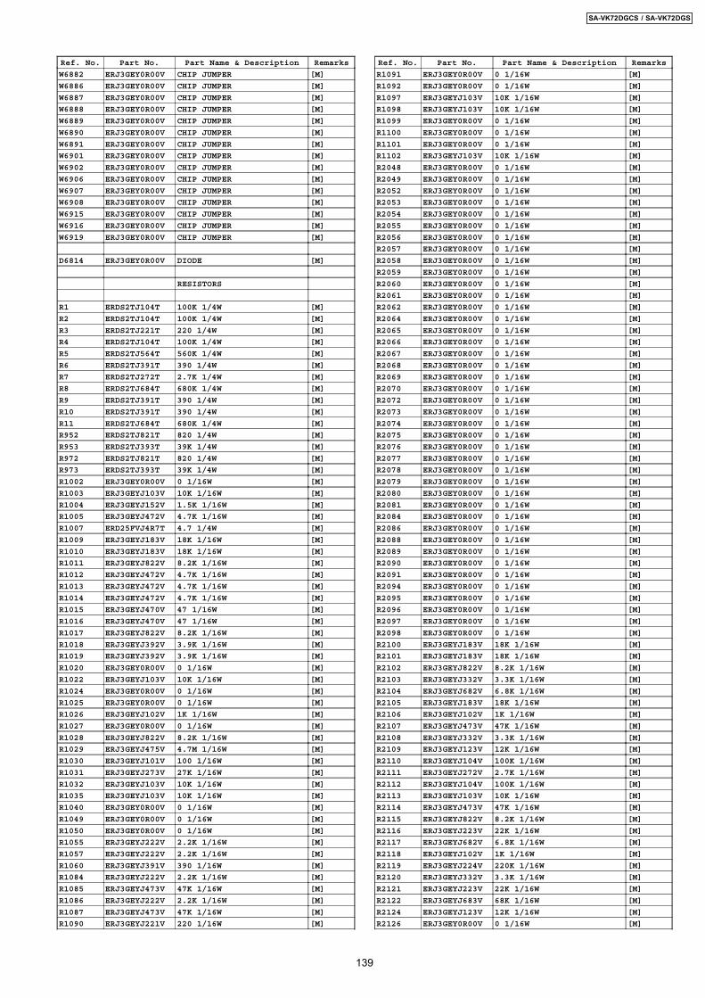
Ref. No. Part No. Part Name & Description Remarks
W6882 ERJ3GEY0R00V CHIP JUMPER [M]
W6886 ERJ3GEY0R00V CHIP JUMPER [M]
W6887 ERJ3GEY0R00V CHIP JUMPER [M]
W6888 ERJ3GEY0R00V CHIP JUMPER [M]
W6889 ERJ3GEY0R00V CHIP JUMPER [M]
W6890 ERJ3GEY0R00V CHIP JUMPER [M]
W6891 ERJ3GEY0R00V CHIP JUMPER [M]
W6901 ERJ3GEY0R00V CHIP JUMPER [M]
W6902 ERJ3GEY0R00V CHIP JUMPER [M]
W6906 ERJ3GEY0R00V CHIP JUMPER [M]
W6907 ERJ3GEY0R00V CHIP JUMPER [M]
W6908 ERJ3GEY0R00V CHIP JUMPER [M]
W6915 ERJ3GEY0R00V CHIP JUMPER [M]
W6916 ERJ3GEY0R00V CHIP JUMPER [M]
W6919 ERJ3GEY0R00V CHIP JUMPER [M]
D6814 ERJ3GEY0R00V DIODE [M]
RESISTORS
R1 ERDS2TJ104T 100K 1/4W [M]
R2 ERDS2TJ104T 100K 1/4W [M]
R3 ERDS2TJ221T 220 1/4W [M]
R4 ERDS2TJ104T 100K 1/4W [M]
R5 ERDS2TJ564T 560K 1/4W [M]
R6 ERDS2TJ391T 390 1/4W [M]
R7 ERDS2TJ272T 2.7K 1/4W [M]
R8 ERDS2TJ684T 680K 1/4W [M]
R9 ERDS2TJ391T 390 1/4W [M]
R10 ERDS2TJ391T 390 1/4W [M]
R11 ERDS2TJ684T 680K 1/4W [M]
R952 ERDS2TJ821T 820 1/4W [M]
R953 ERDS2TJ393T 39K 1/4W [M]
R972 ERDS2TJ821T 820 1/4W [M]
R973 ERDS2TJ393T 39K 1/4W [M]
R1002 ERJ3GEY0R00V 0 1/16W [M]
R1003 ERJ3GEYJ103V 10K 1/16W [M]
R1004 ERJ3GEYJ152V 1.5K 1/16W [M]
R1005 ERJ3GEYJ472V 4.7K 1/16W [M]
R1007 ERD25FVJ4R7T 4.7 1/4W [M]
R1009 ERJ3GEYJ183V 18K 1/16W [M]
R1010 ERJ3GEYJ183V 18K 1/16W [M]
R1011 ERJ3GEYJ822V 8.2K 1/16W [M]
R1012 ERJ3GEYJ472V 4.7K 1/16W [M]
R1013 ERJ3GEYJ472V 4.7K 1/16W [M]
R1014 ERJ3GEYJ472V 4.7K 1/16W [M]
R1015 ERJ3GEYJ470V 47 1/16W [M]
R1016 ERJ3GEYJ470V 47 1/16W [M]
R1017 ERJ3GEYJ822V 8.2K 1/16W [M]
R1018 ERJ3GEYJ392V 3.9K 1/16W [M]
R1019 ERJ3GEYJ392V 3.9K 1/16W [M]
R1020 ERJ3GEY0R00V 0 1/16W [M]
R1022 ERJ3GEYJ103V 10K 1/16W [M]
R1024 ERJ3GEY0R00V 0 1/16W [M]
R1025 ERJ3GEY0R00V 0 1/16W [M]
R1026 ERJ3GEYJ102V 1K 1/16W [M]
R1027 ERJ3GEY0R00V 0 1/16W [M]
R1028 ERJ3GEYJ822V 8.2K 1/16W [M]
R1029 ERJ3GEYJ475V 4.7M 1/16W [M]
R1030 ERJ3GEYJ101V 100 1/16W [M]
R1031 ERJ3GEYJ273V 27K 1/16W [M]
R1032 ERJ3GEYJ103V 10K 1/16W [M]
R1035 ERJ3GEYJ103V 10K 1/16W [M]
R1040 ERJ3GEY0R00V 0 1/16W [M]
R1049 ERJ3GEY0R00V 0 1/16W [M]
R1050 ERJ3GEY0R00V 0 1/16W [M]
R1055 ERJ3GEYJ222V 2.2K 1/16W [M]
R1057 ERJ3GEYJ222V 2.2K 1/16W [M]
R1060 ERJ3GEYJ391V 390 1/16W [M]
R1084 ERJ3GEYJ222V 2.2K 1/16W [M]
R1085 ERJ3GEYJ473V 47K 1/16W [M]
R1086 ERJ3GEYJ222V 2.2K 1/16W [M]
R1087 ERJ3GEYJ473V 47K 1/16W [M]
R1090 ERJ3GEYJ221V 220 1/16W [M]
Ref. No. Part No. Part Name & Description Remarks
R1091 ERJ3GEY0R00V 0 1/16W [M]
R1092 ERJ3GEY0R00V 0 1/16W [M]
R1097 ERJ3GEYJ103V 10K 1/16W [M]
R1098 ERJ3GEYJ103V 10K 1/16W [M]
R1099 ERJ3GEY0R00V 0 1/16W [M]
R1100 ERJ3GEY0R00V 0 1/16W [M]
R1101 ERJ3GEY0R00V 0 1/16W [M]
R1102 ERJ3GEYJ103V 10K 1/16W [M]
R2048 ERJ3GEY0R00V 0 1/16W [M]
R2049 ERJ3GEY0R00V 0 1/16W [M]
R2052 ERJ3GEY0R00V 0 1/16W [M]
R2053 ERJ3GEY0R00V 0 1/16W [M]
R2054 ERJ3GEY0R00V 0 1/16W [M]
R2055 ERJ3GEY0R00V 0 1/16W [M]
R2056 ERJ3GEY0R00V 0 1/16W [M]
R2057 ERJ3GEY0R00V 0 1/16W [M]
R2058 ERJ3GEY0R00V 0 1/16W [M]
R2059 ERJ3GEY0R00V 0 1/16W [M]
R2060 ERJ3GEY0R00V 0 1/16W [M]
R2061 ERJ3GEY0R00V 0 1/16W [M]
R2062 ERJ3GEY0R00V 0 1/16W [M]
R2064 ERJ3GEY0R00V 0 1/16W [M]
R2065 ERJ3GEY0R00V 0 1/16W [M]
R2066 ERJ3GEY0R00V 0 1/16W [M]
R2067 ERJ3GEY0R00V 0 1/16W [M]
R2068 ERJ3GEY0R00V 0 1/16W [M]
R2069 ERJ3GEY0R00V 0 1/16W [M]
R2070 ERJ3GEY0R00V 0 1/16W [M]
R2072 ERJ3GEY0R00V 0 1/16W [M]
R2073 ERJ3GEY0R00V 0 1/16W [M]
R2074 ERJ3GEY0R00V 0 1/16W [M]
R2075 ERJ3GEY0R00V 0 1/16W [M]
R2076 ERJ3GEY0R00V 0 1/16W [M]
R2077 ERJ3GEY0R00V 0 1/16W [M]
R2078 ERJ3GEY0R00V 0 1/16W [M]
R2079 ERJ3GEY0R00V 0 1/16W [M]
R2080 ERJ3GEY0R00V 0 1/16W [M]
R2081 ERJ3GEY0R00V 0 1/16W [M]
R2084 ERJ3GEY0R00V 0 1/16W [M]
R2086 ERJ3GEY0R00V 0 1/16W [M]
R2088 ERJ3GEY0R00V 0 1/16W [M]
R2089 ERJ3GEY0R00V 0 1/16W [M]
R2090 ERJ3GEY0R00V 0 1/16W [M]
R2091 ERJ3GEY0R00V 0 1/16W [M]
R2094 ERJ3GEY0R00V 0 1/16W [M]
R2095 ERJ3GEY0R00V 0 1/16W [M]
R2096 ERJ3GEY0R00V 0 1/16W [M]
R2097 ERJ3GEY0R00V 0 1/16W [M]
R2098 ERJ3GEY0R00V 0 1/16W [M]
R2100 ERJ3GEYJ183V 18K 1/16W [M]
R2101 ERJ3GEYJ183V 18K 1/16W [M]
R2102 ERJ3GEYJ822V 8.2K 1/16W [M]
R2103 ERJ3GEYJ332V 3.3K 1/16W [M]
R2104 ERJ3GEYJ682V 6.8K 1/16W [M]
R2105 ERJ3GEYJ183V 18K 1/16W [M]
R2106 ERJ3GEYJ102V 1K 1/16W [M]
R2107 ERJ3GEYJ473V 47K 1/16W [M]
R2108 ERJ3GEYJ332V 3.3K 1/16W [M]
R2109 ERJ3GEYJ123V 12K 1/16W [M]
R2110 ERJ3GEYJ104V 100K 1/16W [M]
R2111 ERJ3GEYJ272V 2.7K 1/16W [M]
R2112 ERJ3GEYJ104V 100K 1/16W [M]
R2113 ERJ3GEYJ103V 10K 1/16W [M]
R2114 ERJ3GEYJ473V 47K 1/16W [M]
R2115 ERJ3GEYJ822V 8.2K 1/16W [M]
R2116 ERJ3GEYJ223V 22K 1/16W [M]
R2117 ERJ3GEYJ682V 6.8K 1/16W [M]
R2118 ERJ3GEYJ102V 1K 1/16W [M]
R2119 ERJ3GEYJ224V 220K 1/16W [M]
R2120 ERJ3GEYJ332V 3.3K 1/16W [M]
R2121 ERJ3GEYJ223V 22K 1/16W [M]
R2122 ERJ3GEYJ683V 68K 1/16W [M]
R2124 ERJ3GEYJ123V 12K 1/16W [M]
R2126 ERJ3GEY0R00V 0 1/16W [M]
139
SA-VK72DGCS / SA-VK72DGS
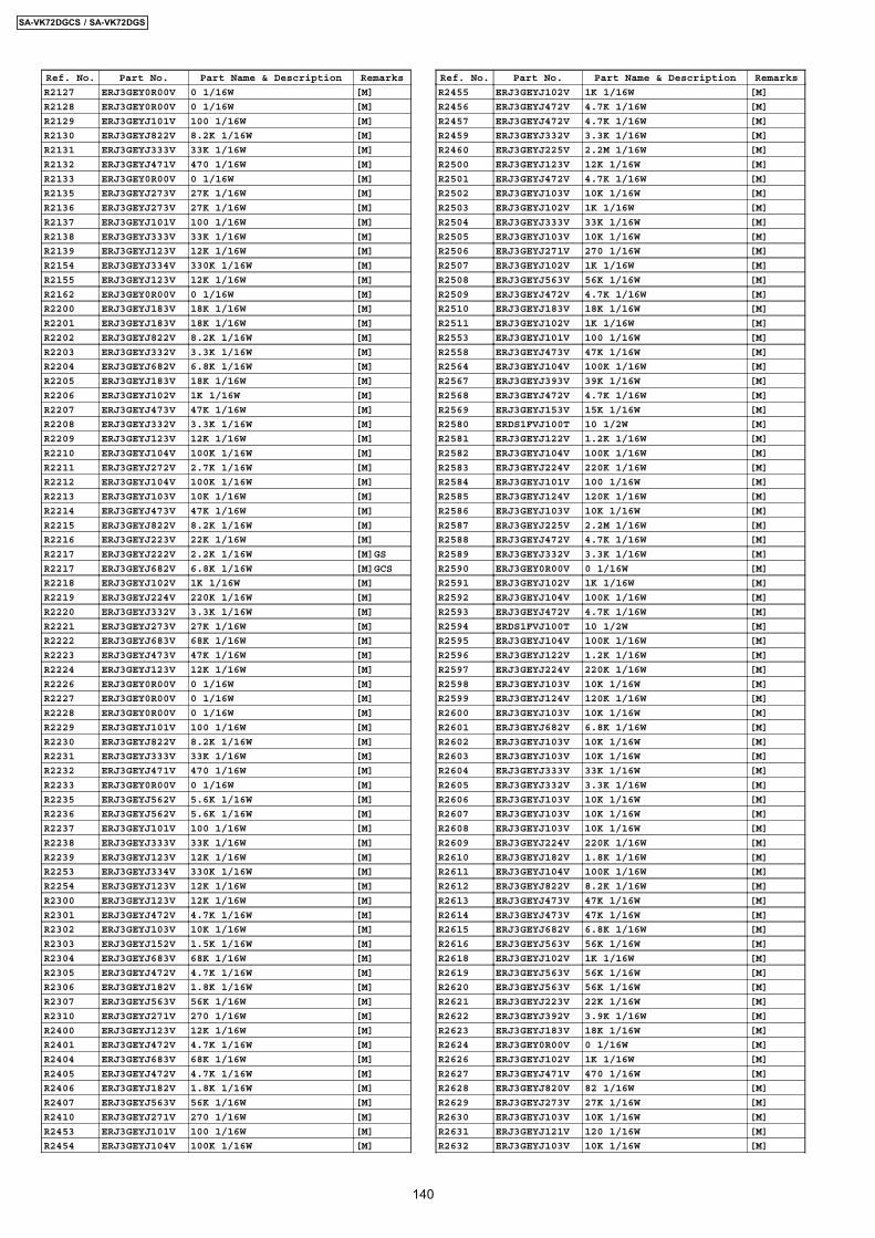
Ref. No. Part No. Part Name & Description Remarks
R2127 ERJ3GEY0R00V 0 1/16W [M]
R2128 ERJ3GEY0R00V 0 1/16W [M]
R2129 ERJ3GEYJ101V 100 1/16W [M]
R2130 ERJ3GEYJ822V 8.2K 1/16W [M]
R2131 ERJ3GEYJ333V 33K 1/16W [M]
R2132 ERJ3GEYJ471V 470 1/16W [M]
R2133 ERJ3GEY0R00V 0 1/16W [M]
R2135 ERJ3GEYJ273V 27K 1/16W [M]
R2136 ERJ3GEYJ273V 27K 1/16W [M]
R2137 ERJ3GEYJ101V 100 1/16W [M]
R2138 ERJ3GEYJ333V 33K 1/16W [M]
R2139 ERJ3GEYJ123V 12K 1/16W [M]
R2154 ERJ3GEYJ334V 330K 1/16W [M]
R2155 ERJ3GEYJ123V 12K 1/16W [M]
R2162 ERJ3GEY0R00V 0 1/16W [M]
R2200 ERJ3GEYJ183V 18K 1/16W [M]
R2201 ERJ3GEYJ183V 18K 1/16W [M]
R2202 ERJ3GEYJ822V 8.2K 1/16W [M]
R2203 ERJ3GEYJ332V 3.3K 1/16W [M]
R2204 ERJ3GEYJ682V 6.8K 1/16W [M]
R2205 ERJ3GEYJ183V 18K 1/16W [M]
R2206 ERJ3GEYJ102V 1K 1/16W [M]
R2207 ERJ3GEYJ473V 47K 1/16W [M]
R2208 ERJ3GEYJ332V 3.3K 1/16W [M]
R2209 ERJ3GEYJ123V 12K 1/16W [M]
R2210 ERJ3GEYJ104V 100K 1/16W [M]
R2211 ERJ3GEYJ272V 2.7K 1/16W [M]
R2212 ERJ3GEYJ104V 100K 1/16W [M]
R2213 ERJ3GEYJ103V 10K 1/16W [M]
R2214 ERJ3GEYJ473V 47K 1/16W [M]
R2215 ERJ3GEYJ822V 8.2K 1/16W [M]
R2216 ERJ3GEYJ223V 22K 1/16W [M]
R2217 ERJ3GEYJ222V 2.2K 1/16W [M]GS
R2217 ERJ3GEYJ682V 6.8K 1/16W [M]GCS
R2218 ERJ3GEYJ102V 1K 1/16W [M]
R2219 ERJ3GEYJ224V 220K 1/16W [M]
R2220 ERJ3GEYJ332V 3.3K 1/16W [M]
R2221 ERJ3GEYJ273V 27K 1/16W [M]
R2222 ERJ3GEYJ683V 68K 1/16W [M]
R2223 ERJ3GEYJ473V 47K 1/16W [M]
R2224 ERJ3GEYJ123V 12K 1/16W [M]
R2226 ERJ3GEY0R00V 0 1/16W [M]
R2227 ERJ3GEY0R00V 0 1/16W [M]
R2228 ERJ3GEY0R00V 0 1/16W [M]
R2229 ERJ3GEYJ101V 100 1/16W [M]
R2230 ERJ3GEYJ822V 8.2K 1/16W [M]
R2231 ERJ3GEYJ333V 33K 1/16W [M]
R2232 ERJ3GEYJ471V 470 1/16W [M]
R2233 ERJ3GEY0R00V 0 1/16W [M]
R2235 ERJ3GEYJ562V 5.6K 1/16W [M]
R2236 ERJ3GEYJ562V 5.6K 1/16W [M]
R2237 ERJ3GEYJ101V 100 1/16W [M]
R2238 ERJ3GEYJ333V 33K 1/16W [M]
R2239 ERJ3GEYJ123V 12K 1/16W [M]
R2253 ERJ3GEYJ334V 330K 1/16W [M]
R2254 ERJ3GEYJ123V 12K 1/16W [M]
R2300 ERJ3GEYJ123V 12K 1/16W [M]
R2301 ERJ3GEYJ472V 4.7K 1/16W [M]
R2302 ERJ3GEYJ103V 10K 1/16W [M]
R2303 ERJ3GEYJ152V 1.5K 1/16W [M]
R2304 ERJ3GEYJ683V 68K 1/16W [M]
R2305 ERJ3GEYJ472V 4.7K 1/16W [M]
R2306 ERJ3GEYJ182V 1.8K 1/16W [M]
R2307 ERJ3GEYJ563V 56K 1/16W [M]
R2310 ERJ3GEYJ271V 270 1/16W [M]
R2400 ERJ3GEYJ123V 12K 1/16W [M]
R2401 ERJ3GEYJ472V 4.7K 1/16W [M]
R2404 ERJ3GEYJ683V 68K 1/16W [M]
R2405 ERJ3GEYJ472V 4.7K 1/16W [M]
R2406 ERJ3GEYJ182V 1.8K 1/16W [M]
R2407 ERJ3GEYJ563V 56K 1/16W [M]
R2410 ERJ3GEYJ271V 270 1/16W [M]
R2453 ERJ3GEYJ101V 100 1/16W [M]
R2454 ERJ3GEYJ104V 100K 1/16W [M]
Ref. No. Part No. Part Name & Description Remarks
R2455 ERJ3GEYJ102V 1K 1/16W [M]
R2456 ERJ3GEYJ472V 4.7K 1/16W [M]
R2457 ERJ3GEYJ472V 4.7K 1/16W [M]
R2459 ERJ3GEYJ332V 3.3K 1/16W [M]
R2460 ERJ3GEYJ225V 2.2M 1/16W [M]
R2500 ERJ3GEYJ123V 12K 1/16W [M]
R2501 ERJ3GEYJ472V 4.7K 1/16W [M]
R2502 ERJ3GEYJ103V 10K 1/16W [M]
R2503 ERJ3GEYJ102V 1K 1/16W [M]
R2504 ERJ3GEYJ333V 33K 1/16W [M]
R2505 ERJ3GEYJ103V 10K 1/16W [M]
R2506 ERJ3GEYJ271V 270 1/16W [M]
R2507 ERJ3GEYJ102V 1K 1/16W [M]
R2508 ERJ3GEYJ563V 56K 1/16W [M]
R2509 ERJ3GEYJ472V 4.7K 1/16W [M]
R2510 ERJ3GEYJ183V 18K 1/16W [M]
R2511 ERJ3GEYJ102V 1K 1/16W [M]
R2553 ERJ3GEYJ101V 100 1/16W [M]
R2558 ERJ3GEYJ473V 47K 1/16W [M]
R2564 ERJ3GEYJ104V 100K 1/16W [M]
R2567 ERJ3GEYJ393V 39K 1/16W [M]
R2568 ERJ3GEYJ472V 4.7K 1/16W [M]
R2569 ERJ3GEYJ153V 15K 1/16W [M]
R2580 ERDS1FVJ100T 10 1/2W [M]
R2581 ERJ3GEYJ122V 1.2K 1/16W [M]
R2582 ERJ3GEYJ104V 100K 1/16W [M]
R2583 ERJ3GEYJ224V 220K 1/16W [M]
R2584 ERJ3GEYJ101V 100 1/16W [M]
R2585 ERJ3GEYJ124V 120K 1/16W [M]
R2586 ERJ3GEYJ103V 10K 1/16W [M]
R2587 ERJ3GEYJ225V 2.2M 1/16W [M]
R2588 ERJ3GEYJ472V 4.7K 1/16W [M]
R2589 ERJ3GEYJ332V 3.3K 1/16W [M]
R2590 ERJ3GEY0R00V 0 1/16W [M]
R2591 ERJ3GEYJ102V 1K 1/16W [M]
R2592 ERJ3GEYJ104V 100K 1/16W [M]
R2593 ERJ3GEYJ472V 4.7K 1/16W [M]
R2594 ERDS1FVJ100T 10 1/2W [M]
R2595 ERJ3GEYJ104V 100K 1/16W [M]
R2596 ERJ3GEYJ122V 1.2K 1/16W [M]
R2597 ERJ3GEYJ224V 220K 1/16W [M]
R2598 ERJ3GEYJ103V 10K 1/16W [M]
R2599 ERJ3GEYJ124V 120K 1/16W [M]
R2600 ERJ3GEYJ103V 10K 1/16W [M]
R2601 ERJ3GEYJ682V 6.8K 1/16W [M]
R2602 ERJ3GEYJ103V 10K 1/16W [M]
R2603 ERJ3GEYJ103V 10K 1/16W [M]
R2604 ERJ3GEYJ333V 33K 1/16W [M]
R2605 ERJ3GEYJ332V 3.3K 1/16W [M]
R2606 ERJ3GEYJ103V 10K 1/16W [M]
R2607 ERJ3GEYJ103V 10K 1/16W [M]
R2608 ERJ3GEYJ103V 10K 1/16W [M]
R2609 ERJ3GEYJ224V 220K 1/16W [M]
R2610 ERJ3GEYJ182V 1.8K 1/16W [M]
R2611 ERJ3GEYJ104V 100K 1/16W [M]
R2612 ERJ3GEYJ822V 8.2K 1/16W [M]
R2613 ERJ3GEYJ473V 47K 1/16W [M]
R2614 ERJ3GEYJ473V 47K 1/16W [M]
R2615 ERJ3GEYJ682V 6.8K 1/16W [M]
R2616 ERJ3GEYJ563V 56K 1/16W [M]
R2618 ERJ3GEYJ102V 1K 1/16W [M]
R2619 ERJ3GEYJ563V 56K 1/16W [M]
R2620 ERJ3GEYJ563V 56K 1/16W [M]
R2621 ERJ3GEYJ223V 22K 1/16W [M]
R2622 ERJ3GEYJ392V 3.9K 1/16W [M]
R2623 ERJ3GEYJ183V 18K 1/16W [M]
R2624 ERJ3GEY0R00V 0 1/16W [M]
R2626 ERJ3GEYJ102V 1K 1/16W [M]
R2627 ERJ3GEYJ471V 470 1/16W [M]
R2628 ERJ3GEYJ820V 82 1/16W [M]
R2629 ERJ3GEYJ273V 27K 1/16W [M]
R2630 ERJ3GEYJ103V 10K 1/16W [M]
R2631 ERJ3GEYJ121V 120 1/16W [M]
R2632 ERJ3GEYJ103V 10K 1/16W [M]
140
SA-VK72DGCS / SA-VK72DGS
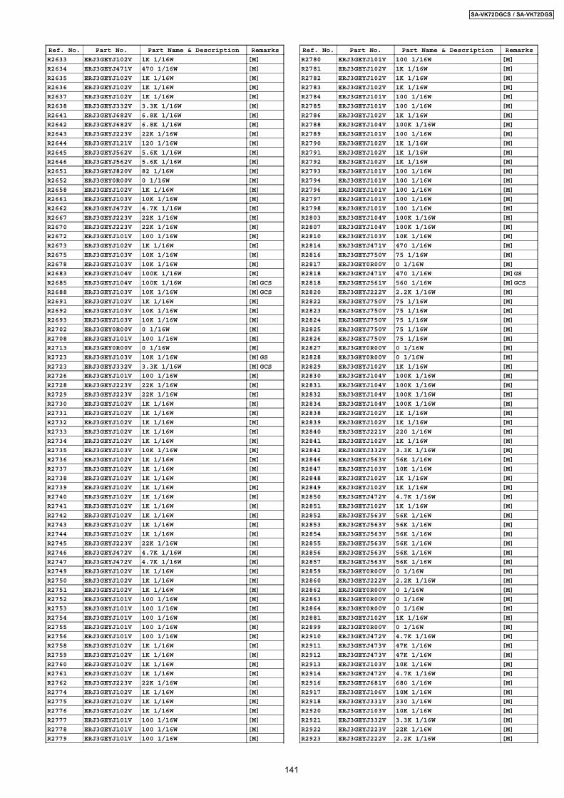
Ref. No. Part No. Part Name & Description Remarks
R2633 ERJ3GEYJ102V 1K 1/16W [M]
R2634 ERJ3GEYJ471V 470 1/16W [M]
R2635 ERJ3GEYJ102V 1K 1/16W [M]
R2636 ERJ3GEYJ102V 1K 1/16W [M]
R2637 ERJ3GEYJ102V 1K 1/16W [M]
R2638 ERJ3GEYJ332V 3.3K 1/16W [M]
R2641 ERJ3GEYJ682V 6.8K 1/16W [M]
R2642 ERJ3GEYJ682V 6.8K 1/16W [M]
R2643 ERJ3GEYJ223V 22K 1/16W [M]
R2644 ERJ3GEYJ121V 120 1/16W [M]
R2645 ERJ3GEYJ562V 5.6K 1/16W [M]
R2646 ERJ3GEYJ562V 5.6K 1/16W [M]
R2651 ERJ3GEYJ820V 82 1/16W [M]
R2652 ERJ3GEY0R00V 0 1/16W [M]
R2658 ERJ3GEYJ102V 1K 1/16W [M]
R2661 ERJ3GEYJ103V 10K 1/16W [M]
R2662 ERJ3GEYJ472V 4.7K 1/16W [M]
R2667 ERJ3GEYJ223V 22K 1/16W [M]
R2670 ERJ3GEYJ223V 22K 1/16W [M]
R2672 ERJ3GEYJ101V 100 1/16W [M]
R2673 ERJ3GEYJ102V 1K 1/16W [M]
R2675 ERJ3GEYJ103V 10K 1/16W [M]
R2678 ERJ3GEYJ103V 10K 1/16W [M]
R2683 ERJ3GEYJ104V 100K 1/16W [M]
R2685 ERJ3GEYJ104V 100K 1/16W [M]GCS
R2688 ERJ3GEYJ103V 10K 1/16W [M]GCS
R2691 ERJ3GEYJ102V 1K 1/16W [M]
R2692 ERJ3GEYJ103V 10K 1/16W [M]
R2693 ERJ3GEYJ103V 10K 1/16W [M]
R2702 ERJ3GEY0R00V 0 1/16W [M]
R2708 ERJ3GEYJ101V 100 1/16W [M]
R2713 ERJ3GEY0R00V 0 1/16W [M]
R2723 ERJ3GEYJ103V 10K 1/16W [M]GS
R2723 ERJ3GEYJ332V 3.3K 1/16W [M]GCS
R2726 ERJ3GEYJ101V 100 1/16W [M]
R2728 ERJ3GEYJ223V 22K 1/16W [M]
R2729 ERJ3GEYJ223V 22K 1/16W [M]
R2730 ERJ3GEYJ102V 1K 1/16W [M]
R2731 ERJ3GEYJ102V 1K 1/16W [M]
R2732 ERJ3GEYJ102V 1K 1/16W [M]
R2733 ERJ3GEYJ102V 1K 1/16W [M]
R2734 ERJ3GEYJ102V 1K 1/16W [M]
R2735 ERJ3GEYJ103V 10K 1/16W [M]
R2736 ERJ3GEYJ102V 1K 1/16W [M]
R2737 ERJ3GEYJ102V 1K 1/16W [M]
R2738 ERJ3GEYJ102V 1K 1/16W [M]
R2739 ERJ3GEYJ102V 1K 1/16W [M]
R2740 ERJ3GEYJ102V 1K 1/16W [M]
R2741 ERJ3GEYJ102V 1K 1/16W [M]
R2742 ERJ3GEYJ102V 1K 1/16W [M]
R2743 ERJ3GEYJ102V 1K 1/16W [M]
R2744 ERJ3GEYJ102V 1K 1/16W [M]
R2745 ERJ3GEYJ223V 22K 1/16W [M]
R2746 ERJ3GEYJ472V 4.7K 1/16W [M]
R2747 ERJ3GEYJ472V 4.7K 1/16W [M]
R2749 ERJ3GEYJ102V 1K 1/16W [M]
R2750 ERJ3GEYJ102V 1K 1/16W [M]
R2751 ERJ3GEYJ102V 1K 1/16W [M]
R2752 ERJ3GEYJ101V 100 1/16W [M]
R2753 ERJ3GEYJ101V 100 1/16W [M]
R2754 ERJ3GEYJ101V 100 1/16W [M]
R2755 ERJ3GEYJ101V 100 1/16W [M]
R2756 ERJ3GEYJ101V 100 1/16W [M]
R2758 ERJ3GEYJ102V 1K 1/16W [M]
R2759 ERJ3GEYJ102V 1K 1/16W [M]
R2760 ERJ3GEYJ102V 1K 1/16W [M]
R2761 ERJ3GEYJ102V 1K 1/16W [M]
R2762 ERJ3GEYJ223V 22K 1/16W [M]
R2774 ERJ3GEYJ102V 1K 1/16W [M]
R2775 ERJ3GEYJ102V 1K 1/16W [M]
R2776 ERJ3GEYJ102V 1K 1/16W [M]
R2777 ERJ3GEYJ101V 100 1/16W [M]
R2778 ERJ3GEYJ101V 100 1/16W [M]
R2779 ERJ3GEYJ101V 100 1/16W [M]
Ref. No. Part No. Part Name & Description Remarks
R2780 ERJ3GEYJ101V 100 1/16W [M]
R2781 ERJ3GEYJ102V 1K 1/16W [M]
R2782 ERJ3GEYJ102V 1K 1/16W [M]
R2783 ERJ3GEYJ102V 1K 1/16W [M]
R2784 ERJ3GEYJ101V 100 1/16W [M]
R2785 ERJ3GEYJ101V 100 1/16W [M]
R2786 ERJ3GEYJ102V 1K 1/16W [M]
R2788 ERJ3GEYJ104V 100K 1/16W [M]
R2789 ERJ3GEYJ101V 100 1/16W [M]
R2790 ERJ3GEYJ102V 1K 1/16W [M]
R2791 ERJ3GEYJ102V 1K 1/16W [M]
R2792 ERJ3GEYJ102V 1K 1/16W [M]
R2793 ERJ3GEYJ101V 100 1/16W [M]
R2794 ERJ3GEYJ101V 100 1/16W [M]
R2796 ERJ3GEYJ101V 100 1/16W [M]
R2797 ERJ3GEYJ101V 100 1/16W [M]
R2798 ERJ3GEYJ101V 100 1/16W [M]
R2803 ERJ3GEYJ104V 100K 1/16W [M]
R2807 ERJ3GEYJ104V 100K 1/16W [M]
R2810 ERJ3GEYJ103V 10K 1/16W [M]
R2814 ERJ3GEYJ471V 470 1/16W [M]
R2816 ERJ3GEYJ750V 75 1/16W [M]
R2817 ERJ3GEY0R00V 0 1/16W [M]
R2818 ERJ3GEYJ471V 470 1/16W [M]GS
R2818 ERJ3GEYJ561V 560 1/16W [M]GCS
R2820 ERJ3GEYJ222V 2.2K 1/16W [M]
R2822 ERJ3GEYJ750V 75 1/16W [M]
R2823 ERJ3GEYJ750V 75 1/16W [M]
R2824 ERJ3GEYJ750V 75 1/16W [M]
R2825 ERJ3GEYJ750V 75 1/16W [M]
R2826 ERJ3GEYJ750V 75 1/16W [M]
R2827 ERJ3GEY0R00V 0 1/16W [M]
R2828 ERJ3GEY0R00V 0 1/16W [M]
R2829 ERJ3GEYJ102V 1K 1/16W [M]
R2830 ERJ3GEYJ104V 100K 1/16W [M]
R2831 ERJ3GEYJ104V 100K 1/16W [M]
R2832 ERJ3GEYJ104V 100K 1/16W [M]
R2834 ERJ3GEYJ104V 100K 1/16W [M]
R2838 ERJ3GEYJ102V 1K 1/16W [M]
R2839 ERJ3GEYJ102V 1K 1/16W [M]
R2840 ERJ3GEYJ221V 220 1/16W [M]
R2841 ERJ3GEYJ102V 1K 1/16W [M]
R2842 ERJ3GEYJ332V 3.3K 1/16W [M]
R2846 ERJ3GEYJ563V 56K 1/16W [M]
R2847 ERJ3GEYJ103V 10K 1/16W [M]
R2848 ERJ3GEYJ102V 1K 1/16W [M]
R2849 ERJ3GEYJ102V 1K 1/16W [M]
R2850 ERJ3GEYJ472V 4.7K 1/16W [M]
R2851 ERJ3GEYJ102V 1K 1/16W [M]
R2852 ERJ3GEYJ563V 56K 1/16W [M]
R2853 ERJ3GEYJ563V 56K 1/16W [M]
R2854 ERJ3GEYJ563V 56K 1/16W [M]
R2855 ERJ3GEYJ563V 56K 1/16W [M]
R2856 ERJ3GEYJ563V 56K 1/16W [M]
R2857 ERJ3GEYJ563V 56K 1/16W [M]
R2859 ERJ3GEY0R00V 0 1/16W [M]
R2860 ERJ3GEYJ222V 2.2K 1/16W [M]
R2862 ERJ3GEY0R00V 0 1/16W [M]
R2863 ERJ3GEY0R00V 0 1/16W [M]
R2864 ERJ3GEY0R00V 0 1/16W [M]
R2881 ERJ3GEYJ102V 1K 1/16W [M]
R2899 ERJ3GEY0R00V 0 1/16W [M]
R2910 ERJ3GEYJ472V 4.7K 1/16W [M]
R2911 ERJ3GEYJ473V 47K 1/16W [M]
R2912 ERJ3GEYJ473V 47K 1/16W [M]
R2913 ERJ3GEYJ103V 10K 1/16W [M]
R2914 ERJ3GEYJ472V 4.7K 1/16W [M]
R2916 ERJ3GEYJ681V 680 1/16W [M]
R2917 ERJ3GEYJ106V 10M 1/16W [M]
R2918 ERJ3GEYJ331V 330 1/16W [M]
R2920 ERJ3GEYJ103V 10K 1/16W [M]
R2921 ERJ3GEYJ332V 3.3K 1/16W [M]
R2922 ERJ3GEYJ223V 22K 1/16W [M]
R2923 ERJ3GEYJ222V 2.2K 1/16W [M]
141
SA-VK72DGCS / SA-VK72DGS
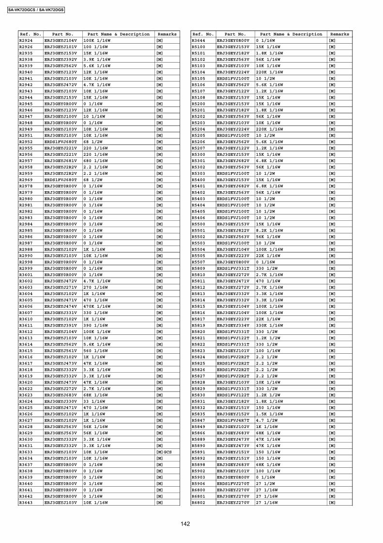
Ref. No. Part No. Part Name & Description Remarks
R2924 ERJ3GEYJ104V 100K 1/16W [M]
R2926 ERJ3GEYJ101V 100 1/16W [M]
R2935 ERJ3GEYJ153V 15K 1/16W [M]
R2938 ERJ3GEYJ392V 3.9K 1/16W [M]
R2939 ERJ3GEYJ562V 5.6K 1/16W [M]
R2940 ERJ3GEYJ123V 12K 1/16W [M]
R2941 ERJ3GEYJ103V 10K 1/16W [M]
R2942 ERJ3GEYJ472V 4.7K 1/16W [M]
R2943 ERJ3GEYJ103V 10K 1/16W [M]
R2944 ERJ3GEYJ153V 15K 1/16W [M]
R2945 ERJ3GEY0R00V 0 1/16W [M]
R2946 ERJ3GEYJ123V 12K 1/16W [M]
R2947 ERJ3GEYJ100V 10 1/16W [M]
R2948 ERJ3GEY0R00V 0 1/16W [M]
R2949 ERJ3GEYJ103V 10K 1/16W [M]
R2951 ERJ3GEYJ103V 10K 1/16W [M]
R2952 ERDS1FVJ680T 68 1/2W [M]
R2955 ERJ3GEYJ221V 220 1/16W [M]
R2956 ERJ3GEYJ221V 220 1/16W [M]
R2957 ERJ3GEYJ681V 680 1/16W [M]
R2958 ERJ3GEYJ2R2V 2.2 1/16W [M]
R2959 ERJ3GEYJ2R2V 2.2 1/16W [M]
R2969 ERDS1FVJ680T 68 1/2W [M]
R2978 ERJ3GEY0R00V 0 1/16W [M]
R2979 ERJ3GEY0R00V 0 1/16W [M]
R2980 ERJ3GEY0R00V 0 1/16W [M]
R2981 ERJ3GEY0R00V 0 1/16W [M]
R2982 ERJ3GEY0R00V 0 1/16W [M]
R2983 ERJ3GEY0R00V 0 1/16W [M]
R2984 ERJ3GEY0R00V 0 1/16W [M]
R2985 ERJ3GEY0R00V 0 1/16W [M]
R2986 ERJ3GEY0R00V 0 1/16W [M]
R2987 ERJ3GEY0R00V 0 1/16W [M]
R2988 ERJ3GEYJ102V 1K 1/16W [M]
R2990 ERJ3GEYJ103V 10K 1/16W [M]
R2998 ERJ3GEY0R00V 0 1/16W [M]
R2999 ERJ3GEY0R00V 0 1/16W [M]
R3601 ERJ3GEY0R00V 0 1/16W [M]
R3602 ERJ3GEYJ472V 4.7K 1/16W [M]
R3603 ERJ3GEYJ271V 270 1/16W [M]
R3604 ERJ3GEYJ102V 1K 1/16W [M]
R3605 ERJ3GEYJ471V 470 1/16W [M]
R3606 ERJ3GEYJ474V 470K 1/16W [M]
R3607 ERJ3GEYJ331V 330 1/16W [M]
R3610 ERJ3GEYJ102V 1K 1/16W [M]
R3611 ERJ3GEYJ391V 390 1/16W [M]
R3612 ERJ3GEYJ104V 100K 1/16W [M]
R3613 ERJ3GEYJ103V 10K 1/16W [M]
R3614 ERJ3GEYJ562V 5.6K 1/16W [M]
R3615 ERJ3GEYJ561V 560 1/16W [M]
R3616 ERJ3GEYJ102V 1K 1/16W [M]
R3617 ERJ3GEYJ473V 47K 1/16W [M]
R3618 ERJ3GEYJ332V 3.3K 1/16W [M]
R3619 ERJ3GEYJ332V 3.3K 1/16W [M]
R3620 ERJ3GEYJ473V 47K 1/16W [M]
R3622 ERJ3GEYJ272V 2.7K 1/16W [M]
R3623 ERJ3GEYJ683V 68K 1/16W [M]
R3624 ERJ3GEYJ330V 33 1/16W [M]
R3625 ERJ3GEYJ471V 470 1/16W [M]
R3626 ERJ3GEYJ102V 1K 1/16W [M]
R3627 ERJ3GEYJ102V 1K 1/16W [M]
R3628 ERJ3GEYJ563V 56K 1/16W [M]
R3629 ERJ3GEYJ563V 56K 1/16W [M]
R3630 ERJ3GEYJ332V 3.3K 1/16W [M]
R3631 ERJ3GEYJ332V 3.3K 1/16W [M]
R3633 ERJ3GEYJ103V 10K 1/16W [M]GCS
R3634 ERJ3GEYJ103V 10K 1/16W [M]
R3637 ERJ3GEY0R00V 0 1/16W [M]
R3638 ERJ3GEY0R00V 0 1/16W [M]
R3639 ERJ3GEY0R00V 0 1/16W [M]
R3640 ERJ3GEY0R00V 0 1/16W [M]
R3641 ERJ3GEY0R00V 0 1/16W [M]
R3642 ERJ3GEY0R00V 0 1/16W [M]
R3643 ERJ3GEYJ103V 10K 1/16W [M]
Ref. No. Part No. Part Name & Description Remarks
R3644 ERJ3GEY0R00V 0 1/16W [M]
R5100 ERJ3GEYJ153V 15K 1/16W [M]
R5101 ERJ3GEYJ182V 1.8K 1/16W [M]
R5102 ERJ3GEYJ563V 56K 1/16W [M]
R5103 ERJ3GEYJ103V 10K 1/16W [M]
R5104 ERJ3GEYJ224V 220K 1/16W [M]
R5105 ERDS1FVJ100T 10 1/2W [M]
R5106 ERJ3GEYJ562V 5.6K 1/16W [M]
R5107 ERJ3GEYJ122V 1.2K 1/16W [M]
R5108 ERJ3GEYJ153V 15K 1/16W [M]
R5200 ERJ3GEYJ153V 15K 1/16W [M]
R5201 ERJ3GEYJ182V 1.8K 1/16W [M]
R5202 ERJ3GEYJ563V 56K 1/16W [M]
R5203 ERJ3GEYJ103V 10K 1/16W [M]
R5204 ERJ3GEYJ224V 220K 1/16W [M]
R5205 ERDS1FVJ100T 10 1/2W [M]
R5206 ERJ3GEYJ562V 5.6K 1/16W [M]
R5207 ERJ3GEYJ122V 1.2K 1/16W [M]
R5300 ERJ3GEYJ153V 15K 1/16W [M]
R5301 ERJ3GEYJ682V 6.8K 1/16W [M]
R5302 ERJ3GEYJ563V 56K 1/16W [M]
R5303 ERDS1FVJ100T 10 1/2W [M]
R5400 ERJ3GEYJ153V 15K 1/16W [M]
R5401 ERJ3GEYJ682V 6.8K 1/16W [M]
R5402 ERJ3GEYJ563V 56K 1/16W [M]
R5403 ERDS1FVJ100T 10 1/2W [M]
R5404 ERDS1FVJ100T 10 1/2W [M]
R5405 ERDS1FVJ100T 10 1/2W [M]
R5406 ERDS1FVJ100T 10 1/2W [M]
R5500 ERJ3GEYJ153V 15K 1/16W [M]
R5501 ERJ3GEYJ822V 8.2K 1/16W [M]
R5502 ERJ3GEYJ563V 56K 1/16W [M]
R5503 ERDS1FVJ100T 10 1/2W [M]
R5504 ERJ3GEYJ104V 100K 1/16W [M]
R5505 ERJ3GEYJ223V 22K 1/16W [M]
R5507 ERJ3GEY0R00V 0 1/16W [M]
R5809 ERDS1FVJ331T 330 1/2W [M]
R5810 ERJ3GEYJ272V 2.7K 1/16W [M]
R5811 ERJ3GEYJ471V 470 1/16W [M]
R5812 ERJ3GEYJ272V 2.7K 1/16W [M]
R5813 ERJ3GEYJ332V 3.3K 1/16W [M]
R5814 ERJ3GEYJ332V 3.3K 1/16W [M]
R5815 ERJ3GEYJ104V 100K 1/16W [M]
R5816 ERJ3GEYJ104V 100K 1/16W [M]
R5817 ERJ3GEYJ223V 22K 1/16W [M]
R5819 ERJ3GEYJ334V 330K 1/16W [M]
R5820 ERDS1FVJ331T 330 1/2W [M]
R5821 ERDS1FVJ122T 1.2K 1/2W [M]
R5822 ERDS1FVJ331T 330 1/2W [M]
R5823 ERJ3GEYJ101V 100 1/16W [M]
R5824 ERDS1FVJ2R2T 2.2 1/2W [M]
R5825 ERDS1FVJ2R2T 2.2 1/2W [M]
R5826 ERDS1FVJ2R2T 2.2 1/2W [M]
R5827 ERDS1FVJ2R2T 2.2 1/2W [M]
R5828 ERJ3GEYJ103V 10K 1/16W [M]
R5829 ERDS1FVJ331T 330 1/2W [M]
R5830 ERDS1FVJ122T 1.2K 1/2W [M]
R5831 ERJ3GEYJ182V 1.8K 1/16W [M]
R5832 ERJ3GEYJ151V 150 1/16W [M]
R5835 ERJ3GEYJ152V 1.5K 1/16W [M]
R5847 ERDS1FVJ4R7T 4.7 1/2W [M]
R5849 ERJ3GEYJ102V 1K 1/16W [M]
R5866 ERJ3GEYJ683V 68K 1/16W [M]
R5889 ERJ3GEYJ473V 47K 1/16W [M]
R5890 ERJ3GEYJ473V 47K 1/16W [M]
R5891 ERJ3GEYJ151V 150 1/16W [M]
R5892 ERJ3GEYJ151V 150 1/16W [M]
R5898 ERJ3GEYJ683V 68K 1/16W [M]
R5902 ERJ3GEYJ101V 100 1/16W [M]
R5903 ERJ3GEY0R00V 0 1/16W [M]
R5906 ERDS1FVJ270T 27 1/2W [M]
R6800 ERJ3GEYJ270V 27 1/16W [M]
R6801 ERJ3GEYJ270V 27 1/16W [M]
R6802 ERJ3GEYJ270V 27 1/16W [M]
142
SA-VK72DGCS / SA-VK72DGS
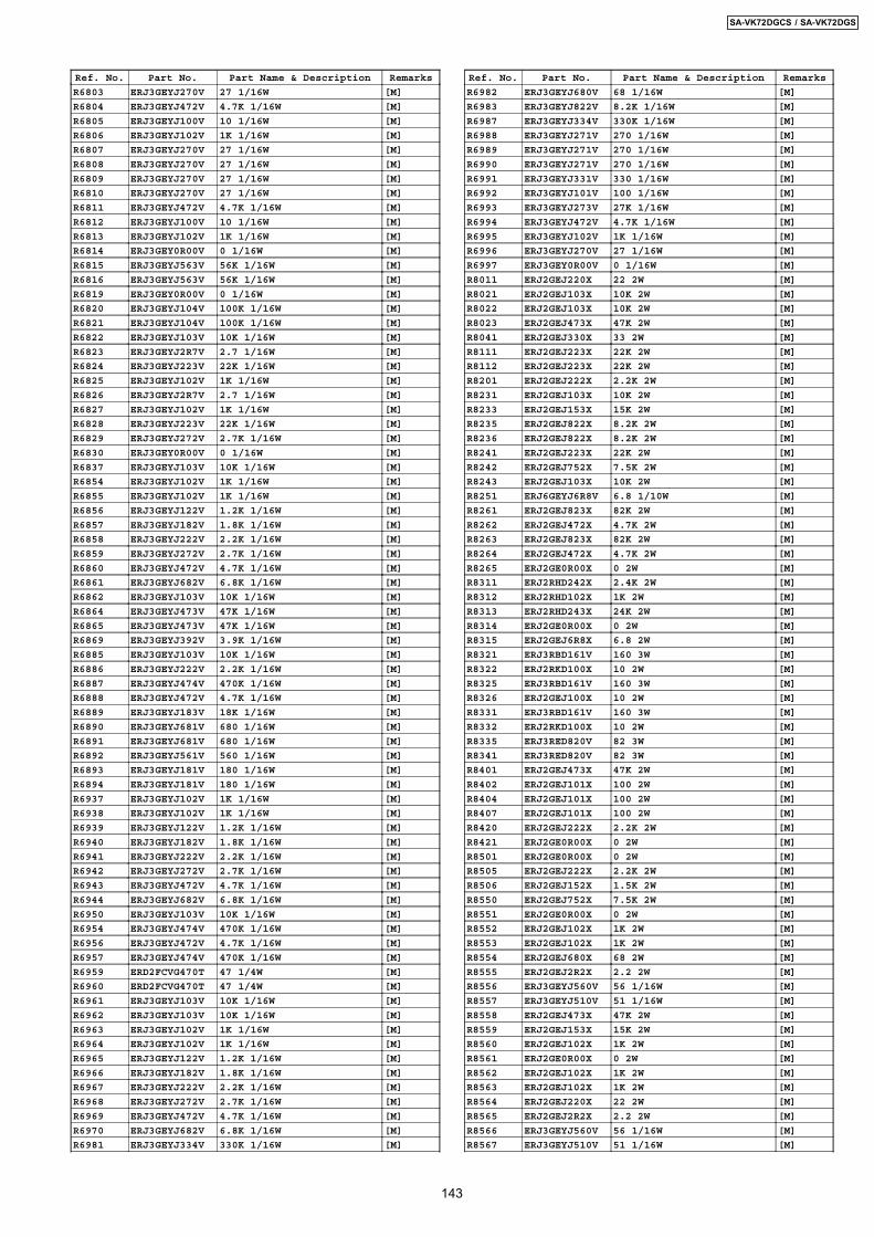
Ref. No. Part No. Part Name & Description Remarks
R6803 ERJ3GEYJ270V 27 1/16W [M]
R6804 ERJ3GEYJ472V 4.7K 1/16W [M]
R6805 ERJ3GEYJ100V 10 1/16W [M]
R6806 ERJ3GEYJ102V 1K 1/16W [M]
R6807 ERJ3GEYJ270V 27 1/16W [M]
R6808 ERJ3GEYJ270V 27 1/16W [M]
R6809 ERJ3GEYJ270V 27 1/16W [M]
R6810 ERJ3GEYJ270V 27 1/16W [M]
R6811 ERJ3GEYJ472V 4.7K 1/16W [M]
R6812 ERJ3GEYJ100V 10 1/16W [M]
R6813 ERJ3GEYJ102V 1K 1/16W [M]
R6814 ERJ3GEY0R00V 0 1/16W [M]
R6815 ERJ3GEYJ563V 56K 1/16W [M]
R6816 ERJ3GEYJ563V 56K 1/16W [M]
R6819 ERJ3GEY0R00V 0 1/16W [M]
R6820 ERJ3GEYJ104V 100K 1/16W [M]
R6821 ERJ3GEYJ104V 100K 1/16W [M]
R6822 ERJ3GEYJ103V 10K 1/16W [M]
R6823 ERJ3GEYJ2R7V 2.7 1/16W [M]
R6824 ERJ3GEYJ223V 22K 1/16W [M]
R6825 ERJ3GEYJ102V 1K 1/16W [M]
R6826 ERJ3GEYJ2R7V 2.7 1/16W [M]
R6827 ERJ3GEYJ102V 1K 1/16W [M]
R6828 ERJ3GEYJ223V 22K 1/16W [M]
R6829 ERJ3GEYJ272V 2.7K 1/16W [M]
R6830 ERJ3GEY0R00V 0 1/16W [M]
R6837 ERJ3GEYJ103V 10K 1/16W [M]
R6854 ERJ3GEYJ102V 1K 1/16W [M]
R6855 ERJ3GEYJ102V 1K 1/16W [M]
R6856 ERJ3GEYJ122V 1.2K 1/16W [M]
R6857 ERJ3GEYJ182V 1.8K 1/16W [M]
R6858 ERJ3GEYJ222V 2.2K 1/16W [M]
R6859 ERJ3GEYJ272V 2.7K 1/16W [M]
R6860 ERJ3GEYJ472V 4.7K 1/16W [M]
R6861 ERJ3GEYJ682V 6.8K 1/16W [M]
R6862 ERJ3GEYJ103V 10K 1/16W [M]
R6864 ERJ3GEYJ473V 47K 1/16W [M]
R6865 ERJ3GEYJ473V 47K 1/16W [M]
R6869 ERJ3GEYJ392V 3.9K 1/16W [M]
R6885 ERJ3GEYJ103V 10K 1/16W [M]
R6886 ERJ3GEYJ222V 2.2K 1/16W [M]
R6887 ERJ3GEYJ474V 470K 1/16W [M]
R6888 ERJ3GEYJ472V 4.7K 1/16W [M]
R6889 ERJ3GEYJ183V 18K 1/16W [M]
R6890 ERJ3GEYJ681V 680 1/16W [M]
R6891 ERJ3GEYJ681V 680 1/16W [M]
R6892 ERJ3GEYJ561V 560 1/16W [M]
R6893 ERJ3GEYJ181V 180 1/16W [M]
R6894 ERJ3GEYJ181V 180 1/16W [M]
R6937 ERJ3GEYJ102V 1K 1/16W [M]
R6938 ERJ3GEYJ102V 1K 1/16W [M]
R6939 ERJ3GEYJ122V 1.2K 1/16W [M]
R6940 ERJ3GEYJ182V 1.8K 1/16W [M]
R6941 ERJ3GEYJ222V 2.2K 1/16W [M]
R6942 ERJ3GEYJ272V 2.7K 1/16W [M]
R6943 ERJ3GEYJ472V 4.7K 1/16W [M]
R6944 ERJ3GEYJ682V 6.8K 1/16W [M]
R6950 ERJ3GEYJ103V 10K 1/16W [M]
R6954 ERJ3GEYJ474V 470K 1/16W [M]
R6956 ERJ3GEYJ472V 4.7K 1/16W [M]
R6957 ERJ3GEYJ474V 470K 1/16W [M]
R6959 ERD2FCVG470T 47 1/4W [M]
R6960 ERD2FCVG470T 47 1/4W [M]
R6961 ERJ3GEYJ103V 10K 1/16W [M]
R6962 ERJ3GEYJ103V 10K 1/16W [M]
R6963 ERJ3GEYJ102V 1K 1/16W [M]
R6964 ERJ3GEYJ102V 1K 1/16W [M]
R6965 ERJ3GEYJ122V 1.2K 1/16W [M]
R6966 ERJ3GEYJ182V 1.8K 1/16W [M]
R6967 ERJ3GEYJ222V 2.2K 1/16W [M]
R6968 ERJ3GEYJ272V 2.7K 1/16W [M]
R6969 ERJ3GEYJ472V 4.7K 1/16W [M]
R6970 ERJ3GEYJ682V 6.8K 1/16W [M]
R6981 ERJ3GEYJ334V 330K 1/16W [M]
Ref. No. Part No. Part Name & Description Remarks
R6982 ERJ3GEYJ680V 68 1/16W [M]
R6983 ERJ3GEYJ822V 8.2K 1/16W [M]
R6987 ERJ3GEYJ334V 330K 1/16W [M]
R6988 ERJ3GEYJ271V 270 1/16W [M]
R6989 ERJ3GEYJ271V 270 1/16W [M]
R6990 ERJ3GEYJ271V 270 1/16W [M]
R6991 ERJ3GEYJ331V 330 1/16W [M]
R6992 ERJ3GEYJ101V 100 1/16W [M]
R6993 ERJ3GEYJ273V 27K 1/16W [M]
R6994 ERJ3GEYJ472V 4.7K 1/16W [M]
R6995 ERJ3GEYJ102V 1K 1/16W [M]
R6996 ERJ3GEYJ270V 27 1/16W [M]
R6997 ERJ3GEY0R00V 0 1/16W [M]
R8011 ERJ2GEJ220X 22 2W [M]
R8021 ERJ2GEJ103X 10K 2W [M]
R8022 ERJ2GEJ103X 10K 2W [M]
R8023 ERJ2GEJ473X 47K 2W [M]
R8041 ERJ2GEJ330X 33 2W [M]
R8111 ERJ2GEJ223X 22K 2W [M]
R8112 ERJ2GEJ223X 22K 2W [M]
R8201 ERJ2GEJ222X 2.2K 2W [M]
R8231 ERJ2GEJ103X 10K 2W [M]
R8233 ERJ2GEJ153X 15K 2W [M]
R8235 ERJ2GEJ822X 8.2K 2W [M]
R8236 ERJ2GEJ822X 8.2K 2W [M]
R8241 ERJ2GEJ223X 22K 2W [M]
R8242 ERJ2GEJ752X 7.5K 2W [M]
R8243 ERJ2GEJ103X 10K 2W [M]
R8251 ERJ6GEYJ6R8V 6.8 1/10W [M]
R8261 ERJ2GEJ823X 82K 2W [M]
R8262 ERJ2GEJ472X 4.7K 2W [M]
R8263 ERJ2GEJ823X 82K 2W [M]
R8264 ERJ2GEJ472X 4.7K 2W [M]
R8265 ERJ2GE0R00X 0 2W [M]
R8311 ERJ2RHD242X 2.4K 2W [M]
R8312 ERJ2RHD102X 1K 2W [M]
R8313 ERJ2RHD243X 24K 2W [M]
R8314 ERJ2GE0R00X 0 2W [M]
R8315 ERJ2GEJ6R8X 6.8 2W [M]
R8321 ERJ3RBD161V 160 3W [M]
R8322 ERJ2RKD100X 10 2W [M]
R8325 ERJ3RBD161V 160 3W [M]
R8326 ERJ2GEJ100X 10 2W [M]
R8331 ERJ3RBD161V 160 3W [M]
R8332 ERJ2RKD100X 10 2W [M]
R8335 ERJ3RED820V 82 3W [M]
R8341 ERJ3RED820V 82 3W [M]
R8401 ERJ2GEJ473X 47K 2W [M]
R8402 ERJ2GEJ101X 100 2W [M]
R8404 ERJ2GEJ101X 100 2W [M]
R8407 ERJ2GEJ101X 100 2W [M]
R8420 ERJ2GEJ222X 2.2K 2W [M]
R8421 ERJ2GE0R00X 0 2W [M]
R8501 ERJ2GE0R00X 0 2W [M]
R8505 ERJ2GEJ222X 2.2K 2W [M]
R8506 ERJ2GEJ152X 1.5K 2W [M]
R8550 ERJ2GEJ752X 7.5K 2W [M]
R8551 ERJ2GE0R00X 0 2W [M]
R8552 ERJ2GEJ102X 1K 2W [M]
R8553 ERJ2GEJ102X 1K 2W [M]
R8554 ERJ2GEJ680X 68 2W [M]
R8555 ERJ2GEJ2R2X 2.2 2W [M]
R8556 ERJ3GEYJ560V 56 1/16W [M]
R8557 ERJ3GEYJ510V 51 1/16W [M]
R8558 ERJ2GEJ473X 47K 2W [M]
R8559 ERJ2GEJ153X 15K 2W [M]
R8560 ERJ2GEJ102X 1K 2W [M]
R8561 ERJ2GE0R00X 0 2W [M]
R8562 ERJ2GEJ102X 1K 2W [M]
R8563 ERJ2GEJ102X 1K 2W [M]
R8564 ERJ2GEJ220X 22 2W [M]
R8565 ERJ2GEJ2R2X 2.2 2W [M]
R8566 ERJ3GEYJ560V 56 1/16W [M]
R8567 ERJ3GEYJ510V 51 1/16W [M]
143
SA-VK72DGCS / SA-VK72DGS
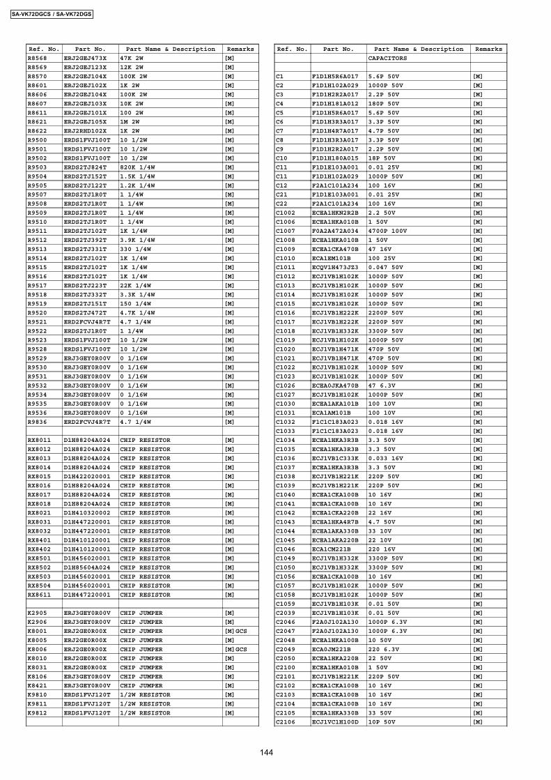
Ref. No. Part No. Part Name & Description Remarks
R8568 ERJ2GEJ473X 47K 2W [M]
R8569 ERJ2GEJ123X 12K 2W [M]
R8570 ERJ2GEJ104X 100K 2W [M]
R8601 ERJ2GEJ102X 1K 2W [M]
R8606 ERJ2GEJ104X 100K 2W [M]
R8607 ERJ2GEJ103X 10K 2W [M]
R8611 ERJ2GEJ101X 100 2W [M]
R8621 ERJ2GEJ105X 1M 2W [M]
R8622 ERJ2RHD102X 1K 2W [M]
R9500 ERDS1FVJ100T 10 1/2W [M]
R9501 ERDS1FVJ100T 10 1/2W [M]
R9502 ERDS1FVJ100T 10 1/2W [M]
R9503 ERDS2TJ824T 820K 1/4W [M]
R9504 ERDS2TJ152T 1.5K 1/4W [M]
R9505 ERDS2TJ122T 1.2K 1/4W [M]
R9507 ERDS2TJ1R0T 1 1/4W [M]
R9508 ERDS2TJ1R0T 1 1/4W [M]
R9509 ERDS2TJ1R0T 1 1/4W [M]
R9510 ERDS2TJ1R0T 1 1/4W [M]
R9511 ERDS2TJ102T 1K 1/4W [M]
R9512 ERDS2TJ392T 3.9K 1/4W [M]
R9513 ERDS2TJ331T 330 1/4W [M]
R9514 ERDS2TJ102T 1K 1/4W [M]
R9515 ERDS2TJ102T 1K 1/4W [M]
R9516 ERDS2TJ102T 1K 1/4W [M]
R9517 ERDS2TJ223T 22K 1/4W [M]
R9518 ERDS2TJ332T 3.3K 1/4W [M]
R9519 ERDS2TJ151T 150 1/4W [M]
R9520 ERDS2TJ472T 4.7K 1/4W [M]
R9521 ERD2FCVJ4R7T 4.7 1/4W [M]
R9522 ERDS2TJ1R0T 1 1/4W [M]
R9523 ERDS1FVJ100T 10 1/2W [M]
R9528 ERDS1FVJ100T 10 1/2W [M]
R9529 ERJ3GEY0R00V 0 1/16W [M]
R9530 ERJ3GEY0R00V 0 1/16W [M]
R9531 ERJ3GEY0R00V 0 1/16W [M]
R9532 ERJ3GEY0R00V 0 1/16W [M]
R9534 ERJ3GEY0R00V 0 1/16W [M]
R9535 ERJ3GEY0R00V 0 1/16W [M]
R9536 ERJ3GEY0R00V 0 1/16W [M]
R9836 ERD2FCVJ4R7T 4.7 1/4W [M]
RX8011 D1H88204A024 CHIP RESISTOR [M]
RX8012 D1H88204A024 CHIP RESISTOR [M]
RX8013 D1H88204A024 CHIP RESISTOR [M]
RX8014 D1H88204A024 CHIP RESISTOR [M]
RX8015 D1H422020001 CHIP RESISTOR [M]
RX8016 D1H88204A024 CHIP RESISTOR [M]
RX8017 D1H88204A024 CHIP RESISTOR [M]
RX8018 D1H88204A024 CHIP RESISTOR [M]
RX8021 D1H410320002 CHIP RESISTOR [M]
RX8031 D1H447220001 CHIP RESISTOR [M]
RX8032 D1H447220001 CHIP RESISTOR [M]
RX8401 D1H410120001 CHIP RESISTOR [M]
RX8402 D1H410120001 CHIP RESISTOR [M]
RX8501 D1H456020001 CHIP RESISTOR [M]
RX8502 D1H85604A024 CHIP RESISTOR [M]
RX8503 D1H456020001 CHIP RESISTOR [M]
RX8504 D1H456020001 CHIP RESISTOR [M]
RX8611 D1H447220001 CHIP RESISTOR [M]
K2905 ERJ3GEY0R00V CHIP JUMPER [M]
K2906 ERJ3GEY0R00V CHIP JUMPER [M]
K8001 ERJ2GE0R00X CHIP JUMPER [M]GCS
K8005 ERJ2GE0R00X CHIP JUMPER [M]
K8006 ERJ2GE0R00X CHIP JUMPER [M]GCS
K8010 ERJ2GE0R00X CHIP JUMPER [M]
K8031 ERJ2GE0R00X CHIP JUMPER [M]
K8106 ERJ3GEY0R00V CHIP JUMPER [M]
K8421 ERJ3GEY0R00V CHIP JUMPER [M]
K9810 ERDS1FVJ120T 1/2W RESISTOR [M]
K9811 ERDS1FVJ120T 1/2W RESISTOR [M]
K9812 ERDS1FVJ120T 1/2W RESISTOR [M]
Ref. No. Part No. Part Name & Description Remarks
CAPACITORS
C1 F1D1H5R6A017 5.6P 50V [M]
C2 F1D1H102A029 1000P 50V [M]
C3 F1D1H2R2A017 2.2P 50V [M]
C4 F1D1H181A012 180P 50V [M]
C5 F1D1H5R6A017 5.6P 50V [M]
C6 F1D1H3R3A017 3.3P 50V [M]
C7 F1D1H4R7A017 4.7P 50V [M]
C8 F1D1H3R3A017 3.3P 50V [M]
C9 F1D1H2R2A017 2.2P 50V [M]
C10 F1D1H180A015 18P 50V [M]
C11 F1D1E103A001 0.01 25V [M]
C11 F1D1H102A029 1000P 50V [M]
C12 F2A1C101A234 100 16V [M]
C21 F1D1E103A001 0.01 25V [M]
C22 F2A1C101A234 100 16V [M]
C1002 ECEA1HKN2R2B 2.2 50V [M]
C1006 ECEA1HKA010B 1 50V [M]
C1007 F0A2A472A034 4700P 100V [M]
C1008 ECEA1HKA010B 1 50V [M]
C1009 ECEA1CKA470B 47 16V [M]
C1010 ECA1EM101B 100 25V [M]
C1011 ECQV1H473JZ3 0.047 50V [M]
C1012 ECJ1VB1H102K 1000P 50V [M]
C1013 ECJ1VB1H102K 1000P 50V [M]
C1014 ECJ1VB1H102K 1000P 50V [M]
C1015 ECJ1VB1H102K 1000P 50V [M]
C1016 ECJ1VB1H222K 2200P 50V [M]
C1017 ECJ1VB1H222K 2200P 50V [M]
C1018 ECJ1VB1H332K 3300P 50V [M]
C1019 ECJ1VB1H102K 1000P 50V [M]
C1020 ECJ1VB1H471K 470P 50V [M]
C1021 ECJ1VB1H471K 470P 50V [M]
C1022 ECJ1VB1H102K 1000P 50V [M]
C1023 ECJ1VB1H102K 1000P 50V [M]
C1026 ECEA0JKA470B 47 6.3V [M]
C1027 ECJ1VB1H102K 1000P 50V [M]
C1030 ECEA1AKA101B 100 10V [M]
C1031 ECA1AM101B 100 10V [M]
C1032 F1C1C183A023 0.018 16V [M]
C1033 F1C1C183A023 0.018 16V [M]
C1034 ECEA1HKA3R3B 3.3 50V [M]
C1035 ECEA1HKA3R3B 3.3 50V [M]
C1036 ECJ1VB1C333K 0.033 16V [M]
C1037 ECEA1HKA3R3B 3.3 50V [M]
C1038 ECJ1VB1H221K 220P 50V [M]
C1039 ECJ1VB1H221K 220P 50V [M]
C1040 ECEA1CKA100B 10 16V [M]
C1041 ECEA1CKA100B 10 16V [M]
C1042 ECEA1CKA220B 22 16V [M]
C1043 ECEA1HKA4R7B 4.7 50V [M]
C1044 ECEA1AKA330B 33 10V [M]
C1045 ECEA1AKA220B 22 10V [M]
C1046 ECA1CM221B 220 16V [M]
C1049 ECJ1VB1H332K 3300P 50V [M]
C1050 ECJ1VB1H332K 3300P 50V [M]
C1056 ECEA1CKA100B 10 16V [M]
C1057 ECJ1VB1H102K 1000P 50V [M]
C1058 ECJ1VB1H102K 1000P 50V [M]
C1059 ECJ1VB1H103K 0.01 50V [M]
C2039 ECJ1VB1H103K 0.01 50V [M]
C2046 F2A0J102A130 1000P 6.3V [M]
C2047 F2A0J102A130 1000P 6.3V [M]
C2048 ECEA1HKA100B 10 50V [M]
C2049 ECA0JM221B 220 6.3V [M]
C2050 ECEA1HKA220B 22 50V [M]
C2100 ECEA1HKA010B 1 50V [M]
C2101 ECJ1VB1H221K 220P 50V [M]
C2102 ECEA1CKA100B 10 16V [M]
C2103 ECEA1CKA100B 10 16V [M]
C2104 ECEA1CKA100B 10 16V [M]
C2105 ECEA1HKA330B 33 50V [M]
C2106 ECJ1VC1H100D 10P 50V [M]
144
SA-VK72DGCS / SA-VK72DGS
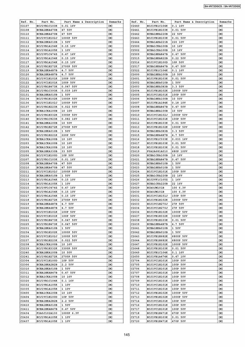
Ref. No. Part No. Part Name & Description Remarks
C2107 ECJ1VB1C103K 0.01 16V [M]
C2108 ECEA1HKA470B 47 50V [M]
C2110 ECEA1HKA470B 47 50V [M]
C2111 ECJ1VC1H102J 1000P 50V [M]
C2112 ECEA1HKA010B 1 50V [M]
C2113 ECJ1VB1A154K 0.15 10V [M]
C2114 ECJ1VB1A105K 1 10V [M]
C2115 ECJ1VF1C474Z 0.47 16V [M]
C2116 ECJ1VB1A154K 0.15 10V [M]
C2117 ECJ1VB1A154K 0.15 10V [M]
C2118 ECJ1VB1H272K 2700P 50V [M]
C2119 ECEA1HKA4R7B 4.7 50V [M]
C2120 ECEA1HKA4R7B 4.7 50V [M]
C2121 ECJ1VC1H101K 100P 50V [M]
C2122 ECJ1VC1H101K 100P 50V [M]
C2123 ECJ1VB1H473K 0.047 50V [M]
C2124 ECJ1VB1C393K 0.039 16V [M]
C2131 ECEA1HKA010B 1 50V [M]
C2134 ECJ1VB1H102K 1000P 50V [M]
C2136 ECJ1VC1H102J 1000P 50V [M]
C2137 ECJ1VB1H223K 0.022 50V [M]
C2138 ECEA1CKA100B 10 16V [M]
C2139 ECJ1VB1H332K 3300P 50V [M]
C2140 ECJ1VB1C823K 0.082 16V [M]
C2141 ECEA1HKA100B 10 50V [M]
C2142 ECJ1VB1H272K 2700P 50V [M]
C2200 ECEA1HKA010B 1 50V [M]
C2201 ECJ1VB1H221K 220P 50V [M]
C2202 ECEA1CKA100B 10 16V [M]
C2203 ECEA1CKA100B 10 16V [M]
C2204 ECEA1CKA100B 10 16V [M]
C2205 ECEA1HKA330B 33 50V [M]
C2206 ECJ1VC1H100D 10P 50V [M]
C2207 ECJ1VB1C103K 0.01 16V [M]
C2208 ECEA1HKA470B 47 50V [M]
C2210 ECEA1HKA470B 47 50V [M]
C2211 ECJ1VC1H102J 1000P 50V [M]
C2212 ECEA1HKA010B 1 50V [M]
C2213 ECJ1VB1A154K 0.15 10V [M]
C2214 ECJ1VB1A105K 1 10V [M]
C2215 ECJ1VF1C474Z 0.47 16V [M]
C2216 ECJ1VB1A154K 0.15 10V [M]
C2217 ECJ1VB1A154K 0.15 10V [M]
C2218 ECJ1VB1H272K 2700P 50V [M]
C2219 ECEA1HKA4R7B 4.7 50V [M]
C2220 ECEA1HKA4R7B 4.7 50V [M]
C2221 ECJ1VC1H101K 100P 50V [M]
C2222 ECJ1VC1H101K 100P 50V [M]
C2223 ECJ1VB1H473K 0.047 50V [M]
C2225 ECJ1VB1H473K 0.047 50V [M]
C2231 ECEA1HKA010B 1 50V [M]
C2234 ECJ1VB1H102K 1000P 50V [M]
C2236 ECJ1VC1H102J 1000P 50V [M]
C2237 ECJ1VB1H223K 0.022 50V [M]
C2238 ECEA1CKA100B 10 16V [M]
C2239 ECJ1VB1H332K 3300P 50V [M]
C2240 ECEA1HKA100B 10 50V [M]
C2241 ECJ1VB1H272K 2700P 50V [M]
C2304 ECJ1VC1H100D 10P 50V [M]
C2306 ECEA1HKA2R2B 2.2 50V [M]
C2310 ECEA1HKA010B 1 50V [M]
C2311 ECEA1HKAR47B 0.47 50V [M]
C2312 ECEA1CKA100B 10 16V [M]
C2320 ECJ1VB1C104K 0.1 16V [M]
C2332 ECJ1VB1A105K 1 10V [M]
C2335 ECJ1VB1A105K 1 10V [M]
C2400 ECEA1CKA100B 10 16V [M]
C2404 ECJ1VC1H100D 10P 50V [M]
C2406 ECEA1HKA2R2B 2.2 50V [M]
C2410 ECEA1HKA010B 1 50V [M]
C2411 ECEA1HKAR47B 0.47 50V [M]
C2434 F2A0J102A130 1000P 6.3V [M]
C2436 ECJ1VB1A105K 1 10V [M]
C2437 ECJ1VB1A105K 1 10V [M]
Ref. No. Part No. Part Name & Description Remarks
C2440 ECJ1VB1C104K 0.1 16V [M]
C2441 ECJ1VB1H103K 0.01 50V [M]
C2442 ECEA1HKA220B 22 50V [M]
C2443 ECJ1VB1H103K 0.01 50V [M]
C2444 ECEA1AKA221B 220 10V [M]
C2500 ECEA1CKA100B 10 16V [M]
C2502 ECEA1CKA100B 10 16V [M]
C2509 ECEA1HKAR47B 0.47 50V [M]
C2515 ECEA1HKAR22B 0.22 50V [M]
C2516 ECJ1VC1H100D 10P 50V [M]
C2517 ECEA1HKAR47B 0.47 50V [M]
C2522 ECJ1VB1C104K 0.1 16V [M]
C2600 ECEA1HKA100B 10 50V [M]
C2601 ECJ1VB1H103K 0.01 50V [M]
C2602 ECEA1HKA010B 1 50V [M]
C2603 ECEA1HKA3R3B 3.3 50V [M]
C2604 ECJ1VB1H102K 1000P 50V [M]
C2605 ECJ1VC1H101K 100P 50V [M]
C2606 ECEA1HKA100B 10 50V [M]
C2607 ECJ1VB1A184K 0.18 10V [M]
C2608 ECEA1HKAR47B 0.47 50V [M]
C2609 ECEA1HKA100B 10 50V [M]
C2610 ECJ1VC1H102J 1000P 50V [M]
C2611 ECJ1VC1H101K 100P 50V [M]
C2612 ECJ1VB1H103K 0.01 50V [M]
C2613 ECJ1VB1H102K 1000P 50V [M]
C2614 ECEA1HKA3R3B 3.3 50V [M]
C2615 ECEA1HKA4R7B 4.7 50V [M]
C2616 ECJ1VB1C333K 0.033 16V [M]
C2617 ECJ1VB1H103K 0.01 50V [M]
C2618 ECJ1VB1H103K 0.01 50V [M]
C2619 F0A2A681A010 680P 100V [M]
C2620 ECEA1CKA100B 10 16V [M]
C2621 ECEA1HKAR47B 0.47 50V [M]
C2622 ECEA1HKA010B 1 50V [M]
C2623 ECEA1HKA010B 1 50V [M]
C2624 ECJ1VC1H101K 100P 50V [M]
C2625 ECEA1CKA220B 22 16V [M]
C2626 ECJ2VF1C105Z 1 16V [M]
C2627 ECEA1CKA220B 22 16V [M]
C2629 ECA0JM101B 100 6.3V [M]
C2630 ECA0JM101B 100 6.3V [M]
C2631 ECJ1VC1H151J 150P 50V [M]
C2632 ECJ1VB1H102K 1000P 50V [M]
C2633 ECJ1VC1H270J 27P 50V [M]
C2634 ECJ1VC1H270J 27P 50V [M]
C2636 ECJ1VB1H102K 1000P 50V [M]
C2637 ECJ1VB1H332K 3300P 50V [M]
C2638 ECJ1VB1H103K 0.01 50V [M]
C2639 ECEA1HKA4R7B 4.7 50V [M]
C2641 ECEA1HKA010B 1 50V [M]
C2642 ECEA1HKA010B 1 50V [M]
C2643 ECJ1VB1H682K 6800P 50V [M]
C2644 ECJ1VB1H682K 6800P 50V [M]
C2647 ECJ1VB1H102K 1000P 50V [M]
C2648 ECJ1VB1H103K 0.01 50V [M]
C2649 ECJ1VB1C104K 0.1 16V [M]
C2650 ECJ1VB1A474K 0.47 10V [M]
C2704 ECJ1VC1H101K 100P 50V [M]
C2705 ECJ1VC1H101K 100P 50V [M]
C2706 ECJ1VC1H101K 100P 50V [M]
C2707 ECJ1VC1H101K 100P 50V [M]
C2708 ECJ1VC1H101K 100P 50V [M]
C2709 ECJ1VC1H101K 100P 50V [M]
C2710 ECJ1VC1H101K 100P 50V [M]
C2711 ECJ1VC1H101K 100P 50V [M]
C2712 ECJ1VB1H102K 1000P 50V [M]
C2713 ECJ1VB1H102K 1000P 50V [M]
C2714 ECJ1VC1H101K 100P 50V [M]
C2716 ECJ1VC1H101K 100P 50V [M]
C2717 ECJ1VC1H101K 100P 50V [M]
C2718 ECJ1VB1H471K 470P 50V [M]
C2719 ECJ1VB1H103K 0.01 50V [M]
C2720 ECJ1VB1H471K 470P 50V [M]
145
SA-VK72DGCS / SA-VK72DGS
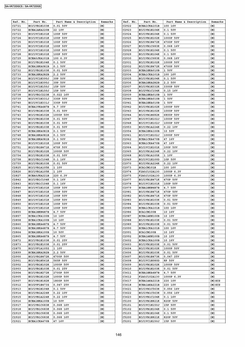
Ref. No. Part No. Part Name & Description Remarks
C2721 ECJ1VB1H103K 0.01 50V [M]
C2722 ECEA1AKA220B 22 10V [M]
C2723 ECJ1VC1H101K 100P 50V [M]
C2724 ECJ1VC1H101K 100P 50V [M]
C2725 ECJ1VC1H101K 100P 50V [M]
C2726 ECJ1VC1H101K 100P 50V [M]
C2727 ECJ1VC1H101K 100P 50V [M]
C2728 ECJ1VC1H101K 100P 50V [M]
C2729 ECEA0JKA101B 100 6.3V [M]
C2730 ECJ1VB1H104K 0.1 50V [M]
C2731 ECEA1HKA0R1B 0.1 50V [M]
C2732 ECJ1VB1H103K 0.01 50V [M]
C2733 ECEA1HKA2R2B 2.2 50V [M]
C2734 ECJ1VC1H390J 39P 50V [M]
C2735 ECJ1VC1H390J 39P 50V [M]
C2736 ECJ1VC1H150J 15P 50V [M]
C2737 ECJ1VC1H150J 15P 50V [M]
C2738 ECJ1VB1C223K 0.022 16V [M]
C2739 ECJ1VC1H331J 330P 50V [M]
C2740 ECJ1VC1H331J 330P 50V [M]
C2741 ECEA1VKA4R7B 4.7 35V [M]
C2742 ECJ1VB1H103K 0.01 50V [M]
C2743 ECJ1VB1H102K 1000P 50V [M]
C2744 ECJ1VB1H103K 0.01 50V [M]
C2745 ECJ1VB1H103K 0.01 50V [M]
C2746 ECJ1VB1H103K 0.01 50V [M]
C2747 ECEA1HKA0R1B 0.1 50V [M]
C2748 ECEA1HKA0R1B 0.1 50V [M]
C2749 ECEA1HKA0R1B 0.1 50V [M]
C2750 ECJ1VC1H101K 100P 50V [M]
C2751 ECJ1VB1H471K 470P 50V [M]
C2752 ECJ1VB1H102K 1000P 50V [M]
C2754 ECJ1VB1H103K 0.01 50V [M]
C2758 ECJ1VB1C104K 0.1 16V [M]
C2759 ECJ1VB1H103K 0.01 50V [M]
C2825 ECJ1VB1A105K 1 10V [M]
C2826 ECJ1VB1A105K 1 10V [M]
C2827 ECEA0JKA221B 220 6.3V [M]
C2842 ECJ1VB1C104K 0.1 16V [M]
C2843 ECJ1VB1C104K 0.1 16V [M]
C2846 ECJ1VC1H101K 100P 50V [M]
C2847 ECJ1VC1H101K 100P 50V [M]
C2848 ECJ1VC1H101K 100P 50V [M]
C2849 ECJ1VC1H101K 100P 50V [M]
C2850 ECJ1VC1H101K 100P 50V [M]
C2851 ECJ1VC1H101K 100P 50V [M]
C2855 ECEA1HKN4R7B 4.7 50V [M]
C2857 ECEA1CKA100B 10 16V [M]
C2858 ECEA1CKA100B 10 16V [M]
C2860 ECEA1HKA4R7B 4.7 50V [M]
C2862 ECEA1HKA4R7B 4.7 50V [M]
C2864 ECEA1HKA100B 10 50V [M]
C2865 ECEA1HKA4R7B 4.7 50V [M]
C2872 ECJ1VB1E103K 0.01 25V [M]
C2873 ECJ1VB1E103K 0.01 25V [M]
C2875 ECJ1VF1A105Z 1 10V [M]
C2899 ECEA1HKA2R2B 2.2 50V [M]
C2900 ECJ1VB1H472K 4700P 50V [M]
C2901 ECJ1VB1H561K 560P 50V [M]
C2902 ECJ1VB1H102K 1000P 50V [M]
C2903 ECJ1VB1E103K 0.01 25V [M]
C2904 ECJ1VB1H272K 2700P 50V [M]
C2905 ECJ1VB1H102K 1000P 50V [M]
C2907 ECJ1VB1H182K 1800P 50V [M]
C2912 ECJ2VF1E473Z 0.047 25V [M]
C2913 ECJ1VB1H104K 0.1 50V [M]
C2914 ECJ1VB1A224K 0.22 10V [M]
C2915 ECJ1VB1A224K 0.22 10V [M]
C2916 ECEA1HKA100B 10 50V [M]
C2917 ECJ1VB1C683K 0.068 16V [M]
C2918 ECJ1VB1C683K 0.068 16V [M]
C2919 ECJ1VB1C683K 0.068 16V [M]
C2920 ECJ1VB1C683K 0.068 16V [M]
C2921 ECEA1CKA470B 47 16V [M]
Ref. No. Part No. Part Name & Description Remarks
C2922 ECEA1CKA101B 100 16V [M]
C2923 ECJ1VB1H104K 0.1 50V [M]
C2924 ECJ1VB1H104K 0.1 50V [M]
C2925 ECJ1VB1H102K 1000P 50V [M]
C2926 ECJ1VB1H472K 4700P 50V [M]
C2927 ECJ1VB1C683K 0.068 16V [M]
C2928 ECJ1VB1H104K 0.1 50V [M]
C2929 ECJ1VB1H104K 0.1 50V [M]
C2930 ECJ1VB1C683K 0.068 16V [M]
C2931 ECJ1VB1H102K 1000P 50V [M]
C2932 ECJ1VB1H472K 4700P 50V [M]
C2933 ECEA1HKA010B 1 50V [M]
C2934 ECEA1CKA101B 100 16V [M]
C2935 ECJ1VB1H104K 0.1 50V [M]
C2936 ECEA1HKA2R2B 2.2 50V [M]
C2937 ECJ1VB1H332K 3300P 50V [M]
C2938 ECJ2VB1C154K 0.15 16V [M]
C2939 ECEA1HKA010B 1 50V [M]
C2940 ECEA1HKA010B 1 50V [M]
C2941 ECEA1HKA010B 1 50V [M]
C2942 ECJ1VB1H102K 1000P 50V [M]
C2943 ECJ1VB1H102K 1000P 50V [M]
C2944 ECJ1VB1H682K 6800P 50V [M]
C2947 ECJ1VC1H102J 1000P 50V [M]
C2948 ECJ1VC1H102J 1000P 50V [M]
C2953 ECJ1VB1A224K 0.22 10V [M]
C2954 ECEA1HKA100B 10 50V [M]
C2961 ECJ1VC1H102J 1000P 50V [M]
C2962 ECEA1CKA470B 47 16V [M]
C2963 ECEA1CKA470B 47 16V [M]
C2964 ECJ1VC1H101K 100P 50V [M]
C2965 ECJ1VB1A224K 0.22 10V [M]
C2968 ECJ1VB1A105K 1 10V [M]
C2969 ECJ1VC1H100D 10P 50V [M]
C2970 ECJ1VB1A224K 0.22 10V [M]
C2973 ECA1CM101B 100 16V [M]
C2974 F2A0J102A130 1000P 6.3V [M]
C2975 F2A0J102A130 1000P 6.3V [M]
C2977 ECJ1VB1H471K 470P 50V [M]
C2978 ECJ1VC1H101K 100P 50V [M]
C2979 ECEA1HKN4R7B 4.7 50V [M]
C2981 ECJ1VB1H471K 470P 50V [M]
C2982 ECJ1VB1H471K 470P 50V [M]
C2983 ECJ1VB1H103K 0.01 50V [M]
C2984 ECJ1VB1H103K 0.01 50V [M]
C2985 ECEA1CKA101B 100 16V [M]
C2986 ECA1CM100B 10 16V [M]
C2987 ECEA1AKN100B 10 10V [M]
C2988 ECJ1VB1H103K 0.01 50V [M]
C2989 ECJ1VB1H103K 0.01 50V [M]
C2990 ECEA1CKA101B 100 16V [M]
C2991 ECA1CM100B 10 16V [M]
C2992 ECEA1AKN100B 10 10V [M]
C3602 ECEA1CKA100B 10 16V [M]
C3603 ECJ1VB1H103K 0.01 50V [M]
C3604 ECJ1VB1H102K 1000P 50V [M]
C3606 ECJ1VB1H103K 0.01 50V [M]
C3607 ECJ1VB1E473K 0.047 25V [M]
C3608 ECJ1VC1H080D 8P 50V [M]
C3609 ECJ1VB1H102K 1000P 50V [M]
C3610 ECJ1VB1H103K 0.01 50V [M]
C3611 ECEA1HKA4R7B 4.7 50V [M]
C3612 F2A0J102A130 1000P 6.3V [M]
C3617 ECEA1AKA221B 220 10V [M]GCS
C3618 ECEA1AKA221B 220 10V [M]GCS
C3621 ECJ1VB1C563K 0.056 16V [M]
C3622 ECJ1VB1C563K 0.056 16V [M]
C3623 ECJ1VB1C104K 0.1 16V [M]
C5100 ECJ1VB1H821K 820P 50V [M]
C5101 ECJ1VC1H150J 15P 50V [M]
C5102 ECJ1VB1H104K 0.1 50V [M]
C5103 ECJ1VB1H104K 0.1 50V [M]
C5200 ECJ1VB1H821K 820P 50V [M]
C5201 ECJ1VC1H150J 15P 50V [M]
146
SA-VK72DGCS / SA-VK72DGS
Ref. No. Part No. Part Name & Description Remarks
C5202 ECJ1VB1H104K 0.1 50V [M]
C5203 ECJ1VB1H104K 0.1 50V [M]
C5300 ECJ1VC1H150J 15P 50V [M]
C5301 ECJ1VB1H104K 0.1 50V [M]
C5302 ECJ1VB1H104K 0.1 50V [M]
C5303 ECJ1VB1H821K 820P 50V [M]
C5400 ECJ1VC1H150J 15P 50V [M]
C5401 ECJ1VB1H104K 0.1 50V [M]
C5402 ECJ1VB1H104K 0.1 50V [M]
C5403 ECJ1VB1H821K 820P 50V [M]
C5500 ECJ1VB1H821K 820P 50V [M]
C5501 ECJ1VC1H150J 15P 50V [M]
C5502 ECJ1VB1H104K 0.1 50V [M]
C5503 ECJ1VB1H104K 0.1 50V [M]
C5801 F2A1E471A205 470P 25V [M]
C5802 ECA1CM331B 330 16V [M]
C5803 ECJ1VB1H102K 1000P 50V [M]
C5804 ECJ1VB1H103K 0.01 50V [M]
C5805 ECA1CM101B 100 16V [M]
C5806 ECJ1VB1H103K 0.01 50V [M]
C5807 ECEA1HKA2R2B 2.2 50V [M]
C5808 ECA1CM331B 330 16V [M]
C5809 ECJ1VB1H103K 0.01 50V [M]
C5810 ECA1EM101B 100 25V [M]
C5811 ECJ1VB1H103K 0.01 50V [M]
C5812 ECEA1EKA330B 33 25V [M]
C5813 ECEA0JKA221B 220 6.3V [M]
C5814 ECJ1VB1H103K 0.01 50V [M]
C5815 F2A1J332A306 3300P 63V [M]
C5818 F2A1J332A306 3300P 63V [M]
C5819 ECJ1VB1H103K 0.01 50V [M]
C5834 ECEA1HKA010B 1 50V [M]
C5836 ECEA2AU100B 10 100V [M]
C6800 ECEA1CKA470B 47 16V [M]
C6801 ECJ1VB1H102K 1000P 50V [M]
C6802 ECEA1CKA470B 47 16V [M]
C6803 ECJ1VB1H102K 1000P 50V [M]
C6804 ECEA1HKA4R7B 4.7 50V [M]
C6805 ECJ1VC1H101K 100P 50V [M]
C6806 ECJ2VF1E473Z 0.047 25V [M]
C6807 ECJ1VB1H102K 1000P 50V [M]
C6809 ECJ1VB1H103K 0.01 50V [M]
C6810 ECJ1VC1H101K 100P 50V [M]
C6811 ECA1CM471B 470 16V [M]
C6812 ECJ1VB1H102K 1000P 50V [M]
C6813 ECEA0JKA101B 100 6.3V [M]
C6843 ECJ1VB1C223K 0.022 16V [M]
C6844 ECJ1VB1C223K 0.022 16V [M]
C6853 ECEA0JKA470B 47 6.3V [M]
C6854 ECEA1HKA3R3B 3.3 50V [M]
C6855 ECEA1HKA220B 22 50V [M]
C6856 ECEA1HKA220B 22 50V [M]
C6865 ECEA1HKA010B 1 50V [M]
C6866 ECJ1VB1H102K 1000P 50V [M]
C6867 ECJ1VC1H101K 100P 50V [M]
C6868 ECJ1VB1H102K 1000P 50V [M]
C6870 ECEA1HKA010B 1 50V [M]
C6871 ECJ1VB1H103K 0.01 50V [M]
C6872 ECEA1HKAR33B 0.33 50V [M]
C6873 ECJ1VB1C105K 1 16V [M]
C6875 ECJ1VB1C223K 0.022 16V [M]
C6876 ECJ1VB1C223K 0.022 16V [M]
C6879 ECEA1HKA4R7B 4.7 50V [M]
C6881 ECEA1HKA3R3B 3.3 50V [M]
C6882 ECJ1VB1H471K 470P 50V [M]
C6885 ECJ1VB1H331K 330P 50V [M]
C6886 ECJ1VB1H331K 330P 50V [M]
C6887 ECJ1VB1H331K 330P 50V [M]
C6888 ECJ1VB1H331K 330P 50V [M]
C6889 ECJ1VB1H104K 0.1 50V [M]
C6890 ECEA0JKA101B 100 6.3V [M]
C6891 ECJ1VC1H101K 100P 50V [M]
C6894 ECJ1VB1H102K 1000P 50V [M]
C6895 ECA1CAK100XB 10 16V [M]
Ref. No. Part No. Part Name & Description Remarks
C6896 ECJ1VC1H101K 100P 50V [M]
C6897 ECJ1VC1H101K 100P 50V [M]
C6898 ECJ1VB1H332K 3300P 50V [M]
C8001 F2G0J101A066 100P 6.3V [M]
C8002 F2G0G331A012 330P 4V [M]
C8003 ECJ0EB1E222K 2200P 25V [M]
C8004 ECJ0EF1C104Z 0.1 16V [M]
C8005 ECJ0EF1C104Z 0.1 16V [M]
C8006 ECJ0EF1C104Z 0.1 16V [M]
C8007 ECJ0EF1C104Z 0.1 16V [M]
C8008 ECJ0EF1C104Z 0.1 16V [M]
C8009 ECJ0EF1C104Z 0.1 16V [M]
C8010 ECJ0EF1C104Z 0.1 16V [M]
C8011 ECJ1VB0J105K 1 6.3V [M]
C8012 ECJ0EF1C104Z 0.1 16V [M]
C8013 ECJ0EF1C104Z 0.1 16V [M]
C8014 ECJ0EF1C104Z 0.1 16V [M]
C8015 ECJ1VB0J105K 1 6.3V [M]
C8016 ECJ1VB0J105K 1 6.3V [M]
C8017 ECJ0EF1C104Z 0.1 16V [M]
C8018 ECJ0EF1C104Z 0.1 16V [M]
C8019 ECJ1VB0J105K 1 6.3V [M]
C8020 ECJ0EF1C104Z 0.1 16V [M]
C8021 ECJ0EF1C104Z 0.1 16V [M]
C8022 ECJ0EF1C104Z 0.1 16V [M]
C8023 ECJ1VB0J105K 1 6.3V [M]
C8024 ECJ1VB0J105K 1 6.3V [M]
C8025 ECJ0EF1C104Z 0.1 16V [M]
C8026 ECJ0EB1E222K 2200P 25V [M]
C8027 ECJ0EF1C104Z 0.1 16V [M]
C8028 ECJ1VB0J105K 1 6.3V [M]
C8031 ECJ0EF1C104Z 0.1 16V [M]
C8051 ECJ1VB0J105K 1 6.3V [M]
C8052 ECJ0EF1C104Z 0.1 16V [M]
C8053 ECJ0EC1H221J 220P 50V [M]
C8054 ECJ1VB0J105K 1 6.3V [M]
C8055 ECJ1VB0J105K 1 6.3V [M]
C8056 ECJ0EF1C104Z 0.1 16V [M]
C8057 ECJ0EB1E222K 2200P 25V [M]
C8111 ECJ0EB1A104K 0.1 10V [M]
C8112 ECJ1VB0J105K 1 6.3V [M]
C8113 ECJ0EB1E471K 470P 25V [M]
C8201 F2H0J101A003 100P 6.3V [M]
C8202 F2G0J101A066 100P 6.3V [M]
C8203 ECJ0EF1C104Z 0.1 16V [M]
C8204 ECJ0EF1C104Z 0.1 16V [M]
C8205 ECJ0EF1C104Z 0.1 16V [M]
C8206 ECJ1VB0J105K 1 6.3V [M]
C8207 ECJ1VF1C104Z 0.1 16V [M]
C8208 ECJ0EF1C104Z 0.1 16V [M]
C8211 ECJ0EB1A333K 0.033 10V [M]
C8212 ECJ0EF1C104Z 0.1 16V [M]
C8213 ECJ0EF1C104Z 0.1 16V [M]
C8214 ECJ0EF1C104Z 0.1 16V [M]
C8215 ECJ0EB1E562K 5600P 25V [M]
C8216 ECJ0EB1C183K 0.018 16V [M]
C8217 ECJ1VB0J105K 1 6.3V [M]
C8218 ECJ1VB0J105K 1 6.3V [M]
C8221 ECJ0EB1A104K 0.1 10V [M]
C8222 ECJ0EB1A104K 0.1 10V [M]
C8223 ECJ0EB1A104K 0.1 10V [M]
C8224 ECJ0EB1A104K 0.1 10V [M]
C8225 ECJ0EF1C104Z 0.1 16V [M]
C8226 ECJ0EF1C104Z 0.1 16V [M]
C8227 ECJ0EF1C104Z 0.1 16V [M]
C8228 ECJ1VB0J105K 1 6.3V [M]
C8229 ECJ1VB0J105K 1 6.3V [M]
C8232 ECJ1VF1C104Z 0.1 16V [M]
C8233 ECJ0EB1E472K 4700P 25V [M]
C8234 ECJ0EF1C104Z 0.1 16V [M]
C8235 ECJ0EB1H102K 1000P 50V [M]
C8236 ECJ0EB1H102K 1000P 50V [M]
C8237 ECJ0EB1H102K 1000P 50V [M]
C8238 ECJ0EB1H821K 820P 50V [M]
147
SA-VK72DGCS / SA-VK72DGS
Ref. No. Part No. Part Name & Description Remarks
C8241 ECJ0EB1A104K 0.1 10V [M]
C8242 ECJ0EB1A104K 0.1 10V [M]
C8251 F2G0J221A065 220P 6.3V [M]
C8252 F2G1C470A076 47P 16V [M]
C8253 F2H1C220A003 22P 16V [M]
C8254 ECJ0EF1C104Z 0.1 16V [M]
C8255 ECJ0EF1C104Z 0.1 16V [M]
C8256 ECJ0EF1C104Z 0.1 16V [M]
C8257 ECJ0EF1C104Z 0.1 16V [M]
C8261 ECJ0EF1C104Z 0.1 16V [M]
C8262 ECJ0EF1C104Z 0.1 16V [M]
C8301 F2H0J2210006 220P 6.3V [M]
C8302 F2H0J330A003 33P 6.3V [M]
C8303 ECJ0EF1C104Z 0.1 16V [M]
C8304 ECJ1VB0J105K 1 6.3V [M]
C8307 ECJ0EF1C104Z 0.1 16V [M]
C8308 ECJ0EC1H150J 15P 50V [M]
C8311 ECJ0EF1C104Z 0.1 16V [M]
C8312 ECJ1VB0J105K 1 6.3V [M]
C8421 F2G0J101A083 100P 6.3V [M]
C8422 ECJ0EF1C104Z 0.1 16V [M]
C8423 F2G0J330A083 33P 6.3V [M]
C8424 ECJ0EF1C104Z 0.1 16V [M]
C8426 ECJ0EF1C104Z 0.1 16V [M]
C8427 ECJ0EF1C104Z 0.1 16V [M]
C8428 ECJ0EF1C104Z 0.1 16V [M]
C8501 ECJ3YB1A106M 10 10V [M]
C8502 ECJ0EF1C104Z 0.1 16V [M]
C8503 ECJ0EF1C104Z 0.1 16V [M]
C8504 ECJ0EF1C104Z 0.1 16V [M]
C8505 ECJ0EC1H221J 220P 50V [M]
C8506 ECJ0EC1H101J 100P 50V [M]
C8550 F2H0J330A003 33P 6.3V [M]
C8551 ECJ0EF1C104Z 0.1 16V [M]
C8552 F2G1C100A072 10P 16V [M]
Ref. No. Part No. Part Name & Description Remarks
PACKING MATERIALS
P1 RPGX1470 PACKING CASE [M]GS
P1 RPGX1471 PACKING CASE [M]GCS
P2 RPNX0330 POLYFOAM [M]
P3 RPFX0007 MIRAMAT BAG [M]
ACCESSORIES
A1 N2QAJB000143 REMOTE CONTROL [M]
A1-1 RKK-HTR0051K R/C BATTERY COVER [M]
A2 K2CQ2CA00002 AC CORD [M]
A2 RJA0053-3X AC CORD [M]GS
A3 RQT8169-L O/I BOOK (En) [M]
A3 RQT8170-A O/I BOOK (Pe/Ar) [M]GS
A4 RSA0006-J FM ANTENNA [M]
A5 N1DAAAA00001 AM ANTENNA [M]
A6 K2KA2BA00001 VIDEO CABLE [M]
Ref. No. Part No. Part Name & Description Remarks
C8553 F2H0J470A003 47P 6.3V [M]
C8554 ECJ1VB0J105K 1 6.3V [M]
C8561 ECJ0EF1C104Z 0.1 16V [M]
C8562 F2G1C100A072 10P 16V [M]
C8563 F2H0J470A003 47P 6.3V [M]
C8564 ECJ1VB0J105K 1 6.3V [M]
C8601 ECJ0EF1C104Z 0.1 16V [M]
C8606 ECJ0EF1C104Z 0.1 16V [M]
C8607 ECJ0EB0J224K 0.22 6.3V [M]
C8611 ECJ0EF1C104Z 0.1 16V [M]
C8621 ECJ0EC1H120J 12P 50V [M]
C8622 ECJ0EC1H120J 12P 50V [M]
C8651 ECJ0EF1C104Z 0.1 16V [M]
C8652 ECJ0EF1C104Z 0.1 16V [M]
C8691 ECJ0EF1C104Z 0.1 16V [M]
C8695 ECJ0EF1C104Z 0.1 16V [M]
C9501 ECQE1104KF3 0.1 100V [M]
C9502 ECKR1H103MD5 0.01 50V [M]
C9503 ECKR1H102ZF5 1000P 50V [M]
C9504 F1B1H103A153 0.01 50V [M]
C9505 ECKR1H103MD5 0.01 50V [M]
C9506 F1B2H103A060 0.01 500V [M]
C9507 F1D1H101A012 100P 50V [M]
C9508 ECEA1AKA470B 47 10V [M]
C9509 ECA1HM470B 47 50V [M]
C9510 F2A1E471A205 470P 25V [M]
C9511 F2A1E471A205 470P 25V [M]
C9512 ECA1HM470B 47 50V [M]
C9513 ECA1EM472B 4700 25V [M]
C9514 EEUFC1E102B 1000P 25V [M]
C9515 ECA0JM102B 1000 6.3V [M]
C9517 ECEA1HKA100B 10 50V [M]
C9533 ECA1JM222B 2200 63V [M]
C9533 ECEA1HKA010B 1 50V [M]
C9534 ECA1JM222B 2200 63V [M]
27.5. Packing Materials & Accessories Parts List
148
SA-VK72DGCS / SA-VK72DGS
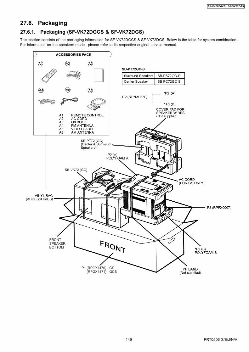
27.6. Packaging27.6.1. Packaging (SF-VK72DGCS & SF-VK72DGS)This section consists of the packaging information for SF-VK72DGCS & SF-VK72DGS. Below is the table for system combination.For information on the speakers model, please refer to its respective original service manual.
149
SA-VK72DGCS / SA-VK72DGS
PRT0506 S/E/J/N/A