run iib upgrade technical design report - nevis labs
TRANSCRIPT

DØ CollaborationSeptember 12, 2002
Run IIb UpgradeTechnical
Design Report

2
(This page intentionally left blank)

3
CONTENTS
Preface................................................................................................................................. 5
Part I: Physics Goals .......................................................................................................... 9
Part II: Silicon Detector ................................................................................................... 25
Part III: Trigger Upgrade ............................................................................................... 277
Part IV: DAQ/Online Computing .................................................................................. 445
Part V: Installation .......................................................................................................... 465
Summary ......................................................................................................................... 479

4
(This page intentionally left blank)

5
PREFACE
DØ Run IIb Upgrade Technical
Design Report

6
(This page intentionally left blank)

7
PREFACE There is broad agreement within the experimental and theoretical high-energy physics communities that the most pressing issue facing particle physics is the search for the origin of mass. More specifically, we seek to understand the mechanism by which the W and Z particles that mediate the weak force gain mass, while the photon, which has the same couplings to matter, remains massless. In the Standard Model of particle interactions, this electroweak symmetry breaking occurs through interactions with a so-far unobserved particle, called the Higgs boson. Furthermore, within the Standard Model framework, the Higgs particle is responsible for the masses of all the known particles. Searching for the Higgs has become the highest priority in the High Energy Physics community, not only because it is the last undiscovered particle of the Standard Model, but also because its unique role within the Standard Model provides a window that may help us understand the new physics that must be present at higher mass scales.
The Tevatron Collider at Fermilab is currently the only facility in the world capable of making a Higgs discovery. Simulation studies have shown that the two Tevatron Collider experiments, CDF and DØ, are sensitive to the Higgs over almost all of its presently allowed mass range. Our goal is to accumulate sufficient data to make a sensitive search for the Higgs that will have a high probability of success if the Standard Model predictions are correct.
These goals cannot be achieved without upgrades to the DØ detector. The silicon tracking detector is not expected to survive beyond the 2-4 fb-1 of integrated luminosity that will be delivered during Run IIa, well short of the 15 fb-1 goal for Run IIb. The corresponding increase in instantaneous luminosity necessitates upgrading the trigger system to maintain high trigger efficiency for the Higgs search and other elements of the Run IIb physics program while providing the required background rejection. Finally, data acquisition (DAQ) and online computing upgrades are needed to continue efficient operation of the experiment beyond Run IIa.
This document presents the technical design for the DØ Run IIb upgrades. It is divided into five parts, covering the Run IIb physics goals, the Silicon Detector, the Trigger Upgrade, DAQ/Online Computing, and Installation. Each part is organized so that it is self-contained, providing the motivation, goals, and technical description of the proposed upgrade. A brief summary concludes this report.

8
(This page intentionally left blank)
9
PHYSICS GOALS
DØ Run IIb Upgrade Technical
Design Report

DØ Run IIb Physics Goals
10
(This page intentionally left blank)

DØ Run IIb Physics Goals
11
PHYSICS GOALS CONTENTS
1 Introduction................................................................................................................................ 13
2 Standard Model Higgs Boson Searches..................................................................................... 14
3 Physics Beyond the Standard Model ......................................................................................... 17
4 Standard Model Physics............................................................................................................. 21
5 Summary of Physics Objectives ................................................................................................ 23

DØ Run IIb Physics Goals
12
(This page intentionally left blank)
DØ Run IIb Physics Goals
13
1 INTRODUCTION
Proton-antiproton collisions at =s 2 TeV have proved to be a very fruitful tool for deepening our understanding of the standard model and for searching for physics beyond this framework. DØ has published more than a hundred papers from Run I, including the discovery and precision measurements of the top quark, precise tests of electroweak predictions, QCD tests with jets and photons, and searches for supersymmetry and other postulated new particles. With the addition of a magnetic field, silicon and fiber trackers, and substantial upgrades to other parts of the detector, DØ has started with the goal of building on this broad program, taking advantage of significantly higher luminosities, and adding new measurements in b-physics. The strengths of the DØ detector are its liquid argon calorimetry, which provides outstanding measurements of electrons, photons, jets and missing ET; its large solid angle, multi-layer muon system and robust muon triggers; and its state of the art tracking system using a silicon detector surrounded by a fiber tracker providing track triggers.
A series of physics workshops organized by Fermilab's Theory group together with the CDF and DØ collaborations has mapped out the physics terrain of the Tevatron in some detail. It is clear from the very large amount of work carried out in these meetings and described in the reports1 that integrated luminosities much higher than the 2fb-1, which was the original goal of Run II, add significantly to the program. While all areas of physics benefit from increased statistics, it is the very real possibility of discovering the standard model Higgs boson (or its supersymmetric versions) and/or supersymmetric particles or other physics beyond the standard model, that forms the core motivation for the Laboratory's luminosity goal of 15 fb-1 per detector. We have therefore used the most promising Higgs discovery channels as benchmark processes for the Run IIb upgrade, which is described in this design report, and have optimized the detector configuration for them. All other high pT physics programs benefit from this detector optimization (though for the QCD and b-physics programs the benefits will be balanced by decreased trigger allocations and some loss of geometric acceptance). In the following, we discuss physics requirements on the Run IIb upgrade imposed by Higgs searches and their implications for other high pT physics programs.
1 http://fnth37.fnal.gov/run2.html

DØ Run IIb Physics Goals
14
2 STANDARD MODEL HIGGS BOSON SEARCHES The highest cross section Higgs production channel at the Tevatron is the gluon fusion reaction gg → H. Unfortunately, for Higgs masses below about 135 GeV, its dominant decay mode is tobb and is swamped by QCD production of b-jets. The most promising Higgs search strategy in this mass range is to focus on associated production of a Higgs with a W or Z boson,pp → WH andpp → ZH. The leptonic decays of the W and Z enable a much better signal to background ratio to be achieved, but one must pay the cost of a production cross section about one fifth that of inclusive production together with the leptonic branching ratios of the vector bosons. This relatively low signal cross section times branching ratio motivates the need for high integrated luminosity. In turn, the need for high integrated luminosity forces the accelerator to operate in a mode where each high pT event is likely to be accompanied by a significant number of low pT "minimum bias" events occurring in the same pp bunch crossing. The mean number of interactions <n> is around 5 for a luminosity of 2×1032cm-2s-1 at 132ns bunch spacing. This high occupancy environment is one of the main challenges for Run IIb.
Figure 1 - Standard Model Higgs decay branching ratios as a function of Higgs mass.
Figure 1 shows the decay modes of the Standard Model Higgs in the mass range relevant to DØ. For Higgs masses below roughly 135 GeV, the Higgs decays dominantly to b-quark pairs, and for masses above this (but less than thett threshold) the decay is dominantly to W and Z boson pairs. Thus, searches for Higgs boson in the low mass region MH < 135 GeV must assume H →bb decays. Searches for the lightest Higgs in supersymmetric models must also assume decay to b-quark pairs.
DØ Run IIb Physics Goals
15
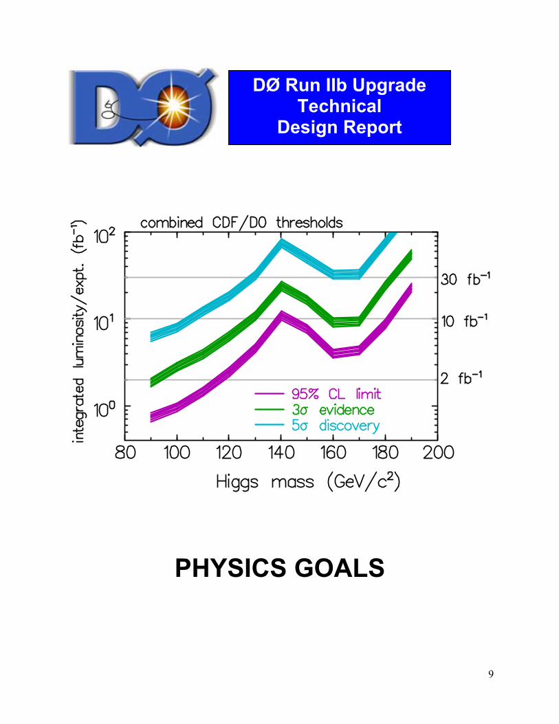
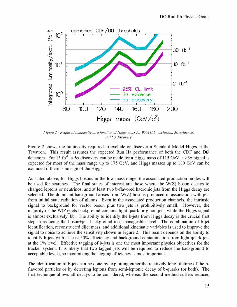
Figure 2 - Required luminosity as a function of Higgs mass for 95% C.L. exclusion, 3σ evidence, and 5σ discovery.
Figure 2 shows the luminosity required to exclude or discover a Standard Model Higgs at the Tevatron. This result assumes the expected Run IIa performance of both the CDF and DØ detectors. For 15 fb-1, a 5σ discovery can be made for a Higgs mass of 115 GeV, a >3σ signal is expected for most of the mass range up to 175 GeV, and Higgs masses up to 180 GeV can be excluded if there is no sign of the Higgs.
As stated above, for Higgs bosons in the low mass range, the associated-production modes will be used for searches. The final states of interest are those where the W(Z) boson decays to charged leptons or neutrinos, and at least two b-flavored hadronic jets from the Higgs decay are selected. The dominant background arises from W(Z) bosons produced in association with jets from initial state radiation of gluons. Even in the associated production channels, the intrinsic signal to background for vector boson plus two jets is prohibitively small. However, the majority of the W(Z)+jets background contains light quark or gluon jets, while the Higgs signal is almost exclusivelybb. The ability to identify the b-jets from Higgs decay is the crucial first step in reducing the boson+jets background to a manageable level. The combination of b-jet identification, reconstructed dijet mass, and additional kinematic variables is used to improve the signal to noise to achieve the sensitivity shown in Figure 2. This result depends on the ability to identify b-jets with at least 50% efficiency and background contamination from light quark jets at the 1% level. Effective tagging of b-jets is one the most important physics objectives for the tracker system. It is likely that two tagged jets will be required to reduce the background to acceptable levels, so maximizing the tagging efficiency is most important.
The identification of b-jets can be done by exploiting either the relatively long lifetime of the b-flavored particles or by detecting leptons from semi-leptonic decay of b-quarks (or both). The first technique allows all decays to be considered, whereas the second method suffers reduced

DØ Run IIb Physics Goals
16
statistical precision because of the ~30-40% decay branching ratio of b-quarks to final states including leptons. The long lifetime of the b-quarks is reflected in a B-meson decay that occurs some distance from the primary beam interaction point. For b-flavored particles with energies expected from Higgs decay, the mean decay length is 2 mm, and the mean impact parameter is roughly 250 µm. Thus, efficiently and cleanly identifying these decays requires a detector with the ability to reconstruct tracks with an impact parameter resolution in the tens of microns. The most feasible technology for this is silicon microstrip detectors.
One of the low-mass Higgs signatures is particularly noteworthy: Higgs production in association with a Z boson, which decays into a neutrino-antineutrino pair, resulting in missing energy and two b-jets in the final state. One of the main strengths of the DØ detector is its good missing energy identification; yet to keep trigger rates under control the present threshold on the missing ET trigger is about 35 GeV. A search for the Higgs boson in the ZH channel can certainly benefit from a lower trigger threshold. This can be achieved by implementing an efficient 2-jet trigger at the first trigger level and using information about displaced tracks at the second trigger level. The proposed calorimeter trigger upgrade will enable us to efficiently trigger on jets of moderate transverse energy, while the silicon track trigger upgrade will retain our ability to trigger on displaced tracks with the upgraded silicon tracker.
Searches for the Higgs boson in the intermediate mass region 135<MH<200 GeV/c2 assume inclusively-produced Higgs decaying to WW* and ZZ*, where at least one of the vector bosons decays to leptons. Effective lepton triggering and identification, essential for vector boson detection, is important for Higgs searches in both low and intermediate mass regions. The tracking system plays a crucial role in electron, muon and, arguably, tau lepton triggering and identification. Leptons from W and Z decays are fairly energetic, with pT>20 GeV/c. The requirement that we efficiently trigger on high-pT tracks is the primary motivation for the track trigger upgrade and the cal-track match system, while the requirement that we efficiently reconstruct these tracks is an important design requirement for the silicon tracker upgrade.
Higgs production in association with tt has received a lot of attention recently2. Though low in cross section, this channel provides a very rich signature with leptons, missing energy, and 4 b-jets in the final state. B-jets produced in this process have higher energy than those in processes such as WH production. Tracks in such jets tend to be more collimated, emphasizing the need for robust pattern recognition in the high occupancy environment. Another challenge for this channel is ambiguity in b-jet assignment, which can be reduced if the charge of the b-quark can be tagged. Several methods for b-charge tagging have been developed so far, e.g. same side tagging, jet charge tagging. Having information about charge of tracks in the secondary and tertiary b-decay vertices could be invaluable to improve purity of these tagging methods. This puts additional emphasis on precise impact parameter reconstruction.
2 J. Goldstein et al., “ Httpp → : A discovery mode for Higgs boson at the Tevatron”, Phys. Rev. Lett. 86, 1694 (2001).

DØ Run IIb Physics Goals
17
It is important to note that Higgs searches at the Tevatron and at the LHC are complementary to each other. While LHC experiments3 emphasize the γγ→→ Hgg channel, where Higgs is produced and decays via loop diagrams, the Tevatron’s emphasis is on tree-level production and tree-level decay. For a Standard Model Higgs, the branching ratio to γγ is very low, making it impossible to observe this channel at the Tevatron. However, some models predict a “bosophilic” Higgs, for which this decay mode is enhanced. Thus, high-energy photon identification is important for Higgs search beyond the Standard Model. Photon/electron separation is essential for high-purity photon identification. For this purpose the tracking system must ensure low fake track rate and a good momentum resolution.
3 PHYSICS BEYOND THE STANDARD MODEL Searches for SUSY and strong dynamics will benefit from the requirements imposed on the tracking system by the Standard Model Higgs searches. SUSY extensions of the Standard Model predict two Higgs doublets with five physical Higgs bosons – two neutral scalars (h,H), one neutral pseudoscalar (A) and two charged bosons (H±). Over much of the remaining allowed parameter space, the lightest neutral boson h behaves similarly to the Standard Model Higgs, and has a mass in the range 115-130 GeV, while the H, A and H± masses are larger. The standard model Higgs searches described above are, at the same time, searches for the lightest SUSY Higgs h. In addition, some Higgs cross sections are enhanced in SUSY, e.g. pp →bb(A/h) with A,h →bb in a high βtan scenario. Efficient b-jet triggering, tagging, and b-charge identification is essential for Higgs discovery in these channels, which contain four b-jets. The charged Higgs boson can be detected in top decays or through pair production of H+H-, and decays to cb or ντ − , depending on βtan . Again, good heavy flavor triggering, tagging, and tracking (for tau-lepton identification) are important. Studies have shown that the Tevatron can exclude almost the whole plane of SUSY Higgs parameters (mA, tan β) at the 95% level, if no signal is seen in 5 fb-1, and can discover at least one SUSY Higgs at the 5 standard deviation level with 15-20 fb-1 per experiment.
3 M. Carena, S. Mrenna, C. Wagner, “Complementarity of the CERN LEP collider, the Fermilab Tevatron, and the CERN LHC in the search for a light MSSM Higgs boson” Phys Rev. D62, 055008 (2000).
DØ Run IIb Physics Goals
18
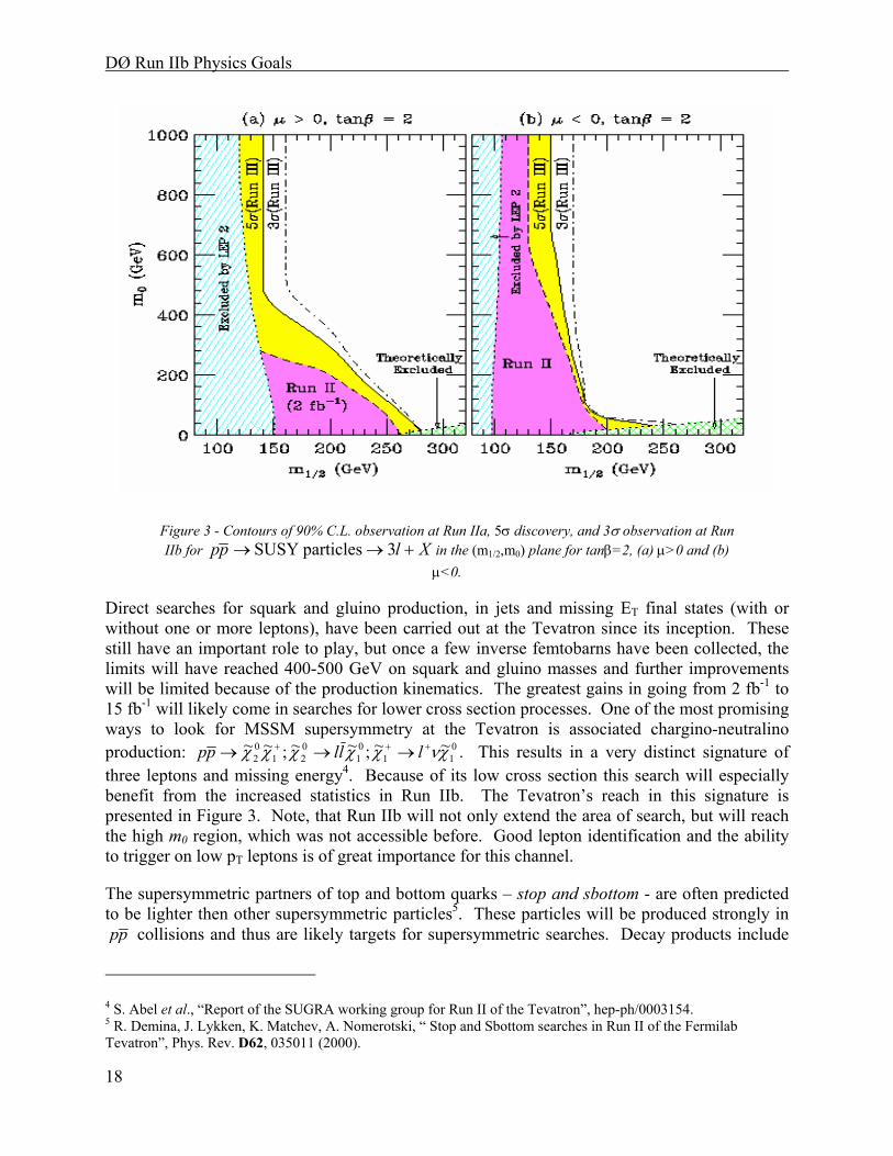
Figure 3 - Contours of 90% C.L. observation at Run IIa, 5σ discovery, and 3σ observation at Run IIb for Xlpp +→→ 3particles SUSY in the (m1/2,m0) plane for tanβ=2, (a) µ>0 and (b)
µ<0.
Direct searches for squark and gluino production, in jets and missing ET final states (with or without one or more leptons), have been carried out at the Tevatron since its inception. These still have an important role to play, but once a few inverse femtobarns have been collected, the limits will have reached 400-500 GeV on squark and gluino masses and further improvements will be limited because of the production kinematics. The greatest gains in going from 2 fb-1 to 15 fb-1 will likely come in searches for lower cross section processes. One of the most promising ways to look for MSSM supersymmetry at the Tevatron is associated chargino-neutralino production: 0
1101
021
02
~~;~~;~~ χνχχχχχ +++ →→→ lllpp . This results in a very distinct signature of three leptons and missing energy4. Because of its low cross section this search will especially benefit from the increased statistics in Run IIb. The Tevatron’s reach in this signature is presented in Figure 3. Note, that Run IIb will not only extend the area of search, but will reach the high m0 region, which was not accessible before. Good lepton identification and the ability to trigger on low pT leptons is of great importance for this channel.
The supersymmetric partners of top and bottom quarks – stop and sbottom - are often predicted to be lighter then other supersymmetric particles5. These particles will be produced strongly in
pp collisions and thus are likely targets for supersymmetric searches. Decay products include
4 S. Abel et al., “Report of the SUGRA working group for Run II of the Tevatron”, hep-ph/0003154. 5 R. Demina, J. Lykken, K. Matchev, A. Nomerotski, “ Stop and Sbottom searches in Run II of the Fermilab Tevatron”, Phys. Rev. D62, 035011 (2000).
DØ Run IIb Physics Goals
19
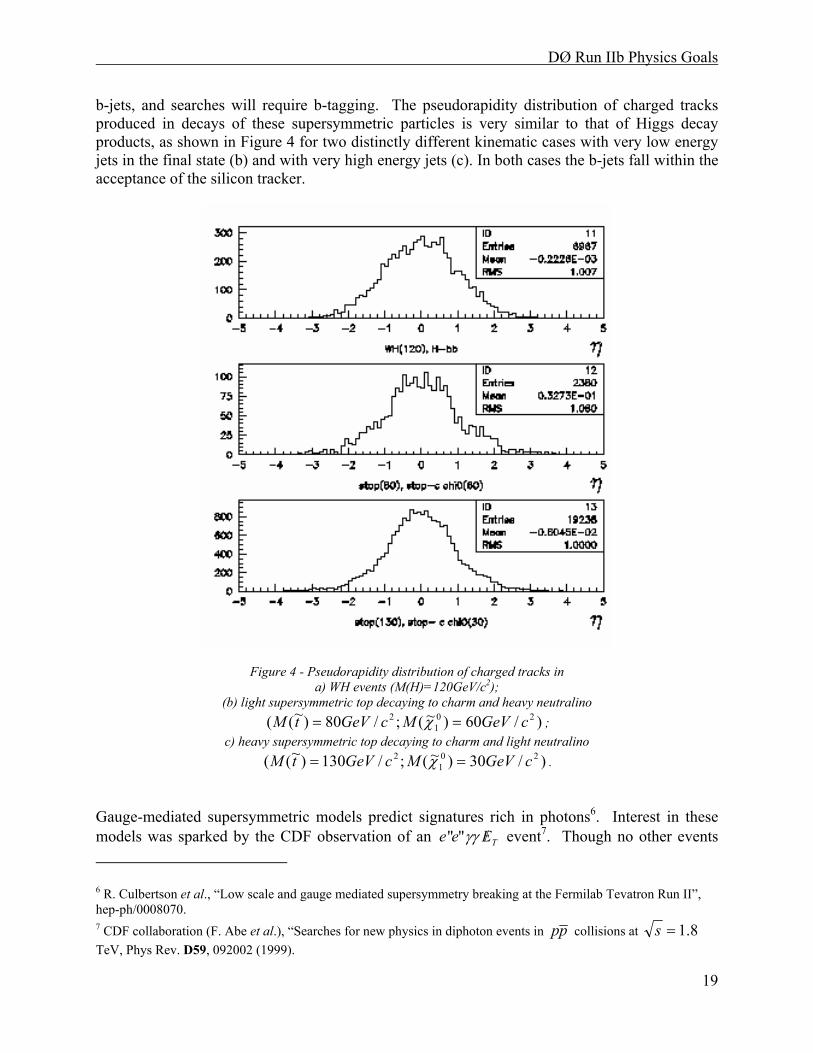
b-jets, and searches will require b-tagging. The pseudorapidity distribution of charged tracks produced in decays of these supersymmetric particles is very similar to that of Higgs decay products, as shown in Figure 4 for two distinctly different kinematic cases with very low energy jets in the final state (b) and with very high energy jets (c). In both cases the b-jets fall within the acceptance of the silicon tracker.
Figure 4 - Pseudorapidity distribution of charged tracks in a) WH events (M(H)=120GeV/c2);
(b) light supersymmetric top decaying to charm and heavy neutralino )/60)~(;/80)~(( 20
12 cGeVMcGeVtM == χ ;
c) heavy supersymmetric top decaying to charm and light neutralino )/30)~(;/130)~(( 20
12 cGeVMcGeVtM == χ .
Gauge-mediated supersymmetric models predict signatures rich in photons6. Interest in these models was sparked by the CDF observation of an TEee /γγ"" event7. Though no other events 6 R. Culbertson et al., “Low scale and gauge mediated supersymmetry breaking at the Fermilab Tevatron Run II”, hep-ph/0008070. 7 CDF collaboration (F. Abe et al.), “Searches for new physics in diphoton events in pp collisions at 8.1=s TeV, Phys Rev. D59, 092002 (1999).

DØ Run IIb Physics Goals
20
have been found, photonic signatures are worth investigating in Run IIb. The phenomenology of extra dimensions also predicts signatures rich in photons8.
Alternatives to SUSY are strong dynamics models, for example technicolor or topcolor. Technicolor models predict the existence of technibosons decaying to heavy flavor and gauge bosons9, e.g. bbWpp TT →→ ππ , . Such searches give vector boson plus heavy-flavor-jets signatures, just like the Higgs search, and will benefit from the detector optimizations motivated by Higgs signatures. More recent topcolor models10 emphasize non-standard behavior of the top quark and thus could be detected indirectly with thorough studies of top quark properties, or directly through observation of anomalous tb production or production of non-standard Higgs-like bosons decaying to heavy flavor jets.
8 T. Rizzo “Indirect collider tests for large extra dimensions”, hep-ph/9910255. 9 E. Eichten, K. Lane and J. Womersley, “Finding Low-Scale Technicolor at Hadron Colliders”, Phys. Lett. B 405, 305 (1997). 10 C. Hill, “Topcolor assisted Technicolor”, Phys. Rev. D49, 4454 (1994).

DØ Run IIb Physics Goals
21
4 STANDARD MODEL PHYSICS The searches for new particles will be complemented by precision measurements of the quanta of the standard model, which provide indirect constraints on new physics, and which will provide the detailed understanding of backgrounds that discoveries will require.
The Tevatron is entering a new era for top quark physics. Greatly increased statistics will be combined, in DØ, with much improved signal sample purity made possible by silicon vertex b-tagging. We anticipate significant improvements in the precision of the top quark mass measurement, which should reach a level of ~2 GeV with 2 fb-1. The additional statistics of Run IIb should allow a precision of ~1 GeV. Single top production (through the electroweak coupling of the top) has never been observed. Measurement of the cross section would allow the CKM matrix element |Vtb| to be extracted. With 2 fb-1, the cross section can likely be measured at the 20% level, allowing |Vtb| to be extracted with a precision of 12%. With 15 fb-1, this uncertainty could be roughly halved. The signatures for top pair and single top production involve vector bosons and heavy flavor jets, just like the SM Higgs. They must be understood in detail for the Higgs search and they will benefit from the detector upgrade.
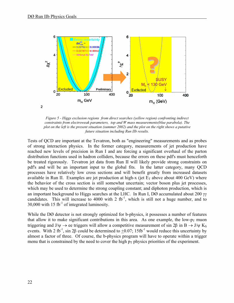
Precision measurements of the properties of the weak boson will continue to be an important part of the Tevatron program. The W-mass precision should reach 30 MeV per experiment with 2fb-1 and 15-20 MeV may be achievable with 15 fb-1 (theoretical uncertainties are a big unknown in this extrapolation). A W-mass measurement δmW = 20 MeV combined with a top mass measurement δmt = 2 GeV will be sufficient to constrain the Higgs mass between roughly 0.7 and 1.5 times its central value11. For a 100 GeV best fit, the upper limit of 150 GeV would be well within the Tevatron's region of sensitivity. Such a comparison between direct and indirect Higgs mass measurements would be very interesting whether or not a Higgs signal is seen, as shown in Figure 5.
11 M. Grünewald et al., hep-ph/0111217 (2001).
DØ Run IIb Physics Goals
22
Figure 5 - Higgs exclusion regions from direct searches (yellow region) confronting indirect
constraints from electroweak parameters, top and W mass measurements(blue parabola). The plot on the left is the present situation (summer 2002) and the plot on the right shows a putative
future situation including Run IIb results.
Tests of QCD are important at the Tevatron, both as "engineering" measurements and as probes of strong interaction physics. In the former category, measurements of jet production have reached new levels of precision in Run I and are forcing a significant overhaul of the parton distribution functions used in hadron colliders, because the errors on these pdf's must henceforth be treated rigorously. Tevatron jet data from Run II will likely provide strong constraints on pdf's and will be an important input to the global fits. In the latter category, many QCD processes have relatively low cross sections and will benefit greatly from increased datasets available in Run II. Examples are jet production at high-x (jet ET above about 400 GeV) where the behavior of the cross section is still somewhat uncertain; vector boson plus jet processes, which may be used to determine the strong coupling constant; and diphoton production, which is an important background to Higgs searches at the LHC. In Run I, DØ accumulated about 200 γγ candidates. This will increase to 4000 with 2 fb-1, which is still not a huge number, and to 30,000 with 15 fb-1 of integrated luminosity.
While the DØ detector is not strongly optimized for b-physics, it possesses a number of features that allow it to make significant contributions in this area. As one example, the low-pT muon triggering and J/ψ → ee triggers will allow a competitive measurement of sin 2β in B → J/ψ KS events. With 2 fb-1, sin 2β could be determined to +0.07; 15fb-1 would reduce this uncertainty by almost a factor of three. Of course, the b-physics program will have to operate within a trigger menu that is constrained by the need to cover the high pT physics priorities of the experiment.
0
2
4
6
10020 400
mH GeV
∆χ2
Excluded Preliminary
∆αhad =∆α(5)
0.02761+÷∠ 0.00036
0.02747+÷∠ 0.00012
Without NuTeV
theory uncertainty
??SUSY
Mh < 130 GeV↓0
2
4
6
10020 400
mH GeV
∆χ2
Excluded Preliminary
∆αhad =∆α(5)
0.02761+÷∠ 0.00036
0.02747+÷∠ 0.00012
Without NuTeV
theory uncertainty
??SUSY
Mh < 130 GeV↓
??SUSY
Mh < 130 GeV↓

DØ Run IIb Physics Goals
23
5 SUMMARY OF PHYSICS OBJECTIVES The DØ Run IIb upgrade is optimized for Higgs boson observation in the 110<MH<180GeV/c2 mass region. A low-mass Higgs boson decays predominantly to bb , and thus efficient b-tagging is of paramount importance to Higgs boson searches. Trigger upgrades that allow the efficient recording of Higgs events are also crucial elements of the upgrade. Lepton identification, crucial for much of the Run IIb physics program, requires efficient triggering and tracking of high pT tracks in a high occupancy environment, in conjunction with the excellent muon and calorimeter of the DØ detector. tHt production puts additional, more stringent, constraints on efficient tracking and secondary and tertiary vertex reconstruction.
It is clear that the entire DØ physics menu of searches, top quark physics, electroweak measurements, QCD, and even b-physics, will benefit from Run IIb. The upgraded tracker will ensure efficient tracking in a high occupancy environment, the upgraded trigger will allow the required data samples to be recorded with high efficiency, and efficient heavy flavor tagging will be a key ingredient for final states with b and c-quark jets.

24
(This page intentionally left blank)
25
SILICON DETECTOR
DØ Run IIb Upgrade Technical
Design Report

DØ Run IIb Silicon Detector
26
(This page intentionally left blank)

DØ Run IIb Silicon Detector
27
SILICON DETECTOR CONTENTS
1 Introduction................................................................................................................................ 33
2 Silicon Detector Design ............................................................................................................. 35
2.1 Introduction......................................................................................................................... 35
2.2 Design Constraints .............................................................................................................. 35
2.2.1 Tevatron parameters..................................................................................................... 35
2.2.2 Radiation environment................................................................................................. 35
2.2.3 Silicon track trigger...................................................................................................... 36
2.2.4 Cable plant ................................................................................................................... 36
2.3 Baseline Design Overview.................................................................................................. 37
3 Silicon Sensors........................................................................................................................... 44
3.1 Introduction......................................................................................................................... 44
3.1.1 Lessons from Run IIa................................................................................................... 44
3.1.2 Radiation damage in silicon......................................................................................... 45
3.1.3 Radiation hard designs................................................................................................. 47
3.2 Silicon Sensors for Run IIb................................................................................................. 48
3.3 Fluence Estimation for Run IIb........................................................................................... 51
3.4 Silicon Sensor Performance Extrapolations for Run IIb..................................................... 53
3.4.1 Leakage current and shot noise estimations................................................................. 53
3.4.2 Leakage currents for a realistic silicon temperature profile......................................... 56
3.4.3 Depletion voltage predictions ...................................................................................... 57
3.4.4 Signal to noise ratio ..................................................................................................... 60
3.5 Radiation Testing of Silicon Sensors.................................................................................. 63
3.5.1 Radiation Damage Facility .......................................................................................... 63
3.5.2 Run IIa detector irradiation studies.............................................................................. 64

DØ Run IIb Silicon Detector
28
3.5.3 Run IIb detector irradiation studies.............................................................................. 67
3.6 Conclusion .......................................................................................................................... 68
4 Mechanical Design, Structures, And Infrastructure................................................................... 70
4.1 Overview............................................................................................................................. 70
4.2 Overall Support Structure ................................................................................................... 73
4.2.1 Outer support cylinders, stave positioning bulkheads, and z = 0 membranes ............. 73
4.2.2 Alignment precision and survey accuracy ................................................................... 75
4.3 Layer 0-1 Silicon Mechanical Support Structure................................................................ 75
4.3.1 Introduction.................................................................................................................. 75
4.3.2 Design of the Layer 0-1 Silicon Mechanical Support Structure .................................. 76
4.3.3 FEA analysis of the L0/L1 mechanical structures ....................................................... 88
4.3.4 Properties of Carbon Fiber Composites....................................................................... 98
4.3.5 Fabrication Techniques.............................................................................................. 108
4.3.6 Assembly Procedures................................................................................................. 117
4.3.7 Radiation Length Calculations................................................................................... 122
4.4 Layer 2-5 Mechanical Design........................................................................................... 127
4.4.1 Readout configuration................................................................................................ 127
4.4.2 Silicon modules.......................................................................................................... 128
4.4.3 Stave assemblies ........................................................................................................ 129
4.4.4 Stave mass and radiation length................................................................................. 131
4.4.5 Stave mechanical connection..................................................................................... 132
4.4.6 Alignment precision and stave mounts ...................................................................... 133
4.4.7 Layer 2-5 stave thermal performance ........................................................................ 133
4.4.8 Layer 2-5 stave mechanical performance .................................................................. 137
4.5 Installation of the Run IIb Silicon Tracker ....................................................................... 138

DØ Run IIb Silicon Detector
29
4.6 Alignment within the Fiber Tracker ................................................................................. 139
4.7 Mechanical Infrastructure at DAB.................................................................................... 140
4.7.1 Cooling system........................................................................................................... 140
4.7.2 Dry gas system........................................................................................................... 141
4.7.3 Monitoring, interlocks, and controls.......................................................................... 142
4.7.4 Systems electrical power............................................................................................ 142
4.7.5 Existing chiller overview ........................................................................................... 142
4.7.6 Additional chiller overview ....................................................................................... 142
4.7.7 Current process control system overview.................................................................. 143
4.7.8 Silicon cooling system integration into the current process control system.............. 143
4.7.9 Silicon cooling system computer security ................................................................. 143
4.7.10 Monitoring via the DAQ system.............................................................................. 144
4.7.11 Interlocks.................................................................................................................. 144
4.7.12 Alarms...................................................................................................................... 145
5 Readout Electronics ................................................................................................................. 147
5.1 Overview........................................................................................................................... 147
5.2 SVX4 Readout Chip ......................................................................................................... 150
5.2.1 SVX4 tests with Stimulus Setup ................................................................................ 156
5.3 Analog Cables................................................................................................................... 162
5.3.1 Layer 0 Prototype....................................................................................................... 166
5.4 Hybrids.............................................................................................................................. 171
5.5 Cables, Adapter Card and Interface Board Overview ...................................................... 176
5.6 Digital Jumper Cables....................................................................................................... 176
5.7 Junction Cards................................................................................................................... 177
5.8 Twisted Pair Cable............................................................................................................ 178

DØ Run IIb Silicon Detector
30
5.9 Adapter Card..................................................................................................................... 180
5.9.1 Adapter Card Implementation Details ....................................................................... 182
5.9.2 Purple Card ................................................................................................................ 184
5.10 Interface Board................................................................................................................ 185
5.11 Sequencer........................................................................................................................ 185
5.12 Low Voltage Distribution ............................................................................................... 186
5.13 High Voltage Distribution............................................................................................... 186
5.14 Performance .................................................................................................................... 188
5.15 Carbon Fiber Grounding Studies .................................................................................... 192
6 Production And Testing ........................................................................................................... 196
6.1 Overview........................................................................................................................... 196
6.2 Sensor tests........................................................................................................................ 197
6.3 Hybrid assembly and initial tests ...................................................................................... 202
6.4 Test stand hardware .......................................................................................................... 204
6.5 Fast functionality test for stuffed hybrids ......................................................................... 210
6.6 Module Assembly ............................................................................................................. 211
6.7 Debugging of Detector Modules....................................................................................... 212
6.8 Burn-in Tests for hybrids and detector modules............................................................... 213
6.9 QA Test for Detector Modules ......................................................................................... 214
6.10 QA Test for Stave Assembly .......................................................................................... 215
6.11 Electrical Tests during Stave and Tracker Assembly ..................................................... 215
6.12 Full System Electrical Test ............................................................................................. 216
6.13 Production Database ....................................................................................................... 217
7 Radiation and Temperature Monitoring................................................................................... 219
7.1 Radiation Monitoring and Beam Abort System................................................................ 219
DØ Run IIb Silicon Detector
31
7.1.1 The Run IIa system .................................................................................................... 219
7.1.2 The Run IIb radiation monitoring system.................................................................. 227
7.2 Temperature Monitoring................................................................................................... 229
7.2.1 Run IIa Temperature Monitoring............................................................................... 229
7.2.2 Run IIb Temperature Monitoring............................................................................... 229
8 Software ................................................................................................................................... 231
8.1 Online Software Components ........................................................................................... 231
8.1.1 The Oracle Database .................................................................................................. 231
8.1.2 Graphical User Interfaces .......................................................................................... 233
8.1.3 Secondary Data Acquisition ...................................................................................... 235
8.1.4 Run IIb Modifications................................................................................................ 238
8.1.5 Data Monitoring During Runs ................................................................................... 238
8.2 Offline software ................................................................................................................ 242
8.3 Hardware Operations ........................................................................................................ 243
8.3.1 VRB ........................................................................................................................... 243
8.3.2 SEQ............................................................................................................................ 243
8.3.3 SEQ channel............................................................................................................... 244
8.3.4 KSU Interface board (INT)........................................................................................ 244
8.3.5 HDI ............................................................................................................................ 244
8.3.6 VRB Crate (VRBCR): ............................................................................................... 244
8.3.7 VRB Controller (VRBC) ........................................................................................... 245
8.3.8 VRB Buffer Driver (VBD). ....................................................................................... 245
8.3.9 Sequencer Controller (SEQC).................................................................................... 246
8.3.10 Global options.......................................................................................................... 246
9 Simulation of the Silicon Detector Performance for Run IIb .................................................. 248

DØ Run IIb Silicon Detector
32
9.1 Overview........................................................................................................................... 248
9.2 Silicon Geometry in the Simulation.................................................................................. 248
9.3 Simulation of Signal, Digitization and Cluster Reconstruction........................................ 251
9.4 Analysis Tools .................................................................................................................. 252
9.5 Performance Benchmarks ................................................................................................. 253
9.6 Results............................................................................................................................... 253
9.6.1 Occupancy.................................................................................................................. 253
9.6.2 Cluster size and spatial resolution.............................................................................. 257
9.7 Physics Performance of the Run IIb Tracker.................................................................... 265
9.7.1 Single track performance ........................................................................................... 265
9.7.2 b-tagging performance ............................................................................................... 269
9.8 Conclusions....................................................................................................................... 273
10 Summary ................................................................................................................................ 274
DØ Run IIb Silicon Detector
33
1 INTRODUCTION The current DØ silicon tracker was built to withstand the 2 – 4 fb-1 of integrated luminosity originally projected for Run II. Because of the tantalizing physics prospects a higher integrated luminosity brings, the laboratory supports extended running of the Tevatron collider, called Run IIb, which would deliver a total integrated luminosity of 15 fb-1 over the course of the full Run II. However, the higher integrated luminosity now scheduled for Run IIb will render the inner layers of the present silicon tracker inoperable due to radiation damage. Of particular importance to be able to exploit the physics potential of the Tevatron is the construction of a replacement of the silicon detector in approximately three years with minimal Tevatron down time. The DØ collaboration carefully studied two options for a Run IIb silicon tracker replacement: “partial replacement” and “full replacement.” In the partial replacement option, the present tracker design is retained and the inner two silicon layers are replaced with new radiation tolerant detectors. In the full replacement option, the entire Run IIa silicon tracker is replaced with a new device. An internal review of these two options identified significant risks with the partial replacement option. These include the risk of damage to the components not being replaced, the long down-time required to retrofit the existing detector, an inadequate supply of the SVX2 readout chips, difficulties in adequately cooling the inner layers, and marginal radiation hardness for the extended operation of Run IIb in the layers not being replaced. Furthermore, it is nearly impossible to re-optimize the detector for the Run IIb physics program with the partial replacement option. For these reasons, DØ decided to proceed with the full replacement option for Run IIb and build a new silicon tracker that is optimized for the Higgs search and other high-pT physics processes.
The design studies for the new silicon detector were carried out within a set of boundary conditions set by the Laboratory and derived from the physics goals for Run IIb. The first requirement imposed is that the detector be able to withstand an integrated luminosity of 15 fb-1. For 15 fb-1, combining the data of both the CDF and DØ detectors, a 5σ discovery of the Standard Model Higgs can be made for a Higgs mass of 115 GeV, a >3σ signal is expected for most of the mass range up to 175 GeV, and Higgs masses up to 180 GeV can be excluded if there is no sign of the Higgs. This result depends crucially on the ability to efficiently tag b-jets, which drives the detector design towards placing the silicon detectors at relatively small distances from the beam. Collecting 15 fb-1 of integrated luminosity with a tracking device so close to the interaction point puts stringent requirements on the cooling for the inner layers, and has led to a natural division of the detector into two radial groups: an inner group and an outer group. The laboratory has required that the shutdown for replacement of the current silicon detectors should occur in the year 2005 and should not exceed six months in duration. This timeframe is set by the startup of the LHC collider at CERN. This stringent timetable forces the detector to be replaced in the DØ collision hall. A rollout of the detector, out of the collision hall into the assembly hall, replacing the silicon detector, and rolling it back in is an operation estimated to take at least nine months and would risk further damage and delay. Installation of the new silicon detector in the collision hall constrains the installable package length to 52”, determined by the space available between the central and end calorimeters in the collision hall which is only 39”. The last requirement imposed by the Laboratory is that the project should be completed within a tightly constrained budget. To reduce the cost and to keep to the schedule, as much of the present data acquisition system as possible will be retained. Even though there are

DØ Run IIb Silicon Detector
34
significant boundary conditions, the new detector presented in this document is designed to have better performance than the Run IIa detector and is expected to be completed within the allocated time, calling for an installation in the summer of 2005.
This report describes the current conceptual design of the new silicon detector for the DØ experiment for Run IIb. Section 2 gives an overview of the proposed DØ silicon detector design and serves as an introduction to the following sections. Section 3 discusses the silicon sensors, Section 4 the mechanical aspects of the design, and Section 5 the readout electronics. Section 6 describes the production and testing, Section 7 describes temperature and radiation monitoring, and Section 8 describes the software needed for the quality assurance and testing of the devices. Section 9 presents the results of simulation studies to determine the expected detector performance and Section 10 summarizes the silicon part of the TDR.

DØ Run IIb Silicon Detector
35
2 SILICON DETECTOR DESIGN
2.1 Introduction
The silicon detector project is introduced in this section. The design is based on an optimization of the physics performance of the detector while at the same time satisfying various boundary conditions, both external and internal. The external boundary conditions come from the anticipated accelerator performance in Run IIb. Interfacing the new detector within the existing framework, notably the trigger framework, sets internal constraints. Moreover, building on our experience constructing the Run IIa silicon detector, fabrication and assembly methods proposed for the new silicon detector were reevaluated and the strategy adopted for Run IIb should result in a much more efficient construction cycle. The new detector, for example, will employ only single-sided silicon technology. The remainder of this section will describe the basic design features of the proposed silicon detector.
2.2 Design Constraints
2.2.1 Tevatron parameters
The DØ Run IIb TDR describes a silicon detector designed to operate at a luminosity of 5x1032 cm-2 sec-1 with 132 ns bunch spacing and a small crossing angle. At this luminosity, an average of 5 minimum bias interactions will accompany the high-pT interaction of interest. The laboratory has recently changed the baseline plan for Run IIb operations to a luminosity of 2x1032 cm-2 sec-1 with 396 ns bunch spacing and no crossing angle. Luminosity leveling will be used to hold the luminosity at 2x1032 cm-2 sec-1 and the achievable integrated luminosity is expected to be the same as if there were no leveling and an initial luminosity of about 3.4x1032 cm-2 sec-1. This mode of operation also yields an average of 5 minimum bias interactions accompany the high-pT interaction. Thus, detector performance should be nearly identical for these two operating modes except for the difference in crossing angle. For 396 ns bunch spacing, the absence of a crossing angle leads to a larger longitudinal spread in the luminous region, with 5% of the interaction vertices occurring outside the 96 cm fiducial length of the innermost silicon layers. This loss in geometrical acceptance is not included in the detector studies presented below.
2.2.2 Radiation environment
The collaboration embarked on radiation studies of silicon sensors for both the present and proposed Run IIb detector to determine the timescale within which the present detector would become inoperable and to determine the operating parameters for the new detector. The leakage currents and depletion voltages were measured using 8 GeV protons from the booster facility at Fermilab up to a dose of 15 MRad. The measurements agree with others made outside of DØ and will be described in the next section. Based on these measurements, and parameters obtained by other experiments, simulation studies were carried out of the leakage current, depletion voltage, and equivalent noise to determine the silicon operating temperature and to ensure that the device can withstand the foreseen accumulated dose. The design operating
DØ Run IIb Silicon Detector
36
temperature of the inner layer was chosen to be –10 degrees Celsius. We also determined that a minimum radius of about 18 mm for the innermost layer of silicon will allow for an adequate safety margin for running the detector to integrated luminosities of 15 fb-1.
2.2.3 Silicon track trigger
The Run IIa silicon detector employs a Silicon Track Trigger (STT) that processes data from the Level 1 Central Track Trigger (CTT) and the silicon tracker. It associates hits in the silicon with tracks found by the Level 1 CTT. These hits are then fit together with the Level 1 CTT information, thus improving the resolution in momentum and impact parameter, and the rejection of fake tracks. The STT has three types of electronics modules:
• The Fiber Road Card (FRC), which receives the data from CTT and fans them out to the other modules.
• The Silicon Trigger Card (STC), which receives the raw data from the silicon tracker front end. It processes the data to find clusters of hit strips that are associated with the tracks found by the CTT. Each card accepts input from at most eight readout hybrids.
• The Track Fit Card (TFC), which fits a trajectory to the CTT tracks and the silicon clusters associated with it. These results are relayed to the Level 2 Central Track Trigger. Each card can accept at most eight STC inputs.
The trigger observes a 6-fold φ-symmetry. The STT modules are located in 6 VME crates, each serving two 30-degree azimuthal sectors. Currently each of these crates holds one FRC, nine STCs, and two TFCs - one per 30-degree sector. Each crate can hold at most 12 STCs, with a possibility to go to 16 STC cards with a redesigned backplane. It is these constraints, combined with the 6-fold symmetry that has to be observed for the new silicon detector, which severely limits the parameter space for the geometry of the tracker.
The data from the silicon tracker must be channeled into the TFC cards such that all hits from a track are contained in one TFC. In layers 0, 1, and 2 overlaps between adjacent sensors are large enough so that each sensor can be uniquely associated with one TFC. This divides the detector into 12 azimuthal sectors. To maintain full acceptance for tracks with pT>1.5 GeV/c and impact parameter < 2 mm, the data from some sensors in layers 3, 4, and 5 must be channeled into two TFCs, which are in some cases located in different crates. These constraints have resulted in a geometry with 12-fold symmetry for layers 0 through 2, and an 18-, 24- and 30-fold geometry for layers 3, 4 and 5, respectively.
2.2.4 Cable plant
The total number of readout modules in the new system is constrained by the currently available cable plant, which allows for about 940 cables. The present Run IIa detector has 912 readout modules. The cable plant is limited due to space constraints. There simply is not enough space between the central and end calorimeters to route more cables. Only replacing the full cable plant would allow an increase in the number of cables, but this is cost prohibitive. Given that the new detector has more silicon sensors, this implies that not every sensor can be read out and that

DØ Run IIb Silicon Detector
37
an adequate ganging scheme will have to be implemented. An elegant solution using double-ended hybrids has been found which is described in the next section.
2.3 Baseline Design Overview
The proposed silicon detector has a 6 layer geometry arranged in a barrel design. The detector will be built in two independent barrel assemblies joined at z=0. The six layers, numbered 0 through 5, are divided in two radial groups. The inner group, consisting of layers 0 and 1, will have axial readout only. Driven by the stringent constraints on cooling, these layers will be grouped into one mechanical unit called the inner barrel. These layers have a significantly reduced radius relative to the current tracker. Given the tight space constraints, emphasis has been placed on improving the impact parameter resolution. The outer group is comprised of layers 2 through 5. Each outer layer will have axial and stereo readout. The outer layers are also important for providing stand-alone silicon tracking with acceptable momentum resolution in the region 1.7 < |η| < 2.0 where DØ has good muon and electron coverage but lacks coverage in the fiber tracker. The outer layers are assembled in a mechanical unit called the outer barrel. The inner barrel is inserted into the outer barrel forming a barrel assembly. A barrel assembly is the basic unit that is installed in the collision hall. While all 6 layers are designed to withstand 15 fb-
1 of integrated luminosity with adequate margin, separating the inner layers into a separate radial group provides a path for possible replacement of these layers. The outer layers should easily withstand luminosities up to ~25 fb-1. The inner two layers with axial readout will provide an adequate impact parameter resolution for tagging of b-jets. Two layers as close to the interaction point as possible are preferred to efficiently tag b-jets. The remaining space can accommodate at most four axial-stereo layers, which is adequate to do the pattern recognition. Hence our design calls for six layers.
Of paramount importance to the successful construction of the new detector in the less than 3 years available, is a simple modular design with a minimum number of part types. This is one of the reasons that single-sided silicon sensors are used throughout the detector. Only three types of sensors are foreseen: highly radiation tolerant sensors for layers 0 and 1, with two sizes to best fit the geometrical constraints, and a single sensor size for the four outer layers. All of the sensors are envisioned to have axial traces with intermediate strips. The stereo readout in the outer layers will be accomplished by tilting the sensor slightly with respect to the beam axis.
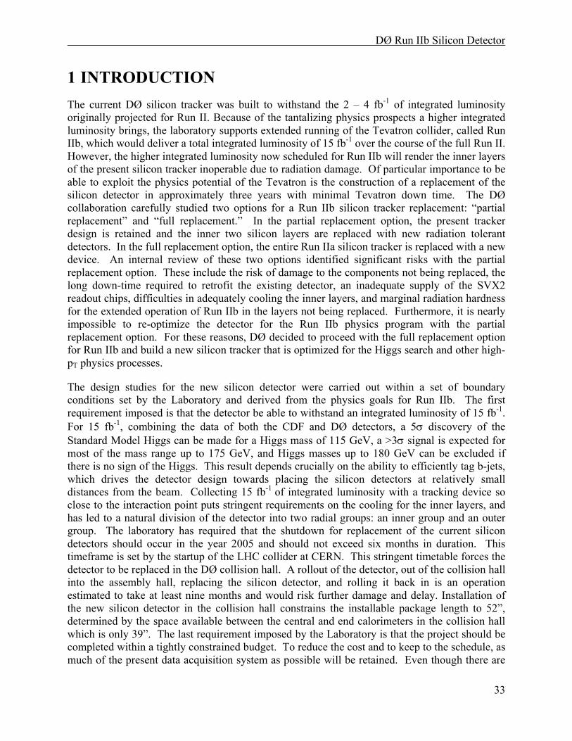
Figure 1 shows an axial view of the Run IIb silicon tracker. The emphasis is on obtaining improved impact parameter resolution in the R-φ plane while maintaining good pattern recognition. The inner two layers have 12-fold crenellated geometry and will be mounted on a carbon fiber support structure. Figure 2 shows an axial view of these two inner layers. Layer 0 will have its innermost sensor located at a radius of about 18.6 mm. These sensors will be two-chip wide, 78.4mm long with 50 micron readout pitch and intermediate strips. The pitch is chosen to obtain the best impact parameter resolution possible using conventional technology. Given the size of the luminous region, 6 sensors in z are used in each barrel assembly.
DØ Run IIb Silicon Detector
38
Figure 1 - Axial view of the proposed tracker upgrade. The outer four layers provide both axial and stereo track measurements, while the inner two layers only provide axial track measurements.
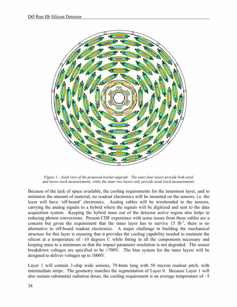
Because of the lack of space available, the cooling requirements for the innermost layer, and to minimize the amount of material, no readout electronics will be mounted on the sensors, i.e. the layer will have ‘off-board’ electronics. Analog cables will be wirebonded to the sensors, carrying the analog signals to a hybrid where the signals will be digitized and sent to the data acquisition system. Keeping the hybrid mass out of the detector active region also helps in reducing photon conversions. Present CDF experience with noise issues from these cables are a concern but given the requirement that the inner layer has to survive 15 fb-1, there is no alternative to off-board readout electronics. A major challenge in building the mechanical structure for this layer is ensuring that it provides the cooling capability needed to maintain the silicon at a temperature of –10 degrees C while fitting in all the components necessary and keeping mass to a minimum so that the impact parameter resolution is not degraded. The sensor breakdown voltages are specified to be >700V. The bias system for the inner layers will be designed to deliver voltages up to 1000V.
Layer 1 will contain 3-chip wide sensors, 79.4mm long with 58 micron readout pitch, with intermediate strips. The geometry matches the segmentation of Layer 0. Because Layer 1 will also sustain substantial radiation doses, the cooling requirement is an average temperature of –5
DØ Run IIb Silicon Detector
39
degrees C, while the bias voltage supply requirements will be the same as for Layer 0. Although the heat load from putting hybrids directly on the sensors is greatly increased (0.5 Watts per readout chip), noise and production considerations have led to on-board electronics for all layers except Layer 0.
Figure 2- Axial view of Layers 0 and 1 within the sensor active region. The silicon sensors are mounted on a carbon-fiber support structure with inboard cooling tubes. The readout uses analog
low mass cables which connect to hybrids outside of the active region.
In Layers 2-5 only one type of sensor will be used. The sensors will be 5 chips wide, 100mm long with 60 micron readout pitch and intermediate strips. This pitch allows for direct bonding between SVX chips and the sensors and retaining the fine resolution in Layer 5 significantly improves pattern recognition. These layers employ stiff stave support structures. A stave will have an inner core that will carry the cooling lines. Silicon will be mounted on the core; on one side there will be axial readout and on the other small-angle stereo. The stereo angle will be obtained by rotating the sensors. The design allows for a depletion voltage of >300V for these outer layers. Recall that the detector is built in two halves, north and south; each stave will thus cover a half-length in z.
DØ Run IIb Silicon Detector
40
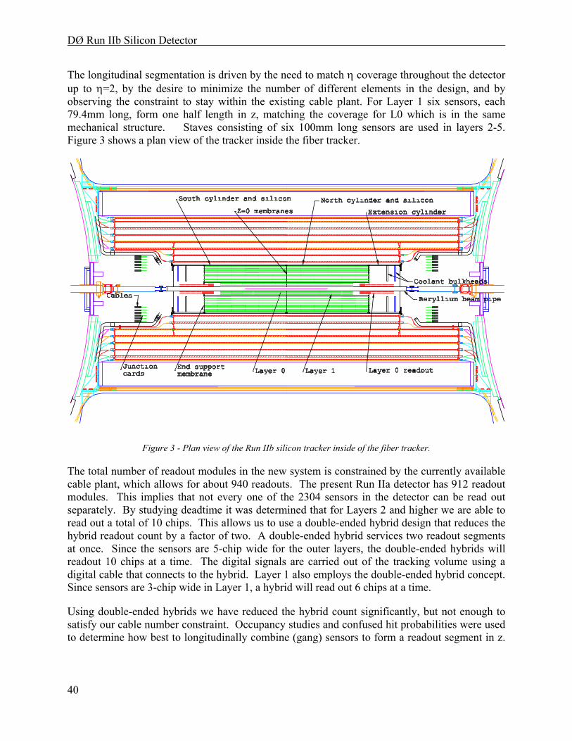
The longitudinal segmentation is driven by the need to match η coverage throughout the detector up to η=2, by the desire to minimize the number of different elements in the design, and by observing the constraint to stay within the existing cable plant. For Layer 1 six sensors, each 79.4mm long, form one half length in z, matching the coverage for L0 which is in the same mechanical structure. Staves consisting of six 100mm long sensors are used in layers 2-5. Figure 3 shows a plan view of the tracker inside the fiber tracker.
Figure 3 - Plan view of the Run IIb silicon tracker inside of the fiber tracker.
The total number of readout modules in the new system is constrained by the currently available cable plant, which allows for about 940 readouts. The present Run IIa detector has 912 readout modules. This implies that not every one of the 2304 sensors in the detector can be read out separately. By studying deadtime it was determined that for Layers 2 and higher we are able to read out a total of 10 chips. This allows us to use a double-ended hybrid design that reduces the hybrid readout count by a factor of two. A double-ended hybrid services two readout segments at once. Since the sensors are 5-chip wide for the outer layers, the double-ended hybrids will readout 10 chips at a time. The digital signals are carried out of the tracking volume using a digital cable that connects to the hybrid. Layer 1 also employs the double-ended hybrid concept. Since sensors are 3-chip wide in Layer 1, a hybrid will read out 6 chips at a time.
Using double-ended hybrids we have reduced the hybrid count significantly, but not enough to satisfy our cable number constraint. Occupancy studies and confused hit probabilities were used to determine how best to longitudinally combine (gang) sensors to form a readout segment in z.
DØ Run IIb Silicon Detector
41
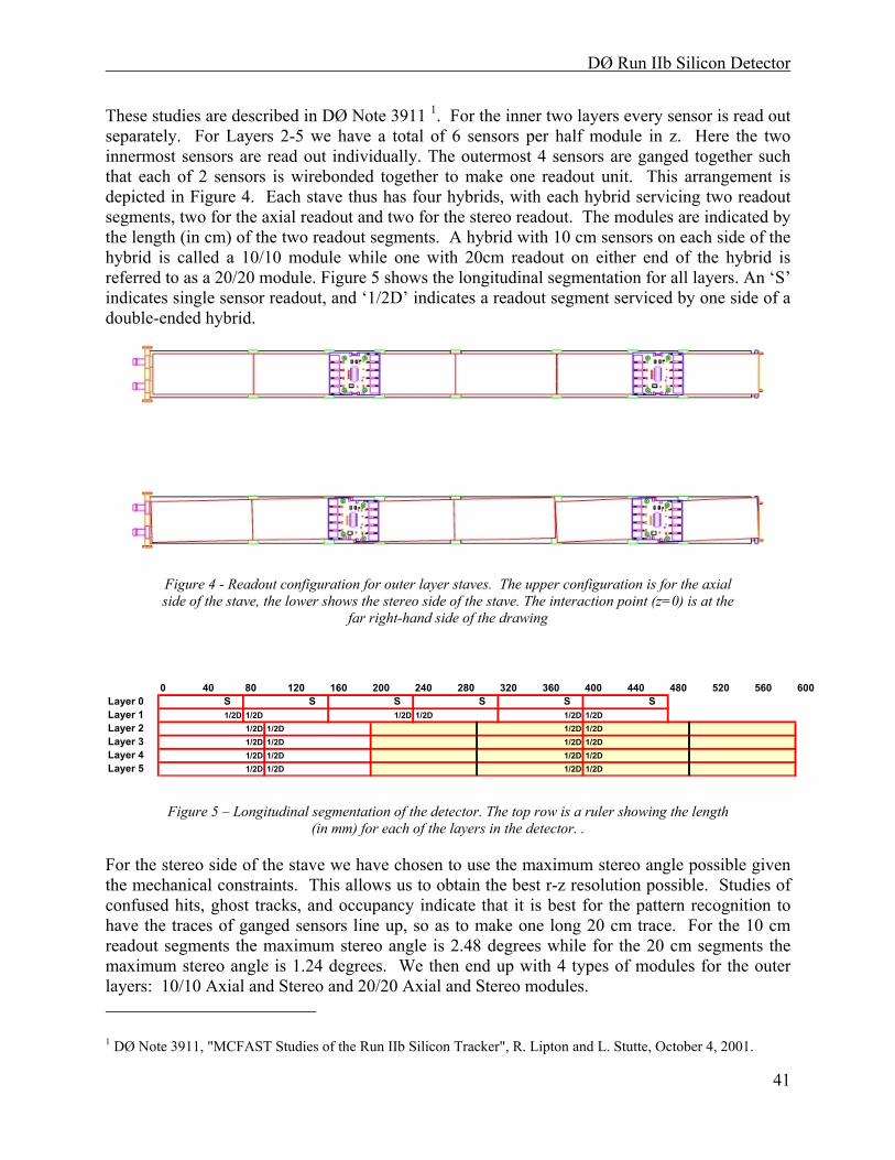
These studies are described in DØ Note 3911 1. For the inner two layers every sensor is read out separately. For Layers 2-5 we have a total of 6 sensors per half module in z. Here the two innermost sensors are read out individually. The outermost 4 sensors are ganged together such that each of 2 sensors is wirebonded together to make one readout unit. This arrangement is depicted in Figure 4. Each stave thus has four hybrids, with each hybrid servicing two readout segments, two for the axial readout and two for the stereo readout. The modules are indicated by the length (in cm) of the two readout segments. A hybrid with 10 cm sensors on each side of the hybrid is called a 10/10 module while one with 20cm readout on either end of the hybrid is referred to as a 20/20 module. Figure 5 shows the longitudinal segmentation for all layers. An ‘S’ indicates single sensor readout, and ‘1/2D’ indicates a readout segment serviced by one side of a double-ended hybrid.
Figure 4 - Readout configuration for outer layer staves. The upper configuration is for the axial side of the stave, the lower shows the stereo side of the stave. The interaction point (z=0) is at the
far right-hand side of the drawing
0 40 80 120 160 200 240 280 320 360 400 440 480 520 560 600Layer 0 S S S S S SLayer 1 1/2D 1/2D 1/2D 1/2D 1/2D 1/2DLayer 2 1/2D 1/2D 1/2D 1/2DLayer 3 1/2D 1/2D 1/2D 1/2DLayer 4 1/2D 1/2D 1/2D 1/2DLayer 5 1/2D 1/2D 1/2D 1/2D
Figure 5 – Longitudinal segmentation of the detector. The top row is a ruler showing the length (in mm) for each of the layers in the detector. .
For the stereo side of the stave we have chosen to use the maximum stereo angle possible given the mechanical constraints. This allows us to obtain the best r-z resolution possible. Studies of confused hits, ghost tracks, and occupancy indicate that it is best for the pattern recognition to have the traces of ganged sensors line up, so as to make one long 20 cm trace. For the 10 cm readout segments the maximum stereo angle is 2.48 degrees while for the 20 cm segments the maximum stereo angle is 1.24 degrees. We then end up with 4 types of modules for the outer layers: 10/10 Axial and Stereo and 20/20 Axial and Stereo modules. 1 DØ Note 3911, "MCFAST Studies of the Run IIb Silicon Tracker", R. Lipton and L. Stutte, October 4, 2001.
DØ Run IIb Silicon Detector
42
The decision was made in November 2000 to read out the new silicon system using the SVX4 chip. Both CDF and DØ will use this chip. This chip is based on the SVX3 chip, but will be produced in 0.25 micron technology. This chip is intrinsically radiation hard and is expected to be able to withstand the radiation doses incurred in the innermost layers. In order not to have to redesign the entire DØ data acquisition and trigger system, the SVX4 chip will be read out in SVX2 mode. The SVX2 chip is the readout chip for the Run IIa detector and incurs deadtime on every readout cycle unlike the SVX3 chip that can run in a deadtimeless mode. As the readout chip is a joint project with both CDF and DØ, there is a premium on employing the same hybrid technology so that the design work can be shared. We plan to use ceramic hybrids using beryllia. No pitch adapters will be needed in the DØ design so that the SVX4 chips will be wirebonded directly to the silicon sensors for layers 1-5.
The digital signals will be launched onto a jumper cable from the hybrid through an AVX connector. These flex cables will run on the top and bottom of the stave to a junction card located at the end of the active region on a bulkhead. There will be one junction card per stave. That is, each junction card will service four hybrids, the two hybrids from the axial readout and the two hybrids from the stereo readout. The junction card is a passive element and simply carries the signals from the digital cable to a twisted-pair cable. The twisted-pair cables run to the adapter cards that are mounted on the face of the calorimeter. The adapter card will interface to the existing data acquisition system. The adapter card has two new functions in Run IIb. First, it will convert 5V lines to 2.5V, necessary for operating the SVX4 chip. The current data acquisition system uses the SVX2 chip, in which the lines are single-ended. The SVX4 chip will be run differentially at 2.5V. The adapter cards will convert the single-ended lines to differential lines. From the adapter card downstream, it is anticipated that we can retain the full data acquisition system as is. Some modifications will be needed for the interface boards that pass the voltages to the detector to allow for higher voltages for the biases for the inner layers, but no major modifications are foreseen.
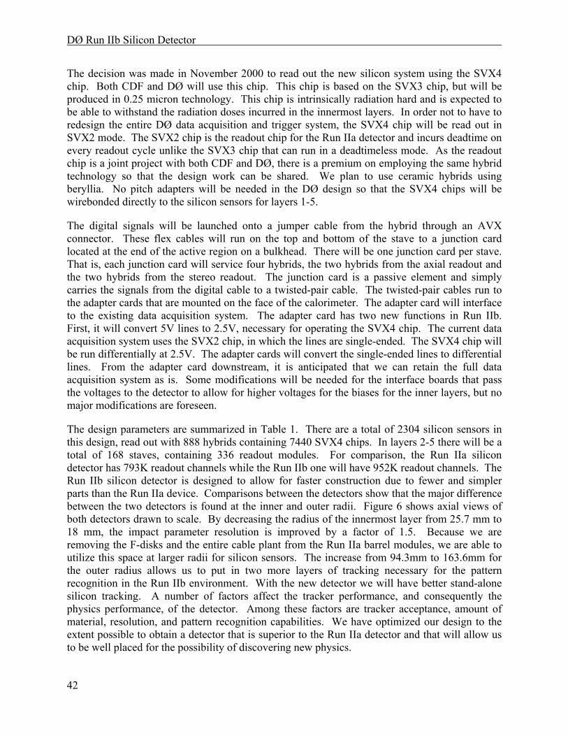
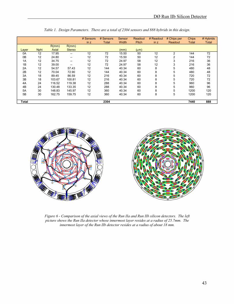
The design parameters are summarized in Table 1. There are a total of 2304 silicon sensors in this design, read out with 888 hybrids containing 7440 SVX4 chips. In layers 2-5 there will be a total of 168 staves, containing 336 readout modules. For comparison, the Run IIa silicon detector has 793K readout channels while the Run IIb one will have 952K readout channels. The Run IIb silicon detector is designed to allow for faster construction due to fewer and simpler parts than the Run IIa device. Comparisons between the detectors show that the major difference between the two detectors is found at the inner and outer radii. Figure 6 shows axial views of both detectors drawn to scale. By decreasing the radius of the innermost layer from 25.7 mm to 18 mm, the impact parameter resolution is improved by a factor of 1.5. Because we are removing the F-disks and the entire cable plant from the Run IIa barrel modules, we are able to utilize this space at larger radii for silicon sensors. The increase from 94.3mm to 163.6mm for the outer radius allows us to put in two more layers of tracking necessary for the pattern recognition in the Run IIb environment. With the new detector we will have better stand-alone silicon tracking. A number of factors affect the tracker performance, and consequently the physics performance, of the detector. Among these factors are tracker acceptance, amount of material, resolution, and pattern recognition capabilities. We have optimized our design to the extent possible to obtain a detector that is superior to the Run IIa detector and that will allow us to be well placed for the possibility of discovering new physics.
DØ Run IIb Silicon Detector
43
Table 1. Design Parameters. There are a total of 2304 sensors and 888 hybrids in this design.
Figure 6 - Comparison of the axial views of the Run IIa and Run IIb silicon detectors. The left picture shows the Run IIa detector whose innermost layer resides at a radius of 25.7mm. The
innermost layer of the Run IIb detector resides at a radius of about 18 mm.
# Sensors # Sensors Sensor Readout # Readout # Chips per Chips # Hybridsin z Total Width Pitch in z Readout Total Total
R(mm) R(mm)Layer Nphi Axial Stereo (mm) (µm)
0A 12 17.95 -- 12 72 15.50 50 12 2 144 720B 12 24.80 -- 12 72 15.50 50 12 2 144 721A 12 34.75 -- 12 72 24.97 58 12 3 216 361B 12 39.00 -- 12 72 24.97 58 12 3 216 362A 12 54.57 57.43 12 144 40.34 60 8 5 480 482B 12 70.04 72.90 12 144 40.34 60 8 5 480 483A 18 89.45 86.59 12 216 40.34 60 8 5 720 723B 18 103.67 100.81 12 216 40.34 60 8 5 720 724A 24 116.52 119.38 12 288 40.34 60 8 5 960 964B 24 130.48 133.35 12 288 40.34 60 8 5 960 965A 30 148.83 145.97 12 360 40.34 60 8 5 1200 1205B 30 162.75 159.75 12 360 40.34 60 8 5 1200 120
Total 2304 7440 888

DØ Run IIb Silicon Detector
44
3 SILICON SENSORS
3.1 Introduction
The main requirements for the silicon detector are: efficient and reliable tracking, precise vertex measurement, and radiation hardness. As described above, this is achieved with a 6-layer device. The four outer layers are constructed of 60 µm readout pitch silicon sensors and provide hits essential for pattern recognition in a high-occupancy environment. In addition, two inner layers (layer 0 and 1), constructed with 50/58 µm readout pitch silicon sensors with intermediate strips at 25/29 µm, provide precise coordinate measurement essential for good secondary vertex separation. Reliable operation of silicon sensors in a high-radiation environment is critical to the experiment’s success. Over the operating period, the inner layers of the Run IIb silicon detector will be subject to a fluence of about 2 x 10¹⁴ equivalent 1 MeV neutrons per cm2. We were guided in our design and technology choice by our experience in Run IIa detector construction as well as by recent research and development in the radiation hard technology.
3.1.1 Lessons from Run IIa
Several difficulties were encountered by DØ during the Run IIa silicon detector prototyping and construction. The gained Run IIa experiences and important conclusions are:
• Sophisticated double-sided silicon sensors were difficult to produce and lead to lower yield and hence significant delays. Single-sided sensors however, which have been produced both by Elma for the H-disks and Micron for the 1st and 3rd layers of barrels 1 and 6 for the Run IIa detector, had higher yields and caused much less trouble due to their simplicity.
• The introduction of an alternative vendor at the later stages helped to speed up production.
• The large number of sensor types complicated the production process.
• Double-sided sensors proved to be very difficult to handle.
• Radiation studies have shown that double-sided (and especially 90o double-metal) silicon sensors have limited radiation hardness (more details in “Radiation testing”)
• Detailed pattern recognition studies have shown that in high occupancy environment, “ghost” hits produced in 90o sensors lead to a significant fraction of fake tracks and increased reconstruction time.
For the Run IIb silicon sensors, we adopted the following guidelines:
• Use only single sided silicon sensors.
• Try to identify alternative vendors whenever possible.

DØ Run IIb Silicon Detector
45
• Limit the number of sensor types to 3.
• Use only small stereo angles, achieved by sensor rotation.
• Avoid double metallization.
In our choice of radiation hard technology we have benefited greatly from radiation hard silicon R&D studies motivated primarily by the needs of LHC experiments.
3.1.2 Radiation damage in silicon
The most important damage mechanism in silicon is the bulk damage due to the non-ionizing part of the energy loss, which leads to a displacement of the silicon atoms in their lattice. It causes changes in doping concentration (and, eventually, silicon type inversion), increased leakage current, and decreased charge collection efficiency. Surface damage due to ionizing radiation results in charge trapping at the surface interfaces and leads to increased interstrip capacitance and electronics noise. A general overview of radiation damage in silicon detectors can be found in DØ Note 3803.
The change in the effective impurity or doping concentration Neff = [2εε0/(ed2)]⋅Vdepl measured as a function of the particle fluence for n-type starting material shows a decrease until the donor concentration equals the acceptor concentration or until the depletion voltage Vdepl is almost zero, indicating intrinsic material. Towards higher fluences the effective concentration starts to increase again and shows a linear rise of acceptor like defects. The phenomena of changing from n-type to p-type like material has been confirmed by many experimental groups and usually the detector is said to have undergone a “type inversion” from n-type to p-type. The change of the effective doping concentration can be parameterized as
Neff(Φ) = ND,0 ⋅ exp(-cDΦ) - gcΦ
where the first term describes donor removal from the starting donor concentration ND,0 and gc indicates the rate of the radiation induced acceptor state increase. Hence donor removal happens exponentially whereas acceptor states are created linearly with fluence. Type inversion for standard n-type material with resistivity ρ≈5kΩcm typically occurs at a fluence of about (1-2)×1013cm-2.
The radiation-induced changes of the doping concentration are initially not stable and exhibit two main components with different time behaviors and temperature dependences. With time constants in the range of a few days a decrease in the radiation induced changes occurs soon after irradiation. This effect is called short-term annealing or beneficial annealing, because it mitigates the acceptor creation and hence the type inversion process. However, at room temperature an increase in the acceptor states appears after about two weeks of annealing leading to even higher depletion voltages. This long term or reverse annealing is a major concern because of its limiting factor for long-term operation of silicon detectors in high fluence regions. Reverse annealing can be almost completely suppressed by cooling the detector to 0oC or less and by minimizing the maintenance periods of the silicon detectors at room temperature.
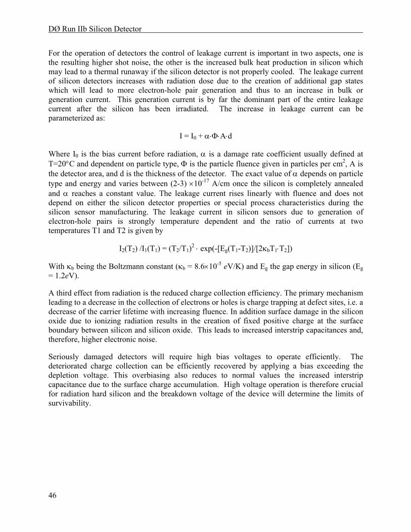
DØ Run IIb Silicon Detector
46
For the operation of detectors the control of leakage current is important in two aspects, one is the resulting higher shot noise, the other is the increased bulk heat production in silicon which may lead to a thermal runaway if the silicon detector is not properly cooled. The leakage current of silicon detectors increases with radiation dose due to the creation of additional gap states which will lead to more electron-hole pair generation and thus to an increase in bulk or generation current. This generation current is by far the dominant part of the entire leakage current after the silicon has been irradiated. The increase in leakage current can be parameterized as:
I = I0 + α⋅Φ⋅A⋅d
Where I0 is the bias current before radiation, α is a damage rate coefficient usually defined at T=20°C and dependent on particle type, Φ is the particle fluence given in particles per cm2, A is the detector area, and d is the thickness of the detector. The exact value of α depends on particle type and energy and varies between (2-3) ×10-17 A/cm once the silicon is completely annealed and α reaches a constant value. The leakage current rises linearly with fluence and does not depend on either the silicon detector properties or special process characteristics during the silicon sensor manufacturing. The leakage current in silicon sensors due to generation of electron-hole pairs is strongly temperature dependent and the ratio of currents at two temperatures T1 and T2 is given by
I2(T2) /I1(T1) = (T2/T1)2 ⋅ exp(-[Eg(T1-T2)]/[2κbT1⋅T2])
With κb being the Boltzmann constant (κb = 8.6×10⁻⁵ eV/K) and Eg the gap energy in silicon (Eg = 1.2eV).
A third effect from radiation is the reduced charge collection efficiency. The primary mechanism leading to a decrease in the collection of electrons or holes is charge trapping at defect sites, i.e. a decrease of the carrier lifetime with increasing fluence. In addition surface damage in the silicon oxide due to ionizing radiation results in the creation of fixed positive charge at the surface boundary between silicon and silicon oxide. This leads to increased interstrip capacitances and, therefore, higher electronic noise.
Seriously damaged detectors will require high bias voltages to operate efficiently. The deteriorated charge collection can be efficiently recovered by applying a bias exceeding the depletion voltage. This overbiasing also reduces to normal values the increased interstrip capacitance due to the surface charge accumulation. High voltage operation is therefore crucial for radiation hard silicon and the breakdown voltage of the device will determine the limits of survivability.

DØ Run IIb Silicon Detector
47
3.1.3 Radiation hard designs
The CMS collaboration designed single-sided 300 µm thick n-type sensors, which were reliably working after heavy irradiation at bias voltages up to 500 V2. The main features of the design are p+ strips in n-bulk silicon, which are biased with polysilicon resistors and are AC coupled to the readout electronics. The front side of the detector (with p+ strips) has a peripheral n+ implantation (n-well) at the edge and is followed by a p+ single guard ring structure to prevent junction breakdowns. This guard ring design has been optimized in cooperation with Hamamatsu and is also successfully implemented with other producers. It is proven to be radiation hard and CDF is using this type of sensors for the L00 of SVX in Run IIa. Other radiation hard designs reduce the risk of an early breakdown at the edges of the silicon by including a multi-guard ring structure3.
We note here that in the case of AC-coupled double-sided sensors (as presently used by CDF and DØ in Run IIa) the high bias voltage is applied across the coupling capacitor on one of the sides (unless the electronics is floating at the same potential). Together with considerably higher costs related to the double-sided wafer processing, the requirement that AC capacitors hold off the bias voltage is a strong limitation for the double-sided detectors and we are not considering using them for the upgrade.
Another option to improve the radiation hardness at moderate fluences is the use of low-resistivity silicon as an initial detector material4. Low bulk resistivity of silicon corresponds to high depletion voltage of the device. For example, a 300 µm thick detector with bulk resistivity of cmk ⋅Ω≈ 0.1ρ depletes at 300≈deplV V. High initial depletion voltage values shift the type-inversion point towards higher fluences, and limits the depletion voltage growth after the type inversion, thus improving the radiation hardness of the sensor in the moderate fluence regime of up to 1014 cm-2.
A new technological development driven by the R&D work of the ROSE collaboration5 uses oxygenated silicon materials to improve the radiation hardness of silicon detectors. Oxygen concentrations ( 31710][ −≈ cmOi ) in silicon considerably improves the radiation hardness of the detector for charged particle fluence and effectively lowers the needed bias voltage for radiation damaged detectors. No improvement was observed for damage caused by neutrons. The charged particle component is expected to dominate (for example at CMS only 1/10th of the damage is accounted for by neutrons). There are indications also that the reverse annealing saturates at high fluences for oxygen enriched silicon.
2 S. Braibant et al., Investigation of design parameters for radiation hard silicon, Nucl.Instr.Meth A485:343-361,2002. 3 A. Bischoff et al., Breakdown protection and long term stabilization for Si-detectors, Nucl. Instr. & Meths. A326 (1993)27-37. 4 RD20 collaboration, "Radiation damage studies of field plate and p-stop n-side silicon microstrip detectors", Nucl. Instr. & Meths. A362 (1995) 297-314, 1995. 5 Rose Collaboration, Nucl. Instr. & Meth. in Phys. Res. A466 (2001) 308-326

DØ Run IIb Silicon Detector
48
High oxygen concentrations reduce the donor (n-impurity) removal rate significantly and can mitigate the acceptor (p-impurity) creation. The simplest way to enrich silicon material with oxygen is a diffusion process in the Co1200~ oxygen atmosphere of a quartz oven. This technology is easy and economic and has been successfully transferred to a number of silicon detector vendors.
Finally there is an alternative to use n+ strips on n type silicon. It has been shown that they offer a better charge collection efficiency at under-depleted voltages and, therefore, would improve the performance after irradiation. However, the detectors technologically are more complicated and require further R&D efforts. Since for n+n sensors certain techniques like p-stop or p-spray are necessary to maintain the strip isolation, the detectors are becoming more and more complex which would considerably drive up the costs. Furthermore, it is not clear that such a fine pitch structure of 25µm we are requiring for layer 0 is technologically feasible on n+n devices. Except LHCb, which is pursuing a n+n option for its vertex microstrip detector, neither of the other LHC silicon strip detectors will use n+n and we are considering this technology as too risky for the tight Run IIb schedule.
In summary, three approaches have been successfully explored so far:
• Special designed guard ring structures. Such guard rings are important in order to keep the breakdown voltage before and after irradiation as high as possible.
• Low-resistivity silicon sensors. Increasing initial donor concentration leads to type inversion after higher radiation doses, thus slowing the radiation damage.
• Oxygenated silicon. Controlled increase in oxygen concentration slows down the growth of depletion voltage with irradiation dose.
It is possible to combine all three approaches. The techniques have been transferred to multiple silicon vendors.
3.2 Silicon Sensors for Run IIb
For the construction of the Silicon Microstrip Tracker for Run IIb DØ we propose the use of AC-coupled, single-sided single-metal p+ on n-bulk silicon devices with integrated polysilicon resistors as baseline sensors. Only bias resistors based on polysilicon are capable of sustaining the high radiation level the Run IIb detector will experience. Either a multiguard structure (see Figure 7a) or a single guard ring structure with a peripheral n-well at the scribing edge (see Figure 7b), developed in cooperation with Hamamatsu’s design engineers, is necessary to allow operation at high bias voltages.
DØ Run IIb Silicon Detector
49
a)
b)
Figure 7 a) Multiguard ring structure of ELMA prototype sensors. b) Hamamatsu’s sensor with a single guard ring structure and a peripheral n-well.
We prefer a silicon microstrip vendor capable of doing multilayered dielectric substrates for the coupling capacitors for two reasons. First, it will significantly reduce the number of pinholes and therefore shorted capacitors in the detector. Secondly, by using silicon nitride (Si3N4) in addition to silicon oxide, the coupling capacitor value can be increased while leaving the thickness of the dielectric substrate constant.
Oxygenation is considered as a serious option for the inner layers 0 and 1 in order to improve the radiation hardness further.
DØ envisions using 3 sensor types for Run IIb. Their geometric parameters are summarized in Table 2.
Table 2 Geometric parameters of silicon sensors.
Layers Active Length (mm)
Active Width (mm)
Strip pitch /readout pitch (µm)
# readout channels # of sensors + spares
0 77.36 12.8 25/50 256 144+50%=216
1 77.36 22.272 29/58 384 144+50%=216
2-5 98.33 38.372 30/60 639 1896+20%=2280
All outer layers are constructed from sensors of the same type. In the specified geometry, two such sensors can fit on one 6” silicon wafer. Unfortunately, 6” technology is not widely used among companies capable of producing silicon sensors. Hamamatsu, ST Microelectronics, SINTEF and Micron Semiconductors are the only vendors which have implemented 6” technology successfully so far. We have contacted all of the mentioned vendors above and

DØ Run IIb Silicon Detector
50
believe that only Hamamatsu and ST Microelectronics are able to produce the amount and quality we require for the Run IIb detector at decent costs. Since ST Microelectronics is presently processing only 6’’-wafers with a thickness of 500µm, the number of potential vendors is reduced to one company: Hamamatsu. The other vendors, which could manufacture silicon strip sensors, continue to produce sensors using 4” or even 5’’ technology. Although it would be possible to modify the design to use two 50-mm long sensors to fit on a 4” wafer, instead of one 100-mm long sensor, this choice has many drawbacks: increased number of parts; additional wire bonding and sensor testing load; increased dead area; and, most importantly, significant increase in cost.
Upon our request, the company ST Microelectronics is currently evaluating if their 5’’-wafer production line is suited for the fabrication of fine pitch microstrip silicon detectors in the wafer thickness we are requesting. One L2-L5 sensor would fit on a 5’’-wafer. However, we have to wait for the outcome of the evaluation study at ST, in order to understand if ST could be considered as an additional potential vendor.
We have chosen to use sensors with an active length of 77.36 mm for layers 1 and 0 to minimize occupancy and noise, and more importantly, to take advantage of a wider choice of vendors. These sensors can be fabricated with two L0 type sensors or one L1 type sensor on a single 4” wafer. Since these sensors will be subject to a very harsh radiation environment, it is critical to choose a vendor that can provide radiation-resilient devices.
DØ Run IIb Silicon Detector
51
Table 3 The main specifications for layer 0 and 1 and the outer layers 2-5.
Specifications: Layer 0/1 Layer 2-5
Wafer thickness 320±20µm, wafer warp less than 50µm
320±20µm, wafer warp less than 50µm
Depletion voltage V<300V V<300V
Leakage current <100nA/cm2 at RT and FDV+10%V, total current < 4µA at 700V
<100nA/cm2 at RT and FDV+10%V, total current < 16µA at 350V
Junction breakdown >700V >350V
Implant width 7µm 8µm
Al width 2-3 µm overhanging metal 2-3 µm overhanging metal
Coupling capacitance >10pF/cm >12pF/cm
Coupling capacitor breakdown >100V >100V
Interstrip capacitance <1.2pF/cm <1.2pF/cm
Polysilicon bias resistor 0.8±0.3 MΩ 0.8±0.3 MΩ
Not working strips <1% <1%
We plan to use intermediate strips in all sensors to improve the single hit resolution. A multiple guard-ring, or alternatively, a Hamamatsu-style single guard-ring structure is necessary to ensure high breakdown voltage after irradiation. The two aforementioned structures occupy roughly a 1-mm wide area on each edge of a silicon sensor. The main parameters of the silicon sensors are given in Table 2 and Table 3.
3.3 Fluence Estimation for Run IIb
Several fluence predictions for Run II have been given by Matthews et al6, Frautschi et al.7 and Ellison et al.8 Leakage current measurements performed on the CDF SVX and SVX’ silicon detectors as a function of sensor radius from the beam and delivered luminosity during the Run
6 John A. J. Matthews et al., CDF Notes 3408 and 3937. 7 M. Frautschi, CDF Note 2368. 8 J. Ellison and A. Heinson, “Effects of Radiation Damage on the DØ Silicon Tracker”, DØ Note 2679 (July 1995).
DØ Run IIb Silicon Detector
52
Ia+b provide us with a solid basis for expectations. The derived charged particle fluence quantities vary among the various authors between 1.5×10¹³ MIPs/cm2/fb-1 and 1.9×10¹³ MIPs/cm2/fb-1 for the new SVXII layer 0 detectors which are located at a radial distance of r≈2.42cm from the beam axis. All of the mentioned CDF expectations have in common that the radial scaling of the fluence occurs as r-1.68, a fact, which has been verified by independent dose measurements in the CDF detector.
To normalize the observed CDF leakage current measurements to a standard neutron or proton fluence, assumptions about the radiation damage rate constant α have to be made. Matthews9 has given an equivalent 1 MeV neutron fluence per fb-1 of (2.19±0.63)×1013⋅r[cm]-1.68[cm-2/fb-1]. In his fluence determination, he assumed a frequently used α value for 1 MeV neutrons in order to convert the observed current increase to an effective 1 MeV neutron fluence. He took α to be (2.86±0.18)×10-17 A/cm, which is still a good value for neutrons10 if most of the annealing of the leakage currents has occurred. Since the CDF strip measurements are not done in a fully annealed state, he applied a factor of 1.1 to α according to common annealing parameterizations11 in order to take the partial annealing of the detector currents into account. Matthews propagated the uncertainties on silicon temperature, leakage current measurements, and α value into a final fluence uncertainty of ±30%.
The number of secondary particles produced in the Be beam pipes of the CDF and DØ experiment should be rather similar. The only difference may occur in the number of curling particles which are traversing the silicon layers more than once (caused by different magnetic field strengths in each experiment). CDF has a solenoid with 1.4T while DØ has a 2T field for their magnet. In the study of Ellison et al, it was found that 50% of the total fluence will come from looper particles in the DØ magnetic field. Frautschi, who has done similar studies for CDF assumed only a 30% contribution.
The strategy of the predictions for the leakage current rise and depletion voltage changes for Run IIb presented here will be as follows: For the leakage current estimations we are using the measured strip current numbers by CDF in Run I and scale to the appropriate DØ geometries and temperatures. This approach is essentially independent of the α value, but assumes the same fluences of charged particles in the CDF and DØ experiments. In order to estimate the upper uncertainties for the leakage currents, we varied the temperature at which the CDF strip leakage current measurements took place according to their given uncertainties. Furthermore, we then increased the CDF strip currents and hence the fluence by another 20% in order to take into account a possible difference in the numbers of looper particles between DØ and CDF. More details on this approach and on the results can be found in DØ Note 3959.
The proposed 1 MeV equivalent fluence of (2.19 ±0.63)×1013⋅r[cm]-1.68[cm-2/fb-1] by Matthews can be translated into an equivalent fluence of any other particle at any kinetic energy by knowing the corresponding so-called non-ionizing energy loss (NIEL) damage or displacement damage cross section value of the particle at a given energy. These NIEL values for neutrons, 9 J. Matthew et al., CDF Notes 3408 and 3937. 10 M. Moll, private communication. 11 R. Wunstorf, Ph.D. Thesis, Hamburg, 1992.
DØ Run IIb Silicon Detector
53
protons, pions and electrons are normalized to the standard displacement damage cross section for 1 MeV neutrons according to an ASTM standard and are tabulated in a useful online compilation12.
For the depletion voltage predictions, the 1 MeV neutron fluence number as given by Matthews is taken, and under the assumption of the NIEL hypothesis, we calculate the depletion voltage changes according to the latest parameters of the Hamburg model, which gives the best current phenomenological description of the change in effective doping concentration in silicon during hadron irradiation. To obtain an upper bound on the depletion voltage after irradiation, a safety factor of 1.5 (in agreement with CDF) is added and the 1 MeV equivalent fluence is varied accordingly.
3.4 Silicon Sensor Performance Extrapolations for Run IIb
3.4.1 Leakage current and shot noise estimations
Strip leakage current measurements from CDF as a function of sensor radius from the beam and delivered luminosity are used to derive an average increase in the strip currents at T=(24±2)°C which can be scaled from their strip geometry to the DØ configuration as shown in Table 4. The thickness of the silicon sensors is taken to be 320µm. Radial scaling is taken to be r-1.7.
The strip leakage currents in nA and per fb-1 for the various layers of the DØ Run IIb detectors at five different temperatures, which are of interest for the operation in Run IIb, are given in Table 5. Note that not only a readout strip, which is AC coupled to the preamplifier, but also an intermediate strip produces the same current. Therefore we do not distinguish between the two types of strips if only strip currents are considered. The calculations assume that the silicon sensors generating the leakage currents are held uniformly at the considered temperature. In reality however, the silicon sensors have temperature drops along the silicon length and an attempt to include the temperature gradient along the silicon sensors is given in the next section.
12 A. Vasilescu and G. Lindstrom, Displacement damage in silicon, online compilation, http://sesam.desy.de/gunnar/Si-dfuncs.html
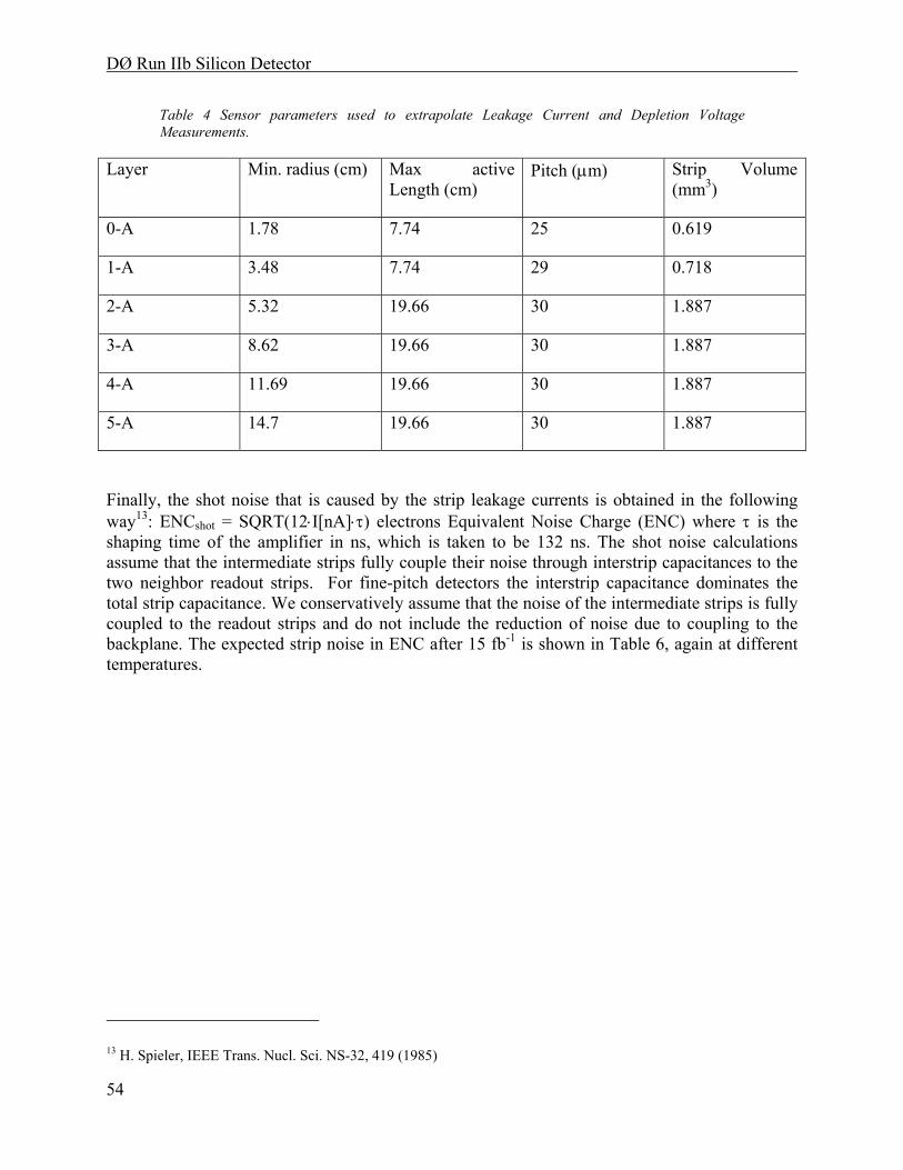
DØ Run IIb Silicon Detector
54
Table 4 Sensor parameters used to extrapolate Leakage Current and Depletion Voltage Measurements.
Layer Min. radius (cm) Max active Length (cm)
Pitch (µm) Strip Volume (mm3)
0-A 1.78 7.74 25 0.619
1-A 3.48 7.74 29 0.718
2-A 5.32 19.66 30 1.887
3-A 8.62 19.66 30 1.887
4-A 11.69 19.66 30 1.887
5-A 14.7 19.66 30 1.887
Finally, the shot noise that is caused by the strip leakage currents is obtained in the following way13: ENCshot = SQRT(12⋅I[nA]⋅τ) electrons Equivalent Noise Charge (ENC) where τ is the shaping time of the amplifier in ns, which is taken to be 132 ns. The shot noise calculations assume that the intermediate strips fully couple their noise through interstrip capacitances to the two neighbor readout strips. For fine-pitch detectors the interstrip capacitance dominates the total strip capacitance. We conservatively assume that the noise of the intermediate strips is fully coupled to the readout strips and do not include the reduction of noise due to coupling to the backplane. The expected strip noise in ENC after 15 fb-1 is shown in Table 6, again at different temperatures.
13 H. Spieler, IEEE Trans. Nucl. Sci. NS-32, 419 (1985)
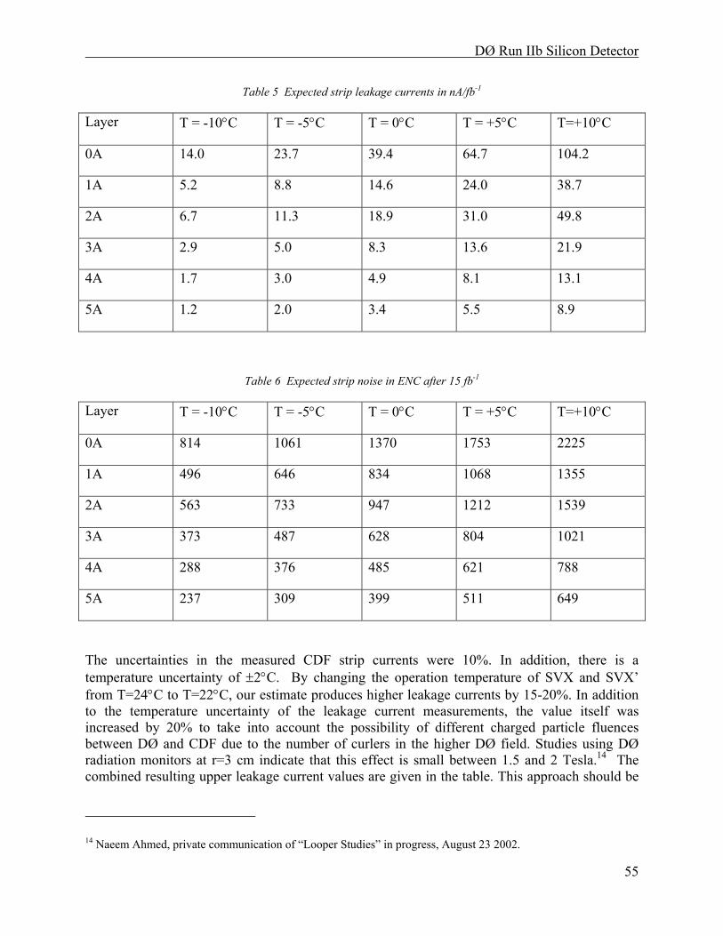
DØ Run IIb Silicon Detector
55
Table 5 Expected strip leakage currents in nA/fb-1
Layer T = -10°C T = -5°C T = 0°C T = +5°C T=+10°C
0A 14.0 23.7 39.4 64.7 104.2
1A 5.2 8.8 14.6 24.0 38.7
2A 6.7 11.3 18.9 31.0 49.8
3A 2.9 5.0 8.3 13.6 21.9
4A 1.7 3.0 4.9 8.1 13.1
5A 1.2 2.0 3.4 5.5 8.9
Table 6 Expected strip noise in ENC after 15 fb-1
Layer T = -10°C T = -5°C T = 0°C T = +5°C T=+10°C
0A 814 1061 1370 1753 2225
1A 496 646 834 1068 1355
2A 563 733 947 1212 1539
3A 373 487 628 804 1021
4A 288 376 485 621 788
5A 237 309 399 511 649
The uncertainties in the measured CDF strip currents were 10%. In addition, there is a temperature uncertainty of ±2°C. By changing the operation temperature of SVX and SVX’ from T=24°C to T=22°C, our estimate produces higher leakage currents by 15-20%. In addition to the temperature uncertainty of the leakage current measurements, the value itself was increased by 20% to take into account the possibility of different charged particle fluences between DØ and CDF due to the number of curlers in the higher DØ field. Studies using DØ radiation monitors at r=3 cm indicate that this effect is small between 1.5 and 2 Tesla.14 The combined resulting upper leakage current values are given in the table. This approach should be
14 Naeem Ahmed, private communication of “Looper Studies” in progress, August 23 2002.
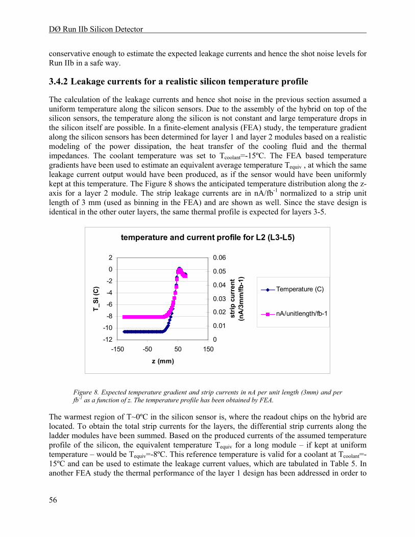
DØ Run IIb Silicon Detector
56
conservative enough to estimate the expected leakage currents and hence the shot noise levels for Run IIb in a safe way.
3.4.2 Leakage currents for a realistic silicon temperature profile
The calculation of the leakage currents and hence shot noise in the previous section assumed a uniform temperature along the silicon sensors. Due to the assembly of the hybrid on top of the silicon sensors, the temperature along the silicon is not constant and large temperature drops in the silicon itself are possible. In a finite-element analysis (FEA) study, the temperature gradient along the silicon sensors has been determined for layer 1 and layer 2 modules based on a realistic modeling of the power dissipation, the heat transfer of the cooling fluid and the thermal impedances. The coolant temperature was set to Tcoolant=-15ºC. The FEA based temperature gradients have been used to estimate an equivalent average temperature Tequiv , at which the same leakage current output would have been produced, as if the sensor would have been uniformly kept at this temperature. The Figure 8 shows the anticipated temperature distribution along the z-axis for a layer 2 module. The strip leakage currents are in nA/fb-1 normalized to a strip unit length of 3 mm (used as binning in the FEA) and are shown as well. Since the stave design is identical in the other outer layers, the same thermal profile is expected for layers 3-5.
temperature and current profile for L2 (L3-L5)
-12
-10
-8
-6
-4
-2
0
2
-150 -50 50 150
z (mm)
T_Si
(C)
0
0.01
0.02
0.03
0.04
0.05
0.06
strip
cur
rent
(n
A/3
mm
/fb-1
)
Temperature (C)
nA/unitlength/fb-1
Figure 8. Expected temperature gradient and strip currents in nA per unit length (3mm) and per fb-1 as a function of z. The temperature profile has been obtained by FEA.
The warmest region of T~0ºC in the silicon sensor is, where the readout chips on the hybrid are located. To obtain the total strip currents for the layers, the differential strip currents along the ladder modules have been summed. Based on the produced currents of the assumed temperature profile of the silicon, the equivalent temperature Tequiv for a long module – if kept at uniform temperature – would be Tequiv=-8ºC. This reference temperature is valid for a coolant at Tcoolant=-15ºC and can be used to estimate the leakage current values, which are tabulated in Table 5. In another FEA study the thermal performance of the layer 1 design has been addressed in order to
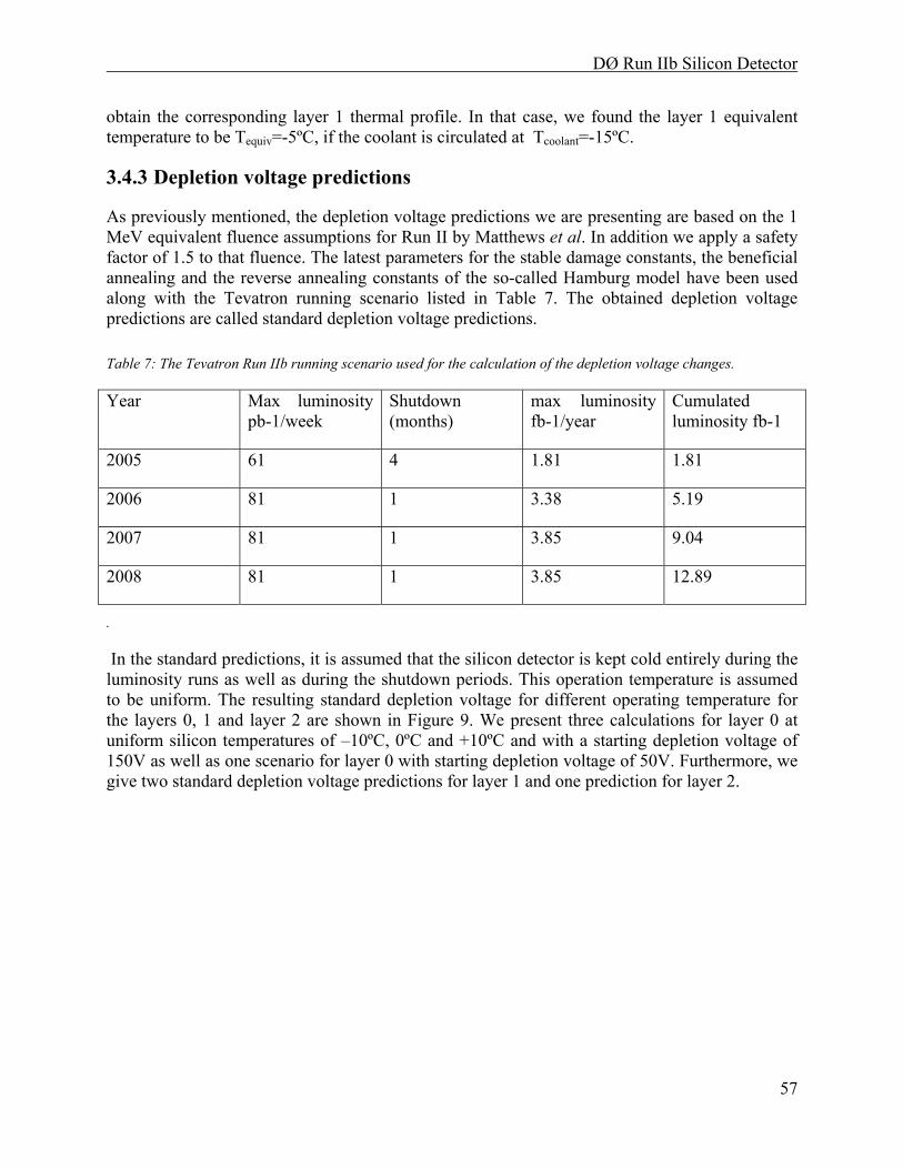
DØ Run IIb Silicon Detector
57
obtain the corresponding layer 1 thermal profile. In that case, we found the layer 1 equivalent temperature to be Tequiv=-5ºC, if the coolant is circulated at Tcoolant=-15ºC.
3.4.3 Depletion voltage predictions
As previously mentioned, the depletion voltage predictions we are presenting are based on the 1 MeV equivalent fluence assumptions for Run II by Matthews et al. In addition we apply a safety factor of 1.5 to that fluence. The latest parameters for the stable damage constants, the beneficial annealing and the reverse annealing constants of the so-called Hamburg model have been used along with the Tevatron running scenario listed in Table 7. The obtained depletion voltage predictions are called standard depletion voltage predictions.
Table 7: The Tevatron Run IIb running scenario used for the calculation of the depletion voltage changes.
Year Max luminosity pb-1/week
Shutdown (months)
max luminosity fb-1/year
Cumulated luminosity fb-1
2005 61 4 1.81 1.81
2006 81 1 3.38 5.19
2007 81 1 3.85 9.04
2008 81 1 3.85 12.89
.
In the standard predictions, it is assumed that the silicon detector is kept cold entirely during the luminosity runs as well as during the shutdown periods. This operation temperature is assumed to be uniform. The resulting standard depletion voltage for different operating temperature for the layers 0, 1 and layer 2 are shown in Figure 9. We present three calculations for layer 0 at uniform silicon temperatures of –10ºC, 0ºC and +10ºC and with a starting depletion voltage of 150V as well as one scenario for layer 0 with starting depletion voltage of 50V. Furthermore, we give two standard depletion voltage predictions for layer 1 and one prediction for layer 2.
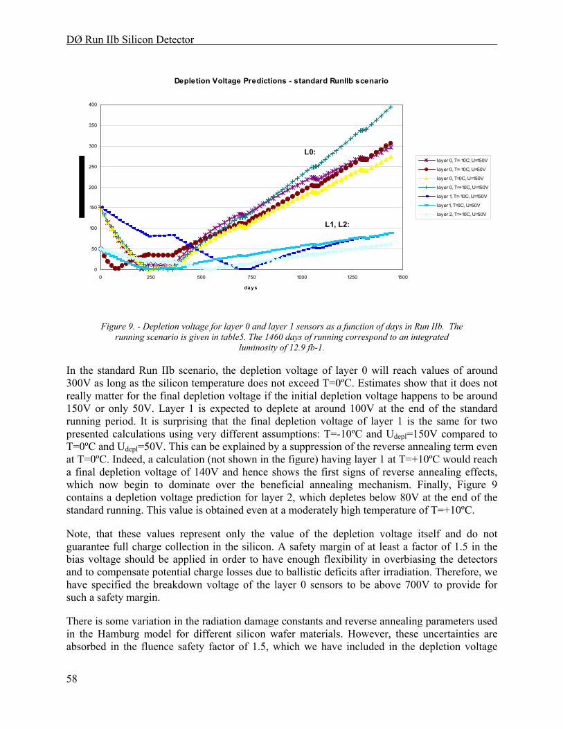
DØ Run IIb Silicon Detector
58
Depletion Voltage Predictions - standard RunIIb scenario
0
50
100
150
200
250
300
350
400
0 250 500 750 1000 1250 1500
da y s
layer 0, T=-10C, U=150V
layer 0, T=-10C, U=50V
layer 0, T=0C, U=150V
layer 0, T=+10C, U=150V
layer 1, T=-10C, U=150V
layer1, T=0C, U=50V
layer 2, T=+10C, U=50V
L0:
L1, L2:
Figure 9. - Depletion voltage for layer 0 and layer 1 sensors as a function of days in Run IIb. The running scenario is given in table5. The 1460 days of running correspond to an integrated
luminosity of 12.9 fb-1.
In the standard Run IIb scenario, the depletion voltage of layer 0 will reach values of around 300V as long as the silicon temperature does not exceed T=0ºC. Estimates show that it does not really matter for the final depletion voltage if the initial depletion voltage happens to be around 150V or only 50V. Layer 1 is expected to deplete at around 100V at the end of the standard running period. It is surprising that the final depletion voltage of layer 1 is the same for two presented calculations using very different assumptions: T=-10ºC and Udepl=150V compared to T=0ºC and Udepl=50V. This can be explained by a suppression of the reverse annealing term even at T=0ºC. Indeed, a calculation (not shown in the figure) having layer 1 at T=+10ºC would reach a final depletion voltage of 140V and hence shows the first signs of reverse annealing effects, which now begin to dominate over the beneficial annealing mechanism. Finally, Figure 9 contains a depletion voltage prediction for layer 2, which depletes below 80V at the end of the standard running. This value is obtained even at a moderately high temperature of T=+10ºC.
Note, that these values represent only the value of the depletion voltage itself and do not guarantee full charge collection in the silicon. A safety margin of at least a factor of 1.5 in the bias voltage should be applied in order to have enough flexibility in overbiasing the detectors and to compensate potential charge losses due to ballistic deficits after irradiation. Therefore, we have specified the breakdown voltage of the layer 0 sensors to be above 700V to provide for such a safety margin.
There is some variation in the radiation damage constants and reverse annealing parameters used in the Hamburg model for different silicon wafer materials. However, these uncertainties are absorbed in the fluence safety factor of 1.5, which we have included in the depletion voltage
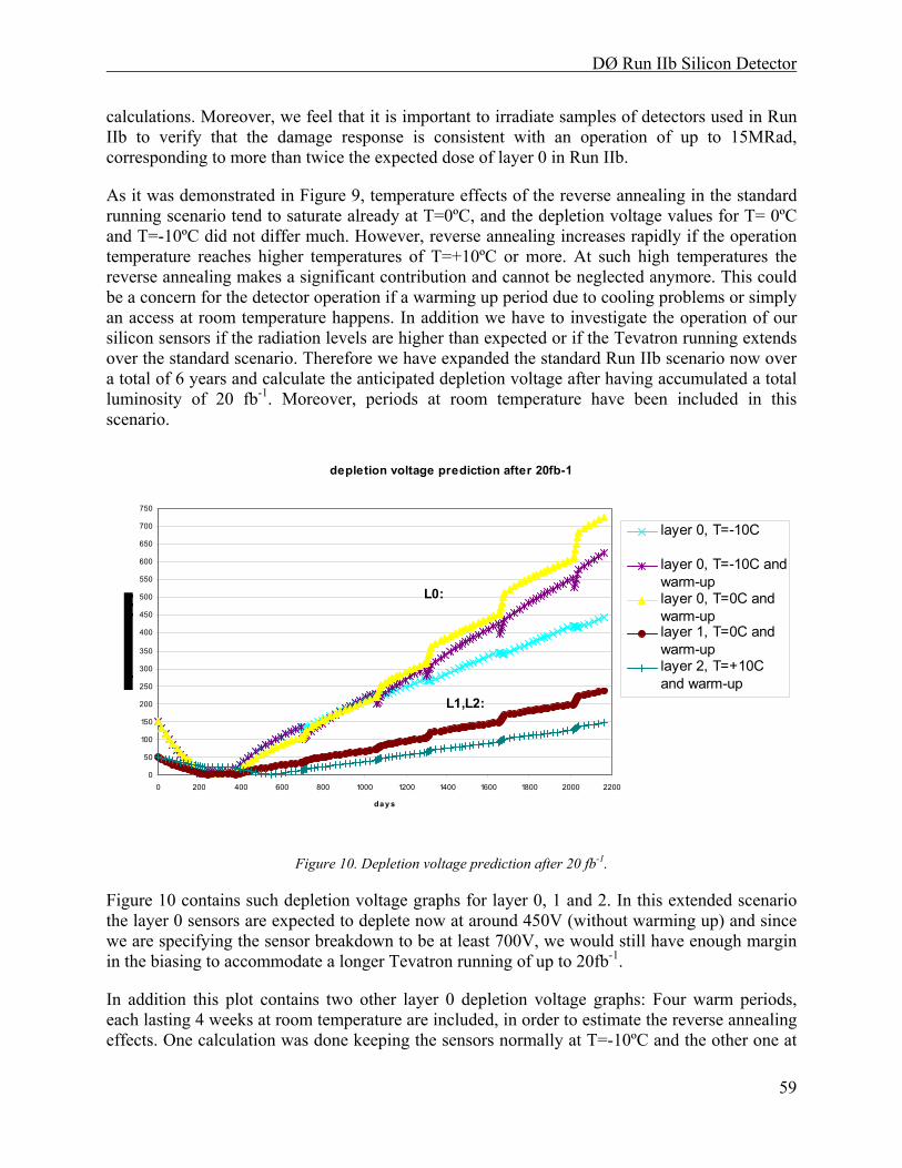
DØ Run IIb Silicon Detector
59
calculations. Moreover, we feel that it is important to irradiate samples of detectors used in Run IIb to verify that the damage response is consistent with an operation of up to 15MRad, corresponding to more than twice the expected dose of layer 0 in Run IIb.
As it was demonstrated in Figure 9, temperature effects of the reverse annealing in the standard running scenario tend to saturate already at T=0ºC, and the depletion voltage values for T= 0ºC and T=-10ºC did not differ much. However, reverse annealing increases rapidly if the operation temperature reaches higher temperatures of T=+10ºC or more. At such high temperatures the reverse annealing makes a significant contribution and cannot be neglected anymore. This could be a concern for the detector operation if a warming up period due to cooling problems or simply an access at room temperature happens. In addition we have to investigate the operation of our silicon sensors if the radiation levels are higher than expected or if the Tevatron running extends over the standard scenario. Therefore we have expanded the standard Run IIb scenario now over a total of 6 years and calculate the anticipated depletion voltage after having accumulated a total luminosity of 20 fb-1. Moreover, periods at room temperature have been included in this scenario.
depletion voltage prediction after 20fb-1
0
50
100
150
200
250
300
350
400
450
500
550
600
650
700
750
0 200 400 600 800 1000 1200 1400 1600 1800 2000 2200
da y s
layer 0, T=-10C
layer 0, T=-10C andwarm-uplayer 0, T=0C andwarm-uplayer 1, T=0C andwarm-uplayer 2, T=+10Cand warm-up
L0:
L1,L2:
Figure 10. Depletion voltage prediction after 20 fb-1.
Figure 10 contains such depletion voltage graphs for layer 0, 1 and 2. In this extended scenario the layer 0 sensors are expected to deplete now at around 450V (without warming up) and since we are specifying the sensor breakdown to be at least 700V, we would still have enough margin in the biasing to accommodate a longer Tevatron running of up to 20fb-1.
In addition this plot contains two other layer 0 depletion voltage graphs: Four warm periods, each lasting 4 weeks at room temperature are included, in order to estimate the reverse annealing effects. One calculation was done keeping the sensors normally at T=-10ºC and the other one at

DØ Run IIb Silicon Detector
60
T=0ºC. The reverse annealing will now dominate and will shift the depletion voltage to much higher levels of around 700V. It is therefore quite important to avoid any warm up after the detector has been irradiated. We should point out, that for the operation of the silicon detectors in layer 0 and 1, a temperature as cold as possible is safer against reverse annealing, especially if warm periods are included in the depletion voltage scenario.
3.4.4 Signal to noise ratio
Signal to noise ratio (S/N) is an important parameter that ultimately limits the detector lifetime. Based on previous studies and CDF experience in Run 1, S/N starts affecting b-tagging efficiency seriously when it degrades below a value of 5 15. Our design goal is to keep the S/N conservatively above 10 for all layers of the detector. The S/N should remain above this limit even for an extended Run IIb of up to 20fb-1. In addition we prefer to set the operation temperatures such, that the S/N of the silicon layers should not degrade by more than 15% over the course of the Run IIb period in order to ensure a stable and robust S/N over the full lifetime of the silicon detector.
In our signal-to-noise (S/N) estimates we assume that sensors can be fully depleted and that one MIP produces a most probable charge value of 23,000 e- in 320 µm silicon. We have considered several contributions to the total noise:
• Noise in the front end due to capacitive load: the analog cable in layer 0 contributes with 0.4 pF/cm to the total capacitive load. The silicon sensors are conservatively assumed to have a total load capacitance of 1.4pF/cm, dominated by the interstrip capacitance. The ENC noise behavior of the front end chip (SVX4) is taken to be 450+43*C(pF) according to the specifications.
• Noise due to the series resistance of the aluminum traces of the silicon sensors and – for layer 0- the copper traces of the analog cable. The serial noise varies between ~210e for layer 1 sensors (only 7.66cm long) and ~780e for 19.7 cm long modules in layer 2-5.
• Shot noise from detector leakage current as calculated before. A shaping time of 132 ns is assumed
• Thermal noise due to the finite value of the bias resistor (~250e).
15 J. Albert et al. " The relationship between signal-to-noise ratio and b-tag efficiency." CDF Note #3338.
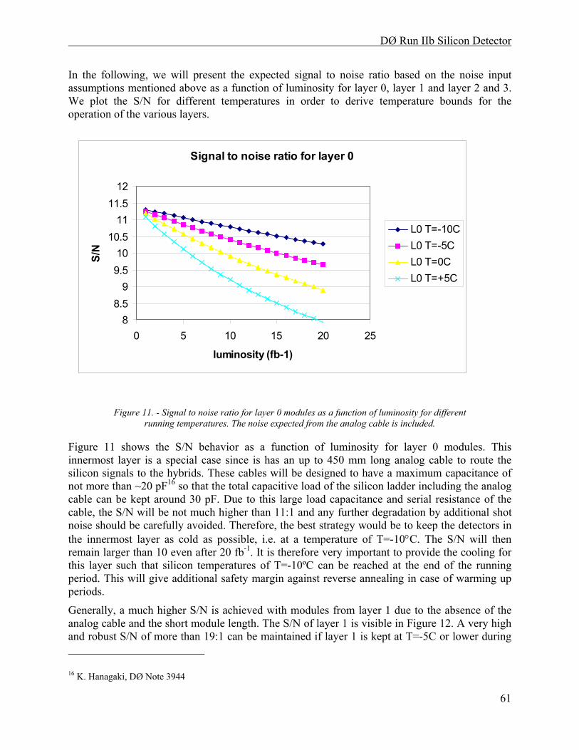
DØ Run IIb Silicon Detector
61
In the following, we will present the expected signal to noise ratio based on the noise input assumptions mentioned above as a function of luminosity for layer 0, layer 1 and layer 2 and 3. We plot the S/N for different temperatures in order to derive temperature bounds for the operation of the various layers.
Signal to noise ratio for layer 0
88.5
99.510
10.511
11.512
0 5 10 15 20 25
luminosity (fb-1)
S/N
L0 T=-10CL0 T=-5CL0 T=0CL0 T=+5C
Figure 11. - Signal to noise ratio for layer 0 modules as a function of luminosity for different
running temperatures. The noise expected from the analog cable is included.
Figure 11 shows the S/N behavior as a function of luminosity for layer 0 modules. This innermost layer is a special case since is has an up to 450 mm long analog cable to route the silicon signals to the hybrids. These cables will be designed to have a maximum capacitance of not more than ~20 pF16 so that the total capacitive load of the silicon ladder including the analog cable can be kept around 30 pF. Due to this large load capacitance and serial resistance of the cable, the S/N will be not much higher than 11:1 and any further degradation by additional shot noise should be carefully avoided. Therefore, the best strategy would be to keep the detectors in the innermost layer as cold as possible, i.e. at a temperature of T=-10°C. The S/N will then remain larger than 10 even after 20 fb-1. It is therefore very important to provide the cooling for this layer such that silicon temperatures of T=-10ºC can be reached at the end of the running period. This will give additional safety margin against reverse annealing in case of warming up periods.
Generally, a much higher S/N is achieved with modules from layer 1 due to the absence of the analog cable and the short module length. The S/N of layer 1 is visible in Figure 12. A very high and robust S/N of more than 19:1 can be maintained if layer 1 is kept at T=-5C or lower during 16 K. Hanagaki, DØ Note 3944
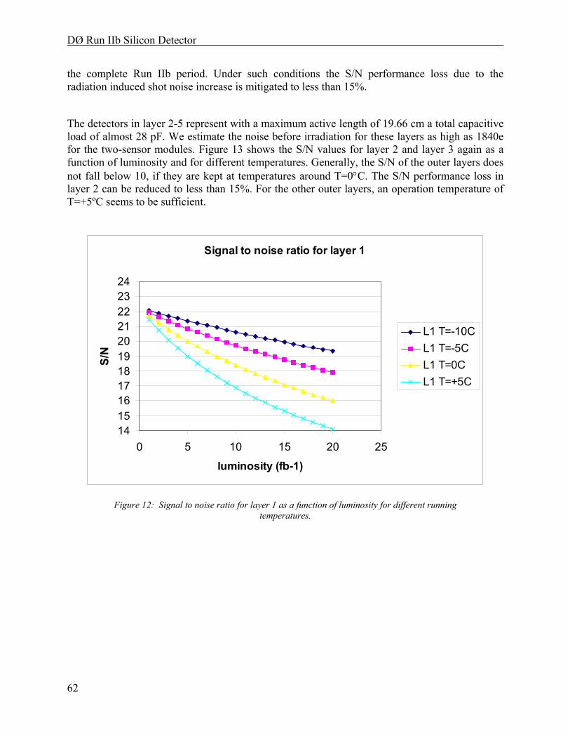
DØ Run IIb Silicon Detector
62
the complete Run IIb period. Under such conditions the S/N performance loss due to the radiation induced shot noise increase is mitigated to less than 15%.
The detectors in layer 2-5 represent with a maximum active length of 19.66 cm a total capacitive load of almost 28 pF. We estimate the noise before irradiation for these layers as high as 1840e for the two-sensor modules. Figure 13 shows the S/N values for layer 2 and layer 3 again as a function of luminosity and for different temperatures. Generally, the S/N of the outer layers does not fall below 10, if they are kept at temperatures around T=0°C. The S/N performance loss in layer 2 can be reduced to less than 15%. For the other outer layers, an operation temperature of T=+5ºC seems to be sufficient.
Signal to noise ratio for layer 1
1415161718192021222324
0 5 10 15 20 25
luminosity (fb-1)
S/N
L1 T=-10CL1 T=-5CL1 T=0CL1 T=+5C
Figure 12: Signal to noise ratio for layer 1 as a function of luminosity for different running temperatures.
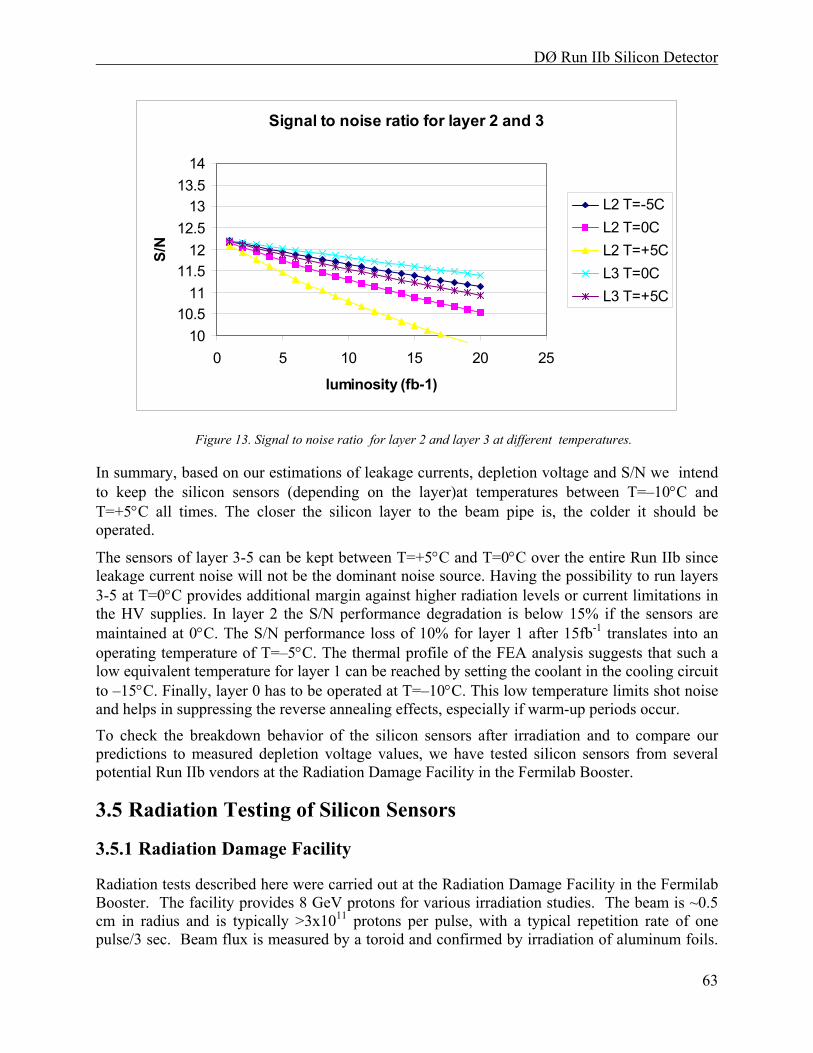
DØ Run IIb Silicon Detector
63
Signal to noise ratio for layer 2 and 3
1010.5
1111.5
1212.5
1313.5
14
0 5 10 15 20 25
luminosity (fb-1)
S/N
L2 T=-5CL2 T=0CL2 T=+5CL3 T=0C L3 T=+5C
Figure 13. Signal to noise ratio for layer 2 and layer 3 at different temperatures.
In summary, based on our estimations of leakage currents, depletion voltage and S/N we intend to keep the silicon sensors (depending on the layer)at temperatures between T=–10°C and T=+5°C all times. The closer the silicon layer to the beam pipe is, the colder it should be operated.
The sensors of layer 3-5 can be kept between T=+5°C and T=0°C over the entire Run IIb since leakage current noise will not be the dominant noise source. Having the possibility to run layers 3-5 at T=0°C provides additional margin against higher radiation levels or current limitations in the HV supplies. In layer 2 the S/N performance degradation is below 15% if the sensors are maintained at 0°C. The S/N performance loss of 10% for layer 1 after 15fb-1 translates into an operating temperature of T=–5°C. The thermal profile of the FEA analysis suggests that such a low equivalent temperature for layer 1 can be reached by setting the coolant in the cooling circuit to –15°C. Finally, layer 0 has to be operated at T=–10°C. This low temperature limits shot noise and helps in suppressing the reverse annealing effects, especially if warm-up periods occur.
To check the breakdown behavior of the silicon sensors after irradiation and to compare our predictions to measured depletion voltage values, we have tested silicon sensors from several potential Run IIb vendors at the Radiation Damage Facility in the Fermilab Booster.
3.5 Radiation Testing of Silicon Sensors
3.5.1 Radiation Damage Facility
Radiation tests described here were carried out at the Radiation Damage Facility in the Fermilab Booster. The facility provides 8 GeV protons for various irradiation studies. The beam is ~0.5 cm in radius and is typically >3x10¹¹ protons per pulse, with a typical repetition rate of one pulse/3 sec. Beam flux is measured by a toroid and confirmed by irradiation of aluminum foils.
DØ Run IIb Silicon Detector
64
Detectors are mounted in a cold box, which maintains detector temperature at 5°C and allows for detector bias and monitoring. The box is in turn mounted on a x-y table which scans the detector assembly through the beam; insuring uniform irradiation.
Irradiation typically takes one shift. This intense irradiation can leave a substantial charge in the oxide and on detector surfaces. Detectors are then left at 5°C to “cool down” and anneal for ~1 week before testing.
3.5.2 Run IIa detector irradiation studies
To understand the expected lifetime of the Run IIa detector we performed a series of measurements with spare or grade B modules. These tests are described in detail in Ref. 17. We used 3 different ladder/wedge types of double-sided detectors and one type of single sided detector. All detectors are processed on n-type bulk silicon material with a typical thickness of 300µm with integrated AC coupling and polysilicon bias resistors. The double-sided ladders had either 6, 9 or 14 readout chips on the their front end hybrid, which was directly glued on the silicon. The 6-chip detector is manufactured on a 6”-wafer technology and has 90° stereo strips on the n-side. The 9-chip detector is a stereo detector with a small angle view of 2°. The 14-chip module is a double-sided wedge-shaped detector with varying strip length and angle of ±15° on both sides.
The lifetime of the Run IIa detectors is likely to be determined by the limited voltage that can be applied across the AC coupling capacitors. These capacitors break down near 150 V and can only be safely operated to ~100 V. Thus, with split bias we expect to be limited to a total bias of 200 V. In addition during ladder testing we found that the Micron detectors are subject to microdischarge breakdown on the junction side. The breakdown voltage varies on a detector-to-detector basis but can limit the junction side bias to as low as 10 V. This effect switches sides upon type inversion and is partially mitigated on the n side by compensating effects of oxide charge.
In order to characterize the performance of the irradiated detectors and to understand their behavior after irradiation the following measurements have been carried out:
• leakage current measurements
• depletion voltage determination
• average noise determination
• number of noisy channels
Depletion voltage was measured by measuring the response to a 1064 nm laser, noise and current measurements were performed using our standard set of detector burn-in tests.
17 J. Gardner et al. “Results from Irradiation Tests on DØ silicon Detectors at the Radiation Damage Facility at Fermilab”, DØ Note in progress.
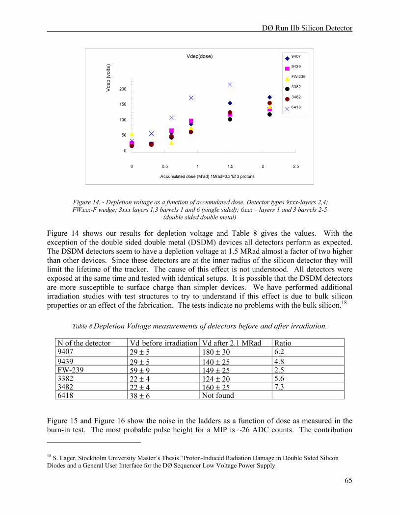
DØ Run IIb Silicon Detector
65
Vdep(dose)
0
50
100
150
200
0 0.5 1 1.5 2 2.5
Accumulated dose (Mrad) 1Mrad=3.3*E13 protons
Vde
p (v
olts
)
9407
9439
FW-239
3382
3482
6418
Figure 14. - Depletion voltage as a function of accumulated dose. Detector types 9xxx-layers 2,4; FWxxx-F wedge; 3xxx layers 1,3 barrels 1 and 6 (single sided); 6xxx – layers 1 and 3 barrels 2-5
(double sided double metal)
Figure 14 shows our results for depletion voltage and Table 8 gives the values. With the exception of the double sided double metal (DSDM) devices all detectors perform as expected. The DSDM detectors seem to have a depletion voltage at 1.5 MRad almost a factor of two higher than other devices. Since these detectors are at the inner radius of the silicon detector they will limit the lifetime of the tracker. The cause of this effect is not understood. All detectors were exposed at the same time and tested with identical setups. It is possible that the DSDM detectors are more susceptible to surface charge than simpler devices. We have performed additional irradiation studies with test structures to try to understand if this effect is due to bulk silicon properties or an effect of the fabrication. The tests indicate no problems with the bulk silicon.18
Table 8 Depletion Voltage measurements of detectors before and after irradiation. N of the detector Vd before irradiation Vd after 2.1 MRad Ratio 9407 29 ± 5 180 ± 30 6.2 9439 29 ± 5 140 ± 25 4.8 FW-239 59 ± 9 149 ± 25 2.5 3382 22 ± 4 124 ± 20 5.6 3482 22 ± 4 160 ± 25 7.3 6418 38 ± 6 Not found
Figure 15 and Figure 16 show the noise in the ladders as a function of dose as measured in the burn-in test. The most probable pulse height for a MIP is ~26 ADC counts. The contribution 18 S. Lager, Stockholm University Master’s Thesis “Proton-Induced Radiation Damage in Double Sided Silicon Diodes and a General User Interface for the DØ Sequencer Low Voltage Power Supply.
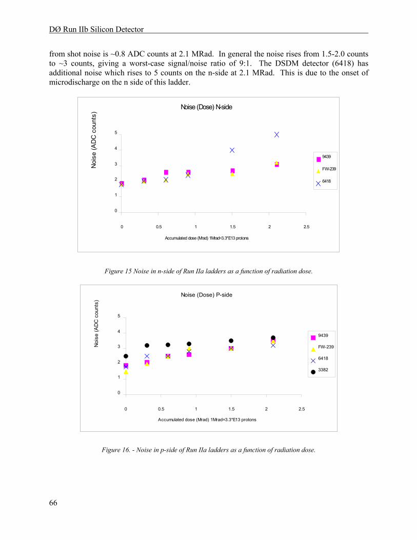
DØ Run IIb Silicon Detector
66
from shot noise is ~0.8 ADC counts at 2.1 MRad. In general the noise rises from 1.5-2.0 counts to ~3 counts, giving a worst-case signal/noise ratio of 9:1. The DSDM detector (6418) has additional noise which rises to 5 counts on the n-side at 2.1 MRad. This is due to the onset of microdischarge on the n side of this ladder.
Noise (Dose) N-side
0
1
2
3
4
5
0 0.5 1 1.5 2 2.5
Accumulated dose (Mrad) 1Mrad=3.3*E13 protons
Noi
se (A
DC
cou
nts)
9439
FW-239
6418
Figure 15 Noise in n-side of Run IIa ladders as a function of radiation dose.
Noise (Dose) P-side
0
1
2
3
4
5
0 0.5 1 1.5 2 2.5
Accumulated dose (Mrad) 1Mrad=3.3*E13 protons
Noi
se (A
DC
cou
nts)
9439
FW-239
6418
3382
Figure 16. - Noise in p-side of Run IIa ladders as a function of radiation dose.
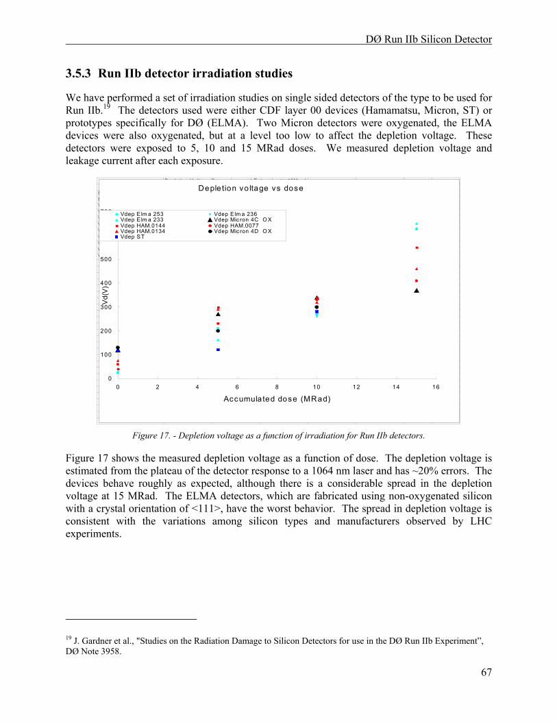
DØ Run IIb Silicon Detector
67
3.5.3 Run IIb detector irradiation studies
We have performed a set of irradiation studies on single sided detectors of the type to be used for Run IIb.19 The detectors used were either CDF layer 00 devices (Hamamatsu, Micron, ST) or prototypes specifically for DØ (ELMA). Two Micron detectors were oxygenated, the ELMA devices were also oxygenated, but at a level too low to affect the depletion voltage. These detectors were exposed to 5, 10 and 15 MRad doses. We measured depletion voltage and leakage current after each exposure.
Depletion V oltage Com parison and E x tens ion to 15M rad(line fit ted)
M rad 0 5 10 15M rad 0 5.03 10 15V dep E lm a 253 25 160 270 630V dep E lm a 236 25 210 260 625V dep E lm a 233 28 210 270 650V dep M ic ron 4C OX 120 270 340 370V dep HA M .0144 40 300 340 550V dep HA M .0077 60 230 330 410V dep HA M .0134 75 290 320 460V dep M ic ron 4D OX 130 200 300V dep S T 115 120 280
D e p l e t i o n v o l t a g e v s. a c c u m u l a t e d d o se
0
200
400
600
800
0 2 4 6 8 10 12 14 16D o se ( M R a d )
V dep E lma 253 V dep E lma 236V dep E lma 233 V dep Micron 4C OXV dep HA M.0144 V dep HA M.0077 V dep HA M.0134
Deple tion vo ltage vs dose
0
100
200
300
400
500
600
700
0 2 4 6 8 10 12 14 16
Accumula ted dose (MRad)
Vd(
V)
Vdep E lm a 253 Vdep E lm a 236Vdep E lm a 233 Vdep Mic ron 4C O XVdep HAM.0144 Vdep HAM.0077 Vdep HAM.0134 Vdep Mic ron 4D O XVdep ST
Figure 17. - Depletion voltage as a function of irradiation for Run IIb detectors.
Figure 17 shows the measured depletion voltage as a function of dose. The depletion voltage is estimated from the plateau of the detector response to a 1064 nm laser and has ~20% errors. The devices behave roughly as expected, although there is a considerable spread in the depletion voltage at 15 MRad. The ELMA detectors, which are fabricated using non-oxygenated silicon with a crystal orientation of <111>, have the worst behavior. The spread in depletion voltage is consistent with the variations among silicon types and manufacturers observed by LHC experiments.
19 J. Gardner et al., "Studies on the Radiation Damage to Silicon Detectors for use in the DØ Run IIb Experiment”, DØ Note 3958.
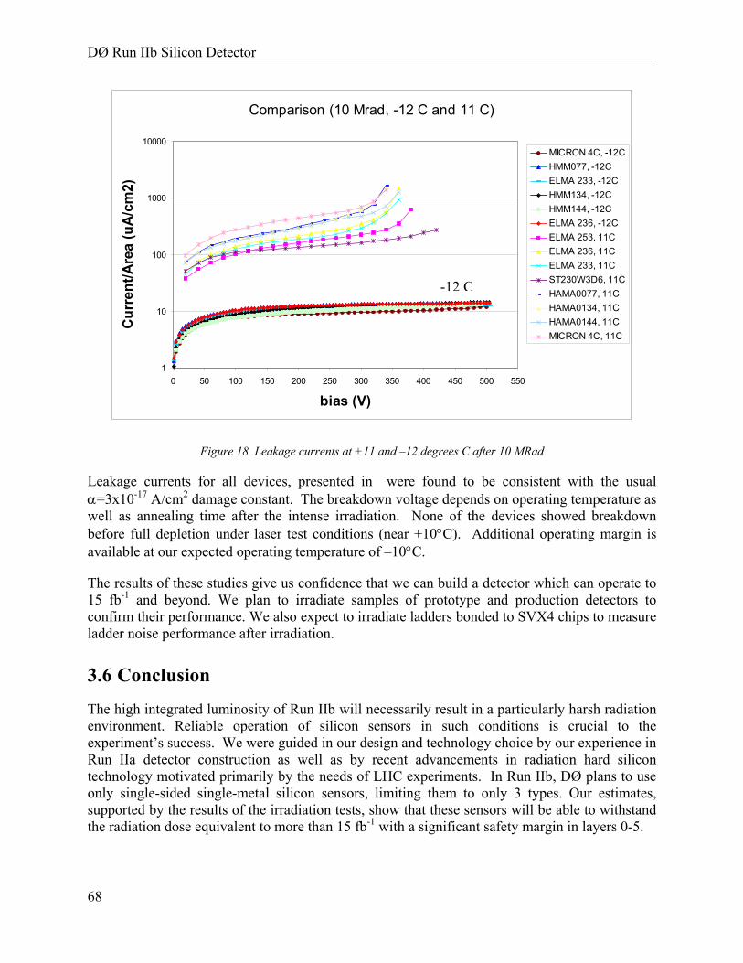
DØ Run IIb Silicon Detector
68
Comparison (10 Mrad, -12 C and 11 C)
1
10
100
1000
10000
0 50 100 150 200 250 300 350 400 450 500 550
bias (V)
Curr
ent/A
rea
(uA/
cm2)
MICRON 4C, -12CHMM077, -12CELMA 233, -12CHMM134, -12CHMM144, -12CELMA 236, -12CELMA 253, 11CELMA 236, 11CELMA 233, 11CST230W3D6, 11CHAMA0077, 11CHAMA0134, 11CHAMA0144, 11CMICRON 4C, 11C
Figure 18 Leakage currents at +11 and –12 degrees C after 10 MRad
Leakage currents for all devices, presented in were found to be consistent with the usual α=3x10-17 A/cm2 damage constant. The breakdown voltage depends on operating temperature as well as annealing time after the intense irradiation. None of the devices showed breakdown before full depletion under laser test conditions (near +10°C). Additional operating margin is available at our expected operating temperature of –10°C.
The results of these studies give us confidence that we can build a detector which can operate to 15 fb-1 and beyond. We plan to irradiate samples of prototype and production detectors to confirm their performance. We also expect to irradiate ladders bonded to SVX4 chips to measure ladder noise performance after irradiation.
3.6 Conclusion
The high integrated luminosity of Run IIb will necessarily result in a particularly harsh radiation environment. Reliable operation of silicon sensors in such conditions is crucial to the experiment’s success. We were guided in our design and technology choice by our experience in Run IIa detector construction as well as by recent advancements in radiation hard silicon technology motivated primarily by the needs of LHC experiments. In Run IIb, DØ plans to use only single-sided single-metal silicon sensors, limiting them to only 3 types. Our estimates, supported by the results of the irradiation tests, show that these sensors will be able to withstand the radiation dose equivalent to more than 15 fb-1 with a significant safety margin in layers 0-5.
-12 C

DØ Run IIb Silicon Detector
69
The depletion voltage for layer 0 sensors is expected to reach 300V for the assumed Tevatron Run IIb scenario of accumulating a luminosity of 13 fb-1 within 4 years. The layer 0 sensors will be specified to breakdown not earlier than 700V, providing enough flexibility in overbiasing these detectors. Warm periods of several weeks for maintenance should be carefully avoided in order to prevent reverse annealing. As an additional safety measure against the depletion voltage rise, the layer 0 sensors could be oxygenated. An oxygenation of these sensors is expected to slow down the depletion voltage growth after the type inversion. Further R&D studies are needed to confirm this approach.

DØ Run IIb Silicon Detector
70
4 MECHANICAL DESIGN, STRUCTURES, AND INFRASTRUCTURE
4.1 Overview
The mechanical design of the Run IIb silicon detector is challenging. It must satisfy strict requirements on material mass, on precision of construction and positioning, it must allow for signal readout and cooling of the detectors, and must satisfy overall size constraints imposed by the need to install the detector through the limited space between the calorimeter cryostats. In order to meet the latter requirement, the silicon for Run IIb will be divided about z = 0 into identical north and south barrel assemblies. That division addresses the limited installation space available after the end calorimeters have been opened 39" and allows a net length of silicon associated structures to exceed the 52" that would otherwise be available. Final connections between north and south assemblies will be made via reproducible ball mounts during installation at DØ. Testing and experience with the Run IIa silicon, which relied upon similar connections for support from the fiber tracker, demonstrated that a reproducibility of 2 µm is achieved with such ball mounts.
Each assembly comprises six silicon layers and is subdivided into an inner barrel with layers 0-1 and an outer barrel with layers 2-5. Inner and outer barrels will be fabricated individually, mated at SiDet to form either a north or a south barrel assembly, and brought to DØ as a completed, tested assembly. The inner diameter of those assemblies allows installation of a 1.16" outside diameter beryllium beam pipe through the silicon region after the barrel assemblies are in place at DØ. Figure 19 shows a plan view of the detector while Figure 20 shows an axial view.
In each of the north and south barrel assemblies, a double-walled cylinder, which is integral with the outer barrel, positions and supports a thin (~0.5 mm) carbon fiber reinforced resin (CFRR) silicon-positioning membrane near z = 0 and a thicker (~1 mm) CFRR outer silicon-positioning bulkhead at z = ±600 mm. A reproducible ball mount connection will be made between the support cylinder of the outer barrel and an additional cylinder extending from the outer positioning bulkhead to the end of fiber tracker barrel 1. The additional cylinder allows better access for precision CMM measurements of silicon positions and better access for work on the ends of silicon sub-assemblies. After all assemblies are in place and all mechanical connections are completed, the equivalent of a single 356 mm outside diameter support cylinder will extend ~1650 mm from one end of fiber tracker barrel 1 to the other.
Silicon sensors of the inner barrel, layers 0 and 1, are mounted on facets of quasi-polygonal cylindrical structures similar to the one used in Run IIa for CDF layer 00. All inner barrel sensors will be placed so that their traces are axial. The inner barrel is supported by the silicon-positioning membrane and by the silicon-positioning bulkhead of the outer barrel. Silicon of the outer barrel, layers 2-5, is contained in 84 staves, which are supported from the silicon-positioning membrane and the outer silicon-positioning bulkhead of the barrel. In order to provide azimuthal overlap between sensors, each silicon layer will be divided into inner and outer sub-layers "a" and "b". Each of the staves of the outer barrel will contain a set of sensors
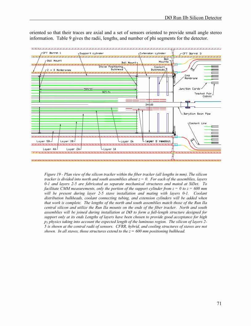
DØ Run IIb Silicon Detector
71
oriented so that their traces are axial and a set of sensors oriented to provide small angle stereo information. Table 9 gives the radii, lengths, and number of phi segments for the detector.
Figure 19 - Plan view of the silicon tracker within the fiber tracker (all lengths in mm). The silicon tracker is divided into north and south assemblies about z = 0. For each of the assemblies, layers 0-1 and layers 2-5 are fabricated as separate mechanical structures and mated at SiDet. To facilitate CMM measurements, only the portion of the support cylinder from z = 0 to z = 600 mm will be present during layer 2-5 stave installation and mating with layers 0-1. Coolant distribution bulkheads, coolant connecting tubing, and extension cylinders will be added when that work is complete. The lengths of the north and south assemblies match those of the Run IIa central silicon and utilize the Run IIa mounts on the ends of the fiber tracker. North and south assemblies will be joined during installation at DØ to form a full-length structure designed for support only at its ends Lengths of layers have been chosen to provide good acceptance for high pT physics taking into account the expected length of the luminous region. The silicon of layers 2-5 is shown at the central radii of sensors. CFRR, hybrid, and cooling structures of staves are not shown. In all staves, those structures extend to the z = 600 mm positioning bulkhead.
DØ Run IIb Silicon Detector
72
Table 9 - Silicon geometric parameters of a barrel assembly (units = mm)
Figure 20 - End view of the layer 0-1 module, layer 2-5 staves and the outer silicon-positioning bulkhead. Silicon radii and sensor widths have been chosen to provide >99% r-phi geometric acceptance for tracks of pT > 1.5 GeV/c originating within 2 mm of the nominal beamline. The design of the layer 0-1 and layer 2-5 assemblies allows removal of layers 0-1 at DØ and replacement with good precision. The inner diameter of layer 0 has been chosen to permit beam pipe installation after all silicon is in place at DØ.
Layer 0a 0b 1a 1b 2a 2b 3a 3b 4a 4b 5a 5b
R axial 18.0 24.8 34.8 39.0 54.6 70.0 89.5 103.7 116.5 130.5 148.8 162.7
R stereo --- --- --- --- 57.4 72.9 86.6 100.8 119.4 133.4 146.0 159.9
Length(z) 475 475 479 479 601 601 601 601 601 601 601 601
# Phi 6 6 6 6 6 6 9 9 12 12 15 15

DØ Run IIb Silicon Detector
73
4.2 Overall Support Structure
The main structural components must provide accurate, stable positioning of both the inner and outer detector elements. The main components are a double-walled carbon fiber cylinder that resides outside the outermost silicon layer and a set of bulkheads that provide the precision mounting points for the outer layer staves and the inner layer sub-assemblies. The details of these components and the alignment constraints are provided in the following sub-sections.
4.2.1 Outer support cylinders, stave positioning bulkheads, and z = 0 membranes
The design of the 356 mm outside diameter support cylinders is based upon that of the 306 mm outside diameter cylinders of Run IIa. Each cylinder will have inner and outer carbon fiber reinforced resin (CFRR) walls ~0.56 mm thick separated by CFRR "ribs" ~0.40 mm thick. Seven or more layers of flame retardant free, high modulus (>90 Msi), unidirectional fiber prepreg will be used for the shells and six or more layers for the ribs. The number of layers will depend upon the thickness of the high modulus material which is available. Individual CFRR pieces are cured at elevated temperature and then bonded to one another at room temperature with epoxy. Based upon the performance of the Run IIa cylinders, beam deflection should be less than 40 µm over a length of 1650 mm. Compensation for that deflection can be made by offsetting either the z = 0 positioning membranes or the outer positioning bulkheads when they are glued to the cylinder. The ribs, end rings, membranes, and bulkheads stiffen the completed structure against out-of-round distortions. Based upon performance of Run IIa cylinders before openings were cut for silicon installation, out-of-round distortions should be minimal. However, prototypes will need to be fabricated and measured to verify beam and out-of-round deflections.
The CFRR stave-positioning bulkhead will be made of multiple layers of flame-retardant-free, high modulus (>90 Msi), unidirectional fiber prepreg with an elevated temperature cure. These bulkheads are expected to be a sandwich structure of two ~0.5mm thick CFRR panels with ruby bearings mounted to the inside face of the outer panel. The sandwich structure provides stiffness to resist longitudinal loads from the staves, particularly coming from the stave electrical and cooling services. Openings in the bulkheads are intended to match stave profiles, including cables, and to provide 0.5 mm clearance about the full stave periphery. Staves will be installed through the openings and located by pins which engage locating bearings glued into the bulkhead. We plan to locate the bearings using high-precision fixturing as they are glued into place. The intent is to place the stave locating bearings and the stave pins which engage them well enough to allow interchangeability among staves.
DØ Run IIb Silicon Detector
74
Figure 21 - Cut profile supplied to Lab 8 for a prototype positioning bulkhead. The profile of a stave opening is shown on the right; the locations of openings are shown on the left.
The CFRR z = 0 membrane will be made in a similar manner as the z=600mm bulkheads. Again, a sandwich structure will be used, but in this case the innermost panel could be a full disk with an opening for the beam pipe, since staves do not pass through it. In practice, openings will be cut in the membrane to reduce material. A design for the openings remains to be developed. Bearings will be glued onto the outer face of the innermost membrane to engage stave-positioning pins. Local reinforcement will be provided at each bearing location. A precision fixture will be used to position bearings as they are glued into place.
CFRR end rings for each cylinder include sockets of the ball mounts and features to allow one cylinder to be securely coupled to the next. Based upon Run IIa experience, twelve ball mounts, evenly space in azimuth, should be sufficient per end ring. Due to the 30-fold symmetry of the outer silicon layer we anticipate using 15 ball mounts. Screws or studs through the balls will be used to couple cylinders. Openings through the outer walls of cylinders, with suitable reinforcement, will provide access to install and tighten fasteners. The end rings will be made of multiple layers of flame retardant free, high modulus (>90 Msi), unidirectional fiber prepreg with an elevated temperature cure. Precision jig plates will be used to position the ball mount openings.
A CMM will be needed as pieces of cylinder assemblies are glued to one another in order to establish clockings and offsets. Whenever practical, end rings will be mated during the gluing process. A full procedure for establishing end ring clockings and offsets remains to be developed. In general, we plan to employ ruby or sapphire balls as reference features for CMM touch probe measurements. Positions of stave locating features can be measured in a coordinate system established by these reference features.

DØ Run IIb Silicon Detector
75
4.2.2 Alignment precision and survey accuracy
All alignment constants, both at the trigger level and offline, assume that the silicon sensors are perfect planes. Six constants are used, three offsets used to define the position of the center of the sensor and three Euler angles used to define the rotations of the sensor about that center. Survey data taken during assembly, or obtained from offline alignment with tracks, can be used to determine the alignment constants for the tracker. No real-time alignment constants are available so it is critical for the trigger that the detector be stable over time scales of weeks to months.
It is important to make a clear distinction between the precision required for the placement of the sensors and the required survey accuracy. The physical alignment precision for the sensors is determined primarily by the requirements of the impact parameter trigger, which is used to identify events with tracks originating from the decay of heavy quarks outside the beam spot. Having satisfied these constraints, other considerations, such as having tractable offline alignment constants, are also satisfied. The survey accuracy, whether done using optical or mechanical survey on the bench, or using tracks in situ, should have accuracy on the scale of the intrinsic device resolution (≈8µ transverse to the sensor strips).
No stereo information is available at the trigger level so the trigger is most sensitive to rotations about the two axes transverse to the beam line (pitch and yaw) that result in Z-dependent r-φ errors. Deviations from planarity are also important, both at the trigger level and for the offline analyses since these are not corrected for. The figure of merit for location of sensors is that, relative to the beam spot size, the errors introduced have a small effect on the impact parameter resolution. For a rotation about an axis perpendicular to the plane of the sensors (yaw), the desired alignment tolerance is <10µ over the length of a readout segment. The pitch angle affects strips at the edges of the sensors, but not at the center. For a radial deviation dR at an angle φ from the center of the sensor, the transverse measurement error dX is given by dX=dRtanφ. Local radial displacements due to a lack of sensor flatness contribute in the same way as an overall pitch of the sensor. Again, the desired tolerance is dX<10µ within a readout segment.
4.3 Layer 0-1 Silicon Mechanical Support Structure
4.3.1 Introduction
The Layer 0 and 1 silicon support structures described in this TDR are carbon fiber structures with each layer consisting of an inner and outer carbon fiber shell. In L1 a pyrolytic graphite layer that transfers heat to the cooling tubes is inserted between the inner and outer layers. Our design is geometrically similar to the Run IIa CDF inner silicon support structure that is also made from carbon fiber composite. In L0 the hybrids are cooled by a separate system that is designed in two layers to facilitate installation of the hybrids and the associated cables. We have chosen carbon fiber cooling tubes with relatively high axial thermal conductivity in order to meet our cooling requirements. The manifolds needed to combine all of the cooling circuits in one inlet and one outlet connection also serve as structural bulkheads. A third bulkhead provides the

DØ Run IIb Silicon Detector
76
support point for connecting L0 to the inside of L1 and L1 to the L2-L5 structure. The other support point at Z=0 consists of a set of discs and precision pins.
We have developed a full solid CAD model of the design that includes all components and cables. We have a complete mechanical and thermal FEA analysis for Layer 1 that is described herein. We measured the basic tensile and thermal properties of the carbon fiber materials we are using and experimentally verified that we can use lay-up theory to obtain tensile and thermal properties for the specific structures we are using, see section 4.3.4.
A brief description of the work done to date on fabrication techniques and how we obtain mechanical precision is given in section 4.3.5.
4.3.2 Design of the Layer 0-1 Silicon Mechanical Support Structure
The silicon sensors and associated electronics in layer 0 and layer 1 require a very lightweight and rigid support structure, constructed to very demanding mechanical tolerances. Provision must also be made for cooling of the sensors and the hybrid electronics. Carbon fiber composite provides the most effective combination of low density and rigidity along with manufacturing flexibility. A research study was made to determine the most effective fiber type and lay-up and to examine the manufacturing issues involved. The most effective combination was found to be a K13C2U high modulus, high thermal conductivity fiber. This is used in a 6-layer [0o/20o/-20o]s lay-up in the castellated shells and in a 4-layer [0o/90o]s lay-up for the inner tube. The cooling tubes use K1392U fiber in a 4-layer [25o/-25o]slay-up. This was needed to permit lay-up around the small tube radii. Both composite materials use a cyanate ester resin that has high radiation tolerance and very low moisture absorption. To meet the grounding requirements specified by the Electronics Group, a layer of thin aluminum foil is incorporated in the layup as needed.
4.3.2.1 L0 Structure
The L0 layer of the detector is shown in Figure 22. The support structure (Figure 23) consists of a backbone tube and an outer, castellated tube on which the sensors are mounted. This structure extends from Z=0 to Z=480 mm. The hybrids are mounted separately from the sensors on structures, shown in Figure 24, that extend out to Z=806 mm. To provide further bending stiffness, the inner carbon fiber tube has its wall thickness doubled in the region of the hybrids.
DØ Run IIb Silicon Detector
77
Figure 22: Complete layer 0 assembly.
Figure 23: Layer 0 support structure.
Figure 24: Hybrid support structure (A layer only is shown).
DØ Run IIb Silicon Detector
78
The silicon sensors are mounted on the castellated tube using epoxy adhesive. Two insulating layers of Kapton separate the silicon backplane, operating at up to 700V, from the grounded carbon/epoxy structure.
Note that there are two layers of these sensors at different radii (layers 0a and 0b). Analog cables connect each sensor to its specific hybrid. A carbon fiber cooling tube is embedded in the castellation below each of the outer silicon sensors as shown in Figure 25. A water/40% glycol mixture circulates through these tubes to maintain the desired chip temperature. The flow is turned around at Z=0 as shown in Figure 26.
Figure 25: Cooling tubes for the sensors are inside the castellations.
Figure 26: Exploded view of cooling tubes showing the turnaround pipe.
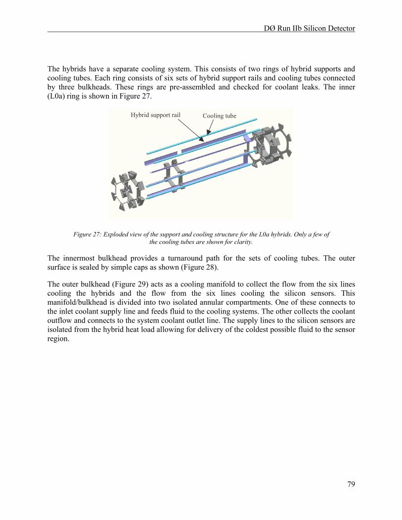
DØ Run IIb Silicon Detector
79
The hybrids have a separate cooling system. This consists of two rings of hybrid supports and cooling tubes. Each ring consists of six sets of hybrid support rails and cooling tubes connected by three bulkheads. These rings are pre-assembled and checked for coolant leaks. The inner (L0a) ring is shown in Figure 27.
Hybrid support rail Cooling tube
Figure 27: Exploded view of the support and cooling structure for the L0a hybrids. Only a few of the cooling tubes are shown for clarity.
The innermost bulkhead provides a turnaround path for the sets of cooling tubes. The outer surface is sealed by simple caps as shown (Figure 28).
The outer bulkhead (Figure 29) acts as a cooling manifold to collect the flow from the six lines cooling the hybrids and the flow from the six lines cooling the silicon sensors. This manifold/bulkhead is divided into two isolated annular compartments. One of these connects to the inlet coolant supply line and feeds fluid to the cooling systems. The other collects the coolant outflow and connects to the system coolant outlet line. The supply lines to the silicon sensors are isolated from the hybrid heat load allowing for delivery of the coldest possible fluid to the sensor region.
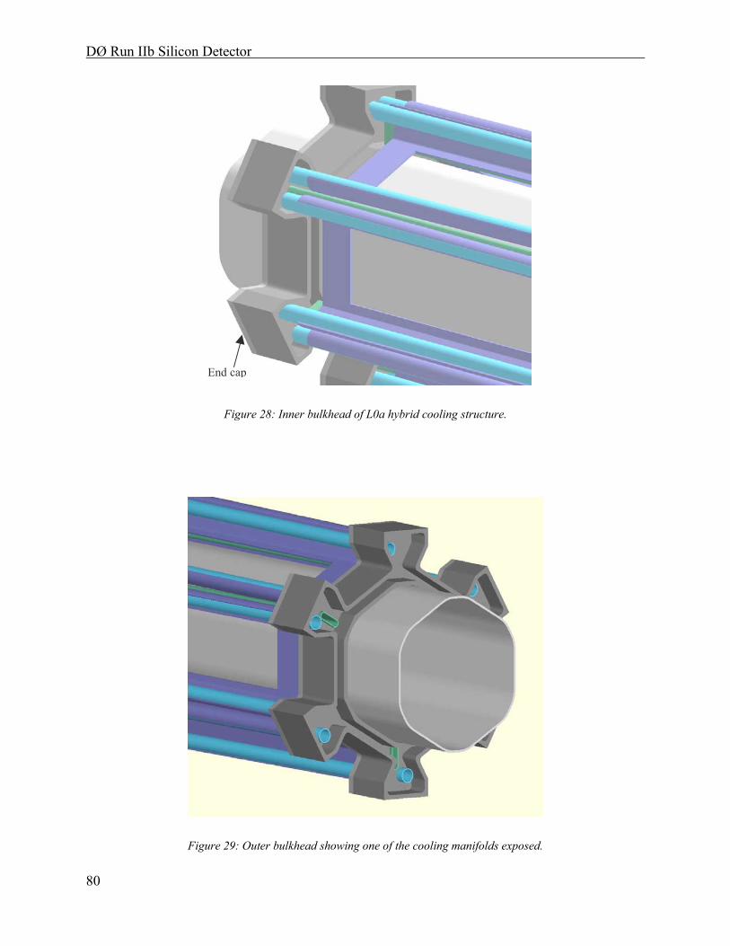
DØ Run IIb Silicon Detector
80
End cap
Figure 28: Inner bulkhead of L0a hybrid cooling structure.
Figure 29: Outer bulkhead showing one of the cooling manifolds exposed.
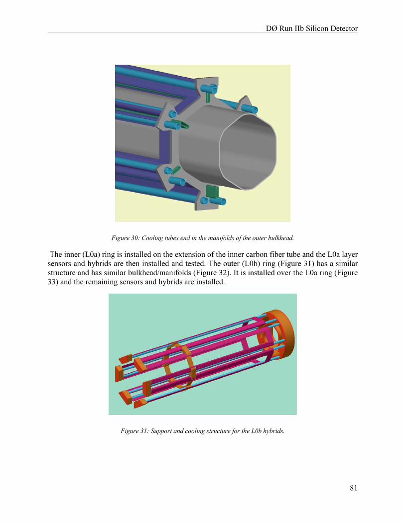
DØ Run IIb Silicon Detector
81
Figure 30: Cooling tubes end in the manifolds of the outer bulkhead.
The inner (L0a) ring is installed on the extension of the inner carbon fiber tube and the L0a layer sensors and hybrids are then installed and tested. The outer (L0b) ring (Figure 31) has a similar structure and has similar bulkhead/manifolds (Figure 32). It is installed over the L0a ring (Figure 33) and the remaining sensors and hybrids are installed.
Figure 31: Support and cooling structure for the L0b hybrids.
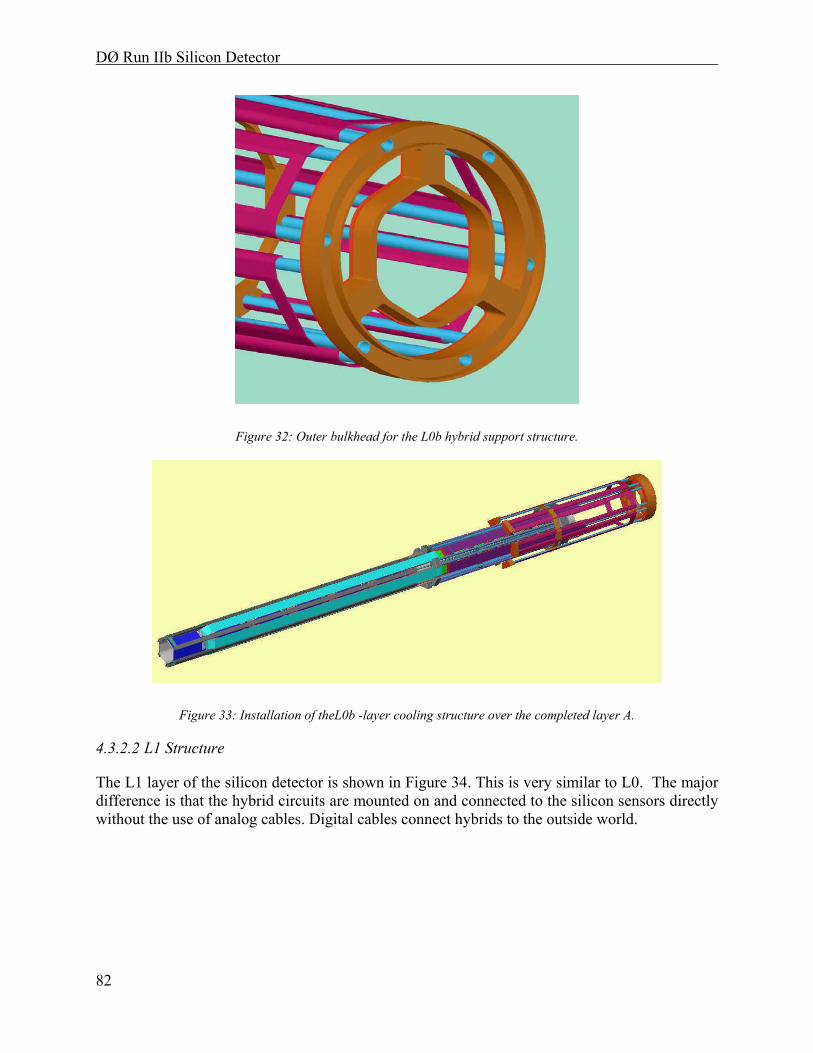
DØ Run IIb Silicon Detector
82
Figure 32: Outer bulkhead for the L0b hybrid support structure.
Figure 33: Installation of theL0b -layer cooling structure over the completed layer A.
4.3.2.2 L1 Structure
The L1 layer of the silicon detector is shown in Figure 34. This is very similar to L0. The major difference is that the hybrid circuits are mounted on and connected to the silicon sensors directly without the use of analog cables. Digital cables connect hybrids to the outside world.
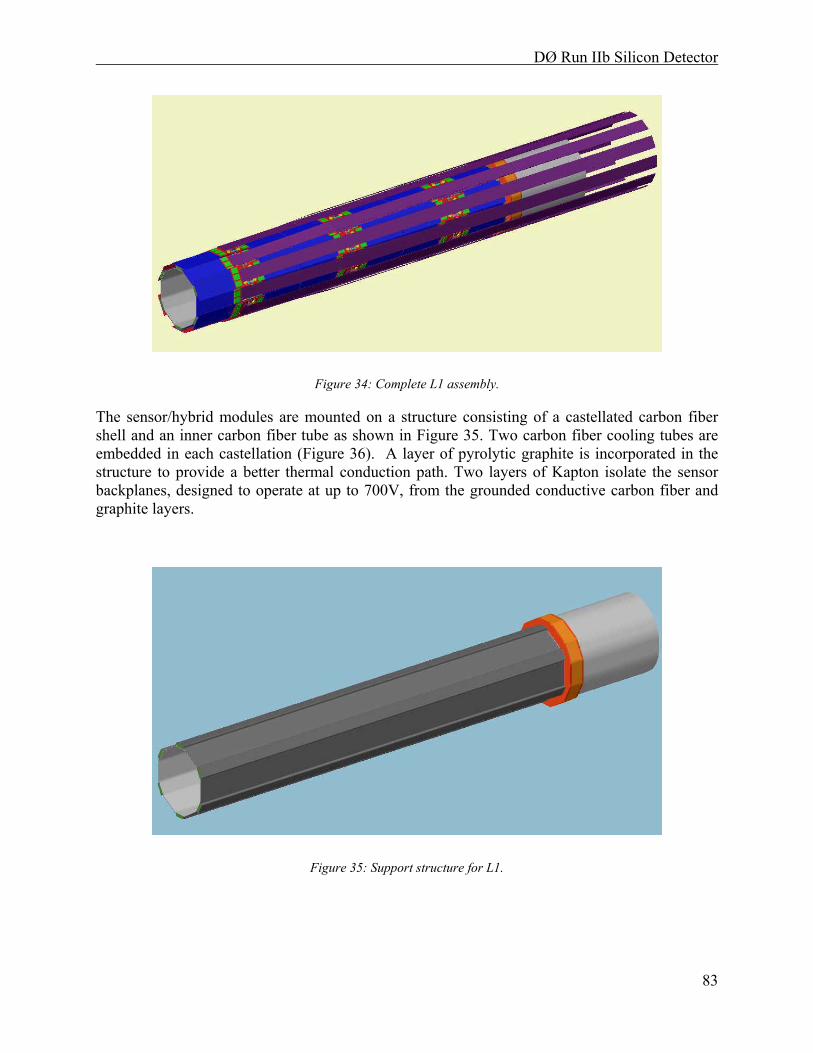
DØ Run IIb Silicon Detector
83
Figure 34: Complete L1 assembly.
The sensor/hybrid modules are mounted on a structure consisting of a castellated carbon fiber shell and an inner carbon fiber tube as shown in Figure 35. Two carbon fiber cooling tubes are embedded in each castellation (Figure 36). A layer of pyrolytic graphite is incorporated in the structure to provide a better thermal conduction path. Two layers of Kapton isolate the sensor backplanes, designed to operate at up to 700V, from the grounded conductive carbon fiber and graphite layers.
Figure 35: Support structure for L1.
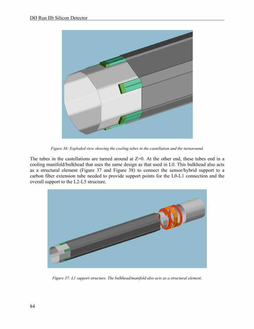
DØ Run IIb Silicon Detector
84
Figure 36: Exploded view showing the cooling tubes in the castellation and the turnaround.
The tubes in the castellations are turned around at Z=0. At the other end, these tubes end in a cooling manifold/bulkhead that uses the same design as that used in L0. This bulkhead also acts as a structural element (Figure 37 and Figure 38) to connect the sensor/hybrid support to a carbon fiber extension tube needed to provide support points for the L0-L1 connection and the overall support to the L2-L5 structure.
Figure 37: L1 support structure. The bulkhead/manifold also acts as a structural element.
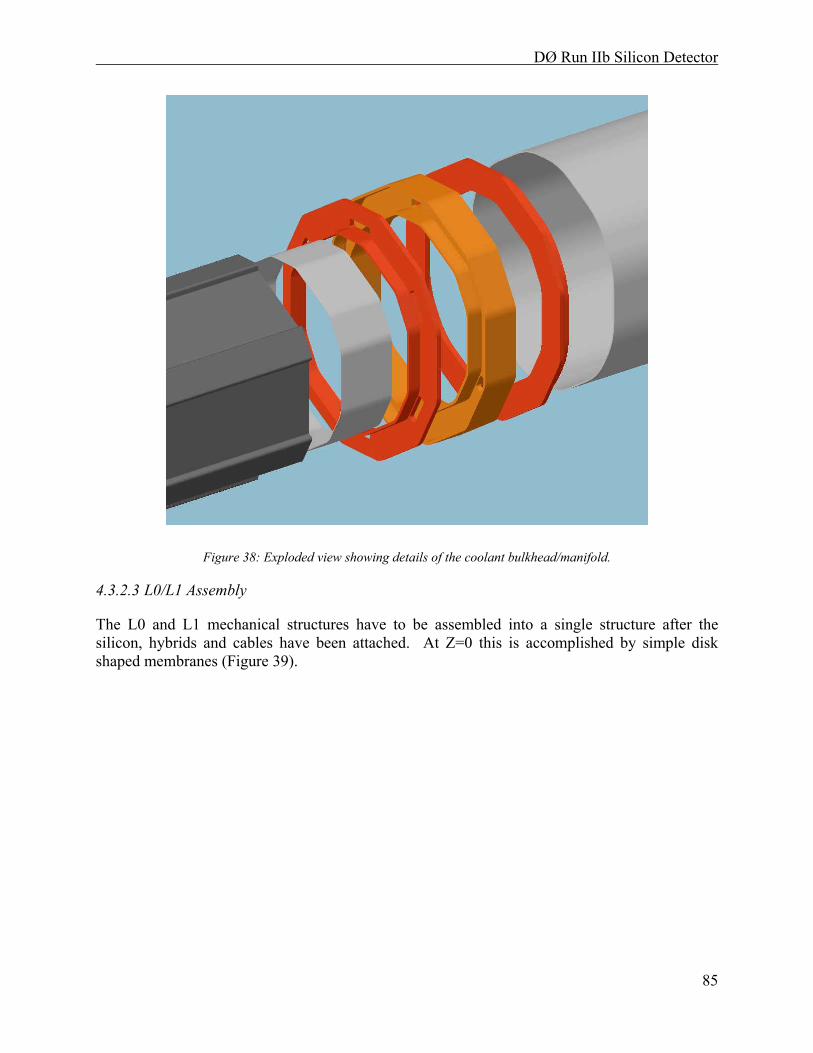
DØ Run IIb Silicon Detector
85
Figure 38: Exploded view showing details of the coolant bulkhead/manifold.
4.3.2.3 L0/L1 Assembly
The L0 and L1 mechanical structures have to be assembled into a single structure after the silicon, hybrids and cables have been attached. At Z=0 this is accomplished by simple disk shaped membranes (Figure 39).
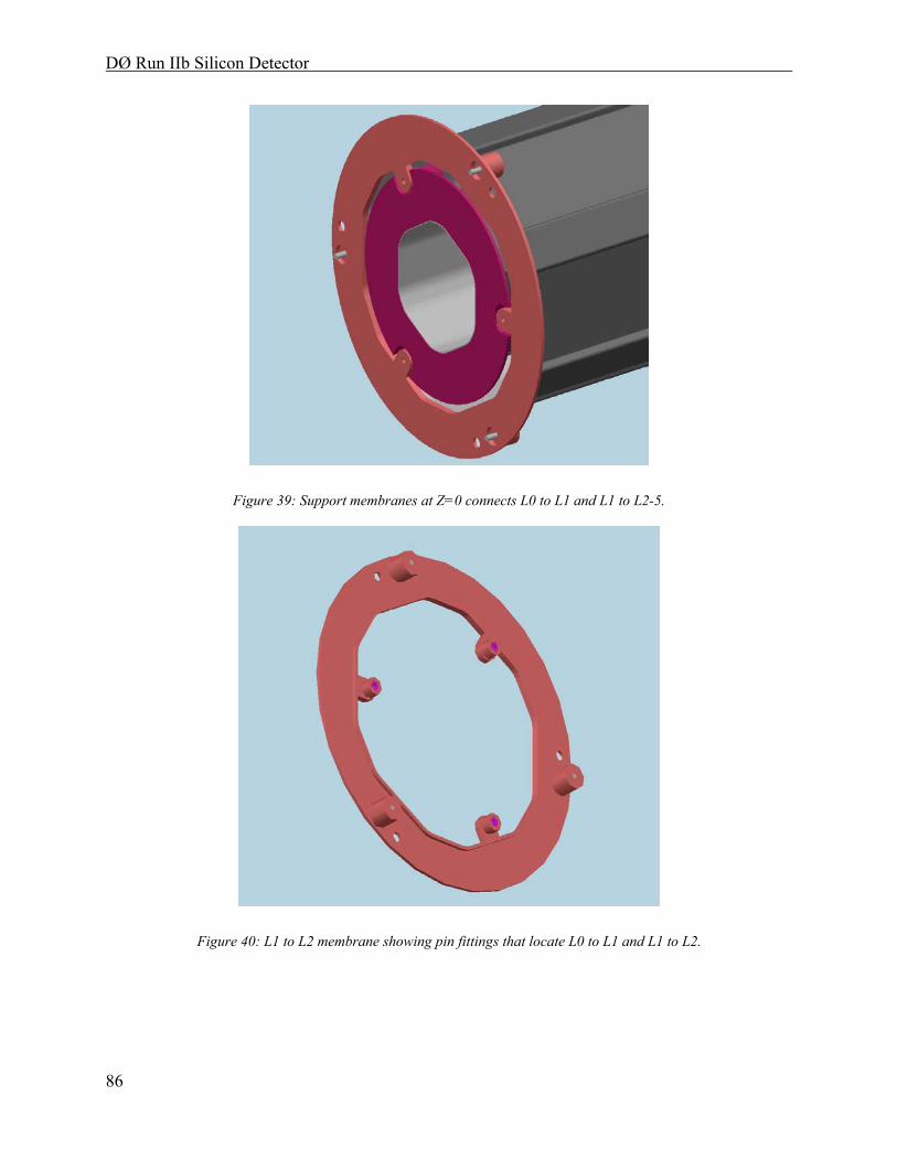
DØ Run IIb Silicon Detector
86
Figure 39: Support membranes at Z=0 connects L0 to L1 and L1 to L2-5.
Figure 40: L1 to L2 membrane showing pin fittings that locate L0 to L1 and L1 to L2.

DØ Run IIb Silicon Detector
87
Figure 41: Membrane that connects L0 to L1 at Z=0.
This membrane has precision pin fittings (Figure 40) that locate L0 and L1 to the membrane and to each other (Figure 41). Another set of such pins locates the membrane to the L2/L5 support structure.
At Z=609 mm, the L0 structure is connected to the inner surface of the L1 structure via the L0 hybrid support ring at that location (Figure 42). This connection will also use precision pins so that L0 is located in a precise position within L1. The outer surface of the L1 structure is connected to the L2/L5 structure in a similar way (Figure 42). To avoid any backlash problems, all of these connections will be spring loaded against precision stops.
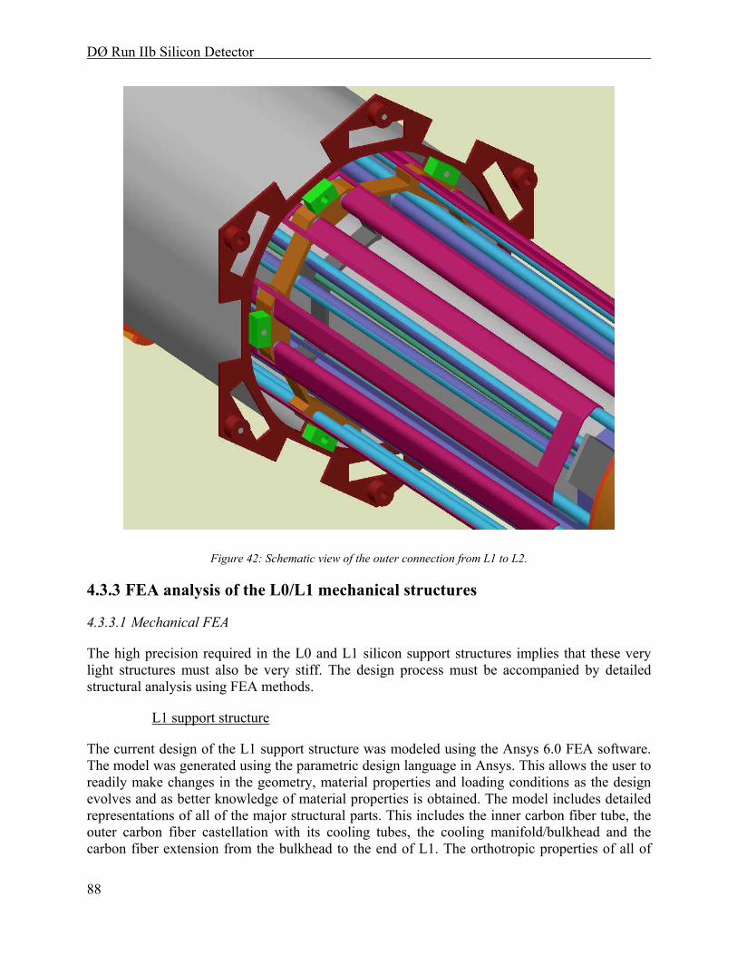
DØ Run IIb Silicon Detector
88
Figure 42: Schematic view of the outer connection from L1 to L2.
4.3.3 FEA analysis of the L0/L1 mechanical structures
4.3.3.1 Mechanical FEA
The high precision required in the L0 and L1 silicon support structures implies that these very light structures must also be very stiff. The design process must be accompanied by detailed structural analysis using FEA methods.
L1 support structure
The current design of the L1 support structure was modeled using the Ansys 6.0 FEA software. The model was generated using the parametric design language in Ansys. This allows the user to readily make changes in the geometry, material properties and loading conditions as the design evolves and as better knowledge of material properties is obtained. The model includes detailed representations of all of the major structural parts. This includes the inner carbon fiber tube, the outer carbon fiber castellation with its cooling tubes, the cooling manifold/bulkhead and the carbon fiber extension from the bulkhead to the end of L1. The orthotropic properties of all of

DØ Run IIb Silicon Detector
89
the fiber structures were determined as discussed below in Section 4.3.4. To keep the model to a manageable size, the stacks of layers involved at the sensors and hybrids (pyrolytic graphite, Kapton, epoxy, silicon and the hybrid substrates) were not modeled in detail. These parts were represented by elements with ‘dummy’ material properties such that they have equivalent weight and bending stiffness to the actual structures. This was done by modeling short lengths of the silicon and hybrid layers in Ansys and deriving the desired ‘dummy’ properties from the calculated deflections. The weight of the cooling fluid is accounted for in this step.
The model was loaded by gravity only. Other loads, such as forces from the digital cables and cooling connections, will be added later. Given the symmetry of the structure and the loads, only one half of the structure was modeled (Figure 43). Ansys has a display option that allows one to view the whole structure and this is used in all other figures below. Figure 44, Figure 45 and Figure 46 show details of the element structure at various places in the model.
Figure 43: View of the actual model (volumes shown) of the L1 structure.
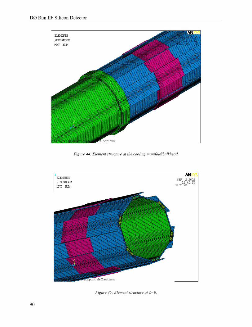
DØ Run IIb Silicon Detector
90
Figure 44: Element structure at the cooling manifold/bulkhead.
Figure 45: Element structure at Z=0.
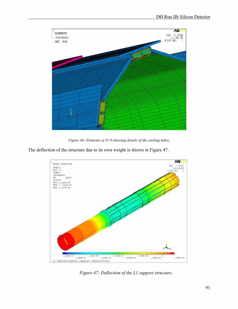
DØ Run IIb Silicon Detector
91
Figure 46: Elements at Z=0 showing details of the cooling tubes.
The deflection of the structure due to its own weight is shown in Figure 47.
Figure 47: Deflection of the L1 support structure.

DØ Run IIb Silicon Detector
92
The maximum sagitta of the main part of the structure is only 1.55 µm.
L0 support structure
Calculations similar to those done for L1 show that the gravitational deflection of the L0 support structure is well within the required tolerance. In the sensor region, the maximum deflection is less than 6 µm as seen in Figure 48.
Figure 48: Deflection of L0 support structure.
4.3.3.2 Thermal FEA
L1 support structure
In L1, the hybrids with the heat generating SVX4 chips are mounted on top of the silicon sensors.
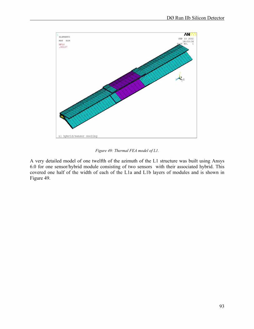
DØ Run IIb Silicon Detector
93
Figure 49: Thermal FEA model of L1.
A very detailed model of one twelfth of the azimuth of the L1 structure was built using Ansys 6.0 for one sensor/hybrid module consisting of two sensors with their associated hybrid. This covered one half of the width of each of the L1a and L1b layers of modules and is shown in Figure 49.
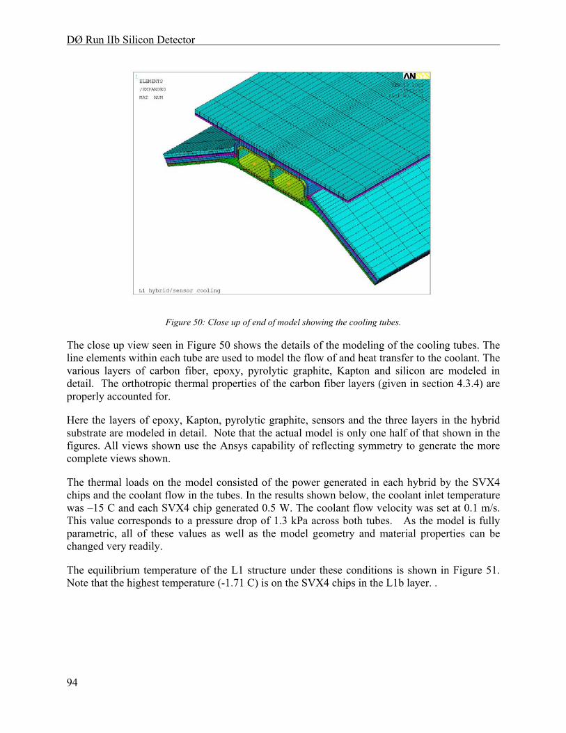
DØ Run IIb Silicon Detector
94
Figure 50: Close up of end of model showing the cooling tubes.
The close up view seen in Figure 50 shows the details of the modeling of the cooling tubes. The line elements within each tube are used to model the flow of and heat transfer to the coolant. The various layers of carbon fiber, epoxy, pyrolytic graphite, Kapton and silicon are modeled in detail. The orthotropic thermal properties of the carbon fiber layers (given in section 4.3.4) are properly accounted for.
Here the layers of epoxy, Kapton, pyrolytic graphite, sensors and the three layers in the hybrid substrate are modeled in detail. Note that the actual model is only one half of that shown in the figures. All views shown use the Ansys capability of reflecting symmetry to generate the more complete views shown.
The thermal loads on the model consisted of the power generated in each hybrid by the SVX4 chips and the coolant flow in the tubes. In the results shown below, the coolant inlet temperature was –15 C and each SVX4 chip generated 0.5 W. The coolant flow velocity was set at 0.1 m/s. This value corresponds to a pressure drop of 1.3 kPa across both tubes. As the model is fully parametric, all of these values as well as the model geometry and material properties can be changed very readily.
The equilibrium temperature of the L1 structure under these conditions is shown in Figure 51. Note that the highest temperature (-1.71 C) is on the SVX4 chips in the L1b layer. .
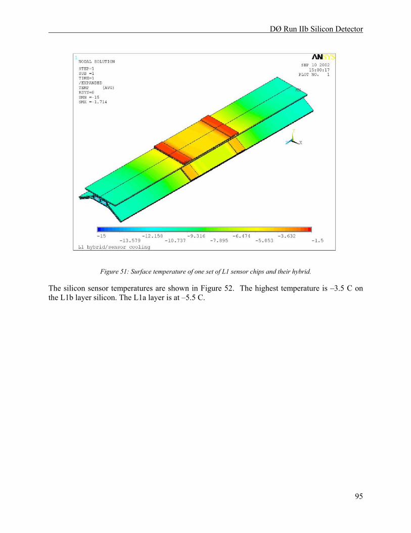
DØ Run IIb Silicon Detector
95
Figure 51: Surface temperature of one set of L1 sensor chips and their hybrid.
The silicon sensor temperatures are shown in Figure 52. The highest temperature is –3.5 C on the L1b layer silicon. The L1a layer is at –5.5 C.

DØ Run IIb Silicon Detector
96
Figure 52: Temperature map showing the silicon sensors
The temperature rise in the coolant is 0.661 C as shown in Figure 53. The temperature change shown is for flow in one tube, 160 mm in length. This is because only one half of the width of the sensors is actually used in the model. Also the length of the section modeled is only one third of the total length and heat load of the full structure. . The actual heat generated is, thus, six times the values given above. The overall temperature rise in the fluid is also six times the above values. In practice, fluid enters along one edge and leaves in the opposite direction along the other. The cooling tubes within the castellations run very close to each other but are not in direct contact. The fluid enters on one tube, flows to the end at Z=0, turns around and then flows in the opposite direction to the incoming flow. The possible heat transfer between the tubes was studied and found to be negligible.
As the silicon sensors age in use, they generate more heat. A thermal load of 0.1 W per chip was added to the model to simulate this. As shown in Figure 54, this load increases the maximum sensor temperature to –2.0 C.
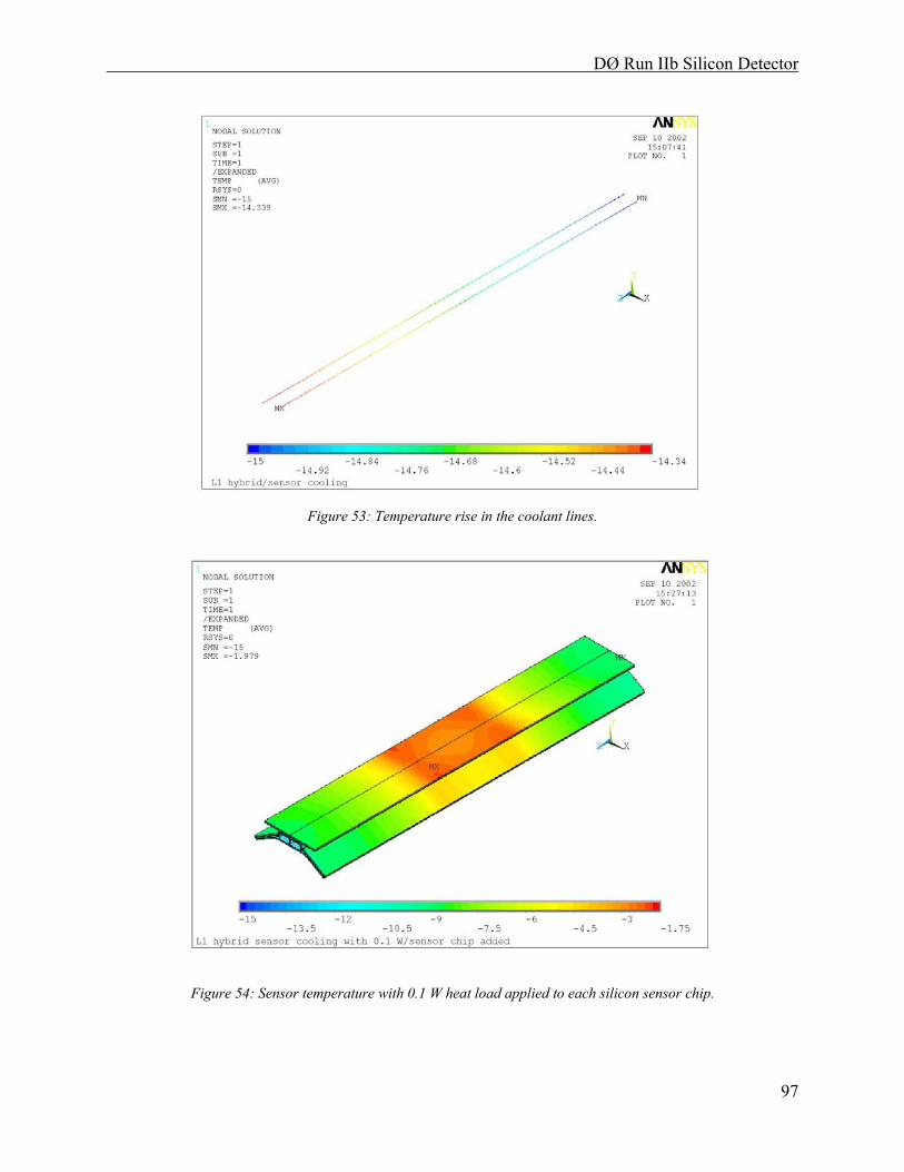
DØ Run IIb Silicon Detector
97
Figure 53: Temperature rise in the coolant lines.
Figure 54: Sensor temperature with 0.1 W heat load applied to each silicon sensor chip.

DØ Run IIb Silicon Detector
98
L0 support structure
Simple 2-d thermal FEA analysis was used in the design phase for the L0 cooling system. This showed that the adopted design has more than adequate cooling capacity. The L0 silicon sensors are cooled by a separate cooling circuit from their associated hybrids and are thus, easy to cool.
4.3.3.3 Conclusions
The deflection results obtained for L1 show that this structure is extremely stiff and that the mechanical design has a large design reserve. For L0, a study of the stiffness of the main structure shows that the gravitational sag is very similar to that seen in the L1 FEA calculations, well within the allowed tolerance.
The L1 thermal results show that, prior to irradiation, with the coolant inlet temperature at –15 C, the maximum temperature seen on the silicon sensors is 3.5 C. With irradiation, this increases to –2.0 C.
Thermal results obtained on some simple 2-d FEA studies on L0 were used during the design phase for the L0 cooling system. These showed that the design was capable of easily meeting the requirement that the maximum silicon temperature be maintained below -10 C.
4.3.4 Properties of Carbon Fiber Composites
A detailed FEA analysis has been performed to support the design of the L0/L1 support structure. The validity of this analysis hinges on an accurate a priori knowledge of the elastic and thermal properties of the composite laminates used within the structure. Laminates with different stacking sequences will be used and, therefore, properties will vary substantially from one laminate to the next.
Elastic and thermal properties of a given laminate have been predicted on the basis of standard classical lamination theory (CLT). This requires that the following elastic and thermal properties for unidirectional laminates must be known:
- E1 and E2 (Young’s modulus parallel and perpendicular to the fiber direction)
- ν12 (the “major” Poisson ratio)
- G12 (the shear modulus)
- α1 and α2 (thermal expansion coefficients parallel and perpendicular to the fiber direction), and
- K1 and K2 (thermal conductivity parallel and perpendicular to the fiber direction)
Once these properties are known, CLT can then be used to predict the equivalent properties for a composite laminate of any desired stacking sequence. A series of tests was performed to
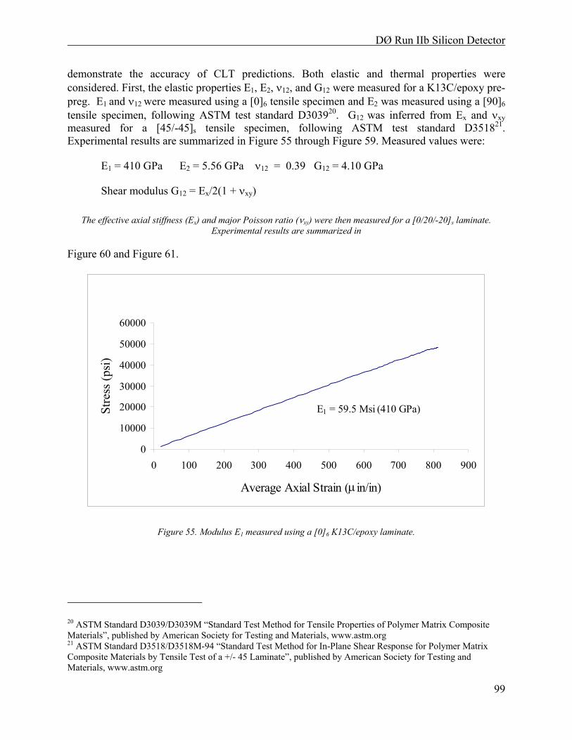
DØ Run IIb Silicon Detector
99
demonstrate the accuracy of CLT predictions. Both elastic and thermal properties were considered. First, the elastic properties E1, E2, ν12, and G12 were measured for a K13C/epoxy pre-preg. E1 and ν12 were measured using a [0]6 tensile specimen and E2 was measured using a [90]6 tensile specimen, following ASTM test standard D303920. G12 was inferred from Ex and νxy measured for a [45/-45]s tensile specimen, following ASTM test standard D351821. Experimental results are summarized in Figure 55 through Figure 59. Measured values were:
E1 = 410 GPa E2 = 5.56 GPa ν12 = 0.39 G12 = 4.10 GPa
Shear modulus G12 = Ex/2(1 + νxy)
The effective axial stiffness (Ex) and major Poisson ratio (νxy) were then measured for a [0/20/-20]s laminate. Experimental results are summarized in
Figure 60 and Figure 61.
0
10000
20000
30000
40000
50000
60000
0 100 200 300 400 500 600 700 800 900
Average Axial Strain (µin/in)
Stre
ss (p
si)
E1 = 59.5 Msi (410 GPa)
Figure 55. Modulus E1 measured using a [0]6 K13C/epoxy laminate.
20 ASTM Standard D3039/D3039M “Standard Test Method for Tensile Properties of Polymer Matrix Composite Materials”, published by American Society for Testing and Materials, www.astm.org 21 ASTM Standard D3518/D3518M-94 “Standard Test Method for In-Plane Shear Response for Polymer Matrix Composite Materials by Tensile Test of a +/- 45 Laminate”, published by American Society for Testing and Materials, www.astm.org
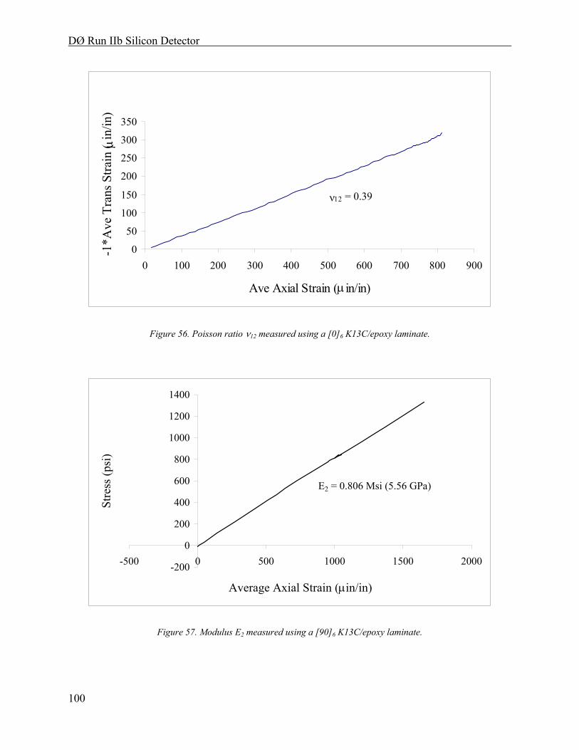
DØ Run IIb Silicon Detector
100
0
50
100
150
200
250
300
350
0 100 200 300 400 500 600 700 800 900
Ave Axial Strain (µin/in)
-1*A
ve T
rans
Stra
in ( µ
in/in
)
ν12 = 0.39
Figure 56. Poisson ratio ν12 measured using a [0]6 K13C/epoxy laminate.
-200
0
200
400
600
800
1000
1200
1400
-500 0 500 1000 1500 2000
Average Axial Strain (µin/in)
Stre
ss (p
si)
E2 = 0.806 Msi (5.56 GPa)
Figure 57. Modulus E2 measured using a [90]6 K13C/epoxy laminate.
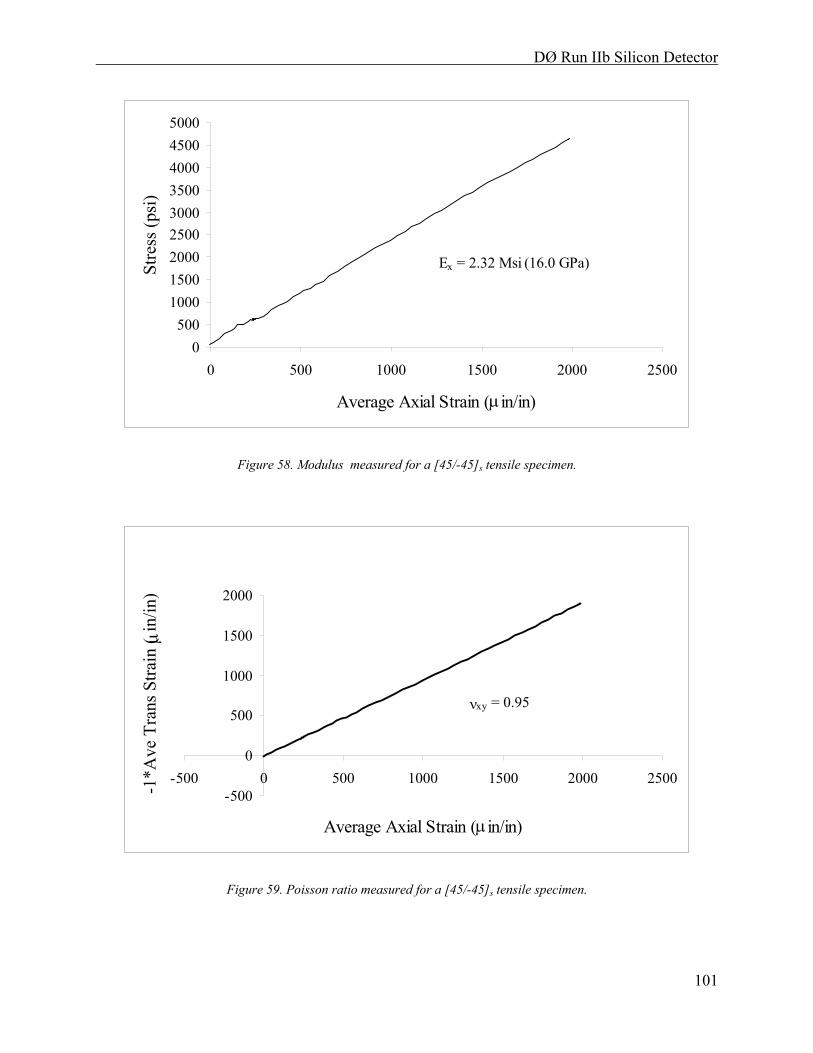
DØ Run IIb Silicon Detector
101
0500
100015002000250030003500400045005000
0 500 1000 1500 2000 2500
Average Axial Strain (µin/in)
Stre
ss (p
si)
Ex = 2.32 Msi (16.0 GPa)
Figure 58. Modulus measured for a [45/-45]s tensile specimen.
-500
0
500
1000
1500
2000
-500 0 500 1000 1500 2000 2500
Average Axial Strain (µin/in)
-1*A
ve T
rans
Stra
in ( µ
in/in
)
νxy = 0.95
Figure 59. Poisson ratio measured for a [45/-45]s tensile specimen.
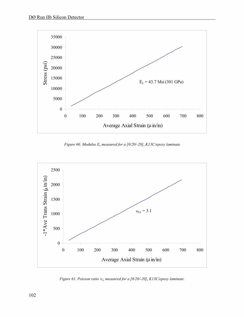
DØ Run IIb Silicon Detector
102
0
5000
10000
15000
20000
25000
30000
35000
0 100 200 300 400 500 600 700 800
Average Axial Strain (µin/in)
Stre
ss (p
si)
Ex = 43.7 Msi (301 GPa)
Figure 60. Modulus Ex measured for a [0/20/-20]s K13C/epoxy laminate
0
500
1000
1500
2000
2500
0 100 200 300 400 500 600 700 800
Average Axial Strain (µin/in)
-1*A
ve T
rans
Stra
in ( µ
in/in
)
νxy = 3.1
Figure 61. Poisson ratio νxy measured for a [0/20/-20]s K13C/epoxy laminate.
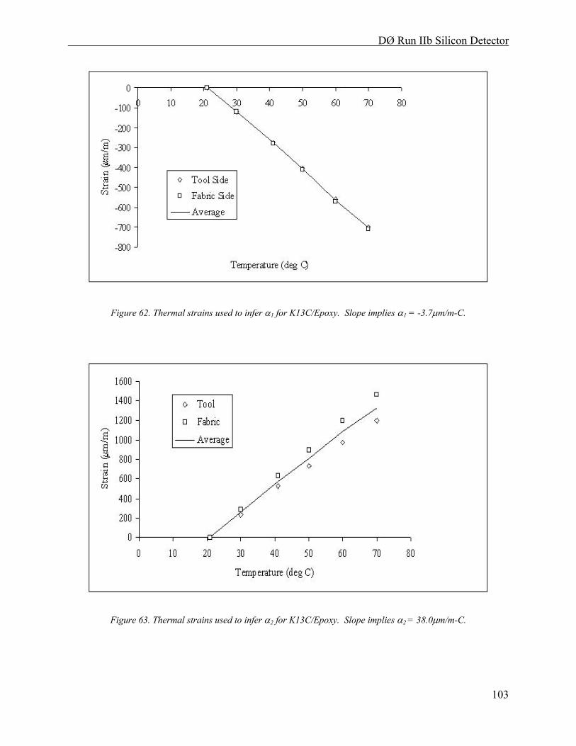
DØ Run IIb Silicon Detector
103
Figure 62. Thermal strains used to infer α1 for K13C/Epoxy. Slope implies α1 = -3.7µm/m-C.
Figure 63. Thermal strains used to infer α2 for K13C/Epoxy. Slope implies α2 = 38.0µm/m-C.
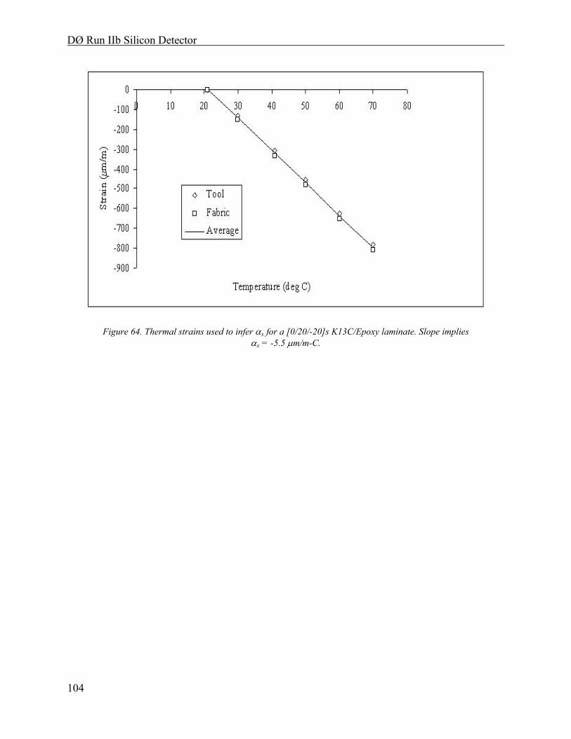
DØ Run IIb Silicon Detector
104
Figure 64. Thermal strains used to infer αx for a [0/20/-20]s K13C/Epoxy laminate. Slope implies αx = -5.5 µm/m-C.
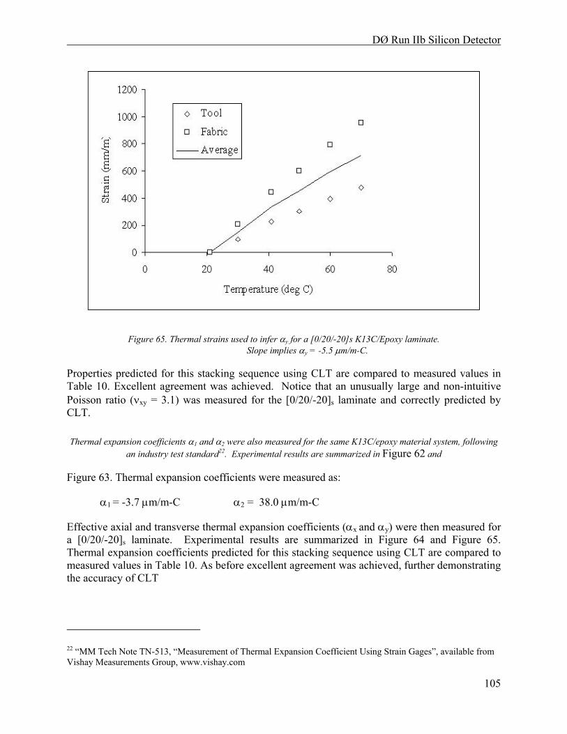
DØ Run IIb Silicon Detector
105
Figure 65. Thermal strains used to infer αy for a [0/20/-20]s K13C/Epoxy laminate. Slope implies αy = -5.5 µm/m-C.
Properties predicted for this stacking sequence using CLT are compared to measured values in Table 10. Excellent agreement was achieved. Notice that an unusually large and non-intuitive Poisson ratio (νxy = 3.1) was measured for the [0/20/-20]s laminate and correctly predicted by CLT.
Thermal expansion coefficients α1 and α2 were also measured for the same K13C/epoxy material system, following an industry test standard22. Experimental results are summarized in Figure 62 and
Figure 63. Thermal expansion coefficients were measured as:
α1 = -3.7 µm/m-C α2 = 38.0 µm/m-C
Effective axial and transverse thermal expansion coefficients (αx and αy) were then measured for a [0/20/-20]s laminate. Experimental results are summarized in Figure 64 and Figure 65. Thermal expansion coefficients predicted for this stacking sequence using CLT are compared to measured values in Table 10. As before excellent agreement was achieved, further demonstrating the accuracy of CLT
22 “MM Tech Note TN-513, “Measurement of Thermal Expansion Coefficient Using Strain Gages”, available from Vishay Measurements Group, www.vishay.com
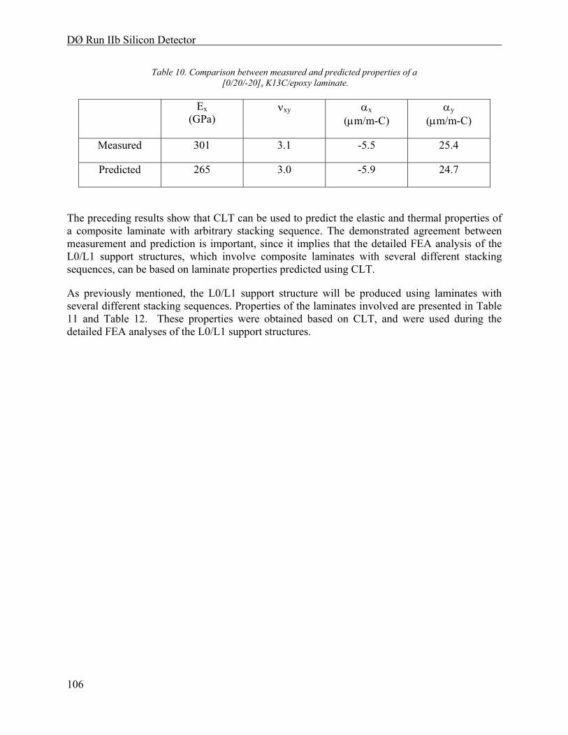
DØ Run IIb Silicon Detector
106
Table 10. Comparison between measured and predicted properties of a [0/20/-20]s K13C/epoxy laminate.
Ex (GPa)
νxy αx
(µm/m-C) αy
(µm/m-C)
Measured 301 3.1 -5.5 25.4
Predicted 265 3.0 -5.9 24.7
The preceding results show that CLT can be used to predict the elastic and thermal properties of a composite laminate with arbitrary stacking sequence. The demonstrated agreement between measurement and prediction is important, since it implies that the detailed FEA analysis of the L0/L1 support structures, which involve composite laminates with several different stacking sequences, can be based on laminate properties predicted using CLT.
As previously mentioned, the L0/L1 support structure will be produced using laminates with several different stacking sequences. Properties of the laminates involved are presented in Table 11 and Table 12. These properties were obtained based on CLT, and were used during the detailed FEA analyses of the L0/L1 support structures.
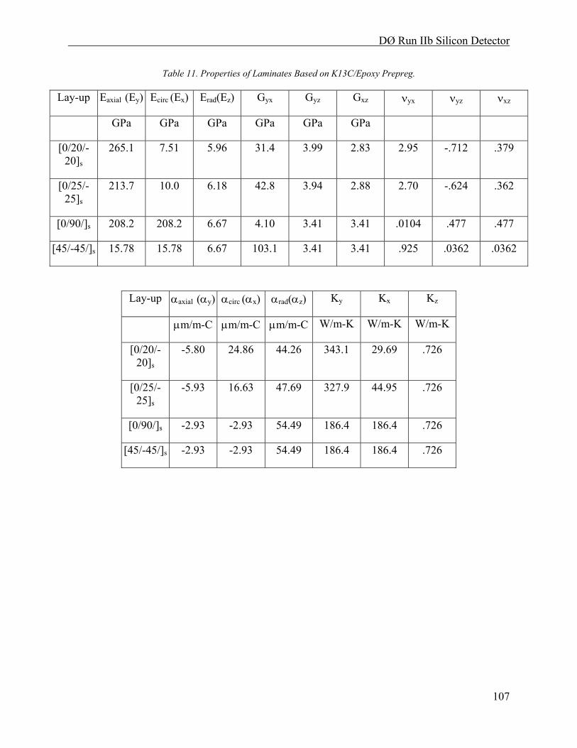
DØ Run IIb Silicon Detector
107
Table 11. Properties of Laminates Based on K13C/Epoxy Prepreg.
Lay-up Eaxial (Ey) Ecirc (Ex) Erad(Ez) Gyx Gyz Gxz νyx νyz νxz
GPa GPa GPa GPa GPa GPa
[0/20/-20]s
265.1 7.51 5.96 31.4 3.99 2.83 2.95 -.712 .379
[0/25/-25]s
213.7 10.0 6.18 42.8 3.94 2.88 2.70 -.624 .362
[0/90/]s 208.2 208.2 6.67 4.10 3.41 3.41 .0104 .477 .477
[45/-45/]s 15.78 15.78 6.67 103.1 3.41 3.41 .925 .0362 .0362
Lay-up αaxial (αy) αcirc (αx) αrad(αz) Ky Kx Kz
µm/m-C µm/m-C µm/m-C W/m-K W/m-K W/m-K
[0/20/-20]s
-5.80 24.86 44.26 343.1 29.69 .726
[0/25/-25]s
-5.93 16.63 47.69 327.9 44.95 .726
[0/90/]s -2.93 -2.93 54.49 186.4 186.4 .726
[45/-45/]s -2.93 -2.93 54.49 186.4 186.4 .726
DØ Run IIb Silicon Detector
108
Table 12. Laminates Based on K139/Epoxy Prepreg.
Lay-up Eaxial (Ey) Ecirc (Ex) Erad(Ez) Gyx Gyz Gxz νyx νyz νxz
GPa GPa GPa GPa GPa GPa
[0/20/-20]s
243.2 6.09 4.51 29.52 3.53 2.786 3.29 -.871 .379
[0/25/-25]s
196.2 8.50 4.68 40.41 3.50 2.82 2.89 -.718 .362
[0/90/]s 196.9 196.9 5.01 3.60 3.16 3.16 .0078 .464 .464
[45/-45/]s 13.9 13.9 5.01 97.7 3.16 3.16 .930 .0327 .0327
Lay-up αaxial (αy) αcirc (αx) αrad(αz) Ky Kx Kz
µm/m-C µm/m-C µm/m-C W/m-K W/m-K W/m-K
[0/20/-20]s
-5.97 21.2 42.7 116.3 10.5 .726
[0/25/-25]s
-6.01 13.1 46.0 111.2 15.65 .726
[0/90/]s -3.52 -3.52 51.85 63.41 63.41 .726
[45/-45/]s -3.52 -3.52 51.85 63.41 63.41 .726
4.3.5 Fabrication Techniques
The L0/L1 support structure is fabricated using pre-preg tape and hand-lay-up, as described below.
4.3.5.1 Support Structure Fabrication
The support structure shells are fabricated by wrapping carbon fiber pre-preg material around mandrels that are machined to the specified cross-sectional dimensions. The outer, castellated shells are 6 ply lay-ups, with fiber orientations of [0°/20°/-20°]s. The inner shells are 4 ply lay-ups in the sensor regions, with fiber orientations of [0°/90°]s. To increase the stiffness of the inner shells, an additional 4 plies are added outside of the sensor regions, also at [0°/90°]s. A cross-section of the L0 shell assembly is shown in Figure 66.
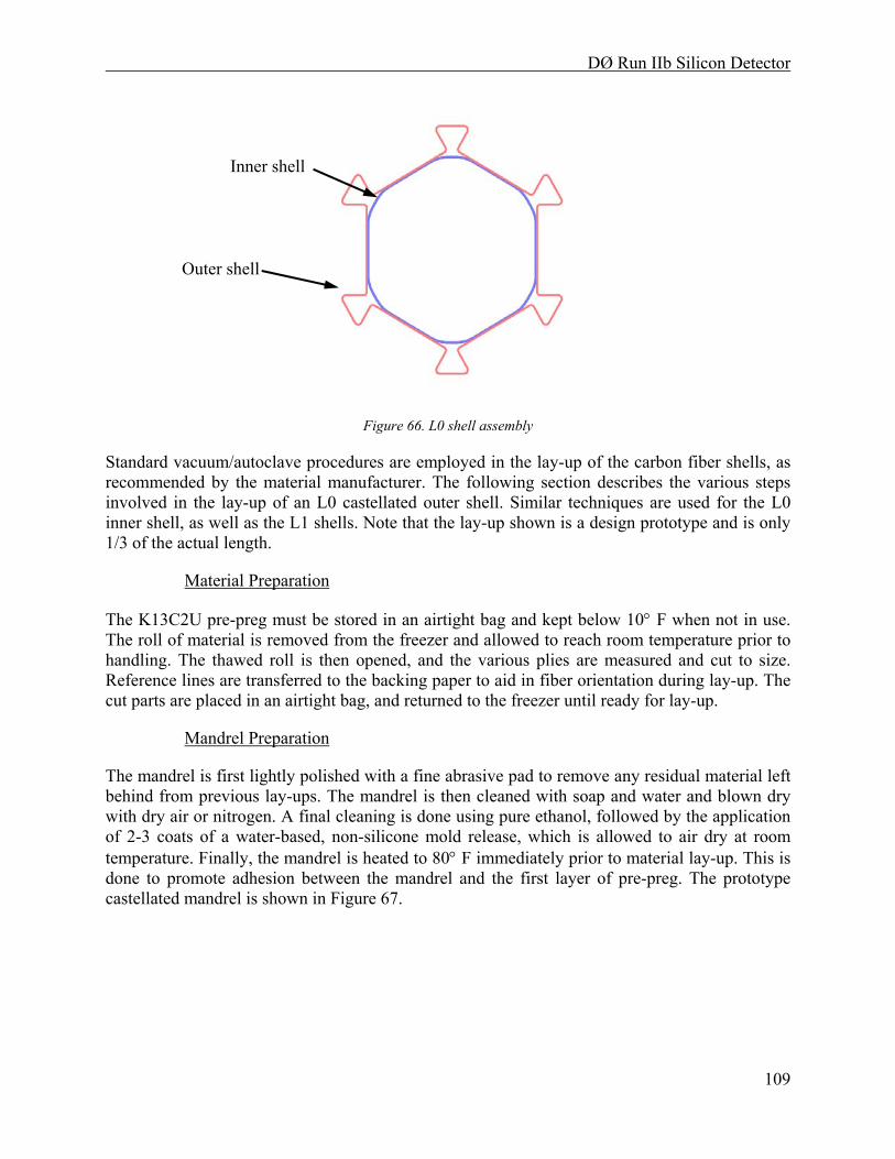
DØ Run IIb Silicon Detector
109
Figure 66. L0 shell assembly
Standard vacuum/autoclave procedures are employed in the lay-up of the carbon fiber shells, as recommended by the material manufacturer. The following section describes the various steps involved in the lay-up of an L0 castellated outer shell. Similar techniques are used for the L0 inner shell, as well as the L1 shells. Note that the lay-up shown is a design prototype and is only 1/3 of the actual length.
Material Preparation
The K13C2U pre-preg must be stored in an airtight bag and kept below 10° F when not in use. The roll of material is removed from the freezer and allowed to reach room temperature prior to handling. The thawed roll is then opened, and the various plies are measured and cut to size. Reference lines are transferred to the backing paper to aid in fiber orientation during lay-up. The cut parts are placed in an airtight bag, and returned to the freezer until ready for lay-up.
Mandrel Preparation
The mandrel is first lightly polished with a fine abrasive pad to remove any residual material left behind from previous lay-ups. The mandrel is then cleaned with soap and water and blown dry with dry air or nitrogen. A final cleaning is done using pure ethanol, followed by the application of 2-3 coats of a water-based, non-silicone mold release, which is allowed to air dry at room temperature. Finally, the mandrel is heated to 80° F immediately prior to material lay-up. This is done to promote adhesion between the mandrel and the first layer of pre-preg. The prototype castellated mandrel is shown in Figure 67.
Inner shell
Outer shell
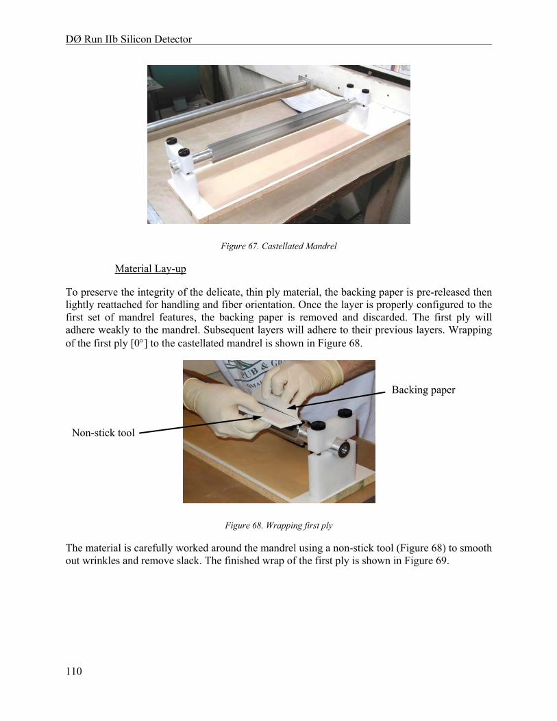
DØ Run IIb Silicon Detector
110
Figure 67. Castellated Mandrel
Material Lay-up
To preserve the integrity of the delicate, thin ply material, the backing paper is pre-released then lightly reattached for handling and fiber orientation. Once the layer is properly configured to the first set of mandrel features, the backing paper is removed and discarded. The first ply will adhere weakly to the mandrel. Subsequent layers will adhere to their previous layers. Wrapping of the first ply [0°] to the castellated mandrel is shown in Figure 68.
Figure 68. Wrapping first ply
The material is carefully worked around the mandrel using a non-stick tool (Figure 68) to smooth out wrinkles and remove slack. The finished wrap of the first ply is shown in Figure 69.
Non-stick tool
Backing paper
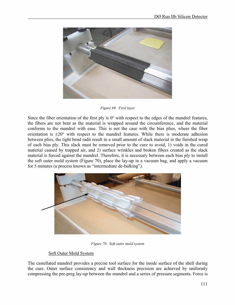
DØ Run IIb Silicon Detector
111
Figure 69. First layer
Since the fiber orientation of the first ply is 0° with respect to the edges of the mandrel features, the fibers are not bent as the material is wrapped around the circumference, and the material conforms to the mandrel with ease. This is not the case with the bias plies, where the fiber orientation is ±20° with respect to the mandrel features. While there is moderate adhesion between plies, the tight bend radii result in a small amount of slack material in the finished wrap of each bias ply. This slack must be removed prior to the cure to avoid, 1) voids in the cured material caused by trapped air, and 2) surface wrinkles and broken fibers created as the slack material is forced against the mandrel. Therefore, it is necessary between each bias ply to install the soft outer mold system (Figure 70), place the lay-up in a vacuum bag, and apply a vacuum for 5 minutes (a process known as “intermediate de-bulking”).
Figure 70. Soft outer mold system
Soft Outer Mold System
The castellated mandrel provides a precise tool surface for the inside surface of the shell during the cure. Outer surface consistency and wall thickness precision are achieved by uniformly compressing the pre-preg lay-up between the mandrel and a series of pressure segments. Force is
DØ Run IIb Silicon Detector
112
applied using a combination of vacuum bagging and external air pressure. The pressure segments consist of precision cast RTV strips wrapped in breather cloth and covered with a layer of porous release ply. The individual segments are wedged between the castellations before installing the vacuum bag Figure 70 A single segment is shown in Figure 71.
Figure 71. Single segment
Vacuum Bag/Autoclave
Once the outer mold segments are installed to the lay-up, the entire assembly is wrapped in breather cloth, and then thin nylon film. The nylon film is sealed around the mandrel with vacuum tape, creating a “vacuum bag”. One end of the mandrel is equipped with a vacuum port. Figure 72 shows the mandrel ready for vacuum testing.
Figure 72. Lay-up ready for vacuum test
Once the lay-up is vacuum tested and found to be leak free, it is loaded into the autoclave, shown in Figure 73.
Porous release ply
Breather cloth RTV strip
Vacuum port
Vacuum tape
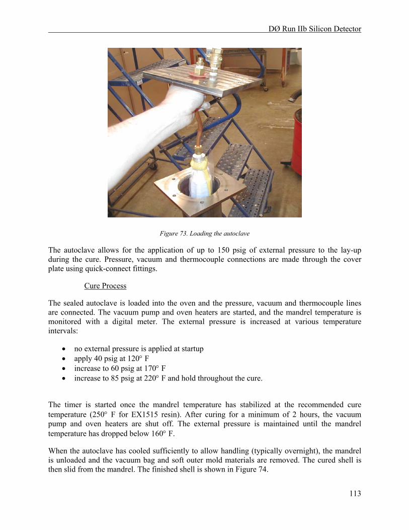
DØ Run IIb Silicon Detector
113
Figure 73. Loading the autoclave
The autoclave allows for the application of up to 150 psig of external pressure to the lay-up during the cure. Pressure, vacuum and thermocouple connections are made through the cover plate using quick-connect fittings.
Cure Process
The sealed autoclave is loaded into the oven and the pressure, vacuum and thermocouple lines are connected. The vacuum pump and oven heaters are started, and the mandrel temperature is monitored with a digital meter. The external pressure is increased at various temperature intervals:
• no external pressure is applied at startup • apply 40 psig at 120° F • increase to 60 psig at 170° F • increase to 85 psig at 220° F and hold throughout the cure.
The timer is started once the mandrel temperature has stabilized at the recommended cure temperature (250° F for EX1515 resin). After curing for a minimum of 2 hours, the vacuum pump and oven heaters are shut off. The external pressure is maintained until the mandrel temperature has dropped below 160° F.
When the autoclave has cooled sufficiently to allow handling (typically overnight), the mandrel is unloaded and the vacuum bag and soft outer mold materials are removed. The cured shell is then slid from the mandrel. The finished shell is shown in Figure 74.
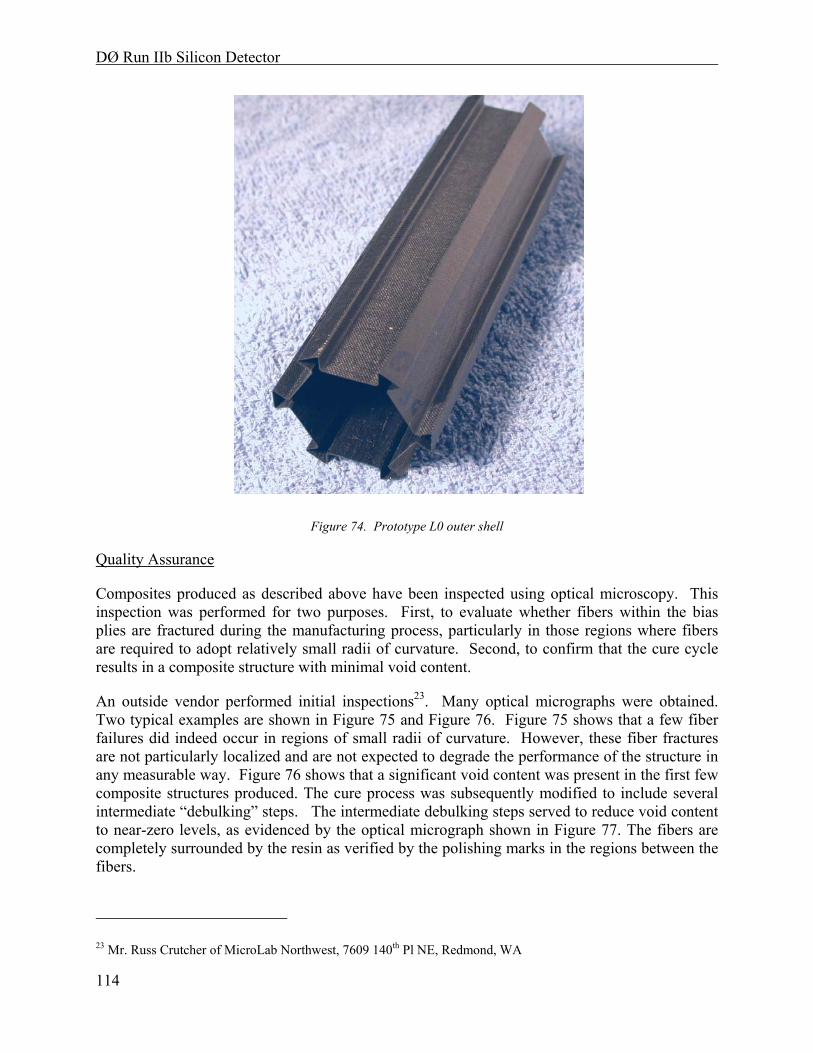
DØ Run IIb Silicon Detector
114
Figure 74. Prototype L0 outer shell
Quality Assurance
Composites produced as described above have been inspected using optical microscopy. This inspection was performed for two purposes. First, to evaluate whether fibers within the bias plies are fractured during the manufacturing process, particularly in those regions where fibers are required to adopt relatively small radii of curvature. Second, to confirm that the cure cycle results in a composite structure with minimal void content.
An outside vendor performed initial inspections23. Many optical micrographs were obtained. Two typical examples are shown in Figure 75 and Figure 76. Figure 75 shows that a few fiber failures did indeed occur in regions of small radii of curvature. However, these fiber fractures are not particularly localized and are not expected to degrade the performance of the structure in any measurable way. Figure 76 shows that a significant void content was present in the first few composite structures produced. The cure process was subsequently modified to include several intermediate “debulking” steps. The intermediate debulking steps served to reduce void content to near-zero levels, as evidenced by the optical micrograph shown in Figure 77. The fibers are completely surrounded by the resin as verified by the polishing marks in the regions between the fibers.
23 Mr. Russ Crutcher of MicroLab Northwest, 7609 140th Pl NE, Redmond, WA
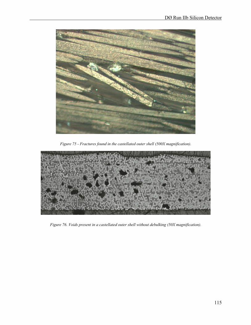
DØ Run IIb Silicon Detector
115
Figure 75 - Fractures found in the castellated outer shell (500X magnification).
Figure 76. Voids present in a castellated outer shell without debulking (50X magnification).
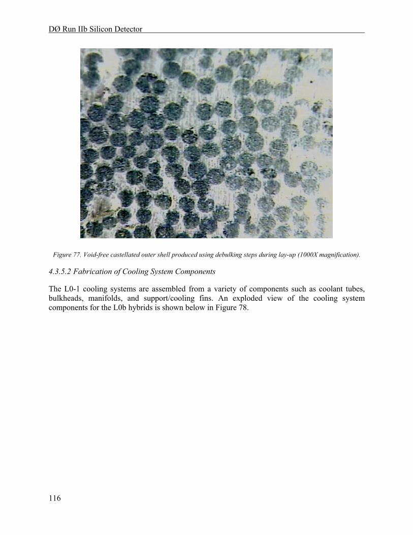
DØ Run IIb Silicon Detector
116
Figure 77. Void-free castellated outer shell produced using debulking steps during lay-up (1000X magnification).
4.3.5.2 Fabrication of Cooling System Components
The L0-1 cooling systems are assembled from a variety of components such as coolant tubes, bulkheads, manifolds, and support/cooling fins. An exploded view of the cooling system components for the L0b hybrids is shown below in Figure 78.

DØ Run IIb Silicon Detector
117
Figure 78. L0b hybrid cooling components
The fabrication methods used to produce the various components are as follows:
The coolant tubes are fabricated from K1392U/EX1515 carbon fiber pre-preg using techniques developed for the stave tubes at Lab 3. The material is wrapped around a soft RTV inner mandrel and compressed into a precision steel mold during the cure. The 4-ply stacking sequence is [25°/-25°]s.
The support/cooling fins are fabricated from K13C2U/EX1515 carbon fiber pre-preg. The material is laid up over a precision steel form and cured using the standard vacuum bag/autoclave technique. The 4-ply stacking sequence is [0°/90°]s.
The bulkheads, manifolds, and support parts are generally thicker and more complex than the other components, and will be CNC machined from pre-molded, fiber-filled, cyanate ester plates.
4.3.6 Assembly Procedures
4.3.6.1 Support Structure Shell Assembly
The sensor placement surface positions must be controlled to very high precision. The radial flexibility that is inherent in the geometry of the castellated shells results in a small ‘range’ of possible radial dimensions. The radial dimensions become fixed once the castellated shells are coupled to the inner shells. In order to precisely fix the sensor placement surfaces at the specified positions, the outer shell is adhesively bonded to the inner shell using precision tooling. The sensor cooling tubes run inside the castellations and are adhesively bonded to both the outer and
Turnaround Bulkheads
Inlet/Outlet Manifold Assy.
Coolant Tubes
Support/Cooling
Fins
HybridSupport Post
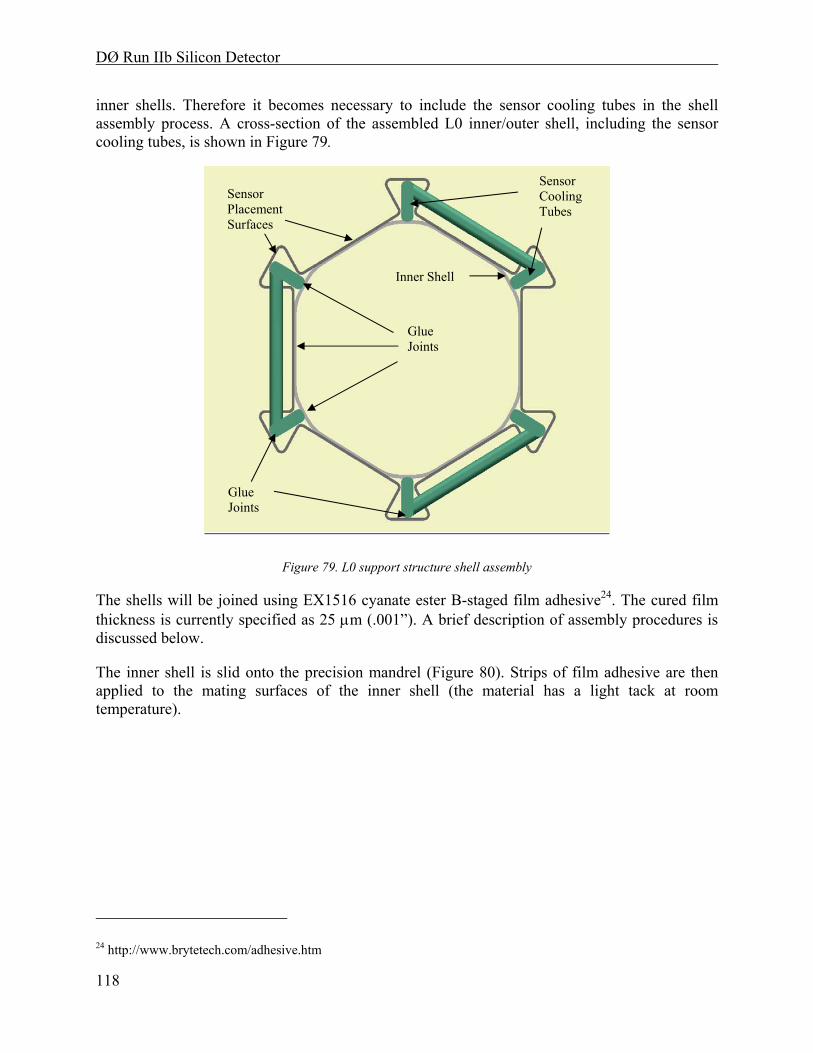
DØ Run IIb Silicon Detector
118
inner shells. Therefore it becomes necessary to include the sensor cooling tubes in the shell assembly process. A cross-section of the assembled L0 inner/outer shell, including the sensor cooling tubes, is shown in Figure 79.
Figure 79. L0 support structure shell assembly
The shells will be joined using EX1516 cyanate ester B-staged film adhesive24. The cured film thickness is currently specified as 25 µm (.001”). A brief description of assembly procedures is discussed below.
The inner shell is slid onto the precision mandrel (Figure 80). Strips of film adhesive are then applied to the mating surfaces of the inner shell (the material has a light tack at room temperature).
24 http://www.brytetech.com/adhesive.htm
Sensor Placement Surfaces
Inner Shell
Sensor Cooling Tubes
Glue Joints
Glue Joints

DØ Run IIb Silicon Detector
119
Figure 80. L0 precision mandrel with inner shell
Strips of film adhesive are applied to the inner surfaces of the outer shell castellations where the cooling tubes are bonded. The outer shell and cooling tubes are then slid over the inner shell (Figure 81). The cooling tubes are not shown below – refer to Figure 26 of section 4.3.2.
Figure 81. Outer shell installed over inner shell and cooling tubes (cooling tubes not shown).
Once the parts have been properly positioned a set of precision steel pressure-bars is installed onto the mandrel (Figure 82 and Figure 83). The bars have a step machined in the bottom that defines the overall distance between the mandrel surface and the outer surface of the castellated shell (Figure 84).
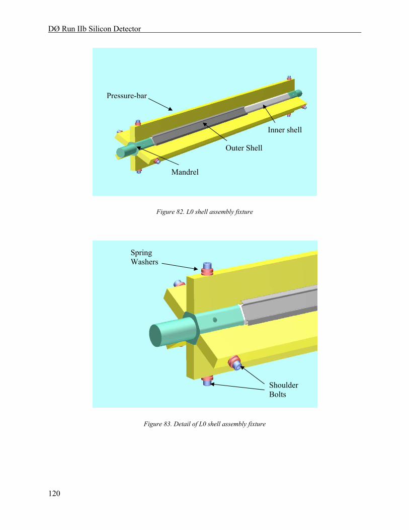
DØ Run IIb Silicon Detector
120
Figure 82. L0 shell assembly fixture
Figure 83. Detail of L0 shell assembly fixture
Inner shell
Outer Shell
Mandrel
Pressure-bar
Shoulder Bolts
Spring Washers
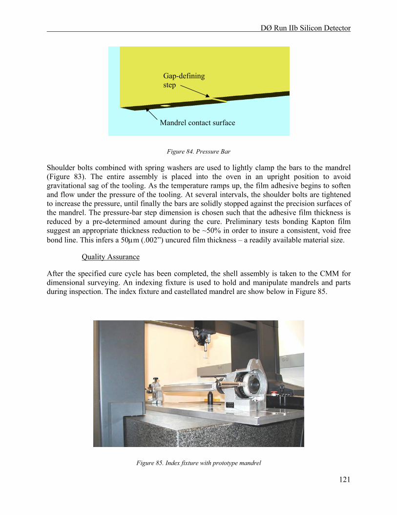
DØ Run IIb Silicon Detector
121
Figure 84. Pressure Bar
Shoulder bolts combined with spring washers are used to lightly clamp the bars to the mandrel (Figure 83). The entire assembly is placed into the oven in an upright position to avoid gravitational sag of the tooling. As the temperature ramps up, the film adhesive begins to soften and flow under the pressure of the tooling. At several intervals, the shoulder bolts are tightened to increase the pressure, until finally the bars are solidly stopped against the precision surfaces of the mandrel. The pressure-bar step dimension is chosen such that the adhesive film thickness is reduced by a pre-determined amount during the cure. Preliminary tests bonding Kapton film suggest an appropriate thickness reduction to be ~50% in order to insure a consistent, void free bond line. This infers a 50µm (.002”) uncured film thickness – a readily available material size.
Quality Assurance
After the specified cure cycle has been completed, the shell assembly is taken to the CMM for dimensional surveying. An indexing fixture is used to hold and manipulate mandrels and parts during inspection. The index fixture and castellated mandrel are show below in Figure 85.
Figure 85. Index fixture with prototype mandrel
Gap-defining step
Mandrel contact surface

DØ Run IIb Silicon Detector
122
4.3.6.2 Cooling system assembly
The cooling tubes located inside the castellations in both L0 and L1 are incorporated in the basic structures of these layers during assembly of the shells as discussed above. The only remaining assembly needed for these parts of the cooling system is the connection of the tubes to the cooling manifolds.
L0 cooling system assembly
For L0 the complete cooling system (Figure 27) is pre-assembled on a jig. This includes the L0a hybrid supports and cooling tubes, the support bulkheads and the sensor cooling tubes with their turnaround bridges. All of these pieces are glued together with cyanate ester adhesive. The complete cooling system assembly can then be leak tested prior to final assembly of the castellated shell and the inner shell as described above. The L0b cooling system (Figure 31) is separately pre-assembled on a jig and leak tested prior to installation.
L0 final assembly
Final assembly of L0 will be done at FNAL on precision tooling. With the completed base structure and L0a hybrid cooling system installed on the tooling, the sensors and hybrids are installed in the following order:
1. Each sensor is connected by its analog cable to its hybrid and brought to the assembly site.
2. For each row of L0a, start with the sensor furthest from the IP. 3. Add the other five sensors, working progressively closer to the IP. Note that, as each
hybrid is added, it goes over the analog cable of the previously installed hybrid. Special tooling is used to hold the cable down so that it does not push up on the hybrid as the glue cures. This is particularly important for the final hybrid as the space below it is now filled with five analog cables.
4. Repeat the above steps for the other five rows of sensors. The L0b hybrid cooling assembly can now be slid over the assembly and fixed in position (Figure 33). The L0b sensors and hybrids are now installed in the same manner as the L0a ones.
L1 cooling assembly
For L1, the hybrid cooling manifold/bulkhead is pre-assembled on a jig and leak tested. The base assembly of the castellated shell, the inner tube, manifold/bulkhead and extension tube is then completed as discussed above and installed on the final installation tooling. The sensor/hybrid modules are then positioned precisely and glued in place.
4.3.7 Radiation Length Calculations
The average radiation lengths seen by particles traversing the L0 and L1 detectors have been estimated for the design described above and are summarized in Table 13 through Table 15. Table 13 and Table 14 give values in the silicon sensor region (- 480 mm < z < 480 mm) for L0 and L1, respectively. Table 15 gives the values in the region outside the active volume where the

DØ Run IIb Silicon Detector
123
L0 hybrids reside (500 mm < |z| < 800 mm). In all cases material of discrete objects such as hybrids is averaged over ϕ and along the beam direction. The amount of material in the hybrid circuits averaged over the area of the hybrid is estimated to be equivalent to 2.3%. Other radiation lengths are based on estimates of composition of the material. The details are included in the Tables.
For L0 in the silicon sensor region, the average material amounts to 1.51% of a radiation length of which about two thirds is due to silicon sensors and the mechanical support. The actual fractional contributions are: silicon 38%, analog cables and HV insulation 22%, cooling 14% and mechanical support 26%. The average material in the silicon sensor region for L1 is 2.93% of a radiation length of which the fractional contributions are: silicon 15%, hybrid circuits, digital cables and HV insulation 55%, cooling 10% and mechanical supports 20%. For the L0 hybrid region, the total material is 5.98% of a radiation length, of which about 60% comes from the hybrids and digital cables.
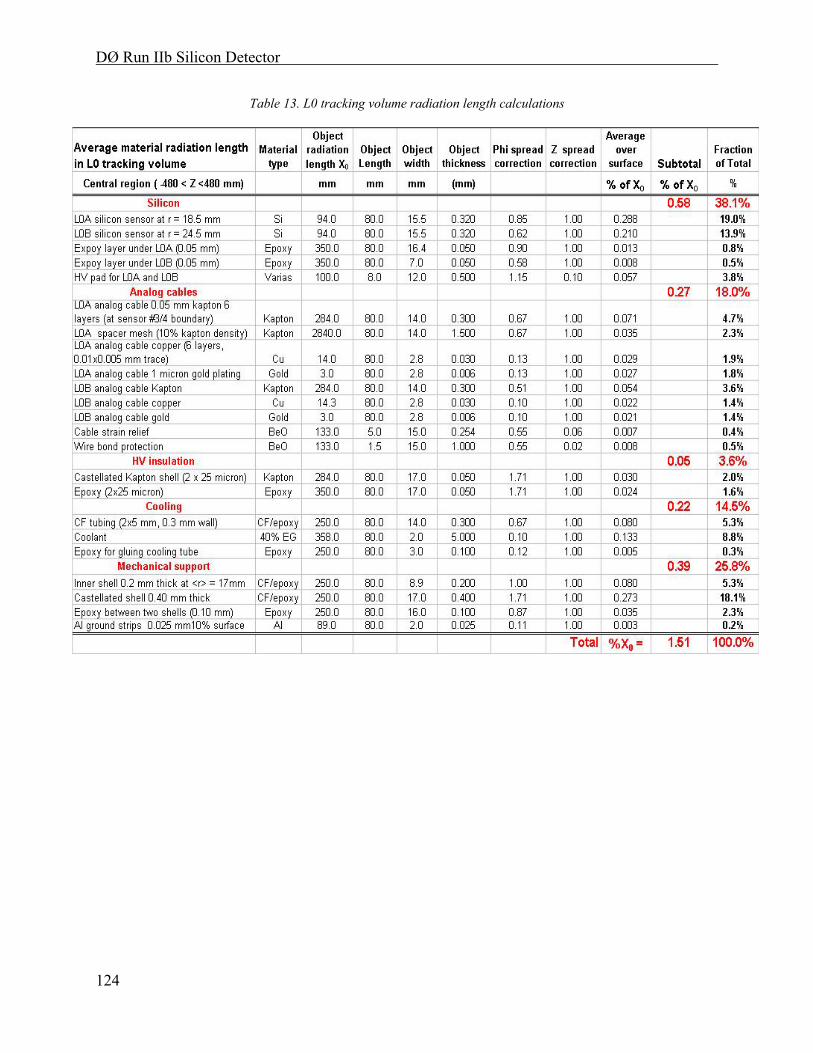
DØ Run IIb Silicon Detector
124
Table 13. L0 tracking volume radiation length calculations
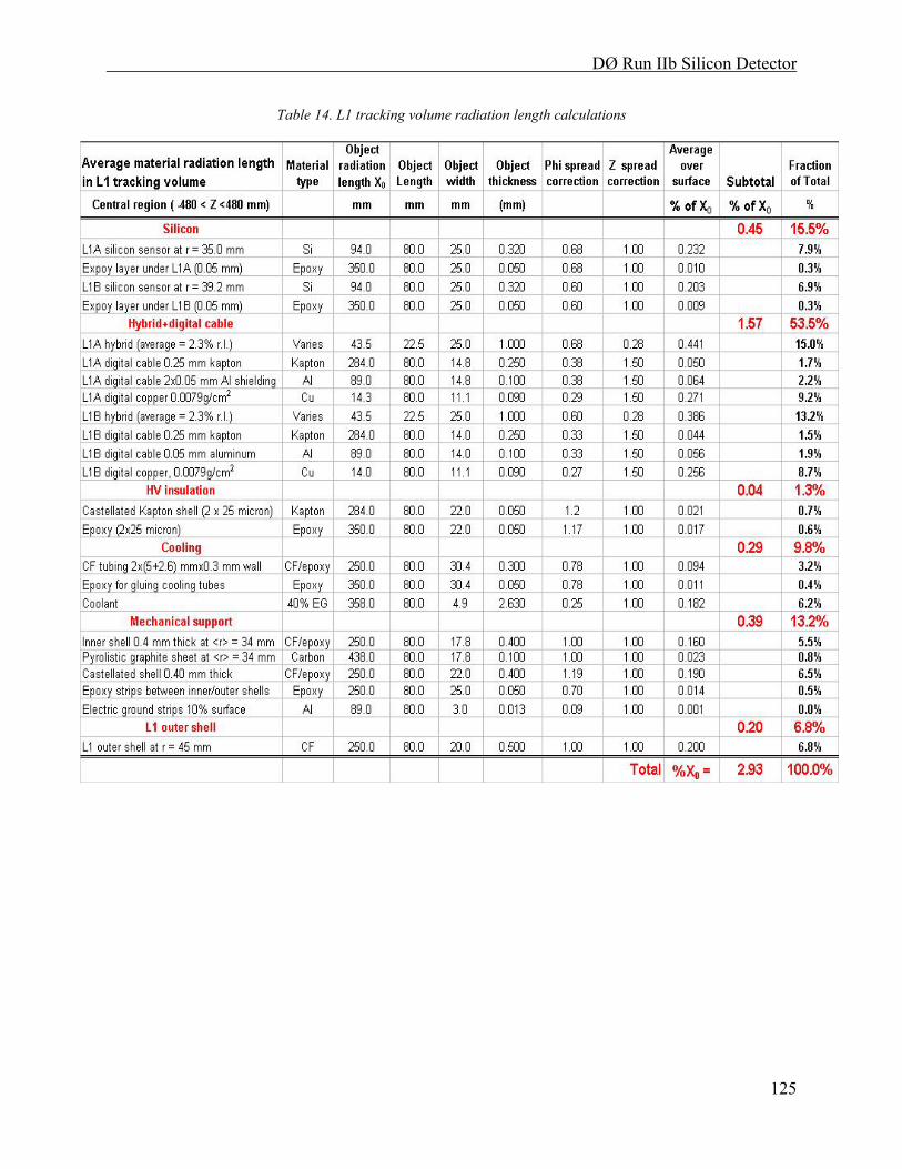
DØ Run IIb Silicon Detector
125
Table 14. L1 tracking volume radiation length calculations
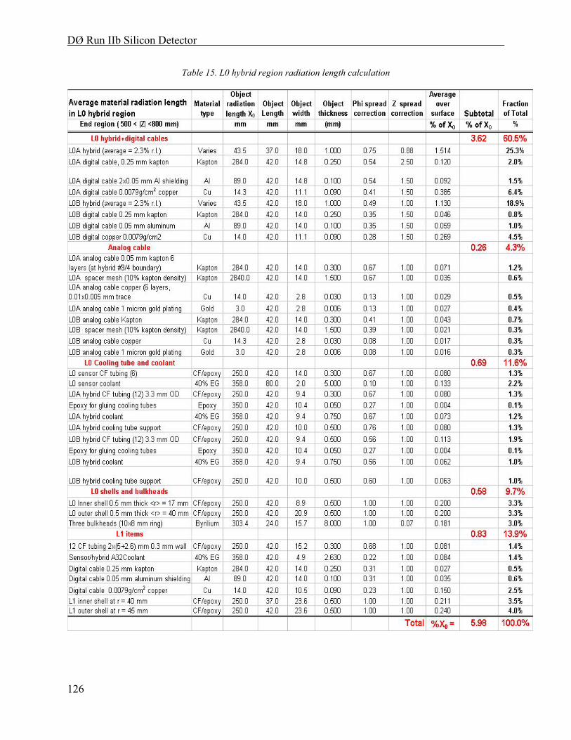
DØ Run IIb Silicon Detector
126
Table 15. L0 hybrid region radiation length calculation
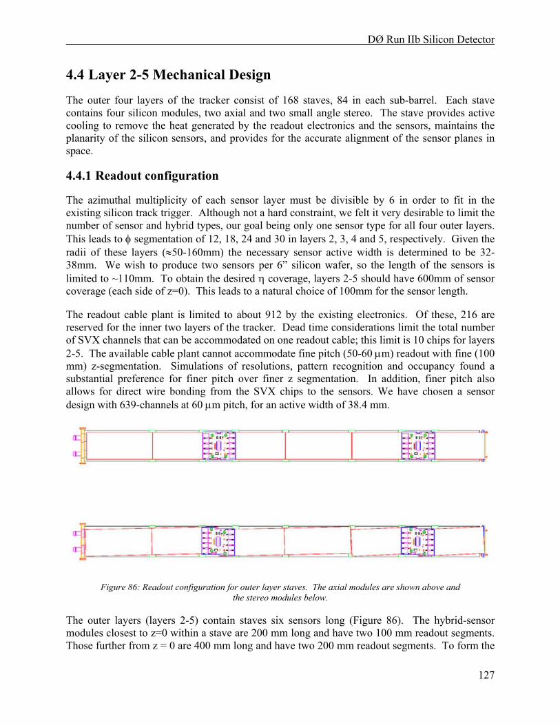
DØ Run IIb Silicon Detector
127
4.4 Layer 2-5 Mechanical Design
The outer four layers of the tracker consist of 168 staves, 84 in each sub-barrel. Each stave contains four silicon modules, two axial and two small angle stereo. The stave provides active cooling to remove the heat generated by the readout electronics and the sensors, maintains the planarity of the silicon sensors, and provides for the accurate alignment of the sensor planes in space.
4.4.1 Readout configuration
The azimuthal multiplicity of each sensor layer must be divisible by 6 in order to fit in the existing silicon track trigger. Although not a hard constraint, we felt it very desirable to limit the number of sensor and hybrid types, our goal being only one sensor type for all four outer layers. This leads to φ segmentation of 12, 18, 24 and 30 in layers 2, 3, 4 and 5, respectively. Given the radii of these layers (≈50-160mm) the necessary sensor active width is determined to be 32-38mm. We wish to produce two sensors per 6” silicon wafer, so the length of the sensors is limited to ~110mm. To obtain the desired η coverage, layers 2-5 should have 600mm of sensor coverage (each side of z=0). This leads to a natural choice of 100mm for the sensor length.
The readout cable plant is limited to about 912 by the existing electronics. Of these, 216 are reserved for the inner two layers of the tracker. Dead time considerations limit the total number of SVX channels that can be accommodated on one readout cable; this limit is 10 chips for layers 2-5. The available cable plant cannot accommodate fine pitch (50-60 µm) readout with fine (100 mm) z-segmentation. Simulations of resolutions, pattern recognition and occupancy found a substantial preference for finer pitch over finer z segmentation. In addition, finer pitch also allows for direct wire bonding from the SVX chips to the sensors. We have chosen a sensor design with 639-channels at 60 µm pitch, for an active width of 38.4 mm.
Figure 86: Readout configuration for outer layer staves. The axial modules are shown above and the stereo modules below.
The outer layers (layers 2-5) contain staves six sensors long (Figure 86). The hybrid-sensor modules closest to z=0 within a stave are 200 mm long and have two 100 mm readout segments. Those further from z = 0 are 400 mm long and have two 200 mm readout segments. To form the
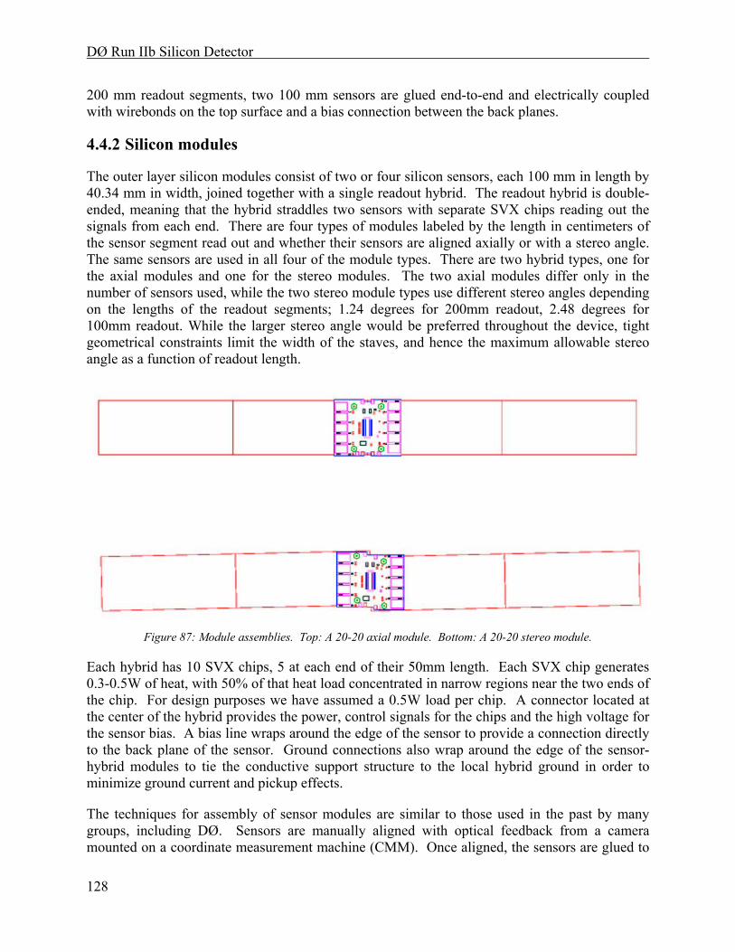
DØ Run IIb Silicon Detector
128
200 mm readout segments, two 100 mm sensors are glued end-to-end and electrically coupled with wirebonds on the top surface and a bias connection between the back planes.
4.4.2 Silicon modules
The outer layer silicon modules consist of two or four silicon sensors, each 100 mm in length by 40.34 mm in width, joined together with a single readout hybrid. The readout hybrid is double-ended, meaning that the hybrid straddles two sensors with separate SVX chips reading out the signals from each end. There are four types of modules labeled by the length in centimeters of the sensor segment read out and whether their sensors are aligned axially or with a stereo angle. The same sensors are used in all four of the module types. There are two hybrid types, one for the axial modules and one for the stereo modules. The two axial modules differ only in the number of sensors used, while the two stereo module types use different stereo angles depending on the lengths of the readout segments; 1.24 degrees for 200mm readout, 2.48 degrees for 100mm readout. While the larger stereo angle would be preferred throughout the device, tight geometrical constraints limit the width of the staves, and hence the maximum allowable stereo angle as a function of readout length.
Figure 87: Module assemblies. Top: A 20-20 axial module. Bottom: A 20-20 stereo module.
Each hybrid has 10 SVX chips, 5 at each end of their 50mm length. Each SVX chip generates 0.3-0.5W of heat, with 50% of that heat load concentrated in narrow regions near the two ends of the chip. For design purposes we have assumed a 0.5W load per chip. A connector located at the center of the hybrid provides the power, control signals for the chips and the high voltage for the sensor bias. A bias line wraps around the edge of the sensor to provide a connection directly to the back plane of the sensor. Ground connections also wrap around the edge of the sensor-hybrid modules to tie the conductive support structure to the local hybrid ground in order to minimize ground current and pickup effects.
The techniques for assembly of sensor modules are similar to those used in the past by many groups, including DØ. Sensors are manually aligned with optical feedback from a camera mounted on a coordinate measurement machine (CMM). Once aligned, the sensors are glued to

DØ Run IIb Silicon Detector
129
one another, directly or via a connecting substrate. Reasonable expectations for this alignment are a few microns. The hybrid, previously assembled, burned-in and tested, is glued directly to the silicon sensors. Wire bonding is then done between the hybrid and the sensors, and from sensor to sensor for the modules with 200mm readout segments. The sensor pitch has been chosen so that the hybrid to sensor bonding can be done directly from the SVX chips to silicon sensors without a pitch adapter. The total numbers of wire bonds required for layers 2-5 are 430K sensor-to-sensor plus 860K hybrid-to-sensor, for a total of 1290K bonds. For the longer modules, the sensor-to-sensor wire bonding can be done either before or after the hybrid is mounted. Sensor alignment and sensor-to-sensor wire bonding can proceed prior to hybrid delivery, should that become a production constraint.
Prior to assembly into staves the completed module will undergo electrical testing, additional burn-in and in some cases laser scanning (described elsewhere in this document).
4.4.3 Stave assemblies
The outer four layers of the silicon tracker are constructed as 168 staves, approximately 46mm wide by 8.9mm tall by 610mm in length (Figure 88). Each stave is independently mounted to a set of bulkheads, described previously. The stave structures consist of a core with silicon mounted to both surfaces and two external C-channels that stiffen the structure. The core structure has an integrated cooling circuit to remove the heat generated by both the hybrid electronics and the silicon sensors. The core also provides the precise reference features for aligning and mounting sensor modules to the core and the completed stave to the bulkheads. Finally, the core maintains the flatness of the silicon sensors. The external C-channels provide the necessary bending and torsional stiffness to the stave.
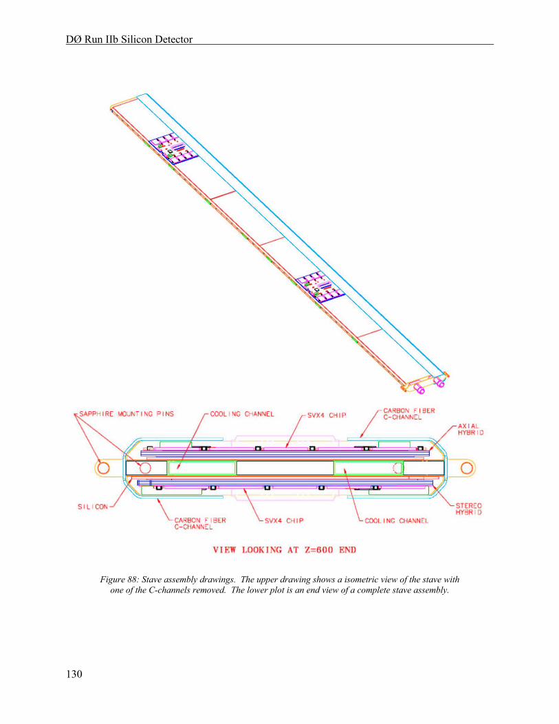
DØ Run IIb Silicon Detector
130
Figure 88: Stave assembly drawings. The upper drawing shows a isometric view of the stave with one of the C-channels removed. The lower plot is an end view of a complete stave assembly.

DØ Run IIb Silicon Detector
131
The core structure is about 2mm tall. The main element is the cooling tube. The tube is made from high strength carbon fiber (IM7 or similar) with a cyanate ester resin (Bryte EX-1515 or similar) that features very low moisture absorption. The cooling passage is 2mm tall by 10mm wide (outside) with a 200-250 micron wall thickness. The tube is a U-shape, turning around near Z=0. The mechanical structure is built up from this tube using “outriggers” made of similar tube to carry the silicon module load out to the C-channels. The remaining space will likely be filled with Rohacell foam to provide a uniform mounting surface for the sensors. The core structure will be laminated with 50 micron Kapton MT, a polyimide loaded with alumina for better thermal conductivity, to provide an electrically insulating layer between the back plane of the sensors, at 300V, and the tube, which will be grounded. The fluid dynamics, thermal performance and mechanical performance of this structure are described below. Precision mounting and alignment features - ruby and sapphire rods and spheres - are an integral part of the core structure. Once assembled, the core structure can be leak checked and inspected for dimensional tolerances prior to population with silicon modules.
The silicon modules are bonded directly to the stave core. One side of the core is populated with axial sensor modules while the other is populated with small angle stereo modules. The mounting and reference features on the stave core are accessible from both sides of the stave so that they can be used to establish the reference system on a CMM for alignment of the silicon modules to the stave core. Past experience is that module-to-module alignment can be done at the sub-5µ level.
Carbon fiber C-channel structures mount to the core on each side with cross-members at several locations along the length of the stave. These structures provide most of the stiffness of the completed stave, provide a surface for the readout cables to attach to as they run to the end of the stave, and help to protect the sensors and hybrids from damage during further processing steps.
4.4.4 Stave mass and radiation length
The stave mass and radiation length have been estimated. The stave weight per unit length is 2.38g/cm. The radiation length (Table 16), averaged over the silicon area, is 2.53%X0 per layer. The breakdown of the material is 0.68%X0 sensors, 0.55%X0 hybrids, 0.56%X0 readout cables, 0.31%X0 coolant and tube, and 0.43%X0 for the stave structure and adhesives. The equivalent of 1.5 readout cables are included in this estimate; the first cable begins at Z=100mm and the second at Z=400mm. A track passing at normal incidence through the hybrids sees roughly 5.3%X0 per layer. Near Z=0, where there are no cables or hybrids, the radiation length is only 1.4%X0 per layer.
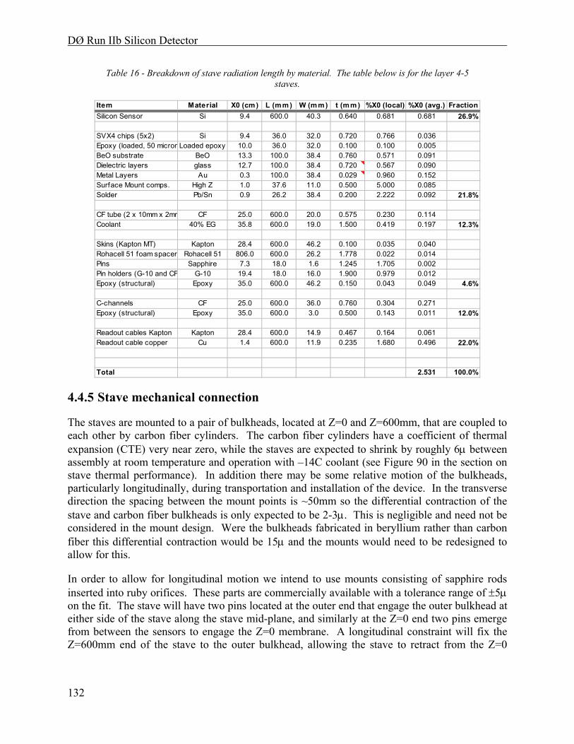
DØ Run IIb Silicon Detector
132
Table 16 - Breakdown of stave radiation length by material. The table below is for the layer 4-5 staves.
Item Material X0 (cm) L (mm ) W (m m) t (mm ) %X0 (local) %X0 (avg.) FractionSilicon Sensor Si 9.4 600.0 40.3 0.640 0.681 0.681 26.9%
SVX4 chips (5x2) Si 9.4 36.0 32.0 0.720 0.766 0.036Epoxy (loaded, 50 micronLoaded epoxy 10.0 36.0 32.0 0.100 0.100 0.005BeO substrate BeO 13.3 100.0 38.4 0.760 0.571 0.091Dielectric layers glass 12.7 100.0 38.4 0.720 0.567 0.090Metal Layers Au 0.3 100.0 38.4 0.029 0.960 0.152Surface Mount comps. High Z 1.0 37.6 11.0 0.500 5.000 0.085Solder Pb/Sn 0.9 26.2 38.4 0.200 2.222 0.092 21.8%
CF tube (2 x 10mm x 2mm CF 25.0 600.0 20.0 0.575 0.230 0.114Coolant 40% EG 35.8 600.0 19.0 1.500 0.419 0.197 12.3%
Skins (Kapton MT) Kapton 28.4 600.0 46.2 0.100 0.035 0.040Rohacell 51 foam spacer Rohacell 51 806.0 600.0 26.2 1.778 0.022 0.014Pins Sapphire 7.3 18.0 1.6 1.245 1.705 0.002Pin holders (G-10 and CF G-10 19.4 18.0 16.0 1.900 0.979 0.012Epoxy (structural) Epoxy 35.0 600.0 46.2 0.150 0.043 0.049 4.6%
C-channels CF 25.0 600.0 36.0 0.760 0.304 0.271Epoxy (structural) Epoxy 35.0 600.0 3.0 0.500 0.143 0.011 12.0%
Readout cables Kapton Kapton 28.4 600.0 14.9 0.467 0.164 0.061Readout cable copper Cu 1.4 600.0 11.9 0.235 1.680 0.496 22.0%
Total 2.531 100.0%
4.4.5 Stave mechanical connection
The staves are mounted to a pair of bulkheads, located at Z=0 and Z=600mm, that are coupled to each other by carbon fiber cylinders. The carbon fiber cylinders have a coefficient of thermal expansion (CTE) very near zero, while the staves are expected to shrink by roughly 6µ between assembly at room temperature and operation with –14C coolant (see Figure 90 in the section on stave thermal performance). In addition there may be some relative motion of the bulkheads, particularly longitudinally, during transportation and installation of the device. In the transverse direction the spacing between the mount points is ~50mm so the differential contraction of the stave and carbon fiber bulkheads is only expected to be 2-3µ. This is negligible and need not be considered in the mount design. Were the bulkheads fabricated in beryllium rather than carbon fiber this differential contraction would be 15µ and the mounts would need to be redesigned to allow for this.
In order to allow for longitudinal motion we intend to use mounts consisting of sapphire rods inserted into ruby orifices. These parts are commercially available with a tolerance range of ±5µ on the fit. The stave will have two pins located at the outer end that engage the outer bulkhead at either side of the stave along the stave mid-plane, and similarly at the Z=0 end two pins emerge from between the sensors to engage the Z=0 membrane. A longitudinal constraint will fix the Z=600mm end of the stave to the outer bulkhead, allowing the stave to retract from the Z=0
DØ Run IIb Silicon Detector
133
membrane during cool-down. A four-point mount is necessary since the staves do not have large torsional stiffness (θ/τ=1mrad/120g-mm) compared to their mass (140g) and width (40mm).
4.4.6 Alignment precision and stave mounts
The alignment requirements for the sensors are determined by the requirements of the impact parameter trigger. The trigger does not have the stereo sensor information so any misalignment of the axial sensors to the beam axis results in a degradation of the r-φ resolution at the trigger level. The intrinsic device resolution is ≈8µ.
The roll angle, i.e. rotation around an axis parallel to the beam line, does not affect trigger resolution, provided that it is known from survey. For a rotation in the plane of the sensors (yaw), the desired alignment tolerance is <10µ over a readout segment, or an angle of <50µrad. This results in an r.m.s. alignment tolerance of ±30µ over the full stave length. The pitch angle affects strips at the edges of the sensors, but not at the center. For a radial deviation dR at an angle φ from the center of the sensor, the transverse measurement error dX is given by dX=dRtanφ. The worst case is at the edges of the sensors where tanφ=0.27(0.11) in layer 2(5). This implies a radial positioning tolerance of ±110(285)µ over the length of a stave in layer 2(5). If the sensors are not held flat within the stave the effect is identical to that of the pitch angle. Here the length scale is 100mm, so the tolerance on the sensor flatness is of order 20µ. It is difficult to anticipate the degree of warping which the production sensors will have due to stresses induced in manufacturing. Very flat vacuum fixtures will be used to hold the sensors flat during bonding to the core. The 2mm tall core structure with sensors on both sides provides a significant moment of inertia to constrain the sensors flat.
The tolerances on the pins and orifices intended for mounting the staves are sufficiently tight to permit a mounting system without adjustment, provided the orifices can be located in the bulkheads with high precision. This is considered to be feasible.
4.4.7 Layer 2-5 stave thermal performance
The mechanical and thermal characteristics of the staves have been evaluated both analytically and using finite element analysis (FEA). The radiation environment of Run IIb affects both the depletion voltage and the leakage current (noise) of the silicon sensors. The former depends on the magnitude of the reverse annealing term, which saturates for temperatures below 0C and is fairly insignificant up to temperatures of +10C. Here the relevant temperature is the peak temperature on the sensors. The leakage current for a strip, and hence the associated noise, depends on the integrated current along the strip, and hence is a function of the average temperature, with appropriate weighting, along the strip. We have used the FEA temperature profiles to calculate the expected strip currents and then used this to extract an equivalent temperature, corresponding to the uniform temperature that would produce the same leakage current. Our design goal is <15% degradation in signal to noise ratio, with a minimum S/N of 10 at 20fb-1. The result is that the equivalent temperature should be kept below 0C in layer 2 and below +5C in layers 3-5.

DØ Run IIb Silicon Detector
134
The stave cooling channel will operate below atmospheric pressure, hence the pressure drop is limited to ≈3psi. The total stave heat load is dominated by the hybrids that generate up to 20W, while the sensors are not expected to contribute more than 3W in layer 2 after 30fb-1 of exposure. The expected operating point for the stave is a flow rate of 0.175lpm resulting in a pressure drop of 2.6psi from inlet to outlet with a bulk temperature rise of 1.9C. The tube wall will operate roughly 7C above the bulk temperature locally under the hybrids.
Figure 89 shows the result of a finite element analysis (FEA) of the stave structure. This model assumes a heat transfer coefficient of 835W/m2K, as expected for the design flow, and an inlet fluid temperature of –14C. The maximum temperature on the structure is –1.0C on the hybrid, while the maximum temperature on the sensor is –4.3C. Experimental studies are underway to confirm the FEA results. Figure 90 shows the thermal distortions expected in the silicon sensors, perpendicular to the plane of the sensor and longitudinally. The thermal distortions are less than 10µ.
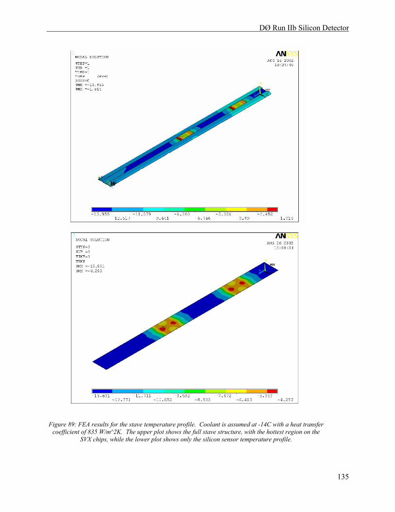
DØ Run IIb Silicon Detector
135
Figure 89: FEA results for the stave temperature profile. Coolant is assumed at -14C with a heat transfer coefficient of 835 W/m^2K. The upper plot shows the full stave structure, with the hottest region on the
SVX chips, while the lower plot shows only the silicon sensor temperature profile.
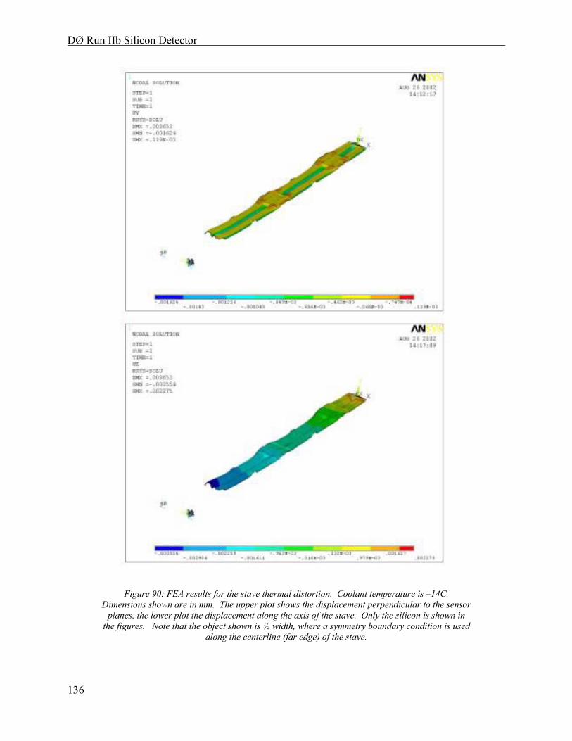
DØ Run IIb Silicon Detector
136
Figure 90: FEA results for the stave thermal distortion. Coolant temperature is –14C. Dimensions shown are in mm. The upper plot shows the displacement perpendicular to the sensor
planes, the lower plot the displacement along the axis of the stave. Only the silicon is shown in the figures. Note that the object shown is ½ width, where a symmetry boundary condition is used
along the centerline (far edge) of the stave.

DØ Run IIb Silicon Detector
137
4.4.8 Layer 2-5 stave mechanical performance
Mechanical performance of the stave has been evaluated using both analytical and FEA calculations, with good agreement between these results. The expected deflection of the staves is under 60µ with static gravitational loading (Figure 91). While somewhat larger deflections may not adversely affect the detector resolution, they lead to stave natural frequencies that are approaching the 60Hz range and the possible reduction in stave mass is negligible compared to the mass of the sensors, electronics and cables. In addition, reduced deflection allows for tighter installation and assembly clearances and easier handling during fabrication and installation of the staves into the barrel assemblies.
Figure 91: Stave deflection results for gravitational loading.
We have looked at extreme load conditions, for example application of a 1 kg load at the center of the stave, to study the robustness of the design. We find that, while the deflections are quite large, the stress levels in the sensors and structural elements remain far from failure levels. These studies were primarily aimed at understanding the handling requirements during fabrication and assembly.
A critical issue for the sensor alignment precision is deflection of the staves from external loads, in particular loads induced through the cables and cooling lines. To induce a 100µ deflection at
DØ Run IIb Silicon Detector
138
the center of the beam requires a moment of 35kg-mm (3.0in-lbs). This is well above what could be induced through the external connections to the staves.
4.5 Installation of the Run IIb Silicon Tracker
The Run IIb silicon tracker is to be delivered to the DØ experimental hall in two halves, north and south. We intend to deliver these halves in a manner similar to the one used for the Run IIa tracker. Unlike Run IIa, the two halves of the detector will be mated prior to installation into the central fiber tracker (CFT). This is necessary in order to achieve the required alignment. For Run IIa the two silicon barrel support structures were surveyed in the CFT on a CMM prior to installation of the CFT. The silicon was then aligned to the barrel support structures based on those surveys. This is not possible for the Run IIb device.
For Run IIa, each half of the detector was packaged in a protective enclosure prior to transportation. This enclosure provided mechanical protection of the assembly, storage for the cables attached to the assembly and a sealed gas volume that could be purged with nitrogen to prevent condensation and or contamination. The shipping enclosure also had an integrated rail system that was previously aligned to existing rails inside the CFT so that the detector halves could be slid directly into the CFT from the enclosure, one from each end. A set of roller bearings mounted from the enclosure provided a coupling to a trolley system used to move the silicon tracker inside the DØ detector cathedral and calorimeter gap areas. To reduce loads during transportation an air-ride cart was built which provided a stable rolling platform for each detector half. Once mounted inside the protective enclosure, each half of the detector was moved onto the cart. The cart was rolled to a loading bay, onto a truck lift gate and into the back of the truck. During several test runs and the final detector deliveries for Run IIa this cart consistently kept accelerations below 5g in all three directions. At DØ the cart was rolled back onto the lift gate and the detector was lifted off of the cart and delivered by crane to the assembly hall. At this point the detector was supported from above on roller bearings on a tube. This tube formed the first section of a trolley rail system used to bring the detector along the cathedral area into the calorimeter gap. When the detector arrived at the final turn into the CFT it was lowered onto a “table” mounted to the central calorimeter. Final alignment to the CFT was done by sliding the silicon tracker and enclosure base on the table surface.
For Run IIb we expect to use a similar enclosure for mechanical protection and dry gas purge. We will either reuse the existing air-ride cart or fabricate a similar one, for transporting the detector halves from the silicon detector facility to the DØ experimental hall. The detector is expected to remain on the beam line so it will not be possible to deliver the silicon tracker by crane directly from the truck to the detector cathedral area. Instead, the crane would be used to deliver the detector and cart to the floor of the assembly hall and the cart would then be rolled into the collision hall. A hoist would then be used to raise the silicon tracker up to the platform level. It may be possible to extend the trolley system used for the Run IIa installation to receive the Run IIb device directly from this hoist and deliver it to the calorimeter gap area. Both halves will be delivered to the same end of the CFT, mated and then slid into the CFT as one unit.

DØ Run IIb Silicon Detector
139
4.6 Alignment within the Fiber Tracker
The Level II silicon track trigger (L2STT)25 of the DØ detector imposes limitations on the permissible magnitude of coherent misalignment of the Silicon Detector. The L2STT allows the selection of events that contain decays of long-lived particles by performing a precise reconstruction of charged particle tracks in the Silicon Detector and the CFT.
In addition to improving the resolution of the measurement of track pT over that of the CFT alone (by a factor of 2-3 depending on pT), the L2STT also determines the impact parameter of charged tracks with respect to the nominal beam position. If the beam is tilted with respect to the Silicon Detector, the rate of tracks with large fake impact parameters becomes excessive, giving rise to unwanted triggers. Monte-Carlo studies of ttbar and B events have shown that it is necessary to limit angular misalignment of the Silicon Detector with respect to the beam to less than ±200 µrad to limit the fraction of fakes to less than 5% for impact parameters of 100µ.
Lateral offsets should be kept below 1 mm to limit inefficiencies due to tracks crossing Silicon sectors. Lateral offsets of less than 1 mm are expected to be achievable by final realignment of the detector , and it is expected that orbit tuning can reduce residual lateral offsets to nominally zero after they are measured by the Silicon Detector.
The same angular constraints apply to the beam during stores, and the lateral position of the beam must be held steady to 30µ or so to avoid creation of an increased trigger rate due to apparent impact parameter increase. During Run I, CDF showed that lateral variations during stores did not typically exceed 40µ and angular variations were typically too small to measure. Angular variations store-to-store varied less than 100µrad. Preliminary DØ results for Run IIa are consistent with these values.
The present Run IIa Silicon Detector has already been shown to be aligned to the CFT to ± 70 µ at any individual silicon sensor. Since the overall length of the sensor staves of the Run IIb Silicon Detector is on the order of 1 m, such potential misalignment leads to well below 100 µrad of angular misalignment of the stave. It is intended to “recycle” the present mounting system between the CFT and the Run IIa Silicon Detector in such a manner that the quality of this relative alignment is not lost.
For this reason, and in view of the constraints on the required alignment, no type of dynamic alignment mechanism is contemplated for the Run IIb Silicon Detector. Precision fiducials will be provided on the silicon detector to enable the installed position of the device to be related to that of the existing CFT, so that the precision of this relationship can be verified after installation is completed
25 U. Heintz, DØ Note 3516

DØ Run IIb Silicon Detector
140
4.7 Mechanical Infrastructure at DAB
4.7.1 Cooling system
DØ installed the two-piece Silicon Detector for Run IIa into the DØ fiber tracker in late 2000 and early 2001. Those two pieces are referred to the South half and the North half. Each half is read out by onboard electronics that generates heat which must be removed. Removal of that heat is performed by redundant chillers that circulate a glycol and water mixture in parallel closed loop systems with a common coolant reservoir. The coolant of the existing system is chilled to –10° C. For Run IIb, an additional system will be added to chill a portion of the coolant to -20° C.
Silicon in Layers 0-1 will be cooled to –10o C while Layers 2-5 will be cooled to a minimum temperature of –5o C. A temperature gradient may be allowed in Layers 2-5, with –5o C at Layer 2 and a maximum temperature of +5o C at Layer 5. These temperatures will be achieved using a water-glycol cooling loop.
Use of the existing cooling system in place for Run IIa is possible, but with modifications to provide the two-tiered cooling needs of Run IIb. Currently the cooling system circulates 30% by volume ethylene glycol at –10o C to the detector. For Run IIb, one glycol stream will need to be chilled to –20o C for Layers 0 and 1 while a second stream will need to be –15o C for outer Layers 2-5. Much of the existing piping and process control system can be preserved if a second chiller and supply line is provided for the colder silicon layers while allowing both streams to use the existing return lines in common. The existing chiller has a cooling specification of 4400 W at –10o C and was tested to deliver 5500 W during actual tests at Fermilab.
To prevent freeze-out of coolant in the chillers, the freezing point of the circulating mixture must be 5.9o C lower (10 F) than the fluid’s control point temperature. Since coolant will be chilled to –20o C, the fluid’s freezing point must be –25.6o C or lower. A glycol concentration of 41% by volume is chosen for the system, which has a freezing point of –25.9o C. A 41% ethylene glycol, 59% water mixture by volume has the following properties which are used to define the Run IIb detector’s flow rate and pressure drop limits if the existing system is to be used: at –20o C, density = 1073.5 kg/m3, viscosity = .01638 N/(m2-s), vapor pressure = 0.7 mmHg.
To avoid risk of pump cavitation, the minimum allowable pump suction pressure is –10.4 PSIG. The calculation assumes a required pump NPSH = 8 FT and that the fluid vapor pressure is high (pv = 18.1 mmHg) at startup because the fluid is warm. The pump suction pressure is determined by system flow losses (the pressure drops both in the piping and the detector) and the elevation of the detector relative to the pump. The detector is about 3.96 meters above the pump intake. Piping flow losses are calculated using an Excel spreadsheet developed by Herman Cease for Run IIa but using fluid properties of 41% glycol, 59% water mixture at –20o C. Table 17 (below) summarizes calculations by providing maximum pressure drops allowed across the detector for two possible flow rates, 10 GPM and 12 GPM.

DØ Run IIb Silicon Detector
141
Table 17 - Maximum Allowable Pressure Drop Across Detector
Coolant flow rate 10 GPM 12 GPM
Ps, minimum pump suction pressure to avoid cavitation -10.4 PSI -10.4 PSI
-(Head), due to detector elevation = 3.96 m -6.1 PSI -6.1 PSI
-dPpipes, piping flow losses 6.1 PSI 8.3 PSI
Max allowable flow losses across detector,
dPdet= Ps – Head - dPpipes
-10.4 PSI -8.2 PSI
The table shows the tradeoff to be considered to cool the detector. If higher flow rates are desired, the flow passages must be far less restrictive to limit pressure drops. The calculations above are concerned only with piping downstream of the system’s expansion tank, since only those components control the suction pressure at the pump. Flow losses in the piping are calculated for existing piping only. As discussed above, a new separate supply line is required to deliver –20o C fluid to the inner layers, while the existing piping would supply fluid to Layers 2-5. The calculations therefore assume that the new parallel stream supplying coolant to the inner layers will have losses equivalent the existing piping supplying Layers 2-5.
4.7.2 Dry gas system
Temperatures inside the detector will be as much as 30o C cooler than the maximum ambient dew point temperature (typically 10o C) maintained by D-Zero’s HVAC system. It is critical that moist ambient air be displaced from the detector volume with a dry purge source to prevent the formation of condensate and ice.
The existing dry gas purge and process control systems will be used for Run IIb, but the compressors, dryers, and cooling system will require appropriate maintenance after five years of continued service. The dry gas source proved failsafe for Run IIa through a ‘What-If’ failure analysis. An additional ‘What-If’ analysis is required if any changes are made for Run IIb. The dry gas system remains operational during all probable failure modes or has enough of a dry gas reservoir to continue to purge the detector until it is warmed above building dew point temperature. The purge source is reliable through extreme summer (40o C, 100% relative humidity) and winter (-35 C) weather. The system is capable of delivering 60 SCFM of dry air purge. The maximum dew point temperature of the delivered gas is –60o C.

DØ Run IIb Silicon Detector
142
4.7.3 Monitoring, interlocks, and controls
Monitoring, control, and interlock functions for the dry purge system and the silicon cooling system were added to the existing system commonly known as the DØ Cryo Control System for monitoring, interlocks, and alarming.
Mechanical piping and vessels of the dry gas and cooling systems were designed and fabricated with proper safety and relief devices so that the monitoring and interlock systems are not relied upon for personnel safety. All electrical loads have proper overload protection.
The Silicon Detector power system has an extensive internal interlock protection scheme provided by its power supply and processor control and data acquisition electronics
Thirty RTD temperature sensors were installed throughout the VLPC fiber barrel structure in order to track the fiber barrel temperatures as the Silicon system is cooled and its purge air flows are adjusted. Those thirty temperature sensors are displayed on the silicon computer graphics pictures.
4.7.4 Systems electrical power
DØ has backup electrical power provided by a diesel generator that starts automatically upon commercial power loss. The Silicon purge air compressors, the Silicon chiller cabinets, and the U.P.S. that supplies power to the Silicon cooling system control system are all on backup power. The silicon cooling system monitoring and interlock systems are powered by a U.P.S., which prevents power interruption to those control systems.
4.7.5 Existing chiller overview
There are two chiller cabinets, they have been designated chiller #1 and chiller #2. They are commercial units which contain a coolant pump, a chiller compressor, and the associated motor controls to run and control the unit. The temperature control is a stand alone single loop controller with a relay output and it is mounted on the chiller cabinet.
The chiller cabinet motor controls have been modified for remote interlock control. The remote interlocks have been implemented using solid state relays26.
Each chiller has two bypass key-switches built into the cabinet. One key switch overrides the external pump interlocks while the other key switch overrides the external cooling interlocks. These were installed for emergency and diagnostic reasons. The keys to these key-switches will be administratively controlled.
4.7.6 Additional chiller overview
Two chiller cabinets will be added for the additional cooling loop expected to operate at -20° C. They have been designated chiller #3 and chiller #4. Either can be the active chiller with the 26 Fermilab drawing 3823.112-EE-330338

DØ Run IIb Silicon Detector
143
other as a backup but not running. These will have interlocks and key switches similar to the original chillers.
4.7.7 Current process control system overview
The current process control system is based on a number of commercial Siemens Programmable Logic Controllers (PLC’s) and is commonly referred to as the CRYO control system. These PLC’s are capable of handling thousands of physical I/O through remote I/O bases. These remote I/O bases can have many types of modules installed in any of the slots for handling different types of field I/O. These PLC’s are commercial computers which have many prewritten communication drivers available. Programming the PLC’s is also done through commercial software.
The operator interface is based on the commercial distributed control platform of Intellutions FIX32. FIX32 provides computer alarms, graphical pictures with real time values, operator security, and historical collection of data. The use of FIX32 originated at DØ and is now commonly used throughout the Lab.
The Cryo Control System monitors and controls the Helium Refrigerator, LAR Calorimeters Cryo, Super conducting Solenoid cryo, Instrument Air, Vacuum, Building HVAC, WAMUS and Solenoid magnet power supplies, and the VLPC cryo.
4.7.8 Silicon cooling system integration into the current process control system
The Cryo control system was expanded with the addition of I/O base eleven on the South sidewalk and I/O bases seven, eight, and ten on the detector platform in order to pickup the physical field devices for the Silicon cooling system and dry purge air system.
The Silicon cooling system and dry purge air system logic programming were added to the PLC which has plenty of program capacity.
The Silicon cooling system and dry purge air system computer graphical pictures and database blocks were developed and added to the FIX32 system.
4.7.9 Silicon cooling system computer security
The Silicon Cooling System’s computer security, along with all of DØ’s other process control system’s computer security are provided by a combination of Intellution’s FIX32 and Microsoft’s NT Operating System Platform.
The computer system’s infrastructure is controlled and protected by Microsoft’s Windows NT Domain Controllers. This infrastructure includes domain user accounts, server file protection, Remote Access Services (RAS), and distributed networking. This is the “DMACS” domain at Fermilab. There are currently three domain controllers, two at DØ and one at CDF. This domain is shared by many groups at Fermilab. The domain administrators control the domains user accounts and file privileges.
DØ Run IIb Silicon Detector
144
The process control system’s security is provided by Intellutions’s Fix32 and Fix Dynamics. This security is setup by the system developers who draw the pictures and build the databases. The system developers lay out their system based on a predefined set of rules. They then grant privileges to the users and operators who would need some control over these systems. These “privileges” are what allows some and denies others access to opening and closing a valve for instance.
Remote Process Control System access is provided by an NT RAS connection and Microsoft’s NetMeeting. Remote access allows someone to view process data from home or elsewhere. The NT RAS security is provided by the NT domain controller, this security is essentially someone logging into the domain through a modem connection. NetMeeting allows someone to remotely take control of a workstations desktop. NetMeeting only allows an administrator to do this. The Process Control System security through NetMeeting is handled by NetMeeting, FIX32 or Dynamics, and the NT domain controllers. Other future remote access paths include the Internet i.e. a Website, however this is not well developed at this time.
4.7.10 Monitoring via the DAQ system
The DØ physics data acquisition and file system commonly referred to as the DZERO DAQ system will have access to the Silicon data along with all the other process control data. All the process data will be stored on a SCADA node dedicated to accessing and conditioning data just for the DAQ system. The DAQ programmers will be responsible for organizing a data polling list, then manipulating and storing the data in the physics file system. They may also choose to setup some sort of alarm system.
4.7.11 Interlocks
All interlock design and wiring practices use “failsafe” methods. That is a device must have positive feedback to its electronic circuits or it is considered “tripped”. For example, a normally closed contact would be used on temperature switch in the field. This allows for a lost signal or a disconnected field device to generate a tripped condition. Discriminator modules are used in this system in order to convert an analog value into a discrete signal. These modules are all configured in their failsafe mode, which allows for loss of signal or transmitter failure to result in a tripped condition.
There is one exception to the failsafe practice in the Silicon Cooling System design. That is the control of the cooling circuit in the chiller cabinets. The chiller cooling control is called the Hot Bypass valve, when this valve is energized the chiller is not cooling. If the control signal is lost, the chiller would be forced into the cooling mode, since a solid state relay is used to control this circuit. This scenario has been countered by using this same DC control voltage that controls the Hot Bypass control, to control the main chiller power solid state relay. Therefore, if the DC control voltage were lost for any reason the entire chiller would shutdown.
Interlock Layers
The Silicon detector has two functional interlock layers. The primary power interlock system is embedded in the detector power supply and its control system. This system is capable of

DØ Run IIb Silicon Detector
145
monitoring temperature and other parameters and shutting down individual channels and groups of channels.
The secondary interlock system is based around the cooling system parameters and referred to as the external interlock system. The external interlock system is designed to protect the Silicon detector from temperature and dew point limits.
4.7.12 Alarms
The Silicon cooling system may run attended or unattended by operators. The alarms have been picked, programmed, and configured to be consistent with the other systems that the control system runs and monitors.
Alarm Layers
DØ incorporates a layered alarm strategy. There are typically three layers of alarms. The first is a computer alarm that notes when a parameter is slightly out of normal tolerance. The second is a computer alarm when a parameter is more than slightly out of tolerance. The third is an Auto-Dialer alarm when the parameter is at a point where immediate attention is necessary.
Computer Alarms
Computer alarms are generated by the FIX32 software mentioned earlier in this paper. An operator with the correct security privileges may set the alarm thresholds and also acknowledge these alarms.
A computer alarm can be routed and filtered by any of many FIX32 nodes throughout DØ and Fermilab. When a computer alarm occurs, all the FIX32 nodes that are set up to filter in the alarm area of a particular alarm will start beeping. This beeping will continue until the alarm condition is cleared and the alarm is acknowledged.
Auto Dialer Alarms
An operator with the correct security privileges may set the alarm thresholds and also acknowledge these alarms.
The Auto-Dialer alarm is generated by the PLC and a computer dedicated to running a software package called WIN911. This software package is capable of paging people’s pagers with a numeric code as well as calling inside and outside the lab using the telephone system with a voice synthesized message. The Auto-Dialer is preprogrammed with a list of “experts” who can deal with the particular systems’ problem that created the alarm. The Auto-Dialer will continue paging and calling people serially on this list until someone acknowledges the alarm or the alarm condition ceases.
The Auto-Dialer is what really makes unattended operation practical at DØ.

DØ Run IIb Silicon Detector
146
DAQ Alarms
All the PLC data from all process systems will be available to the programmers that program the DØ DAQ system. Once this data is picked sorted the programmers will likely set up a set of alarms. This assumption is based on last run’s experience. The infrastructure for this data transfer is well defined and in progress of being implemented. The data sets remain to be defined.
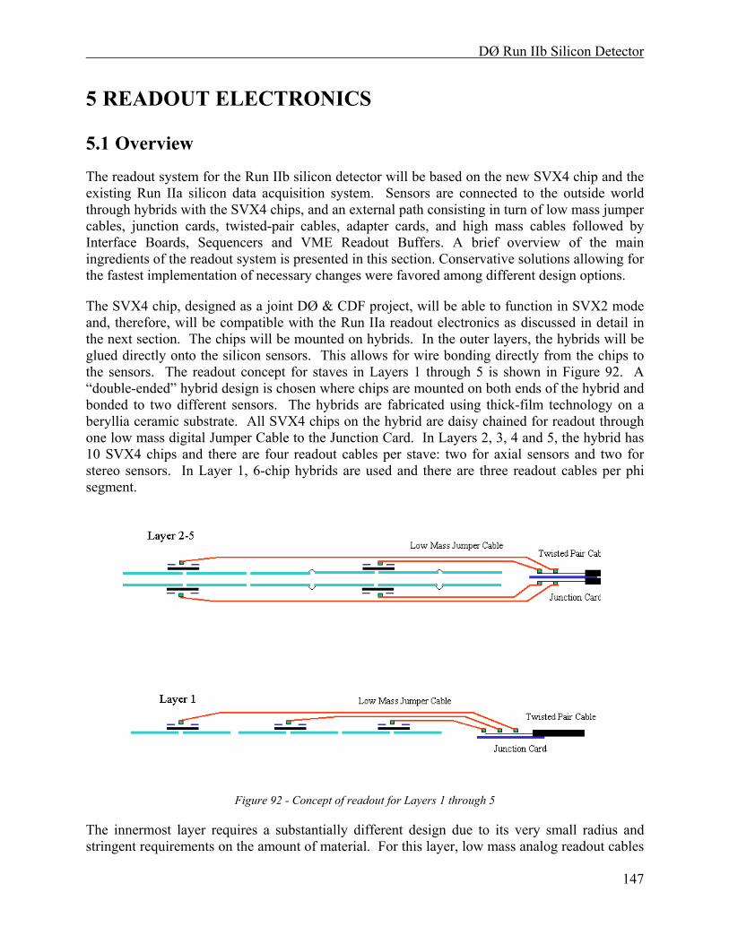
DØ Run IIb Silicon Detector
147
5 READOUT ELECTRONICS
5.1 Overview
The readout system for the Run IIb silicon detector will be based on the new SVX4 chip and the existing Run IIa silicon data acquisition system. Sensors are connected to the outside world through hybrids with the SVX4 chips, and an external path consisting in turn of low mass jumper cables, junction cards, twisted-pair cables, adapter cards, and high mass cables followed by Interface Boards, Sequencers and VME Readout Buffers. A brief overview of the main ingredients of the readout system is presented in this section. Conservative solutions allowing for the fastest implementation of necessary changes were favored among different design options.
The SVX4 chip, designed as a joint DØ & CDF project, will be able to function in SVX2 mode and, therefore, will be compatible with the Run IIa readout electronics as discussed in detail in the next section. The chips will be mounted on hybrids. In the outer layers, the hybrids will be glued directly onto the silicon sensors. This allows for wire bonding directly from the chips to the sensors. The readout concept for staves in Layers 1 through 5 is shown in Figure 92. A “double-ended” hybrid design is chosen where chips are mounted on both ends of the hybrid and bonded to two different sensors. The hybrids are fabricated using thick-film technology on a beryllia ceramic substrate. All SVX4 chips on the hybrid are daisy chained for readout through one low mass digital Jumper Cable to the Junction Card. In Layers 2, 3, 4 and 5, the hybrid has 10 SVX4 chips and there are four readout cables per stave: two for axial sensors and two for stereo sensors. In Layer 1, 6-chip hybrids are used and there are three readout cables per phi segment.
Figure 92 - Concept of readout for Layers 1 through 5
The innermost layer requires a substantially different design due to its very small radius and stringent requirements on the amount of material. For this layer, low mass analog readout cables
DØ Run IIb Silicon Detector
148
will couple the silicon and hybrids as shown in Figure 93. This allows the hybrids and silicon to be mounted independently, moving the mass and heat load of the hybrids out of the active detector volume. One 2-chip hybrid reads out one silicon sensor. To equalize the length of the analog cable between different sensors, the sensor closest to z=0 is connected to the closest hybrid. Digital jumper cables connect the hybrids to Junction Cards. While the added capacitance from the flex cable degrades the signal-to-noise (S/N) ratio, we expect to achieve a S/N>10 for the SVX4 with analog cable readout even at the end of Run IIb as was explained in Section 3.2. Section 5.3 discusses issues related to the analog cables.
Figure 93 - Concept of readout for Layer 0
The total readout cable count is 888 with the cable count per layer given in Table 18. A detailed discussion of the hybrid and stave electrical properties is presented in Section 5.4.
Table 18 - Cable count per Layer
Layer Chips per hybrid # readout cables
0 2 144 1 6 72 2 10 96 3 10 144 4 10 192 5 10 240
A major consideration in the design has been to preserve as much of the existing Run IIa silicon data acquisition system as possible and to reuse the associated cable plant. Nevertheless, a few modifications are necessary to address two important issues:
1. The SVX4, produced in 0.25 micron technology will require lower operational voltage, 2.5 V as compared to 5 V necessary for SVX2. The allowed operational range of 2.25 – 2.75 V for SVX4 poses significant restrictions on the voltage drop in the power lines.
DØ Run IIb Silicon Detector
149
2. Modification of control signals are needed to accommodate the difference between the SVX2 chip and the SVX4 chip operating in SVX2 mode.
Figure 94 shows a block diagram of the Run IIa silicon data acquisition. SVX2 chips are read out with approximately 2.5 meter long low mass cables to the passive Adapter Cards located on the face of the calorimeter (Horseshoe). Interface Boards are connected to the Adaptor Cards with 6 meter long 80 conductor cables and serve as distributors of low voltages, bias voltages, data and control sequences for the detector. Interface Boards also monitor the temperatures and low voltages. Sequencers on the Platform provide clock and control signals for the SVX2 chips. The sequencers are also used to read out data from the chips and send them to the VME Readout Buffers via optical fibers. Only parts highlighted in gray will be modified for the Run IIb readout system. Adapter Cards and Low Mass Cables will be replaced with new components. Some firmware modifications in the sequencers will also be required as discussed in Section 5.11.
Figure 94 - Block diagram of the Run IIa silicon data acquisition system
Figure 95 shows the block diagram of the new components for the Run IIb data acquisition system. The Run IIa philosophy, having each hybrid connected to a single Interface Board channel, is preserved. However, the segmentation of this connection and the functionality of the intermediate pieces is different from that in Run IIa. A short low mass jumper cable starts from the hybrid and goes to the back of the detector where a passive junction card is located. The
DØ Run IIb Silicon Detector
150
junction card is connected to a new Adapter Card via a 2.4 meter long twisted pair cable. Data lines are driven differentially from SVX4 chips to the Adapter Card in contrast to the Run IIa approach which has single ended readout. Downstream of the Adapter Card, the lines are single ended.
Figure 95 - Block diagram of the new components of the Run IIb data acquisition system
The Adapter Card is the key new component of the data acquisition accommodating most of the necessary modifications. It will perform the voltage regulation and will contain simple logic for the SVX4/SVX2 conversion as explained in Section 5.9. The Adapter Card is connected to the Interface Board with the existing 80-conductor cable. Some changes required for the Interface Boards are described in Section 5.10. Sections 5.6, 5.7, and 5.8 contain information about low mass Jumper Cables, Junction Cards and Twisted Pair Cables. Sections 5.12 and 5.13 have a discussion about low voltage and high voltage supplies and distribution. Results of simulations related to the readout performance are presented in Section 5.14. Grounding issues are discussed in Section 5.15.
5.2 SVX4 Readout Chip
The readout of the detector is accomplished by the use of the SVX4 readout chip, which is presently under development. The SVX4 is the last of a series of chips developed for silicon sensor readout by the FNAL-LBL collaboration. Earlier versions of such chips were the SVX-B and SVX-H (used in the readout of the first silicon vertex detectors of CDF), the SVX2 (used in the present DØ detector), and the SVX3 (used in the present CDF vertex detector). The SVX4 design thus draws heavily upon the experience gained from these earlier efforts and incorporates many of the desired features gleaned from this experience.
The SVX4 has 128 inputs with a 48 µm pitch, which receive the charge generated by 128 strips of a silicon detector. The input charge, for a well-defined period of time corresponding to a single beam crossing, is integrated and deposited in a capacitor of a switch-capacitor array called the pipeline. This pipeline has 46 cells, in which 42 can be used to store the charge, thus allowing the successive storage of the charge generated during 42 successive beam crossings. If an event is accepted by the Level 1 trigger framework during any one of the 42 beam crossings, the charge of the appropriate capacitor is digitized by an on board ADC, and the resulting digitized data is sent to the data acquisition system. The data can be read in a read-all mode (i.e. in its totality), in a sparsification mode (i.e. only channels above a certain threshold value), or in a sparsification mode with neighbors (i.e. in addition to the channels above threshold the
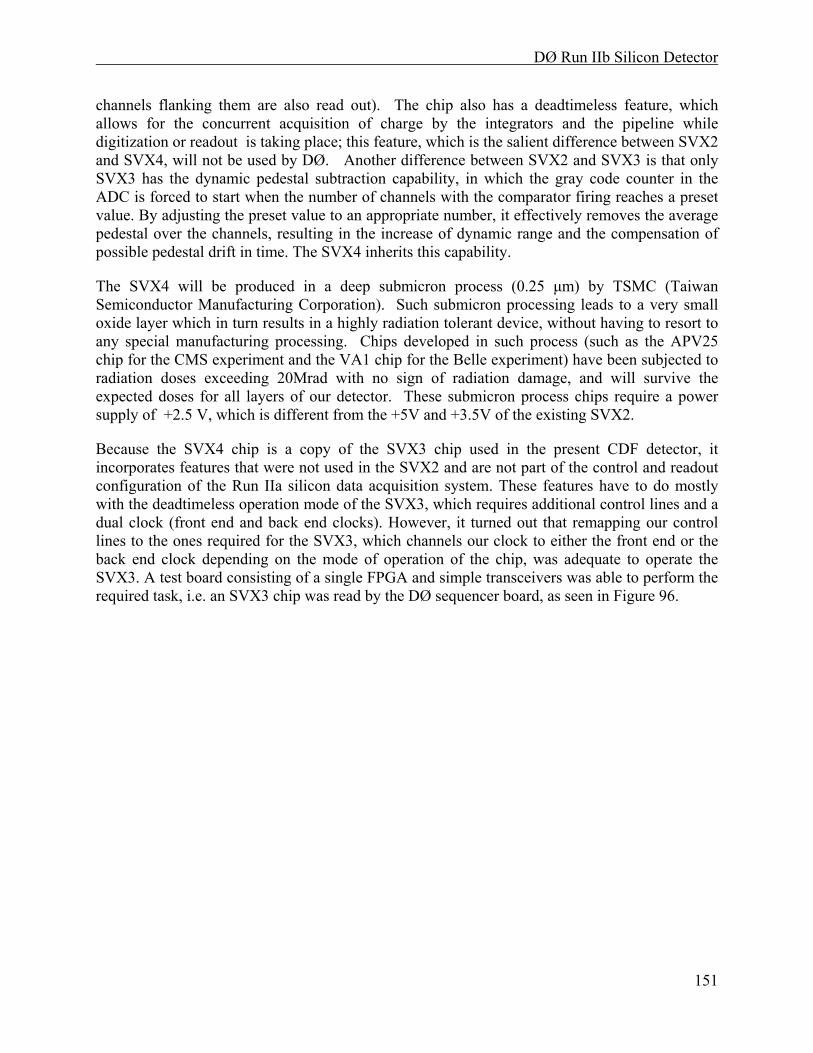
DØ Run IIb Silicon Detector
151
channels flanking them are also read out). The chip also has a deadtimeless feature, which allows for the concurrent acquisition of charge by the integrators and the pipeline while digitization or readout is taking place; this feature, which is the salient difference between SVX2 and SVX4, will not be used by DØ. Another difference between SVX2 and SVX3 is that only SVX3 has the dynamic pedestal subtraction capability, in which the gray code counter in the ADC is forced to start when the number of channels with the comparator firing reaches a preset value. By adjusting the preset value to an appropriate number, it effectively removes the average pedestal over the channels, resulting in the increase of dynamic range and the compensation of possible pedestal drift in time. The SVX4 inherits this capability.
The SVX4 will be produced in a deep submicron process (0.25 µm) by TSMC (Taiwan Semiconductor Manufacturing Corporation). Such submicron processing leads to a very small oxide layer which in turn results in a highly radiation tolerant device, without having to resort to any special manufacturing processing. Chips developed in such process (such as the APV25 chip for the CMS experiment and the VA1 chip for the Belle experiment) have been subjected to radiation doses exceeding 20Mrad with no sign of radiation damage, and will survive the expected doses for all layers of our detector. These submicron process chips require a power supply of +2.5 V, which is different from the +5V and +3.5V of the existing SVX2.
Because the SVX4 chip is a copy of the SVX3 chip used in the present CDF detector, it incorporates features that were not used in the SVX2 and are not part of the control and readout configuration of the Run IIa silicon data acquisition system. These features have to do mostly with the deadtimeless operation mode of the SVX3, which requires additional control lines and a dual clock (front end and back end clocks). However, it turned out that remapping our control lines to the ones required for the SVX3, which channels our clock to either the front end or the back end clock depending on the mode of operation of the chip, was adequate to operate the SVX3. A test board consisting of a single FPGA and simple transceivers was able to perform the required task, i.e. an SVX3 chip was read by the DØ sequencer board, as seen in Figure 96.
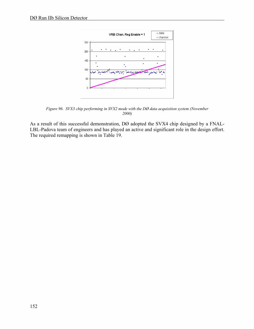
DØ Run IIb Silicon Detector
152
Figure 96. SVX3 chip performing in SVX2 mode with the DØ data acquisition system (November 2000)
As a result of this successful demonstration, DØ adopted the SVX4 chip designed by a FNAL-LBL-Padova team of engineers and has played an active and significant role in the design effort. The required remapping is shown in Table 19.
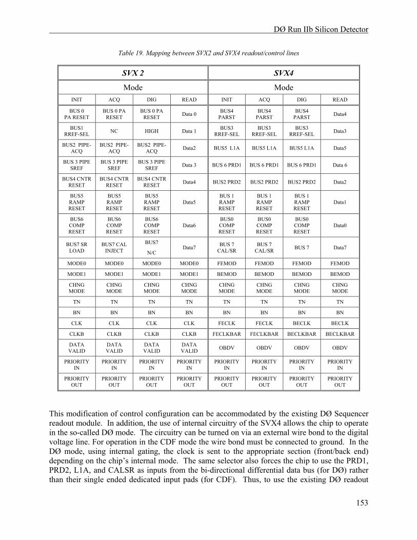
DØ Run IIb Silicon Detector
153
Table 19. Mapping between SVX2 and SVX4 readout/control lines
SVX 2 SVX4
Mode Mode INIT ACQ DIG READ INIT ACQ DIG READ
BUS 0 PA RESET
BUS 0 PA RESET
BUS 0 PA RESET Data 0 BUS4
PARST BUS4
PARST BUS4
PARST Data4
BUS1 RREF-SEL NC HIGH Data 1 BUS3
RREF-SEL BUS3
RREF-SEL BUS3
RREF-SEL Data3
BUS2 PIPE-ACQ
BUS2 PIPE-ACQ
BUS2 PIPE-ACQ Data2 BUS5 L1A BUS5 L1A BUS5 L1A Data5
BUS 3 PIPE SREF
BUS 3 PIPE SREF
BUS 3 PIPE SREF Data 3 BUS 6 PRD1 BUS 6 PRD1 BUS 6 PRD1 Data 6
BUS4 CNTR RESET
BUS4 CNTR RESET
BUS4 CNTR RESET Data4 BUS2 PRD2 BUS2 PRD2 BUS2 PRD2 Data2
BUS5 RAMP RESET
BUS5 RAMP RESET
BUS5 RAMP RESET
Data5 BUS 1 RAMP RESET
BUS 1 RAMP RESET
BUS 1 RAMP RESET
Data1
BUS6 COMP RESET
BUS6 COMP RESET
BUS6 COMP RESET
Data6 BUS0 COMP RESET
BUS0 COMP RESET
BUS0 COMP RESET
Data0
BUS7 SR LOAD
BUS7 CAL INJECT
BUS7
N/C Data7 BUS 7
CAL/SR BUS 7
CAL/SR BUS 7 Data7
MODE0 MODE0 MODE0 MODE0 FEMOD FEMOD FEMOD FEMOD
MODE1 MODE1 MODE1 MODE1 BEMOD BEMOD BEMOD BEMOD
CHNG MODE
CHNG MODE
CHNG MODE
CHNG MODE
CHNG MODE
CHNG MODE
CHNG MODE
CHNG MODE
TN TN TN TN TN TN TN TN
BN BN BN BN BN BN BN BN
CLK CLK CLK CLK FECLK FECLK BECLK BECLK
CLKB CLKB CLKB CLKB FECLKBAR FECLKBAR BECLKBAR BECLKBAR
DATA VALID
DATA VALID
DATA VALID
DATA VALID OBDV OBDV OBDV OBDV
PRIORITY IN
PRIORITY IN
PRIORITY IN
PRIORITY IN
PRIORITY IN
PRIORITY IN
PRIORITY IN
PRIORITY IN
PRIORITY OUT
PRIORITY OUT
PRIORITY OUT
PRIORITY OUT
PRIORITY OUT
PRIORITY OUT
PRIORITY OUT
PRIORITY OUT
This modification of control configuration can be accommodated by the existing DØ Sequencer readout module. In addition, the use of internal circuitry of the SVX4 allows the chip to operate in the so-called DØ mode. The circuitry can be turned on via an external wire bond to the digital voltage line. For operation in the CDF mode the wire bond must be connected to ground. In the DØ mode, using internal gating, the clock is sent to the appropriate section (front/back end) depending on the chip’s internal mode. The same selector also forces the chip to use the PRD1, PRD2, L1A, and CALSR as inputs from the bi-directional differential data bus (for DØ) rather than their single ended dedicated input pads (for CDF). Thus, to use the existing DØ readout
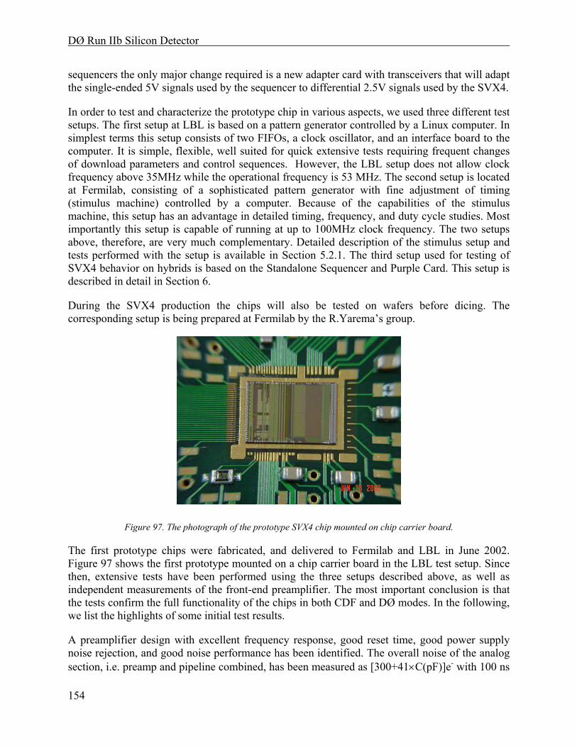
DØ Run IIb Silicon Detector
154
sequencers the only major change required is a new adapter card with transceivers that will adapt the single-ended 5V signals used by the sequencer to differential 2.5V signals used by the SVX4.
In order to test and characterize the prototype chip in various aspects, we used three different test setups. The first setup at LBL is based on a pattern generator controlled by a Linux computer. In simplest terms this setup consists of two FIFOs, a clock oscillator, and an interface board to the computer. It is simple, flexible, well suited for quick extensive tests requiring frequent changes of download parameters and control sequences. However, the LBL setup does not allow clock frequency above 35MHz while the operational frequency is 53 MHz. The second setup is located at Fermilab, consisting of a sophisticated pattern generator with fine adjustment of timing (stimulus machine) controlled by a computer. Because of the capabilities of the stimulus machine, this setup has an advantage in detailed timing, frequency, and duty cycle studies. Most importantly this setup is capable of running at up to 100MHz clock frequency. The two setups above, therefore, are very much complementary. Detailed description of the stimulus setup and tests performed with the setup is available in Section 5.2.1. The third setup used for testing of SVX4 behavior on hybrids is based on the Standalone Sequencer and Purple Card. This setup is described in detail in Section 6.
During the SVX4 production the chips will also be tested on wafers before dicing. The corresponding setup is being prepared at Fermilab by the R.Yarema’s group.
Figure 97. The photograph of the prototype SVX4 chip mounted on chip carrier board.
The first prototype chips were fabricated, and delivered to Fermilab and LBL in June 2002. Figure 97 shows the first prototype mounted on a chip carrier board in the LBL test setup. Since then, extensive tests have been performed using the three setups described above, as well as independent measurements of the front-end preamplifier. The most important conclusion is that the tests confirm the full functionality of the chips in both CDF and DØ modes. In the following, we list the highlights of some initial test results.
A preamplifier design with excellent frequency response, good reset time, good power supply noise rejection, and good noise performance has been identified. The overall noise of the analog section, i.e. preamp and pipeline combined, has been measured as [300+41×C(pF)]e- with 100 ns
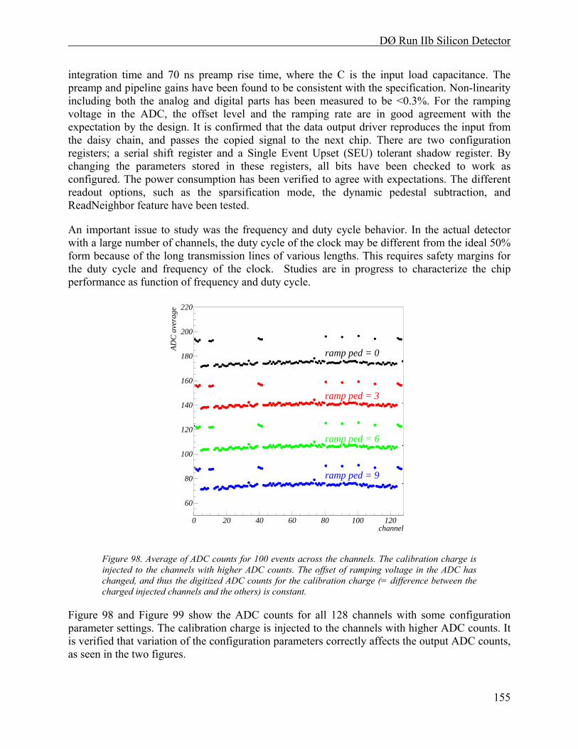
DØ Run IIb Silicon Detector
155
integration time and 70 ns preamp rise time, where the C is the input load capacitance. The preamp and pipeline gains have been found to be consistent with the specification. Non-linearity including both the analog and digital parts has been measured to be <0.3%. For the ramping voltage in the ADC, the offset level and the ramping rate are in good agreement with the expectation by the design. It is confirmed that the data output driver reproduces the input from the daisy chain, and passes the copied signal to the next chip. There are two configuration registers; a serial shift register and a Single Event Upset (SEU) tolerant shadow register. By changing the parameters stored in these registers, all bits have been checked to work as configured. The power consumption has been verified to agree with expectations. The different readout options, such as the sparsification mode, the dynamic pedestal subtraction, and ReadNeighbor feature have been tested.
An important issue to study was the frequency and duty cycle behavior. In the actual detector with a large number of channels, the duty cycle of the clock may be different from the ideal 50% form because of the long transmission lines of various lengths. This requires safety margins for the duty cycle and frequency of the clock. Studies are in progress to characterize the chip performance as function of frequency and duty cycle.
60
80
100
120
140
160
180
200
220
0 20 40 60 80 100 120channel
AD
C a
vera
ge
ramp ped = 0
ramp ped = 3
ramp ped = 6
ramp ped = 9
Figure 98. Average of ADC counts for 100 events across the channels. The calibration charge is injected to the channels with higher ADC counts. The offset of ramping voltage in the ADC has changed, and thus the digitized ADC counts for the calibration charge (= difference between the charged injected channels and the others) is constant.
Figure 98 and Figure 99 show the ADC counts for all 128 channels with some configuration parameter settings. The calibration charge is injected to the channels with higher ADC counts. It is verified that variation of the configuration parameters correctly affects the output ADC counts, as seen in the two figures.
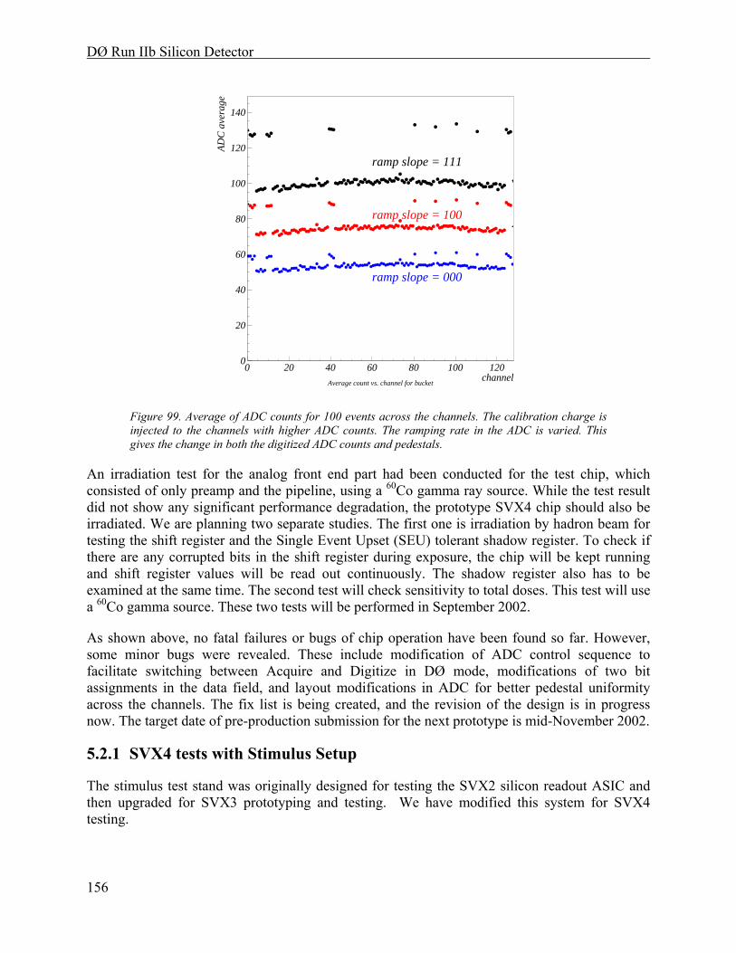
DØ Run IIb Silicon Detector
156
Average count vs. channel for bucket
0
20
40
60
80
100
120
140
0 20 40 60 80 100 120channel
AD
C a
vera
ge
ramp slope = 111
ramp slope = 100
ramp slope = 000
Figure 99. Average of ADC counts for 100 events across the channels. The calibration charge is injected to the channels with higher ADC counts. The ramping rate in the ADC is varied. This gives the change in both the digitized ADC counts and pedestals.
An irradiation test for the analog front end part had been conducted for the test chip, which consisted of only preamp and the pipeline, using a 60Co gamma ray source. While the test result did not show any significant performance degradation, the prototype SVX4 chip should also be irradiated. We are planning two separate studies. The first one is irradiation by hadron beam for testing the shift register and the Single Event Upset (SEU) tolerant shadow register. To check if there are any corrupted bits in the shift register during exposure, the chip will be kept running and shift register values will be read out continuously. The shadow register also has to be examined at the same time. The second test will check sensitivity to total doses. This test will use a 60Co gamma source. These two tests will be performed in September 2002.
As shown above, no fatal failures or bugs of chip operation have been found so far. However, some minor bugs were revealed. These include modification of ADC control sequence to facilitate switching between Acquire and Digitize in DØ mode, modifications of two bit assignments in the data field, and layout modifications in ADC for better pedestal uniformity across the channels. The fix list is being created, and the revision of the design is in progress now. The target date of pre-production submission for the next prototype is mid-November 2002.
5.2.1 SVX4 tests with Stimulus Setup
The stimulus test stand was originally designed for testing the SVX2 silicon readout ASIC and then upgraded for SVX3 prototyping and testing. We have modified this system for SVX4 testing.
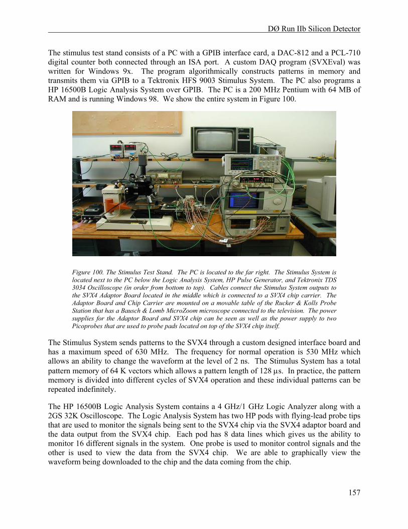
DØ Run IIb Silicon Detector
157
The stimulus test stand consists of a PC with a GPIB interface card, a DAC-812 and a PCL-710 digital counter both connected through an ISA port. A custom DAQ program (SVXEval) was written for Windows 9x. The program algorithmically constructs patterns in memory and transmits them via GPIB to a Tektronix HFS 9003 Stimulus System. The PC also programs a HP 16500B Logic Analysis System over GPIB. The PC is a 200 MHz Pentium with 64 MB of RAM and is running Windows 98. We show the entire system in Figure 100.
Figure 100. The Stimulus Test Stand. The PC is located to the far right. The Stimulus System is located next to the PC below the Logic Analysis System, HP Pulse Generator, and Tektronix TDS 3034 Oscilloscope (in order from bottom to top). Cables connect the Stimulus System outputs to the SVX4 Adaptor Board located in the middle which is connected to a SVX4 chip carrier. The Adaptor Board and Chip Carrier are mounted on a movable table of the Rucker & Kolls Probe Station that has a Bausch & Lomb MicroZoom microscope connected to the television. The power supplies for the Adaptor Board and SVX4 chip can be seen as well as the power supply to two Picoprobes that are used to probe pads located on top of the SVX4 chip itself.
The Stimulus System sends patterns to the SVX4 through a custom designed interface board and has a maximum speed of 630 MHz. The frequency for normal operation is 530 MHz which allows an ability to change the waveform at the level of 2 ns. The Stimulus System has a total pattern memory of 64 K vectors which allows a pattern length of 128 µs. In practice, the pattern memory is divided into different cycles of SVX4 operation and these individual patterns can be repeated indefinitely.
The HP 16500B Logic Analysis System contains a 4 GHz/1 GHz Logic Analyzer along with a 2GS 32K Oscilloscope. The Logic Analysis System has two HP pods with flying-lead probe tips that are used to monitor the signals being sent to the SVX4 chip via the SVX4 adaptor board and the data output from the SVX4 chip. Each pod has 8 data lines which gives us the ability to monitor 16 different signals in the system. One probe is used to monitor control signals and the other is used to view the data from the SVX4 chip. We are able to graphically view the waveform being downloaded to the chip and the data coming from the chip.
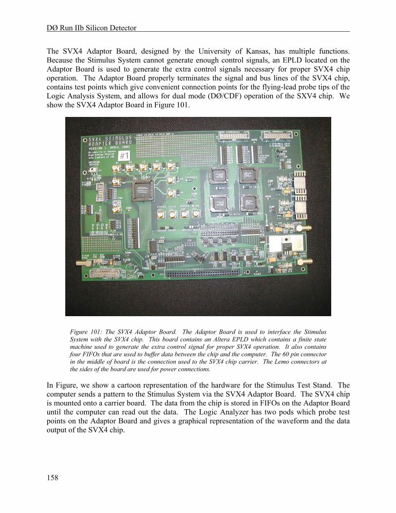
DØ Run IIb Silicon Detector
158
The SVX4 Adaptor Board, designed by the University of Kansas, has multiple functions. Because the Stimulus System cannot generate enough control signals, an EPLD located on the Adaptor Board is used to generate the extra control signals necessary for proper SVX4 chip operation. The Adaptor Board properly terminates the signal and bus lines of the SVX4 chip, contains test points which give convenient connection points for the flying-lead probe tips of the Logic Analysis System, and allows for dual mode (DØ/CDF) operation of the SXV4 chip. We show the SVX4 Adaptor Board in Figure 101.
Figure 101: The SVX4 Adaptor Board. The Adaptor Board is used to interface the Stimulus System with the SVX4 chip. This board contains an Altera EPLD which contains a finite state machine used to generate the extra control signal for proper SVX4 operation. It also contains four FIFOs that are used to buffer data between the chip and the computer. The 60 pin connector in the middle of board is the connection used to the SVX4 chip carrier. The Lemo connectors at the sides of the board are used for power connections.
In Figure, we show a cartoon representation of the hardware for the Stimulus Test Stand. The computer sends a pattern to the Stimulus System via the SVX4 Adaptor Board. The SVX4 chip is mounted onto a carrier board. The data from the chip is stored in FIFOs on the Adaptor Board until the computer can read out the data. The Logic Analyzer has two pods which probe test points on the Adaptor Board and gives a graphical representation of the waveform and the data output of the SVX4 chip.
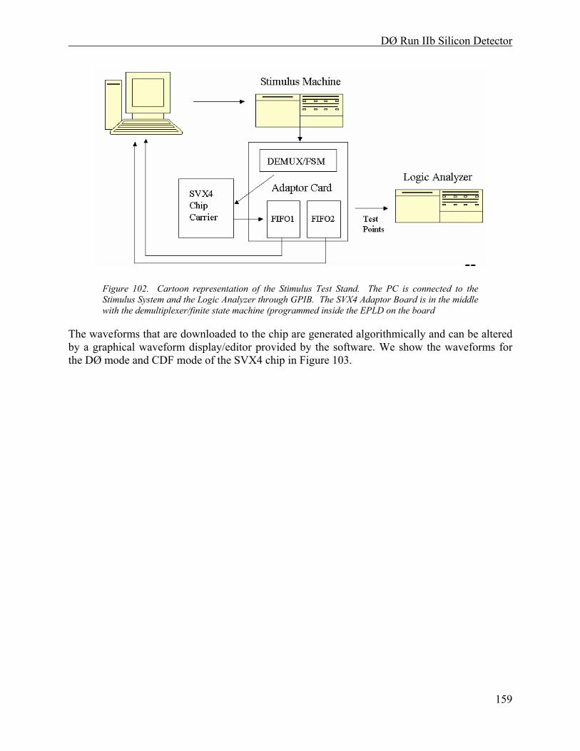
DØ Run IIb Silicon Detector
159
Figure 102. Cartoon representation of the Stimulus Test Stand. The PC is connected to the Stimulus System and the Logic Analyzer through GPIB. The SVX4 Adaptor Board is in the middle with the demultiplexer/finite state machine (programmed inside the EPLD on the board
The waveforms that are downloaded to the chip are generated algorithmically and can be altered by a graphical waveform display/editor provided by the software. We show the waveforms for the DØ mode and CDF mode of the SVX4 chip in Figure 103.
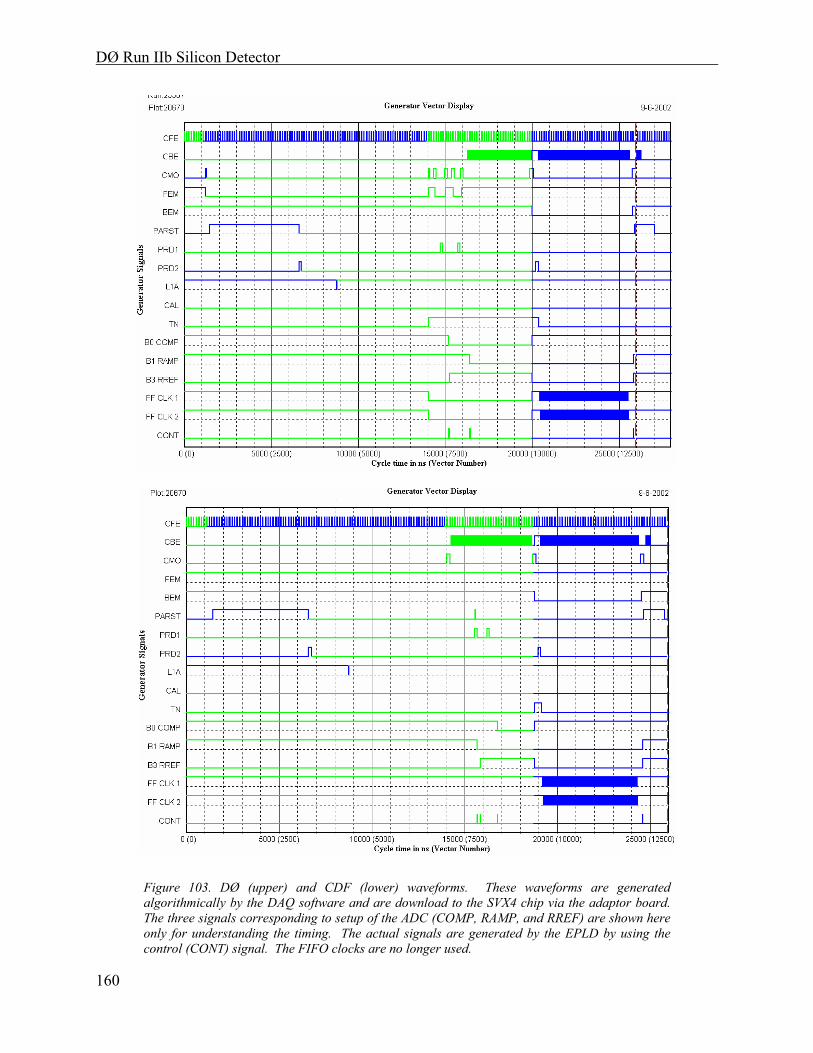
DØ Run IIb Silicon Detector
160
Figure 103. DØ (upper) and CDF (lower) waveforms. These waveforms are generated algorithmically by the DAQ software and are download to the SVX4 chip via the adaptor board. The three signals corresponding to setup of the ADC (COMP, RAMP, and RREF) are shown here only for understanding the timing. The actual signals are generated by the EPLD by using the control (CONT) signal. The FIFO clocks are no longer used.
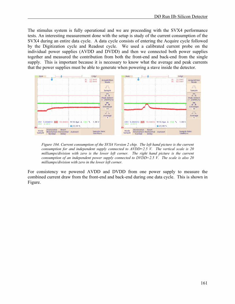
DØ Run IIb Silicon Detector
161
The stimulus system is fully operational and we are proceeding with the SVX4 performance tests. An interesting measurement done with the setup is study of the current consumption of the SVX4 during an entire data cycle. A data cycle consists of entering the Acquire cycle followed by the Digitization cycle and Readout cycle. We used a calibrated current probe on the individual power supplies (AVDD and DVDD) and then we connected both power supplies together and measured the contribution from both the front-end and back-end from the single supply. This is important because it is necessary to know what the average and peak currents that the power supplies must be able to generate when powering a stave inside the detector.
Figure 104. Current consumption of the SVX4 Version 2 chip. The left hand picture is the current consumption for and independent supply connected to AVDD=2.5 V. The vertical scale is 20 milliamps/division with zero is the lower left corner. The right hand picture is the current consumption of an independent power supply connected to DVDD=2.5 V. The scale is also 20 milliamps/division with zero in the lower left corner.
For consistency we powered AVDD and DVDD from one power supply to measure the combined current draw from the front-end and back-end during one data cycle. This is shown in Figure.
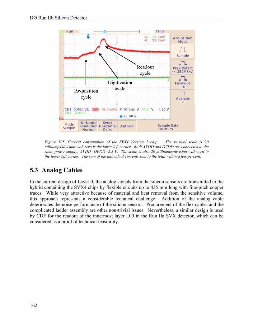
DØ Run IIb Silicon Detector
162
Figure 105. Current consumption of the SVX4 Version 2 chip. The vertical scale is 20 milliamps/division with zero is the lower left corner. Both AVDD and DVDD are connected to the same power supply: AVDD=DVDD=2.5 V. The scale is also 20 milliamps/division with zero in the lower left corner. The sum of the individual currents sum to the total within a few percent.
5.3 Analog Cables
In the current design of Layer 0, the analog signals from the silicon sensors are transmitted to the hybrid containing the SVX4 chips by flexible circuits up to 435 mm long with fine-pitch copper traces. While very attractive because of material and heat removal from the sensitive volume, this approach represents a considerable technical challenge. Addition of the analog cable deteriorates the noise performance of the silicon sensors. Procurement of the flex cables and the complicated ladder assembly are other non-trivial issues. Nevertheless, a similar design is used by CDF for the readout of the innermost layer L00 in the Run IIa SVX detector, which can be considered as a proof of technical feasibility.
DØ Run IIb Silicon Detector
163
0
500
1000
1500
2000
2500
3000
0 5 10 15 20 25 30 35 40 45 50
before irradiation
after 15 fb-1
Csi + Ccable (pF)
Tot
al n
oise
(e- )
Figure 106. Expectation for the total noise as a function of sum of sensor and cable capacitance.
One of the most important aspects in the design and technical realization of a long analog cable is the capacitance between the traces, which has to be as small as possible. Any load capacitance will contribute to the noise seen by the preamplifier. Our design goal is to maintain a S/N ratio of better than 10 for Layer 0 after irradiation corresponding to 15 fb-1 of data. Figure 106 shows the expected noise level as a function of capacitance summed over silicon sensor and analog cable. Assuming that a minimum ionizing particle creates 22,000 electrons by traveling through a silicon sensor with the thickness of 300 µm, the total capacitance must be kept below 33 pF to maintain the S/N better than 10 given the measured SVX4 noise performance. The 8 cm long silicon sensor will have about 10 pF of capacitance. This means that the analog cable is required to have capacitance less than 23 pF or 0.53 pF/cm.
The flexible dielectric substrate of the cable affects the capacitance. The material of choice in high-energy applications is polyimide such as Kapton HN with a dielectric constant of 3.5 at a frequency of 1MHz. This material is radiation hard with good mechanical and electrical properties. Other synthesized polyimide materials on the market achieve a lower dielectric constant by adding halogens. They are not radiation hard and are not in compliance with CERN and Fermilab fire safety regulations. Although materials like polyethylene or polypropylenes are used in the flex industry and possess a lower dielectric constant, they are also not radiation hard up to the 10-15 MRad level, to which the innermost layer of the silicon tracker will be exposed. The material choices for the flex cable are, therefore, limited to the standard polyimide.
Considering the tight schedule and the technical difficulties, we investigated a design that allows a manufacturer to produce cables reliably, and also satisfies the capacitance requirement.
DØ Run IIb Silicon Detector
164
Figure 107. Schematic view of the proposed connections between the sensor, analog cable and the hybrid for Layer 0
Figure 107 shows the schematic view of the proposed arrangement for the sensor, analog cable and the hybrid. Two cables with constant 91 micron pitch are laminated together with a lateral shift of 45 µm. This works effectively as a cable with 45 µm pitch. We think this is a simpler alternative to the L00 approach which has fan-in and fan-out regions adapting the 45 micron pitch to 100 micron pitch. We also investigated the dependence of the cable capacitance on the trace width to understand the trade-off between the reliability and performance.
0.2
0.25
0.3
0.35
0.4
0.45
0.5
0.55
0.6
0 5 10 15 20 25 30trace width (µm)
C (
pF/c
m)
Figure 108. Capacitance calculations by ANSYS. The capacitance of one trace to all other traces is shown as a function of trace width. The blue squares represent 50 µm trace pitch, and red circles 100 µm
Figure 108 shows the expected capacitance for various trace width and different pitch by finite element calculations using the ANSYS program. The height of the traces is assumed to be 8 µm

DØ Run IIb Silicon Detector
165
in the calculations. It turns out that the 100 µm pitch cable reduces the capacitance by 30% compared to the 50 µm pitch. Besides, the dependence on the trace width is weaker for the 100 µm pitch, correspondingly 0.0052 pF/cm/µm for the 100 µm pitch and 0.0109 pF/cm/µm for the 50 µm pitch. Based on this result of the calculations, we adopt the following design as a baseline: 16 µm trace width and 91 µm constant pitch with no fan-in/out region. The 16 micron trace width is a factor of two larger than the trace width of the L00 CDF cable, which we expect to result in increased reliability and higher production yield of the cable. In the final design the pitch is reduced from 100 to 91 µm because the HV trace must hold up to ~1000 V and, therefore, needs to be separated by more space on the cable.
In order to reduce the capacitance contribution from the adjacent cables, a spacer will be placed between the cables. A candidate for the spacer material is polypropylene mesh sheet with dielectric constant 3.5. Taking into account the 50% volume occupancy due to the mesh structure, and the possible reduction of the amount of material by punching more holes, the dielectric constant can be effectively as low as 1.5. The thickness of the spacer would be 200 µm at maximum because of mechanical constraints. The capacitances calculated by ANSYS for the configuration with two cables and a spacer are summarized in Table 20.
Table 20. Capacitance in one trace relative to all other traces calculated by ANSYS. The first line is for a single cable, and the other for the configuration where two cables are laminated together with the 200 µm thick spacer. The first column is the dielectric constant for the spacer.
εr of spacer Capacitance (pF/cm)
Single cable 0.339
1 0.342
2 0.466
3 0.585
This result indicates that separating two cables by a proper spacer can maintain cable capacitance below the required value. From this encouraging result, DØ adopts the method of using two 91 µm pitch cables for one chip readout, in which a pair of cables with a spacer functions as a 45 µm pitch cable. Hence the trace pitch can be almost twice that of the old design, resulting in relief of the technical difficulty.
Based on good prior experience with high density interconnects (HDI) from Dyconex Inc. in Zurich, Switzerland, we contacted them in May 2001. After a few iterations of their prototyping and our technical evaluation, in July 2002 they delivered 27 good prototypes. Figure 109 is a photograph of one of the prototype cables. The copper traces are gold-plated, and the bonding pads have been confirmed to be bondable. Out of the 27 cables, 25 cables satisfy the specification in the number of open traces. While the specification is that 128 traces out of 129 (one trace is spare) are continuous, 16 cables have no opens, and 9 cables have 1 open. Another important requirement is capacitance. The specification is <0.40 pF/cm. The capacitance of one
DØ Run IIb Silicon Detector
166
trace to neighboring two traces has been measured to be 0.30 pF/cm. From ANSYS calculations, 10-15% of increase is expected from contributions besides the two neighbors. Measurements on the old prototype cable with all the traces were shorted together had verified this increase rate. Therefore, 0.35 pF/cm is a fair estimate of the capacitance. This is within the specification.
Figure 109. Photograph showing the edge of the most recent prototype cable.
5.3.1 Layer 0 Prototype
In Layer 0, the tight space constraints and heat dissipation require us to use a low-mass analog cable to couple the silicon sensor and the SVX4 chip mounted on the hybrid. As discussed in Section 5.3, special attention has to be paid to the capacitance increase caused by the long analog cable, to avoid degradation of the noise performance. In addition, the experience of the Run IIa L00 in CDF reveals other possible noise sources: noise due to capacitive coupling between the detector and nearby floating metal such as cooling tubes, and also RF pickup noise by the analog cable.
DØ Run IIb Silicon Detector
167
Figure 110. The photograph of the connected region between the sensor and the analog cable (left) and between the cable and the chip (right).
In order to study the effect of these additional noise sources, a L0 prototype was assembled from a L0 prototype sensor manufactured by ELMA, an analog cable manufactured by Dyconex, and a Run IIa hybrid for the readout. The wire-bonding regions for the sensor to the analog cable and for the cable to the chip are displayed in displayed in Figure 110. The L0 prototype fixture is put inside a plastic box for light tightness, and is well insulated to avoid any capacitive coupling to the assembly. There are three SVX2 readout chips mounted on the hybrid. Out of the three, two are used to read out the signal from the sensor through the analog cable, while the remaining chip does not have any input loads, and serves as a reference noise level in the test setup. In the noise study described in this section, the noise level is defined as the RMS of pedestal distributions for 100 events.
Apart from the electrical measurements described below, this prototype is a successful demonstration of the proposed arrangement for analog cables. The prototype allowed us to come up with specifications on exact dimensions for the final system and to verify the feasibility of bonding between the cables and the sensor and between the cables and the hybrid.
First we measure the noise level in an electrically quiet environment (accomplished by wrapping the whole fixture by aluminum foil connected to ground), to estimate the amount of additional noise due to the load capacitance of the analog cable. The left plot in Figure 111 shows the noise level for each channel. The projection in each chip is shown in the right. From Gaussian fits of the distributions, the average noise level is 2.2 ADC counts, compared to 1.4 ADC counts in the third (reference) chip. Assuming one ADC count is equivalent to 1000 electrons, the increase of noise level can be translated as 800 electrons. Using the fact that a minimum ionizing particle creates roughly 22,000 electrons in a sensor, the observed noise from the additional capacitive load is acceptable even for the old SVX2 chip.
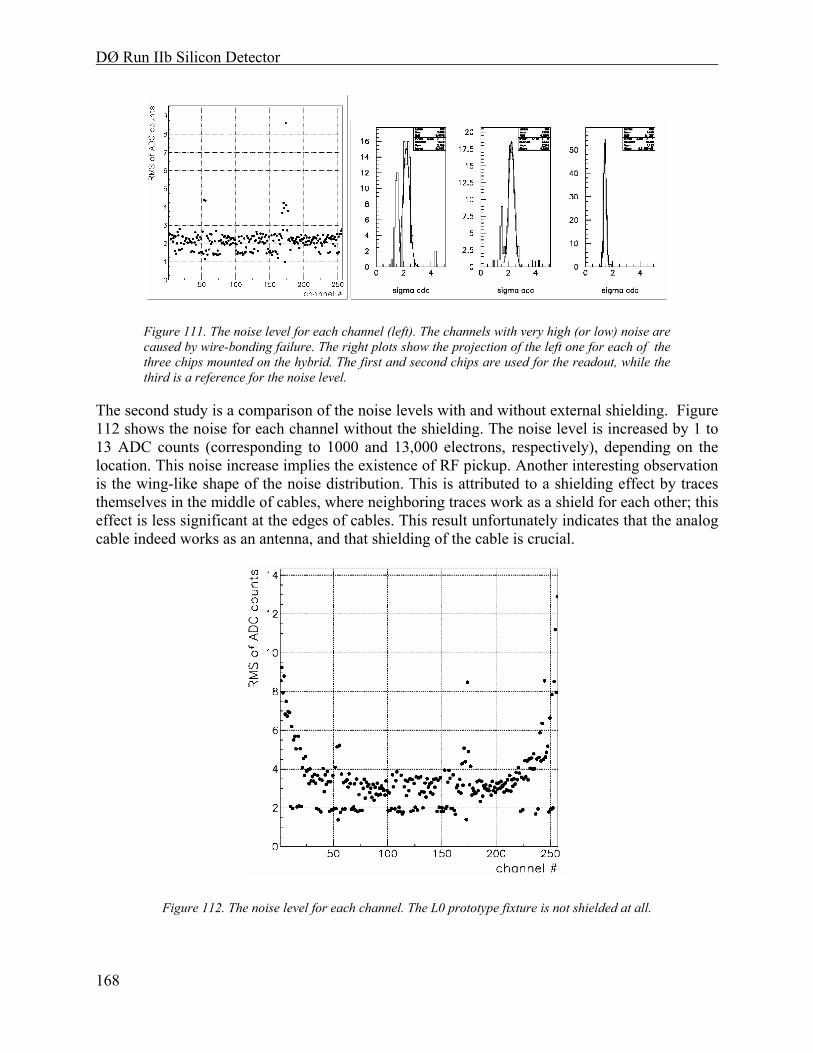
DØ Run IIb Silicon Detector
168
Figure 111. The noise level for each channel (left). The channels with very high (or low) noise are caused by wire-bonding failure. The right plots show the projection of the left one for each of the three chips mounted on the hybrid. The first and second chips are used for the readout, while the third is a reference for the noise level.
The second study is a comparison of the noise levels with and without external shielding. Figure 112 shows the noise for each channel without the shielding. The noise level is increased by 1 to 13 ADC counts (corresponding to 1000 and 13,000 electrons, respectively), depending on the location. This noise increase implies the existence of RF pickup. Another interesting observation is the wing-like shape of the noise distribution. This is attributed to a shielding effect by traces themselves in the middle of cables, where neighboring traces work as a shield for each other; this effect is less significant at the edges of cables. This result unfortunately indicates that the analog cable indeed works as an antenna, and that shielding of the cable is crucial.
Figure 112. The noise level for each channel. The L0 prototype fixture is not shielded at all.
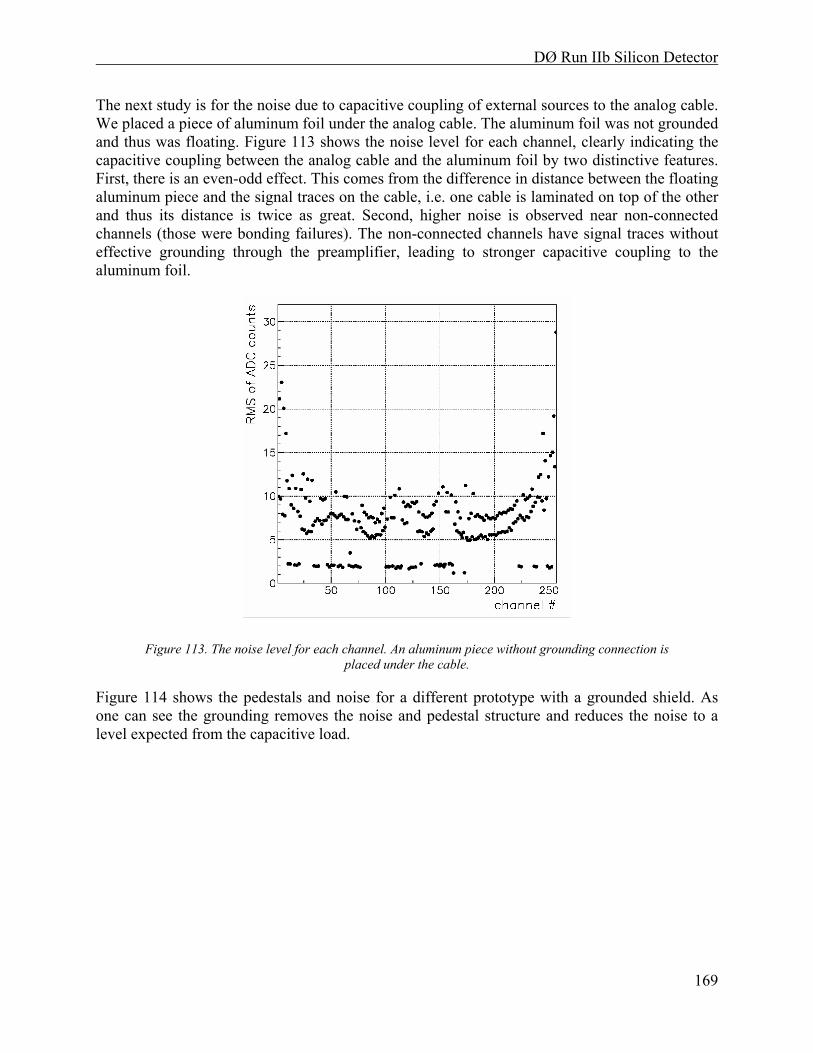
DØ Run IIb Silicon Detector
169
The next study is for the noise due to capacitive coupling of external sources to the analog cable. We placed a piece of aluminum foil under the analog cable. The aluminum foil was not grounded and thus was floating. Figure 113 shows the noise level for each channel, clearly indicating the capacitive coupling between the analog cable and the aluminum foil by two distinctive features. First, there is an even-odd effect. This comes from the difference in distance between the floating aluminum piece and the signal traces on the cable, i.e. one cable is laminated on top of the other and thus its distance is twice as great. Second, higher noise is observed near non-connected channels (those were bonding failures). The non-connected channels have signal traces without effective grounding through the preamplifier, leading to stronger capacitive coupling to the aluminum foil.
Figure 113. The noise level for each channel. An aluminum piece without grounding connection is placed under the cable.
Figure 114 shows the pedestals and noise for a different prototype with a grounded shield. As one can see the grounding removes the noise and pedestal structure and reduces the noise to a level expected from the capacitive load.
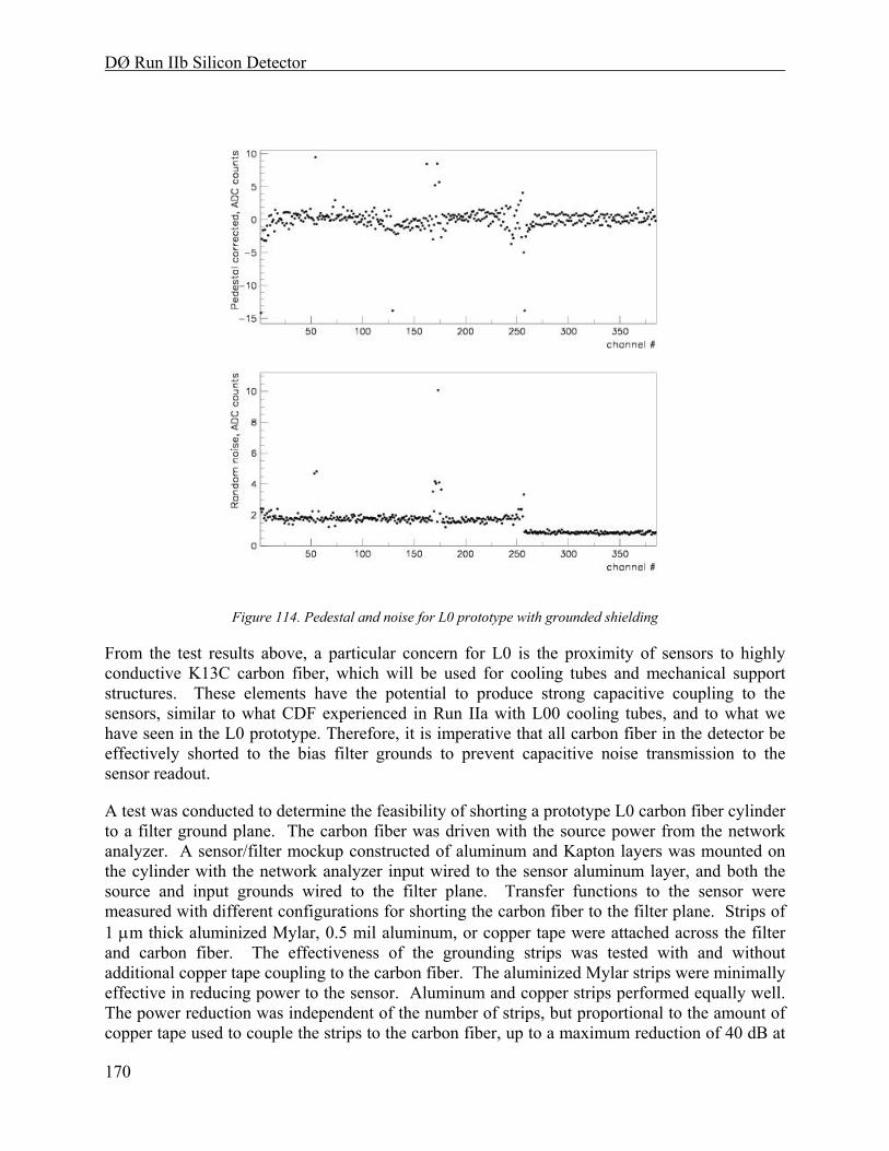
DØ Run IIb Silicon Detector
170
Figure 114. Pedestal and noise for L0 prototype with grounded shielding
From the test results above, a particular concern for L0 is the proximity of sensors to highly conductive K13C carbon fiber, which will be used for cooling tubes and mechanical support structures. These elements have the potential to produce strong capacitive coupling to the sensors, similar to what CDF experienced in Run IIa with L00 cooling tubes, and to what we have seen in the L0 prototype. Therefore, it is imperative that all carbon fiber in the detector be effectively shorted to the bias filter grounds to prevent capacitive noise transmission to the sensor readout.
A test was conducted to determine the feasibility of shorting a prototype L0 carbon fiber cylinder to a filter ground plane. The carbon fiber was driven with the source power from the network analyzer. A sensor/filter mockup constructed of aluminum and Kapton layers was mounted on the cylinder with the network analyzer input wired to the sensor aluminum layer, and both the source and input grounds wired to the filter plane. Transfer functions to the sensor were measured with different configurations for shorting the carbon fiber to the filter plane. Strips of 1 µm thick aluminized Mylar, 0.5 mil aluminum, or copper tape were attached across the filter and carbon fiber. The effectiveness of the grounding strips was tested with and without additional copper tape coupling to the carbon fiber. The aluminized Mylar strips were minimally effective in reducing power to the sensor. Aluminum and copper strips performed equally well. The power reduction was independent of the number of strips, but proportional to the amount of copper tape used to couple the strips to the carbon fiber, up to a maximum reduction of 40 dB at

DØ Run IIb Silicon Detector
171
1 MHz. Further studies determined that aluminum foil embedded in the carbon fiber provides very good coupling for grounding to the filter plane. The embedded aluminum will have 2mm wide strip extensions that will be folded over and shorted to ground pads on the filter. Further details of the carbon fiber grounding studies can be found in 5.15.
Based on the grounding scheme studied above, we plan to assemble another L0 prototype that will be mounted on the carbon fiber structure, in which the carbon fiber is shorted to the bias filter ground through the 2 mm wide aluminum strip. Noise reduction by this proposed grounding scheme must be identified with the prototype module.
5.4 Hybrids
This section describes the hybrid design and related electrical issues for the stave design. The proposed beryllia hybrids minimize the amount of material in the detector and are a well- established technique used previously in a number of experiments.
Commonly, the circuits connecting the SVX chips to the low mass jumper cable are called “hybrids.” The hybrids will be based on the technology of thick film deposition on ceramics successfully used in a number of high energy physics experiments including all CDF SVX detectors and the CLEO microvertex detector27 . In our case, the 380 micron beryllia substrate will be used to reduce the amount of material in Layers 1 through 5 where the hybrids will be mounted directly in the sensitive volume. For Layer 0 which has off-board hybrids at higher Z, the material issue is of less importance. However, beryllia ceramic is preferred here because of its significantly better thermal conductivity with respect to alumina.
Thick film deposition by screen-printing is a mature technology allowing for a minimal via size in dielectric of 200 micron and minimum trace width of 100 micron. Multi-layer designs are routinely achievable. Typical thickness of dielectric and metal layers are 40 and 7 micron, respectively. We have identified CPT, Oceanside CA and Amitron, NH as our potential vendors. Both companies have solid backgrounds in hybrid production.
There are four types of hybrids in the proposed design. Two of them are 10-chip, double-ended versions for Layers 2 through 5: one for axial sensors (L2A hybrid) and one for stereo sensors (L2S hybrid). The others are a 6-chip, double-ended version for Layer 1 (L1 hybrid) and a 2-chip version for Layer 0 (L0 hybrid).
In addition to providing a secure mount for the SVX chips and cable connector, the hybrids also have capacitors for bypassing the analog and digital voltages and the detector bias. The low- mass flat cable connects to the hybrid with an AVX connector plug (hybrid side) and receptacle (cable side). These are 0.5mm pitch, low profile 50-pin connectors with a maximum height of 3.1 mm above the surface of the hybrid. The CDF Run IIa SVX detector uses similar connectors with a low failure rate. Placement of the connector on the hybrid allows for easy testing of hybrids with and without attached silicon sensors during all phases of the hybrid and stave production. This is essential for the modularity of the design and for quality checking during 27 Nucl.Inst.Meth. A435, 9-15, 1999.
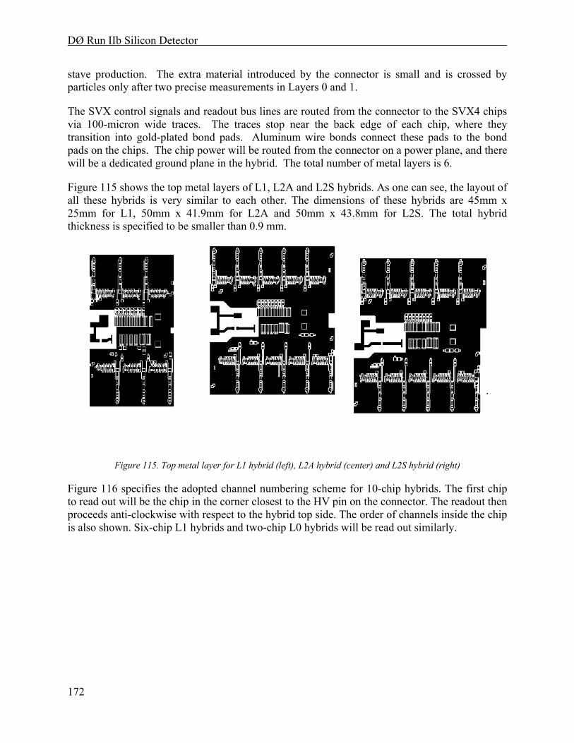
DØ Run IIb Silicon Detector
172
stave production. The extra material introduced by the connector is small and is crossed by particles only after two precise measurements in Layers 0 and 1.
The SVX control signals and readout bus lines are routed from the connector to the SVX4 chips via 100-micron wide traces. The traces stop near the back edge of each chip, where they transition into gold-plated bond pads. Aluminum wire bonds connect these pads to the bond pads on the chips. The chip power will be routed from the connector on a power plane, and there will be a dedicated ground plane in the hybrid. The total number of metal layers is 6.
Figure 115 shows the top metal layers of L1, L2A and L2S hybrids. As one can see, the layout of all these hybrids is very similar to each other. The dimensions of these hybrids are 45mm x 25mm for L1, 50mm x 41.9mm for L2A and 50mm x 43.8mm for L2S. The total hybrid thickness is specified to be smaller than 0.9 mm.
Figure 115. Top metal layer for L1 hybrid (left), L2A hybrid (center) and L2S hybrid (right)
Figure 116 specifies the adopted channel numbering scheme for 10-chip hybrids. The first chip to read out will be the chip in the corner closest to the HV pin on the connector. The readout then proceeds anti-clockwise with respect to the hybrid top side. The order of channels inside the chip is also shown. Six-chip L1 hybrids and two-chip L0 hybrids will be read out similarly.
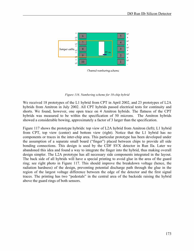
DØ Run IIb Silicon Detector
173
Figure 116. Numbering scheme for 10-chip hybrid We received 18 prototypes of the L1 hybrid from CPT in April 2002, and 23 prototypes of L2A hybrids from Amitron in July 2002. All CPT hybrids passed electrical tests for continuity and shorts. We found, however, one open trace on 4 Amitron hybrids. The flatness of the CPT hybrids was measured to be within the specification of 50 microns. The Amitron hybrids showed a considerable bowing, approximately a factor of 3 larger than the specification.
Figure 117 shows the prototype hybrids: top view of L2A hybrid from Amitron (left); L1 hybrid from CPT, top view (center) and bottom view (right). Notice that the L1 hybrid has no components or traces in the inter-chip area. This particular prototype has been developed under the assumption of a separate small board (“finger”) placed between chips to provide all side bonding connections. This design is used by the CDF SVX detector in Run IIa. Later we abandoned this idea and found a way to integrate the finger into the hybrid, thus making overall design simpler. The L2A prototype has all necessary side components integrated in the layout. The back side of all hybrids will have a special printing to avoid glue in the area of the guard ring; see right photo in Figure 117. This should improve the breakdown voltage (hence, the radiation hardness) of the design, preventing potential discharge path through the glue in the region of the largest voltage difference between the edge of the detector and the first signal traces. The printing has two “pedestals” in the central area of the backside raising the hybrid above the guard rings of both sensors.
DØ Run IIb Silicon Detector
174
Figure 117.Prototype hybrids : Top view of L2A hybrid from Amitron (left); L1 hybrid from CPT, top view (center) and bottom view (right).
In July 2002 we assembled several L1 prototype hybrids (Figure 118). The prototype has 4 SVX4 chips at the corners of the hybrid. The two central chips were replaced by a simple finger kludge board to provide all side connections for two neighboring chips.
Figure 118. Prototype L1 hybrid
Using this hybrid and two prototype L1 sensors from ELMA we also assembled a L1 prototype module (Figure 119). Only two chips, #2 (bottom left) and #3 (bottom right) were bonded to sensors.
DØ Run IIb Silicon Detector
175
Figure 119. L1 prototype module
Figure 120 shows the channel ID, pedestal and total noise x 10 from readout of this L1 module. Noise is defined as the RMS of the pedestal. Four SVX4 chips are represented on the plot. The channel ID is incremented for each of them from 0 to 127. The value of pedestal was set at around 30 ADC counts. The noise level is approximately 1.0 ADC counts for chips 1 and 4, and 1.7 ADC counts for chips 2 and 3. The difference is explained by the extra capacitance load from the silicon sensors. The sensors were biased above depletion voltage at 50V. The total HV current for both sensors was 1.5 uA. Several noisy channels are visible for chips bonded to the detector. Making some assumptions about calibrations, we determine a preliminary noise of 700 e for bare chip and 1100 e for chips connected to silicon. This corresponds to a S/N of ~20:1 for the prototype module, assuming a MIP signal is 22000 e. Work is in progress to improve understanding of the noise level.
Figure 120. Channel ID, pedestal and noise plots for L1 prototype module

DØ Run IIb Silicon Detector
176
5.5 Cables, Adapter Card and Interface Board Overview
A primary goal of the Run IIB readout chain design is to preserve as much of the Run IIA electronics and cable plant as possible. In particular, we want to keep: 1) the Interface Boards (IBs), located at the base of the central calorimeter, that relay digital signals between the sequencers and the SVX4 chip, supply both low-voltage power and high-voltage bias, and monitor current and temperature; 2) the high-mass cables, consisting of 3M 80 conductor cables and parallel coaxial clock cables that run from the IBs to Adapter Cards on the calorimeter face. Because of the complexity of these IBs, any required changes beyond the scope of component replacements or hand-wired jumpers will likely mandate complete replacement. Also, the space for connectors on the IB face is saturated. A required line count into the IB exceeding that available on the 80-conductor cables could not be accommodated.
As described below, the present design aims to preserve the IBs by replacing the Run IIa passive Adapter Cards on the calorimeter face with active ones that translate between single-ended (IB) and differential (SVX4) signals, and that also regulate supply voltages. The long (up to 2.7 m) Run IIa low-mass cables, which do not have differential-signal capability, will be replaced with new cables comprised of Twisted Pairs connected by small, passive Junction Cards to new, relatively short, low-mass Digital Jumper Cables.
5.6 Digital Jumper Cables
Digital Jumper Cables (DJCs) will carry digital signals and power between the hybrids and the Junction Cards, where they connect to the Twisted-Pair Cables. In all, each DJC carries 11 pairs of differential signals, 6 single-ended signals, 5 sense lines, 2 power voltages and ground, and sensor bias of up to 1000 V. They will be flex-circuit striplines similar to the low-mass cables used in Run IIA, which minimize the amount of material in the sensitive volume. Although they will be shorter than the Run IIA cables, they will be narrower and carry more signal traces, so that the feature size is 20% smaller. There will be 888 DJC’s 14.7 mm wide, with a distribution of lengths between 44 cm and 103 cm. Signal traces 125 microns wide with 300 micron pitch, and also broad power and ground traces, will be located on both sides of a Kapton dielectric 102 microns thick. The layout for all five layers is the same, with a 50-pin, 0.5 mm pitch AVX 5046 connector soldered to pads on both ends. DJC’s for Layers 2-5 will be made with 1-ounce rather than ½-ounce copper traces because of their larger (10-chip) power requirements. The DJC’s will be reinforced by thin G10 backing behind the connectors to make them more robust during handling. Photographs of one end of a 50 cm prototype DJC (before connector installation) are shown in Figure 121 and Figure 122.
.
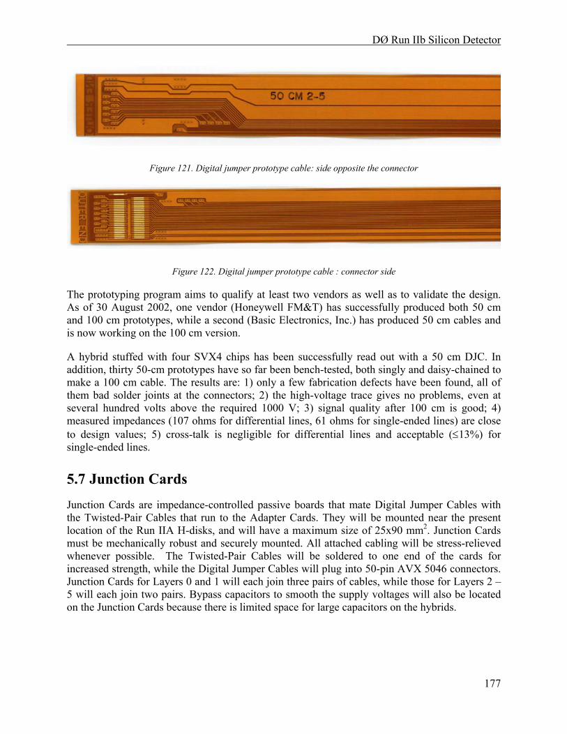
DØ Run IIb Silicon Detector
177
Figure 121. Digital jumper prototype cable: side opposite the connector
Figure 122. Digital jumper prototype cable : connector side
The prototyping program aims to qualify at least two vendors as well as to validate the design. As of 30 August 2002, one vendor (Honeywell FM&T) has successfully produced both 50 cm and 100 cm prototypes, while a second (Basic Electronics, Inc.) has produced 50 cm cables and is now working on the 100 cm version.
A hybrid stuffed with four SVX4 chips has been successfully read out with a 50 cm DJC. In addition, thirty 50-cm prototypes have so far been bench-tested, both singly and daisy-chained to make a 100 cm cable. The results are: 1) only a few fabrication defects have been found, all of them bad solder joints at the connectors; 2) the high-voltage trace gives no problems, even at several hundred volts above the required 1000 V; 3) signal quality after 100 cm is good; 4) measured impedances (107 ohms for differential lines, 61 ohms for single-ended lines) are close to design values; 5) cross-talk is negligible for differential lines and acceptable (≤13%) for single-ended lines.
5.7 Junction Cards
Junction Cards are impedance-controlled passive boards that mate Digital Jumper Cables with the Twisted-Pair Cables that run to the Adapter Cards. They will be mounted near the present location of the Run IIA H-disks, and will have a maximum size of 25x90 mm2. Junction Cards must be mechanically robust and securely mounted. All attached cabling will be stress-relieved whenever possible. The Twisted-Pair Cables will be soldered to one end of the cards for increased strength, while the Digital Jumper Cables will plug into 50-pin AVX 5046 connectors. Junction Cards for Layers 0 and 1 will each join three pairs of cables, while those for Layers 2 – 5 will each join two pairs. Bypass capacitors to smooth the supply voltages will also be located on the Junction Cards because there is limited space for large capacitors on the hybrids.
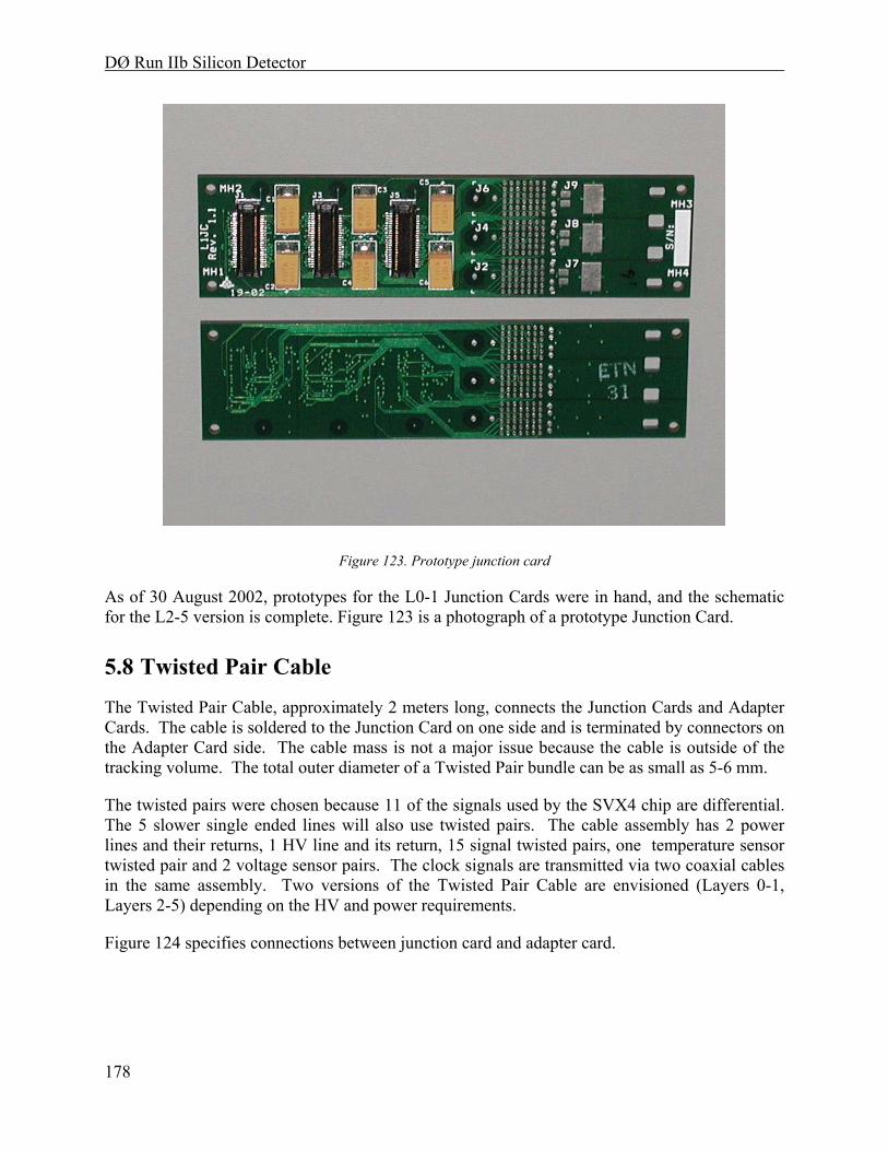
DØ Run IIb Silicon Detector
178
Figure 123. Prototype junction card
As of 30 August 2002, prototypes for the L0-1 Junction Cards were in hand, and the schematic for the L2-5 version is complete. Figure 123 is a photograph of a prototype Junction Card.
5.8 Twisted Pair Cable
The Twisted Pair Cable, approximately 2 meters long, connects the Junction Cards and Adapter Cards. The cable is soldered to the Junction Card on one side and is terminated by connectors on the Adapter Card side. The cable mass is not a major issue because the cable is outside of the tracking volume. The total outer diameter of a Twisted Pair bundle can be as small as 5-6 mm.
The twisted pairs were chosen because 11 of the signals used by the SVX4 chip are differential. The 5 slower single ended lines will also use twisted pairs. The cable assembly has 2 power lines and their returns, 1 HV line and its return, 15 signal twisted pairs, one temperature sensor twisted pair and 2 voltage sensor pairs. The clock signals are transmitted via two coaxial cables in the same assembly. Two versions of the Twisted Pair Cable are envisioned (Layers 0-1, Layers 2-5) depending on the HV and power requirements.
Figure 124 specifies connections between junction card and adapter card.
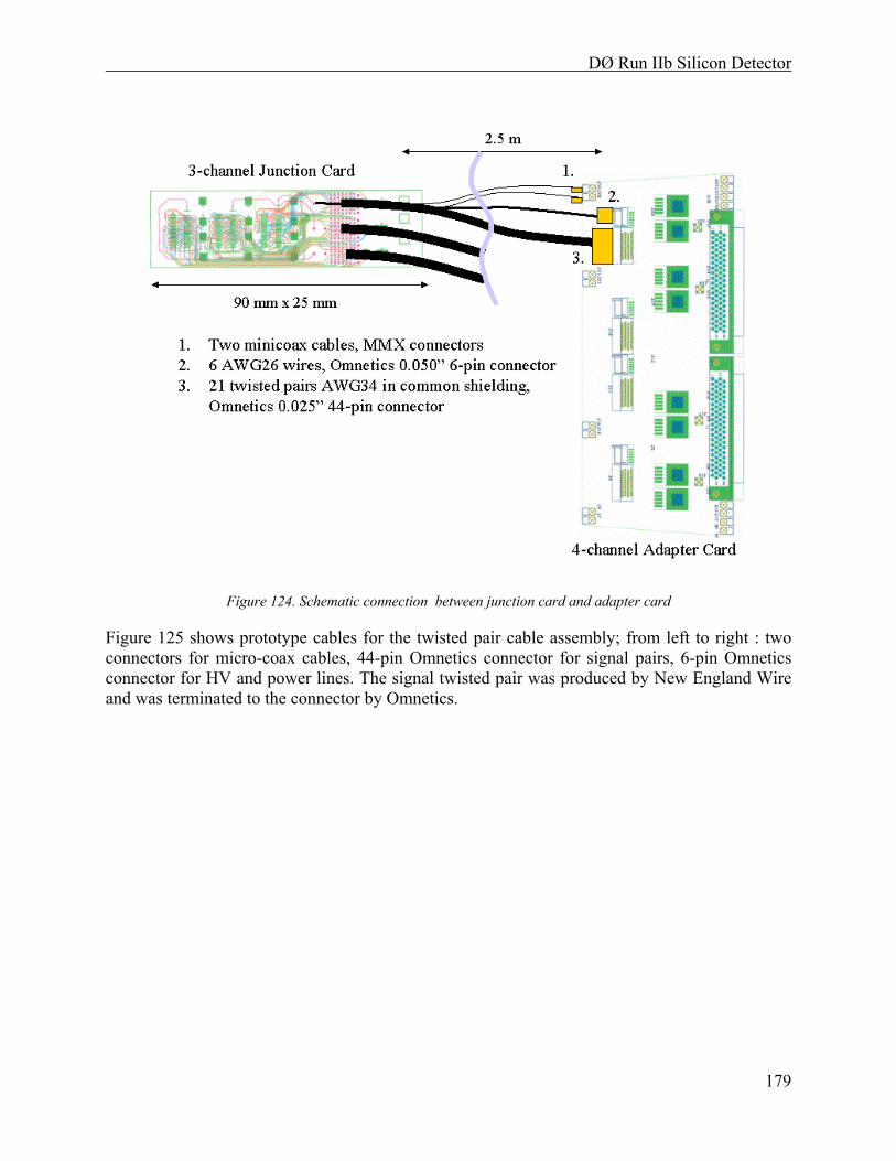
DØ Run IIb Silicon Detector
179
Figure 124. Schematic connection between junction card and adapter card
Figure 125 shows prototype cables for the twisted pair cable assembly; from left to right : two connectors for micro-coax cables, 44-pin Omnetics connector for signal pairs, 6-pin Omnetics connector for HV and power lines. The signal twisted pair was produced by New England Wire and was terminated to the connector by Omnetics.
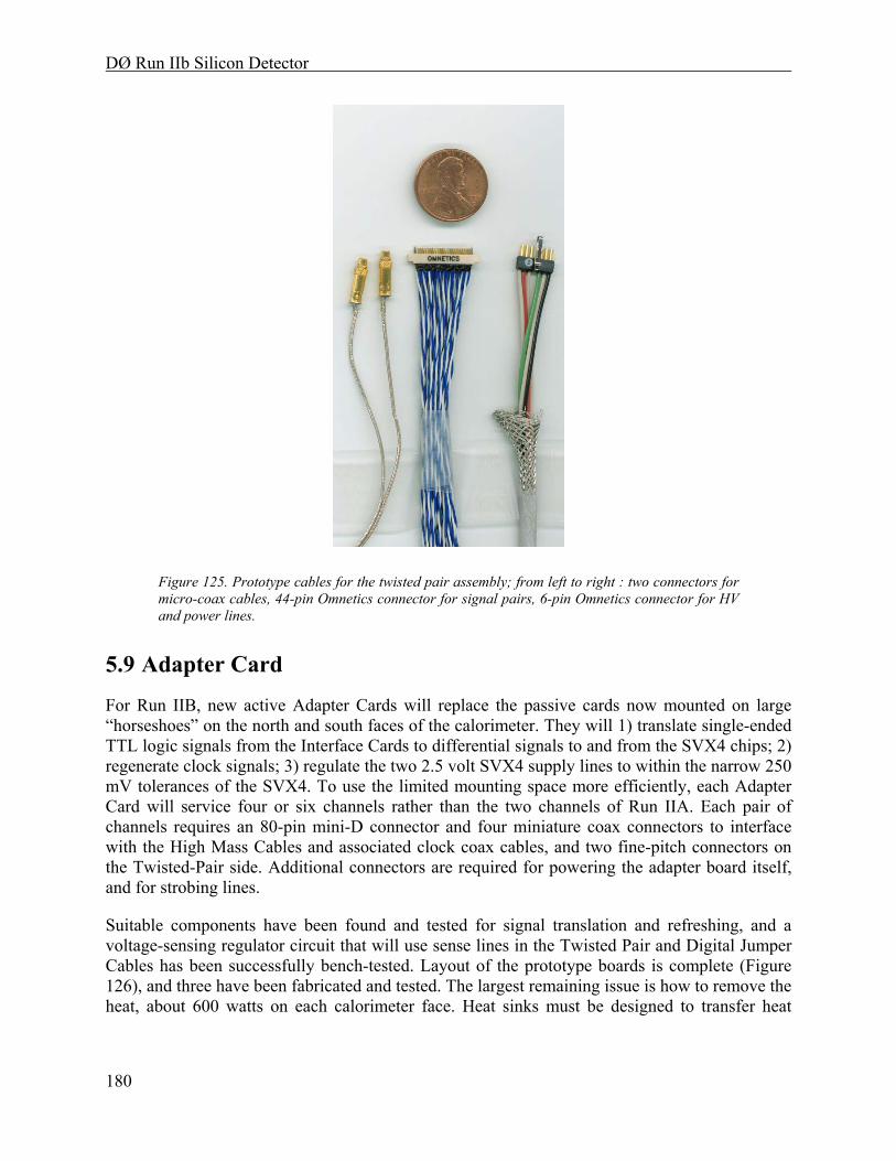
DØ Run IIb Silicon Detector
180
Figure 125. Prototype cables for the twisted pair assembly; from left to right : two connectors for micro-coax cables, 44-pin Omnetics connector for signal pairs, 6-pin Omnetics connector for HV and power lines.
5.9 Adapter Card
For Run IIB, new active Adapter Cards will replace the passive cards now mounted on large “horseshoes” on the north and south faces of the calorimeter. They will 1) translate single-ended TTL logic signals from the Interface Cards to differential signals to and from the SVX4 chips; 2) regenerate clock signals; 3) regulate the two 2.5 volt SVX4 supply lines to within the narrow 250 mV tolerances of the SVX4. To use the limited mounting space more efficiently, each Adapter Card will service four or six channels rather than the two channels of Run IIA. Each pair of channels requires an 80-pin mini-D connector and four miniature coax connectors to interface with the High Mass Cables and associated clock coax cables, and two fine-pitch connectors on the Twisted-Pair side. Additional connectors are required for powering the adapter board itself, and for strobing lines.
Suitable components have been found and tested for signal translation and refreshing, and a voltage-sensing regulator circuit that will use sense lines in the Twisted Pair and Digital Jumper Cables has been successfully bench-tested. Layout of the prototype boards is complete (Figure 126), and three have been fabricated and tested. The largest remaining issue is how to remove the heat, about 600 watts on each calorimeter face. Heat sinks must be designed to transfer heat
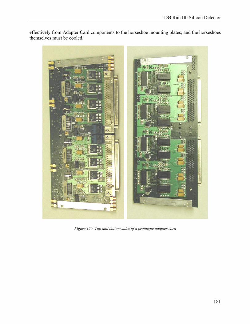
DØ Run IIb Silicon Detector
181
effectively from Adapter Card components to the horseshoe mounting plates, and the horseshoes themselves must be cooled.
Figure 126. Top and bottom sides of a prototype adapter card
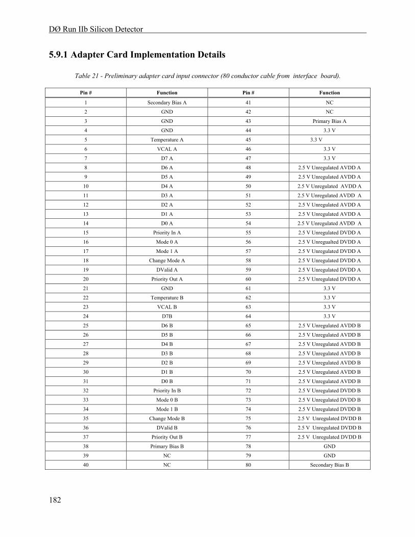
DØ Run IIb Silicon Detector
182
5.9.1 Adapter Card Implementation Details
Table 21 - Preliminary adapter card input connector (80 conductor cable from interface board).
Pin # Function Pin # Function
1 Secondary Bias A 41 NC
2 GND 42 NC
3 GND 43 Primary Bias A
4 GND 44 3.3 V
5 Temperature A 45 3.3 V
6 VCAL A 46 3.3 V
7 D7 A 47 3.3 V
8 D6 A 48 2.5 V Unregulated AVDD A
9 D5 A 49 2.5 V Unregulated AVDD A
10 D4 A 50 2.5 V Unregulated AVDD A
11 D3 A 51 2.5 V Unregulated AVDD A
12 D2 A 52 2.5 V Unregulated AVDD A
13 D1 A 53 2.5 V Unregulated AVDD A
14 D0 A 54 2.5 V Unregulated AVDD A
15 Priority In A 55 2.5 V Unregulated DVDD A
16 Mode 0 A 56 2.5 V Unregualted DVDD A
17 Mode 1 A 57 2.5 V Unregulated DVDD A
18 Change Mode A 58 2.5 V Unregulated DVDD A
19 DValid A 59 2.5 V Unregulated DVDD A
20 Priority Out A 60 2.5 V Unregulated DVDD A
21 GND 61 3.3 V
22 Temperature B 62 3.3 V
23 VCAL B 63 3.3 V
24 D7B 64 3.3 V
25 D6 B 65 2.5 V Unregulated AVDD B
26 D5 B 66 2.5 V Unregulated AVDD B
27 D4 B 67 2.5 V Unregulated AVDD B
28 D3 B 68 2.5 V Unregulated AVDD B
29 D2 B 69 2.5 V Unregulated AVDD B
30 D1 B 70 2.5 V Unregulated AVDD B
31 D0 B 71 2.5 V Unregulated AVDD B
32 Priority In B 72 2.5 V Unregulated DVDD B
33 Mode 0 B 73 2.5 V Unregulated DVDD B
34 Mode 1 B 74 2.5 V Unregulated DVDD B
35 Change Mode B 75 2.5 V Unregulated DVDD B
36 DValid B 76 2.5 V Unregulated DVDD B
37 Priority Out B 77 2.5 V Unregulated DVDD B
38 Primary Bias B 78 GND
39 NC 79 GND
40 NC 80 Secondary Bias B

DØ Run IIb Silicon Detector
183
Table 22 - Preliminary adapter card output connector pinout.
Pin # Function Pin # Function
1 Primary Bias 21 D2+
2 Secondary Bias 22 D2-
3 AVDD 23 D1+
4 GND 24 D1-
5 Sense A + 25 D0+
6 Sense A - 26 D0-
7 Temperature 27 DV+
8 Temperature Return 28 DV-
9 VCAL 29 Priority Out +
10 NC 30 Priority Out -
11 D7+ 31 Clock +
12 D7- 32 Clock -
13 D6+ 33 Mode 0
14 D6- 34 Mode 1
15 D5+ 35 Change Mode
16 D5- 36 Priority In
17 D4+ 37 Sense D +
18 D4- 38 Sense D -
19 D3+ 39 GND
20 D3- 40 DVDD
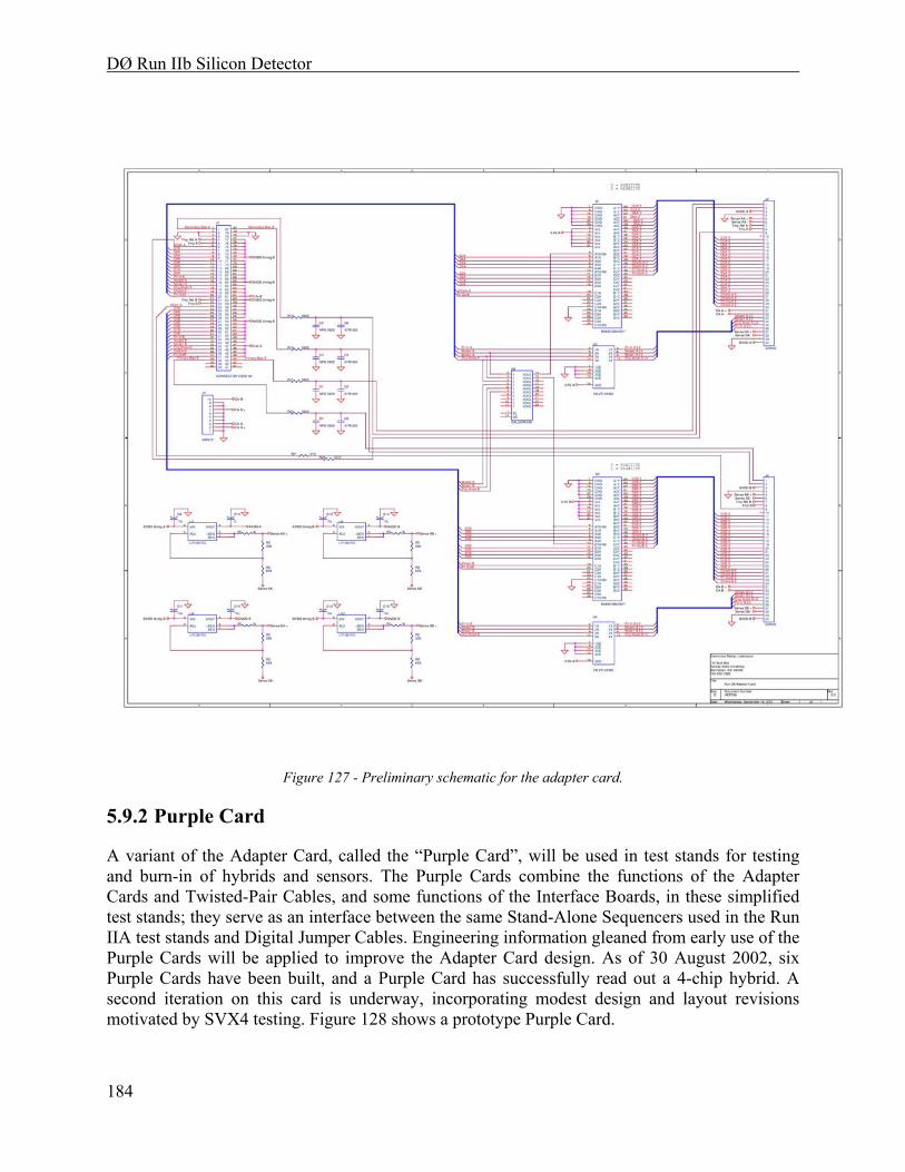
DØ Run IIb Silicon Detector
184
Figure 127 - Preliminary schematic for the adapter card.
5.9.2 Purple Card
A variant of the Adapter Card, called the “Purple Card”, will be used in test stands for testing and burn-in of hybrids and sensors. The Purple Cards combine the functions of the Adapter Cards and Twisted-Pair Cables, and some functions of the Interface Boards, in these simplified test stands; they serve as an interface between the same Stand-Alone Sequencers used in the Run IIA test stands and Digital Jumper Cables. Engineering information gleaned from early use of the Purple Cards will be applied to improve the Adapter Card design. As of 30 August 2002, six Purple Cards have been built, and a Purple Card has successfully read out a 4-chip hybrid. A second iteration on this card is underway, incorporating modest design and layout revisions motivated by SVX4 testing. Figure 128 shows a prototype Purple Card.
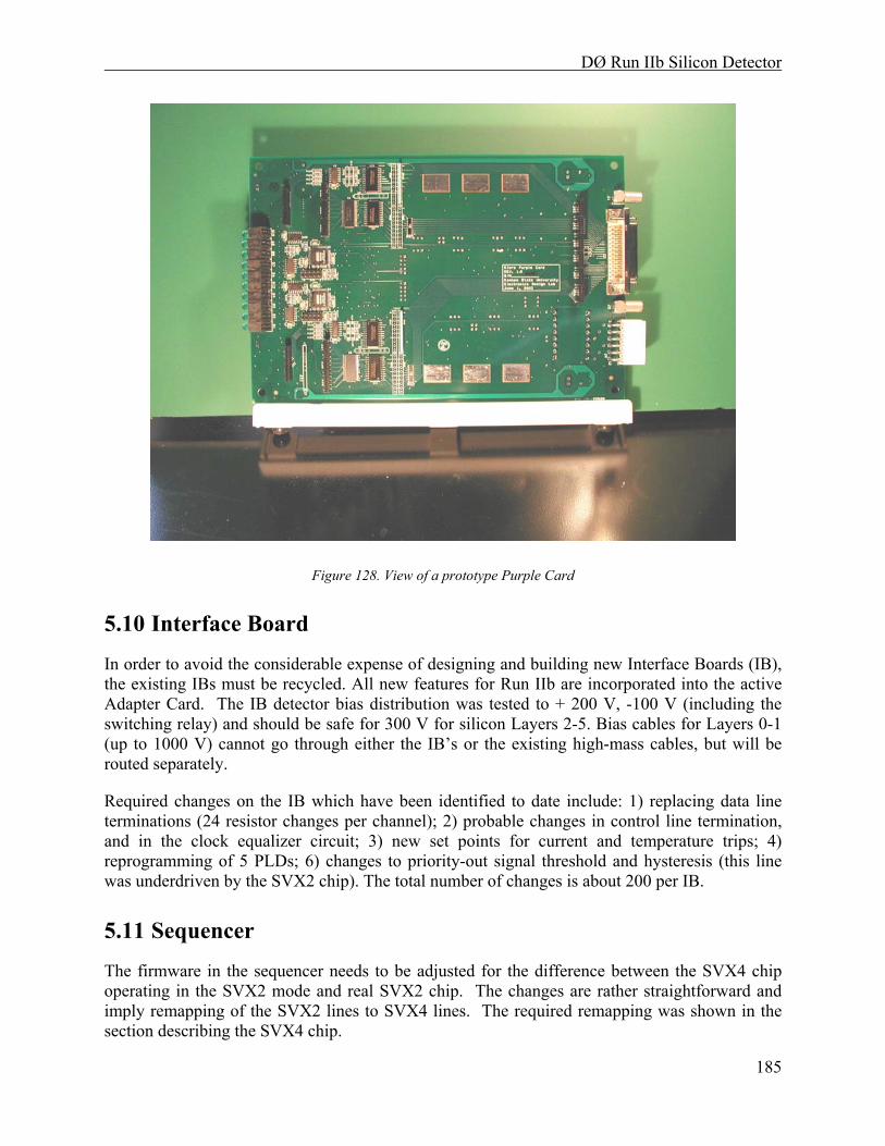
DØ Run IIb Silicon Detector
185
Figure 128. View of a prototype Purple Card
5.10 Interface Board
In order to avoid the considerable expense of designing and building new Interface Boards (IB), the existing IBs must be recycled. All new features for Run IIb are incorporated into the active Adapter Card. The IB detector bias distribution was tested to + 200 V, -100 V (including the switching relay) and should be safe for 300 V for silicon Layers 2-5. Bias cables for Layers 0-1 (up to 1000 V) cannot go through either the IB’s or the existing high-mass cables, but will be routed separately.
Required changes on the IB which have been identified to date include: 1) replacing data line terminations (24 resistor changes per channel); 2) probable changes in control line termination, and in the clock equalizer circuit; 3) new set points for current and temperature trips; 4) reprogramming of 5 PLDs; 6) changes to priority-out signal threshold and hysteresis (this line was underdriven by the SVX2 chip). The total number of changes is about 200 per IB.
5.11 Sequencer
The firmware in the sequencer needs to be adjusted for the difference between the SVX4 chip operating in the SVX2 mode and real SVX2 chip. The changes are rather straightforward and imply remapping of the SVX2 lines to SVX4 lines. The required remapping was shown in the section describing the SVX4 chip.
DØ Run IIb Silicon Detector
186
5.12 Low Voltage Distribution
Currently VICOR switching power supplies 28 are used to provide power for the SVX2 chips and Interface Boards. For Run IIb we intend to preserve those supplies and the distribution scheme through the Interface Boards.
The massive power lines from the VICOR supplies are split between different channels in the fuse panel. After the individual protection fuses, the power is distributed to the custom J1 backplane of 9U x 280 mm custom crates. The J2 and J3 backplanes of the crates provide connectors for the cable runs to the sequencers, while J1 contains connectors for low-voltage power for each Interface Board and up to eight dependent silicon hybrids, the 1553 connector and bus (used to monitor the SVX4 power and current, and hybrid temperature), and a connector to bring in 16 bias voltages and returns for eight hybrids.
We are investigating the feasibility of replacing the J1 backplane. This would have the benefit of eliminating the existing fuse panels; these panels are time-consuming to wire, and contain ~150 fuses which experience has shown to be somewhat unreliable due to oxidation of contacts. A small number of fuses would still need to be placed for safety reasons on J1 and perhaps on the IB (replacing existing ferrite beads there). Another advantage of J1 replacement is that remote sensing from the external power supplies would go to the J1 bus instead of stopping at the fuse panel. We will have more space at the backplane because a 34-pin bias connector can be replaced with a smaller one, since the new single sided detectors only need one bias voltage. The feasibility of this scheme must be established, and mechanical and electrical layouts need to be done. The Interface Board side of the backplane would be unchanged.
5.13 High Voltage Distribution
Reliable high voltage operation is crucial to ensure the increased radiation tolerance of the new Silicon Tracker. Operation at voltages up to +1000 V is specified for the Layers 0 and 1 and up to +300 V for the Layers 2 through 5.
The high voltage bias will be applied to the backplane of the single-sided silicon sensors. For 10-chip hybrids the high voltage will arrive at the hybrid on the Jumper Cable and will be routed to a side pin of the AVX connector. Two neighboring pins will be removed to ensure a safe distance to the nearest ground. The proposed scheme has been tested to operate reliably to 2 kV with a prototype jumper cable and a stuffed L1 prototype hybrid. The bias voltage will be brought to the sensor backplane with a foil wrapped around the sensor edge and glued to the backplane with a conductive silver epoxy. The foil will be insulated from the sensor edge and from the outside with a 50 micron Kapton tape. For Layer 1 the backplane connection will be provided similarly to the 10-chip hybrids while for Layer 0 the bias voltage will be fed to a line on the analog cable and then will be connected to the backplane of the sensor near the end of the cable.
28 4 kw MegaPAC AC-DC Switcher, Vicor Corporation, Andover, MA.
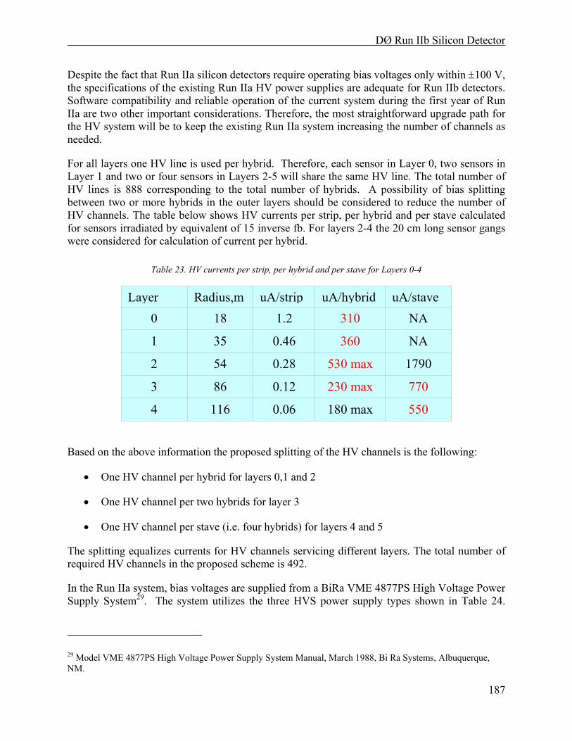
DØ Run IIb Silicon Detector
187
Despite the fact that Run IIa silicon detectors require operating bias voltages only within ±100 V, the specifications of the existing Run IIa HV power supplies are adequate for Run IIb detectors. Software compatibility and reliable operation of the current system during the first year of Run IIa are two other important considerations. Therefore, the most straightforward upgrade path for the HV system will be to keep the existing Run IIa system increasing the number of channels as needed.
For all layers one HV line is used per hybrid. Therefore, each sensor in Layer 0, two sensors in Layer 1 and two or four sensors in Layers 2-5 will share the same HV line. The total number of HV lines is 888 corresponding to the total number of hybrids. A possibility of bias splitting between two or more hybrids in the outer layers should be considered to reduce the number of HV channels. The table below shows HV currents per strip, per hybrid and per stave calculated for sensors irradiated by equivalent of 15 inverse fb. For layers 2-4 the 20 cm long sensor gangs were considered for calculation of current per hybrid.
Table 23. HV currents per strip, per hybrid and per stave for Layers 0-4
Based on the above information the proposed splitting of the HV channels is the following:
• One HV channel per hybrid for layers 0,1 and 2
• One HV channel per two hybrids for layer 3
• One HV channel per stave (i.e. four hybrids) for layers 4 and 5
The splitting equalizes currents for HV channels servicing different layers. The total number of required HV channels in the proposed scheme is 492.
In the Run IIa system, bias voltages are supplied from a BiRa VME 4877PS High Voltage Power Supply System29. The system utilizes the three HVS power supply types shown in Table 24.
29 Model VME 4877PS High Voltage Power Supply System Manual, March 1988, Bi Ra Systems, Albuquerque, NM.
770 230 max 0.12 86 3
550 180 max 0.06 116 4
1790 530 max 0.28 54 2
NA 360 0.46 35 1
NA 310 1.2 18 0 uA/stave uA/hybriduA/stripRadius,mLayer
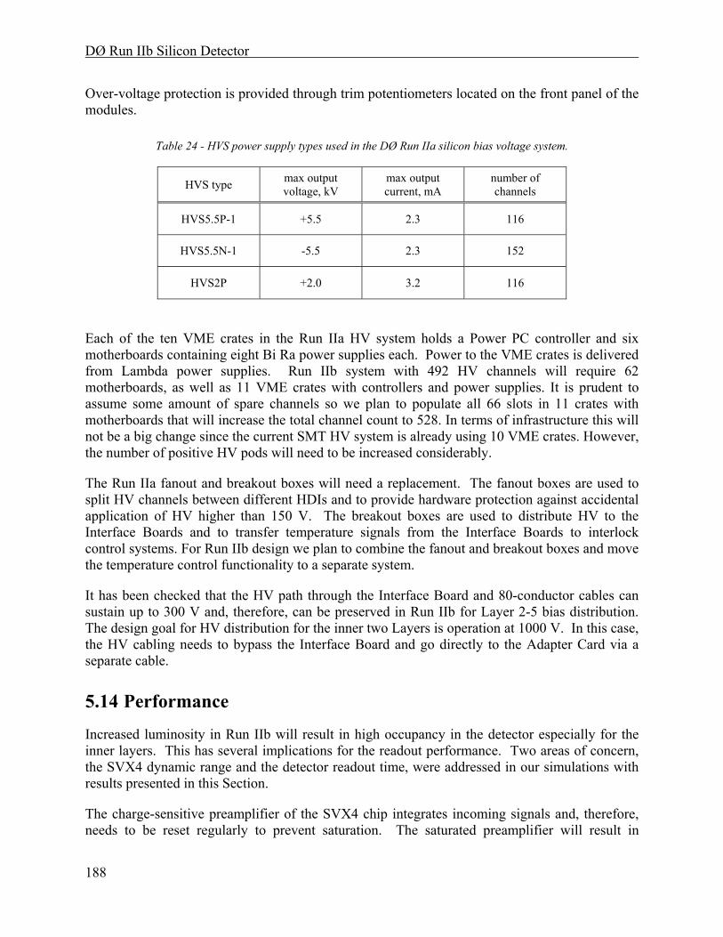
DØ Run IIb Silicon Detector
188
Over-voltage protection is provided through trim potentiometers located on the front panel of the modules.
Table 24 - HVS power supply types used in the DØ Run IIa silicon bias voltage system.
HVS type max output voltage, kV
max output current, mA
number of channels
HVS5.5P-1 +5.5 2.3 116
HVS5.5N-1 -5.5 2.3 152
HVS2P +2.0 3.2 116
Each of the ten VME crates in the Run IIa HV system holds a Power PC controller and six motherboards containing eight Bi Ra power supplies each. Power to the VME crates is delivered from Lambda power supplies. Run IIb system with 492 HV channels will require 62 motherboards, as well as 11 VME crates with controllers and power supplies. It is prudent to assume some amount of spare channels so we plan to populate all 66 slots in 11 crates with motherboards that will increase the total channel count to 528. In terms of infrastructure this will not be a big change since the current SMT HV system is already using 10 VME crates. However, the number of positive HV pods will need to be increased considerably.
The Run IIa fanout and breakout boxes will need a replacement. The fanout boxes are used to split HV channels between different HDIs and to provide hardware protection against accidental application of HV higher than 150 V. The breakout boxes are used to distribute HV to the Interface Boards and to transfer temperature signals from the Interface Boards to interlock control systems. For Run IIb design we plan to combine the fanout and breakout boxes and move the temperature control functionality to a separate system.
It has been checked that the HV path through the Interface Board and 80-conductor cables can sustain up to 300 V and, therefore, can be preserved in Run IIb for Layer 2-5 bias distribution. The design goal for HV distribution for the inner two Layers is operation at 1000 V. In this case, the HV cabling needs to bypass the Interface Board and go directly to the Adapter Card via a separate cable.
5.14 Performance
Increased luminosity in Run IIb will result in high occupancy in the detector especially for the inner layers. This has several implications for the readout performance. Two areas of concern, the SVX4 dynamic range and the detector readout time, were addressed in our simulations with results presented in this Section.
The charge-sensitive preamplifier of the SVX4 chip integrates incoming signals and, therefore, needs to be reset regularly to prevent saturation. The saturated preamplifier will result in
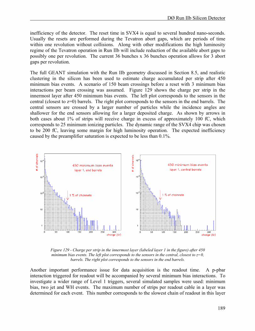
DØ Run IIb Silicon Detector
189
inefficiency of the detector. The reset time in SVX4 is equal to several hundred nano-seconds. Usually the resets are performed during the Tevatron abort gaps, which are periods of time within one revolution without collisions. Along with other modifications the high luminosity regime of the Tevatron operation in Run IIb will include reduction of the available abort gaps to possibly one per revolution. The current 36 bunches x 36 bunches operation allows for 3 abort gaps per revolution.
The full GEANT simulation with the Run IIb geometry discussed in Section 8.5, and realistic clustering in the silicon has been used to estimate charge accumulated per strip after 450 minimum bias events. A scenario of 150 beam crossings before a reset with 3 minimum bias interactions per beam crossing was assumed. Figure 129 shows the charge per strip in the innermost layer after 450 minimum bias events. The left plot corresponds to the sensors in the central (closest to z=0) barrels. The right plot corresponds to the sensors in the end barrels. The central sensors are crossed by a larger number of particles while the incidence angles are shallower for the end sensors allowing for a larger deposited charge. As shown by arrows in both cases about 1% of strips will receive charge in excess of approximately 100 fC, which corresponds to 25 minimum ionizing particles. The dynamic range of the SVX4 chip was chosen to be 200 fC, leaving some margin for high luminosity operation. The expected inefficiency caused by the preamplifier saturation is expected to be less than 0.1%.
Figure 129 - Charge per strip in the innermost layer (labeled layer 1 in the figure) after 450 minimum bias events. The left plot corresponds to the sensors in the central, closest to z=0,
barrels. The right plot corresponds to the sensors in the end barrels.
Another important performance issue for data acquisition is the readout time. A p-pbar interaction triggered for readout will be accompanied by several minimum bias interactions. To investigate a wider range of Level 1 triggers, several simulated samples were used: minimum bias, two jet and WH events. The maximum number of strips per readout cable in a layer was determined for each event. This number corresponds to the slowest chain of readout in this layer

DØ Run IIb Silicon Detector
190
and is relevant to estimate the readout time for the detector and the associated dead time. The number of hit strips has been scaled by appropriate factors to account for the closest neighbors that normally are also included in the sparse mode readout. The factors were determined from the cluster size distributions and were typically around 1.7 for the cases without noise and 2.8 for the cases with noise. Figure 130 shows the maximum number of strips per readout cable as a function of radius for minimum bias events (left plot) and QCD two jet events (right plot). Each layer corresponds to two points in those plots from different sublayers. Four different cases were considered: without noise for the two thresholds of 4 and 5 ADC counts, and with noise (rms 2.1 ADC counts) for the same thresholds. The average simulated signal was equal to 20 ADC counts corresponding to a S/N ratio of 9.5. Figure 131 shows the maximum number of strips per readout cable as a function of radius for WH + 0 minimum bias events (left plot) and WH + six minimum bias events (right plot).
Comparison of the inner three layers with the highest rates suggests that Layer 1 with 6 chips in the readout chain and Layer 2 with 10 chips will operate in similar conditions for all types of events. Layer 0 with 2 chips in the readout chain has rates a factor of 2 lower. However, this layer will experience the worst radiation damage and, as a result, a lower S/N. The effect of the noise on occupancy depends on the threshold. For the threshold over noise ratio equal to 2.4 the deterioration of S/N from 9.5 to 8 increases the maximum number of readout strips by 40% in Layer 0, by 50% in Layer 1 and by 75% in Layer 2, all for two jet events. The largest increase is observed in the 10-chip readout chain of Layer 2 due to the simple fact that the number of noisy strips is proportional to the number of chips. A lower S/N ratio in the innermost layer 0 can easily increase the number of readout strips by a factor of two and make its rate comparable to the Layers 1 and 2. As a result of these simulations, we feel it is prudent to daisy-chain only two chips in Layer 0 and leave a safety margin to accommodate higher noise occupancy in this layer after irradiation.
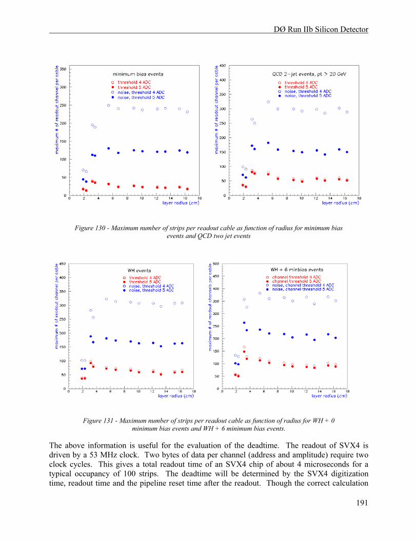
DØ Run IIb Silicon Detector
191
Figure 130 - Maximum number of strips per readout cable as function of radius for minimum bias events and QCD two jet events
Figure 131 - Maximum number of strips per readout cable as function of radius for WH + 0 minimum bias events and WH + 6 minimum bias events.
The above information is useful for the evaluation of the deadtime. The readout of SVX4 is driven by a 53 MHz clock. Two bytes of data per channel (address and amplitude) require two clock cycles. This gives a total readout time of an SVX4 chip of about 4 microseconds for a typical occupancy of 100 strips. The deadtime will be determined by the SVX4 digitization time, readout time and the pipeline reset time after the readout. Though the correct calculation

DØ Run IIb Silicon Detector
192
should combine information from all silicon layers and all levels of the DØ trigger in a queue analysis, essentially one buffer structure of the DØ data acquisition makes a simple rough estimate possible. The total deadtime can be estimated as
3 (digitization) + 4 (readout) + 4.2 (pipeline reset) = 11.2 microseconds
At 10 kHz Level2 trigger input rate, corresponding to 100 microseconds between Level_1_Accept signals, the deadtime will be equal to approximately 11.2%. The deadtime and the readout time are acceptable for the DØ data acquisition system and in particular for the Silicon Track Trigger at Level 2.
5.15 Carbon Fiber Grounding Studies
A significant concern in the electronic and mechanical design of the detector is the proper grounding of carbon fiber elements. Highly conductive carbon fiber will be used for the cooling tubes and mechanical support structures. These carbon fiber elements have the potential to exhibit strong capacitive coupling to the sensors The experience of CDF in Run IIa with L00 cooling tubes has shown that sensor coupling to nearby floating metal can be a very troublesome source of noise. It is imperative that all carbon fiber in the detector is effectively shorted to the hybrid (L1-L5) or bias filter (L0) grounds to prevent capacitive noise transmission to the sensor readout.
The first test on the carbon fiber was to verify its conductivity through capacitive coupling. Two identically sized plate capacitors were constructed: the first with one copper plate and one type K139 carbon fiber plate, the second with two copper plates. Both capacitors were measured to be 132±2 pF. Additionally, each capacitor was individually connected in series to a network analyzer to produce a high-pass filter. The transfer functions and break frequencies for the two capacitors were identical. Therefore, the conductivity of the K139 carbon fiber is high enough to make it virtually indistinguishable from copper in terms of capacitive noise transmission. Furthermore, K139 is the carbon fiber type that will be used in L2-L5. K13C, which is more conductive than K139, will be used in L0-L1where the proximity of sensors to carbon fiber is much greater.
Because the grounding concerns are most acute in L0, a test was conducted to determine the feasibility of shorting a prototype L0 K13C carbon fiber cylinder to a hybrid or filter ground plane. The test configuration is shown in Figure 132. The interior of the castellated L0 cylinder was driven with the source power from the network analyzer. A sensor/filter mockup constructed of aluminum and Kapton layers was mounted on the cylinder with the network analyzer input wired to the sensor aluminum layer, and both the source and input grounds wired to the filter plane. Transfer functions to the sensor were measured with different configurations for shorting the carbon fiber to the filter plane. One to four 1/8” wide strips of 1 µm thick aluminized Mylar, 0.5 mil aluminum, or copper tape were attached across the filter and carbon fiber. The effectiveness of the grounding strips was tested with and without additional cooper tape coupling to the carbon fiber. The aluminized Mylar strips were minimally effective in reducing power to the sensor. Aluminum and copper strips performed equally well. The power
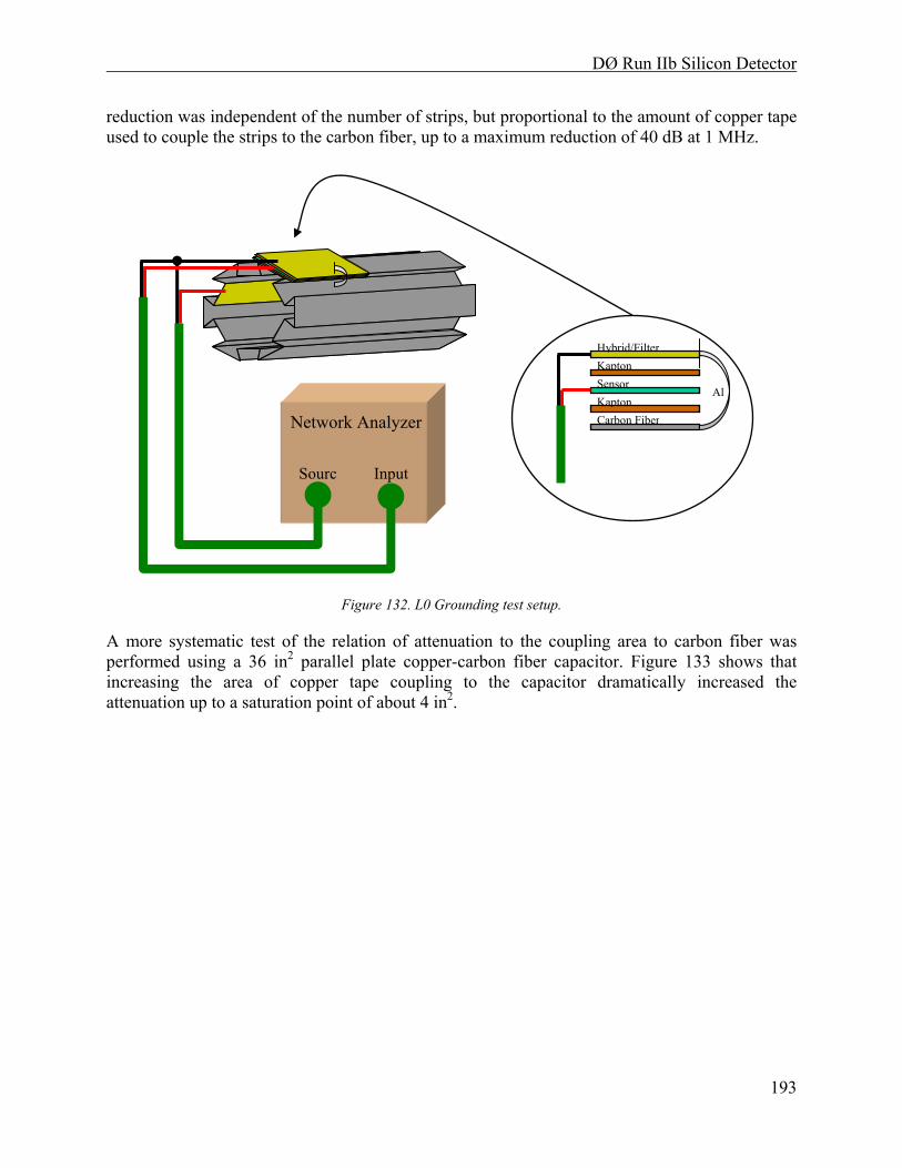
DØ Run IIb Silicon Detector
193
reduction was independent of the number of strips, but proportional to the amount of copper tape used to couple the strips to the carbon fiber, up to a maximum reduction of 40 dB at 1 MHz.
Figure 132. L0 Grounding test setup.
A more systematic test of the relation of attenuation to the coupling area to carbon fiber was performed using a 36 in2 parallel plate copper-carbon fiber capacitor. Figure 133 shows that increasing the area of copper tape coupling to the capacitor dramatically increased the attenuation up to a saturation point of about 4 in2.
Network Analyzer
Sourc Input
Hybrid/Filter Kapton
KaptonSensor
Carbon Fiber
Al
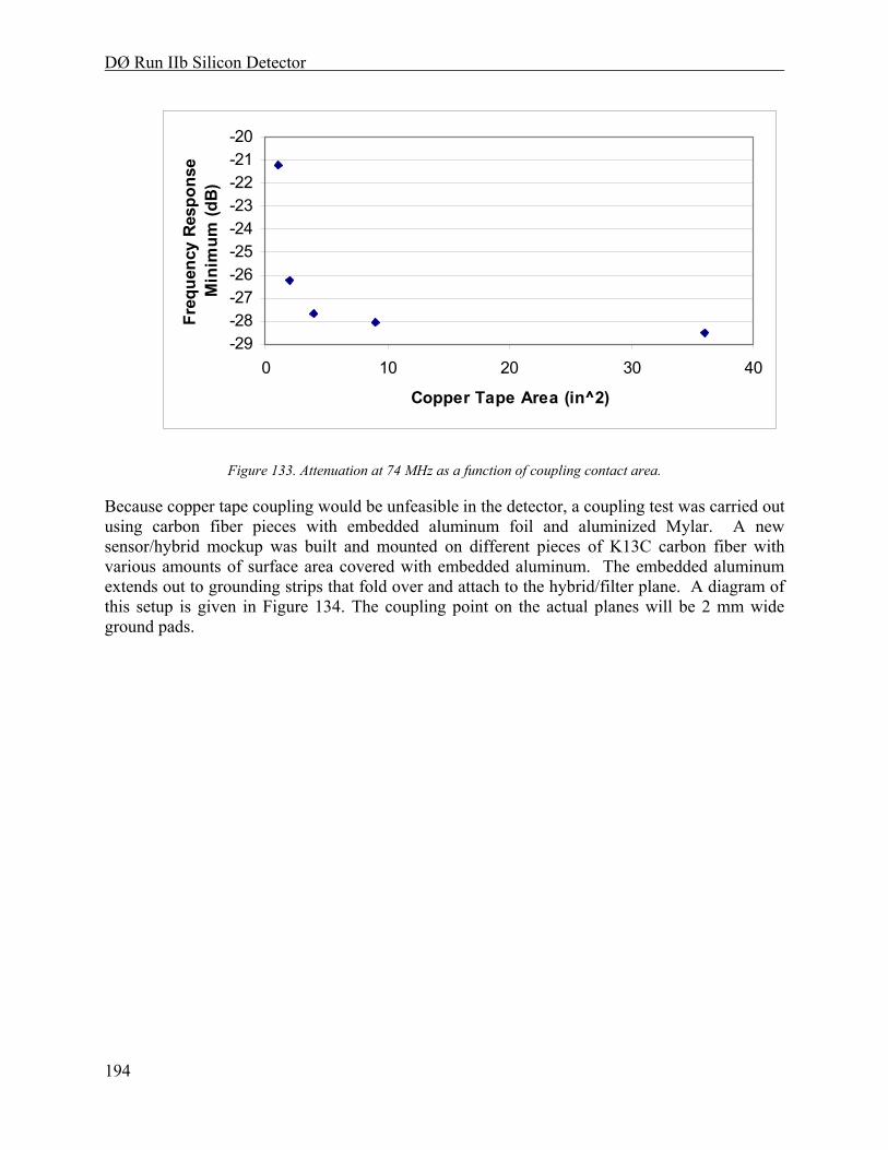
DØ Run IIb Silicon Detector
194
-29-28-27-26-25-24-23-22-21-20
0 10 20 30 40
Copper Tape Area (in^2)
Freq
uenc
y Re
spon
se
Min
imum
(dB)
Figure 133. Attenuation at 74 MHz as a function of coupling contact area.
Because copper tape coupling would be unfeasible in the detector, a coupling test was carried out using carbon fiber pieces with embedded aluminum foil and aluminized Mylar. A new sensor/hybrid mockup was built and mounted on different pieces of K13C carbon fiber with various amounts of surface area covered with embedded aluminum. The embedded aluminum extends out to grounding strips that fold over and attach to the hybrid/filter plane. A diagram of this setup is given in Figure 134. The coupling point on the actual planes will be 2 mm wide ground pads.
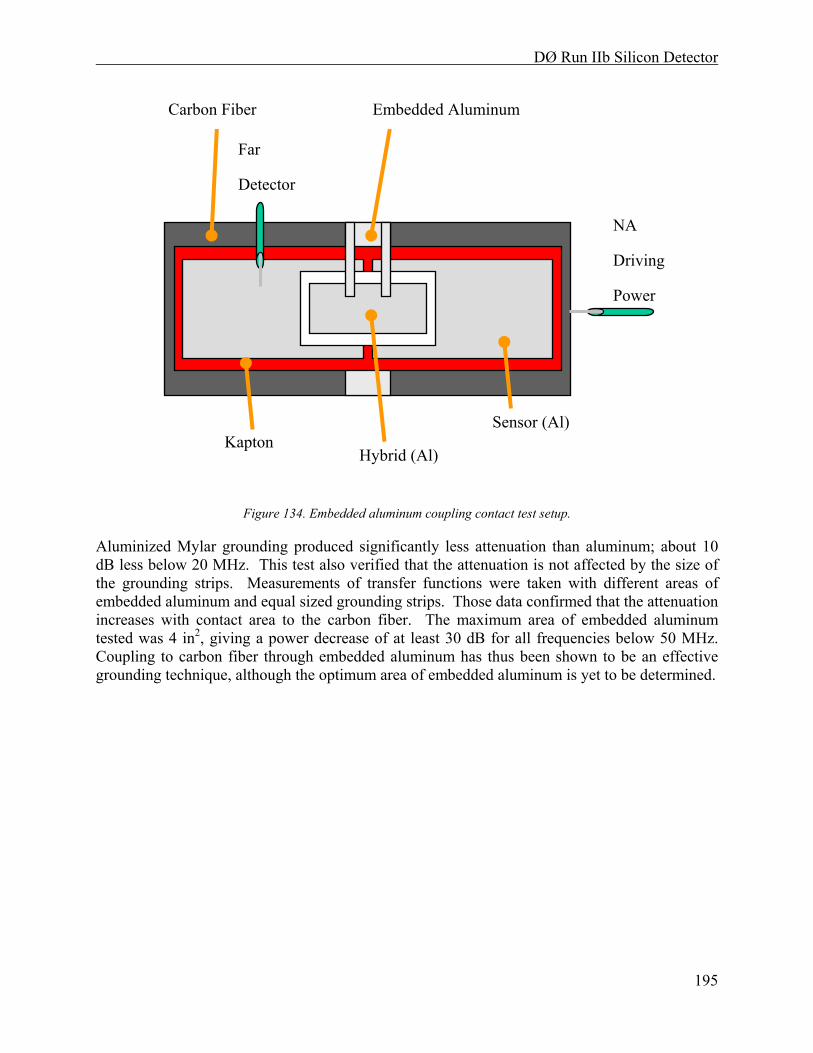
DØ Run IIb Silicon Detector
195
Figure 134. Embedded aluminum coupling contact test setup.
Aluminized Mylar grounding produced significantly less attenuation than aluminum; about 10 dB less below 20 MHz. This test also verified that the attenuation is not affected by the size of the grounding strips. Measurements of transfer functions were taken with different areas of embedded aluminum and equal sized grounding strips. Those data confirmed that the attenuation increases with contact area to the carbon fiber. The maximum area of embedded aluminum tested was 4 in2, giving a power decrease of at least 30 dB for all frequencies below 50 MHz. Coupling to carbon fiber through embedded aluminum has thus been shown to be an effective grounding technique, although the optimum area of embedded aluminum is yet to be determined.
Hybrid (Al)
Carbon Fiber Embedded Aluminum
Kapton Sensor (Al)
NA
Driving
Power
Far
Detector

DØ Run IIb Silicon Detector
196
6 PRODUCTION AND TESTING
6.1 Overview
This section describes the full chain of testing of the individual components needed to build silicon readout modules and the assembly of the components into modules and staves. The building and testing sequence is described, starting from individual components, resulting in fully certified staves. It relies on the successful production and testing effort DØ organized during the construction of the Run IIa Silicon Microstrip Tracker.
The essential building blocks of a detector module are the silicon sensors, the SVX4 readout chips, and the readout hybrids. Each component is tested as described below before it is assembled into a module. After the assembly the modules are tested again before they are mounted on staves. A detailed description of the stave assembly and installation is included in Section 4.4. Testing of staves and of the full readout system are also included below.
The basic production and testing sequence is the following:
1. SVX4 chips are tested as described in Section 5
2. Bare hybrids are tested for continuity and shorts by the manufacturer
3. 100% (5-10%) of bare preproduction (production) hybrids are re-tested
4. SVX4 chips and passive components are surface mounted on the hybrids
5. Fully assembled hybrids undergo an initial functionality test
6. Hybrids that pass the functionality test are burned-in at Fermilab
7. Sensors are produced and tested at the manufacturer
8. 100% (5-10%) of the preproduction (production) sensors are re-tested
9. Sensors and burned-in hybrids are assembled into a detector module.
10. Detector modules undergo initial functionality test at Fermilab
11. Detector modules that pass the functionality test are burned-in at Fermilab
12. 5-10% of burned-in detector modules are subject to more detailed QA tests
13. Burned-in modules are assembled into staves (L2-L5) or mounted on support structure (L0-L1)
14. Up to 6 detector modules are read out simultaneously
Each of the steps in the testing procedure is described in detail below.
DØ Run IIb Silicon Detector
197
6.2 Sensor tests
To ensure high quality of the silicon sensors, DØ plans a series of quality assurance (QA) tests to be performed by the supplier and by DØ. The complete description of the silicon sensor QA program, including detailed instructions, procedures, implementation rules and responsibilities can be found in30. A summary of these activities is included in this section.
Quality assurance will be a collaborative effort and is shared among different institutions. The institutions participating in the QA program provide for silicon sensor testing centers, where the quality checks of the QA program will be carried out in a consistent manner. Fermilab serves as a central distribution and control center with dedicated testing and coordinating tasks. Fermilab and two additional remote sites are available as backup locations to perform the standard QA testing of sensors if needed. Figure 135 shows a graphical representation of the QA program with the silicon sensor flow during production.
30 See http://d0server1.fnal.gov/projects/run2b/Silicon/www/smt2b/Testing/testing.html under Sensor Quality Assurance Procedure
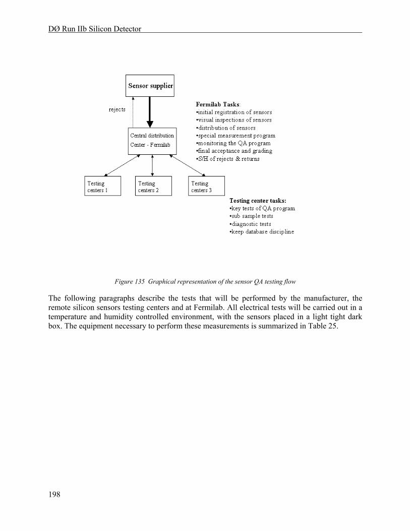
DØ Run IIb Silicon Detector
198
Figure 135 Graphical representation of the sensor QA testing flow
The following paragraphs describe the tests that will be performed by the manufacturer, the remote silicon sensors testing centers and at Fermilab. All electrical tests will be carried out in a temperature and humidity controlled environment, with the sensors placed in a light tight dark box. The equipment necessary to perform these measurements is summarized in Table 25.

DØ Run IIb Silicon Detector
199
Table 25- Sensor Probing equipment
Dark Box Mechanical Shop
Keithley 237 Keithley Instruments
Rack Mounting kit Keithley Instruments
HP LCR 4284A Agilent
Cable option Agilent
Test Leads Agilent
Isolation Vibration Table Kinetic Systems 1201-05-11
Probe Station Alessi Rel – 6100, Cascade microtech
Guard Box self made
Storage
The following tasks will take place at Fermilab:
• Initial registration of sensors
• Visual inspection
• Distribution of sensors to remote testing centers
• Sensor characterizations on sub-samples, as described in this document
• Shipping and handling of the rejects which are returned to the supplier
• Overall monitoring of the QA program
• Final acceptance and grading of sensors
We expect the manufacturer to perform the following tests:
1) Tests on each sensor
a) Leakage current as a function of reverse bias up to 800 V at room temperature (T = 21 ± 1°C) and relative humidity (RH) < 50%
b) Optical inspection for defects, opens, shorts and mask alignment (better than 2.5 µm)

DØ Run IIb Silicon Detector
200
c) Depletion voltage measurement either by measurement of the capacitance between back-plane and the bias ring at 1 kHz frequency as a function of reverse bias, or by similar measurement performed on a test diode produced on the corresponding wafer.
2) Tests on each strip
a) Capacitance value measurement and pinhole determination
b) Leakage current at Full Depletion Voltage (FDV) and Room Temperature (RT)
c) The total number of not working channels must not exceed 1%. Non-working channels are defined as:
i) Pinholes – current through capacitor >10 nA at 80 V and RT
ii) Short – coupling capacitor >1.2 times the typical value
iii) Open – coupling capacitor <0.8 times the typical value
iv) Leakage current above 10 nA/strip at FDV and RT
v) Strips with bias and interstrip resistance values out of our specifications
3) Tests on test structure
a) Poly-resistor value
b) Sheet and implant resistivity
c) Coupling capacitor breakdown voltage
The corresponding quality control data of the tests performed by the supplier will be provided together with each sensor on paper or in a computer readable format agreed upon by both parties. The silicon distribution and control center will initially qualify the sensors according to the test results of the supplier. So-called key sensor tests of the QA program will be carried out independently on every delivered sensor for verification at the testing centers. Additional QA measurements will be performed on a sub-sample of the delivered sensors as described below. Based upon the results of these measurements, the silicon distribution and control center has the ability to reject a sensor within 6 months after delivery. The manufacturer will be notified and upon request the sensors will be returned for re-measurements. Both parties – the supplier and the silicon control center together with the Run IIb silicon sensor coordinators - can agree upon the acceptance of individual sensors if specifications are missed only marginally.
The QA program for silicon sensors will be performed at Fermilab and remote sensor testing centers. It consists of four main parts:
1) key tests are performed on every received sensor. The measurements/procedures belonging to this QA part are the most important ones to effectively determine the basic sensor parameters. They include

DØ Run IIb Silicon Detector
201
a) Initial registration of the sensor in the database
b) Visual inspection
c) I-V measurement
d) C-V measurement
2) subset tests are conducted on a certain fraction of delivered sensors only. The main goal of the subset tests is to verify the specifications more in detail. The fraction of sensors subject to these tests will be different for prototype or production type sensors, as follows:
a) During prototype phase the subset sample will consist of a minimum of 80% of all delivered prototypes
b) During pre- or pilot-production phase the subset sample will consist of 50% of all delivered sensors
c) During production phase the subset sample will consist of 25% of all delivered sensors. As production progresses, we expect to reduce the rate to10% of all delivered sensors, if the measurements are consistent with those performed by the manufacturer and stable over the time.
d) The sensor subset tests consist of the following measurements:
i) Leakage current stability I(t)
ii) Full Strip Test (AC scan)
iii) Strip leakage current test (DC-scan)
3) The diagnostic tests will be performed on random sensor samples as well as on sensors with observed irregularities in the key or subset sensor tests. The diagnostic tests measure in much more detail complex electrical parameters in order to get a deeper insight into the sensor qualities and to monitor the production process. The diagnostic tests will be routinely performed on 10-15% of the delivered sensors per batch with a minimum of 1-2 sensors/batch. The diagnostic tests consist of the following measurements:
a) Polysilicon resistor measurements
b) Strip and interstrip capacitance
c) Metal series resistance
d) Implant sheet resistance
e) Flat band voltage measurements on MOS test structure (if available)

DØ Run IIb Silicon Detector
202
f) Interstrip resistance
g) Coupling capacitor and coupling capacitor breakdown value on test structure
4) The mechanical test measurements are introduced to verify the mechanical tolerances on the wafers. They will be routinely performed on 25% of the delivered sensors per batch. Tests will check for
a) Sensor thickness
b) Sensor warp
c) Sensor cut dimensions and cutting accuracy
Only sensors that meet all the qualification criteria will be used to build modules.
6.3 Hybrid assembly and initial tests
There will be 4 different hybrid types used in the Run IIb silicon detector: those for use in Layer 0 (L0), those mounted on the silicon sensors in Layer 1 (L1), those mounted on the axial silicon sensors for Layers 2-5 (L2A), and those mounted on the stereo sensors for Layers 2-5 (L2S). The hybrids consist of several elements, which are assembled to form the final readout unit. The beryllia ceramic substrate contains a multi-layer printed circuit. Passive components are mounted on the hybrid, as well as the custom SVX4 readout chip. An AVX connector allows a jumper cable to be attached to the hybrid which carries the digital signals to the downstream data acquisition system. Approximately 1200 production hybrids will need to be assembled and tested with a breakdown as given in Table 26.
Table 26 Parameters for hybrids for the silicon detector
Hybrid Type # chips/hybrid # hybrids needed
# spares ordered
Total # of hybrids
L0 2 144 46 190
L1 6 72 28 100
L2A 10 336 104 440
L2S 10 336 104 440
TOTAL 888 282 1170
The hybrid is to be constructed of alternating thick film layers of gold and dielectric built up onto a beryllia substrate. There are six conductor layers and five dielectric layers on the top side of
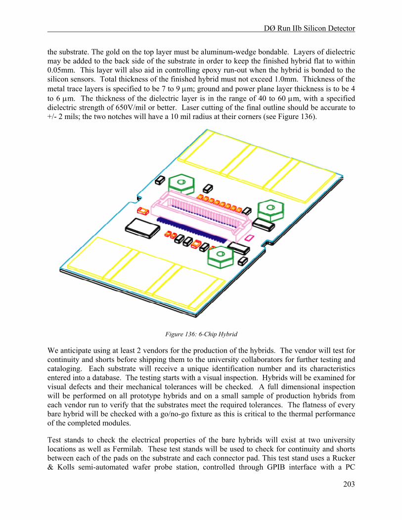
DØ Run IIb Silicon Detector
203
the substrate. The gold on the top layer must be aluminum-wedge bondable. Layers of dielectric may be added to the back side of the substrate in order to keep the finished hybrid flat to within 0.05mm. This layer will also aid in controlling epoxy run-out when the hybrid is bonded to the silicon sensors. Total thickness of the finished hybrid must not exceed 1.0mm. Thickness of the metal trace layers is specified to be 7 to 9 µm; ground and power plane layer thickness is to be 4 to 6 µm. The thickness of the dielectric layer is in the range of 40 to 60 µm, with a specified dielectric strength of 650V/mil or better. Laser cutting of the final outline should be accurate to +/- 2 mils; the two notches will have a 10 mil radius at their corners (see Figure 136).
Figure 136: 6-Chip Hybrid
We anticipate using at least 2 vendors for the production of the hybrids. The vendor will test for continuity and shorts before shipping them to the university collaborators for further testing and cataloging. Each substrate will receive a unique identification number and its characteristics entered into a database. The testing starts with a visual inspection. Hybrids will be examined for visual defects and their mechanical tolerances will be checked. A full dimensional inspection will be performed on all prototype hybrids and on a small sample of production hybrids from each vendor run to verify that the substrates meet the required tolerances. The flatness of every bare hybrid will be checked with a go/no-go fixture as this is critical to the thermal performance of the completed modules.
Test stands to check the electrical properties of the bare hybrids will exist at two university locations as well as Fermilab. These test stands will be used to check for continuity and shorts between each of the pads on the substrate and each connector pad. This test stand uses a Rucker & Kolls semi-automated wafer probe station, controlled through GPIB interface with a PC

DØ Run IIb Silicon Detector
204
running LabView. Given a coordinate map of the hybrid circuit, the probe station stage positions each pad under a probe tip, connection is made through a GPIB multiplexing box, and a GPIB controlled multimeter checks for continuity or shorts between the appropriate connector point and the probe.
This testing procedure was tuned for use for the hybrids in the Run IIa SMT detector. The yield of good, bare flexible hybrids used in Run IIa, varied significantly between vendors and between various production batches and ranged from 30% to 100%. For Run IIa it was therefore necessary to test every single bare hybrid. We will have the capability to probe every single ceramic hybrid for Run IIb, but expect that we will only need to spot check around 5-10% of the hybrids before they are sent for stuffing and wirebonding.
6.4 Test stand hardware
Essentially the same type of test stands will be used for all the electrical tests performed on the readout hybrids and the detector modules. These test stands are based on the Stand Alone Sequencer Board (SASeq), which was developed at Fermilab. These SASeq based test stands were successfully used in Run IIa. They are developed independently from the full DØ readout system, and are relatively cheap which allows us to replicate them in large quantities and distribute them at various locations at Fermilab and at remote institutions. The two-channel SASeq board is a self-contained data acquisition card designed to interface to the SVX chips. Its basic function is to control the SVX chip for data acquisition, collect the SVX data when a data cycle is requested, and to relay the data to the processor in the crate. To achieve the planned rate of testing we plan to set up 4 different types of SASeq based test stations:
1. Two hybrid burn-in stations (16 channels each) for burn-in of hybrids
2. Two module burn-in stations (32 channels each) for burn-in of detector modules
3. Eleven 2-Saseq stations (one channel each) for fast functionality test, debugging of modules and QA tests, with 6 stations at Fermilab and 5 at remote institutions;
4. Two 3-Saseq stations (6 channels each) for simultaneous read out of up to 6 modules during assembly of staves and stave mounting in the final support structure
Each Module burn-in station consists of two Cooling Racks and a VME Rack between them. Each Hybrid burn-in station consists of a Shelve Rack and a VME Rack. We plan to reutilize the two racks that were used in Run IIa as Shelve Racks with small changes concerning the electrical parts.
The base hardware unit for the burn-in stations is shown in Figure 137. The Burn-in Crate configuration for module burn-in is shown in Figure 138. It consists of a VME crate that contains a Bit-3 VME controller card, sixteen SASeqs, a scanning 12-bit 64 channel analog-to-digital converter board (VMIVME-3113A) for temperature measurement, and a master vertical interconnect board for high voltage crate control. High voltage supply sources are located in a separate VME crate.

DØ Run IIb Silicon Detector
205
The HV VME crate for the burn-in stations contains four VME 4877PS Motherboards and a slave vertical interconnect board for high voltage crate control. Every Motherboard carries eight HV pods. Thus, the HV crate provides 32 independent voltages for silicon detector biasing and supports monitoring of the detector currents. The 4877PS Motherboard allows the voltage to be set from 0 to 5000 V, with a maximum current of 2mA per channel. To ensure the safe operation of the burn-in stations, the over-voltage hardware protection of the HV supply will be set to 300V.
The interface between the hybrids and the SASeq is provided in Run IIb by a circuit board dubbed the Purple Card. It is the functional analogue of the Interface Card and Connector Adapter Module used in Run IIa. The Purple Card is located close to the device under test inside the Cooling Rack. Every Purple Card has two independent channels and is used as a bi-directional interconnect between the SASeq and the Hybrid through the Digital Jumper Cable (DJC). The board contains the logic to control the power of the SVX chip as well as the HV. The board also prepares the data for the temperature measurement. All low voltages are fused on the Purple Card. The Card is equipped with test points and LED’s to monitor the functionality and provide diagnostic capabilities if they require servicing.
Each SASeq is connected to a Purple Card by a 10 foot long 50-conductor cable with impedance of 82 Ohms. Three low voltage power supplies are used to supply the two operating voltages (AVDD, DVDD) needed by the SVX chips and to supply the voltage to power the Purple Card. Low Voltage Distribution wire Buses are located on the side of each Cooling Rack or Shelve Rack and are used for the distribution of the SVX power and the Purple Card power for each of the sixteen Cards.
The Hybrid burn-in station and the Module burn-in station only differ in two aspects, which are the High Voltage crate and the cooling system. The Module burn-in stations need a separate VME crate to house the high voltage modules to bias the detectors, which is not needed for the Hybrid burn-in stations. For the one-SASeq and three-SASeq test stations the HV module is located in the same VME crate as the SASeq. The second aspect in which they differ is the cooling. The Module burn-in stations are outfitted with a cooling system to operate the detectors at low temperature. Up to 16 detectors are placed on 8 shelves inside a Cooling Rack that is thermally isolated. The chiller temperature is set to 5C, and the detectors will run at temperatures between 10C and 15C, depending on the number of chips on the HDI and on the water flow rate. Each detector module is placed on a custom made, 17 x 3.5 inch aluminum Cooling Plate Figure 139, designed to accept any kind of Module. Every Cooling Plate is equipped with a pipe for cooling water and special holes to provide nitrogen flow through the storage box that encloses the device under test. Two Cooling Plates together with the Purple Card and signal cables are placed on plywood board. This board, called the Slider Plate, is equipped with sliders to simplify loading and unloading of the devices under test (Figure 140). Plywood is chosen because it is a cheap, thermally non-conductive material that helps minimize possible risk of condensation on surfaces inside the Cooling Rack. Every Slider Plate has its own water and nitrogen pipe.
A control panel attached to the rack side provides control of the water and gas flow. One chiller supplies two control panels. A software based interlock system monitors the temperature on each device and shuts off the power in the event the temperature exceeds 50C, to avoid melting of the epoxy used in detector assembly.
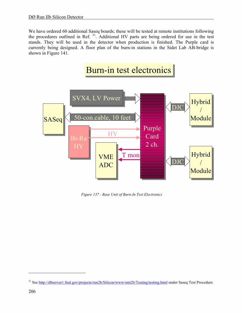
DØ Run IIb Silicon Detector
206
We have ordered 60 additional Saseq boards; these will be tested at remote institutions following the procedures outlined in Ref. 31. Additional HV parts are being ordered for use in the test stands. They will be used in the detector when production is finished. The Purple card is currently being designed. A floor plan of the burn-in stations in the Sidet Lab AB-bridge is shown in Figure 141.
SASeq SASeq
Bi-Ra
HV
Bi-Ra
HV
VMEADC
VMEADC
SVX4, LV PowerSVX4, LV Power
PurpleCard2 ch.
PurpleCard2 ch.
Hybrid/
Module
Hybrid/
Module
Hybrid/
Module
Hybrid/
Module
DJC
DJC
50-con.cable, 10 feet
HV
T mon
Burn-in test electronics Burn-in test electronics
Figure 137 - Base Unit of Burn-In Test Electronics
31 See http://d0server1.fnal.gov/projects/run2b/Silicon/www/smt2b/Testing/testing.html under Saseq Test Procedure

DØ Run IIb Silicon Detector
207
Bit-
3V
ertic
al in
terc
onne
ctSA
SEQ
#1
SASE
Q #
16V
MIV
ME-
3113
A
POW
ER
SASE
Q #
2SA
SEQ
#3
SASE
Q #
4SA
SEQ
#5
SASE
Q #
6SA
SEQ
#7
SASE
Q #
8SA
SEQ
#9
SASE
Q #
10SA
SEQ
#11
SASE
Q #
12SA
SEQ
#13
SASE
Q #
14SA
SEQ
#15
1 2 3 4 5 6 217 8 9 10 11 12 13 14 15 16 17 18 19 20
Ver
tical
inte
rcon
nect
1 2 3 4 5 6 217 8 9 10 11 12 13 14 15 16 17 18 19 20
Bi Ra#1 Bi Ra#2 Bi Ra#3 Bi Ra#4
HV VME CRATE
SASEQ VME CRATE
Figure 138 - Burn-in Test Crates.
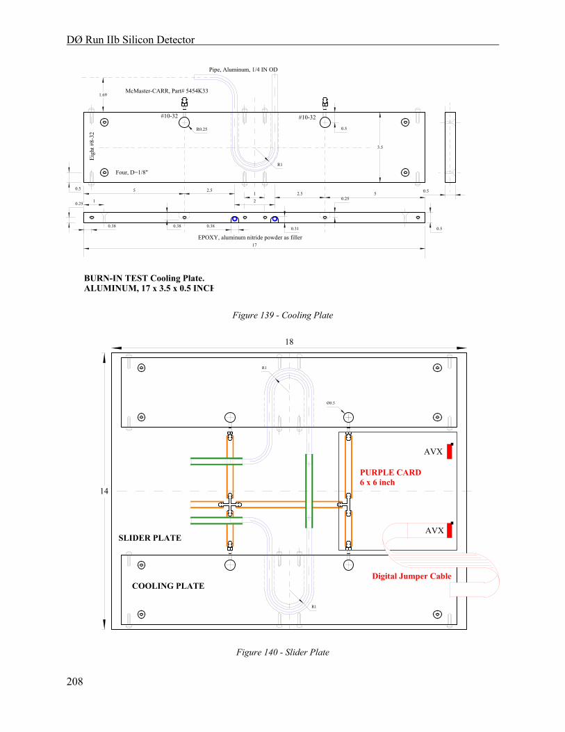
DØ Run IIb Silicon Detector
208
R1
0.5
3.5
1 2.52.5
2
0.5
55
17
Eigh
t #8-
32
Pipe, Aluminum, 1/4 IN OD
1.69
Four, D=1/8"
McMaster-CARR, Part# 5454K33
#10-32
1
0.38
0.25
0.5
0.38 0.31
#10-32
EPOXY, aluminum nitride powder as filler
BURN-IN TEST Cooling Plate.ALUMINUM, 17 x 3.5 x 0.5 INCH
R0.25
0.38
0.5
0.25
Figure 139 - Cooling Plate
R1
R1
Ø0.5
PURPLE CARD6 x 6 inch
SLIDER PLATE
18
COOLING PLATE
AVX
AVX
Digital Jumper Cable
14
Figure 140 - Slider Plate
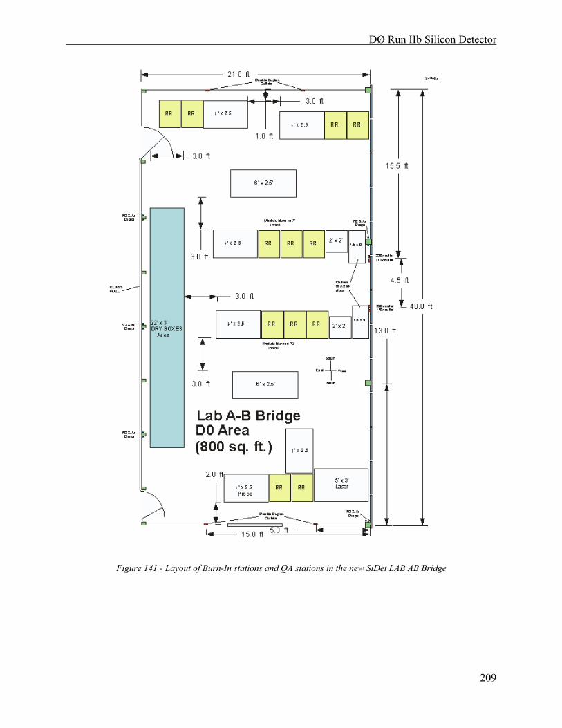
DØ Run IIb Silicon Detector
209
Figure 141 - Layout of Burn-In stations and QA stations in the new SiDet LAB AB Bridge
DØ Run IIb Silicon Detector
210
6.5 Fast functionality test for stuffed hybrids
Once the bare hybrid is ready for surface mount of components, it will be shipped to the stuffing vendor. The vendor will surface mount the passive components, including the AVX connector, using a pick and place machine, perform a simple continuity and short test, attach the SVX4 die to the beryllia substrate using silver epoxy, and then wirebond the SVX4 chip to the substrate. The vendor will ship the finished hybrids back to university collaborators for functional testing.
The initial functionality test at the collaborating universities includes a visual inspection (to ensure that the components were mounted correctly and wire bonds were made to the right pads), and examination of distributions of pedestal and noise as a function of channel number for each of the SVX4 chips on the hybrid. The behavior of the hybrid will also be tested using a large number of successive downloads and in cal-inject mode. Students and technicians at two universities are currently in training to conduct these tests.
The visual inspection is done using a high powered microscope. The purpose is to obtain quick feedback for the stuffing vendors, including general wirebonding problems (too-long tails for example) and to attempt to ameliorate any problems before electrical tests. Typical “repairs'' at this point may include manually straightening out bent bonds, identify missing or broken wire bonds for repair in-house, locating SVX4 chips with obvious defects, and also to blow off or pick off debris from previous handling. A K&S manual wire bonder is available at each university hybrid testing site for these quick repairs.
After the visual inspection, there will be a static electrical test to check for power shorts and to verify the connection of the platinum temperature measuring resistor. Hybrids with shorts will be set aside for possible debugging. The functional electronic readout tests are performed using 1-SASeq stands at each university. These stands are already in place from the Run IIa detector and just need to be modified for use with the SVX4 chip. This is the basic test of download and readout. We require 100 successful downloads, and error free readout of 10,000 calibration and pedestal events.
Download failures are, if possible, localized to a single chip using a manual probe station in conjunction with an oscilloscope and logic analyzer, and defective SVX4 chips marked for replacement. Hybrids with problems are scanned at high magnification (50-250X) to search for chip and other defects. For the Run IIa hybrids, in about 50% of the download and readout failures cases, an SVX2 chip flaw was visible. For Run IIa the repair statistics were:
- Diagnostic success was stated to be >70%, meaning that at least 70% of the download and readout failures, when localizable to a single chip, could be recovered.
- About 30% of the hybrids with shorts were recovered, in some cases by burning off debris at “high'' current (less than 1A in order not to melt wire bonds), or by manipulation of hybrid tails.
The initial yield of working hybrids that were stuffed for Run IIa was 70% and varied significantly between different hybrid types and batches. The yield after repairs for working stuffed hybrids was around 90%.

DØ Run IIb Silicon Detector
211
The plans for testing are being prepared assuming yields such as those found in Run IIa for the stuffing and wirebonding vendors, which we believe to be conservative. University collaborators will interact with vendors, and perform the initial functionality test and needed repair. Hybrids that pass the functionality test are sent to Fermilab for burn-in. Hybrids that pass the burn-in test are used to assembly detector modules.
6.6 Module Assembly
Information about the depletion voltage and the number of bad strips will be provided as input to the testing and assembly group and taken into account when choosing sensors for a particular detector module. Only those hybrids meeting the desired criteria will be matched to silicon sensors and assembled into detector modules. The techniques for assembly of detector modules will be similar to those used in the past by many groups, including DØ. Sensors will be manually aligned with optical feedback from a camera mounted on a coordinate measurement machine (CMM). Once aligned, the sensors will be glued to one another via a connecting substrate of Kapton or Mylar. The bias connection on the backside of the sensors will be made using aluminized Mylar glued with silver filled epoxy. In the hybrid region this foil will extend beyond the edge of the sensor so that it can be wrapped around the edge and glued to the HV pad on the top of the hybrid to make the HV connection. This is essentially what was done by CDF for the L00 device currently installed in that experiment. The hybrid will be glued directly to the silicon sensors in such a manner that the guard rings are not bridged by adhesive, to avoid any performance problems. Module assembly will utilize 5 Zeiss CMMs for the L1-5 modules, each with a capacity of 2 modules per day. The L0 modules do not require high accuracy alignment as each consist of a single sensor, flex cable and readout hybrid so these can be assembled on a granite surface plate. The total assembly capacity will be 8 modules for L2-5 plus 2 each for L0 and L1 per day, or 60 modules per week, exceeding by more than a factor of two the average production rate we have assumed in our resource loaded schedule. We are investigating high purity, fast curing (<5 hours) adhesives to increase the peak capacity and to more efficiently utilize the equipment and human resources available.
Wire bonding will then be done between the hybrid and the sensors, and from sensor to sensor for the modules with 20 cm readout segments. The sensor pitch is such that the hybrid to sensor bonding can be done directly from the SVX chips to the silicon sensors without a pitch adapter. The total numbers of wire bonds required for layers 2-5 are 353K sensor-to-sensor plus 860K hybrid-to-sensor, for a total of 1213K bonds. We anticipate doing all of the production bonding on a single K&S 8090 machine, with repair work being performed on a K&S 1478. For the longer modules, the sensor-to-sensor wire bonding can be done either before or after the hybrid is mounted. Sensor alignment and sensor-to-sensor wire bonding could therefore proceed prior to hybrid delivery, should that become a production constraint. At several steps during the assembly sequence, the module will be electrically tested, repeating the short functionality test. In order to be able to read out the hybrid, a short digital jumper cable (testing cable) needs to be connected to the module. This will be done after assembly and wire bonding of the detector module, or when an electrical test is required. The connection of this testing cable needs to be done by a skilled technician, as it is a delicate operation that takes place with exposed wire bonds. The testing cable will remain attached to the module during the complete testing process until the module is installed in the tracker and the final jumper cable is connected.

DØ Run IIb Silicon Detector
212
Malfunctioning modules at any step of the assembly sequence will be sent to the repair team for diagnosis and repair. We will consider the possibility that the individual modules may require cooling during the diagnostic tests to avoid over heating. Once a module has been assembled, wire bonded, and a testing cable has been connected, it will be stored in boxes similar to those used in Run IIa. These boxes allow for electrical testing, providing a path out of the box for the digital readout cable, ports in the base for dry gas purge, cooling of the sensors through the base plate of the box and a light-tight seal to allow biasing of the sensors. The modules will remain in these boxes through testing and burn-in and will only be removed when they are to be installed on the staves. Modules can be electrically tested by connecting the testing cable to the purple card, without opening the storage box.
Completed detector modules will be sent to the debugging team to investigate their performance under HV bias. Pinholes could develop during wire bonding and can be removed by pulling the wire bond between the AC sensor pad and the SVX4 chip preamplifier. Because all our silicon modules use single-sided silicon sensors, we expect the debugging of detector modules to be much less demanding than the one required by double-sided sensors. Once the detector module is operational under high voltage, it will be sent for module burn-in.
6.7 Debugging of Detector Modules
Immediately after a detector module is produced, and before it is burned-in, it needs to undergo a functionality test, that we call “debugging”. The likelihood of damaging the detector modules during construction, in particular during wirebonding, is not negligible. An intermediate step between production and before module burn-in is needed to restore the functionality of the modules before performing any electrical tests. The steps we plan to follow during the debugging process are the following.
o Visual Inspection: A thorough visual inspection of the finished module will ensure that no mistakes were made during wire bonding and no mechanical damage occurred.
o Functionality test: this test is done on the module without applying bias voltage to the sensor to assure the electrical integrity of the hybrid after module production.
o Biasing of the detector: bias voltage is applied in 5V increments, monitoring the leakage current. Capacitors that might be broken during wirebonding will be identified during this step. Strips corresponding to broken capacitors will be disconnected from the readout electronics by pulling the wirebond between the silicon sensor AC bonding pad and the SVX preamplifier.
o Characterize the module by producing V-I and V-noise curves and determining the operation voltage.
We plan to have two 1-Saseq debugging stations in the Lab D clean room to check out modules as soon as they have been completed. With an average production for modules of about 30 modules per week, we would debug 3 modules per day in each station, which provides ample time to work on modules that might have been damaged during production. If necessary, both

DØ Run IIb Silicon Detector
213
debugging stations could be manned in two shifts, doubling the debugging capacity, which would allow us to match the planned maximum possible throughput of 60 modules per week.
6.8 Burn-in Tests for hybrids and detector modules
The burn-in test is part and parcel of the testing procedure for module production. It will be performed first on the stuffed hybrid after it has passed the initial functionality test described above. At this point the hybrids are subjected to long term readout cycles. The goal of the test is to select good hybrids for module assembly. The second burn-in test will be carried out after a module has been produced and it has passed the initial functionality test. The idea of the burn-in test is to run every component for a long period of time (up to 72 hours) under conditions similar to those expected in the experiment and monitor its performance, in particular, measure pedestals, total noise, random noise and gain and examine occupancy in sparse readout mode. Other parameters that will be monitored include temperature, chip current, and detector bias voltage and dark current measurement (in module burn-in only). Typical problems that are revealed by the burn-in tests are SVX chip failures, broken and shorted bonds, grounding problems, noisy strips and coupling capacitor failures.
We plan to set up two hybrid burn-in stations, with a capacity of 16 channels each, and two module burn-in stations, with a capacity of 32 channels each. This gives us a total capacity of 96 channels per burn-in cycle, which we consider adequate to accommodate an anticipated production rate of about 30 modules per week, with a maximum production capacity of 60 modules per week. For comparison, our production rate during Run IIa averaged 20 modules per week, and our burn-in capability was 32 channels. We expect to have two burn-in cycles per week, per station, on average. The large volume of information coming from the burn-in tests and the necessity to run the test for many devices requires the burn-in test software to be user friendly so that non-expert physicists taking shifts can operate the burn-in stations. The Run IIa software was based on a user-friendly Graphical User Interface written in the TCL/TK scripting language with the graphical toolkit in the Windows environment. This choice of software interface created a flexible system for performing a variety of tests using executables written in different programming languages, for data taking, monitoring and data analysis. We plan to reuse the Run IIa burn-in software, modifying it for our new modules, and reducing the amount of human intervention in processing the data and storing the information. Given the increase in our production rate compared to Run IIa, we will do most of the processing of data and storage of summary plots in the database automatically.
The different tests performed during burn-in are the following:
o Temperature sensor test: performed at room temperature, before the SVX chip is powered.
o Data integrity check: tests the stability of downloading the SVX chip and verifies chip identification number (ID) and channel numbers of the SVX data for each chip.
o Long term burn-in test: it consists of a number of runs with an idle interval between them in which the chips remain powered. In each run, the SVX chips are tested in “read all” and “read neighbor” modes. In “read all” mode, chip pedestals are read out to evaluate

DØ Run IIb Silicon Detector
214
the noise in each SVX channel and the chip calibration is performed. In sparse readout mode (“read neighbor''), where only the channels whose response exceeds the preset threshold and their immediate neighbors have to be read out, the frequency of false readouts is studied.
For detector modules, this test is performed with the module under bias. For a detailed description of the tests performed during burn-in in Run IIa, see DØ Note 3841. We plan to run the same tests during Run IIb. A Hybrid and Module burn-in run lasts typically 60 hours; the duration might be reduced as production progresses if no failures are encountered and a larger throughput is required.
6.9 QA Test for Detector Modules
Mechanically, all modules will be surveyed using the OGP, an optical CMM with pattern recognition that can quickly measure all of the fiducials on the sensors. This was done with the ladders in Run IIa. This measurement will also provide data on the flatness of the freestanding modules. The modules will be constrained to be flat during mounting on the stave core. The stave core with mounted hybrids is substantially stiffer than the individual components so that we expect to have very flat module assemblies in the finished staves. A number of completed staves will be inspected on the OGP to confirm that this is the case.
We plan to subject a small fraction (~10%) of detector modules to a thorough set of QA tests. The final set of tests will be developed once prototype modules are being produced. The current plan is to test modules in the following areas:
o Laser test: This test is meant to verify the response of the silicon sensor to a light signal. Detector modules will be placed on an x-y movable table enclosed in a dark box, biased and illuminated with a highly-collimated pulsed IR laser, providing a detailed test of each strip of the detector module in a functional setting. The same system was used during Run IIa. It is based on a 1-Saseq test stand, with the addition of the movable table, dark box, and Laser. The solid state laser operates at a wavelength of 1064nm, a wavelength chosen because the high resistivity silicon used in the detectors is partially transparent to it. The attenuation as a function of silicon thickness has been measured, resulting in an attenuation length of 206µm. This laser will thus test the whole depth of the 320µm thick detector and not just a surface layer. We plan to do a detailed scan of the modules to check for uneven response of the sensor to the laser.
o Temperature cycles: The cooling provided during burn-in is only meant to avoid mechanical and electrical damage to the modules. The modules will run at a temperature between 10 and 15C, depending on the number of chips. We consider that a detailed temperature cycle test, in which modules are read out and checked for mechanical integrity after being subject to temperatures of –10C, is desired.
o Probe testing: We do have the ability to probe test silicon sensors after they were assembled into modules, or to do detailed checks of signals in the SVX chips by means of a logic analyzer and a probe tip. We can use this tools for QA tests if found appropriate once we gain experience during the R&D and pre-production phase.

DØ Run IIb Silicon Detector
215
o Pull Tests: we will test wire bonds on the hybrids and between hybrids and sensors on their pull strength during the R&D and pre-production phase, and might consider doing it in a small fraction of modules during production if needed.
6.10 QA Test for Stave Assembly
For the detector modules from Layers 2-5, two axial and two stereo modules will be mounted on a stave before the stave is inserted in the bulkhead. The stave assembly sequence is a 3-day process, with an intended average production rate of one stave per day. The stave production capacity is 2 staves per day. On the first day the axial modules are pre-tested and then aligned and glued to the stave core. While the adhesive is wet, a quick functionality test may be done to ensure that no damage was done to the modules during mounting. In Run IIa this was done, but there were few instances of problems not associated with recognized human error. The remaining problems were related to migration of conductive adhesive being used to mount the ladders, which will not be an issue in Run IIb where we will be using non-conductive adhesive. On the second day the axial modules will be tested, the stave will be flipped and pre-tested stereo modules will be mounted to the stave. On the third day the stereo modules will be tested and then the structural elements will be glued to the stave. After this the stave will be tested with simultaneous readout of all 4 modules. The module installation requires high precision optical feedback for alignment. We anticipate doing this work on the new Browne and Sharp CMM that has been ordered, or on the LK machine in Lab C. The other machine will be used for installation of L0 and L1 modules, which mount directly to the castellated cylindrical support structures.
6.11 Electrical Tests during Stave and Tracker Assembly
We plan to do two types of tests on the modules during stave assembly. Both tests will be performed using a 2-Saseq test stand located in Lab C, close to the stave assembly stations. The first test will be performed on individual modules, immediately before and after installation on the stave. The second test will read out the four modules simultaneously after installation on the stave, to check for cross talk and grounding problems. Layer 0 and 1 modules are not installed on staves, but are mounted individually on the support structure. We plan to perform the same two types of tests during assembly (single module and simultaneous readout of in this case 6 modules), using a 3-Saseq test stand located in LabC, close to the L0/L1 assembly station. The steps of the single module test will be specified following the procedure used during insertion of ladders into the Run IIa SMT bulkhead (see Ref. 32), and are summarized below:
1. Temperature sensor check at room temperature: ensures that the temperature sensor on the module is working properly. This test is done before the chips are powered.
2. Download of SVX chips for data mode operation
32 See http://d0server1.fnal.gov/projects/run2b/Silicon/www/smt2b/Testing/testing.html under Procedure for ladder Assembly into Barrels for the SMT

DØ Run IIb Silicon Detector
216
3. Check channel and chip ID
4. Take 100 events in data mode. Check for uniformity of pedestals and noise level
5. Download of SVX chips for cal-inject mode operation
6. Take 100 events in cal-inject mode. Check for uniformity of pedestals and noise level
7. Bias the detector to the operation voltage (depletion voltage + 5V)
8. Repeat steps 2 to 6
After four L2-L5 modules are installed in one stave, or 6 L0/L1 modules are installed on one sector of the support structure, they will be connected and read out simultaneously, to check for crosstalk and grounding problems. Cooling of the modules during assembly and testing will be done with water at 3C. Details still need to be understood to minimize the number of times cooling is connected and disconnected during the assembly process.
6.12 Full System Electrical Test
All the tests described so far on stuffed hybrids and detector modules during production and assembly of the tracker are performed using Stand-alone (Saseq) based test stands.
These tests are aimed at testing a large number of detector modules extensively and with redundancy in order to detect problems and fix them. The production testing needs to be complemented with a test of the real readout chain, the one that will eventually be used for the data acquisition in the experiment. This test is described below.
We plan to test the full readout chain with a maximum achievable number of full staves , or an equivalent number of stuffed hybrids, through all of the components of the final readout chain. The goal of this test is to understand the full readout system and perform modifications well before the system needs to be operated in the collider. The same idea was behind the so-called 10% Test during the production of the Run IIa detector, which was crucial in understanding the data acquisition system. At that time, a large number of components that were eventually installed in the detector were used for the test. Because we are reusing a fair amount of components for Run IIb, we cannot plan on a large-scale full system test like the one we had during Run IIa. The added cost of the equipment to test 10% of all readout channels would be prohibitive. Nevertheless, we believe that careful tests of the full readout chain are imperative. The SVX4 chip, hybrids, the cabling plant connecting the hybrids to the adapter cards and the adapter cards themselves are all new components requiring testing.
We plan to perform those tests with DØ readout electronics in the Silicon Detector Facility. We will maintain two test stands, which we call the Vertical Slice - Single Unit Full Chain (1%) Test Stand and the Multi Unit Full Chain (10%) Test Stand. The 1% test stand is a minimal setup without the need of a full high voltage or low voltage system. This test stand will include one module of each necessary component to make a full chain test. It is capable of testing up to 2 staves (8 hybrids) or one L0 sector (6 hybrids), or two L1 sectors (2x3 hybrids). The Multi Unit
DØ Run IIb Silicon Detector
217
Full Chain (10%) test stand will increase the number of hybrids tested from 8 to possibly 80. The setup includes all three types of crates participating in the SMT readout: an Interface Board crate, Sequencer crate and VRB crate. The High Voltage System and LV system will be integrated into the test stand as it becomes available. The crates are populated with spare Run IIa boards. The DØ Trigger Framework functionality is replaced with a FPGA board that emulates those functions required. This allows us the flexibility of operating without the DØ trigger framework. Data will flow from the detectors to the SBC and then by Ethernet to a local LINUX based computer. The electronics can be controlled either by software based on Excel spreadsheets or by the Run IIa SMT online software. The Excel based software is currently used by the DØ engineers to debug the hardware while the online software provides a realistic test at full readout speed.
As we start receiving prototypes we plan to perform the following tests using this setup:
o Hybrid with SVX4 chips connected with Jumper Cable to the Purple test card and to the Sequencer. This test is complementary to similar tests with SASeqs. In addition it will allow developing of all firmware changes for production Sequencers before we receive other prototypes.
o Full readout chain: Hybrid – Jumper Cable – Junction Card – Twisted Pair Cable – Adapter Card – 80-conductor cable – Interface Board – 50-conductor cable – Sequencer. These tests are crucial to verify the performance of all components. The timing studies are especially important to verify the impedance matching between different components and the signal terminations.
o Multi-channel readout test. We have capabilities to install several Interface Boards, Sequencers and VRBs, up to 10 boards of each type (80 readout channels). The exact number will be limited by the amount of spares that we will be available to use. In order to connect a sizeable number of hybrids and/or detector modules we will need to provide adequate cooling and a light-tight box.
6.13 Production Database
The amount of information that we need to keep track of during the construction of the DØ Run IIb silicon tracker arises mainly from the number of components in the device itself, but also on the rather large number of vendors and universities involved, and the need to maintain a stringent and uniform quality control. We are designing a production and testing database to store all the information relevant to the production and testing.
We have set up a Linux server for this purpose. We have designed a relational database using mySQL, where each item (hybrid, sensor, module, stave, etc.) has its unique ID for easy identification and tracking. We then use PHP to provide a web-based interface to the database. Every object entered into the database will become an entry in the ITEMS table, containing information about type of object, location, status, etc. For each test performed on an item, an entry will be generated in the TESTS table. Test results on various formats will be stored directly in the database. The access to the database will be web-based. Any user will be able to DISPLAY information, but the EDITING of information will be password protected. HISTORY

DØ Run IIb Silicon Detector
218
will be available for every item, and also for all editing done by a particular user. For the design of this database, we’re following the description of the ATLAS Silicon Tracker production database33.
33 http://www.hep.man.ac.uk/groups/atlas/SCTdatabase/Database.html

DØ Run IIb Silicon Detector
219
7 RADIATION AND TEMPERATURE MONITORING All silicon detectors will eventually be rendered inoperable or develop inferior performance due to the effects of radiation. Care must be taken to minimize the effects of radiation and to avoid unnecessary and premature damage. The most important parameter to control the effects of radiation damage is the operating temperature of the silicon. Since the front-end readout electronics is, in most cases, mounted on the silicon sensors, the danger of excessive heat and possible thermal run-away is always present. Without adequate cooling the energy dissipation in the front-end electronics could swiftly render the detector useless for physics. Less extreme heating, while not causing catastrophic damage, can greatly exacerbate the effects of radiation damage. For these reasons, the monitoring of currents, temperatures, and radiation dose are crucial to the safe and reliable operation of the detector. In Run IIa, currents, temperatures, voltages, and radiation dose from the accelerator are all monitored. Currents and temperatures are interlocked at several levels, so that deviations from set limits will trip off the appropriate power supplies. The radiation monitor has the ability to abort the Tevatron beam if radiation dose levels reach unacceptable levels. Some modest improvements are planned for the radiation and temperature monitoring systems for Run IIb silicon, consistent with the changes in detector design, as described below. The current and voltage monitors from Run IIa will be retained for the Run IIb detector.
7.1 Radiation Monitoring and Beam Abort System
7.1.1 The Run IIa system
A radiation monitoring and beam abort system is currently in operation for Run IIa. This system consists of two mostly independent subsystems: a system based on the Beam Loss Monitors as they are used by the FNAL beams division, and a system based on silicon diode sensors. Both systems are independent up to a last stage, where the output of both are recorded in the same data stream and where a combination of the information of both systems can be made to trigger a Tevatron beam abort. An overview of the current system is given in Figure 142.
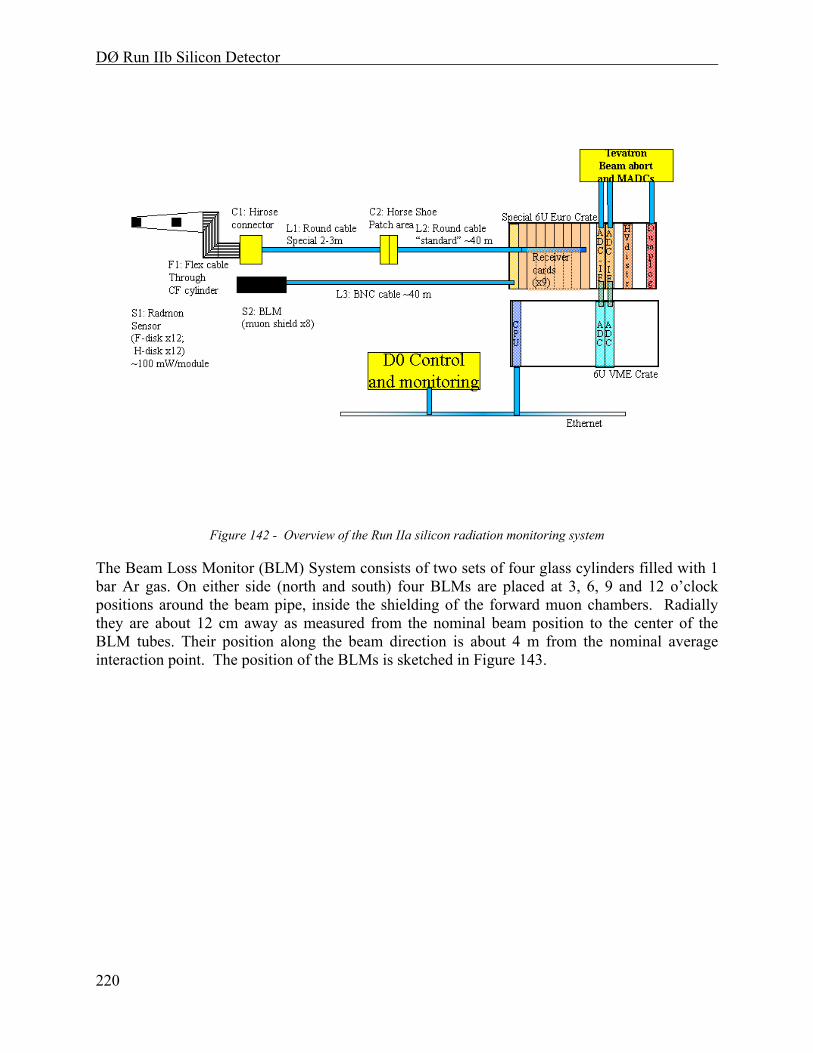
DØ Run IIb Silicon Detector
220
Figure 142 - Overview of the Run IIa silicon radiation monitoring system
The Beam Loss Monitor (BLM) System consists of two sets of four glass cylinders filled with 1 bar Ar gas. On either side (north and south) four BLMs are placed at 3, 6, 9 and 12 o’clock positions around the beam pipe, inside the shielding of the forward muon chambers. Radially they are about 12 cm away as measured from the nominal beam position to the center of the BLM tubes. Their position along the beam direction is about 4 m from the nominal average interaction point. The position of the BLMs is sketched in Figure 143.
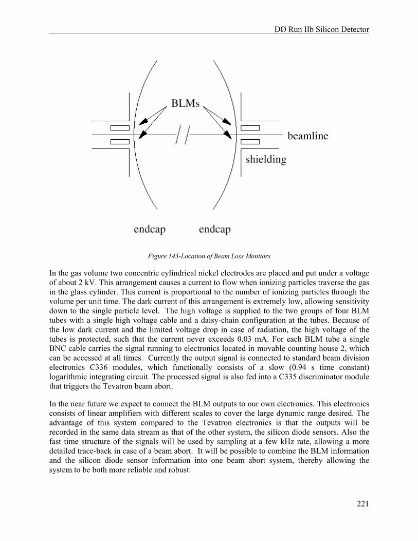
DØ Run IIb Silicon Detector
221
Figure 143-Location of Beam Loss Monitors
In the gas volume two concentric cylindrical nickel electrodes are placed and put under a voltage of about 2 kV. This arrangement causes a current to flow when ionizing particles traverse the gas in the glass cylinder. This current is proportional to the number of ionizing particles through the volume per unit time. The dark current of this arrangement is extremely low, allowing sensitivity down to the single particle level. The high voltage is supplied to the two groups of four BLM tubes with a single high voltage cable and a daisy-chain configuration at the tubes. Because of the low dark current and the limited voltage drop in case of radiation, the high voltage of the tubes is protected, such that the current never exceeds 0.03 mA. For each BLM tube a single BNC cable carries the signal running to electronics located in movable counting house 2, which can be accessed at all times. Currently the output signal is connected to standard beam division electronics C336 modules, which functionally consists of a slow (0.94 s time constant) logarithmic integrating circuit. The processed signal is also fed into a C335 discriminator module that triggers the Tevatron beam abort.
In the near future we expect to connect the BLM outputs to our own electronics. This electronics consists of linear amplifiers with different scales to cover the large dynamic range desired. The advantage of this system compared to the Tevatron electronics is that the outputs will be recorded in the same data stream as that of the other system, the silicon diode sensors. Also the fast time structure of the signals will be used by sampling at a few kHz rate, allowing a more detailed trace-back in case of a beam abort. It will be possible to combine the BLM information and the silicon diode sensor information into one beam abort system, thereby allowing the system to be both more reliable and robust.
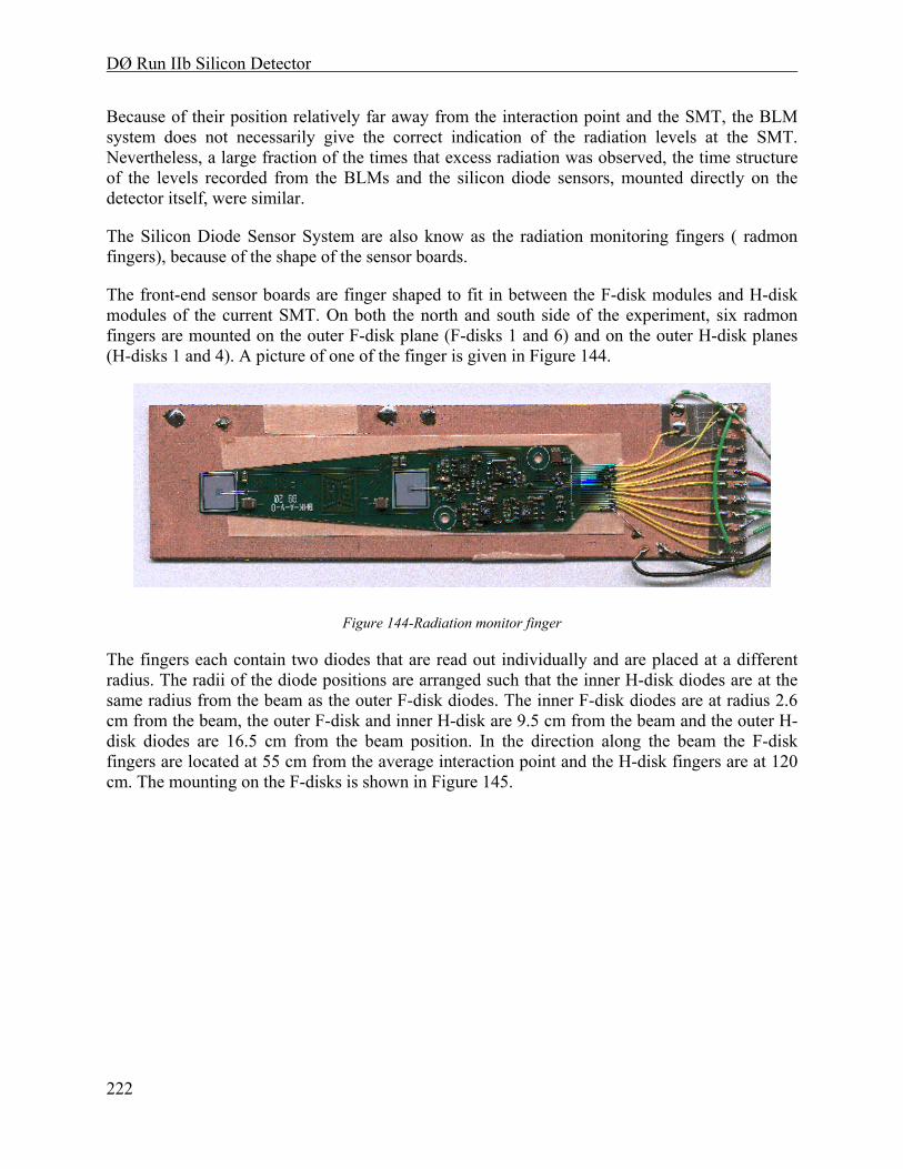
DØ Run IIb Silicon Detector
222
Because of their position relatively far away from the interaction point and the SMT, the BLM system does not necessarily give the correct indication of the radiation levels at the SMT. Nevertheless, a large fraction of the times that excess radiation was observed, the time structure of the levels recorded from the BLMs and the silicon diode sensors, mounted directly on the detector itself, were similar.
The Silicon Diode Sensor System are also know as the radiation monitoring fingers ( radmon fingers), because of the shape of the sensor boards.
The front-end sensor boards are finger shaped to fit in between the F-disk modules and H-disk modules of the current SMT. On both the north and south side of the experiment, six radmon fingers are mounted on the outer F-disk plane (F-disks 1 and 6) and on the outer H-disk planes (H-disks 1 and 4). A picture of one of the finger is given in Figure 144.
Figure 144-Radiation monitor finger
The fingers each contain two diodes that are read out individually and are placed at a different radius. The radii of the diode positions are arranged such that the inner H-disk diodes are at the same radius from the beam as the outer F-disk diodes. The inner F-disk diodes are at radius 2.6 cm from the beam, the outer F-disk and inner H-disk are 9.5 cm from the beam and the outer H-disk diodes are 16.5 cm from the beam position. In the direction along the beam the F-disk fingers are located at 55 cm from the average interaction point and the H-disk fingers are at 120 cm. The mounting on the F-disks is shown in Figure 145.
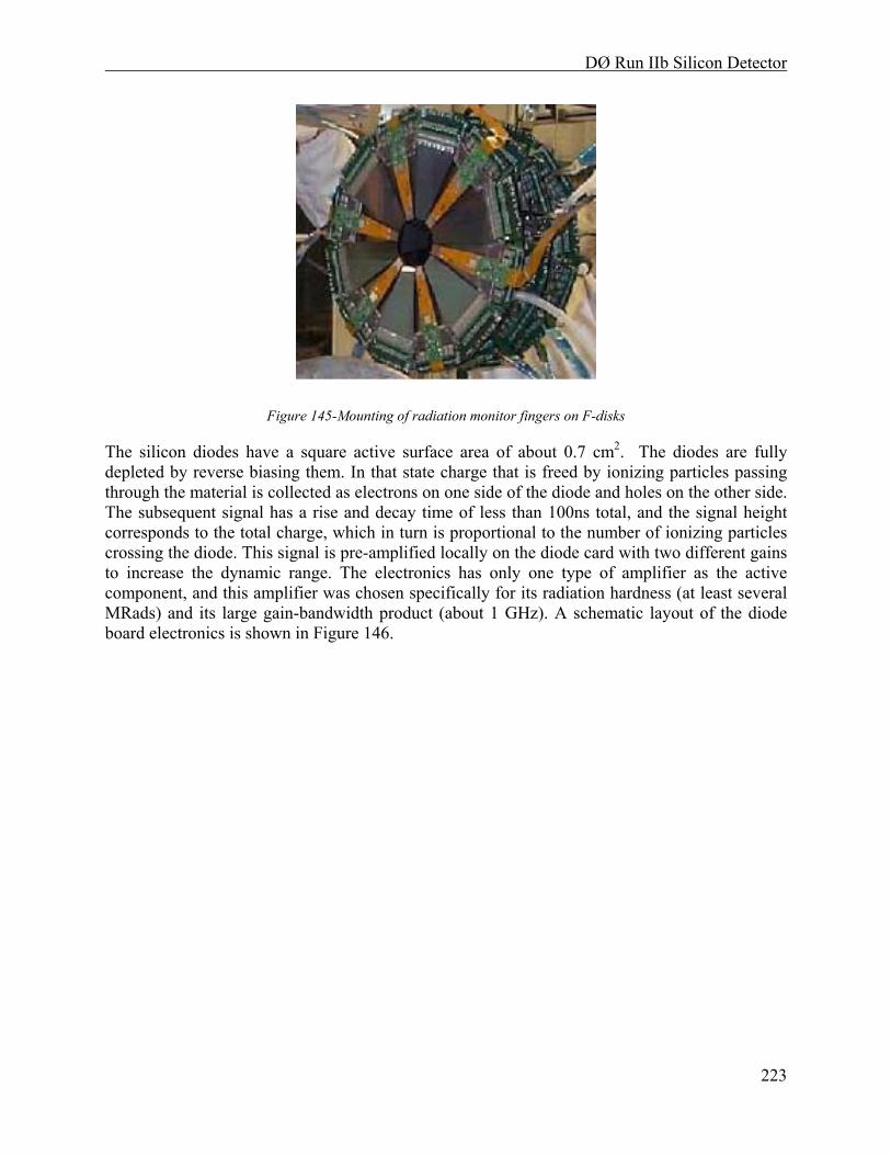
DØ Run IIb Silicon Detector
223
Figure 145-Mounting of radiation monitor fingers on F-disks
The silicon diodes have a square active surface area of about 0.7 cm2. The diodes are fully depleted by reverse biasing them. In that state charge that is freed by ionizing particles passing through the material is collected as electrons on one side of the diode and holes on the other side. The subsequent signal has a rise and decay time of less than 100ns total, and the signal height corresponds to the total charge, which in turn is proportional to the number of ionizing particles crossing the diode. This signal is pre-amplified locally on the diode card with two different gains to increase the dynamic range. The electronics has only one type of amplifier as the active component, and this amplifier was chosen specifically for its radiation hardness (at least several MRads) and its large gain-bandwidth product (about 1 GHz). A schematic layout of the diode board electronics is shown in Figure 146.
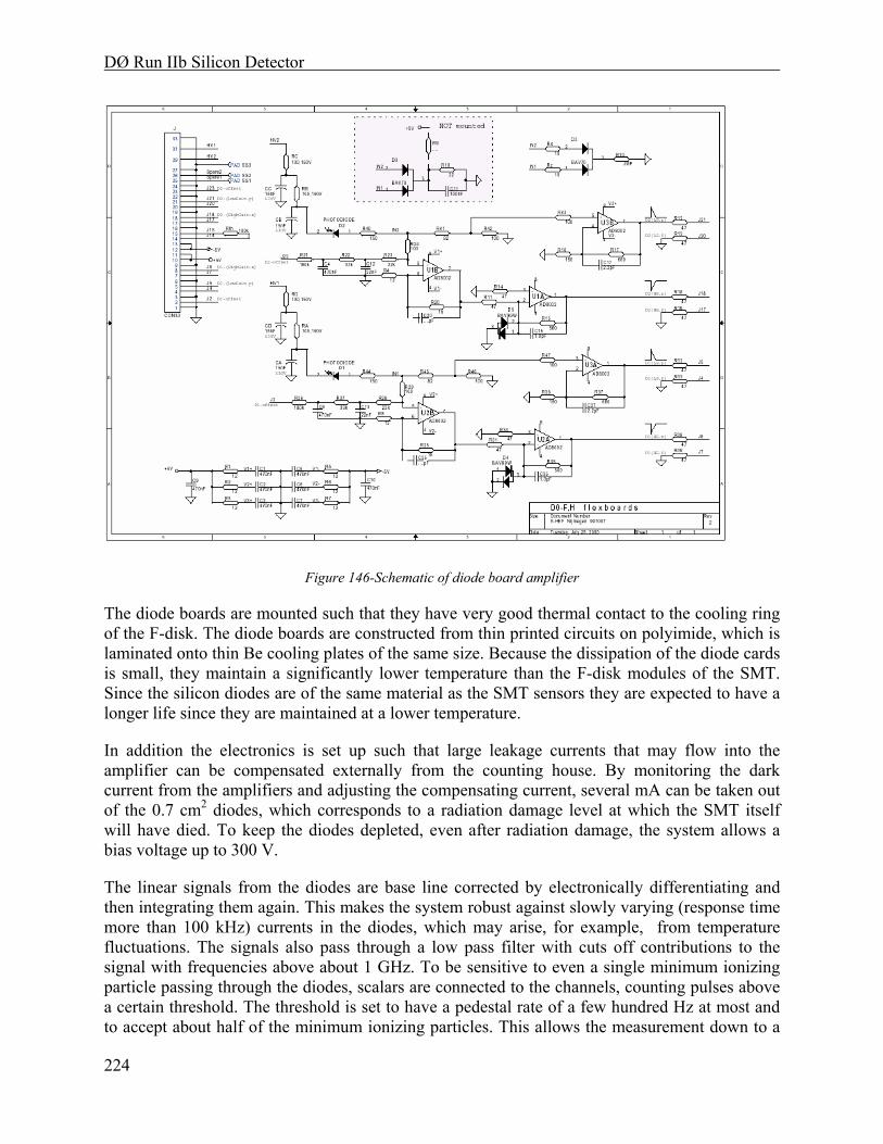
DØ Run IIb Silicon Detector
224
Figure 146-Schematic of diode board amplifier
The diode boards are mounted such that they have very good thermal contact to the cooling ring of the F-disk. The diode boards are constructed from thin printed circuits on polyimide, which is laminated onto thin Be cooling plates of the same size. Because the dissipation of the diode cards is small, they maintain a significantly lower temperature than the F-disk modules of the SMT. Since the silicon diodes are of the same material as the SMT sensors they are expected to have a longer life since they are maintained at a lower temperature.
In addition the electronics is set up such that large leakage currents that may flow into the amplifier can be compensated externally from the counting house. By monitoring the dark current from the amplifiers and adjusting the compensating current, several mA can be taken out of the 0.7 cm2 diodes, which corresponds to a radiation damage level at which the SMT itself will have died. To keep the diodes depleted, even after radiation damage, the system allows a bias voltage up to 300 V.
The linear signals from the diodes are base line corrected by electronically differentiating and then integrating them again. This makes the system robust against slowly varying (response time more than 100 kHz) currents in the diodes, which may arise, for example, from temperature fluctuations. The signals also pass through a low pass filter with cuts off contributions to the signal with frequencies above about 1 GHz. To be sensitive to even a single minimum ionizing particle passing through the diodes, scalars are connected to the channels, counting pulses above a certain threshold. The threshold is set to have a pedestal rate of a few hundred Hz at most and to accept about half of the minimum ionizing particles. This allows the measurement down to a
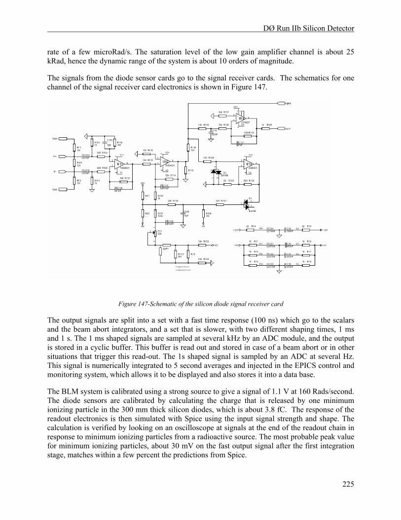
DØ Run IIb Silicon Detector
225
rate of a few microRad/s. The saturation level of the low gain amplifier channel is about 25 kRad, hence the dynamic range of the system is about 10 orders of magnitude.
The signals from the diode sensor cards go to the signal receiver cards. The schematics for one channel of the signal receiver card electronics is shown in Figure 147.
Figure 147-Schematic of the silicon diode signal receiver card
The output signals are split into a set with a fast time response (100 ns) which go to the scalars and the beam abort integrators, and a set that is slower, with two different shaping times, 1 ms and 1 s. The 1 ms shaped signals are sampled at several kHz by an ADC module, and the output is stored in a cyclic buffer. This buffer is read out and stored in case of a beam abort or in other situations that trigger this read-out. The 1s shaped signal is sampled by an ADC at several Hz. This signal is numerically integrated to 5 second averages and injected in the EPICS control and monitoring system, which allows it to be displayed and also stores it into a data base.
The BLM system is calibrated using a strong source to give a signal of 1.1 V at 160 Rads/second. The diode sensors are calibrated by calculating the charge that is released by one minimum ionizing particle in the 300 mm thick silicon diodes, which is about 3.8 fC. The response of the readout electronics is then simulated with Spice using the input signal strength and shape. The calculation is verified by looking on an oscilloscope at signals at the end of the readout chain in response to minimum ionizing particles from a radioactive source. The most probable peak value for minimum ionizing particles, about 30 mV on the fast output signal after the first integration stage, matches within a few percent the predictions from Spice.
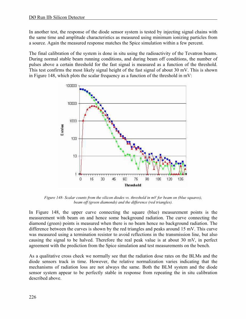
DØ Run IIb Silicon Detector
226
In another test, the response of the diode sensor system is tested by injecting signal chains with the same time and amplitude characteristics as measured using minimum ionizing particles from a source. Again the measured response matches the Spice simulation within a few percent.
The final calibration of the system is done in situ using the radioactivity of the Tevatron beams. During normal stable beam running conditions, and during beam off conditions, the number of pulses above a certain threshold for the fast signal is measured as a function of the threshold. This test confirms the most likely signal height of the fast signal of about 30 mV. This is shown in Figure 148, which plots the scalar frequency as a function of the threshold in mV:
Figure 148- Scalar counts from the silicon diodes vs. threshold in mV for beam on (blue squares), beam off (green diamonds) and the difference (red triangles).
In Figure 148, the upper curve connecting the square (blue) measurement points is the measurement with beam on and hence some background radiation. The curve connecting the diamond (green) points is measured when there is no beam hence no background radiation. The difference between the curves is shown by the red triangles and peaks around 15 mV. This curve was measured using a termination resistor to avoid reflections in the transmission line, but also causing the signal to be halved. Therefore the real peak value is at about 30 mV, in perfect agreement with the prediction from the Spice simulation and test measurements on the bench.
As a qualitative cross check we normally see that the radiation dose rates on the BLMs and the diode sensors track in time. However, the relative normalization varies indicating that the mechanisms of radiation loss are not always the same. Both the BLM system and the diode sensor system appear to be perfectly stable in response from repeating the in situ calibration described above.
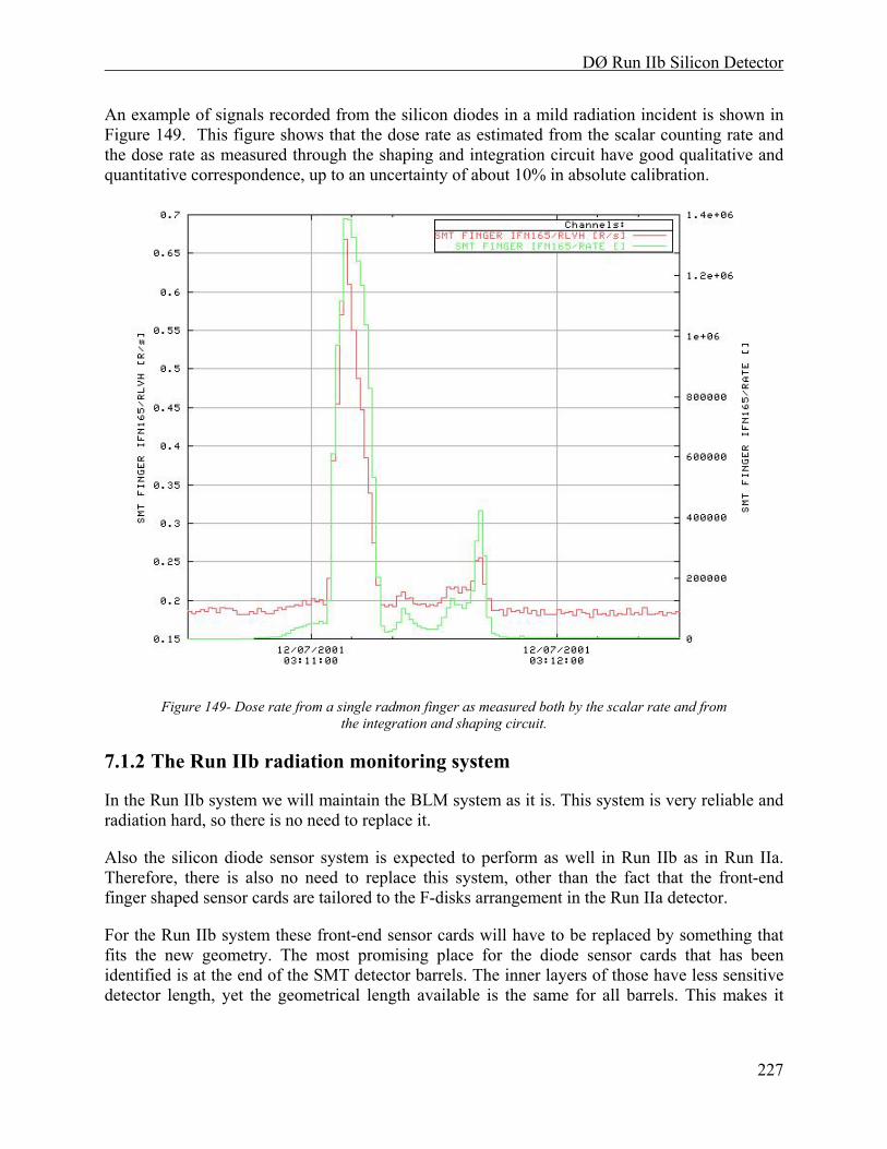
DØ Run IIb Silicon Detector
227
An example of signals recorded from the silicon diodes in a mild radiation incident is shown in Figure 149. This figure shows that the dose rate as estimated from the scalar counting rate and the dose rate as measured through the shaping and integration circuit have good qualitative and quantitative correspondence, up to an uncertainty of about 10% in absolute calibration.
Figure 149- Dose rate from a single radmon finger as measured both by the scalar rate and from the integration and shaping circuit.
7.1.2 The Run IIb radiation monitoring system
In the Run IIb system we will maintain the BLM system as it is. This system is very reliable and radiation hard, so there is no need to replace it.
Also the silicon diode sensor system is expected to perform as well in Run IIb as in Run IIa. Therefore, there is also no need to replace this system, other than the fact that the front-end finger shaped sensor cards are tailored to the F-disks arrangement in the Run IIa detector.
For the Run IIb system these front-end sensor cards will have to be replaced by something that fits the new geometry. The most promising place for the diode sensor cards that has been identified is at the end of the SMT detector barrels. The inner layers of those have less sensitive detector length, yet the geometrical length available is the same for all barrels. This makes it
DØ Run IIb Silicon Detector
228
possible to mount silicon diode sensor cards in the area where the cables attach to the SMT modules.
Replacing the diode sensor cards also makes it necessary to replace the cables between the sensor cards and the interconnection “horseshoe” that is located between the central and forward calorimeter cryostats. These cables have to be made to size, as space constraints are tight.
Redoing the sensor cards allows for some small improvements. In the Run IIa system we can clearly see the detector readout signals as noise in our system. Although the noise level is not jeopardizing the system, we think we can reduce it even further. The main area where the noise couples in at the moment is thought to be the sensor board itself, which is very close to the F-disk modules, but even more likely the low mass HDI cables that are fed through the carbon fiber support cylinder packed together with similar low mass F-disk module cables. These low mass cables consist of polyimide foil with metal circuit traces printed on them. Only one side of these foils consists of a grounding plane, leaving the power, signal and control line traces on the other side electromagnetically unprotected.
In the new system we will cover the diode sensor cards with aluminized polyimide that electrically connects to the ground plane of the signal board, thus forming a Faraday cage. The group shielded cable will be soldered directly to the sensor boards, with the shield connected to the ground plane. These cables, made to the correct size, will connect to the existing connector in the horseshoe.
The design depends only on the choice of the position and shape of the diode sensor cards. A minimum surface area of about 8 cm2 is needed and the card should nowhere be narrower than 1.2 cm. A cable route has to be found for a round composite cable of 3 mm diameter from each of the sensor cards to a corresponding horseshoe connector. On both south and north side of the detector now more than 12 sensor boards can be accommodated, and we have a preference to use all these slots to have enough redundancy and geometrical information on radiation rates and doses.
Production of the sensor cards and attached cables can start after their position and geometry have been fixed. We intend to produce the sensor cards on thin, but standard PCB material. There is no need for a Be cooling plate as was used for the Run IIa sensors, because the sensors will be outside the active detector area. If needed the PCBs can be laminated onto thin Al cooling plates.
The other critical item for the production of the sensor boards is the silicon diodes. The stock of best quality diodes left from Run IIa is marginal, so all diodes have to be produced. These are diodes of the same material as the SMT detector wafers and are simple multi-guard ring structures. In fact these diodes will be added as test structures on the detector wafers to be procured from Hamamatsu. The diodes will be tested for stability and leakage current behavior, and their depletion voltage will be determined from the CV characteristic.

DØ Run IIb Silicon Detector
229
7.2 Temperature Monitoring
Due to the proximity of much of the electronics to the silicon sensors, temperature monitoring of the detector is crucial. Enough heat is generated by the electronics to easily start a fire if the cooling failed. Moreover, effects of radiation damage can be exacerbated by high temperatures. Remote-sensing devices mounted on or near the sensors themselves are needed not only to continuously monitor temperatures, but also to provide interlocks to shut off power in the event of a loss of cooling or other problem. The temperature-sensing device of choice is a Resistance Temperature Detector (RTD), a thin-film platinum resistor with a high temperature coefficient of resistance. These devices are widely used in industry, stable, reliable, and readily available.
7.2.1 Run IIa Temperature Monitoring
In the Run IIa, the temperature of each High Density Interconnect (HDI) is monitored with an RTD. There are about 900 RTDs in the Run IIa silicon system. They are read out through a two-wire system in which the same leads both supply a DC current and read out the resulting voltage. This readout method, which does not compensate for the resistance of the leads, limits the accuracy to about 1-2C. The analog voltage signal (a DC voltage level) goes to the Interface Board, where it is digitized and read out serially to the 1553 monitoring system. The reading from each RTD is interlocked so that if the temperature goes above 15C, the power to the appropriate HDI (only) is tripped.
In addition to the temperature monitor on each HDI, 88 of these signals have a second readout. An analog signal is taken off the Interface Cards before digitization and read out through an ADC in the DØ Cryo Control System, which is a Programmable Controller (PLC), a commercial system widely used in industry for monitoring and interlocks. The 88 RTDs read out in this way serve as one of several signals that interlock power to the entire silicon system. The Cryo Control System serves as a redundant system to the 1553 interlocks, and is on a UPS so it would still function in the case of a power outage.
7.2.2 Run IIb Temperature Monitoring
In Run IIb there will also be two somewhat redundant temperature-monitoring systems. The system that interlocks the current in each HDI will be reproduced. For Run IIb the HDIs are replaced by hybrids. Each hybrid will have an RTD mounted as one of the elements. Plans and costs for these devices are part of the hybrid design and budget. The devices chosen are Honeywell HEL-700 1000 Ω platinum thin-film RTDs. Signals from each of these RTDs will be digitized on the Interface Card and read out through the 1553 as is currently done for Run IIa. The temperature monitors on each hybrid will be used to interlock the power of that individual hybrid.
For Run IIb, there will be a second temperature-monitoring system which will be decoupled from the hybrids. There will be on order 100 RTDs mounted at various locations on the sensors and cooling system. Each RTD will be mounted on low-mass quad-lead 4-wire ribbon cables with polyimide insulation, which is known to have good rad-hard properties. The cable will extend to the “horseshoe” area, where the low mass cables will be coupled through simple junction cards to high-mass cables which then go to standard RTD readout modules in the DØ
DØ Run IIb Silicon Detector
230
Cryo Control System. A commercially-available module, the CTI505, model 2557-SPQ334, from Control Technology Incorporated, will be used to both provide current to the RTDs and readout the resulting voltages. These modules have been used often at Fermilab. This system will provide an independent set of interlocks on the silicon temperature. The CTI505 modules allow either two or four wire readout and therefore can provide for more accurate monitoring than was available for the Run IIa system. We plan to use the four-wire readout to have more accurate temperature information for these 100 RTDs.
There are several reasons that a second, independent temperature monitoring system is needed in Run IIb. In L0 the hybrids will not be located near the actual sensors. Therefore, for L0, the temperatures of the hybrids, not the sensors themselves, will be monitored with the 1553 system. It is desirable to have additional monitoring which measures the temperatures of the sensors themselves. The stand-alone system will measure the temperature of the sensors, or perhaps the cooling channels nearby. For layers outside of L0, the RTDs mounted on the hybrids also do not directly monitor the temperatures of the sensors, although they are nearby. Additional temperature sensors, mounted either directly on the sensors or on the nearby cooling channels, will provide supplemental information and interlock capability for the outer layers. This capability could be especially important for L1, for which preliminary designs indicate the cooling may be most difficult. Improved accuracy on some subset of the RTDs would allow for improved understanding the cooling system. It is desirable to be able to measure, for example, the difference between the input and output temperatures of the cooling system, but the current temperature readouts are not accurate enough to measure such a small temperature difference. The additional RTDs will be read out via a 4-wire system that compensates for lead resistance and therefore will be more accurate and uniform. Finally, in a system as vulnerable to damage from over-temperature as the silicon detector, redundancy in the interlock system is an advantage if not a requirement.
DØ Run IIb Silicon Detector
231
8 SOFTWARE This section describes online and offline software needed for SMT commissioning and online calibration, monitoring and readout of the detector. For both offline and online software effort, we will use the system developed for Run IIa and upgrade it appropriately for Run IIb where needed. Here we describe this system.
8.1 Online Software Components
The software requirements are mainly determined by the hardware that is used. The SVX amplifier chip requires a set of parameters like the amplifier bandwidth, a threshold for zero suppression and various ADC settings. The delay for the readout is set at the Sequencer Controller module. Each module requires an individual set of parameters. These parameters are downloaded after power up. Special data taking modes, e.g. calibration runs, require a different set of parameters. In addition some parameters might change with time. The most important example is the threshold for zero suppression, which changes with fluctuations of pedestal and noise. Constant monitoring ensures that the download parameters are still correct. Monitoring is also necessary for ensuring a constant high data quality and the safety of the detector.
The main components of the SMT online software are the ORACLE database, Graphical User Interfaces for control and monitoring, the Secondary Data Acquisition for calibration and monitoring, and Examine programs, which are part of the offline framework but are used in the online context.
8.1.1 The Oracle Database
The Online Database for SMT consists of three parts, the Hardware Database, the Electronics Database and the Online Calibration Database. The Hardware Database contains the definition of EPICS process variables (see below). These are required for communication with hardware modules. In addition alarm information is stored which is used for monitoring and the Significant Event System (SES). The Electronics Database contains the complete mapping of the hardware. Every type of readout module has its own table. An individual module is represented by a row in this table. A representation of single channels of modules allows the necessary multiple to multiple references between readout modules. The database contains the hardware identification for the modules as well as all the parameters necessary to operate the module. A history mechanism allows keeping track of changes to download parameters. This retains a history of the parameters that have been used at any time during the data taking period. The Online Calibration Database contains the basic calibration data for each readout channel per calibration run as well as summary information per SVX chip per calibration run. In addition a status word is assigned to each of the readout channels. These databases are implemented using ORACLE, which is software maintained by the computing division at Fermilab.
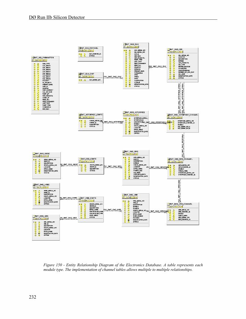
DØ Run IIb Silicon Detector
232
Figure 150 - Entity Relationship Diagram of the Electronics Database. A table represents each module type. The implementation of channel tables allows multiple to multiple relationships.
DØ Run IIb Silicon Detector
233
8.1.2 Graphical User Interfaces
The Graphical User Interfaces (GUIs) include EPICS as well as other control and monitoring interfaces. EPICS (Experimental Physics and Industrial Control System) is used to communicate with the hardware. An Input/Output Controller (IOC), a VME single board computer of the Power PC mv23xx series, maintains a database of symbolic names, which are mapped to one or more hardware addresses. A host computer can access these symbolic names via an EPICS client. EPICS client and server communicate via the Ethernet network. This system allows an easy implementation of a centralized controls and monitoring system with distributed hardware.
The MIL1553 standard is used to communicate with non-VME modules. A custom built VME module, the 1553 Controller, is used to access the 1553 bus. The 1553 bus is a robust communication link widely used in commercial and military aircraft. EPICS is used to communicate with 1553 devices.
EPICS allows periodic sampling of the hardware. Threshold values are used to issue warning or error messages to the Significant Event System (SES). This allows a distributed monitoring of variables locally without the need for a central host. In principle it is possible to implement an immediate response to a monitor value that exceeds a set limit directly on the local machine. The shift crew regularly monitors messages of the SES. These messages are archived as well.
The programming language used to interface the database and the hardware is Python. Python has several advantages:
• Python is an Object Oriented Language. It therefore allows the use of modern programming techniques.
• Python is a script language. It is compiled to a compact, byte-oriented stream for efficient execution. Program development has fast turn around cycles.
• Python has a convenient to use Tcl/Tk library. The programming of Graphical User Interfaces (GUI) is simple and fast.
• Python also has a freely available interface to ORACLE databases. • A Python wrapper around the C-interface to EPICS has been developed by DØ.
Because of those advantages Python has been the choice to develop GUIs for interaction with the database and with the hardware. One of the few disadvantages is that the execution speed is not as fast as for example a ‘C’ program could be.
A GUI, the so-called Download GUI, has been developed to interface both the ORACLE database and the hardware. The database is used to determine the mapping of the readout electronics. Each module is represented by one GUI entity. Each entity has two functionalities:
• The parameters for a specific module that are stored in the database can be modified. • The hardware registers of this module can be accessed.

DØ Run IIb Silicon Detector
234
Specifically it allows operations on the following list of hardware (the complete list of operations is given later in this chapter under 8.3 Hardware Operations.
• VRB • VRB Controller • Sequencer • Sequencer Controller • KSU Interface Board • HDI • VRB Crate • VBD
Additional GUIs are available for:
• Monitoring of voltages, currents and temperatures of all the HDIs. The KSU Interface Board is used to determine these parameters. Most commonly the value of the DVDD current and color-coded status information (on, off, limit exceeded trip) is displayed. The protection against over current or over temperature is implemented in hardware in the KSU Interface Board.
• Monitoring and Control of the bias voltage of the silicon. Each silicon detector has one or two bias voltages that have to be set individually. Characteristic values are: trip voltage, which is set as hardware limit at the HV module itself, maximum current, nominal voltage, lower/higher minor/major alarm limits for voltages and currents, and the ramping time constant. These values are stored in an ORACLE database. If one of the predefined limits is exceeded an alarm is sent to the Significant Event System. Two different GUIs allow the manipulation of the HV system.
• Monitoring of temperatures of the Interface Boards. Six channels of the KSU Interface Board per crate are used to read the temperature of the cooling air for those crates. The result is displayed in a separate GUI. The crate is switched off if more than 2 temperature read backs exceed a given limit.
• Monitoring and Control of the low voltage power supplies. There is one GUI each for the power supply of the KSU Interface Boards and for the power supply of the sequencers. Voltages and currents are monitored and alarm messages are sent to the Significant Event System in case that limits are exceeded. The GUIs also provide the possibility to switch power on and off and to reset trips.
• Monitoring and Control of the VME single board computers. CPU usage, memory usage and the number of used file descriptors are monitored for all of the IOCs. Alarm limits are set for the Significant Event System. The GUI allows the user as well to reboot any IOC remotely.
• Security monitoring. Environmental variables of electronic racks are monitored using the Rack Monitor. Monitored parameters are airflow, smoke detection, water flow and water drip. The rack power and air blower are interlocked with any of these parameters in hardware. If a water drip is detected the water flow is switched off. An alarm message is sent to the Significant Event System if a trip is detected. A GUI allows to monitor the environmental parameters and to reset a trip.

DØ Run IIb Silicon Detector
235
Any EPICS variable can be read out with a frequency of up to 10Hz. For archiving purposes the following quantities are read out once per minute:
• Silicon ambient temperature • Cooling water input/output temperature • Count rate of the SMT radiation monitor fingers • Voltage and temperature of the high voltage power supplies • Voltage, current and temperature of the sequencer power supplies • Voltage, current, temperature and magnetic field of the KSU Interface Board power
supplies (rate 1Hz) • Voltage and current for each HV channel • Voltage, current and temperature of each of the HDIs
This data is stored on disk and on a weekly basis transferred to SAM for permanent archiving. Two other tools allow working with that data: The Strip Tools can display a strip chart of any EPICS variable online. Data that has already been archived in a file can be displayed using the Channel Archiver GUI.
8.1.3 Secondary Data Acquisition
The calibration of the silicon detectors is done using the Secondary Data Acquisition (SDAQ) system. SDAQ is integrated in the DØ DAQ framework (see Figure 151). The Coordinator Process (COOR) hands control over to the Calibration Manager when the shifter requests a calibration run. The SDAQ Supervisor receives a list of crates that are configured for the calibration run. The Input/Output Controller (IOC) of each crate receives the request for a calibration run together with all configuration parameters necessary for its execution.
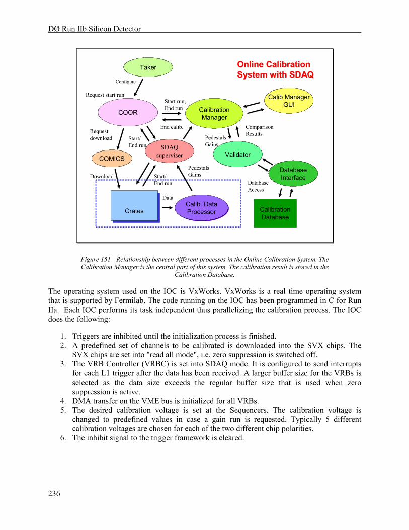
DØ Run IIb Silicon Detector
236
Taker
COOR
COMICS
CratesCrates
CalibrationManager
CalibrationDatabase
Calib. DataProcessor
Calib. DataProcessor
DatabaseInterface
Configure
Request start run
Request download
Download Start/End run
Start/End run
Data
PedestalsGains
PedestalsGains
ComparisonResults
DatabaseAccess
End calib.
Start run, End run
Online CalibrationOnline CalibrationSystem with SDAQSystem with SDAQ
Validator
Calib ManagerGUI
SDAQsuperviser
Figure 151- Relationship between different processes in the Online Calibration System. The Calibration Manager is the central part of this system. The calibration result is stored in the
Calibration Database.
The operating system used on the IOC is VxWorks. VxWorks is a real time operating system that is supported by Fermilab. The code running on the IOC has been programmed in C for Run IIa. Each IOC performs its task independent thus parallelizing the calibration process. The IOC does the following:
1. Triggers are inhibited until the initialization process is finished. 2. A predefined set of channels to be calibrated is downloaded into the SVX chips. The
SVX chips are set into "read all mode", i.e. zero suppression is switched off. 3. The VRB Controller (VRBC) is set into SDAQ mode. It is configured to send interrupts
for each L1 trigger after the data has been received. A larger buffer size for the VRBs is selected as the data size exceeds the regular buffer size that is used when zero suppression is active.
4. DMA transfer on the VME bus is initialized for all VRBs. 5. The desired calibration voltage is set at the Sequencers. The calibration voltage is
changed to predefined values in case a gain run is requested. Typically 5 different calibration voltages are chosen for each of the two different chip polarities.
6. The inhibit signal to the trigger framework is cleared.

DØ Run IIb Silicon Detector
237
The Trigger Framework sends regular L1 Triggers to all crates participating in the calibration run. The data is collected in the usual way (see Figure 94): The Sequencer Controllers and the VRB Controllers receive the L1 triggers. The SVX data is read out and stored in the VRBs. The calibration run requires a L2 reject for each given L1 trigger in contrast to the normal data taking mode. In this way the data is processed locally in the crate processor and is not sent to the L3 farm. The VRBC prepares the VRBs to be read out and sends an interrupt on the VME bus. The IOC catches this signal and a VME 64-bit DMA transfer from all VRBs is initiated. The IOC processes the data:
1. Additional triggers are inhibited while the data is being processed. 2. The data is decoded to get information about each strip. 3. Basic error checking is performed. 4. The number of events, the sum of the data values and the sum of the squares are stored
per strip.
Typically 800 events are collected for a calibration run. The mean and r.m.s. of the collected data is calculated for each calibration voltage setting. In case of a gain run a two parameter fit to the data is performed. The final result per strip is the pedestal value, the r.m.s. of the pedestal, the slope of the fitted line, the uncertainty on the slope, and an error flag. This result is sent to the Calibration Manager. The Validator can perform a simple data integrity check. Approved data is finally stored in the Calibration Database.
A separate process uses this information to calculate significant parameters for each readout chip. Each SVX readout chip requires a single threshold for zero suppression. The new threshold is chosen to be the average pedestal of the 128 readout channels plus 6 ADC counts. The typical pedestal r.m.s is about 2 ADC counts so that the threshold is 3 r.m.s above the pedestal level. Figure 152 shows the calibration result for an HDI as example. Several checks are performed on this result:
• The new threshold should not differ by more than 5 ADC counts from the previous threshold. Experience shows that pedestal levels change only slowly.
• The number of noisy strips per chip is calculated. An HDI is marked as problematic if more than 2% of the strips have an ADC count greater than 6. An SVX chip can be masked out if the resulting occupancy is too high.
• A channel is suppressed if the pedestal for the channel is more than 25 ADC counts below threshold. An HDI is marked as problematic if more than 2% of its channels are suppressed.
In case a problem is detected human intervention is required. A GUI that displays the calibration result and gives the user the possibility to manipulate the data exists. The final new threshold can be used as download parameter for the next data taking period.
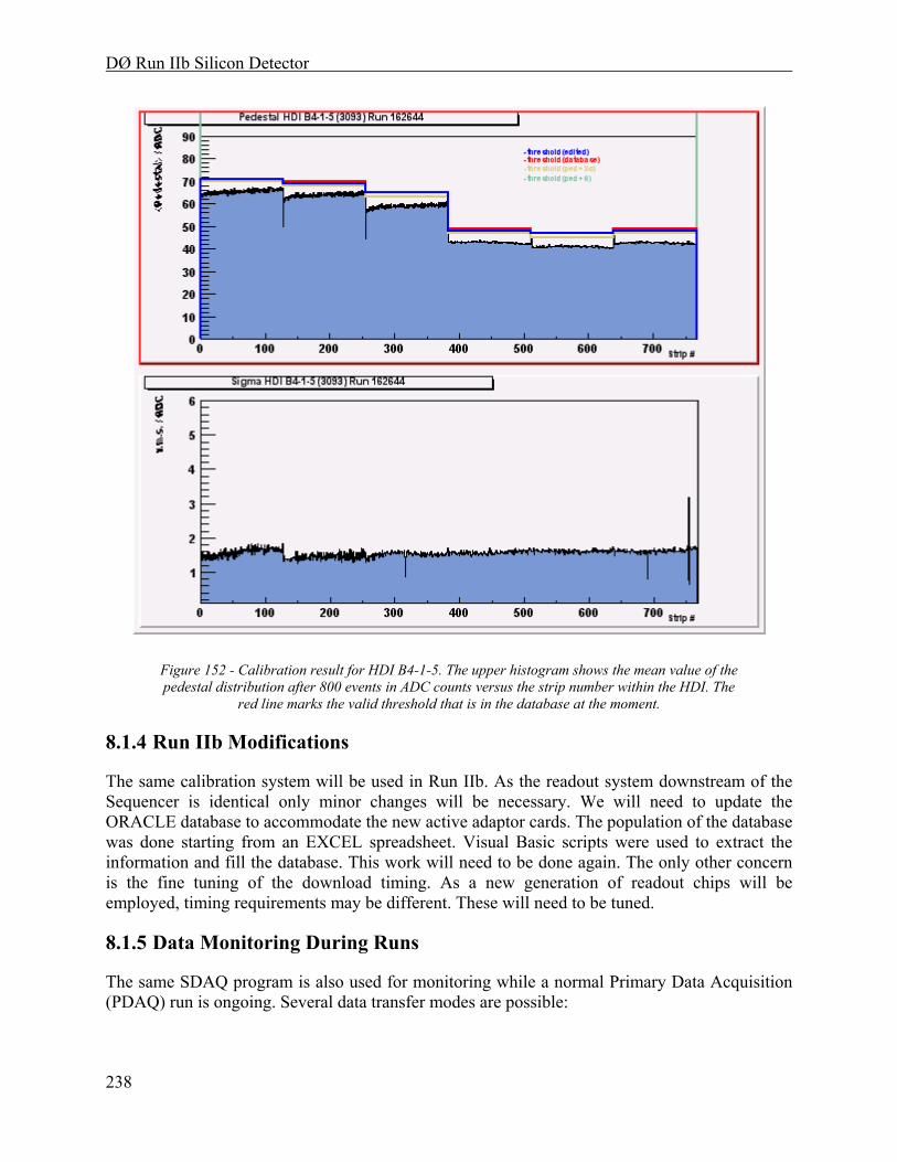
DØ Run IIb Silicon Detector
238
Figure 152 - Calibration result for HDI B4-1-5. The upper histogram shows the mean value of the pedestal distribution after 800 events in ADC counts versus the strip number within the HDI. The
red line marks the valid threshold that is in the database at the moment.
8.1.4 Run IIb Modifications
The same calibration system will be used in Run IIb. As the readout system downstream of the Sequencer is identical only minor changes will be necessary. We will need to update the ORACLE database to accommodate the new active adaptor cards. The population of the database was done starting from an EXCEL spreadsheet. Visual Basic scripts were used to extract the information and fill the database. This work will need to be done again. The only other concern is the fine tuning of the download timing. As a new generation of readout chips will be employed, timing requirements may be different. These will need to be tuned.
8.1.5 Data Monitoring During Runs
The same SDAQ program is also used for monitoring while a normal Primary Data Acquisition (PDAQ) run is ongoing. Several data transfer modes are possible:

DØ Run IIb Silicon Detector
239
• The IOC catches an interrupt sent by the VRBC when the data is available. A prescale can be set to adjust the rate of monitor events. The IOC reads the data from an internal Monitor FIFO of the VRB, the so-called Spy Memory. As this memory area can only be accessed by single word read operations, the data transfer is rather slow. Eight different VRB channels share one Spy memory so that only 1/8 of an event can be read.
• The 8KByte large FIFO can also be read out through an auxiliary port. For the time being only the VME readout is implemented but alternate readout schemes like IEEE1394 are under consideration for this.
• The IOC reads the data from the regular VRB memory. This procedure can introduce additional dead time while the VRB is read out.
• The IOC reads data from the Single Board Computer (SBC), the module that replaced the VBD as L3 Trigger interface. In this case a fast VME 64-bit transfer can be used, utilizing spare bandwidth of the VME backplane.
The data is collected and analyzed by the IOC, which sends analyzed data to a LINUX host computer. A three-threaded monitoring application is running on this machine:
1. One thread collects data from all IOCs via TCP IP sockets and stores them in a global data structure. This global data structure is modeled after the hardware configuration of crates, VRBs, HDIs and chips as defined by the ORACLE database. It contains information about signals, hit distributions, occupancy and errors for all HDIs and chips.
2. The second thread serves data to Java Servlets (TCP IP sockets) that are used to display histograms on a WWW browser.
3. The third thread is used to check data every 10000 events and sends information about dead or faulty hardware or high occupancy HDIs to the Significant Event System.
All common data structures shared by the threads are synchronized by a set of semaphores. The Java Servlets allow querying for:
• Dead hardware: HDIs are marked dead when a readout chip gives no signals. • Faulty hardware: HDIs are marked faulty when a previously working channel gives no
signal. • Occupancy: Contains the occupancy distribution for HDIs and chips. • Data signal: Distribution of mean values of all signals per HDI or SVX. • Hit count: Hit count per SVX and per readout channel. An example is shown in Figure
153. • Errors: Errors detected in the collected data (missing strips, wrong chip id, channel
ordering error).
The servlets generate output in a text mode and a graphics mode. Histograms are created using the free product JPGraph written in PHP.

DØ Run IIb Silicon Detector
240
Observing the occupancy allows monitoring when a new threshold for zero suppression needs to be determined. A message is sent to the Significant Event System if the occupancy reaches a predefined limit.
The offline monitoring with "Examine" processes allows full reconstruction of a small number of events. Apart from occupancy histograms this allows a SMT specific event display, Landau distributions of clusters and the reconstruction of tracks and vertices.
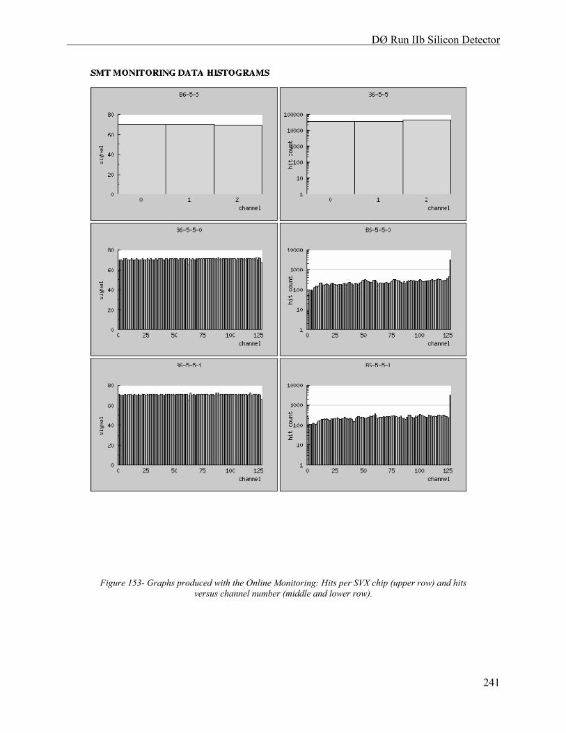
DØ Run IIb Silicon Detector
241
Figure 153- Graphs produced with the Online Monitoring: Hits per SVX chip (upper row) and hits versus channel number (middle and lower row).
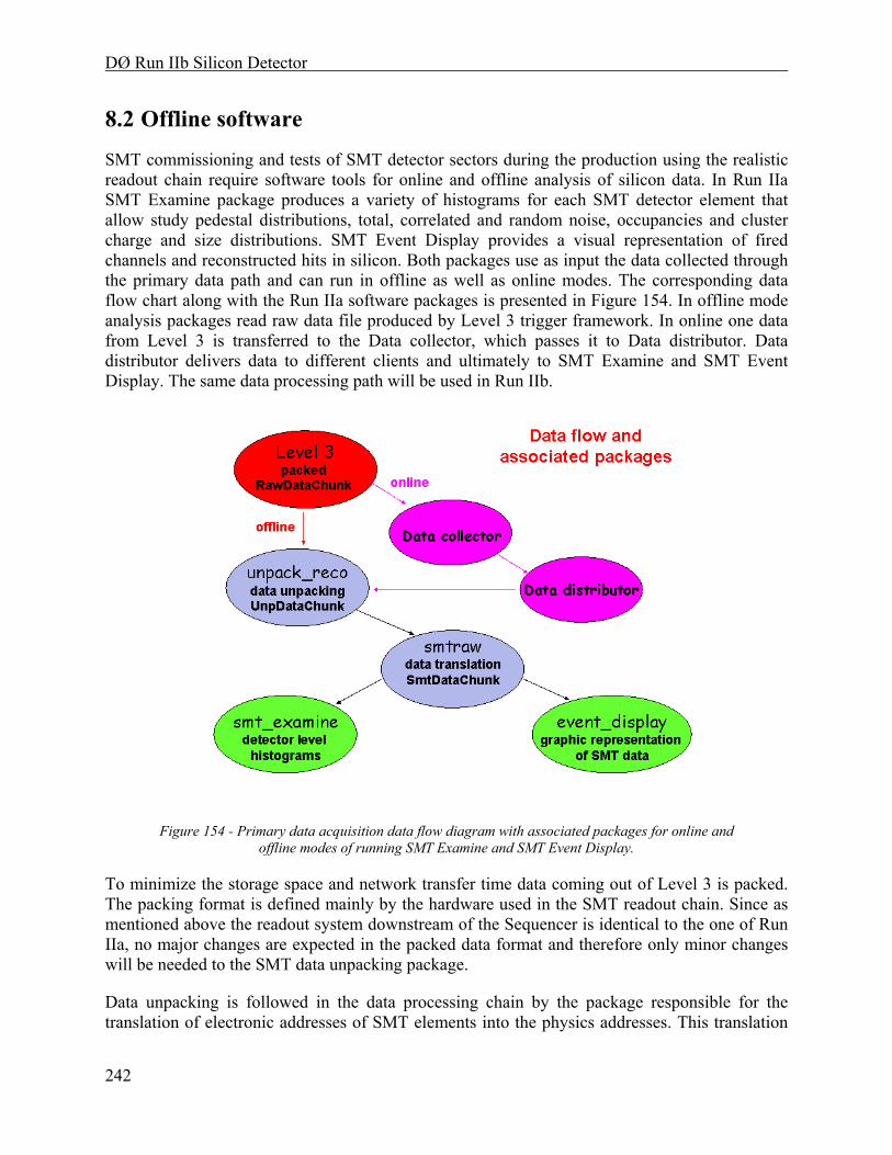
DØ Run IIb Silicon Detector
242
8.2 Offline software
SMT commissioning and tests of SMT detector sectors during the production using the realistic readout chain require software tools for online and offline analysis of silicon data. In Run IIa SMT Examine package produces a variety of histograms for each SMT detector element that allow study pedestal distributions, total, correlated and random noise, occupancies and cluster charge and size distributions. SMT Event Display provides a visual representation of fired channels and reconstructed hits in silicon. Both packages use as input the data collected through the primary data path and can run in offline as well as online modes. The corresponding data flow chart along with the Run IIa software packages is presented in Figure 154. In offline mode analysis packages read raw data file produced by Level 3 trigger framework. In online one data from Level 3 is transferred to the Data collector, which passes it to Data distributor. Data distributor delivers data to different clients and ultimately to SMT Examine and SMT Event Display. The same data processing path will be used in Run IIb.
Figure 154 - Primary data acquisition data flow diagram with associated packages for online and offline modes of running SMT Examine and SMT Event Display.
To minimize the storage space and network transfer time data coming out of Level 3 is packed. The packing format is defined mainly by the hardware used in the SMT readout chain. Since as mentioned above the readout system downstream of the Sequencer is identical to the one of Run IIa, no major changes are expected in the packed data format and therefore only minor changes will be needed to the SMT data unpacking package.
Data unpacking is followed in the data processing chain by the package responsible for the translation of electronic addresses of SMT elements into the physics addresses. This translation
DØ Run IIb Silicon Detector
243
is based on the cabling scheme of the SMT detector, which will be replaced to match Run IIb SMT design. Significant modifications of the translation package will be required to accommodate these changes. The same is true for SMT Examine and SMT Event Display packages which also heavily depend on the SMT design.
8.3 Hardware Operations
In the following interactions with the different hardware modules are described. The actual values for the download are extracted from the database if not stated otherwise.
8.3.1 VRB
• reset: Issues a reset. • init: Initializes the channel selection, simulation mode and Grey decoding registers. • j3enable/j3disable: Enables/disables communication via the custom made part of the
backplane • chan disable: Disables all VRB input channels. • sim data: Switches to auto generated data. • conf buffer: Configures the VRB buffers. • print register: Prints all status registers.
8.3.2 SEQ
• download: Downloads all SVX chips connected to this Sequencer. • HDI off: Sets the HDI enable bits to 0. The effect is that the low voltage to the SVX chips
is switched off. • complete init: Downloads all SVX chips and initializes the sequencer • init: Initializes the sequencer only. • reset: Sends a reset command to the sequencer. • set cxpw: Sets the crossing pulse width. • set calv: Sets the calibration voltage. • set calv 0: Sets the calibration voltage to zero. • set hdim: Sets the HDI mask. This bit pattern allows ignoring certain input channels. • set powr: Sets the power/hdi enable bit for each channel • power on: Sets the power/hdi enable bits for all channels to 1. • print temp: Prints the temperature as measured by the upper most optical transmitter. • print status: Prints the 1553 status word. Should be 0 if the last transmission was correct. • print CALV: Prints the value of the calibration voltage currently set. • print HV status: Prints the status of the HV for all HDIs of this sequencer (On, Off,
Locked, Tripped, Disabled).

DØ Run IIb Silicon Detector
244
8.3.3 SEQ channel
• download: Downloads the two HDIs connected to this sequencer channel. • power off: Sets the HDI enable bits for those two HDIs to 0. • set nch: Sets the number of SVX chips for the HDIs. • check hdis: Compares the read back of the SVX configuration with the download value. • print HV status: Prints the status of the HV for those two HDIs. • print SVX read back: Prints the read back of the SVX download string as series of hex
numbers.
8.3.4 KSU Interface board (INT)
• start HV GUI: Starts HV GUI for the HDIs connected to this Interface Board. • start IB GUI: Starts the IB GUI for those HDIs. This GUI display the voltage, current and
temperature information as read by the KSU Interface Board.
8.3.5 HDI
• power off: Sets the HDI enable bit for this HDI to 0. • print HV pods: Lists the HV pods for this HDI. • print HV status: Prints the HV status for this HDI. • HV pods GUI: Starts the HV GUI for HV pods connected to this HDI. • SVX GUI: Starts a GUI that allows changing individual SVX download parameters. • SVX Thresholds: Starts a GUI that displays the Thresholds of the last ten calibration runs
for all SVX of this HDI. This GUI allows a simple manipulation of threshold values for the next download.
In addition to providing an interface to single readout modules, global functions acting on a complete readout crate are implemented:
8.3.6 VRB Crate (VRBCR):
Operations to all modules of the same type connected to this VRB crate.
• HDI power off: Sets the HDI enable bits to 0 for all sequencers. • SEQ set CALV: Sets the calibration voltage on all sequencers. • SEQ CALV 0: Sets the calibration voltage on all sequencers to 0. • SEQ set CXPW: Sets the crossing pulse width on all sequencers. • VRB reset: Resets all VRBs • VRB init: Initializes all VRBs • VRB enable: Tells the database and the GUI to use all VRBs. • VRB disable: Tells the database and the GUI to ignore all VRBs. • VRB j3enable: Sets the j3enable for all VRBs.

DØ Run IIb Silicon Detector
245
• VRB j3disable: Sets the j3disable for all VRBs. • VRB j3default: Sets the j3enable bit according to the database enable information. • VRB pattern: Switches all VRBs into auto generated data mode. • VRB no pattern: Switches all VRBs back to normal data taking mode. • VRB print reg: Prints the register content of all VRBs. • scan HV: Scans the HV status of all HDIs. The result is displays in different color codes. • start HV GUI: Starts a HV GUI with all HV channels that are connected to HDIs in this
crate. • print hdi list: Prints a list of HDIs in this crate. • write sdaq file: Writes a configuration file containing the current settings that can be read
by a sdaq process. • write mon cal file: Writes a file with calibration database information for online
monitoring. • write off cal file: Writes a file with the most recent calibration information for examine
and offline processes. • write pickle file: Writes a file with download information for COMICS. • write transl map: Writes a file with the latest translation map between VRB channels and
HDIs.
8.3.7 VRB Controller (VRBC)
• init: Initializes the VRBC. • reset: Sends reset command to the VRBC. • 53 MHz: Switches internal 53 MHz oscillator of the VRBC on. • idle mode: Switches the internal NRZ generator into idle mode. • acquire mode: Switches the internal NRZ generator into acquire mode. • PDAQ mode: Switches the VRBC into PDAQ mode. • SDAQ mode: Switches the VRBC into SDAQ mode. • P+SDAQ mode: Switches the VRBC into PDAQ monitoring mode. • 16x2K buffer: Selects the 16 buffers of the VRB of 2K size. • 8x4K buffer: Selects the 8 buffers of the VRB of 4K size. The physical memory is
actually the same, the address space is configured differently. • send trigger: Sends a trigger command to the VRBC. • cal inject: Sends a trigger command to the VRBC and causes a NRZ calibration pulse
code to be generated. • N cal inject: Sends N=10 cal inject commands. • print SCL status: Prints the contents of the SCL status register. • print mode: Prints the current mode information of the VRBC.
8.3.8 VRB Buffer Driver (VBD).
The VBD has been replaced with a Single Board Computer (SBC). However, the SBC emulates the VBD and has therefore the same register structure.

DØ Run IIb Silicon Detector
246
• init: Initializes the VBD. • clear memory: Clears the VBD memory. • use VME: Tells the VBD to use the VME backplane for data transfer. • read evt len: Reads the event length information from the VBD. • read event: Reads a complete event from the VBD. The result is displayed graphically in
a separate GUI window. • print crate type: Prints the crate type information. • print event address: Prints the register containing the event address. • print status: Prints the status register.
8.3.9 Sequencer Controller (SEQC)
• reset: Sends a reset command. • init: Initializes the SEQC. • delay: Sets the delay registers. • set rdo abort: Switches the readout abort feature on. In this mode the readout is aborted
after 3.5µs. • clr rdo abort: Switches the readout abort feature off. • use SCL: Switches the SEQC into SCL mode. • use 1553: Switches the SEQC into 1553 mode. • use SCL Cal: Switches the SEQC into SCL mode. For each L1 Trigger a calibration pulse
is issued. This mode is used for gain calibration runs. • idle mode: Switches the SEQC into idle mode for download. • acquire mode: Switches the SEQC into acquire mode for data taking. • cal inject: Sends a trigger command to the SEQC. A calibration pulse is injected into the
SVX. • N cal inject: Sends N=10 cal inject commands. • print status: Prints the status registers.
8.3.10 Global options
• download: Complete initialization of all modules connected to this crate is performed. • HDIs off: Switch all HDIs in this crate off. • cal inject: Generation, recording and displaying of a pedestal or pulser event. • reinit VME: Reinitialize all VRBs, the VRBC, VBD and SEQC connected to this crate. • calibration:
o Process Pedestal Run: Processes a calibration run and calculates new thresholds. o Process Gain Run: Processes a gain run and determines potentially dead strips. o Print Stat all Runs: Prints a summary of the last 10 calibration runs for this crate. o Print Stat one Run: Prints a summary of the last calibration run. o Select new threshold: Starts a GUI that allows the selection of a new threshold for
zero suppression for the next download.

DØ Run IIb Silicon Detector
247
The status registers of all the modules are polled with a predefined frequency. The result of this poll is displayed in the GUI as different color codes. The following colors are used:
Grey: Status is unknown. Orange: Power is off. White: The module is not usable. Yellow: The module is disabled. Green: OK. Sea green: The module is OK but not in its standard configuration. Magenta: The module needs to be updated. Red: The module returns an error status.

DØ Run IIb Silicon Detector
248
9 SIMULATION OF THE SILICON DETECTOR PERFORMANCE FOR RUN IIB
9.1 Overview
The DØ Run IIb group performed a detailed simulation of the Run IIb silicon microstrip tracker. The simulation included a full Geant simulation of the underlying physical process, data-tuned models of detector response, and complete reconstruction of simulated events, including pattern recognition, within the DØ Run IIb software framework. Quantitative calculations of occupancy, impact parameter resolution, momentum resolution, and b-quark tagging efficiency verify substantial improvements in performance over the presently operating Run IIa silicon detector. These full Geant results are presented below.
9.2 Silicon Geometry in the Simulation
The Run IIb silicon detector is modeled as a barrel tracker consisting of six concentric cylindrical layers, numbered from 0 to 5 in going from the innermost radius of 19 mm to the outermost radius of 164 mm, respectively. Pseudorapidity coverage extends from -2.5 to +2.5. Each layer consists of two sub-layers that preserve a six-fold symmetry for the silicon track trigger. Layers 0 and 1 were simulated with axial silicon detectors only, while layers 2 through 5 contained axial-stereo pairs of single-sided detectors in each sub-layer. Figure 155 shows an x-y view of the Run IIb silicon detector geometry as implemented in the simulations, Figure 156 shows an x-z view, and Table 27 gives positions, dimensions, and stereo angles of the detector modules used for this work.
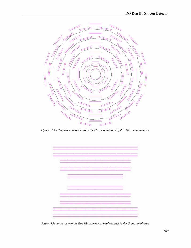
DØ Run IIb Silicon Detector
249
Figure 155 - Geometric layout used in the Geant simulation of Run IIb silicon detector.
Figure 156 An xz view of the Run IIb detector as implemented in the Geant simulation.
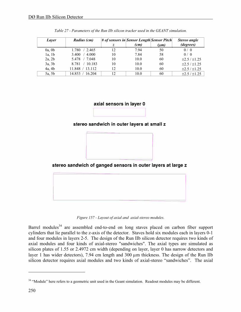
DØ Run IIb Silicon Detector
250
Table 27 - Parameters of the Run IIb silicon tracker used in the GEANT simulation.
Layer Radius (cm) # of sensors in z
Sensor Length (cm)
Sensor Pitch (µm)
Stereo angle (degrees)
0a, 0b 1.780 / 2.465 12 7.94 50 0 / 0 1a, 1b 3.400 / 4.000 10 7.84 58 0 / 0 2a, 2b 5.478 / 7.048 10 10.0 60 ±2.5 / ±1.25 3a, 3b 8.781 / 10.183 10 10.0 60 ±2.5 / ±1.25 4a, 4b 11.848 / 13.112 12 10.0 60 ±2.5 / ±1.25 5a, 5b 14.853 / 16.204 12 10.0 60 ±2.5 / ±1.25
Figure 157 - Layout of axial and axial-stereo modules.
Barrel modules34 are assembled end-to-end on long staves placed on carbon fiber support cylinders that lie parallel to the z-axis of the detector. Staves hold six modules each in layers 0-1 and four modules in layers 2-5. The design of the Run IIb silicon detector requires two kinds of axial modules and four kinds of axial-stereo "sandwiches". The axial types are simulated as silicon plates of 1.55 or 2.4972 cm width (depending on layer, layer 0 has narrow detectors and layer 1 has wider detectors), 7.94 cm length and 300 µm thickness. The design of the Run IIb silicon detector requires axial modules and two kinds of axial-stereo “sandwiches”. The axial
34 “Module” here refers to a geometric unit used in the Geant simulation. Readout modules may be different.

DØ Run IIb Silicon Detector
251
type is simulated as a silicon plate of 1.48 cm width, 7.84 cm length and 300 µm thickness35. A sandwich silicon module consists of two equivalent silicon sensors, one axially oriented and the other rotated with respect to the beam axis. The radial distance between the two silicon planes in the sandwich is 3.094 mm, and the angle of the rotation is ±2.5 degrees for the small sandwiches and ±1.25 degrees for the stereo pairs of ganged detectors. The size of the silicon ladders in the sandwiches is 4.11 cm × 10 cm × 300 µm. Axial and stereo modules are shown in Figure 157.
All studies assume a functioning CFT in Run IIb. Thus, a central track can have up to 14 hits—six in the SMT and eight in the CFT. The new layer 0 becomes the innermost hit on the track, and the new layer 5 is the sixth of fourteen hits.
Low mass readout cables are modeled as copper plates of 1 cm width that go out of the edge of first and third silicon modules in every layer.
9.3 Simulation of Signal, Digitization and Cluster Reconstruction
Geant simulates hits in the silicon sensors, and a modified DØ Run IIa package DØSim36 package digitizes signals.
Input for DØSim consists of a bank of GEANT hits, each of which is described by entry/exit positions and energy deposition in the silicon. Silicon dE/dx is simulated via explicit generation of δ-rays that resulted in a Landau distribution of deposited energy. No additional fluctuations in energy loss were considered.
In order to reproduce the effects of ganging sensors together correctly in the readout, hits within ±1.5 mm of the midpoint in z of long axial/stereo sandwich modules were discarded at the digitization step.
The total deposited energy is converted into the number of electron-hole pairs using a coefficient C=2.778×10⁸ GeV-1. Charge collection on strips is computed from a diffusion model with the standard drift and Hall mobility of the charge carriers in silicon evaluated at the nominal silicon operating temperature. Charge sharing between strips through intermediate strip wiring is determined by inter-strip capacitance, readout-ground capacitance, and the input capacitance of preamplifier, values of which are taken from Run IIa measurements.
Electronic noise is added to the readout strips after hits have been digitized. Parameters for noise simulation were extracted from the readout electronics noise parameterization and silicon detector prototype studies for Run IIa37. This set of parameters leads to a S/N ratio of 16:1, and this value is used for all tracking performance studies. For occupancy studies the average noise was simulated for each channel according to Gaussian distribution with σ=2.1 ADC counts that decreases the signal-to-noise ratio to 10:1, again consistent with the Run IIa data. A similar
35 The actual sensors turn out to be 320 µm thick. 36 http://www-d0.fnal.gov/newd0/d0atwork/computing/MonteCarlo/simulation/d0sim.html. 37 J. Ellison and A. Heinson, “Effects of Radiation Damage on the DØ Silicon Tracker”, DØ Note 2679, July, 1995.
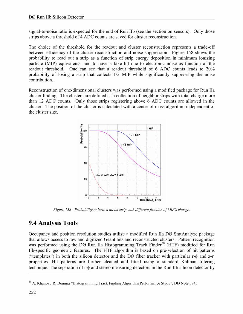
DØ Run IIb Silicon Detector
252
signal-to-noise ratio is expected for the end of Run IIb (see the section on sensors). Only those strips above a threshold of 4 ADC counts are saved for cluster reconstruction.
The choice of the threshold for the readout and cluster reconstruction represents a trade-off between efficiency of the cluster reconstruction and noise suppression. Figure 158 shows the probability to read out a strip as a function of strip energy deposition in minimum ionizing particle (MIP) equivalents, and to have a fake hit due to electronic noise as function of the readout threshold. One can see that a readout threshold of 6 ADC counts leads to 20% probability of losing a strip that collects 1/3 MIP while significantly suppressing the noise contribution.
Reconstruction of one-dimensional clusters was performed using a modified package for Run IIa cluster finding. The clusters are defined as a collection of neighbor strips with total charge more than 12 ADC counts. Only those strips registering above 6 ADC counts are allowed in the cluster. The position of the cluster is calculated with a center of mass algorithm independent of the cluster size.
Figure 158 - Probability to have a hit on strip with different fraction of MIP's charge.
9.4 Analysis Tools
Occupancy and position resolution studies utilize a modified Run IIa DØ SmtAnalyze package that allows access to raw and digitized Geant hits and reconstructed clusters. Pattern recognition was performed using the DØ Run IIa Histogramming Track Finder38 (HTF) modified for Run IIb-specific geometric features. The HTF algorithm is based on pre-selection of hit patterns (“templates”) in both the silicon detector and the DØ fiber tracker with particular r-φ and z-η properties. Hit patterns are further cleaned and fitted using a standard Kalman filtering technique. The separation of r-φ and stereo measuring detectors in the Run IIb silicon detector by 38 A. Khanov, R. Demina “Histogramming Track Finding Algorithm Performance Study”, DØ Note 3845.
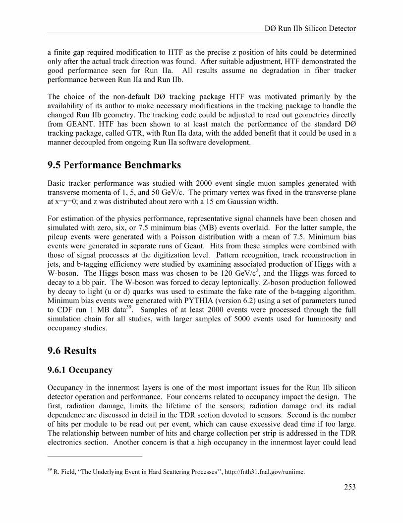
DØ Run IIb Silicon Detector
253
a finite gap required modification to HTF as the precise z position of hits could be determined only after the actual track direction was found. After suitable adjustment, HTF demonstrated the good performance seen for Run IIa. All results assume no degradation in fiber tracker performance between Run IIa and Run IIb.
The choice of the non-default DØ tracking package HTF was motivated primarily by the availability of its author to make necessary modifications in the tracking package to handle the changed Run IIb geometry. The tracking code could be adjusted to read out geometries directly from GEANT. HTF has been shown to at least match the performance of the standard DØ tracking package, called GTR, with Run IIa data, with the added benefit that it could be used in a manner decoupled from ongoing Run IIa software development.
9.5 Performance Benchmarks
Basic tracker performance was studied with 2000 event single muon samples generated with transverse momenta of 1, 5, and 50 GeV/c. The primary vertex was fixed in the transverse plane at x=y=0; and z was distributed about zero with a 15 cm Gaussian width.
For estimation of the physics performance, representative signal channels have been chosen and simulated with zero, six, or 7.5 minimum bias (MB) events overlaid. For the latter sample, the pileup events were generated with a Poisson distribution with a mean of 7.5. Minimum bias events were generated in separate runs of Geant. Hits from these samples were combined with those of signal processes at the digitization level. Pattern recognition, track reconstruction in jets, and b-tagging efficiency were studied by examining associated production of Higgs with a W-boson. The Higgs boson mass was chosen to be 120 GeV/c2, and the Higgs was forced to decay to a bb pair. The W-boson was forced to decay leptonically. Z-boson production followed by decay to light (u or d) quarks was used to estimate the fake rate of the b-tagging algorithm. Minimum bias events were generated with PYTHIA (version 6.2) using a set of parameters tuned to CDF run 1 MB data39. Samples of at least 2000 events were processed through the full simulation chain for all studies, with larger samples of 5000 events used for luminosity and occupancy studies.
9.6 Results
9.6.1 Occupancy
Occupancy in the innermost layers is one of the most important issues for the Run IIb silicon detector operation and performance. Four concerns related to occupancy impact the design. The first, radiation damage, limits the lifetime of the sensors; radiation damage and its radial dependence are discussed in detail in the TDR section devoted to sensors. Second is the number of hits per module to be read out per event, which can cause excessive dead time if too large. The relationship between number of hits and charge collection per strip is addressed in the TDR electronics section. Another concern is that a high occupancy in the innermost layer could lead
39 R. Field, “The Underlying Event in Hard Scattering Processes’’, http://fnth31.fnal.gov/runiimc.
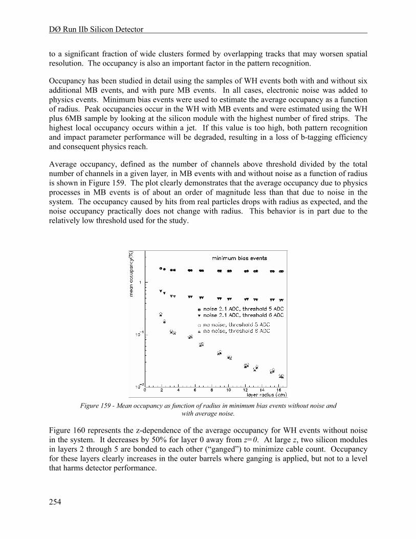
DØ Run IIb Silicon Detector
254
to a significant fraction of wide clusters formed by overlapping tracks that may worsen spatial resolution. The occupancy is also an important factor in the pattern recognition.
Occupancy has been studied in detail using the samples of WH events both with and without six additional MB events, and with pure MB events. In all cases, electronic noise was added to physics events. Minimum bias events were used to estimate the average occupancy as a function of radius. Peak occupancies occur in the WH with MB events and were estimated using the WH plus 6MB sample by looking at the silicon module with the highest number of fired strips. The highest local occupancy occurs within a jet. If this value is too high, both pattern recognition and impact parameter performance will be degraded, resulting in a loss of b-tagging efficiency and consequent physics reach.
Average occupancy, defined as the number of channels above threshold divided by the total number of channels in a given layer, in MB events with and without noise as a function of radius is shown in Figure 159. The plot clearly demonstrates that the average occupancy due to physics processes in MB events is of about an order of magnitude less than that due to noise in the system. The occupancy caused by hits from real particles drops with radius as expected, and the noise occupancy practically does not change with radius. This behavior is in part due to the relatively low threshold used for the study.
Figure 159 - Mean occupancy as function of radius in minimum bias events without noise and
with average noise.
Figure 160 represents the z-dependence of the average occupancy for WH events without noise in the system. It decreases by 50% for layer 0 away from z=0. At large z, two silicon modules in layers 2 through 5 are bonded to each other (“ganged”) to minimize cable count. Occupancy for these layers clearly increases in the outer barrels where ganging is applied, but not to a level that harms detector performance.
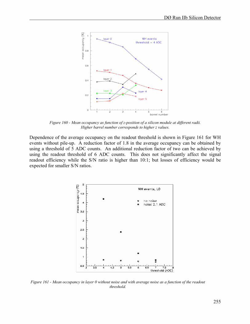
DØ Run IIb Silicon Detector
255
Figure 160 - Mean occupancy as function of z-position of a silicon module at different radii.
Higher barrel number corresponds to higher z values.
Dependence of the average occupancy on the readout threshold is shown in Figure 161 for WH events without pile-up. A reduction factor of 1.8 in the average occupancy can be obtained by using a threshold of 5 ADC counts. An additional reduction factor of two can be achieved by using the readout threshold of 6 ADC counts. This does not significantly affect the signal readout efficiency while the S/N ratio is higher than 10:1; but losses of efficiency would be expected for smaller S/N ratios.
Figure 161 - Mean occupancy in layer 0 without noise and with average noise as a function of the readout threshold.
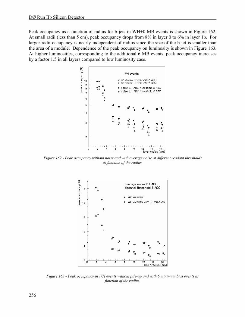
DØ Run IIb Silicon Detector
256
Peak occupancy as a function of radius for b-jets in WH+0 MB events is shown in Figure 162. At small radii (less than 5 cm), peak occupancy drops from 8% in layer 0 to 6% in layer 1b. For larger radii occupancy is nearly independent of radius since the size of the b-jet is smaller than the area of a module. Dependence of the peak occupancy on luminosity is shown in Figure 163. At higher luminosities, corresponding to the additional 6 MB events, peak occupancy increases by a factor 1.5 in all layers compared to low luminosity case.
Figure 162 - Peak occupancy without noise and with average noise at different readout thresholds
as function of the radius.
Figure 163 - Peak occupancy in WH events without pile-up and with 6 minimum bias events as function of the radius.
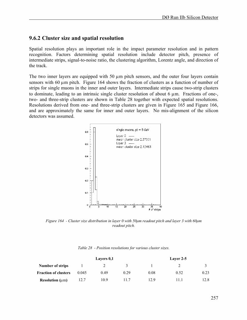
DØ Run IIb Silicon Detector
257
9.6.2 Cluster size and spatial resolution
Spatial resolution plays an important role in the impact parameter resolution and in pattern recognition. Factors determining spatial resolution include detector pitch, presence of intermediate strips, signal-to-noise ratio, the clustering algorithm, Lorentz angle, and direction of the track.
The two inner layers are equipped with 50 µm pitch sensors, and the outer four layers contain sensors with 60 µm pitch. Figure 164 shows the fraction of clusters as a function of number of strips for single muons in the inner and outer layers. Intermediate strips cause two-strip clusters to dominate, leading to an intrinsic single cluster resolution of about 6 µm. Fractions of one-, two- and three-strip clusters are shown in Table 28 together with expected spatial resolutions. Resolutions derived from one- and three-strip clusters are given in Figure 165 and Figure 166, and are approximately the same for inner and outer layers. No mis-alignment of the silicon detectors was assumed.
Figure 164 - Cluster size distribution in layer 0 with 50µm readout pitch and layer 3 with 60µm readout pitch.
Table 28 - Position resolutions for various cluster sizes.
Layers 0,1 Layer 2-5
Number of strips 1 2 3 1 2 3
Fraction of clusters 0.045 0.49 0.29 0.08 0.52 0.23
Resolution (µm) 12.7 10.9 11.7 12.9 11.1 12.8
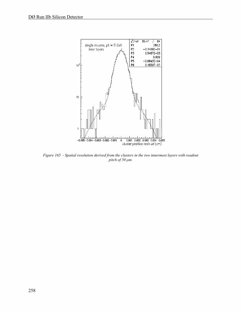
DØ Run IIb Silicon Detector
258
Figure 165 - Spatial resolution derived from the clusters in the two innermost layers with readout pitch of 50 µm.
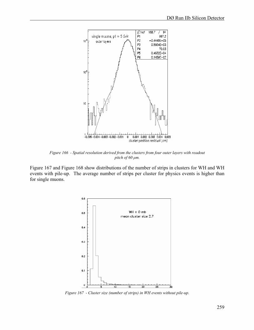
DØ Run IIb Silicon Detector
259
Figure 166 - Spatial resolution derived from the clusters from four outer layers with readout pitch of 60 µm.
Figure 167 and Figure 168 show distributions of the number of strips in clusters for WH and WH events with pile-up. The average number of strips per cluster for physics events is higher than for single muons.
Figure 167 - Cluster size (number of strips) in WH events without pile-up.
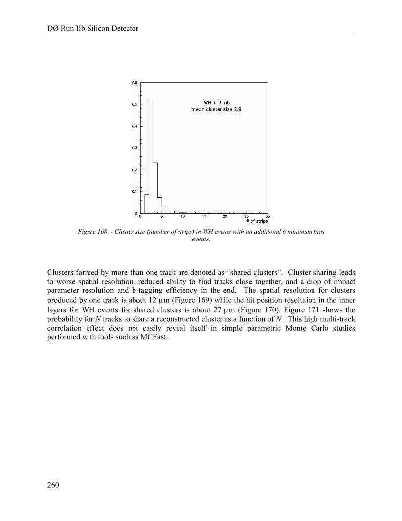
DØ Run IIb Silicon Detector
260
Figure 168 - Cluster size (number of strips) in WH events with an additional 6 minimum bias
events.
Clusters formed by more than one track are denoted as “shared clusters”. Cluster sharing leads to worse spatial resolution, reduced ability to find tracks close together, and a drop of impact parameter resolution and b-tagging efficiency in the end. The spatial resolution for clusters produced by one track is about 12 µm (Figure 169) while the hit position resolution in the inner layers for WH events for shared clusters is about 27 µm (Figure 170). Figure 171 shows the probability for N tracks to share a reconstructed cluster as a function of N. This high multi-track correlation effect does not easily reveal itself in simple parametric Monte Carlo studies performed with tools such as MCFast.
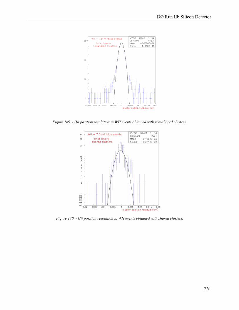
DØ Run IIb Silicon Detector
261
Figure 169 - Hit position resolution in WH events obtained with non-shared clusters.
Figure 170 - Hit position resolution in WH events obtained with shared clusters.
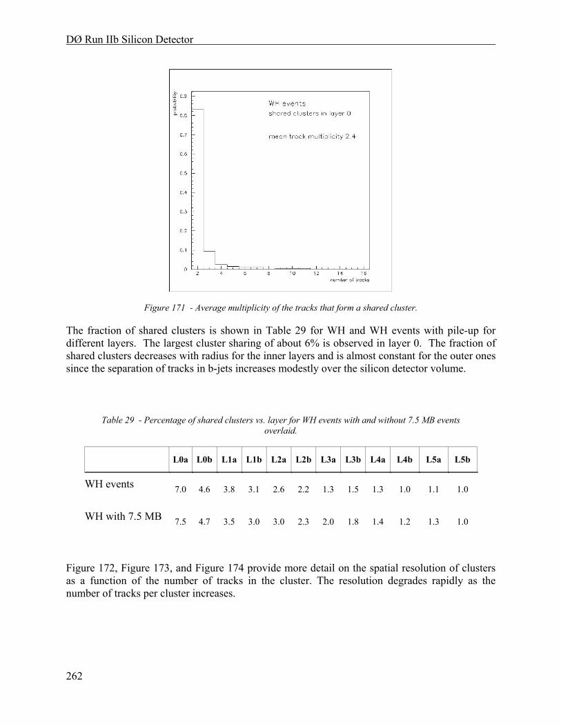
DØ Run IIb Silicon Detector
262
Figure 171 - Average multiplicity of the tracks that form a shared cluster.
The fraction of shared clusters is shown in Table 29 for WH and WH events with pile-up for different layers. The largest cluster sharing of about 6% is observed in layer 0. The fraction of shared clusters decreases with radius for the inner layers and is almost constant for the outer ones since the separation of tracks in b-jets increases modestly over the silicon detector volume.
Table 29 - Percentage of shared clusters vs. layer for WH events with and without 7.5 MB events overlaid.
L0a L0b L1a L1b L2a L2b L3a L3b L4a L4b L5a L5b
WH events 7.0 4.6 3.8 3.1 2.6 2.2 1.3 1.5 1.3 1.0 1.1 1.0
WH with 7.5 MB 7.5 4.7 3.5 3.0 3.0 2.3 2.0 1.8 1.4 1.2 1.3 1.0
Figure 172, Figure 173, and Figure 174 provide more detail on the spatial resolution of clusters as a function of the number of tracks in the cluster. The resolution degrades rapidly as the number of tracks per cluster increases.
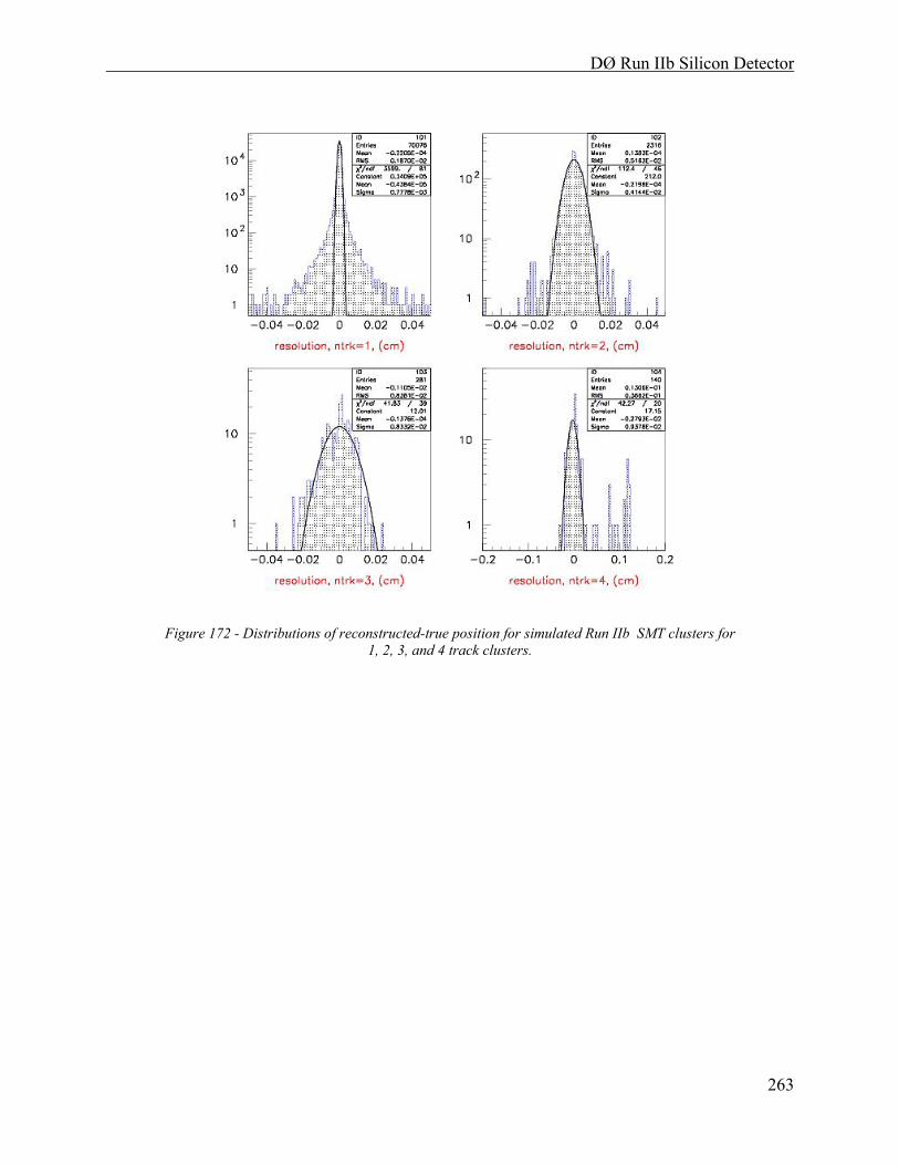
DØ Run IIb Silicon Detector
263
Figure 172 - Distributions of reconstructed-true position for simulated Run IIb SMT clusters for 1, 2, 3, and 4 track clusters.
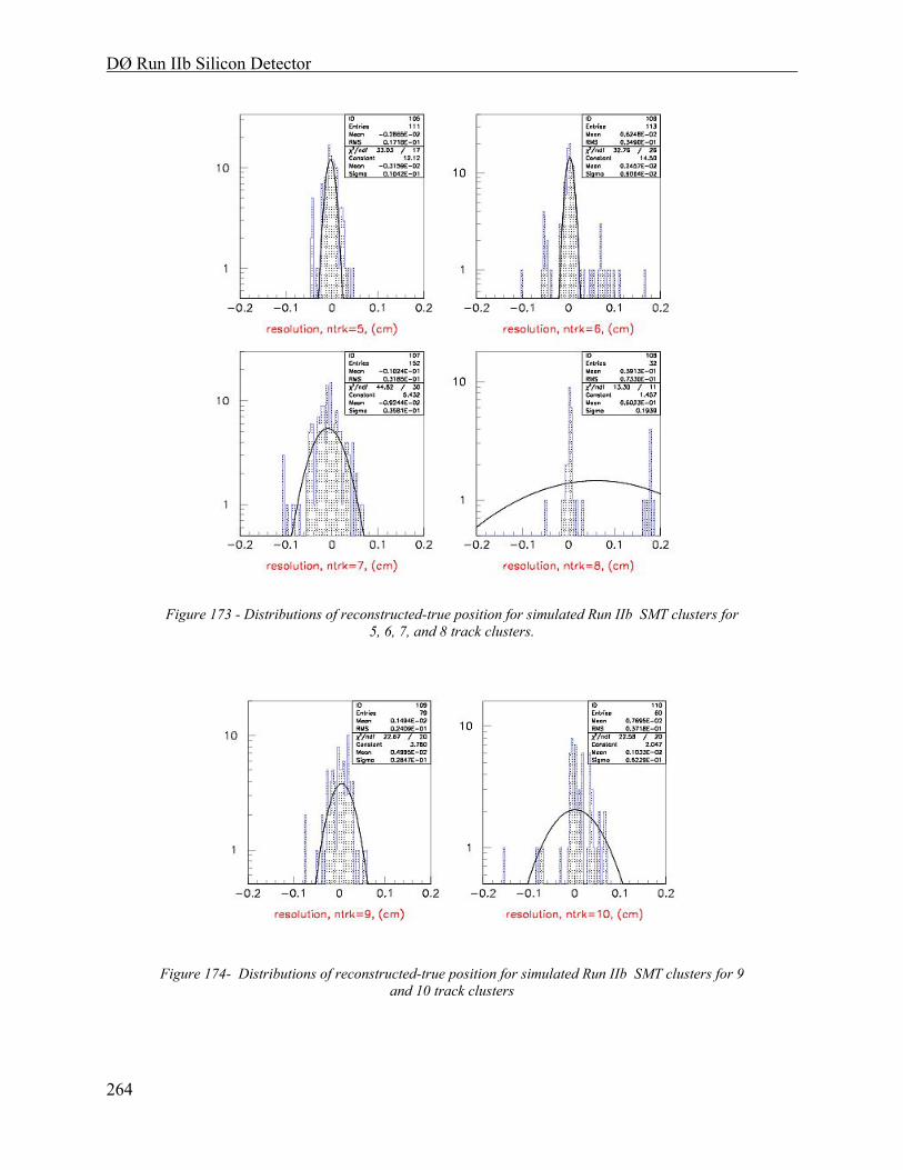
DØ Run IIb Silicon Detector
264
Figure 173 - Distributions of reconstructed-true position for simulated Run IIb SMT clusters for 5, 6, 7, and 8 track clusters.
Figure 174- Distributions of reconstructed-true position for simulated Run IIb SMT clusters for 9 and 10 track clusters

DØ Run IIb Silicon Detector
265
9.7 Physics Performance of the Run IIb Tracker
As discussed earlier in this document, the main Run IIb physics goal is the search for the Higgs boson. Other important investigations will center on top-quark properties, precision measurements of W-boson mass and width, b-physics, and searches for supersymmetry and other new phenomena. All physics would benefit from improved track reconstruction efficiency and momentum resolution in a Run IIb tracker with an upgraded silicon detector. However, higher b-tagging efficiency keys new physics discovery potential in DØ.
It is worth summarizing the essentials of simple cuts-based search for WH. Requirements include:
1. A high pT lepton of at least 20 GeV with |η|<2 and a missing ET>20 GeV. This strongly suppresses all final states without a W or Z, selecting ttX, WX, and ZX.
2. No other isolated tracks with pT>10 GeV. This suppresses events with Z ll and tt llX.
3. No more than two central jets with ET>20 GeV. This suppresses tt blνbjj.
4. At least two tagged b-jets. This suppresses Wjj lνjj and WZ lνjj
Note that the suppression of QCD events is largely accomplished without b-tagging in this final state. The largest backgrounds turn out to be contributions from Wbb lνbb, WZ lνbb, and tt,tb lνbb(njmiss) that cannot be reduced by any improvement in the SMT. The irreducibility of the backgrounds (at least without a more sophisticated analysis) implies that S/B will be independent of the b-tagging efficiency and that S/sqrt(B) will be linear(not quadratic) in single b-jet tagging efficiency.
The following sections summarize the track reconstruction efficiency, accuracy of the track parameter measurements, and b-tagging efficiency obtained from studies of WH events.
9.7.1 Single track performance
The pT resolution σ(pT) for single muons is shown in Figure 175, together with σ(pT) calculated for the Run IIa tracker. Resolution is obtained from a Gaussian fit to q/pT, where q is the particle charge. No tails were observed in this distribution for single muons. For low pT, where the pT resolution is dominated by multiple scattering there is no difference between Run IIa and Run IIb trackers. An improvement at high pT is observed due to larger number of precise measurements per track. The difference is big at small |η| and disappears at |η| above 1.5, as it is shown in Figure 175 (left).
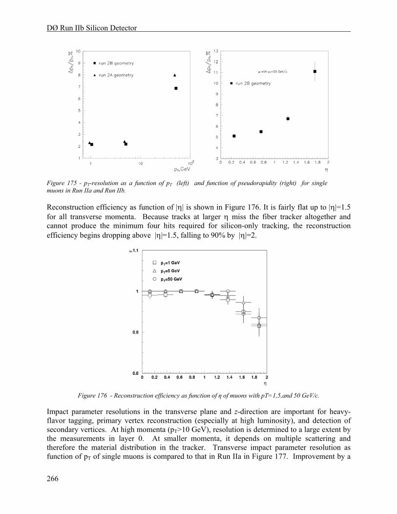
DØ Run IIb Silicon Detector
266
Figure 175 - pT-resolution as a function of pT (left) and function of pseudorapidity (right) for single muons in Run IIa and Run IIb.
Reconstruction efficiency as function of |η| is shown in Figure 176. It is fairly flat up to |η|=1.5 for all transverse momenta. Because tracks at larger η miss the fiber tracker altogether and cannot produce the minimum four hits required for silicon-only tracking, the reconstruction efficiency begins dropping above |η|=1.5, falling to 90% by |η|=2.
Figure 176 - Reconstruction efficiency as function of η of muons with pT=1,5,and 50 GeV/c.
Impact parameter resolutions in the transverse plane and z-direction are important for heavy-flavor tagging, primary vertex reconstruction (especially at high luminosity), and detection of secondary vertices. At high momenta (pT>10 GeV), resolution is determined to a large extent by the measurements in layer 0. At smaller momenta, it depends on multiple scattering and therefore the material distribution in the tracker. Transverse impact parameter resolution as function of pT of single muons is compared to that in Run IIa in Figure 177. Improvement by a
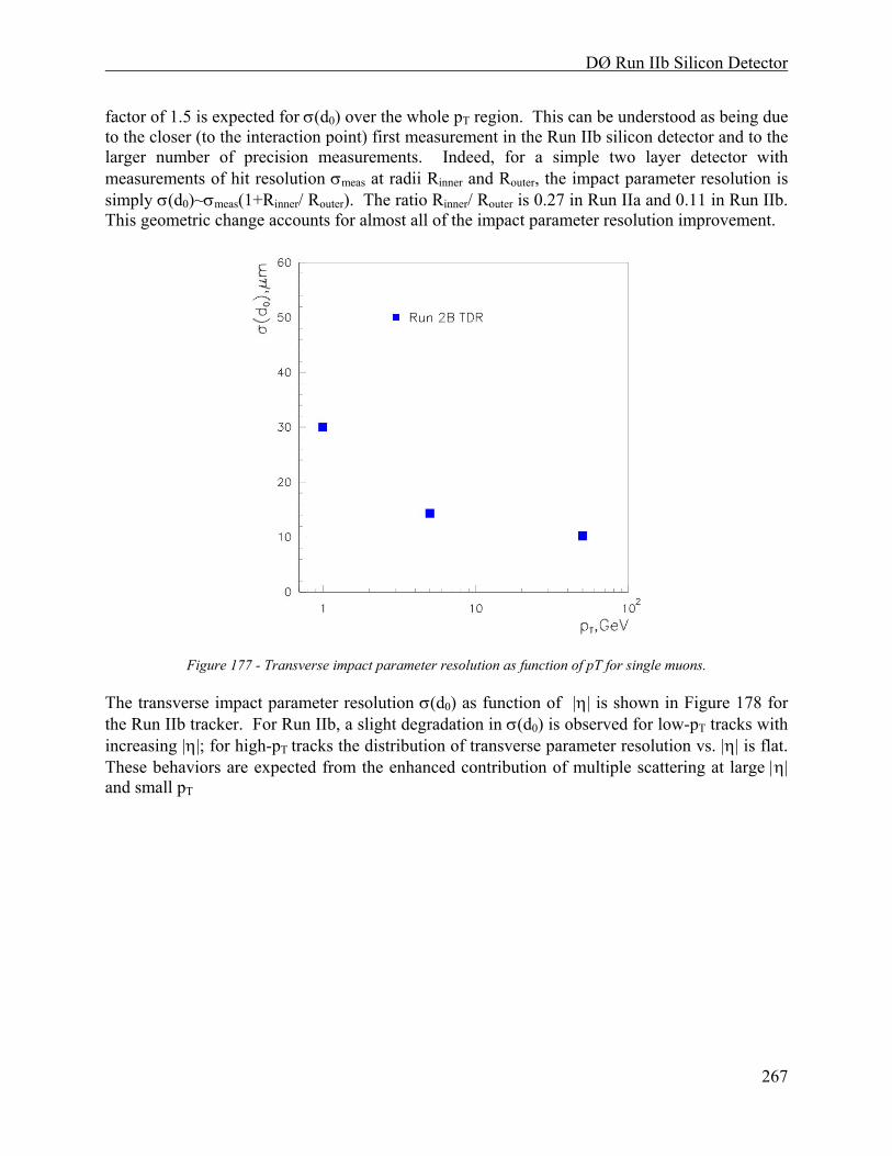
DØ Run IIb Silicon Detector
267
factor of 1.5 is expected for σ(d0) over the whole pT region. This can be understood as being due to the closer (to the interaction point) first measurement in the Run IIb silicon detector and to the larger number of precision measurements. Indeed, for a simple two layer detector with measurements of hit resolution σmeas at radii Rinner and Router, the impact parameter resolution is simply σ(d0)~σmeas(1+Rinner/ Router). The ratio Rinner/ Router is 0.27 in Run IIa and 0.11 in Run IIb. This geometric change accounts for almost all of the impact parameter resolution improvement.
Figure 177 - Transverse impact parameter resolution as function of pT for single muons.
The transverse impact parameter resolution σ(d0) as function of |η| is shown in Figure 178 for the Run IIb tracker. For Run IIb, a slight degradation in σ(d0) is observed for low-pT tracks with increasing |η|; for high-pT tracks the distribution of transverse parameter resolution vs. |η| is flat. These behaviors are expected from the enhanced contribution of multiple scattering at large |η| and small pT
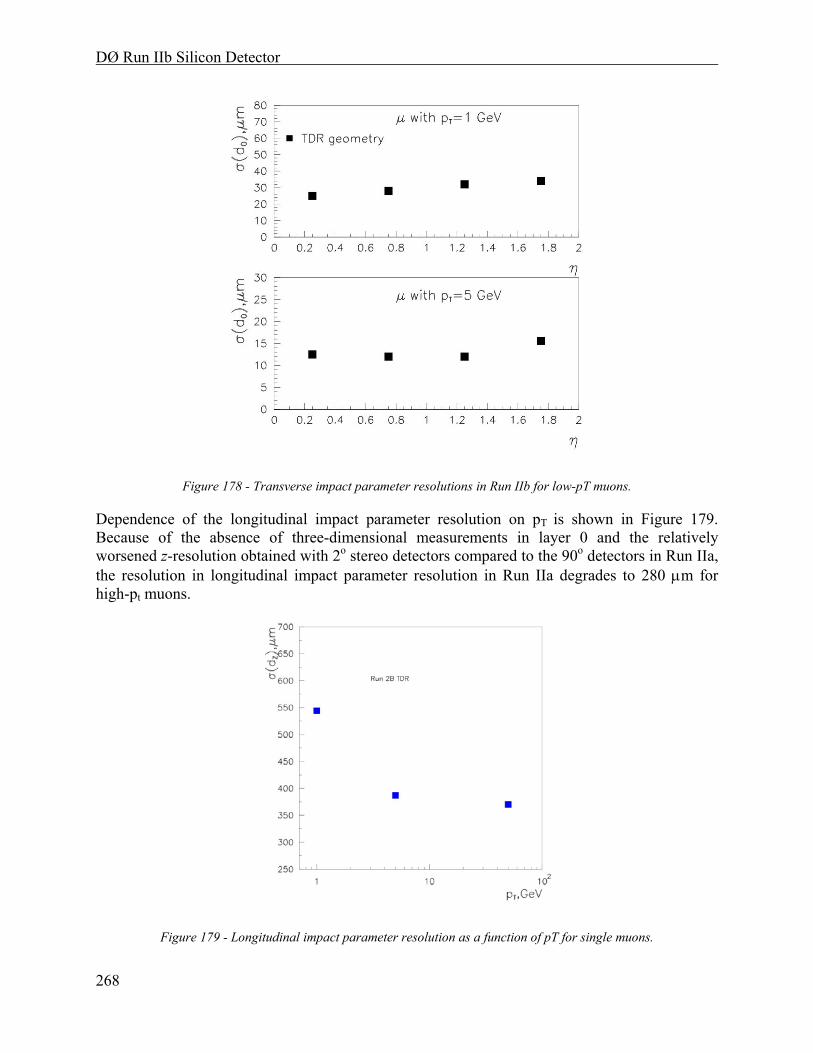
DØ Run IIb Silicon Detector
268
Figure 178 - Transverse impact parameter resolutions in Run IIb for low-pT muons.
Dependence of the longitudinal impact parameter resolution on pT is shown in Figure 179. Because of the absence of three-dimensional measurements in layer 0 and the relatively worsened z-resolution obtained with 2o stereo detectors compared to the 90o detectors in Run IIa, the resolution in longitudinal impact parameter resolution in Run IIa degrades to 280 µm for high-pt muons.
Figure 179 - Longitudinal impact parameter resolution as a function of pT for single muons.
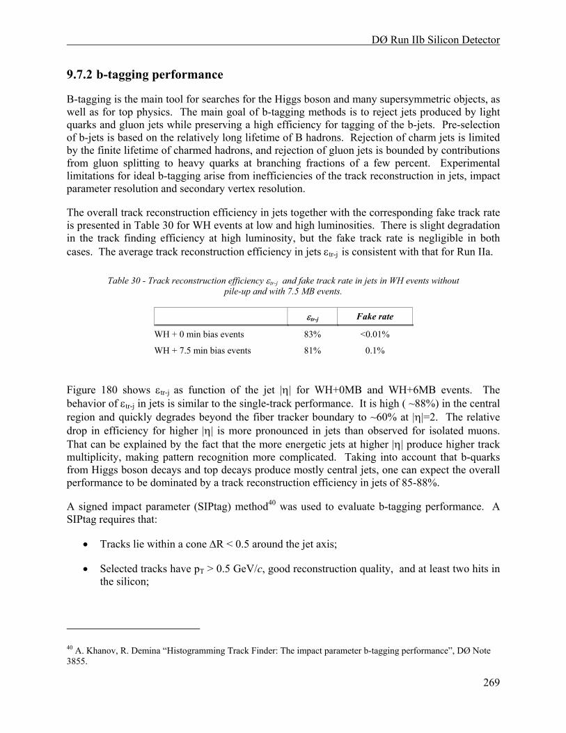
DØ Run IIb Silicon Detector
269
9.7.2 b-tagging performance
B-tagging is the main tool for searches for the Higgs boson and many supersymmetric objects, as well as for top physics. The main goal of b-tagging methods is to reject jets produced by light quarks and gluon jets while preserving a high efficiency for tagging of the b-jets. Pre-selection of b-jets is based on the relatively long lifetime of B hadrons. Rejection of charm jets is limited by the finite lifetime of charmed hadrons, and rejection of gluon jets is bounded by contributions from gluon splitting to heavy quarks at branching fractions of a few percent. Experimental limitations for ideal b-tagging arise from inefficiencies of the track reconstruction in jets, impact parameter resolution and secondary vertex resolution.
The overall track reconstruction efficiency in jets together with the corresponding fake track rate is presented in Table 30 for WH events at low and high luminosities. There is slight degradation in the track finding efficiency at high luminosity, but the fake track rate is negligible in both cases. The average track reconstruction efficiency in jets εtr-j is consistent with that for Run IIa.
Table 30 - Track reconstruction efficiency εtr-j and fake track rate in jets in WH events without pile-up and with 7.5 MB events.
εtr-j Fake rate
WH + 0 min bias events 83% <0.01%
WH + 7.5 min bias events 81% 0.1%
Figure 180 shows εtr-j as function of the jet |η| for WH+0MB and WH+6MB events. The behavior of εtr-j in jets is similar to the single-track performance. It is high ( ~88%) in the central region and quickly degrades beyond the fiber tracker boundary to ~60% at |η|=2. The relative drop in efficiency for higher |η| is more pronounced in jets than observed for isolated muons. That can be explained by the fact that the more energetic jets at higher |η| produce higher track multiplicity, making pattern recognition more complicated. Taking into account that b-quarks from Higgs boson decays and top decays produce mostly central jets, one can expect the overall performance to be dominated by a track reconstruction efficiency in jets of 85-88%.
A signed impact parameter (SIPtag) method40 was used to evaluate b-tagging performance. A SIPtag requires that:
• Tracks lie within a cone ∆R < 0.5 around the jet axis;
• Selected tracks have pT > 0.5 GeV/c, good reconstruction quality, and at least two hits in the silicon;
40 A. Khanov, R. Demina “Histogramming Track Finder: The impact parameter b-tagging performance”, DØ Note 3855.
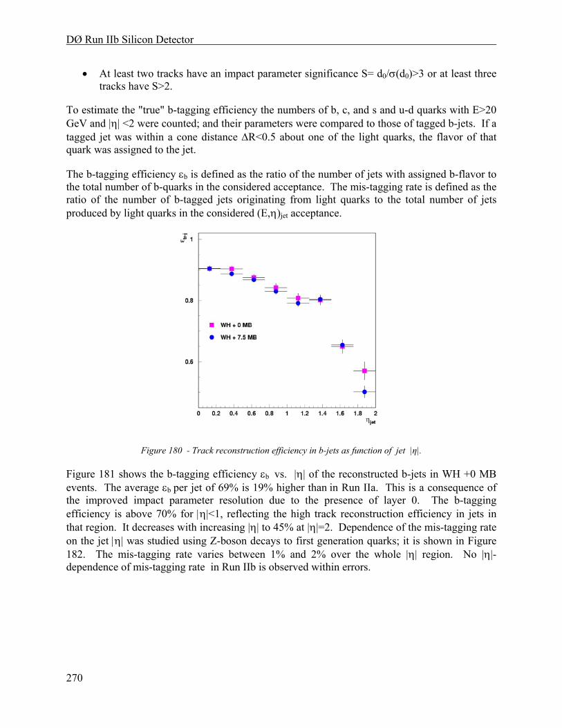
DØ Run IIb Silicon Detector
270
• At least two tracks have an impact parameter significance S= d0/σ(d0)>3 or at least three tracks have S>2.
To estimate the "true" b-tagging efficiency the numbers of b, c, and s and u-d quarks with E>20 GeV and |η| <2 were counted; and their parameters were compared to those of tagged b-jets. If a tagged jet was within a cone distance ∆R<0.5 about one of the light quarks, the flavor of that quark was assigned to the jet.
The b-tagging efficiency εb is defined as the ratio of the number of jets with assigned b-flavor to the total number of b-quarks in the considered acceptance. The mis-tagging rate is defined as the ratio of the number of b-tagged jets originating from light quarks to the total number of jets produced by light quarks in the considered (E,η)jet acceptance.
Figure 180 - Track reconstruction efficiency in b-jets as function of jet |η|.
Figure 181 shows the b-tagging efficiency εb vs. |η| of the reconstructed b-jets in WH +0 MB events. The average εb per jet of 69% is 19% higher than in Run IIa. This is a consequence of the improved impact parameter resolution due to the presence of layer 0. The b-tagging efficiency is above 70% for |η|<1, reflecting the high track reconstruction efficiency in jets in that region. It decreases with increasing |η| to 45% at |η|=2. Dependence of the mis-tagging rate on the jet |η| was studied using Z-boson decays to first generation quarks; it is shown in Figure 182. The mis-tagging rate varies between 1% and 2% over the whole |η| region. No |η|-dependence of mis-tagging rate in Run IIb is observed within errors.
DØ Run IIb Silicon Detector
271
Figure 181 - b-tagging efficiency as function of |η| of the tagged jet.
Figure 182 - Mis-tagging rate as function of |η| of the tagged jet.
Dependencies of the b-tagging efficiency and the mis-tagging rate on reconstructed jet energy Ej are shown in Figure 183 and Figure 184, respectively. The best performance in terms of b-tagging is expected for jets with Ej ~ 70-100 GeV. The rise of efficiency above 150 GeV is not statistically significant. Due to insufficient statistics, the mistagging rate is estimated only up to 140 GeV and is demonstrated to be about 1.5 % in the whole considered energy scale.
DØ Run IIb Silicon Detector
272
Figure 183 - b-tagging efficiency as function of the energy of the tagged jet.
Figure 184 - Mis-tagging rate as function of the energy of the tagged jet.
Probabilities to tag an event with one or two b-jets are shown for Run IIa (estimated from Z-boson decays to bb) and Run IIb (from WH events) in Table 31.
Table 31 - Probabilities to tag an event with one or two b-jets.
One can see from the table that an essential improvement in the selection of events with b-tagged jets can be achieved with the Run IIb tracker as compared to the existing tracker. Taking into
Run IIa Run IIb P(nb ≥ 1) 68% 76% P(nb ≥ 2) 21% 33%

DØ Run IIb Silicon Detector
273
account the lower mis-tagging rate obtained in the Run IIb geometry, one can conclude that the signal-to-background ratio in all analyses involving b-jets will be significantly better in the next run.
Because of the slight degradation of track reconstruction efficiency in jets with increasing luminosity, the b-tagging efficiency per jet (εb) deteriorates from 69% without pileup to 66% with an additional six MB events. This leads to the slightly decreased values P(nb ≥ 1)=76% and P(nb ≥ 2)=33%. Mis-tagging rates were not seen to increase significantly at higher luminosity.
9.8 Conclusions
The Run IIb silicon detector demonstrates good physics performance in a realistic simulation that includes detailed physics and detector response modeling and full pattern recognition. The physics performance studies prove that the proposed silicon design meets the requirements of the physics program of DØ Run IIb.
Detailed studies of occupancy in the Run IIb silicon detector show the expected higher rates (about 12% for busy events) in the inner layers. However, no accompanying worsening in the spatial resolution of hits is seen. Only 6% of reconstructed clusters in layer 0 are expected to be shared by more than one track. The remaining single hit clusters determine a single hit position with an accuracy of 12 µm.
The choice of small-degree stereo detectors leads to a significant decrease in ghost tracks and a consequent improvement in pattern recognition. The additional layer 5 at radius R=16.4 cm helps to improve pT resolution for non-central tracks. The new layer 0 at a small radius results in a factor of 1.5 improvement in impact parameter resolution. As a consequence the single b-tagging efficiency per jet improves by 19% compared to that obtained with Run IIa; and the percentage of events with two b-tagged jets will be 67% higher than in Run IIa at a fixed mis-tagging rate.
Predictions made for discovery limits of the Higgs boson in Run IIb were based on the assumption that DØ would have the same performance as in Run IIa. The proposed silicon detector is shown to deliver even better performance for high-pT processes.
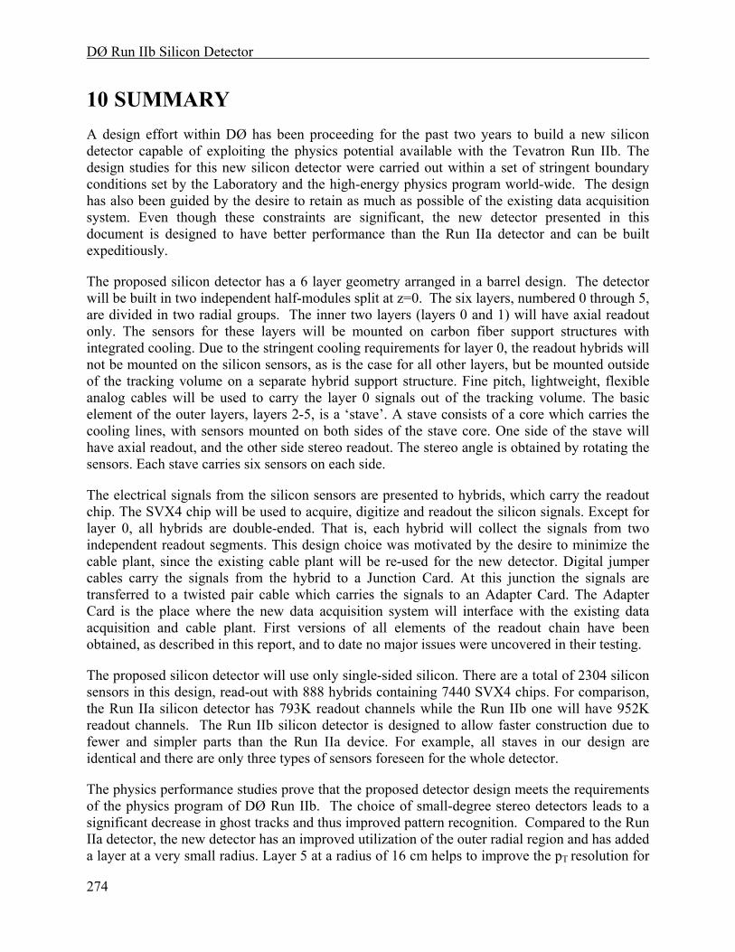
DØ Run IIb Silicon Detector
274
10 SUMMARY A design effort within DØ has been proceeding for the past two years to build a new silicon detector capable of exploiting the physics potential available with the Tevatron Run IIb. The design studies for this new silicon detector were carried out within a set of stringent boundary conditions set by the Laboratory and the high-energy physics program world-wide. The design has also been guided by the desire to retain as much as possible of the existing data acquisition system. Even though these constraints are significant, the new detector presented in this document is designed to have better performance than the Run IIa detector and can be built expeditiously.
The proposed silicon detector has a 6 layer geometry arranged in a barrel design. The detector will be built in two independent half-modules split at z=0. The six layers, numbered 0 through 5, are divided in two radial groups. The inner two layers (layers 0 and 1) will have axial readout only. The sensors for these layers will be mounted on carbon fiber support structures with integrated cooling. Due to the stringent cooling requirements for layer 0, the readout hybrids will not be mounted on the silicon sensors, as is the case for all other layers, but be mounted outside of the tracking volume on a separate hybrid support structure. Fine pitch, lightweight, flexible analog cables will be used to carry the layer 0 signals out of the tracking volume. The basic element of the outer layers, layers 2-5, is a ‘stave’. A stave consists of a core which carries the cooling lines, with sensors mounted on both sides of the stave core. One side of the stave will have axial readout, and the other side stereo readout. The stereo angle is obtained by rotating the sensors. Each stave carries six sensors on each side.
The electrical signals from the silicon sensors are presented to hybrids, which carry the readout chip. The SVX4 chip will be used to acquire, digitize and readout the silicon signals. Except for layer 0, all hybrids are double-ended. That is, each hybrid will collect the signals from two independent readout segments. This design choice was motivated by the desire to minimize the cable plant, since the existing cable plant will be re-used for the new detector. Digital jumper cables carry the signals from the hybrid to a Junction Card. At this junction the signals are transferred to a twisted pair cable which carries the signals to an Adapter Card. The Adapter Card is the place where the new data acquisition system will interface with the existing data acquisition and cable plant. First versions of all elements of the readout chain have been obtained, as described in this report, and to date no major issues were uncovered in their testing.
The proposed silicon detector will use only single-sided silicon. There are a total of 2304 silicon sensors in this design, read-out with 888 hybrids containing 7440 SVX4 chips. For comparison, the Run IIa silicon detector has 793K readout channels while the Run IIb one will have 952K readout channels. The Run IIb silicon detector is designed to allow faster construction due to fewer and simpler parts than the Run IIa device. For example, all staves in our design are identical and there are only three types of sensors foreseen for the whole detector.
The physics performance studies prove that the proposed detector design meets the requirements of the physics program of DØ Run IIb. The choice of small-degree stereo detectors leads to a significant decrease in ghost tracks and thus improved pattern recognition. Compared to the Run IIa detector, the new detector has an improved utilization of the outer radial region and has added a layer at a very small radius. Layer 5 at a radius of 16 cm helps to improve the pT resolution for

DØ Run IIb Silicon Detector
275
non-central tracks. Layer 0 at a radius of about 18 mm results in a factor of 1.5 improvement in impact parameter resolution. As a consequence, the single b-tagging efficiency per jet improves by 19% compared to that obtained with Run IIa, and the percentage of events with two b-tagged jets at fixed mistag rate will be 14% higher than in Run IIa. With the new detector we will also have better stand-alone silicon tracking. Predictions made for discovery limits of the Higgs boson in Run IIb were based on the assumption that DØ would have the same performance as in Run IIa. The proposed detector is shown to be well-matched to the search for the Higgs boson and the study of a wide variety of high-pT processes.

276
(This page intentionally left blank)
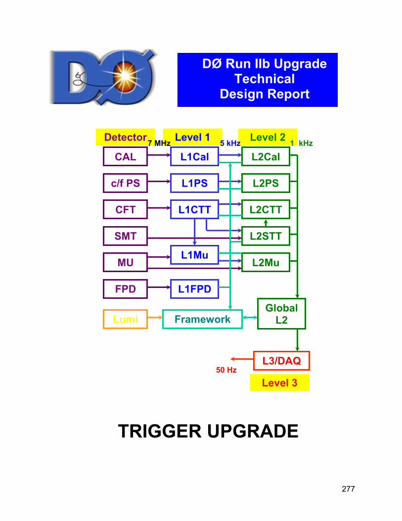
277
CAL
c/f PS
CFT
SMT
MU
FPD
L1Cal
L1PS
L1CTT
L1Mu
L1FPD
L2Cal
L2PS
L2CTT
L2STT
L2Mu
Global L2 Framework
Detector
Lumi
Level 1 Level 2 7 MHz 5 kHz 1 kHz
L3/DAQ
Level 3 50 Hz
TRIGGER UPGRADE
DØ Run IIb UpgradeTechnical
Design Report

DØ Run IIb Trigger Upgrade
278
(This page intentionally left blank)
DØ Run IIb Trigger Upgrade
279
TRIGGER UPGRADE CONTENTS 1 Introduction..............................................................................................283
2 Triggers, Trigger Terms, and Trigger Rates ............................................285
2.1 Overview of the DØ Run IIa Trigger System.....................................285
2.2 Leptonic Triggers ..............................................................................287
2.3 Leptons plus Jets ..............................................................................287
2.4 Leptons/Jets plus Missing ET ............................................................288
2.5 Triggers for Higgs Searches .............................................................288
2.6 Trigger Menu and Rates ...................................................................289
3 Level 1 Tracking Trigger..........................................................................291
3.1 Goals ................................................................................................291
3.1.1 Track Triggers ............................................................................291
3.1.2 Electron/Photon Identification.....................................................291
3.1.3 Track Matching...........................................................................291
3.2 Description of Current Tracking Trigger ............................................292
3.2.1 Tracking Detectors .....................................................................292
3.2.2 CTT Segmentation .....................................................................292
3.2.3 Tracking Algorithm .....................................................................294
3.3 Performance with the Run IIa Tracking Trigger.................................295
3.3.1 Simulations of the Run IIa trigger ...............................................295
3.3.2 Studies of CFT Occupancy.........................................................297
3.3.3 Performance of the Run IIa Track Trigger ..................................298
3.4 Track Trigger Upgrade Strategy........................................................300
3.5 Singlet Equations in Track Finding....................................................300
3.5.1 Concept ......................................................................................300
3.5.2 Equation Algorithm Generation ..................................................302
3.5.3 Rates and Rejection Improvements ...........................................303
3.6 Implementation of Level 1 Central Track Trigger ..............................304
3.6.1 CTT Electronics..........................................................................304
3.6.2 CTT Outputs...............................................................................307
3.6.3 Implementation of the Run IIb upgrade ......................................308
DØ Run IIb Trigger Upgrade
280
3.6.4 DFE motherboard.......................................................................309
3.6.5 DFEA daughterboard .................................................................310
3.6.6 Resource evaluation...................................................................314
3.7 L1 Tracking Trigger Summary and Conclusions ...............................315
4 Level 1 Calorimeter Trigger .....................................................................317
4.1 Goals ................................................................................................317
4.2 Description of Run IIa Calorimeter Electronics..................................318
4.2.1 Overview ....................................................................................318
4.2.2 Trigger pickoff.............................................................................319
4.2.3 Trigger summers ........................................................................320
4.2.4 Trigger sum driver ......................................................................321
4.2.5 Signal transmission, cable dispersion ........................................322
4.3 Description of Current L1 Calorimeter Trigger ..................................323
4.3.1 Overview ....................................................................................323
4.3.2 Global Triggers...........................................................................325
4.3.3 Cluster Triggers..........................................................................325
4.3.4 Hardware Implementation ..........................................................326
4.3.5 Physical Layout ..........................................................................328
4.4 Motivations for Upgrading the Current System .................................328
4.4.1 Bunch Crossing mis-Identification ..............................................329
4.4.2 Background Rates and Rejection ...............................................329
4.4.3 Conclusions/implications for high luminosity ..............................332
4.4.4 Overview of Calorimeter Trigger Upgrade..................................333
4.5 Digital Filtering ..................................................................................334
4.5.1 Concept & physics implications ..................................................334
4.5.2 Pileup rejection...........................................................................334
4.5.3 Input data and simulation tools...................................................335
4.5.4 Algorithm evaluation parameters................................................335
4.5.5 Algorithms studied......................................................................336
4.5.6 Conclusions................................................................................346
4.6 Clustering algorithm simulation results .............................................346
4.6.1 Jet algorithms .............................................................................348
4.6.2 Electron algorithms.....................................................................360
DØ Run IIb Trigger Upgrade
281
4.6.3 Tau algorithms............................................................................361
4.6.4 Global sums ...............................................................................363
4.7 L1 Calorimeter Trigger Implementation.............................................369
4.7.1 Constraints .................................................................................369
4.7.2 L1 Calorimeter Trigger Architectural Overview...........................370
4.7.3 Trigger Tower Mapping ..............................................................371
4.7.4 ADF System design and Implementation ...................................372
4.7.5 ADF Card Description ................................................................372
4.7.6 Timing signals fanout card..........................................................378
4.7.7 Analog signal splitters ................................................................380
4.7.8 ADF to TAB Data Transfer .........................................................380
4.7.9 TAB implementation ...................................................................382
4.7.10 GAB Implementation ................................................................394
4.7.11 TAB-GAB Crate........................................................................396
4.7.12 Output to L2 and L3..................................................................396
4.7.13 Latency of Output to the Cal-Track Match System ...................397
4.8 Summary & Conclusions...................................................................398
5 Level 1 Calorimeter-Track Matching........................................................400
5.1 Overview...........................................................................................400
5.2 Simulation .........................................................................................400
5.2.1 Improving Calorimeter EM Rates Using the L1CTT ...................400
5.2.2 Improving L1CTT Rates Using Calorimeter Jets .......................402
5.3 Implementation .................................................................................404
5.3.1 L1Muo System ...........................................................................404
5.4 L1CalTrack Trigger ...........................................................................412
5.5 L1CalTrack Cards .............................................................................420
5.5.1 Serial Link Daughter Board (SLDB)............................................420
5.5.2 Muon Trigger Card (MTCxx).......................................................421
5.5.3 Muon Trigger Flavor Board (MTFB) ...........................................421
5.5.4 Muon Trigger Crate Manager (MTCM) .......................................421
5.5.5 Muon Splitter Cards (MSPLIT) ...................................................421
5.5.6 Muon Trigger Test Card (MTT)...................................................422
5.5.7 Timing.........................................................................................422
DØ Run IIb Trigger Upgrade
282
6 Level 2 βeta Trigger.................................................................................423
6.1 Motivation .........................................................................................423
6.2 L2βeta Architecture...........................................................................423
6.3 Run IIb Algorithm Changes...............................................................425
6.4 Summary ..........................................................................................428
7 Level 2 Silicon Track Trigger ...................................................................429
7.1 Motivation .........................................................................................429
7.2 Brief description of Run IIa STT architecture ....................................429
7.3 Changes in tracker geometry and implications for STT ....................433
7.4 Simulation of the Run IIb STT...........................................................435
7.5 Implementation description for STT upgrade ....................................440
8 Trigger Upgrade Summary and Conclusions...........................................442
DØ Run IIb Trigger Upgrade
283
1 Introduction A powerful and flexible trigger is the cornerstone of a modern hadron collider
experiment. It dictates what physics processes can be studied properly and what is ultimately left unexplored. The trigger must offer sufficient flexibility to respond to changing physics goals and new ideas. It should allow the pursuit of complementary approaches to a particular event topology in order to maximize trigger efficiency and allow measurement of trigger turn-on curves. Adequate bandwidth for calibration, monitoring, and background samples must be provided in order to calibrate the detector and control systematic errors. If the trigger is not able to achieve sufficient selectivity to meet these requirements, the capabilities of the experiment will be seriously compromised.
The DØ Run IIb Trigger Upgrade is designed to meet these goals within the context of the physics program described in Part II and the challenges of triggering at the high instantaneous luminosities that will be present in Run IIb. The upgrade will allow DØ to select with high efficiency the wide variety of data samples required for the Higgs search and the high-pT physics program, while providing sufficient background rejection to meet constraints imposed by the readout electronics and DAQ system.
The DØ Run IIb Trigger Upgrade is designed for operation at a peak luminosity of 5x1032 cm-2s-1 with 132 ns bunch spacing. We have also investigated operating at a luminosity of 2x1032 cm-2 sec-1 with 396 ns bunch spacing. In this operating mode, luminosity leveling is used to hold the luminosity at 2x1032 cm-2 sec-1 and the achievable integrated luminosity is expected to be the same as if there were no leveling and an initial luminosity of about 3.4x1032 cm-2 sec-1. Both modes of operation yield an average of 5 minimum bias interactions accompanying the high-pT interaction and require a factor of ~2.5 increase in trigger rejection over the Run IIa design.
Laboratory guidance for Run IIb is that a luminosity of 2x1032 cm-2 sec-1 with 396 ns bunch spacing and luminosity leveling is the baseline plan, but that CDF and DØ should have the capability of operating at higher instantaneous luminosities with either 132 ns or 396 ns bunch spacing should luminosity leveling not meet expectations. Our proposed trigger upgrade is consistent with this guidance.
We will retain the present trigger architecture with three trigger levels. The Level 1 (L1) trigger employs fast, deterministic algorithms, generating an accept/reject decision every 132 ns. Each detector element (except for the Silicon Tracker) has a dedicated trigger processor that implements the trigger algorithm and supplies “And/Or” input bits to the Trigger Framework, which makes the L1 trigger decision. The Level 2 (L2) trigger utilizes both DSP and general-purpose processors to implement more complex algorithms with variable processing time and correlate information from different detectors into the trigger decision. An important part of the L2 trigger is the Silicon Track Trigger (STT), which performs track fits using fiber and silicon tracker hits and allows triggering on displaced vertices. The Level 3 (L3) trigger is based on a farm of high-

DØ Run IIb Trigger Upgrade
284
performance commodity processors, each analyzing a complete event. While the L1 and L2 trigger rely on dedicated trigger data paths, the L3 trigger utilizes the DAQ readout to collect all event data in a L3 processing node. Since the L3 trigger is an integral part of the DAQ, we defer discussion of the L3 trigger upgrade to Part 4: DAQ/Online Computing of the TDR.
We cannot accommodate the higher Run IIb luminosity by simply increasing trigger rates. The L1 trigger rate is limited to a peak rate of ~5 kHz by readout deadtime. The L2 trigger rate is limited to a peak rate of ~1 kHz by the calorimeter digitization time. Finally, we have set a goal of ~50 Hz for the average L3 trigger rate to limit the strain on (and cost of) data storage and offline computing.
The above L1 and L2 rate limits remain the same in Run IIb as in Run IIa. Thus, for Run IIb we must increase the L1 trigger rejection by a factor of 2.5 and maintain the current L2 rejection factor of 5. Since Run IIb will focus primarily on high-pT physics processes, we expect some bandwidth will be freed by reducing the trigger rate devoted to low-pT processes. As we show in Section 2, this reduction is not sufficient to meet our rate limitations, nor does it address the difficulties in triggering efficiently on some important high-pT processes. Only by upgrading the trigger will we have a reasonable level of confidence in our ability to acquire the data samples needed to carry out the Run IIb physics program.
Potential Run IIb trigger upgrades are further limited by the relatively short time available. The upgrade must be ready for installation in 2005 so that installation of the trigger and silicon upgrades can proceed in parallel. Thus, we have been careful to limit the number and scope of the proposed Run IIb trigger upgrades to those that are necessary and sufficient to meet the Run IIb goals.
In the sections below, we describe the technical design of the Run IIb trigger upgrade. Section 2 provides an overview of the trigger architecture and some of the triggering challenges that must be overcome for Run IIb. Section 3 describes the design of the L1 track trigger, which generates track-based triggers and provides tracking information to several other trigger systems. Section 4 describes the design of a new L1 calorimeter trigger that will replace the current trigger (one of the few remaining pieces of Run 1 electronics in DØ). The calorimeter upgrade will employ digital filtering to associate energy with the correct beam crossing in the Run IIb environment and provide the capability of clustering energy from multiple trigger towers. It will also allow improved e/γ/τ triggers that make fuller use of the calorimeter (HAD/EM, cluster shape/size, isolation) and tracking information. Section 5 describes the calorimeter-track matching system, which is based on the existing muon-track matching system. These improvements to the L1 trigger will significantly reduce the rate for multijet background by sharpening trigger thresholds and improving particle identification. Section 6 describes the upgrade of the L2 βeta processors to provide additional computational power at L2. Section 7 describes the changes to the L2 Silicon Track Trigger needed to accommodate the new silicon tracker being built for Run IIb. Lastly, Section 8 summarizes the trigger part of the Technical Design Report.
DØ Run IIb Trigger Upgrade
285
2 Triggers, Trigger Terms, and Trigger Rates The primary feature driving the design of the Run IIb trigger elements is the
higher rates associated with the increased instantaneous luminosity that will be delivered to the experiments. The rate of events accepted by the Level 1 trigger still must be limited to ~5 kHz to maintain acceptable deadtime levels, so the overall aim of the Level 1 upgrade is to increase the rejection by a factor of at least 2.5.
At 2 TeV, the inelastic proton-antiproton cross section is very large, about 50 mb. At Run 2 luminosities, this results in interaction rates of ~25 MHz, with multiple interactions occurring in most beam crossings. Virtually all of these events are without interest to the physics program. In contrast, at these luminosities W bosons are produced at a few Hz and a few top quark pairs are produced per hour. It is evident that sophisticated triggers are necessary to separate out the rare events of physics interest from the overwhelming backgrounds. Rejection factors of nearly 106 must be achieved in decision times of a few milliseconds.
The salient features of interesting physics events naturally break down into specific signatures which can be sought after in a programmable trigger. The appearance in an event of a high pT lepton, for example, can signal the presence of a W or a Z. Combined with jets containing b quark tags, the same lepton signature could now be indicative of top quark pair production or the Higgs. Leptons combined instead with missing energy is a classic SUSY discovery topology, etc. The physics “menu” of Run 2 is built on the menu of signatures and topologies available to the trigger. In order for the physics program to succeed, these fundamental objects must remain un-compromised at the highest luminosities. The following paragraphs give a brief overview of the trigger system and a sampling of the physics impact of the various combinations of trigger objects. 2.1 Overview of the DØ Run IIa Trigger System
The DØ trigger system for Run II is divided into three levels of increasing complexity and capability. The Level 1 (L1) trigger is entirely implemented in hardware (see Figure 1). It looks for patterns of hits or energy deposition consistent with the passage of high energy particles through the detector. The calorimeter trigger tests for energy in calorimeter towers above pre-programmed thresholds. Hit patterns in the muon system and the Central Fiber Tracker (CFT) are examined to see if they are consistent with charged tracks above various transverse momentum thresholds. These tests take up to 3.5 µs to complete, the equivalent of 27 beam crossings. Since ~10 µs of deadtime for readout is incurred following a L1 trigger, we have set a maximum L1 trigger rate of 5 kHz.
Each L1 system prepares a set of terms representing specific conditions that are satisfied (e.g. 2 or more CFT tracks with pT above 3 GeV). These hardware terms are sent to the L1 Trigger Framework, where specific triggers are formed from combinations of terms (e.g. 2 or more CFT tracks with pT above 3 GeV AND
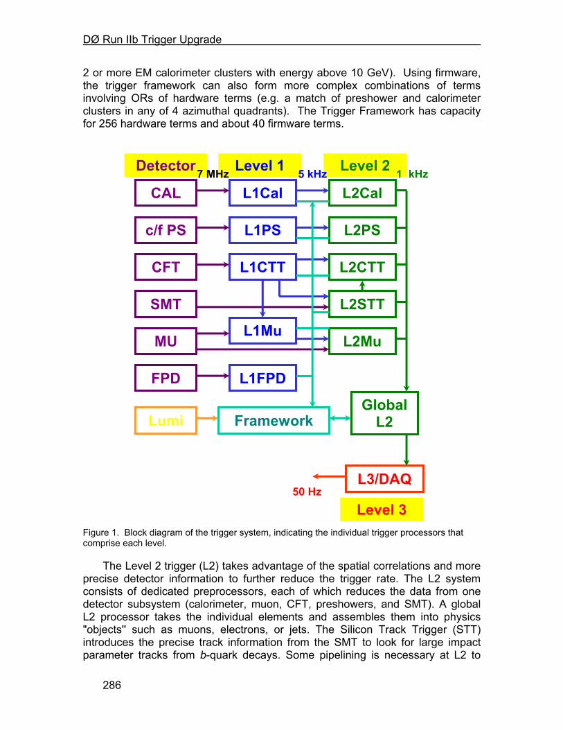
DØ Run IIb Trigger Upgrade
286
2 or more EM calorimeter clusters with energy above 10 GeV). Using firmware, the trigger framework can also form more complex combinations of terms involving ORs of hardware terms (e.g. a match of preshower and calorimeter clusters in any of 4 azimuthal quadrants). The Trigger Framework has capacity for 256 hardware terms and about 40 firmware terms.
CAL
c/f PS
CFT
SMT
MU
FPD
L1Cal
L1PS
L1CTT
L1Mu
L1FPD
L2Cal
L2PS
L2CTT
L2STT
L2Mu
Global L2 Framework
Detector
Lumi
Level 1 Level 2 7 MHz 5 kHz 1 kHz
L3/DAQ
Level 3 50 Hz
Figure 1. Block diagram of the trigger system, indicating the individual trigger processors that comprise each level.
The Level 2 trigger (L2) takes advantage of the spatial correlations and more precise detector information to further reduce the trigger rate. The L2 system consists of dedicated preprocessors, each of which reduces the data from one detector subsystem (calorimeter, muon, CFT, preshowers, and SMT). A global L2 processor takes the individual elements and assembles them into physics "objects'' such as muons, electrons, or jets. The Silicon Track Trigger (STT) introduces the precise track information from the SMT to look for large impact parameter tracks from b-quark decays. Some pipelining is necessary at L2 to

DØ Run IIb Trigger Upgrade
287
meet the constraints of the 100 µs decision time. L2 can accept events and pass them on to Level 3 at a rate of up to 1 kHz.
The Level 3 (L3) trigger consists of a farm of fast, high-level computers (PCs) which perform a simplified reconstruction of the entire event. Even within the tight time budget of 25 ms, this event reconstruction will allow the application of algorithms in the trigger with sophistication very close to that of the offline analyses. Events that satisfy desired characteristics will then be written out to a permanent storage medium. The average L3 output for Run IIa is 50 Hz and is largely dictated by downstream computing limits. 2.2 Leptonic Triggers
Leptons provide the primary means of selecting events containing W and Z bosons. They can also tag b quarks through their semileptonic decays, complementing the more efficient (but only available at Level 2 through the STT) lifetime selection. The impact of the purely leptonic tag is seen most strongly in the measurements of the W mass, the W and Z production cross sections, and the W width, since the events containing W and Z bosons are selected solely by requiring energetic leptons. The increased statistics provided by Run IIb should allow for a significant improvement in the precision of these measurements, complementing the direct searches in placing more stringent constraints on the Standard Model.
In addition to their inherent physics interest, leptonic signals will play an increasingly important role in the calibration of the energy and momentum scales of the detectors, which is crucial for the top quark and W mass measurements. This will be accomplished using Z→e+e−, Υ→e+e−, and J/Ψ→e+e− for the electromagnetic calorimeter energy scale and the corresponding muon decays for the momentum scale. Since the trigger bandwidth available for acquiring calibration samples must be non-zero, another set of constraints is imposed on the overall allocation of trigger resources. 2.3 Leptons plus Jets
During Run I, lepton-tagged decays of the W bosons and b quarks played an essential role in the discovery of the top quark and were exploited in the measurements of the top mass and production cross section. The new capability provided by the STT to tag b quark decays on-line will allow the collection of many thousands of tt pairs in the channel tt → ℓν+jets with one b-tagged jet. This will be sufficient to allow the study of top production dynamics as well as the measurement of the top decay branching fractions. The precision in measuring the top quark mass will ultimately be limited by our ability to control systematic errors, and the increase in statistics for Run IIb will allow the reduction of several key systematic errors for this channel as well as for the channel tt → ℓνℓ′ν+jets. One of these, the uncertainty in the jet energy scale, can be reduced by understanding the systematics of the direct reconstruction of W or Z boson decays into jets. The most promising channel in this case is the decay Z → bb ,

DØ Run IIb Trigger Upgrade
288
in which secondary vertex triggers can provide the needed rejection against the dominant two-jet background. 2.4 Leptons/Jets plus Missing ET
Events containing multiple leptons and missing energy are often referred to as the “gold-plated” SUSY discovery mode. These signatures, such as three leptons plus missing energy, were explored in Run I to yield some of the most stringent limits on physics beyond the Standard Model. These investigations will be an integral part of the search for new physics in Run 2. Missing energy is characteristic of any physics process where an invisible particle, such as an energetic neutrino or a massive stable neutral particle, carries away a large fraction of the available energy. Missing energy combined with leptons/photons or jets can be a manifestation of the presence of large extra dimensions, different SUSY configurations, or other new physics beyond the Standard Model. 2.5 Triggers for Higgs Searches
One of the primary goals of the Run IIb physics program will be to exploit the delivered luminosity as fully as possible in search of the Higgs boson up to the highest accessible Higgs mass1. Since even a delivered luminosity of 15 fb-1 per experiment may not lead to a statistically significant discovery, the emphasis will be on the combination of as many decay channels and production mechanisms as possible to maximize the prospects for Higgs discovery. For the trigger, this implies that flexibility, ease of monitoring, and selectivity will be critical issues.
Coverage of the potential window of discovery is provided by the decay channel H → bb at low masses, and by H → W(*)W at higher masses. In the first case, the production mechanism with the highest sensitivity will probably be in the mode pp → WH. For leptonic W decays, the leptons can be used to trigger on the events directly. If the W decays hadronically, however, the four jets from the bbqq final state will have to be pulled out from the large QCD backgrounds. Tagging b jets on-line will provide a means to select these events and ensure that they are recorded. Of course, three or four jets with sufficient transverse energy are also required. Another decay mode with good sensitivity is pp → ZH, where the Z decays to leptons, neutrinos, or hadrons. From a trigger perspective, the case where the Z decays hadronically is identical to the WH all-hadronic final state. The final state ZH → bbνν , however, provides a stringent test for the jet and missing ET triggers, since the final state is only characterized by two modest b jets and missing energy.
Recently, the secondary decay mode H → τ+ τ − has come under scrutiny as a means of bolstering the statistics for Higgs discovery in the low mass region. A trigger that is capable of selecting hadronic tau decays by means of isolated, stiff tracks or very narrow jets will give access to the gluon-fusion production mode gg
1 Report of the Higgs Working Group of the Tevatron Run 2 SUSY/Higgs Workshop, M. Carena et al, hep-ph/0010338.

DØ Run IIb Trigger Upgrade
289
→ H → τ+ τ − for lower Higgs masses. A preliminary analysis has demonstrated2 that the inclusion of this mode could reduce by 35% the luminosity required for a discovery/exclusion of the SM Higgs boson up to masses of 140 GeV, making it clearly worth pursuing. This mode can also be important in some of the large tanβ SUSY scenarios, where the Higgs coupling to bb is reduced, leaving H → τ+ τ − as the dominant decay mode for the lightest Higgs.
The higher Higgs mass regime will be covered by selecting events from pp → H → W(*)W with one or two high-energy leptons from the W → ℓν decay.
This decay mode thus requires a trigger on missing ET in addition to leptons or leptons plus jets. Supersymmetric Higgs searches will require triggering on final states containing 4 b-quark jets. This will require jet triggers at L1 followed by use of the STT to select jets at L2. 2.6 Trigger Menu and Rates
As even this cursory review makes clear, the high-pT physics menu for Run IIb requires efficient triggers for jets, leptons (including taus, if possible), and missing ET at Level 1. The STT will be crucial in selecting events containing b quark decays; however, its rejection power is not available until Level 2, making it all the more critical that the Level 1 system be efficient enough to accept all the events of interest without overwhelming levels of backgrounds.
In an attempt to set forth a trigger strategy that meets the physics needs of the experiment, the Run 2 Trigger Panel suggested a preliminary set of Trigger Terms for Level 1 and Level 2 triggers3. In order to study the expected rates in Run IIb, we have simulated an essential core of triggers which cover the essential high-pt physics signatures: Higgs boson produced in association with W and Z bosons with Higgs decays to b-bbar, Higgs production and decay to tau leptons, top quark decays in leptonic and semi-leptonic channels, inclusive W and Z boson decays into lepton and muons. The simple triggers we have currently implemented at Level 1 for Run IIa will not be able to cope with the much higher occupancies expected in Run IIb without a drastic reduction in the physics scope of the experiment and/or prescaling of important physics triggers. Our rate studies have used QCD jets samples in order to determine the effects of background, including multiple low-pT minimum bias events superimposed on the dominant processes. Table 1 shows the effect of the Run IIb trigger upgrades described below on this selection of L1 triggers for a luminosity of 2x1032 cm-2 sec-1 with 396 ns bunch spacing. Without the upgrade, the L1 trigger rate will far exceed the allowed bandwidth of 5 kHz. With the upgrade, the L1 trigger rate meets the bandwidth constraint with some headroom for the additional triggers that will be required for a robust Run IIb physics program.
2 A. Belyaev, T. Han, and R. Rosenfeld “gg→H→ττ at the Upgraded Fermilab Tevatron”, hep-ph/0204210, April 2002. 3 The report of the Run 2 Trigger Panel can be found at http://d0server1.fnal.gov/projects/run2b/Trigger/Docs/Trigger_Panel_Report.ps.
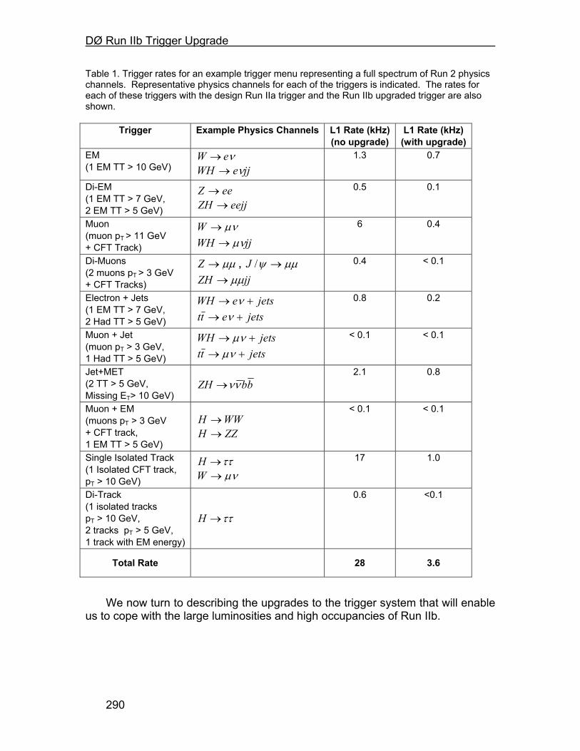
DØ Run IIb Trigger Upgrade
290
Table 1. Trigger rates for an example trigger menu representing a full spectrum of Run 2 physics channels. Representative physics channels for each of the triggers is indicated. The rates for each of these triggers with the design Run IIa trigger and the Run IIb upgraded trigger are also shown.
Trigger Example Physics Channels L1 Rate (kHz) (no upgrade)
L1 Rate (kHz) (with upgrade)
EM (1 EM TT > 10 GeV)
νeW → jjeWH ν→
1.3 0.7
Di-EM (1 EM TT > 7 GeV, 2 EM TT > 5 GeV)
eeZ → eejjZH →
0.5 0.1
Muon (muon pT > 11 GeV + CFT Track)
µν→W jjWH µν→
6 0.4
Di-Muons (2 muons pT > 3 GeV + CFT Tracks)
µµ→Z , µµψ →/J jjZH µµ→
0.4 < 0.1
Electron + Jets (1 EM TT > 7 GeV, 2 Had TT > 5 GeV)
jetseWH +→ ν
jetsett +→ ν
0.8 0.2
Muon + Jet (muon pT > 3 GeV, 1 Had TT > 5 GeV)
jetsWH +→ µν
jetstt +→ µν
< 0.1 < 0.1
Jet+MET (2 TT > 5 GeV, Missing ET> 10 GeV)
bbZH νν→ 2.1 0.8
Muon + EM (muons pT > 3 GeV + CFT track, 1 EM TT > 5 GeV)
WWH → ZZH →
< 0.1 < 0.1
Single Isolated Track (1 Isolated CFT track, pT > 10 GeV)
ττ→H µν→W
17 1.0
Di-Track (1 isolated tracks pT > 10 GeV, 2 tracks pT > 5 GeV, 1 track with EM energy)
ττ→H
0.6 <0.1
Total Rate 28 3.6
We now turn to describing the upgrades to the trigger system that will enable
us to cope with the large luminosities and high occupancies of Run IIb.

DØ Run IIb Trigger Upgrade
291
3 Level 1 Tracking Trigger The Level 1 Central Tracking Trigger (CTT) plays a crucial role in the full
range of L1 triggers. In this section, we outline the goals for the CTT, provide an overview of the performance and implementation of the present track trigger, and describe the proposed Run IIb CTT upgrade. 3.1 Goals
The goals for the CTT include providing stand-alone track triggers, combining tracking and preshower information to identify electron and photon candidates, and generating track lists that allow other trigger systems to perform track matching. The latter is a critical part of the L1 muon trigger. We briefly discuss these goals below. 3.1.1 Track Triggers
The CTT provides various Level 1 trigger terms based on counting the number of tracks whose transverse momentum (pT) exceeds a threshold. Track candidates are identified in the axial view of the Central Fiber Tracker (CFT) by looking for predetermined patterns of hits in all 8 fiber doublet layers. Four different sets of roads are defined, corresponding to pT thresholds of 1.5, 3, 5, and 10 GeV, and the number of tracks above each threshold can be used in the trigger decision. For example, a trigger on two high pT tracks could require two tracks with pT>5 GeV and one track with pT>10 GeV.
Triggering on isolated tracks provides a complementary approach to identifying high-pT electron and muon candidates, and is potentially useful for triggering on hadronic tau decays. To identify isolated tracks, the CTT looks for additional tracks within a 12º region in azimuth (φ). 3.1.2 Electron/Photon Identification
Electron and photon identification is augmented by requiring a significant energy deposit in the preshower detector. The Central Preshower (CPS) and Forward Preshower (FPS) detectors utilize the same readout and trigger electronics as the fiber tracker, and are included in the discussion of tracking triggers. Clusters found in the axial layer of the CPS are matched in phi with track candidates to identify central electron and photon candidates. The FPS cannot be matched with tracks, but comparing energy deposits before/after the lead radiator allows photon and electron candidates to be distinguished. 3.1.3 Track Matching
Track candidates found in the CTT are important as input to several other trigger systems. CTT information is used to correlate tracks with other detector measurements and to serve as seeds for pattern recognition algorithms.
The Level 1 muon trigger matches CTT tracks with hits in the muon detector. To meet timing requirements, the CTT tracks must arrive at the muon trigger on the same time scale as the muon proportional drift tube (PDT) information becomes available.
DØ Run IIb Trigger Upgrade
292
The current Level 1 trigger allows limited azimuthal matching of tracking and calorimeter information at the quadrant level (see Section 2.1). Significantly increasing the flexibility and granularity of the calorimeter track matching is an integral part of the proposed modifications for Run IIb (see Section 5).
The L2 Silicon Track Trigger (STT) uses tracks from the CTT to generate roads for finding tracks in the Silicon Microstrip Tracker (SMT). The precision of the SMT measurements at small radius, combined with the larger radius of the CFT, allows displaced vertex triggers, sharpening of the momentum thresholds for track triggers, and elimination of fake tracks found by the CTT. The momentum spectrum for b-quark decay products extends to low pT. The CTT therefore aims to provide tracks down to the lowest pT possible. The Run IIa CTT generates track lists down to pT≈1.5 GeV. The CTT tracks must also have good azimuthal (φ) resolution to minimize the width of the road used by the STT.
In addition to the track lists sent to the STT, each portion of the L1 track trigger (CFT, axial CPS, and FPS) provides information for the Level 2 trigger decision. The stereo CPS signals are also sent to L2 to allow 3-D matching of calorimeter and CPS signals. 3.2 Description of Current Tracking Trigger
We have limited our consideration of potential track trigger upgrades to those that preserve the overall architecture of the current tracking trigger. The sections below describe the tracking detectors, trigger segmentation, trigger electronics, outputs of the track trigger, and the trigger algorithms that have been developed for Run IIa. 3.2.1 Tracking Detectors
The CFT is made of scintillating fibers mounted on eight low-mass cylinders. Each of these cylinders supports four layers of fibers arranged into two doublet layers. The innermost doublet layer on each cylinder has its fibers oriented parallel to the beam axis. These are referred to as axial doublet layers. The second doublet layer has its fibers oriented at a small angle to the beam axis, with alternating sign of the stereo angle. These are referred to as stereo doublet layers. Only the axial doublet layers are incorporated into the current L1 CTT. Each fiber is connected to a visible light photon counter (VLPC) that converts the light pulse to an electrical signal.
The CPS and FPS detectors are made of scintillator strips with wavelength-shifting fibers threaded through each strip. The CPS has an axial and two stereo layers mounted on the outside of the solenoid. The FPS has two stereo layers in front of a lead radiator and two stereo layers behind the radiator. The CPS/FPS fibers are also read out using VLPCs. 3.2.2 CTT Segmentation
The CTT is divided in φ into 80 Trigger Sectors (TS). A single TS is illustrated schematically in Figure 2. To find tracks in a given sector, information is needed from that sector, called the home sector, and from each of its two neighboring
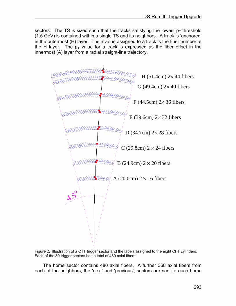
DØ Run IIb Trigger Upgrade
293
sectors. The TS is sized such that the tracks satisfying the lowest pT threshold (1.5 GeV) is contained within a single TS and its neighbors. A track is ‘anchored’ in the outermost (H) layer. The φ value assigned to a track is the fiber number at the H layer. The pT value for a track is expressed as the fiber offset in the innermost (A) layer from a radial straight-line trajectory.
4.5o
H (51.4cm) 2× 44 fibers
G (49.4cm) 2× 40 fibers
F (44.5cm) 2× 36 fibers
E (39.6cm) 2× 32 fibers
D (34.7cm) 2× 28 fibers
C (29.8cm) 2 × 24 fibers
B (24.9cm) 2 × 20 fibers
A (20.0cm) 2 × 16 fibers
Figure 2. Illustration of a CTT trigger sector and the labels assigned to the eight CFT cylinders. Each of the 80 trigger sectors has a total of 480 axial fibers.
The home sector contains 480 axial fibers. A further 368 axial fibers from each of the neighbors, the ‘next’ and ‘previous’, sectors are sent to each home
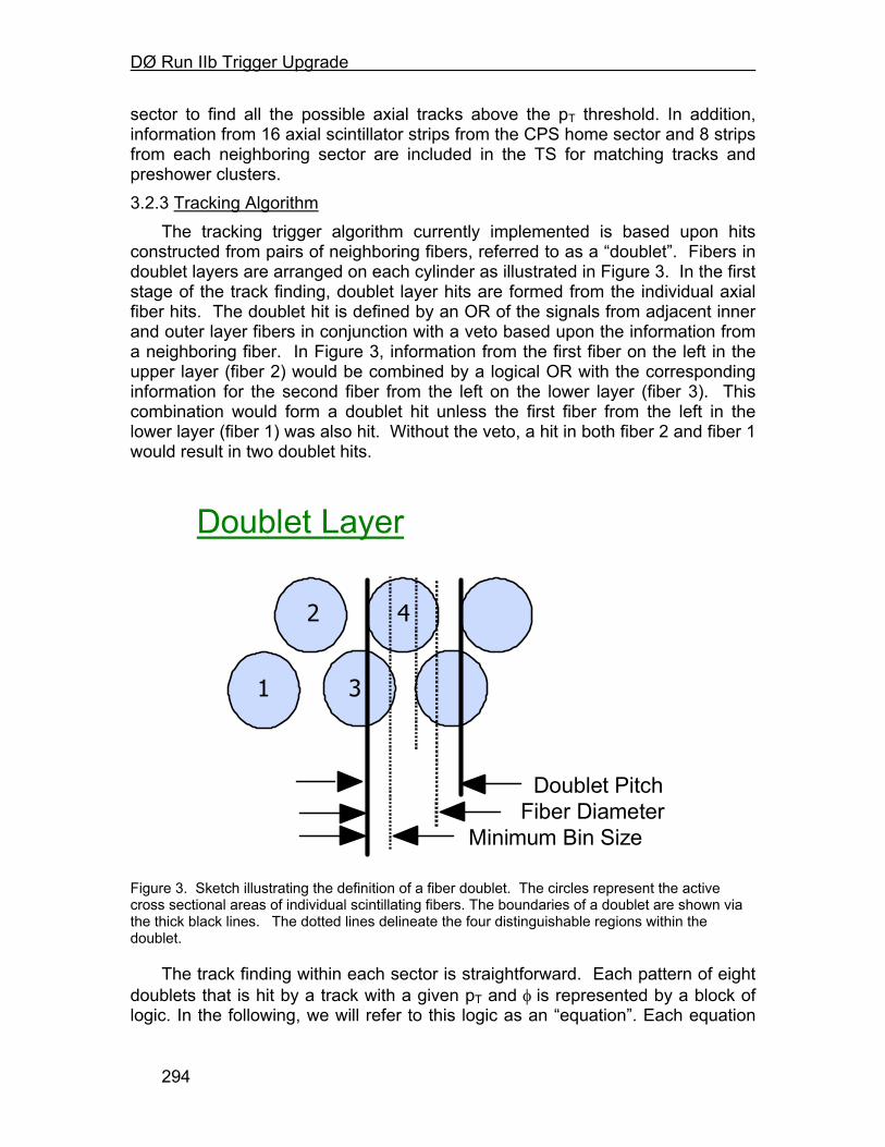
DØ Run IIb Trigger Upgrade
294
sector to find all the possible axial tracks above the pT threshold. In addition, information from 16 axial scintillator strips from the CPS home sector and 8 strips from each neighboring sector are included in the TS for matching tracks and preshower clusters. 3.2.3 Tracking Algorithm
The tracking trigger algorithm currently implemented is based upon hits constructed from pairs of neighboring fibers, referred to as a “doublet”. Fibers in doublet layers are arranged on each cylinder as illustrated in Figure 3. In the first stage of the track finding, doublet layer hits are formed from the individual axial fiber hits. The doublet hit is defined by an OR of the signals from adjacent inner and outer layer fibers in conjunction with a veto based upon the information from a neighboring fiber. In Figure 3, information from the first fiber on the left in the upper layer (fiber 2) would be combined by a logical OR with the corresponding information for the second fiber from the left on the lower layer (fiber 3). This combination would form a doublet hit unless the first fiber from the left in the lower layer (fiber 1) was also hit. Without the veto, a hit in both fiber 2 and fiber 1 would result in two doublet hits.
Doublet Layer
Doublet Pitch Fiber Diameter
Minimum Bin Size
1
2
3
4
Figure 3. Sketch illustrating the definition of a fiber doublet. The circles represent the active cross sectional areas of individual scintillating fibers. The boundaries of a doublet are shown via the thick black lines. The dotted lines delineate the four distinguishable regions within the doublet.
The track finding within each sector is straightforward. Each pattern of eight doublets that is hit by a track with a given pT and φ is represented by a block of logic. In the following, we will refer to this logic as an “equation”. Each equation
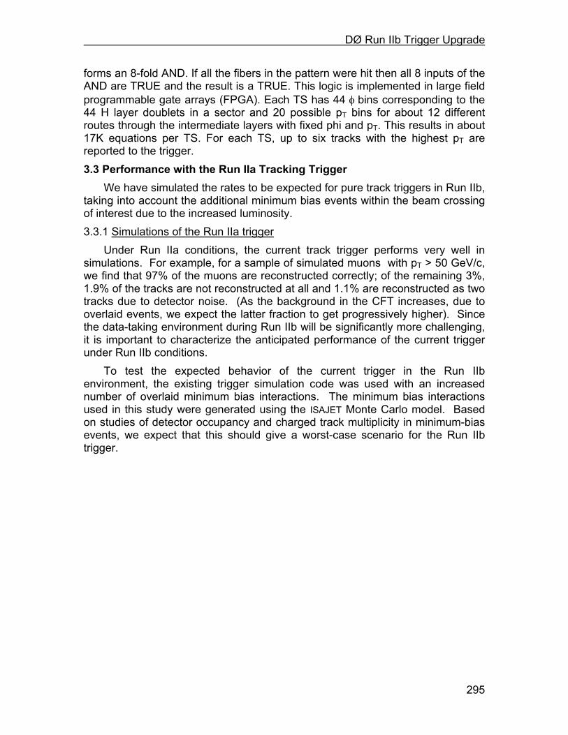
DØ Run IIb Trigger Upgrade
295
forms an 8-fold AND. If all the fibers in the pattern were hit then all 8 inputs of the AND are TRUE and the result is a TRUE. This logic is implemented in large field programmable gate arrays (FPGA). Each TS has 44 φ bins corresponding to the 44 H layer doublets in a sector and 20 possible pT bins for about 12 different routes through the intermediate layers with fixed phi and pT. This results in about 17K equations per TS. For each TS, up to six tracks with the highest pT are reported to the trigger. 3.3 Performance with the Run IIa Tracking Trigger
We have simulated the rates to be expected for pure track triggers in Run IIb, taking into account the additional minimum bias events within the beam crossing of interest due to the increased luminosity. 3.3.1 Simulations of the Run IIa trigger
Under Run IIa conditions, the current track trigger performs very well in simulations. For example, for a sample of simulated muons with pT > 50 GeV/c, we find that 97% of the muons are reconstructed correctly; of the remaining 3%, 1.9% of the tracks are not reconstructed at all and 1.1% are reconstructed as two tracks due to detector noise. (As the background in the CFT increases, due to overlaid events, we expect the latter fraction to get progressively higher). Since the data-taking environment during Run IIb will be significantly more challenging, it is important to characterize the anticipated performance of the current trigger under Run IIb conditions.
To test the expected behavior of the current trigger in the Run IIb environment, the existing trigger simulation code was used with an increased number of overlaid minimum bias interactions. The minimum bias interactions used in this study were generated using the ISAJET Monte Carlo model. Based on studies of detector occupancy and charged track multiplicity in minimum-bias events, we expect that this should give a worst-case scenario for the Run IIb trigger.
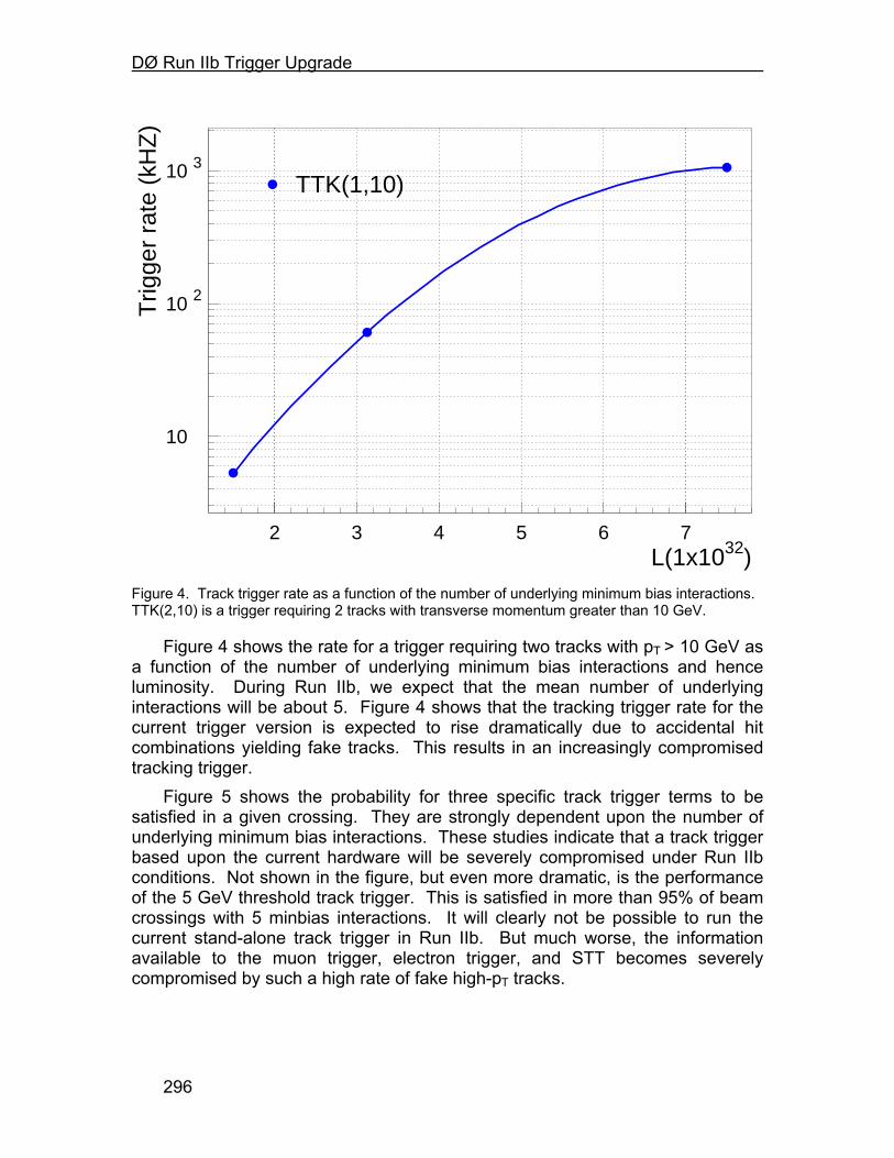
DØ Run IIb Trigger Upgrade
296
TTK(1,10)
L(1x1032)
Trig
ger
rate
(kH
Z)
10
10 2
10 3
2 3 4 5 6 7
Figure 4. Track trigger rate as a function of the number of underlying minimum bias interactions. TTK(2,10) is a trigger requiring 2 tracks with transverse momentum greater than 10 GeV.
Figure 4 shows the rate for a trigger requiring two tracks with pT > 10 GeV as a function of the number of underlying minimum bias interactions and hence luminosity. During Run IIb, we expect that the mean number of underlying interactions will be about 5. Figure 4 shows that the tracking trigger rate for the current trigger version is expected to rise dramatically due to accidental hit combinations yielding fake tracks. This results in an increasingly compromised tracking trigger.
Figure 5 shows the probability for three specific track trigger terms to be satisfied in a given crossing. They are strongly dependent upon the number of underlying minimum bias interactions. These studies indicate that a track trigger based upon the current hardware will be severely compromised under Run IIb conditions. Not shown in the figure, but even more dramatic, is the performance of the 5 GeV threshold track trigger. This is satisfied in more than 95% of beam crossings with 5 minbias interactions. It will clearly not be possible to run the current stand-alone track trigger in Run IIb. But much worse, the information available to the muon trigger, electron trigger, and STT becomes severely compromised by such a high rate of fake high-pT tracks.
DØ Run IIb Trigger Upgrade
297
TTK(1,10)
TTK(1,10)+TTK(2,5)
mean number of minbias
Fra
ctio
n of
eve
nts
trig
gere
d (%
)
0
2.5
5
7.5
10
12.5
15
17.5
20
0 1 2 3 4 5 6
Figure 5. The fraction of events satisfying several track term requirements as a function of the number of minimum bias events overlaid. TTK(n,pT) is a trigger requiring n tracks with transverse momentum greater than pT.
Based upon these simulations, we believe that the significant number of multiple interactions in Run IIb and the large CFT occupancy fractions they induce will compromise performance of the current tracking trigger. 3.3.2 Studies of CFT Occupancy
At this time, the Run IIa L1CTT track trigger is still being commissioned. Recently, however, the final CFT read-out electronics began to function at close to their expected signal-to-noise performance. Given this, we can study the CFT occupancy due to noise and minimum bias events. Since we expect minimum bias events to dominate the detector occupancy during high-luminosity running, it is crucial to understand the detector’s response to these events.
Our baseline simulation uses the Pythia Monte Carlo generator tuned to CDF Run I data in order to generate minimum bias events. The minimum bias model includes contributions from two-body quark-quark, quark-gluon, and gluon-gluon scattering, in addition to single- and double-diffractive interactions. The Monte Carlo-estimated cross section for the “hard” portion of these events, which includes the two-body interactions and double-diffractive events, is 47 mb. The lower-occupancy single-diffractive events have a cross section of approximately 12 mb, giving a total cross-section for the Pythia events of 59 mb. Based on very preliminary occupancy studies conducted in 2000 with pre-production versions of
DØ Run IIb Trigger Upgrade
298
the CFT electronics, we selected for these studies to overlay minimum bias events with a Poisson distribution averaging 7.5 Pythia events per beam crossing. Based on the above cross sections, we expect an average of 5 “hard (non-diffractive)” minimum bias events at an instantaneous luminosity of 5×1032 cm-2s-1. If 7.5 events representing the total cross section are used, this corresponds instead to approximately 6 “hard” minimum bias events, resulting in additional CFT occupancy. This increase in occupancy was necessary to match the occupancy measured with the pre-production electronics, but should be verified in the current system.
Recently, we have been able begin a detailed study of the CFT occupancy and signal-to-noise performance using the production electronics. Preliminary results are given in Figure 6, which shows the layer-by-layer occupancy of fibers in the CFT in single minimum bias events from Tevatron collisions, compared with that from the simulated Pythia minimum bias events. The occupancy in data was derived from minimum- and zero-bias trigger samples. The appropriate luminosity-weighting was used in subtracting the zero-bias occupancy to obtain the equivalent occupancy of a single minbias event. In order to make an appropriate comparison, only those Pythia events with pass a simulation of the minimum bias trigger used in the real data are considered. Finally, the Pythia occupancy has been scaled by a factor of 6/5 to represent the effective average occupancy of a single “hard” minimum bias event from our Monte Carlo sample. With these corrections, the agreement is quite good. We have indications that the discrepancy at low radius can be explained by detailed treatment of the material in the Monte Carlo and are working to resolve this. 3.3.3 Performance of the Run IIa Track Trigger
We have tested the functionality of the offline track trigger simulation by comparing its performance to that of the offline tracking. Using hits from Collider events where two muons have been reconstructed in the decay Z→µµ, we find a tracking efficiency of approximately 90% from the L1CTT for the high pT muons. An example of this success is shown in Figure 7, where the left event display shows the tracks found by the trigger simulation overlaid on the tracks reconstructed offline. The event display on the right shows the locations of the two muons in the muon system.
In order to use the hits from the CFT, the correct track-finding equations were generated using the “as built” geometry of the CFT instead of a perfect detector geometry, thereby testing one of the crucial components of the Run IIa L1CTT and demonstrating the validity of the equation algorithms. Work is underway to understand the efficiency loss within the general context of commissioning the system.
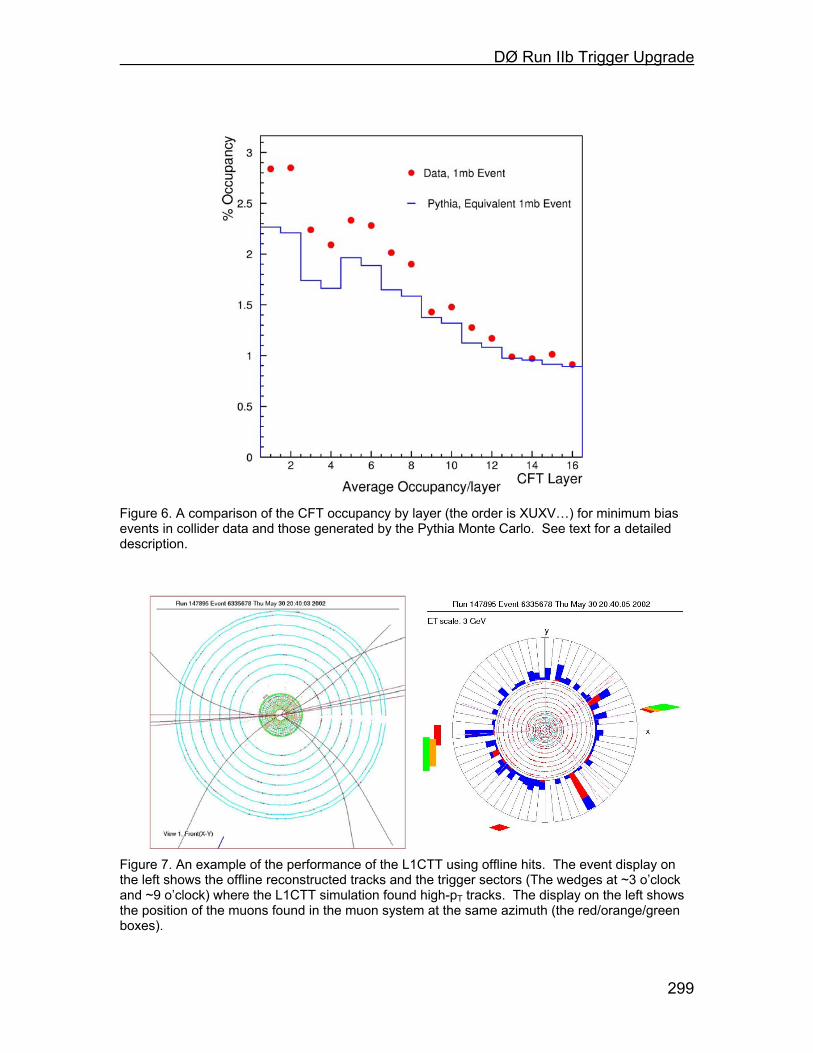
DØ Run IIb Trigger Upgrade
299
Figure 6. A comparison of the CFT occupancy by layer (the order is XUXV…) for minimum bias events in collider data and those generated by the Pythia Monte Carlo. See text for a detailed description.
Figure 7. An example of the performance of the L1CTT using offline hits. The event display on the left shows the offline reconstructed tracks and the trigger sectors (The wedges at ~3 o’clock and ~9 o’clock) where the L1CTT simulation found high-pT tracks. The display on the left shows the position of the muons found in the muon system at the same azimuth (the red/orange/green boxes).
DØ Run IIb Trigger Upgrade
300
3.4 Track Trigger Upgrade Strategy As demonstrated above, the primary concern with the track trigger is the
increase in rate for fake tracks as the tracker occupancy grows. Since the current track trigger requires hits in all 8 axial doublet layers, the only path to improving trigger rejection is to improve the trigger selectivity by incorporating additional information into the trigger algorithm. The short timescale until the beginning of Run IIb and resource limitations conspire to make it impossible to improve the physical granularity of the fiber tracker or to add additional tracking layers to the CFT. Instead, we propose to upgrade the track trigger logic. Essentially, more processing power allows the use of the full granularity and resolution of the individual CFT fibers rather than doublets in Level 1 track finding. Studies of this approach are presented below. 3.5 Singlet Equations in Track Finding 3.5.1 Concept
The motivation behind the use of singlet equations is illustrated in Figure 3, which shows a fragment of a CFT doublet layer. The thick black lines mark the area corresponding to a doublet hit, the current granularity of the L1CTT. As one can see from Figure 3, the doublet is larger than the fiber diameter. Since the hits from adjacent fibers are combined into the doublets before the tracking algorithm is run, this results in a widening of the effective width of a fiber to that of a doublet, decreasing the resolution of the hits that are used for track finding. In particular, the doublet algorithm is such that if fibers 1 and 4 shown on Figure 3 are hit, the trigger considers the doublet formed by fibers 1 and 2 and the doublet formed by fibers 3 and 4 to be hit. As the single-fiber occupancy grows, the application of this doublet algorithm results in a disproportionate increase in the hit occupancy seen by the trigger.
Hit patterns based instead on single fibers will be inherently narrower and will therefore have a reduced probability of selecting a random combination of hits. We have simulated different trigger configurations which include the all-singlet case (16 layers), as well as mixed schemes where some CFT layers are treated as pairs of singlet layers and the rest as doublets. In order to label the schemes we use the fact that the 8 layers of the CFT are labeled from A to H (see Figure 2). We use upper case letters to indicate that hits in this layer were treated as doublets; lower case letters indicate singlets. In this notation “ABCDEFGH” indicates the Run IIa CTT scheme with 8 layers of doublets and “abcdefgh” indicates 16 layers of singlets. Equations specifying which fibers should be hit as a function of momentum and azimuthal angle were generated for all configurations. Note that, in the results reported here, the equations have been generated specifying only which fibers should be hit, and not using vetoes on fibers that should not be hit. This will be discussed more completely in the next Section. , but it should be noted here that only stipulating the hit fibers insures that the efficiency of the track-finding algorithms is not compromised at high detector occupancies; if the hit fibers are present, the tracks will be found.
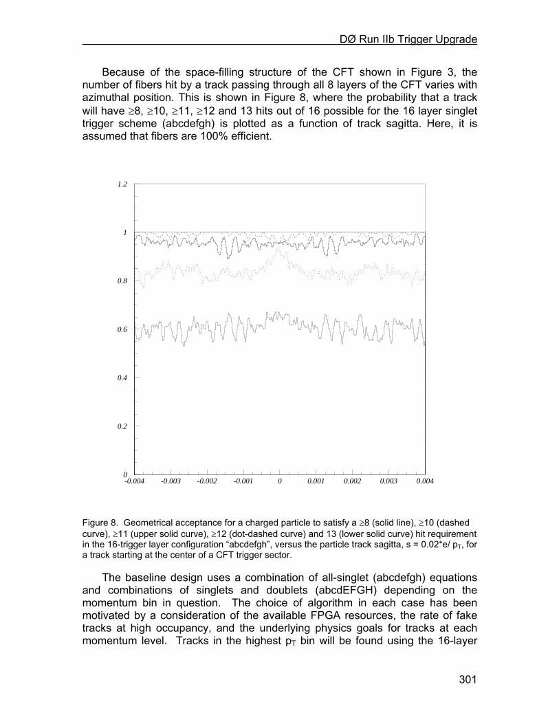
DØ Run IIb Trigger Upgrade
301
Because of the space-filling structure of the CFT shown in Figure 3, the number of fibers hit by a track passing through all 8 layers of the CFT varies with azimuthal position. This is shown in Figure 8, where the probability that a track will have ≥8, ≥10, ≥11, ≥12 and 13 hits out of 16 possible for the 16 layer singlet trigger scheme (abcdefgh) is plotted as a function of track sagitta. Here, it is assumed that fibers are 100% efficient.
0
0.2
0.4
0.6
0.8
1
1.2
-0.004 -0.003 -0.002 -0.001 0 0.001 0.002 0.003 0.004
Figure 8. Geometrical acceptance for a charged particle to satisfy a ≥8 (solid line), ≥10 (dashed curve), ≥11 (upper solid curve), ≥12 (dot-dashed curve) and 13 (lower solid curve) hit requirement in the 16-trigger layer configuration “abcdefgh”, versus the particle track sagitta, s = 0.02*e/ pT, for a track starting at the center of a CFT trigger sector.
The baseline design uses a combination of all-singlet (abcdefgh) equations and combinations of singlets and doublets (abcdEFGH) depending on the momentum bin in question. The choice of algorithm in each case has been motivated by a consideration of the available FPGA resources, the rate of fake tracks at high occupancy, and the underlying physics goals for tracks at each momentum level. Tracks in the highest pT bin will be found using the 16-layer

DØ Run IIb Trigger Upgrade
302
singlet equations (abcdefgh), which give the highest possible resolution and the best rejection of fake tracks, all of which is aimed at running a high-pT isolated track trigger. In contrast, the lowest momentum bin (1.5 GeV<pT<3 GeV) is covered by a hybrid scheme (abcdEFGH) with high granularity in the inner layers of the CFT and doublets in the outer layers where the occupancy is lower and multiple scattering will move the tracks off of their ideal trajectories. This choice is motivated by reducing the sheer number of equations, which increases as 1/pT, the desire to maintain high-efficiency for these tracks, since they are critical for b-tagging in the STT, and the relative insensitivity of the STT to some number of fake tracks. A summary of the chosen algorithms for each momentum bin is shown in Table 2. 3.5.2 Equation Algorithm Generation
An “equation” as defined here is a set of 12 or 16 terms specifying which fibers are hit by the tracks that traverse a given trajectory in a CFT Trigger sector. The equations are generated by a uniform sampling of all possible trajectories across a given trigger sector using many millions of iterations. The hit fibers along each trajectory are recorded. Trajectories with identical sets of hit fibers are combined, such that each equation corresponds to a specific average pT and a specific location in φ. The relative “acceptance” of each equation is determined by calculating how many of the possible trajectories are represented by each of the equation terms.
The effects of CFT fiber inefficiencies/readout thresholds have been explicitly included in the equation generation. For each trajectory, the expected number of photoelectrons for each hit fiber is calculated from a Landau distribution based on the path length of the trajectory through the fiber. A threshold cut corresponding to 1.5 photoelectrons is then applied to each fiber in order to determine whether or not that fiber should appear as “hit” in the equation pattern. In this way, after many samplings, high efficiency is maintained on average for those trajectories which pass through the edges of fibers. Note that, since misses due to inefficiency and geometry are explicitly allowed, not all of the 12 or 16 terms need contain a fiber index.
Given the limits of finite FPGA resources, an optimization must be done separately for each of the pT bins considered by the track trigger. Just as an example, if all of the singlet equations for the highest pT bin (pT>10 GeV), including those allowing some number of missed layers, were to be implemented in hardware, it would take some 300 times the FPGA resources of the current Run IIa system. Since this is clearly untenable, algorithms have been created to “prune” the sets of equations down to an acceptable level of complexity while maintaining high efficiency and low fake rates.
A simple set of cuts has been applied to reduce the number of equations needed in track finding:
1. All equations with no hit in any CFT doublet layer are discarded.

DØ Run IIb Trigger Upgrade
303
2. Equations with small relative acceptance of the total track phase space are discarded. For the 16-singlet equations, any single equation with a relative acceptance less than 3×10⁻⁵ of the total ensemble of possible trajectories is rejected. For the hybrid 12-layer scheme, only equations with an acceptance of 1.5×10⁻⁶ are kept.
3. Redundant equations having more hit fibers than a “shorter” overlapping equation are removed. A minimum of 8 hit fibers is required.
Motivations for these cuts are as follows. Hits in the middle layers of the CFT
give the most precise information on the sagitta of the found tracks. Without a constraint in this region, real lower-momentum tracks are more easily “promoted” to fake high-pT tracks with the addition of noise. As far as equation acceptance is concerned, many of the generated equations are satisfied by an extremely small number of possible tracks, but are as likely as any other equation to be satisfied by random noise hits. Therefore, the acceptance for fake tracks can be dramatically reduced by removing those equations that are essentially only efficient for picking up fake tracks due to noise. Removal of redundant equations is a simple technique: an equation specifying a trajectory that hit 8 specific fibers will still be satisfied by a more restrictive equation that hit 2 other specific fibers in addition to the original 8. As long as more fakes are not generated by the use of less-restrictive equations, full efficiency can be maintained with fewer equations. The high-pT bin serves well as an example of the success of these methods: there are 697k original generated equations for the high-pT bin shown in Table 2. After the above cuts have been applied, only 9.4k equations remain, with little loss in efficiency and a much lower fake rate. 3.5.3 Rates and Rejection Improvements
The existing trigger simulation was adapted to make a realistic estimate of the trigger performance. Single muons were generated, overlaid on events containing a Poisson-distributed set of (Pythia) minimum bias interactions with a mean of 7.5 interactions per crossing and put through the detailed DØ simulation. (See the discussion of Monte Carlo generation, cross sections, and luminosity in Section 3.3.2.) They were then put through the modified trigger simulator. The fraction of events in which a trigger track matched the muon is defined as the trigger efficiency. A separate sample containing Poisson-distributed minimum bias events with the same 7.5 events/crossing rate is used to measure the fake rate, since there are no high-pT tracks in this sample. All of the results presented in this section were obtained using a detailed description of the photons generated in the CFT. The ADC spectrum of the Monte Carlo hits was tuned to match that observed in the data, and a realistic threshold cut equivalent to 1.5 photoelectrons was applied to each of the channels.
The results of the procedure described are summarized in Table 2, which shows the performance of the baseline L1CTT algorithmic design. Shown in the table for each of the momentum bins is the singlet/doublet scheme employed, the fraction of each of the pure 7.5 minbias events that produces a fake track in each
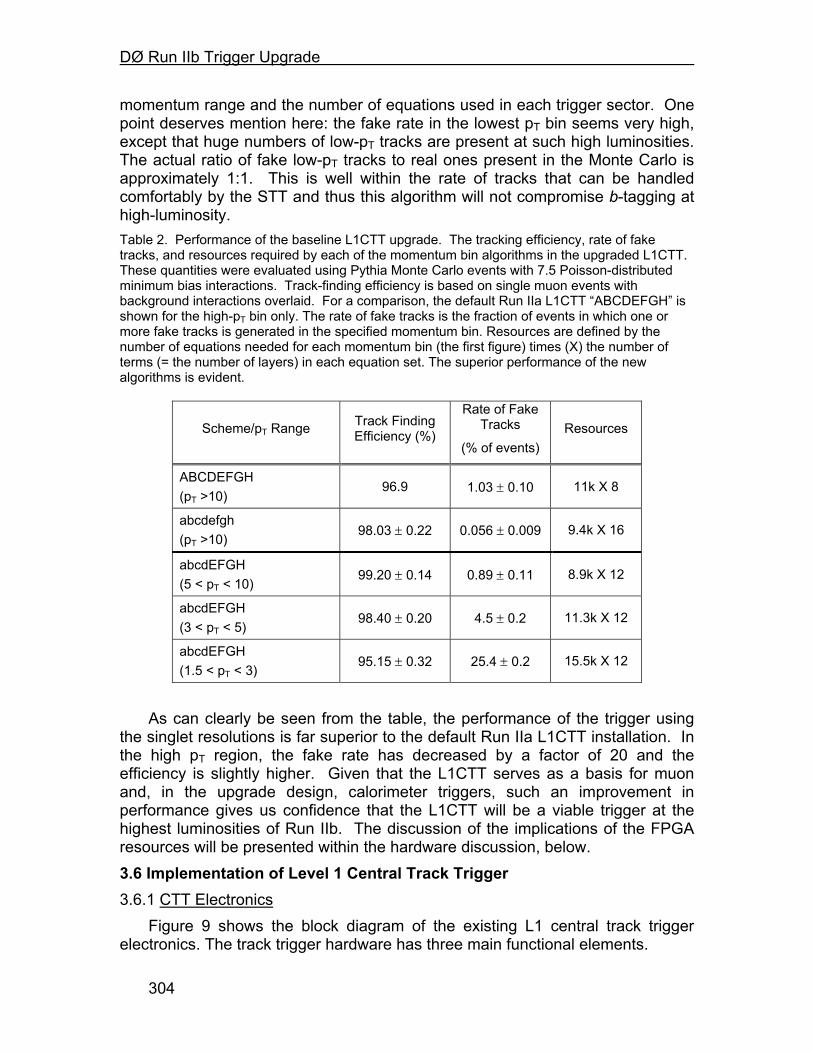
DØ Run IIb Trigger Upgrade
304
momentum range and the number of equations used in each trigger sector. One point deserves mention here: the fake rate in the lowest pT bin seems very high, except that huge numbers of low-pT tracks are present at such high luminosities. The actual ratio of fake low-pT tracks to real ones present in the Monte Carlo is approximately 1:1. This is well within the rate of tracks that can be handled comfortably by the STT and thus this algorithm will not compromise b-tagging at high-luminosity. Table 2. Performance of the baseline L1CTT upgrade. The tracking efficiency, rate of fake tracks, and resources required by each of the momentum bin algorithms in the upgraded L1CTT. These quantities were evaluated using Pythia Monte Carlo events with 7.5 Poisson-distributed minimum bias interactions. Track-finding efficiency is based on single muon events with background interactions overlaid. For a comparison, the default Run IIa L1CTT “ABCDEFGH” is shown for the high-pT bin only. The rate of fake tracks is the fraction of events in which one or more fake tracks is generated in the specified momentum bin. Resources are defined by the number of equations needed for each momentum bin (the first figure) times (X) the number of terms (= the number of layers) in each equation set. The superior performance of the new algorithms is evident.
Scheme/pT Range Track Finding Efficiency (%)
Rate of Fake Tracks
(% of events) Resources
ABCDEFGH (pT >10)
96.9 1.03 ± 0.10 11k X 8
abcdefgh (pT >10)
98.03 ± 0.22 0.056 ± 0.009 9.4k X 16
abcdEFGH (5 < pT < 10)
99.20 ± 0.14 0.89 ± 0.11 8.9k X 12
abcdEFGH (3 < pT < 5)
98.40 ± 0.20 4.5 ± 0.2 11.3k X 12
abcdEFGH (1.5 < pT < 3) 95.15 ± 0.32 25.4 ± 0.2 15.5k X 12
As can clearly be seen from the table, the performance of the trigger using
the singlet resolutions is far superior to the default Run IIa L1CTT installation. In the high pT region, the fake rate has decreased by a factor of 20 and the efficiency is slightly higher. Given that the L1CTT serves as a basis for muon and, in the upgrade design, calorimeter triggers, such an improvement in performance gives us confidence that the L1CTT will be a viable trigger at the highest luminosities of Run IIb. The discussion of the implications of the FPGA resources will be presented within the hardware discussion, below. 3.6 Implementation of Level 1 Central Track Trigger 3.6.1 CTT Electronics
Figure 9 shows the block diagram of the existing L1 central track trigger electronics. The track trigger hardware has three main functional elements.
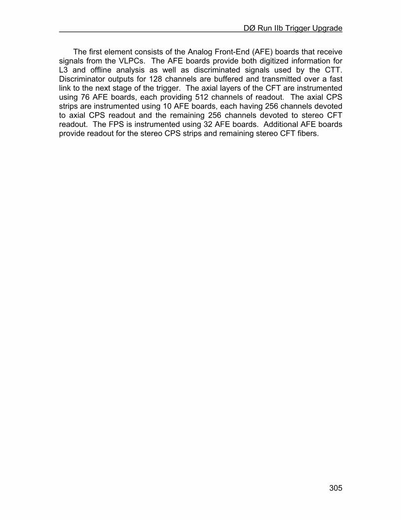
DØ Run IIb Trigger Upgrade
305
The first element consists of the Analog Front-End (AFE) boards that receive signals from the VLPCs. The AFE boards provide both digitized information for L3 and offline analysis as well as discriminated signals used by the CTT. Discriminator outputs for 128 channels are buffered and transmitted over a fast link to the next stage of the trigger. The axial layers of the CFT are instrumented using 76 AFE boards, each providing 512 channels of readout. The axial CPS strips are instrumented using 10 AFE boards, each having 256 channels devoted to axial CPS readout and the remaining 256 channels devoted to stereo CFT readout. The FPS is instrumented using 32 AFE boards. Additional AFE boards provide readout for the stereo CPS strips and remaining stereo CFT fibers.
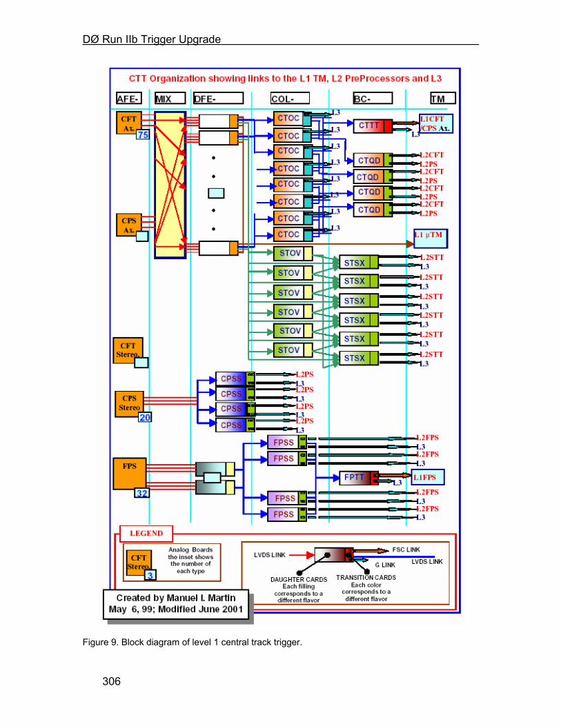
DØ Run IIb Trigger Upgrade
306
Figure 9. Block diagram of level 1 central track trigger.
DØ Run IIb Trigger Upgrade
307
The second hardware element is the Mixer System (MIX). The MIX resides in a single crate and is composed of 20 boards. It receives the signals from the AFE boards and sorts them for the following stage. The signals into the AFE boards are ordered in increasing azimuth for each of the tracker layers, while the trigger is organized into TS wedges covering all radial CFT/CPS axial layers within 4.5 degrees in φ. Each MIX board has sixteen CFT inputs and one CPS input. It shares these inputs with boards on either side within the crate and sorts them for output. Each board then outputs signals to two DFEA boards (described below), with each DFEA covering two TS.
The third hardware element is based on the Digital Front-End (DFE) motherboard. These motherboards provide the common buffering and communication links needed for all DFE variants and support two different types of daughter boards, single-wide and double-wide. The daughter boards implement the trigger logic using FPGA chips. These have a very high density of logic gates and lend themselves well to the track equations. Within these chips all 17k equations are processed simultaneously in under 200 ns. This design also keeps the board hardware as general as possible. The motherboard is simply an I/O device and the daughter boards are general purpose processors. Since algorithms and other details of the design are implemented in the FPGA, which can be reprogrammed via high level languages, one can download different trigger configurations for each run or for special runs and the trigger can evolve during the run. The signals from the Mixer System are received by 40 DFE Axial (DFEA) boards. There are also 5 DFE Stereo (DFES) boards that prepare the signals from the CPS stereo layers for L2 and 16 DFEF boards that handle the FPS signals. 3.6.2 CTT Outputs
The current tracking trigger was designed to do several things. For the L1 Muon trigger it provides a list of found tracks for each crossing. For the L1 Track Trigger it counts the number of tracks found in each of four pT bins. It determines the number of tracks that are isolated (no other tracks in the home sector or its neighbors). The sector numbers for isolated tracks are recorded to permit triggers on acoplanar high pT tracks. Association of track and CPS clusters provides the ability to recognize both electron and photon candidates. FPS clusters are categorized as electrons or photons, depending on an association of MIP and shower layer clusters. Finally, the L1 trigger boards store lists of tracks for each beam crossing, and the appropriate lists are transferred to L2 processors when an L1 trigger accept is received.
The L1 CTT must identify real tracks within four pT bins with high efficiency. The nominal pT thresholds of the bins are 1.5, 3, 5, and 10 GeV. The L1 CTT must also provide rejection of fake tracks (due to accidental combinations in the high multiplicity environment). The trigger must perform its function for each beam crossing at either 396 ns or 132 ns spacing between crossings. For each crossing a list of up to six found tracks per pT bin is packed into 96 bits and transmitted from each of the 80 trigger sectors. These tracks are used by the L1
DØ Run IIb Trigger Upgrade
308
muon trigger and must be received within 1000 ns of the crossing. These track lists are transmitted over copper serial links from the DFEA boards.
The L1 CTT counts the number of tracks found in each of the four pT bins, with subcategories such as the number of tracks correlated with showers in the Central Preshower Detector, and the number of isolated tracks. Azimuthal information is also preserved so that information from each φ region can be correlated with information from other detectors. The information from each of the 80 TS is output to a set of 8 Central Tracker Octant Card (CTOC) boards, which are DFE mother boards equipped with CTOC type double-wide daughter boards. During L1 running mode, these boards collect the information from 10 DFEA boards, combine the information, and pass it on to a single Central Track Trigger Terms (CTTT) board. The CTTT board, also a DFE-type mother board equipped with a similar double wide daughter board, assembles the information from the eight CTOC boards and makes all possible trigger terms for transmission to the Trigger Manager (TM). The TM constructs the 32 AND/OR terms that are used by the Trigger Framework in forming the L1 trigger decision. For example, the term “TPQ(2,3)” indicates two tracks associated with CPS hits were present in quadrant 3. Additional AND/OR terms provide CPS and FPS cluster characterization for use in L1. The Trigger Framework accommodates a total of 256 such terms, feeding them into a large programmable AND/OR network that determines whether the requirements for generating a trigger are met.
The DFEA boards store lists of tracks from each crossing, and these lists are transferred to the L2 processors when an L1 trigger accept is received. A list of up to 6 tracks is stored for each pT bin. When an L1 trigger accept is received, the normal L1 traffic is halted and the list of tracks is forwarded to the CTOC board. This board recognizes the change to L2 processing mode and combines the many input track lists into a single list that is forwarded to the L2 processors. Similar lists of preshower clusters are built by the DFES and DFEF boards for the CPS stereo and FPS strips and transferred to the L2 processors upon receiving an L1 trigger accept. 3.6.3 Implementation of the Run IIb upgrade
The implementation, cost and schedule depends largely on the algorithm chosen and what FPGA resources the algorithm requires. The entire track finding logic is included on the 80 DFEA daughter boards located on 40 mother boards. The proposed upgrade will be restricted to replacing the existing DFEA daughterboards with new ones. The current design already brings the singlet hits onto these daughter boards so we do not anticipate any changes to the mother boards or any of the upstream electronics and cabling. The current system publishes the six highest pT tracks in each of four momentum bins (24 tracks). The new design will do the same so that no changes are needed to the output daughter cards nor to the downstream cabling. The crate controller card stores the logic in flash memory for local downloading to the other cards in the crate. The present design uses 1.6 Mbytes and the controller can hold 512 Mbytes,
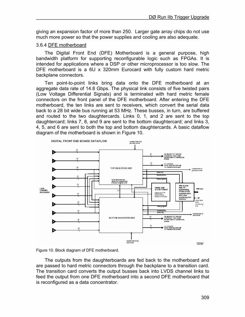
DØ Run IIb Trigger Upgrade
309
giving an expansion factor of more than 250. Larger gate array chips do not use much more power so that the power supplies and cooling are also adequate. 3.6.4 DFE motherboard
The Digital Front End (DFE) Motherboard is a general purpose, high bandwidth platform for supporting reconfigurable logic such as FPGAs. It is intended for applications where a DSP or other microprocessor is too slow. The DFE motherboard is a 6U x 320mm Eurocard with fully custom hard metric backplane connectors.
Ten point-to-point links bring data onto the DFE motherboard at an aggregate data rate of 14.8 Gbps. The physical link consists of five twisted pairs (Low Voltage Differential Signals) and is terminated with hard metric female connectors on the front panel of the DFE motherboard. After entering the DFE motherboard, the ten links are sent to receivers, which convert the serial data back to a 28 bit wide bus running at 53 MHz. These busses, in turn, are buffered and routed to the two daughtercards. Links 0, 1, and 2 are sent to the top daughtercard; links 7, 8, and 9 are sent to the bottom daughtercard; and links 3, 4, 5, and 6 are sent to both the top and bottom daughtercards. A basic dataflow diagram of the motherboard is shown in Figure 10.
Figure 10. Block diagram of DFE motherboard.
The outputs from the daughterboards are fed back to the motherboard and are passed to hard metric connectors through the backplane to a transition card. The transition card converts the output busses back into LVDS channel links to feed the output from one DFE motherboard into a second DFE motherboard that is reconfigured as a data concentrator.
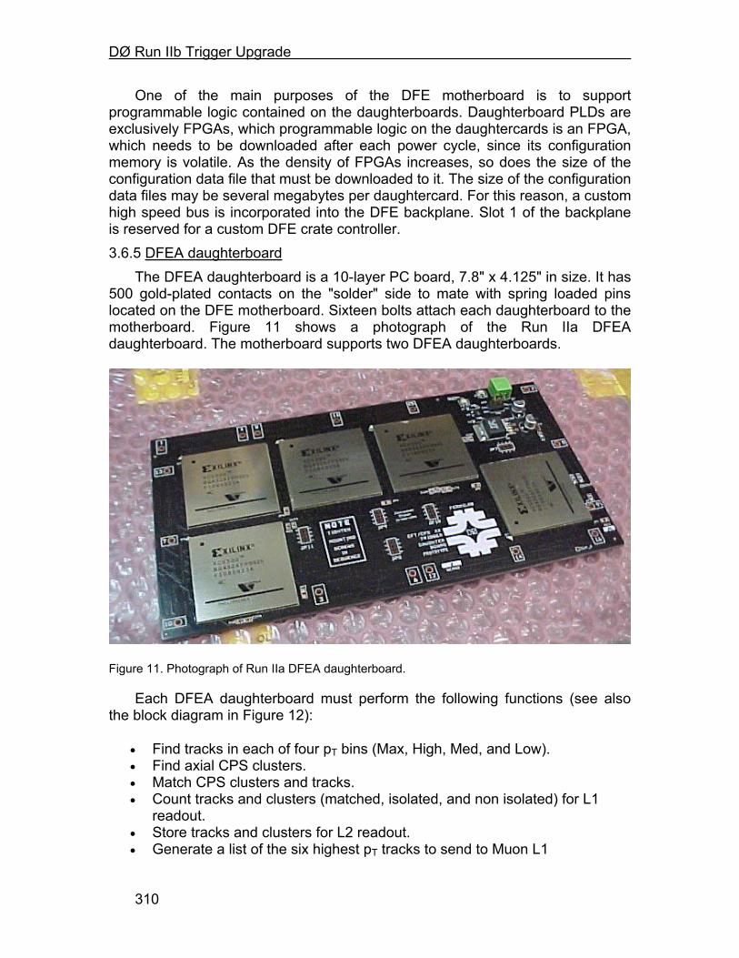
DØ Run IIb Trigger Upgrade
310
One of the main purposes of the DFE motherboard is to support programmable logic contained on the daughterboards. Daughterboard PLDs are exclusively FPGAs, which programmable logic on the daughtercards is an FPGA, which needs to be downloaded after each power cycle, since its configuration memory is volatile. As the density of FPGAs increases, so does the size of the configuration data file that must be downloaded to it. The size of the configuration data files may be several megabytes per daughtercard. For this reason, a custom high speed bus is incorporated into the DFE backplane. Slot 1 of the backplane is reserved for a custom DFE crate controller. 3.6.5 DFEA daughterboard
The DFEA daughterboard is a 10-layer PC board, 7.8" x 4.125" in size. It has 500 gold-plated contacts on the "solder" side to mate with spring loaded pins located on the DFE motherboard. Sixteen bolts attach each daughterboard to the motherboard. Figure 11 shows a photograph of the Run IIa DFEA daughterboard. The motherboard supports two DFEA daughterboards.
Figure 11. Photograph of Run IIa DFEA daughterboard.
Each DFEA daughterboard must perform the following functions (see also the block diagram in Figure 12):
• Find tracks in each of four pT bins (Max, High, Med, and Low). • Find axial CPS clusters. • Match CPS clusters and tracks. • Count tracks and clusters (matched, isolated, and non isolated) for L1
readout. • Store tracks and clusters for L2 readout. • Generate a list of the six highest pT tracks to send to Muon L1
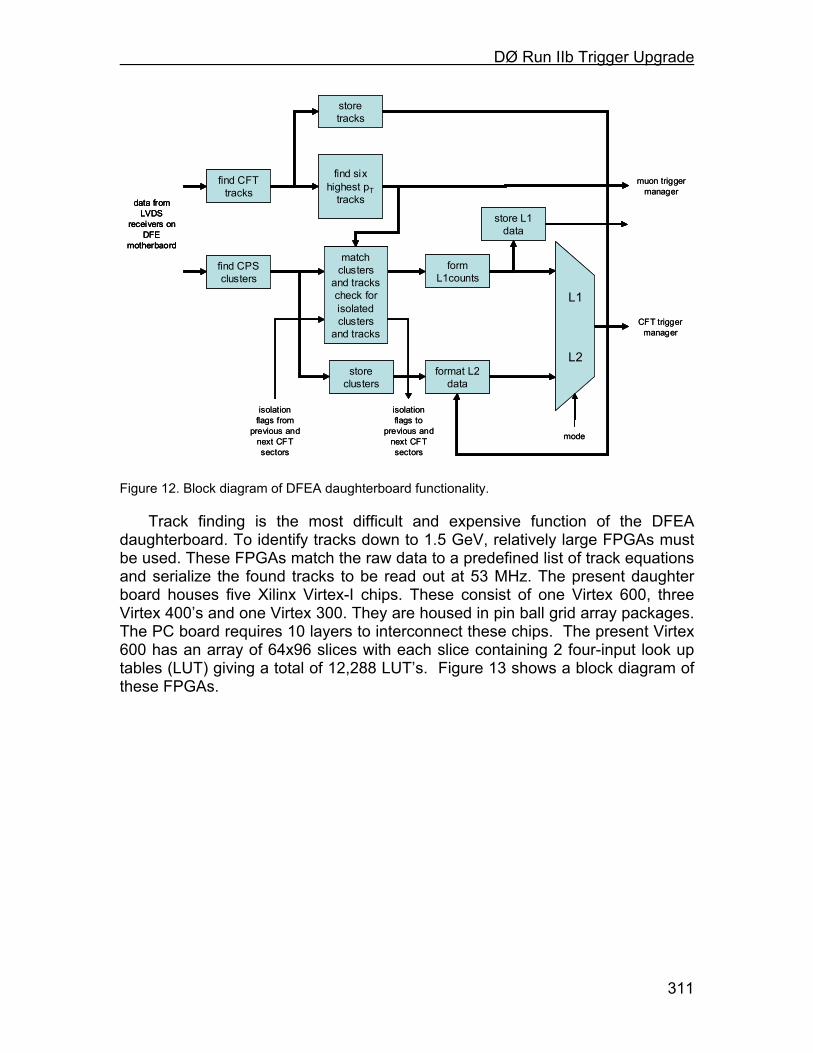
DØ Run IIb Trigger Upgrade
311
find CFT tracks
store tracks
find six highest pT
tracks
store clusters
find CPS clusters
form L1counts
format L2 data
store L1 data
isolation flags from
previous and next CFT sectors
data from LVDS
receivers on DFE
motherbaord
muon trigger manager
L1
L2
CFT trigger manager
match clusters
and trackscheck for isolated clusters
and tracks
isolation flags to
previous and next CFT sectors
mode
find CFT tracks
store tracks
find six highest pT
tracks
store clusters
find CPS clusters
form L1counts
format L2 data
store L1 data
isolation flags from
previous and next CFT sectors
data from LVDS
receivers on DFE
motherbaord
data from LVDS
receivers on DFE
motherbaord
muon trigger manager
L1
L2
L1
L2
CFT trigger manager
match clusters
and trackscheck for isolated clusters
and tracks
match clusters
and trackscheck for isolated clusters
and tracks
isolation flags to
previous and next CFT sectors
mode
Figure 12. Block diagram of DFEA daughterboard functionality.
Track finding is the most difficult and expensive function of the DFEA daughterboard. To identify tracks down to 1.5 GeV, relatively large FPGAs must be used. These FPGAs match the raw data to a predefined list of track equations and serialize the found tracks to be read out at 53 MHz. The present daughter board houses five Xilinx Virtex-I chips. These consist of one Virtex 600, three Virtex 400’s and one Virtex 300. They are housed in pin ball grid array packages. The PC board requires 10 layers to interconnect these chips. The present Virtex 600 has an array of 64x96 slices with each slice containing 2 four-input look up tables (LUT) giving a total of 12,288 LUT’s. Figure 13 shows a block diagram of these FPGAs.
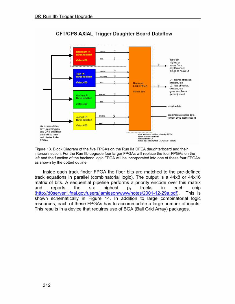
DØ Run IIb Trigger Upgrade
312
Figure 13. Block Diagram of the five FPGAs on the Run IIa DFEA daughterboard and their interconnection. For the Run IIb upgrade four larger FPGAs will replace the four FPGAs on the left and the function of the backend logic FPGA will be incorporated into one of these four FPGAs as shown by the dotted outline.
Inside each track finder FPGA the fiber bits are matched to the pre-defined track equations in parallel (combinatorial logic). The output is a 44x8 or 44x16 matrix of bits. A sequential pipeline performs a priority encode over this matrix and reports the six highest pT tracks in each chip (http://d0server1.fnal.gov/users/jamieson/www/notes/2001-12-29a.pdf). This is shown schematically in Figure 14. In addition to large combinatorial logic resources, each of these FPGAs has to accommodate a large number of inputs. This results in a device that requires use of BGA (Ball Grid Array) packages.
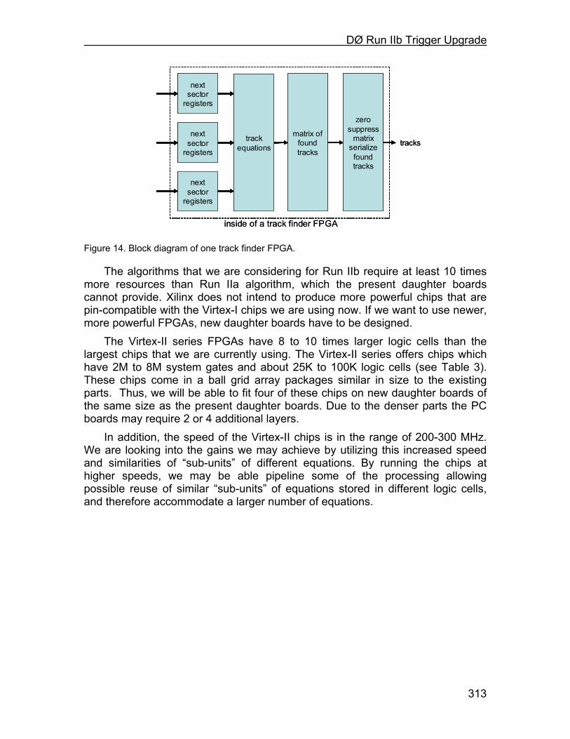
DØ Run IIb Trigger Upgrade
313
next sector
registers
next sector
registers
next sector
registers
matrix of found tracks
zero suppress
matrixserialize
found tracks
tracks
inside of a track finder FPGA
track equations
next sector
registers
next sector
registers
next sector
registers
matrix of found tracks
zero suppress
matrixserialize
found tracks
tracks
inside of a track finder FPGA
track equations
track equations
Figure 14. Block diagram of one track finder FPGA.
The algorithms that we are considering for Run IIb require at least 10 times more resources than Run IIa algorithm, which the present daughter boards cannot provide. Xilinx does not intend to produce more powerful chips that are pin-compatible with the Virtex-I chips we are using now. If we want to use newer, more powerful FPGAs, new daughter boards have to be designed.
The Virtex-II series FPGAs have 8 to 10 times larger logic cells than the largest chips that we are currently using. The Virtex-II series offers chips which have 2M to 8M system gates and about 25K to 100K logic cells (see Table 3). These chips come in a ball grid array packages similar in size to the existing parts. Thus, we will be able to fit four of these chips on new daughter boards of the same size as the present daughter boards. Due to the denser parts the PC boards may require 2 or 4 additional layers.
In addition, the speed of the Virtex-II chips is in the range of 200-300 MHz. We are looking into the gains we may achieve by utilizing this increased speed and similarities of “sub-units” of different equations. By running the chips at higher speeds, we may be able pipeline some of the processing allowing possible reuse of similar “sub-units” of equations stored in different logic cells, and therefore accommodate a larger number of equations.
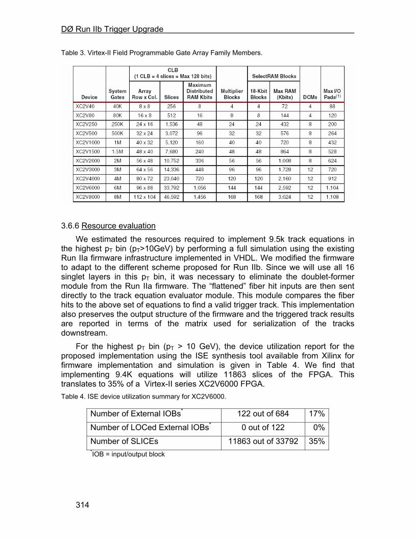
DØ Run IIb Trigger Upgrade
314
Table 3. Virtex-II Field Programmable Gate Array Family Members.
3.6.6 Resource evaluation
We estimated the resources required to implement 9.5k track equations in the highest pT bin (pT>10GeV) by performing a full simulation using the existing Run IIa firmware infrastructure implemented in VHDL. We modified the firmware to adapt to the different scheme proposed for Run IIb. Since we will use all 16 singlet layers in this pT bin, it was necessary to eliminate the doublet-former module from the Run IIa firmware. The “flattened” fiber hit inputs are then sent directly to the track equation evaluator module. This module compares the fiber hits to the above set of equations to find a valid trigger track. This implementation also preserves the output structure of the firmware and the triggered track results are reported in terms of the matrix used for serialization of the tracks downstream.
For the highest pT bin (pT > 10 GeV), the device utilization report for the proposed implementation using the ISE synthesis tool available from Xilinx for firmware implementation and simulation is given in Table 4. We find that implementing 9.4K equations will utilize 11863 slices of the FPGA. This translates to 35% of a Virtex-II series XC2V6000 FPGA. Table 4. ISE device utilization summary for XC2V6000.
Number of External IOBs* 122 out of 684 17% Number of LOCed External IOBs* 0 out of 122 0% Number of SLICEs 11863 out of 33792 35% *IOB = input/output block
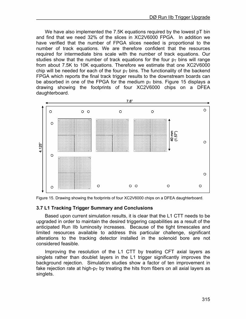
DØ Run IIb Trigger Upgrade
315
We have also implemented the 7.5K equations required by the lowest pT bin and find that we need 32% of the slices in XC2V6000 FPGA. In addition we have verified that the number of FPGA slices needed is proportional to the number of track equations. We are therefore confident that the resources required for intermediate bins scale with the number of track equations. Our studies show that the number of track equations for the four pT bins will range from about 7.5K to 10K equations. Therefore we estimate that one XC2V6000 chip will be needed for each of the four pT bins. The functionality of the backend FPGA which reports the final track trigger results to the downstream boards can be absorbed in one of the FPGA for the medium pT bins. Figure 15 displays a drawing showing the footprints of four XC2V6000 chips on a DFEA daughterboard.
4.12
5”
7.8”
40 m
m(1
.57”
)
4.12
5”
7.8”
40 m
m(1
.57”
)
Figure 15. Drawing showing the footprints of four XC2V6000 chips on a DFEA daughterboard.
3.7 L1 Tracking Trigger Summary and Conclusions Based upon current simulation results, it is clear that the L1 CTT needs to be
upgraded in order to maintain the desired triggering capabilities as a result of the anticipated Run IIb luminosity increases. Because of the tight timescales and limited resources available to address this particular challenge, significant alterations to the tracking detector installed in the solenoid bore are not considered feasible.
Improving the resolution of the L1 CTT by treating CFT axial layers as singlets rather than doublet layers in the L1 trigger significantly improves the background rejection. Simulation studies show a factor of ten improvement in fake rejection rate at high-pT by treating the hits from fibers on all axial layers as singlets.

DØ Run IIb Trigger Upgrade
316
The proposed FPGA upgrade provides a major increase in the number of equations and number of terms per equation that can be handled, and provides increased flexibility in the track finding algorithms that may be implemented. Depending on the pT range, either mixtures of doublet and singlet layers or full singlet layers are proposed. Finally, we have demonstrated the technical feasibility of the upgrade by implementing the proposed algorithm in currently available FPGAs (e.g. Xilinx Virtex II series).

DØ Run IIb Trigger Upgrade
317
4 Level 1 Calorimeter Trigger 4.1 Goals
The primary focus of Run IIb will be the search for the mechanism of electroweak symmetry breaking, including the search for the Higgs boson, supersymmetry, or other manifestations of new physics at a large mass scale. This program demands the selection of events with particularly large transverse momentum objects. The increase in luminosity (and thus increasing multiple interactions), and the decreased bunch spacing (132ns) for Run IIb will impose heavy loads on the Level 1 (L1) calorimeter trigger. The L1 calorimeter trigger upgrade should provide performance improvements over the Run IIa trigger system to allow increased rejection of backgrounds from QCD jet production, and new tools for recognition of interesting signatures. We envision a variety of improvements, each of which will contribute to a substantial improvement in our ability to control rates at the L1 trigger. In the following sections we describe how the L1 calorimeter trigger upgrade will provide
• An improved capability to correctly assign the calorimeter energy deposits to the correct bunch crossing via digital filtering
• A significantly sharper turn-on for jet triggers, thus reducing the rates
• Improved trigger turn-on for electromagnetic objects
• The ability to make shape and isolation cuts on electromagnetic triggers, and thus reducing rates
• The ability to match tracks to energy deposition in calorimeter trigger towers, leading to reduced rates
• The ability to include the energy in the intercryostat region (ICR) when calculating jet energies and the missing ET
• The ability to add topological triggers which will aid in triggering on specific Higgs final states.
The complete implementation of all these improvements will provide us with the ability to trigger effectively with the calorimeter in the challenging environment of Run IIb.
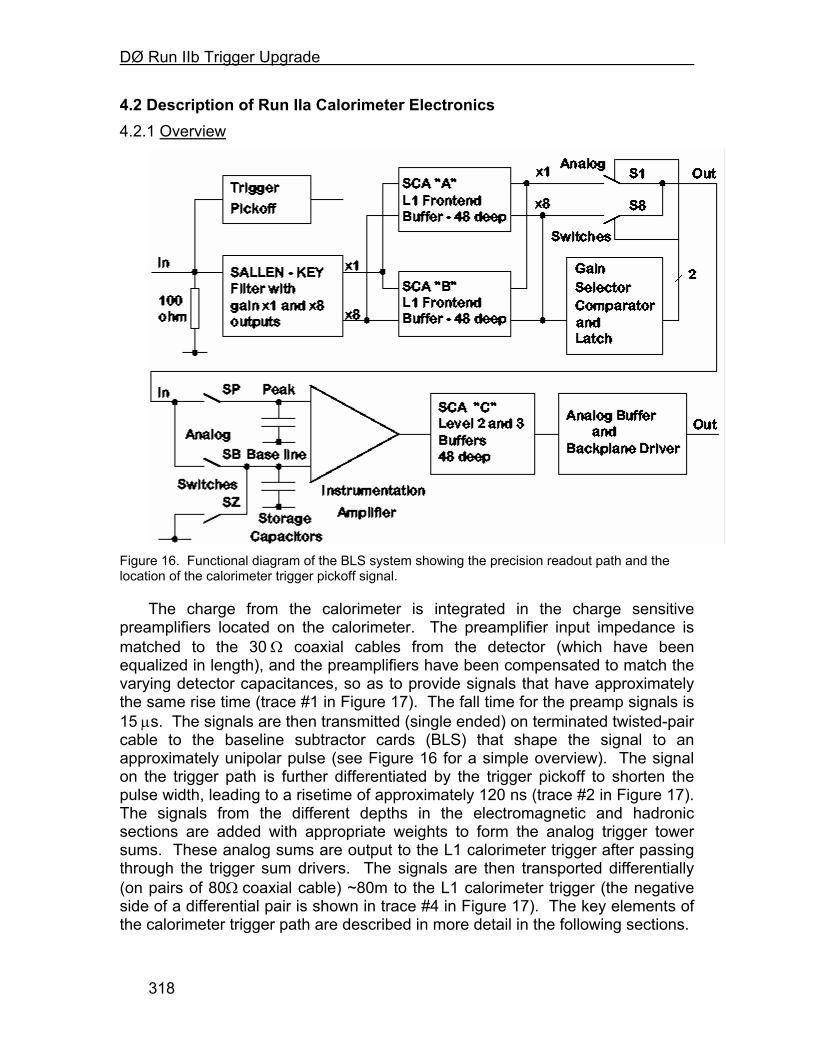
DØ Run IIb Trigger Upgrade
318
4.2 Description of Run IIa Calorimeter Electronics 4.2.1 Overview
Figure 16. Functional diagram of the BLS system showing the precision readout path and the location of the calorimeter trigger pickoff signal.
The charge from the calorimeter is integrated in the charge sensitive preamplifiers located on the calorimeter. The preamplifier input impedance is matched to the 30 Ω coaxial cables from the detector (which have been equalized in length), and the preamplifiers have been compensated to match the varying detector capacitances, so as to provide signals that have approximately the same rise time (trace #1 in Figure 17). The fall time for the preamp signals is 15 µs. The signals are then transmitted (single ended) on terminated twisted-pair cable to the baseline subtractor cards (BLS) that shape the signal to an approximately unipolar pulse (see Figure 16 for a simple overview). The signal on the trigger path is further differentiated by the trigger pickoff to shorten the pulse width, leading to a risetime of approximately 120 ns (trace #2 in Figure 17). The signals from the different depths in the electromagnetic and hadronic sections are added with appropriate weights to form the analog trigger tower sums. These analog sums are output to the L1 calorimeter trigger after passing through the trigger sum drivers. The signals are then transported differentially (on pairs of 80Ω coaxial cable) ~80m to the L1 calorimeter trigger (the negative side of a differential pair is shown in trace #4 in Figure 17). The key elements of the calorimeter trigger path are described in more detail in the following sections.
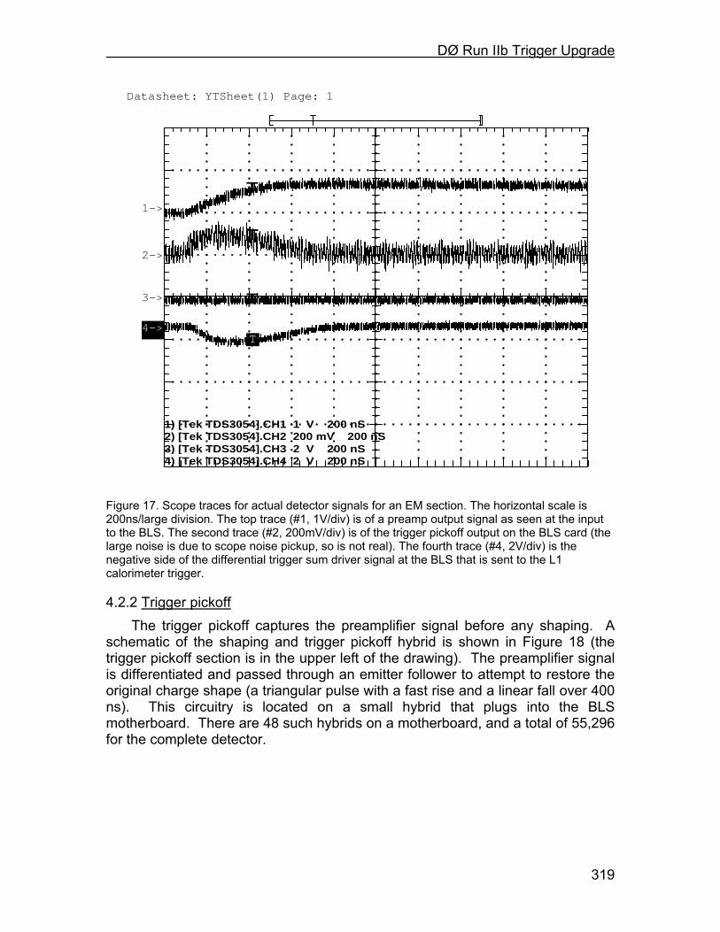
DØ Run IIb Trigger Upgrade
319
Datasheet: YTSheet(1) Page: 1
T1->
T2->
T3->
T4->
1) [Tek TDS3054].CH1 1 V 200 nS 2) [Tek TDS3054].CH2 200 mV 200 nS 3) [Tek TDS3054].CH3 2 V 200 nS 4) [Tek TDS3054].CH4 2 V 200 nS
Figure 17. Scope traces for actual detector signals for an EM section. The horizontal scale is 200ns/large division. The top trace (#1, 1V/div) is of a preamp output signal as seen at the input to the BLS. The second trace (#2, 200mV/div) is of the trigger pickoff output on the BLS card (the large noise is due to scope noise pickup, so is not real). The fourth trace (#4, 2V/div) is the negative side of the differential trigger sum driver signal at the BLS that is sent to the L1 calorimeter trigger.
4.2.2 Trigger pickoff The trigger pickoff captures the preamplifier signal before any shaping. A
schematic of the shaping and trigger pickoff hybrid is shown in Figure 18 (the trigger pickoff section is in the upper left of the drawing). The preamplifier signal is differentiated and passed through an emitter follower to attempt to restore the original charge shape (a triangular pulse with a fast rise and a linear fall over 400 ns). This circuitry is located on a small hybrid that plugs into the BLS motherboard. There are 48 such hybrids on a motherboard, and a total of 55,296 for the complete detector.
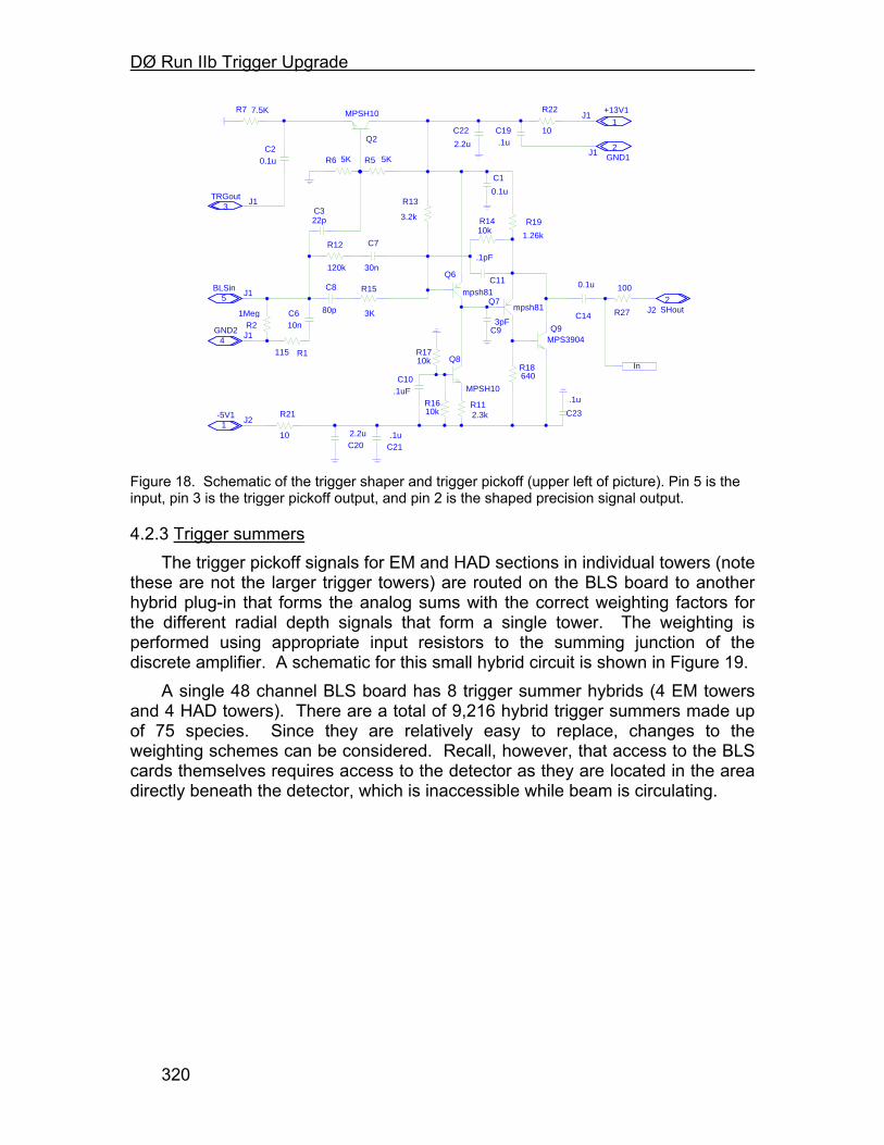
DØ Run IIb Trigger Upgrade
320
10nC6
R12
120k
C322p
R6 5KC2
0.1u
R7 7.5K
10kR16
MPSH10
Q8
mpsh81Q7
mpsh81
Q6
C23
.1u
0.1u
C14
R22
10
2.2u
C22
R5 5K
MPSH10
Q2
0.1u
C1
2.3kR11
C10.1uF
3pFC9
10kR17
C7
30n
R15
3K
C21.1u
C202.2u
.1uC19
10
R21
100
R27
R21Meg
R1115
640R18
MPS3904Q9
R13
3.2k
1.26k
R19
.1pF
C11
10kR14
C8
80p
+13V11
J1
TRGoutJ1
3
In
GND1J1
2
BLSinJ1
5
GND2J1
4
-5V1J2
1
2J2 SHout
Figure 18. Schematic of the trigger shaper and trigger pickoff (upper left of picture). Pin 5 is the input, pin 3 is the trigger pickoff output, and pin 2 is the shaped precision signal output.
4.2.3 Trigger summers The trigger pickoff signals for EM and HAD sections in individual towers (note
these are not the larger trigger towers) are routed on the BLS board to another hybrid plug-in that forms the analog sums with the correct weighting factors for the different radial depth signals that form a single tower. The weighting is performed using appropriate input resistors to the summing junction of the discrete amplifier. A schematic for this small hybrid circuit is shown in Figure 19.
A single 48 channel BLS board has 8 trigger summer hybrids (4 EM towers and 4 HAD towers). There are a total of 9,216 hybrid trigger summers made up of 75 species. Since they are relatively easy to replace, changes to the weighting schemes can be considered. Recall, however, that access to the BLS cards themselves requires access to the detector as they are located in the area directly beneath the detector, which is inaccessible while beam is circulating.

DØ Run IIb Trigger Upgrade
321
Figure 19. Schematic of the trigger summer hybrid. Up to 8 inputs from the various layers in a single tower can be summed with varying gains determined by the resistors to the summing junction (shown at left).
4.2.4 Trigger sum driver The outputs of the 4 EM trigger summers and the 4 HAD trigger summers on
a single BLS board are summed separately (except at high η) once more by the trigger sum driver circuit (see the schematic in Figure 20) where a final overall gain can be introduced. This circuit is also a hybrid plug-in to the BLS board and is thus easily replaceable if necessary (with the same access restrictions discussed for the trigger summers). In addition the driver is capable of driving the coaxial lines to the L1 Calorimeter trigger. There are a total of 2,560 such drivers in 8 species (although most are of two types).
Figure 20. Schematic of the trigger sum driver hybrid. This circuit sums the outputs of up to 4 trigger summer outputs of the type shown in Figure 19.
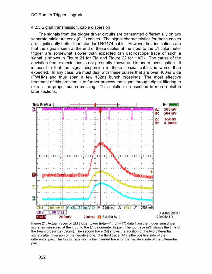
DØ Run IIb Trigger Upgrade
322
4.2.5 Signal transmission, cable dispersion The signals from the trigger driver circuits are transmitted differentially on two
separate miniature coax (0.1”) cables. The signal characteristics for these cables are significantly better than standard RG174 cable. However first indications are that the signals seen at the end of these cables at the input to the L1 calorimeter trigger are somewhat slower than expected (an oscilloscope trace of such a signal is shown in Figure 21 for EM and Figure 22 for HAD). The cause of the deviation from expectations is not presently known and is under investigation. It is possible that the signal dispersion in these coaxial cables is worse than expected. In any case, we must deal with these pulses that are over 400ns wide (FWHM) and thus span a few 132ns bunch crossings. The most effective treatment of this problem is to further process the signal through digital filtering to extract the proper bunch crossing. This solution is described in more detail in later sections.
Figure 21. Actual traces of EM trigger tower (ieta=+1, iphi=17) data from the trigger sum driver signal as measured at the input to the L1 calorimeter trigger. The top trace (#3) shows the time of the beam crossings (396ns). The second trace (M) shows the addition of the two differential signals after inversion of the negative one. The third trace (#1) is the positive side of the differential pair. The fourth trace (#2) is the inverted trace for the negative side of the differential pair.
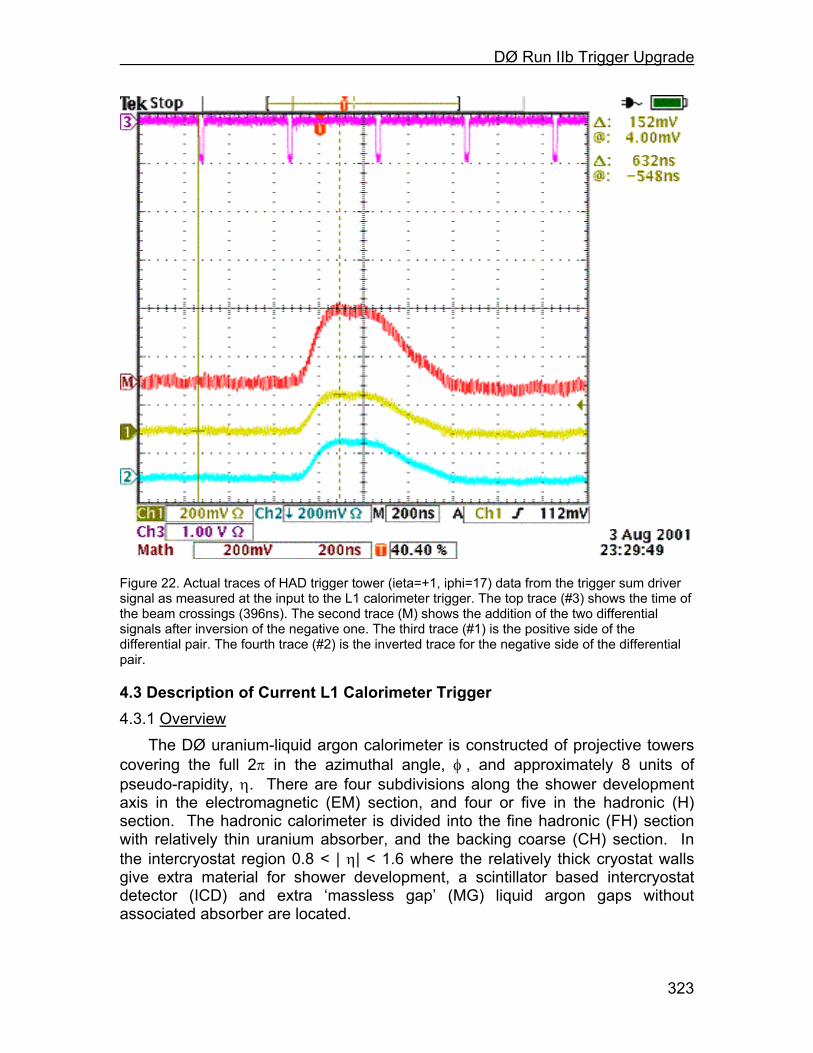
DØ Run IIb Trigger Upgrade
323
Figure 22. Actual traces of HAD trigger tower (ieta=+1, iphi=17) data from the trigger sum driver signal as measured at the input to the L1 calorimeter trigger. The top trace (#3) shows the time of the beam crossings (396ns). The second trace (M) shows the addition of the two differential signals after inversion of the negative one. The third trace (#1) is the positive side of the differential pair. The fourth trace (#2) is the inverted trace for the negative side of the differential pair.
4.3 Description of Current L1 Calorimeter Trigger 4.3.1 Overview
The DØ uranium-liquid argon calorimeter is constructed of projective towers covering the full 2π in the azimuthal angle, φ , and approximately 8 units of pseudo-rapidity, η. There are four subdivisions along the shower development axis in the electromagnetic (EM) section, and four or five in the hadronic (H) section. The hadronic calorimeter is divided into the fine hadronic (FH) section with relatively thin uranium absorber, and the backing coarse (CH) section. In the intercryostat region 0.8 < | η| < 1.6 where the relatively thick cryostat walls give extra material for shower development, a scintillator based intercryostat detector (ICD) and extra ‘massless gap’ (MG) liquid argon gaps without associated absorber are located.
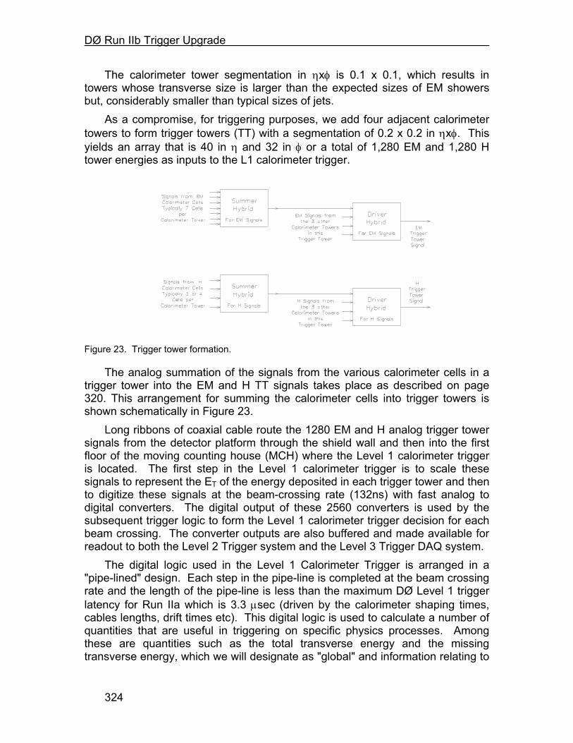
DØ Run IIb Trigger Upgrade
324
The calorimeter tower segmentation in ηxφ is 0.1 x 0.1, which results in towers whose transverse size is larger than the expected sizes of EM showers but, considerably smaller than typical sizes of jets.
As a compromise, for triggering purposes, we add four adjacent calorimeter towers to form trigger towers (TT) with a segmentation of 0.2 x 0.2 in ηxφ. This yields an array that is 40 in η and 32 in φ or a total of 1,280 EM and 1,280 H tower energies as inputs to the L1 calorimeter trigger.
Figure 23. Trigger tower formation.
The analog summation of the signals from the various calorimeter cells in a trigger tower into the EM and H TT signals takes place as described on page 320. This arrangement for summing the calorimeter cells into trigger towers is shown schematically in Figure 23.
Long ribbons of coaxial cable route the 1280 EM and H analog trigger tower signals from the detector platform through the shield wall and then into the first floor of the moving counting house (MCH) where the Level 1 calorimeter trigger is located. The first step in the Level 1 calorimeter trigger is to scale these signals to represent the ET of the energy deposited in each trigger tower and then to digitize these signals at the beam-crossing rate (132ns) with fast analog to digital converters. The digital output of these 2560 converters is used by the subsequent trigger logic to form the Level 1 calorimeter trigger decision for each beam crossing. The converter outputs are also buffered and made available for readout to both the Level 2 Trigger system and the Level 3 Trigger DAQ system.
The digital logic used in the Level 1 Calorimeter Trigger is arranged in a "pipe-lined" design. Each step in the pipe-line is completed at the beam crossing rate and the length of the pipe-line is less than the maximum DØ Level 1 trigger latency for Run IIa which is 3.3 µsec (driven by the calorimeter shaping times, cables lengths, drift times etc). This digital logic is used to calculate a number of quantities that are useful in triggering on specific physics processes. Among these are quantities such as the total transverse energy and the missing transverse energy, which we will designate as "global" and information relating to

DØ Run IIb Trigger Upgrade
325
"local" or cluster aspects of the energy deposits in the calorimeter. The latter would include the number of EM and H-like clusters exceeding a set of programmable thresholds. 4.3.2 Global Triggers
Interesting global quantities include: the total transverse energies:
( ) ( )∑=
=1280
1ii
EMTTotal
EMT EE
( ) ( )∑=
=1280
1ii
HTTotal
HT EE
and
( ) ( ) ( )TotalHTTotal
EMTTotalT EEE +=
the missing transverse energy: 2 2 ( y x T E E Mp + = )
where:
( ) ( )[ ]∑=
+=1280
1)cos(
iii
HTi
EMTx EEE φ
and
( ) ( )[ ]∑=
+=1280
1)sin(
iii
HTi
EMTy EEE φ
Any of these global quantities can be used in constructing triggers. Each quantity is compared to a number of thresholds and the result of these comparisons is passed to the Trigger Framework where up to 128 different Level 1 triggers can be formed. 4.3.3 Cluster Triggers
The DØ detector was designed with the intent of optimizing the detection of leptons, quarks and gluons. Electrons and photons will manifest themselves as localized EM energy deposits and the quarks and gluons as hadron-like clusters.
Energy deposited in a Trigger tower is called EM-like if it exceeds one of the EM ET thresholds and if it is not vetoed by the H energy behind it. Up to four EM ET thresholds and their associated H veto thresholds may be programmed for each of the 1280 trigger towers. Hadronic energy deposits are detected by calculating the EM ET + H ET of each Trigger tower and comparing each of these 1280 sums to four programmable thresholds.
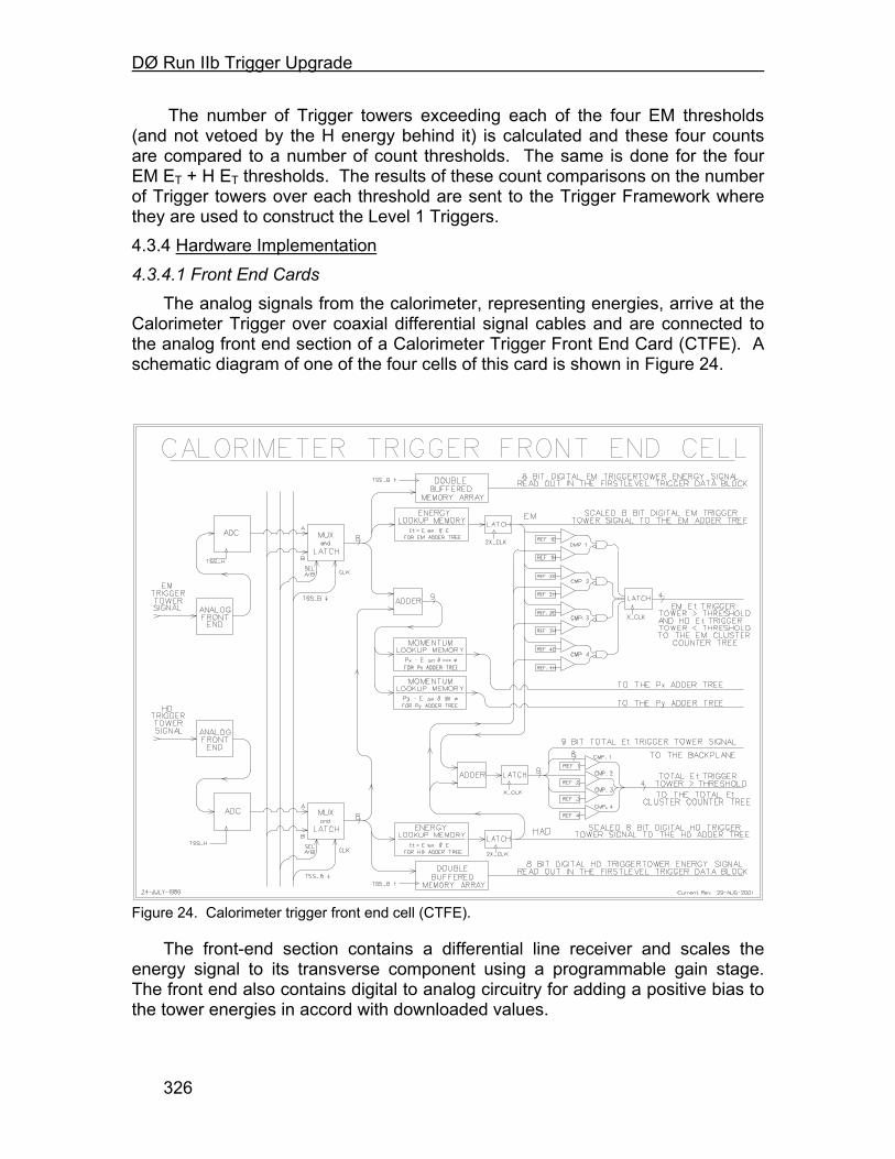
DØ Run IIb Trigger Upgrade
326
The number of Trigger towers exceeding each of the four EM thresholds (and not vetoed by the H energy behind it) is calculated and these four counts are compared to a number of count thresholds. The same is done for the four EM ET + H ET thresholds. The results of these count comparisons on the number of Trigger towers over each threshold are sent to the Trigger Framework where they are used to construct the Level 1 Triggers. 4.3.4 Hardware Implementation 4.3.4.1 Front End Cards
The analog signals from the calorimeter, representing energies, arrive at the Calorimeter Trigger over coaxial differential signal cables and are connected to the analog front end section of a Calorimeter Trigger Front End Card (CTFE). A schematic diagram of one of the four cells of this card is shown in Figure 24.
Figure 24. Calorimeter trigger front end cell (CTFE).
The front-end section contains a differential line receiver and scales the energy signal to its transverse component using a programmable gain stage. The front end also contains digital to analog circuitry for adding a positive bias to the tower energies in accord with downloaded values.

DØ Run IIb Trigger Upgrade
327
Immediately after the analog front end, the EM or H signal is turned into an 8 bit number by fast (20 ns from input to output) FADC's. With our current choice of 0.25 GeV least count this gives a maximum of 64 GeV for the single tower transverse energy contribution.
The data are synchronized at this point by being clocked into latches and then follow three distinct parallel paths. One of these paths leads to a pipeline register for digital storage to await the L1 trigger decision and subsequent readout to the Level 2 Trigger system and the Level 3 Trigger DAQ system.
On the other two paths, each 8-bit signal becomes the address to a look up memory. The content of the memory at a specified address in one case is the transverse energy with all necessary corrections such as lower energy requirements etc. In the other case, the EM + H transverse energies are first added and then subjected to two look-ups to return the two Cartesian components of the transverse energy for use in constructing MPT. The inherent flexibility of this scheme has a number of advantages: any energy dependent quantity can be generated, individual channels can be corrected or turned off at this level and arbitrary individual tower efficiencies can be accommodated.
The CTFE card performs the function of adding the ET's of the four individual cells for both the EM and H sections and passing the resulting sums onto the Adder Trees. In addition it tests each of the EM and EM+H tower transverse energies against the four discrete thresholds and increments the appropriate counts. These counts are passed onto the EM cluster counter trees and the total ET counter trees, respectively. 4.3.4.2 Adder and Counter Trees
The adder and counter trees are similar in that they both quickly add a large number of items to form one sum. At the end of each tree the sum is compared to a number of thresholds and the result this comparison is passed to the Trigger Framework. A typical adder tree is shown in Figure 25.

DØ Run IIb Trigger Upgrade
328
Figure 25. Adder tree for EM and Had quantities.
4.3.5 Physical Layout Ten racks are used to hold the Level 1 Calorimeter Trigger, which is located
in the first floor moving counting house. The lower section of each rack contains the CTFE cards for 128 Trigger towers (all 32 φ's for four consecutive η's). The upper section of each rack contains a component of one of the Adder or Counter Trees. 4.4 Motivations for Upgrading the Current System
The current L1 calorimeter trigger, which was built in 1988, and was used in Run 1 and Run IIa, has a number of features that limit its usefulness in Run IIb.
1) Trigger tower analog signals have rise times that are slightly longer than the 132 ns bunch spacing possible in Run IIb. The fall time of the signals, ~400 ns, is also significantly longer than the time between collisions. This makes it impossible for the current L1 calorimeter trigger to reliably assign calorimeter energy to the correct beam crossing, resulting in L1 trigger accepts being generated for the wrong beam crossing. Since information about the correct (interesting) beam crossing would be lost in these cases, finding a solution to this problem is imperative.
2) The fixed size trigger towers used in the current L1 calorimeter trigger are much smaller than the typical lateral size of a jet, resulting in extremely slow “turn-on” curves for jet and electron triggers. For example, a 6 GeV single tower threshold becomes ~100% efficient only for jets with transverse energies greater than 60 GeV. This poor resolution, convoluted with the steeply falling jet ET spectrum, results in an overwhelming background of low energy jets passing a given threshold at high luminosity.

DØ Run IIb Trigger Upgrade
329
3) Total ET and missing ET resolution is significantly degraded because signals from the ICR detectors are not included in the trigger sums.
To run efficiently under all possible Run IIb conditions, the problem of triggering on the wrong bunch crossing must be resolved. Beyond that, the limited clustering capabilities in the current system result in unacceptably high rates for the triggers needed to discover the Higgs and pursue the rest of the DØ physics program. Each of these issues is discussed in more detail in the rest of this section, while our solutions are presented in the following sections. 4.4.1 Bunch Crossing mis-Identification
Because the width of the shaped analog TT signals is >400 ns, the current system will experience difficulties, as mentioned previously, if the spacing between bunches in the Tevatron is reduced from 396 ns to 132 ns. The main issue here is identifying energy deposited in the calorimeter with the correct bunch crossing. This is illustrated in Figure 21 and Figure 22, which show representative TT analog signals. The calorimeter readout timing is set such that the peak of the analog signal (~200 ns after it begins to rise) corresponds to the bunch crossing, n, where the relevant energy was deposited. For large amplitude signals, however, one or more of the TT ET thresholds may be crossed early enough on the signal’s rise to be associated with bunch crossing n-1. Additionally, the signal may not fall below threshold for several bunch crossings (n+1, n+2,…) after the signal peaks due to the long fall time. Because no events are accepted after an L1 trigger accept is issued until the silicon detector is read out, triggering on bunch crossing n-1 would cause DØ to lose the interesting event at bunch crossing n in such a case. 4.4.2 Background Rates and Rejection 4.4.2.1 Simulation of the Current System
In order to assess the physics performance of the present L1 calorimeter trigger, the following simulation is used. The jet performance is studied using a Monte-Carlo sample of QCD events (PYTHIA, with parton pT cuts of 5, 10, 20, 40 GeV and 0.5 overlaid minimum bias events). A cone algorithm with a radius of 0.4 in ηxφ is applied to the generated stable hadrons in order to find the generated jets and their direction. The direction of each generated jet is extrapolated to the calorimeter surface; leading to the “center TT” hit by the jet. The highest ET TT in a 3x3 trigger tower region (which is 0.6x0.6 in ηxφ space) around this center is then used to define the “trigger ET” corresponding to the jet. 4.4.2.2 Energy measurement and turn-on curves
In the present L1 calorimeter trigger, the trigger towers are constructed using fixed ηxφ towers. Thus we expect that a trigger tower only captures a small fraction of the total jet energy since the size of the 0.2 x 0.2 trigger towers is small compared to the spatial extent of hadronic showers. This is illustrated in Figure 26, which shows, for simulated 40 GeV ET jet events, the ratio of the ET observed by the trigger to the generated ET. It can be seen in Figure 26 that this transverse energy is only 25% of the jet ET on average. Therefore we must use
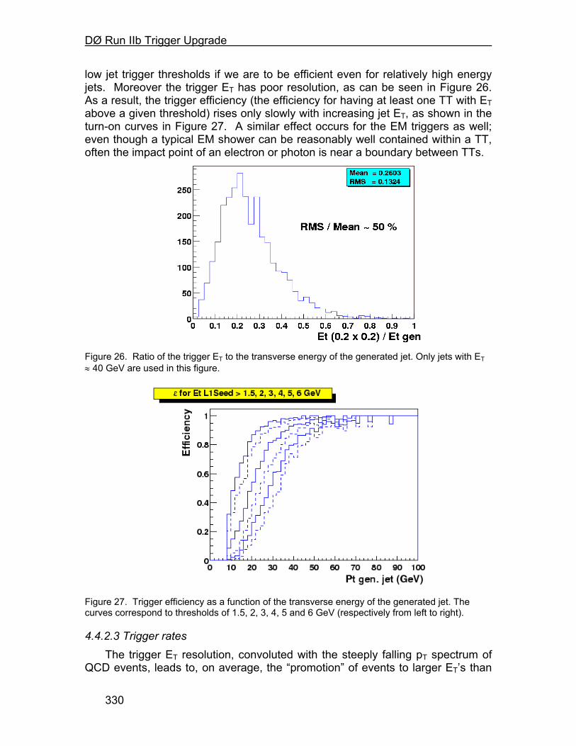
DØ Run IIb Trigger Upgrade
330
low jet trigger thresholds if we are to be efficient even for relatively high energy jets. Moreover the trigger ET has poor resolution, as can be seen in Figure 26. As a result, the trigger efficiency (the efficiency for having at least one TT with ET above a given threshold) rises only slowly with increasing jet ET, as shown in the turn-on curves in Figure 27. A similar effect occurs for the EM triggers as well; even though a typical EM shower can be reasonably well contained within a TT, often the impact point of an electron or photon is near a boundary between TTs.
Figure 26. Ratio of the trigger ET to the transverse energy of the generated jet. Only jets with ET ≈ 40 GeV are used in this figure.
Figure 27. Trigger efficiency as a function of the transverse energy of the generated jet. The curves correspond to thresholds of 1.5, 2, 3, 4, 5 and 6 GeV (respectively from left to right).
4.4.2.3 Trigger rates The trigger ET resolution, convoluted with the steeply falling pT spectrum of
QCD events, leads to, on average, the “promotion” of events to larger ET’s than
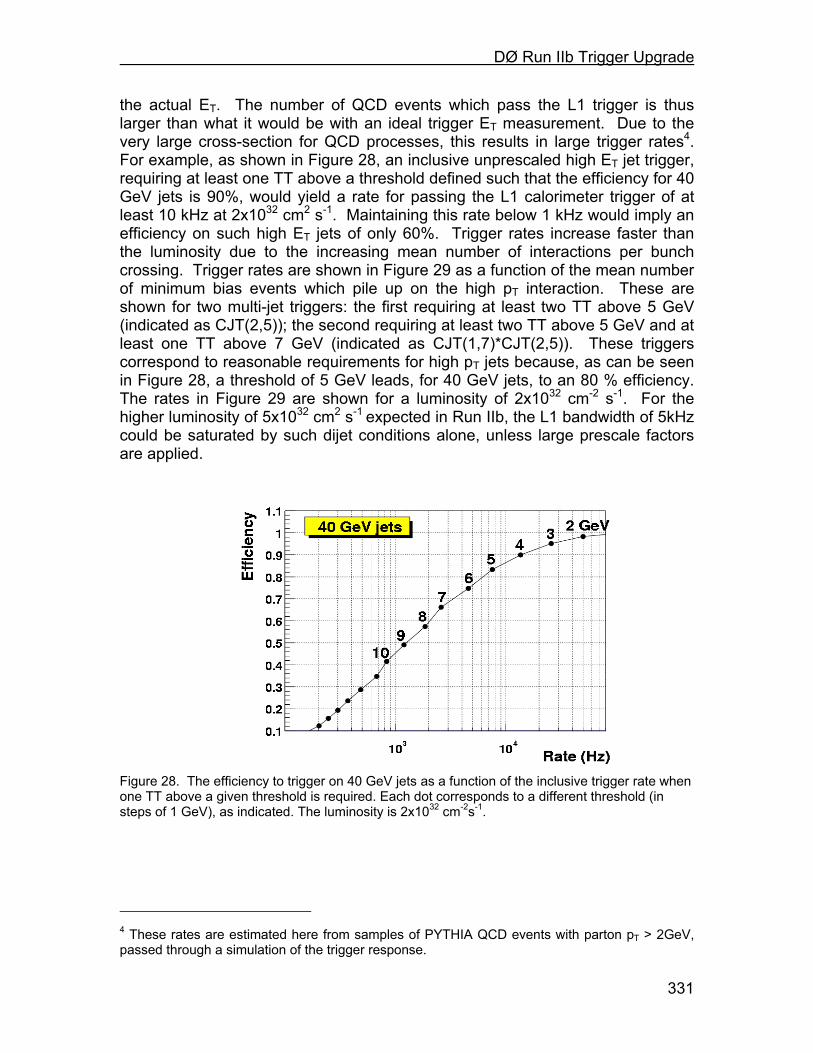
DØ Run IIb Trigger Upgrade
331
the actual ET. The number of QCD events which pass the L1 trigger is thus larger than what it would be with an ideal trigger ET measurement. Due to the very large cross-section for QCD processes, this results in large trigger rates4. For example, as shown in Figure 28, an inclusive unprescaled high ET jet trigger, requiring at least one TT above a threshold defined such that the efficiency for 40 GeV jets is 90%, would yield a rate for passing the L1 calorimeter trigger of at least 10 kHz at 2x1032 cm2 s-1. Maintaining this rate below 1 kHz would imply an efficiency on such high ET jets of only 60%. Trigger rates increase faster than the luminosity due to the increasing mean number of interactions per bunch crossing. Trigger rates are shown in Figure 29 as a function of the mean number of minimum bias events which pile up on the high pT interaction. These are shown for two multi-jet triggers: the first requiring at least two TT above 5 GeV (indicated as CJT(2,5)); the second requiring at least two TT above 5 GeV and at least one TT above 7 GeV (indicated as CJT(1,7)*CJT(2,5)). These triggers correspond to reasonable requirements for high pT jets because, as can be seen in Figure 28, a threshold of 5 GeV leads, for 40 GeV jets, to an 80 % efficiency. The rates in Figure 29 are shown for a luminosity of 2x1032 cm-2 s-1. For the higher luminosity of 5x1032 cm2 s-1 expected in Run IIb, the L1 bandwidth of 5kHz could be saturated by such dijet conditions alone, unless large prescale factors are applied.
Figure 28. The efficiency to trigger on 40 GeV jets as a function of the inclusive trigger rate when one TT above a given threshold is required. Each dot corresponds to a different threshold (in steps of 1 GeV), as indicated. The luminosity is 2x1032 cm-2s-1.
4 These rates are estimated here from samples of PYTHIA QCD events with parton pT > 2GeV, passed through a simulation of the trigger response.
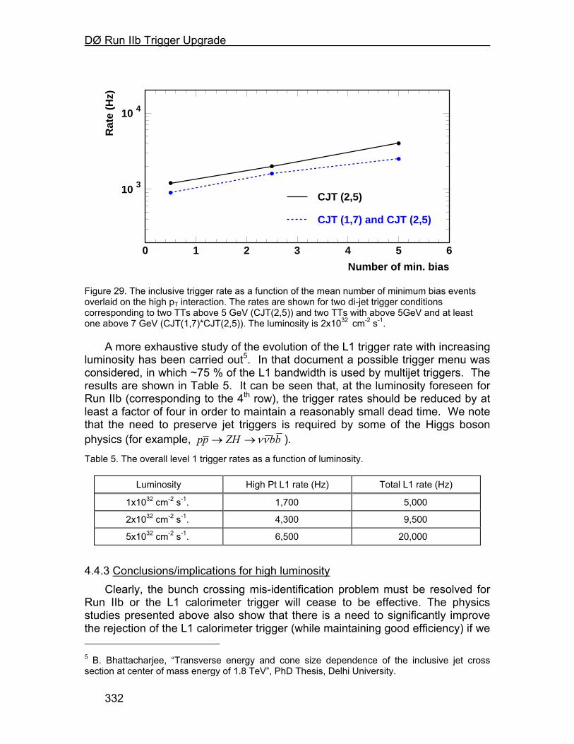
DØ Run IIb Trigger Upgrade
332
CJT (2,5)
CJT (1,7) and CJT (2,5)
Number of min. bias
Rat
e (H
z)
10 3
10 4
0 1 2 3 4 5 6
Figure 29. The inclusive trigger rate as a function of the mean number of minimum bias events overlaid on the high pT interaction. The rates are shown for two di-jet trigger conditions corresponding to two TTs above 5 GeV (CJT(2,5)) and two TTs with above 5GeV and at least one above 7 GeV (CJT(1,7)*CJT(2,5)). The luminosity is 2x1032 cm-2 s-1.
A more exhaustive study of the evolution of the L1 trigger rate with increasing luminosity has been carried out5. In that document a possible trigger menu was considered, in which ~75 % of the L1 bandwidth is used by multijet triggers. The results are shown in Table 5. It can be seen that, at the luminosity foreseen for Run IIb (corresponding to the 4th row), the trigger rates should be reduced by at least a factor of four in order to maintain a reasonably small dead time. We note that the need to preserve jet triggers is required by some of the Higgs boson physics (for example, bbZHpp νν→→ ). Table 5. The overall level 1 trigger rates as a function of luminosity.
Luminosity High Pt L1 rate (Hz) Total L1 rate (Hz)
1x1032 cm-2 s-1. 1,700 5,000
2x1032 cm-2 s-1. 4,300 9,500
5x1032 cm-2 s-1. 6,500 20,000
4.4.3 Conclusions/implications for high luminosity
Clearly, the bunch crossing mis-identification problem must be resolved for Run IIb or the L1 calorimeter trigger will cease to be effective. The physics studies presented above also show that there is a need to significantly improve the rejection of the L1 calorimeter trigger (while maintaining good efficiency) if we 5 B. Bhattacharjee, “Transverse energy and cone size dependence of the inclusive jet cross section at center of mass energy of 1.8 TeV”, PhD Thesis, Delhi University.

DØ Run IIb Trigger Upgrade
333
are to access the physics of Run IIb. One obvious way to help achieve this is to migrate the tools used at L2 (from Run IIa) into L1. In particular, the ability to trigger on “objects” such as electromagnetic showers and jets would help significantly. The “clustering” of TT’s at L1, could reduce the trigger rates by a factor 2 to 4 as will be shown later. The principal reason for this gain comes from the improvement in the quality of the energy cut, when applied to a cluster of trigger towers. Transferring to level 1 some of the functions that currently belong to level 2 would also permit the introduction of new selection algorithms at the L1 trigger level. So while it is clear that there are additional gains to be made through EM trigger tower shape cuts and missing ET filtering, they will require further study to quantify the specific gains. These studies remain to be done.
From a conceptual viewpoint, an important consequence of selecting physics “objects” at level 1 is that it allows a more “inclusive” and hence less biased selection of signatures for the more complicated decays to be studied in Run IIb. Thus we expect that the trigger menus will become simpler and, above all, less sensitive to biases arising from the combinations of primary objects. 4.4.4 Overview of Calorimeter Trigger Upgrade
We have examined various possibilities for the changes necessary to address the incorrect bunch crossing assignment problem at 132 ns bunch spacing and the trigger energy resolution problem. The age and architecture of the current system prohibit an incremental solution to these issues. Changing one aspect of the system, for example implementing a new clustering algorithm, has an impact on all other parts since in the current electronics both digitization of TT signals and the search for TTs above threshold happens on the same board. We therefore propose to design and build an entirely new L1 calorimeter trigger system, which will replace all elements of the current trigger downstream of the BLS cables. A partial list of improvements provided by the new system is given below.
• Necessary hardware improvements in filtering to allow proper triggering on the correct bunch crossing at 132 ns bunch spacing.
• Implementation of a “sliding window” algorithm for jets, electrons and taus.
• The addition of presently unused calorimeter energy information from the intercryostat detector (ICD) and massless gaps (MG) in the L1 trigger.
• Optimization of trigger tower thresholds.
• The ability to better correlate tracks from the fiber tracker to calorimeter clusters.
Studies of these improvements are discussed in the following sections with the exception of the correlation between tracks and calorimeter clusters, which is described in the Cal-Track Match system section. The design of the new system is then outlined in the remaining parts of the chapter.
DØ Run IIb Trigger Upgrade
334
4.5 Digital Filtering Digital filtering offers a way to reduce the effect of unwanted triggers due to
collisions in close proximity to the desired trigger. 4.5.1 Concept & physics implications
The pulse shape, and particularly the rise time, of the trigger pickoff signal is not optimized for 132ns beam bunch crossing operation (see Figure 21 and Figure 22). Since the trigger pickoff pulse width significantly exceeds the 132ns bunch spacing time of Run IIb, the ability to correctly identify the correct trigger bunch crossing is compromised. There may be intermediate solutions to address this problem at the lower luminosities, but a long-term solution must be developed. This could be done by means of an analog filter with shorter shaping, but this is only achieved with a further loss in signal. A digital filter is a better solution because it is much more flexible for a similar cost.
The trigger pickoff signal is at the end of the calorimeter electronic chain described above. The ideal energy deposition shape is a "saw-tooth" pulse (infinitely fast rise and a linear ~400ns fall) from energy deposited in the cells of the calorimeter at each beam crossing. This is modified by the transfer function of the electronics. The inverse transfer function will transform the pickoff signal back to original energy deposition pulse shape. Digital filtering would be implemented at this stage. The inverse function can be implemented by a FIR (Finite Impulse Response) digital filter. In the presence of noise, the digital filter offers an additional advantage: one can use the theory of optimal filtering to minimize the noise contribution.
In order to define the exact form of a digital filter best suited to the task, a measurement of noise in the trigger pickoff signals is needed. As such measurements become available, a refined design will be undertaken. 4.5.2 Pileup rejection
Two different "pile-up" effects arise with increasing luminosity, the first is due to extra collisions in the crossing of interest (and thus unavoidable), and the second is due to collisions in neighboring crossings that contribute to the crossing of interest because of signal shapes.
In the first case, we find that as the luminosity increases, then for each triggered beam crossing there are several minimum bias events that appear in that same beam crossing. The number of such additional events is Poisson distributed with a mean proportional to the luminosity. The energy added by these events has a distribution close to that of a double exponential (Laplacian). It is possible to minimize the contribution of this noise by using an appropriate digital filter (Matched Median Filter).
In the second case, because the width of the trigger pickoff signal extends over several beam crossing (6 at 132ns on the positive side of the signal), then when two such pulses are close in time, there is some overlap and thus the shape of the pickoff signal becomes more complicated than that of a single isolated pulse. The inverse filter will extract from this signal the two original
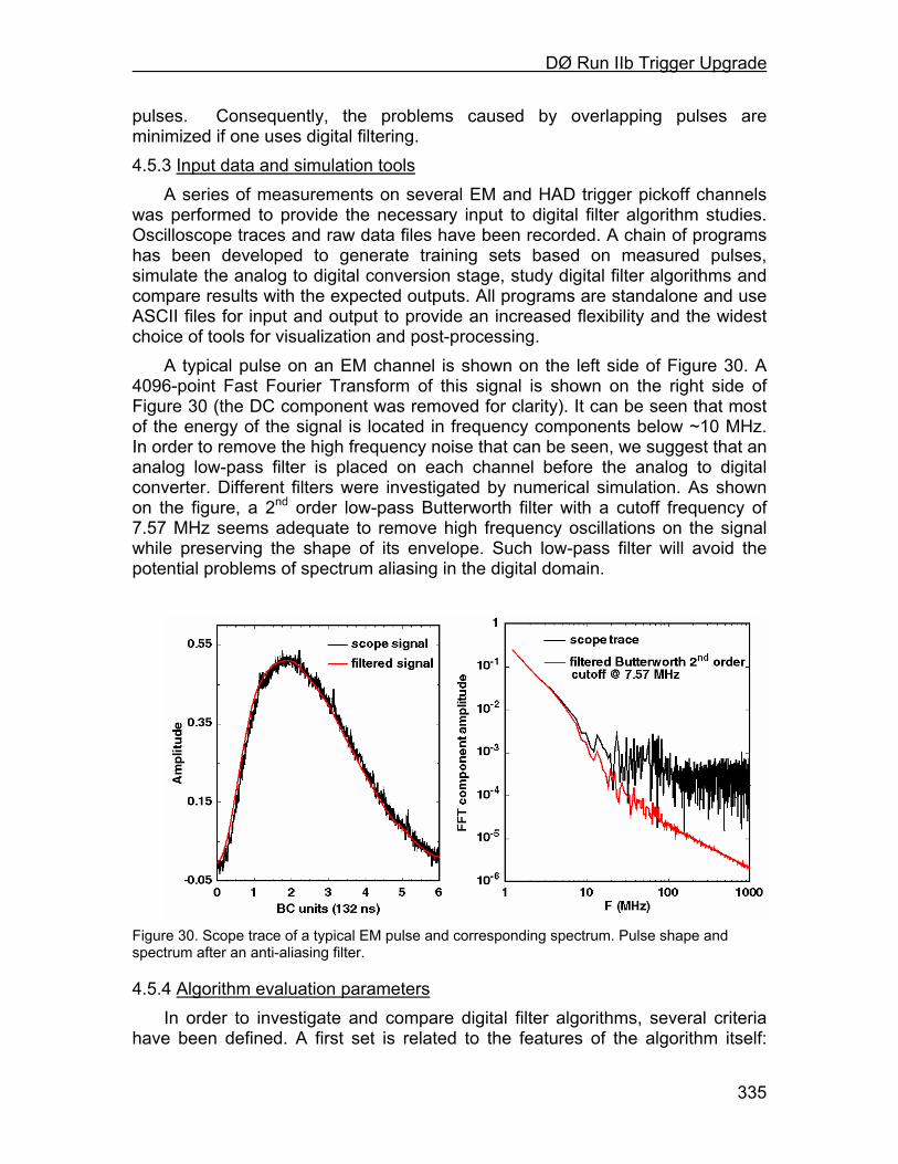
DØ Run IIb Trigger Upgrade
335
pulses. Consequently, the problems caused by overlapping pulses are minimized if one uses digital filtering. 4.5.3 Input data and simulation tools
A series of measurements on several EM and HAD trigger pickoff channels was performed to provide the necessary input to digital filter algorithm studies. Oscilloscope traces and raw data files have been recorded. A chain of programs has been developed to generate training sets based on measured pulses, simulate the analog to digital conversion stage, study digital filter algorithms and compare results with the expected outputs. All programs are standalone and use ASCII files for input and output to provide an increased flexibility and the widest choice of tools for visualization and post-processing.
A typical pulse on an EM channel is shown on the left side of Figure 30. A 4096-point Fast Fourier Transform of this signal is shown on the right side of Figure 30 (the DC component was removed for clarity). It can be seen that most of the energy of the signal is located in frequency components below ~10 MHz. In order to remove the high frequency noise that can be seen, we suggest that an analog low-pass filter is placed on each channel before the analog to digital converter. Different filters were investigated by numerical simulation. As shown on the figure, a 2nd order low-pass Butterworth filter with a cutoff frequency of 7.57 MHz seems adequate to remove high frequency oscillations on the signal while preserving the shape of its envelope. Such low-pass filter will avoid the potential problems of spectrum aliasing in the digital domain.
Figure 30. Scope trace of a typical EM pulse and corresponding spectrum. Pulse shape and spectrum after an anti-aliasing filter.
4.5.4 Algorithm evaluation parameters In order to investigate and compare digital filter algorithms, several criteria
have been defined. A first set is related to the features of the algorithm itself:
DØ Run IIb Trigger Upgrade
336
irreducible latency, number of parameters to adjust and channel dependency, procedure for parameter determination and tuning, operating frequency, behavior under digital and analog saturation… A second family of criteria relates to the quality of the algorithm: precision on the estimated Et value for the beam-crossing of interest and residual error on adjacent beam-crossings, time/amplitude resolution, ability to separate pulses close in time, probability of having pulses undetected or assigned to the wrong beam-crossing. Several criteria are related to the sensitivity of an algorithm: robustness against electrical noise, ability to reject pileup noise, sensitivity to signal phase and jitter with respect to a reference clock, dependence on pulse shape distortion, performance with limited precision arithmetic, influence of coefficient truncation and input quantization, etc. The last set of comparison criteria concerns implementation: amount of logic required and operating speed of the various components, effective latency.
Defining and selecting the algorithm that will lead to the best trade-off between all these – sometimes contradictory – criteria is not straightforward. Some compromises on performance and functionality will necessarily be done in order to fit in the tight, non-extensible, latency budget that can be devoted to this task while keeping the system simple enough to be implemented with modern, industrial electronic devices at an affordable cost. Algorithm definition and test by computer simulation, electronic hardware simulation and validation with a prototype card connected to real detector signals are among the necessary steps for a successful definition of the digital filter. 4.5.5 Algorithms studied
At present, three types of algorithms have been proposed and investigated. These are:
• A Finite Impulse Response (FIR) deconvolution filter; • A peak detector followed by a weighed moving average filter; • A matched filter followed by a peak detector.
We describe these algorithms and their simulation studies of their performance below. Based on these studies, the matched filter algorithm has been selected for the baseline calorimeter trigger design. 4.5.5.1 FIR deconvolution
The deconvolution filter is designed to implement the inverse transfer function of the complete calorimeter pickoff chain. When driven with a typical trigger pickoff saw-tooth shaped pulse, the output of the filter is the original pulse. In order to produce a meaningful output for each beam crossing, the filter must have a bandwidth equal at least to the beam crossing frequency. Hence, input samples must be acquired at least at twice the beam-crossing rate (Shannon’s sampling theorem). However, only one output value per beam crossing is computed. Coefficient count must be sufficient to ensure that the output of the filter remains null during the falling edge of the input pickoff signal. The determination of coefficients can be made using a set of input training samples
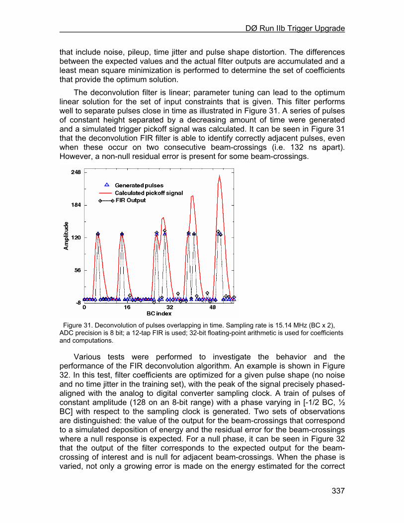
DØ Run IIb Trigger Upgrade
337
that include noise, pileup, time jitter and pulse shape distortion. The differences between the expected values and the actual filter outputs are accumulated and a least mean square minimization is performed to determine the set of coefficients that provide the optimum solution.
The deconvolution filter is linear; parameter tuning can lead to the optimum linear solution for the set of input constraints that is given. This filter performs well to separate pulses close in time as illustrated in Figure 31. A series of pulses of constant height separated by a decreasing amount of time were generated and a simulated trigger pickoff signal was calculated. It can be seen in Figure 31 that the deconvolution FIR filter is able to identify correctly adjacent pulses, even when these occur on two consecutive beam-crossings (i.e. 132 ns apart). However, a non-null residual error is present for some beam-crossings.
Figure 31. Deconvolution of pulses overlapping in time. Sampling rate is 15.14 MHz (BC x 2), ADC precision is 8 bit; a 12-tap FIR is used; 32-bit floating-point arithmetic is used for coefficients and computations.
Various tests were performed to investigate the behavior and the performance of the FIR deconvolution algorithm. An example is shown in Figure 32. In this test, filter coefficients are optimized for a given pulse shape (no noise and no time jitter in the training set), with the peak of the signal precisely phased-aligned with the analog to digital converter sampling clock. A train of pulses of constant amplitude (128 on an 8-bit range) with a phase varying in [-1/2 BC, ½ BC] with respect to the sampling clock is generated. Two sets of observations are distinguished: the value of the output for the beam-crossings that correspond to a simulated deposition of energy and the residual error for the beam-crossings where a null response is expected. For a null phase, it can be seen in Figure 32 that the output of the filter corresponds to the expected output for the beam-crossing of interest and is null for adjacent beam-crossings. When the phase is varied, not only a growing error is made on the energy estimated for the correct
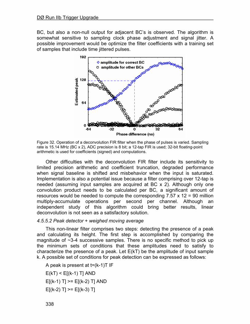
DØ Run IIb Trigger Upgrade
338
BC, but also a non-null output for adjacent BC’s is observed. The algorithm is somewhat sensitive to sampling clock phase adjustment and signal jitter. A possible improvement would be optimize the filter coefficients with a training set of samples that include time jittered pulses.
Figure 32. Operation of a deconvolution FIR filter when the phase of pulses is varied. Sampling rate is 15.14 MHz (BC x 2), ADC precision is 8 bit; a 12-tap FIR is used; 32-bit floating-point arithmetic is used for coefficients (signed) and computations.
Other difficulties with the deconvolution FIR filter include its sensitivity to limited precision arithmetic and coefficient truncation, degraded performance when signal baseline is shifted and misbehavior when the input is saturated. Implementation is also a potential issue because a filter comprising over 12-tap is needed (assuming input samples are acquired at BC x 2). Although only one convolution product needs to be calculated per BC, a significant amount of resources would be needed to compute the corresponding 7.57 x 12 = 90 million multiply-accumulate operations per second per channel. Although an independent study of this algorithm could bring better results, linear deconvolution is not seen as a satisfactory solution. 4.5.5.2 Peak detector + weighed moving average
This non-linear filter comprises two steps: detecting the presence of a peak and calculating its height. The first step is accomplished by comparing the magnitude of ~3-4 successive samples. There is no specific method to pick up the minimum sets of conditions that these amplitudes need to satisfy to characterize the presence of a peak. Let E(kT) be the amplitude of input sample k. A possible set of conditions for peak detection can be expressed as follows:
A peak is present at t=(k-1)T IF E(kT) < E[(k-1) T] AND E[(k-1) T] >= E[(k-2) T] AND E[(k-2) T] >= E[(k-3) T]
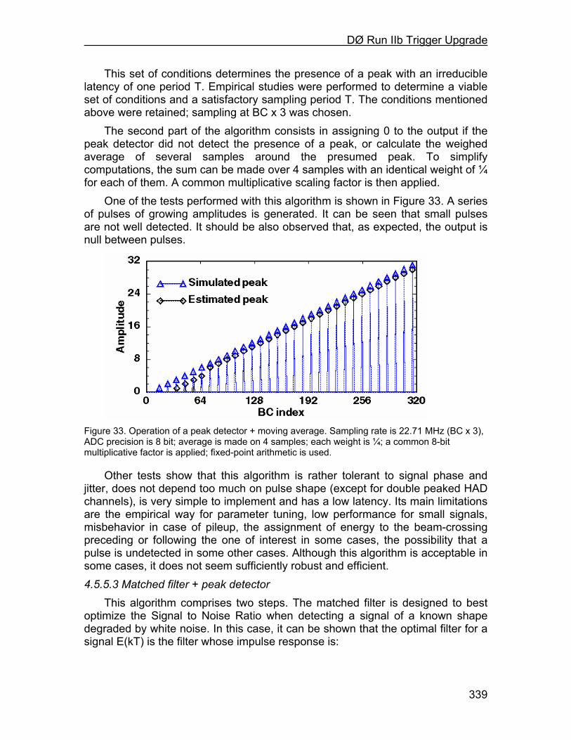
DØ Run IIb Trigger Upgrade
339
This set of conditions determines the presence of a peak with an irreducible latency of one period T. Empirical studies were performed to determine a viable set of conditions and a satisfactory sampling period T. The conditions mentioned above were retained; sampling at BC x 3 was chosen.
The second part of the algorithm consists in assigning 0 to the output if the peak detector did not detect the presence of a peak, or calculate the weighed average of several samples around the presumed peak. To simplify computations, the sum can be made over 4 samples with an identical weight of ¼ for each of them. A common multiplicative scaling factor is then applied.
One of the tests performed with this algorithm is shown in Figure 33. A series of pulses of growing amplitudes is generated. It can be seen that small pulses are not well detected. It should be also observed that, as expected, the output is null between pulses.
Figure 33. Operation of a peak detector + moving average. Sampling rate is 22.71 MHz (BC x 3), ADC precision is 8 bit; average is made on 4 samples; each weight is ¼; a common 8-bit multiplicative factor is applied; fixed-point arithmetic is used.
Other tests show that this algorithm is rather tolerant to signal phase and jitter, does not depend too much on pulse shape (except for double peaked HAD channels), is very simple to implement and has a low latency. Its main limitations are the empirical way for parameter tuning, low performance for small signals, misbehavior in case of pileup, the assignment of energy to the beam-crossing preceding or following the one of interest in some cases, the possibility that a pulse is undetected in some other cases. Although this algorithm is acceptable in some cases, it does not seem sufficiently robust and efficient. 4.5.5.3 Matched filter + peak detector
This algorithm comprises two steps. The matched filter is designed to best optimize the Signal to Noise Ratio when detecting a signal of a known shape degraded by white noise. In this case, it can be shown that the optimal filter for a signal E(kT) is the filter whose impulse response is:
DØ Run IIb Trigger Upgrade
340
h(kT) = E(T0 – kT) where T0 is a multiple of the sampling period T and is selected to cover a sufficient part of the signal. Because T0 has a direct influence on the irreducible latency of the algorithm, the number of filter taps and the operating frequency of the corresponding hardware, its value should be carefully chosen. The parameters to determine are: the sampling period T, the number of samples during T0, and the phase with respect to the training pulse of the temporal window used to determine the impulse response of the matched filter. It should also be mentioned that the peak produced at the output of a matched filter occurs at (nT+T0) and that this irreducible latency does not correspond to a fixed delay with respect to the occurrence of the peak in the signal being detected when some of the parameters of the filter are changed. When designing a series of filters running in parallel, care must be taken to ensure that algorithm latency is identical for all channels.
The second step of the algorithm is peak detection. A possible algorithm is the 3-point peak detector described by the following pseudo-code:
Peak present at t=(k-1)T IF E(kT) < E[(k-1) T] AND E[(k-1) T] > E[(k-2) T] This peak-detector adds one period T of irreducible latency. If the conditions that characterize a peak are not satisfied, the output is set to 0, otherwise it is assigned the value of the matched
filter.
Figure 34 where pulses of growing amplitudes (up to 1/8th of the full 8-bit scale) have been generated. It can be seen that the algorithm performs well in that range. All pulses but the smallest ones have been correctly detected and have been assigned to the correct beam crossing. The output is exactly zero for the beam-crossings around those of interest. Intuitively, one can easily understand that the capability to produce minimal width pulses (one sample width) surrounded by strictly null outputs is more easily achieved with a non-linear filter than with a linear algorithm.
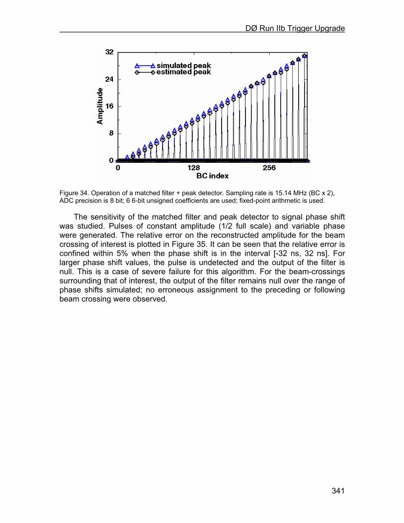
DØ Run IIb Trigger Upgrade
341
Figure 34. Operation of a matched filter + peak detector. Sampling rate is 15.14 MHz (BC x 2), ADC precision is 8 bit; 6 6-bit unsigned coefficients are used; fixed-point arithmetic is used.
The sensitivity of the matched filter and peak detector to signal phase shift was studied. Pulses of constant amplitude (1/2 full scale) and variable phase were generated. The relative error on the reconstructed amplitude for the beam crossing of interest is plotted in Figure 35. It can be seen that the relative error is confined within 5% when the phase shift is in the interval [-32 ns, 32 ns]. For larger phase shift values, the pulse is undetected and the output of the filter is null. This is a case of severe failure for this algorithm. For the beam-crossings surrounding that of interest, the output of the filter remains null over the range of phase shifts simulated; no erroneous assignment to the preceding or following beam crossing were observed.
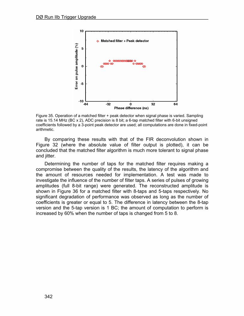
DØ Run IIb Trigger Upgrade
342
Figure 35. Operation of a matched filter + peak detector when signal phase is varied. Sampling rate is 15.14 MHz (BC x 2), ADC precision is 8 bit; a 6-tap matched filter with 6-bit unsigned coefficients followed by a 3-point peak detector are used; all computations are done in fixed-point arithmetic.
By comparing these results with that of the FIR deconvolution shown in Figure 32 (where the absolute value of filter output is plotted), it can be concluded that the matched filter algorithm is much more tolerant to signal phase and jitter.
Determining the number of taps for the matched filter requires making a compromise between the quality of the results, the latency of the algorithm and the amount of resources needed for implementation. A test was made to investigate the influence of the number of filter taps. A series of pulses of growing amplitudes (full 8-bit range) were generated. The reconstructed amplitude is shown in Figure 36 for a matched filter with 8-taps and 5-taps respectively. No significant degradation of performance was observed as long as the number of coefficients is greater or equal to 5. The difference in latency between the 8-tap version and the 5-tap version is 1 BC; the amount of computation to perform is increased by 60% when the number of taps is changed from 5 to 8.
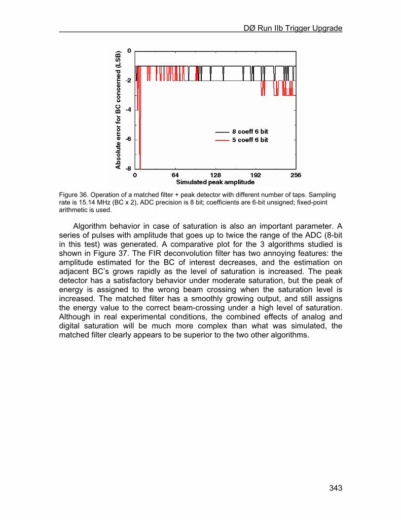
DØ Run IIb Trigger Upgrade
343
Figure 36. Operation of a matched filter + peak detector with different number of taps. Sampling rate is 15.14 MHz (BC x 2), ADC precision is 8 bit; coefficients are 6-bit unsigned; fixed-point arithmetic is used.
Algorithm behavior in case of saturation is also an important parameter. A series of pulses with amplitude that goes up to twice the range of the ADC (8-bit in this test) was generated. A comparative plot for the 3 algorithms studied is shown in Figure 37. The FIR deconvolution filter has two annoying features: the amplitude estimated for the BC of interest decreases, and the estimation on adjacent BC’s grows rapidly as the level of saturation is increased. The peak detector has a satisfactory behavior under moderate saturation, but the peak of energy is assigned to the wrong beam crossing when the saturation level is increased. The matched filter has a smoothly growing output, and still assigns the energy value to the correct beam-crossing under a high level of saturation. Although in real experimental conditions, the combined effects of analog and digital saturation will be much more complex than what was simulated, the matched filter clearly appears to be superior to the two other algorithms.
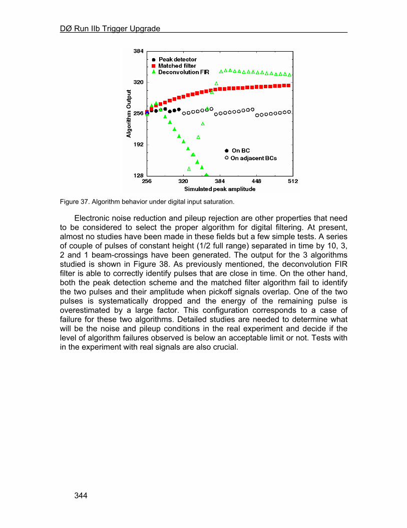
DØ Run IIb Trigger Upgrade
344
Figure 37. Algorithm behavior under digital input saturation.
Electronic noise reduction and pileup rejection are other properties that need to be considered to select the proper algorithm for digital filtering. At present, almost no studies have been made in these fields but a few simple tests. A series of couple of pulses of constant height (1/2 full range) separated in time by 10, 3, 2 and 1 beam-crossings have been generated. The output for the 3 algorithms studied is shown in Figure 38. As previously mentioned, the deconvolution FIR filter is able to correctly identify pulses that are close in time. On the other hand, both the peak detection scheme and the matched filter algorithm fail to identify the two pulses and their amplitude when pickoff signals overlap. One of the two pulses is systematically dropped and the energy of the remaining pulse is overestimated by a large factor. This configuration corresponds to a case of failure for these two algorithms. Detailed studies are needed to determine what will be the noise and pileup conditions in the real experiment and decide if the level of algorithm failures observed is below an acceptable limit or not. Tests with in the experiment with real signals are also crucial.
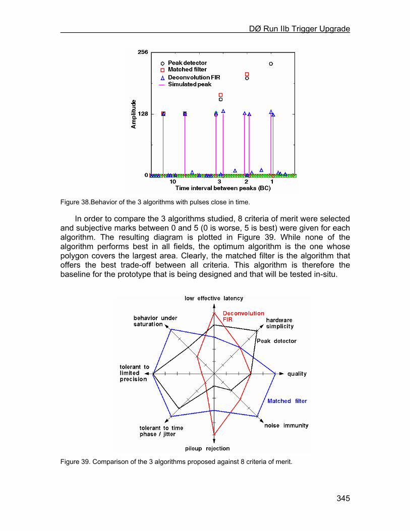
DØ Run IIb Trigger Upgrade
345
Figure 38.Behavior of the 3 algorithms with pulses close in time.
In order to compare the 3 algorithms studied, 8 criteria of merit were selected and subjective marks between 0 and 5 (0 is worse, 5 is best) were given for each algorithm. The resulting diagram is plotted in Figure 39. While none of the algorithm performs best in all fields, the optimum algorithm is the one whose polygon covers the largest area. Clearly, the matched filter is the algorithm that offers the best trade-off between all criteria. This algorithm is therefore the baseline for the prototype that is being designed and that will be tested in-situ.
Figure 39. Comparison of the 3 algorithms proposed against 8 criteria of merit.

DØ Run IIb Trigger Upgrade
346
A number of studies still need to be done to confirm that this algorithm is the most appropriate. These include noise and pileup studies, the possibility to run computations at the beam-crossing rate (instead of running at BC x 2), the development of a scheme and program for the automatic determination of filter coefficients, etc. Tests on the detector must also be done and analyzed. While simulation offers a very good mean of investigation, real signals shapes, noise, time jitter, pileup conditions and many other effects cannot be taken into account without performing a real test. At present, studies on the digital filter allowed to select a candidate algorithm. In the prototype implementation, some flexibility will be allowed at that level, but algorithm changes will be confined to the capability of the available programmable logic. 4.5.6 Conclusions
Given the relatively slow trigger sum driver pulse shapes observed in Figure 16 and Figure 17, we believe that a digital filter is required to suppress the contributions from signals in nearby bunch crossings to that containing a high pT trigger. The matched filter algorithm offers the best performance among the digital filter algorithms studied and has been selected. Details of the implementation of the digital filter are given in Section 4.7.5. 4.6 Clustering algorithm simulation results
Algorithms relying on “sliding” trigger towers (TTs) can significantly improve the trigger performances, compared to the current calorimeter trigger based on single 0.2 x 0.2 TTs by better identifying the physical objects. Such algorithms have been extensively studied for the Atlas experiment, as described in the ATLAS Level-1 Trigger Technical Design Report6.
Various algorithms can be used to cluster the trigger towers and look for “regions of interest” (R), i.e. for regions of fixed size, S, in ηxφ in which the deposited ET has a local maximum. To find those regions of interest, a window of size S is shifted in both directions by steps of 0.2 in η and φ . By convention each window is unambiguously (although arbitrarily in the 2 x 2 case) anchored on one trigger tower T and is labeled S(T). Examples are shown in Figure 40.
6 “The ATLAS Level-1 Trigger Technical Design Report”, http://atlasinfo.cern.ch/Atlas/GROUPS/DAQTRIG/TDR/tdr.html, June 1998. See also “Trigger Performance Status Report”, CERN/LHCC 98-1

DØ Run IIb Trigger Upgrade
347
( a ) ( b )
Figure 40. Examples of (a) a 3x3 and (b) 2x2 sliding window S(T) associated to a trigger tower T. Each square represents a 0.2 x 0.2 trigger tower. The trigger tower T is shown as the shaded region.
The sliding windows algorithm aims to find the optimum region of the calorimeter for inclusion of energy from jets (or EM objects) by moving a window grid across the calorimeter η, φ space so as to maximize the transverse energy seen within the window. This is simply a local maximum finding algorithm on a grid, with the slight complication that local maxima are found by comparing energies in windows, S(T), which may have overlapping entries. Care must therefore be taken to ensure that only a single local maximum is found when two adjacent windows have the same S(T). A specific example of how the local maximum could be defined is shown in Figure 41. This process, which avoids multiple counting of jet (or EM object) candidates, is often referred to as “declustering”.
The window corresponding to a local maximum is called the region of interest, R, and is referenced by a specific TT within R as indicated in Figure 40 for a 3x3 or a 2x2 window. The total ET within R plus that within a defined neighbor region is termed the trigger cluster ET relevant to the jet or EM object.
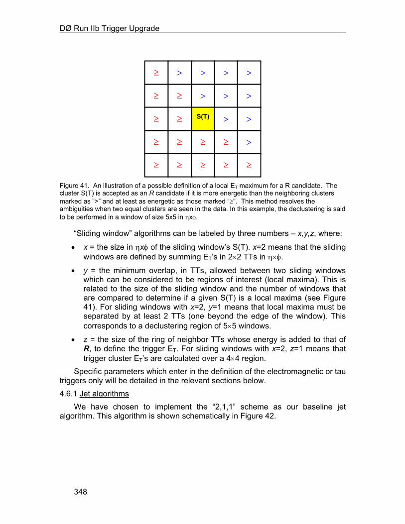
DØ Run IIb Trigger Upgrade
348
≥ > > > >
≥ ≥ > > >
≥ ≥ S(T) > >
≥ ≥ ≥ ≥ >
≥ ≥ ≥ ≥ ≥
Figure 41. An illustration of a possible definition of a local ET maximum for a R candidate. The cluster S(T) is accepted as an R candidate if it is more energetic than the neighboring clusters marked as “>” and at least as energetic as those marked “≥". This method resolves the ambiguities when two equal clusters are seen in the data. In this example, the declustering is said to be performed in a window of size 5x5 in ηxφ.
“Sliding window” algorithms can be labeled by three numbers – x,y,z, where:
• x = the size in ηxφ of the sliding window’s S(T). x=2 means that the sliding windows are defined by summing ET’s in 2×2 TTs in η×φ.
• y = the minimum overlap, in TTs, allowed between two sliding windows which can be considered to be regions of interest (local maxima). This is related to the size of the sliding window and the number of windows that are compared to determine if a given S(T) is a local maxima (see Figure 41). For sliding windows with x=2, y=1 means that local maxima must be separated by at least 2 TTs (one beyond the edge of the window). This corresponds to a declustering region of 5×5 windows.
• z = the size of the ring of neighbor TTs whose energy is added to that of R, to define the trigger ET. For sliding windows with x=2, z=1 means that trigger cluster ET’s are calculated over a 4×4 region.
Specific parameters which enter in the definition of the electromagnetic or tau triggers only will be detailed in the relevant sections below. 4.6.1 Jet algorithms
We have chosen to implement the “2,1,1” scheme as our baseline jet algorithm. This algorithm is shown schematically in Figure 42.
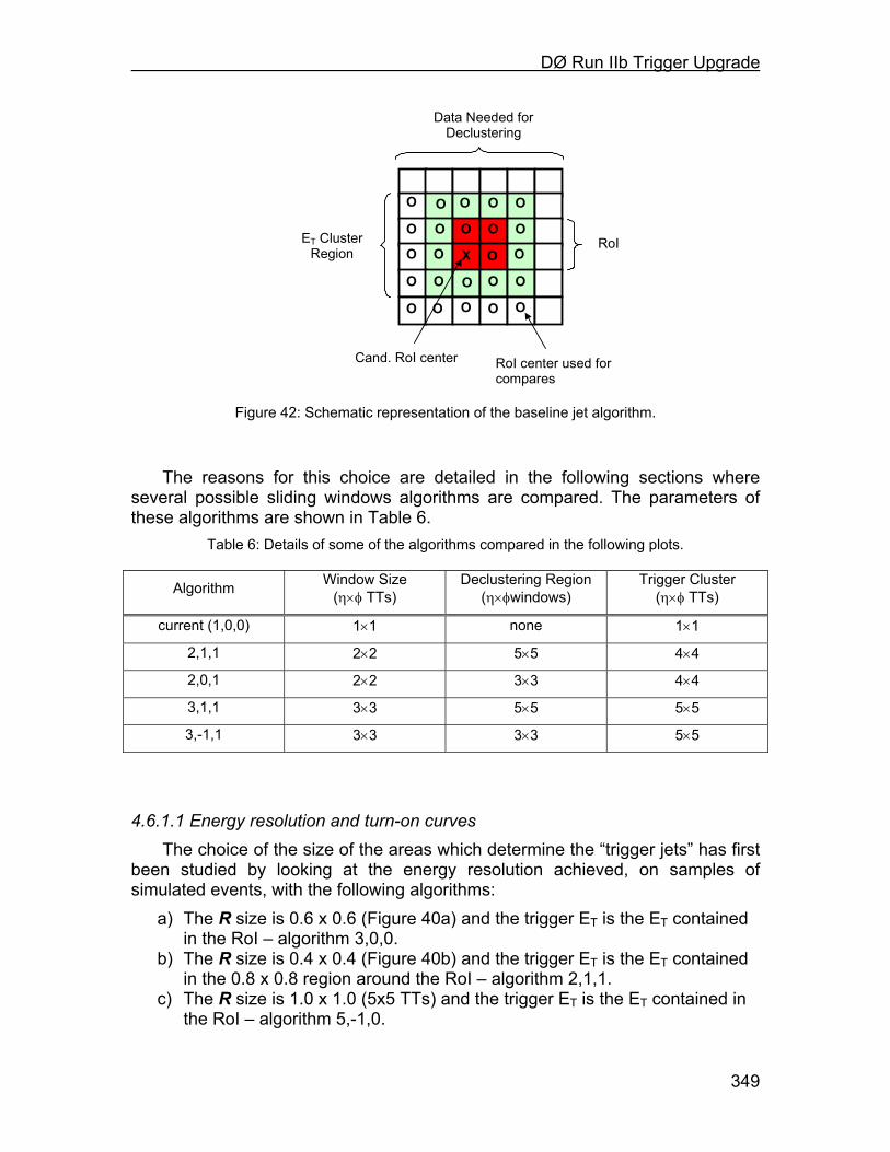
DØ Run IIb Trigger Upgrade
349
XRoIET Cluster
Region
Data Needed for Declustering
Cand. RoI center
O O O O O
O O O O O
O O O O
O O O O O
O O O O O
RoI center used for compares
Figure 42: Schematic representation of the baseline jet algorithm.
The reasons for this choice are detailed in the following sections where
several possible sliding windows algorithms are compared. The parameters of these algorithms are shown in Table 6.
Table 6: Details of some of the algorithms compared in the following plots.
Algorithm Window Size (η×φ TTs)
Declustering Region (η×φwindows)
Trigger Cluster (η×φ TTs)
current (1,0,0) 1×1 none 1×1
2,1,1 2×2 5×5 4×4
2,0,1 2×2 3×3 4×4
3,1,1 3×3 5×5 5×5
3,-1,1 3×3 3×3 5×5
4.6.1.1 Energy resolution and turn-on curves The choice of the size of the areas which determine the “trigger jets” has first
been studied by looking at the energy resolution achieved, on samples of simulated events, with the following algorithms:
a) The R size is 0.6 x 0.6 (Figure 40a) and the trigger ET is the ET contained in the RoI – algorithm 3,0,0.
b) The R size is 0.4 x 0.4 (Figure 40b) and the trigger ET is the ET contained in the 0.8 x 0.8 region around the RoI – algorithm 2,1,1.
c) The R size is 1.0 x 1.0 (5x5 TTs) and the trigger ET is the ET contained in the RoI – algorithm 5,-1,0.
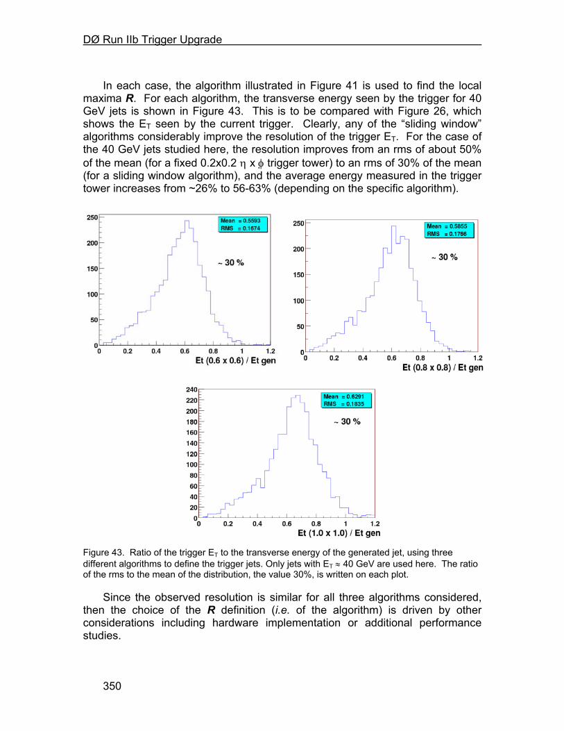
DØ Run IIb Trigger Upgrade
350
In each case, the algorithm illustrated in Figure 41 is used to find the local
maxima R. For each algorithm, the transverse energy seen by the trigger for 40 GeV jets is shown in Figure 43. This is to be compared with Figure 26, which shows the ET seen by the current trigger. Clearly, any of the “sliding window” algorithms considerably improve the resolution of the trigger ET. For the case of the 40 GeV jets studied here, the resolution improves from an rms of about 50% of the mean (for a fixed 0.2x0.2 η x φ trigger tower) to an rms of 30% of the mean (for a sliding window algorithm), and the average energy measured in the trigger tower increases from ~26% to 56-63% (depending on the specific algorithm).
Figure 43. Ratio of the trigger ET to the transverse energy of the generated jet, using three different algorithms to define the trigger jets. Only jets with ET ≈ 40 GeV are used here. The ratio of the rms to the mean of the distribution, the value 30%, is written on each plot.
Since the observed resolution is similar for all three algorithms considered, then the choice of the R definition (i.e. of the algorithm) is driven by other considerations including hardware implementation or additional performance studies.
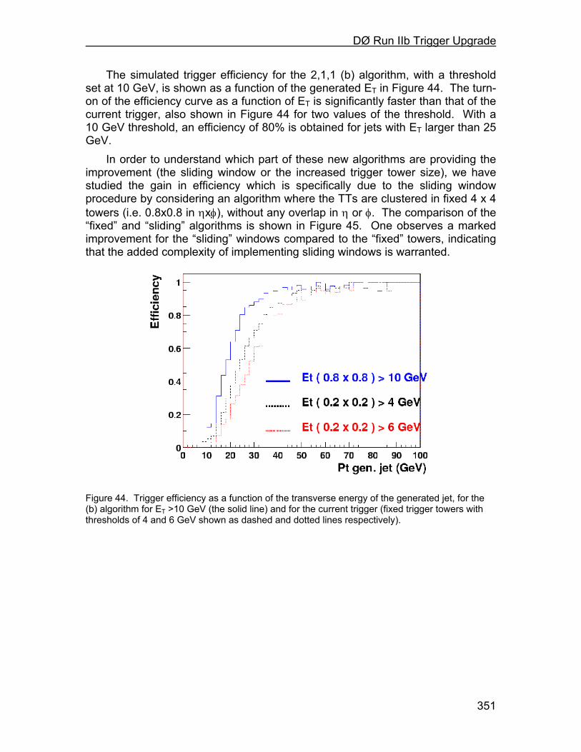
DØ Run IIb Trigger Upgrade
351
The simulated trigger efficiency for the 2,1,1 (b) algorithm, with a threshold set at 10 GeV, is shown as a function of the generated ET in Figure 44. The turn-on of the efficiency curve as a function of ET is significantly faster than that of the current trigger, also shown in Figure 44 for two values of the threshold. With a 10 GeV threshold, an efficiency of 80% is obtained for jets with ET larger than 25 GeV.
In order to understand which part of these new algorithms are providing the improvement (the sliding window or the increased trigger tower size), we have studied the gain in efficiency which is specifically due to the sliding window procedure by considering an algorithm where the TTs are clustered in fixed 4 x 4 towers (i.e. 0.8x0.8 in ηxφ), without any overlap in η or φ. The comparison of the “fixed” and “sliding” algorithms is shown in Figure 45. One observes a marked improvement for the “sliding” windows compared to the “fixed” towers, indicating that the added complexity of implementing sliding windows is warranted.
Figure 44. Trigger efficiency as a function of the transverse energy of the generated jet, for the (b) algorithm for ET >10 GeV (the solid line) and for the current trigger (fixed trigger towers with thresholds of 4 and 6 GeV shown as dashed and dotted lines respectively).
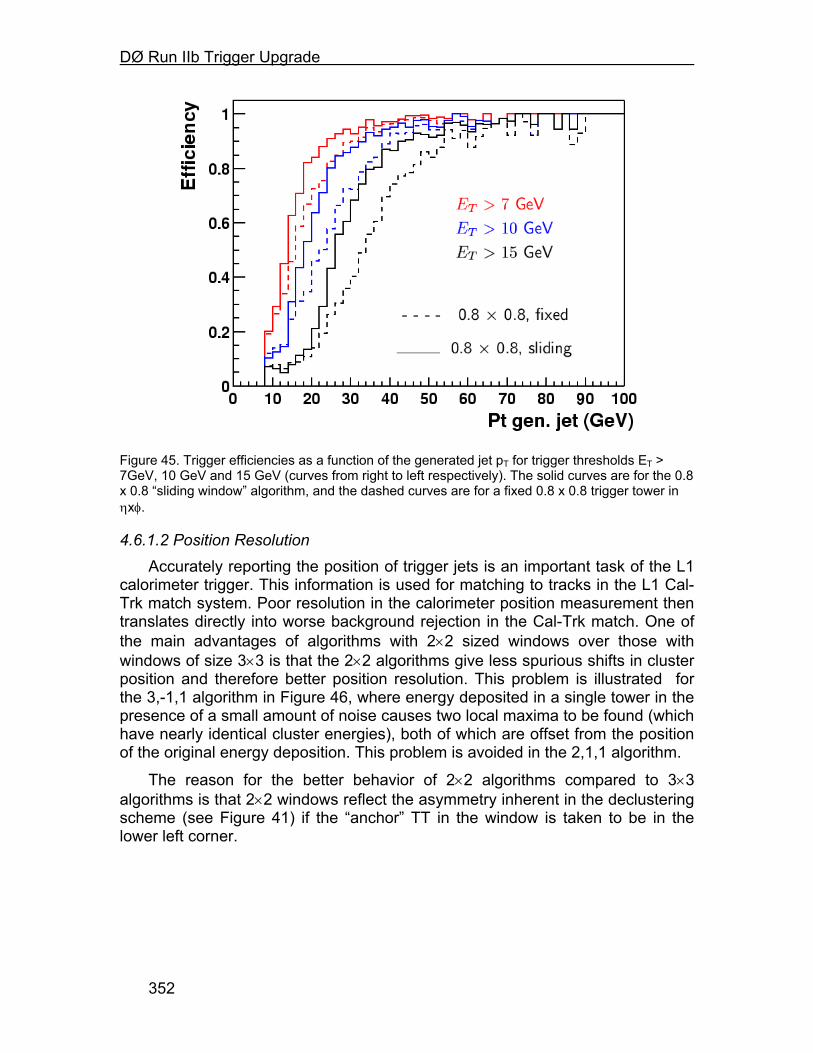
DØ Run IIb Trigger Upgrade
352
Figure 45. Trigger efficiencies as a function of the generated jet pT for trigger thresholds ET > 7GeV, 10 GeV and 15 GeV (curves from right to left respectively). The solid curves are for the 0.8 x 0.8 “sliding window” algorithm, and the dashed curves are for a fixed 0.8 x 0.8 trigger tower in ηxφ.
4.6.1.2 Position Resolution Accurately reporting the position of trigger jets is an important task of the L1
calorimeter trigger. This information is used for matching to tracks in the L1 Cal-Trk match system. Poor resolution in the calorimeter position measurement then translates directly into worse background rejection in the Cal-Trk match. One of the main advantages of algorithms with 2×2 sized windows over those with windows of size 3×3 is that the 2×2 algorithms give less spurious shifts in cluster position and therefore better position resolution. This problem is illustrated for the 3,-1,1 algorithm in Figure 46, where energy deposited in a single tower in the presence of a small amount of noise causes two local maxima to be found (which have nearly identical cluster energies), both of which are offset from the position of the original energy deposition. This problem is avoided in the 2,1,1 algorithm.
The reason for the better behavior of 2×2 algorithms compared to 3×3 algorithms is that 2×2 windows reflect the asymmetry inherent in the declustering scheme (see Figure 41) if the “anchor” TT in the window is taken to be in the lower left corner.
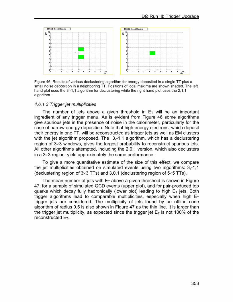
DØ Run IIb Trigger Upgrade
353
Figure 46: Results of various declustering algorithm for energy deposited in a single TT plus a small noise deposition in a neighboring TT. Positions of local maxima are shown shaded. The left hand plot uses the 3,-1,1 algorithm for declustering while the right hand plot uses the 2,1,1 algorithm.
4.6.1.3 Trigger jet multiplicities The number of jets above a given threshold in ET will be an important
ingredient of any trigger menu. As is evident from Figure 46 some algorithms give spurious jets in the presence of noise in the calorimeter, particularly for the case of narrow energy deposition. Note that high energy electrons, which deposit their energy in one TT, will be reconstructed as trigger jets as well as EM clusters with the jet algorithm proposed. The 3,-1,1 algorithm, which has a declustering region of 3×3 windows, gives the largest probability to reconstruct spurious jets. All other algorithms attempted, including the 2,0,1 version, which also declusters in a 3×3 region, yield approximately the same performance.
To give a more quantitative estimate of the size of this effect, we compare the jet multiplicities obtained on simulated events using two algorithms: 3,-1,1 (declustering region of 3×3 TTs) and 3,0,1 (declustering region of 5×5 TTs).
The mean number of jets with ET above a given threshold is shown in Figure 47, for a sample of simulated QCD events (upper plot), and for pair-produced top quarks which decay fully hadronically (lower plot) leading to high ET jets. Both trigger algorithms lead to comparable multiplicities, especially when high ET trigger jets are considered. The multiplicity of jets found by an offline cone algorithm of radius 0.5 is also shown in Figure 47 as the thin line. It is larger than the trigger jet multiplicity, as expected since the trigger jet ET is not 100% of the reconstructed ET.
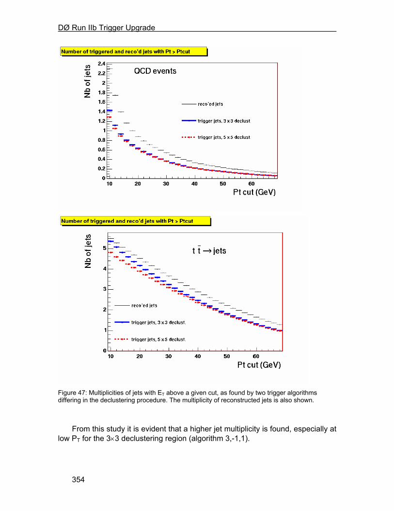
DØ Run IIb Trigger Upgrade
354
Figure 47: Multiplicities of jets with ET above a given cut, as found by two trigger algorithms differing in the declustering procedure. The multiplicity of reconstructed jets is also shown.
From this study it is evident that a higher jet multiplicity is found, especially at
low PT for the 3×3 declustering region (algorithm 3,-1,1).

DØ Run IIb Trigger Upgrade
355
4.6.1.4 Rates and rejection improvements In this section, we compare the performance of the sliding window and the
existing trigger algorithms. We compare both of these algorithms’ trigger efficiencies and the associated rates from QCD jet events as a function of trigger ET. Rates versus trigger efficiency on hard QCD events
In these studies we require that for the 2,1,1 sliding window algorithm there be at least one region of interest with a trigger ET above threshold which varies from 5 to 40 GeV in steps of 1 GeV. Similarly, for the current trigger algorithm, we require at least one TT above threshold which varies from 2 GeV to 20 GeV in steps of 1 GeV. For both algorithms and for each threshold, we calculate the corresponding inclusive trigger rate and the efficiency to trigger on relatively hard QCD events, i.e. with parton pT > 20GeV and pT > 40GeV respectively. To simulate high luminosity running, we overlay additional minimum bias events (a mean of 2.5 or 5 additional minimum bias events) in the Monte Carlo sample used to calculate the rates and efficiencies. While the absolute rates may not be completely reliable given the approximate nature of the simulation, we believe that the relative rates are reliable estimators of the performance of the trigger algorithms. Focusing on the region of moderate rates and reasonable efficiencies, the results are plotted in Figure 48 where lower curves (open squares) in the plots are for the current trigger algorithm and the upper curve (solid circles) corresponds to the 2,1,1 sliding window algorithm. It is apparent from Figure 48 the sliding window algorithm can reduce the inclusive rate by a factor of 2 to 4 for any given efficiency. It is even more effective at higher luminosities (i.e. for the plots with 5 overlaid minimum bias events).
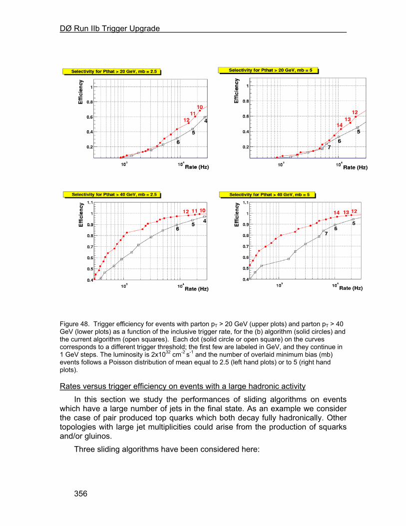
DØ Run IIb Trigger Upgrade
356
Figure 48. Trigger efficiency for events with parton pT > 20 GeV (upper plots) and parton pT > 40 GeV (lower plots) as a function of the inclusive trigger rate, for the (b) algorithm (solid circles) and the current algorithm (open squares). Each dot (solid circle or open square) on the curves corresponds to a different trigger threshold; the first few are labeled in GeV, and they continue in 1 GeV steps. The luminosity is 2x1032 cm-2 s-1 and the number of overlaid minimum bias (mb) events follows a Poisson distribution of mean equal to 2.5 (left hand plots) or to 5 (right hand plots).
Rates versus trigger efficiency on events with a large hadronic activity In this section we study the performances of sliding algorithms on events
which have a large number of jets in the final state. As an example we consider the case of pair produced top quarks which both decay fully hadronically. Other topologies with large jet multiplicities could arise from the production of squarks and/or gluinos.
Three sliding algorithms have been considered here:

DØ Run IIb Trigger Upgrade
357
i. The size of the regions of interest is 0.6x0.6 (i.e. 3x3 TTs); the trigger ET is that of R; the declustering is performed in a 5x5 window. This algorithm is labeled 3_0_0.
ii. As (i) but the trigger ET is obtained by summing the ET of R and the ET of the closest neighboring TTs. This algorithm is labeled 3_0_1.
iii. As (ii) but the declustering is performed in a 3x3 window. This algorithm is labeled 3_m1_1.
In each case, the trigger condition requires that there be at least three trigger jets with ET above a varying threshold. In addition, the ET of the highest ET jet should be above 40 GeV. A similar trigger condition has also been applied using the 0.2x0.2 TTs instead of the trigger jets; in this latter case the highest ET TT should have ET > 15 GeV. The inclusive QCD rate has been obtained as before, using QCD Monte Carlo events where a mean number of 7.5 minimum bias events has been overlaid. Figure 49 shows the resulting efficiencies and rates. Inclusive rates are shown here for a luminosity of 5 x 1032 cm2 s-1 .
It can be seen that the three sliding algorithms considered lead to very similar performances. In particular, no noticeable difference is seen between algorithms 3_0_1 and 3_m1_1 (which differ by the declustering procedure only), as was seen in Section 4.6.1.2. The figure also shows that the performances of sliding algorithms are better than those of the current trigger system, also for events with many jets in the final state.
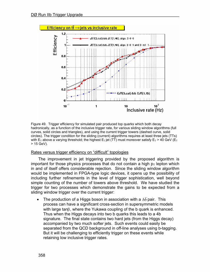
DØ Run IIb Trigger Upgrade
358
Figure 49. Trigger efficiency for simulated pair produced top quarks which both decay hadronically, as a function of the inclusive trigger rate, for various sliding window algorithms (full curves, solid circles and triangles), and using the current trigger towers (dashed curve, solid circles). The trigger condition for the sliding (current) algorithms requires at least three jets (TTs) with ET above a varying threshold; the highest ET jet (TT) must moreover satisfy ET > 40 GeV (ET > 15 GeV).
Rates versus trigger efficiency on “difficult” topologies The improvement in jet triggering provided by the proposed algorithm is
important for those physics processes that do not contain a high pT lepton which in and of itself offers considerable rejection. Since the sliding window algorithm would be implemented in FPGA-type logic devices, it opens up the possibility of including further refinements in the level of trigger sophistication, well beyond simple counting of the number of towers above threshold. We have studied the trigger for two processes which demonstrate the gains to be expected from a sliding window trigger over the current trigger:
• The production of a Higgs boson in association with a bb pair. This process can have a significant cross-section in supersymmetric models with large tanβ, where the Yukawa coupling of the b quark is enhanced. Thus when the Higgs decays into two b quarks this leads to a 4b signature. The final state contains two hard jets (from the Higgs decay) accompanied by two much softer jets. Such events could easily be separated from the QCD background in off-line analyses using b-tagging. But it will be challenging to efficiently trigger on these events while retaining low inclusive trigger rates.
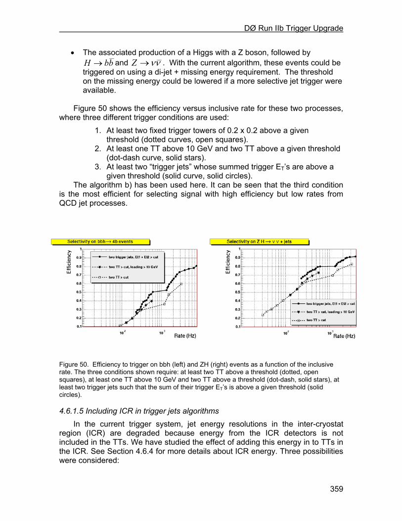
DØ Run IIb Trigger Upgrade
359
• The associated production of a Higgs with a Z boson, followed by bbH → and νν→Z . With the current algorithm, these events could be
triggered on using a di-jet + missing energy requirement. The threshold on the missing energy could be lowered if a more selective jet trigger were available.
Figure 50 shows the efficiency versus inclusive rate for these two processes,
where three different trigger conditions are used: 1. At least two fixed trigger towers of 0.2 x 0.2 above a given
threshold (dotted curves, open squares). 2. At least one TT above 10 GeV and two TT above a given threshold
(dot-dash curve, solid stars). 3. At least two “trigger jets” whose summed trigger ET’s are above a
given threshold (solid curve, solid circles). The algorithm b) has been used here. It can be seen that the third condition
is the most efficient for selecting signal with high efficiency but low rates from QCD jet processes.
Figure 50. Efficiency to trigger on bbh (left) and ZH (right) events as a function of the inclusive rate. The three conditions shown require: at least two TT above a threshold (dotted, open squares), at least one TT above 10 GeV and two TT above a threshold (dot-dash, solid stars), at least two trigger jets such that the sum of their trigger ET’s is above a given threshold (solid circles).
4.6.1.5 Including ICR in trigger jets algorithms In the current trigger system, jet energy resolutions in the inter-cryostat
region (ICR) are degraded because energy from the ICR detectors is not included in the TTs. We have studied the effect of adding this energy in to TTs in the ICR. See Section 4.6.4 for more details about ICR energy. Three possibilities were considered:
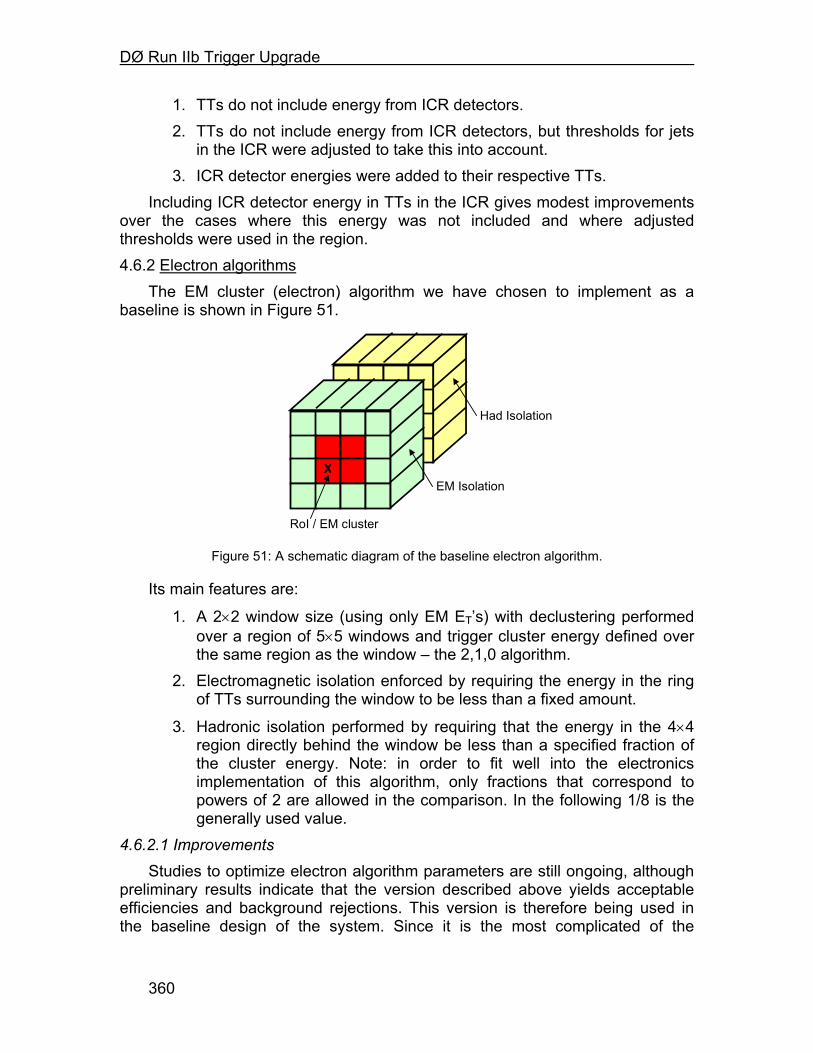
DØ Run IIb Trigger Upgrade
360
1. TTs do not include energy from ICR detectors. 2. TTs do not include energy from ICR detectors, but thresholds for jets
in the ICR were adjusted to take this into account. 3. ICR detector energies were added to their respective TTs.
Including ICR detector energy in TTs in the ICR gives modest improvements over the cases where this energy was not included and where adjusted thresholds were used in the region. 4.6.2 Electron algorithms
The EM cluster (electron) algorithm we have chosen to implement as a baseline is shown in Figure 51.
X
RoI / EM cluster
EM Isolation
Had Isolation
Figure 51: A schematic diagram of the baseline electron algorithm.
Its main features are:
1. A 2×2 window size (using only EM ET’s) with declustering performed over a region of 5×5 windows and trigger cluster energy defined over the same region as the window – the 2,1,0 algorithm.
2. Electromagnetic isolation enforced by requiring the energy in the ring of TTs surrounding the window to be less than a fixed amount.
3. Hadronic isolation performed by requiring that the energy in the 4×4 region directly behind the window be less than a specified fraction of the cluster energy. Note: in order to fit well into the electronics implementation of this algorithm, only fractions that correspond to powers of 2 are allowed in the comparison. In the following 1/8 is the generally used value.
4.6.2.1 Improvements Studies to optimize electron algorithm parameters are still ongoing, although
preliminary results indicate that the version described above yields acceptable efficiencies and background rejections. This version is therefore being used in the baseline design of the system. Since it is the most complicated of the

DØ Run IIb Trigger Upgrade
361
electron algorithms that we are considering, this should lead to a conservative design. 4.6.3 Tau algorithms
With some refinements, the sliding window algorithms presented in Section 4.6.1 could lead to some sensitivity to the process gg → H → τ+τ- at the trigger level. This could be achieved by exploiting the fact that τ jets are narrower than “standard” jets. In its most basic form, such an algorithm would be simple to implement using information already calculated for the jet and EM clusters. We are studying an algorithm with the following characteristics:
1. A 2×2 window size (using EM+H ET's) with declustering performed over a region of 5×5 windows and trigger cluster energy defined over the same region as the window - the 2,1,0 algorithm. Window formation and declustering would be performed as part of the jet algorithm.
2. Narrow jets (isolation) defined by cutting on the ratio of the EM+H energy in the 2×2 jet cluster to that in the 4×4 region centered on the cluster. Both of these sums are available as part of the jet algorithm calculations.
4.6.3.1 Transverse isolation of τ jets We consider here the 2,1,1 sliding window algorithm described in Section
4.6.1, where the size of regions of interest is 0.4x0.4 (2x2 TTs), while the size of trigger jets is 0.8x0.8 (4x4 TTs). We compare the ratio of the R ET to the trigger ET, for τ jets coming from gg → H → τ+τ- and for jets coming from QCD processes. As shown in Figure 52, QCD jets become more and more collimated as their ET increases, but the ratio of the “core ET” to the trigger jet ET (called the “core fraction”) remains a powerful variable to discriminate between τ jets and QCD jets.
DØ Run IIb Trigger Upgrade
362
Figure 52: Ratio of the R ET to the trigger ET, for the sliding window algorithm (b). The ratio is shown for τ jets coming from a Higgs decay (full histogram), and for jets coming from QCD processes (hashed histograms).
4.6.3.2 Rates and rejection improvement This can be exploited by defining a specific trigger condition, which requires
at least two jets whose summed trigger ET’s is above a threshold, and for which the core faction is above 85%. As can be seen in Figure 53, it seems possible to have a reasonable efficiency on the signal (70 %) while maintaining the inclusive rate below 300 Hz. The figure also shows that such an algorithm reduces the inclusive rate by a factor of about 3, compared to the current trigger system.
DØ Run IIb Trigger Upgrade
363
Figure 53: Efficiency to trigger on gg →H →ττ events as a function of the inclusive QCD rate, for: (closed circles) the sliding window algorithm (b), when requiring at least two jets whose summed ET is above a varying threshold, and whose core fraction is above 85%; (open squares) the current trigger system, requiring two TTs whose summed ET is above a varying threshold. The inclusive rates shown here correspond to a luminosity of 2 x 1032 cm2 s-1.
4.6.4 Global sums
The region around 0.8<|η|<1.5, known as the inter cryostat region (ICR) encompasses the transition from showers contained within the CC and showers contained within the EC. There is a gap in EM coverage and a major thinning of FH coverage in this area. Since these are the layers which comprise standard trigger towers, there is a major degradation in Level 1 calorimeter response and resolution in this region. This is exacerbated by the presence of significant dead material in the solenoid in Run2. To aid in recovering the energy losses in the ICR region, we use the intercryostat detectors (ICD), which consists of scintillators located in the gap between the calorimeter cryostats, and the “massless gaps” (MG) which consist of the front sections of the endcap calorimeter that have no absorber in front. In this section we study ways to improve the energy measurement at the trigger level. 4.6.4.1 Concept & performance
Global tower ET sums such as missing ET or scalar ET, while very useful, suffer from several significant problems at the L1 trigger. There are two significant issues: first is that the ICR sampling layers are not available in the
DØ Run IIb Trigger Upgrade
364
calculation at Level 1; second is that the imprecision of the tower ET's gets compounded for global sums, resulting in significantly degraded effectiveness. This is particularly true in a multiple interaction environment. There are two possible solutions to these problems. First we can take advantage of work done for Run IIa to make the ICR layers available at Level 2 and add these towers back into the global sums at Level 1 in Run IIb. Second, we can develop a scheme which discriminates towers which are from multiple interactions and avoids adding them into the sum.
Simulations of single pions and jets in this region indicate that the energy scale in this region goes as low as 40% of the CC/EC scale (as shown in Figure 54), and the resolution is as bad as 6 times worse than in the CC or EC (as shown in Figure 55). These results are very consistent with findings from Run1 Level 1 missing ET analyses (see Figure 56). One of the major results of this deficiency is that the efficiency and rejection of a Level 1 missing ET selection are noticeably degraded. These simulations also indicate that adding ICD and MG cells into trigger towers can improve the scale by a factor of 2, while optimizing the resolution by a factor of 3.
-1
-0.8
-0.6
-0.4
-0.2
0
0.2
0.4
0 5 10 15 20 25 30 35 40
ieta
∆E/E
20 GeV wts
20 GeV wts with ICR wts = 0
20 GeV wts optimized w/o ICR
Figure 54. The relative calorimeter energy response in the ICR region for incident 20 GeV pions as a function of x10. The stars are the response if the ICR weights are set to zero, the open diamonds are the response if the ICR energies are ignored and the remaining calorimeter weights are re-optimized, and the open circles are the response when the ICR region is included and the weights are optimized.
0
0.5
1
1.5
2
2.5
3
3.5
4
0 5 10 15 20 25 30 35 40
ieta
σ/√E
20 GeV wts
20 GeV wts with ICR wts = 0
20 GeV wts optimized w/o ICR
Figure 55. The calorimeter energy resolution in the ICR region for incident 20 GeV pions as a function of x10. The stars are the response if the ICR weights are set to zero, the open diamonds are the response if the ICR energies are ignored and the remaining calorimeter weights are re-optimized, and the open circles are the response when the ICR region is included and the weights are optimized.
DØ Run IIb Trigger Upgrade
365
Figure 56. The L1 missing ET response as a function of η for 85 GeV jets using the Run 1 DØ detector simulation.
4.6.4.2 Simulation results In principle, it is straightforward to estimate the effect of the ICD and MG to
the missing ET calculation. However our present simulations do not yet fully address a number of issues (including a proper treatment of trigger tower sampling weights and the verification of the modeling and calibration for the ICR). To estimate the effect of adding the ICR detectors into the missing ET, we therefore consider the fact that in the region of 1.0<|η|<1.4, the sampling weight simulations indicate approximately half of the energy will be deposited in the EM+FH, and the other half in the ICD+MG. As a crude estimate of the magnitude of the effect of adding the ICR layers, we will merely consider the missing ET measurement with and without the EM+FH layers in this region and assume the ICR improvement will be similar. Although the sample used for this calculation is a QCD sample with jet pT > 20 GeV and 0 minimum bias events overlaid, for historical reasons it is a different sample than that mentioned in the rest of this document with the same specifications. The missing ET mean and rms in this sample behave as follows:
if remove all ICR TTs: µ/rms = 6.7 GeV / 4.8 GeV
if only use EM+FH TTs: µ/rms = 5.5 GeV / 3.9 GeV The number of events passing various Level 1 missing ET cuts in this sample
are shown in Table 7.
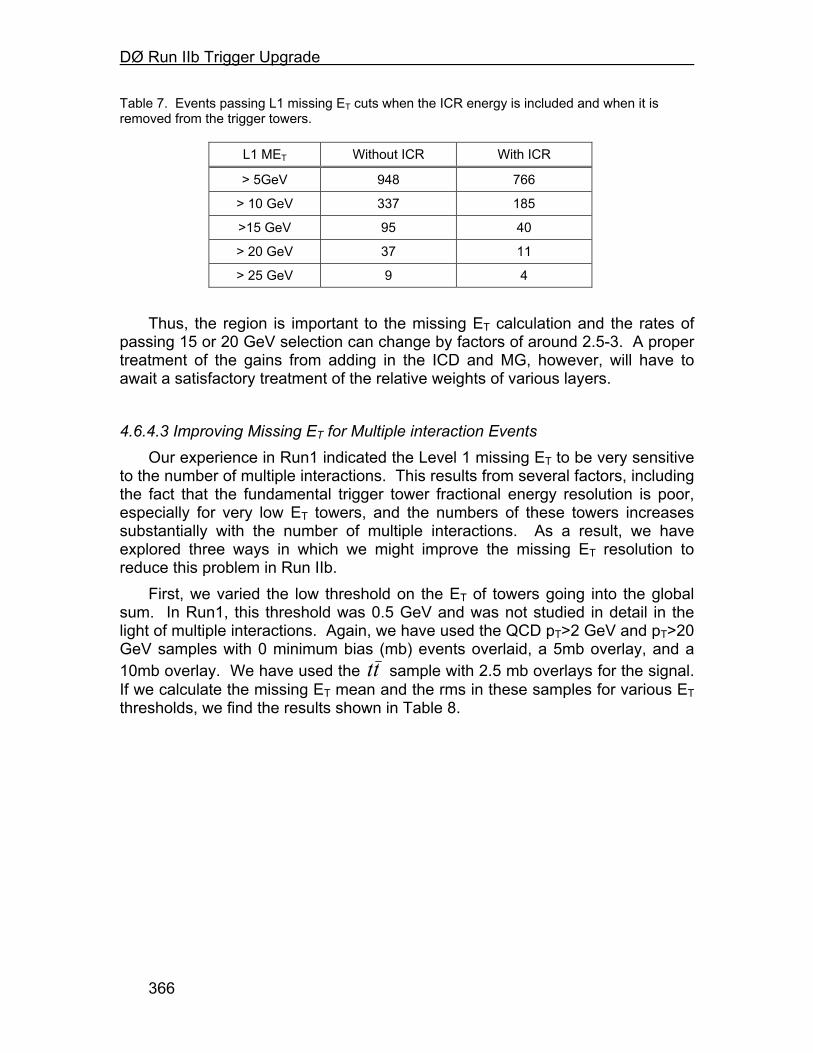
DØ Run IIb Trigger Upgrade
366
Table 7. Events passing L1 missing ET cuts when the ICR energy is included and when it is removed from the trigger towers.
L1 MET Without ICR With ICR
> 5GeV 948 766
> 10 GeV 337 185
>15 GeV 95 40
> 20 GeV 37 11
> 25 GeV 9 4 Thus, the region is important to the missing ET calculation and the rates of
passing 15 or 20 GeV selection can change by factors of around 2.5-3. A proper treatment of the gains from adding in the ICD and MG, however, will have to await a satisfactory treatment of the relative weights of various layers.
4.6.4.3 Improving Missing ET for Multiple interaction Events
Our experience in Run1 indicated the Level 1 missing ET to be very sensitive to the number of multiple interactions. This results from several factors, including the fact that the fundamental trigger tower fractional energy resolution is poor, especially for very low ET towers, and the numbers of these towers increases substantially with the number of multiple interactions. As a result, we have explored three ways in which we might improve the missing ET resolution to reduce this problem in Run IIb.
First, we varied the low threshold on the ET of towers going into the global sum. In Run1, this threshold was 0.5 GeV and was not studied in detail in the light of multiple interactions. Again, we have used the QCD pT>2 GeV and pT>20 GeV samples with 0 minimum bias (mb) events overlaid, a 5mb overlay, and a 10mb overlay. We have used the tt sample with 2.5 mb overlays for the signal. If we calculate the missing ET mean and the rms in these samples for various ET thresholds, we find the results shown in Table 8.
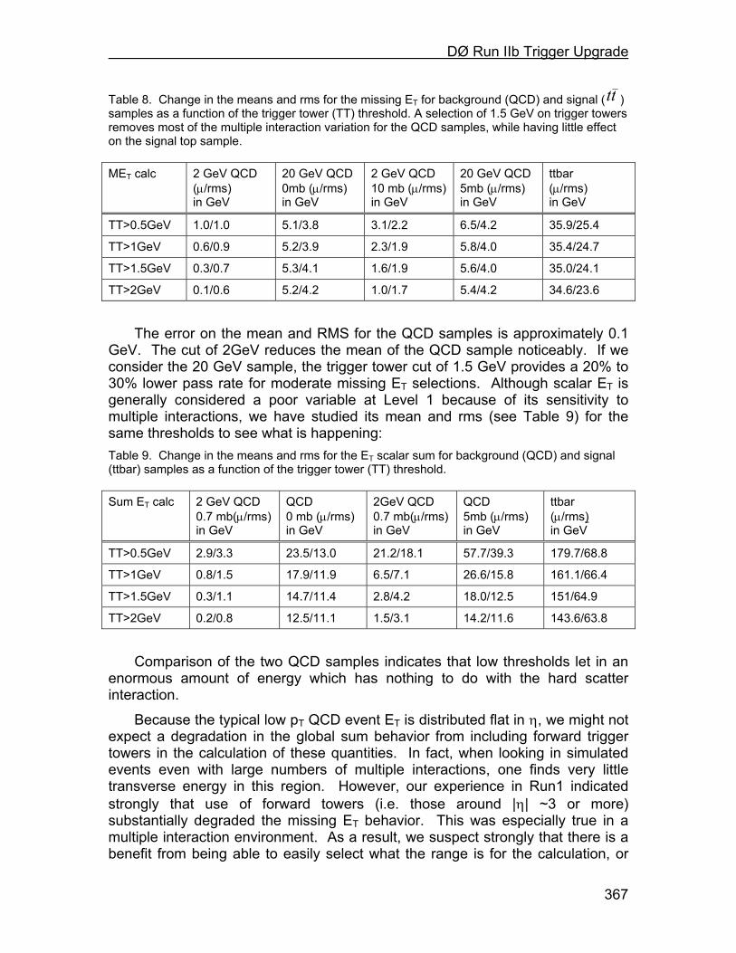
DØ Run IIb Trigger Upgrade
367
Table 8. Change in the means and rms for the missing ET for background (QCD) and signal ( tt ) samples as a function of the trigger tower (TT) threshold. A selection of 1.5 GeV on trigger towers removes most of the multiple interaction variation for the QCD samples, while having little effect on the signal top sample.
MET calc 2 GeV QCD (µ/rms) in GeV
20 GeV QCD 0mb (µ/rms) in GeV
2 GeV QCD 10 mb (µ/rms)in GeV
20 GeV QCD 5mb (µ/rms) in GeV
ttbar (µ/rms) in GeV
TT>0.5GeV 1.0/1.0 5.1/3.8 3.1/2.2 6.5/4.2 35.9/25.4
TT>1GeV 0.6/0.9 5.2/3.9 2.3/1.9 5.8/4.0 35.4/24.7
TT>1.5GeV 0.3/0.7 5.3/4.1 1.6/1.9 5.6/4.0 35.0/24.1
TT>2GeV 0.1/0.6 5.2/4.2 1.0/1.7 5.4/4.2 34.6/23.6 The error on the mean and RMS for the QCD samples is approximately 0.1
GeV. The cut of 2GeV reduces the mean of the QCD sample noticeably. If we consider the 20 GeV sample, the trigger tower cut of 1.5 GeV provides a 20% to 30% lower pass rate for moderate missing ET selections. Although scalar ET is generally considered a poor variable at Level 1 because of its sensitivity to multiple interactions, we have studied its mean and rms (see Table 9) for the same thresholds to see what is happening: Table 9. Change in the means and rms for the ET scalar sum for background (QCD) and signal (ttbar) samples as a function of the trigger tower (TT) threshold.
Sum ET calc 2 GeV QCD 0.7 mb(µ/rms) in GeV
QCD 0 mb (µ/rms) in GeV
2GeV QCD 0.7 mb(µ/rms)in GeV
QCD 5mb (µ/rms) in GeV
ttbar (µ/rms) in GeV
TT>0.5GeV 2.9/3.3 23.5/13.0 21.2/18.1 57.7/39.3 179.7/68.8
TT>1GeV 0.8/1.5 17.9/11.9 6.5/7.1 26.6/15.8 161.1/66.4
TT>1.5GeV 0.3/1.1 14.7/11.4 2.8/4.2 18.0/12.5 151/64.9
TT>2GeV 0.2/0.8 12.5/11.1 1.5/3.1 14.2/11.6 143.6/63.8 Comparison of the two QCD samples indicates that low thresholds let in an
enormous amount of energy which has nothing to do with the hard scatter interaction.
Because the typical low pT QCD event ET is distributed flat in η, we might not expect a degradation in the global sum behavior from including forward trigger towers in the calculation of these quantities. In fact, when looking in simulated events even with large numbers of multiple interactions, one finds very little transverse energy in this region. However, our experience in Run1 indicated strongly that use of forward towers (i.e. those around |η| ~3 or more) substantially degraded the missing ET behavior. This was especially true in a multiple interaction environment. As a result, we suspect strongly that there is a benefit from being able to easily select what the range is for the calculation, or
DØ Run IIb Trigger Upgrade
368
perhaps include the η parameter into a weighting scheme with the trigger tower ET. This requires further study only possible once data is available.
Another concern for the missing ET measurement involves the truncation of trigger tower ET's into 0.5 GeV bins. Since one to two hundred towers are typically added into the Missing ET, this resolution loss can start to be noticeable. Taking the QCD pT>20 GeV sample with minimum bias overlay of 0 and 1648 events, we can use the simulator described above in the ICR discussion and toggle truncation on and off. The results are shown in Table 10.
Table 10. Comparison of the effect of TT truncation on the missing ET. The table lists the number of events (out of a sample of 1648, QCD with pT> 20GeV and no minimum bias overlaid events) that pass the listed missing ET thresholds.
Missing ET no truncation no truncation, TT>0.5GeV
with truncation
>5 GeV 947 868 766
>10 GeV 309 261 185
>15 GeV 76 51 40
>20 GeV 22 17 11
>25 GeV 7 5 4 The first column indicates truncation turned off and no threshold applied to
trigger towers. The second column also has no truncation and zeros out all towers with ET <0.5. The third column employs the normal 0.5 GeV truncation. Since truncation lowers tower ET's only to the next lowest 0.5 GeV increment, it effectively deweights all of the poorly measured ET in low ET towers. In fact, if we consider the QCD Pt>20 GeV sample with 5mb already discussed, the missing ET mean and rms are mildly improved over the straight 1.5GeV threshold by a simple weighting scheme. If we choose weights of 5%, 25%, and 75% for ET = 0.5, 1.0, and 1.5 GeV, respectively, we find the results shown in Table 11. Table 11. Comparison of simple TT threshold vs. weighting scheme for 20GeV QCD jet sample.
Scheme µ (GeV) rms
TT ET>1.5 GeV: 5.41 4.20
Weighted TT: 5.41 3.96 Because the trigger tower threshold seems to be the simplest solution that
shows progress, and the weighting also seems to help, one might ask whether rejecting low ET towers unless they are near significant neighbors might help. Looking again in the 5mb QCD sample at missing ET means and sigmas, we find the results shown in Table 12. These results point to a significant degradation in missing the ET mean and resolution.
DØ Run IIb Trigger Upgrade
369
Table 12. Comparison of effect of rejection low ET towers unless they are near trigger towers (NN) with significant energy deposits.
Cut µ (GeV) rms (GeV)
None : 6.45 4.17
NN ET > 0.5 GeV: 6.45 4.37
NN ET > 1.5 GeV: 6.56 4.37
NN ET > 3.0 GeV: 6.72 4.86
NN ET > 10 GeV: 5.62 4.57
NN ET > 1k GeV: 5.41 4.20 4.6.4.4 Conclusions
In this section, we have explored several different ways to improve the calorimeter missing ET measurement at Level 1. Studies leading to the optimization of the Run IIa trigger have indicated a large improvement in the scale and resolution of jets in this region if the ICD and MG are used. Although our current simulation samples do not have a proper treatment of this region, a crude estimate indicates that this amount of energy should have a noticeable improvement on the missing ET resolution.
Several attempts were also made to improve the behavior of missing ET in a multiple interaction environment. The most promising appears to be a simple tightening of the ET threshold on a trigger tower to around 1.5 GeV which would reduce the background by around 20% in our QCD sample. We take this to be our baseline design. The actual degradation in the real data may be larger than we see here, however, and the corresponding gain may also increase. We will be in a better position to evaluate this when we have reliable data at various luminosities. There is some evidence that a weighting scheme would provide further benefits. 4.7 L1 Calorimeter Trigger Implementation 4.7.1 Constraints
Because the L1 calorimeter system needs to be integrated into the existing DØ DAQ system it must obey several constraints. 4.7.1.1 Existing interfaces
The interfaces of the new system to the existing hardware should be compatible. In particular the new system must interface to the input pickoff signals, the L1 framework, the L2 and L3 data, the clock, and the timing and control systems.
The layout of the existing input signal cables places a special constraint on the new system. Moving these cables from their current locations in the Moving Counting House would require an enormous effort. Physical locations of the
DØ Run IIb Trigger Upgrade
370
boards in the new system will have to be adapted to the locations of the existing cables. 4.7.1.2 L1 Latency
The total L1 trigger latency is 4.2 µsec. After accounting for all transit times and front end processing, the maximum time remaining for complete signal processing, which includes digitization, filtering and the processing of the cluster algorithms is less than 2.7 µsec.
Additional, constraints are placed on the latency of the new system by the requirement of transmitting calorimeter clusters to the Cal-Track Matching system in time for it to meet the total L1 latency requirement. To match the arrival time of tracks from the L1 track trigger at the Cal-Track Match cards the calorimeter trigger must send out its clusters within 1500 ns of the beam crossing. 4.7.2 L1 Calorimeter Trigger Architectural Overview
A block diagram of the new L1 calorimeter trigger system is shown in Figure 57.
FPGALogic
ADC(8bit)
+Digitalfilter
ADC + Digital-Filter (ADF)
TT Signal Processing
H
E Σ
Σ
2560 TT 0.2x0.2
One EM + One HAD
clustersJets
Existing BLS Cards
Et Mpt
Cal-Track Match Signals from
L1 Track
Interfaces
x 80 x 8
Timing (SCL) Control (TCC) L2 & L3
Trig Algo’s(TAB) sums
Global +
Control (GAB)
EM F r a m e w o r k
Sliding Windows
Global Sums
x 1
timing/ctrl
8-bit TT Et
16 EM + 16 Had
tau
encodedclusters
timing/ctrl
ADF Timing Fanout
Figure 57. Block diagram of L1 calorimeter trigger, with the baseline subtractor (BLS) cards shown at left
The main elements of the system are listed below.
• ADC-Digital-Filter Boards (ADF) that receive analog TT signals from the BLS cards, digitize them, convert from energy to transverse energy (ET) and perform the digital filtering to associate energy with the correct bunch
DØ Run IIb Trigger Upgrade
371
crossing. Each of these boards deals with signals from 16 EM TTs and 16 H TTs.
• ADF Timing Fanout boards that send timing signals coming from the trigger framework to the ADF cards.
• Trigger Algorithm Boards (TAB) that receive TT transverse energies from the ADF boards, produce EM and jet cluster ET’s using the sliding windows algorithm and begin the global summing process that will yield scalar summed transverse energy (ET,total) and missing transverse energy (MpT). Outputs will also be provided at this level for data transmission to L2/L3 and to the Cal-Track Match system.
• A Global Algorithm Board (GAB) that receives data from the TABs and produces the final ET,total and MpT, as well as providing an interface to the DØ Trigger Framework and a timing fanout. One GAB is required for the system. It will be housed in the same crate as the TABs to facilitate communication between them.
These new electronics and associated communications cards will be housed in VME crates in two to three racks, replacing the present ADC and logic cards located in 10 racks.
Detailed design work has started on all elements of the L1 calorimeter trigger system. We describe below the various elements of the proposed calorimeter trigger. 4.7.3 Trigger Tower Mapping
The 2560 EM and Had Trigger Towers (TT) map to an η×φ grid of 40x32 cells with 0.2x0.2 extent. This grid extends from –4.0 to 4.0 in η and from 0 to 2π in φ. Cells are referenced by η- and φ-indices (ieta and iphi) which run from –20-20 (excluding 0) and from 1-32, respectively. This grid has been modified, for Run 2, from a strict geographic mapping at the extreme values of ieta (±19 and ±20) to allow inclusion of ICR detectors (the ICD and the MG) in the trigger.
The mapping of TTs in η is given in Table 13. All mapping in φ corresponds to the physical location of the TT in azimuthal angle. In the table, the column marked “Cable” signifies the labeling scheme for the cable carrying the data, while in the “Comments” column, the EM or Had refers to whether the relevant TTs appear physically in the EM or Hadronic parts of a shower and to which TTs the ICR energies should be added.
DØ Run IIb Trigger Upgrade
372
Table 13: Trigger Tower mapping scheme.
TT |ieta| Cable Detector η and φ Comments
all EM & Had φ = (iphi – 0.5) x 2π/32
≤ 16 EM & Had η = (sign ieta) x (|ieta| - 0.5) x 0.2 EM: include only EM cells Had: include only FH cells
17 EM <η> = 3.45 EM: include only EM cells
Had <η> = 3.45 Had: include only FH cells
18 EM <η> = 3.9 EM: include only EM cells
Had <η> = 4.1 Had: include only FH cells
19 EM <η> = 0.95 MG → Cal ieta = 5 Had
Had <η> = 1.25 ICD&MG → Cal ieta = 7 EM
20 EM <η> = 0.75 MG → Cal ieta = 4 Had
Had <η> = 1.05 ICD&MG → Cal ieta = 6 Had
4.7.4 ADF System design and Implementation The ADF system comprises the following components: - ADF boards. These make the conversion of trigger pickoff analog
signals to digital format and perform digital filtering to compute for each channel and for each beam crossing an 8 bit ET calibrated energy value. These digital values are sent to the TAB system via high-speed links.
- ADF crates and controller interfaces. Each crate houses a number of ADF boards and includes an interface to the Trigger Control Computer (TCC). This slow path is used for downloading, calibration and monitoring.
- A timing distribution card. This card is connected to a Serial Control Link (SCL) receiver and is in charge of distributing the necessary clocks, synchronization and control signals within the ADF system.
In order to be able to test prototype ADF cards in spy-mode on the current DØ Run IIa setup, analog signal splitter cards are also designed. These duplicate the analog signals of several BLS’s and connect to the CTFEs and the ADF cards being tested.
4.7.5 ADF Card Description 4.7.5.1 ADC precision, rate and analog section
Analog signals are digitized with 10-bit precision. The input voltage range is identical for all channels. This scheme is adequate to guarantee 0.25 GeV of resolution and a 62 GeV scale in ET for all η values. The proposed conversion frequency is 30.28 MHz (i.e. BC x 4). This rate is a good trade-off between the
DØ Run IIb Trigger Upgrade
373
aim of a short conversion latency and the cost of a faster analog to digital converter. The ADC that was chosen is Analog Devices AD9218 (dual 40 Mbps 3V 10-bit ADC). Conversion latency is 165 ns when operated at 30.28 MHz.
The analog section of the ADF card includes:
• A differential receiver whose input impedance matches that of the driving cable and that provides an attenuation factor to bring trigger pickoff signals in the desired range;
• Circuitry for baseline subtraction to adjust the offset of the previous signal; a digital to analog converter produces a static correction voltage in a programmable way;
• The analog to digital converter previously mentioned;
• An anti-aliasing filter (2nd order Butterworth filter). The proposed cutoff frequency for this filter is 7.57 MHz given the fact that the spectrum of the signals to process does not have much content above that frequency. Tests will be conducted on the prototype and filter parameters will be modified if needed.
The device selected for the differential receiver is Analog Devices low distortion differential ADC driver AD8138. The device for the zero-offset digital to analog converter is Maxim octal 12-bit serial DAC MAX 5306. The anti-aliasing filter is implemented with passive RC components placed on the feedback loops of the differential receiver and at the input of the analog to digital converter. 4.7.5.2 Digital filters
The digital processing algorithm for trigger pickoff signals is a matched filter followed by a 3-point peak detector. Only static compensation of the baseline is performed. The matched filter operates at a rate of BC x 2. Decimation by a factor of 2 on the stream of values converted by the ADC is done prior to filtering. Selecting on a per tower basis the samples to process allows implementing some coarse compensation of delays. In addition, each channel can be individually programmed to have its analog input sampled on the rising edge or the falling edge of the common BC x 4 ADC sampling clock. Hence, the sampling phase for each channel can be adjusted in steps of 16.5 ns (i.e. 1:8 of the BC period). The filter comprises up to 8 taps. Implementing a lower number of taps is achieved by setting to 0 unused coefficients. Input samples are 10-bit unsigned numbers while coefficients are unsigned 6-bit numbers. Convolution is accumulated with the full 19-bit precision and 16-bits are kept for peak detection. The output of the peak detector is decimated by a factor of 2 (to produce only one output result per beam crossing) and results are truncated to 11-bit (1 overflow bit + 10 significant bits). These 11-bits are used to address a look-up table that implements the final ET conversion (including clipping and saturation). The final result is an 8-bit quantity per channel and per beam crossing. All decimation parameters, coefficient values and look-up table content are programmable at run-time.
DØ Run IIb Trigger Upgrade
374
4.7.5.3 Raw samples and intermediate results buffering Each channel keeps in circular memories the latest samples converted, the
outputs of the filter (before peak detection) and the final ET results. In the current design, the per-channel buffer uses a single 1Kx18bit block of dual-ported static RAM. Half of this memory (512 18-bit words) is used to hold the 18 most significant bits of the latest outputs of the digital filter. The other half of this memory is used to store the 512 latest raw ADC samples (10 bits) and final ET results (8 bits). Raw ADC samples come at BC x 4. Because we need to time-share the input bus of the SRAM, it is clocked at BC x 8. A side effect is that each output of the filter (computed at BC X 2) is written twice, and each final output result (one per BC) is written four times. This is indeed not an issue because the depth of these history buffers translates to 128 BCs (i.e. 17 us), which is largely sufficient to cope with the latency of the Level 1 Trigger. The content of these buffers can be frozen under various circumstances (typically a Level 1 trigger) as explained in the next section.
A second use of the history buffers is to run the ADF card in test mode without analog signal inputs. For each channel, the history buffer can be pre-loaded with a sequence of raw samples values that are then played at the input of the digital filter. This mode of operation is useful for standalone functional tests, to check the correctness of computations with a known input pattern, etc. 4.7.5.4 Digital output to Trigger Algorithm Board
In order to simplify the design of the TAB system, it seems preferable to make the necessary duplication of data at the level of each ADF card, although this increases the number of cables between the two sub-systems. Each ADF card shall therefore include three identical output links. The net bandwidth per output link is 242.24 MByte/s, corresponding to 32 8-bit ET values sent every 132 ns. In addition to that data, each ADF will also transmit the content of its own bunch crossing counter, a framing bit to indicate when the bits being sent are the LSBs, a signal to indicate whether 8-bit or 10-bit frames are being sent, and a parity bit for error detection. Each ADF channel is also equipped with a 16-bit pseudo-random generator and a constant value register that can drive its serial output when programmed to do so. The random traffic pattern generator is intended to test the communication link to the TABs independently of the digital filter. The constant register value can be used to debug the system (to know which channel goes where) or in normal data taking mode, to turn-off a noisy channel or switch off a particular digital filter (although this can also be accomplished by filling the ET look-up table with the desired value).
Several possible implementations of the serial link have been proposed. These are discussed in more detail in section 4.7. 4.7.5.5 Clock and control signals
The ADF system receives from the Serial Command Link (SCL) interface the following signals:
DØ Run IIb Trigger Upgrade
375
• The 7.57 MHz beam-crossing clock. This clock is the only source of timing for the ADF system. All other clocks (for the ADC’s, the logic and the output links) are derived from the 7.57 MHz beam-crossing clock.
• The initialize geographic section flag. This is used to initialize the ADF system. The ADF system returns an acknowledge signal when the initialization process is completed.
• The Turn Marker. Each ADF card increments locally a Beam Crossing counter and a Turn counter. These counters are intended to check that all ADF cards are properly synchronized.
• The L1 accept signal.
• One L1 qualifier. This signal is used to indicate that a special action has to be performed by the ADF cards for the current level 1 accept. A typical action is to freeze the content of all history buffers until these have been read-out via the slow control interface.
The ADF system returns to the trigger framework the following signals via the SCL interface:
• A initialize acknowledge signal.
• A L1 busy and a L1 error signal. In addition to signals coming from the SCL, a number of signals need to be
distributed to all ADF cards simultaneously. The timing distribution card is used to fanout these signals. 4.7.5.6 Slow Control Interface
Each ADF card includes a slave A24/D16 VME interface (Cypress CY7C964A and CY7C960A) connected to a standard J1 VME connector. This VME path is used to download FPGA configuration, to control each ADF card (adjust zero-offset DAC, program digital filter coefficients, download lookup tables…), to run tests programs, and to read-back the raw ADF samples that are captured following a monitoring request or following a self-trigger when the ADF card runs in standalone data acquisition mode. 4.7.5.7 Sources of trigger and modes of operation
The ADF system can respond to several sources of trigger and reacts to each of them in different ways. Each ADF channel can issue a self-trigger when the raw sample from the ADC considered is above a programmable threshold. Self-trigger signals are OR-ed together within each ADF board and are OR-wired at the level of each ADF crate. The self-trigger signal of each crate is relayed to the ADF Timing fanout card that dispatches this information to all ADF cards in a fully synchronous way. Upon reception of a self-trigger signal, each ADF card can freeze the content of its history buffers. These buffers can be read-out via the slow control interface before a synchronous order to resume recording is distributed. This mode of operation allows capturing pulses of various amplitudes
DØ Run IIb Trigger Upgrade
376
in selected channels, for signal shape characterization and for the determination of digital filter parameters.
Software triggers can be generated via the slow-control interface. These types of triggers are useful to capture complete views of the ADF inputs, intermediate results and final results on random beam crossings. This mode of operation can be used for system debugging in the absence of another source of trigger. It can also be used while the system is in operation, to verify that the ADF system does not mask any signal of significant amplitude. Technically, software triggers are generated by a write operation in the appropriate register of an ADF card. The timing fanout card relays the information in order to dispatch it to all ADF cards synchronously.
The principal source of triggers in normal data-taking mode is the Level-1 trigger. The Level-1 trigger information is distributed to all ADF cards from DØ Serial Control Link (SCL) using the ADF timing fanout card. A L1 Qualifier is also distributed along with each L1 accept signal. This L1 Qualifier is intended to indicate that the Trigger Control Computer (TCC) wishes to perform a monitoring operation for that L1 accepted event. For L1 accepted events with the L1 qualifier asserted, the ADF system freezes all its history buffer memories. The TCC reads out from each ADF card the relevant data and instructs the ADF system to resume raw samples and results recording. Note that while recording operations are suspended, the digital filter and sub-sequent logic continues to operate. Hence the monitoring operation does not introduce any dead time for data taking. Obviously a second monitoring request cannot be issued to the ADF system if it is already in the mode where data recording is suspended.
The ADF system can also be programmed to send raw samples to the TAB system following a Level 1 accept. When that functionality is disabled, L1 triggers are ignored by the ADF system (only L1 triggers with the L1 qualifier asserted are susceptible to be taken into account). When the function for sending raw samples to the TAB system is enabled, the following operations take place in the ADF upon reception of a L1 trigger:
o The content of all history buffer memories is frozen. o Copies of the current beam crossing and turn number counters are
latched in parallel-load serial-out registers o A burst counter is loaded with the number of raw samples to be
sent. o The stream serialized to the TABs is switched from the output of
the filter to the history buffer and a bit is set to indicate to the TABs that 10 bit frames are sent instead of 8 bit frames.
o Beam crossing number, turn number, and raw samples are sent. o This operation repeats until the burst counter reaches 0.
When this operation is completed, the serial stream is switched back to the output of the filter and data recording in history buffers resumes automatically if
DØ Run IIb Trigger Upgrade
377
the event did not have the event qualifier asserted. In that later case, the ADF will send raw samples to the TABs and will wait for the software to resume recording. Sending raw samples after a Level 1 trigger to the TABs introduces a dead time in data taking proportional to the amount of data that is read-out. Assuming that a time window of 5 beam-crossings around that of interest is sent, 20 samples per channel are transmitted. The corresponding dead time is ~25 BC, i.e. 3.3 us. It should also be mentioned that the history buffer of each ADF channel is used both for read-out via the slow control and via the TABs. Following a qualified L1 trigger or a software trigger, raw sample recording is suspended until it is resumed by software. Consequently, for all the Level 1 triggers that occur during the corresponding period, none of the raw samples are captured and no raw data can be sent to the TABs (but filtered samples continue to flow).
In the ADF system, each source of trigger (self trigger, software trigger, L1 trigger and L1 qualifier) can be individually enabled/disabled. 4.7.5.8 Calibration, Monitoring and Data Acquisition
Calibration comprises two steps: coefficient determination and gain scaling. The first step consists in recording for each channel series of pulses in order to have sets of typical pulses shape. At this level, there is no need to correlate measurements with the energy that is effectively measured by the precision readout. Once filter coefficients have been determined, these need to be scaled to give the correct transverse energy value. The exact mechanism to correlate the raw ADC data that will be captured via the TCC to the output of the precision readout is still being discussed. In calibration mode, each ADF channel is programmed to record all raw samples until the occurrence of a self-trigger or software trigger.
Monitoring is done by capturing all ADC data on random beam crossings and for a fraction of L1 accept. This allows verifying that interesting events are not missed and that digital filters operate properly. Each ADF card includes sufficient buffering to keep all ADC raw samples and intermediate results during L1 latency (but no buffering beyond L1 latency is incorporated). No link between the ADF cards and the rest of DØ data acquisition exists. The only fast data path of the ADF cards is the links to the TAB. Following a L1 accept, the ADC boards do not re-send to the TABs the corresponding 2560 filtered energy values, but can optionally send the series of raw ADC values that correspond to the event that caused the trigger. Both raw samples and filtered energy values are therefore made available to the TAB system (with some restrictions as previously described). 4.7.5.9 ADF board implementation
Each ADF card is a 6U VME card that incorporates 32 channels. All analog and digital I/O connectors are placed on the rear side of the card. Analog inputs are placed on J2 connector, while digital outputs (cables connected to the TABs) are assigned to J0 connector. One ADF card per crate is also connected to the timing distribution card; the corresponding cable goes to pins on J0.
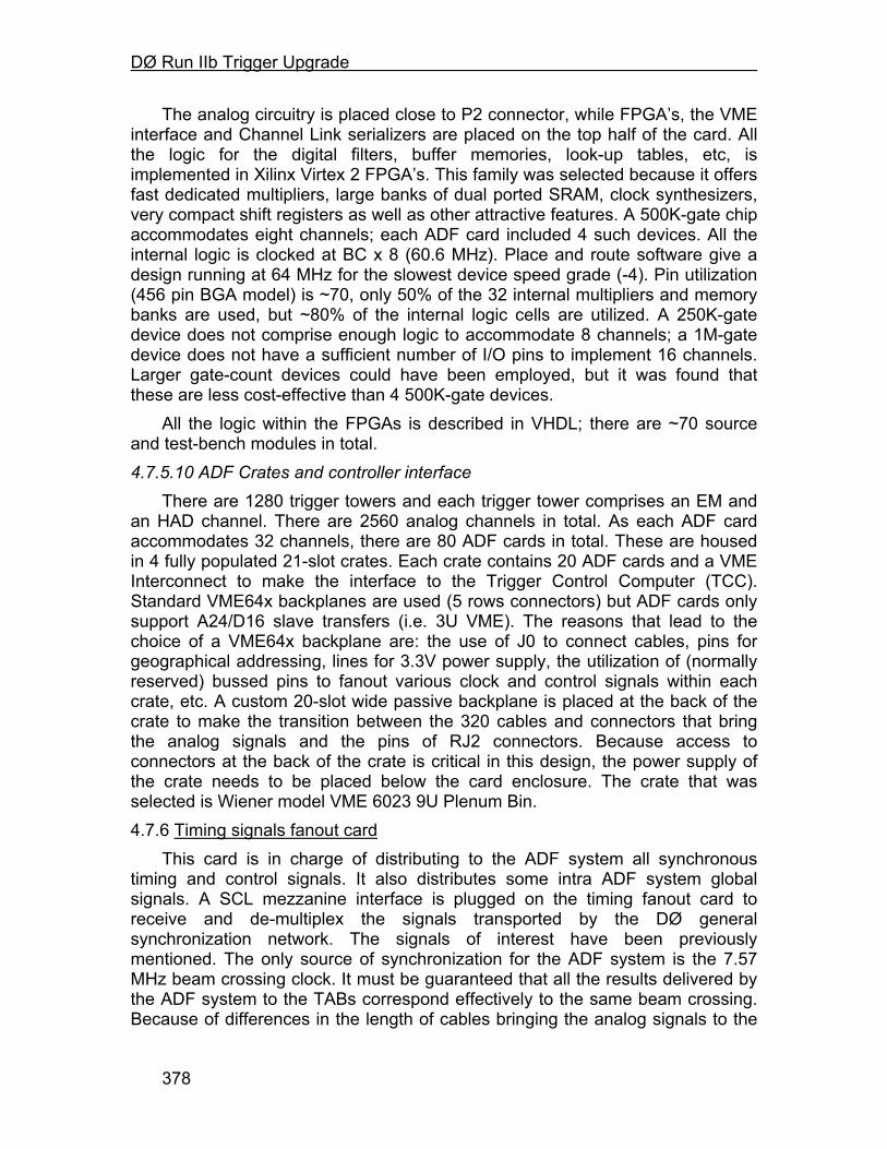
DØ Run IIb Trigger Upgrade
378
The analog circuitry is placed close to P2 connector, while FPGA’s, the VME interface and Channel Link serializers are placed on the top half of the card. All the logic for the digital filters, buffer memories, look-up tables, etc, is implemented in Xilinx Virtex 2 FPGA’s. This family was selected because it offers fast dedicated multipliers, large banks of dual ported SRAM, clock synthesizers, very compact shift registers as well as other attractive features. A 500K-gate chip accommodates eight channels; each ADF card included 4 such devices. All the internal logic is clocked at BC x 8 (60.6 MHz). Place and route software give a design running at 64 MHz for the slowest device speed grade (-4). Pin utilization (456 pin BGA model) is ~70, only 50% of the 32 internal multipliers and memory banks are used, but ~80% of the internal logic cells are utilized. A 250K-gate device does not comprise enough logic to accommodate 8 channels; a 1M-gate device does not have a sufficient number of I/O pins to implement 16 channels. Larger gate-count devices could have been employed, but it was found that these are less cost-effective than 4 500K-gate devices.
All the logic within the FPGAs is described in VHDL; there are ~70 source and test-bench modules in total. 4.7.5.10 ADF Crates and controller interface
There are 1280 trigger towers and each trigger tower comprises an EM and an HAD channel. There are 2560 analog channels in total. As each ADF card accommodates 32 channels, there are 80 ADF cards in total. These are housed in 4 fully populated 21-slot crates. Each crate contains 20 ADF cards and a VME Interconnect to make the interface to the Trigger Control Computer (TCC). Standard VME64x backplanes are used (5 rows connectors) but ADF cards only support A24/D16 slave transfers (i.e. 3U VME). The reasons that lead to the choice of a VME64x backplane are: the use of J0 to connect cables, pins for geographical addressing, lines for 3.3V power supply, the utilization of (normally reserved) bussed pins to fanout various clock and control signals within each crate, etc. A custom 20-slot wide passive backplane is placed at the back of the crate to make the transition between the 320 cables and connectors that bring the analog signals and the pins of RJ2 connectors. Because access to connectors at the back of the crate is critical in this design, the power supply of the crate needs to be placed below the card enclosure. The crate that was selected is Wiener model VME 6023 9U Plenum Bin. 4.7.6 Timing signals fanout card
This card is in charge of distributing to the ADF system all synchronous timing and control signals. It also distributes some intra ADF system global signals. A SCL mezzanine interface is plugged on the timing fanout card to receive and de-multiplex the signals transported by the DØ general synchronization network. The signals of interest have been previously mentioned. The only source of synchronization for the ADF system is the 7.57 MHz beam crossing clock. It must be guaranteed that all the results delivered by the ADF system to the TABs correspond effectively to the same beam crossing. Because of differences in the length of cables bringing the analog signals to the
DØ Run IIb Trigger Upgrade
379
ADF cards, there is a spread in time (~60 ns) between the peak observed on the earliest tower and that produced on the latest tower for any given beam crossing. In order to guarantee that a given beam crossing produces analog pulses that are seen by the ADF system as occurring during the same period of the BC clock, the following synchronization scheme is devised. Master timing signals are elaborated on the timing distribution card by inserting programmable delay lines on the relevant signals delivered by the SCL. All ADF cards receive a copy of these master timing signals via paths of equal length.
The timing card has 5 identical outputs links: 4 of these are connected to one ADF card within each ADF crate by a cable plugged in RJ0. The spare output is intended for test and debugging. The type of cable used is similar to these linking the ADF cards to the TABs. One of the cable wires is hard-wired to a know logic level on the timing card, while a resistor drives the corresponding pin to the opposite logic level on each ADF card. An ADF card detects the presence of the timing signals cable by sensing the logic level of the pin corresponding to the wire used for signaling. If the cable is present, that ADF card distributes the timing signals via the backplane bus to all the ADF cards within that crate (including itself). If no cable is detected, the ADF card places in tri-state all the outputs connected to the timing distribution lines. Any ADF card within a crate can act as a distributor of signals for that crate. However, in order to minimize ADF board-to-board signal skew, a card located close to the middle of the crate is preferably assigned that role of signal distributor. Given the differences in trace length, it is expected that the synchronization skew between any two ADF cards within the system is less than ~4 ns.
The timing card is also in charge of distributing to all ADF cards synchronous signals generated within the ADF system itself or issued by the TCC. These include for example, self-triggers and software triggers, the order to suspend and resume operation, the order to resume recording in the history buffers, etc. The different control commands are issued by the TCC to one of the ADF card that is a distributor of signals within a crate. The commands are transmitted to the timing card that makes the fanout to all ADF cards.
Because the number of signals to be exchanged between an ADF crate and the timing distribution card exceeds the number of pairs of wires available, a simple bit serial protocol is used to time multiplex the corresponding information over 2 half-duplex channels: a pair of wires transports data going upstream from the ADF to the synchronization card, a second pair transports data flowing in the opposite direction.
The timing distribution card is designed to avoid the need of a slow control interface. Nonetheless, several internal registers can be configured by the TCC through the ADF system by sending specific commands over any of the serial links going upstream from ADF crates to the timing card. Because all ADF crates are fully populated, there is no slot available at that level to accommodate the timing card. One option is to place it at the back of the controller in one of the ADF crates. The alternative is to house the ADF timing card in the TAB crate (the card only needs power and cooling).
DØ Run IIb Trigger Upgrade
380
4.7.7 Analog signal splitters These cards are intended to test ADF card prototypes in the Run IIa setup
without interfering with the CTFE system that is in operation. The analog splitter card receives the differential signals delivered by a BLS and makes two identical copies of these signals. One output is connected to a CTFE, the other output is available to an ADF. Because a split of the differential signals with a passive device would have lead to a reduction of the amplitude of the signals delivered to the CTFE and ADF, an active analog splitter is designed. Each channel of the splitter is composed of a fully-differential amplifier of gain 2− driving a parallel branch of 2 fully-differential amplifiers of gain 2− . Hence, when both the input and the output are connected to properly terminated cards, the global gain of the splitter is unity. In order to reject common-mode noise as much as possible, fully differential operational amplifiers (THS4141) are used. All channels have a fixed gain; an optional capacitor can be soldered to limit the bandwidth individually. Each splitter card comprises 8 channels, i.e. 4 trigger towers. Connector spacing matches the pitch of the CTFE card to ease connections. Because only +5V and –5.2V are available within the crate housing the CTFEs while a swing from 0 to +5.5V of the analog signals is needed, an on-board DC/DC converter is used on each splitter card to generate locally +12V and –12V power supplies. 4.7.8 ADF to TAB Data Transfer
As discussed above, each of the 80 ADF cards will send three copies of data from 16 EM TTs and 16 H TTs to the TABs bit-serially in 8-bit words. Data transmission between the ADFs and the TABs will be accomplished using LVDS links. This solution is the simplest and most cost effective way of transmitting the large amount of data in the system. Two options were considered to implement the LVDS technology: solutions with LVDS drivers and receivers implemented in FPGAs or the use of LVDS driver/receiver chipsets. Both schemes are acceptable at the level of the ADC cards. The FPGA solution offers the advantages of elegance, flexibility and lower component count but requires more coordinated engineering than a ready-to-use chipset. Constraints at the TAB level favor the Channel Link solution and this is the solution that has been chosen for the baseline. 4.7.8.1 LVDS Serializers and Deserializers
The ADF cards to TAB links will be based on 48-bit Channel Link chipset7 DS90CR483/484, which multiplexes its 48 parallel inputs to 8 data pairs. A total of 32 of the 48 inputs mapped to 6 output data pairs will be used to transmit the 16 EM and 16 H TTs on each ADF. Input data is clocked into the chip at 8xBC (60.6 MHz) while the output pairs run at 364 MHz. The format of the data transported on the links, including a list of possible error detection and synchronization characters is given in Table 14.
7 National Semiconductor: Channel Link Chipset – DS90CR484, http://www.national.com/pf/DS/DS90CR484.html.
DØ Run IIb Trigger Upgrade
381
Table 14: Data transport protocol for LVDS links between ADFs and TABs.
Pins Signal Input Data Streams (0-31)
Differential Data 0,1,2,3,4,5
Differential Data 8,9,10,11,12,13
Differential Data 16,17,18,19,20,21
Differential Data 6,7,14,15,22,23
Differential Data 24,25,26,27,28,29
Differential Data 30,31
Differential Clock
Framing bit
Select 8/10-bit frames
Parity
Grounds
4.7.8.2 Cables The cabling diagram between the 80 ADFs and 8 TABs is shown in Figure
58. Each ADF sends out 3 cables carrying identical copies of its data. Each TAB accepts 30 ADF cables giving it more than the 40×9 TTs of data in η×φ that it requires to find RoIs over the full eta range and 4 phi slices.
TAB 8 φ=32-29
TAB 7 φ=28-25
TAB 6φ=24-21
TAB 5φ=20-17
TAB 4φ=16-13
TAB 3φ=12-9
TAB 2 φ=8-5
TAB 1φ=4-1
ADFs 80-71
ADFs 70-61
ADFs60-51
ADFs50-41
ADFs40-31
ADFs30-21
ADFs 20-11
ADFs10-1
η=40-1 φ=8-5
η=40-1 φ=12-9
η=40-1φ=16-13
η=40-1φ=20-17
η=40-1φ=24-21
η=40-1 φ=28-25
η=40-1φ=4-1
η=40-1 φ=32-29
101010
Figure 58: Diagram of cabling between the ADFs and the TABs.

DØ Run IIb Trigger Upgrade
382
4.7.9 TAB implementation The Trigger Algorithm Boards (TAB) are the main processing component of
the L1 calorimeter trigger. They perform the following tasks for a specific η×φ region of the calorimeter.
• Find EM, Jet and tau clusters and estimate their ET using sliding windows algorithms.
• Send a list of EM, Jet and tau clusters passing several different ET thresholds to the GAB.
• Send a list of EM and Jet clusters over threshold to the Cal-Track Match system.
• Calculate a scalar ET sum and Ex and Ey sums for all TTs in the TAB’s region for use in ET,total and MpT.
• Send the ET, Ex and Ey sums to the GAB.
• Format and buffer data for use in L2 and L3 and send this out on receipt of L1 and L2 trigger accepts.
• Allow insertion of fake data, by computer, directly after the inputs to test system functionality.
4.7.9.1 Overall TAB Architecture A block diagram of the TAB is given in Figure 59. The architecture is driven
by several global considerations.
• Our target algorithms use 2×2 windows and 5×5 declustering regions.
• ADF design is simplified if each such board is identical. Practically this means that the same number of output cables must be sent from each board.
• A large number of TT signals must be sent to a given TAB to find ET cluster local maxima
• Latency must be kept to a minimum
• Small, low-speed FPGAs should be used to minimize costs. These considerations have led us to a design in which each TAB checks for
local maxima in a region covering the full η region by 4 bins in φ. This means that each TAB will output information on 31×4 possible local maxima. Note that there are only 31 possibilities in η because of the four TTs devoted to the ICR and the five TTs at the edges of the calorimeter for which not enough data exists to decluster.
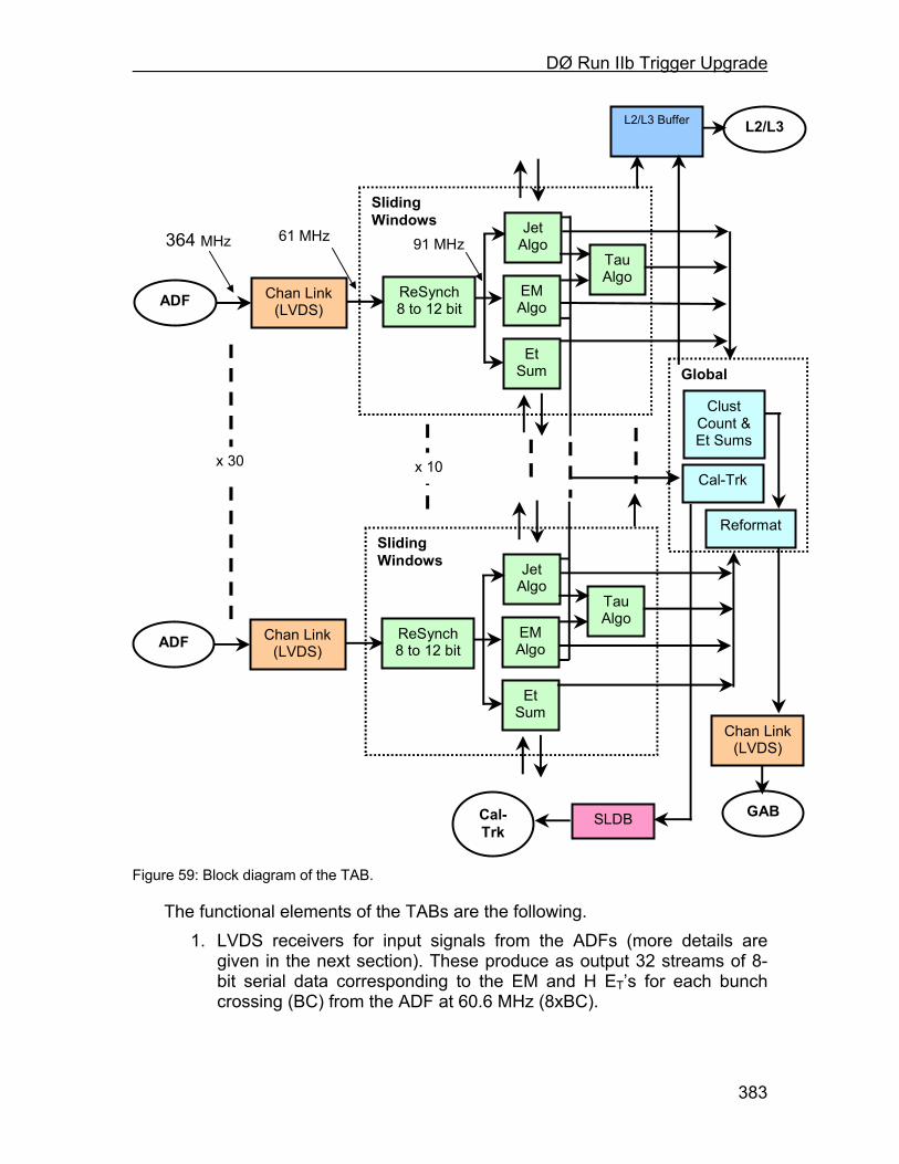
DØ Run IIb Trigger Upgrade
383
L2/L3 Buffer
SLDB
ADF Chan Link (LVDS)
ReSynch8 to 12 bit
Jet Algo
EM Algo
Tau Algo
Et Sum
SlidingWindows
Chan Link(LVDS)
L2/L3
ADF Chan Link (LVDS)
ReSynch8 to 12 bit
Jet Algo
EM Algo
Tau Algo
Et Sum
SlidingWindows
Clust Count & Et Sums
Cal-Trk
Global
Reformat
GABCal-Trk
x 30 x 10
364 MHz 61 MHz 91 MHz
Figure 59: Block diagram of the TAB.
The functional elements of the TABs are the following. 1. LVDS receivers for input signals from the ADFs (more details are
given in the next section). These produce as output 32 streams of 8-bit serial data corresponding to the EM and H ET’s for each bunch crossing (BC) from the ADF at 60.6 MHz (8xBC).
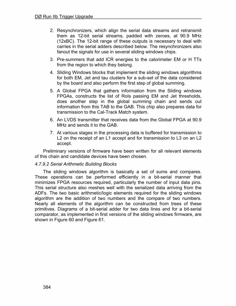
DØ Run IIb Trigger Upgrade
384
2. Resynchronizers, which align the serial data streams and retransmit them as 12-bit serial streams, padded with zeroes, at 90.9 MHz (12xBC). The 12-bit range of these outputs is necessary to deal with carries in the serial adders described below. The resynchronizers also fanout the signals for use in several sliding windows chips.
3. Pre-summers that add ICR energies to the calorimeter EM or H TTs from the region to which they belong.
4. Sliding Windows blocks that implement the sliding windows algorithms for both EM, Jet and tau clusters for a sub-set of the data considered by the board and also perform the first step of global summing.
5. A Global FPGA that gathers information from the Sliding windows FPGAs, constructs the list of RoIs passing EM and Jet thresholds, does another step in the global summing chain and sends out information from this TAB to the GAB. This chip also prepares data for transmission to the Cal-Track Match system.
6. An LVDS transmitter that receives data from the Global FPGA at 90.9 MHz and sends it to the GAB.
7. At various stages in the processing data is buffered for transmission to L2 on the receipt of an L1 accept and for transmission to L3 on an L2 accept.
Preliminary versions of firmware have been written for all relevant elements of this chain and candidate devices have been chosen. 4.7.9.2 Serial Arithmetic Building Blocks
The sliding windows algorithm is basically a set of sums and compares. These operations can be performed efficiently in a bit-serial manner that minimizes FPGA resources required, particularly the number of input data pins. This serial structure also meshes well with the serialized data arriving from the ADFs. The two basic arithmetic/logic elements required for the sliding windows algorithm are the addition of two numbers and the compare of two numbers. Nearly all elements of the algorithm can be constructed from trees of these primitives. Diagrams of a bit-serial adder for two data lines and for a bit-serial comparator, as implemented in first versions of the sliding windows firmware, are shown in Figure 60 and Figure 61.
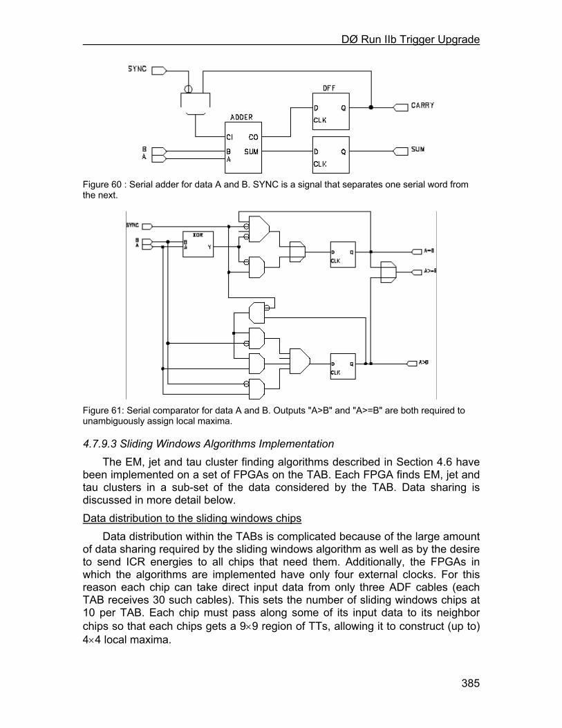
DØ Run IIb Trigger Upgrade
385
Figure 60 : Serial adder for data A and B. SYNC is a signal that separates one serial word from the next.
Figure 61: Serial comparator for data A and B. Outputs "A>B" and "A>=B" are both required to unambiguously assign local maxima.
4.7.9.3 Sliding Windows Algorithms Implementation The EM, jet and tau cluster finding algorithms described in Section 4.6 have
been implemented on a set of FPGAs on the TAB. Each FPGA finds EM, jet and tau clusters in a sub-set of the data considered by the TAB. Data sharing is discussed in more detail below. Data distribution to the sliding windows chips
Data distribution within the TABs is complicated because of the large amount of data sharing required by the sliding windows algorithm as well as by the desire to send ICR energies to all chips that need them. Additionally, the FPGAs in which the algorithms are implemented have only four external clocks. For this reason each chip can take direct input data from only three ADF cables (each TAB receives 30 such cables). This sets the number of sliding windows chips at 10 per TAB. Each chip must pass along some of its input data to its neighbor chips so that each chips gets a 9×9 region of TTs, allowing it to construct (up to) 4×4 local maxima.

DØ Run IIb Trigger Upgrade
386
An example of the intra-TAB data paths for TAB-2 (dealing with φ’s 5-8) is shown in Figure 62. The diagram shows cable inputs to each chip, the data it shares with its neighbors, the distribution of ICR data (in η’s 1,2 and 39,40) to all the chips that need it and the chip’s output local maxima.
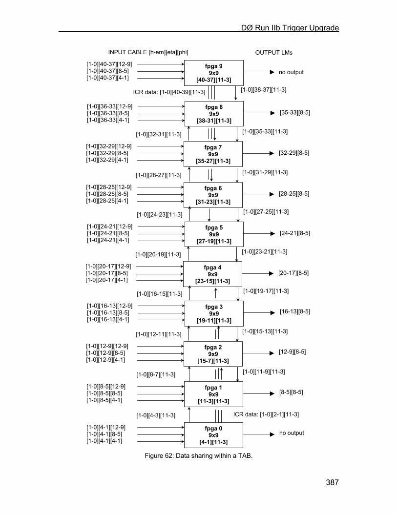
DØ Run IIb Trigger Upgrade
387
no output
[35-33][8-5]
[32-29][8-5]
[28-25][8-5]
[24-21][8-5]
[16-13][8-5]
[12-9][8-5]
[8-5][8-5]
no output
[1-0][38-37][11-3]
fpga 99x9
[40-37][11-3]
fpga 89x9
[38-31][11-3]
fpga 79x9
[35-27][11-3]
[1-0][35-33][11-3] [1-0][32-31][11-3]
ICR data: [1-0][40-39][11-3]
fpga 69x9
[31-23][11-3]
[1-0][31-29][11-3] [1-0][28-27][11-3]
[1-0][40-37][12-9] [1-0][40-37][8-5] [1-0][40-37][4-1]
[1-0][36-33][12-9] [1-0][36-33][8-5] [1-0][36-33][4-1]
[1-0][32-29][12-9] [1-0][32-29][8-5] [1-0][32-29][4-1]
[1-0][28-25][12-9] [1-0][28-25][8-5] [1-0][28-25][4-1]
fpga 59x9
[27-19][11-3]
[1-0][27-25][11-3] [1-0][24-23][11-3]
[1-0][24-21][12-9] [1-0][24-21][8-5] [1-0][24-21][4-1]
fpga 49x9
[23-15][11-3]
[1-0][23-21][11-3] [1-0][20-19][11-3]
[20-17][8-5] [1-0][20-17][12-9] [1-0][20-17][8-5] [1-0][20-17][4-1]
fpga 39x9
[19-11][11-3]
[1-0][19-17][11-3] [1-0][16-15][11-3]
[1-0][16-13][12-9] [1-0][16-13][8-5] [1-0][16-13][4-1]
fpga 29x9
[15-7][11-3]
[1-0][15-13][11-3] [1-0][12-11][11-3]
[1-0][12-9][12-9] [1-0][12-9][8-5] [1-0][12-9][4-1]
fpga 19x9
[11-3][11-3]
[1-0][11-9][11-3] [1-0][8-7][11-3]
[1-0][8-5][12-9] [1-0][8-5][8-5] [1-0][8-5][4-1]
fpga 09x9
[4-1][11-3]
ICR data: [1-0][2-1][11-3] [1-0][4-3][11-3]
[1-0][4-1][12-9] [1-0][4-1][8-5] [1-0][4-1][4-1]
INPUT CABLE [h-em][eta][phi] OUTPUT LMs
Figure 62: Data sharing within a TAB.
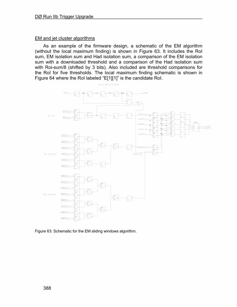
DØ Run IIb Trigger Upgrade
388
EM and jet cluster algorithms
As an example of the firmware design, a schematic of the EM algorithm (without the local maximum finding) is shown in Figure 63. It includes the RoI sum, EM isolation sum and Had isolation sum, a comparison of the EM isolation sum with a downloaded threshold and a comparison of the Had isolation sum with Roi-sum/8 (shifted by 3 bits). Also included are threshold comparisons for the RoI for five thresholds. The local maximum finding schematic is shown in Figure 64 where the RoI labeled “E[1][1]” is the candidate RoI.
Figure 63: Schematic for the EM sliding windows algorithm.
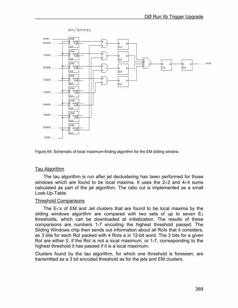
DØ Run IIb Trigger Upgrade
389
Figure 64: Schematic of local maximum-finding algorithm for the EM sliding window.
Tau Algorithm
The tau algorithm is run after jet declustering has been performed for those windows which are found to be local maxima. It uses the 2×2 and 4×4 sums calculated as part of the jet algorithm. The ratio cut is implemented as a small Look-Up-Table. Threshold Comparisons
The ET’s of EM and Jet clusters that are found to be local maxima by the sliding windows algorithm are compared with two sets of up to seven ET thresholds, which can be downloaded at initialization. The results of these comparisons are numbers 1-7 encoding the highest threshold passed. The Sliding Windows chip then sends out information about all RoIs that it considers, as 3 bits for each RoI packed with 4 RoIs a in 12-bit word. The 3 bits for a given RoI are either 0, if the RoI is not a local maximum, or 1-7, corresponding to the highest threshold it has passed if it is a local maximum. Clusters found by the tau algorithm, for which one threshold is foreseen, are transmitted as a 3 bit encoded threshold as for the jets and EM clusters.

DØ Run IIb Trigger Upgrade
390
Table 15: Cluster encoding for data transmitted from sliding windows chip to global chip.
3-bit Value Meaning
0 RoI is not a local maximum
1-7 RoI is a local maximum Value = index of highest Et threshold passed
ET Sums Preliminary sums for use in calculating ET,total and MpT are also computed on the Sliding Windows chips. Each chip sums all TT EM and EM+H ET’s over all η for each of the four φ’s considered in the chip. Clusters for the Cal-Trk Match system
For use by the Cal-Trk match system, each sliding windows chip constructs a count over all η of the EM and jet clusters passing each of four thresholds. In order to save the time, this information is sent on to the Global chip in parallel before the main threshold comparisons. Sliding Windows Chip Outputs The outputs of the Sliding Windows chips sent to the Global chip are then a set of 12-bit words sent serially at 90.9 MHz as shown in Table 16 and the 32 lines for fast Cal-Trk match data, corresponding to four thresholds for EM and jet clusters for each of the four φ’s dealt with by the chip (Table 17).
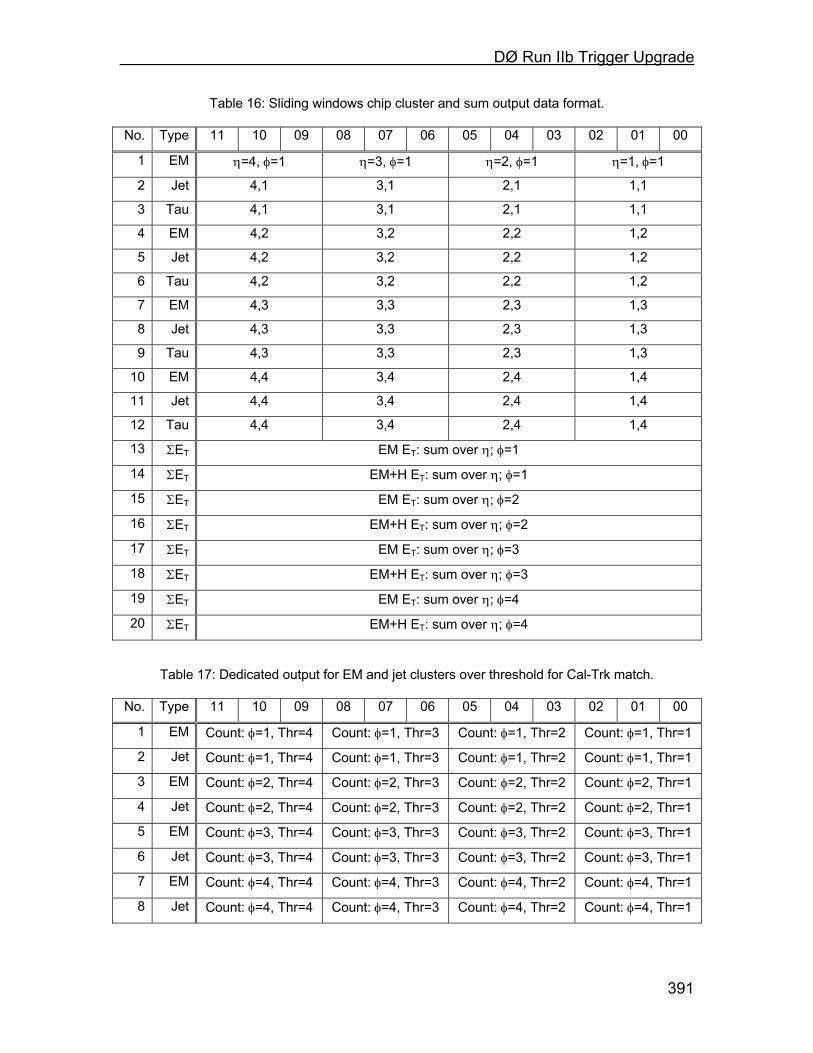
DØ Run IIb Trigger Upgrade
391
Table 16: Sliding windows chip cluster and sum output data format.
No. Type 11 10 09 08 07 06 05 04 03 02 01 00
1 EM η=4, φ=1 η=3, φ=1 η=2, φ=1 η=1, φ=1
2 Jet 4,1 3,1 2,1 1,1
3 Tau 4,1 3,1 2,1 1,1
4 EM 4,2 3,2 2,2 1,2
5 Jet 4,2 3,2 2,2 1,2
6 Tau 4,2 3,2 2,2 1,2
7 EM 4,3 3,3 2,3 1,3
8 Jet 4,3 3,3 2,3 1,3
9 Tau 4,3 3,3 2,3 1,3
10 EM 4,4 3,4 2,4 1,4
11 Jet 4,4 3,4 2,4 1,4
12 Tau 4,4 3,4 2,4 1,4
13 ΣET EM ET: sum over η; φ=1
14 ΣET EM+H ET: sum over η; φ=1
15 ΣET EM ET: sum over η; φ=2
16 ΣET EM+H ET: sum over η; φ=2
17 ΣET EM ET: sum over η; φ=3
18 ΣET EM+H ET: sum over η; φ=3
19 ΣET EM ET: sum over η; φ=4
20 ΣET EM+H ET: sum over η; φ=4
Table 17: Dedicated output for EM and jet clusters over threshold for Cal-Trk match.
No. Type 11 10 09 08 07 06 05 04 03 02 01 00
1 EM Count: φ=1, Thr=4 Count: φ=1, Thr=3 Count: φ=1, Thr=2 Count: φ=1, Thr=1
2 Jet Count: φ=1, Thr=4 Count: φ=1, Thr=3 Count: φ=1, Thr=2 Count: φ=1, Thr=1
3 EM Count: φ=2, Thr=4 Count: φ=2, Thr=3 Count: φ=2, Thr=2 Count: φ=2, Thr=1
4 Jet Count: φ=2, Thr=4 Count: φ=2, Thr=3 Count: φ=2, Thr=2 Count: φ=2, Thr=1
5 EM Count: φ=3, Thr=4 Count: φ=3, Thr=3 Count: φ=3, Thr=2 Count: φ=3, Thr=1
6 Jet Count: φ=3, Thr=4 Count: φ=3, Thr=3 Count: φ=3, Thr=2 Count: φ=3, Thr=1
7 EM Count: φ=4, Thr=4 Count: φ=4, Thr=3 Count: φ=4, Thr=2 Count: φ=4, Thr=1
8 Jet Count: φ=4, Thr=4 Count: φ=4, Thr=3 Count: φ=4, Thr=2 Count: φ=4, Thr=1
DØ Run IIb Trigger Upgrade
392
4.7.9.4 Global FPGA The Global FPGA receives information from the TABs outlined in Table 16
and Table 17. Its main job is to collect the encoded EM and Jet data for output and calculate Ex and Ey, derived from the ET φ-sums bit-serially using x,y weights stored in ROM as a Look-Up-Table. It also counts the number of EM, jet and tau clusters over threshold.
The Global chip also provides data to the Cal-Track match system based on the fast Cal-Trk data lines. OR’s of the threshold bits are constructed over all η and counts are made of the number of EM and jet clusters passing one of the thresholds. This information is then packed into 8-bit words – one for each EM and jet cluster considered by the TAB. The bit definition of these words is given in Table 18.
Table 18: Format of 8-bit Cal-Trk match word sent from Global chip. One such word is sent for each φ for EM and Jet values.
07 06 05 04 03 02 01 00
Threshold bits ORed over η
cluster count – Thr n Thr 4 Thr 3 Thr 2 Thr 1
4.7.9.5 Output to the GAB The Global FPGA on each TAB produces the following types of data.
1. Counts of EM and jet clusters over each of the seven thresholds. 2. A count of the number of tau clusters over threshold. 3. EM and EM+H ET sums for the region considered by the TAB. 4. EM+H Ex and Ey sums for the region considered by the TAB.
Each TAB considers 31×4 = 124 possible local maxima. However, since the 2,1,1 algorithm requires that local maxima be separated by at least two TTs in η and φ, only 31 EM and 31 jet clusters are allowed. Thus, cluster counts can be safely stored as 6-bit words.
The TABs will send their data out to the GAB serially using the same LVDS system as used for the ADF to TAB transmission. In this case, the TABs will send data as 12-bit words using the format given in Table 19.

DØ Run IIb Trigger Upgrade
393
Table 19: Data format for TAB to GAB transfer.
No. 11 10 09 08 07 06 05 04 03 02 01 00
1 Jet Count: Threshold=1 EM count: Threshold=1 … … … 7 Jet Count: Threshold=7 EM count: Threshold=7 8 Tau count
9 EM ET: sum over η, φ=110 EM+H ET: sum over η, φ=1… …15 EM ET: sum over η, φ=416 EM+H ET: sum over η, φ=417 EM+H Ex
18 EM+H Ey
4.7.9.6 Output to Cal-Trk match system Data is sent to the Cal-Trk system using an existing L1Muon Serial Link
Daughterboard8. The Cal-Trk system expects 16-bit words at a frequency of 53 MHz. A maximum of 7 such words can be sent in one B.C. for a total bit-count on a single cable of 112 bits per B.C. The number of cables from L1Cal to the Cal-Trk system is limited to approximately 12, which is safely above the 8 sent by the baseline system.
During periods with no data (SYNC_GAP, etc.) the Cal-Trk receiver expects to receive NULL (K28.5) characters as data words.
Several control bits are required by the Cal-Trk system8. The two of most relevance to L1Cal transmission are:
• Enable (E): high = data enabled
• Parity_Enable (P): high = data is longitudinal parity The Global FPGA formats data according to the specifications of the L1
Muon SLDB. Its output will have the form given in Table 20.
8 Serial Link Daughter Board Specification, http://hound.physics.arizona.edu/l1mu/l1mu.htm.

DØ Run IIb Trigger Upgrade
394
Table 20: Format for data from a TAB to the Cal-Trk match system
No P E 15 14 13 12 11 10 09 08 07 06 05 04 03 02 01 00
… 0 0 NULL
1 0 1 Jet: count + ET: φ=1 EM: count + ET: φ=1
2 0 1 Jet: count + ET: φ=2 EM: count + ET: φ=2
3 0 1 Jet: count + ET: φ=3 EM: count + ET: φ=3
4 0 1 Jet: count + ET: φ=4 EM: count + ET: φ=4
5 1 1 Longitudinal Parity
4.7.10 GAB Implementation
The Global Algorithm Board (GAB) is the final step in the L1 calorimeter chain before the Trigger Framework. A list of the tasks that this board will perform is given below.
• Calculates ET,total and Ex, Ey from the TAB partial sums and transmits them to the Trigger Framework
• Constructs trigger terms from counts of clusters over threshold and global sums and sends these to the trigger framework.
• Receives timing and control information from the Trigger Framework over the Serial Command Link (SCL) via an SCL Receiver mezzanine card9 (SCLR) and fans this out to the ADFs and TABs as necessary.
• Sends data to L2 and L3. 4.7.10.1 Output to the Trigger Framework
Trigger terms sent from the GAB to the Trigger Framework are still being explored. All quantities currently sent to the Trigger Framework by the L1 calorimeter trigger (see Section 4.3) will continue to be sent though. 4.7.10.2 Control and Timing Signals for the TAB-GAB System
The TABs need to receive global control signals such as a bunch crossing clock and event number. This information is available from the Trigger Framework via the Serial Command Link (SCL) using custom SCL Receiver mezzanine cards9. However, the TABs need only a small subset of the full SCL information. It is therefore more efficient to receive this information centrally in the GAB and then fan out the required sub-set to the TABs.
A list of SCL signals, their sources and their destinations within the system is given in Table 21.
9 DØ Trigger Distribution System: Serial Command Link Receiver (SCLR),
http://www-ese.fnal.gov/d0trig/default.htm.
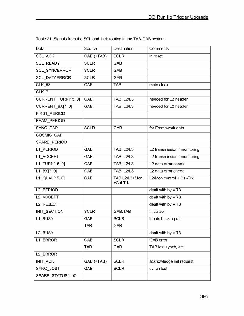
DØ Run IIb Trigger Upgrade
395
Table 21: Signals from the SCL and their routing in the TAB-GAB system.
Data Source Destination Comments
SCL_ACK GAB (+TAB) SCLR in reset
SCL_READY SCLR GAB
SCL_SYNCERROR SCLR GAB
SCL_DATAERROR SCLR GAB
CLK_53 GAB TAB main clock
CLK_7
CURRENT_TURN[15..0] GAB TAB: L2/L3 needed for L2 header
CURRENT_BX[7..0] GAB TAB: L2/L3 needed for L2 header
FIRST_PERIOD
BEAM_PERIOD
SYNC_GAP SCLR GAB for Framework data
COSMIC_GAP
SPARE_PERIOD
L1_PERIOD GAB TAB: L2/L3 L2 transmission / monitoring
L1_ACCEPT GAB TAB: L2/L3 L2 transmission / monitoring
L1_TURN[15..0] GAB TAB: L2/L3 L2 data error check
L1_BX[7..0] GAB TAB: L2/L3 L2 data error check
L1_QUAL[15..0] GAB TAB:L2/L3+Mon +Cal-Trk
L2/Mon control + Cal-Trk
L2_PERIOD dealt with by VRB
L2_ACCEPT dealt with by VRB
L2_REJECT dealt with by VRB
INIT_SECTION SCLR GAB,TAB initialize
L1_BUSY GAB
TAB
SCLR
GAB
inputs backing up
L2_BUSY dealt with by VRB
L1_ERROR GAB
TAB
SCLR
GAB
GAB error
TAB lost synch, etc
L2_ERROR
INIT_ACK GAB (+TAB) SCLR acknowledge init request
SYNC_LOST GAB SCLR synch lost
SPARE_STATUS[1..0]
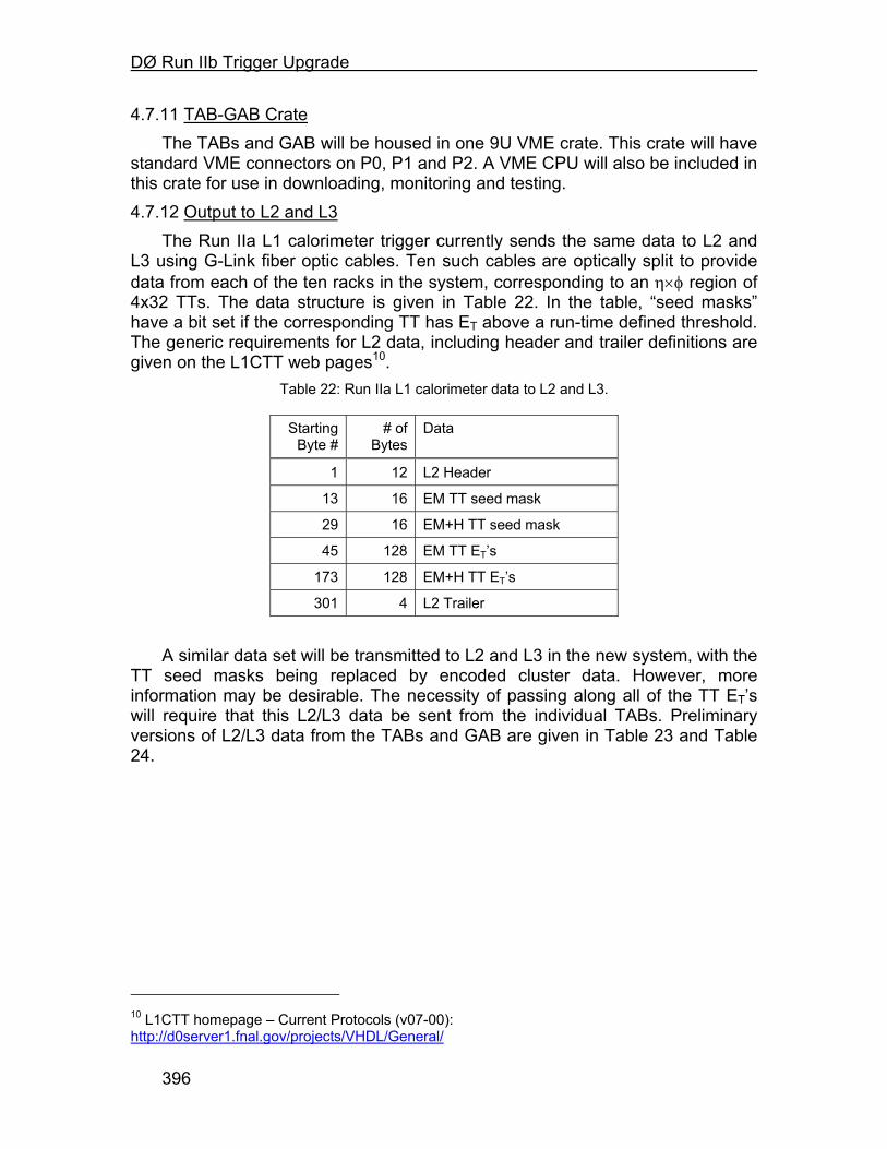
DØ Run IIb Trigger Upgrade
396
4.7.11 TAB-GAB Crate The TABs and GAB will be housed in one 9U VME crate. This crate will have
standard VME connectors on P0, P1 and P2. A VME CPU will also be included in this crate for use in downloading, monitoring and testing. 4.7.12 Output to L2 and L3
The Run IIa L1 calorimeter trigger currently sends the same data to L2 and L3 using G-Link fiber optic cables. Ten such cables are optically split to provide data from each of the ten racks in the system, corresponding to an η×φ region of 4x32 TTs. The data structure is given in Table 22. In the table, “seed masks” have a bit set if the corresponding TT has ET above a run-time defined threshold. The generic requirements for L2 data, including header and trailer definitions are given on the L1CTT web pages10.
Table 22: Run IIa L1 calorimeter data to L2 and L3.
Starting Byte #
# of Bytes
Data
1 12 L2 Header
13 16 EM TT seed mask
29 16 EM+H TT seed mask
45 128 EM TT ET’s
173 128 EM+H TT ET’s
301 4 L2 Trailer
A similar data set will be transmitted to L2 and L3 in the new system, with the TT seed masks being replaced by encoded cluster data. However, more information may be desirable. The necessity of passing along all of the TT ET’s will require that this L2/L3 data be sent from the individual TABs. Preliminary versions of L2/L3 data from the TABs and GAB are given in Table 23 and Table 24.
10 L1CTT homepage – Current Protocols (v07-00): http://d0server1.fnal.gov/projects/VHDL/General/
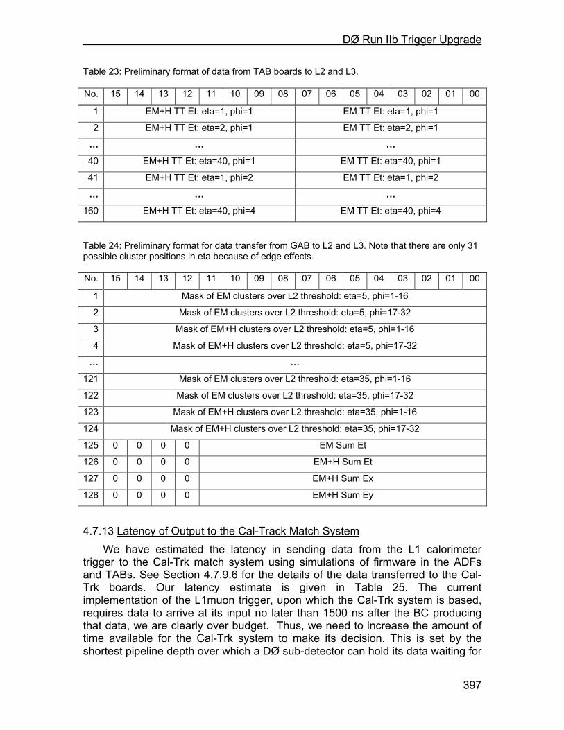
DØ Run IIb Trigger Upgrade
397
Table 23: Preliminary format of data from TAB boards to L2 and L3.
No. 15 14 13 12 11 10 09 08 07 06 05 04 03 02 01 00
1 EM+H TT Et: eta=1, phi=1 EM TT Et: eta=1, phi=1
2 EM+H TT Et: eta=2, phi=1 EM TT Et: eta=2, phi=1
… … …
40 EM+H TT Et: eta=40, phi=1 EM TT Et: eta=40, phi=1
41 EM+H TT Et: eta=1, phi=2 EM TT Et: eta=1, phi=2
… … …
160 EM+H TT Et: eta=40, phi=4 EM TT Et: eta=40, phi=4
Table 24: Preliminary format for data transfer from GAB to L2 and L3. Note that there are only 31 possible cluster positions in eta because of edge effects.
No. 15 14 13 12 11 10 09 08 07 06 05 04 03 02 01 00
1 Mask of EM clusters over L2 threshold: eta=5, phi=1-16
2 Mask of EM clusters over L2 threshold: eta=5, phi=17-32
3 Mask of EM+H clusters over L2 threshold: eta=5, phi=1-16
4 Mask of EM+H clusters over L2 threshold: eta=5, phi=17-32
… … 121 Mask of EM clusters over L2 threshold: eta=35, phi=1-16
122 Mask of EM clusters over L2 threshold: eta=35, phi=17-32
123 Mask of EM+H clusters over L2 threshold: eta=35, phi=1-16
124 Mask of EM+H clusters over L2 threshold: eta=35, phi=17-32
125 0 0 0 0 EM Sum Et
126 0 0 0 0 EM+H Sum Et
127 0 0 0 0 EM+H Sum Ex
128 0 0 0 0 EM+H Sum Ey
4.7.13 Latency of Output to the Cal-Track Match System
We have estimated the latency in sending data from the L1 calorimeter trigger to the Cal-Trk match system using simulations of firmware in the ADFs and TABs. See Section 4.7.9.6 for the details of the data transferred to the Cal-Trk boards. Our latency estimate is given in Table 25. The current implementation of the L1muon trigger, upon which the Cal-Trk system is based, requires data to arrive at its input no later than 1500 ns after the BC producing that data, we are clearly over budget. Thus, we need to increase the amount of time available for the Cal-Trk system to make its decision. This is set by the shortest pipeline depth over which a DØ sub-detector can hold its data waiting for
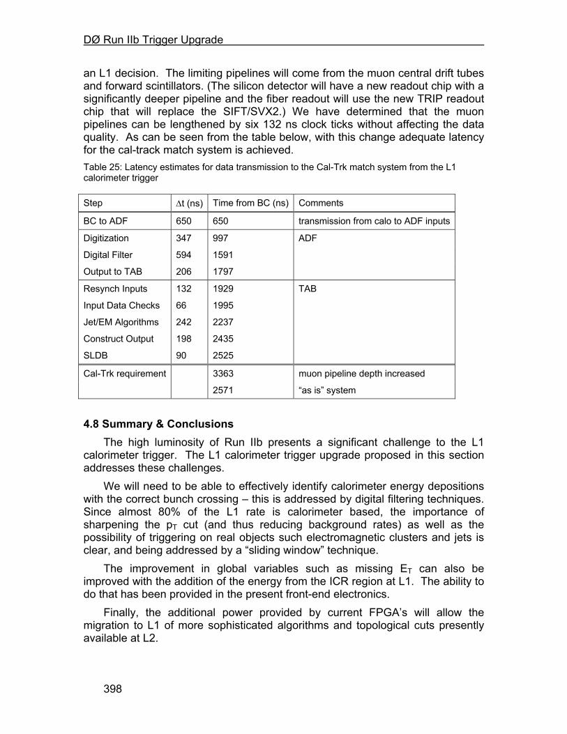
DØ Run IIb Trigger Upgrade
398
an L1 decision. The limiting pipelines will come from the muon central drift tubes and forward scintillators. (The silicon detector will have a new readout chip with a significantly deeper pipeline and the fiber readout will use the new TRIP readout chip that will replace the SIFT/SVX2.) We have determined that the muon pipelines can be lengthened by six 132 ns clock ticks without affecting the data quality. As can be seen from the table below, with this change adequate latency for the cal-track match system is achieved. Table 25: Latency estimates for data transmission to the Cal-Trk match system from the L1 calorimeter trigger
Step ∆t (ns) Time from BC (ns) Comments
BC to ADF 650 650 transmission from calo to ADF inputs
Digitization 347 997 ADF
Digital Filter 594 1591
Output to TAB 206 1797
Resynch Inputs 132 1929 TAB
Input Data Checks 66 1995
Jet/EM Algorithms 242 2237
Construct Output 198 2435
SLDB 90 2525
Cal-Trk requirement 3363 muon pipeline depth increased
2571 “as is” system
4.8 Summary & Conclusions The high luminosity of Run IIb presents a significant challenge to the L1
calorimeter trigger. The L1 calorimeter trigger upgrade proposed in this section addresses these challenges.
We will need to be able to effectively identify calorimeter energy depositions with the correct bunch crossing – this is addressed by digital filtering techniques. Since almost 80% of the L1 rate is calorimeter based, the importance of sharpening the pT cut (and thus reducing background rates) as well as the possibility of triggering on real objects such electromagnetic clusters and jets is clear, and being addressed by a “sliding window” technique.
The improvement in global variables such as missing ET can also be improved with the addition of the energy from the ICR region at L1. The ability to do that has been provided in the present front-end electronics.
Finally, the additional power provided by current FPGA’s will allow the migration to L1 of more sophisticated algorithms and topological cuts presently available at L2.

DØ Run IIb Trigger Upgrade
399
This set of tools provided by the proposed L1 calorimeter trigger will allow us to make the optimal use of the Run IIb luminosity.
The hardware implementation of these improvements has been explored, leading to an overall architectural design. Preliminary detailed designs for several of the most important elements of the system have been made, with a full first-pass design anticipated by summer 2002.
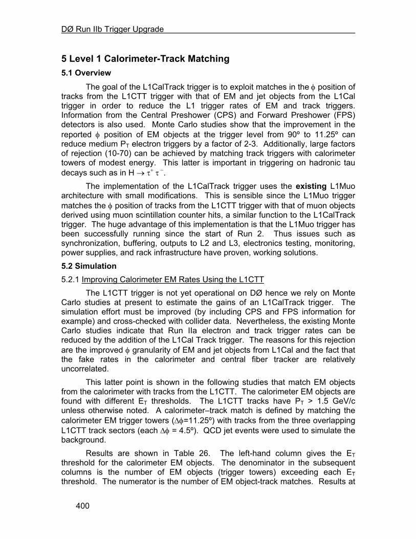
DØ Run IIb Trigger Upgrade
400
5 Level 1 Calorimeter-Track Matching 5.1 Overview
The goal of the L1CalTrack trigger is to exploit matches in the φ position of tracks from the L1CTT trigger with that of EM and jet objects from the L1Cal trigger in order to reduce the L1 trigger rates of EM and track triggers. Information from the Central Preshower (CPS) and Forward Preshower (FPS) detectors is also used. Monte Carlo studies show that the improvement in the reported φ position of EM objects at the trigger level from 90º to 11.25º can reduce medium PT electron triggers by a factor of 2-3. Additionally, large factors of rejection (10-70) can be achieved by matching track triggers with calorimeter towers of modest energy. This latter is important in triggering on hadronic tau decays such as in H → τ+ τ −.
The implementation of the L1CalTrack trigger uses the existing L1Muo architecture with small modifications. This is sensible since the L1Muo trigger matches the φ position of tracks from the L1CTT trigger with that of muon objects derived using muon scintillation counter hits, a similar function to the L1CalTrack trigger. The huge advantage of this implementation is that the L1Muo trigger has been successfully running since the start of Run 2. Thus issues such as synchronization, buffering, outputs to L2 and L3, electronics testing, monitoring, power supplies, and rack infrastructure have proven, working solutions. 5.2 Simulation 5.2.1 Improving Calorimeter EM Rates Using the L1CTT
The L1CTT trigger is not yet operational on DØ hence we rely on Monte Carlo studies at present to estimate the gains of an L1CalTrack trigger. The simulation effort must be improved (by including CPS and FPS information for example) and cross-checked with collider data. Nevertheless, the existing Monte Carlo studies indicate that Run IIa electron and track trigger rates can be reduced by the addition of the L1Cal Track trigger. The reasons for this rejection are the improved φ granularity of EM and jet objects from L1Cal and the fact that the fake rates in the calorimeter and central fiber tracker are relatively uncorrelated.
This latter point is shown in the following studies that match EM objects from the calorimeter with tracks from the L1CTT. The calorimeter EM objects are found with different ET thresholds. The L1CTT tracks have PT > 1.5 GeV/c unless otherwise noted. A calorimeter–track match is defined by matching the calorimeter EM trigger towers (∆φ=11.25º) with tracks from the three overlapping L1CTT track sectors (each ∆φ = 4.5º). QCD jet events were used to simulate the background.
Results are shown in Table 26. The left-hand column gives the ET threshold for the calorimeter EM objects. The denominator in the subsequent columns is the number of EM objects (trigger towers) exceeding each ET threshold. The numerator is the number of EM object-track matches. Results at
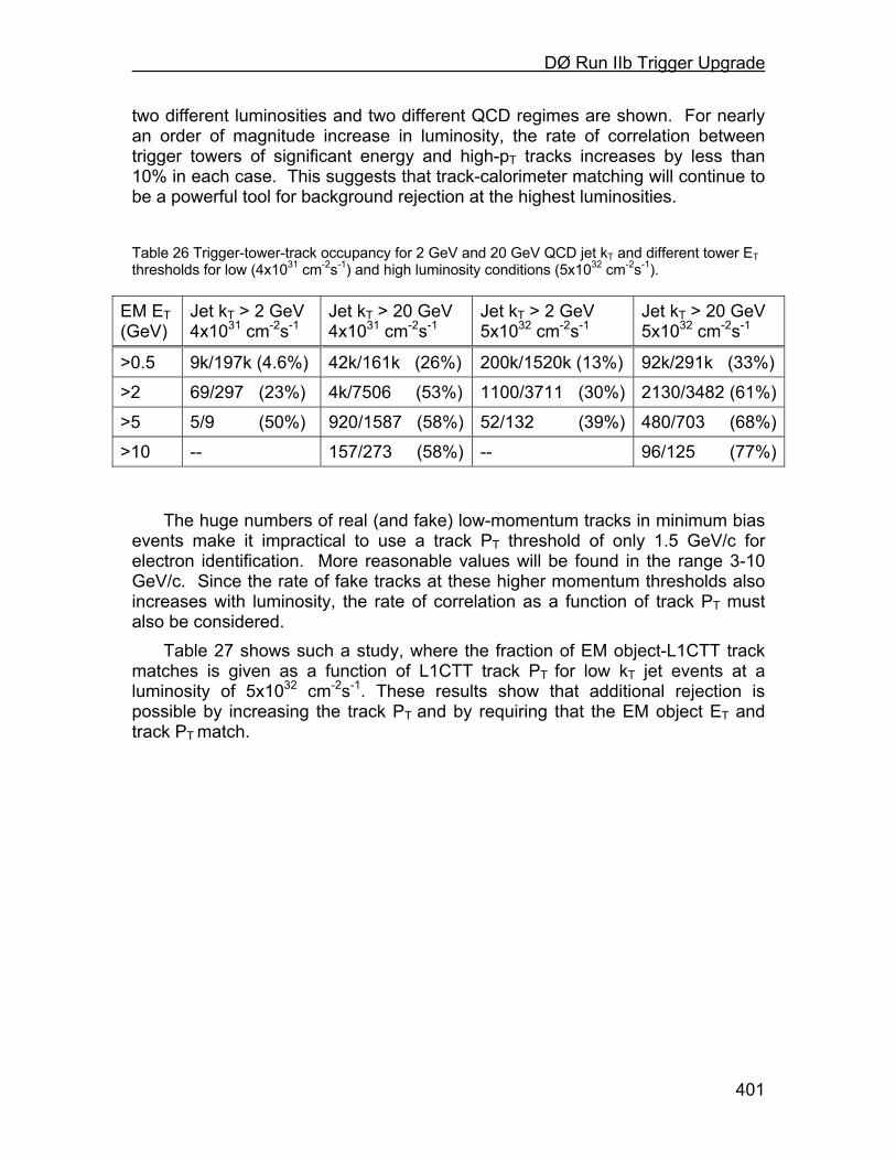
DØ Run IIb Trigger Upgrade
401
two different luminosities and two different QCD regimes are shown. For nearly an order of magnitude increase in luminosity, the rate of correlation between trigger towers of significant energy and high-pT tracks increases by less than 10% in each case. This suggests that track-calorimeter matching will continue to be a powerful tool for background rejection at the highest luminosities.
Table 26 Trigger-tower-track occupancy for 2 GeV and 20 GeV QCD jet kT and different tower ET thresholds for low (4x1031 cm-2s-1) and high luminosity conditions (5x1032 cm-2s-1).
EM ET (GeV)
Jet kT > 2 GeV 4x1031 cm-2s-1
Jet kT > 20 GeV 4x1031 cm-2s-1
Jet kT > 2 GeV 5x1032 cm-2s-1
Jet kT > 20 GeV 5x1032 cm-2s-1
>0.5 9k/197k (4.6%) 42k/161k (26%) 200k/1520k (13%) 92k/291k (33%) >2 69/297 (23%) 4k/7506 (53%) 1100/3711 (30%) 2130/3482 (61%)>5 5/9 (50%) 920/1587 (58%) 52/132 (39%) 480/703 (68%)>10 -- 157/273 (58%) -- 96/125 (77%)
The huge numbers of real (and fake) low-momentum tracks in minimum bias events make it impractical to use a track PT threshold of only 1.5 GeV/c for electron identification. More reasonable values will be found in the range 3-10 GeV/c. Since the rate of fake tracks at these higher momentum thresholds also increases with luminosity, the rate of correlation as a function of track PT must also be considered.
Table 27 shows such a study, where the fraction of EM object-L1CTT track matches is given as a function of L1CTT track PT for low kT jet events at a luminosity of 5x1032 cm-2s-1. These results show that additional rejection is possible by increasing the track PT and by requiring that the EM object ET and track PT match.
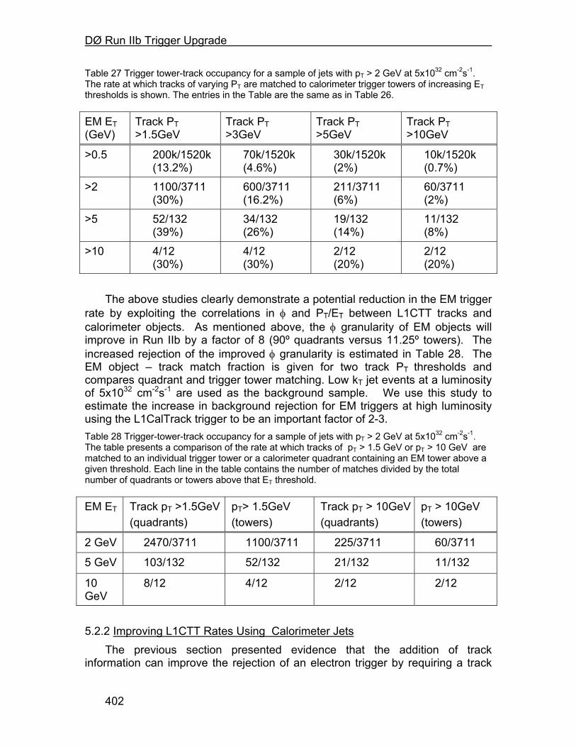
DØ Run IIb Trigger Upgrade
402
Table 27 Trigger tower-track occupancy for a sample of jets with pT > 2 GeV at 5x1032 cm-2s-1. The rate at which tracks of varying PT are matched to calorimeter trigger towers of increasing ET thresholds is shown. The entries in the Table are the same as in Table 26.
EM ET (GeV)
Track PT >1.5GeV
Track PT >3GeV
Track PT >5GeV
Track PT >10GeV
>0.5 200k/1520k (13.2%)
70k/1520k (4.6%)
30k/1520k (2%)
10k/1520k (0.7%)
>2 1100/3711 (30%)
600/3711 (16.2%)
211/3711 (6%)
60/3711 (2%)
>5 52/132 (39%)
34/132 (26%)
19/132 (14%)
11/132 (8%)
>10 4/12 (30%)
4/12 (30%)
2/12 (20%)
2/12 (20%)
The above studies clearly demonstrate a potential reduction in the EM trigger
rate by exploiting the correlations in φ and PT/ET between L1CTT tracks and calorimeter objects. As mentioned above, the φ granularity of EM objects will improve in Run IIb by a factor of 8 (90º quadrants versus 11.25º towers). The increased rejection of the improved φ granularity is estimated in Table 28. The EM object – track match fraction is given for two track PT thresholds and compares quadrant and trigger tower matching. Low kT jet events at a luminosity of 5x1032 cm-2s-1 are used as the background sample. We use this study to estimate the increase in background rejection for EM triggers at high luminosity using the L1CalTrack trigger to be an important factor of 2-3. Table 28 Trigger-tower-track occupancy for a sample of jets with pT > 2 GeV at 5x1032 cm-2s-1. The table presents a comparison of the rate at which tracks of pT > 1.5 GeV or pT > 10 GeV are matched to an individual trigger tower or a calorimeter quadrant containing an EM tower above a given threshold. Each line in the table contains the number of matches divided by the total number of quadrants or towers above that ET threshold.
EM ET Track pT >1.5GeV (quadrants)
pT> 1.5GeV (towers)
Track pT > 10GeV (quadrants)
pT > 10GeV (towers)
2 GeV 2470/3711 1100/3711 225/3711 60/3711
5 GeV 103/132 52/132 21/132 11/132
10 GeV
8/12 4/12 2/12 2/12
5.2.2 Improving L1CTT Rates Using Calorimeter Jets
The previous section presented evidence that the addition of track information can improve the rejection of an electron trigger by requiring a track
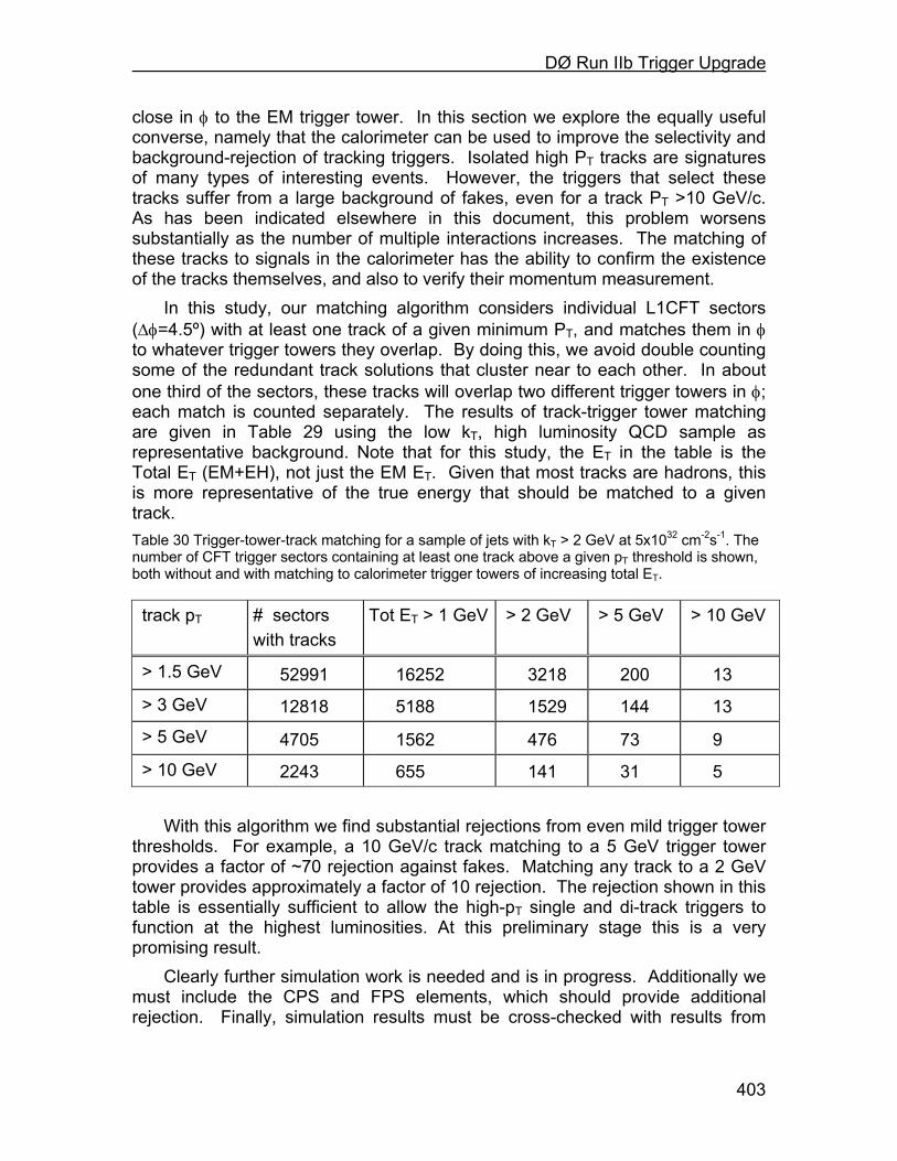
DØ Run IIb Trigger Upgrade
403
close in φ to the EM trigger tower. In this section we explore the equally useful converse, namely that the calorimeter can be used to improve the selectivity and background-rejection of tracking triggers. Isolated high PT tracks are signatures of many types of interesting events. However, the triggers that select these tracks suffer from a large background of fakes, even for a track PT >10 GeV/c. As has been indicated elsewhere in this document, this problem worsens substantially as the number of multiple interactions increases. The matching of these tracks to signals in the calorimeter has the ability to confirm the existence of the tracks themselves, and also to verify their momentum measurement.
In this study, our matching algorithm considers individual L1CFT sectors (∆φ=4.5º) with at least one track of a given minimum PT, and matches them in φ to whatever trigger towers they overlap. By doing this, we avoid double counting some of the redundant track solutions that cluster near to each other. In about one third of the sectors, these tracks will overlap two different trigger towers in φ; each match is counted separately. The results of track-trigger tower matching are given in Table 29 using the low kT, high luminosity QCD sample as representative background. Note that for this study, the ET in the table is the Total ET (EM+EH), not just the EM ET. Given that most tracks are hadrons, this is more representative of the true energy that should be matched to a given track. Table 30 Trigger-tower-track matching for a sample of jets with kT > 2 GeV at 5x1032 cm-2s-1. The number of CFT trigger sectors containing at least one track above a given pT threshold is shown, both without and with matching to calorimeter trigger towers of increasing total ET.
track pT # sectors with tracks
Tot ET > 1 GeV > 2 GeV > 5 GeV > 10 GeV
> 1.5 GeV 52991 16252 3218 200 13
> 3 GeV 12818 5188 1529 144 13
> 5 GeV 4705 1562 476 73 9
> 10 GeV 2243 655 141 31 5 With this algorithm we find substantial rejections from even mild trigger tower
thresholds. For example, a 10 GeV/c track matching to a 5 GeV trigger tower provides a factor of ~70 rejection against fakes. Matching any track to a 2 GeV tower provides approximately a factor of 10 rejection. The rejection shown in this table is essentially sufficient to allow the high-pT single and di-track triggers to function at the highest luminosities. At this preliminary stage this is a very promising result.
Clearly further simulation work is needed and is in progress. Additionally we must include the CPS and FPS elements, which should provide additional rejection. Finally, simulation results must be cross-checked with results from
DØ Run IIb Trigger Upgrade
404
collider data. These latter studies will be carried out in the near future when the L1CTT trigger is operational.
5.3 Implementation
Our working assumption is that the L1CalTrack trigger architecture can be made identical to that of the existing and operational Level 1 Muon (L1Muo) trigger with only small and straightforward modifications. Specifically, we will use minimally modified muon trigger (MTCxx) cards with a new flavor board (MTFB) that performs the calorimeter-track match algorithms. However even the new flavor board will be a straightforward upgrade of the existing flavor board that contains the muon detector-track match algorithms. The L1CalTrack trigger crate manager (MTCM) and trigger manager (MTM) will be duplicates of those used for the L1Muo trigger. Most importantly, the engineering effort on traditionally time-consuming details such as synchronization, buffering, messages to L2 and L3, electronics testing, monitoring, power supplies, and crate infrastructure is then virtually nil. A key (and unresolved) question is whether 16 serial link inputs will suffice for the L1CalTrack trigger. Nevertheless, given all the advantages of using L1Muo trigger hardware and the fact that the L1Muo trigger is being successfully operated, we continue on this path at present. 5.3.1 L1Muo System
A brief description of the L1Muo trigger is given here. This is followed by a few technical details on serial links, synchronization, and buffering. A brief description of how the L1CalTrack trigger uses the L1Muo hardware and possible need modifications.
The L1Muo trigger satisfies the following requirements:
∗ Delivers an L1Muo Trigger decision to the TF at 3.3 µs after Bunch Crossing (BC)
∗ Transmits an L1Muo decision for every BC not occurring in the Synch Gap
∗ Operates with 132 or 396 ns BC times ∗ Synchronizes inputs to each Muon Trigger Card (MTCxx) ∗ Provides buffering for input and output data pending an L1 decision
from the TF ∗ Provides 16 buffers for data pending a Level 2 (L2) decision from the
TF ∗ Provides 8 buffers for data pending readout to Level 3 (L3) ∗ Deadtimeless operation ∗ Field programmable trigger logic ∗ Online and offline monitoring ∗ Complete documentation
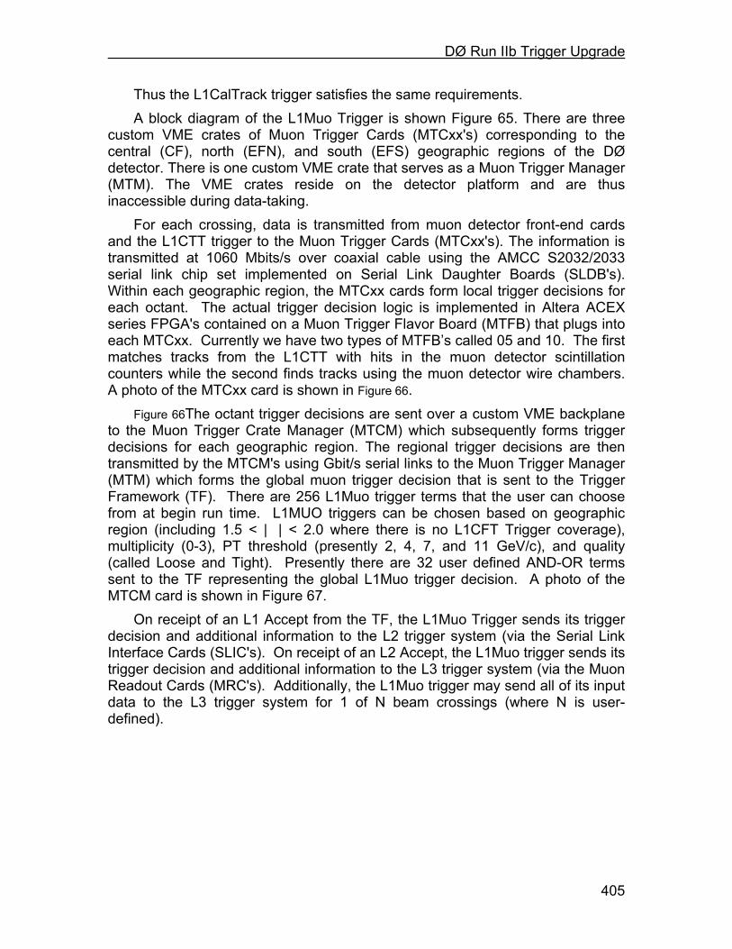
DØ Run IIb Trigger Upgrade
405
Thus the L1CalTrack trigger satisfies the same requirements. A block diagram of the L1Muo Trigger is shown Figure 65. There are three
custom VME crates of Muon Trigger Cards (MTCxx's) corresponding to the central (CF), north (EFN), and south (EFS) geographic regions of the DØ detector. There is one custom VME crate that serves as a Muon Trigger Manager (MTM). The VME crates reside on the detector platform and are thus inaccessible during data-taking.
For each crossing, data is transmitted from muon detector front-end cards and the L1CTT trigger to the Muon Trigger Cards (MTCxx's). The information is transmitted at 1060 Mbits/s over coaxial cable using the AMCC S2032/2033 serial link chip set implemented on Serial Link Daughter Boards (SLDB's). Within each geographic region, the MTCxx cards form local trigger decisions for each octant. The actual trigger decision logic is implemented in Altera ACEX series FPGA's contained on a Muon Trigger Flavor Board (MTFB) that plugs into each MTCxx. Currently we have two types of MTFB’s called 05 and 10. The first matches tracks from the L1CTT with hits in the muon detector scintillation counters while the second finds tracks using the muon detector wire chambers. A photo of the MTCxx card is shown in Figure 66.
Figure 66The octant trigger decisions are sent over a custom VME backplane to the Muon Trigger Crate Manager (MTCM) which subsequently forms trigger decisions for each geographic region. The regional trigger decisions are then transmitted by the MTCM's using Gbit/s serial links to the Muon Trigger Manager (MTM) which forms the global muon trigger decision that is sent to the Trigger Framework (TF). There are 256 L1Muo trigger terms that the user can choose from at begin run time. L1MUO triggers can be chosen based on geographic region (including 1.5 < || < 2.0 where there is no L1CFT Trigger coverage), multiplicity (0-3), PT threshold (presently 2, 4, 7, and 11 GeV/c), and quality (called Loose and Tight). Presently there are 32 user defined AND-OR terms sent to the TF representing the global L1Muo trigger decision. A photo of the MTCM card is shown in Figure 67.
On receipt of an L1 Accept from the TF, the L1Muo Trigger sends its trigger decision and additional information to the L2 trigger system (via the Serial Link Interface Cards (SLIC's). On receipt of an L2 Accept, the L1Muo trigger sends its trigger decision and additional information to the L3 trigger system (via the Muon Readout Cards (MRC's). Additionally, the L1Muo trigger may send all of its input data to the L3 trigger system for 1 of N beam crossings (where N is user-defined).
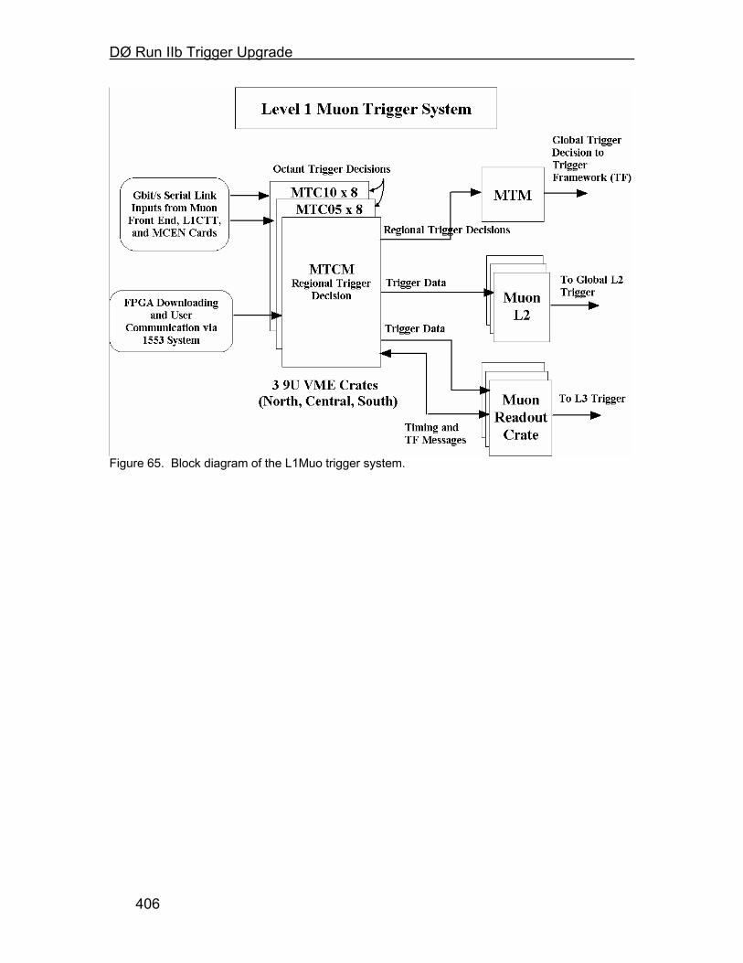
DØ Run IIb Trigger Upgrade
406
Figure 65. Block diagram of the L1Muo trigger system.
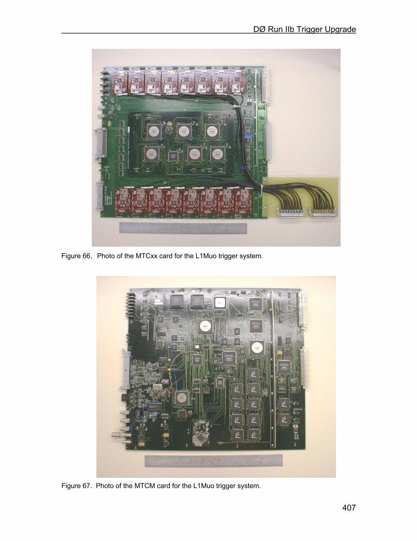
DØ Run IIb Trigger Upgrade
407
Figure 66. Photo of the MTCxx card for the L1Muo trigger system.
Figure 67. Photo of the MTCM card for the L1Muo trigger system.
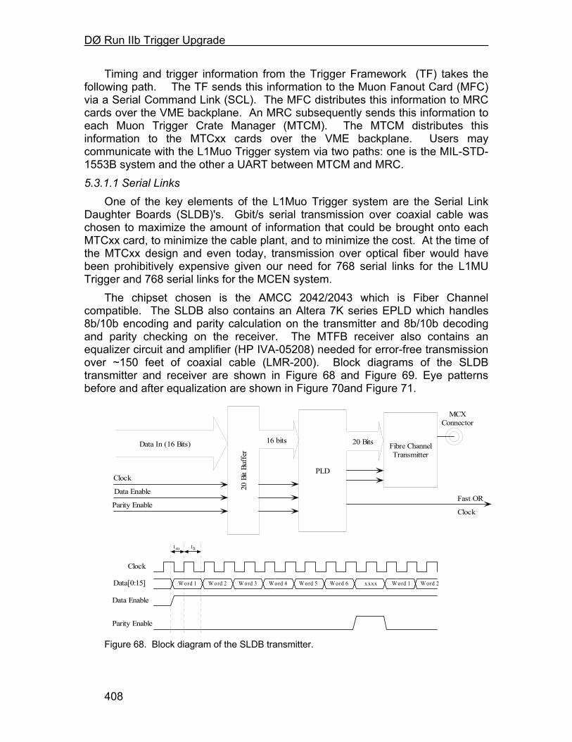
DØ Run IIb Trigger Upgrade
408
Timing and trigger information from the Trigger Framework (TF) takes the following path. The TF sends this information to the Muon Fanout Card (MFC) via a Serial Command Link (SCL). The MFC distributes this information to MRC cards over the VME backplane. An MRC subsequently sends this information to each Muon Trigger Crate Manager (MTCM). The MTCM distributes this information to the MTCxx cards over the VME backplane. Users may communicate with the L1Muo Trigger system via two paths: one is the MIL-STD-1553B system and the other a UART between MTCM and MRC. 5.3.1.1 Serial Links
One of the key elements of the L1Muo Trigger system are the Serial Link Daughter Boards (SLDB)'s. Gbit/s serial transmission over coaxial cable was chosen to maximize the amount of information that could be brought onto each MTCxx card, to minimize the cable plant, and to minimize the cost. At the time of the MTCxx design and even today, transmission over optical fiber would have been prohibitively expensive given our need for 768 serial links for the L1MU Trigger and 768 serial links for the MCEN system.
The chipset chosen is the AMCC 2042/2043 which is Fiber Channel compatible. The SLDB also contains an Altera 7K series EPLD which handles 8b/10b encoding and parity calculation on the transmitter and 8b/10b decoding and parity checking on the receiver. The MTFB receiver also contains an equalizer circuit and amplifier (HP IVA-05208) needed for error-free transmission over ~150 feet of coaxial cable (LMR-200). Block diagrams of the SLDB transmitter and receiver are shown in Figure 68 and Figure 69. Eye patterns before and after equalization are shown in Figure 70and Figure 71.
Figure 68. Block diagram of the SLDB transmitter.
Data In (16 Bits)
20 B
it Bu
ffer
Clock
Data Enable
Parity Enable
PLD
Fibre ChannelTransmitter
16 bits 20 Bits
Fast OR
Clock
MCXConnector
Clock
W ord 1 W ord 2 W ord 3 W ord 4 W ord 5 W ord 6 W ord 1 W ord 2xxxxData[0:15]
Data Enable
Parity Enable
t su t h
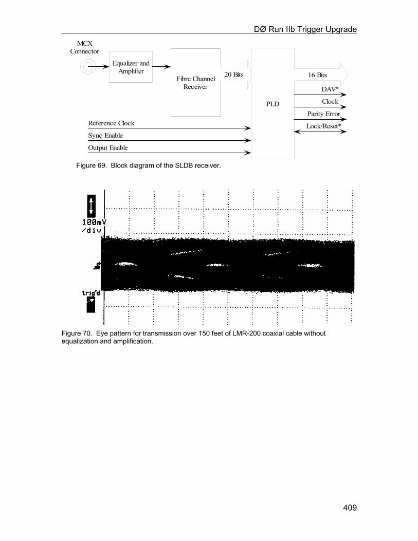
DØ Run IIb Trigger Upgrade
409
Figure 69. Block diagram of the SLDB receiver.
Figure 70. Eye pattern for transmission over 150 feet of LMR-200 coaxial cable without equalization and amplification.
Fibre ChannelReceiver
MCXConnector
PLD
Equalizer andAmplifier 20 Bits 16 Bits
Reference Clock
Sync Enable
Output Enable
DAV*
Clock
Parity Error
Lock/Reset*
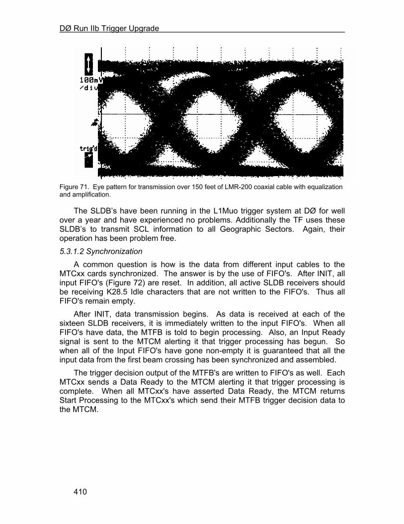
DØ Run IIb Trigger Upgrade
410
Figure 71. Eye pattern for transmission over 150 feet of LMR-200 coaxial cable with equalization and amplification.
The SLDB’s have been running in the L1Muo trigger system at DØ for well over a year and have experienced no problems. Additionally the TF uses these SLDB’s to transmit SCL information to all Geographic Sectors. Again, their operation has been problem free. 5.3.1.2 Synchronization
A common question is how is the data from different input cables to the MTCxx cards synchronized. The answer is by the use of FIFO's. After INIT, all input FIFO's (Figure 72) are reset. In addition, all active SLDB receivers should be receiving K28.5 Idle characters that are not written to the FIFO's. Thus all FIFO's remain empty.
After INIT, data transmission begins. As data is received at each of the sixteen SLDB receivers, it is immediately written to the input FIFO's. When all FIFO's have data, the MTFB is told to begin processing. Also, an Input Ready signal is sent to the MTCM alerting it that trigger processing has begun. So when all of the Input FIFO's have gone non-empty it is guaranteed that all the input data from the first beam crossing has been synchronized and assembled.
The trigger decision output of the MTFB's are written to FIFO's as well. Each MTCxx sends a Data Ready to the MTCM alerting it that trigger processing is complete. When all MTCxx's have asserted Data Ready, the MTCM returns Start Processing to the MTCxx's which send their MTFB trigger decision data to the MTCM.
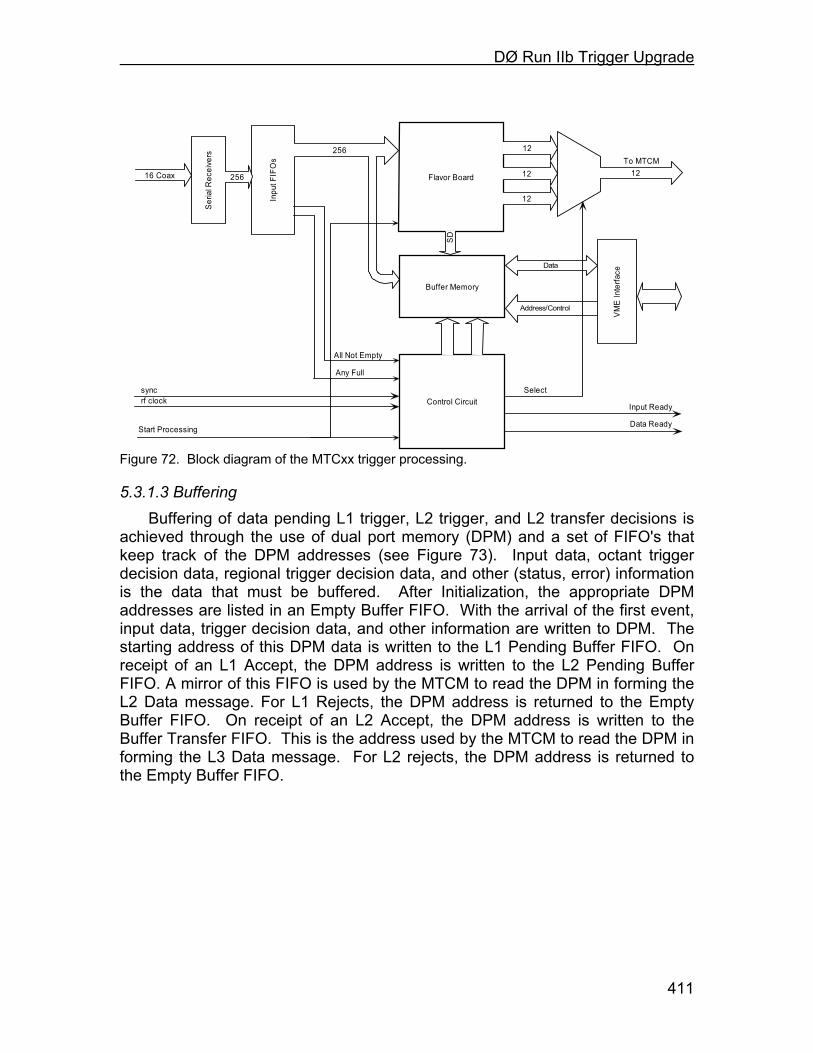
DØ Run IIb Trigger Upgrade
411
Figure 72. Block diagram of the MTCxx trigger processing.
5.3.1.3 Buffering Buffering of data pending L1 trigger, L2 trigger, and L2 transfer decisions is
achieved through the use of dual port memory (DPM) and a set of FIFO's that keep track of the DPM addresses (see Figure 73). Input data, octant trigger decision data, regional trigger decision data, and other (status, error) information is the data that must be buffered. After Initialization, the appropriate DPM addresses are listed in an Empty Buffer FIFO. With the arrival of the first event, input data, trigger decision data, and other information are written to DPM. The starting address of this DPM data is written to the L1 Pending Buffer FIFO. On receipt of an L1 Accept, the DPM address is written to the L2 Pending Buffer FIFO. A mirror of this FIFO is used by the MTCM to read the DPM in forming the L2 Data message. For L1 Rejects, the DPM address is returned to the Empty Buffer FIFO. On receipt of an L2 Accept, the DPM address is written to the Buffer Transfer FIFO. This is the address used by the MTCM to read the DPM in forming the L3 Data message. For L2 rejects, the DPM address is returned to the Empty Buffer FIFO.
Address/Control
Data
Control Circuit
Flavor Board
Buffer Memory
Any Full
To MTCM
syncrf clock
Input Ready
Data Ready
Inpu
tFIF
Os
256
Seria
l Rec
eive
rs
Start Processing
All Not Empty
12
12
12
SD
VME
Inte
rface
Select
1216 Coax 256
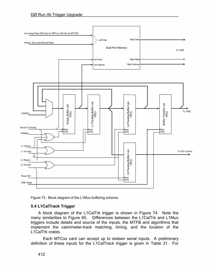
DØ Run IIb Trigger Upgrade
412
Figure 73. Block diagram of the L1Muo buffering scheme.
5.4 L1CalTrack Trigger A block diagram of the L1CalTrk trigger is shown in Figure 74. Note the
many similarities to Figure 65. Differences between the L1CalTrk and L1Muo triggers include details and source of the inputs, the MTFB and algorithms that implement the calorimeter-track matching, timing, and the location of the L1CalTrk crates.
Each MTCxx card can accept up to sixteen serial inputs. A preliminary definition of these inputs for the L1CalTrack trigger is given in Table 31. For
Dual Port Memory
Empt
y Bu
ffer L
ist
FIFO
ReadWrite
To VME
Bunch Crossing
L1 Reject
L1 Accept
Read SD
To SD Control
VME Read
L1 P
endi
ng B
uffe
r Lis
tFI
FO
ReadWrite
L2 P
endi
ng B
uffe
r Lis
tFI
FOReadWrite
Buffe
r Tra
nsfe
r Lis
tFI
FO
ReadWrite
L2 P
endi
ng B
uffe
r Lis
tFI
FO
ReadWrite
L2 Reject
L2 Accept
Left Address
Left Write
Incoming Data (256 bits for MTCxx, 96 bits for MTCM)
Status, Error and Result DataLeft Data Right Data
Right Read
Right Address
To VME
Initialize
Initialize
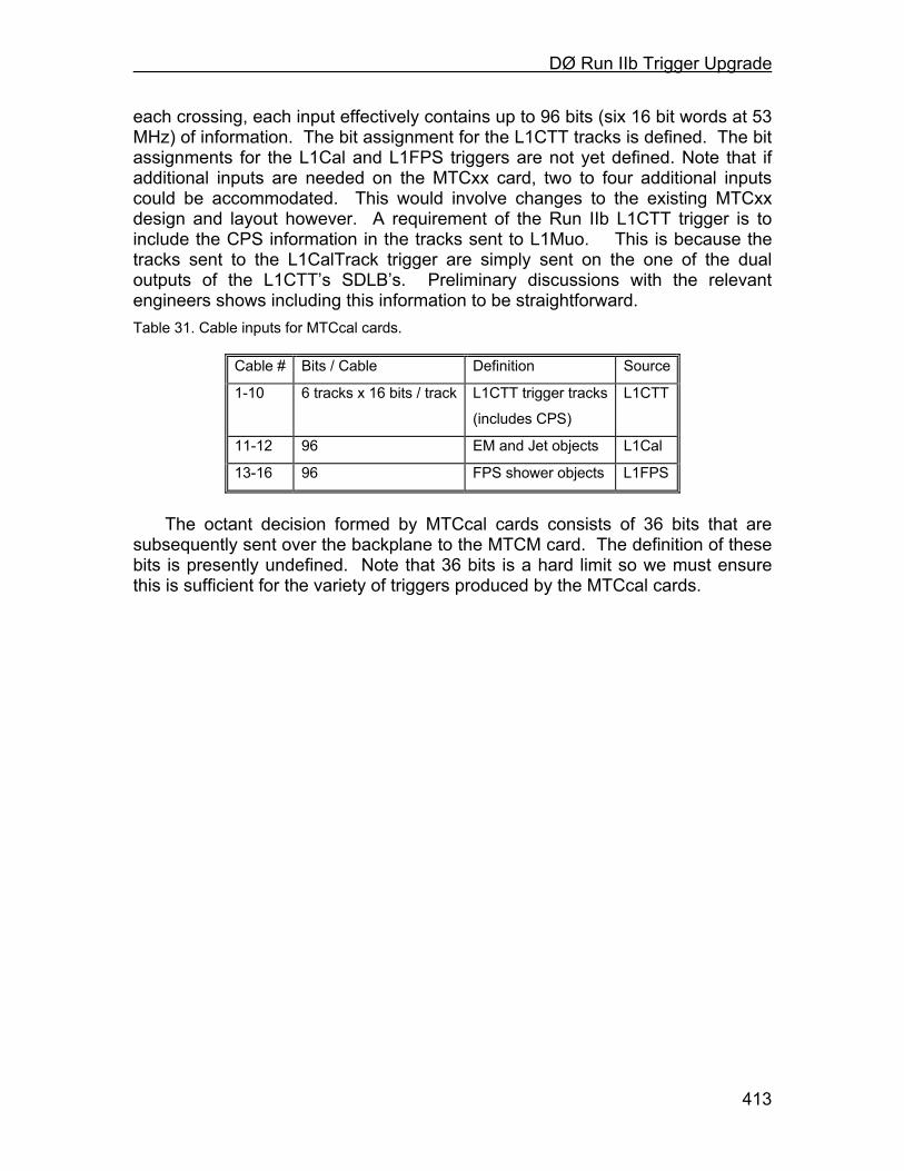
DØ Run IIb Trigger Upgrade
413
each crossing, each input effectively contains up to 96 bits (six 16 bit words at 53 MHz) of information. The bit assignment for the L1CTT tracks is defined. The bit assignments for the L1Cal and L1FPS triggers are not yet defined. Note that if additional inputs are needed on the MTCxx card, two to four additional inputs could be accommodated. This would involve changes to the existing MTCxx design and layout however. A requirement of the Run IIb L1CTT trigger is to include the CPS information in the tracks sent to L1Muo. This is because the tracks sent to the L1CalTrack trigger are simply sent on the one of the dual outputs of the L1CTT’s SDLB’s. Preliminary discussions with the relevant engineers shows including this information to be straightforward. Table 31. Cable inputs for MTCcal cards.
Cable # Bits / Cable Definition Source
1-10 6 tracks x 16 bits / track L1CTT trigger tracks
(includes CPS)
L1CTT
11-12 96 EM and Jet objects L1Cal
13-16 96 FPS shower objects L1FPS
The octant decision formed by MTCcal cards consists of 36 bits that are
subsequently sent over the backplane to the MTCM card. The definition of these bits is presently undefined. Note that 36 bits is a hard limit so we must ensure this is sufficient for the variety of triggers produced by the MTCcal cards.
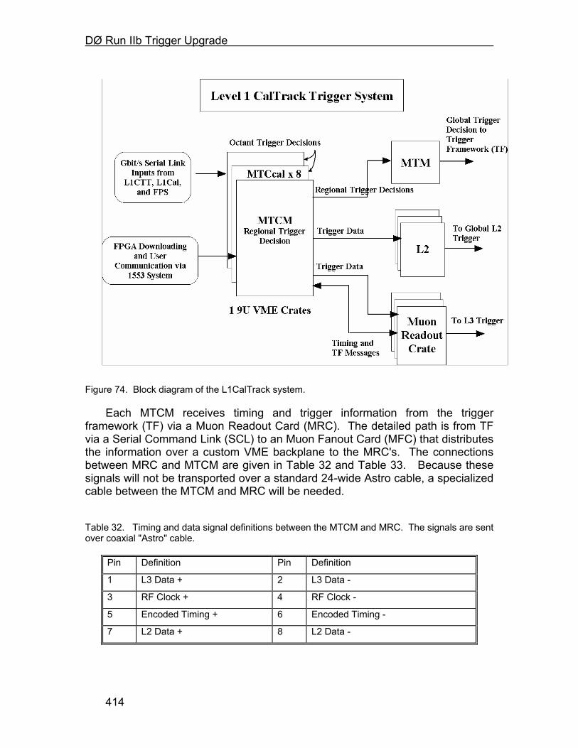
DØ Run IIb Trigger Upgrade
414
Figure 74. Block diagram of the L1CalTrack system.
Each MTCM receives timing and trigger information from the trigger framework (TF) via a Muon Readout Card (MRC). The detailed path is from TF via a Serial Command Link (SCL) to an Muon Fanout Card (MFC) that distributes the information over a custom VME backplane to the MRC's. The connections between MRC and MTCM are given in Table 32 and Table 33. Because these signals will not be transported over a standard 24-wide Astro cable, a specialized cable between the MTCM and MRC will be needed.
Table 32. Timing and data signal definitions between the MTCM and MRC. The signals are sent over coaxial "Astro" cable.
Pin Definition Pin Definition
1 L3 Data + 2 L3 Data -
3 RF Clock + 4 RF Clock -
5 Encoded Timing + 6 Encoded Timing -
7 L2 Data + 8 L2 Data -
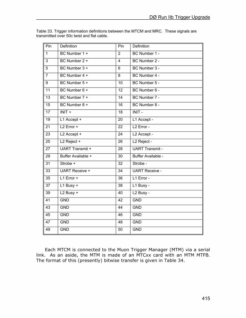
DØ Run IIb Trigger Upgrade
415
Table 33. Trigger information definitions between the MTCM and MRC. These signals are transmitted over 50c twist and flat cable.
Pin Definition Pin Definition
1 BC Number 1 + 2 BC Number 1 -
3 BC Number 2 + 4 BC Number 2 -
5 BC Number 3 + 6 BC Number 3 -
7 BC Number 4 + 8 BC Number 4 -
9 BC Number 5 + 10 BC Number 5 -
11 BC Number 6 + 12 BC Number 6 -
13 BC Number 7 + 14 BC Number 7 -
15 BC Number 8 + 16 BC Number 8 -
17 INIT + 18 INIT -
19 L1 Accept + 20 L1 Accept -
21 L2 Error + 22 L2 Error -
23 L2 Accept + 24 L2 Accept -
25 L2 Reject + 26 L2 Reject -
27 UART Transmit + 28 UART Transmit -
29 Buffer Available + 30 Buffer Available -
31 Strobe + 32 Strobe -
33 UART Receive + 34 UART Receive -
35 L1 Error + 36 L1 Error -
37 L1 Busy + 38 L1 Busy -
39 L2 Busy + 40 L2 Busy -
41 GND 42 GND
43 GND 44 GND
45 GND 46 GND
47 GND 48 GND
49 GND 50 GND
Each MTCM is connected to the Muon Trigger Manager (MTM) via a serial link. As an aside, the MTM is made of an MTCxx card with an MTM MTFB. The format of this (presently) bitwise transfer is given in Table 34.
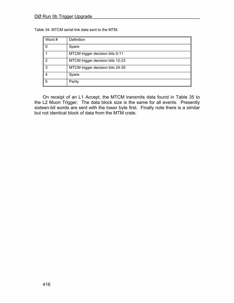
DØ Run IIb Trigger Upgrade
416
Table 34. MTCM serial link data sent to the MTM.
Word # Definition
0 Spare
1 MTCM trigger decision bits 0-11
2 MTCM trigger decision bits 12-23
3 MTCM trigger decision bits 24-35
4 Spare
5 Parity
On receipt of an L1 Accept, the MTCM transmits data found in Table 35 to
the L2 Muon Trigger. The data block size is the same for all events. Presently sixteen-bit words are sent with the lower byte first. Finally note there is a similar but not identical block of data from the MTM crate.
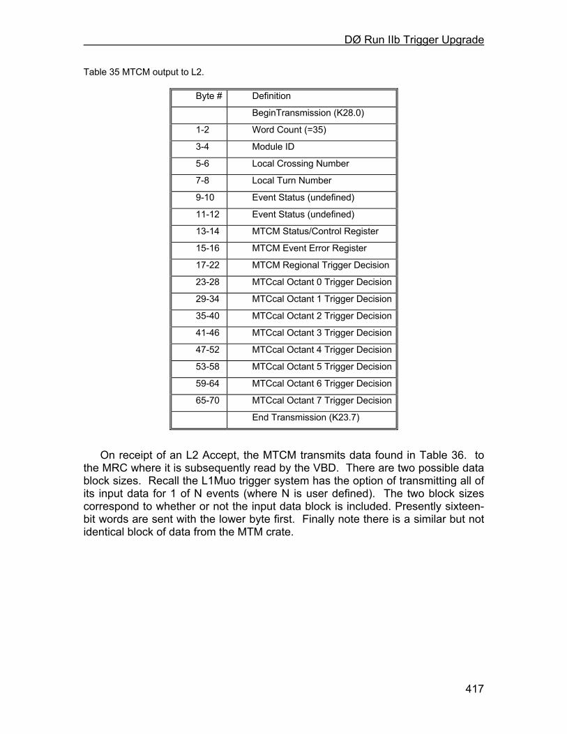
DØ Run IIb Trigger Upgrade
417
Table 35 MTCM output to L2.
Byte # Definition
BeginTransmission (K28.0)
1-2 Word Count (=35)
3-4 Module ID
5-6 Local Crossing Number
7-8 Local Turn Number
9-10 Event Status (undefined)
11-12 Event Status (undefined)
13-14 MTCM Status/Control Register
15-16 MTCM Event Error Register
17-22 MTCM Regional Trigger Decision
23-28 MTCcal Octant 0 Trigger Decision
29-34 MTCcal Octant 1 Trigger Decision
35-40 MTCcal Octant 2 Trigger Decision
41-46 MTCcal Octant 3 Trigger Decision
47-52 MTCcal Octant 4 Trigger Decision
53-58 MTCcal Octant 5 Trigger Decision
59-64 MTCcal Octant 6 Trigger Decision
65-70 MTCcal Octant 7 Trigger Decision
End Transmission (K23.7)
On receipt of an L2 Accept, the MTCM transmits data found in Table 36. to
the MRC where it is subsequently read by the VBD. There are two possible data block sizes. Recall the L1Muo trigger system has the option of transmitting all of its input data for 1 of N events (where N is user defined). The two block sizes correspond to whether or not the input data block is included. Presently sixteen-bit words are sent with the lower byte first. Finally note there is a similar but not identical block of data from the MTM crate.

DØ Run IIb Trigger Upgrade
418
Table 36. MTCM output sent to L3.
Word # Definition
BeginTransmission (K28.0)
Upper 16 bits of VBD Word Count = 0
VBD Word Count = 246 or 1142 decimal
1 Word Count = 492 or 2284 decimal
2 Module ID
3 Local Crossing Number
4 Local Turn Number
5 Event Status = MTCM Event Error Register from DPM
6 Event Status (undefined)
7 MTCM Control Register
8 MTCM Event Error Register from DPM
9 MTCM Latched Error Register
10 MTCM Trigger Logic FPGA Program ID
11 MTCM Message Builder FPGA Program ID
12 MTCM L1_Accept Divider Number
13 MTCM L2_Accept Divider Number
14 MTCM MTCxx Readout Mask
15 MTCM MTCxx Trigger Mask
16 MTCM L1 Error Mask
17-19 MTCM Regional Trigger Decision
20 MTCxx #0 MTCxx Serial Number
21 MTCxx #0 Flavor Board Type/Serial Number
22 MTCxx #0 MTCxx Status Register
23 MTCxx #0 MTCxx Flash Memory Status
24-34 MTCxx #0 Various Error Registers (82,86,8a,8e,92,94, pad rest with zeros)
35-38 MTCxx #0 Various Mask Registers (06,08,0a,0c)
39-46 MTCxx #0 FPGA Program ID's (total of 8)
47-73 MTCxx #1 Info Block
74-100 MTCxx #2 Info Block
101-127 MTCxx #3 Info Block
128-154 MTCxx #4 Info Block
155-181 MTCxx #5 Info Block
182-208 MTCxx #6 Info Block

DØ Run IIb Trigger Upgrade
419
209-235 MTCxx #7 Info Block
MTCcal Octant 0 Trigger Decision
MTCcal Octant 1 Trigger Decision
MTCcal Octant 2 Trigger Decision
MTCcal Octant 3 Trigger Decision
MTCcal Octant 4 Trigger Decision
MTCcal Octant 5 Trigger Decision
MTCcal Octant 6 Trigger Decision
MTCcal Octant 7 Trigger Decision
MTCxx Input Data
End Transmission (K23.7)
Finally, the MTM MTFB (which is used in concert with an MTCxx mothercard)
takes the regional trigger decision data from the three MTCM cards and forms a variety of global trigger decisions. The specific triggers sent to the Trigger Framework are downloaded during the physics trigger download of a data acquisition run. The data sent to the Trigger Framework from the MTM MTFB is given in Table 37.
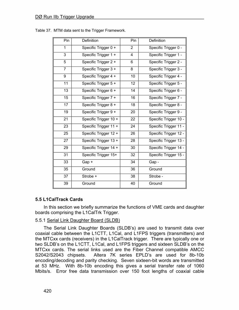
DØ Run IIb Trigger Upgrade
420
Table 37. MTM data sent to the Trigger Framework.
Pin Definition Pin Definition
1 Specific Trigger 0 + 2 Specific Trigger 0 -
3 Specific Trigger 1 + 4 Specific Trigger 1 -
5 Specific Trigger 2 + 6 Specific Trigger 2 -
7 Specific Trigger 3 + 8 Specific Trigger 3 -
9 Specific Trigger 4 + 10 Specific Trigger 4 -
11 Specific Trigger 5 + 12 Specific Trigger 5 -
13 Specific Trigger 6 + 14 Specific Trigger 6 -
15 Specific Trigger 7 + 16 Specific Trigger 7 -
17 Specific Trigger 8 + 18 Specific Trigger 8 -
19 Specific Trigger 9 + 20 Specific Trigger 9 -
21 Specific Trigger 10 + 22 Specific Trigger 10 -
23 Specific Trigger 11 + 24 Specific Trigger 11 -
25 Specific Trigger 12 + 26 Specific Trigger 12 -
27 Specific Trigger 13 + 28 Specific Trigger 13 -
29 Specific Trigger 14 + 30 Specific Trigger 14 -
31 Specific Trigger 15+ 32 Specific Trigger 15 -
33 Gap + 34 Gap -
35 Ground 36 Ground
37 Strobe + 38 Strobe -
39 Ground 40 Ground
5.5 L1CalTrack Cards
In this section we briefly summarize the functions of VME cards and daughter boards comprising the L1CalTrk Trigger. 5.5.1 Serial Link Daughter Board (SLDB)
The Serial Link Daughter Boards (SLDB’s) are used to transmit data over coaxial cable between the L1CTT, L1Cal, and L1FPS triggers (transmitters) and the MTCxx cards (receivers) in the L1CalTrack trigger. There are typically one or two SLDB’s on the L1CTT, L1Cal, and L1FPS triggers and sixteen SLDB’s on the MTCxx cards. The serial links used are the Fiber Channel compatible AMCC S2042/S2043 chipsets. Altera 7K series EPLD’s are used for 8b-10b encoding/decoding and parity checking. Seven sixteen-bit words are transmitted at 53 MHz. With 8b-10b encoding this gives a serial transfer rate of 1060 Mbits/s. Error free data transmission over 150 foot lengths of coaxial cable

DØ Run IIb Trigger Upgrade
421
(LMR-200) is achieved by using an equalization circuit and high-speed amplifier (HP IVA-05208) on the SLDB receiver boards. 5.5.2 Muon Trigger Card (MTCxx)
The Muon Trigger Cards (MTCxx cards) are the primary trigger cards in the L1CalTrack system. The MTCxx card is a generic VME card that accepts a Muon Trigger Flavor Board (MTFB) as a daughter card. The actual calorimeter-track match trigger logic is implemented on the MTFB. The MTCxx/MTFB combination is used form an octant trigger decision. The MTCxx card also contains sixteen SLDB receivers that are used to accept data from the various input sources. The primary functions of the MTCxx cards are to receive and synchronize sixteen serial inputs, to buffer input data (which is subsequently sent to the MTFB) and to buffer input and supplemental trigger decision data pending L1, L2 and L3 accepts.
5.5.3 Muon Trigger Flavor Board (MTFB) The Muon Trigger Flavor Board (MTFB) is a daughterboard that is used in
concert with the MTCxx card. For the L1CalTrack trigger a new flavor board will be used called MTCcal. This flavor board will contain the calorimeter-track match trigger logic. Note that the present MTC05 MTFB matches tracks from the L1CTT with hits in the muon detector scintillation counters and hence can be used as a good estimate for the calorimeter-track logic. The MTCcal MTFB will match tracks from the L1CTT with EM and jet objects from L1Cal. While we must simulate all calorimeter-track match algorithms in both the C++ trigger simulator and MAXPLUS2 FPGA simulator before a final choice of FPGA family is made, preliminary studies show that the four FPGA’s on the present MTC05 MTFB can be replaced with one larger FPGA. In addition, the MTCcal MTFB will contain a Gbit/s serial link. This will allow the MTCM to be bypassed in forming the trigger decision that is sent to the Trigger Framework. 5.5.4 Muon Trigger Crate Manager (MTCM)
The Muon Trigger Crate Manager (MTCM) reads the octant trigger decisions from each MTCxx card and uses this data to form a regional trigger decision that is subsequently sent to the Muon Trigger Manager (MTM). The MTCM also serves to buffer the octant trigger decision data from each MTCxx card and the regional trigger decision pending L2 and L3 accepts. L2 data and L3 data are sent to their respective systems using the Cypress Hotlink (CY7B923/CY7B933) chipset. The MTCM accepts timing and trigger information from the Trigger Framework (TF) and reports error and busy conditions to the TF also via the MRC. The MTCM maintains two paths by which a user can communicate to the L1MU system: 1553 and UART. The UART path is a link between the MTCM and MRC. Either path can be used for downloading, monitoring, and testing. 5.5.5 Muon Splitter Cards (MSPLIT)
The MSPLIT cards are used as fanouts for many of the Gbit/s serial input signals to the MTCxx cards. They are mentioned here because the location of the L1CalTrack crates is now in MCH1 rather than collision hall. This means we
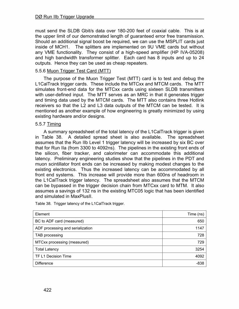
DØ Run IIb Trigger Upgrade
422
must send the SLDB Gbit/s data over 180-200 feet of coaxial cable. This is at the upper limit of our demonstrated length of guaranteed error free transmission. Should an additional signal boost be required, we can use the MSPLIT cards just inside of MCH1. The splitters are implemented on 9U VME cards but without any VME functionality. They consist of a high-speed amplifier (HP IVA-05208) and high bandwidth transformer splitter. Each card has 8 inputs and up to 24 outputs. Hence they can be used as cheap repeaters. 5.5.6 Muon Trigger Test Card (MTT)
The purpose of the Muon Trigger Test (MTT) card is to test and debug the L1CalTrack trigger cards. These include the MTCxx and MTCM cards. The MTT simulates front-end data for the MTCxx cards using sixteen SLDB transmitters with user-defined input. The MTT serves as an MRC in that it generates trigger and timing data used by the MTCM cards. The MTT also contains three Hotlink receivers so that the L2 and L3 data outputs of the MTCM can be tested. It is mentioned as another example of how engineering is greatly minimized by using existing hardware and/or designs. 5.5.7 Timing
A summary spreadsheet of the total latency of the L1CalTrack trigger is given in Table 38. A detailed spread sheet is also available. The spreadsheet assumes that the Run IIb Level 1 trigger latency will be increased by six BC over that for Run IIa (from 3300 to 4092ns). The pipelines in the existing front ends of the silicon, fiber tracker, and calorimeter can accommodate this additional latency. Preliminary engineering studies show that the pipelines in the PDT and muon scintillator front ends can be increased by making modest changes to the existing electronics. Thus the increased latency can be accommodated by all front end systems. This increase will provide more than 600ns of headroom in the L1CalTrack trigger latency. The spreadsheet also assumes that the MTCM can be bypassed in the trigger decision chain from MTCxx card to MTM. It also assumes a savings of 132 ns in the existing MTC05 logic that has been identified and simulated in MaxPlusII. Table 38. Trigger latency of the L1CalTrack trigger.
Element Time (ns)
BC to ADF card (measured) 650
ADF processing and serialization 1147
TAB processing 728
MTCxx processing (measured) 729
Total Latency 3254
TF L1 Decision Time 4092
Difference -838
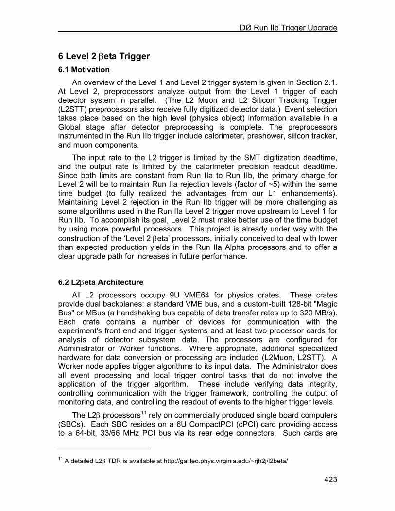
DØ Run IIb Trigger Upgrade
423
6 Level 2 βeta Trigger 6.1 Motivation
An overview of the Level 1 and Level 2 trigger system is given in Section 2.1. At Level 2, preprocessors analyze output from the Level 1 trigger of each detector system in parallel. (The L2 Muon and L2 Silicon Tracking Trigger (L2STT) preprocessors also receive fully digitized detector data.) Event selection takes place based on the high level (physics object) information available in a Global stage after detector preprocessing is complete. The preprocessors instrumented in the Run IIb trigger include calorimeter, preshower, silicon tracker, and muon components.
The input rate to the L2 trigger is limited by the SMT digitization deadtime, and the output rate is limited by the calorimeter precision readout deadtime. Since both limits are constant from Run IIa to Run IIb, the primary charge for Level 2 will be to maintain Run IIa rejection levels (factor of ~5) within the same time budget (to fully realized the advantages from our L1 enhancements). Maintaining Level 2 rejection in the Run IIb trigger will be more challenging as some algorithms used in the Run IIa Level 2 trigger move upstream to Level 1 for Run IIb. To accomplish its goal, Level 2 must make better use of the time budget by using more powerful processors. This project is already under way with the construction of the ‘Level 2 βeta’ processors, initially conceived to deal with lower than expected production yields in the Run IIa Alpha processors and to offer a clear upgrade path for increases in future performance.
6.2 L2βeta Architecture All L2 processors occupy 9U VME64 for physics crates. These crates
provide dual backplanes: a standard VME bus, and a custom-built 128-bit "Magic Bus" or MBus (a handshaking bus capable of data transfer rates up to 320 MB/s). Each crate contains a number of devices for communication with the experiment's front end and trigger systems and at least two processor cards for analysis of detector subsystem data. The processors are configured for Administrator or Worker functions. Where appropriate, additional specialized hardware for data conversion or processing are included (L2Muon, L2STT). A Worker node applies trigger algorithms to its input data. The Administrator does all event processing and local trigger control tasks that do not involve the application of the trigger algorithm. These include verifying data integrity, controlling communication with the trigger framework, controlling the output of monitoring data, and controlling the readout of events to the higher trigger levels.
The L2β processors11 rely on commercially produced single board computers (SBCs). Each SBC resides on a 6U CompactPCI (cPCI) card providing access to a 64-bit, 33/66 MHz PCI bus via its rear edge connectors. Such cards are
11 A detailed L2β TDR is available at http://galileo.phys.virginia.edu/~rjh2j/l2beta/
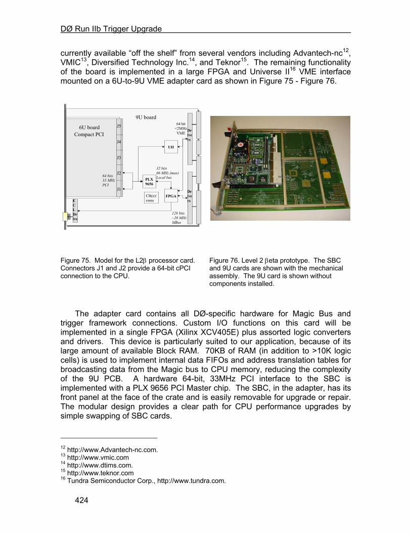
DØ Run IIb Trigger Upgrade
424
currently available “off the shelf” from several vendors including Advantech-nc12, VMIC13, Diversified Technology Inc.14, and Teknor15. The remaining functionality of the board is implemented in a large FPGA and Universe II16 VME interface mounted on a 6U-to-9U VME adapter card as shown in Figure 75 - Figure 76.
6U boardCompact PCI
9U board64 bit
<2MHzVME
FPGAECLDrive
128 bits~20 MHzMBus
32 bits66 MHz (max)Local bus64 bits
33 MHzPCI
J1
J2
J3
J5
J4
PLX9656
UII
Drivers
Drivers
Clk(s)/roms
Figure 75. Model for the L2β processor card. Connectors J1 and J2 provide a 64-bit cPCI connection to the CPU.
Figure 76. Level 2 βeta prototype. The SBC and 9U cards are shown with the mechanical assembly. The 9U card is shown without components installed.
The adapter card contains all DØ-specific hardware for Magic Bus and
trigger framework connections. Custom I/O functions on this card will be implemented in a single FPGA (Xilinx XCV405E) plus assorted logic converters and drivers. This device is particularly suited to our application, because of its large amount of available Block RAM. 70KB of RAM (in addition to >10K logic cells) is used to implement internal data FIFOs and address translation tables for broadcasting data from the Magic bus to CPU memory, reducing the complexity of the 9U PCB. A hardware 64-bit, 33MHz PCI interface to the SBC is implemented with a PLX 9656 PCI Master chip. The SBC, in the adapter, has its front panel at the face of the crate and is easily removable for upgrade or repair. The modular design provides a clear path for CPU performance upgrades by simple swapping of SBC cards.
12 http://www.Advantech-nc.com. 13 http://www.vmic.com 14 http://www.dtims.com. 15 http://www.teknor.com 16 Tundra Semiconductor Corp., http://www.tundra.com.
DØ Run IIb Trigger Upgrade
425
Given comparable I/O capabilities, the amount of time required to run complex algorithms should be inversely proportional to the processor speed; more complicated algorithms can be used to process the available data if the processors are faster. However, an increase of processing power is more useful when supplied in the form of a single processor than in the form of a second identical processor working in parallel. This is because load balancing among multiple nodes is difficult in the Level 2 system due to constraints imposed by the front-end digitization. The front-end digitization holds buffers for 16 events awaiting Level 2 trigger decisions. A critical restriction in the system is that L2 results (accept or reject) must be reported to the front-end buffers in the order in which the triggers were taken at L1. While one processor works on an event with a long processing time, other events will arrive and fill the 16 front-end buffers. Other processors working on these events will go idle if they finish processing them quickly, since they cannot receive new events until the pending decision on the oldest event is taken. In other words a farm model is not appropriate for processing events at Level 2. Faster processing for each event in turn is thus more desirable than adding additional processors, once a baseline level of parallelism is established.
The quality of the Run IIb physics program will depend in large measure on effective rejection of background events in this more demanding environment. The Level 2 βeta upgrade will provide more resources needed to keep Level 2 in step with these demands and to further improve on background rejection from an upgraded Level 1. A subset of the most heavily-loaded processors should be replaced with higher-performance processors. Assuming that processors in the format used by the L2βetas increase performance by Moore's law, a purchase near the start of Run IIb could gain another factor of 4 in processing power over the first L2βeta processors. 6.3 Run IIb Algorithm Changes
We have begun to consider Run IIb algorithms that would profit from additional CPU power. Several performance enhancements are summarized in this section.
With longitudinal sectors on the order of 10cm vertex resolution of order ~few cm should be possible at L2 with the tracks output by the Level 2 Silicon Track Trigger (L2STT). At present all calorimeter tower information is reported to L2 relative to a vertex position of 0cm (centered with respect to the detector). The applications of vertex information at L2 are several.
To first order fast processors will supply resources to correct calorimetric information for vertex positions and significantly enhance resolutions at Level~2 for jets (including taus), electro-magnetic objects, and Missing ET. Improved resolutions allow higher trigger thresholds for a given signal efficiency. For example, in the case of single jet triggers of moderate transverse energy, if 10cm vertex resolution is available, trigger rates may be improved by as much as 30-
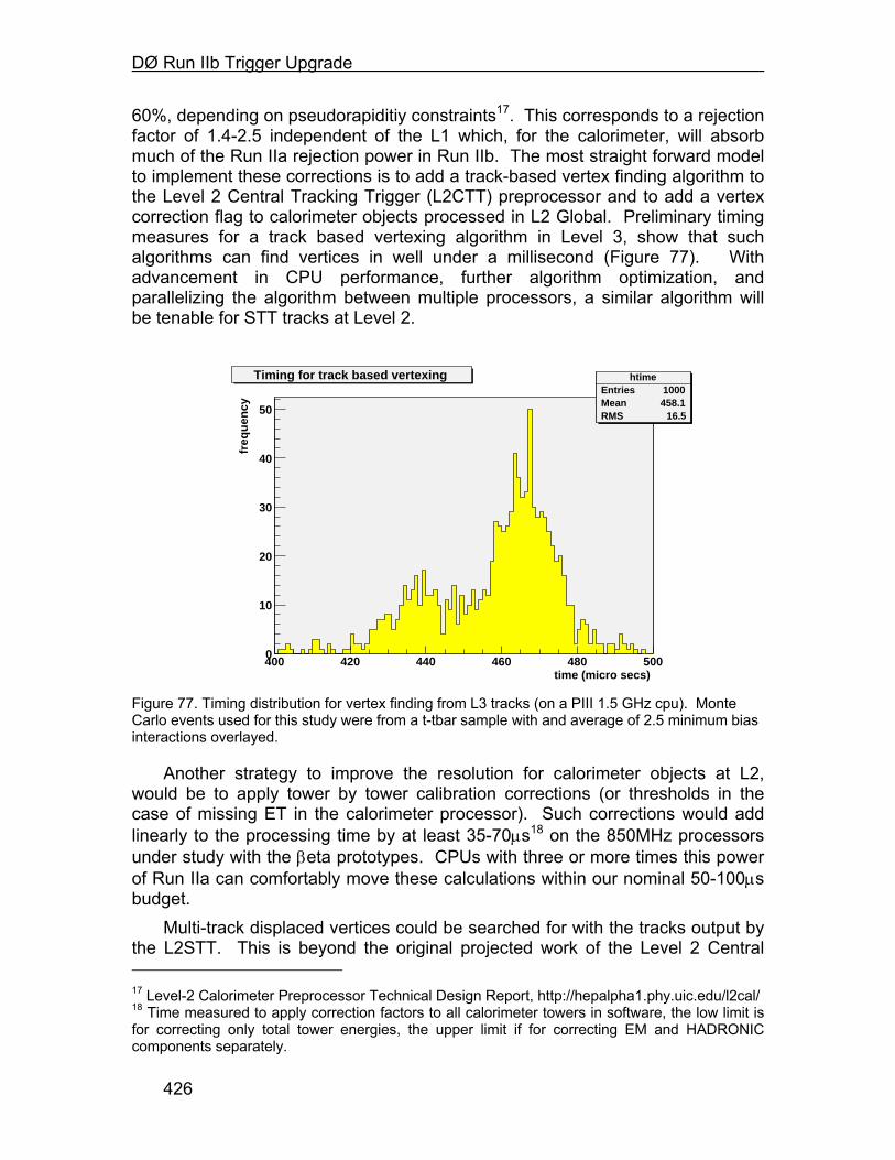
DØ Run IIb Trigger Upgrade
426
60%, depending on pseudorapiditiy constraints17. This corresponds to a rejection factor of 1.4-2.5 independent of the L1 which, for the calorimeter, will absorb much of the Run IIa rejection power in Run IIb. The most straight forward model to implement these corrections is to add a track-based vertex finding algorithm to the Level 2 Central Tracking Trigger (L2CTT) preprocessor and to add a vertex correction flag to calorimeter objects processed in L2 Global. Preliminary timing measures for a track based vertexing algorithm in Level 3, show that such algorithms can find vertices in well under a millisecond (Figure 77). With advancement in CPU performance, further algorithm optimization, and parallelizing the algorithm between multiple processors, a similar algorithm will be tenable for STT tracks at Level 2.
time (micro secs)400 420 440 460 480 500
freq
uen
cy
0
10
20
30
40
50
htimeEntries 1000Mean 458.1RMS 16.5
Timing for track based vertexing htimeEntries 1000Mean 458.1RMS 16.5
Figure 77. Timing distribution for vertex finding from L3 tracks (on a PIII 1.5 GHz cpu). Monte Carlo events used for this study were from a t-tbar sample with and average of 2.5 minimum bias interactions overlayed.
Another strategy to improve the resolution for calorimeter objects at L2, would be to apply tower by tower calibration corrections (or thresholds in the case of missing ET in the calorimeter processor). Such corrections would add linearly to the processing time by at least 35-70µs18 on the 850MHz processors under study with the βeta prototypes. CPUs with three or more times this power of Run IIa can comfortably move these calculations within our nominal 50-100µs budget.
Multi-track displaced vertices could be searched for with the tracks output by the L2STT. This is beyond the original projected work of the Level 2 Central 17 Level-2 Calorimeter Preprocessor Technical Design Report, http://hepalpha1.phy.uic.edu/l2cal/ 18 Time measured to apply correction factors to all calorimeter towers in software, the low limit is for correcting only total tower energies, the upper limit if for correcting EM and HADRONIC components separately.
DØ Run IIb Trigger Upgrade
427
Tracking Trigger preprocessor, and would be more CPU intensive. On another front, a sophisticated neural-net filter may search for tau events in the L2 Global processor. The effectiveness of such improvements depends on the actual mix of triggers chosen for Run IIb physics, so these should only be considered as examples. We have not yet studied which algorithms can be imported from Level 3 and applied to the lower-precision data available in Level 2.
A clear need for additional CPU power is in the global processor, which does the work of final Level 2 trigger selection by combining the results of preprocessors across detectors. More powerful CPUs will allow us to break the present software restriction of one to one mapping of Level 1 and Level 2 trigger bits (128 each at this point). This would allow more specific trigger processing to be applied to individual L1 trigger conditions at Level 2, as we currently do in Level 3. In addition to channels with inherent physics interest, many signals will play increasingly important roles in the calibration of the detector and efficiency measures for the main physics menu's selection criteria. Added trigger branching will greatly facilitate the collection of these data. It is at times impossible to simulate a dataset with the necessary accuracy to calculate efficiencies and acceptances for complex trigger conditions, especially when hardware calibration effects have exceedingly strong bearing. The cpu cost in trigger branching would grow at least linearly with the number of triggers reported.
The anticipated distribution of the new processors is as follows:
• Calorimeter (2 SBCs) - Apply data corrections to improve ET resolution jets, electrons, Missing ET.
• Global (3 SBCs) – Apply vertex corrections to calorimeter objects, improve b-tagging by searching for multi-track displaced vertices. Enhanced trigger branching.
• Tracker (2 SBCs) – Handle increased number of silicon layers, calculate quantities needed for z-vertex and multi-track displaced vertices.Muon (1 SBC) - Maintain rejection at high occupancy.Preshower (2 SBCs) – Maintain rejection at high occupancy.
• Spare/test (2 SBCs) – Spare+“shadow” nodes for test/development purposes.
In addition to the primary upgrade path of adding higher power CPU cards, a further upgrade avenue may include equipping the cards with dual processors that share the card’s memory and I/O. This upgrade is attractive because its incremental cost is low, but it will require a substantial software effort to turn it into increased throughput, even if it is possible to build code that takes advantage of the dual processors without writing thread-safe code. However, a dual-processor upgrade might be attractive for reasons other than performance. One processor could keep the Linux operating system active for debugging of problems in algorithms run in the second processor. Or one could run a production algorithm in one processor and a developmental version in the
DØ Run IIb Trigger Upgrade
428
second processor. This second processor might even be operated in a “shadow” mode (as in Level 3), processing events parasitically, but skipping events if the developmental algorithm gets behind, or is being debugged. These possibilities will be studied prior to Run IIb, though dual CPU cards are not intended as a substitute for higher power upgrade processors. 6.4 Summary
For Run IIb, we are proposing a partial upgrade of the Level 2β system that replaces the processors on 12 boards. This is in anticipation of the potential increase in computing power that could at that time be used to implement more sophisticated tracking, STT, and calorimeter/track matching algorithms at Level 2 in response to the increased luminosity.

DØ Run IIb Trigger Upgrade
429
7 Level 2 Silicon Track Trigger 7.1 Motivation
The DØ Level 2 Silicon Track Trigger (L2STT) receives the raw data from the SMT on every level 1 accept. It processes the data from the axial strips in the barrel detectors to find hits in the SMT that match tracks found by the level 1 track trigger in the CFT. It then fits a trajectory to the CFT and SMT hits. This improves the resolution in momentum and impact parameter, and the rejection of fake tracks, compared to the central track trigger alone.
The L2STT matched to the Run IIa SMT detector is being constructed with NSF and DOE funds for delivery in 2002. An upgrade for Run IIb, however, will be necessary in order to match the new geometry of the Run IIb Silicon Tracker. Upgrading the L2STT to optimize its rejection power by using all of the information from the new Run IIb SMT is an important part of maintaining the rejection of the Level 2 trigger in Run IIb.
Tracks with large impact parameter are indicative of long-lived particles (such as b-quarks) which travel for several millimeters before they decay. The L2STT thus provides a tool to trigger on events with b-quarks in the level 2 trigger. Such events are of particular importance for the physics goals of Run 2. The Higgs boson decays predominantly to bb pairs if its mass is less than about 135 GeV/c2. The most promising process for detection of a Higgs boson in this mass range at the Tevatron is associated production of Higgs bosons with W or Z bosons. If the Z boson decays to neutrino pairs, the b-quarks from the Higgs decay are the only detectable particles. In order to trigger on such events (which constitute a significant fraction of associated Higgs production) the L2STT is essential to detect at the trigger level jets that originate from b-quarks. The L2STT will also allow the collection of a large enough sample of inclusive bb events to see the decay Z→ bb . Such a sample is important to understand the mass resolution and detection efficiency for bb resonances, and to calibrate the calorimeter response to b-quark jets. The latter will also help to drastically reduce the uncertainty in the top quark mass measurement, which is dominated by the jet energy scale uncertainty. Detailed descriptions of the physics benefits of STT are written up as DØ Notes19,20. 7.2 Brief description of Run IIa STT architecture
The STT is a level-2 trigger preprocessor, which receives inputs from the level 1 central track trigger (L1CTT) and the silicon microstrip tracker (SMT). The STT filters the signals from the SMT to select hits that are consistent with tracks found by L1CTT. The L1CTT uses only the axial fibers of the CFT to find track patterns. No z-information is available for level-1 tracks and SMT hits are filtered
19 “A silicon track trigger for the DØ experiment in Run II – Technical Design Report”, Evans, Heintz, Heuring, Hobbs, Johnson, Mani, Narain, Stichelbaut, and Wahl, DØ Note 3510. 20 “A silicon track trigger for the DØ experiment in Run II – Proposal to Fermilab”, DØ Collaboration, DØ Note 3516.
DØ Run IIb Trigger Upgrade
430
based only on their r-φ coordinates. Then the L2STT fits a trajectory to each level-1 track and the associated selected hits. In the fit, only axial information is used. Matching axial and stereo hits from the SMT is too complex a task to complete in the available time budget. In the selection of the SMT hits, however, the constraint is imposed that they originate from at most two adjacent barrel sections. The distribution of the hit pattern over the two barrel-sections must be consistent with a track. The fit improves the precision of the measurements of transverse momentum and impact parameter, compared to the level-1 track trigger. It also helps reject fake level-1 tracks for which there are no matching SMT hits.
The STT processes these data for 12 azimuthal sectors independently. Each sector consists of 36 detector elements in four radial layers and six barrel segments. The geometry of the SMT in Run IIa provides enough overlap between adjacent detector elements that each detector element can be uniquely associated with one of these sectors without significant loss of acceptance due to tracks that cross sectors.
There are three distinct functional modules in the STT. The fiber road card (FRC) receives the data from L1CTT and fans them out to all other cards that process hits from the same sector. The silicon trigger card (STC) receives the raw data from the SMT front ends and filters the hits to associate them with level-1 tracks. The track fit card (TFC) finally fits trajectories to level-1 tracks and SMT hits. Each of these modules is implemented as a 9Ux400 mm VME card, based on a common motherboard. The main functionality is concentrated in large daughter boards, which are distinct for the three modules. Communication between modules is achieved through serial links. The serial links use low voltage differential signaling (LVDS) at 132 MB/s. We designed PC-MIP standard mezzanine boards that accommodate either 3 LVDS transmitters or 3 LVDS receivers. The motherboard has six slots to accommodate these boards. Data are transferred between the VME bus, the daughter cards and the link mezzanine boards over three interconnected 32-bit/33 MHz PCI busses. Figure 78 shows a block diagram and photograph of the motherboard.
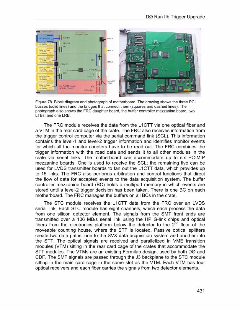
DØ Run IIb Trigger Upgrade
431
Figure 78. Block diagram and photograph of motherboard. The drawing shows the three PCI busses (solid lines) and the bridges that connect them (squares and dashed lines). The photograph also shows the FRC daughter board, the buffer controller mezzanine board, two LTBs, and one LRB.
The FRC module receives the data from the L1CTT via one optical fiber and a VTM in the rear card cage of the crate. The FRC also receives information from the trigger control computer via the serial command link (SCL). This information contains the level-1 and level-2 trigger information and identifies monitor events for which all the monitor counters have to be read out. The FRC combines the trigger information with the road data and sends it to all other modules in the crate via serial links. The motherboard can accommodate up to six PC-MIP mezzanine boards. One is used to receive the SCL; the remaining five can be used for LVDS transmitter boards to fan out the L1CTT data, which provides up to 15 links. The FRC also performs arbitration and control functions that direct the flow of data for accepted events to the data acquisition system. The buffer controller mezzanine board (BC) holds a multiport memory in which events are stored until a level-2 trigger decision has been taken. There is one BC on each motherboard. The FRC manages the buffers on all BCs in the crate.
The STC module receives the L1CTT data from the FRC over an LVDS serial link. Each STC module has eight channels, which each process the data from one silicon detector element. The signals from the SMT front ends are transmitted over a 106 MB/s serial link using the HP G-link chips and optical fibers from the electronics platform below the detector to the 2nd floor of the moveable counting house, where the STT is located. Passive optical splitters create two data paths, one to the SVX data acquisition system and another into the STT. The optical signals are received and parallelized in VME transition modules (VTM) sitting in the rear card cage of the crates that accommodate the STT modules. The VTMs are an existing Fermilab design, used by both DØ and CDF. The SMT signals are passed through the J3 backplane to the STC module sitting in the main card cage in the same slot as the VTM. Each VTM has four optical receivers and each fiber carries the signals from two detector elements.

DØ Run IIb Trigger Upgrade
432
In the STC module, each level-1 track is translated to a range of strips (a “road”) in each of the eight detector elements that may contain hits from the particle that gave rise to the level-1 track using a look-up table. The SMT data are clustered to combine adjacent strips hit by the same particle. These hits are then compared to the roads defined by the level-1 tracks. The hits that are in one or more roads are queued for transfer to the TFC module over an LVDS serial link. The main logic of the STC module is implemented in a single large field programmable gate array (FPGA).
Each TFC receives all hits from one azimuthal sector that were associated with at least one road. Because of the way SMT detector elements are mapped onto the optical fibers, three STC modules receive hits from both sectors in the crate. The outputs of these three STC modules go to both TFC modules in the crate. The remaining six STC modules receive hits from only one sector and their outputs go to only one TFC module. Thus each TFC module has six incoming LVDS serial links. The hits that come in over these links are sorted according to the level-1 track they are associated with. Then all data associated with one level-1 track is sent to one of eight DSPs that perform a linearized chi-squared fit. The results of the fits and the L1CTT data are sent via a Cypress hotlink to the level-2 central track trigger (L2CTT). The L2CTT acts as a concentrator for the 12 hotlink inputs from the six STT crates.
The number of crates required for the entire system is driven by the number of STC modules required to instrument all barrel detectors. Each SMT module can process the data from eight detector elements. Each azimuthal sector consists of 36 detector elements. Thus, each azimuthal sector requires 4.5 STC modules. We can accommodate two such sectors in one VME crate, so that one crate contains one FRC module, nine STC modules, and 2 TFC modules (one per azimuthal sector). In addition, each STT crate also houses a power PC and a Single Board Computer (SBC) card. The former controls the VME bus, and is used to download data tables and firmware into the STT modules and to monitor the performance of the STT. The SBC transfers the data of accepted events to the data acquisition system. Figure 79 shows the layout of one STT crate.
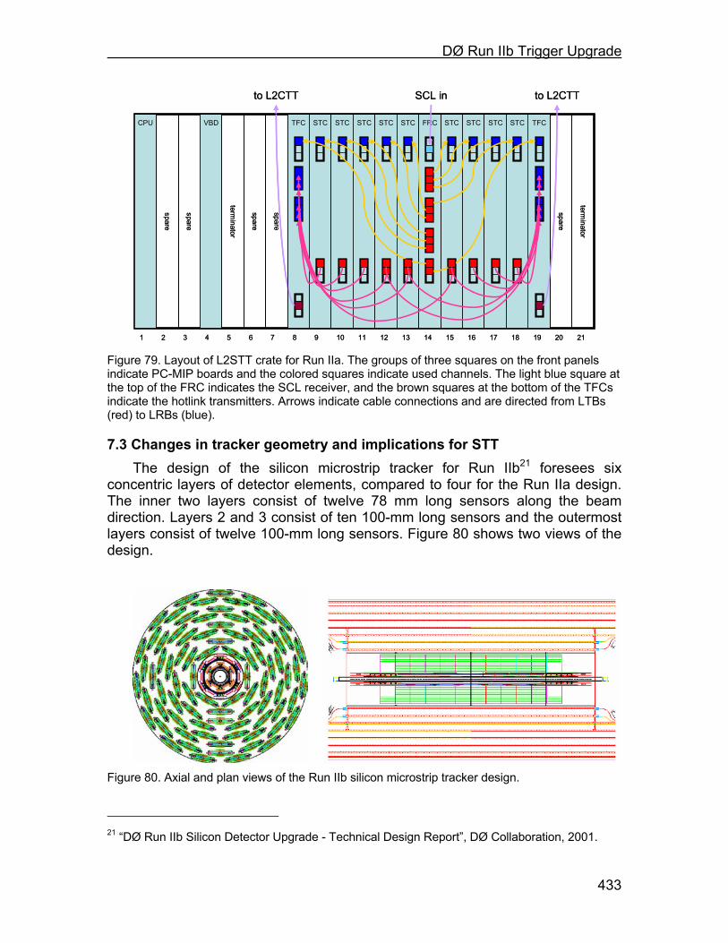
DØ Run IIb Trigger Upgrade
433
CPU
1 2
spare
3
VBD
4 5 6 7
STC
8
STC
9
STC
10
STC
11
STC
12
STC
13
FRC
14
STC
15
STC
16
TFC
20
TFC
1918
STC
17 21
spare
terminator
spare
terminator
spare
spare
SCL in to L2CTTto L2CTT
CPU
1 2
spare
3
VBD
4 5 6 7
STC
8
STC
9
STC
10
STC
11
STC
12
STC
13
FRC
14
STC
15
STC
16
TFC
20
TFC
1918
STC
17 21
spare
terminator
spare
terminator
spare
spare
SCL in to L2CTTto L2CTT
Figure 79. Layout of L2STT crate for Run IIa. The groups of three squares on the front panels indicate PC-MIP boards and the colored squares indicate used channels. The light blue square at the top of the FRC indicates the SCL receiver, and the brown squares at the bottom of the TFCs indicate the hotlink transmitters. Arrows indicate cable connections and are directed from LTBs (red) to LRBs (blue).
7.3 Changes in tracker geometry and implications for STT The design of the silicon microstrip tracker for Run IIb21 foresees six
concentric layers of detector elements, compared to four for the Run IIa design. The inner two layers consist of twelve 78 mm long sensors along the beam direction. Layers 2 and 3 consist of ten 100-mm long sensors and the outermost layers consist of twelve 100-mm long sensors. Figure 80 shows two views of the design.
Figure 80. Axial and plan views of the Run IIb silicon microstrip tracker design.
21 “DØ Run IIb Silicon Detector Upgrade - Technical Design Report”, DØ Collaboration, 2001.
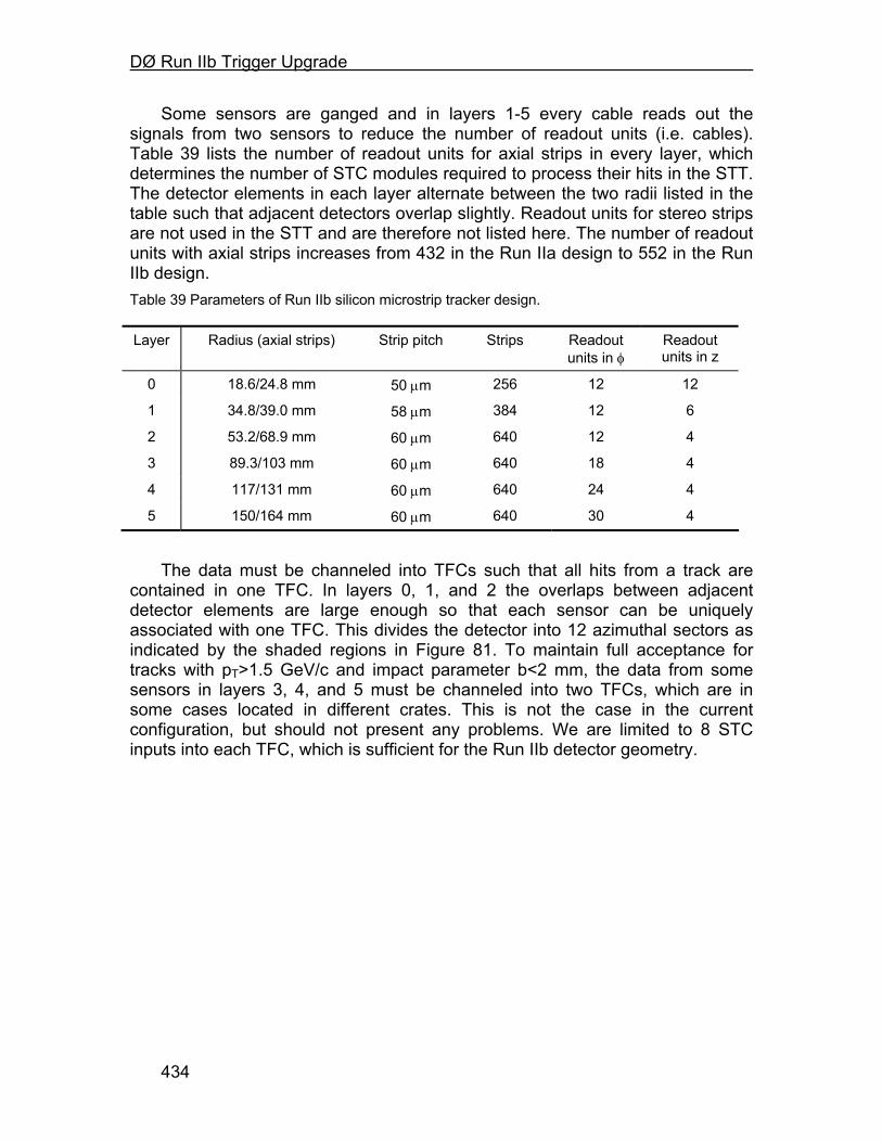
DØ Run IIb Trigger Upgrade
434
Some sensors are ganged and in layers 1-5 every cable reads out the signals from two sensors to reduce the number of readout units (i.e. cables). Table 39 lists the number of readout units for axial strips in every layer, which determines the number of STC modules required to process their hits in the STT. The detector elements in each layer alternate between the two radii listed in the table such that adjacent detectors overlap slightly. Readout units for stereo strips are not used in the STT and are therefore not listed here. The number of readout units with axial strips increases from 432 in the Run IIa design to 552 in the Run IIb design. Table 39 Parameters of Run IIb silicon microstrip tracker design.
Layer Radius (axial strips) Strip pitch Strips Readout units in φ
Readout units in z
0 18.6/24.8 mm 50 µm 256 12 12
1 34.8/39.0 mm 58 µm 384 12 6
2 53.2/68.9 mm 60 µm 640 12 4
3 89.3/103 mm 60 µm 640 18 4
4 117/131 mm 60 µm 640 24 4
5 150/164 mm 60 µm 640 30 4
The data must be channeled into TFCs such that all hits from a track are
contained in one TFC. In layers 0, 1, and 2 the overlaps between adjacent detector elements are large enough so that each sensor can be uniquely associated with one TFC. This divides the detector into 12 azimuthal sectors as indicated by the shaded regions in Figure 81. To maintain full acceptance for tracks with pT>1.5 GeV/c and impact parameter b<2 mm, the data from some sensors in layers 3, 4, and 5 must be channeled into two TFCs, which are in some cases located in different crates. This is not the case in the current configuration, but should not present any problems. We are limited to 8 STC inputs into each TFC, which is sufficient for the Run IIb detector geometry.
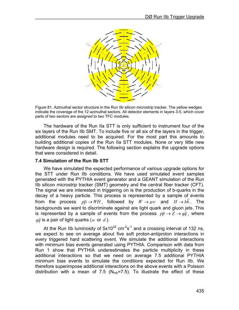
DØ Run IIb Trigger Upgrade
435
Figure 81. Azimuthal sector structure in the Run IIb silicon microstrip tracker. The yellow wedges indicate the coverage of the 12 azimuthal sectors. All detector elements in layers 3-5, which cover parts of two sectors are assigned to two TFC modules.
The hardware of the Run IIa STT is only sufficient to instrument four of the six layers of the Run IIb SMT. To include five or all six of the layers in the trigger, additional modules need to be acquired. For the most part this amounts to building additional copies of the Run IIa STT modules. None or very little new hardware design is required. The following section explains the upgrade options that were considered in detail. 7.4 Simulation of the Run IIb STT
We have simulated the expected performance of various upgrade options for the STT under Run IIb conditions. We have used simulated event samples generated with the PYTHIA event generator and a GEANT simulation of the Run IIb silicon microstrip tracker (SMT) geometry and the central fiber tracker (CFT). The signal we are interested in triggering on is the production of b-quarks in the decay of a heavy particle. This process is represented by a sample of events from the process WHpp → , followed by µν→W and bbH → . The backgrounds we want to discriminate against are light quark and gluon jets. This is represented by a sample of events from the process qqZpp →→ , where
qq is a pair of light quarks (u or d ).
At the Run IIb luminosity of 5x1032 cm-2s-1 and a crossing interval of 132 ns, we expect to see on average about five soft proton-antiproton interactions in every triggered hard scattering event. We simulate the additional interactions with minimum bias events generated using PYTHIA. Comparison with data from Run 1 show that PYTHIA underestimates the particle multiplicity in these additional interactions so that we need on average 7.5 additional PYTHIA minimum bias events to simulate the conditions expected for Run IIb. We therefore superimpose additional interactions on the above events with a Poisson distribution with a mean of 7.5 (Nmb=7.5). To illustrate the effect of these
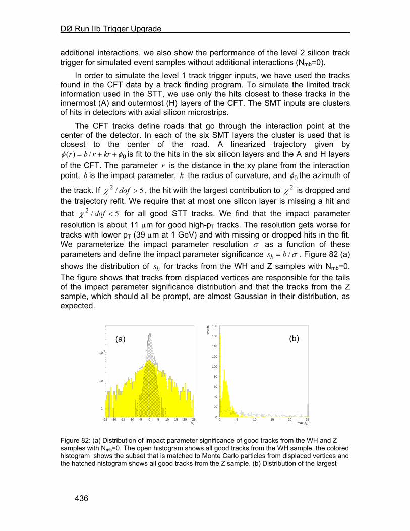
DØ Run IIb Trigger Upgrade
436
additional interactions, we also show the performance of the level 2 silicon track trigger for simulated event samples without additional interactions (Nmb=0).
In order to simulate the level 1 track trigger inputs, we have used the tracks found in the CFT data by a track finding program. To simulate the limited track information used in the STT, we use only the hits closest to these tracks in the innermost (A) and outermost (H) layers of the CFT. The SMT inputs are clusters of hits in detectors with axial silicon microstrips.
The CFT tracks define roads that go through the interaction point at the center of the detector. In each of the six SMT layers the cluster is used that is closest to the center of the road. A linearized trajectory given by
0/)( φφ ++= krrbr is fit to the hits in the six silicon layers and the A and H layers of the CFT. The parameter r is the distance in the xy plane from the interaction point, b is the impact parameter, k the radius of curvature, and 0φ the azimuth of
the track. If 5/2 >dofχ , the hit with the largest contribution to 2χ is dropped and the trajectory refit. We require that at most one silicon layer is missing a hit and that 5/2 <dofχ for all good STT tracks. We find that the impact parameter resolution is about 11 µm for good high-pT tracks. The resolution gets worse for tracks with lower pT (39 µm at 1 GeV) and with missing or dropped hits in the fit. We parameterize the impact parameter resolution σ as a function of these parameters and define the impact parameter significance σ/bsb = . Figure 82 (a) shows the distribution of bs for tracks from the WH and Z samples with Nmb=0. The figure shows that tracks from displaced vertices are responsible for the tails of the impact parameter significance distribution and that the tracks from the Z sample, which should all be prompt, are almost Gaussian in their distribution, as expected.
sb
1
10
10 2
-25 -20 -15 -10 -5 0 5 10 15 20 25max(sb)
even
ts
0
20
40
60
80
100
120
140
160
180
0 5 10 15 20 25
Figure 82: (a) Distribution of impact parameter significance of good tracks from the WH and Z samples with Nmb=0. The open histogram shows all good tracks from the WH sample, the colored histogram shows the subset that is matched to Monte Carlo particles from displaced vertices and the hatched histogram shows all good tracks from the Z sample. (b) Distribution of the largest
(a) (b)
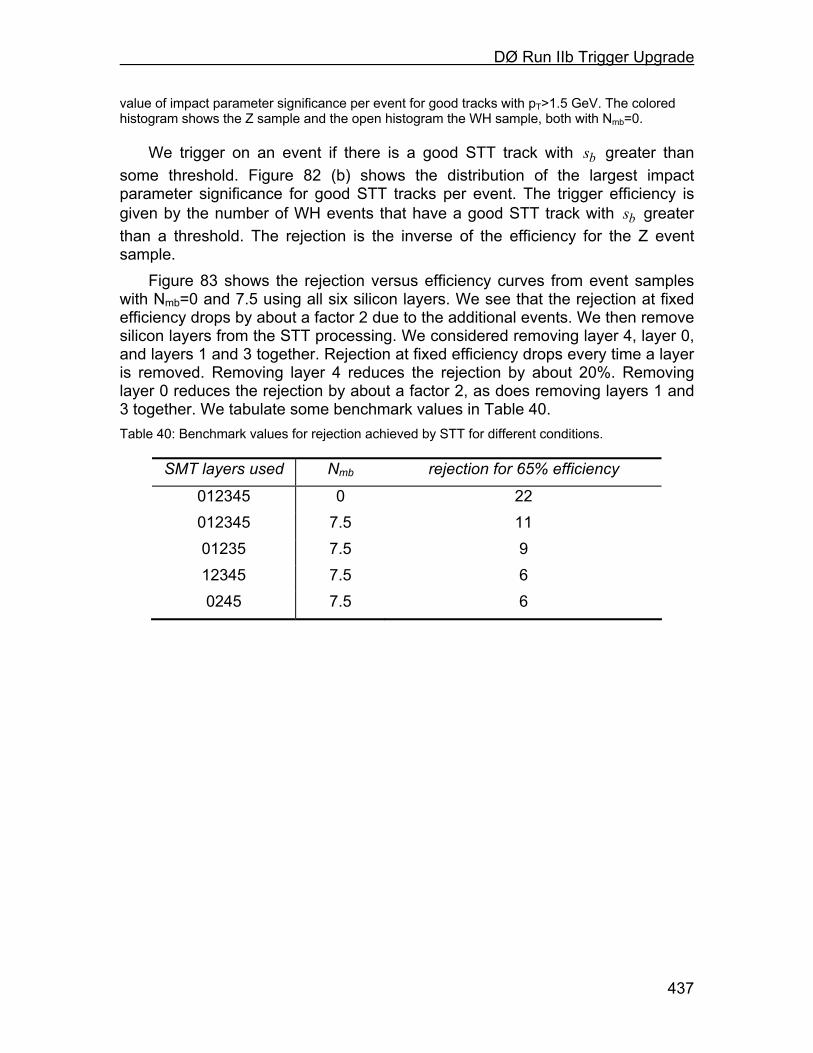
DØ Run IIb Trigger Upgrade
437
value of impact parameter significance per event for good tracks with pT>1.5 GeV. The colored histogram shows the Z sample and the open histogram the WH sample, both with Nmb=0.
We trigger on an event if there is a good STT track with bs greater than some threshold. Figure 82 (b) shows the distribution of the largest impact parameter significance for good STT tracks per event. The trigger efficiency is given by the number of WH events that have a good STT track with bs greater than a threshold. The rejection is the inverse of the efficiency for the Z event sample.
Figure 83 shows the rejection versus efficiency curves from event samples with Nmb=0 and 7.5 using all six silicon layers. We see that the rejection at fixed efficiency drops by about a factor 2 due to the additional events. We then remove silicon layers from the STT processing. We considered removing layer 4, layer 0, and layers 1 and 3 together. Rejection at fixed efficiency drops every time a layer is removed. Removing layer 4 reduces the rejection by about 20%. Removing layer 0 reduces the rejection by about a factor 2, as does removing layers 1 and 3 together. We tabulate some benchmark values in Table 40. Table 40: Benchmark values for rejection achieved by STT for different conditions.
SMT layers used Nmb rejection for 65% efficiency
012345 0 22 012345 7.5 11 01235 7.5 9 12345 7.5 6 0245 7.5 6
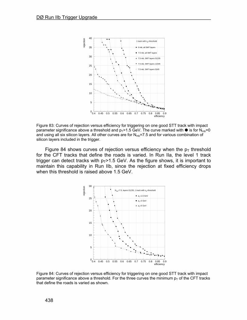
DØ Run IIb Trigger Upgrade
438
1 track with sb>threshold
0 mb, all SMT layers
7.5 mb, all SMT layers
7.5 mb, SMT layers 01235
7.5 mb, SMT layers 12345
7.5 mb, SMT layers 0245
efficiency
reje
ctio
n
0
5
10
15
20
25
30
35
40
0.4 0.45 0.5 0.55 0.6 0.65 0.7 0.75 0.8 0.85 0.9
Figure 83: Curves of rejection versus efficiency for triggering on one good STT track with impact parameter significance above a threshold and pT>1.5 GeV. The curve marked with is for Nmb=0 and using all six silicon layers. All other curves are for Nmb=7.5 and for various combination of silicon layers included in the trigger.
Figure 84 shows curves of rejection versus efficiency when the pT threshold for the CFT tracks that define the roads is varied. In Run IIa, the level 1 track trigger can detect tracks with pT>1.5 GeV. As the figure shows, it is important to maintain this capability in Run IIb, since the rejection at fixed efficiency drops when this threshold is raised above 1.5 GeV.
Nmb=7.5, layers 01235, 1 track with sb>threshold
pT>1.5 GeV
pT>3 GeV
pT>5 GeV
efficiency
reje
ctio
n
0
5
10
15
20
25
30
0.4 0.45 0.5 0.55 0.6 0.65 0.7 0.75 0.8 0.85 0.9
Figure 84: Curves of rejection versus efficiency for triggering on one good STT track with impact parameter significance above a threshold. For the three curves the minimum pT of the CFT tracks that define the roads is varied as shown.
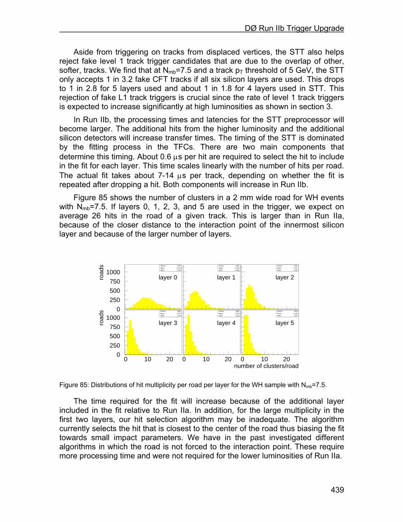
DØ Run IIb Trigger Upgrade
439
Aside from triggering on tracks from displaced vertices, the STT also helps reject fake level 1 track trigger candidates that are due to the overlap of other, softer, tracks. We find that at Nmb=7.5 and a track pT threshold of 5 GeV, the STT only accepts 1 in 3.2 fake CFT tracks if all six silicon layers are used. This drops to 1 in 2.8 for 5 layers used and about 1 in 1.8 for 4 layers used in STT. This rejection of fake L1 track triggers is crucial since the rate of level 1 track triggers is expected to increase significantly at high luminosities as shown in section 3.
In Run IIb, the processing times and latencies for the STT preprocessor will become larger. The additional hits from the higher luminosity and the additional silicon detectors will increase transfer times. The timing of the STT is dominated by the fitting process in the TFCs. There are two main components that determine this timing. About 0.6 µs per hit are required to select the hit to include in the fit for each layer. This time scales linearly with the number of hits per road. The actual fit takes about 7-14 µs per track, depending on whether the fit is repeated after dropping a hit. Both components will increase in Run IIb.
Figure 85 shows the number of clusters in a 2 mm wide road for WH events with Nmb=7.5. If layers 0, 1, 2, 3, and 5 are used in the trigger, we expect on average 26 hits in the road of a given track. This is larger than in Run IIa, because of the closer distance to the interaction point of the innermost silicon layer and because of the larger number of layers.
EntriesMeanRMS
3381 10.34 4.436
layer 0road
s EntriesMeanRMS
3381 6.035 3.085
layer 1
EntriesMeanRMS
3381 4.274 2.490
layer 2
EntriesMeanRMS
3381 3.076 1.944
layer 3road
s EntriesMeanRMS
3381 2.765 1.818
layer 4
EntriesMeanRMS
3381 2.429 1.587
layer 5
number of clusters/road
0
250
500
750
1000
0
250
500
750
1000
0 10 20 0 10 20 0 10 20
Figure 85: Distributions of hit multiplicity per road per layer for the WH sample with Nmb=7.5.
The time required for the fit will increase because of the additional layer included in the fit relative to Run IIa. In addition, for the large multiplicity in the first two layers, our hit selection algorithm may be inadequate. The algorithm currently selects the hit that is closest to the center of the road thus biasing the fit towards small impact parameters. We have in the past investigated different algorithms in which the road is not forced to the interaction point. These require more processing time and were not required for the lower luminosities of Run IIa.
DØ Run IIb Trigger Upgrade
440
Queuing simulations show that the STT operates within its time budget of about 100 µs on average. However latencies up to 250 µs are observed and these times will increase in Run IIb for the reasons mentioned in the previous paragraphs. In order to avoid exceeding our time budget, we will require additional processor cards (TFC).
From this work, we conclude that the STT must be upgraded to include at least five of the six layers of the Run IIb SMT. Without any upgrade, the STT performance will be severely degraded. Ideally, we would like to instrument all six silicon layers to create a trigger with the most rejection power. Considering the fiscal constraints, however, we propose to upgrade the STT to instrument five silicon layers (0, 1, 2, 3, and 5). Since we likely to exceed our time budget with the increased processing time required for the additional silicon layer, we also propose to double the number of TFCs so that two TFCs are assigned to each azimuthal sector. 7.5 Implementation description for STT upgrade
The layout for an STT crate during Run IIb is shown in Figure 86. Instrumenting SMT layers 0, 1, 2, 3, and 5 requires one additional STC and
the associated VTM per crate. Increasing the CPU power for fitting requires two additional TFCs per crate. All of these will require motherboards. We have to build additional link transmitters and receivers to ship the data to and from the new boards. The designs for all of these already exist in the Run IIa STT. Thus we have to only go through additional production runs. Additional optical splitters and fibers must also be purchased for the larger number of silicon input channels.
In order to maintain the same number of output cables into L2CTT we have to merge the outputs of the two TFCs that are assigned to the same channel. We will achieve this by daisy-chaining the two TFCs. That means one TFC uses the existing hotlink transmitter to send its output into the second TFC. It will be received by a hotlink repeater, which will have all the functionality of the existing hotlink transmitter and in addition a hotlink receiver and logic to merge the two data streams before they are sent to L2CTT.
There are three spare slots in the J3 backplane that can accommodate the new boards. Thus no modification has to be made to the crates. Our power supplies are also dimensioned large enough for the additional boards.
The fitting algorithm in the TFCs has to be modified to reflect the different number of layers and new coordinate conversion tables will have to be computed. The firmware in the STCs will have to be modified to handle the modified inputs from the L1CTT and new road look-up tables will have to be computed.
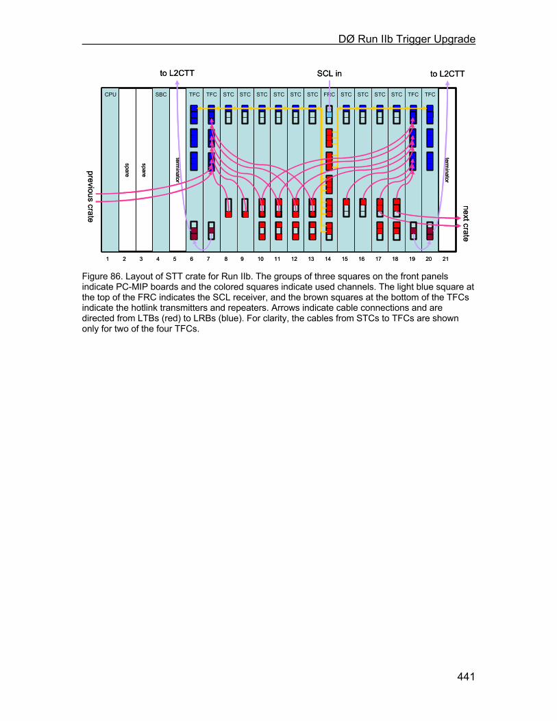
DØ Run IIb Trigger Upgrade
441
STC STC STC STC TFC TFCSTC STCFRC STC STC STCSTCTFCCPU
1 2
spare
3
SBC
4 5 6 7 9 10 11 12 13 14 15 16 20
TFC
191817 21
spare
terminator
terminator
to L2CTT SCL in to L2CTT
8
previous crate
next crateSTC STC STC STC TFC TFCSTC STCFRC STC STC STCSTCTFCCPU
1 2
spare
3
SBC
4 5 6 7 9 10 11 12 13 14 15 16 20
TFC
191817 21
spare
terminator
terminator
to L2CTT SCL in to L2CTT
8
previous crate
next crate
Figure 86. Layout of STT crate for Run IIb. The groups of three squares on the front panels indicate PC-MIP boards and the colored squares indicate used channels. The light blue square at the top of the FRC indicates the SCL receiver, and the brown squares at the bottom of the TFCs indicate the hotlink transmitters and repeaters. Arrows indicate cable connections and are directed from LTBs (red) to LRBs (blue). For clarity, the cables from STCs to TFCs are shown only for two of the four TFCs.

DØ Run IIb Trigger Upgrade
442
8 Trigger Upgrade Summary and Conclusions The DØ experiment has an extraordinary opportunity for discovering new
physics, either through direct detection or precision measurement of SM parameters. An essential ingredient in exploiting this opportunity is a powerful and flexible trigger that will enable us to efficiently record the data samples required to perform this physics. Some of these samples, such as
ννbbZHpp →→ , are quite challenging to trigger on. Furthermore, the increased luminosity and higher occupancy expected in Run IIb require substantial increases in trigger rejection, since hardware constraints prevent us from increasing our L1 and L2 trigger rates. Upgrades to the present trigger are essential if we are to have confidence in our ability to meet the Run IIb physics goals.
To determine how best to meet our Run IIb trigger goals, a Run IIb Trigger Task Force was formed to study the performance of the current trigger and investigate options for upgrading the trigger. Based on the task force recommendations, we have adopted the following plan for the trigger upgrade: 1. Replacement of the Level 1 Central Track Trigger (CTT) DFEA daughter
boards. The CTT is very sensitive to occupancy in the fiber tracker, leading to a large increase in the rate for fake high-pT tracks in the Run IIb environment. The new daughter board will utilize more powerful FPGAs to implement individual fiber “singlets” in the trigger, rather than the “doublets” currently used. Preliminary studies show significant reductions in the rate of fake tracks can be achieved with this upgrade.
2. Replacement of the Level 1 calorimeter trigger. The calorimeter trigger is an essential ingredient for the majority of DØ triggers, and limitations in the current calorimeter trigger, which is essentially unchanged from the Run 1, pose a serious threat to the Run IIb physics program. The two most serious issues are the long pulse width of the trigger pickoff signals and the absence of clustering in the jet trigger. The trigger pickoff signals are significantly longer than 132 ns, jeopardizing our ability to trigger on the correct beam crossing. The lack of clustering in the jet trigger makes the trigger very sensitive to jet fluctuations, leading to a large loss in rejection for a given trigger efficiency and a very slow turn-on. Other limitations include exclusion of ICD energies, inability to impose isolation or HAD/EM requirements on EM triggers, and very limited capabilities for matching tracking and calorimeter information. The new L1 calorimeter trigger would provide:
• A digital filter that utilizes several samplings of the trigger pickoff signals to properly assign energy deposits to the correct beam crossing.
• Jet triggers that utilize a sliding window algorithm to cluster calorimeter energies and significantly sharpen jet energy thresholds.
• Inclusion of ICD energy in the global energy sums to improve missing ET resolution.
DØ Run IIb Trigger Upgrade
443
• Electron/photon triggers with the ability to impose isolation and/or HAD/EM requirements to improve jet rejection.
• Topological triggers that aid in specific event topologies, such as acoplanar jets.
3. A new calorimeter-track match system. Significant improvements in rates have been demonstrated for both EM and track-based τ triggers from correlating calorimeter and tracking information. The cal-track match system utilizes boards that have already been developed for the muon-track matching system.
4. No major changes are foreseen for the Level 1 Muon trigger. Since the muon trigger matches muon and tracking information, it will benefit indirectly from the track trigger upgrade.
5. Some of the L2βeta processors will be replaced to provide additional processing power.
6. The L2 Silicon Track Trigger (STT) requires additional cards to accommodate the increased number of inputs coming from the Run IIb silicon tracker.
7. Maintaining Level 3 trigger rejection as the luminosity increases will require increasing the processing power of the L3 processor farm as part of the upgrade to the online system (see Part IV: DAQ/Online Computing). Simulation studies indicate that the above upgrades will provide the required
rejection for the Run IIb physics program. In particular, the expected trigger rate for the primary Higgs channels, WH and ZH, is compatible with our trigger rate limitations. The technical designs for these systems are making rapid progress. The designs are largely based on existing technologies, such as FPGAs and commercial processors, minimizing the technical risk. We foresee no major technical hurdles in implementing the proposed trigger upgrade.

444
(This page intentionally left blank)

445
Collector
Distributor EXAMINE
DataLogger
DLCAT
DLSAM
DiskBuffer
ORACLEDB
TapeLevel 3Process
SDAQProcess
Data Flow
SBC VMEReadout
ControlsProcessor
DAQ/ONLINE COMPUTING
DØ Run IIb UpgradeTechnical
Design Report

DØ Run IIb DAQ/Online Computing
446
(This page intentionally left blank)

DØ Run IIb DAQ/Online Computing
447
DAQ/ONLINE COMPUTING CONTENTS
1 DAQ/Online Computing Overview ......................................... 449
1.1 Scope................................................................................................449
1.2 Software Architecture........................................................................449
1.3 Hardware Architecture ......................................................................449
1.4 Motivations........................................................................................451
1.4.1 Enhanced Capabilities................................................................451
1.4.2 Hardware and Software Maintenance ........................................452
1.4.3 Software Support........................................................................452
1.5 Interaction with the Computing Division ............................................452
1.6 Comments on Run IIa configuration..................................................453
2 DAQ/Online Computing Upgrades for Run IIb ....................... 454
2.1 Operational Parameters....................................................................454
2.1.1 Level 3 parameters.....................................................................454
2.1.2 Event rate parameters................................................................454
2.1.3 System availability......................................................................455
2.2 Online Network .................................................................................455
2.2.1 Description .................................................................................455
2.2.2 Run IIb Upgrade Plan.................................................................456
2.3 Level 3 Linux Filter Farm ..................................................................456
2.3.1 Description .................................................................................456
2.3.2 Level 3 Processing needs for Run IIb.........................................456
2.3.3 Run IIb Upgrade Plan. ................................................................457
2.4 Host Online Systems ........................................................................458
2.4.1 Description .................................................................................458
2.4.2 Run IIa Host Online system........................................................458
2.4.3 Run IIb Upgrade plan .................................................................458
2.5 Control Room Systems .....................................................................459
2.5.1 Description .................................................................................459
2.5.2 Run IIb Upgrade plan .................................................................460
2.6 Data Monitoring Systems..................................................................460
DØ Run IIb DAQ/Online Computing
448
2.6.1 Description .................................................................................460
2.6.2 Run IIb Upgrade plan .................................................................460
2.7 Database Servers .............................................................................460
2.7.1 Description .................................................................................460
2.7.2 Run IIb Upgrade plan .................................................................461
2.8 File Servers.......................................................................................461
2.8.1 Description .................................................................................461
2.8.2 Run IIb Upgrade plans ...............................................................461
2.9 Slow Control Systems.......................................................................462
2.9.1 Description .................................................................................462
2.9.2 Run IIb Upgrade Plan.................................................................462
3 DAQ/Online Computing Summary ......................................... 464

DØ Run IIb DAQ/Online Computing
449
1 DAQ/Online Computing Overview 1.1 Scope
For the purposes of this document, the DØ DAQ and Online Computing systems will be defined to consist of the following components:
• DAQ and Online network, • Single Board Computers (SBCs) in VME readout crates, • Level 3 Linux software filter farm, • Host Online system, • Control room computing systems, • Data monitoring computing systems, • Database servers, • File servers, • Slow control system, including VME processors, • plus the associated software for each of these elements.
1.2 Software Architecture
Collector
Distributor EXAMINE
DataLogger
DLCAT
DLSAM
DiskBuffer
ORACLEDB
TapeLevel 3Process
SDAQProcess
Data Flow
SBC VMEReadout
ControlsProcessor
Figure 1. DAQ system software components
The software architecture of the Run IIb Online system is unchanged from that of Run IIa. Some components will need updating, but there are no structural differences planned. The major software components in the event data path are illustrated in Figure 1. The slow control system components are not illustrated in the figure, nor are the non-event monitoring systems. 1.3 Hardware Architecture
The hardware architecture of the Run IIb Online system is also unchanged from that of Run IIa. The current architecture is illustrated in Figure 2 and Figure
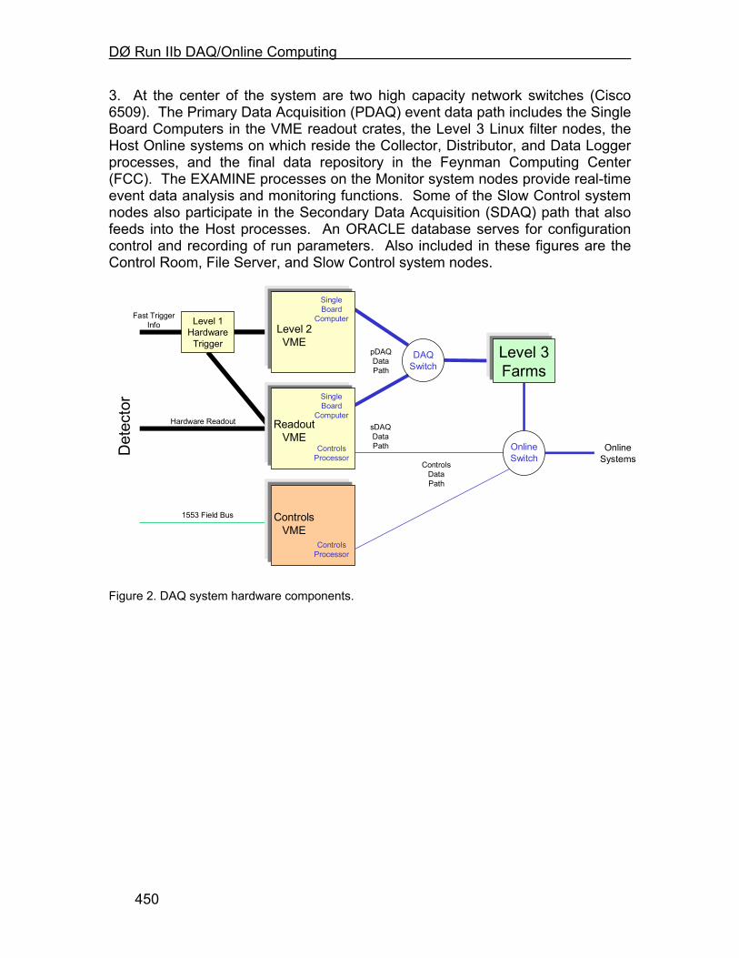
DØ Run IIb DAQ/Online Computing
450
3. At the center of the system are two high capacity network switches (Cisco 6509). The Primary Data Acquisition (PDAQ) event data path includes the Single Board Computers in the VME readout crates, the Level 3 Linux filter nodes, the Host Online systems on which reside the Collector, Distributor, and Data Logger processes, and the final data repository in the Feynman Computing Center (FCC). The EXAMINE processes on the Monitor system nodes provide real-time event data analysis and monitoring functions. Some of the Slow Control system nodes also participate in the Secondary Data Acquisition (SDAQ) path that also feeds into the Host processes. An ORACLE database serves for configuration control and recording of run parameters. Also included in these figures are the Control Room, File Server, and Slow Control system nodes.
ReadoutVME
SingleBoard
Computer
ControlsProcessor
ControlsVME
ControlsProcessor
DAQSwitch
Level 1Hardware
TriggerLevel 2VME
SingleBoard
Computer
1553 Field Bus
Hardware Readout
Fast TriggerInfo
Level 3Farms
OnlineSwitch
OnlineSystems
pDAQDataPath
sDAQDataPath
ControlsDataPath
Det
ecto
r
Figure 2. DAQ system hardware components.
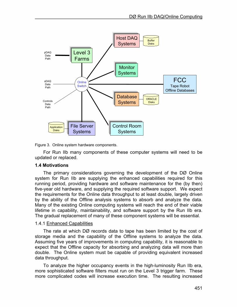
DØ Run IIb DAQ/Online Computing
451
Level 3Farms
OnlineSwitch
sDAQDataPath
ControlsDataPath
pDAQDataPath
FCCTape Robot
Offline Databases
MonitorSystems
Control RoomSystems
Host DAQSystems
BufferDisks
DatabaseSystems
ORACLEDisks
File ServerSystems
ApplicationDisks
Figure 3. Online system hardware components.
For Run IIb many components of these computer systems will need to be updated or replaced. 1.4 Motivations
The primary considerations governing the development of the DØ Online system for Run IIb are supplying the enhanced capabilities required for this running period, providing hardware and software maintenance for the (by then) five-year old hardware, and supplying the required software support. We expect the requirements for the Online data throughput to at least double, largely driven by the ability of the Offline analysis systems to absorb and analyze the data. Many of the existing Online computing systems will reach the end of their viable lifetime in capability, maintainability, and software support by the Run IIb era. The gradual replacement of many of these component systems will be essential. 1.4.1 Enhanced Capabilities
The rate at which DØ records data to tape has been limited by the cost of storage media and the capability of the Offline systems to analyze the data. Assuming five years of improvements in computing capability, it is reasonable to expect that the Offline capacity for absorbing and analyzing data will more than double. The Online system must be capable of providing equivalent increased data throughput.
To analyze the higher occupancy events in the high-luminosity Run IIb era, more sophisticated software filters must run on the Level 3 trigger farm. These more complicated codes will increase execution time. The resulting increased
DØ Run IIb DAQ/Online Computing
452
computing demand in Level 3 will need to be met by either an increase in the number of processors, replacement of these units by more capable processors, or both.
It is also expected that data quality monitoring software will be vastly improved by the Run IIb era. These capabilities again are likely to come at the cost of increased execution time and/or higher statistical sampling requirements. In either case, more numerous and more powerful monitoring systems will be required. 1.4.2 Hardware and Software Maintenance
By the time of Run IIb, the computing systems purchased for Run IIa will be more than five years old. In the world of computing hardware, this is ancient. Hardware maintenance of such old equipment is likely to be either impossible or unreasonably expensive. Experience shows that replacement by new (and under warranty) equipment is more cost effective. Since replacement of obsolete equipment not only addresses the maintenance question, but also issues of increased capability, it is the most effective course of action.
The DØ Online system is composed of several subsystems that have differing hardware components and differing maintenance needs. Subsystem specific issues will be addressed in the following sections. 1.4.3 Software Support
Several different operating systems are present in the Online system, with numerous custom applications. We have tried, wherever possible, to develop software in as general a fashion as possible so that it can be migrated from machine to machine and from platform to platform. However, support of certain applications is closely tied to the operating system on which the applications run. In particular, ORACLE database operations require expertise that is often specialized to the host operating system. By the time of Run IIb, there is expected to be a consolidation in ORACLE support by the Laboratory that will not include the existing DØ Online database Compaq / Tru64 Unix platform. These platforms will thus need to be replaced. 1.5 Interaction with the Computing Division
The Run IIa Online system was developed through an active partnership with the Computing Division’s Online and Database Systems (CD/ODS) group. It is essential that this relationship be maintained during the transition to the Run IIb system. While the level of effort expended by CD/ODS personnel has already decreased relative to what it was during the height of the software development phase of the Run IIa Online system, the continued participation of this group will be needed to maintain the system and to migrate the existing software to new platforms as these are acquired. Computing Division assistance and expertise will be particularly critical in the area of database support since the Oracle consultant who led the design of the current system is not expected to be involved in maintaining the system. The continued involvement of the CD in the Online effort, which will presumably be described in a future MOU, will be left
DØ Run IIb DAQ/Online Computing
453
mostly implicit in later sections of this document, but will nevertheless continue to be crucial to the success of the effort. 1.6 Comments on Run IIa configuration
For Run IIa many of the Online functions have been combined on a single cluster of large servers. The Data Logger, Database, and File Server operations are all performed on one or more of a set of three Compaq AlphaServers configured as a TruCluster. The cluster configuration allows each of the three nodes to share disk resources, which include the event data buffer disks, database disks, and general user disks. The cluster acts as an NFS server for the control room and monitoring nodes, and as the NIS master for Online accounts. High availability and reliability for these functions are provided by the cluster configuration, allowing one of the three nodes to go down with the remaining nodes assuming the critical functions.
The Run IIa cluster includes a dual-processor AlphaServer 4000 (purchased in 1997), a second dual-processor AlphaServer 4000 (1998), and a quad-processor AlphaServer GS80 (2000). Disk storage shared among the cluster members includes 1.1 TB in a fibre channel RAID array, 2.8 TB in fibre channel JBOD, and 0.6 TB in a shared SCSI RAID array. Backups are performed on a single DLT4000 tape drive on each cluster member.
The remaining Online Host, Control Room, and Monitoring nodes are single or dual processor Linux systems. These nodes are mostly interchangeable, with only the Control Room systems being slightly unusual with their configuration requiring multiple graphics cards and monitors. Other than system and scratch disks, these systems get all of their storage resources from the AlphaServer cluster.
The cluster configuration has proved both reliable and efficient. However, the I/O performance of the AlphaServer components, because of both age and architecture, is not optimal. The existing Run IIa components are maximally utilized in order to provide the Run IIa target event data rate of 50 Hz. Concentrating a large number of functions in a small number (3) of machines leads to potential congestion. The addition of resources to this specialized configuration is possible but costly.
The Run IIb architecture addresses the performance and expandability / flexibility issues by replacing the central cluster with a larger number of dedicated function Linux systems. There is a philosophy of one machine per function, with redundant systems where necessary. Where possible, functions are spread across multiple parallel machines. The details of the architecture are described in following sections.

DØ Run IIb DAQ/Online Computing
454
2 DAQ/Online Computing Upgrades for Run IIb A description of planned upgrades follows for each component noted in the
Introduction. The philosophy and architecture of the Online system will not change, but components will be updated. Note that most changes are best achieved by a continuous, staged approach, while others involve large systems that will need to be replaced as units. 2.1 Operational Parameters
Table 1 summarizes the Run 2 parameters relevant to the Level 3 and Online systems. The impact of each value upon the system configuration will be discussed in the following sections. Table 1. Run 2 Level 3 and Online parameters
Parameter Run IIa Run IIb Level 3 farm nodes (dual processors) 112 160 Average event size ~ 250 Kbytes ~ 300 Kbytes Level 3 input rate 1000 Hz 1000 Hz Peak Level 3 accept rate 50 Hz 100 Hz Peak logging rate 12.5 Mbytes/sec 30 Mbytes/secDetector duty factor > 99% > 99% Accelerator duty factor ~ 75% ~ 75% Online system availability > 99% > 99% Local data buffer 48 hours 48 hours Local data buffer ~ 2 Tbytes ~ 4 Tbytes
2.1.1 Level 3 parameters The required number of Level 3 farm nodes is a function of the event rate
into Level 3 and the required processing time for filtering. These are highly tunable numbers. The input rate can be adjusted with thresholds in Level 1 and Level 2. The processing time depends upon the choice of software filters. If a required Level 3 rejection rate is not possible in the available time, then thresholds can be adjusted at Level 3. The choice in Table 1 of 160 Level 3 farm nodes for Run IIb results from the best estimate of the required analysis time with the target input rate. 2.1.2 Event rate parameters
The rate at which events are logged determines the required capabilities of the Host Online system. The rate is bounded by the maximum trigger rejection ratio and the maximum Offline storage, reconstruction, and analysis capacities.
DØ Run IIb DAQ/Online Computing
455
The Online system must be designed to cope with the largest rate otherwise allowed. This limitation is from the Offline computing systems, which see a Run IIb rate of 100 Hz with a 75% overall duty factor as the maximum allowable. The average output design rate as mentioned in the trigger overview is 50 Hz. 2.1.3 System availability
The DØ experience in Run1 was that an uptime of > 99% for the computing systems is achievable. In Run2 there is a similar goal, such that lost beam time from computing problems is small compared to other sources of detector down time (the Detector duty factor). Since the DØ event data is transferred to the Feynman Computing Center for logging, problems in this step can potentially contribute to system down time. To decouple possible problems with the tape robot and database systems, which are principally Offline systems with competing priorities, we require a local disk buffer to retain data for a period of 48 hours. This period should be sufficiently long to recover from any Offline system disruptions. 2.2 Online Network 2.2.1 Description
The backbone of the DØ Online computing system is the switched Ethernet network through which all components are interconnected. The Run IIa network is based on a pair of Cisco 6509 switches, one for the event data path from the SBCs in the VME readout crates to the Level 3 filter farm nodes, and the other which services the Level 3 event data output as well as general network traffic. Each switch is composed of a chassis with an interconnecting backplane and various modules that supply ports for attaching the DAQ and Online nodes. The total capacity of each switch is determined both by the chassis version and the number and versions of the component modules. The DAQ switch has a fabric-enabled backplane capable of a total throughput of 128 Gbps. The Online switch has a backplane capable of a total throughput of 64 Gbps.
The Cisco 6509 for the DAQ network can currently support 16 Gb fiber connections from the SBCs (via Cisco 2948G switches in the counting house) and 96 100Mb connections to Level 3 farm and support nodes. The existing 48 farm nodes, a pending 32-node farm addition, and a handful of support nodes will fully utilize available ports. When the number of farm nodes is increased beyond 80, additional 48-port 100Mb blades will need to be purchased for the switch.
The Online Cisco 6509 switch currently directly supports over 100 nodes, including 48 Level 3 nodes. There are approximately 48 available 100Mb ports, 32 of which will be used immediately for a Level 3 farm addition. More 100Mb blades will be needed to expand beyond the current level. An increase in the number of high bandwidth host system nodes will require more gigabit ports beyond the current fully-utilized 10 ports, necessitating the addition of a Gb capable blade.
DØ Run IIb DAQ/Online Computing
456
2.2.2 Run IIb Upgrade Plan To support a total of 160 Level 3 nodes, two additional 100baseT modules
are required on each switch. To support the expanded Host Data Logging systems (page 458), one additional 1000baseT module is required in the Online switch. If a 1000baseT module is not available, existing 3COM 4900 switches (with 24 available 1000baseT ports) can be used with 1000baseSx uplinks. In this case an additional 1000baseSx module would be needed. 2.3 Level 3 Linux Filter Farm 2.3.1 Description
The Level 3 trigger consists of two principle elements: a high speed data acquisition system that provides readout of the entire detector at rates expected to exceed 1 kHz, and a processor farm that utilizes software filters written to select events that will be permanently recorded. Since the required Run IIb data acquisition bandwidth is expected to be made available once the Run IIa Level 3 hardware is fully commissioned, the most likely need for Level 3 upgrades will be to provide increased processing power in the farm.
The Run IIb Level 1 and Level 2 triggers will have increased selectivity and there will be a matching increase in selectivity of the Level 3 filter. This requires the use of more complex algorithms that necessitate the need for faster processors in the Level 3 nodes. Historically, DØ has equipped the Level 3 farm with the fastest processors on the market within this chosen processor family and this approach must be continued. At the time of the Run IIb upgrade, Moore's law would lead us to expect a four-fold increase in processing speed over what is currently available. Thus, a significant increase in Level 3 processing power will be obtained by enhancing the Run IIa Level 3 processors with the latest technology available in 2004.
There are currently 48 dual-processor Linux nodes in the Run IIa Level 3 filter farm. An additional 32 are to be installed by late 2002. 2.3.2 Level 3 Processing needs for Run IIb
The Level 3 event processing time has been measured in Run IIa running at peak luminosities of ~2×1031 cm-2s-1. On a 1 GHz PIII processor (~40 Si95), the filtering code with global tracking takes approximately 300 msec/event before any emphasis on time optimization. This maps into an approximate time of 250 msec/event for events with only one interaction. In the language of computing benchmarks, this translates into about 10 Si95-secs/event.
The amount of processing needed per event depends on the complexity of the event, which in turn depends on luminosity and bunch crossing time. Monte Carlo studies coupled with data analysis shows that the reconstruction time rises with the number of interactions in an event. For offline code with detailed tracking, this rise is much faster than linear mostly due to combinatorics in the global tracking. For the Online Level 3 code, we only need a limited reconstruction, depending on the lower level trigger results, to filter the event.

DØ Run IIb DAQ/Online Computing
457
This reconstruction depends more on detector occupancy than event complexity, thus we assume a linear rise in processing requirements per number of interactions. With this assumption then the amount of processing power needed for 5 background interactions/bunch crossing and 1kHz Level 3 input rate leads to a predicted CPU requirement of 60k Si95.
The above argument gives us an idea of the approximate processing power needed for the Level 3 filter, however a precise processing requirement is difficult to predict. For example, with the ability to trigger on secondary vertices, the Level 3 filter code will additionally perform secondary vertex analysis. With some trigger rejection moving into Level 1 and Level 2, Level 3 may also need to work harder to get the desired rejection ratio. 2.3.3 Run IIb Upgrade Plan.
The Level 3 farm is very similar to the processing farms used in the Offline event reconstruction and analysis. A standard configuration is a 2U rack-mounted system with dual processors and 1 Gbyte of memory. The Level 3 nodes benefit from dual 100 Mb network connections to segregate input and output event data networks. The evaluation and purchase steps for Level 3 farm nodes will closely follow Offline farm activities.
Large farm purchases at Fermilab over the last 10 years have shown that processing power for commodity (desktop-like) computing has doubled every 1.5 years (Moore’s law), and that prices/box remain roughly the same. This scenario is used universally inside and outside Fermilab to predict computing prices in the next 5-10 years.
Table 2 provides a scenario for the staged acquisition of farm nodes. Beyond the existing node purchases of FY01 and FY02, Moore’s law is applied to predict the processing power increase relative to a dual 1 GHz machine. With an acquisition of 32 nodes per year through 2004, an eventual retirement of older nodes, and a bulk purchase of 96 nodes immediately prior to Run IIb, a farm of 160 dual-processor nodes (320 processors) with 3-4 times the Run IIa performance is expected by 2006. Table 2. Level 3 processor acquisition schedule
Year FY01 FY02 FY03 FY04 FY05Added nodes 48 32 32 32 96Node type Dual 1 GHz PIII Dual 1.67 GHz AMD 2003 model 2004 model 2005 modelClock factor 1.00 1.67 2.67 4.28 6.84Equivalent Dual 1 GHz PIII 48 53 85 136 656Retired nodes 48 32Node type Dual 1 GHz PIII Dual 1.67 GHz AMDClock factor 1.00 1.67Equivalent Dual 1 GHz PIII 48 53Net number of nodes/ports 48 80 112 96 160Net equivalent Dual 1 GHz PIII 48 101 186 274 877
In this scenario, the total installed Level 3 computing for Run IIb is 70k Si95 compared to a need of 60k Si95. This plan is well matched to Level 3 needs given the caveats mentioned above.

DØ Run IIb DAQ/Online Computing
458
2.4 Host Online Systems 2.4.1 Description
The Online Host nodes perform the functions of the Collector, Data Logger, Data Distributor, and the processes for shipping event data to the Feynman Computing Center (FCC) for recording on tape. The Collector (one or more processes acting in parallel) receives event data from the Level 3 filter farm nodes and routes it to Data Logger and Data Distributor processes. The Data Logger (one or more processes acting in parallel) writes the event data to the buffer disks. The Data Distributor maintains an event pool for monitoring applications and transmits the events to the various monitoring nodes. The DLSAM and DLCAT processes read the event data and metadata from the buffer disks and ship the information over the network to the FCC.
The Host system must be able to absorb over the network the maximum recorded data rate of 30 MB/s. This rate must be sustained as events are logged to the buffer disk, read back from the buffer disk, and shipped over the network to the FCC. Additionally, a fraction of the event stream must be routed to the event monitoring tasks. There is additional network traffic internal to the Host system as events are routed among parallel tasks.
The Host system is an integral and required component of the experiment. As such, it must be a highly available system. The target availability is greater than 99%. 2.4.2 Run IIa Host Online system
The current DØ Online Host system is centered upon three Compaq / Digital AlphaServers in a cluster configuration. Two of the machines are AlphaServer 4000s (purchased in 1997 and 1998) and the third is an AlphaServer GS80 (purchased in 2000). These machines mount disks in the form of two RAID arrays, ~600 GB in a Compaq/Digital HSZ50 unit and ~1.1 TB in a Compaq/Digital HSG80 unit, and an additional 2.8 TB in Fibre Channel JBOD disk. This cluster supports data logging, the ORACLE databases, and general file serving for the remainder of the Online system.
The long-term maintenance of these systems is a serious concern. While they can be expected to still be operational in the Run IIb era, the high availability required for critical system components may be compromised by the inability to obtain the necessary maintenance support. Maintenance costs for these systems, particularly 7x24 coverage, will increase with age. By the time of Run IIb, maintenance costs are likely to exceed replacement costs.
These systems currently run Compaq Tru64 UNIX, previously known as Digital UNIX, or Digital OSF1. With the merger of Compaq and Hewlett Packard, long-term support for this operating system may be problematic. 2.4.3 Run IIb Upgrade plan
All applications developed for the data acquisition system that currently run on the Host systems were written with portability in mind. In particular, all will
DØ Run IIb DAQ/Online Computing
459
work under Linux. The proposed upgrade to the Host systems is therefore to replace them with Linux servers. Since the existing Host system provides Data Logging, Database support, and File Serving functions, each of these needs must be accommodated by the replacement system. These requirements will be addressed individually in this and following sections.
The Data Logging system must, with high (> 99%) availability, be capable of absorbing data from the Level 3 filter systems, distributing it to logging and monitoring applications, spooling it to disk, reading it from disk, and dispatching it to tape-writing nodes in the FCC. The maximum input data rate is 30 Mbytes/sec. A local disk buffer of ~4 Tbytes is required to retain event data if the Offline tape robots are unavailable. The event data on the buffer disks is normally read and transferred to the FCC at the 30 Mbytes/sec input rate, but a 2x higher rate is necessary to both take sustained new data and unload stored event data following any outage. The high availability requirement, satisfied in the current system by using a cluster of three machines, precludes the use of a single machine. Currently the cluster members share the disk buffers, but this is not a strict requirement.
The proposed upgrade solution is for a set (two or three) of Linux servers (dual or quad processors) to act as the new Data Logging nodes. The data acquisition applications can run in parallel to distribute the load at full bandwidth, but a single node should be capable of handling nearly the entire bandwidth for running under special conditions. Each system will require gigabit connectivity to the Online switch, thereby raising the number of gigabit ports required.
Some R&D effort is needed to test such a configuration. The possibility of clustering the Linux nodes and the possibility of sharing the disk storage will be examined. The purchase of the complete Data Logging system can be staged, as not all members need to be identical (as noted above, the current Host system was purchased in three increments). It is expected that the R&D unit to be purchased could suffice as the third server in a three-server configuration.
The expected configuration consists of three high-end servers with a SAN JBOD disk array. A typical server would be configured with four CPUs, 4 Gbytes of memory, a local RAID controller for system disks, gigabit network cards, and available 64-bit PCI slots. The buffer disk array will be built from commodity disks in a JBOD Fibre Channel crate, as currently employed for the Run IIa system.
Other components of the Host Online system – the Collector and Distributor – will be housed on Run IIa Linux systems which will remain sufficiently capable for these functions in Run IIb. 2.5 Control Room Systems 2.5.1 Description
The current DØ Control Room system is composed of 12 Linux nodes (single and dual processor) that manage 27 monitors. These systems range in age from one to five years. Many of the monitors are already showing the effects of age.

DØ Run IIb DAQ/Online Computing
460
It is expected that we should replace some fraction of the Control Room nodes and monitors each year. 2.5.2 Run IIb Upgrade plan
The Control Room systems will be gradually upgraded and replaced throughout the lifetime of the DØ experiment. Assuming a 5-year viable lifetime for these components, we should expect to replace 20% each year. This implies that 2 to 3 systems supporting 5 to 6 monitors will need to be replaced annually. This will be done with purchases of moderate-performance (dual CPU, multiple graphics cards) graphics systems or reuse of systems otherwise made available. 2.6 Data Monitoring Systems 2.6.1 Description
Real-time monitoring of event data is accomplished by a scheme in which representative events are replicated and distributed to monitoring nodes as they are acquired. The monitoring ranges from examination of low-level quantities such as hit and pulse height distributions to complete event reconstruction. In the latter case, the environment and the code are similar to that of the Offline reconstruction farms. There are one or more monitoring applications for each detector subsystem, and for the trigger, luminosity, and global reconstruction tasks.
The rate at which the monitoring tasks can process events, as well as the complexity of monitoring, is limited by the processing capabilities of the monitoring nodes. The Control Room systems and several rack-mounted Linux nodes currently share this load. Much can be gained by upgrading the experiment’s monitoring capability. As more sophisticated analysis software becomes available, these improved codes can be run in the Online environment to provide immediate feedback on data quality. 2.6.2 Run IIb Upgrade plan
The monitoring nodes, rack mounted Linux systems, will need to be continually updated. Such upgrades can occur gradually. As with the Control Room nodes, a useful lifetime of 5 years implies that 20% of the monitoring systems should be upgraded each year. A typical monitoring node configuration is a 2U rack-mounted dual-processor system with 1 GB of memory. These systems are very similar to the Level 3 or Offline farm nodes, and purchases will be made in conjunction with these larger acquisitions. Four or five nodes will be upgraded per year. 2.7 Database Servers 2.7.1 Description
The ORACLE databases currently run on the AlphaServer cluster, with the database files residing on the attached RAID arrays. As mentioned above, long-term support for this hardware is questionable. Additionally, ORACLE database and application support from the Computing Division no longer includes the Tru64 UNIX platform.
DØ Run IIb DAQ/Online Computing
461
The principal requirement for the database server is high availability (> 99%). Support needs include maintaining the hardware, the operating system, and the application software (ORACLE). User application development also benefits from having independent production and development database instances. 2.7.2 Run IIb Upgrade plan
The planned replacement of the database servers is by two redundant Linux systems with common access to RAID disk arrays. The Computing Division supports this system. The purchase of these systems is best staged over two years, with early purchase of the development machine and later purchase of the production machine. The performance required of the database machines is not expected to be extremely demanding. A mid-range server system should be sufficient.
The RAID array for the database will likely be shared with the File Server systems, as neither application has particularly demanding disk I/O performance. The production database instance is expected to require no more than 400 Gbytes, and 100 Gbytes should suffice for the development instance (Run IIa sizes are 80 Gbytes and 35 Gbytes). An additional 200 Gbytes will be necessary as spooling space for the ORACLE backups.
The Database system will be supported with a backup system, in conjunction with the File Server systems of the next section. 2.8 File Servers 2.8.1 Description
The Host cluster currently provides general-purpose file serving. Linux nodes within the Online system access the Host file systems by NFS. Approximately 500 GB of RAID disk is currently available. Files stored include the DØ software library, Fermilab software products, DAQ configuration files, detector subsystem application data, and user home areas. Since the existing file servers are the AlphaServers, replacement is necessary, for reasons already delineated.
The requirement for the file server system is primarily one of high reliability (> 99%) of both system and disks. The needed network and disk I/O rate is moderate, with 5 Mbytes/sec being sufficient and easily achievable. 2.8.2 Run IIb Upgrade plans
The proposed solution is a pair of redundant Linux servers with common access to both RAID and JBOD disk arrays. The RAID array will be shared with the Database systems. Assuming a 1.3 TB RAID array and the previously stated database needs, then 600 GB will be available for general system use. The JBOD disk is typically provided from otherwise unused disk space on local disks of the distributed nodes, so no explicit purchase is necessary. A tape stacker system of moderate capability is needed for backups. Acquisition of these systems can be staged.
DØ Run IIb DAQ/Online Computing
462
2.9 Slow Control Systems 2.9.1 Description
The Slow Controls system consists of host-level console computers that run the controls application programs and that communicate with Input/Output Controller (IOC) computers over an Ethernet LAN. The IOC's, in turn, communicate with detector hardware components (many of which have their own embedded process control computers) over two types of field bus: (a) the VME parallel backplane and (b) the MIL/STD1553B serial bus.
An IOC processor is either a Motorola 68K or PowerPC single-board computer. The operating system for these processors is VxWorks and the controls-specific software consists of EPICS (Experimental Physics and Industrial Control System) plus a number of EPICS extensions developed by the DØ controls group. The node-specific EPICS configuration, which is loaded into an IOC at boot time, is maintained in an ORACLE database from which the IOC configuration files are extracted. The processors have both Ethernet connections to the Online network and serial line connections from their console ports to network terminal servers. The console connections allow users to communicate directly with the VxWorks shell and the EPICS local user interface.
The IOC nodes perform downloading, monitoring, calibration, and other time-critical functions essential to the operation of the detector. The host-level nodes execute applications such as operator monitoring and control GUI's, the detector configuration manager, the central significant event (alarm) system, and other, less time-critical tasks.
Multiple MIL/STD1553B busses provide the communication link to all the electronic components on the platform and many of the components in the movable counting house. Controller cards that are located in VME crates containing an IOC processor drive these busses. The MIL/STD1553B bus was selected for its robustness and for the low electrical noise environment required for devices located on the detector platform.
A significant fraction of the sensors that are managed by the slow controls system are connected via a generic analog/digital interface unit called a rack monitor (RM) that communicates with an IOC via a MIL/STD1553B bus. The environmental conditions in electronics racks on the platform and in the movable counting house are monitored by a Rack Monitor Interface (RMI) unit that, in turn, is connected to a RM. 2.9.2 Run IIb Upgrade Plan
Both the Motorola 68K and PowerPC processor families used for Run IIa have limited lifetimes. By the beginning of Run IIb, repairs or replacements for the 68K processor boards will no longer be available and, by the end of the run, the same situation may also exist for the PowerPC boards. Furthermore, the functionality of the 68K processors in the Muon detector read-out crates is now severely limited by their available memory (4 Mbytes). Due to the age of these processors, memory upgrades are no longer available. Monitoring, control, and

DØ Run IIb DAQ/Online Computing
463
calibration functionality would be greatly improved by a complete replacement of these aging processors.
To remedy this situation, we have developed a plan for replacing several groups of processors in a manner that addresses performance needs and requirements for spares. Table 3 notes the replacement scheme. Table 3 Controls processor upgrade plan
Detector subsystem # of Processors
Processor types Replacement plan
Control and Monitoring 12 (6) 16MB PowerPC (5) 64MB PowerPC (1) 128MB PowerPC
Replace, use old processors for HV or spares
High Voltage 29 (29) 16MB PowerPC Retain, with new and spare needs met from other replacements
Muon ~40 (40) 4MB 68K Replace (17) in readout crates, retain as spares
Tracker readout 24 (12) 64MB PowerPC (12) 128MB PowerPC
Replace, use old processors for HV or spares
Test stands ~7 mixed low end Use available The replacement processors will be selected on the basis of performance,
cost, and support by the EPICS community. They are expected to be very similar to, if not identical, the SBC processors used for the DAQ readout. Long term spare and maintenance support will be eased if the components are the same.
The DØ Electrical group supports the MIL/STD1553B controllers, Rack Monitors, and Rack Monitor Interfaces. They expect to produce new units sufficient to supply the needs of Run IIb for new systems and spares.

DØ Run IIb DAQ/Online Computing
464
3 DAQ/Online Computing Summary The need to update and replace DØ DAQ and Online Computing equipment
is based mainly on the problems associated with the rapid aging and obsolescence of computing hardware. Maintenance costs, particularly 7x24 costs for high availability systems, rapidly approach replacement costs by systems with much greater functionality. Additionally, software support for operating systems and critical applications (ORACLE) is potentially problematic for the platforms currently in use. There is a need for higher bandwidth data logging made possible by improved Offline capabilities. There are very real benefits to be accrued from more complex trigger filters and data monitoring software. For these reasons, we plan to update and replace the Online systems.
Replacement systems, wherever possible, will be based on commodity Linux solutions. This is expected to provide the best performance at the lowest cost. The Fermilab Computing Division is expected to support Linux as a primary operating system, with full support of local products and commercial applications. We plan to follow a “one machine, one function” philosophy in organizing the structure of the Online system. In this way, less costly commodity processors can replace costly large machines.
The maintenance of the Control System will be difficult in the Run IIb era as the component parts become difficult to acquire. The plan is to replace a number of processors, using the replaced components as spares for the remainder.
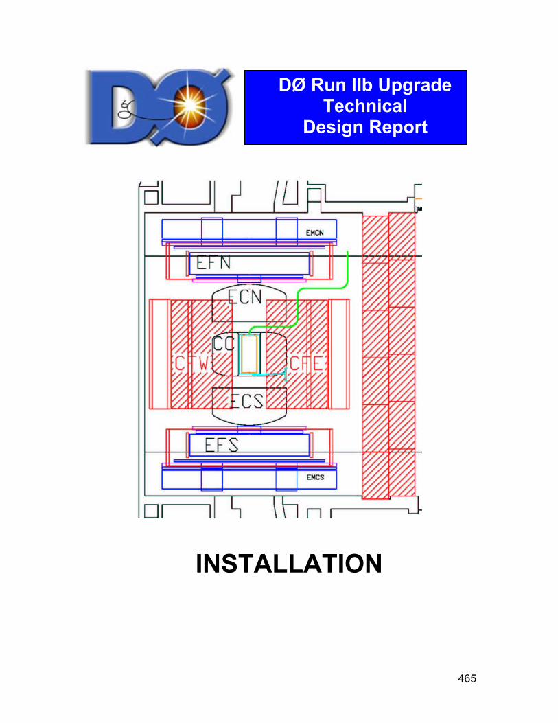
465
INSTALLATION
DØ Run IIb UpgradeTechnical
Design Report

DØ Run IIb Installation
466
(This page intentionally left blank)

DØ Run IIb Installation
467
INSTALLATION CONTENTS
1 Installation Introduction .......................................................... 469
1.1 Overview...........................................................................................469
1.2 Scope................................................................................................469
1.3 Schedule...........................................................................................470
1.4 Management .....................................................................................471
2 Installation Specifics .............................................................. 472
2.1 Run IIa Silicon Removal....................................................................472
2.2 Run IIb Silicon Installation.................................................................472
2.3 Technical Commissioning of Silicon..................................................473
2.4 L1 Calorimeter Trigger System .........................................................473
2.5 L1 Cal Track Match...........................................................................473
2.6 L1 Central Track Trigger ...................................................................473
2.7 L2 Beta Processors...........................................................................474
2.8 Silicon Track Trigger Upgrade ..........................................................474
3 Installation Resources and Schedule..................................... 475
3.1 Resources.........................................................................................475
3.2 Schedule...........................................................................................475
4 Installation Summary ............................................................. 477

DØ Run IIb Installation
468
(This page intentionally left blank)

DØ Run IIb Installation
469
1 Installation Introduction 1.1 Overview
A new silicon microstrip detector will be fabricated for the DØ detector for Run IIb. Upgrades to the DØ trigger system will also be prepared for Run IIb. It is important to conduct the installation of these systems to minimize the shutdown period of the Tevatron collider between Run IIa and Run IIb.
Because the new silicon detector has been designed to part at z = 0, each of the two halves of the system are sufficiently compact to permit them to be installed without rolling the DØ detector out of the collision hall. This feature will save substantial time and effort during the shutdown. Also, the Run IIa silicon signal cable plant and high voltage system will be reused for Run IIb, saving substantial effort and time during the installation period.
The majority of the new trigger system elements will be installed in the DØ Moveable Counting House (MCH), so they do not require substantial access to the detector during the shutdown.
The DAQ/Online computing system will also receive substantial upgrades for Run IIb. Because these upgrades consist largely of enhanced-capacity single components that will be installed over time without significant change to the architecture of the Run IIa system, their installation can be conveniently managed along with general DAQ/Online system support and maintenance. Thus their installation will not be discussed herein.
Finally, certain of the infrastructure needs of both the silicon and trigger systems can be prepared in advance so installation and commissioning time are minimized. 1.2 Scope
The Run IIb Installation task will concern itself with the installation and technical commissioning of the elements of the DØ detector that have been upgraded for Run IIb:
• Silicon Microstrip Detector, • Level 1 Calorimeter Trigger, • Level 1 Calorimeter Track Matching, • Level 1 Central Track Trigger, • Level 2 β Processors, • Silicon Track Trigger, • Plus the associated detector infrastructure for each of these elements.
For the Installation task, “technical commissioning” means that after an
upgrade element is installed, it will be powered up and performance-tested until it is deemed “ready for beam”, i.e. the DØ detector can be closed and the collision hall secured because daily access to the element in question is no longer required. For example, for the silicon detector, technical commissioning includes demonstrating that all components power up safely to design voltage and current
DØ Run IIb Installation
470
and that all actively cooled components stabilize at desired temperatures. Technical commissioning also includes demonstrating that all crates can be downloaded, that all electronic channels are properly mapped to physics channels, that noise, pedestals, (even cosmic rays if appropriate) are understood, that simulations using stored patterns are processed properly by the system, and that the silicon software is sufficiently mature to operate the system as required. Technical commissioning ends when the system is deemed by its commissioners to be fully ready for beam.
1.3 Schedule
Given the date of completion of the Run IIb DØ silicon detector at SiDet it is appropriate to plan the overall installation schedule so that when the tasks necessary to remove the existing Run IIa silicon system are considered, the latest access time to the detector (i.e. the shutdown date of the Tevatron) can be chosen. This date is found to be approximately 9 weeks in advance of the completion of the silicon.
The shutdown will begin with the opening of the detector and the draining of the coolant from the existing silicon, followed promptly by the uncabling of the silicon. Then the beryllium beampipe and the silicon system itself will be removed, along with the old adapter card supports (“horseshoes”). After the new horseshoes are installed, the Run IIb silicon will be delivered and installed, the cables reconnected, and the new beampipe inserted. This point will be reached approximately 10 weeks after the new silicon is delivered.
At this time, the technical commissioning of the silicon will begin because during the preceding weeks the new silicon infrastructure (interface boards, power supplies, temperature and radiation monitoring systems, cooling systems, etc.) will have been installed and hooked up. Approximately 11 weeks will be required for technical commissioning which brings the new silicon system to the state that it is ready for beam. At this point the detector will be closed and Tevatron operations may resume. The total shutdown time of the Tevatron is approximately 30 weeks.
Also at the beginning of the shutdown, the Level 1 Calorimeter trigger will be removed from the MCH and the new system installed. The other elements of the trigger upgrades will be installed, and in the ensuing weeks all new trigger systems will be brought to a state of operation such that they too are ready for beam.
The installation task is complete when the detector is closed up and ready for beam.
Note that certain of the infrastructure tasks (e.g. preparation of the racks for the L1 Cal trigger, preliminary installation of the silicon cooling system on the sidewalks outside the collision hall, testing and labeling of cables, etc.) will begin well before the shutdown of the Tevatron. These tasks are included in the installation schedule because their timely completion directly bears on the

DØ Run IIb Installation
471
success of the post-shutdown portions of the installation schedule. These infrastructure tasks begin approximately one year before the end of Run IIa. 1.4 Management
Four Level 3 managers (one for silicon mechanical, two for silicon electronic, and one for trigger) are presently in place who have expertise in the electrical and mechanical details of the silicon detector or are knowledgeable in matters pertaining to the trigger system. Each has Run IIa installation experience.
These managers have already begun to plan the infrastructure tasks appropriate to their positions and they will direct these activities during the last year or so of Run IIa. For example, the Level 3 silicon electronic installation manager will participate in the design of the new silicon low voltage system and cables so that installation planning for these elements is detailed and credible. As soon as all the new cable systems are defined and understood, the procured cables will be tested, labeled, bundled if appropriate, and held in full readiness for installation when the shutdown begins. Effort is included in the Installation schedule that provides for a “cable czar” who will be responsible for all aspects of cable preparation and installation. That person will provide continuity for this substantial responsibility and with a Level 3 silicon electronic manager will direct the installation of the cables. Similar considerations pertain to the silicon cooling systems, and the adapter card supports.
The Level 3 managers also have begun to plan the primary installation activities (i.e. silicon and trigger systems), and they will direct these tasks during the shutdown. During Run IIa the Level 3 managers will meet periodically with the principals (engineers and physicists) of the silicon and trigger tasks so that full understanding of the state of readiness of these systems is monitored and understood. For example, the redesign of the high voltage system will be tracked so that installation planning is relevant, detailed and credible. Likewise, the planning for the redressing of the L1 Calorimeter trigger cable plant will be thorough and fully organized so when the shutdown begins the work can proceed with minimal chance of significant upset to the schedule.
DØ Run IIb Installation
472
2 Installation Specifics 2.1 Run IIa Silicon Removal
Immediately after the opening of the detector, the “low mass” cables from the existing silicon detector will be disconnected from the adapter cards on the horseshoes and the beryllium beampipe will be removed. This beampipe will be withdrawn out through the beampipe bore of an end calorimeter. The 80-conductor “high mass” cables from the adapter cards will be removed from the horseshoes and carefully draped aside on the face of the central calorimeter (CC) for reuse. The H-disks of the old silicon tracker will then be removed from the Central Fiber Tracker (CFT), and both the north (N) and south (S) halves of the silicon tracker removed in turn. To ensure no damage to the CFT, the installation fixturing used to install the silicon for RunIIa will be reused to carefully remove the silicon detector halves. While the N silicon is withdrawn, the S horseshoe will be demounted, and vice-versa.
Also as soon as the detector is opened, one crate’s worth of interface boards will be removed from one IB crate beside the CC. These boards will be express-shipped to KSU for reworking for Run IIb. Because it is estimated to take three weeks to modify and test these boards, it is important to get the KSU facility “up and running” promptly. Helpfully, one crate’s worth of boards will already have been modified at KSU for use at SiDet much earlier. The balance of the eight IB crates will be removed and emptied over a two-week period and the boards shipped to KSU to be folded into the modify/test schedule there. As each IB crate is removed the 80-conductor cables that fed it will be tested and certified for reuse in RunIIb. The low voltage (LV) power supplies and ancillary components above the IB crates will be removed at this time as well. 2.2 Run IIb Silicon Installation
The new horseshoes will be installed on CC and the precision mounts installed in the CFT that support the new silicon. As soon as the latter are verified for proper alignment, the silicon will be installed in CFT. As was done during Run IIa, the two halves will be installed separately using a trolley and table. Novel for Run IIb however, the z=0 joint will be made up by sliding both halves towards an EC to expose the fasteners at the z=0 joint. The joined halves will then be moved back in z to the center of the CFT and the end mounts made up and checked for alignment. The cooling and dry gas systems will be connected and put into operation, and the milestone “Silicon installed in CFT” will have been achieved.
While work inside the detector has proceeded, the new low voltage system and augmented high voltage (HV) systems have been installed in the MCH and on the detector platform and checked.
In the detector itself, after the silicon is in place, the new junction cards (which carry the new twisted-pair signal cables) will be installed in the bore of CFT and the flex-cables from the silicon connected to them. The original 80-conductor cables will be connected to the new adapter cards on the horseshoes,
DØ Run IIb Installation
473
and the new beryllium beam tube will be installed in the silicon. Reworked and tested interface boards will have steadily returned from KSU and will have been installed in IB crates in sequence. 2.3 Technical Commissioning of Silicon
Inasmuch as the HV and LV power supply systems will have by this point been cabled to the IB crate area and horseshoes, and the cooling system will be up and running, and the detector fully cabled, the technical commissioning of the silicon will begin, quadrant by quadrant as the IB crates are loaded . As the fraction of the detector that is commissioned grows, the online and level 3 software will be tested, and all hardware channel to physics channel mappings will be verified.
When the technical commissioning is complete, the detector is closed and the silicon system is ready for beam. 2.4 L1 Calorimeter Trigger System
Immediately at the beginning of the shutdown, the 13 Level 1 Calorimeter Trigger racks will be uncabled and removed from MCH1. The L1 Cal trigger cables underneath the floor in MCH1 will be extracted from the very limited volume where they were installed prior to the beginning of Run I nearly 15 years ago, and the bundles undone, sorted, redressed so they will reach the new trigger crates, and tested. When this very time-consuming job is completed, the new racks (prepared and tested prior to the shutdown) will be brought into MCH1 and fastened in place. The new trigger crates containing the ADF’s (ADC with Digital Filtering), TAB’s (Trigger Algorithm Boards), and GAB’s (Global Algorithm Boards) will be reinstalled in the racks, all rack services reconnected, and the very extensive technical commissioning of L1 Cal trigger will begin.
It should be noted that critical services (chief among which is the VESDA fire detection system) for the trigger framework (TFW) will be maintained from the beginning of the work in MCH1 so that the TFW remains available throughout the shutdown (except for perhaps a day or two at the beginning). This means that work on the DAQ, as well as commissioning activities for the silicon and the trigger, can proceed when otherwise ready. 2.5 L1 Cal Track Match
After a modest period of installation for the two new VME crates with new trigger components (SLDB’s – Serial Link Daughter Boards), MTCxx’s and MTCM’s (L1 Track and Cal Match), and MTFB (Muon Trigger Flavor Boards), the extensive system tests of the new Cal Track Match system can begin as soon as one-eight of the L1 Cal Trig system is up and running. 2.6 L1 Central Track Trigger
After a short period of installation of the new DFEA’s (Digital Front End Axial) daughter boards in existing crates, technical commissioning of this system can begin, since the TFW will be available soon after the shutdown begins and the

DØ Run IIb Installation
474
balance of the DAQ is not expected to experience significant downtime as it too is upgraded
2.7 L2 Beta Processors
The new beta SBC’s (single board computers) will be direct replacements of existing SBC’s in the L2 Trigger crates, so installation of these elements will be straightforward. Commissioning of these new processors will be completed early in the shutdown. 2.8 Silicon Track Trigger Upgrade
An additional 20 VME motherboards, with a variety of daughterboards and special-function modules mostly from Run IIa, plus repeaters, and additional splitters and fiber cables, will be installed in MCH2. Due to the simplicity of this work, it will be completed promptly, but technical commissioning of the STT upgrade cannot finish until the L1 Cal Track Match is substantially commissioned and the silicon is also substantially commissioned. These latter two constraints mean that the STT will not be ready for beam until late in the shutdown.

DØ Run IIb Installation
475
3 Installation Resources and Schedule 3.1 Resources
Installation effort by technicians and physicists dominates the cost of installation. With modest leveling a peak of 17.5 FTE technicians and a peak of 19.1 FTE physicists are required during the shutdown. Over the 8 months the average number of technicians is 9.5 FTE’s and the average number of physicists is 13.7 FTE’s. The peak for electrical engineers is 3.2 FTE’s and for mechanical engineers, 2.3 FTE’s. 3.2 Schedule
The schedule (Table 1) developed for the installation period necessarily keys to the completion date of the silicon at SiDet. Additional trigger element completion dates are also inherited, but they are not found to constrain the installation schedule. These milestones in Table 1 are shown in italic to distinguish them from those internal to the installation itself, and red text guides the eye to key milestones.

DØ Run IIb Installation
476
Table 1. Installation milestones.
Milestone Date L1 Cal/Track Match Production and Testing Completed 6/16/04 STT Hardware production complete 12/8/04 Level 2 Beta Production Complete 1/28/05 L1 Cal TAB/GAB Production And Testing Complete 2/1/05 L1 Central Track Trigger DFEA Production And Testing Complete 3/9/05 Shutdown for Installation Begins 5/25/05 Detector Open and Ready for Access 6/1/05 Run IIa Silicon H-Disks Removed 6/16/05 Run IIa North and South Silicon Detectors Removed 6/30/05 STT Hardware Installed 7/7/05 Level 2 Upgrade Beta Installed & Commissioned 7/11/05 Run IIa North and South Cable Horseshoes Installed on EC Faces 7/15/05 Silicon Ready To Move To DAB 7/22/05 Silicon Infrastructure Prepared 8/1/05 Level 1 Tracking Installation Complete 8/18/05 Detector Installed In Fiber Tracker 8/22/05 RunIIb Silicon High Voltage System Installed 9/1/05 RunIIb Silicon Low Voltage System Installed 9/9/05 Ready to begin Technical Commissioning of Silicon 9/28/05 Silicon 80-conductor and Clock Cables Installed 10/4/05 Run IIb Beam Tube Installed 10/18/05 Level 1 Calorimeter Trigger Installed 12/20/05 Level 1 Calorimeter Track Matching Installation Complete 12/20/05 Silicon Track Trigger Operational 12/20/05 Trigger Upgrade Ready for Beam 12/20/05 Silicon System Ready for Beam 12/22/05 Run IIb Detector Ready for Beam 12/22/05

DØ Run IIb Installation
477
4 Installation Summary The technical details of the installation of the RunIIb silicon will not vary
greatly from those of the Run IIa silicon. Hindsight is a good teacher, and it is believed that with careful advance planning and thorough preparation of infrastructure (cabling, etc.), plus the recycling of much of the Run IIa cable plant, the schedule for the Run IIb installation can be significantly shorter than that experienced for Run IIa, when cabling alone required five months elapsed time, working two shifts per day. Major simplifications from the Run IIa experience include the fact that no operation of the Tevatron is expected during the installation period as happened for Run IIa, that the high-mass cables will not be replaced, and that all electronics will be on hand and installed before cabling begins.
As the milestone table shows, the infrastructure tasks will be completed before any of the elements they provide are required, and all of the trigger upgrade electronics will be in hand before Run IIa ends. The same engineering team that prepared the silicon will be available to guide its installation, and many of the physicists who participated in the commissioning of the Run IIa silicon are expected to participate in the commissioning of the Run IIb silicon.

478
(This page intentionally left blank)
479
SUMMARY
DØ Run IIb Upgrade Technical
Design Report

480
(This page intentionally left blank)

481
SUMMARY
Clear and compelling physics goals, as outlined in the first part of this report, are the driving force behind the DØ Run IIb upgrade. The Fermilab Tevatron collider provides a unique opportunity during the next several years to make incisive searches for the Higgs, SUSY, and a wide variety of new phenomena beyond the Standard Model. These exciting prospects for a major discovery are complemented by the ability to make sensitive studies of top quark properties, precision electroweak measurements, and a wide range of investigations of Standard Model predictions.
Success in these goals can only be achieved by upgrading the DØ detector to meet the challenges posed by extended running at high luminosity. We present in this report our studies demonstrating the need for upgrades to the silicon detector, the trigger, and the DAQ/online computing systems. These studies establish the performance of the proposed upgrades, evaluated both in terms of technical performance and in the metric of the Standard Model Higgs search.
The bulk of this report deals with the detailed technical design of the proposed upgrades. Extensive engineering studies have been performed, and detailed designs for all major components of the Run IIb upgrade are described. An aggressive prototyping phase is underway to verify the feasibility and performance of the design. Long leadtime elements, such as development of the SVX4 chip, have been given special attention. Finally, extensive simulations have verified that the design meets the performance requirements set by the Run IIb physics program.

482
(This page intentionally left blank)