raa458100gnp/raa457100gbm wireless charging system
TRANSCRIPT
APPLICATION NOTE
R19AN0041EJ0100Rev.1.00
2017.03.31
RAA458100GNP / RAA457100GBMLow Power Wireless Charging System Configuration and Function
Page 1 of 18R19AN0041EJ0100 Rev.1.002017.03.31
Contents1. Battery charging system configuration
1.1 Overview of pin function1.2 Battery charging system configuration, operation and pin settings1.3 Power transmission start or stop timing1.4 Data configuration of EEPROM(TxROM)
2. WPT communication function (communication function on wireless power transfer carrier)2.1 Packet configuration of WPT communication2.2 Modulation and demodulation method, and detailed demodulation function
3. Automatic transmission power control function and WPT communication procedure3.1 Overview of automatic transmission power control function3.2 WPT communication packet in ATPC Mode, MCU Control Mode3.3 Automatic transmission power control timing3.4 Control error and RECT pin converged voltage3.5 Update timing for ADC output codes storage registers3.6 WPT communication procedure in each charging system configuration
4. Error detection function4.1 Error detection items and post-processing4.2 Error detection items in each charging system configuration4.3 Over power detection of transmission power
5. Test registers
OutlineRAA458100 / RAA457100 are power control IC for wireless charging. RAA458100 / RAA457100 are suitable for small capacity Li-ion
secondary battery charging and various battery charging systems can be constructed by some function setting pins.To adjust transmission power automatically, and to set battery charging parameters (RAA457100 register) from a transmitter system can
be realized by bi-directional wireless communication function implemented in RAA458100 / RAA457100. Also, register accessing to amain device (RxMCU) in a receiver system can be performed from a main device (TxMCU) in a transmitter system. This documentdescribes some wireless charging system configuration examples, the wireless communication function and the automatic transmissionpower control function.
The following table shows the abbreviations and the meanings used in this document.
Term Description
TxIC Wireless charging system transmitter IC RAA458100GNP.
RxIC Wireless charging system receiver IC RAA457100GBM.
TxROM, EEPROM EEPROM in transmitter system.
TxMCU The device connected to TxIC by 2-wire interface. (mainly microcomputer)
RxMCU The device connected to RxIC by 2-wire interface. (mainly microcomputer)
Tx system Wireless charging transmitter system. It is constructed by “TxIC only” or “TxIC and TxMCU” or “TxIC and EEPROM”.
Rx system Wireless charging receiver system. It is constructed by “RxIC only” or “RxIC and RxMCU”.
WPT communication Communication on wireless power transmission carrier signal.
Tx2Rx WPT communication WPT communication from TxIC to RxIC.
Rx2Tx WPT communication WPT communication from RxIC to TxIC.
T_Header The header of Tx2Rx WPT communication packet.
R_Header The header of Rx2Tx WPT communication packet..
T_0xXX D[X]Register address and data bit of TxIC(Example : T_0x02 D[4:1] means that TxIC register address is 0x02, register data bits are D4, D3, D2, D1)
R_0xXX D[X]Register address and data bit of RxIC.(Example : R_0x10 D[7:5] means that RxIC register address is 0x10, register data bits are D7, D6, D5)
Abbreviations and the meanings
Remark : The values described in this document are reference values, not guaranteed.
Low Power Wireless Charging System Configuration and FunctionRAA458100GNP and RAA457100GBM
Page 2 of 18R19AN0041EJ0100 Rev.1.002017.03.31
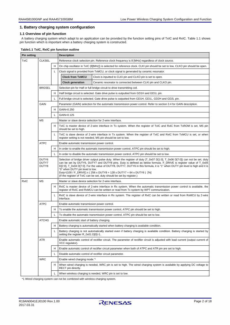
Table1.1 TxIC, RxIC pin function outline
Pin setting Description
TxIC CLKSEL Reference clock selection pin. Reference clock frequency is 8 [MHz] regardless of clock source.
H On chip oscillator in TxIC (8[MHz]) is selected for reference clock. CLKI pin should be set to low, CLKO pin should be open.
L Clock signal is provided from TxMCU, or clock signal is generated by ceramic resonator.
Clock from TxMCU Clock is inputted to CLKI pin and CLKO pin is set to open.
Clock generation Ceramic resonator is connected between CLKI pin and CLKO pin.
BRGSEL Selection pin for Half or full bridge circuit to drive transmitting coil.
H Half bridge circuit is selected. Gate drive pulse is outputted from GD1H and GD1L pin.
L Full bridge circuit is selected. Gate drive pulse is outputted from GD1H, GD1L, GD2H and GD2L pin.
GAIN Parameter (GAIN) selection for the automatic transmission power control. Refer to section 3.4 for GAIN description.
H GAIN=0.250
L GAIN=0.125
MS Master or slave device selection for 2-wire interface.
H TxIC is master device of 2-wire interface in Tx system. When the register of TxIC and RxIC from TxROM is set, MS pinshould be set to high.
L TxIC is slave device of 2-wire interface in Tx system. When the register of TxIC and RxIC from TxMCU is set, or whenregister setting is not needed, MS pin should be set to low.
ATPC Enable automatic transmission power control.
H In order to enable the automatic transmission power control, ATPC pin should be set to high.
L In order to disable the automatic transmission power control, ATPC pin should be set to low.
DUTY6DUTY7DUTY8
Selection of bridge driver output pulse duty. When the register of duty (T_0x07 D[1:0], T_0x06 D[7:0]) can not be set, dutycan be set by DUTY6, DUTY7 and DUTY8 pins. Duty is defined as below formula. F_DRIVE is register value of T_0x05D[2:0], T_0x04 D[7:0]. For the value of DUTY8, DUTY7, DUTY6 in this formula, it is “1” when DUTY pin level is high and it is“0” when DUTY pin level is low.Duty=(100 / F_DRIVE) x ( 256 x DUTY8 + 128 x DUTY7 + 64 x DUTY6 ) [%](If the register of TxIC can be set, duty should be set by register.)
RxIC MS Master or slave device selection for 2-wire interface.
H RxIC is master device of 2-wire interface in Rx system. When the automatic transmission power control is available, theregister of RxIC and RxMCU can be written or read from Tx system by WPT communication.
L RxIC is slave device of 2-wire interface in Rx system. The register of RxIC can be written or read from RxMCU by 2-wireinterface.
ATPC Enable automatic transmission power control.
H To enable the automatic transmission power control, ATPC pin should be set to high.
L To disable the automatic transmission power control, ATPC pin should be set to low.
ATCHG Enable automatic start of battery charging.
H Battery charging is automatically started when battery charging is available condition.
L Battery charging is not automatically started even if battery charging is available condition. Battery charging is started bysetting the register R_0x01 D[0]=1.
ATR Enable automatic control of rectifier circuit. The parameter of rectifier circuit is adjusted with load current (output current ofVCC regulator).
H Enable automatic control of rectifier circuit parameter when both of ATPC and ATR pin are set to high.
L Disable automatic control of rectifier circuit parameter.
WRC Enable wired charging mode.*1
H When wired charging is needed, WRC pin is set to high. The wired charging system is available by applying DC voltage toRECT pin directly.
L When wireless charging is needed, WRC pin is set to low.
*1 Wired charging system can not be combined with wireless charging system.
1. Battery charging system configuration
1.1 Overview of pin functionA battery charging system which adapt to an application can be provided by the function setting pins of TxIC and RxIC. Table 1.1 shows
pin function which is important when a battery charging system is constructed.
Low Power Wireless Charging System Configuration and FunctionRAA458100GNP and RAA457100GBM
Page 3 of 18R19AN0041EJ0100 Rev.1.002017.03.31
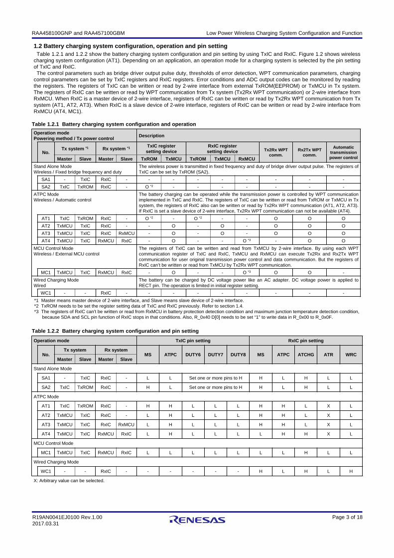
1.2 Battery charging system configuration, operation and pin settingTable 1.2.1 and 1.2.2 show the battery charging system configuration and pin setting by using TxIC and RxIC. Figure 1.2 shows wireless
charging system configuration (AT1). Depending on an application, an operation mode for a charging system is selected by the pin settingof TxIC and RxIC.
The control parameters such as bridge driver output pulse duty, thresholds of error detection, WPT communication parameters, chargingcontrol parameters can be set by TxIC registers and RxIC registers. Error conditions and ADC output codes can be monitored by readingthe registers. The registers of TxIC can be written or read by 2-wire interface from external TxROM(EEPROM) or TxMCU in Tx system.The registers of RxIC can be written or read by WPT communication from Tx system (Tx2Rx WPT communication) or 2-wire interface fromRxMCU. When RxIC is a master device of 2-wire interface, registers of RxIC can be written or read by Tx2Rx WPT communication from Txsystem (AT1, AT2, AT3). When RxIC is a slave device of 2-wire interface, registers of RxIC can be written or read by 2-wire interface fromRxMCU (AT4, MC1).
Table 1.2.1 Battery charging system configuration and operation
Operation modePowering method / Tx power control
Description
No.Tx system *1 Rx system *1 TxIC register
setting deviceRxIC register setting device Tx2Rx WPT
comm.Rx2Tx WPT
comm.
Automatictransmission power controlMaster Slave Master Slave TxROM TxMCU TxROM TxMCU RxMCU
Stand Alone ModeWireless / Fixed bridge frequency and duty
The wireless power is transmitted in fixed frequency and duty of bridge driver output pulse. The registers ofTxIC can be set by TxROM (SA2).
SA1 - TxIC RxIC - - - - - - - - -
SA2 TxIC TxROM RxIC - O *2 - - - - - - -
ATPC ModeWireless / Automatic control
The battery charging can be operated while the transmission power is controlled by WPT communicationimplemented in TxIC and RxIC. The registers of TxIC can be written or read from TxROM or TxMCU in Txsystem, the registers of RxIC also can be written or read by Tx2Rx WPT communication (AT1, AT2, AT3).If RxIC is set a slave device of 2-wire interface, Tx2Rx WPT communication can not be available (AT4).
AT1 TxIC TxROM RxIC - O *2 - O *2 - - O O O
AT2 TxMCU TxIC RxIC - - O - O - O O O
AT3 TxMCU TxIC RxIC RxMCU - O - O - O O O
AT4 TxMCU TxIC RxMCU RxIC - O - - O *3 - O O
MCU Control ModeWireless / External MCU control
The registers of TxIC can be written and read from TxMCU by 2-wire interface. By using each WPTcommunication register of TxIC and RxIC, TxMCU and RxMCU can execute Tx2Rx and Rx2Tx WPTcommunication for user original transmission power control and data communication. But the registers ofRxIC can’t be written or read from TxMCU by Tx2Rx WPT communication.
MC1 TxMCU TxIC RxMCU RxIC - O - - O *3 O O -
Wired Charging ModeWired
The battery can be charged by DC voltage power like an AC adapter. DC voltage power is applied toRECT pin. The operation is limited in initial register setting.
WC1 - - RxIC - - - - - - - - -
*1 Master means master device of 2-wire interface, and Slave means slave device of 2-wire interface.*2 TxROM needs to be set the register setting data of TxIC and RxIC previously. Refer to section 1.4.*3 The registers of RxIC can’t be written or read from RxMCU in battery protection detection condition and maximum junction temperature detection condition,
because SDA and SCL pin function of RxIC stops in that conditions. Also, R_0x40 D[0] needs to be set “1” to write data in R_0x00 to R_0x0F.
Table 1.2.2 Battery charging system configuration a nd pin setting
Operation mode TxIC pin setting RxIC pin setting
No.Tx system Rx system
MS ATPC DUTY6 DUTY7 DUTY8 MS ATPC ATCHG ATR WRCMaster Slave Master Slave
Stand Alone Mode
SA1 - TxIC RxIC - L L Set one or more pins to H H L H L L
SA2 TxIC TxROM RxIC - H L Set one or more pins to H H L H L L
ATPC Mode
AT1 TxIC TxROM RxIC - H H L L L H H L X L
AT2 TxMCU TxIC RxIC - L H L L L H H L X L
AT3 TxMCU TxIC RxIC RxMCU L H L L L H H L X L
AT4 TxMCU TxIC RxMCU RxIC L H L L L L H H X L
MCU Control Mode
MC1 TxMCU TxIC RxMCU RxIC L L L L L L L H L L
Wired Charging Mode
WC1 - - RxIC - - - - - - H L H L H
X: Arbitrary value can be selected.
Low Power Wireless Charging System Configuration and FunctionRAA458100GNP and RAA457100GBM
Page 4 of 18R19AN0041EJ0100 Rev.1.002017.03.31
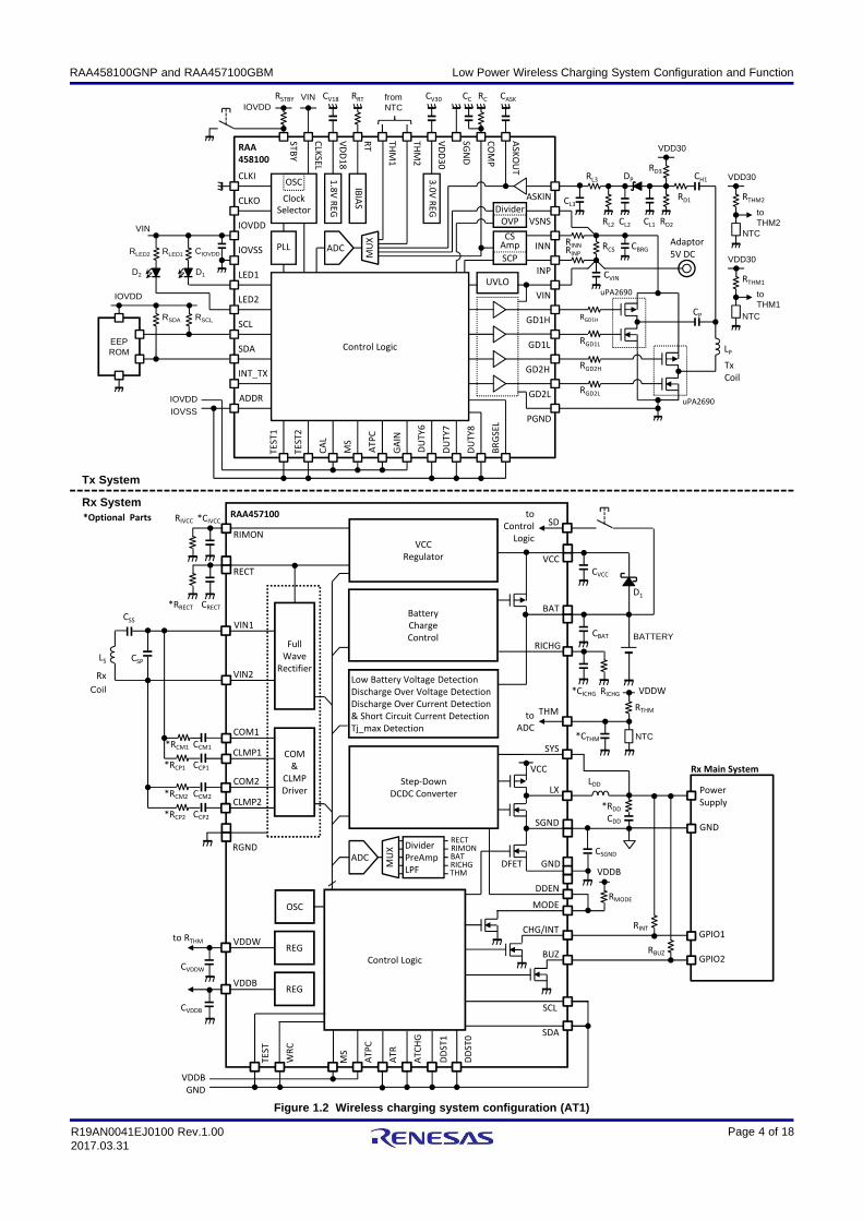
Figure 1.2 Wireless charging system configuration (AT1)
RAA
458100
Control Logic
ST
BY
AS
KO
UT
CO
MP
SG
ND
VD
D3
0
TH
M2
TH
M1
RT
VD
D1
8
CLK
SE
L
CLKI
CLKO
IOVDD
IOVSS
LED1
LED2
SCL
SDA
INT_TX
ADDR
TE
ST
1
TE
ST
2
CA
L
MS
AT
PC
GA
IN
DU
TY
8
DU
TY
7
DU
TY
6
BR
GS
EL
PGND
GD2L
GD2H
GD1L
GD1H
VIN
INP
INN
VSNS
ASKIN
UVLO
1.8
V R
EG
IBIA
S
PLL
3.0
V R
EG
ADC
MU
X
Divider
OVP
OSC
Clock
Selector
SCP
CSAmp
NTC
NTC
IOVSSIOVDD
toTHM1
toTHM2
VDD30
VDD30
fromNTCIOVDD
VDD30
Tx
Coil
RGD1H
RGD1L
RGD2H
RGD2L
uPA2690
uPA2690
RCS CBRGAdaptor
5V DC
LP
CP
Tx System
Rx System
CVIN
RINP
RINN
CH1
RD1
RD2
RD3
CL1CL2
CL3
RL3
CASKCC RCCV30CV18 RRTRSTBY
RTHM2
RTHM1
GND
RL2
DP
BATTERY
LDD
CDD
*CIVCCRIVCC
CVDDW
CVDDB
CCP2
CCP1
CCM1
CCM2
CSP
CSS
CRECT
RICHG
RAA457100
Rx
Coil
CBAT
CVCC
RTHM
Low Battery Voltage Detection
Discharge Over Voltage Detection
Discharge Over Current Detection
& Short Circuit Current Detection
Tj_max Detection
Step-Down
DCDC Converter
Control Logic
DDEN
SYS
RECT
SDA
SCL
LX
VCC
THM
BAT
MODE
CHG/INT
COM1
COM2
CLMP1
CLMP2
VIN1
VIN2
COM
&
CLMP
Driver
VDDW
VDDB
RIMON
REG
OSC
SGND
RGND
TE
ST
Full
Wave
Rectifier
RICHG
GND
Battery
Charge
Control
VCC
Regulator
REG
D1
NTC
VDDW*CICHG
to RTHM
*RCM1
*RCM2
*RCP1
*RCP2
VCC
VDDB
BUZ
MS
DD
ST
0
DD
ST
1
AT
R
AT
CH
G
AT
PC
DFET
SD
RMODE
WR
C
*CTHM
*RRECT
*Optional Parts
*RDD
to
Control
Logic
CSGNDADC
MU
X Divider
PreAmp
LPF
RECTRIMONBATRICHGTHM
to
ADC
Power
Supply
Rx Main System
GND
RBUZ
RINTGPIO1
GPIO2
VDDB
LS
VIN
EEPROM
VIN
IOVDD
RLED1RLED2
RSCLRSDA
D1D2
CIOVDD
Low Power Wireless Charging System Configuration and FunctionRAA458100GNP and RAA457100GBM
Page 5 of 18R19AN0041EJ0100 Rev.1.002017.03.31
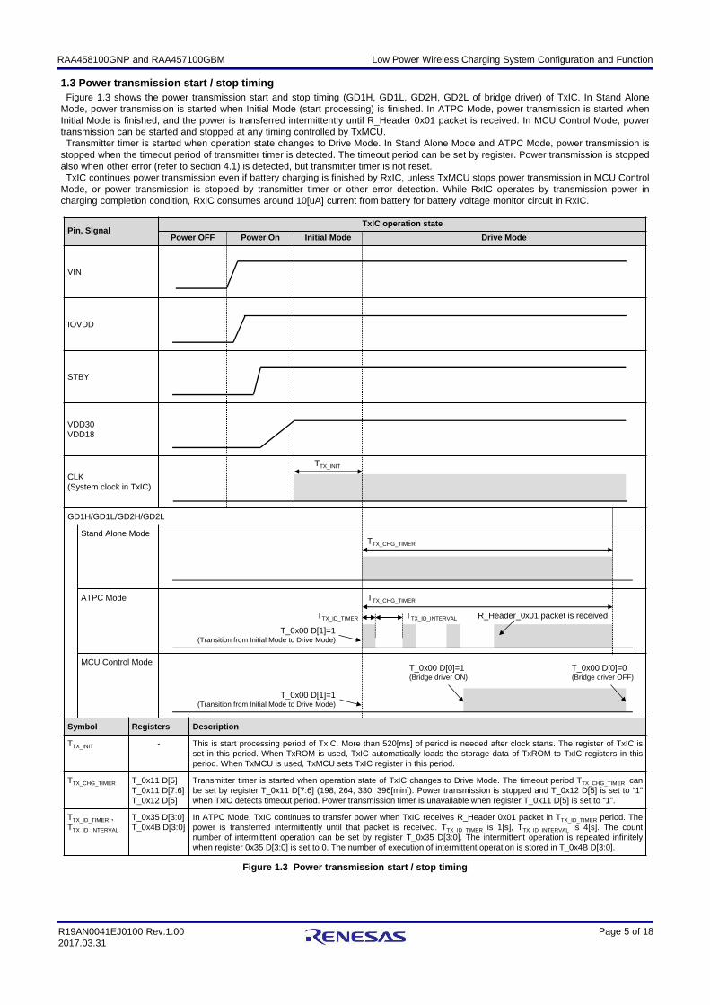
Pin, SignalTxIC operation state
Power OFF Power On Initial Mode Drive Mode
VIN
IOVDD
STBY
VDD30VDD18
CLK(System clock in TxIC)
GD1H/GD1L/GD2H/GD2L
Stand Alone Mode
ATPC Mode
MCU Control Mode
1.3 Power transmission start / stop timingFigure 1.3 shows the power transmission start and stop timing (GD1H, GD1L, GD2H, GD2L of bridge driver) of TxIC. In Stand Alone
Mode, power transmission is started when Initial Mode (start processing) is finished. In ATPC Mode, power transmission is started whenInitial Mode is finished, and the power is transferred intermittently until R_Header 0x01 packet is received. In MCU Control Mode, powertransmission can be started and stopped at any timing controlled by TxMCU.
Transmitter timer is started when operation state changes to Drive Mode. In Stand Alone Mode and ATPC Mode, power transmission isstopped when the timeout period of transmitter timer is detected. The timeout period can be set by register. Power transmission is stoppedalso when other error (refer to section 4.1) is detected, but transmitter timer is not reset.
TxIC continues power transmission even if battery charging is finished by RxIC, unless TxMCU stops power transmission in MCU ControlMode, or power transmission is stopped by transmitter timer or other error detection. While RxIC operates by transmission power incharging completion condition, RxIC consumes around 10[uA] current from battery for battery voltage monitor circuit in RxIC.
Symbol Registers Description
TTX_INIT - This is start processing period of TxIC. More than 520[ms] of period is needed after clock starts. The register of TxIC isset in this period. When TxROM is used, TxIC automatically loads the storage data of TxROM to TxIC registers in thisperiod. When TxMCU is used, TxMCU sets TxIC register in this period.
TTX_CHG_TIMER T_0x11 D[5]T_0x11 D[7:6]T_0x12 D[5]
Transmitter timer is started when operation state of TxIC changes to Drive Mode. The timeout period TTX_CHG_TIMER canbe set by register T_0x11 D[7:6] (198, 264, 330, 396[min]). Power transmission is stopped and T_0x12 D[5] is set to “1”when TxIC detects timeout period. Power transmission timer is unavailable when register T_0x11 D[5] is set to “1”.
TTX_ID_TIMER , TTX_ID_INTERVAL
T_0x35 D[3:0]T_0x4B D[3:0]
In ATPC Mode, TxIC continues to transfer power when TxIC receives R_Header 0x01 packet in TTX_ID_TIMER period. Thepower is transferred intermittently until that packet is received. TTX_ID_TIMER is 1[s], TTX_ID_INTERVAL is 4[s]. The countnumber of intermittent operation can be set by register T_0x35 D[3:0]. The intermittent operation is repeated infinitelywhen register 0x35 D[3:0] is set to 0. The number of execution of intermittent operation is stored in T_0x4B D[3:0].
Figure 1.3 Power transmission start / stop timing
TTX_INIT
TTX_CHG_TIMER
TTX_CHG_TIMER
TTX_ID_TIMER TTX_ID_INTERVAL
T_0x00 D[0]=1 (Bridge driver ON)
R_Header_0x01 packet is received
T_0x00 D[1]=1(Transition from Initial Mode to Drive Mode)
T_0x00 D[1]=1(Transition from Initial Mode to Drive Mode)
T_0x00 D[0]=0 (Bridge driver OFF)
Low Power Wireless Charging System Configuration and FunctionRAA458100GNP and RAA457100GBM
Page 6 of 18R19AN0041EJ0100 Rev.1.002017.03.31
1.4 Data configuration of EEPROM (TxROM)By applying EEPROM(TxROM) in Tx system, TxIC registers can be set. RxIC registers can be set by Tx2Rx WPT communication in
ATPC Mode(AT1). TxIC reads the data from EEPROM in start process(Initial Mode), and set the data into the register of TxIC. For theRxIC register setting, TxIC reads the RxIC register data stored in EEPROM and it sends the data to RxIC by Tx2Rx WPT communicationat proper timing. Tx2Rx WPT communication does not affect Rx2Tx WPT communication.
Table 1.4 shows the data configuration of EEPROM. Device slave address of EEPROM should be set 7’b1010000 or 7’b101001. TxICreads the data which were stored in EEPROM in turn from word address “0” to the address that completion code was written. Read cycleis random read cycle. TxIC can not write data to the EEPROM.
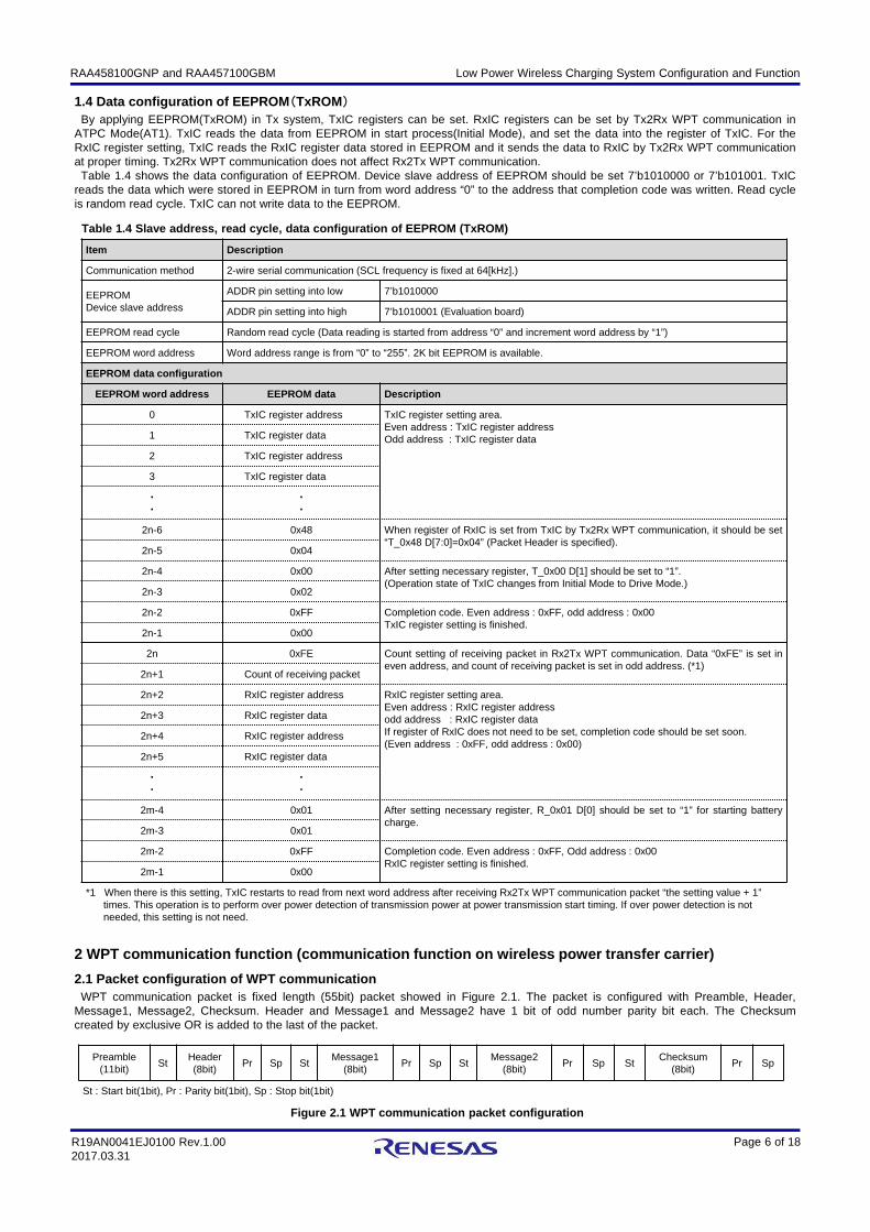
Preamble(11bit)
StHeader(8bit)
Pr Sp StMessage1
(8bit)Pr Sp St
Message2(8bit)
Pr Sp StChecksum
(8bit)Pr Sp
St : Start bit(1bit), Pr : Parity bit(1bit), Sp : Stop bit(1bit)
Figure 2.1 WPT communication packet configuration
2 WPT communication function (communication function on wireless power transfer carrier)
2.1 Packet configuration of WPT communicationWPT communication packet is fixed length (55bit) packet showed in Figure 2.1. The packet is configured with Preamble, Header,
Message1, Message2, Checksum. Header and Message1 and Message2 have 1 bit of odd number parity bit each. The Checksumcreated by exclusive OR is added to the last of the packet.
Table 1.4 Slave address, read cycle, data configuratio n of EEPROM (TxROM)
Item Description
Communication method 2-wire serial communication (SCL frequency is fixed at 64[kHz].)
EEPROMDevice slave address
ADDR pin setting into low 7’b1010000
ADDR pin setting into high 7’b1010001 (Evaluation board)
EEPROM read cycle Random read cycle (Data reading is started from address “0” and increment word address by “1”)
EEPROM word address Word address range is from “0” to “255”. 2K bit EEPROM is available.
EEPROM data configuration
EEPROM word address EEPROM data Description
0 TxIC register address TxIC register setting area.Even address : TxIC register addressOdd address : TxIC register data1 TxIC register data
2 TxIC register address
3 TxIC register data
・・
・・
2n-6 0x48 When register of RxIC is set from TxIC by Tx2Rx WPT communication, it should be set“T_0x48 D[7:0]=0x04” (Packet Header is specified).
2n-5 0x04
2n-4 0x00 After setting necessary register, T_0x00 D[1] should be set to “1”.(Operation state of TxIC changes from Initial Mode to Drive Mode.)
2n-3 0x02
2n-2 0xFF Completion code. Even address : 0xFF, odd address : 0x00TxIC register setting is finished.
2n-1 0x00
2n 0xFE Count setting of receiving packet in Rx2Tx WPT communication. Data “0xFE” is set ineven address, and count of receiving packet is set in odd address. (*1)
2n+1 Count of receiving packet
2n+2 RxIC register address RxIC register setting area.Even address : RxIC register addressodd address : RxIC register dataIf register of RxIC does not need to be set, completion code should be set soon.(Even address : 0xFF, odd address : 0x00)
2n+3 RxIC register data
2n+4 RxIC register address
2n+5 RxIC register data
・・
・・
2m-4 0x01 After setting necessary register, R_0x01 D[0] should be set to “1” for starting batterycharge.
2m-3 0x01
2m-2 0xFF Completion code. Even address : 0xFF, Odd address : 0x00RxIC register setting is finished.
2m-1 0x00
*1 When there is this setting, TxIC restarts to read from next word address after receiving Rx2Tx WPT communication packet “the setting value + 1”times. This operation is to perform over power detection of transmission power at power transmission start timing. If over power detection is notneeded, this setting is not need.
Low Power Wireless Charging System Configuration and FunctionRAA458100GNP and RAA457100GBM
Page 7 of 18R19AN0041EJ0100 Rev.1.002017.03.31
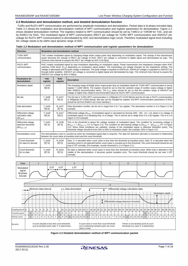
1 0 1
2.2 Modulation and demodulation method, and detaile d demodulation functionTx2Rx and Rx2Tx WPT communication are performed by amplitude modulation and demodulation. Packet data is bi-phase encoded data.
Table 2.2 shows the modulation and demodulation method of WPT communication and register parameters for demodulation. Figure 2.2shows detailed demodulation method. The registers related to WPT communication should be set by TxMCU or TxROM for TxIC, and setby RxMCU for RxIC. The modulated signal of WPT communication (RECT pin voltage for Tx2Rx WPT communication and ASKOUT pinvoltage for Rx2Tx WPT communication) is demodulated by ADC and demodulation logic circuit. Therefore modulated signal level includingDC voltage needs to be within input dynamic range of ADC.
Differential voltage detection threshold
Modulation depth
Data 1 1 0 1 0 0 1 1
Modulatedsignal
Bi-phaseEncode
0.5T 0.5T 1.0T
Minimum data interval Data decimation Differential voltage calculation data
Table 2.2 Modulation and demodulation method of WPT c ommunication and register parameters for demodulatio n
Direction Modulation and demodulation method
Tx2Rx WPTcommunication
TxIC creates modulated signal by changing bridge driver output pulse duty depending on modulation signal. The change of the transmissionpower becomes the change of RECT pin voltage of RxIC. RECT pin voltage is converted to digital signal and demodulated by logic. Theminimum time interval to acquire the RECT pin voltage by ADC is 62.5[us].
Rx2Tx WPTcommunication
RxIC creates modulated signal by load modulation depending on modulation signal. Power transmission line impedance changes when RxICswitches COM driver (CCM) depending on modulation signal pattern. The transmitting coil voltage changes by the impedance shifting. Thevoltage is attenuated and its peak voltage is detected. The peak voltage is inputted to ASKIN pin. ASKIN pin voltage is outputted to ASKOUT pinthrough buffer amplifier. ASKOUT pin voltage is converted to digital signal and demodulated by logic. The minimum time interval to acquire theASKOUT pin voltage by ADC is 64[us].
Parameters for demodulation
TxICregister
RxICregister
Description
Modulation depth T_0x0D D[6:0]
- The changing range of bridge driver output pulse duty as modulation depth for Tx2Rx WPT communication is set byregister T_0x0D D[6:0]. The register should be set so that the variation range of rectifier output voltage is higherthan 200[mV] (recommended value). The CCM value should be set so that the variation range of ASKOUT pinvoltage is higher than 100[mV] (recommended value) for Rx2Tx WPT communication.
Bit rate T_0x0E D[2:1]
R_0x27D[1:0]
The bit rate in Tx2Rx WPT communication is 125[bps](1.0T=1/125=8[ms]) and the bit rate in Rx2Tx communicationis 250[bps](1.0T=1/250=4[ms]). (Bit rate can be changed by register, but WPT communication parameters of RxICshould be set from RxMCU by 2-wire interface.)
Data decimation T_0x30 D[3:0]
R_0x27 D[7:4]
Data decimation number can be set in range from 0 to 7 by register. The decimation number is 3 in Figure 2.2 forexample.
Differential voltage calculation data(ΔVDIFF)
T_0x30 D[5:4]
R_0x27 D[3:2]
Differential voltage ΔVDIFF of modulated signal is calculated by formula V[N] - V[N - (m + 1)], where V is voltage ofmodulated signal, N is sampling time, m is integer. The m can be set in range from 0 to 3 by register. The m is 3 inFigure 2.2 for example.
Differential voltage detection threshold(ΔVDIFF_TH)
T_0x31 D[7:0]
R_0x28 D[7:0]
This is the threshold to detect the voltage variation of modulated signal. The condition for increasing voltage isΔVDIFF > + ΔVDIFF_TH (“U” in Figure 2.2). The condition for decreasing voltage is ΔVDIFF < - ΔVDIFF_TH (“D” in Figure2.2). When these conditions are satisfied, change of the modulated signal is detected (transition point). Thethreshold voltage should be from 25% to 50% of modulation depth. (for example, 50% in Figure 2.2)
Demodulation count The demodulation count is counted up when the modulated signal data is acquired. The data 0/1 detection (decode) is executed in relationshipbetween the count value at transition point and the count threshold.
Count thresholdfor data 0/1 decode
T_0x33 D[7:0]
R_0x29D[7:0]
Data “1” is decoded when count value is less than this threshold at transition point. Data “0” is decoded when thetransition point is not detected before count value is counted up to this threshold. The count threshold should be setnear 0.75T normally. (For example, counter threshold is 11 in Figure 2.2.)
Count thresholdfor no data
T_0x34D[7:0]
R_0x2AD[7:0]
No data is detected when count value is more than this threshold at transition point. When that is detected in themiddle of the demodulation, it becomes packet reception error. The count threshold should be set near 1.25Tnormally.
Figure 2.2 Detailed demodulation method of WPT comm unication packet
Sampling time N 0 1 2 3 4 5 6 7 8 9 10 11 12 13 14 15 16 17 18 19 20 21 22 23 24 25 26 27 28 29 30 31 32 33 34 35 36 37 38 39 40 41
Transition point - U U U U - - - - D D D D - - - - U U U U - - - - - - - - - - - - D D D D - - - - U
Demod. count - 0 1 2 3 4 5 6 7 8 9 10 11 12 13 14 15 0 1 2 3 4 5 6 7 8 9 10 11 12 13 14 15 0 1 2 3 4 5 6 7 0
Remarks
↑ ↑ ↑
If count value(8) is less than count threshold (11) at transition point, data “1” is determined.
If count value is more than count threshold (11) in detecting transition point, the count value is reset.
If there is not transition point at count threshold (11), data “0” is determined.
Low Power Wireless Charging System Configuration and FunctionRAA458100GNP and RAA457100GBM
Page 8 of 18R19AN0041EJ0100 Rev.1.002017.03.31
Table 3.2.1 Header list for each battery charging sys tem
Operation mode Tx2Rx WPT communication Header (T_Head er) Rx2Tx WPT communication Header (R_Header)
No.Tx system Rx system
0x02 0x03 0x04 0x05 0x060x10To
0xFF0x00 0x01 0x02 0x03 0x04
0x10To
0xFFMaster Slave Master Slave
ATPC Mode
AT1 TxIC TxROM RxIC - - - O - - - O O O O O -
AT2 TxMCU TxIC RxIC - O O O - - - O O O O O -
AT3 TxMCU TxIC RxIC RxMCU O O O O O - O O O O O -
AT4 TxMCU TxIC RxMCU RxIC - - - - - - O O - O O -
MCU Control Mode
MC1 TxMCU TxIC RxMCU RxIC - - - - - O - - - - - O
O : Used Header
Table 3.2.2 Rx2Tx WPT communication response packet (Header) for Tx2Rx WPT communication packet (Heade r)
ATPC Phase T_Header R_Header Description
Ping - - TxIC does not receive R_Header 0x01 packet.
Identification - 0x01RxIC ID & Config.
RxIC sends R_Header 0x01 packet to TxIC when RxIC is ready to communicate.
Configurationor Battery Charge
No Send,0x00, 0x01,0x07 to 0x0F
0x03RxIC Status
When RxIC does not receive Tx2Rx WPT communication packet, RxIC periodically sendsR_Header 0x03 and 0x04 packet alternately to TxIC. If the status of RxIC is changed,RxIC sends R_Header 0x03 packet preferentially. If RxIC receives undefined Tx2Rx WPTcommunication packet (T_Header 0x00, 0x01, 0x07 to 0x0F), RxIC ignores that data.This behavior is the same as no Tx2Rx WPT communication.
0x04Received Power
0x02RxIC Reg.Read Req.
0x02Response Reg.Read Req.
RxIC replies R_Header 0x02 packet (requested register address data) to TxIC whenRxIC receives T_Header 0x02 packet (register read request to RxIC).
0x03RxIC Reg.Write Req.
0x03RxIC Status
RxIC replies R_Header 0x03 packet (RxIC status) to TxIC when RxIC receives T_Header0x03 packet (register write request to RxIC). When register write is normally executed,Message2 D[0] of R_Header 0x03 packet is set to “1”.
0x04RxIC Reg.Write & Read Req.
0x02Response Reg.Read Req.
When RxIC receives T_Header 0x04 packet (register write and read for verificationrequest), RxIC performs register write processing and then replies R_Header 0x02packet (requested register data) to TxIC.
0x05RxMCU Reg.Read Req.
0x02Response Reg.Read Req.
When RxIC receives T_Header 0x05 packet (register read request from RxMCU), RxICreads the register data from RxMCU by 2-wire interface and then RxIC replies R_Header0x02 packet including the data. If communication error occurs in 2-wire interface, RxICreplies R_Header 0x03 packet (RxIC status) to TxIC.
0x03RxIC Status
0x06RxMCU Reg.Write Req.
0x03RxIC Status
When RxIC receives T_Header 0x06 packet (register write request to RxMCU), RxICwrites the register data to RxMCU by 2-wire interface and then RxIC replies R_Header0x03 packet (RxIC status) to TxIC. When the register write is finished normally,Message2 D[0] of the packet is set to ”1”. When the communication error is occurred in2-wire interface, Message2 D[0] of R_Header 0x03 packet is set to ”0”.
ALL Phase - 0x00End PowerTransfer
When RxIC detects particular error, RxIC sends R_Header 0x00 packet to TxIC.
3. Automatic transmission power control function an d WPT communication procedure
3.1 Overview of automatic transmission power control functionIn ATPC Mode, the rectified voltage is automatically adjusted depending on the battery voltage by automatic transmission power control
function. The power consumption of RxIC during battery charging can be suppressed by this function. RxIC periodically sends differentialvoltage information between battery voltage and rectified voltage by Rx2Tx WPT communication. TxIC controls bridge driver output pulseduty based on the differential voltage information. So rectified voltage is converged to expected voltage.
The operation state in automatic transmission power control is defined as ATPC Phase. There are four phases of Ping, Identification,Configuration and Battery Charge Phase.
3.2 WPT communication packet in ATPC Mode, MCU Contr ol ModeIn ATPC Mode, WPT communication packets with Header 0x00 to 0x0F are used (There are unused Header in 0x00 to 0x0F). Rx2Tx
WPT communication packet is sent by RxIC periodically. Tx2Rx WPT communication is executed to access to RxIC or RxMCU registerfrom Tx system (AT1, AT2, AT3). Table 3.2.2 shows Rx2Tx WPT communication response packet for Tx2Rx WPT communication packet.Table 3.2.3 and 3.2.4 show packet construction in detail. Refer to section 3.6 about WPT communication procedure.
In MCU Control Mode, WPT communication packets with Header 0x10 to 0xFF are used. Tx2Rx and Rx2Tx WPT communication isexecuted by external MCUs (TxMCU and RxMCU).
Low Power Wireless Charging System Configuration and FunctionRAA458100GNP and RAA457100GBM
Page 9 of 18R19AN0041EJ0100 Rev.1.002017.03.31
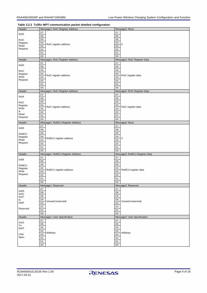
Table 3.2.3 Tx2Rx WPT communication packet detailed configuration
Header Message1: RxIC Register Address Message2: None
0x02
RxICRegisterReadRequest
D7
RxIC register address
D7
0
D6 D6D5 D5D4 D4D3 D3D2 D2D1 D1D0 D0
Header Message1: RxIC Register Address Message2: RxIC Register Data
0x03
RxICRegisterWriteRequest
D7
RxIC register address
D7
RxIC register data
D6 D6D5 D5D4 D4D3 D3D2 D2D1 D1D0 D0
Header Message1: RxIC Register Address Message2: RxIC Register Data
0x04
RxICRegisterWrite&ReadRequest
D7
RxIC register address
D7
RxIC register data
D6 D6D5 D5D4 D4D3 D3D2 D2D1 D1D0 D0
Header Message1: RxMCU Register Address Message2: None
0x05
RxMCURegisterReadRequest
D7
RxMCU register address
D7
0
D6 D6D5 D5D4 D4D3 D3D2 D2D1 D1D0 D0
Header Message1: RxMCU Register Address Message2: RxMCU Register Data
0x06
RxMCURegisterWriteRequest
D7
RxMCU register address
D7
RxMCU register data
D6 D6D5 D5D4 D4D3 D3D2 D2D1 D1D0 D0
Header Message1: Reserved Message2: Reserved
0x00,0x01,0x07to0x0F
Reserved
D7
Unused (reserved)
D7
Unused (reserved)
D6 D6D5 D5D4 D4D3 D3D2 D2D1 D1D0 D0
Header Message1: User Specification Message2: User Specification
0x10To0xFF
UserSpec.
D7
Arbitrary
D7
Arbitrary
D6 D6D5 D5D4 D4D3 D3D2 D2D1 D1D0 D0
Low Power Wireless Charging System Configuration and FunctionRAA458100GNP and RAA457100GBM
Page 10 of 18R19AN0041EJ0100 Rev.1.002017.03.31
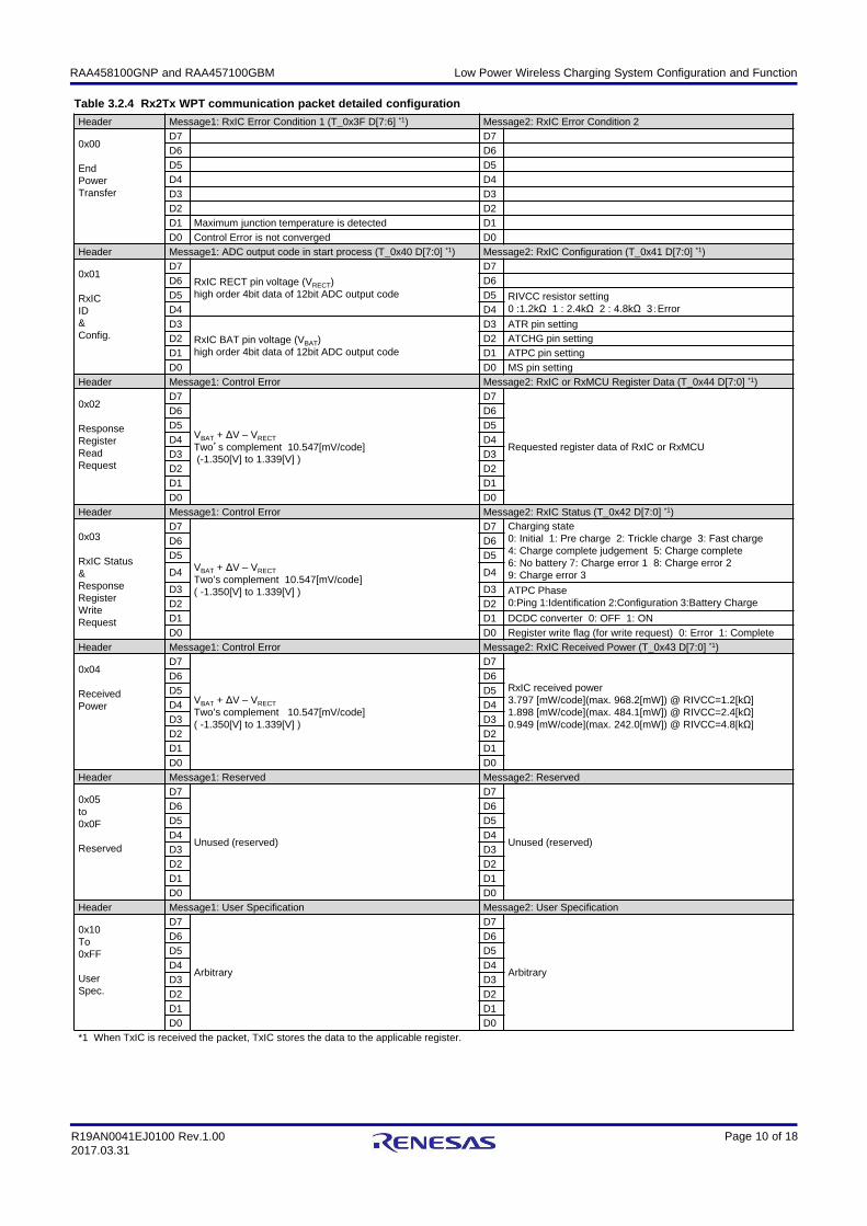
Table 3.2.4 Rx2Tx WPT communication packet detailed configuration
Header Message1: RxIC Error Condition 1 (T_0x3F D[7:6] *1) Message2: RxIC Error Condition 2
0x00
EndPowerTransfer
D7 D7D6 D6D5 D5D4 D4D3 D3D2 D2D1 Maximum junction temperature is detected D1D0 Control Error is not converged D0
Header Message1: ADC output code in start process (T_0x40 D[7:0] *1) Message2: RxIC Configuration (T_0x41 D[7:0] *1)
0x01
RxICID&Config.
D7
RxIC RECT pin voltage (VRECT) high order 4bit data of 12bit ADC output code
D7D6 D6D5 D5 RIVCC resistor setting
0 :1.2kΩ 1 : 2.4kΩ 2 : 4.8kΩ 3:ErrorD4 D4D3
RxIC BAT pin voltage (VBAT)high order 4bit data of 12bit ADC output code
D3 ATR pin settingD2 D2 ATCHG pin settingD1 D1 ATPC pin settingD0 D0 MS pin setting
Header Message1: Control Error Message2: RxIC or RxMCU Register Data (T_0x44 D[7:0] *1)
0x02
ResponseRegisterReadRequest
D7
VBAT + ΔV – VRECT
Two’s complement 10.547[mV/code](-1.350[V] to 1.339[V] )
D7
Requested register data of RxIC or RxMCU
D6 D6D5 D5D4 D4D3 D3D2 D2D1 D1D0 D0
Header Message1: Control Error Message2: RxIC Status (T_0x42 D[7:0] *1)
0x03
RxIC Status&ResponseRegisterWriteRequest
D7
VBAT + ΔV – VRECTTwo’s complement 10.547[mV/code]( -1.350[V] to 1.339[V] )
D7 Charging state0: Initial 1: Pre charge 2: Trickle charge 3: Fast charge4: Charge complete judgement 5: Charge complete 6: No battery 7: Charge error 1 8: Charge error 2 9: Charge error 3
D6 D6D5 D5
D4 D4
D3 D3 ATPC Phase0:Ping 1:Identification 2:Configuration 3:Battery ChargeD2 D2
D1 D1 DCDC converter 0: OFF 1: ON D0 D0 Register write flag (for write request) 0: Error 1: Complete
Header Message1: Control Error Message2: RxIC Received Power (T_0x43 D[7:0] *1)
0x04
ReceivedPower
D7
VBAT + ΔV – VRECTTwo’s complement 10.547[mV/code]( -1.350[V] to 1.339[V] )
D7
RxIC received power3.797 [mW/code](max. 968.2[mW]) @ RIVCC=1.2[kΩ]1.898 [mW/code](max. 484.1[mW]) @ RIVCC=2.4[kΩ]0.949 [mW/code](max. 242.0[mW]) @ RIVCC=4.8[kΩ]
D6 D6D5 D5D4 D4D3 D3D2 D2D1 D1D0 D0
Header Message1: Reserved Message2: Reserved
0x05to0x0F
Reserved
D7
Unused (reserved)
D7
Unused (reserved)
D6 D6D5 D5D4 D4D3 D3D2 D2D1 D1D0 D0
Header Message1: User Specification Message2: User Specification
0x10To0xFF
UserSpec.
D7
Arbitrary
D7
Arbitrary
D6 D6D5 D5D4 D4D3 D3D2 D2D1 D1D0 D0
*1 When TxIC is received the packet, TxIC stores the data to the applicable register.
Low Power Wireless Charging System Configuration and FunctionRAA458100GNP and RAA457100GBM
Page 11 of 18R19AN0041EJ0100 Rev.1.002017.03.31
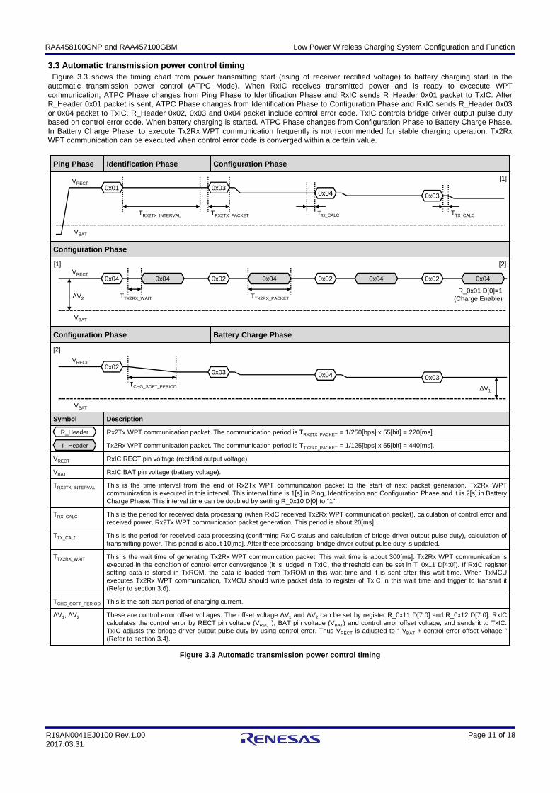
Ping Phase Identification Phase Configuration Phase
Configuration Phase
Configuration Phase Battery Charge Phase
0x01 0x030x04
0x04 0x04
0x03
0x02 0x04 0x02 0x04 0x02 0x04
0x020x03 0x04 0x03
TRX2TX_INTERVAL TRX_CALC TTX_CALC
TTX2RX_WAITΔV2
ΔV1
R_0x01 D[0]=1(Charge Enable)
VBAT
VRECT
TCHG_SOFT_PERIOD
VBAT
VRECT
VBAT
VRECT
Symbol Description
Rx2Tx WPT communication packet. The communication period is TRX2TX_PACKET = 1/250[bps] x 55[bit] = 220[ms].
Tx2Rx WPT communication packet. The communication period is TTX2RX_PACKET = 1/125[bps] x 55[bit] = 440[ms].
VRECT RxIC RECT pin voltage (rectified output voltage).
VBAT RxIC BAT pin voltage (battery voltage).
TRX2TX_INTERVAL This is the time interval from the end of Rx2Tx WPT communication packet to the start of next packet generation. Tx2Rx WPTcommunication is executed in this interval. This interval time is 1[s] in Ping, Identification and Configuration Phase and it is 2[s] in BatteryCharge Phase. This interval time can be doubled by setting R_0x10 D[0] to “1”.
TRX_CALC This is the period for received data processing (when RxIC received Tx2Rx WPT communication packet), calculation of control error andreceived power, Rx2Tx WPT communication packet generation. This period is about 20[ms].
TTX_CALC This is the period for received data processing (confirming RxIC status and calculation of bridge driver output pulse duty), calculation oftransmitting power. This period is about 10[ms]. After these processing, bridge driver output pulse duty is updated.
TTX2RX_WAIT This is the wait time of generating Tx2Rx WPT communication packet. This wait time is about 300[ms]. Tx2Rx WPT communication isexecuted in the condition of control error convergence (it is judged in TxIC, the threshold can be set in T_0x11 D[4:0]). If RxIC registersetting data is stored in TxROM, the data is loaded from TxROM in this wait time and it is sent after this wait time. When TxMCUexecutes Tx2Rx WPT communication, TxMCU should write packet data to register of TxIC in this wait time and trigger to transmit it(Refer to section 3.6).
TCHG_SOFT_PERIOD This is the soft start period of charging current.
ΔV1, ΔV2 These are control error offset voltages. The offset voltage ΔV1 and ΔV2 can be set by register R_0x11 D[7:0] and R_0x12 D[7:0]. RxICcalculates the control error by RECT pin voltage (VRECT), BAT pin voltage (VBAT) and control error offset voltage, and sends it to TxIC.TxIC adjusts the bridge driver output pulse duty by using control error. Thus VRECT is adjusted to “ VBAT + control error offset voltage ”(Refer to section 3.4).
3.3 Automatic transmission power control timing Figure 3.3 shows the timing chart from power transmitting start (rising of receiver rectified voltage) to battery charging start in the
automatic transmission power control (ATPC Mode). When RxIC receives transmitted power and is ready to excecute WPTcommunication, ATPC Phase changes from Ping Phase to Identification Phase and RxIC sends R_Header 0x01 packet to TxIC. AfterR_Header 0x01 packet is sent, ATPC Phase changes from Identification Phase to Configuration Phase and RxIC sends R_Header 0x03or 0x04 packet to TxIC. R_Header 0x02, 0x03 and 0x04 packet include control error code. TxIC controls bridge driver output pulse dutybased on control error code. When battery charging is started, ATPC Phase changes from Configuration Phase to Battery Charge Phase.In Battery Charge Phase, to execute Tx2Rx WPT communication frequently is not recommended for stable charging operation. Tx2RxWPT communication can be executed when control error code is converged within a certain value.
TRX2TX_PACKET
TTX2RX_PACKET
Figure 3.3 Automatic transmission power control timi ng
R_Header
T_Header
[1]
[1] [2]
[2]
Low Power Wireless Charging System Configuration and FunctionRAA458100GNP and RAA457100GBM
Page 12 of 18R19AN0041EJ0100 Rev.1.002017.03.31
Table 3.4 Control error formula and Monotonically set tling condition of RECT pin voltage
Symbol Description Register V RECT converged voltage (target settling voltage)
ΔV1 Control error offset voltage 1 (register setting of RxIC) R_0x11 D[7:0]
ΔV2 Control error offset voltage 2 (register setting of RxIC) R_0x12 D[7:0]
VRECT RxIC RECT pin voltage -
VBAT RxIC BAT pin voltage -
ICHG RxIC battery charging current -
Control error Condition (&: Logical AND, |: Logical OR)
VBAT + ΔV1 – VRECT (Fast charging & Charge current > 0.2 x ICHGR )
VBAT + ΔV2 – VRECT (VBAT > 3V & the state except for fast charging *1)| ( Fast charging state & charging current < 0.15 x ICHGR )
*1 : including non charging condition
3 + ΔV2 – VRECT VBAT < 3V
Condition for V RECT monotonically settling VRECT – Tx Bridge Duty characteristic (example)
GAIN < 10.547[mV] / ( SRD_MAX[mV/%] x ( 100 / F_DRIVE )[%] )
Symbol Description
GAIN Setting by TxIC GAIN pin level (L: 0.125 H: 0.250)
F_DRIVE Setting by T_0x05 D[2:0], T_0x04 D[7:0] (applied by T_0x05 D[7])
SRD_MAX Maximum slope of VRECT - Duty characteristic in actual use range.
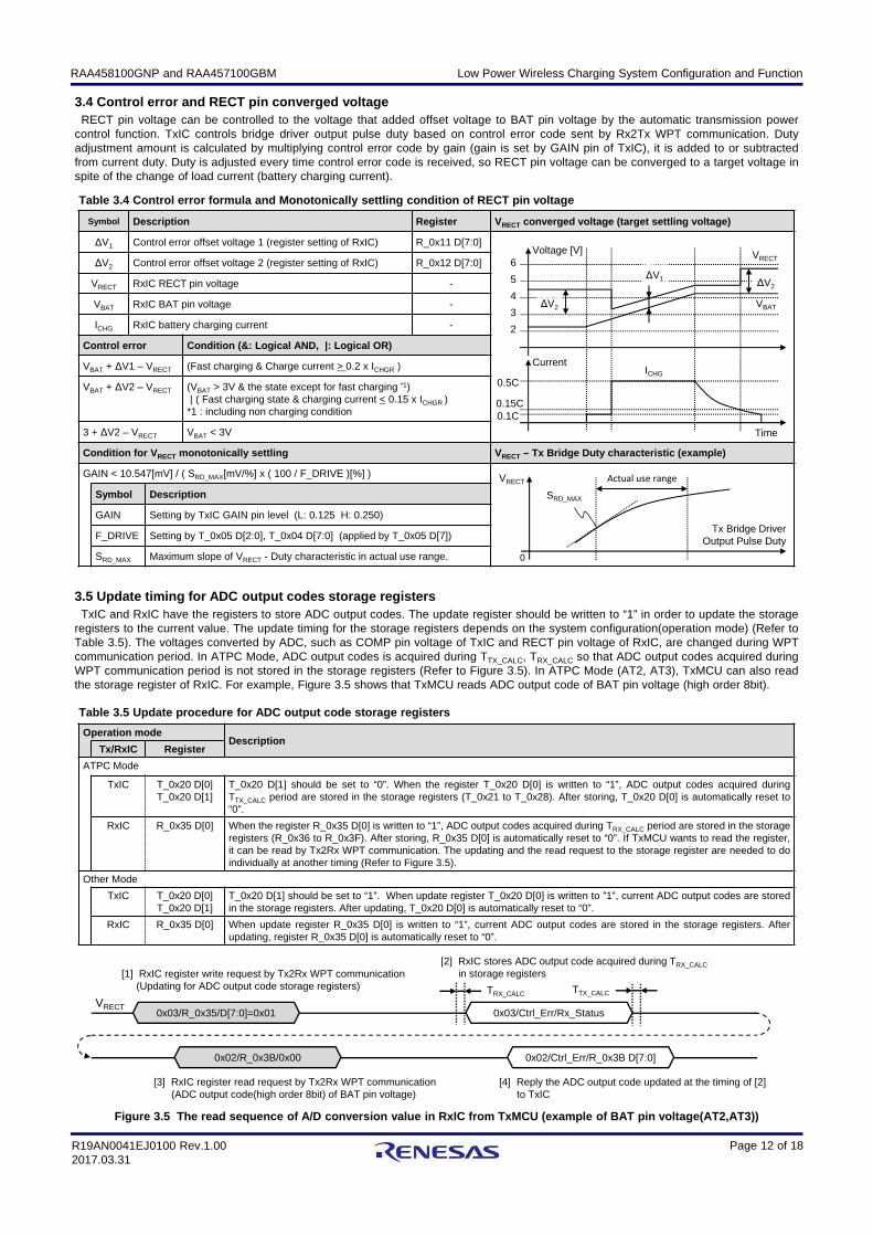
3.5 Update timing for ADC output codes storage regis tersTxIC and RxIC have the registers to store ADC output codes. The update register should be written to “1” in order to update the storage
registers to the current value. The update timing for the storage registers depends on the system configuration(operation mode) (Refer toTable 3.5). The voltages converted by ADC, such as COMP pin voltage of TxIC and RECT pin voltage of RxIC, are changed during WPTcommunication period. In ATPC Mode, ADC output codes is acquired during TTX_CALC, TRX_CALC so that ADC output codes acquired duringWPT communication period is not stored in the storage registers (Refer to Figure 3.5). In ATPC Mode (AT2, AT3), TxMCU can also readthe storage register of RxIC. For example, Figure 3.5 shows that TxMCU reads ADC output code of BAT pin voltage (high order 8bit).
Table 3.5 Update procedure for ADC output code storage registers
Operation modeDescription
Tx/RxIC Register
ATPC Mode
TxIC T_0x20 D[0]T_0x20 D[1]
T_0x20 D[1] should be set to “0”. When the register T_0x20 D[0] is written to “1”, ADC output codes acquired duringTTX_CALC period are stored in the storage registers (T_0x21 to T_0x28). After storing, T_0x20 D[0] is automatically reset to“0”.
RxIC R_0x35 D[0] When the register R_0x35 D[0] is written to “1”, ADC output codes acquired during TRX_CALC period are stored in the storageregisters (R_0x36 to R_0x3F). After storing, R_0x35 D[0] is automatically reset to “0”. If TxMCU wants to read the register,it can be read by Tx2Rx WPT communication. The updating and the read request to the storage register are needed to doindividually at another timing (Refer to Figure 3.5).
Other Mode
TxIC T_0x20 D[0]T_0x20 D[1]
T_0x20 D[1] should be set to “1”. When update register T_0x20 D[0] is written to ”1”, current ADC output codes are storedin the storage registers. After updating, T_0x20 D[0] is automatically reset to “0”.
RxIC R_0x35 D[0] When update register R_0x35 D[0] is written to “1”, current ADC output codes are stored in the storage registers. Afterupdating, register R_0x35 D[0] is automatically reset to “0”.
3.4 Control error and RECT pin converged voltageRECT pin voltage can be controlled to the voltage that added offset voltage to BAT pin voltage by the automatic transmission power
control function. TxIC controls bridge driver output pulse duty based on control error code sent by Rx2Tx WPT communication. Dutyadjustment amount is calculated by multiplying control error code by gain (gain is set by GAIN pin of TxIC), it is added to or subtractedfrom current duty. Duty is adjusted every time control error code is received, so RECT pin voltage can be converged to a target voltage inspite of the change of load current (battery charging current).
ΔV1ΔV2
VRECT
VBATΔV23
4
5
6
2
0.5C
0.1C
Voltage [V]
CurrentICHG
0.15C
0x03/R_0x35/D[7:0]=0x01 0x03/Ctrl_Err/Rx_StatusVRECT
TTX_CALCTRX_CALC
0x02/R_0x3B/0x00 0x02/Ctrl_Err/R_0x3B D[7:0]
[2] RxIC stores ADC output code acquired during TRX_CALCin storage registers
[4] Reply the ADC output code updated at the timing of [2]to TxIC
[1] RxIC register write request by Tx2Rx WPT communication(Updating for ADC output code storage registers)
[3] RxIC register read request by Tx2Rx WPT communication(ADC output code(high order 8bit) of BAT pin voltage)
Figure 3.5 The read sequence of A/D conversion val ue in RxIC from TxMCU (example of BAT pin voltage(AT2 ,AT3))
Time
Tx Bridge DriverOutput Pulse Duty
VRECT
0
SRD_MAX
Actual use range
Low Power Wireless Charging System Configuration and FunctionRAA458100GNP and RAA457100GBM
Page 13 of 18R19AN0041EJ0100 Rev.1.002017.03.31
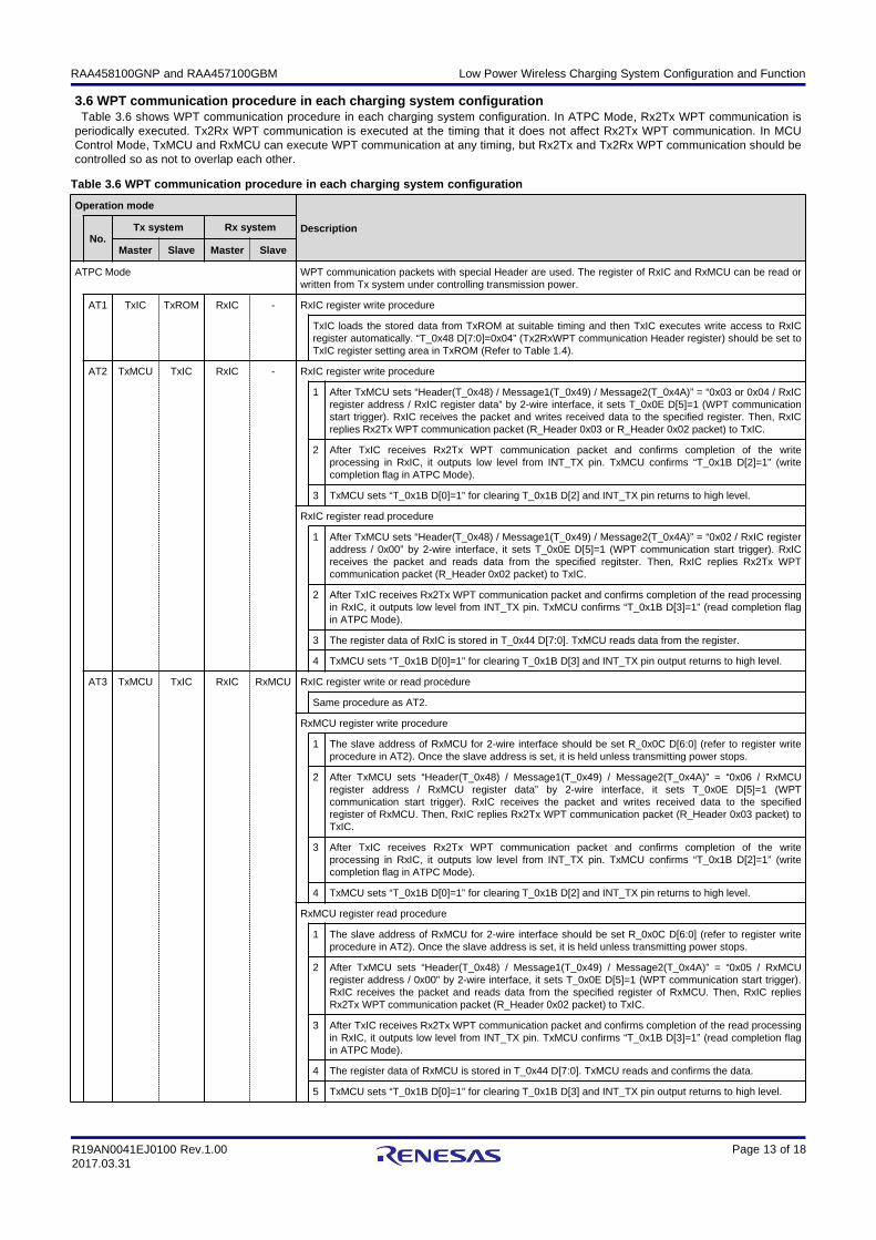
3.6 WPT communication procedure in each charging sy stem configurationTable 3.6 shows WPT communication procedure in each charging system configuration. In ATPC Mode, Rx2Tx WPT communication is
periodically executed. Tx2Rx WPT communication is executed at the timing that it does not affect Rx2Tx WPT communication. In MCUControl Mode, TxMCU and RxMCU can execute WPT communication at any timing, but Rx2Tx and Tx2Rx WPT communication should becontrolled so as not to overlap each other.
Table 3.6 WPT communication procedure in each chargin g system configuration
Operation mode
DescriptionNo.
Tx system Rx system
Master Slave Master Slave
ATPC Mode WPT communication packets with special Header are used. The register of RxIC and RxMCU can be read orwritten from Tx system under controlling transmission power.
AT1 TxIC TxROM RxIC - RxIC register write procedure
TxIC loads the stored data from TxROM at suitable timing and then TxIC executes write access to RxICregister automatically. “T_0x48 D[7:0]=0x04” (Tx2RxWPT communication Header register) should be set toTxIC register setting area in TxROM (Refer to Table 1.4).
AT2 TxMCU TxIC RxIC - RxIC register write procedure
1 After TxMCU sets “Header(T_0x48) / Message1(T_0x49) / Message2(T_0x4A)” = “0x03 or 0x04 / RxICregister address / RxIC register data” by 2-wire interface, it sets T_0x0E D[5]=1 (WPT communicationstart trigger). RxIC receives the packet and writes received data to the specified register. Then, RxICreplies Rx2Tx WPT communication packet (R_Header 0x03 or R_Header 0x02 packet) to TxIC.
2 After TxIC receives Rx2Tx WPT communication packet and confirms completion of the writeprocessing in RxIC, it outputs low level from INT_TX pin. TxMCU confirms “T_0x1B D[2]=1” (writecompletion flag in ATPC Mode).
3 TxMCU sets “T_0x1B D[0]=1” for clearing T_0x1B D[2] and INT_TX pin returns to high level.
RxIC register read procedure
1 After TxMCU sets “Header(T_0x48) / Message1(T_0x49) / Message2(T_0x4A)” = “0x02 / RxIC registeraddress / 0x00” by 2-wire interface, it sets T_0x0E D[5]=1 (WPT communication start trigger). RxICreceives the packet and reads data from the specified regitster. Then, RxIC replies Rx2Tx WPTcommunication packet (R_Header 0x02 packet) to TxIC.
2 After TxIC receives Rx2Tx WPT communication packet and confirms completion of the read processingin RxIC, it outputs low level from INT_TX pin. TxMCU confirms “T_0x1B D[3]=1” (read completion flagin ATPC Mode).
3 The register data of RxIC is stored in T_0x44 D[7:0]. TxMCU reads data from the register.
4 TxMCU sets “T_0x1B D[0]=1” for clearing T_0x1B D[3] and INT_TX pin output returns to high level.
AT3 TxMCU TxIC RxIC RxMCU RxIC register write or read procedure
Same procedure as AT2.
RxMCU register write procedure
1 The slave address of RxMCU for 2-wire interface should be set R_0x0C D[6:0] (refer to register writeprocedure in AT2). Once the slave address is set, it is held unless transmitting power stops.
2 After TxMCU sets “Header(T_0x48) / Message1(T_0x49) / Message2(T_0x4A)” = “0x06 / RxMCUregister address / RxMCU register data” by 2-wire interface, it sets T_0x0E D[5]=1 (WPTcommunication start trigger). RxIC receives the packet and writes received data to the specifiedregister of RxMCU. Then, RxIC replies Rx2Tx WPT communication packet (R_Header 0x03 packet) toTxIC.
3 After TxIC receives Rx2Tx WPT communication packet and confirms completion of the writeprocessing in RxIC, it outputs low level from INT_TX pin. TxMCU confirms “T_0x1B D[2]=1” (writecompletion flag in ATPC Mode).
4 TxMCU sets “T_0x1B D[0]=1” for clearing T_0x1B D[2] and INT_TX pin returns to high level.
RxMCU register read procedure
1 The slave address of RxMCU for 2-wire interface should be set R_0x0C D[6:0] (refer to register writeprocedure in AT2). Once the slave address is set, it is held unless transmitting power stops.
2 After TxMCU sets “Header(T_0x48) / Message1(T_0x49) / Message2(T_0x4A)” = “0x05 / RxMCUregister address / 0x00” by 2-wire interface, it sets T_0x0E D[5]=1 (WPT communication start trigger).RxIC receives the packet and reads data from the specified register of RxMCU. Then, RxIC repliesRx2Tx WPT communication packet (R_Header 0x02 packet) to TxIC.
3 After TxIC receives Rx2Tx WPT communication packet and confirms completion of the read processingin RxIC, it outputs low level from INT_TX pin. TxMCU confirms “T_0x1B D[3]=1” (read completion flagin ATPC Mode).
4 The register data of RxMCU is stored in T_0x44 D[7:0]. TxMCU reads and confirms the data.
5 TxMCU sets “T_0x1B D[0]=1” for clearing T_0x1B D[3] and INT_TX pin output returns to high level.
Low Power Wireless Charging System Configuration and FunctionRAA458100GNP and RAA457100GBM
Page 14 of 18R19AN0041EJ0100 Rev.1.002017.03.31
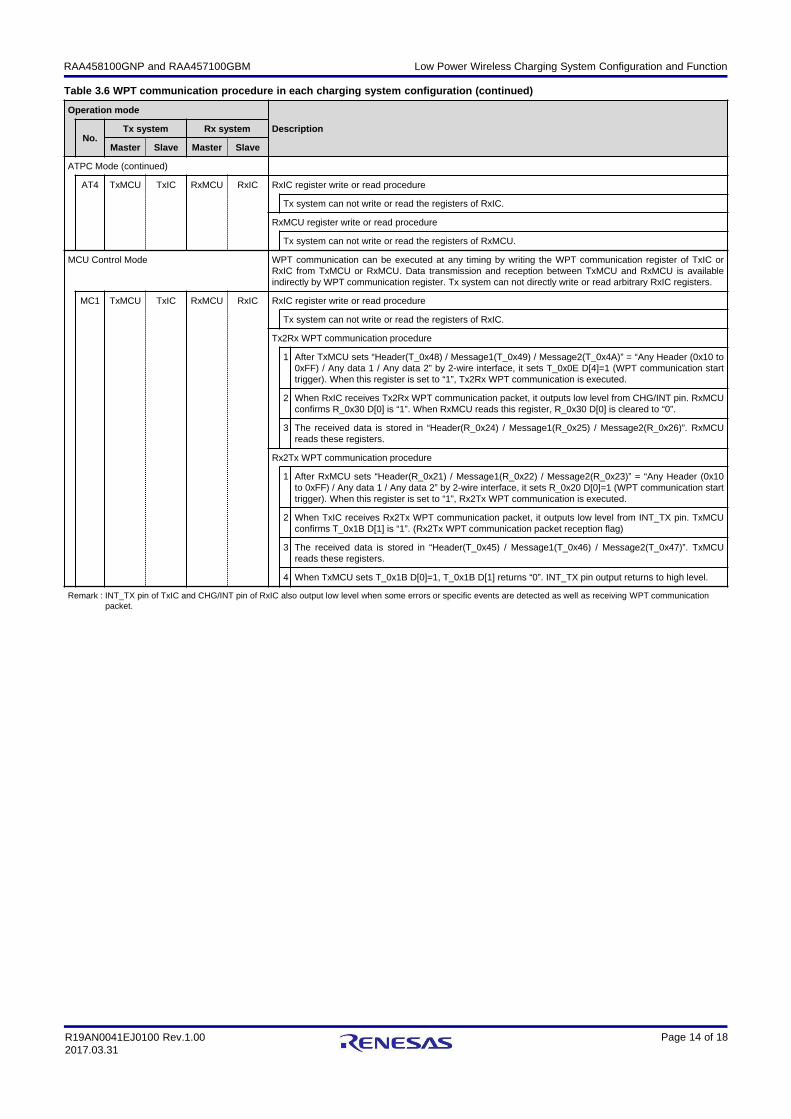
Table 3.6 WPT communication procedure in each chargin g system configuration (continued)
Operation mode
DescriptionNo.
Tx system Rx system
Master Slave Master Slave
ATPC Mode (continued)
AT4 TxMCU TxIC RxMCU RxIC RxIC register write or read procedure
Tx system can not write or read the registers of RxIC.
RxMCU register write or read procedure
Tx system can not write or read the registers of RxMCU.
MCU Control Mode WPT communication can be executed at any timing by writing the WPT communication register of TxIC orRxIC from TxMCU or RxMCU. Data transmission and reception between TxMCU and RxMCU is availableindirectly by WPT communication register. Tx system can not directly write or read arbitrary RxIC registers.
MC1 TxMCU TxIC RxMCU RxIC RxIC register write or read procedure
Tx system can not write or read the registers of RxIC.
Tx2Rx WPT communication procedure
1 After TxMCU sets “Header(T_0x48) / Message1(T_0x49) / Message2(T_0x4A)” = “Any Header (0x10 to0xFF) / Any data 1 / Any data 2” by 2-wire interface, it sets T_0x0E D[4]=1 (WPT communication starttrigger). When this register is set to “1”, Tx2Rx WPT communication is executed.
2 When RxIC receives Tx2Rx WPT communication packet, it outputs low level from CHG/INT pin. RxMCUconfirms R_0x30 D[0] is “1”. When RxMCU reads this register, R_0x30 D[0] is cleared to “0”.
3 The received data is stored in “Header(R_0x24) / Message1(R_0x25) / Message2(R_0x26)”. RxMCUreads these registers.
Rx2Tx WPT communication procedure
1 After RxMCU sets “Header(R_0x21) / Message1(R_0x22) / Message2(R_0x23)” = “Any Header (0x10to 0xFF) / Any data 1 / Any data 2” by 2-wire interface, it sets R_0x20 D[0]=1 (WPT communication starttrigger). When this register is set to “1”, Rx2Tx WPT communication is executed.
2 When TxIC receives Rx2Tx WPT communication packet, it outputs low level from INT_TX pin. TxMCUconfirms T_0x1B D[1] is “1”. (Rx2Tx WPT communication packet reception flag)
3 The received data is stored in “Header(T_0x45) / Message1(T_0x46) / Message2(T_0x47)”. TxMCUreads these registers.
4 When TxMCU sets T_0x1B D[0]=1, T_0x1B D[1] returns “0”. INT_TX pin output returns to high level.
Remark : INT_TX pin of TxIC and CHG/INT pin of RxIC also output low level when some errors or specific events are detected as well as receiving WPT communicationpacket.
Low Power Wireless Charging System Configuration and FunctionRAA458100GNP and RAA457100GBM
Page 15 of 18R19AN0041EJ0100 Rev.1.002017.03.31
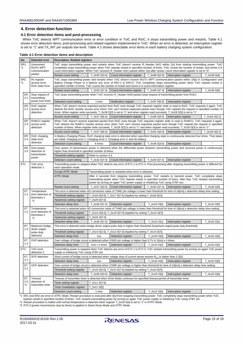
4. Error detection function4.1 Error detection items and post-processing
When TxIC detects WPT communication error or error condition in TxIC and RxIC, it stops transmitting power and restarts. Table 4.1shows error detection items, post-processing and related registers implemented in TxIC. When an error is detected, an interruption registeris set to “1” and TX_INT pin outputs low level. Table 4.2 shows detectable error items in each battery charging system configuration.
Table 4.1 Error detection items and description
No. Detected error Description, Related registers
ER1*1
Unreceived Rx2Tx WPTcommunication packet
TxIC stops transmitting power and restarts when TxIC doesn’t receive R_Header 0x01 within 1[s] from starting transmitting power. TxICcompletely stops transmitting power when TxIC repeats restart in specified number of times. TxIC counts the number of restart, and stores it incount information register. When TxIC receives R_Header 0x01 packet within 1[s] after restart, count information register is set to “0”.
Restart count setting T_0x35 D[3:0] Count information register T_0x4B D[3:0] Interruption register T_0x1B D[4]
ER2*1
Rx register access error,RxIC state error
TxIC stops transmitting power and restarts when TxIC doesn’t receive Rx2Tx WPT communication packet within 16[s] in Configuration andBattery Charge Phase or it detects any error of ER2-1 to ER2-5. TxIC completely stops transmitting power when TxIC repeats restart inspecified number of times. TxIC counts the number of restart and stores it in count information register.
Restart count setting T_0x35 D[7:4] Count information register T_0x4B D[7:4] Interruption register T_0x1B D[4]
ER2-1
Stop request of transmitting power from RxIC
TxIC stops transmitting power when TxIC receives R_Header 0x00 packet (stop request of transmitting power from RxIC).
Detection count setting 1 time Notification register T_0x3F D[6:5] Interruption register -
ER2-2
RxIC register access error detection
When TxIC doesn’t receive expected packet from RxIC even though TxIC requests register write or read to RxIC, TxIC requests it again. TxICdetects the RxIC resister access error when TxIC can’t receive expected packet even though TxIC repeats the request in specified number oftimes. When register write succeeds, T_0x1B D[2] is set to “1” and when register read succeeds, T_0x1B D[3] is set to “1”.
Access count setting T_0x37 D[6:4] Count information register T_0x38 D[3:0] Interruption register T_0x1B D[3:2]
ER2-3
RxMCU registeraccess error detection
When TxIC doesn’t receive expected packet from RxIC even though TxIC requests register write or read to RxMCU, TxIC requests it again.TxIC detects the RxMCU resister access error when TxIC can’t receive expected packet even though TxIC repeats the request in specifiednumber of times. When register write succeeds, T_0x1B D[2] is set to “1” and when register read succeeds, T_0x1B D[3] is set to “1”.
Access count setting T_0x37 D[6:4] Count information register T_0x3A D[3:0] Interruption register T_0x1B D[3:2]
ER2-4
RxIC chargingstate error detection
In Battery Charging Phase, RxIC charging state error is detected when specified charging state is continuously detected four times. That statesare Initial, Charging error 1, Charging error 2, Charging error 3, and No battery.
Detection count setting 4 times Count information register T_0x39 D[3:0] Interruption register -
ER2-5
Over power detection of transmission power
Over power of transmission power is detected when the differential power between transmitting power and received power is continuouslyhigher than threshold in specified number of times.
Threshold setting register Refer to section 4.3.
Detection count setting T_0x32 D[7:4] Count information register T_0x39 D[7:4] Interruption register -
ET1 TxIC error detection 1
Transmitting power is stopped when TxIC detects any error of ET1-1 to ET1-4. Post-processing after stopping transmitting power is different foreach operation mode.
Except ATPC Mode Transmitting power is restarted when error is released.
ATPC Mode After 4 seconds from stopping transmitting power, TxIC restarts to transmit power. TxIC completely stopstransmitting power when TxIC repeats restart in specified number of times. After that, TxIC restarts transmittingpower by turning on again TxIC power supply or initializing TxIC using STBY pin.
Restart count setting T_0x37 D[3:0] Count information register T_0x3A D[7:4] Interruption register T_0x1B D[4]
ET1-1
Temperature error detection of thermistor 1*2
This error is detected when AD conversion value of THM1 pin voltage is lower than threshold for time of 16[ms] x detection delay time setting.
Threshold setting register T_0x18 D[3:0], T_0x17 D[7:0] (Applied by setting T_0x18 D[7])
Hysteresis setting register T_0x29 D[7:0]
Detection delay time T_0x36 D[7:4] Detection register T_0x1D D[0] Interruption register T_0x1D D[0]
ET1-2
Temperature error detection of thermistor 2*2
This error is detected when AD conversion value of THM2 pin voltage is lower than threshold for time of 16[ms] x detection delay time setting.
Threshold setting register T_0x1A D[3:0], T_0x19 D[7:0] (Applied by setting T_0x1A D[7])
Hysteresis setting register T_0x2A D[7:0]
Detection delay time T_0x36 D[7:4] Detection register T_0x1D D[1] Interruption register T_0x1D D[1]
ET1-3
Maximum bridge driver output pulse duty detection
This error is detected when bridge driver output pulse duty is higher than threshold (maximum output pulse duty threshold).
Threshold setting register T_0x14 D[1:0], T_0x13 D[7:0] (Applied by setting T_0x14 D[7])
Detection delay time 1us Detection register T_0x1D D[4] Interruption register T_0x1D D[4]
ET1-4
OVP detection Over voltage of bridge circuit is detected when VSNS pin voltage is higher than 5.7V in 1[ms] x 4 times.
Detection delay time 1ms x 4 times Detection register T_0x1D D[2] Interruption register T_0x1D D[2]
ET2 TxIC error detection 2
Transmitting power is stopped when TxIC detects any error of ET2-1 to ET2-3. TxIC restarts transmitting power by turning on again TxIC powersupply or initializing TxIC using STBY pin.
ET2-1
SCP detection Short current of bridge circuit is detected when voltage drop of current sense resistor RCS is higher than 2.2[V].
Detection delay time 1us Detection register T_0x1D D[3] Interruption register T_0x1D D[3]
ET2-2
OCP detection Over current of bridge circuit is detected when COMP pin voltage is higher than threshold for time of 16[ms] x detection delay time setting.
Threshold setting register T_0x16 D[3:0], T_0x15 D[7:0] (Applied by setting T_0x16 D[7])
Detection delay time T_0x36 D[3:0] Detection register T_0x1D D[5] Interruption register T_0x1D D[5]
ET2-3*3
Timeout detection oftransmitter timer
Timeout of transmitter timer is detected when Drive Mode continues for specified timeout period of transmitter timer.
Timer setting register T_0x11 D[7:6]
Timer invalidation register T_0x11 D[5]
Detection count setting 1 time Detection register T_0x12 D[5] Interruption register -
*1 ER1 and ER2 are error in ATPC Mode. Restart procedure is executed after 4[s] from stopping transmitting power. TxIC completely stops transmitting power when TxICrepeats restart in specified number of times. TxIC restarts transmitting power by turning on again TxIC power supply or initializing TxIC using STBY pin.
*2 Restart procedure is halted until normal temperature is detected when register T_0x18 D[4] is set to “1” in ATPC Mode.*3 ET2-3 (power transmission stop by timer) is applied to Stand Alone Mode and ATPC Mode.
Low Power Wireless Charging System Configuration and FunctionRAA458100GNP and RAA457100GBM
Page 16 of 18R19AN0041EJ0100 Rev.1.002017.03.31
4.2 Error detection items in each charging system c onfigurationTable 4.2 shows error detection items in each charging system configuration.
4.3 Over power detection of transmission powerR_Header 0x04 packet in ATPC Mode includes output power information of RxIC. When over power detection function of transmission
power is available, TxIC calculates differential power ΔP between transmission power calculated by TxIC and RxIC output power includedin R_Header 0x04 packet. When differential power ΔP is higher than threshold ΔPTH, TxIC detects over power condition and stopstransmitting power. ΔPTH consists of fixed threshold region that is not depend on duty and linear function region that is depend on duty.ΔPTH is set by registers showed in Table 4.3. ΔPTH should be set in Initial Mode of TxIC. After register settings of ΔPOVCNTTH(T_0x32D[7:4]), RCS(T_0x3F D[1:0]), ΔPSLOPE(T_0x3B D[7:0]), ΔPOS(T_0x3C D[7:0]) and DΔPCONST(T_0x3D D[7:0]), enable register T_0x3F D[3]should be set to “1”.
Table 4.3 Threshold parameters of over power detecti on of transmitter power
Parameters for over power detection
Symbol Register DescriptionReference figure(Differential power, Curve of bridge Duty)
Enable of over power detection
- T_0x3FD[3]
Available or unavailable selection.0 : Unavailable 1 : Available
Error count threshold of over power detection
ΔPOVCNTTH T_0x32D[7:4]
Over power detection count can be set 1 to 15. Transmittingpower is stopped when the count of over power detection isreached the specified number of times. If this register is setto 0, over power detection is unavailable.
Error count of over power detection
- T_0x39D[7:4]
Error count value of over power detection is stored in T_0x39D[7:4].
Mask of over power detection
- T_0x3FD[2]
When control error value is not converged within specifiedvalue, over power detection is masked.0 : Unmask 1 : Mask
Bridge Currentdetection resistor
RCS T_0x3FD[1:0]
The value of bridge current detection resistor RCS can beselected. When over power detection is available, currentdetection resistor must be selected in this setting. The gainof current sense amplifier is 10 times.0 : 0.25[Ω] 1 : 0.5[Ω] 2 : 1[Ω] 3 : 2[Ω]
Slope of ΔP-Duty line
ΔPSLOPE T_0x3BD[7:0]
Set from 0 to 255.{ 3.797 / (100/F_DRIVE) } x (1/64) [mW/code]
ΔP offset ΔPOS T_0x3CD[7:0]
Set from 0 to 255.3.797[mW/code] : 0 to 968.2[mW]
Duty of ΔP fixed threshold
DΔPCONST T_0x3ED[7:0]
Set duty range applied for ΔP fixed threshold. DΔPCONSTcorresponds to high order 8 bit for 10bit duty setting code.
ΔP fixed threshold
ΔPCONST For Duty < DΔPCONST, the detection threshold is ΔPCONST.
ΔPOS
ΔPCONST
ΔPSLOPE
Tx Bridge Driver
Output Pulse Duty
ΔP
DΔPCONST0
Normal
Condition
Abnormal
Condition
ΔPTH=ΔPSLOPE x Duty + ΔPOS
ΔPTH=
ΔPCONST
ΔPTH
Over Power Detection
Table 4.2 Error detection items in each charging sys tem configuration
Operation mode WPT communication or RxIC error *1 TxIC error *1
No.Tx System Rx System
ER1
ER2
ET1
ET2
Master Slave Master Slave ER2-1
ER2-2
ER2-3
ER2-4
ER2-5
ET1-1
ET1-2
ET1-3
ET1-4
ET2-1
ET2-2
ET2-3
Stand Alone Mode
SA1 - TxIC RxIC - - - - - - - - C C *2 C *2 C C C C C *3 C
SA2 TxIC TxROM RxIC - - - - - - - - C V V V C C C V V
ATPC Mode
AT1 TxIC TxROM RxIC - V V C V - C V V V V V C C C V V
AT2 TxMCU TxIC RxIC - V V C V - C V V V V V C C C V V
AT3 TxMCU TxIC RxIC RxMCU V V C V V C V V V V V C C C V V
AT4 TxMCU TxIC RxMCU RxIC V V C - - C V V V V V C C C V V
MCU Control Mode
MC1 TxMCU TxIC RxMCU RxIC - - - - - - - C V V V C C C V -
*1 V means variable threshold or detection count by register. C means fixed value for threshold or detection count.*2 In Stand Alone Mode (SA1), temperature threshold of thermistor 1 and 2 (NTC thermistor) for error detection can be adjusted by pull-up resistor value
even though that threshold can not be changed by registers. *3 Detection current threshold of OCP(over current protection) can be adjusted by RCS resistor value when Over power detection of transmitting power is
unused.
Low Power Wireless Charging System Configuration and FunctionRAA458100GNP and RAA457100GBM
Page 17 of 18R19AN0041EJ0100 Rev.1.002017.03.31
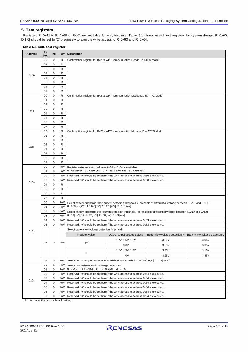
5. Test registersRegisters R_0x41 to R_0x6F of RxIC are available for only test use. Table 5.1 shows useful test registers for system design. R_0x60
D[1:0] should be set to “2” previously to execute write access to R_0x63 and R_0x64.
Table 5.1 RxIC test register
AddressBitNo.
Init R/W Description
0x5D
D0 0 R Confirmation register for Rx2Tx WPT communication Header in ATPC Mode
D1 0 R
D2 0 R
D3 0 R
D4 0 R
D5 0 R
D6 0 R
D7 0 R
0x5E
D0 0 R Confirmation register for Rx2Tx WPT communication Message1 in ATPC Mode
D1 0 R
D2 0 R
D3 0 R
D4 0 R
D5 0 R
D6 0 R
D7 0 R
0x5F
D0 0 R Confirmation register for Rx2Tx WPT communication Message2 in ATPC Mode
D1 0 R
D2 0 R
D3 0 R
D4 0 R
D5 0 R
D6 0 R
D7 0 R
0x60
D0 0 R/W Register write access to address 0x61 to 0x64 is available.0 : Reserved 1 : Reserved 2 : Write is available 3 : ReservedD1 0 R/W
D2 0 R/W Reserved. “0” should be set here if the write access to address 0x60 is executed.
D3 0 R/W Reserved. “0” should be set here if the write access to address 0x60 is executed.
D4 0 R
D5 0 R
D6 0 R
D7 0 R
0x63
D0 0 R/W Select battery discharge short current detection threshold. (Threshold of differential voltage between SGND and GND) 0 : 160[mV](*1) 1 : 140[mV] 2 : 120[mV] 3 : 100[mV]D1 0 R/W
D2 0 R/W Select battery discharge over current detection threshold. (Threshold of differential voltage between SGND and GND) 0 : 80[mV](*1) 1 : 70[mV] 2 : 60[mV] 3 : 50[mV]D3 0 R/W
D4 0 R/W Reserved. “0” should be set here if the write access to address 0x63 is executed.
D5 0 R/W Reserved. “0” should be set here if the write access to address 0x63 is executed.
D6 0 R/W
Select battery low voltage detection threshold.
Register value DCDC output voltage setting Battery low voltage detection H Battery low voltage detection L
0 (*1)1.2V, 1.5V, 1.8V 3.20V 3.05V
3.0V 3.55V 3.35V
11.2V, 1.5V, 1.8V 3.30V 3.15V
3.0V 3.65V 3.45V
D7 0 R/W Select maximum junction temperature detection threshold 0 : 68[degC] 1 : 79[degC]
0x64
D0 1 R/W Select ON resistance of discharge control FET0 : 0.2[Ω] 1 : 0.4[Ω] (*1) 2 : 0.5[Ω] 3 : 0.7[Ω]D1 0 R/W
D2 0 R/W Reserved. “0” should be set here if the write access to address 0x64 is executed.
D3 0 R/W Reserved. “0” should be set here if the write access to address 0x64 is executed.
D4 0 R/W Reserved. “0” should be set here if the write access to address 0x64 is executed.
D5 0 R/W Reserved. “0” should be set here if the write access to address 0x64 is executed.
D6 0 R/W Reserved. “0” should be set here if the write access to address 0x64 is executed.
D7 0 R/W Reserved. “0” should be set here if the write access to address 0x64 is executed.
*1 It indicates the factory default setting.
Low Power Wireless Charging System Configuration and FunctionRAA458100GNP and RAA457100GBM
Page 18 of 18R19AN0041EJ0100 Rev.1.002017.03.31
Website and Support
Renesas Electronics Websitehttp://www.renesas.com/
Inquireshttp://www.renesas.com/contact/

Revision Record
Rev. DataDescription
Page Summary
1.00 2017.03.31 - First edition issued
All trademarks and registered trademarks are the property of their respective owners.
Notice1. Descriptions of circuits, software and other related information in this document are provided only to illustrate the operation of semiconductor products and application examples. You are fully responsible for
the incorporation or any other use of the circuits, software, and information in the design of your product or system. Renesas Electronics disclaims any and all liability for any losses and damages incurred by
you or third parties arising from the use of these circuits, software, or information.
2. Renesas Electronics hereby expressly disclaims any warranties against and liability for infringement or any other disputes involving patents, copyrights, or other intellectual property rights of third parties, by or
arising from the use of Renesas Electronics products or technical information described in this document, including but not limited to, the product data, drawing, chart, program, algorithm, application
examples.
3. No license, express, implied or otherwise, is granted hereby under any patents, copyrights or other intellectual property rights of Renesas Electronics or others.
4. You shall not alter, modify, copy, or otherwise misappropriate any Renesas Electronics product, whether in whole or in part. Renesas Electronics disclaims any and all liability for any losses or damages
incurred by you or third parties arising from such alteration, modification, copy or otherwise misappropriation of Renesas Electronics products.
5. Renesas Electronics products are classified according to the following two quality grades: "Standard" and "High Quality". The intended applications for each Renesas Electronics product depends on the
product’s quality grade, as indicated below.
"Standard": Computers; office equipment; communications equipment; test and measurement equipment; audio and visual equipment; home electronic appliances; machine tools; personal electronic
equipment; and industrial robots etc.
"High Quality": Transportation equipment (automobiles, trains, ships, etc.); traffic control (traffic lights); large-scale communication equipment; key financial terminal systems; safety control equipment; etc.
Renesas Electronics products are neither intended nor authorized for use in products or systems that may pose a direct threat to human life or bodily injury (artificial life support devices or systems, surgical
implantations etc.), or may cause serious property damages (space and undersea repeaters; nuclear power control systems; aircraft control systems; key plant systems; military equipment; etc.). Renesas
Electronics disclaims any and all liability for any damages or losses incurred by you or third parties arising from the use of any Renesas Electronics product for which the product is not intended by Renesas
Electronics.
6. When using the Renesas Electronics products, refer to the latest product information (data sheets, user’s manuals, application notes, "General Notes for Handling and Using Semiconductor Devices" in the
reliability handbook, etc.), and ensure that usage conditions are within the ranges specified by Renesas Electronics with respect to maximum ratings, operating power supply voltage range, heat radiation
characteristics, installation, etc. Renesas Electronics disclaims any and all liability for any malfunctions or failure or accident arising out of the use of Renesas Electronics products beyond such specified
ranges.
7. Although Renesas Electronics endeavors to improve the quality and reliability of Renesas Electronics products, semiconductor products have specific characteristics such as the occurrence of failure at a
certain rate and malfunctions under certain use conditions. Further, Renesas Electronics products are not subject to radiation resistance design. Please ensure to implement safety measures to guard them
against the possibility of bodily injury, injury or damage caused by fire, and social damage in the event of failure or malfunction of Renesas Electronics products, such as safety design for hardware and
software including but not limited to redundancy, fire control and malfunction prevention, appropriate treatment for aging degradation or any other appropriate measures by your own responsibility as warranty
for your products/system. Because the evaluation of microcomputer software alone is very difficult and not practical, please evaluate the safety of the final products or systems manufactured by you.
8. Please contact a Renesas Electronics sales office for details as to environmental matters such as the environmental compatibility of each Renesas Electronics product. Please investigate applicable laws and
regulations that regulate the inclusion or use of controlled substances, including without limitation, the EU RoHS Directive carefully and sufficiently and use Renesas Electronics products in compliance with all
these applicable laws and regulations. Renesas Electronics disclaims any and all liability for damages or losses occurring as a result of your noncompliance with applicable laws and regulations.
9. Renesas Electronics products and technologies shall not be used for or incorporated into any products or systems whose manufacture, use, or sale is prohibited under any applicable domestic or foreign laws
or regulations. You shall not use Renesas Electronics products or technologies for (1) any purpose relating to the development, design, manufacture, use, stockpiling, etc., of weapons of mass destruction,
such as nuclear weapons, chemical weapons, or biological weapons, or missiles (including unmanned aerial vehicles (UAVs)) for delivering such weapons, (2) any purpose relating to the development,
design, manufacture, or use of conventional weapons, or (3) any other purpose of disturbing international peace and security, and you shall not sell, export, lease, transfer, or release Renesas Electronics
products or technologies to any third party whether directly or indirectly with knowledge or reason to know that the third party or any other party will engage in the activities described above. When exporting,
selling, transferring, etc., Renesas Electronics products or technologies, you shall comply with any applicable export control laws and regulations promulgated and administered by the governments of the
countries asserting jurisdiction over the parties or transactions.
10. Please acknowledge and agree that you shall bear all the losses and damages which are incurred from the misuse or violation of the terms and conditions described in this document, including this notice,
and hold Renesas Electronics harmless, if such misuse or violation results from your resale or making Renesas Electronics products available any third party.
11. This document shall not be reprinted, reproduced or duplicated in any form, in whole or in part, without prior written consent of Renesas Electronics.
12. Please contact a Renesas Electronics sales office if you have any questions regarding the information contained in this document or Renesas Electronics products.
(Note 1) "Renesas Electronics" as used in this document means Renesas Electronics Corporation and also includes its majority-owned subsidiaries.
(Note 2) "Renesas Electronics product(s)" means any product developed or manufactured by or for Renesas Electronics.
http://www.renesas.comRefer to "http://www.renesas.com/" for the latest and detailed information.
Renesas Electronics America Inc.2801 Scott Boulevard Santa Clara, CA 95050-2549, U.S.A.Tel: +1-408-588-6000, Fax: +1-408-588-6130Renesas Electronics Canada Limited9251 Yonge Street, Suite 8309 Richmond Hill, Ontario Canada L4C 9T3Tel: +1-905-237-2004Renesas Electronics Europe LimitedDukes Meadow, Millboard Road, Bourne End, Buckinghamshire, SL8 5FH, U.KTel: +44-1628-585-100, Fax: +44-1628-585-900Renesas Electronics Europe GmbHArcadiastrasse 10, 40472 Düsseldorf, GermanyTel: +49-211-6503-0, Fax: +49-211-6503-1327Renesas Electronics (China) Co., Ltd.Room 1709, Quantum Plaza, No.27 ZhiChunLu Haidian District, Beijing 100191, P.R.ChinaTel: +86-10-8235-1155, Fax: +86-10-8235-7679Renesas Electronics (Shanghai) Co., Ltd.Unit 301, Tower A, Central Towers, 555 Langao Road, Putuo District, Shanghai, P. R. China 200333Tel: +86-21-2226-0888, Fax: +86-21-2226-0999Renesas Electronics Hong Kong LimitedUnit 1601-1611, 16/F., Tower 2, Grand Century Place, 193 Prince Edward Road West, Mongkok, Kowloon, Hong KongTel: +852-2265-6688, Fax: +852 2886-9022Renesas Electronics Taiwan Co., Ltd.13F, No. 363, Fu Shing North Road, Taipei 10543, TaiwanTel: +886-2-8175-9600, Fax: +886 2-8175-9670Renesas Electronics Singapore Pte. Ltd.80 Bendemeer Road, Unit #06-02 Hyflux Innovation Centre, Singapore 339949Tel: +65-6213-0200, Fax: +65-6213-0300Renesas Electronics Malaysia Sdn.Bhd.Unit 1207, Block B, Menara Amcorp, Amcorp Trade Centre, No. 18, Jln Persiaran Barat, 46050 Petaling Jaya, Selangor Darul Ehsan, MalaysiaTel: +60-3-7955-9390, Fax: +60-3-7955-9510Renesas Electronics India Pvt. Ltd.No.777C, 100 Feet Road, HAL II Stage, Indiranagar, Bangalore, IndiaTel: +91-80-67208700, Fax: +91-80-67208777Renesas Electronics Korea Co., Ltd.12F., 234 Teheran-ro, Gangnam-Gu, Seoul, 135-080, KoreaTel: +82-2-558-3737, Fax: +82-2-558-5141
SALES OFFICES
© 2017 Renesas Electronics Corporation. All rights reserved.Colophon 6.0
(Rev.3.0-1 November 2016)