power topology considerations for solar string inverters and
TRANSCRIPT
Application ReportPower Topology Considerations for Solar String Invertersand Energy Storage Systems
Salil Chellappan, Jayanth Rangaraju
ABSTRACTAs PV solar installations continues to grow rapidly over the last decade, the need for solar inverter with highefficiency, improved power density and higher power handling capabilities continues to scale up. In addition,more and more solar inverters are looking to integrate energy storage systems to reduce energy dependency onthe central utility gird. This application report looks into topology considerations for designing power stagescommonly used in Solar Inverters and Energy Storage Systems (ESS).
Table of Contents1 Introduction.............................................................................................................................................................................22 Solar String Inverters............................................................................................................................................................. 2
2.1 Power Stages for DC/DC MPPT........................................................................................................................................ 22.2 DC/AC Inverter Stage........................................................................................................................................................ 2
3 ESS Integration: Storage-ready Inverters............................................................................................................................ 43.1 DC/DC MPPT Power Stage............................................................................................................................................... 63.2 Bidirectional DC/DC Power Stage......................................................................................................................................63.3 Bidirectional Inverter/ PFC Power Stage............................................................................................................................6
4 Power Converter Topologies for DC/DC Power Stages...................................................................................................... 74.1 Synchronous and Interleaved Boost Converter................................................................................................................. 74.2 Phase-shifted Full Bridge (PSFB)...................................................................................................................................... 84.3 Resonant LLC Converter................................................................................................................................................... 94.4 CLLLC Converter............................................................................................................................................................. 104.5 Dual Active Bridge (DAB)................................................................................................................................................. 114.6 Active Clamped Current-fed Bridge................................................................................................................................. 124.7 Comparison of Topologies................................................................................................................................................13
5 Power Converter Topologies for DC/AC Stages................................................................................................................ 145.1 Two-level H-bridge Inverter.............................................................................................................................................. 145.2 Highly Efficient and Reliable Inverter Concept (HERIC).................................................................................................. 155.3 Three-level TNPC Inverter............................................................................................................................................... 165.4 Three-level NPC Inverter................................................................................................................................................. 175.5 Three-level ANPC Inverter............................................................................................................................................... 185.6 Summary of DC/AC Topologies....................................................................................................................................... 19
6 Future Technology and Trends............................................................................................................................................206.1 WBG Semiconductors......................................................................................................................................................206.2 Differential Power Processing.......................................................................................................................................... 20
7 Summary............................................................................................................................................................................... 228 References............................................................................................................................................................................ 23
TrademarksAll trademarks are the property of their respective owners.
www.ti.com Table of Contents
SLLA498 – OCTOBER 2020Submit Document Feedback
Power Topology Considerations for Solar String Inverters and Energy StorageSystems
1
Copyright © 2020 Texas Instruments Incorporated
1 IntroductionSolar string inverters are used to convert the DC power output from a string of solar panels to a usable ACpower. String inverters are commonly used in residential and commercial installations. Recent improvements insemiconductor technology is allowing for string inverters with high power density (from 10s of kW to 100s of kW).Due to modularity and ease of serviceability of string inverters, they are becoming a popular alternative overcentral inverters.
The main limitation of solar installations is the supply and demand gap - solar energy is abundantly availableduring peak day hours when the demand for energy is not high. So electrical energy generated from solar powerhas low demand. This problem has spawned a new type of solar inverter with integrated energy storage. Thisapplication report identifies and examines the most popular power topologies used in solar string inverters aswell as Power Conversion Systems (PCS) in Energy Storage Systems (ESS).
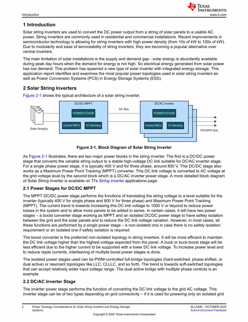
2 Solar String InvertersFigure 2-1 shows the typical architecture of a solar string inverter.
DC/AC Inverter
DC/AC Inverter
DC/DC MPPT
POWER STAGE
Control MCU V/I Sensing
DC/AC Inverter
POWER STAGE
Solar Array(s)
DC Bus
1PH/3PH Grid
Control MCU V/I Sensing
Figure 2-1. Block Diagram of Solar String Inverter
As Figure 2-1 illustrates, there are two major power blocks in the string inverter. The first is a DC/DC powerstage that converts the variable string output to a stable high-voltage DC link suitable for DC/AC inverter stage.For a single phase power stage, it is typically 400 V and for three phase, around 800 V. This DC/DC stage alsoworks as a Maximum Power Point Tracking (MPPT) converter. This DC link voltage is converted to AC voltage atthe grid voltage level by the second block which is a DC/AC inverter power stage. A more detailed block diagramof Solar String inverter is available on TI's String inverter applications page.
2.1 Power Stages for DC/DC MPPTThe MPPT DC/DC power stage performs the functions of translating the string voltage to a level suitable for theinverter (typically 400 V for single phase and 800 V for three phase) and Maximum Power Point Tracking(MPPT). The current trend is towards increasing this DC link voltage to 1000 V or beyond to reduce powerlosses in the system and to allow more panels to be added in series. In certain cases, it will have two powerstages – a boost converter stage working as MPPT and an isolated DC/DC power stage to have safety isolationbetween the grid and the solar panels and to reduce the DC link voltage variation. However, in most cases, allthese functions are performed by a single power stage – a non-isolated one in case there is no safety isolationrequirement or an isolated one if safety isolation is required.
The boost converter is the preferred non-isolated topology in string inverters. It will be more efficient to maintainthe DC link voltage higher than the highest voltage expected from the panel. A buck or buck-boost stage will beless efficient due to the higher current to be supported with a lower DC link voltage. To increase power level andto reduce ripple currents, interleaving of multiple boost power stages is done.
The isolated power stages used can be PWM-controlled full-bridge topologies (hard-switched, phase-shifted, ordual active) or resonant topologies like LLC, CLLLC, and so forth. The trend is towards soft-switched topologiesthat can accept relatively wider input voltage range. The dual active bridge with multiple phase controls is anexample.
2.2 DC/AC Inverter StageThe inverter power stage performs the function of converting the DC link voltage to the grid AC voltage. Thisinverter stage can be of two types depending on grid connectivity – if it is used for powering only an isolated grid
Introduction www.ti.com
2 Power Topology Considerations for Solar String Inverters and Energy StorageSystems
SLLA498 – OCTOBER 2020Submit Document Feedback
Copyright © 2020 Texas Instruments Incorporated
(like only a building) on its own, it is called an off-grid inverter and if it connects to a larger grid sharing the loadfrom other sources, it is called a grid-tied inverter.
An off-grid inverter could be used as a back-up source or as a main power source, but while it is active, it is theonly source in the micro grid it powers. Therefore, this type of inverter need not have to address the burden ofsynchronizing with other sources in the grid. They are used only in smaller capacity systems with lesser need tocommunicate with other systems.
A grid-tied inverter has the additional task of synchronizing in amplitude, frequency, and phase with the existinggrid comprised of multiple sources and loads. It also needs to address the situation of detecting and isolatingitself from the grid in the event of any faults in the grid like black-out, brown-out, overvoltage, and so forth. This iscalled anti-islanding protection. Grid-tied inverters tend to be of comparatively higher power than off-gridinverters. Since there could be multiple grid-tied inverters in a typical application, the need for communication ismore important with them.
Various buck derived non-isolated topologies modulated with a sine PWM are used as inverters. These includetwo-level H-bridge, HERIC, three-level TNPC, three-level NPC, and three-level ANPC.
www.ti.com Solar String Inverters
SLLA498 – OCTOBER 2020Submit Document Feedback
Power Topology Considerations for Solar String Inverters and Energy StorageSystems
3
Copyright © 2020 Texas Instruments Incorporated
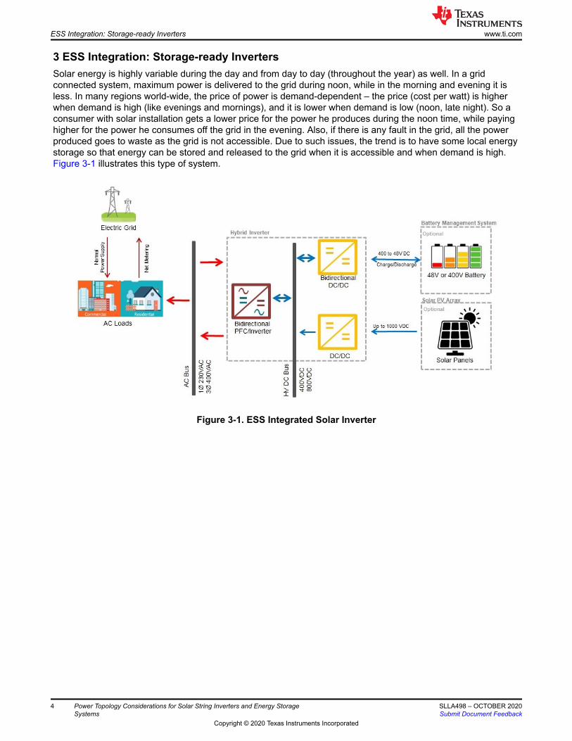
3 ESS Integration: Storage-ready InvertersSolar energy is highly variable during the day and from day to day (throughout the year) as well. In a gridconnected system, maximum power is delivered to the grid during noon, while in the morning and evening it isless. In many regions world-wide, the price of power is demand-dependent – the price (cost per watt) is higherwhen demand is high (like evenings and mornings), and it is lower when demand is low (noon, late night). So aconsumer with solar installation gets a lower price for the power he produces during the noon time, while payinghigher for the power he consumes off the grid in the evening. Also, if there is any fault in the grid, all the powerproduced goes to waste as the grid is not accessible. Due to such issues, the trend is to have some local energystorage so that energy can be stored and released to the grid when it is accessible and when demand is high.Figure 3-1 illustrates this type of system.
Figure 3-1. ESS Integrated Solar Inverter
ESS Integration: Storage-ready Inverters www.ti.com
4 Power Topology Considerations for Solar String Inverters and Energy StorageSystems
SLLA498 – OCTOBER 2020Submit Document Feedback
Copyright © 2020 Texas Instruments Incorporated
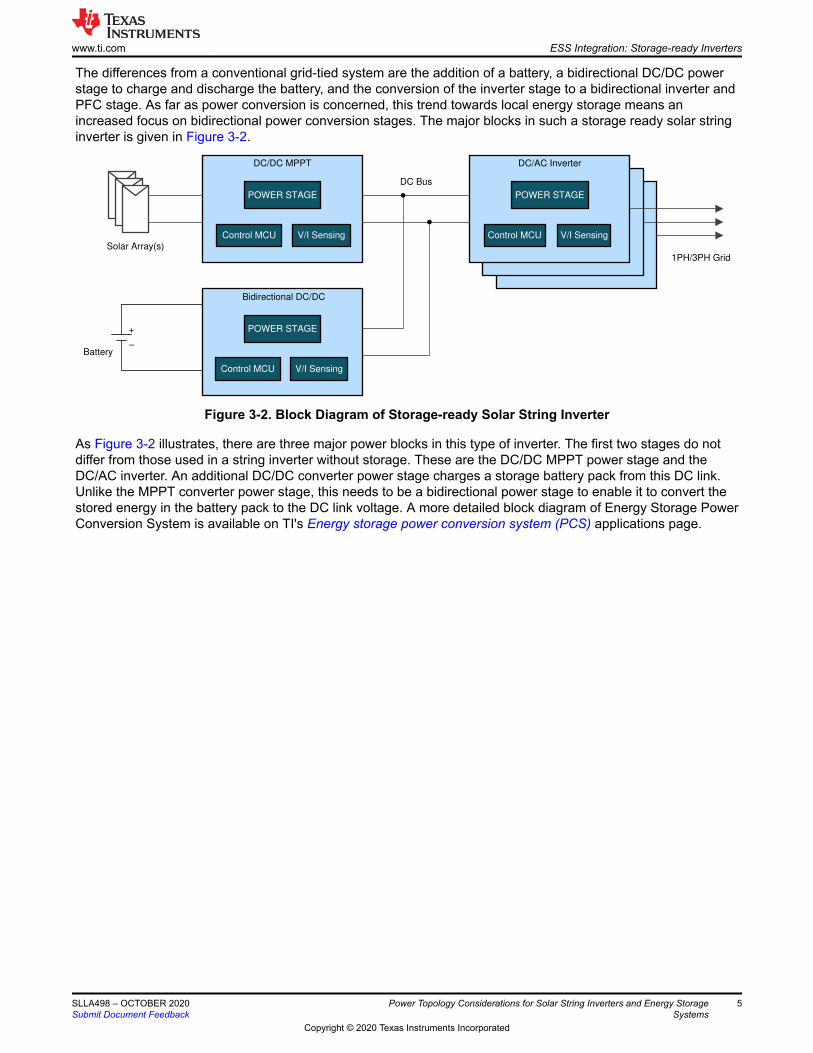
The differences from a conventional grid-tied system are the addition of a battery, a bidirectional DC/DC powerstage to charge and discharge the battery, and the conversion of the inverter stage to a bidirectional inverter andPFC stage. As far as power conversion is concerned, this trend towards local energy storage means anincreased focus on bidirectional power conversion stages. The major blocks in such a storage ready solar stringinverter is given in Figure 3-2.
DC/AC Inverter
DC/AC Inverter
DC/DC MPPT
POWER STAGE
Control MCU V/I Sensing
DC/AC Inverter
POWER STAGE
Control MCU V/I Sensing
Bidirectional DC/DC
POWER STAGE
Control MCU V/I Sensing
Solar Array(s)
Battery
DC Bus
1PH/3PH Grid
+
±
Figure 3-2. Block Diagram of Storage-ready Solar String Inverter
As Figure 3-2 illustrates, there are three major power blocks in this type of inverter. The first two stages do notdiffer from those used in a string inverter without storage. These are the DC/DC MPPT power stage and theDC/AC inverter. An additional DC/DC converter power stage charges a storage battery pack from this DC link.Unlike the MPPT converter power stage, this needs to be a bidirectional power stage to enable it to convert thestored energy in the battery pack to the DC link voltage. A more detailed block diagram of Energy Storage PowerConversion System is available on TI's Energy storage power conversion system (PCS) applications page.
www.ti.com ESS Integration: Storage-ready Inverters
SLLA498 – OCTOBER 2020Submit Document Feedback
Power Topology Considerations for Solar String Inverters and Energy StorageSystems
5
Copyright © 2020 Texas Instruments Incorporated
3.1 DC/DC MPPT Power StageThe DC/DC MPPT power stage in a storage ready inverter does not differ from the power stages used in normalstring inverter. The boost converter (interleaved for higher power levels) is the preferred topology for non-isolatedconfiguration, while the phase-shifted full bridge, dual active bridge , LLC and CLLLC are used in isolatedconfiguration.
3.2 Bidirectional DC/DC Power StageThis power stage is unique to the storage ready inverters. It works as a battery charger in one direction and as aconstant voltage DC/DC converter to convert the variable battery voltage to the required constant bus voltagelevel in the other direction. Though Lead-acid type batteries are very popular in energy storage systems, newersystems are increasingly moving to various types of Lithium batteries. The battery voltage depends upon thesystem power level. Lower power single phase systems commonly use 48-V battery, while higher power threephase systems use 400-V battery. Intermediate battery voltages are used infrequently. Systems with higherpower range of string inverters could use 800-V battery for storage.
The common topologies for the bidirectional DC/DC power stage are the CLLLC converter and the Dual ActiveBridge (DAB) in isolated configuration. In non-isolated configurations, the synchronous boost converter can beused as a bidirectional power stage. In low cost single phase systems with lower battery voltages, current-fedpush-pull topology (with or without active clamp) is also used.
3.3 Bidirectional Inverter/ PFC Power StageThe power stages used in the inverter power stage needs to be bidirectional in the storage ready inverter as itshould be able to charge the battery when the situation demands it. However, there is no need for any specialpower topology to achieve this, as the inverter power stages commonly used in standard string inverters like two-level H-bridge, HERIC, three-level TNPC, three-level NPC, and three-level ANPC are all capable of bidirectionaloperation. The only difference will be in the firmware used for controlling these power stages to enable bi-directional operation.
ESS Integration: Storage-ready Inverters www.ti.com
6 Power Topology Considerations for Solar String Inverters and Energy StorageSystems
SLLA498 – OCTOBER 2020Submit Document Feedback
Copyright © 2020 Texas Instruments Incorporated
4 Power Converter Topologies for DC/DC Power StagesThis section explores five popular topologies used in the DC/DC power stage of solar string inverters.
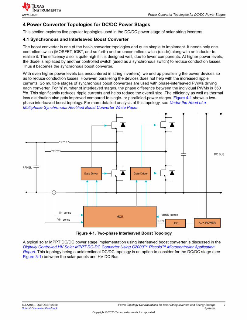
4.1 Synchronous and Interleaved Boost ConverterThe boost converter is one of the basic converter topologies and quite simple to implement. It needs only onecontrolled switch (MOSFET, IGBT, and so forth) and an uncontrolled switch (diode) along with an inductor torealize it. The efficiency also is quite high if it is designed well, due to fewer components. At higher power levels,the diode is replaced by another controlled switch (used as a synchronous switch) to reduce conduction losses.Thus it becomes the synchronous boost converter.
With even higher power levels (as encountered in string inverters), we end up paralleling the power devices soas to reduce conduction losses. However, paralleling the devices does not help with the increased ripplecurrents. So multiple stages of synchronous boost converters are used with phase-interleaved PWMs drivingeach converter. For ‘n’ number of interleaved stages, the phase difference between the individual PWMs is 360o/n. This significantly reduces ripple currents and helps reduce the overall size. The efficiency as well as thermalloss distribution also gets improved compared to single- or paralleled-power stages. Figure 4-1 shows a two-phase interleaved boost topology. For more detailed analysis of this topology, see Under the Hood of aMultiphase Synchronous Rectified Boost Converter White Paper.
LDO
MCU
AUX POWER
Vin_sense
Iin_senseVBUS_sense
3.3 V
PANEL
DC BUS
Gate Driver Gate Driver
Figure 4-1. Two-phase Interleaved Boost Topology
A typical solar MPPT DC/DC power stage implementation using interleaved boost converter is discussed in theDigitally Controlled HV Solar MPPT DC-DC Converter Using C2000™ Piccolo™ Microcontroller ApplicationReport. This topology being a unidirectional DC/DC topology is an option to consider for the DC/DC stage (seeFigure 3-1) between the solar panels and HV DC Bus.
www.ti.com Power Converter Topologies for DC/DC Power Stages
SLLA498 – OCTOBER 2020Submit Document Feedback
Power Topology Considerations for Solar String Inverters and Energy StorageSystems
7
Copyright © 2020 Texas Instruments Incorporated
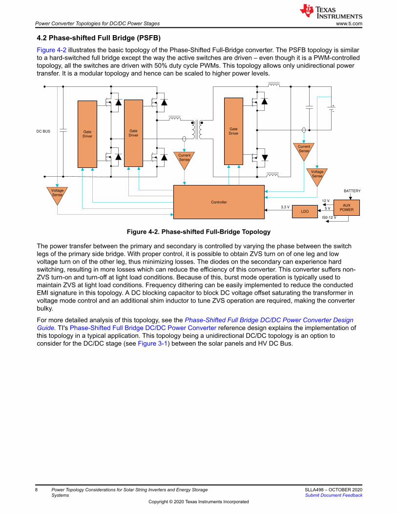
4.2 Phase-shifted Full Bridge (PSFB)Figure 4-2 illustrates the basic topology of the Phase-Shifted Full-Bridge converter. The PSFB topology is similarto a hard-switched full bridge except the way the active switches are driven – even though it is a PWM-controlledtopology, all the switches are driven with 50% duty cycle PWMs. This topology allows only unidirectional powertransfer. It is a modular topology and hence can be scaled to higher power levels.
Controller
DC BUS
LDO
AUX
POWER5 V3.3 V
IS0-12 V
BATTERY
12 V
Gate
DriverGate
Driver
Current
Sense
Voltage
Sense
Gate
Driver
Current
Sense
Voltage
Sense
+
±
Figure 4-2. Phase-shifted Full-Bridge Topology
The power transfer between the primary and secondary is controlled by varying the phase between the switchlegs of the primary side bridge. With proper control, it is possible to obtain ZVS turn on of one leg and lowvoltage turn on of the other leg, thus minimizing losses. The diodes on the secondary can experience hardswitching, resulting in more losses which can reduce the efficiency of this converter. This converter suffers non-ZVS turn-on and turn-off at light load conditions. Because of this, burst mode operation is typically used tomaintain ZVS at light load conditions. Frequency dithering can be easily implemented to reduce the conductedEMI signature in this topology. A DC blocking capacitor to block DC voltage offset saturating the transformer involtage mode control and an additional shim inductor to tune ZVS operation are required, making the converterbulky.
For more detailed analysis of this topology, see the Phase-Shifted Full Bridge DC/DC Power Converter DesignGuide. TI's Phase-Shifted Full Bridge DC/DC Power Converter reference design explains the implementation ofthis topology in a typical application. This topology being a unidirectional DC/DC topology is an option toconsider for the DC/DC stage (see Figure 3-1) between the solar panels and HV DC Bus.
Power Converter Topologies for DC/DC Power Stages www.ti.com
8 Power Topology Considerations for Solar String Inverters and Energy StorageSystems
SLLA498 – OCTOBER 2020Submit Document Feedback
Copyright © 2020 Texas Instruments Incorporated
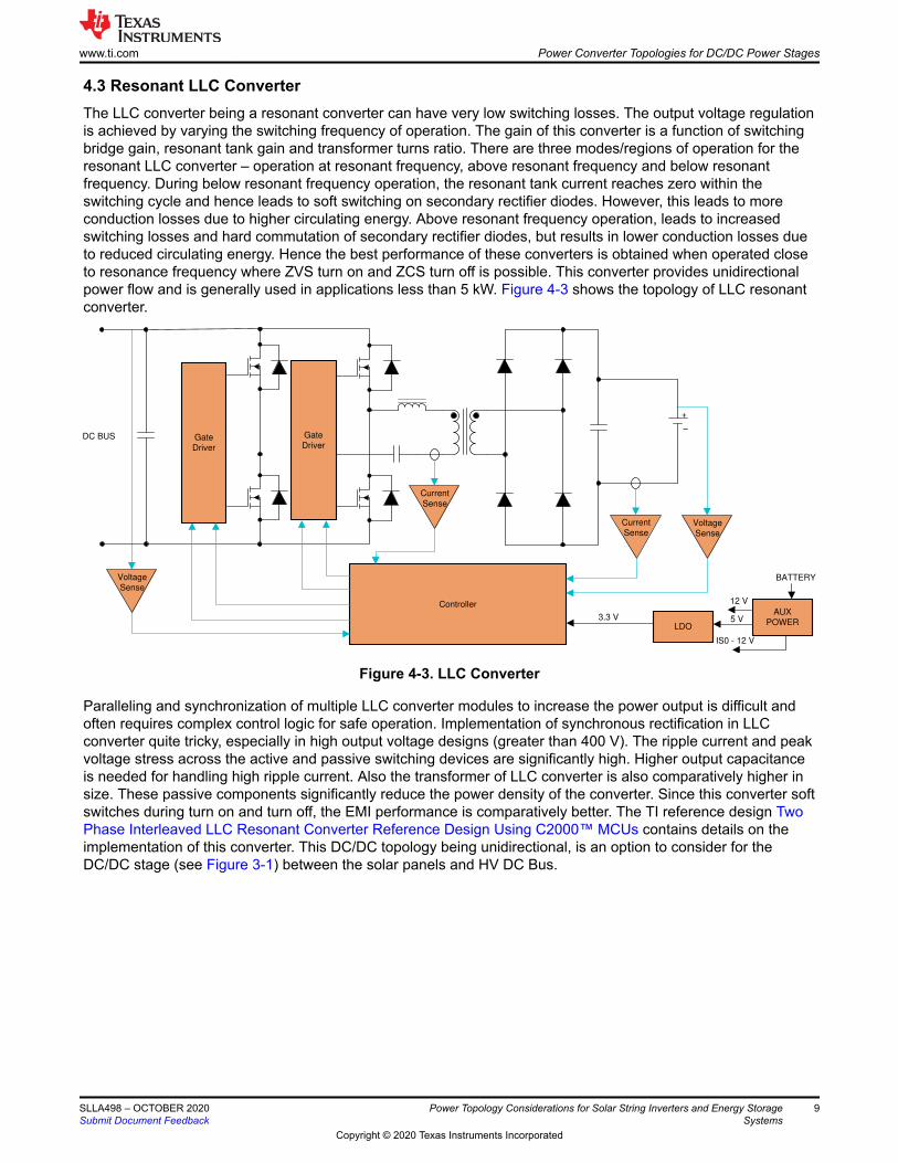
4.3 Resonant LLC ConverterThe LLC converter being a resonant converter can have very low switching losses. The output voltage regulationis achieved by varying the switching frequency of operation. The gain of this converter is a function of switchingbridge gain, resonant tank gain and transformer turns ratio. There are three modes/regions of operation for theresonant LLC converter – operation at resonant frequency, above resonant frequency and below resonantfrequency. During below resonant frequency operation, the resonant tank current reaches zero within theswitching cycle and hence leads to soft switching on secondary rectifier diodes. However, this leads to moreconduction losses due to higher circulating energy. Above resonant frequency operation, leads to increasedswitching losses and hard commutation of secondary rectifier diodes, but results in lower conduction losses dueto reduced circulating energy. Hence the best performance of these converters is obtained when operated closeto resonance frequency where ZVS turn on and ZCS turn off is possible. This converter provides unidirectionalpower flow and is generally used in applications less than 5 kW. Figure 4-3 shows the topology of LLC resonantconverter.
Controller
DC BUS
LDO
AUX
POWER5 V3.3 V
IS0 - 12 V
BATTERY
12 V
Gate
DriverGate
Driver
Current
Sense
Voltage
Sense
Current
SenseVoltage
Sense
+
±
Figure 4-3. LLC Converter
Paralleling and synchronization of multiple LLC converter modules to increase the power output is difficult andoften requires complex control logic for safe operation. Implementation of synchronous rectification in LLCconverter quite tricky, especially in high output voltage designs (greater than 400 V). The ripple current and peakvoltage stress across the active and passive switching devices are significantly high. Higher output capacitanceis needed for handling high ripple current. Also the transformer of LLC converter is also comparatively higher insize. These passive components significantly reduce the power density of the converter. Since this converter softswitches during turn on and turn off, the EMI performance is comparatively better. The TI reference design TwoPhase Interleaved LLC Resonant Converter Reference Design Using C2000™ MCUs contains details on theimplementation of this converter. This DC/DC topology being unidirectional, is an option to consider for theDC/DC stage (see Figure 3-1) between the solar panels and HV DC Bus.
www.ti.com Power Converter Topologies for DC/DC Power Stages
SLLA498 – OCTOBER 2020Submit Document Feedback
Power Topology Considerations for Solar String Inverters and Energy StorageSystems
9
Copyright © 2020 Texas Instruments Incorporated
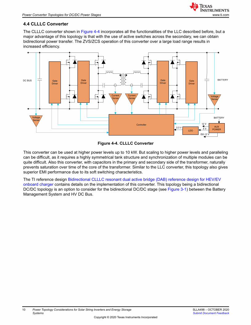
4.4 CLLLC ConverterThe CLLLC converter shown in Figure 4-4 incorporates all the functionalities of the LLC described before, but amajor advantage of this topology is that with the use of active switches across the secondary, we can obtainbidirectional power transfer. The ZVS/ZCS operation of this converter over a large load range results inincreased efficiency.
Controller
DC BUS
LDO
AUX
POWER5 V3.3 V
IS0-12 V
BATTERY
12 V
Gate
DriverGate
Driver
Current
Sense
Voltage
Sense
Gate
DriverGate
Driver
Current
Sense
BATTERY
Voltage
Sense
Figure 4-4. CLLLC Converter
This converter can be used at higher power levels up to 10 kW. But scaling to higher power levels and parallelingcan be difficult, as it requires a highly symmetrical tank structure and synchronization of multiple modules can bequite difficult. Also this converter, with capacitors in the primary and secondary side of the transformer, naturallyprevents saturation over time of the core of the transformer. Similar to the LLC converter, this topology also givessuperior EMI performance due to its soft switching characteristics.
The TI reference design Bidirectional CLLLC resonant dual active bridge (DAB) reference design for HEV/EVonboard charger contains details on the implementation of this converter. This topology being a bidirectionalDC/DC topology is an option to consider for the bidirectional DC/DC stage (see Figure 3-1) between the BatteryManagement System and HV DC Bus.
Power Converter Topologies for DC/DC Power Stages www.ti.com
10 Power Topology Considerations for Solar String Inverters and Energy StorageSystems
SLLA498 – OCTOBER 2020Submit Document Feedback
Copyright © 2020 Texas Instruments Incorporated
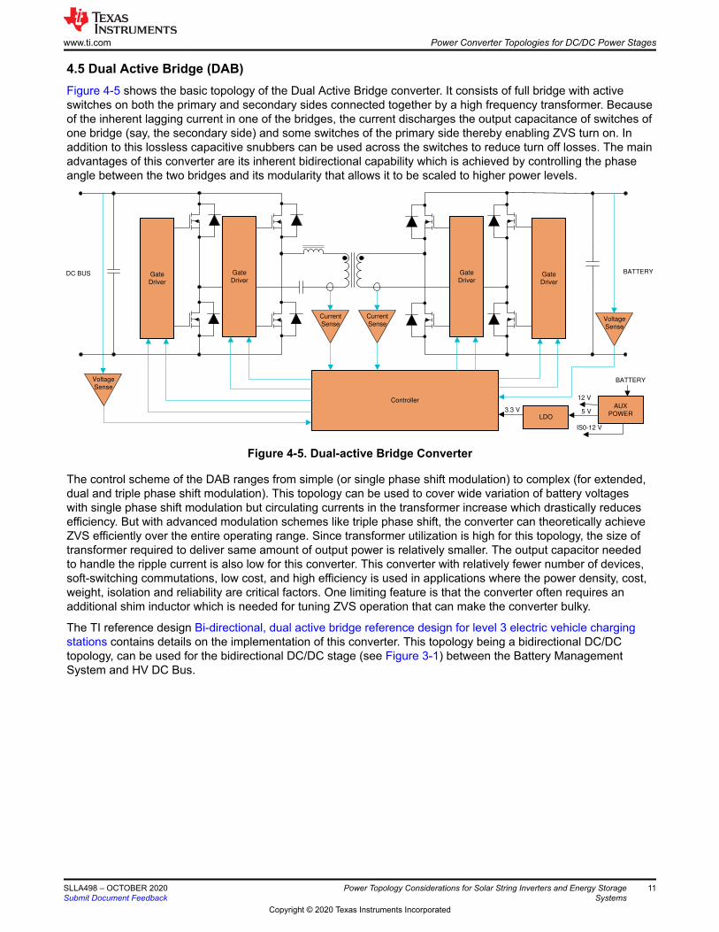
4.5 Dual Active Bridge (DAB)Figure 4-5 shows the basic topology of the Dual Active Bridge converter. It consists of full bridge with activeswitches on both the primary and secondary sides connected together by a high frequency transformer. Becauseof the inherent lagging current in one of the bridges, the current discharges the output capacitance of switches ofone bridge (say, the secondary side) and some switches of the primary side thereby enabling ZVS turn on. Inaddition to this lossless capacitive snubbers can be used across the switches to reduce turn off losses. The mainadvantages of this converter are its inherent bidirectional capability which is achieved by controlling the phaseangle between the two bridges and its modularity that allows it to be scaled to higher power levels.
Controller
DC BUS
LDO
AUX
POWER5 V3.3 V
IS0-12 V
BATTERY
12 V
Gate
DriverGate
Driver
Current
Sense
Voltage
Sense
Gate
DriverGate
Driver
Current
Sense
BATTERY
Voltage
Sense
Figure 4-5. Dual-active Bridge Converter
The control scheme of the DAB ranges from simple (or single phase shift modulation) to complex (for extended,dual and triple phase shift modulation). This topology can be used to cover wide variation of battery voltageswith single phase shift modulation but circulating currents in the transformer increase which drastically reducesefficiency. But with advanced modulation schemes like triple phase shift, the converter can theoretically achieveZVS efficiently over the entire operating range. Since transformer utilization is high for this topology, the size oftransformer required to deliver same amount of output power is relatively smaller. The output capacitor neededto handle the ripple current is also low for this converter. This converter with relatively fewer number of devices,soft-switching commutations, low cost, and high efficiency is used in applications where the power density, cost,weight, isolation and reliability are critical factors. One limiting feature is that the converter often requires anadditional shim inductor which is needed for tuning ZVS operation that can make the converter bulky.
The TI reference design Bi-directional, dual active bridge reference design for level 3 electric vehicle chargingstations contains details on the implementation of this converter. This topology being a bidirectional DC/DCtopology, can be used for the bidirectional DC/DC stage (see Figure 3-1) between the Battery ManagementSystem and HV DC Bus.
www.ti.com Power Converter Topologies for DC/DC Power Stages
SLLA498 – OCTOBER 2020Submit Document Feedback
Power Topology Considerations for Solar String Inverters and Energy StorageSystems
11
Copyright © 2020 Texas Instruments Incorporated
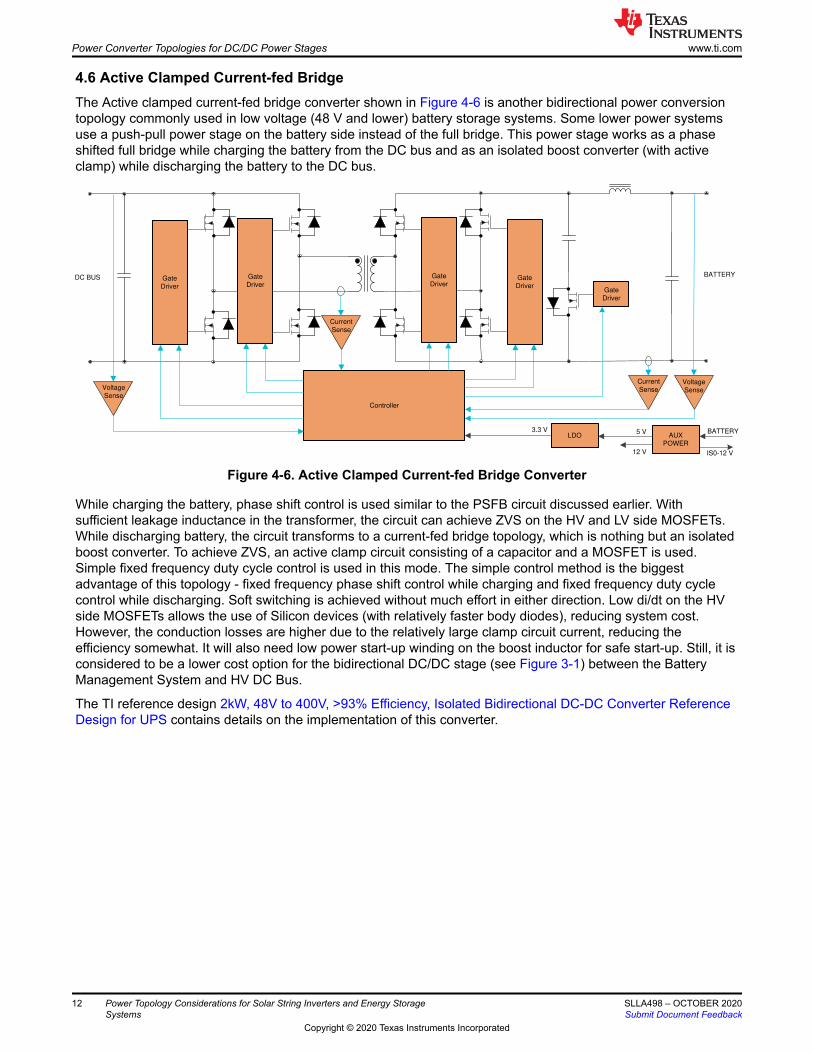
4.6 Active Clamped Current-fed BridgeThe Active clamped current-fed bridge converter shown in Figure 4-6 is another bidirectional power conversiontopology commonly used in low voltage (48 V and lower) battery storage systems. Some lower power systemsuse a push-pull power stage on the battery side instead of the full bridge. This power stage works as a phaseshifted full bridge while charging the battery from the DC bus and as an isolated boost converter (with activeclamp) while discharging the battery to the DC bus.
Controller
DC BUS
LDO AUX
POWER
5 V3.3 V
IS0-12 V
BATTERY
12 V
Gate
DriverGate
Driver
Current
Sense
Voltage
Sense
Gate
DriverGate
Driver
Current
Sense
BATTERY
Voltage
Sense
Gate
Driver
Figure 4-6. Active Clamped Current-fed Bridge Converter
While charging the battery, phase shift control is used similar to the PSFB circuit discussed earlier. Withsufficient leakage inductance in the transformer, the circuit can achieve ZVS on the HV and LV side MOSFETs.While discharging battery, the circuit transforms to a current-fed bridge topology, which is nothing but an isolatedboost converter. To achieve ZVS, an active clamp circuit consisting of a capacitor and a MOSFET is used.Simple fixed frequency duty cycle control is used in this mode. The simple control method is the biggestadvantage of this topology - fixed frequency phase shift control while charging and fixed frequency duty cyclecontrol while discharging. Soft switching is achieved without much effort in either direction. Low di/dt on the HVside MOSFETs allows the use of Silicon devices (with relatively faster body diodes), reducing system cost.However, the conduction losses are higher due to the relatively large clamp circuit current, reducing theefficiency somewhat. It will also need low power start-up winding on the boost inductor for safe start-up. Still, it isconsidered to be a lower cost option for the bidirectional DC/DC stage (see Figure 3-1) between the BatteryManagement System and HV DC Bus.
The TI reference design 2kW, 48V to 400V, >93% Efficiency, Isolated Bidirectional DC-DC Converter ReferenceDesign for UPS contains details on the implementation of this converter.
Power Converter Topologies for DC/DC Power Stages www.ti.com
12 Power Topology Considerations for Solar String Inverters and Energy StorageSystems
SLLA498 – OCTOBER 2020Submit Document Feedback
Copyright © 2020 Texas Instruments Incorporated
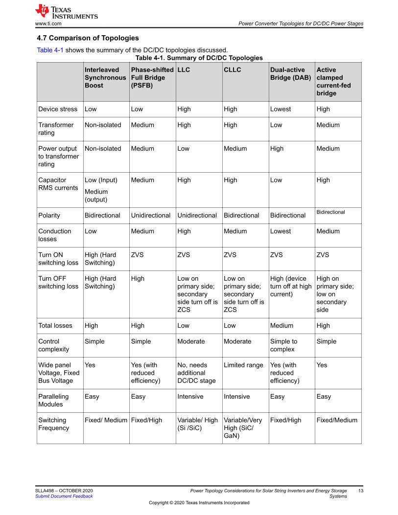
4.7 Comparison of TopologiesTable 4-1 shows the summary of the DC/DC topologies discussed.
Table 4-1. Summary of DC/DC Topologies
InterleavedSynchronousBoost
Phase-shiftedFull Bridge(PSFB)
LLC CLLC Dual-activeBridge (DAB)
Activeclampedcurrent-fedbridge
Device stress Low Low High High Lowest High
Transformerrating
Non-isolated Medium High High Low Medium
Power outputto transformerrating
Non-isolated Medium Low Medium High Medium
CapacitorRMS currents
Low (Input)
Medium(output)
Medium High High Low High
Polarity Bidirectional Unidirectional Unidirectional Bidirectional Bidirectional Bidirectional
Conductionlosses
Low Medium High Medium Lowest Medium
Turn ONswitching loss
High (HardSwitching)
ZVS ZVS ZVS ZVS ZVS
Turn OFFswitching loss
High (HardSwitching)
High Low onprimary side;secondaryside turn off isZCS
Low onprimary side;secondaryside turn off isZCS
High (deviceturn off at highcurrent)
High onprimary side;low onsecondaryside
Total losses High High Low Low Medium High
Controlcomplexity
Simple Simple Moderate Moderate Simple tocomplex
Simple
Wide panelVoltage, FixedBus Voltage
Yes Yes (withreducedefficiency)
No, needsadditionalDC/DC stage
Limited range Yes (withreducedefficiency)
Yes
ParallelingModules
Easy Easy Intensive Intensive Easy Easy
SwitchingFrequency
Fixed/ Medium Fixed/High Variable/ High(Si /SiC)
Variable/VeryHigh (SiC/GaN)
Fixed/High Fixed/Medium
www.ti.com Power Converter Topologies for DC/DC Power Stages
SLLA498 – OCTOBER 2020Submit Document Feedback
Power Topology Considerations for Solar String Inverters and Energy StorageSystems
13
Copyright © 2020 Texas Instruments Incorporated
5 Power Converter Topologies for DC/AC StagesThis section examines five popular topologies used in the DC/AC power stage of solar string inverters.
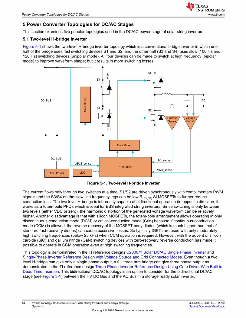
5.1 Two-level H-bridge InverterFigure 5-1 shows the two-level H-bridge inverter topology which is a conventional bridge inverter in which onehalf of the bridge uses fast switching devices S1 and S2, and the other half (S3 and S4) uses slow (100 Hz and120 Hz) switching devices (unipolar mode). All four devices can be made to switch at high frequency (bipolarmode) to improve waveform shape; but it results in more switching losses.
Controller
Current
Sense
Si
FET
Ga
te D
rive
r
LDOAux. Power
Voltage
Sense
VBUS_sense
3.3 V VAC_sense
IAC_sense
ACDC BUS
DC BUS
S1
S2
S3
S4
Gate Driver
Si
FET
Figure 5-1. Two-level H-bridge Inverter
The current flows only through two switches at a time. S1/S2 are driven synchronously with complimentary PWMsignals and the S3/S4 on the slow line frequency legs can be low RDS(on) Si MOSFETs to further reduceconduction loss. The two level H-bridge is inherently capable of bidirectional operation (in opposite direction, itworks as a totem-pole PFC), which is ideal for ESS integrated string inverters. Since switching is only betweentwo levels (either VDC or zero), the harmonic distortion of the generated voltage waveform can be relativelyhigher. Another disadvantage is that with silicon MOSFETs, the totem-pole arrangement allows operating in onlydiscontinuous-conduction mode (DCM) or critical-conduction mode (CrM) because if continuous-conductionmode (CCM) is allowed, the reverse recovery of the MOSFET body diodes (which is much higher than that ofstandard fast-recovery diodes) can cause excessive losses. So typically IGBTs are used with only moderatelyhigh switching frequencies (below 25 kHz) when CCM operation is required. However, with the advent of siliconcarbide (SiC) and gallium nitride (GaN) switching devices with zero-recovery reverse conduction has made itpossible to operate in CCM operation even at high switching frequencies.
This topology is demonstrated in the TI reference designs C2000™ Solar DC/AC Single Phase Inverter andSingle-Phase Inverter Reference Design with Voltage Source and Grid Connected Modes. Even though a twolevel H-bridge can give only a single phase output, a full three arm bridge can give three phase output asdemonstrated in the TI reference design Three-Phase Inverter Reference Design Using Gate Driver With Built-inDead Time Insertion. This bidirectional DC/AC topology is an option to consider for the bidirectional DC/ACstage (see Figure 3-1) between the HV DC Bus and the AC Bus in a storage ready solar inverter.
Power Converter Topologies for DC/AC Stages www.ti.com
14 Power Topology Considerations for Solar String Inverters and Energy StorageSystems
SLLA498 – OCTOBER 2020Submit Document Feedback
Copyright © 2020 Texas Instruments Incorporated
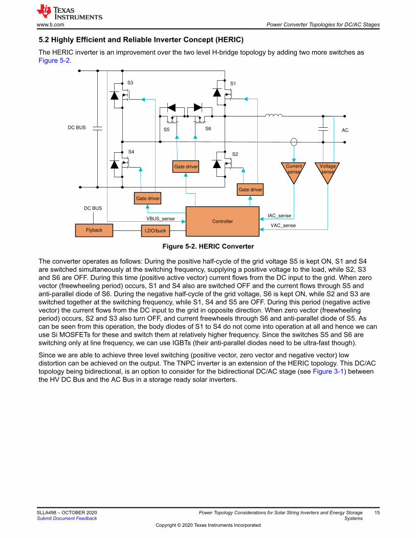
5.2 Highly Efficient and Reliable Inverter Concept (HERIC)The HERIC inverter is an improvement over the two level H-bridge topology by adding two more switches asFigure 5-2.
Current
sense
Controller
LDO/buckFlybackVAC_sense
IAC_senseVBUS_sense
AC
Gate driver
Voltage
sense
Gate driver
Gate driver
S1
DC BUS
S2
S3
S4
S5 S6
DC BUS
Figure 5-2. HERIC Converter
The converter operates as follows: During the positive half-cycle of the grid voltage S5 is kept ON, S1 and S4are switched simultaneously at the switching frequency, supplying a positive voltage to the load, while S2, S3and S6 are OFF. During this time (positive active vector) current flows from the DC input to the grid. When zerovector (freewheeling period) occurs, S1 and S4 also are switched OFF and the current flows through S5 andanti-parallel diode of S6. During the negative half-cycle of the grid voltage, S6 is kept ON, while S2 and S3 areswitched together at the switching frequency, while S1, S4 and S5 are OFF. During this period (negative activevector) the current flows from the DC input to the grid in opposite direction. When zero vector (freewheelingperiod) occurs, S2 and S3 also turn OFF, and current freewheels through S6 and anti-parallel diode of S5. Ascan be seen from this operation, the body diodes of S1 to S4 do not come into operation at all and hence we canuse Si MOSFETs for these and switch them at relatively higher frequency. Since the switches S5 and S6 areswitching only at line frequency, we can use IGBTs (their anti-parallel diodes need to be ultra-fast though).
Since we are able to achieve three level switching (positive vector, zero vector and negative vector) lowdistortion can be achieved on the output. The TNPC inverter is an extension of the HERIC topology. This DC/ACtopology being bidirectional, is an option to consider for the bidirectional DC/AC stage (see Figure 3-1) betweenthe HV DC Bus and the AC Bus in a storage ready solar inverters.
www.ti.com Power Converter Topologies for DC/AC Stages
SLLA498 – OCTOBER 2020Submit Document Feedback
Power Topology Considerations for Solar String Inverters and Energy StorageSystems
15
Copyright © 2020 Texas Instruments Incorporated
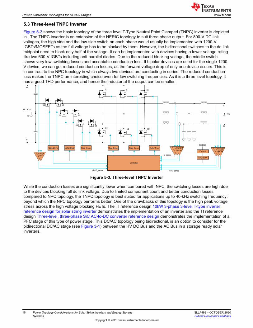
5.3 Three-level TNPC InverterFigure 5-3 shows the basic topology of the three level T-Type Neutral Point Clamped (TNPC) inverter is depictedin . The TNPC inverter is an extension of the HERIC topology to suit three phase output. For 800-V DC linkvoltages, the high side and the low-side switch on each phase would usually be implemented with 1200-VIGBTs/MOSFETs as the full voltage has to be blocked by them. However, the bidirectional switches to the dc-linkmidpoint need to block only half of the voltage. It can be implemented with devices having a lower voltage ratinglike two 600-V IGBTs including anti-parallel diodes. Due to the reduced blocking voltage, the middle switchshows very low switching losses and acceptable conduction loss. If bipolar devices are used for the single 1200-V device, we can get reduced conduction losses, as the forward voltage drop of only one device occurs. This isin contrast to the NPC topology in which always two devices are conducting in series. The reduced conductionloss makes the TNPC an interesting choice even for low switching frequencies. As it is a three level topology, ithas a good THD performance; and hence the inductor at the output can be smaller.
Gate Driver
Controller
LDO/Buck
Flyback
Gate Driver
VAC_sense
IL_sense
VBUS_sense
Gate Driver
S1
DC BUS
S2
S3
S4
S5 S6
DC BUS
S1
S2
S5 S6
S5 S6
Gate Driver Gate DriverGate Driver
Voltage
sense
Current
senseVoltage
sense
AC
V+
V-
B
Y
R
N
Figure 5-3. Three-level TNPC Inverter
While the conduction losses are significantly lower when compared with NPC, the switching losses are high dueto the devices blocking full dc link voltage. Due to limited component count and better conduction lossescompared to NPC topology, the TNPC topology is best suited for applications up to 40-kHz switching frequency;beyond which the NPC topology performs better. One of the drawbacks of this topology is the high peak voltagestress across the high voltage blocking FETs. The TI reference design 10kW 3-phase 3-level T-type inverterreference design for solar string inverter demonstrates the implementation of an inverter and the TI referencedesign Three-level, three-phase SiC AC-to-DC converter reference design demonstrates the implementation of aPFC stage of this type of power stage. This DC/AC topology being bidirectional, is an option to consider for thebidirectional DC/AC stage (see Figure 3-1) between the HV DC Bus and the AC Bus in a storage ready solarinverters.
Power Converter Topologies for DC/AC Stages www.ti.com
16 Power Topology Considerations for Solar String Inverters and Energy StorageSystems
SLLA498 – OCTOBER 2020Submit Document Feedback
Copyright © 2020 Texas Instruments Incorporated
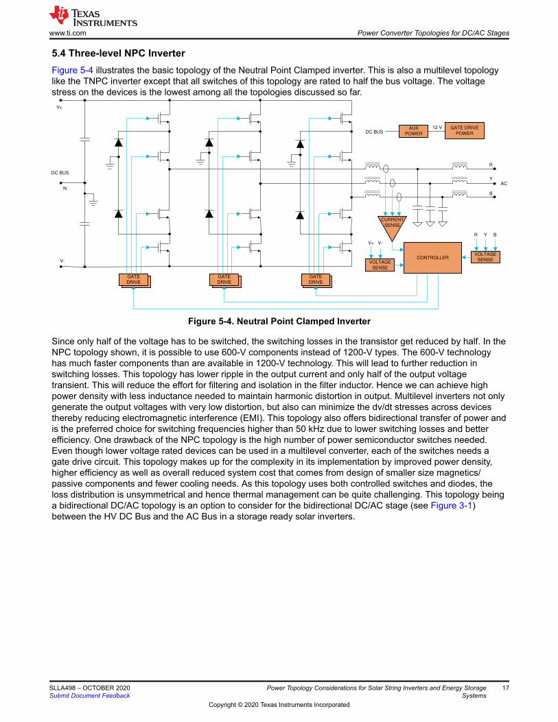
5.4 Three-level NPC InverterFigure 5-4 illustrates the basic topology of the Neutral Point Clamped inverter. This is also a multilevel topologylike the TNPC inverter except that all switches of this topology are rated to half the bus voltage. The voltagestress on the devices is the lowest among all the topologies discussed so far.
V+
V-
N
R
Y
B
GATE
DRIVE
CONTROLLER
CURRENT
SENSE
VOLTAGE
SENSE
V+ V-
VOLTAGE
SENSE
R Y B
GATE
DRIVE
GATE
DRIVE
AUX
POWERDC BUS
12 V GATE DRIVE
POWER
AC
DC BUS
Figure 5-4. Neutral Point Clamped Inverter
Since only half of the voltage has to be switched, the switching losses in the transistor get reduced by half. In theNPC topology shown, it is possible to use 600-V components instead of 1200-V types. The 600-V technologyhas much faster components than are available in 1200-V technology. This will lead to further reduction inswitching losses. This topology has lower ripple in the output current and only half of the output voltagetransient. This will reduce the effort for filtering and isolation in the filter inductor. Hence we can achieve highpower density with less inductance needed to maintain harmonic distortion in output. Multilevel inverters not onlygenerate the output voltages with very low distortion, but also can minimize the dv/dt stresses across devicesthereby reducing electromagnetic interference (EMI). This topology also offers bidirectional transfer of power andis the preferred choice for switching frequencies higher than 50 kHz due to lower switching losses and betterefficiency. One drawback of the NPC topology is the high number of power semiconductor switches needed.Even though lower voltage rated devices can be used in a multilevel converter, each of the switches needs agate drive circuit. This topology makes up for the complexity in its implementation by improved power density,higher efficiency as well as overall reduced system cost that comes from design of smaller size magnetics/passive components and fewer cooling needs. As this topology uses both controlled switches and diodes, theloss distribution is unsymmetrical and hence thermal management can be quite challenging. This topology beinga bidirectional DC/AC topology is an option to consider for the bidirectional DC/AC stage (see Figure 3-1)between the HV DC Bus and the AC Bus in a storage ready solar inverters.
www.ti.com Power Converter Topologies for DC/AC Stages
SLLA498 – OCTOBER 2020Submit Document Feedback
Power Topology Considerations for Solar String Inverters and Energy StorageSystems
17
Copyright © 2020 Texas Instruments Incorporated
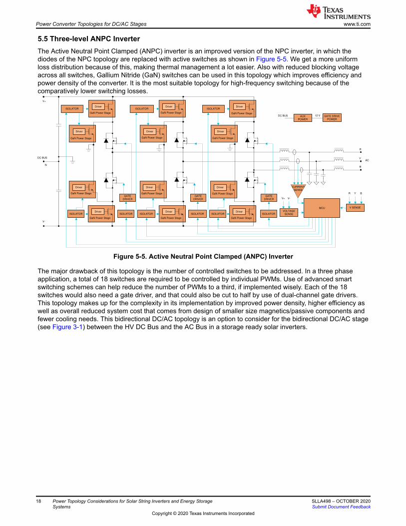
5.5 Three-level ANPC InverterThe Active Neutral Point Clamped (ANPC) inverter is an improved version of the NPC inverter, in which thediodes of the NPC topology are replaced with active switches as shown in Figure 5-5. We get a more uniformloss distribution because of this, making thermal management a lot easier. Also with reduced blocking voltageacross all switches, Gallium Nitride (GaN) switches can be used in this topology which improves efficiency andpower density of the converter. It is the most suitable topology for high-frequency switching because of thecomparatively lower switching losses.
Driver
GaN Power Stage
N
MCU
CURRENT
SENSE
VOLTAGE
SENSE
V+ V-
V SENSE
R Y B
AUX
POWER
DC BUS 12 V GATE DRIVE
POWER
GATE
DRIVER
Driver
Driver
DriverISOLATOR
ISOLATOR
ISOLATOR
Driver
GATE
DRIVER
Driver
Driver
DriverISOLATOR
ISOLATOR
ISOLATOR
Driver
GATE
DRIVER
Driver
Driver
DriverISOLATOR
ISOLATOR
ISOLATOR
R
Y
B
GaN Power Stage
GaN Power Stage
GaN Power Stage GaN Power Stage
GaN Power Stage
GaN Power Stage
GaN Power Stage GaN Power Stage
GaN Power Stage
GaN Power Stage
GaN Power Stage
DC BUS
V+
V-
AC
Figure 5-5. Active Neutral Point Clamped (ANPC) Inverter
The major drawback of this topology is the number of controlled switches to be addressed. In a three phaseapplication, a total of 18 switches are required to be controlled by individual PWMs. Use of advanced smartswitching schemes can help reduce the number of PWMs to a third, if implemented wisely. Each of the 18switches would also need a gate driver, and that could also be cut to half by use of dual-channel gate drivers.This topology makes up for the complexity in its implementation by improved power density, higher efficiency aswell as overall reduced system cost that comes from design of smaller size magnetics/passive components andfewer cooling needs. This bidirectional DC/AC topology is an option to consider for the bidirectional DC/AC stage(see Figure 3-1) between the HV DC Bus and the AC Bus in a storage ready solar inverters.
Power Converter Topologies for DC/AC Stages www.ti.com
18 Power Topology Considerations for Solar String Inverters and Energy StorageSystems
SLLA498 – OCTOBER 2020Submit Document Feedback
Copyright © 2020 Texas Instruments Incorporated
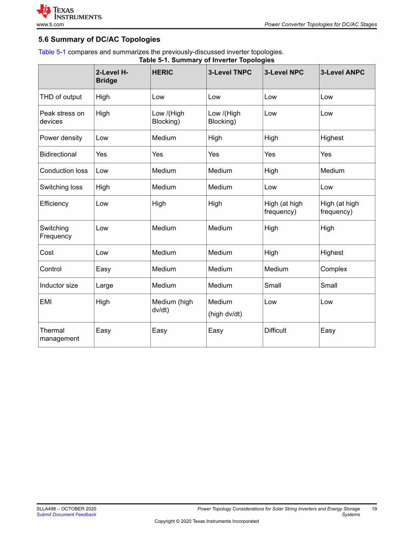
5.6 Summary of DC/AC TopologiesTable 5-1 compares and summarizes the previously-discussed inverter topologies.
Table 5-1. Summary of Inverter Topologies
2-Level H-Bridge
HERIC 3-Level TNPC 3-Level NPC 3-Level ANPC
THD of output High Low Low Low Low
Peak stress ondevices
High Low /(HighBlocking)
Low /(HighBlocking)
Low Low
Power density Low Medium High High Highest
Bidirectional Yes Yes Yes Yes Yes
Conduction loss Low Medium Medium High Medium
Switching loss High Medium Medium Low Low
Efficiency Low High High High (at highfrequency)
High (at highfrequency)
SwitchingFrequency
Low Medium Medium High High
Cost Low Medium Medium High Highest
Control Easy Medium Medium Medium Complex
Inductor size Large Medium Medium Small Small
EMI High Medium (highdv/dt)
Medium
(high dv/dt)
Low Low
Thermalmanagement
Easy Easy Easy Difficult Easy
www.ti.com Power Converter Topologies for DC/AC Stages
SLLA498 – OCTOBER 2020Submit Document Feedback
Power Topology Considerations for Solar String Inverters and Energy StorageSystems
19
Copyright © 2020 Texas Instruments Incorporated
6 Future Technology and TrendsA lot of research and development is occurring in power conversion associated with solar string inverters. Theaim is towards preserving the energy harvested by increasing the efficiency of power conversion stages and bystoring the energy in distributed storage batteries. Increasing reliability of the system also has been another areaof continued focus. In this context, some emerging technologies like usage of new Wider Band Gap (WBG)semiconductors for power conversion and Differential Power Processing (DPP) in panel power optimization aresome of the new trends discussed in this section.
6.1 WBG SemiconductorsThere has been a continuous effort in increasing the switching frequency of power converters so as to reducetheir size and cost and to increase efficiency. While increasing switching frequency can help in reducing lossesin passive components (due to the reduced bulk), it has the opposite effect on losses in active components. Thelimitation of conventional switching devices based on Silicon as base material (such as IGBTs and MOSFETs) tooperate efficiently at higher switching frequencies prompted the development of switching devices based onwider bandgap materials like SiC and GaN. These devices now allow operation of power conversion topologiesat multiple hundreds of kHz compared to Si devices that were limited to operation at a few tens of kHz. Also,these devices are capable of operating at higher temperatures than Si devices, increasing the reliability in solarinverters that typically need to operate at higher ambient temperatures.
Nowadays, SiC MOSFET devices are available at comparable voltage withstand capability as Si IGBTs, allowingthem to directly replace IGBTs in topologies like HERIC, TNPC and so forth, at the same time increasingswitching frequencies tenfold. While GaN devices are currently not available in higher withstand voltage levelsas IGBTs, multiple sources are available for 600-V to 700-V rated devices. As they are capable of switching ateven higher frequencies than SiC devices, there is keen interest in multi-level topologies like NPC, ANPC, andso forth, that can accommodate these devices efficiently. Also, isolated DC/DC topologies like CLLLC and DABcan operate much more efficiently with GaN devices allowing operation at multiple hundreds of kHz.
While WBG semiconductor devices help in reducing the size and increasing efficiency of power converters, theirfast switching operation introduces newer challenges like more critical layout, higher EMI (due to increased dv/dt), and more complex thermal management. The layout and package parasitics become more prominent withhigher speed switching. This leads to higher integration as in the case on TI’s gate driver integrated GaN powerdevice. To reduce parasitics, GaN switches are packaged as SMD devices, making their thermal managementmore difficult. More insights into addressing these challenges are available in TI’s Design considerations of GaNdevices for improving power converter efficiency and density white paper.
6.2 Differential Power ProcessingIn solar string inverters, individual solar panels are connected in series to get a voltage high enough to doefficient power processing. However, series strings of PV cells often experience severe power decrease whenthere is mismatch in the electrical characteristics of the PV cells, often caused by partial shading, panels atdifferent tilt angles, dust accumulation, or cell degradation. Even after implementing a string-level MPPTconverter, the power available may not be completely extracted. While individual power optimizers for eachpanel can solve this issue effectively, it has to process the entire power from the panel to which it is connected;hence called the Full Power Processing (FPP) method. This results in higher losses in conversion, and also
Future Technology and Trends www.ti.com
20 Power Topology Considerations for Solar String Inverters and Energy StorageSystems
SLLA498 – OCTOBER 2020Submit Document Feedback
Copyright © 2020 Texas Instruments Incorporated
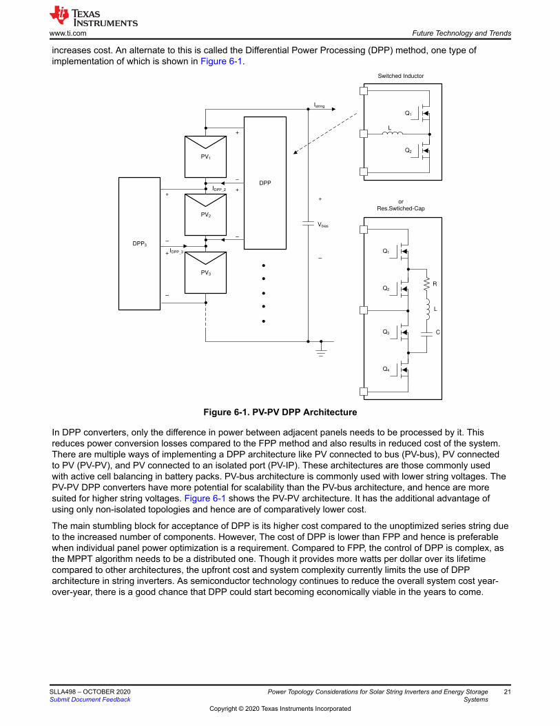
increases cost. An alternate to this is called the Differential Power Processing (DPP) method, one type ofimplementation of which is shown in Figure 6-1.
DPP3
PV1
PV2
PV3
DPP
Vbias
+
±
+
±
IDPP_3
IDPP_2
Istring
Switched Inductor
C
R
L
L
Q1
Q2
Q1
Q2
Q3
Q4
or
Res.Swtiched-Cap
+
±
+
±
+
±
Figure 6-1. PV-PV DPP Architecture
In DPP converters, only the difference in power between adjacent panels needs to be processed by it. Thisreduces power conversion losses compared to the FPP method and also results in reduced cost of the system.There are multiple ways of implementing a DPP architecture like PV connected to bus (PV-bus), PV connectedto PV (PV-PV), and PV connected to an isolated port (PV-IP). These architectures are those commonly usedwith active cell balancing in battery packs. PV-bus architecture is commonly used with lower string voltages. ThePV-PV DPP converters have more potential for scalability than the PV-bus architecture, and hence are moresuited for higher string voltages. Figure 6-1 shows the PV-PV architecture. It has the additional advantage ofusing only non-isolated topologies and hence are of comparatively lower cost.
The main stumbling block for acceptance of DPP is its higher cost compared to the unoptimized series string dueto the increased number of components. However, The cost of DPP is lower than FPP and hence is preferablewhen individual panel power optimization is a requirement. Compared to FPP, the control of DPP is complex, asthe MPPT algorithm needs to be a distributed one. Though it provides more watts per dollar over its lifetimecompared to other architectures, the upfront cost and system complexity currently limits the use of DPParchitecture in string inverters. As semiconductor technology continues to reduce the overall system cost year-over-year, there is a good chance that DPP could start becoming economically viable in the years to come.
www.ti.com Future Technology and Trends
SLLA498 – OCTOBER 2020Submit Document Feedback
Power Topology Considerations for Solar String Inverters and Energy StorageSystems
21
Copyright © 2020 Texas Instruments Incorporated
7 SummaryThe ultimate choice of a power topology boils down to the intended use case of that specific power converterblock, namely the input and output parameters, the targeted power levels, efficiency and power density targets toname a few. While high power 3-phase commercial inverters would look at complex multilevel three-phase PFCstage and DC-DC stage to pack more-and-more power into them, the single phase residential inverters could beaddressed by a simple 2-level H-bridge type PFC stage followed by a LLC DC/DC stage. With storage readyinverters becoming more commonplace, engineers may have to limit their Inverter and DC/DC topology choicesto those that support bidirectional power transfer (such as TNPC, ANPC, DAB, and CLLLC between the localbattery pack and the Grid.
No matter your choice of use case, the advancement in the field of power electronics in tandem withsemiconductor technology is ready to offer everything you need to build your next generation storage ready solarinverter or a stand-alone energy storage system.
Summary www.ti.com
22 Power Topology Considerations for Solar String Inverters and Energy StorageSystems
SLLA498 – OCTOBER 2020Submit Document Feedback
Copyright © 2020 Texas Instruments Incorporated
8 References1. Texas Instruments, Under the Hood of a Multiphase Synchronous Rectified Boost Converter White Paper2. Texas Instruments, Digitally Controlled HV Solar MPPT DC-DC Converter Using C2000™ Piccolo™
Microcontroller Application Report3. Texas Instruments, Phase-Shifted Full Bridge DC/DC Power Converter Design Guide4. Texas Instruments, Phase-Shifted Full Bridge DC/DC Power Converter5. Texas Instruments, Two Phase Interleaved LLC Resonant Converter Reference Design Using C2000™
MCUs6. Texas Instruments, Bidirectional CLLLC resonant dual active bridge (DAB) reference design for HEV/EV
onboard charger7. Texas Instruments, Bi-directional, dual active bridge reference design for level 3 electric vehicle charging
stations8. Texas Instruments, 2kW, 48V to 400V, >93% Efficiency, Isolated Bidirectional DC-DC Converter Reference
Design for UPS9. Texas Instruments, C2000™ Solar DC/AC Single Phase Inverter10.Texas Instruments, Single-Phase Inverter Reference Design with Voltage Source and Grid Connected Modes11.Texas Instruments, Three-Phase Inverter Reference Design Using Gate Driver With Built-in Dead Time
Insertion12.Texas Instruments, 10kW 3-phase 3-level T-type inverter reference design for solar string inverter13.Texas Instruments, Three-level, three-phase SiC AC-to-DC converter reference design14.Texas Instruments, Design considerations of GaN devices for improving power converter efficiency and
density white paper15. M. Schweizer, J. W. Kolar, "Design and Implementation of a Highly Efficient Three-Level T-Type Converter
for Low-Voltage Applications", IEEE Transactions on Power Electronics, Vol. 28, No. s2, pp. 899-907,February 2013.
16. B. Zhao, Q. Song, W. Liu and Y. Sun, "Overview of Dual-Active-Bridge Isolated Bidirectional DC–DCConverter for High-Frequency-Link Power-Conversion System", IEEE Transactions on Power Electronics, vol.29, no. 8, pp. 4091-4106, Aug. 2014.
17. H. Jeong, H. Lee, Y. Liu and K. A. Kim, "Review of Differential Power Processing Converter Techniques forPhotovoltaic Applications", IEEE Transactions on Energy Conversion, vol. 34, no. 1, pp. 351-360, March2019.
18. P. Q. Dzung, D. N. Dat, N. B. Anh, L. C. Hiep and H. Lee, "Design of HERIC inverter for PV systems byusing hardware in the loop (HIL) concept", 9th IEEE Conference on Industrial Electronics and Applications,Hangzhou, 2014.
www.ti.com References
SLLA498 – OCTOBER 2020Submit Document Feedback
Power Topology Considerations for Solar String Inverters and Energy StorageSystems
23
Copyright © 2020 Texas Instruments Incorporated
IMPORTANT NOTICE AND DISCLAIMER
TI PROVIDES TECHNICAL AND RELIABILITY DATA (INCLUDING DATASHEETS), DESIGN RESOURCES (INCLUDING REFERENCE DESIGNS), APPLICATION OR OTHER DESIGN ADVICE, WEB TOOLS, SAFETY INFORMATION, AND OTHER RESOURCES “AS IS” AND WITH ALL FAULTS, AND DISCLAIMS ALL WARRANTIES, EXPRESS AND IMPLIED, INCLUDING WITHOUT LIMITATION ANY IMPLIED WARRANTIES OF MERCHANTABILITY, FITNESS FOR A PARTICULAR PURPOSE OR NON-INFRINGEMENT OF THIRD PARTY INTELLECTUAL PROPERTY RIGHTS.These resources are intended for skilled developers designing with TI products. You are solely responsible for (1) selecting the appropriate TI products for your application, (2) designing, validating and testing your application, and (3) ensuring your application meets applicable standards, and any other safety, security, or other requirements. These resources are subject to change without notice. TI grants you permission to use these resources only for development of an application that uses the TI products described in the resource. Other reproduction and display of these resources is prohibited. No license is granted to any other TI intellectual property right or to any third party intellectual property right. TI disclaims responsibility for, and you will fully indemnify TI and its representatives against, any claims, damages, costs, losses, and liabilities arising out of your use of these resources.TI’s products are provided subject to TI’s Terms of Sale (www.ti.com/legal/termsofsale.html) or other applicable terms available either on ti.com or provided in conjunction with such TI products. TI’s provision of these resources does not expand or otherwise alter TI’s applicable warranties or warranty disclaimers for TI products.
Mailing Address: Texas Instruments, Post Office Box 655303, Dallas, Texas 75265Copyright © 2020, Texas Instruments Incorporated