omap - micro-semiconductor.com
TRANSCRIPT
REF: 5912TM_HDS OMAP5912 TM HW Design Specification
Revision 2.3
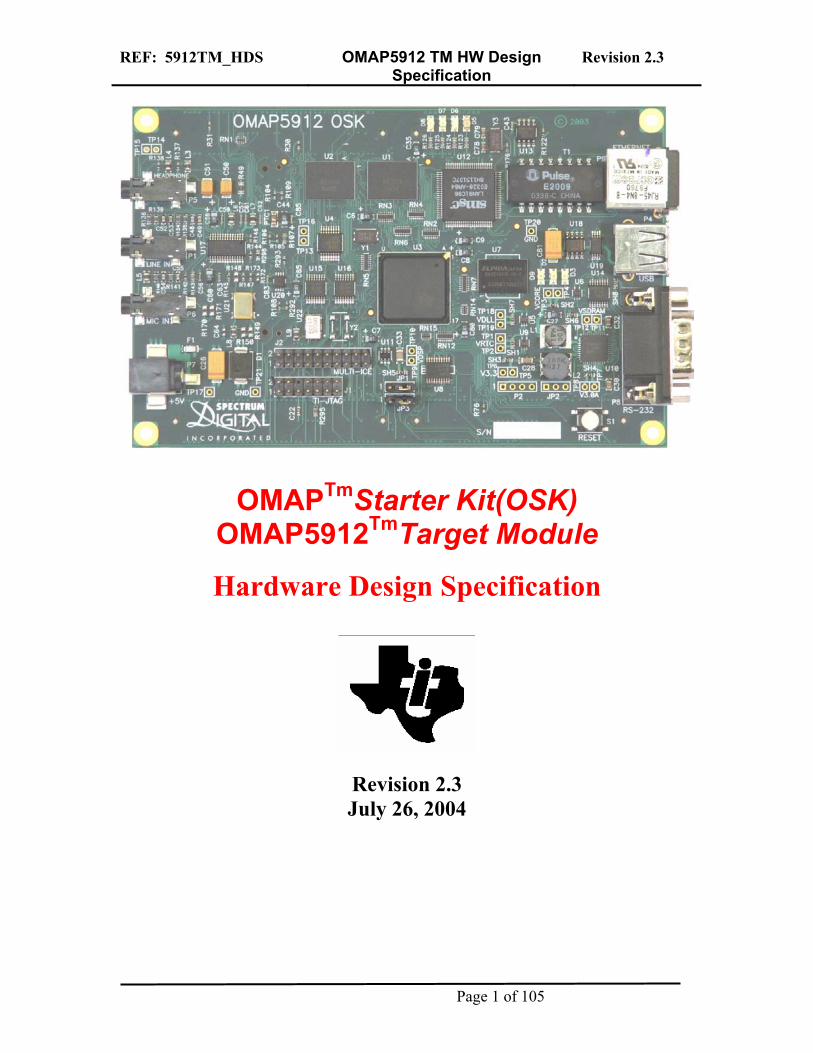
OMAPTmStarter Kit(OSK) OMAP5912TmTarget Module
Hardware Design Specification
Revision 2.3 July 26, 2004
Page 1 of 105
REF: 5912TM_HDS OMAP5912 TM HW Design Specification
Revision 2.3
Table of Contents 1.0 OVERVIEW................................................................................................................................... 7 2.0 CHANGE HISTORY..................................................................................................................... 7 3.0 DEFINITIONS, REFERENCES, AND ISSUES ......................................................................... 8
3.1 DEFINITIONS ........................................................................................................ 8 3.2 REFERENCES ........................................................................................................ 8
4.0 OMAP5912 TARGET MODULE................................................................................................. 9 4.1 PRODUCT REQUIREMENTS ................................................................................... 9
5.0 DETAILED DESIGN................................................................................................................... 10 5.1 MEMORY MAP ................................................................................................... 11
5.1.1 Flash Memory Bus Memory Map ............................................................. 11 5.1.2 SDRAM Memory Map............................................................................... 12
5.2 OMAP5912 PROCESSOR.................................................................................... 12 5.2.1 OMAP5912 Processor .............................................................................. 12 5.2.2 Clock Interface.......................................................................................... 13 5.2.3 Reset Interface .......................................................................................... 15 5.2.4 Power Connections ................................................................................... 17 5.2.5 Configuration Pins.................................................................................... 19
5.3 POWER MANAGEMENT....................................................................................... 20 5.3.1 Block Diagram.......................................................................................... 20 5.3.2 Power Budget............................................................................................ 21 5.3.3 TPS65010.................................................................................................. 22 5.3.4 DC Input.................................................................................................... 24 5.3.5 SDRAM Voltage ........................................................................................ 25 5.3.6 3.3V Supply ............................................................................................... 26 5.3.7 3V Supply .................................................................................................. 28 5.3.8 Control Interface....................................................................................... 29 5.3.9 RTC Power................................................................................................ 31 5.3.10 DSP Voltage Control ................................................................................ 33 5.3.11 DLL Voltage.............................................................................................. 34 5.3.12 Core Voltage ............................................................................................. 35 5.3.13 Battery Mode............................................................................................. 37
5.4 FLASH MEMORY ................................................................................................ 38 5.4.1 Supported Configurations......................................................................... 38 5.4.2 Supported FLASH Devices ....................................................................... 38 5.4.3 FLASH Circuit Design.............................................................................. 39 5.4.4 Address Bus............................................................................................... 40 5.4.5 Data Bus.................................................................................................... 40 5.4.6 Control Signals ......................................................................................... 40 5.4.7 Address Decode Logic .............................................................................. 40 5.4.8 GP Mode Support ..................................................................................... 41
5.5 DDR SDRAM ................................................................................................... 42
Page 2 of 105
REF: 5912TM_HDS OMAP5912 TM HW Design Specification
Revision 2.3
5.5.1 DDR SDRAM Circuit Design.................................................................... 42 5.5.2 Micron DDR Device ................................................................................. 43 5.5.3 Samsung DDR Device............................................................................... 43 5.5.4 Elpida DDR Device.................................................................................. 45 5.5.5 Device Compatibility ................................................................................ 46
5.6 AUDIO CODEC.................................................................................................... 48 5.6.1 Audio CODEC Design .............................................................................. 48 5.6.2 Audio Inputs .............................................................................................. 49 5.6.3 Audio Outputs ........................................................................................... 50 5.6.4 Clocking .................................................................................................... 51 5.6.5 Power ........................................................................................................ 52 5.6.6 OMAP5912 Interface ................................................................................ 53
5.7 COMPACT FLASH ............................................................................................... 54 5.7.1 Integrated Interface .................................................................................. 54 5.7.2 Compact Flash Interface Signals.............................................................. 55 5.7.3 CFLASH.IREQ.......................................................................................... 55 5.7.4 Address Decode Logic .............................................................................. 55 5.7.5 Databus Interface...................................................................................... 57 5.7.6 Power interface......................................................................................... 57
5.8 JTAG/MULTIICE INTERFACE............................................................................ 57 5.8.1 JTAG/MultiICE Features.......................................................................... 57 5.8.2 Design Description ................................................................................... 57
5.9 USB PORT ......................................................................................................... 58 5.9.1 USB Features ............................................................................................ 59 5.9.2 Design Description ................................................................................... 59
5.10 SERIAL PORT...................................................................................................... 61 5.10.1 Features .................................................................................................... 61 5.10.2 Design Description ................................................................................... 61
5.11 ETHERNET.......................................................................................................... 62 5.11.1 Ethernet Circuit Design ............................................................................ 62 5.11.2 Interrupt .................................................................................................... 63 5.11.3 Memory Address Decode .......................................................................... 63 5.11.4 LAN91C96................................................................................................. 64 5.11.5 Crystal....................................................................................................... 65 5.11.6 Output Section........................................................................................... 65 5.11.7 EEPROM................................................................................................... 66 5.11.8 Status LEDS .............................................................................................. 67
6.0 EXPANSION CONNECTORS ................................................................................................... 67 6.1 CONNECTOR A................................................................................................... 69 6.2 CONNECTOR B ................................................................................................... 70 6.3 CONNECTOR C ................................................................................................... 71 6.4 CONNECTOR D................................................................................................... 72 6.5 CONNECTOR SPECIFICATION .............................................................................. 73
7.0 I/O CONNECTORS..................................................................................................................... 73 7.1.1 Serial ......................................................................................................... 74
Page 3 of 105
REF: 5912TM_HDS OMAP5912 TM HW Design Specification
Revision 2.3
7.1.2 Ethernet..................................................................................................... 74 7.1.3 JTAG ......................................................................................................... 75 7.1.4 MultiICE ................................................................................................... 76 7.1.5 DC Power.................................................................................................. 77 7.1.6 Compact Flash .......................................................................................... 78 7.1.7 Headphones............................................................................................... 79 7.1.8 Line In ....................................................................................................... 80 7.1.9 Microphone In........................................................................................... 80 7.1.10 USB Host................................................................................................... 81 7.1.11 USB Client Adapter................................................................................... 81
8.0 MECHANICAL SPECIFICATIONS......................................................................................... 82 8.1.1 TM Card.................................................................................................... 82
9.0 COMPONENT LOCATIONS .................................................................................................... 84 9.1 KEY COMPONENTS............................................................................................. 84 9.2 CONNECTORS AND JUMPERS .............................................................................. 85 9.3 INDICATORS ....................................................................................................... 86
APPENDIX A- COMPONENT LOCATIONS ........................................................................................ 87 APPENDIX B- BOARD DIMENSIONS .................................................................................................. 89 APPENDIX C- SCHEMATICS ................................................................................................................ 91 APPENDIX D- CURRENT MEASUREMENT PROCEDURE........................................................... 101
Figures Figure 1. OMAP5912 Target Module Block Diagram 10 Figure 2. OMAP5912 Clock Inputs 13 Figure 3. OMAP5912 Clock Inputs 13 Figure 4. OMAP5912 Reset Interface 15 Figure 5. OMAP5912 Power Connections 17 Figure 6. OMAP5912 Configuration Pins 19 Figure 7. Power Management Block Diagram 20 Figure 8. DC Input Design 24 Figure 9. SDRAM Power Design 26 Figure 10. 3.3V Power Design 27 Figure 11. 3V Power Design 28 Figure 12. TPS65010 Control Interfaces 29 Figure 13. RTC Power Design 32 Figure 14. RTC Voltage Adjustment 33 Figure 15. DSP Voltage Control 33 Figure 16. DLL Voltage Circuit 34 Figure 17. DLL Voltage Adjustment 35 Figure 18. Core Voltage Circuit 36 Figure 19. Optional Battery Configuration 37
Page 4 of 105
REF: 5912TM_HDS OMAP5912 TM HW Design Specification
Revision 2.3
Figure 20. FLASH Circuitry Design 39 Figure 21. FLASH Decode Logic 40 Figure 22. Mobile DDR SDRAM Design 43 Figure 23. DDR SDRAM Pin outs 46 Figure 24. Samsung DDR Mechanical 47 Figure 25. Elpida DDR Mechanical 47 Figure 26. AIC23 Audio CODEC Design 48 Figure 27. AIC23 Audio Inputs 49 Figure 28. AIC23 Audio Outputs 50 Figure 29. AIC23 Clocking Options 51 Figure 30. AIC23 Power Section 52 Figure 31. AIC23 OMAP5912 Interface 53 Figure 32. Compact Flash Socket Design 54 Figure 33. Compact Flash Decode Logic 56 Figure 34. JTAG Interface Design 58 Figure 35. USB Host Design 59 Figure 36. Serial Port Interface 62 Figure 37. 10Mb Ethernet Design 63 Figure 38. Ethernet Address Decode Logic 64 Figure 39. Ethernet Output Section 66 Figure 40. Ethernet EEPROM 66 Figure 41. Expansion Connector 73 Figure 42. MultiICE Connector Pin out 76 Figure 43. DC Power Jack Pin out 77 Figure 44. Compact Flash Connector 79 Figure 45. Headphone Pin out 80 Figure 46. Line In Pin out 80 Figure 47. Microphone Jack Pin out 80 Figure 48. USB Client Adapter 81 Figure 49. OMAP5912 TM Top Side 82 Figure 50. OMAP5912 TM Back Side 83 Figure 51. Key Top Side Components 84 Figure 52. Connectors 85 Figure 53. Indicators 86
Tables Table 1. Change History 7 Table 2. OMAP5912 OSK Target Module Specifications 9 Table 3. Flash Bus Memory MAP 11 Table 4. SDRAM Memory MAP 12 Table 5. TM Power Budgets 21 Table 6. FLASH Configurations 38 Table 7. Supported FLASH Devices 39 Table 8. Flash Address Decode Resistor Options 41 Table 9. Flash Chip Select Resistor Options 41
Page 5 of 105
REF: 5912TM_HDS OMAP5912 TM HW Design Specification
Revision 2.3
Table 10. Samsung DDR Pin Definitions 44 Table 11. AIC23 I2C Address Definition 53 Table 12. OMAP5912 Compact Flash Interface 55 Table 13. Compact Flash Memory Mapping 56 Table 14. Ethernet Status LEDs 67 Table 15. Connector A Pinout 69 Table 16. Connector B Pin out 70 Table 17. Connector C Pin out 71 Table 18. Connector D Pin out 72 Table 19. Serial Connector Pin out 74 Table 20. Ethernet Pin out 74 Table 21. JTAG Pinout 75 Table 22. Compact Flash Connector Pin out 78 Table 23. Headphone Pin out 79 Table 24. Line In Pin out 80 Table 25. Microphone Input Pin out 80 Table 26. USB Host Pinout 81
Page 6 of 105

REF: 5912TM_HDS OMAP5912 TM HW Design Specification
Revision 2.3
1.0 Overview This document covers the design of the OMAP5912 Target Module (TM) to be used in the OMAP5912 Starter Kit (OSK). In covers in detail the design of each aspect of the TM. Sufficient detail is provided to show how each component interacts and what functions they are performing. Additional information will likely be required from the individual component datasheets of the components used. The sections that make up this Design Specification include:
Change History TM Requirements Detailed Design Expansion Connectors I/O Connectors Mechanical Specifications
2.0 Change History The following table tracks the changes made for each revision of this document.
Table 1. Change History Rev Changes Date By 1.00 1. Release for revision 1.0 of the TM 12/18/03 GC
RB 1.1 1. Fixed typos. Corrected pin numbering on Table 22. 1/13/04 GC
2.0
Changes made to reflect the Alpha2 version of the OMAP5912 OSK. 1. Changed Fig 32 for the Compact Flash to reflect changes made. Fixed buffer. 2. Changed Fig 26 and 27 for the Audio circuit to reflect changes made to the circuit. Corrected wiring error on the Microphone jack 3. Changed Fig 12 to reflect changes in the default core voltage. Added section to describe ability to set default voltage. 4. Changed Fig 33 to reflect new decode configuration. Added text to describe. Also changed Fig 38 and the text as required. 5. Removed CFLASH.DIS signal from Expansion Connector A. Replaced it with nEX_CS3. Changed pin 75 to nEX_CS4. 6. Changed Connector B to reflect changes for the UART1.CTS pin. 7. Added section to describe the ability to use either the CFLASH.IREQ pin or GPIO62 for the CFLASH.IREQ function. 8. Showed changes in the PWR_INT configuration. 9. Updated the USB to reflect new configuration and the dual mode option. 10. Removed references to Innovator and H2. 11. Cleaned up text to match current design
2/17/04
GC
2.1 Updated pictures to reflect the latest layout of the board. 3/8/04 GC
2.2 1. Table 3 was changed a) to show default mode of Flash as dual 16MB devices, 32MB total
Page 7 of 105
REF: 5912TM_HDS OMAP5912 TM HW Design Specification
Revision 2.3
b) Updated to show memory area can be used by activating the disable pin on the expansion connector. c) Corrected 16MB chip select address map for slot 2. d) Corrected address map on Compact Flash. Shows now as CS2. 2. Corrected Table to show dual 16MB mode as the default. 3. Minor updates on the schematic to reflect wrong values in the CD table on sheet 2. Does not affect the design of the board. 4. Added more detail on USB Client support. 5. Added information on power measurement feature being installed and how to use it, covered in Appendix C.
5/11/04 GC
2.3 1. Added clarification on the use of the external 32khz and the integrated crystal oscillator. 2. Added Appendix B to cover the board dimensions. The other two appendices were incremented. 3. Clarified text. Changed Table 2 title from Requirements to Specification. 4. Added reference to other OSs in section 4. 5. Section 5.4.1 Changed text to read dual 16MB devices is the standard configuration. 6. Section 5.5 Deleted reference to Micron 512Mb Mobile DDR throughout the entire section..
7/26/04
GC
3.0 Definitions, References, and Issues 3.1 Definitions SDRAM-Synchronous Dynamic Random Access Memory DDR- Dual Data Rate SDR- Single Data rate Flash-Nonvolatile memory OTC-OMAP Technology Center JTAG-Joint Test Access Group USB-Universal Serial Bus GP-General Purpose ROM TM-Target Module EM- Expansion Module 3.2 References OMAP5910 Data Sheet OMAP5910 Technical Reference Manual OMAP GP Device Functional Specification OMAP5912 Datasheet, SPRS231
Page 8 of 105
REF: 5912TM_HDS OMAP5912 TM HW Design Specification
Revision 2.3
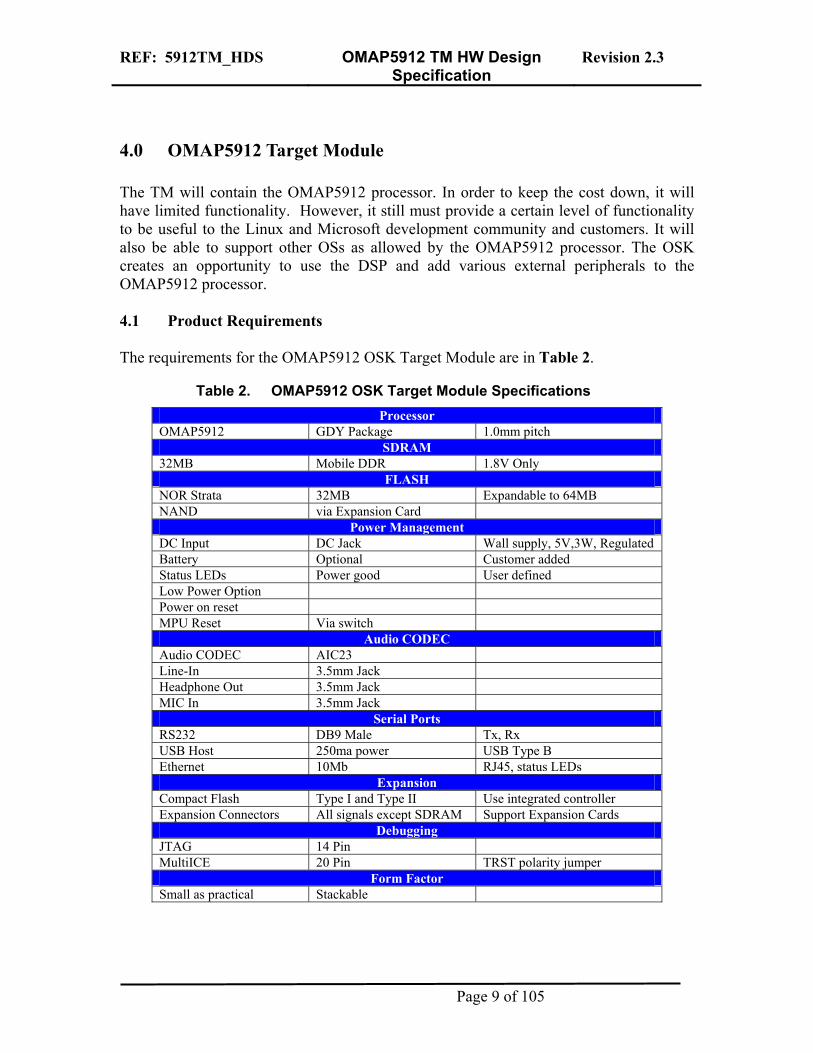
4.0 OMAP5912 Target Module The TM will contain the OMAP5912 processor. In order to keep the cost down, it will have limited functionality. However, it still must provide a certain level of functionality to be useful to the Linux and Microsoft development community and customers. It will also be able to support other OSs as allowed by the OMAP5912 processor. The OSK creates an opportunity to use the DSP and add various external peripherals to the OMAP5912 processor. 4.1 Product Requirements The requirements for the OMAP5912 OSK Target Module are in Table 2.
Table 2. OMAP5912 OSK Target Module Specifications Processor
OMAP5912 GDY Package 1.0mm pitch SDRAM
32MB Mobile DDR 1.8V Only FLASH
NOR Strata 32MB Expandable to 64MB NAND via Expansion Card
Power Management DC Input DC Jack Wall supply, 5V,3W, Regulated Battery Optional Customer added Status LEDs Power good User defined Low Power Option Power on reset MPU Reset Via switch
Audio CODEC Audio CODEC AIC23 Line-In 3.5mm Jack Headphone Out 3.5mm Jack MIC In 3.5mm Jack
Serial Ports RS232 DB9 Male Tx, Rx USB Host 250ma power USB Type B Ethernet 10Mb RJ45, status LEDs
Expansion Compact Flash Type I and Type II Use integrated controller Expansion Connectors All signals except SDRAM Support Expansion Cards
Debugging JTAG 14 Pin MultiICE 20 Pin TRST polarity jumper
Form Factor Small as practical Stackable
Page 9 of 105
REF: 5912TM_HDS OMAP5912 TM HW Design Specification
Revision 2.3
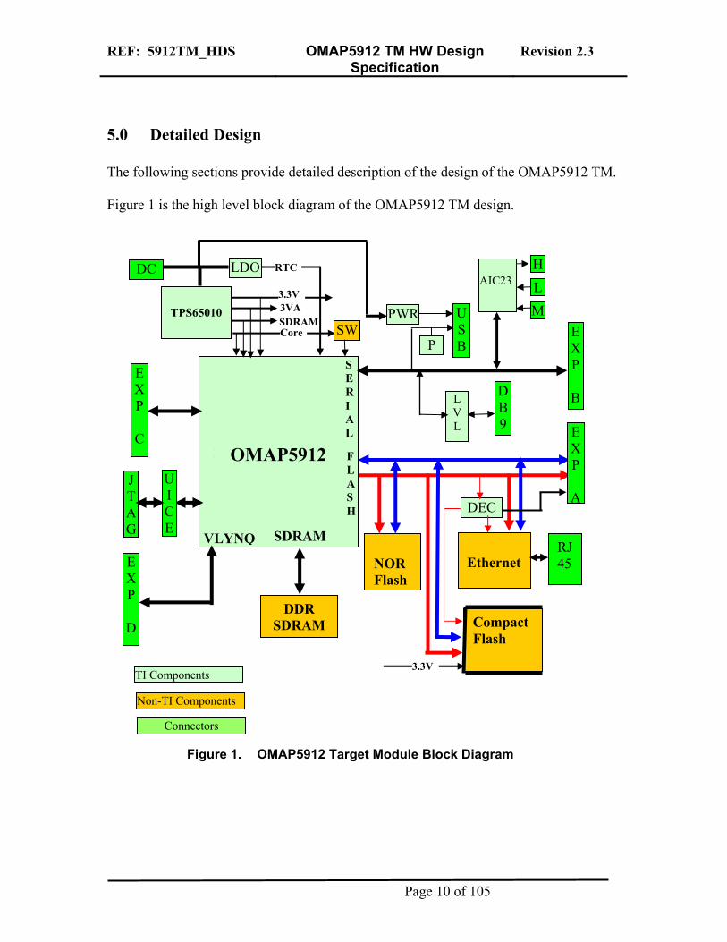
5.0 Detailed Design The following sections provide detailed description of the design of the OMAP5912 TM. Figure 1 is the high level block diagram of the OMAP5912 TM design.
M OMAP5912
S
Ethernet
RJ45
Compact
EXP
A
EXP
C
USB
DB9
L V L
FLASH
P
PWR TPS65010
DC
Core S M3VA 3.3V
LDO RTC
SW
H L
AIC23
SERIAL
M
DEC
J TAG
U ICE
EXP
D
TI Components
Q
EXP
B
Non-TI Components
Connectors
Figure 1. OM
DDR DRAM
AP5912 Target
NOR Flash
Flash
3.3V
Module Block Diagram
Page 10 of 105
SDRAM
LCD CA
DRA
VLYN
REF: 5912TM_HDS OMAP5912 TM HW Design Specification
Revision 2.3
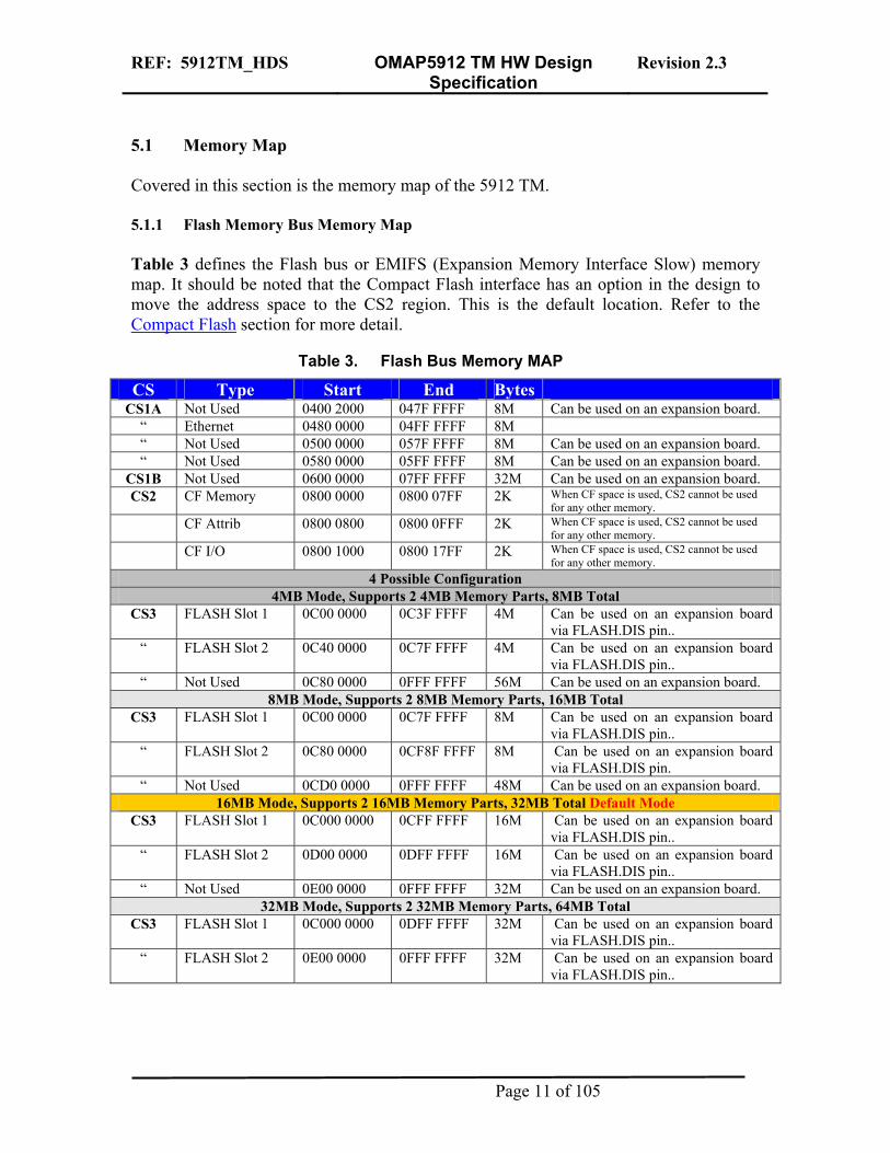
5.1 Memory Map Covered in this section is the memory map of the 5912 TM. 5.1.1 Flash Memory Bus Memory Map Table 3 defines the Flash bus or EMIFS (Expansion Memory Interface Slow) memory map. It should be noted that the Compact Flash interface has an option in the design to move the address space to the CS2 region. This is the default location. Refer to the Compact Flash section for more detail.
Table 3. Flash Bus Memory MAP
CS Type Start End Bytes CS1A Not Used 0400 2000 047F FFFF 8M Can be used on an expansion board.
“ Ethernet 0480 0000 04FF FFFF 8M “ Not Used 0500 0000 057F FFFF 8M Can be used on an expansion board. “ Not Used 0580 0000 05FF FFFF 8M Can be used on an expansion board.
CS1B Not Used 0600 0000 07FF FFFF 32M Can be used on an expansion board. CS2 CF Memory 0800 0000 0800 07FF 2K When CF space is used, CS2 cannot be used
for any other memory. CF Attrib 0800 0800 0800 0FFF 2K When CF space is used, CS2 cannot be used
for any other memory. CF I/O 0800 1000 0800 17FF 2K When CF space is used, CS2 cannot be used
for any other memory. 4 Possible Configuration
4MB Mode, Supports 2 4MB Memory Parts, 8MB Total CS3 FLASH Slot 1 0C00 0000 0C3F FFFF 4M Can be used on an expansion board
via FLASH.DIS pin.. “ FLASH Slot 2 0C40 0000 0C7F FFFF 4M Can be used on an expansion board
via FLASH.DIS pin.. “ Not Used 0C80 0000 0FFF FFFF 56M Can be used on an expansion board.
8MB Mode, Supports 2 8MB Memory Parts, 16MB Total CS3 FLASH Slot 1 0C00 0000 0C7F FFFF 8M Can be used on an expansion board
via FLASH.DIS pin.. “ FLASH Slot 2 0C80 0000 0CF8F FFFF 8M Can be used on an expansion board
via FLASH.DIS pin. “ Not Used 0CD0 0000 0FFF FFFF 48M Can be used on an expansion board.
16MB Mode, Supports 2 16MB Memory Parts, 32MB Total Default Mode CS3 FLASH Slot 1 0C000 0000 0CFF FFFF 16M Can be used on an expansion board
via FLASH.DIS pin.. “ FLASH Slot 2 0D00 0000 0DFF FFFF 16M Can be used on an expansion board
via FLASH.DIS pin.. “ Not Used 0E00 0000 0FFF FFFF 32M Can be used on an expansion board.
32MB Mode, Supports 2 32MB Memory Parts, 64MB Total CS3 FLASH Slot 1 0C000 0000 0DFF FFFF 32M Can be used on an expansion board
via FLASH.DIS pin.. “ FLASH Slot 2 0E00 0000 0FFF FFFF 32M Can be used on an expansion board
via FLASH.DIS pin..
Page 11 of 105
REF: 5912TM_HDS OMAP5912 TM HW Design Specification
Revision 2.3
The TM supports multiple configurations of NOR FLASH that can be loaded with various devices to create the different configurations. For more information on the different configurations refer to the Flash memory section in Section 5.4. 5.1.2 SDRAM Memory Map A single DDR SDRAM device is provided on the TM. Table 4 defines the memory map for the DDR SDRAM. The 32MB configuration is the default mode.
Table 4. SDRAM Memory MAP
Mode Start End Bytes 32MB 1000 0000 11FF FFFF 32M Default configuration 64MB 1000 0000 13FF FFFF 64M
Reserved 1800 0000 18FF FFFF 5.2 OMAP5912 Processor This section covers the part of the design that is specific to the OMAP5912 processor. Covered in this section will be:
OMAP Processor Clock Interface Reset Circuitry Power connections Configuration pins
5.2.1 OMAP5912 Processor There are two different packages available for the OMAP5912.
ZDY Plastic BGA ZZG Plastic BGA
Both of these devices are 289 pins. The ZZG package is a much smaller package and has a finer pitch. The TM will use the ZDY package. Figure 2 shows the pin out of the ZZG package.
Page 12 of 105
REF: 5912TM_HDS OMAP5912 TM HW Design Specification
Revision 2.3
Figure 2. OMAP5912 Clock Inputs
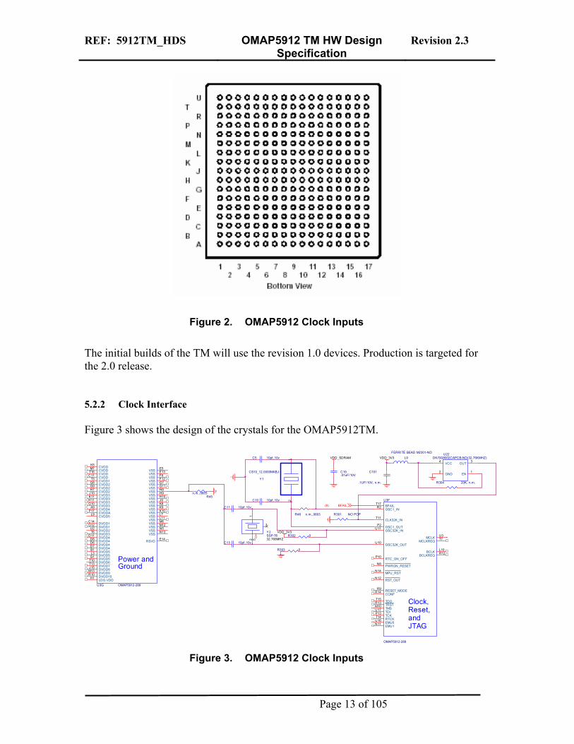
The initial builds of the TM will use the revision 1.0 devices. Production is targeted for the 2.0 release. 5.2.2 Clock Interface Figure 3 shows the design of the crystals for the OMAP5912TM.
Clock,Reset, andJTAG
U3F
OMAP5912-289
R2
P2U11
U10
N12
N8
U17
T15
M10
P13
R13
U16N11
T14
R14
T17
T11
N14
R9
P10
U3T7
R12L10
OSC1_IN
OSC1_OUTOSC32K_IN
OSC32K_OUT
RST_OUT
PWRON_RESET
TDI
TDO
TMS
TCK
TRST
EMU0EMU1
RTCK
CONF
BFAIL
CLK32K_IN
MPU_RST
RESET_MODE
RTC_ON_OFF
MCLKMCLKREQ
BCLKREQBCLK
R46 n.m.,0603
C13 10pf ,10v
VDD_SDRAM VDD_3V3
R304 20K, n.m.
VDD_3V3
C5 10pf ,10v
C10 10pf ,10v
Y2SSP-T632.768MHZ
12
3
5
R303 0
R45n.m.,0603
Y1
CS10_12.0000MABJ
12
L9
FERRITE BEAD M2301-ND
C19.01uF/10V
U22DK/SG8002CAPCB-ND(32.76KMHZ)
3
2 1
4OUT
GND EN
VCC
R302 0
Power andGround
U3G OMAP5912-289
T6U2
J15M13
T13
B1
G1
G7
L3
D11D8D6D7
T10
J9
N13
M12N5
M6
L7
E5E13
H9
P17
G11
F12
T16M7
T3
R10
J10
H11K11
K8K9K10
K5
G8
C11
H1
C14
F6
H10
L11
E14
G10
L9
H8G9H7
A9
G12
DVDD3DVDD2
DVDD8DVDD9
DVDD7
DVDD5
DVDD5
VSS
DVDD5
DVDD4DVDD4DVDD4DVDD4
DVDD6
VSS
VSS
VSSVSS
VSS
VSS
VSSVSS
VSS
CVDDA
VSS
VSS
CVDDCVDD
CVDD1
DVDD10
CVDD3
CVDD3CVDD3
VSSVSSVSS
CVDD
CVDD2
CVDD
LDO.VDD
DVDD1
VSS
VSS
VSS
RSVD
CVDD3
CVDD5
VSSCVDD2CVDD2
CVDD4
DVDD1
R301 NO POP
C11 10pf ,10v
C101
.1UF/10V, n.m.
BFAIL(9)
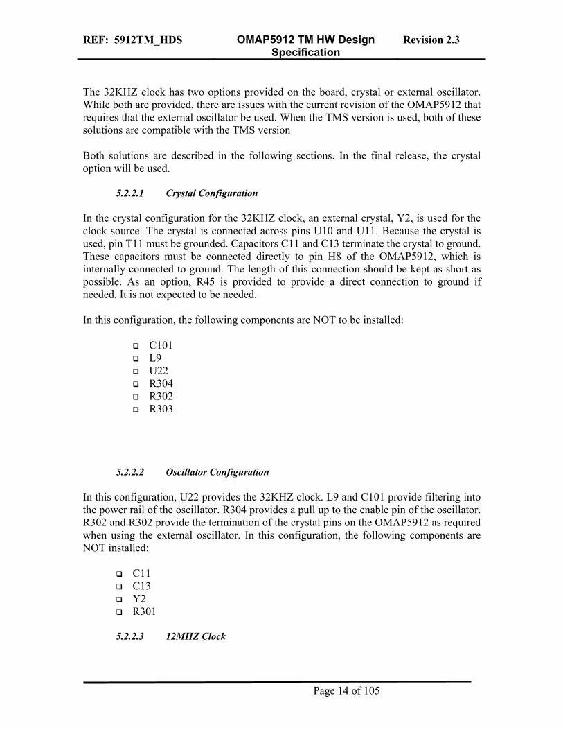
Figure 3. OMAP5912 Clock Inputs
Page 13 of 105
REF: 5912TM_HDS OMAP5912 TM HW Design Specification
Revision 2.3
The 32KHZ clock has two options provided on the board, crystal or external oscillator. While both are provided, there are issues with the current revision of the OMAP5912 that requires that the external oscillator be used. When the TMS version is used, both of these solutions are compatible with the TMS version Both solutions are described in the following sections. In the final release, the crystal option will be used.
5.2.2.1 Crystal Configuration In the crystal configuration for the 32KHZ clock, an external crystal, Y2, is used for the clock source. The crystal is connected across pins U10 and U11. Because the crystal is used, pin T11 must be grounded. Capacitors C11 and C13 terminate the crystal to ground. These capacitors must be connected directly to pin H8 of the OMAP5912, which is internally connected to ground. The length of this connection should be kept as short as possible. As an option, R45 is provided to provide a direct connection to ground if needed. It is not expected to be needed. In this configuration, the following components are NOT to be installed:
C101 L9 U22 R304 R302 R303
5.2.2.2 Oscillator Configuration In this configuration, U22 provides the 32KHZ clock. L9 and C101 provide filtering into the power rail of the oscillator. R304 provides a pull up to the enable pin of the oscillator. R302 and R302 provide the termination of the crystal pins on the OMAP5912 as required when using the external oscillator. In this configuration, the following components are NOT installed:
C11 C13 Y2 R301
5.2.2.3 12MHZ Clock
Page 14 of 105
REF: 5912TM_HDS OMAP5912 TM HW Design Specification
Revision 2.3
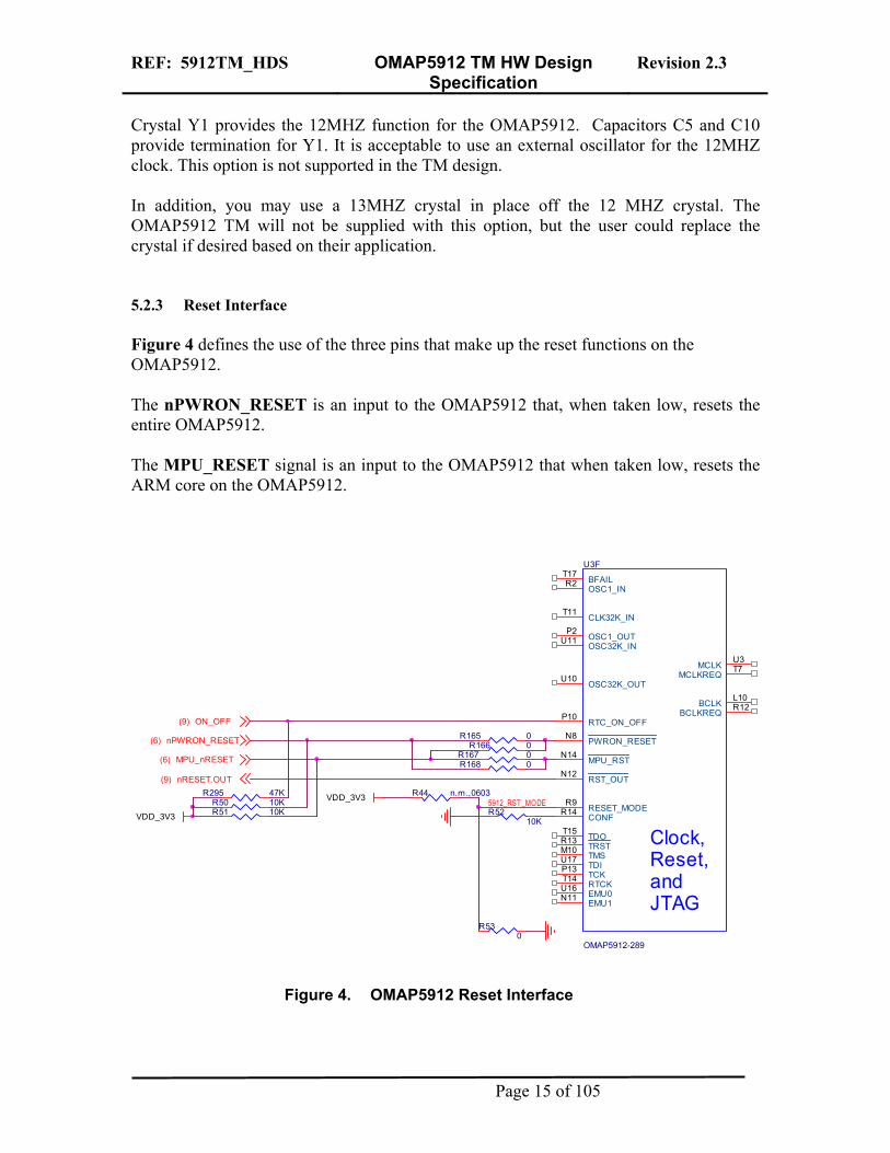
Crystal Y1 provides the 12MHZ function for the OMAP5912. Capacitors C5 and C10 provide termination for Y1. It is acceptable to use an external oscillator for the 12MHZ clock. This option is not supported in the TM design. In addition, you may use a 13MHZ crystal in place off the 12 MHZ crystal. The OMAP5912 TM will not be supplied with this option, but the user could replace the crystal if desired based on their application. 5.2.3 Reset Interface Figure 4 defines the use of the three pins that make up the reset functions on the OMAP5912. The nPWRON_RESET is an input to the OMAP5912 that, when taken low, resets the entire OMAP5912. The MPU_RESET signal is an input to the OMAP5912 that when taken low, resets the ARM core on the OMAP5912.
R168 0
Clock,Reset, andJTAG
U3F
OMAP5912-289
R2
P2U11
U10
N12
N8
U17
T15
M10
P13
R13
U16N11
T14
R14
T17
T11
N14
R9
P10
U3T7
R12L10
OSC1_IN
OSC1_OUTOSC32K_IN
OSC32K_OUT
RST_OUT
PWRON_RESET
TDI
TDO
TMS
TCK
TRST
EMU0EMU1
RTCK
CONF
BFAIL
CLK32K_IN
MPU_RST
RESET_MODE
RTC_ON_OFF
MCLKMCLKREQ
BCLKREQBCLK
R167 0
VDD_3V3
R5210K
R530
VDD_3V3 R51 10K
R166 0R165 0
R44 n.m.,0603R50 10K
R295 47K
nRESET.OUT(9)
ON_OFF(9)
5912_RST_MODE
nPWRON_RESET(6)
MPU_nRESET(6)
Figure 4. OMAP5912 Reset Interface
Page 15 of 105
REF: 5912TM_HDS OMAP5912 TM HW Design Specification
Revision 2.3
There is an issue with the current revision of the OMAP5912 processor. If the MPU_RESET signal is used, it may cause the EMIFS bus to lock. For this reason, it is not desirable to use MPU_Reset signal on the initial units. The current TM design takes care of this issue. We have four resistors on the board, which based on the way they are loaded, gives us several options to configure the reset signals. The reset signals for the nPWRON_RESET and the nMPU_Reset are generated by the TPS65010 power management device. Both of these signals are open drain outputs. For more information on this refer to section on the TPS65010. The following sections define how the design is intended to work for both the initial and production builds.
5.2.3.1 Initial Builds In the current builds of the boards, we need both the nPWRON_RESET and nMPU_RESET to generate an nPWRON_RESET signal into the OMAP5912. The reset switch on the TPS65010 will only generate a nMPU_RST. Because we can only use the nPWRON_RESET signal on the OMAP5912, we need to make sure that both resets from the TPS65010 only generate the nPWRON_RESET signal. This is done by loading the resistors as follows:
R165, connecting nPWRON_RESET to nPWRON_RESET of the OMAP5912
R166, connecting nMPU_RST to the nPWRON_RESET of the OMAP5912. R167 and R168 are not installed.
This will allow both reset signals from the TPS65010 to only generate an nPWRON_RESET into the OMAP5912.
5.2.3.2 Final Builds In the TMS version of the OMAP5912 build of the boards, it is expected that we will allow the resets to work such that the nPWRON_RESET and nMPU_RESET generate separate resets. In order to do this, load the resistors as follows:
R165, connecting nPWRON_RESET to nPWRON_RESET of the OMAP5912
R167, connecting nMPU_RESET to the nPWRON_RESET of the OMAP5912.
R166 and R168 are not installed. The nRESET_OUT signal is an output from the OMAP5912. The nRESET_OUT signal is connected to pin 60 of the B expansion connector.
Page 16 of 105
REF: 5912TM_HDS OMAP5912 TM HW Design Specification
Revision 2.3
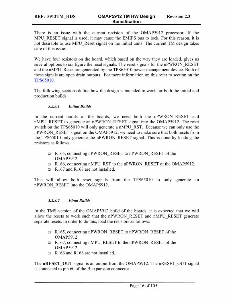
The RESET_MODE pin is controlled by the loading of one of two resistors. R53 is the default configuration. It is not envisioned that the other mode, where R44 is loaded instead, will ever be used. There are no plans to support this mode at all. However, it was decided to support both modes just in case we needed it someday. 5.2.4 Power Connections Figure 5 shows the power connections on the OMAP5912 processor. Each of these is discussed in the following paragraphs.
C84
.01uF/10V
VDD_3V3
C15
1uF, 10V, X5R, 0402
VDD_3V3
+C80
10uf /10V
VDD_3V3
C12.01uF/10V
C14.01uF/10V
VDD_RTC
Power andGround
U3G OMAP5912-289
T6U2
J15M13
T13
B1
G1
G7
L3
D11D8D6D7
T10
J9
N13
M12N5
M6
L7
E5E13
H9
P17
G11
F12
T16M7
T3
R10
J10
H11K11
K8K9K10
K5
G8
C11
H1
C14
F6
H10
L11
E14
G10
L9
H8G9H7
A9
G12
DVDD3DVDD2
DVDD8DVDD9
DVDD7
DVDD5
DVDD5
VSS
DVDD5
DVDD4DVDD4DVDD4DVDD4
DVDD6
VSS
VSS
VSSVSS
VSS
VSS
VSSVSS
VSS
CVDDA
VSS
VSS
CVDDCVDD
CVDD1
DVDDRTC
CVDD3
CVDD3CVDD3
VSSVSSVSS
CVDD
CVDD2
CVDD
LDO.VDD
DVDD1
VSS
VSS
VSS
RSVD
CVDD3
CVDDRTC
VSSCVDD2CVDD2
CVDDDLL
DVDD1
VDD_DSP
C16
.01uF/10V VDD_3V3
R47 10
VDD_DSPVDD_CORE
VDD_3V3
VDD_SDRAM
C18
.01uF/10V
VDD_3V3
VDD_DLL
R48 10
C17
.01uF/10V
Figure 5. OMAP5912 Power Connections
The VDD_DLL power on the OMAP5912 can be sensitive to noise. For this reason a couple of RC circuits are used to provide enhanced noise immunity. R47 and C12 provide a filter for the CVDDLL pin, which is the core voltage supply pin for the DLL. R48 and C14 perform the same function for the CDDDA pin, which provides the power
Page 17 of 105
REF: 5912TM_HDS OMAP5912 TM HW Design Specification
Revision 2.3
to the DLL itself. Capacitor C80 provides low frequency filtering for the DLL supply. Power for the DLL is supplied by a separate LDO, U5. Information on this can be found in the Power Management section. VDD_CORE is the main supply to the internal core voltages of the OMAP5912 and is a nominal 1.6V but can be set to 1.1V-1.5 V under SW control via the TPS65010. Refer to the Power Management section for more details. Filtering of the voltage is supplied by the bypass and filter capacitors. VDD_DSP is the supply pins for the DSP in the OMAP5912. Power for the DSP is supplied through U11. U11 should be placed as close as possible to the OMAP5912 in the layout process. U11 can be disabled by taking GPIO4 of the TPS65010 low. VDD_RTC supplies power to the Real Time Clock inside the OMAP5912. Power is supplied by U9. Refer to SVDD_RTC Section for a more detailed description. VDD_3V3 is the 3.3V supply for the OMAP5912. This supplies power to the various I/O function pins as well as the FLASH bus. VDD_SDRAM supplies voltage to the output pins for the SDRAM interface. Pin H1 on the OMAP5912 Processor is the output of a regulated supply that is delivered by an embedded LDO to the DPLL macros. The regulated supply is available on the OMAP5912 at pad H1. A decoupling capacitor of 1 µF must be connected externally between LDO.FILTER and ground. All power is connected to a common ground. All leads from the ground pins on the OMAP5912 to the actual ground plane should be kept as short as practical.
Page 18 of 105
REF: 5912TM_HDS OMAP5912 TM HW Design Specification
Revision 2.3
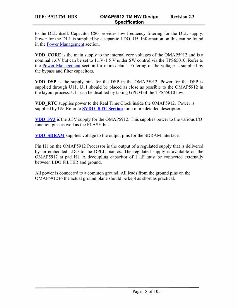
5.2.5 Configuration Pins There are a group of pins that are used to configure the OMAP5912 processor based on each individual application. Figure 6 shows these pins.
R44 n.m.,0603VDD_3V3R52
10K
Clock,Reset, andJTAG
U3F
OMAP5912-289 GDY
R2
P2U11
U10
N12
N8
U17
T15
M10
P13
R13
U16N11
T14
R14
T17
T11
N14
R9
P10
U3T7
R12L10
OSC1_IN
OSC1_OUTOSC32K_IN
OSC32K_OUT
RST_OUT
PWRON_RESET
TDI
TDO
TMS
TCK
TRST
EMU0EMU1
RTCK
CONF
BFAIL
CLK32K_IN
MPU_RST
RESET_MODE
ON_OFF
MCLKMCLKREQ
BCLKREQBCLK
5912_RST_MODE
BFAIL
ON_OFF
Figure 6. OMAP5912 Configuration Pins
BFAIL is the battery power failure and external FIQ interrupt input. BFAIL can be used to gate certain input pins when battery power is low or failing. The pins that can be gated are configured via software. This pin can also optionally be used as an external FIQ interrupt source to the MPU. The function of this pin is configurable via software. On the TM, this pin connects to pin 54 of expansion connector B. It is not used by any circuitry on the TM and is free to be used by an expansion card. On_OFF controls the internal RTC. When pulled low, the RTC is disabled. A resistor insures that the RTC is enabled by pulling the pin to VDD_RTC. This pin also connects to pin 56 of expansion connector B for use by expansion cards as needed either as a way to disable the internal RTC or to be used as one of its optional features. Refer to the OMAP5912 Datasheet for more detail on how the pin can be used.
Page 19 of 105
REF: 5912TM_HDS OMAP5912 TM HW Design Specification
Revision 2.3
CONF must be tied low through a 10K ohm resistor to put the OMP5912 in the operational mode. Pulling this pin Hi puts the device in the test mode. The test mode is not used on the TM design. 5.3 Power Management This section covers the design of the power management circuitry for the OMAP5912 TM. Covered in this section will be:
Block Diagram Power Budgets TPS65010 DC Input SDRAM Voltage VDD_3V3 Supply VDD_3V Supply
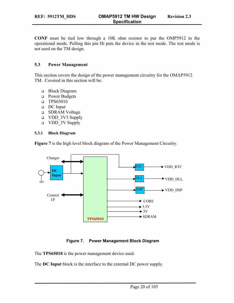
5.3.1 Block Diagram Figure 7 is the high level block diagram of the Power Management Circuitry.
33
DC Input
DLL
DSP
C EControl
I/F
RTC VDD_RTC
Charger
VDD_DLL
VDD_DSP
S M
Figure 7.
The TPS65010 is the power The DC Input block is the in
TPS65010
Power Management Block D
management device used.
terface to the external DC pow
Page 20
OR
.3V V DRAiagram
er supply.
of 105
REF: 5912TM_HDS OMAP5912 TM HW Design Specification
Revision 2.3
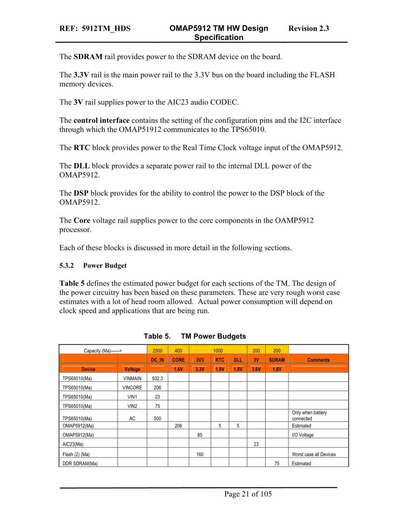
The SDRAM rail provides power to the SDRAM device on the board. The 3.3V rail is the main power rail to the 3.3V bus on the board including the FLASH memory devices. The 3V rail supplies power to the AIC23 audio CODEC. The control interface contains the setting of the configuration pins and the I2C interface through which the OMAP51912 communicates to the TPS65010. The RTC block provides power to the Real Time Clock voltage input of the OMAP5912. The DLL block provides a separate power rail to the internal DLL power of the OMAP5912. The DSP block provides for the ability to control the power to the DSP block of the OMAP5912. The Core voltage rail supplies power to the core components in the OAMP5912 processor. Each of these blocks is discussed in more detail in the following sections. 5.3.2 Power Budget Table 5 defines the estimated power budget for each sections of the TM. The design of the power circuitry has been based on these parameters. These are very rough worst case estimates with a lot of head room allowed. Actual power consumption will depend on clock speed and applications that are being run.
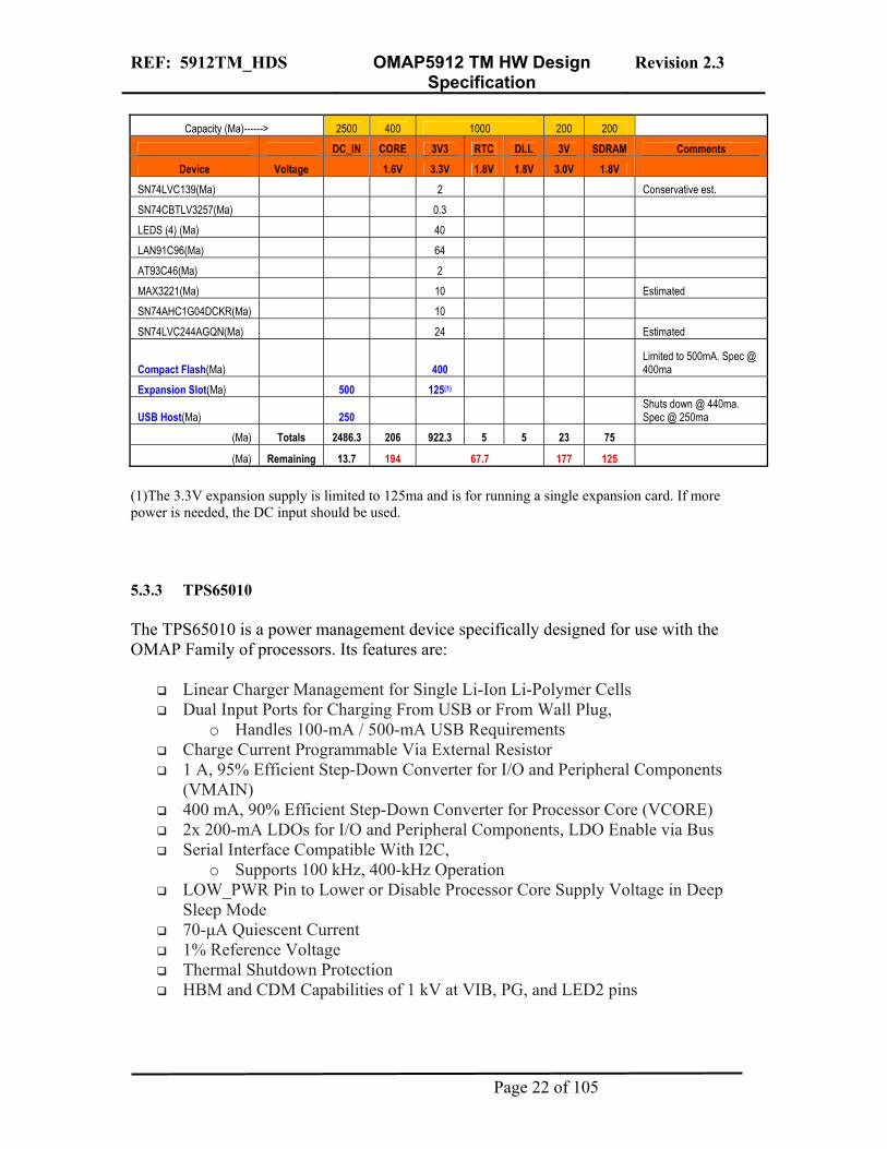
Table 5. TM Power Budgets
Capacity (Ma)------> 2500 400 1000 200 200
DC_IN CORE 3V3 RTC DLL 3V SDRAM Comments Device Voltage 1.6V 3.3V 1.8V 1.8V 3.0V 1.8V
TPS65010(Ma) VINMAIN 932.3
TPS65010(Ma) VINCORE 206
TPS65010(Ma) VIN1 23
TPS65010(Ma) VIN2 75
TPS65010(Ma) AC 500 Only when battery connected
OMAP5912(Ma) 206 5 5 Estimated
OMAP5912(Ma) 85 I/O Voltage
AIC23(Ma) 23
Flash (2) (Ma) 160 Worst case all Devices
DDR SDRAM(Ma) 75 Estimated
Page 21 of 105
REF: 5912TM_HDS OMAP5912 TM HW Design Specification
Revision 2.3
Capacity (Ma)------> 2500 400 1000 200 200
DC_IN CORE 3V3 RTC DLL 3V SDRAM Comments Device Voltage 1.6V 3.3V 1.8V 1.8V 3.0V 1.8V
SN74LVC139(Ma) 2 Conservative est.
SN74CBTLV3257(Ma) 0.3
LEDS (4) (Ma) 40
LAN91C96(Ma) 64
AT93C46(Ma) 2
MAX3221(Ma) 10 Estimated
SN74AHC1G04DCKR(Ma) 10
SN74LVC244AGQN(Ma) 24 Estimated
Compact Flash(Ma) 400 Limited to 500mA. Spec @ 400ma
Expansion Slot(Ma) 500 125(1)
USB Host(Ma) 250 Shuts down @ 440ma. Spec @ 250ma
(Ma) Totals 2486.3 206 922.3 5 5 23 75
(Ma) Remaining 13.7 194 67.7 177 125
(1)The 3.3V expansion supply is limited to 125ma and is for running a single expansion card. If more power is needed, the DC input should be used. 5.3.3 TPS65010 The TPS65010 is a power management device specifically designed for use with the OMAP Family of processors. Its features are:
Linear Charger Management for Single Li-Ion Li-Polymer Cells Dual Input Ports for Charging From USB or From Wall Plug,
o Handles 100-mA / 500-mA USB Requirements Charge Current Programmable Via External Resistor 1 A, 95% Efficient Step-Down Converter for I/O and Peripheral Components
(VMAIN) 400 mA, 90% Efficient Step-Down Converter for Processor Core (VCORE) 2x 200-mA LDOs for I/O and Peripheral Components, LDO Enable via Bus Serial Interface Compatible With I2C,
o Supports 100 kHz, 400-kHz Operation LOW_PWR Pin to Lower or Disable Processor Core Supply Voltage in Deep
Sleep Mode 70-µA Quiescent Current 1% Reference Voltage Thermal Shutdown Protection HBM and CDM Capabilities of 1 kV at VIB, PG, and LED2 pins
Page 22 of 105
REF: 5912TM_HDS OMAP5912 TM HW Design Specification
Revision 2.3
The TPS65010 is an integrated power and battery management IC for applications powered by one Li-Ion or Li-Polymer cell, and which require multiple power rails. Both step-down converters enter a low power mode at light load for maximum efficiency across the widest possible range of load currents. The LOW_PWR pin allows the core converter to lower its output voltage when the application processor goes into deep sleep. The TPS65010 also integrates two 200-mA LDO voltage regulators, which are enabled via the serial interface. Each LDO operates with an input voltage range between 1.8 V and 6.5 V, allowing them to be supplied from one of the step-down converters or directly from the battery. The TPS65010 also has an integrated and flexible Li-Ion linear charger and system power management. It offers integrated ac-adapter supply management with autonomous power-source selection, power FET and current sensor, high accuracy current and voltage regulation, charge status, and charge termination. The USB mode is for the charger and is not used in this particular design. In the ac-adapter configuration an external resistor sets the maximum value of charge current. The battery is charged in three phases: conditioning, constant current and constant voltage. Charge is normally terminated based on minimum current. An internal charge timer provides a safety backup for charge termination. The TPS65010 automatically restarts the charge if the battery voltage falls below an internal threshold. The charger automatically enters sleep mode when the DC supply is removed. NOTE: While the battery can be added to the OSK, it is not supported with the OSK. The user will need to add a battery as needed. The serial interface can be used for dynamic voltage scaling, for collecting information on and controlling the battery charger status, for optionally controlling 2 LED driver outputs, masking interrupts, or for disabling and setting the LDO output voltages. The interface is compatible with the fast/standard mode I2C specification allowing transfers at up to 400 kHz.
Page 23 of 105
REF: 5912TM_HDS OMAP5912 TM HW Design Specification
Revision 2.3
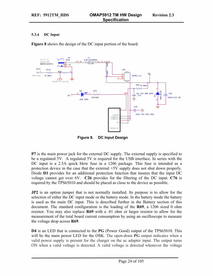
5.3.4 DC Input Figure 8 shows the design of the DC input portion of the board.
C76
22uF, 10V, X7R, 0402
R68 0
8
R114
10, 0603
R70
330,0603
7
DC D1
SM
CJ6
.0A
21
6
R69
0,08
05
F12.5A_QuickBlow
12
VINCORE
DC
VINMAIN_A
TP171
VINMAIN_B
JP2
HDR3, n.m.123
VCC
Center positiv e.
5
R95 10, 0603
ESD Ring
PG
DC 5V In,regulated4A
C771uF, 10V, X5R, 0402
TPS65010
D9
LED, GRN
2 1
Delete D9 use PG.
+ C26
220uF,6.3V ,AE
P7DC8
321
5
DC_IN
nPG
DC_IN_FUSED
Figure 8. DC Input Design
P7 is the main power jack for the external DC supply. The external supply is specified to be a regulated 5V. A regulated 5V is required for the USB interface. In series with the DC input is a 2.5A quick blow fuse in a 1206 package. This fuse is intended as a protection device in the case that the external +5V supply does not shut down properly. Diode D1 provides for an additional protection function that insures that the input DC voltage cannot get over 6V. C26 provides for the filtering of the DC input. C76 is required by the TPS65010 and should be placed as close to the device as possible. JP2 is an option jumper that is not normally installed. Its purpose is to allow for the selection of either the DC input mode or the battery mode. In the battery mode the battery is used as the main DC input. This is described further in the Battery section of this document. The standard configuration is the loading of the R69, a 1206 sized 0 ohm resistor. You may also replace R69 with a .01 ohm or larger resistor to allow for the measurement of the total board current consumption by using an oscilloscope to measure the voltage drop across R69. D4 is an LED that is connected to the PG (Power Good) output of the TPS65010. This will be the main power LED for the OSK. The open-drain PG output indicates when a valid power supply is present for the charger on the ac adapter input. The output turns ON when a valid voltage is detected. A valid voltage is detected whenever the voltage
Page 24 of 105
REF: 5912TM_HDS OMAP5912 TM HW Design Specification
Revision 2.3
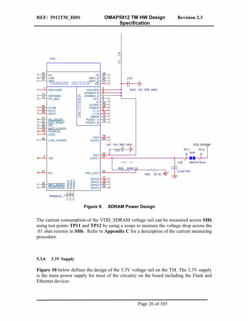
rises above the voltage on VBAT plus 100 mV. This output is turned off in the sleep mode. The PG output can also be programmed via the LED1_ON and LED1_PER registers in the serial interface of the TPS65010. It can then be programmed to be permanently on, off, or to blink with defined on- and period-times. PG is controlled per default via the charger. Due to the nature of the TPS65010 design, the main DC input can exhibit noise. For this reason, the VCC input of the TPS65010 must be filtered. This is done via an RC circuit comprised of R95 and C77. The supply current of the VCC rail for the TPS65010 is specified at 50uA. You will also notice a single point ground connection. This is the point in which the Frame ground and signal ground connect at a single point via R68 which is not actually required but is intended mainly to insure that the ground buses stay separated and that the PCB layout software does not try to interconnect the ground planes anywhere other than at this single point. This point should be as close to the DC input ground pin as possible. In addition there is an ESD ring that goes around the board that also connects to this single point via R111 which is used to lower the current of the discharged voltage. 5.3.5 SDRAM Voltage The SDRAM voltage bus has a dedicated voltage supply which minimizes noise on the bus. Figure 9 covers the portion of the design that comprises the SDRAM voltage supply. The SDRAM and the OMAP5912 voltage pins use LDO1 of the TPS65010. Resistors R82 and R83 are supplied to allow for the voltage to be offset back into the sense input of the TPS65010. This allow for the voltage to be adjusted for voltage drops experienced by the layout. The default configuration is to set the voltage at 1.8V which is done by making R82 a 243K and R83 a 93.1K into the sense input. LDO1 will deliver up to 200ma. The requirement for the SDRAM is 75ma. The voltage on LDO1 can be adjusted via software, however the default setting is external adjust. The optional settings under SW control will not be used. Refer to the TPS65010 Datasheet for more detail. Capacitor C32 provides filtering for the voltage rail. Power for the VLDO1 is supplied by the main DC voltage input rail. Capacitor C31 is required to minimize ripple into the LDO which can be generated by the TPS65010 back onto the main DC rail.
Page 25 of 105
REF: 5912TM_HDS OMAP5912 TM HW Design Specification
Revision 2.3
+C32
2.2uF/10V
VDD_SDRAM
DC_IN
CHARGER SECTIONSWITCHER
U10
TPS65010_1
1
2
3
4
5
678
910
11
12
13
14
1516
1817
1920
21
22
23
24
2526
27
28
2930
31
3233
34
35
36
37
38
39
4043
4241
44 45
46
47
48
DEFCORE
LED2
VIB
L2
VINCORE
VCCVINMAIN_AVINMAIN_B
L1_AL1_B
PG
DEFAMIN
VMAIN
PS_SEQ
PGND1_APGND1_B
GPIO3GPIO4
VIN2VLDO2
AGN
D1
VIN1
VFB_LDO1
VLDO1
GPIO2GPIO1
NC
IFLSB
SDATSCLK
HOT_RESET
MPU_RESETRESPWRON
PWRFAIL
INT
LOW_POWER
ISET
TS
BATT_COVER
ACUSB
VBAT_AVBAT_B
AGN
D2
AGN
D3
PGND2
PB_ONOFF
VCORE
R82 243K,1%
C76
22uF, 10V, X7R, 0402
SH6
0603-R-Short
TP11
1
C31
1uF, 10V, X5R, 0402
TP12
1
R83 93.1K, 1%
Vref .5V
Figure 9. SDRAM Power Design
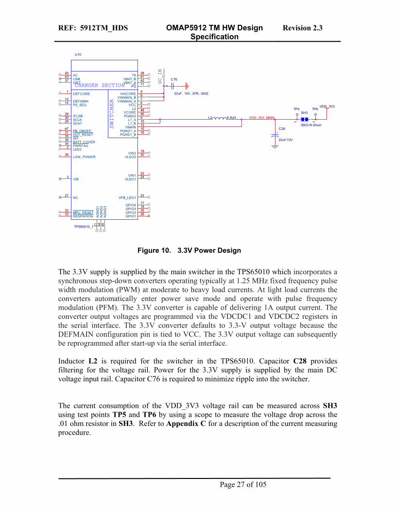
The current consumption of the VDD_SDRAM voltage rail can be measured across SH6 using test points TP11 and TP12 by using a scope to measure the voltage drop across the .01 ohm resistor in SH6. Refer to Appendix C for a description of the current measuring procedure. 5.3.6 3.3V Supply Figure 10 below defines the design of the 3.3V voltage rail on the TM. The 3.3V supply is the main power supply for most of the circuitry on the board including the Flash and Ethernet devices.
Page 26 of 105
REF: 5912TM_HDS OMAP5912 TM HW Design Specification
Revision 2.3
+C28
22uf /10V
DC_IN
TP6
1
TP5
1
C76
22uF, 10V, X7R, 0402
SH3
0603-R-Short
CHARGER SECTION
SWITCHER
U10
TPS65010_1
1
2
3
4
5
678
910
11
12
13
14
1516
1817
1920
21
22
23
24
2526
27
28
2930
31
3233
34
35
36
37
38
39
4043
4241
44 45
46
47
48
DEFCORE
LED2
VIB
L2
VINCORE
VCCVINMAIN_AVINMAIN_B
L1_AL1_B
PG
DEFAMIN
VMAIN
PS_SEQ
PGND1_APGND1_B
GPIO3GPIO4
VIN2VLDO2
AG
ND
1
VIN1
VFB_LDO1
VLDO1
GPIO2GPIO1
NC
IFLSB
SDATSCLK
HOT_RESET
MPU_RESETRESPWRON
PWRFAIL
INT
LOW_POWER
ISET
TS
BATT_COVER
ACUSB
VBAT_AVBAT_B
AG
ND
2A
GN
D3
PGND2
PB_ONOFF
VCOREL2 6.8uH
VDD_3V3
VDD_3V3_MAIN
Figure 10. 3.3V Power Design
The 3.3V supply is supplied by the main switcher in the TPS65010 which incorporates a synchronous step-down converters operating typically at 1.25 MHz fixed frequency pulse width modulation (PWM) at moderate to heavy load currents. At light load currents the converters automatically enter power save mode and operate with pulse frequency modulation (PFM). The 3.3V converter is capable of delivering 1A output current. The converter output voltages are programmed via the VDCDC1 and VDCDC2 registers in the serial interface. The 3.3V converter defaults to 3.3-V output voltage because the DEFMAIN configuration pin is tied to VCC. The 3.3V output voltage can subsequently be reprogrammed after start-up via the serial interface. Inductor L2 is required for the switcher in the TPS65010. Capacitor C28 provides filtering for the voltage rail. Power for the 3.3V supply is supplied by the main DC voltage input rail. Capacitor C76 is required to minimize ripple into the switcher. The current consumption of the VDD_3V3 voltage rail can be measured across SH3 using test points TP5 and TP6 by using a scope to measure the voltage drop across the .01 ohm resistor in SH3. Refer to Appendix C for a description of the current measuring procedure.
Page 27 of 105
REF: 5912TM_HDS OMAP5912 TM HW Design Specification
Revision 2.3
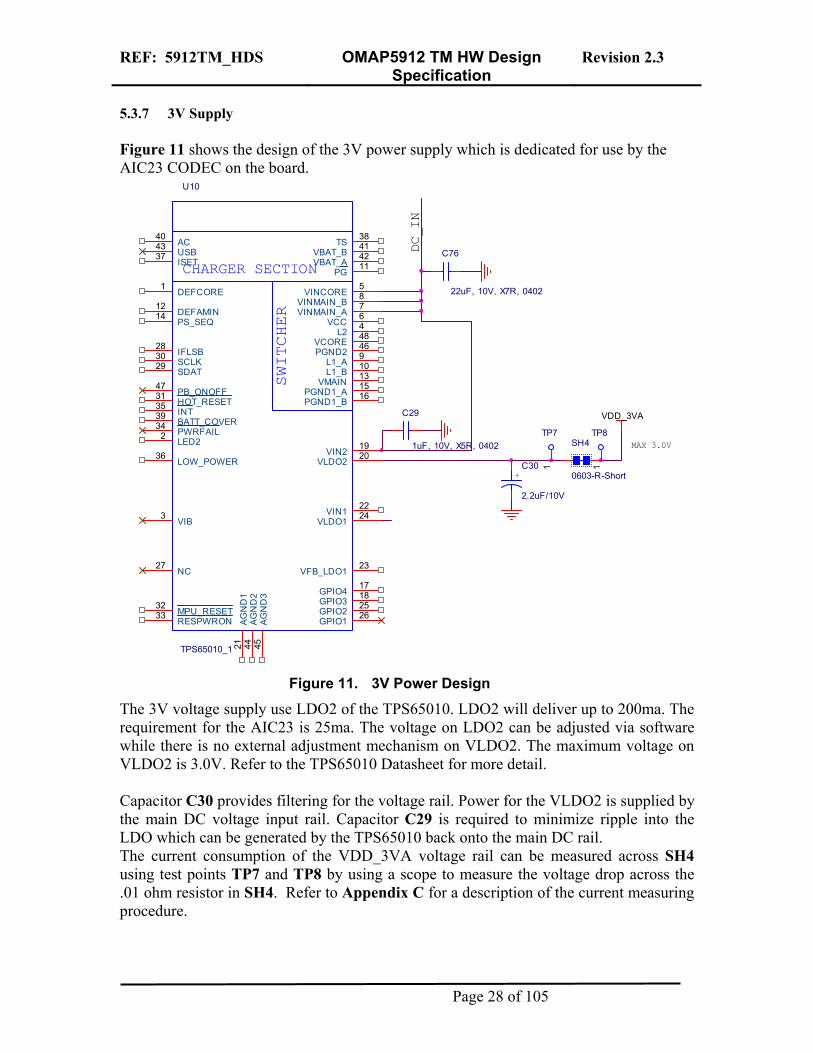
5.3.7 3V Supply Figure 11 shows the design of the 3V power supply which is dedicated for use by the AIC23 CODEC on the board.
TP7
1
MAX 3.0V
C29
1uF, 10V, X5R, 0402
DC_IN
CHARGER SECTIONSWITCHER
U10
TPS65010_1
1
2
3
4
5
678
910
11
12
13
14
1516
1817
1920
21
22
23
24
2526
27
28
2930
31
3233
34
35
36
37
38
39
4043
4241
44 45
46
47
48
DEFCORE
LED2
VIB
L2
VINCORE
VCCVINMAIN_AVINMAIN_B
L1_AL1_B
PG
DEFAMIN
VMAIN
PS_SEQ
PGND1_APGND1_B
GPIO3GPIO4
VIN2VLDO2
AGN
D1
VIN1
VFB_LDO1
VLDO1
GPIO2GPIO1
NC
IFLSB
SDATSCLK
HOT_RESET
MPU_RESETRESPWRON
PWRFAIL
INT
LOW_POWER
ISET
TS
BATT_COVER
ACUSB
VBAT_AVBAT_B
AGN
D2
AGN
D3
PGND2
PB_ONOFF
VCORE
C76
22uF, 10V, X7R, 0402
SH4
0603-R-Short
VDD_3VA
+C30
2.2uF/10V
TP8
1
Figure 11. 3V Power Design
The 3V voltage supply use LDO2 of the TPS65010. LDO2 will deliver up to 200ma. The requirement for the AIC23 is 25ma. The voltage on LDO2 can be adjusted via software while there is no external adjustment mechanism on VLDO2. The maximum voltage on VLDO2 is 3.0V. Refer to the TPS65010 Datasheet for more detail. Capacitor C30 provides filtering for the voltage rail. Power for the VLDO2 is supplied by the main DC voltage input rail. Capacitor C29 is required to minimize ripple into the LDO which can be generated by the TPS65010 back onto the main DC rail. The current consumption of the VDD_3VA voltage rail can be measured across SH4 using test points TP7 and TP8 by using a scope to measure the voltage drop across the .01 ohm resistor in SH4. Refer to Appendix C for a description of the current measuring procedure.
Page 28 of 105
REF: 5912TM_HDS OMAP5912 TM HW Design Specification
Revision 2.3
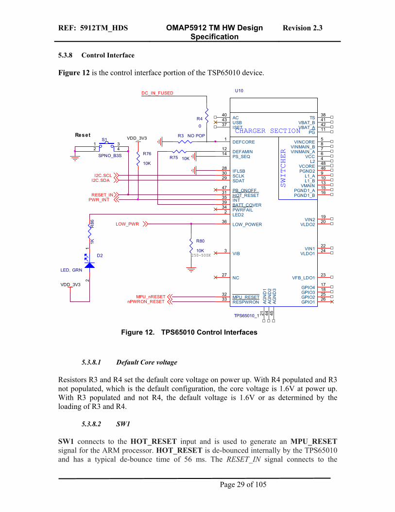
5.3.8 Control Interface Figure 12 is the control interface portion of the TSP65010 device.
R76
10K
S1
SPNO_B3S
12
34
R86
1K
D2
LED, GRN
21
R75 10K
R4
0
VDD_3V3
ResetCHARGER SECTION
SWITCHER
U10
TPS65010_1
1
2
3
4
5
678
910
11
12
13
14
1516
1817
1920
21
22
23
24
2526
27
28
2930
31
3233
34
35
36
37
38
39
4043
4241
44 45
46
47
48
DEFCORE
LED2
VIB
L2
VINCORE
VCCVINMAIN_AVINMAIN_B
L1_AL1_B
PG
DEFAMIN
VMAIN
PS_SEQ
PGND1_APGND1_B
GPIO3GPIO4
VIN2VLDO2
AGN
D1
VIN1
VFB_LDO1
VLDO1
GPIO2GPIO1
NC
IFLSB
SDATSCLK
HOT_RESET
MPU_RESETRESPWRON
PWRFAIL
INT
LOW_POWER
ISET
TS
BATT_COVER
ACUSB
VBAT_AVBAT_B
AGN
D2
AGN
D3
PGND2
PB_ONOFF
VCORE
250-500K
VDD_3V3 R3 NO POP
R80
10K
MPU_nRESET
RESET_INPWR_INT
I2C.SDAI2C.SCL
LOW_PWR
DC_IN_FUSED
nPWRON_RESET
Figure 12. TPS65010 Control Interfaces
5.3.8.1 Default Core voltage Resistors R3 and R4 set the default core voltage on power up. With R4 populated and R3 not populated, which is the default configuration, the core voltage is 1.6V at power up. With R3 populated and not R4, the default voltage is 1.6V or as determined by the loading of R3 and R4.
5.3.8.2 SW1 SW1 connects to the HOT_RESET input and is used to generate an MPU_RESET signal for the ARM processor. HOT_RESET is de-bounced internally by the TPS65010 and has a typical de-bounce time of 56 ms. The RESET_IN signal connects to the
Page 29 of 105
REF: 5912TM_HDS OMAP5912 TM HW Design Specification
Revision 2.3
Expansion Connector B pin 59 to allows the ADM or expansion cards to generate a MPU_RESET if needed. It can also be used to exit LOW POWER MODE, in this case the TPS65010 waits until the VCORE voltage has stabilized before generating the MPU_RESET pulse. The MPU_RESET pulse is active low for 100 usec. HOT_RESET has an internal 1M pullup to VCC. NOTE: Refer to the Reset Section for an updated description on the use of the nMPU_RST signal.
5.3.8.3 LED D2 The LED2 output is connected to D2 and can be programmed to blink or be permanently on or off. The LED2_ON and LED2_PER registers are used to control the blink rate. For LED2, the minimum blink on time is 10 ms and this can be increased in 127 10 ms-steps to 1280 ms. The minimum blink period is 100 ms and this can be increased in 127 100-ms steps to 12800 ms. Software applications are free to use this as needed.
5.3.8.4 LOW_POWER Input The low_power state is entered via the processor setting the ENABLE_LP bit in the serial interface and then raising the LOW_PWR pin. The TPS65010 actually uses the rising edge of the internal signal formed by a logical AND of the LOW_PWR and ENABLE LP signals to enter low power mode. The VMAIN switching converter remains active, but the VCORE converter may be disabled in low power mode via the serial interface by setting the LP_COREOFF bit in the VDCDC2 register. If left enabled, the VCORE voltage is set to the value predefined by the CORELP0/1 bits in the VDCDC2 register. The LDO1OFF/nSLP and LDO2OFF/nSLP bits in the VREGS1 register determine whether the LDOs are turned off or put in a reduced power mode (transient speed-up circuitry disabled in order to minimize quiescent current) in low power mode. All TPS65010 features remain addressable via the serial interface. TPS65010 can exit this state either due to an under-voltage condition at VCC, due to an OVERTEMP condition, by the processor deasserting the LOW_POWER pin or by the user activating the HOT_RESET pin or the PB_ONOFF pin.
5.3.8.5 Interrupt Output The open drain INT pin is used to combine and report all possible conditions via a single pin to the OMAP5912. INT can also be activated if any of the regulators are below the regulation threshold. The PWR_INT signal connects to MPUIO1 on the OMAP5912.
Page 30 of 105
REF: 5912TM_HDS OMAP5912 TM HW Design Specification
Revision 2.3
5.3.8.6 I2C
The SDA and SCL pins form the I2C interface that connects to the OMAP5912 Processor to allow applications on the OMAP5912 to control the functions of the TPS65010 device. The I2C serial interface is compatible with the standard and fast mode I2C specifications, allowing transfers at up to 400 kHz. The interface enables most functions to be programmed to new Register contents remain intact as long as VCC remains above 2 V. The TPS65010 has a 7-bit address with the LSB set by the IFLSB pin which is tied to ground. The 6 MSBs are 100100. Attempting to read data from register addresses not listed in this section results in FFh being read out. For normal data transfer, DATA is allowed to change only when CLK is low. Changes when CLK is high are reserved for indicating the start and stop conditions. During data transfer, the data line must remain stable whenever the clock line is high. There is one clock pulse per bit of data. Each data transfer is initiated with a start condition and terminated with a stop condition. When addressed, the TPS65010 device generates an acknowledge bit after the reception of each byte. The OMAP5912 must generate an extra clock pulse that is associated with the acknowledge bit. The TPS65010 device must pull down the DATA line during the acknowledge clock pulse so that the DATA line is a stable low during the high period of the acknowledge clock pulse. The DATA line is a stable low during the high period of the acknowledge-related clock pulse. Setup and hold times must be taken into account. During read operations, a master must signal the end of data to the slave by not generating an acknowledge bit on the last byte that was clocked out of the slave. In this case, the slave TPS65010 device must leave the data line high to enable the master to generate the stop condition. 5.3.9 RTC Power The RTC section provides power to the separate Real Time Clock input of the OAMP5912 Processor. Figure 13 provides the design of the circuit.
Page 31 of 105
REF: 5912TM_HDS OMAP5912 TM HW Design Specification
Revision 2.3
R73
1M,1%,0603
VDD_RTC
Place close to the OMAPProcessor.
C24
.47uF/10VR72
270K,1%,0603
TP1
1
U9TPS71501DCK
4
3
5
1
2
Vin
NC
OUT
FB
G
TP2
1
SH1
0603-R-ShortC75
.47uF/10V
DC IN
Figure 13. RTC Power Design
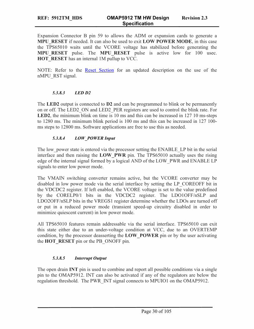
The RTC power regulator is separate from the TSP6510 and is fed directly by the main DC supply. This insures that power can be fed continuously from the external supply or the battery, when installed. Even though the TPS6510 can power down, the voltage to the RTC will always be supplied. U9 is a TPS71501 LDO regulator. The features of this regulator include:
50-mA Low-Dropout Regulator Available in 2.5 V, 3.0 V, 3.3 V, 5.0 V, and Adjustable 24-V Maximum Input Voltage Low 3.2-µA Quiescent Current at 50 mA 5-Pin SC70/SOT-323 (DCK) Package Stable With Any Capacitor (>0.47 µF) Over Current Limitation –40°C to 125°C Operating Junction Temperature Range
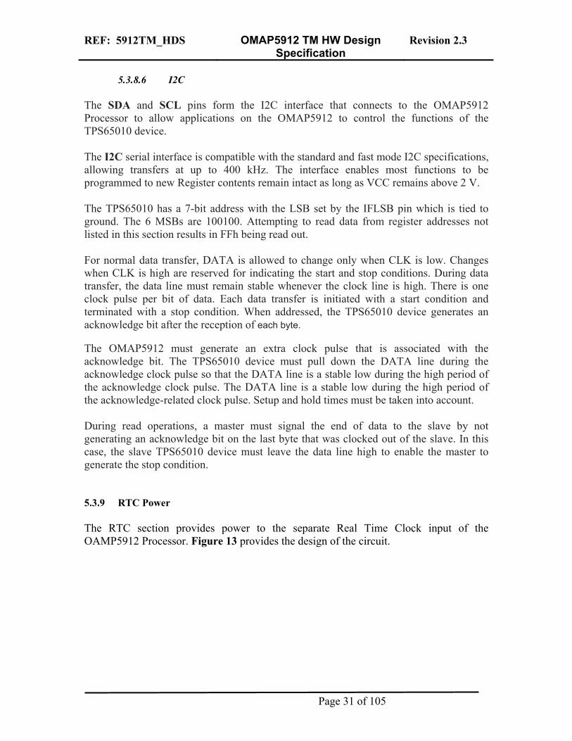
The TM design uses the adjustable version of the regulator which allows the voltage to be set by changing R72 and R73. This insures that no matter how the layout is done, that we can be sure that exactly 1.8V is on the OMAP5912 processor pins. In the Figure 13 resistors R1 and R2 should be chosen for approximately 1.5-µA divider current. Lower value resistors can be used for improved noise performance, but the solution consumes more power. Higher resistor values should be avoided as leakage current into/out of FB across R1/R2 creates an offset voltage that artificially increases/decreases the feedback voltage and thus erroneously decreases/increases VO. The recommended design procedure is to choose R2 = 1 MΩ to set the divider current at 1.5 µA, and then calculate R1 using the information in Figure 14:
Page 32 of 105
REF: 5912TM_HDS OMAP5912 TM HW Design Specification
Revision 2.3
Figure 14. RTC Voltage Adjustment
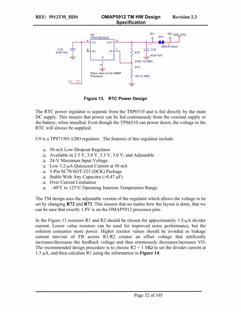
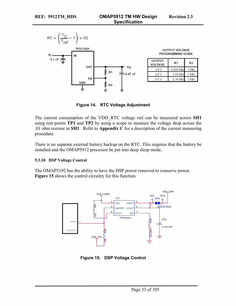
The current consumption of the VDD_RTC voltage rail can be measured across SH1 using test points TP1 and TP2 by using a scope to measure the voltage drop across the .01 ohm resistor in SH1. Refer to Appendix C for a description of the current measuring procedure. There is no separate external battery backup on the RTC. This requires that the battery be installed and the OMAP5912 processor be put into deep sleep mode. 5.3.10 DSP Voltage Control The OMAP5192 has the ability to have the DSP power removed to conserve power. Figure 15 shows the control circuitry for this function.
17
SH5
0603-R-Short
R85
10K
VDD_CORETP10
1
+C33
4.7uf /10V
GPIO4
VDD_3V3
VDD_DSP
TP9
1R
8415
0,06
03
R81
15K
TPS65010
U11
FDC6331L
4 3
2
6
5
1
VIN VOUT
VOUT
R1/C1
ON/OFF
R2
Figure 15. DSP Voltage Control
Page 33 of 105
REF: 5912TM_HDS OMAP5912 TM HW Design Specification
Revision 2.3
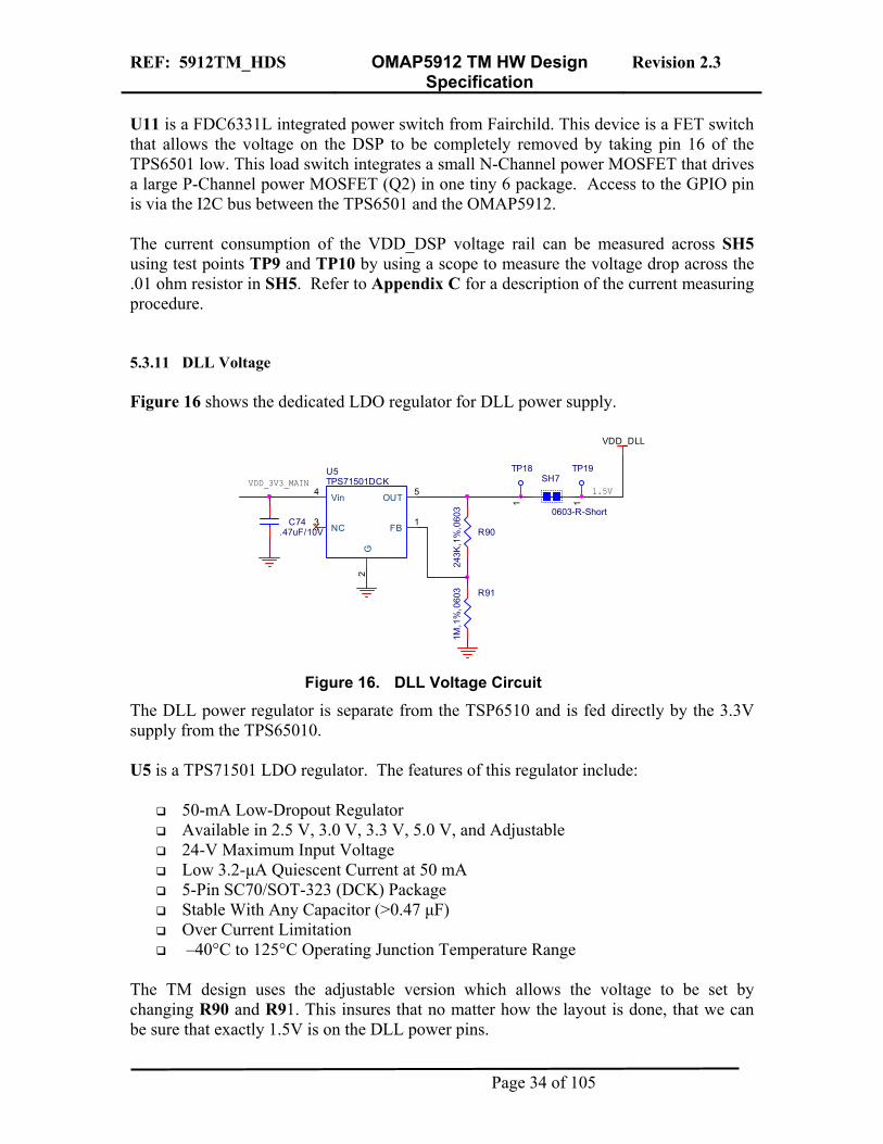
U11 is a FDC6331L integrated power switch from Fairchild. This device is a FET switch that allows the voltage on the DSP to be completely removed by taking pin 16 of the TPS6501 low. This load switch integrates a small N-Channel power MOSFET that drives a large P-Channel power MOSFET (Q2) in one tiny 6 package. Access to the GPIO pin is via the I2C bus between the TPS6501 and the OMAP5912. The current consumption of the VDD_DSP voltage rail can be measured across SH5 using test points TP9 and TP10 by using a scope to measure the voltage drop across the .01 ohm resistor in SH5. Refer to Appendix C for a description of the current measuring procedure. 5.3.11 DLL Voltage Figure 16 shows the dedicated LDO regulator for DLL power supply.
1.5V
U5TPS71501DCK
4
3
5
1
2
Vin
NC
OUT
FB
G
VDD_DLL
SH7
0603-R-Short
R90
243K
,1%
,060
3TP18
1
VDD_3V3_MAIN
TP19
1
C74.47uF/10V
R91
1M,1
%,0
603
Figure 16. DLL Voltage Circuit
The DLL power regulator is separate from the TSP6510 and is fed directly by the 3.3V supply from the TPS65010. U5 is a TPS71501 LDO regulator. The features of this regulator include:
50-mA Low-Dropout Regulator Available in 2.5 V, 3.0 V, 3.3 V, 5.0 V, and Adjustable 24-V Maximum Input Voltage Low 3.2-µA Quiescent Current at 50 mA 5-Pin SC70/SOT-323 (DCK) Package Stable With Any Capacitor (>0.47 µF) Over Current Limitation –40°C to 125°C Operating Junction Temperature Range
The TM design uses the adjustable version which allows the voltage to be set by changing R90 and R91. This insures that no matter how the layout is done, that we can be sure that exactly 1.5V is on the DLL power pins.
Page 34 of 105
REF: 5912TM_HDS OMAP5912 TM HW Design Specification
Revision 2.3
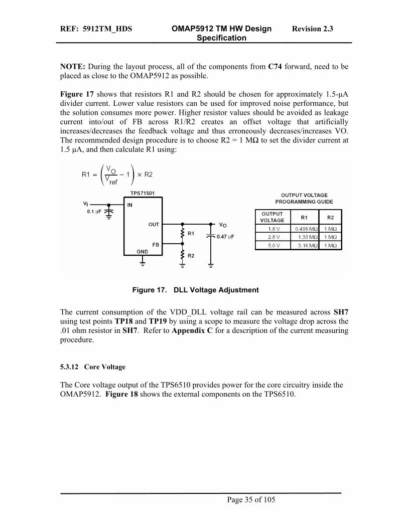
NOTE: During the layout process, all of the components from C74 forward, need to be placed as close to the OMAP5912 as possible. Figure 17 shows that resistors R1 and R2 should be chosen for approximately 1.5-µA divider current. Lower value resistors can be used for improved noise performance, but the solution consumes more power. Higher resistor values should be avoided as leakage current into/out of FB across R1/R2 creates an offset voltage that artificially increases/decreases the feedback voltage and thus erroneously decreases/increases VO. The recommended design procedure is to choose R2 = 1 MΩ to set the divider current at 1.5 µA, and then calculate R1 using:
Figure 17. DLL Voltage Adjustment
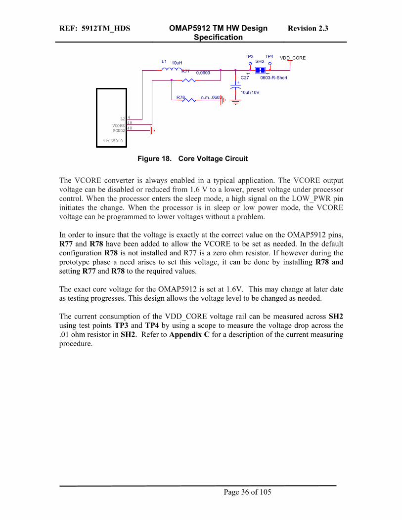
The current consumption of the VDD_DLL voltage rail can be measured across SH7 using test points TP18 and TP19 by using a scope to measure the voltage drop across the .01 ohm resistor in SH7. Refer to Appendix C for a description of the current measuring procedure. 5.3.12 Core Voltage The Core voltage output of the TPS6510 provides power for the core circuitry inside the OMAP5912. Figure 18 shows the external components on the TPS6510.
Page 35 of 105
REF: 5912TM_HDS OMAP5912 TM HW Design Specification
Revision 2.3
48
L1 10uH
48
TP4
1
TPS65010
L2
TP3
1R77 0,0603
4
PGND2
R78 n.m..0603
SH2
0603-R-Short+
C27
10uf /10V
VCORE
VDD_CORE
Figure 18. Core Voltage Circuit
The VCORE converter is always enabled in a typical application. The VCORE output voltage can be disabled or reduced from 1.6 V to a lower, preset voltage under processor control. When the processor enters the sleep mode, a high signal on the LOW_PWR pin initiates the change. When the processor is in sleep or low power mode, the VCORE voltage can be programmed to lower voltages without a problem. In order to insure that the voltage is exactly at the correct value on the OMAP5912 pins, R77 and R78 have been added to allow the VCORE to be set as needed. In the default configuration R78 is not installed and R77 is a zero ohm resistor. If however during the prototype phase a need arises to set this voltage, it can be done by installing R78 and setting R77 and R78 to the required values. The exact core voltage for the OMAP5912 is set at 1.6V. This may change at later date as testing progresses. This design allows the voltage level to be changed as needed. The current consumption of the VDD_CORE voltage rail can be measured across SH2 using test points TP3 and TP4 by using a scope to measure the voltage drop across the .01 ohm resistor in SH2. Refer to Appendix C for a description of the current measuring procedure.
Page 36 of 105
REF: 5912TM_HDS OMAP5912 TM HW Design Specification
Revision 2.3
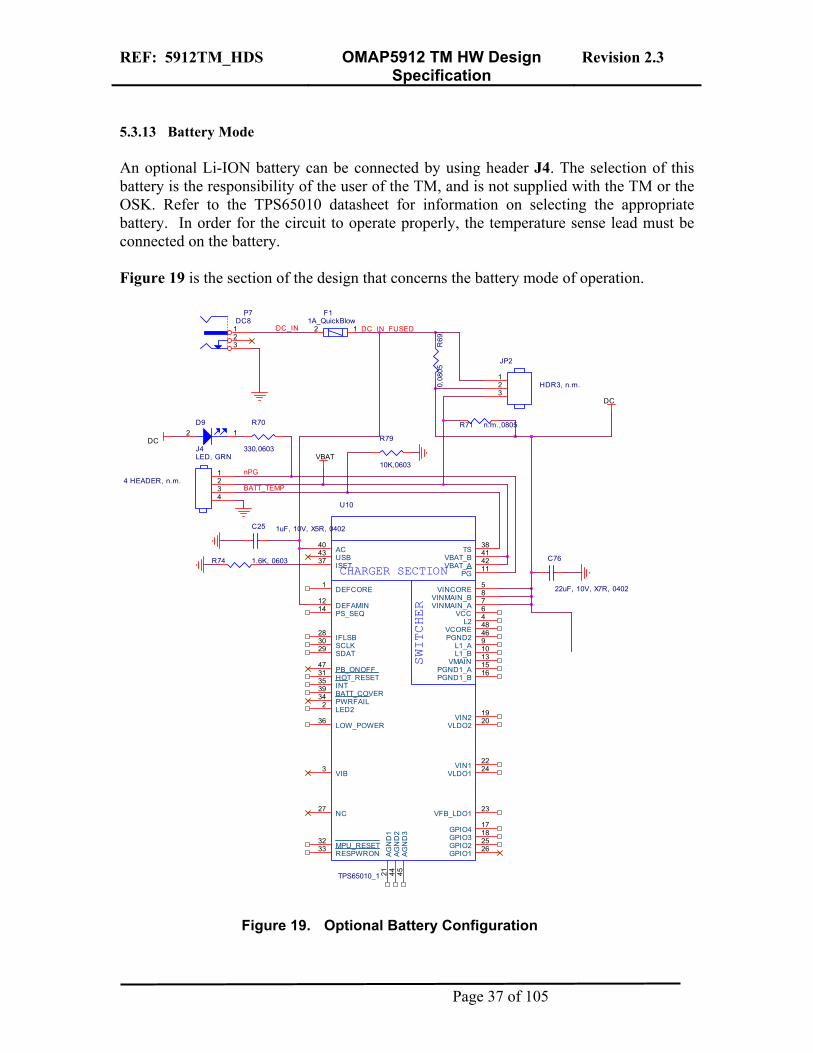
5.3.13 Battery Mode An optional Li-ION battery can be connected by using header J4. The selection of this battery is the responsibility of the user of the TM, and is not supplied with the TM or the OSK. Refer to the TPS65010 datasheet for information on selecting the appropriate battery. In order for the circuit to operate properly, the temperature sense lead must be connected on the battery. Figure 19 is the section of the design that concerns the battery mode of operation.
VBAT
R71 n.m.,0805
C76
22uF, 10V, X7R, 0402
C25 1uF, 10V, X5R, 0402
R70
330,0603R
690,
0805
DC
P7DC8
321
JP2
HDR3, n.m.123
J4
4 HEADER, n.m.1234
F11A_QuickBlow
12
DC
CHARGER SECTION
SWITCHER
U10
TPS65010_1
1
2
3
4
5
678
910
11
12
13
14
1516
1817
1920
21
22
23
24
2526
27
28
2930
31
3233
34
35
36
37
38
39
4043
4241
44 45
46
47
48
DEFCORE
LED2
VIB
L2
VINCORE
VCCVINMAIN_AVINMAIN_B
L1_AL1_B
PG
DEFAMIN
VMAIN
PS_SEQ
PGND1_APGND1_B
GPIO3GPIO4
VIN2VLDO2
AGN
D1
VIN1
VFB_LDO1
VLDO1
GPIO2GPIO1
NC
IFLSB
SDATSCLK
HOT_RESET
MPU_RESETRESPWRON
PWRFAIL
INT
LOW_POWER
ISET
TS
BATT_COVER
ACUSB
VBAT_AVBAT_B
AGN
D2
AGN
D3
PGND2
PB_ONOFF
VCORE
R79
10K,0603
R74 1.6K, 0603
D9
LED, GRN
2 1
DC_IN
nPG
BATT_TEMP
DC_IN_FUSED
Figure 19. Optional Battery Configuration
Page 37 of 105
REF: 5912TM_HDS OMAP5912 TM HW Design Specification
Revision 2.3
In order for the TPS65010 to operate correctly in the Non-Battery mode, resistor R79 must be installed to insure that the temperature detection circuitry in the TPS65010 is kept happy. When in the battery mode of operation, R79 MUST is removed. JP2 can be used to attach the battery to the Circuitry by placing it so that pins 2 and 3 are shorted. For this to work, R69 and R71 must be removed. Optionally, R69 can be removed and R71 installed. This places the battery as the main voltage source and uses the DC input only as a supply to the charger circuit of the TPS65010. C25 is a filter for the input of the battery charger circuit in the TPS65010. R74 sets the default charge current for the battery. 5.4 Flash Memory The TM supports two NOR FLASH devices and can be configured in several ways to obtain a range of Flash densities as needed. It also provides for a mechanism whereby the FLASH can be disabled by an expansion board and that expansion board is then the provider of the FLASH devices. The following sections provide a description of the FLASH circuitry on the OMAP5912 TM. 5.4.1 Supported Configurations Table 6 defines the supported FLASH memory configuration on the TM. The standard configuration is the dual 16MB devices for a total of 32MB.
Table 6. FLASH Configurations
Size Slot 1 Slot 2 4Mb 4Mb - 8Mb 4Mb 4MB 8Mb 8Mb - 16Mb 8Mb 8Mb 16Mb 16Mb - 32Mb 16Mb 16Mb 32Mb 32Mb 64Mb 32Mb 32Mb
5.4.2 Supported FLASH Devices
Page 38 of 105
REF: 5912TM_HDS OMAP5912 TM HW Design Specification
Revision 2.3
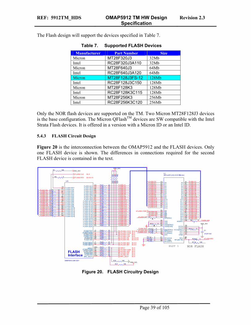
The Flash design will support the devices specified in Table 7.
Table 7. Supported FLASH Devices Manufacturer Part Number Size
Micron MT28F320J3 32Mb Intel RC28F320J3A110 32Mb Micron MT28F640J3 64Mb Intel RC28F640J3A120 64Mb Micron MT28F128J3FS-12 128Mb Intel RC28F128J3C150 128Mb Micron MT28F128K3 128Mb Intel RC28F128K3C115 128Mb Micron MT28F256K3 256Mb Intel RC28F256K3C120 256Mb
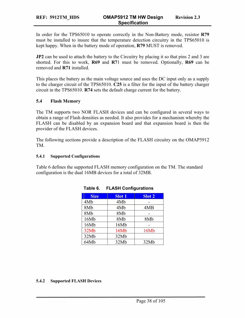
Only the NOR flash devices are supported on the TM. Two Micron MT28F128J3 devices is the base configuration. The Micron QFlashTM devices are SW compatible with the Intel Strata Flash devices. It is offered in a version with a Micron ID or an Intel ID. 5.4.3 FLASH Circuit Design Figure 20 is the interconnection between the OMAP5912 and the FLASH devices. Only one FLASH device is shown. The differences in connections required for the second FLASH device is contained in the text.
FLASHInterface
U3I
OMAP5912-289 GDY
L6K1L1M1L2J7M2L4K6N1L5N2M4M3K7P1R1N4
D3C2E4E3D2C1E2D1E1F2F1F5G3G4G2G5G6H3H4F4H5H2J2J4
J3
J8J6
M5P3
K2J1
H6R3N3
F3
K3
H14
T1
M15
FLASH.RDYFLASH.CLKFLASH.D[0]FLASH.D[1]FLASH.D[2]FLASH.D[3]FLASH.D[4]FLASH.D[5]FLASH.D[6]FLASH.D[7]FLASH.D[8]FLASH.D[9]FLASH.D[10]FLASH.D[11]FLASH.D[12]FLASH.D[13]FLASH.D[14]FLASH.D[15]
FLASH.A[1]FLASH.A[2]FLASH.A[3]FLASH.A[4]FLASH.A[5]FLASH.A[6]FLASH.A[7]FLASH.A[8]FLASH.A[9]
FLASH.A[10]FLASH.A[11]FLASH.A[12]FLASH.A[13]FLASH.A[14]FLASH.A[15]FLASH.A[16]FLASH.A[17]FLASH.A[18]FLASH.A[19]FLASH.A[20]FLASH.A[21]FLASH.A[22]FLASH.A[23]FLASH.A[24]
FLASH.CS1
FLASH.CS2FLASH.CS3
FLASH.OEFLASH.WE
FLASH.BE[1]FLASH.BE[0]
FLASH.ADVFLASH.WPFLASH.RP
FLASH.A[25]
FLASH.CS2B
MPU_BOOT
FLASH.CS1B
GPIO1
R6
10K
R192 22
R170 22
R189 22
R178 22
R193 22
I
R162 22
R190 22
R169 22
VDD_3V3
R166 22
R175 22
R186 22
R179 22R181 22
VDD_3V3
R200 22
R168 22
R182 22
A
R14 0
B
R110 10K
G
R209 22
R210 22
R203 22
R199 22
R191 22
R164 22
R2 0
R204 22
R176 22
R195 22
R5
10K
NOR FLASH
R7 0
R177 22
R205 22
R196 22
R30 10K
R188 22
R165 22
R13 0
R187 22
R11 0
R212 22
R9 0
F
U128FxxxK3 [J3] (4-32 MBy tes)
A1B1C1D1D2A2C2A3B3C3D3C4A5B5C5D7D8A7B7C7
F2E2G3E4E5G5G6H7E1E3F3F4F5H5G7E7
H2
B2H4
B4F8G8D4C6
C8
E6F6F7
A8G1H8
H3A6
D5H6
D6
A4
G2H1
F1B6
G4
E8
B8
A0A1A2A3A4A5A6A7A8A9
A10A11A12A13A14A15A16A17A18A19
D0D1D2D3D4D5D6D7D8D9D10D11D12D13D14D15
VSSQ[DNU]
VSSVSS
CEOEWERPWP[DNU]
A20
CLK[DNU]ADV[DNU]WAIT[DNU]
A21A22
A23[NC]
VCCVCC
VCCQVSSQ[VSS]
VCCQ[DNU]
VPEN
RFU[A0]RFU[CE2]
RFU[BYTE]RFU
VCCQ
STS
RFU[CE1]
R172 22
R161 22
SLOT 1R211 22
R23 0
R213 22
R19 0
R184 22
R194 22
R3
10K
R185 22
R1 10K
R173 22
J
R180 22
R215 22
R167 22
H
R31 10K
VDD_3V3
C1
.01UF/10VE
VDD_3V3
R206 22
R201 22
C
R21 0
R4
10K
R208 22
R183 22
R197 22
R202 22
R171 22
D
R207 22
R214 22
R17 0
R198 22
R163 22
R24 0
R174 22
R27 0K
FLASH.A22nFLASH.WP
nFLASH.BE1 Sh.8,9
MPU_BOOT Sh.9
FLASH.A4
FLASH.A8
FLASH.A12
FLASH.A7
FLASH.A9
FLASH.D2
FLASH.A12
FLASH.D5
FLASH.A1 FLASH.D2
FLASH.A8
FLASH.D10
FLASH.D1
FLASH.RDY Sh.8,9,10
FLASH.A19
nFLASH.WP Sh.9
FLASH.A2
FLASH.D11
FLASH.D10
FLASH.D14
FLASH.A9
GPIO1 Sh.9
FLASH.A21
FLASH.RDY
nFLASH.CS2B Sh.9
FLASH.A1
FLASH.A22
FLASH.A16
FLASH.A24
FLASH.A25
FLASH.A20
FLASH.A3
FLASH.D9
nFLASH.CS1B Sh.9
FLASH.A18
FLASH.D3
FLASH.A11
FLASH.CLK
FLASH.A10
FLASH.A7FLASH.A5
FLASH.D15
FLASH.A5
FLASH.D0
FLASH.D12
FLASH.A19
FLASH.A6
FLASH.D8
nFLASH.OE Sh.8,9,10
FLASH.A23
FLASH.D13
FLASH.D3
FLASH.A11
nFLASH.CSXA
FLASH.D1
FLASH.D9
FLASH.A16
nFLASH.ADV
FLASH.A15
nFLASH.BE0 Sh.8,9
FLASH.A24
FLASH.D6
nFLASH.CS1A Sh.9,10
nFLASH.CS2 Sh.9
FLASH.A14
FLASH.D12nFLASH.OE
FLASH.A23
FLASH.D13
FLASH.A15
nFLASH.CS3 Sh.9
FLASH.A10
FLASH.CLK Sh.9
nFLASH.WE
FLASH.D5
FLASH.A6
FLASH.D8
FLASH.A20
FLASH.D7
FLASH.D0
FLASH.A13
FLASH.A3
FLASH.D11
nFLASH.RP Sh.9
FLASH.D7
FLASH.D15
FLASH.A2
nFLASH.WE Sh.8,9,10
nFLASH.RP
nFLASH.ADV Sh.9
FLASH.A21
nFLASH.BE0
FLASH.D4
FLASH.D6
FLASH.A17
FLASH.A13
FLASH.D14
FLASH.A14
FLASH.A17FLASH.A18
FLASH.D4
FLASH.A4
Figure 20. FLASH Circuitry Design
Page 39 of 105

REF: 5912TM_HDS OMAP5912 TM HW Design Specification
Revision 2.3
5.4.4 Address Bus The OMAP5912 has 24 address lines, A1-A25. Only address lines 1-24 are used for the largest device. Even though all of the address lines are connected to the devices, not all of the pins may be used depending on which device is installed. 5.4.5 Data Bus The data bus from the OMAP5912 is 16 bits wide. All of the data bits are connected to each of the Flash devices. 5.4.6 Control Signals All signals are the same for both slots except the CS signal. Slot 0 uses the CSXA while Slot 1 uses CSXB. Depending on the type of memory used, some of the signals may not be connected. This is handled by the populating or unpopulating of certain resistors. The signal GPIO1 is used to set the configuration of the Flash bus. To be compatible with the TM design, this pin must be tied to ground. The MPU_BOOT signal should be tied Hi for the TM application. 5.4.7 Address Decode Logic Figure 21 is the design of the decode logic for the FLASH devices.
VDD_3V3
R32 0
R37 0
L
R
P
C69
.01UF/10V
MRx
0
R29
10K
R33 0
U4A
74LVC139
23
1
4567
168
AB
G
Y0Y1Y2Y3
VC
CG
NDQ
R36 0
VDD_3V3
R34 0
NR38 0
R35 0
O
nFLASH.CS2nFLASH.CS1B
FLASH.A23FLASH.A22
nFLASH.CS3
nFLASH.CSXA
FLASH.DIS
FLASH.A[1..25]
FLASH.A25FLASH.A24
nFLASH.CSXB
Figure 21. FLASH Decode Logic
Table 8 below defines how the resistors are to be loaded for each of the supported memory size configurations. In order to support contiguous memory between the two memory device slots, the address decoding for the second block must be moved. This is done by placing the A bit of the ‘139 decoder to the appropriate address line at the beginning of the Slot 2 address range. Highlighted is the default value of the TM design.
Page 40 of 105
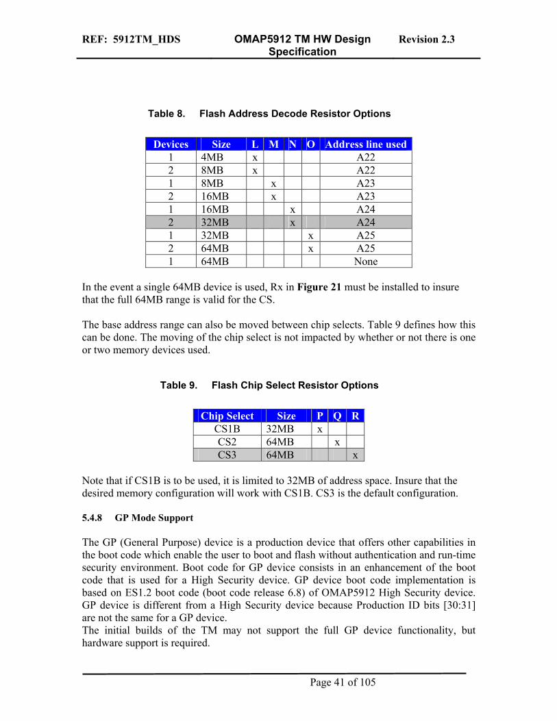
REF: 5912TM_HDS OMAP5912 TM HW Design Specification
Revision 2.3
Table 8. Flash Address Decode Resistor Options
Devices Size L M N O Address line used
1 4MB x A22 2 8MB x A22 1 8MB x A23 2 16MB x A23 1 16MB x A24 2 32MB x A24 1 32MB x A25 2 64MB x A25 1 64MB None
In the event a single 64MB device is used, Rx in Figure 21 must be installed to insure that the full 64MB range is valid for the CS. The base address range can also be moved between chip selects. Table 9 defines how this can be done. The moving of the chip select is not impacted by whether or not there is one or two memory devices used.
Table 9. Flash Chip Select Resistor Options
Chip Select Size P Q R
CS1B 32MB x CS2 64MB x CS3 64MB x
Note that if CS1B is to be used, it is limited to 32MB of address space. Insure that the desired memory configuration will work with CS1B. CS3 is the default configuration. 5.4.8 GP Mode Support The GP (General Purpose) device is a production device that offers other capabilities in the boot code which enable the user to boot and flash without authentication and run-time security environment. Boot code for GP device consists in an enhancement of the boot code that is used for a High Security device. GP device boot code implementation is based on ES1.2 boot code (boot code release 6.8) of OMAP5912 High Security device. GP device is different from a High Security device because Production ID bits [30:31] are not the same for a GP device. The initial builds of the TM may not support the full GP device functionality, but hardware support is required.
Page 41 of 105
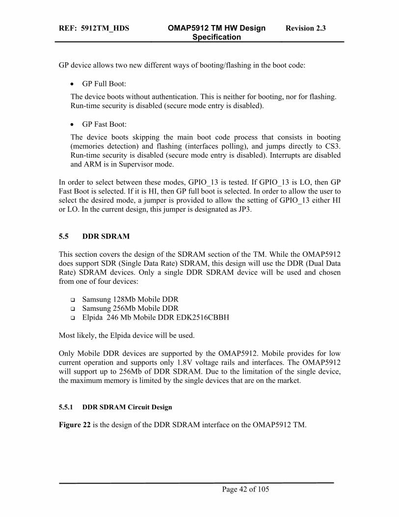
REF: 5912TM_HDS OMAP5912 TM HW Design Specification
Revision 2.3
GP device allows two new different ways of booting/flashing in the boot code:
• GP Full Boot:
The device boots without authentication. This is neither for booting, nor for flashing. Run-time security is disabled (secure mode entry is disabled).
• GP Fast Boot:
The device boots skipping the main boot code process that consists in booting (memories detection) and flashing (interfaces polling), and jumps directly to CS3. Run-time security is disabled (secure mode entry is disabled). Interrupts are disabled and ARM is in Supervisor mode.
In order to select between these modes, GPIO_13 is tested. If GPIO_13 is LO, then GP Fast Boot is selected. If it is HI, then GP full boot is selected. In order to allow the user to select the desired mode, a jumper is provided to allow the setting of GPIO_13 either HI or LO. In the current design, this jumper is designated as JP3. 5.5 DDR SDRAM This section covers the design of the SDRAM section of the TM. While the OMAP5912 does support SDR (Single Data Rate) SDRAM, this design will use the DDR (Dual Data Rate) SDRAM devices. Only a single DDR SDRAM device will be used and chosen from one of four devices:
Samsung 128Mb Mobile DDR Samsung 256Mb Mobile DDR Elpida 246 Mb Mobile DDR EDK2516CBBH
Most likely, the Elpida device will be used. Only Mobile DDR devices are supported by the OMAP5912. Mobile provides for low current operation and supports only 1.8V voltage rails and interfaces. The OMAP5912 will support up to 256Mb of DDR SDRAM. Due to the limitation of the single device, the maximum memory is limited by the single devices that are on the market. 5.5.1 DDR SDRAM Circuit Design Figure 22 is the design of the DDR SDRAM interface on the OMAP5912 TM.
Page 42 of 105
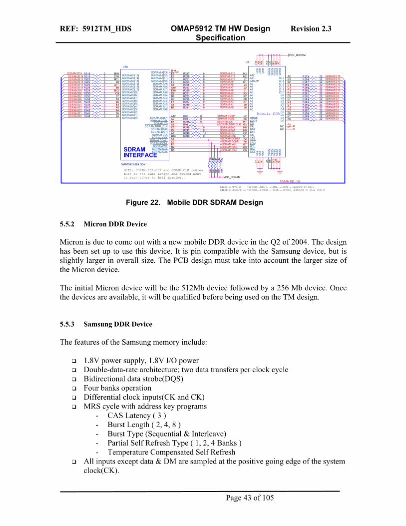
REF: 5912TM_HDS OMAP5912 TM HW Design Specification
Revision 2.3
R240 0
R221 0
R239 0
R39
10K
R254 22
VDD_SDRAM
R226 0
R248 10
R268 22
R224 0
R267 22
R225 0
R242 0
R223 0
R92 0
R218 0
R259 22
R233 0
R216 0
R40
10K
R243 0
R232 0
R260 22
R245 0
R247 0
R258 22R222 0
R231 0R230 0
R227 0
R93 0
R246 0
R269 22
VDD_SDRAM
R263 22
R43
10K
R262 22
R238 0
R270 22
R264 22R237 0R234 0
R244 0
R249 0
K4x56163DPE(L/F)C2 =100MHZ..16Mx16...32MB...256Mb...Samsung 60 Ball (6x10)
R261 22
R219 0 R253 22
Mobile DDR
U7 A7
A8
A9
B7B8
A1
C7C8
B1
D7D8
A3
E7
C9
G7
G8G9
H7
H8H9
J7
J8J9K7K8
D1
B9
K2K3J1J2J3H1
H2
G2
F1
E3
E9
D2D3
C1
C2C3
F9
B2B3
D9
A2
E1
H3
F3
E2E8
F2
F7
F8
G1
G3
K1
K9
VD
DQ
D0
VD
D
D1D2
VS
S
D3D4
VD
DQ
D5D6
VS
SQ
D7
VD
DQ
WE
CASRAS
CS
BA0BA1
A10/AP
A0A1A2A3
VD
DQ
VS
SQ
A4A5A6A7A8A9
A11
CK
VS
S
D8
VD
DQ
D9D10
VS
SQ
D11D12
VD
D
D13D14
VS
SQ
D15
VS
SQ
A12
NC
UDQSLDQS
UDM
NC
LDM
CKE
CK
VS
SV
DD
R235 0
SDRAMINTERFACE
U3A
OMAP5912-289 GDY
B10C10B11B9
A11B8
B12C9B7A3B6B3A5A4B5B4
E8E9F8F9C6A10E10C8D9C3F7A1B2
C5C4A7B13A8
E6
D5D4
D10
E7
C7
A12A2
A6
SDRAM.D[15]SDRAM.D[14]SDRAM.D[13]SDRAM.D[12]SDRAM.D[11]SDRAM.D[10]SDRAM.D[9]SDRAM.D[8]SDRAM.D[7]SDRAM.D[6]SDRAM.D[5]SDRAM.D[4]SDRAM.D[3]SDRAM.D[2]SDRAM.D[1]SDRAM.D[0]
SDRAM.A[12]SDRAM.A[11]SDRAM.A[10]SDRAM.A[9]SDRAM.A[8]SDRAM.A[7]SDRAM.A[6]SDRAM.A[5]SDRAM.A[4]SDRAM.A[3]SDRAM.A[2]SDRAM.A[1]SDRAM.A[0]
SDRAM.BA[0]SDRAM.BA[1]SDRAM.CLKSDRAM.CKE
SDRAM.DQMU
SDRAM.WE
SDRAM.CASSDRAM.RAS
SDRAM.A[13]
SDRAM.CS
SDRAM.DQML
SDRAM.DQSHSDRAM.DQSL
SDRAM.DDR_CLK
R229 0R228 0
R217 0
R41
10K
R266 22
R257 22
R241 0
R94 10
R236 0R265 22
NOTE: SDRAM.DDR.CLK and SDRAM.CLK routesmust be the same length and routed nextto each other at 4mil spacing..
K4x28163PEVG100 =100MHZ..8Mx16...16MB...128Mb...Samsung 60 Ball(6x10)
R220 0
R42
10K
SDRAM.D15
SDRAM.A6
nSDRAM.RAS
SDRAM.D9
SDRAM.D15
SDRAM.DQSL
SDRAM.D5 SDRAM.D6
SDRAM.CKE
SDRAM.D1
SDRAM.A11
nSDRAM.DQMU
nSDRAM.CS
SDRAM.A1
SDRAM.D0
SDRAM.D11
SDRAM.A4
SDRAM.D13
SDRAM.D5
SDRAM.A8
SDRAM.D6
SDRAM.D4
SDRAM.D9SDRAM.D10
SDRAM.A2
SDRAM.A10
SDRAM.CLK
SDRAM.D10
SDRAM.D2
SDRAM.BA1
SDRAM.A12SDRAM.D14
SDRAM.A3
SDRAM.A5
SDRAM.D12
nSDRAM.CAS
SDRAM.D1
SDRAM.BA0nSDRAM.DDR.CLK
SDRAM.D13
SDRAM.D3
nSDRAM.WE
SDRAM.D12
SDRAM.DQSH
SDRAM.D3
SDRAM.D11SDRAM.A7
SDRAM.D7
SDRAM.A9
SDRAM.A0
nSDRAM.DQML
SDRAM.D8
SDRAM.D7
SDRAM.D2SDRAM.D0
SDRAM.D4
SDRAM.D14
SDRAM.D8
SDRAM.D[0..15]
Figure 22. Mobile DDR SDRAM Design
5.5.2 Micron DDR Device Micron is due to come out with a new mobile DDR device in the Q2 of 2004. The design has been set up to use this device. It is pin compatible with the Samsung device, but is slightly larger in overall size. The PCB design must take into account the larger size of the Micron device. The initial Micron device will be the 512Mb device followed by a 256 Mb device. Once the devices are available, it will be qualified before being used on the TM design. 5.5.3 Samsung DDR Device The features of the Samsung memory include:
1.8V power supply, 1.8V I/O power Double-data-rate architecture; two data transfers per clock cycle Bidirectional data strobe(DQS) Four banks operation Differential clock inputs(CK and CK) MRS cycle with address key programs
- CAS Latency ( 3 ) - Burst Length ( 2, 4, 8 ) - Burst Type (Sequential & Interleave) - Partial Self Refresh Type ( 1, 2, 4 Banks ) - Temperature Compensated Self Refresh
All inputs except data & DM are sampled at the positive going edge of the system clock(CK).
Page 43 of 105
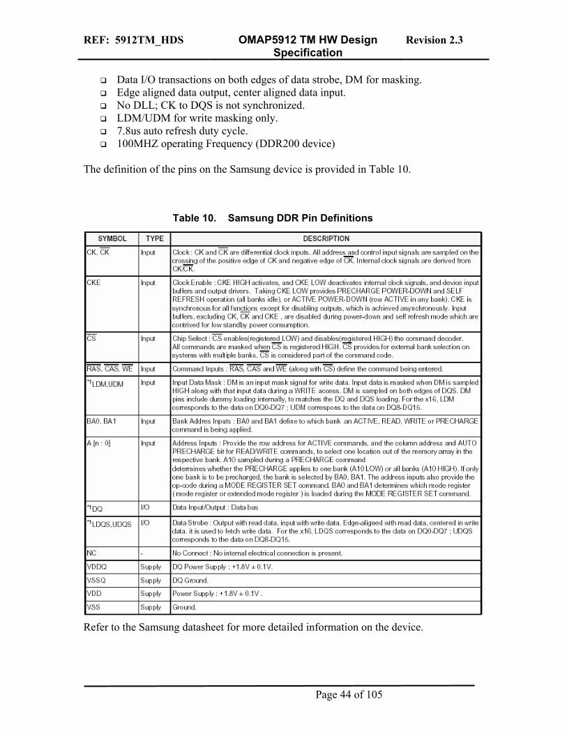
REF: 5912TM_HDS OMAP5912 TM HW Design Specification
Revision 2.3
Data I/O transactions on both edges of data strobe, DM for masking. Edge aligned data output, center aligned data input. No DLL; CK to DQS is not synchronized. LDM/UDM for write masking only. 7.8us auto refresh duty cycle. 100MHZ operating Frequency (DDR200 device)
The definition of the pins on the Samsung device is provided in Table 10.
Table 10. Samsung DDR Pin Definitions
Refer to the Samsung datasheet for more detailed information on the device.
Page 44 of 105
REF: 5912TM_HDS OMAP5912 TM HW Design Specification
Revision 2.3
5.5.4 Elpida DDR Device The features of the Elpida device include:
Low voltage power supply o VDD: 1.8V ± 0.15V o VDDQ: 1.8V ± 0.15V
Wide temperature range (.25°C to 85°C) Programmable Partial Array Self Refresh Programmable Driver Strength Auto Temperature Compensated Self Refresh by built-in temperature sensor. Deep power down mode Small package (60-ball FBGA) FBGA package is lead free solder (Sn-Ag-Cu) Data rate: 200Mbps/IO(max) Double Data Rate architecture: two data transfers per one clock cycle Bi-directional, data strobe (DQS) is transmitted received with data, to be used in
capturing data at the receiver. 1.8V LVCMOS interface Command and address signals refer to a positive clock edge Quad internal banks controlled by BA0 and BA1 Data mask (DM) for write data Wrap sequence = Sequential/ Interleave Programmable burst length (BL) = 2, 4, 8 Automatic precharge and controlled precharge Auto refresh and self refresh 8,192 refresh cycles/64ms (7.8µs maximum average periodic refresh interval) Burst termination by Burst stop command and Precharge command
Page 45 of 105
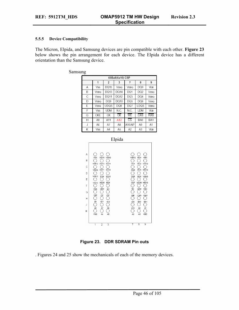
REF: 5912TM_HDS OMAP5912 TM HW Design Specification
Revision 2.3
5.5.5 Device Compatibility The Micron, Elpida, and Samsung devices are pin compatible with each other. Figure 23 below shows the pin arrangement for each device. The Elpida device has a different orientation than the Samsung device. S
. Figures 24 and 2
amsung
E a
Figure 23. DDR
5 show the mechanical
lpid
SDRAM Pin outs
s of each of the memory devices.
Page 46 of 105
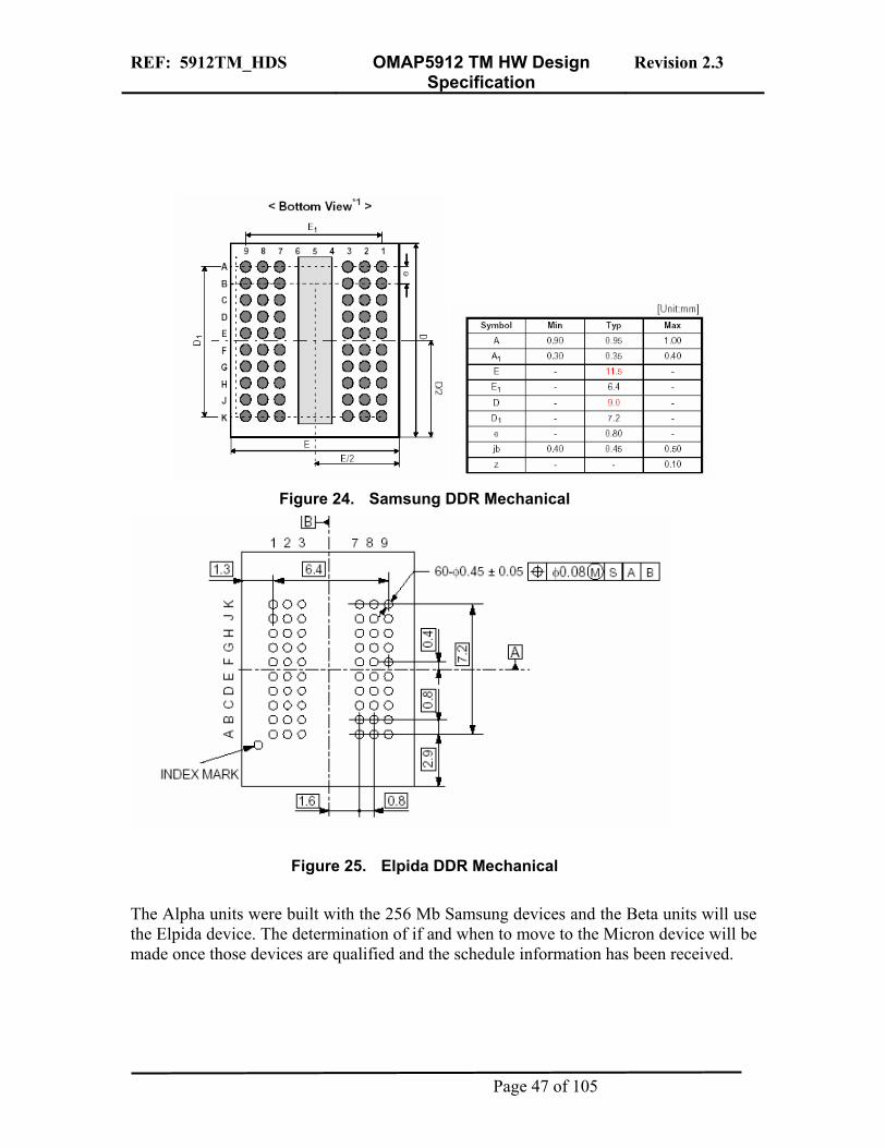
REF: 5912TM_HDS OMAP5912 TM HW Design Specification
Revision 2.3
Figure 24. Samsung DDR Mechanical
Figure 25. Elpida DDR Mechanical
The Alpha units were built with the 256 Mb Samsung devices and the Beta units will use the Elpida device. The determination of if and when to move to the Micron device will be made once those devices are qualified and the schedule information has been received.
Page 47 of 105
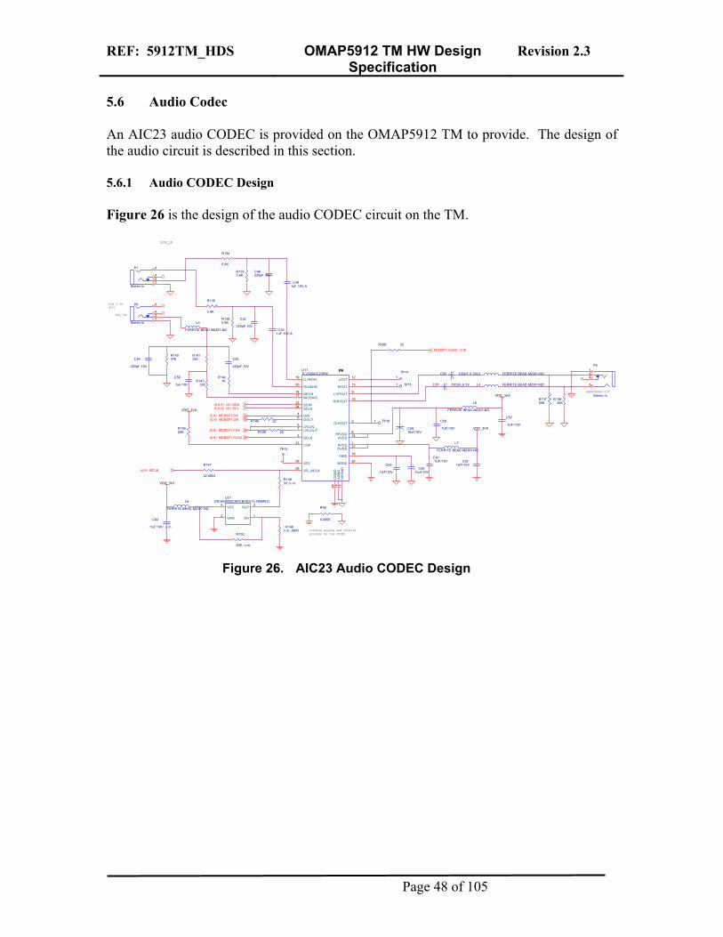
REF: 5912TM_HDS OMAP5912 TM HW Design Specification
Revision 2.3
5.6 Audio Codec An AIC23 audio CODEC is provided on the OMAP5912 TM to provide. The design of the audio circuit is described in this section. 5.6.1 Audio CODEC Design Figure 26 is the design of the audio CODEC circuit on the TM.
C54
220pF,10V
R143330
C55
220pF,10V
+C51 100UF,6.3V
R14520K
C59
.1UF/10V
R149n.m.,0603
R49
0,0805C64
.1UF/10V, n.m.
R13720K
P1
Stereo In
3
421
R136
5.6K
R1395.6K
C52
220pF,10V
LINE_IN
R141330
U17TLV320AIC23PW
12
13
19
20
1817
4
5
3
25
26
21
22
127
28
9
10
1115
16
814
2
7
6
2324
LOUT
ROUT
LLINEIN
RLINEIN
MICINMICBIAS
DIN
LRCIN
BCLK
XTL_MCLK
XTO
CS#
MODE
BVDDDVDD
DG
ND
LHPOUT
RHPOUT
HP
GN
DA
GN
D
VMID
HPVDDAVDD
CLKOUT
LRCOUT
DOUT
SDINSCLK
C61.1UF/10V
P5
Stereo In
3
421
MIC_IN
C531uF,10V,A
L5
FERRITE BEAD M2301-ND
R150
20K, n.m.
HEADPHONE OUT
R134
5.6K
VDD_3VA+
C5810uf /10V
C491uF,10V,A
PW
C57
.1UF/10V
U21DK/SG8002CAPCB-ND(12.000MHZ)
3
2 1
4OUT
GND EN
VCC
R1355.6K
+C50 100UF,6.3V
C62.1UF/10V
C48220pF,10V
+C60
10uf /10V
R14833, n.m.
L3 FERRITE BEAD M2301-ND
C63
.1UF/10V
Joining analog and digitalgrounds by the CODEC
TP13
1
VDD_3VA
R147
22,0603
PIN 2 TO3???
L6
FERRITE BEAD M2301-ND
TP151
R144 22
R298 22
L7
FERRITE BEAD M2301-ND
P6
Stereo In
3
421
C56
.1uF/10V
VDD_3VA
L4 FERRITE BEAD M2301-ND
R14047K
R13820K
TP161
R1421K
VDD_3V3
R146 22
L8
FERRITE BEAD M2301-ND
TP141
MCBSP1.CLKX(5,9)
MCBSP1.CLKS (5,9)
I2C.SDA(5,6,9)
MCLK(4,9)
I2C.SCL(5,6,9)
MCBSP1.DX(5,9)
MCBSP1.FSX(5,9)
MCBSP1.DR(5,9)
Figure 26. AIC23 Audio CODEC Design
Page 48 of 105
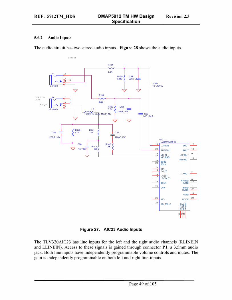
REF: 5912TM_HDS OMAP5912 TM HW Design Specification
Revision 2.3
5.6.2 Audio Inputs The audio circuit has two stereo audio inputs. Figure 28 shows the audio inputs.
C54
220pF,10V
R143330
C55
220pF,10V
P1
Stereo In
3
421
R136
5.6K
R1395.6K
C52
220pF,10V
LINE_IN
R141330
U17TLV320AIC23PW
12
13
19
20
1817
4
5
3
25
26
21
22
127
28
9
10
1115
16
814
2
7
6
2324
LOUT
ROUT
LLINEIN
RLINEIN
MICINMICBIAS
DIN
LRCIN
BCLK
XTL_MCLK
XTO
CS#
MODE
BVDDDVDD
DG
ND
LHPOUT
RHPOUT
HP
GN
DA
GN
D
VMID
HPVDDAVDD
CLKOUT
LRCOUT
DOUT
SDINSCLK
MIC_IN
C531uF,10V,A
L5
FERRITE BEAD M2301-ND
R134
5.6K
C491uF,10V,A
R1355.6K
C48220pF,10V
PIN 2 TO3???
P6
Stereo In
3
421
C56
.1uF/10V
R14047K
R1421K
Figure 27. AIC23 Audio Inputs
The TLV320AIC23 has line inputs for the left and the right audio channels (RLINEIN and LLINEIN). Access to these signals is gained through connector P1, a 3.5mm audio jack. Both line inputs have independently programmable volume controls and mutes. The gain is independently programmable on both left and right line-inputs.
Page 49 of 105
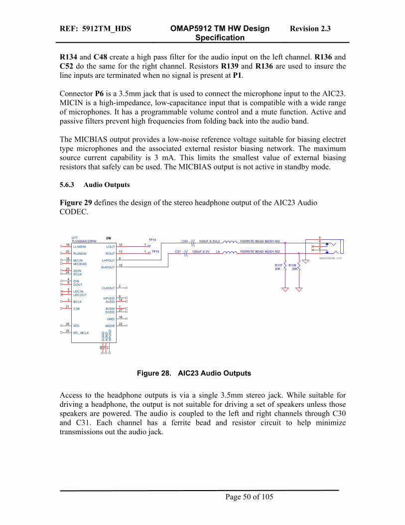
REF: 5912TM_HDS OMAP5912 TM HW Design Specification
Revision 2.3
R134 and C48 create a high pass filter for the audio input on the left channel. R136 and C52 do the same for the right channel. Resistors R139 and R136 are used to insure the line inputs are terminated when no signal is present at P1. Connector P6 is a 3.5mm jack that is used to connect the microphone input to the AIC23. MICIN is a high-impedance, low-capacitance input that is compatible with a wide range of microphones. It has a programmable volume control and a mute function. Active and passive filters prevent high frequencies from folding back into the audio band. The MICBIAS output provides a low-noise reference voltage suitable for biasing electret type microphones and the associated external resistor biasing network. The maximum source current capability is 3 mA. This limits the smallest value of external biasing resistors that safely can be used. The MICBIAS output is not active in standby mode. 5.6.3 Audio Outputs Figure 29 defines the design of the stereo headphone output of the AIC23 Audio CODEC.
12345
TP141
U17TLV320AIC23PW
12
13
19
20
1817
4
5
3
25
26
21
22
127
28
9
10
1115
16
814
2
7
6
2324
LOUT
ROUT
LLINEIN
RLINEIN
MICINMICBIAS
DIN
LRCIN
BCLK
XTL_MCLK
XTO
CS#
MODE
BVDDDVDD
DG
ND
LHPOUT
RHPOUT
HP
GN
DA
GN
D
VMID
HPVDDAVDD
CLKOUT
LRCOUT
DOUT
SDINSCLK
+C50 100UF,6.3V
L4 FERRITE BEAD M2301-ND+C51 100UF,6.3V
HEADPHONE OUT
PW
R13720K
TP151
L3 FERRITE BEAD M2301-ND
R13820K
Figure 28. AIC23 Audio Outputs
Access to the headphone outputs is via a single 3.5mm stereo jack. While suitable for driving a headphone, the output is not suitable for driving a set of speakers unless those speakers are powered. The audio is coupled to the left and right channels through C30 and C31. Each channel has a ferrite bead and resistor circuit to help minimize transmissions out the audio jack.
Page 50 of 105
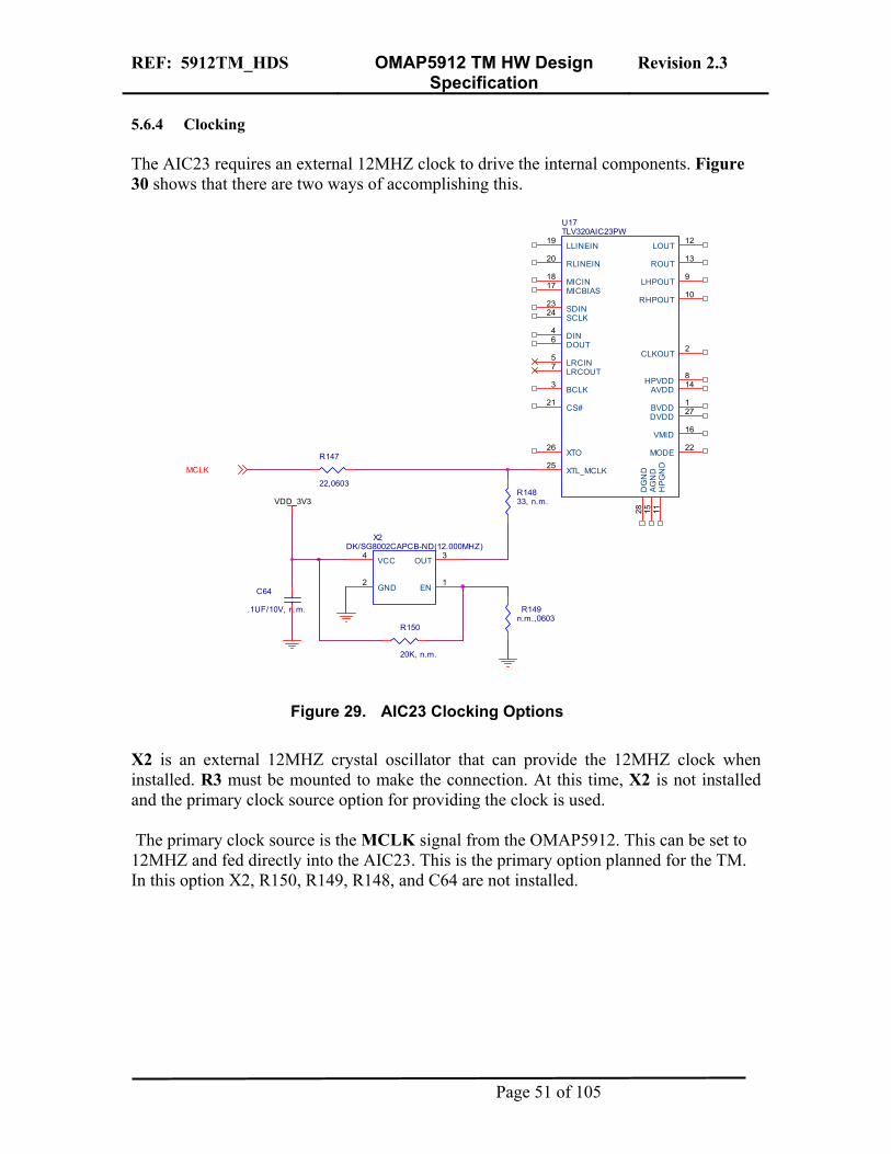
REF: 5912TM_HDS OMAP5912 TM HW Design Specification
Revision 2.3
5.6.4 Clocking The AIC23 requires an external 12MHZ clock to drive the internal components. Figure 30 shows that there are two ways of accomplishing this.
VDD_3V3
X2DK/SG8002CAPCB-ND(12.000MHZ)
3
2 1
4OUT
GND EN
VCC
R150
20K, n.m.
U17TLV320AIC23PW
12
13
19
20
1817
4
5
3
25
26
21
22
127
28
9
10
1115
16
814
2
7
6
2324
LOUT
ROUT
LLINEIN
RLINEIN
MICINMICBIAS
DIN
LRCIN
BCLK
XTL_MCLK
XTO
CS#
MODE
BVDDDVDD
DG
ND
LHPOUT
RHPOUT
HPG
ND
AGN
D
VMID
HPVDDAVDD
CLKOUT
LRCOUT
DOUT
SDINSCLK
R149n.m.,0603
R147
22,0603
C64
.1UF/10V, n.m.
R14833, n.m.
MCLK
Figure 29. AIC23 Clocking Options
X2 is an external 12MHZ crystal oscillator that can provide the 12MHZ clock when installed. R3 must be mounted to make the connection. At this time, X2 is not installed and the primary clock source option for providing the clock is used. The primary clock source is the MCLK signal from the OMAP5912. This can be set to 12MHZ and fed directly into the AIC23. This is the primary option planned for the TM. In this option X2, R150, R149, R148, and C64 are not installed.
Page 51 of 105
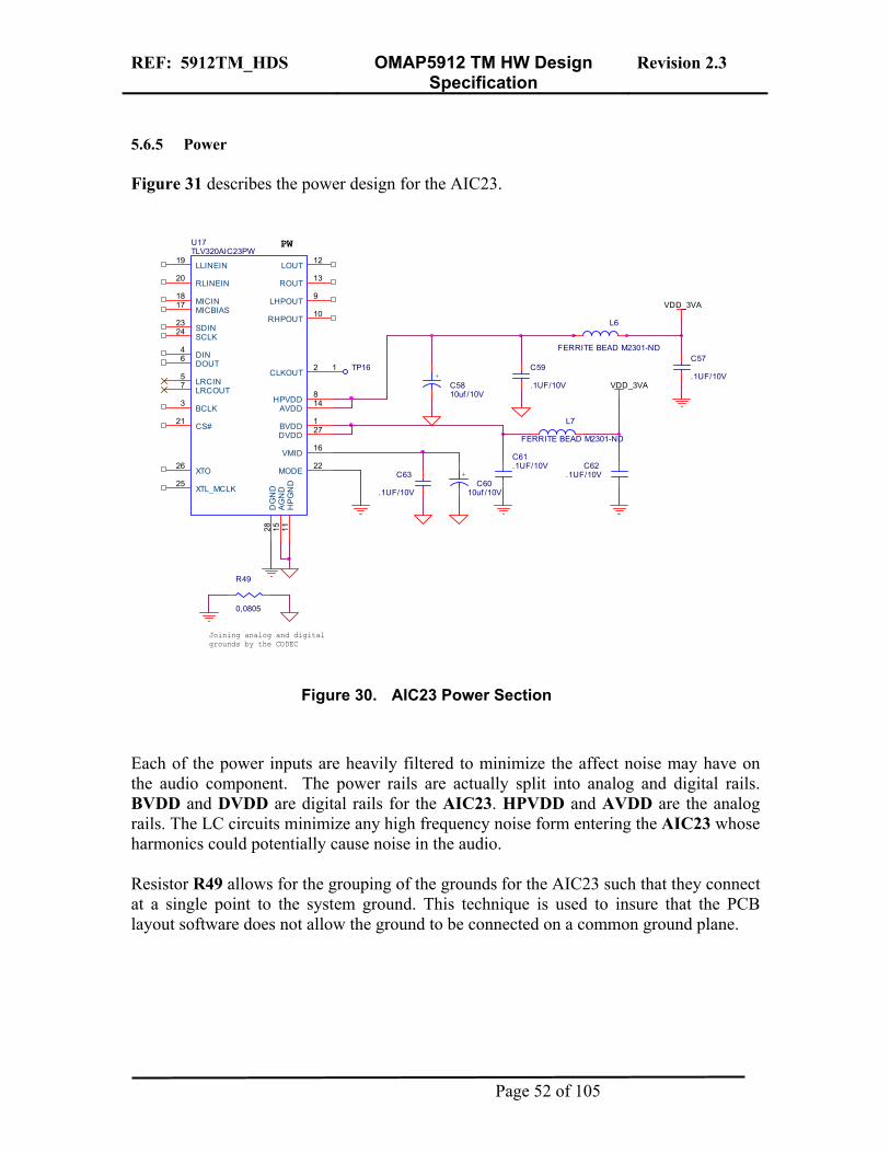
REF: 5912TM_HDS OMAP5912 TM HW Design Specification
Revision 2.3
5.6.5 Power Figure 31 describes the power design for the AIC23.
C62.1UF/10V
R49
0,0805
L6
FERRITE BEAD M2301-ND
+C5810uf /10V
VDD_3VA
TP161
+C60
10uf /10V
C63
.1UF/10V
L7
FERRITE BEAD M2301-ND
C57
.1UF/10V
VDD_3VA
C59
.1UF/10V
PWU17TLV320AIC23PW
12
13
19
20
1817
4
5
3
25
26
21
22
127
28
9
10
1115
16
814
2
7
6
2324
LOUT
ROUT
LLINEIN
RLINEIN
MICINMICBIAS
DIN
LRCIN
BCLK
XTL_MCLK
XTO
CS#
MODE
BVDDDVDD
DG
ND
LHPOUT
RHPOUT
HPG
ND
AGN
D
VMID
HPVDDAVDD
CLKOUT
LRCOUT
DOUT
SDINSCLK
Joining analog and digitalgrounds by the CODEC
C61.1UF/10V
Figure 30. AIC23 Power Section
Each of the power inputs are heavily filtered to minimize the affect noise may have on the audio component. The power rails are actually split into analog and digital rails. BVDD and DVDD are digital rails for the AIC23. HPVDD and AVDD are the analog rails. The LC circuits minimize any high frequency noise form entering the AIC23 whose harmonics could potentially cause noise in the audio. Resistor R49 allows for the grouping of the grounds for the AIC23 such that they connect at a single point to the system ground. This technique is used to insure that the PCB layout software does not allow the ground to be connected on a common ground plane.
Page 52 of 105
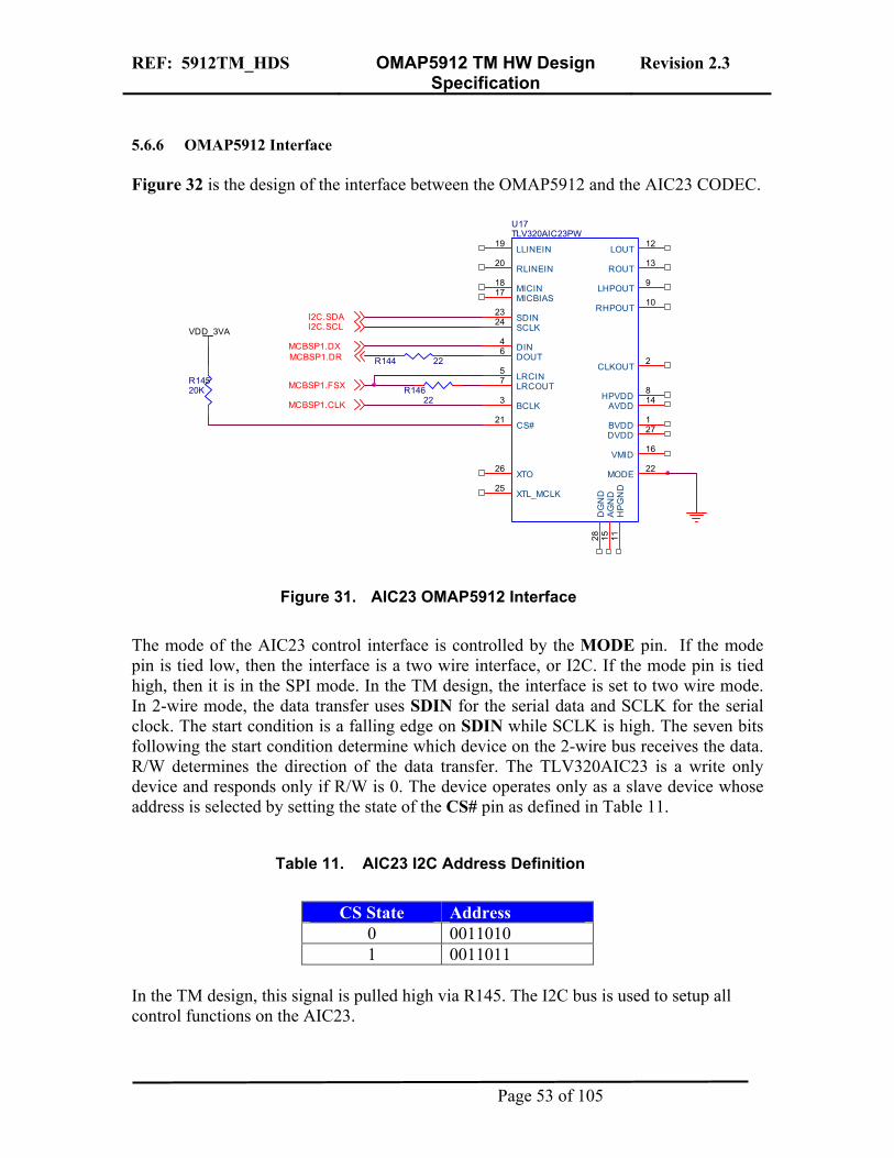
REF: 5912TM_HDS OMAP5912 TM HW Design Specification
Revision 2.3
5.6.6 OMAP5912 Interface Figure 32 is the design of the interface between the OMAP5912 and the AIC23 CODEC.
VDD_3VA
U17TLV320AIC23PW
12
13
19
20
1817
4
5
3
25
26
21
22
127
28
9
10
1115
16
814
2
7
6
2324
LOUT
ROUT
LLINEIN
RLINEIN
MICINMICBIAS
DIN
LRCIN
BCLK
XTL_MCLK
XTO
CS#
MODE
BVDDDVDD
DG
ND
LHPOUT
RHPOUT
HP
GN
DA
GN
D
VMID
HPVDDAVDD
CLKOUT
LRCOUT
DOUT
SDINSCLK
R144 22
R14622
R14520K
MCBSP1.CLK
MCBSP1.DX
I2C.SCLI2C.SDA
MCBSP1.DR
MCBSP1.FSX
Figure 31. AIC23 OMAP5912 Interface
The mode of the AIC23 control interface is controlled by the MODE pin. If the mode pin is tied low, then the interface is a two wire interface, or I2C. If the mode pin is tied high, then it is in the SPI mode. In the TM design, the interface is set to two wire mode. In 2-wire mode, the data transfer uses SDIN for the serial data and SCLK for the serial clock. The start condition is a falling edge on SDIN while SCLK is high. The seven bits following the start condition determine which device on the 2-wire bus receives the data. R/W determines the direction of the data transfer. The TLV320AIC23 is a write only device and responds only if R/W is 0. The device operates only as a slave device whose address is selected by setting the state of the CS# pin as defined in Table 11.
Table 11. AIC23 I2C Address Definition
CS State Address
0 0011010 1 0011011
In the TM design, this signal is pulled high via R145. The I2C bus is used to setup all control functions on the AIC23.
Page 53 of 105
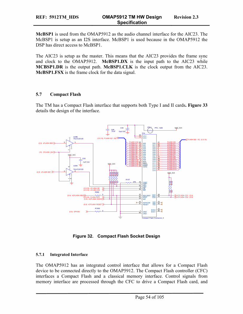
REF: 5912TM_HDS OMAP5912 TM HW Design Specification
Revision 2.3
McBSP1 is used from the OMAP5912 as the audio channel interface for the AIC23. The McBSP1 is setup as an I2S interface. McBSP1 is used because in the OMAP5912 the DSP has direct access to McBSP1. The AIC23 is setup as the master. This means that the AIC23 provides the frame sync and clock to the OMAP5912. McBSP1.DX is the input path to the AIC23 while MCBSP1.DR is the output path. McBSP1.CLK is the clock output from the AIC23. McBSP1.FSX is the frame clock for the data signal. 5.7 Compact Flash The TM has a Compact Flash interface that supports both Type I and II cards. Figure 33 details the design of the interface.
C85.01uF
VDD_3V3
R10
510
K
R10
810
K
PTC1 PTC, 1206
R29
21K
R29
31K
R10
410
K
U20B74LVC2G125
5 3
7
VDD_3V3
R9990
R10747K
VDD_3V3
P14
Compact Flash Connector_0
1
23456
7
8
9
101112
13
141516171819
212223
242526
2728293031
32
33
36
37
38
39
4041
42
43
4546
474849
50 GND
D03D04D05D06D07
CE1
A10
OE
A09A08A07
VCC
A06A05A04A03A02A01A00 D00
D01D02
WPCD2CD1
D11D12D13D14D15
CE2
VS1
IORDIOWR
WE
RDY/BSY
VCC
CSEL
VS2RESET
WAIT
INPACK#
REG
BVD2BVD1
D08D09D10
GND
VDD_3V3
C83
.1UF/10V
U20A
74LVC2G1252 6
18
4
R10
910
K
R10
610
K
R10000
+C44
10uf /10V
nFLASH.WE(2,9,10)
FLASH.D11
FLASH.A3
nCFLASH.CD2 (5,9)
FLASH.D5
FLASH.A14
FLASH.D3
FLASH.D7
nFLASH.BE1(2,9)
FLASH.A13
FLASH.D8
nFLASH.BE0(2,9)
FLASH.D15
FLASH.RDY(2,9,10)
FLASH.D4
FLASH.A[1..25](2,9,10)
FLASH.D1
FLASH.A5
FLASH.A9
FLASH.D[0..15] (2,9,10)
FLASH.A11
CFLASH_EN(10)
FLASH.D13
FLASH.A4
FLASH.A6FLASH.A7
FLASH.D14
FLASH.A2
nCFLASH.RESET(5,9)
FLASH.D10
20
343544
FLASH.D9
nCFLASH.CD1 (5,9)
FLASH.D2
nFLASH.OE(2,9,10)
FLASH.A12
FLASH.D6
GPIO62(5,9)
FLASH.D0
FLASH.A8
FLASH.A1
FLASH.A10
FLASH.D12
nCFLASH.IOIS16(5,9)
nCFLASH.IREQ(5,9)
Figure 32. Compact Flash Socket Design
5.7.1 Integrated Interface The OMAP5912 has an integrated control interface that allows for a Compact Flash device to be connected directly to the OMAP5912. The Compact Flash controller (CFC) interfaces a Compact Flash and a classical memory interface. Control signals from memory interface are processed through the CFC to drive a Compact Flash card, and
Page 54 of 105
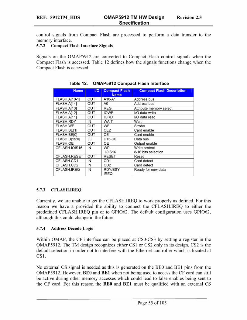
REF: 5912TM_HDS OMAP5912 TM HW Design Specification
Revision 2.3
control signals from Compact Flash are processed to perform a data transfer to the memory interface. 5.7.2 Compact Flash Interface Signals Signals on the OMAP5912 are converted to Compact Flash control signals when the Compact Flash is accessed. Table 12 defines how the signals functions change when the Compact Flash is accessed.
Table 12. OMAP5912 Compact Flash Interface Name I/O Compact Flash
Name Compact Flash Description
FLASH.A[10-1] OUT A10-A1 Address bus FLASH.A[14] OUT A0 Address bus FLASH.A[13] OUT REG Attribute memory select FLASH.A[12] OUT IOWR I/O data write FLASH.A[11] OUT IORD I/O data read FLASH.RDY IN WAIT Wait FLASH.WE OUT WE Strobe FLASH.BE[1] OUT CE2 Card enable FLASH.BE[0] OUT CE1 Card enable FLASH.D[15:0] I/O D15-D0 Data bus FLASH.OE OUT OE Output enable CFLASH.IOIS16 IN WP
IOIS16 Write protect 8/16 bits selection
CFLASH.RESET OUT RESET Reset CFLASH.CD1 IN CD1 Card detect CFLASH.CD2 IN CD2 Card detect CFLASH.IREQ IN RDY/BSY
IREQ Ready for new data
5.7.3 CFLASH.IREQ Currently, we are unable to get the CFLASH.IREQ to work properly as defined. For this reason we have a provided the ability to connect the CFLASH.IREQ to either the predefined CFLASH.IREQ pin or to GPIO62. The default configuration uses GPIO62, although this could change in the future. 5.7.4 Address Decode Logic Within OMAP, the CF interface can be placed at CS0-CS3 by setting a register in the OMAP5912. The TM design recognizes either CS1 or CS2 only in its design. CS2 is the default selection in order not to interfere with the Ethernet controller which is located at CS1. No external CS signal is needed as this is generated on the BE0 and BE1 pins from the OMAP5912. However, BE0 and BE1 when not being used to access the CF card can still be active during other memory accesses which could lead to false enables being sent to the CF card. For this reason the BE0 and BE1 must be qualified with an external CS
Page 55 of 105
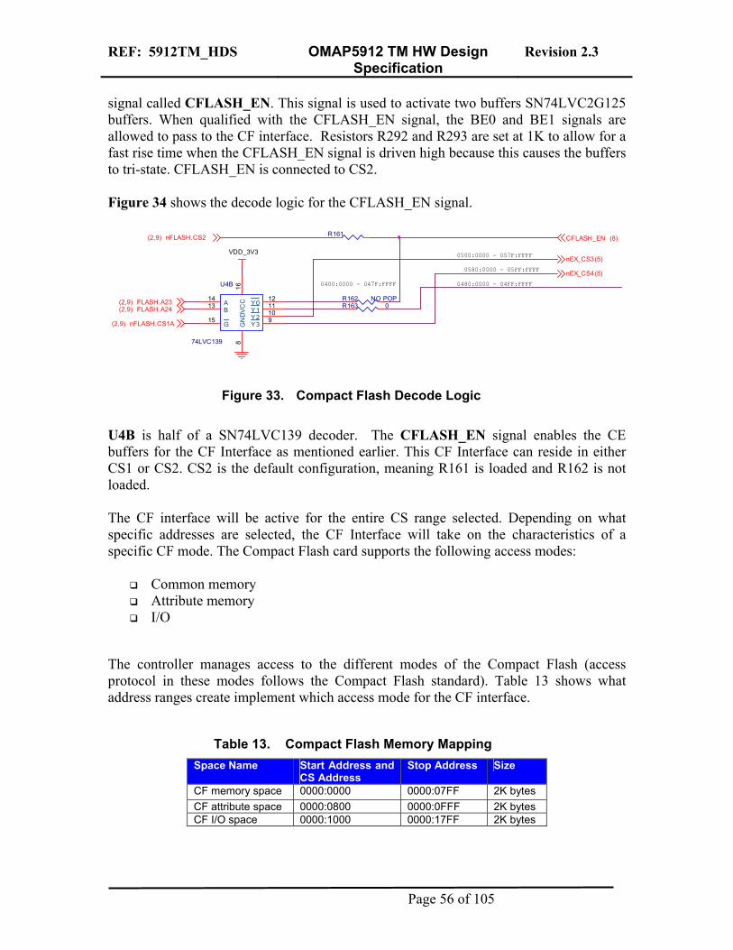
REF: 5912TM_HDS OMAP5912 TM HW Design Specification
Revision 2.3
signal called CFLASH_EN. This signal is used to activate two buffers SN74LVC2G125 buffers. When qualified with the CFLASH_EN signal, the BE0 and BE1 signals are allowed to pass to the CF interface. Resistors R292 and R293 are set at 1K to allow for a fast rise time when the CFLASH_EN signal is driven high because this causes the buffers to tri-state. CFLASH_EN is connected to CS2. Figure 34 shows the decode logic for the CFLASH_EN signal.
R162R163 0
R161
NO POP
VDD_3V3
0400:0000 - 047F:FFFF
0500:0000 - 057F:FFFF
0480:0000 - 04FF:FFFF
0580:0000 - 05FF:FFFF
U4B
74LVC139
1413
15
1211109
168
AB
G
Y0Y1Y2Y3
VC
CG
ND
FLASH.A23(2,9)
nFLASH.CS1A(2,9)
CFLASH_EN (8)
FLASH.A24(2,9)
nFLASH.CS2(2,9)
nEX_CS4(5)
nEX_CS3(5)
Figure 33. Compact Flash Decode Logic
U4B is half of a SN74LVC139 decoder. The CFLASH_EN signal enables the CE buffers for the CF Interface as mentioned earlier. This CF Interface can reside in either CS1 or CS2. CS2 is the default configuration, meaning R161 is loaded and R162 is not loaded. The CF interface will be active for the entire CS range selected. Depending on what specific addresses are selected, the CF Interface will take on the characteristics of a specific CF mode. The Compact Flash card supports the following access modes:
Common memory Attribute memory I/O
The controller manages access to the different modes of the Compact Flash (access protocol in these modes follows the Compact Flash standard). Table 13 shows what address ranges create implement which access mode for the CF interface.
Table 13. Compact Flash Memory Mapping Space Name Start Address and
CS Address Stop Address Size
CF memory space 0000:0000 0000:07FF 2K bytes CF attribute space 0000:0800 0000:0FFF 2K bytes CF I/O space 0000:1000 0000:17FF 2K bytes
Page 56 of 105
REF: 5912TM_HDS OMAP5912 TM HW Design Specification
Revision 2.3
5.7.5 Databus Interface The databus is connected to the CF Interface and is used as with any normal memory device interface. 5.7.6 Power interface Power to the CF Interface is supplied by the 3.3V supply. PTC1 is a self healing current limiting device. This is provided in lieu of a fuse device. When the current exceeds 1A max, the resistance of the PTC will go up, limiting the current to the CF Interface. The hold current, is specified at 500ma. 5.8 JTAG/MultiICE Interface A single standard 14 pin JTAG connector is provided on the design to allow access to the JTAG interface of the OMAP 5.8.1 JTAG/MultiICE Features The JTAG/MultiICE interface provides the following features:
JTAG port Buffer Standard 14 pin JTAG connector 20 Pin MultiICE Connector Ability to reset the ARM processor for the Multi ICE interface Strappable JTAG reset nTRST pull down Disable pin for ADM shutdown
5.8.2 Design Description Figure 35 is the design of the JTAG interface on the TM.
Page 57 of 105
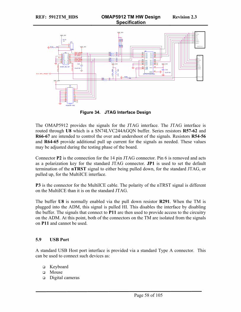
REF: 5912TM_HDS OMAP5912 TM HW Design Specification
Revision 2.3
71
R67 33
67
P2
EHDR_SM_14P
1234567891011121314
12345678910
11121314
TMSTDI
R55
100K
73
TMS
C23
.01uF/10V
TDOR13
U16
R133 10K
nEMU1
R61 33
JTAG_DIS
VDD_3V3
TCK
nEMU0N11
VDD_3V3
70
U17
C22
.01uF/10V
R58 33
P3
HEADER 10X2
135791113151719
2468
101214161820
R54
100K
RTCK
M10
R56
100K
VDD_3V3
TCK
R66 33
R60 33
R65
4.7K
R1191K
74
nTRST
VDD_3V3
75
76
R59 33
R64
4.7K
P11
JP1
CON3
123
VDD_3V3
TDIP13
RTCK
R29110K
T15
nTRST
nEMU1
69
OMAP5912
TDO
R62 33
VDD_3V3
SN74LVC244AGQN
U8
B3C2D3E2
E4D4C4B4
B2C3D2E3
D1C1B1A1
A3A4
E1
A22Y42Y32Y22Y1
1Y41Y31Y21Y1
2A42A32A22A1
1A41A31A21A1
VCC2OE
GND
1OE
T14
72 nEMU0
R57 33
TRST_MAINn
JTA
G_E
MU
0
TMS_MAIN
JTAG
_EM
U1
TCKR_MAIN
MPU_nRESETSh.6
TDO_MAIN
TCK_MAIN
TDI_MAIN
Figure 34. JTAG Interface Design
The OMAP5912 provides the signals for the JTAG interface. The JTAG interface is routed through U8 which is a SN74LVC244AGQN buffer. Series resistors R57-62 and R66-67 are intended to control the over and undershoot of the signals. Resistors R54-56 and R64-65 provide additional pull up current for the signals as needed. These values may be adjusted during the testing phase of the board. Connector P2 is the connection for the 14 pin JTAG connector. Pin 6 is removed and acts as a polarization key for the standard JTAG connector. JP1 is used to set the default termination of the nTRST signal to either being pulled down, for the standard JTAG, or pulled up, for the MultiICE interface. P3 is the connector for the MultiICE cable. The polarity of the nTRST signal is different on the MultiICE than it is on the standard JTAG. The buffer U8 is normally enabled via the pull down resistor R291. When the TM is plugged into the ADM, this signal is pulled HI. This disables the interface by disabling the buffer. The signals that connect to P11 are then used to provide access to the circuitry on the ADM. At this point, both of the connectors on the TM are isolated from the signals on P11 and cannot be used. 5.9 USB Port A standard USB Host port interface is provided via a standard Type A connector. This can be used to connect such devices as:
Keyboard Mouse Digital cameras
Page 58 of 105
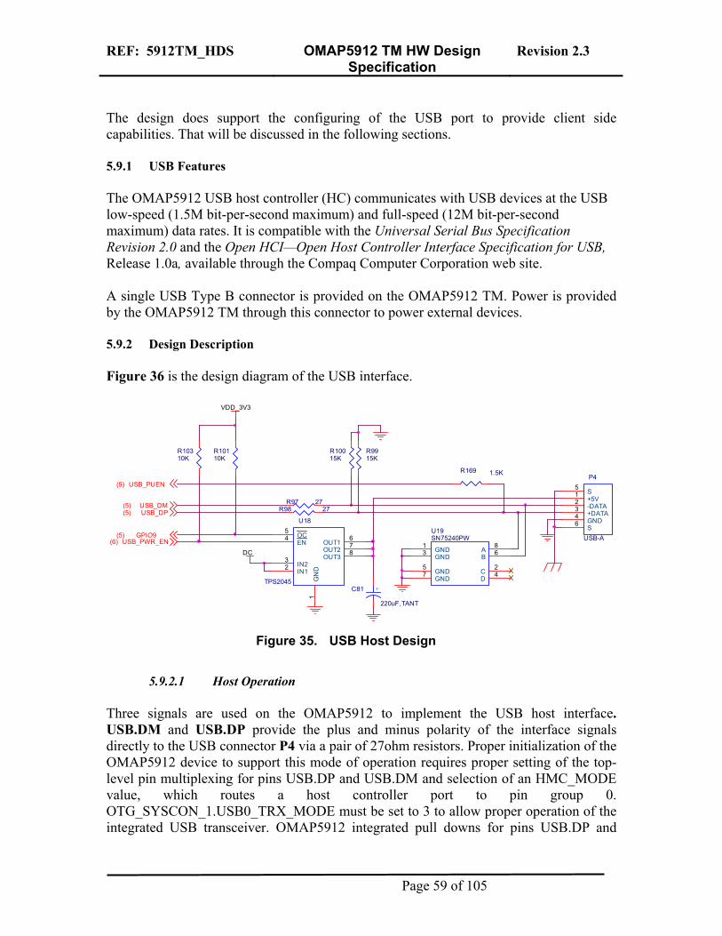
REF: 5912TM_HDS OMAP5912 TM HW Design Specification
Revision 2.3
The design does support the configuring of the USB port to provide client side capabilities. That will be discussed in the following sections. 5.9.1 USB Features The OMAP5912 USB host controller (HC) communicates with USB devices at the USB low-speed (1.5M bit-per-second maximum) and full-speed (12M bit-per-second maximum) data rates. It is compatible with the Universal Serial Bus Specification Revision 2.0 and the Open HCI—Open Host Controller Interface Specification for USB, Release 1.0a, available through the Compaq Computer Corporation web site. A single USB Type B connector is provided on the OMAP5912 TM. Power is provided by the OMAP5912 TM through this connector to power external devices. 5.9.2 Design Description Figure 36 is the design diagram of the USB interface.
R9915K
DC
U19SN75240PW
1
2
3
45
6
7
8GND
C
GND
DGND
B
GND
A
R10015K
+C81
220uF,TANT
R169 1.5K
R10110K
R98 27
R10310K
R97 27
U18
TPS2045
1
23
54 6
78
GN
DIN1IN2
OCEN OUT1
OUT2OUT3
VDD_3V3
P4
USB-A
1234
5
6
+5V-DATA+DATAGND
S
S
USB_DM(5)USB_DP(5)
USB_PWR_EN(6)GPIO9(5)
USB_PUEN(5)
Figure 35. USB Host Design
5.9.2.1 Host Operation
Three signals are used on the OMAP5912 to implement the USB host interface. USB.DM and USB.DP provide the plus and minus polarity of the interface signals directly to the USB connector P4 via a pair of 27ohm resistors. Proper initialization of the OMAP5912 device to support this mode of operation requires proper setting of the top-level pin multiplexing for pins USB.DP and USB.DM and selection of an HMC_MODE value, which routes a host controller port to pin group 0. OTG_SYSCON_1.USB0_TRX_MODE must be set to 3 to allow proper operation of the integrated USB transceiver. OMAP5912 integrated pull downs for pins USB.DP and
Page 59 of 105
REF: 5912TM_HDS OMAP5912 TM HW Design Specification
Revision 2.3
USB.DM do not meet the USB specifications for D+ and D– pull downs. The external 15K pull down resistors, R199 and R100, are implemented to meet this requirement. USB.PUEN is used in the GPIO mode to detect the over current mode. Proper initialization of the OMAP5912 device to support this mode of operation on pin P4 requires proper setting of the top-level pin multiplexing. Resistor R169 is not required for the Host mode of operation, which is the default mode of the design. If Client mode is required, an external adapter can be purchased that will connect to P4 and convert it to the client gender (See section 7.1.11). R169 is used to signal the host that it is active and wishes to be identified. This does not interfere with host operation as the USB.PUEN is not activated via software. To select USB Host, GPIO9 needs to be high (default selection), and ball P4 on OMAP5912 (USB.PUEN) needs to be placed into high Z state (by setting FUNC_MUX_CTRL_D[5:3] = 100) in order to negate the impact of the 1.5k ohm resistor pull up on the D+ signal. To select USB Client(Function) (with the use of an external adapter), GPIO9 must be low, and the USB.PUEN signal must be muxed onto the P4 ball (set FUNC_MUX_CTRL_D[5:3] = 000). U16 is a TPS2014 is a power distribution switch. The TPS2014 power distribution switches are intended for applications where heavy capacitive loads and short circuits are likely to be encountered. The high-side switch is a 95-mW n-channel MOSFET. The switch is controlled by a logic enable that is compatible with 3-V logic. Gate drive is provided by an internal charge pump designed to control the power switch rise times and fall times to minimize current surges during switching. The charge pump requires no external components and allows operation from supplies as low as 4 V. When the output load exceeds the current-limit threshold or a short is present, the TPS2014 limits the output current to a safe level by switching into a constant-current mode, and the over current logic output is set to low. Continuous heavy overloads and short circuits will increase the power dissipation in the switch and cause the junction temperature to rise. A thermal protection circuit is implemented, which shuts the switch off to prevent damage when the junction temperature exceeds its thermal limit. An under voltage lockout is provided to ensure the switch is in the off state at start-up. The TPS2014 is designed to limit at 1.2 A. C81 is a low ESR capacitor required for the output of the TPS2014. U19 is a USB port transient protection device. The SN75240 is a dual transient voltage suppressors designed to provide additional electrical noise transient protection to two USB ports. Any cabled I/O can be subjected to electrical noise transients from various sources. These noise transients can cause damage to the OMAP5912 if they are of sufficient magnitude and duration. The SN75240 significantly increase the port ESD protection level and reduce the risk of damage to the large and expensive circuits of the USB port.
Page 60 of 105
REF: 5912TM_HDS OMAP5912 TM HW Design Specification
Revision 2.3
U10 is the TPS65010 power management device. In order to save as many GPIO pins on the OMAP5912 as possible, the GPIO pin on the TPS65010 was used as the enable pin for the TPS2014. A high on EN turns off the power switch and the bias for the charge pump, driver, and other circuitry to reduce the supply current to less than 10 mA. A logic zero input restores bias to the drive and control circuits and turns the power on. To access the GPIO pin on the TPS65010, the I2C interface is used to communicate to the GPIO pin. Access to the USB.DM, USB.DP, and USB.PUEN (GPIO58) can be obtained via the B connector P10 if use by the expansion cards or ADM is desired. In order for this to happen, the nothing can be plugged into the USB connector P4.
5.9.2.2 Client Operation With the use of an adapter, the USB interface can be converted for use as a client interface. Refer to Figure 36. Resistor R169 is connected to the USB_PUEN signal. This is required to activate the client interface. In the host mode, this pin is left tri-stated. By default U18 is not enabled. This must be left disabled in the client mode. The adapter is defined in the pin out section of the document. 5.10 Serial Port Access to a single serial port with an RS232 level driver via a DB9 connector will be provided. This will be used for downloading and connection to a serial debugger or terminal device. 5.10.1 Features Features of the serial interface are:
OMAP5912 UART1 connection default OMAP5912 UART3 connection optional 240K Baud Max speed DB9 Male Connector Disable pin accessible via the expansion connectors TX,RX signals Ground
5.10.2 Design Description Figure 37 is the design diagram of the serial interface.
Page 61 of 105
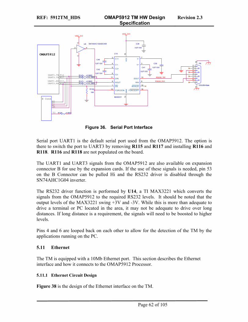
REF: 5912TM_HDS OMAP5912 TM HW Design Specification
Revision 2.3
UART3.RX
C41
.1UF/10V
R102
10K
43
R116 n.m.,0603
U14
MAX3221
1
2
4
5
6
8
1415
16
3
7
9
13
10
12
11
EN
C1+
C1-
C2+
C2-
RIN
GN
DV
CC
FORCEOFF
V+
V-
ROUT
DOUT
INVALID
FORCEON
DIN
OMAP5912
4742
R117 0,0603
C38
.1UF/10V
45
U13
C39
.1UF/10V
K17
U6 SN74AHC1G04DCKR
2 4
53
T12
K15
B Conn
R115 0,0603
53
P8
DSUB9-Male
594837261
1011
UART1.TXUART3.TX
R118 n.m.,0603
C40
.1UF/10V
R120 0,0603
UART1.RX
C42
.1UF/10V
VDD_3V3
RS232_TX1
VDD_3V3
RS232_RX1
Figure 36. Serial Port Interface
Serial port UART1 is the default serial port used from the OMAP5912. The option is there to switch the port to UART3 by removing R115 and R117 and installing R116 and R118. R116 and R118 are not populated on the board. The UART1 and UART3 signals from the OMAP5912 are also available on expansion connector B for use by the expansion cards. If the use of these signals is needed, pin 53 on the B Connector can be pulled Hi and the RS232 driver is disabled through the SN74AHC1G04 inverter. The RS232 driver function is performed by U14, a TI MAX3221 which converts the signals from the OMAP5912 to the required RS232 levels. It should be noted that the output levels of the MAX3221 swing +3V and -3V. While this is more than adequate to drive a terminal or PC located in the area, it may not be adequate to drive over long distances. If long distance is a requirement, the signals will need to be boosted to higher levels. Pins 4 and 6 are looped back on each other to allow for the detection of the TM by the applications running on the PC. 5.11 Ethernet The TM is equipped with a 10Mb Ethernet port. This section describes the Ethernet interface and how it connects to the OMAP5912 Processor. 5.11.1 Ethernet Circuit Design Figure 38 is the design of the Ethernet interface on the TM.
Page 62 of 105
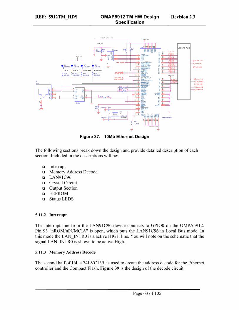
REF: 5912TM_HDS OMAP5912 TM HW Design Specification
Revision 2.3
R130 5.1
TXLED
VDD_3V3
R124330, 0603
Chip Select
BSELED
OMAP5912R12210K
VDD_3V3
D6LED,YEL
D7LED, GRN
P9RJ45
12345678
10 9
A1A2A3A4A5A6A7A8S0 S1
R9610K
U12
LAN91C96-TQFP
99
12345
78910
11
12131415
1718
19
2021232425
2627283031323334353637
38
394041424344454647
48
4950515253
55565758
59
60616263
656667686970
71
72
737475
7677
79
80818283848588
89
90919394959697
98
100
6 22 29 54 64 92 16 78 86 87
IOS2
ENEEPEEDO/SDOUTEEDIEECSEESK
D8D9
D10D11
VDD
D12D13D14D15
INTR0/IREQ/INTRINTR1/INPACK
VDD
INTR2/DTACK/0INTR3/DTACT/1IOCS16/IOIS16SBHE/CE2BALE/WE
A0A1A2A3A4A5A6A7A8A9
A10/FWE
VDD
A11/FCSA12A13A14A15A16A17A18
A19/CE1
VDD
IORD/XDSIOWR/R/WMEM/OEAEN/REG/ASIOCHRDY/WAIT
D0D1D2D3
VDD
D4D5D6D7
RESETPWRDWN/TXCLKBSELED/RXDLNKLED/TXDRXLED/RXCLKTXLED/TXEN
AVD
D
TPETXDP
TPETXNTPETXDNTPETXP
TXN/CRSTXP/COLL
AVD
D
COLNCOLPRECNRECPTPERXNTPERXPRBIAS
AVD
D
XENDECEN16OM/PCMCIAXTAL1XTAL2IOS0IOS1
VDD
GN
DG
ND
GN
DG
ND
GN
DG
ND
GN
DG
ND
AG
ND
AG
ND
AG
ND
R129 13
R160
0, 0603
D8LED,YEL
D5LED,RED
VDD_3V3
LINKLEDR126330, 0603
Y3
FXP200-2020.000MHZ
123
4
R13222K
C7920pf ,10V
R127 13
GROUNDED PINS
R125330, 0603
U13AT93C46
12
34
5
67
8
CSSK
DIDO
GN
D
ORGDC
VC
C
R131 100
C7820pf ,10V
RXLED
C43.01uF/10V
VDD_3V3
R12110K
R128 5.1
R123330, 0603
T1
E2009
8
6
9
11 141216
3
15TD+
TD-
RD+
RD- RX-RXCT
RX+
TX-
TX+TXCT
nFLASH.CS1A
FLASH.D1
nFLASH.OE
FLASH.D10
LAN_INTR0FLASH.D9
FLASH.D4
FLASH.D2
LAN_RESET
nFLASH.OE
FLASH.D7
FLASH.RDY
FLASH.A23
FLASH.D6FLASH.D5
FLASH.RDYFLASH.A3
nFLASH.WE
FLASH.A24
FLASH.D15
FLASH.D8
FLASH.A2
nFLASH.WE
FLASH.D11
FLASH.A1
FLASH.D14FLASH.D13
FLASH.D3
LAN_RESET LAN_INTRO
FLASH.D12
FLASH.D0
Figure 37. 10Mb Ethernet Design
The following sections break down the design and provide detailed description of each section. Included in the descriptions will be:
Interrupt Memory Address Decode LAN91C96 Crystal Circuit Output Section EEPROM Status LEDS
5.11.2 Interrupt The interrupt line from the LAN91C96 device connects to GPIO0 on the OMPA5912. Pin 93 "nROM/nPCMCIA" is open, which puts the LAN91C96 in Local Bus mode. In this mode the LAN_INTR0 is a active HIGH line. You will note on the schematic that the signal LAN_INTR0 is shown to be active High. 5.11.3 Memory Address Decode The second half of U4, a 74LVC139, is used to create the address decode for the Ethernet controller and the Compact Flash. Figure 39 is the design of the decode circuit.
Page 63 of 105
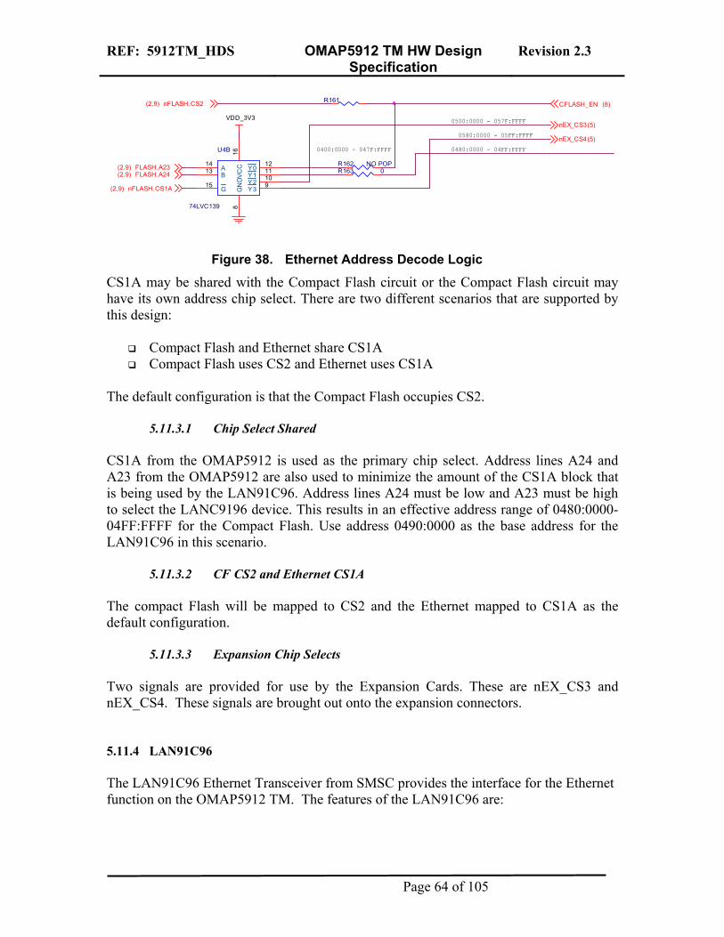
REF: 5912TM_HDS OMAP5912 TM HW Design Specification
Revision 2.3
R162R163 0
R161
NO POP
VDD_3V3
0400:0000 - 047F:FFFF
0500:0000 - 057F:FFFF
0480:0000 - 04FF:FFFF
0580:0000 - 05FF:FFFF
U4B
74LVC139
1413
15
1211109
168
AB
G
Y0Y1Y2Y3
VC
CG
ND
FLASH.A23(2,9)
nFLASH.CS1A(2,9)
CFLASH_EN (8)
FLASH.A24(2,9)
nFLASH.CS2(2,9)
nEX_CS4(5)
nEX_CS3(5)
Figure 38. Ethernet Address Decode Logic
CS1A may be shared with the Compact Flash circuit or the Compact Flash circuit may have its own address chip select. There are two different scenarios that are supported by this design:
Compact Flash and Ethernet share CS1A Compact Flash uses CS2 and Ethernet uses CS1A
The default configuration is that the Compact Flash occupies CS2.
5.11.3.1 Chip Select Shared CS1A from the OMAP5912 is used as the primary chip select. Address lines A24 and A23 from the OMAP5912 are also used to minimize the amount of the CS1A block that is being used by the LAN91C96. Address lines A24 must be low and A23 must be high to select the LANC9196 device. This results in an effective address range of 0480:0000-04FF:FFFF for the Compact Flash. Use address 0490:0000 as the base address for the LAN91C96 in this scenario.
5.11.3.2 CF CS2 and Ethernet CS1A The compact Flash will be mapped to CS2 and the Ethernet mapped to CS1A as the default configuration.
5.11.3.3 Expansion Chip Selects Two signals are provided for use by the Expansion Cards. These are nEX_CS3 and nEX_CS4. These signals are brought out onto the expansion connectors. 5.11.4 LAN91C96 The LAN91C96 Ethernet Transceiver from SMSC provides the interface for the Ethernet function on the OMAP5912 TM. The features of the LAN91C96 are:
Page 64 of 105
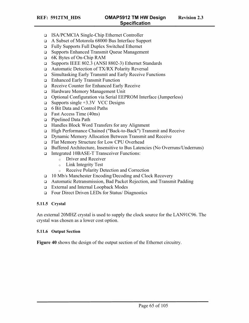
REF: 5912TM_HDS OMAP5912 TM HW Design Specification
Revision 2.3
ISA/PCMCIA Single-Chip Ethernet Controller A Subset of Motorola 68000 Bus Interface Support Fully Supports Full Duplex Switched Ethernet Supports Enhanced Transmit Queue Management 6K Bytes of On-Chip RAM Supports IEEE 802.3 (ANSI 8802-3) Ethernet Standards Automatic Detection of TX/RX Polarity Reversal Simultasking Early Transmit and Early Receive Functions Enhanced Early Transmit Function Receive Counter for Enhanced Early Receive Hardware Memory Management Unit Optional Configuration via Serial EEPROM Interface (Jumperless) Supports single +3.3V VCC Designs 6 Bit Data and Control Paths Fast Access Time (40ns) Pipelined Data Path Handles Block Word Transfers for any Alignment High Performance Chained ("Back-to-Back") Transmit and Receive Dynamic Memory Allocation Between Transmit and Receive Flat Memory Structure for Low CPU Overhead Buffered Architecture, Insensitive to Bus Latencies (No Overruns/Underruns) Integrated 10BASE-T Transceiver Functions:
o Driver and Receiver o Link Integrity Test o Receive Polarity Detection and Correction
10 Mb/s Manchester Encoding/Decoding and Clock Recovery Automatic Retransmission, Bad Packet Rejection, and Transmit Padding External and Internal Loopback Modes Four Direct Driven LEDs for Status/ Diagnostics
5.11.5 Crystal An external 20MHZ crystal is used to supply the clock source for the LAN91C96. The crystal was chosen as a lower cost option. 5.11.6 Output Section Figure 40 shows the design of the output section of the Ethernet circuitry.
Page 65 of 105
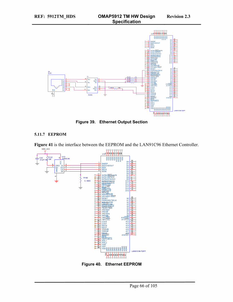
REF: 5912TM_HDS OMAP5912 TM HW Design Specification
Revision 2.3
R128 5.1
P9RJ45
12345678
10 9
A1A2A3A4A5A6A7A8S
0S
1
R131 100
R130 5.1R129 13
T1
E2009
8
6
9
11 141216
3
15TD+
TD-
RD+
RD- RX-RXCT
RX+
TX-
TX+TXCT
R127 13
U12
LAN91C96-TQFP
99
12345
78910
11
12131415
1718
19
2021232425
2627283031323334353637
38
394041424344454647
48
4950515253
55565758
59
60616263
656667686970
71
72
737475
7677
79
80818283848588
89
90919394959697
98
100
6 22 29 54 64 92 16 78 86 87
IOS2
ENEEPEEDO/SDOUTEEDIEECSEESK
D8D9
D10D11
VD
D
D12D13D14D15
INTR0/IREQ/INTRINTR1/INPACK
VD
D
INTR2/DTACK/0INTR3/DTACT/1IOCS16/IOIS16SBHE/CE2BALE/WE
A0A1A2A3A4A5A6A7A8A9
A10/FWE
VD
D
A11/FCSA12A13A14A15A16A17A18
A19/CE1
VD
D
IORD/XDSIOWR/R/WMEM/OEAEN/REG/ASIOCHRDY/WAIT
D0D1D2D3
VD
D
D4D5D6D7
RESETPWRDWN/TXCLKBSELED/RXDLNKLED/TXDRXLED/RXCLKTXLED/TXEN
AV
DD
TPETXDP
TPETXNTPETXDNTPETXP
TXN/CRSTXP/COLL
AV
DD
COLNCOLPRECNRECPTPERXNTPERXPRBIAS
AV
DD
XENDECEN16OM/PCMCIAXTAL1XTAL2IOS0IOS1
VD
D
GN
DG
ND
GN
DG
ND
GN
DG
ND
GN
DG
ND
AG
ND
AG
ND
AG
ND
Figure 39. Ethernet Output Section
5.11.7 EEPROM Figure 41 is the interface between the EEPROM and the LAN91C96 Ethernet Controller.
R12210K
C43.01uF/10V
VDD_3V3
R160
0, 0603
U12
LAN91C96-TQFP
99
12345
78910
11
12131415
1718
19
2021232425
2627283031323334353637
38
394041424344454647
48
4950515253
55565758
59
60616263
656667686970
71
72
737475
7677
79
80818283848588
89
90919394959697
98
100
6 22 29 54 64 92 16 78 86 87
IOS2
ENEEPEEDO/SDOUTEEDIEECSEESK
D8D9
D10D11
VD
D
D12D13D14D15
INTR0/IREQ/INTRINTR1/INPACK
VD
D
INTR2/DTACK/0INTR3/DTACT/1IOCS16/IOIS16SBHE/CE2BALE/WE
A0A1A2A3A4A5A6A7A8A9
A10/FWE
VD
D
A11/FCSA12A13A14A15A16A17A18
A19/CE1
VD
D
IORD/XDSIOWR/R/WMEM/OEAEN/REG/ASIOCHRDY/WAIT
D0D1D2D3
VD
D
D4D5D6D7
RESETPWRDWN/TXCLKBSELED/RXDLNKLED/TXDRXLED/RXCLKTXLED/TXEN
AVD
D
TPETXDP
TPETXNTPETXDNTPETXP
TXN/CRSTXP/COLL
AVD
D
COLNCOLPRECNRECPTPERXNTPERXPRBIAS
AVD
D
XENDECEN16OM/PCMCIAXTAL1XTAL2IOS0IOS1
VD
D
GN
DG
ND
GN
DG
ND
GN
DG
ND
GN
DG
ND
AGN
DAG
ND
AGN
D
U13AT93C46
12
34
5
67
8
CSSK
DIDO
GN
D
ORGDC
VCC
Figure 40. Ethernet EEPROM
Page 66 of 105

REF: 5912TM_HDS OMAP5912 TM HW Design Specification
Revision 2.3
The LAN91C96 has the ability to retrieve configuration information from a serial EEPROM on reset or power-up. The serial EPROM acts as storage of configuration and IEEE Ethernet address information. The device used is the AT93C46 EEPROM from Atmel. The AT93C46 provides 1024bits of serial electrically erasable programmable read only memory (EEPROM) organized as 64words of 16 bits each. The ORG pin is pulled high which controls the bit configuration. Pin 1 on the LAN91C96 is the EEPROM enabled pin. It has an internal pull-up in the LAN91C96. If the EEPROM is not to be used, then R160 must be populated. The default is that R160 is not installed. Power for the AT93C46 is provided by the 3.3V voltage rail which is the same rail as is used by the LAN91C96. 5.11.8 Status LEDS There are four status LEDS on the LAN91C96 device. Table 14 defines the meaning of each LED and the corresponding color for each LED and how each of the status LEDS are used by the LANC9196.
Table 14. Ethernet Status LEDs
LED Function TX Activated by transmit activity. RX Activated by receive activity. LINK Reflects the link integrity status. BSE Board select LED. Activated when the board space is
accessed, namely on accesses to the LAN91C96 register space or the ROM area decoded by the LAN91C96. The signal is stretched to 125ms.
6.0 Expansion Connectors This section defines the type and pinout of the expansion connectors for the system. In order to insure proper operation of the system, the functions of each pin on the connector is being fixed. Not all pins on the connectors will be used by all processors. A lot of the pins have multiple functions that they can perform. All of these expansion cards will have access to all of the functions found on each pin if needed. The default naming convention will not show any additional functions in the name; however the
Page 67 of 105

REF: 5912TM_HDS OMAP5912 TM HW Design Specification
Revision 2.3
additional functions are defined in the OMAP5912 datasheet. If certain signals are used by the OMAP5912 TM in something other than the default mode, this will also be indicated. Descriptions for the signals will only cover the signal as it is used on the OMAP5912 TM. The following sections cover each of the four expansion connectors.
Page 68 of 105
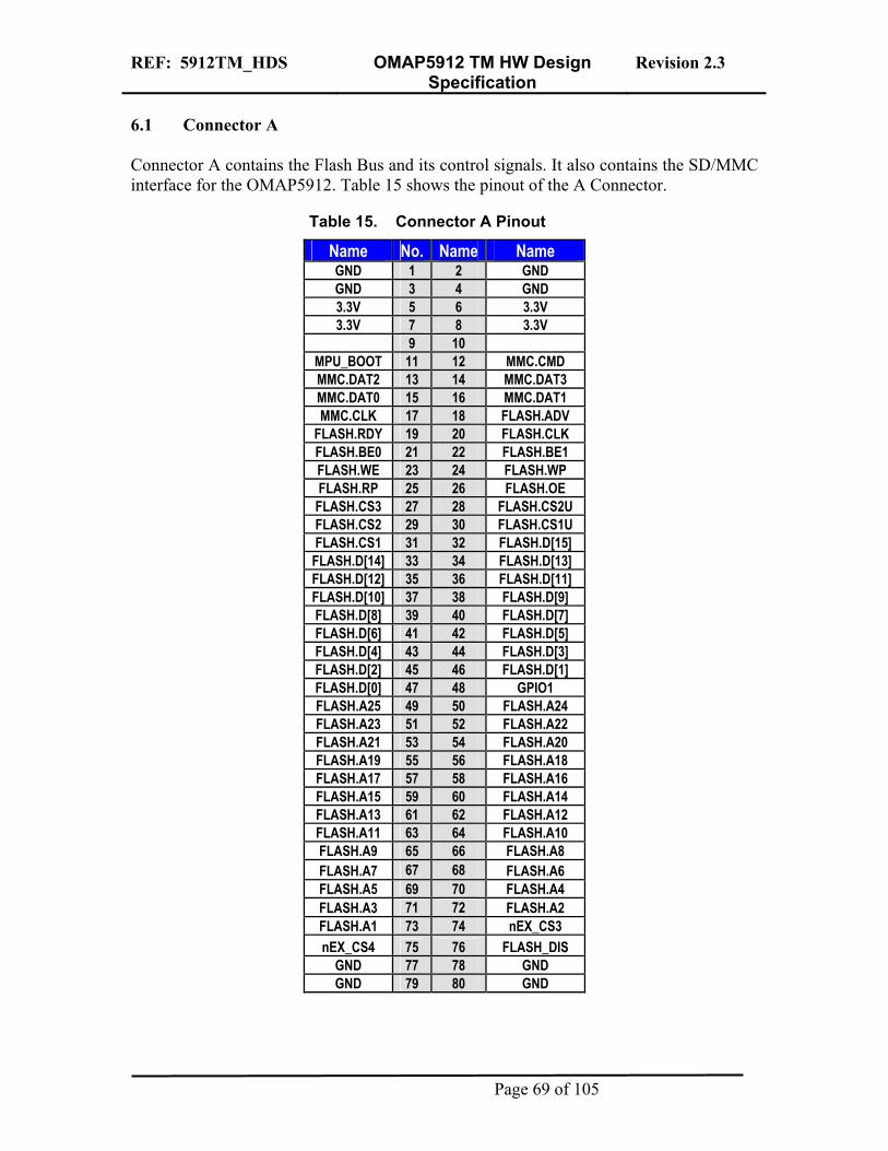
REF: 5912TM_HDS OMAP5912 TM HW Design Specification
Revision 2.3
6.1 Connector A Connector A contains the Flash Bus and its control signals. It also contains the SD/MMC interface for the OMAP5912. Table 15 shows the pinout of the A Connector.
Table 15. Connector A Pinout
Name No. Name Name GND 1 2 GND GND 3 4 GND 3.3V 5 6 3.3V 3.3V 7 8 3.3V
9 10 MPU_BOOT 11 12 MMC.CMD MMC.DAT2 13 14 MMC.DAT3 MMC.DAT0 15 16 MMC.DAT1 MMC.CLK 17 18 FLASH.ADV
FLASH.RDY 19 20 FLASH.CLK FLASH.BE0 21 22 FLASH.BE1 FLASH.WE 23 24 FLASH.WP FLASH.RP 25 26 FLASH.OE FLASH.CS3 27 28 FLASH.CS2U FLASH.CS2 29 30 FLASH.CS1U FLASH.CS1 31 32 FLASH.D[15] FLASH.D[14] 33 34 FLASH.D[13] FLASH.D[12] 35 36 FLASH.D[11] FLASH.D[10] 37 38 FLASH.D[9] FLASH.D[8] 39 40 FLASH.D[7] FLASH.D[6] 41 42 FLASH.D[5] FLASH.D[4] 43 44 FLASH.D[3] FLASH.D[2] 45 46 FLASH.D[1] FLASH.D[0] 47 48 GPIO1 FLASH.A25 49 50 FLASH.A24 FLASH.A23 51 52 FLASH.A22 FLASH.A21 53 54 FLASH.A20 FLASH.A19 55 56 FLASH.A18 FLASH.A17 57 58 FLASH.A16 FLASH.A15 59 60 FLASH.A14 FLASH.A13 61 62 FLASH.A12 FLASH.A11 63 64 FLASH.A10 FLASH.A9 65 66 FLASH.A8 FLASH.A7 67 68 FLASH.A6 FLASH.A5 69 70 FLASH.A4 FLASH.A3 71 72 FLASH.A2 FLASH.A1 73 74 nEX_CS3 nEX_CS4 75 76 FLASH_DIS
GND 77 78 GND GND 79 80 GND
Page 69 of 105
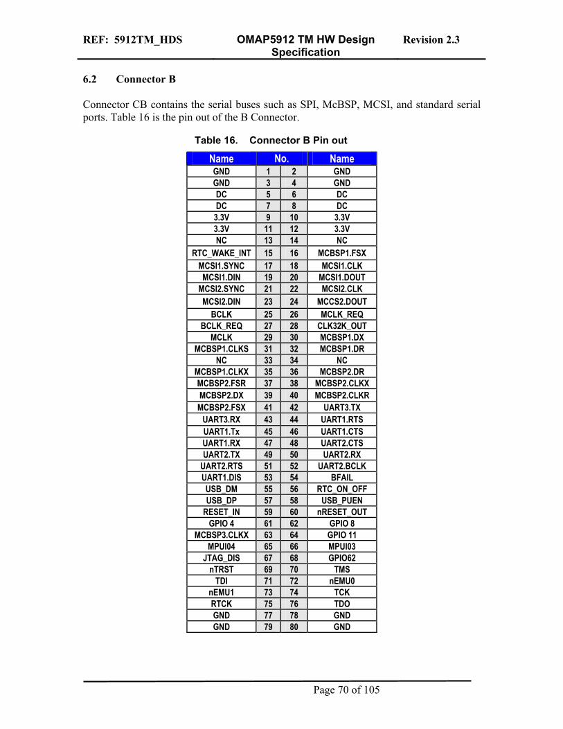
REF: 5912TM_HDS OMAP5912 TM HW Design Specification
Revision 2.3
6.2 Connector B Connector CB contains the serial buses such as SPI, McBSP, MCSI, and standard serial ports. Table 16 is the pin out of the B Connector.
Table 16. Connector B Pin out
Name No. Name GND 1 2 GND GND 3 4 GND DC 5 6 DC DC 7 8 DC
3.3V 9 10 3.3V 3.3V 11 12 3.3V NC 13 14 NC
RTC_WAKE_INT 15 16 MCBSP1.FSX MCSI1.SYNC 17 18 MCSI1.CLK MCSI1.DIN 19 20 MCSI1.DOUT
MCSI2.SYNC 21 22 MCSI2.CLK MCSI2.DIN 23 24 MCCS2.DOUT
BCLK 25 26 MCLK_REQ BCLK_REQ 27 28 CLK32K_OUT
MCLK 29 30 MCBSP1.DX MCBSP1.CLKS 31 32 MCBSP1.DR
NC 33 34 NC MCBSP1.CLKX 35 36 MCBSP2.DR MCBSP2.FSR 37 38 MCBSP2.CLKX MCBSP2.DX 39 40 MCBSP2.CLKR MCBSP2.FSX 41 42 UART3.TX
UART3.RX 43 44 UART1.RTS UART1.Tx 45 46 UART1.CTS UART1.RX 47 48 UART2.CTS UART2.TX 49 50 UART2.RX
UART2.RTS 51 52 UART2.BCLK UART1.DIS 53 54 BFAIL USB_DM 55 56 RTC_ON_OFF USB_DP 57 58 USB_PUEN
RESET_IN 59 60 nRESET_OUT GPIO 4 61 62 GPIO 8
MCBSP3.CLKX 63 64 GPIO 11 MPUI04 65 66 MPUI03
JTAG_DIS 67 68 GPIO62 nTRST 69 70 TMS
TDI 71 72 nEMU0 nEMU1 73 74 TCK RTCK 75 76 TDO GND 77 78 GND GND 79 80 GND
Page 70 of 105
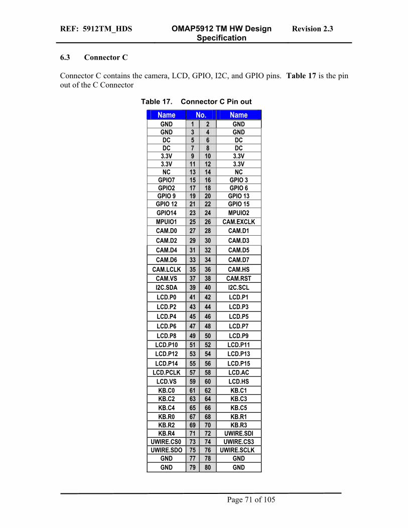
REF: 5912TM_HDS OMAP5912 TM HW Design Specification
Revision 2.3
6.3 Connector C Connector C contains the camera, LCD, GPIO, I2C, and GPIO pins. Table 17 is the pin out of the C Connector
Table 17. Connector C Pin out
Name No. Name GND 1 2 GND GND 3 4 GND DC 5 6 DC DC 7 8 DC
3.3V 9 10 3.3V 3.3V 11 12 3.3V NC 13 14 NC
GPIO7 15 16 GPIO 3 GPIO2 17 18 GPIO 6 GPIO 9 19 20 GPIO 13 GPIO 12 21 22 GPIO 15 GPIO14 23 24 MPUIO2 MPUIO1 25 26 CAM.EXCLK CAM.D0 27 28 CAM.D1 CAM.D2 29 30 CAM.D3 CAM.D4 31 32 CAM.D5 CAM.D6 33 34 CAM.D7
CAM.LCLK 35 36 CAM.HS CAM.VS 37 38 CAM.RST I2C.SDA 39 40 I2C.SCL LCD.P0 41 42 LCD.P1 LCD.P2 43 44 LCD.P3 LCD.P4 45 46 LCD.P5 LCD.P6 47 48 LCD.P7 LCD.P8 49 50 LCD.P9 LCD.P10 51 52 LCD.P11 LCD.P12 53 54 LCD.P13 LCD.P14 55 56 LCD.P15
LCD.PCLK 57 58 LCD.AC LCD.VS 59 60 LCD.HS KB.C0 61 62 KB.C1 KB.C2 63 64 KB.C3 KB.C4 65 66 KB.C5 KB.R0 67 68 KB.R1 KB.R2 69 70 KB.R3 KB.R4 71 72 UWIRE.SDI
UWIRE.CS0 73 74 UWIRE.CS3 UWIRE.SDO 75 76 UWIRE.SCLK
GND 77 78 GND GND 79 80 GND
Page 71 of 105
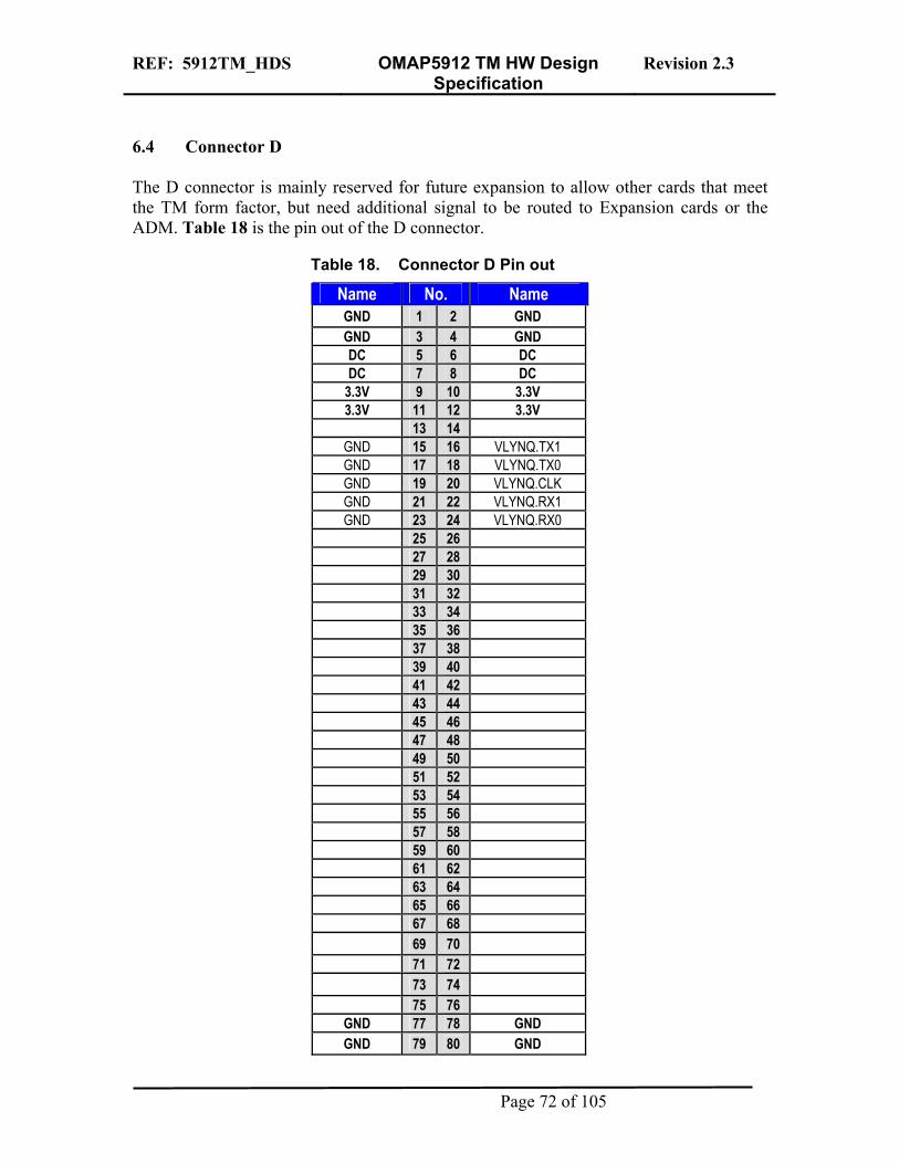
REF: 5912TM_HDS OMAP5912 TM HW Design Specification
Revision 2.3
6.4 Connector D The D connector is mainly reserved for future expansion to allow other cards that meet the TM form factor, but need additional signal to be routed to Expansion cards or the ADM. Table 18 is the pin out of the D connector.
Table 18. Connector D Pin out
Name No. Name GND 1 2 GND GND 3 4 GND DC 5 6 DC DC 7 8 DC
3.3V 9 10 3.3V 3.3V 11 12 3.3V
13 14 GND 15 16 VLYNQ.TX1 GND 17 18 VLYNQ.TX0 GND 19 20 VLYNQ.CLK GND 21 22 VLYNQ.RX1 GND 23 24 VLYNQ.RX0
25 26 27 28 29 30 31 32 33 34 35 36 37 38 39 40 41 42 43 44 45 46 47 48 49 50 51 52 53 54 55 56 57 58 59 60 61 62 63 64 65 66 67 68 69 70 71 72 73 74 75 76
GND 77 78 GND GND 79 80 GND
Page 72 of 105
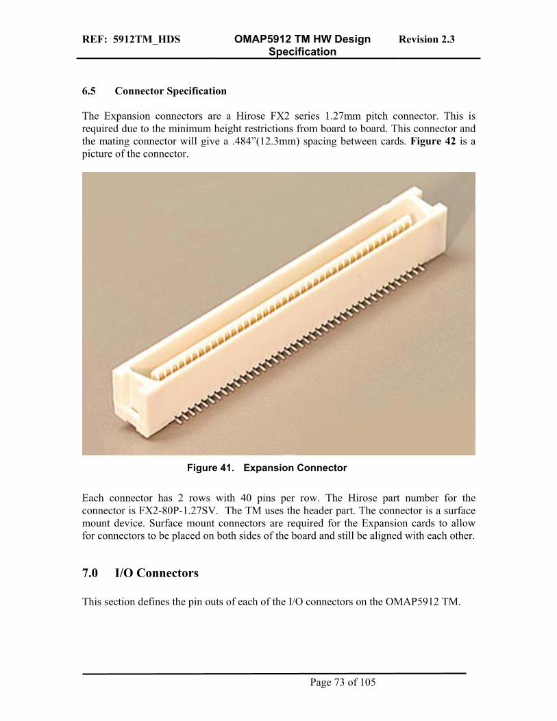
REF: 5912TM_HDS OMAP5912 TM HW Design Specification
Revision 2.3
6.5 Connector Specification The Expansion connectors are a Hirose FX2 series 1.27mm pitch connector. This is required due to the minimum height restrictions from board to board. This connector and the mating connector will give a .484”(12.3mm) spacing between cards. Figure 42 is a picture of the connector.
Figure 41. Expansion Connector
Each connector has 2 rows with 40 pins per row. The Hirose part number for the connector is FX2-80P-1.27SV. The TM uses the header part. The connector is a surface mount device. Surface mount connectors are required for the Expansion cards to allow for connectors to be placed on both sides of the board and still be aligned with each other.
7.0 I/O Connectors This section defines the pin outs of each of the I/O connectors on the OMAP5912 TM.
Page 73 of 105
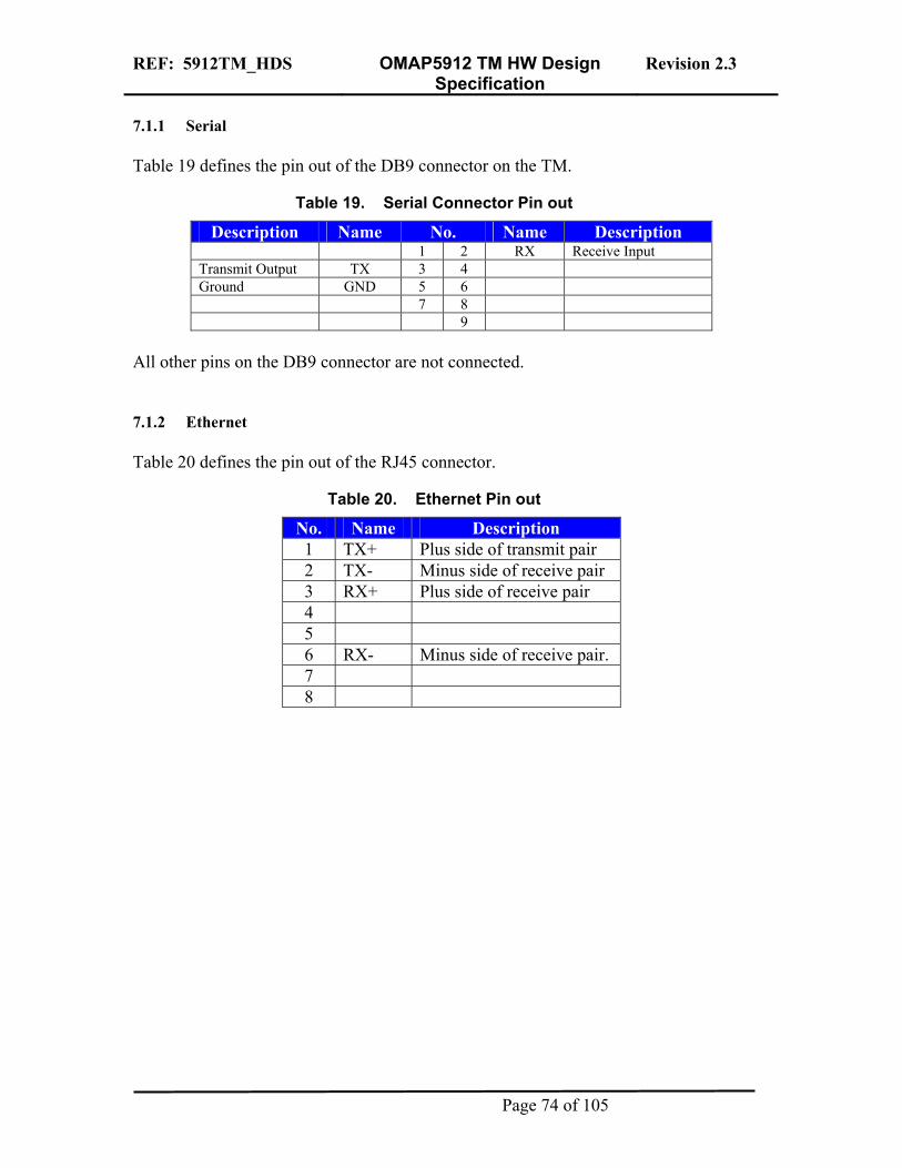
REF: 5912TM_HDS OMAP5912 TM HW Design Specification
Revision 2.3
7.1.1 Serial Table 19 defines the pin out of the DB9 connector on the TM.
Table 19. Serial Connector Pin out
Description Name No. Name Description 1 2 RX Receive Input Transmit Output TX 3 4 Ground GND 5 6 7 8 9
All other pins on the DB9 connector are not connected. 7.1.2 Ethernet Table 20 defines the pin out of the RJ45 connector.
Table 20. Ethernet Pin out
No. Name Description 1 TX+ Plus side of transmit pair 2 TX- Minus side of receive pair 3 RX+ Plus side of receive pair 4 5 6 RX- Minus side of receive pair. 7 8
Page 74 of 105
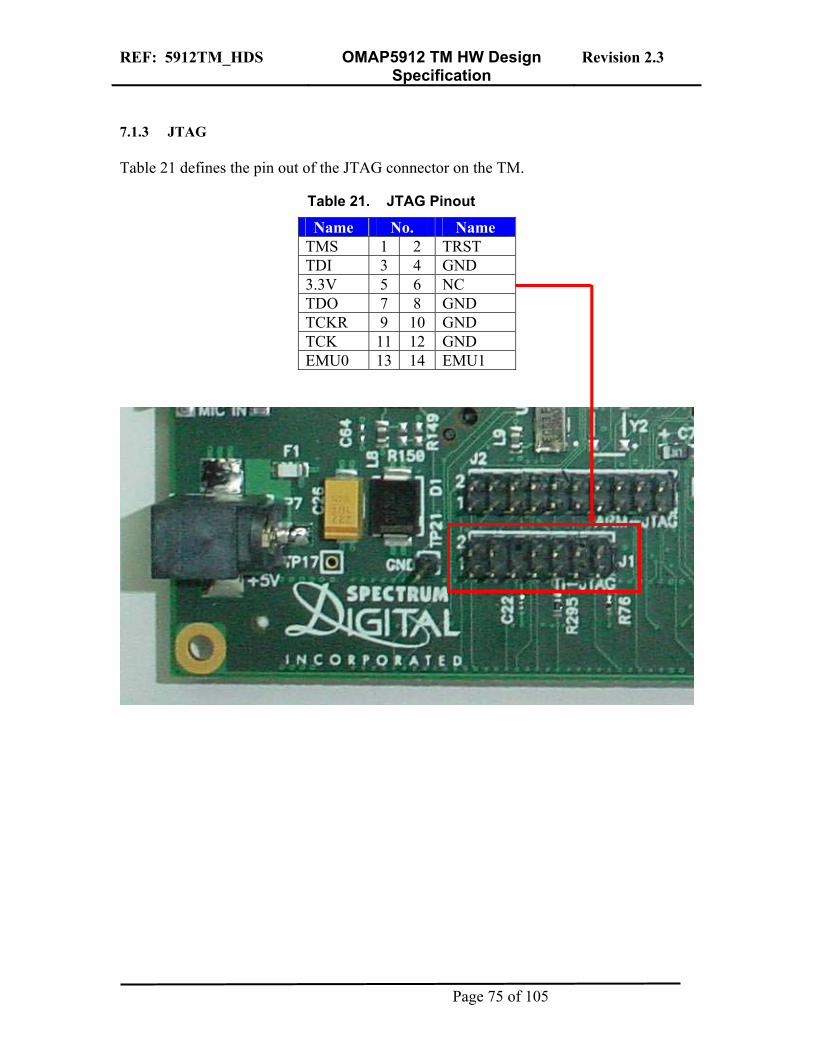
REF: 5912TM_HDS OMAP5912 TM HW Design Specification
Revision 2.3
7.1.3 JTAG Table 21 defines the pin out of the JTAG connector on the TM.
Table 21. JTAG Pinout
Name No. Name TMS 1 2 TRST TDI 3 4 GND 3.3V 5 6 NC TDO 7 8 GND TCKR 9 10 GND TCK 11 12 GND EMU0 13 14 EMU1
Page 75 of 105
REF: 5912TM_HDS OMAP5912 TM HW Design Specification
Revision 2.3
7.1.4 MultiICE Figure 42 is the pin out of the MultiICE connector.
Figure 42. MultiICE Connector Pin out
Page 76 of 105
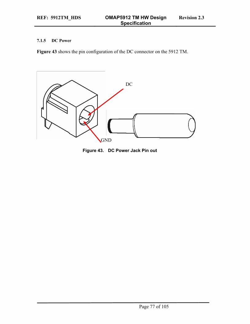
REF: 5912TM_HDS OMAP5912 TM HW Design Specification
Revision 2.3
7.1.5 DC Power Figure 43 shows the pin configuration of the DC connector on the 5912 TM.
DC
GND
Figure 43. DC Power Jack Pin out
Page 77 of 105
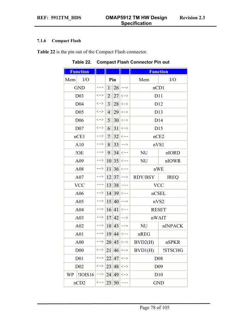
REF: 5912TM_HDS OMAP5912 TM HW Design Specification
Revision 2.3
7.1.6 Compact Flash Table 22 is the pin out of the Compact Flash connector.
Table 22. Compact Flash Connector Pin out
Function Function Mem I/O Pin Mem I/O
GND --- 1 26 --> nCD1
D03 <-> 2 27 <-> D11
D04 <-> 3 28 <-> D12
D05 <-> 4 29 <-> D13
D06 <-> 5 30 <-> D14
D07 <-> 6 31 <-> D15
nCE1 --> 7 32 <-- nCE2
A10 --> 8 33 --> nVS1
!OE --> 9 34 <-- NU nIORD
A09 --> 10 35 <-- NU nIOWR
A08 --> 11 36 <-- nWE
A07 --> 12 37 --> RDY/BSY IREQ
VCC --- 13 38 --- VCC
A06 --> 14 39 <-- nCSEL
A05 --> 15 40 --> nVS2
A04 --> 16 41 <-- RESET
A03 --> 17 42 --> nWAIT
A02 --> 18 43 --> NU nINPACK
A01 --> 19 44 <-- nREG
A00 --> 20 45 <-> BVD2(H) nSPKR
D00 <-> 21 46 <-> BVD1(H) !STSCHG
D01 <-> 22 47 <-> D08
D02 <-> 23 48 <-> D09
WP !IOIS16 --> 24 49 <-> D10
nCD2 <-- 25 50 --- GND
Page 78 of 105
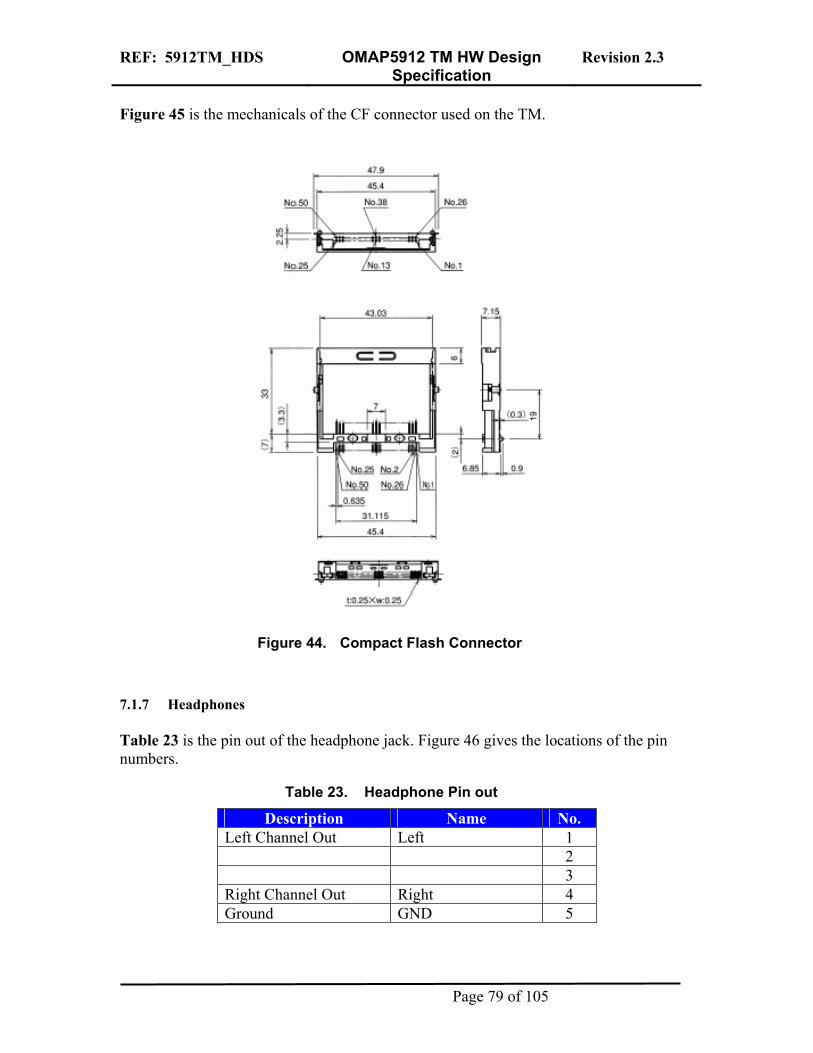
REF: 5912TM_HDS OMAP5912 TM HW Design Specification
Revision 2.3
Figure 45 is the mechanicals of the CF connector used on the TM.
Figure 44. Compact Flash Connector
7.1.7 Headphones Table 23 is the pin out of the headphone jack. Figure 46 gives the locations of the pin numbers.
Table 23. Headphone Pin out
Description Name No. Left Channel Out Left 1 2 3 Right Channel Out Right 4 Ground GND 5
Page 79 of 105
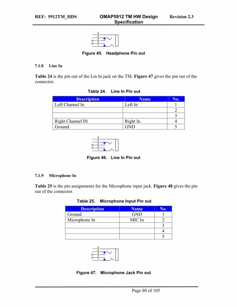
REF: 5912TM_HDS OMAP5912 TM HW Design Specification
Revision 2.3
12345
Figure 45. Headphone Pin out
7.1.8 Line In Table 24 is the pin out of the Lin In jack on the TM. Figure 47 gives the pin out of the connector.
Table 24. Line In Pin out
Description Name No. Left Channel In Left In 1 2 3 Right Channel IN Right In 4 Ground GND 5
12345
Figure 46. Line In Pin out
7.1.9 Microphone In Table 25 is the pin assignments for the Microphone input jack. Figure 48 gives the pin out of the connector.
Table 25. Microphone Input Pin out
Description Name No. Ground GND 1 Microphone In MIC In 2 3 4 5
12345
Figure 47. Microphone Jack Pin out
Page 80 of 105
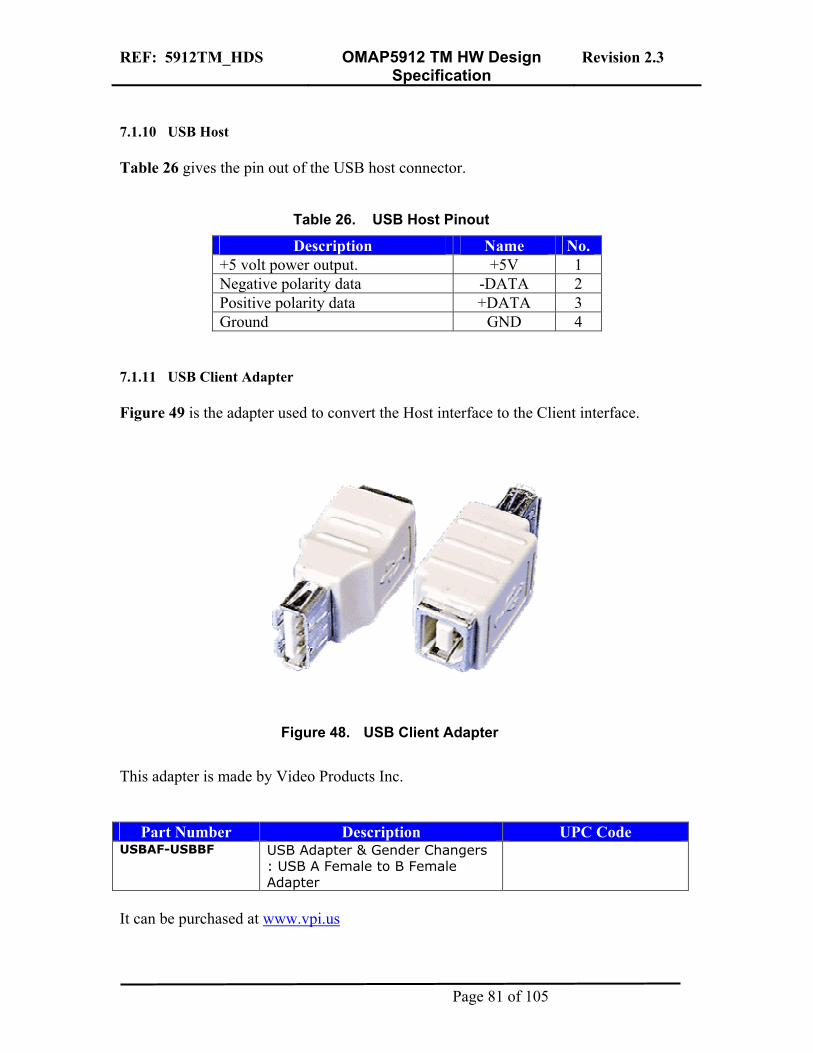
REF: 5912TM_HDS OMAP5912 TM HW Design Specification
Revision 2.3
7.1.10 USB Host Table 26 gives the pin out of the USB host connector.
Table 26. USB Host Pinout
Description Name No. +5 volt power output. +5V 1 Negative polarity data -DATA 2 Positive polarity data +DATA 3 Ground GND 4
7.1.11 USB Client Adapter Figure 49 is the adapter used to convert the Host interface to the Client interface.
Figure 48. USB Client Adapter
This adapter is made by Video Products Inc.
Part Number Description UPC Code USBAF-USBBF USB Adapter & Gender Changers
: USB A Female to B Female Adapter
It can be purchased at www.vpi.us
Page 81 of 105
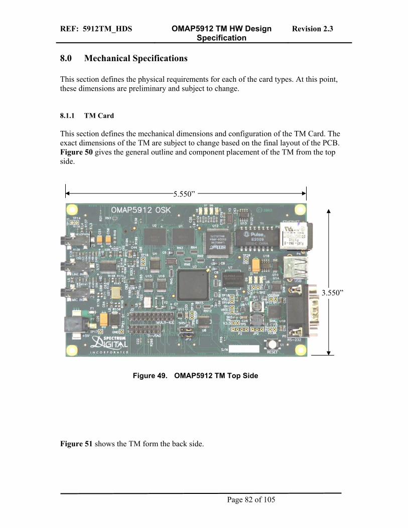
REF: 5912TM_HDS OMAP5912 TM HW Design Specification
Revision 2.3
8.0 Mechanical Specifications This section defines the physical requirements for each of the card types. At this point, these dimensions are preliminary and subject to change. 8.1.1 TM Card This section defines the mechanical dimensions and configuration of the TM Card. The exact dimensions of the TM are subject to change based on the final layout of the PCB. Figure 50 gives the general outline and component placement of the TM from the top side. 5.550”
3.550”
Figure 49. OMAP5912 TM Top Side
Figure 51 shows the TM form the back side.
Page 82 of 105
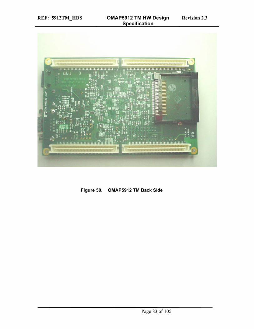
REF: 5912TM_HDS OMAP5912 TM HW Design Specification
Revision 2.3
Figure 50. OMAP5912 TM Back Side
Page 83 of 105
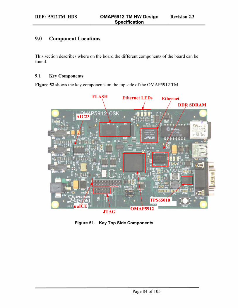
REF: 5912TM_HDS OMAP5912 TM HW Design Specification
Revision 2.3
9.0 Component Locations
This section describes where on the board the different components of the board can be found.
9.1 Key Components
Figure 52 shows the key components on the top side of the OMAP5912 TM.
FLASH Ethernet Ethernet LEDs
AIC23
DDR SDRAM
TPS65010
JTAGuuICE OMAP5912
Figure 51. Key Top Side Components
Page 84 of 105
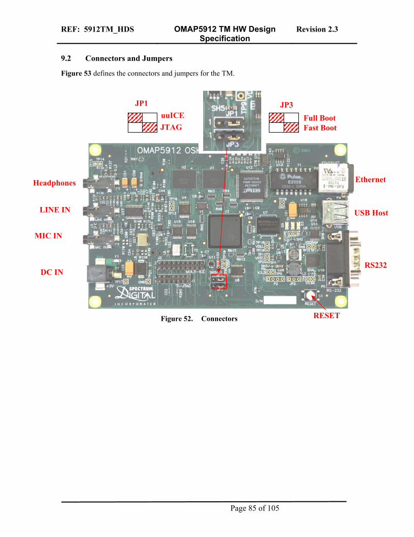
REF: 5912TM_HDS OMAP5912 TM HW Design Specification
Revision 2.3
9.2 Connectors and Jumpers
Figure 53 defines the connectors and jumpers for the TM.
JP1
JTAG uuICE
Headphones
LINE IN
MIC IN
DC IN
Figure 52.
JP3
Fast Boot Full Boot
Ethernet
USB Host
RS232
RESETConnectors
Page 85 of 105
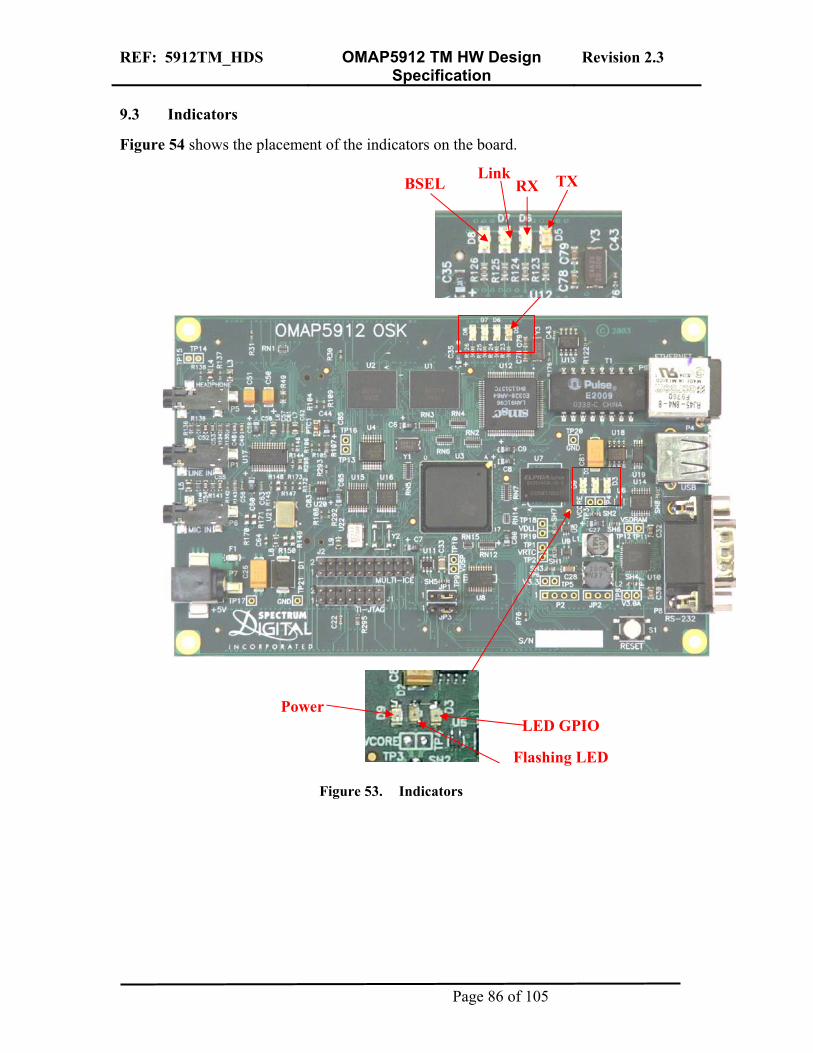
REF: 5912TM_HDS OMAP5912 TM HW Design Specification
Revision 2.3
9.3 Indicators
Figure 54 shows the placement of the indicators on the board.
TX RX Link
BSEL
Power
Figure 53. Indic
Flashing LED
LED GPIO
ators
Page 86 of 105
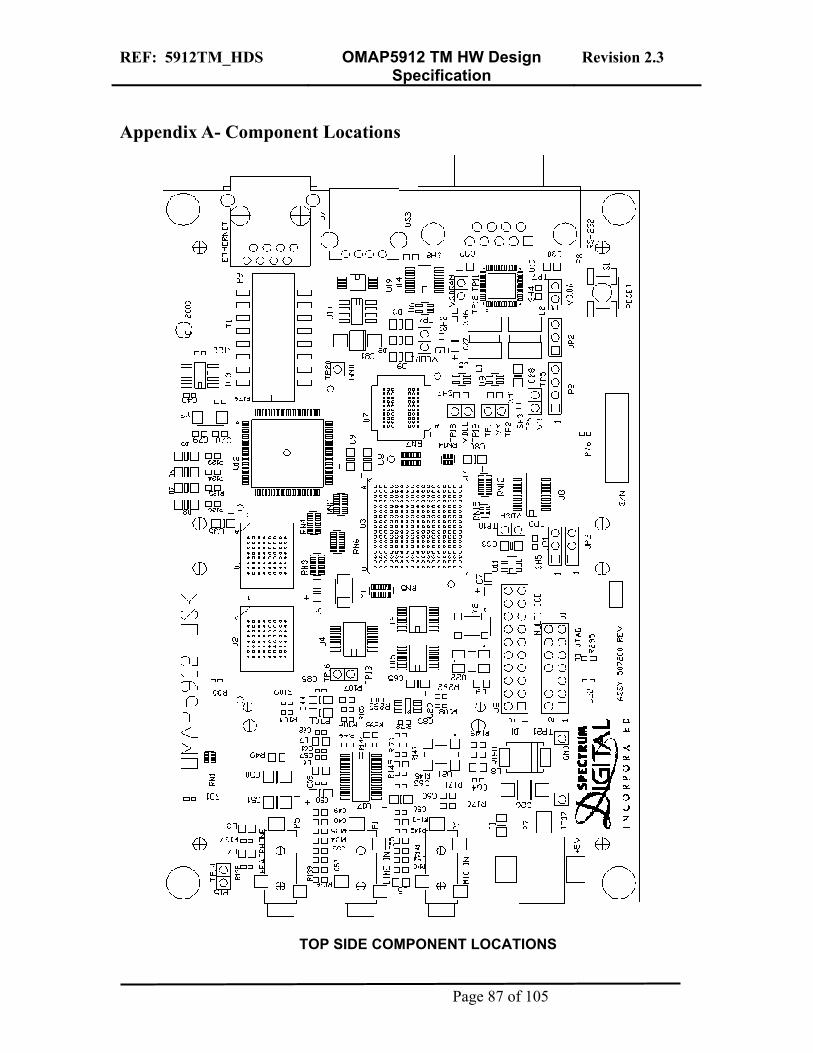
REF: 5912TM_HDS OMAP5912 TM HW Design Specification
Revision 2.3
Appendix A- Component Locations
TOP SIDE COMPONENT LOCATIONS
Page 87 of 105
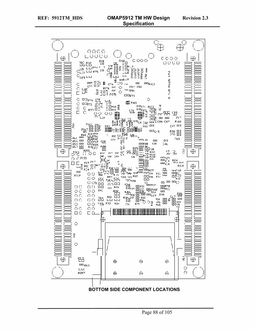
REF: 5912TM_HDS OMAP5912 TM HW Design Specification
Revision 2.3
BOTTOM SIDE COMPONENT LOCATIONS
Page 88 of 105
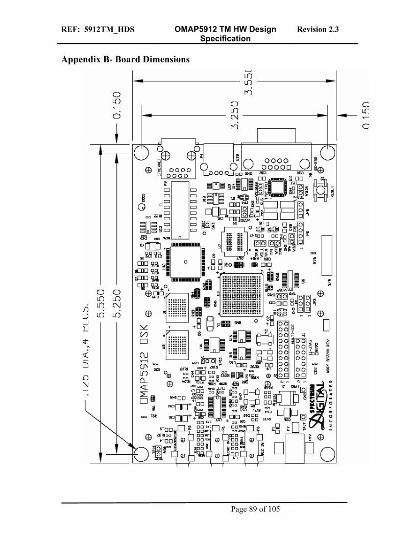
REF: 5912TM_HDS OMAP5912 TM HW Design Specification
Revision 2.3
Appendix B- Board Dimensions
Page 89 of 105
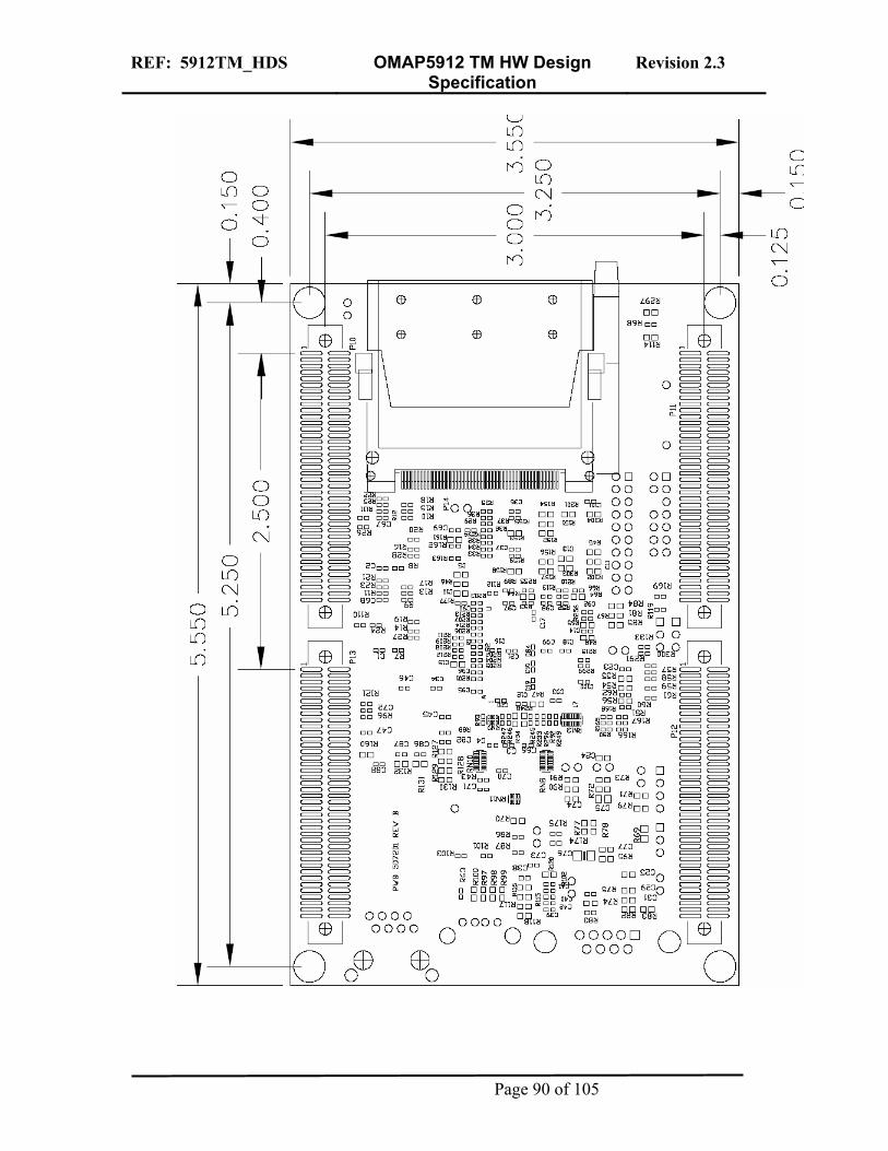
REF: 5912TM_HDS OMAP5912 TM HW Design Specification
Revision 2.3
Page 90 of 105
REF: 5912TM_HDS OMAP5912 TM HW Design Specification
Revision 2.3
Appendix C- Schematics
G. ColeyRevision A release.
Version
A1
Date
G. ColeyUpdated Symbol to official symbol. Make corrections for a few typos.
A
1
OM
AP5912 Starter Kit
B
110
Monday
, July 26, 2004
G. C
oley
Notes P
ageTitle :
Size
Docum
ent Num
berR
ev
Date:
Sheet
of
12203 Southwest F
reeway
Stafford, Texas 77477
Catalog OM
AP Group
Modified by
:
This document contains
information on a product under
developm
ent and is issued forev
aluation purposes only.
Features characteristic data
and other information are
subject to change.
AuthorNotes
A7/26/045/11/04
NOTES:
1. All resistors are in the 0402 package unless otherwise specified.
2. There is an ESD ring around the outer edges of the board on the top
and bottom side.
3. The ESD ring is connected to the standoffs and extends around
the edge of the board.
Page 91 of 105
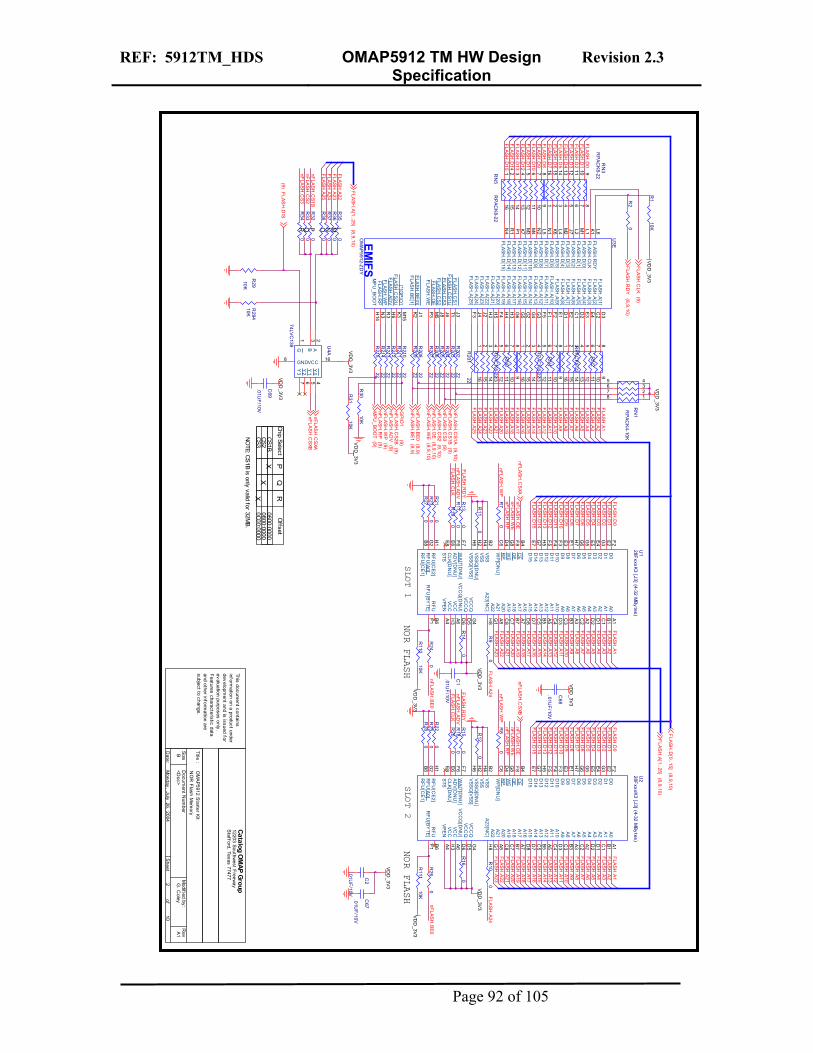
REF: 5912TM_HDS OMAP5912 TM HW Design Specification
Revision 2.3
Page 92 of 105
VDD
_3V3
ASH
R12
0
R17
0
RN
6
RP
ACK
8-22
116
215
314
413
512
611
710
89
R7
0
R13
0
CS1B
R19
0
R9
0
R211
22
R30
10K
VDD
_3V3
VDD
_3V3
R27
0
R21
0
R10
0
R2
0
X
R213
22
X
R28
0
R
Offset
SLOT 2
0600:0000X
R209
22
R23
0
U2
28FxxxK3 [J3] (4-32 M
Bytes)
A1
B1
C1
D1
D2
A2
C2
A3
B3
C3
D3
C4
A5
B5
C5
D7
D8
A7
B7
C7
F2E2G
3E4E5G
5G
6H
7E1E3F3F4F5H
5G
7E7
H2 B2
H4 B4F8
G8
D4
C6
C8
E6 F6 F7
A8
G1
H8
H3
A6
D5
H6
D6
A4
G2
H1
F1
B6
G4
E8B8
A0
A1
A2
A3
A4
A5
A6
A7
A8
A9
A10A11A12A13A14A15A16A17A18A19
D0
D1
D2
D3
D4
D5
D6
D7
D8
D9
D10
D11
D12
D13
D14
D15
VSSQ
[DN
U]
VSSVSS
CE
OE
WE
RP
WP
[DN
U]
A20
CLK
[DN
U]
ADV[D
NU
]W
AIT[D
NU
]
A21A22
A23[NC
]
VCC
VCC
VCC
QVSS
Q[V
SS]
VCC
Q[D
NU
]
VPEN
RFU
[A0]
RFU
[CE2]
RFU
[BY
TE]R
FU
VCC
Q
STS
RFU
[CE1]
P
0C00:0000
M
CS3
R32
0
R35
0
CS2
RN
3R
PAC
K8-22
116
215
314
413
512
611
710
89
nFL
P
RN
2
RPA
CK8-22
116
215
314
413
512
611
710
89
R18
0
NOR FLASH
EMIFS
U3E
OM
AP5912-ZD
Y
L6K1L1M
1L2J7M
2L4K6N
1L5N
2M
4M
3K7P1R
1N
4
D3
C2
E4E3D2
C1
E2D1
E1F2F1F5G3
G4
G2
G5
G6
H3
H4
F4H5
H2
J2J4J3J8 J6M5
P3K2 J1H6
R3
N3
F3K3H14
T1M15
FLASH.R
DY
FLASH.C
LKFLASH
.D[0]
FLASH.D
[1]FLASH
.D[2]
FLASH.D
[3]FLASH
.D[4]
FLASH.D
[5]FLASH
.D[6]
FLASH.D
[7]FLASH
.D[8]
FLASH.D
[9]FLASH
.D[10]
FLASH.D
[11]FLASH
.D[12]
FLASH.D
[13]FLASH
.D[14]
FLASH.D
[15]
FLASH
.A[1]
FLASH
.A[2]
FLASH
.A[3]
FLASH
.A[4]
FLASH
.A[5]
FLASH
.A[6]
FLASH
.A[7]
FLASH
.A[8]
FLASH
.A[9]
FLA
SH.A[10]
FLA
SH.A[11]
FLA
SH.A[12]
FLA
SH.A[13]
FLA
SH.A[14]
FLA
SH.A[15]
FLA
SH.A[16]
FLA
SH.A[17]
FLA
SH.A[18]
FLA
SH.A[19]
FLA
SH.A[20]
FLA
SH.A[21]
FLA
SH.A[22]
FLA
SH.A[23]
FLA
SH.A[24]
FLA
SH.C
S1
FLA
SH.C
S2F
LASH
.CS3
FLASH
.OE
FLASH
.WE
FLASH.BE
[1]FLASH
.BE[0]
FLASH.AD
VF
LASH.W
PFLAS
H.R
P
FLA
SH.A[25]
FLA
SH.C
S2U
MP
U_B
OO
T
FLA
SH.C
S1U
[*]GP
IO1
R210
22
VDD
_3V3
NOR FLASH
R11
0
VD
D_3V
3R
3110K
R110
10K
Q
SLOT 1
R14
0R
150
C68
.01UF
/10V
P
R20
0
R26
0
R208
22
R
R1
10K
R33
0
RN
1
RP
ACK
4-10K
12345
678
VDD
_3V3
C69
.01UF
/10V
NOTE: CS1B is only valid for 32M
B.
R205
22R
220
nFLP
R34
0
OR
380
R29
10K
R24
0
Q
FLA
R204
22
R212
22
L
R111
10K
R206
22R
250
AS
R207
22
R203
22
C67
.01UF/10V
VDD
_3V3
N
R8
0
R201
22
C2
.01UF/10V
Chip Select
R16
0
R294
10K
R202
22
VD
D_3V
3
RN
4
RP
ACK
8-22
116
215
314
413
512
611
710
89
VDD
_3V3
R214
22R
21522
(
U4A
74LVC
139
231
4567
168
ABG
Y0
Y1
Y2
Y3
VCCGND
R36
0
VD
D_3V
3
VD
D_3V
3
<Doc>
A1
OM
AP5912 Starter Kit
B
210
Monday
, July 26, 2004
G. C
oley
NO
R Flash M
emory
Title :
SizeD
ocument N
umber
Rev
Date:
Sheetof
12203 Southwest FreewayS
tafford, Texas 77477
Catalog OM
AP Group
Modified by:
This document contains
information on a product under
development and is issued for
evaluation purposes only.F
eatures characteristic dataand other inform
ation aresubject to change.
0800:0000
R37
0
C1
.01UF
/10V
RN
5R
PAC
K8-22
116
215
314
413
512
611
710
89
U1
28FxxxK3 [J3] (4-32 MBy
tes)
A1
B1
C1
D1
D2
A2
C2
A3
B3
C3
D3
C4
A5
B5
C5
D7
D8
A7
B7
C7
F2E2G
3E4E5G
5G
6H
7E1E3F3F4F5H
5G
7E7
H2 B2
H4 B4F8
G8
D4
C6
C8
E6 F6 F7
A8
G1
H8
H3
A6
D5
H6
D6
A4
G2
H1
F1
B6
G4
E8B8
A0A1A2A3A4A5A6A7A8A9A10A11A12A13A14A15A16A17A18A19
D0
D1
D2
D3
D4
D5
D6
D7
D8
D9
D10
D11
D12
D13
D14
D15
VSSQ
[DN
U]
VSS
VSS
CE
OE
WE
RP
WP
[DN
U]
A20
CLK[D
NU
]AD
V[D
NU
]W
AIT[D
NU
]
A21A22
A23[N
C]
VCC
VCC
VCC
QVS
SQ[V
SS]
VCC
Q[D
NU
]
VPE
N
RFU
[A0]R
FU[C
E2]R
FU[BY
TE]R
FU
VCC
Q
STS
RFU
[CE1]
FL
.A23
FLASH.A24
FLASH
.D9
FLASH
.RD
Y
FLASH
.D2
FLASH
.D8
FLA
SH.A21
FLA
SH.A15
nFLA
SH.C
S1B(9)
nFLASH
.BE0
nFLA
SH.C
S2
FLASH
.D1
FLASH
.D11
nFLA
SH.B
E0
FLA
SH.A15
FLASH
.D9
FLASH
.A24
nFLA
SH.R
P(9)
FLA
SH.A19
FLASH.D
[0..15](8,9,10)
FLA
SH.A
7
FLA
SH.A
2
FLA
SH.A22
FLASH
.A22
FLA
SH.A19
nFLA
SH.O
E(8,9,10)
FLA
SH.D
1
FLASH
.D14
FLA
SH.A
3
FLASH
.D0
nFLA
SH.B
E0(8,9)
FLASH
.D14
FLASH
.D4
FLA
SH.A3
nFLASH
.WP
nFLA
SH.C
S1B
FLASH
.D6
nFLASH
.WP
FLASH
.D6
FLASH
.D0
FLA
SH.A14
FLA
SH.A13
FLA
SH.A20
GPIO
1(9)
FLA
SH.A
5
FLA
SH.A
[1..25](8,9,10)
FLASH
.A25
nFLASH
.CS
XB
FLA
SH.A
13
FLASH
.D1
FLASH
.D5
FLA
SH.A
21
FLASH
.D3
FLA
SH.A6
FLA
SH.A16
FLASH
.D13
FLASH
.RD
Y
FLASH
.D8
ASH
.R
FLA
SH.A5
FLASH
.D4
nFLASH.C
SXA
FLASH
.D11
FLA
SH.A16
FLASH
.DIS
(9)
FLA
SH.A
22
FLA
SH.A8
FLA
SH.A
8
nFLA
SH.A
DV
(9)
FLA
SH.A
24
FLA
SH.C
LK
FLA
SH.A14
FLASH
.D0
nFLA
SH.B
E1(8,9)
FLASH
.D12
FLASH
.D13
FLASH
.D5
FLA
SH.A
10
FLA
SH.A
17
FLA
SH.A7
FLA
SH.A
20
FLA
SH.D
5
FLA
SH.A1
nFLA
SH.C
S1A(9,10)
FLASH
.D14
FLASH
.D8
FLA
SH.A
16
FLA
SH.A1
FLA
SH.A22
FLASH
.D3
FLA
SH.A7
nFLA
SH.W
E
FLA
SH.A2
FLASH
.D10
nFLASH.C
SXA
FLA
SH.D
2
FLA
SH.A10
MPU
_BOO
T(9)
nFLA
SH.C
S2B(9)
FLA
SH.A12
nFLA
SH.O
E
FLA
SH.A9
FLA
SH.A2
FLASH
.D10
FLA
SH.A17
FLASH
.D10
FLA
SH.A
18
FLA
SH.A5
FLA
SH.A
6
FLA
SH.D
6
FLA
SH.A
14
FLA
SH.A18
ASH
.R
FLA
SH.D
4
nFLASH
.WE
FLASH
.D11
FLA
SH.A21
FLA
SH.A
9
nFLA
SH.C
S3(9)
FLASH
.A[1..25]
(8,9,10)
FLASH
.D15
FLA
SH.D
3
nFLASH.C
SXB
SH.C
LK
FLASH
.D2
FLA
SH.A25
FLA
SH.A4
FLA
SH.A23
FLA
SH.A11
FLASH
.D9
FLA
SH.A12
FLASH
.D15
FLASH
.D15
FLA
SH.A8
FLA
SH.A13
FLASH
.D13
FL
H.A23
FLASH
.D7
FLA
SH.A4
FLA
SH.A17
FLA
SH.C
LK(9)
FLASH
.D12
FLA
SH.A
19F
LASH
.A18
nFLASH
.AD
V
FLASH
.A23
FLA
SH.A3
nFLASH
.OE
nFLA
SH.C
S3
FLA
SH.A
4
FLA
SH.A11
nFLA
SH.W
P(9)
nFLASH
.ADV
FLASH
.D7
FLASH
.D12
FLA
SH.A10
FLA
SH.A24
nFLA
SH.W
E8,9,10)
nFLA
SH.C
S2(9,10)
FLA
SH.A
12
FLA
SH.A20
FLA
SH.A
11
FLA
SH.R
DY
(8,9,10)
FLA
SH.A
15
FLA
SH.A
1
FLA
SH.A9
FLA
SH.D
7
FLA
SH.A6
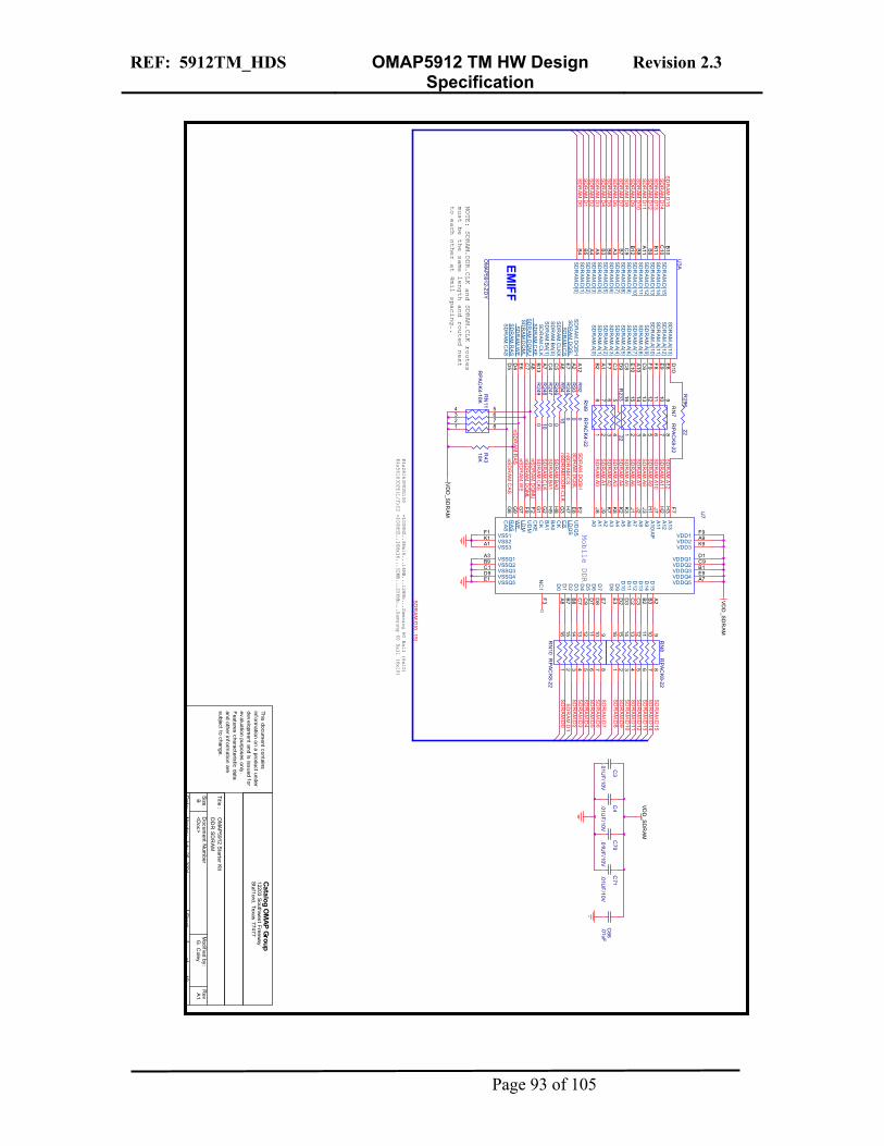
REF: 5912TM_HDS OMAP5912 TM HW Design Specification
Revision 2.3
SD
RAM
.D1
SDR
AM.D
QSL
nSD
RA
M.W
E
SD
RA
M.A7
nSD
RA
M.D
QM
U
SD
RA
M.A4
SD
RAM
.D0
nSD
RAM
.CS
SD
RA
M.D
2
SD
RAM
.D13
SD
RA
M.BA
0
SD
RA
M.D
6
SD
RA
M.D
3
SD
RAM
.D2
SD
RA
M.A11
SD
RA
M.A2
SD
RA
M.D
4
SD
RA
M.D
10
nSD
RAM
.DD
R.C
LK
SD
RA
M.A12
SD
RA
M.A10
SD
RA
M.D
11S
DR
AM.D
8
SD
RA
M.A3
SD
RA
M.C
LKS
DR
AM
.CK
E
SD
RA
M.A5
SDR
AM.D
QSH
SD
RAM
.D12
SD
RAM
.D9
SD
RA
M.D
12
SD
RA
M.D
0
SD
RA
M.A0
SD
RAM
.D7
SD
RAM
.D3
SD
RA
M.D
8
SD
RA
M.BA
1
SD
RA
M.A6
nSD
RA
M.C
AS
SD
RA
M.D
9
nSD
RA
M.D
QM
L
SDR
AM.D
15
SD
RA
M.D
13
SD
RAM
.D14
SD
RAM
.D4
SD
RA
M.D
5
SD
RAM
.D11
SD
RA
M.D
7S
DR
AM.D
5
nSD
RA
M.R
AS
SDR
AM.D
[0..15]
SD
RA
M.D
14S
DR
AM
.D15
SD
RAM
.D10
SD
RA
M.A1
SD
RA
M.A8
SD
RAM
.D1
SD
RA
M.A9
SD
RAM
.D6
R94
10
R247
0
C71
.01UF
/10V
Mobile DDR
U7
A7
A8
A9
B7 B8
A1
C7
C8
B1
D7
D8
A3
E7
C9
G7
G8
G9
H7
H8
H9 J7J8 J9 K7 K8
D1B9
K2 K3 J1 J2 J3H
1
H2
G2
F1
E3
E9
D2
D3
C1
C2
C3
F9
B2 B3
D9
A2
E1
H3
F3
E2E8F2 F7F8
G1
G3
K1K9
VDDQ5D0
VDD2
D1
D2
VSS3
D3
D4
VDDQ3
D5
D6
VSSQ1
D7
VDDQ2
WE
CA
SR
AS
CS
BA0
BA1
A10/AP
A0
A1
A2
A3
VDDQ1VSSQ2
A4
A5
A6
A7
A8
A9
A11
CK
VSS1
D8
VDDQ4
D9
D10
VSSQ3
D11
D12
VDD1
D13
D14
VSSQ4 D15VSSQ5
A12
NC
1
UD
QS
LDQ
S
UD
M
A13
LDM
CK
E
CK
VSS2VDD3
<Doc>
A1
OM
AP5912 S
tarter Kit
B
310
Monday, July
26, 2004
G. C
oley
DD
R S
DR
AM
Title :
SizeD
ocument N
umber
Rev
Date:
Sheetof
12203 Southw
est Freeway
Stafford, Texas 77477
Catalog OM
AP Group
Modified by
:
This document contains
information on a product under
development and is issued for
evaluation purposes only.
Features characteristic data
and other information are
subject to change.
C66
.01uF
C4
.01UF
/10V
C3
.01UF/10V
VD
D_S
DR
AM
C70
.01UF/10V
R249
0
K4x56163DPE(L/F)C2 =100MHZ..16Mx16...32MB...256Mb...Samsung 60 Ball (6x10)
VD
D_S
DR
AM
R296
22
R233
22
R93
0
K4x28163PEVG100 =100MHZ..8Mx16...16MB...128Mb...Samsung 60 Ball (6x10)
RN
7R
PAC
K8-22
116
215
314
413
512
611
710
89R
N9
RP
ACK4-22
1 2 3 45678
R245
0
RN
11R
PA
CK4-10K
1234 5
678
RN
10R
PAC
K8-22
116
215
314
413
512
611
710
89
R246
0
EMIFF
U3A
OM
AP5912-ZD
Y
B10
C10
B11B
9A
11B
8B
12C
9B
7A
3B
6B
3A
5A
4B
5B
4
E8
E9
F8
F9
C6
A10
E10
C8
D9
C3
F7
A1
B2
C5
C4
A7
B13
A8
E6
D5
D4
D10
E7
C7
A12
A2
A6
SD
RAM
.D[15]
SD
RAM
.D[14]
SD
RAM
.D[13]
SD
RAM
.D[12]
SD
RAM
.D[11]
SD
RAM
.D[10]
SD
RAM
.D[9]
SD
RAM
.D[8]
SD
RAM
.D[7]
SD
RAM
.D[6]
SD
RAM
.D[5]
SD
RAM
.D[4]
SD
RAM
.D[3]
SD
RAM
.D[2]
SD
RAM
.D[1]
SD
RAM
.D[0]
SD
RA
M.A
[12]S
DR
AM
.A[11]
SD
RA
M.A
[10]SD
RA
M.A
[9]SD
RA
M.A
[8]SD
RA
M.A
[7]SD
RA
M.A
[6]SD
RA
M.A
[5]SD
RA
M.A
[4]SD
RA
M.A
[3]SD
RA
M.A
[2]SD
RA
M.A
[1]SD
RA
M.A
[0]
SD
RA
M.BA
[0]S
DR
AM
.BA[1]
SD
RA
M.C
LKS
DR
AM.C
KE
SD
RAM
.DQ
MU
SD
RAM
.WE
SD
RAM
.CA
SS
DR
AM.R
AS
SD
RA
M.A
[13]
SDR
AM
.CS
SD
RA
M.D
QM
L
SD
RA
M.D
QS
HSD
RA
M.D
QSL
SD
RA
M.C
LKX
R92
0
VD
D_S
DR
AM
R248
10
RN
8R
PAC
K8-22
116
215
314
413
512
611
710
89
NOTE: SDRAM.DDR.CLK and SDRAM.CLK routes
must be the same length and routed next
to each other at 4mil spacing..
R43
10K
Page 93 of 105
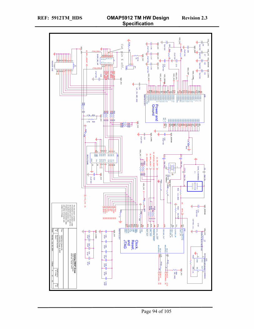
REF: 5912TM_HDS OMAP5912 TM HW Design Specification
Revision 2.3
Page 94 of 105
VDD
_3V3
VDD
_3V3
C101
.1UF
/10V, n.m
.
VDD
_3V3
R55100K
R291
10K
R57
33
R89
10K, 0402
C11
10pf,10v
C100
.01uF
VDD
_SD
RAM
JP1
CO
N3
123
VDD
_DLL
L9
FER
RITE BE
AD M
2301-ND
R301
NO
POP
VDD
_3V3
J2
HE
ADER
10X2 135791113151719
2468101214161820
R46
n.m.,0603
VDD
_3V3
R59
33
R654.7K
C10
10pf,10v
+C
8
10uf/10V
R44
n.m.,0603
VDD
_DSP
VDD
_3V3
VDD
_3V3
VDD
_3V3
Y2
SSP-T6
32.768MH
Z
12
3
5
C17
.01uF/10V
Y1
CS
10_12.0000MAB
J
12
+C
80
10uf/10V
C97
.01uF
R58
33
C22
.01uF/10V
C84
.01uF/10V
C16
.01uF/10V
Clock,
Reset,
andJTAG
U3C
OM
AP5912-ZD
Y
R2
P2
U11
U10
N12
N8
U17
T15
M10
P13
R13
U16
N11
T14
R14
T17
T11
N14
R9
P10
U3
T7R12
L10
OSC
1_IN
OSC
1_OU
TO
SC32K_IN
OSC
32K_OU
T
RST_O
UT
PWR
ON
_RES
ET
TDI
TDO
TMS
TCK
TRS
T
EMU
0EM
U1
RTC
K
CO
NF
BFAIL/E
XT_FIQ
CLK
32K_IN
MPU
_RST
VSS
RTC
_ON
_OFF
MC
LKM
CLK
REQ
BC
LKR
EQBC
LK
VDD
_SDR
AM
R52
10K
R166
0
<Doc>
A1
OM
AP5912 Starter Kit
B
410
Monday, July
26, 2004
G. C
oley
JTAG/O
SC/Pow
er & GN
DTitle :
SizeD
ocument N
umber
Rev
Date:
Sheetof
12203 Southwest Freeway
Stafford, Texas 77477
Catalog OM
AP Group
Modified by:
This document contains
information on a product under
development and is issued for
evaluation purposes only.
Features characteristic dataand other inform
ation aresubject to change.
R66
33
VD
D_C
OR
E
R165
0
R47
10
U8
SN74LVT244B 20
2468
18161412
1
10
19 11131517
9753
Vcc
1A11A21A31A4
1Y1
1Y2
1Y3
1Y4
1OE
GN
D
2OE
2A12A22A32A4
2Y1
2Y2
2Y3
2Y4
C5
10pf,10v
R133
10K
VD
D_3V3
C13
10pf,10v
VDD
_3V3
R304
20K, n.m.
VDD
_CO
RE
VDD
_CO
RE
+C
6
10uf/10V
C23
.01uF/10VC
92.01uF
C95
.01uF
VD
D_C
OR
E
R168
0
VDD
_SDR
AM
R60
33
R54100K
Cut pin 6 off.
R67
33
Power and
Ground
U3D
OM
AP5912-ZD
Y
T6U
2
J15M
13
T13 B1
G1
G7
L3
D11D
8D
6D
7
T10
J9N13
M12
N5
M6
L7 E5E13
H9
P17
G11
F12
T16M
7T3
R10
J10
H11
K11
K8K9K10
K5
G8
C11
H1
C14
F6H10
L11
E14
G10L9
H8
G9
H7A9
G12
K4
DVD
D3
DVD
D2
DVD
D8
DVD
D9
DVD
D7
DVD
D5_0
DVD
D5_2
VSS
DVD
D5_1
DVD
D4_0
DVD
D4_1
DVD
D4_2
DVD
D4_3
DVD
D6
VSS
VSS
VSSVSS
VSS
VSS
VSSVSS
VSS
CVD
DA
VSS
VSS
CVD
D_2
CVD
D_1
CVD
D1
DVD
DR
TC
CVD
D3_0
CVD
D3_2
CVD
D3_1
VSSVSSVSS
CVD
D_0
CVD
D2_0
CVD
D_3
LDO
.FILTER
DVD
D1_0
VSS
VSS
VSS
NC
_0
CVD
D3_3
CVD
DR
TC
VSSC
VDD
2_1C
VDD
2_2
CVD
DD
LL
DVD
D1_1
NC
_1
C12
.01uF/10V
R53
0
VDD
_3V3
VD
D_3V3
VD
D_3V3
C19
.01uF/10V
C98
.01uFR
6133
R119
1K
R113
22V
DD
_3V3
R45
n.m.,0603
R644.7K
VDD
_3V3U
22D
K/SG
8002CAPC
B-ND
(12.000MH
Z)3
21
4O
UT
GN
DEN
VCC
+C
9
10uf/10V
VD
D_3V3
C99
.01uF
R295
47K
VDD
_3V3
C18
.01uF/10V VD
D_R
TC
J1
EHD
R_SM
_14P
12
34
56
78
910
1112
1314
12
34
56
78
910
1112
1314
VD
D_3V3
R302
0
C96
.01uF
C93
.01uF
C21
.01uF/10V
R51
10K
VDD
_SDR
AM
C15
1uF, 10V, X5R, 0402
R56100K
C90
.01uF
VDD
_DSP
C20
.01uF/10VC
14.01uF/10V
VDD
_3V3
VDD
_3V3
C91
.01uF
R62
33
R112
22
+C
7
10uf/10V
R303
0
R50
10K
R167
0
R48
10
ON
_OFF
(9)
TCKR
_MA
IN
MP
U_nR
ESET
(6)
TRST_M
AIN
nTD
O(9)
BCLK
(9)
MC
LKR
EQ(9)
TDI_M
AIN
TCK_M
AIN
TCK
(9)
TMS_M
AIN
BCLKR
EQ(9)
JTAG_D
IS(9)
TDI
(9)
nEM
U1
(9)
TDO
_MAIN
MPU
_nRE
SET(6)
nTRST
(9)TM
S(9)
RTC
K(9)
JTAG_EMU0
MC
LK(7,9)
nRES
ET.OU
T(9)
nEM
U0
(9)
BFAIL
(9)
JTAG_EMU1
nPWR
ON
_RESET
(6)
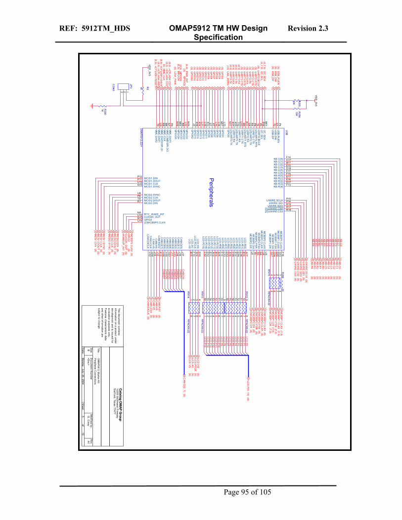
REF: 5912TM_HDS OMAP5912 TM HW Design Specification
Revision 2.3
Page 95 of 105
CAM
.D7
UW
IRE.SD
O(9)
MC
SI1.SYN
C(9)
CAM
.D5
CAM
.D0
MC
SI2.CLK
(9)
UAR
T2.RTS
(9)
KB.C5
UAR
T1.CTS
(9)
GPIO
3(9)
CAM
.D[0..7]
(9)
CAM
.VS(9)
LCD
.P11
CAM
.D3
MC
BSP1.CLKS
(7,9)
LOW
_PWR
(6)
I2C.SC
L(6,7,9)
OM
CBSP
2.FSR(8)
KB.R4
(9)
LCD
.P1
UAR
T3.RX
(8,9)
GPIO
14(9)
KB.C1
(9)
CAM
.D6
nCF
LASH.R
ESET
(8,9)
UW
IRE.SD
I(9)
KB.R1
(9)
LCD
.P0
MC
BSP1.CLKX
(7,9)
GPIO
11(9)M
MC
.CLK
(9)
LCD
.PCLK
(9)
KB.R0
KB.C4
(9)
LCD
.P4
LAN_IN
TR0
(10)
LCD
.VS(9)
MPU
IO3
(8,9)
LCD
.P7
MC
SI1.CLK
(9)
KB.C3
MC
BSP1.DX
(7,9)
GPIO
2(9)
MC
SI2.SYN
C(9)
MC
BSP1.DR
(7,9)
LCD
.P8
USB_D
P(9)
CAM
.EXCLK
(9)
LCD
.P15
KB.R2
GPIO
7(9) U
ART2.BC
LK(9)
CAM
.HS
(9)
LCD
.P6
KB.C0
GPIO
62(9)
I2C.SD
A(6,7,9)
OM
CBSP
2.FSX(8)
UAR
T1.TX(8,9)
KB.R3
(9)
LCD
.P12
CAM
.D1
LCD
.P10
GPIO
13(9)
CAM
.D2
nCFLASH
.IREQ
(8,9)
KB.C0
(9)KB.C
1
KB.R0
(9)
LCD
.P13
LCD
.P3
OM
CBSP
2.CLKX
(8)
GPIO
9(9)
LCD
.HS
(9)
nCFLASH
.CD
2(8,9)
MC
SI1.DO
UT
(9)
KB.C3
(9)
KB.R3
GPIO
6(9)
MC
BSP1.FSX(7,9)
WAKEU
P_INT
(9)
UAR
T2.CTS
(9)
MC
SI2.DIN
(9)
UAR
T2.RX
(9)
LCD
.P5
MC
BSP3.CLKX
(9)
CAM
.D4
LCD
.P9
KB.C2
UW
IRE.C
S3(9)
MC
SI1.DIN
(9)
LCD
.P2
USB_D
M(9)
UAR
T1.RTS
(9)
GPIO
4(9)
CAM
.RST
(9)
CAM
.LCLK
(9)
OM
CBSP
2.CLKR
(8)
USB_PU
EN
(9)
KB.R4
UAR
T2.TX(9)
UAR
T3.TX(8,9)
MPU
IO2
(9) PWR
_INT
(6,9)
GPIO
15(9)
MPU
IO4
(6,9)
KB.C2
(9)
UAR
T1.RX
(8,9)
KB.R2
(9)
UW
IRE.C
S0(9)
KB.C4
GPIO
12(9)
OM
CBSP
2.DR
(8)
nCF
LASH.IO
IS16
(8,9)
KB.C5
(9)
OM
CBSP
2.DX
(8)
GPIO
8(9)
UW
IRE.SC
LK(9)
nCFLASH
.CD
1(8,9)
LCD
.AC(9)
MC
SI2.DO
UT
(9)
LCD
.P14
KB.R1
LCD
.P[0..15](9)
CLK32K_O
UT
9)
R299
22
R300
1K
RN
12R
PAC
K8-22
116
215
314
413
512
611
710
89
Peripherals
U3B
OM
AP5912-ZD
Y
M16
M17
L14L15
P16M
11 T2U
1
F14C17B17E15D16F17F15E17E16D17F13
J17J16J14H
13J11H
17H
15H
16
J12J13G
16H
12
P4
N15
L12
M14
N16
K12
K13
L13J5
A17B16C
16D
14E12C
15A16D
13C
13F11A15B14A13E11D
12C
12
D15
A14F10B15
L17K14K16 P7U
7
R6P9
N7
M8
R8
U9T9
N17
L16
F16G
13G
15G
14G
17
U5
U6
N6
R5
T5L8
P12P11U15N10
U8P8T8R7
T4P6R
4U
4R
11M
9U
13T12K15K17 P5
R16R17R15P14P15
N9U12
U14 GPIO2
GP
IO4
GP
IO6
GP
IO7
I2C.SC
LI2C
.SDA
US
B.DP
US
B.DM
KB.C[0]KB.C[1]KB.C[2]KB.C[3]KB.C[4]KB.C[5]KB.R[0]KB.R[1]KB.R[2]KB.R[3]KB.R[4]
CAM
.D[0]
CAM
.D[1]
CAM
.D[2]
CAM
.D[3]
CAM
.D[4]
CAM
.D[5]
CAM
.D[6]
CAM
.D[7]
CAM
.HS
CAM
.VS
CAM
.LCLK
CAM
.EXCLK
US
B.PUEN
MP
UIO
1M
PU
IO2
MP
UIO
4M
PU
IO5
CAM
.RS
TZ
GP
IO11
GP
IO3
GP
IO62
LCD
.P[0]
LCD
.P[1]
LCD
.P[2]
LCD
.P[3]
LCD
.P[4]
LCD
.P[5]
LCD
.P[6]
LCD
.P[7]
LCD
.P[8]
LCD
.P[9]
LCD
.P[10]LC
D.P[11]
LCD
.P[12]LC
D.P[13]
LCD
.P[14]LC
D.P[15]
LCD
.HS
LCD
.PCLK
LCD
.AC
LCD
.VS
GP
IO13
GP
IO14
GP
IO15
GP
IO8
GP
IO9
MP
UIO
3
MM
C.D
AT3M
MC
.CM
D/SP
I.DO
MM
C.C
LKM
MC
.DAT0/S
PI.DI
MM
C.D
AT1M
MC
.DAT2
GP
IO0
GP
IO12
MC
BSP1.CLK
XM
CBSP1.C
LKS
MC
BSP1.FSX
MC
BSP1.DX
MC
BSP1.DR
MC
BSP2.CLK
XM
CBSP2.C
LKR
MC
BSP2.FSX
MC
BSP2.FSR
MC
BSP2.DX
MC
BSP2.DR
MCSI1.DINMCSI1.DOUTMCSI1.CLKMCSI1.SYNC
MCSI2.SYNCMCSI2.CLKMCSI2.DOUTMCSI2.DIN
[Z]UAR
T2.RTS
UA
RT2.C
TS[Z
]UAR
T2.TXU
AR
T2.RX
[Z]UAR
T1.RTS
UA
RT1.C
TSU
AR
T1.RX
[Z]U
ART1.TX
UA
RT3.R
X[Z
]UAR
T3.TX
UA
RT2.BC
LK
[Z]UWIRE.CS3[Z]UWIRE.CS0
UWIRE.SDOUWIRE.SDI
UWIRE.SCLK
RTC_WAKE_INTCLK32K_OUT
[Z]MCBSP3.CLKX
R256
10K
VDD
_3V3
RN
13R
PAC
K8-221
162
153
144
135
126
117
108
9
VDD
_3V3
RN
15R
PAC
K4-22
12345 6 7 8
<Doc>
A1
OM
AP5912 Starter Kit
B
510
Monday, July 26, 2004
G. C
oley
Peripheral C
onnectionsTitle :
SizeD
ocument N
umber
Rev
Date:
Sheetof
12203 Southwest FreewayStafford, Texas 77477
Catalog OM
AP Group
Modified by:
This document contains
information on a product under
development and is issued for
evaluation purposes only.F
eatures characteristic dataand other inform
ation aresubject to change.
RN
14R
PAC
K4-221 2 3 4
5678
R5
1K
JP3
CO
N3 123
R255
10K
(
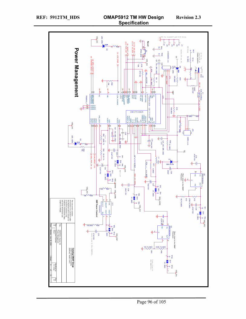
REF: 5912TM_HDS OMAP5912 TM HW Design Specification
Revision 2.3
Page 96 of 105
TP11
1
R861K
Place close to the OM
APP
rocessor.
VDD
_3V3
R91
1M,1%,0603
DC
R78
n.m..0603
P7
DC
8
SH
6
.01, 0603
VDD
_3V3
+
C76
22uf/10V R
8393.1K
1%
C25
1uF, 10V, X5R
, 0402
VB
AT
C77
1uF, 10V, X5R
, 0402
R84150,0603
C28
22uF,10V
1.5V VD
D_D
LL
VDD
_3V3
Z1
1
C31
1uF, 10V, X5R
, 0402V
DD
_SD
RA
M
TP19
1
R69.01,0805
VD
D_D
SP
SH
1.01, 0603
D9
LED
, GR
N
DC 5V In,regulated 4A
<Doc>
A1
OM
AP5912 Starter Kit
B
610
Monday
, July 26, 2004
G. C
oley
Power M
anagement
Title :
Size
Docum
ent Num
berR
ev
Date:
Sheet
of
12203 Southwest F
reeway
Stafford, Texas 77477
Catalog OM
AP Group
Modified by
:
This document contains
information on a product under
developm
ent and is issued forev
aluation purposes only.
Features characteristic data
and other information are
subject to change.
R71
n.m.,0805
TP31
TP81
TP41
R72
270K,1%,0603
VD
D_C
OR
E
250-500K
D1
SMCJ6.0A
U5
TPS71501DC
K43
51
2
Vin
NC
OU
T
FB
G
TP12
1
Delete D9 use PG.
D2
LED
, GR
N
F1
2.5A_Q
uickBlow1
2
Vref .5V
TP171
+C
30
2.2uF/10V
R79
10K,0603
PTH for standoff and 4-40 Screw
S1
SPNO
_B3S
AA
ABB
B
SH
7.01, 0603
R871K
TP71
JP2
HD
R3, n.m
.123
SH
4
.01, 0603TP
10
1
R8115K
C75
.47uF/10V
R82
243K 1%
R75
10K
Place close to the OMAP5912.
TP201
VDD
_3V3
+C
27
10uf/10V
Z3
1
C291uF
, 10V, X5R
, 0402
Place close tothe OMAP5912.
VD
D_C
OR
E
Power M
anagement
TP61
+C
33
4.7uf/10V
R114
10, 0603
Z4
1
VD
D_R
TC
R95
10, 0603
TP51
Reset
U9
TPS71501DC
K43
51
2
Vin
NC
OU
T
FB
G
VDD
_3VA
TP11
VDD
_3V3
SH
2.01, 0603
R73
1M,1%
,0603
R297
NO
PO
P
CHARGER SECTION
SWITCHER
U10
TPS65010_1
123
4 56 7 8910 11
12
13
14
151618 17 1920
21
2223 242526
27 2829 30313233 34 3536 37
38
39 404342 41
4445
46
47
48
DE
FC
OR
E
LED2
VIB
L2
VIN
CO
RE
VC
CV
INM
AIN
_AV
INM
AIN
_B
L1_AL1_B
PG
DE
FA
MIN
VM
AIN
PS_SEQ
PGN
D1_A
PGN
D1_B
GP
IO3
GP
IO4
VIN
2VLD
O2
AGND1
VIN
1
VF
B_LDO
1
VLDO
1
GP
IO2
GP
IO1
NC
IFLS
B
SD
AT
SCLK
HO
T_RE
SE
T
MP
U_R
ES
ET
RE
SP
WR
ON
PW
RF
AIL
INT
LOW
_PO
WE
R
ISE
T
TS
BA
TT_CO
VE
R
AC
US
BV
BA
T_AV
BA
T_B
AGND2AGND3
PG
ND
2
PB
_ON
OF
F
VC
OR
E
Center positiv
e.C
24
.47uF/10V
R76
10K
R88
10K
+C
32
2.2uF/10V
Z2
1
R8510K
TP91
DSP Power C
ontrol
R74
1.6K, 0603
R80
10K
R68
0
R90
243K,1%,0603
R77
0,0603
R4
0
MAX 3.0V
SH
5.01, 0603
R70
330,0603
R3
NO
PO
P
SH
3
.01, 0603
L26.8uH
C74
.47uF/10V
ESD Ring
+C
26
220uF
TP211
P2
4 HE
AD
ER
, n.m.
1234
L110uH
TP18
1
Place close to the OM
APProcessor.
D3
LED
, GR
N
DC
TP21
U11F
DC
6331L
432
6 5
1
VIN
VO
UT
VO
UT
R1/C
1
ON
/OF
F
R2
I2C.S
CL
(5,7,9)I2C.S
DA
(5,7,9)
nPG
PW
R_IN
T(5,9)
nPW
RO
N_R
ES
ET
(4)
DC
_IN
US
B_PWR
_EN
(9)
BA
TT_TEM
P
VD
D_3V
3_MA
IN
RE
SE
T_IN(9)
DC
_IN_F
US
ED
LOW
_PW
R(5)
LAN_R
ESET(10)
MP
U_nR
ESET(4)
REF: 5912TM_HDS OMAP5912 TM HW Design Specification
Revision 2.3
Page 97 of 105
C54
220pF,10V
R144
22
VD
D_3V
A
C61
.1UF
/10V
C55
220pF,10V
C56
.1uF/10V
L4FE
RR
ITE B
EA
D M
2301-ND
L5
FE
RR
ITE B
EAD
M2301-N
D
R298
22
+
C51
100UF
,6.3V
<Doc>
A1
OM
AP
5912 Starter K
it
B
710
Monday
, July 26, 2004
T. Tran
Audio C
OD
EC
Title :
Size
Docum
ent Num
berR
ev
Date:
Sheet
of
12203 Southwest F
reeway
Stafford, Texas 77477
Catalog OM
AP Group
Modified by
:
This document contains
information on a product under
development and is issued for
evaluation purposes only.
Features characteristic data
and other information are
subject to change.
C62
.1UF
/10V
TP141
VD
D_3V
A
R143330
TP15
1
R141
330
MIC_IN
U17
TLV320A
IC23P
W1213
1920181745325 26 21
22 127
28
910
1115
16 814 2
7 6 2324
LOU
T
RO
UT
LLINE
IN
RLIN
EIN
MIC
INM
ICB
IAS
DIN
LRC
IN
BCLK
XTL_MC
LK
XTO
CS
#
MO
DE
BVD
DD
VD
D
DGND
LHPO
UT
RH
POU
THPGNDAGND V
MID
HP
VD
DAV
DD
CLKO
UT
LRC
OU
T
DO
UT
SDIN
SCLK
C57
.1UF
/10V
R149
n.m.,0603
R49
0,0805C
64
.1UF
/10V, n.m.
R136
5.6K
R139
5.6KC
52
220pF,10V
C63
.1UF
/10V
R137
20K
L7
FER
RITE
BE
AD
M2301-N
DTP13
1
C53
1uF,10V
,A
P6
Stereo In
3421
+C
6010uf/10V
LINE_IN
+C
5810uf/10V
U21
DK/S
G8002C
AP
CB
-ND
(12.000MH
Z)
3
21
4O
UT
GN
DE
N
VCC
L8
FE
RR
ITE BE
AD
M2301-N
D
C49
1uF,10V
,A
HEADPHONE OUT
VD
D_3V
A
R150
20K, n.m
.
R145
20KR
14622
C59
.1UF
/10V
PW
R147
22,0603
L6
FER
RITE
BE
AD
M2301-N
D
C48
220pF,10V
R134
5.6K
L3FE
RR
ITE B
EA
D M
2301-ND
Joining analog and digitalgrounds by the CODEC
P5
Stereo In
3 4 2 1
VD
D_3V
3
R1421K
R13820K
R140
47K
R148
33, n.m.
TP16
1
R135
5.6K
+
C50
100UF
,6.3V
P1
Stereo In
3421
PIN 2 TO3???
MC
BSP
1.FS
X(5,9)
MC
BS
P1.C
LKS
(5,9)
MC
BSP
1.DR
(5,9)
MC
BSP
1.CLKX
(5,9)
MC
LK(4,9)
I2C.S
DA
(5,6,9)I2C
.SC
L(5,6,9)
MC
BSP
1.DX
(5,9)
REF: 5912TM_HDS OMAP5912 TM HW Design Specification
Revision 2.3
Page 98 of 105
VDD
_3V3
U15
SN
74CB
TLV3257
235611101413151
47912
168
1A1B2A2B3A3B4A4BGA/B
1Y2Y3Y4Y
VCCGND
Com
pact FlashR10510K
C73
.01uF
(
R10910K
R159
20K
R120
0,0603
R10610K
U16
SN
74CB
TLV3257
235611101413151
47912
168
1A1B2A2B3A3B4A4BGA/B
1Y2Y3Y4Y
VCCGND
R102
10K
R117
0,0603
C38
.1UF/10V
R10810K
C83
.1UF/10V
VDD
_3V3
<Doc>
A1
OM
AP5912 Starter Kit
B
810
Monday, July 26, 2004
G. C
oley
Com
pact Flash, RS
232, VlynqTitle :
SizeD
ocument N
umber
Rev
Date:
Sheet
of
12203 Southwest F
reewayS
tafford, Texas 77477
Catalog OM
AP Group
Modified by
:
This document contains
information on a product under
developm
ent and is issued forevaluation purposes only.F
eatures characteristic dataand other inform
ation aresubject to change.
C39
.1UF
/10V
R1000
0
+C
44
10uf/10V R2921KR2931K
R10410K
VDD
_3V3
R153
10
R151
10
C85
.01uF
C37
.1UF/10V
R118
n.m.,0603
R156
10
R154
100K
VDD
_3V3
C36
.1UF/10V
R157
10
R107
47K
PTC1
PTC
, 1206
U6
SN74AH
C1G
04DC
KR
24
53
C40
.1UF/10V
VD
D_3V3
R152
10
C41
.1UF/10V
R999
0
R115
0,0603
R155
20K
R158
10
P8
DS
UB
9-Male
594837261
1011
SH
80603-R
-Short
C42
.1UF/10V
(
U20B
74LVC2G
125
53
7
+C
65
10uf/10V
P14
Com
pact Flash Connector_0
1
23456
7 89 10 11 12 1314 15 16 17 18 19 20212223
2425 26 2728293031
32
33
34 353637 3839
4041 4243 44
4546 474849
50G
ND
D03
D04
D05
D06
D07
CE1
A10
OE
A09
A08
A07
VC
C
A06
A05
A04
A03
A02
A01
A00
D00
D01
D02
WP
CD
2C
D1
D11
D12
D13
D14
D15
CE2
VS1
IOR
DIO
WR
WE
RD
Y/BS
Y
VC
C
CSEL
VS2
RESE
T
WA
IT
INP
ACK
#
REG
BVD
2BV
D1
D08
D09
D10
GN
D
VDD
_3V3
U14
MAX3221
1 2456
8
14 15
16 3 7
9
1310
12 11
EN
C1+
C1-
C2+
C2-
RIN
GND VCC
FOR
CE
OFF V+ V-
RO
UT
DO
UT
INV
ALID
FO
RC
EON
DIN
Debug R
S-232 Transceiver
VD
D_3V3
R116
n.m.,0603
U20A
74LVC2G
1252
6
1 84
VLYN
Q.R
X1(9)
UAR
T3.TX(5,9)
FLASH.D
12F
LASH
.A13
CF
LASH
_EN(10)
FLA
SH.A
5
MC
BSP
2.DR
(9)
VLYN
Q.TX1
9)O
MC
BSP2.C
LKX
(5)
nCF
LASH
.IOIS16
(5,9)
FLASH.D
7
nCFLASH
.CD
1(5,9)
FLASH.D
9
RS232_R
X1
MC
BSP
2.DX
(9)
FLA
SH.A
14
FLASH.D
15
FLA
SH.A
2
FLA
SH.A
7
OM
CBS
P2.CLK
R(5)
RS232_TX1
MC
BSP
2.CLKR
(9)
FLASH.D
6
FLA
SH.A
[1..25](2,9,10)
FLASH.D
2
MC
BSP
2.FSX
(9)
nCFLASH
.CD
2(5,9)
OM
CBS
P2.FSX
(5)
MP
UIO
3(5,9)
FLASH.D
0
FLASH.D
14
GP
IO62
(5,9)
MC
BSP
2.CLKX
(9)
FLASH.D
3
OM
CBS
P2.DX
(5)
FLA
SH.A
12
FLA
SH.D
[0..15](2,9,10)
MC
BSP
2.FSR
(9)
VDD
_3V3
FLASH.D
4
nCFLAS
H.IR
EQ(5,9)
VLYN
Q.R
X0(9)
FLASH.D
1
UAR
T1.RX
(5,9)
UA
RT_D
IS(9)
FLA
SH.A
9
nCF
LASH
.RESE
T(5,9)
VD
D_3V
3
FLASH.D
10F
LASH
.A10
OM
CBS
P2.FSR
(5)
FLA
SH.A
11
nFLASH
.WE
(2,9,10)
FLA
SH.A
3
nFLA
SH.B
E1(2,9)
VLYN
Q.TX0
9)
UAR
T3.RX
(5,9)
FLASH.D
8
VLYN
Q.C
LK(9)
UAR
T1.TX(5,9)
FLA
SH.A
8
nFLASH
.OE
(2,9,10)
FLASH.D
11
FLA
SH.A
4
nFLA
SH.B
E0(2,9)
OM
CBS
P2.DR
(5)
FLA
SH.A
1
FLASH.D
13
FLA
SH.R
DY
(2,9,10)
FLA
SH.A
6FLASH
.D5
REF: 5912TM_HDS OMAP5912 TM HW Design Specification
Revision 2.3
Page 99 of 105
R100
15K
VD
D_3V
3
CONN A
P10
FX2-80P
-1.27SV
12
34
56
78
910
7372
7170
6968
6766
6564
6362
6160
5958
5756
5554
5352
5150
4948
4746
4544
4342
4140
3938
3736
3534
3332
3130
2928
2726
2524
2322
2120
1918
1716
1514
1312
11
7475
7677
7879
80
GN
D1
GN
D5
GN
D2
GN
D6
3.3V1
3.3V33.3V
23.3V4
NC
1N
C3
FLA
SH.A1
FLA
SH
.A2F
LASH
.A3F
LAS
H.A4
FLA
SH.A5
FLA
SH
.A6F
LASH
.A7F
LAS
H.A8
FLA
SH.A9
FLA
SH
.A10F
LASH
.A11F
LAS
H.A12
FLA
SH.A13
FLA
SH
.A14F
LASH
.A15F
LAS
H.A16
FLA
SH.A17
FLA
SH
.A18F
LASH
.A19F
LAS
H.A20
FLA
SH.A21
FLA
SH
.A22F
LASH
.A23F
LAS
H.A24
FLA
SH.A25
GPIO
1F
LASH
.D0
FLA
SH
.D1
FLA
SH.D
2F
LAS
H.D
3F
LASH
.D4
FLA
SH
.D5
FLA
SH.D
6F
LAS
H.D
7F
LASH
.D8
FLA
SH
.D9
FLA
SH.D
10F
LAS
H.D
11F
LASH
.D12
FLA
SH
.D13
FLA
SH.D
14F
LAS
H.D
15F
LASH
.CS
1FLA
SH
.CS
1BF
LASH
.CS
2FLA
SH
.CS
2BF
LASH
.CS
3F
LAS
H.O
EF
LASH
.RP
FLA
SH.W
PF
LASH
.WE
FLA
SH
.BE1
FLA
SH.BE
0F
LAS
H.C
LKF
LASH
.RD
YFLA
SH
.AD
VM
MC
.CLK
MM
C.D
AT1M
MC
.DA
T0M
MC
.DAT3
MM
C.D
AT2
MM
C.C
MD
MPU
_BO
OT
nEX_C
S3nE
X_CS
4F
LAS
H.D
ISG
ND
3G
ND
7G
ND
4G
ND
8
<Doc>
A1
OM
AP
5912 Starter K
it
B
910
Monday, July
26, 2004
G. C
oley
Expansion C
onnectors, US
B Host
Title :
Size
Docum
ent Num
berR
ev
Date:
Sheet
of
12203 Southw
est Freew
ayS
tafford, Texas 77477
Catalog OM
AP Group
Modified by:
This document contains
information on a product under
developm
ent and is issued forev
aluation purposes only.
Features characteristic data
and other information are
subject to change.
VD
D_3V
3
DC
VD
D_3V3
(
CO
NN
B
P11
FX2-80P-1.27SV
12
34
56
78
910
1112
55
14
57
1617
1819
2021
2223
242527
26
2928
33
3031
32
3534
3736
3938
4140
6970
7172
7374
7576
7778
7980
4345474951535961636567
4244464850526062646668 545658
1315
GN
DG
ND
GN
DG
ND
DC
DC
DC
DC
VC
C_3V
3V
CC
_3V3
VC
C_3V
3V
CC
_3V3
US
B_DM
NC
US
B_DP
MC
BS
P1.F
SX
MC
SI1.S
YN
CM
CSI1.C
LKM
CS
I1.DIN
MC
SI1.D
OU
TM
CS
I2.SY
NC
MC
SI2.CLK
MC
SI2.D
INM
CS
I2.DO
UT
BC
LKB
CLK
RE
QM
CLK
RE
Q
MC
LKC
LK32K_O
UT
NC
MC
BS
P1.D
XM
CB
SP
1.CLK
SM
CBS
P1.D
R
MC
BS
P1.C
LKX
NC
MC
BS
P2.F
SR
MC
BSP
2.DR
MC
BS
P2.D
XM
CB
SP
2.CLK
X
MC
BS
P2.F
SX
MC
BSP
2.CLK
R
NTR
ST
TMS
TDI
NE
MU
0N
EM
U1
TCK
RTC
KTD
OG
ND
GN
DG
ND
GN
D
UA
RT3.R
XU
AR
T1.TXU
AR
T1.RX
UA
RT2.TX
UA
RT2.R
TSU
AR
T1.DIS
RE
SET_IN
GP
IO4
MC
BS
P3.C
LKX
MP
UIO
4JTA
G_D
IS
UA
RT3.TX
UA
RT1.R
TSU
AR
T1.CTS
UA
RT2.C
TSU
AR
T2.RX
UAR
T2.BCLK
nRES
ET.O
UT
GP
IO8
GP
IO11
MP
UIO
3G
PIO
62
BF
AILO
N_O
FF
US
B_P
UE
N
NC
RTC
_WA
KE_IN
T
(
VDD
_3V3
VD
D_3V
3
R97
27
U18
TPS
2045
1
2 3 54678
GND
IN1
IN2
OC
EN
OU
T1O
UT2
OU
T3
+C
81
220uF,TA
NT
VD
D_3V
3
DC
R169
1.5KP4
USB
-A
1234 56
+5V-D
ATA
+DATA
GN
D
SS
DC
Conn D
P13FX2-80P
-1.27SV
135791113
24681012143637
3839
4041
4243
4445
4647
4849
5051
5253
5455
5657
5859
6061
6263
6465
6667
6869
7071
72
7778
7980
1516
1718
1920
2122
2324
2526
2728
2930
3132
3334
357374
7576
GN
DG
ND
DC
DC
VC
C_3V
3V
CC
_3V3
NC
GN
DG
ND
DC
DC
VCC
_3V3VC
C_3V3
NC
NC
NC
NC
NC
NC
NC
NC
NC
NC
NC
NC
NC
NC
NC
NC
NC
NC
NC
NC
NC
NC
NC
NC
NC
NC
NC
NC
NC
NC
NC
NC
NC
NC
NC
NC
NC
NC
GN
DG
ND
GN
DG
ND
GN
DV
LYN
Q.TX1
GN
DV
LYN
Q.TX0
GN
DV
LYN
Q.C
LKG
ND
VLYN
Q.R
X1G
ND
VLYN
Q.R
X0N
CN
CN
CN
CN
CN
CN
CN
CN
CN
CN
C
NC
NC
NC
NC
DC
R101
10K
R98
27
VD
D_3V
3
R99
15K
VD
D_3V
3D
C
R103
10K
Conn C
P12F
X2-80P-1.27SV
135791113
246810121415
1617
1819
2021
2223
2425
74
2728
2930
3132
3334
35
26
373638
394142
4344
4546
4748
4950
5152
5354
5556
5758
5960
6162
6364
6566
6768
6970
71
7673
72
7778
7980
75
40
GN
DG
ND
DC
DC
VC
C_3V
3V
CC
_3V3
NC
GN
DG
ND
DC
DC
VC
C_3V
3V
CC
_3V3
NC
GP
IO7
GP
IO3
GP
IO2
GP
IO6
GP
IO9
GP
IO13
GP
IO12
GP
IO15
GP
IO14
MP
UIO
2M
PU
IO1
UW
IRE
.CS
3
CA
M.D
0C
AM
.D1
CA
M.D
2C
AM
.D3
CA
M.D
4C
AM
.D5
CA
M.D
6C
AM
.D7
CA
M.LC
LK
CAM
.EXC
LK
CA
M.V
SC
AM
.HS
CAM
.RS
TZI2C
.SD
ALC
D.P
0LC
D.P
1LC
D.P
2LC
D.P
3LC
D.P
4LC
D.P
5LC
D.P
6LC
D.P
7LC
D.P
8LC
D.P
9LC
D.P
10LC
D.P
11LC
D.P
12LC
D.P
13LC
D.P
14LC
D.P
15LC
D.P
CLK
LCD
.AC
LCD
.VS
LCD
.HS
KB
.C0
KB
.C1
KB
.C2
KB
.C3
KB
.C4
KB
.C5
KB
.R0
KB
.R1
KB
.R2
KB
.R3
KB
.R4
UW
IRE
.SC
LKU
WIR
E.C
S0
UW
IRE
.SD
I
GN
DG
ND
GN
DG
ND
UW
IRE
.SD
O
I2C.S
CL
DC
VDD
_3V3
DC
U19
SN
75240PW1
2
3
45
6
7
8G
ND
C
GN
D
DG
ND
B
GN
D
A
TMS
(4)
UW
IRE
.SC
LK(5)
nCF
LAS
H.IR
EQ
(5,8)
FLAS
H.D
1
GP
IO13
(5)
nFLAS
H.O
E(2,8,10)
FLAS
H.A
15
FLAS
H.A
8
LCD
.AC(5)
FLAS
H.A
[1..25](2,8,10)
FLASH
.D2
UA
RT_D
IS(8)
LCD
.P12
ON
_OFF
(4)
LCD
.P4
FLAS
H.R
DY
(2,8,10)
CA
M.D
5
FLAS
H.A
16
CA
M.H
S(5)
CA
M.D
1
FLAS
H.A
9
MC
SI2.C
LK(5)
UA
RT2.R
X(5)
VLY
NQ
.TX1(8)
UW
IRE
.CS
3(5)
MC
BS
P2.CLKX
8)
GPIO
12(5)
KB
.C2
(5)
nFLA
SH.C
S2
(2,10)M
CLK
(4,7) BC
LKRE
Q(4)
LCD
.P5
FLASH
.D0
nEM
U0
(4)
US
B_P
WR
_EN
6)
FLAS
H.A
6
GP
IO15
(5)
nCF
LAS
H.C
D1
(5,8)
FLAS
H.A
17
KB
.C1
(5) MC
BS
P2.F
SR
(8)
UA
RT1.R
X(5,8)
UA
RT1.C
TS(5,8)
nFLAS
H.W
P(2)
FLAS
H.D
3
GP
IO62
(5)
LCD
.P8
FLAS
H.A
25
MC
BS
P2.CLKR
(8)
GPIO
7(5)
nFLA
SH.BE
0(2,8)
MC
SI1.D
IN(5)
CLK
32K_O
UT
(5)
UW
IRE
.CS
0(5)
FLAS
H.A
3
CA
M.D
3
GPIO
14(5)
US
B_P
UE
N(5)
LCD
.P9
CA
M.D
4
LCD
.P[0..15]
(5)
FLA
SH.A[1..25]
(2,8,10)
TCK
(4)
UA
RT2.R
TS(5)
MC
BS
P1.DX
(5,7)
GP
IO11
(5)
GPIO
2(5)
LCD
.PCLK
(5)
LCD
.P10
MP
UIO
2(5)
LCD
.P0
KB
.C3
(5)
VLY
NQ
.TX0(8)
FLAS
H.A
13
LCD
.P11
FLASH
.D4
FLASH
.D10
FLAS
H.D
13
MC
BS
P2.D
X(8)
RES
ET_IN
(6)
MC
BS
P3.C
LKX(5)
FLAS
H.A
14
MC
SI2.D
IN(5)
KB
.C5
(5)
US
B_D
P(5)
nEX_CS
3(5)
FLAS
H.D
15
VLY
NQ
.RX1
(8)nFLA
SH
.BE
1(2,8)
FLAS
H.A
7
FLAS
H.D
IS(2)
UW
IRE
.SD
O(5)
I2C.S
DA
(5,6,7)
FLA
SH
.D[0..15]
(2,8,10)
TDO
(4)
UA
RT2.B
CLK
(5)
KB
.R4
(5)
LCD
.P13
CA
M.EXC
LK(5)
UA
RT1.R
TS(5)
LCD
.P2
MP
U_B
OO
T(2)
FLAS
H.A
18
GP
IO4
(5)
CA
M.R
ST
(5)
MC
BS
P1.DR
(5,7)
nRE
SE
T.OU
T(4)
FLAS
H.A
5
MC
SI2.S
YN
C(5)
LCD
.P6
FLAS
H.A
19
US
B_D
M(5)
FLAS
H.A
2
KB
.R1
(5)
MC
LKR
EQ
(4)
FLAS
H.A
12
TDI
(4)
MC
BS
P2.F
SX
(8)
CA
M.V
S(5)
nTRS
T(4)
nFLA
SH
.CS
1A(2,10)
LCD
.VS(5)
LCD
.P[0..15]
(5)
BFA
IL(4)
nFLAS
H.W
E(2,8,10)
FLAS
H.D
11
KB
.R2
(5)
nCFLA
SH
.RE
SET
(5,8)
FLAS
H.D
9
LCD
.HS
(5)
FLAS
H.C
LK(2)
nCF
LAS
H.C
D2
(5,8)
LCD
.P14
LCD
.P15
UA
RT2.C
TS(5)
UA
RT2.TX
(5)
MC
SI1.D
OU
T(5)
nFLAS
H.C
S1B
(2)
FLASH
.D14
FLASH
.D12
FLAS
H.D
5
MC
SI1.S
YN
C(5)
FLAS
H.A
20
KB
.R0
(5)
PW
R_IN
T(5,6)
LCD
.P7
CA
M.D
6
JTAG
_DIS
(4)
BC
LK(4)
RTC
K(4)
FLAS
H.A
23
UA
RT3.TX
(5,8)
CA
M.LC
LK(5)
GP
IO1
(2)
CA
M.D
[0..7](5)
CA
M.D
7
FLAS
H.A
10
MP
UIO
3(5,8)
GPIO
9(5)
KB
.R3
(5)
UA
RT3.R
X(5,8)
nCF
LAS
H.IO
IS16
(5,8)
US
B_P
UE
N(5)
nEX_C
S4
(5)
VLY
NQ
.CLK
(8)M
CS
I1.CLK
(5)
FLAS
H.A
11
GP
IO3
(5)
USB
_DP
(5)
FLAS
H.D
7
FLAS
H.A
21
MC
BS
P1.C
LKS(5,7)
GP
IO8
(5)
WA
KEU
P_IN
T(5)
nFLA
SH
.RP
(2)
MP
UIO
4(5,7)
LCD
.P1
FLASH
.D6
USB
_DM
(5)
nEM
U1
(4)
nFLAS
H.A
DV
(2)
KB
.C4
(5)
nFLAS
H.C
S2B
(2)
FLAS
H.D
[0..15](2,8,10)
CA
M.D
2
UW
IRE
.SD
I(5)
MC
BS
P2.DR
(8)
I2C.SC
L(5,6,7)
MC
BS
P1.FS
X(5,7)
FLAS
H.A
24
MM
C.C
LK(5)
GP
IO9
(5)
LCD
.P3
MC
SI2.D
OU
T(5)
VLY
NQ
.RX0
(8)
CA
M.D
0
FLAS
H.A
22
GP
IO6
(5)
FLASH
.D8
MC
BS
P1.C
LKX(5,7)
FLAS
H.A
1
UA
RT1.TX
(5,8)
CA
M.D
[0..7](5)
KB
.C0
(5)
FLAS
H.A
4
nFLA
SH.C
S3
(2)
REF: 5912TM_HDS OMAP5912 TM HW Design Specification
Revision 2.3
Page 100 of 105
C87
.01uF
R128
5.1
R132
22K
C82
.01uF
0480:0000 - 04FF:FFFF
D5
LED,R
ED
VDD
_3V3
T1E2009
8691114 12 16 3 15
TD+
TD-
RD
+
RD
-R
X-R
XCT
RX+
TX-
TX+TXC
T D7
LED, G
RN
P9RJ45
12345678
109
A1
A2
A3
A4
A5
A6
A7
A8
S0S1
VDD
_3V3
R130
5.1
U4B
74LVC139
141315
1211109168
ABG
Y0
Y1
Y2
Y3
VCCGND
0580:0000 - 05FF:FFFF
VDD
_3V3
U13
AT93C
46
12 34
5
67
8CS
SK DI
DO
GND
OR
GD
C
VCC
0500:0000 - 057F:FFFF
R122
10K
GROUNDED PINS
+C
35
10uf/10V
LINK
LED
Y3FXP
200-2020.000M
HZ
12
R125
330, 0603R
126330, 0603
RXLE
D
VD
D_3V3
D8
LED,Y
EL
C34
.01uF
VDD
_3V3
R127
13
C46
.01uF/10V
D6
LED,Y
EL
BS
ELE
D
C78
20pf,10V
R96
10K
R161
NO
POP
C72
.01uF
C47
.01uF/10V
C86
.01uF
<Doc>
A1
OM
AP5912 S
tarter Kit
B
1010
Monday, July 26, 2004
G. C
oley
10Mb Etherent
Title :
Size
Docum
ent Num
berR
ev
Date:
Sheet
of
12203 Southwest FreewayS
tafford, Texas 77477
Catalog OM
AP Group
Modified by
:
This document contains
information on a product under
development and is issued for
evaluation purposes only.F
eatures characteristic dataand other inform
ation aresubject to change.
C45
.01uF/10V
VD
D_3V3
TXLED
0400:0000 - 047F:FFFFVD
D_3V
3
R160
0, 0603
C88
.01uF
R131
100
R162
R124
330, 0603R
123330, 0603
U12
LAN
91C96-TQ
FP
99 12345
78910
11
12131415
1718
19
2021232425
2627283031323334353637
38
394041424344454647
48
4950515253
55565758
59
60616263
656667686970
71
7273 74 757677
79
80818283848588
89
90919394959697
98
1006222954649216788687
IOS
2
ENE
EPEE
DO
/SDO
UT
EED
IEE
CS
EESK
D8
D9
D10
D11
VDD
D12
D13
D14
D15
INTR
0/IREQ
/INTR
INTR
1/INPA
CK
VDD
INTR
2/DTA
CK/0
INTR
3/DTA
CT/1
IOC
S16/IO
IS16
SBH
E/CE
2BA
LE/W
E
A0A1A2A3A4A5A6A7A8A9A10/FW
E
VDD
A11/FC
SA
12A
13A
14A
15A
16A
17A
18A
19/CE1
VDD
IOR
D/XD
SIO
WR
/R/W
MEM
/OE
AEN
/REG
/AS
IOC
HR
DY
/WAIT
D0
D1
D2
D3
VDD
D4
D5
D6
D7
RES
ETPW
RD
WN
/TXCLK
BSELED
/RXD
LNKLED
/TXDR
XLED
/RXC
LKTXLED
/TXEN
AVDD
TPETXDP
TPETXNTPETXD
NTPETXP
TXN/C
RS
TXP/C
OLL
AVDD
CO
LNC
OLP
REC
NR
ECP
TPERXN
TPERXP
RBIAS
AVDD
XEND
ECEN
16O
M/P
CM
CIA
XTAL1
XTAL2
IOS
0IO
S1
VDD
GNDGNDGNDGNDGNDGNDGNDGNDAGNDAGNDAGND
R129
13
R163
0
R121
10KC
43.01uF/10V
C79
20pf,10V
FLAS
H.A2
nFLASH.C
S1A(2,9)
FLASH.D
4
LAN_R
ESET
(6)
nFLASH.C
S2(2,9)
FLAS
H.A1
FLASH.D
1
FLA
SH.A24
(2,9)
FLASH.D
3
FLASH.D
12
nFLA
SH.W
E(2,8,9)
CFLASH
_EN(8)
FLASH.D
8
FLAS
H.A3
FLASH.D
9
FLASH.D
14
FLASH.A
[1..25](2,8,9)
FLASH.D
0
FLASH.D
13
FLASH.D
6
nEX_CS3(5)
nEX_CS4(5)
FLASH.D
7
FLA
SH.D
[0..15](2,8,9)
FLASH.D
10
FLASH.D
5
nFLASH.O
E(2,8,9)
FLA
SH.A23
(2,9)
FLASH.D
15
FLASH.D
11
FLA
SH.R
DY
(2,8,9)
FLASH.D
2
LAN
_INTR
0(5)

REF: 5912TM_HDS OMAP5912 TM HW Design Specification
Revision 2.3
Appendix D- Current Measurement Procedure
This appendix describes how to properly use the test points on the OMAP5912 OSK Target Module to take current measurements for each of the voltage rails.
Basic Principle
The basic concept is measuring the voltage drop across a .1 ohm resistor to determine the total current consumed. These technique is voltage level independent The formula used to determine the current is:
Voltage Drop /resistor = Current (ma)
The table below shows the measured voltage drop across a .1 resistor for each of the subsequent current flows:
Voltage Drop Current(ma)
.0001 1
.001 10
.05 50
.01 100
.02 200
.05 500
.1 1000
The reason such a small value has been chosen is to:
limit the power
limit the size of the resistor
limit the voltage drop to a point where it minimizes the impact on the actual voltage level
Basic Measuring Techniques
Care must be taken to minimize the impact on the operation of the circuitry on the voltage rails while taking the measurements. There are two basic ways in which the voltage drop across the resistors can be measured without impacting the operation of the circuit:
Mill volt Voltmeter
o Good for steady state current readings
o Poor response to current changes
Page 101 of 105
REF: 5912TM_HDS OMAP5912 TM HW Design Specification
Revision 2.3
Oscilloscope
o Good for real-time measurement
o Good for storage of the data
o Good response to current changes
Following are the connection methods and setup for each of these methods.
Voltmeter-
WARNING: Insure that the voltmeter used is either battery powered or if AC powered, that the ground of the meter is isolated from the earth and system ground. We don’t want to tie one side of the resistor to ground while attempting the test . It will result in shorting out the voltage supply.
1) Power off the system.
2) Set the meter to the Mv setting
3) Set the scale to 1000mv
4) Connect the meter as shown below:
5) Turn on the syste
6) The voltage disp
TPx
xm power.
layed will be in mV. A
TPx
SHdisplay of 10mV is equ
Page 102 of 105
10 MV
al to 100ma.
REF: 5912TM_HDS OMAP5912 TM HW Design Specification
Revision 2.3
Oscilloscope-
WARNING:
Insure that the Oscilloscope used is either battery powered or if AC powered, that the ground of the scope is isolated from the earth and system ground. We don’t want to tie one side of the resistor to ground while attempting the test. It will result in shorting out the voltage supply.
This test will take two probes for the test. It will take the voltage measured at TPx and add it to the inverted level measured at TPy, giving the differential voltage between the two points displayed on the Oscilloscope.
1) Power off the system.
2) Set the Oscilloscope as follows:
A channel to DC
B channel to DC
Set trigger source as A
Set A channel to .01 V/DIV
Set B channel to .01 V/DIV
Set B channel to inverted
Set A channel + B channel (Add)
Set to .1 Sec/Div (Various settings are OK)
3) Connect the Oscilloscope as shown:
5) Turn on the syste
TPx
xm power.
TPy
SHTrig CH A CH A
Page 103 of 105

REF: 5912TM_HDS OMAP5912 TM HW Design Specification
Revision 2.3
6) The voltage displayed will be in mV. A display of 10mV is equal to 100ma.
7) Current can be measured over time by getting the value at any point across the trace. As current loads change, the voltage display will change. An example scope display is shown below.
1.2 div = 12mv = 120ma 2 div = 20mv = 200ma
Oscilloscope Techniques-
Another nice function of the oscilloscope is to trigger the collection of data. This can be useful when you want to measure the current based upon an event from Software or during a specific period where the SW is in a particular piece of code.
The following procedure shows how to set things up for this technique. This will require a 4 channel scope.
1) Power off the system.
2) Set the Oscilloscope as follows:
B channel to DC
Set trigger source as external
Set A channel to .01 V/DIV
B channel inverted
Set A channel + B channel
Set to .1 Sec/Div
A channel to DC
Set B channel to .01 V/DIV
Page 104 of 105
REF: 5912TM_HDS OMAP5912 TM HW Design Specification
Revision 2.3
3) Connect the Oscilloscope as shown:
5) Turn on the syste
7) Using the storagevent or triggered bchange. An exampl
External trigger point sucha GPIO pin
6) The voltage disp
T
2 div = 20
By measuring the vcurrent can be calcu
TPx
m power.
e mode of the scoy the event. As curr
e scope display is sh
x
as
layed will be in mV. A
rigger
3 div = 30mv =
mv = 200ma
oltage at multiple poilated.
TPx
SHPage 105 of 105
pe, current can be measured during the ent loads change, the voltage display will own below.
Trig CH A CH A
display of .100mV is equal to 10ma.
120ma
nts within the trigger window, the average