nanophotonic waveguide enhanced raman spectroscopy
TRANSCRIPT
Nanophotonic Waveguide Enhanced Raman Spectroscopy
Nanofotonische golfgeleiderversterkte Ramanspectroscopie
Ashim Dhakal
Promotoren: prof. dr. ir. R. Baets, prof. dr. N. Le ThomasProefschrift ingediend tot het behalen van de graad van Doctor in de ingenieurswetenschappen: fotonica
Vakgroep InformatietechnologieVoorzitter: prof. dr. ir. D. De ZutterFaculteit Ingenieurswetenschappen en ArchitectuurAcademiejaar 2015 - 2016

ISBN 978-90-8578-928-4NUR 950Wettelijk depot: D/2016/10.500/60

GHENT UNIVERSITYFACULTY OF ENGINEERING AND ARCHITECTURE
DEPARTMENT OF INFORMATION TECHNOLOGY
Examination Committee :Prof. Dr. Ir. Patrick De Baets (Chair, Board of Governers, UGent)Prof. Dr. Ir. Peter Bienstman (Secretary, Dept. INTEC, UGent)Prof. Dr. Kevin Braeckmans (Member, UGent, Dept. Pharmaceutics, UGent)Prof. Dr. Ir. Jacob Caro (Member, Dept. Quant. Nanotech, Delft UTech.)Prof. Dr. Ir. Thomas Krauss (Member, Dept. Physics, University of York)Prof. Dr. Ir. Liesbet Lagae (Member, Director, Life Sci. Tech., IMEC)Prof. Dr. Andre Skirtach (Member, UGent, Dept. Molecular Biotech.)
Advisers and non-voting members:Prof. Dr. Ir. Roel BaetsProf. Dr. Nicolas Le Thomas
A dissertation submitted to obtainthe degree of Doctor of Photonics Engineering
Academic Year 2015-2016


List of Acronyms
ATR Attenuated total reflection (spectroscopy)CCD Charge-coupled devicecDNA Complementary deoxyribonuclic acidCMOS Complementary-metal-oxide semiconductor (technology)CM Confocal microscopeDNA Deoxyribonuclic acidFWHM Full width at half maximaIPA Isopropyl alcoholLoD Limit of detectionLDOS Local density of statesMIR Mid-infrared (wavelength region)NA Numerical apertureNIR Near-infrared (wavelength region)NWERS Nanophotonic waveguide enhanced Raman spectroscopySERS Surface enhanced Raman spectroscopySNR Signal to noise ratioSNRF Silicon nitride rich filmSOI Silicon-on-insulatorSPM Scanning probe microscopySPR Surface plasmon resonance (technique for molecular detec-
tion)TERS Tip enhanced Raman spectroscopyTE (quasi) Transverse electric (polarization)TM (quasi) Transverse magnectic (polarization)WGBL Waveguide background luminiscenceWGM Wishpering gallery mode (technique for molecular detec-
tion)


List of Symbols
P0 Power emitted by a dipole in free-space
Pin Input pump power to a waveguide or a free-space mode.
PDL,0(~r0) Power scattered by a molecule located at a position ~r0 when
excited by a diffraction-limited beam.
PDL,B Power collected from a bulk analyte by a diffraction-limited
optics when excited by a diffraction-limited beam.
PDL,S Power collected from a adsobed surface analyte by a
diffraction-limited optics when excited by a diffraction-limited
beam.
P2D Total power collected by a 2D structure such as a waveguide
from bulk cladding
Pcol,s Total power collected by a waveguide from surface molecules
Pcol Total power collected by a waveguide from bulk cladding
Ptx Transmitted pump power (without the pump filter) through the
waveguide meausred by the Raman signal collection optics
ζ(l) Power collected by a waveguide normalized to the transmitted
pump power, is a funtion of waveguide length l
ξ(l) Power collected by a waveguide normalized to the input pump
power.
Aeff,w Effective interaction area for the a monolayer of particles on a
waveguide contributing to the Raman signal.
viii
Aeff (ω) Effective mode area in context of enhancement of emission,
evaluated at an arbitrary cross-section of the waveguide.
leff (ω) Effective mode width in context of enhancement of emission,
evaluated in the direction transverse to the symmetry.
leq Equivalent length of the waveguide that provides same signal as
that of the diffraction limited beam carrying the same power
Veff,w Effective interaction volume for the bulk analyte on top of a
waveguide contributing to the Raman signal
Veff (ω) Effective mode volume in context of enhancement of emission,
evaluated at the maxima of the field.
Veff (ω,~r) Effective local mode volume in context of enhancement of
emission, evaluated at ~r.
φ Bulk enhancement factor for NWERS comapred to free sapce.
ηs Conversion efficiency for surface species (monolayer); same as
enhancement factor for NWERS comapred to free sapce.
η0 Conversion efficiency for bulk material or, for arbitrarily
distributed particles.
σ,σdiff Differential (Raman) scattering cross-section.
σnorm Wavenumber normalized (Raman) scattering cross-section.
σtot Total (Raman) scattering cross-section.
σIR Infrared absorption cross-section.
σflr Fluorescence emission cross-section.
β Raman scattering efficincy for an ensamble of emitters (the
product of σ and ρ)
ρ Volume molecular number density (unit: m−3).
ρs Surface molecular number density(unit: m−2).

ix
s Slot-sidth of slotted waveguide (assumed symmetric in this
book.
h Height of the waveguides (thickness of the deposited nitride )
= 220 nm in this book.
w Width of the waveguides.
Pw,0 Scattered optical power coupled to a waveguide from a particle
in the surrounding, normalized to the average of a diffraction
limited beam carying the same pump power.
ΛDL Integrated luminousity for a diffraction limited beam.
Λcav Integrated luminousity for an arbitrary cavity.
Λ1D Integrated luminousity for an inhomegenous system with 1D
symmetry such as a channel waveguide.
Λ2D Integrated luminousity for an inhomegenous system with 2D
symmetry such as a slab waveguide.
Dcav Local density of states inside an arbitrary cavity
D0 Local density of states for freespace.
Df Total density of states for free-space (averaged over three
othogonal directions)
D1D Local density of states for an inhomegenous system with 1D
symmetry such as a channel waveguide
D2D Total density of states for an inhomegenous system with 2D
symmetry such as a slab waveguide
~eg(~r) Field profile vector for a diffraction limited (Gaussian) beam,
normalized to the total energy/power flowing across the beam
waist (unit: m−2).
~e(~r) Field profile vector for a an arbitrary cavity, normalized to the
total energy contaied in the cavity (unit: m−3).

x
~e1(~r) Field profile vector for a an inhomegenous system with 1D
symmetry, normalized to the total enrgy stored across its
cross-section (unit: m−2).
~e2(~r) Field profile vector for an inhomegenous system with 2D
symmetry, normalized to the total enrgy stored per unit area
across the plane of symmetry (unit: m−1).
∆n Index contrast for an aribitraty waveguide
∆ Is the parameter due to a difference δα is waveguide losses for
pump and staokes frequencies, characterizing the deviation
from the linear dependence.
Q0j Average position of an ion in a molecule for a molecular
vibration with index j
Qj Normal coordinate for the position of an ion in a molecule
characterizing a vibration with index j
tint Signal integration (acquisition) time
C(ωs) Photon-phonon coupling coeficient

This book is due to you. Thanks.
(in the order of size of the text)
Roel.
For being my father figure.
Jury members.
Bettering this work.
Nicolas.
Pushing for the scientific exactness which
have made all this very much better.
Ali.
Doing some hard, boring but important
experiments.
Frederic. Jeroen.
My partner in crime (& research)
JanWillem.
Techno-nights, and awesome parities.
Stephanne, Ananth, Eva.
Numerous suggestions and advices.
Utsav, Sanjeev.
Cooking my food and tolerating my mess.
Pieter W.
Always being a supportive friend.
Being open and critical to the several
experiments we did together. Not the least:
for the dutch translation of the summary.
Photonics Research Group.
For your group meeting presentations, and
the drinks afterwards, goodbye parties,
Photonics days, light nights, good Fridays,
bad Mondays,... the list never ends.
Nuria, Jindrich.
Innumerable happy times: baziel, melac,
spijker and, of course.. BTW is that
lavender?
2*Ilse, Kristien, Mike, Michael
I will rememeber your face full of joy,
smile, and a helpful attitude; I wish I can
be like you guys.

xii
Els, Sam & De Dappere Pootjes.
Helping me explore this country the
dappere way. You are brave, kind and
awesome!
Ben, Jerry, Daniel, and RGSC diving
team.
Unforgivable times of flights, and the bike
races!
Helena.
The sweetest love.
Peter dC, Adil.
Spiritual and philosophical explorations.
Ram, Lila, 2*Sunil.
My mamaghar in Gent.
Asheesh, Sambridhi.
My home in Gent.
Vinod Golu Nashib Piyush Raju Dina Bidur.
I owe you.
Dhakal & Dahal Family.
My dears who always supported me.
Kaka-hajurba,
Atul & Savina,
Sanjeeva & Avyudaya,
Sova, and my Mom.
I dedicate this work to you. Your incessant
support and love made this possible.
My father.
Here I Am Bereft Of You.
Thus Without You, I Have Earned,
What You Yearned For Me.
Yet, Without Thee, I Would Not Be.
Nor ’d I Be Me, Nor’d ’tis All Be.
Gent, September 2016Ashim Dhakal

Table of Contents
This book is due to you. Thanks. xi
Table of Contents xiii
Nederlandse samenvatting xvii
English summary xxiii
1 Introduction 1-11.1 Raman spectroscopy and its major challenges . . . . . . . . . . . 1-11.2 The need for integrated photonics for Raman spectroscopy . . . . 1-21.3 Silicon nitride integrated waveguides for Raman spectroscopy . . 1-41.4 Problem definition and research objective . . . . . . . . . . . . . 1-61.5 Thesis outline . . . . . . . . . . . . . . . . . . . . . . . . . . . . 1-61.6 Contributions and Publications . . . . . . . . . . . . . . . . . . . 1-7
2 A Brief review of light-matter interaction and Raman spectroscopy 2-12.1 Classical description of light-matter interaction . . . . . . . . . . 2-12.2 Scattering processes . . . . . . . . . . . . . . . . . . . . . . . . . 2-2
2.2.1 Rayleigh scattering . . . . . . . . . . . . . . . . . . . . . 2-32.2.2 Raman scattering . . . . . . . . . . . . . . . . . . . . . . 2-32.2.3 Brillouin scattering . . . . . . . . . . . . . . . . . . . . . 2-5
2.3 Various definitions of scattering cross sections . . . . . . . . . . . 2-62.4 Fluorescence . . . . . . . . . . . . . . . . . . . . . . . . . . . . 2-72.5 Infrared Absorption . . . . . . . . . . . . . . . . . . . . . . . . . 2-8
2.5.1 Mutual Exclusion . . . . . . . . . . . . . . . . . . . . . . 2-92.5.2 Infrared Absorption spectroscopy . . . . . . . . . . . . . 2-92.5.3 Problems with IR spectroscopy . . . . . . . . . . . . . . 2-9
2.6 Characteristics of spontaneous Raman scattering . . . . . . . . . . 2-112.7 Efficiency of Raman scattering in an ideal free-space system . . . 2-12
2.7.1 Collection efficiency for bulk sensing . . . . . . . . . . . 2-132.7.2 Collection efficiency for surface sensing . . . . . . . . . . 2-14
2.8 Closing Remarks . . . . . . . . . . . . . . . . . . . . . . . . . . 2-15
xiv
3 Enhancement of spontaneous scattering by optical confinement 3-13.1 Classical description of enhancement of emission . . . . . . . . . 3-23.2 Enhancement of the emission in a cavity with a well-defined Q-factor 3-33.3 Scattering in a cavity with a well-defined Q-factor . . . . . . . . . 3-43.4 Scattering in an inhomogeneous medium with a 2D invariance . . 3-6
3.4.1 Calculation of LDOS and enhancement . . . . . . . . . . 3-63.4.2 Scattering efficiency . . . . . . . . . . . . . . . . . . . . 3-7
3.5 Scattering in an inhomogeneous medium with a 1D invariance . . 3-83.5.1 Comparison with free-space excitation and collection . . . 3-9
3.6 Closing Remarks . . . . . . . . . . . . . . . . . . . . . . . . . . 3-103.6.1 Resonators formed with dielectric channel waveguides . . 3-113.6.2 Fluorescence and non-radiative transitions . . . . . . . . . 3-12
4 NWERS of bulk material in the cladding 4-14.1 The efficiency of scattering . . . . . . . . . . . . . . . . . . . . . 4-1
4.1.1 Efficiency for Strip waveguides . . . . . . . . . . . . . . 4-24.1.2 Efficiency for slotted waveguides . . . . . . . . . . . . . 4-34.1.3 Equivalent length and enhancement . . . . . . . . . . . . 4-4
4.2 Considerations for coupling losses and waveguide losses . . . . . 4-54.3 Experimental demonstration of evanescent Raman scattering . . . 4-6
4.3.1 Measurement setup . . . . . . . . . . . . . . . . . . . . . 4-64.3.2 Evanescent spectroscopy of bulk liquid . . . . . . . . . . 4-7
4.4 Validation of the Theoretical Model . . . . . . . . . . . . . . . . 4-94.4.1 Sources of errors . . . . . . . . . . . . . . . . . . . . . . 4-9
4.5 Performance in comparison to the confocal microscopes . . . . . 4-104.6 Closing Remarks . . . . . . . . . . . . . . . . . . . . . . . . . . 4-13
5 NWERS of Monolayers and thin layers 5-15.1 Importance of Raman spectroscopy of Monolayers . . . . . . . . 5-25.2 Collection efficiency for monolayers . . . . . . . . . . . . . . . . 5-35.3 Experiments . . . . . . . . . . . . . . . . . . . . . . . . . . . . . 5-4
5.3.1 Demonstration of enhancement . . . . . . . . . . . . . . 5-45.4 DNA hybridization kinetics using spontaneous Raman signal . . . 5-75.5 Quantification of surface loading for a submonolayer of biotin and
biotin-streptavidin complex . . . . . . . . . . . . . . . . . . . . . 5-95.6 Determination of the cross-section of cy3 . . . . . . . . . . . . . 5-135.7 Raman spectroscopy of cell-membranes . . . . . . . . . . . . . . 5-13
5.7.1 Importance of Raman spectroscopy of Cell-membranes . . 5-135.7.2 Biocompatibility of Silicon Nitride and growth process . . 5-135.7.3 Spectrum of the cells . . . . . . . . . . . . . . . . . . . . 5-14
5.8 Closing Remarks . . . . . . . . . . . . . . . . . . . . . . . . . . 5-16
xv
6 Dependence of the efficiency on channel waveguide parameters 6-16.1 Role of index contrast in the enhancement and scattering . . . . . 6-16.2 A generic channel waveguide immersed in a medium . . . . . . . 6-26.3 Integrated channel waveguides on a substrate . . . . . . . . . . . 6-56.4 Closing Remarks . . . . . . . . . . . . . . . . . . . . . . . . . . 6-7
7 Background from waveguides and Signal-to-noise Ratio considerations 7-17.1 The origin of the waveguide WGBL . . . . . . . . . . . . . . . . 7-1
7.1.1 Raman features in the WGBL . . . . . . . . . . . . . . . 7-17.1.2 Dependence with materials . . . . . . . . . . . . . . . . . 7-27.1.3 Dependence on pump frequency . . . . . . . . . . . . . . 7-37.1.4 Dependence with pump power . . . . . . . . . . . . . . . 7-57.1.5 Origin of the broad feature in the background . . . . . . . 7-6
7.2 Determination of the WGBL efficiency . . . . . . . . . . . . . . . 7-67.3 Modeling and subtraction of the WGBL . . . . . . . . . . . . . . 7-97.4 Closing Remarks . . . . . . . . . . . . . . . . . . . . . . . . . . 7-11
8 General conclusions and perspectives on Integration with plasmonicstructures, resonators and spectrometers 8-18.1 Integration with plasmonic nanoantennas and comparison . . . . . 8-28.2 Integrated resonators . . . . . . . . . . . . . . . . . . . . . . . . 8-28.3 Comparison with techniques based on refractive index sensing . . 8-38.4 General Conclusions . . . . . . . . . . . . . . . . . . . . . . . . 8-4
8.4.1 Microscope-less . . . . . . . . . . . . . . . . . . . . . . 8-48.4.2 Smallest etendue enabling integration with compact spec-
trometers and light sources . . . . . . . . . . . . . . . . . 8-48.4.3 High Performance . . . . . . . . . . . . . . . . . . . . . 8-58.4.4 CMOS compatible . . . . . . . . . . . . . . . . . . . . . 8-5
8.5 Closing Remarks: Applications . . . . . . . . . . . . . . . . . . . 8-5
A Calculation of free-space Green’s Dyadic A-1
B Calculation of Signal-to-noise ratio B-1
C DNA hybridization kinetics C-1
D Etendue of a beam, number of modes and spectrometer size D-1
References D-5


Nederlandse samenvatting–Summary in Dutch–
Nanophotonische golfgeliederversterkte Ramanspectroscopie. Hoewel Ram-anspectroscopie de laatste decennia een enorme vooruitgang gekend heeft in ver-scheidene disciplines, hebben tot heden weinig toepassingen de stap gezet heeftvan het gespecialiseerde laboratorium naar een industriele omgeving. De extreemzwakke aard van Raman verstrooiing vereist niet alleen zeer gevoelige detectie-technieken, in veel gevallen is ook een versterking vereist van het intrinsieke sig-naal. Coherente, gestimuleerde of surface-enhanced Raman scattering zijn enkelegeavanceerde methodes om deze versterking te bereiken. Een eenvoudiger conceptbestaat erin het licht enerzijds te begrenzen tot een zeer klein volume en anderzijdsgebruik te maken van een grotere interactielengte tussen het licht en de moleculendie aanleiding geven tot Raman verstrooiing. In dit werk bespreken we de verschil-lende aspecten van nanofotonische, golfgeleider-versterkte Ramanspectroscopie.We zullen aantonen hoe geıntegreerde enkelvoudige-mode golfgeleiders gebruiktkunnen worden om een Raman signaal zowel evanescent te exciteren als op tevangen, waarbij de intrinsieke voordelen van Raman spectroscopie in een lab-on-chip framework duidelijk worden. De combinatie van een groot detectievolumesamen met de veldversterking nabij hoog index-contrast golfgeleiders leidt hierbijtot meer dan duizendvoudige signaalversterking in vergelijking met een conventi-onele Raman microscoop.
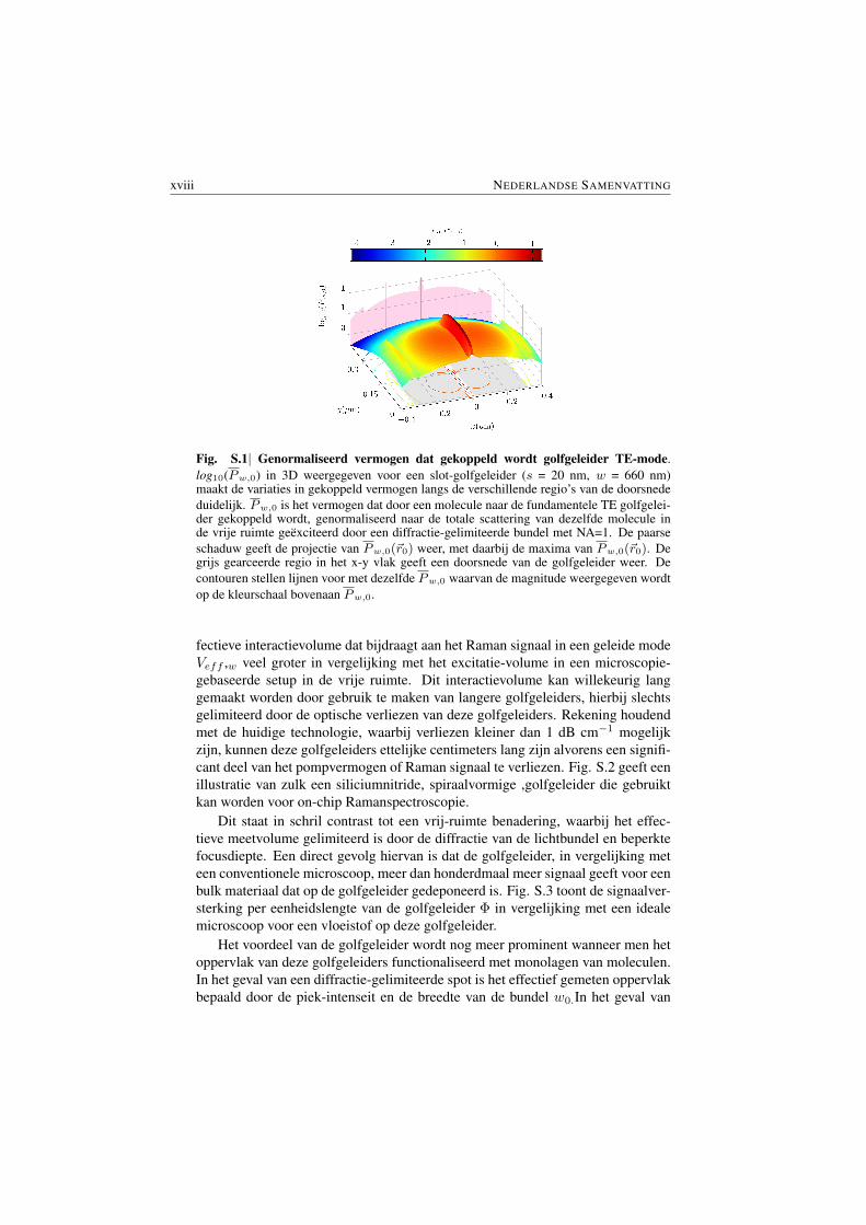
Fig. S.1 toont een logaritmische plot van het genormaliseerde Raman vermo-gen Pw,0 dat op verschillende posities gekoppeld wordt naar de fundamentele TEmode van een door water omringde siliciumnitride slot golfgeleider (s = 20 nm,w = 660 nm). Teneinde dit de vergelijken met microscopische technieken is hetRaman signaal in deze figuur genormaliseerd naar het totale Raman vermogen datuitgestraald wordt door dezelfde molecule wanneer deze geexciteerd wordt dooreen ideale, diffractie-gelimiteerde lichtbundel (NA = 1) met hetzelfde vermogen inde vrije ruimte. De figuur toont aan dat het Raman vermogen dat gecollecteerdwordt van een molecule in de slot van de waveguide meer dan tien keer hoger isin vergelijking met het diffractie-gelimiteerde systeem. Dit duidt op de immensemogelijkheid tot versterking van het Raman signaal door gebruik te maken vangoed ontworpen golfgeleiders.
Naast de transversaal versterking, zoals geıllustreerd in Fig. S.1 is de meest be-langrijke bijdrage aan de versterking bij het NWERS concept afkomstig van de lon-gitudinale propagatie van de mode langsheen de golfgeleider. Hierdoor is het ef-
xviii NEDERLANDSE SAMENVATTING
Fig. S.1| Genormaliseerd vermogen dat gekoppeld wordt golfgeleider TE-mode.log10(Pw,0) in 3D weergegeven voor een slot-golfgeleider (s = 20 nm, w = 660 nm)maakt de variaties in gekoppeld vermogen langs de verschillende regio’s van de doorsnededuidelijk. Pw,0 is het vermogen dat door een molecule naar de fundamentele TE golfgelei-der gekoppeld wordt, genormaliseerd naar de totale scattering van dezelfde molecule inde vrije ruimte geexciteerd door een diffractie-gelimiteerde bundel met NA=1. De paarseschaduw geeft de projectie van Pw,0(~r0) weer, met daarbij de maxima van Pw,0(~r0). Degrijs gearceerde regio in het x-y vlak geeft een doorsnede van de golfgeleider weer. Decontouren stellen lijnen voor met dezelfde Pw,0 waarvan de magnitude weergegeven wordtop de kleurschaal bovenaan Pw,0.
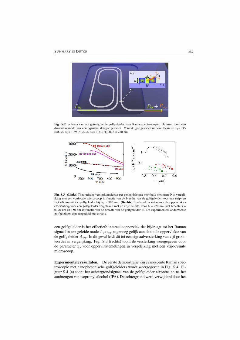
fectieve interactievolume dat bijdraagt aan het Raman signaal in een geleide modeVeff ,w veel groter in vergelijking met het excitatie-volume in een microscopie-gebaseerde setup in de vrije ruimte. Dit interactievolume kan willekeurig langgemaakt worden door gebruik te maken van langere golfgeleiders, hierbij slechtsgelimiteerd door de optische verliezen van deze golfgeleiders. Rekening houdendmet de huidige technologie, waarbij verliezen kleiner dan 1 dB cm−1 mogelijkzijn, kunnen deze golfgeleiders ettelijke centimeters lang zijn alvorens een signifi-cant deel van het pompvermogen of Raman signaal te verliezen. Fig. S.2 geeft eenillustratie van zulk een siliciumnitride, spiraalvormige ,golfgeleider die gebruiktkan worden voor on-chip Ramanspectroscopie.
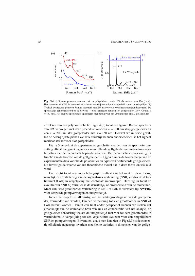
Dit staat in schril contrast tot een vrij-ruimte benadering, waarbij het effec-tieve meetvolume gelimiteerd is door de diffractie van de lichtbundel en beperktefocusdiepte. Een direct gevolg hiervan is dat de golfgeleider, in vergelijking meteen conventionele microscoop, meer dan honderdmaal meer signaal geeft voor eenbulk materiaal dat op de golfgeleider gedeponeerd is. Fig. S.3 toont de signaalver-sterking per eenheidslengte van de golfgeleider Φ in vergelijking met een idealemicroscoop voor een vloeistof op deze golfgeleider.
Het voordeel van de golfgeleider wordt nog meer prominent wanneer men hetoppervlak van deze golfgeleiders functionaliseerd met monolagen van moleculen.In het geval van een diffractie-gelimiteerde spot is het effectief gemeten oppervlakbepaald door de piek-intenseit en de breedte van de bundel w0.In het geval van
SUMMARY IN DUTCH xix
Fig. S.2| Schema van een geıntegreerde golfgeleider voor Ramanspectroscopie. De inzet toont eendwarsdoorsnede van een typische slot-golfgeleider. Voor de golfgeleider in deze thesis is n1=1.45(SiO2), n2= 1.89 (Si3N4), n3= 1.33 (H2O), h = 220 nm.
Fig. S.3 | (Links) Theoretische versterkingsfactor per eenheidslengte voor bulk metingen Φ in vergeli-jking met een confocale microscoop in functie van de breedte van de golfgeleider voor een strip- enslot siliciumnitride golfgeleider bij λ0 = 785 nm. (Rechts) Berekende warden voor de oppervlakte-efficientieηsvoor een golfgeleider vergeleken met de vrije ruimte, voor h = 220 nm, slot breedte s =0, 20 nm en 150 nm in functie van de breedte van de golfgeleider w. De experimenteel onderzochtegolfgeleiders zijn aangeduid met cirkels.
een golfgeleider is het effectiefe interactieoppervlak dat bijdraagt tot het Ramansignaal in een geleide mode Aeff ,w nagenoeg gelijk aan de totale oppervlakte vande golfgeleider Awg . In dit geval leidt dit tot een signaalversterking van vijf groot-teordes in vergelijking. Fig. S.3 (rechts) toont de versterking weergegeven doorde parameter ηs voor oppervlaktemetingen in vergelijking met een vrije-ruimtemicroscoop.
Experimentele resultaten. De eerste demonstratie van evanescente Raman spec-troscopie met nanophotonische golfgeleiders wordt weergegeven in Fig. S.4. Fi-guur S.4 (a) toont het achtergrondsignaal van de golfgeleider alvorens en na hetaanbrengen van isopropyl alcohol (IPA). De achtergrond werd verwijderd door het
xx NEDERLANDSE SAMENVATTING
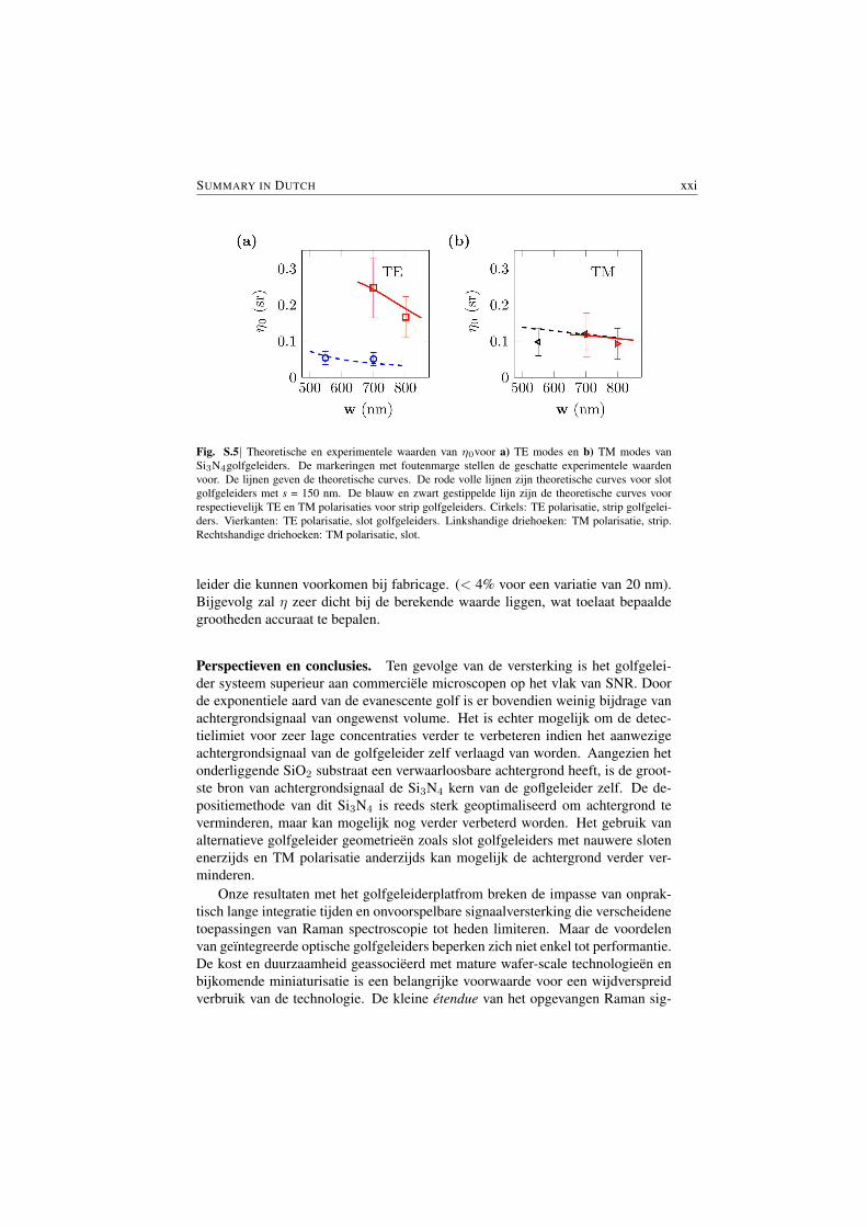
Fig. S.4| a) Spectra gemeten met een 1.6 cm golfgeleider zonder IPA (blauw) en met IPA (rood).Het spectrum van IPA is verticaal verschoven waarbij het nulpunt aangeduid is met de stippellijn. B)Typisch evanescent gemeten Raman spectrum van IPA na correctie voor het achtergrondspectrum. Despectra zijn genormaliseerd op de 819 cm−1 piek verkregen met een slot golfgeleider. (w = 700 nm, s= 150 nm). Het blauwe spectrum is opgemeten met behulp van een 700 nm strip Si3N4 golfgeleider.
aftrekken van een polynomische fit. Fig S.4 (b) toont een typisch Raman spectrumvan IPA verkregen met deze procedure voor een w = 700 nm strip golfgeleider eneen w = 700 nm slot golfgeleider met s = 150 nm. Hoewel we in beide geval-len de belangrijkste pieken van IPA duidelijk kunnen onderscheiden, is het signaalmerbaar sterker voor slot golfgeleider.
Fig. S.5 vergelijkt de experimenteel geschatte waarden van de specifieke om-zetting efficientieη0verkregen voor verschillende golfgeleider-geometrieen en –po-larisaties met de theoretisch bepaalde waarden. De theoretische curves van η0 infunctie van de breedte van de golfgeleider w liggen binnen de foutenmarge van deexperimentele data voor beide polarisaties en types van bestudeerde golfgeleiders.Dit bevestigd de waarde van het theoretische model dat in deze thesis ontwikkeldwerd.
Fig. (S.6) toont een ander belangrijk resultaat van het werk in deze thesis,namelijk een verbetering van de signaal-ruis verhouding (SNR) en dus de detec-tielimiet (LoD) in vergelijking met confocale microscopie. Deze figuur toont deevolutie van SNR bij variaties in de densiteitρs of crosssectie σ van de moleculen.Meer dan twee grootteordes verbetering in SNR of LoD is verwacht bij NWERSvoor eenzelfde pompvermogen en integratietijd.
Indien het hagelruis, afkomstig van het achtergrondsignaal van de golfgelei-der, verminder kan worden, kan een verbetering tot vier grootteordes in SNR ofLoD bereikt worden. Vanuit een licht ander perspectief kunnen we stellen datafhankelijk van de dominante bron van ruis en concentratie van het analyte, degolfgeleider-benadering toelaat de integratietijd met vier tot acht grootteordes teverminderen in vergelijking tot een vrije-ruimte systeem voor een vergelijkbareSNR en pompvermogen. Bovendien, zoals men kan zien in Fig (S.3) is de conver-tie efficientie nagenoeg invariant met kleine variaties in dimensies van de golfge-
SUMMARY IN DUTCH xxi
Fig. S.5| Theoretische en experimentele waarden van η0voor a) TE modes en b) TM modes vanSi3N4golfgeleiders. De markeringen met foutenmarge stellen de geschatte experimentele waardenvoor. De lijnen geven de theoretische curves. De rode volle lijnen zijn theoretische curves voor slotgolfgeleiders met s = 150 nm. De blauw en zwart gestippelde lijn zijn de theoretische curves voorrespectievelijk TE en TM polarisaties voor strip golfgeleiders. Cirkels: TE polarisatie, strip golfgelei-ders. Vierkanten: TE polarisatie, slot golfgeleiders. Linkshandige driehoeken: TM polarisatie, strip.Rechtshandige driehoeken: TM polarisatie, slot.
leider die kunnen voorkomen bij fabricage. (< 4% voor een variatie van 20 nm).Bijgevolg zal η zeer dicht bij de berekende waarde liggen, wat toelaat bepaaldegrootheden accuraat te bepalen.
Perspectieven en conclusies. Ten gevolge van de versterking is het golfgelei-der systeem superieur aan commerciele microscopen op het vlak van SNR. Doorde exponentiele aard van de evanescente golf is er bovendien weinig bijdrage vanachtergrondsignaal van ongewenst volume. Het is echter mogelijk om de detec-tielimiet voor zeer lage concentraties verder te verbeteren indien het aanwezigeachtergrondsignaal van de golfgeleider zelf verlaagd van worden. Aangezien hetonderliggende SiO2 substraat een verwaarloosbare achtergrond heeft, is de groot-ste bron van achtergrondsignaal de Si3N4 kern van de goflgeleider zelf. De de-positiemethode van dit Si3N4 is reeds sterk geoptimaliseerd om achtergrond teverminderen, maar kan mogelijk nog verder verbeterd worden. Het gebruik vanalternatieve golfgeleider geometrieen zoals slot golfgeleiders met nauwere slotenenerzijds en TM polarisatie anderzijds kan mogelijk de achtergrond verder ver-minderen.
Onze resultaten met het golfgeleiderplatfrom breken de impasse van onprak-tisch lange integratie tijden en onvoorspelbare signaalversterking die verscheidenetoepassingen van Raman spectroscopie tot heden limiteren. Maar de voordelenvan geıntegreerde optische golfgeleiders beperken zich niet enkel tot performantie.De kost en duurzaamheid geassocieerd met mature wafer-scale technologieen enbijkomende miniaturisatie is een belangrijke voorwaarde voor een wijdverspreidverbruik van de technologie. De kleine etendue van het opgevangen Raman sig-

xxii NEDERLANDSE SAMENVATTING
Fig. S.6 | Evolutie van SNR voor verschillende ρsσsvoor een monolaag van molecules gebaseerdop de gemeted waarde (aangeduid met de verticale cyaan lijn). De evolutie voor een ideaal systeem,waarbij hagelrius van het signaal de enige ruisbron is, is aangeduid met stippellijn voor beide systemen.
naal in een enkelvoudige-mode golfgeleider laat bovendien de integratie toe metde kleinst mogelijke geıntegreerde spectrometers. Een performante, goedkope encompacte Raman sensor kan dus geıntegreerd worden op een chip. Bovendien kandit platform gecombineerd worden met nanoplasmonische antennes voor SERS,waarbij een nog hogere signaalversterking het mogelijk maakt om zeer kleine vo-lumes te detecteren.
Ter conclusie vatten we de voornaamste resultaten van het doctoraatsonder-zoek in deze thesis samen:
1. Ontwikkelen van een model voor het kwantificeren van de versterking me-chanismes nabij golfgeleiders en caviteiten. Voorspelling van het signaal ineen realistische configuratie en de experimentele validatie hiervan.
2. Eerste demonstratie van evanescente Ramanspectroscopie met nanofotoni-sche golfgeleiders.
3. Microscoop-vrij, lab-on-a-chip, geıntegreerd CMOS compatible Raman plat-form voor zowel bulk vloeistoffen en monolagen van moleculen in het nabijeinfrarood.
4. Theoretische en experimentele demonstratie van minstens twee grootte-ordersverbetering van signaal-ruisverhouding in vergelijking met een vrije-ruimtesysteem door gebruik te maken van een geıntegreerd platform.
5. Onderzoek van het achtergrondsignaal van de golfgeleiders in functie vanverschillende experimentele variabelen.
English summary
Nanophotonic waveguide enhanced Raman spectroscopy. Despite the enor-mous progress made over the past decades in demonstrating and identifying sev-eral applications, Raman spectroscopy has not yet found a widespread use as apoint-of-need tool outside of the specialized labs. As the Raman scattering pro-cess is intrinsically weak, it requires advanced techniques to enhance and detectthe signal. Coherent Raman scattering, stimulated Raman scattering, and surfaceenhanced Raman scattering (SERS) are only a few examples of advanced tech-niques devised to enhance the Raman signal. One method to enhance the Ramansignal is to confine the light in a very small volume using nanophotonic waveg-uides thereby improving the evanescent interaction and simultaneously also ex-tending the interaction volume, by the means of waveguiding, to boost the Ramansignal. In this thesis, we discuss various aspects of this nanophotonic waveguideenhanced Raman spectroscopy (NWERS). We will show that integrated single-mode waveguides can be used to evanescently excite and collect Raman signalsand have intrinsic performance advantages to implement Raman spectroscopy ina lab-on-a-chip framework. A large detection volume of the analyte molecules inthe surrounding of a long single mode waveguide is combined with the field en-hancement near a high-index-contrast waveguide to obtain more than three ordersof magnitude larger signal compared to conventional free-space setup.
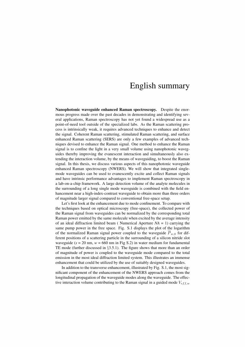
Let’s first look at the enhancement due to mode confinement. To compare withthe techniques based on optical microscopy (free-space), the collected power ofthe Raman signal from waveguides can be normalized by the corresponding totalRaman power emitted by the same molecule when excited by the average intensityof an ideal diffraction limited beam ( Numerical Aperture NA = 1) carrying thesame pump power in the free space. Fig. S.1 displays the plot of the logarithmof the normalized Raman signal power coupled to the waveguide Pw,0 for dif-ferent positions of a scattering particle in the surrounding of a silicon nitride slotwaveguide (s = 20 nm, w = 660 nm in Fig S.2) in water medium for fundamentalTE mode (further discussed in §3.5.1). The figure shows that more than an orderof magnitude of power is coupled to the waveguide mode compared to the totalemission in the most ideal diffraction limited system. This illustrates an immenseenhancement that could be utilized by the use of suitably designed waveguides.
In addition to the transverse enhancement, illustrated by Fig. S.1, the most sig-nificant component of the enhancement of the NWERS approach comes from thelongitudinal propagation of the waveguide modes along the waveguide. The effec-tive interaction volume contributing to the Raman signal in a guided mode Veff,w
xxiv ENGLISH SUMMARY
Fig. S.1| Normalized power coupled to the waveguide mode. log10(Pw,0(~r0)) for a slotted waveg-uide (s = 20 nm, w = 660 nm) shown in 3D highlighting the variations of the coupled power acrossthe various regions of the section. Pw,0(~r0) is the power coupled from a particle to the fundamentalTE waveguide mode as a function of the emitter position ~r0, normalized to the total emission from theparticle when excited by a diffraction limited beam with NA = 1. The purple shaded area shows theprojection of Pw,0(~r0), indicating the maxima of the Pw,0(~r0). The gray shaded region in the x-yplane indicates the waveguide cross-section. The contours represent the lines with the same Pw,0 andthe color bar shows the magnitude of Pw,0.
is much larger than the confocal volume in a free-space setup. This Veff,w can bemade arbitrarily large by using longer waveguide, limited only by the waveguidelosses. With the current technology, waveguide losses smaller than 1 dB cm−1
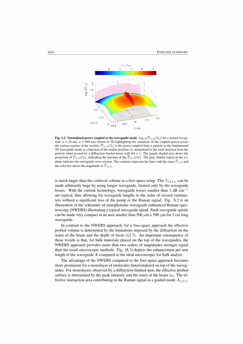
are typical, thus allowing for waveguide lengths in the order of several centime-ters without a significant loss of the pump or the Raman signal. Fig. S.2 is anillustration of the schematic of nanophotonic waveguide enhnanced Raman spec-troscopy (NWERS) illustrating a typical waveguide spiral. Such waveguide spiralscan be made very compact in an area smaller than 500 µm x 500 µm for 1 cm longwaveguide.
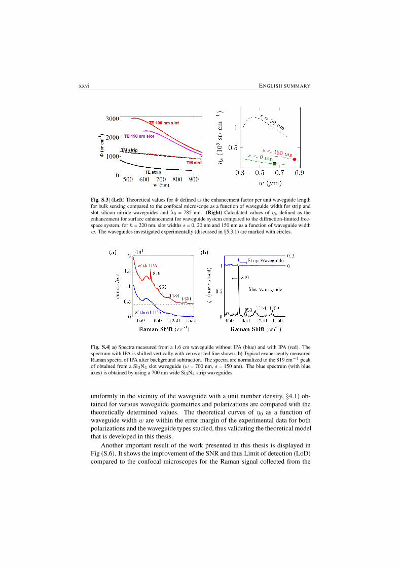
In contrast to the NWERS approach, for a free-space approach the effectiveprobed volume is determined by the limitations imposed by the diffraction on thewaist of the beam and the depth of focus (§2.7). An important consequence ofthese results is that, for bulk materials placed on the top of the waveguides, theNWERS approach provides more than two orders of magnitudes stronger signalthan the usual microscopic methods. Fig. (S.3) depicts the enhancement per unitlength of the waveguide Φ compared to the ideal microscopes for bulk analyte.
The advantage of the NWERS compared to the free-space approach becomesmore prominent for a monolayer of molecules functionalized on top of the waveg-uides. For monolayers observed by a diffraction-limited spot, the effective probedsurface is determined by the peak intensity and the waist of the beam w0. The ef-fective interaction area contributing to the Raman signal in a guided mode Aeff,w

ENGLISH SUMMARY xxv
Fig. S.2| The schematic of the waveguide integrated Raman spectroscopic system. Inset shows a cross-section of a generic slot waveguide. For the waveguide used in this article n1= 1.45 (SiO2), n2= 1.89(Si3N4), n3= 1.33 (H2O), h = 220 nm.
is almost equal to the total surface area Awg of the waveguides. This leads tomore than five orders of magnitude enhancement in the signal compared to thefree-space approach (discussed further in §5.2). Fig. S.3 (Right) shows the en-hancement (quantified by a parameter surface conversion efficiency ηs) for surfacesensing compared to the free-space.
Further, as can be seen in Fig (S.3), the conversion efficiency values are practi-cally invariant with small variations in the waveguide dimensions that might occurduring fabrication (< 4 % for a variation of 20 nm); hence it will remain very closeto the calculated value in average. This makes the design of the spectroscopic sys-tem quite robust in spite of fabrication tolerances.
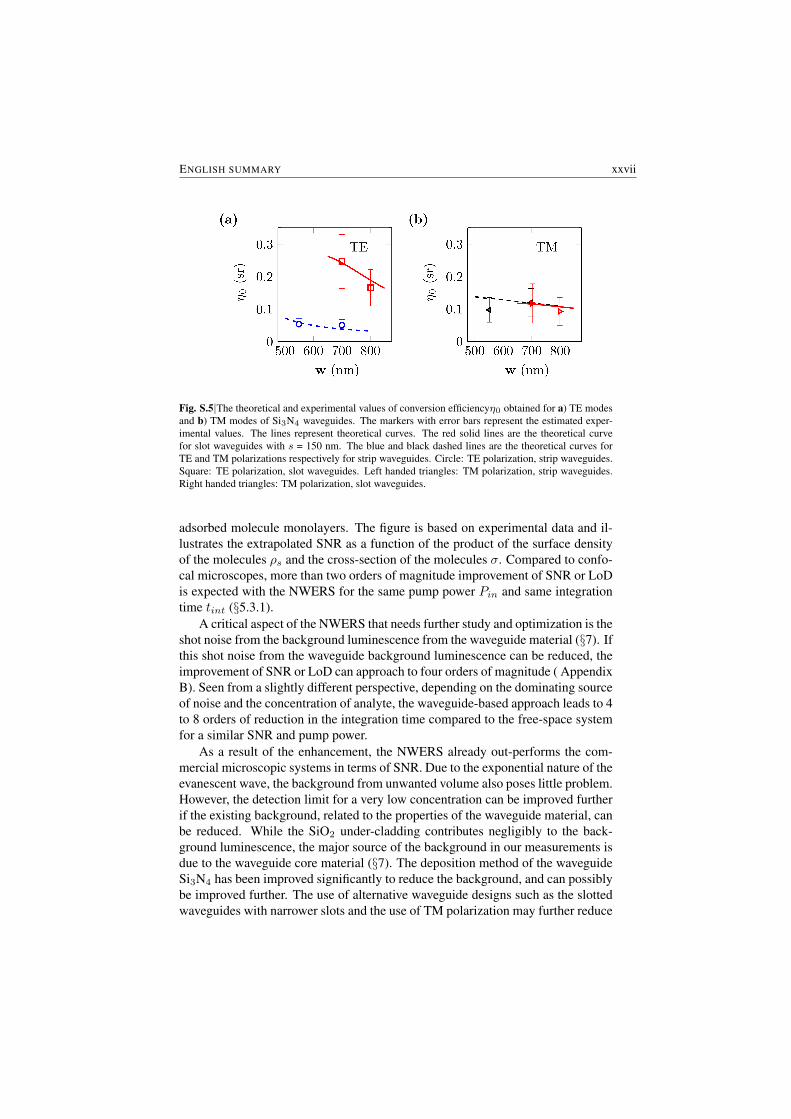
Experimental Results. The first demonstration of NWERS is presented in Fig.S.4. Fig. S.4 (a) shows the signal observed from the Si3N4 waveguide ( §1.3)before and after application of an analyte on the upper cladding of the waveguide.The background luminescence from the waveguide observed before applicationof the analyte (in the present case it is isopropyl alcohol (IPA)) was fitted witha truncated polynomial and was removed by subtracting the corresponding poly-nomial fit ( S 7.4). Fig. S.4 (b) shows typical Raman spectra of IPA obtainedusing such a procedure for a strip waveguide with width w = 700 nm and a slot-ted waveguide with total width w = 700 nm and slot width s = 150 nm. All themajor peaks of IPA are clearly distinguishible. A major highlight of Fig S.4 (b) isabout 8 times enhanced signal for slotted waveguides. This demonstrates anotherimportant characteristic of the NWERS which allows us to tailor the waveguideenhancement.
In Fig. S.5, the experimental values of the specific conversion efficiency η0
(defined as the ratio of collected Raman power per unit input pump power in awaveguide of unit length for particles of unit scattering cross-section distributed
xxvi ENGLISH SUMMARY
Fig. S.3| (Left) Theoretical values for Φ defined as the enhancement factor per unit waveguide lengthfor bulk sensing compared to the confocal microscope as a function of waveguide width for strip andslot silicon nitride waveguides and λ0 = 785 nm. (Right) Calculated values of ηs defined as theenhancement for surface enhancement for waveguide system compared to the diffraction-limited free-space system, for h = 220 nm, slot widths s = 0, 20 nm and 150 nm as a function of waveguide widthw. The waveguides investigated experimentally (discussed in §5.3.1) are marked with circles.
Fig. S.4| a) Spectra measured from a 1.6 cm waveguide without IPA (blue) and with IPA (red). Thespectrum with IPA is shifted vertically with zeros at red line shown. b) Typical evanescently measuredRaman spectra of IPA after background subtraction. The spectra are normalized to the 819 cm−1 peakof obtained from a Si3N4 slot waveguide (w = 700 nm, s = 150 nm). The blue spectrum (with blueaxes) is obtained by using a 700 nm wide Si3N4 strip waveguides.
uniformly in the vicinity of the waveguide with a unit number density, §4.1) ob-tained for various waveguide geometries and polarizations are compared with thetheoretically determined values. The theoretical curves of η0 as a function ofwaveguide width w are within the error margin of the experimental data for bothpolarizations and the waveguide types studied, thus validating the theoretical modelthat is developed in this thesis.
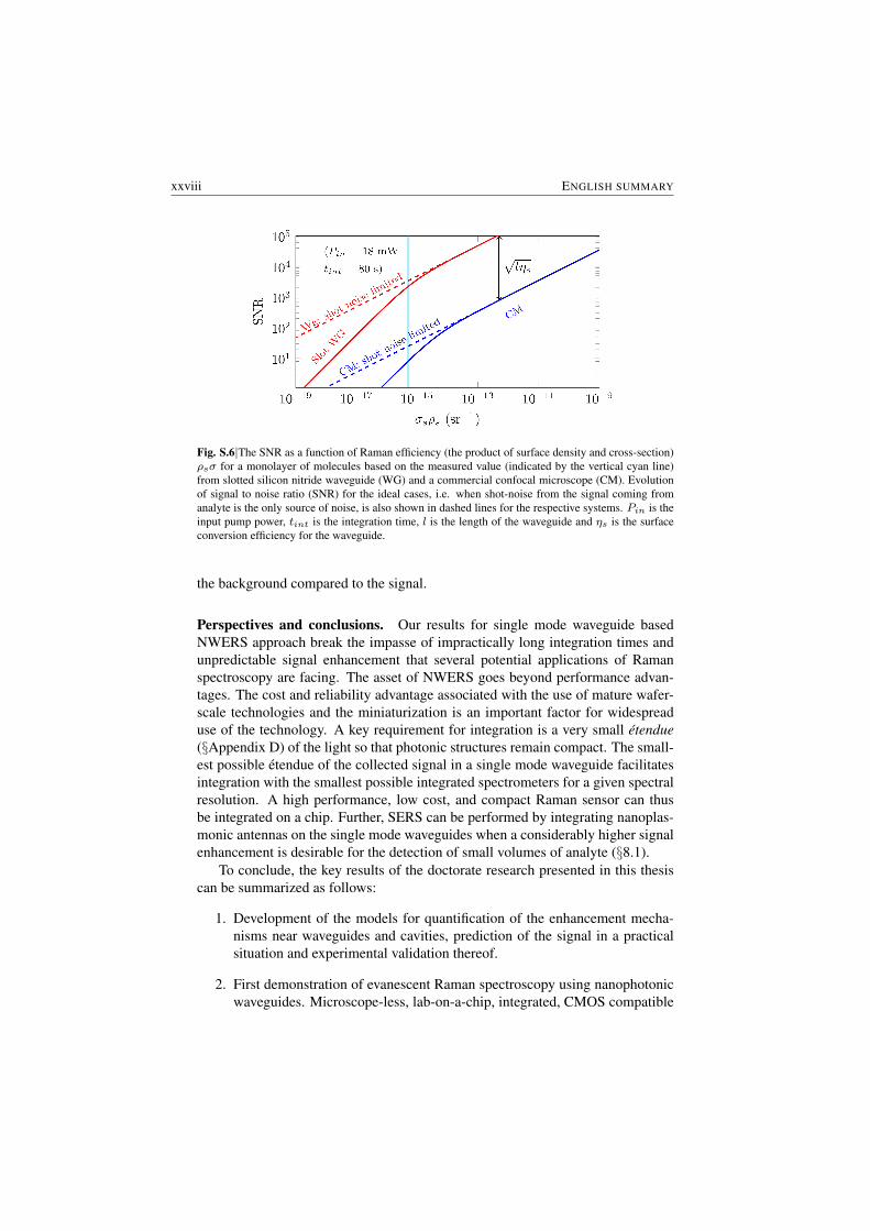
Another important result of the work presented in this thesis is displayed inFig (S.6). It shows the improvement of the SNR and thus Limit of detection (LoD)compared to the confocal microscopes for the Raman signal collected from the
ENGLISH SUMMARY xxvii
Fig. S.5|The theoretical and experimental values of conversion efficiencyη0 obtained for a) TE modesand b) TM modes of Si3N4 waveguides. The markers with error bars represent the estimated exper-imental values. The lines represent theoretical curves. The red solid lines are the theoretical curvefor slot waveguides with s = 150 nm. The blue and black dashed lines are the theoretical curves forTE and TM polarizations respectively for strip waveguides. Circle: TE polarization, strip waveguides.Square: TE polarization, slot waveguides. Left handed triangles: TM polarization, strip waveguides.Right handed triangles: TM polarization, slot waveguides.
adsorbed molecule monolayers. The figure is based on experimental data and il-lustrates the extrapolated SNR as a function of the product of the surface densityof the molecules ρs and the cross-section of the molecules σ. Compared to confo-cal microscopes, more than two orders of magnitude improvement of SNR or LoDis expected with the NWERS for the same pump power Pin and same integrationtime tint (§5.3.1).
A critical aspect of the NWERS that needs further study and optimization is theshot noise from the background luminescence from the waveguide material (§7). Ifthis shot noise from the waveguide background luminescence can be reduced, theimprovement of SNR or LoD can approach to four orders of magnitude ( AppendixB). Seen from a slightly different perspective, depending on the dominating sourceof noise and the concentration of analyte, the waveguide-based approach leads to 4to 8 orders of reduction in the integration time compared to the free-space systemfor a similar SNR and pump power.
As a result of the enhancement, the NWERS already out-performs the com-mercial microscopic systems in terms of SNR. Due to the exponential nature of theevanescent wave, the background from unwanted volume also poses little problem.However, the detection limit for a very low concentration can be improved furtherif the existing background, related to the properties of the waveguide material, canbe reduced. While the SiO2 under-cladding contributes negligibly to the back-ground luminescence, the major source of the background in our measurements isdue to the waveguide core material (§7). The deposition method of the waveguideSi3N4 has been improved significantly to reduce the background, and can possiblybe improved further. The use of alternative waveguide designs such as the slottedwaveguides with narrower slots and the use of TM polarization may further reduce
xxviii ENGLISH SUMMARY
Fig. S.6|The SNR as a function of Raman efficiency (the product of surface density and cross-section)ρsσ for a monolayer of molecules based on the measured value (indicated by the vertical cyan line)from slotted silicon nitride waveguide (WG) and a commercial confocal microscope (CM). Evolutionof signal to noise ratio (SNR) for the ideal cases, i.e. when shot-noise from the signal coming fromanalyte is the only source of noise, is also shown in dashed lines for the respective systems. Pin is theinput pump power, tint is the integration time, l is the length of the waveguide and ηs is the surfaceconversion efficiency for the waveguide.
the background compared to the signal.
Perspectives and conclusions. Our results for single mode waveguide basedNWERS approach break the impasse of impractically long integration times andunpredictable signal enhancement that several potential applications of Ramanspectroscopy are facing. The asset of NWERS goes beyond performance advan-tages. The cost and reliability advantage associated with the use of mature wafer-scale technologies and the miniaturization is an important factor for widespreaduse of the technology. A key requirement for integration is a very small etendue(§Appendix D) of the light so that photonic structures remain compact. The small-est possible etendue of the collected signal in a single mode waveguide facilitatesintegration with the smallest possible integrated spectrometers for a given spectralresolution. A high performance, low cost, and compact Raman sensor can thusbe integrated on a chip. Further, SERS can be performed by integrating nanoplas-monic antennas on the single mode waveguides when a considerably higher signalenhancement is desirable for the detection of small volumes of analyte (§8.1).
To conclude, the key results of the doctorate research presented in this thesiscan be summarized as follows:
1. Development of the models for quantification of the enhancement mecha-nisms near waveguides and cavities, prediction of the signal in a practicalsituation and experimental validation thereof.
2. First demonstration of evanescent Raman spectroscopy using nanophotonicwaveguides. Microscope-less, lab-on-a-chip, integrated, CMOS compatible
ENGLISH SUMMARY xxix
Raman spectroscopy of both bulk and a monolayer of molecules in the NIRwavelength region.
3. Characterization of the dependence of waveguide background luminescencespectrum from the waveguides as a function of different experimental vari-ables.
4. Study of the impact of the waveguide background noise on the performanceof the NWERS. Experimental demonstration of at least two orders of mag-nitude enhancement in SNR, compared to free-space system, by the use ofthe waveguide in an integrated platform.

1Introduction
In this chapter, the context of this PhD thesis will be introduced and its objectivesand key findings will be outlined. Some texts of this chapter have been adaptedfrom my recently published review article [1].
1.1 Raman spectroscopy and its major challenges
Raman scattering is a scattering process where incident photons are scattered in-elastically by the molecules. Here the term inelastic refers to the fact that there arenet exchanges of energies between the molecules and the incident photons, witha net loss of energy from the scattering particles into new photonic and vibronicstates. The lost energy results in shifts in the frequency of the scattered photonscompared to the frequency of the incident photons and changes in the vibrationalenergies of the scattering molecules [2] - [4]. The frequency of the scattered pho-ton is shifted by an amount corresponding to vibrational energies of the moleculesand the intensity of the scattered light is proportional to the number of scatteringmolecules and the intensity of the incident light. Hence, the Raman spectrum con-stitutes a specific pattern that allows one to identify the molecules, quantify theirnumber, and to study their vibrational properties. In his Nobel lecture Sir C. V. Ra-man, the discoverer of the Raman effect, himself recognized Raman spectroscopyas “the new field of spectroscopy that has practically unrestricted scope in thestudy of problems relating to the structure of matter” shortly after the discoveryof the Raman Effect [5]. However, it was not until the technological advances
1-2 INTRODUCTION
after mid-1980s that Raman spectroscopy established itself as a mainstream an-alytic tool for analytic chemistry and biology. The major drawback of Ramanspectroscopy is the extremely small cross-section of the spontaneous Raman scat-tering process. It is in the order of 10−30 cm2, which is fifteen orders of magnitudesmaller compared to fluorescence that competes with this process in detection sys-tems [2]. Advances in improved Charge-Coupled Device (CCD) detectors, nearinfrared (NIR) diode lasers, dielectric filters and computer technology improvedthe applicability of the technique for various scientific problems [6]. Since then,owing to its non-invasive and label-free nature, Raman spectroscopy has been es-tablished as a powerful spectroscopic technique for basic research and a myriad ofapplications ranging from biology, chemistry to material sciences [3] - [4]. Scien-tists have applied Raman spectroscopy for a wide variety of remarkable applica-tions such as the study of viruses [7], the classification of tumour cells [8] and thedetection of single molecules [9].
Despite the enormous progress made over the past decades in demonstrat-ing and identifying several applications, Raman spectroscopy has not yet founda widespread use as a point-of-need tool outside of the specialized labs. The ex-tremely weak nature of the Raman scattering process necessitates advanced tech-niques to enhance and detect the signal. Coherent Raman scattering [10], stimu-lated Raman scattering, and surface enhanced Raman scattering [11] - [12] (SERS)are only a few examples of advanced techniques devised to enhance the Ramansignal. However, in conventional setups these techniques still require a confo-cal microscope combined with advanced laser sources, detectors and usually alarge monochromator with a cooled detector, hence, limiting the use of the Ramanspectroscopic techniques to specialized lab environments. In short, Raman spec-troscopy has an enormous potential in bio-chemical analysis, if the sensitivity canbe improved and if the spectroscopic devices can be made cheaper and handier.
1.2 The need for integrated photonics for Raman spec-troscopy
An integrated electronic circuit is a well-known example of a monolithic inte-gration where several electronic components and functionalities are miniaturized,integrated and fabricated together on a single substrate, thereby simultaneouslyreducing the size, parasitic effects and cost of the integrated system. With the ad-vent of integrated laser diodes, the applications and complexity of photonic com-ponents have tremendously grown, from telecom applications and consumables,to biochemical sensing. The increase of complexity in optical systems has de-manded the need of application specific and seamless integration of the photoniccomponents to reduce the size, coupling losses and cost. Other advantages for the
INTRODUCTION 1-3
photonic integration are:
1. Elimination of moving parts that take up significant amount of efforts andcost to stabilize the optical system.
2. Elimination of the need of beam alignment within the optical circuitry.
3. Reduction of coupling and misalignment losses due to seamless integration.
4. Reduction of the system size, leading to small form-factor, portable, andpluggable devices.
5. Reduction of the cost by the use of optimized processes of mass fabricationof a device.
6. Possibility of modular designs which could be reusable for similar devices.
The efforts of photonic integration have led to the development of dielectric waveg-uides integrated on a substrate like silicon, so that light could be produced, prop-agated and utilized by wave-guiding within a photonic chip without a significantoptical loss. Dielectric waveguides constitute a high refractive index (ncore) mate-rial called core surrounded by, one or more, lower refractive index materials calledcladding (with lowest refractive index nclad) so that the light is guided in the coreby total internal reflection [13].
Optical fibres are a well-known example of dielectric waveguides (not yet in-tegrated) with a very low index contrast ∆n, defined as ∆n = 1-nclad/ncore. Inthe realm of integrated photonics, however, a high index core is usually defined bysilicon (Si, refractive index nsi = 3.45) on top of a low refractive index materialsuch as silica (SiO2) undercladding (refractive index nox = 1.45), by selectivelyetching the unwanted Si region [14] [15]. This particular example of a platform fordefining Si waveguides on SiO2 is popularly called the silicon-on-insulator (SOI)technology platform or simply called silicon photonics. It is the epitome of highindex contrast waveguide integration platforms and has matured substantially inthe recent years. Silicon photonics makes use of the standard materials and litho-graphical technologies available in an advanced CMOS fab developed and maturedover past fifty years for the electronics industry. The price per silicon chip can thusbe kept minimal thanks to the use of the high yield mass-fabrication process in awell-estabilised CMOS fab.
An important aspect of silicon photonics is the use of high index contrastwaveguides. High index contrast waveguides confine the light in a very smallarea, which leads to many advantages. One important advantage of the high indexcontrast waveguide is the enhancement of the field intensity in the vicinity of thewaveguides, thus increasing the light-matter interaction, which we shall explorein forthcoming chapters. Another critical advantage is the significant reduction
1-4 INTRODUCTION
of etendue (the product of the area A and the solid angle Ω of a light beam, see§Appendix D) of pump and signals that allows small spectrometers with an opti-mal spectral resolution, and facilitates compact integration. Yet another advantageis a small circuit size due to the possibility of using a small bend radius for thewaveguides.
The development of optoelectronic and photonic technologies such as diodelasers and CCD detectors has enormously advanced the use of Raman spectroscopyfor numerous applications [6]. Recent advances in integrated photonics technol-ogy have opened up unique ways towards cheap and compact point-of-need Ramananalysis tools by integrating the essential components of the spectroscopic systemon a chip [16]- [17]. However, effective transduction methods to generate Ra-man signals in an on-chip integrated Raman spectroscopic system have remainedlargely unexplored. A large enhancement and a small etendue are two key require-ments of a transduction method for an integrated Raman sensor. A large enhance-ment is needed to eliminate the necessity of cooled detectors and expensive filterswhich are typically used in Raman spectroscopy. A small etendue is essential tokeep the size of the integrated spectrometer as small as possible for a given resolu-tion and sensitivity. These requirements have neither been identified nor addressedin an integrated setup.
Nevertheless, Kanger et al, have demonstrated the use of multilayer planarwaveguides for the evanescent excitation of adsorbed thin layers for Raman spec-troscopy [18]. Although this technique is not readily integrable with an optimalon-chip spectrometer, and still requires a conventional microscope to collect thesignal from the top, this work took the idea of confining light and extending the in-teraction volume to boost the Raman signal using waveguides proposed by Raboltet. al. [19]. The readers are referred to [20] for a review of spectroscopic tech-niques based on planar waveguides. Photonic crystal fibres filled with gaseousanalyte [21] and hollow core fibres filled with liquid analyte [22] are other pop-ular examples of the techniques that recognize wave-guiding as a mechanism toenhance Raman signal, but fail to be directly integrable on a chip. In this thesisadvantages, challenges and prosepct of the use of integrated photonics for Ramanspectroscopy will be explored. In the next section CMOS compatible silicon ni-tride integrated photonics technology mainly developed for the purposes of visiblelight biospectroscopy is briefly discussed.
1.3 Silicon nitride integrated waveguides for Ramanspectroscopy
A standard SOI integration platform, with a pump wavelength λ0 = 1.55µm, wouldbe a possible choice for on-chip Raman spectroscopy, owing to its maturity and
INTRODUCTION 1-5
extensive use in the long-haul telecom applications and compatibility with CMOStechnology. However, the Raman scattering cross-section roughly scales as λ−4
– the inverse to the fourth power of the pump wavelength [2]. Thus, a shorterwavelength is generally preferred as long as the fluorescence and absorption, char-acteristically associated with the use of shorter wavelengths, remains manageable.A near-infrared wavelength of 785 nm is a popular choice in Raman spectroscopyfor biological applications because of the low water absorption, low fluorescenceoriginating from biological molecules, but still fairly short wavelength for achiev-ing a reasonably high scattering cross-section. The availability of high efficiency,high quality and low-cost sources and detectors in the 700-1000 nm wavelengthregion is also an important drive for the choice of 785 nm wavelength. Unfortu-nately, the popular SOI platform is not suitable for 785 nm wavelength as siliconabsorbs heavily for wavelengths < 1 µm, so an alternative integration platform isrequired.
Silicon nitride (Si3N4) is another common material used in CMOS fabricationtechnology. It has a small absorption in the 500 nm – 2500 nm wavelength region,a moderately high refractive index nsin = 1.8 - 2.2, exhibits low fluorescence andis a very robust material capable of handling large optical powers [23] [24]. ThusSi3N4 waveguides [25] [26] defined on top of a silica undercladding constitutes agood trade-off for Raman spectroscopy at visible and near-infrared wavelengths,satisfying several technological constraints.
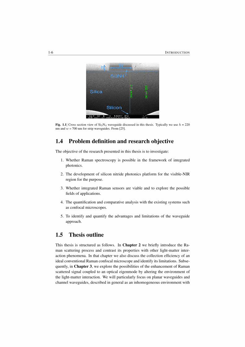
Si3N4 waveguide circuits discussed in this thesis are fabricated on 200 mmdiameter silicon wafers with a thickness of 700 µm. A stack of 220 nm thickSi3N4 on top of 2.4 µm thick SiO2 is deposited on top of the Si wafer. The Si3N4
as well as the SiO2 are deposited by plasma enhanced chemical vapor deposition[25]. The waveguide structures are defined with 193 nm optical lithography andsubsequently etched by fluorine based inductively coupled plasma reactive ion-etch process to get the final structure. Fig 1.1 shows the structure of a typicalSi3N4 waveguide on a silica-on-silicon substrate.
Si3N4 platform is becoming a mature platform, and has been estabilished asan alternative, medium-index-contrast material for integrated photonics. Indeed,all the essential components such as lasers [27], detectors, planar concave gratings[28], arrayed waveguide gratings [29], Mach-Zehnder interferometer filters [30][31], ring cavity filters [32] and Bragg gratings [33] have been demonstrated usingchip-scale nanophotonics. As for many other optical devices mentioned before, aRaman spectroscopic system may also be miniaturized and integrated on a chip.This is one of the goals of the research presented in this thesis. Other aims arediscussed in the next section.
1-6 INTRODUCTION
Fig. 1.1| Cross section view of Si3N4 waveguide discussed in this thesis. Typically we use h = 220nm and w = 700 nm for strip waveguides. From [25].
1.4 Problem definition and research objectiveThe objective of the research presented in this thesis is to investigate:
1. Whether Raman spectroscopy is possible in the framework of integratedphotonics.
2. The development of silicon nitride photonics platform for the visible-NIRregion for the purpose.
3. Whether integrated Raman sensors are viable and to explore the possiblefields of applications.
4. The quantification and comparative analysis with the existing systems suchas confocal microscopes.
5. To identify and quantify the advantages and limitations of the waveguideapproach.
1.5 Thesis outlineThis thesis is structured as follows. In Chapter 2 we briefly introduce the Ra-man scattering process and contrast its properties with other light-matter inter-action phenomena. In that chapter we also discuss the collection efficiency of anideal conventional Raman confocal microscope and identify its limitations. Subse-quently, in Chapter 3, we explore the possibilities of the enhancement of Ramanscattered signal coupled to an optical eigenmode by altering the environment ofthe light-matter interaction. We will particularly focus on planar waveguides andchannel waveguides, described in general as an inhomogeneous environment with
INTRODUCTION 1-7
1D and 2D symmetry respectively. In Chapter 4 we will be concerned with theo-retical and experimental explorations of the Raman spectroscopy of bulk materialin the cladding using channel waveguides. In Chapter 5 we demonstrate Ramanspectroscopy of biological sub-monolayers functionalized on top of the waveg-uides and discuss few applications of the nanophotonic waveguide enhanced Ra-man spectroscopy (NWERS) of monolayers and thin layers. In the chapter wewill also compare the NWERS results with a free-space approach for Raman spec-troscopy. In Chapter 6 we discuss different parameters on which the efficiency ofthe NWERS approach depends. Beginning with an empirical investigation on theorigin of the waveguide background, in Chapter 7, we investigate the dependenceof the waveguide background luminiscence on several experimental variable andsubsequenbtly suggest some minimization and subtraction strategies. Chapter 8,the final chapter of this thesis, is dedicated to a short discussion about the possibledirections that this research might develop towards.
1.6 Contributions and Publications
This work has led to following publications. Some proportion of the texts andfigures in this thesis has been adapted from many of these published and submittedworks. All conference contributions were presented orally except for the onesmarked with an asterix (*).
International Journals
1. A. Dhakal, F. Peyskens, S. Clemmen, A. Raza, P. Wuytens, H Zhao, N. Le Thomas,R. Baets, “Single mode waveguide platform for spontaneous and surface-enhancedon-chip Raman spectroscopy”, Interface Focus, (6) 20160015, (2016)
2. A. Dhakal, P. Wuytens, F. Peyskens, K. Jans, N. Le Thomas, R. Baets, “Nanopho-tonic waveguide enhanced Raman spectroscopy of biological submonolayers on aCMOS-compatible platform”, Submitted (arXiv preprint: http://arxiv.org/abs/1608.08002)
3. F. Peyskens, A. Dhakal, P. Van Dorpe, N. Le Thomas, R. Baets, Surface EnhancedRaman Spectroscopy Using a Single Mode Nanophotonic-Plasmonic Platform, ACSPhotonics, 3 (1), p.102-108 (2016)
4. A. Dhakal, A. Raza, F. Peyskens, A. Subramanian, S. Clemmen, N. Le Thomas,R. Baets, ”Efficiency of evanescent excitation and collection of spontaneous Ramanscattering near high index contrast channel waveguides”, Optics express, 23 (21),p.27391-27404 (2015).
5. A. Subramanian, E.M.P. Ryckeboer, A. Dhakal, F. Peyskens, A. Malik, B. Kuyken,H. Zhao, S. Pathak, A. Ruocco, A. De Groote, P.C. Wuytens, D. Martens, F. Leo,W. Xie, U.D. Dave, M. Muneeb, Pol Van Dorpe, Joris Van Campenhout, W. Bo-gaerts, P. Bienstman, N. Le Thomas, D. Van Thourhout, Zeger Hens, G. Roelkens,R. Baets,”Silicon and silicon nitride photonic circuits for spectroscopic sensing on–a–chip”, Photonics Research (invited), 5(3), p.B47 (2015)
1-8 INTRODUCTION
6. H. Zhao, B. Kuyken, S. Clemmen, F. Leo, A. Subramanian, A. Dhakal, P. Helin, S.Simone, E. Brainis, G. Roelkens, R. Baets,”Visible-to-near-infrared octave spanningsupercontinuum generation in a silicon nitride waveguide”, Optics Letters, 40 (10),p.2177-2180 (2015)
7. F. Peyskens, A. Subramanian, P. Neutens, A. Dhakal, P. Van Dorpe, N. Le Thomas,R. Baets, ”Bright and dark plasmon resonances of nanoplasmonic antennas evanes-cently coupled with a silicon nitride waveguide”, Optics Express, 23(3), p.3088-3101(2015)
8. A. Dhakal, A. Subramanian, P.C. Wuytens, F. Peyskens, N. Le Thomas, R. Baets,“Evanescent excitation and collection of spontaneous Raman spectra using siliconnitride nanophotonic waveguides”, Optics Letters, 39 (13), p.4025-4028 (2014)
9. A. Subramanian, P. Neutens, A. Dhakal, R. Jansen, T. Claes, X. Rottenberg, F.Peyskens, S. Selvaraja, P. Helin, B. Du Bois, K. Leyssens, S. Severi, P. Deshpande,R. Baets, P. Van Dorpe, “Low-loss singlemode PECVD silicon nitride photonicwire waveguides for 532-900 nm wavelength window fabricated within a CMOSpilot line”, IEEE Photonics Journal, 5 (6), p.2202809 (2013).
10. A. Subramanian, S. Selvaraja, P. Verheyen, A. Dhakal, K. Komorowska, R. Baets,”Near infrared grating couplers for silicon nitride photonic wires”, IEEE PhotonicsTechnology Letters, 24 (19), p.1700-1703 (2012)
International Conferences
1. A. Dhakal, A. Raza, P.C. Wuytens, F. Peyskens, A. Skirtach, R. Baets, “Lab-on-a-chip Raman sensors outperforming Raman microscopes”, CLEO 2016, San Jose(2016).
2. F. Peyskens, A. Dhakal, P. Van Dorpe, N. Le Thomas, R. Baets,“Hybrid SingleMode Nanophotonic-Plasmonic Waveguides for On-Chip Surface Enhanced RamanSpectroscopy”, accepted for publication in META 2016, Spain, (to be published).
3. F. Peyskens, A. Dhakal, P. Van Dorpe, N. Le Thomas, R. Baets, “Surface EnhancedRaman Spectroscopy on Single Mode Nanophotonic-Plasmonic Waveguides”, CLEO2016, San Jose (2016)
4. A. Dhakal, P.C. Wuytens, F. Peyskens, A. Subramanian, A. Skirtach, N. Le Thomas,R. Baets, “Nanophotonic Lab-On-A-Chip Raman Sensors: a Sensitivity Comparisonwith Confocal Raman Microscope”, BioPhotonics 2015, Florence, p.Th6.3 (2015)
5. S. Clemmen, H. Zhao, F. Peyskens, A. Dhakal, P.C. Wuytens, A. Subramanian,N. Le Thomas, R. Baets,“Coherent anti-Stokes Raman spectroscopy on chip”, 28thIEEE Photonics Conference (IPC 2015), United States, p.623-624 (2015)
6. D. Delbeke, A. Subramanian, P. Cardile, W. Woestenborghs, A. Ruocco, J.W. Hoste,D. Martens, A. Dhakal, P. Bienstman, G. Roelkens, N. Le Thomas, R. Baets,“Siliconphotonics for on-chip spectrophotometry”, 12th International Conference on GPF(invited), United States, p.FC1(2015).
INTRODUCTION 1-9
7. A. Dhakal, F. Peyskens, A. Subramanian, N. Le Thomas, R. Baets, Enhanced Spon-taneous Raman Signal Collected Evanescently by Silicon Nitride Slot Waveguides,CLEO: 2015, United States, p.paper STh4H.3 (2015).
8. R. Baets, A. Subramanian, A. Dhakal, F. Peyskens, P.C. Wuytens, E.M.P. Rycke-boer, G. Roelkens, N. Le Thomas, Spectroscopic sensing enabled by silicon photon-ics, Asia Communications and Photonics Conference (ACP) (invited), China (2014).
9. R. Baets, A. Dhakal, F. Peyskens, P.C. Wuytens, A. Skirtach, N. Le Thomas, A. Sub-ramanian, “Resonant enhancement mechanisms in lab-on-chip raman spectroscopyon a silicon nitride waveguide platform”, IEEE Photonics Conference 2014 (IPC)(invited),United States,p.500-501(2014).
10. A. Dhakal, P.C. Wuytens, F. Peyskens, A. Subramanian, N. Le Thomas, R. Baets,“EvnascentRaman spectroscopy using photonic waveguides”, International Conference on ra-man Spectroscopy- ICORS 2014,Germany,p.WeA-O-006(2014).
11. F. Peyskens, A. Subramanian, P. Neutens, A. Dhakal, P.C. Wuytens, P. Van Dorpe,N. Le Thomas, R. Baets, “Enhancement of Raman scattering efficiency by on-chipnanoplasmonic antennas”, Surface-Enhanced Spectroscopies, Germany, (2014)
12. A. Dhakal, P.C. Wuytens, F. Peyskens, A. Subramanian, N. Le Thomas, R. Baets,“Silicon-nitride waveguides for on-chip Raman spectroscopy”, SPIE Photonics Europe 14(2014)
13. P. Neutens, A. Subramanian, M. Ul Hassan, C. Chen, R. Jansen, T. Claes, X. Rot-tenberg, B. Du Bois, K. Leyssens, P. Helin, S. Severi, A. Dhakal, F. Peyskens, L.Lagae, P. Deshpande, R. Baets, P. Van Dorpe, “Characterization of PECVD siliconnitride photonic components at 532 and 900 nm wavelength”, 4th Conference onSilicon Photonics and Photonic Integrated Circuits, Belgium, p.article 91331F (6pages) (2014)
14. A. Dhakal, P.C. Wuytens, F. Peyskens, A. Subramanian, N. Le Thomas, R. Baets, “Ra-man spectroscopy using photonic waveguides”, IPS Benelux 2013, Netherlands, (2013)
15. N. Le Thomas, A. Dhakal, F. Peyskens, A. Subramanian, T. Claes, K. De Vos,E.M.P. Ryckeboer, R. Bockstaele, P. Bienstman, R. Baets, “Biological sensing withintegrated silicon and silicon nitride photonics”, The 2nd BioPhotonics Conference(invited),Taiwan,p.28-29(2013)
16. A. Dhakal, F. Peyskens, A. Subramanian, N. Le Thomas, R. Baets,“Enhancement oflight absorption, scattering and emission in high index contrast waveguides”, OSA-Advanced Photonics Congress, Optical Sensors, United States, p.ST2B.5 (2013)
17. F. Peyskens, A. Subramanian, A. Dhakal, N. Le Thomas, R. Baets,“Enhancementof Raman Scattering Efficiency by a Metallic Nano-antenna on Top of a High IndexContrast Waveguide“, CLEO 2013, United States, p.paper CM2F.5 (2013)
18. R. Baets, A. Subramanian, A. Dhakal, S. Selvaraja, K. Komorowska, F. Peyskens,E.M.P. Ryckeboer, N.A Yebo, G. Roelkens, N. Le Thomas, Spectroscopy-on-chipapplications of silicon photonics, Photonics West (invited), 8627(01), United States,p.86270I-1 - 86270I-10 (2013).

1-10 INTRODUCTION
19. A. Subramanian, S. Selvaraja, A. Dhakal, K. Komorowska, R. Baets,”Grating cou-plers for Si3N4 waveguides at 900 nm”, 16th European Conference on IntegratedOptics (ECIO 2012),Spain,p.paper 182(2012).
20. *A. Dhakal, A. Subramanian, N. Le Thomas, R. Baets, “The role of index contrastin the efficiency of absorption and emission of a luminescent particle near a slabwaveguide”, 16th European Conference on Integrated Optics (ECIO 2012), Spain,p.paper 131(2012).

2A brief review of light-matter
interaction and Raman spectroscopy
In this chapter, the classical theory of radiation and light-matter interaction is in-troduced. The Raman scattering process, which is our major concern in this thesis,can be modelled in a simplistic manner from the classical theory. The theory de-veloped in the chapter is sufficient to understand the work presented in this thesis.For a detailed and complete analysis of Raman scattering process, a quantum the-ory is needed. The readers are referred to excellent text books by Loudon [34],Novotny [35], Long [2] and Jackson [36] for a detailed and in-depth treatment ofthe topic. Some texts and figures in this chapter have been adapted from some ofmy published articles [1] [37].
2.1 Classical description of light-matter interaction
In a large majority of classical light-matter interaction problems, matter is modeledas a collection of electrical dipoles. An electrical dipole is a pair of oppositelycharged particles separated by a small distance, potentially oscillating with oneor several orthonormal modes of vibrations. An incoming light is modeled as anoscillating electromagnetic field with the electric field ~E = ~E0e
iω0t + cc. Theoscillating field would then drive the oscillation of the dipoles, which in turn re-radiates the power into the environment according to the normal modes that areexcited. At the molecular level, such a polarization is described by an induced
2-2 RAMAN SCAT. REVIEW
local dipole moment ~d, which is a function of the incoming oscillating field ~E
and a material dependent quantity called polarizability α. In general α can have anon-linear tensorial form. But for the purposes of this thesis we make a linear andisotropic approximation, such that polarizability can be considered a scalar and theinduced dipole moment can be described in the following form:
~d = α~E (2.1)
The polarizability of a molecule α is dependent on the molecular propertiessuch as the distribution of charges in the molecule, and the frequency of the res-onance of the normal vibrational modes that the molecular charges are subject to.Polarizability increases if the electrons are loosely bound to the nuclei. In gen-eral, larger molecules have more loosely held electrons in comparison to smallermolecules with the electrons tightly bound to the nuclei. In case of atoms in the pe-riodic table for example, polarizability increases from right to left and from top tobottom of the periodic table. The dominant component of polarizability, which iscalled the static polarizability α0, is dependent on the average charge distribution,and it can be described by an average normal coordinateQ0
j . However, the polariz-ability also has a dynamic component described by a set of normal coordinates Qjcorresponding to each normal modes j of the molecular vibrations. The normalcoordinates Qj and the corresponding angular frequency ωj are related such thatQj = Q0
je−iωjt + cc. The total polarizability α can thus be decomposed into the
static and dynamic components as follows,
α = α0 +∑j
(∂α
∂Qj
)Qj + .. (2.2)
2.2 Scattering processes
Here, we outline a simplified picture of Raman, Rayleigh and Brillouin scatteringbased on dipole radiation and dynamic polarizability described in the previoussection. A detailed classical treatment of Raman scattering can be found in [2] anda quantum mechanical description of Raman scattering or light-matter interactionin general can be found in [34], [36].
Ignoring higher order terms, Eq. (2.1) and Eq. (2.2) yields,
~d = α0~E + ~E0
∑j
(∂α∂Qj
)Q0j
[e−i(ω0−ωj)t + e−i(ω0+ωj)t
]+ cc
= ~d(ω0) + ~d(ω0−ωj) + ~d(ω0+ωj)
(2.3)
CHAPTER 2 2-3
Eq. (2.3) suggests that the induced dipole oscillates at three frequencies, onecorresponding to the incident light ω0 and the other two at frequencies ω0 ± ωjcorresponding to the incident light modulated by each of the molecular vibrationalmodes j for which ∂α/∂Qj 6= 0. Since a dipole oscillating at a frequency ωradiates at the same frequency, the scattered or re-radiated light has the same fre-quencies as that of the induced dipole oscillation. The total time-average powerradiated by a dipole of strength ~d is proportional to ~|d|2 ( given by Eq. (A.7) inAppendix A). Hence, for each dipole term in Eq. (2.10) respectively yields powersPRY , PST and PAS :
Pscat = PRY (ω0) + PST (ω0 − ωj) + PAS(ω0 + ωj) (2.4)
2.2.1 Rayleigh scattering
In Eq. (2.4) the power PRY corresponding to the elastic scattering of light, i.e.the scattering conserving the frequency of the incident light ω0 is called Rayleighscattering. Since it is dependent only on the strongest static polarizability, it isthe strongest component in the light scattered by the molecule. In the absence ofabsorption (or absence of resonance, i.e. ω 6= ω0), Rayleigh scattering is in phasewith the incident field in the forward direction. Thus, for a medium with somesignificant degree of molecular order, the first term in Eq. (2.4) is responsible forthe forward propagation of light. However, in reality, there also exists a consid-erable degree of disorder among the positions of the molecules depending on theamorphosity, thermal properties and the temperature. The random positioning ofthe scattering molecules with respect to an arbitrary location leads to an incoher-ent addition of scattered light at that location. For a collection of molecules, thisincoherent collection of scattered light at an arbitrary position is historically calledRayleigh scattered light, and the in-phase component of forward propagating lightoriginating from the first term of Eq. (2.4) is just termed as the forward propa-gating or transmitted light. Nevertheless, the process of light propagation in themedium and Rayleigh scattering is governed by the same static polarizability.
2.2.2 Raman scattering
The inelastic component of scattered light described by second and third termsof Eq. (2.4), i.e. the scattering where the light exchanges its energy with themolecules thereby changing the frequency, is called Raman scattering. For eachmolecular vibration yielding Raman scattering, there are positive (third term inEq. 2.4) and negative frequency shifts (second term in Eq. 2.4). Raman scatteringwhere the scattered light gains energy from the molecules, thereby manifestingwith larger frequency, is called anti-Stokes Raman scattering. The opposite casewhere the light loses energy is called Stokes Raman scattering. In a state of

2-4 RAMAN SCAT. REVIEW
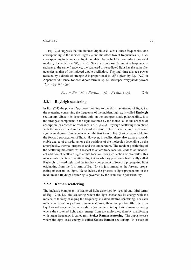
Fig. 2.1|: Raman Stokes (S), anti-Stokes (AS), resonance Raman and Rayleigh scattering depicted interms of transitions between a virtual state and the vibrational states. In case of Rayleigh scatteringthere is no exchange of energy between the molecule and the light as the initial and final vibrationalstates are the same, hence, incident and scattered photons have the same frequency ω0. In case ofStokes Raman scattering the molecule absorbs energy from the light hence has less frequency comparedto the incident photon and in case of anti-Stokes Raman scattering molecule loses energy, hence thescattered photon has more energy than the incident photon. Their approximate relative intensities inthe units of incident intensity are also shown. The states S0 and S1 are electronic states; hence usuallyhave high transition energy (in visible and UV frequency region).
CHAPTER 2 2-5
thermal equilibrium, the population of the molecules occupying the excited stateis smaller than the population of the molecules in the ground state by the Boltz-mann factor, exp
(− ~ωkBT
). Hence the intensity of anti-Stokes light is smaller
than the Stokes light by this factor. The phase of Raman scattering is dependenton the phase of the individual molecular vibrations, which are vibrating incoher-ently, hence spontaneous Raman emission described by second and third terms ofEq. (2.4) have arbitrary phase relative to each other, and thus incoherent. This isin contrast to Rayleigh scattering, where incoherence in the scattered light is dueto random position of the emitters rather than the randomness in the phase of thevibrations of the molecules.
Fig. 2.1 illustrates Stokes and anti-Stokes Raman light, and Rayleigh scatteredlight and their relative intensities. At room temperature Rayleigh, anti-Stokes andStokes scattered intensities are in the order of 10−5, 10−11, 10−8 respectively nor-malized to the incident intensity. These numbers are typical for the Stokes shift inthe order of ∼ 0.3 eV (∼ 2500 cm−1). The intensity of anti-Stokes with respectto the Stokes, however, depends on the Boltzmann factor i.e. reduces exponen-tially with the ωj/T . The corresponding quantum mechanical picture in terms ofenergy levels is also illustrated in Fig 2.1. In a quantum mechanical model, theRaman scattering process is described as the scattering between two bosonic par-ticles photons and phonons, the quanta of molecular vibrations. In esensce, thisis anhilation (or absorption) of a phonon and subsequent creation (emission) of aphoton via an intermediate non-resonant virtual quantum state of a material. As aresult, the frequency of emitted photons is shifted by the amount corresponding tothe energy of the phonons which are anihilated. In case of anti-stokes, the phonosare created at the expense of the energy of the photons.
When an intermediate state is nearby a resonant electronic state, the corre-sponding Raman scattering process is is called Resonant Raman scattering. Res-onant Raman scattering is distinguished from ordinary Raman scattering for theexcitation wavelengths at or very close to the electronic resonant wavelengths.Such a scattering leads to an enhanced intensity, which unfortunately, also comeswith a significant amount of fluorescence (§2.5) that forms a strong background inthe measurement of the Raman signal.
2.2.3 Brillouin scattering
So far we have implicitly qualified the applicability of Eq. (2.4) to the molec-ular vibrations in the optical frequencies (i.e. > 10 THz) with high energy vi-brational modes of the molecules.The normal modes Qi corresponding to thesevibrations are called optical normal modes (the corresponding quantum particlesare called optical phonons) as their energies correspond to the optical light at themid-infrared (MIR) wavelengths. However, a similar analysis can be applied to
2-6 RAMAN SCAT. REVIEW
the cases of acoustic normal modes where the large scale collective vibrations ofthe molecules in acoustic frequencies (i.e. < 1 THz) are of concern. The scat-tering corresponding to the polarizations due to molecular vibrations in acousticfrequencies is called Brillouin scattering. The low energy acoustical vibrationsrelates to the collective oscillations of ions (where they move together). This isin contrast to the optical vibrational modes where the ions swing independently.Brillouin scattering is distinguished from Raman scattering as the scattered signaldoes not reveal the internal ionic structure of the molecules but relates to the largescale vibrations of a collection of molecules. A detailed description, referencesand its analysis in context of integrated photonics can be found in Raphael VanLaer’s PhD thesis [109] .
2.3 Various definitions of scattering cross sectionsUsing definition of wave numbers, ν = ω/(2πc), the power P emitted by a dipole~d oscilating at frequency ω is given by following equation ( see §Appendix A fordetails, follows from (A.11) ):
P = n2π3c
ε0ν4∣∣∣~d∣∣∣2 (2.5)
The intensity of incident light I0, assuming that it is a plane wave in a free space,is given by the following equation:
I0 =cε0
2n
∣∣∣ ~E∣∣∣2 (2.6)
It is useful to define a quantity σtot defined as the ratio of average scatteredpower per molecule scattered in all space for a given pump intensity I0. Assumingthe molecules lie in a homogenous free-space medium, and a scalar polarizability(hence the dipole to be in the same direction as that of the incoming field ~E), wecan write,
σtot =〈P 〉I0
= 4πkvν4α2 (2.7)
with kν = π2/ε20 = 1.26 · 1023C−2V2m2 as a constant for conversion. σtot
is more precisely called the total scattering cross-section, also just referred toas the scattering cross-section in the literature. The scattering cross-section σtotis a function of the average polarizability of an ensemble of molecules and thewavenumber of incident light. It is a quantity directly measured in most of theexperiments and has m2 molecule−1 as its SI unit.
In many situations one is concerned with different pump frequencies (hencedifferent absolute Stokes frequencies), in such cases σtot is an inconvenient quan-tity as it is function of absolute wavenumbers. The power PdΩ scattered by a
CHAPTER 2 2-7
molecule towards a given direction in a given solid angle dΩ is dependent on theelectronic configurations and orientations of the constituent atoms. It is depen-dent on the so called Placzek polarizability tensor [2], which in general dependson the direction relative to a particular molecular orientation and is independentof the wavelength. Hence it is convenient to define the wavenumber-normalizedscattering cross-section σnorm defined as:
σnorm = ν−4
(1
I0
d
dΩPdΩ
)= ν−4
(d
dΩσtot
)= kvα
2 (2.8)
Here the last step is valid only for the scalar polarizability. Wavenumber-normalized scattering cross-section σnorm is usually tabulated as β0 in the lit-erature and is typically used in theoretical estimations of cross-section and formeasurements with crystalline materials. It has SI units of m6 sr−1 molecule−1.
In Eq.(2.8) the bracketed term is another common definition of cross-sectioncalled differential cross-section σdiff [2] usually tabulated as dσ/dΩ in the liter-ature. For an ensemble of randomly oriented molecules, as we mostly deal in thisthesis, the emission is isotropic, hence, in such cases
σdiff =dσtotdΩ
=σtot4π
= kvν4α2 (2.9)
This definition of cross-section is handy for calculations bridging theoreticalcalculations and experiments, and used extensively in the literature referring toit just as cross-section, any ambiguity with the total scattering cross-section isresolved by its unit m2 sr−1molecule−1. We follow the same convenience in thisthesis and use the symbol σ for differential cross-section, without any subscriptlabel for qualification, unless we need to make an explicit differentiation.
2.4 Fluorescence
If the frequency of an incoming light is near an electronic transition resonance of amolecule (characterized with a transition energy> 1.5 eV in contrast to low energy< 1 eV molecular vibrations), the total polarizability of the molecule is changeddue to the rearrangement of the electron cloud in the resonance. This leads tothe absorption of the incoming light and a net change in dipole moment. Somepart of the absorbed energy is non-radiatively dissipated by the molecules duringcollisions and internal vibrionic transitions. The remaining absorbed energy ismostly reradiated with reduced frequency (Stokes shift) in the form of emissioncalled fluorescence.
In a quantum mechanical description, as depicted in Fig. 2.1, the moleculemakes a transition to a high energy electronic state upon absorption of the reso-nant light. This is in contrast to the Raman scattering process where a non-resonant
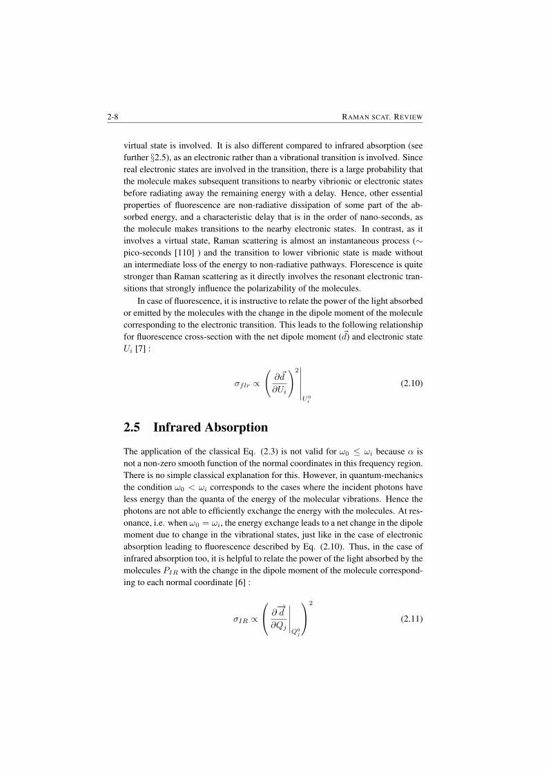
2-8 RAMAN SCAT. REVIEW
virtual state is involved. It is also different compared to infrared absorption (seefurther §2.5), as an electronic rather than a vibrational transition is involved. Sincereal electronic states are involved in the transition, there is a large probability thatthe molecule makes subsequent transitions to nearby vibrionic or electronic statesbefore radiating away the remaining energy with a delay. Hence, other essentialproperties of fluorescence are non-radiative dissipation of some part of the ab-sorbed energy, and a characteristic delay that is in the order of nano-seconds, asthe molecule makes transitions to the nearby electronic states. In contrast, as itinvolves a virtual state, Raman scattering is almost an instantaneous process (∼pico-seconds [110] ) and the transition to lower vibrionic state is made withoutan intermediate loss of the energy to non-radiative pathways. Florescence is quitestronger than Raman scattering as it directly involves the resonant electronic tran-sitions that strongly influence the polarizability of the molecules.
In case of fluorescence, it is instructive to relate the power of the light absorbedor emitted by the molecules with the change in the dipole moment of the moleculecorresponding to the electronic transition. This leads to the following relationshipfor fluorescence cross-section with the net dipole moment (~d) and electronic stateUi [7] :
σflr ∝
(∂ ~d
∂Ui
)2∣∣∣∣∣∣U0i
(2.10)
2.5 Infrared Absorption
The application of the classical Eq. (2.3) is not valid for ω0 ≤ ωi because α isnot a non-zero smooth function of the normal coordinates in this frequency region.There is no simple classical explanation for this. However, in quantum-mechanicsthe condition ω0 < ωi corresponds to the cases where the incident photons haveless energy than the quanta of the energy of the molecular vibrations. Hence thephotons are not able to efficiently exchange the energy with the molecules. At res-onance, i.e. when ω0 = ωi, the energy exchange leads to a net change in the dipolemoment due to change in the vibrational states, just like in the case of electronicabsorption leading to fluorescence described by Eq. (2.10). Thus, in the case ofinfrared absorption too, it is helpful to relate the power of the light absorbed by themolecules PIR with the change in the dipole moment of the molecule correspond-ing to each normal coordinate [6] :
σIR ∝
∂−→d
∂Qj
∣∣∣∣∣Q0j
2
(2.11)
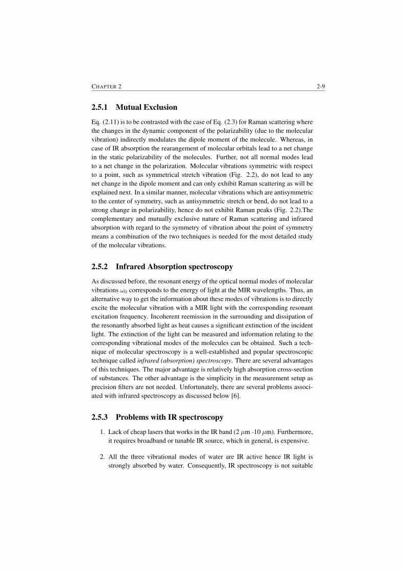
CHAPTER 2 2-9
2.5.1 Mutual Exclusion
Eq. (2.11) is to be contrasted with the case of Eq. (2.3) for Raman scattering wherethe changes in the dynamic component of the polarizability (due to the molecularvibration) indirectly modulates the dipole moment of the molecule. Whereas, incase of IR absorption the rearangement of molecular orbitals lead to a net changein the static polarizability of the molecules. Further, not all normal modes leadto a net change in the polarization. Molecular vibrations symmetric with respectto a point, such as symmetrical stretch vibration (Fig. 2.2), do not lead to anynet change in the dipole moment and can only exhibit Raman scattering as will beexplained next. In a similar manner, molecular vibrations which are antisymmetricto the center of symmetry, such as antisymmetric stretch or bend, do not lead to astrong change in polarizability, hence do not exhibit Raman peaks (Fig. 2.2).Thecomplementary and mutually exclusive nature of Raman scattering and infraredabsorption with regard to the symmetry of vibration about the point of symmetrymeans a combination of the two techniques is needed for the most detailed studyof the molecular vibrations.
2.5.2 Infrared Absorption spectroscopy
As discussed before, the resonant energy of the optical normal modes of molecularvibrations ω0 corresponds to the energy of light at the MIR wavelengths. Thus, analternative way to get the information about these modes of vibrations is to directlyexcite the molecular vibration with a MIR light with the corresponding resonantexcitation frequency. Incoherent reemission in the surrounding and dissipation ofthe resonantly absorbed light as heat causes a significant extinction of the incidentlight. The extinction of the light can be measured and information relating to thecorresponding vibrational modes of the molecules can be obtained. Such a tech-nique of molecular spectroscopy is a well-established and popular spectroscopictechnique called infrared (absorption) spectroscopy. There are several advantagesof this techniques. The major advantage is relatively high absorption cross-sectionof substances. The other advantage is the simplicity in the measurement setup asprecision filters are not needed. Unfortunately, there are several problems associ-ated with infrared spectroscopy as discussed below [6].
2.5.3 Problems with IR spectroscopy
1. Lack of cheap lasers that works in the IR band (2 µm -10 µm). Furthermore,it requires broadband or tunable IR source, which in general, is expensive.
2. All the three vibrational modes of water are IR active hence IR light isstrongly absorbed by water. Consequently, IR spectroscopy is not suitable
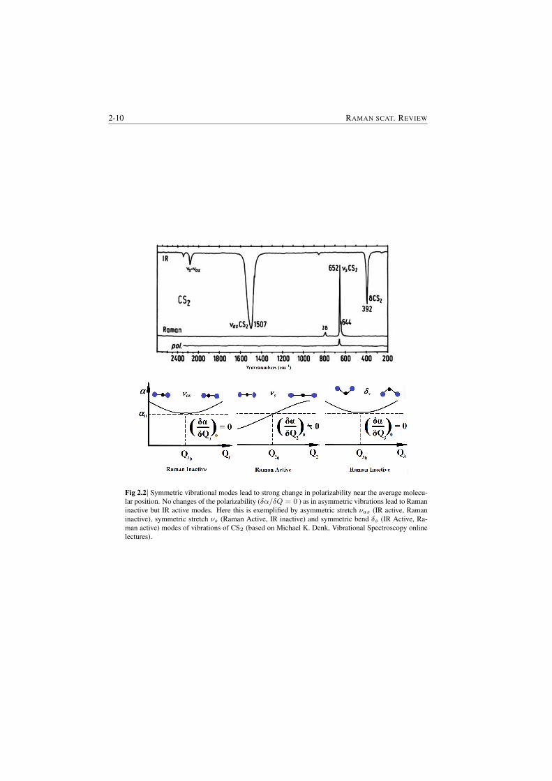
2-10 RAMAN SCAT. REVIEW
Fig 2.2| Symmetric vibrational modes lead to strong change in polarizability near the average molecu-lar position. No changes of the polarizability (δα/δQ = 0 ) as in asymmetric vibrations lead to Ramaninactive but IR active modes. Here this is exemplified by asymmetric stretch νas (IR active, Ramaninactive), symmetric stretch νs (Raman Active, IR inactive) and symmetric bend δs (IR Active, Ra-man active) modes of vibrations of CS2 (based on Michael K. Denk, Vibrational Spectroscopy onlinelectures).

CHAPTER 2 2-11
for aqueous samples. Interference from atmospheric water and trace water insamples or contaiNWERS are also regular problems in the IR measurement.
3. Absorption of light heats the sample and therefore may potentially lead tosample damage.
4. Mid-IR light is not transparent to many common optical materials, thus re-stricting sampling flexibility. A total penetration of the light through thesample is is usually needed to determine the absorption, except for caseswhere a sophisticated attenuated total reflection (ATR) spectroscopy is usedby exploiting attenuation due to evanascent tail of the light.
5. To minimize the interference from optics and containers itself, IR spec-troscopy requires special and costly optics.
6. Long wavelength used in IR absorption renders spatial resolution worse.
2.6 Characteristics of spontaneous Raman scatter-ing
Based on the discussions in the previous sections, we can derive several conclu-sions about the characteristics of the Raman scattering process on its utility andlimitations. These are enumerated as follows.
1. From Eq.(2.2), it can be concluded that Raman scattering is exhibited onlyby the vibrations that change the polarizability i.e. which ∂α/∂Qj 6= 0.Usually the symmetrical vibrations exhibit strong Raman signal. The Ramansignal corresponding to the asymmetric stretches and bends are weak.
2. It follows from Eq.(2.3) and Eq.(2.5 ) that Raman scattering is a linear pro-cess with respect to the intensity of the incident field or power of the incom-ing light.
3. Raman scattering can be described by an effective dipole moment as inEq.(2.2). Thus a conclusion derived for a dipole radiation problem can beapplied to Raman scattering problem. It is an important conclusion as itmeans that several enhancement mechanisms, such as cavity enhancementsor enhancement by heterogeneous media, generally developed to describeenhancement of dipole radiation can be used to study the enhancement ofRaman signal. This will be of our concern in the next chapter.
4. From Eq.(2.2) it can be seen that one strong pump at frequency ω0 is suffi-cient to produce a Raman spectrum corresponding to several vibrionic stateswith energies almost up to the pump frequency ω0. Since the vibrational
2-12 RAMAN SCAT. REVIEW
energies are less than 1eV, usually a visible or near-infrared light can beused to obtain all the essential Raman signals. This also means that well-established techniques developed for visible microscopy and imaging canbe used for Raman spectroscopy. This is in sharp distinction with the IRspectroscopy which either requires a broadband or a tunable source in theinfrared band.
5. Raman scattering is a non-resonant process, hence the cross-section is muchweaker compared to infrared absorption or fluorescence. This is a criticaldrawback of the Raman scattering process, and leads to an extremely lowsensitivity of the Raman signal compared to the signal from fluorescence orIR absorption.
6. The signal-to-noise ratio for Raman systems are very low because of theshot noise from competing processes like fluorescence, in addition to weaknature of the Rmana scattering process (discussed further in Appendix B).
2.7 Efficiency of Raman scattering in an ideal free-space system
When deriving Eq. (2.7) we assumed an electromagnetic plane wave impingingon an ensemble of molecules lying uniformly in a medium. However, any real-istic light beam is subject to diffraction. Here, the efficiency of excitation andcollection of a Raman signal using an ideal diffraction-limited beam employinga dispersionless (and lossless) free-space optical system is described. We choosea diffraction-limited beam, the fundamental Gaussian mode in free-space, in ouranalysis because it ensures minimum possible etendue for Raman microscopes.Minimum etendue warrants maximal power density for maximal excitation, henceserves as the best case scenario for the free space excitation and collection. Fur-ther, smallest etendue is required to have small spectrometer, high resolution andhigh power density at the detector (explained in Appendix D). For the scatteringproblem we are concerned with, we consider the beam profile at the beam waistwhere the field intensity Ig(~r) is maximal to excite a particle and assume that thenumerical aperture of the optics NA = 1, corresponding to the most ideal situationin the free-space. The total power of light scattered by the particle in all directionsat an arbitrary location ~r of the beam within the beam waist w0 is given by,
PDL,0(~r) = σtotIg(~r) = 4πσdiffPpumpπw2
0
|~eg(~r)|2 (2.12)
Here, |~eg|2is the well-known normalized Gaussian beam profile given by exp(-(2r2)/w0
2) for the fundamental Gaussian mode with a waist w0 = λ0/π (we as-sume, NA = 1) [38]. The scattering efficiency is then,
CHAPTER 2 2-13
PDL,0Ppump
= 4πσdiff|~eg(~r)|2
πw20
= σdiff
(4π2 |~eg(~r)|2
λ20
)= ΛDLσdiff (2.13)
Here, following the terminology used in particle scattering theory [39], wehave defined a cross-section independent parameter for the diffraction-limited beam,called integrated luminosity for the free-space ΛDL. Integrated luminosity for adiffraction limited beam (with NA = 1), ΛDL is given by the term in the bracketsin Eq. 2.13. This quantity will be handy in the next chapter to compare scatteringefficiencies for various systems (Table 3.1).
2.7.1 Collection efficiency for bulk sensing
The intensity of a diffraction-limited beam reduces as 1/(1+ (z/zR)2) with the dis-tance z away from the beam waist, where zR = w0/θ is the Rayleigh range of thebeam for a beam divergence θ and beam waistw0. The excitation intensity reducesby more than half the amount for the sample volume away from the range Rayleighrange. Hence, in case of confocal microscopes employing diffraction limited ex-citation and collection, the collected signal essentially originates from particleslocated in the confocal volume, i.e. within the depth-of-focus 2zR. Further, onlythe emission inside a solid angle Ω corresponding to a half-acceptance angle θ(Fig 2.3) of the collection optics is collected. We assume that the collection opticshas the same acceptance width (slit width of the spectrometer) as the 1/e2 widthof the exciting beam. Then, in terms of differential scattering cross-section σ andthe density of the particles ρ, the overall efficiency of excitation and collection canthen be calculated as [37], [40]
PDL,BulkPpump
= 2zRΩσρ (2.14)
Assuming a small beam divergence, θ = w0/zR = λ0/ (nπw0), the solid anglecan be expressed in terms of the parameters of the diffraction-limited beam:
Ω = 4π sin2
(θ
2
)≈ π
(w0
zR
)2
=λ0
nzR(2.15)
Hence,
PDL,BulkPpump
= 2
(λ0
n
)σρ (2.16)
Note that the SI unit for solid angle steradian (sr) is implicit in the pre-factorof Eq. (2.16). The approximation carried out in Eq. (2.15) overestimates thesolid angle, as in general, w0/zR > sin(θ). Hence, Eq. (2.16) sets the upper-limit for the confocal microscopic systems. Microscopes with higher transmission

2-14 RAMAN SCAT. REVIEW
Fig. 2.3| Schematic of the beam geometry for a confocal microscope. Only signal fromconfocal volume contributes significantly to the signal. The aperture size of the collectionoptics is assumed to be the same as that of the size of the excitation beam. A slit is usu-ally present in the collection Fourier plane to collect signal exclusively from the confocalvolume.
losses and having larger divergence than diffraction-limited systems behave worse.Eq. (2.16) is independent of any system-specific parameters such as numericalaperture or focal length. It reveals the opposite effects due to the beam divergenceand the depth of focus, which restricts the detection volume and field intensity,hence, the collected power [37]. In chapter 3, we describe the use of dielectricwaveguides to overcome the limit imposed by diffraction by means of waveguidingand electromagnetic confinement.
2.7.2 Collection efficiency for surface sensing
For a monolayer or a very thin layer of molecules with surface density ρs whenexcited and collected by a diffraction limited free-space system, the interactionarea is limited by the beam waist. Integrating Eq. (2.12) within the beam waist,the power emitted in every direction when excited by a diffraction-limited beam isgiven by, PDL,s = σρsPpump. Thus for collection using NA = 1, which collectsall the light from the half-space,
PDL,SPpump
=1
2σρs (2.17)
Just like Eq. (2.16) sets an upper limit for the bulk collection, Eq. (2.17) setsan upper limit in the collection of a Raman signal from a monolayer of moleculesusing a free-space system. As in the case of Eq. (2.16), the ideal excitation andcollection in a free-space system is independent of the system dependent parame-ters such as focal length of the focusing lens (beam waist) because of the opposingeffects of divergence and sampling area. In Chapter 4 we will compare this value
CHAPTER 2 2-15
limited by the diffraction with a realistic waveguide system that overcomes thediffraction by means of electromagnetic confinement, which leads to waveguidingand enhancement.
2.8 Closing RemarksIn this chapter we discussed several aspects of light-matter interaction relevant toRaman spectroscopy in a homogenous medium. In particular we introduced Ra-man scattering and distinguished it from other forms of light matter interactions.Further, we developed an upper-limit case for the generic free-space Raman exci-tation and collection system. We shall refer to several equations and conclusionsdeveloped in this chapter in later chapters.

3Enhancement of spontaneous
scattering by optical confinement
In Chapter 2 we discussed that spontaneous Raman scattering is a non-resonantprocess, and therefore it is an extremely weak process. In this chapter we explorethe possibility of enhancing the Raman scattering rate by changing the boundaryconditions of the environment. Before mid-1940s the radiated power of a dipole, asgiven by Eq. (2.5), was thought to be a sufficient description for the classical dipoleemission. Even during the development of quantum mechanics, the spontaneousemission rate of excited molecules was assumed to be intrinsic to the molecules. Inthe context of nuclear magnetic resonance, in 1946 E. M. Purcell suggested [41]that the spontaneous emission rate is strongly influenced by the electromagneticenvironment. Specifically, he proposed that for an emitter coupled to a resonantmode of a cavity, the spontaneous emission rate is modified by the properties of thecavity. Subsequently, the idea has been applied in a variety of practical problemsto enhance or inhibit emissions, such as fluorescence [42]. In this chapter we lookat the modification of the emission depending on the boundary conditions of theenvironment of an emitter. Although the problem has a quantum-mechanical root,we will limit ourselves to the classical description. As we shall see in this chapter,the enhancement of emission in an inhomogeneous medium including Purcell’soriginal equation for a cavity can be derived classically.

3-2 CHAPTER 3
3.1 Classical description of enhancement of emission
In appendix A we show that the enhancement and inhibition of emission in aninhomogeneous medium is governed by the local density of states (LDOS). Inthe context of classical electromagnetic modes, LDOS D(~r, ω) is defined as thenumber of available modes at a given position ~r per unit frequency per unit volume.Then, the emitted power P for a dipole ~d in an inhomogeneous medium is givenby (see Appendix A for details):
P =πω2
4εε0
∣∣∣~d∣∣∣2D(~r0, ω0) (3.1)
In many practical situations we can exploit a symmetry present in the environ-ment and the LDOS can be calculated by counting the number of states in k-space(Fig. 3.1), as only certain values of k lead to a valid wave solution in a given vol-ume V . For example, in an isotropic homogenous medium with refractive index n,the dispersion is given by dk/dω = vg = c/n, hence the LDOS can be calculatedas follows,
D0(ω) =1
V
dN
dω=
2
V
4π |k|2
(2π/l)3
dk
dω=ω2
π2
n3
c3=k2
π2
n
c(3.2)
Here an arbitrary length l defines a cube of volume V . The prefactor 2 takesthe two possible transverse polarization modes of the field into account. It is in-structive to introduce the so called total density of states for the homogeneousmedium given by Df (ω) = D0(ω)/3 which is an average over the three possi-ble dipole orientations along the three possible orthonormal spatial orientations.Hence, the emission of a dipole in an inhomogeneous environment, normalized tothe emission in a homogeneous medium, is given by,
P (~r0, ω0)
P0=D(~r0, ω0)
Df (ω0)= 3
D(~r0, ω0)
D0(ω0)(3.3)
Notice that according to Eq. (3.3) the emission in a homogenous mediumis, as expected, 3P0 which is the emission power without spatial averaging. Thereaders are referred to [35] and [43] for a more detailed treatment of the densityof states and the emission problem in a homogenous space. For the purposesof the forthcoming sections, it is useful to define Eq. (3.3) in terms of scalarpolarizability α, the corresponding wavenumber normalized cross-section σnorm,(using Eq. (2.9) ) and the excitation field ~E, as follows:
ENHANCEMENT OF SPONTANEOUS SCATTERING 3-3
Fig 3.1| the number of k-states in a 3D homogenous medium. Each k value is shown as a point inthe k-space. A shell of radius k and thickness dk contains the allowed states. The number of thesepoints is given by 4πk2dk. (from: http://britneyspears.ac)
P =πω2
4ε(~r0)ε0α2∣∣∣−→E (~r0, ω)
∣∣∣2D(~r0, ω0)
=πω2
4ε(r0)ε0
(ε2
0
π2σnorm
) ∣∣∣−→E (~r0, ω)∣∣∣2D(~r0, ω0)
= σnormε0
π
(ω2
4ε(~r0)
) ∣∣∣−→E (−→r0 , ω)∣∣∣2D(~r0, ω0) (3.4)
3.2 Enhancement of the emission in a cavity with awell-defined Q-factor
In a cavity, the homogeneity of the medium is broken, and the LDOS is no longergiven by Eq. (3.2). Instead, the LDOS is determined by the resonance condi-tions of the cavity, which is ultimately determined by the boundary conditions ofthe cavity. A cavity mode is characterized by the Q-factor of the mode which isdefined as,
Q = ωW
Pcav=
ω
∆ω(3.5)
3-4 CHAPTER 3
The Q-factor is defined as the ratio of the energy stored in the cavity W tothat of the dissipated energy per radian of the oscillation cycle of the mode. Ina steady state, the dissipated energy (or, input energy for critical coupling) perradian of oscillation is the ratio of power Pcav pumped into the particular modeand the cavity frequency ω. Incidentally, the ratio ∆ω = Pcav/W is identifiedas the FWHM line-width of the resonance frequency of a mode centered at thefrequency ω. Assuming that the cavity resonance is described with a Lorentzianline-shape function, the normalized field density, hence, LDOS for a cavity withQ and the effective mode volume Veff is given by:
Dcav(ω) =1
Veff
[∆ω2π(
∆ω2
)2+ (ω − ω0)
2
]ω=ω0−−−−→ 2
π
1
∆ωVeff=
2
πω
Q
Veff(3.6)
Here the bracketed term describes the Loretzian lineshape function. If thecavity consists of lossless composite materials, and a modal field ~E effective modevolume Veff calculated at the maxima of the modal field ~Emax is given by:
Veff (ω) ≡
˝ε(~r0, ω)
∣∣∣−→E (~r, ω)∣∣∣2
ε(~r0, ω)∣∣∣−→Emax(~rmax, ω)
∣∣∣2 (3.7)
Hence, an emitter, if oriented parallel to the polarization of the modal field ofthe cavity, would emit with a rate enhanced by a factor, called Purcell factor Fp
Fp =Dcav
Df=
3
4π2
(λ
n
)3Q
Veff(3.8)
This is the famous equation suggested by Purcell in his original 1947 paperbased on quantum mechanical arguments for nuclear magnetic resonance [41].
3.3 Scattering in a cavity with a well-defined Q-factor
In the Eq. (3.7) the effective mode volume is measured at the maxima of the field.This way of defining the effective mode volume is customary in cavity quantumelectrodynamics. However, an emitter may be located at any location of the cavity.For a mode denoted by an indexm, and a modal field
−→Em the local effective mode
volume, Veff is defined as:
Veff (~r0, ω) =
˝ε(~r0,ω)
∣∣∣−−→Em(~r,ω)∣∣∣2
ε(~r0,ω)∣∣∣−→Em(~r0,ω)
∣∣∣2= W
ε0ε(~r0,ω)∣∣∣−→Em(~r0,ω)
∣∣∣2 = 1
|−→e |2(3.9)
ENHANCEMENT OF SPONTANEOUS SCATTERING 3-5
Note that this definition of the local effective mode volume is position depen-dent. This definition of effective volume renders it as another way of expressingthe field intensity of the mode at a given point in terms of the total energy in thecavity W or the energy-normalized field of the cavity mode |~e|2 (unit: m−3) asshown in Eq. (3.9). Using Eq. (3.4) with Eq. (3.6) and (3.9), the emission power,P can be written in terms of the energy-normalized field ~e of the cavity mode :
P = Qω
2εε0
∣∣∣−→d .~e∣∣∣2 (3.10)
Here we have used the vector dot product to ensure that the dipole ~d is orientedin the direction of the modal field. Thus, we conclude that the emission in a cavityis proportional to the square of the normalized field in the direction of the dipole atthe dipole location. When the cavity mode is excited by a steady state power Pcavwhich in turn excites the dipole, the modal field
−→Em can be written in terms of
Pcav , if we assume that the pump is also resonant in the cavity with aQp = Q(ωp).Using the relationship between the modal field
−→Em, the energy stored in the cavity
W , i.e. Eq. (3.9), and the definition of Q, i.e. Eq. (3.5), one can write,
P (ωs, ~r) = σnormε0π
(ω2s
4ε(ωs)
) ∣∣∣ ~Em(ωp, ~r)∣∣∣2 2Qs
ωsπ|~e(ωs, ~r)|2
= σnormQsωsε0
2ε(ωs)π2
(W (ωp)|~e(ωp)|2
ε0ε(ωp)
)|~e(ωs)|2
= σnorm2π2
[ωsQs
|~e(ωs)|2ε(ωs)
] [QpPcav(ωp)
ωp
|~e(ωp)|2ε(ωp)
]=⇒ P (ωs,~r)
Pcav(ωp) =σnorm(ωp,ωs)
2ωsωp
[Qsπ|~e(ωs)|2ε(ωs,~r)
] [Qpπ|~e(ωp)|2ε(ωp,,~r)
] (3.11)
If the Stokes shift is negligible, then the equation takes a simpler form in termsof differential cross-section (see Eq. (2.9)):
P (ω,~r)
Pcav=σdiff
2
(λ
n
)4(Q
π
)2
|~e(ω,~r)|4 = σdiffΛcav (3.12)
As for Eq. (2.19), in the previous chapter, we can define a cross-section in-dependent parameter for the cavity called integrated luminosity of the cavity Λcavas,
Λcav (ω,~r) =1
2
(λ2
0
ε(ω,~r)
Q
π|~e(ω,~r)|2
)2
(3.13)
Thus, scattering in a cavity is proportional to the square of the Q of the cavityand the fourth power of the modal field, if both pump and stokes are resonantwith the cavity. Eq. (3.13) is expedient to determine the scattering efficiencyin heterogeneous cavities using a mode solver. We shall briefly comment on theuse of this equation to determine the relative efficiency of resonators based ondielectric channel waveguides at the end of this chapter (§3.6.1).
3-6 CHAPTER 3
3.4 Scattering in an inhomogeneous medium with a2D invariance
In many cases, as we shall describe next, the boundary conditions of the inhomo-geneous medium lead to electromagnetic solutions in terms of orthonormal eigen-modes. In such cases, calculation of the LDOS for each of the eigenmodes issimplified by counting the respective spatial mode density and calculating the cor-responding mode volume.
3.4.1 Calculation of LDOS and enhancement
In case of an inhomogeneity with a 2D invariance, such as planar dielectric waveg-uides (say, slab waveguides with its normal oriented in Z direction), the calcula-tion of the LDOS for the eigenmodes can be performed by counting the numberof spatial modes in 2D kxky- space. For a k-space within a radius k defined by anarbitrary square of side l in the direction of the symmetry (Fig. 3.2), the numberof modes is given by N = πk2/(2π/l)2. The LDOS for such a structure is thengiven by:
D2D(−→r 0, ω) = 1Veff (−→r 0,ω)
dNdω
= 4πkVeff (−→r 0,ω)(2π/l)2
dkdω
= 12πleff (−→r 0,ω)
kvg
(3.14)
Here, Veff and leff are respectively the effective mode volume and effectivemode width defined by Eq. (3.8) and Eq. (3.15) respectively. Because of thespatial invariance in the x-y plane, the arbitrary area l2 in xy plane is the sameas the corresponding integral component in x-y plane. Hence, the effective modevolume is reduced to an effective mode width leff defined as follows,
leff (~r0, ωp) ≡
∞
−∞ε(~r,ω)
∣∣∣−→Em(~r,ω)∣∣∣2d~r
ε(~r0,ω)∣∣∣−→Em(~r0,ω)
∣∣∣2= W2
ε(~r0,ω)ε0
∣∣∣−→Em(~r0,ω)∣∣∣2
= 1
|−→e 2(~r0,ω)|2
(3.15)
where |~e2|2 (unit: m−1) is the modal field intensity, normalized to the unitenergy W2 stored in the structure per unit area in the x-y plane [47]. Hence,using Eq. (3.3), the enhancement compared to the free-space emission for a dipoleorientation parallel to the modal field is given by,
F2D =D2D(ω)
Df (ω)=
3
4
ngneff
(λ
n
)1
leff=
3
4
ngneff
(λ
n
)|−→e 2|
2 (3.16)
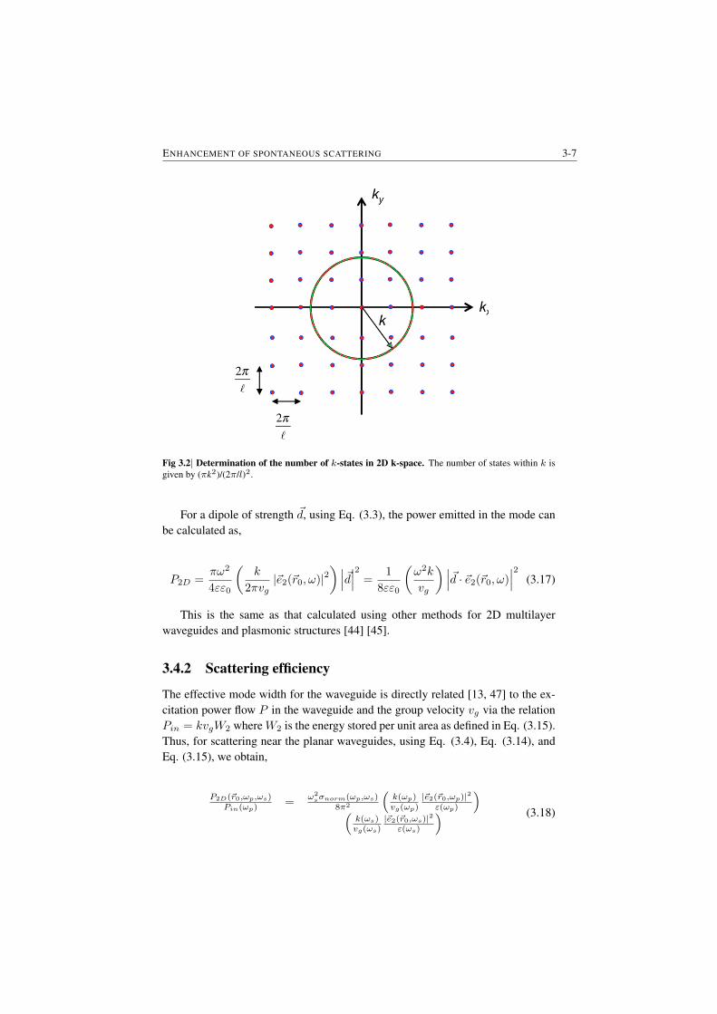
ENHANCEMENT OF SPONTANEOUS SCATTERING 3-7
Fig 3.2| Determination of the number of k-states in 2D k-space. The number of states within k isgiven by (πk2)/(2π/l)2.
For a dipole of strength ~d, using Eq. (3.3), the power emitted in the mode canbe calculated as,
P2D =πω2
4εε0
(k
2πvg|~e2(~r0, ω)|2
) ∣∣∣~d∣∣∣2 =1
8εε0
(ω2k
vg
) ∣∣∣~d · ~e2(~r0, ω)∣∣∣2 (3.17)
This is the same as that calculated using other methods for 2D multilayerwaveguides and plasmonic structures [44] [45].
3.4.2 Scattering efficiency
The effective mode width for the waveguide is directly related [13, 47] to the ex-citation power flow P in the waveguide and the group velocity vg via the relationPin = kvgW2 whereW2 is the energy stored per unit area as defined in Eq. (3.15).Thus, for scattering near the planar waveguides, using Eq. (3.4), Eq. (3.14), andEq. (3.15), we obtain,
P2D(~r0,ωp,ωs)Pin(ωp) =
ω2sσnorm(ωp,ωs)
8π2
(k(ωp)vg(ωp)
|~e2(~r0,ωp)|2ε(ωp)
)(k(ωs)vg(ωs)
|~e2(~r0,ωs)|2ε(ωs)
) (3.18)
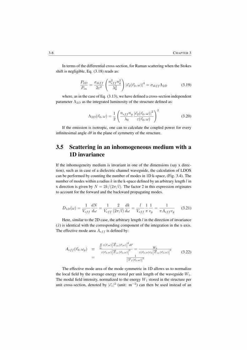
3-8 CHAPTER 3
In terms of the differential cross-section, for Raman scattering when the Stokesshift is negligible, Eq. (3.18) reads as:
P2D
Pin=σdiff2ε2
(n2effn
2g
λ20
)|~e2(~r0, ω)|4 = σdiffΛ2D (3.19)
where, as in the case of Eq. (3.13), we have defined a cross-section independentparameter Λ2D as the integrated luminosity of the structure defined as:
Λ2D(~r0, ω) =1
2
(neffngλ0
|~e2(~r0, ω)|2
ε(~r0, ω)
)2
(3.20)
If the emission is isotropic, one can to calculate the coupled power for everyinfinitesimal angle dθ in the plane of symmetry of the structure.
3.5 Scattering in an inhomogeneous medium with a1D invariance
If the inhomogeneity medium is invariant in one of the dimensions (say x direc-tion), such as in case of a dielectric channel waveguide, the calculation of LDOScan be performed by counting the number of modes in 1D k-space, (Fig. 3.4). Thenumber of modes within a radius k in the k-space defined by an arbitrary length l inx direction is given by N = 2k/(2π/l). The factor 2 in this expression originatesto account for the forward and the backward propagating modes.
D1D(ω) =1
Veff
dN
dω=
1
Veff
2
(2π/l)
dk
dω=
l
Veff
1
π
1
vg=
1
πAeffvg(3.21)
Here, similar to the 2D case, the arbitrary length l in the direction of invariance(x) is identical with the corresponding component of the integration in the x-axis.The effective mode area Aeff is defined by:
Aeff (~r0, ωp) ≡˜∞ε(~r,ω)
∣∣∣−→Em(~r,ω)∣∣∣2d~r
ε(~r0,ω)∣∣∣−→Em(~r0,ω)
∣∣∣2 = W1
ε(~r0,ω)ε0
∣∣∣−→Em(~r0,ω)∣∣∣2
= 1
|−→e 1(~r0,ω)|2(3.22)
The effective mode area of the mode symmetric in 1D allows us to normalizethe local field by the average energy stored per unit length of the waveguide W1.The modal field intensity, normalized to the energy W1 stored in the structure perunit cross-section, denoted by |~e1|2 (unit: m−2) can then be used instead of an
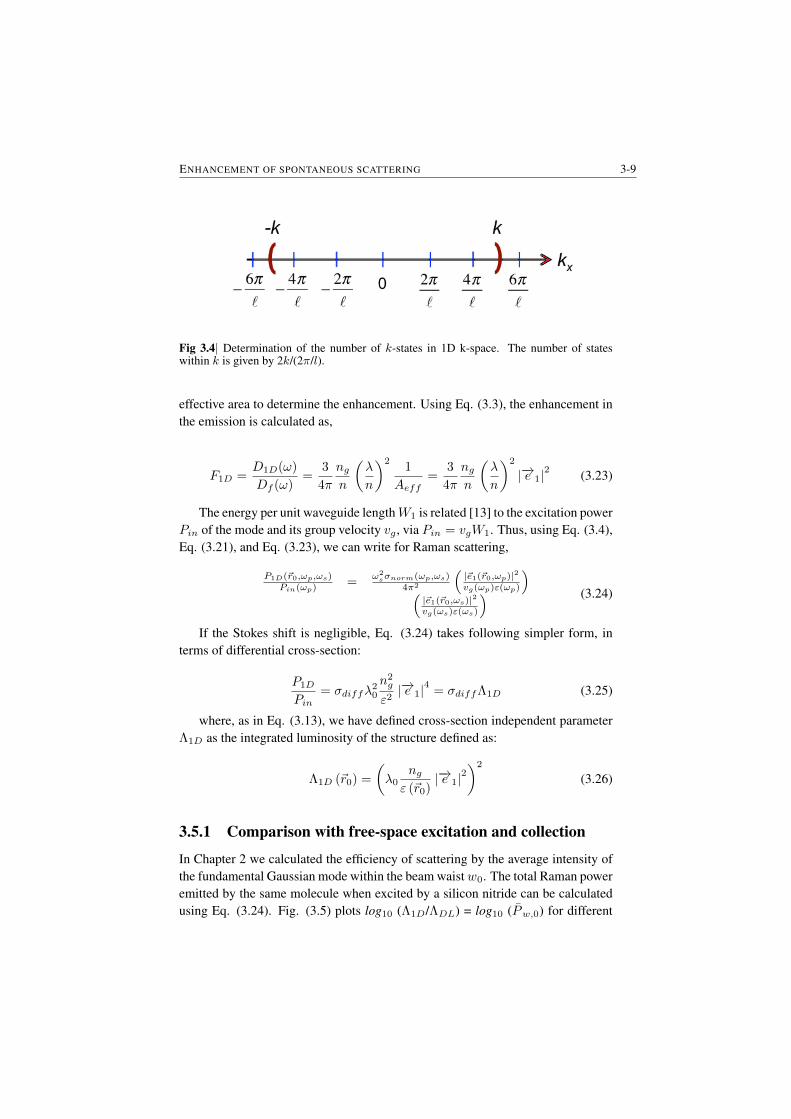
ENHANCEMENT OF SPONTANEOUS SCATTERING 3-9
Fig 3.4| Determination of the number of k-states in 1D k-space. The number of stateswithin k is given by 2k/(2π/l).
effective area to determine the enhancement. Using Eq. (3.3), the enhancement inthe emission is calculated as,
F1D =D1D(ω)
Df (ω)=
3
4π
ngn
(λ
n
)21
Aeff=
3
4π
ngn
(λ
n
)2
|−→e 1|2 (3.23)
The energy per unit waveguide lengthW1 is related [13] to the excitation powerPin of the mode and its group velocity vg , via Pin = vgW1. Thus, using Eq. (3.4),Eq. (3.21), and Eq. (3.23), we can write for Raman scattering,
P1D(~r0,ωp,ωs)Pin(ωp) =
ω2sσnorm(ωp,ωs)
4π2
(|~e1(~r0,ωp)|2vg(ωp)ε(ωp)
)(|~e1(~r0,ωs)|2vg(ωs)ε(ωs)
) (3.24)
If the Stokes shift is negligible, Eq. (3.24) takes following simpler form, interms of differential cross-section:
P1D
Pin= σdiffλ
20
n2g
ε2|−→e 1|
4= σdiffΛ1D (3.25)
where, as in Eq. (3.13), we have defined cross-section independent parameterΛ1D as the integrated luminosity of the structure defined as:
Λ1D (~r0) =
(λ0
ngε (~r0)
|−→e 1|2)2
(3.26)
3.5.1 Comparison with free-space excitation and collection
In Chapter 2 we calculated the efficiency of scattering by the average intensity ofthe fundamental Gaussian mode within the beam waistw0. The total Raman poweremitted by the same molecule when excited by a silicon nitride can be calculatedusing Eq. (3.24). Fig. (3.5) plots log10 (Λ1D/ΛDL) = log10 (Pw,0) for different
3-10 CHAPTER 3
Fig. 3.5| Power coupled to a slot waveguide mode normalized to an ideal free-space excitationand collection. log10(Pw,0) for a slotted waveguide (s = 20 nm, w = 660 nm, see inset for a cross-section of slotted waveguide) shown in 3D highlighting the variations of the coupled power across thevarious regions of the section. The purple shaded area shows the projection of Pw,0(~r0), indicatingthe maxima of the Pw,0(~r0). The contours represent the lines with the same Pw,0 and the colorbar shows the magnitude of Pw,0. The gray shaded region in the x-y plane indicates the waveguidecross-section which is also shown in the inset.
positions in the surrounding of a silicon nitride slot waveguide (s = 20 nm,w =660 nm, see Fig 3.5 for a cross-section of a slotted waveguide, also discussed in§4.1.2 in more detail) in water calculated by the COMSOL finite elements modesolver for the fundamental TE mode. Pw,0 is the power coupled from a particleto the fundamental TE waveguide mode, normalized to the total emission from theparticle when excited by a diffraction limited beam with NA = 1. The figure showsthat more than one order of magnitude of power is coupled to the waveguide modecompared to the total emission in the most ideal diffraction-limited system. Thisresult demonstrates the possibility of a large broadband Purcell enhancement [76]that could be utilized with waveguides. Implications of this result will be discussedin detail in forthcoming sections.
3.6 Closing Remarks
Table 3.1 summarizes the integrated luminosity calculated for excitation and col-lection by means of eigenmodes in medium described by different symmetry prop-erties. Note that the normalized mode profile has different units depending ondifferent symmetry conditions and corresponding normalization. We see that the
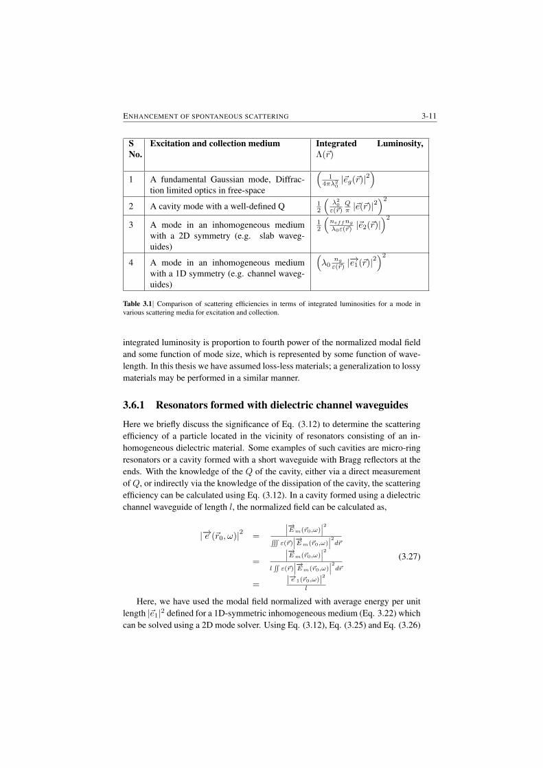
ENHANCEMENT OF SPONTANEOUS SCATTERING 3-11
SNo.
Excitation and collection medium Integrated Luminosity,Λ(~r)
1 A fundamental Gaussian mode, Diffrac-tion limited optics in free-space
(1
4πλ20|~eg(~r)|2
)2 A cavity mode with a well-defined Q 1
2
(λ20
ε(~r)Qπ |~e(~r)|
2)2
3 A mode in an inhomogeneous mediumwith a 2D symmetry (e.g. slab waveg-uides)
12
(neffngλ0ε(~r)
|~e2(~r)|)2
4 A mode in an inhomogeneous mediumwith a 1D symmetry (e.g. channel waveg-uides)
(λ0
ngε(~r) |−→e1(~r)|2
)2
Table 3.1| Comparison of scattering efficiencies in terms of integrated luminosities for a mode invarious scattering media for excitation and collection.
integrated luminosity is proportion to fourth power of the normalized modal fieldand some function of mode size, which is represented by some function of wave-length. In this thesis we have assumed loss-less materials; a generalization to lossymaterials may be performed in a similar manner.
3.6.1 Resonators formed with dielectric channel waveguides
Here we briefly discuss the significance of Eq. (3.12) to determine the scatteringefficiency of a particle located in the vicinity of resonators consisting of an in-homogeneous dielectric material. Some examples of such cavities are micro-ringresonators or a cavity formed with a short waveguide with Bragg reflectors at theends. With the knowledge of the Q of the cavity, either via a direct measurementof Q, or indirectly via the knowledge of the dissipation of the cavity, the scatteringefficiency can be calculated using Eq. (3.12). In a cavity formed using a dielectricchannel waveguide of length l, the normalized field can be calculated as,
|−→e (~r0, ω)|2 =
∣∣∣−→Em(~r0,ω)∣∣∣2
˝ε(~r)
∣∣∣−→Em(~r0,ω)∣∣∣2d~r
=
∣∣∣−→Em(~r0,ω)∣∣∣2
l˜ε(~r)
∣∣∣−→Em(~r0,ω)∣∣∣2d~r
=|−→e 1(~r0,ω)|2
l
(3.27)
Here, we have used the modal field normalized with average energy per unitlength |~e1|2 defined for a 1D-symmetric inhomogeneous medium (Eq. 3.22) whichcan be solved using a 2D mode solver. Using Eq. (3.12), Eq. (3.25) and Eq. (3.26)
3-12 CHAPTER 3
we find that,
Pwg,cavPwg
=ΛcavΛwg
=1
2
(Q
π
λ0
lng
)2
(3.28)
Eq. (3.28) means that if a molecule lying in the vicinity of a standard dielectricwaveguide scatters a power Pwg then, the molecule radiates a power Pwg,cav en-hanced by a factor Λcav/Λwg given by Eq. (3.28). It is true if the waveguide formsa cavity of waveguide length l and both pump and Stokes are resonant. Thus asexpected, the enhancement is high for small resonators, shorter wavelengths andhigh Q resonators.
3.6.2 Fluorescence and non-radiative transitions
We have treated the radiation and scattering problem classically and we haveneglected the non-radiative decay process and interactions within the molecule.Moreover, strong coupling regime leading to Rabi oscillations is neglected. A com-plete analysis requires a quantum mechanical treatment which is outside the scopeof this thesis. Our classical treatment is sufficient in many the typical cases of bio-chemical sensing in so called weak coupling regime, where the coupling betweenthe dipole and the field is sufficiently low. The reader is referred to Loudon [34] fora detailed quantum mechanical description of the emission process that is neededto describe the process in strong coupling regime. The results discussed in thischapter are also applicable for the florescence process, if the emission process isdominated by radiative transitions.
4NWERS of bulk material in the
cladding
In the previous chapter we looked into efficiencies of scattering in different types ofinhomogeneous dielectric media. In this chapter we specifically focus on evanes-cent Raman scattering near single-mode dielectric channel waveguides, which has1D symmetry. Dielectric channel waveguides are very popular in integrated pho-tonics as they confine light with the lowest etendue (§Appendix D) and also forits relative ease of fabrication using chemical etching processes. In this chapterwe will also discuss experimental demonstration of Raman spectroscopy of bulkmaterials using a high index contrast, CMOS-compatible, integrated single-modesilicon nitride (Si3N4) waveguides in the context of nanophotonic waveguide en-hanced Raman spectroscopy (NWERS). We also derive the dependence of col-lected Raman power with the waveguide parameters and experimentally verify thederived relations. Some sections of the text and figures have been adapted fromsome of my published papers [1], [48] - [50].
4.1 The efficiency of scattering
In Chapter 3, we saw that the efficiency of excitation and collection of Ramansignal depends on waveguide dependent factor called integrated luminosity of thewaveguide symbolized by Λ1D(~r, ω) with the waveguide. We now investigatethe total integrated power collected by a waveguide assuming that the scattering
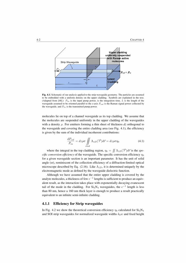
4-2 CHAPTER 4
Fig. 4.1| Schematic of our analysis applied to the strip waveguide geometry. The particles are assumedto be embedded with a uniform density on the upper cladding. Symbols are explained in the text.(Adapted from [48].) Pin is the input pump power, is the integration time, L is the length of thewaveguide assumed to be oriented parallel to the z-axis Pcol is the Raman signal power collected bythe waveguide, and Ptx is the transmitted pump power.
molecules lie on top of a channel waveguide as its top cladding. We assume thatthe molecules are suspended uniformly in the upper cladding of the waveguideswith a density ρ. For emitters forming a thin sheet of thickness dz orthogonal tothe waveguide and covering the entire cladding area (see Fig. 4.1), the efficiencyis given by the sum of the individual incoherent contributions:
dPcolPin
= dzρσ
¨
clad
Λ1D(−→r )d~r = dzρση0 (4.1)
where the integral in the top cladding region, η0 =˜
Λ1D(−→r )d~r is the spe-cific conversion efficiency of the waveguide. The specific conversion efficiency η0
for a given waveguide section is an important parameter. It has the unit of solidangle (sr), reminiscent of the collection efficiency of a diffraction-limited opticalmicroscope described by Eq. (2.16). Like Λ1D, it is determined uniquely by theelectromagnetic mode as defined by the waveguide dielectric function.
Although we have assumed that the entire upper cladding is covered by theanalyte molecules, a thickness of few e−1 lengths is sufficient to produce an equiv-alent result, as the interaction takes place with exponentially decaying evanescenttail of the mode in the cladding. For Si3N4 waveguides, the e−1 length is lessthan 80 nm, hence a 160 nm thick layer is enough to produce a result practicallyequivalent to an infinite semi-infinite cladding.
4.1.1 Efficiency for Strip waveguides
In Fig. 4.2 we show the theoretical conversion efficiency η0 calculated for Si3N4
and SOI strip waveguides for normalized waveguide widths k0w and fixed height
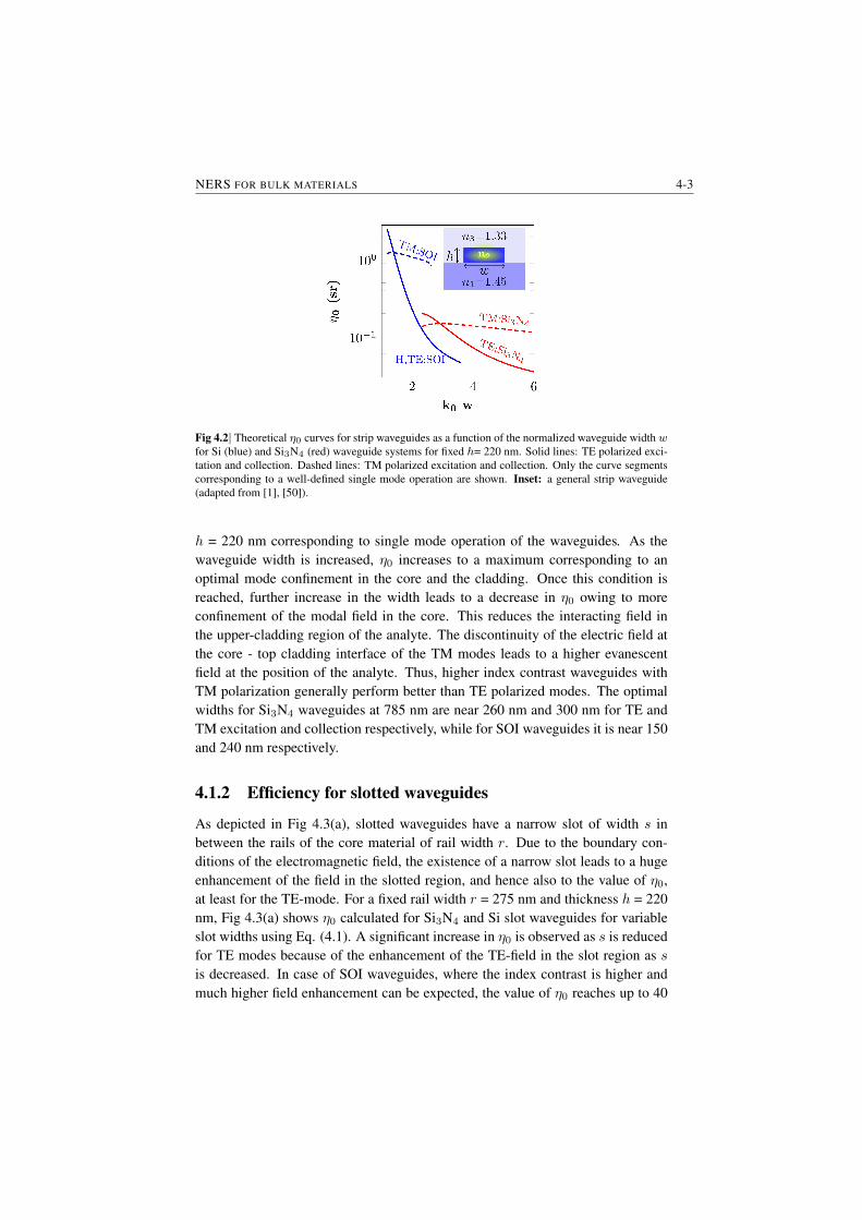
NERS FOR BULK MATERIALS 4-3
Fig 4.2| Theoretical η0 curves for strip waveguides as a function of the normalized waveguide widthwfor Si (blue) and Si3N4 (red) waveguide systems for fixed h= 220 nm. Solid lines: TE polarized exci-tation and collection. Dashed lines: TM polarized excitation and collection. Only the curve segmentscorresponding to a well-defined single mode operation are shown. Inset: a general strip waveguide(adapted from [1], [50]).
h = 220 nm corresponding to single mode operation of the waveguides. As thewaveguide width is increased, η0 increases to a maximum corresponding to anoptimal mode confinement in the core and the cladding. Once this condition isreached, further increase in the width leads to a decrease in η0 owing to moreconfinement of the modal field in the core. This reduces the interacting field inthe upper-cladding region of the analyte. The discontinuity of the electric field atthe core - top cladding interface of the TM modes leads to a higher evanescentfield at the position of the analyte. Thus, higher index contrast waveguides withTM polarization generally perform better than TE polarized modes. The optimalwidths for Si3N4 waveguides at 785 nm are near 260 nm and 300 nm for TE andTM excitation and collection respectively, while for SOI waveguides it is near 150and 240 nm respectively.
4.1.2 Efficiency for slotted waveguides
As depicted in Fig 4.3(a), slotted waveguides have a narrow slot of width s inbetween the rails of the core material of rail width r. Due to the boundary con-ditions of the electromagnetic field, the existence of a narrow slot leads to a hugeenhancement of the field in the slotted region, and hence also to the value of η0,at least for the TE-mode. For a fixed rail width r = 275 nm and thickness h = 220nm, Fig 4.3(a) shows η0 calculated for Si3N4 and Si slot waveguides for variableslot widths using Eq. (4.1). A significant increase in η0 is observed as s is reducedfor TE modes because of the enhancement of the TE-field in the slot region as sis decreased. In case of SOI waveguides, where the index contrast is higher andmuch higher field enhancement can be expected, the value of η0 reaches up to 40

4-4 CHAPTER 4
Fig. 4.3| Theoretical conversion efficiency η0 for slotted waveguides for SOI (blue) and Si3N4 (red)waveguide systems. a) Fixed r = 350 nm, h = 220 nm, as a function of slot width s for fundamental TEmode. b) Fixed s = 150 nm,h = 220 nm, as a function of waveguide width w = s+2r. Solid lines: TEpolarized excitation and collection. Dashed lines: TM polarized excitation and collection. (Adaptedfrom [1], [50] )
sr for s = 20 nm.Fig 4.3(b) shows η0 calculated for Si3N4 and SOI for a fixed slot width s =
150 nm and for various total widths w, inclusive of the slot width s (note: r =
(w − s)/2). As observed in the case of strip waveguides, η0 decreases when thewaveguide width is increased as a result of the confinement of the mode in the coreand consequent reduction of the interaction volume in the analyte region. Due tothe continuity of the electric field, the field enhancement in the slot is much less incase of TM polarization leading to comparatively insignificant enhancement.
4.1.3 Equivalent length and enhancement
Comparing Eq. (4.1) and Eq. (2.16), we can define an equivalent length leq , whichcorresponds to the length of the waveguide that gives the same signal as that of
NERS FOR BULK MATERIALS 4-5
diffraction limited confocal microscopes.
leq =2
η0
(λ0
n
)(4.2)
Depending on the index contrast, polarization and design of the waveguides,η0 may typically vary from 0.1 sr to 50 sr. Thus a waveguide length l < 20λ0
wavelengths is enough to provide an efficiency equivalent to that of a diffraction-limited confocal microscope. A single mode waveguide loss of 1dB/cm is typicalfor the considered integrated photonics platforms, allowing more than a centimeterof waveguide without significant loss of the pump or collected signal. This leads to3-5 orders of magnitude enhancement of the signal compared to diffraction-limitedfree-space systems.
4.2 Considerations for coupling losses and waveg-uide losses
Now we consider a practical situation and consider coupling and waveguide losses.We refer again to Fig. 4.1. A pump laser with power Pin is incident on the in-put facet of the waveguides, of which a fraction gets coupled to the waveguidemode with coupling efficiency γin and propagates along the waveguide. Duringthe propagation, molecules in the cladding are excited, and the scattered sponta-neous Raman signal is collected via evanescent coupling to the same waveguide,as described by Eq. (4.1) in both forward and backward propagating directions.In the forward propagating configuration, only half of the collected power is mea-sured at the output facet with an output coupling efficiency γout. Accounting forcoupling losses and attenuation of the pump and collected signal in the waveguide,the ratio of signal power collected (Pcol) at the end of the waveguide to the inputpower (Pin) is given by:
Pcol(L)Pin
≡ ξ(L) = ρση02 γinγout
L
0
e−αpze−αs(L−z)dz
= ρση02 γinγoute
−αpL[eδαL−1δα
] (4.3)
where αp and αs are the waveguide losses at the pump wavelength and at theStokes wavelength respectively and δα = αp−αs is their difference. The factor of1/2 accounts for a backward propagating signal that is not collected in the currentconfiguration of our experimental setup. The term in brackets evolves to L whenδα→ 0.
If we assume that the coupling efficiencies from the waveguide end to the de-tector are equal for the pump and the Stokes signal, the Raman power collected atthe end of the waveguide can be expressed in terms of the transmitted pump power
4-6 CHAPTER 4
(Ptx) at the detector, which can be directly measured. Thus, for many practicalcases, it is convenient to define a quantity ζ(l) that is independent of coupling andwaveguide losses:
ζ(l) ≡ Pcol(l)
Ptx(l)=ρση0
2
[eδαl − 1
δα
]=η0
2σρl (1 + ∆) (4.4)
Here, ∆ = (lδα)/2! +(lδα)2/3! +... is generally a negligible quantity for smallwaveguide lengths, small waveguide losses or small stokes shifts. In a later sectionwe show how the effect of ∆ can be determined for an accurate measurement.
Eq.(4.1) - Eq.(4.4) are the main theoretical results of this chapter and expresshow the collected signal power depends on the input or transmitted pump power.In many situations, the quantity ξ(L) is of practical interest, as the direct measureof the collected power for a given input power. However, it depends on couplingefficiencies and waveguide loss, which vary in the experiments. The quantity ζ(L)is independent of the coupling and the waveguide loss and can be used for thepurposes of direct analysis of signal strength with respect to concentration, cross-section, waveguide geometry and length.
4.3 Experimental demonstration of evanescent Ra-man scattering
In this section we describe the experimental setup and the experimental resultsobtained for the silicon nitride waveguides, and compare with the results based ontheoretical models described in previous sections. The details of the waveguidefabrication technology used for the experiments have been briefly discussed in§1.3.
4.3.1 Measurement setup
The setup used in our measurements is described in Fig. 4.4. A tunable Ti:sapphirelaser is set to a pump wavelength of λP = 785 nm (red) after which the polarizedbeam passes through a half-wave plate (λ0/2) in order to rotate the polarizationto a TE-polarized beam. The pump beam then passes through a laser line filter(LLF) for side-band suppression before it is coupled into the chip by an asphericlens (ASPH). The output beam is collected with an objective (OBJ) and passesthrough a polarizer P (set to either TE or TM depending on the measurement ) be-fore it is filtered by a dichroic mirror which reflects the pump beam and transmitsall Stokes wavelengths (green). The Stokes light is collected into a fiber using aparabolic mirror collimator (PMC) after which the fiber is split by a fiber splitter(FS) of which 1% goes to a power meter (PM) and 99% to a commercial spec-trometer either from Avantes (AvaSpec-ULS2048XL) or Andor (Shamrock 303i
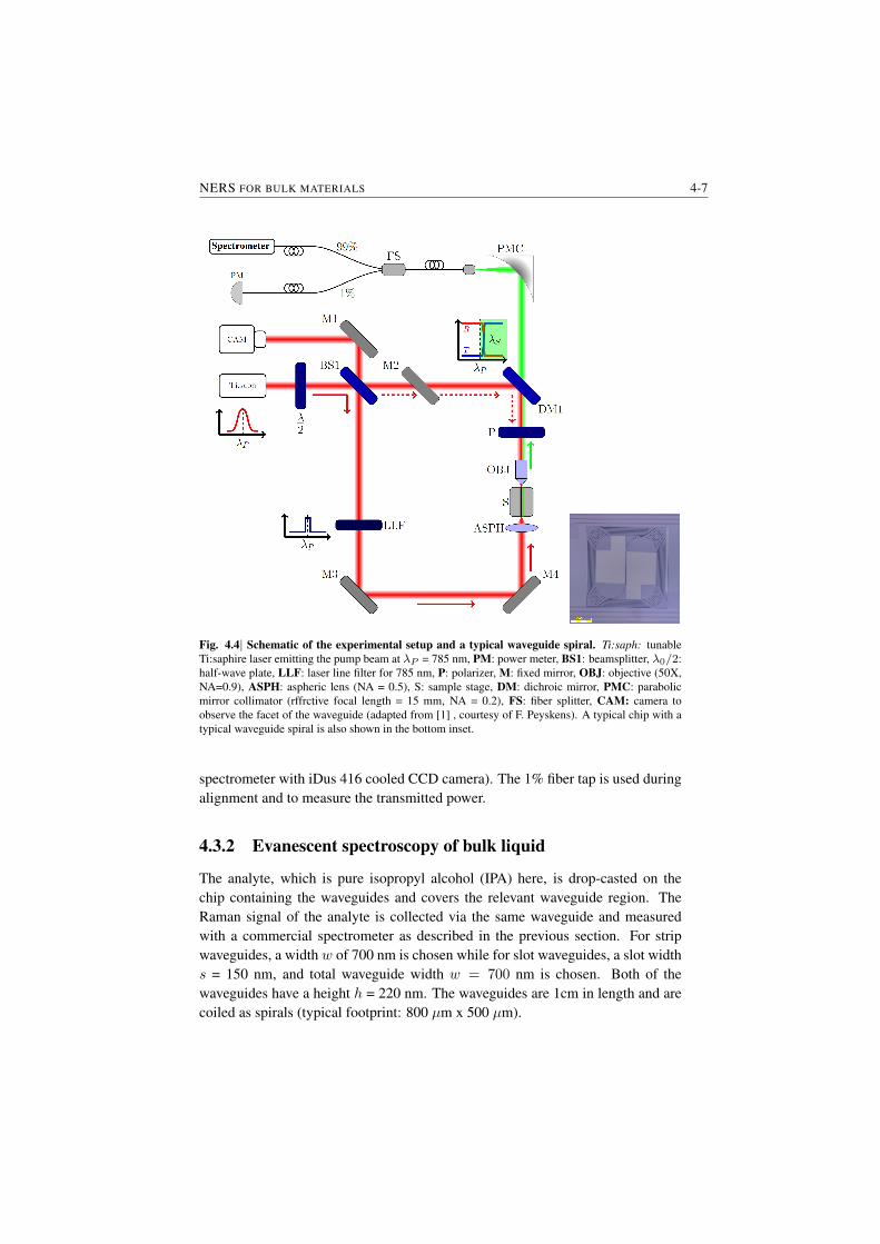
NERS FOR BULK MATERIALS 4-7
Fig. 4.4| Schematic of the experimental setup and a typical waveguide spiral. Ti:saph: tunableTi:saphire laser emitting the pump beam at λP = 785 nm, PM: power meter, BS1: beamsplitter, λ0/2:half-wave plate, LLF: laser line filter for 785 nm, P: polarizer, M: fixed mirror, OBJ: objective (50X,NA=0.9), ASPH: aspheric lens (NA = 0.5), S: sample stage, DM: dichroic mirror, PMC: parabolicmirror collimator (rffrctive focal length = 15 mm, NA = 0.2), FS: fiber splitter, CAM: camera toobserve the facet of the waveguide (adapted from [1] , courtesy of F. Peyskens). A typical chip with atypical waveguide spiral is also shown in the bottom inset.
spectrometer with iDus 416 cooled CCD camera). The 1% fiber tap is used duringalignment and to measure the transmitted power.
4.3.2 Evanescent spectroscopy of bulk liquid
The analyte, which is pure isopropyl alcohol (IPA) here, is drop-casted on thechip containing the waveguides and covers the relevant waveguide region. TheRaman signal of the analyte is collected via the same waveguide and measuredwith a commercial spectrometer as described in the previous section. For stripwaveguides, a width w of 700 nm is chosen while for slot waveguides, a slot widths = 150 nm, and total waveguide width w = 700 nm is chosen. Both of thewaveguides have a height h = 220 nm. The waveguides are 1cm in length and arecoiled as spirals (typical footprint: 800 µm x 500 µm).
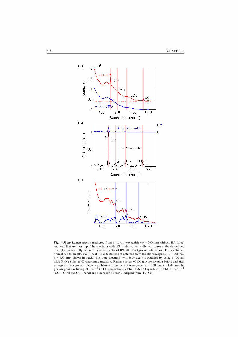
4-8 CHAPTER 4
Fig. 4.5| (a) Raman spectra measured from a 1.6 cm waveguide (w = 700 nm) without IPA (blue)and with IPA (red) on top. The spectrum with IPA is shifted vertically with zeros at the dashed redline. (b) Evanescently measured Raman spectra of IPA after background subtraction. The spectra arenormalized to the 819 cm−1 peak (C-C-O stretch) of obtained from the slot waveguide (w = 700 nm,s = 150 nm), shown in black. The blue spectrum (with blue axes) is obtained by using a 700 nmwide Si3N4 strip. (c) Evanescently measured Raman spectra of 1M glucose solution before and afterwaveguide background subtraction obtained from the slot waveguide (w = 700 nm, s = 150 nm), theglucose peaks including 911 cm−1 ( CCH symmetric stretch), 1126 (CO symetric stretch), 1365 cm−1
(OCH, COH and CCH bend) and others can be seen . Adapted from [1], [50]
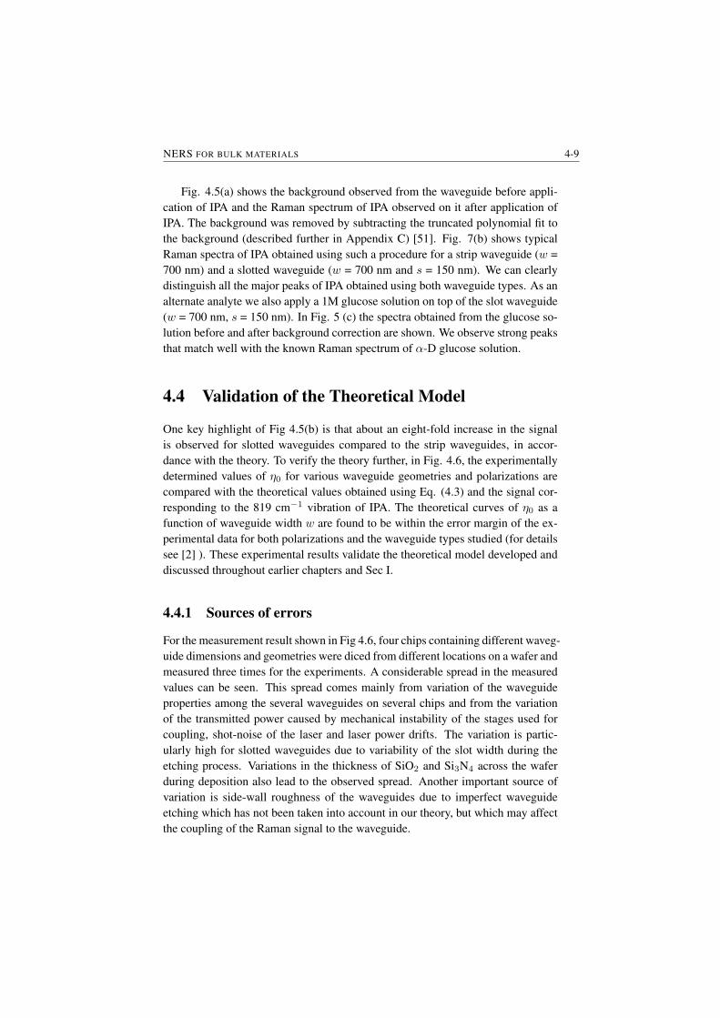
NERS FOR BULK MATERIALS 4-9
Fig. 4.5(a) shows the background observed from the waveguide before appli-cation of IPA and the Raman spectrum of IPA observed on it after application ofIPA. The background was removed by subtracting the truncated polynomial fit tothe background (described further in Appendix C) [51]. Fig. 7(b) shows typicalRaman spectra of IPA obtained using such a procedure for a strip waveguide (w =700 nm) and a slotted waveguide (w = 700 nm and s = 150 nm). We can clearlydistinguish all the major peaks of IPA obtained using both waveguide types. As analternate analyte we also apply a 1M glucose solution on top of the slot waveguide(w = 700 nm, s = 150 nm). In Fig. 5 (c) the spectra obtained from the glucose so-lution before and after background correction are shown. We observe strong peaksthat match well with the known Raman spectrum of α-D glucose solution.
4.4 Validation of the Theoretical Model
One key highlight of Fig 4.5(b) is that about an eight-fold increase in the signalis observed for slotted waveguides compared to the strip waveguides, in accor-dance with the theory. To verify the theory further, in Fig. 4.6, the experimentallydetermined values of η0 for various waveguide geometries and polarizations arecompared with the theoretical values obtained using Eq. (4.3) and the signal cor-responding to the 819 cm−1 vibration of IPA. The theoretical curves of η0 as afunction of waveguide width w are found to be within the error margin of the ex-perimental data for both polarizations and the waveguide types studied (for detailssee [2] ). These experimental results validate the theoretical model developed anddiscussed throughout earlier chapters and Sec I.
4.4.1 Sources of errors
For the measurement result shown in Fig 4.6, four chips containing different waveg-uide dimensions and geometries were diced from different locations on a wafer andmeasured three times for the experiments. A considerable spread in the measuredvalues can be seen. This spread comes mainly from variation of the waveguideproperties among the several waveguides on several chips and from the variationof the transmitted power caused by mechanical instability of the stages used forcoupling, shot-noise of the laser and laser power drifts. The variation is partic-ularly high for slotted waveguides due to variability of the slot width during theetching process. Variations in the thickness of SiO2 and Si3N4 across the waferduring deposition also lead to the observed spread. Another important source ofvariation is side-wall roughness of the waveguides due to imperfect waveguideetching which has not been taken into account in our theory, but which may affectthe coupling of the Raman signal to the waveguide.

4-10 CHAPTER 4
Fig. 4.6|The theoretical and experimental values of η0 obtained for (a) TE modes and (b) TM modes ofSi3N4 waveguides. The markers with error bars represent the estimated experimental errors [50]. Thelines represent theoretical curves. The red solid lines are the theoretical curve for slot waveguides withs = 150 nm. The blue and black dashed lines are the theoretical curves for TE and TM polarizationsrespectively for strip waveguides. Circle: TE polarization, strip waveguides. Square: TE polarization,slot waveguides. Left handed triangles: TM polarization, strip waveguides. Right handed triangles:TM polarization, slot waveguides (adapted from [1], [50]).
4.5 Performance in comparison to the confocal mi-croscopes
Having established the relevance of our model, we will now experimentally in-vestigate the enhancement predicted by the model. In section I (Eq. 4.2), weintroduced the equivalent length leq of the NWERS system which theoreticallypredicts an enhancement Φ = l−1
eq per unit length per sr compared to a confocalmicroscope. The enhancement Φis plotted in Fig. 4.7. In this section, we showthat compared to the confocal microscopes, a 1 cm long silicon nitride (Si3N4)waveguide leads to more than three orders of magnitude higher signal. Such anenhancement of the signal contributes to a higher SNR for the waveguide systemscompared to the dark-noise limited Raman microscopic systems. We also showthat the use of the slotted waveguides increases the signal-to-noise Ratio (SNR)and collection efficiency in accordance with the theoretical results shown in Fig4.7.
For experiments described in this chapter, strip waveguides with a width wof 700 nm is chosen while for slot waveguides, slot width s = 150 nm, and totalwaveguide width w = 700 is chosen. Both of the waveguides have the heighth = 220 nm. As in the earlier experiments, the waveguides are 1cm in lengthand are coiled as spirals. To compare the on-chip approach with the conventionalRaman microscope, we use a commercial confocal Raman microscope (WITecAlpha300R+). For both cases, the same excitation laser wavelength and the same
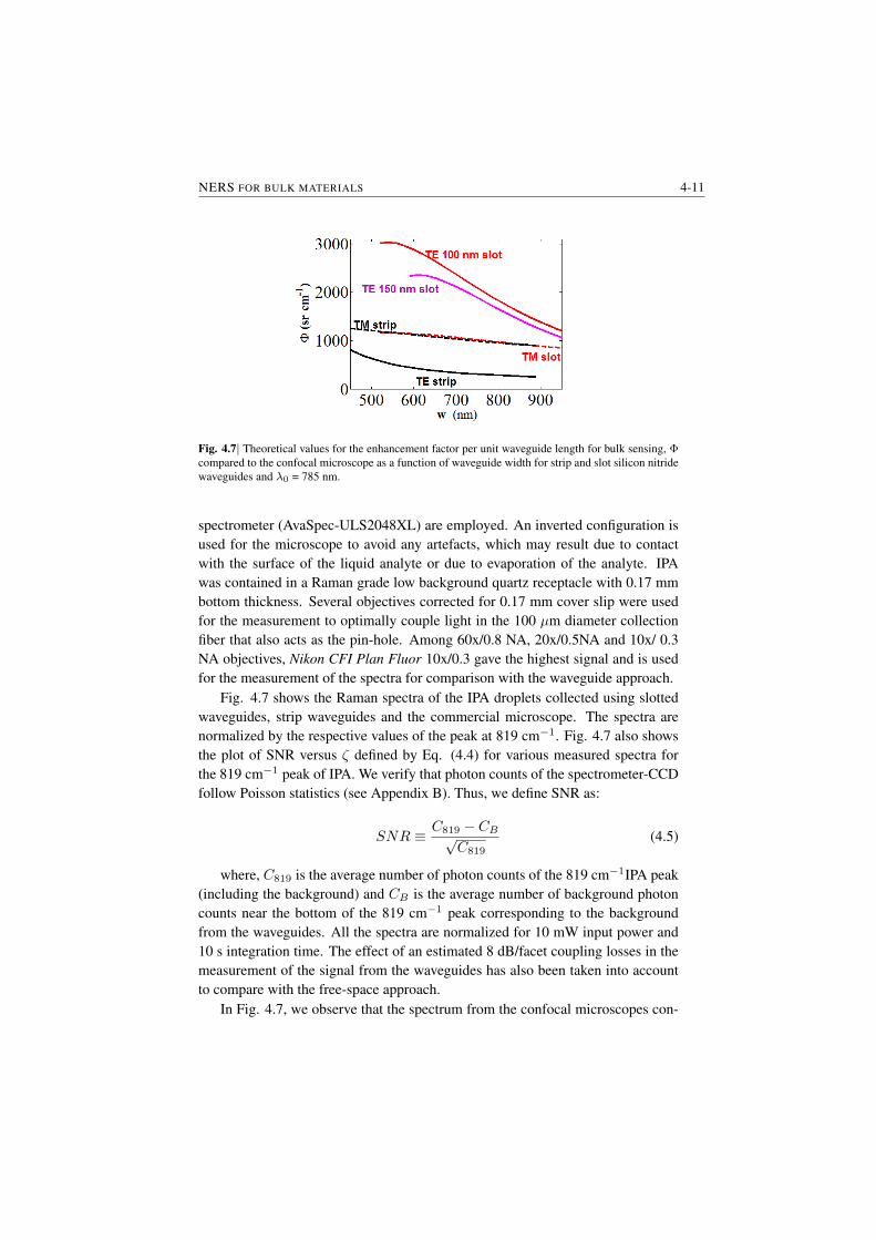
NERS FOR BULK MATERIALS 4-11
Fig. 4.7| Theoretical values for the enhancement factor per unit waveguide length for bulk sensing, Φcompared to the confocal microscope as a function of waveguide width for strip and slot silicon nitridewaveguides and λ0 = 785 nm.
spectrometer (AvaSpec-ULS2048XL) are employed. An inverted configuration isused for the microscope to avoid any artefacts, which may result due to contactwith the surface of the liquid analyte or due to evaporation of the analyte. IPAwas contained in a Raman grade low background quartz receptacle with 0.17 mmbottom thickness. Several objectives corrected for 0.17 mm cover slip were usedfor the measurement to optimally couple light in the 100 µm diameter collectionfiber that also acts as the pin-hole. Among 60x/0.8 NA, 20x/0.5NA and 10x/ 0.3NA objectives, Nikon CFI Plan Fluor 10x/0.3 gave the highest signal and is usedfor the measurement of the spectra for comparison with the waveguide approach.
Fig. 4.7 shows the Raman spectra of the IPA droplets collected using slottedwaveguides, strip waveguides and the commercial microscope. The spectra arenormalized by the respective values of the peak at 819 cm−1. Fig. 4.7 also showsthe plot of SNR versus ζ defined by Eq. (4.4) for various measured spectra forthe 819 cm−1 peak of IPA. We verify that photon counts of the spectrometer-CCDfollow Poisson statistics (see Appendix B). Thus, we define SNR as:
SNR ≡ C819 − CB√C819
(4.5)
where, C819 is the average number of photon counts of the 819 cm−1IPA peak(including the background) and CB is the average number of background photoncounts near the bottom of the 819 cm−1 peak corresponding to the backgroundfrom the waveguides. All the spectra are normalized for 10 mW input power and10 s integration time. The effect of an estimated 8 dB/facet coupling losses in themeasurement of the signal from the waveguides has also been taken into accountto compare with the free-space approach.
In Fig. 4.7, we observe that the spectrum from the confocal microscopes con-
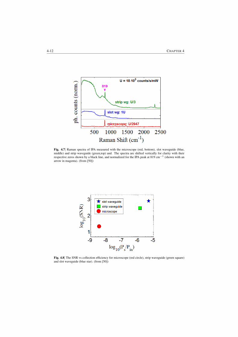
4-12 CHAPTER 4
Fig. 4.7| Raman spectra of IPA measured with the microscope (red, bottom), slot waveguide (blue,middle) and strip waveguide (green,top) and. The spectra are shifted vertically for clarity with theirrespective zeros shown by a black line, and normalized for the IPA peak at 819 cm−1 (shown with anarrow in magenta). (from [50])
Fig. 4.8| The SNR vs collection efficiency for microscope (red circle), strip waveguide (green square)and slot waveguide (blue star). (from [50])
NERS FOR BULK MATERIALS 4-13
tained only the dark-noise from the spectrometer and contained negligible back-ground. This is anticipated because the signal was taken directly from IPA at theconfocal volume and a low-background Raman grade quartz receptacle was used.In contrast, the spectrum collected from the waveguides is composed of the Ra-man signal from the analyte and the background originating from the Si3N4 coreof the waveguide (discussed in detail in Chapter 7). Nevertheless, from Fig. 4.8one can observe that in comparison to the confocal microscopic systems, about 3orders of magnitude higher signal is obtained from the waveguides resulting in alarge improvement in the SNR. Note that compared to the strip waveguides, theslotted waveguides have lower background relative to the corresponding IPA peak.This can be explained by the strong enhancement of the field in the slotted regionresulting in a stronger interaction with the analyte (see Chapter 6). In contrast, forstrip waveguides, the maximum intensity lies in the Si3N4 core region thus col-lecting more background from it. Use of a slotted waveguide configuration alsoleads to about an eight-fold enhancement in the signal strength compared to thestrip waveguide. Therefore, a significantly higher SNR can be observed for theslotted waveguides.
In conclusion, because of the enhancement of the collected Raman signal inwaveguide-based evanescent Raman spectroscopy, a higher SNR and collectionefficiency are obtained in comparison to the confocal microscope despite the back-ground noise from the waveguide core. The SNR can further be lowered by appro-priate waveguide designs such as the slotted waveguide that enhances the interact-ing field intensity in the analyte region.
4.6 Closing RemarksThe reported experiments and simulations are performed for IPA as the analytein the uppercladding. However, the experimental and theoretical assessments havealso been performed using other liquid and solid analytes, such as, acetone, dimethylsulfoxide, and spin coated photoresists. The confinement properties of the waveg-uide mode changes if the refractive index of the uppercladding varies; therefore,according to Eq. (4.1) the numerical values of the conversion efficiency willslightly differ. Nonetheless, the results discussed in this article are pertinent foranalytes of general interest such as a glucose solution.

5NWERS of Monolayers and thin layers
In the previous chapter we saw that for the bulk materials placed on the top ofthe waveguides, the use of Si3N4 waveguide provides a signal more than 2 or-ders of magnitudes compared to the free-space methods. The comparative ad-vantage of the nanophotonic waveguide enhanced Raman spectroscopy (NWERS)approach is more prominent for a monolayer of molecules functionalized on top ofthe waveguides. It is because the evanescent interaction is much stronger near thesurface of the waveguide (§3.5) in addition to integration of the signal along thewaveguide. In this chapter, we discuss evanescent Raman spectroscopy of mono-layers. It will be shown that this method provides a signal which is four orders ofmagnitude greater than that for the most ideal free-space Raman system, even witha one centimeter long waveguide. This huge enhancement of the signal leads toan integration time for a realistic waveguide system that is reduced by almost sixorders of magnitude in comparison with a commercial Raman microscope system.The enhancement and reduced signal acquisition time open up new opportunitiesin the applications of Raman spectroscopy for monolayers, such as, monitoring ofthe biological and chemical processes with highly specific, quantitative and infor-mative spontaneous Raman signals in real-time in the NIR wavelength region. Wewill also discuss observation of DNA hybridization process in real time and subse-quently extract the relevant experimental parameters such as association constantand hybridization density. Furthermore, we show that the specificity of the Ramansignal combined with the quantitative nature of the enhancement allows us to ac-curately detect and quantify sub-monolayers of biotin and streptavidin molecules.The content of this chapter has been submitted for peer reviewed publication with a
5-2 CHAPTER 5
title, “Nanophotonic waveguide enhanced Raman spectroscopy of biological sub-monolayers on a CMOS-compatible platform”.
5.1 Importance of Raman spectroscopy of Monolay-ers
Monolayers or thin layers of materials are ubiquitous in nature and play a criticalrole in modern instrumentation and technology [52]. Many important physico-chemical and biological interactions of cells happen at the level of surfaces andinterfaces, such as cell-membranes [53]- [54]. The study of layers at the bioin-terfaces is crucial for applications ranging from clinical diagnostics, genomics,proteomics, and biomaterials to tissue engineering [52] - [60] . Furthermore, thereis an emergence of numerous interesting physical processes and novel optoelec-tronic applications that use 2D monolayers of materials such as graphene [60] andgraphene-like 2D materials [61] - [62]. Hence, a paramount importance is placedon understanding the structural, physical and biochemical properties of monolay-ers or very thin layers of molecules.
In monolayer research, there is a need for a precise tool that provides con-solidated information about composition, molecular structure, and density of thesurface molecules. Simultaneously characterizing the kinetics of the bio-chemicalinteractions at interfaces is equally important in many applications [52]- [59], suchas the study of DNA hybridization. Obtaining such consolidated information frommonolayers is particularly challenging because only a small number of moleculescontribute to the signal. The prevalent techniques such as scanning probe mi-croscopy (SPM) [63], X-ray based techniques [64] [65] and nuclear magnetic res-onance microscopy [67] are often invasive, expensive, necessitate a long time forsample preparation and data acquisition, and require a restrictive environment forsamples. As such, existing techniques for monolayer characterization are unsuit-able for a variety of applications.
Raman spectroscopy is a powerful technique, and is particularly well-suited foridentification and quantification of various physicochemical properties of molecules.Raman spectroscopy has been successfully used for the characterization of mono-layers of materials such as graphene that have a high Raman scattering efficiency[68] or via a pump wavelength resonant to the fluorescence that allows for ahuge enhancement in the Raman signal [69]. Very thin layers of small Ramancross-section molecules, such as nucleic acids, proteins or lipids, present a ma-jor challenge for this technique, because the associated signal acquisition timesto obtain a sufficient signal-to-noise ratio (SNR) are impractically long. This isespecially the case for near-infrared (NIR) wavelengths, where auto-fluorescencebackground from most of the biological materials is weak, yet, unfortunately the
NERS OF MONOLAYERS AND THIN LAYERS 5-3
Raman scattering cross-sections are also very small. Surface enhanced Ramanscattering (SERS) has been used to mitigate this problem [70] [71] by means ofelectromagnetic enhancement due to surface plasmon resonance effects. SERS hasbeen sucessfully used for an extreme signal enhancement, leading to enhancementthat allow even dection of single molecules [72]. However, SERS signals dependstrongly on geometrical features at the nanoscale and the resultant variations fromone substrate to another necessitate sophisticated fabrication techniques for repro-ducibility and uniformity [72]- [74]. Tip enhanced Raman spectroscopy (TERS),a technique combining SPM with a SERS nano-tip to greatly enhance the signal,has been recently used to study polymer monolayers [75], albeit with the disad-vantages of long integration time and inhomogeneity of signal strength inherent toSPM and SERS.
Here we report a real-time observation of immobilized DNA hybridization andan accurate and direct measurement of the density of sub-monolayers of biotin-streptavidin complex using this on-chip nanophotonic waveguide enhanced Ramanspectroscopy (NWERS) technique. This prospect emerges as a consequence ofelectromagnetic enhancement and an increase in number of the probed molecules,bringing about an enormous reduction of the integration time for a practical SNR.The following section describes this matter in detail.
5.2 Collection efficiency for monolayersFor a monolayer of molecules with surface density ρs uniformly distributed overa transversely symmetric waveguide of length l, the total normalized surface con-version efficiency for the waveguide system is given by the sum of individual in-coherent contributions from each molecule:
Pw,sPin
= σρsl´line
Λ1D(~r)d~r
= lρsσηs(5.1)
where, Λ1D is the integrated luminosity of the waveguide introduced in Chap-ter 3. The line integral is defined along the interface between the core and uppercladding (Fig. 5.1) on an arbitrary section of a waveguide. We call the integral, ηsthe specific surface conversion efficiency and given by Eq. (5.2).
ηs ≡ˆ
line
Λ1D(~r)d~r (5.2)
For the similar monolayer when excited and collected by a diffraction limitedfree-space system, the interaction area is limited by the beam waist. As we saw inChapter 2, the power emitted in every direction when excited by a Gaussian beamis given by, PDL,s = Pinσρs.
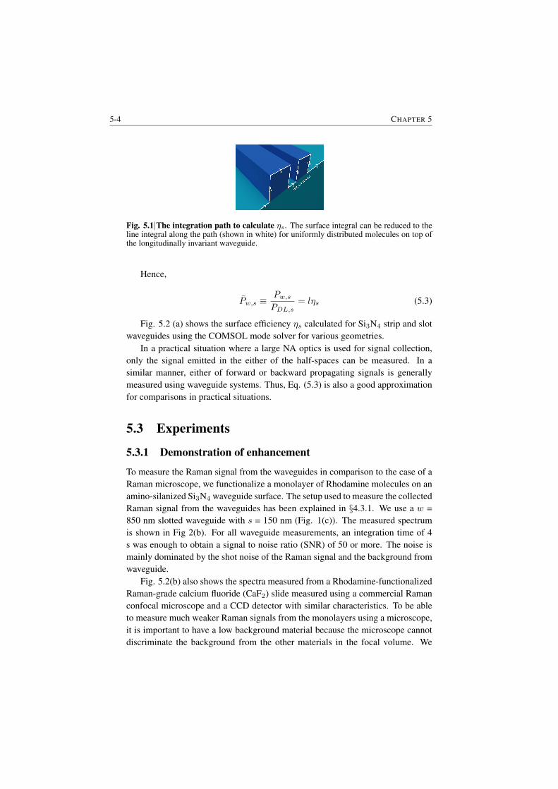
5-4 CHAPTER 5
Fig. 5.1|The integration path to calculate ηs. The surface integral can be reduced to theline integral along the path (shown in white) for uniformly distributed molecules on top ofthe longitudinally invariant waveguide.
Hence,
Pw,s ≡Pw,sPDL,s
= lηs (5.3)
Fig. 5.2 (a) shows the surface efficiency ηs calculated for Si3N4 strip and slotwaveguides using the COMSOL mode solver for various geometries.
In a practical situation where a large NA optics is used for signal collection,only the signal emitted in the either of the half-spaces can be measured. In asimilar manner, either of forward or backward propagating signals is generallymeasured using waveguide systems. Thus, Eq. (5.3) is also a good approximationfor comparisons in practical situations.
5.3 Experiments
5.3.1 Demonstration of enhancement
To measure the Raman signal from the waveguides in comparison to the case of aRaman microscope, we functionalize a monolayer of Rhodamine molecules on anamino-silanized Si3N4 waveguide surface. The setup used to measure the collectedRaman signal from the waveguides has been explained in §4.3.1. We use a w =850 nm slotted waveguide with s = 150 nm (Fig. 1(c)). The measured spectrumis shown in Fig 2(b). For all waveguide measurements, an integration time of 4s was enough to obtain a signal to noise ratio (SNR) of 50 or more. The noise ismainly dominated by the shot noise of the Raman signal and the background fromwaveguide.
Fig. 5.2(b) also shows the spectra measured from a Rhodamine-functionalizedRaman-grade calcium fluoride (CaF2) slide measured using a commercial Ramanconfocal microscope and a CCD detector with similar characteristics. To be ableto measure much weaker Raman signals from the monolayers using a microscope,it is important to have a low background material because the microscope cannotdiscriminate the background from the other materials in the focal volume. We
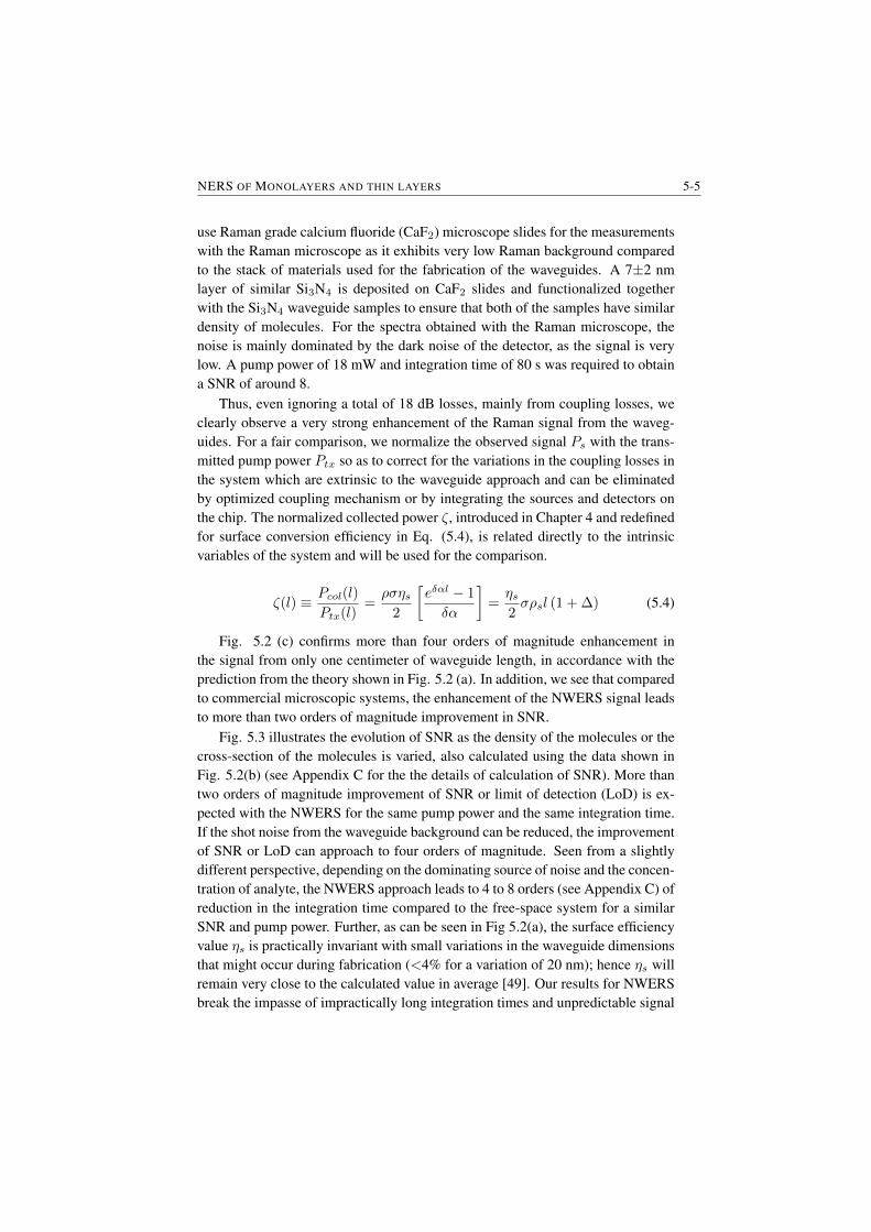
NERS OF MONOLAYERS AND THIN LAYERS 5-5
use Raman grade calcium fluoride (CaF2) microscope slides for the measurementswith the Raman microscope as it exhibits very low Raman background comparedto the stack of materials used for the fabrication of the waveguides. A 7±2 nmlayer of similar Si3N4 is deposited on CaF2 slides and functionalized togetherwith the Si3N4 waveguide samples to ensure that both of the samples have similardensity of molecules. For the spectra obtained with the Raman microscope, thenoise is mainly dominated by the dark noise of the detector, as the signal is verylow. A pump power of 18 mW and integration time of 80 s was required to obtaina SNR of around 8.
Thus, even ignoring a total of 18 dB losses, mainly from coupling losses, weclearly observe a very strong enhancement of the Raman signal from the waveg-uides. For a fair comparison, we normalize the observed signal Ps with the trans-mitted pump power Ptx so as to correct for the variations in the coupling losses inthe system which are extrinsic to the waveguide approach and can be eliminatedby optimized coupling mechanism or by integrating the sources and detectors onthe chip. The normalized collected power ζ, introduced in Chapter 4 and redefinedfor surface conversion efficiency in Eq. (5.4), is related directly to the intrinsicvariables of the system and will be used for the comparison.
ζ(l) ≡ Pcol(l)
Ptx(l)=ρσηs
2
[eδαl − 1
δα
]=ηs2σρsl (1 + ∆) (5.4)
Fig. 5.2 (c) confirms more than four orders of magnitude enhancement inthe signal from only one centimeter of waveguide length, in accordance with theprediction from the theory shown in Fig. 5.2 (a). In addition, we see that comparedto commercial microscopic systems, the enhancement of the NWERS signal leadsto more than two orders of magnitude improvement in SNR.
Fig. 5.3 illustrates the evolution of SNR as the density of the molecules or thecross-section of the molecules is varied, also calculated using the data shown inFig. 5.2(b) (see Appendix C for the the details of calculation of SNR). More thantwo orders of magnitude improvement of SNR or limit of detection (LoD) is ex-pected with the NWERS for the same pump power and the same integration time.If the shot noise from the waveguide background can be reduced, the improvementof SNR or LoD can approach to four orders of magnitude. Seen from a slightlydifferent perspective, depending on the dominating source of noise and the concen-tration of analyte, the NWERS approach leads to 4 to 8 orders (see Appendix C) ofreduction in the integration time compared to the free-space system for a similarSNR and pump power. Further, as can be seen in Fig 5.2(a), the surface efficiencyvalue ηs is practically invariant with small variations in the waveguide dimensionsthat might occur during fabrication (<4% for a variation of 20 nm); hence ηs willremain very close to the calculated value in average [49]. Our results for NWERSbreak the impasse of impractically long integration times and unpredictable signal
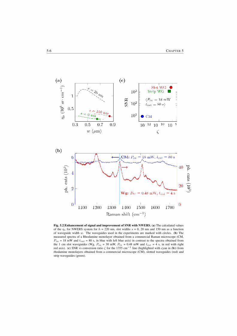
5-6 CHAPTER 5
Fig. 5.2|Enhancement of signal and improvement of SNR with NWERS. (a) The calculated valuesof the ηs for NWERS system for h = 220 nm, slot widths s = 0, 20 nm and 150 nm as a functionof waveguide width w. The waveguides used in the experiments are marked with circles. (b) Themeasured spectra of a Rhodamine monolayer obtained from a commercial Raman microscope (CM,Pin = 18 mW and tint = 80 s, in blue with left blue axis) in contrast to the spectra obtained fromthe 1 cm slot waveguides (Wg, Pin = 30 mW, Ptx = 0.48 mW and tint = 4 s, in red with rightred axis). (c) SNR vs conversion ratio ζ for the 1355 cm−1 line (highlighted with cyan in (b)) fromrhodamine monolayers obtained from a commercial microscope (CM), slotted waveguides (red) andstrip waveguides (green).
NERS OF MONOLAYERS AND THIN LAYERS 5-7
Fig. 5.3| Evolution of SNR for different ρsσ based on the data presented in Fig. 5.2 (b) and highlightedby a cyan bar in the figure (solid lines). Evolution of SNR for the ideal cases, when shot-noise fromthe signal is the only source of noise, is also shown in dashed lines for the respective systems.
enhancement that several potential applications of Raman spectroscopy are facing.Such an asset of NWERS is implemented for two different applications describedsubsequently in this chapter. In the next section, we outline real-time observationof DNA hybridization on the surface of silicon nitride waveguides using NWERS.
5.4 DNA hybridization kinetics using spontaneousRaman signal
DNA microarrays are indispensable tools in modern biotechnology with a broadrange of applications from gene expression profiling and drug discovery to foren-sics [57] [58]. In DNA microarrays, one of the strands of nucleic acid (probeDNA) is immobilized on a solid surface and the complimentary (cDNA) strand ofnucleic acid in analyte solution is detected with extremely high specificity. Dur-ing the hybridization process the analyte identifies and binds to its complementarytarget. This process is regarded as the most critical element of nucleic acid-basedbiosensor technology [77]. A reliable, cost-effective and sensitive quantificationmethod for real-time analysis of DNA hybridization has been identified as a keynecessity to broaden the range of applications of the DNA microarrays [57]. Herewe demonstrate a real-time analysis of DNA hybridization using NWERS, with anenormous prospective for large scale integration and parallelization.
Oligonucleotide strands (DNA: 5’- /hexynyl/-TTT TTT TTT TCA CCA GCTCCA ACT ACC AC -3’) of K-Ras gene - an important gene the activation of whichis responsible for 17-25% of all human cancer tumors [78], are immobilized on ourchips using copper-catalyzed alkyne-azide 1,3-dipolar cycloaddition reaction on a
5-8 CHAPTER 5
silanized surface. The density of DNA probes was estimated to be about 6±1·1012
cm−2, based on measurement of P-concentration by total X-ray fluorescence spec-troscopy. A 500 nM solution of cDNA with cy3 marker (5’- /cy3/- GTG GTA GTTGGA GCT GAA AAA AAA AA -3’), in a 0.5M NaCl/TE buffer is used as analytefor the hybridization process.
Initially, a 150 µl of buffer is drop-casted on the chip to measure the Ramanspectra from the chip with immobilized hexynyl-DNA in buffer. At timet = 60 s,15 µl of cDNA is added on the chip and the changes of the Raman spectrum aremonitored until a stationary regime is reached. The changes in the Raman spec-trum are directly related to the hybridization kinetics (see Appendix C) hence astationary Raman spectrum indicates a saturation of the reaction. The hybridiza-tion reaction saturates in about 250 s after application of the cDNA solution. Fig-ure 5.4(a) shows the spectrogram of the observed Raman spectra collected fromthe chip as it evolves during the hybridization process. Each spectrum is measuredevery two seconds with about 0.25 mW effective powers in the waveguide andcorrected for the background from the waveguide (Chapter 8). Fig. 5.4(b) showsthe Raman spectra of the immobilized hexynyl-DNA complex in buffer (at t = 6 s)and Raman spectra of the DNA hybridization duplex (hyxynyl-DNA·cDNA-Cy3)after the hybridization reaction saturates (t = 250 s). The reaction kinetics can bequantified via one of the peaks corresponding to cDNA. In our case, we choose the1392 cm−1 line of cy3 for its distinctive nature.
As seen in Fig. 5.4(c), the reaction kinetic observed using the 1392 cm−1Ramanline fits well with the first order Langmuir equation [79]- [80] (see Appendix C):ζ(τ) = ζ∞1−e−Kρτ. In the present case, ζ (τ ) is the normalized Raman signalintensity collected through the waveguide at a time τ after the start of the reaction,ζ∞ is the normalized Raman signal corresponding to the total number of bindingsites i.e Raman signal at the time of saturation ρA is the concentration of the react-ing analyte on the chip (ρA = 45.4 nM in this study). The least-square-error fit tothe above equation yielded a goodness of fit R2 = 0.95. The association constantK1 is estimated to be 2.9 ± 0.6 · 105 M−1 s−1from the fit. A higher temperature∼ 26 C of our experiments may explain the slightly higher value we obtainedcompared to values reported in the literature (1.2·105 M−1 s−1 for 20 C) [79]-[80] under otherwise similar experimental conditions such as chain length, targetconcentration and probe density.
Although cDNA with a marker label is used in this proof of concept exper-iment, a natural next step is a label-free measurement of hybridization kineticsusing NWERS. For this purpose changes in the Raman spectra of the nucleic acidsduring hybridization have to be identified and quantified. The current spectra areoverwhelmed by the Raman signal from cy3 dye, hence are not suitable for identi-fication of such changes during hybridization.
Since ζ∞ in Fig. 5.4, is the normalized Raman signal corresponding to a
NERS OF MONOLAYERS AND THIN LAYERS 5-9
known probe density, we can use Eq. (5.4) to accurately determine the sponta-neous scattering cross-section of the analyte molecules corresponding to a Ramanpeak (see §5.6). Once the cross-section of a molecule is determined, the NWERStechnique can be used to calculate the loading density of the probes, in a futureexperiment, without a need for determination of probe density that would other-wise require specialized techniques such as XFS. In the next section we discussthis application of NWERS for a robust quantification of the surface loading in an-other important biological assay based on biotin-avidin binding. There are severalindirect techniques for the study of hybridization kinetics [79]- [81]. The appealof the proposed NWERS is its simplicity and a direct correspondence of the spon-taneous Raman signals with the number of the probed molecules. This makesNWERS intrinsically robust against the non-specific binding, photo damage, andphoto bleaching that constitute a major source of error in most of the existing tech-niques, such as those based on fluorescence, X-rays or a microbalance.
5.5 Quantification of surface loading for a submono-layer of biotin and biotin-streptavidin complex
Thanks to its unique structure and small size, biotin shows specific and very strongnon-covalent binding to particular proteins such as avidin and histone, withoutsignificantly altering the biological activity of the molecules in its surrounding[82]- [85]. Hence, biotin-based assays have been an indispensable tool in modernbiotechnology [82] for the detection and localization of specific proteins, nucleicacids, lipids, and carbohydrates. Here, we demonstrate that NWERS can allowdirect detection of amino-silane precursor generally used for functionalization, bi-otin, and NeutrAvidin and can be used for quantification of the biotin-StreptAvidinloading density when applied to the biotin based assays.
To this end, we incubate biotinylated chips with unconjugated NeutrAvidinand StreptAvidin conjugated with Rhodamine red. These avidin derivatives areknown to bind with high specificity to the biotinylated surface of the chips [84].Fig. 5.5(a) depicts a schematic of molecules attached to the waveguides at variousstages of functionalization process. Typical Raman spectra obtained from the chipscorresponding to these stages are shown in Fig 5.5(b). We see several peaks corre-sponding to the molecules that are present at the specific stages of functionaliza-tion. Specifically, spontaneous Raman signals from monolayers of functionalized3-aminopropyltriethoxysilane [86]– (henceforth, referred to as amino-silane (AS)),biotin [71], [87] covalently bound to AS (AS-B), NeutrAvidin [87] non-covalentlybound to functionalized biotin (AS-B·NA), and StreptAvidin-Rhodamine [88] [89]conjugate bound to functionalized biotin (AS-B·SA-Rh) can all be detected withacquisition times in the order of a few seconds with a SNR >10.
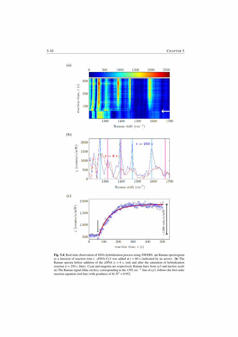
5-10 CHAPTER 5
Fig. 5.4| Real time observation of DNA hybridization process using NWERS. (a) Raman spectrogramas a function of reaction time t. cDNA-Cy3 was added at t = 60 s (indicated by an arrow). (b) TheRaman spectra before addition of the cDNA (t = 6 s, red) and after the saturation of hybridizationreaction (t = 250 s, blue). Cyan and magenta are respectively Raman lines from cy3 and nucleic acids(c) The Raman signal (blue circles), corresponding to the 1392 cm−1 line of cy3, follows the first orderreaction equation (red line) with goodness of fit R2 = 0.952.
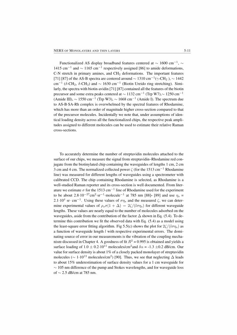
NERS OF MONOLAYERS AND THIN LAYERS 5-11
Functionalized AS display broadband features centered at ∼ 1600 cm−1, ∼1415 cm−1 and ∼ 1165 cm−1 respectively assigned [86] to amide deformations,C-N stretch in primary amines, and CH2 deformations. The important features[71] [87] of the AS-B spectra are centered around ∼ 1310 cm−1(γ-CH2 ), ∼ 1442cm−1 (δ-CH2, δ-CH3) and ∼ 1630 cm−1 (Biotin Ureido ring stretching). Simi-larly, the spectra with biotin-avidin [71] [87] contained all the features of the biotinprecursor and some extra peaks centered at ∼ 1132 cm−1 (Trp W7),∼ 1250 cm−1
(Amide III), ∼ 1550 cm−1 (Trp W3), ∼ 1668 cm−1 (Amide I). The spectrum dueto AS-B·SA-Rh complex is overwhelmed by the spectral features of Rhodamine,which has more than an order of magnitude higher cross-section compared to thatof the precursor molecules. Incidentally we note that, under assumptions of iden-tical loading density across all the functionalized chips, the respective peak ampli-tudes assigned to different molecules can be used to estimate their relative Ramancross-sections.
To accurately determine the number of streptavidin molecules attached to thesurface of our chips, we measure the signal from streptavidin–Rhodamine red con-jugate from the biotinylated chip containing the waveguides of lengths 1 cm, 2 cm3 cm and 4 cm. The normalized collected power ζ (for the 1513 cm−1 Rhodamineline) was measured for different lengths of waveguides using a spectrometer withcalibrated CCD. The chip containing Rhodamine is selected, as Rhodamine is awell-studied Raman reporter and its cross-section is well documented. From liter-ature we estimate σ for the 1513 cm−1 line of Rhodamine used for the experimentto be about 2.8·10−27cm2·sr−1·molecule−1 at 785 nm [88]- [89] and use ηs =2.1·104 sr· cm−1. Using these values of σηs and the measured ζ, we can deter-mine experimental values of ρsσ(1 + ∆) = 2ζ/(lσηs) for different waveguidelengths. These values are nearly equal to the number of molecules adsorbed on thewaveguides, aside from the contribution of the factor ∆ shown in Eq. (5.4). To de-termine this contribution we fit the observed data with Eq. (5.4) as a model usingthe least-square error fitting algorithm. Fig 5.5(c) shows the plot for 2ζ/(lσηs) asa function of waveguide length l with respective experimental errors. The domi-nating source of error in our measurements is the vibration of the coupling mecha-nism,discussed in Chapter 4. A goodness of fitR2 = 0.995 is obtained and yields asurface loading of 1.0 ± 0.2·1011 molecules/cm2and δα = -1.3 ±0.2 dB/cm. Ourvalue for surface density is about 1% of a closely packed monolayer of streptavidinmolecules (∼ 1·1013 molecules/cm2) [90]. Thus, we see that neglecting ∆ leadsto about 15% underestimation of surface density values for a 1 cm waveguide for∼ 105 nm difference of the pump and Stokes wavelengths, and for waveguide lossof ∼ 2.5 dB/cm at 785 nm.
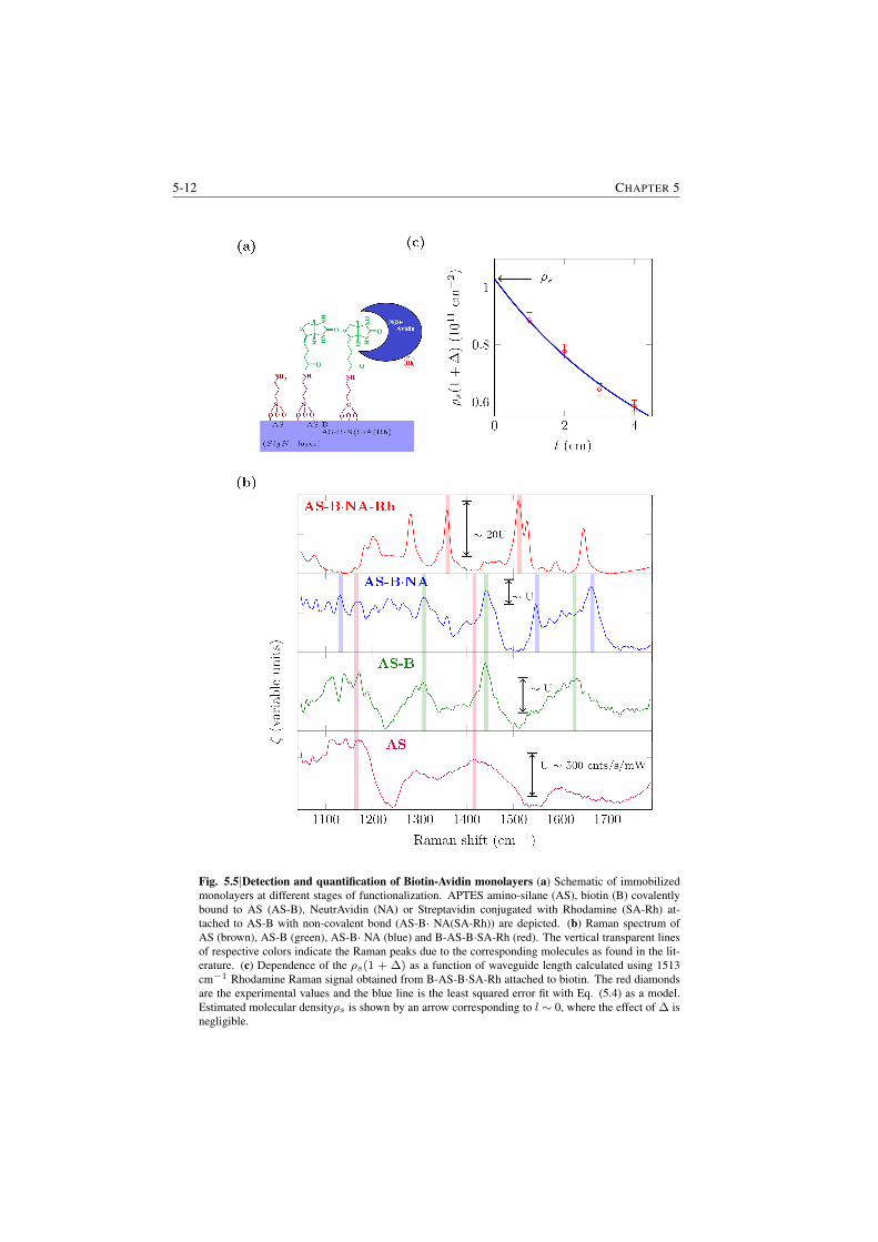
5-12 CHAPTER 5
Fig. 5.5|Detection and quantification of Biotin-Avidin monolayers (a) Schematic of immobilizedmonolayers at different stages of functionalization. APTES amino-silane (AS), biotin (B) covalentlybound to AS (AS-B), NeutrAvidin (NA) or Streptavidin conjugated with Rhodamine (SA-Rh) at-tached to AS-B with non-covalent bond (AS-B· NA(SA-Rh)) are depicted. (b) Raman spectrum ofAS (brown), AS-B (green), AS-B· NA (blue) and B-AS-B·SA-Rh (red). The vertical transparent linesof respective colors indicate the Raman peaks due to the corresponding molecules as found in the lit-erature. (c) Dependence of the ρs(1 + ∆) as a function of waveguide length calculated using 1513cm−1 Rhodamine Raman signal obtained from B-AS-B·SA-Rh attached to biotin. The red diamondsare the experimental values and the blue line is the least squared error fit with Eq. (5.4) as a model.Estimated molecular densityρs is shown by an arrow corresponding to l ∼ 0, where the effect of ∆ isnegligible.
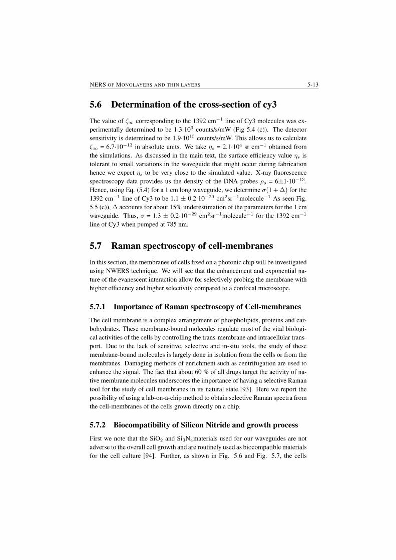
NERS OF MONOLAYERS AND THIN LAYERS 5-13
5.6 Determination of the cross-section of cy3The value of ζ∞ corresponding to the 1392 cm−1 line of Cy3 molecules was ex-perimentally determined to be 1.3·103 counts/s/mW (Fig 5.4 (c)). The detectorsensitivity is determined to be 1.9·1015 counts/s/mW. This allows us to calculateζ∞ = 6.7·10−13 in absolute units. We take ηs = 2.1·104 sr cm−1 obtained fromthe simulations. As discussed in the main text, the surface efficiency value ηs istolerant to small variations in the waveguide that might occur during fabricationhence we expect ηs to be very close to the simulated value. X-ray fluorescencespectroscopy data provides us the density of the DNA probes ρs = 6±1·10−13.Hence, using Eq. (5.4) for a 1 cm long waveguide, we determine σ(1 + ∆) for the1392 cm−1 line of Cy3 to be 1.1 ± 0.2·10−29 cm2sr−1molecule−1 As seen Fig.5.5 (c)), ∆ accounts for about 15% underestimation of the parameters for the 1 cmwaveguide. Thus, σ = 1.3 ± 0.2·10−29 cm2sr−1molecule−1 for the 1392 cm−1
line of Cy3 when pumped at 785 nm.
5.7 Raman spectroscopy of cell-membranesIn this section, the membranes of cells fixed on a photonic chip will be investigatedusing NWERS technique. We will see that the enhancement and exponential na-ture of the evanescent interaction allow for selectively probing the membrane withhigher efficiency and higher selectivity compared to a confocal microscope.
5.7.1 Importance of Raman spectroscopy of Cell-membranes
The cell membrane is a complex arrangement of phospholipids, proteins and car-bohydrates. These membrane-bound molecules regulate most of the vital biologi-cal activities of the cells by controlling the trans-membrane and intracellular trans-port. Due to the lack of sensitive, selective and in-situ tools, the study of thesemembrane-bound molecules is largely done in isolation from the cells or from themembranes. Damaging methods of enrichment such as centrifugation are used toenhance the signal. The fact that about 60 % of all drugs target the activity of na-tive membrane molecules underscores the importance of having a selective Ramantool for the study of cell membranes in its natural state [93]. Here we report thepossibility of using a lab-on-a-chip method to obtain selective Raman spectra fromthe cell-membranes of the cells grown directly on a chip.
5.7.2 Biocompatibility of Silicon Nitride and growth process
First we note that the SiO2 and Si3N4materials used for our waveguides are notadverse to the overall cell growth and are routinely used as biocompatible materialsfor the cell culture [94]. Further, as shown in Fig. 5.6 and Fig. 5.7, the cells
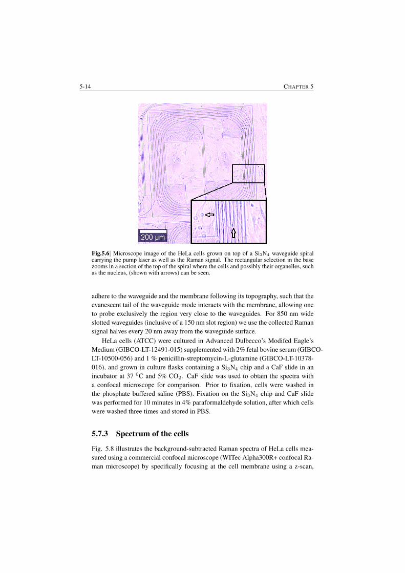
5-14 CHAPTER 5
Fig.5.6| Microscope image of the HeLa cells grown on top of a Si3N4 waveguide spiralcarrying the pump laser as well as the Raman signal. The rectangular selection in the basezooms in a section of the top of the spiral where the cells and possibly their organelles, suchas the nucleus, (shown with arrows) can be seen.
adhere to the waveguide and the membrane following its topography, such that theevanescent tail of the waveguide mode interacts with the membrane, allowing oneto probe exclusively the region very close to the waveguides. For 850 nm wideslotted waveguides (inclusive of a 150 nm slot region) we use the collected Ramansignal halves every 20 nm away from the waveguide surface.
HeLa cells (ATCC) were cultured in Advanced Dulbecco’s Modifed Eagle’sMedium (GIBCO-LT-12491-015) supplemented with 2% fetal bovine serum (GIBCO-LT-10500-056) and 1 % penicillin-streptomycin-L-glutamine (GIBCO-LT-10378-016), and grown in culture flasks containing a Si3N4 chip and a CaF slide in anincubator at 37 0C and 5% CO2. CaF slide was used to obtain the spectra witha confocal microscope for comparison. Prior to fixation, cells were washed inthe phosphate buffered saline (PBS). Fixation on the Si3N4 chip and CaF slidewas performed for 10 minutes in 4% paraformaldehyde solution, after which cellswere washed three times and stored in PBS.
5.7.3 Spectrum of the cells
Fig. 5.8 illustrates the background-subtracted Raman spectra of HeLa cells mea-sured using a commercial confocal microscope (WITec Alpha300R+ confocal Ra-man microscope) by specifically focusing at the cell membrane using a z-scan,

NERS OF MONOLAYERS AND THIN LAYERS 5-15
Fig. 5.7| A SEM micrograph of a cell fixed to the surface of the Si3N4- SiO2 chip. A goodadhesion of the cells with the surface of the chip is observed.
with a confocal height of 1.5 µm. This limited z-resolution inhibits a selectiveprobing of the cell membrane, a problem which is resolved using our on-chip ap-proach. The figure also shows two background-subtracted example spectra of thecells grown on the chip and measured by evanescently exciting and collecting themembrane molecules using the waveguide. The typical integration times were lessthan 10 s for an effective pump power of 500 µW in the waveguide to obtain asignal-to-noise ratio (SNR) > 50. To obtain a spectrum with a similar SNR usingsimilar pump power, the integration time needed for a confocal microscope wouldbe > 500 s.
To simulate cell membranes consisting of only lipids, the spectrum of a lipidbilayer formed on the chip using the vesicle [95] (using vesicles formed by 4:4:2mixture of dioleoyl phosphatidylethanolamine, dioleoyl phosphatidyl choline, andCholesterol) and evanescently measured using the waveguides is displayed. Incontrast to the spectrum of the lipid bilayer, the spectra of the cells additionallycontain distinctive peaks [96] due to proteins and nucleic acids. The spectra mea-sured using the waveguide have some similarity with the one obtained using theconfocal microscope, but several distinctive peaks due to proteins and nucleic acidsbecome more prominent with the waveguide due to exclusivity and localization ofthe Raman interaction near the membranes.
Interestingly, the spectra of the cells differ from one waveguide to anotherwhile retaining certain general characteristics, such as the peaks related to lipid.A possible reason for this difference between the spectra of the membranes canbe the complex and heterogeneous nature of the cell membrane that alters signifi-cantly depending on the stress conditions of the individual cells in their respective
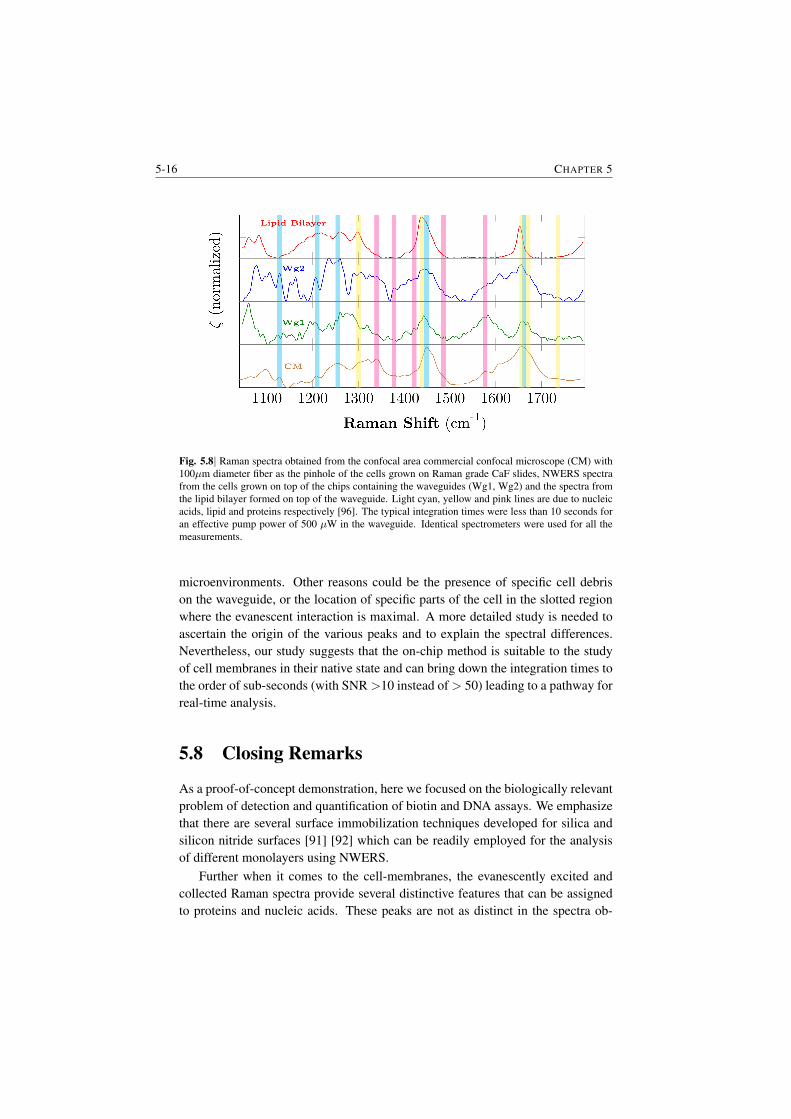
5-16 CHAPTER 5
Fig. 5.8| Raman spectra obtained from the confocal area commercial confocal microscope (CM) with100µm diameter fiber as the pinhole of the cells grown on Raman grade CaF slides, NWERS spectrafrom the cells grown on top of the chips containing the waveguides (Wg1, Wg2) and the spectra fromthe lipid bilayer formed on top of the waveguide. Light cyan, yellow and pink lines are due to nucleicacids, lipid and proteins respectively [96]. The typical integration times were less than 10 seconds foran effective pump power of 500 µW in the waveguide. Identical spectrometers were used for all themeasurements.
microenvironments. Other reasons could be the presence of specific cell debrison the waveguide, or the location of specific parts of the cell in the slotted regionwhere the evanescent interaction is maximal. A more detailed study is needed toascertain the origin of the various peaks and to explain the spectral differences.Nevertheless, our study suggests that the on-chip method is suitable to the studyof cell membranes in their native state and can bring down the integration times tothe order of sub-seconds (with SNR>10 instead of> 50) leading to a pathway forreal-time analysis.
5.8 Closing Remarks
As a proof-of-concept demonstration, here we focused on the biologically relevantproblem of detection and quantification of biotin and DNA assays. We emphasizethat there are several surface immobilization techniques developed for silica andsilicon nitride surfaces [91] [92] which can be readily employed for the analysisof different monolayers using NWERS.
Further when it comes to the cell-membranes, the evanescently excited andcollected Raman spectra provide several distinctive features that can be assignedto proteins and nucleic acids. These peaks are not as distinct in the spectra ob-
NERS OF MONOLAYERS AND THIN LAYERS 5-17
tained with a confocal microscope. We ascribe these features of the Raman spectracollected using the waveguides to the exclusivity and localization of the evanes-cent Raman interaction near the membrane-waveguide contact region. Further,the increased interaction area with the optical mode results in an enhanced signalcompared to a commercial confocal microscope. The enhanced signal results in asignal acquisition time below 10 s for a SNR> 50. Our preliminary study suggeststhat the on-chip method using the nanophotonic waveguides is suitable for study-ing cell membranes in their native state, while also bringing down the integrationtimes to the order of sub-seconds with a reasonable SNR. This leads to a pathwayfor a real-time analysis of the interactions that happen in the cell-membranes.
Thus, our lab-on-a-chip-based technique offers a simple and apposite alter-native to existing techniques which suffer from several problems, such as highexpense, photo-damage, the necessity of a vacuum for operation, photo-bleaching,heating and inability to detect non-specific binding, etc.

6Dependence of the efficiency on
channel waveguide parameters
In the previous chapters, the dependence of efficiency of Raman scattering withwidth of silicon nitride (Si3N4) and silicon on insulator (SOI) waveguides wasbriefly discussed. In addition the theoretical model developed therein were experi-mentally verified. Having established the relevance of our model, we elaborate theresults discussed in the previous chapters to ascertain parameters of relevance andextend the theoretical analysis to TiO2 and SOI waveguides. Some text has beenadapted from the some of my published papers [97], [49].
6.1 Role of index contrast in the enhancement andscattering
To understand the enhancement effects inherent to the waveguides and the role ofrefractive index contrast, we investigate a common planar/slab waveguide with asilica undercladding, an air uppercladding (n1=1), and variable core index ncandcore thicknessd (inset Fig. 6.1). A scattering molecule is located at the air under-cladding on top of the core. We investigate two common CMOS compatible corematerials, Si (nc = 3.45) and Si3N4 (nc = 1.89), for the two orthogonal dipole ori-entations with respect to the slab waveguide surface. Fig. 6.1 shows the power Pcoupled to the fundamental TE and TM modes of a slab waveguide from a dipolelocated at the surface of the waveguide, normalized to the total free-space emission
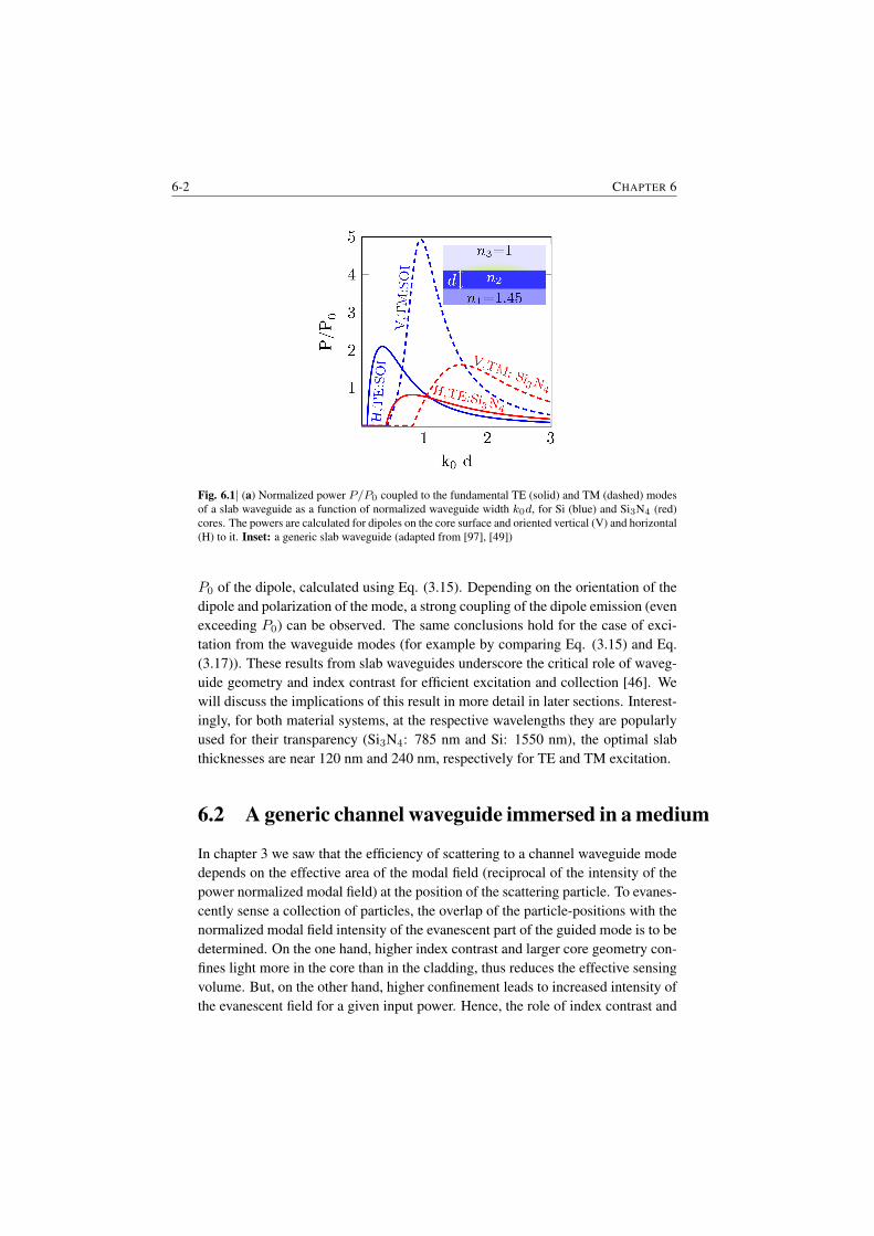
6-2 CHAPTER 6
Fig. 6.1| (a) Normalized power P/P0 coupled to the fundamental TE (solid) and TM (dashed) modesof a slab waveguide as a function of normalized waveguide width k0d, for Si (blue) and Si3N4 (red)cores. The powers are calculated for dipoles on the core surface and oriented vertical (V) and horizontal(H) to it. Inset: a generic slab waveguide (adapted from [97], [49])
P0 of the dipole, calculated using Eq. (3.15). Depending on the orientation of thedipole and polarization of the mode, a strong coupling of the dipole emission (evenexceeding P0) can be observed. The same conclusions hold for the case of exci-tation from the waveguide modes (for example by comparing Eq. (3.15) and Eq.(3.17)). These results from slab waveguides underscore the critical role of waveg-uide geometry and index contrast for efficient excitation and collection [46]. Wewill discuss the implications of this result in more detail in later sections. Interest-ingly, for both material systems, at the respective wavelengths they are popularlyused for their transparency (Si3N4: 785 nm and Si: 1550 nm), the optimal slabthicknesses are near 120 nm and 240 nm, respectively for TE and TM excitation.
6.2 A generic channel waveguide immersed in a medium
In chapter 3 we saw that the efficiency of scattering to a channel waveguide modedepends on the effective area of the modal field (reciprocal of the intensity of thepower normalized modal field) at the position of the scattering particle. To evanes-cently sense a collection of particles, the overlap of the particle-positions with thenormalized modal field intensity of the evanescent part of the guided mode is to bedetermined. On the one hand, higher index contrast and larger core geometry con-fines light more in the core than in the cladding, thus reduces the effective sensingvolume. But, on the other hand, higher confinement leads to increased intensity ofthe evanescent field for a given input power. Hence, the role of index contrast and
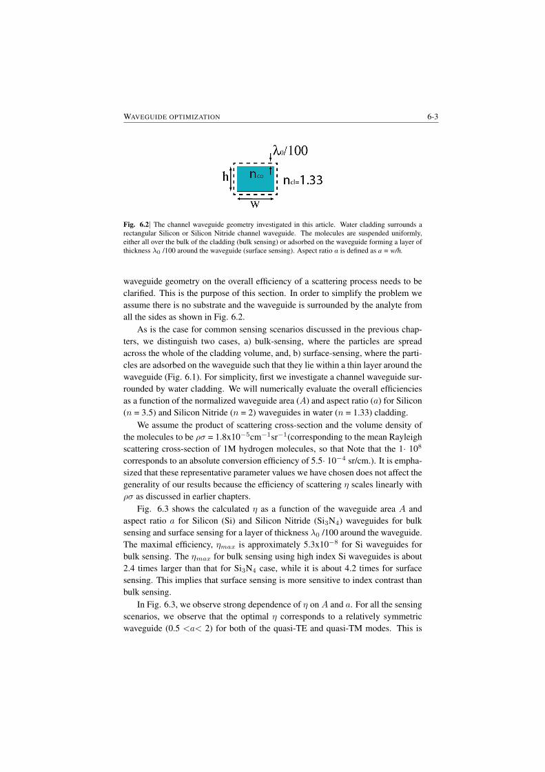
WAVEGUIDE OPTIMIZATION 6-3
Fig. 6.2| The channel waveguide geometry investigated in this article. Water cladding surrounds arectangular Silicon or Silicon Nitride channel waveguide. The molecules are suspended uniformly,either all over the bulk of the cladding (bulk sensing) or adsorbed on the waveguide forming a layer ofthickness λ0 /100 around the waveguide (surface sensing). Aspect ratio a is defined as a = w/h.
waveguide geometry on the overall efficiency of a scattering process needs to beclarified. This is the purpose of this section. In order to simplify the problem weassume there is no substrate and the waveguide is surrounded by the analyte fromall the sides as shown in Fig. 6.2.
As is the case for common sensing scenarios discussed in the previous chap-ters, we distinguish two cases, a) bulk-sensing, where the particles are spreadacross the whole of the cladding volume, and, b) surface-sensing, where the parti-cles are adsorbed on the waveguide such that they lie within a thin layer around thewaveguide (Fig. 6.1). For simplicity, first we investigate a channel waveguide sur-rounded by water cladding. We will numerically evaluate the overall efficienciesas a function of the normalized waveguide area (A) and aspect ratio (a) for Silicon(n = 3.5) and Silicon Nitride (n = 2) waveguides in water (n = 1.33) cladding.
We assume the product of scattering cross-section and the volume density ofthe molecules to be ρσ = 1.8x10⁻⁵cm−1sr−1(corresponding to the mean Rayleighscattering cross-section of 1M hydrogen molecules, so that Note that the 1· 108
corresponds to an absolute conversion efficiency of 5.5· 10−4 sr/cm.). It is empha-sized that these representative parameter values we have chosen does not affect thegenerality of our results because the efficiency of scattering η scales linearly withρσ as discussed in earlier chapters.
Fig. 6.3 shows the calculated η as a function of the waveguide area A andaspect ratio a for Silicon (Si) and Silicon Nitride (Si3N4) waveguides for bulksensing and surface sensing for a layer of thickness λ0 /100 around the waveguide.The maximal efficiency, ηmax is approximately 5.3x10⁻⁸ for Si waveguides forbulk sensing. The ηmax for bulk sensing using high index Si waveguides is about2.4 times larger than that for Si3N4 case, while it is about 4.2 times for surfacesensing. This implies that surface sensing is more sensitive to index contrast thanbulk sensing.
In Fig. 6.3, we observe strong dependence of η on A and a. For all the sensingscenarios, we observe that the optimal η corresponds to a relatively symmetricwaveguide (0.5 <a< 2) for both of the quasi-TE and quasi-TM modes. This is

6-4 CHAPTER 6
a) b)
c) d)
Fig. 6.3|Overall efficiency as function of core area (A), normalized to square of free-space wavelength,for several aspect ratios (a) for the fundamental quasi-TE modes of a) Si waveguide for bulk sensing,b) Si waveguide for surface sensing, c) Si3N4 waveguide for bulk sensing and d) Si3N4 waveguidefor surface sensing. Pump is assumed to be of the same polarization. Note that due to symmetry ofthe problem, the fundamental quasi-TE mode for a = 1/x is the same as the fundamental quasi-TMmode for a = x, and for a = 1 quasi-TE and quasi-TM modes are degenerate. Note that the 1 ·108
corresponds to an absolute conversion efficiency of 5.5·10−4 sr/cm.
WAVEGUIDE OPTIMIZATION 6-5
rather surprising knowing that, for a given area, a nonsymmetrical waveguide hasa larger sensing surface. This means that the effective sensing area is determinedpredominantly by the modal field properties rather than by the actual sensing area.We also see that the optimal η is less dependent on a for bulk sensing comparedto surface sensing. For example, the optimal η for Si (Si3N4) waveguides changesby 36% (25%) as we go from a = 1 to a = 5, while for bulk sensing, the changeis only about 19% (13%). Further, the A corresponding to optimal η, for a givena, is higher for surface sensing than for bulk sensing. For instance, for a = 2,the optimal A for surface sensing is 0.004 λ2
0 higher than for bulk sensing withSi waveguide while it is 0.048 λ2
0 higher for Si3N4waveguides. This observationmeans that a higher optical confinement in the core leads to higher intensity at thewaveguide surface and is favored for optimal surface sensing compared to bulksensing.
6.3 Integrated channel waveguides on a substrate
In order to simplify the problem assumed a substrate-less waveguide in the previ-ous chapter. In this section we compare three popular waveguide platforms silicon-on-insulator (SOI) waveguide platform [98] and an emerging waveguide platformbased on Titanium oxide (TiO2). To be in line with the experimental parametersused for the experiments with the Si3N4waveguides, we perform simulations withan excitation wavelength λ0= 785 nm. The refractive indices of the core, SiO2
undercladding and IPA upper cladding are respectively taken to be nsin = 1.89,nox = 1.45 and nipa = 1.37. In case of SOI waveguides, λ0= 1550 nm was chosenbecause of a low optical absorption. The refractive index of silicon is taken to bensi = 3.44. As for TiO2 waveguides, the refractive index nTiO2 = 2.4 reportedin [99] is used. For the TiO2 case we study η0 at λ0= 785 nm and also at λ0=1064 nm. The latter choice of λ0 corresponds to a material wavelength compara-ble to that of SOI (at λ0= 1550 nm) and Si3N4(at λ0 = 785 nm). The aforemen-tioned choice of the comparable material wavelengths ensures similar fabricationconstraints and practical waveguide dimensions for single mode operation. Theheight of the waveguides is fixed at h = 220 nm for all waveguide types, which is atypical deposition thickness during the fabrication of Si3N4 and TiO2 waveguides,and also a typical silicon thickness for SOI waveguides. The conversion efficiencyη0 was calculated using Eq. (4.1) with COMSOL finite elements mode solver.
In Fig. 6.4 we show theoretical conversion efficiency η0 for randomly dis-tributed particles lying uniformly in the upper cladding of Si3N4, TiO2 and SOIstrip waveguides of several waveguide widths w corresponding to the single modeoperation of the waveguides. As the waveguide width is increased, initially η0 in-creases to a maximum corresponding to an optimal mode confinement in the coreand the cladding. Once this condition is reached, further increase in the width
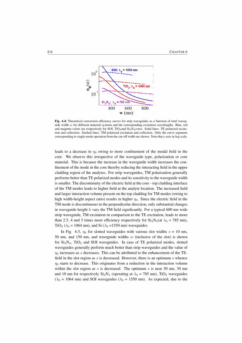
6-6 CHAPTER 6
Fig. 6.4| Theoretical conversion efficiency curves for strip waveguides as a function of total waveg-uide width w for different material systems and the corresponding excitation wavelengths. Blue, redand magenta colors are respectively for SOI, TiO2and Si3N4cores. Solid lines: TE polarized excita-tion and collection. Dashed lines: TM polarized excitation and collection. Only the curve segmentscorresponding to single mode operation from the cut-off width are shown. Note that y-axis in log scale.
leads to a decrease in η0 owing to more confinement of the modal field in thecore. We observe this irrespective of the waveguide type, polarization or corematerial. This is because the increase in the waveguide width increases the con-finement of the mode in the core thereby reducing the interacting field in the uppercladding region of the analytes. For strip waveguides, TM polarization generallyperforms better than TE polarized modes and its sensitivity to the waveguide widthis smaller. The discontinuity of the electric field at the core - top cladding interfaceof the TM modes leads to higher field at the analyte location. The increased fieldand larger interaction volume present on the top cladding for TM modes (owing tohigh width-height aspect ratio) results in higher η0. Since the electric field in theTM mode is discontinuous in the perpendicular direction, only substantial changesin waveguide height h vary the TM field significantly. For a typical 600 nm widestrip waveguide, TM excitation in comparison to the TE excitation, leads to morethan 2.5, 4 and 5 times more efficiency respectively for Si3N4(at λ0 = 785 nm),TiO2 (λ0 = 1064 nm), and Si (λ0 =1550 nm) waveguides.
In Fig. 6.5, η0 for slotted waveguides with various slot widths s = 10 nm,50 nm, and 150 nm, and waveguide widths w (inclusive of the slot) is shownfor Si3N4, TiO2 and SOI waveguides. In case of TE polarized modes, slottedwaveguides generally perform much better than strip waveguides and the value ofη0 increases as s decreases. This can be attributed to the enhancement of the TE-field in the slot region as s is decreased. However, there is an optimum s whenceη0 starts to decrease. This originates from a reduction in the interaction volumewithin the slot region as s is decreased. The optimum s is near 50 nm, 30 nmand 10 nm for respectively Si3N4 (operating at λ0 = 785 nm), TiO2 waveguides(λ0 = 1064 nm) and SOI waveguides (λ0 = 1550 nm). As expected, due to the

WAVEGUIDE OPTIMIZATION 6-7
continuity of the electric field, the field enhancement in the slot is much less incase of TM polarization (Fig. 6.6); hence, the effect of s is not significant in caseof TM polarization.
In Fig. 6.6 we compare the conversion efficiency η0 of TiO2 waveguides forλ0 = 785 nm and λ0 = 1064 nm. η0 is generally higher for λ0 = 1064 nm becausethe field is confined more to the cladding where analyte is located. Due to a shortermaterial wavelength, the modal field is more confined to the high index TiO2regionwhen excited at 785 nm, compared to excitation at 1064 nm. Consequently, theoptimal slot width for TiO2(λ0 = 785 nm) is narrower: about 10 nm compared toabout 30 nm λ0 = 1064 nm. For λ0 = 785 nm η0 also increases weakly for widerslots (such as 150 nm > s > 100 nm). This can be understood with the help ofFig. 6.6.
In Fig. 6.7, we show the conversion efficiency η0 of slot waveguides withs = 100 nm, as a function of the total waveguide width w for different materialsystems. We observe a strong enhancement in η0 with the increase in the indexcontrast of the waveguide. Higher index contrast leads to a lower mode area,higher modal field intensity and higher field discontinuity, thus giving rise to astronger evanescent field for interaction. From the simulation data presented inFig. 6.5 and Fig. 6.7, we can conclude that a slot of width s = 100 nm leads toabout 90, 20 and 7 fold higher efficiency respectively for SOI (excited at λ0 = 1550nm), TiO2 (λ0 = 1064 nm), Si3N4(λ0 = 785 nm) slot waveguides of w = 600 nmcompared to the strip waveguide of the same dimension.
6.4 Closing Remarks
In this chapter we explored the effect of geometry and index contrast for the effi-ciency of the waveguides. We also explored the possibility to use SOI and TiO2
platforms as an alternative integrated waveguide platform to use as Raman spec-troscopy.
When comparing different waveguide systems operating at different excitationwavelengths, however, the corresponding change in the scattering cross-sectionalso has to be taken into account. As the scattering cross-section varies approxi-mately as λ−4
0 (Chapter 2), the total collected power also varies in a similar manner.We can include this correction factor and compare the respective net efficienciesfor slot waveguides (w = 600 nm and s = 100 nm), Si3N4waveguides (λ0 = 785nm), TiO2 waveguides (λ0= 1064 nm) and the SOI waveguides (λ0= 1550 nm).After the λ−4
0 correction at these respective operating wavelengths, SOI is abouttwice as efficient, and TiO2 is about 30% more efficient than Si3N4 waveguidesowing to their higher index contrast.
Note that in Fig. 6.4 and Fig. 6.6, η0 > 4π sr, for SOI waveguides in a certainrange of waveguide dimensions. This is a result of high importance. To appreci-
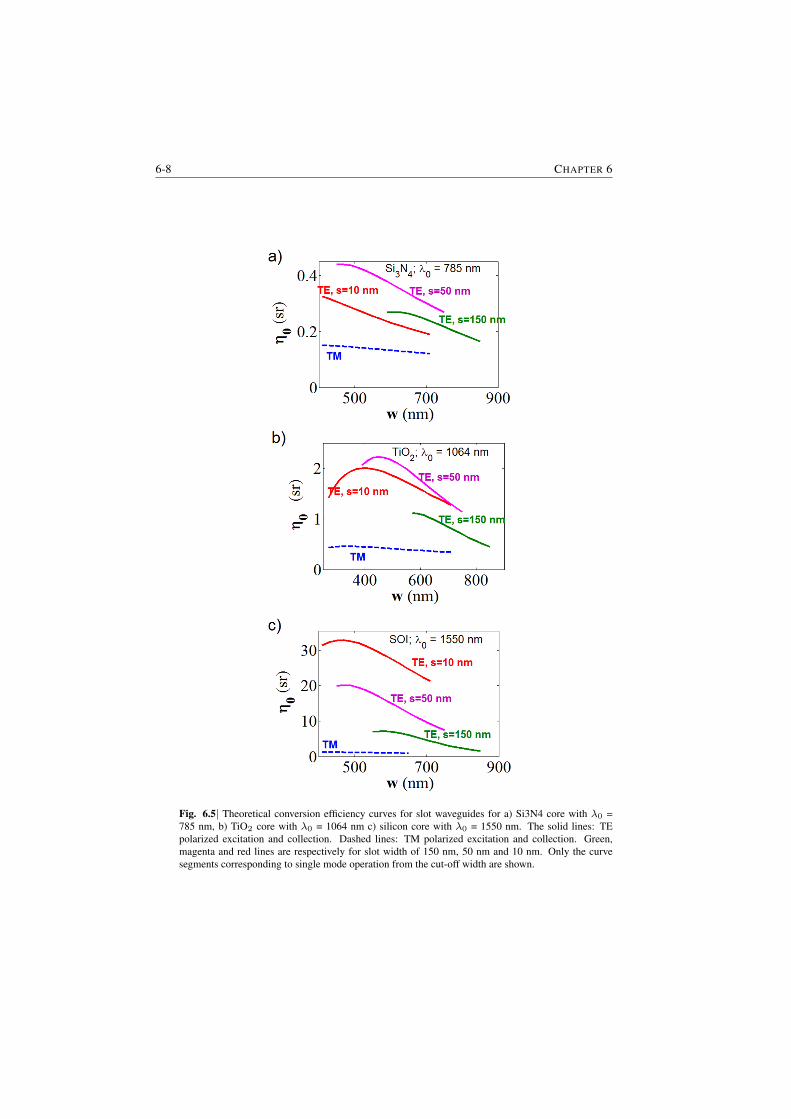
6-8 CHAPTER 6
Fig. 6.5| Theoretical conversion efficiency curves for slot waveguides for a) Si3N4 core with λ0 =785 nm, b) TiO2 core with λ0 = 1064 nm c) silicon core with λ0 = 1550 nm. The solid lines: TEpolarized excitation and collection. Dashed lines: TM polarized excitation and collection. Green,magenta and red lines are respectively for slot width of 150 nm, 50 nm and 10 nm. Only the curvesegments corresponding to single mode operation from the cut-off width are shown.
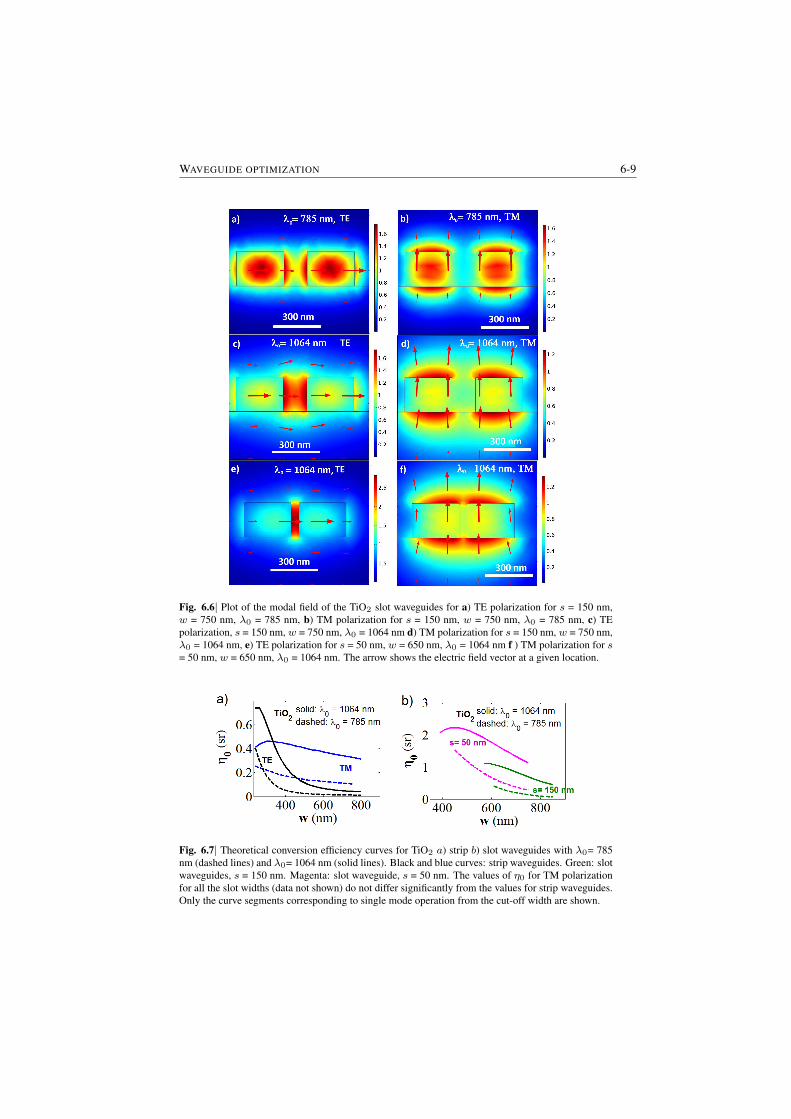
WAVEGUIDE OPTIMIZATION 6-9
Fig. 6.6| Plot of the modal field of the TiO2 slot waveguides for a) TE polarization for s = 150 nm,w = 750 nm, λ0 = 785 nm, b) TM polarization for s = 150 nm, w = 750 nm, λ0 = 785 nm, c) TEpolarization, s = 150 nm, w = 750 nm, λ0 = 1064 nm d) TM polarization for s = 150 nm, w = 750 nm,λ0 = 1064 nm, e) TE polarization for s = 50 nm, w = 650 nm, λ0 = 1064 nm f ) TM polarization for s= 50 nm, w = 650 nm, λ0 = 1064 nm. The arrow shows the electric field vector at a given location.
Fig. 6.7| Theoretical conversion efficiency curves for TiO2 a) strip b) slot waveguides with λ0= 785nm (dashed lines) and λ0= 1064 nm (solid lines). Black and blue curves: strip waveguides. Green: slotwaveguides, s = 150 nm. Magenta: slot waveguide, s = 50 nm. The values of η0 for TM polarizationfor all the slot widths (data not shown) do not differ significantly from the values for strip waveguides.Only the curve segments corresponding to single mode operation from the cut-off width are shown.
6-10 CHAPTER 6
ate this, we apply Eq. (4.1) for free space beams with η0 = 4π and integrate dzarbitrarily. This is possible in an ideal situation when we can collect the scatteredlight perfectly from total solid angle of 4π sr, and if particles are excited with adiffraction-less beam so that dz in Eq. (4.1) can be integrated arbitrarily. Thus,we conclude that due to enhanced excitation and emission (Purcell enhancement,Chapter 3) near the high index contrast waveguides, the overall efficiency of exci-tation and collection of a practical single mode waveguide can be higher than theideal free space excitation and collection. For a realistic diffraction-limited free-space microscope system, however, the collection and excitation depth of focusare limited due an inverse relationship between the collection angle and the depthof focus. Hence, NWERS approach in general, performs much better than realisticfree space optical systems.
If the upper cladding refractive index varies, the confinement properties ofthe waveguide mode also changes. Consequently, the conversion efficiency willvary via Eq. (4.1). Nevertheless, the qualitative conclusions discussed in thischapter are applicable for analytes with refractive index in the range 1.3-1.44. Foranalytes with refractive indices significantly different from IPA (n = 1.37), η0 canbe calculated using Eq. (4.1).
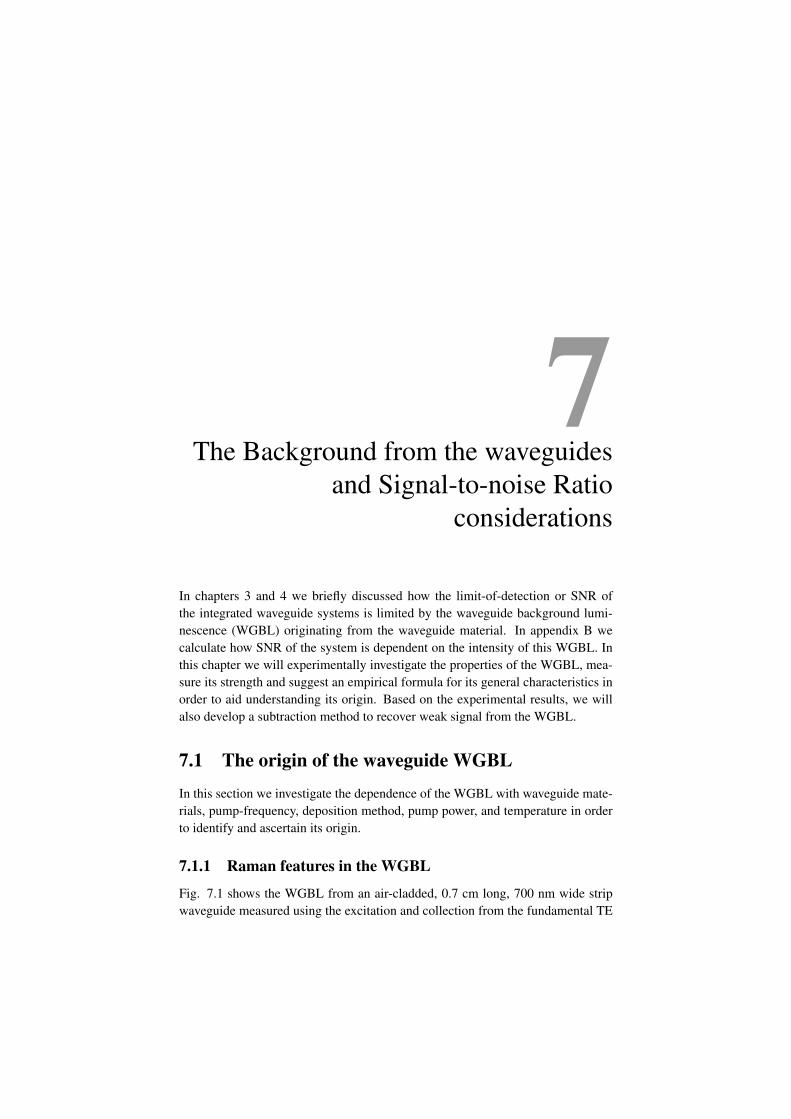
7The Background from the waveguides
and Signal-to-noise Ratioconsiderations
In chapters 3 and 4 we briefly discussed how the limit-of-detection or SNR ofthe integrated waveguide systems is limited by the waveguide background lumi-nescence (WGBL) originating from the waveguide material. In appendix B wecalculate how SNR of the system is dependent on the intensity of this WGBL. Inthis chapter we will experimentally investigate the properties of the WGBL, mea-sure its strength and suggest an empirical formula for its general characteristics inorder to aid understanding its origin. Based on the experimental results, we willalso develop a subtraction method to recover weak signal from the WGBL.
7.1 The origin of the waveguide WGBL
In this section we investigate the dependence of the WGBL with waveguide mate-rials, pump-frequency, deposition method, pump power, and temperature in orderto identify and ascertain its origin.
7.1.1 Raman features in the WGBL
Fig. 7.1 shows the WGBL from an air-cladded, 0.7 cm long, 700 nm wide stripwaveguide measured using the excitation and collection from the fundamental TE
7-2 CHAPTER 7
Fig. 7.1| Complete WGBL from a 0.7 cm long, 700 nm wide air-cladded strip waveguide measured(green solid line) using excitation and collection from the fundamental TE mode, the 5th order polyno-mial fit to the WGBL (red dashed line) and the polynomial subtracted Raman component in the WGBL(blue lower line). In the inset, we also show the same spectra in log-log scale so that several smallpeaks are visible.
mode. The WGBL contains several narrow-band and broadband peaks. In orderto separate these features with the slowly varying component (defined by the reddashed line) and identify the origin of the peaks, we implement a 5th order polyno-mial fit to the WGBL and subtract the polynomial. The subtraction yields a spec-trum very similar to the infrared absorption spectrum measured for silicon-nitridethin-films [100–102]. The major peaks centered at 450 cm−1, 850 cm−1, 1175cm−1 and 2226 cm−1 are assigned respectively to Si breathing, Si-N stretch, N-Hbending , N-H2 bending and Si-H stretch [100]- [102]. The strong narrowbandpeak at 2330 cm−1may be due to interstitial N2 formed in the core material duringthe deposition process [103]. Thus, we conclude that the WGBL mainly containsRaman peaks originating from the waveguide core material, and depends on [100]– [103] the waveguide core deposition process and its chemical composition.
7.1.2 Dependence with materials
Several peaks corresponding to Si3N4 deposition chemistry suggested that themost of the Raman features in the WGBL originates from the core. However, theWGBL may also have contribution from SiO2 which forms the lower cladding. Inorder to identify the dominating source of the WGBL, we performed a confocalRaman z-scan of a stack of material that were used to fabricate the waveguide.The stack contained a 220 nm PECVD Si3N4 top layer on 2.4 µm silicon diox-ide, which was deposited on a silicon-substrate using the same deposition chem-istry. The spectra were measured using a commercial confocal Raman microscope(WITec) with a 532 nm laser, focused through a 0.9 NA air objective with a 20

BACKGROUND FROM WAVEGUIDES AND SIGNAL-TO-NOISE RATIO CONSIDERATIONS 7-3
Fig. 7.2| A confocal Raman z-scan of a 220 nm PECVD Si3N4top layer on 2.4 µm silicon dioxide,deposited on a silicon-substrate confirms the major contribution to the WGBL originates from Si3N4.The peaks at 520 cm−1 and 960 cm−1 are ascribed to the peaks from Si. The spectra presented areoffset for clarity. Adapted from [104].
mW pump power on sample and a 60 second integration time. Fig. 7.2 displaysthe Raman spectra of the z-scan. For the z corresponding to the silicon substrate,we see the well-known silicon Raman peaks at 520 cm−1 and 960 cm−1. Whenmoving up in the material stack, we can identify Raman contributions specific toSi3N4 discussed before. Further, a similar z-scan measurement was performedin a silicon dioxide–silicon material stack. The z-scan measurement of this stackshowed no such Raman peaks thus confirming that the peaks indeed originate fromthe Si3N4 core region.
Furthermore, we fabricated waveguides using Si3N4 rich material depositedusing different deposition methods and compared the spectra of the correspondingWGBL. The relative WGBL strength varied strongly with the type of Si3N4 de-posited (Fig. 7.3). Hence, we conclude that the major contribution of the WGBLoriginates from the core material. In the hindsight, it is not surprising since theconfinement factor of the light in the core is generally > 50 %.
7.1.3 Dependence on pump frequency
Having established the origin of the narrow peaks in the WGBL, we now inves-tigate the nature of the broad and slowly-varying feature of the WGBL that wasapproximated by the fifth order polynomial function in the last section (Fig 7.1).Generally such a polynomial background emission in a Raman measurement is as-sociated with auto-fluorescence arising from the electronic transitions of the mate-rial itself. A common strategy to discern the auto-fluorescence is to excite the ma-terial with wavenumbers that differ by some significant amount (> 500 cm−1) and
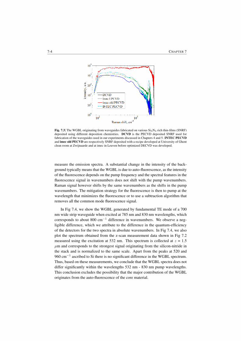
7-4 CHAPTER 7
Fig. 7.3| The WGBL originating from waveguides fabricated on various Si3N4 rich thin-films (SNRF)deposited using different deposition chemistries. DCVD is the PECVD deposited SNRF used forfabrication of the waveguides used in our experiments discussed in Chapters 4 and 5. INTEC PECVDand imec old PECVD are respectively SNRF deposited with a recipe developed at University of Ghentclean room at Zwijnaarde and at imec in Leuven before optimized DECVD was developed.
measure the emission spectra. A substantial change in the intensity of the back-ground typically means that the WGBL is due to auto-fluorescence, as the intensityof the fluorescence depends on the pump frequency and the spectral features in thefluorescence signal in wavenumbers does not shift with the pump wavenumbers.Raman signal however shifts by the same wavenumbers as the shifts in the pumpwavenumbers. The mitigation strategy for the fluorescence is then to pump at thewavelength that minimizes the fluorescence or to use a subtraction algorithm thatremoves all the common mode fluorescence signal.
In Fig 7.4, we show the WGBL generated by fundamental TE mode of a 700nm wide strip waveguide when excited at 785 nm and 830 nm wavelengths, whichcorresponds to about 800 cm−1 difference in wavenumbers. We observe a neg-ligible difference, which we attribute to the difference in the quantum-efficiencyof the detectors for the two spectra in absolute wavenumbers. In Fig 7.4, we alsoplot the spectrum obtained from the z-scan measurement data shown in Fig 7.2measured using the excitation at 532 nm. This spectrum is collected at z = 1.5µm and corresponds to the strongest signal originating from the silicon-nitride inthe stack and is normalized to the same scale. Apart from the peaks at 520 and960 cm−1 ascribed to Si there is no significant difference in the WGBL spectrum.Thus, based on these measurements, we conclude that the WGBL spectra does notdiffer significantly within the wavelengths 532 nm - 830 nm pump wavelengths.This conclusion excludes the possibility that the major contribution of the WGBLoriginates from the auto-fluorescence of the core material.
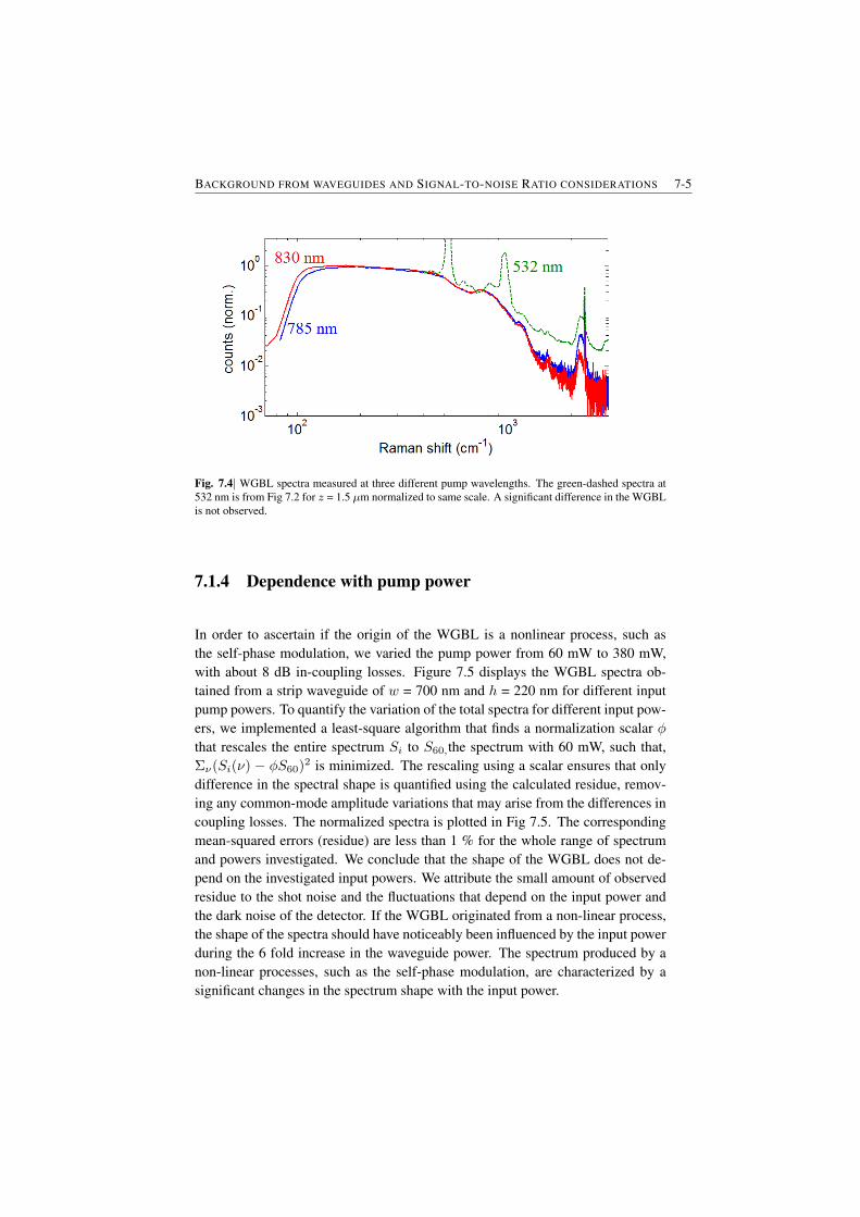
BACKGROUND FROM WAVEGUIDES AND SIGNAL-TO-NOISE RATIO CONSIDERATIONS 7-5
Fig. 7.4| WGBL spectra measured at three different pump wavelengths. The green-dashed spectra at532 nm is from Fig 7.2 for z = 1.5 µm normalized to same scale. A significant difference in the WGBLis not observed.
7.1.4 Dependence with pump power
In order to ascertain if the origin of the WGBL is a nonlinear process, such asthe self-phase modulation, we varied the pump power from 60 mW to 380 mW,with about 8 dB in-coupling losses. Figure 7.5 displays the WGBL spectra ob-tained from a strip waveguide of w = 700 nm and h = 220 nm for different inputpump powers. To quantify the variation of the total spectra for different input pow-ers, we implemented a least-square algorithm that finds a normalization scalar φthat rescales the entire spectrum Si to S60,the spectrum with 60 mW, such that,Σν(Si(ν) − φS60)2 is minimized. The rescaling using a scalar ensures that onlydifference in the spectral shape is quantified using the calculated residue, remov-ing any common-mode amplitude variations that may arise from the differences incoupling losses. The normalized spectra is plotted in Fig 7.5. The correspondingmean-squared errors (residue) are less than 1 % for the whole range of spectrumand powers investigated. We conclude that the shape of the WGBL does not de-pend on the investigated input powers. We attribute the small amount of observedresidue to the shot noise and the fluctuations that depend on the input power andthe dark noise of the detector. If the WGBL originated from a non-linear process,the shape of the spectra should have noticeably been influenced by the input powerduring the 6 fold increase in the waveguide power. The spectrum produced by anon-linear processes, such as the self-phase modulation, are characterized by asignificant changes in the spectrum shape with the input power.

7-6 CHAPTER 7
Fig. 7.5| The WGBL spectra obtained from a strip waveguide of w = 700 nm and h = 220 nm waveg-uide for different input pump powers. The spectra are normalized by a factor obtained using the least-squared-error algorithm. The corresponding mean-squared errors (residue) are less than 1%. Thespectral residue is plotted in the inset.
7.1.5 Origin of the broad feature in the background
Based on the experiments discussed earlier, the theoretical treatments in the lit-erature on the Raman spectrum of amorphous materials [105, 106, 119, 122] theorigin and the shape of the broad feature of the WGBL without the Raman peaksidentified earlier (described by dashed line in Fig. 7.1), is possibly related to break-ing of momentum selection rules due to amorphous nature of the waveguide ma-terial. For amorphous materials characterized by a short correlation length lc ofthe dielectric function (compared to the wavelength of the pump lc < λ/10 ),Suker et. al. [105] derived a frequency dependent amplitude in terms of the den-sity of states (g(ωs)), Bose-Einstein distribution function and a frequency depen-dent photon-phonon coupling coefficient (C(ωs)). However, their equation maynot directly applicable in the case of waveguides, because of the ambiguity in thefrequency dependence of the photon-phonon coupling coefficients [106], and thelack of understanding on how the optical and thermal confinement properties ofthe waveguides affect C(ωs). It was shown that C(ωs) may have a complicatedspectral dependence [122]. Needless to say, more theoretical and experimental in-vestigation is needed to understand and ascertain the behavior and the origin of theWGBL.
7.2 Determination of the WGBL efficiency
We have seen that the WGBL depends on the material of the waveguide core. Theratio RS/B between the signal counts from analyte CS and the counts due to theWGBL CBG, neglecting the dark counts of the detector, can then be written as:

BACKGROUND FROM WAVEGUIDES AND SIGNAL-TO-NOISE RATIO CONSIDERATIONS 7-7
Fig. 7.8| The ratio of signal to the WGBL counts (RS/B) as a function of length for 819 cm−1 IPAline. RS/B remains practically a constant. The values are extracted from at least three chips measuredthree times from the experimental data already discussed in §. 4.6.
RS/B(ν) = CS(ν)CBG(ν)
= ηsηBG
ρSσSβBG
= χ (ν)σSρS
(7.1)
where, ηsηBG≡ ηS/B is the ratio of analyte signal conversion efficiency to the
WGBL conversion efficiency given by the ratio of the integral of the integrated-luminosity of the waveguides respectively in the core region and the analyte region:
ηS/B =ηsηBG
=
˜clad
Λ1D(~r)d~r˜core
Λ1D(~r)d~r(7.2)
and χ is the signal-to-background (S-B) conversion factor, defined as
χ =ηS/B
βBG(7.3)
Eq. (7.1) can be used to plot RS/B as a function of concentration of analytein an experiment, from which the signal to WGBL conversion factor χ(ν) canbe determined. Once χ(ν) is determined, one can measure the concentration orcross-section of the analyte present in the cladding in an absolute manner, withouthaving to measure the transmitted pump power that is needed if we use Eq. (4.4).
However, here we take a slightly different route to calculate the WGBL ef-ficiency βBG, in order to avoid ambiguity due to variations in the concentrationduring the measurement. This also serves to verify several implicit assumptions,such as linear dependence of WGBL with the lengths, that were made to arrive atEq. (7.1). In Fig 7.8, we show RS/B for pure IPA (819 cm−1 line) for different
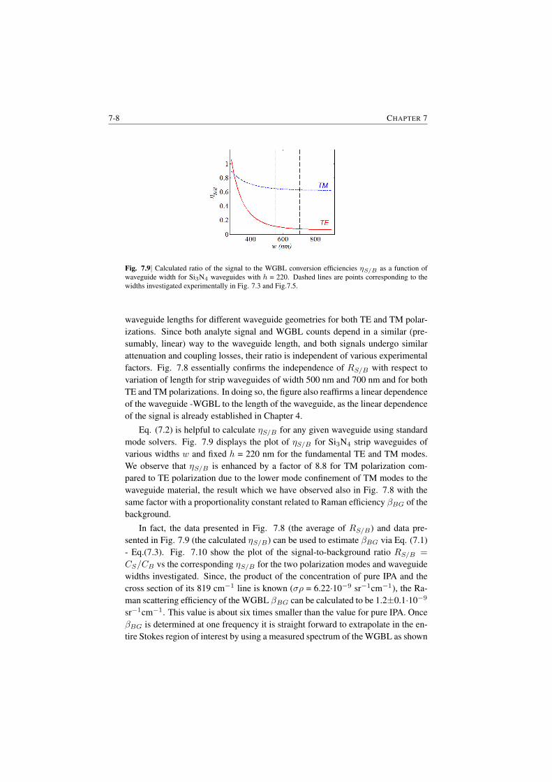
7-8 CHAPTER 7
Fig. 7.9| Calculated ratio of the signal to the WGBL conversion efficiencies ηS/B as a function ofwaveguide width for Si3N4 waveguides with h = 220. Dashed lines are points corresponding to thewidths investigated experimentally in Fig. 7.3 and Fig.7.5.
waveguide lengths for different waveguide geometries for both TE and TM polar-izations. Since both analyte signal and WGBL counts depend in a similar (pre-sumably, linear) way to the waveguide length, and both signals undergo similarattenuation and coupling losses, their ratio is independent of various experimentalfactors. Fig. 7.8 essentially confirms the independence of RS/B with respect tovariation of length for strip waveguides of width 500 nm and 700 nm and for bothTE and TM polarizations. In doing so, the figure also reaffirms a linear dependenceof the waveguide -WGBL to the length of the waveguide, as the linear dependenceof the signal is already established in Chapter 4.
Eq. (7.2) is helpful to calculate ηS/B for any given waveguide using standardmode solvers. Fig. 7.9 displays the plot of ηS/B for Si3N4 strip waveguides ofvarious widths w and fixed h = 220 nm for the fundamental TE and TM modes.We observe that ηS/B is enhanced by a factor of 8.8 for TM polarization com-pared to TE polarization due to the lower mode confinement of TM modes to thewaveguide material, the result which we have observed also in Fig. 7.8 with thesame factor with a proportionality constant related to Raman efficiency βBG of thebackground.
In fact, the data presented in Fig. 7.8 (the average of RS/B) and data pre-sented in Fig. 7.9 (the calculated ηS/B) can be used to estimate βBG via Eq. (7.1)- Eq.(7.3). Fig. 7.10 show the plot of the signal-to-background ratio RS/B =
CS/CB vs the corresponding ηS/B for the two polarization modes and waveguidewidths investigated. Since, the product of the concentration of pure IPA and thecross section of its 819 cm−1 line is known (σρ = 6.22·10−9 sr−1cm−1), the Ra-man scattering efficiency of the WGBL βBG can be calculated to be 1.2±0.1·10−9
sr−1cm−1. This value is about six times smaller than the value for pure IPA. OnceβBG is determined at one frequency it is straight forward to extrapolate in the en-tire Stokes region of interest by using a measured spectrum of the WGBL as shown
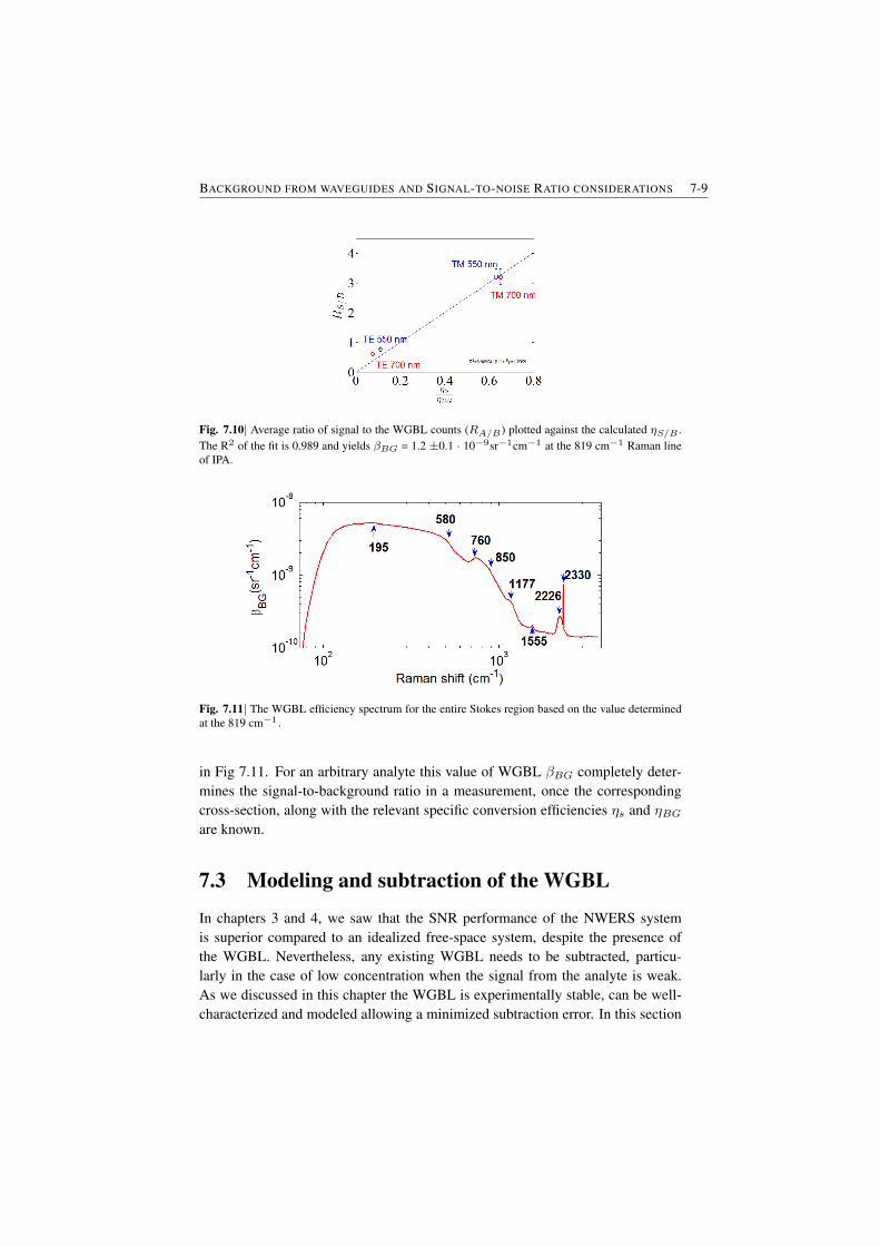
BACKGROUND FROM WAVEGUIDES AND SIGNAL-TO-NOISE RATIO CONSIDERATIONS 7-9
Fig. 7.10| Average ratio of signal to the WGBL counts (RA/B) plotted against the calculated ηS/B .The R2 of the fit is 0.989 and yields βBG = 1.2 ±0.1 · 10−9sr−1cm−1 at the 819 cm−1 Raman lineof IPA.
Fig. 7.11| The WGBL efficiency spectrum for the entire Stokes region based on the value determinedat the 819 cm−1.
in Fig 7.11. For an arbitrary analyte this value of WGBL βBG completely deter-mines the signal-to-background ratio in a measurement, once the correspondingcross-section, along with the relevant specific conversion efficiencies ηs and ηBGare known.
7.3 Modeling and subtraction of the WGBL
In chapters 3 and 4, we saw that the SNR performance of the NWERS systemis superior compared to an idealized free-space system, despite the presence ofthe WGBL. Nevertheless, any existing WGBL needs to be subtracted, particu-larly in the case of low concentration when the signal from the analyte is weak.As we discussed in this chapter the WGBL is experimentally stable, can be well-characterized and modeled allowing a minimized subtraction error. In this section
7-10 CHAPTER 7
we describe a simple model of the WGBL and a simple WGBL subtraction algo-rithm.
We model the measured NWERS signal SMES as:
SMES(λ) = RANL(λ) + PSIN+ANL(λ) +RSIN (λ) (7.4)
Here RANL is the Raman signal exclusively from the analyte, PSIN+ANL isthe polynomial WGBL from the Si3N4core discussed in §7.1, possibly with somepolynomial contribution from the analyte too, RSIN is the Raman signal from theSi3N4core discussed in §7.1. A reference spectrum from the waveguide, measuredwithout the analyte is:
SREF (λ) = PSIN (λ) + αRSIN (λ) (7.5)
The polynomial background PSIN and PSIN+ANL can be approximated byusing the asymmetric cost function algorithm [51] that finds the polynomial thatminimize the cost defined as the mean squared difference between the spectrumand the polynomial. After subtraction of the WGBL polynomial this becomes:
SMES = SMES − PSIN+ANL = RANL +RSIN + e1 (7.6)
and,
SREF = SREF − PSIN = αRSIN + e2 (7.7)
where e1 and e2 are small residual errors that might have remained during thesubtraction process. The Raman signal contribution from the core RSIN in Eq.(7.4) can now be obtained from the SREF by calculating the linear scaling factorα using least square algorithm that minimizes the cost defined as follows:
C =
(SMES(λ)− SREF (λ)
α
)2
(7.8)
An approximate Raman spectrum of the analyte on top of the waveguide isthen given by:
RANL = SMES −SREFα
+ e (7.9)
The approximate spectrum may contain some residual WGBL e that has notbeen completely removed during the process. The residual WGBL e is then re-moved using a variant of the low order asymmetric Whittaker method developedby Eilers [107].
Fig. 7.13 illustrates the WGBL subtraction algorithm discussed previously.First the reference spectrum SREF of the waveguides without the analyte is mea-sured as shown in Fig. 7.13(a). The third order polynomial part of the WGBL,
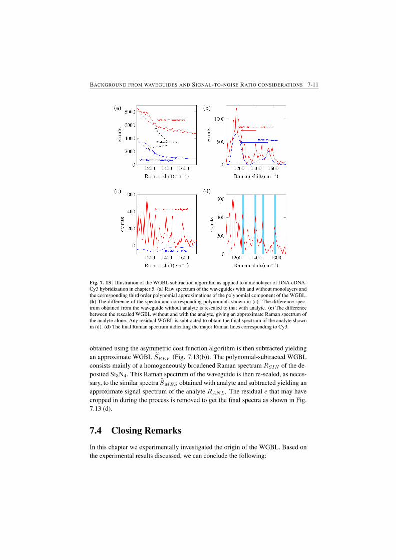
BACKGROUND FROM WAVEGUIDES AND SIGNAL-TO-NOISE RATIO CONSIDERATIONS 7-11
Fig. 7. 13 | Illustration of the WGBL subtraction algorithm as applied to a monolayer of DNA·cDNA-Cy3 hybridization in chapter 5. (a) Raw spectrum of the waveguides with and without monolayers andthe corresponding third order polynomial approximations of the polynomial component of the WGBL.(b) The difference of the spectra and corresponding polynomials shown in (a). The difference spec-trum obtained from the waveguide without analyte is rescaled to that with analyte. (c) The differencebetween the rescaled WGBL without and with the analyte, giving an approximate Raman spectrum ofthe analyte alone. Any residual WGBL is subtracted to obtain the final spectrum of the analyte shownin (d). (d) The final Raman spectrum indicating the major Raman lines corresponding to Cy3.
obtained using the asymmetric cost function algorithm is then subtracted yieldingan approximate WGBL SREF (Fig. 7.13(b)). The polynomial-subtracted WGBLconsists mainly of a homogeneously broadened Raman spectrum RSIN of the de-posited Si3N4. This Raman spectrum of the waveguide is then re-scaled, as neces-sary, to the similar spectra SMES obtained with analyte and subtracted yielding anapproximate signal spectrum of the analyte RANL. The residual e that may havecropped in during the process is removed to get the final spectra as shown in Fig.7.13 (d).
7.4 Closing Remarks
In this chapter we experimentally investigated the origin of the WGBL. Based onthe experimental results discussed, we can conclude the following:
7-12 CHAPTER 7
1. Various peaks observed in the WGBL can be assigned to different vibra-tions due to the molecules and impurities confined in the core during thedeposition process. The waveguide core forms the dominating source of theWGBL.
2. The broad background feature of the spectrum can be modeled as a 5th orderpolynomial. However, our preliminary studies show that this feature is mostprobably related to the Raman scattering of amorphous materials and can bestudied with Bose-Einstein statstics or its high temerature approximation,namely, Maxwell-Boltzmann statistics. A thorough theoretical analysis ofphonon-photon coupling factor and a temperature dependent measurementof the spectra is needed to understand and ascertain the origin of WGBL,and to subsequently develop strategies to reduce the WGBL.
3. The maxima of the Raman efficiency of the WGBL is about 5·10−9 sr-1
cm−1 which is about 3 times smaller than Raman efficiency of 819 cm−1
line of the pure isopropyl alcohol.
4. The use of special designs such as slotted waveguide and the use of TMpolarization leads to smaller background relative to the signal.
5. The background can be modeled and subtracted using a very simple back-ground subtraction method.

8Perspectives on integration with
plasmonic structures, resonators andspectrometers, and General
conclusions
The potential of waveguiding to enhance Raman signal was recognized [19] asearly as 1980 and used in various forms, such as hollow core fiber [21] for gases,liquid core waveguides [22] for transparent liquids and, as discussed in introduc-tion, also in thin-films [18], [20]. However, these techniques, along with all manyother techniques for Raman spectroscopy not discussed in this thesis are not easilyintegrable on a chip so as to allow mass fabrication of a low cost lab-on-a-chipdevice. The major appeal of the waveguide based approach presented in this thesisis its use of as with CMOS-compatible process and its inherently microscope-freenature. In this thesis I demonstrated this lab-on-a-chip approach for quantitativespontaneous Raman sensing of bulk and monolayers of materials.
In this chapter we will explore some directions on which the work presented inthis thesis is developing towards, mainly via integration with plasmonic structures,integrated resonators and spectrometers, and conclude with some perspectives forfurther developments. First we discuss our efforts to integrate plasmonic structureson chip.
8-2 CHAPTER 8
8.1 Integration with plasmonic nanoantennas and com-parison
For the case of evanescent waveguide sensing discussed in this thesis, the mostsignificant component of signal enhancement is due to a large interaction volumedistributed over the length of the waveguide. Hence, these sensors are suitable forsensing relatively larger analyte volumes. The Purcell-enhancement componentof these waveguides cannot be increased arbitrarily and a very high enhancement,needed for e.g. single molecule detection, is not possible using standard designs.
To overcome with this limitation of the NWERS approach, we have also beenworking towards an alternative approach of using the waveguides with integratednanoplasmonic structures. In this approach, the enhancement is the result of aplasmonic resonance effect at discrete ‘hot-spots’, i.e. regions of extreme local-ization of the electric field. Hence, waveguides integrated with nanoantennas aresuitable for studying very small number of localized molecules. We have theoret-ically shown that for integrated nanoantennas, an enhancement as high as 1010 ispossible [108]. Hence, single molecule detection in an integrated framework maybe possible with such hybrid nanophotonic-plasmonic waveguides. The reader isreferred to F. Peyskens’ Ph.D thesis (Ghent University, 2016) for more details.
Depending on the dimensions and the geometry of the antennas and the waveg-uide, we estimated that each integrated antenna discussed in this paper has anequivalent Si3N4 rib waveguide length of 250-2500 nm. This equivalent lengthis the physical length of a bare Si3N4 waveguide (without any gold) that is re-quired to generate the same signal as one integrated nanoplasmonic antenna. As arough estimate, 1 µm of a Si3N4 rib waveguide produces the same Raman signalas 1 plasmonic nanoantenna integrated on top of the waveguide. However, for thenanoantennas, the loss associated with gold absorption, elastic scattering, surfaceroughness etc. is about ep∼ es∼ 0.5 dB per antenna [1, 113, 114]. The loss perantenna is quite high compared to the 10−4 dB/µm for waveguides without theantenna. For bulk sensing, the integration of nanoplasmonic antennas is hencecompletely redundant because the signal generated by bare waveguides will bemuch larger due to the large waveguide length and small waveguide loss. On-chipSERS will however outperform the bare waveguide sensing case when particularanalytes are adsorbed on the metal surface. In that case one can make use of the ex-treme local Raman enhancement of the plasmonic hotspots, which can be orders ofmagnitude higher than the field enhancement of dielectric rib or slot waveguides.
8.2 Integrated resonators
Another route to reduce the required number of probed molecules is by using in-tegrated resonators, such as ring resonators or by fabricating Fabry–Perot type

GENERAL CONCLUSIONS AND PERSPECTIVES 8-3
resonators using Bragg reflectors. If both pump and Stokes frequencies are reso-nant with a Q-factor Q, we also saw (S3.6.1) that for a resonator of length l andthe collected signal enhances compared to the simple waveguide by a factor givenby,
PringPwg
=1
2
(Qn
πng
λ0
l
)2
(8.1)
While reducing the number of probe volume these resonators also enhance the sig-nal. Several designs in this route have been fabricated and will soon be measured.
8.3 Comparison with techniques based on refractiveindex sensing
The data presented in Fig. 5.3 allows us to quantify the 1σ detection limit interms of the Raman efficiency (ρsσ) in the order of 10−19 sr−1. For the di-mensions of our waveguides (∼ 10−4 cm2), using the surface loading value (∼1011 molecules/cm2) evaluated in §5.5 we calculate ∼ 107 molecules loaded ontothe waveguide; from this we calculate a detection limit of ∼ 104 ( ∼ 0.1 atto-mole) rhodamine molecules. Some techniques such as surface plasmon resonance(SPR) [115, 117] and dielectric refractive index (DRI) sensors (such as whisper-ing gallery mode (WGM) [116] sensors) measure adsorption reactions via an ex-tremely sensitive resonance shifts occurring due to minute changes in the refrac-tive index near a surface. For these sensors, the local refractive index sensitivityas high as ∆n/n ∼ 10−6 has been reported [116, 120]. In terms of molecu-lar sensitivity, as low as attomolar detection limit has been reported [121] in aRNA micro-array based on SPR. As such, these two quantities are not compa-rable because of differences in the experimental premises. Nevertheless, fromtheir respective detection detection limit values, we can conclude that NWERStechnique outperforms SPR sensors for high Raman cross-section molecules asrhodamine. For small cross-section molecules, the corresponding molecular sen-sitivity is comparable. Maturing over more than three decades of research, severalSPR technologies, such as Biacore, has been successfully commercialized as mas-sively parallelizable biomolecular analytical system. Although nascent NWERStechnology is inherently parallelizable, as of now, the parallelization density ofseveral thousand bimolecular interactions as possible with SPR sensors may notachievable with NWERS. Recently, a sophisticated combination of SPR and WGMtechniques was used to monitor single molecule nucleic acid interactions [118]. Incontrast, NWERS technique intrinsically depends on moderate electromagneticenhancement of the spontaneous Raman signal collected from a large number ofmolecules. Hence, in terms of molecular sensitivity, NWERS is inherently non-
8-4 CHAPTER 8
competitive with this technique. However, it is important to note that these tech-niques are indirect measurement techniques, as they measure change in the re-fractive index of the surface, hence offer a limited information compared to therich information provided by a Raman spectrum from NWERS. Further, since theSPR/WGM signals lack a direct molecular signature, these techniques are proneto errors occurring from non-specific binding, or due to changes in the refractiveindex of the buffer, a regularly occurring problem in molecular biochemistry. Inaddition, as discussed in the previous sections, NWERS technique can potentiallyecho the advantages of SPR and WGM techniques by the integration of ring res-onators and plasmonic nanoantennas, with added value of specificity and richnessof Raman signal. It is for the direct correspondence of the Raman signals with thebiochemistry of the molecule, and the properties described in the next section thatthe proposed NWERS technique is truly unique and useful.
8.4 General Conclusions
In this thesis we discussed an integrated-waveguide approach for on-chip sponta-neous Raman spectroscopy using the evanescent field of the dielectric waveguidefor excitation and collection. The effects of the waveguide parameters and polar-ization of the modes on the overall evanescent excitation and collection efficiencyof spontaneous Raman scattering were discussed and validated experimentally.Here we reiterate the major significance of the results presented in this thesis.
8.4.1 Microscope-less
Microscope is a costly and bulky part of a Raman system commonly employedin laboratories. It has several moving parts and optics that needs to be alignedprecisely. The results presented in this thesis shows that Raman spectroscopy ispossible using all-integrated optics platform, without any moving parts. This isfacilitated by the smallest etendue of the single mode waveguides described next.
8.4.2 Smallest etendue enabling integration with compact spec-trometers and light sources
The etendue is an important parameter characterizing the throughput of opticalpower in an optical beam or optical systems (described in appendix D). As a lightbeam propagates in an optical system, etendue either remains constant or increases,a statement known as the principle conservation of etendue. Thus, small etendue isalways preferred in an optical system design. Small etendue of light ensures maxi-mal illumination on the detector for a given optical power, hence allows for a smallspectrometer size with a high resolution. The etendue of the fundamental modes of
GENERAL CONCLUSIONS AND PERSPECTIVES 8-5
the waveguides are the smallest by definition. Hence, the light collected in a singlemode waveguide can be analyzed by the smallest integrated spectrometers witha high resolution and high power efficiency. Similarly, coupling of light from asource to an optical system is also governed by the conservation of etendue. Manyof the single mode laser sources are thus directly integrable to the single modewaveguide system as the sensing apparatus, where both excitation and collectionlight travel. Hence, low etendue of the NWERS sensors discussed in this thesiswarrants a compact all-integrated sensor with a single mode laser source, a highresolution and compact spectrometer, and possibly filters and detectors all inte-grated on a single chip, without loss of a significant amount of light. The readersare referred to Appendix D for a formal proof of the role of etendue the modenumber on the integration of the spectrometer.
8.4.3 High Performance
As discussed (Chapter 3 and Chapter 4), NWERS is based on enhanced interactionvolume and enhanced scattering efficiency of spontaneous Raman scattering nearnanophotonic waveguides. For a monolayer of analyte on top of one centimetersilicon nitride waveguide, NWERS delivers a signal that is more than four ordersof magnitude higher in comparison to a confocal Raman microscope. Similarlyfor bulk, more than about three orders of magnitude signal is expected comparedto a confocal Raman microscope.
8.4.4 CMOS compatible
In the past 50 years the electronics industry has invested billions of dollars in de-veloping the CMOS fabrication infrastructure that has scaled up in volume andprecision, while at the same time scaled down in cost per device. One of the mostimportant characteristic of our waveguides is its compatibility with CMOS fabri-cation infrastructure. Silicon nitride used for our waveguides are routinely usedas lithographic mask in CMOS fabrication processes. Using the same infrastruc-ture for fabrication of the devices and integration of light sources and detectorsprovides a mass-fabrication platform which we envisage would lead a way to apoint-of-need Raman devices
8.5 Closing Remarks: Applications
In this thesis we have focused more on conceptual developments and proof-of-concept demonstrations of the use of NWERS approach. Nevertheless, we dis-cussed a few proof-of-concept applications of the NWERS approach for Ramanspectroscopy, namely,

8-6 CHAPTER 8
1. Raman spectroscopy of bulk liquids and solutions.
2. Raman spectroscopy of the solid materials constituting the waveguide itself.
3. Raman spectroscopy of monolayers of biotin/streptavidin etc.
4. Real-time observation of hybridization of DNA monolayers.
5. Raman spectroscopy of cell membranes.
It is important to explore a variety of potential applications of the NWERS. Thetechnique is particularly suited for point-of-need applications to really take theadvantages of the compactness and sensitivity that we have discussed. Needlessto say, exploration of each of these potential applications of NWERS, in their ownright, require a substantial research effort and time.
ACalculation of Green’s Dyadic and
density of states
According to Poynting’s theorem [36], the out of phase component of the oscillat-ing current density ~J and the corresponding driving electric field ~E, dissipates apower P as follows
P =dW
dt= −1
2
ˆ< ~J∗ · ~EdV (A.1)
An oscillating current density ~J(~r) at an arbitrary location ~r can be written interms of an oscillating dipole ~d at a location ~r0, also oscillating at the same angularfrequency ω, such that,
~J(~r) = −iω−→d δ(~r − ~r0) (A.2)
Using Eq. (A.1) and Eq. (A.2), the dissipation of the dipole can be calculatedas:
P = −1
2
ˆ<−→J ∗ ·
−→E
=ω
2=−→d ∗ ·−→E (~r0)
(A.3)
If the current ~J is not subject to other dissipation pathways, such as thermallosses, the dissipation power given by Eq. (A.3) is directly related to the radiatedelectromagnetic field. Eq. (A.3) can be simplified further if the impinging field~E(~r0) in Eq. (A.3) is expressed as a radiation from a similar dipole located at the
A-2 APPENDIX A
same location. This can be done by using a second order tensor (dyadic) calledGreen’s dyadic function
←→G (~r, ~r0). The Green’s dyadic
←→G (~r, ~r0) describes the
field ~E(~r) at a point ~r from a point dipole source located at a position ~r is givenby:
−→E (−→r ) = ω2µ0
←→G (~r, ~r0)~d (A.4)
Using Eq. (A.3) and (A.4), and unit vectors in the direction of d we obtain:
P =ω3∣∣∣~d∣∣∣2 µ0
2
[d · =
←→G (~r0, ~r0)
· d]
(A.5)
Thus, we see that the dissipation of electromagnetic energy by a dipole is de-termined by the magnitude of the dipole strength and imaginary component of theGreen’s dyadic in the direction of the dipole. Green’s dyadic is related to vectorpotentials and related the radiation fields with the source field. For a completetreatment of Green’s Dyadic the readers are referred to chapter 2 of [35]. In brief,in an isotropic and homogenous space, the dyadic Greens function
←→G is given by
:
←→G (−→r ,−→r 0) =
[←→I +
1
k2∇∇
]eik|~r−~r0|
4π |~r − ~r0|(A.6)
←→G (~r, ~r0) =[←→
I + 1k2∇∇
]1
4π
(1
|~r−~r0| + ik2! −
k2|~r−~r0|23! + ..
) (A.7)
Here, the term outside the square brackets is well-known scalar Green’s func-tion, used as the source of scalar waves. The dyadic terms inside the square brack-ets accounts for the transverse nature of the radiation. The expansion in Eq. (A.6)allows us to distinguish the real and imaginary part and calculate the near fieldapproximation of the Green’s function. In an isotropic and homogeneous mediumonly the dyadic components in the direction the dipole (as represented by d) giverise to a non-zero contribution. In such a case, the square bracketed term reduces tothe trace of the dyadic. Using expansion in Eq. (A.6), taking the limit|~r−~r0| → 0
, we obtain: [d · Im
←→G (~r0, ~r0)
· d]
= =Tr[←→G (~r0, ~r0)
]= 1
4π
(k2
)[2]
= k4π
(A.8)
Hence, using Eq. (A.5)
CALCULATION OF FREESPACE GREEN’S DYADIC A-3
P =ω3∣∣∣~d∣∣∣2 µ0
2
2
3=Tr[←→G (~r0, ~r0)
]=ω3∣∣∣~d∣∣∣2 µ0
2
2
3
(k
4π
)(A.9)
P = nω4
12πε0c3
∣∣∣~dω∣∣∣2 (A.10)
Eq. (A.8) gives the total space-time-averaged power radiated by a dipole ina homogenous medium with refractive index n. The 2/3 factor in front of thetrace in Eq. (A.3) originates from the averaging of the Green’s function over thethree possible dipole orientations and two polarizations because of the rotationalsymmetry of the problem. In Eq. (A.7), 2 is the trace of the dyadic part of theGreen’s function, i.e square bracketed terms.
In Eq. (A.8) the square bracketed term is the Green’s function for the free spaceevaluated in the direction of dipole. Because of the symmetry of a homogeneousmedium, one cannot assign a specific direction to the dipole. Hence, we need toaverage over three possible dipole orientations and two possible polarizations ofthe radiation field, which leads to an extra factor of 2/3 (in front of the square-brackets). However, as we discuss in Chapter 3, if the dipole is constrained toemit at a particular direction and polarization, such as in case of scattering or acavity, where the incoming field or the normalized field of the cavity determinesthe scattering direction and polarization, the power of emission is given by:
P3/2 =ω3∣∣∣~d∣∣∣2 µ0
2
[k
4π
]= n
ω4
8πε0c3
∣∣∣~d∣∣∣2 (A.11)
It is usueful for discussion in Chapter 3 to express Greens dyadic in terms of den-sity of statesD(~r, ω0) defined as the number of available modes per unit frequencyper unit volume [35, 43]:
D(~r, ω0) ≡ 6ω
πc2
[d · =
←→G (~r0, ~r0)
· d]
This allows to write Eq. (A.5) in terms of density of states which is calculatedexplicitely in Chapter 3 for diferent cases in several inhomogeneous media,
P =πω2
4εε0
∣∣∣~d∣∣∣2D(~r0, ω0) (A.12)

BCalculation of Signal-to-noise ratio
Here we discuss the signal-to-noise performance of the WGBL shot-noise limitedNERS system for low concentration in comparison with the dark-noise limitedfree-space system.
We verified that the photon counts statistics of the CCD detector follows aPoisson distribution (Fig B.1 and Fig B.2). It follows that the SNR can be definedas:
SNR ≡ Cυ − CBG√Cυ
(B.1)
whereCν is the average number of photon counts of the signal peak at wavenum-ber ν and CBG is the average number of photon counts near the bottom of the peakthat correspond to the WGBL (see Chapter 7). In terms of experimental variablessuch as input power Pin, signal integration time tint, the product of scatteringcross-section and the density of the molecules (βs for signal and βBG for the background), interaction length l and detector dark noise equivalent power D, the SNRcan be expressed as:
SNR = θPinηslβs
√tint√
Pinl(ηsβs + ηBGβBG) +D(B.2)
Where, θ is square root of the detector sensitivity which will be omitted in thefollowing. Here we have implicitly used the experimental fact that dark counts arelinear with the integration time and that the noise follows the Poison statistics (Fig
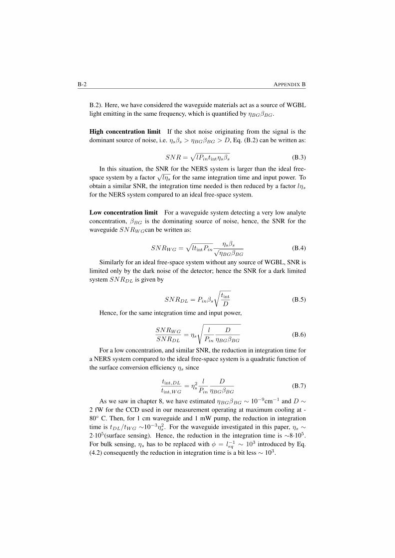
B-2 APPENDIX B
B.2). Here, we have considered the waveguide materials act as a source of WGBLlight emitting in the same frequency, which is quantified by ηBGβBG.
High concentration limit If the shot noise originating from the signal is thedominant source of noise, i.e. ηsβs > ηBGβBG > D, Eq. (B.2) can be written as:
SNR =√lPintintηsβs (B.3)
In this situation, the SNR for the NERS system is larger than the ideal free-space system by a factor
√lηs for the same integration time and input power. To
obtain a similar SNR, the integration time needed is then reduced by a factor lηsfor the NERS system compared to an ideal free-space system.
Low concentration limit For a waveguide system detecting a very low analyteconcentration, βBG is the dominating source of noise, hence, the SNR for thewaveguide SNRWGcan be written as:
SNRWG =√ltintPin
ηsβs√ηBGβBG
(B.4)
Similarly for an ideal free-space system without any source of WGBL, SNR islimited only by the dark noise of the detector; hence the SNR for a dark limitedsystem SNRDL is given by
SNRDL = Pinβs
√tint
D(B.5)
Hence, for the same integration time and input power,
SNRWG
SNRDL= ηs
√l
Pin
D
ηBGβBG(B.6)
For a low concentration, and similar SNR, the reduction in integration time fora NERS system compared to the ideal free-space system is a quadratic function ofthe surface conversion efficiency ηs since
tint,DL
tint,WG= η2
s
l
Pin
D
ηBGβBG(B.7)
As we saw in chapter 8, we have estimated ηBGβBG ∼ 10−9cm−1 and D ∼2 fW for the CCD used in our measurement operating at maximum cooling at -80 C. Then, for 1 cm waveguide and 1 mW pump, the reduction in integrationtime is tDL/tWG ∼10−3η2
s . For the waveguide investigated in this paper, ηs ∼2·105(surface sensing). Hence, the reduction in the integration time is ∼8·105.For bulk sensing, ηs has to be replaced with φ = l−1
eq ∼ 103 introduced by Eq.(4.2) consequently the reduction in integration time is a bit less ∼ 103.
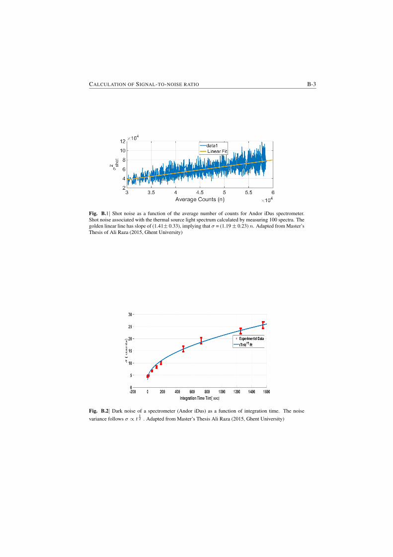
CALCULATION OF SIGNAL-TO-NOISE RATIO B-3
Fig. B.1| Shot noise as a function of the average number of counts for Andor iDus spectrometer.Shot noise associated with the thermal source light spectrum calculated by measuring 100 spectra. Thegolden linear line has slope of (1.41± 0.33), implying that σ = (1.19± 0.23) n. Adapted from Master’sThesis of Ali Raza (2015, Ghent University)
Fig. B.2| Dark noise of a spectrometer (Andor iDus) as a function of integration time. The noisevariance follows σ ∝ t
12 . Adapted from Master’s Thesis Ali Raza (2015, Ghent University)

CDNA hybridization kinetics
Here we develop a model of Raman signal dependence as a function of DNAhybridization. We consider a probe monolayer of DNA immobilized on top of thephotonic chip with a total surface density ρt. The free (unoccupied) immobilizedprobe DNA with average surface density ρf and the target cDNA in the analytesolution with surface density ρa,s (with a proportional volume density ρa) producethe hybridization duplex with surface density ρh, such that ρt = ρh + ρf . Thereaction can be described by the following kinetic equation.
ρf + ρa,s ρh (C.1)
Here K1 is the association constant that describes the binding rate of DNAand cDNA, while K−1 is the dissociation constant which describes the rate ofdissociation of hybridization duplex into the surface DNA and cDNA.
Assuming no other interactions between the species occur, the hybridizationrate can be described by a first order rate equation as follows.
dρhdt
= K1ρfρa −K−1ρh (C.2)
The unoccupied DNA density ρf participating in the reaction is the differencebetween total probe DNA concentration ρt and hybridized DNAs concentration,i.e ρf = ρt − ρh. Thus,
dρhdt
= −ρh (K1ρa +K−1) + ρaρtK1 (C.3)
C-2 APPENDIX C
We assume that the concentration ρa of the target cDNA on top of the waveg-uide remains constant and is sufficiently low to affect the signal from hybridizationcomplex. Then, the measured Raman signal from the hybridization is proportionalto the density of the hybridization complex ρh as per Eq. (4.4). Hence, we obtainEq. (C.4) for the evolution of the Raman signal.
ζ (τ) = ζ∞
(1− e−(K1ρa+K−1)τ
)(C.4)
where, ζ(τ ) is the normalized Raman signal intensity, defined by Eq. (4.4)in the main article, collected through the waveguide at a time τ after the startof the reaction, ζ∞ is the normalized Raman signal corresponding to the totalnumber of binding sites i.e.the Raman signal at the time of saturation. For thehybridization of DNA with a chain length > 20, as in our case, typically [79]-[80]K−1 << 10−4s−1 while K1> 105 M−1s−1, thus, for a concentration ρa>10nM, the equation is reduced to:
ζ (τ) = ζ∞(1− e−τK1ρA
)(C.5)
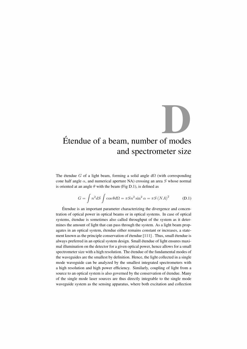
DEtendue of a beam, number of modes
and spectrometer size
The etendue G of a light beam, forming a solid angle dΩ (with correspondingcone half angle α, and numerical aperture NA) crossing an area S whose normalis oriented at an angle θ with the beam (Fig D.1), is defined as
G =
ˆn2dS
ˆcos θdΩ = πSn2 sin2 α = πS (NA)
2 (D.1)
Etendue is an important parameter characterizing the divergence and concen-tration of optical power in optical beams or in optical systems. In case of opticalsystems, etendue is sometimes also called throughput of the system as it deter-mines the amount of light that can pass through the system. As a light beam prop-agates in an optical system, etendue either remains constant or increases, a state-ment known as the principle conservation of etendue [111] . Thus, small etendue isalways preferred in an optical system design. Small etendue of light ensures maxi-mal illumination on the detector for a given optical power, hence allows for a smallspectrometer size with a high resolution. The etendue of the fundamental modes ofthe waveguides are the smallest by definition. Hence, the light collected in a singlemode waveguide can be analyzed by the smallest integrated spectrometers witha high resolution and high power efficiency. Similarly, coupling of light from asource to an optical system is also governed by the conservation of etendue. Manyof the single mode laser sources are thus directly integrable to the single modewaveguide system as the sensing apparatus, where both excitation and collection
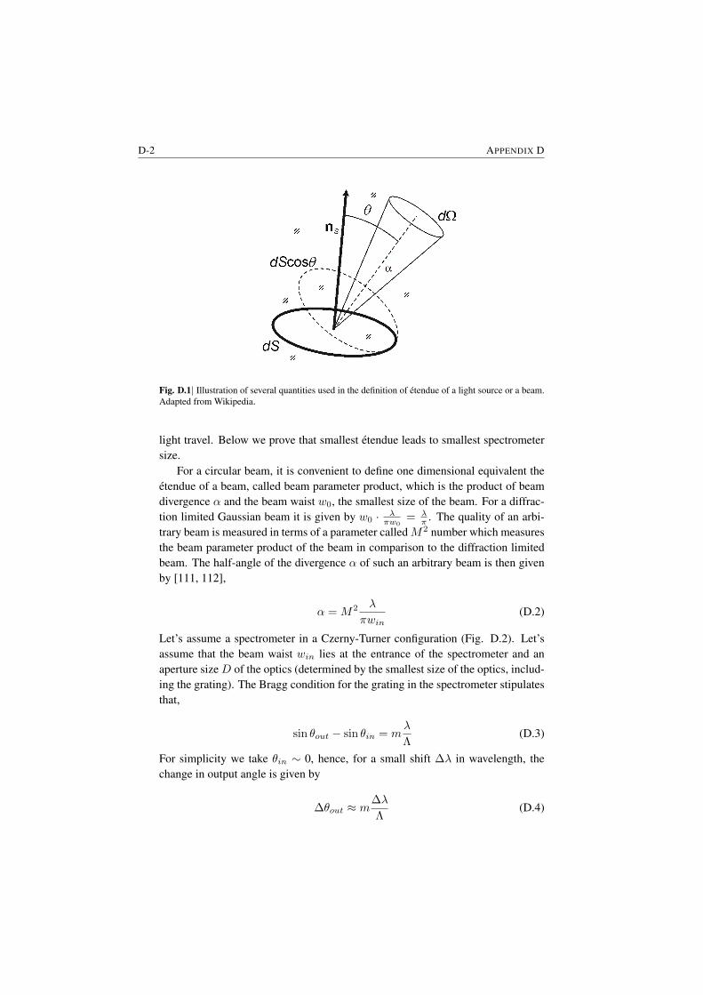
D-2 APPENDIX D
Fig. D.1| Illustration of several quantities used in the definition of etendue of a light source or a beam.Adapted from Wikipedia.
light travel. Below we prove that smallest etendue leads to smallest spectrometersize.
For a circular beam, it is convenient to define one dimensional equivalent theetendue of a beam, called beam parameter product, which is the product of beamdivergence α and the beam waist w0, the smallest size of the beam. For a diffrac-tion limited Gaussian beam it is given by w0 · λ
πw0= λ
π . The quality of an arbi-trary beam is measured in terms of a parameter calledM2 number which measuresthe beam parameter product of the beam in comparison to the diffraction limitedbeam. The half-angle of the divergence α of such an arbitrary beam is then givenby [111, 112],
α = M2 λ
πwin(D.2)
Let’s assume a spectrometer in a Czerny-Turner configuration (Fig. D.2). Let’sassume that the beam waist win lies at the entrance of the spectrometer and anaperture size D of the optics (determined by the smallest size of the optics, includ-ing the grating). The Bragg condition for the grating in the spectrometer stipulatesthat,
sin θout − sin θin = mλ
Λ(D.3)
For simplicity we take θin ∼ 0, hence, for a small shift ∆λ in wavelength, thechange in output angle is given by
∆θout ≈ m∆λ
Λ(D.4)

ETENDUE OF A BEAM, NUMBER OF MODES AND SPECTROMETER SIZE D-3
Fig. D.2| A spectrometer in Czerny-Turner configuration. The smallest aperture size D, beam diver-gence α, M2 of the input modeand the device beam path l of the spectrometer and determines thespectral resolution.
Which leads to a shift of the spot position in the image plane given by
∆xout = 2lm∆λ
Λ= win (D.5)
The spectral resolution ∆λ of a spectrometer is determined by the requirementthat the shift in the image spot ∆x is larger than or equal to the spot-size of theimage ∆xout ≥ 2wout = 2win, where the system is assumed to be of unitymagnification and the pitch of the detector array is assumed to be small enoughcompared to the width of ( wout). This leads to following relationship for thespectral resolution
∆λ
λ= M2 2Λ
πmD(D.6)
Thus, the resolution of a spectrometer is proportional to M2 of the beam, whichis a function of etendue of the beam or the optics. A diffraction-limited beam hasan M2 factor of 1 and smaller values of M2 are physically not possible. A mul-timode beam of order (n, m), for example Hermite–Gaussian beam for TEMnm
resonator mode, has an M2 factor of (2n+1) in the x direction, and (2m+1) in they direction [111, 112]. Hence, the resolution of a system increases as the order ofmode of the beam, and fundamental mode n = m = 0 ensures smallest resolutionof the spectrometer. Further, we see that the aperture size D of the spectrometerfor a given resolution is smallest for M2 = 1.
.

References
[1] Dhakal, A., Peyskens, F., Clemmen, S., Raza, A., Wuytens, P., Zhao, H.,Le Thomas, N. and Baets, R., 2016. Single mode waveguide platform forspontaneous and surface-enhanced on-chip Raman spectroscopy. InterfaceFocus, 6(4), p.20160015. §1, 2, 4, 4.2, 4.3, 4.4, 4.5, 4.6, 8.1
[2] Long, D.A., 2002. The Raman Effect: A Unified Treatment of the Theoryof Raman Scattering by Molecules, John Wiley & Sons Ltd. West Sussex,England §1.1, 1.3, 2, 2.2, 2.3, 2.3, 4.4
[3] Ferraro, J.R., 2003. Introductory Raman spectroscopy. Academic press. §1.1
[4] Laserna J. J. , Modern Techniques in Raman Spectroscopy., John Wiley &Sons (1996) §1.1
[5] Sir C. V Raman, Nobel Lecture, December 11, 1930 §1.1
[6] McCreery, R.L., 2005. Raman spectroscopy for chemical analysis (Vol.225). John Wiley & Sons. §1.1, 1.2, 2.5, 2.5.2
[7] Cialla, D., Deckert-Gaudig, T., Budich, C., Laue, M., Moller, R., Naumann,D., Deckert, V. and Popp, J., 2009. Raman to the limit: tip-enhanced Ramanspectroscopic investigations of a single tobacco mosaic virus. Journal ofRaman Spectroscopy, 40(3), pp.240-243. §1.1, 2.4
[8] Dochow, S., Beleites, C., Henkel, T., Mayer, G., Albert, J., Clement, J.,Krafft, C. and Popp, J., 2013. Quartz microfluidic chip for tumour cell iden-tification by Raman spectroscopy in combination with optical traps. Analyt-ical and bioanalytical chemistry, 405(8), pp.2743-2746. §1.1
[9] Kneipp, K., Wang, Y., Kneipp, H., Perelman, L.T., Itzkan, I., Dasari, R.R.and Feld, M.S., 1997. Single molecule detection using surface-enhancedRaman scattering (SERS). Physical review letters, 78(9), p.1667. 1.1
[10] Begley, R.F., Harvey, A.B. and Byer, R.L., 1974. Coherent anti-Stokes Ra-man spectroscopy. Applied Physics Letters, 25(7), pp.387-390. §1.1
D-6 REFERENCES
[11] Le Ru, E. and Etchegoin, P., 2008. Principles of Surface-Enhanced RamanSpectroscopy: and related plasmonic effects. Elsevier. §1.1
[12] Fan, M., Andrade, G.F. and Brolo, A.G., 2011. A review on the fabricationof substrates for surface enhanced Raman spectroscopy and their applica-tions in analytical chemistry. Analytica Chimica Acta, 693(1), pp.7-25. §1.1
[13] Snyder A. W. and Love J. D. , Optical Waveguide Theory Chapman and HallNew York, 1983. §1.2, 3.4.2, 3.5
[14] Pavesi, L. and Lockwood, D.J., 2004. Silicon photonics (Vol. 1). SpringerScience & Business Media. §1.2
[15] Soref, R., 2010. Silicon photonics: a review of recent literature. Silicon,2(1), pp.1-6. §1.2
[16] Subramanian, A.Z., Ryckeboer, E., Dhakal, A., Peyskens, F., Malik, A.,Kuyken, B., Zhao, H., Pathak, S., Ruocco, A., De Groote, A. et al., 2015.Silicon and silicon nitride photonic circuits for spectroscopic sensing on-a-chip. Photonics Research, 3(5), pp. B47-B59. §1.2
[17] Hu, Z., Glidle, A., Ironside, C.N., Sorel, M., Strain, M.J., Cooper, J. andYin, H., 2012. Integrated microspectrometer for fluorescence based analysisin a microfluidic format. Lab on a Chip, 12(16), pp.2850-2857. §1.2
[18] Kanger, J.S., Otto, C., Slotboom, M. and Greve, J., 1996. Waveguide Ra-man spectroscopy of thin polymer layers and monolayers of biomoleculesusing high refractive index waveguides. The Journal of Physical Chemistry,100(8), pp.3288-3292. §1.2, 8
[19] Rabolt, J.F., Santo, R. and Swalen, J.D., 1980. Raman measurements onthin polymer films and organic monolayers. Applied Spectroscopy, 34(5),pp.517-521. §1.2, 8
[20] Bradshaw, J.T., Mendes, S.B. and Saavedra, S.S., 2005. Planar integratedoptical waveguide spectroscopy. Analytical Chemistry, 77(1), pp.28-A. §1.2, 8
[21] Benabid, F., Knight, J.C., Antonopoulos, G. and Russell, P.S.J., 2002. Stim-ulated Raman scattering in hydrogen-filled hollow-core photonic crystalfiber. Science, 298 (5592), pp.399-402. §1.2, 8
[22] Zhang, Y., Shi, C., Gu, C., Seballos, L. and Zhang, J.Z., 2007. Liquid corephotonic crystal fiber sensor based on surface enhanced Raman scattering.Applied Physics Letters, 90(19), p.193504. §1.2, 8

REFERENCES D-7
[23] Moss, D.J., Morandotti, R., Gaeta, A.L. and Lipson, M., 2013. New CMOS-compatible platforms based on silicon nitride and Hydex for nonlinear op-tics. Nature Photonics, 7(8), pp.597-607. §1.3
[24] Zhao, H., Kuyken, B., Clemmen, S., Leo, F., Subramanian, A., Dhakal, A.,Helin, P., Severi, S., Brainis, E., Roelkens, G. and Baets, R., 2015. Visible-to-near-infrared octave spanning supercontinuum generation in a silicon ni-tride waveguide. Optics letters, 40 (10), pp.2177-2180. §1.3
[25] Subramanian, A.Z., Neutens, P., Dhakal, A., Jansen, R., Claes, T., Rotten-berg, X., Peyskens, F., Selvaraja, S., Helin, P., Dubois, B. and Leyssens, K.,2013. Low-loss singlemode PECVD silicon nitride photonic wire waveg-uides for 532–900 nm wavelength window fabricated within a CMOS pilotline. Photonics Journal, IEEE, 5 (6), pp.2202809. §1.3, 1.1
[26] Romero-Garcıa, S., Merget, F., Zhong, F., Finkelstein, H. and Witzens,J., 2013. Silicon nitride CMOS-compatible platform for integrated photon-ics applications at visible wavelengths. Optics express, 21(12), pp.14036-14046. §1.3
[27] Haglund, E.P., Kumari, S., Westbergh, P., Gustavsson, J.S., Roelkens,G., Baets, R. and Larsson, A., 2015. Silicon-integrated short-wavelengthhybrid-cavity VCSEL. Optics Express, 23(26), pp.33634-33640. §1.3
[28] Brouckaert, J., Bogaerts, W., Dumon, P., Thourhout, D.V. and Baets, R.,2007. Planar concave grating demultiplexer fabricated on a nanophotonicsilicon-on-insulator platform. Lightwave Technology, Journal of, 25(5),pp.1269-1275. §1.3
[29] Martens, D., Subramanian, A.Z., Pathak, S., Vanslembrouck, M., Bienst-man, P., Bogaerts, W. and Baets, R.G., 2015. Compact silicon nitride ar-rayed waveguide gratings for very near-infrared wavelengths. PhotonicsTechnology Letters, IEEE, 27(2), pp.137-140. §1.3
[30] Momeni, B., Hosseini, E.S. and Adibi, A., 2009. Planar photonic crystalmicrospectrometers in silicon-nitride for the visible range. Optics express,17(19), pp.17060-17069. §1.3
[31] Tu, X., Song, J., Liow, T.Y., Park, M.K., Yiying, J.Q., Kee, J.S., Yu, M.and Lo, G.Q., 2012. Thermal independent silicon-nitride slot waveguidebiosensor with high sensitivity. Optics express, 20(3), pp.2640-2648. §1.3
[32] Barwicz, T., Popovi, M., Rakich, P., Watts, M., Haus, H., Ippen, E. andSmith, H., 2004. Microring-resonator-based add-drop filters in SiN: fabri-cation and analysis. Optics express, 12(7), pp.1437-1442. §1.3
D-8 REFERENCES
[33] Zhang, Z., Liu, D., de Felipe, D., Liu, A., Keil, N. and Grote, N., 2013.Polymer embedded silicon nitride thermally tunable Bragg grating filters.Applied Physics Letters, 102(18), p.181105. §1.3
[34] Loudon, R., 2000. The quantum theory of light. OUP Oxford. §2, 2.2, 3.6.2
[35] Novotny, L. and Hecht, B., 2012. Principles of nano-optics. Cambridge uni-versity press. §2, 3.1, A, A
[36] Jackson, J.D., 1999. Classical electrodynamics. Wiley. §2, 2.2, A
[37] Dhakal, A., Wuytens, P., Peyskens, F., Subramanian, A., Skirtach, A., LeThomas, N. and Baets, R., 2015, May. Nanophotonic lab-on-a-chip Ra-man sensors: A sensitivity comparison with confocal Raman microscope.In BioPhotonics (BioPhotonics), 2015 International Conference on IEEE.Florence §2, 2.7.1, 2.7.1
[38] Pampaloni, F. and Enderlein, J., 2004. Gaussian, hermite-gaussian, andlaguerre-gaussian beams: A primer. arXiv preprint physics/0410021. §2.7
[39] W. Herr, B. J. Holzer, and B. Muratori, “Chapter 6.4 Concept of luminosity,”in Accelerators and Colliders (Springer Berlin, 2013), pp. 140–146. §2.7
[40] Turrell, G. and Corset, J. eds., 1996. Raman microscopy: developments andapplications. Academic Press, pp. 43 §2.7.1
[41] Purcell, E.M., 1946. Spontaneous emission probabilities at radio frequen-cies. Physical Review, 69, p.681 §3, 3.2
[42] Yablonovitch, E., 1987. Inhibited spontaneous emission in solid-statephysics and electronics. Physical review letters, 58, (20), p.2059. §3
[43] Xu, Y., Lee, R.K. and Yariv, A., 2000. Quantum analysis and the classicalanalysis of spontaneous emission in a microcavity. Physical Review A, 61(3), p.033807. §3.1, A
[44] Rigneault, H. and Monneret, S., 1996. Modal analysis of spontaneous emis-sion in a planar microcavity. Physical Review A, 54 (3), p.2356 §3.4.1
[45] Jun, Y.C., Kekatpure, R.D., White, J.S. and Brongersma, M.L., 2008. Non-resonant enhancement of spontaneous emission in metal-dielectric-metalplasmon waveguide structures. Physical Review B, 78(15), p.153111. §3.4.1
[46] Dhakal, A., Subramanian, A., Baets, R. and Le Thomas, N., 2012. The roleof index contrast in the efficiency of absoprtion and emission of a lumi-nescent particle near a slab waveguide. In 16th European Conference onIntegrated Optics (ECIO-2012). §6.1
REFERENCES D-9
[47] Kogelnik, H. and Weber, H.P., 1974. Rays, stored energy, and power flowin dielectric waveguides. JOSA, 64(2), pp.174-185. §3.4.1, 3.4.2
[48] Dhakal, A., Subramanian, A.Z., Wuytens, P., Peyskens, F., Le Thomas, N.and Baets, R., 2014. Evanescent excitation and collection of spontaneousRaman spectra using silicon nitride nanophotonic waveguides. Optics let-ters, 39 (13), pp.4025-4028. §4, 4.1
[49] Dhakal, A., Raza, A., Peyskens, F., Subramanian, A.Z., Clemmen, S., LeThomas, N. and Baets, R., 2015. Efficiency of evanescent excitation andcollection of spontaneous Raman scattering near high index contrast chan-nel waveguides. Optics express, 23 (21), pp.27391-27404. §5.3.1, 6, 6.1
[50] Dhakal, A., Wuytens, P, Raza, A., Peyskens, F., Subramanian, A.Z., Clem-men, S., Le Thomas, N. and Baets, R.,, “Lab-on-a-chip Raman sensors out-performing Raman microscopes,” in CLEO 2016, USA § 4, 4.2, 4.3, 4.5,4.6, 4.8, 4.9
[51] Mazet, V., Carteret, C., Brie, D., Idier, J., & Humbert, B., ‘Backgroundremoval from spectra by designing and minimising a non-quadratic costfunction’, Chemom. Intell. Lab. Syst. 121-133. 76 (2) (2005) §4.3.2, 7.3
[52] Ulman, A., 2013. An Introduction to Ultrathin Organic Films: From Lang-muir–Blodgett to Self-Assembly. Academic press. §5.1
[53] Gennis, R.B. ed., 2013. Biomembranes: molecular structure and function.Springer Science & Business Media. §5.1
[54] Richter, R.P., Berat, R. and Brisson, A.R., 2006. Formation of solid-supported lipid bilayers: an integrated view. Langmuir, 22(8), pp.3497-3505. §5.1
[55] Lu, B., Smyth, M.R. and O’Kennedy, R., 1996. Tutorial review. Orientedimmobilization of antibodies and its applications in immunoassays and im-munosensors. Analyst, 121(3), pp.29R-32R. §
[56] Heller, M.J., 2002. DNA microarray technology: devices, systems, and ap-plications. Annual review of biomedical engineering, 4(1), pp.129-153. §
[57] Southern, E., Mir, K. and Shchepinov, M., 1999. Molecular interactions onmicroarrays. Nature genetics, 21, pp.5-9. §5.4
[58] Castner, D.G. and Ratner, B.D., 2002. Biomedical surface science: Founda-tions to frontiers. Surface Science, 500(1), pp.28-60. §5.4
[59] Chilkoti, A. and Hubbell, J.A., 2005. Biointerface science. MRS Bulletin,30(03), pp.175-179. §5.1
D-10 REFERENCES
[60] Bonaccorso, F., Sun, Z., Hasan, T. and Ferrari, A.C., 2010. Graphene pho-tonics and optoelectronics. Nature photonics, 4(9), pp.611-622. §5.1
[61] Xu, M., Liang, T., Shi, M. and Chen, H., 2013. Graphene-like two-dimensional materials. Chemical reviews, 113(5), pp.3766-3798. §5.1
[62] Castellanos-Gomez, A, 2016. Why all the fuss about 2D semiconductors?Nature Photonics, 10, 202–204. §5.1
[63] Poggi, M.A., Gadsby, E.D., Bottomley, L.A., King, W.P., Oroudjev, E.and Hansma, H., 2004. Scanning probe microscopy. Analytical chemistry,76(12), pp.3429-3444. §5.1
[64] Lee, P.A., Citrin, P.H., Eisenberger, P.T. and Kincaid, B.M., 1981. Extendedx-ray absorption fine structure—its strengths and limitations as a structuraltool. Reviews of Modern Physics, 53(4), p.769. §5.1
[65] Cesareo, R., 2010. X-Ray Fluorescence Spectrometry. Wiley-VCH VerlagGmbH & Co. KGaA. §5.1
[66] Ray, S., & Shard, A. G. Quantitative analysis of adsorbed proteins by X-ray photoelectron spectroscopy. Analytical chemistry, 83(22), 8659-8666(2011). §
[67] Degen, C.L., Poggio, M., Mamin, H.J., Rettner, C.T. and Rugar, D.,2009. Nanoscale magnetic resonance imaging. Proceedings of the NationalAcademy of Sciences, 106(5), pp.1313-1317. §5.1
[68] Ferrari, A.C. and Basko, D.M., 2013. Raman spectroscopy as a versatiletool for studying the properties of graphene. Nature nanotechnology, 8(4),pp.235-246. §5.1
[69] Kagan, M.R. and McCreery, R.L., 1995. Quantitative surface Raman spec-troscopy of physisorbed monolayers on glassy carbon. Langmuir, 11(10),pp.4041-4047. §5.1
[70] Kneipp, K., Kneipp, H., Itzkan, I., Dasari, R.R. and Feld, M.S., 2002.Surface-enhanced Raman scattering and biophysics. Journal of Physics:Condensed Matter, 14(18), p.R597. §5.1
[71] Galarreta, B.C., Norton, P.R. and Lagugne-Labarthet, F., 2011. SERS De-tection of Streptavidin/Biotin Monolayer Assemblies. Langmuir, 27 (4),pp.1494-1498. §5.1, 5.5
REFERENCES D-11
[72] Lim, D.K., Jeon, K.S., Hwang, J.H., Kim, H., Kwon, S., Suh, Y.D. andNam, J.M., 2011. Highly uniform and reproducible surface-enhanced Ra-man scattering from DNA-tailorable nanoparticles with 1-nm interior gap.Nature nanotechnology, 6 (7), pp.452-460. §5.1
[73] Liu, X., Shao, Y., Tang, Y. and Yao, K.F., 2014. Highly uniform and re-producible surface enhanced raman scattering on air-stable metallic glassynanowire array. Scientific reports, 4. §
[74] Peyskens, F., Dhakal, A., Van Dorpe, P., Le Thomas, N. and Baets,R., 2016,. Surface enhanced Raman spectroscopy using a single modenanophotonic-plasmonic platform. ACS Photonics. 3 (1), pp 102-108 §5.1
[75] Opilik, L., Payamyar, P., Szczerbinski, J., Schutz, A.P., Servalli, M.,Hungerland, T., Schluter, A.D. and Zenobi, R., 2015. Minimally InvasiveCharacterization of Covalent Monolayer Sheets Using Tip-Enhanced Ra-man Spectroscopy. ACS nano, 9 (4), pp.4252-4259. §5.1
[76] Jun, Y.C., Briggs, R.M., Atwater, H.A. and Brongersma, M.L., 2009.Broadband enhancement of light emission in silicon slot waveguides. OpticsExpress, 17 (9), pp.7479-7490. §3.5.1
[77] Ouldridge, T.E., Sulc, P., Romano, F., Doye, J.P. and Louis, A.A., 2013.DNA hybridization kinetics: zippering, internal displacement and sequencedependence. Nucleic acids research, 41 (19), pp.8886-8895. §5.4
[78] Kranenburg, O., 2005. The KRAS oncogene: past, present, and future.Biochimica et Biophysica Acta (BBA)-Reviews on Cancer, 1756 (2), pp.81-82. §5.4
[79] Okahata, Y., Kawase, M., Niikura, K., Ohtake, F., Furusawa, H. andEbara, Y., 1998. Kinetic measurements of DNA hybridization on anoligonucleotide-immobilized 27-MHz quartz crystal microbalance. Analyt-ical Chemistry, 70(7), pp.1288-1296. §5.4, C
[80] Jeng, E.S., Barone, P.W., Nelson, J.D. and Strano, M.S., 2007. Hybridiza-tion Kinetics and Thermodynamics of DNA Adsorbed to Individually Dis-persed Single-Walled Carbon Nanotubes. Small, 3(9), pp.1602-1609. § 5.4,C
[81] Sorgenfrei, S., Chiu, C.Y., Gonzalez Jr, R.L., Yu, Y.J., Kim, P., Nuckolls,C. and Shepard, K.L., 2011. Label-free single-molecule detection of DNA-hybridization kinetics with a carbon nanotube field-effect transistor. Naturenanotechnology, 6(2), pp.126-132. §5.4
[82] Hermanson, G.T., 2013. Bioconjugate techniques. Academic press. §5.5

D-12 REFERENCES
[83] Weber, P.C., Ohlendorf, D.H., Wendoloski, J.J. and Salemme, F.R., 1989.Structural origins of high-affinity biotin binding to streptavidin. Science,243(4887), pp.85-88. §
[84] Diamandis, E.P. and Christopoulos, T.K., 1991. The biotin-(strept) avidinsystem: principles and applications in biotechnology. Clinical chemistry,37(5), pp.625-636. §5.5
[85] Langer, P.R., Waldrop, A.A. and Ward, D.C., 1981. Enzymatic synthesis ofbiotin-labeled polynucleotides: novel nucleic acid affinity probes. Proceed-ings of the National Academy of Sciences, 78(11), pp.6633-6637. §5.5
[86] Bistricic, L., Volovsek, V. and Dananic, V., 2007. Conformational and vibra-tional analysis of gamma-aminopropyltriethoxysilane. Journal of molecularstructure, 834, pp.355-363. §5.5
[87] Fagnano, C., Fini, G. and Torreggiani, A., 1995. Raman spectroscopic studyof the avidin—biotin complex. Journal of Raman Spectroscopy, 26(11),pp.991-995. §5.5
[88] Shim, S., Stuart, C.M. and Mathies, R.A., 2008. Resonance Raman Cross-Sections and Vibronic Analysis of Rhodamine 6G from Broadband Stimu-lated Raman Spectroscopy. ChemPhysChem, 9(5), pp.697-699. §5.5
[89] Kagan, M.R. and McCreery, R.L., 1994. Reduction of fluorescence inter-ference in Raman spectroscopy via analyte adsorption on graphitic carbon.Analytical Chemistry, 66(23), pp.4159-4165. §5.5
[90] Hoff, J.D., Cheng, L.J., Meyhofer, E., Guo, L.J. and Hunt, A.J., 2004.Nanoscale protein patterning by imprint lithography. Nano letters, 4(5),pp.853-857. §5.5
[91] Arafat, A., Giesbers, M., Rosso, M., Sudholter, E.J., Schroen, K., White,R.G., Yang, L., Linford, M.R. and Zuilhof, H., 2007. Covalent biofunction-alization of silicon nitride surfaces. Langmuir, 23(11), pp.6233-6244. §5.8
[92] Zhang, F. and Srinivasan, M.P., 2004. Self-assembled molecular filmsof aminosilanes and their immobilization capacities. Langmuir, 20(6),pp.2309-2314. §5.8
[93] Yıldırım, M.A., Goh, K.I., Cusick, M.E., Barabasi, A.L. and Vidal, M.,2007. Drug—target network. Nature biotechnology, 25(10), pp.1119-1126.§5.7.1
[94] Carter, E.A., Rayner, B.S., McLeod, A.I., Wu, L.E., Marshall, C.P., Levina,A., Aitken, J.B., Witting, P.K., Lai, B., Cai, Z. and Vogt, S., 2010. Silicon

REFERENCES D-13
nitride as a versatile growth substrate for microspectroscopic imaging andmapping of individual cells. Molecular Biosystems, 6 (7), pp.1316-1322. §5.7.2
[95] Richter, R.P., Berat, R. and Brisson, A.R., 2006. Formation of solid-supported lipid bilayers: an integrated view. Langmuir, 22 (8), pp.3497-3505. §5.7.3
[96] Krafft, C., Knetschke, T., Siegner, A., Funk, R.H. and Salzer, R.,2003. Mapping of single cells by near infrared Raman microspec-troscopy.Vibrational Spectroscopy, 32 (1), pp.75-83. §5.7.3, 5.8
[97] Dhakal, A., Peyskens, F., Subramanian, A., Le Thomas, N. and Baets, R.G.,2013, July. Enhancement of light absorption, scattering and emission in highindex contrast waveguides. In Optical Sensors, Puerto Ricco (pp. ST2B-5).Optical Society of America. §6, 6.1
[98] Bogaerts, W., Baets, R., Dumon, P., Wiaux, V., Beckx, S., Taillaert, D.,Luyssaert, B., Van Campenhout, J., Bienstman, P. and Van Thourhout,D., 2005. Nanophotonic waveguides in silicon-on-insulator fabricated withCMOS technology. Lightwave Technology, Journal of, 23 (1), pp.401-412.§6.3
[99] Hayrinen, M., Roussey, M., Saynatjoki, A., Kuittinen, M. and Honkanen,S., 2015. Titanium dioxide slot waveguides for visible wavelengths. Appliedoptics, 54(10), pp.2653-2657. §6.3
[100] Tsu, D.V., Lucovsky, G. and Mantini, M.J., 1986. Local atomic structure inthin films of silicon nitride and silicon diimide produced by remote plasma-enhanced chemical-vapor deposition. Physical Review B, 33(10), p.7069. §7.1.1
[101] Narikawa, S., Kojima, Y. and Ehara, S., 1985. Investigations of NH and Si-N bonding configurations in hydrogenated amorphous silicon nitride filmsby infrared absorption spectroscopy. Japanese journal of applied physics,24(11A), p.L861. §7.1.1
[102] Smith, D.L., Alimonda, A.S., Chen, C.C., Ready, S.E. and Wacker, B.,1990. Mechanism of SiN x H y Deposition from NH 3-SiH4 Plasma. Jour-nal of the Electrochemical Society, 137(2), pp.614-623. §7.1.1
[103] Soudi, A., Khan, E.H., Dickinson, J.T. and Gu, Y., 2009. Observation ofunintentionally incorporated nitrogen-related complexes in ZnO and GaNnanowires. Nano letters, 9(5), pp.1844-1849. §7.1.1
D-14 REFERENCES
[104] Dhakal, A., Wuytens, P., Peyskens, F., Subramanian, A.Z., Le Thomas, N.and Baets, R., 2014, May. Silicon-nitride waveguides for on-chip Ramanspectroscopy. In SPIE Photonics Europe (pp. 91411C). International Soci-ety for Optics and Photonics. §7.2
[105] Shuker, R. and Gammon, R.W., 1970. Raman-scattering selection-rulebreaking and the density of states in amorphous materials. Physical ReviewLetters, 25(4), p.222. §7.1.5
[106] Sokolov, A.P., Kisliuk, A., Quitmann, D. and Duval, E., 1993. Evaluationof density of vibrational states of glasses from low-frequency Raman spec-tra.Physical Review B, 48(10), p.7692. §7.1.5
[107] Eilers, P. H., & Boelens, H. F. (2005). Baseline correction with asymmetricleast squares smoothing. Leiden University Medical Centre Report. Leidenuniversity. §7.3
[108] Peyskens, F., Subramanian, A., Dhakal, A., Le Thomas, N. and Baets,R., 2013, June. Enhancement of Raman scattering efficiency by a metallicnano-antenna on top of a high index contrast waveguide. In CLEO: Scienceand Innovations (pp. CM2F-5). Optical Society of America. §8.1
[109] Raphael Van Laer, 2016, Light-Sound Interaction in Nanoscale SiliconWaveguides. PhD Thesis, Ghent University. §2.2.3
[110] Hamaguchi, H.O., Kato, C. and Tasumi, M., 1983. Observation of transientresonance raman spectra of the S 1 state of trans-stilbene. Chemical physicsletters, 100(1), pp.3-7. §2.4
[111] Chaves, J., 2015. Introduction to nonimaging optics. CRC Press. §D, D, D
[112] Meinhart, C.D. and Wereley, S.T., 2003. The theory of diffraction-limitedresolution in microparticle image velocimetry. Measurement science andtechnology, 14(7), p.1047. §D, D
[113] Peyskens, F., Subramanian, A.Z., Neutens, P., Dhakal, A., Van Dorpe, P.,Le Thomas, N. and Baets, R., 2015. Bright and dark plasmon resonances ofnanoplasmonic antennas evanescently coupled with a silicon nitride waveg-uide. Optics express, 23(3), pp.3088-3101. §8.1
[114] Peyskens, F., Dhakal, A., Van Dorpe, P., Le Thomas, N. and Baets, R., 2015.Surface enhanced Raman spectroscopy using a single mode nanophotonic-plasmonic platform. ACS Photonics, 3(1), pp.102-108. §8.1
[115] Mrksich, M., Sigal, G.B. and Whitesides, G.M., 1995. Surface plas-mon resonance permits in situ measurement of protein adsorp-tion on
REFERENCES D-15
self-assembled monolayers of alkanethiolates on gold. Langmuir, 11(11),pp.4383-4385. 18. §8.3
[116] Vollmer, F. and Arnold, S., 2008. Whispering-gallery-mode bio-sensing:label-free detection down to single molecules. Nature methods, 5(7),pp.591-596. §8.3
[117] Homola, J., 2003. Present and future of surface plasmon resonance biosen-sors. Analytical and bioanalytical chemistry, 377(3), pp.528-539. §8.3
[118] Baaske, M.D., Foreman, M.R. and Vollmer, F., 2014. Single-molecule nu-cleic acid interactions monitored on a label-free microcavity biosensor plat-form. Nature nanotechnology, 9(11), pp.933-9. §8.3
[119] Koreeda, A., Takano, R. and Saikan, S., 2009. Light scattering in a phonongas. Physical Review B, 80(16), p.165104. 7.1.5
[120] Homola, J., Yee, S.S. and Gauglitz, G., 1999. Surface plasmon resonancesensors: review. Sensors and Actuators B: Chemical, 54(1), pp.3-15. 8.3
[121] Fang, S., Lee, H.J., Wark, A.W. and Corn, R.M., 2006. Attomole microar-ray detection of microRNAs by nanoparticle-amplified SPR imaging mea-surements of surface polyadenylation reactions. Journal of the AmericanChemical Society, 128(43), pp.14044-14046. 8.3
[122] Martin, A.J. and Brenig, W., 1974. Model for Brillouin scattering in amor-phous solids. physica status solidi (b), 64(1), pp.163-172.
7.1.5