modification of n-si characteristics by annealing and cooling at different rates
TRANSCRIPT

Active and Passive Elec. Comp.,
December 2003, Vol. 26, No. 4, pp. 213–230
MODIFICATION OF n-Si CHARACTERISTICS BYANNEALING AND COOLING AT DIFFERENT RATES
SUBHI K. SALIHa, HIKMAT S. HILALa,*, IYAD A. SA’DEDDINa,
ELISABETH SELLIERb and GUY CAMPETb
aCollege of Sciences, An-Najah N. University, P.O. Box 7, West Bank, Palestine;bInstitut de Chimie de la Matiere Condensee de Bordeaux du CNRS, Chateau Brivazac,
avenue du Dr. A. Schweitzer, 33608 Pessac, France
(Received 30 December 2002; In final form 21 March 2003)
The effect of annealing of the n-Si semiconductor on its characteristics in photoelectrochemical systems has beeninvestigated. The annealing improved the dark current density vs. potential plots. The surface was improved byannealing, as manifested by SEM results. The effect of the cooling rate on preheated n-Si wafers was alsoinvestigated. It was found that the slowly cooled electrodes gave better dark current density vs. potential plots,for samples annealed at lower than 550 �C. For samples annealed at higher temperatures, quenching gave betterdark-current density vs. potential plots. SEM measurements showed parallel results to these findings. Enhancedsurface textures were observed for slowly cooled wafers from temperatures below 550 �C. Samples quenchedfrom temperatures above 550 �C showed better surfaces than slowly cooled counterparts.
Keywords: n-Si; Annealing; Cooling rate; J–V plots; SEM
1 INTRODUCTION
Semiconductor (SC) surface enhancement can be obtained by annealing the wafer. Annealing
of SC wafers leads to enhancement of their efficiency in the PEC solar cells [1].
Crystal imperfection is a common feature associated with elevated heating. In metallic con-
ductors, the heat imperfection causes expansions and conductivity lowering behavior in
the crystal. The rate of cooling of heated metal crystals affects the crystal properties.
Quenching of heated aluminum rods prevents contraction to their original length [2].
Metastable spheres in the heated crystal will be deprived of any energy that is needed for return.
Alternatively, slow cooling would allow the return of metastable spheres to their original
positions. Therefore, it is assumed that slow cooling improves crystallinity.
Literature shows how annealing SC wafers improves their crystallinity [1, 3–8]. Slow
cooling of annealed SC wafers is also reported to enhance crystallinity [9–13]. It has also
been found that the dark current could be greatly reduced through rapid thermal annealing
of porous silicon SC [14].
* Corresponding author. E-mail: [email protected]
ISSN 0882-7516 print; ISSN 1563-5031 online # 2003 Taylor & Francis LtdDOI: 10.1080=0882751031000116124
By improving crystallinity, the SC wafer treatment should improve its characteristics
at the solid=liquid interface in PEC. If the annealed SC is slowly cooled, it would retain
its original order, with fewer imperfections. If quenched, the annealed crystal would become
more imperfect.
In our efforts to enhance the efficiency of light to electricity onto SC surfaces, we
hereby present a convenient method to enhance the band-edge and surface structures
of monocrystalline commercially made SCs for the purpose of enhancing their PEC char-
acteristics.
2 EXPERIMENTAL
2.1 Materials
LiClO4, K3Fe(CN)6 and K4Fe(CN)6 were purchased from Aldrich. All organic solvents
(methanol, dichloromethane, DMF) were obtained from Riedel-DeHaen in a pure form.
2.2 Equipment
J–V plots were measured using a computerized PAR 263A potentiostat. A three-electrode
one-compartment photoelectrochemical cell, equipped with a platinum counter electrode,
SCE reference, was used. Fe(CN)3�=4�6 (0.05 M K3Fe(CN)6, 0.05 M K4Fe(CN)6) was used
as a redox couple in distilled water with (pH 6.5), and LiClO4 as a supporting electrolyte.
N2 was bubbled through the solution at least 5 min before each experiment, and was kept
to bubble above the solution during the experiment to minimize contamination with air.
SEM measurements were conducted using a JEOL 2000 FX electron microscope.
2.3 Wafer Annealing
Annealing was conducted using a thermostated horizontal tube furnace. A closed clay cruci-
ble, with the SC wafer inside, was inserted in a long stainless steel cylinder and the assembly
was placed inside the furnace under an N2 stream. The temperature was set and kept at the
desired level (400, 500, 600 or 700 �C) for an extra 20 min. Cooling was then started.
Quenching was conducted by dipping the stainless steel cylinder into enough amounts of
water. The room temperature was reached within one minute. Slow cooling was conducted
in a stepwise process. In each step, the temperature setting was lowered by 50 degrees
and allowed to settle for 20 min. Depending on the starting annealing temperature, a total
of 8–12 hours was needed for slow cooling to occur.
2.4 Electrode Fabrication
Mono-crystalline h111i single-surface polished n-Si wafers, with 300–500 ohm-cm resisti-
vity, were used. The thickness was �300 mm. The n-Si electrodes were fabricated as follows:
the wafer was cut into small pieces (�0.1 cm2). The pieces were then annealed at the desired
temperatures. After cooling to room temperature, the piece was mounted to a copper plate
(welded to a copper wire), using Ga–In eutectic on both the copper plate and the semicon-
ductor unpolished (back) face [15]. The copper wire was Teflon-insulated. The exposed Cu
and Ga–In eutectic with semiconductor edges of the electrode were then sealed with
epoxy cement, leaving only the electrode polished mirror face exposed to the solution.
214 S. K. SALIH et al.
The electrodes were left to dry for at least 24 hours at room temperature under nitrogen,
before rinsing with methanol and drying with a slow stream of N2.
All electrodes were etched, prior to use, with HF solution (49% by mass), as shown
earlier [16]. The electrode was immersed in the HF solution for about 20 s, rinsed with
distilled water, and then washed with methanol. The above process was repeated three
times to remove undesirable oxides and obtain a shiny mirror surface.
3 RESULTS
n-Si wafers were treated by heating and cooling. The wafers were heated to a desired
temperature (400 �C, 500 �C, 600 �C, 700 �C, or 800 �C). Cooling of heated wafers to room
temperature (25 �C) was done using two different methods, quenching and slow cooling.
Dark J–V plots and SEM measurements of surface probed the effect of treatment on the
SC characteristics.
3.1 Dark J–V Plot Enhancement of n-Si Samples
3.1.1 Annealing Effect on n-Si Characteristics
The n-Si samples were heated, to different temperatures, and then cooled (slowly or by
quenching) to room temperatures. The heated samples showed better dark J–V plots than
the untreated samples.
Figure 1 shows better dark J–V plots for quenched samples than for the untreated counter-
parts. The quenched samples, from heating temperatures of 600 �C and 700 �C, showed the
best J–V plots. In fact, we will observe that the best dark J–V plots was obtained with the
highest annealing temperature. Better dark J–V plots for slowly cooled samples were also
obtained, compared to untreated ones, as shown in Figure 2, but in this case the plot quality
was independent of annealing temperature.
3.1.2 Effect of Rate of Cooling from Temperatures Below 550 �C
Figures 3 and 4 show dark J–V plots measured for slowly cooled and quenched samples from
400 �C and 500 �C, respectively. We notice that slowly cooled samples showed better dark
J–V plots than quenched counterparts. In fact we established that such behavior occurs provi-
ded that the heating temperature does not exceed 550 �C.
3.1.3 Effect of Rate of Cooling from Temperatures Above 550 �C
Contrary to the lower temperature range, the quenched samples showed better dark J–V plots
than the slowly cooled ones (Figs. 5 and 6).
3.2 SEM Results
The surface quality is a key factor in SC performance in photoelectrochemical (PEC)
systems. SEM is helpful to study the surface quality.
n-Si ANNEALING AND COOLING 215

FIGURE 1 Dark J–V plots for (a) unheated n-Si. Quenched n-Si samples from (b) 400 �C, (c) 500 �C, (d) 600 �C, and (e) 700 �C. All J–V measurements were conducted inwater=LiClO4=K4[Fe(CN)6]=K3[Fe(CN)6] at 25 �C.
21
6S
.K
.S
AL
IHet
al.

FIGURE 2 Dark J–V plots for (a) unheated n-Si. Slowly cooled n-Si samples from (b) 400 �C, (c) 500 �C, (d) 600 �C, and (e) 700 �C. All J–V measurements were conducted inwater=LiClO4=K4[Fe(CN)6]=K3[Fe(CN)6] at 25 �C.
n-S
iA
NN
EA
LIN
GA
ND
CO
OL
ING
21
7

FIGURE 3 Dark J–V plots of (a) slowly cooled and (b) quenched n-Si samples from 400 �C. All J–V measurements were conducted in water=LiClO4=K4[Fe(CN)6]=K3[Fe(CN)6] at 25 �C.
21
8S
.K
.S
AL
IHet
al.

FIGURE 4 Dark J–V plots of (a) slowly cooled and (b) quenched n-Si from 500 �C. All J–V measurements were conducted in water=LiClO4=K4[Fe(CN)6]=K3[Fe(CN)6] at 25 �C.
n-S
iA
NN
EA
LIN
GA
ND
CO
OL
ING
21
9
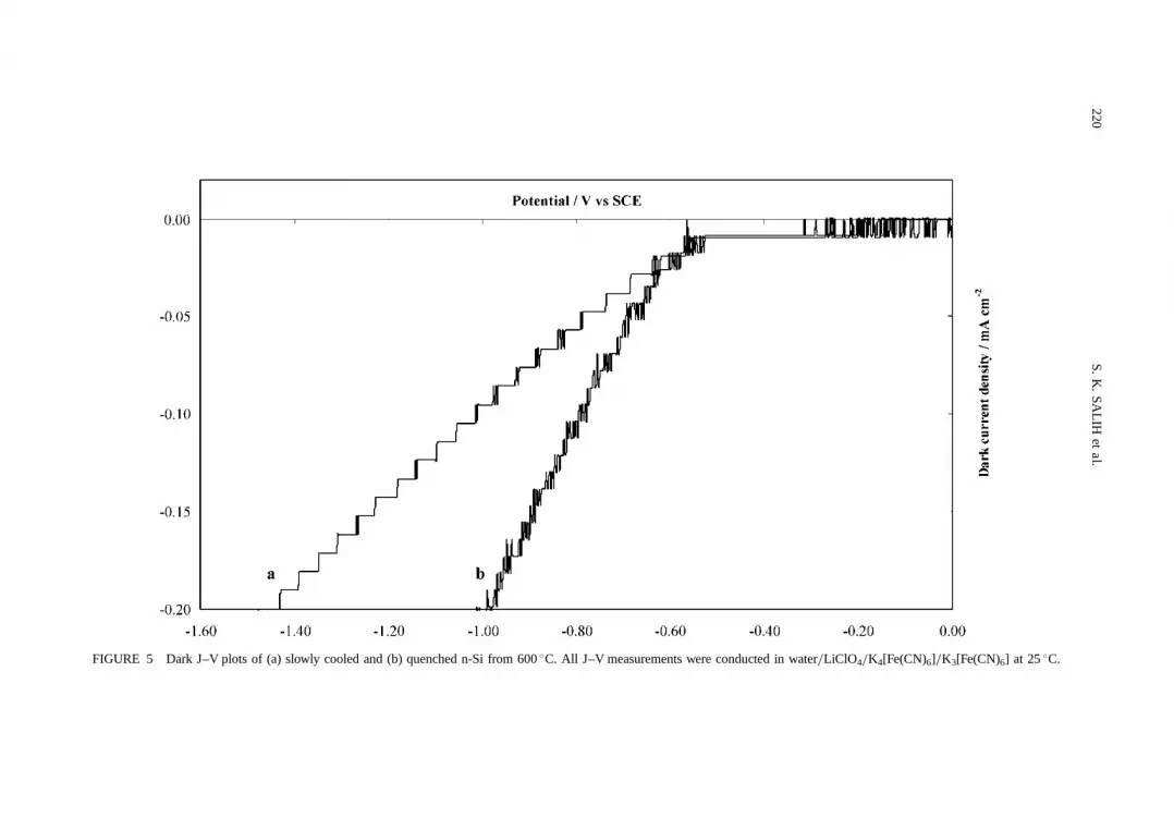
FIGURE 5 Dark J–V plots of (a) slowly cooled and (b) quenched n-Si from 600 �C. All J–V measurements were conducted in water=LiClO4=K4[Fe(CN)6]=K3[Fe(CN)6] at 25 �C.
22
0S
.K
.S
AL
IHet
al.

FIGURE 6 Dark J–V plots of (a) slowly cooled and (b) quenched n-Si from 700 �C. All J–V measurements were conducted in water=LiClO4=K4[Fe(CN)6]=K3[Fe(CN)6] at 25 �C.
n-S
iA
NN
EA
LIN
GA
ND
CO
OL
ING
22
1
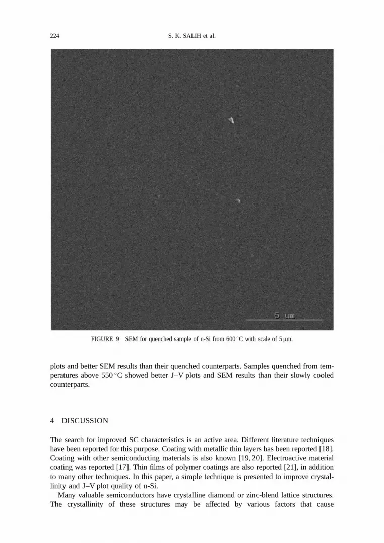
3.2.1 Effect of SC Heating on SEM Results
SEM results for Si samples, annealed and then cooled to room temperature, showed better
quality surfaces than untreated counterparts. This was evident in both quenching and slow
cooling processes.
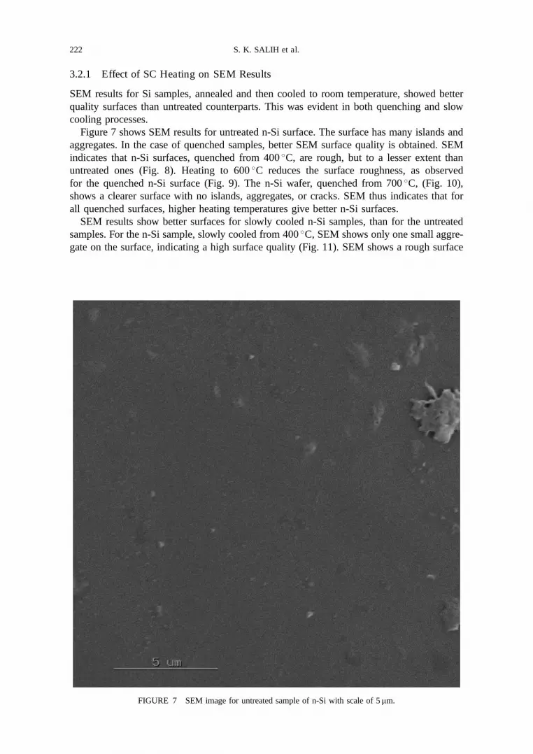
Figure 7 shows SEM results for untreated n-Si surface. The surface has many islands and
aggregates. In the case of quenched samples, better SEM surface quality is obtained. SEM
indicates that n-Si surfaces, quenched from 400 �C, are rough, but to a lesser extent than
untreated ones (Fig. 8). Heating to 600 �C reduces the surface roughness, as observed
for the quenched n-Si surface (Fig. 9). The n-Si wafer, quenched from 700 �C, (Fig. 10),
shows a clearer surface with no islands, aggregates, or cracks. SEM thus indicates that for
all quenched surfaces, higher heating temperatures give better n-Si surfaces.
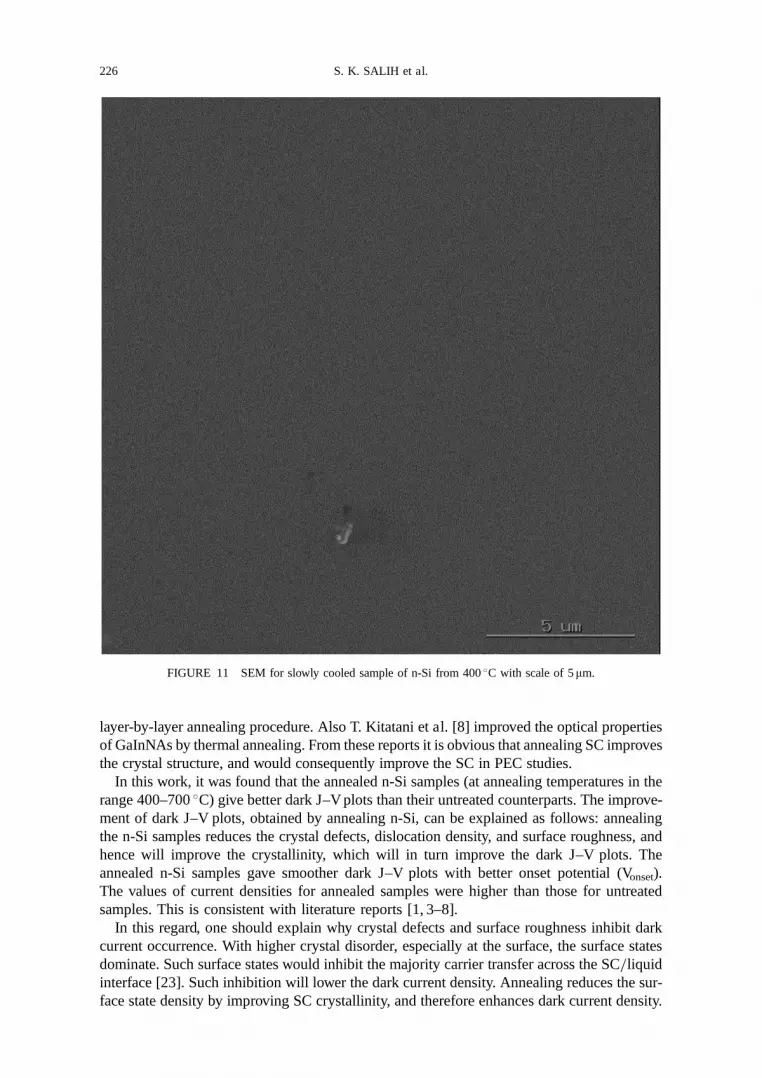
SEM results show better surfaces for slowly cooled n-Si samples, than for the untreated
samples. For the n-Si sample, slowly cooled from 400 �C, SEM shows only one small aggre-
gate on the surface, indicating a high surface quality (Fig. 11). SEM shows a rough surface
FIGURE 7 SEM image for untreated sample of n-Si with scale of 5 mm.
222 S. K. SALIH et al.

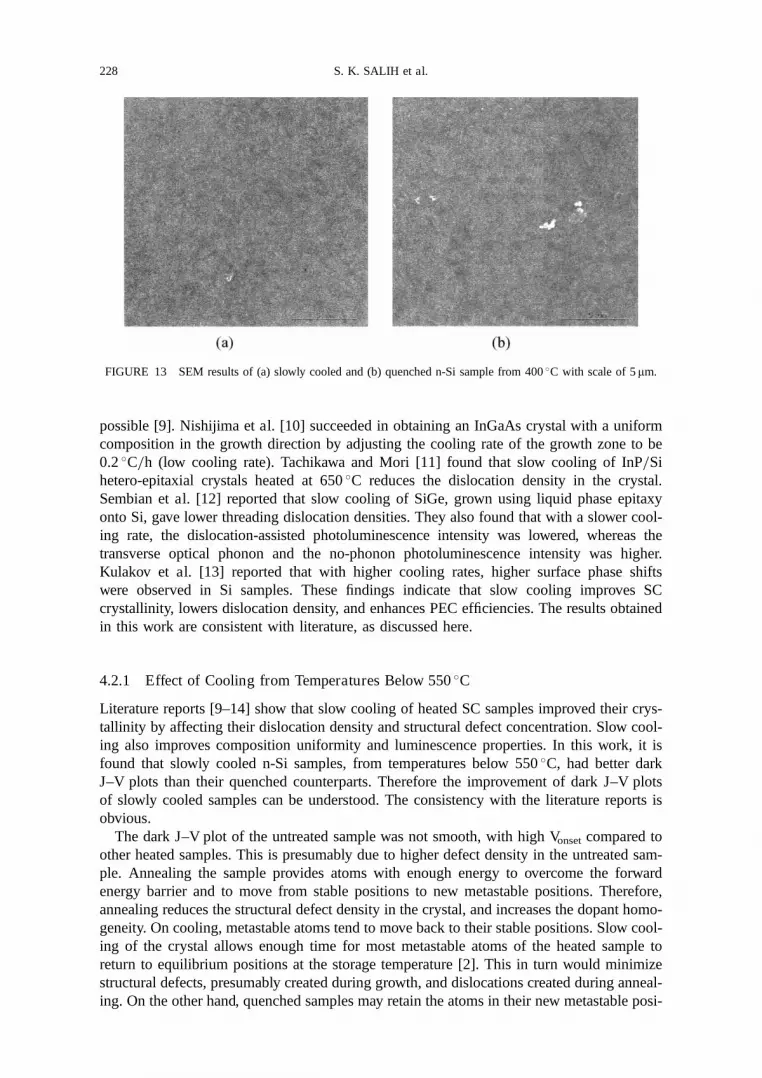
for the slowly cooled sample from 600 �C (Fig. 12). The surface of the slowly cooled sample
is still far better than the untreated surface, as appears from Figure 13.
3.2.2 Effect of Rate of Cooling from Temperatures below 550 �C
SEM results show that slowly cooled samples, from temperatures below 550 �C, have better
surface quality than the quenched samples from the same temperature.
3.2.3 Effect of Rate of Cooling from Temperatures above 550 �C
Above 550 �C the quenched samples show better surface quality than the slowly cooled ones.
3.3 Consistency Between Dark J–V Plot and SEM Data
SEM results are consistent with J–V plot results. In each case, annealing enhanced the n-Si
samples. Furthermore, the samples slowly cooled from 550 �C or lower showed better J–V
FIGURE 8 SEM for quenched sample of n-Si from 400 �C with scale of 5 mm.
n-Si ANNEALING AND COOLING 223
plots and better SEM results than their quenched counterparts. Samples quenched from tem-
peratures above 550 �C showed better J–V plots and SEM results than their slowly cooled
counterparts.
4 DISCUSSION
The search for improved SC characteristics is an active area. Different literature techniques
have been reported for this purpose. Coating with metallic thin layers has been reported [18].
Coating with other semiconducting materials is also known [19, 20]. Electroactive material
coating was reported [17]. Thin films of polymer coatings are also reported [21], in addition
to many other techniques. In this paper, a simple technique is presented to improve crystal-
linity and J–V plot quality of n-Si.
Many valuable semiconductors have crystalline diamond or zinc-blend lattice structures.
The crystallinity of these structures may be affected by various factors that cause
FIGURE 9 SEM for quenched sample of n-Si from 600 �C with scale of 5 mm.
224 S. K. SALIH et al.

defects [22]. In here, the enhancement effect of annealing and rate of cooling on n-Si
physical characteristics will be reasoned.
4.1 Effect of Annealing
Annealing of semiconductor wafers enhances the crystal homogeneity, quality, performance
and reliability. Annealing also reduces defects, and lowers surface roughness. This has been
reported in the literature.
It has been shown that photothermal processing can provide better performance and higher
reliability of SC devices [3]. Fujioka et al. demonstrated that annealing SC in ultra-high
vacuum chambers at about 700 �C effectively lowers the SC surface roughness [4]. Plane
defects were lowered by annealing [5]. Thermal annealing plays an important role in the crys-
tallization process of homogeneous ultra-thin a-Si:H sub-layers [6]. Das et al. showed that, for
thin films of n-InSe, surface treatment such as etching and annealing leads to an increase in the
efficiency of the PEC solar cells, at a pH value of 6.2 [1]. Kitatani et al. [7] improved the crystal
quality of highly strained GaInNAs=GaAs double quantum well structure, by developing a
FIGURE 10 SEM for quenched sample of n-Si from 700 �C with scale of 5 mm.
n-Si ANNEALING AND COOLING 225
layer-by-layer annealing procedure. Also T. Kitatani et al. [8] improved the optical properties
of GaInNAs by thermal annealing. From these reports it is obvious that annealing SC improves
the crystal structure, and would consequently improve the SC in PEC studies.
In this work, it was found that the annealed n-Si samples (at annealing temperatures in the
range 400–700 �C) give better dark J–V plots than their untreated counterparts. The improve-
ment of dark J–V plots, obtained by annealing n-Si, can be explained as follows: annealing
the n-Si samples reduces the crystal defects, dislocation density, and surface roughness, and
hence will improve the crystallinity, which will in turn improve the dark J–V plots. The
annealed n-Si samples gave smoother dark J–V plots with better onset potential (Vonset).
The values of current densities for annealed samples were higher than those for untreated
samples. This is consistent with literature reports [1, 3–8].
In this regard, one should explain why crystal defects and surface roughness inhibit dark
current occurrence. With higher crystal disorder, especially at the surface, the surface states
dominate. Such surface states would inhibit the majority carrier transfer across the SC=liquid
interface [23]. Such inhibition will lower the dark current density. Annealing reduces the sur-
face state density by improving SC crystallinity, and therefore enhances dark current density.
FIGURE 11 SEM for slowly cooled sample of n-Si from 400 �C with scale of 5mm.
226 S. K. SALIH et al.

In addition to lowering dislocation and defect densities, annealing may improve the SC
properties by increasing the homogeneity in doping density distribution in the SC bulk
because of maximizing randomness [24]. The enhancement of dark current density, observed
by annealing n-Si in this work, can therefore be understood.
Convincing evidence for this discussion comes from SEM results. The heated n-Si samples
exhibit lower surface roughness than the unheated samples. This result supports the discus-
sion that heating SC improves dark J–V plots by lowering surface state densities.
4.2 Effect of Cooling Rate
Many SC crystal parameters are affected by cooling rates. Examples of such parameters are:
composition, uniformity, growth, film thickness, and luminescence properties. The disloca-
tion density and concentration of structural defects also depend on the cooling rate of
SC crystals. A uniform film growth of Si from Cu–Si solution, with constant temperature
gradient distribution, at the cooling rate of 0.1 �C=s and 0.05 �C=s (low cooling rate), was
FIGURE 12 SEM for slowly cooled sample of n-Si from 600 �C with scale of 5mm.
n-Si ANNEALING AND COOLING 227
possible [9]. Nishijima et al. [10] succeeded in obtaining an InGaAs crystal with a uniform
composition in the growth direction by adjusting the cooling rate of the growth zone to be
0.2 �C=h (low cooling rate). Tachikawa and Mori [11] found that slow cooling of InP=Si
hetero-epitaxial crystals heated at 650 �C reduces the dislocation density in the crystal.
Sembian et al. [12] reported that slow cooling of SiGe, grown using liquid phase epitaxy
onto Si, gave lower threading dislocation densities. They also found that with a slower cool-
ing rate, the dislocation-assisted photoluminescence intensity was lowered, whereas the
transverse optical phonon and the no-phonon photoluminescence intensity was higher.
Kulakov et al. [13] reported that with higher cooling rates, higher surface phase shifts
were observed in Si samples. These findings indicate that slow cooling improves SC
crystallinity, lowers dislocation density, and enhances PEC efficiencies. The results obtained
in this work are consistent with literature, as discussed here.
4.2.1 Effect of Cooling from Temperatures Below 550 �C
Literature reports [9–14] show that slow cooling of heated SC samples improved their crys-
tallinity by affecting their dislocation density and structural defect concentration. Slow cool-
ing also improves composition uniformity and luminescence properties. In this work, it is
found that slowly cooled n-Si samples, from temperatures below 550 �C, had better dark
J–V plots than their quenched counterparts. Therefore the improvement of dark J–V plots
of slowly cooled samples can be understood. The consistency with the literature reports is
obvious.
The dark J–V plot of the untreated sample was not smooth, with high Vonset compared to
other heated samples. This is presumably due to higher defect density in the untreated sam-
ple. Annealing the sample provides atoms with enough energy to overcome the forward
energy barrier and to move from stable positions to new metastable positions. Therefore,
annealing reduces the structural defect density in the crystal, and increases the dopant homo-
geneity. On cooling, metastable atoms tend to move back to their stable positions. Slow cool-
ing of the crystal allows enough time for most metastable atoms of the heated sample to
return to equilibrium positions at the storage temperature [2]. This in turn would minimize
structural defects, presumably created during growth, and dislocations created during anneal-
ing. On the other hand, quenched samples may retain the atoms in their new metastable posi-
FIGURE 13 SEM results of (a) slowly cooled and (b) quenched n-Si sample from 400 �C with scale of 5 mm.
228 S. K. SALIH et al.

tions after annealing. Quenching would deprive the metastable atoms from any pathways to
return to their stable positions. The defect density in quenched samples will therefore be
greater than their slowly cooled counterparts. In short, slow cooling reduces the surface
state density. Such an effect improves SC composition, and therefore enhances dark current
density.
Consistently with that, SEM results showed that the slowly cooled n-Si sample from
400 �C exhibited lower surface roughness than its quenched counterpart. This result supports
the discussion shown above.
4.2.2 Effect of Cooling from Temperatures above 550 �C
Increasing the annealing temperature results in removal of point defects, such as vacancies,
and reduces the concentration of impurity interstitials at the surface. This is due to dopant
diffusion in the SC bulk. When SC annealing is conducted at temperatures above 550 �C,
for prolonged times, dislocations are formed, and the dopant concentration at the surface
will be lowered [25]. Thus long-time annealing (slow cooling) of SC affects the sample crys-
tallinity, which will in turn affect the SC surface roughness and its dark J–V plots. In this
work, quenched n-Si samples, from temperatures above 550 �C, had better dark J–V plots
than their slowly cooled counterparts.
The dark J–V plot improvement of quenched samples can be explained. The quenched
sample dark J–V plots are better than those of slowly cooled ones. This is due to high dis-
location density in slowly cooled samples. Slow cooling of annealed n-Si samples allows
longer exposure to higher temperatures. Diffusion of impurities will therefore increase.
Such diffusion is represented by vacancy and interstitial diffusion, in addition to self diffu-
sion of Si atoms. This in turn causes the formation of dislocations in addition to point-defects
in slowly cooled samples. Thus exposure of n-Si to annealing temperatures above 550 �C for
longer times would increase dislocation and point-defect densities. The presence of a high
density of dislocation and point defects affects sample crystallinity. Consequently, the surface
state density increases at the SC=liquid interface, and lowers the quality of dark J–V plots. On
the other hand, quenching of annealed samples from temperatures above 550 �C would pre-
vent other diffusion mechanisms that may occur. Thus fewer dislocations or point-defects
will be formed. In conclusion, quenching of n-Si samples from temperatures above 550 �C
improves the n-Si crystallinity, and consequently the dark J–V plots.
These discussions have direct supporting evidence from SEM. The n-Si sample, quenched
from 600 �C, exhibits lower surface roughness than the slowly cooled counterparts. As stated ear-
lier, the lower roughness is an indicator of lower dislocations and lower point-defect densities.
Work is underway here to study the effects of the cooling rate on characteristics of other
SC materials.
5 CONCLUSIONS
Annealing n-Si wafers enhances their characteristics at the solid=liquid interface in PEC
experiments, as exhibited in dark J–V plot improvement. Slow cooling of annealed samples
from 550 �C or lower further enhances PEC characteristics. With higher annealing tempera-
tures, quenching gives better results than slow cooling. SEM results confirmed all PEC study
results. It is therefore possible to enhance semiconductor characteristics at the solid=liquid
interface in addition to their surface characteristics by controlling annealing temperatures
and rates of cooling.
n-Si ANNEALING AND COOLING 229

Acknowledgements
The authors wish to acknowledge help from the scanning electron microscopy facility at
ICMCB, University of Bordeaux, France. Technical assistance from colleagues at
An-Najah N. University is acknowledged. Helpful discussions from Dr. Ayman Daoud and
Dr. Mosa Hasan are also appreciated. Assistantships from EGIDE offices, France, are also
acknowledged.
References
[1] Das, V. D., Sathyanarayanan, J. and Damodare, L. (1997). Effect of annealing and surface treatment on theefficiency of photoelectrochemical (PEC) solar cells with vacuum-deposited n-InSe thin film electrode. Surf.Coat. Technol., 94–95, 669–671.
[2] Van Vlack, L. H. (1970). Material Science for Engineers. Addison-Wesley Publishing Company, Inc., Reading,pp. 105–107.
[3] Singh, R., Fakhruddin, M. and Poole, K. F. (2000). Rapid photothermal processing as a semiconductormanufacturing technology for 21st Century. Applied Surface Science, 168, 198–203.
[4] Fujioka, H., Ohta, J., Katada, H., Ikida, T., Noguchi, Y. and Oshima, M. (2001). Epitaxial growth ofsemiconductor on SrTiO3 substrates. J. Crystal Growth, 229, 137–141.
[5] Claverie, A., Colombeau, B., Assayag, G. B., Bonafos, C., Cristiano, F., Omri, M. and Mauduit, B. (2000).Thermal evolution of extended defects in implanted Si: Impact on dopant diffusion. Material science inSemiconductor Processing, 3, 269–277.
[6] Wang, L., Huang, X., Ma, Z., Li, Z., Shi, J., Zhang, L., Bao, Y., Wang, X., Li, W., Xu, J. and Chen, K. (2001).Thermal annealing of a-Si:H=a-SiNx:H multilayers. Appl. Phys. A.
[7] Kitatani, T., Kondow, M. and Tanaka, T. (2000). Effect of thermal annealing procedure and a strainedintermediate layer on a highly-strained GaInNAs=GaAs double-quantum-well structure. J. Crystal Growth,221, 491–495.
[8] Kitatani, T., Nakahara, K., Kondow, M., Uomi, K. and Tanaka, T. (2000). Mechanism analysis of improvedGaInNAs optical properties through thermal annealing. J. Crystal Growth, 209, 345–349.
[9] Kita, K., Wen, C., Otomo, J., Yamada, K., Komiyama, H. and Takahashi, H. (2002). Study on the lateral growthof silicon films from metal solutions with temperature gradient. J. Crystal Growth, 234, 153–158.
[10] Nishijima, Y., Makajima, K., Ostubo, K. and Ishikama, H. (2000). InGaAs single crystal with a uniformcomposition in the growth direction grown on an InGaAs seed using the multicomponent zone growth method.J. Crystal Growth, 208, 171–178.
[11] Tachikawa, M. and Mori, H. (1998). Reduction of dislocation generation for heteroepitaxial III-V=Si by slowcooling. J. Crystal Growth, 183, 89–94.
[12] Sembian, A. M., Banhart, F., Konuma, M., Weber, J., Babu, S. M. and Ramasamy, P. (2000). Influence of coolingrate on the dislocation and related luminescence in LPE SiGe layers grown on Si (100) substrates. Thin SolidFilms, 372, 1–5.
[13] Kulakov, M. A., Hoster, H., Zhang, Z. and Bullemer, B. (1997). Cooling rate determination of Si samples in aradiative quench and observation of an apparent temperature shift of the 1� 1–7� 7 surface phase transition.Surface Science, 376, L414–L418.
[14] Lee, M. K., Tseng, Y. C. and Chu, C. H. (1998). A high-gain porous silicon metal-semiconductor-metalphotodetector through rapid thermal oxidation and rapid thermal annealing. Appl. Phys. A, 67, 541–543.
[15] Hilal, H., Turner, J. and Frank, A. Tailoring the energetics and kinetics of interfacial charge transfer at thesemiconductor=liquid junction: Chemically modified n-GaAs, unpublished observations.
[16] Mao, D., Kim, K. and Frank, A. J. (1994). Open-circuit photovoltage and charge recombination at semicon-ductor=liquid interfaces. J. Electrochem. Soc., 141, 1231–1236.
[17] Hilal, H. S., Shakhshir, S. and Masoud, M. M. (2002). J. Electronal Chem., 527, 47.[18] Fan, R., Keil, G. and Bard, A. J. (1983). J. Am. Chem. Soc., 105, 220.[19] Bergene (1995). Trapping of minority charge at irradiated semiconductor=electrolyte heterojunctions. Int. J.
Hydrogen Energy, 20, 785–788.[20] Badawy, W. A. (2002). Improved n-Si=oxide junctions for environmentally safe solar energy conversion. Solar
Energy Materials & Solar Cells, 71, 281–294.[21] Lewis, N. S. (2001). Frontier of research in electrochemical solar energy conversion. J. Electroanal. Chem.,
508, 1–10.[22] Sze, S. M. (1981). Physics of Semiconductor Devices. John Wiley & Sons, Inc., New York, pp. 8–9.[23] Finklea, H. O. (Ed.) (1988). Semiconductor Electrodes. Elsevier, Amsterdam, pp.32–38.[24] Streetman, B. G. (1980). Solid State Electronic Device, 2nd ed. Prentice-Hall, Inc. Englewood Cliffs, N.J.,
pp. 133–136.[25] Seidel, T. E. (1983). In: Sze, S. M. (Ed.), VLSI Technology. McGraw-Hill Book Company, New York,
pp. 242–244.
230 S. K. SALIH et al.