linear antenna parameters analytical derivation and feko simulations
TRANSCRIPT

Linear Antenna Parameters Analytical Derivation andFEKO Simulations
Sujeet Patole
©The University of Texas at Dallas(Manuscript of this work is being submitted to IEEE transaction on Education)
1 Introduction
Antenna is a device used to transfer power from one point to another without any physicalcontact, a device capable of radiating and receiving EM waves. The frequency selected forthe simulations is 2.4 GHz commonly used in wireless LAN routers. The half wave dipoleantenna is constructed with the copper metal.
2 Objective
The objective of this project is to understand the physics of an simple wire antenna and toderive commonly used antenna parameters using it. The second part includes simulating afat wire antenna and compare its result against ideal wire antenna with very small radius.
3 Description of the Physical Structure and Presenta-
tion of Results (Analytical Derivation and Compar-
ison with FEKO results)
To derive the expression for the commonly used antenna parameters, the dipole antenna isdescribed in terms of its current. The description of current is used to derive expression forthe current vector potential, which is differentiated to form the magentic field equation andhence electric field.
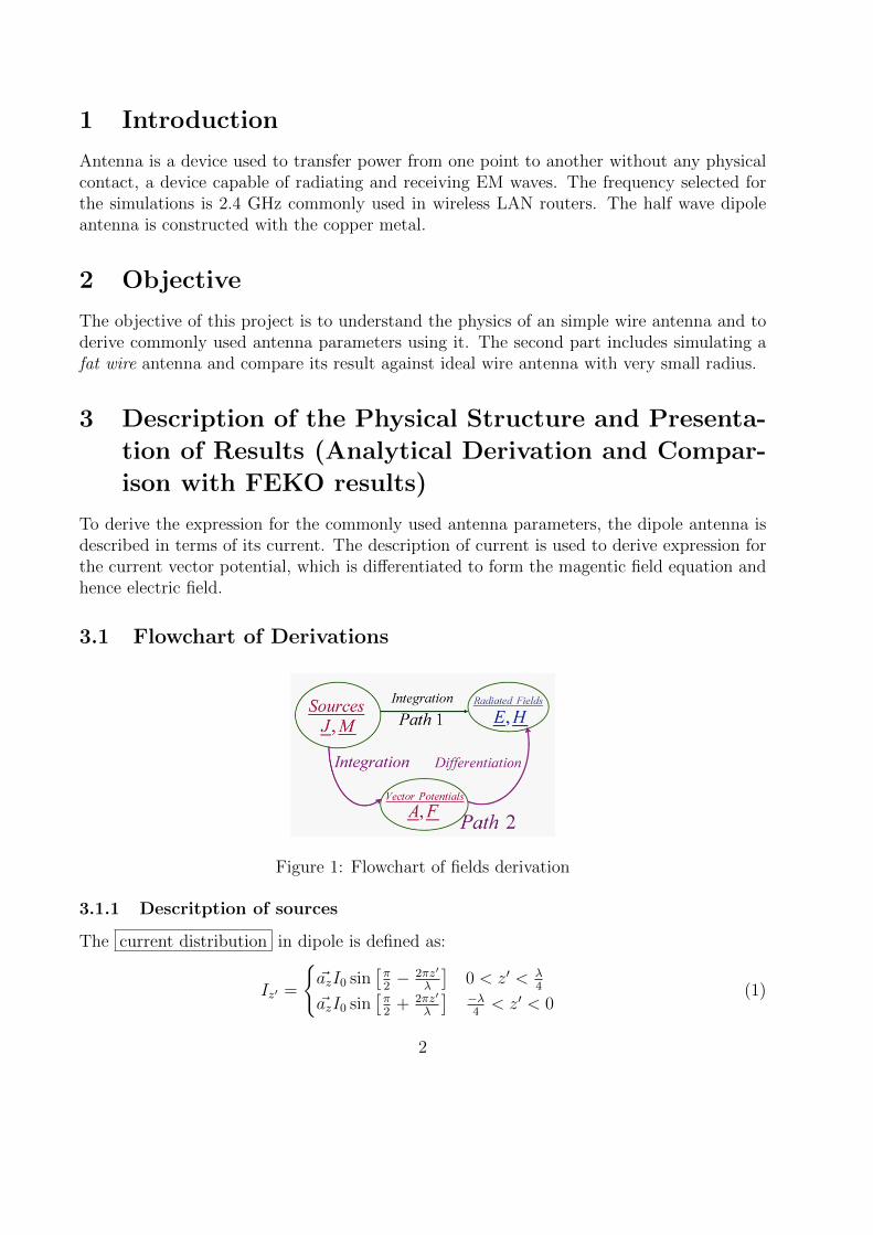
3.1 Flowchart of Derivations
Figure 1: Flowchart of fields derivation
3.1.1 Descritption of sources
The current distribution in dipole is defined as:
Iz′ =
~azI0 sin
[π2− 2πz′
λ
]0 < z′ < λ
4
~azI0 sin[π2
+ 2πz′
λ
] −λ4< z′ < 0
(1)
2
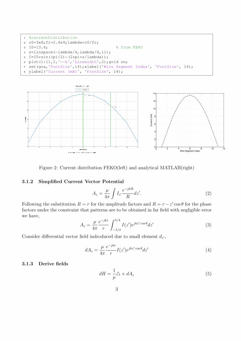
1 %currentDistribution2 c0=3e8;fr=2.4e9;lambda=c0/fr;3 I0=13.6; % from FEKO4 z=linspace(−lambda/4,lambda/4,11);5 I=I0*sin((pi/2)−(2*pi*z/lambda));6 plot(1:11,I,'−−k','Linewidth',2);grid on;7 set(gca,'FontSize',14);xlabel('Wire Segment Index', 'FontSize', 14);8 ylabel('Current (mA)', 'FontSize', 14);
0 2 4 6 8 10 120
2
4
6
8
10
12
14
Wire Segment IndexC
urr
en
t (m
A)
Figure 2: Current distribution FEKO(left) and analytical MATLAB(right)
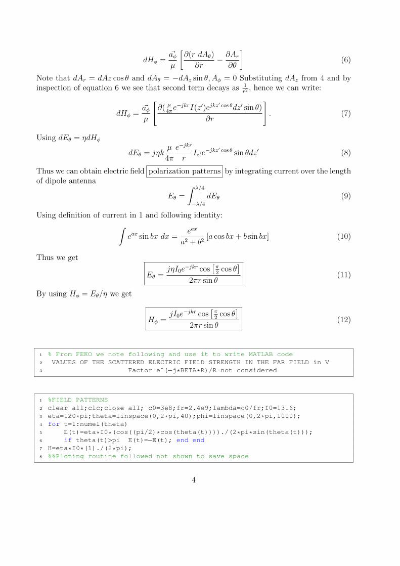
3.1.2 Simplified Current Vector Potential
Az =µ
4π
∫Iz′e−jkR
Rdz′. (2)
Following the substitution R = r for the amplitude factors and R = r−z′ cos θ for the phasefactors under the constraint that patterns are to be obtained in far field with negligible errorwe have,
Az =µ
4π
e−jkr
r
∫ λ/4
−λ/4I(z′)ejkz
′ cos θdz′ (3)
Consider differential vector field indroduced due to small element dz′ ,
dAz =µ
4π
e−jkr
rI(z′)ejkz
′ cos θdz′ (4)
3.1.3 Derive fields
dH =1
µ4× dAz (5)
3
dHφ =~aφµ
[∂(r dAθ)
∂r− ∂Ar
∂θ
](6)
Note that dAr = dAz cos θ and dAθ = −dAz sin θ, Aφ = 0 Substituting dAz from 4 and byinspection of equation 6 we see that second term decays as 1
r2, hence we can write:
dHφ =~aφµ
[∂( µ
4πe−jkrI(z′)ejkz
′ cos θdz′ sin θ)
∂r
]. (7)
Using dEθ = ηdHφ
dEθ = jηkµ
4π
e−jkr
rIz′e
−jkz′ cos θ sin θdz′ (8)
Thus we can obtain electric field polarization patterns by integrating current over the lengthof dipole antenna
Eθ =
∫ λ/4
−λ/4dEθ (9)
Using definition of current in 1 and following identity:∫eax sin bx dx =
eax
a2 + b2[a cos bx+ b sin bx] (10)
Thus we get
Eθ =jηI0e
−jkr cos[π2
cos θ]
2πr sin θ(11)
By using Hφ = Eθ/η we get
Hφ =jI0e
−jkr cos[π2
cos θ]
2πr sin θ(12)
1 % From FEKO we note following and use it to write MATLAB code2 VALUES OF THE SCATTERED ELECTRIC FIELD STRENGTH IN THE FAR FIELD in V3 Factor eˆ(−j*BETA*R)/R not considered
1 %FIELD PATTERNS2 clear all;clc;close all; c0=3e8;fr=2.4e9;lambda=c0/fr;I0=13.6;3 eta=120*pi;theta=linspace(0,2*pi,40);phi=linspace(0,2*pi,1000);4 for t=1:numel(theta)5 E(t)=eta*I0*(cos((pi/2)*cos(theta(t))))./(2*pi*sin(theta(t)));6 if theta(t)>pi E(t)=−E(t); end end7 H=eta*I0*(1)./(2*pi);8 %%Ploting routine followed not shown to save space
4
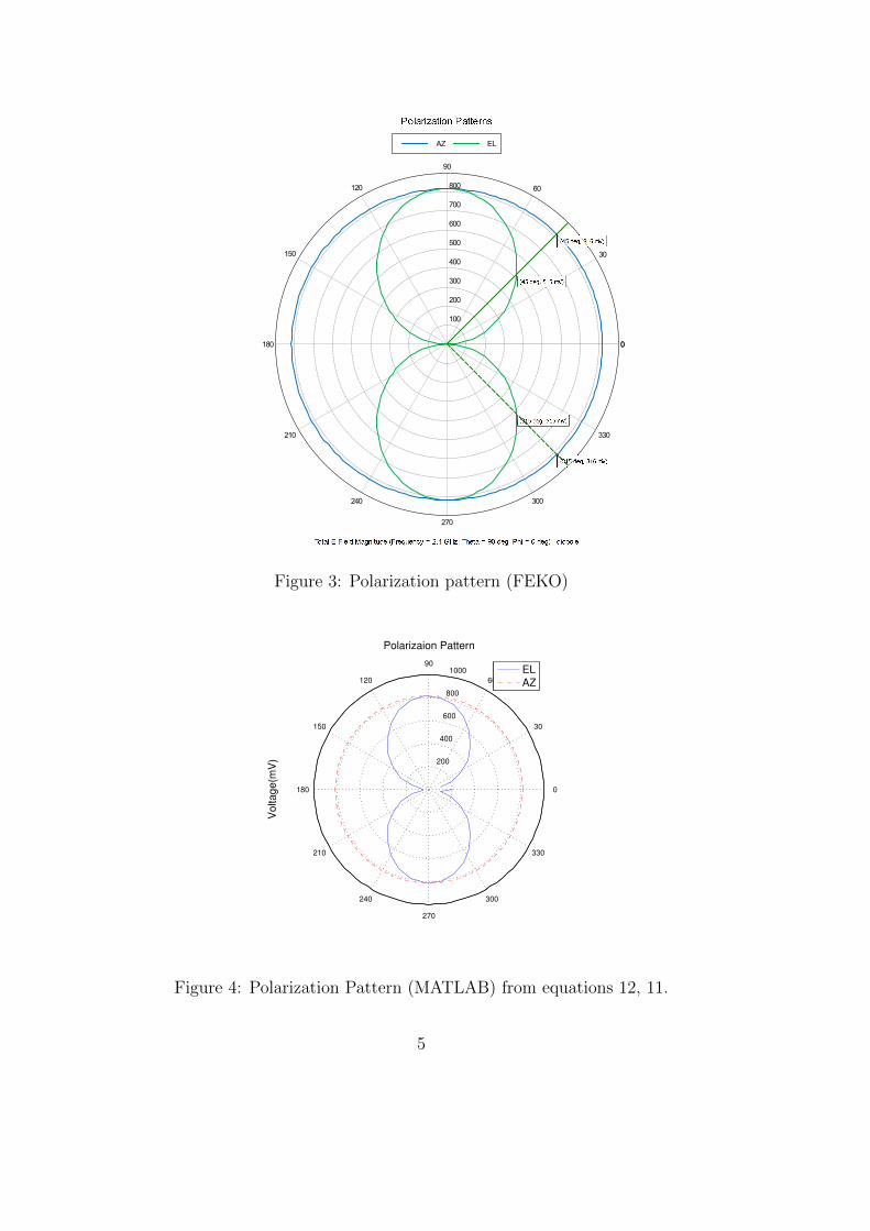
Figure 3: Polarization pattern (FEKO)
200
400
600
800
1000
30
210
60
240
90
270
120
300
150
330
180 0
Polarizaion Pattern
Vo
lta
ge
(mV
)
EL
AZ
Figure 4: Polarization Pattern (MATLAB) from equations 12, 11.
5
3.2 Derivation of other Antenna Parameters
3.2.1 Average Radiated Power Density
Wav =1
2[Eθ ×H∗φ] =
η
2|Eθ|2
=ηI20 cos2
[π2
cos θ]
8π2r2 sin2 θ(13)
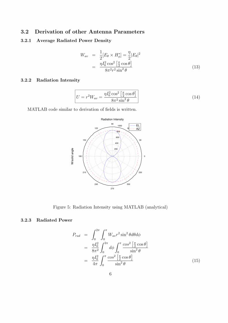
3.2.2 Radiation Intensity
U = r2Wav =ηI20 cos2
[π2
cos θ]
8π2 sin2 θ(14)
MATLAB code similar to derivation of fields is written.
200
400
600
800
1000
30
210
60
240
90
270
120
300
150
330
180 0
Radiation Intensity
W/s
olid
an
gle
EL
AZ
Figure 5: Radiation Intensity using MATLAB (analytical)
3.2.3 Radiated Power
Prad =
∫ 2π
0
∫ π
0
Wavr2 sin2 θdθdφ
=ηI208π2
∫ 2π
0
dφ
∫ π
0
cos2[π2
cos θ]
sin2 θ
=ηI204π
∫ π
0
cos2[π2
cos θ]
sin2 θ(15)
6
Using MATHEMATICA to evaluate integral
1 Integrate[Cos[Pi*Cos[x]/2]ˆ2/Sin[x], x, 0, Pi];2 N[1/2 (EulerGamma − CosIntegral[2 \[Pi]] + Log[2 \[Pi]])]
which when numerically simplified yields value 1.21883. Thus,
Prad =1.21883ηI20
4π(16)
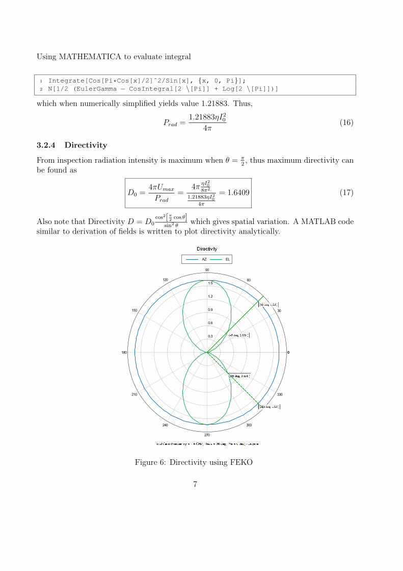
3.2.4 Directivity
From inspection radiation intensity is maximum when θ = π2, thus maximum directivity can
be found as
D0 =4πUmaxPrad
=4π
ηI208π2
1.21883ηI204π
= 1.6409 (17)
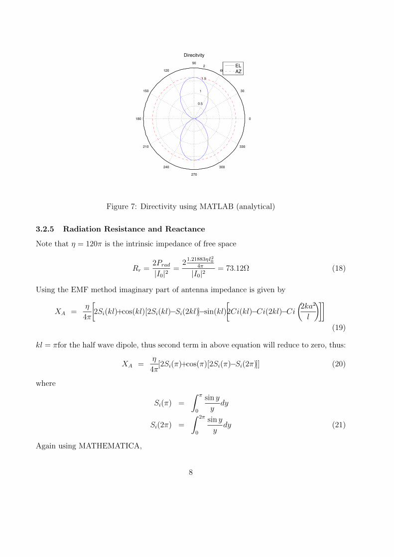
Also note that Directivity D = D0cos2[π2 cos θ]
sin2 θwhich gives spatial variation. A MATLAB code
similar to derivation of fields is written to plot directivity analytically.
Figure 6: Directivity using FEKO
7
0.5
1
1.5
2
30
210
60
240
90
270
120
300
150
330
180 0
Direcitvity
EL
AZ
Figure 7: Directivity using MATLAB (analytical)
3.2.5 Radiation Resistance and Reactance
Note that η = 120π is the intrinsic impedance of free space
Rr =2Prad|I0|2
=21.21883ηI20
4π
|I0|2= 73.12Ω (18)
Using the EMF method imaginary part of antenna impedance is given by
XA =η
4π
[2Si(kl)+cos(kl)[2Si(kl)−Si(2kl)]−sin(kl)
[2Ci(kl)−Ci(2kl)−Ci
(2ka2
l
)]](19)
kl = πfor the half wave dipole, thus second term in above equation will reduce to zero, thus:
XA =η
4π[2Si(π)+cos(π)[2Si(π)−Si(2π)]] (20)
where
Si(π) =
∫ π
0
sin y
ydy
Si(2π) =
∫ 2π
0
sin y
ydy (21)
Again using MATHEMATICA,
8
1 Integrate[Sin[x]/x, x, 0, Pi]2 SinIntegral[\[Pi]]=1.851943 Integrate[Sin[x]/x, x, 0, 2*Pi]4 SinIntegral[2\[Pi]]=1.41815
thus,
XA =η
4π[Si(2π)]]
XA =120π
4π[1.41815] = 42.51Ω (22)
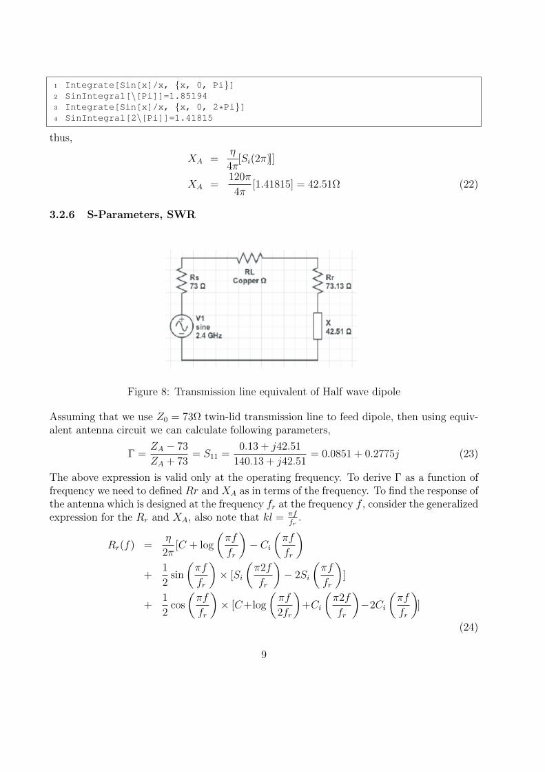
3.2.6 S-Parameters, SWR
Figure 8: Transmission line equivalent of Half wave dipole
Assuming that we use Z0 = 73Ω twin-lid transmission line to feed dipole, then using equiv-alent antenna circuit we can calculate following parameters,
Γ =ZA − 73
ZA + 73= S11 =
0.13 + j42.51
140.13 + j42.51= 0.0851 + 0.2775j (23)
The above expression is valid only at the operating frequency. To derive Γ as a function offrequency we need to defined Rr and XA as in terms of the frequency. To find the response ofthe antenna which is designed at the frequency fr at the frequency f , consider the generalizedexpression for the Rr and XA, also note that kl = πf
fr.
Rr(f) =η
2π[C + log
(πf
fr
)− Ci
(πf
fr
)+
1
2sin
(πf
fr
)× [Si
(π2f
fr
)− 2Si
(πf
fr
)]
+1
2cos
(πf
fr
)× [C+log
(πf
2fr
)+Ci
(π2f
fr
)−2Ci
(πf
fr
)]
(24)
9

Where C = 0.5772, Ci(x) =∫ x∞
cos yydy, Si(x) =
∫ x0
sin yydy Similarly,
XA(f) =η
4π[2Si
(πf
fr
)+ cos
(πf
fr
)[2Si
(πf
fr
)− Si
(2πf
fr
)]
− sin
(πf
fr
)[2Ci
(πf
fr
)−Ci
(2πf
fr
)−Ci
(4πffra
2
c2
)]] (25)
where a is radius of wire and c is speed of light Thus, ZA(f) = Rr(f) + XA(f) can be usedto find new reflection coefficient
Γ(f) =ZA(f)− 73
ZA(f) + 73= S11(f) (26)
V SWR(f) =1 + |Γ(f)|1− |Γ(f)|
(27)
MATLAB will be used to evaluated this values as follows:
1 clear all;clc;close all;jay=sqrt(−1);2 fr=2.4e9;f=1e9:0.02e9:5e9;3 %Radiaiton Resistance and XA calculation4 for k=1:numel(f)5 RadR(k)=radR(f(k),fr);6 end7 plot(f,RadR)grid on;hold on;set(gca,'FontSize',14);8 xlabel('frequency', 'FontSize', 14);ylabel('Impedance', 'FontSize', 14);9 for k=1:numel(f)
10 Xa(k)=xA(f(k),fr);11 end12 plot(f,Xa,'.−r')13 magZa=sqrt(Xa.ˆ2+RadR.ˆ2);plot(f,magZa,'−−k')14 legend('Radiation Resistance','Imaginary part of Impedance','Magnitude ...
Impedance')15
16 %S11 and SWR calculation17 Za= RadR + jay*Xa ;18 Gamma= (Za−73)./(Za+73);19 S11= 10*log10(abs(Gamma));20 figure;plot(f,S11,'k');grid on;set(gca,'FontSize',14);21 xlabel('frequency', 'FontSize', 14);ylabel('S11 (dB)', 'FontSize', 14);22
23 SWR=(1+ abs(Gamma))./(1−abs(Gamma));SWRdb=10*log10(SWR);24 figure;plot(f,SWRdb,'k');grid on;25 set(gca,'FontSize',14);xlabel('frequency', 'FontSize', 14);26 ylabel('SWR (dB)', 'FontSize', 14);
10
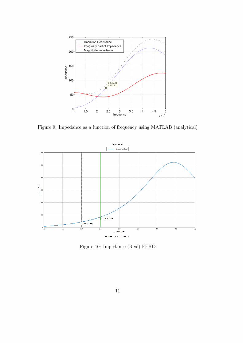
1 1.5 2 2.5 3 3.5 4 4.5 5
x 109
0
50
100
150
200
250
X: 2.4e+09Y: 73.13
frequency
Imp
ed
an
ce
Radiation Resistance
Imaginary part of Impedance
Magnitude Impedance
Figure 9: Impedance as a function of frequency using MATLAB (analytical)
l
ll
ll
ll
ll
ll
ll
_l _ _l _ _l _ _l _ _l
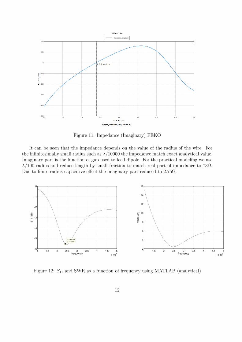
Figure 10: Impedance (Real) FEKO
11
cii
cii
cii
cyii
crii
i
rii
yii
r_i r_ y_i y_ _i _ _i _ _i
Figure 11: Impedance (Imaginary) FEKO
It can be seen that the impedance depends on the value of the radius of the wire. Forthe infinitesimally small radius such as λ/10000 the impedance match exact analytical value.Imaginary part is the function of gap used to feed dipole. For the practical modeling we useλ/100 radius and reduce length by small fraction to match real part of impedance to 73Ω.Due to finite radius capacitive effect the imaginary part reduced to 2.75Ω.
1 1.5 2 2.5 3 3.5 4 4.5 5
x 109
−6
−5
−4
−3
−2
−1
0
X: 2.4e+09Y: −5.536
frequency
S11 (
dB
)
1 1.5 2 2.5 3 3.5 4 4.5 5
x 109
2
4
6
8
10
12
14
16
frequency
SW
R (
dB
)
Figure 12: S11 and SWR as a function of frequency using MATLAB (analytical)
12
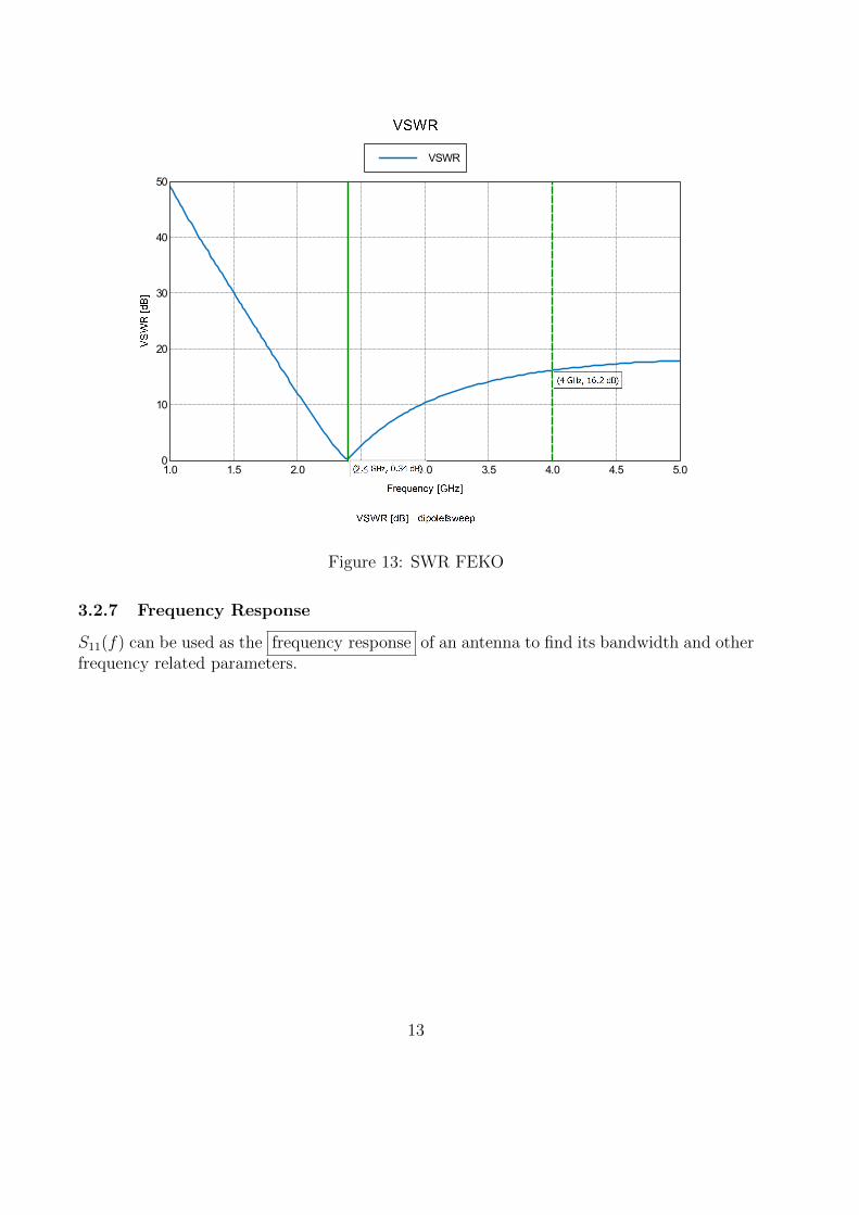
Figure 13: SWR FEKO
3.2.7 Frequency Response
S11(f) can be used as the frequency response of an antenna to find its bandwidth and otherfrequency related parameters.
13
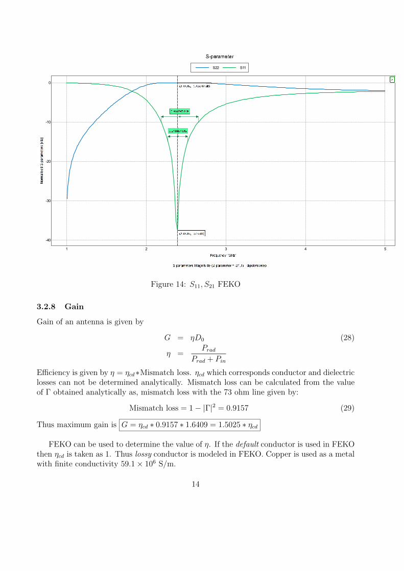
Figure 14: S11, S21 FEKO
3.2.8 Gain
Gain of an antenna is given by
G = ηD0 (28)
η =Prad
Prad + Pin
Efficiency is given by η = ηcd∗Mismatch loss. ηcd which corresponds conductor and dielectriclosses can not be determined analytically. Mismatch loss can be calculated from the valueof Γ obtained analytically as, mismatch loss with the 73 ohm line given by:
Mismatch loss = 1− |Γ|2 = 0.9157 (29)
Thus maximum gain is G = ηcd ∗ 0.9157 ∗ 1.6409 = 1.5025 ∗ ηcd
FEKO can be used to determine the value of η. If the default conductor is used in FEKOthen ηcd is taken as 1. Thus lossy conductor is modeled in FEKO. Copper is used as a metalwith finite conductivity 59.1× 10⁶ S/m.
14
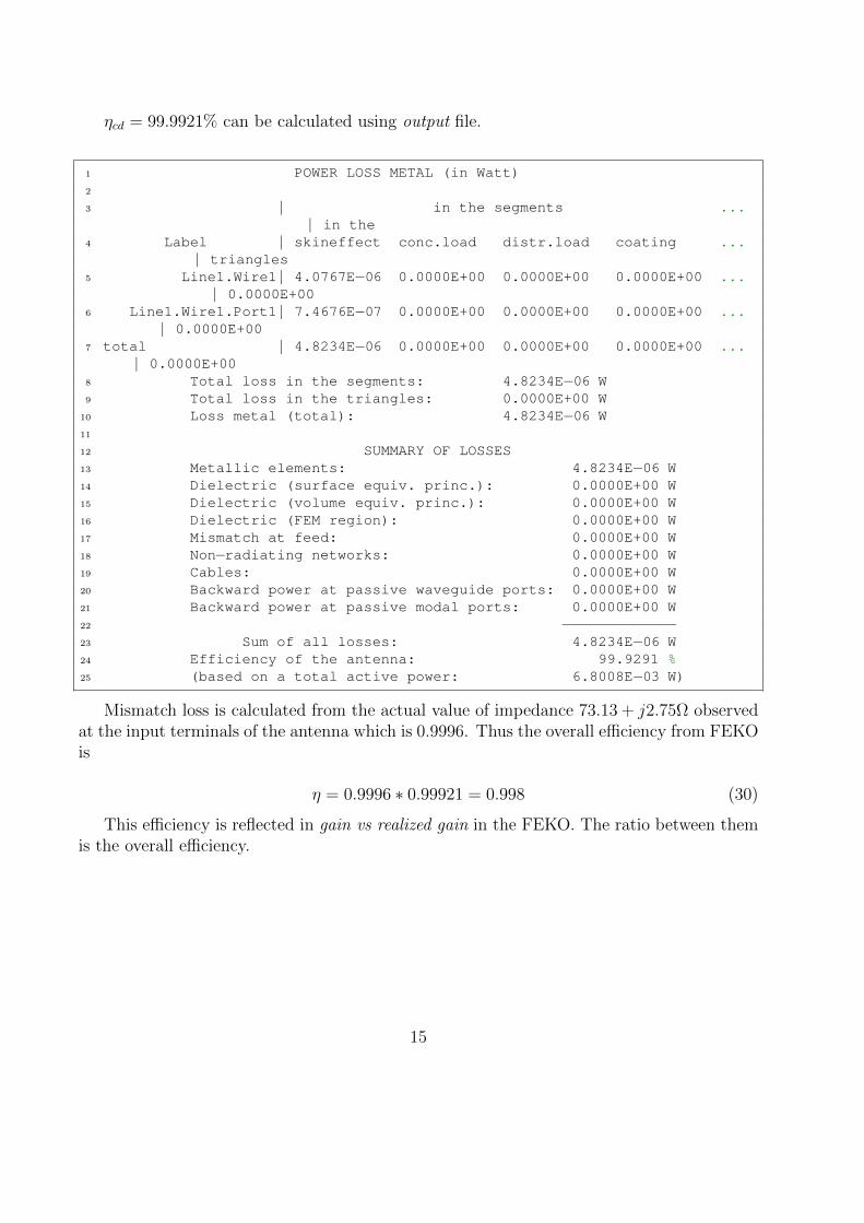
ηcd = 99.9921% can be calculated using output file.
1 POWER LOSS METAL (in Watt)2
3 | in the segments ...| in the
4 Label | skineffect conc.load distr.load coating ...| triangles
5 Line1.Wire1 | 4.0767E−06 0.0000E+00 0.0000E+00 0.0000E+00 ...| 0.0000E+00
6 Line1.Wire1.Port1 | 7.4676E−07 0.0000E+00 0.0000E+00 0.0000E+00 ...| 0.0000E+00
7 total | 4.8234E−06 0.0000E+00 0.0000E+00 0.0000E+00 ...| 0.0000E+00
8 Total loss in the segments: 4.8234E−06 W9 Total loss in the triangles: 0.0000E+00 W
10 Loss metal (total): 4.8234E−06 W11
12 SUMMARY OF LOSSES13 Metallic elements: 4.8234E−06 W14 Dielectric (surface equiv. princ.): 0.0000E+00 W15 Dielectric (volume equiv. princ.): 0.0000E+00 W16 Dielectric (FEM region): 0.0000E+00 W17 Mismatch at feed: 0.0000E+00 W18 Non−radiating networks: 0.0000E+00 W19 Cables: 0.0000E+00 W20 Backward power at passive waveguide ports: 0.0000E+00 W21 Backward power at passive modal ports: 0.0000E+00 W22 −−−−−−−−−−−−−23 Sum of all losses: 4.8234E−06 W24 Efficiency of the antenna: 99.9291 %25 (based on a total active power: 6.8008E−03 W)
Mismatch loss is calculated from the actual value of impedance 73.13 + j2.75Ω observedat the input terminals of the antenna which is 0.9996. Thus the overall efficiency from FEKOis
η = 0.9996 ∗ 0.99921 = 0.998 (30)
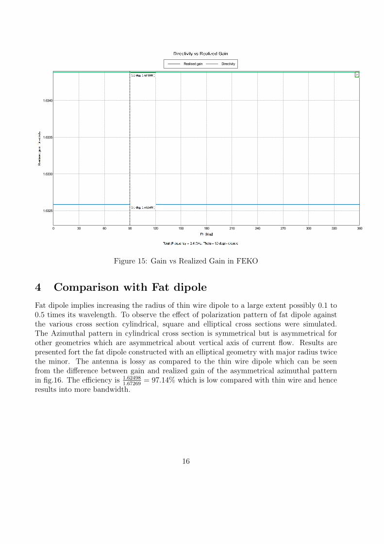
This efficiency is reflected in gain vs realized gain in the FEKO. The ratio between themis the overall efficiency.
15
gstDnc
gstDD
gstDDc
gstDr
D t gn gc gy ng nr nv D DD Dt
6
Figure 15: Gain vs Realized Gain in FEKO
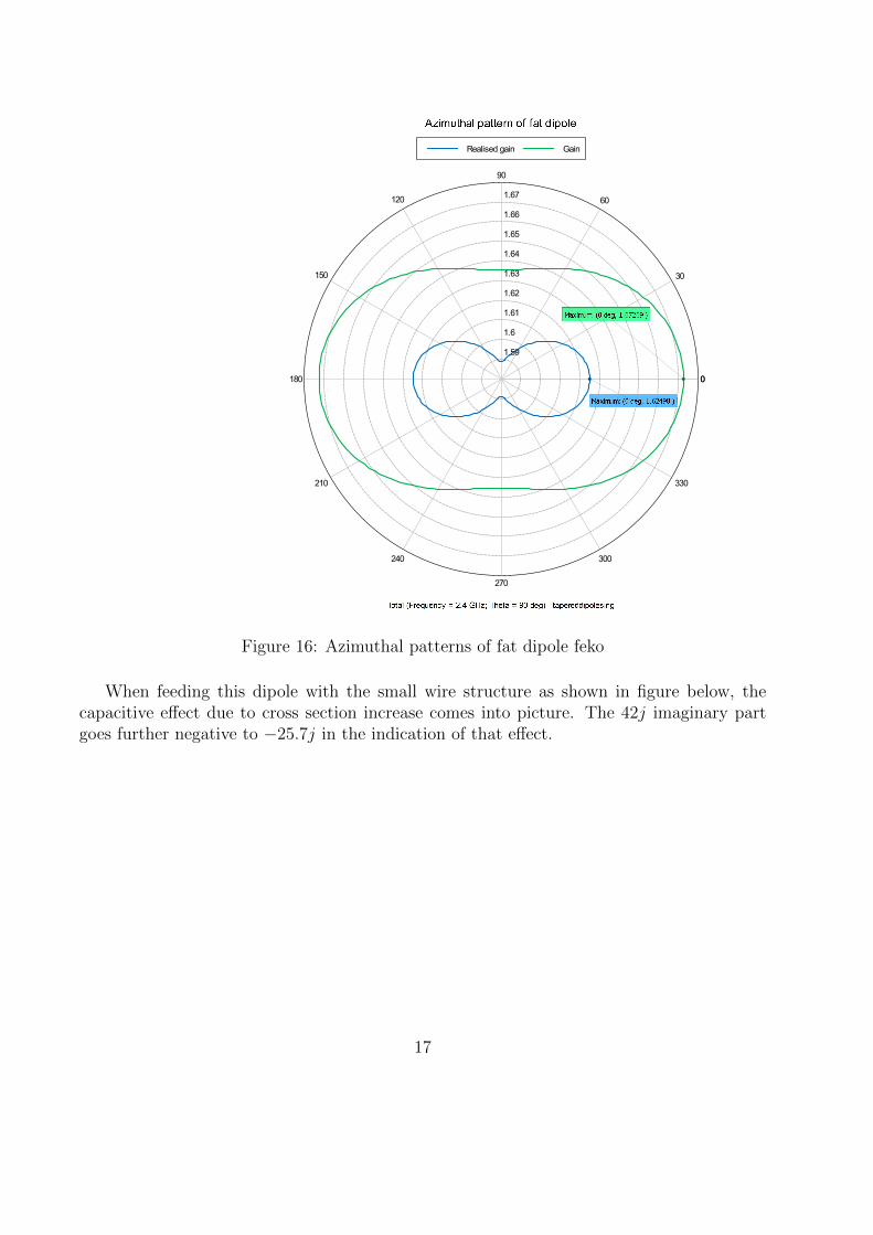
4 Comparison with Fat dipole
Fat dipole implies increasing the radius of thin wire dipole to a large extent possibly 0.1 to0.5 times its wavelength. To observe the effect of polarization pattern of fat dipole againstthe various cross section cylindrical, square and elliptical cross sections were simulated.The Azimuthal pattern in cylindrical cross section is symmetrical but is asymmetrical forother geometries which are asymmetrical about vertical axis of current flow. Results arepresented fort the fat dipole constructed with an elliptical geometry with major radius twicethe minor. The antenna is lossy as compared to the thin wire dipole which can be seenfrom the difference between gain and realized gain of the asymmetrical azimuthal patternin fig.16. The efficiency is 1.62498
1.67269= 97.14% which is low compared with thin wire and hence
results into more bandwidth.
16
gs
gs
gsg
gsn
gsG
gs
gs
gs
gs
G
gn
g
g
ng
n
n
G
GG
5
Figure 16: Azimuthal patterns of fat dipole feko
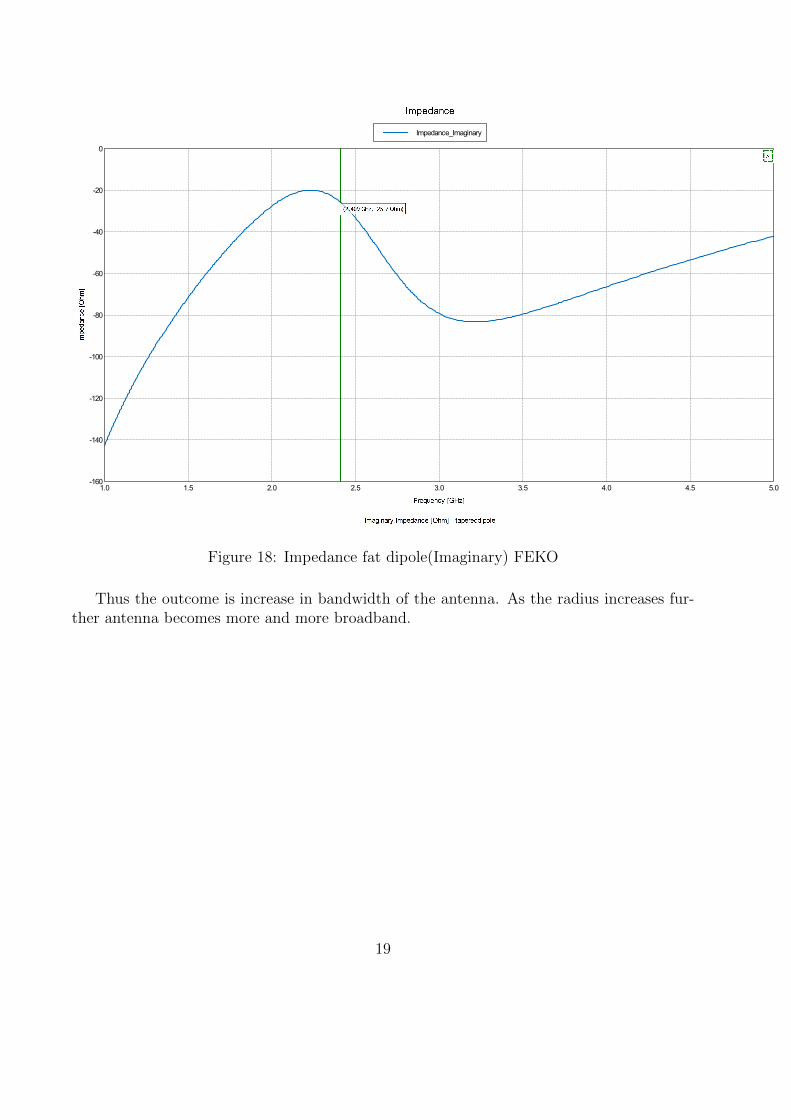
When feeding this dipole with the small wire structure as shown in figure below, thecapacitive effect due to cross section increase comes into picture. The 42j imaginary partgoes further negative to −25.7j in the indication of that effect.
17
p
dp
np
cp
p
p
p
p
p
p
dpp
dIp dI nIp nI cIp cI Ip I Ip
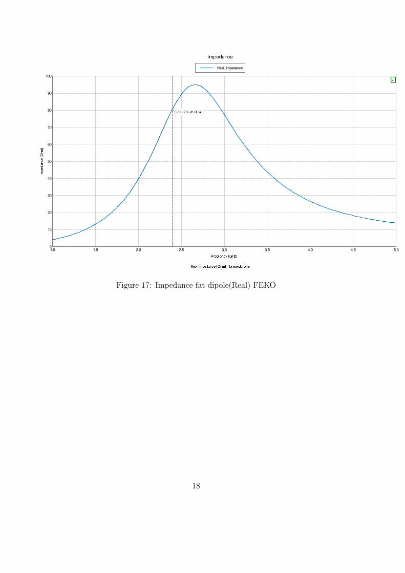
Figure 17: Impedance fat dipole(Real) FEKO
18
ag_
agy_
agi_
ag__
a_
a_
ay_
ai_
_
gn_ gn in_ in rn_ rn yn_ yn n_
Figure 18: Impedance fat dipole(Imaginary) FEKO
Thus the outcome is increase in bandwidth of the antenna. As the radius increases fur-ther antenna becomes more and more broadband.
19
m
m
m
m
m
m
e e e e e e e e e
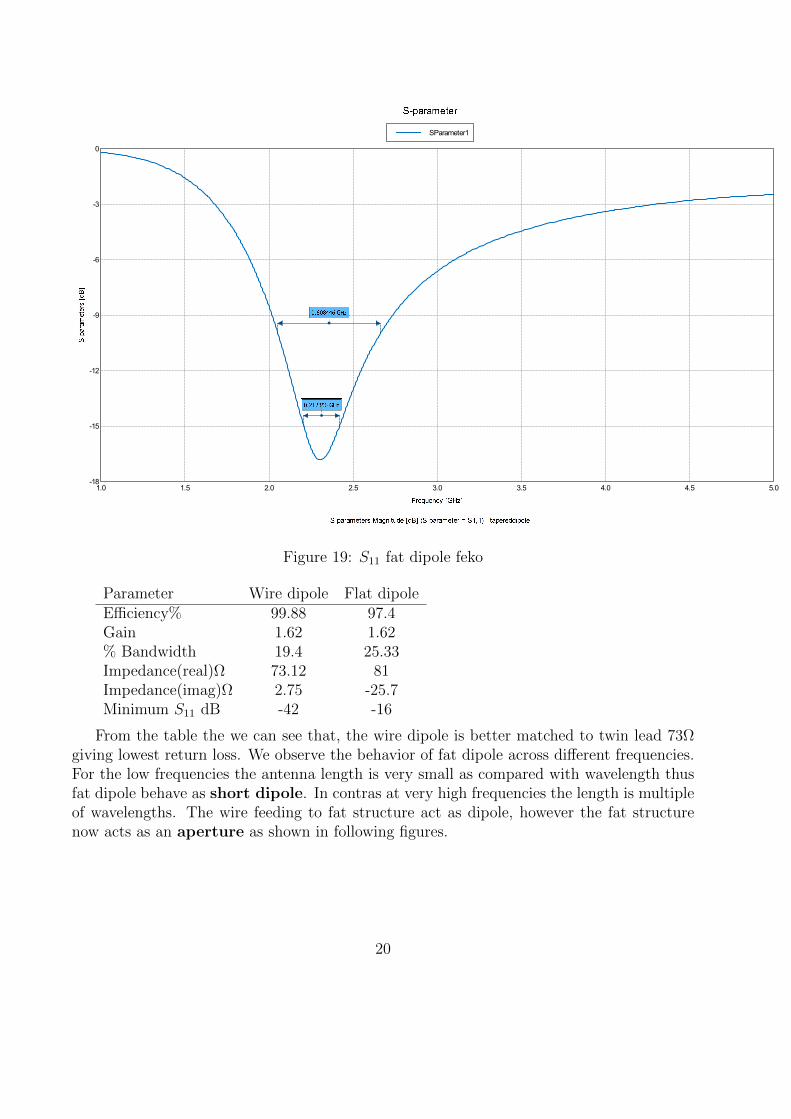
Figure 19: S11 fat dipole feko
Parameter Wire dipole Flat dipoleEfficiency% 99.88 97.4Gain 1.62 1.62% Bandwidth 19.4 25.33Impedance(real)Ω 73.12 81Impedance(imag)Ω 2.75 -25.7Minimum S11 dB -42 -16
From the table the we can see that, the wire dipole is better matched to twin lead 73Ωgiving lowest return loss. We observe the behavior of fat dipole across different frequencies.For the low frequencies the antenna length is very small as compared with wavelength thusfat dipole behave as short dipole. In contras at very high frequencies the length is multipleof wavelengths. The wire feeding to fat structure act as dipole, however the fat structurenow acts as an aperture as shown in following figures.
20

Figure 20: 3D pattern of fat dipole at low 600 MHz (left) and high 10GHz frequencies (right)
5 Summary and Conclusions
Analytical derivation of half wave dipole was done and the results were compared againstplots from EM simulation software FEKO. Copper with finite conductivity was used. TheFEKO software calculates losses in metal and the same due to mismatch and gives realizedantenna gain pattern taking them into consideration. Asymmetrical fat dipole yields asym-metrical azimuthal pattern due to asymmetrical currents. Also BW is increased when fatstructure is used as it is more lossy. At low frequencies fat dipole behave as short dipole andat high frequencies as an aperture antenna.
Bibliography
FEKO user manual, EM Software & Systems-S.A. (Pty) Ltd;
Constantine A. Balanis, (2012). Antenna Theory ; John Wiley & Sons.
http://www.understanding-copper.com online
21