ilyas thesis
TRANSCRIPT
QUANTUM DOTS IN PHOTONIC CRYSTALS: FROM
QUANTUM INFORMATION PROCESSING TO SINGLE PHOTON
NONLINEAR OPTICS
A DISSERTATION
SUBMITTED TO THE DEPARTMENT OF APPLIED PHYSICS
AND THE COMMITTEE ON GRADUATE STUDIES
OF STANFORD UNIVERSITY
IN PARTIAL FULFILLMENT OF THE REQUIREMENTS
FOR THE DEGREE OF
DOCTOR OF PHILOSOPHY
Ilya Fushman
December 2008

UMI Number: 3343582
INFORMATION TO USERS
The quality of this reproduction is dependent upon the quality of the copy
submitted. Broken or indistinct print, colored or poor quality illustrations and
photographs, print bleed-through, substandard margins, and improper
alignment can adversely affect reproduction.
In the unlikely event that the author did not send a complete manuscript
and there are missing pages, these will be noted. Also, if unauthorized
copyright material had to be removed, a note will indicate the deletion.
®
UMI UMI Microform 3343582
Copyright 2009 by ProQuest LLC.
All rights reserved. This microform edition is protected against
unauthorized copying under Title 17, United States Code.
ProQuest LLC 789 E. Eisenhower Parkway
PO Box 1346 Ann Arbor, Ml 48106-1346

© Copyright by Ilya Fushman 2009
All Rights Reserved

I certify that I have read this dissertation and that, in my opinion, it
is fully adequate in scope and quality as a dissertation for the degree
of Doctor of Philosophy.
(Jelena Vuckovic) Principal Adviser
I certify that I have read this dissertation and that, in my opinion, it
is fully adequate in scope and quality as a dissertation for the degree
of Doctor of Philosophy.
(David A.B. Miller)
I certify that I have read this dissertation and that, in my opinion, it
is fully adequate in scope and quality as a dissertation for the degree
of Doctor of Philosophy.
(Stephen E. Harris)
Approved for the University Committee on Graduate Studies.
hi
Abstract
Photons are attractive candidates for both quantum and classical information pro
cessing where they act as essential carriers of information and can greatly reduce the
operating power, respectively. Efficient photon routing and switching devices are re
quired for both applications, and necessitate the development of optical nonlinearities
that work at single photon-single emitter levels.
This work presents experimental and theoretical efforts toward the realization of
nonlinear optical devices that operate at low photon numbers and reach single photon
levels that are suitable for quantum information processing. We show that a single
quantum dot coupled to a photonic crystal cavity can be used to realize a controlled
phase gate between photons. In addition, this work also describes attempts at im
proving the operation of all-optical switches and modulators with the use of photonic
bandgap devices where the density of photon states is modified and tight photon con
finement leads to enhanced field strengths. We show that the combination of cavities
with standard nonlinearities can be used to realize fast optoelectronic modulators and
switches. Finally we review efforts to combine this photonic technology with novel
light emitters that operate at room temperature and have the potential to realize
functional and cost effective quantum information processing devices.
The main results of this work are the development of an experimental technique for
coherent probing of a quantum dot inside a photonic crystal cavity and the realization
of a controlled phase shift interaction between photons on the semiconductor chip
[1, 2]. This interaction is enabled by the nonlinearity of a single quantum dot that is
embedded in an optical microcavity.
IV
Acknowledgements
During my time at Stanford I had the pleasure of interacting and working together
with many inspirational people who have helped me grow as a scientist and human
being. In particular, I would like to thank my advisor Jelena Vuckovic for the support
and education she has provided throughout the years. Under her guidance, I was able
to explore many different topics and learn how to succeed and fail. I would also like to
thank my close friends, co-workers and collaborators Dirk Englund, Andrei Faraon,
and Edo Waks without whom the most exciting results would not be possible.
I would like to thank my oral and reading committee members, Professors Steve
Harris, David Miller, Steve Quake and David Goldhaber-Gordon. I would also like
to thank Prof. Harris and Prof. Miller for taking time to discuss academic questions
with me throughout my time at Stanford.
My time in the Vuckovic group greatly benefitted from the members Hatice Altug,
Maria Makarova, Bryan Ellis, Yiyang Gong, Kelley Rivoire, Arka Majumdar and Jesse
Lu.
I would like to thank Prof. Vanessa Sih for her help with developing electrical
contacts and teaching me about electron spins in quantum dots.
Throughout my time at Stanford I benefitted from many discussions with Ofer
Levi and Michelle Povinelli, as well as Shanhui Fan, and members of the Yamamoto
Group: David Fattal, Thaddeus Ladd, Kai-Mei Fu, Chales Santori, David Press,
Na-Young Kim.
In my last year at Stanford, I had the opportunity to work with Tornas Sarmiento
in Prof. James Harris' group. I would like to thank both Tomas and Prof. Harris for
teaching me about semiconductor optoelectronic devices and semiconductor growth.
v

Finally I would like to thank my mother Dina and my father David, who made
everything possible in my life. This thesis is dedicated to you.
VI
Contents
Abstract iv
Acknowledgements v
1 Introduction 1
1.1 Overview 1
1.2 Quantum dots 3
1.3 Photonic crystal cavities 3
1.4 Interaction between coherent light and a quantum dot in a photonic
crystal cavity 6
1.4.1 Weak coupling regime 8
1.4.2 Strong coupling regime 9
1.4.3 Transmission of light through the cavity: weak and strong cou
pling regime 10
1.4.4 How a cavity-QD system can be used for quantum information
processing? 12
1.5 Brief introduction to quantum information processing 14
1.5.1 Encoding information in photon states 16
1.5.2 Quantum operations on photons 17
2 Photonic Crystal Cavity Design 20
2.1 Introduction 20
2.2 A simple look at photonic crystal design 21
2.3 Numerical solution methods 22
vn
2.4 Bloch modes, reciprocal space and cavities 24
2.5 Inverse Approach 26
2.5.1 Simplified relation between Q of a cavity mode and its k-space
Distribution 27
2.5.2 Optimal k-space distribution 30
2.5.3 Inverse problem approach to designing PC cavities 33
2.5.4 General trend of Q/V 33
2.5.5 Estimating Photonic Crystal Design from /c-space Field Distri
bution 35
2.6 Genetic Algorithms 41
2.6.1 Algorithm description 42
2.6.2 Algorithm implementation 42
2.6.3 Simulation results: Optimizing planar photonic cavity cavities 44
2.7 Conclusions 45
3 Optical nonlinearities in PC waveguides 48
3.1 Introduction 48
3.2 QND photon detection with Kerr nonlinearities 49
3.3 Pulse Propagation in PC Waveguides 53
3.4 Nonlinear Phase Shift 57
3.5 Conclusion 59
4 Nonlienarities for QIP 61
4.1 Introduction 61
4.2 Measurement description 62
4.3 Coherent probing of a cavity-QD system 62
4.4 Phase measurement 65
4.5 Controlling the phase 70
4.5.1 Control and signal beams at the same wavelength (Acontr.0/ =
^signal) • *-*
4.5.2 Control and signal beams at different wavelengths (\c<mtroi ¥"
•^signal) '^
Vlll
4.6 Conclusion 76
5 Towards room temperature cavity-QED 80
5.1 Introduction 80
5.2 Room temperature operation 81
5.3 Conclusion 87
6 Ultra Fast Modulation 88
6.1 Introduction 88
6.2 Free Carrier Tuning 90
6.3 Thermal Tuning 93
6.4 Conclusion 95
7 Fabrication 98
7.1 Introduction 98
7.2 PC fabrication 99
7.2.1 Sample preparation 100
7.2.2 Cleaving 101
7.2.3 Exposure 101
7.2.4 Development 101
7.2.5 Etching 101
7.2.6 Undercut 102
7.2.7 Wet Oxidation 103
7.2.8 Wet Oxidation Undercut 103
7.3 PMMA doped with colloidal QDs 103
7.3.1 PMMA 103
7.3.2 Dissolving QDs in PMMA 103
7.4 PC laser/detector and electrical contact fabrication 104
7.4.1 Wafer design 105
7.4.2 Mask design 105
7.4.3 Lithography process 107
7.4.4 Wet Etch 109
IX
7.4.5 Metal contacts 110
7.4.6 Electrical isolation by resist I l l
7.4.7 Device fabrication flow 112
8 Conclusion and Future Directions 113
8.1 Cavity QED and quantum information processing 113
8.2 Classical Information Processing 115
A Equivalence between the CNOT and CZ gate 116
B Derivation of Cavity Radiative Loss 118
C Pulses in a nonlinear PC waveguide 121
C.0.1 Derivation of the propagation equations 121
D Cavity QED Experiment and Derivations 128
D.l Experimental setup 128
D.2 Quantum dot visibility 129
D.3 Quantum dot saturation 129
D.4 Amplitude and phase of the interference signal 130
D.5 Computational model 132
Bibliography 135
x

List of Tables
2.1 Q values of structures derived with inverse-approach 1 39
3.1 values for coupling 7 for different modes of the waveguide in units of
a'2, and mode volumes for each unit cell of the waveguide (in units of
a - 3 ) . 1 and 2 refer to the first and second modes of the waveguide. . 56
4.1 Nonlinear parameters and phase modulation derived from experimental
data for the strongly (first row) and weakly (second row) coupled QDs.
A(f) is a maximum differential phase shift (A</>=<̂ >(nc)-</>(0)) which is
achieved at the intra-cavity photon number nc in the last column. . . 76
7.1 Pquest etch recipe for GaAs membranes with thickness up to 200 nm. 102
XI
List of Figures
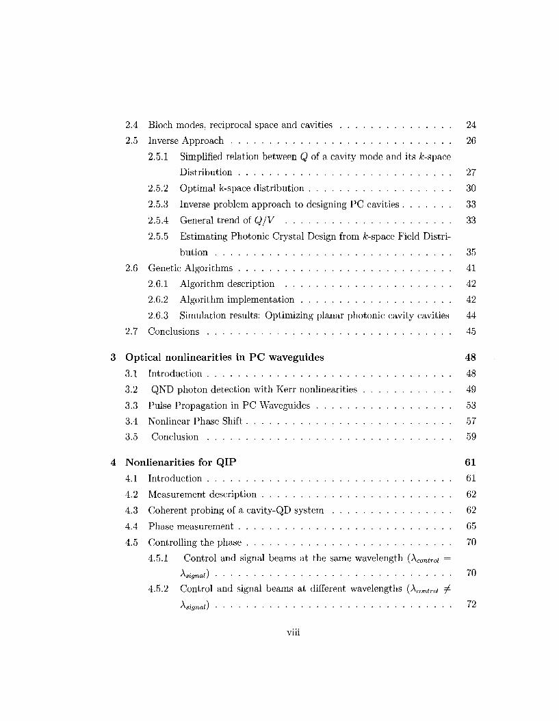
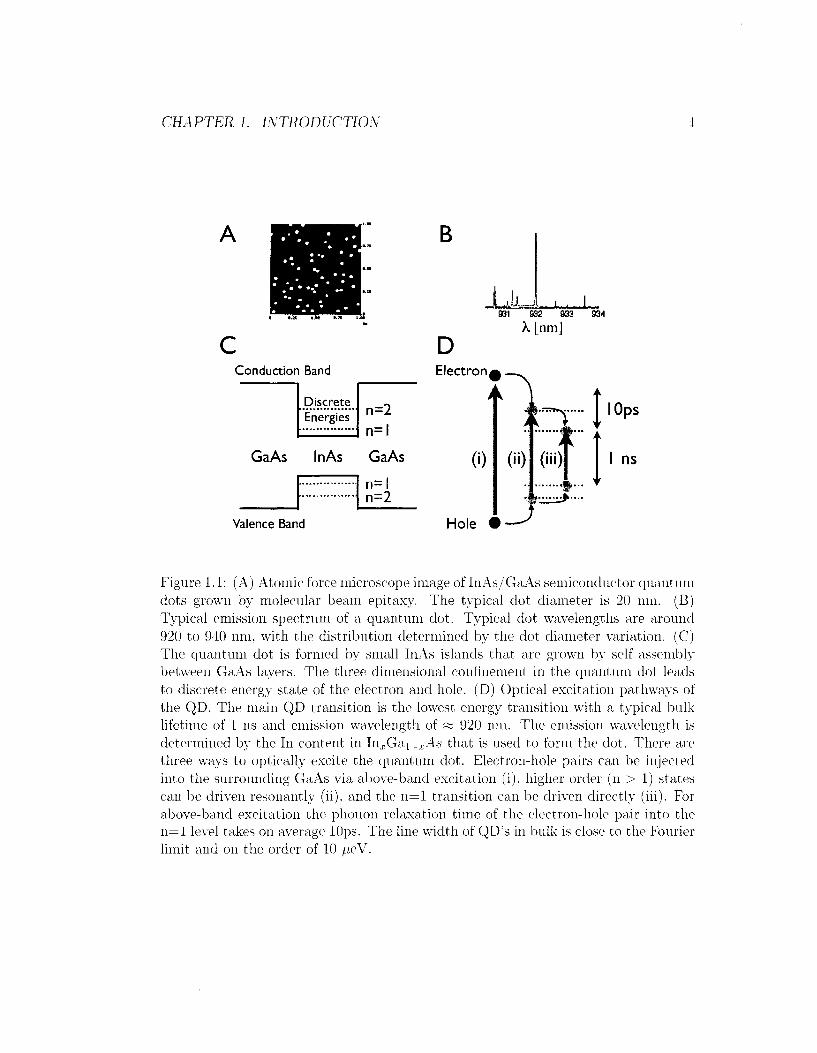
1.1 (A) Atomic force microscope image of InAs/GaAs semiconductor quan
tum dots grown by molecular beam epitaxy. The typical dot diameter
is 20 nm. (B) Typical emission spectrum of a quantum dot. Typi
cal dot wavelengths are around 920 to 940 nm, with the distribution
determined by the dot diameter variation. (C) The quantum dot is
formed by small InAs islands that are grown by self assembly between
GaAs layers. The three dimensional confinement in the quantum dot
leads to discrete energy state of the electron and hole. (D) Optical
excitation pathways of the QD. The main QD transition is the low
est energy transition with a typical bulk lifetime of 1 ns and emission
wavelength of ~ 920 nm. The emission wavelength is determined by
the In content in InxGsLi_xAs that is used to form the dot. There are
three ways to optically excite the quantum dot. Electron-hole pairs
can be injected into the surrounding GaAs via above-band excitation
(i), higher order (n > 1) states can be driven resonantly (ii), and the
n = l transition can be driven directly (iii). For above-band excitation
the phonon relaxation time of the electron-hole pair into the n = l level
takes on average lOps. The line width of QD's in bulk is close to the
Fourier limit and on the order of 10 /xeV 4
xn
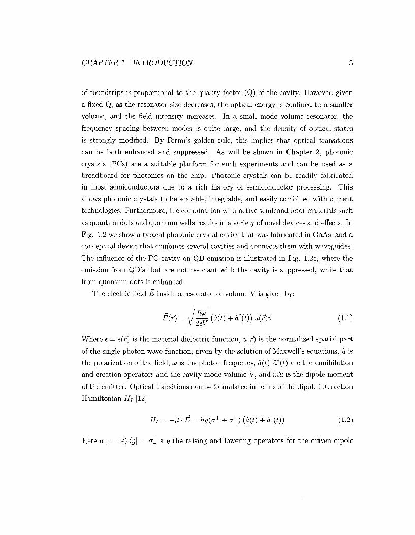
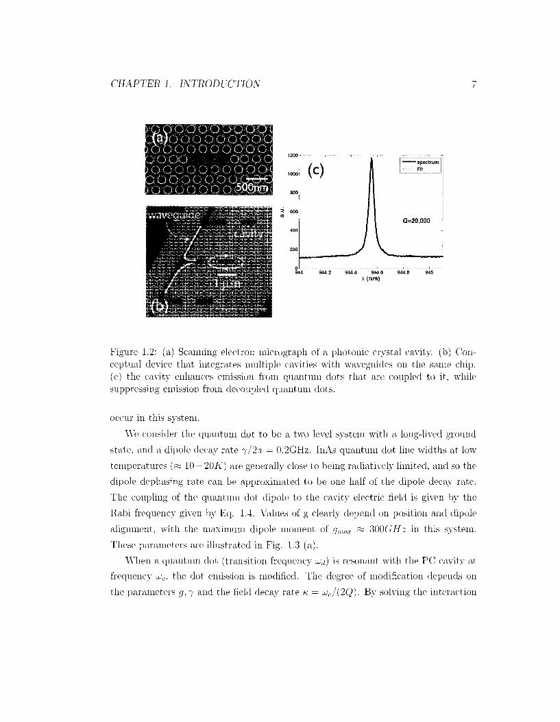
2 (a) Scanning electron micrograph of a photonic crystal cavity, (b)
Conceptual device that integrates multiple cavities with waveguides
on the same chip, (c) the cavity enhances emission from quantum
dots that are coupled to it, while suppressing emission from decoupled
quantum dots 7
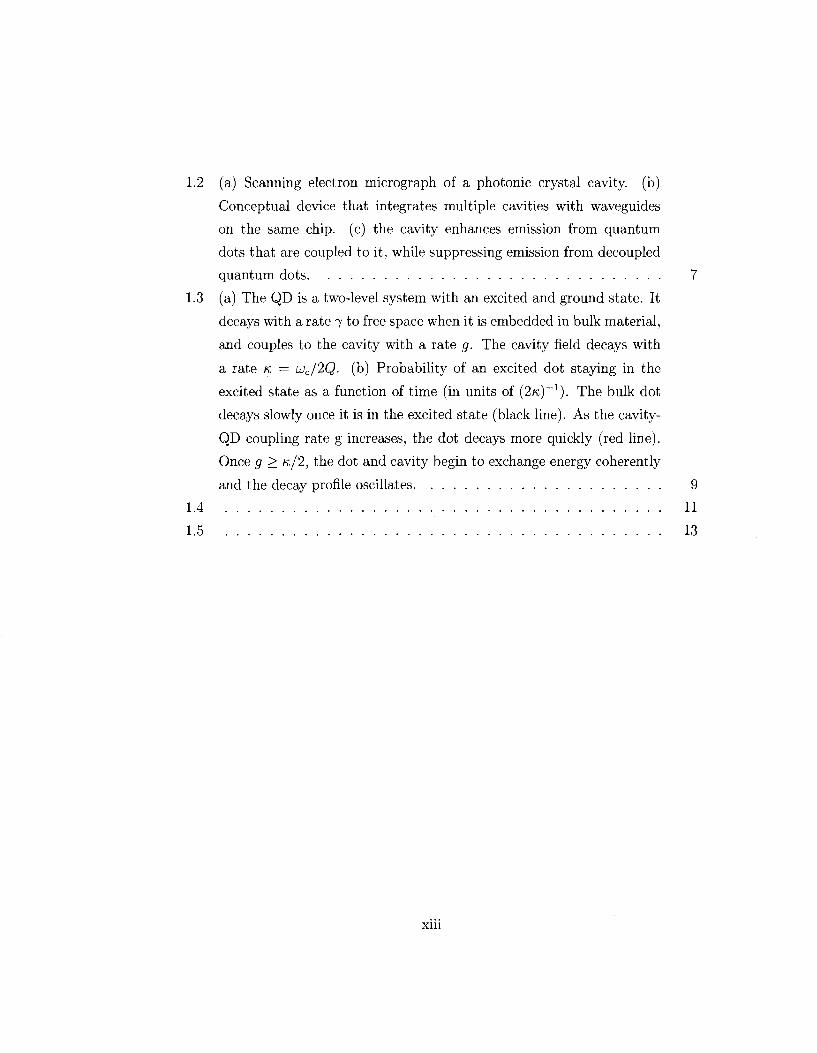
3 (a) The QD is a two-level system with an excited and ground state. It
decays with a rate 7 to free space when it is embedded in bulk material,
and couples to the cavity with a rate g. The cavity field decays with
a rate K — UJC/2Q. (b) Probability of an excited dot staying in the
excited state as a function of time (in units of (2K) _ 1 ) . The bulk dot
decays slowly once it is in the excited state (black line). As the cavity-
QD coupling rate g increases, the dot decays more quickly (red line).
Once g > K /2 , the dot and cavity begin to exchange energy coherently
and the decay profile oscillates 9
4 11
5 13
xin
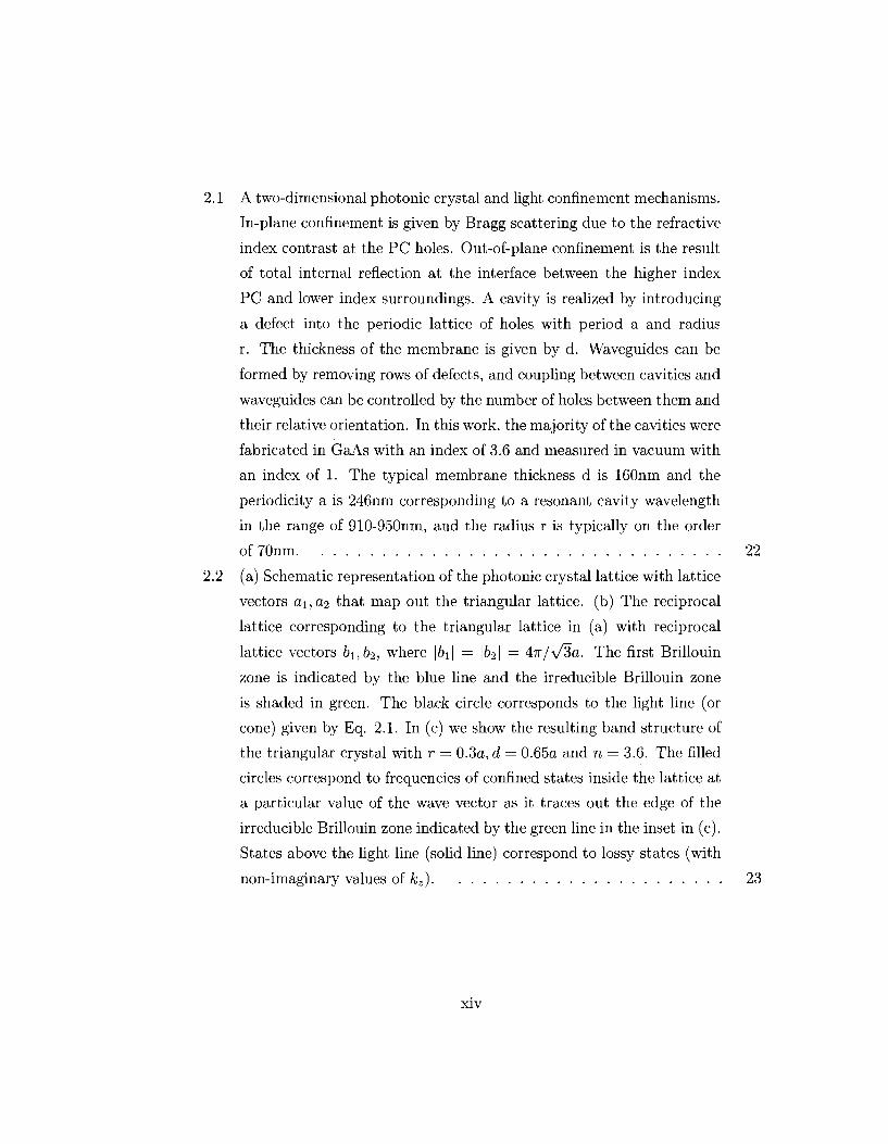
A two-dimensional photonic crystal and light confinement mechanisms.
In-plane confinement is given by Bragg scattering due to the refractive
index contrast at the PC holes. Out-of-plane confinement is the result
of total internal reflection at the interface between the higher index
PC and lower index surroundings. A cavity is realized by introducing
a defect into the periodic lattice of holes with period a and radius
r. The thickness of the membrane is given by d. Waveguides can be
formed by removing rows of defects, and coupling between cavities and
waveguides can be controlled by the number of holes between them and
their relative orientation. In this work, the majority of the cavities were
fabricated in GaAs with an index of 3.6 and measured in vacuum with
an index of 1. The typical membrane thickness d is 160nm and the
periodicity a is 246nm corresponding to a resonant cavity wavelength
in the range of 910-950nm, and the radius r is typically on the order
of 70nm
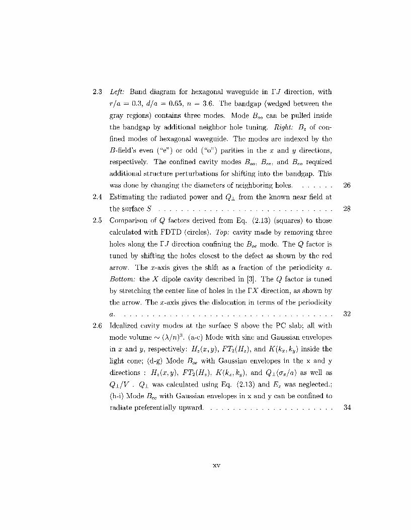
(a) Schematic representation of the photonic crystal lattice with lattice
vectors a,i,a,2 that map out the triangular lattice, (b) The reciprocal
lattice corresponding to the triangular lattice in (a) with reciprocal
lattice vectors 61,62, where |6i| = |62| = 4ir/\/3a. The first Brillouin
zone is indicated by the blue line and the irreducible Brillouin zone
is shaded in green. The black circle corresponds to the light line (or
cone) given by Eq. 2.1. In (c) we show the resulting band structure of
the triangular crystal with r = 0.3a, d = 0.65a and n = 3.6. The filled
circles correspond to frequencies of confined states inside the lattice at
a particular value of the wave vector as it traces out the edge of the
irreducible Brillouin zone indicated by the green line in the inset in (c).
States above the light line (solid line) correspond to lossy states (with
non-imaginary values of kz)
xiv
3 Left: Band diagram for hexagonal waveguide in TJ direction, with
r/a = 0.3, d/a = 0.65, n = 3.6. The bandgap (wedged between the
gray regions) contains three modes. Mode B00 can be pulled inside
the bandgap by additional neighbor hole tuning. Right: Bz of con
fined modes of hexagonal waveguide. The modes are indexed by the
5-field's even ("e") or odd ("o") parities in the x and y directions,
respectively. The confined cavity modes B00, Bee, and Beo required
additional structure perturbations for shifting into the bandgap. This
was done by changing the diameters of neighboring holes 26
4 Estimating the radiated power and Q± from the known near field at
the surface S 28
5 Comparison of Q factors derived from Eq. (2.13) (squares) to those
calculated with FDTD (circles). Top: cavity made by removing three
holes along the TJ direction confining the Boe mode. The Q factor is
tuned by shifting the holes closest to the defect as shown by the red
arrow. The x-axis gives the shift as a fraction of the periodicity a.
Bottom: the X dipole cavity described in [3]. The Q factor is tuned
by stretching the center line of holes in the TX direction, as shown by
the arrow. The rr-axis gives the dislocation in terms of the periodicity
6 Idealized cavity modes at the surface S above the PC slab; all with
mode volume ~ (A/n)3. (a-c) Mode with sine and Gaussian envelopes
in x and y, respectively: Hz(x,y), FT2(i/z), and K(kx,ky) inside the
light cone; (d-g) Mode Boe with Gaussian envelopes in the x and y
directions : Hz(x,y), FT2(HZ), K(kx,ky), and Q±(o-x/a) as well as
Q±/V . Qj_ was calculated using Eq. (2.13) and Ez was neglected.;
(h-i) Mode Bee with Gaussian envelopes in x and y can be confined to
radiate preferentially upward 34
xv
FDTD simulations for the derived Gaussian cavity (a-c) and the de
rived sine cavity (d-f). Gaussian: (a) Bz\ (b) \E\; (c) FT pattern of
Bz taken above the PC slab (blue) and target pattern (red). Sine: (d)
Bz; (e) \E\; (f) FT pattern of Bz taken above the PC slab (blue) and
target pattern (red) (The target FT for the sine cavity appears jagged
due to sampling, since the function was expressed with the resolution
of the simulations). The cavities were simulated with a discretiza
tion of 20 points per period a, PC slab hole radius r — 0.3a, slab
thickness of 0.6a and refractive index 3.6. Starting at the center, the
defect hole radii in units of periodicity a are: (0,0,0.025,0.05,0.075,0.1
, 0.075, 0.075,0.1,0.125,0.125,0.125,0.1,0.125,0.15,0.3,0.3) for the sine
cavity, and (0.025,0.025,0.05,0.1,0.225) for the Gaussian cavity. . . .
Top-left: Real-space mode profile after optimizing for closest-match to
a sine-envelope target mode. Top-right: k-space mode profile of the
optimized simulated mode and a sine-envelope target mode. Bottom:
Real-space and k-space mode profiles for matching against a sinc2-
envelope target mode. All: Red curves represent the real-space (k-
space) mode profiles of the optimized fields, blue curves represents the
real-space (k-space) mode profiles of the target fields
The setup for QND detection of a signal beam with average expected
photon number Ns and phase <j>3ig. The probe is split on the 50/50
beamsplitter BS into two beams with photon numbers Np and phases
<f>probe- The mirrors Mi and M2 pass the signal and reflect the probe
with negligible losses. The two beams co-propagate in one arm of
the interferometer through a PC waveguide made in a medium with a
large Kerr nonlinearity (x(3)). The signal Ns is unmodified and only
the phase is distorted to <p'sig. The probe photon number is preserved,
but the phase is modified to 4>probe — 4>probe oc Na. The probe phase
rotation 4>Wobe ~~ 4>probe is detected by a homodyne measurement on
detectors Dt, D2 and yields the photon number Na
xvi
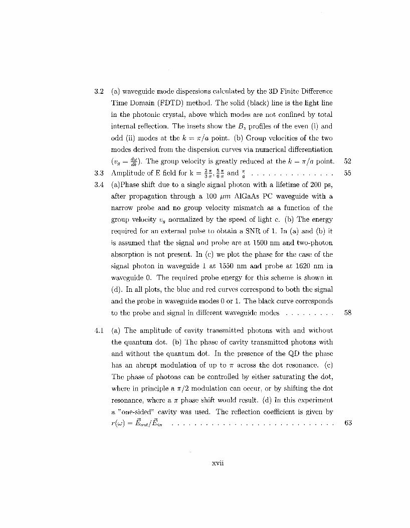
2 (a) waveguide mode dispersions calculated by the 3D Finite Difference
Time Domain (FDTD) method. The solid (black) line is the light line
in the photonic crystal, above which modes are not confined by total
internal reflection. The insets show the Bz profiles of the even (i) and
odd (ii) modes at the k = n/a point, (b) Group velocities of the two
modes derived from the dispersion curves via numerical differentiation
(vg — g|). The group velocity is greatly reduced at the k — ir/a point. 52
3 Amplitude of E field for k = \\, | f and \ 55
4 (a)Phase shift due to a single signal photon with a lifetime of 200 ps,
after propagation through a 100 \±m AlGaAs PC waveguide with a
narrow probe and no group velocity mismatch as a function of the
group velocity vg normalized by the speed of light c. (b) The energy
required for an external pulse to obtain a SNR of 1. In (a) and (b) it
is assumed that the signal and probe are at 1500 nm and two-photon
absorption is not present. In (c) we plot the phase for the case of the
signal photon in waveguide 1 at 1550 nm and probe at 1620 nm in
waveguide 0. The required probe energy for this scheme is shown in
(d). In all plots, the blue and red curves correspond to both the signal
and the probe in waveguide modes 0 or 1. The black curve corresponds
to the probe and signal in different waveguide modes 58
1 (a) The amplitude of cavity transmitted photons with and without
the quantum dot. (b) The phase of cavity transmitted photons with
and without the quantum dot. In the presence of the QD the phase
has an abrupt modulation of up to n across the dot resonance, (c)
The phase of photons can be controlled by either saturating the dot,
where in principle a 7r/2 modulation can occur, or by shifting the dot
resonance, where a IT phase shift would result, (d) In this experiment
a "one-sided" cavity was used. The reflection coefficient is given by
r(uj) = Eout/Ein 63
xvn
2 A cross polarization setup is used to reject direct laser scatter from the
sample and collect only cavity-coupled photons. Instead of tuning the
probing laser, the cavity and QD wavelength are shifted with temper
ature by heating a "heating pad" with a 980 nm laser that does not
excite carriers in GaAs and the QD. The QD shifts « 3 — 4 times faster
than the cavity as detailed in [4]. The temperature is varied period
ically between 20K and 27K and the amplitude of the cavity-coupled
probing beam is collected on the spectrometer 64
3 66
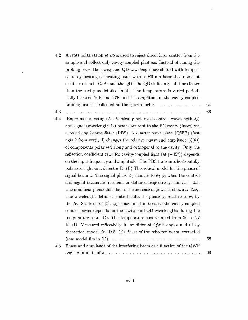
4 Experimental setup (A). Vertically polarized control (wavelength Ac)
and signal (wavelength \s) beams are sent to the PC cavity (Inset) via
a polarizing beamsplitter (PBS). A quarter wave plate (QWP) (fast
axis 9 from vertical) changes the relative phase and amplitude (£(#))
of components polarized along and orthogonal to the cavity. Only the
reflection coefficient r(uj) for cavity-coupled light (at |—45°)) depends
on the input frequency and amplitude. The PBS transmits horizontally
polarized light to a detector D. (B) Theoretical model for the phase of
signal beam 0. The signal phase 0i changes to 02,03 when the control
and signal beams are resonant or detuned respectively, and nc = 0.3.
The nonlinear phase shift due to the increase in power is shown as A0i.
The wavelength detuned control shifts the phase 03 relative to 0i by
the AC Stark effect [5]. 03 is asymmetric because the cavity-coupled
control power depends on the cavity and QD wavelengths during the
temperature scan (C). The temperature was scanned from 20 to 27
K. (D) Measured reflectivity R for different QWP angles and fit by
theoretical model Eq. D.8. (E) Phase of the reflected beam, extracted
from model fits in (D) 68
5 Phase and amplitude of the interfering beam as a function of the QWP
angle 9 in units of 7T 69
xvni
4.6 A. Is(u) taken for several values of 9. Interference between the refer
ence beam and cavity coupled beam are clearly visible. B. Extracted
amplitude |r(u;)| and phase arctan(Im(r(uj))/Re(r{ui))) of the cavity
reflection coefficient 69
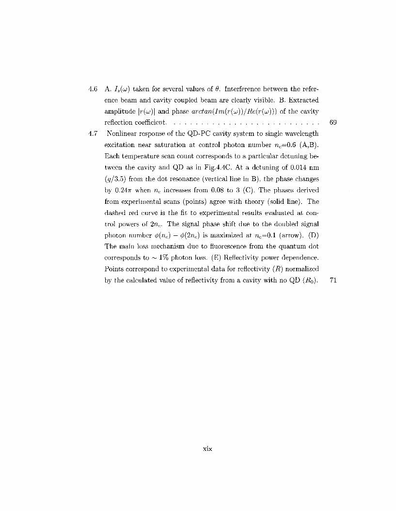
4.7 Nonlinear response of the QD-PC cavity system to single wavelength
excitation near saturation at control photon number nc=0.6 (A,B).
Each temperature scan count corresponds to a particular detuning be
tween the cavity and QD as in Fig.4.4C. At a detuning of 0.014 nm
(gr/3.5) from the dot resonance (vertical line in B), the phase changes
by 0.247T when nc increases from 0.08 to 3 (C). The phases derived
from experimental scans (points) agree with theory (solid line). The
dashed red curve is the fit to experimental results evaluated at con
trol powers of 2nc. The signal phase shift due to the doubled signal
photon number </>(nc) — </>(2nc) is maximized at nc=0.1 (arrow). (D)
The main loss mechanism due to fluorescence from the quantum dot
corresponds to ~ 1% photon loss. (E) Reflectivity power dependence.
Points correspond to experimental data for reflectivity (R) normalized
by the calculated value of reflectivity from a cavity with no QD (RQ). 71
xix
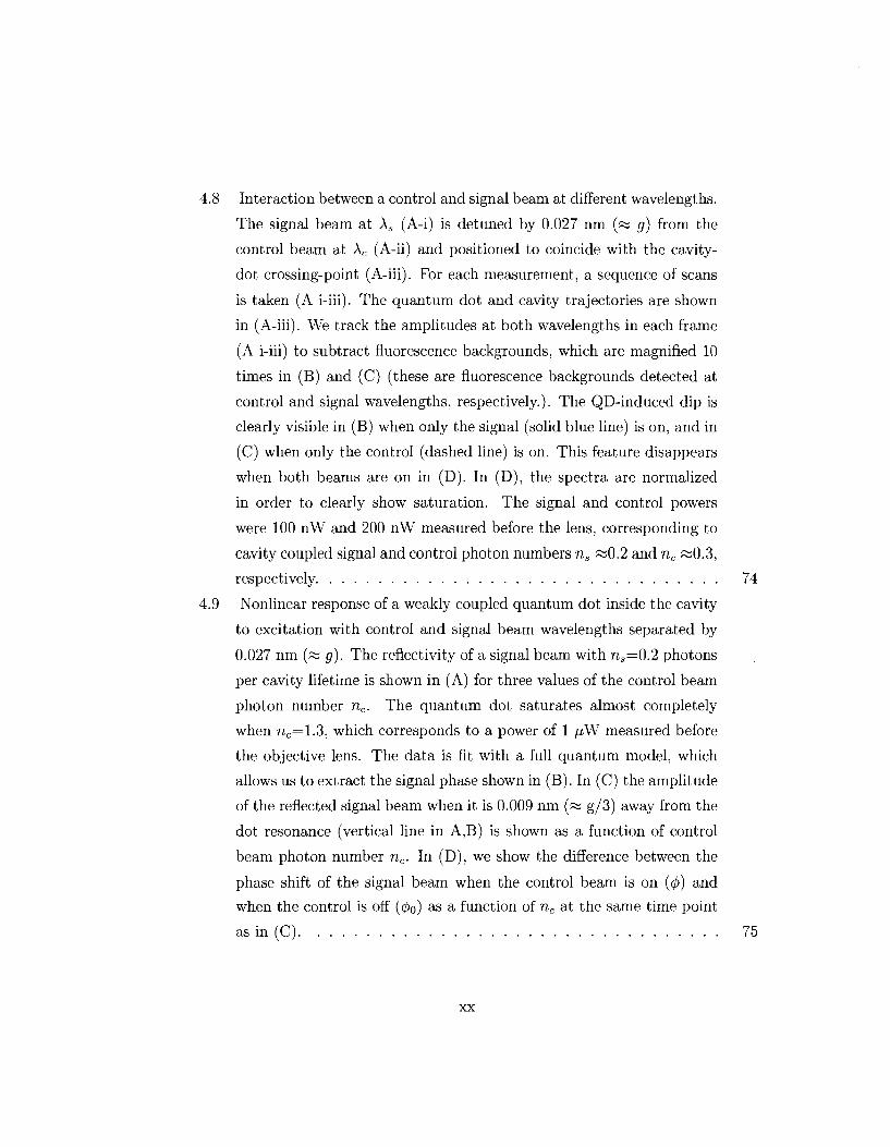
Interaction between a control and signal beam at different wavelengths.
The signal beam at Xs (A-i) is detuned by 0.027 nm (« g) from the
control beam at Ac (A-ii) and positioned to coincide with the cavity-
dot crossing-point (A-iii). For each measurement, a sequence of scans
is taken (A i-iii). The quantum dot and cavity trajectories are shown
in (A-iii). We track the amplitudes at both wavelengths in each frame
(A i-iii) to subtract fluorescence backgrounds, which are magnified 10
times in (B) and (C) (these are fluorescence backgrounds detected at
control and signal wavelengths, respectively.). The QD-induced dip is
clearly visible in (B) when only the signal (solid blue line) is on, and in
(C) when only the control (dashed line) is on. This feature disappears
when both beams are on in (D). In (D), the spectra are normalized
in order to clearly show saturation. The signal and control powers
were 100 nW and 200 nW measured before the lens, corresponding to
cavity coupled signal and control photon numbers ns «0.2 and nc ^0.3,
respectively
Nonlinear response of a weakly coupled quantum dot inside the cavity
to excitation with control and signal beam wavelengths separated by
0.027 nm (~ g). The reflectivity of a signal beam with ns=0.2 photons
per cavity lifetime is shown in (A) for three values of the control beam
photon number nc. The quantum dot saturates almost completely
when nc=1.3, which corresponds to a power of 1 fiW measured before
the objective lens. The data is fit with a full quantum model, which
allows us to extract the signal phase shown in (B). In (C) the amplitude
of the reflected signal beam when it is 0.009 nm (sa g/3) away from the
dot resonance (vertical line in A,B) is shown as a function of control
beam photon number nc. In (D), we show the difference between the
phase shift of the signal beam when the control beam is on (</>) and
when the control is off (0o) as a function of nc at the same time point
as in (C)
xx
4.10 Simulated differential phase shift 4>{2n) — 4>(n) as a function of probe
detuning from the cavity u>i — toc when the QD is on resonance with
the cavity ui^ot — wc = 0. A maximum of 0.1 n occurs when the aver
age photon number inside the cavity is close to nc « 0.1 as observed
experimentally 78
4.11 A. Differential phase shift 4>(2n) — cf)(n) as a function of probe detuning
from the cavity u>i — uic for different QD detunings Udot —uc. B. Maxima
from A vs dot detuning in units of g. Theory predicts that for large
detunings, the differential phase shift approaches n/2. Also plotted is
the average intra-cavity photon number (nc) corresponding to the par
ticular maximum differential phase shift. If the lowest photon number
operating point is desired, the detuning should be uidot — uc « g. . . 79
5.1 Influence of 7 on the transmission through a cavity with an embedded
QD. As 7 increases due to phonon scattering at elevated temperatures,
the transmission dip diminishes and the transmitted amplitude falls
due to energy losses into phonon modes. For the plots it is assumed
that g = K 82
5.2 Left: Scanning electron micrograph showing the photonic crystal cavity
(a). Middle: Simulated electric field intensity of the x (b) and y (c)
dipole modes in the asymmetric cavity. The measured Q factors are
400 and 200 respectively 83
5.3 PbS quantum dot spectra: 850 and 950 dot spectra taken on a bulk
silicon wafer 83
5.4 Cavity resonances mapped out by quantum dots in PMMA. Left: Po
larization dependence of modes confirming that they are x and y dipole
modes. Right: Ex dipole mode measured at two orthogonal polariza
tions. Angles refer to analyzer positions 85
xxi
(a): Scanning electron micrograph of the L3 type cavity fabricated in
a GaAs material with a high density of InAs quantum dots, (b): high-
Q mode electric field amplitude distribution, as predicted by FDTD
simulations, (c): FDTD simulations of frequency and Q changes as
An/n changes from ±10"3 -» ±10_ 1 . A high-Q (QHQ = 20000) and
low-L (QLQ = 2000) cavity were tuned: (qi) AQ/Q for An > 0 and
Q = QHQ, (<?2) AQ/Q for An > 0 and Q = QLQ, (ui) ALO/UJ for
An < O , ^ ) Aw/w for An > 0 for both high Q and low Q modes, (qj)
AQ/Q for An < 0 Q = QLQ, (q4) AQ/Q for An < 0 Q = QHQ. The
lines An/n for An > 0 and An < 0 are also plotted and overlap exactly
with u>2 and u\. As can be seen, the magnitude of the relative frequency
change is independent of Q, but the higher Q cavity is degraded more
strongly by the change in index. For an increase in n, the Q increases
due to stronger Total Internal Reflection confinement in the slab, as
expected
Numerical model of a free-carrier tuned cavity. In (a) the cavity is
always illuminated by a light source. Panel (b) shows the cavity reso
nance at the peak of the free carrier distribution (t=0) and 50 ps later,
as indicated by the yellow arrows in (a). The time-integrated spec
trum is shown as the asymmetric black line (labeled Sp) in (b), and
corresponds to the signal seen on the spectrometer, which is the inte
gral over the whole time window of the shifted cavity. The asymmetric
spectrum indicates shifting. In (c) and (d) the same data is plotted,
but now we consider the cavity illuminated only by QD emission with
a turn-on delay of 30 ps due to the carrier capture lifetime rc, and a
QD lifetime of 200 ps. In (d) the dashed line is the un-normalized t=0
spectrum, which now appears much smaller in magnitude. Further
more, the asymmetry of the line is even smaller in this case
xxn
Experimental result of FC cavity tuning for the L3 cavity. In (a) the
cavity is always illuminated by a light source and pulsed with a 3ps
Ti:Sapphire pulse. Panel (b) shows the cavity resonance at the peak
of the FC distribution (t=0) and 50 ps later, as indicated by the yellow
arrows in (a). In order to verify that the cavity tunes at the arrival
at the pulse, we combine the pulsed excitation with a weak CW above
band pump. The emission due to the CW source is always present, and
is in the box labeled CW in (a). This very weak emission is reproduced
in Panel (b) as the broad background with a peak at the cold cavity
resonance in (b). The time-integrated spectrum is shown as the black
line (Spectrometer) in (b). In (c) and (d) the same data is plotted,
but now we consider the cavity illuminated only by QD emission pulsed
by 10 [iW from the Ti:Sapphire source. In (d) suppression by about
.4-.35 at the cold cavity resonance can be seen. The inset shows a
strongly asymmetric spectrum of a dipole type cavity under excitation
of lOO/uH^ and the same cavity at low power after prolonged excitation.
Such strong excitation degrades the Q
Thermal tuning of the L3 cavity under CW excitation (a): Measured
AUJJUJ (left axis) and AQ/Q (right axis) as a function of pump power
for the L3 cavity, obtained from the fits to the spectra shown in (b).
The Q initially increases due to moderate gain and then degrades, while
u! shifts linearly. The straight dashed line fits Aw/w = 3 x 10 - 3 x Pin —
5 x 10~5 with 95% confidence and with root mean square deviation of
« 0.99. At very high power, the change in frequency does not follow
the same trend. The inset in (b) shows a plot of AU/{OJ/Q), which is
a measure of the number of lines that we shift the cavity by. A shift
of three line widths is obtained
xxin
1 A. Overall process flow for fabrication. B Sample GaAs wafer. C
Exposed resist (inset is poor outcome). D Etched resist (inset is poor
outcome). E final undercut PC. The light area around the structure
indicates a successful undercut 100
2 (A) A simulation of the band structure under zero and IV reverse
bias for the structure shown in the inset of (A) are shown. The bias
applied through the Schottky contact is used to control the tunneling
of electrons from the n-doped layer into the InAs QDs in the middle of
the intrinsically doped layer. Appropriate biasing aligns the QD levels
with the Fermi level of the n-doped layer for enhanced tunneling. (B)
A fabricated device in which the p and n contacts have been made
to the appropriate layers. The pattern was made by multiple aligned
writes with the electron beam tool. A wet etch is used to etch down
to the n-GaAs layer of the structure. (C) A preliminary measurement
for the sample under reverse bias. Slight crossing of lines, which is
indicative of charging is potentially observed. The overall line shift is
due to heating in the sample due to reverse breakdown of the diode.
Further measurements could not be made, as the sample shorted. . . 106
3 (A) A simulation of the band structure under zero bias for the structure
shown in (B). In (C) an optical micrograph of the final fabricated
device is shown. In (D) a scanning electron micrograph of the same
device reveals that the metal liftoff with a single layer of resist leaves
a significant edge 107
xxiv

7.4 (A) An optical micrograph of the TLM structure next to active de
vices. The structure consists of metal pads with varying spacing. The
width of the pad should be larger than the spacing. (B) A plot and
fit of resistance R versus pad spacing. R is obtained from the slope
of the ohmic IV curves measured between successive pads in (A). The
slope of the fit gives the sheet resistance Rsh and the intercept is twice
the contact resistance Rc. (C) IV measurements on the fabricated de
vice validate diode behavior and show current limitation due to series
resistance at large forward bias. The device acts as a detector in the
reverse bias configuration 108
D.l Experimental setup. Vertically polarized control (wavelength Ac) and
signal (wavelength Ag) beams are sent to the PC cavity (Inset) via
a polarizing beamsplitter (PBS). A quarter wave plate (QWP) (fast
axis 9 from vertical) changes the relative phase and amplitude (C($))
of components polarized along and orthogonal to the cavity. Only the
reflection coefficient r(uj) for cavity-coupled light (at |—45°)) depends
on the input frequency and amplitude. The PBS transmits horizontally
polarized light to a detector D. (B) Theoretical model for the phase of
signal beam 6 130
xxv
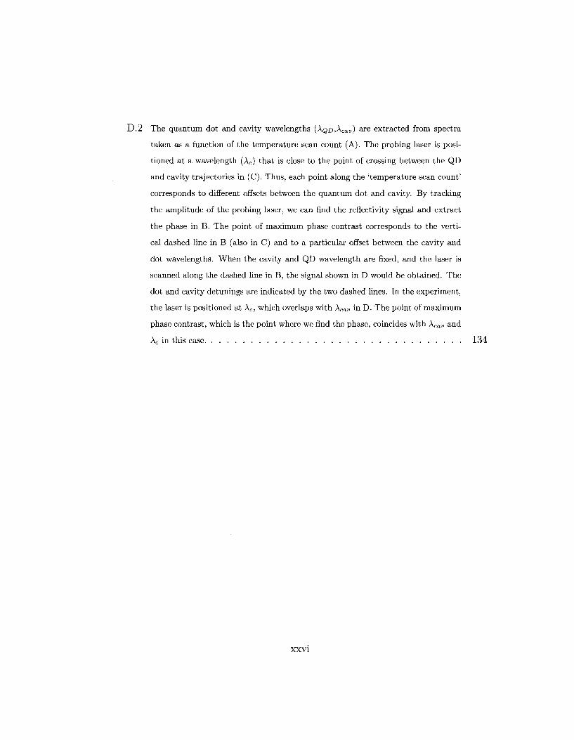
D.2 The quantum dot and cavity wavelengths (AQ£>,Acat,) are extracted from spectra
taken as a function of the temperature scan count (A). The probing laser is posi
tioned at a wavelength (Ac) that is close to the point of crossing between the QD
and cavity trajectories in (C). Thus, each point along the 'temperature scan count'
corresponds to different offsets between the quantum dot and cavity. By tracking
the amplitude of the probing laser, we can find the reflectivity signal and extract
the phase in B. The point of maximum phase contrast corresponds to the verti
cal dashed line in B (also in C) and to a particular offset between the cavity and
dot wavelengths. When the cavity and QD wavelength are fixed, and the laser is
scanned along the dashed line in B, the signal shown in D would be obtained. The
dot and cavity detunings are indicated by the two dashed lines. In the experiment,
the laser is positioned at Ac, which overlaps with \cav in D. The point of maximum
phase contrast, which is the point where we find the phase, coincides with Xcav and
Ac in this case 134
xxv i
Chapter 1
Introduction
1.1 Overview
Photonic quantum and classical information processing are long-standing and rapidly
developing fields of research that had their inception with the development of the
working laser by Maiman in 1960, and the pioneering work of atomic physics. Today,
more than ever, these fields are coming closer to each other and closer to deeply im
pacting computing, communication and the sharing of information. In the realm of
classical information processing, the integration of optical interconnects for board-to-
board, core-to-core, chip-to-chip and potentially on-chip communication is inevitable
and is being actively pursued by companies such as Hewlett-Packard, IBM, Sun Mi
crosystems, Intel, and Luxtera. These efforts are driven by the astronomical savings
in power consumption that could result from replacing copper wires with photonic
channels. Photonics has the potential to account for 90% power savings in today's
chipsets 1 and is already used to significantly reduce the power losses associated with
2% efficient copper transmission lines in data centers 2. Although quantum effects
may not be fully exploited to yield functioning quantum computers in the near future,
lMWhy optics and why now?", Greg Astfalk, Office of Strategy and Technology at Hewlett-Packard: the power spent on communication and data transfer is 33-50% for the processor, 50% in memory, and 90% in the chipset. Delivered in a presentation at the HP Labs Photonic Interconnect Forum, May 12, 2008
2At the time of this thesis, several companies have unveiled optical "wires" for use in datacenters as replacements of lossy electrical connections.
1
CHAPTER 1. INTRODUCTION 2
they have great potential for enhancing the performance of optoelectronic devices.
Enhanced light matter interactions due to quantum effects can already be used to
create extremely low threshold lasers [6], optical modulators[7], logic gates between
photons [2], and switches operating at single photon energies on a semiconductor
chip [2, 1]. This thesis explores how these effects are enabled by the extremely small
optical volumes and high quality factors of photonic crystal cavities, which are an
electromagnetic breadboard for tailoring the interaction between photons and atoms
on the chip. As the aforementioned devices are nonlinear in nature, this thesis fo
cuses on our exploration of engineered high efficiency nonlinear materials that can be
tailored for particular applications.
In this chapter, I begin by reviewing quantum dots, resonators, and field quanti
zation in small volumes. The small optical volume of photonic crystal cavities results
in large electric fields even due to a single photon. Furthermore, the resonator leads
to a modified density of states for photons, and this effect can be used to enhance
or suppress real and virtual optical absorption processes. I then discuss how photons
can be used to encode quantum bits and demonstrate that a cavity with an embedded
nonlinear medium can be used to realize quantum logic between photons on the chip.
I then review the interaction between photons and quantum dot that is embedded
in a cavity. I briefly review the concepts of classical nonlinear processes, such as the
intensity dependent refractive index, and show how these are affected by the presence
of the cavity. Although losses of off-resonant nonlinearities cannot be efficiently con
trolled, the resonant nonlinearities due to the refractive index of a single emitter can
be greatly enhanced and modified with the use of a photonic cavity, yielding interac
tions between photons at the single photon level and modulation of the transmission
through the cavity with up to 99% contrast.
In Chapter 2, I will review the basics of photonic crystal cavities and discuss our
development of theoretical and numerical methods for the modeling of photonic band
gap cavities. I will focus on the inverse design approach and genetic algorithms as
well as the design of asymmetric cavities with differing refractive indices on the top
and bottom side of the PC membrane. In Chapter 3, I will introduce our attempts
at enhancing classical nonlinearities with the use of photonic bandgap cavities in the
CHAPTER 1. INTRODUCTION 3
context of quantum non-demolition measurements, and use this as a motivation for
• the results of Chapter 4, where I will more deeply explore the interaction between a
quantum dot and an optical cavity and the use of this system as a high efficiency non
linear optical element for controlled phase interaction between photons. In Chapter 5
I will review our attempts at realizing cavity-quantum dot interactions at room tem
perature. In Chapter 6 I will present our results on ultra-fast all-optical modulation
in photonic crystal cavities.
1.2 Quantum dots
Some of the greatest advances in experimental quantum information processing have
been realized in experiments with atoms and trapped ions [8, 9, 10, 11]. In order to
develop scalable and manufacturable analogues of such experiments, it is advanta
geous to follow in the steps of the semiconductor industry and look for a solid-state
semiconductor based implementation of quantum memories and technologies. Since
photons will be used as carriers of information, an optically active semiconductor
quantum bit is required. A natural choice is a quantum dot (QD), which acts as a
single atom with discrete energy states, optically active transitions, and controllable
spin states for the development of quantum memories. The quantum dot is formed
by capping a chunk of a low band gap semiconductor with a higher bandgap sur
rounding material, which results in three-dimensional confinement for electrons and
holes, and the formation of discrete energy levels. For the purposes of this thesis,
the quantum dot acts as a two-level atom with an excited and ground state, that
is accessible to optical transitions. The main features of a quantum dot along with
excitation strategies are illustrated in Fig. 1.1.
1.3 Photonic crystal cavities
The use of optical cavities enhances the interaction between light and matter. In the
simplest case, the optical cavity recirculates photons and allows the interaction to
occur several times before the photons leak out of the cavity mirrors. The number
CHAPTER 1. INTRODUCTION 4
o i.as
Conduction Band
Discrete Energies n=2
n=l
B
JLLJ., - L 981 932 933 934
X [nm]
GaAs In As GaAs
n=l n=2
Valence Band Hole
Figure 1.1: (A) Atomic force microscope image of InAs/GaAs semiconductor quantum dots grown by molecular beam epitaxy. The typical dot diameter is 20 nm. (B) Typical emission spectrum of a quantum dot. Typical dot wavelengths are around 920 to 940 nm. with the distribution determined by the dot diameter variation. (C) The quantum dot is formed by small InAs islands that are grown by self assembly between GaAs layers. The three dimensional confinement in the quantum dot leads to discrete energy state of the electron and hole. (D) Optical excitation pathways of the QD. The main QD transition is the lowest energy transition with a typical bulk lifetime of 1 ns and emission wavelength of « 920 nm. The emission wavelength is determined by the In content in IncGai_.EAs that is used to form the dot. There are three ways to optically excite the quantum dot. Electron-hole pairs can be injected into the surrounding GaAs via above-band excitation (i), higher order (n > 1) states can be driven resonantly (ii), and the n = l transition can be driven directly (iii). For above-band excitation the plionon relaxation time of the electron-hole pair into the n=l level takes on average lOps. The line width of QD's in bulk is close to the Fourier limit and on the order of 10 //,eV.
CHAPTER 1. INTRODUCTION 5
of roundtrips is proportional to the quality factor (Q) of the cavity. However, given
a fixed Q, as the resonator size decreases, the optical energy is confined to a smaller
volume, and the field intensity increases. In a small mode volume resonator, the
frequency spacing between modes is quite large, and the density of optical states
is strongly modified. By Fermi's golden rule, this implies that optical transitions
can be both enhanced and suppressed. As will be shown in Chapter 2, photonic
crystals (PCs) are a suitable platform for such experiments and can be used as a
breadboard for photonics on the chip. Photonic crystals can be readily fabricated
in most semiconductors due to a rich history of semiconductor processing. This
allows photonic crystals to be scalable, integrable, and easily combined with current
technologies. Furthermore, the combination with active semiconductor materials such
as quantum dots and quantum wells results in a variety of novel devices and effects. In
Fig. 1.2 we show a typical photonic crystal cavity that was fabricated in GaAs, and a
conceptual device that combines several cavities and connects them with waveguides.
The influence of the PC cavity on QD emission is illustrated in Fig. 1.2c, where the
emission from QD's that are not resonant with the cavity is suppressed, while that
from quantum dots is enhanced.
The electric field E inside a resonator of volume V is given by:
E{f) = ^ { a { t ) + a\t))u{r)u (1.1)
Where e = e(f) is the material dielectric function, u{f) is the normalized spatial part
of the single photon wave function, given by the solution of Maxwell's equations, u is
the polarization of the field, u> is the photon frequency, a(t), at(t) are the annihilation
and creation operators and the cavity mode volume V, and rrvu is the dipole moment
of the emitter. Optical transitions can be formulated in terms of the dipole interaction
Hamiltonian Hi [12]:
#7 = -/7 • i? = hg(a+ + a') (a(i) + a\t)) (1.2)
Here a+ = |e) (g\ = a_ are the raising and lowering operators for the driven dipole
CHAPTER 1. INTRODUCTION 6
that is assumed to have an excited |e) and ground state \g), while g is the vacuum
Rabi frequency, which determines the dipole-field coupling rate. Retaining only the
energy conserving terms (i.e. those that excite the dipole and destroy a photon, and
vice versa):
Hi = fig (a+a(t) + a\t)a~) (1.3)
The vacuum Rabi frequency inside the cavity g is then
The mode volume V is defined as:
max{e \E\2} \nj
In the above expression A is the wavelength of light and n is the refractive index of
the medium surrounding the dipole. In typical resonators C, » 1, and we can see that
the electric field of a single photon is small. However, in a photonic crystal resonator,
C = 0(1), with a lower bound of 1/8, and the fields are significantly enhanced.
For comparison, typical atomic cavities have Q ~ 0(1000). Therefore, interaction
strengths between the cavity field and the two-level system are significantly enhanced
in a photonic crystal cavity.
1.4 Interaction between coherent light and a quan
tum dot in a photonic crystal cavity
The theory of an emitter coupled to an optical cavity can be found in Refs. [13, 14].
As described above, the novelty of photonic crystal cavities is that the optical mode
volume is very small (on the order of (A/n)3, where n is the refractive index of the
material in which the dipole is embedded, and A is the resonant wavelength of the
cavity). Therefore, even with moderate quality factors, highly nonlinear effects can
CHAPTER 1. INTRODUCTION i
Figure 1.2: (a) Scanning electron micrograph of a photonic crystal cavity, (b) Conceptual device that integrates multiple cavities with waveguides on the same chip. (c) the cavity enhances emission from quantum dots that are coupled to it, while suppressing emission from decoupled quantum dots.
occur in this system.
We consider the quantum dot to be a two level system with a long-lived ground
state, and a clipole decay rate 7/2TT = 0.2GHz. InAs quantum dot line widths at low
temperatures (w 10 —20A") are generally close to being radiatively limited, and so the
dipole dephasing rate can be approximated to be one half of the dipole decay rate.
The coupling of the quantum dot dipole to the cavity electric field is given by the
Rabi frequency given by Eq. 1.4. Values of g clearly depend on position and dipole
alignment, with the maximum dipole moment of gmax « ZtiOGHz in this system.
These parameters are illustrated in Fig. 1.3 (a).
When a quantum dot (transition frequency u;,/) is resonant with the PC cavity at
frequency ajc, the dot emission is modified. The degree of modification depends on
the parameters g. 7 and the field decay rate K = aJc/(2Q). By solving the interaction
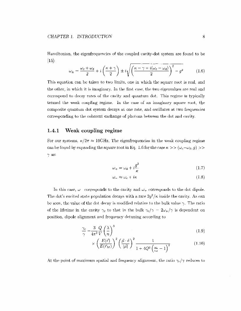
CHAPTER 1. INTRODUCTION 8
Hamiltonian, the eigenfrequencies of the coupled cavity-dot system are found to be
[15]:
^ = —2-+z{-r)±i{ 2 ) ~g (L6)
This equation can be taken to two limits, one in which the square root is real, and
the other, in which it is imaginary. In the first case, the two eigenvalues are real and
correspond to decay rates of the cavity and quantum dot. This regime is typically
termed the weak coupling regime. In the case of an imaginary square root, the
composite quantum dot system decays at one rate, and oscillates at two frequencies
corresponding to the coherent exchange of photons between the dot and cavity.
1.4.1 Weak coupling regime
For our systems, K/2TT SS 16GHZ, The eigenfrequencies in the weak coupling regime
can be found by expanding the square root in Eq. 1.6 for the case K » (ujc—uid, g) »
7 as:
Q2
u+=ud + i^- (1.7) K
U- ~ LUC + in (1.8)
In this case, w_ corresponds to the cavity and u+ corresponds to the dot dipole.
The dot's excited state population decays with a rate 2g2//c inside the cavity. As can
be seen, the value of the dot decay is modified relative to the bulk value 7. The ratio
of the lifetime in the cavity 7C to that in the bulk 7c/7 = 2u;+/7 is dependent on
position, dipole alignment and frequency detuning according to
7c 3 Q (\^ 7 47r2 V \n
E(f) V ffl-e
(1.9)
(1.10) ,WM)J \\fl\J 1 + 4 Q 2 ( v _ 1 y
At the point of maximum spatial and frequency alignment, the ratio 7c/7 reduces to
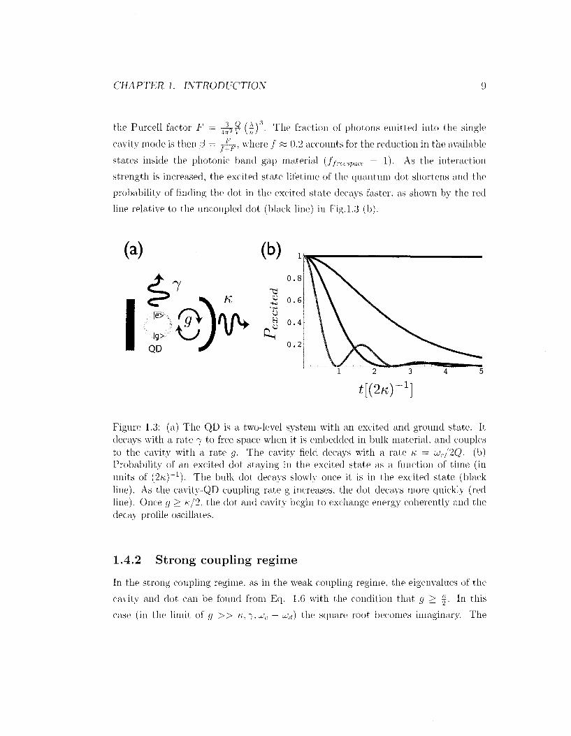
CHAPTER 1. INTRODUCTION 9
the Purcell factor F
cavity mode is then li
4§2^ (^) • The fraction of photons emitted into the single
f+F where / « 0.2 accounts for the reduction in the available
1). As the interaction states inside the photonic band gap material (f/reespace
strength is increased, the excited state lifetime of the quantum dot shortens and the
probability of finding the clot in the excited state decays faster, as shown by the red
line relative to the uncoupled dot (black line) in Fig.1.3 (b).
(a) (b) ,
~e
CD CL,
t[{2H)-1
Figure 1.3: (a) The QD is a two-level system with an excited and ground state. It decays with a rate 7 to free space when it is embedded in bulk material, and couples to the cavity with a rate g. The cavity field decays with a rate K = LUC/2Q. (b) Probability of an excited dot staying in the excited state as a function of time (in units of (2K;) - 1 ) . The bulk dot decays slowly once it is in the excited state (black line). As the cavity-QD coupling rate g increases, the dot decays more quickly (red line). Once g > K/2, the dot and cavity begin to exchange energy coherently and the decay profile oscillates.
1.4.2 Strong coupl ing regime
In the strong coupling regime, as in the weak coupling regime, the eigenvalues of the
cavity and dot can be found from Eq. 1.6 with the condition that g > £. In this
case (in the limit of g » K,-f,u>c — u>d) the square root becomes imaginary. The
CHAPTER 1. INTRODUCTION 10
cavity and quantum dot cannot be treated separately, but exist in a time dependent
superposition state, with photons exchanging energy between the two at a rate of
« 2g. For large g, the eigenvalues of this system are
a)± = (̂ + ̂ )+i(l+2)± j W ^ + ' K - ^ y (1.U)
K(^) + . (^+ I)± 9 ( 1 1 2 )
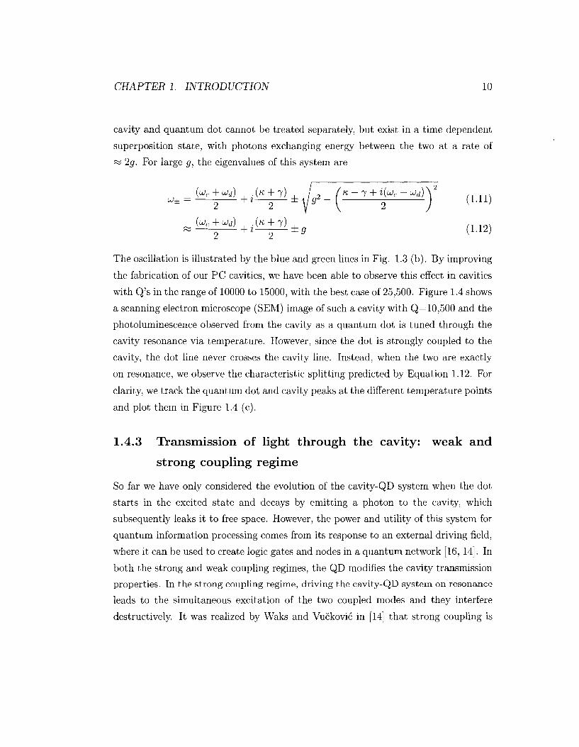
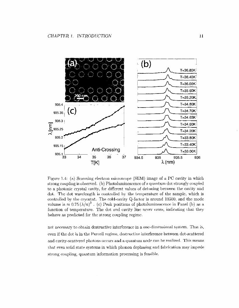
The oscillation is illustrated by the blue and green lines in Fig. 1.3 (b). By improving
the fabrication of our PC cavities, we have been able to observe this effect in cavities
with Q's in the range of 10000 to 15000, with the best case of 25,500. Figure 1.4 shows
a scanning electron microscope (SEM) image of such a cavity with Q=10,500 and the
photoluminescence observed from the cavity as a quantum dot is tuned through the
cavity resonance via temperature. However, since the dot is strongly coupled to the
cavity, the dot line never crosses the cavity line. Instead, when the two are exactly
on resonance, we observe the characteristic splitting predicted by Equation 1.12. For
clarity, we track the quantum dot and cavity peaks at the different temperature points
and plot them in Figure 1.4 (c).
1.4.3 Transmission of light through the cavity: weak and
strong coupling regime
So far we have only considered the evolution of the cavity-QD system when the dot
starts in the excited state and decays by emitting a photon to the cavity, which
subsequently leaks it to free space. However, the power and utility of this system for
quantum information processing comes from its response to an external driving field,
where it can be used to create logic gates and nodes in a quantum network [16, 14]. In
both the strong and weak coupling regimes, the QD modifies the cavity transmission
properties. In the strong coupling regime, driving the cavity-QD system on resonance
leads to the simultaneous excitation of the two coupled modes and they interfere
destructively. It was realized by Waks and Vuckovic in [14] that strong coupling is
CHAPTER 1. INTRODUCTION 11
J \^J: • \J>:
V,-*' V—/'
Vwr* \ - /
935.1
• (b ) -
-
-
.
-
^
_vv_ TV y\ J\
_/v. f\ / \
/ \
/v A, /V A
T=36.80K
T=36.40K"
T=36.00K
T=35.60K
T=35.20K-
T=34.80K
T=34.70K
T=34.65K
T=34.60K
T=34.20K-
T=33.80K
T=33.40K"
T=33.00K
934.5 935 935.5 A,(nm)
936
Figure 1.4: (a) Scanning electron microscope (SEM) image of a PC cavity in which strong coupling is observed, (b) Photoluminescence of a quantum dot strongly coupled to a photonic crystal cavity, for different values of detuning between the cavity and dot. The dot wavelength is controlled by the temperature of the sample, which is controlled by the cryostat. The cold-cavity Q-factor is around 10500, and the mode volume is « 0.75 (A/n)3 . (c) Peak positions of photoluminescence in Panel (b) as a function of temperature. The dot and cavity line never cross, indicating that they behave as predicted for the strong coupling regime.
not necessary to obtain destructive interference in a one-dimensional system. That is,
even if the dot is in the Purcell regime, destructive interference between dot-scattered
and cavity-scattered photons occurs and a quantum node can be realized. This means
that even solid state systems in which phonon dephasing and fabrication may impede
strong coupling, quantum information processing is feasible.
CHAPTER 1. INTRODUCTION 12
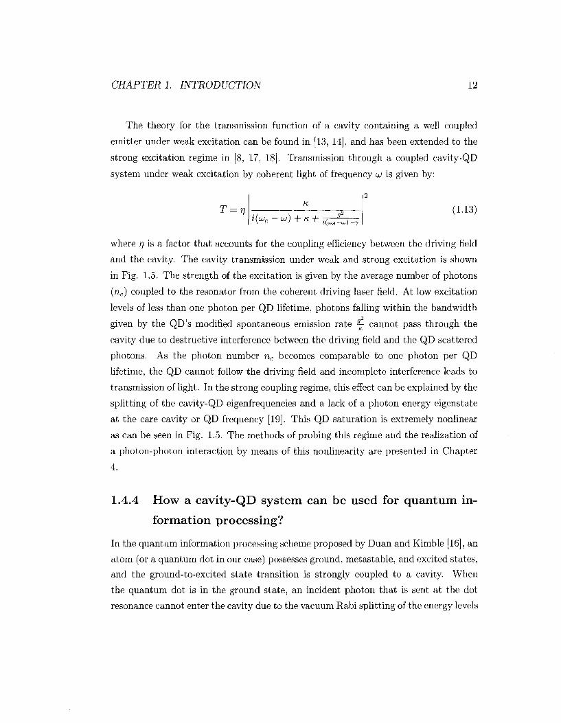
The theory for the transmission function of a cavity containing a well coupled
emitter under weak excitation can be found in [13, 14], and has been extended to the
strong excitation regime in [8, 17, 18]. Transmission through a coupled cavity-QD
system under weak excitation by coherent light of frequency ui is given by:
T = r) K
i{ujc - u) + K + j i (cu d -a j )+7
(1.13)
where 7? is a factor that accounts for the coupling efficiency between the driving field
and the cavity. The cavity transmission under weak and strong excitation is shown
in Fig. 1.5. The strength of the excitation is given by the average number of photons
(nc) coupled to the resonator from the coherent driving laser field. At low excitation
levels of less than one photon per QD lifetime, photons falling within the bandwidth 2
given by the QD's modified spontaneous emission rate ^- cannot pass through the
cavity due to destructive interference between the driving field and the QD scattered
photons. As the photon number nc becomes comparable to one photon per QD
lifetime, the QD cannot follow the driving field and incomplete interference leads to
transmission of light. In the strong coupling regime, this effect can be explained by the
splitting of the cavity-QD eigenfrequencies and a lack of a photon energy eigenstate
at the care cavity or QD frequency [19]. This QD saturation is extremely nonlinear
as can be seen in Fig. 1.5. The methods of probing this regime and the realization of
a photon-photon interaction by means of this nonlinearity are presented in Chapter
4.
1.4.4 How a cavity-QD system can be used for quantum in
formation processing?
In the quantum information processing scheme proposed by Duan and Kimble [16], an
atom (or a quantum dot in our case) possesses ground, metastable, and excited states,
and the ground-to-excited state transition is strongly coupled to a cavity. When
the quantum dot is in the ground state, an incident photon that is sent at the dot
resonance cannot enter the cavity due to the vacuum Rabi splitting of the energy levels
CHAPTER 1. INTRODUCTION 13
Cavity transmission for g=K Cavity transmission for g=K/4
w-coc [g] o)-coc [g]
Figure 1.5: The transmission of a coherent field at a frequency uii through a cavity with frequency uic depends on the presence of a QD, the coupling strength g, and the strength of the driving field. In (a) the transmission of a cavity with a strongly coupled QD (g = K) is shown for various values of the average photon number inside the cavity. As the driving strength increases, the QD saturates nonlinearly an tends toward the empty cavity transmission function (dashed line). In (b) the same series is shown for a weakly coupled dot g = K/4 . AS in the case of a strongly coupled system, the QD prohibits transmission at its resonance.
and cannot pass. However, when the dot is in the decoupled (metastable) state, the
photon can be transmitted. Thus, the cavity essentially acts as a read/write interface
between a quantum memory that is realized by the quantum dot. The interference of
photons that interact with such cavities can be used to realize entangling operations on
QDS and therefore this system acts as a resource for quantum information processing.
Furthermore, such a strongly coupled system can be used to realize a quantum state
preparation device, because incident coherent light with Poissonian photon statistics
will be converted to non-Poissonian light, since the probability of transmitting higher
photon number states is suppressed at the dot resonance. In the ultimate limit of
strong coupling with high-Q cavities, a photon number state generating device can
be realized [19].
Unfortunately the realization of a robust three-level QD-cavity system is not
straightforward and may require controlled charging of a QD in a strong magnetic
CHAPTER 1. INTRODUCTION 14
field [20]. However, the nonlinear behavior of the QD response to the driving field
(shown in Fig.1.5) can be used to realize deterministic controlled logic between pho
tonic qubits even with only a two-level system. Such a scheme for quantum logic
between photons was first realized by Turchette et. al. in an atomic system [8], and
extended to the solid state in our work [2].
1.5 Brief introduction to quantum information pro
cessing
Since their inception in 1981 [21], quantum computers have been an active area of
research. Their greatest promise lies in the ability to solve intractable problems
that are of fundamental importance to fundamental science [21], drug discovery, and
information processing [22, 23]. The main concepts behind quantum information
processing will be discussed below.
In parallel, the application of quantum systems to unconditionally secure commu
nication has emerged as a novel technology [24, 25, 26, 27] and has seen the most
progress in deployment and implementation, with several systems currently operating
around the world and several companies commercializing this technology 3.
Most quantum information processing systems for computation or communication
rely on photons as carriers of information [24, 28]. Photons are ideally suited for this
task because they propagate over long distances with low loss, therefore preserving
information, and do not require large operating powers. Photons can also exist in
several convenient orthogonal logic states: horizontal and vertical polarization (or
right hand and left hand circular), propagation in one of two physical channels, and
propagation in one of two time slots.
There are two requirements in quantum information processing with photons [29].
First, one must be able to manipulate each photon individually. For logical bits stored
3Companics providing quantum cryptography systems: id Quantique sells quantum key distribution products, and was used in the 2007 Swiss national elections to transmit ballot information in Geneva MagiQ Technologies sells quantum devices for cryptography SmartQuantum provides hardware solutions for quantum and digital cryptography

CHAPTER 1. INTRODUCTION 15
in the horizontal or vertical polarization, this is easily accomplished with waveplates.
Second, a two-photon logic gate is required. Such a gate takes two photons and, if
both are vertically polarized, changes one of them to horizontal. Since photons do
not interact with each other, such a gate requires a nonlinear medium whose response
depends on the number of photons. Finding a sufficiently nonlinear medium that has
low losses has been a great challenge and one of the biggest impediments to realizing
such gates. It will be shown in Chapter 4 that such a medium can be engineered by
placing a semiconductor quantum dot inside an optical cavity in a photonic crystal.
The advantage of quantum bits for information processing stems from the number
of states that a string of N quantum bits can occupy. A classical bit can only exist in
either one of two states [classical) — |0) or [classical] — |1). A quantum bit, on the
other hand, can exist in an arbitrary superposition of these states [quantum) = a |0) +
b |1) where \a\ +[b\ = 1. For example, we can start with two physical quantum bits in
the state [quantum) = |0) |0) and rotate each bit to the state 4|(|0) + |1)). The overall
state becomes [quantum) = \ (|0) |0) + |0) |1) + |1) |0) + |1) |1)). Thus, N quantum
bits can be used to create all 2N states of length N, which are all possible classical input
bit strings. Quantum mechanical operations are linear, and therefore the "quantum
computing device" that operates on the physical bits computes all possible outputs
for all possible inputs in a single computational step. However, only one bit string
of length N can be measured at the outcome of the computation. Thus, it is not
possible to retrieve all the answers, and the quantum computer must take advantage
of the quantum encoding before the state is measured. Fortunately, two powerful
algorithms due to Shor and Grover exist, and are sufficiently interesting to motivate
research in this area. Although Shor's algorithm for prime number factorization has
been the most notorious for its promise to break encryption, Graver's algorithm for
unsorted database searches is particularly useful for problems such as drug discovery
and processing of large data-sets [22, 23].
CHAPTER 1. INTRODUCTION 16
1.5.1 Encoding information in photon states
The single photon is an elementary constituent of light and can be used to encode
information in several schemes. The fundamental difference between a single photon
and a classical photon pulse can be illustrated by the output of a beamsplitter acting
on either of the states. It is well known that a 50/50 non-polarizing beamsplitter
(NPBS) divides an incident coherent pulse \a) (photon number is given by \a\ ) into
two equal energy pulses with 1/2 of the energy of the input pulse. A single photon,
however, can only go into one of the ports. Denoting by UNPBS the beamsplitter
operator, and assigning labels 1 and 2 to the two input ports and 3 and 4 to the two
output ports, the action of the NPBS on a coherent state and a vacuum state arriving
at ports 1 and 2, respectively is:
UNPBS |a)i |0)2 = a \
7 2 / 3 +
a \
7i/4
Which means that we have two photon packets in two output ports with equal ampli
tude. However, when the beamsplitter acts on a single photon, the photon can only
go into one of two ports:
1
V2 UNPBS | l)x |0)2 = ^ = (|0)3 |1}4 + |1)3 |0}4)
This is an entangled state of the photon and the two channels and is a powerful
medium for the transmission and communication of quantum information between
quantum nodes. There are several ways to encode quantum information in photons:
Dual rail:
The above example results in a quantum correlation between the state of the photon
and the two ports of the beamsplitter. This is the "dual-rail" representation, where
the single photon can exist in one of two channels spatial channels. The above single
photon state is then the superposition state of logical qubits ^ ( | 0 ) + |1))
Single rail (time energy):
We can also divide the photons between different time bins that are determined by a
computer clock. Thus a photon can exist in superpositions of occupying several time
CHAPTER 1. INTRODUCTION 17
bins.
Polarization encoding:
The photon can exist in superpositions of polarization states such as horizontal and
vertical (\H) , \V)) or right hand and left hand circular (|±) = ^(\H) ± i \V))).
The results of our work are most directly applicable to polarization and single
rail encoding strategies. In order to take advantage of the dual rail encoding scheme,
momentum preserving resonators, such as ring resonators, may be necessary and will
be the subject of future research.
1.5.2 Quantum operations on photons
It was shown by DiVincenzo [29] that single and two-qubit gates are universal for
quantum computation. Several single qubit gates and two-bit gates can be considered.
However, a complete set is formed from arbitrary single qubit rotations and the two-
photon controlled-NOT (CNOT) gate.
In our work, qubits are encoded in the polarization state of photons, such as
horizontal and vertical (\H), \V)) or circular (\H) ±i\V)) polarization. The optical
cavity used in our experiments is a one-sided polarizing cavity that is formed from a
linearly polarized PC cavity with a distributed Bragg reflector (DBR) placed under
neath. The DBR eliminates radiative losses from the back mirror of the cavity. The
particular geometry of this PC cavity results in a fundamental mode that is linearly
polarized (see Chapter 2). Thus, only photons that are polarized along the cavity can
couple to it can interact with each other via a cavity-embedded nonlinear medium.
Single qubit gates
In the polarization encoding, an arbitrary single qubit state is given by:
\i,)=a\H) + b\V) (1.14)
with \a\ +\b\ = 1 with a, b being complex numbers. Single qubit gates manipulate the
complex coefficient a,b. An arbitrary polarization state can be generated with phase
CHAPTER 1. INTRODUCTION 18
plates. The particularly useful gate operations are the Hadamard gate, controlled
phase gate, TT/8 gate and the X,Y,Z gates [30]. The Hadamard gate is one of the
most useful, and is given by:
(1.15)
It can be easily seen that the Hadamard transformation is realized with a A/2
wave plate (HWP) set to 7r/8.
/ cos(2<9) sin(20) \ HWP(8) = V ' (1.16)
\ sin(20) - cos(26>) /
Two-qubit gates
The two-qubit state (using qubits encoded in photon polarization) can be written
as \V)S\H)C, where subscripts label the signal photon s and control photon c. The
controlled-NOT (CNOT) gate changes the state of the signal photon conditioned on
the state of the control photon:
\H)a\H)c-*\H)a\H)c (1.17)
\V)s\H)c^\V)s\H)c (1.18)
\H).\V)e^\V),\V)e (1.19)
\V)a\V)e-*\H)a\V)c (1.20)
In a photonic system, the CNOT gate can be obtained from another two-photon
interaction called the controlled phase gate and manipulation of the two photons via
Hadamard transforms (enabled by waveplates). For polarization encoded qubits, the
controlled phase gate can be easily realized by a linearly polarized cavity containing a
nonlinear optical medium whose refractive index is sensitive to the number of photons
inside of it. This means that given signal and control photon numbers ns and nc inside
CHAPTER 1. INTRODUCTION 19
the cavity, the phase shift <f> acquired by the photons inside the cavity satisfies:
|0(nc) + (f)(ns) - 4>{nc + na)\ = A > 0 (1.21)
In the case of A=7T, the interaction results in a controlled-phase (controlled-X,i.e.
CZ) gate. The details of the operation of the CZ gate, the transformation between
the CNOT and CZ gate, and the realization of such a gate in a linearly polarized
nonlinear cavity are given in Appendix A.
In Chapter 3 we will show that classical nonlinearities cannot easily satisfy these
conditions at the single photon levels, and present our preliminary results toward the
realization of the CZ gate in photonic crystal cavities in Chapter 4.
Chapter 2
Photonic Crystal Cavity Design
2.1 Introduction
Photonic crystals can be viewed as a " breadboard" for photonics on the semiconduc
tor chip. These crystals are formed by periodically changing the refractive index of
a thin semiconductor slab in two dimensions. Through clever manipulation of the
refractive index, a variety of optical elements including cavities, waveguides, focusing
and dispersive elements can be made and connected on the same chip in one mono
lithic step. However, the design problem is not simple. The space of solutions may
have many local optima and analytical techniques are seldom used. The optical res
onator is the most relevant element for quantum information processing experiments,
and in this chapter we discuss our efforts at reducing the complexity of techniques
used in finding optimal solutions for the design of cavities with high quality factors
and small optical volumes.
The main result is an analytical model that reduces the design problem from a
computationally intensive search to a simple analytical inversion of Maxwell's equa
tions when the cavity is formed along a one direction of high symmetry [31] given in
Section 2.5
Although the results of this approach are quite satisfactory, the resulting devices
are difficult to fabricate. Using the intuition developed in our analytical work, we
20
CHAPTER 2. PHOTONIC CRYSTAL CAVITY DESIGN 21
present an optimization approach based on Genetic algorithms [32] that can be con
strained to produce realistic devices in Section 2.6.
2.2 A simple look at photonic crystal design
Photonic crystals (PCs) are made by introducing periodic variations in refractive
index that lead to a bandstructure for photons in one, two and three dimensions. The
periodic nature of the refractive index leads to Bloch states of photons supported in
the structure and results in the formation of energy band gaps for photons, as a result
of the distributed Bragg reflection (DBR). Photons with energies in the energy gap
cannot propagate through such a structure and can therefore be confined and trapped
in defects in the periodic dielectric structure. In the directions without periodicity,
light is confined by total internal reflection (TIR). The operating principle of a two-
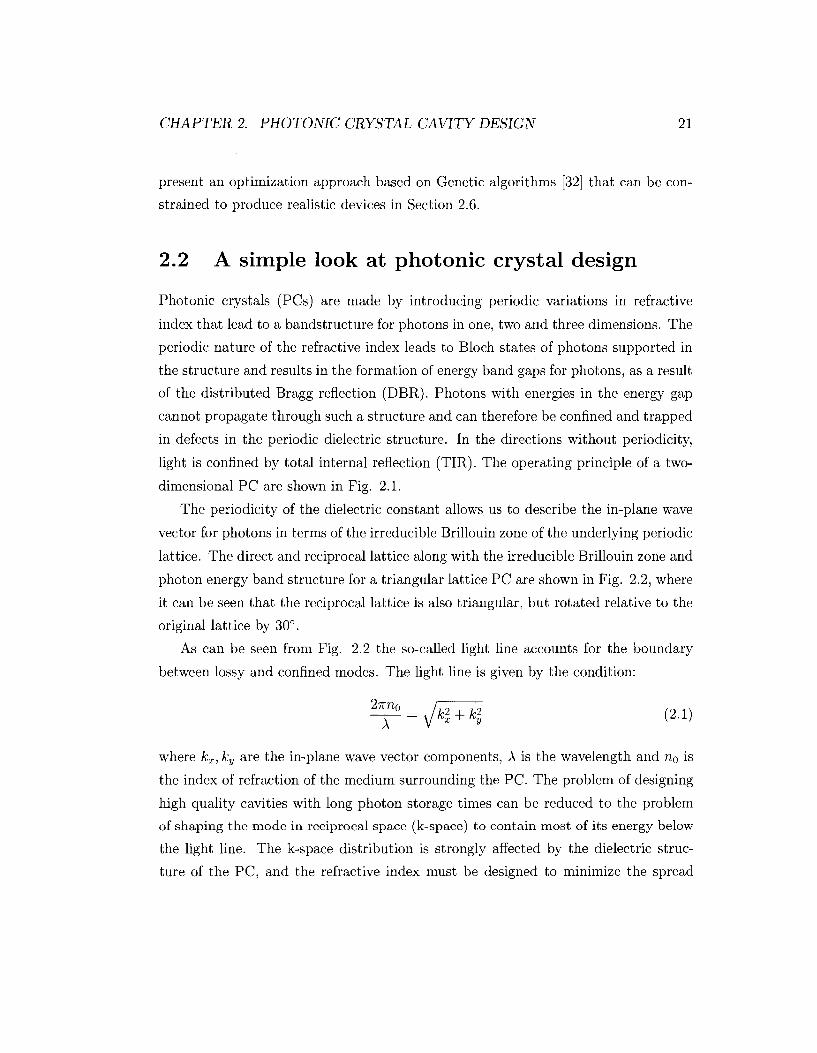
dimensional PC are shown in Fig. 2.1.
The periodicity of the dielectric constant allows us to describe the in-plane wave
vector for photons in terms of the irreducible Brillouin zone of the underlying periodic
lattice. The direct and reciprocal lattice along with the irreducible Brillouin zone and
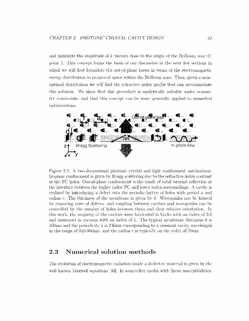
photon energy band structure for a triangular lattice PC are shown in Fig. 2.2, where
it can be seen that the reciprocal lattice is also triangular, but rotated relative to the
original lattice by 30°.
As can be seen from Fig. 2.2 the so-called light line accounts for the boundary
between lossy and confined modes. The light line is given by the condition:
^ = ̂ T S (2.1)
where kx, ky are the in-plane wave vector components, A is the wavelength and no is
the index of refraction of the medium surrounding the PC. The problem of designing
high quality cavities with long photon storage times can be reduced to the problem
of shaping the mode in reciprocal space (k-space) to contain most of its energy below
the light line. The k-space distribution is strongly affected by the dielectric struc
ture of the PC, and the refractive index must be designed to minimize the spread
CHAPTER 2. PHOTONIC CRYSTAL CAVITY DESIGN 22
and minimize the amplitude of k vectors close to the origin of the Brillouin zone (T
point ). This concept forms the basis of our discussion in the next few sections in
which we will first formulate the out-of-plane losses in terms of the electromagnetic
energy distribution in reciprocal space within the Brillouin zone. Then, given a near-
optimal distribution we will find the refractive index profile that can accommodate
this solution. We show that this procedure is analytically solvable under symme
try constraints, and that this concept can be more generally applied to numerical
optimizations.
Figure 2.1: A two-dimensional photonic crystal and light confinement mechanisms. In-plane confinement is given by Bragg scattering due to the refractive index contrast at the PC holes. Out-of-plane confinement is the result of total internal reflection at the interface between the higher index PC and lower index surroundings. A cavity is realized by introducing a defect into the periodic lattice of holes with period a and radius r. The thickness of the membrane is given by d. Waveguides can be formed by removing rows of defects, and coupling between cavities and waveguides can be controlled by the number of holes between them and their relative orientation. In this work, the majority of the cavities were fabricated in GaAs with an index of 3.6 and measured in vacuum with an index of 1. The typical membrane thickness d is 160nm and the periodicity a is 246nm corresponding to a resonant cavity wavelength in the range of 910-950nm. and the radius r is typically on the order of 70nm.
2.3 Numerical solution methods
The evolution of electromagnetic radiation inside a dielectric material is given by the
well known Maxwell equations [33]. In source-free media with linear susceptibilities.
CHAPTER 2. PHOTONIC CRYSTAL CAVITY DESIGN 23
Figure 2.2: (a) Schematic representation of the photonic crystal lattice with lattice vectors ai,a2 that map out the triangular lattice, (b) The reciprocal lattice corresponding to the triangular lattice in (a) with reciprocal lattice vectors 61,62, where |6i| = |62| = 47r/\/3a. The first Brillouin zone is indicated by the blue line and the irreducible Brillouin zone is shaded in green. The black circle corresponds to the light line (or cone) given by Eq. 2.1. In (c) we show the resulting band structure of the triangular crystal with r = 0.3a, d = 0.65a and n = 3.6. The filled circles correspond to frequencies of confined states inside the lattice at a particular value of the wave vector as it traces out the edge of the irreducible Brillouin zone indicated by the green line in the inset in (c). States above the light line (solid line) correspond to lossy states (with non-imaginary values of kz).
CHAPTER 2. PHOTONIC CRYSTAL CAVITY DESIGN 24
the equations reduce to the following wave equation for the electric field (with a
similar equation for the magnetic field):
V x V x £ ( r > - ^ ^ T (2-2)
The wave equation is numerically solved in the time domain using the Finite Dif
ference Time Domain - FDTD algorithm, which accurately models radiative losses and
simulates boundary conditions that appropriately simulate free space; the overview
of these numerical methods can be found in Ref. [34]. In most of the work PCs are
discretized with 20 points (unit spatial increments) per period a.
2.4 Bloch modes, reciprocal space and cavities
As discussed previously, our optimization technique relies on tailoring the electro
magnetic mode distribution in reciprocal space. In this section we give the Fourier
formulation of the fundamental PC lattice and waveguide modes. The cavity is formed
by closing the ends of the PC waveguide and can therefore be expanded in waveguide
modes. This results in a formulation of the electromagnetic problem that is conve
nient for an analytical solution, as the mode is constrained to translational invariance
in one dimension.
The periodic refractive index e(f) — e(f+R) can be written as a Fourier sum over
spatial frequency components in the periodic plane:
e(r) = J2 W** (2-3) G
Here G are the reciprocal lattice vectors in the (kx, ky) plane and are defined by
G • R = 27rm for integer m. The real and reciprocal lattice vectors for the square and
hexagonal lattices with periodicity a are:
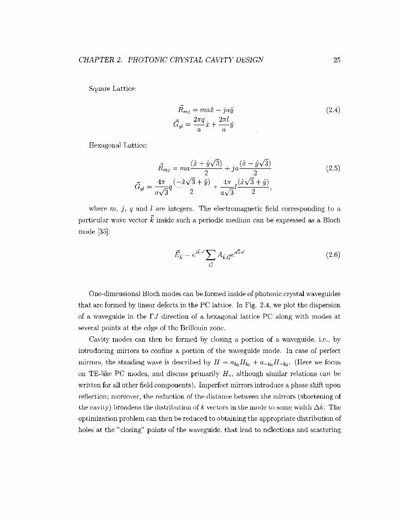
CHAPTER 2. PHOTONIC CRYSTAL CAVITY DESIGN 25
Square Lattice:
Rmj = max + jay (2.4) - 2-rrq A 2TTI A
G? / = x H y a a
Hexagonal Lattice:
- (x + yy/3) {x- yV3) Rmj = ma- + ja- (2.5)
^ = _4TT_ (-xV3 + y) 4TT (xy/3 + y)
ay/3 2 a\/3 2
where m, j , q and / are integers. The electromagnetic field corresponding to a
particular wave vector k inside such a periodic medium can be expressed as a Bloch
mode [35]:
Ej: = e^J2\G^ (2.6) G
One-dimensional Bloch modes can be formed inside of photonic crystal waveguides
that are formed by linear defects in the PC lattice. In Fig. 2.4, we plot the dispersion
of a waveguide in the YJ direction of a hexagonal lattice PC along with modes at
several points at the edge of the Brillouin zone.
Cavity modes can then be formed by closing a portion of a waveguide, i.e., by
introducing mirrors to confine a portion of the waveguide mode. In case of perfect
mirrors, the standing wave is described by H = akQHkQ + a_fc0i/_fe0. (Here we focus
on TE-like PC modes, and discuss primarily Hz, although similar relations can be
written for all other field components). Imperfect mirrors introduce a phase shift upon
reflection; moreover, the reduction of the distance between the mirrors (shortening of
the cavity) broadens the distribution of k vectors in the mode to some width Ak. The
optimization problem can then be reduced to obtaining the appropriate distribution of
holes at the "closing" points of the waveguide, that lead to reflections and scattering
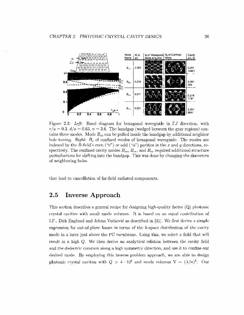
CHAPTER 2. PHOTONIC CRYSTAL CAVITY DESIGN 26
Figure 2.3: Left: Band diagram for hexagonal waveguide in IV direction, with r/a = 0.3, d/a = 0.65, n = 3.6. The bandgap (wedged between the gray regions) contains three modes. Mode B00 can be pulled inside the bandgap by additional neighbor hole tuning. Right: Bz of confined modes of hexagonal waveguide. The modes are indexed by the 5-field's even ("e") or odd ("o") parities in the x and y directions, respectively. The confined cavity modes B00, Bee, and Beo required additional structure perturbations for shifting into the bandgap. This was done by changing the diameters of neighboring holes.
that lead to cancellation of far-field radiated components.
2.5 Inverse Approach
This section describes a general recipe for designing high-quality factor (Q) photonic
crystal cavities with small mode volumes. It is based on an equal contribution of
I.F., Dirk Englund and Jelena Vuckovic as described in [31]. We first derive a simple
expression for out-of-plane losses in terms of the /c-space distribution of the cavity
mode in a layer just above the PC membrane. Using this, we select a field that will
result in a high Q. We then derive an analytical relation between the cavity field
and the dielectric constant along a high symmetry direction, and use it to confine our
desired mode. By employing this inverse problem approach, we are able to design
photonic crystal cavities with Q > 4 • 106 and mode volumes V ~ (A/n)3. Our
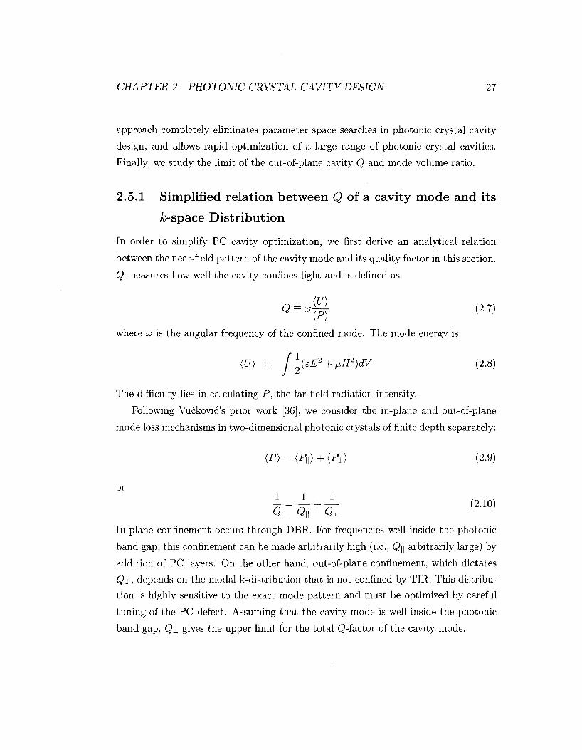
CHAPTER 2. PHOTONIC CRYSTAL CAVITY DESIGN 27
approach completely eliminates parameter space searches in photonic crystal cavity
design, and allows rapid optimization of a large range of photonic crystal cavities.
Finally, we study the limit of the out-of-plane cavity Q and mode volume ratio.
2.5.1 Simplified relation between Q of a cavity mode and its
fc-space Distribution
In order to simplify PC cavity optimization, we first derive an analytical relation
between the near-field pattern of the cavity mode and its quality factor in this section.
Q measures how well the cavity confines light and is defined as
Q = ^ y (2-7)
where u is the angular frequency of the confined mode. The mode energy is
(U) = J \{eE2 + ^H2)dV (2.8)
The difficulty lies in calculating P, the far-field radiation intensity.
Following Vuckovic's prior work [36], we consider the in-plane and out-of-plane
mode loss mechanisms in two-dimensional photonic crystals of finite depth separately:
<P> = ^ l ) + (Px> (2-9)
or
£ = 4 + £ (210)
In-plane confinement occurs through DBR. For frequencies well inside the photonic
band gap, this confinement can be made arbitrarily high (i.e., Q\\ arbitrarily large) by
addition of PC layers. On the other hand, out-of-plane confinement, which dictates
Q±, depends on the modal k-distribution that is not confined by TIR. This distribu
tion is highly sensitive to the exact mode pattern and must be optimized by careful
tuning of the PC defect. Assuming that the cavity mode is well inside the photonic
band gap, Qj_ gives the upper limit for the total Q-factor of the cavity mode.
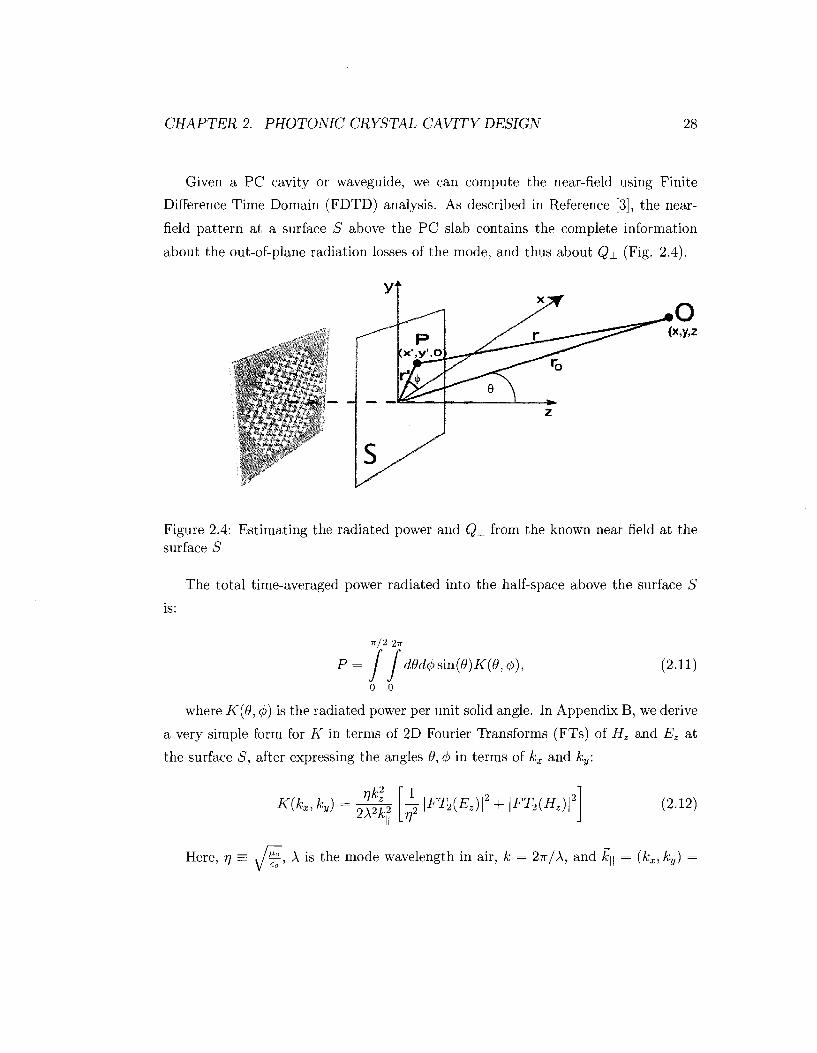
CHAPTER 2. PHOTONIC CRYSTAL CAVITY DESIGN 28
Given a PC cavity or waveguide, we can compute the near-field using Finite
Difference Time Domain (FDTD) analysis. As described in Reference [3], the near-
field pattern at a surface S above the PC slab contains the complete information
about the out-of-plane radiation losses of the mode, and thus about Q± (Fig. 2.4).
<x,y,z
Figure 2.4: Estimating the radiated power and Q± from the known near field at the surface S
The total time-averaged power radiated into the half-space above the surface S
is:
TT/2 2TT
f f d9d(i>sm{9)K(0,<t>), (2.11)
o o
where K(9, (j>) is the radiated power per unit solid angle. In Appendix B, we derive
a very simple form for K in terms of 2D Fourier Transforms (FTs) of Hz and Ez at
the surface S, after expressing the angles 9, 4> in terms of kx and ky:
77 A* K{kx,ky) = 2^2^.2
1 \FT2{EZ)\2 + \FT2(HZ (2.12)
Here, r\ = 4/—, A is the mode wavelength in air, k = 2ir/\, and fc|j = (kx,ky) =
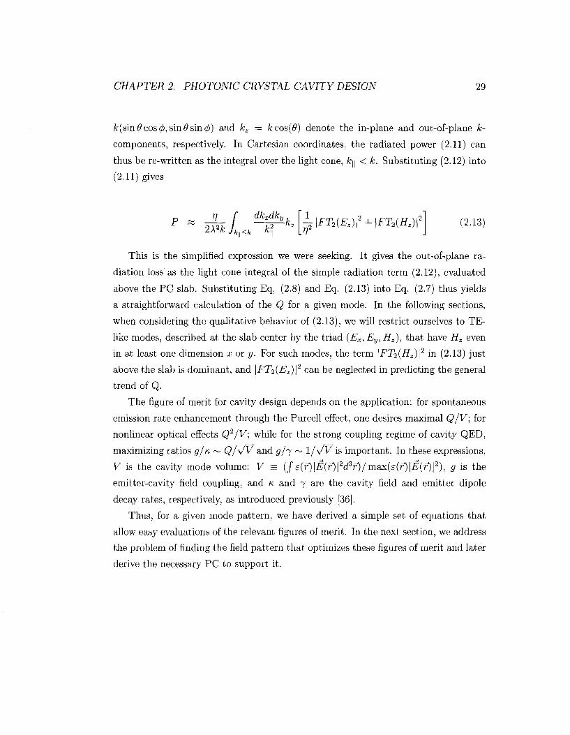
CHAPTER 2. PHOTONIC CRYSTAL CAVITY DESIGN 29
k(s'm6cos(fi,sin#sin</>) and kz = kcos(6) denote the in-plane and out-of-plane k-
components, respectively. In Cartesian coordinates, the radiated power (2.11) can
thus be re-written as the integral over the light cone, k^ < k. Substituting (2.12) into
(2.11) gives
V f ^ ' / / CtKxu,Ky
2A k Jk <k &ii ~\FT2(EZ)\2 + \FT2(HZ)\2
V (2.13)
This is the simplified expression we were seeking. It gives the out-of-plane ra
diation loss as the light cone integral of the simple radiation term (2.12), evaluated
above the PC slab. Substituting Eq. (2.8) and Eq. (2.13) into Eq. (2.7) thus yields
a straightforward calculation of the Q for a given mode. In the following sections,
when considering the qualitative behavior of (2.13), we will restrict ourselves to TE-
like modes, described at the slab center by the triad (Ex, Ey,Hz), that have Hz even
in at least one dimension x or y. For such modes, the term \FT2(HZ)\2 in (2.13) just
above the slab is dominant, and \FT2(EZ)\2 can be neglected in predicting the general
trend of Q.
The figure of merit for cavity design depends on the application: for spontaneous
emission rate enhancement through the Purcell effect, one desires maximal Q/V; for
nonlinear optical effects Q2/V; while for the strong coupling regime of cavity QED,
maximizing ratios gJK ~ Q/W and g/j ~ 1/y/V is important. In these expressions,
V is the cavity mode volume: V = (/e(r)\E(r)\2d3r)/m&x(e(f)\E(r)\2), g is the
emitter-cavity field coupling, and K and 7 are the cavity field and emitter dipole
decay rates, respectively, as introduced previously [36].
Thus, for a given mode pattern, we have derived a simple set of equations that
allow easy evaluations of the relevant figures of merit. In the next section, we address
the problem of finding the field pattern that optimizes these figures of merit and later
derive the necessary PC to support it.
CHAPTER 2. PHOTONIC CRYSTAL CAVITY DESIGN 30
2.5.2 Opt imal k-space d is tr ibut ion
The magnetic field in a closed waveguide cavity can be written in terms of the forward
and backward propagating waveguide modes as:
ko+Ak/2
#.(*,*) ~ E E (\G^+ A-i&-**) ^ (2-14) G feo-Afe/2
A similar expansion of Hz can be made at the surface S directly above the PC
slab (see Fig. 2.4), which is relevant for calculation of radiation losses. The Fourier
transform of the above equation gives the fc-space distribution of the cavity mode,
with coefficients A% Q and A_^ Q. The distribution peaks are positioned at ±k0 ± G,
with widths directly proportional to Ak. The fc-space distribution is mapped to other
points in Fourier space by the reciprocal lattice vectors G. To reduce radiative losses,
the mapping of components into the light cone should be minimized [3]. Therefore, the
center of the mode distribution k0 should be positioned at the edge of the first Brillouin
zone, which is the region in &-space that cannot be mapped into the light cone by
any reciprocal lattice vector G (see Fig. 2.2). For example, this region corresponds to
k0 = ±jx^kx±jy^ky for the square lattice, where jx,jy e 0,1. Clearly, \jx\ = \jy\ = 1
is a better choice for k0, since it defines the edge point of the 1st Brillouin zone
which is farthest from the light cone. Thus, modes centered at this point and fc-space
broadened due to confinement, will radiate the least. Similarly, the optimum k0 for
the cavities resonating in the TJ direction of the hexagonal lattice is ko = ±£fcx (as
it is for the cavity from Ref. [37], and for the TX direction is k0 = ±-2y=ky (as it is
for the cavity from Refs. [36] and [3]).
Assuming that the optimum choice of k0 at the edge of the first Brillouin zone has
been made, the summation over G can be neglected in Eq. (2.14), because it only
gives additional Fourier components which are even further away from the light cone
and do not contribute to the calculation of the radiation losses. In that case, we can
express the field distribution as:
Hz(x,y)= [ fdkxdkyA(kx,ky)e^, (2.15)
CHAPTER 2. PHOTONIC CRYSTAL CAVITY DESIGN 31
where A(kx, ky) is the Fourier space envelope of the mode, which is some function cen
tered at k0 = (±kox, ±koy) with the full-width half-maximum (FWHM) determined
by Ak = (Akx,Aky) in the kx and ky directions respectively. Eq. (2.15) implies
that Hz(x,y) and A(kx,ky) are related by 2D Fourier transforms. For example, if
A(kx, ky) can be approximated by a Gaussian centered at kQ = (k0x, k0y) and with the
FWHM of (Akx, Aky), the real space field distribution Hz(x, y) is a function periodic
in the x and y directions with the spatial frequencies of kox and k0y, respectively, and
modulated by Gaussian envelope with the widths Ax ~ l/Akx and Ay ~ 1/Aky.
Therefore, the properties of the Fourier transforms imply that the extent of the mode
in the Fourier space AA; is inversely proportional to the mode extent in real space
(i.e., the cavity length), making the problem of Q maximization even more challeng
ing when V needs to be simultaneously minimized. This has already been attempted
in the past for a dipole cavity [36, 3] and a linear defect [37, 38, 39], by using extensive
parameters space search. In the following sections, we will design high Q cavities by
completely eliminating the need for parameter space searches and iterative trial and
error approaches.
There are two main applications of Eq. (2.13). First, this formulation of the
cavity Q factor allows us to investigate the theoretical limits of this parameter and
its relation to the mode volume of the cavity. Second, it allows us to quantify the
effect of our perturbation on the optimization of Q using only one or two layers of the
computational field and almost negligible computational time compared to standard
numerical methods. We applied Eq. (2.13) to cavities obtained from an iterative
parameter space search. These cavities were previously studied in [3] and [37]. The
results for Q using Eq. (2.13) at S, as well as full first-principle FDTD simulations are
shown in Fig. 2.5. A good match is observed. Therefore, our expression (2.13) is a
valid measure of the radiative properties of the cavity and can be used to theoretically
approach the design problem; we can also use this form to speed up the optimization
of the cavity parameters. The discrepancy between Eq. (2.13) and FDTD is primarily
due to discretization errors.
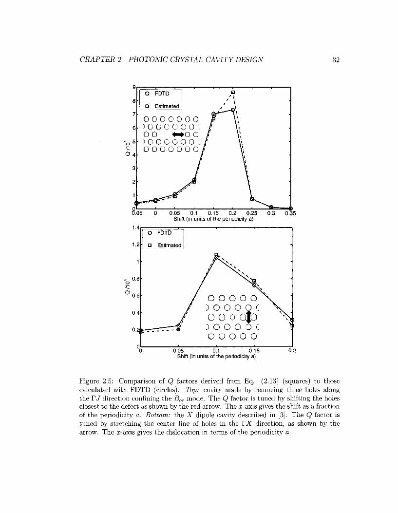
CHAPTER 2. PHOTONIC CRYSTAL CAVITY DESIGN 32
o o 4
O FDTD
D Estimated
0 0 0 0 0 0 0 I- ) 0 0 0 0 0 0 (
o o «-+o o I- ) 0 0 0 0 0 0 C
0 0 0 0 0 0 0
3.05 0 0.05 0.1 0.15 0.2 0.25 Shift (in units of the periodicity a)
1.4
1.2
O FDTD
• Estimated
) 0 0 0 0 ( o o o o o
0.05 0.1 0.15 Shift (in units of the periodicity a)
0.3 0.35
0.2
Figure 2.5: Comparison of Q factors derived from Eq. (2.13) (squares) to those calculated with FDTD (circles). Top: cavity made by removing three holes along the YJ direction confining the Boe mode. The Q factor is tuned by shifting the holes closest to the defect as shown by the red arrow. The x-scxis gives the shift as a fraction of the periodicity a. Bottom: the X dipole cavity described in [3]. The Q factor is tuned by stretching the center line of holes in the FX direction, as shown by the arrow. The x-axis gives the dislocation in terms of the periodicity a.
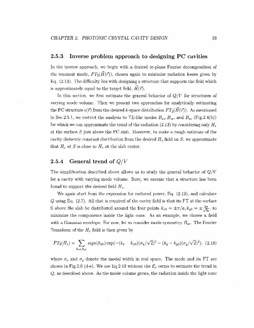
CHAPTER 2. PHOTONIC CRYSTAL CAVITY DESIGN 33
2.5.3 Inverse problem approach to designing PC cavities
In the inverse approach, we begin with a desired in-plane Fourier decomposition of
the resonant mode, FT2(H(f)), chosen again to minimize radiation losses given by
Eq. (2.13). The difficulty lies with designing a structure that supports the field which
is approximately equal to the target field, H{f).
In this section, we first estimate the general behavior of Q/V for structures of
varying mode volume. Then we present two approaches for analytically estimating
the PC structure e(f) from the desired &-space distribution FT2(H(r)). As mentioned
in Sec.2.5.1, we restrict the analysis to TE-like modes Beo,Boe, and Bee (Fig.2.4(b))
for which we can approximate the trend of the radiation (2.13) by considering only Hz
at the surface S just above the PC slab. Moreover, to make a rough estimate of the
cavity dielectric constant distribution from the desired Hz field on S, we approximate
that Hz at S is close to Hz at the slab center.
2.5.4 General trend of Q/V
The simplification described above allows us to study the general behavior of Q/V
for a cavity with varying mode volume. Here, we assume that a structure has been
found to support the desired field Hz.
We again start from the expression for radiated power, Eq. (2.13), and calculate
Q using Eq. (2.7). All that is required of the cavity field is that its FT at the surface
S above the slab be distributed around the four points kx$ = ±n/a,kyo = ±-^=-, to
minimize the components inside the light cone. As an example, we choose a field
with a Gaussian envelope. For now, let us consider mode symmetry Boe. The Fourier
Transform of the Hz field is then given by
FT2{HZ) = Y, sign(kx0)exp(-(kx - kx0)(ax/V2)2 - (kv - ky0)(ay/V2)2), (2.16)
where ox and ay denote the modal width in real space. The mode and its FT are
shown in Fig.2.6 (d-e). We use Eq.2.13 without the Ez terms to estimate the trend in
Q, as described above. As the mode volume grows, the radiation inside the light cone
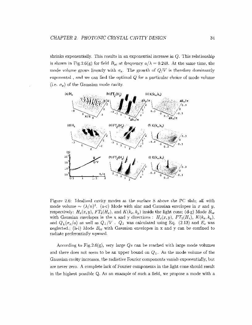
CHAPTER 2. PHOTONIC CRYSTAL CAVITY DESIGN 34
shrinks exponentially. This results in an exponential increase in Q. This relationship
is shown in Fig.2.6(g) for field Boe at frequency a/A = 0.248. At the same time, the
mode volume grows linearly with ax. The growth of Q/V is therefore dominantly
exponental , and we can find the optimal Q for a particular choice of mode volume
(i.e. <jx) of the Gaussian mode cavity.
(a)Hz WFT^hy <c)K(kx,ky)
a,ky/jt t
f /v i / / /
J ' 1 / a - 2
(i) K(kx,kv)
0.5 1.5 2
Figure 2.6: Idealized cavity modes at the surface S above the PC slab; all with mode volume ~ (A/n)3. (a-c) Mode with sine and Gaussian envelopes in x and y, respectively: Hz(x,y), FT2(HZ), and K(kx,ky) inside the light cone; (d-g) Mode Boe
with Gaussian envelopes in the x and y directions : Hz(x,y), FT2{HZ), K(kx,ky), and Q±(<Jx/a) as well as Q±/V . Q± was calculated using Eq. (2.13) and Ez was neglected.; (h-i) Mode Bee with Gaussian envelopes in x and y can be confined to radiate preferentially upward.
According to Fig.2.6(g), very large Qs can be reached with large mode volumes
and there does not seem to be an upper bound on Qj_. As the mode volume of the
Gaussian cavity increases, the radiative Fourier components vanish exponentially, but
are never zero. A complete lack of Fourier components in the light cone should result
in the highest possible Q. As an example of such a field, we propose a mode with a
CHAPTER 2. PHOTONIC CRYSTAL CAVITY DESIGN 35
sine envelope in x and a Gaussian one in y. The FT of this mode in Fig.2.6(b) is
described by
FT2{HZ)= Yl eM~(K ~ ky0)2(ay/V2)2)Rect(kx - kx0,Akx), (2.17)
KxQ tfcyO
where Rect(kx, Akx) is a rectangular function of width Akx and centered at kx.
The Fourier-transform implies that the cavity mode is described by a sine function
in x whose width is inversely proportional to the width of the rectangle Rect(kx, Akx).
To our knowledge, this target field has not been previously considered in PC cavity
design. This field is shown in Fig.2.6(a-c). Though it has no out-of-plane losses, this
field drops off as - and therefore requires a larger structure than the Gaussian field
for confinement.
Over the past years, many new designs with ever-higher theoretical quality factors
have been suggested [39]. In light of our result that Q/V increases exponentially with
mode size, these large Qs are not surprising.
It is interesting to note that Eq. (2.12) also allows one to calculate the field
required to radiate with a desired radiation distribution. For example, many applica
tions require radiation with a strong vertical component; waveguide modes with even
Hz can be confined for this purpose so that K(kXlky) dominates losses at the origin
in k—space, as shown for instance in Fig. 2.6(h-i) for the confined mode pattern Bee
of Fig.2.4.
2.5.5 Estimating Photonic Crystal Design from £>space Field
Distribution
Now we introduce two analytical ways of estimating the dielectric structure e(f) that
supports a cavity field that is approximately equal to the desired field Hc. These
methods directly calculate the dielectric profile from the desired field distribution,
without any dynamic tuning of PC parameters, and are thus computationally fast.
We focus on TE-like modes, since they see a large bandgap and exhibit electric-field
CHAPTER 2. PHOTONIC CRYSTAL CAVITY DESIGN 36
maxima at the slab center. For TE-like modes, Hc = Hcz at the center of the slab,
and Hc w Hcz at the surface. First, we relate Hc to one of the allowed waveguide
fields Hw. The fields Hc and Hw at the center of the PC slab (z — 0) are solutions to
the homogeneous wave equation with the corresponding refractive indices e.c and ew,
respectively.
f)2 ff 1 - ^ o — ^ = ulimHc = V x - V x | (2.18)
dt2 ec
-^o^-~ = (JtfM>Hw = V x i v x f f f f i (2.19) Oh €w
Here UJC and LOW are the frequencies of the cavity and waveguide fields. We expand
the cavity mode into waveguide Bloch modes:
HC = Y, CkUk{f)e^-^t] (2.20)
where uk is the periodic part of the Bloch wave. Assuming that the cavity field is
composed of the waveguide modes with k ss fc0, we can approximate uk{r) ~ Uko{r),
which leads to the slowly varying envelope approximation:
Hc « Uk^rje1^-"^ J2 ckei^-^)-r-^k-Uw)t) = HwHe, (2.21)
k
where the waveguide mode Hw = uiio(f)e^ko'r~UJ,nt"1 and the cavity field envelope He — V ^ c, ei{(k-k0)-r-(ujk-ujw)t)
The cavity and waveguide fields FT-distributions are concentrated at the edge of -, |2
the Brillouin zone, where uJi ss UJ2 + a k — ko and a « l (i.e., the band is nearly
flat). Differentiating (2.21) in time twice gives:
d2H, = -u2Hc = -J2 W^eW-^ [wl + a\k- kn\
2} r ^ j
dt2
k
-Hw ^ C k e ^ - k ^ - ^ - ^ [u2w + a\k- k0\
2] = -co2wHwHe + aHwV2He (2.22)
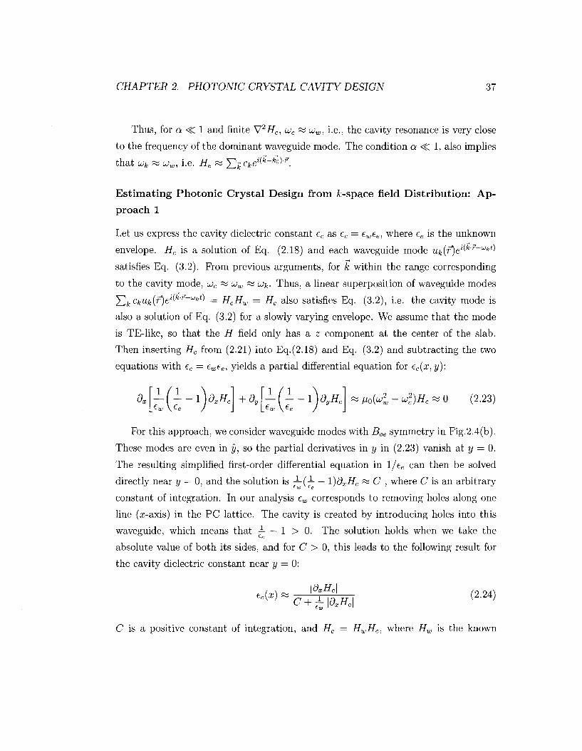
CHAPTER 2. PHOTONIC CRYSTAL CAVITY DESIGN 37
Thus, for a <C 1 and finite V2ife, LUC « UJW, i.e., the cavity resonance is very close
to the frequency of the dominant waveguide mode. The condition a < l , also implies
that <jjk ~ UJW, i.e. He ss J2n Ckei{k~h°yif-
Estimating Photonic Crystal Design from fc-space field Distribution: Ap
proach 1
Let us express the cavity dielectric constant ec as ec = ewee, where ee is the unknown
envelope. Hc is a solution of Eq. (2.18) and each waveguide mode Uk{r)eli-k'?~lJJkf:)
satisfies Eq. (3.2). Prom previous arguments, for k within the range corresponding
to the cavity mode, UJC « u>w « ujk. Thus, a linear superposition of waveguide modes T^2kckuk{;r)el{-k'r~UJkt'> = HeHw = Hc also satisfies Eq. (3.2), i.e. the cavity mode is
also a solution of Eq. (3.2) for a slowly varying envelope. We assume that the mode
is TE-like, so that the H field only has a z component at the center of the slab.
Then inserting Hc from (2.21) into Eq.(2.18) and Eq. (3.2) and subtracting the two
equations with ec = ewee, yields a partial differential equation for ec(x,y):
dx ^ e
-l)dxHc + 9y l ( I - i )<yf c Mo(^ - UJ2C)HC « 0 (2.23)
For this approach, we consider waveguide modes with Boe symmetry in Fig.2.4(b).
These modes are even in y, so the partial derivatives in y in (2.23) vanish at y = 0.
The resulting simplified first-order differential equation in l/ee can then be solved
directly near y — 0, and the solution is —(— — l)dxHc « C , where C is an arbitrary
constant of integration. In our analysis ew corresponds to removing holes along one
line (x-axis) in the PC lattice. The cavity is created by introducing holes into this
waveguide, which means that — — 1 > 0. The solution holds when we take the
absolute value of both its sides, and for C > 0, this leads to the following result for
the cavity dielectric constant near y = 0:
C is a positive constant of integration, and Hc = HwHe, where Hw is the known
CHAPTER 2. PHOTONIC CRYSTAL CAVITY DESIGN 38
waveguide field and He is the desired field envelope. C can be chosen by fixing the
value of ec at some x, leading to a particular solution for ec. In our cavity designs we
chose C such that the value of ec is close to ew at the cavity center. To implement
this design in a practical structure, we need to approximate this continuous ec by
means of a binary function with low and high-index materials e/ and eh, respectively.
We do this by finding, in every period j , the air hole radius r, that gives the same
field-weighted averaged index on the a>axis:
fja+a/2 ja+a/2
/ (eh + (ei -eh)Rect(ja,rj)) Ec dx = ec(x) Ec dx, (2.25) Jja—a/2 Jja—a/2
where Ec is estimated from a linear superposition of waveguide modes as Ec oc V x Hc.
We assume that the holes are centered at the positions of the unperturbed hexagonal
lattice PC holes.
The radii rj thus give the required index profile along the x symmetry axis. The
exact shape of the holes in 3D is secondary - we choose cylindrical holes for conve
nience. Furthermore, we are free to preserve the original hexagonal crystal structure
of the PC far away from the cavity where the field is vanishing.
To illustrate the power of this inverse approach, we now design PC cavities that
support the Gaussian and sine-type modes of Eq. (2.16), (2.17). In each case, we start
with the waveguide field Boe of Fig.2.4(b) confined in a line-defect of a hexagonal PC.
The calculated dielectric structures and FDTD simulated fields inside them are shown
in Fig. 2.7. The FT fields on S also show a close match and very little power radiated
inside the light cone (Fig.2.7(c,f)). This results in very large Q values, estimated from
Q± to limit computational constraints. These estimates were done in two ways, using
first principles FDTD simulations [36], and direct integration of lossy components
by Eq. (2.13). The results are listed in Table 2.1 and show an improvement of
roughly three orders of magnitude over the unmodified structure of Fig. 2.5 with
as small increase in mode volume. Furthermore, a fit of the resulting field pattern
to a Gaussian envelope multiplied by a Sine, yielded a value of ax/a « 1.6, which,
according to the plot in Fig. 2.6 g., puts us at the attainable limit of Q± at this mode
volume.
CHAPTER 2. PHOTONIC CRYSTAL CAVITY DESIGN 39
In our FDTD simulations, we verified that Q± correctly estimates Q by noting
that Q± did not change appreciably as the number of PC periods in the x— and
y— directions, Nx and Ny, was increased: for the Gaussian-type (sine-type) mode,
increasing the simulation size from Nx = 13, Nv = 13 (Nx = 21, Ny = 9) PC periods
to Nx = 25, Ny = 13 (Nx = 33, Ny = 13) changed quality factors from Q\\ = 22 •
103, Q± = 1.4 • 106 (Q|| = 17 • 103, Q± = 4.2 • 106) to Q,, = 180 • 103, Q± = 1.48 • 106
(Q|j = 260 • 103, Q± = 4.0 • 106). (The number of PC periods in the x-direction in
which the holes are modulated to introduce a cavity is 9 and 29 for Gaussian and
sine cavity, respectively, while both cavities consist of only one line of defect holes
in the y-direction.) Thus, with enough periods, the quality factors would be limited
to Q±, as summarized in the table. In the calculation of Q, the vertically emitted
power (F||) was estimated from the fields a distance ~ 0.25 • A above the PC surface.
Note that the frequencies a/A closely match those of the original waveguide field Boe
(a/Aca„=0.251), validating the assumption in the derivation.
Table 2.1: Q values of structures derived with inverse-approach 1
Gaussian Sine
Unmodified 3-hole defect
^V "cav
0.248 0.247 0.251
Qcav (freq. filter) 1.4 • 10b
4.2 • 106
6.6 • 103
Qcav (Eq. (2.13)) 1.6 • 10° 4.3 • 106
6.4 • 103
' mode \ v )
0.85 1.43 0.63
Estimating Photonic Crystal Design from A;-space Field Distribution: Ap
proach 2
We now derive a closed-form expression for ec(x, y) that is valid in the whole PC
plane (instead of the center line only). Again, begin with the cavity field H(r) — zHc
consisting of the product of the waveguide field and a slowly varying envelope, Hc =
HwHe, and treat the cavity dielectric constant as: — = —^—h 7-. In the PC plane,
CHAPTER 2. PHOTONIC CRYSTAL CAVITY DESIGN 40
Figure 2.7: FDTD simulations for the derived Gaussian cavity (a-c) and the derived sine cavity (d-f). Gaussian: (a) Bz; (b) \E\; (c) FT pattern of Bz taken above the PC slab (blue) and target pattern (red). Sine: (d) Bz; (e) \E\; (f) FT pattern of Bz taken above the PC slab (blue) and target pattern (red) (The target FT for the sine cavity appears jagged due to sampling, since the function was expressed with the resolution of the simulations). The cavities were simulated with a discretization of 20 points per period a, PC slab hole radius r = 0.3a, slab thickness of 0.6a and refractive index 3.6. Starting at the center, the defect hole radii in units of periodicity a are: (0,0,0.025,0.05,0.075,0.1 ,0.075,0.075,0.1,0.125,0.125,0.125,0.1,0.125,0.15,0.3,0.3) for the sine cavity, and (0.025,0.025,0.05,0.1,0.225) for the Gaussian cavity.
Eq. (2.18, 3.2) for a TE-like mode can be rewritten as
-<4lM>Hc = V - ( - V # c ) (2.26)
-LU2wfi0Hw = V - ( - V # w ) (2.27)
Multiplying the last equation by He, subtracting from the first, and recalling that
UJC ~ tow yields
u2wIM)HeHw - uj2
cii0Hc = HoHc(u>2w - LO2
C) W 0 (2.28)
= V • ( -Vi f c ) - HeV • (—VHW) €c tw
sa V - ( — V H C ) (2.29) tpert
CHAPTER 2. PHOTONIC CRYSTAL CAVITY DESIGN 41
where the last line results after some algebra and dropping spatial derivatives of
the slowly varying envelope He. This relation is a quasilinear partial differential
equation in l/epert. With boundary conditions that can be estimated from the original
waveguide field, this equation can in principle be solved for ec (e.g., [40]).
Alternatively, one can find a formal solution for epert by assuming a vector function
£(r) chosen to satisfy the boundary conditions, so that
VHC = V x £ (2.30) £pert
or 1 V x £• VH*
71 = IV/T p C (2"31)
^pert | v ±±c\
This gives is the formal solution of the full dielectric constant ec = (e~^rt + e^1) - 1 in
the plane of the photonic crystal.
2.6 Genetic Algorithms
Although the inverse methods yield interesting results, they do not take into account
fabrication difficulties, and so may yield designs that cannot be realized. It is difficult
to introduce design constraints into the inverse approach. Brute force techniques can
easily incorporate fabrication constraints, but are computationally intensive, and so
a smart design technique is necessary. In large parameter spaces, the optimization
problem may have multiple local optima, and the typical gradient search methods
and convex optimization may not be applicable to the modeling of photonic crystal
resonators. One of the most promising numerical methods for the rapid design of
photonic structures is the approach of genetic algorithms (GAs). This section is
taken from Ref. [32], which came as a result of my mentorship of Joel Goh, who
was an undergraduate researcher in the Vuckovic group. I will first introduce and
describe the algorithm and then give an example application of the algorithm to
the optimization of the far field radiation of a one-dimensional resonator, which uses
either integration over the Fourier space to minimize power losses, or requires the
resulting electromagnetic mode to be closest to a desired field profile, as in Section
CHAPTER 2. PHOTONIC CRYSTAL CAVITY DESIGN 42
2.5. Thus, we can apply the theory used in the previous sections as a fitness measure
in our optimization algorithm.
2.6.1 Algorithm description
Genetic algorithms (also known as Evolutionary algorithms) are a class of optimiza
tion algorithms that apply principles of natural evolution to optimize a given ob
jective [41, 42, 43]. In the genetic optimization of a problem, different solutions to
the problem are picked (usually randomly), and a measure of fitness is assigned to
each solution. On a given generation of the design, a set of operations, analogous
to mutation and reproduction in natural selection, are performed on these solutions
to create a new generation of solutions, which should theoretically be "fitter" than
their parents. This process is repeated until the algorithm terminates, typically after
a pre-defined number of generations, or after a particularly "fit" solution is found, or
more generally, when a generation of solutions meets some pre-defined convergence
criterion.
2.6.2 Algorithm implementation
Genetic algorithms have already been used in PC design to find non-intuitive large-
bandgap designs [44, 45] and for designing PC fibers [46]. In this work, we implement
a general GA to optimize 1 and 2-dimensional photonic bandgap structures, and show
that it is able to robustly optimize these structures for a wide variety of objectives.
In the 1-dimensional case, we consider the design of planar photonic crystal cavities
(which are infinite in extent in the remaining two spatial dimensions) by varying the
widths of dielectric stacks; and in the 2-dimensional case, we perform the genetic
optimization by varying the sizes of circular holes in a triangular lattice. These
approaches were chosen because the search space is conveniently well-constrained in
these paradigms, and the optimized structures (for the triangular lattice) can be easily
fabricated.
In addition, we used the following parameters for the implementation of our GA:
CHAPTER 2. PHOTONIC CRYSTAL CAVITY DESIGN 43
Chromosome encoding. We used a direct-chromosome encoding, where the var
ious optimization parameters were stored in a vector. For the current sim
ulations, for simplicity, we only varied the radii of cylindrical holes in a tri
angular lattice. Our implementation can be easily modified to include other
optimization parameters as well, such as the positions of the various holes, or
the refractive index of the dielectric material.
Selection. We used fitness-proportionate selection (also known as roulette-wheel
selection), to choose parent chromosomes for mating. In this selection scheme,
a chromosome is selected with a probability Pj that is proportional to its fitness
fi, as shown in Eq. (2.32).
Pi = -j~- (2-32)
IVIating. After a pair of parent chromosomes Vparent,\ and vparentt2 were selected,
they were mated to produce a child chromosome vchud by taking a random
convex combination of the parent vectors, as in Eq. (2.33).
A ~ Z7(0,1)
V child = ^parent,! + (1 — tyvparent,2 (2.33)
Muta t ion . Mutation was used to introduce diversity in the population. We used
two types of mutation in our simulations, a random-point crossover and a gaus-
sian mutation.
1) Random-point crossover: For an original chromosome vector vorig of
length N, we select a random index, k, from 0 to N as the crossover point, and
swap the two halves of v^g to produce the mutated vector, vmut, as represented
CHAPTER 2. PHOTONIC CRYSTAL CAVITY DESIGN 44
in Eq. (2.34).
Vorig = (Vl,V2j..-,VN)T
k ~ U{0,1,2,....,N}
Vmut = (vk+1,Vk+2,...,VN,Vi,V2,...,Vk^i)T (2.34)
2) Gaussian mutation: To mutate a chromosome vector by Gaussian mu
tation, we define each element of vmut to be independent and identically dis
tributed Gaussian Random Variables with mean v^g and a standard deviation
proportional to the corresponding elements of vorig. This searches the space in
the vicinity of the original chromosome vector vorig-
v™ut ^N^f^a2), i e {0,1, 2, . . . . ,#} (2.35)
a2 is an algorithm-specific variance, and can be tuned to change the extent of
parameter-space exploration due to mutation.
Cloning. To ensure that the maximum fitness of the population does not decrease,
we copied (cloned) the top few chromosomes with the highest fitness in each
generation and inserted them into the next generation.
2.6.3 Simulation results: Optimizing planar photonic cavity
cavities
Q-factor maximization
As in Section 2.5, we wish to minimize the fc-space amplitude inside the light cone, to
minimize radiation losses. Since it was shown that the inverse design problem leads
to satisfactory results when the problem is reduced to an effectively one-dimensional
problem, we decided to use this one dimensional problem as the starting point of the
optimization. We used one-dimensional photonic crystals as an approximation to the
closed waveguide cavities, and simulated them using the standard Transfer Matrix

CHAPTER 2. PHOTONIC CRYSTAL CAVITY DESIGN 45
method for the E-field [35]. The reflectance spectrum of the each cavity was obtained
using the Transfer Matrix method, and we used a heuristic peak-finding algorithm to
automatically search the spectrum for sharp resonance peaks. The resulting resonant
modes were then evaluated according to the chosen fitness function (which differed
depending on our optimization objective), and the maximum fitness found from all
the resonant modes was assigned as the fitness for the particular cavity. The fitness
function was taken as:
fitness ex I / \fsim{x) - ftarget(x)\2dx I (2.36)
The results are shown in Fig. 2.8, where we applied the GA to finding a dielectric
structure that supports an electric field with a sine and sine2 like envelopes that
should result in a high degree of suppression of radiative components at the k\\ = 0
point. Although the matching to both envelopes is not exact, it is quite promising.
Part of the error arises due to the finite simulation structure and discretization used
in the simulations. This work demonstrates that the GA is a good candidate for
optimizing PC cavities when the calculation time per structure is short, since many
trial solutions must be made per convergence cycle.
2.7 Conclusions
We have described a simple recipe for designing two-dimensional photonic crystal
cavities. Although the approach is general, we have demonstrated its utility on the
design of cavities with very large Q > 106 and near-minimal mode volume ~ (A/n)3.
These values follow our theoretically estimated value of Q±/V for the cavity with the
Gaussian field envelope, which means that we were able to find the maximal Q for
the given mode volume V under our assumptions. Our approach is analytical, and
the results are obtained within a single computational step. We first derive a simple
expression of the modal out-of-plane radiative loss and demonstrate its utility by
the straightforward calculation of Q factors on several cavity designs. Based on this
radiation expression, the recipe begins with choosing the FT mode pattern that gives
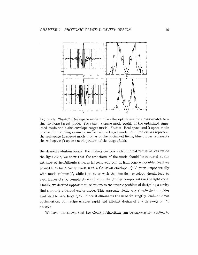
CHAPTER 2. PHOTONIC CRYSTAL CAVITY DESIGN 46
Figure 2.8: Top-left: Real-space mode profile after optimizing for closest-match to a sine-envelope target mode. Top-right: k-space mode profile of the optimized simulated mode and a sine-envelope target mode. Bottom: Real-space and k-space mode profiles for matching against a sinc2-envelope target mode. All: Red curves represent the real-space (k-space) mode profiles of the optimized fields, blue curves represents the real-space (k-space) mode profiles of the target fields.
the desired radiation losses. For high-Q cavities with minimal radiative loss inside
the light cone, we show that the transform of the mode should be centered at the
extremes of the Brillouin Zone, as far removed from the light cone as possible. Next we
proved that for a cavity mode with a Gaussian envelope, Q/V grows exponentially
with mode volume V, while the cavity with the sine field envelope should lead to
even higher Q's by completely eliminating the Fourier components in the light cone.
Finally, we derived approximate solutions to the inverse problem of designing a cavity
that supports a desired cavity mode. This approach yields very simple design guides
that lead to very large Q/V. Since it eliminates the need for lengthy trial-and-error
optimization, our recipe enables rapid and efficient design of a wide range of PC
cavities.
We have also shown that the Genetic Algorithm can be successfully applied to
CHAPTER 2. PHOTONIC CRYSTAL CAVITY DESIGN 47
designing photonic structures when the conditions on the reciprocal space field profile
are chosen as fitness parameters. This kind of algorithm can be successfully applied
to optimization problems where the instances of the problem can be quickly solved.
Chapter 3
Optical nonlinearities in PC
waveguides
3.1 Introduction
Photonic crystal waveguides are well suited to facilitate nonlinear optical interac
tions. The typical cross-sectional dimensions of PC waveguides are on the order of
a2 « (\/n) , and result in large electric field amplitudes inside the structures. The
dispersion of the PC waveguide contains regions of extremely low group velocity.
Of particular interest to quantum optics and information processing are third order
Kerr nonlinearities characterized by a refractive index that depends on the number
of photons that are interacting with it. Such nonlinearities have been shown to be
extremely interesting for the realization of photon-photon interactions and quantum
nondemolition (QND) measurement of photons [47, 48, 49], or highly sensitive clas
sical detectors.
We show that, in principle, such experiments may be feasible with current photonic
technologies [50]. The major drawback to enhancing nonlinear interactions between
photons due to classical nonlinear processes is the fact that the losses due to absorp
tion and scattering are equally enhanced by the PC. Since the classical off-resonant
nonlinearity is unaffected by the PC, we cannot reduce radiative losses. It will be
shown in Chapter 4 that loss processes in resonant nonlinearities can be manipulated
48
CHAPTER 3. OPTICAL NONLINEARITIES IN PC WAVEGUIDES 49
with PC structures and are promising for photon-photon interactions and nonlinear
optics at single photon power levels.
3.2 QND photon detection with Kerr nonlineari-
ties
The principle of such a QND measurement is shown in Fig. 3.2, and is modeled
after Ref. [51]. We consider the case of a signal pulse from either a photon number
emitter or a coherent state. A typical single photon source is an InAs quantum dot
(QD) coupled to a PC cavity as in [52]. The radiative lifetime of such QD's coupled
to PC cavities is « 0.2 — Ins. In the QND measurement this signal with average
photon number Ns and phase <j>sig is combined with a strong coherent probe with
average photon number Np and phase </>pro(,e in one arm of a Michelson interferometer.
Due to the nonlinear Kerr medium, the probe acquires a phase shift that is directly
proportional to the signal photon number and is destructively detected, while the
signal acquires a phase shift, but is retained for further use. The main source of
losses in this scheme are first and second order material absorption. The probe phase
delay consists of two terms </>pro&e = 4>s + <f>P where <f>a is the probe phase shift due to
the signal photon number Ns and <pp is the phase shift due to self-phase modulation
of the probe with photon number Np.
The Kerr effect is typically characterized by either an intensity dependent refrac
tive index ra2 or a third-order susceptibility x^3\ which are related via 3 x ^ = cn2ri2,
where c is the speed of light and n is the intensity independent refractive index of
the material [53]. We will focus on Aluminium Gallium Arsenide (AlGaAs), which
has a high n2 ~ 1.51CT13£p- at a wavelength of 1500 nm and a high refractive index
n « 3.4 [54, 55]. This large refractive index is attractive for the fabrication of PC
devices and can be combined with our current QD sources.
An order of magnitude estimate of the phase due to the nonlinearity can be gained
by expanding the index n + n2I, where / is the light intensity. The intensity
dependent term adds a phase to the detection beam p, over the co-propagation length
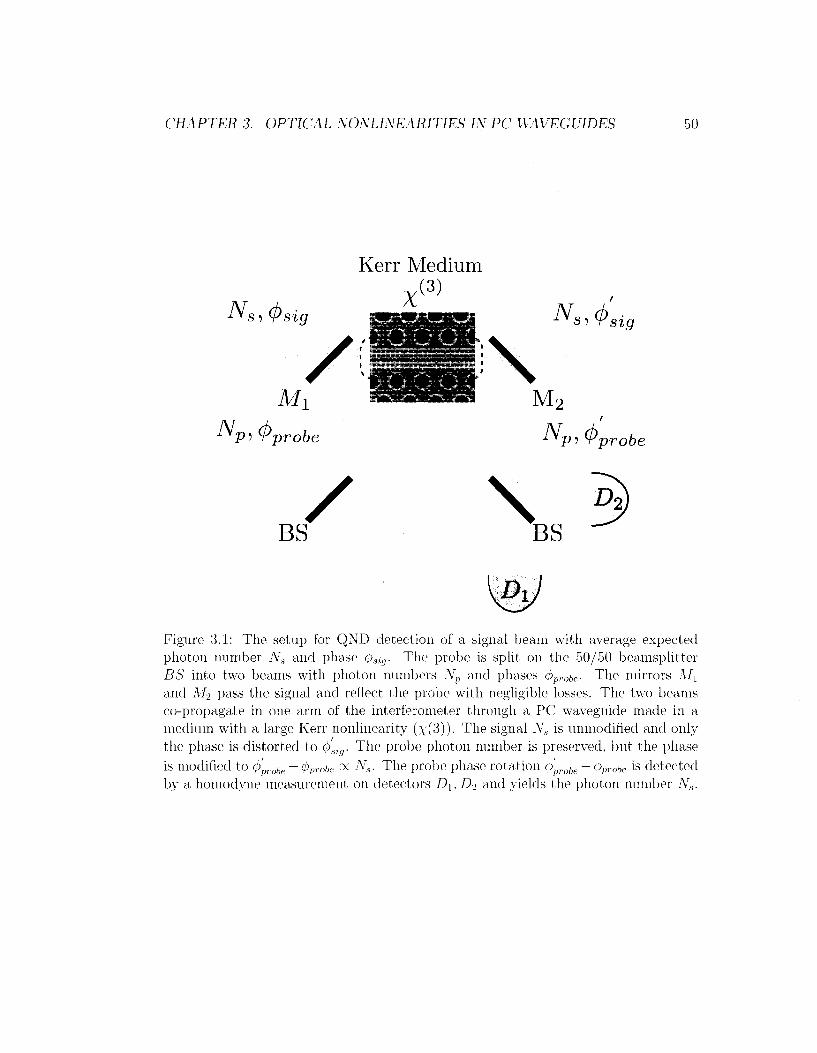
CHAPTER 3. OPTICAL NONLINEARITIES IN PC WAVEGUIDES
Kerr Medium
x ( 3 )
Ns,4>sig 35*8*8*5* N8,(j)sig
Mi « • • • M2
Np,<fiprobe NpA probe
/ BS \ s
Figure 3.1: The setup for QND detection of a signal beam with average expected photon number iV, and phase 0sig. The probe is split on the 50/50 beamsplitter BS into two beams with, photon numbers Np and phases dproi,e. The mirrors il/ t
and M-2 pass the signal and reflect the probe with negligible losses. The two beams co-propagate in one arm of the interferometer through a PC waveguide made in a medium with a large Kerr nonlinearity (,\;(3)). The signal JV, is unmodified and only the phase is distorted to Qmg. The probe photon number is preserved, but the phase
is detected is modified to $ 'obe 9Pro6e oc Ns. The probe phase rotation o obe O probe
by a homodyne measurement on detectors Di, D2 and yields the photon number Ar.,.
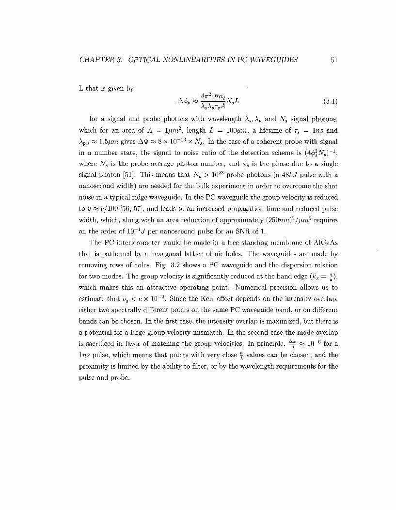
CHAPTER 3. OPTICAL NONLINEARITIES IN PC WAVEGUIDES 51
L that is given by
AsApTsA
for a signal and probe photons with wavelength \s,\p and Ns signal photons,
which for an area of A — l//m2, length L = lOO/im, a lifetime of TS = Ins and
XPtS « 1.5/um gives A $ « 8 x 10~13 x iVs. In the case of a coherent probe with signal
in a number state, the signal to noise ratio of the detection scheme is (402JVP)_1,
where Np is the probe average photon number, and 4>s is the phase due to a single
signal photon [51]. This means that Np > 1023 probe photons (a 48k J pulse with a
nanosecond width) are needed for the bulk experiment in order to overcome the shot
noise in a typical ridge waveguide. In the PC waveguide the group velocity is reduced
to v « c/100 [56, 57], and leads to an increased propagation time and reduced pulse
width, which, along with an area reduction of approximately (250nm)2//um2 requires
on the order of 10_1 J per nanosecond pulse for an SNR of 1.
The PC interferometer would be made in a free standing membrane of AlGaAs
that is patterned by a hexagonal lattice of air holes. The waveguides are made by
removing rows of holes. Fig. 3.2 shows a PC waveguide and the dispersion relation
for two modes. The group velocity is significantly reduced at the band edge (kx = - ) ,
which makes this an attractive operating point. Numerical precision allows us to
estimate that vg < c x 10~2. Since the Kerr effect depends on the intensity overlap,
either two spectrally different points on the same PC waveguide band, or on different
bands can be chosen. In the first case, the intensity overlap is maximized, but there is
a potential for a large group velocity mismatch. In the second case the mode overlap
is sacrificed in favor of matching the group velocities. In principle, — w 10~6 for a
Ins pulse, which means that points with very close j values can be chosen, and the
proximity is limited by the ability to filter, or by the wavelength requirements for the
pulse and probe.
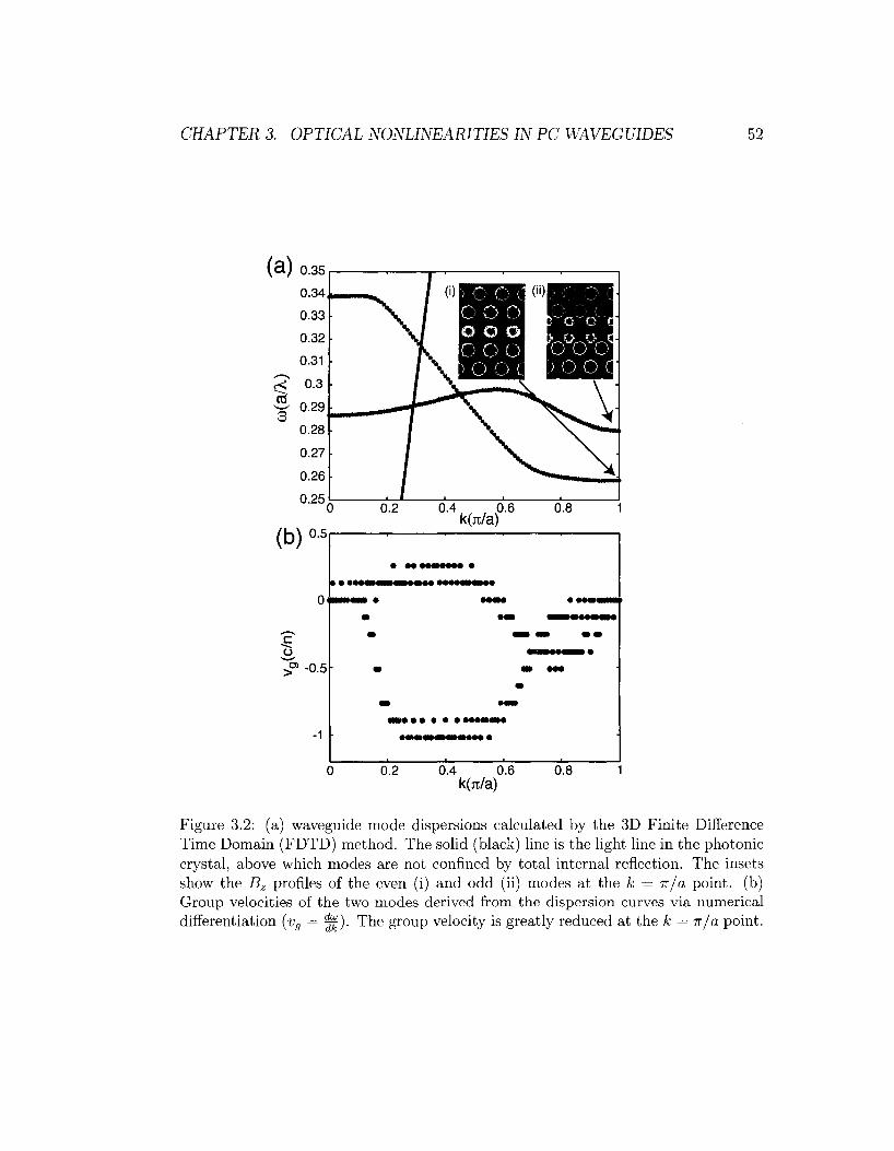
CHAPTER 3. OPTICAL NONLINEARITIES IN PC WAVEGUIDES 52
0.4 0.6 k(jt/a)
Figure 3.2: (a) waveguide mode dispersions calculated by the 3D Finite Difference Time Domain (FDTD) method. The solid (black) line is the light line in the photonic crystal, above which modes are not confined by total internal reflection. The insets show the Bz profiles of the even (i) and odd (ii) modes at the k = n/a point, (b) Group velocities of the two modes derived from the dispersion curves via numerical differentiation (Vg = ^). The group velocity is greatly reduced at the k = n/a point.
CHAPTER 3. OPTICAL NONLINEARITIES IN PC WAVEGUIDES 53
3.3 Pulse Propagation in PC Waveguides
First, we derive the equations of motion for the signal and probe pulse in the inter
ferometer. The eigenstates of the PC waveguide are solutions to:
V > V » l . - i ? f ,3,,
where e(f) is the relative spatially varying waveguide dielectric constant. The solu
tions are Bloch modes n™(f)el(fc2-"W;) where u™(r + az) = u™(r) for the lattice with
periodicity a, z is the direction of propagation along the waveguide, and m is the
index of the band of particular symmetry. These modes satisfy the wave equation:
V x V x (uk(r)eikz) = ^ ! e ( r > f c ( r ) e f c (3.3) cr
The Bloch state is re-normalized for convenience in the last part of the chapter. The
waveguide modes can be shown to obey the following orthogonality conditions :
/ d 3 re ( r )« ,e*( f c - f e > = 8mn8kk, (3.4)
where the integral is taken over the whole space Q. The Bloch modes un,um are
orthogonal over a unit cell of the waveguide, and in the case when the difference
k — k! is small, the integral may be taken over a unit cell. In what follows, index m is
dropped, unless it is necessary, and e = e(r). The waveguide modes can be rewritten
to solve a different Hermitian operator:
6 = -^=V x V x -^ (3.5)
The eigenstates of this operator are (r \u, m, k) = v^/T\f)el{~hz^ul{-k^ with eigenvalue
" a , and (u,m,k \u, n, I) = &m,n&k,i by Eq. 3.4. The inner product denotes integra
tion over all physical space.
A pulse propagating in the PC waveguide in the presence of the weak nonlinearity
may be written as E — 4j J dkA(k,t)\u,m,k) where A(k,t) is a time dependent
CHAPTER 3. OPTICAL NONLINEARITIES IN PC WAVEGUIDES 54
coefficient of each k component. The k-space range over which the integrand is
appreciable depends on the frequency distribution of the pulse. For pulses with ^ «
10~6, and group velocity of v = j^j, ^ sa 10~4. So the integrand in the expression
for E is dominated by a particular k about which the pulse can be expanded:
. i[{k-k0)z-(u(k)-wo)t] E= f dkA{k,t)uk(r)ei{kz-"{k)t) ^ Uk^e1^02-^ f dkA(k,t)t
(3.6)
expanding u(k) = co(k0) + ^\k=ko(k - k0) + \^\k=k(j{k - k0)2 = ui0 + vgq + ^^q2
with q = k — k0 gives:
uk0(r)e«k°*-^ [dqA(q + k0,t)eilq{'-v''t)-^^t] E
= uko(*y to'-"*') x F(z, t) = 4= \u, ko) x F(z, t) (3.7)
Here F is a slowly spatially and time varying envelope of the signal or probe, which
extends over many periods of the waveguide. In order to determine the interaction of
pulses propagating in the PC waveguide, we need to know the evolution of such an
envelope. In Appendix C, first order perturbation theory is applied to the operator
O to determine the evolution of the Fourier components of the envelope. To first
order in the nonlinear perturbation, and with negligible group velocity dispersion,
the evolution of two pulses (S and P) in the same waveguide, but possibly coupled to
different waveguide modes {s,p) is given by (see Appendix C):
S = qnus(%,s\S\2 + 27 s ,p |P|2)5 - vsS' + i\d-§±S" (3.8)
P = i |«wp(7 p j , |P |2 + 2lpJS\2)P - vpP' + i^P" (3.9)
with:
7-* = - [ d3re(f)\us\2\up\
2 (3.10) a J A
The dot in the above equation denotes differentiation in time, and the prime is
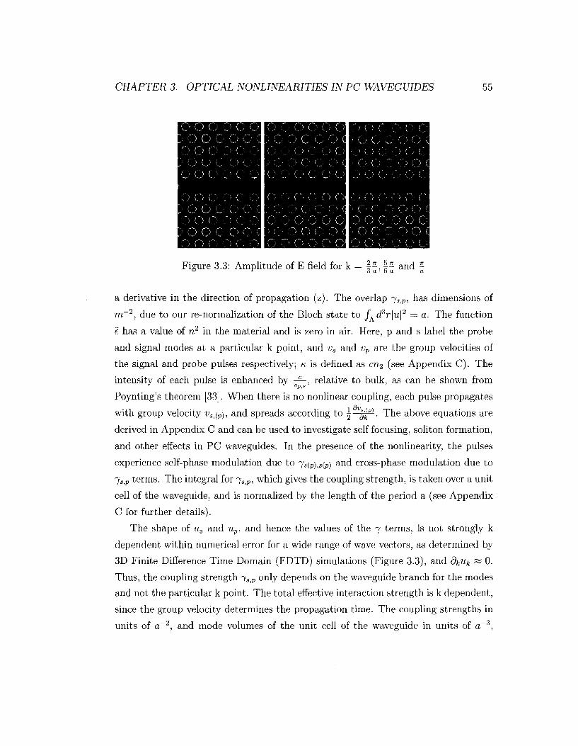
CHAPTER 3. OPTICAL NONLINEARITIES IN PC WAVEGUIDES 55
Figure 3.3: Amplitude of E field for k = |f, | f and f
a derivative in the direction of propagation (z). The overlap 7SiP, has dimensions of
m~2, due to our re-normalization of the Bloch state to fAd3r\u\2 — a. The function
e has a value of n2 in the material and is zero in air. Here, p and s label the probe
and signal modes at a particular k point, and vs and vp are the group velocities of
the signal and probe pulses respectively; K is defined as cn2 (see Appendix C). The
intensity of each pulse is enhanced by ^ - , relative to bulk, as can be shown from
Poynting's theorem [33]. When there is no nonlinear coupling, each pulse propagates
with group velocity i>s,(p), and spreads according to | Vg^p). The above equations are
derived in Appendix C and can be used to investigate self focusing, soliton formation,
and other effects in PC waveguides. In the presence of the nonlinearity, the pulses
experience self-phase modulation due to 7s(p),s(p) and cross-phase modulation due to
7SjP terms. The integral for j ^ p , which gives the coupling strength, is taken over a unit
cell of the waveguide, and is normalized by the length of the period a (see Appendix
C for further details).
The shape of us and up, and hence the values of the 7 terms, is not strongly k
dependent within numerical error for a wide range of wave vectors, as determined by
3D Finite Difference Time Domain (FDTD) simulations (Figure 3.3), and dkUk ~ 0.
Thus, the coupling strength j3tP only depends on the waveguide branch for the modes
and not the particular k point. The total effective interaction strength is k dependent,
since the group velocity determines the propagation time. The coupling strengths in
units of a - 2 , and mode volumes of the unit cell of the waveguide in units of or3,

CHAPTER 3. OPTICAL NONLINEARITIES IN PC WAVEGUIDES 56
Table 3.1: values for coupling 7 for different modes of the waveguide in units of a - 2 , and mode volumes for each unit cell of the waveguide (in units of a - 3 ) . 1 and 2 refer to the first and second modes of the waveguide.
Ui,j
1i,j
''mode
1,1 6.4 x 1(T2
3.9 x l f r 1
2,2 7.9 x 1(T2
2.8 x 1CT1
1,2 1.4 x lO"2
2.5 x 1G-1
are shown in the Table 3.1. The mode volume for each waveguide mode is defined
as VL,I(2,2) = (e\ui(2)\2)m1
ax JAd3re\ui^)\2, ana^ the m °de volume for the overlap is
Vi,2 = (eMKI taL /A^HN-Each equation can be transformed into a coordinate frame moving with the probe
and signal respectively via x — z — vst and x — z — vpt. The dispersion terms in 3.8
complicate the solution. We will assume that the length of the waveguide is small
enough so that the measurement of the induced phase and the measurement of the
phase on the probe is unaffected by the dispersion throughout the propagation. With
^ r and -^ neglected, the solution and upper bounds on the phases on the probe
after time t = — are:
P(z') = Exp[-iKujp f0{iP,P\P(z>)\2 + 2lsJS(z> + Avt')\2)dt']P(0)
<j>P = lKupf*jPtP\P(z')\2dt' w ±KUJP-/P^\P{Z')\2
<f>S = KUJp f0 1s,p\S(z' + Avt')\2dt' » KUpls^\S{z')\2
(3.11)
(3.12)
(3.13)
(3.14)
Where vp and vs are the group velocities of the signal and probe beams and L is
the interaction length. <f>s gives the phase shift of the probe due to the signal photon
number.
CHAPTER 3. OPTICAL NONLINEARITIES IN PC WAVEGUIDES 57
3.4 Nonlinear Phase Shift
The phase <f>s is the phase on the probe due to the nonlinear interaction with the
signal, and gives the signal photon number. In Appendix C we derive that the ideal
case of a negligible group velocity mismatch and a narrow probe, gives the phase shift
per signal photon of: L I .
<Ps,ideai = cn2jS)Phuisojp (3.15) VpVsTs
L is the length of the PC and r3 is the temporal width of the signal wave packet.
Both the signal and probe wave undergo material absorption and scattering due
to waveguide losses. PC waveguide losses are already as low as 14dB/cm and will
improve with time [58]. The material absorption consists of the linear absorption
coefficient a.\ and the nonlinear coefficients, of which we will only consider the two
photon absorption coefficient a2. In the case of AlGaAs at the half band gap, the
values of ot\ and a2 were found to be w .1cm -1 and ss . 2 ^ respectively [54]. Thus,
ax limits us to L— RS 10cm. For uJ and sub-//J pulses, a2 results in a smaller
attenuation length on the order of 50/um at best. Thus, experiments with the signal
and probe at the half-gap are not feasible. In order to circumvent pump depletion
due to two photon absorption, a pump at even longer wavelengths above 1550 nm
should be used [59]. In that case, a2 is close to zero, and we will assume that the
100 /im PC waveguide length is the limit. In this case, the pump will propagate
in the lower branch of the waveguide, while the signal should couple to the upper
branch. For example for a signal at 1550 nm in the upper waveguide branch, a pump
at 1620 nm should be used in order to have both beams velocity matched at the
ir/a point. We briefly mention that the GalnAsP material system has a\ « 1cm-1,
and n2 ~ 5 x \Q~l2~ and most likely similar two-photon absorption, which means
that both materials are suitable candidates for an experiment. While the nonlinearity
is enhanced closer to the band-edge of the semiconductor band gap, the absorption
increases accordingly and reduced the interaction length.
The phase due to a single photon in signal S and the energy required for an SNR
of 1 for number state detection in AlGaAs, are plotted in Fig. 3.4. We plot both the
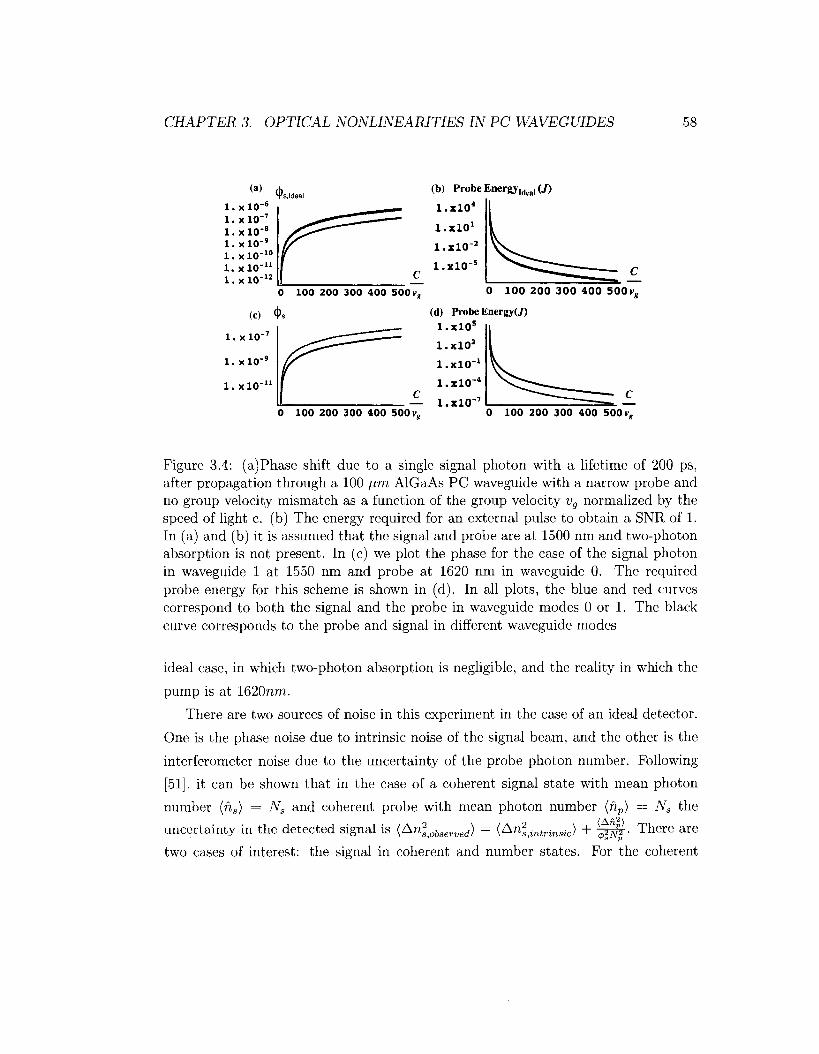
CHAPTER 3. OPTICAL NONLINEARITIES IN PC WAVEGUIDES 58
100 200 300 400 500 v.
(b) Probe Energy [deal (7)
l . x l O 4
100 2 0 0 3 0 0 4 0 0 500v„
(d) Probe Energyt/)
l . x l O 5
•>2
100 200 300 400 500 v. 100 200 300 400 500 v„
Figure 3.4: (a)Phase shift due to a single signal photon with a lifetime of 200 ps, after propagation through a 100 jim AlGaAs PC waveguide with a narrow probe and no group velocity mismatch as a function of the group velocity vg normalized by the speed of light c. (b) The energy required for an external pulse to obtain a SNR of 1. In (a) and (b) it is assumed that the signal and probe are at 1500 nm and two-photon absorption is not present. In (c) we plot the phase for the case of the signal photon in waveguide 1 at 1550 nm and probe at 1620 nm in waveguide 0. The required probe energy for this scheme is shown in (d). In all plots, the blue and red curves correspond to both the signal and the probe in waveguide modes 0 or 1. The black curve corresponds to the probe and signal in different waveguide modes
ideal case, in which two-photon absorption is negligible, and the reality in which the
pump is at 1620nm.
There are two sources of noise in this experiment in the case of an ideal detector.
One is the phase noise due to intrinsic noise of the signal beam, and the other is the
interferometer noise due to the uncertainty of the probe photon number. Following
[51], it can be shown that in the case of a coherent signal state with mean photon
number (hs) = Ns and coherent probe with mean photon number (np) = Ns the
uncertainty in the detected signal is (Anlobserved) = {An2sintrinsic) + {-^. There are
two cases of interest: the signal in coherent and number states. For the coherent
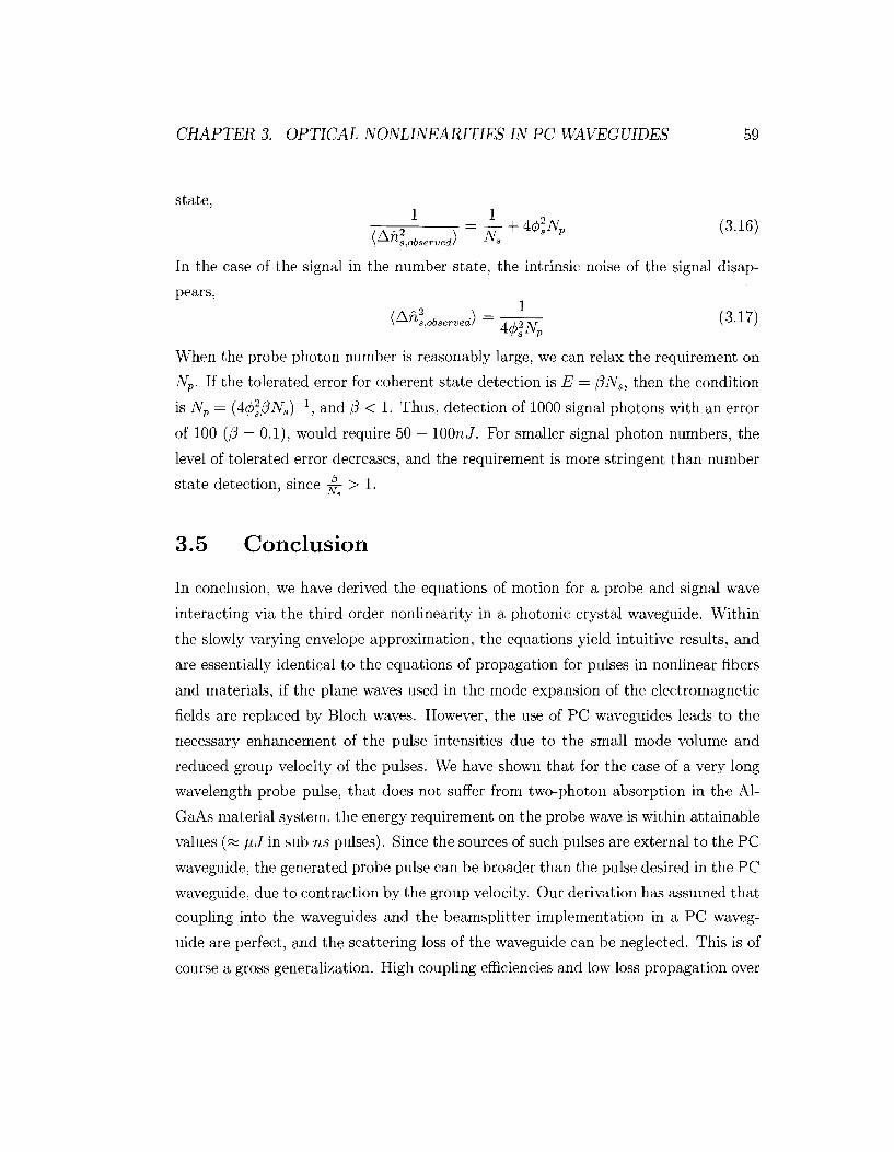
CHAPTER 3. OPTICAL NONLINEARITIES IN PC WAVEGUIDES 59
state,
7 ^ r = ̂ + 4 * X (3.16) \L-^"'s,observed/ J v «
In the case of the signal in the number state, the intrinsic noise of the signal disap
pears,
\^ns,observed) = A A2 AT (3.17)
4(f) jNp
When the probe photon number is reasonably large, we can relax the requirement on
Np. If the tolerated error for coherent state detection is E = /3N3, then the condition
is Np = {A4>23[3Ns)~
l, and (5 < 1. Thus, detection of 1000 signal photons with an error
of 100 (/? = 0.1), would require 50 — lOOnJ. For smaller signal photon numbers, the
level of tolerated error decreases, and the requirement is more stringent than number
state detection, since ^- > 1.
3.5 Conclusion
In conclusion, we have derived the equations of motion for a probe and signal wave
interacting via the third order nonlinearity in a photonic crystal waveguide. Within
the slowly varying envelope approximation, the equations yield intuitive results, and
are essentially identical to the equations of propagation for pulses in nonlinear fibers
and materials, if the plane waves used in the mode expansion of the electromagnetic
fields are replaced by Bloch waves. However, the use of PC waveguides leads to the
necessary enhancement of the pulse intensities due to the small mode volume and
reduced group velocity of the pulses. We have shown that for the case of a very long
wavelength probe pulse, that does not suffer from two-photon absorption in the Al-
GaAs material system, the energy requirement on the probe wave is within attainable
values («» fiJ in sub ns pulses). Since the sources of such pulses are external to the PC
waveguide, the generated probe pulse can be broader than the pulse desired in the PC
waveguide, due to contraction by the group velocity. Our derivation has assumed that
coupling into the waveguides and the beamsplitter implementation in a PC waveg
uide are perfect, and the scattering loss of the waveguide can be neglected. This is of
course a gross generalization. High coupling efficiencies and low loss propagation over

CHAPTER 3. OPTICAL NONLINEARITIES IN PC WAVEGUIDES 60
10's of microns have been shown, and will only improve in time. We are in general
most strongly limited by two photon absorption in this proposal. Other material sys
tems such as GalnAsP [60], which also exhibit higher n? values that AlGaAs, could
also be considered for this implementation, but ultimately atomic resonance systems
and systems with a high phase shift and low loss are necessary [5, 48]. In principle,
an on-chip QND photon number detector could be a component of a photonic crystal
based quantum circuit, or can serve as a sensitive intensity detector and switch. The
derivation presented here, can be easily extended to other types of intensity and field
dependent nonlinearities, and can be used to analyze other nonlinear optical effects
in PC waveguides, as well as soliton formation and propagation.
Chapter 4
Nonlinearities for quantum
information processing
4.1 Introduction
As introduced in Chapter 1, the cavity-QD system is highly nonlinear. The coupling
of the QD strongly modifies the transmission function of a PC cavity and prohibits
photons from passing through at the QD resonance in both the weak and strong
coupling regimes (see Section 1.4.3). This single-photon sensitive cavity transmission
along with two stable QD ground states can be exploited for quantum information
processing as detailed in [16, 14]. Additionally, the QD response to the driving field
is itself nonlinear due to QD saturation at high driving field strengths. The QD
can only scatter one photon per Rabi flop, and as the strength of the driving field
that is incident on the cavity increases, the QD cannot follow the driving field and
photons are transmitted. This indicates that the response of the QD to two photons
that arrive simultaneously differs from that of two photons arriving separately added
together. Thus, even without the availability of stable ground states, the QD can be
exploited to interact single photons and can be used for quantum logic operations.
This kind of two-photon interaction scheme was first realized by Turchette et. al. in
an experiment with atoms [8]. To date, the largest nonlinearities have been realized
with single atoms and atomic ensembles. We showed in [2] that a single quantum
61
CHAPTER 4. NONLIENARITIES FOR QIP 62
dot (QD) coupled to a PC nanocavity can facilitate controlled phase and amplitude
modulation between two modes of light at the single photon level. We observed
phase shifts up to n/4 and amplitude modulation up to 50%. This is accomplished
by varying the photon number in the control beam at the wavelength which is the
same as the signal, or at a wavelength which is detuned by several QD linewidths from
the signal. Our results present a step towards quantum logic devices and quantum
nondemolition measurements on a chip. In this chapter I will discuss the controlled
phase shift experiment and result. The following discussion is based on References
[2, 1], where I.F., Dirk Englund and Andrei Faraon were equal contributors.
4.2 Measurement description
The concept of the controlled phase interaction from an experimental point is illus
trated in Fig. 4.1. A QD inside the PC cavity modifies the cavity transmission func
tion and with it the phase of photons that are reflected from it due to the dispersive
component of the QD susceptibility. Thus, by controlling the quantum dot, the phase
of cavity scattered photons can be altered. If this control is exerted through another
photon stream, a controlled phase shift results. In our experiments, a one-sided cavity
was used. In such a case, the reflection coefficient r(u) = E^t/Em « 1 — -A-p w 1,
where F is the Purcell factor and / is fraction of energy emitted into modes other
than the cavity mode (see Section 1.4.3). Thus in a one-sided cavity, only the phase
of cavity reflected photons is modified. As will be described further on, our experi
mental implementation results in a reflection coefficient of the one-sided cavity that
is equivalent to a transmission coefficient of a two-sided cavity.
4.3 Coherent probing of a cavity-QD system
Before a controlled phase interaction between photons inside a PC cavity can be
attempted, coherent interaction between an external laser field and the cavity must
be realized in order to be able to map out the cavity transmission function and the
phase of cavity scattered photons. A diagram of experimental setup for coherently
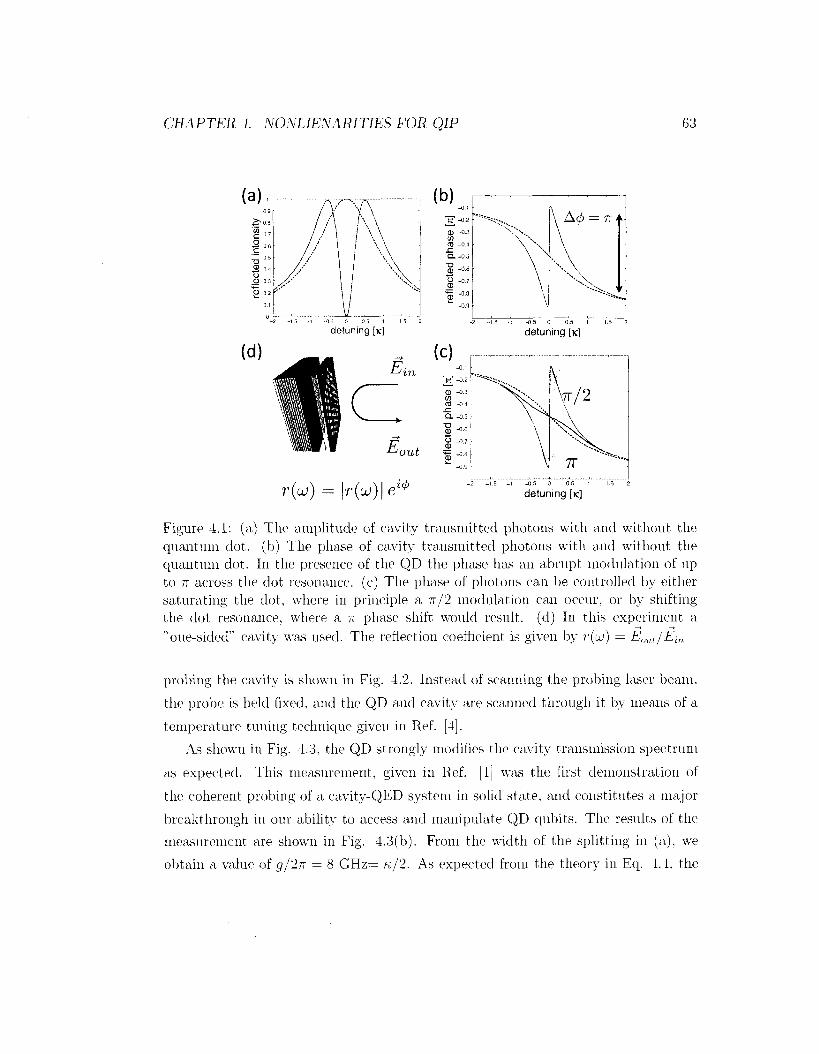
CHAPTER 4. NONLIENAMTIES FOR QIP 63
(d) detuning [K]
f -0.5 0 0.5 1 15 2
detuning [K]
(C)
in _̂
out =
r(uj) = \r(cj)\ el -0.5 0 0.5
detuning [K]
Figure 4.1: (a) The amplitude of cavity transmitted photons with and without the quantum dot. (b) The phase of cavity transmitted photons with and without the quantum dot. In the presence of the QD the phase has an abrupt modulation of up to 7T across the dot resonance, (c) The phase of photons can be controlled by either saturating the dot, where in principle a TT/2 modulation can occur, or by shifting the dot resonance, where a n phase shift would result, (cl) In this experiment a "one-sided" cavity was used. The reflection coefficient is given by r(uj) = Eout/Ein
probing the cavity is shown in Fig. 4.2. Instead of scanning the probing laser beam,
the probe is held fixed, and the QD and cavity are scanned through it by means of a
temperature tuning technique given in Ref. [4].
As shown in Fig. 4.3, the QD strongly modifies the cavity transmission spectrum
as expected. This measurement, given in Ref. [1] was the first demonstration of
the coherent probing of a cavity-QED system in solid state, and constitutes a major
breakthrough in our ability to access and manipulate QD qubits. The results of the
measurement are shown in Fig. 4.3(b). From the width of the splitting in (a), we
obtain a value of g/2ir = 8 GHz= K/2. As expected from the theory in Eq. 4.4, the
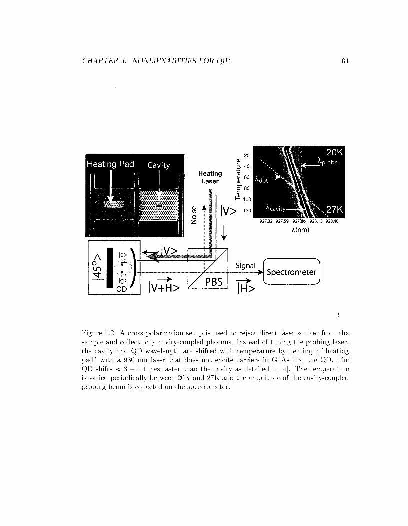
CHAPTER 4. NONLIENARITIES FOR QIP 64
927.32 927.59 927.86 928.13 928.40
20K ^probe
X27K
Figure 4.2: A cross polarization setup is used to reject direct laser scatter from the sample and collect only cavity-coupled photons. Instead of tuning the probing laser, the cavity and QD wavelength are shifted with temperature by heating a "heating pad'1 with a 980 run laser that does not excite carriers in GaAs and the QD. The QD shifts ~ 3 — 4 times faster than the cavity as detailed in [4]. The temperature is varied periodically between 20K and 27K and the amplitude of the cavity-coupled probing beam is collected on the spectrometer.
CHAPTER 4. NONLIENARITIES FOR QIP 65
cavity reflectivity is strongly modified. The observed reflectivity does not drop down
directly to zero at the dot resonance. We attribute this discrepancy to experimental
noise. In particular, we observed that the temperature of the heating laser fluctuated
by 0.7%, which resulted in a fluctuation of the quantum dot on the order of 0.005 nm.
We obtain good agreement with the theory, when we account for this fluctuation. The
coupling efficiency was found to be 2%, and indicates that without cross-polarization,
the observation of this effect would be nearly impossible without a lock-in technique.
Next, we explore the nonlinear behavior of this system, by increasing the power
of the probing laser. As shown in Figure 4.3(c), we observe saturation at power levels
which correspond to several photons in the cavity, which indicates one of the largest
optical nonlinearities available in the solid state systems. The major advantage of
this nonlinearity is that photons are conserved, because they are primarily re-emitted
into the cavity mode. While the coupling efficiency of 2% in this experiment is quite
low, this can be greatly improved when the probe laser is coupled to the cavity
via a waveguide [61], and this nonlinearity can be used for on-chip photon-photon
interactions.
4.4 Phase measurement
We measure the phase of cavity-reflected photons by interfering them with a reference
beam of known amplitude and phase (Fig. 4.4). As in the previous section, the reflec
tivity of the linearly polarized cavity is isolated from background laser scatter using
a cross-polarized setup [62, 1]. Here, the cavity field decay rate is n/2n = 16GHz,
corresponding to a quality factor Q=10000. The quantum dot has an estimated spon
taneous emission rate 7/27r = 0.2GHz. In the described experiments, we employ two
quantum dots: a strongly coupled QD with vacuum Rabi frequency <?/2-7r = 16GHz,
and a weakly coupled one with g/2n = 8GHz.
The reference beam is introduced by inserting a quarter wave plate (QWP) be
tween the beamsplitter and the cavity. The QWP converts the linearly polarized
signal into an elliptically polarized beam with components parallel and orthogonal to
the cavity polarization. In this way, both the signal and interfering beam traverse the
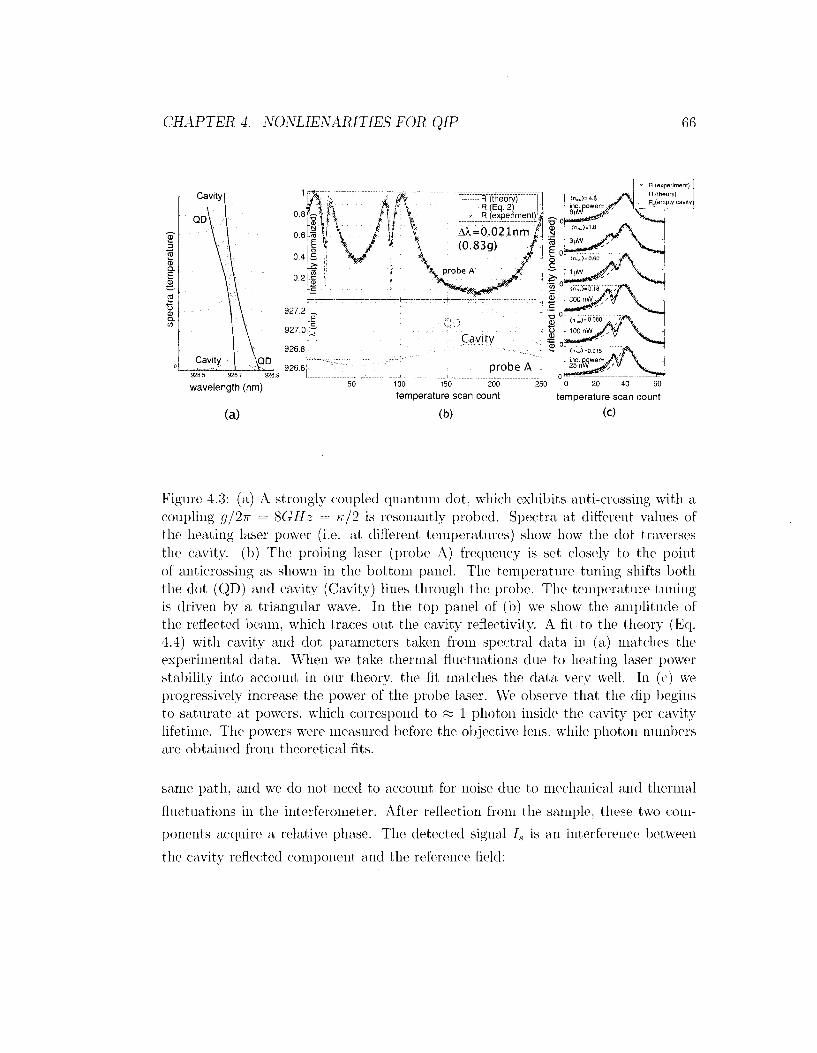
CHAPTER 4. NONLIENARITIES FOR QIP 66
* H (experiment)
0 20 40 60
temperature scan count
(0
Figure 4.3: (a) A strongly coupled quantum dot, which exhibits anti-crossing with a coupling g/2w = 8GHz = K / 2 is resonantly probed. Spectra at different values of the heating laser power (i.e. at different temperatures) show how the dot traverses the cavity, (b) The probing laser (probe A) frequency is set closely to the point of anticrossing as shown in the bottom panel. The temperature tuning shifts both the dot (QD) and cavity (Cavity) lines through the probe. The temperature tuning is driven by a triangular wave. In the top panel of (b) we show the amplitude of the reflected beam, which traces out the cavity reflectivity. A fit to the theory (Eq. 4.4) with cavity and dot parameters taken from spectral da ta in (a.) matches the experimental data. When we take thermal fluctuations due to heating laser power stability into account in our theory, the fit matches the data very well. In (c) we progressively increase the power of the probe laser. We observe that the dip begins to saturate at powers, which correspond to ~ I photon inside the cavity per cavity lifetime. The powers were measured before the objective lens, while photon numbers are obtained from theoretical fits.
same path, and we do not need to account for noise due to mechanical and thermal
fluctuations in the interferometer. After reflection from the sample, these two com
ponents acquire a relative phase. The detected signal /., is an interference between
the cavity reflected component and the reference field:
926.5 9267 926.9
wavelength (nm)
(a)
00 150 200
temperature scan count
(b)
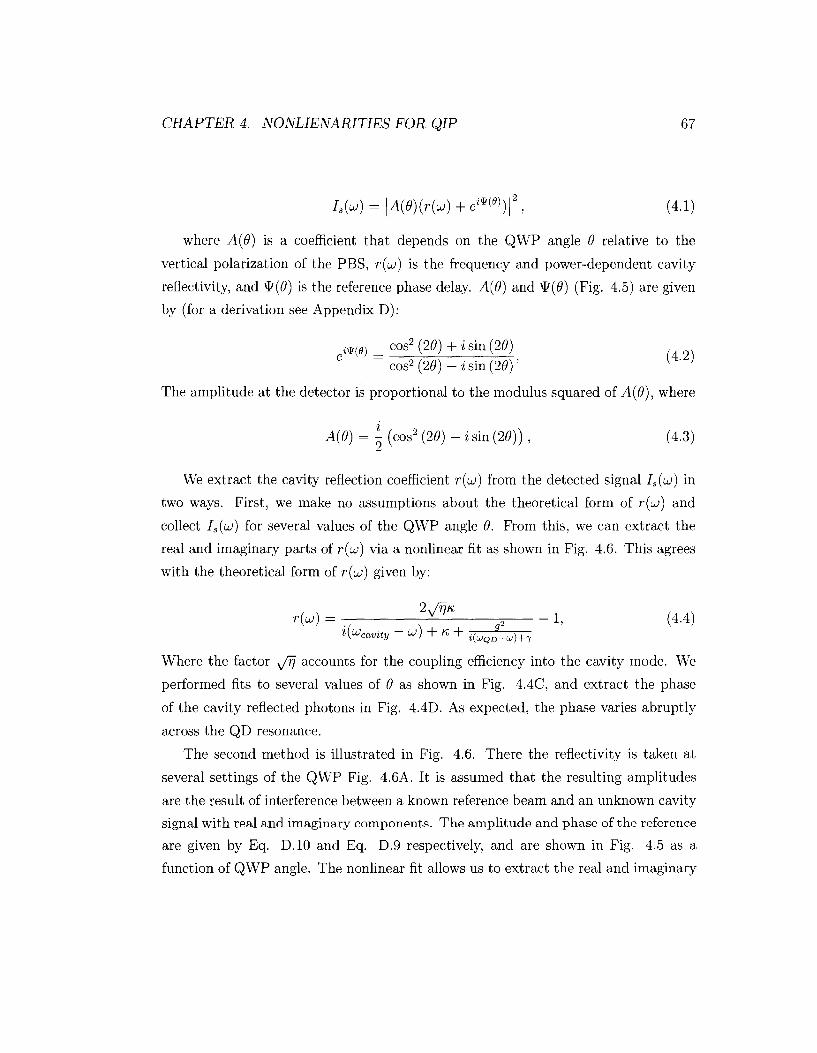
CHAPTER 4. NONLIENARITIES FOR QIP 67
Is(oj) = \A(9)(r(oj) + ei^)\2, (4.1)
where A{9) is a coefficient that depends on the QWP angle 6 relative to the
vertical polarization of the PBS, r{uj) is the frequency and power-dependent cavity
reflectivity, and ty(0) is the reference phase delay. A{6) and \I/(0) (Fig. 4.5) are given
by (for a derivation see Appendix D):
m$) = cos2(2fl)+isin(2fl) cos2 ( 2 0 ) - i sin (20)'
The amplitude at the detector is proportional to the modulus squared of A(9), where
A{9) = %- (cos2 {26) - i sin {29)) , (4.3)
We extract the cavity reflection coefficient r{u) from the detected signal IS{LO) in
two ways. First, we make no assumptions about the theoretical form of r(u>) and
collect Is{u) for several values of the QWP angle 9. From this, we can extract the
real and imaginary parts of r(uj) via a nonlinear fit as shown in Fig. 4.6. This agrees
with the theoretical form of r{uj) given by:
r M = f ^ fl2 - 1, (4-4)
Where the factor ^/rj accounts for the coupling efficiency into the cavity mode. We
performed fits to several values of 9 as shown in Fig. 4.4C, and extract the phase
of the cavity reflected photons in Fig. 4.4D. As expected, the phase varies abruptly
across the QD resonance.
The second method is illustrated in Fig. 4.6. There the reflectivity is taken at
several settings of the QWP Fig. 4.6A. It is assumed that the resulting amplitudes
are the result of interference between a known reference beam and an unknown cavity
signal with real and imaginary components. The amplitude and phase of the reference
are given by Eq. D.10 and Eq. D.9 respectively, and are shown in Fig. 4.5 as a
function of QWP angle. The nonlinear fit allows us to extract the real and imaginary
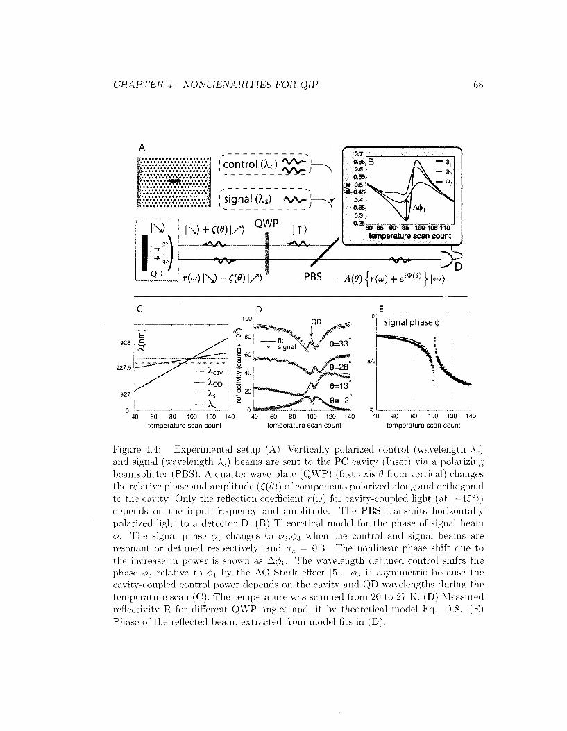
CHAPTER 4. NONLIENARITIES FOR QIP 68
I l\>
• i f
I, ig>l
QD
3 ; control a c )^: j -
v l | I signal {Xs) >v\^j~
IV + CWI/*) Q ^ P IT) ^W> 1 ^AA.*-
*%/%/*" '
r(«) | \> - CW I / )
r . . . . . . . . . . . ^ 0.7 0.65 0.6 0.5S
K 0.S ^•O.AS
0.4 0.35 0.3 0 25
' . B A -<t>,
M<h 80 85 90 95 100 105 110 temperature scan count
j
PBS i4(«){r(w) + e ' * w } M S
D 100.
927.5
temperature scan count 100 120 140
temperature scan count
-It/2
signal phase §
40 60 80 100 120 140
temperature scan count
Figure 4.4: Experimental setup (A). Vertically polarized control (wavelength A,.) and signal (wavelength A.,) beams are sent to the PC cavity (Inset) via a polarizing beamsplitter (PBS). A quarter wave plate (QWP) (fast axis 9 from vertical) changes the relative phase and amplitude (C(#)) of components polarized along and orthogonal to the cavity. Only the reflection coefficient r(ui) for cavity-coupled light (at |— 45°}) depends on the input frequency and amplitude. The PBS transmits horizontally polarized light to a detector D. (B) Theoretical model for the phase of signal beam 0. The signal phase p t changes to 02-0^ when the control and signal beams are resonant or detuned respectively, and nc = 0.3. The nonlinear phase shift due to the increase in power is shown as A0L. The wavelength detuned control shifts the phase 03 relative to 0L by the AC Stark effect [5]. 03 is asymmetric because the cavity-coupled control power depends on the cavity and QD wavelengths during the temperature scan (C). The temperature was scanned from 20 to 27 K. (D) Measured reflectivity R for different QWP angles and fit by theoretical model Eq. D.8. (E) Phase of the reflected beam, extracted from model fits in (D).
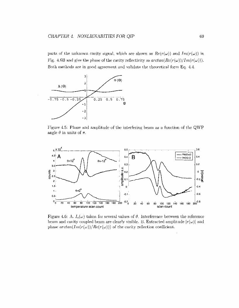
CHAPTER 4. NONLIENARITIES FOR QIP 69
parts of the unknown cavity signal, which are shown as Re(r(u)) and Im(r(uj)) in
Fig. 4.6B and give the phase of the cavity reflectivity as arctan(Re(r(ui))/Im(r(uj))).
Both methods are in good agreement and validate the theoretical form Eq. 4.4.
Figure 4.5: Phase and amplitude of the interfering beam as a function of the QWP angle 9 in units of n.
0 20 40 60 80 100 120 140 160 180 200 ~°% 20 40 60 80 100 120 140 160 180 20o"°''
temperature scan count scan count
Figure 4.6: A. Is(u/) taken for several values of 9. Interference between the reference beam and cavity coupled beam are clearly visible. B. Extracted amplitude \r(uj)\ and phase arctan(Im(r{uj))/Re(r(u>))) of the cavity reflection coefficient.
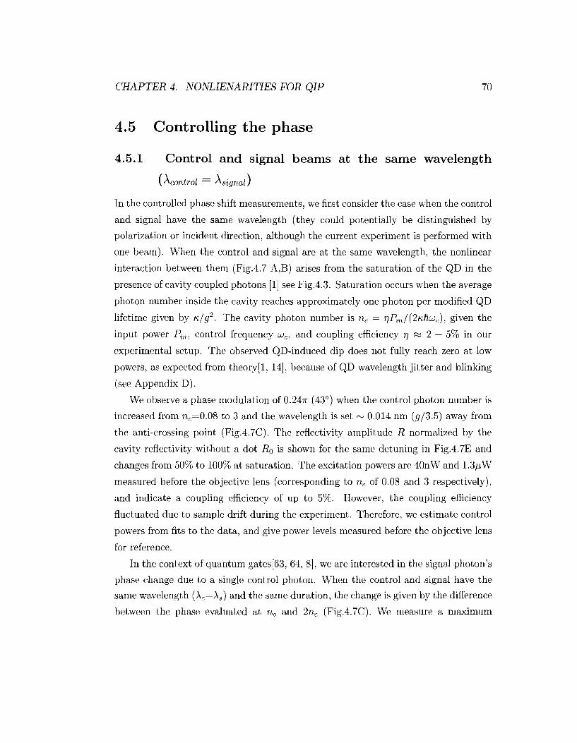
CHAPTER 4. NONLIENARITIES FOR QIP 70
4.5 Controlling the phase
4.5.1 Control and signal beams at the same wavelength
control ~ ^signal)
In the controlled phase shift measurements, we first consider the case when the control
and signal have the same wavelength (they could potentially be distinguished by
polarization or incident direction, although the current experiment is performed with
one beam). When the control and signal are at the same wavelength, the nonlinear
interaction between them (Fig.4.7 A,B) arises from the saturation of the QD in the
presence of cavity coupled photons [1] see Fig.4.3. Saturation occurs when the average
photon number inside the cavity reaches approximately one photon per modified QD
lifetime given by n/g2. The cavity photon number is nc = r]Pin/(2K,hujc), given the
input power Pin, control frequency uc, and coupling efficiency r\ s=s 2 — 5% in our
experimental setup. The observed QD-induced dip does not fully reach zero at low
powers, as expected from theory[1, 14], because of QD wavelength jitter and blinking
(see Appendix D).
We observe a phase modulation of 0.24-7T (43°) when the control photon number is
increased from ric=0.08 to 3 and the wavelength is set ~ 0.014 nm (5/3.5) away from
the anti-crossing point (Fig.4.7C). The reflectivity amplitude R normalized by the
cavity reflectivity without a dot R0 is shown for the same detuning in Fig.4.7E and
changes from 50% to 100% at saturation. The excitation powers are 40nW and 1.3/iW
measured before the objective lens (corresponding to nc of 0.08 and 3 respectively),
and indicate a coupling efficiency of up to 5%. However, the coupling efficiency
fluctuated due to sample drift during the experiment. Therefore, we estimate control
powers from fits to the data, and give power levels measured before the objective lens
for reference.
In the context of quantum gates[63, 64, 8], we are interested in the signal photon's
phase change due to a single control photon. When the control and signal have the
same wavelength (AC=AS) and the same duration, the change is given by the difference
between the phase evaluated at nc and 2nc (Fig.4.7C). We measure a maximum
A
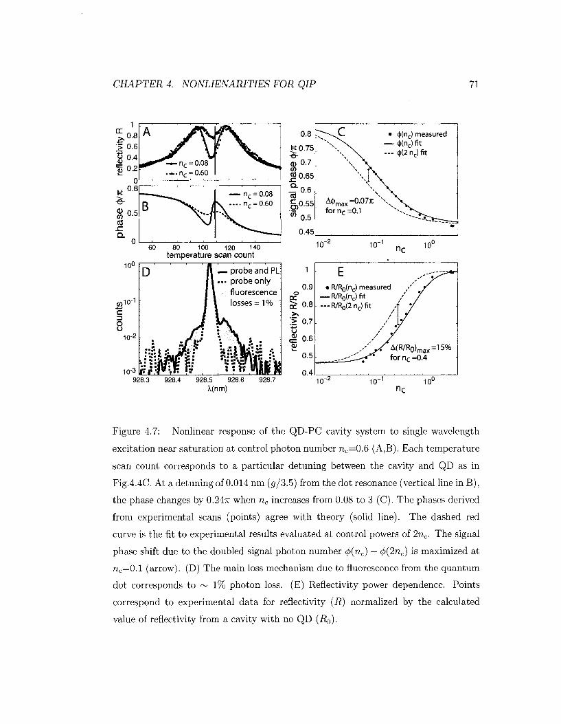
CHAPTER 4. NONLIENARITIES FOR QIP 71
X(nm) ric
Figure 4.7: Nonlinear response of the QD-PC cavity system to single wavelength
excitation near saturation at control photon number nc—0.G (A,B)- Each temperature
scan count corresponds to a particular detuning between the cavity and QD as in
Fig.4.4C. At a detuning of 0.014 nm (g/3.5) from the dot resonance (vertical line in B),
the phase changes by 0.247T when nc increases from 0.08 to 3 (C). The phases derived
from experimental scans (points) agree with theory (solid line). The dashed red
curve is the fit to experimental results evaluated at control powers of 2nc. The signal
phase shift due to the doubled signal photon number (f)(nc) — </>(2nc) is maximized at
nc=0.1 (arrow). (D) The main loss mechanism due to fluorescence from the quantum
dot corresponds to ~ 1% photon loss. (E) Reflectivity power dependence. Points
correspond to experimental data for reflectivity (R) normalized by the calculated
value of reflectivity from a cavity with no QD (i?o).
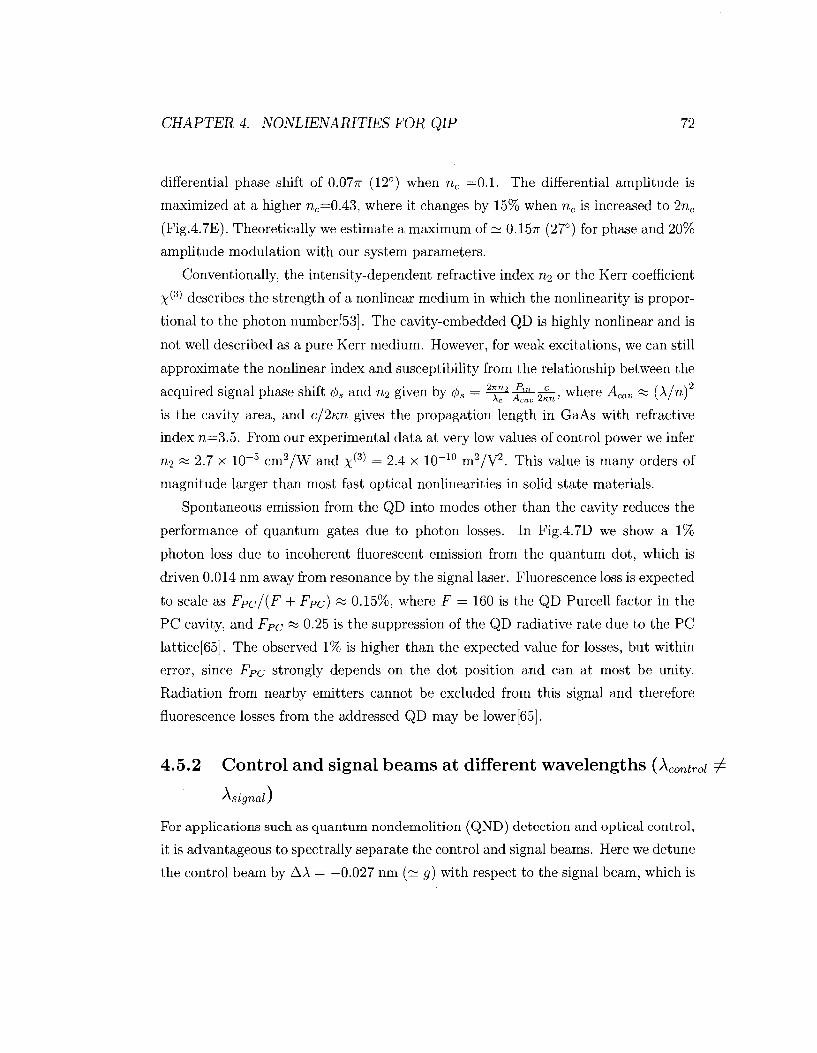
CHAPTER 4. NONLIENARITIES FOR QIP 72
differential phase shift of 0.077T (12°) when nc =0.1. The differential amplitude is
maximized at a higher nc=0.43, where it changes by 15% when nc is increased to 2nc
(Fig.4.7E). Theoretically we estimate a maximum of ~ 0.157T (27°) for phase and 20%
amplitude modulation with our system parameters.
Conventionally, the intensity-dependent refractive index n2 or the Kerr coefficient
X ^ describes the strength of a nonlinear medium in which the nonlinearity is propor
tional to the photon number [53]. The cavity-embedded QD is highly nonlinear and is
not well described as a pure Kerr medium. However, for weak excitations, we can still
approximate the nonlinear index and susceptibility from the relationship between the
acquired signal phase shift <f>s and n2 given by (f>s — ^x^-p^^fi, where Acav ss (A/n)
is the cavity area, and c/2nn gives the propagation length in GaAs with refractive
index n=3.5. From our experimental data at very low values of control power we infer
n2 ~ 2.7 x 10~5 cm2/W and x(3) = 2.4 x 10~10 m2/V2. This value is many orders of
magnitude larger than most fast optical nonlinearities in solid state materials.
Spontaneous emission from the QD into modes other than the cavity reduces the
performance of quantum gates due to photon losses. In Fig.4.7D we show a 1%
photon loss due to incoherent fluorescent emission from the quantum dot, which is
driven 0.014 nm away from resonance by the signal laser. Fluorescence loss is expected
to scale as Fpc/(F + Fpc) ~ 0.15%, where F — 160 is the QD Purcell factor in the
PC cavity, and FPC ~ 0.25 is the suppression of the QD radiative rate due to the PC
lattice[65]. The observed 1% is higher than the expected value for losses, but within
error, since Fpc strongly depends on the dot position and can at most be unity.
Radiation from nearby emitters cannot be excluded from this signal and therefore
fluorescence losses from the addressed QD may be lower[65].
4.5.2 Control and signal beams at different wavelengths {\Controi
^•signal)
For applications such as quantum nondemolition (QND) detection and optical control,
it is advantageous to spectrally separate the control and signal beams. Here we detune
the control beam by AA = —0.027 nm (~ g) with respect to the signal beam, which is
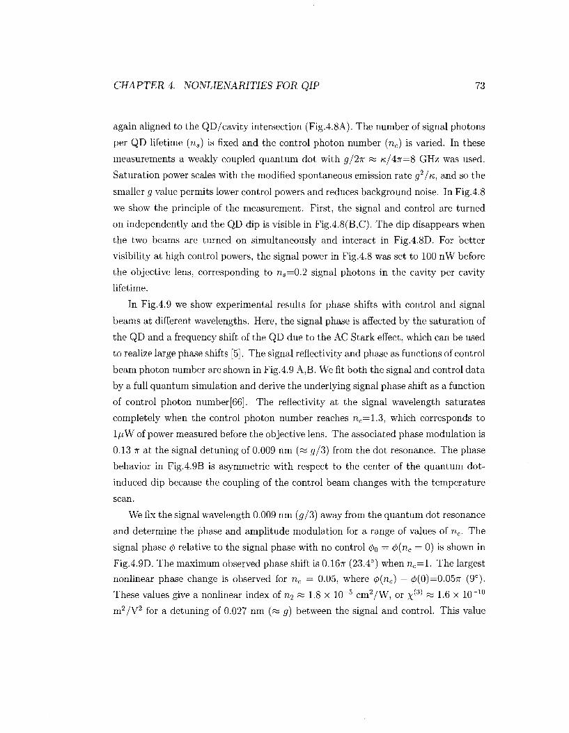
CHAPTER 4. NONLIENARITIES FOR QIP 73
again aligned to the QD/cavity intersection (Fig.4.8A). The number of signal photons
per QD lifetime (ns) is fixed and the control photon number (nc) is varied. In these
measurements a weakly coupled quantum dot with g/2Tt « K/47T=8 GHZ was used.
Saturation power scales with the modified spontaneous emission rate g2/it, and so the
smaller g value permits lower control powers and reduces background noise. In Fig.4.8
we show the principle of the measurement. First, the signal and control are turned
on independently and the QD dip is visible in Fig.4.8(B,C). The dip disappears when
the two beams are turned on simultaneously and interact in Fig.4.8D. For better
visibility at high control powers, the signal power in Fig.4.8 was set to 100 nW before
the objective lens, corresponding to ns=0.2 signal photons in the cavity per cavity
lifetime.
In Fig.4.9 we show experimental results for phase shifts with control and signal
beams at different wavelengths. Here, the signal phase is affected by the saturation of
the QD and a frequency shift of the QD due to the AC Stark effect, which can be used
to realize large phase shifts [5]. The signal reflectivity and phase as functions of control
beam photon number are shown in Fig.4.9 A,B. We fit both the signal and control data
by a full quantum simulation and derive the underlying signal phase shift as a function
of control photon number[66]. The reflectivity at the signal wavelength saturates
completely when the control photon number reaches nc=1.3, which corresponds to
1/uW of power measured before the objective lens. The associated phase modulation is
0.13 7T at the signal detuning of 0.009 nm (sa g/3) from the dot resonance. The phase
behavior in Fig.4.9B is asymmetric with respect to the center of the quantum dot-
induced dip because the coupling of the control beam changes with the temperature
scan.
We fix the signal wavelength 0.009 nm (<y/3) away from the quantum dot resonance
and determine the phase and amplitude modulation for a range of values of nc. The
signal phase 4> relative to the signal phase with no control (f)0 — (j){nc = 0) is shown in
Fig.4.9D. The maximum observed phase shift is 0.167T (23.4°) when n c =l . The largest
nonlinear phase change is observed for nc = 0.05, where (f>(nc) — </>(0)=0.057r (9°).
These values give a nonlinear index of n2 « 1.8 x 10~5 cm2/W, or x ^ ~ 1-6 x 10 -10
m2/V2 for a detuning of 0.027 nm (« g) between the signal and control. This value
CHAPTER 4. NONLIENARITIES FOR QIP 74
927.0 927.2 927.4 927.6 20 40 60 80 100 120
A,(nm) temperature scan count
Figure 4.8: Interaction between a control and signal beam at different wavelengths.
The signal beam at Xs (A-i) is detuned by 0.027 nm (« g) from the control beam
at Ac (A-ii) and positioned to coincide with the cavity-dot crossing-point (A-iii). For
each measurement, a sequence of scans is taken (A i-iii). The quantum dot and
cavity trajectories are shown in (A-iii). We track the amplitudes at both wavelengths
in each frame (A i-iii) to subtract fluorescence backgrounds, which are magnified 10
times in (B) and (C) (these are fluorescence backgrounds detected at control and
signal wavelengths, respectively.). The QD-induced dip is clearly visible in (B) when
only the signal (solid blue line) is on, and in (C) when only the control (dashed line)
is on. This feature disappears when both beams are on in (D). In (D), the spectra
are normalized in order to clearly show saturation. The signal and control powers
were 100 nW and 200 nW measured before the lens, corresponding to cavity coupled
signal and control photon numbers ns «0.2 and nc ~0.3, respectively.
CHAPTER 4. NONLIENARITIES FOR QIP 75
120
-e-
0.7
0.6
0.5
0.4
0.3
B
•7 ° \
n = 1.3 0
— n=0.3 c
n = 0.05 c
**K
60 70 80 90
temperature scan count 100 10" 10
control power (nc)
Figure 4.9: Nonlinear response of a weakly coupled quantum dot inside the cavity
to excitation with control and signal beam wavelengths separated by 0.027 nm (as g).
The reflectivity of a signal beam with ns=0.2 photons per cavity lifetime is shown
in (A) for three values of the control beam photon number nc. The quantum dot
saturates almost completely when roc=1.3, which corresponds to a power of 1 fxW
measured before the objective lens. The data is fit with a full quantum model, which
allows us to extract the signal phase shown in (B). In (C) the amplitude of the reflected
signal beam when it is 0.009 nm (« g/3) away from the dot resonance (vertical line
in A,B) is shown as a function of control beam photon number nc. In (D), we show
the difference between the phase shift of the signal beam when the control beam is
on ((f)) and when the control is off (<̂ o) as a function of nc at the same time point as
in (C).
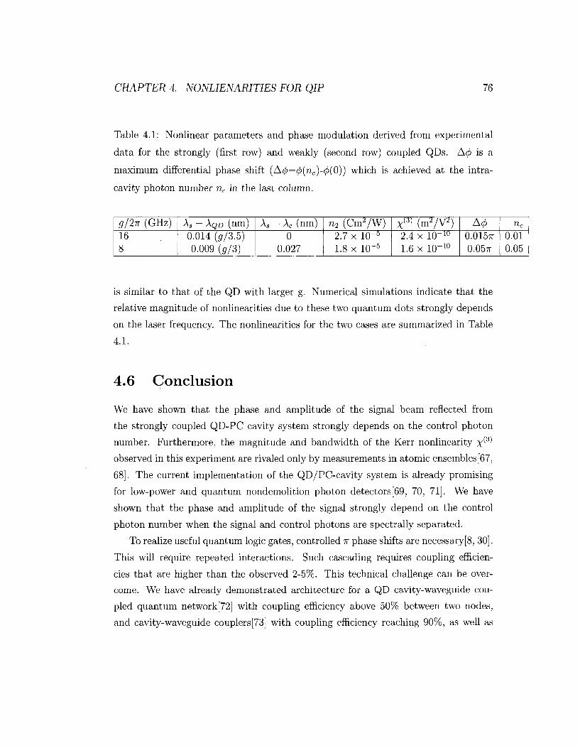
CHAPTER 4. NONLIENARITIES FOR QIP 76
Table 4.1: Nonlinear parameters and phase modulation derived from experimental
data for the strongly (first row) and weakly (second row) coupled QDs. A0 is a
maximum differential phase shift (A(f>=(f)(nc)-<f)(0)) which is achieved at the intra-
cavity photon number nc in the last column.
g/2-K (GHz) 16 8
K - AQD (nm) 0.014 {g/3.5) 0.009 (g/3)
Xs - \c (nm) 0
0.027
n2 (Cm2/W) 2.7 x 10"5
1.8 x 10~5
x(3) ( m 2 / ^ )
2.4 x 10"iU
1.6 x 10⁻¹⁰
A<l> 0.0157T 0.057T
nc
0.01 0.05
is similar to that of the QD with larger g. Numerical simulations indicate that the
relative magnitude of nonlinearities due to these two quantum dots strongly depends
on the laser frequency. The nonlinearities for the two cases are summarized in Table
4.1.
4.6 Conclusion
We have shown that the phase and amplitude of the signal beam reflected from
the strongly coupled QD-PC cavity system strongly depends on the control photon
number. Furthermore, the magnitude and bandwidth of the Kerr nonlinearity x^
observed in this experiment are rivaled only by measurements in atomic ensembles[67,
68]. The current implementation of the QD/PC-cavity system is already promising
for low-power and quantum nondemolition photon detectors[69, 70, 71]. We have
shown that the phase and amplitude of the signal strongly depend on the control
photon number when the signal and control photons are spectrally separated.
To realize useful quantum logic gates, controlled n phase shifts are necessary[8, 30].
This will require repeated interactions. Such cascading requires coupling efficien
cies that are higher than the observed 2-5%. This technical challenge can be over
come. We have already demonstrated architecture for a QD cavity-waveguide cou
pled quantum network[72] with coupling efficiency above 50% between two nodes,
and cavity-waveguide couplers [73] with coupling efficiency reaching 90%, as well as
CHAPTER 4. NONLIENARITIES FOR QIP 77
coherent probing of a strongly coupled QD-PC cavity system in a circuit configuration
[61]. The observed fluorescence losses are already sufficiently low to allow scalable
computation[74], and can be further improved with increases in cavity Q. The ability
to tailor photon-QD interactions by photonic crystal fabrication makes this a highly
versatile platform for a variety of quantum optics experiments with great potential
for compact scalable quantum devices.
The observed differential phase shifts are far from the expected values of 7r/2 for
full saturation and n for full Stark shifts. This is in part due to the structure of the
nonlinearity, and in part due to the parameters which were used in our experiments.
In the case of signal and control beams at distinct frequencies, the control beam
was applied close to the QD resonance, and so both saturation and Stark shift are
included in the observed measurements. The operating point was mostly dictated by
the available laser sources and experimental resolution. Analytically, however, we can
span a larger parameter space for expected values of the phase shift. In Fig. 4.6, we
show the phase shift as a function of frequency when the QD is on resonance with the
cavity. The simulation parameters for g and K are the same as used in our experiment.
The maximum phase shift in this case is PH 0.17T as in the experiment. In Fig. 4.11
we show the phase shift as the quantum dot is detuned from the cavity. Here, a near
7r/2 phase shift occurs at a high detuning and is close to what is expected from full
saturation.
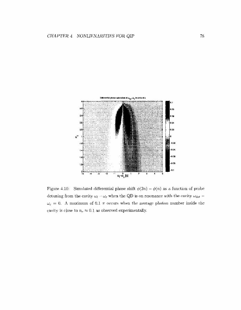
CHAPTER 4. NONLIENARITIES FOR QIP 78
Differential phase saturation at OOL^SOJ In units o l n
Figure 4.10: Simulated differential phase shift 4>(2n) — 4>(n) as a function of probe
detuning from the cavity coi — uc when the QD is on resonance with the cavity uj^ot —
UJC = 0. A maximum of 0.1 IT occurs when the average photon number inside the
cavity is close to Tip ~ 0.1 as observed experimentally.
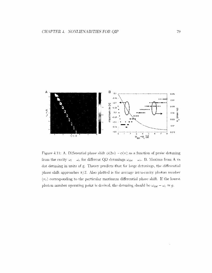
CHAPTER 4. NONLIENARITIES FOR QIP 79
Figure 4.11: A. Differential phase shift (p{2n) — <p{n) as a function of probe detuning
from the cavity ujt — JJC for different QD detunings jjjA)t — vjr. B. Maxima from A vs
dot detuning in units of g. Theory predicts that for large detunings, the differential
phase shift approaches ir/2. Also plotted is the average intra-cavity photon number
(nr) corresponding to the particular maximum differential phase shift. If the lowest
photon number operating point is desired, the detuning should be njdot — u>r ~ ().
Chapter 5
Towards room temperature
cavity-QED
5.1 Introduction
In Chapter 4, it was shown that single quantum dots coupled to photonic crystal
cavities can serve as building blocks of quantum information processing devices. Cur
rent state of the art experiments are performed at cryogenic temperatures, because
electron-hole pairs cannot be confined in In As quantum dots at elevated temperatures.
However, a variety of emitters operate at room temperature and can potentially serve
as a two or three level system for quantum information processing experiments. Room
temperature generation of single photons has been observed from single molecules [75],
nitrogen vacancy centers [76], and CdSe quantum dots [77], but collection efficien
cies were reduced due to lack of coupling to good cavities. These sources, operate
at visible wavelengths and are therefore difficult to combine with cavities made in
high index semiconductor slabs. In contrast, PbS quantum dots (and other colloidal
quantum dots such as PbSe) can be made to cover a very broad wavelength range.
Furthermore, these dots can be easily deposited onto passive structures in a low in
dex polymer and can be used to map out the resonances of the structures [78]. This
method is potentially easier than transmission and reflectivity type measurements on
single cavities. Lastly, PbS quantum dots are successfully used as fluorescent labels
80
CHAPTER 5. TOWARDS ROOM TEMPERATURE CAVITY-QED 81
in biological imaging applications. Cavity enhanced emission and collection efficiency
from such dots could prove to be a valuable technique for targeted signal amplification
of a target molecule bound to or in the vicinity of the resonant cavity.
5.2 Room temperature operation
Room temperature operation requires exceptionally high-Q and low-V cavities in or
der to overcome the phonon broadening of the main quantum dot transition line. This
is illustrated in Fig. 5.1 where we plot the transmission function of a cavity with an
embedded QD whose bulk decay rate 7 is allowed to increase due to a mechanism
such as phonon broadening. It can be seen that as 7 increases, the QD induced trans
mission dip saturates and the amplitude of the transmitted component diminishes,
as energy is scattered out of the system. The reduction in the transmission dip can
only be mitigated by increasing g or decreasing K since this drives the system into
stronger coupling where losses to the cavity mode dominate scattering losses. The
same challenges are faced by attempts of using cavity-coupled nitrogen vacancies in
diamond as quantum memory nodes [79].
Photonic crystals are potentially ideally suited for the realization of cavities for
coupling such room temperature emitters due to the high Q/V ratios available in
these devices and the ability to fabricate them in a variety of substrates. However,
the combination of PC cavities with external emitters had not been demonstrated
prior to our work described here [78]. Photonic crystal cavities were made in a 160
nm thick AlGaAs (33% Al) membrane on top of 500 nm of AlAs. The cavities
were defined in 3% 450 K molecular weight (KmW) PMMA with the Raith Electron
Beam Lithography system. The patterns were transferred from PMMA developed
in 3:1 Methyl Isobutyl Ketone (MIBK) to the membrane with an electron-cyclotron
resonance (ECR) plasma etch process. The Al rich substrate was then oxidized at
420° C for 10 minutes in the presence of water vapor in order to create an index
contrast of 3.4:1.8 between membrane and substrate. A scanning electron micrograph
of the sample structure is shown in Fig. 5.2. PbS quantum dots emitting at 850
nm and 950 nm were obtained from Evident Technologies. The dots were dissolved
CHAPTER 5. TOWARDS ROOM TEMPERATURE CAVITY-QED 82
Transmission as a function of y toi g=K
Figure 5.1: Influence of 7 on the transmission through a cavity with an embedded QD. As 7 increases due to phonon scattering at elevated temperatures, the transmission dip diminishes and the transmitted amplitude falls due to energy losses into phonon modes. For the plots it is assumed that g = K
together in 1% 75 KmW PMMA at a concentration of 0.1 mg/ml in toluene and
spun onto the structures at 2 krpm, resulting in a 20nm-100nm membrane (bulk
spectra shown in Fig. 5.3). The coating was not uniform due to the small chip size
~ (5mm2) and presence of structures on the chip surface. This concentration of
emitters corresponds to ~ 102 dots per fim2 in a 100 nm membrane. The dots were
kept under vacuum, and excited with femtosecond pulses from a Ti:Saph laser at 760
nm. Cavity spectra, collected under pulsed excitation, are shown in Fig. 5.4. The
spectra reveal two orthogonally polarized modes as expected for this type of photonic
crystal cavity. The linearly increasing background observed on the spectra can be
explained by considering the emission profile of the dots and the reflectivity of the
PMMA/AlGaAs/AlOx structure, which leads to an almost linear emission profile of
dots on the AlGaAs slab.
The cavity used is shown in Fig. 5.2. The coupling between a cavity and emitter
depends on both the spatial alignment and the orientation of the emitter dipole
CHAPTER 5. TOWARDS ROOM TEMPERATURE CAVITY-QED 83
Figure 5.2: Left: Scanning electron micrograph showing the photonic crystal cavity (a). Middle: Simulated electric field intensity of the x (b) and y (c) dipole modes in the asymmetric cavity. The measured Q factors are 400 and 200 respectively.
Figure 5.3: PbS quantum dot spectra: 850 and 950 dot spectra taken on a bulk silicon wafer.
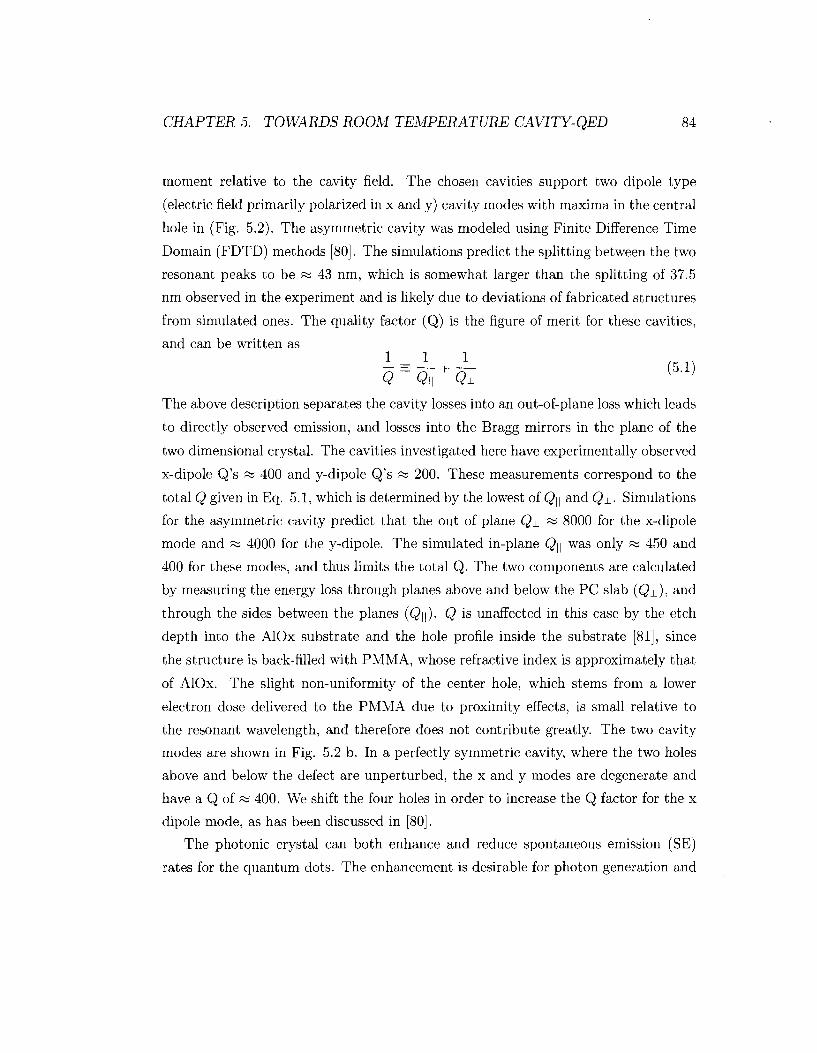
CHAPTER 5. TOWARDS ROOM TEMPERATURE CAVITY-QED 84
moment relative to the cavity field. The chosen cavities support two dipole type
(electric field primarily polarized in x and y) cavity modes with maxima in the central
hole in (Fig. 5.2). The asymmetric cavity was modeled using Finite Difference Time
Domain (FDTD) methods [80]. The simulations predict the splitting between the two
resonant peaks to be w 43 nm, which is somewhat larger than the splitting of 37.5
nm observed in the experiment and is likely due to deviations of fabricated structures
from simulated ones. The quality factor (Q) is the figure of merit for these cavities,
and can be written as 1 - l 1
Q = ^ + O l { }
The above description separates the cavity losses into an out-of-plane loss which leads
to directly observed emission, and losses into the Bragg mirrors in the plane of the
two dimensional crystal. The cavities investigated here have experimentally observed
x-dipole Q's « 400 and y-dipole Q's « 200. These measurements correspond to the
total Q given in Eq. 5.1, which is determined by the lowest of Q\\ and Q±. Simulations
for the asymmetric cavity predict that the out of plane Q± « 8000 for the x-dipole
mode and ~ 4000 for the y-dipole. The simulated in-plane Q\\ was only ss 450 and
400 for these modes, and thus limits the total Q. The two components are calculated
by measuring the energy loss through planes above and below the PC slab (Q±), and
through the sides between the planes (Q\\). Q is unaffected in this case by the etch
depth into the AlOx substrate and the hole profile inside the substrate [81], since
the structure is back-filled with PMMA, whose refractive index is approximately that
of AlOx. The slight non-uniformity of the center hole, which stems from a lower
electron dose delivered to the PMMA due to proximity effects, is small relative to
the resonant wavelength, and therefore does not contribute greatly. The two cavity
modes are shown in Fig. 5.2 b. In a perfectly symmetric cavity, where the two holes
above and below the defect are unperturbed, the x and y modes are degenerate and
have a Q of « 400. We shift the four holes in order to increase the Q factor for the x
dipole mode, as has been discussed in [80].
The photonic crystal can both enhance and reduce spontaneous emission (SE)
rates for the quantum dots. The enhancement is desirable for photon generation and
CHAPTER 5. TOWARDS ROOM TEMPERATURE CAVITY-QED 85
Mnm) X(nm)
Figure 5.4: Cavity resonances mapped out by quantum dots in PMMA. Left: Polarization dependence of modes confirming that they are x and y dipole modes. Right: Ex dipole mode measured at two orthogonal polarizations. Angles refer to analyzer positions.
spectroscopy applications due to increased signal rate and strength. The figure of
merit for this modification is the Purcell factor F = jp-. Here T is the emission rate 1 o
in the cavity, and F0 is that without the cavity. The observed spontaneous emission
rate for an emitter with dipole moment /I at a point on the cavity can be derived
from Fermi's Golden rule [82], and the total rate takes the form
rjL = J-Jj—)' f +Fpc (5.2) r o ^ max{£} \jl\ j AAC
2 + 4(A - Ac)2
Here E is the electric field at the position of the emitter, Vmod,e is the cavity mode
volume, AA is the detuning from the cavity resonance wavelength Ac. For an emitter
that is on resonance with the cavity and has a dipole moment aligned with the field,
Fc = ( A i 3u— ) • The mode volume is calculated from the FDTD simulation results y 47T n Vmotie J
as Vmode = f ,L,i d3r, with e as the position dependent dielectric constant. For . • . . max{e .E } •
this cavity, the volume has a value of Vmode = 0.96-f, where n is the index in AlGaAs.
The term Fpc describes the modification of the SE rate due to the presence of the
photonic crystal lattice and modes other than the cavity mode. This modification
results in a suppression of emission [83, 65]. The cavity mode volume can be quite
CHAPTER 5. TOWARDS ROOM TEMPERATURE CAVITY-QED 86
accurately derived from FDTD calculations, and with the cavity Q derived from
the spectra, we calculate an Fc ~ 30. We can also derive an average value of the
suppression Fpc from the experimental data. The total intensity collected by the
spectrometer 1$ is given by the emission rate Eq. 5.2, integrated over the spatial and
spectral density of the emitters.
1+= T0JdflJd\Jd3fp(X,f,p) x (5.3)
Here (p is the value of the polarizer angle, r\c is the collection efficiency due to the
cavity radiation profile, r/o is the collection efficiency from an emitter embedded in the
PMMA layer and uncoupled to the cavity, p(X, f, p) contains the spectral and spatial
distribution of the dots and the orientations of their dipole moments. The value of
r/c can be estimated from numerically integrating the PC emission profile over the
numerical aperture (NA) of the lens, and is rjc ~ 8%. The coupling efficiency of the
bulk emitter is given by the integral over the sub-critical solid angle defined by the NA o dvcsin,(— )
of the objective lens 770 = ^ /„ d<f> J0 npMMA sm(6)d0 « 3% (Here NA = 0.5
and TIPMMA = 1-5). Since the cavity modes are primarily linearly polarized, the ratio
of the integrated intensities for polarizer angles of 0° and 90° gives:
J dp dX d3fp(\, f, jl) M \ AA^
R^^-^Fc1^ V —4- + 1 (5.4) I90o r)Q J dn d\ d3r FPC p(A, r, fi)
Using the value of Fc and the x-dipole field, the average value of Fpc over the
lattice around the cavity can thus be estimated from the spectra. Assuming random
dipole orientation, the integral over /2 gives | . We take the spectral distribution of the
dots to be Gaussian and centered at 850 and 950 nm with a FWHM of 100 nm. The
cavity line shape is Lorentzian with a FWHM of 2 nm. Only dots which are excited
by the pump are contributing to the intensity, and so the spatial density corresponds
to the excitation of a uniform dot distribution by a Gaussian pulse with a FWHM of
600nm in the x,y plane and uniform in z, since the layer is thin relative to the focal
CHAPTER 5. TOWARDS ROOM TEMPERATURE CAVITY-QED 87
depth. The integral over the field is done numerically with the simulated cavity field
components. The spectral data shown in Fig. 5.4 b. gives R ?s 1.07. Using the value
of Fc = 30, Fpc is estimated to be Fpc ~ 0.6, which qualitatively agrees with the
values found in [83, 65].
5.3 Conclusion
In conclusion, we have shown coupling of PbS quantum dots dissolved in PMMA to
photonic crystal cavities at room temperature. The dot emission maps out the cavity
resonances and is enhanced relative to the bulk emission by a maximal Purcell factor
of 30. Using the emission spectra with and without cavity lines, we derive a photonic
crystal lattice spontaneous emission rate modification of « 0.6. To our knowledge this
is the first demonstration of coupling of colloidal quantum dots to photonic crystal
cavities, and the first use of such dots as a broadband on-chip source for cavity
characterization. Following our work, other demonstrations of colloidal QD coupling
to PC cavities have been made [84, 85]. Since such dots are available in a variety of
emission wavelengths, this characterization technique can be applied to many different
semiconductor devices. The deposition technique presented in this work is easy to use
and allows many different types of emitters to be deposited and re-deposited onto both
passive and doped structures. Furthermore, E-beam lithography can then be used to
remove dot-doped PMMA from regions around the cavity, and the resulting emission
will only come from the emitters in the cavity. The use of colloidal quantum dots for
characterization of PC structures is similar to internal light source techniques [86],
but has a number of advantages: first, our method permits characterization of passive
PC structures, where internal light sources are not available. Moreover, our technique
allows deposition of sources on select areas on the chip, as well as re-deposition and
removal after characterization. Finally, our technique, combined with tuning of the
QD concentration in PMMA, can enable isolation of a single emitter inside the cavity,
which would be beneficial for construction of single photon sources that are cheap and
reusable, as opposed to those based on self-assembled QD's embedded in a PC cavity
[65].
Chapter 6
Ultra Fast Modulation
6.1 Introduction
Nonlinear optical switching in photonic networks is a promising approach for ultra-
fast low-power optical data processing and storage [87]. In addition, optical data
processing will be essential for optics-based quantum information processing systems.
A number of elements of an all optical network have been proposed and demonstrated
in silicon photonic crystals [88, 89]. Fast tuning of the photonic crystal bands has
also been demonstrated [90, 91]. Here, we directly observe ultrafast (« 20 GHz)
nonlinear optical tuning of photonic crystal (PC) cavities containing quantum dots
(QD). We perform the fast tuning via free carrier injection, which alters the cavity
refractive index, and observe it directly in the time domain. Three material effects
can be used to quickly alter the refractive index. The first is the index change due to
free carrier (FC) generation, which is discussed in this work, and has been explored
elsewhere [90]. The cavity resonance shifts to shorter wavelengths due to the free-
carrier effect. Switching via free-carrier generation is limited by the lifetime of free
carriers and depends strongly on the material system and geometry of the device. In
our case, the large surface area and small mode volume of the PC reduce the lifetime
of free carriers in GaAs. Free carriers can alternatively be swept out of the cavity
by applying a potential across the device [92]. The second effect that can be used
to modify the refractive index is the Kerr effect, which is promising for a variety of
88

CHAPTER 6. ULTRA FAST MODULATION 89
other applications [93, 50] and, in principle, should result in modulation rates exceed
ing THz. However, the free carrier effect is more easily achieved in the GaAs PC
considered here. The third effect is thermal tuning (TT) via optical heating of the
sample through absorption of the pump laser. This process is much slower than free
carrier and Kerr effects and shifts the cavity resonance to longer wavelengths due to
the temperature dependence of the refractive index. The time scale for this process
is on the order of microseconds. Here we consider these two processes for modulating
cavity resonances, and focus on the higher-speed FC tuning. Here we consider both
FC and TT for modulating cavity resonances.
Photonic crystal samples investigated in this study are grown by molecular beam
epitaxy on a Si n-doped GaAs (100) substrate with a 1 jim buffer layer. The sample
contains a 10 period distributed Bragg reflector (DBR) mirror consisting of alternat
ing layers of AlAs/GaAs with thicknesses of 80.2/67.6 nm respectively. A 918 nm
sacrificial layer of Al0.sGa0.2As is located above the DBR mirror. The active region
consists of a 150 nm thick GaAs region with a centered InGaAs/GaAs QD layer. QDs
self-assemble during epitaxy operating in the Stranski-Krastanov growth mode with
a density of 100 dots per /j,m2. InGaAs islands are partially covered with GaAs and
annealed before completely capping with GaAs. This procedure blue shifts the QDs
emission wavelengths [94] towards the spectral region where Si-based detectors are
more efficient.
PC cavities, such as those shown in Fig.6.1, were fabricated in GaAs membranes
using standard electron beam lithography and reactive ion etching techniques. Finite
Difference Time Domain (FDTD) simulations predict that the fundamental resonance
in the cavity has a field maximum in the high index region (Fig.6.1), and thus a
change in the value of the dielectric constant should affect these modes strongly.
We investigated the dipole cavity (Fig.6.1), the linear three-hole defect cavity [38],
and the linear two-hole defect cavity designs. The experimentally observed Q's for
all three cavities were in the range of 1000-2000 (optimized cavities can have much
higher Q's), and consequently the experimental tuning results were similar for all
three cavities.
Photonic crystal cavities were made to spectrally overlap with the QD emission,
CHAPTER 6. ULTRA FAST MODULATION 90
and are visible above the QD emission background due to an increased emission rate
and collection efficiency of dots coupled to the cavity. Quantum dot emission was
excited with a Ti:Sapphire laser tuned to 750 nm in a pulsed or CW configuration.
In the pulsed mode, the pump produced 3ps pulses at an 80 MHz repetition rate.
Tuning was achieved by pulsing the cavity with appropriate pump power. The cavity
emission was detected on a spectrometer and on a streak camera for the time resolved
measurements.
Tuning is achieved by quickly changing the value of the dielectric constant e = n2
of the cavity with a control pulse. The magnitude of the refractive index shift An
can be estimated from
Aco l[Ae\E\2dV An ftj ' ' Ri (6 1)
LU 2 fe\E\2dV n K }
Above, ui is the resonance of the un-shifted cavity, \E\2 is the amplitude of the cavity
mode, and the integral goes over all space. In order to shift by a line width, we require
~ = 7j, which gives An = 0. Finite difference time domain (FDTD) calculations
indeed verify that for a linear cavity with Q 1000, a An ~ 10 - 2 shifts the resonance
by more than a line width, as seen in Fig. 6.1.
As described above, two tuning mechanisms were investigated in this work. The
first is temperature tuning, which is quite slow (on the time scale of microseconds).
The second is the free carrier induced refractive index change, which is found to occur
on the time scale of tens of picoseconds. Therefore, we can look at the two effects
separately in the time domain.
6.2 Free Carrier Tuning
In the case of Free Carrier (FC) tuning only,
An(t) = An / e(t) =
n n

CHAPTER 6. ULTRA FAST MODULATION 91
Figure 6.1: (a): Scanning electron micrograph of the L3 type cavity fabricated in a GtiAs material with a high density of InAs quantum clots, (b): high-Q mode electric field amplitude distribution, as predicted by FDTD simulations, (c): FDTD simulations of frequency and Q changes as An/n changes from ±10~'! —> ±10" l . A high-Q (QHQ = 20000) and low-L (QLQ = 2000) cavity were tuned: (qx) AQ/Q for An > 0 and Q = QHQ- (q-i) AQ/Q for An > 0 and Q = QLQ, LJJ\) AJJ/^J for
An < 0,(^2) AUJJUJ for An > 0 for both high Q and low Q modes. (q-,$) AQ/Q for An < 0 Q = QLQ, (en) AQ/Q for An < 0 Q = QHQ- The lines An/n for An > 0 and An. < 0 are also plotted and overlap exactly with ^2
a n d u/[. As can be seen, the magnitude of the relative frequency change is independent of Q, but the higher Q cavity is degraded more strongly by the change in index. For an increase in 11, the Q increases due to stronger Total Internal Reflection confinement in the slab, as expected.
CHAPTER 6. ULTRA FAST MODULATION 92
where Nfc(t) is the density of free carriers in the GaAs slab, and the value of r\ is
given in terms of fundamental constants (e0,c), DC refractive index (n0), charge (e),
effective electron mass (m*) and wavelength (A) as 77 = — 87r2e2eA
n m . [95] , and we
calculate rj sa 10~21cm3 for our system.
The FC density changes with the pump photon number density P(t), with pulse
width TP, in time t as: dNfc 1 Ar Pit) , ,
The carriers decay with — = — -\—-—|- —, where rT,Tm are the radiative and
non-radiative recombination times of free carriers, and rc is the relaxation time (or
capture time) into the QDs. While rc « 30 — 50ps « rr,Tnr, the dot capture is
not the dominant relaxation process. The dots saturate for the duration of the dot
recombination lifetime r^ « 2Q0ps — lns, and, because the dot density is much smaller
than the FC density, the effective capture time is much longer. Qualitatively, we can
describe this effect by lengthening rc by a factor 1/x as rc —> rc/x » Tr,Tnr, where
x « 1 is essentially the ratio of QD to FC densities. The FC density is then given
by:
Nfc(t) = Nfc(0)e rtc+e *•/= / e-tr.-L±^ (6.4) JO Tp
In order to shift the cavity resonance by a line width (An/n — 10~3), we need
NfC « 1018cm-3 according to Eq. 6.2. Taking into account the GaAs absorption
coefficient a « 104cm_1, reflection losses from the 160 nm GaAs membrane (R =
Cai rI" f faA3)2 ~ -3), lens losses (50%), and an approximately 5/um spot size, average
3ps pulse powers as low as 1-10 /iW should yield the desired shifts of order ^ « 10^3.
In our experiment, we monitor the cavity resonance during the tuning process
using QD emission. Thus, we need to account for the delay between the pump and
onset of emission in QDs. The QDs are excited by free carriers according to:
^ = _±^+^£ („.5) at Td TC
From Eqs. 6.5 and 6.4, the QD population (assuming no excited dots at carriers
CHAPTER 6. ULTRA FAST MODULATION 93
at t=0) is given by:
t_
Nqd(t) = / e v V / e^P(t")dfdt' (6.6)
where rp is the pump pulse width, rqrf RS 200 ps is the average cavity coupled QD
lifetime, TJC « 30ps is the FC lifetime, and P(t) is the pump photon number density.
The observed spectrum is that of a Lorentzian with a time - varying central frequency
u>o(t) (for simplicity, we assume that the Q factor is time invariant), which we define
as:
5(Wl«) = (l + 4 g 2 ( l - ^ ) ) - 1 (6.7)
ur
The numerical results are shown in Fig. 6.2. We find that going beyond 10's of
[iW does not result in a larger shift, but destroys and shifts the cavity Q permanently.
The experimental data is shown in Fig. 6.3. We used moderate power («10 /iW)
to shift the cavity by one half line width. Stronger excitation results in higher shifts
as indicated by an extremely asymmetric spectrum shown on the inset in (d) of Fig.
6.3, where 100 /J,W were used. However, prolonged excitation at this power leads to
a sharp reduction in Q over time.
6.3 Thermal Tuning
In the case of thermal tuning, the refractive index is given by:
An(t)
n = (3T (6.8)
where j3 is the material dependent coefficient giving the refractive index dependence
on temperature.
Continuous wave above-band excitation of the sample results in both free carrier
generation and heating. In this case, the heating mechanism dominates, and the
cavity red-shifts. The predominant effect on the dielectric constant is the change in
the band gap with temperature due to lattice expansion and phonon population. The
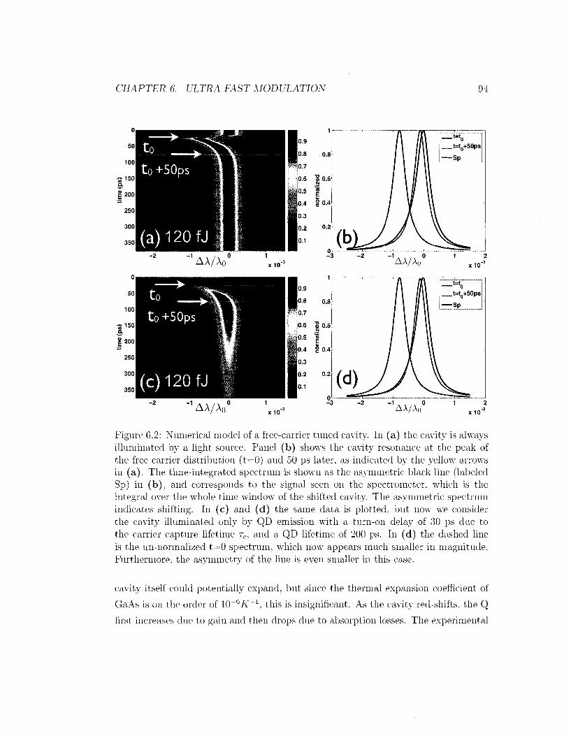
CHAPTER 6. ULTRA FAST MODULATION 94
Figure 6.2: Numerical model of a free-carrier timed cavity. In (a) the cavity is always illuminated by a light source. Panel (b) shows the cavity resonance at the peak of the free carrier distribution (t=0) and 50 ps later, as indicated by the yellow arrows in (a). The time-integrated spectrum is shown as the asymmetric black line (labeled Sp) in (b), and corresponds to the signal seen on the spectrometer, which is the integral over the whole time window of the shifted cavity. The asymmetric spectrum indicates shifting. In (c) and (d) the same data is plotted, but now we consider the cavity illuminated only by QD emission with a turn-on delay of 30 ps due to the carrier capture lifetime rc, and a QD lifetime of 200 ps. In (d) the dashed line is the un-normalized t=0 spectrum, which now appears much smaller in magnitude. Furthermore, the asymmetry of the line is even smaller in this case.
cavity itself could potentially expand, but since the thermal expansion coefficient of
GaAs is on the order of 10~6A'~L. this is insignificant. As the cavity red-shifts, the Q
first increases due to gain and then drops clue to absorption losses. The experimental
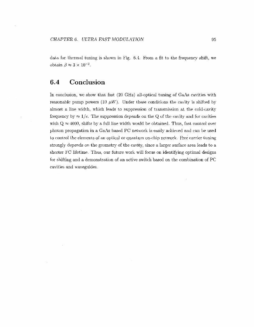
CHAPTER 6. ULTRA FAST MODULATION 95
data for thermal tuning is shown in Fig. 6.4. From a fit to the frequency shift, we
obtain /? » 3 x 10~3.
6.4 Conclusion
In conclusion, we show that fast (20 GHz) all-optical tuning of GaAs cavities with
reasonable pump powers (10 /J.W). Under these conditions the cavity is shifted by
almost a line width, which leads to suppression of transmission at the cold-cavity
frequency by « 1/e. The suppression depends on the Q of the cavity and for cavities
with Q RS 4000, shifts by a full line width would be obtained. Thus, fast control over
photon propagation in a GaAs based PC network is easily achieved and can be used
to control the elements of an optical or quantum on-chip network. Free carrier tuning
strongly depends on the geometry of the cavity, since a larger surface area leads to a
shorter FC lifetime. Thus, our future work will focus on identifying optimal designs
for shifting and a demonstration of an active switch based on the combination of PC
cavities and waveguides.
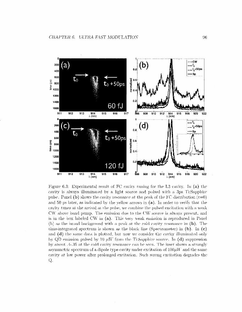
CHAPTER 6. ULTRA FAST MODULATION 96
X(nm) ?v(nm)
Figure 6.3: Experimental result of FC cavity tuning for the L3 cavity. In (a) the cavity is always illuminated by a light source and pulsed with a 3ps TkSapphire pulse. Panel (b) shows the cavity resonance at the peak of the FC distribution ( t=0) and 50 ps later, as indicated by the yellow arrows in (a ) . In order to verify that the cavity tunes at the arrival at the pulse, we combine the pulsed excitation with a weak CW above band pump. The emission due to the CW source is always present, and is in the box labeled CW in (a) . This very weak emission is reproduced in Panel (b) as the broad background with a peak at the cold cavity resonance in (b ) . The time-integrated spectrum is shown as the black line (Spectrometer) in (b ) . In (c) and (d) the same data is plotted, but now we consider the cavity illuminated only by QD emission pulsed by 10 f.i\V from the TkSapphire source. In (d) suppression by about .4-.35 at the cold cavity resonance can be seen. The inset shows a strongly asymmetric spectrum of a dipole type cavity under excitation of 100/iIF and the same cavitv at low power after prolonged excitation. Such strong excitation degrades the
Q.
CHAPTER 6. ULTRA FAST MODULATION 97
2 3 4 5 Pump Power (mW)
Figure 6.4: Thermal tuning of the L3 cavity under CW excitation (a): Measured Aui/uJ (left axis) and AQ/Q (right axis) as a function of pump power for the L3 cavity, obtained from the fits to the spectra shown in (b). The Q initially increases clue to moderate gain and then degrades, while uj shifts linearly. The straight dashed line fits Au/w = 3 x 10"-3 x Pir x 10 ° with 95% confidence and with root mean square deviation of ~ 0.99. At very high power, the change in frequency does not follow the same trend. The inset in (b) shows a plot of AU)/(UJ/Q), which is a measure of the number of lines that we shift the cavity by. A shift of three line widths is obtained.
Chapter 7
Fabrication
7.1 Introduction
In this chapter I review the fabrication techniques used to make our standard devices
and review our early attempts at making electrically controlled PC structures for
realizing a three-level system in an InAs QD for quantum memory applications, as
well as an electrically driven modulator/detector/source in a PC doped with quan
tum wells. Much of the research in the field of PC crystals is driven by simulations
and modeling such as that discussed in Chapter 2. However, there is a large dis
crepancy between the predicted designs and the performance of fabricated devices.
Much of this difference is due to the fabrication process - some due to the quality of
equipment used (which cannot be rectified), and some due to the methodology used.
In Section 7.2, I will review our progress toward realizing high quality PC cavities
in the Stanford Nanofabrication Facility (SNF). While the tools available elsewhere
will dramatically modify the outcomes in other fabs, the general methodology of a
systematic fabrication parameter space and cleanliness that were vital to our success
should be applicable everywhere.
Next to the quality and repeatability of fabrication, electrical control over PC
structures is the single most important technical challenge for the field of PC enabled
devices and their success and integration into real-world technologies. Due to the
thin structure of PC membranes, a high sheet resistance and tendency of current to
98
CHAPTER 7. FABRICATION 99
recombine at the contact the problem of placing electrical contacts on PC structures
is nontrivial. In Section 7.4, I review our early attempts at realizing electrically
controlled structures for quantum information processing and classical information
processing applications. For quantum optics, robust electrical control can result in
controlled charge loading into the quantum dot and, with an application of a magnetic
field, a quantum memory. For classical devices, a variety of monolithically integrated
devices such as modulators, detectors, and light sources could be realized.
7.2 PC fabrication
The devices are fabricated in high index semiconductors such as Si, GaAs, and Al-
GaAs. Fabrication in SiN and lower index materials is also possible [96], but limits the
quality factor of these devices due to low TIR confinement. In the next sections, the
numerical and analytical techniques for optimizing devices will be described. How
ever, in practice it turns out that reaching the exact design can prove difficult due
to an uncertainty in processes and accumulation of errors during the fabrication pro
cess. At the writing of this thesis, the highest Q demonstrated in GaAs at cryogenic
temperatures in our group was « 25,000. This is on par with the best devices found
in literature, and is limited most likely by fabrication and scattering losses. It took
several years to reach this Q. Two significant steps that increased the fabrication
performace were as follows:
• The r/a parameter space was experimentally spanned in order to create the
devices that operate in the desired frequency range. An optimal value of the
periodicity a=246 nm and radius r=60 nm (written, which resulted in 140 nm
diameter fabricated holes) was found. This raised the Q from a maximum of
« 3,000 to ^8 ,000 .
• The cavities were extensively cleaned after fabrication. Cleaning of the cavities
after fabrication raised the Q to the 10,000 to 20,000 range. It was found by
Faraon that a long acetone soak cleaned the devices and reduced scattering
losses.
CHAPTER 7. FABRICATION 100
JJKX h—I *•• •«• ummm-nmmm
Figure 7.1: A. Overall process flow for fabrication. B Sample GaAs wafer. C Exposed resist (inset is poor outcome). D Etched resist (inset is poor outcome). E final undercut PC. The light area around the structure indicates a successful undercut.
Thus, in the fabrication of PC devices, simulations have to be used as guidelines and
the fabrication parameter space must be sampled.
The overall GaAs PC fabrication process is illustrated in Fig. 7.1.
7.2.1 Sample preparation
• Clean wafers in Acetone and Isopropyl Alcohol for 10 niin each.
• Bake wafers at 90° C for 1 niin to evaporate solvents
• Cover bottom of wafer with blue tape
• Spin 4.5% 950K MW PMMA (in Anisole) at 3500 rpm for 40 sec. Dispense
resist with a glass pipette for small pieces, or pour from a beaker for larger
wafers. Syringes tend to stick due to solvent and PMMA.
CHAPTER 7. FABRICATION 101
• Remove blue tape and bake for 2 min at 180-200° C
• Cleave or re-attach blue tape to keep sample in one place. Keep in N2 atmo
sphere in low light.
7.2.2 Cleaving
To cleave GaAs samples score the desired area on the opposing sides of the cleave
with a diamond scribe. The sample should cleave under light pressure applied around
the cleave marks along one of the cleave planes. Keep the sample on some cleanroom
paper to allow it to bend. To cleave Si, you have to flick the sample with the scribe,
because there are no cleave planes as in GaAs.
7.2.3 Exposure
Expose the PMMA with the Raith E-beam tool. Use the 10 fim aperture and 10 kV
for best results. Typical dose is 140 f.iC. Make sure that the step size is below 10 nm
and write speed is below 10 mm/s. Best results are obtained with a 3 nm step and
4mm/s.
7.2.4 Development
• Develop exposed PMMA in 3:1 Isopropanol to Methyl Iso Butyl Ketone for 45
s with light agitation.
• Rinse in Isorpopanol for 30 sec.
• Bake for 1-2 min at 90°.
7.2.5 Etching
• For thermal contact glue the chip to a Si wafer carrier in the carrier in the
Electron Cyclotron Resonance Reactive Ion Etcher (ECR RIE) Pquest.
• Use a glass pipette to put a small amount of PMMA on the carrier.
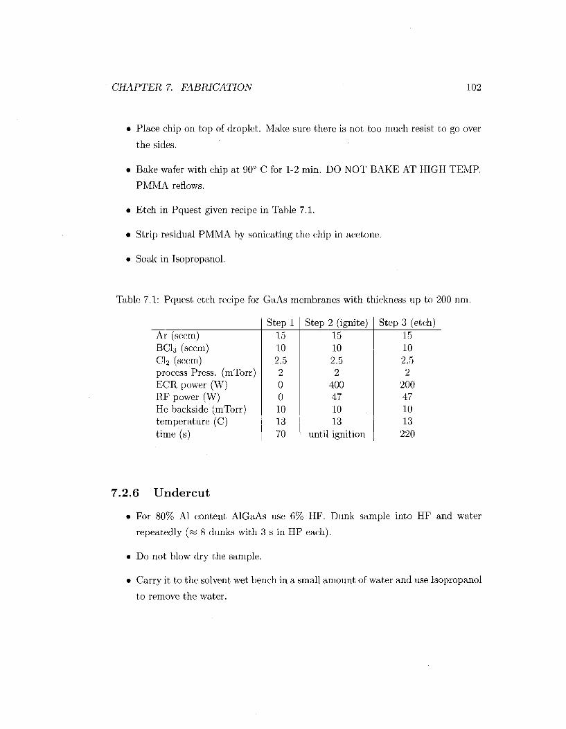
CHAPTER 7. FABRICATION 102
• Place chip on top of droplet. Make sure there is not too much resist to go over
the sides.
• Bake wafer with chip at 90° C for 1-2 min. DO NOT BAKE AT HIGH TEMP.
PMMA reflows.
• Etch in Pquest given recipe in Table 7.1.
• Strip residual PMMA by sonicating the chip in acetone.
• Soak in Isopropanol.
Table 7.1: Pquest etch recipe for GaAs membranes with thickness up to 200 nm.
Ar (seem) BC13 (seem) CI2 (seem) process Press. (mTorr) ECR power (W) RF power (W) He backside (mTorr) temperature (C) time (s)
Step 1 15 10 2.5 2 0 0 10 13 70
Step 2 (ignite) 15 10 2.5 2
400 47 10 13
until ignition
Step 3 (etch) 15 10 2.5 2
200 47 10 13
220
7.2.6 Undercut
• For 80% Al content AlGaAs use 6% HF. Dunk sample into HF and water
repeatedly (« 8 dunks with 3 s in HF each).
• Do not blow dry the sample.
• Carry it to the solvent wet bench in a small amount of water and use Isopropanol
to remove the water.
CHAPTER 7. FABRICATION 103
• Put wet sample into Isopropanol and then take it out and dry under low N2
flow.
• Inspect under microscope. Repeat if necessary.
7.2.7 Wet Oxidation
• set up GaAs oxidation furnace as per instructions: make sure the bubbler is
working and gas flow and water temperature are correct.
• put sample on glass boat
• drive boat very slowly into furnace
• to undercut a typical PC structure, leave there for 30 min, but times can vary
based on vapor and gas flows.
• remove sample carefully and slowly
7.2.8 Wet Oxidation Undercut
undercut oxidized sample in KOH and rinse in water similar to HF undercut.
7.3 P M M A doped with colloidal QDs
7.3.1 PMMA
Combine PMMA of a desired molecular weight with a solvent such as Toluene in a
closed container. Stir on a magnetic stirrer overnight, or until beads are dissolved.
Filter the PMMA prior to use for best results.
7.3.2 Disso lv ing Q D s in P M M A
If the QD's are in Toluene, simply combine them with the desired volume of premade
PMMA to obtain the proper concentration. If the dots are not in the same solvent, a
CHAPTER 7. FABRICATION 104
solvent transfer may be necessary if a high volume of dots is needed. Otherwise, the
two solvents can be mixed.
7.4 PC laser/detector and electrical contact fabri
cation
In Chapter 6 we discussed all-optical modulation of PC cavities. However, to become
truly useful in signal processing and low power optical switching and light sources,
electrical control over PC structures must be exerted. In this section I discuss our
preliminary efforts toward realizing electrical control over PC chips. These efforts were
not only motivated by applications to optical signal processing, but also the possibility
of electron loading into QDs in order to realize a three-level system and a quantum
memory. As this was the first serious effort towards electrical control of PC devices,
the results are incomplete. However, a significant amount of progress was made
in creating electrical contacts on the chip and characterizing these contacts. With
optoelectronic applications as the main focus, a PIN diode structure with one and
three quantum wells was grown by Tomas Sarmiento in Prof. James Harris' group. In
parallel, a PIN diode sample with a layer of quantum dots was grown by Prof. Pierre
Petroff's group at UCSB. In all cases, the p-doped, intrinsic and n-doped layers had a
thickness on the order of 100 nm and were grown on an insulating AlGaAs layer with
80% Al. Thus, one of the challenges was a precise chemical wet etch that targets
each layer. Targeted ohmic contacts were fabricated and measured. Preliminary
experiments with quantum dot samples showed resistive heating effects and some
indication of control over the dot carrier population in reverse bias. Unfortunately few
of the samples survived to carry out quantifiable experiments. For the quantum well
devices, ohmic contacts were successfully fabricated. However, there was insufficient
time left to continue with this project.
CHAPTER 7. FABRICATION 105
7.4.1 Wafer design
The sample design was modeled on existing devices such as VCSELS and p-i-n diodes
in consultation with Profs. James Harris and Pierre Petroff. The sample structure,
band simulations, a fabricated device and a preliminary measurement for the QD are
shown in Fig. 7.2. The band structure was obtained with the "ID Poisson" software
written by Prof. Gregory Snider and available from http : //www.nd.edu/ gsnider/.
A preliminary device for optoelectronic applications is shown in Fig. 7.3. The fab
rication of this device is given in the next sections. The electrical properties of the
optoelectronic device were found to strongly depend on the quality of contacts. To
characterize the contacts a transmission line measurement (TLM) structure is fabri
cated along with the active devices. Measurements on this structure give the contact
resistance and allow the quality of the contacts to be acessed. Once ohmic contacts
are made, an IV curve for the device is obtained in order to quantify the limitations
due to series resistance and reverse breakdown. The TLM structures and measure
ment as well as an IV curve under dark and light conditions for the device in Fig. 7.3
are shown in Fig. 7.4. The forward current is limited in this device due to resistance
effects. However, the device already functions as a fairly sensitive detector for room
lights.
7.4.2 Mask design
When using electron beam lithography to define the contacts, no physical mask is
necessary, but the writes must be carefully designed to allow overlay exposure of
patterns. For optical lithography a standard mask with multiple patterns can be
made if the mask can move relative to the device in the exposure system. Otherwise,
a mask for each layer must be made. Several things should be kept in mind when
designing the mask:
• The mask should not be opaque everywhere outside the pattern, so that the
chip can be properly positioned.
• The alignment tolerances are on the order of 5 fim on standard optical systems,
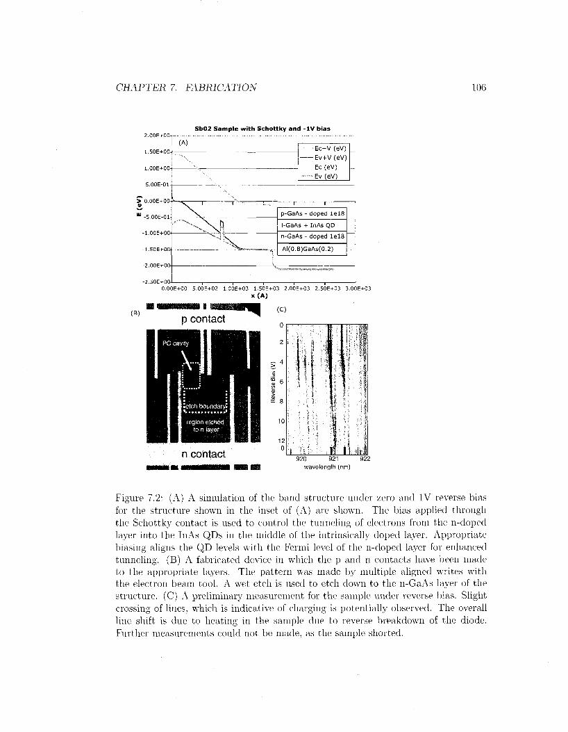
CHAPTER 7. FABRICATION 106
Sb02 Sample with Schottky and - I V bias
Ec+V (eV) - Ev+V (eV) Ec (eV)
-Ev(eV)
0.00E+00 5.00E+02 1.00E+03 1.50E+03 2.00E+03 2.50E+03 3.00E+03 x(A)
(B)
920 921 wavelength (nm)
922
Figure 7.2: (A) A simulation of the band structure under zero and IV reverse bias for the structure shown in the inset of (A) are shown. The bias applied through the Schottky contact is used to control the tunneling of electrons from the n-doped layer into the InAs QDs in the middle of the intrinsically doped layer. Appropriate biasing aligns the QD levels with the Fermi level of the n-doped layer for enhanced tunneling. (B) A fabricated device in which the p and n contacts have been made to the appropriate layers. The pattern was made by multiple aligned writes with the electron beam tool. A wet etch is used to etch down to the n-GaAs layer of the structure. (C) A preliminary measurement for the sample under reverse bias. Slight crossing of lines, which is indicative of charging is potentially observed. The overall line shift is due to heating in the sample clue to reverse breakdown of the diode. Further measurements could not be made, as the sample shorted.
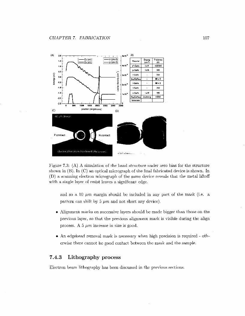
CHAPTER 7. FABRICATION 107
(A) 2.0
1.5
1.0
0.5
0.0
-0.5
-1.0
-1.5
-2.0
-2.5
I ' I • 1 • ] 1 • 1 ' 1
Ec(eV) n(cm-3) t \ . Ev(eV) p(cm-3)
in 7 ca
rrie
r densi
ty (
cm"3)
1
5x10" (8)
Material
p*-GaAs
p-GaAs
i-GaAs
InaaGaAsoa
I-GaAs
i-GaAs
n-GaAs
Alo.aGaAso.2
Substrate
Doping (cnv=)
Iel9
Iel8
Iel8
insulating
Thickness (A)
100/200
400
250
80x5
80x5
250
400
10000
Figure 7.3: (A) A simulation of the band structure under zero bias for the structure shown in (B). In (C) an optical micrograph of the final fabricated device is shown. In (D) a scanning electron micrograph of the same device reveals that the metal liftoff with a single layer of resist leaves a significant edge.
and so a 10 /im margin should be included in any part of the mask (i.e. a
pattern can shift by 5 [im and not short any device).
• Alignment marks on successive layers should be made bigger than those on the
previous layer, so that the previous alignment mark is visible during the align
process. A 5 fxm increase in size is good.
• An edgebead removal mask is necessary when high precision is required - oth
erwise there cannot be good contact between the mask and the sample.
7.4.3 Lithography process
Electron beam lithography has been discussed in the previous sections.
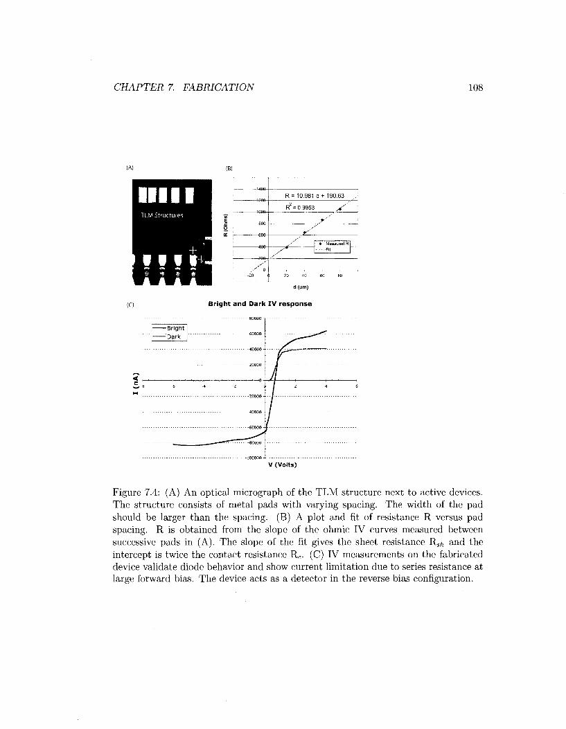
CHAPTER 7. FABRICATION
(A) (B)
mi i
i • • i
: : i
*(O
h
,7"
R = 10.981 d + 190.63 ,
R2 = 0.9953 X''
X
y* y
* Measured R Fit
-20 (1 20 40 60 80
(C)
d(um)
Bright and Dark I V response
--89000 T
V (Volts)
Figure 7.4: (A) An optical micrograph of the TLM structure next to active devices. The structure consists of metal pads with varying spacing. The width of the pad should be larger than the spacing. (B) A plot and fit of resistance R versus pad spacing. R is obtained from the slope of the ohmic IV curves measured between successive pads in (A). The slope of the fit gives the sheet resistance Rsh and the intercept is twice the contact resistance Rc. (C) IV measurements on the fabricated device validate diode behavior and show current limitation due to series resistance at large forward bias. The device acts as a detector in the reverse bias configuration.
CHAPTER 7. FABRICATION 109
For optical lithography using Shipley 3612 photoresist:
• Cover the backside of the chip with blue tape.
• Spin coat resist at 4000 rpm for a 1/im thick film.
• Remove blue tape and bake resist at 90° C for 60s.
• For edgebead and coarse features: expose 3 times with 8s each and 5s between
exposures. Use a large gap (e.g. 70 /im).
• For fine features: expose 1 time with 4s. Use a small gap (e.g. 30-40 //m).
• Develop in LDD26W for approximately 60s. Check under optical for cleared
resist.
7.4.4 Wet Etch
For controlled etching to a layer without an etch stop, a slow etch should be used.
If possible, the resist should be baked at 125° C for 30 minutes in order to make it
more etch resistant. The following etches work well for GaAs:
• 200:8:4 t^ChH^SO^H^C^ - 1-2 nm/s etch rate at room temperature.
• 25:1:1 H20:H3P04:H202 - 2-3 nm/s etch rate at room temperature.
All etching is followed by a deionized (DI) water rinse and Nitrogen blow dry. The
etch rate should be checked on the alphastep.
The rates of both of these etches change over time is small etchant quantities are
mixed. Since the etch works by peroxide oxidation of the semiconductor and a strip
of the oxide in the acid. The etches cannot be premixed. A larger volume of etchant
ensures that the etch composition does not change significantly, and furthermore
means that a smaller relative error is made when mixing the components.
CHAPTER 7. FABRICATION 110
7.4.5 Metal contacts
Metal contacts are made by depositing the appropriate metal through a mask onto
the sample. The simplest mask is a patterned photoresist. A two-layer resist can be
used for optimal contact performance, but a single layer resist works well for contacts
that are relatively thin. For contacts with a thickness of several 100 nm, the 1/im
of Shipley 3612 yields satisfactory results. Once the metal is deposited, the resist
mask is removed in a liftoff process. The best results are obtained with an overnight
soak in acetone. Sonication may aid in the liftoff process, but can also damage the
contact. When doing liftoff it is usually best not to let metal particles dry on the
sample. They will be difficult to remove.
Before contact deposition, the samples should be cleaned in 15:1 H20:NaOH for
30s to remove oxides. Once contacts to the n and p doped layers are made, large Au
contact pads can be deposited in one step to allow probe contacts and wire bonding
to the sample.
When low resistance Ohmic contacts are required, a transmission line measure
ment (TLM) structure should be made to measure the contact resistance and Ohmic-
ity of the contacts.
N-Contact
The n contact is typically an annealed contact and may need to be done first depend
ing on the thermal constraints for the sample. A description of such contacts is given
in Ref. [97]. During the anneal, Ge diffuses into GaAs and alloys with it.
The following contact recipe was used, with the first Ge layer on the n-doped
GaAs:
• Ge(108A)/Au(102A)/Ge(62A)/Au(236A)/Ni(100A)/Au(2000A)
The contacts were annealed with the following recipe:
• Ramp 0° C to 420° C for 60s
• Hold at 420° C for 60s
• Cool
CHAPTER 7. FABRICATION 111
P-Contact
P contacts are difficult to make for low levels of doping, and best results were obtained
for doping levels of 5el8. A description of such contacts is given in Ref. [98]. The
standard contact does not include the first layer below, but this layer was found to
decrease the contact resistance by a factor of 4.
The following contact recipe was used:
• Pt(100A)/Ti(200A)/Pt(100A)/Au(2000A)
P contacts do not need to be annealed, but do not degrade with the aforementioned
anneal recipe.
7.4.6 Electrical isolation by resist
Several materials can be used for electrical isolation including polymers and deposited
nitrides and oxides. We chose a hard-baked photoresist due to it's reflow properties
and ease of deposition and pattern definition. The resist process is as follows:
• spin AZ9260 photoresist at 3000 rpm for 60s.
• bake spun resist at 100°C for 3 minutes on a hot plate
• remove edge bead with a 100 s exposure
• develop the resist in 421K developer for 2 minutes
• expose the desired pattern for 40 s
• develop the resist in 42IK developer for 1 minute
The resist is then cured in the BLUEM Oven in N2 atmosphere with the following
recipe:
• 1.5 hr ramp to 140°C
• 2 hr hold
CHAPTER 7. FABRICATION 112
• 4.5 hr ramp to 325°C
• 2 hr hold
• 1 hr ramp to 25°C
7.4.7 Device fabrication flow
The overall device fabrication flow for the quantum well device is as follows:
• Lithography for wet etch.
• Wet etch.
• Lithography for n-Contact.
• n-Contact metal deposition.
• n-Contact liftoff.
• n-Contact anneal.
• Lithography for p-Contact.
• p-Contact metal deposition.
• p-Contact liftoff.
• Lithography for electrical isolation.
• Resist hard bake for electrical isolation.
• Lithography for contact pads.
• Metal deposition for contact pads.
Chapter 8
Conclusion and Future Directions
8.1 Cavity QED and quantum information pro
cessing
In our cavity-QED work we have so far demonstrated the fundamental capability of
the PC-QD system to serve as a platform for on-chip quantum information processing
and cavity-QED experiments. The two main results - experimental realization of
coherent probing of a strongly coupled cavity-QD system [1] and of controlled phase
interaction between individual photons [2] have shown that on-chip solid state systems
can be used to perform fundamental cavity-QED quantum optics experiments on the
chip.
In particular:
• We have developed, and for the first time demonstrated coherent driving of an
InAs QD inside a PC cavity on a semiconductor chip. This is a major enabling
step to exerting coherent optical control over the PC-QD system and quantum
optics experiments on the chip.
• We have shown that a single InAs quantum dot can significantly modify the
transmission properties of a PC cavity in the regimes of strong and weak cou
pling with low scattering losses. This verifies that that PC-QD system is a
viable platform for scalable quantum information processing on the chip.
113
CHAPTER 8. CONCLUSION AND FUTURE DIRECTIONS 114
• We have shown that the response of the QD is highly nonlinear and used this
effect to perform a proof of concept controlled-phase interaction between two
photon streams at the single photon level, in which we demonstrated that a
single photon is able to impart a 0.077T phase shift on another identical pho
ton. With an appropriate choice of cavity-QD detuning this phase shift can be
increased to RS 7r/2, and could be used in an all-optical quantum information
processing device.
• Although it was not discussed in this thesis, we have also demonstrated the
phenomena of photon blockade and photon induced tunneling by measuring
the photon statistics of a cavity-coupled beam in the presence of the quantum
dot [19]. We have shown that the QD can be used to convert a coherent state
of light into an anti-bunched or bunched stream of photons. With reasonable
improvements in cavity quality factors, such a system can be used to generate
on-demand single photons, and is a demonstration of the highest possible optical
nonlinearity.
• We have shown in our early work that emitters operating at room temperature
can be coupled to the PC cavity via a simple spin-on technique. Thus, with
improved light sources and cavities, such systems could potentially be used to
realize quantum information processing devices that operate at or above liquid
nitrogen temperatures.
These experiments serve as a springboard for further investigation into quantum
logic and memory [16] and quantum systems such as repeaters [99, 100], and sim
ulators and computers [30]. However, to achieve such goals several technological
challenges must be overcome.
Future work will have to focus on two main challenges: scalability and coherent
storage. The promise of the PC platform is that it allows robust and fast scaling
to multiple qubit systems. Device variability introduced in the fabrication process,
as well as the inherent size variation (sa 5%) in QDs dramatically limit scalability
in the system, due to frequency misalignment between resonators and dots on the
chip. These challenges have been in part adressed by the work of Andrei Faraon in
CHAPTER 8. CONCLUSION AND FUTURE DIRECTIONS 115
our group, who has developed techniques to tune QDs and resonators independently
on the same chip [101, 102]. Still the possibility of aligning more than two QDs
and cavities is not very large in these systems, and quantum information processing
protocols that are insensitive to frequency differences should be investigated.
In order to truly implement quantum information processing proposals such as
Ref. [16, 99, 100], a quantum memory with a long storage time is required. The QDs
used in this work were two-level systems with a ground and excited state. A third
level that is accessible through optical or electrical signals is necessary for quantum
information processing protocols. Such a level can be realized with a charged QD
inside a magnetic field [20, 103]. Though alternative protocols based on polarization
splitting of QDs can in principle be used to make a three-level system, the storage
times in such protocols are too low to realize truly functioning devices, and attempts
should be made to bring the proven approach of Ref. [103] inside a PC cavity.
8.2 Classical Information Processing
We have developed a variety of modeling and optimization tools for designing high
quality PC resonators. Due to the size and the planar and monolithic nature of
such devices, they are attractive candidates for low power optoelectronic devices and
photonics for rack-to-rack, board-to-board and chip-to-chip communication in data
centers and future computers [104].
We have shown that such devices can yield highly nonlinear elements and take
advantage of material nonlinearities. Furthermore, we have shown that the free-carrier
induced refractive index changes can greatly affect the resonances of PC cavities with
lower power inputs when compared to classical optoelectronic switches. Thus, PC
based resonators may reduce power consumption in routers and switches. However,
the main challenge that has yet to be overcome is the development of robust electrical
control over such devices.
Appendix A
Equivalence between the CNOT
and CZ gate
The matrix representation of the CNOT gate in the basis {\H)s\H)c,\H)s\V)c,
\V)a\H)e,\V)a\V)e}is:
/ 1 0 0 0 \
0 1 0 0 CNOT =
0 0 0 1
\ 0 0 1 0 /
The controlled-Z (CZ) gate, that is given by the following matrix:
/ 1 0 0 0 \
0 1 0 0
0 0 1 0
\ 0 0 0 - 1 /
(A.l)
CZ (A.2)
Suppose that the cavity realizes the CZ gate. That is, the nonlinear interaction
delays photons that are coupled to the vartically polarized cavity and phase shifts
the state |V") |V) relative to the other states by re. Further, if the second qubit is
Hadamard transformed by a waveplate on the way into and out of the cavity. The
116
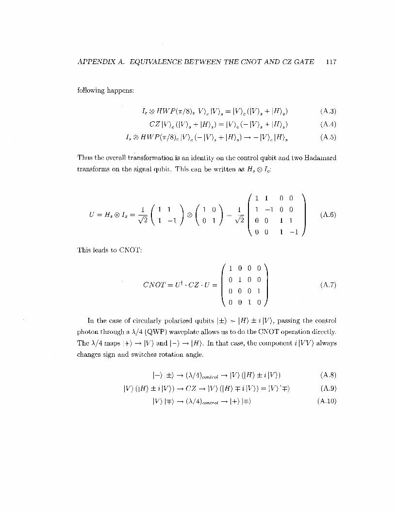
APPENDIX A. EQUIVALENCE BETWEEN THE CNOT AND CZ GATE 117
following happens:
Ic ® HWP(ir/8)s \V)C \V)a = \V)C (\V)a + \H)S)
CZ\V)e(\V)a + \H),) = \V)c(-\V)a + \H)a)
Is ® HWP(ir/8)c \V)C (- \V)a + \H)a) -> - \V)C \H)a
(A.3)
(A-4)
(A.5)
Thus the overall transformation is an identity on the control qubit and two Hadamard
transforms on the signal qubit. This can be written as Hs ® Ic:
1 / 1 1 U = Hs <g> I x = - =
y/2 \ 1 -
This leads to CNOT:
1
1 0
0 1
1
72
/ 1 1 0 0 \
1 - 1 0 0
0 0 1 1
\ o o i - l )
CNOT = £/f -CZ-U =
( 1 0 0 0 \
0 1 0 0
0 0 0 1
V o o i o )
(A.6)
(A.7)
In the case of circularly polarized qubits |±) = \H) ±i\V), passing the control
photon through a A/4 (QWP) waveplate allows us to do the CNOT operation directly.
The A/4 maps |+) —>• \V) and |—) —• \H). In that case, the component i \VV) always
changes sign and switches rotation angle.
I+)I±> \V){\H)±i\V))
(X/4)cmtroi^\V)(\H)±i\V))
CZ-*\V)(\H)^i\V)) = \V)\T)
W) IT) - (A/4)c n,trol IT)
(A.8)
(A.9)
(A.10)
Appendix B
Derivation of Cavity Radiative
Loss
The radiated power per unit solid angle K(9,4>) can be expressed in terms of the
radiation vectors N and L in spherical polar coordinates (r, 9, </>) :
K(9, JL 8A2
Ne + ^ V
2
+ N$- u_ V
(B.l)
where r\ = J^- The radiation vectors in spherical polar coordinates can be expressed
from their components in Cartesian coordinates:
Ng = (Nx cos 4> + Ny sin (j>) cos 9
Nj, = —Nx sin <f> + Ny cos 4>,
(B.2)
and similarly for Lg and L<p. As described in Reference [3], the radiation vectors in
Cartesian coordinates are proportional to 2D Fourier transforms of the parallel (x
and y) field components at the surface S (Fig. 2.4):
118
APPENDIX B. DERIVATION OF CAVITY RADIATIVE LOSS 119
Nx =
Ny --
L>x -
Ly -
= -FT2{HV)
= FT2(HX)
~- FT2(Ey)
fc|
fe.
-- -FT2{EX)
k\\
kz
x v = k(—,—) = ksm9(cos<j)x + smcj)y)
= kcosO,
(B.3)
where k = 2TT/\, A is the mode wavelength in air, and k\\ = ksinl
Here the 2D Fourier Transform of the function f(x,y) is
FT2(f(x,y)) = J Jdxdyf(x,y)e^x^
= J Jdxdvf(x,y)e^+k^
(B.4)
(B.5)
Substitution of expressions (B.3) and (B.4) into (B.l) now yields an expression for
the radiated power (2.11) in terms of the FTs of the four scalars Hx, Hy, Ex, and Ey.
This expression is in general difficult to track analytically. We will now use Maxwell's
relations to express (B.l) in terms of only two scalars, Hz and Ez.
Noting that for a bounded function g, FT2(^) = —ikxFT2(g) (similarly for ^-),
we can re-write No as
N0 h\k (-kxFT2(Hv) + kyFT2(Hx)) (B.6)
i kz FTJdHy 9Hx' k\\k dx dy '
kzce0 FT2{EZ
APPENDIX B. DERIVATION OF CAVITY RADIATIVE LOSS 120
where the last step follows from Maxwell's Eq. V x H = e0Wr = iue0E. Similarly,
we find Le = ™ F T 2 ( i ^ ) . From V • H = 0 and V • E = 0 at the surface S, it also
follows that Nj, = =±FT2(^) and L0 = -f F T 2 ( ^ ) . Substituting these expressions
into Eq. (B.l) yields
K[kx, ky) — 8\2k2 T]z
kzFT2{Ez) + iFT2{ dEz
dz + a IT
kzFT2{Hz) + iFT2{--^-)
(B-7)
Furthermore, Ez, Hz oc exp(ikzz) for propagating waves inside the light cone
(which are the only ones that determine P), implying that FT2{^-) = —ikzFT2(Ez)
and similarly for Hz. This allows further simplification of the previous expression to
Tik K(kx, ky) = 2\^k2 \FT2{EZ)\2 + \FT2{HZ)[ (B.8)
Substituting this result back into the expression for total radiated power (2.11)
gives the required result (2.13):
TT/2 2TT
= I (d6dcj)sm(6)K(9,<t>)
o o
— / dkxdky—J\ykx,ky)\J{kx,k. Jk»<k
2A k 7fcn<fc fcii
(B.9)
\\FT2(EZ)\2 + \FT2(HZ)\2
Above, J(kx, ky) is the Jacobian resulting from the change of coordinates from
{B,4>) to (kx,ky).
Appendix C
Pulses in a nonlinear PC waveguide
C.0.1 Derivation of the propagation equations
The probe envelope evolves according to (with q = k — ho):
^ = | J dkA(k, i)e'[(fc-fco)2-Mfc)-^)t]
at 1 „2 dv9
(C.l)
ftjdqA{q+k,Mq{z-V3t)~w
= J dq{d-^hA _ t{Vgq + ±%Ltf)A(q + fc0, f))e'[ ,(-'*t)-* ,a3M = f rfga(A(g+fco,t)ci[g(^-f9t)-^
2^-t]
= j dq§A^L^'-v't)-^^t] - Vg§-zp + qdit&p
in the case of nonlinearity, the wave equation with c~2 = [i0e0 is:
„ „ - 1 d2(e(r)E) d2P
And we can rewrite this equation in terms of the previously introduced Hermitian
field operator as:
121
APPENDIX C. PULSES IN A NONLINEAR PC WAVEGUIDE 122
Here, in general, the polarizability P is given by
Pi = ,(3) £o 2 ^ 2 ^ xUk,iE(u'p)iE(u,')jE(vp)i< (C.4) j,k,l m,n,p
(3)
where Xij,k,i a r e *n e components of the third order nonlinearity tensor. In our case,
we consider the system to be isotropic, the response instantaneous, and only two
frequencies (UJS,UJP) to be present. To find the time evolution of the coefficients, we
use the wave equation. In the presence of the nonlinearity we expand e ~ e + 5 and
O as:
0 + AO = | V x V x | -
6 + Ad « 6 - |[f 6 + of] = 6 - ±{f, 6} £ 4=V x V x 4= + -7-V x V x - M + 0 5\2
(!) J(C5)
Let (u'\ = (u,k',n'\, \u) = \u,k,n), A = A(k,t). Then we have:
(u'\ (O + AO) J dkA \u) - - (u'\ jigiJdkA \u)
J dkA({u'\ 6 \u) + {u'\ AO) \u) = - (u'\ ± J dk(A - u2A - 2iuA) \u)
J dkA (u'\ AO \u) = ^J dkA {u') u
-\$dkA (u'\ s-0 + Of \u) = ^A{k')
-±fdkA(u'\ f \u) (*£ + £) = 2-fA{k>) '-A{k')
(C.6)
J dkA(k) (ic\ - \u) ,/i 5 2iu)
Above, we neglect second derivatives of the envelope and combine the two fre
quency terms as UJ '2 •UJ 2UJ2 + vs(k — k') ~ 2UJ2, because the (k — k') term will lead
to the derivative of the slowly varying envelope multiplied by the nonlinearity and is
very small. Since the frequency bandwidth of the envelope is small, the envelope is
slowly varying in time, and the second order time variation in the coefficients A(k)
is neglected. Furthermore, we have also assumed that the inner product (v!) u is
roughly unchanged by the nonlinearity - it remains a delta function. The perturba
tion 8s^p contains both the real and imaginary parts of the third order susceptibility.
The real part is responsible for the cross phase modulation, while the nonlinear term
APPENDIX C. PULSES IN A NONLINEAR PC WAVEGUIDE 123
gives the two photon absorption of the signal and probe. The figure of merit for the
feasibility of the experiments is the phase-shift gained per loss length (- point). The
full perturbation can be written as:
8StP = iax + 360(xl3) + «xi3 ))( |£K,P) |2 + 2\E{uPtS)\2) (C.7)
Where x ^ is the third order polarizability (which is assumed to have only one value
and to be infinitely fast), and E(ujStP) = {S, P}ukspel^ks-pZ~u'a^ is the electric field of
the two modes. The linear loss ct\ is the imaginary part of the dielectric constant.
The value of \r c a n be determined from the experimentally observed bulk in
tensity dependent refractive index defined via n — n + n2I, where I is the average
field intensity. For a bulk material I is given by I = \^ —\E\2 = ^ce0n\E\2. Thus,
3^(3) _ c n2n 2_ p o r AlGaAs at the wavelength of 1.5 fim, n2 ~ 1.5 x 1CT 1 3 ^ ;
furthermore, the index is very similar for TE and TM polarization in AlGaAs slab
waveguides [54]. Since x ^ measures the response of the local charge distribution to
the local electric field, the coefficient itself is a material property and is not modified
in the PCW, except possibly due to surface effects (e.g. reduced response or arti
ficially added birefringence). Thus, we can derive the value of the coefficient from
bulk experiments and combine it with the modified electromagnetic fields to get the
resulting effect in the PCW. The x ^ coupling term only exists in the material, and
we can replace the n2 term with a dielectric which is equal to the spatially patterned
index of AlGaAs in the PCW and is zero in the air. We set 3 x ^ = cri2e(f). And
we define K = ceon2, so that the perturbation due to real part of the nonlinearity
becomes <5SiP = Ke(f)(\E(iOS:P)\2 + 2\E(iOPtS)\2) . The loss terms are similarly deter
mined from a fit to atotai = oti + o.^!- The linear loss a\ results in an exponential
decay of the signal with a characteristic length (a i ) _ 1 . The nonlinear loss gives a
characteristic length of (a^ / ) - 1 . We will drop the losses for now, in order to derive
the equation of motion for the pulses, and will assume that the Bloch components
of the eigenstate \u) and \u') belong to the same waveguide branch n = n!. Each of
un,k, un,k' is t h e n roughly given by some central k component that is modulated by an
envelope un^eikz ~ Mnfcoe«(feo2-wo*)e»[(fc-fco)z-Mfc)-"o)«]_ \ye now insert the exact form
APPENDIX C. PULSES IN A NONLINEAR PC WAVEGUIDE 124
for (u'\ and \u) into the above equation, and only look at the cross phase modulation
component on the probe due to the signal. We take n to be branch of the pump mode
p, and m to be that of the signal s, and only treat the perturbation due to the signal
explicitly. Also, we will assume for simplicity that the signal group velocity vs at k
and k', as well as the dispersion ^ - , so that we can combine them in the expansion
of the Bloch state. Eq. C.6 then implies:
A{k') = iup J dk" j dh' A{k")Kl\up\2\us\
2\S{z')\2e^k"^
« iupn J dk"A(k") J ^ / |5(2 /)|2e l [ ( fc"- fc ' )z '- (a j ( fc" )-w(fe ' ) )^/Arf3re>s |2 |«p |2 (C.8)
« WJ„K7SIP / dk"A(k") f dz'\S{z')\2e^k"-k'^-^k"^k'W
This is now inserted back into the evolution equation for the envelope C.l, and
we re-substitute k — fc0 = q and keep the frequency term in the form uj(k) — oj(ko) for
convenience.
/dkA{k,t)ei{k-ko)z-(-'Jj{k)-U0^ =
= *wpK7a,p JdkJ dk"A{k") J '̂|5(y)|2ei[(fe"-fc)^-(^(fe")-uJ(fc))t]el[(fc-fco)^(^(fe)-^o)t]
= iujpK^StP f dz' J dk''A{k'')\S{z')\2ei[{k''z'-koz)~{bj{k'')~^)t]) J dketk^-z,)
- iupKls<p J dz'\S(z')\2elk^z'-^5(z - z') J dk"A(k")e^k"-k°>'-^k"^W
= iujpKjSiP Jdz'\S(z')\2eiko^'^6(z - z')P(z')
= iupK-fStP\S(z)\2P(z)
The y/e terms cancel the denominator of the perturbation. The term 7SjP contains
an effective area integral j S t P = ^ JAd3re|ris |2 |np |2 « J dxdye\ua\
2\up\2. Since the
Bloch states are periodic, their integral in each unit cell ("fs,p) is the same, and we
simply weigh it by the average value of the slowly varying envelope in that cell to
find the integral over the whole volume. A is the unit cell volume. S and P are only
functions of time and the propagation coordinate (z here), and are uniform in the
transverse (x,y) plane. The term K contains the strength of the nonlinearity. We now
re-normalize the Bloch state and the field:
APPENDIX C. PULSES IN A NONLINEAR PC WAVEGUIDE 125
Nshujs =11 f d3fe0e(f)\S\2\us\2 (CIO)
« [dze0\S\2- f d3fe(r)\us\2 (C.ll)
J a JA
Nshcos =fdze0\S\2 (C.12)
1 = 1 [ d3fe{f)\us\2 (C.13)
"A The above normalization means that [7] = m~2 and [\S\2] = Volt2. Thus the term
KJLJ\S\2 has units of s_1 , as desired. We now insert the form for A into C.l:
The refractive index due to cross-phase modulation is twice that of self phase
modulation [53]. The evolution of the slowly varying envelope is given by:
5 = qKius(7s>s\S\2 + 2ls,p\P\2)S - vsS' + i\%S" (C.14)
P = q>Kup(%,p\P\2 + 2%tS\S\2)P - vpP> + i\^P" (C.15)
We will now show the qualitative behavior of the two pulses, assuming a weak
interaction. Take P = p{z,t)ei^z't) and S = r]{z, t)e^z't]. Inserting P into C.15, the
real and imaginary parts satisfy:
Real:
p+(Vp+d^)p = --*-<$'p (C.16)
Imaginary:
i\>p + vv4p = -KLUP^PIPP2 + 27s,p7?2)p + -&-(p" - {c^fp) (C.17)
If we assume that in C.16 the second derivative term vanishes, then we can see
that the envelope moves along a characteristic given by vp + -^4> « vp(ko+ (/>'), which,
in the natter regions of the dispersion curve is very close to vp(ko). If 7^ (^-) < < 1,
then C.17 simplifies to give an equation for the phase along a characteristic given by
APPENDIX C. PULSES IN A NONLINEAR PC WAVEGUIDE 126
vP(k0 + *-)•
dvp -.
<P + vP(t>' + -|-(<£')2 = -«wp(7p,pP2 + 2js,Pr]2) (C18)
Since we will not generally be able to generate a pulse that is a solution to the
nonlinear system, we will assume that the pulses are Gaussian and drop the dispersion
terms for simplicity of the analysis. We are essentially assuming that the envelopes
are very slowly varying and that the interaction time and dispersion are not strong
enough to affect the phase measurement, which is dominated by the group velocity
term rather than the group velocity dispersion term. Thus, we will rewrite Eq. C.15
in a frame moving with the group velocity in terms of z' = z — vpt and t' = t, and
neglect the terms with -~^ and ^ . Since the two pulses may have different group
velocities, we have Av = (vp—vs). If the group velocity dispersion terms are neglected,
each envelope is only a function of z'.
dJ^ « ^p(lP,P\P(z')\2 + 2laj>\S(z' + Avt)\2)P(z>) (C.19)
The solution, and upper bounds on the phases after time t = — are:
P(z') = P(0)EXP[^KU;P J\iPtP\P(z')\2 + 27stP\S(z' + Avt')\2)dt'} = P ( 0 ) e ^ + t ^ 2 0 )
<J)P = \KUP I lp,p\P{z')\2dt' ~ \KUJP1P,P-\P{Z'\$.2\) l J 0 Z Vp
<t>s = «wP / ls>P\S(z' + Avt')\2dt' « KLUP1S,P-\S{Z'\$.22) JO vp
If the second arm of the interferometer is adjusted for a phase shift of 7r/2, the
difference in the intensity signal on the two detectors gives the phase, and thus
an estimate of the photon number. The total integrated signal energy is Idet =
fffd3re0e\P(z')\2\un\2sin((f>s). Starting from NBhw„ = J ^ d * ' e 0 |S(*')|2 = J^dz 'eo lS lM*' )
with | 5 | 2 = ^ g ^ (similarly, \P(z')\2 = \P\2p(z') and \P\2 = ^j£%j), the integral

APPENDIX C. PULSES IN A NONLINEAR PC WAVEGUIDE 127
for Idet is re-ordered again:
het « f f J d'reolPiz'^MzyKl2 (C.23)
« f dz'e0\P{z')\2^s{z')- f d3re\up\2 (C.24)
J a J A
= J dz'e0\P(z')\2<f>s(z') (C25)
~ KWP7S)P -^—- / dzp(z )s{z ) (C.26) Wp €0LefftS Lieff,P J
In the case when P is much narrower than the signal pulse S, we can view it as a quasi
delta function p(z') « Lefftp5(x — x0). The effective length can be approximated by
the spatial width of the pulse, which is TSVS, the product of the temporal width and
the group velocity of S. In this approximation the detected intensity is :
Idet ss KWp7piS —-Nptkjp (C.27) vp e0Tsva
2 2 LNSNP = cn2n LOpuis^PtS (C.28)
Vp TSVS
And the phase shift per photon of S is N ^ e ^ = cn2^p,shiosLVpf-~^r• In order to
make a comparison to our initial plane wave argument, we can identify 7P)S as the
effective inverse area, -£— as the effective pulse bandwidth in the waveguide, and —
as the enhanced interaction length (time).
Appendix D
Cavity QED Experiment and
Derivations
D.l Experimental setup
In our measurements a strongly coupled quantum dot is identified by the QD/cavity
anti-crossing signature in photoluminescence. Anti-crossing is observed by temperature-
tuning a QD through the cavity resonance, using the method detailed in Ref. [4].
During the temperature scan, a 980 nm diode heating laser is incident upon a metal
pad next to the cavity and modulated by a triangular wave form, whose period de
termines the heating cycle. Both the cavity and quantum dot wavelengths shift with
temperature, with the dot shifting three times faster, as shown in Fig.lC of the main
text. Thus each point of the temperature scan corresponds to a particular detuning
between the QD and cavity, as the system is probed at a fixed point by the reso
nant laser beam. This is illustrated in Fig.D.2, where we show how the quantum
dot and cavity trajectories and phase shifts are determined. A narrow-band (5 MHz
linewidth) frequency tunable external cavity diode laser is focused into the cavity and
observed in cross-polarization, as detailed in Ref. [1] and shown in Fig.lA of the main
text. The sample temperature changes from 20 to 27 K during the heating cycle.
This signal beam probes the cavity-QD system at various detunings between the QD
and cavity. The control beam is combined with the signal beam input path and also
128
APPENDIX D. CAVITY QED EXPERIMENT AND DERIVATIONS 129
directed at the cavity.
D.2 Quantum dot visibility
The visibility of the QD-induced feature is reduced due to wavelength jitter (through
thermal fluctuations [1]) as well as QD blinking between an optically active and an
optically dark state. From an analysis of second-order coherence, similar to that
presented in Ref.[105], we deduce a dark-state probability of 25%. This limits the
QD-induced features to a visibility of V=(hright - Idark)l{hright + /darfc)=75%. With
blinking and sampling taken into account, the theoretical fits agree well with experi
mental data. In more recent experiments, we have observed V=90% dip visibility for
quantum dots that do not exhibit blinking.
D.3 Quantum dot saturation
The response of the quantum dot to the driving electric field is given by its suscep
tibility x[53]. This function determines the dot's radiative properties and gives the
phase and amplitude of the field that interacts with the quantum dot. When the
control beam is resonant with the QD, \ can be expressed as [18],
X - *F P. (D.l)
where Pin is the input power, and F is the Purcell factor F=^-. x is a nonlinear
function, and is typically given by an expansion in the driving electric field E as
X = X^1' +X^ 'E + x^E2 +.... The field E is related to the input power via Pin/Acav —
2no^e0/n0 \E\ , where Acav « ( ̂ -J is the cavity area, no is the refractive index
of GaAs and e0 and /J,0 are the dielectric constant and permeability of free space.
Generally, the Kerr coefficient x^ gives the phase modulation. Another conventional
measure of nonlinearity is the intensity-dependent refractive index n2, which is related
to the Kerr coefficient via n2 j p -j^- = ^— \E\ [53]. Here the units of n2 are cm2/W,
c is the speed of light in m/s, and x*^ is in units of m2/V2. A beam propagating
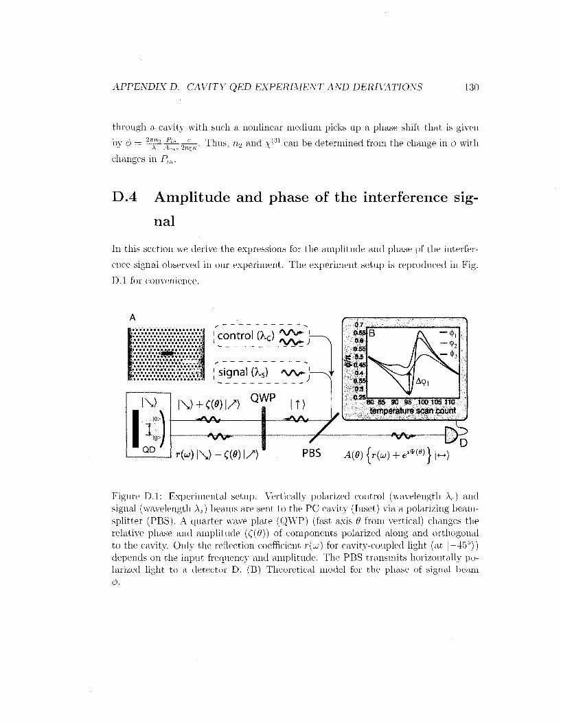
APPENDIX D. CAVITY QED EXPERIMENT AND DERIVATIONS 130
through a cavity with such a nonlinear medium picks up a phase shift that is given
bv 6 = ^~i-p^-^-—. Thus. n--> and y('3' can be determined from the change in o with
changes in Pin.
D.4 Amplitude and phase of the interference sig
nal
In this section we derive the expressions for the amplitude and phase pf the interfer
ence signal observed in our experiment. The experiment setup is reproduced in Fig.
D.l for convenience.
• • i.'
r.' [ • • • • # • • # • • • • • « t, . -
I ; control (Xc) # v v " L
/ \A^J
i | | signal (ks) > w -
l\> + CWI/> ~*f\/\t
QWP
* W -
r(«) | \> - CW \A
0.7 0.65 0.6 0.55
fi 0.5 •e-0.45
0.4 0.35 0.3 0 25
B A - i f .
yf\ ~*:
v. /l/~^C~(')'
]Wi 80 85 90 95 100 105 110
• \
temperature scan count
*\/\/»
PBS A(9) {r(u>) + e*W} ^
Figure D.l: Experimental setup. Vertically polarized control (wavelength A(.) and signal (wavelength A,5) beams are sent to the PC cavity (Inset) via a polarizing beamsplitter (PBS). A quarter wave plate (QWP) (fast axis 6 from vertical) changes the relative phase and amplitude (C(#)) of components polarized along and orthogonal to the cavity. Only the reflection coefficient r(jj) for cavity-coupled light (at (—45°)) depends on the input frequency and amplitude. The PBS transmits horizontally polarized light to a detector D. (B) Theoretical model for the phase of signal beam
APPENDIX D. CAVITY QED EXPERIMENT AND DERIVATIONS 131
The detected signal is modeled by considering the propagation through each opti
cal element. Vertically polarized light passes through the QWP to the cavity that is
tilted by 7r/4. The component of the incident beam along the cavity is reflected with
coefficient r(ui), while the orthogonal component reflects from the distributed bragg
reflector (DBR) with TUBR- The beam then passes back through the QWP and the
horizontal component is passed by the beamsplitter.
In beamsplitter polarization the vertical input and horizontal output are
* - : . " - ( M )
Rotation of the QWP and cavity relative to vertical are accounted for by applying
the rotation matrix:
,„x I cos(#) -sin(0) \ , „ , R(0) =[ K ' y ' ) (D.3)
\ sin(0) cos{6) J
The QWP (with a horizontal fast axis) rotated by 9 from vertical is given by
QWP(6) = eiv/4R(d)• ( l °)-nr1(d) (D.4) 0 i
Interaction with the cavity is given by
RC = R(ir/4) • I r ( w ) ° ) • R-\TT/4) (D.5) \ 0 rDBR J
The transfer matrix for the scattering process is then
T - QWP(9) • RC • QWP(9) (D.6)
APPENDIX D. CAVITY QED EXPERIMENT AND DERIVATIONS 132
and the field going to the detector is given by
E^t = Transposed) • QWP(9) • RC • QWP{9) • V (D.7)
= | (r(to)(cos2(29) - isin(29)) - rDBR(cos2(29) + isin(29)))
From which, in the limit rDBR —>• — 1 we obtain
Is(u>) = \E0Ut\2 = I ^ X r ^ + e^))!2 , (D.8)
with the interference term
. m = cos2 (29) +ism(29)
cos2 (20) -ism (20)' l '
and detected amplitude
A(9) = %- (cos2 (20) - i sin (20)) , (D.10)
D.5 Computational model
The Hamiltonian for the two-beam interaction with a cavity embedded quantum dot
is given by:
H = fkuQDaz + hujcava)a + hg(a+a + aV_) + ^ ( E ^ ^ + Ese~iulst)(a + af) (D.ll)
Where LOQD, ^cav, wc, LOS are the quantum dot transition frequency, cavity resonant fre
quency and the control and signal frequencies respectively. Es, Ec are the control and
signal driving fields respectively. The cavity photon number is given by ncav = (a^a).
Fits to the data were performed with the Quantum Optics Toolbox[66] which numer
ically solves this Hamiltonian with a photon number basis that ensured convergence
(up to 30 photons). In the case of frequency detuned beams, a matrix continued
fractions method was used to solve for the cavity mode at the signal frequency us un
der excitation of a driving field with two frequency components UJC,US. This method
APPENDIX D. CAVITY QED EXPERIMENT AND DERIVATIONS 133
expands operators in a Fourier series and solves for coefficients at the appropriate
frequencies. The matlab code is available upon request.
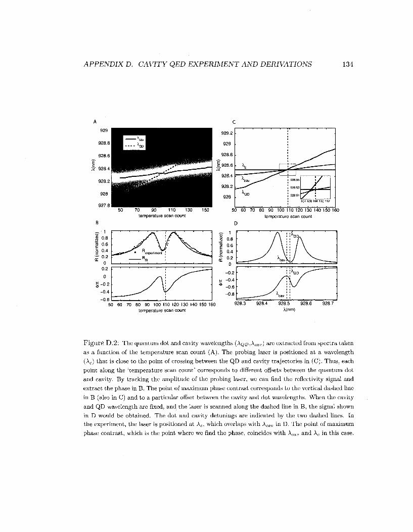
APPENDIX D. CAVITY QED EXPERIMENT AND DERIVATIONS 134
50 60 70 80 90 100 110 120 130 140 150 160 928.3 928.4 928.5 928.6 928.7 temperature scan count X(nm)
Fi gu re D.2: The quantum dot and cavity wavelengths (AQ£i,AcatJ) are extracted from spectra taken
as a function of the temperature scan count (A). The probing laser is positioned at a wavelength
(Ac) that is close to the point of crossing between the QD and cavity trajectories in (C). Thus, each
point along the 'temperature scan count' corresponds to different offsets between the quantum dot
and cavity. By tracking the amplitude of the probing laser, we can find the reflectivity signal and
extract the phase in B. The point of maximum phase contrast corresponds to the vertical dashed line
in B (also in C) and to a particular offset between the cavity and dot wavelengths. When the cavity
and QD wavelength are fixed, and the laser is scanned along the dashed line in B, the signal shown
in D would be obtained. The dot and cavity detunings are indicated by the two dashed lines. In
the experiment, the laser is positioned at Ac, which overlaps with \cav in D. The point of maximum
phase contrast, which is the point where we find the phase, coincides with Aca„ and Ac in this case.
Bibliography
[1] D. Englund, A. Faraon, I. Fushman, N. Stoltz, P. Petroff, and J. Vuckovic,
"Controlling cavity reflectivity with a single quantum dot," Nature, vol. 450,
pp. 857 861, Dec. 2007.
[2] I. Fushman, D. Englund, A. Faraon, N. Stoltz, P. Petroff, and J. Vuckovic,
"Controlled phase shifts with a single quantum dot," Science, vol. 320, pp. 769
772, May 2008.
[3] J. Vuckovic, M. Loncar, H. Mabuchi, and A. Scherer, "Optimization of Q factor
in microcavities based on free-standing membranes," IEEE Journal of Quantum
Electronics, vol. 38, pp. 850-856, July 2002.
[4] A. Faraon, D. Englund, I. Fushman, N. Stoltz, P. Petroff, and J. Vuckovic, "Lo
cal quantum dot tuning on photonic crystal chips," Appl. Phys. Lett., vol. 90,
p. 213110, May 2007.
[5] E. Waks and J. Vuckovic, "Dispersive properties and large Kerr non-linearities
using Dipole Induced Transparency in a single-sided cavity," Physical Review
A, vol. 73, no. 041803, p. 041803, 2006.
[6] H. Altug, D. Englund, and J. Vuckovic, "Ultra-fast Photonic Crystal
Nanolasers," Nature Physics, vol. 2, pp. 484 488, July 2006.
[7] I. Fushman, E. Waks, D. Englund, N. Stoltz, P. Petroff, and J. Vuckovic, "Ultra
Fast Nonlinear Optical Tuning of Photonic Crystal Cavities," Applied Physics
Letters, vol. 90, no. 091118, 2007.
135
BIBLIOGRAPHY 136
[8] Q. Turchette, C. Hood, W. Lange, H. Mabuchi, and H. J. Kimble, "Measure
ment of conditional phase shifts for quantum logic," Physical Review Letters,
vol. 75, pp. 4710 4713, 1995.
[9] A. Rauschenbeutel, G. Nogues, S. Osnaghi, P. Bertet, M. Brune, J. M. Raimond,
and S. Haroche, "Coherent Operation of a Tunable Quantum Phase Gate in
Cavity QED," Physical Review Letters, vol. 83, pp. 5166 5169, 1999.
[10] C. Monroe, D. Meekhof, B. King, W. Itano, , and D. Wineland, "Demonstra
tion of a Fundamental Quantum Logic Gate," Physical Review Letters, vol. 75,
pp. 4714-4717, 1995.
[11] B. Blinov, D. Moehring, L. Duan, and C.Monroe, "Observation of entanglement
between a single trapped atom and a single photon," Nature, vol. 428, pp. 153
157, 2004.
[12] M. O. S. . M. S. Zubairy, Quantum Optics. Cambridge: Cambridge Univ. Press,
1997.
[13] H. J. Kimble, in Cavity Quantum Electrodynamics, edited by P. Berman. San
Diego: Academic Press, 1994.
[14] E. Waks and J. Vuckovic, "Dipole induced transparency in frop-filter cavity-
waveguide systems," Physical Review Letters, vol. 80, April 2006.
[15] H. J. Kimble, in Cavity Quantum Electrodynamics, edited by P. Berman. San
Diego: Academic Press, 1994.
[16] L. Duan and H. Kimble, "Scalable Photonic Quantum Computation through
Cavity-Assisted Interactions," Physical Review Letters, vol. 92, p. 127902, 2004.
[17] R. Thompson, Q. Turchette, O. Carnal, and H. J. Kimble, "Nonlinear spec
troscopy in the strong-coupling limit of cavity QED," Physical Review A, vol. 57,
pp. 3084 3104, 1998.
BIBLIOGRAPHY 137
[18] A. Auffves-Garnier, C. Simon, J. Gerard, and J.-P. Poizat, "Giant optical non-
linearity induced by a single two-level system interacting with a cavity in the
Purcell regime ," Phys. Rev. A, vol. 75, p. 053823, May 2007.
[19] A. Faraon, I. Fushman, D. Englund, N. Stoltz, P. Petroff, and J. Vuckovic, "Co
herent generation of non-classical light on a chip via photon-induced tunneling
and blockade," Nature Physics, vol. 4, pp. 859 863, Sept. 2008.
[20] X. Xu, Y. Wu, B. Sun, Q. Huang, J. Cheng, D. G. Steel, A. S. Bracker, D. Gam
mon, C. Emary, and L. J. Sham, "Fast Spin State Initialization in a Singly
Charged InAs-GaAs Quantum Dot by Optical Cooling," Physical Review Let
ters, vol. 99, p. 097401, Aug. 2007.
[21] R. Feynman, "Simulating physics with computers," International Journal of
Theoretical Physics, vol. 21, no. 6&7, pp. 467 488, 1982.
[22] P. Shor, "Algorithms for quantum computation: Discrete log and factoring,"
Proceedings of the 35th Annual Symposium on the Foundations of Computer
Science, pp. 124 134, 1994.
[23] L. K. Grover, "A fast quantum mechanical algorithm for database search," 8th
Annual ACM Symposium on the Theory of Computing (STOC), pp. 212 219,
1997.
[24] C. Bennett and G. Brassard, "," Proceedings of IEEE International Conference
on Computers, Systems, and Signal Processing, Bangalore, India IEEE, New
York, p. 175, 1984.
[25] C. H. Bennett, G. Brassard, and N. D. Mermin, "Quantum cryptography with
out Bell's theorem," Physical Review Letters, vol. 68, p. 557, 1992.
[26] A. K. Eckert, "Quantum cryptography based on Bells theorem," Phys. Rev.
Lett, vol. 6, pp. 661-663, Aug. 1991.
[27] H. Takesue, S. Nam, Q. Zhang, R. Hadfield, H. Toshimori, K. Tamaki, and
Y. Yamamoto, "Quantum key distribution over a 40-dB channel loss using
BIBLIOGRAPHY 138
superconducting single-photon detectors," Nature Photonics, vol. 6, pp. 343
348, June 2007.
[28] J. I. Cirac, P. Zoller, H. J. Kimble, and H. Mabuchi, "Quantum State Transfer
and Entanglement Distribution among Distant Nodes in a Quantum Network,"
Physical Review Letters, vol. 78, pp. 3221-24, Apr. 1997.
[29] D. P. DiVincenzo, "Two-Bit Gates are Universal for Quantum Computation,"
Physical Review A, vol. 48, pp. 771 83, 2000.
[30] M. A. Nielsen and I. L. Chuang, Quantum Computation and Quantum Infor
mation. Cambridge: Cambridge Univ. Press, 2000.
[31] D. Englund, I. Fushman, and J. Vuckovic, "General Recipe for Designing Pho
tonic Crystal Cavities," Optics Express, vol. 12, pp. 5961-75, Aug. 2005.
[32] J. Goh, I. Fushman, D. Englund, and J. Vuckovic, "Genetic optimization of
photonic bandgap structures," Optics Express, vol. 15, no. 13, pp. 8218 8230,
2007.
[33] J. D. Jackson, Classical Electrodynamics. John Wiley and Sons Inc., 1998.
[34] A. Taflove and S. C. Hagness, The Finite-Difference Time-Domain Method, 3rd
ed. Artech House, 2005.
[35] A. Yariv and P. Yeh, Optical Waves in Crystals. Wiley Interscience, 2003.
[36] J. Vuckovic, M. Loncar, H. Mabuchi, and A. Scherer, "Design of photonic crystal
microcavities for cavity QED," Physical Review E, vol. 65, p. 016608, 2002.
[37] Y. Akahane, T. Asano, B.-S. Song, and S. Noda, "High-Q photonic nanocavity
in a two-dimensional photonic crystal ," Nature, vol. 425, pp. 944 947, Oct.
2003.
[38] Y. Akahane, T. Asano, B.-S. Song, and S. Noda, "Fine-tuned high-Q photonic-
crystal nanocavity," Optics Express, vol. 13, no. 4, p. 1202, 2005.
BIBLIOGRAPHY 139
[39] B. Song, S. Noda, T. Asano, and Y. Akahane, "Ultra-high-Q photonic double
heterostructure nanocavity," Nature Materials, vol. 4, p. 207, 2005.
[40] R. Haberman, ed., Elementary Applied Partial Differential Equations. Prentice
Hall, 1987.
[41] J. H. Holland, Adaptation in Natural and Artificial Systems: An Introductory
Analysis with Applications to Biology, Control and Artificial Intelligence. Univ.
of Michigan Press, 1975.
[42] D. E. Goldberg, Genetic Algorithms in Search, Optimization and Machine
Learning. Addison Wesley, 1989.
[43] L. Davis, Genetic Algorithms and Simulated Annealing. Morgan Kaufmann,
1987.
[44] S. Preble, H. Lipson, and M. Lipson, "Two-dimensional photonic crystals de
signed by evolutionary algorithms," Appl. Phys. Lett., vol. 86, 2005.
[45] L. Shen, Z. Ye, and S. He, "Design of two-dimensional photonic crystals with
large absolute band gaps using a genetic algorithm," Phys. Rev. B, vol. 68,
2003.
[46] E. Kerrinckx, L. Bigot, M. Douay, and Y. Quiquempois, "Photonic crystal fiber
design by means of a genetic algorithm," Optics Express, vol. 12, 2004.
[47] K. Nemoto, W. Munro, T. Spiller, and R. Beausoleil, "Quantum non-demolition
measurements: a new resource for making linear logic scalable," HPL-2004-135,
2004.
[48] K. Nemoto and W. J. Munro, "Nearly deterministic linear optical controlled-not
gate," Physical Review Letters, vol. 93, p. 250502, Dec. 2004.
[49] W. J. Munro, K. Nemoto, R. Beausoleil, and T. Spiller, "High-efciency
quantum-nondemolition single-photon-number-resolving detector," Physical
Review A, vol. 71, p. 033819, 2005.
BIBLIOGRAPHY 140
[50] I. Fushman and J. Vuckovic, "Analysis of a quantum nondemolition measure
ment scheme based on kerr nonlinearity in photonic crystal waveguides," Optics
Express, vol. 15, pp. 5559 5571, 2007.
[51] Y. Yamamoto and A. Imamoglu, Mesoscopic Quantum Optics. John Wiley and
Sons Inc., 1999.
[52] D. Englund, D. Fattal, E. Waks, G. Solomon, B. Zhang, T. Nakaoka,
Y. Arakawa, Y. Yamamoto, and J. Vuckovic, "Controlling the Spontaneous
Emission Rate of Single Quantum Dots in a Two-Dimensional Photonic Crys
tal," Physical Review Letters, vol. 95, July 2005.
[53] R. Boyd, Nonlinear Optics 2nd Edition. Elsevier, 2003.
[54] J. S. Aitchison, D. C. Hutchings, J. U. Kang, G. I. Stegeman, and A. Villeneuve,
"The nonlinear optical properties of algaas at the half band gap," IEEE JOUR
NAL OF QUANTUM ELECTRONICS, vol. 33, p. 341, Mar. 1997.
[55] S. Hoa, C. Soccolich, M. Islam, W. Hobson, A. Levi, and R. Slusher, "Large
nonlinear phase shifts in low-loss aixgai_xas waveguides near half-gap," Applied
Physics Letters, vol. 59, p. 2558, Nov. 1991.
[56] H. Altug and J. Vuckovic, "Experimental demonstration of the slow group ve
locity of light in two-dimensional coupled photonic crystal microcavity arrays
," Applied Physics Letters, vol. 86, p. 102, 2005.
[57] Y. Vlasov, M. OBoyle, H. Hamann, and S. J. McNab, "Active control of slow
light on a chip with photonic crystal waveguides," Nature, vol. 438, p. 66, Nov.
2005.
[58] M. Settle, M. Salib, A. Michaeli, and T. F. Krauss, "Low loss silicon on insu
lator photonic crystal waveguides made by 193nm optical lithography," Optics
Express, vol. 14, p. 2440, Mar. 2006.
BIBLIOGRAPHY 141
[59] A. Villeneuve, C. Yang, G. Stegeman, C. Lin, and H. Lin, "Nonlinear refractive-
index and two photon-absorption near half the band gap in algaas," Applied
Physics Letters, vol. 62, p. 2465, May 1993.
[60] K. Nakatsuhara, T. Mizumoto, E. Takahashi, S. Hossain, Y. Saka, B.-J. Ma, and
Y. Nakano, "All-optical switching in a distributed-feedback gainasp waveguide,"
Applied Optics, vol. 38, p. 3911, June 1999.
[61] A. Faraon, I. Fushman, D. Englund, N. Stoltz, P. Petroff, and J. Vuckovic,
"Dipole induced transparency in waveguide coupled photonic crystal cavities,"
Optics Express, vol. 16, p. 12154, Aug. 2008.
[62] H. Altug and J. Vuckovic, "Polarization control and sensing with two-
dimensional coupled photonic crystal microcavity arrays ," Optics Letters,
vol. 30, p. 982, May 2005.
[63] I. Chuang and Y. Yamamoto, "Simple Quantum Computer," Physical Review
A, vol. 52, p. 3489, Nov 1995.
[64] K. N. W.J. Munro and T. Spiller, "Weak nonlinearities: a new route to optical
quantum computation," New Journal of Physics, vol. 7, p. 137, May 2005.
[65] D. Englund, D. Fattal, E. Waks, G. Solomon, B. Zhang, T. Nakaoka,
Y. Arakawa, Y. Yamamoto, and J. Vuckovic, "Controlling the Spontaneous
Emission Rate of Single Quantum Dots in a Two-Dimensional Photonic Crys
tal," Physical Review Letters, vol. 95, p. 013904, July 2005.
[66] S. Tan, "Quantum Optics Toolbox," www.qo.phy.auckland.ac.nz/qotoolbox.html.
[67] S. Harris, J. Field, and A. Imamoglu, "Nonlinear Optical Processes Using
Electromagnetically Induced Transparency," Physical Review Letters, vol. 64,
pp. 1107-10, Mar. 1991.
[68] S. Harris, J. Field, and A. Imamoglu, "Observation of Electromagnetically In
duced Transparency," Physical Review Letters, vol. 66, p. 2593, May 1991.
BIBLIOGRAPHY 142
[69] N. Imoto, H. Haus, and Y. Yamamoto, "Quantum nondemolition measure
ment of the photon number via the optical Kerr effect," Phys. Rev. A, vol. 32,
pp. 2287 2292, 1985.
[70] J. P. Poizat and P. Grangier, "Experimental Realization of a Quantum Optical
Tap," Physical Review Letters, vol. 70, no. 3, p. 271, 1993.
[71] G. Nogues, A. Rauschenbeutel, S. Osnaghi, M. Brune, J. M. Raimond, and
S. Haroche, "Seeing a single photon without destroying it," Nature, vol. 400,
pp. 239-242, 1999.
[72] D. Englund, A. Faraon, B. Zhang, Y. Yamamoto, and J. Vuckovic, "Generation
and transfer of single photons on a photonic crystal chip," Optics Express,
vol. 15, pp. 5550-8, Apr. 2007.
[73] A. Faraon, E. Waks, D. Englund, I. Fushman, and J. Vuckovic, "Efficient pho
tonic crystal cavity-waveguide couplers," Applied Physics Letters, vol. 90, Feb
2007.
[74] E. Knill, "Quantum computing with realistically noisy devices," Nature,
vol. 434, pp. 39 44, Mar. 2005.
[75] B. Lounis and W. Moerner, "Single photons on demand from a single molecule
at room temperature," Nature, vol. 407, p. 491, Sept. 2000.
[76] A. Beveratos, R. Brouri, T. Gacoin, J. Poizat, and P. Grangier, "Nonclassical ra
diation from diamond nanocrystals," Physical Review A, vol. 64, pp. 061802/1
4, Dec. 2001.
[77] P. Michler, A. Imamoglu, M. Mason, P. Carson, G. F. Strouse, and S. K.
Buratto, "Quantum correlation among photons from a single quantum dot at
room temperature," Nature, vol. 406, p. 968, Aug. 2000.
[78] I. Fushman, D. Englund, and J. Vuckovic, "Coupling of PbS quantum dots to
photonic crystal cavities at room temperature," Applied Physics Letters, vol. 87,
Dec. 2005.
BIBLIOGRAPHY 143
[79] M. G. Dutt, L. Childress, L. Jiang, E. Togan, J. Maze, F. Jelezko, A. S. Zibrov,
P. R. Hemmer, and M. D. Lukin, "Quantum Register Based on Individual
Electronic and Nuclear Spin Qubits in Diamond," Science, vol. 316, pp. 1312
1316, June 2007.
[80] J. Vuckovic and Y. Yamamoto, "Photonic crystal microcavities for cavity quan
tum electrodynamics with a single quantum dot.," Applied Physics Letters,
vol. 82, pp. 2374 6, Apr 2003.
[81] R. Ferrini, B. Lombardet, B. Wild, and R. Houdr, "Hole depth- and shape-
induced radiation losses in two-dimensional photonic crystals," Appl. Phys.
Lett, vol. 82, p. 1009, Feb. 2003.
[82] M. O. S. . M. S. Zubairy, Quantum Optics. Cambridge: Cambridge Univ. Press,
1997.
[83] R. Lee, R. Xu, and A. Yariv, "Modified spontaneous emission from a two-
dimensional photonic bandgap crystal slab," Journal of the Optical Society of
America B, vol. 17, p. 143842, Aug. 2000.
[84] R. Bose, X. Yang, R. Chatterjee, J. Gao, and C. W. Wong, "Weak coupling
interactions of colloidal lead sulfide nanocrystals with silicon photonic crys
tal nanocavities near 1.55 um at room temperature," Applied Physics Letters,
vol. 90, no. 111117, 2007.
[85] Z. Wu, Z. Mi, P. Bhattacharya, T. Zhu, and J. Xu, "Enhanced spontaneous
emission at 1.55 um from colloidal PbSe quantum dots in a Si photonic crystal
microcavity," Applied Physics Letters, vol. 90, no. 171105, 2007.
[86] D. Labilloy, H. Benisty, C. Weisbuch, T. Krauss, R. Houdre, and U. Oesterle,
"Use of guided spontaneous emission of a semiconductor to probe the optical
properties of two-dimensional photonic crystals," Appl. Phys. Lett., vol. 71,
p. 738, Aug. 1997.

BIBLIOGRAPHY 144
[87] M. Soljacic and J. D. Joannopoulos, "Enhancement of nonlinear effects using
photonic crystals," Nature Materials, vol. 3, Apr. 2004.
[88] A. Shinya, S. Mitsugi, T. Tanabe, M. Notomi, I. Yokohama, H. Takara, and
S. Kawanishi, "All-optical flip-flop circuit composed of coupled two-port reso
nant tunneling filter in two-dimensional photonic crystal slab," Optics Express,
vol. 14, p. 1230, Feb. 2006.
[89] A. Shinya, T. Tanabe, E. Kuramochi, and M. Notomi, "All-optical switch and
digital light processing using photonic crystals," NTT Technical Review, vol. 3,
p. 61, Dec. 2005.
[90] A. D. Bristow, J.-P. R. Wells, W. H. Fan, A. M. Fox, M. S. Skolnick, D. M.
Whittaker, J. S. Roberts, and T. F. Krauss, "Ultrafast nonlinear response of
algaas two-dimensional photonic crystal waveguides," Applied Physics Letters,
vol. 83, p. 851, Aug. 2003.
[91] P. M. Johnson, A. F. Koenderink, and W. L. Vos, "Ultrafast switching of
photonic density of states in photonic crystals," Physical Review B, vol. 66,
p. 081102, 2002.
[92] H. Rong, R. Jones, A. Liu, O. Cohen, D. Hak, A. Fang, and M. Paniccia, "A
continuous-wave raman silicon laser," Nature, vol. 433, pp. 725 728, Feb. 2005.
[93] M. Hochberg, T. Baehr-Jones, G. Wang, M. Shearn, K. Harvard, J. Luo,
B. Chen, Z. Shi, R. Lawson, P. Sullivan, A. Jen, L. Dalton, and A. Scherer,
"Terahertz all-optical modulation in a siliconpolymer hybrid system," Nature
Materials, vol. 5, pp. 703 709, Aug. 2006.
[94] P. Petroff, A. Lorke, and A. Imamoglu, "Epitaxial self assembled quantum
dots," Physics Today, vol. 46, p. 54, 2001.
[95] B. Bennett, R. Soref, and J. Del-Alamo, "Carrier-induced change in refractive
index of inp, gaas and ingaasp," IEEE Journal of Quantum Electronics, vol. 36,
p. 113, Jan. 1990.
BIBLIOGRAPHY 145
[96] M. Makarova, J. Vuckovic, H. Sanda, and Y. Nishi, "Silicon based photonic
crystal nanocavity light emitters," Applied Physics Letters, vol. 89, p. 221101,
2006.
[97] M. Ogawa, "Alloying behavior of Ni/Au-Ge films on GaAs," Journal of Applied
Physics, vol. 51, p. 406, Jan. 1980.
[98] H. Okada, S. Shikata, and H. Hayashi, "Electrical characteristics and reliability
of P t /Ti /P t /Au ohmic contacts to p-Type GaAs," Japanese Journal of Applied
Physics, vol. 30, pp. 558 560, Apr. 1991.
[99] L. Childress, J. M. Taylor, A. S. Srensen, , and M. D. Lukin, "Fault-tolerant
quantum repeaters with minimal physical resources and implementations based
on single-photon emitters," Physical Review A, vol. 72, p. 052330, 2005.
[100] T. Ladd, P. van Loock, K. N. K, W. WJ, and Y. Y, "Hybrid quantum repeater
based on dispersive CQED interactions between matter qubits and bright co
herent light," New Journal of Physics, vol. 8, p. 184, 2006.
[101] A. Faraon, D. Englund, D. Bulla, B. Luther-Davies, B. J. Eggleton, N. Stoltz,
P. Petroff, and J. Vuckovic, "Local Tuning of Photonic Crystal Cavities Using
Chalcogenide Glasses ," Applied Physics Letters, vol. 92, p. 043123, 2008.
[102] A. Faraon, D. Englund, I. Fushman, N. Stoltz, P. Petroff, and J. Vuckovic, "Lo
cal quantum dot tuning on photonic crystal chips," Appl. Phys. Lett., vol. 90,
p. 213110, May 2007.
[103] X. Xu, B. Sun, P. R. Berman, D. G. Steel, A. S. Bracker, D. Gammon, and L. J.
Sham, "Coherent population trapping of an electron spin in a single negatively
charged quantum dot ," Nature Physics, vol. 4, pp. 692 695, Aug 2008.
[104] D. A. B. Miller, "Rationale and challenges for optical interconnects to electronic
chips," Proceedings of the IEEE, vol. 88, p. 728, June 2000.
BIBLIOGRAPHY 146
[105] C. Santori, D. Fattal, J. Vuckovic, G. S. Solomon, E. Waks, and Y. Yamamoto,
"Submicrosecond correlations in photoluminescence from InAs quantum dots,"
Physical Review B, vol. 69, p. 205324, May 2004.