ph.d. thesis
TRANSCRIPT
UNIVERSIDADE DE SANTIAGO DE COMPOSTELA
Departamento de Electrónica e Computación
PhD Thesis
DYNAMICALLY RECONFIGURABLE ARCHITECTURE FOREMBEDDED COMPUTER VISION SYSTEMS
Author:Alejandro Manuel Nieto Lareo
PhD supervisors:David López VilariñoVíctor Manuel Brea Sánchez
Santiago de Compostela, September 2012

Dr. David López Vilariño, Profesor Titular de Universidade da Área de Electrónica da
Universidade de Santiago de Compostela
Dr. Víctor Manuel Brea Sánchez, Profesor Contratado Doutor da Área de Electrónica da
Universidade de Santiago de Compostela
FAN CONSTAR:
Que a memoria titulada DYNAMICALLY RECONFIGURABLE ARCHITECTURE FOR EM-BEDDED COMPUTER VISION SYSTEMS foi realizada por D. Alejandro Manuel Nieto Lareobaixo a nosa dirección no Departamento de Electrónica e Computación e no Centro Singular de In-
vestigación en Tecnoloxías da Información (CITIUS) da Universidade de Santiago de Compostela, e
constitúe a Tese que se presenta para optar ao grado de Doutor.
Santiago de Compostela, setembro de 2012
David López VilariñoCodirector da tese
Víctor Manuel Brea SáncezCodirector da tese
DoutorandoAlejandro Manuel Nieto Lareo


Aos meus pais e ao meu irmán,
pero sobre todo, aos meus avós.


Don’t worry head, the computer will do our
thinking now!
Homer J. Simpson (after buying one)
People who are really serious about software
should make their own hardware.
Alan Kay

Acknowledgements
It is a pleasure to thank the many people who made this thesis possible.It is difficult to overstate my gratitude to my PhD. supervisors, Dr. David López Vilariño
and Dr. Víctor Manuel Brea Sánchez. With their enthusiasm, their inspiration, and theirgreat efforts to explain things clearly and simply, they helped to make research fun for me.Throughout all my thesis period, they provided encouragement, sound advice, good teaching,good company, and lots of good ideas. I would have been lost without them.
I wish to express my warm and sincere thanks to Associate Professor Javier Díaz Alonsofrom the Universidad de Granada, and Professor Nigel Topham from the University of Ed-inburgh, who not only allowed me to improve the results of this work and expand the initialobjectives, but also they have given me the opportunity to work with leading research groupsand have allowed me to enjoy new experiences.
My sincere thanks to Professor Diego Cabello Ferrer, Associate Professor Paula LópezMartínez and Dr. Fernando Rafael Pardo Seco from the Universidade de Santiago de Com-postela, Associate Professor Roberto Rodríguez Osorio from the Universidade da Coruña andDr. Carmen Alonso Montes, for all the help they rendered me during my research period. Ialso wish to thank Dr. Jordi Albó Canals from the Universitat Ramon Llull, Dr. Freddie Quand Christopher Thompson from the University of Edinburgh, and all members of the Depar-tamento de Arquitectura y Tecnología de Computadores of the Universidad de Granada, forthey support during my research stays. My gratitude is also extended to all members of theDepartamento de Electrónica e Computación of the University of Santiago de Compostela,and in particular to the Grupo de Visión Artificial.
I am indebted to my many colleagues for providing a stimulating and fun environment inwhich to learn and grow. I am especially grateful to David, Bea B., Bea P., Roi, Fernando,Levo, Natalia, Manuel, Cris, Yago, Pablo, María and Juan at the Departamento de Electrónica
x
e Computación of the Universidade de Santiago de Compostela, for all the emotional support,comraderie, entertainment, and caring they provided. I also wish to thank Xabier, Lorena,Mar, Isa, Raquel, Paloma, Ana, Yolanda and many others who have been there all these years.I also want make special mention to the people of the Banda de Música de Arca, because workis not everything. And in general, to all those who in one way or another have been there allthese years.
Tamén quero agradecer á Xunta de Galicia a creación do Programa María Barbeito, asícomo aos proxectos PGIDT06TIC10502PR, 10PXIB206168PR e 10PXIB206037PR, que mepermitiron financiar esta tese e gozar da experiencia de colaborar con outros grupos de inves-tigación, algo moi importante para a consecución dos meus obxectivos.
Finalmente, e o máis importante, quero darlle as gracias aos meus pais, Ma Obdulia eManuel, ao meu irmán Adrián, e aos meus avós Secundino e Obdulia. Eles déronme todo oapoio que precisei estes anos non so para acabar este traballo senón para medrar como persoa.A eles lles dedico esta tese.
Santiago de Compostela, September 2012
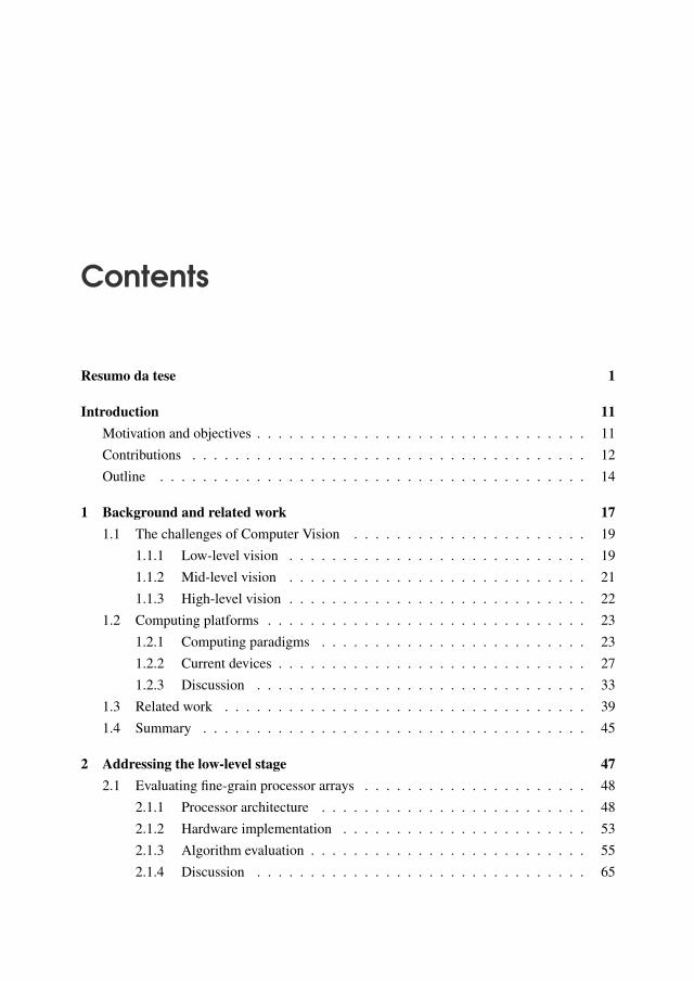
Contents
Resumo da tese 1
Introduction 11Motivation and objectives . . . . . . . . . . . . . . . . . . . . . . . . . . . . . . . 11Contributions . . . . . . . . . . . . . . . . . . . . . . . . . . . . . . . . . . . . . 12Outline . . . . . . . . . . . . . . . . . . . . . . . . . . . . . . . . . . . . . . . . 14
1 Background and related work 171.1 The challenges of Computer Vision . . . . . . . . . . . . . . . . . . . . . . 19
1.1.1 Low-level vision . . . . . . . . . . . . . . . . . . . . . . . . . . . . 191.1.2 Mid-level vision . . . . . . . . . . . . . . . . . . . . . . . . . . . . 211.1.3 High-level vision . . . . . . . . . . . . . . . . . . . . . . . . . . . . 22
1.2 Computing platforms . . . . . . . . . . . . . . . . . . . . . . . . . . . . . . 231.2.1 Computing paradigms . . . . . . . . . . . . . . . . . . . . . . . . . 231.2.2 Current devices . . . . . . . . . . . . . . . . . . . . . . . . . . . . . 271.2.3 Discussion . . . . . . . . . . . . . . . . . . . . . . . . . . . . . . . 33
1.3 Related work . . . . . . . . . . . . . . . . . . . . . . . . . . . . . . . . . . 391.4 Summary . . . . . . . . . . . . . . . . . . . . . . . . . . . . . . . . . . . . 45
2 Addressing the low-level stage 472.1 Evaluating fine-grain processor arrays . . . . . . . . . . . . . . . . . . . . . 48
2.1.1 Processor architecture . . . . . . . . . . . . . . . . . . . . . . . . . 482.1.2 Hardware implementation . . . . . . . . . . . . . . . . . . . . . . . 532.1.3 Algorithm evaluation . . . . . . . . . . . . . . . . . . . . . . . . . . 552.1.4 Discussion . . . . . . . . . . . . . . . . . . . . . . . . . . . . . . . 65
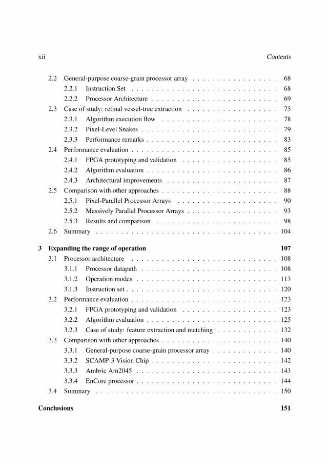
xii Contents
2.2 General-purpose coarse-grain processor array . . . . . . . . . . . . . . . . . 682.2.1 Instruction Set . . . . . . . . . . . . . . . . . . . . . . . . . . . . . 682.2.2 Processor Architecture . . . . . . . . . . . . . . . . . . . . . . . . . 69
2.3 Case of study: retinal vessel-tree extraction . . . . . . . . . . . . . . . . . . 752.3.1 Algorithm execution flow . . . . . . . . . . . . . . . . . . . . . . . 782.3.2 Pixel-Level Snakes . . . . . . . . . . . . . . . . . . . . . . . . . . . 792.3.3 Performance remarks . . . . . . . . . . . . . . . . . . . . . . . . . . 83
2.4 Performance evaluation . . . . . . . . . . . . . . . . . . . . . . . . . . . . . 852.4.1 FPGA prototyping and validation . . . . . . . . . . . . . . . . . . . 852.4.2 Algorithm evaluation . . . . . . . . . . . . . . . . . . . . . . . . . . 862.4.3 Architectural improvements . . . . . . . . . . . . . . . . . . . . . . 87
2.5 Comparison with other approaches . . . . . . . . . . . . . . . . . . . . . . . 882.5.1 Pixel-Parallel Processor Arrays . . . . . . . . . . . . . . . . . . . . 902.5.2 Massively Parallel Processor Arrays . . . . . . . . . . . . . . . . . . 932.5.3 Results and comparison . . . . . . . . . . . . . . . . . . . . . . . . 98
2.6 Summary . . . . . . . . . . . . . . . . . . . . . . . . . . . . . . . . . . . . 104
3 Expanding the range of operation 1073.1 Processor architecture . . . . . . . . . . . . . . . . . . . . . . . . . . . . . 108
3.1.1 Processor datapath . . . . . . . . . . . . . . . . . . . . . . . . . . . 1083.1.2 Operation modes . . . . . . . . . . . . . . . . . . . . . . . . . . . . 1133.1.3 Instruction set . . . . . . . . . . . . . . . . . . . . . . . . . . . . . . 120
3.2 Performance evaluation . . . . . . . . . . . . . . . . . . . . . . . . . . . . . 1233.2.1 FPGA prototyping and validation . . . . . . . . . . . . . . . . . . . 1233.2.2 Algorithm evaluation . . . . . . . . . . . . . . . . . . . . . . . . . . 1253.2.3 Case of study: feature extraction and matching . . . . . . . . . . . . 132
3.3 Comparison with other approaches . . . . . . . . . . . . . . . . . . . . . . . 1403.3.1 General-purpose coarse-grain processor array . . . . . . . . . . . . . 1403.3.2 SCAMP-3 Vision Chip . . . . . . . . . . . . . . . . . . . . . . . . . 1423.3.3 Ambric Am2045 . . . . . . . . . . . . . . . . . . . . . . . . . . . . 1433.3.4 EnCore processor . . . . . . . . . . . . . . . . . . . . . . . . . . . . 144
3.4 Summary . . . . . . . . . . . . . . . . . . . . . . . . . . . . . . . . . . . . 150
Conclusions 151

Contents xiii
A SIMD/MIMD Hybrid Processor timing diagrams 155
List of acronyms 161
Bibliography 163
List of Figures 183
List of Tables 185

Resumo da tese
Seguindo o regulamento dos estudios de terceiro ciclo da Universidade de Santiago de Com-
postela, aprobado na Xunta de Goberno do día 7 de abril de 2000 (DOG de 6 de marzo
de 2001) e modificado pola Xunta de Goberno de 14 de novembro de 2000, o Consello de
Goberno de 22 de novembro de 2003, de 18 de xullo de 2005 (artigos 30 a 45), de 11 de no-
vembro de 2008 e de 14 de maio de 2009; e, concretamente, cumprindo coas especificacións
indicadas no capítulo 4, artigo 30, apartado 3 de dito regulamento, amósase a continuación
un resumo en galego da presente tese.
Motivación e obxectivos
Os algoritmos e técnicas de Visión por Computador son cada vez máis robustos e precisos,ofrecendo novas posibilidades para o tratamento da información visual. Sen embargo, istoimplica un aumento dos requisitos de cómputo polo que a súa implementación en dispositivosmáis aló do alcance dos prototipos está a voltarse máis complexo. Son precisos novos enfo-ques que non afecten ás características dos algoritmos para acadar solucións de compromisoen termos de velocidade, latencia, consumo de potencia ou custo. Isto inclúe tanto ao apar-tado do software como ao da arquitectura hardware para poder aproveitar eficientemente ascaracterísticas do dispositivo e explotar plenamente as capacidades dos algoritmos.
Para solventar un problema no ámbito da Visión por Computador existen moitas técnicase aproximacións dispoñibles na literatura. A variedade de algoritmos é moi ampla e presentancaracterísticas moi diferentes, incluíndo non so a representación de datos ou as operaciónsaritméticas, se non tamén os paradigmas de computación ou a complexidade dos programas.Isto fai que o deseño das arquitecturas hardware sexa un desafío se é a mesma arquitectura aque ten que afrontar algoritmos diferentes cumprindo unhas restricións estritas.
2 Resumo da tese
Os ordenadores de escritorio son a miúdo empregados para desenvolver os algoritmos.Ofrecen unha gran flexibilidade para executar calquera algoritmo e avaliar a súa viabilidadee precisión. Con todo, o dispositivo obxectivo depende da aplicación e adoitan empregarsemódulos adicionais para acelerar o proceso. Para cumprir os requisitos da aplicación pode serincluso necesario deseñar unha arquitectura específica. Neste caso é posible optimizar todasas figuras de mérito implicadas. Os diferentes campos de aplicación fixan diferentes requisitospolo que as distintas arquitecturas deben adaptarse aos mesmos de forma eficaz.
Os avances na industria do semicondutor permiten incluír cada vez máis recursos na mes-ma unidade de área, mantendo un consumo de potencia contido. Isto fixo posible desenvol-ver novos sistemas embebidos cun rendemento similar aos sistemas convencionais do pasadorecente. Deste xeito, as novas aplicacións son tecnicamente factibles e o mercado de aplica-cións de visión embebidos está aumentando significativamente. Os sistemas nun chip posibi-litan embeber no mesmo chip todos os módulos necesarios para un sistema dado, incluíndocomputación, control e comunicacións, proporcionando unha vantaxe significativa sobre o seuequivalente sistema multi-chip. Sen embargo, os sistemas nun chip requiren un longo períodode deseño e moitos recursos, tanto humanos como materiais. Ademais, as arquitecturas a me-dida tamén requiren un período de adestramento polos enxeñeiros de software para explotarplenamente as súas capacidades, reducíndose así a vantaxe competitiva destes sistemas. Isto écrítico cando medra o número de unidades de propósito específico que executan os diferentesalgoritmos empregados.
O obxectivo deste traballo é proporcionar unha arquitectura capaz de executar a maioríados algoritmos de Visión por Computador cun rendemento adaptable ás distintas etapas decada algoritmo. Ademais, ten que ser capaz de executar as etapas restantes de xeito que orendemento global non se vexa comprometido. A arquitectura tamén está pensada para reduciro tempo empregado en migrar os algoritmos, reducindo a etapa de migración facilitando aparalelización e a sincronización entre os diferentes bloques concurrentes do algoritmo. Desdeo punto de vista da flexibilidade, o sistema ten que ser modular e escalable para afrontardiferentes áreas de mercado con diferentes requisitos, como rendemento, consumo de área oucusto. As melloras na arquitectura ou as modificacións baixo demanda deben ser posible senmudar dramaticamente a forma en que o hardware traballa. Todos estes elementos combinadosproporcionarán suficiente flexibilidade e rendemento para executar eficientemente a maiorparte dos algoritmos de Visión de Computador, co beneficio de empregar un so dispositivo.
Resumo da tese 3
Esta tese está dividida en tres capítulos. O Capítulo 1 presenta os desafíos da Visión porComputador, incluíndo os diferentes paradigmas de computación e as arquitecturas hardwaree dispositivos empregados para afrontar os requisitos dos algoritmos. No Capítulo 2 presén-tase unha nova arquitectura hardware para executar algoritmos de visión temperá. Despois deexaminar diferentes aproximacións, estudiaranse as capacidades dun procesador masivamenteparalelo para o procesamento de imaxes binarias. As conclusións deste estudio son esenciaispara o deseño dunha arquitectura máis eficiente e capaz para tarefas de visión temperá. Tes-tearase empregando un algoritmo usado en aplicacións médicas, altamente custoso en termoscomputacionais. No Capítulo 3, os resultados obtidos da comparativa do procesador de pro-pósito xeral descrito no capítulo anterior son empregados para definir unha nova arquitectura.Esta arquitectura está deseñada para aplicacións embebidas e enfocada na reconfiguracióndinámica do seu camiño de datos para reproducir o fluxo de execución do algoritmo en exe-cución. Deste xeito, a arquitectura aumenta o seu rango de operación de modo que todas asetapas dun algoritmo de Visión de Computador xenérico poden ser implementadas de xeitoeficiente nun único dispositivo embebido. Os resultados da execución de diversos algoritmosde procesado de imaxe e a comparativa con outras solucións similares completan este capítulo.Finalmente, extráense as principais conclusións deste traballo.
Introdución
A gran variedade de aplicacións de Visión por Computador fai difícil clasificalas en categoríasclaramente diferenciadas. Como resultado, o deseño dunha única arquitectura hardware queexecute eficientemente todas as etapas de procesado que inclúe calquera algoritmo de Visiónpor Computador convértese nunha tarefa moi complexa. Na literatura están dispoñibles di-versos estudios onde diferentes plataformas son testeadas baixo as mesmas condicións. Estesestudios amosan que o axuste fino dos parámetros é crítico en termos de rendemento e que odeseño de novas técnicas de computación paralela é un requisito para explorar as capacida-des dos dispositivos que inclúen máis dunha unidade de cómputo. Ademais, o aumento dasvendas e a aparición de mercados emerxentes fai que os investimentos en novo hardware sexaunha necesidade.
A plataforma máis accesible é un computador persoal equipado cunha GPU con soportepara cómputo de propósito xeral. Tanto como plataforma de deseño como dispositivo final, ocomputador persoal reduce enormemente o tempo de desenvolvemento e os custos asociados.
4 Resumo da tese
As GPUs ofrecen un alto rendemento nas tarefas máis intensivas mentres que as CPUs ofre-cen extensións multimedia que permiten acelerar o cómputo nas etapas nas que non é posibleempregar ás GPUs. Ademais, inclúen todos os elementos necesarios para comunicacións, al-macenamento e interacción co usuario. A dispoñibilidade de modelos é moi grande polo queé posible seleccionar a plataforma máis adecuada segundo para cada aplicación, cumprindoasí os seus requisitos. Cando o rendemento da CPU non é adecuado, os DSPs son unha seriaalternativa. Ademais, o seu uso é case obrigatorio cando estamos a falar de sistemas embebi-dos e non queremos comprometer o rendemento, e onde o consumo de potencia ou o factorde forma son moi restritivos. Son amplamente utilizados para prototipar chips de aplicaciónespecífica aínda que as FPGAs reduciron o seu nicho de mercado. Os FPGAs ofrecen unhaalta integración e flexibilidade ademais dun grande número de unidades xa dispoñibles quepermiten reducir os custos asociados ao deseño, desenvolvemento e testeo. A pesar de quetodos os dispositivos descritos son de aplicación específica, non foron concibidos para unhaaplicación única. Para reducir os custos, os fabricantes expanden o seu rango de operación,aínda que é posible atopar familias de produtos específicas para certos nichos. Sen embar-go, tamén hai dispositivos específicos para tarefas moi concretas, onde os requisitos son tanestritos que ningún outro dispositivo os cumpre. A flexibilidade é completa e non hai restri-cións para empregar as tecnoloxías máis avanzadas que so estarán dispoñibles en dispositivoscomerciais nun futuro próximo.
Case todas as aplicacións de Visión por Computador necesitan afrontar todas etapas deprocesamento nun menor ou maior grao. A miúdo, isto conleva aplicar mecanismos que in-clúen o manexo do paralelismo espacial (dato), temporal (instrución) e secuencial, ou inclusounha combinación deles. Cada etapa corresponde aproximadamente cun tipo de paralelismo,co que todos estes mecanismos adoitan implementarse na maior parte das aplicacións. As eta-pas de baixo nivel benefícianse do paralelismo masivo con sistemas de distribución de datose operacións aritméticas sinxelos. Cando a abstracción aumenta, durante as tarefas de medionivel, os algoritmos requiren maior información acerca do problema a resolver, polo que seincrementa a súa complexidade. Isto conleva estruturas de datos e fluxos de execución máiscomplexos, onde a distribución da información fai difícil explotar o paralelismo espacial, aín-da que normalmente está presente. As arquitecturas paralelas a nivel de tarefa son capaces deexplotar de forma máis eficiente e sinxela esta etapa. As etapas de baixo e medio nivel po-den implementarse en solucións hardware puras porque con frecuencia so executan tarefas decómputo. Sen embargo, a etapa de alto nivel está máis próxima ao software e os enxeñeiros
Resumo da tese 5
poden explotar este feito para construír sistemas máis complexos usando un procesador depropósito xeral. Ademais, permitirá actuar como sistema de control das unidades de cómpu-to ou dos sistemas de comunicación. Isto non está directamente relacionado cos problemasda Visión por Computador pero sen embargo é un requerimento para un prototipo funcio-nal. Neste caso, o uso dun procesador de propósito xeral é un claro beneficio pois facilitaenormemente o control e incrementa a flexibilidade do sistema.
A pesar de que é case imposible desenvolver un sistema capaz de executar todas as ope-racións dun xeito óptimo dada a rica natureza das aplicacións de Visión por Computador, édesexable que proporcione a capacidade para executar calquera operación. O deseño ten queser escalable para adaptalo ás necesidades específicas de cada aplicación. Deste xeito é posi-ble proporcionar unha familia de dispositivos con diferentes capacidades de cómputo de xeitosinxelo. A arquitectura interna debe ser tamén modular, de modo que desde un esbozo básicose poidan engadir máis características sen cambios dramáticos. En xeral, un microprocesa-dor de alto nivel é un requisito para xestionar comunicacións e operacións complexas entre osistema e os compoñentes externos do sistema completo. Un certo número de unidades auxi-liares capaces de manexar os paradigmas de computación paralelos a nivel de dato e de tarefaexecutarían a parte máis custosa do algoritmo. En particular, unha unidade de SIMD grandeaumentará o rendemento nas primeiras etapas. Un controlador integrado para memorias dealta velocidade é tamén crítico para reducir os problemas de acceso aos datos na memoriaexterna. Todos estes elementos combinados son capaces de afrontar eficientemente a maioríadas situacións que se atopan nos algoritmos máis comunmente empregados.
Abordando a etapa de baixo nivel
As tarefas da etapa de baixo nivel caracterízanse por ser simples, repetitivas e aplicadas sobreunha gran cantidade de datos, e non requiren unha alta precisión. Sen embargo, son moicustosas computacionalmente, especialmente en sistemas embebidos, o ámbito que se abordaneste traballo.
No segundo capítulo preséntase un procesador de propósito xeral para o procesado deimaxes a baixo nivel. En primeiro lugar, preséntase un estudio dunha arquitectura para imaxesbinarias (branco e negro), onde se conclúe que o paralelismo espacial masivo non represen-ta a solución máis eficiente. A pesares que a distribución matricial do conxunto de unidadesde cómputo con comunicación local entre elas pode explotar moi eficientemente as caracte-
6 Resumo da tese
rísticas das tarefas que executan nesta etapa, a correspondencia dun procesador por píxel daimaxe ten varias serias desvantaxes. Por un lado, o número de recursos hardware necesariosé elevado, resultando en procesadores que traballan con imaxes con pouca resolución e confrecuencias de reloxo baixas. A pesares de tratarse de problemas técnicos, o rendemento reale a conveniencia deste tipo de procesadores é menor do esperable teoricamente. Deste xeito,solucións a priori menos óptimas poden superar estas limitacións e ofrecer mellores figurasde mérito.
Como resultado, este procesador preliminar foi ampliado para procesar imaxes non bi-narias, estendendo as capacidades de cada unidade de cómputo e reducindo o paralelismo.Esta arquitectura, unha matriz de procesadores de gran groso, proporciona mellores figurasde mérito. En particular, é máis sinxelo escalar a matriz sen comprometer a frecuencia dereloxo e permite manexar imaxes de maior resolución. Cando se compara con outras propos-tas, unha implementación en FPGA desta arquitectura mellora os resultados dun procesadorSIMD masivamente paralelo que conta con 8500% máis unidades de cómputo. Esta densida-de de integración é acadada empregando arquitecturas de sinal mixta que limitan o tamaño damatriz e a frecuencia de reloxo, limitando a potencia que se pode extraer del. Sen embargo,o consumo de potencia acadado é moi difícil de bater. As matrices masivamente paralelasde procesadores tamén amosan un alto rendemento explotando o paralelismo temporal, aín-da que as operacións recursivas reducen en gran medida o rendemento, sendo difícil atoparunha solución de compromiso. O algoritmo empregado para comparar o rendemento e pos-terior discusión é representativo da súa clase, proporcionando información adicional acercade como os datos interactúan cando se concatenan os diferentes operadores. Isto danos un-ha vantaxe durante a etapa de deseño dunha arquitectura especializada en acelerar este tipode operacións. Os resultados tamén amosan que CPUs convencionais non son eficientes paratarefas de visión temperá, polo que outras aproximacións están claramente xustificadas.
As principais conclusións refírense a como as unidades aritméticas están organizadas ecomo se distribúen os datos entre elas. Como se víu, unha organización matricial permiteafrontar de xeito eficiente operacións de baixo nivel, que inclúen operacións píxel a píxel einteraccións locais. Polo contrario, cando se procesan datos que non son puramente imaxes,unha matriz bidimensional non proporciona a necesaria flexibilidade. Isto acentúase segundoo nivel de abstracción aumenta. A matriz masivamente paralela de procesadores, que explotaen gran medida o paralelismo temporal é unha boa proba deste feito. Un problema non resoltopolo momento é a entrada e saída de datos. As tarefas de procesado de imaxe normalmente
Resumo da tese 7
requiren un gran ancho de banda e unidades de almacenamento de alta capacitade, o que podelimitar o rendemento se as unidades de cómputo están consumindo tempo esperando polosdatos a procesar. Superpoñer a transferencia de datos e o seu procesado é esencial.
As conclusións expostas neste capítulo lévannos a propoñer unha versión mellorada daarquitectura inicial, enfocándose en estender o rango de aplicación sen comprometer o rende-mento, ampliar os requisitos hardware ou o consumo de potencia.
Expandindo o rango de operación
O terceiro capítulo amosa unha extensiva optimización da arquitectura proposta no segundocapítulo. A primeira proposta foi deseñada para abordar a etapa de baixo nivel que inclúen amaioría das aplicacións de Visión por Computador, que consumen a maior parte da carga detraballo da CPU. A matriz de procesadores de gran groso probou ser moi eficaz nestas tarefas.Sen embargo, a súa flexibilidade está limitada e non manexa de forma eficiente as posterioresetapas de procesado. A distribución das unidades aritméticas, a representación dos datos e asoperacións de entrada/saída non son as adecuadas para as etapas de medio e alto nivel.
Para deseñar a arquitectura finalmente proposta seleccionáronse as mellores característi-cas dos paradigmas de computación SIMD (espacial) e MIMD (temporal), e combináronsepara reducir os recursos hardware empregados. Deste xeito, a nova arquitectura pode explotartanto os paradigmas de computación paralela a nivel espacial e temporal, executando opera-cións masivamente paralelas en modo SIMD, a nivel de tarefa en modo MIMD e de alto nivelou de xeito serie nun procesador secuencial. O paradigma de computación pode cambiarseen tempo de execución segundo os requisitos que marque cada un dos algoritmos implemen-tados. O manexo da entrada/saída de datos foi mellorado e permite superpoñer computacióne transferencia de datos, reducindo o colo de botella e facilitando o acceso á memoria exter-na onde se almacenan os datos. Un dos obxectivos desta arquitectura é prover da suficienteflexibilidade como para manexar situacións moi diversas, incluíndo diferentes tipos de datos,tamaños de imaxe ou representacións abstractas. Para este propósito empréganse dúas redesdiferentes para intercambiar datos entre as unidades de cómputo. As súas características fa-cilitan a distribución dos datos e reducen o tempo empregado no proceso, aumentando así orendemento. Ademais da flexibilidade, outro obxectivo perseguido é o de facer a arquitecturaaltamente configurable, de forma que esta non dependa do número de unidades de cómputo, otamaño das memorias ou o tipo de operacións aritméticas empregadas. Isto permite crear unha
8 Resumo da tese
familia de procesadores que aborden diferentes aplicacións en diferentes campos, axustandoasí non so o rendemento ou o consumo de potencia, se non tamén o custo.
O procesador SIMD/MIMD híbrido foi testeado nun sistema embebido baseado en FPGA.Un conxunto de operadores e algoritmos foi implementado para avaliar o seu rendemento ea súa factibilidade. Os resultados proban que se pode alcanzar un alto rendemento cando osdiferentes modos de computación se empregan adecuadamente. A arquitectura foi comparacon outras propostas similares, incluíndo a matriz de procesadores de gran groso proposta nosegundo capítulo. Os resultados amosan que o prezo a pagar debido ao incremento de hard-ware e á inclusión de características de cómputo de propósito xeral, que poderían penalizar orendemento en tarefas específicas, é menor que a ganancia en termos de flexibilidade xa queo rendemento non se ve comprometido.
Conclusións
Neste traballo, presentouse unha nova arquitectura hardware para acelerar aplicacións de Vi-sión por Computador en sistemas embebidos. Esta arquitectura hardware proporciona un dis-positivo dun único chip capaz de executar a maioría dos algoritmos de procesado de imaxe etarefas relacionadas.
En primeiro lugar introduciuse o problema da Visión por Computador e analizáronse asfamilias de algoritmos relacionados. Despois de reseñar as súas características, tipo de opera-cións e complexidade do fluxo de programa, avaliáronse os diferentes paradigmas de compu-tación. Partindo deste coñecemento, propúxose a arquitectura dun procesador masivamenteparalelo avaliando a súa viabilidade con tecnoloxía actual. Este procesador incluía un grannúmero de unidades de cómputo, moi sinxelas, dispostas nunha matriz bidimensional con co-nexións locais entre eles para intercambiar datos. A pesar de que soamente procesaba imaxesbinarias, os resultados amosan que as implementacións prácticas están limitadas a aplicaciónsque procesan imaxes de baixa resolución e onde o ancho de banda é o maior limitante dosistema. Unha versión posterior deste procesador, estendido para manexar imaxes en escalade grises e a cor, mellora os resultados reducindo o paralelismo pero mellorando as caracterís-ticas das unidades de cómputo. Esta arquitectura, como a anterior, prototipouse nunha FPGApara validar as melloras engadidas. Para isto utilizouse un algoritmo que extrae de xeito auto-mático a árbore de veas a partir de imaxes retinianas. Trátase dunha aplicación moi esixente erepresentativa dos algoritmos de visión temperá, etapa de baixo nivel que o procesador debe
Resumo da tese 9
ser capaz de abordar. A arquitectura proposta, unha matriz de procesadores de gran groso,explota o paralelismo de dato dos algoritmos, e foi comparada cunha CPU de propósito xe-ral, un procesador de plano focal cun esquema dun procesador por píxel, e unha matriz deprocesadores masivamente paralela, que explota o paralelismo temporal.
Os resultados obtidos da comparativa das diferentes arquitecturas foi moi valiosa paraespandir o rango de operación. Unha das conclusións obtidas é que unha distribución bidi-mensional das unidades de cómputo non proporciona a suficiente flexibilidade para abordaras etapas posteriores ao baixo nivel. Ademais, explotar o paralelismo a nivel de tarefa noné posible, algo moi importante en gran cantidade de algoritmos incluso aínda que a súa pre-sencia sexa reducida, tal e como amosa a comparativa anterior. Estas conclusións leváronnosa deseñar unha nova arquitectura, baseada na anterior, onde os diferentes módulos permitenreconfigurarse baixo demanda e en tempo de execución.
As novas melloras introducidas aumentan a flexibilidade e o rendemento da arquitectura.Deste xeito, é posible configurar dous modos de execución, SIMD e MIMD. No primeiro mo-do, todos os procesadores executan a mesma instrución. As unidades de cómputo dispóñensenunha matriz unidimensional con conexións locais entre unidades adxacentes. Neste modo, oparalelismo de dato pode ser plenamente explotado empregando a memoria interna que cadaunidade aritmética inclúe. Os operadores baseados en ventá, moi importantes nos primeirospasos de case todos os algoritmos de Visión por Computador, poden implementarse facilmen-te almacenando varias filas da imaxe de forma adxacente. No modo MIMD, cada unidadede cómputo executa un pequeno programa, unha parte do algoritmo completo. Os diferentesmódulos interconéctanse empregando unha rede local programable para reconstruír o fluxode execución do algoritmo. Este modo explota o paralelismo temporal de forma nativo xa quetodas as unidades están traballando de xeito concurrente. A rede autoxestiónase polo que noné preciso incluír control adicional, facilitando a migración de depuración do algoritmo. Enambos modos, dous procesadores independentes controlan a saída e entrada de datos entre asunidades de cómputo e a memoria externa. Isto permite superpoñer a transferencia de datos eo cómputo, incrementando o rendemento global do sistema.
A arquitectura final foi prototipada nunha FPGA e diversos algoritmos foron avaliados pa-ra determinar os beneficios que supoñen estas melloras. A pesar de que presenta capacidadesde propósito xeral, os resultados mostran que é posible de conseguir un rendemento simi-lar á arquitecturas máis específicas, como a presentada no capítulo segundo, sendo posibleaumentar de xeito considerable a flexibilidade sen comprometer o rendemento.
10 Resumo da tese
Traballo futuro
A arquitectura proposta neste traballo proporciona unha base sólida sobre a cal é posible enga-dir novas características para aumentar a súa flexibilidade e rendemento, entre outras figurasde mérito. En particular e baseado nos resultados obtidos, unha arquitectura multi-núcleoproporcionará melloras importantes. Para executar simultaneamente ambos paradigmas decomputación, SIMD e MIMD, unha interconexión interna para transferir os datos entre os di-versos núcleos é máis interesante que aumentar o número de unidades de cómputo mantendoun so chip.
Máis aló de modificacións estruturais e implementacións baseadas en FPGAs, a arqui-tectura foi concibida para implementarse en ASICs. A arquitectura pode ser optimizada a unnivel máis profundo, especialmente o apartado referente ás unidades aritméticas, restrinxidasen capacidade debido á limitación dos recursos dispoñibles na FPGA. Isto abre novas direc-cións de investigación e permite avaliar de xeito máis preciso parámetros como o consumo depotencia ou os requisitos de área.
Introduction
Motivation and objectives
Computer Vision algorithms and techniques are increasingly robust and accurate, offeringnew possibilities for the treatment of visual information. However, this entails an increasingin the computing requirements, and their implementation on devices beyond the scope of theprototypes is becoming more complex. Novel approaches are required in order not to trim thecharacteristics of the algorithms and to meet the different trade-offs such as speed, latency,power consumption or cost. This includes both hardware architectures and software tech-niques to fully exploit the computing capabilities of the target device and to take advantage ofthe characteristics of the algorithms.
For a given Computer Vision problem there are many different techniques and approachesproposed in the literature. The variety of algorithms is very broad and they present verydifferent characteristics, including not only data representation or arithmetic operations butalso different computing paradigms and program complexity. This makes the design of thehardware devices very challenging if the same architecture has to face different algorithmswith tight constraints.
Desktop computers are often employed to develop the algorithms. They offer large flex-ibility to run any algorithm and evaluate its feasibility and accuracy. However, the targetdevice is application-dependent and supplementary hardware modules are frequently used tospeed-up the computation. In order to meet the requirements of the application, a custom ar-chitecture may be a need. In this case, all figures of merit are likely to be optimized. There aremany different fields where the different trade-offs are more or less important so the differentarchitectures have to deal with different restrictions.
12 Resumo da tese
The advances in the semiconductor industry enable embedding more and more resourcesin the same unit of area while maintaining a restrained power consumption. This have madepossible to develop new embedded processors with similar performance to recent-past conven-tional systems. This way, new applications are now technically feasible and the importanceof the embedded vision market is increasing significantly. Custom systems-on-chip enable toembed on the same chip all the necessary modules for a given system, including computing,control and communication, providing a significant advantage over equivalent multi-chip sys-tems. However, custom systems-on-chip require a long period of design and many resources,human and materials. In addition, custom hardware also requires a training period by thesoftware engineers to fully exploit the capabilities of the hardware, reducing the competitiveadvantage of these systems. This becomes critical as the number of specific units grows toface the different algorithms employed to solve the Computer Vision problem.
The objective of this work is to provide a single-chip architecture able to run most of theComputer Vision algorithms with adaptive performance on the critical steps of the algorithms.In addition, it must be able to run all the other steps so that the overall performance is notcompromised. The architecture also aims to reduce the time spent in migrating the algorithms,reducing the mapping stage by easing algorithm parallelization and synchronization betweenthe different concurrent kernels of the algorithm. From the flexibility point of view, the systemhas to be modular and scalable in order to address different targets on the market and meetdifferent trade-offs such as performance, area or cost. Architectural improvements and custommodifications must be done easily without dramatically change the way the hardware works.All these elements combined will provide enough flexibility and performance in order to runefficiently many different Computer Vision algorithms, with the benefit of employing a singledevice.
Contributions
The primary contributions of this dissertation are:
• An analysis of how representative and conceptually different hardware architectures im-plement diverse Computer Vision algorithms by taking advantage of their mathematicaloperations and dataflow.
Resumo da tese 13
• An architecture for low-level and early vision image processing which solve a num-ber of technical problems found on existing devices, expanding its range of operation,flexibility, accuracy, cost and development times.
• A modular and scalable architecture for embedded Computer Vision systems, whichfocus on easing algorithm migration by natively parallelize the processing threads anddata transfer. This architecture features general-purpose capabilities and dynamicallyreconfiguration at runtime to adapt the internal datapath according to the operations ofthe algorithm it is running.
• A demonstration and evaluation of the potential value of reconfigurable datapaths toface complex operations, beyond the Computer Vision field.
These contributions can be found in the publications listed below:
• SIMD Array on FPGA for B/W Image Processing. Alejandro Manuel Nieto Lareo,Víctor Manuel Brea Sánchez and David López Vilariño, in 11th International workshop
on Cellular Neural Networks and their Applications (CNNA 2008).
• SIMD and Cellular Neural Networks as Fine-Grained Parallel Solutions for Earlyvision on FPGAs. Alejandro Manuel Nieto Lareo, Natalia F., Jordi A.C., J. Riera,Víctor Manuel Brea Sánchez and David López Vilariño, in 23th Conference on Design
of Circuits and Integrated Systems (DCIS 2008).
• A Digital Cellular-Based System for Retinal Vessel-Tree Extraction. César R., Ale-jandro Manuel Nieto Lareo, Roberto O., Víctor Manuel Brea Sánchez and David LópezVilariño, in 19th European Conference on Circuit Theory and Design (ECCTD 2009).
• On-Chip Retinal Image Processing: Performance Analysis on Different Approaches.Alejandro Manuel Nieto Lareo, Roberto O., Víctor Manuel Brea Sánchez and DavidLópez Vilariño, in 24th Conference on Design of Circuits and Integrated Systems (DCIS
2009).
• An FPGA-based Topographic Computer for Binary Image Processing. AlejandroManuel Nieto Lareo, Víctor Manuel Brea Sánchez and David López Vilariño, in Image
Processing (In-Tech Education and Publishing, 2009).
14 Resumo da tese
• FPGA-Accelerated Retinal Vessel-Tree Extraction. Alejandro Manuel Nieto Lareo,Víctor Manuel Brea Sánchez and David López Vilariño, in 19th International Confer-
ence on Field Programmable Logic and Applications (FPL 2009).
• Performance analysis of massively parallel hardware architectures for medical im-age processing. Alejandro Manuel Nieto Lareo, Víctor Manuel Brea Sánchez andDavid López Vilariño, in Eurasip Journal on Image and Video Processing - Special
Issue on Real-Time Image Processing on Multi-Cores, Many-Cores and High-level
FPGA-based Platforms (2011).
• Towards the optimal hardware architecture for Computer Vision. Alejandro ManuelNieto Lareo, Víctor Manuel Brea Sánchez and David López Vilariño, in Machine Vision
(In-Tech Education and Publishing, 2011).
• Feature detection and matching on an SIMD/MIMD hybrid embedded processor.Alejandro Manuel Nieto Lareo, David López Vilariño and Víctor Manuel Brea Sánchez,in 8th IEEE Workshop on Embedded Vision (EVW 2012).
• SIMD/MIMD dynamically-reconfigurable architecture for high-performance em-bedded vision systems. Alejandro Manuel Nieto Lareo, Víctor Manuel Brea Sánchezand David López Vilariño, in 23rd IEEE International Conference on Application-
specific Systems, Architectures and Processors (ASAP 2012).
The results of this work are also reflected in the following patent:
• Arquitectura híbrida SIMD/MIMD dinámicamente reconfigurable de un coproce-sador para sistemas de visión. Alejandro Manuel Nieto Lareo, David López Vilariñoand Víctor Manuel Brea Sánchez. Patent Application Number P201101381, Spain (De-
cember 30th, 2011).
Outline
This thesis is divided in three chapters. Chapter 1 introduces the challenges of ComputerVision. The different computing paradigms and hardware architectures and devices to facethe algorithms requirements are also reviewed. In Chapter 2, a new hardware architecturefor early vision processing is presented. After examining different approaches, a study of a
Resumo da tese 15
massively parallel processor for binary image processing is carried out. The conclusions ofthe study are essential for the design of a more efficient and capable architecture for general-purpose early vision processing, which is extensively tested employing a highly computation-ally consuming algorithm employed in medical applications. In Chapter 3, the results of thecomparison of the general-purpose early vision processor are employed to define a new andenhanced architecture. This architecture is intended for embedded devices and focuses ondynamic reconfiguration to reproduce the algorithm’s dataflow. This way, the architecture in-creases its range of operation so that all steps of a general Computer Vision algorithm can beperformed efficiently by the embedded device. The results of implementing several commonimage processing algorithms and a comparison with similar approaches complete this chapter.Finally, the main conclusions of this thesis are conveyed.

CHAPTER 1
BACKGROUND AND RELATED WORK
Computer Vision systems are experiencing a large increase in both range of applications andmarket sales [1]. From industry to entertainment, Computer Vision systems are becomingmore and more important and the research community is making a big effort to make themable to handle complex scenes focusing on the accuracy and the robustness of the results. Thenew algorithms enable more advanced and comprehensive analysis of the images, expandingthe set of tools to implement these applications [2].
Although there are new algorithms available to approach sophisticated new applicationswith a high degree of accuracy, not all the algorithms are adequate to be deployed in industrialsystems. Parameters like power consumption, integration with other system modules, costand performance limit the range of suitable platforms. In most cases, the algorithms must beadapted to achieve a trade-off solution and to take advantage of the selected platform.
Conventional systems like PCs or GPUs are increasingly improving performance and in-cluding more features but their use is limited to areas where portability, power consumptionand integration are not critical. When the algorithm is highly complex, with an irregularexecution flow, complex data representation and elaborated patterns to access to data, a sig-nificant gain is not achieved when moving the algorithm to an ad hoc hardware design. Inthis case, a high-end CPU and a GPU with support for GPGPU is a flexible and very powerfulcombination that will outperform other choices [3].
However, when a conventional system does not meet the requirements of the application,a more ambitious planning is needed. For instance, migrating the algorithm to a dedicateddevice such as a DSP, an FPGA or a custom chip [4]. At this point, the designers have to
18 Chapter 1. Background and related work
consider alternatives as to reduce operating range, accuracy and robustness of the results, orto remove expensive operations in order to simplify the hardware that will be implemented[5]. Otherwise, a significant improvement will not be achieved. PC-based systems enablea great flexibility at cost of performance, so pure software-based algorithms hardly matchpure hardware implementations. This is a serious limitation because it can compromise theefficiency of the application. This is the reason why the industry is making great effortsto develop novel architectures that enable greater flexibility to adapt the algorithms withoutcompromising the quality of the results.
Computer Vision applications are often divided into several stages depending on the ab-straction level and thus in the complexity of the operations. Initially, operations are quitesimple and repetitive but applied over a large set of data with a very reduced data dependentprogram flow, so massive parallelism is essential for performance. Then, the level of abstrac-tion increases, resulting in more complex algorithms. Temporal and task parallelism is keyas the data set is smaller and the program flow is often data-dependent. Finally, the systemoutput has to be determined, performing high level operations over complex data represen-tations but reduced data sets and with higher precision as usual requirement. An efficientComputer Vision system must deal with all these stages. The selection of the computationmodel will determine the performance of the device in each one of the stages. According toFlynn’s Taxonomy [6], paradigms can be classified into four categories based on the numberof instructions and data streams processed simultaneously. So, which is the optimal paradigmfor such applications? Increase the number of concurrent instructions? Increase the numberof data elements processed simultaneously? A combination of both?
Taking into account the application requirements, a suitable platform to build the systemmust be selected. Besides general parameters (performance, cost and integration), there is aset of factors that restrict the computing paradigms and the devices that can be selected. Forinstance, a critical parameter is the way the data are transferred to the device because I/Ooperations are one of the bottlenecks in high-performance systems. Data type (integer, fixed-point or floating-point) and representation will affect the computational units. The programflow will constrain the inner connections between these units and the storage elements. Totackle these and other parameters, a careful analysis of the state-of-the-art of the algorithmshas to be made.
This chapter addresses a review of different computing paradigms and platforms orientedto image processing. In addition, a representative set of Computer Vision algorithms covering
1.1. The challenges of Computer Vision 19
the three levels of processing is evaluated. This study will allow us to observe the algorithmsbased on a set of common characteristics: operations, data type, program flow, etc. This iscritical to design new hardware architectures in order to maximize performance. The analysisfrom the hardware point of view will highlight the best features of the most used computingparadigms in order to establish a relationship between the type of operation, data, program-ming model and hardware architecture. An efficient architecture for Computer Vision mustcombine all the selected features. The analysis of the characteristics of the different algorithmswill lead us to an optimized general-purpose hardware architecture for Computer Vision.
1.1 The challenges of Computer Vision
Traditionally, Computer Vision (CV) applications include building blocks from three compu-tation levels: low-, mid- and high-level vision computing. The type of operations, the datarepresentation and the flow execution of programs depend deeply on the considered level ofthis hierarchy. Nevertheless, current CV-algorithms are composed of many different process-ing steps regarding the type of data and the way these are computed, which makes difficult toclassify them only in one subgroup. Following, a rather rough classification of widely usedCV-algorithms is made, keeping in mind the data domain and the complexity of the involvedoperations.
1.1.1 Low-level vision
After image acquisition, some preprocessing steps are often required. These are intendedto provide reliable input data for subsequent computing stages. Some typical operations arenoise reduction, color balancing, geometrical transformation, etc. Most of these operationsare based on point or near-neighborhood operations. Point operations are performed at pixel-level in such a way that the output only depends on the value of any individual pixels fromone or several input images. With this type of operation it is possible to modify the pixelintensity to enhance parts of the image, by increasing contrast or brightness. Equally, simplepixel-to-pixel arithmetic and Boolean operations also enable the construction of operators asalpha blending, for image combination or color space conversion. Neighborhood operationstake also into account the value of adjacent pixels. This operation type is the basis of filtering,binary morphology or geometric transformation. They are characterized by simple operations,typically combining weighted sums, Boolean and thresholding processing steps.
20 Chapter 1. Background and related work
After preprocessing stages, useful information has to be extracted from the resulting im-ages. Common operations are edge detection, feature extraction or image segmentation.Edges are usually defined as step discontinuities in the image signal so finding local max-ima in the derivative of the image or zero-crossings in the second derivative are suitable todetect boundaries. Both tasks are usually performed by the convolution of the input imagewith spatial filtering masks that approximate a first or second derivative operator.
Feature points are widely used for subsequent computing steps in multiple CV-applications.Basically, a feature represents a point in the image which differs from its neighborhood. Oneof the benefits of local features is the robustness against occlusion and the ability to managegeometric deformations between images when dealing with viewpoint changes. In addition,they improve accuracy when, in the same scene, objects are at different planes, (i.e. at dif-ferent scales). One of the most popular techniques is that proposed by Harris [7] to detectcorners. It is widely used due to its strong invariance to rotation, image noise and no largeillumination changes. It uses the local auto-correlation function, which describes the gra-dient distribution in a local neighborhood of each image point to detect the location of thecorners. Using the locally averaged moment matrix from the image gradients, corners willbe located at the maximum values. Another frequently used technique is the Scale-InvariantFeature Transform (SIFT) [8]. SIFT localizes extrema both in space and scale. Using theDifference of Gaussians as scale-space function, the images are filtered with Gaussian kernelsof different sizes (scales). This is performed for different image sizes (octaves). The responseof each filter is subtracted from the immediately following in the same octave. The interestpoints are scale-space extrema so local maxima and minima are extracted by comparing theneighborhood points in the same, the previous and the subsequent scales. To improve accu-racy, a sub-pixel approximation step is done, interpolating the location of the feature insidethe scale-space structure. The number of octaves and scales can be tuned to meet the sys-tem requirements. SIFT provides invariance against scale, orientation and affine distortion,as well as partial occlusion and illumination changes. Other algorithms were proposed toimprove accuracy or performance like, the Speeded Up Robust Features (SURF) [9] or theGradient Location and Orientation Histogram (GLOH) [10]. This kind of detectors are quitecomplex and their performance can be low even using custom hardware. For this reason,less reliable algorithms are still in use, as Harris Corner Detector, FAST [11] or the Small-est Univalue Segment Assimilating Nucleus (SUSAN) [12] corner detectors. In this sense,techniques such as [13] provide a framework for very fast feature detection and matching.
1.1. The challenges of Computer Vision 21
Segmentation refers to the process of separating the data into several sets according tocertain characteristics. There are several techniques to carry out this task, either based onboundaries or regions [14] [15]. Nevertheless, most of them rely on near-neighborhood op-erations. Particular attention deserves the clustering methods like the popular k-means whichpartitions the data set into several clusters according to a proximity criterion defined by adistance function. These methods are not restricted to image data. N-dimensional sets of ab-stract data can also be partitioned. Furthermore, information about the scene or domain canbe introduced (number and characteristics of the target clusters). Therefore, they might beclassified either as a low or mid-level vision stage.
1.1.2 Mid-level vision
Mid-level CV stages usually operate on images from previous processing steps, often binaryimages, and produce a lower amount of data but with a higher concentration of information.Some common operations are object classification and scene reconstruction.
One of the goals of Computer Vision is to recognize objects in a scene. Based on objectlocation, pose or 2D/3D spatial relations between the objects, the algorithms have to be ableto analyze the scene and its content. This involves issues such as dealing with object mod-els, classifiers and the ability to integrate new information in the models. In the literature, alarge amount of techniques can be found, usually classified as global methods, more intendedfor object detection and local feature-based methods for object recognition. In all of themgood image registration is essential for both accuracy and performance [16]. As for the globalmethods, common techniques are based on template-based matching, which employs a con-volution mask or template to measure the similarity between an object patch and the template.In this sense, normalized cross-correlation (NCC), sum of squared differences (SSD) or sum
of absolute differences (SAD) are widely used. As for local methods, local feature descriptorsplay an important role. Roughly speaking, a descriptor is an abstract characterization of afeature point based on its environment. One of the most popular techniques is the proposedin second part of the SIFT algorithm based on stacked orientation histograms which associatea high dimension vector to each keypoint. In order to reduce the amount of false positivesand negatives during the matching stage the search area is limited by using strategies like thenearest neighbor search (NNS) which attempts to find the nearest points of a given one in avector space. An indexing structure allows to search for features near a given feature rapidly.
22 Chapter 1. Background and related work
This is the case of the K-dimensional trees, which organize points in a k-dimensional space insuch a way that each node has at most two child nodes.
Scene reconstruction consists of the generation of scene models starting from their com-ponents. There are different techniques to reconstruct one or several objects in a scene. Tobuild a 3D model, coordinates of scene points have to be calculated from the objects. If thelocation of the camera is known, 3D coordinates of a scene point can be determined fromits projection on image planes of different viewpoints. The whole process starts with featureextraction and matching. Using geometric consistency tests it is possible to eliminate wrongmatches. There are different solutions to estimate the fundamental matrix, as the RANdom
SAmple Consensus (RANSAC). Once the matches between images are consistent, camerapose and scene geometry is reconstructed using Structure from Motion methods and refinedwith Bundle adjustment techniques [17].
1.1.3 High-level vision
The high-level stage often starts from an abstract representation of the information. This stageis highly application-dependent, but due to the variety of operations, data structures, memoryaccess patterns and program flow characteristics are often only compatible with a generalpurpose processor. High-level processing is characterized by the use of a small set of data torepresent knowledge about the application domain. More complex data structures are neededto store and process this information efficiently, making the operations and the memory accesspatterns more elaborated. This, together with the inherent complexity of decision making,makes the program flow very variable.
Robust pattern recognition, object identification, complex decision making or systemadaptation are some of the benefits of integrating Artificial Intelligence methods with Com-puter Vision. Otherwise, the system would be limited to a predetermined set of actions. Ma-chine learning makes computers capable of improving automatically with experience. Thisway it is possible to generalize the behavior from unstructured information with techniquessuch as neural networks, decision trees, genetic algorithms, regression models or support vec-tor machines. Machine learning has emerged as a key component of intelligent computervision systems, contributing to a better understanding of complex images [18] [19].
Data mining is the process of analyzing data using a set of statistical techniques in order tosummarize into segments of useful information. This makes possible analyze data from differ-ent dimensions or angles, categorizing and summarizing the identified relationships, making
1.2. Computing platforms 23
evident hidden relationships or patterns between events. Contrary to Machine learning, datamining focuses on discovering hidden patterns instead of generalizing known patterns usingthe new data.
It is very difficult to establish a classification of tasks and operations for high-level pro-cessing. Some of the performed tasks fall within the scope of the measurement of applicationspecific parameters such as size and pose of objects, fault detection and monitoring specificevents such as traffic situations, for example. The algorithms and technologies are very di-verse and most of them lie in statistical analysis and artificial intelligence domains.
As it was previously mentioned some tasks that initially fit into the low or medium levelstages due to its context actually are more like high-level operations by the type of operationsperformed. This is related with the commonly used bottom-up image analysis, which startsfrom raw data to extend the knowledge of the scene. However, new approaches include feed-back to perform top-down analysis. This way, low- and mid-level stages can be controlledwith general knowledge of the image, improving the results.
1.2 Computing platforms
Given the wide range of algorithms and applications of Computer Vision, it is clear that itdoes not exist a unique computing paradigm or an optimal hardware platform. The type ofoperations, the complexity of data structures and especially the data access patterns greatlydetermine parameters such as the range of application, performance, power consumption orcost. This section presents some of the most prominent platforms in image processing, focus-ing on their strengths and weaknesses.
1.2.1 Computing paradigms
The Flynn’s taxonomy [6] classifies the computer architectures in four big groups accordingto the number of concurrent instructions and data sets processed. Image processing tasksperform more or less efficiently depending on the selected paradigm. In order to developa Computer Vision application it is crucial to exploit the spatial (data) or temporal (task)parallelism to meet trade-offs among performance, power consumption or cost.
24 Chapter 1. Background and related work
SISD
Single Instruction Single Data (SISD) refers to the conventional computing model. A singleprocessing unit executes a sequence of instructions on a unique data stream. Most moderncomputers are placed under this category and, although only one processor and one memoryelement are present, those which are able to pipeline their data-path are generally classifiedunder the SISD category as they are still serial computers.
This paradigm performs better when spatial and temporal parallelism are hard to exploit.As seen previously, high-level image processing fits the SISD paradigm because most tasksare sequential, with a complex program flow and strong dependences between data. As pro-cessing is done sequentially, most optimizations aims to enhance the access between the mem-ory and the arithmetic unit. Memory and processor speed are the main constraints. Further-more, some kind of parallelism can be exploited when pipelining the data-path. Data alloca-tion, pre-fetching and reducing stalls in the pipeline are some of the possible optimizations.
SIMD
SIMD (Single Instruction Multiple Data) computers have an unique control unit and multipleprocessing units. This control unit sends the same instruction to all processing units, whichoperates over different data streams. This paradigm focuses on exploiting the spatial paral-lelism. It is also possible to pipeline the data-path or to employ several memories to store thedata in order to increase the bandwidth. SIMD computers are commonly specific-purpose,intended to speed-up certain critical tasks.
One of the drawbacks of SIMD machines is data transference. A network is required toboth supply data to each processing unit and share data among them. Its size grows withthe number of connected nodes so SIMD architectures have a practical limitation. Anotherrestriction is data alignment when gathering and scattering data into SIMD units. This resultsin a reduction of flexibility in practical implementations. It is needed to determine the correctmemory addresses and reordering data adequately, affecting performance. In addition, asthis paradigm exploits spatial parallelism, program flow is heavily limited because all unitsexecute the same instruction. Additional operations are needed to enable at least simple flowcontrol tasks.
Low-level image processing benefits greatly of SIMD units. As it was described previ-ously, most operations are quite simple but repetitive over the whole set of data. In addition,
1.2. Computing platforms 25
certain tasks of mid and high-level can also take advantage of SIMD units when using in con-junction with others paradigms. The simplicity of the arithmetic units and the memory accesspatterns make feasible to design efficient units, which is crucial to increase the parallelism.Memory bandwidth and data distribution among the processors is also key for performance.
Two types of SIMD accelerators can be distinguished based on the number of processingunits: fine-grain and coarse-grain processors, where the major difference is the number ofprocessing units. While the first includes a large amount of very simple processors with a rigidnetwork, the second features major flexibility although with a much lower parallelism. Whenusing in low-level image processing, fine-grain processor arrays match with massively paralleloperations such as filters or morphological operations. Using a processor-per-pixel schemeand local communications, neighborhood operations are completed in just a few instructions.On the contrary, when the parallelism level is lower a configuration as vector processor isusually preferable. By reducing communications and increasing core complexity, they aremuch more flexible and efficient not only for low-level operations but also for other processingstages.
MIMD
Multiple Instruction Multiple Data (MIMD) refers to architectures where several data streamsare processed using multiple instruction streams. MIMD architectures have several process-ing units executing different instructions to exploit task parallelism. Processors perform in-dependently and asynchronously. MIMD systems are classified depending on the memoryarchitecture.
In Shared Memory Systems, all processors have access to an unique memory. Connectionhierarchy and latencies are the same for all processors. This scheme eases data transferenceamong processors although simultaneous access must be taken into account to avoid datahazards. Scalability is also reduced because it is hard to increase the memory bandwidth atthe same rate as the number of processors.
If each processor has its own and private memory it is possible to upscale more easily asmemory and processors are regarded as a unit. This scheme is known as Distributed Memory
System. In addition, local memory access is usually faster. The major disadvantage is theaccess to data which are located outside the private memory because dedicated buses and amessage passing system to communicate with the processors are needed. This can result inhigh access times and an increase of hardware requirements.
26 Chapter 1. Background and related work
In a Distributed Shared Memory System, the processors have access to a common sharedmemory but without a shared channel. Each processor is provided with local memory whichis interconnected with other processors through a high-speed channel. All processors can ac-cess to different banks a global address space. Access to memory is done under the schemesas Non-Uniform Memory Access (NUMA), which takes less time to access the local memorythan to access the remote memory of other processor. This way scalability is not compro-mised.
Very long Instruction Word (VLIW) and superscalar architectures are also classified withinMIMD paradigm because they exploit instruction-level parallelism, executing multiple in-structions in parallel. Pipelining also executes multiple instructions but splitting them in in-dependent steps to keep all the units of the processor working at a time.
Mid-level image processing and some operations of the other processing levels of Com-puter Vision can exploit MIMD processors. Operations are relatively simple, with data-dependent program flow. Temporal and task parallelism are easier to exploit than spatial par-allelism although a reduced degree is usually present in this type of algorithms. Each MIMDprocessing element can include SIMD units. This way it is possible to process complex tasksmore efficiently, from kernel operations as when pre-processing images concurrently in multi-view vision systems to high level tasks as multiple object recognition and tracking. In general,any set of tasks with weak dependences between them to reduce internal communications cantake advantage of this paradigm.
MISD
There is one more paradigm, Multiple Instruction Single Data (MISD), which achieves higherparallelism than SISD executing different instructions over the same data set employing sev-eral computing units.
Systolic arrays are regular n-dimensional arrays of simple cores with nearest-neighborsinterconnections. Each core operates on the input data and shares the result to its neighbor,flowing the data synchronously usually with different flow in different directions. They areemployed for tasks such as image filtering or matrix multiplication. Pipelined architecturesbelong to this type, as they are considered one-dimensional systolic arrays, but they are com-monly considered an improved version of the other aforementioned paradigms.
This paradigm is rarely used for Computer Vision as the others paradigms match better andoffer higher performance and flexibility when dealing with real Computer Vision problems.
1.2. Computing platforms 27
Summary
Low-level Computer Vision entails the largest processing times in most applications. Datasets are usually very large and the kind of operations simple and repetitive. Operations areinherently massively parallel and the data access patterns are regular. It is feasible to exploitthese features to design very optimized SIMD custom hardware accelerators or to migrate thealgorithms to existing hardware.
It is harder to extract parallelism in the mid-level stage because operations involve morecomplex data-flow. In addition, the data set is smaller so the benefits of including dedicatedunits to speed-up the computation are lower than expected. Despite this, hybrid processors(SIMD-MIMD) able to exploit both spatial and temporal parallelism can overcome this limi-tation.
Finally, the amount of data involved in the high-level stage is usually small so it is rarelynecessary to sacrifice precision in order to get better performance. Moreover, unlike in previ-ous stages, the disparity in the type of data makes the use of floating-point often a requirement.Another characteristic of this stage is the program flow, far more complex, which may evenconsume more computation time than the arithmetic operations. The kind of computation per-formed at this stage is so varied that the best option is often a general purpose SISD processor.
1.2.2 Current devices
There are different possibilities to implement the aforementioned computation paradigms.There is not an unique and direct correspondence between a paradigm and its hardware im-plementation. On the one hand, it can be designed a dedicated hardware which follows theoriginal conception. On the other hand, the paradigm can be emulated both in hardware orsoftware.
Microprocessors
Microprocessors, SISD machines, are the most straightforward devices to develop a Com-puter Vision application. Their main advantage is their versatility, the ability to perform verydifferent tasks for a low cost. They can perform any type of data processing, although itsefficiency, measured in parameters such as cost, power consumption or integration capabili-ties, is not always optimal because of their general-purpose condition. The large variety ofavailable technologies, libraries, support and programs cut down the cold start, enabling to
28 Chapter 1. Background and related work
get the system ready for development in a short time. Developers can focus on the problemitself instead of technical issues [20].
Basically, they are composed of a main memory and a processing unit which includes thearithmetic and the control modules. From this basic structure more optimized microprocessorscan be designed. From caches to cut down the memory access times, tightly coupled high-speed memory controllers or specialized units for critical tasks, the variability of architecturesis as large as the amount of fields in the market [21]. However, despite the evolution of theindustry pure SISD microprocessors do not offer adequate performance for a large set of tasks.That is why a wide range of accelerator modules have been included, as specific-purposearithmetic units and sets of instructions or co-processors. The inclusion of SIMD units isdecisive for tasks such as video encoding and decoding, but any data-intensive algorithm cantake advantage of them [22].
As it will be discussed later, the advances in the semiconductor industry allows to increasethe integration density so it is possible to include more processing power on the same Siliconarea. This has led to abandon the race for speed (to increase the working frequency) to moreefficient systems where energy consumption is vital and parallelism is the way to overcome thelimitations of Moore’s Law [23]. Most of modern processors are multi-core and the numberof cores is expected to grow in the near future. Programming languages and techniques aswell as image processing algorithms have to be adapted to this new reality [24].
Microprocessors are employed in a wide range of applications, from developing and test-ing algorithms such as autonomous driving [25] to final platforms as medical image recon-struction [26]. Even its use in restrictive stand-alone devices is also viable such as autonomousflight [27]. Microprocessors stand out in high-level tasks, as the latest stages of image retrieval[28] and scene understanding [29], where handling image databases, storing and communicat-ing data are fairly complex to implement them on specific purpose devices. Video surveillancetasks can take advantage of these features for image processing [30] and event control in com-plex distributed systems [31].
Mobile processors have become a benchmark in innovation and development after theexplosion of the mobile market. As discussed below, they integrate several general purposecores, graphics processing units and other co-processors on a single chip keeping power con-sumption very low. The applications they can address are increasingly complex [32] [33][34].
1.2. Computing platforms 29
Graphics Processing Units
A Graphics Processing Unit (GPU) is a specialized co-processor for graphic processing toreduce the workload of the main microprocessor in PCs. They implement highly optimizedgraphic operations or primitives. Current GPUs provide a high processing power and exploitthe massively spatial parallelism of these operations. Because of their specialization, they canperform operations faster than a modern microprocessor even at lower clock rates. GPUs havehundreds of independent processing units working on floating point data. Memory access iscritical to avoid processing downtimes, both in bandwidth and speed.
Their high processing power makes GPUs an attractive device for non-related graphictasks. General Purpose GPU (GPGPU) is a technique to perform general computation notrelated to graphics on these devices [35] [36]. This makes possible to use its specialized andlimited pipeline to perform complex operations over complex data types. In addition, it easesmemory management and data access. Flow control, as looping or branching, is restricted asin other SIMD processors. Modern GPUs architectures as [37] or [38] have added supportfor these operations, although slightly penalizing throughput. Word size is also a limitation inGPGPU techniques. It was reduced to increase the integration density as graphic operations donot usually require high precision. However, since this was a serious limitation for scientificapplications, large word-sizes support was added later [39].
GPUs are effective when using stream processing, a paradigm related to SIMD [40]. Aset of operations (kernel) is applied to each element of a set of data (stream). The flexibilityis reduced to increase the parallelism and to lower the communication requirements wheninvolving hundreds of processing elements. Otherwise, providing data to hundreds of pro-cessors would be a bottleneck. Processors are usually pipelined in a way that results passfrom one arithmetic unit to the next one. This way, the locality and concurrency are betterexploited, reducing communication requirements because most of the data are stored on-chip.
The use of GPUs to speed-up the computing has greatly increased, specially after theoptimization of libraries and functions that mask low-level technical difficulties. Most imageprocessing kernels and algorithms were adapted to work in GPGPUs, obtaining significantimprovements. Basic image processing [41], FFT transforms [42], feature extraction [43] orstereo-vision [44], all of them computationally expensive, benefit greatly of the massivelyparallelism of GPU. They can be used also to emulate other computing paradigms frequentlyused in low level vision [45]. However, some authors argue that the gap between GPUs andCPUs is not as large as it seems if key optimizations are carried out [46].
30 Chapter 1. Background and related work
Digital Signal Processors
A Digital Signal Processor (DSP) is a microprocessor-based system with a set of instruc-tions and hardware optimized for intensive data applications. They are specially useful forreal-time processing of analog signals but they offer a high throughput in any data intensiveapplication. DSP market is well established and offers a large range of devices, optimizedfor each particular task [47]. Apart from attached processors, to assist a general purpose hostmicroprocessor, DSPs are often used in embedded systems, including all necessary elementsand software.
They are able to exploit parallelism both in instruction execution and data processing.In a von Neumann architecture, instruction and data share the same memory space. How-ever, DSP applications usually require several memory accesses to read and write data perinstruction. To exploit concurrency, many DSPs are based on a Harvard architecture, withseparate memories for data and instructions. Many modern devices are based on Very Long
Instruction Word (VLIW) architectures, so they are able to execute several instructions simul-taneously [48]. Compilers are fundamental to find the parallelism in the instructions, and alarge improvement can be obtained after an efficient placement of data and programs in mem-ory. Superscalar processors and pipelined data-paths also improve the overall performance,although this is done by hardware. They include specialized hardware for intense calcula-tion, such as multiply-accumulate operation, which is able to produce a result in one clockcycle. Although many DSPs have floating-point arithmetic units, fixed-point units fit betterin battery-power devices. Formerly, floating-point units were slower and more expensive butthis gap is getting smaller and smaller. They also include zero-overhead looping, roundingand saturated arithmetic or dedicated units for address management [49, 50, 51].
DSPs are usually designed for intensive data processing so performance can be penalizedin mixed tasks. However, current all-in-one devices are able to handle complete applicationsefficiently. In addition, DSPs are not only available as independent devices, but also as partof integrated circuits such as FPGAs or SoCs.
DSPs have a large tradition on image processing tasks. As optimized versions of conven-tional processors, they were used to accelerate the most expensive operations. These opera-tions were related mainly with low-level image processing [52], where parallelism and dataaccess enable a large performance increase. Stereo vision [53], Fourier transform [54] orvideo matching and tracking [55] are some samples. However, higher level algorithms also
1.2. Computing platforms 31
suit for DSPs, specially in industrial tasks [56] [57]. Nowadays, DSPs are able to handle largesets of operations efficiently both for co-processing [58] or standalone [59].
Field Programmable Gate Arrays
A Field Programmable Gate Array (FPGA) is a device with user-programmable hardwarelogic. It is made of a large set of logic cells connected together through a network. Bothelements are programmable in such a way that the logic cells emulate combinational func-tions and the network permits to join them to build more complex functions. In addition, theprogram can be rewritten as many times as needed.
The main advantage of FPGAs is their high density of interconnections between cells,which provides a very high flexibility. This network has a complex hierarchy with optimiza-tions for specific functions. It provides specialized lines to propagate clock or reset signalsacross all the FPGA or to build buses with high fan-out within acceptable time delays. Withthese very basic elements it is possible to build highly complex modules as arithmetic units,controllers or even embedded microprocessors. Large memory elements, DSP arithmeticunits, networking and memory controllers or even embedded microprocessors are availableon modern FPGAs [60].
These devices are an excellent mechanism to build proof-of-concept prototypes. On theone hand due to their flexibility any computing paradigm can be implemented, restrictedmainly for the number of available cells. On the other hand, thanks to the re-programmabilityit is possible to debug and test on real hardware. Even more, nowadays some final productsare implemented exclusively on FPGAs, instead of migrating the design to custom integratedcircuits. The achieved performance can be tens of times higher with lower power consump-tion than standard PC-based approaches [61]. FPGAs are widely employed as co-processorsin personal computers such as GPUs or as accelerators in specific purpose devices as high-capacity network systems [62] or high-performance computing [63]. Nowadays, it is possibleto embed full systems on a single FPGA.
One of the major disadvantages of FPGAs is the set-up time, still higher than in pure-software approaches. Traditional FPGA programming is done with HDL languages, forcingto design at a very low level. High-level languages, such as C extensions, are more friendly forsoftware engineers, although the control over the design is much lower [64]. The FPGA-baseddesigns can be exported and distributed as IP Cores because these languages are platform-independent, unless very specific features of a given FPGA are employed. This way, non-
32 Chapter 1. Background and related work
recurring engineering costs (NRE) are cut-down. Therefore FPGAs are in an intermediatestage between software and hardware. Algorithms are programmed by software and compiled
to a hardware architecture, so a careful hardware/software codesign is fundamental [65]. Theyare able to exploit both spatial and temporal parallelism very efficiently. Since logic cells areindependent many arithmetic units can process concurrently, with custom routing betweenthem. In addition, the memory subsystem can be tuned to exploit the on-chip memory banks,reducing the access to the external memories.
Regarding Computer Vision, FPGAs are widely used both in industry and research. Theyoffer a high degree of flexibility and performance to handle many different applications. Mostcompute-intensive algorithms were migrated to FPGAs: stereo vision [66], geometric algebra[67], optical flow [68], object recognition [69] or video surveillance [70] [71] to name someexamples. Low and mid-level image processing stages, based on SIMD/MIMD paradigmscan be efficiently implemented. However, high-level processing, although it could be possibleto implement on an FPGA, fits better on conventional processors. Nevertheless, FPGAs canuse external processors connected through high-speed off-chip communications or includegeneral-purpose processors. There are available soft-core (emulated) [72] and hard-core [73]embedded processors. While the first offers a large degree of configuration, adapting allparameters of the design to the particular needs of the applications, the last features betterperformance. This way FPGAs are able to implement all the stages of a complete application[74].
Application-specific integrated circuits
An Application-Specific Integrated Circuit (ASIC) is a device designed for a particular taskinstead of for general purpose functionality. In this case, designers have to work at the verybottom level of design, so this process is long and error-prone. As there are elements presentin almost all ICs, a set of libraries is usually provided making easier system-design. This wayit is possible to work at different levels of abstraction. Full Custom designs require a greatereffort because it is necessary to design both functionality and physical layout. However, itallows better optimizations and performance. Standard Cells allow to focus on the logicoperation instead on the physical design, splitting the process into two parts. Physical designis usually done by the manufacturer, who provides from simple logic gates to more complexunits such as Flip-Flops or adders. Apart from simple units, third party manufacturers providemore complex modules for specific functions, known as IP Cores. This way, they can be used
1.2. Computing platforms 33
as subcomponents in a large design. There is a large variety of cores to tackle all needs, asit happens with the FPGAs, and there is available from IO controllers (RAM, PCI-Express,ethernet) to arithmetic cores (signal processing, video and audio decoding) or even completemicroprocessors.
The IC-level design allows to build embedded systems, System-on-Chip, efficiently. It ispossible to include all the elements of the system on a single chip, even if there are digital,analog and mixed-signal modules. Nowadays, custom ASICs are the unique alternative forcomplex SoCs although FPGAs size grows with each generation and are becoming a viablealternative. IC design leads to high costs, both in design and manufacturing when productionvolume is low. However, some applications still need ICs because the alternatives do notmatch with performance, power consumption or size [75].
It is true that some of the devices previously mentioned are in some way ASICs. However,the design of a custom architecture for a concrete algorithm provides the best possible results.Many custom chips were designed and built instead of mapping them in a programmabledevice, for specific algorithms [76], domain applications [77] or complete general purposeSoCs [78].
Because of this flexibility a large set of exotic devices can be found in the market or inthe specialized literature. While some aim to address very specific tasks or novel computingparadigms, others are taking their first steps on the market after that technology has allowed itsviability. Pixel-parallel Processor Arrays are the natural platform for low-level vision. Theyare massively parallel SIMD processors laid down on a 2D grid with a processor-per-pixelcorrespondence and local connections among neighbors. Each processor, very simple, canalso include an image sensor to eliminate the IO bottleneck. Some representative examplesare [79, 80, 81]. There are also approaches closer to the biological vision, as [82] or [83].More information is available in [84]. Massively Parallel Processor Arrays (MPPAs) providehundreds to thousands of processors. They are encapsulated and have their own program andmemories. They work in MIMD mode but also include internal improvements as pipelines,superscalar capabilities or SIMD units. Some examples are [85, 86, 87].
1.2.3 Discussion
As described previously in this section, there is a wide range of hardware devices suitable forComputer Vision. Depending on the application requirements, a compromise between perfor-mance, cost, power consumption and development time is needed. Commercial applications
34 Chapter 1. Background and related work
are heavily constrained by the time-to-market, so suboptimal solutions are preferable if thedevelopment cycle is shorter. This way, software-based solutions are usually better from thecommercial point of view.
As discussed before, the large amount of highly optimized libraries make PCs (conven-tional microprocessors) the first choice both as development and production platform. Multi-core and SIMD programming are key for performance, although this can significantly increasethe development time. One of the benefits of choosing a PC as platform is that a GPU is in-cluded "at no cost". This is, most applications require some kind of graphical display soincluding a GP-capable GPU provides a much greater benefit with a very low cost/perfor-mance ratio, even using a low-cost card. The combined use of CPU-GPU has proved to bevery effective, although very restricted in terms of form factor and specially in power con-sumption. Only if these parameters are very constrained DSP-based solutions are preferable.This is the case of mobile applications, although low-power microprocessors are taking ad-vantage in this field. As these are extensively used, development kits, compilers and librariesare very optimized, helping to cut down time-to-market and related costs.
However, if the aforementioned devices do not provide acceptable results, it will be re-quired to go into the hardware. As application developers, we need to search for exotic de-vices such as MPPAs or dedicated image processors. In contrast to the previous devices, theseare not normally industry standards, therefore a greater effort during development is needed.However, we are still under the software coverage. On the contrary, if the requirements arevery strict or if the production volume is very high, a custom chip is the unique alternative toreach the desired performance or to lower the cost per unit. FPGAs are an excellent platformfor testing before manufacturing the final design on a custom chip. As they are reconfig-urable, different architectures can be evaluated before sending to the foundry. On the otherhand, some authors claim that software development is the bottleneck in the current ASICdevelopment. The software stage can not start until a device where to do tests has been built.Although emulators (both functional and cycle-accurate) are used, their performance is verylow, resulting in very large test cycles and poor feedback for those programmers at the hard-ware control layer. This is why FPGAs are widely used as proof-of-concept devices, as theyenable software development cycles many months before a test chip is built.
Table 1.1 shows performance comparison of a computationally intensive algorithm asSURF [9] for different platforms. PCs offer uneven performance if heavily use multithread-ing programming [88] or a straightforward implementation [89]. GPUs feature very large
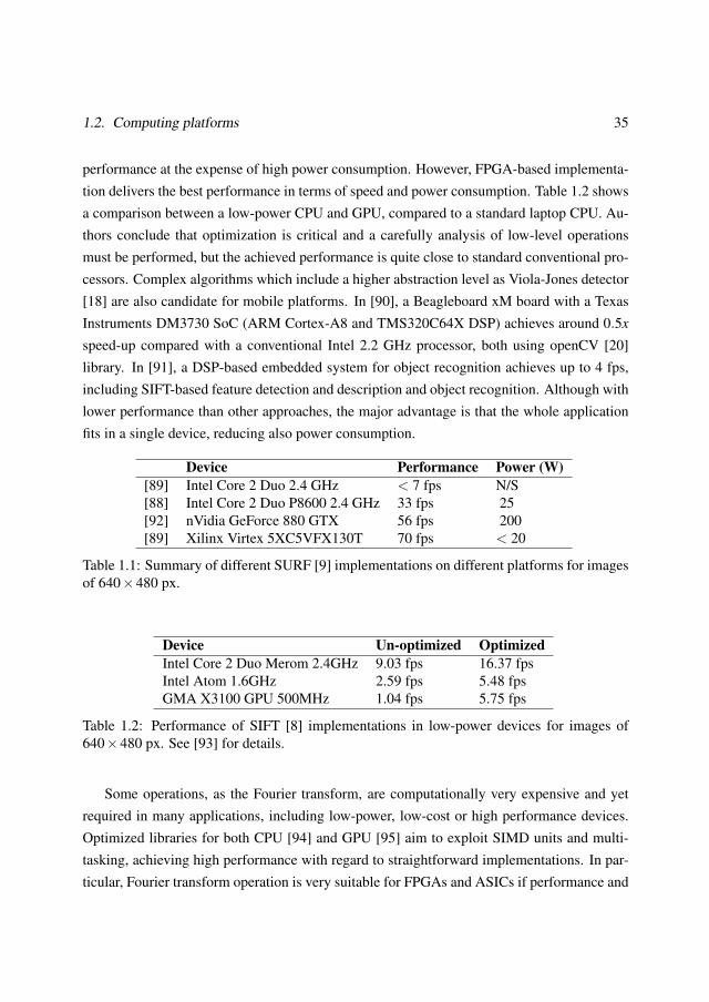
1.2. Computing platforms 35
performance at the expense of high power consumption. However, FPGA-based implementa-tion delivers the best performance in terms of speed and power consumption. Table 1.2 showsa comparison between a low-power CPU and GPU, compared to a standard laptop CPU. Au-thors conclude that optimization is critical and a carefully analysis of low-level operationsmust be performed, but the achieved performance is quite close to standard conventional pro-cessors. Complex algorithms which include a higher abstraction level as Viola-Jones detector[18] are also candidate for mobile platforms. In [90], a Beagleboard xM board with a TexasInstruments DM3730 SoC (ARM Cortex-A8 and TMS320C64X DSP) achieves around 0.5x
speed-up compared with a conventional Intel 2.2 GHz processor, both using openCV [20]library. In [91], a DSP-based embedded system for object recognition achieves up to 4 fps,including SIFT-based feature detection and description and object recognition. Although withlower performance than other approaches, the major advantage is that the whole applicationfits in a single device, reducing also power consumption.
Device Performance Power (W)[89] Intel Core 2 Duo 2.4 GHz < 7 fps N/S[88] Intel Core 2 Duo P8600 2.4 GHz 33 fps 25[92] nVidia GeForce 880 GTX 56 fps 200[89] Xilinx Virtex 5XC5VFX130T 70 fps < 20
Table 1.1: Summary of different SURF [9] implementations on different platforms for imagesof 640×480 px.
Device Un-optimized OptimizedIntel Core 2 Duo Merom 2.4GHz 9.03 fps 16.37 fpsIntel Atom 1.6GHz 2.59 fps 5.48 fpsGMA X3100 GPU 500MHz 1.04 fps 5.75 fps
Table 1.2: Performance of SIFT [8] implementations in low-power devices for images of640×480 px. See [93] for details.
Some operations, as the Fourier transform, are computationally very expensive and yetrequired in many applications, including low-power, low-cost or high performance devices.Optimized libraries for both CPU [94] and GPU [95] aim to exploit SIMD units and multi-tasking, achieving high performance with regard to straightforward implementations. In par-ticular, Fourier transform operation is very suitable for FPGAs and ASICs if performance and
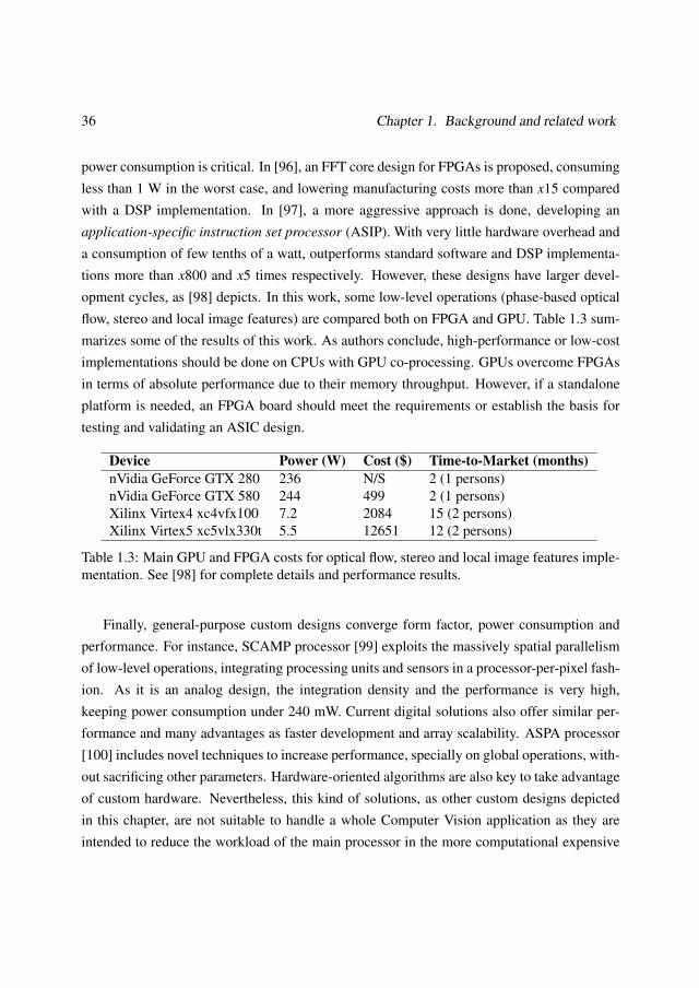
36 Chapter 1. Background and related work
power consumption is critical. In [96], an FFT core design for FPGAs is proposed, consumingless than 1 W in the worst case, and lowering manufacturing costs more than x15 comparedwith a DSP implementation. In [97], a more aggressive approach is done, developing anapplication-specific instruction set processor (ASIP). With very little hardware overhead anda consumption of few tenths of a watt, outperforms standard software and DSP implementa-tions more than x800 and x5 times respectively. However, these designs have larger devel-opment cycles, as [98] depicts. In this work, some low-level operations (phase-based opticalflow, stereo and local image features) are compared both on FPGA and GPU. Table 1.3 sum-marizes some of the results of this work. As authors conclude, high-performance or low-costimplementations should be done on CPUs with GPU co-processing. GPUs overcome FPGAsin terms of absolute performance due to their memory throughput. However, if a standaloneplatform is needed, an FPGA board should meet the requirements or establish the basis fortesting and validating an ASIC design.
Device Power (W) Cost ($) Time-to-Market (months)nVidia GeForce GTX 280 236 N/S 2 (1 persons)nVidia GeForce GTX 580 244 499 2 (1 persons)Xilinx Virtex4 xc4vfx100 7.2 2084 15 (2 persons)Xilinx Virtex5 xc5vlx330t 5.5 12651 12 (2 persons)
Table 1.3: Main GPU and FPGA costs for optical flow, stereo and local image features imple-mentation. See [98] for complete details and performance results.
Finally, general-purpose custom designs converge form factor, power consumption andperformance. For instance, SCAMP processor [99] exploits the massively spatial parallelismof low-level operations, integrating processing units and sensors in a processor-per-pixel fash-ion. As it is an analog design, the integration density and the performance is very high,keeping power consumption under 240 mW. Current digital solutions also offer similar per-formance and many advantages as faster development and array scalability. ASPA processor[100] includes novel techniques to increase performance, specially on global operations, with-out sacrificing other parameters. Hardware-oriented algorithms are also key to take advantageof custom hardware. Nevertheless, this kind of solutions, as other custom designs depictedin this chapter, are not suitable to handle a whole Computer Vision application as they areintended to reduce the workload of the main processor in the more computational expensive
1.2. Computing platforms 37
tasks, such as the low-level image processing. Approaches as [101] or [102] can completelyembed highly complex applications without compromising its efficiency.
Looking ahead
The progress of new technologies, marked by Moore’s Law allows increasingly integrationdensity. More hardware resources, with higher clock frequencies, are available for the de-signer. However, although the ultimate goal is to increase the performance, other parameterscome into play. Nowadays, one of the critical trade-offs is power consumption, directly re-lated with energy efficiency and power dissipation, some of the most decisive limitation designconstraints [103].
Power consumption is driven by two sources, dynamic and static. Static consumptionis a result of the leakage current and it refers when all inputs are held, so the circuit is notchanging state. On the contrary, the dynamic term refers to the circuit switching at a givenfrequency. This power is dominated in today CMOS circuits, being directly proportional tofrequency. This is one of the capital reasons why the semiconductor industry moves from arace for frequency to a race for parallelism. In recent years, the industry is making a big effortto increase the parallelism of most devices to keep the performance increase rate. Apart frommore arithmetic units, leading architectures integrate more systems previously contained onseparated circuits, as microcontrollers or GPUs. To achieve these results, it is still necessary toscale down the transistors. In this sense, the advent of emerging technologies like CMOS-3D[104] will permit to integrate heterogeneous functions on the same monolithic solution moreeasily. A vision-oriented ASIC could integrate the image acquisition stage to an eventualprocessor. At the same time, more conventional solutions as PCs or FPGAs would yield largeparallelism using this and other advances such as the Tri-Gate technology [105]. However,this involves problems as the increment of leakage currents, thereby increasing static powerconsumption, not negligible at all nowadays [106] [103]. In addition, new manufacturingmethods are more expensive because the yield is lower and more time is needed to compensatefor the investments. Or equivalently, it is necessary to sell more devices to continue growingat the rate set by Moore’s Law.
Conventional microprocessors are in the leading edge of evolution. There is a large marketwhich justifies large investments in R&D to meet the growing needs of consumers, especiallyby large increase in media consumption. This way, it is now possible to find low-cost mul-ticore microprocessors. It is expected that the current evolution towards a greater number of
38 Chapter 1. Background and related work
cores will be maintained but increasingly including more elements previously located on ex-ternal chips, reducing the bottleneck when communicating with off-chip elements [21]. Newparallel computing techniques need to be developed to take advantage of the available multi-threading capabilities.
PCs also benefit of GPU capabilities. GPU performance grows at a higher rate than mi-croprocessors. As they are very specialized devices, although featuring general purpose com-puting, the technical improvements in the semiconductor industry are clearly more beneficial.As discussed previously, there are available hardware resources to increase the parallelismand enhance the datapath pipeline. Leading GPUs have more than 1000 processing units andhigh speed and bandwidth memories. It is also possible to combine multi-core GPUs to worktogether, achieving a very large throughput. Still, their major disadvantage is being the powerconsumption. New architectures are taking advantage of the fixed-function hardware to im-prove area usage and power efficiency. GPU design will focus entirely on improving GPGPUcomputing [107].
DSPs are also moving to multicore architectures. As specialized microprocessors, theycan take advantage of all the improvements in the consumer market, both in hardware andsoftware improvements such as compilers or other optimization techniques. Although com-petitors are strong, DSP will continue to be used because they lead to compact circuit boards,lower power consumption and cost, if the appropiate device is selected based on the applica-tion requirements. In addition, they benefit of the extensive experience in DSP development,with shorter time-to-market thanks to the very optimized compilers and libraries. This is spe-cially relevant in embedded applications, to take advantage of the multi-core capabilities ofmodern DSPs. This way it is possible to integrate several DSP cores, each one optimized fora specific task, on a single chip [108]. Low-power devices which still keep reasonable perfor-mance are fundamental in hand-held and portable devices, where traditional microprocessorsare not suitable.
Microprocessors and GPUs tend to converge on a single chip. Apart from the obviousbenefits of integration, reducing cost, size, power consumption, the performance will increasebecause the reduction of off-chip communications. In addition, architectures as AMD Fusionintegrate in the same units 3D acceleration, parallel processing and other functions of GPUs[109]. On the other hand, mobile microprocessors are becoming more important. Thesemicroprocessors embed very low-power GPUs and auxiliary DSP units for co-processing onthe same chip [110].
1.3. Related work 39
Programmable systems, not only FPGAs, are able to get the same performance as recentpast ASICs, keeping time-to-market and non-recurring engineering costs lower compared tocustom ICs. As discussed previously, FPGAs are between software and hardware solutions.Modern FPGAs experienced a large increase in hardware resources, both in dedicated unitsand logic cells. High-level programming languages are another major reason why FPGAsare becoming increasingly competitive, specially when dealing with complex FPGAs and tomaintain and keep the designs portable [111]. Nowadays these devices can address completeSoCs, integrating memory and IO controller natively. Manufacturer roadmaps show theirinclusion in a very near future and it is expected a big leap in performance and flexibility[112].
1.3 Related work
To accurately solve the problems they face, Computer Vision algorithms become more com-plex, leading to tight requirements in order to efficiently address the computation they involve.Application-specific processors become a requirement when standard processors are not ableto meet a trade-off solution which involves performance, power consumption, form factoror cost. Although this is also applicable in many other fields, Computer Vision applicationsare particularly constrained to the processing capabilities of the hardware platforms. Theliterature is plenty of new hardware architectures which, besides taking advantage of the im-provements of the semiconductor industry, aim to increasing the processing power and theflexibility without penalizing other figures of merit.
Low-level image processing usually represents most of the workload of a Computer Visionapplication. Improving this stage will significantly increase the overall performance. Basedon this assumption, the scientific community has proposed a wide range of general-purposeand application-specific processors, auxiliary units, computing paradigms and many otherapproaches to efficiently address this low-level stage.
Traditionally, conventional microprocessors are employed for algorithm design and val-idation. The performance is constrained due to the general-purpose capabilities, being hardto reach tight requirements of certain Computer Vision applications. The inclusion of SIMDunits for intensive operations such as video compression significantly improves the perfor-mance. Several SIMD instructions sets were proposed [113] to take advantage of the inherentspatial parallelism of the operations of the low-level stage. Besides parallelizing the compu-
40 Chapter 1. Background and related work
tation, application-specific operands can also reduce the computational time. In this sense,DSPs usually outperform conventional CPUs by including specific instruction sets and ar-chitectures which take advantage of data parallelism, including a number of computationunits [114], executing several instructions at a time [48] or including specific units for addresscalculations [115]. Although DSPs are widely used, the improvements in the semiconductorindustry has made possible to greatly increase the number of computation units, leading tomore specific architectures. Processor arrays can fully take advantage of the nature of thelow-level operations. These processors implement the SIMD paradigm and offer impressiveperformance when executing native operations [84]. However, when the requirements are verytight, specially in terms of computational power and power consumption, it is necessary to usespecialized processors. Below are reviewed some relevant application-specific processors.
The Xetal processor [116] implements a massively-parallel SIMD unit to exploit dataparallelism. It includes a set of line memories which store several lines of the input image.This on-chip storage supplies data to a linear processor array greatly reducing the memorybottleneck and enabling single-cycle operand readout and result storage. It features general-purpose capabilities. The Xetal-II architecture [117] improves not only parallelism and powerconsumption but also data I/O by including dedicated input and output processors to managedata transfers and perform certain post-processing tasks. The Xetal-II prototype chip achievesup to 140 GOPS at 110 MHz, consuming 785 mW. The IMAP-CE [118] is an embeddedprocessor for video recognition. As the Xetal architecture, it implements a linear memoryarray to supply data to a highly parallel SIMD linear processor, resulting in 128 units of8 bit 4-way VLIW each, clocked at 100 MHz. An additional RISC processor controls thewhole system. In addition, it enables more flexible memory access patterns than the Xetalarchitecture, permitting to address more image processing techniques by applying paralleland systolic algorithmic techniques to the linear processor array.
The MIPA4k processor [119] is a focal plane processor array. It includes a 2-dimensionalgrid of SIMD mixed-signal processing units which share data employing local connections.It also integrates the sensing stage on each processing unit, permitting to effectively integratesensing and processing by eliminating the bottleneck between these two stages. It consists ofan 8×8 array, implemented with 0.13µm CMOS technology. The Xenon V3 processor [81]is a similar processor which employs 3D manufacturing techniques for a more efficiently in-tegration between sensors and processors. The test ASIC implementation is able to process64×64 px images using UMC 0.18µm technology. The SCAMP-3 processor, described later
1.3. Related work 41
in Section 2.5 also features similar capabilities. To achieve a high integration and very lowpower consumption, mixed-signal architectures are employed in focal plane processor arrays.This yields lower accuracy and large development times compared to digital designs. TheASPA processor [120] is a focal plane digital processor array which features synchronousand asynchronous processing capabilities. The 19× 22 test device provides a peak perfor-mance of 9.6 MOPS per processing unit when operating at 150 MHz. FLIP-Q [121] is asmart image sensor composed by a processor-per-pixel SIMD array. It is intended for scalespace and Gaussian pyramid generation and multiresolution scene representation. The analogprocessing units are arranged into a QCIF-sized array and requires very low power (17.6 mW).
MorphoSys [122] is a reconfigurable system for computation-intensive applications. Be-sides a RISC processor for control tasks, it includes reconfigurable cell array, a coarse-grainSIMD coprocessor, of 8× 8 elements. The elements of the array are arranged through a2-dimensional mesh with an enhanced connectivity between blocks of 4×4 elements. There-fore, it is an intermediate approach between linear processor such as Xetal and focal planeprocessor as ASPA. Other approaches such as [123] provide a set of arithmetic units and theability to reconfigure them into 1D and 2D arrays to match the low-level image processingoperations. This multi-SIMD architecture also includes broadcast and summation functionsand other different data access patterns to perform additional computation on-chip and reducebandwidth requirements.
Many early vision algorithms are addressed employing other computing paradigms suchas Cellular Neural Networks (CNNs) [124] or bio-inspired models [125]. The CNN compu-tation paradigm is widely used in autonomous embedded and fast response systems. TheACE16k [126] processor is a focal-plane mixed-signal processor capable of operating atframe rates higher than 1000 FPS on 128× 128px images, featuring up to 330 GOPS andvery low power consumption. It implements CNN computation as well as standard SIMDarithmetics. Although CNNs are able to fully exploit analog computing, their implementationis not straightforward. Digital CNN emulator such as Falcon [127] aims to address technicalissues and to provide more flexibility. This is a highly flexible FPGA-based architecture whichenables high performance on different CNN configurations. Bio-inspired processors as [128]achieve very high performance on tasks such as object recognition. This implementation isable to detect and recognize several objects at a time employing biologically inspired neuralnetworks and fuzzy logic circuits.
42 Chapter 1. Background and related work
All the above architectures and devices take advantage of the massively parallelism of thelow-level operations and some mid-level tasks to achieve this goal. However, to provide amore abstract representation of the scene content is considerably expensive in terms of com-putation and power consumption. Subsequent steps of Computer Vision algorithms requiremore flexible architectures, so these devices are not able to handle them. In spite of that,this shows that tackling the very first steps of most algorithms is essential for a successfulalgorithm implementation. Low-level image processing and certain mid-level tasks performefficiently when employing the SIMD paradigm. However, subsequent tasks do not alwaysfit this approach. MIMD paradigm enables a more flexible solution when the program flowbecomes more complex and eases to exploit the task-level parallelism.
Stream processing has proved to be very effective for the sake of exploiting a limitedform of parallel processing. In this mode, a series of operations are applied to a stream of
data in a predetermined order, taking advantage of the on-chip memories and restricting theparallelism. There are a variety of devices that implement this concept, some of which aredescribed below.
The Imagine stream processor [129] employs this paradigm for multimedia applications.It includes a specific programing model to directly operate with streams. This architecturepermits to scale the number of arithmetic units and internal registers to meet the computationrequirements. The prototype consists of 48 floating-point arithmetic units and it is able toachieve 18.3 GOPS while consuming 2.2 W. The arithmetic units are grouped into 8 clusters,each one connected to a register file which provides a high bandwidth and interfaces fourexternal SDRAM memories. A microcontroller manages data input and output between theregister file and each arithmetic cluster. During the execution of each kernel, all clustersexecute the same VLIW instruction (Very Large Instruction Word). This scheme permits totake advantage of the on-chip memories to store intermediate results.
The Merrimac processor [130] is a stream processor which focuses on scientific applica-tions. It includes a scalar core to perform control and to issue instructions to the stream unit.This module contains 64 64-bit floating point units, arranged in 16 clusters of 4 units each,and a register hierarchy which exploits the parallelism of the algorithm under execution. Theregisters of each cluster interfaces a larger register, which at the same time interfaces a set ofcache banks. The bandwidth of this network is higher as it gets closer to the computing units,and permits to store intermediate results without accessing the external memory. At 1 GHz,the peak performance is 128 GFLOPS. Each cluster executes the same VLIW instruction,
1.3. Related work 43
which configures the internal network according to build the desired datapath for the kernelunder execution.
The CRISP stream processor (Coarse-grained Reconfigurable Image Stream Processor) [131]aims to fill the gap between DSPs and ASICs to meet the processing requirements withoutcompromising the cost. In particular, it addresses the image processing pipeline of digitalcameras, acting as a specific processor in image preview mode and as a DSP for picture tak-ing. Employing 0.18 µm technology, it outperforms state-of-the-art DSPs by a factor largerthan 80. Its architecture is made up of a set of specific-purpose processing units includingALUs, MACs, line buffers, and window-based registers and specific-purpose units for imagedownsampling, color interpolation or pixel-based operations. An internal reconfigurable net-work permits to combine them in order to build the desired datapath for the current operation,adapting them to the algorithm requirements.
Other approaches are closer to the MIMD paradigm, allowing to execute different tasksat a time instead of focusing on data parallelism. This is the case of the MORA processor(Multimedia Oriented Reconfigurable Array) [132]. Intended for multimedia processing, itincludes a large set of simple processing elements, which exchange data employing a limitednetwork. As a difference with other approaches, it does not include a global storage but a dis-tributed storage as each processing element includes a small dedicated RAM. Processing unitprogramming and routing control is also eliminated by configuring them adequately duringthe program loading. This way, the architecture can be configured according to the algorithmdataflow.
Network-on-chip processors implement on the same chip several processing units con-nected employing a communication subsystems. It permits to efficiently interconnect general-purpose and special-purpose units to accomplish certain tasks. Architectures such as [133]for SIFT feature extraction have proven its efficiency. This processor integrates 10 SIMDprocessing units and 8 image-specialized memories. The advantages of the low overheadinterconnection between the processing units eases task level parallelism. The specializedmemories are optimized for window-based processing while the processing units perform themost basic operations for SIFT feature extraction. The processor has a peak performance of81.6 GOPS running at 200 MHz.
The previous approaches are able to exploit a reduced form of parallelism when the pro-gram dataflow becomes more complex. The increased level of abstraction of mid-level andhigh-level steps limits the efficiency of large SIMD units as it was mentioned at the begin-
44 Chapter 1. Background and related work
ning of this section. However, combining both kinds of processing, SIMD and MIMD, in thesame unit permits to address both stages employing the same processor, greatly reducing thehardware requirements [134].
The HERA processor (HEterogeneous Reconfigurable Architecture) [135] is an FPGA-based reconfigurable architecture which implements SIMD and MIMD computing paradigmssimultaneously. It consists of a set of processing elements arranged into a 2-dimensionalmesh, which fits matrix-based computation. A NEWS (north-east-west-south) network en-ables data sharing between these units. A 32-bit floating-point unit is the main module of theprocessing element, which also includes two dual-port local memories for data and programstorage. A global unit issues instructions when operating in SIMD mode. Dataflow control islimited as this architecture focuses on data-intensive computation.
The Ter@Code FPGA architecture [136] implements a 128-unit processor for multi-processing computation. It consists of several general-purpose processors for sequential pro-cessing assisted by a number of processing units which exchange data through two differentnetworks, latency- and throughput-optimized respectively. As the general-purpose proces-sors are independent, they feature MIMD computation. The processing units, which dependon a given general-purpose processor, enable SIMD computation. The number of units eachgeneral-purpose processor have depends on the particular implementation and can be config-ured according to the target application. In fact, they do not have to be identical. The 128-unitimplementation only include a general-purpose processor, which runs at 150 MHz. The pro-cessing units include an ALU and two RAM slices for private storage and data exchangingthrough the network. The peak performance is 19.2 GOPS.
The IMAPCAR-XC processor [137] is a reconfigurable SIMD/MIMD architecture forembedded vision systems. It consists of 128 SIMD units which can be configured to 32-MIMD independent processing units, each one containing independent data and instructionstorage besides a floating-point unit. A central RISC core executes the sequential part of thealgorithm, performs address computation and executes control tasks. The processing elementsshare data employing three different networks. One of them interfaces the external memoryand permits data I/O. Another one connects adjacent processing elements for fast data ex-change. The last one provides an extensive network along the 8 processing elements whichform a cluster. The architecture is based on a linear processor array but permits flexible dataaccess patterns not to compromise performance.
1.4. Summary 45
Low-level image processing usually consumes much of the computation time. However,subsequent tasks are also time-consuming and custom accelerators are often a requirement.In this sense, hybrid architectures permit to face both processing stages, reducing hardwarerequirements and taking advantage of the interaction between these stages to improve perfor-mance, instead of considering them independently.
1.4 Summary
The large variety of Computer Vision applications makes difficult to classify them into tightcategories. As a result, it is extremely challenging to design a unique hardware architecturewhich handles efficiently all processing stages of any Computer Vision algorithm. In the lit-erature there are available several studies where different platforms are tested under the sameconditions [138, 139, 140, 52]. They show that to tune-up is key for performance and thatnew parallel computing techniques are a requirement to exploit parallel devices. In addition,the increase of the sales and the appearance of emerging markets make investment in newhardware platforms a necessity.
The most accessible platform is a Personal Computer equipped with a GP-capable GPU.Either as test or final platform, it cuts down development time and costs. GPUs give enoughperformance for most intensive tasks, while by using the CPU multimedia extensions it ispossible to meet the requirements in the other stages. In addition, they include all necessaryelements for user IO, communication, storage and information display. The availability ofmodels is large enough to select the adequate platform according to the application trade-offs. When CPU performance is not adequate, DSPs are a serious alternative. In addition,it becomes almost mandatory when dealing with embedded devices without compromisingperformance, where power consumption and form factor are very restrictive. They are widelyused for prototyping custom ICs but FPGA-based applications have their own niche. Inte-gration and high flexibility besides a large number of available IP Cores allow to drop NREcosts. Although all devices described in this chapter are ASICs, they were not conceived foran unique application. To lower costs, the manufacturer expands their range of applicationalthough it is possible to find families specialized in specific tasks. But there are availabledevices very specific for critical tasks, where the requirements are very tight and any other de-vice does not comply with them. Flexibility is complete and there is not restriction to employcutting-edge technologies which are not available in commercial devices until a near future.
46 Chapter 1. Background and related work
Almost all Computer Vision applications need to face all processing stages in a lesser ora greater degree. Often, this leads to implement efficient mechanisms to tackle massivelyspatial parallelism, mixed spatial and temporal parallelism and sequential processing. Eachstage matches with a level of processing so all mechanisms have to be implemented in mostapplications. Low-level stages benefit of massively parallelism with simple data distributionsystems as operations. When the data abstraction level grows, during mid-level tasks, moreinformation about the problem is required by the algorithms, increasing their complexity. Thisleads to complex architectures, where information distribution and sharing makes it difficult toexploit spatial parallelism, although it is usually present. Task-parallel architectures are able toexploit better their characteristics. Low and mid-level processing stages can be implementedin pure hardware solutions because they often implement kernel operations. However, high-level is closer to software and designers can take advantage of this to build complex systemseasier by using general purpose processors. In addition, the device which performs the imageprocessing related tasks needs to communicate or to control other devices. This is not strictlyrelated with the Computer Vision domain but it is clearly a requirement in the final solution. Inthis case, the use of a general purpose processor is beneficial because it allows easier controland it increases the flexibility of the whole system.
Although it is almost impossible to develop a system able to run all operations in an opti-mal way due to the rich nature of the Computer Vision applications, it is desirable to providethe capability to perform any operation. The design must be scalable to adapt it to the specificneeds of each application. This way, a product ranging from low to high-end devices can beeasily built. The internal architecture should be also modular, so that from a basic outline morefeatures could be added without dramatic changes. In general, a high-end microprocessor isa requirement to manage complex operations and communications between the system andthe external components of the complete system. A number of auxiliary units able to handleboth SIMD and MIMD computing paradigms would tackle the most expensive computation.In particular, a large SIMD unit will greatly increase the performance by addressing the firststeps of most algorithms, specially in the low-level stage. Embedded high-speed memorycontrollers are also key to reduce the data-access bottleneck. All these elements, together, areable to face efficiently most of the situations described throughout this chapter.
CHAPTER 2
ADDRESSING THE LOW-LEVEL STAGE
As discussed previously in Chapter 1, low-level and certain mid-level Computer Vision oper-ations are characterized for being repetitive and simple and applied over a large set of data.Therefore, these operations usually represent the highest percentage of workload for a proces-sor running image processing tasks. In particular, the overall performance of the applicationwill increase significantly only optimizing the low-level steps.
An efficient Computer Vision processor has to deal efficiently with a wide range of oper-ations, data dependencies and program flows. Its hardware must be flexible enough to facethe different algorithms with an adequate performance without wasting hardware resources.Regarding to early vision or low-level, the operations do not usually require large word sizes,so we can take advantage of this to increase the density of integration and thus to enhancethe parallelism as it is key for performance. However, a large amount of processing units isnot effective without a flexible interconnection to exchange data between them. The designmust also be modular, scalable and easy to adapt to the needs of the different applications.This way, memory or word sizes as well as the mathematical operations available on the corecomputing units have to be adjustable to obtain a flexible and capable processor for the mostcomputational expensive tasks.
This chapter introduces an architecture for low-level image processing, focusing on the in-herent massively spatial-parallelism of the operations to efficiently address this computation.The low-level image processor, conceived as a co-processor of a conventional general-purposemicroprocessor, was designed keeping in mind the conclusions drawn in Chapter 1. Finally,a comparison between this accelerator and other related approaches is accomplished to deter-
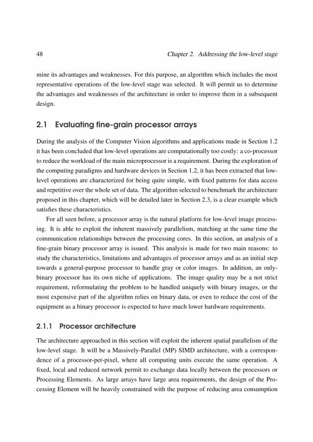
48 Chapter 2. Addressing the low-level stage
mine its advantages and weaknesses. For this purpose, an algorithm which includes the mostrepresentative operations of the low-level stage was selected. It will permit us to determinethe advantages and weaknesses of the architecture in order to improve them in a subsequentdesign.
2.1 Evaluating fine-grain processor arrays
During the analysis of the Computer Vision algorithms and applications made in Section 1.2it has been concluded that low-level operations are computationally too costly: a co-processorto reduce the workload of the main microprocessor is a requirement. During the exploration ofthe computing paradigms and hardware devices in Section 1.2, it has been extracted that low-level operations are characterized for being quite simple, with fixed patterns for data accessand repetitive over the whole set of data. The algorithm selected to benchmark the architectureproposed in this chapter, which will be detailed later in Section 2.3, is a clear example whichsatisfies these characteristics.
For all seen before, a processor array is the natural platform for low-level image process-ing. It is able to exploit the inherent massively parallelism, matching at the same time thecommunication relationships between the processing cores. In this section, an analysis of afine-grain binary processor array is issued. This analysis is made for two main reasons: tostudy the characteristics, limitations and advantages of processor arrays and as an initial steptowards a general-purpose processor to handle gray or color images. In addition, an only-binary processor has its own niche of applications. The image quality may be a not strictrequirement, reformulating the problem to be handled uniquely with binary images, or themost expensive part of the algorithm relies on binary data, or even to reduce the cost of theequipment as a binary processor is expected to have much lower hardware requirements.
2.1.1 Processor architecture
The architecture approached in this section will exploit the inherent spatial parallelism of thelow-level stage. It will be a Massively-Parallel (MP) SIMD architecture, with a correspon-dence of a processor-per-pixel, where all computing units execute the same operation. Afixed, local and reduced network permit to exchange data locally between the processors orProcessing Elements. As large arrays have large area requirements, the design of the Pro-cessing Element will be heavily constrained with the purpose of reducing area consumption
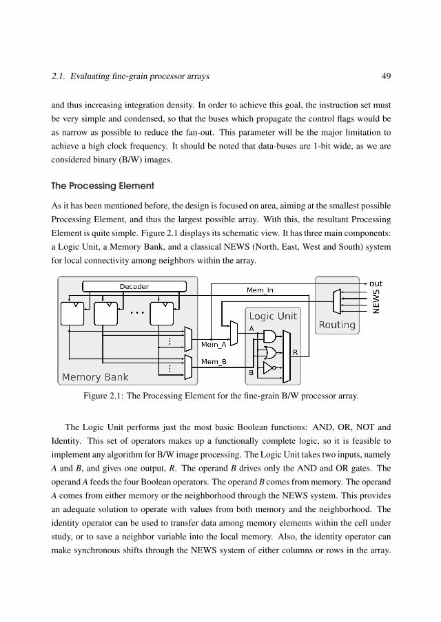
2.1. Evaluating fine-grain processor arrays 49
and thus increasing integration density. In order to achieve this goal, the instruction set mustbe very simple and condensed, so that the buses which propagate the control flags would beas narrow as possible to reduce the fan-out. This parameter will be the major limitation toachieve a high clock frequency. It should be noted that data-buses are 1-bit wide, as we areconsidered binary (B/W) images.
The Processing Element
As it has been mentioned before, the design is focused on area, aiming at the smallest possibleProcessing Element, and thus the largest possible array. With this, the resultant ProcessingElement is quite simple. Figure 2.1 displays its schematic view. It has three main components:a Logic Unit, a Memory Bank, and a classical NEWS (North, East, West and South) systemfor local connectivity among neighbors within the array.
Figure 2.1: The Processing Element for the fine-grain B/W processor array.
The Logic Unit performs just the most basic Boolean functions: AND, OR, NOT andIdentity. This set of operators makes up a functionally complete logic, so it is feasible toimplement any algorithm for B/W image processing. The Logic Unit takes two inputs, namelyA and B, and gives one output, R. The operand B drives only the AND and OR gates. Theoperand A feeds the four Boolean operators. The operand B comes from memory. The operandA comes from either memory or the neighborhood through the NEWS system. This providesan adequate solution to operate with values from both memory and the neighborhood. Theidentity operator can be used to transfer data among memory elements within the cell understudy, or to save a neighbor variable into the local memory. Also, the identity operator canmake synchronous shifts through the NEWS system of either columns or rows in the array.
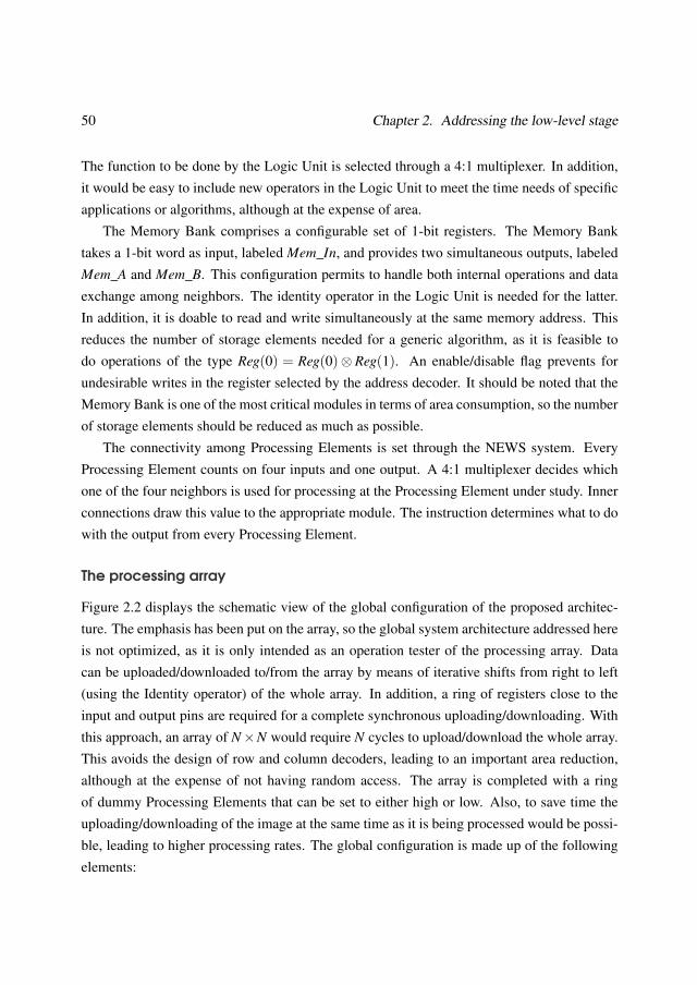
50 Chapter 2. Addressing the low-level stage
The function to be done by the Logic Unit is selected through a 4:1 multiplexer. In addition,it would be easy to include new operators in the Logic Unit to meet the time needs of specificapplications or algorithms, although at the expense of area.
The Memory Bank comprises a configurable set of 1-bit registers. The Memory Banktakes a 1-bit word as input, labeled Mem_In, and provides two simultaneous outputs, labeledMem_A and Mem_B. This configuration permits to handle both internal operations and dataexchange among neighbors. The identity operator in the Logic Unit is needed for the latter.In addition, it is doable to read and write simultaneously at the same memory address. Thisreduces the number of storage elements needed for a generic algorithm, as it is feasible todo operations of the type Reg(0) = Reg(0)⊗ Reg(1). An enable/disable flag prevents forundesirable writes in the register selected by the address decoder. It should be noted that theMemory Bank is one of the most critical modules in terms of area consumption, so the numberof storage elements should be reduced as much as possible.
The connectivity among Processing Elements is set through the NEWS system. EveryProcessing Element counts on four inputs and one output. A 4:1 multiplexer decides whichone of the four neighbors is used for processing at the Processing Element under study. Innerconnections draw this value to the appropriate module. The instruction determines what to dowith the output from every Processing Element.
The processing array
Figure 2.2 displays the schematic view of the global configuration of the proposed architec-ture. The emphasis has been put on the array, so the global system architecture addressed hereis not optimized, as it is only intended as an operation tester of the processing array. Datacan be uploaded/downloaded to/from the array by means of iterative shifts from right to left(using the Identity operator) of the whole array. In addition, a ring of registers close to theinput and output pins are required for a complete synchronous uploading/downloading. Withthis approach, an array of N×N would require N cycles to upload/download the whole array.This avoids the design of row and column decoders, leading to an important area reduction,although at the expense of not having random access. The array is completed with a ringof dummy Processing Elements that can be set to either high or low. Also, to save time theuploading/downloading of the image at the same time as it is being processed would be possi-ble, leading to higher processing rates. The global configuration is made up of the followingelements:
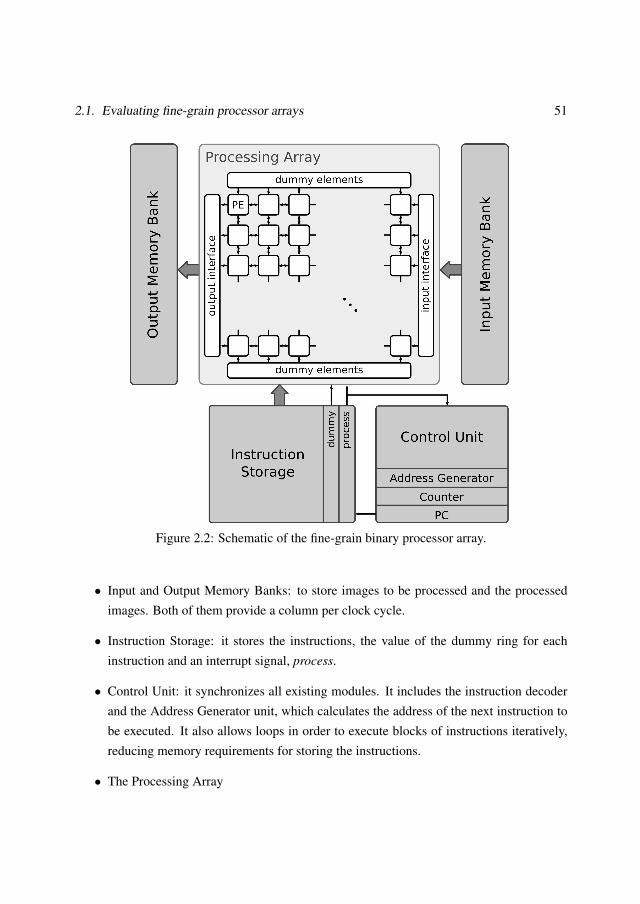
2.1. Evaluating fine-grain processor arrays 51
Figure 2.2: Schematic of the fine-grain binary processor array.
• Input and Output Memory Banks: to store images to be processed and the processedimages. Both of them provide a column per clock cycle.
• Instruction Storage: it stores the instructions, the value of the dummy ring for eachinstruction and an interrupt signal, process.
• Control Unit: it synchronizes all existing modules. It includes the instruction decoderand the Address Generator unit, which calculates the address of the next instruction tobe executed. It also allows loops in order to execute blocks of instructions iteratively,reducing memory requirements for storing the instructions.
• The Processing Array
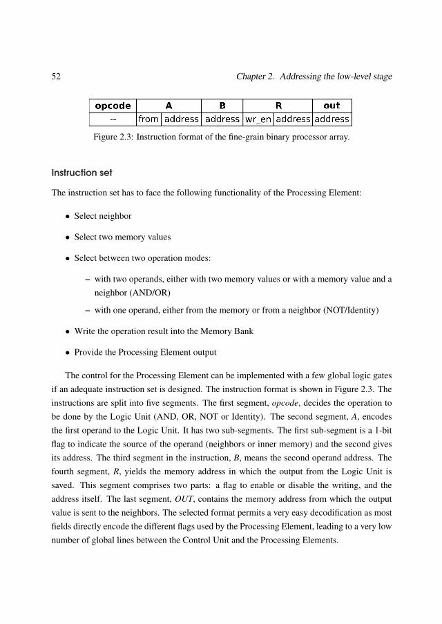
52 Chapter 2. Addressing the low-level stage
Figure 2.3: Instruction format of the fine-grain binary processor array.
Instruction set
The instruction set has to face the following functionality of the Processing Element:
• Select neighbor
• Select two memory values
• Select between two operation modes:
– with two operands, either with two memory values or with a memory value and aneighbor (AND/OR)
– with one operand, either from the memory or from a neighbor (NOT/Identity)
• Write the operation result into the Memory Bank
• Provide the Processing Element output
The control for the Processing Element can be implemented with a few global logic gatesif an adequate instruction set is designed. The instruction format is shown in Figure 2.3. Theinstructions are split into five segments. The first segment, opcode, decides the operation tobe done by the Logic Unit (AND, OR, NOT or Identity). The second segment, A, encodesthe first operand to the Logic Unit. It has two sub-segments. The first sub-segment is a 1-bitflag to indicate the source of the operand (neighbors or inner memory) and the second givesits address. The third segment in the instruction, B, means the second operand address. Thefourth segment, R, yields the memory address in which the output from the Logic Unit issaved. This segment comprises two parts: a flag to enable or disable the writing, and theaddress itself. The last segment, OUT, contains the memory address from which the outputvalue is sent to the neighbors. The selected format permits a very easy decodification as mostfields directly encode the different flags used by the Processing Element, leading to a very lownumber of global lines between the Control Unit and the Processing Elements.
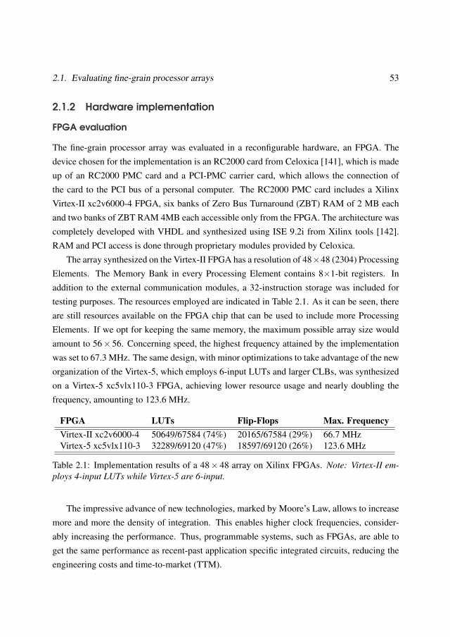
2.1. Evaluating fine-grain processor arrays 53
2.1.2 Hardware implementation
FPGA evaluation
The fine-grain processor array was evaluated in a reconfigurable hardware, an FPGA. Thedevice chosen for the implementation is an RC2000 card from Celoxica [141], which is madeup of an RC2000 PMC card and a PCI-PMC carrier card, which allows the connection ofthe card to the PCI bus of a personal computer. The RC2000 PMC card includes a XilinxVirtex-II xc2v6000-4 FPGA, six banks of Zero Bus Turnaround (ZBT) RAM of 2 MB eachand two banks of ZBT RAM 4MB each accessible only from the FPGA. The architecture wascompletely developed with VHDL and synthesized using ISE 9.2i from Xilinx tools [142].RAM and PCI access is done through proprietary modules provided by Celoxica.
The array synthesized on the Virtex-II FPGA has a resolution of 48×48 (2304) ProcessingElements. The Memory Bank in every Processing Element contains 8×1-bit registers. Inaddition to the external communication modules, a 32-instruction storage was included fortesting purposes. The resources employed are indicated in Table 2.1. As it can be seen, thereare still resources available on the FPGA chip that can be used to include more ProcessingElements. If we opt for keeping the same memory, the maximum possible array size wouldamount to 56×56. Concerning speed, the highest frequency attained by the implementationwas set to 67.3 MHz. The same design, with minor optimizations to take advantage of the neworganization of the Virtex-5, which employs 6-input LUTs and larger CLBs, was synthesizedon a Virtex-5 xc5vlx110-3 FPGA, achieving lower resource usage and nearly doubling thefrequency, amounting to 123.6 MHz.
FPGA LUTs Flip-Flops Max. FrequencyVirtex-II xc2v6000-4 50649/67584 (74%) 20165/67584 (29%) 66.7 MHzVirtex-5 xc5vlx110-3 32289/69120 (47%) 18597/69120 (26%) 123.6 MHz
Table 2.1: Implementation results of a 48× 48 array on Xilinx FPGAs. Note: Virtex-II em-ploys 4-input LUTs while Virtex-5 are 6-input.
The impressive advance of new technologies, marked by Moore’s Law, allows to increasemore and more the density of integration. This enables higher clock frequencies, consider-ably increasing the performance. Thus, programmable systems, such as FPGAs, are able toget the same performance as recent-past application specific integrated circuits, reducing theengineering costs and time-to-market (TTM).
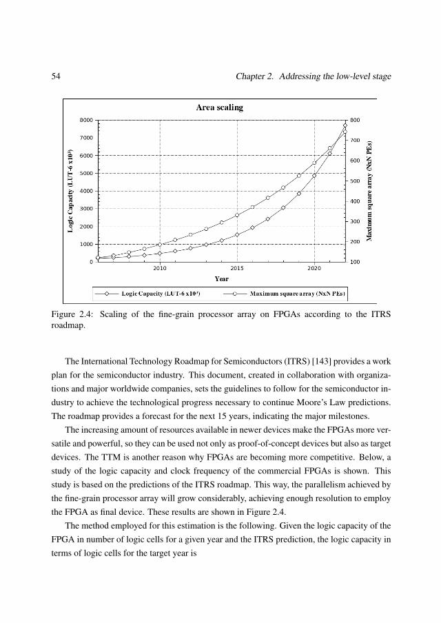
54 Chapter 2. Addressing the low-level stage
Figure 2.4: Scaling of the fine-grain processor array on FPGAs according to the ITRSroadmap.
The International Technology Roadmap for Semiconductors (ITRS) [143] provides a workplan for the semiconductor industry. This document, created in collaboration with organiza-tions and major worldwide companies, sets the guidelines to follow for the semiconductor in-dustry to achieve the technological progress necessary to continue Moore’s Law predictions.The roadmap provides a forecast for the next 15 years, indicating the major milestones.
The increasing amount of resources available in newer devices make the FPGAs more ver-satile and powerful, so they can be used not only as proof-of-concept devices but also as targetdevices. The TTM is another reason why FPGAs are becoming more competitive. Below, astudy of the logic capacity and clock frequency of the commercial FPGAs is shown. Thisstudy is based on the predictions of the ITRS roadmap. This way, the parallelism achieved bythe fine-grain processor array will grow considerably, achieving enough resolution to employthe FPGA as final device. These results are shown in Figure 2.4.
The method employed for this estimation is the following. Given the logic capacity of theFPGA in number of logic cells for a given year and the ITRS prediction, the logic capacity interms of logic cells for the target year is
2.1. Evaluating fine-grain processor arrays 55
CapacityB =CapacityA ·DensityB
DensityA· Die_SizeB
Die_SizeA
where A and B subscripts refer to the known and the target years. The parameter Die_Size
refers to the chip size, although the ITRS prediction indicates that the chip size will not changein the next years. In the Density parameter, the measure of the number of million of transistorsper square centimeter also includes the effects of the routing and the different size of N andP MOS transistors, as well as other parameters which limit the density of integration. Thisequation is only valid if the internal architecture of the FPGA does not change. This study isbased on [144], updating its results.
The FPGA employed as a reference is a Xilinx Virtex-5 xc5vlx330. It includes more than50000 logic cells (207360 6-input LUTs) and employs 65nm technology. This family replacedthe 4-input LUT internal architecture for a new 6-input LUT, and a different packaging of thelogic cells, enabling more density of integration. Figure 2.4 shows how this family scalesaccording to the ITRS predictions. These results have to be considered as an upper boundaryof the capacity as other elements of the FPGA are not considered. Embedded units suchas multipliers of Block RAMs are becoming more important and new designs should takeadvantage of their inclusions. However, the accuracy of the study is enough for our purposeas the fine-grain processor does not make use of none of the embedded slices of the FPGA.
Under this new architecture, each Processing Element of the fine-grain processor arrayemploys 8 Flip-Flops and 14 6-LUTs, with the same configuration of the array indicated in thissection. Therefore, the limiting factor is the number of LUTs available in the FPGA. Resultsshow that employing the technology of 2009, a QCIF (144×176px) is feasible, while around2013 and 2019, it would be possible to manipulate images of 256× 256px and 512× 512pxrespectively, without splitting them into sub-windows.
2.1.3 Algorithm evaluation
By the nature of the instruction set, a Boolean equation that means how each PE changesits value according to a given neighborhood must be found. This equation can be obtainedin various ways: from the original image and the expected image, observing the differencesbetween them; translating the effects of a mask or a filter; directly designing the Booleanequation, etc. Next, a selection of algorithms to test and show as the proposed system worksis listed. The examples were extracted from the Cellular Wave Computing Library (CWCL)[145], which collects the most used templates in image processing on Cellular Neural Net-
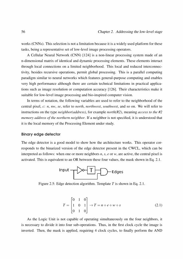
56 Chapter 2. Addressing the low-level stage
works (CNNs). This selection is not a limitation because it is a widely used platform for thesetasks, being a representative set of low-level image processing operators.
A Cellular Neural Network (CNN) [124] is a non-linear processing system made of ann-dimensional matrix of identical and dynamic processing elements. These elements interactthrough local connections on a limited neighborhood. This local and reduced interconnec-tivity, besides recursive operations, permit global processing. This is a parallel computingparadigm similar to neural networks which features general-purpose computing and enablesvery high performance although there are certain technical limitations in practical applica-tions such as image resolution or computation accuracy [126]. Their characteristics make itsuitable for low-level image processing and bio-inspired computer vision.
In terms of notation, the following variables are used to refer to the neighborhood of thecentral pixel, c: n, nw, se, refer to north, northwest, southwest, and so on. We will refer toinstructions on the type neighbor(address), for example north(R2), meaning access to the #2
memory address of the northern neighbor. If a neighbor is not specified, it is understood thatit is the local memory of the Processing Element under study.
Binary edge detector
The edge detector is a good model to show how the architecture works. This operator cor-responds to the binarized version of the edge detector present in the CWCL, which can beinterpreted as follows: when one or more neighbors n, s, e or w, are active, the central pixel isactivated. This is equivalent to an OR between these four values, the mask shown in Eq. 2.1.
Figure 2.5: Edge detection algorithm. Template T is shown in Eq. 2.1.
T =
0 1 01 0 10 1 0
→ T = n+ e+w+ s (2.1)
As the Logic Unit is not capable of operating simultaneously on the four neighbors, itis necessary to divide it into four sub-operations. Thus, in the first clock cycle the image isinverted. Then, the mask is applied, requiring 4 clock cycles, to finally perform the AND
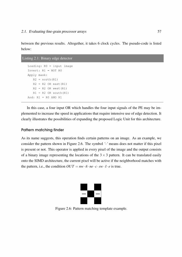
2.1. Evaluating fine-grain processor arrays 57
between the previous results. Altogether, it takes 6 clock cycles. The pseudo-code is listedbelow:
Listing 2.1: Binary edge detector
Loading: R0 = input image
Invert: R1 = NOT R0
Apply mask:
R2 = north(R1)
R2 = R2 OR east(R1)
R2 = R2 OR west(R1)
R1 = R2 OR south(R1)
And: R1 = R0 AND R1
In this case, a four input OR which handles the four input signals of the PE may be im-plemented to increase the speed in applications that require intensive use of edge detection. Itclearly illustrates the possibilities of expanding the proposed Logic Unit for this architecture.
Pattern matching finder
As its name suggests, this operation finds certain patterns on an image. As an example, weconsider the pattern shown in Figure 2.6. The symbol ’-’ means does not matter if this pixelis present or not. This operator is applied in every pixel of the image and the output consistsof a binary image representing the locations of the 3× 3 pattern. It can be translated easilyonto the SIMD architecture, the current pixel will be active if the neighborhood matches withthe pattern, i.e., the condition OUT = nw · n̄ ·ne · c · sw · s̄ · e is true.
Figure 2.6: Pattern matching template example.
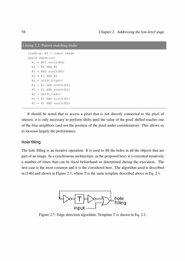
58 Chapter 2. Addressing the low-level stage
Listing 2.2: Pattern matching finder
Loading: R0 = input image
Apply equation:
R1 = NOT north(R0)
R1 = R0 AND R1
R2 = AND south(R0)
R1 = R1 AND R2
R2 = shift(right)
R1 = R1 AND north(R2)
R1 = R1 AND south(R2)
R2 = shift(left)
R1 = R1 AND north(R2)
R1 = R1 AND south(R2)
It should be noted that to access a pixel that is not directly connected to the pixel ofinterest, it is only necessary to perform shifts until the value of the pixel shifted reaches oneof the four neighbors (and not the position of the pixel under consideration). This allows usto increase largely the performance.
Hole filling
The hole filling is an iterative operation. It is used to fill the holes in all the objects that arepart of an image. In a synchronous architecture, as the proposed here, it is executed iterativelya number of times that can be fixed beforehand or determined during the execution. Thefirst case is the most common and it is the considered here. The algorithm used is describedin [146] and shown in Figure 2.7, where T is the same template described above in Eq. 2.1.
Figure 2.7: Edge detection algorithm. Template T is shown in Eq. 2.1.
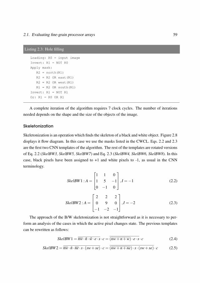
2.1. Evaluating fine-grain processor arrays 59
Listing 2.3: Hole filling
Loading: R0 = input image
Invert: R1 = NOT R0
Apply mask:
R2 = north(R1)
R2 = R2 OR east(R1)
R2 = R2 OR west(R1)
R1 = R2 OR south(R1)
Invert: R1 = NOT R1
Or: R1 = R0 OR R1
A complete iteration of the algorithm requires 7 clock cycles. The number of iterationsneeded depends on the shape and the size of the objects of the image.
Skeletonization
Skeletonization is an operation which finds the skeleton of a black and white object. Figure 2.8displays it flow diagram. In this case we use the masks listed in the CWCL. Eqs. 2.2 and 2.3are the first two CNN templates of the algorithm. The rest of the templates are rotated versionsof Eq. 2.2 (SkelBW3, SkelBW5, SkelBW7) and Eq. 2.3 (SkelBW4, SkelBW6, SkelBW8). In thiscase, black pixels have been assigned to +1 and white pixels to -1, as usual in the CNNterminology.
SkelBW1 : A =
1 1 01 5 −10 −1 0
, I =−1 (2.2)
SkelBW2 : A =
2 2 20 9 0−1 −2 −1
, I =−2 (2.3)
The approach of the B/W skeletonization is not straightforward as it is necessary to per-form an analysis of the cases in which the active pixel changes state. The previous templatescan be rewritten as follows:
SkelBW1 = nw · n̄ · w̄ · e · s · c = (nw+n+w) · e · s · c (2.4)
SkelBW2 = nw · n̄ ·ne · s · (sw+ se) · c = (nw+n+ne) · s · (sw+ se) · c (2.5)
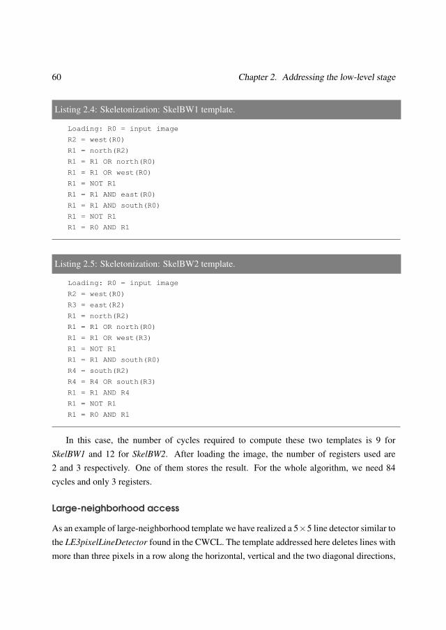
60 Chapter 2. Addressing the low-level stage
Listing 2.4: Skeletonization: SkelBW1 template.
Loading: R0 = input image
R2 = west(R0)
R1 = north(R2)
R1 = R1 OR north(R0)
R1 = R1 OR west(R0)
R1 = NOT R1
R1 = R1 AND east(R0)
R1 = R1 AND south(R0)
R1 = NOT R1
R1 = R0 AND R1
Listing 2.5: Skeletonization: SkelBW2 template.
Loading: R0 = input image
R2 = west(R0)
R3 = east(R2)
R1 = north(R2)
R1 = R1 OR north(R0)
R1 = R1 OR west(R3)
R1 = NOT R1
R1 = R1 AND south(R0)
R4 = south(R2)
R4 = R4 OR south(R3)
R1 = R1 AND R4
R1 = NOT R1
R1 = R0 AND R1
In this case, the number of cycles required to compute these two templates is 9 forSkelBW1 and 12 for SkelBW2. After loading the image, the number of registers used are2 and 3 respectively. One of them stores the result. For the whole algorithm, we need 84cycles and only 3 registers.
Large-neighborhood access
As an example of large-neighborhood template we have realized a 5×5 line detector similar tothe LE3pixelLineDetector found in the CWCL. The template addressed here deletes lines withmore than three pixels in a row along the horizontal, vertical and the two diagonal directions,
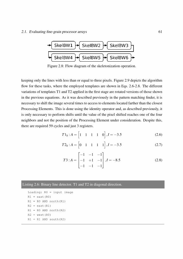
2.1. Evaluating fine-grain processor arrays 61
Figure 2.8: Flow diagram of the skeletonization operation.
keeping only the lines with less than or equal to three pixels. Figure 2.9 depicts the algorithmflow for these tasks, where the employed templates are shown in Eqs. 2.6-2.8. The differentvariations of templates T1 and T2 applied in the first stage are rotated versions of those shownin the previous equations. As it was described previously in the pattern matching finder, it isnecessary to shift the image several times to access to elements located farther than the closestProcessing Elements. This is done using the identity operator and, as described previously, itis only necessary to perform shifts until the value of the pixel shifted reaches one of the fourneighbors and not the position of the Processing Element under consideration. Despite this,there are required 59 cycles and just 3 registers.
T 1h : A =[1 1 1 1 0
], I =−3.5 (2.6)
T 2h : A =[0 1 1 1 1
], I =−3.5 (2.7)
T 3 : A =
−1 −1 −1−1 +1 −1−1 −1 −1
, I =−8.5 (2.8)
Listing 2.6: Binary line detector. T1 and T2 in diagonal direction.
Loading: R0 = input image
R1 = east(R0)
R1 = R0 AND north(R1)
R2 = east(R1)
R1 = R0 AND north(R2)
R2 = west(R0)
R1 = R1 AND south(R2)
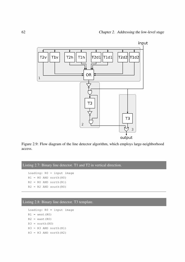
62 Chapter 2. Addressing the low-level stage
Figure 2.9: Flow diagram of the line detector algorithm, which employs large-neighborhoodaccess.
Listing 2.7: Binary line detector. T1 and T2 in vertical direction.
Loading: R0 = input image
R1 = R0 AND north(R0)
R2 = R0 AND north(R1)
R2 = R2 AND south(R0)
Listing 2.8: Binary line detector. T3 template.
Loading: R0 = input image
R1 = west(R0)
R2 = east(R0)
R3 = north(R0)
R3 = R3 AND north(R1)
R3 = R3 AND north(R2)
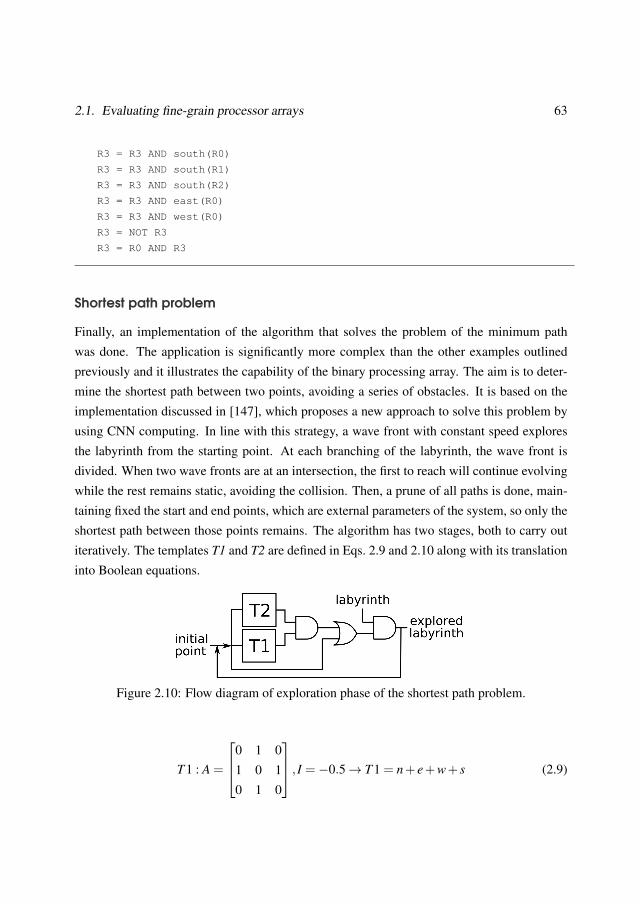
2.1. Evaluating fine-grain processor arrays 63
R3 = R3 AND south(R0)
R3 = R3 AND south(R1)
R3 = R3 AND south(R2)
R3 = R3 AND east(R0)
R3 = R3 AND west(R0)
R3 = NOT R3
R3 = R0 AND R3
Shortest path problem
Finally, an implementation of the algorithm that solves the problem of the minimum pathwas done. The application is significantly more complex than the other examples outlinedpreviously and it illustrates the capability of the binary processing array. The aim is to deter-mine the shortest path between two points, avoiding a series of obstacles. It is based on theimplementation discussed in [147], which proposes a new approach to solve this problem byusing CNN computing. In line with this strategy, a wave front with constant speed exploresthe labyrinth from the starting point. At each branching of the labyrinth, the wave front isdivided. When two wave fronts are at an intersection, the first to reach will continue evolvingwhile the rest remains static, avoiding the collision. Then, a prune of all paths is done, main-taining fixed the start and end points, which are external parameters of the system, so only theshortest path between those points remains. The algorithm has two stages, both to carry outiteratively. The templates T1 and T2 are defined in Eqs. 2.9 and 2.10 along with its translationinto Boolean equations.
Figure 2.10: Flow diagram of exploration phase of the shortest path problem.
T 1 : A =
0 1 01 0 10 1 0
, I =−0.5→ T 1 = n+ e+w+ s (2.9)
64 Chapter 2. Addressing the low-level stage
T 2 : A =
0 −1 0−1 0 −10 −1 0
, I =−1→ T 2 = n · (w+ s+ e)+ e · (w+ s)+w · s (2.10)
The second stage, the pruning, is done executing iteratively T3, defined in Eq. 2.11. Thistemplate is equivalent to an AND between the labyrinth and explored the result of invert theapplication of T2 on the explored labyrinth, so the above equations will be used again.
T 3 : A =
0 1 01 3 10 1 0
, I =−2 (2.11)
During the exploration phase, T1 requires 4 clock cycles, T2 9 cycles and the additionallogic operations, 3 cycles. All in all, each iteration requires 16 cycles. The pruning phase isexecuted in 9 cycles, 8 for T2 and one for the additional operations. The number of necessaryiterations for each stage depends on the labyrinth. Figure 2.11 shows the different stages ofeach phase on a test labyrinth.
Listing 2.9: Shortest Path Problem. Exploration phase.
Loading: R0 = input image
Loading: R1 = start point
Apply T1
R2 = north(R1)
R2 = R2 OR east(R1)
R2 = R2 OR west(R1)
R1 = R2 OR south(R1)
Apply T2
R3 = west(R1)
R4 = R3 AND south(R1)
R5 = R3 OR south(R1)
R3 = R5 AND east(R1)
R3 = R3 OR R4
R4 = R5 OR east(R1)
R4 = R4 AND north(R1)
R3 = R3 OR R4
R3 = NOT R3
Others
R2 = R2 AND R3
R2 = R2 OR R1
2.1. Evaluating fine-grain processor arrays 65
R1 = R0 AND R2
Listing 2.10: Shortest Path Problem. Pruning phase.
Loading: R7 = Destination point
Loading: R1 = R1 OR R7
Apply T2
R3 = west(R1)
R4 = R3 AND south(R1)
R5 = R3 OR south(R1)
R3 = R5 AND east(R1)
R3 = R3 OR R4
R4 = R5 OR east(R1)
R4 = R4 AND north(R1)
R3 = R3 OR R4
R3 = NOT R3
Others
R3 = NOT R3
R1 = R1 AND R3
Summary
Table 2.2 gives a summary of processing times for each algorithm, considering only oneiteration. The maximum working frequency for the Virtex-II FPGA xc2v6000 is 67.3 MHz.It also includes the number of required registers per Processing Element for its execution,counting the one used to store the input image, which does not change during processing,although this would not be necessary in all cases. For the iterative algorithms, Table 2.3 showsthe total execution times. The test images have the same size as the matrix, i.e., 48×48 pixels.We have to remark that each instruction only takes one clock cycle to be executed.
2.1.4 Discussion
After the study of fine-grain processor arrays, we can extract some major conclusions. Asthe processor matches the operations of the low-level stage and as data exchange betweencomputing cores is done at the same time as computation, overlapping both processes, thethroughput is very high and the peak performance is easily achieved. In addition, the perfor-mance is independent of the size of the image. However, fine-grain processor arrays feature
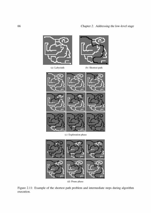
66 Chapter 2. Addressing the low-level stage
(a) Labyrinth (b) Shortest path
(c) Exploration phase
(d) Prune phase
Figure 2.11: Example of the shortest path problem and intermediate steps during algorithmexecution.
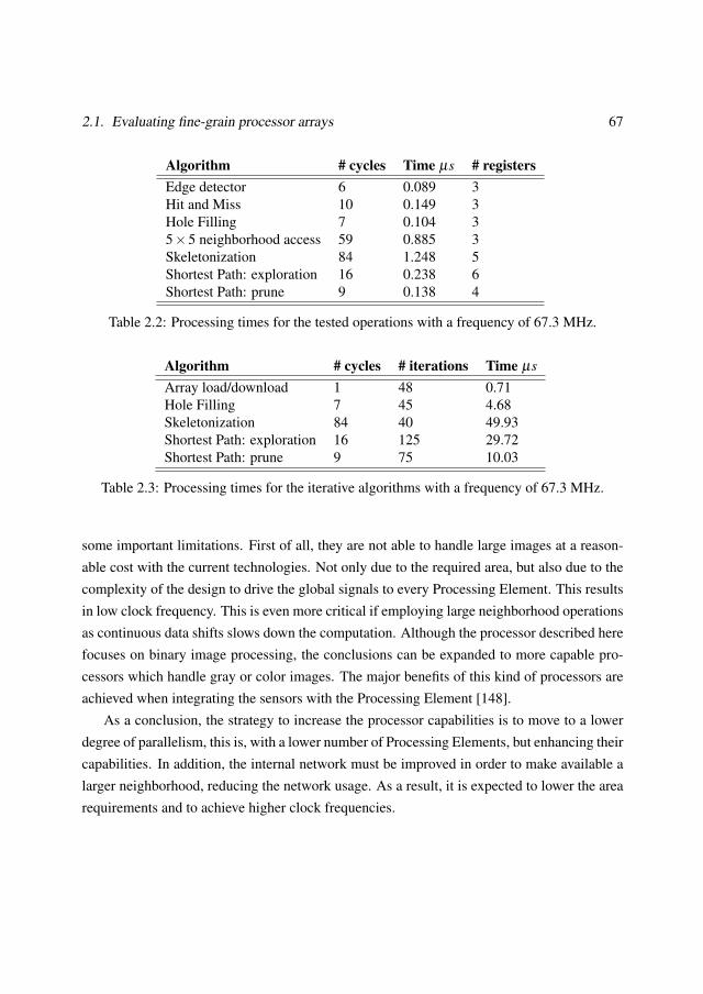
2.1. Evaluating fine-grain processor arrays 67
Algorithm # cycles Time µs # registersEdge detector 6 0.089 3Hit and Miss 10 0.149 3Hole Filling 7 0.104 35×5 neighborhood access 59 0.885 3Skeletonization 84 1.248 5Shortest Path: exploration 16 0.238 6Shortest Path: prune 9 0.138 4
Table 2.2: Processing times for the tested operations with a frequency of 67.3 MHz.
Algorithm # cycles # iterations Time µsArray load/download 1 48 0.71Hole Filling 7 45 4.68Skeletonization 84 40 49.93Shortest Path: exploration 16 125 29.72Shortest Path: prune 9 75 10.03
Table 2.3: Processing times for the iterative algorithms with a frequency of 67.3 MHz.
some important limitations. First of all, they are not able to handle large images at a reason-able cost with the current technologies. Not only due to the required area, but also due to thecomplexity of the design to drive the global signals to every Processing Element. This resultsin low clock frequency. This is even more critical if employing large neighborhood operationsas continuous data shifts slows down the computation. Although the processor described herefocuses on binary image processing, the conclusions can be expanded to more capable pro-cessors which handle gray or color images. The major benefits of this kind of processors areachieved when integrating the sensors with the Processing Element [148].
As a conclusion, the strategy to increase the processor capabilities is to move to a lowerdegree of parallelism, this is, with a lower number of Processing Elements, but enhancing theircapabilities. In addition, the internal network must be improved in order to make available alarger neighborhood, reducing the network usage. As a result, it is expected to lower the arearequirements and to achieve higher clock frequencies.
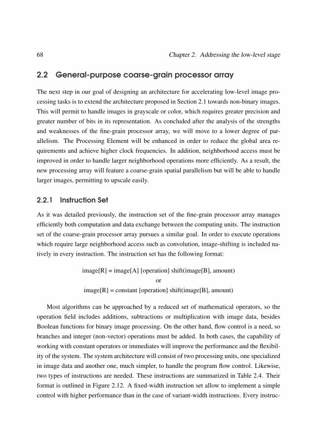
68 Chapter 2. Addressing the low-level stage
2.2 General-purpose coarse-grain processor array
The next step in our goal of designing an architecture for accelerating low-level image pro-cessing tasks is to extend the architecture proposed in Section 2.1 towards non-binary images.This will permit to handle images in grayscale or color, which requires greater precision andgreater number of bits in its representation. As concluded after the analysis of the strengthsand weaknesses of the fine-grain processor array, we will move to a lower degree of par-allelism. The Processing Element will be enhanced in order to reduce the global area re-quirements and achieve higher clock frequencies. In addition, neighborhood access must beimproved in order to handle larger neighborhood operations more efficiently. As a result, thenew processing array will feature a coarse-grain spatial parallelism but will be able to handlelarger images, permitting to upscale easily.
2.2.1 Instruction Set
As it was detailed previously, the instruction set of the fine-grain processor array managesefficiently both computation and data exchange between the computing units. The instructionset of the coarse-grain processor array pursues a similar goal. In order to execute operationswhich require large neighborhood access such as convolution, image-shifting is included na-tively in every instruction. The instruction set has the following format:
image[R] = image[A] [operation] shift(image[B], amount)or
image[R] = constant [operation] shift(image[B], amount)
Most algorithms can be approached by a reduced set of mathematical operators, so theoperation field includes additions, subtractions or multiplication with image data, besidesBoolean functions for binary image processing. On the other hand, flow control is a need, sobranches and integer (non-vector) operations must be added. In both cases, the capability ofworking with constant operators or immediates will improve the performance and the flexibil-ity of the system. The system architecture will consist of two processing units, one specializedin image data and another one, much simpler, to handle the program flow control. Likewise,two types of instructions are needed. These instructions are summarized in Table 2.4. Theirformat is outlined in Figure 2.12. A fixed-width instruction set allow to implement a simplecontrol with higher performance than in the case of variant-width instructions. Every instruc-
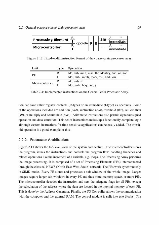
2.2. General-purpose coarse-grain processor array 69
Figure 2.12: Fixed-width instruction format of the coarse-grain processor array.
Unit Type Operation
PE R add, sub, mult, mac, thr, identity, and, or, notI addi, subi, multi, maci, thri, andi, ori
Microcontroller R add, sub, sltI addi, subi, beq, bne, j
Table 2.4: Implemented instructions on the Coarse-Grain Processor Array.
tion can take either register contents (R-type) or an immediate (I-type) as operands. Someof the operations included are addition (add), subtraction (sub), threshold (thr), set less than(slt), or multiply and accumulate (mac). Arithmetic instructions also permit signed/unsignedoperation and data saturation. This set of instructions makes up a functionally complete logicalthough custom instructions for time-sensitive applications can be easily added. The thresh-old operation is a good example of this.
2.2.2 Processor Architecture
Figure 2.13 shows the top-level view of the system architecture. The microcontroller storesthe program, issues the instructions and controls the program flow, handling branches andrelated operations like the increment of a variable, e.g. loops. The Processing Array performsthe image processing. It is composed of a set of Processing Elements (PEs) interconnectedthrough the classical NEWS (North-East-West-South) network. The PEs work synchronouslyin SIMD mode. Every PE stores and processes a sub-window of the whole image. Largerimages require larger sub-windows in every PE and thus more memory space, or more PEs.The microcontroller decodes the instruction and sets the adequate flags for all PEs, exceptthe calculation of the address where the data are located in the internal memory of each PE.This is done by the Address Generator. Finally, the I/O Controller allows the communicationwith the computer and the external RAM. The control module is split into two blocks. The
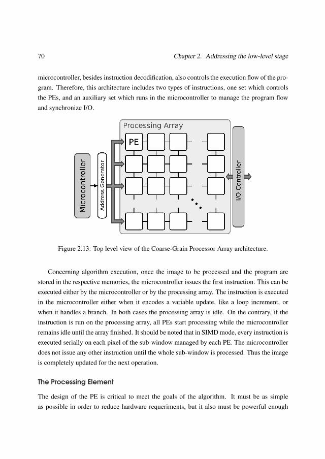
70 Chapter 2. Addressing the low-level stage
microcontroller, besides instruction decodification, also controls the execution flow of the pro-gram. Therefore, this architecture includes two types of instructions, one set which controlsthe PEs, and an auxiliary set which runs in the microcontroller to manage the program flowand synchronize I/O.
Figure 2.13: Top level view of the Coarse-Grain Processor Array architecture.
Concerning algorithm execution, once the image to be processed and the program arestored in the respective memories, the microcontroller issues the first instruction. This can beexecuted either by the microcontroller or by the processing array. The instruction is executedin the microcontroller either when it encodes a variable update, like a loop increment, orwhen it handles a branch. In both cases the processing array is idle. On the contrary, if theinstruction is run on the processing array, all PEs start processing while the microcontrollerremains idle until the array finished. It should be noted that in SIMD mode, every instruction isexecuted serially on each pixel of the sub-window managed by each PE. The microcontrollerdoes not issue any other instruction until the whole sub-window is processed. Thus the imageis completely updated for the next operation.
The Processing Element
The design of the PE is critical to meet the goals of the algorithm. It must be as simpleas possible in order to reduce hardware requeriments, but it also must be powerful enough
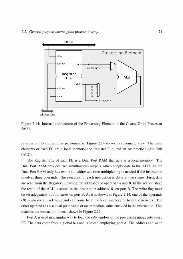
2.2. General-purpose coarse-grain processor array 71
Figure 2.14: Internal architecture of the Processing Element of the Coarse-Grain ProcessorArray.
in order not to compromise performance. Figure 2.14 shows its schematic view. The mainelements of each PE are a local memory, the Register File, and an Arithmetic Logic Unit(ALU).
The Register File of each PE is a Dual Port RAM that acts as a local memory. TheDual Port RAM provides two simultaneous outputs which supply data to the ALU. As theDual Port RAM only has two input addresses, time multiplexing is needed if the instructioninvolves three operands. The execution of each instruction is done in two stages. First, dataare read from the Register File using the addresses of operands A and B. In the second stagethe result of the ALU is stored in the destination address, R, on port B. The write flag mustbe set adequately in both cases on port B. As it is shown in Figure 2.14, one of the operands(B) is always a pixel value and can come from the local memory of from the network. Theother operand (A) is a local pixel value or an immediate value encoded in the instruction. Thismatches the instruction format shown in Figure 2.12.
Port A is used in a similar way to load the sub-window of the processing image into everyPE. The data come from a global bus and is stored employing port A. The address and write
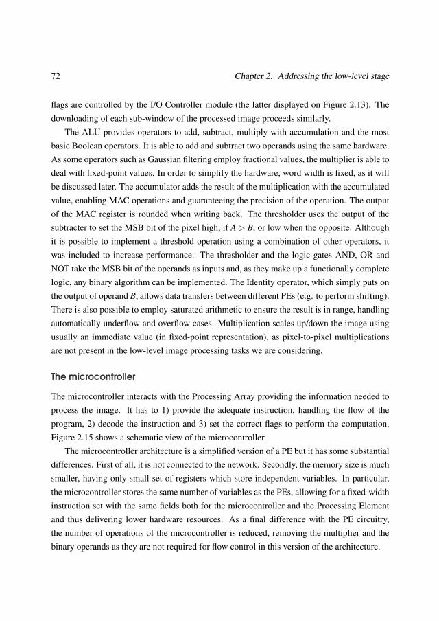
72 Chapter 2. Addressing the low-level stage
flags are controlled by the I/O Controller module (the latter displayed on Figure 2.13). Thedownloading of each sub-window of the processed image proceeds similarly.
The ALU provides operators to add, subtract, multiply with accumulation and the mostbasic Boolean operators. It is able to add and subtract two operands using the same hardware.As some operators such as Gaussian filtering employ fractional values, the multiplier is able todeal with fixed-point values. In order to simplify the hardware, word width is fixed, as it willbe discussed later. The accumulator adds the result of the multiplication with the accumulatedvalue, enabling MAC operations and guaranteeing the precision of the operation. The outputof the MAC register is rounded when writing back. The thresholder uses the output of thesubtracter to set the MSB bit of the pixel high, if A > B, or low when the opposite. Althoughit is possible to implement a threshold operation using a combination of other operators, itwas included to increase performance. The thresholder and the logic gates AND, OR andNOT take the MSB bit of the operands as inputs and, as they make up a functionally completelogic, any binary algorithm can be implemented. The Identity operator, which simply puts onthe output of operand B, allows data transfers between different PEs (e.g. to perform shifting).There is also possible to employ saturated arithmetic to ensure the result is in range, handlingautomatically underflow and overflow cases. Multiplication scales up/down the image usingusually an immediate value (in fixed-point representation), as pixel-to-pixel multiplicationsare not present in the low-level image processing tasks we are considering.
The microcontroller
The microcontroller interacts with the Processing Array providing the information needed toprocess the image. It has to 1) provide the adequate instruction, handling the flow of theprogram, 2) decode the instruction and 3) set the correct flags to perform the computation.Figure 2.15 shows a schematic view of the microcontroller.
The microcontroller architecture is a simplified version of a PE but it has some substantialdifferences. First of all, it is not connected to the network. Secondly, the memory size is muchsmaller, having only small set of registers which store independent variables. In particular,the microcontroller stores the same number of variables as the PEs, allowing for a fixed-widthinstruction set with the same fields both for the microcontroller and the Processing Elementand thus delivering lower hardware resources. As a final difference with the PE circuitry,the number of operations of the microcontroller is reduced, removing the multiplier and thebinary operands as they are not required for flow control in this version of the architecture.
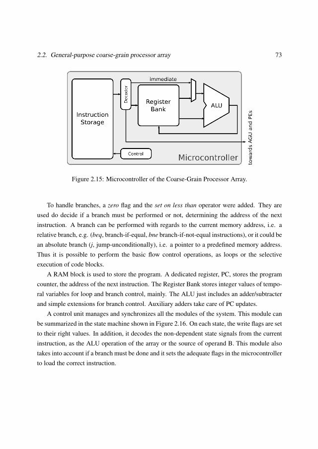
2.2. General-purpose coarse-grain processor array 73
Figure 2.15: Microcontroller of the Coarse-Grain Processor Array.
To handle branches, a zero flag and the set on less than operator were added. They areused do decide if a branch must be performed or not, determining the address of the nextinstruction. A branch can be performed with regards to the current memory address, i.e. arelative branch, e.g. (beq, branch-if-equal, bne branch-if-not-equal instructions), or it could bean absolute branch (j, jump-unconditionally), i.e. a pointer to a predefined memory address.Thus it is possible to perform the basic flow control operations, as loops or the selectiveexecution of code blocks.
A RAM block is used to store the program. A dedicated register, PC, stores the programcounter, the address of the next instruction. The Register Bank stores integer values of tempo-ral variables for loop and branch control, mainly. The ALU just includes an adder/subtracterand simple extensions for branch control. Auxiliary adders take care of PC updates.
A control unit manages and synchronizes all the modules of the system. This module canbe summarized in the state machine shown in Figure 2.16. On each state, the write flags are setto their right values. In addition, it decodes the non-dependent state signals from the currentinstruction, as the ALU operation of the array or the source of operand B. This module alsotakes into account if a branch must be done and it sets the adequate flags in the microcontrollerto load the correct instruction.
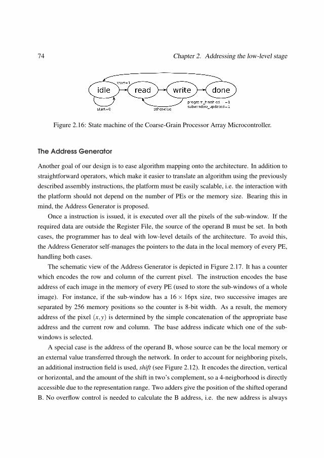
74 Chapter 2. Addressing the low-level stage
Figure 2.16: State machine of the Coarse-Grain Processor Array Microcontroller.
The Address Generator
Another goal of our design is to ease algorithm mapping onto the architecture. In addition tostraightforward operators, which make it easier to translate an algorithm using the previouslydescribed assembly instructions, the platform must be easily scalable, i.e. the interaction withthe platform should not depend on the number of PEs or the memory size. Bearing this inmind, the Address Generator is proposed.
Once a instruction is issued, it is executed over all the pixels of the sub-window. If therequired data are outside the Register File, the source of the operand B must be set. In bothcases, the programmer has to deal with low-level details of the architecture. To avoid this,the Address Generator self-manages the pointers to the data in the local memory of every PE,handling both cases.
The schematic view of the Address Generator is depicted in Figure 2.17. It has a counterwhich encodes the row and column of the current pixel. The instruction encodes the baseaddress of each image in the memory of every PE (used to store the sub-windows of a wholeimage). For instance, if the sub-window has a 16× 16px size, two successive images areseparated by 256 memory positions so the counter is 8-bit width. As a result, the memoryaddress of the pixel (x,y) is determined by the simple concatenation of the appropriate baseaddress and the current row and column. The base address indicate which one of the sub-windows is selected.
A special case is the address of the operand B, whose source can be the local memory oran external value transferred through the network. In order to account for neighboring pixels,an additional instruction field is used, shift (see Figure 2.12). It encodes the direction, verticalor horizontal, and the amount of the shift in two’s complement, so a 4-neigborhood is directlyaccessible due to the representation range. Two adders give the position of the shifted operandB. No overflow control is needed to calculate the B address, i.e. the new address is always
2.3. Case of study: retinal vessel-tree extraction 75
Figure 2.17: Internal datapath of the Address Generator of the Coarse-Grain Processor Array.
correct. However, it is needed to select the source of the operand because if an overflow oran underflow occurs, the data would be outside the local memory and the network shouldbe used. In this way the system becomes self-governing, being able to handle any array andmemory size.
In order to reduce the fan-out of the global signals, the calculated addresses are distributedthrough a bus, as shown in Figure 2.13, which is pipelined. This results in an increment up toa 60% on the clock frequency.
2.3 Case of study: retinal vessel-tree extraction
The image processor under study is conceived to handle low-level image processing tasks.Instead of designing a test-bench with different operators, a more practical approach is done.It is important to study not only the operators, but also the relationships between them whenintegrated in real-world applications. This is related with internal and external data storage.For instance, a processor can offer a poor performance executing a single operation and a highperformance when linking together several of them, taking advantage of on-chip memory toavoid an intensive use of the external RAM, considerably slower. For this purpose a represen-tative low-level algorithm was selected, a retinal vessel-tree extractor, designed focusing onparallelism and performance. It includes not only common tasks such as point-to-point, neigh-borhood or morphological operators but also recursive and data-dependent program flow. As
76 Chapter 2. Addressing the low-level stage
it can be drawn from this section, the algorithm satisfies all our requirements. The algorithmwill permit to determine the advantages of the proposed architecture and the key aspects tobe improved for a successful design. The algorithm is highly representative of the operationspresent in the early stages of a Computer Vision application. Therefore, it will also permitsto verify if the minimum requirements in terms of flexibility and performance are met. Theconclusions of this study will lead to a new architecture capable of dealing with more complexalgorithms.
Retinal vessel-tree extraction is a very demanding computational task. It can be used in ap-plications as early diagnoses of diseases like diabetes [149] or in person authentication [150].In these practical operations, complex algorithms have to be processed fast. Usually, retinalimages feature high resolution, so providing the vessel-tree requires thousands of operationsat pixel-level. For instance, this processing step consumes more than 90% of the overall timeperformance in the person authentication application addressed in [151].
This retinal vessel tree extraction algorithm was proposed by Alonso-Montes et al. [152].This technique uses a set of active contours that fit the external boundaries of the vessels.This is an advantage against other active contour-based techniques which start the contourevolution from inside the vessels. This way, narrow vessels are segmented without breakpointsand the central reflection in the widest ones is sorted out, providing better results. In addition,automatic initialization is more reliable, avoiding human interaction in the whole process.Figure 2.18 shows the result of applying the algorithm to a retinal image.
An active contour (or snake) is defined by a set of connected curves which delimit theoutline of an object [153]. It may be visualized as a rubber band that will be deformed by theinfluence of constraints and forces trying to get the contour as close as possible to the objectboundaries. The contour model attempts to minimize the energy associated to the snake. Thisenergy is the sum of different terms:
• The internal energy, which controls the shape and the curvature of the snake.
• The external energy, which controls the snake movement to fit the object position.
• Other energies with the aim of increasing the robustness, derived from potentials (as theso-called inflated potential) or momenta (as the moment of inertia) [154].
The snake will reach the final position and shape when the sum of all these terms reaches aminimum. Several iterations are normally required to find this minimum. Each step is compu-tationally expensive, so the global computational effort is quite high. Also, the placement of
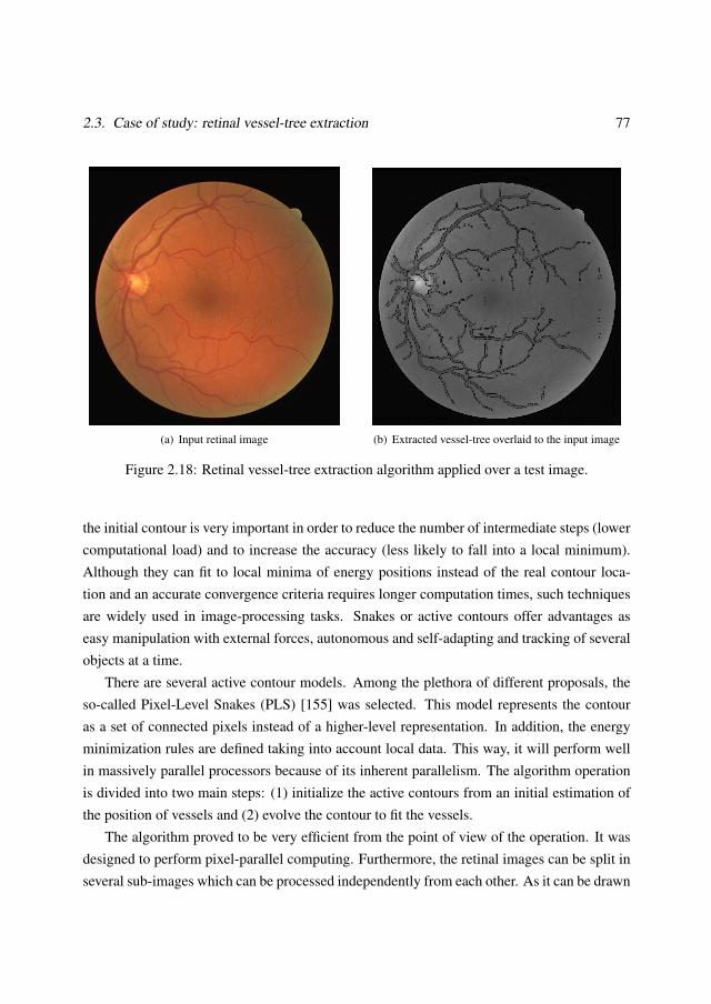
2.3. Case of study: retinal vessel-tree extraction 77
(a) Input retinal image (b) Extracted vessel-tree overlaid to the input image
Figure 2.18: Retinal vessel-tree extraction algorithm applied over a test image.
the initial contour is very important in order to reduce the number of intermediate steps (lowercomputational load) and to increase the accuracy (less likely to fall into a local minimum).Although they can fit to local minima of energy positions instead of the real contour loca-tion and an accurate convergence criteria requires longer computation times, such techniquesare widely used in image-processing tasks. Snakes or active contours offer advantages aseasy manipulation with external forces, autonomous and self-adapting and tracking of severalobjects at a time.
There are several active contour models. Among the plethora of different proposals, theso-called Pixel-Level Snakes (PLS) [155] was selected. This model represents the contouras a set of connected pixels instead of a higher-level representation. In addition, the energyminimization rules are defined taking into account local data. This way, it will perform wellin massively parallel processors because of its inherent parallelism. The algorithm operationis divided into two main steps: (1) initialize the active contours from an initial estimation ofthe position of vessels and (2) evolve the contour to fit the vessels.
The algorithm proved to be very efficient from the point of view of the operation. It wasdesigned to perform pixel-parallel computing. Furthermore, the retinal images can be split inseveral sub-images which can be processed independently from each other. As it can be drawn
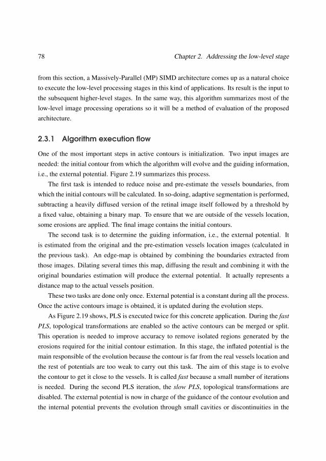
78 Chapter 2. Addressing the low-level stage
from this section, a Massively-Parallel (MP) SIMD architecture comes up as a natural choiceto execute the low-level processing stages in this kind of applications. Its result is the input tothe subsequent higher-level stages. In the same way, this algorithm summarizes most of thelow-level image processing operations so it will be a method of evaluation of the proposedarchitecture.
2.3.1 Algorithm execution flow
One of the most important steps in active contours is initialization. Two input images areneeded: the initial contour from which the algorithm will evolve and the guiding information,i.e., the external potential. Figure 2.19 summarizes this process.
The first task is intended to reduce noise and pre-estimate the vessels boundaries, fromwhich the initial contours will be calculated. In so-doing, adaptive segmentation is performed,subtracting a heavily diffused version of the retinal image itself followed by a threshold bya fixed value, obtaining a binary map. To ensure that we are outside of the vessels location,some erosions are applied. The final image contains the initial contours.
The second task is to determine the guiding information, i.e., the external potential. Itis estimated from the original and the pre-estimation vessels location images (calculated inthe previous task). An edge-map is obtained by combining the boundaries extracted fromthose images. Dilating several times this map, diffusing the result and combining it with theoriginal boundaries estimation will produce the external potential. It actually represents adistance map to the actual vessels position.
These two tasks are done only once. External potential is a constant during all the process.Once the active contours image is obtained, it is updated during the evolution steps.
As Figure 2.19 shows, PLS is executed twice for this concrete application. During the fast
PLS, topological transformations are enabled so the active contours can be merged or split.This operation is needed to improve accuracy to remove isolated regions generated by theerosions required for the initial contour estimation. In this stage, the inflated potential is themain responsible of the evolution because the contour is far from the real vessels location andthe rest of potentials are too weak to carry out this task. The aim of this stage is to evolvethe contour to get it close to the vessels. It is called fast because a small number of iterationsis needed. During the second PLS iteration, the slow PLS, topological transformations aredisabled. The external potential is now in charge of the guidance of the contour evolution andthe internal potential prevents the evolution through small cavities or discontinuities in the
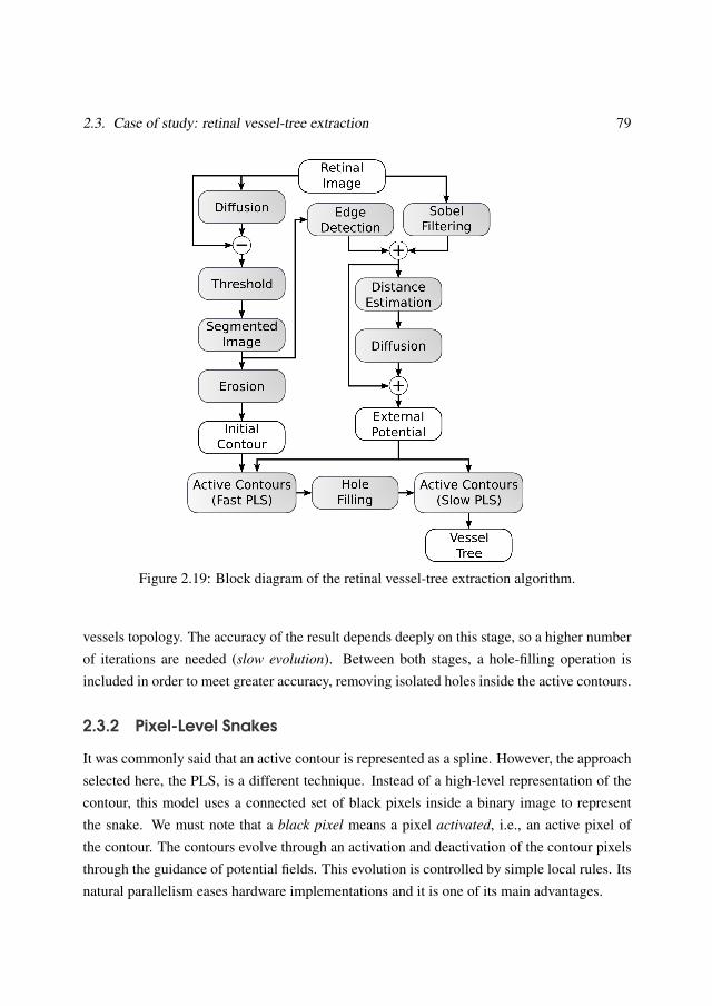
2.3. Case of study: retinal vessel-tree extraction 79
Figure 2.19: Block diagram of the retinal vessel-tree extraction algorithm.
vessels topology. The accuracy of the result depends deeply on this stage, so a higher numberof iterations are needed (slow evolution). Between both stages, a hole-filling operation isincluded in order to meet greater accuracy, removing isolated holes inside the active contours.
2.3.2 Pixel-Level Snakes
It was commonly said that an active contour is represented as a spline. However, the approachselected here, the PLS, is a different technique. Instead of a high-level representation of thecontour, this model uses a connected set of black pixels inside a binary image to representthe snake. We must note that a black pixel means a pixel activated, i.e., an active pixel ofthe contour. The contours evolve through an activation and deactivation of the contour pixelsthrough the guidance of potential fields. This evolution is controlled by simple local rules. Itsnatural parallelism eases hardware implementations and it is one of its main advantages.
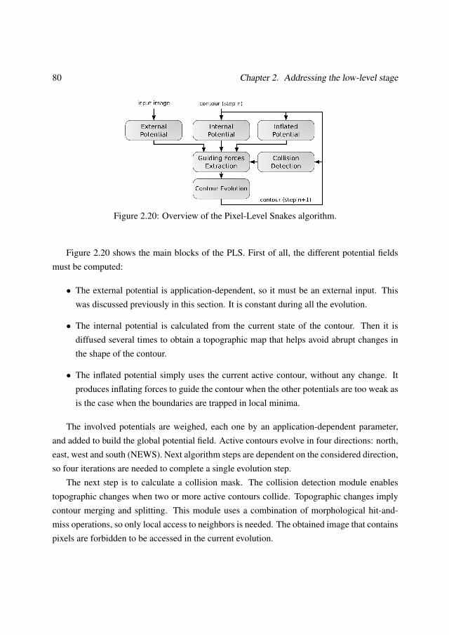
80 Chapter 2. Addressing the low-level stage
Figure 2.20: Overview of the Pixel-Level Snakes algorithm.
Figure 2.20 shows the main blocks of the PLS. First of all, the different potential fieldsmust be computed:
• The external potential is application-dependent, so it must be an external input. Thiswas discussed previously in this section. It is constant during all the evolution.
• The internal potential is calculated from the current state of the contour. Then it isdiffused several times to obtain a topographic map that helps avoid abrupt changes inthe shape of the contour.
• The inflated potential simply uses the current active contour, without any change. Itproduces inflating forces to guide the contour when the other potentials are too weak asis the case when the boundaries are trapped in local minima.
The involved potentials are weighed, each one by an application-dependent parameter,and added to build the global potential field. Active contours evolve in four directions: north,east, west and south (NEWS). Next algorithm steps are dependent on the considered direction,so four iterations are needed to complete a single evolution step.
The next step is to calculate a collision mask. The collision detection module enablestopographic changes when two or more active contours collide. Topographic changes implycontour merging and splitting. This module uses a combination of morphological hit-and-miss operations, so only local access to neighbors is needed. The obtained image that containspixels are forbidden to be accessed in the current evolution.
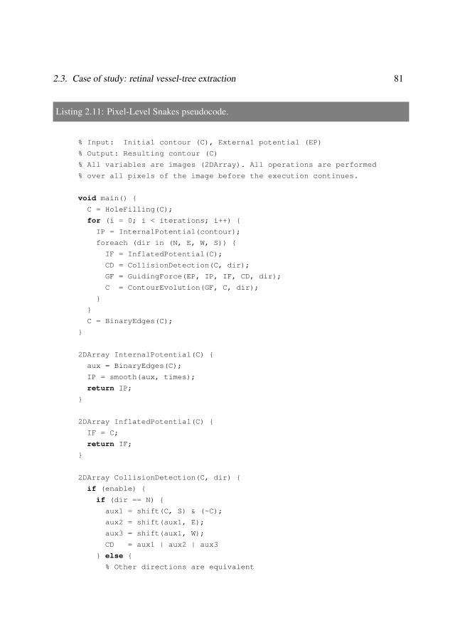
2.3. Case of study: retinal vessel-tree extraction 81
Listing 2.11: Pixel-Level Snakes pseudocode.
% Input: Initial contour (C), External potential (EP)
% Output: Resulting contour (C)
% All variables are images (2DArray). All operations are performed
% over all pixels of the image before the execution continues.
void main() {
C = HoleFilling(C);
for (i = 0; i < iterations; i++) {
IP = InternalPotential(contour);
foreach (dir in (N, E, W, S)) {
IF = InflatedPotential(C);
CD = CollisionDetection(C, dir);
GF = GuidingForce(EP, IP, IF, CD, dir);
C = ContourEvolution(GF, C, dir);
}
}
C = BinaryEdges(C);
}
2DArray InternalPotential(C) {
aux = BinaryEdges(C);
IP = smooth(aux, times);
return IP;
}
2DArray InflatedPotential(C) {
IF = C;
return IF;
}
2DArray CollisionDetection(C, dir) {
if (enable) {
if (dir == N) {
aux1 = shift(C, S) & (~C);
aux2 = shift(aux1, E);
aux3 = shift(aux1, W);
CD = aux1 | aux2 | aux3
} else {
% Other directions are equivalent
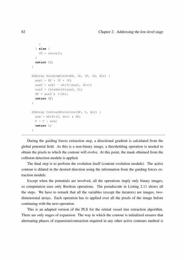
82 Chapter 2. Addressing the low-level stage
}
} else {
CD = zeros();
}
return CD;
}
2DArray GuidingForce(EP, IP, IF, CD, dir) {
aux1 = EP + IP + IF;
aux2 = aux1 - shift(aux1, dir);
aux3 = threshold(aux2, 0);
GF = aux3 & (~CD);
return GF;
}
2DArray ContourEvolution(GF, C, dir) {
aux = shift(C, dir) & GF;
C = C | aux;
return C;
}
During the guiding forces extraction step, a directional gradient is calculated from theglobal potential field. As this is a non-binary image, a thresholding operation is needed toobtain the pixels to which the contour will evolve. At this point, the mask obtained from thecollision detection module is applied.
The final step is to perform the evolution itself (contour evolution module). The activecontour is dilated in the desired direction using the information from the guiding forces ex-traction module.
Except when the potentials are involved, all the operations imply only binary images,so computation uses only Boolean operations. The pseudocode in Listing 2.11 shows allthe steps. We have to remark that all the variables (except the iterators) are images, two-dimensional arrays. Each operation has to applied over all the pixels of the image beforecontinuing with the next operation.
This is an adapted version of the PLS for the retinal vessel tree extraction algorithm.There are only stages of expansion. The way in which the contour is initialized ensures thatalternating phases of expansion/contraction required in any other active contours method is
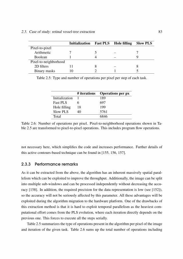
2.3. Case of study: retinal vessel-tree extraction 83
Initialization Fast PLS Hole filling Slow PLSPixel-to-pixel
Arithmetic 7 5 – 7Boolean 1 4 – 9
Pixel-to-neighborhood2D filters 11 8 – 8Binary masks 10 2 1 5
Table 2.5: Type and number of operations per pixel per step of each task.
# iterations Operations per pxInitialization 1 189Fast PLS 6 697Hole filling 18 199Slow PLS 40 5761Total 6846
Table 2.6: Number of operations per pixel. Pixel-to-neighborhood operations shown in Ta-ble 2.5 are transformed to pixel-to-pixel operations. This includes program flow operations.
not necessary here, which simplifies the code and increases performance. Further details ofthis active contours-based technique can be found in [155, 156, 157].
2.3.3 Performance remarks
As it can be extracted from the above, the algorithm has an inherent massively spatial paral-lelism which can be exploited to improve the throughput. Additionally, the image can be splitinto multiple sub-windows and can be processed independently without decreasing the accu-racy [158]. In addition, the required precision for the data representation is low (see [152]),so the accuracy will not be seriously affected by this parameter. All these advantages will beexploited during the algorithm migration to the hardware platform. One of the drawbacks ofthis extraction method is that it is hard to exploit temporal parallelism as the heaviest com-putational effort comes from the PLS evolution, where each iteration directly depends on theprevious one. This forces to execute all the steps serially.
Table 2.5 summarizes the type of operations present in the algorithm per pixel of the imageand iteration of the given task. Table 2.6 sums up the total number of operations including
84 Chapter 2. Addressing the low-level stage
the number of iterations per task and program flow-related tasks. The number of iterationswas determined experimentally and agrees with the worst case of those studied to ensure theconvergence of the contours. To evaluate the efficiency of the implementation, the DRIVEdatabase was used [159]. The retinal images were captured with a Canon CR5 non-mydriatric3CCD. They are 8-bit three channel color images with a size of 768× 584px. Consideringthis image size and that by each pixel 6846 operations must be performed, around 3 giga-operations are required to process the entire image. The operations of this algorithm are veryrepresentative of image-processing operations which are part of the low- and mid-level stages.They comprise operations as filtering, basic arithmetics, logic operations, mask applicationsor basic program flow data dependencies. Any image-processing-oriented hardware must dealproperly with all these tasks.
The retinal vessel tree extraction algorithm was tested employing a PC-based solution. Itwas developed using OpenCV and C++ on a computer equipped with an Intel Core i7 940working at 2.93 GHz (4 physical cores running 8 threads) and 6 GB of DDR3 working at1.6 GHz and in triple-channel configuration. Using this computer, each image requires morethan 13 s to be processed. This implementation makes use of the native SSE support whichOpenCV offers. To take advantage of the multi-core CPU, OpenMP was used to parallelizeloops and some critical blocks of the algorithm which are implemented outside the OpenCVframework. This allows around a 15% higher performance. Previous implementations usingMatLab [160] require more than 40 s to extract the retinal vessel-tree. Although it wouldbe possible to do certain optimizations to further improve performance, it would be verydifficult to achieve times below 10 s. This is because the algorithm is not designed to run onsuch architectures, not because of the algorithmic complexity, but due to the large number ofmemory accesses required, not present in fine-grain processors.
Even with a high-end computer, the result is not satisfactory in terms of speed. Candidatesystems using this algorithm require a faster response. To address this and other problemsassociated with a conventional PC, such as size or power consumption, a dedicated processoror an embedded device attached to the camera is a requirement. It is expected that MP-SIMDarchitectures will perform better than other approaches. This point will be discussed later inSection 2.5.
2.4. Performance evaluation 85
2.4 Performance evaluation
2.4.1 FPGA prototyping and validation
The system chosen for the validation is an XEM3050 card from Opal Kelly [161] with aHigh-speed USB 2.0 board and a Xilinx Spartan-3 FPGA. The most remarkable features ofthis FGPA are 6912 CLBs or 62208 equivalent logic cells (1 Logic Cell = 4-input LUT anda D-flip-flop), 96×18 Kb embedded RAM blocks (where 2 Kb are parity bits) and 520 Kb ofDistributed RAM, 96 dedicated 18-bit multipliers and a Speed Grade of -5. This FPGA uses90 nm process technology. The board also includes two independent 32MB SDRAM units.The implementation has been developed with VHDL and synthesized with the Xilinx ISE10.1 [142]. This board was chosen aiming to lower the cost of the prototype at the expenseof lower performance, as the Xilinx Spartan-3 family was designed focusing on cost-sensitiveand high volume consumer electronic applications.
The synthesized array on this FPGA has a resolution of 9×10 (90) Processing Elementsand is able to handle a window of 144×160px with 8-bits of resolution per pixel. The orig-inal implementation of the algorithm demonstrated that this word width provides sufficientprecision for practical implementations. This will be discussed later in Section 2.5.3. Fixed-point representation handles only 4-bits for the decimal part, providing adequate accuracy forlow-level image processing arithmetic. The Register File of each PE handles 8 different sub-windows of 16×16px each (16 Kbit per PE). The ALU contains an embedded multiplier. Themicrocontroller stores 8 independent integer variables too, and up to 512 instructions. The re-sources consumed when implementing the architecture in the Spartan-3 FPGA are indicatedin Table 2.7. As we can see, there are still resources available on the FPGA chip, although theusage of RAM Blocks and Multipliers limits the number of PEs we can embed. Concerningspeed, the highest clock frequency attained by the implementation was set to 53 MHz.
Besides to the proposed architecture, an additional module was included to handle I/O.Opal Kelly provides a proprietary high-speed USB interface (a Cypress FX2LP - CY68013A [162])to communicate the board with the computer. The amount of resources needed for synchro-nization and data buffering (previous to its storage in the PEs local memory) is quite reduced,and it only consumes LUTs. An additional 18 Kbit RAM Block is needed to pack the inputand output buffers. Image data are transferred to the PEs sequentially, employing a dedicatedpipelined bus, as discussed previously. External RAM is not used, as we are only evaluatingthe performance of the Processing Array.
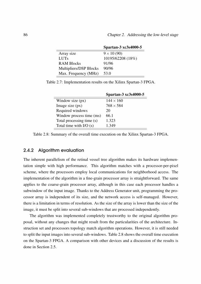
86 Chapter 2. Addressing the low-level stage
Spartan-3 xc3s4000-5Array size 9×10 (90)LUTs 10195/62208 (18%)RAM Blocks 91/96Multipliers/DSP Blocks 90/96Max. Frequency (MHz) 53.0
Table 2.7: Implementation results on the Xilinx Spartan-3 FPGA.
Spartan-3 xc3s4000-5Window size (px) 144×160Image size (px) 768×584Required windows 20Window process time (ms) 66.1Total processing time (s) 1.323Total time with I/O (s) 1.349
Table 2.8: Summary of the overall time execution on the Xilinx Spartan-3 FPGA.
2.4.2 Algorithm evaluation
The inherent parallelism of the retinal vessel tree algorithm makes its hardware implemen-tation simple with high performance. This algorithm matches with a processor-per-pixelscheme, where the processors employ local communications for neighborhood access. Theimplementation of the algorithm in a fine-grain processor array is straightforward. The sameapplies to the coarse-grain processor array, although in this case each processor handles asubwindow of the input image. Thanks to the Address Generator unit, programming the pro-cessor array is independent of its size, and the network access is self-managed. However,there is a limitation in terms of resolution. As the size of the array is lower than the size of theimage, it must be split into several sub-windows that are processed independently.
The algorithm was implemented completely trustworthy to the original algorithm pro-posal, without any changes that might result from the particularities of the architecture. In-struction set and processors topology match algorithm operations. However, it is still neededto split the input images into several sub-windows. Table 2.8 shows the overall time executionon the Spartan-3 FPGA. A comparison with other devices and a discussion of the results isdone in Section 2.5.
2.4. Performance evaluation 87
2.4.3 Architectural improvements
In the light of the obtained results, an enhanced version of the architecture is proposed. Thisnew version does not change the original concept, although the internal datapath of the Pro-cessing Element includes some minor features. One of the major drawbacks of the currentimplementation is the limited use of the Register File, which only permits two simultaneousaccesses. Instructions which employ three operands take two clock cycles, as Figure 2.16shows. This considerably increases the computation time. Apart from other minor and tech-nical enhancements, the datapath was modified by adding an additional stage to the pipeline.This is done for two reasons: to increase the clock frequency, highly limited due to the NEWSrouting and the ALU’s internal datapath length, and to provide more flexibility to overcomethe limitations of the Register File implementation. The control unit of the microcontroller isnow able to handle data-hazards when the instructions include three operands, so instructionsonly take additional cycles when necessary.
The Xilinx Spartan-3 FPGA was selected to lower the cost of the final device. How-ever, this also leads to less available hardware resources and lower performance. The targetplatform for the new implementation of the architecture is a Xilinx Virtex-6 xcv6vlx240t-1FPGA [163], included on the Xilinx ML605 Base Board. The selected FPGA has an interme-diate size within the Virtex-6 family but provides enough resources to evaluate the architecturewithout sacrificing features when adapting the design to the limitations of the device. TheFPGA provides 37680 slices (each one containing four 6-input LUTs and eight flip-flops),416 Block RAMs (36Kb each) and 768 DSP48E1 slices (25×18 two’s complement multipli-er/accumulator with pre-adder, Boolean functions and barrel shifting capabilities) as the mostrelevant resources.
The synthesized array on the Virtex-6 FPGA has a resolution of 16×12 (192) ProcessingElements, handling a window of 384× 256px with 8-bits of resolution per pixel. The largeamount of resources of this FPGA permits to double the array size and to quadruple thewindow resolution. As in the Spartan-3 implementation, fixed-point representation with 4-bits for the decimal part is employed. The Register File of each PE also handles 8 differentsub-windows of 32× 16px each (32Kbit per PE), and it is implemented using a dedicated36Kbit Dual-Port Block RAM. A DSP48E1 slice is used instead of the simple multiplier ofthe Spartan-3 devices, so the internal adder/subtracter can be employed, saving LUTs forother purposes. With these parameters and the included improvements, the maximum clock
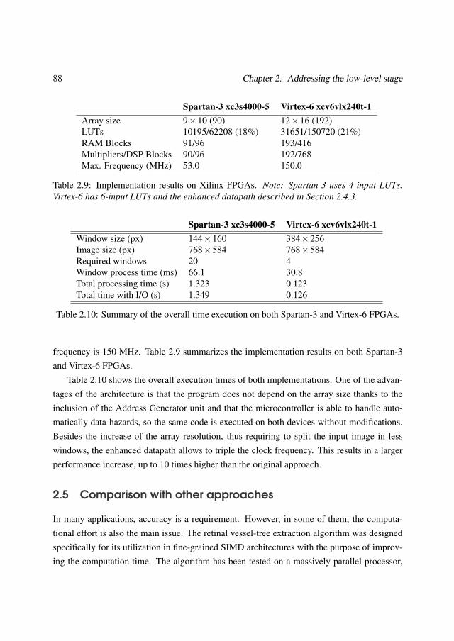
88 Chapter 2. Addressing the low-level stage
Spartan-3 xc3s4000-5 Virtex-6 xcv6vlx240t-1Array size 9×10 (90) 12×16 (192)LUTs 10195/62208 (18%) 31651/150720 (21%)RAM Blocks 91/96 193/416Multipliers/DSP Blocks 90/96 192/768Max. Frequency (MHz) 53.0 150.0
Table 2.9: Implementation results on Xilinx FPGAs. Note: Spartan-3 uses 4-input LUTs.Virtex-6 has 6-input LUTs and the enhanced datapath described in Section 2.4.3.
Spartan-3 xc3s4000-5 Virtex-6 xcv6vlx240t-1Window size (px) 144×160 384×256Image size (px) 768×584 768×584Required windows 20 4Window process time (ms) 66.1 30.8Total processing time (s) 1.323 0.123Total time with I/O (s) 1.349 0.126
Table 2.10: Summary of the overall time execution on both Spartan-3 and Virtex-6 FPGAs.
frequency is 150 MHz. Table 2.9 summarizes the implementation results on both Spartan-3and Virtex-6 FPGAs.
Table 2.10 shows the overall execution times of both implementations. One of the advan-tages of the architecture is that the program does not depend on the array size thanks to theinclusion of the Address Generator unit and that the microcontroller is able to handle auto-matically data-hazards, so the same code is executed on both devices without modifications.Besides the increase of the array resolution, thus requiring to split the input image in lesswindows, the enhanced datapath allows to triple the clock frequency. This results in a largerperformance increase, up to 10 times higher than the original approach.
2.5 Comparison with other approaches
In many applications, accuracy is a requirement. However, in some of them, the computa-tional effort is also the main issue. The retinal vessel-tree extraction algorithm was designedspecifically for its utilization in fine-grained SIMD architectures with the purpose of improv-ing the computation time. The algorithm has been tested on a massively parallel processor,
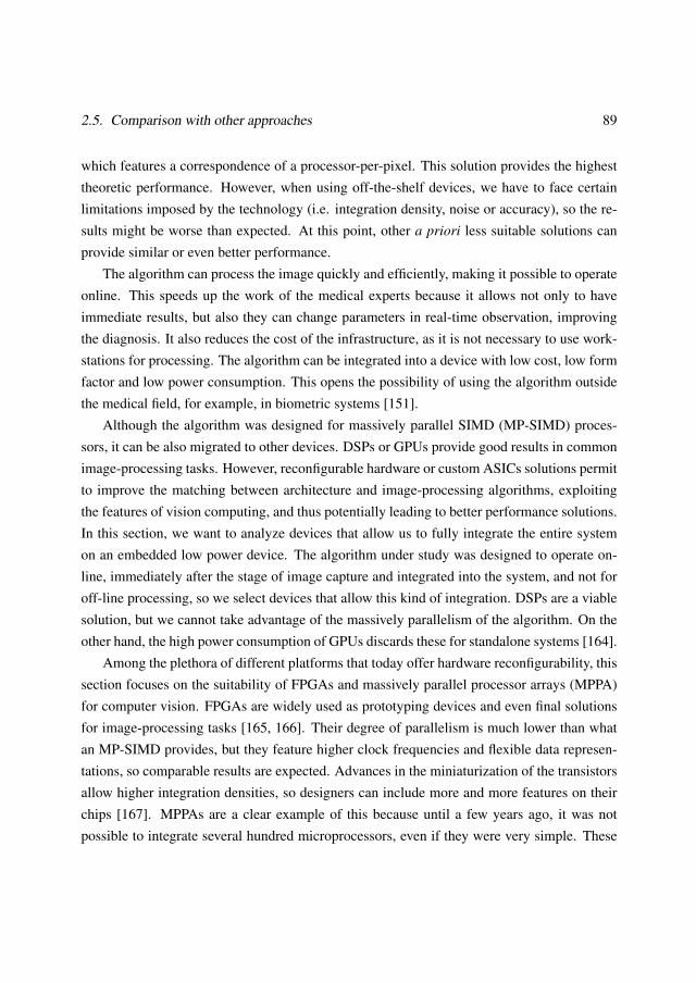
2.5. Comparison with other approaches 89
which features a correspondence of a processor-per-pixel. This solution provides the highesttheoretic performance. However, when using off-the-shelf devices, we have to face certainlimitations imposed by the technology (i.e. integration density, noise or accuracy), so the re-sults might be worse than expected. At this point, other a priori less suitable solutions canprovide similar or even better performance.
The algorithm can process the image quickly and efficiently, making it possible to operateonline. This speeds up the work of the medical experts because it allows not only to haveimmediate results, but also they can change parameters in real-time observation, improvingthe diagnosis. It also reduces the cost of the infrastructure, as it is not necessary to use work-stations for processing. The algorithm can be integrated into a device with low cost, low formfactor and low power consumption. This opens the possibility of using the algorithm outsidethe medical field, for example, in biometric systems [151].
Although the algorithm was designed for massively parallel SIMD (MP-SIMD) proces-sors, it can be also migrated to other devices. DSPs or GPUs provide good results in commonimage-processing tasks. However, reconfigurable hardware or custom ASICs solutions permitto improve the matching between architecture and image-processing algorithms, exploitingthe features of vision computing, and thus potentially leading to better performance solutions.In this section, we want to analyze devices that allow us to fully integrate the entire systemon an embedded low power device. The algorithm under study was designed to operate on-line, immediately after the stage of image capture and integrated into the system, and not foroff-line processing, so we select devices that allow this kind of integration. DSPs are a viablesolution, but we cannot take advantage of the massively parallelism of the algorithm. On theother hand, the high power consumption of GPUs discards these for standalone systems [164].
Among the plethora of different platforms that today offer hardware reconfigurability, thissection focuses on the suitability of FPGAs and massively parallel processor arrays (MPPA)for computer vision. FPGAs are widely used as prototyping devices and even final solutionsfor image-processing tasks [165, 166]. Their degree of parallelism is much lower than whatan MP-SIMD provides, but they feature higher clock frequencies and flexible data represen-tations, so comparable results are expected. Advances in the miniaturization of the transistorsallow higher integration densities, so designers can include more and more features on theirchips [167]. MPPAs are a clear example of this because until a few years ago, it was notpossible to integrate several hundred microprocessors, even if they were very simple. These
90 Chapter 2. Addressing the low-level stage
devices are characterized by a different computation paradigm, focusing on exploiting the taskparallelism of the algorithms [168].
This section shows the results of the implementation of the automatic method to extractthe vessel-tree from retinal images we are using as benchmark. The architecture presented inSection 2.2 on an FPGA is compared with the native platform of the algorithm, an MP-SIMDprocessor, and a completely opposed computing paradigm, an MPPA. This way we covermassively parallelism, coarse-grain parallelism and temporal (task) parallelism respectively.
2.5.1 Pixel-Parallel Processor Arrays
Conventional image-processing systems (which integrate a camera and a digital processor)have many issues for application in general-purpose consumer electronic products: cost,power consumption, size and complexity. One of the main disadvantages is the data transmis-sion bottlenecks between the camera, the processor and the memory. In addition, low-levelimage-processing operations have a high and inherent parallelism which only can be exploitedif the access to data is not heavily restricted. Computer Vision is one of the most intensivedata processing fields, and conventional systems do not provide any mechanism to addressadequately this task, so this issue comes up as an important drawback.
Pixel-parallel processor arrays aim to be the natural platform for low-level image-processingand pixel-parallel algorithms. They are MP-SIMD processors laid down in a 2D grid with aprocessor-per-pixel correspondence and local connections among neighbors. Each proces-sor includes an image sensor, so the I/O bottleneck between the sensor and the processor iseliminated, and the performance and power consumption are highly improved. This and theirmassively parallelism are the main benefits of these devices.
Pixel-parallel processor arrays operate in SIMD mode, where all the processors executesimultaneously the same instruction on their local set of data. To exchange information, theyuse a local interconnection, normally present only between the nearest processors to save sil-icon area. Concerning each processor, although with local memories, data I/O and sensingcontrol to be self-contained, they are as simple as possible in order to reduce area require-ments, but still powerful enough to be general purpose. The idea behind these devices isthat the entire computing is done on-chip, so that input data are logged in through the sen-sors and the output data are a reduced and symbolic representation of the information, withlow-bandwidth requirements.
2.5. Comparison with other approaches 91
One of the drawbacks of this approach is the reduced integration density. The size ofthe processors must be as small as possible because: for a 256× 256 px image, more than65k processors plus interconnections must be embedded in a reduced area. This is the reasonwhy many approaches utilize analog or mixed-signal implementations, where the area can beheavily optimized. Nevertheless, accuracy is its main drawback because it is hard to achievelarge data-word sizes. In addition, a careful design must be done, implying larger designperiods and higher economic costs. The scalability with the technology is not straightforwardbecause of the human intervention in all the process, which does not allow automation. Thesize of the arrays is also limited by capability of distributing the signals across the array. Theeffective size of the arrays forces us to use low-resolution images. Examples of mixed-modefocal-plane processors are the Eye-Ris vision system [169] or the programmable artificialretina [170].
Other approaches use digital implementations with the aim to solve the lack of function-ality, programmability, precision and noise robustness. The ASPA processor [171] and thedesign proposed by Komuro et al. [172] are examples of this kind of implementations.
As each processor includes a photo-sensor, it should occupy a large proportion of the areato receive as much light as possible. However, this will reduce the integration density. Newimprovements in the semiconductor industry enables three-dimensional integration technol-ogy [173]. This introduces a new way to build visions system adding new degrees of freedomto the design process. For instance, [174] proposes a 3D analog processor with a structuresimilar to the eye retina (sensor, bipolar cells and ganglion cells layers, with vertical con-nections between them) and [175] presents a mixed-signal focal-plane processor array withdigital processors, also segmented in layers.
As a representative device of this category, the SCAMP-3 Vision Chip was selected tomap the retinal vessel tree extraction algorithm described in Section 2.3.
The SCAMP-3 processor
The SCAMP-3 Vision Chip prototype [176] is a 128× 128px cellular processor array. Itincludes a processor-per-pixel in a mixed-mode architecture. Each processor, an Analog Pro-cessing Element (APE), operates in the same manner as a common digital processor but work-ing with analog data. It also includes a photo-sensor and the capability to communicate withothers APEs across a fixed network. This network enables data sharing between the nearestneighbors of each APE: NEWS. All processors work simultaneously in SIMD manner.
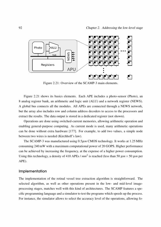
92 Chapter 2. Addressing the low-level stage
Figure 2.21: Overview of the SCAMP-3 main elements.
Figure 2.21 shows its basics elements. Each APE includes a photo-sensor (Photo), an8 analog register bank, an arithmetic and logic unit (ALU) and a network register (NEWS).A global bus connects all the modules. All APEs are connected through a NEWS network,but the array also includes row and column address decoders to access to the processors andextract the results. The data output is stored in a dedicated register (not shown).
Operations are done using switched-current memories, allowing arithmetic operation andenabling general-purpose computing. As current mode is used, many arithmetic operationscan be done without extra hardware [177]. For example, to add two values, a simple nodebetween two wires is needed (Kirchhoff’s law).
The SCAMP-3 was manufactured using 0.5µm CMOS technology. It works at 1.25 MHzconsuming 240 mW with a maximum computational power of 20 GOPS. Higher performancecan be achieved by increasing the frequency, at the expense of a higher power consumption.Using this technology, a density of 410 APEs / mm2 is reached (less than 50 µm×50 µm perAPE).
Implementation
The implementation of the retinal vessel tree extraction algorithm is straightforward. Theselected algorithm, as well as other operations present in the low- and mid-level image-processing stages, matches well with this kind of architectures. The SCAMP features a spe-cific programming language and a simulator to test the programs which speeds up the process.For instance, the simulator allows to select the accuracy level of the operations, allowing fo-
2.5. Comparison with other approaches 93
cusing first on the program functionality and then on the precision of the implementation.This is a necessary step to solve the problem caused by not so accurate memories. Specificdetails, specially those referred to current-mode arithmetic can be found in [177].
However, some modifications had to be added to the algorithm because of the particulari-ties of the device. Some operations were added to increase the accuracy of the algorithm. Thevolatility and the errors due to mismatch effects during the manufacture of the memories mustbe taken into account and the SCAMP has methods to improve the results. The distance es-timation during the external potential estimation and accumulated adding are operations thatneed carefully revision due to the short retention time of the switched-current memories.
Other point to take into account is the data input. While for many applications the opticalinput is the best option, for other applications, where the images are high resolution or thephoto-detectors are not adequate to sense the images, a mechanism to upload the image isneeded. However, one of the greatest benefits of these devices is lost, the elimination of thebottleneck between the sensing and processing steps. For instance, to integrate the APEs withthe sensors of the camera used for the retinal image capture (a Canon CR5 non-mydriatric3CCD [159]) will provide better results.
It has to be noted that in the SCAMP-3, the size of the array is much lower than the size ofthe utilized images. The input images can be resized, but the result will be seriously affected.This forces us to split the image into several sub-images and process it independently. As itwas mentioned in Section 2.3, this algorithm allows to consider the sub-images as independentwithout affecting the quality of the results. However, it affects the performance and it can benot applicable on other algorithms, highlighting the problems of these devices when their sizeis not easily scalable. More details of the implementation can be found in [178].
2.5.2 Massively Parallel Processor Arrays
MPPA provides hundreds or even thousands of processors. Each unit is encapsulated andworks independently, so they have their own program and data memories. All units are con-nected to a programmable interconnection, enabling data exchange between them. These areusually point-to-point channels controlled by a message passing system which allows its syn-chronization. MPAAs also include distributed memories which are connected to the networkusing the same channels. This independent memories will help during the development pro-cess to store data when the local memory of each processor is not enough or to build FIFOqueues, for instance.
94 Chapter 2. Addressing the low-level stage
The main differences between MPPA and multicore or manycore architectures are thenumber of processing units (which traditionally was much higher, though latest GPUs have in-creasingly computational units, making them comparable), their originally conceived general-purpose character and that they do not include a shared memory (as is the case of symmetricmultiprocessing) [179].
They are focused on exploiting the functional and temporal parallelism of the algorithmsinstead of the spatial parallelism (as happened with the Pixel-parallel processor array). Theidea is to split the original algorithm into several subtasks and match each with one or severalprocessors of the array. Each processor executes sequential code, a module of the algorithm orthe application. The different modules are connected together using the channels in a similarway of a flow diagram of an algorithm. This way they attempt to solve the bottleneck betweenprocessors and the external memory and avoid the need to load all data at a time while thefunctional units are stopped. Stream computing has been proved to be very efficient [168].The parallelism is obtained running different modules in parallel. However, processors caninclude internal SIMD units making them even more powerful and flexible.
As they are encapsulated, higher working frequencies can be achieved, making them com-petitive despite the lower parallelism level if we compare them with a cellular processor, forexample. The use of multiple computational units without explicitly managing allocation,synchronization or communication among those units are also one of its major advantages.This is one of the goals of MPPAs, to ease the development process. As all these processescan be done (commonly) through a friendly high-level programming language, some authorssay that MPPAs are the next evolution of FPGAs [180]. Designers are increasingly demand-ing high-performance units to address parts of the application which are difficult to map ona pure-hardware implementation. This is one of the reasons why future FPGAs will includehigh-end embedded microprocessors [181]. MPPAs already provide this capability includ-ing a standard interface with the rest of modules of the system. Dedicated hardware as thiswill cut down power consumption and hardware resources while performance will be heavilyincreased. However, FPGAs are still faster for intensive computing applications [182].
As remarkable examples of MPPAs devices, we should cite the picoChip [85], the TileraProcessor [183] or the PARO-design system [184].
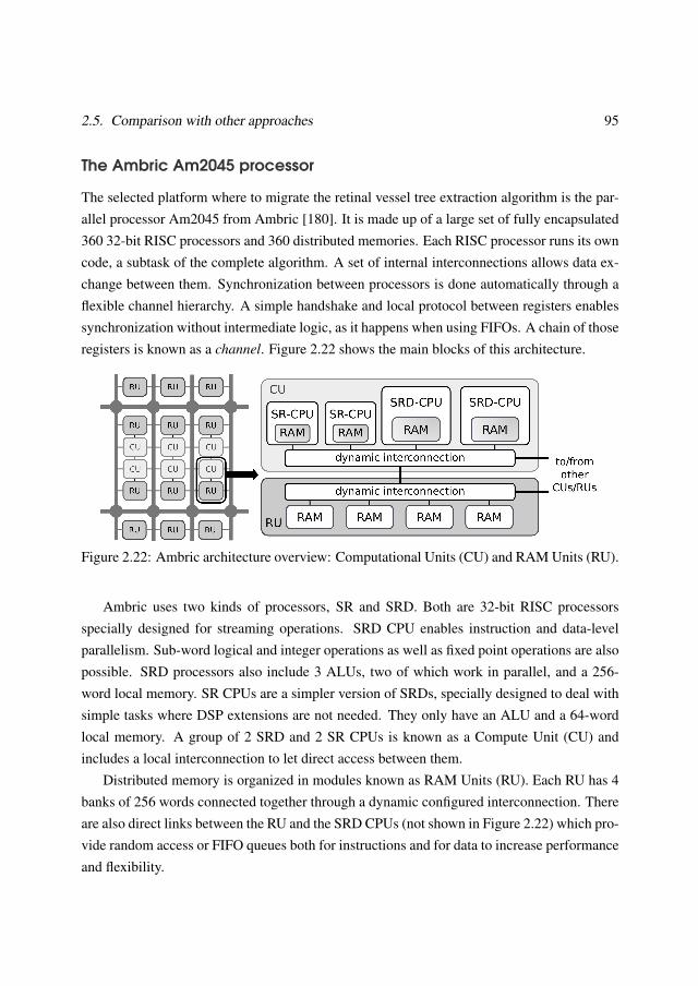
2.5. Comparison with other approaches 95
The Ambric Am2045 processor
The selected platform where to migrate the retinal vessel tree extraction algorithm is the par-allel processor Am2045 from Ambric [180]. It is made up of a large set of fully encapsulated360 32-bit RISC processors and 360 distributed memories. Each RISC processor runs its owncode, a subtask of the complete algorithm. A set of internal interconnections allows data ex-change between them. Synchronization between processors is done automatically through aflexible channel hierarchy. A simple handshake and local protocol between registers enablessynchronization without intermediate logic, as it happens when using FIFOs. A chain of thoseregisters is known as a channel. Figure 2.22 shows the main blocks of this architecture.
Figure 2.22: Ambric architecture overview: Computational Units (CU) and RAM Units (RU).
Ambric uses two kinds of processors, SR and SRD. Both are 32-bit RISC processorsspecially designed for streaming operations. SRD CPU enables instruction and data-levelparallelism. Sub-word logical and integer operations as well as fixed point operations are alsopossible. SRD processors also include 3 ALUs, two of which work in parallel, and a 256-word local memory. SR CPUs are a simpler version of SRDs, specially designed to deal withsimple tasks where DSP extensions are not needed. They only have an ALU and a 64-wordlocal memory. A group of 2 SRD and 2 SR CPUs is known as a Compute Unit (CU) andincludes a local interconnection to let direct access between them.
Distributed memory is organized in modules known as RAM Units (RU). Each RU has 4banks of 256 words connected together through a dynamic configured interconnection. Thereare also direct links between the RU and the SRD CPUs (not shown in Figure 2.22) which pro-vide random access or FIFO queues both for instructions and for data to increase performanceand flexibility.
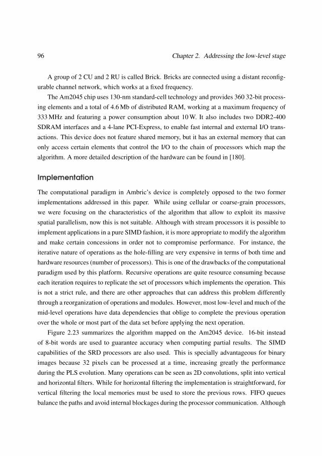
96 Chapter 2. Addressing the low-level stage
A group of 2 CU and 2 RU is called Brick. Bricks are connected using a distant reconfig-urable channel network, which works at a fixed frequency.
The Am2045 chip uses 130-nm standard-cell technology and provides 360 32-bit process-ing elements and a total of 4.6 Mb of distributed RAM, working at a maximum frequency of333 MHz and featuring a power consumption about 10 W. It also includes two DDR2-400SDRAM interfaces and a 4-lane PCI-Express, to enable fast internal and external I/O trans-actions. This device does not feature shared memory, but it has an external memory that canonly access certain elements that control the I/O to the chain of processors which map thealgorithm. A more detailed description of the hardware can be found in [180].
Implementation
The computational paradigm in Ambric’s device is completely opposed to the two formerimplementations addressed in this paper. While using cellular or coarse-grain processors,we were focusing on the characteristics of the algorithm that allow to exploit its massivespatial parallelism, now this is not suitable. Although with stream processors it is possible toimplement applications in a pure SIMD fashion, it is more appropriate to modify the algorithmand make certain concessions in order not to compromise performance. For instance, theiterative nature of operations as the hole-filling are very expensive in terms of both time andhardware resources (number of processors). This is one of the drawbacks of the computationalparadigm used by this platform. Recursive operations are quite resource consuming becauseeach iteration requires to replicate the set of processors which implements the operation. Thisis not a strict rule, and there are other approaches that can address this problem differentlythrough a reorganization of operations and modules. However, most low-level and much of themid-level operations have data dependencies that oblige to complete the previous operationover the whole or most part of the data set before applying the next operation.
Figure 2.23 summarizes the algorithm mapped on the Am2045 device. 16-bit insteadof 8-bit words are used to guarantee accuracy when computing partial results. The SIMDcapabilities of the SRD processors are also used. This is specially advantageous for binaryimages because 32 pixels can be processed at a time, increasing greatly the performanceduring the PLS evolution. Many operations can be seen as 2D convolutions, split into verticaland horizontal filters. While for horizontal filtering the implementation is straightforward, forvertical filtering the local memories must be used to store the previous rows. FIFO queuesbalance the paths and avoid internal blockages during the processor communication. Although
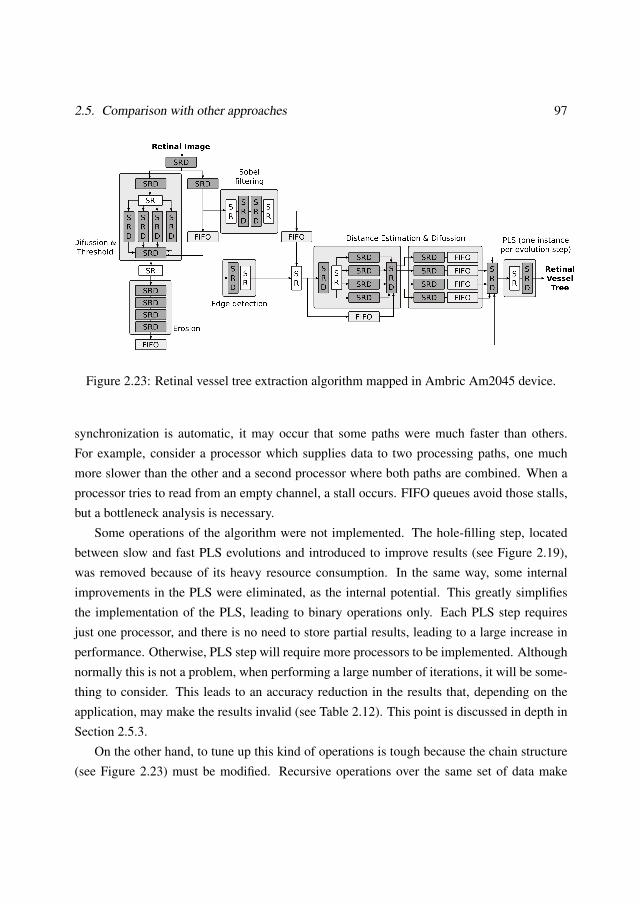
2.5. Comparison with other approaches 97
Figure 2.23: Retinal vessel tree extraction algorithm mapped in Ambric Am2045 device.
synchronization is automatic, it may occur that some paths were much faster than others.For example, consider a processor which supplies data to two processing paths, one muchmore slower than the other and a second processor where both paths are combined. When aprocessor tries to read from an empty channel, a stall occurs. FIFO queues avoid those stalls,but a bottleneck analysis is necessary.
Some operations of the algorithm were not implemented. The hole-filling step, locatedbetween slow and fast PLS evolutions and introduced to improve results (see Figure 2.19),was removed because of its heavy resource consumption. In the same way, some internalimprovements in the PLS were eliminated, as the internal potential. This greatly simplifiesthe implementation of the PLS, leading to binary operations only. Each PLS step requiresjust one processor, and there is no need to store partial results, leading to a large increase inperformance. Otherwise, PLS step will require more processors to be implemented. Althoughnormally this is not a problem, when performing a large number of iterations, it will be some-thing to consider. This leads to an accuracy reduction in the results that, depending on theapplication, may make the results invalid (see Table 2.12). This point is discussed in depth inSection 2.5.3.
On the other hand, to tune up this kind of operations is tough because the chain structure(see Figure 2.23) must be modified. Recursive operations over the same set of data make
98 Chapter 2. Addressing the low-level stage
the implementation in stream processors much more complex than in cellular processors, andthese operations are common during the first stages of image processing [185].
2.5.3 Results and comparison
The main results of the algorithm implementation on the different platforms are summarizedin Table 2.11. We can see that even with a high-end CPU, the results are not satisfactory.Systems running this kind of algorithms usually are required for a rapid response, somethingthat a PC hardly can provide.
As it was detailed in Section 2.3, it was developed using OpenCV/OpenMP and C++ ona computer equipped with a 4-core Intel Core i7 940. This way, compared with the initialstraightforward MATLAB implementation (for test purposes) time execution drops from 41to 13.7 s. As explained above, this algorithm was designed to work on-line following thecapture stage, so a PC is not a good choice. However, we will use it as a reference system forcomparison.
When executing the retinal vessel tree extraction algorithm, we were not only seekingways to reduce the processing time but also we wanted to test different platforms and deter-mine their strengths. This way, SCAMP-3 implementation adds operations to improve accu-racy (necessary when using analog memories), FPGA gets the most accurate results becauseit is possible to implement the original method trustworthy (at the cost of reducing perfor-mance) and Ambric’s device provides the fastest results but reducing the accuracy (requiredhardware resources would be very high otherwise).
It can be seen in Table 2.11 that Ambric’s device gives the highest performance, loweringthe total execution time and achieving a high speed-up. This is in part due to the simpli-fications we made in the algorithm as it was explained previously in Section 2.5.2. Thisimplementation enables a performance not achievable by computers or FPGAs (at least usinga low-cost device). We must emphasize that the simplification of the algorithm provides accu-rate and valid results, but they may not be suitable for certain applications. For instance, theyare still valid to obtain the skeleton of the retinal tree but not to measure the vascular caliber.When migrating the algorithm to this platform, we have faced a trade-off between speed andvalidity of the results for any application and in this case and for comparison purposes, wegive priority to the processing speed.
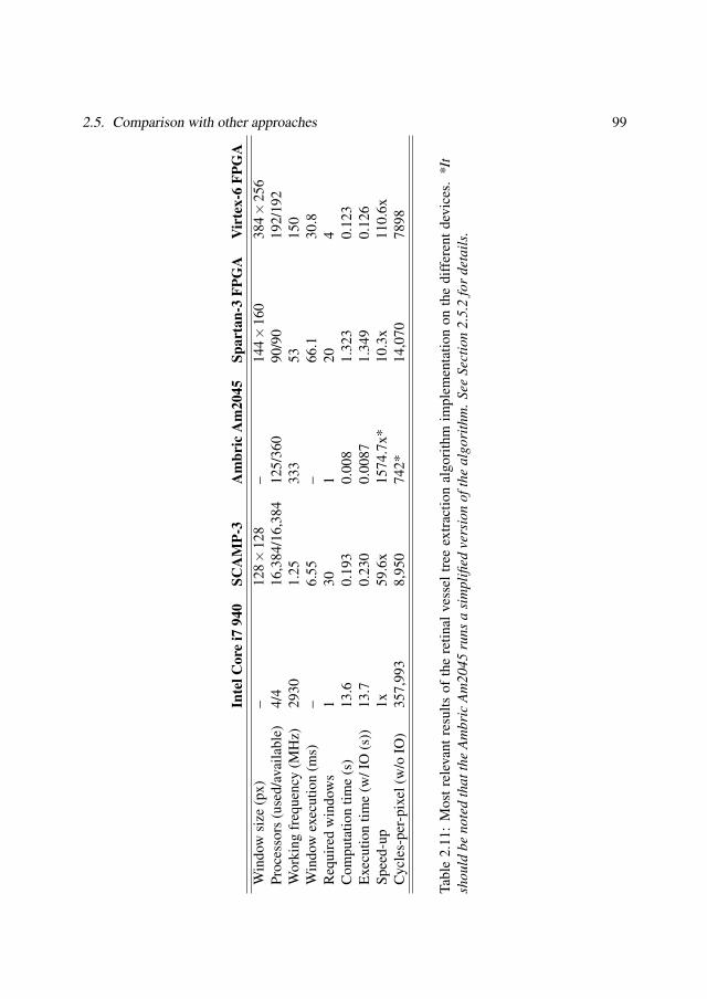
2.5. Comparison with other approaches 99
Inte
lCor
ei7
940
SCA
MP-
3A
mbr
icA
m20
45Sp
arta
n-3
FPG
AV
irte
x-6
FPG
AW
indo
wsi
ze(p
x)–
128×
128
–14
4×
160
384×
256
Proc
esso
rs(u
sed/
avai
labl
e)4/
416
,384
/16,
384
125/
360
90/9
019
2/19
2W
orki
ngfr
eque
ncy
(MH
z)29
301.
2533
353
150
Win
dow
exec
utio
n(m
s)–
6.55
–66
.130
.8R
equi
red
win
dow
s1
301
204
Com
puta
tion
time
(s)
13.6
0.19
30.
008
1.32
30.
123
Exe
cutio
ntim
e(w
/IO
(s))
13.7
0.23
00.
0087
1.34
90.
126
Spee
d-up
1x59
.6x
1574
.7x*
10.3
x11
0.6x
Cyc
les-
per-
pixe
l(w
/oIO
)35
7,99
38,
950
742*
14,0
7078
98
Tabl
e2.
11:
Mos
trel
evan
tres
ults
ofth
ere
tinal
vess
eltr
eeex
trac
tion
algo
rith
mim
plem
enta
tion
onth
edi
ffer
entd
evic
es.
*It
shou
ldbe
note
dth
atth
eA
mbr
icA
m20
45ru
nsa
sim
plifi
edve
rsio
nof
the
algo
rith
m.S
eeSe
ctio
n2.
5.2
for
deta
ils.
100 Chapter 2. Addressing the low-level stage
The other main reason for the high performance of the Ambric’s device is the high workingfrequency of the Am2045 device (333 MHz), which is considerably faster than those achievedby the SCAMP or the FPGA. Digital solutions provide higher clock frequencies but theyare commonly limited by the interconnection between the processing units, as is the caseof the FPGA. MPPAs architectures implement point to point connections with minor recon-figurable options than FPGAs, so clock frequency does not depend on the algorithm whichis being running. However, recent FPGAs families increase its computing capacity consider-ably. This was observed during the implementation of the coarse-grain processor array. Whilethe Spartan-3 offers good performance compared to a desktop PC, it can not compete againstan ASIC. However, a newer FPGA as the Virtex-6 largely improves the throughput withoutcompromissing accuracy in the original algorithm as the Ambric device does. It should betaken into account that the Virtex-6 implements a larger array and an enhanced datapath, be-ing this possible thanks to that the selected FPGA family focuses on performance rather thancost.
The cycles-per-pixel (CPP) metric measures the number of clock cycles required to exe-cute all operations that result on each one of the pixels in the resulting image (see Table 2.6),normalizing the differences in frequency and number of processing cores. The above dis-cussion is summarized using this value. It should be noted that the Ambric Am2045 runs asimplified version of the algorithm. When the number of operations is corrected, this leadsus to an obvious reduction in performance, approximately multiplying by 3 the CPP value.Although the theoretical performance would remain higher than the other approaches, theproblem we face is different: there is not enough processors and interconnections to fit thealgorithm in the device. This was the main reason why it was decided to simplify it.
Analog computing increases greatly the density of integration. In the SCAMP-3 with arelatively old 0.5µm CMOS technology, each processing element occupies an area lower than50µm×50µm and it remains flexible enough to implement any kind of computation. How-ever, accuracy must be considered due to the nature of the data representation (current mode)and the technology issues (mismatch, memory volatility, noise effects...). Analog computingallows to integrate a processor per pixel of the sensor, eliminating one of the most importantbottlenecks in traditional architectures. Given the number of bits of the data representation,digital platforms guarantee accuracy independently of the technology process. While 7–8 bitsare hard to reach using mixed-signal architectures [158], 32-bit or 64-bit architectures arecommon in digital devices.
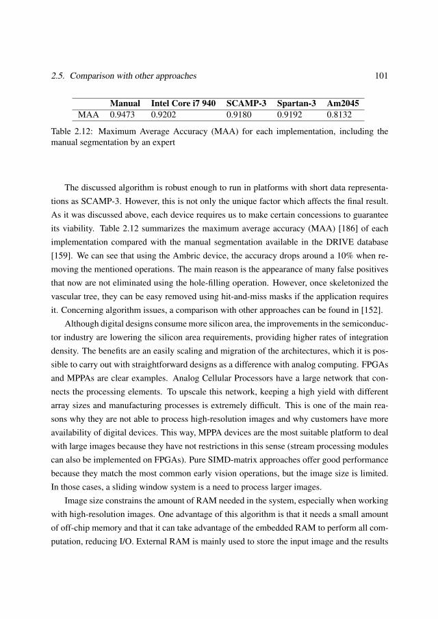
2.5. Comparison with other approaches 101
Manual Intel Core i7 940 SCAMP-3 Spartan-3 Am2045MAA 0.9473 0.9202 0.9180 0.9192 0.8132
Table 2.12: Maximum Average Accuracy (MAA) for each implementation, including themanual segmentation by an expert
The discussed algorithm is robust enough to run in platforms with short data representa-tions as SCAMP-3. However, this is not only the unique factor which affects the final result.As it was discussed above, each device requires us to make certain concessions to guaranteeits viability. Table 2.12 summarizes the maximum average accuracy (MAA) [186] of eachimplementation compared with the manual segmentation available in the DRIVE database[159]. We can see that using the Ambric device, the accuracy drops around a 10% when re-moving the mentioned operations. The main reason is the appearance of many false positivesthat now are not eliminated using the hole-filling operation. However, once skeletonized thevascular tree, they can be easy removed using hit-and-miss masks if the application requiresit. Concerning algorithm issues, a comparison with other approaches can be found in [152].
Although digital designs consume more silicon area, the improvements in the semiconduc-tor industry are lowering the silicon area requirements, providing higher rates of integrationdensity. The benefits are an easily scaling and migration of the architectures, which it is pos-sible to carry out with straightforward designs as a difference with analog computing. FPGAsand MPPAs are clear examples. Analog Cellular Processors have a large network that con-nects the processing elements. To upscale this network, keeping a high yield with differentarray sizes and manufacturing processes is extremely difficult. This is one of the main rea-sons why they are not able to process high-resolution images and why customers have moreavailability of digital devices. This way, MPPA devices are the most suitable platform to dealwith large images because they have not restrictions in this sense (stream processing modulescan also be implemented on FPGAs). Pure SIMD-matrix approaches offer good performancebecause they match the most common early vision operations, but the image size is limited.In those cases, a sliding window system is a need to process larger images.
Image size constrains the amount of RAM needed in the system, especially when workingwith high-resolution images. One advantage of this algorithm is that it needs a small amountof off-chip memory and that it can take advantage of the embedded RAM to perform all com-putation, reducing I/O. External RAM is mainly used to store the input image and the results
102 Chapter 2. Addressing the low-level stage
so 4–8 MB are enough. The SCAMP-3 Vision Chip can store on-chip up to 8 128×128px im-ages (equivalent to 128 Kb, taking into account that the computation in done in analog mode),the architecture proposed for the Spartan-3 up to 8 144×160px images (176Kb) and the Am-bric Am2045 can store up to 4.6 Mb of data. This is the main reason why PC performance isso low: the selected devices are capable of doing all the processing on-chip, accessing to theexternal memory just for loading the input image. On the contrary, the PC should make anintensive use of external memory to store partial results, making memory access a bottleneck.Explicit load/store operations are needed and this is why CPP is much higher than the otherapproaches.
Analog processing allows to integrate the processors with the image sensors. But thiskind of processor distribution, although adequate for low and some steps of mid-level im-age processing, is not suitable for complex algorithms with more complex data dependencies.SCAMP-3 is very powerful for early vision tasks, but it lacks the flexibility to address higher-level operations. Using FPGAs, different architectures and computing paradigms can be easilyemulated. Its dense network, although it consumes a large silicon area, provides this flexibil-ity. MPPAs attempt to build more powerful computing elements by reducing interconnectionbetween processors. The fixed network of Cellular Processors limits its range of application.The programmable and dense network of FPGAs enables any kind of architecture emulation,but reducing integration density and the working frequency. MPPAs are located in an inter-mediate position. Its programmable network provides enough flexibility to cover a wide rangeof applications, freeing up space to build more powerful processors, but limiting the kind ofcomputations that can address. This is why recursive operations are hard to implement andthe resource usage is so high. PLS had to be simplified to deal with this trade-off.
With respect to the algorithm development process, Time-To-Market (TTM) is key inindustry. Ambric’s platform offers the system with the lowest TTM. A complete softwaredevelopment kit that provides a high-level language and tools for rapid profiling make the de-velopment much faster than in other platforms. This is one of the purposes of the platform, tooffer a high-performance device keeping prototyping rapid and closer to software. Using HDLlanguage to develop complex architectures or software-to-hardware implementations is muchmore expensive because they are closer to hardware than to software. This is specially true inthe second case, where a high-level language (as SystemC or ImpulseC) is recommended.
Regarding portability, it is clear that a computer-based solution (even a mobile version) isnot a valid solution because of size, power consumption or lack of integration and compact-
2.5. Comparison with other approaches 103
ness between its components. For early vision tasks, a focal-plane processor (as SCAMP-3)is the best choice. The processors are integrated together with the sensors and their powerconsumption is very reduced. To accomplish complex operations, FPGAs offer reduced sizeand power consumption in its low-end products, allowing to build complex Systems-on-Chipand compacting all the processing on the same chip. For better performance, an MPPA or alarger FPGA is needed. Power consumption will be higher, specially for the high-end FPGAs,but the amount of processing units we can include is considerably higher.
Although the conclusions we have drawn in this section come from a specific algorithm,this has features common to most algorithms for low- and many medium-level image-processingtasks, as discussed in Section 2.3. We have seen that visual processors as SCAMP are excel-lent in early vision operations, but specific algorithms are needed to address the subsequentprocessing steps. MPPAs provide an environment closer to the programmer, with a great per-formance, limited by the low-level operations. FPGAs enable us to replicate any applicationwith very acceptable results, although the development time is higher.
In summary, this algorithm was specifically designed focusing on performance and tooperate online in a device with reduced size, cost and power consumption, opening new pos-sibilities in other areas apart from the medical imaging. It was specifically designed focusingon performance, so an MP-SIMD processor array offers good results. Due to the algorithminherent nature, an MP-SIMD processor array offers good results. However, the technologylimitations, especially array size and a limited accuracy, make us consider other approaches.FPGAs enable us to speed up most applications with acceptable results. They take advantageof its highly reconfigurable network to improve the matching between architecture and algo-rithm, exploiting its characteristics and potentially leading to better performance solutions.Advances in semiconductor industry enable to integrate more and more functional units ina reduced silicon area. MPPAs take advantage of this integrating hundred of processors onthe same chip. They focus on exploiting the task parallelism of the algorithms, and resultsprove that this approach provides remarkable performance. However, certain trade-offs mustbe done when dealing with low-level image processing not to compromise efficiency.
Results show that even using a high-end CPU, a significant gain can be achieved usinghardware accelerators. A cost-sensitive FPGA outperforms the Intel Core i7 940 by a factorof 10x. With a focal plane-processor, this factor reaches 60x. Using the selected MPPA, afactor of more than 1500x was reached, but we have to take into account that the algorithmwas simplified in order to sort the limitations of the platform when dealing with low-level
104 Chapter 2. Addressing the low-level stage
image processing. The accuracy drops about 10% which might compromise its suitabilityfor some applications. The coarse-grain processor array has proven to be very effective onFPGA, leading to high throughput and straightforward array scaling, as Spartan-3 and Virtex-6 FPGAs implementations show. This permits to outperform the focal-plane processor, whichis the natural platform for this kind of algorithms.
The retinal vessel-tree extraction algorithm presents common features to most of the low-and mid-level algorithms available in the literature. Except for high-level operations overcomplex data sets, where high precision is needed, the presented architectures perform ad-equately for low- and mid-level stages, where operations are simple and have to be appliedover a large set of data. They are able to exploit the massive spatial parallelism of low-levelvision, featuring general-purpose computation. Ambric’s processor requires a special mentionbecause, although it can exploit spatial parallelism of low-level vision, its throughput is veryhigh when dealing with the mid-level stage, where task parallelism is clearly advantageous.However, SCAMP-3 is mainly restricted to the low-level stage where its low power consump-tion and form factor fit well. FPGAs are flexible enough to cover the complete application.Their major drawback is the time required to get the system ready.
2.6 Summary
In this chapter, a dedicated processor for general-purpose low-level image processing is pre-sented. The tasks of the low-level stage are characterized for being simple, repetitive andapplied over a very large set of data, and do not require high accuracy. Therefore, they arevery expensive computationally, specially on embedded systems, the field where this proces-sor is focused.
After a preliminary study where a binary (B/W) processor was designed, it has been con-cluded that a massively parallel architecture does not face adequately low-level operations.Although a 2D arrangement of arithmetic cores can take advantage of the nature and inter-relationships between image pixels, a processor-per-pixel correspondence is heavy resourceconsumption, dealing with low resolution processors and low clock frequencies. Even thoughthese are technical issues, the real performance and suitability of these processors are muchlower than theoretically expected, so other solutions a-priori less suitable might overcomethese limitations.
2.6. Summary 105
As a result, the preliminary processor was enhanced to process non-binary data, extendingthe capabilities of each processing core and reducing the parallelism. This architecture, acoarse-grain processor array, provides better figures of merit, as results show. In particular, itis easier to upscale the array without compromising the clock frequency, leading to processorable to handle images of larger resolution. When comparing it with other approaches, anFPGA-based implementation of the coarse-grain processor array outperforms a MP-SIMDprocessor which has an 8500% more computing units. This integration density is achievedusing mixed-signal architectures which limit the array size and the clock frequency, leadingto poorer results although the power consumption requirements achieved are very difficult tobeat. MPPA devices also show a very high performance exploiting task parallelism, althoughrecursive operations drops performance or accuracy, been hard to reach a trade-off solution.The algorithm employed for this comparison and posterior discussion is representative of itsclass, providing additional information about how data interacts when concatenating differentoperators. This gives us an advantage during the design stage of a dedicated architecture tospeed-up this kind of operations. Results show that conventional CPUs are not efficient forearly vision tasks, so other different approaches are clearly justified.
The major conclusions of this chapter refer to arithmetic cores organization and data distri-bution between them. As seen before, a 2D arrangement faces adequately low-level pixel-to-pixel and neighborhood operations, especially when processing image data. On the contrary,when processing non-image (abstract) data, a 2D array does not provide the necessary flex-ibility for its processing. This is more acute with a higher level of abstraction. The MPPAprocessor, which takes advantage of task parallelism, is a proof. One unresolved issue isdata I/O. Image processing tasks require a high bandwidth and large storage elements, limit-ing the performance if the arithmetic units remain waiting for data to process. Overlap dataprocessing and transferring is essential.
The conclusions drawn in this chapter lead us to propose an improved architecture, fo-cusing on an extended range of operation without compromising performance, resource andpower consumption.

CHAPTER 3
EXPANDING THE RANGE OF OPERATION
Chapter 2 summarizes the efforts made to speed-up the low-level stages on Computer Visionapplications. These stages represent most of the workload of a typical Computer Vision appli-cation. A 2-dimensional massively parallel processor array to tackle higher level stages wasdiscarded as its flexibility is reduced. This is also true for the coarse-grain processor array,although it solves issues regarding operation accuracy and image size capability. However,the inclusion of large on-chip memories helps to provide large throughput. On the other hand,task parallelism has proven to be very effective even facing natively spatial parallel opera-tions. However, some operations have to be discarded as the number of processing units islimited to efficiently implement them.
SIMD processors are widely used to speed-up repetitive and massively parallel operations.However, programs with more complex dataflow do not fit well in this kind of processors,being needed a different scheme. In this case, MIMD computers can address more efficientlystreaming processing because they are focused on exploiting the task parallelism. Our goalis to combine both paradigms on a single architecture in a way that it could be configuredaccording to the type of parallelism of the algorithm. This way, spatial-parallel operationsare executed in SIMD mode, task-parallel operations are carried out in MIMD mode and thehigh-level steps are performed using the SISD paradigm, with a sequential processor.
This chapter introduces a hybrid SIMD/MIMD architecture for embedded devices whichreconfigures its internal connections to face low-, mid- and some operations of the high-levelstages. It focuses on flexibility and easing programming without compromising performance,permitting to adapt internal parameters to address different key applications. The architec-
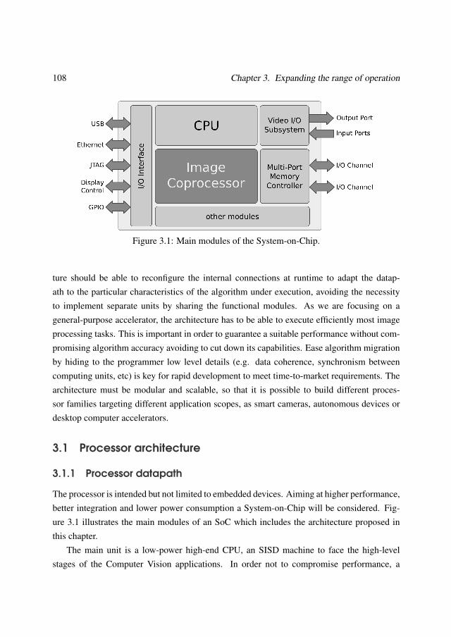
108 Chapter 3. Expanding the range of operation
Figure 3.1: Main modules of the System-on-Chip.
ture should be able to reconfigure the internal connections at runtime to adapt the datap-ath to the particular characteristics of the algorithm under execution, avoiding the necessityto implement separate units by sharing the functional modules. As we are focusing on ageneral-purpose accelerator, the architecture has to be able to execute efficiently most imageprocessing tasks. This is important in order to guarantee a suitable performance without com-promising algorithm accuracy avoiding to cut down its capabilities. Ease algorithm migrationby hiding to the programmer low level details (e.g. data coherence, synchronism betweencomputing units, etc) is key for rapid development to meet time-to-market requirements. Thearchitecture must be modular and scalable, so that it is possible to build different proces-sor families targeting different application scopes, as smart cameras, autonomous devices ordesktop computer accelerators.
3.1 Processor architecture
3.1.1 Processor datapath
The processor is intended but not limited to embedded devices. Aiming at higher performance,better integration and lower power consumption a System-on-Chip will be considered. Fig-ure 3.1 illustrates the main modules of an SoC which includes the architecture proposed inthis chapter.
The main unit is a low-power high-end CPU, an SISD machine to face the high-levelstages of the Computer Vision applications. In order not to compromise performance, a
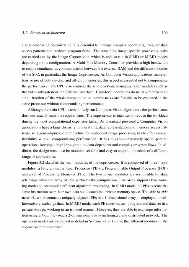
3.1. Processor architecture 109
signal-processing optimized CPU is essential to manage complex operations, irregular dataaccess patterns and intricate program flows. The remaining image-specific processing tasksare carried out by the Image Coprocessor, which is able to run in SIMD or MIMD modesdepending on its configuration. A Multi-Port Memory Controller provides a high bandwidthto enable simultaneous communication between the external RAM and the different modulesof the SoC, in particular, the Image Coprocessor. As Computer Vision applications make in-tensive use of both on-chip and off-chip memories, this aspect is essential not to compromisethe performance. The CPU also controls the whole system, managing other modules such asthe video subsystem or the Ethernet interface. High-level operations do usually represent ansmall fraction of the whole computation so control tasks are feasible to be executed in thesame processor without compromising performance.
Although the main CPU is able to fully run Computer Vision algorithms, the performancedoes not usually meet the requirements. The coprocessor is intended to reduce the workloadduring the most computational expensive tasks. As discussed previously, Computer Visionapplications have a large disparity in operations, data representation and memory access pat-terns, so a general-purpose architecture for embedded image processing has to offer enoughflexibility without compromising performance. It has to exploit massively spatial-paralleloperations, keeping a high throughput on data-dependent and complex program flows. In ad-dition, the design must also be modular, scalable and easy to adapt to the needs of a differentrange of applications.
Figure 3.2 sketches the main modules of the coprocessor. It is composed of three majormodules: a Programmable Input Processor (PIP), a Programmable Output Processor (POP)and a set of Processing Elements (PEs). The two former modules are responsible for dataretrieving while the array of PEs performs the computation. The array supports two work-ing modes to accomplish efficient algorithm processing. In SIMD mode, all PEs execute thesame instruction over their own data set, located in a private memory space. The side-to-side
network, which connects uniquely adjacent PEs in a 1-dimensional array, is employed to col-laboratively exchange data. In MIMD mode, each PE stores its own program and data set in aprivate storage, working in an isolated manner. However, they are able to exchange informa-tion using a local network, a 2-dimensional auto-synchronized and distributed network. Theoperation modes are explained in detail in Section 3.1.2. Below, the different modules of thecoprocessor are described.
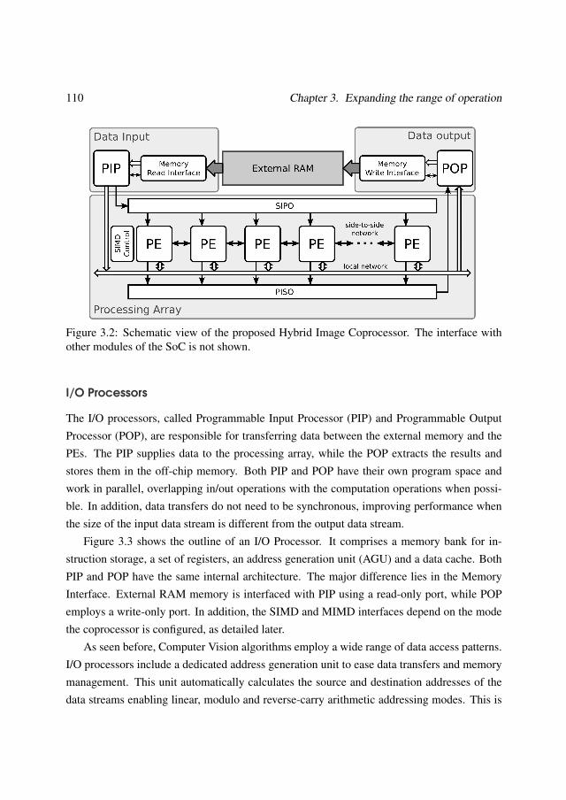
110 Chapter 3. Expanding the range of operation
Figure 3.2: Schematic view of the proposed Hybrid Image Coprocessor. The interface withother modules of the SoC is not shown.
I/O Processors
The I/O processors, called Programmable Input Processor (PIP) and Programmable OutputProcessor (POP), are responsible for transferring data between the external memory and thePEs. The PIP supplies data to the processing array, while the POP extracts the results andstores them in the off-chip memory. Both PIP and POP have their own program space andwork in parallel, overlapping in/out operations with the computation operations when possi-ble. In addition, data transfers do not need to be synchronous, improving performance whenthe size of the input data stream is different from the output data stream.
Figure 3.3 shows the outline of an I/O Processor. It comprises a memory bank for in-struction storage, a set of registers, an address generation unit (AGU) and a data cache. BothPIP and POP have the same internal architecture. The major difference lies in the MemoryInterface. External RAM memory is interfaced with PIP using a read-only port, while POPemploys a write-only port. In addition, the SIMD and MIMD interfaces depend on the modethe coprocessor is configured, as detailed later.
As seen before, Computer Vision algorithms employ a wide range of data access patterns.I/O processors include a dedicated address generation unit to ease data transfers and memorymanagement. This unit automatically calculates the source and destination addresses of thedata streams enabling linear, modulo and reverse-carry arithmetic addressing modes. This is
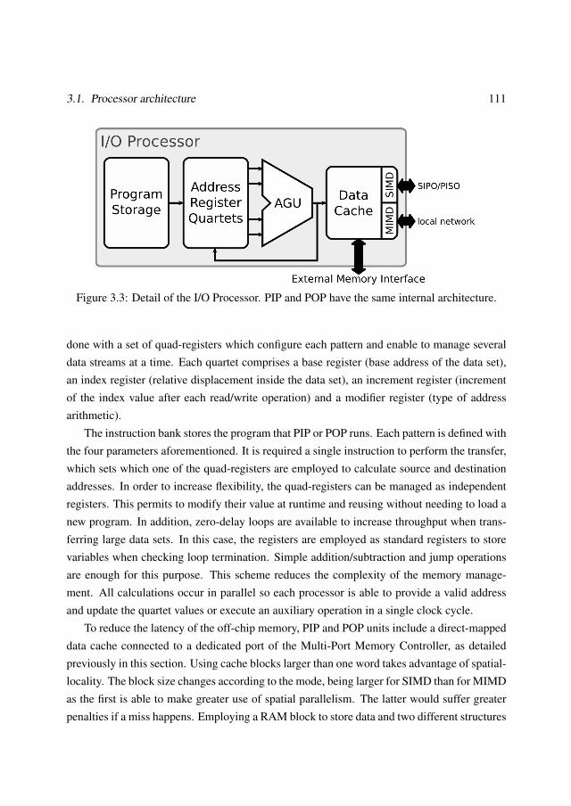
3.1. Processor architecture 111
Figure 3.3: Detail of the I/O Processor. PIP and POP have the same internal architecture.
done with a set of quad-registers which configure each pattern and enable to manage severaldata streams at a time. Each quartet comprises a base register (base address of the data set),an index register (relative displacement inside the data set), an increment register (incrementof the index value after each read/write operation) and a modifier register (type of addressarithmetic).
The instruction bank stores the program that PIP or POP runs. Each pattern is defined withthe four parameters aforementioned. It is required a single instruction to perform the transfer,which sets which one of the quad-registers are employed to calculate source and destinationaddresses. In order to increase flexibility, the quad-registers can be managed as independentregisters. This permits to modify their value at runtime and reusing without needing to load anew program. In addition, zero-delay loops are available to increase throughput when trans-ferring large data sets. In this case, the registers are employed as standard registers to storevariables when checking loop termination. Simple addition/subtraction and jump operationsare enough for this purpose. This scheme reduces the complexity of the memory manage-ment. All calculations occur in parallel so each processor is able to provide a valid addressand update the quartet values or execute an auxiliary operation in a single clock cycle.
To reduce the latency of the off-chip memory, PIP and POP units include a direct-mappeddata cache connected to a dedicated port of the Multi-Port Memory Controller, as detailedpreviously in this section. Using cache blocks larger than one word takes advantage of spatial-locality. The block size changes according to the mode, being larger for SIMD than for MIMDas the first is able to make greater use of spatial parallelism. The latter would suffer greaterpenalties if a miss happens. Employing a RAM block to store data and two different structures
112 Chapter 3. Expanding the range of operation
Figure 3.4: Processing Element of the Hybrid Image Coprocessor for both SIMD/MIMDmodes.
to store the label, index and valid fields, as usual on cache architectures, enables this feature.The performance increase compensates for the additional resources.
Processing Elements Array
The Processing Element (PE) is key for a successful design. It has to be as small as possibleto reduce hardware resources and to build the largest possible array, but flexible enough toface most of the arithmetic operations efficiently. The PEs have a Reduced Instruction SetComputer (RISC) architecture. The purpose is to make the segmentation and the parallelismof the instruction execution easier, integrating a small and common set of regular instructionsfor both modes. This requires less resources, specially important in MIMD mode where eachPE includes its own controller as each one is running an independent program. The process-ing array is made of a set of independent and encapsulated processors connected through areduced and programmable network, as Figure 3.2 shows.
Figure 3.4 depicts the Processing Element. Each PE comprises a Memory Element (ME),an Arithmetic and Logic Unit (ALU), a Register Bank and a set of Stream Queues. The in-
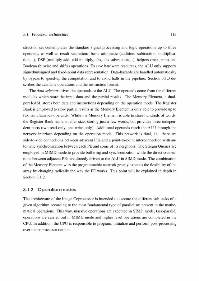
3.1. Processor architecture 113
struction set contemplates the standard signal processing and logic operations up to threeoperands, as well as result saturation: basic arithmetic (addition, subtraction, multiplica-tion,...), DSP (multiply-add, add-multiply, abs, abs-subtraction,...), helpers (max, min) andBoolean (bitwise and shifts) operations. To save hardware resources, the ALU only supportssigned/unsigned and fixed-point data representation. Data-hazards are handled automaticallyby bypass to speed-up the computation and to avoid halts in the pipeline. Section 3.1.3 de-scribes the available operations and the instruction format.
The data selector drives the operands to the ALU. The operands come from the differentmodules which store the input data and the partial results. The Memory Element, a dual-port RAM, stores both data and instructions depending on the operation mode. The RegisterBank is employed to store partial results as the Memory Element is only able to provide up totwo simultaneous operands. While the Memory Element is able to store hundreds of words,the Register Bank has a smaller size, storing just a few words, but provides three indepen-dent ports (two read-only, one write-only). Additional operands reach the ALU through thenetwork interface depending on the operation mode. This network is dual, i.e. there areside-to-side connections between adjacent PEs and a point-to-point interconnection with au-tomatic synchronization between each PE and some of its neighbors. The Stream Queues areemployed in MIMD mode to provide buffering and synchronization while the direct connec-tions between adjacent PEs are directly driven to the ALU in SIMD mode. The combinationof the Memory Element with the programmable network greatly expands the flexibility of thearray by changing radically the way the PE works. This point will be explained in depth inSection 3.1.2.
3.1.2 Operation modes
The architecture of the Image Coprocessor is intended to execute the different sub-tasks of agiven algorithm according to the most fundamental type of parallelism present in the mathe-matical operations. This way, massive operations are executed in SIMD mode, task-paralleloperations are carried out in MIMD mode and higher level operations are completed in theCPU. In addition, the CPU is responsible to program, initialize and perform post-processingover the coprocessor outputs.
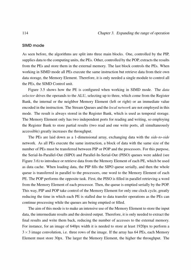
114 Chapter 3. Expanding the range of operation
SIMD mode
As seen before, the algorithms are split into three main blocks. One, controlled by the PIP,supplies data to the computing units, the PEs. Other, controlled by the POP, extracts the resultsfrom the PEs and store them in the external memory. The last block controls the PEs. Whenworking in SIMD mode all PEs execute the same instruction but retrieve data from their owndata storage, the Memory Element. Therefore, it is only needed a single module to control allthe PEs, the SIMD Control unit.
Figure 3.5 shows how the PE is configured when working in SIMD mode. The data
selector drives the operands to the ALU, selecting up to three, which come from the RegisterBank, the internal or the neighbor Memory Element (left or right) or an immediate valueencoded in the instruction. The Stream Queues and the local network are not employed in thismode. The result is always stored in the Register Bank, which is used as temporal storage.The Memory Element only has two independent ports for reading and writing, so employingthe Register Bank to store partial results (two read and one write ports, all simultaneouslyaccessible) greatly increases the throughput.
The PEs are laid down as a 1-dimensional array, exchanging data with the side-to-side
network. As all PEs execute the same instruction, a block of data with the same size of thenumber of PEs must be transferred between PIP or POP and the processors. For this purpose,the Serial-In-Parallel-Out (SIPO) and Parallel-In-Serial-Out (PISO) queues were added (seeFigure 3.6) to introduce or retrieve data from the Memory Element of each PE, which be usedas data cache. When loading data, the PIP fills the SIPO queue serially, and then the wholequeue is transferred in parallel to the processors, one word to the Memory Element of eachPE. The POP performs the opposite task. First, the PISO is filled in parallel retrieving a wordfrom the Memory Element of each processor. Then, the queue is emptied serially by the POP.This way, PIP and POP take control of the Memory Element for only one clock cycle, greatlyreducing the time in which each PE is stalled due to data transfer operations as the PEs cancontinue processing while the queues are being emptied or filled.
The aim of this mode is to make an intensive use of the Memory Element to store the inputdata, the intermediate results and the desired output. Therefore, it is only needed to extract thefinal results and write them back, reducing the number of accesses to the external memory.For instance, for an image of 640px width it is needed to store at least 1920px to perform a3×3 image convolution, i.e. three rows of the image. If the array has 64 PEs, each MemoryElement must store 30px. The larger the Memory Element, the higher the throughput. The
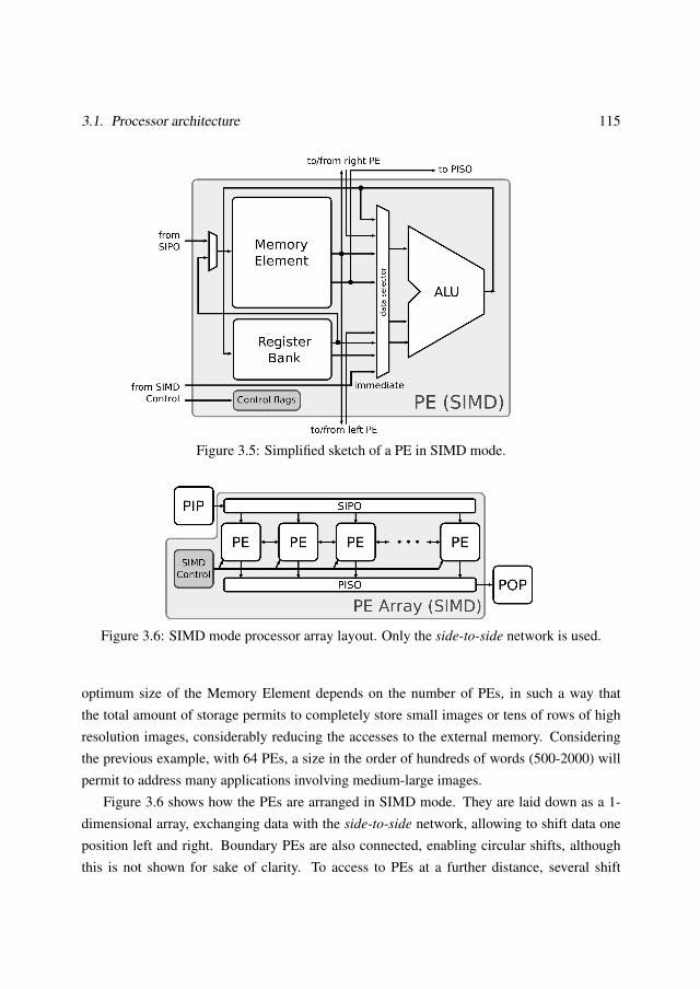
3.1. Processor architecture 115
Figure 3.5: Simplified sketch of a PE in SIMD mode.
Figure 3.6: SIMD mode processor array layout. Only the side-to-side network is used.
optimum size of the Memory Element depends on the number of PEs, in such a way thatthe total amount of storage permits to completely store small images or tens of rows of highresolution images, considerably reducing the accesses to the external memory. Consideringthe previous example, with 64 PEs, a size in the order of hundreds of words (500-2000) willpermit to address many applications involving medium-large images.
Figure 3.6 shows how the PEs are arranged in SIMD mode. They are laid down as a 1-dimensional array, exchanging data with the side-to-side network, allowing to shift data oneposition left and right. Boundary PEs are also connected, enabling circular shifts, althoughthis is not shown for sake of clarity. To access to PEs at a further distance, several shift
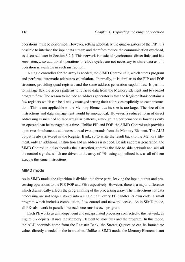
116 Chapter 3. Expanding the range of operation
operations must be performed. However, setting adequately the quad-registers of the PIP, it ispossible to interlace the input data stream and therefore reduce the communication overhead,as discussed later in Section 3.2.2. This network is made of synchronous direct links and haszero-latency, so additional operations or clock cycles are not necessary to share data as thisoperation is available in each instruction.
A single controller for the array is needed, the SIMD Control unit, which stores programand performs automatic addresses calculation. Internally, it is similar to the PIP and POPstructure, providing quad-registers and the same address generation capabilities. It permitsto manage flexible access patterns to retrieve data from the Memory Element and to controlprogram flow. The reason to include an address generator is that the Register Bank contains afew registers which can be directly managed setting their addresses explicitly on each instruc-tion. This is not applicable to the Memory Element as its size is too large. The size of theinstructions and data management would be impractical. However, a reduced form of directaddressing is included to face irregular patterns, although the performance is lower as onlyan operand can be managed at a time. Unlike PIP and POP, the SIMD Control unit providesup to two simultaneous addresses to read two operands from the Memory Element. The ALUoutput is always stored in the Register Bank, so to write the result back to the Memory Ele-ment, only an additional instruction and an address is needed. Besides address generation, theSIMD Control unit also decodes the instruction, controls the side-to-side network and sets allthe control signals, which are driven to the array of PEs using a pipelined bus, as all of themexecute the same instructions.
MIMD mode
As in SIMD mode, the algorithm is divided into three parts, leaving the input, output and pro-cessing operations to the PIP, POP and PEs respectively. However, there is a major differencewhich dramatically affects the programming of the processing array. The instructions for dataprocessing are not longer stored into a single unit: every PE handles its own code, a smallprogram which includes computation, flow control and network access. As in SIMD mode,all PEs also work in parallel, but each one runs its own program.
Each PE works as an independent and encapsulated processor connected to the network, asFigure 3.7 depicts. It uses the Memory Element to store data and the program. In this mode,the ALU operands come from the Register Bank, the Stream Queues or can be immediatevalues directly encoded in the instruction. Unlike in SIMD mode, the Memory Element is not
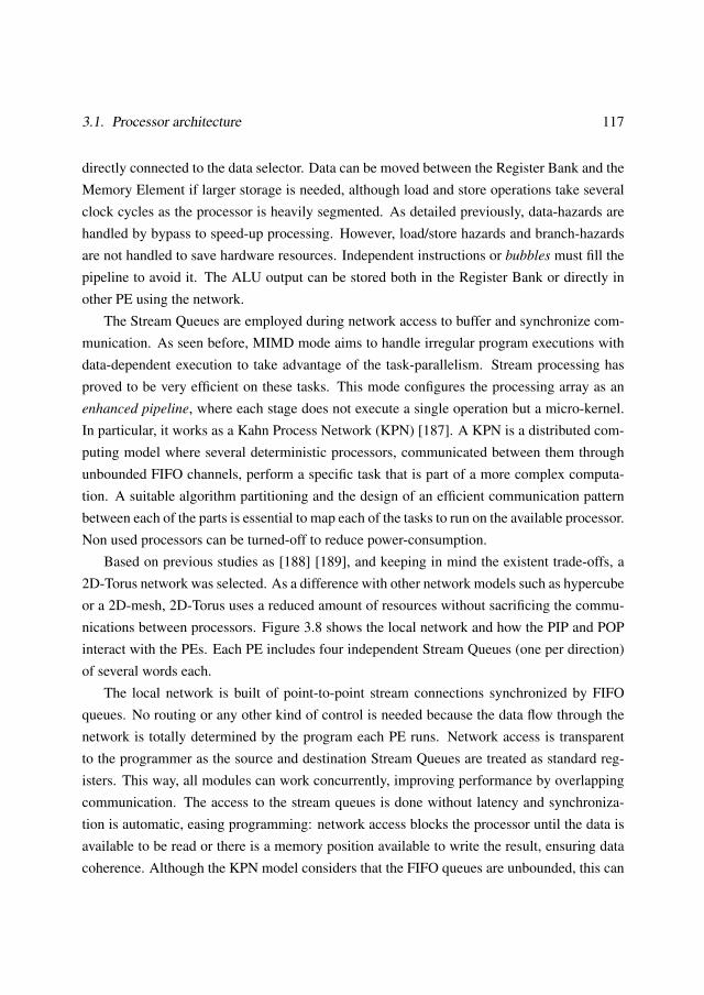
3.1. Processor architecture 117
directly connected to the data selector. Data can be moved between the Register Bank and theMemory Element if larger storage is needed, although load and store operations take severalclock cycles as the processor is heavily segmented. As detailed previously, data-hazards arehandled by bypass to speed-up processing. However, load/store hazards and branch-hazardsare not handled to save hardware resources. Independent instructions or bubbles must fill thepipeline to avoid it. The ALU output can be stored both in the Register Bank or directly inother PE using the network.
The Stream Queues are employed during network access to buffer and synchronize com-munication. As seen before, MIMD mode aims to handle irregular program executions withdata-dependent execution to take advantage of the task-parallelism. Stream processing hasproved to be very efficient on these tasks. This mode configures the processing array as anenhanced pipeline, where each stage does not execute a single operation but a micro-kernel.In particular, it works as a Kahn Process Network (KPN) [187]. A KPN is a distributed com-puting model where several deterministic processors, communicated between them throughunbounded FIFO channels, perform a specific task that is part of a more complex computa-tion. A suitable algorithm partitioning and the design of an efficient communication patternbetween each of the parts is essential to map each of the tasks to run on the available processor.Non used processors can be turned-off to reduce power-consumption.
Based on previous studies as [188] [189], and keeping in mind the existent trade-offs, a2D-Torus network was selected. As a difference with other network models such as hypercubeor a 2D-mesh, 2D-Torus uses a reduced amount of resources without sacrificing the commu-nications between processors. Figure 3.8 shows the local network and how the PIP and POPinteract with the PEs. Each PE includes four independent Stream Queues (one per direction)of several words each.
The local network is built of point-to-point stream connections synchronized by FIFOqueues. No routing or any other kind of control is needed because the data flow through thenetwork is totally determined by the program each PE runs. Network access is transparentto the programmer as the source and destination Stream Queues are treated as standard reg-isters. This way, all modules can work concurrently, improving performance by overlappingcommunication. The access to the stream queues is done without latency and synchroniza-tion is automatic, easing programming: network access blocks the processor until the data isavailable to be read or there is a memory position available to write the result, ensuring datacoherence. Although the KPN model considers that the FIFO queues are unbounded, this can
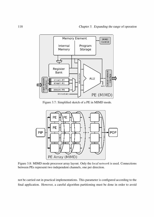
118 Chapter 3. Expanding the range of operation
Figure 3.7: Simplified sketch of a PE in MIMD mode.
Figure 3.8: MIMD mode processor array layout. Only the local network is used. Connectionsbetween PEs represent two independent channels, one per direction.
not be carried out in practical implementations. This parameter is configured according to thefinal application. However, a careful algorithm partitioning must be done in order to avoid
3.1. Processor architecture 119
very unbalanced paths, as fast paths can overload the queues and drop the performance oreven block the computation.
In MIMD mode, the PE uses an expanded instruction set which includes flow controloperations (unconditional-jump, branch-if-equal, branch-if-not-equal...). Each PE includesits own control unit, the MIMD Control, as each one runs a different program.
The data access patterns in MIMD mode are the same as in SIMD mode. PIP and POPfunctionality (flexible access patterns, data alignment or data caches) and architecture remainthe same. However, PIP and POP do not use the SIPO and PISO queues to preload data.Instead of that, they access directly to the Stream Queues which form a local network usinga simple handshake (FIFO) interface. This is the reason why the I/O processor have twointerfaces, one per each mode (see Figure 3.3).
In SIMD mode, PIP and POP run until the SIPO/PISO queues are full or empty, trans-ferring as many data as PEs has the array, one word per processor. This permits to exploitmassively spatial parallelism. On the other hand, when taking advantage of the temporal par-allelism, it is expected that the typical patterns consist of sparse memory accesses of a numberof consecutive words. In addition, MIMD mode resembles a systolic array with a left to right
flow of data. As shown in Figure 3.8, PIP and POP are only connected to the first and lastcolumns of PEs. In MIMD mode, a configurable amount of data is transferred to a single PE,indicated in each transfer. Despite this, data transferring is done in the same way as describedpreviously. A single instruction sets which one of the quad-registers is employed to calculatethe source addresses in the external memory and the destination PE, encoded explicitly in theinstruction. Additionally, a third field encodes the size of the transfer. This is done by PIP tosupply data, but POP works in the same manner.
Selecting the mode
The selection of the operation mode depends on multiple factors. From the operational pointof view, the following steps are involved. The coprocessor is fully guided by instructions, thealgorithm which the user runs. First of all, the CPU selects the mode by setting a global flagwhich directly indicates if the processor is in SIMD (0) or MIMD (1) mode. Then the CPUhas to load the programs of all involved modules, this is, the PIP, POP, and the SIMD Controlunit (if SIMD mode) or the used PEs (in MIMD mode).
As detailed before, the instruction set is common for both modes to ease decoding, al-though separate control units handle each mode. Depending on the value of the global flag,
120 Chapter 3. Expanding the range of operation
they take the control or inhibit its functionality. This way, switching the flag changes modewith zero-delay. However, results might be undefined if we do not ensure that the previousoperations are completed. This is met when the end of the program is reached in all the units.
PIP, POP and SIMD Control modules act during the program transferring. All of them aredirectly accessed through the bus of the system. However, to load the program into all PEswhen running in MIMD mode, a pipelined shared bus is employed to avoid large resourceconsumption and not to drop the clock frequency due to a high fan-out. Program storage isdone serially but with random access, greatly reducing loading time if just a few processorsare employed or a compact program is run.
3.1.3 Instruction set
The selection of the instruction set is important to meet some of the trade-offs of the archi-tecture. Regular and compact instructions permit to decrease hardware requirements and easeinstruction decoding. A RISC architecture was selected to achieve this goal. However, evenmore important is to select a set of operands and complementary operations that permit toefficiently implement most of the Computer Vision algorithms. Inasmuch as the architectureis focused on a general-purpose solution, the instruction set has to contain the basic buildingblocks that enable to execute more complex operands. However, this may result in a per-formance decrease if for every major operation the number of sub-operations is too large. Itis not possible to upscale the number of processors at the same ratio to compensate for thislimitation. Taking into account the proposed architecture, the following trade-off solution isconsidered, aiming to balance both general and CV-oriented operations.
I/O Processors
PIP and POP are responsible for data transferring. Figure 3.9 shows the instruction formatfor the I/O processors. The different operations are grouped according to their format. R-typerefers to regular, I-type to immediate operation, J-type to unconditional jumps and S-typeto other non-standard (special) operations. The move instruction transfers a set of data tothe desired location. Considering the PIP in SIMD mode, the source and destination ad-dresses are calculated using the Address Generation Unit and the configuration stored in thequad-registers. In MIMD mode, the source is also encoded in a quad-register. However, thedestination address is a mask which sets the destination PEs of the first row of the array. Datatransferring is equivalent for POP, although inverting source and destination fields.
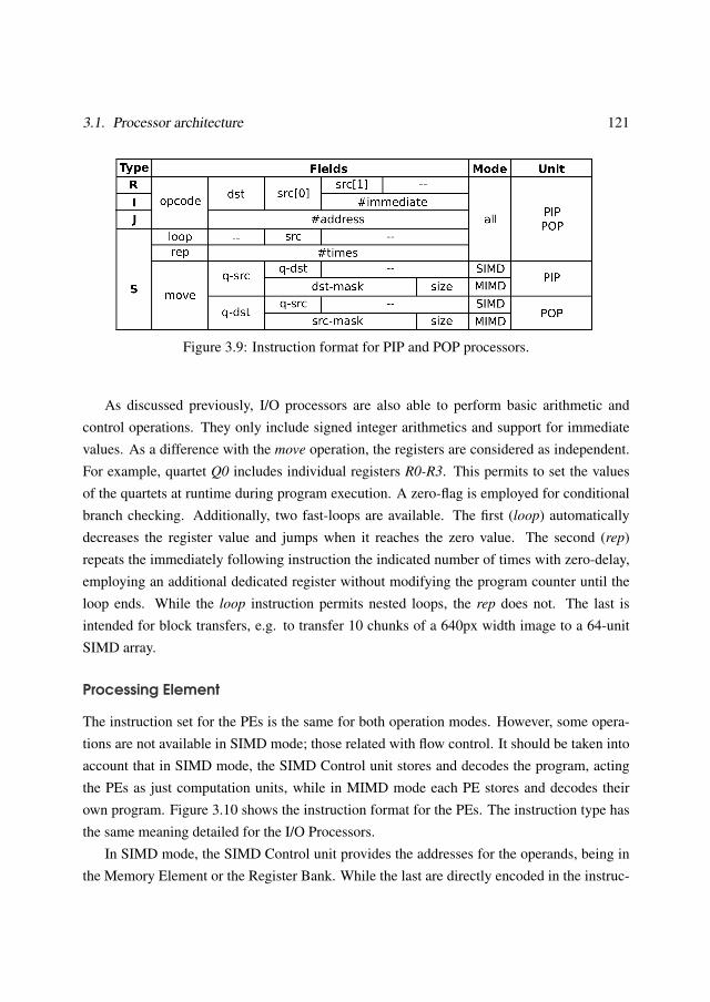
3.1. Processor architecture 121
Figure 3.9: Instruction format for PIP and POP processors.
As discussed previously, I/O processors are also able to perform basic arithmetic andcontrol operations. They only include signed integer arithmetics and support for immediatevalues. As a difference with the move operation, the registers are considered as independent.For example, quartet Q0 includes individual registers R0-R3. This permits to set the valuesof the quartets at runtime during program execution. A zero-flag is employed for conditionalbranch checking. Additionally, two fast-loops are available. The first (loop) automaticallydecreases the register value and jumps when it reaches the zero value. The second (rep)repeats the immediately following instruction the indicated number of times with zero-delay,employing an additional dedicated register without modifying the program counter until theloop ends. While the loop instruction permits nested loops, the rep does not. The last isintended for block transfers, e.g. to transfer 10 chunks of a 640px width image to a 64-unitSIMD array.
Processing Element
The instruction set for the PEs is the same for both operation modes. However, some opera-tions are not available in SIMD mode; those related with flow control. It should be taken intoaccount that in SIMD mode, the SIMD Control unit stores and decodes the program, actingthe PEs as just computation units, while in MIMD mode each PE stores and decodes theirown program. Figure 3.10 shows the instruction format for the PEs. The instruction type hasthe same meaning detailed for the I/O Processors.
In SIMD mode, the SIMD Control unit provides the addresses for the operands, being inthe Memory Element or the Register Bank. While the last are directly encoded in the instruc-
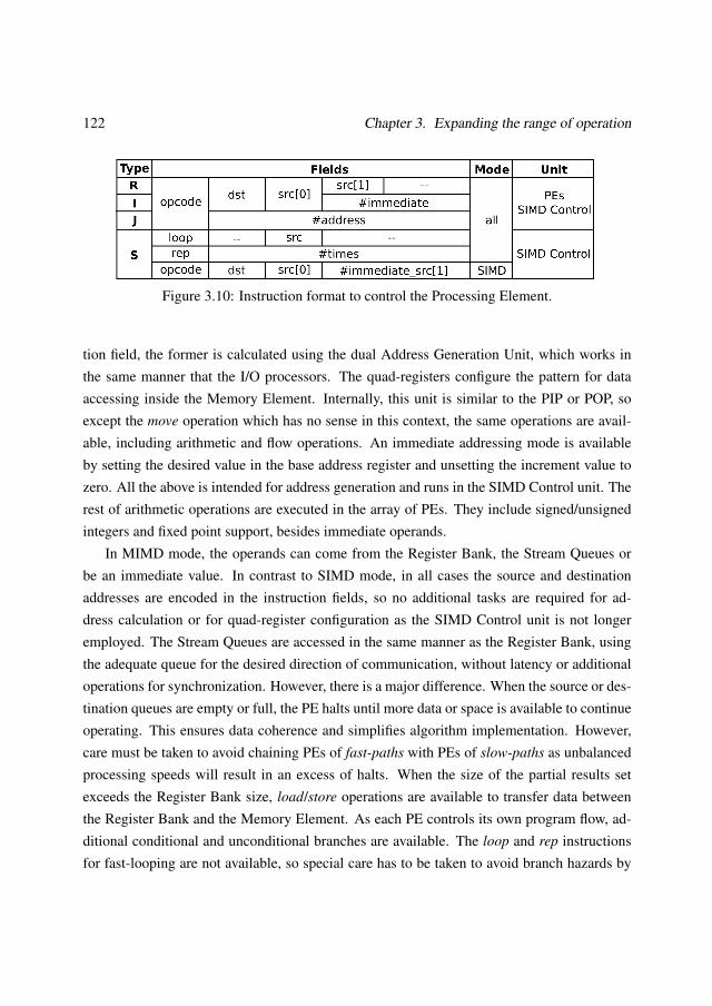
122 Chapter 3. Expanding the range of operation
Figure 3.10: Instruction format to control the Processing Element.
tion field, the former is calculated using the dual Address Generation Unit, which works inthe same manner that the I/O processors. The quad-registers configure the pattern for dataaccessing inside the Memory Element. Internally, this unit is similar to the PIP or POP, soexcept the move operation which has no sense in this context, the same operations are avail-able, including arithmetic and flow operations. An immediate addressing mode is availableby setting the desired value in the base address register and unsetting the increment value tozero. All the above is intended for address generation and runs in the SIMD Control unit. Therest of arithmetic operations are executed in the array of PEs. They include signed/unsignedintegers and fixed point support, besides immediate operands.
In MIMD mode, the operands can come from the Register Bank, the Stream Queues orbe an immediate value. In contrast to SIMD mode, in all cases the source and destinationaddresses are encoded in the instruction fields, so no additional tasks are required for ad-dress calculation or for quad-register configuration as the SIMD Control unit is not longeremployed. The Stream Queues are accessed in the same manner as the Register Bank, usingthe adequate queue for the desired direction of communication, without latency or additionaloperations for synchronization. However, there is a major difference. When the source or des-tination queues are empty or full, the PE halts until more data or space is available to continueoperating. This ensures data coherence and simplifies algorithm implementation. However,care must be taken to avoid chaining PEs of fast-paths with PEs of slow-paths as unbalancedprocessing speeds will result in an excess of halts. When the size of the partial results setexceeds the Register Bank size, load/store operations are available to transfer data betweenthe Register Bank and the Memory Element. As each PE controls its own program flow, ad-ditional conditional and unconditional branches are available. The loop and rep instructionsfor fast-looping are not available, so special care has to be taken to avoid branch hazards by
3.2. Performance evaluation 123
inserting bubbles (nop instruction) or independent operations. The same applies to load/storeoperations.
3.2 Performance evaluation
In order to validate the feasibility of the architecture, it was prototyped on an FPGA. To eval-uate its performance, a set of algorithms were executed. They include some representativetasks of the low-level and mid-level stages, covering the SIMD and MIMD operation modes.Finally and aiming to evaluate not only individual operations but also complete algorithms, afeature extraction and matching technique are thoroughly discussed. This algorithm includesmixed SIMD/MIMD tasks which permit us to discuss which paradigm select to avoid chang-ing the operation mode too many times and to increase the performance.
3.2.1 FPGA prototyping and validation
Nowadays, FGPAs offer a large amount of resources without a significant increment in NREcosts. It is possible to prototype full SoCs into a single FPGA keeping a high throughput.This permits to emulate the architecture in real hardware, avoiding to develop cycle-accurateemulators with considerably less performance. In fact, FPGAs may even become the targetplatform due to the reduction of manufacturing cost, replacing a custom chip.
The proposed architecture has been prototyped on an FPGA to evaluate its feasibility andperformance. The target FPGA we select is an Xilinx Virtex-6 XC6VLX240T-1, included onthe Xilinx ML605 Base Board [142], described above in Section 2.4.3. It provides enoughresources to evaluate the architecture without sacrificing features when adapting the designto the device. As discussed previously, the Image Coprocessor is intended to lighten theworkload of the main CPU. An AXI4-based standard MicroBlaze System-on-Chip was im-plemented. Among other modules, it includes a Multi-Port Memory Controller and a 10/100-Ethernet units. The coprocessor was described using VHDL and synthesized with XilinxDesign Suite tools [142].
The proposed architecture is highly configurable, including the number of processingunits, the size of the internal registers, queues or even the arithmetic operations, being ableto include application-specific extensions for the most demanding algorithms without majormodification in the design. In order to implement a prototype that can run a significant variety
124 Chapter 3. Expanding the range of operation
of algorithms, the critical parameters that balance the computational power of each moduleand the degree of parallelism are detailed below:
• Instructions and data are represented using 32-bit words.
• PIP and POP have 4 quad-registers of 24-bit wide each for off-chip RAM address gen-eration and two caches for instructions and data of 32Kbit (1024 words) each.
• Each PE has a Memory Element of 32Kbit which stores up to 1024 data-words (SIMDmode) or 512 data and 512 instructions (MIMD mode). The Register Bank and eachof the four Stream Queues store 8 and 4 words respectively. The ALU includes 20DSP/Boolean and 12 control and data movement operations.
• The array of PEs is made of 128 units. For SIMD mode, both SIPO and PISO queues are128-word, and the SIMD Control unit includes an instruction cache of 1024 instructionsplus 4 quad-registers of 10-bit wide. In MIMD mode, the PEs form an 8×16 torus, soPIP and POP are interfaced with 8 PEs each and the minimum route between them is16 PEs.
The ML605 board includes 512MB DDR3 SO-DIMM clocked at 400MHz. Ports are con-figured with 64-bit width and, when employing 32-word burst length, providing a maximumdata throughput of 1400 MB/s (reading) and 1140 MB/s (writing). The cache block size ofPIP and POP direct-mapped data caches are configured to 32 words in SIMD mode and 16words in MIMD mode. This way, each burst transfer also preloads adjacent data to the currentaddress location, reducing the memory accesses by transferring more data in each transaction.Two different structures to control cache coherence, hits and miss are implemented using thedistributed memory resources.
Table 3.1 summarizes the synthesized data for the coprocessor in number of LUTs andRegister slices, Block RAMs and DSP slices. The MicroBlaze system, clocked to 150 MHzusing the performance profile, additionally takes around 7500 slice LUTs, 6700 slice registers,10 Block RAMs and 3 DPS48E1 slices. A 128-unit coprocessor fits on the selected FPGAleaving enough space to include other modules of the SoC. The theoretical peak performanceof the coprocessor is 19.6 GOP/s at 150MHz (around 130 operations per clock cycle). Asdata transferring occurs in parallel if a carefully schedule is done, the amount of halts in thepipeline is reduced, so the real performance is expected to be close to this value. The powerconsumption was determined with the Xilinx XPower Estimator [142], resulting in 7.197 W
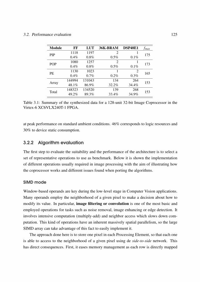
3.2. Performance evaluation 125
Module FF LUT 36K-BRAM DSP48E1 fmax
PIP1118 1197 2 1
1750.4% 0.8% 0.5% 0.1%
POP1080 1257 2 1
1730.4% 0.8% 0.5% 0.1%
PE1130 1023 1 2
1650.4% 0.7% 0.2% 0.3%
Array144994 131043 134 264
15348.1% 86.9% 32.2% 34.4%
Total148323 134520 139 268
15349.2% 89.3% 33.4% 34.9%
Table 3.1: Summary of the synthesized data for a 128-unit 32-bit Image Coprocessor in theVirtex-6 XC6VLX240T-1 FPGA.
at peak performance on standard ambient conditions. 46% corresponds to logic resources and30% to device static consumption.
3.2.2 Algorithm evaluation
The first step to evaluate the suitability and the performance of the architecture is to select aset of representative operations to use as benchmark. Below it is shown the implementationof different operations usually required in image processing with the aim of illustrating howthe coprocessor works and different issues found when porting the algorithms.
SIMD mode
Window-based operands are key during the low-level stage in Computer Vision applications.Many operands employ the neighborhood of a given pixel to make a decision about how tomodify its value. In particular, image filtering or convolution is one of the most basic andemployed operations for tasks such as noise removal, image enhancing or edge detection. Itinvolves intensive computation (multiply-add) and neighbor access which slows down com-putation. This kind of operations have an inherent massively spatial parallelism, so the largeSIMD array can take advantage of this fact to easily implement it.
The approach done here is to store one pixel in each Processing Element, so that each oneis able to access to the neighborhood of a given pixel using de side-to-side network. Thishas direct consequences. First, it eases memory management as each row is directly mapped
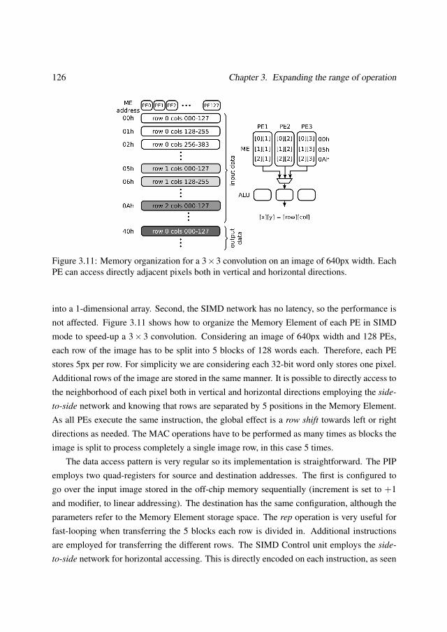
126 Chapter 3. Expanding the range of operation
Figure 3.11: Memory organization for a 3×3 convolution on an image of 640px width. EachPE can access directly adjacent pixels both in vertical and horizontal directions.
into a 1-dimensional array. Second, the SIMD network has no latency, so the performance isnot affected. Figure 3.11 shows how to organize the Memory Element of each PE in SIMDmode to speed-up a 3× 3 convolution. Considering an image of 640px width and 128 PEs,each row of the image has to be split into 5 blocks of 128 words each. Therefore, each PEstores 5px per row. For simplicity we are considering each 32-bit word only stores one pixel.Additional rows of the image are stored in the same manner. It is possible to directly access tothe neighborhood of each pixel both in vertical and horizontal directions employing the side-
to-side network and knowing that rows are separated by 5 positions in the Memory Element.As all PEs execute the same instruction, the global effect is a row shift towards left or rightdirections as needed. The MAC operations have to be performed as many times as blocks theimage is split to process completely a single image row, in this case 5 times.
The data access pattern is very regular so its implementation is straightforward. The PIPemploys two quad-registers for source and destination addresses. The first is configured togo over the input image stored in the off-chip memory sequentially (increment is set to +1and modifier, to linear addressing). The destination has the same configuration, although theparameters refer to the Memory Element storage space. The rep operation is very useful forfast-looping when transferring the 5 blocks each row is divided in. Additional instructionsare employed for transferring the different rows. The SIMD Control unit employs the side-
to-side network for horizontal accessing. This is directly encoded on each instruction, as seen
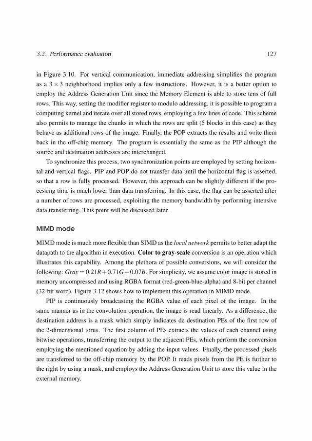
3.2. Performance evaluation 127
in Figure 3.10. For vertical communication, immediate addressing simplifies the programas a 3× 3 neighborhood implies only a few instructions. However, it is a better option toemploy the Address Generation Unit since the Memory Element is able to store tens of fullrows. This way, setting the modifier register to modulo addressing, it is possible to program acomputing kernel and iterate over all stored rows, employing a few lines of code. This schemealso permits to manage the chunks in which the rows are split (5 blocks in this case) as theybehave as additional rows of the image. Finally, the POP extracts the results and write themback in the off-chip memory. The program is essentially the same as the PIP although thesource and destination addresses are interchanged.
To synchronize this process, two synchronization points are employed by setting horizon-tal and vertical flags. PIP and POP do not transfer data until the horizontal flag is asserted,so that a row is fully processed. However, this approach can be slightly different if the pro-cessing time is much lower than data transferring. In this case, the flag can be asserted aftera number of rows are processed, exploiting the memory bandwidth by performing intensivedata transferring. This point will be discussed later.
MIMD mode
MIMD mode is much more flexible than SIMD as the local network permits to better adapt thedatapath to the algorithm in execution. Color to gray-scale conversion is an operation whichillustrates this capability. Among the plethora of possible conversions, we will consider thefollowing: Gray= 0.21R+0.71G+0.07B. For simplicity, we assume color image is stored inmemory uncompressed and using RGBA format (red-green-blue-alpha) and 8-bit per channel(32-bit word). Figure 3.12 shows how to implement this operation in MIMD mode.
PIP is continuously broadcasting the RGBA value of each pixel of the image. In thesame manner as in the convolution operation, the image is read linearly. As a difference, thedestination address is a mask which simply indicates de destination PEs of the first row ofthe 2-dimensional torus. The first column of PEs extracts the values of each channel usingbitwise operations, transferring the output to the adjacent PEs, which perform the conversionemploying the mentioned equation by adding the input values. Finally, the processed pixelsare transferred to the off-chip memory by the POP. It reads pixels from the PE is further tothe right by using a mask, and employs the Address Generation Unit to store this value in theexternal memory.
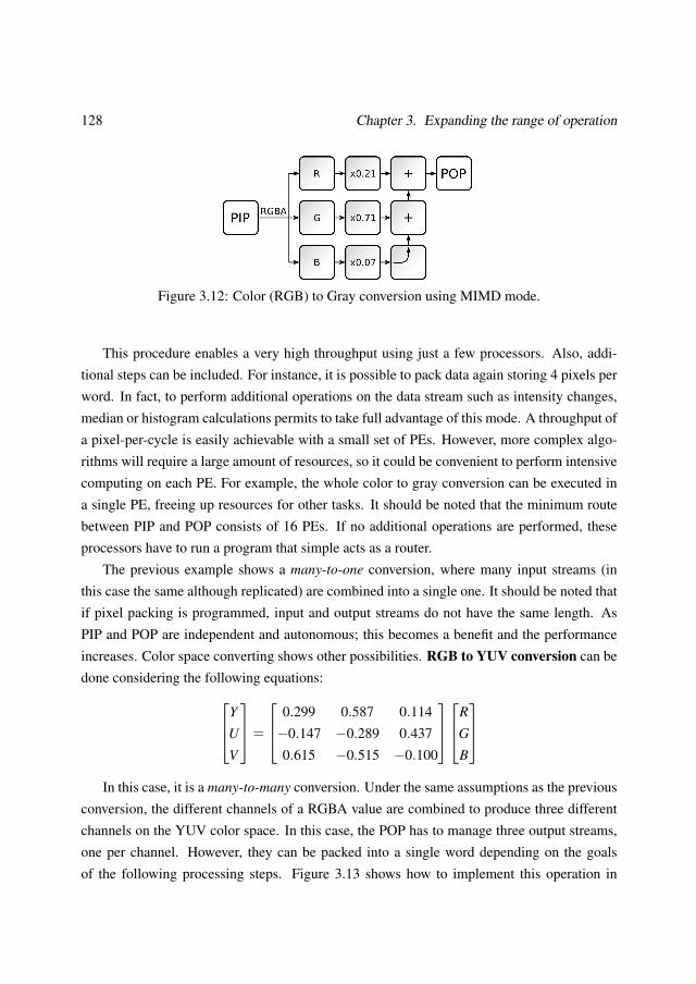
128 Chapter 3. Expanding the range of operation
Figure 3.12: Color (RGB) to Gray conversion using MIMD mode.
This procedure enables a very high throughput using just a few processors. Also, addi-tional steps can be included. For instance, it is possible to pack data again storing 4 pixels perword. In fact, to perform additional operations on the data stream such as intensity changes,median or histogram calculations permits to take full advantage of this mode. A throughput ofa pixel-per-cycle is easily achievable with a small set of PEs. However, more complex algo-rithms will require a large amount of resources, so it could be convenient to perform intensivecomputing on each PE. For example, the whole color to gray conversion can be executed ina single PE, freeing up resources for other tasks. It should be noted that the minimum routebetween PIP and POP consists of 16 PEs. If no additional operations are performed, theseprocessors have to run a program that simple acts as a router.
The previous example shows a many-to-one conversion, where many input streams (inthis case the same although replicated) are combined into a single one. It should be noted thatif pixel packing is programmed, input and output streams do not have the same length. AsPIP and POP are independent and autonomous; this becomes a benefit and the performanceincreases. Color space converting shows other possibilities. RGB to YUV conversion can bedone considering the following equations:Y
U
V
=
0.299 0.587 0.114−0.147 −0.289 0.4370.615 −0.515 −0.100
R
G
B
In this case, it is a many-to-many conversion. Under the same assumptions as the previous
conversion, the different channels of a RGBA value are combined to produce three differentchannels on the YUV color space. In this case, the POP has to manage three output streams,one per channel. However, they can be packed into a single word depending on the goalsof the following processing steps. Figure 3.13 shows how to implement this operation in
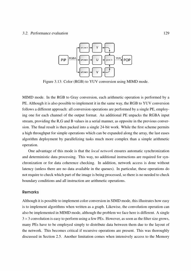
3.2. Performance evaluation 129
Figure 3.13: Color (RGB) to YUV conversion using MIMD mode.
MIMD mode. In the RGB to Gray conversion, each arithmetic operation is performed by aPE. Although it is also possible to implement it in the same way, the RGB to YUV conversionfollows a different approach: all conversion operations are performed by a single PE, employ-ing one for each channel of the output format. An additional PE unpacks the RGBA inputstream, providing the R,G and B values in a serial manner, as opposite in the previous conver-sion. The final result is then packed into a single 24-bit work. While the first scheme permitsa high throughput for simple operations which can be expanded along the array, the last easesalgorithm deployment by parallelizing tasks much more complex than a simple arithmeticoperation.
One advantage of this mode is that the local network ensures automatic synchronizationand deterministic data processing. This way, no additional instructions are required for syn-chronization or for data coherence checking. In addition, network access is done withoutlatency (unless there are no data available in the queues). In particular, these operations donot require to check which part of the image is being processed, so there is no needed to checkboundary conditions and all instruction are arithmetic operations.
Remarks
Although it is possible to implement color conversion in SIMD mode, this illustrates how easyis to implement algorithms when written as a graph. Likewise, the convolution operation canalso be implemented in MIMD mode, although the problem we face here is different. A single3×3 convolution is easy to perform using a few PEs. However, as soon as the filter size grows,many PEs have to be employed simply to distribute data between them due to the layout ofthe network. This becomes critical if recursive operations are present. This was thoroughlydiscussed in Section 2.5. Another limitation comes when intensively access to the Memory
130 Chapter 3. Expanding the range of operation
Element is needed in MIMD mode. The ALU has to perform address calculations and care ofload/store hazards have to be taken into account. It is possible to employ the Memory Elementas a shift register to store the input pixels as usual in straightforward custom implementations[190]. However, if the row lenght is larger than the Memory Element, several PEs have to bechained to emulate a larger storage, adding complexity to the program.
In SIMD mode, all PEs and the whole Memory Element can be used without restrictions.However, only a single task can be executed at a time. On the contrary, MIMD mode allowsmany simultaneous tasks. As detailed above, color conversion can be chained with other tasks.Other possibility is to replicate the same task several times by replicating the distributionof processors in different parts of the 2d-torus. This can greatly increase the performanceavoiding PEs unused by processing several pixels in parallel. As the coprocessor contains 128-units, color conversion can be replicated more than 10 times. Depending on the algorithm, it ispossible that some processors are employed as simple routers, so the implementation could besub-optimal and the performance can not scale linearly with the number of processing units.
Although it is possible to switch mode at a very low cost (essentially the program loadtime), the coprocessor usage must be complete to fully take advantage of each mode. Forinstance, the 3× 3 convolution in SIMD mode is limited by the speed we can enter data. Itonly requires 9 MAC operations (9 clock cycles) while transferring each 128 data block takes129 clock cycles. This is, PEs are 93% of the time waiting for new data to process (datatransferring and processing occur simultaneously). However, if the amount of computationexceeds the time the PIP or POP employ for data transferring, data I/O is no longer the bot-tleneck. As pointed before, employing as much as possible the on-chip memories is essentialto fully take advantage of this mode. MIMD mode does not experience this problem as itprocess streams and data preloading is not necessary. However, it is hard to fully employ theprocessing array as the network does not fit perfectly all data exchanges of most algorithms.
Despite all the above, to select SIMD or MIMD mode depends on the particular algorithmand how operations are scheduled. Consider a color conversion in these two cases: a) followedby a mean calculation for further analysis, and b) followed by a filtering for noise reduction.As discussed above, color conversion suits both for SIMD and MIMD modes. In the first caseit is better to perform both tasks in MIMD mode as only a few processors need to be employedfreeing resources for other parallel or subsequent tasks. Performance is not compromised asa rate of 1 px per clock cycle is easily achievable. However, the second case fits better inSIMD mode. It eases algorithm implementation as large convolutions natively fits this mode
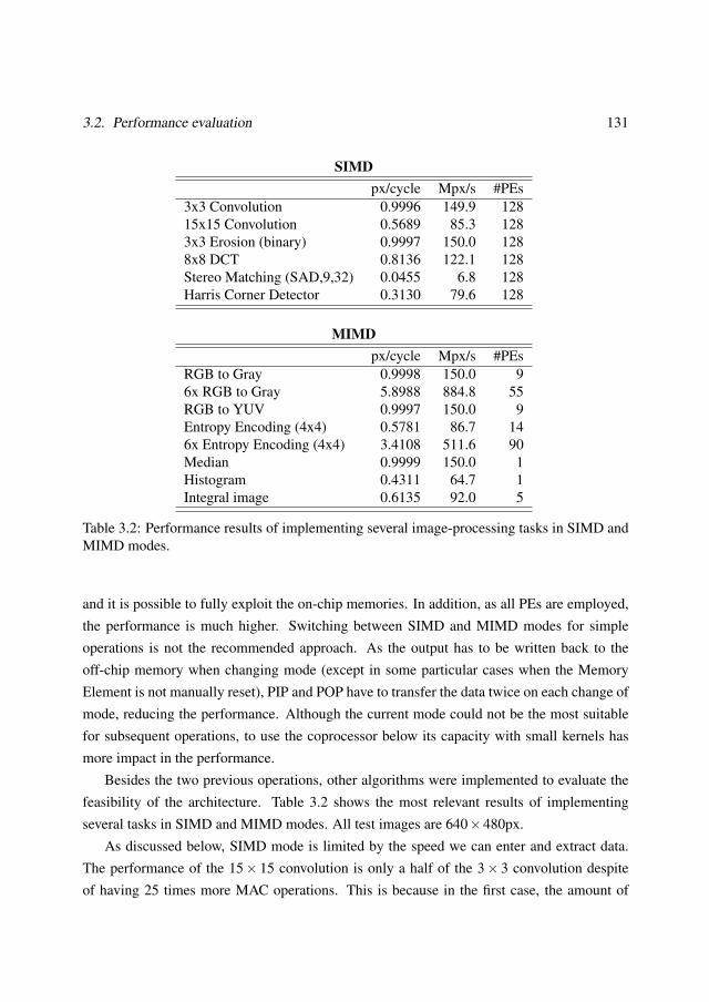
3.2. Performance evaluation 131
SIMDpx/cycle Mpx/s #PEs
3x3 Convolution 0.9996 149.9 12815x15 Convolution 0.5689 85.3 1283x3 Erosion (binary) 0.9997 150.0 1288x8 DCT 0.8136 122.1 128Stereo Matching (SAD,9,32) 0.0455 6.8 128Harris Corner Detector 0.3130 79.6 128
MIMDpx/cycle Mpx/s #PEs
RGB to Gray 0.9998 150.0 96x RGB to Gray 5.8988 884.8 55RGB to YUV 0.9997 150.0 9Entropy Encoding (4x4) 0.5781 86.7 146x Entropy Encoding (4x4) 3.4108 511.6 90Median 0.9999 150.0 1Histogram 0.4311 64.7 1Integral image 0.6135 92.0 5
Table 3.2: Performance results of implementing several image-processing tasks in SIMD andMIMD modes.
and it is possible to fully exploit the on-chip memories. In addition, as all PEs are employed,the performance is much higher. Switching between SIMD and MIMD modes for simpleoperations is not the recommended approach. As the output has to be written back to theoff-chip memory when changing mode (except in some particular cases when the MemoryElement is not manually reset), PIP and POP have to transfer the data twice on each change ofmode, reducing the performance. Although the current mode could not be the most suitablefor subsequent operations, to use the coprocessor below its capacity with small kernels hasmore impact in the performance.
Besides the two previous operations, other algorithms were implemented to evaluate thefeasibility of the architecture. Table 3.2 shows the most relevant results of implementingseveral tasks in SIMD and MIMD modes. All test images are 640×480px.
As discussed below, SIMD mode is limited by the speed we can enter and extract data.The performance of the 15× 15 convolution is only a half of the 3× 3 convolution despiteof having 25 times more MAC operations. This is because in the first case, the amount of
132 Chapter 3. Expanding the range of operation
computation largely exceeds the time required for data preloading in the SIPO/PISO queues.This does not occur with smaller kernels, were the PEs halt until more data are available.To avoid this issue, many operations must be chained and the on-chip data caches have tobe employed to store the partial results. The POP must only extract the final results. Thisis the case of Stereo Matching, which employs sum of absolute differences (SAD) for blockmatching (9×9) with a disparity of 32px.
MIMD results show the performance of several operations when implemented in stream-
like fashion. As seen before, a rate of a pixel-per-cycle can be achievable with few PEs, soit is possible to replicate each mode several times and increasing the throughput. Resultsshow that replicating RGB to Gray and Entropy Encoding 6 times the performance increasespractically linearly. Other operations, such as median calculation, are pure arithmetic and canbe performed very efficiently without consuming resources. However, others require internalstorage as the Register Bank is not large enough. This results in lower throughput as load/storehazards drops the performance if there are not independent instructions to fill the pipeline, asis the case in histogram or integral image calculations.
Program loading represents a small fraction of the whole operation. In SIMD mode, theworst case comes when PIP, POP and SIMD Control instructions storages are filled com-pletely. In the current implementation, all memories are 1024-instructions wide, so less than22 µs are required to fully program the coprocessor (with a clock frequency of 150 MHz). InMIMD mode, each PE stores its own program, which is 512-instructions wide. In the worstcase, all PEs completely fill the memory, requiring at most 460 µs in total. However, this hasnever happened in the test algorithms. In addition, as it is possible to randomly access eachPEs, loading times are usually much lower.
3.2.3 Case of study: feature extraction and matching
In an effort to illustrate the capabilities and advantages of the architecture and how to ad-dress the different issues found when mapping an algorithm, a feature detector and matchingtechnique was implemented [13]. This approach requires a previous training stage, where themodels of the features we want to find are calculated. From a large set of viewpoint trans-formations of the target object, the most repeatable features are combined into a compactrepresentation, called Histogrammed Intensity Patch model (HIP). During execution, match-ing can be performed quickly with bitwise operations between the detected features and the
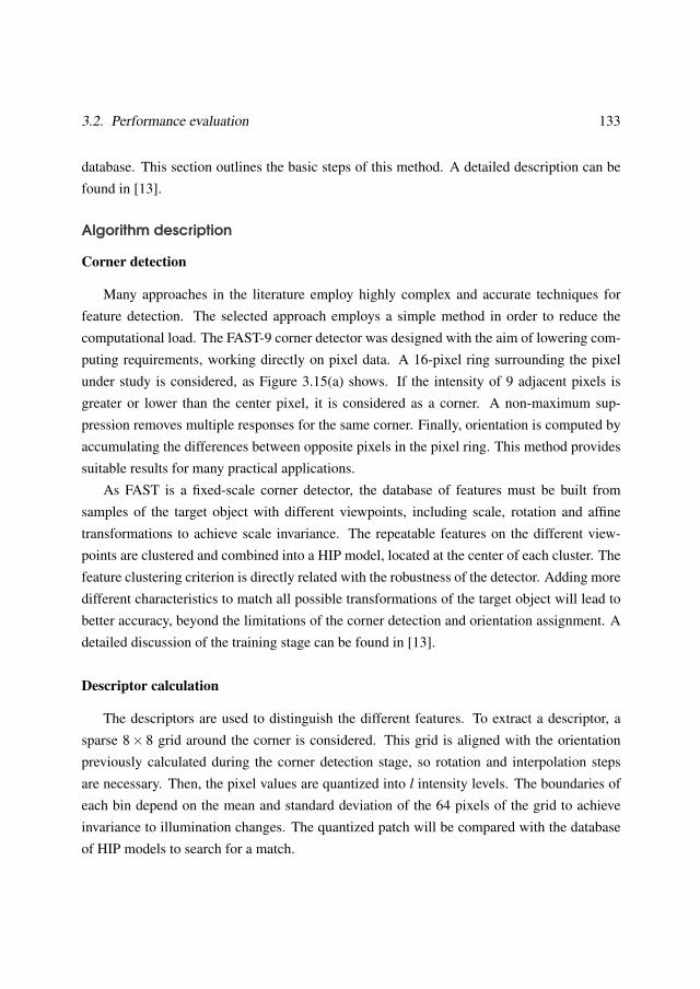
3.2. Performance evaluation 133
database. This section outlines the basic steps of this method. A detailed description can befound in [13].
Algorithm description
Corner detection
Many approaches in the literature employ highly complex and accurate techniques forfeature detection. The selected approach employs a simple method in order to reduce thecomputational load. The FAST-9 corner detector was designed with the aim of lowering com-puting requirements, working directly on pixel data. A 16-pixel ring surrounding the pixelunder study is considered, as Figure 3.15(a) shows. If the intensity of 9 adjacent pixels isgreater or lower than the center pixel, it is considered as a corner. A non-maximum sup-pression removes multiple responses for the same corner. Finally, orientation is computed byaccumulating the differences between opposite pixels in the pixel ring. This method providessuitable results for many practical applications.
As FAST is a fixed-scale corner detector, the database of features must be built fromsamples of the target object with different viewpoints, including scale, rotation and affinetransformations to achieve scale invariance. The repeatable features on the different view-points are clustered and combined into a HIP model, located at the center of each cluster. Thefeature clustering criterion is directly related with the robustness of the detector. Adding moredifferent characteristics to match all possible transformations of the target object will lead tobetter accuracy, beyond the limitations of the corner detection and orientation assignment. Adetailed discussion of the training stage can be found in [13].
Descriptor calculation
The descriptors are used to distinguish the different features. To extract a descriptor, asparse 8× 8 grid around the corner is considered. This grid is aligned with the orientationpreviously calculated during the corner detection stage, so rotation and interpolation stepsare necessary. Then, the pixel values are quantized into l intensity levels. The boundaries ofeach bin depend on the mean and standard deviation of the 64 pixels of the grid to achieveinvariance to illumination changes. The quantized patch will be compared with the databaseof HIP models to search for a match.
134 Chapter 3. Expanding the range of operation
The HIP model summarizes the information contained on each feature cluster obtainedduring the training stage, which includes all considered viewpoints. For each feature, of thecluster, a quantized path is obtained. For each location on the grid, the quantized pixels inten-sities of each patch on the cluster are histogrammed, resulting in 64 independent histogramsof l bins each. To reduce storage and computing requirements, the histogram bin values arebinarized, setting to 1 the rare bins, those with probabilities lower than a certain threshold.This way, matching can be performed by bitwise operations uniquely.
Feature matching
Once at runtime, a set of features of the current frame are obtained using the FAST-9detector. Then, a quantized patch around each feature is calculated. This patch will be com-pared with the HIP database with the purpose of finding a match. As HIP stores binary data,a similarity score can be computed with bitwise operations. The best matches will show asmall number of rarely observed bins. Counting its number (encoded with ones) will identifythe number of match errors. Using the HIP model, a feature is represented by an array of64× l binary values, which can be compacted into a few data-words to compute a wide num-ber of matches on large databases very fast. This approach is expected to be much faster thanstrategies based on distance calculations between features.
Techniques such as tree-based search can take advantage of similarity between HIPs in thedatabase to speed-up the matching stage. It is possible to construct a binary-tree, where eachchild node only differentiates one bit (one bin) from the parent node. This way, similarityscores lower than a threshold eliminate the need to perform matches along that branch of thetree. Otherwise, a search on the entire database would be necessary. The cost of this solutionis larger storage requirements, but the benefits typically outweigh this cost.
Algorithm mapping
As it can be extracted from the previous section, the learning stage where the database isbuilt is carried off-line on a PC-based solution. The FPGA will perform only runtime featuredetection and matching. There are three main steps in this algorithm. First, the corners haveto be located and oriented. Then, the patch around each corner is rotated and quantized.Finally, the matching stage takes place. The algorithm flow is depicted in Figure 3.14. Anoptional pre-processing stage, such as noise reduction, suits for SIMD mode, as discussed
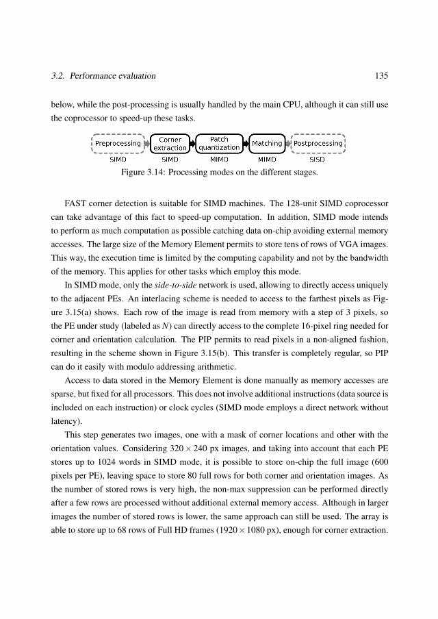
3.2. Performance evaluation 135
below, while the post-processing is usually handled by the main CPU, although it can still usethe coprocessor to speed-up these tasks.
Figure 3.14: Processing modes on the different stages.
FAST corner detection is suitable for SIMD machines. The 128-unit SIMD coprocessorcan take advantage of this fact to speed-up computation. In addition, SIMD mode intendsto perform as much computation as possible catching data on-chip avoiding external memoryaccesses. The large size of the Memory Element permits to store tens of rows of VGA images.This way, the execution time is limited by the computing capability and not by the bandwidthof the memory. This applies for other tasks which employ this mode.
In SIMD mode, only the side-to-side network is used, allowing to directly access uniquelyto the adjacent PEs. An interlacing scheme is needed to access to the farthest pixels as Fig-ure 3.15(a) shows. Each row of the image is read from memory with a step of 3 pixels, sothe PE under study (labeled as N) can directly access to the complete 16-pixel ring needed forcorner and orientation calculation. The PIP permits to read pixels in a non-aligned fashion,resulting in the scheme shown in Figure 3.15(b). This transfer is completely regular, so PIPcan do it easily with modulo addressing arithmetic.
Access to data stored in the Memory Element is done manually as memory accesses aresparse, but fixed for all processors. This does not involve additional instructions (data source isincluded on each instruction) or clock cycles (SIMD mode employs a direct network withoutlatency).
This step generates two images, one with a mask of corner locations and other with theorientation values. Considering 320× 240 px images, and taking into account that each PEstores up to 1024 words in SIMD mode, it is possible to store on-chip the full image (600pixels per PE), leaving space to store 80 full rows for both corner and orientation images. Asthe number of stored rows is very high, the non-max suppression can be performed directlyafter a few rows are processed without additional external memory access. Although in largerimages the number of stored rows is lower, the same approach can still be used. The array isable to store up to 68 rows of Full HD frames (1920×1080 px), enough for corner extraction.
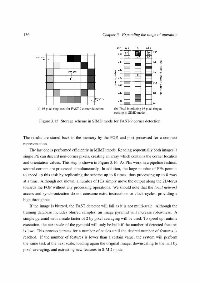
136 Chapter 3. Expanding the range of operation
(a) 16 pixel ring used for FAST-9 corner detection. (b) Pixel interlacing 16 pixel ring ac-cessing in SIMD mode.
Figure 3.15: Storage scheme in SIMD mode for FAST-9 corner detection.
The results are stored back in the memory by the POP, and post-processed for a compactrepresentation.
The last one is performed efficiently in MIMD mode. Reading sequentially both images, asingle PE can discard non-corner pixels, creating an array which contains the corner locationand orientation values. This step is shown in Figure 3.16. As PEs work in a pipeline fashion,several corners are processed simultaneously. In addition, the large number of PEs permitsto speed up this task by replicating the scheme up to 8 times, thus processing up to 8 rowsat a time. Although not shown, a number of PEs simply move the output along the 2D-torustowards the POP without any processing operations. We should note that the local network
access and synchronization do not consume extra instructions or clock cycles, providing ahigh throughput.
If the image is blurred, the FAST detector will fail as it is not multi-scale. Although thetraining database includes blurred samples, an image pyramid will increase robustness. Asimple pyramid with a scale factor of 2 by pixel averaging will be used. To speed up runtimeexecution, the next scale of the pyramid will only be built if the number of detected featuresis low. This process iterates for a number of scales until the desired number of features isreached. If the number of features is lower than a certain value, the system will performthe same task at the next scale, loading again the original image, downscaling to the half bypixel-averaging, and extracting new features in SIMD mode.
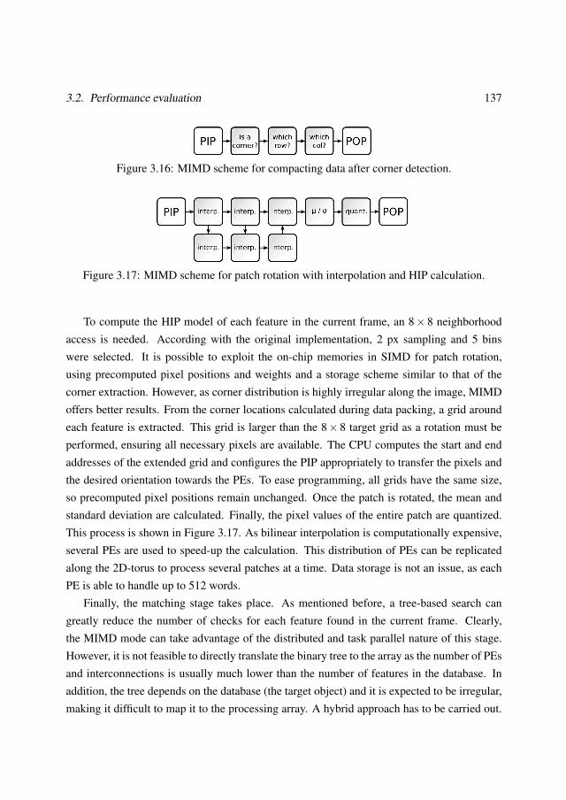
3.2. Performance evaluation 137
Figure 3.16: MIMD scheme for compacting data after corner detection.
Figure 3.17: MIMD scheme for patch rotation with interpolation and HIP calculation.
To compute the HIP model of each feature in the current frame, an 8× 8 neighborhoodaccess is needed. According with the original implementation, 2 px sampling and 5 binswere selected. It is possible to exploit the on-chip memories in SIMD for patch rotation,using precomputed pixel positions and weights and a storage scheme similar to that of thecorner extraction. However, as corner distribution is highly irregular along the image, MIMDoffers better results. From the corner locations calculated during data packing, a grid aroundeach feature is extracted. This grid is larger than the 8× 8 target grid as a rotation must beperformed, ensuring all necessary pixels are available. The CPU computes the start and endaddresses of the extended grid and configures the PIP appropriately to transfer the pixels andthe desired orientation towards the PEs. To ease programming, all grids have the same size,so precomputed pixel positions remain unchanged. Once the patch is rotated, the mean andstandard deviation are calculated. Finally, the pixel values of the entire patch are quantized.This process is shown in Figure 3.17. As bilinear interpolation is computationally expensive,several PEs are used to speed-up the calculation. This distribution of PEs can be replicatedalong the 2D-torus to process several patches at a time. Data storage is not an issue, as eachPE is able to handle up to 512 words.
Finally, the matching stage takes place. As mentioned before, a tree-based search cangreatly reduce the number of checks for each feature found in the current frame. Clearly,the MIMD mode can take advantage of the distributed and task parallel nature of this stage.However, it is not feasible to directly translate the binary tree to the array as the number of PEsand interconnections is usually much lower than the number of features in the database. Inaddition, the tree depends on the database (the target object) and it is expected to be irregular,making it difficult to map it to the processing array. A hybrid approach has to be carried out.
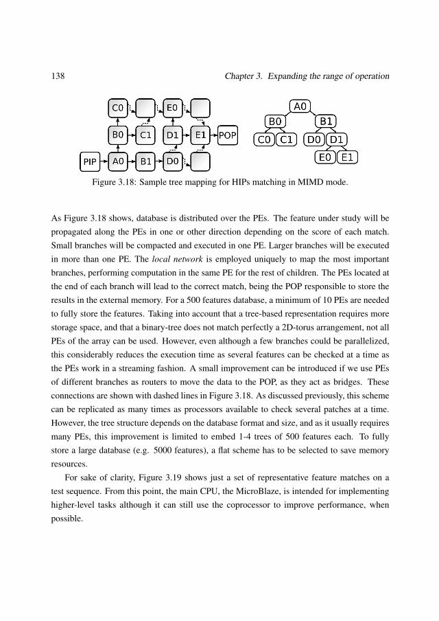
138 Chapter 3. Expanding the range of operation
Figure 3.18: Sample tree mapping for HIPs matching in MIMD mode.
As Figure 3.18 shows, database is distributed over the PEs. The feature under study will bepropagated along the PEs in one or other direction depending on the score of each match.Small branches will be compacted and executed in one PE. Larger branches will be executedin more than one PE. The local network is employed uniquely to map the most importantbranches, performing computation in the same PE for the rest of children. The PEs located atthe end of each branch will lead to the correct match, being the POP responsible to store theresults in the external memory. For a 500 features database, a minimum of 10 PEs are neededto fully store the features. Taking into account that a tree-based representation requires morestorage space, and that a binary-tree does not match perfectly a 2D-torus arrangement, not allPEs of the array can be used. However, even although a few branches could be parallelized,this considerably reduces the execution time as several features can be checked at a time asthe PEs work in a streaming fashion. A small improvement can be introduced if we use PEsof different branches as routers to move the data to the POP, as they act as bridges. Theseconnections are shown with dashed lines in Figure 3.18. As discussed previously, this schemecan be replicated as many times as processors available to check several patches at a time.However, the tree structure depends on the database format and size, and as it usually requiresmany PEs, this improvement is limited to embed 1-4 trees of 500 features each. To fullystore a large database (e.g. 5000 features), a flat scheme has to be selected to save memoryresources.
For sake of clarity, Figure 3.19 shows just a set of representative feature matches on atest sequence. From this point, the main CPU, the MicroBlaze, is intended for implementinghigher-level tasks although it can still use the coprocessor to improve performance, whenpossible.
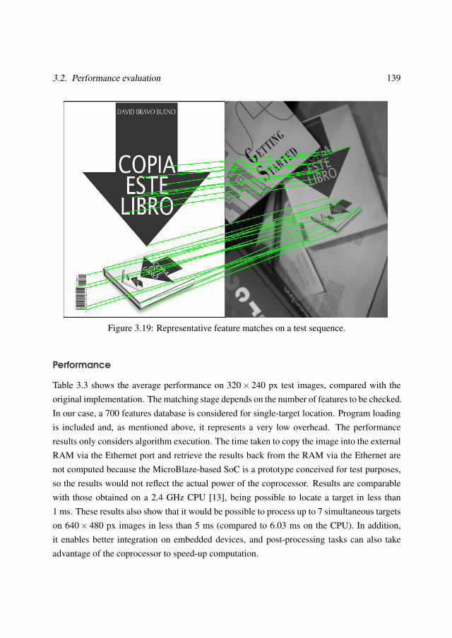
3.2. Performance evaluation 139
Figure 3.19: Representative feature matches on a test sequence.
Performance
Table 3.3 shows the average performance on 320× 240 px test images, compared with theoriginal implementation. The matching stage depends on the number of features to be checked.In our case, a 700 features database is considered for single-target location. Program loadingis included and, as mentioned above, it represents a very low overhead. The performanceresults only considers algorithm execution. The time taken to copy the image into the externalRAM via the Ethernet port and retrieve the results back from the RAM via the Ethernet arenot computed because the MicroBlaze-based SoC is a prototype conceived for test purposes,so the results would not reflect the actual power of the coprocessor. Results are comparablewith those obtained on a 2.4 GHz CPU [13], being possible to locate a target in less than1 ms. These results also show that it would be possible to process up to 7 simultaneous targetson 640× 480 px images in less than 5 ms (compared to 6.03 ms on the CPU). In addition,it enables better integration on embedded devices, and post-processing tasks can also takeadvantage of the coprocessor to speed-up computation.
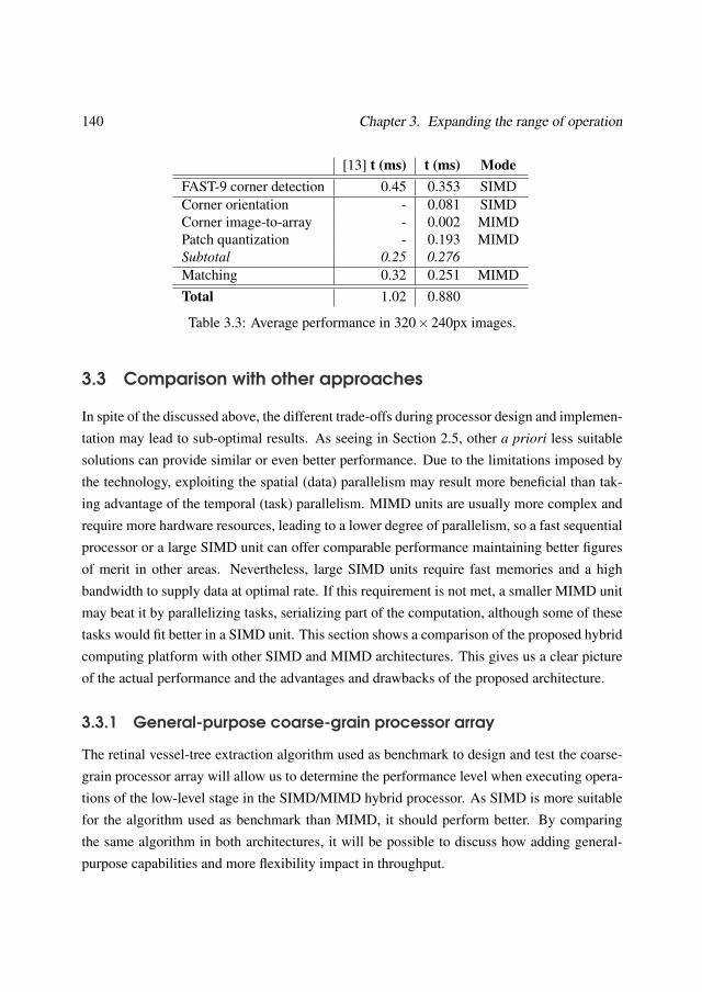
140 Chapter 3. Expanding the range of operation
[13] t (ms) t (ms) ModeFAST-9 corner detection 0.45 0.353 SIMDCorner orientation - 0.081 SIMDCorner image-to-array - 0.002 MIMDPatch quantization - 0.193 MIMDSubtotal 0.25 0.276Matching 0.32 0.251 MIMDTotal 1.02 0.880
Table 3.3: Average performance in 320×240px images.
3.3 Comparison with other approaches
In spite of the discussed above, the different trade-offs during processor design and implemen-tation may lead to sub-optimal results. As seeing in Section 2.5, other a priori less suitablesolutions can provide similar or even better performance. Due to the limitations imposed bythe technology, exploiting the spatial (data) parallelism may result more beneficial than tak-ing advantage of the temporal (task) parallelism. MIMD units are usually more complex andrequire more hardware resources, leading to a lower degree of parallelism, so a fast sequentialprocessor or a large SIMD unit can offer comparable performance maintaining better figuresof merit in other areas. Nevertheless, large SIMD units require fast memories and a highbandwidth to supply data at optimal rate. If this requirement is not met, a smaller MIMD unitmay beat it by parallelizing tasks, serializing part of the computation, although some of thesetasks would fit better in a SIMD unit. This section shows a comparison of the proposed hybridcomputing platform with other SIMD and MIMD architectures. This gives us a clear pictureof the actual performance and the advantages and drawbacks of the proposed architecture.
3.3.1 General-purpose coarse-grain processor array
The retinal vessel-tree extraction algorithm used as benchmark to design and test the coarse-grain processor array will allow us to determine the performance level when executing opera-tions of the low-level stage in the SIMD/MIMD hybrid processor. As SIMD is more suitablefor the algorithm used as benchmark than MIMD, it should perform better. By comparingthe same algorithm in both architectures, it will be possible to discuss how adding general-purpose capabilities and more flexibility impact in throughput.
3.3. Comparison with other approaches 141
The coarse-grain processor array has proved to be efficient, low resource consumer andeasy to scale and to program. The low cost FPGA implementation outperforms a high-endCPU by a factor of 10 while employing a more modern and capable FPGA the difference in-creases up to 110 in the algorithm selected as benchmark (see Table 2.11). In addition, the lastoption offers similar performance to an MP-SIMD processor, which is the native architecturefor the selected algorithm. The coarse-grain processor array employs a 2-dimensional grid ofProcessing Elements with local interconnections to exchange data. The Processing Elementsare made of a dual-port RAM block and a DSP unit for integer and fixed-point arithmetics.The NEWS (north-east-west-south) network between these units permits to fit an image onthe plane of processors so that a small sub-window of the image is stored on each processor.This scheme matches most of the operations of the low-level stage.
As detailed in Section 3.2, the SIMD/MIMD hybrid processor is also able to handle theseoperations. The mode of operation, either SIMD or MIMD, depends on the preceding andsubsequent algorithm steps. This avoids an excess of mode switching taking advantage ofthe on-chip memories, and reducing the number of accesses to the off-chip memory. Theimage is stored row by row in SIMD mode and the side-to-side network permits to exchangedata horizontally. Dedicated connection for vertical access is not required as adjacent rowsare stored in the same Memory Element. In MIMD mode, these operations are carried outsequentially, employing the Memory Element as row buffers if neighbor access is needed.The most suitable configuration for this algorithm is the SIMD mode due to the algorithminherent massively spatial parallelism. The processor array is not large enough to run thealgorithm in MIMD mode without compromising performance or accuracy, so it makes nosense to employ this mode being the SIMD mode available.
Table 3.4 compares the performance of the algorithm with the previous implementationsshown in Section 2.5. The coarse-grain implementation refers to the improved architecturedatapath depicted in Section 2.4.3 and implemented on the same Xilinx Virtex-6 FPGA as theSIMD/MIMD hybrid architecture. The cycles-per-pixel (CPP) metric measures the number ofclock cycles required to execute all the operations on each one of the pixels in the resulting im-age, normalizing the differences in frequency and number of processing cores. It allows us toreliably compare both architectures despite of their different implementations. Results showthat the hybrid architecture requires only 3.73% more clock cycles to accomplish the sametasks. The approach employed was the same as that of the coarse-grain processor array. Alarge subwindow of the input retinal image is stored in the on-chip memories. All processing
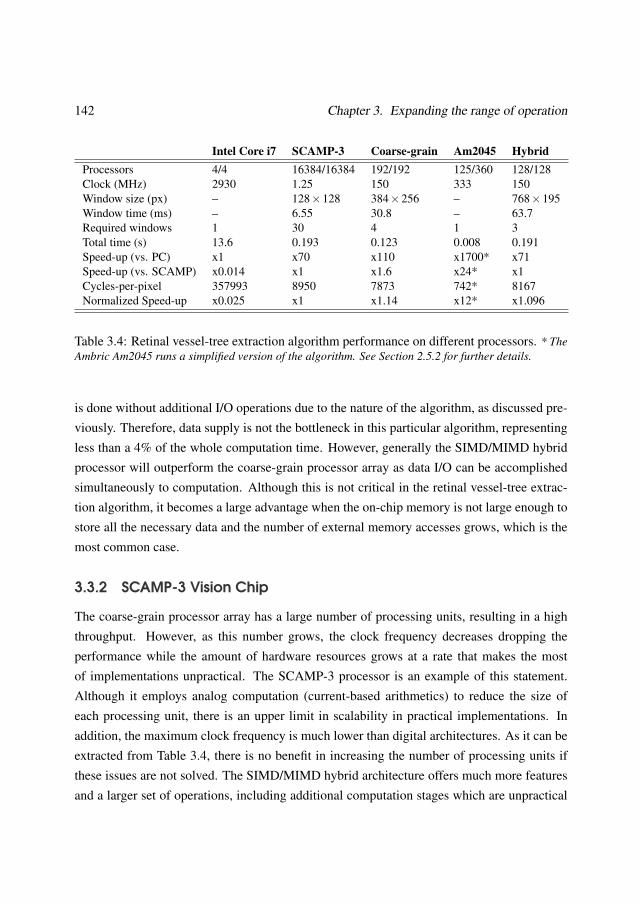
142 Chapter 3. Expanding the range of operation
Intel Core i7 SCAMP-3 Coarse-grain Am2045 HybridProcessors 4/4 16384/16384 192/192 125/360 128/128Clock (MHz) 2930 1.25 150 333 150Window size (px) – 128×128 384×256 – 768×195Window time (ms) – 6.55 30.8 – 63.7Required windows 1 30 4 1 3Total time (s) 13.6 0.193 0.123 0.008 0.191Speed-up (vs. PC) x1 x70 x110 x1700* x71Speed-up (vs. SCAMP) x0.014 x1 x1.6 x24* x1Cycles-per-pixel 357993 8950 7873 742* 8167Normalized Speed-up x0.025 x1 x1.14 x12* x1.096
Table 3.4: Retinal vessel-tree extraction algorithm performance on different processors. * TheAmbric Am2045 runs a simplified version of the algorithm. See Section 2.5.2 for further details.
is done without additional I/O operations due to the nature of the algorithm, as discussed pre-viously. Therefore, data supply is not the bottleneck in this particular algorithm, representingless than a 4% of the whole computation time. However, generally the SIMD/MIMD hybridprocessor will outperform the coarse-grain processor array as data I/O can be accomplishedsimultaneously to computation. Although this is not critical in the retinal vessel-tree extrac-tion algorithm, it becomes a large advantage when the on-chip memory is not large enough tostore all the necessary data and the number of external memory accesses grows, which is themost common case.
3.3.2 SCAMP-3 Vision Chip
The coarse-grain processor array has a large number of processing units, resulting in a highthroughput. However, as this number grows, the clock frequency decreases dropping theperformance while the amount of hardware resources grows at a rate that makes the mostof implementations unpractical. The SCAMP-3 processor is an example of this statement.Although it employs analog computation (current-based arithmetics) to reduce the size ofeach processing unit, there is an upper limit in scalability in practical implementations. Inaddition, the maximum clock frequency is much lower than digital architectures. As it can beextracted from Table 3.4, there is no benefit in increasing the number of processing units ifthese issues are not solved. The SIMD/MIMD hybrid architecture offers much more featuresand a larger set of operations, including additional computation stages which are unpractical
3.3. Comparison with other approaches 143
on the SCAMP-3 processor. For instance, the size of the images are fixed for SCAMP-3 andthe coarse-grain processor array. This constraint is not present on the hybrid processor, whichis able to handle images of any shape and in a large variety of sizes, including resolutionsgreater than Full HD. However, we have to remark that focal-plane vision chips focus onearly vision, where integrating the sensing stage and a basic computation stage for high framerate and very low power consumption is a benefit. In this field, they clearly outperform thehybrid architecture, even though it should be noted that this is a very specific application andmost general purpose solutions may not meet the requirements.
3.3.3 Ambric Am2045
The MIMD mode of the hybrid processor works in a similar way as the Ambric Am2045processor. However, there is a major difference. The last is a massively parallel processorarray which intends to run the algorithms by parallelizing tasks without strictly requiring ageneral purpose CPU. The board employed incorporates a PCI Express bridge for fast andhigh bandwidth communication with a desktop computer. This limits its use on embeddeddevices or stand-alone systems and increases the cost of the final system. The proposed hybridprocessor is intended to systems-on-chip and to reduce the communication gap between CPUand off-chip memory. In addition, the coprocessor was designed to reduce the workload ofthe CPU in certain tasks and not to replace it.
The Ambric Am2045 is made of a large set of encapsulated processors interconnectedthrough a large network. The processors are optimized for signal-processing operations andincludes two different versions with different capabilities in order to save hardware resourcesand to increase the parallelism. The processing elements of the hybrid architecture are all thesame in order to meet the requirements of the SIMD mode. Regarding Ambric’s network, itis made of 1-word depth queues which employs a simple handshake protocol. This permitsto include a large network with few resources, something necessary when the algorithm com-plexity grows and more intrincate communications are required. One disadvantage of thisnetwork is the small depth of the communication channels, leading to halts on the processorswhich block the processing. It is possible to configure the distributed RAM in the Ambricdevice as a buffer to avoid this issue (see Section 2.5.2). The SIMD/MIMD hybrid processorpermits to configure this parameter according to the trade-offs of each particular implementa-tion. As the network is not so complex, the hardware resources do not represent a high cost.In addition, it is also possible to employ the Memory Element as a buffer, although in a more
144 Chapter 3. Expanding the range of operation
limited way as the access to the network is being blocked, and the control of this buffer has tobe done by software, programming the Processing Element adequately.
Considering the retinal-vessel tree extraction algorithm and as it can be drawn from Ta-ble 3.4, Ambric’s architecture offers a very high throughput when performing low-level opera-tions. However, this was achieved after the reduction of algorithm complexity. Otherwise, therequired hardware resources would have to be too large for a practical implementation, and thethroughput would be considerably lower. This point was deeply discussed in Section 2.5.3.The MIMD mode of the hybrid processors also experience similar issues as all processingis done on-chip. However, the existence of the SIMD mode makes unnecessary employ theMIMD computing paradigm to implement the algorithm, disappearing all the mentioned is-sues. This is one clear advantage of using hybrid processors, as it is possible to choose theoptimal computing paradigm according to the characteristics of the algorithm.
3.3.4 EnCore processor
The major difference between the MIMD mode of the hybrid processor and the Ambric’sarchitecture is the the kind of computation they were designed to perform. As commentedabove, Ambric architecture aims to perform all computation on-chip, requiring a more com-plex dapatah. However, the MIMD mode of the hybrid processor aims to work as an enhanced
pipeline of arithmetic units, in which each stage applies a small kernel to the input stream,thus parallelizing the processing.
The EnCore processor [191] was designed with a similar philosophy. It is a configurable32-bit single-issue RISC core which implements the ARCompact instruction set [192]. Forits evaluation in silicon, it was integrated within a system-on-chip, including an extension in-terface to integrate function accelerators. The reconfigurable set extension has a ConfigurableFlow Accelerator (CFA) architecture, which allows certain customizations in application-specific instruction-set processors (ASIPs) by including a static logic which defines a mini-mum instruction set architecture (ISA) and a configurable logic for user-defined instruction setextensions (ISE). Custom instructions enable to adapt the instruction set to the requirementsof the current algorithm by programming the CFA, including additional arithmetic operationsor a combination of them to speed-up critical tasks. In addition, as CFAs are made of severalsingle-function ALUs for resource sharing and are usually pipelined, they can exploit bothspatial and temporal parallelism. The combination of these factors permits a large increase ofthe performance within a limited increase in hardware resources and power consumption.
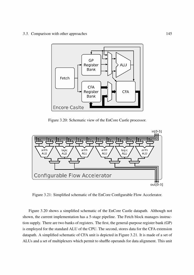
3.3. Comparison with other approaches 145
Figure 3.20: Schematic view of the EnCore Castle processor.
Figure 3.21: Simplified schematic of the EnCore Configurable Flow Accelerator.
Figure 3.20 shows a simplified schematic of the EnCore Castle datapath. Although notshown, the current implementation has a 5-stage pipeline. The Fetch block manages instruc-tion supply. There are two banks of registers. The first, the general-purpose register bank (GP)is employed for the standard ALU of the CPU. The second, stores data for the CFA extensiondatapath. A simplified schematic of CFA unit is depicted in Figure 3.21. It is made of a set ofALUs and a set of multiplexers which permit to shuffle operands for data alignment. This unit
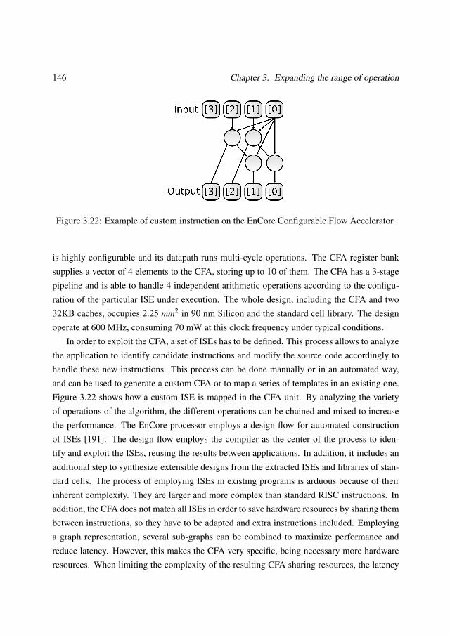
146 Chapter 3. Expanding the range of operation
Figure 3.22: Example of custom instruction on the EnCore Configurable Flow Accelerator.
is highly configurable and its datapath runs multi-cycle operations. The CFA register banksupplies a vector of 4 elements to the CFA, storing up to 10 of them. The CFA has a 3-stagepipeline and is able to handle 4 independent arithmetic operations according to the configu-ration of the particular ISE under execution. The whole design, including the CFA and two32KB caches, occupies 2.25 mm2 in 90 nm Silicon and the standard cell library. The designoperate at 600 MHz, consuming 70 mW at this clock frequency under typical conditions.
In order to exploit the CFA, a set of ISEs has to be defined. This process allows to analyzethe application to identify candidate instructions and modify the source code accordingly tohandle these new instructions. This process can be done manually or in an automated way,and can be used to generate a custom CFA or to map a series of templates in an existing one.Figure 3.22 shows how a custom ISE is mapped in the CFA unit. By analyzing the varietyof operations of the algorithm, the different operations can be chained and mixed to increasethe performance. The EnCore processor employs a design flow for automated constructionof ISEs [191]. The design flow employs the compiler as the center of the process to iden-tify and exploit the ISEs, reusing the results between applications. In addition, it includes anadditional step to synthesize extensible designs from the extracted ISEs and libraries of stan-dard cells. The process of employing ISEs in existing programs is arduous because of theirinherent complexity. They are larger and more complex than standard RISC instructions. Inaddition, the CFA does not match all ISEs in order to save hardware resources by sharing thembetween instructions, so they have to be adapted and extra instructions included. Employinga graph representation, several sub-graphs can be combined to maximize performance andreduce latency. However, this makes the CFA very specific, being necessary more hardwareresources. When limiting the complexity of the resulting CFA sharing resources, the latency
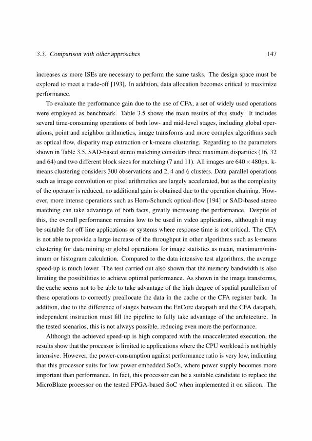
3.3. Comparison with other approaches 147
increases as more ISEs are necessary to perform the same tasks. The design space must beexplored to meet a trade-off [193]. In addition, data allocation becomes critical to maximizeperformance.
To evaluate the performance gain due to the use of CFA, a set of widely used operationswere employed as benchmark. Table 3.5 shows the main results of this study. It includesseveral time-consuming operations of both low- and mid-level stages, including global oper-ations, point and neighbor arithmetics, image transforms and more complex algorithms suchas optical flow, disparity map extraction or k-means clustering. Regarding to the parametersshown in Table 3.5, SAD-based stereo matching considers three maximum disparities (16, 32and 64) and two different block sizes for matching (7 and 11). All images are 640×480px. k-means clustering considers 300 observations and 2, 4 and 6 clusters. Data-parallel operationssuch as image convolution or pixel arithmetics are largely accelerated, but as the complexityof the operator is reduced, no additional gain is obtained due to the operation chaining. How-ever, more intense operations such as Horn-Schunck optical-flow [194] or SAD-based stereomatching can take advantage of both facts, greatly increasing the performance. Despite ofthis, the overall performance remains low to be used in video applications, although it maybe suitable for off-line applications or systems where response time is not critical. The CFAis not able to provide a large increase of the throughput in other algorithms such as k-meansclustering for data mining or global operations for image statistics as mean, maximum/min-imum or histogram calculation. Compared to the data intensive test algorithms, the averagespeed-up is much lower. The test carried out also shown that the memory bandwidth is alsolimiting the possibilities to achieve optimal performance. As shown in the image transforms,the cache seems not to be able to take advantage of the high degree of spatial parallelism ofthese operations to correctly preallocate the data in the cache or the CFA register bank. Inaddition, due to the difference of stages between the EnCore datapath and the CFA datapath,independent instruction must fill the pipeline to fully take advantage of the architecture. Inthe tested scenarios, this is not always possible, reducing even more the performance.
Although the achieved speed-up is high compared with the unaccelerated execution, theresults show that the processor is limited to applications where the CPU workload is not highlyintensive. However, the power-consumption against performance ratio is very low, indicatingthat this processor suits for low power embedded SoCs, where power supply becomes moreimportant than performance. In fact, this processor can be a suitable candidate to replace theMicroBlaze processor on the tested FPGA-based SoC when implemented it on silicon. The
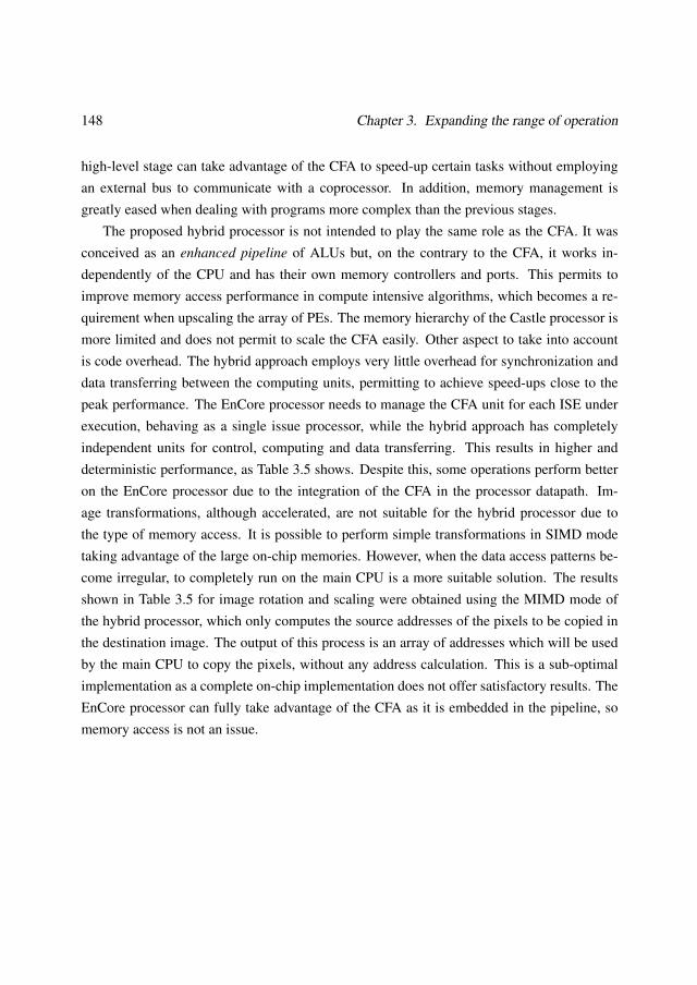
148 Chapter 3. Expanding the range of operation
high-level stage can take advantage of the CFA to speed-up certain tasks without employingan external bus to communicate with a coprocessor. In addition, memory management isgreatly eased when dealing with programs more complex than the previous stages.
The proposed hybrid processor is not intended to play the same role as the CFA. It wasconceived as an enhanced pipeline of ALUs but, on the contrary to the CFA, it works in-dependently of the CPU and has their own memory controllers and ports. This permits toimprove memory access performance in compute intensive algorithms, which becomes a re-quirement when upscaling the array of PEs. The memory hierarchy of the Castle processor ismore limited and does not permit to scale the CFA easily. Other aspect to take into accountis code overhead. The hybrid approach employs very little overhead for synchronization anddata transferring between the computing units, permitting to achieve speed-ups close to thepeak performance. The EnCore processor needs to manage the CFA unit for each ISE underexecution, behaving as a single issue processor, while the hybrid approach has completelyindependent units for control, computing and data transferring. This results in higher anddeterministic performance, as Table 3.5 shows. Despite this, some operations perform betteron the EnCore processor due to the integration of the CFA in the processor datapath. Im-age transformations, although accelerated, are not suitable for the hybrid processor due tothe type of memory access. It is possible to perform simple transformations in SIMD modetaking advantage of the large on-chip memories. However, when the data access patterns be-come irregular, to completely run on the main CPU is a more suitable solution. The resultsshown in Table 3.5 for image rotation and scaling were obtained using the MIMD mode ofthe hybrid processor, which only computes the source addresses of the pixels to be copied inthe destination image. The output of this process is an array of addresses which will be usedby the main CPU to copy the pixels, without any address calculation. This is a sub-optimalimplementation as a complete on-chip implementation does not offer satisfactory results. TheEnCore processor can fully take advantage of the CFA as it is embedded in the pipeline, somemory access is not an issue.
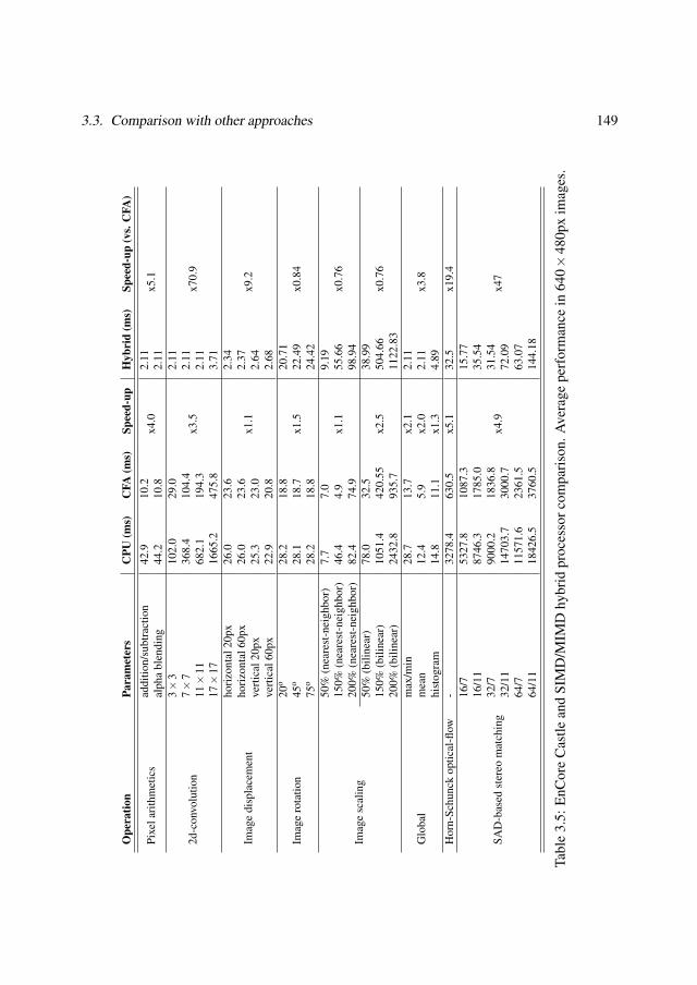
3.3. Comparison with other approaches 149O
pera
tion
Para
met
ers
CPU
(ms)
CFA
(ms)
Spee
d-up
Hyb
rid
(ms)
Spee
d-up
(vs.
CFA
)
Pixe
lari
thm
etic
sad
ditio
n/su
btra
ctio
n42
.910
.2x4
.02.
11x5
.1al
pha
blen
ding
44.2
10.8
2.11
2d-c
onvo
lutio
n
3×
310
2.0
29.0
x3.5
2.11
x70.
97×
736
8.4
104.
42.
1111×
1168
2.1
194.
32.
1117×
1716
65.2
475.
83.
71
Imag
edi
spla
cem
ent
hori
zont
al20
px26
.023
.6
x1.1
2.34
x9.2
hori
zont
al60
px26
.023
.62.
37ve
rtic
al20
px25
.323
.02.
64ve
rtic
al60
px22
.920
.82.
68
Imag
ero
tatio
n20
o28
.218
.8x1
.520
.71
x0.8
445
o28
.118
.722
.49
75o
28.2
18.8
24.4
2
Imag
esc
alin
g
50%
(nea
rest
-nei
ghbo
r)7.
77.
0x1
.19.
19x0
.76
150%
(nea
rest
-nei
ghbo
r)46
.44.
955
.66
200%
(nea
rest
-nei
ghbo
r)82
.474
.998
.94
50%
(bili
near
)78
.032
.5x2
.538
.99
x0.7
615
0%(b
iline
ar)
1051
.442
0.55
504.
6620
0%(b
iline
ar)
2432
.893
5.7
1122
.83
Glo
bal
max
/min
28.7
13.7
x2.1
2.11
x3.8
mea
n12
.45.
9x2
.02.
11hi
stog
ram
14.8
11.1
x1.3
4.89
Hor
n-Sc
hunc
kop
tical
-flow
-32
78.4
630.
5x5
.132
.5x1
9.4
SAD
-bas
edst
ereo
mat
chin
g
16/7
5327
.810
87.3
x4.9
15.7
7
x47
16/1
187
46.3
1785
.035
.54
32/7
9000
.218
36.8
31.5
432
/11
1470
3.7
3000
.772
.09
64/7
1157
1.6
2361
.563
.07
64/1
118
426.
537
60.5
144.
18
Tabl
e3.
5:E
nCor
eC
astle
and
SIM
D/M
IMD
hybr
idpr
oces
sorc
ompa
riso
n.A
vera
gepe
rfor
man
cein
640×
480p
xim
ages
.
150 Chapter 3. Expanding the range of operation
3.4 Summary
This chapter has shown an extensive optimization of the architecture proposed in Chapter 2.This first approach was designed to address the low-level stage of most Computer Visionapplications, which consumes most of the CPU workload. The coarse-grain processor arrayhas proved to be very efficient in these tasks. However, its flexibility is not the most adequateto handle efficiently the subsequent stages. Computing cores distribution, data representationand I/O operations are not suitable to address the mid- and high-level stages.
The architecture described in this chapter takes the best characteristics of SIMD andMIMD paradigms, and combines them in order to save hardware resources. The proposedSIMD/MIMD coprocessor lights the workload of the main CPU of a system-on-chip. Thisway, the new architecture can take advantage of both spatial and temporal parallelism, exe-cuting, massive operations in SIMD mode, task-parallel operations in MIMD mode and thehigh-level steps on a sequential processor. Computing paradigm can be changed at runtime asneeded according to the requirements of the particular algorithm under execution. I/O man-agement is improved by overlapping computation and data transferring, reducing the memorybottleneck and easing off-chip memory management. One of the goals of this architecture is toprovide enough flexibility to handle many different situations, including different data types,image sizes or more abstract representations. For this purpose, two different networks areemployed to exchange data between the computing units. Their characteristics ease data dis-tribution and reduce overhead in order to maximize performance. Besides flexibility, anothergoal is to make the architecture highly configurable, so it does not depend on the number ofcomputing cores, memory sizes or arithmetic operations. This allows to easily create a familyof processors to match different applications or different markets, fitting not only performanceor power consumption but also cost.
The proposed SIMD/MIMD hybrid processor was tested on an FPGA-based System-on-Chip. A set of operators and algorithms were tested to evaluated its performance and feasibil-ity. Results prove that a high throughput is achievable when the different operation modes areselected appropriately. The architecture was compared with other related approaches, includ-ing the coarse-grain processor array proposed in Chapter 2. The results show that the price topay due to the increase of hardware requirements and the addition of general-purpose capa-bilities which could penalize the performance of specific tasks, greatly boosts the flexibilitywithout compromising the performance.
Conclusions
Thesis summary
In this work, a novel hardware architecture to speed-up Computer Vision algorithms on em-bedded systems has been presented. This hardware architecture provides a single-chip deviceable to run most of the image processing and related algorithms present in the ComputerVision applications.
First, the introduction of the Computer Vision problem and the analysis of different al-gorithms were done. After reviewing their characteristics, type of operations and programcomplexity, the different computing paradigms were evaluated. Based on this knowledge, amassively parallel processor array was proposed in order to evaluate its feasibility employingthe current technology. This processor embeds a very large number of computing cores ar-ranged in a two dimensional array employing local connections to exchange data. Althoughprocessing only binary images, the results show that practical implementations are limitedto applications which process low resolution images and where the bandwidth is the majorbottleneck of the system. A later version of this processor, extended to deal with gray andcolor images, improves the results by reducing the parallelism but enhancing the computingunits. This architecture, as the previous one, was prototyped on an FPGA and the results val-idate the improvements included into the architecture. The prototype was evaluated using analgorithm to extract the retinal-vessel tree from retinal images. This high demanding applica-tion is representative of the algorithms the processor must be able to address, mainly on thelow- and mid-level stages, and includes most of the mathematical operations. The proposedarchitecture, a scalable coarse-grain processor array which exploits the data parallelism ofthe algorithms, was compared with a general-purpose desktop CPU, a focal-plane processor
152 Conclusions
which features a processor-per-pixel scheme and a stream processor, which exploits the taskparallelism of the algorithm.
The results obtained from the comparison of the different architectures were very valuablein order to expand the rage of operation of the architecture. One of the conclusions drawn isthat a two-dimensional arrangement of the computing units does not provide enough flexibilityto implement operations beyond the low- and mid-level stages. In addition, to exploit the task-level parallelism of the algorithms is not possible. The previous comparative showed that thisis very important even in algorithms were its presence is reduced. This leads us to design anew architecture, based on the previous one, where the different modules allow to reconfigureon demand and at runtime the computing paradigm.
The latest upgrades greatly increase the flexibility and the performance of the architec-ture. It can run two operation modes, SIMD and MIMD. In the first mode, all processors runthe same instruction. The computing units are arranged into a one-dimensional array withlocal connection between adjacent units. In this mode, data parallelism can be fully exploitedemploying the large on-chip storage each computing unit includes. Window-based operators,very important in the first steps of almost all Computer Vision algorithms, can be also imple-mented by storing several rows of the image adjacently. In MIMD mode, each computing unitruns a small program, a kernel of the whole algorithm. The different kernels are then con-nected employing a local network in order to build the flow diagram of the algorithm. Thismode implements task parallelism natively as all computing units work concurrently. Thisnetwork is self-managed, so no additional control is needed and the algorithm migration anddebugging steps are greatly cut. In both modes, two independent processors managed data I/Obetween the computing units and the external memory. This permits to operate concurrentlydata I/O and computation, increasing the overall performance of the system.
The final architecture was prototyped on an FPGA and several algorithms were imple-mented in order to evaluate the benefits of the included upgrades. Although it features general-purpose capabilities, the results show it is possible to achieve similar performance to the pre-vious version of the architecture for low-level image processing tasks, so it was possible togreatly increase the flexibility without compromise the performance. Besides this review, acomparison with other architectures were also carried out. The results also show the sameconclusion; the price to pay due to the increase of hardware requirements and the addition ofgeneral-purpose capabilities which could penalize the performance of specific tasks, greatlyboosts the flexibility without compromising the performance.
Conclusions 153
Future work
The architecture proposed in this work provides a solid basis on which it is possible to addnew characteristics in order to increase the flexibility and performance, among other figures ofmerit. In particular and based on the obtained results, a multi-core architecture provides majorimprovements. To run simultaneously both SIMD and MIMD computing paradigms, besidesan internal interconnection to drive data among the different cores, is expected to providebetter results than to increase the number of computing units on the single-core proposedarchitecture.
Beyond structural modifications and besides reconfigurable hardware such as FPGAs, thearchitecture is intended to be implemented on custom chips. The architecture can be opti-mized in a much deeper level, specially the arithmetic units, constrained by the available re-sources of the FPGAs. In addition, this opens new research directions and allows to evaluatemore accurately parameters such as power consumption or area requirements.

APPENDIX A
SIMD/MIMD HYBRID PROCESSOR
TIMING DIAGRAMS
This appendix shows how the different operations of each module of the dynamically recon-figurable processor described in Chapter 3 are scheduled. The time scale does not indicate thereal duration of each operation but how the different tasks are scheduled on each operationmode. A sample task for each mode is described below.
SIMD mode
In SIMD mode, all Processing Elements execute the same instruction and are controlled bythe SIMD Control module. The timing diagram refers to them employing the label PE Array.In this example task, three blocks of data are copied from the external RAM to the array ofPEs and then the results are extracted.
• The main CPU loads the program which PIP, POP and SIMD Control will execute.
• All modules are idle until a start flag is asserted by the main CPU.
• The PIP starts filling the SIPO queue according to the program and employing the AGUfor address calculation. If the data is cached, it is not necessary program accesses tothe external RAM. Data are copied serially in the SIPO until it is filled. The rest ofmodules wait until this process ends. Once the SIPO is full, the stored data are movedto the ME of each PE. This only takes one clock cycle, leaving the PEs ready to continue
156 Appendix A. SIMD/MIMD Hybrid Processor timing diagrams
processing. This process is executed as many times as blocks of data are needed by thePEs to start processing (one block, in this example).
• Now, the PEs can start computing. The PIP is able to continue filling the SIPO with anew block of data but it only can be copied when the PE Array finishes processing, asall PEs are busy.
• Once the PE Array finish processing a number of blocks of data, the POP reads theresults from the ME of each PE and copies them in the PISO queue. This only takesone clock cycle, leaving the PEs ready to continue processing.
• The POP extracts the results from the PISO serially and move them to the data cache,and then to the external RAM, according to the program it is running.
• This process iterates until all data are processed. At this point, all modules assert anend flag which is monitored by the main CPU. It should be noted that, as all moduleswork in parallel, simultaneous data transfers between the PIP, POP and PE Array arepossible, greatly increasing the performance.
Diagram nomenclature: E=empty; F=fill
MIMD mode
In MIMD mode, each Processing Element executes a small task of the whole algorithm. Allmodules operate concurrently, so task parallelism is exploited natively by the coprocessor.Each one executes the operations programmed and transfers the data to other adjacent PEusing the local network. This network is automatically synchronized by the Stream Queues.The size of each program is application-dependent, so it is possible that one PE would bewaiting for input data or due to the destination PE is not processing fast enough and its inputqueue is full. In this example, a data stream is processed by the PEs, acting PIP and POP asthe supplier and the receiver of the results, respectively.
• The main CPU loads the program which PIP, POP and all the PEs involved will execute.
• All modules are idle until a start flag is asserted by the main CPU.
157
• The PIP starts supplying data according to the program and employing the AGU foraddress calculation. If the data are cached, it is not necessary program accesses to theexternal RAM. Data are copied serially in the input Stream Queues of the destinationPE. This process is executed iteratively until the whole stream is transferred.
• Once there are data available in the input Stream Queues of the different PEs, they startprocessing, exchanging data according to the program they are running.
• The POP extracts the results from the PEs once they are reaching the end of the pipeline,i.e., the end of the 2D Torus. Results are stored in the data cache, and then copied tothe external RAM, according to the program it is running.
• As soon as the different modules end the processing, they assert an end flag whichis monitored by the main CPU. It should be noted that all units operate in parallel.There are not conflicts for memory access as the Stream Queues automatically managessynchronization and permits simultaneous read and write access. If one queue is full orempty, the unit which is trying to access remains in wait state until more data or spaceis available.
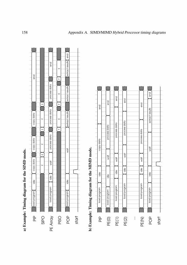
158 Appendix A. SIMD/MIMD Hybrid Processor timing diagrams
a)E
xam
ple:
Tim
ing
diag
ram
for
the
SIM
Dm
ode.
PIP
loa
dp
rog
ram
idle
co
py
da
tac
op
yd
ata
co
py
da
tae
nd
SIPO
FE
FE
FE
PEA
rray
loa
dp
rog
ram
idle
wa
itp
roc
ess
da
tap
roc
ess
da
tap
roc
ess
da
tae
nd
PISO
FE
FE
FE
POP
loa
dp
rog
ram
idle
wa
ite
xtra
ct
resu
ltse
xtra
ct
resu
ltse
xtra
ct
resu
ltse
nd
sta
rt
b)E
xam
ple:
Tim
ing
diag
ram
for
the
MIM
Dm
ode.
PIP
loa
dp
rog
ram
idle
co
py
da
tae
nd
PE[0
]lo
ad
pro
gra
mid
lew
ait
pro
ce
ssd
ata
en
d
PE[1
]lo
ad
pro
gra
mid
lew
ait
pro
ce
ssd
ata
en
d
PE[2
]lo
ad
pro
gra
mid
lew
ait
pro
ce
ssd
ata
en
d
...
PE[N
]lo
ad
pro
gra
mid
lew
ait
pro
ce
ssd
ata
en
d
POP
loa
dp
rog
ram
idle
wa
ite
xtra
ct
resu
ltse
nd
sta
rt


List of acronyms
AGU Address Generation Unit
ALU Arithmetic Logic Unit
ASIC Application Specific Integrated Circuit
ASIP Application-Specific Instruction Set Processor
CNN Cellular Neural Network
CPU Central Processing Unit)
CWCL Cellular Wave Computing Library
DSP Digital Signal Processor
FAST Features from Accelerated Segment Test
FFT Fast Fourier transform
FPGA Field Programmable Gate Array
GPGPU General-Purpose Graphics Processing Unit
GPU Graphics Processing Unit
HDL Hardware Description Language
IC Integrated Circuit
ITRS International Technology Roadmap for Semiconductors
162 LIST OF ACRONYMS
LUT Look-up Table
MAC Multiply-Accumulate
ME Memory Element
MIMD Multiple Instruction Multiple Data
MISD Multiple Instruction Single Data
MPMC Multi-Port Memory Controller
MPPA Massively Parallel Processor Array
MP-SIMD Massively Parallel Simple Instruction Multiple Data
PLS Pixel-Level Snakes
PE Processing Element
RAM Random-Access Memory
SCAMP SIMD Current-mode Analogue Matrix Processor
SIMD Single Instruction Multiple Data
SIFT Scale-Invariant Feature Transform
SiP System in Package
SISD Single Instruction Single Data
SoC System-on-a-Chip
SURF Speeded Up Robust Feature
SSE Streaming SIMD Extensions
TTM Time to market
VHDL Very-High-Speed Integrated Circuits Hardware Description Language
Bibliography
[1] BCC Research. Machine Vision: Technologies and Global Markets. Report IAS010C,BCC Research, June 2010.
[2] R. Szeliski. Computer vision: Algorithms and applications. Springer-Verlag NewYork Inc, 2010.
[3] Daniel Castaño-Díez, Dominik Moser, Andreas Schoenegger, Sabine Pruggnaller, andAchilleas S. Frangakis. Performance evaluation of image processing algorithms onthe GPU. Journal of Structural Biology, 164(1):153 – 160, 2008.
[4] Mukul Shirvaikar and Tariq Bushnaq. A comparison between DSP and FPGAplatforms for real-time imaging applications. volume 7244, page 724406. SPIE, 2009.
[5] M. Kolsch and S. Butner. Hardware Considerations for Embedded Vision Systems.Embedded Computer Vision, Springer, pages 3–26, 2009.
[6] M.J. Flynn. Some computer organizations and their effectiveness. Computers, IEEE
Transactions on, 100(9):948–960, 1972.
[7] C. Harris and M. Stephens. A combined corner and edge detector. In Alvey vision
conference, volume 15, page 50. Manchester, UK, 1988.
[8] D.G. Lowe. Distinctive image features from scale-invariant keypoints. International
journal of computer vision, 60(2):91–110, 2004.
[9] H. Bay, T. Tuytelaars, and L. Van Gool. Surf: Speeded up robust features. Computer
Vision–ECCV 2006, pages 404–417, 2006.
164 Bibliography
[10] K. Mikolajczyk and C. Schmid. A performance evaluation of local descriptors. IEEE
transactions on pattern analysis and machine intelligence, pages 1615–1630, 2005.
[11] M. Trajkovi and M. Hedley. Fast corner detection. Image and Vision Computing,16(2):75–87, 1998.
[12] Stephen M. Smith and J. Michael Brady. Susan‚ a new approach to low level imageprocessing. International Journal of Computer Vision, 23:45–78, 1997.
[13] S. Taylor and T. Drummond. Binary histogrammed intensity patches for efficient androbust matching. International journal of computer vision, pages 1–25, 2011.
[14] Nikhil R. Pal and Sankar K. Pal. A review on image segmentation techniques. Pattern
Recognition, pages 1277–1294, 1993.
[15] Robert M. Haralick and Linda G. Shapiro. Image segmentation techniques. Computer
Vision, Graphics, and Image Processing, 29(1):100 – 132, 1985.
[16] Barbara Zitova and Jan Flusser. Image registration methods: a survey. Image and
Vision Computing, 21(11):977 – 1000, 2003.
[17] Bill Triggs, Philip McLauchlan, Richard Hartley, and Andrew Fitzgibbon. Bundleadjustment: A modern synthesis. In Bill Triggs, Andrew Zisserman, and RichardSzeliski, editors, Vision Algorithms: Theory and Practice, volume 1883 of Lecture
Notes in Computer Science, pages 153–177. Springer Berlin / Heidelberg, 2000.
[18] Paul Viola and Michael Jones. Rapid object detection using a boosted cascade ofsimple features. Computer Vision and Pattern Recognition, IEEE Computer Society
Conference on, 1:511, 2001.
[19] N.M. Oliver, B. Rosario, and A.P. Pentland. A bayesian computer vision system formodeling human interactions. Pattern Analysis and Machine Intelligence, IEEE
Transactions on, 22(8):831 –843, aug 2000.
[20] G.R. Bradski and A. Kaehler. Learning OpenCV. O’Reilly, 2008.
[21] R. Singhal. Inside intel R© next generation nehalem microarchitecture. In Hot Chips,volume 20, 2008.
Bibliography 165
[22] F. Franchetti, S. Kral, J. Lorenz, and C.W. Ueberhuber. Efficient utilization of simdextensions. Proceedings of the IEEE, 93(2):409–425, 2005.
[23] S. Naffziger. Microprocessors of the future: Commodity or engine growth?Solid-State Circuits Magazine, IEEE, 1(1):76 –82, 2009.
[24] B. Chapman. The multicore programming challenge. Lecture Notes in Computer
Science, 4847:3, 2007.
[25] C. Urmson, J. Anhalt, D. Bagnell, C. Baker, R. Bittner, MN Clark, J. Dolan,D. Duggins, T. Galatali, C. Geyer, et al. Autonomous driving in urban environments:Boss and the urban challenge. Journal of Field Robotics, 25(8):425–466, 2008.
[26] C.Y. Chu and S.W. Chen. Parallel implementation for cone beam based 3d computedtomography (ct) medical image reconstruction on multi-core processors. In World
Congress on Medical Physics and Biomedical Engineering, September 7-12, 2009,
Munich, Germany, pages 2066–2069. Springer, 2009.
[27] L. Meier, P. Tanskanen, F. Fraundorfer, and M. Pollefeys. Pixhawk: A system forautonomous flight using onboard computer vision. In Robotics and Automation
(ICRA), 2011 IEEE International Conference on, pages 2992–2997. IEEE, 2011.
[28] T. Deselaers, D. Keysers, and H. Ney. Features for image retrieval: an experimentalcomparison. Information Retrieval, 11(2):77–107, 2008.
[29] L.J. Li, R. Socher, and L. Fei-Fei. Towards total scene understanding: Classification,annotation and segmentation in an automatic framework. In Computer Vision and
Pattern Recognition, 2009. CVPR 2009. IEEE Conference on, pages 2036–2043.IEEE, 2009.
[30] A. Ahmed and K. Terada. A general framework for multi-human tracking. Journal of
Software, 5(9):966–973, 2010.
[31] W.T. Chen, P.Y. Chen, W.S. Lee, and C.F. Huang. Design and implementation of areal time video surveillance system with wireless sensor networks. In Vehicular
Technology Conference, 2008. VTC Spring 2008. IEEE, pages 218–222. IEEE, 2008.
166 Bibliography
[32] Simon Taylor, Edward Rosten, and Tom Drummond. Robust feature matching in2.3µs. In IEEE CVPR Workshop on Feature Detectors and Descriptors: The State Of
The Art and Beyond, June 2009.
[33] J. Wither, Y.T. Tsai, and R. Azuma. Mobile augmented reality: Indirect augmentedreality. Computers and Graphics, 35(4):810–822, 2011.
[34] F. Ren, J. Huang, M. Terauchi, R. Jiang, and R. Klette. Lane detection on the iphone.Arts and Technology, pages 198–205, 2010.
[35] John D. Owens, David Luebke, Naga Govindaraju, Mark Harris, Jens Krüger,Aaron E. Lefohn, and Timothy J. Purcell. A survey of general-purpose computationon graphics hardware. Computer Graphics Forum, 26(1):80–113, 2007.
[36] S. Che, M. Boyer, J. Meng, D. Tarjan, J.W. Sheaffer, and K. Skadron. A performancestudy of general-purpose applications on graphics processors using cuda. Journal of
Parallel and Distributed Computing, 68(10):1370–1380, 2008.
[37] L. Seiler, D. Carmean, E. Sprangle, T. Forsyth, M. Abrash, P. Dubey, S. Junkins,A. Lake, J. Sugerman, R. Cavin, et al. Larrabee: a many-core x86 architecture forvisual computing. ACM Transactions on Graphics (TOG), 27(3):1–15, 2008.
[38] E. Lindholm, J. Nickolls, S. Oberman, and J. Montrym. Nvidia tesla: A unifiedgraphics and computing architecture. Micro, IEEE, 28(2):39–55, 2008.
[39] A. Thall. Extended-precision floating-point numbers for gpu computation. In ACM
SIGGRAPH 2006 Research posters, pages 52–es. ACM, 2006.
[40] S. Rixner, W.J. Dally, U.J. Kapasi, B. Khailany, A. López-Lagunas, P.R. Mattson, andJ.D. Owens. A bandwidth-efficient architecture for media processing. In Proceedings
of the 31st annual ACM/IEEE international symposium on Microarchitecture, pages3–13. IEEE Computer Society Press, 1998.
[41] V. Podlozhnyuk. Image convolution with cuda. NVIDIA Corporation white paper,
June, 2097(3), 2007.
[42] N.K. Govindaraju and D. Manocha. Cache-efficient numerical algorithms usinggraphics hardware. Parallel Computing, 33(10-11):663–684, 2007.
Bibliography 167
[43] S. Heymann, K. Maller, A. Smolic, B. Froehlich, and T. Wiegand. Siftimplementation and optimization for general-purpose gpu. In Proceedings of the
International Conference in Central Europe on Computer Graphics, Visualization and
Computer Vision. Citeseer, 2007.
[44] W.L.D. Lui and R. Jarvis. Eye-full tower: A gpu-based variable multibaselineomnidirectional stereovision system with automatic baseline selection for outdoormobile robot navigation. Robotics and Autonomous Systems, 58(6):747–761, 2010.
[45] R. Dolan and G. DeSouza. Gpu-based simulation of cellular neural networks forimage processing. In Proceedings of the 2009 international joint conference on
Neural Networks, pages 2712–2717. IEEE Press, 2009.
[46] V.W. Lee, C. Kim, J. Chhugani, M. Deisher, D. Kim, A.D. Nguyen, N. Satish,M. Smelyanskiy, S. Chennupaty, P. Hammarlund, et al. Debunking the 100x gpu vs.cpu myth: an evaluation of throughput computing on cpu and gpu. In ACM SIGARCH
Computer Architecture News, volume 38, pages 451–460. ACM, 2010.
[47] R. Schneiderman. Dsps evolving in consumer electronics applications [specialreports]. Signal Processing Magazine, IEEE, 27(3):6–10, 2010.
[48] T.J. Lin, C.N. Liu, S.Y. Tseng, Y.H. Chu, and A.Y. Wu. Overview of itri pacproject-from vliw dsp processor to multicore computing platform. In VLSI Design,
Automation and Test, 2008. VLSI-DAT 2008. IEEE International Symposium on,pages 188–191. IEEE, 2008.
[49] M. Wang, Y. Wang, D. Liu, Z. Qin, and Z. Shao. Compiler-assisted leakage-awareloop scheduling for embedded vliw dsp processors. Journal of Systems and Software,83(5):772–785, 2010.
[50] G. Talavera, M. Jayapala, J. Carrabina, and F. Catthoor. Address generationoptimization for embedded high-performance processors: A survey. Journal of Signal
Processing Systems, 53(3):271–284, 2008.
[51] Texas Instruments. Tms320c6000 programmer’s guide. White Paper, 2002.
[52] D. Baumgartner, P. Roessler, W. Kubinger, C. Zinner, and K. Ambrosch. Benchmarksof low-level vision algorithms for dsp, fpga, and mobile pc processors. Embedded
Computer Vision, pages 101–120, 2009.
168 Bibliography
[53] C.Y. Lin and Y.P. Chiu. The dsp based catcher robot system with stereo vision. InAdvanced Intelligent Mechatronics, 2008. AIM 2008. IEEE/ASME International
Conference on, pages 897–903. IEEE, 2008.
[54] T.Y. Sun and Y.H. Yu. Memory usage reduction method for fft implementations ondsp based embedded system. In Consumer Electronics, 2009. ISCE’09. IEEE 13th
International Symposium on, pages 812–815. IEEE, 2009.
[55] S. Shah, T. Khattak, M. Farooq, Y. Khawaja, A. Bais, A. Anees, and M. Khan. Realtime object tracking in a video sequence using a fixed point dsp. Advances in Visual
Computing, pages 879–888, 2008.
[56] K. Suzuki, H. Ikeda, K. Ishimaru, J. Suzuki, F. Adachi, and Xinlei Wang. New imageretrieval system utilizing image directory on gigabit network for distributing industrialproduct information. Industry Applications, IEEE Transactions on, 43(4):1099 –1107,july-aug. 2007.
[57] C. Neri, G. Baccarelli, S. Bertazzoni, F. Pollastrone, and M. Salmeri. Parallelhardware implementation of radar electronics equipment for a laser inspection system.Nuclear Science, IEEE Transactions on, 52(6):2741 –2748, dec. 2005.
[58] F. Rinnerthaler, W. Kubinger, J. Langer, M. Humenberger, and S. Borbély. Boostingthe performance of embedded vision systems using a dsp/fpga co-processor system.In Systems, Man and Cybernetics, 2007. ISIC. IEEE International Conference on,pages 1141–1146. IEEE, 2007.
[59] M. Bramberger and B. Rinner. An embedded smart camera on a scalableheterogeneous multi-dsp system. In In Proceedings of the European DSP Education
and Research Symposium (EDERS 2004. Citeseer, 2004.
[60] P.H.W. Leong. Recent trends in fpga architectures and applications. In Electronic
Design, Test and Applications, 2008. DELTA 2008. 4th IEEE International
Symposium on, pages 137–141. IEEE, 2008.
[61] P.P. Fasang. Prototyping for industrial applications [industry forum]. Industrial
Electronics Magazine, IEEE, 3(1):4–7, 2009.
Bibliography 169
[62] I.B. Djordjevic, M. Arabaci, and L.L. Minkov. Next generation fec for high-capacitycommunication in optical transport networks. Journal of Lightwave Technology,27(16):3518–3530, 2009.
[63] S. Craven and P. Athanas. Examining the viability of fpga supercomputing. EURASIP
Journal on Embedded systems, 2007(1):13–13, 2007.
[64] P. Coussy, A. Takach, M. McNamara, and M. Meredith. An introduction to thesystemc synthesis subset standard. In Proceedings of the eighth IEEE/ACM/IFIP
international conference on Hardware/software codesign and system synthesis, pages183–184. ACM, 2010.
[65] F. Moreno, I. Lopez, and R. Sanz. A design process for hardware–software systemco-design and its application to designing a reconfigurable fpga. In Digital System
Design - Architectures, Methods and Tools (DSD), 2010 13th Euromicro Conference
on, pages 556–562. IEEE, 2010.
[66] S. Jin, J. Cho, X. Dai Pham, K.M. Lee, S.K. Park, M. Kim, and J.W. Jeon. Fpgadesign and implementation of a real-time stereo vision system. Circuits and Systems
for Video Technology, IEEE Transactions on, 20(1):15–26, 2010.
[67] S. Franchini, A. Gentile, F. Sorbello, G. Vassallo, and S. Vitabile. An embedded,fpga-based computer graphics coprocessor with native geometric algebra support.Integration, the VLSI Journal, 42(3):346–355, 2009.
[68] M. Martineau, Z. Wei, D.J. Lee, and M. Martineau. A fast and accurate tensor-basedoptical flow algorithm implemented in fpga. In Applications of Computer Vision,
2007. WACV’07. IEEE Workshop on, pages 18–18. IEEE, 2007.
[69] H. Meng, K. Appiah, A. Hunter, and P. Dickinson. Fpga implementation of naivebayes classifier for visual object recognition. IEEE Computer Vision and PatternRecognition, 2011.
[70] V. Nair, P.O. Laprise, and J.J. Clark. An fpga-based people detection system.EURASIP journal on applied signal processing, 2005:1047–1061, 2005.
[71] M.A.M. Salem, K. Klaus, F. Winkler, and B. Meffert. Resolution mosaic-based smartcamera for video surveillance. In Distributed Smart Cameras, 2009. ICDSC 2009.
Third ACM/IEEE International Conference on, pages 1–7. IEEE, 2009.
170 Bibliography
[72] R. Lysecky and F. Vahid. A study of the speedups and competitiveness of fpga softprocessor cores using dynamic hardware/software partitioning. In Proceedings of the
conference on Design, Automation and Test in Europe-Volume 1, pages 18–23. IEEEComputer Society, 2005.
[73] B.F. Veale, J.K. Antonio, M.P. Tull, and S.A. Jones. Selection of instruction setextensions for an fpga embedded processor core. In Parallel and Distributed
Processing Symposium, 2006. IPDPS 2006. 20th International, page 8 pp., april 2006.
[74] Y. Shi. Smart cameras for machine vision. Smart Cameras, pages 283–303, 2010.
[75] I. Kuon and J. Rose. Measuring the gap between fpgas and asics. Computer-Aided
Design of Integrated Circuits and Systems, IEEE Transactions on, 26(2):203 –215,feb. 2007.
[76] Kwanho Kim, Joo-Young Kim, Seungjin Lee, Minsu Kim, and Hoi-Jun Yoo. A 211gops/w dual-mode real-time object recognition processor with network-on-chip. InSolid-State Circuits Conference, 2008. ESSCIRC 2008. 34th European, pages 462–465, sept. 2008.
[77] G.P. Stein, E. Rushinek, G. Hayun, and A. Shashua. A computer vision system on achip: a case study from the automotive domain. In Computer Vision and Pattern
Recognition - Workshops, 2005. CVPR Workshops. IEEE Computer Society
Conference on, page 130, june 2005.
[78] B.K. Khailany, T. Williams, J. Lin, E.P. Long, M. Rygh, D.W. Tovey, and W.J. Dally.A programmable 512 gops stream processor for signal, image, and video processing.Solid-State Circuits, IEEE Journal of, 43(1):202 –213, jan. 2008.
[79] S.M. Garrido, J. Listán, L. Alba, C. Utrera, S.Á. Rodríguez-Vázquez,R. Domínguez-Castro, F. Jiménez-Espejo, and R. Romay. The Eye-RIS CMOS VisionSystem. Analog circuit design: sensors, actuators and power drivers; integrated
power amplifiers from wireline to RF; very high frequency front ends, pages 15–32,2008.
[80] A. Lopich and P. Dudek. Aspa: Focal plane digital processor array with asynchronousprocessing capabilities. In Circuits and Systems, 2008. ISCAS 2008. IEEE
International Symposium on, pages 1592–1595. IEEE, 2008.
Bibliography 171
[81] P. Foldesy, Á. Zarándy, and C. Rekeczky. Configurable 3d-integrated focal-planecellular sensor–processor array architecture. International Journal of Circuit Theory
and Applications, 36(5-6):573–588, 2008.
[82] M. Koyanagi, Y. Nakagawa, K.W. Lee, T. Nakamura, Y. Yamada, K. Inamura, K.T.Park, and H. Kurino. Neuromorphic vision chip fabricated using three-dimensionalintegration technology. In Solid-State Circuits Conference, 2001. Digest of Technical
Papers. ISSCC. 2001 IEEE International, pages 270–271. IEEE, 2001.
[83] T.G. Constandinou, J. Georgiou, and C. Toumazou. Towards a bio-inspiredmixed-signal retinal processor. In Circuits and Systems, 2004. ISCAS’04. Proceedings
of the 2004 International Symposium on, volume 5, pages V–493. IEEE, 2004.
[84] Ã. Zarándy. Focal-plane sensor-processor chips. Springer Verlag, 2011.
[85] A. Duller, G. Panesar, and D. Towner. Parallel processing-the picochip way.Communicating Processing Architectures, pages 125–138, 2003.
[86] S. Bell, B. Edwards, J. Amann, R. Conlin, K. Joyce, V. Leung, J. MacKay, M. Reif,L. Bao, J. Brown, et al. Tile64-processor: A 64-core soc with mesh interconnect. InSolid-State Circuits Conference, 2008. ISSCC 2008. Digest of Technical Papers. IEEE
International, pages 88–598. IEEE, 2008.
[87] M. Butts, A.M. Jones, and P. Wasson. A structural object programming model,architecture, chip and tools for reconfigurable computing. In Field-Programmable
Custom Computing Machines, 2007. FCCM 2007. 15th Annual IEEE Symposium on,pages 55–64. IEEE, 2007.
[88] N. Zhang. Computing optimised parallel speeded-up robust features (p-surf) onmulti-core processors. International Journal of Parallel Programming,38(2):138–158, 2010.
[89] D. Bouris, A. Nikitakis, and I. Papaefstathiou. Fast and efficient fpga-based featuredetection employing the surf algorithm. In 2010 18th IEEE Annual International
Symposium on Field-Programmable Custom Computing Machines, pages 3–10. IEEE,2010.
172 Bibliography
[90] PK Aby, A. Jose, B. Jose, LD Dinu, J. John, and G. Sabarinath. Implementation andoptimization of embedded face detection system. In Signal Processing,
Communication, Computing and Networking Technologies (ICSCCN), 2011
International Conference on, pages 250–253. IEEE, 2011.
[91] C. Arth and H. Bischof. Real-time object recognition using local features on adsp-based embedded system. Journal of Real-Time Image Processing, 3(4):233–253,2008.
[92] T.B. Terriberry, L.M. French, and J. Helmsen. Gpu accelerating speeded-up robustfeatures. In Proc. Int. Symp. on 3D Data Processing, Visualization and Transmission
(3DPVT), pages 355–362. Citeseer, 2008.
[93] M. Murphy, K. Keutzer, and H. Wang. Image feature extraction for mobile processors.In Workload Characterization, 2009. IISWC 2009. IEEE International Symposium on,pages 138–147. IEEE, 2009.
[94] D. Takahashi. Implementation and evaluation of parallel fft using simd instructions onmulti-core processors. In Innovative architecture for future generation
high-performance processors and systems, 2007. iwia 2007. international workshop
on, pages 53–59. IEEE, 2007.
[95] Y. Ogata, T. Endo, N. Maruyama, and S. Matsuoka. An efficient, model-basedcpu-gpu heterogeneous fft library. In Parallel and Distributed Processing, 2008.
IPDPS 2008. IEEE International Symposium on, pages 1–10. IEEE, 2008.
[96] H. He and H. Guo. The realization of fft algorithm based on fpga co-processor. InSecond International Symposium on Intelligent Information Technology Application,pages 239–243. IEEE, 2008.
[97] X. Guan, H. Lin, and Y. Fei. Design of an application-specific instruction setprocessor for high-throughput and scalable fft. In Proceedings of the Conference on
Design, Automation and Test in Europe, pages 1302–1307, 2009.
[98] K. Pauwels, M. Tomasi, J.D. Alonso, E. Ros, and M.M. Van Hulle. A comparison offpga and gpu for real-time phase-based optical flow, stereo, and local image features.IEEE Transactions on Computers, 2011.
Bibliography 173
[99] P. Dudek and P.J. Hicks. A general-purpose processor-per-pixel analog simd visionchip. Circuits and Systems I: Regular Papers, IEEE Transactions on, 52(1):13–20,2005.
[100] A. Lopich and P. Dudek. Global operations in simd cellular processor arraysemploying functional asynchronism. In Computer Architecture for Machine
Perception and Sensing, 2006. CAMP 2006. International Workshop on, pages 18–23.IEEE, 2007.
[101] B.K. Khailany, T. Williams, J. Lin, E.P. Long, M. Rygh, D.F.W. Tovey, and W.J. Dally.A programmable 512 gops stream processor for signal, image, and video processing.Solid-State Circuits, IEEE Journal of, 43(1):202–213, 2008.
[102] A. Fijany and F. Hosseini. Image processing applications on a low power highlyparallel simd architecture. In Aerospace Conference, 2011 IEEE, pages 1–12. IEEE,2011.
[103] N.S. Kim, T. Austin, D. Baauw, T. Mudge, K. Flautner, J.S. Hu, M.J. Irwin,M. Kandemir, and V. Narayanan. Leakage current: Moore’s law meets static power.Computer, 36(12):68–75, 2003.
[104] Peter Ramm Philip Garrou, Chistopher Bower. Handbook of 3D Integration.Wiley-VCH, 2008.
[105] Intel. Intel 22nm 3-d tri-gate transistor technology. Intel Documentation, 2011.
[106] G. Koch. Discovering multi-core: extending the benefits of moore’s law. Technology,1, 2005.
[107] Nathan Brookwood. Amd fusion family of apus – enabling a superior, immersive pcexperience. AMD white paper, 2010.
[108] Arnon Friedmann. Enabling small cells with ti’s new multicore soc. Texas
Instruments White Paper, 2010.
[109] Nathan Brookwood. Amd fusion family of apus – enabling a superior, immersive pcexperience. AMD white paper, 2010.
174 Bibliography
[110] NVIDIA. Variable smp – a multi-core cpu architecture for low power and highperformance. NVIDIA Corporation white paper, 2011.
[111] Desh Singh. Higher level programming abstractions for fpgas using opencl. ALTERA,2011.
[112] Keith DeHaven. Extensible processing platform ideal solution for a wide range ofembedded systems. Xilinx White Paper, 2010.
[113] M. Hassaballah, S. Omran, and Y.B. Mahdy. A review of simd multimedia extensionsand their usage in scientific and engineering applications. The Computer Journal,51(6):630–649, 2008.
[114] L.J. Karam, I. AlKamal, A. Gatherer, G.A. Frantz, D.V. Anderson, and B.L. Evans.Trends in multicore dsp platforms. Signal Processing Magazine, IEEE, 26(6):38–49,2009.
[115] M. Ilic and M. Stojcev. Address generation unit as accelerator block in dsp. InTelecommunication in Modern Satellite Cable and Broadcasting Services (TELSIKS),
2011 10th International Conference on, volume 2, pages 563–566. IEEE, 2011.
[116] R.P. Kleihorst, AA Abbo, A. van der Avoird, MJR Op de Beeck, L. Sevat, P. Wielage,R. van Veen, and H. van Herten. Xetal: a low-power high-performance smart cameraprocessor. In Circuits and Systems, 2001. ISCAS 2001. The 2001 IEEE International
Symposium on, volume 5, pages 215–218. IEEE, 2001.
[117] A.A. Abbo, R.P. Kleihorst, V. Choudhary, L. Sevat, P. Wielage, S. Mouy,B. Vermeulen, and M. Heijligers. Xetal-ii: a 107 gops, 600 mw massively parallelprocessor for video scene analysis. Solid-State Circuits, IEEE Journal of,43(1):192–201, 2008.
[118] S. Kyo, S. Okazaki, and T. Arai. An integrated memory array processor for embeddedimage recognition systems. Computers, IEEE Transactions on, 56(5):622–634, 2007.
[119] J. Poikonen, M. Laiho, and A. Paasio. Mipa4k: A 64× 64 cell mixed-mode imageprocessor array. In Circuits and Systems, 2009. ISCAS 2009. IEEE International
Symposium on, pages 1927–1930. IEEE, 2009.
Bibliography 175
[120] A. Lopich and P. Dudek. Aspa: Asynchronous–synchronous focal-planesensor-processor chip. Focal-Plane Sensor-Processor Chips, page 73, 2011.
[121] J. Fernández-Berni, R. Carmona-Galán, and L. Carranza-González. Flip-q: A qcifresolution focal-plane array for low-power image processing. Solid-State Circuits,
IEEE Journal of, 46(3):669–680, 2011.
[122] H. Singh, M.H. Lee, G. Lu, F.J. Kurdahi, N. Bagherzadeh, and E.M. Chaves Filho.Morphosys: an integrated reconfigurable system for data-parallel andcomputation-intensive applications. Computers, IEEE Transactions on,49(5):465–481, 2000.
[123] K. Yamaguchi, Y. Watanabe, T. Komuro, and M. Ishikawa. Design of a massivelyparallel vision processor based on multi-simd architecture. In Circuits and Systems,
2007. ISCAS 2007. IEEE International Symposium on, pages 3498–3501. IEEE, 2007.
[124] L.O. Chua and L. Yang. Cellular neural networks: Applications. Circuits and
Systems, IEEE Transactions on, 35(10):1273–1290, 1988.
[125] Ian Overington. Computer Vision: A Unified, Biologically-Inspired Approach.Elsevier Science Inc., New York, NY, USA, 1992.
[126] A. Rodríguez-Vázquez, G. Liñán-Cembrano, L. Carranza, E. Roca-Moreno,R. Carmona-Galán, F. Jiménez-Garrido, R. Domínguez-Castro, and S.E. Meana.Ace16k: the third generation of mixed-signal simd-cnn ace chips toward vsocs.Circuits and Systems I: Regular Papers, IEEE Transactions on, 51(5):851–863, 2004.
[127] Z. Nagy and P. Szolgay. Configurable multilayer cnn-um emulator on fpga. Circuits
and Systems I: Fundamental Theory and Applications, IEEE Transactions on,50(6):774–778, 2003.
[128] J.Y. Kim, M. Kim, S. Lee, J. Oh, K. Kim, and H.J. Yoo. A 201.4 gops 496 mwreal-time multi-object recognition processor with bio-inspired neural perceptionengine. Solid-State Circuits, IEEE Journal of, 45(1):32–45, 2010.
[129] B. Khailany, W.J. Dally, U.J. Kapasi, P. Mattson, J. Namkoong, J.D. Owens,B. Towles, A. Chang, and S. Rixner. Imagine: Media processing with streams. Micro,
IEEE, 21(2):35–46, 2001.
176 Bibliography
[130] W.J. Dally, F. Labonte, A. Das, P. Hanrahan, J.H. Ahn, J. Gummaraju, M. Erez,N. Jayasena, I. Buck, T.J. Knight, et al. Merrimac: Supercomputing with streams. InProceedings of the 2003 ACM/IEEE conference on Supercomputing, page 35. ACM,2003.
[131] J.C. Chen and S.Y. Chien. Crisp: Coarse-grained reconfigurable image streamprocessor for digital still cameras and camcorders. Circuits and Systems for Video
Technology, IEEE Transactions on, 18(9):1223–1236, 2008.
[132] M. Lanuzza, S. Perri, P. Corsonello, and M. Margala. A new reconfigurablecoarse-grain architecture for multimedia applications. In Adaptive Hardware and
Systems, 2007. AHS 2007. Second NASA/ESA Conference on, pages 119–126. IEEE,2007.
[133] D. Kim, K. Kim, J.Y. Kim, S. Lee, and H.J. Yoo. An 81.6 gops object recognitionprocessor based on noc and visual image processing memory. In Custom Integrated
Circuits Conference, 2007. CICC’07. IEEE, pages 443–446. IEEE, 2007.
[134] H.J. Siegel, J.B. Armstrong, and D.W. Watson. Mapping computer-vision-relatedtasks onto reconfigurable parallel-processing systems. Computer, 25(2):54–63, 1992.
[135] X. Wang and S.G. Ziavras. Hera: A reconfigurable and mixed-mode parallelcomputing engine on platform fpgas. In Parallel and Distributed Computing and
Systems. ACTA Press, 2004.
[136] P. Bonnot, F. Lemonnier, G. Edelin, G. Gaillat, O. Ruch, and P. Gauget. Definitionand simd implementation of a multi-processing architecture approach on fpga. InProceedings of the conference on Design, automation and test in Europe, pages610–615. ACM, 2008.
[137] A. Prengler and K. Adi. A reconfigurable simd-mimd processor architecture forembedded vision processing applications. In SAE World Congress, 2009.
[138] B. Kisacanin. Examples of low-level computer vision on media processors. InComputer Vision and Pattern Recognition-Workshops, 2005. CVPR Workshops. IEEE
Computer Society Conference on, pages 135–135. IEEE, 2005.
Bibliography 177
[139] M. Wnuk. Remarks on hardware implementation of image processing algorithms.International Journal of Applied Mathematics and Computer Science, 18(1):105–110,2008.
[140] S. Asano, T. Maruyama, and Y. Yamaguchi. Performance comparison of fpga, gpuand cpu in image processing. In Field Programmable Logic and Applications, 2009.
FPL 2009. International Conference on, pages 126–131. IEEE, 2009.
[141] Celoxica. http://www.celoxica.com/.
[142] Xilinx, inc. http://www.xilinx.com/.
[143] Itrs. 2011. International Technology Roadmap for Semiconductors,http://public.itrs.net/.
[144] George Varghese and Jan M. Rabaey. Low-Energy FPGAs, Architecture and Design.Kluwer Academic Publishers, 2001.
[145] L. Kék, K. Karacs, and T. Roska. Cellular wave computing library: Templates,algorithms, and programs. MTA-SZTAKI, Budapest, version, 2, 2007.
[146] V.M. Brea, M. Laiho, DL Vilarino, A. Paasio, and D. Cabello. A binary-based on-chipcnn solution for pixel-level snakes. International journal of circuit theory and
applications, 34(4):383–407, 2006.
[147] C. Rekeczky. Skeletonization and the shortest path problem—theoretical investigationand algorithms for cnn universal chips. In Proceedings of International Symposium on
Non-linear Theory and its Applications (NOLTA’99), volume 1, pages 423–426, 1999.
[148] M. Eldesouki, O. Marinov, M.J. Deen, and Q. Fang. Cmos active-pixel sensor within-situ memory for ultrahigh-speed imaging. Sensors Journal, IEEE, (99):1–1, 2011.
[149] C. Alonso-Montes et al. Arteriolar-to-venular diameter ratio estimation: Apixel-parallel approach. 11th International Workshop on Cellular Neural Networks
and Their Applications, pages 86–91, 2008.
[150] C. Mariño, et al. Personal authentication using digital retinal images. Pattern Analysis
& Applications, 9(1):21–33, 2006.
178 Bibliography
[151] C. Alonso-Montes, M. Ortega, MG Penedo, and DL Vilarino. Pixel parallel vessel treeextraction for a personal authentication system. In IEEE International Symposium on
Circuits and Systems, 2008, pages 1596–1599, 2008.
[152] C. Alonso-Montes, DL Vilarino, P. Dudek, and MG Penedo. Fast retinal vessel treeextraction: A pixel parallel approach. International Journal of Circuit Theory and
Applications, 36(5-6):641–651, 2008.
[153] M. Kass, A. Witkin, and D. Terzopoulos. Snakes: Active contour models.International Journal of Computer Vision, 1(4):321–331, 1988.
[154] L.D. Cohen and I. Cohen. Finite-element methods for active contour models andballoons for 2-D and 3-D images. IEEE Transactions on Pattern Analysis and
Machine Intelligence, 15(11):1131–1147, 2002.
[155] D.L. Vilariño and C. Rekeczky. Pixel-level snakes on the CNNUM: algorithm design,on-chip implementation and applications. International Journal of Circuit Theory and
Applications, 33(1):17–51, 2005.
[156] P. Dudek, L. Vilarino, et al. A cellular active contours algorithm based on regionevolution. In 10th International Workshop on Cellular Neural Networks and Their
Applications, 2006. CNNA 2006., pages 1–6. IEEE, 2006.
[157] D.L. Vilarino and P. Dudek. Evolution of Pixel Level Snakes towards an efficienthardware implementation. In IEEE International Symposium on Circuits and Systems,
2007. ISCAS 2007., pages 2678–2681.
[158] Carmen Alonso Montes. Automatic Pixel-Parallel Extraction of the RetinalVascular-Tree: Algorithm Design, On-Chip Implementation and Applications. PhDThesis, Faculty of Informatics, University of A Coruna, 2008.
[159] J.J. Staal, M.D. Abramoff, M. Niemeijer, M.A. Viergever, and B. van Ginneken.Ridge based vessel segmentation in color images of the retina. IEEE Transactions on
Medical Imaging, 23(4):501–509, 2004.
[160] Mathworks, inc. http://www.mathworks.com/.
[161] Opal kelly. http://www.opalkelly.com/.
Bibliography 179
[162] Cypress semiconductor corporation. http://www.cypress.com/.
[163] Virtex-6 Family Overview. In Inc. Xilinx, editor, DS099 White Paper. 2010.
[164] H. Feng-Cheng, H. Shi-Yu, K. Ji-Wei, and C. Yung-Chang. High-Performance SIFTHardware Accelerator for Real-Time Image Feature Extraction. IEEE Transactions on
Circuits and Systems for Video Technology, 22(3):340–351, 2012.
[165] W.J. MacLean. An evaluation of the suitability of FPGAs for embedded visionsystems. In Computer Vision and Pattern Recognition-Workshops, 2005. CVPR
Workshops. IEEE Computer Society Conference on, page 131. IEEE, 2005.
[166] HM Rode, AS Chiddarwar, and SJ Darak. Suitability of FPGA for computationallyintensive image processing algorithms. 2009.
[167] D. Foty. Perspectives on scaling theory and CMOS technology - understanding thepast, present, and future. In Proceedings of the 2004 11th IEEE International
Conference on Electronics, Circuits and Systems, 2004. ICECS 2004., pages 631 –637, dec. 2004.
[168] W.J. Dally, U.J. Kapasi, B. Khailany, J.H. Ahn, and A. Das. Stream processors:Progammability and efficiency. Queue, 2(1):52–62, 2004.
[169] Á. Rodríguez-Vázquez, R. Domínguez-Castro, F. Jiménez-Garrido, S. Morillas,J. Listán, L. Alba, C. Utrera, S. Espejo, and R. Romay. The eye-RIS CMOS visionsystem. Analog Circuit Design, pages 15–32, 2008.
[170] F. Paillet, D. Mercier, and T.M. Bernard. Second generation programmable artificialretina. In Proceedings of the Twelfth Annual IEEE International ASIC/SOC
Conference, 1999., pages 304 –309, 1999.
[171] Alexey Lopich and Piotr Dudek. Asynchronous cellular logic network as aco-processor for a general-purpose massively parallel array. International Journal of
Circuit Theory and Applications, 2010.
[172] T. Komuro, I. Ishii, M. Ishikawa, and A. Yoshida. A digital vision chip specialized forhigh-speed target tracking. IEEE Transactions on Electron Devices, 50(1):191 – 199,jan 2003.
180 Bibliography
[173] A. W. Topol, D. C. La Tulipe, L. Shi, D. J. Frank, K. Bernstein, S. E. Steen, A. Kumar,G. U. Singco, A. M. Young, K. W. Guarini, and M. Ieong. Three-dimensionalintegrated circuits. IBM Journal of Research and Development, 50(4.5):491 –506, july2006.
[174] H. Kurino, M. Nakagawa, K.W. Lee, T. Nakamura, Y. Yamada, K.T. Park, andM. Koyanagi. Smart vision chip fabricated using three dimensional integrationtechnology. Advances in Neural Information Processing Systems, pages 720–726,2001.
[175] P. Foldesy, A. Zarandy, C. Rekeczky, and T. Roska. 3D integrated scalable focal-planeprocessor array. In 18th European Conference on Circuit Theory and Design, 2007.
ECCTD 2007., pages 954 –957, aug. 2007.
[176] P. Dudek. Implementation of simd vision chip with 128x128 array of analogueprocessing elements. In Circuits and Systems, 2005. ISCAS 2005. IEEE International
Symposium on, pages 5806 – 5809 Vol. 6, may 2005.
[177] P. Dudek. A Processing Element for an Analogue SIMD Vision Chip. In European
Conference on Circuit Theory and Design. ECCTD 2003, volume 3, pages 221–224,2003.
[178] C. Alonso-Montes, P. Dudek, DL Vilarifio, and MG Penedo. On chip implementationof a pixel-parallel approach for retinal vessel tree extraction. In 18th European
Conference on Circuit Theory and Design, 2007. ECCTD 2007., pages 511–514.IEEE, 2008.
[179] W. Schroder-Preikschat and G. Snelting. Invasive Computing: An Overview.Multiprocessor System-on-Chip: Hardware Design and Tool Integration, page 241,2010.
[180] M. Butts, A.M. Jones, and P. Wasson. A Structural Object Programming Model,Architecture, Chip and Tools for Reconfigurable Computing. In 15th Annual IEEE
Symposium on Field-Programmable Custom Computing Machines, 2007. FCCM
2007., pages 55 –64, april 2007.
[181] Keith DeHaven. Extensible Processing Platform Ideal Solution for a Wide Range ofEmbedded Systems. In Extensible Processing Platform Overview White Paper. 2010.
Bibliography 181
[182] B. Hutchings, B. Nelson, S. West, and R. Curtis. Comparing fine-grained performanceon the Ambric MPPA against an FPGA. In International Conference on Field
Programmable Logic and Applications, 2009. FPL 2009., pages 174 –179, sept 2009.
[183] A. Agarwal. The Tile processor: A 64-core multicore for embedded processing. InProceedings of HPEC Workshop, 2007.
[184] F. Hannig, H. Ruckdeschel, H. Dutta, and J. Teich. Paro: Synthesis of hardwareaccelerators for multi-dimensional dataflow-intensive applications. Reconfigurable
Computing: Architectures, Tools and Applications, pages 287–293, 2008.
[185] C.D. Resco, A. Nieto, R.R. Osorio, V.M. Brea, and D.L. Vilarino. A digitalcellular-based system for retinal vessel-tree extraction. In European Conference on
Circuit Theory and Design, 2009. ECCTD 2009., pages 835 –838, aug. 2009.
[186] M. Niemeijer, J. Staal, B. van Ginneken, M. Loog, and M.D. Abramoff. Comparativestudy of retinal vessel segmentation methods on a new publicly available database. InProceedings of SPIE, volume 5370, page 648, 2004.
[187] M. Geilen and T. Basten. Requirements on the execution of Kahn process networks.Programming Languages and Systems, pages 319–334, 2003.
[188] J. Lee and L. Shannon. The effect of node size, heterogeneity, and network size onFPGA based NoCs. In International Conference on Field-Programmable Technology,pages 479 –482, dec. 2009.
[189] N. Alaraje, J.E. DeGroat, and H. Jasani. SoFPGA (System-on-FPGA) architecture:Performance analysis. In IEEE International Conference on Electro/Information
Technology, pages 551 –556, may. 2007.
[190] A. Benedetti, A. Prati, and N. Scarabottolo. Image convolution on fpgas: theimplementation of a multi-fpga fifo structure. In Euromicro Conference, 1998.
Proceedings. 24th, volume 1, pages 123–130. IEEE, 1998.
[191] O. Almer, R. Bennett, I. Böhm, A. Murray, X. Qu, M. Zuluaga, B. Franke, andN. Topham. An end-to-end design flow for automated instruction set extension andcomplex instruction selection based on gcc. In International Workshop on GCC
Research Opportunities, 2009.

182 Bibliography
[192] Arc international. http://http://www.synopsys.com/.
[193] M. Zuluaga and N. Topham. Resource sharing in custom instruction set extensions. InApplication Specific Processors, 2008. SASP 2008. Symposium on, pages 7–13. IEEE,2008.
[194] B.K.P. Horn and B.G. Schunck. Determining optical flow. Artificial intelligence,17(1-3):185–203, 1981.
List of Figures
Fig. 2.1 The Processing Element for the fine-grain B/W processor array. . . . . . . . 49Fig. 2.2 Schematic of the fine-grain binary processor array. . . . . . . . . . . . . . . 51Fig. 2.3 Instruction format of the fine-grain binary processor array. . . . . . . . . . . 52Fig. 2.4 Scaling of the fine-grain processor array on FPGAs according to the ITRS
roadmap. . . . . . . . . . . . . . . . . . . . . . . . . . . . . . . . . . . . . 54Fig. 2.5 Edge detection algorithm. Template T is shown in Eq. 2.1. . . . . . . . . . . 56Fig. 2.6 Pattern matching template example. . . . . . . . . . . . . . . . . . . . . . . 57Fig. 2.7 Edge detection algorithm. Template T is shown in Eq. 2.1. . . . . . . . . . . 58Fig. 2.8 Flow diagram of the skeletonization operation. . . . . . . . . . . . . . . . . 61Fig. 2.9 Flow diagram of the line detector algorithm, which employs large-
neighborhood access. . . . . . . . . . . . . . . . . . . . . . . . . . . . . . 62Fig. 2.10 Flow diagram of exploration phase of the shortest path problem. . . . . . . . 63Fig. 2.11 Example of the shortest path problem and intermediate steps during
algorithm execution. . . . . . . . . . . . . . . . . . . . . . . . . . . . . . . 66Fig. 2.12 Fixed-width instruction format of the coarse-grain processor array. . . . . . 69Fig. 2.13 Top level view of the Coarse-Grain Processor Array architecture. . . . . . . 70Fig. 2.14 Internal architecture of the Processing Element of the Coarse-Grain
Processor Array. . . . . . . . . . . . . . . . . . . . . . . . . . . . . . . . . 71Fig. 2.15 Microcontroller of the Coarse-Grain Processor Array. . . . . . . . . . . . . 73Fig. 2.16 State machine of the Coarse-Grain Processor Array Microcontroller. . . . . 74Fig. 2.17 Internal datapath of the Address Generator of the Coarse-Grain Processor
Array. . . . . . . . . . . . . . . . . . . . . . . . . . . . . . . . . . . . . . . 75Fig. 2.18 Retinal vessel-tree extraction algorithm applied over a test image. . . . . . . 77Fig. 2.19 Block diagram of the retinal vessel-tree extraction algorithm. . . . . . . . . 79
184 List of Figures
Fig. 2.20 Overview of the Pixel-Level Snakes algorithm. . . . . . . . . . . . . . . . . 80Fig. 2.21 Overview of the SCAMP-3 main elements. . . . . . . . . . . . . . . . . . . 92Fig. 2.22 Ambric architecture overview: Computational Units (CU) and RAM Units
(RU). . . . . . . . . . . . . . . . . . . . . . . . . . . . . . . . . . . . . . . 95Fig. 2.23 Retinal vessel tree extraction algorithm mapped in Ambric Am2045 device. . 97
Fig. 3.1 System-on-Chip for the Hybrid Image Coprocessor . . . . . . . . . . . . . . 108Fig. 3.2 Hybrid Image Coprocessor Datapath . . . . . . . . . . . . . . . . . . . . . 110Fig. 3.3 I/O Processor of the Hybrid Image Coprocessor . . . . . . . . . . . . . . . 111Fig. 3.4 Processing Element of the Hybrid Image Coprocessor . . . . . . . . . . . . 112Fig. 3.5 Processing Element in SIMD mode . . . . . . . . . . . . . . . . . . . . . . 115Fig. 3.6 Processing array in SIMD mode . . . . . . . . . . . . . . . . . . . . . . . . 115Fig. 3.7 Processing Element in SIMD mode . . . . . . . . . . . . . . . . . . . . . . 118Fig. 3.8 Processing array in SIMD mode . . . . . . . . . . . . . . . . . . . . . . . . 118Fig. 3.9 Instruction format for PIP and POP processors. . . . . . . . . . . . . . . . . 121Fig. 3.10 Instruction format to control the Processing Element. . . . . . . . . . . . . . 122Fig. 3.11 Memory organization for a 3× 3 convolution on an image of 640px width.
Each PE can access directly adjacent pixels both in vertical and horizontaldirections. . . . . . . . . . . . . . . . . . . . . . . . . . . . . . . . . . . . 126
Fig. 3.12 Color (RGB) to Gray conversion using MIMD mode. . . . . . . . . . . . . 128Fig. 3.13 Color (RGB) to YUV conversion using MIMD mode. . . . . . . . . . . . . 129Fig. 3.14 Processing modes on the different stages. . . . . . . . . . . . . . . . . . . . 135Fig. 3.15 Storage scheme in SIMD mode for FAST-9 corner detection. . . . . . . . . . 136Fig. 3.16 MIMD scheme for compacting data after corner detection. . . . . . . . . . . 137Fig. 3.17 MIMD scheme for patch rotation with interpolation and HIP calculation. . . 137Fig. 3.18 Sample tree mapping for HIPs matching in MIMD mode. . . . . . . . . . . 138Fig. 3.19 Representative feature matches on a test sequence. . . . . . . . . . . . . . . 139Fig. 3.20 Schematic view of the EnCore Castle processor. . . . . . . . . . . . . . . . 145Fig. 3.21 Simplified schematic of the EnCore Configurable Flow Accelerator. . . . . . 145Fig. 3.22 EnCore user-defined instruction sample . . . . . . . . . . . . . . . . . . . . 146
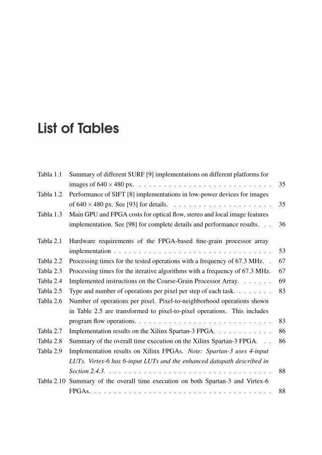
List of Tables
Tabla 1.1 Summary of different SURF [9] implementations on different platforms forimages of 640×480 px. . . . . . . . . . . . . . . . . . . . . . . . . . . . 35
Tabla 1.2 Performance of SIFT [8] implementations in low-power devices for imagesof 640×480 px. See [93] for details. . . . . . . . . . . . . . . . . . . . . 35
Tabla 1.3 Main GPU and FPGA costs for optical flow, stereo and local image featuresimplementation. See [98] for complete details and performance results. . . 36
Tabla 2.1 Hardware requirements of the FPGA-based fine-grain processor arrayimplementation . . . . . . . . . . . . . . . . . . . . . . . . . . . . . . . . 53
Tabla 2.2 Processing times for the tested operations with a frequency of 67.3 MHz. . 67Tabla 2.3 Processing times for the iterative algorithms with a frequency of 67.3 MHz. 67Tabla 2.4 Implemented instructions on the Coarse-Grain Processor Array. . . . . . . 69Tabla 2.5 Type and number of operations per pixel per step of each task. . . . . . . . 83Tabla 2.6 Number of operations per pixel. Pixel-to-neighborhood operations shown
in Table 2.5 are transformed to pixel-to-pixel operations. This includesprogram flow operations. . . . . . . . . . . . . . . . . . . . . . . . . . . . 83
Tabla 2.7 Implementation results on the Xilinx Spartan-3 FPGA. . . . . . . . . . . . 86Tabla 2.8 Summary of the overall time execution on the Xilinx Spartan-3 FPGA. . . 86Tabla 2.9 Implementation results on Xilinx FPGAs. Note: Spartan-3 uses 4-input
LUTs. Virtex-6 has 6-input LUTs and the enhanced datapath described in
Section 2.4.3. . . . . . . . . . . . . . . . . . . . . . . . . . . . . . . . . . 88Tabla 2.10 Summary of the overall time execution on both Spartan-3 and Virtex-6
FPGAs. . . . . . . . . . . . . . . . . . . . . . . . . . . . . . . . . . . . . 88
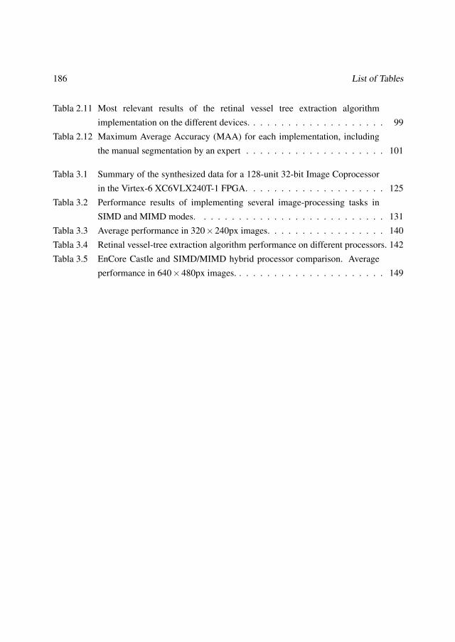
186 List of Tables
Tabla 2.11 Most relevant results of the retinal vessel tree extraction algorithmimplementation on the different devices. . . . . . . . . . . . . . . . . . . . 99
Tabla 2.12 Maximum Average Accuracy (MAA) for each implementation, includingthe manual segmentation by an expert . . . . . . . . . . . . . . . . . . . . 101
Tabla 3.1 Summary of the synthesized data for a 128-unit 32-bit Image Coprocessorin the Virtex-6 XC6VLX240T-1 FPGA. . . . . . . . . . . . . . . . . . . . 125
Tabla 3.2 Performance results of implementing several image-processing tasks inSIMD and MIMD modes. . . . . . . . . . . . . . . . . . . . . . . . . . . 131
Tabla 3.3 Average performance in 320×240px images. . . . . . . . . . . . . . . . . 140Tabla 3.4 Retinal vessel-tree extraction algorithm performance on different processors. 142Tabla 3.5 EnCore Castle and SIMD/MIMD hybrid processor comparison. Average
performance in 640×480px images. . . . . . . . . . . . . . . . . . . . . . 149