i2c slave ip core - lattice radiant software user guide
TRANSCRIPT

I2C Slave IP Core - Lattice Radiant Software
User Guide
FPGA-IPUG-02072-1.3
June 2021
I2C Slave IP Core - Lattice Radiant Software User Guide
© 2019-2021 Lattice Semiconductor Corp. All Lattice trademarks, registered trademarks, patents, and disclaimers are as listed at www.latticesemi.com/legal. All other brand or product names are trademarks or registered trademarks of their respective holders. The specifications and information herein are subject to change without notice.
2 FPGA-IPUG-02072-1.3
Disclaimers Lattice makes no warranty, representation, or guarantee regarding the accuracy of information contained in this document or the suitability of its products for any particular purpose. All information herein is provided AS IS and with all faults, and all risk associated with such information is entirely with Buyer. Buyer shall not rely on any data and performance specifications or parameters provided herein. Products sold by Lattice have been subject to limited testing and it is the Buyer's responsibility to independently determine the suitability of any products and to test and verify the same. No Lattice products should be used in conjunction with mission- or safety-critical or any other application in which the failure of Lattice’s product could create a situation where personal injury, death, severe property or environmental damage may occur. The information provided in this document is proprietary to Lattice Semiconductor, and Lattice reserves the right to make any changes to the information in this document or to any products at any time without notice.
I2C Slave IP Core - Lattice Radiant Software User Guide
© 2019-2021 Lattice Semiconductor Corp. All Lattice trademarks, registered trademarks, patents, and disclaimers are as listed at www.latticesemi.com/legal. All other brand or product names are trademarks or registered trademarks of their respective holders. The specifications and information herein are subject to change without notice.
FPGA-IPUG-02072-1.3 3
Contents Acronyms in This Document ................................................................................................................................................. 5 1. Introduction .................................................................................................................................................................. 6
1.1. Quick Facts .......................................................................................................................................................... 6 1.2. Features .............................................................................................................................................................. 6 1.3. Conventions ........................................................................................................................................................ 7
1.3.1. Nomenclature................................................................................................................................................. 7 1.3.2. Signal Names .................................................................................................................................................. 7 1.3.3. Host ................................................................................................................................................................ 7 1.3.4. Attribute ......................................................................................................................................................... 7
2. Functional Description .................................................................................................................................................. 8 2.1. Overview ............................................................................................................................................................. 8 2.2. Signal Description ................................................................................................................................................ 9 2.3. Attributes Summary .......................................................................................................................................... 10 2.4. Register Description .......................................................................................................................................... 11
2.4.1. Overview ...................................................................................................................................................... 11 2.4.2. Write Data Register (WR_DATA_REG).......................................................................................................... 11 2.4.3. Read Data Register (RD_DATA_REG) ............................................................................................................ 12 2.4.4. Slave Address Registers (SLAVE_ADDRL_REG, SLAVE_ADDRH_REG) ........................................................... 12 2.4.5. Control Register (CONTROL_REG) ................................................................................................................ 12 2.4.6. Target Byte Count Register (TGT_BYTE_CNT_REG) ...................................................................................... 13 2.4.7. Interrupt Status Registers (INT_STATUS1_REG, INT_STATUS2_REG) .......................................................... 13 2.4.8. Interrupt Enable Registers (INT_ENABLE1_REG, INT_ENABLE2_REG) ......................................................... 15 2.4.9. Interrupt Set Registers (INT_SET1_REG, INT_SET2_REG) ............................................................................. 17 2.4.10. FIFO Status Register (FIFO_STATUS_REG) .................................................................................................... 19
2.5. Operations Details ............................................................................................................................................. 20 2.5.1. General I2C Operation .................................................................................................................................. 20 2.5.2. Glitch Filter ................................................................................................................................................... 20 2.5.3. Clock Stretching ............................................................................................................................................ 21 2.5.4. ACK/NACK Response .................................................................................................................................... 21 2.5.5. Selectable Memory-Mapped Interface ........................................................................................................ 21
2.6. Programming Flow ............................................................................................................................................ 22 2.6.1. Initialization .................................................................................................................................................. 22 2.6.2. Data Transfer in response to I2C Master Read ............................................................................................. 22 2.6.3. Data Transfer in response to I2C Master Write ............................................................................................ 22
3. Core Generation, Simulation, and Validation ............................................................................................................. 24 3.1. Licensing the IP .................................................................................................................................................. 24 3.2. Generation and Synthesis ................................................................................................................................. 24 3.3. Running Functional Simulation ......................................................................................................................... 27 3.4. Hardware Evaluation ......................................................................................................................................... 29
Appendix A. Resource Utilization ....................................................................................................................................... 30 References .......................................................................................................................................................................... 31 Technical Support Assistance ............................................................................................................................................. 32 Revision History .................................................................................................................................................................. 33
I2C Slave IP Core - Lattice Radiant Software User Guide
© 2019-2021 Lattice Semiconductor Corp. All Lattice trademarks, registered trademarks, patents, and disclaimers are as listed at www.latticesemi.com/legal. All other brand or product names are trademarks or registered trademarks of their respective holders. The specifications and information herein are subject to change without notice.
4 FPGA-IPUG-02072-1.3
Figures Figure 2.1. I2C Slave IP Core Functional Diagram .................................................................................................................. 8 Figure 2.2. START and STOP Conditions .............................................................................................................................. 20 Figure 3.1. Module/IP Block Wizard ................................................................................................................................... 24 Figure 3.2. Configure User Interface of I2C Slave IP Core ................................................................................................... 25 Figure 3.3. Check Generating Result ................................................................................................................................... 25 Figure 3.4. Simulation Wizard ............................................................................................................................................. 27 Figure 3.5. Adding and Reordering Source ......................................................................................................................... 28 Figure 3.6. Simulation Waveform ....................................................................................................................................... 28
Tables Table 1.1. Quick Facts ........................................................................................................................................................... 6 Table 2.1. I2C Slave IP Core Signal Description ...................................................................................................................... 9 Table 2.2. Attributes Table ................................................................................................................................................. 10 Table 2.3. Attributes Descriptions ...................................................................................................................................... 10 Table 2.4. Registers Address Map ....................................................................................................................................... 11 Table 2.5. Access Type Definition ....................................................................................................................................... 11 Table 2.6. Write Data Register ............................................................................................................................................ 12 Table 2.7. Read Data Register ............................................................................................................................................. 12 Table 2.8. Slave Address Lower Register ............................................................................................................................ 12 Table 2.9. Slave Address Higher Register ............................................................................................................................ 12 Table 2.10. Control Register ............................................................................................................................................... 12 Table 2.11. Target Byte Count Register .............................................................................................................................. 13 Table 2.12. Interrupt Status 1st Register ............................................................................................................................. 14 Table 2.13. Interrupt Status 2nd Register ............................................................................................................................ 15 Table 2.14. Interrupt Enable 1st Register ............................................................................................................................ 15 Table 2.15. Interrupt Enable Second Register .................................................................................................................... 17 Table 2.16. Interrupt Set First Register ............................................................................................................................... 17 Table 2.17. Interrupt Set Second Register .......................................................................................................................... 18 Table 2.18. FIFO Status Register ......................................................................................................................................... 19 Table 3.1. Generated File List ............................................................................................................................................. 26 Table A.1. Resource Utilization ........................................................................................................................................... 30
I2C Slave IP Core - Lattice Radiant Software User Guide
© 2019-2021 Lattice Semiconductor Corp. All Lattice trademarks, registered trademarks, patents, and disclaimers are as listed at www.latticesemi.com/legal. All other brand or product names are trademarks or registered trademarks of their respective holders. The specifications and information herein are subject to change without notice.
FPGA-IPUG-02072-1.3 5
Acronyms in This Document A list of acronyms used in this document.
Acronym Definition
I2C Inter-Integrated Circuit
APB Advanced Peripheral Bus
AMBA Advanced Microcontroller Bus Architecture
FPGA Field Programmable Gate Array
RTL Register Transfer Level
I2C Slave IP Core - Lattice Radiant Software User Guide
© 2019-2021 Lattice Semiconductor Corp. All Lattice trademarks, registered trademarks, patents, and disclaimers are as listed at www.latticesemi.com/legal. All other brand or product names are trademarks or registered trademarks of their respective holders. The specifications and information herein are subject to change without notice.
6 FPGA-IPUG-02072-1.3
1. Introduction I2C (Inter-Integrated Circuit) bus is a simple, low-bandwidth, short-distance protocol. It is often seen in systems with peripheral devices that are accessed intermittently. It is commonly used in short-distance systems, where the number of traces on the board should be minimized. The device that initiates the transmission on the I2C bus is commonly known as the Master, while the device being addressed is called the Slave.
Lattice Semiconductor general-purpose I2C Slave IP Core provides device addressing, read/write operation and an acknowledgement mechanism. The programmable nature of FPGA provides users with the flexibility of configuring the I2C Slave device to any legal Slave address, thus, avoiding a potential Slave address collision on an I2C bus with multiple Slave devices.
1.1. Quick Facts Table 1.1 presents a summary of the I2C Slave IP Core.
Table 1.1. Quick Facts
IP Requirements Supported FPGA Family CrossLink™-NX, Certus™-NX, CertusPro™-NX
Resource Utilization
Targeted Devices LIFCL-40, LIFCL-17, LFD2NX-40, LFD2NX-17, LFCPNX-100
Supported User Interfaces LMMI (Lattice Memory Mapped Interface), APB
Resources See Table A.1.
Design Tool Support
Lattice Implementation IP Core v1.x.x - Lattice Radiant Software 2.1 or later
Synthesis Lattice Synthesis Engine
Synopsys® Synplify Pro for Lattice
Simulation For a list of supported simulators, see the Lattice Radiant Software User Guide
1.2. Features The key features of I2C Slave IP Core include:
Supports 7-bit and 10-bit Addressing Mode
Supports the following bus speeds:
Standard-mode (Sm) – up to 100 kbit/s
Fast-mode (Fm) – up to 400 kbit/s
Fast-mode Plus (Fm+) – up to 1 Mbit/s
Supports Clock stretching
Configurable ACK/NACK response on address and data phases
Integrated Pull-up
Integrated Glitch filter
Polling and Out-of-band Interrupt Modes
I2C Slave IP Core - Lattice Radiant Software User Guide
© 2019-2021 Lattice Semiconductor Corp. All Lattice trademarks, registered trademarks, patents, and disclaimers are as listed at www.latticesemi.com/legal. All other brand or product names are trademarks or registered trademarks of their respective holders. The specifications and information herein are subject to change without notice.
FPGA-IPUG-02072-1.3 7
1.3. Conventions
1.3.1. Nomenclature
The nomenclature used in this document is based on Verilog HDL.
1.3.2. Signal Names
Signal Names that end with:
_n are active low
_i are input signals
_o are output signals
_io are bi-directional input/output signals
1.3.3. Host
The logic unit inside the FPGA interacts with the I2C Slave IP Core through either APB or LMMI.
1.3.4. Attribute The names of attributes in this document are formatted in title case and italicized (Attribute Name).
I2C Slave IP Core - Lattice Radiant Software User Guide
© 2019-2021 Lattice Semiconductor Corp. All Lattice trademarks, registered trademarks, patents, and disclaimers are as listed at www.latticesemi.com/legal. All other brand or product names are trademarks or registered trademarks of their respective holders. The specifications and information herein are subject to change without notice.
8 FPGA-IPUG-02072-1.3
2. Functional Description
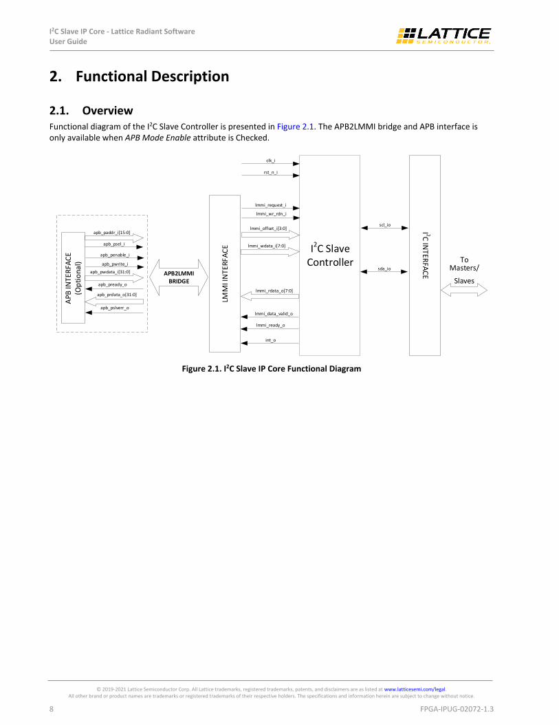
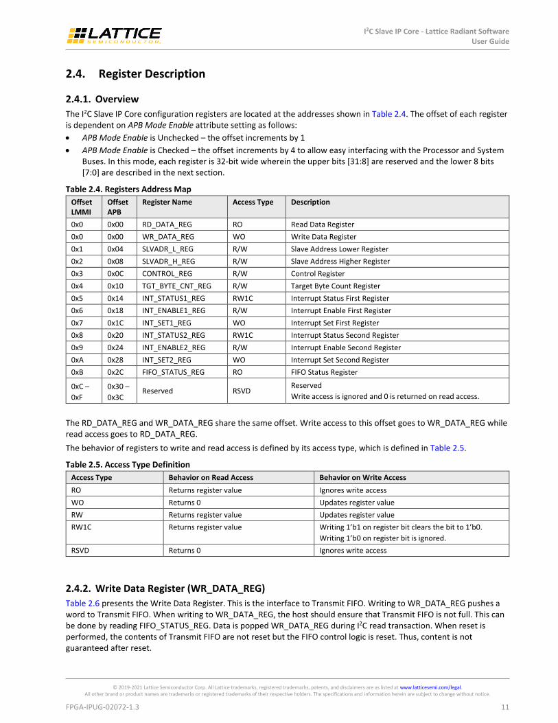
2.1. Overview Functional diagram of the I2C Slave Controller is presented in Figure 2.1. The APB2LMMI bridge and APB interface is only available when APB Mode Enable attribute is Checked.
I2C Slave Controller
lmmi_data_valid_o
lmmi_ready_o
clk_i
LMM
I IN
TE
RF
AC
Elmmi_offset_i[3:0]
rst_n_i
lmmi_request_i
lmmi_wdata_i[7:0]
lmmi_wr_rdn_i
I 2C IN
TERFA
CE
lmmi_rdata_o[7:0]
int_o
scl_io
sda_io
To Masters/
SlavesAPB2LMMI
BRIDGE
AP
B IN
TE
RFA
CE
(O
pti
ona
l)
apb_psel_i
apb_penable_i
apb_pwrite_i
apb_pwdata_i[31:0]
apb_pready_o
apb_prdata_o[31:0]
apb_pslverr_o
apb_paddr_i[15:0]
Figure 2.1. I2C Slave IP Core Functional Diagram
I2C Slave IP Core - Lattice Radiant Software User Guide
© 2019-2021 Lattice Semiconductor Corp. All Lattice trademarks, registered trademarks, patents, and disclaimers are as listed at www.latticesemi.com/legal. All other brand or product names are trademarks or registered trademarks of their respective holders. The specifications and information herein are subject to change without notice.
FPGA-IPUG-02072-1.3 9
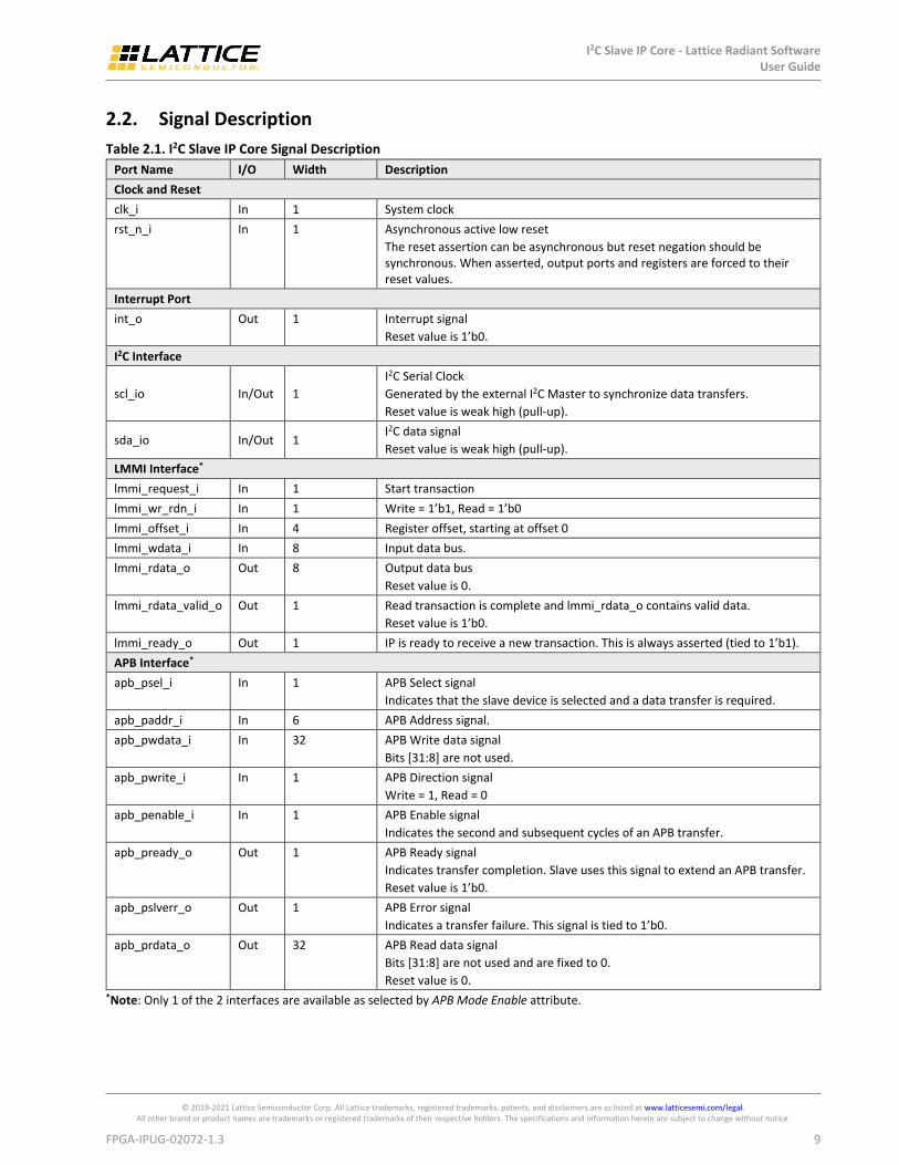
2.2. Signal Description
Table 2.1. I2C Slave IP Core Signal Description
Port Name I/O Width Description
Clock and Reset
clk_i In 1 System clock
rst_n_i In 1 Asynchronous active low reset
The reset assertion can be asynchronous but reset negation should be synchronous. When asserted, output ports and registers are forced to their reset values.
Interrupt Port
int_o Out 1 Interrupt signal
Reset value is 1’b0.
I2C Interface
scl_io In/Out 1
I2C Serial Clock
Generated by the external I2C Master to synchronize data transfers.
Reset value is weak high (pull-up).
sda_io In/Out 1 I2C data signal
Reset value is weak high (pull-up).
LMMI Interface*
lmmi_request_i In 1 Start transaction
lmmi_wr_rdn_i In 1 Write = 1’b1, Read = 1’b0
lmmi_offset_i In 4 Register offset, starting at offset 0
lmmi_wdata_i In 8 Input data bus.
lmmi_rdata_o Out 8 Output data bus
Reset value is 0.
lmmi_rdata_valid_o Out 1 Read transaction is complete and lmmi_rdata_o contains valid data.
Reset value is 1’b0.
lmmi_ready_o Out 1 IP is ready to receive a new transaction. This is always asserted (tied to 1’b1).
APB Interface*
apb_psel_i In 1 APB Select signal
Indicates that the slave device is selected and a data transfer is required.
apb_paddr_i In 6 APB Address signal.
apb_pwdata_i In 32 APB Write data signal
Bits [31:8] are not used.
apb_pwrite_i In 1 APB Direction signal
Write = 1, Read = 0
apb_penable_i In 1 APB Enable signal
Indicates the second and subsequent cycles of an APB transfer.
apb_pready_o Out 1 APB Ready signal
Indicates transfer completion. Slave uses this signal to extend an APB transfer.
Reset value is 1’b0.
apb_pslverr_o Out 1 APB Error signal
Indicates a transfer failure. This signal is tied to 1’b0.
apb_prdata_o Out 32 APB Read data signal
Bits [31:8] are not used and are fixed to 0.
Reset value is 0. *Note: Only 1 of the 2 interfaces are available as selected by APB Mode Enable attribute.
I2C Slave IP Core - Lattice Radiant Software User Guide
© 2019-2021 Lattice Semiconductor Corp. All Lattice trademarks, registered trademarks, patents, and disclaimers are as listed at www.latticesemi.com/legal. All other brand or product names are trademarks or registered trademarks of their respective holders. The specifications and information herein are subject to change without notice.
10 FPGA-IPUG-02072-1.3
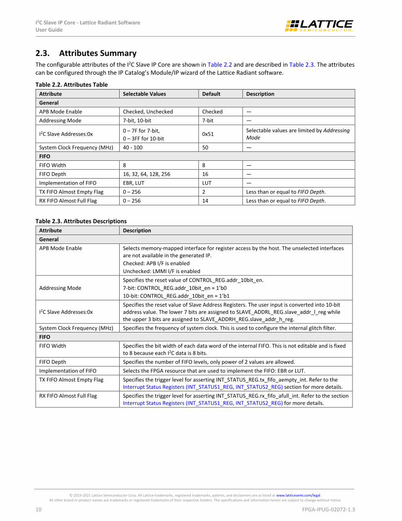
2.3. Attributes Summary The configurable attributes of the I2C Slave IP Core are shown in Table 2.2 and are described in Table 2.3. The attributes can be configured through the IP Catalog’s Module/IP wizard of the Lattice Radiant software.
Table 2.2. Attributes Table
Attribute Selectable Values Default Description
General
APB Mode Enable Checked, Unchecked Checked —
Addressing Mode 7-bit, 10-bit 7-bit —
I2C Slave Addresses:0x 0 – 7F for 7-bit,
0 – 3FF for 10-bit 0x51
Selectable values are limited by Addressing Mode
System Clock Frequency (MHz) 40 - 100 50 —
FIFO
FIFO Width 8 8 —
FIFO Depth 16, 32, 64, 128, 256 16 —
Implementation of FIFO EBR, LUT LUT —
TX FIFO Almost Empty Flag 0 – 256 2 Less than or equal to FIFO Depth.
RX FIFO Almost Full Flag 0 – 256 14 Less than or equal to FIFO Depth.
Table 2.3. Attributes Descriptions
Attribute Description
General
APB Mode Enable Selects memory-mapped interface for register access by the host. The unselected interfaces are not available in the generated IP.
Checked: APB I/F is enabled
Unchecked: LMMI I/F is enabled
Addressing Mode
Specifies the reset value of CONTROL_REG.addr_10bit_en.
7-bit: CONTROL_REG.addr_10bit_en = 1’b0
10-bit: CONTROL_REG.addr_10bit_en = 1’b1
I2C Slave Addresses:0x Specifies the reset value of Slave Address Registers. The user input is converted into 10-bit address value. The lower 7 bits are assigned to SLAVE_ADDRL_REG.slave_addr_l_reg while the upper 3 bits are assigned to SLAVE_ADDRH_REG.slave_addr_h_reg.
System Clock Frequency (MHz) Specifies the frequency of system clock. This is used to configure the internal glitch filter.
FIFO
FIFO Width Specifies the bit width of each data word of the internal FIFO. This is not editable and is fixed to 8 because each I2C data is 8 bits.
FIFO Depth Specifies the number of FIFO levels, only power of 2 values are allowed.
Implementation of FIFO Selects the FPGA resource that are used to implement the FIFO: EBR or LUT.
TX FIFO Almost Empty Flag Specifies the trigger level for asserting INT_STATUS_REG.tx_fifo_aempty_int. Refer to the Interrupt Status Registers (INT_STATUS1_REG, INT_STATUS2_REG) section for more details.
RX FIFO Almost Full Flag Specifies the trigger level for asserting INT_STATUS_REG.rx_fifo_afull_int. Refer to the section Interrupt Status Registers (INT_STATUS1_REG, INT_STATUS2_REG) for more details.
I2C Slave IP Core - Lattice Radiant Software User Guide
© 2019-2021 Lattice Semiconductor Corp. All Lattice trademarks, registered trademarks, patents, and disclaimers are as listed at www.latticesemi.com/legal. All other brand or product names are trademarks or registered trademarks of their respective holders. The specifications and information herein are subject to change without notice.
FPGA-IPUG-02072-1.3 11
2.4. Register Description
2.4.1. Overview
The I2C Slave IP Core configuration registers are located at the addresses shown in Table 2.4. The offset of each register is dependent on APB Mode Enable attribute setting as follows:
APB Mode Enable is Unchecked – the offset increments by 1
APB Mode Enable is Checked – the offset increments by 4 to allow easy interfacing with the Processor and System Buses. In this mode, each register is 32-bit wide wherein the upper bits [31:8] are reserved and the lower 8 bits [7:0] are described in the next section.
Table 2.4. Registers Address Map
Offset LMMI
Offset APB
Register Name Access Type Description
0x0 0x00 RD_DATA_REG RO Read Data Register
0x0 0x00 WR_DATA_REG WO Write Data Register
0x1 0x04 SLVADR_L_REG R/W Slave Address Lower Register
0x2 0x08 SLVADR_H_REG R/W Slave Address Higher Register
0x3 0x0C CONTROL_REG R/W Control Register
0x4 0x10 TGT_BYTE_CNT_REG R/W Target Byte Count Register
0x5 0x14 INT_STATUS1_REG RW1C Interrupt Status First Register
0x6 0x18 INT_ENABLE1_REG R/W Interrupt Enable First Register
0x7 0x1C INT_SET1_REG WO Interrupt Set First Register
0x8 0x20 INT_STATUS2_REG RW1C Interrupt Status Second Register
0x9 0x24 INT_ENABLE2_REG R/W Interrupt Enable Second Register
0xA 0x28 INT_SET2_REG WO Interrupt Set Second Register
0xB 0x2C FIFO_STATUS_REG RO FIFO Status Register
0xC –
0xF
0x30 –
0x3C Reserved RSVD
Reserved
Write access is ignored and 0 is returned on read access.
The RD_DATA_REG and WR_DATA_REG share the same offset. Write access to this offset goes to WR_DATA_REG while read access goes to RD_DATA_REG.
The behavior of registers to write and read access is defined by its access type, which is defined in Table 2.5.
Table 2.5. Access Type Definition
Access Type Behavior on Read Access Behavior on Write Access
RO Returns register value Ignores write access
WO Returns 0 Updates register value
RW Returns register value Updates register value
RW1C Returns register value Writing 1’b1 on register bit clears the bit to 1’b0.
Writing 1’b0 on register bit is ignored.
RSVD Returns 0 Ignores write access
2.4.2. Write Data Register (WR_DATA_REG)
Table 2.6 presents the Write Data Register. This is the interface to Transmit FIFO. Writing to WR_DATA_REG pushes a word to Transmit FIFO. When writing to WR_DATA_REG, the host should ensure that Transmit FIFO is not full. This can be done by reading FIFO_STATUS_REG. Data is popped WR_DATA_REG during I2C read transaction. When reset is performed, the contents of Transmit FIFO are not reset but the FIFO control logic is reset. Thus, content is not guaranteed after reset.
I2C Slave IP Core - Lattice Radiant Software User Guide
© 2019-2021 Lattice Semiconductor Corp. All Lattice trademarks, registered trademarks, patents, and disclaimers are as listed at www.latticesemi.com/legal. All other brand or product names are trademarks or registered trademarks of their respective holders. The specifications and information herein are subject to change without notice.
12 FPGA-IPUG-02072-1.3
Table 2.6. Write Data Register
Field Name Access Width Reset
[7:0] tx_fifo WO 8 not guaranteed
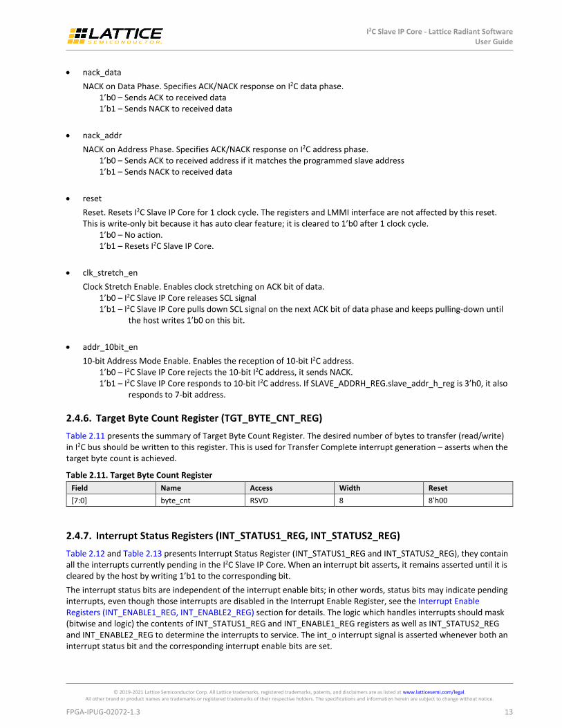
2.4.3. Read Data Register (RD_DATA_REG)
Table 2.7 presents the Read Data register. This is the interface to Receive FIFO. After a data is received from I2C bus during I2C write transaction, the received data is pushed to Receive FIFO. Reading from RD_DATA_REG pops a word from Receive FIFO. The host should ensure that Receive FIFO has data before reading RD_DATA_REG, data is not guaranteed when this register is read during Receive FIFO empty condition. On the other hand, if Receive FIFO is full but I2C Slave continues to receive data, new data is lost. Read FIFO_STATUS_REG to determine the status of Receive FIFO. Similar to Transmit FIFO, the reset value of Receive FIFO is also not guaranteed after reset.
Table 2.7. Read Data Register
Field Name Access Width Reset
[7:0] rx_fifo RO 8 not guaranteed
2.4.4. Slave Address Registers (SLAVE_ADDRL_REG, SLAVE_ADDRH_REG)
The Slave Address Lower Register (SLAVE_ADDRL_REG) shown in Table 2.8 is a 7-bit Slave address. This is used for 7-bit and 10-bit addressing mode as follows:
For 7-bit Addressing Mode, it is the Slave address
For 10-bit Addressing Mode, it is the lower 7 bits of the Slave address
Table 2.8. Slave Address Lower Register
Field Name Access Width Reset
[7] reserved RSVD 1 –
[6:0] slave_addr_l_reg RW 7 I2C Slave Address[6:0]
The Slave Address Higher Register (SLAVE_ADDRH_REG) shown in Table 2.9 is the upper 3 bits of 10-bit Slave address. This is not used in 7-bit addressing mode. The reset values of SLAVE_ADDRL_REG and SLAVE_ADDRH_REG is set by the I2C Slave Address attribute as shown in Table 2.8 and Table 2.9.
Table 2.9. Slave Address Higher Register
Field Name Access Width Reset
[7:3] reserved RSVD 5 –
[2:0] slave_addr_h_reg RW 3 I2C Slave Address[9:7]
2.4.5. Control Register (CONTROL_REG)
Table 2.10 presents a summary of Control Register. This each bit of this register controls the behavior of I2C Slave IP Core.
Table 2.10. Control Register
Field Name Access Width Reset
[7:5] Reserved RSVD 3 –
[4] nack_data RW 1 1’b0
[3] nack_addr RW 1 1’b0
[2] reset WO 1 1’b0
[1] clk_stretch_en RW 1 1’b0
[0] addr_10bit_en RW 1 See Addressing Mode in Table 2.3
I2C Slave IP Core - Lattice Radiant Software User Guide
© 2019-2021 Lattice Semiconductor Corp. All Lattice trademarks, registered trademarks, patents, and disclaimers are as listed at www.latticesemi.com/legal. All other brand or product names are trademarks or registered trademarks of their respective holders. The specifications and information herein are subject to change without notice.
FPGA-IPUG-02072-1.3 13
nack_data
NACK on Data Phase. Specifies ACK/NACK response on I2C data phase. 1’b0 – Sends ACK to received data 1’b1 – Sends NACK to received data
nack_addr
NACK on Address Phase. Specifies ACK/NACK response on I2C address phase. 1’b0 – Sends ACK to received address if it matches the programmed slave address 1’b1 – Sends NACK to received data
reset
Reset. Resets I2C Slave IP Core for 1 clock cycle. The registers and LMMI interface are not affected by this reset. This is write-only bit because it has auto clear feature; it is cleared to 1’b0 after 1 clock cycle.
1’b0 – No action. 1’b1 – Resets I2C Slave IP Core.
clk_stretch_en
Clock Stretch Enable. Enables clock stretching on ACK bit of data. 1’b0 – I2C Slave IP Core releases SCL signal 1’b1 – I2C Slave IP Core pulls down SCL signal on the next ACK bit of data phase and keeps pulling-down until
the host writes 1’b0 on this bit.
addr_10bit_en
10-bit Address Mode Enable. Enables the reception of 10-bit I2C address. 1’b0 – I2C Slave IP Core rejects the 10-bit I2C address, it sends NACK. 1’b1 – I2C Slave IP Core responds to 10-bit I2C address. If SLAVE_ADDRH_REG.slave_addr_h_reg is 3’h0, it also
responds to 7-bit address.
2.4.6. Target Byte Count Register (TGT_BYTE_CNT_REG)
Table 2.11 presents the summary of Target Byte Count Register. The desired number of bytes to transfer (read/write) in I2C bus should be written to this register. This is used for Transfer Complete interrupt generation – asserts when the target byte count is achieved.
Table 2.11. Target Byte Count Register
Field Name Access Width Reset
[7:0] byte_cnt RSVD 8 8’h00
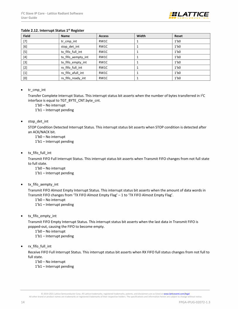
2.4.7. Interrupt Status Registers (INT_STATUS1_REG, INT_STATUS2_REG)
Table 2.12 and Table 2.13 presents Interrupt Status Register (INT_STATUS1_REG and INT_STATUS2_REG), they contain all the interrupts currently pending in the I2C Slave IP Core. When an interrupt bit asserts, it remains asserted until it is cleared by the host by writing 1’b1 to the corresponding bit.
The interrupt status bits are independent of the interrupt enable bits; in other words, status bits may indicate pending interrupts, even though those interrupts are disabled in the Interrupt Enable Register, see the Interrupt Enable Registers (INT_ENABLE1_REG, INT_ENABLE2_REG) section for details. The logic which handles interrupts should mask (bitwise and logic) the contents of INT_STATUS1_REG and INT_ENABLE1_REG registers as well as INT_STATUS2_REG and INT_ENABLE2_REG to determine the interrupts to service. The int_o interrupt signal is asserted whenever both an interrupt status bit and the corresponding interrupt enable bits are set.
I2C Slave IP Core - Lattice Radiant Software User Guide
© 2019-2021 Lattice Semiconductor Corp. All Lattice trademarks, registered trademarks, patents, and disclaimers are as listed at www.latticesemi.com/legal. All other brand or product names are trademarks or registered trademarks of their respective holders. The specifications and information herein are subject to change without notice.
14 FPGA-IPUG-02072-1.3
Table 2.12. Interrupt Status 1st Register
Field Name Access Width Reset
[7] tr_cmp_int RW1C 1 1’b0
[6] stop_det_int RW1C 1 1’b0
[5] tx_fifo_full_int RW1C 1 1’b0
[4] tx_fifo_aempty_int RW1C 1 1’b0
[3] tx_fifo_empty_int RW1C 1 1’b0
[2] rx_fifo_full_int RW1C 1 1’b0
[1] rx_fifo_afull_int RW1C 1 1’b0
[0] rx_fifo_ready_int RW1C 1 1’b0
tr_cmp_int
Transfer Complete Interrupt Status. This interrupt status bit asserts when the number of bytes transferred in I2C interface is equal to TGT_BYTE_CNT.byte_cnt.
1’b0 – No interrupt 1’b1 – Interrupt pending
stop_det_int
STOP Condition Detected Interrupt Status. This interrupt status bit asserts when STOP condition is detected after an ACK/NACK bit.
1’b0 – No interrupt 1’b1 – Interrupt pending
tx_fifo_full_int
Transmit FIFO Full Interrupt Status. This interrupt status bit asserts when Transmit FIFO changes from not full state to full state.
1’b0 – No interrupt 1’b1 – Interrupt pending
tx_fifo_aempty_int
Transmit FIFO Almost Empty Interrupt Status. This interrupt status bit asserts when the amount of data words in Transmit FIFO changes from ‘TX FIFO Almost Empty Flag’ – 1 to ‘TX FIFO Almost Empty Flag’.
1’b0 – No interrupt 1’b1 – Interrupt pending
tx_fifo_empty_int
Transmit FIFO Empty Interrupt Status. This interrupt status bit asserts when the last data in Transmit FIFO is popped-out, causing the FIFO to become empty.
1’b0 – No interrupt 1’b1 – Interrupt pending
rx_fifo_full_int
Receive FIFO Full Interrupt Status. This interrupt status bit asserts when RX FIFO full status changes from not full to full state.
1’b0 – No interrupt 1’b1 – Interrupt pending
I2C Slave IP Core - Lattice Radiant Software User Guide
© 2019-2021 Lattice Semiconductor Corp. All Lattice trademarks, registered trademarks, patents, and disclaimers are as listed at www.latticesemi.com/legal. All other brand or product names are trademarks or registered trademarks of their respective holders. The specifications and information herein are subject to change without notice.
FPGA-IPUG-02072-1.3 15
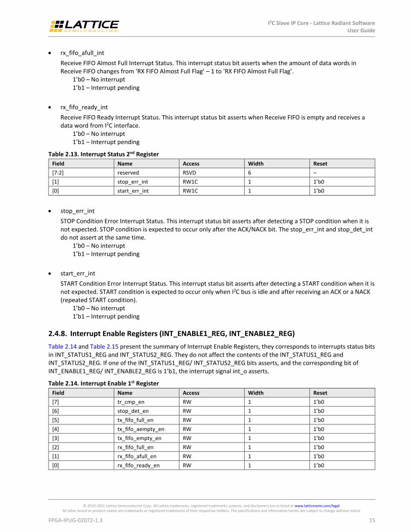
rx_fifo_afull_int
Receive FIFO Almost Full Interrupt Status. This interrupt status bit asserts when the amount of data words in Receive FIFO changes from ‘RX FIFO Almost Full Flag’ – 1 to ‘RX FIFO Almost Full Flag’.
1’b0 – No interrupt 1’b1 – Interrupt pending
rx_fifo_ready_int
Receive FIFO Ready Interrupt Status. This interrupt status bit asserts when Receive FIFO is empty and receives a data word from I2C interface.
1’b0 – No interrupt 1’b1 – Interrupt pending
Table 2.13. Interrupt Status 2nd Register
Field Name Access Width Reset
[7:2] reserved RSVD 6 –
[1] stop_err_int RW1C 1 1’b0
[0] start_err_int RW1C 1 1’b0
stop_err_int
STOP Condition Error Interrupt Status. This interrupt status bit asserts after detecting a STOP condition when it is not expected. STOP condition is expected to occur only after the ACK/NACK bit. The stop_err_int and stop_det_int do not assert at the same time.
1’b0 – No interrupt 1’b1 – Interrupt pending
start_err_int
START Condition Error Interrupt Status. This interrupt status bit asserts after detecting a START condition when it is not expected. START condition is expected to occur only when I2C bus is idle and after receiving an ACK or a NACK (repeated START condition).
1’b0 – No interrupt 1’b1 – Interrupt pending
2.4.8. Interrupt Enable Registers (INT_ENABLE1_REG, INT_ENABLE2_REG)
Table 2.14 and Table 2.15 present the summary of Interrupt Enable Registers, they corresponds to interrupts status bits in INT_STATUS1_REG and INT_STATUS2_REG. They do not affect the contents of the INT_STATUS1_REG and INT_STATUS2_REG. If one of the INT_STATUS1_REG/ INT_STATUS2_REG bits asserts, and the corresponding bit of INT_ENABLE1_REG/ INT_ENABLE2_REG is 1’b1, the interrupt signal int_o asserts.
Table 2.14. Interrupt Enable 1st Register
Field Name Access Width Reset
[7] tr_cmp_en RW 1 1’b0
[6] stop_det_en RW 1 1’b0
[5] tx_fifo_full_en RW 1 1’b0
[4] tx_fifo_aempty_en RW 1 1’b0
[3] tx_fifo_empty_en RW 1 1’b0
[2] rx_fifo_full_en RW 1 1’b0
[1] rx_fifo_afull_en RW 1 1’b0
[0] rx_fifo_ready_en RW 1 1’b0
I2C Slave IP Core - Lattice Radiant Software User Guide
© 2019-2021 Lattice Semiconductor Corp. All Lattice trademarks, registered trademarks, patents, and disclaimers are as listed at www.latticesemi.com/legal. All other brand or product names are trademarks or registered trademarks of their respective holders. The specifications and information herein are subject to change without notice.
16 FPGA-IPUG-02072-1.3
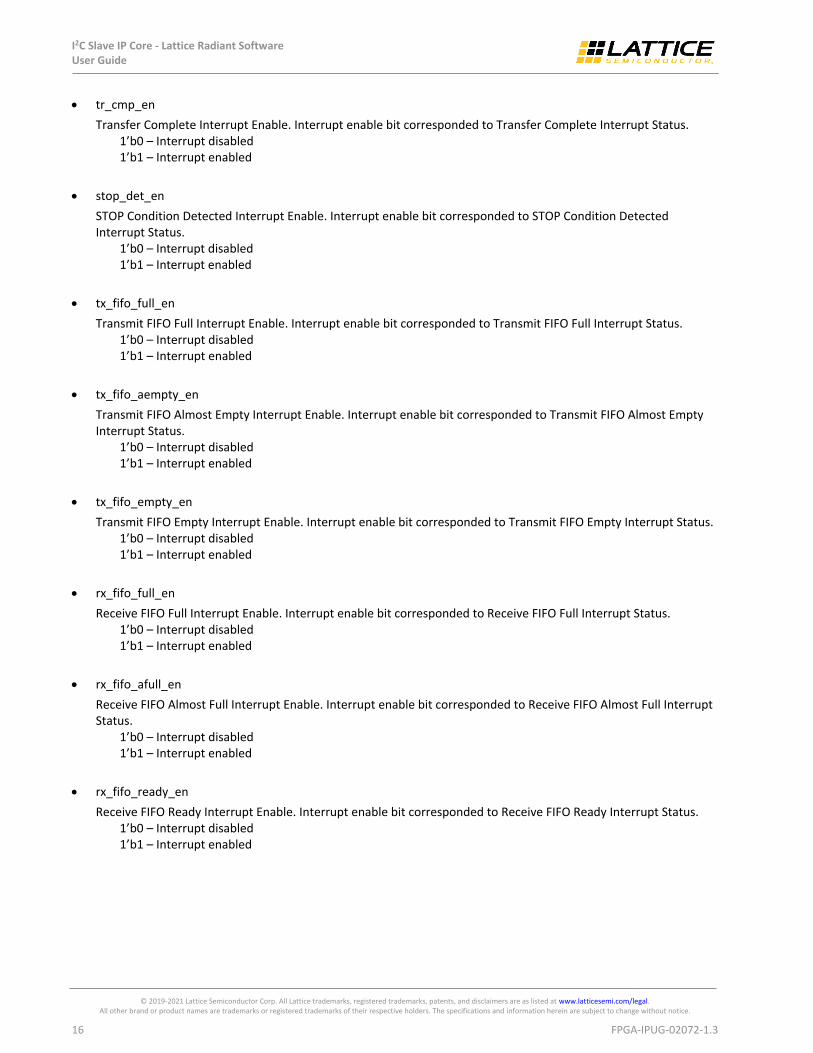
tr_cmp_en
Transfer Complete Interrupt Enable. Interrupt enable bit corresponded to Transfer Complete Interrupt Status. 1’b0 – Interrupt disabled 1’b1 – Interrupt enabled
stop_det_en
STOP Condition Detected Interrupt Enable. Interrupt enable bit corresponded to STOP Condition Detected Interrupt Status.
1’b0 – Interrupt disabled 1’b1 – Interrupt enabled
tx_fifo_full_en
Transmit FIFO Full Interrupt Enable. Interrupt enable bit corresponded to Transmit FIFO Full Interrupt Status. 1’b0 – Interrupt disabled 1’b1 – Interrupt enabled
tx_fifo_aempty_en
Transmit FIFO Almost Empty Interrupt Enable. Interrupt enable bit corresponded to Transmit FIFO Almost Empty Interrupt Status.
1’b0 – Interrupt disabled 1’b1 – Interrupt enabled
tx_fifo_empty_en
Transmit FIFO Empty Interrupt Enable. Interrupt enable bit corresponded to Transmit FIFO Empty Interrupt Status. 1’b0 – Interrupt disabled 1’b1 – Interrupt enabled
rx_fifo_full_en
Receive FIFO Full Interrupt Enable. Interrupt enable bit corresponded to Receive FIFO Full Interrupt Status. 1’b0 – Interrupt disabled 1’b1 – Interrupt enabled
rx_fifo_afull_en
Receive FIFO Almost Full Interrupt Enable. Interrupt enable bit corresponded to Receive FIFO Almost Full Interrupt Status.
1’b0 – Interrupt disabled 1’b1 – Interrupt enabled
rx_fifo_ready_en
Receive FIFO Ready Interrupt Enable. Interrupt enable bit corresponded to Receive FIFO Ready Interrupt Status. 1’b0 – Interrupt disabled 1’b1 – Interrupt enabled
I2C Slave IP Core - Lattice Radiant Software User Guide
© 2019-2021 Lattice Semiconductor Corp. All Lattice trademarks, registered trademarks, patents, and disclaimers are as listed at www.latticesemi.com/legal. All other brand or product names are trademarks or registered trademarks of their respective holders. The specifications and information herein are subject to change without notice.
FPGA-IPUG-02072-1.3 17
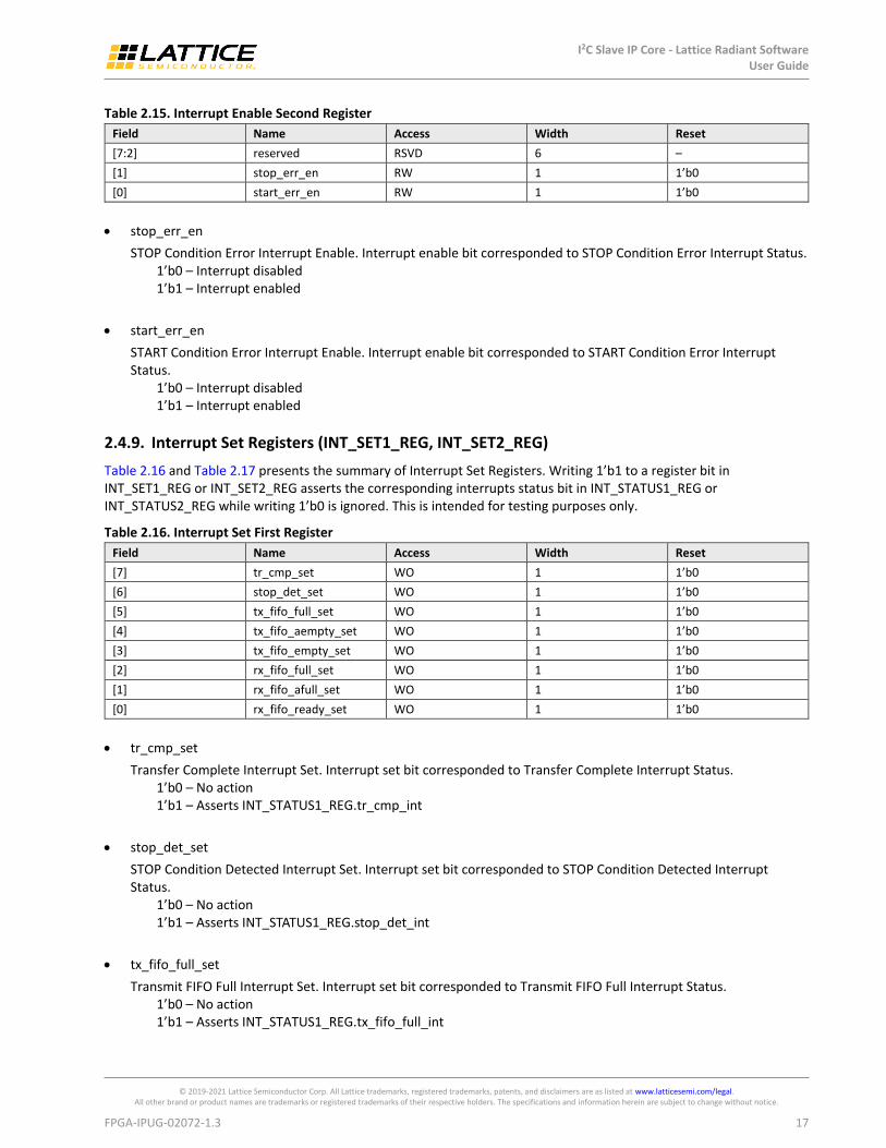
Table 2.15. Interrupt Enable Second Register
Field Name Access Width Reset
[7:2] reserved RSVD 6 –
[1] stop_err_en RW 1 1’b0
[0] start_err_en RW 1 1’b0
stop_err_en
STOP Condition Error Interrupt Enable. Interrupt enable bit corresponded to STOP Condition Error Interrupt Status. 1’b0 – Interrupt disabled 1’b1 – Interrupt enabled
start_err_en
START Condition Error Interrupt Enable. Interrupt enable bit corresponded to START Condition Error Interrupt Status.
1’b0 – Interrupt disabled 1’b1 – Interrupt enabled
2.4.9. Interrupt Set Registers (INT_SET1_REG, INT_SET2_REG)
Table 2.16 and Table 2.17 presents the summary of Interrupt Set Registers. Writing 1’b1 to a register bit in INT_SET1_REG or INT_SET2_REG asserts the corresponding interrupts status bit in INT_STATUS1_REG or INT_STATUS2_REG while writing 1’b0 is ignored. This is intended for testing purposes only.
Table 2.16. Interrupt Set First Register
Field Name Access Width Reset
[7] tr_cmp_set WO 1 1’b0
[6] stop_det_set WO 1 1’b0
[5] tx_fifo_full_set WO 1 1’b0
[4] tx_fifo_aempty_set WO 1 1’b0
[3] tx_fifo_empty_set WO 1 1’b0
[2] rx_fifo_full_set WO 1 1’b0
[1] rx_fifo_afull_set WO 1 1’b0
[0] rx_fifo_ready_set WO 1 1’b0
tr_cmp_set
Transfer Complete Interrupt Set. Interrupt set bit corresponded to Transfer Complete Interrupt Status. 1’b0 – No action 1’b1 – Asserts INT_STATUS1_REG.tr_cmp_int
stop_det_set
STOP Condition Detected Interrupt Set. Interrupt set bit corresponded to STOP Condition Detected Interrupt Status.
1’b0 – No action 1’b1 – Asserts INT_STATUS1_REG.stop_det_int
tx_fifo_full_set
Transmit FIFO Full Interrupt Set. Interrupt set bit corresponded to Transmit FIFO Full Interrupt Status. 1’b0 – No action 1’b1 – Asserts INT_STATUS1_REG.tx_fifo_full_int
I2C Slave IP Core - Lattice Radiant Software User Guide
© 2019-2021 Lattice Semiconductor Corp. All Lattice trademarks, registered trademarks, patents, and disclaimers are as listed at www.latticesemi.com/legal. All other brand or product names are trademarks or registered trademarks of their respective holders. The specifications and information herein are subject to change without notice.
18 FPGA-IPUG-02072-1.3
tx_fifo_aempty_set
Transmit FIFO Almost Empty Interrupt Set. Interrupt set bit corresponded to Transmit FIFO Almost Empty Interrupt Status.
1’b0 – No action 1’b1 – Asserts INT_STATUS1_REG.tx_fifo_aempty_int
tx_fifo_empty_set
Transmit FIFO Empty Interrupt Set. Interrupt set bit corresponded to Transmit FIFO Empty Interrupt Status. 1’b0 – No action 1’b1 – Asserts INT_STATUS1_REG.tx_fifo_empty_int
rx_fifo_full_set
Receive FIFO Full Interrupt Set. Interrupt set bit corresponded to Receive FIFO Full Interrupt Status. 1’b0 – No action 1’b1 – Asserts INT_STATUS1_REG.rx_fifo_full_int
rx_fifo_afull_set
Receive FIFO Almost Full Interrupt Set. Interrupt set bit corresponded to Receive FIFO Almost Full Interrupt Status. 1’b0 – No action 1’b1 – Asserts INT_STATUS1_REG.rx_fifo_afull_int
rx_fifo_ready_set
Receive FIFO Ready Interrupt Set. Interrupt set bit corresponded to Receive FIFO Ready Interrupt Status. 1’b0 – No action 1’b1 – Asserts INT_STATUS1_REG.rx_fifo_ready_int
Table 2.17. Interrupt Set Second Register
Field Name Access Width Reset
[7:2] reserved RSVD 6 –
[1] stop_err_set WO 1 1’b0
[0] start_err_set WO 1 1’b0
stop_err_set
STOP Condition Error Interrupt Set. Interrupt set bit corresponded to STOP Condition Error Interrupt Status. 0 – No action. 1 – Asserts INT_STATUS2_REG.stop_err_set.
start_err_set
START Condition Error Interrupt Set. Interrupt set bit corresponded to START Condition Error Interrupt Status. 0 – No action. 1 – Asserts INT_STATUS2_REG.start_err_set.
I2C Slave IP Core - Lattice Radiant Software User Guide
© 2019-2021 Lattice Semiconductor Corp. All Lattice trademarks, registered trademarks, patents, and disclaimers are as listed at www.latticesemi.com/legal. All other brand or product names are trademarks or registered trademarks of their respective holders. The specifications and information herein are subject to change without notice.
FPGA-IPUG-02072-1.3 19
2.4.10. FIFO Status Register (FIFO_STATUS_REG)
FIFO Status Register reflects the status of Transmit FIFO and Receive FIFO as shown in Table 2.18.
Table 2.18. FIFO Status Register
Field Name Access Width Reset
[7:6] reserved RSVD 2 –
[5] tx_fifo_full RO 1 1’b0
[4] tx_fifo_aempty RO 1 1’b1
[3] tx_fifo_empty RO 1 1’b1
[2] rx_fifo_full RO 1 1’b0
[1] rx_fifo_afull RO 1 1’b0
[0] rx_fifo_empty RO 1 1’b1
tx_fifo_full
Transmit FIFO Full. This bit reflects the full condition of Transmit FIFO. 1’b0 – Transmit FIFO is not full 1’b1 – Transmit FIFO is full
tx_fifo_aempty
Transmit FIFO Almost Empty. This bit reflects the almost empty condition of Transmit FIFO. 1’b0 – Data words in Transmit FIFO is greater than ‘TX FIFO Almost Empty Flag’ attribute 1’b1 – Data words in Transmit FIFO is less than or equal to ‘TX FIFO Almost Empty Flag’ attribute
tx_fifo_empty
Transmit FIFO Empty. This bit reflects the empty condition of Transmit FIFO. 1’b0 – Transmit FIFO is not empty – has at least 1 data word 1’b1 – Transmit FIFO is empty
rx_fifo_full
Receive FIFO Full. This bit reflects the full condition of Receive FIFO. 1’b0 – Receive FIFO is not full 1’b1 – Receive FIFO is full
rx_fifo_afull
Receive FIFO Full. This bit reflects the almost full condition of Receive FIFO. 1’b0 – Data words in Receive FIFO is less than ‘RX FIFO Almost Full Flag’ attribute 1’b1 – Data words in Receive FIFO is greater than or equal to ‘RX FIFO Almost Full Flag’ attribute
rx_fifo_empty
Receive FIFO Full. This bit reflects the empty condition of Receive FIFO. 1’b0 – Receive FIFO is not empty – has at least 1 data word 1’b1 – Receive FIFO is empty
I2C Slave IP Core - Lattice Radiant Software User Guide
© 2019-2021 Lattice Semiconductor Corp. All Lattice trademarks, registered trademarks, patents, and disclaimers are as listed at www.latticesemi.com/legal. All other brand or product names are trademarks or registered trademarks of their respective holders. The specifications and information herein are subject to change without notice.
20 FPGA-IPUG-02072-1.3
2.5. Operations Details
2.5.1. General I2C Operation
In I2C bus, the transaction is always initiated by the master. A slave may not transmit data unless it has been addressed by the master. Each device on the I2C bus has a specific device address to differentiate between other devices that are on the same I2C bus. Data transfer is initiated only when the bus is idle. A bus is considered idle if both SDA and SCL lines are high after a STOP condition.
The general procedure for an I2C transaction is as follows:
Master wants to send data to a slave:
Master-transmitter sends a START condition and addresses the slave-receiver
Master-transmitter sends data to slave-receiver
Master-transmitter terminates the transfer with a STOP condition
Master wants to receive/read data from a slave:
Master-receiver sends a START condition and addresses the slave-transmitter
Master-receiver sends the requested register to read to slave-transmitter
Master-receiver receives data from the slave-transmitter
Master-receiver terminates the transfer with a STOP condition
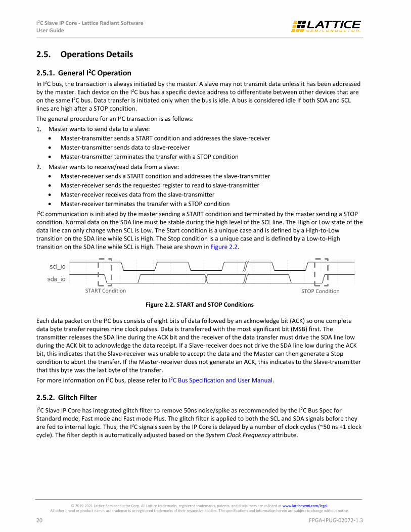
I2C communication is initiated by the master sending a START condition and terminated by the master sending a STOP condition. Normal data on the SDA line must be stable during the high level of the SCL line. The High or Low state of the data line can only change when SCL is Low. The Start condition is a unique case and is defined by a High-to-Low transition on the SDA line while SCL is High. The Stop condition is a unique case and is defined by a Low-to-High transition on the SDA line while SCL is High. These are shown in Figure 2.2.
Figure 2.2. START and STOP Conditions
Each data packet on the I2C bus consists of eight bits of data followed by an acknowledge bit (ACK) so one complete data byte transfer requires nine clock pulses. Data is transferred with the most significant bit (MSB) first. The transmitter releases the SDA line during the ACK bit and the receiver of the data transfer must drive the SDA line low during the ACK bit to acknowledge the data receipt. If a Slave-receiver does not drive the SDA line low during the ACK bit, this indicates that the Slave-receiver was unable to accept the data and the Master can then generate a Stop condition to abort the transfer. If the Master-receiver does not generate an ACK, this indicates to the Slave-transmitter that this byte was the last byte of the transfer.
For more information on I2C bus, please refer to I2C Bus Specification and User Manual.
2.5.2. Glitch Filter
I2C Slave IP Core has integrated glitch filter to remove 50ns noise/spike as recommended by the I2C Bus Spec for Standard mode, Fast mode and Fast mode Plus. The glitch filter is applied to both the SCL and SDA signals before they are fed to internal logic. Thus, the I2C signals seen by the IP Core is delayed by a number of clock cycles (~50 ns +1 clock cycle). The filter depth is automatically adjusted based on the System Clock Frequency attribute.
START Condition
on
STOP Condition
on
I2C Slave IP Core - Lattice Radiant Software User Guide
© 2019-2021 Lattice Semiconductor Corp. All Lattice trademarks, registered trademarks, patents, and disclaimers are as listed at www.latticesemi.com/legal. All other brand or product names are trademarks or registered trademarks of their respective holders. The specifications and information herein are subject to change without notice.
FPGA-IPUG-02072-1.3 21
2.5.3. Clock Stretching
Clock stretching allows the I2C slave to pause a transaction by holding the SCL line Low. The transaction cannot continue until the line is released high again. On the byte level, a slave device may be able to receive bytes of data at a fast rate, but needs more time to store a received byte or prepare another byte to be transmitted. Slaves can then hold the SCL line Low after reception and acknowledgment (ACK bit) of a byte to force the master into a wait state until the slave is ready for the next byte transfer.
I2C Slave IP Core performs clock stretching on the byte level (during ACK/NACK bit) if CONTROL_REG.clk_stretch_en is set to 1. Clock stretching is only performed during data phase. Clock stretching is normally performed when the host need more time before it can address the request of I2C master.
2.5.4. ACK/NACK Response
I2C Slave IP Core can be configured to send an ACK or a NACK based on settings of CONTROL_REG.nack_data and CONTROL_REG.nack_addr, please refer to Control Register (CONTROL_REG) section for details. If the host would like to temporarily disable the access to I2C Slave IP Core, it should set CONTROL_REG.nack_addr = 1’b1. In this case, I2C Slave IP Core sends NACK when it is addressed by the external I2C master.
If the host would like to terminate an on-going I2C write transaction to the I2C Slave IP Core, it should set CONTROL_REG.nack_data = 1’b1. In this case, I2C Slave IP Core sends NACK on the next ACK bit for a data byte. Note that the ACK bit is always sent by the receiver, the CONTROL_REG.nack_data has no effect on I2C read transaction.
2.5.5. Selectable Memory-Mapped Interface
The memory-mapped interface of I2C Slave IP Core is selected by the APB Mode Enable attribute; it can be APB or LMMI. Register access are done via the selected memory-mapped interface. These interfaces are not described in this user guide, references to their respective specifications are provided below.
For LMMI interface, refer to the Lattice Memory Mapped Interface and Lattice Interrupt Interface (FPGA-UG-02039) document for information and for timing diagram of the LMMI. Take note of the following information when checking LMMI timing diagram in the said document:
lmmi_ready_o is always asserted thus, write and read transactions have no wait state
Read latency is one clock cycle
For APB interface, refer to AMBA 3 APB Protocol v1.0 Specification for information and timing diagram of the APB interface. Take note of the following information when checking APB timing diagram in the said document:
Write transaction has one wait state
Read transaction has one wait state (IP Core v1.0.2 or earlier has two wait states)
I2C Slave IP Core - Lattice Radiant Software User Guide
© 2019-2021 Lattice Semiconductor Corp. All Lattice trademarks, registered trademarks, patents, and disclaimers are as listed at www.latticesemi.com/legal. All other brand or product names are trademarks or registered trademarks of their respective holders. The specifications and information herein are subject to change without notice.
22 FPGA-IPUG-02072-1.3
2.6. Programming Flow
2.6.1. Initialization
To perform initialization, load the appropriate registers of the I2C Slave Controller namely:
SLAVE_ADDRL_REG, SLAVE_ADDRH_REG – This step is optional. In most cases, initial value set in I2C Slave Addresses attribute of the user interface does not need to be changed.
CONTROL_REG
TGT_BYTE_CNT_REG – It is recommended to set this if the size of the data is known. Set this to 8'h00 if the number of bytes to transfer is not known,that is receiving unknown amount of data.
INT_ENABLE1_REG – It is recommended to enable only the following interrupts when receiving commands from master.
Transfer Complete Interrupt – If the size of data is known
Receive FIFO Data Interrupt – if the size of data is unknown
INT_ENABLE2_REG – it is recommended to enable both error interrupts
2.6.2. Data Transfer in response to I2C Master Read
Below are the recommended steps to perform data transfer in response to read request of I2C Master. This assumes that the amount of data to send is known.
To perform data transfer in response to read request of I2C Master:
Write data to WR_DATA_REG, amounting to <= FIFO Depth.
Enable only Transfer Complete Interrupt. If transmit data is > FIFO Depth, enable also TX FIFO Almost Empty interrupt. If no more data to transfer, otherwise, proceed to step 7.
Wait for TX FIFO Almost Empty Interrupt. If polling mode is desired, read INT_STATUS1_REG until tx_fifo_aempty_int asserts. If interrupt mode is desired, simply wait for interrupt signal to assert, then read INT_STATUS1_REG and check that tx_fifo_aempt_int is asserted. Read INT_STATUS2_REG also to check that no error occurred.
Clear TX FIFO Almost Empty Interrupt, it also okay to clear all interrupts.
Write data byte to WR_DATA_REG, amounting to less than or equal to (FIFO Depth - TX FIFO Almost Empty Setting).
If there are remaining data to transfer, go back to Step 3, otherwise, disable TX FIFO Almost Empty Interrupt.
Wait for Transfer Complete Interrupt If polling mode is desired, read INT_STATUS1_REG until tr_cmp_int asserts. If interrupt mode is desired, simply wait for interrupt signal to assert, then read INT_STATUS1_REG and check that tr_cmp_int is asserted. Read INT_STATUS2_REG also to check that no error occurred.
Clear all interrupts.
2.6.3. Data Transfer in response to I2C Master Write
Below are the recommended steps to perform data transfer in response to write request of I2C Master. This assumes that the amount of data to receive is known.
To perform data transfer in response to write request of I2C Master:
Enable only Transfer Complete Interrupt. If data to receive is > FIFO Depth, enable also RX FIFO Almost Full interrupt. If data to receive is <= FIFO Depth, proceed to Step 7.
Wait for RX FIFO Almost Full Interrupt. If polling mode is desired, read INT_STATUS2_REG until rx_fifo_afull_int asserts. If interrupt mode is desired, simply wait for interrupt signal to assert, then read INT_STATUS2_REG and check that rx_fifo_afull_int is asserted. Read INT_STATUS2_REG also to check that no error occurred.
I2C Slave IP Core - Lattice Radiant Software User Guide
© 2019-2021 Lattice Semiconductor Corp. All Lattice trademarks, registered trademarks, patents, and disclaimers are as listed at www.latticesemi.com/legal. All other brand or product names are trademarks or registered trademarks of their respective holders. The specifications and information herein are subject to change without notice.
FPGA-IPUG-02072-1.3 23
Clear RX FIFO Almost Full Interrupt, it also okay to clear all interrupts.
Read data byte from RD_DATA_REG, amounting to less than or equal to (FIFO Depth - TX FIFO Almost Empty Setting).
If there are remaining data to receive, go back to Step 2, otherwise, disable RX FIFO Almost Full Interrupt.
Wait for Transfer Complete Interrupt If polling mode is desired, read INT_STATUS1_REG until tr_cmp_int asserts. If interrupt mode is desired, simply wait for interrupt signal to assert, then read INT_STATUS1_REG and check that tr_cmp_int is asserted. Read INT_STATUS2_REG also to check that no error occurred.
Clear all interrupts.
Read all data from RD_DATA_REG.
I2C Slave IP Core - Lattice Radiant Software User Guide
© 2019-2021 Lattice Semiconductor Corp. All Lattice trademarks, registered trademarks, patents, and disclaimers are as listed at www.latticesemi.com/legal. All other brand or product names are trademarks or registered trademarks of their respective holders. The specifications and information herein are subject to change without notice.
24 FPGA-IPUG-02072-1.3
3. Core Generation, Simulation, and Validation This section provides information on how to generate the I2C Slave IP Core using the Lattice Radiant software and how to run simulation and synthesis. For more details on the Lattice Radiant software, refer to the Lattice Radiant Software 2.0 User Guide.
3.1. Licensing the IP An IP core-specific license string is required enable full use of the I2C Slave IP Core in a complete, top-level design. You can fully evaluate the IP core through functional simulation and implementation (synthesis, map, place and route) without an IP license string. This IP core supports Lattice’s IP hardware evaluation capability, which makes it possible to create versions of the IP core, which operate in hardware for a limited time (approximately four hours) without requiring an IP license string. See Hardware Evaluation section for further details. However, a license string is required to enable timing simulation and to generate bitstream file that does not include the hardware evaluation timeout limitation.
3.2. Generation and Synthesis The Lattice Radiant software allows you to customize and generate modules and IPs and integrate them into the device’s architecture. The procedure for generating the I2C Slave IP Core in Lattice Radiant software is described below.
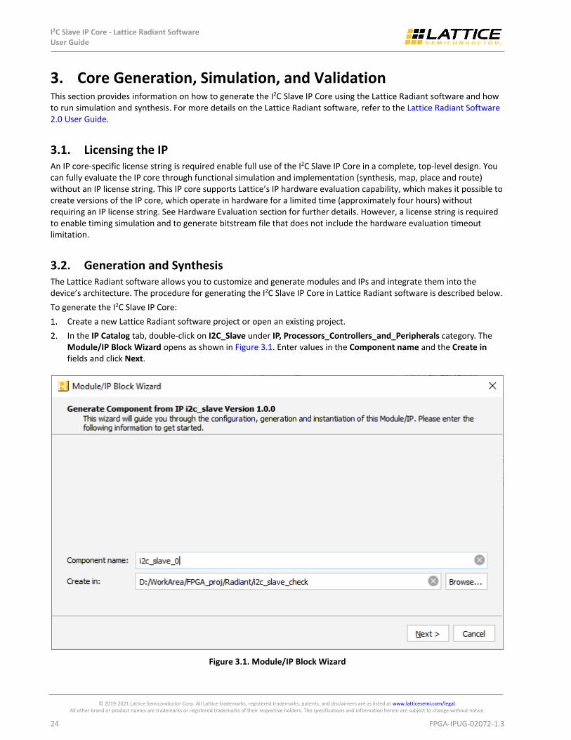
To generate the I2C Slave IP Core:
Create a new Lattice Radiant software project or open an existing project.
In the IP Catalog tab, double-click on I2C_Slave under IP, Processors_Controllers_and_Peripherals category. The Module/IP Block Wizard opens as shown in Figure 3.1. Enter values in the Component name and the Create in fields and click Next.
Figure 3.1. Module/IP Block Wizard
I2C Slave IP Core - Lattice Radiant Software User Guide
© 2019-2021 Lattice Semiconductor Corp. All Lattice trademarks, registered trademarks, patents, and disclaimers are as listed at www.latticesemi.com/legal. All other brand or product names are trademarks or registered trademarks of their respective holders. The specifications and information herein are subject to change without notice.
FPGA-IPUG-02072-1.3 25
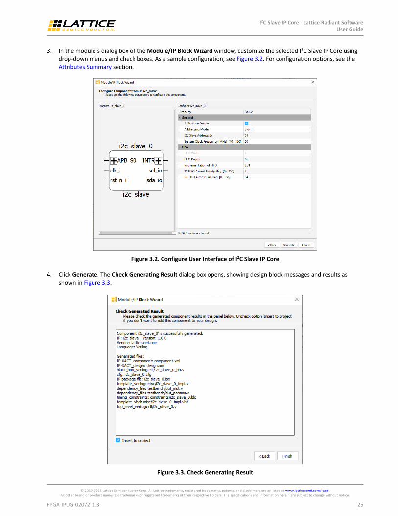
In the module’s dialog box of the Module/IP Block Wizard window, customize the selected I2C Slave IP Core using drop-down menus and check boxes. As a sample configuration, see Figure 3.2. For configuration options, see the Attributes Summary section.
Figure 3.2. Configure User Interface of I2C Slave IP Core
Click Generate. The Check Generating Result dialog box opens, showing design block messages and results as shown in Figure 3.3.
Figure 3.3. Check Generating Result
I2C Slave IP Core - Lattice Radiant Software User Guide
© 2019-2021 Lattice Semiconductor Corp. All Lattice trademarks, registered trademarks, patents, and disclaimers are as listed at www.latticesemi.com/legal. All other brand or product names are trademarks or registered trademarks of their respective holders. The specifications and information herein are subject to change without notice.
26 FPGA-IPUG-02072-1.3
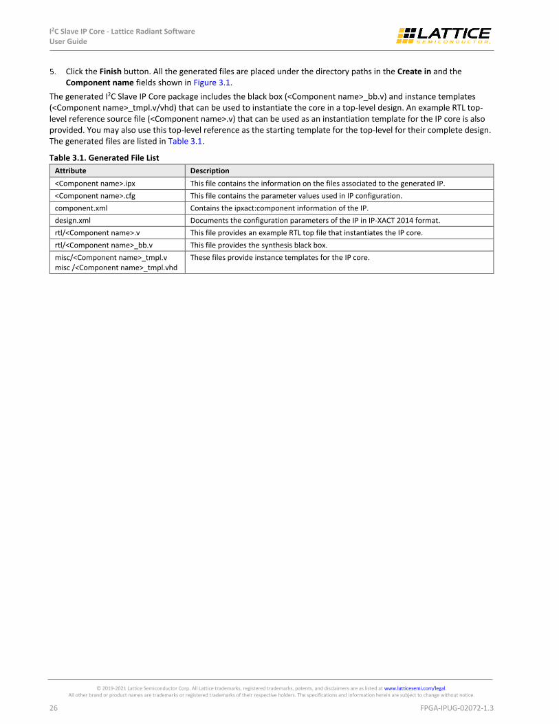
Click the Finish button. All the generated files are placed under the directory paths in the Create in and the Component name fields shown in Figure 3.1.
The generated I2C Slave IP Core package includes the black box (<Component name>_bb.v) and instance templates (<Component name>_tmpl.v/vhd) that can be used to instantiate the core in a top-level design. An example RTL top-level reference source file (<Component name>.v) that can be used as an instantiation template for the IP core is also provided. You may also use this top-level reference as the starting template for the top-level for their complete design. The generated files are listed in Table 3.1.
Table 3.1. Generated File List
Attribute Description
<Component name>.ipx This file contains the information on the files associated to the generated IP.
<Component name>.cfg This file contains the parameter values used in IP configuration.
component.xml Contains the ipxact:component information of the IP.
design.xml Documents the configuration parameters of the IP in IP-XACT 2014 format.
rtl/<Component name>.v This file provides an example RTL top file that instantiates the IP core.
rtl/<Component name>_bb.v This file provides the synthesis black box.
misc/<Component name>_tmpl.v misc /<Component name>_tmpl.vhd
These files provide instance templates for the IP core.
I2C Slave IP Core - Lattice Radiant Software User Guide
© 2019-2021 Lattice Semiconductor Corp. All Lattice trademarks, registered trademarks, patents, and disclaimers are as listed at www.latticesemi.com/legal. All other brand or product names are trademarks or registered trademarks of their respective holders. The specifications and information herein are subject to change without notice.
FPGA-IPUG-02072-1.3 27
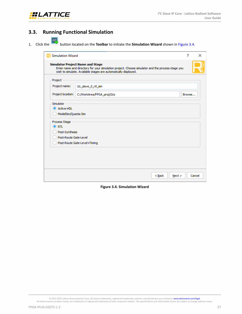
3.3. Running Functional Simulation
Click the button located on the Toolbar to initiate the Simulation Wizard shown in Figure 3.4.
Figure 3.4. Simulation Wizard
I2C Slave IP Core - Lattice Radiant Software User Guide
© 2019-2021 Lattice Semiconductor Corp. All Lattice trademarks, registered trademarks, patents, and disclaimers are as listed at www.latticesemi.com/legal. All other brand or product names are trademarks or registered trademarks of their respective holders. The specifications and information herein are subject to change without notice.
28 FPGA-IPUG-02072-1.3
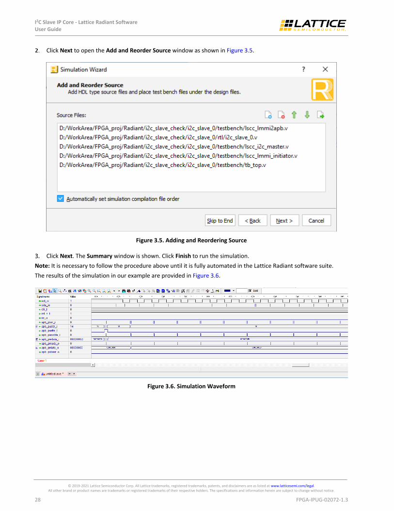
Click Next to open the Add and Reorder Source window as shown in Figure 3.5.
Figure 3.5. Adding and Reordering Source
Click Next. The Summary window is shown. Click Finish to run the simulation.
Note: It is necessary to follow the procedure above until it is fully automated in the Lattice Radiant software suite.
The results of the simulation in our example are provided in Figure 3.6.
Figure 3.6. Simulation Waveform

I2C Slave IP Core - Lattice Radiant Software User Guide
© 2019-2021 Lattice Semiconductor Corp. All Lattice trademarks, registered trademarks, patents, and disclaimers are as listed at www.latticesemi.com/legal. All other brand or product names are trademarks or registered trademarks of their respective holders. The specifications and information herein are subject to change without notice.
FPGA-IPUG-02072-1.3 29
3.4. Hardware Evaluation The I2C Slave IP Core supports Lattice’s IP hardware evaluation capability when used with LIFCL devices. This makes it possible to create versions of the IP core that operate in hardware for a limited period of time (approximately four hours) without requiring the purchase of an IP license. It may also be used to evaluate the core in hardware in user-defined designs. The hardware evaluation capability may be enabled/disabled in the Strategy dialog box. It is enabled by default. To change this setting, go to Project > Active Strategy > LSE/Synplify Pro Settings.
I2C Slave IP Core - Lattice Radiant Software User Guide
© 2019-2021 Lattice Semiconductor Corp. All Lattice trademarks, registered trademarks, patents, and disclaimers are as listed at www.latticesemi.com/legal. All other brand or product names are trademarks or registered trademarks of their respective holders. The specifications and information herein are subject to change without notice.
30 FPGA-IPUG-02072-1.3
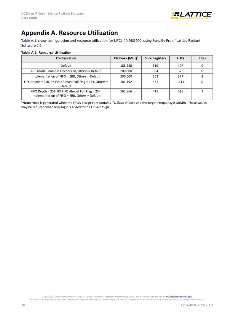
Appendix A. Resource Utilization Table A.1. show configuration and resource utilization for LIFCL-40-9BG400I using Synplify Pro of Lattice Radiant Software 2.1.
Table A.1. Resource Utilization
Configuration Clk Fmax (MHz)* Slice Registers LUTs EBRs
Default 188.288 319 407 0
APB Mode Enable is Unchecked, Others = Default 200.000 304 376 0
Implementation of FIFO = EBR, Others = Default 200.000 303 377 2
FIFO Depth = 256, RX FIFO Almost Full Flag = 254, Others = Default
181.192 431 1211 0
FIFO Depth = 256, RX FIFO Almost Full Flag = 254, Implementation of FIFO = EBR, Others = Default
162.866 415 518 2
*Note: Fmax is generated when the FPGA design only contains I2C Slave IP Core and the target Frequency is 50MHz. These values may be reduced when user logic is added to the FPGA design.
I2C Slave IP Core - Lattice Radiant Software User Guide
© 2019-2021 Lattice Semiconductor Corp. All Lattice trademarks, registered trademarks, patents, and disclaimers are as listed at www.latticesemi.com/legal. All other brand or product names are trademarks or registered trademarks of their respective holders. The specifications and information herein are subject to change without notice.
FPGA-IPUG-02072-1.3 31
References For complete information on Lattice Radiant Project-Based Environment, Design Flow, Implementation Flow and Tasks, as well as on the Simulation Flow, see the Lattice Radiant Software User Guide.
I2C Slave IP Core - Lattice Radiant Software User Guide
© 2019-2021 Lattice Semiconductor Corp. All Lattice trademarks, registered trademarks, patents, and disclaimers are as listed at www.latticesemi.com/legal. All other brand or product names are trademarks or registered trademarks of their respective holders. The specifications and information herein are subject to change without notice.
32 FPGA-IPUG-02072-1.3
Technical Support Assistance Submit a technical support case through www.latticesemi.com/techsupport.
I2C Slave IP Core - Lattice Radiant Software User Guide
© 2019-2021 Lattice Semiconductor Corp. All Lattice trademarks, registered trademarks, patents, and disclaimers are as listed at www.latticesemi.com/legal. All other brand or product names are trademarks or registered trademarks of their respective holders. The specifications and information herein are subject to change without notice.
FPGA-IPUG-02072-1.3 33
Revision History
Revision 1.3, June 2021
Section Change Summary
Introduction Remove second paragraph..
Updated Table 1.1. Quick Facts.
Revised Supported FPGA Families
Revised Targeted Devices
Revised Lattice Implementation.
Revised reference to Lattice Radiant Software User Guide
References Updated this section.
Revision 1.2, June 2020
Section Change Summary
Introduction Updated Table 1.1. Quick Facts.
Added Certus-NX as supported FPGA family.
Added LFD2NX-40 as targeted device.
Changed Synplify version to Pro for Lattice.
Functional Description Updated Implementation of FIFO attribute default value to LUT in Table 2.2.
Updated reset values in Table 2.8, Table 2.9, and Table 2.10.
The wait state of APB read transaction has been reduced to one in Selectable Memory-Mapped Interface section.
Updated content of Initialization section.
Appendix A. Resource Utilization Updated Table A1..
References Updated this section.
Revision 1.1, February 2020
Section Change Summary
Introduction Updated Table 1.1. Quick Facts.
Changed LIFCL to CrossLink-NX as supported FPGA family.
Added LIFCL-17 as targeted device.
Core Generation, Simulation, and Validation
Updated user interface item to IP, Processors_Controllers_and_Peripherals category.
Revision 1.0, December 2019
Section Change Summary
All Changed document status from Preliminary to final.
Introduction Updated Table 1.1. Quick Facts.
Added Resource information.
Updated Lattice Implementation information.
References Removed reference to the FPGA device web page.
Appendix A. Resource Utilization Added resource utilization information.
All Minor editorial changes
Revision 0.80, October 2019
Section Change Summary
All Preliminary release.