hybrid functional- and instruction-level power modeling for embedded and heterogeneous processor...
TRANSCRIPT
Journal of Systems Architecture 53 (2007) 689–702
www.elsevier.com/locate/sysarc
Hybrid functional- and instruction-level power modelingfor embedded and heterogeneous processor architectures
H. Blume a,*, D. Becker a, L. Rotenberg a, M. Botteck b,J. Brakensiek b, T.G. Noll a
a Chair for Electrical Engineering and Computer Systems, RWTH Aachen University, Schinkelstr. 2, 52062 Aachen, Germanyb Nokia Research Center, Meesmannstr. 103, 44807 Bochum, Germany
Received 31 December 2006; received in revised form 10 January 2007; accepted 12 January 2007Available online 20 January 2007
Abstract
In this contribution the concept of functional- level power analysis (FLPA) for power estimation of programmable pro-cessors is extended in order to model embedded as well as heterogeneous processor architectures featuring different embed-ded processor cores. The basic FLPA approach is based on the separation of the processor architecture into functionalblocks like, e.g. processing unit, clock network, internal memory, etc. The power consumption of these blocks is describedby parameterized arithmetic models. By application of a parser based automated analysis of assembler codes the inputparameters of the arithmetic functions like e.g. the achieved degree of parallelism or the kind and number of memoryaccesses can be computed. For modeling an embedded general purpose processor (here, an ARM940T) the basic FLPAmodeling concept had to be extended to a so-called hybrid functional-level and instruction-level (FLPA/ILPA) modelin order to achieve a good modeling accuracy. In order to show the applicability of this approach even a heterogeneousprocessor architecture (OMAP5912) featuring an ARM926EJ-S core and a C55x DSP core has been modeled using thehybrid FLPA/ILPA technique described before. The approach is exemplarily demonstrated and evaluated applying a vari-ety of basic digital signal processing tasks ranging from basic filters to complete audio decoders or classical benchmarksuits. Estimated power figures for the inspected tasks are compared to physically measured values for both inspected pro-cessor architectures. A resulting maximum estimation error of 9% for the ARM940T and less than 4% for the OMAP5912is achieved.� 2007 Elsevier B.V. All rights reserved.
Keywords: Power estimation; Embedded processors; Modeling accuracy
1383-7621/$ - see front matter � 2007 Elsevier B.V. All rights reserved
doi:10.1016/j.sysarc.2007.01.002
* Corresponding author. Tel.: +49 2418097591; fax: +492418092282.
E-mail addresses: [email protected] (H. Blume),[email protected] (D. Becker), [email protected] (L. Rotenberg), [email protected] (M. Bot-teck), [email protected] (J. Brakensiek), [email protected] (T.G. Noll).
1. Introduction
In the course of increasing complexity of digitalsignal processing applications, especially in the fieldof mobile applications, low power techniques are ofcrucial importance. Therefore, it is desirable to esti-mate the power consumption of a system at a very
.

Program cacheMUL: 0111001110100110
ADD: 0010110111100011
0111001110100110
0010110111100 011
Cycle 1
Cycle 2
Register in the processor core
Fig. 1. Sequential execution of two different processorinstructions.
Program cache
ADD: 0010110111100011
0111001110100110Cycle 1
Cycle 2
Register in the processor core
0111001110100110
ADD: 0010110111100011
Fig. 2. Sequential execution of two identical processorinstructions.
690 H. Blume et al. / Journal of Systems Architecture 53 (2007) 689–702
early stage in the design flow. By this means, it ispossible to predict whether a system will meet a cer-tain power budget before it is physically imple-mented. Necessary changes in the system or theunderlying architecture will then be much less timeand money consuming, because no physical imple-mentation is required to determine its powerdissipation.
Like any other architecture block the power con-sumption of a processor depends on several factorslike the switching activity of the input data, theclock frequency and of course the executed taskitself. Besides these dependencies there are manymore processor-specific factors like the type andrate of memory accesses, the usage of specific archi-tecture elements, different compiler settings, pipelinestalls and cache misses but also different program-ming styles or algorithmic alternatives which allstrongly influence the power consumption of a taskthat is executed on a processor.
For this reason it is desirable to consider method-ologies for power estimation that cover all signifi-cant influencing factors and provide a sufficientaccuracy at moderate complexity. Such a methodol-ogy is presented in this paper and verified usingexemplary vehicles. The paper is organized as fol-lows: Section 2 shortly discusses several existingpower estimation techniques in terms of their appli-cability to modern processor kernels. The followingsection describes the so-called functional-levelpower analysis (FLPA) approach in detail. Section4 describes the required basics of the modeled pro-cessor architectures. First the ARM940T generalpurpose processor architecture is explained and sec-ond the heterogeneous OMAP5912 processor archi-tecture featuring an ARM926EJ–S core and a C55xDSP core are discussed. Section 5 explains theexemplary modeling of these processor architecturesand works out the need for a hybrid FLPA/ILPAapproach. A benchmarking of the hybrid FLPA/ILPA models for both processors is performed inSection 6. Finally, a conclusion of the paper is givenin Section 7.
2. Classical approaches for power estimation
One possible straight forward power estimationapproach on processors is the so-called physical-
level power analysis methodology. This approach isbased on the analysis of the switching activity ofall circuit nodes of the processor architecture. Therequirement of this methodology is the availability
of a detailed description of the processor architec-ture on transistor level, which is rarely given formodern processors and even more severe results inan extremely high computational effort.
Architecture-level approaches like [1] reduce thiscomputational effort by abstracted modeling of typ-ical architecture elements like registers, functionalunits or load/store queues. Therefore, these method-ologies can be mainly found in the development ofhigh volume products like e.g. microprocessors.Due to their extremely high computational effortthey are not suited to evaluate the power consump-tion of complete digital signal processing tasks per-formed on a processor in practical use withacceptable computation times.
Another possibility for power estimation of pro-cessors is the so-called instruction-level power analy-
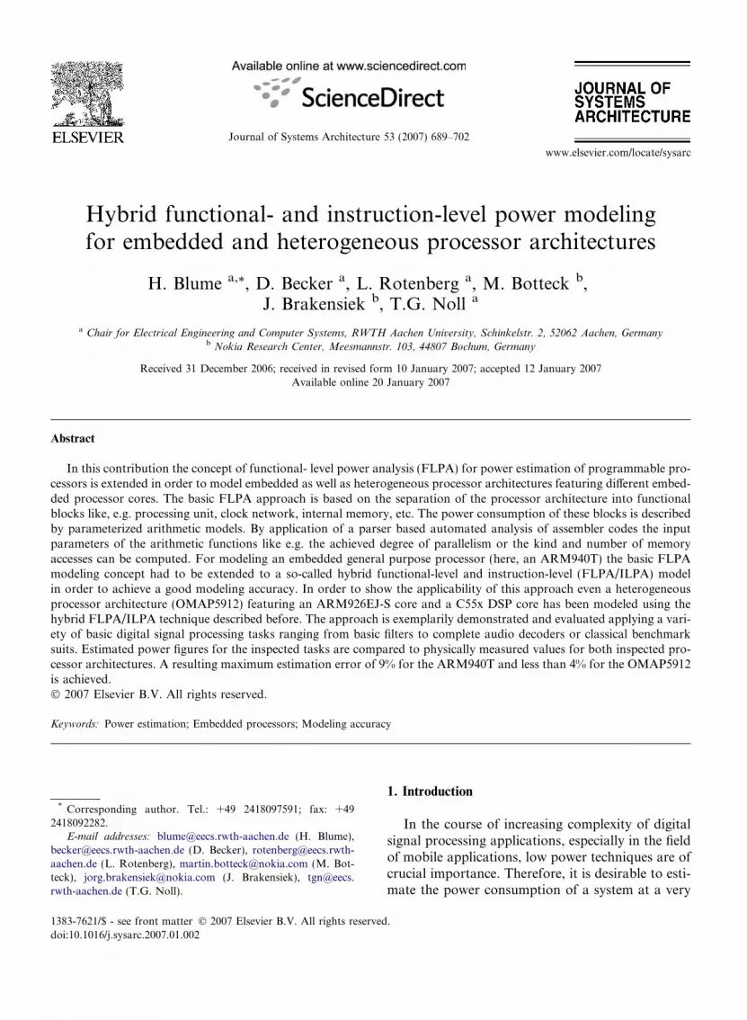
sis [2]. By means of low level simulations or physicalmeasurements the energy consumption of eachinstruction out of the instruction set of a processoris determined. By analysis of the assembler code of atask it is possible to estimate the specific powerconsumption of this program performed on acertain processor. The advantage of this approachis to cope with so-called inter-instruction effects.In general, the energy consumption of a processorinstruction depends on the previously executedinstructions, what can be explained by means ofFigs. 1 and 2.
At a certain stage of a processors pipeline,instruction words are transferred from the programcache into a register in the processor core for furtherprocessing. Fig. 1 shows an ADD instruction wordto replace a MUL instruction word in cycle 2. The
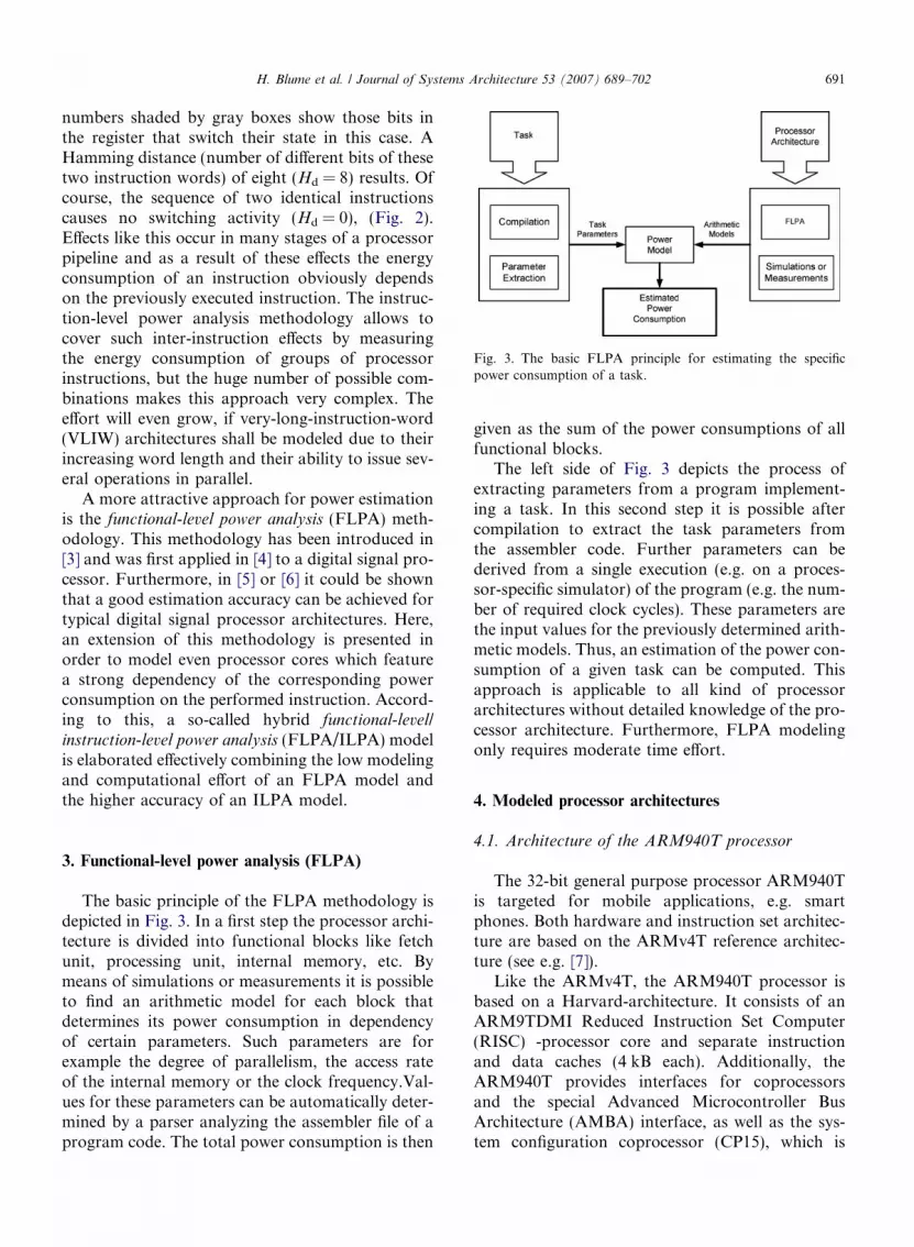
Fig. 3. The basic FLPA principle for estimating the specificpower consumption of a task.
H. Blume et al. / Journal of Systems Architecture 53 (2007) 689–702 691
numbers shaded by gray boxes show those bits inthe register that switch their state in this case. AHamming distance (number of different bits of thesetwo instruction words) of eight (Hd = 8) results. Ofcourse, the sequence of two identical instructionscauses no switching activity (Hd = 0), (Fig. 2).Effects like this occur in many stages of a processorpipeline and as a result of these effects the energyconsumption of an instruction obviously dependson the previously executed instruction. The instruc-tion-level power analysis methodology allows tocover such inter-instruction effects by measuringthe energy consumption of groups of processorinstructions, but the huge number of possible com-binations makes this approach very complex. Theeffort will even grow, if very-long-instruction-word(VLIW) architectures shall be modeled due to theirincreasing word length and their ability to issue sev-eral operations in parallel.
A more attractive approach for power estimationis the functional-level power analysis (FLPA) meth-odology. This methodology has been introduced in[3] and was first applied in [4] to a digital signal pro-cessor. Furthermore, in [5] or [6] it could be shownthat a good estimation accuracy can be achieved fortypical digital signal processor architectures. Here,an extension of this methodology is presented inorder to model even processor cores which featurea strong dependency of the corresponding powerconsumption on the performed instruction. Accord-ing to this, a so-called hybrid functional-level/
instruction-level power analysis (FLPA/ILPA) modelis elaborated effectively combining the low modelingand computational effort of an FLPA model andthe higher accuracy of an ILPA model.
3. Functional-level power analysis (FLPA)
The basic principle of the FLPA methodology isdepicted in Fig. 3. In a first step the processor archi-tecture is divided into functional blocks like fetchunit, processing unit, internal memory, etc. Bymeans of simulations or measurements it is possibleto find an arithmetic model for each block thatdetermines its power consumption in dependencyof certain parameters. Such parameters are forexample the degree of parallelism, the access rateof the internal memory or the clock frequency.Val-ues for these parameters can be automatically deter-mined by a parser analyzing the assembler file of aprogram code. The total power consumption is then
given as the sum of the power consumptions of allfunctional blocks.
The left side of Fig. 3 depicts the process ofextracting parameters from a program implement-ing a task. In this second step it is possible aftercompilation to extract the task parameters fromthe assembler code. Further parameters can bederived from a single execution (e.g. on a proces-sor-specific simulator) of the program (e.g. the num-ber of required clock cycles). These parameters arethe input values for the previously determined arith-metic models. Thus, an estimation of the power con-sumption of a given task can be computed. Thisapproach is applicable to all kind of processorarchitectures without detailed knowledge of the pro-cessor architecture. Furthermore, FLPA modelingonly requires moderate time effort.
4. Modeled processor architectures
4.1. Architecture of the ARM940T processor
The 32-bit general purpose processor ARM940Tis targeted for mobile applications, e.g. smartphones. Both hardware and instruction set architec-ture are based on the ARMv4T reference architec-ture (see e.g. [7]).
Like the ARMv4T, the ARM940T processor isbased on a Harvard-architecture. It consists of anARM9TDMI Reduced Instruction Set Computer(RISC) -processor core and separate instructionand data caches (4 kB each). Additionally, theARM940T provides interfaces for coprocessorsand the special Advanced Microcontroller BusArchitecture (AMBA) interface, as well as the sys-tem configuration coprocessor (CP15), which is

Coprocessor Interface
AMBA Interface
ARM9TDMI
Memory Protection Unit
InstructionCache
DataCache
CP15
Fig. 4. Block diagram of the ARM940T architecture.
ARM926EJ-SProcessor Core
TMS320C55xProcessor Core
MPUInterface
DS P-MMU
TrafficController
SRAM
PeripheralDevices
Fig. 5. Block diagram of the OMAP5912 architecture.
692 H. Blume et al. / Journal of Systems Architecture 53 (2007) 689–702
used to control e.g. the memory protection unit [8].A block diagram of the ARM940T architecture isdepicted in Fig. 4.
The ARM9TDMI RISC-processor core consistsof a five stage pipeline, which is controlled by a32-bit instruction word. Each instruction word isderived from the standard ARM instruction set.The standard ARM instruction set itself is basedon a load/store architecture. As a consequence,the source data of different instructions must beloaded separately into one or two source registers.The result is written back to a target register. There-fore, the instruction set can be divided into load/store and arithmetic instructions. However, branchand control instructions are supplied by the stan-dard ARM instruction set. To improve the codedensity the ARM9TDMI processor core also fea-tures a dynamic instruction set exchange to theThumb instruction set. These 16-bit instructionsare compressed versions of a subset of the standardARM instructions. The exchange is performed bydynamic decompression in the ARM9TDMIpipeline.
The CP15 coprocessor is accessed via the copro-cessor interface using specific assembler directives.It enables and initializes the memory protectionunit, which itself enables instruction and dataregions in the main memory as well as in the instruc-tion and data cache. Moreover, the memory protec-tion unit sets and monitors access rules for thedifferent instruction and data regions.
For the course of this modeling work, a so-calledARM Integrator Core Module featuring anARM940T (manufactured in a 0.18-lm technologywith a core voltage of VDD = 2.5 V and an adaptablecore clock frequency of 12–160 MHz) has beendeployed as reference platform. Internal processorstates could be analyzed using a MultiICE in circuitemulation interface and an instruction set simulator(ARMulator).
4.2. Architecture of the heterogeneous OMAP5912
processor
The OMAP5912 is a state-of-the-art heteroge-neous processor architecture tailored for mobileapplications [9]. This architecture features two sepa-rate processor cores: an ARM926EJ-S core (insidethe OMAP architecture often denoted as micropro-cessor unit, MPU) and a TMS320C55x DSP-core(see Fig. 5). The double-core structure of the OMAPallows to benefit from the advantages of both cores.The C55x DSP-core is a power-optimized DSP fordigital real-time signal processing while the ARM-core is mainly responsible for executing the opera-tion system as well as monitoring and controlingprogram sequences. Both cores inside the OMAPfeature various mechanisms for power management.
The OMAP5912 is manufactured in a 0.13-lmtechnology, powered by a core voltage of VDD =1.6 V and features a maximum clock frequency of192 MHz. The processor provides a 250 kB on-chipSRAM memory which can be accessed by both pro-cessor cores (directly by the ARM-core and via aDSP-MMU by the DSP).
Furthermore, the OMAP5912 includes severalperipheral devices, as for example the so-calledmailbox registers for on-chip interprocessor com-munication, an MPU-interface that provides accessto the complete memory space of the DSP for theARM processor core, and a traffic controller whichmanages the interfaces to internal and externalmemories.
The OMAP5912 is a power-optimized processorand today one of the most frequently used proces-sors for the realization of multimedia applicationsin mobile terminals.
The basic architecture of the ARM926EJ-S coreis very similar to the ARM940T core described inthe section before. It also features a 32-bit RISC-

0
50
100
150
200
250
0 20 40 60 80 100 120 140 160 180f [MHz]
P ins
t_sp
ec(i.
f)[m
W] SUB
MUL
SUB:R²= 0.9993P(f)= 1.32 * f + 5.93
MUL:R²= 0.9995P(f)= 0.86 * f + 3.75
Fig. 6. Power consumption as a function of the frequency of theARM940T core clock while executing SUB and MUL scenarioswithout cache misses.
H. Blume et al. / Journal of Systems Architecture 53 (2007) 689–702 693
processor core with a 5-stage pipeline architecture.In contrast to the ARM940T this processor core isbased on the instruction set architecture ARMv5-TEJ. Besides the 32-bit ARM and the 16-bit Thumbinstruction set this architecture features an extendedDSP instruction set, supporting saturated arithme-tic, multiply accumulate (MAC) instructions anddouble word load/store instructions. The ARM-926EJ-S possesses a 16 kB instruction cache, an8 kB data cache and a memory management unit(MMU). Like the ARM940T, this processor corefeatures a coprocessor interface which can be usedto address the system configuration coprocessorCP15.
The TMS320C55x DSP is a fixed point processorfeaturing a so-called protected pipeline with twodecoupled components: a fetch- and an executionpipeline.
The length of the instructions is variable and canaccount for 1–6 bytes. The C55x is able to executetwo instructions in one clock cycle. The processorcontains video hardware accelerators for discretecosine transformation (DCT/IDCT), motion esti-mation and pixel interpolation as well as on-chipmemories (tightly coupled memories, TCM). Theseon-chip memories include 64 kB dual-access RAM(DARAM) and 96 kB single-access RAM (SAR-AM). Furthermore, the C55x possesses a 16 kBinstruction cache and a MPUI-Port which is con-nected to the MPU-interface of the ARM-system.The DSP-MMU inside the C55x is used for adress-ing the DSP-external memory. It can only be acti-vated and programmed by the ARM processorcore (MPU).
For the modeling work described here, anOMAP OSK5912 board [10] has been used. For thisplatform internal processor states could be analyzedusing a XDS510PP Plus emulator [11]. As SWdevelopment, simulation and programming envi-ronment for both cores the Code Composer StudioV 3.1 has been used. Only for simulation purposesof the ARM926EJ-S core the above mentionedARM instruction set simulator (ARMulator) hasbeen used.
5. Hybrid FLPA/ILPA modeling
5.1. Hybrid FLPA/ILPA model of the ARM940T
In contrast to the FLPA modeling of some com-plex VLIW-DSP-architectures where the processorarchitecture had to be separated into up to seven
functional blocks [5] for the modeling of theARM940T only a separation into three differentfunctional blocks is required. These are theARM9TDMI processor core, the instruction cacheand the data cache. According to the FLPA model-ing concept each functional block is described by anarithmetic model, which itself describes the powerconsumption of the functional block. It can befound via simulations or measurements [5,12].Hence, it is necessary to excite each block sepa-rately. This can be achieved by executing differentparts of assembler code, which will be called scenar-ios in the following. Both, scenarios with and with-out cache misses have to be considered to model theARM9TDMI processor core (execution unit) andthe instruction and data caches.
In Fig. 6 the power consumption is depicted as afunction of the frequency of the core clock while theARM940T is executing exemplary SUB and MULscenarios without cache misses (test loops featuring1000 SUBs (single cycle instruction) or 1000 MULs(three cycle instruction)). The results show thatthere are significant differences between individualinstructions and that for each instruction a nearlyperfect linear frequency dependency results (avg.coefficient of determination, a measure that is usedto determine how well a regression fits [13], for alloperation types is R2
avg ¼ 0:9993, theoretical maxi-mum for R2 is 1). In the following, the accordingpower consumption of a test loop with an instruc-tion i at the frequency f without cache misses isdenoted as instruction-specific offset Pinst_spec(i,f).
It has to be regarded, that the distribution ofbasic instructions significantly varies from applica-tion to application. Two exemplary distributions

0
50
100
150
200
250
0 20 40 60 80 100 120 140 160 180f [MHz]
P[m
W]
looplength 1000looplength 1050looplength 1100looplength 1250looplength 1500looplength 9500
Pbus_spec
Fig. 8. Power consumption as a function of the frequency of thecore clock while executing SUB test scenarios featuring cachemisses.
Fig. 9. Bus-specific offset of the ADD instruction.
694 H. Blume et al. / Journal of Systems Architecture 53 (2007) 689–702
for a 4 tap 1D FIR filter and an MP3 (MPEG1/2Layer3) decoder are depicted in Fig. 7.
The strong dependency of power consumptionon the instruction performed and the significant dif-ference of the distribution of instructions reveals thenecessity to extend the classic FLPA approach by aninstruction dependent part. This new approach isdenoted as hybrid FLPA/ILPA modeling. One keyelement of this approach is that for each applica-tion, respectively task, whose power consumptionhas to be determined, a dynamic determination ofthe distribution of instructions on the basis of theassembler code has to be performed.
Increasing the number of instructions in a testscenario (here more than 1024 instructions, due tothe cache size and the instruction word length) leadsto cache misses. As shown in Fig. 8, the power con-sumption is no longer a linear function of the coreclock frequency while the processor is executingthose test scenarios.
The difference at a given frequency between theinstruction-specific offset and the actual power con-sumption of the ARM940T by executing such testscenarios with cache misses is called the bus-specificoffset Pbus_spec. Hence, the number of cache misseswould be an appropriate parameter influencing themodel for Pbus_spec. Using the ARM instructionset simulator and cycle counter (ARMulator [14])it is possible to derive various cycle counts (coreclocks, memory bus clocks, etc.). These values aremuch more accurate than the number of cachemisses which are also provided by the simulationenvironment [15]. Therefore, the bus-specific offset(see Fig. 9) can be modeled as a linear function ofthe ratio S/T. Here, the variable S denotes the num-ber of bus cycles that are followed by data move-
0
0.05
0.1
0.15
0.2
0.25
0.3
0.35
0.4
TSTTEQ
CMPCMN
ANDORR
SUBSBC
RSBRSC
ADDADC
MOVMVN
MULMLA LD
RSTR
instruction
rela
tive
occu
rrenc
e
MP 3 Decoder4 tap 1D FIR
Fig. 7. The distribution of instructions within the most fre-quently used sections of the assembler code for a 4 tap 1D FIRfilter and an MP3 decoder.
ment and the variable T denotes the total numberof bus cycles. In the following, the ratio S/T isdenoted as the bus cycle ratio u. Using the relativeshare of instruction cache misses ricm and the rela-tive share of data cache misses rdcm the bus cycleratio is split into a bus cycle ratio caused by instruc-tion cache misses uinst and caused by data cachemisses udata, whereby the influence of the instruc-tion and data caches is considered separately fromeach other. So with
uinst ¼ ricm � u and udata ¼ rdcm � u ð1Þ
the bus-specific offset is calculated by the equation:
P bus spec ¼ P bus specði; f ;uinstÞþ P bus specði; f ;udataÞ: ð2Þ
Besides the dependency on the bus cycle ratio u thebus-specific offset is also a function of the frequency.It could be modeled as
P bus specðf ;uÞ ¼ a � f � uþ b � uþ c � f þ d: ð3Þ

H. Blume et al. / Journal of Systems Architecture 53 (2007) 689–702 695
Negative values for Pbus_spec(f,u) are not possibleand clipped to zero.
Finally, the actual power consumption of a giventask executed on the ARM940T can be calculatedby
P ARM940T ¼ P inst spec � P bus spec: ð4Þ
To estimate the complete power consumption of theARM940T processor while executing a task, a pro-filer from the ADS1.2 framework [14] determinesthe share hlabel of the execution time of the differentparts of the assembler code which are produced bythe compiler and which are denoted here as labels.The instruction distribution is determined for everylabel by a special parser which has been imple-mented as a C program, whereby the complete sharehi of every instruction class i in the label is extracted.In case of the ARM940T the parser categorizes theinstruction set into 6 different instruction classes(arithmetic, logic, multiplication, load, store, specialinstructions). It has been analyzed by comprehen-sive inspections that 6 different instruction classesis an attractive compromise between estimationaccuracy and modeling effort. Using less instructionclasses significantly decreases the estimation accu-racy while increasing the number of instruction clas-ses only very marginally improves the estimationaccuracy (see Fig. 10). Finally, the resulting hybridFLPA/ILPA power model of the ARM940T canbe summarized as follows:
P ARM940Tði;f ;uÞ
¼Xlabel
hlabel �X6
i¼1
hi � ðP inst specði;f Þ� P bus specði;f ;uÞÞ !
ð5Þ
0%
1%
2%
3%
4%
5%
6%
7%
8%
9%
2 classes 4 classes 6 classes 18 classes
number of instruction classes
avg
.est
imat
ion
err
or
Fig. 10. Influence of the number of instruction classes on theaverage ARM940T estimation error of the hybrid FLPA/ILPAmodel.
5.2. Hybrid FLPA/ILPA model of the OMAP5912
First of all the two processor cores of theOMAP5912 have been modeled separately.
5.2.1. Power model of the ARM926EJ-S
For the hybrid FLPA/ILPA modeling of theARM926EJ-S processor a separation into five func-tional blocks is required. In addition to the proces-sor core and the two caches, also the differentmemory devices (on-chip SRAM and off-chipSDRAM) must be considered as functional blocks.
The exploration of the instruction set (ARMv5-TEJ) with scenarios not creating cache missesshowed that five different instruction classes are suf-ficient for this modeling. Compared to theARM940T model, the basic arithmetic and logicoperations (ADD, SUB, AND, CMP, . . .) as wellas saturated arithmetic operations (QADD, QSUB,. . .) can be combined in one class. Other classes arethe multiplications, single load and store instruc-tions, and multiple memory accesses (LDM,STM). Furthermore, all instructions showed a lin-ear frequency dependency and only a marginaldependency on addressing modes and inter-instruc-tion effects. In Fig. 11 the power consumption at192 MHz is depicted while the ARM926EJ-S-core is executing exemplary scenarios for eachinstruction class. The maximum difference inpower consumption between the instruction classesis 26%.
Increasing the number of instructions in a test sce-nario (here, more than 4000 instructions) leads tocache misses. Fig. 12 depicts the effect of these cachemisses on the power consumption of the ARM-coreat 192 MHz while using different memory devices.Like for the ARM940T, this effect can be modeledwith the frequency dependent bus-specific offsetPbus_spec(f,u) as a function of the bus cycle ratio u.
0
50
100
150
200
250
300
350
ADD MUL LDR STR LDM/STM
instruction class
po
wer
co
nsu
mp
tio
n
at 1
92M
Hz
[mW
]
Fig. 11. Dynamics of the power consumption between thedifferent instruction classes of the ARM926EJ-S.

160
180
200
200
210
220
230
240
250
260
270
0 2000 4000 6000 8000 10000
number of instructions per test loop
po
wer
co
nsu
mp
tio
n
at 1
92M
Hz
[mW
]
ADD in SRAM
ADD in SDRAM
Fig. 12. Dependency on the loop length of the inspected testscenarios (here: ADD test scenario) of the ARM926EJ-S.
696 H. Blume et al. / Journal of Systems Architecture 53 (2007) 689–702
Additionally, a dependency of power consump-tion on memory placement (Mem = SRAM orMem = SDRAM) must be taken into account.Thus, the bus specific offset can be modeled as
P bus specðf ;u;MemÞ¼XMem
ðaMem � f � uþ bMem � uþ cMem � f þ dMemÞ:
ð6Þ
The resulting hybrid FLPA/ILPA power model ofthe ARM926EJ-S can be described as follows:
P ARM926EJ-Sði;f ;u;MemÞ ¼Xlabel
hlabel
�X5
i¼1
hi � ðP inst specði;f Þ�P bus specði;f ;u;MemÞÞ !
:
ð7Þ
In this equation, hlabel and hi are determined in thesame way as for the ARM940T by means of the pro-filer and the parser. For each of the five classes,Pinst_spec(i, f) is a linear function of the frequencyand the bus-specific offset Pbus_spec(i, f,u,Mem) is alinear function of the frequency and the bus cycleratio u.
0
20
40
60
80
100
120
140
single_DP parallel_DP single_Mem double_Meminstruction classes
po
wer
co
nsu
mp
tio
n
at 1
92M
Hz
[mW
]
Fig. 13. Dynamics of the power consumption between thedifferent instruction classes of the C55x.
5.2.2. Power model of the C55x
For the power modeling, the C55x DSP proces-sor core can be divided into four function blocks:the CPU, the instruction cache, the DSP-internalmemories (TCM) and the DSP-external memories(SRAM, SDRAM).
After the exploration of the instruction set of theC55x, four instruction classes (non-parallel dataprocessing single_DP, parallel data processing par-
allel_DP, single memory access single_Mem, doublememory access double_Mem) have been defined.
Because of the variable instruction length, the testscenario for each class is composed of three exem-plary, randomly distributed instructions featuringdifferent lengths.
In Fig. 13 the power consumption of the C55x at192 MHz is depicted for the processor executing sce-narios exemplary for each instruction class. In thiscase, the DSP-internal memories have been usedfor instruction and data placement. Measurementsfor the same scenarios but using DSP-external mem-ories with instruction cache switched on and nocache misses showed 10% higher power consump-tion. Thus, the use of either DSP-internal or -exter-nal memories must be taken into account for themodeling. The maximum difference in power con-sumption between instruction classes was 25% inboth cases of memory usage.
Because of the complexity of the C55x pipeline,the influence of the pipeline stall rate PSR on thepower consumption was examined. Jumps in theprogram flow, e.g. branch instructions and func-tion calls, cause flushing of the instruction bufferin the fetch pipeline and generate stall cycles. Toproduce the required number of stall cycles, branchinstructions were added to the test scenarios. Insuch scenarios, the program jumps from the mainloop to a destination outside of the main test loopand returns back. The pipeline stall rate for suchscenarios with different number of additionaljumps could be determined with a cycle accuratesimulator in the Code Composer Studio. The dif-ference at a given frequency between the instruc-tion-specific offset and the actual powerconsumption of the C55x while executing test sce-

0
2
4
6
8
10
12
14
0 10 20 30 40 50
pipeline stall rate(PSR) [%]
stal
l-sp
ecif
ic o
ffse
tat
192
MH
z[m
W]
single_DP
Fig. 14. Influence of the pipeline stall rate on the power consumption of the C55x (here: stall-specific offset for the single_DP scenario).
H. Blume et al. / Journal of Systems Architecture 53 (2007) 689–702 697
narios with extra pipeline stalls is called the stall-specific offset Pstall_spec. This offset can be modeledas a linear function of the pipeline stall rate.Fig. 14 depicts the stall-specific offset for the sin-gle_DP scenario at a frequency of 192 MHz.Besides the dependency on the pipeline stall rate,the stall-specific offset is also a function of the fre-quency and can be modeled as
P stall specðf ;PSRÞ ¼ aPSR � f � PSRþ bPSR � PSR
þ cPSR � f þ dPSR: ð8Þ
Negative values for Pstall_spec(f,PSR) are not possi-ble and clipped to zero.
Measurements of the power consumption withdifferent pipeline stall rates showed negligibledependency of the stall specific offset on the memoryplacement.
As well as for the analyzed ARM processorcores, the influence of the instruction cache misseson the power consumption of the C55x can be mod-eled using the bus-specific offset. This offset is a lin-ear function of the frequency and the cache missrate CMR. This rate could be determined using anadequate device simulator in the Code ComposerStudio. Thus, the bus-specific offset for the C55xcan be modeled as
P bus specðf ;CMRÞ ¼ aCMR � f � CMR þ bCMR
� CMRþ cCMR � f þ dCMR: ð9Þ
This offset showed no dependency on memoryplacement in DSP-external memories (SRAM,SDRAM). Finally, the resulting FLPA power mod-el of the C55x can be described as follows:
P C55xði; f ;PSR;CMR;MemÞ
¼Xlabel
hlabel �X4
i¼1
hi � ðP inst specði; f ;MemÞ
� P stall specði; f ;PSRÞ � P bus specði; f ;CMRÞÞ!
ð10Þ
So far, the two processor cores of the OMAP5912have been modeled separately. Measurements ofthe overall power consumption, while executing dif-ferent test scenarios at both processor cores in par-allel, showed that it can be modeled as the sum ofthe estimated values for the two cores plus a periph-eral component. This component results from thefunctional units inside the OMAP5912 which areused to control the DSP operation, e.g. the MPU-interface. The peripheral component has beenempirically determined to be 4% of the sum of theestimated values for the two cores
P OMAP5912 ¼ P ARM926EJ-S þ P C55x þ P periph comp
¼ ðP ARM926EJ�S þ PC55xÞ � 1:04: ð11Þ
6. Benchmarking
6.1. Benchmarking of the hybrid FLPA/ILPAmodel of the ARM940T
The estimated power consumption was comparedto the measured values for a variety of tasks in orderto benchmark the hybrid model (see Fig. 15). Thecomparison of estimated and measured valuesshows a maximum error of 9.1% and an averageerror of 4.7% for the power consumption.

0
20
40
60
80
100
120
140
160
180
mem
copy
color
_inve
rter
imag
e_ro
tate
MP4_
AAC_dec
oder
MP3_
deco
der
histo
gram DES
splin
e_int
erpo
lation
2D lo
g mot
. est.
JPEG_e
ncod
er
mult
istep
mot
. est.
mea
nshif
t (4,
4)
OTS mot
. est.
4 tap
1D F
IR
full_
sear
ch m
ot. e
st.
CDSmot
. est.
3x3
med
ian
Dhrys
tone
2.1
5x5
med
ian
P [m
W] estimation [mW] measurement [mW]
Fig. 15. FLPA estimation results and measurements for the ARM940T architecture (at f = 120 MHz).
698 H. Blume et al. / Journal of Systems Architecture 53 (2007) 689–702
As can be seen in Fig. 15, the variety of taskswhich has been inspected on this platform featuresa dynamics concerning the according power con-sumption of more than 55% (e.g. memcopy:68.7 mW, 5 · 5 median: 165.0 mW). Thus, the esti-mation error is much smaller than the power con-sumption dynamics of the ARM940T. It is one ofthe key features of this modeling technique that itprovides a very robust estimation accuracy whilecovering even a very wide range of applications withtheir according high power consumption dynamics.Some other available power models [16] whichneglect the significant influence of the performedinstructions can provide such an attractive estima-tion accuracy only for a limited range of applica-tions with a corresponding small power dynamics.
050
100150200250300350
mem
copy
histogr
am
imag
e_ro
tate
colo
r_inv
erte
r
JPEG e
ncod
er
3x3
me
P [m
W]
estimat
Fig. 16. FLPA estimation results and measurements for
However, a power modeling approach can beapplied successfully only if it is applicable also fora wide range of signal processing tasks.
6.2. Benchmarking of the hybrid FLPA/ILPA
model of the OMAP5912
Benchmarking has also been performed for theOMAP processor. First of all the separate modelsfor the single cores inside the OMAP have beenbenchmarked. Fig. 16 shows the measured resultsand the estimation results for the ARM926EJ-Sfor a variety of tasks. The maximum erroraccounted for 3.5% and the average error for2.4%. The dynamics of the power consumption ofthe various inspected tasks amounts to 26%.
dian
4ta
p1DF
IR
splin
e in
terp
olation
quick
sort
cach
e te
st
ion [mW] measurement [mW]
the ARM926EJ-S architecture (at f = 192 MHz).

050
100150200250300350400450500
mem
copy
/ ca
chet
est
histog
ram
/ 3x
3m
edian
imag
e_rot
ate
/ JPEG
enco
der
colo
r inverte
r / splin
e
3x3
media
n/ co
lor i
nverte
rsp
line
/ quic
ksor
t
quick
sort
/ imag
e ro
tate
splin
e / s
pline
3x3
med
ian /c
ache
test
cach
e te
st / 3
x3 m
edian
P [m
W]
estimation[ mW]mestimation [mW]estimatio mW measurement [mW]
Fig. 17. FLPA estimation results and measurements for the OMAP5912 architecture (at f = 192 MHz).
H. Blume et al. / Journal of Systems Architecture 53 (2007) 689–702 699
Such an inspection has been also performed forthe C55x core. As it is a power optimized DSParchitecture it features a reduced power dynamicsfor the inspected task set of only 13%. The maxi-mum estimation error accounted for 3.5% and theaverage estimation error for 1.9%.
Finally, a benchmarking for the completeOMAP5912 architecture incl. both cores and thecorresponding peripherals has been performed.The results of this benchmarking are depicted inFig. 17. Here, the two tasks which are listed perbar denote, that the first task is executed on theARM core and the second task is executed on theC55x DSP core. The maximum dynamics amountsto 20% (maximum power value achieved by per-forming a 3 · 3 median filter on the ARM coreand a cache test application on the DSP; minimumpower value achieved by the combination cache teston the ARM and 3 · 3 median filter on the DSP).The maximum estimation error accounts for 3.6%(histogram/3 · 3 median filter) and the average esti-mation error for 2%.
Because of the power optimized architecture andthe reduced power dynamics of the OMAP5912,simplified FLPA models (in the following denotedas model 2 and model 3) for both processor coreshave been developed (the full hybrid FLPA/ILPAmodel as discussed before is denoted as model 1 inthe following).
In model 2, the distribution of the instructionclasses was disregarded. In model 3, only the fre-quency was taken into account as a parameter for
power consumption. Fig. 18 summarizes the param-eters used for all three models.
The test scenario for the simplified models wascomposed of the same number of instructions fromeach instruction class. The estimation effort usingthe simplified models is less than it is for the model
1. For example, no examination of the assembly codewith the parser is required, and in the model 3 evenno simulation. But it is also obvious that the estima-tion error increases with decreasing estimation effort.Fig. 19 exemplarily depicts the maximum estimationerror that occurred while benchmarking the task setwith the three models for the ARM926EJ-S-core.The maximum estimation error using the model 2
accounted for 11%, and using the model 3 itaccounted for 22%. In an analogous manner, themaximum estimation error using the model 2 of theC55x accounted for 7.9%, and using the model 3 itaccounted for 10%. Thus, the accuracy can be tradedfor the estimation effort (model complexity) whilechoosing the appropriate estimation model. Com-paring the additional effort which is required in orderto determine the full parameter set required formodel 1 (parsing the assembly file, performing onesimulation to determine the number of cache misses,etc., typical temporal effort for these tasks in therange of less than one minute) to the loss in estima-tion accuracy when changing from model 1 to model
2/3, this additional effort seems to be appropriate.Therefore, the full model 1 should be used in orderto get accurate estimation results with a highlyattractive effort/accuracy ratio.

Fig. 18. Parameters used for the different OMAP5912 power models.
0
5
10
15
20
25
model 1
decreasing model complexity
model 2 model 3
max
imu
m e
stim
atio
n e
rro
r [%
]
Fig. 19. Tradeoff between model complexity and remaining modeling error.
700 H. Blume et al. / Journal of Systems Architecture 53 (2007) 689–702
7. Conclusion
Different approaches for power estimation forprogrammable processors have been analyzed. Ithas been shown that the concept of so-called func-tional-level power analysis (FLPA) has to beextended by an instruction dependent part in orderto achieve high estimation accuracy for embeddedgeneral purpose processor cores or even heteroge-neous processor architectures featuring several dif-ferent processor cores. According to this hybridfunctional- and instruction-level modeling approach
the processor architecture has been separated intoseveral functional blocks. Power consumption ofthese blocks has been described in terms of param-eterized arithmetic models. A parser which allowsto automatically analyze the assembler codes hasbeen implemented. This parser yields the inputparameters of the arithmetic models like e.g. distri-bution of instructions or the type and number ofmemory accesses. An evaluation of this approachhas been performed applying an ARM940T proces-sor core as well as a heterogeneous OMAP5912 pro-cessor featuring an ARM926EJ-S core and a C55x

H. Blume et al. / Journal of Systems Architecture 53 (2007) 689–702 701
DSP core. For this evaluation a variety of basic sig-nal processing tasks has been implemented on theseprocessors. Resulting estimated power figures werecompared to physically measured values. A maxi-mum estimation error of 9% for the absolute powerconsumption is achieved for the ARM 940T core.This estimation error is much smaller than thedynamics of the power consumption for theinspected variety of tasks (55%). For the heteroge-neous OMAP processor an even better estimationaccuracy has been achieved. Here, the remainingestimation error only accounts for 3.6% while thedynamics of the power consumption of theinspected task set amounts to 20%.
The application of this methodology allows toefficiently evaluate different parameter settings of aprogrammable processor, different coding styles,compiler settings, algorithmic alternatives, etc. con-cerning the resulting power consumption. Therefore,it is a highly valuable means in order to explore thedesign space of processors concerning the accordingpower consumption of tasks implemented on thatprocessor in a very early stage of the design flowi.e. in the software development phase.
References
[1] D. Brooks, V. Tiwari, M. Martonosi, Wattch, A frameworkfor architectural-level power analysis and optimizations, in:Proceedings of the ISCA, 2000, pp. 83–94.
[2] V. Tiwari, S. Malik, A. Wolfe, Instruction level poweranalysis and optimization of software, Journal of VLSISignal Processing 13 (2–3) (1996) 1–18.
[3] G. Qu, N. Kawabe, K. Usami, M. Potkonjak, Function levelpower estimation methodology for microprocessors, in:Proceedings of the Design Automation Conference, 2000,pp. 810–813.
[4] E. Senn, N. Julien, J. Laurent, E. Martin, Power consump-tion estimation of a C program for data-intensive applica-tions. in: Proceedings of the PATMOS Conference, 2002, pp.332–341.
[5] H. Blume, M. Schneider, T.G. Noll, Power estimation on afunctional level for programmable processors. in: Proceed-ings of the TI Devel Conference, Houston, 2004.
[6] J. von Livonius, H. Blume, T.G. Noll. FLPA-based powermodeling and power aware code optimization for a TrimediaDSP, in: Proceedings of the ProRISC-Workshop, Veldho-ven, Netherlands, 2005.
[7] S. Furber, ARM System-on-Chip Architecture, Addison-Wesley, 2000.
[8] ARM: ARM940T Tech. Ref. Manual, Rev2, ARM DDI0144B, 2000.
[9] TI OMAP: OMAP5912 Applications Processor Data Man-ual, Texas Instruments, Lit.-Nr. SPRS231E, December,2005.
[10] TI OSK: OMAP5912 OSK Target Module Hardware DesignSpecification, Texas Instruments, Lit.-Nr. 5912TM HDS,July 2004.
[11] Spectrum Digital Inc.: XDS510PP PLUS Parallel PortJTAG Emulator, Spectrum Digital Inc. Lit.-Nr. 504955-0001, March, 2005.
[12] H. Blume, D. Becker, M. Botteck, J. Brakensiek, T.G. Noll,Hybrid functional and instruction level power modeling forembedded processor architectures, in: Proceedings of theSamos’ 2006 Workshop, Samos, Greece, 17–20th July,Springer, 2006, pp. 216–226, LCNS 4017.
[13] L. Sachs, Angewandte Statistik, Springer Verlag, 1996 (inGerman).
[14] ARM: RealView ARMulator ISS User Guide, V. 1.4, ARMDUI 0207C, 2004.
[15] ARM: App. Note 93 Benchmarking with ARMulator, ARMDAI 0093A, 2002.
[16] E. Senn, N. Julien, J. Laurent, E. Martin, Functional levelpower analysis: an efficient approach for modeling the powerconsumption of complex processors. in: Proceedings of theIEEE DATE, 2004, pp. 666–667.
Holger Blume received his Dipl.-Ing.degree in electrical engineering from theUniversity of Dortmund, Germany in1992. From 1993 to 1998 he worked as aresearch assistant with the Workinggroup on Circuits and Systems forInformation Processing of Prof. Dr. H.Schroder in Dortmund. There he fin-ished his PhD on Nonlinear fault toler-ant interpolation of intermediate imagesin 1997. In 1998 he joined the Chair of
Electrical Engineering and Computer Systems of Prof. Dr. T.G.Noll at the RWTH Aachen University as a senior engineer.
His main research interests are in the field of design spaceexploration and heterogeneous reconfigurable Systems on Chipfor multimedia applications.
Dr. Blume is chairman of the German chapter of the IEEESolid State Circuits Society.
Daniel Becker received his Dipl.-Ing.degree in electrical engineering andinformation technology from RWTHAachen University, Germany in 2006.After he finished his diploma thesis hejoined the Chair of Electrical Engineer-ing and Computer Systems of Prof. Dr.T.G. Noll at RWTH Aachen Universityto conclude his work on power estima-tion for general purpose processors.Afterwards, he joined the division Per-
formance Analysis of Parallel Programs (Helmholtz-UniversityYoung Investigators Group) of Prof. Dr. F. Wolf at the Central
Institute for Applied Mathematics at Forschungszentrum JulichGmbH as a doctoral researcher.His main research interests are in the field of distributed sys-tems and performance analysis of parallel applications.

702 H. Blume et al. / Journal of Systems Architecture 53 (2007) 689–702
Lisa Rotenberg received her Dipl.-Ing.degree in electrical engineering from theRWTH Aachen University in July 2006.Since then she is working as graduateassistant at the Chair of ElectricalEngineering and Computer Systems ofProf. Dr. T.G. Noll at the RWTHAachen University. Her final thesis andrecent activity are in the field of FLPA-based power consumption estimation.
Martin Botteck graduated (Dipl.-Ing.) at
the University of Dortmund in 1988. Heworked as a research assistant with theWorking Group on Circuits and Systemsfor Information Processing of Prof. Dr.H. Schroder in Dortmund. His PhDthesis on multidimensional interpolationtechniques for improved video repro-duction was accepted in 1993. He thenjoined Nokia occupying various leadingpositions in product development andcorporate research.Dr. Botteck is actively interested in wireless solutions for
intuitive multimedia and ad hoc connectivity environments.
Jorg Brakensiek received his Dipl.-Ing.Degree in electrical engineering from theUniversity of Dortmund, Germany in1994. From 1994 to 1998 he worked as aresearch assistant with the chair forCommunication Technologies in Dort-mund. He received his PhD degree in1999 from the University of Dortmund.In 1999 Dr. Brakensiek joined NokiaResearch Center in Bochum, Germany,where he is currently working as aResearch Manager.
His main interest is on mobile computing architectures withrespect to multi-core, low-level software architectures, virtual-ization and hardware abstraction, enabling new mobile applica-tions and services.
Tobias G. Noll, received the Ing. (grad.)degree in Electrical Engineering from theFachhochschule Koblenz, Germany in1974, the Dipl-Ing. degree in ElectricalEngineering from the Technical Univer-sity of Munich in 1982, and the Dr.-Ing.degree from the Ruhr-University ofBochum in 1989.
From 1974 to 1976, he was with theMax-Planck-Institute of Radio Astron-omy, Bonn, Germany, being active in the
development of microwave waveguide and antenna components.Since 1976 he was with the Corporate Research and Development
Department of Siemens and since 1987 he headed a group oflaboratories concerned with the design of algorithm specificintegrated CMOS circuits for high-throughput digital signalprocessing. In 1992, he joined the Electrical Engineering Facultyof the University of Technology RWTH Aachen, Germany,where he is a Professor, holding the chair of Electrical Engi-neering and Computer Systems. In addition to teaching, he isinvolved in research activities on VLSI architectural strategies forhigh-throughput digital signal processing, circuits concepts, anddesign methodologies with a focus on low power CMOS and deepsubmicron issues, as well as on digital signal processing formedicine electronics.