high-voltage esd structures and esd protection concepts in
TRANSCRIPT
High-Voltage ESD Structures and ESD Protection Concepts in Smart
Power Technologies
Bei der Fakultät für Elektrotechnik und Informationstechnik der Technischen Universität Dortmund eingereichte
Dissertation
zur Erlangung des akademischen Grades
Doktor der Ingenieurwissenschaften
(Dr.-Ing.)
von
Dipl.-Ing. Yiqun Cao
Dortmund, 2019
Hauptreferent: Prof. Dr.-Ing. Stephan Frei Korreferent: Prof. Dr.-Ing. Bernd Deutschmann Tag der mündlichen Prüfung: 8. Oktober 2019

Danksagung Diese Arbeit entstand während meiner Tätigkeit als Infineon Technologies AG
Mitarbeiter in Zusammenarbeit mit dem Arbeitsgebiet Bordsysteme der Technischen
Universität Dortmund.
Besonders danken möchte ich Prof. Dr.-Ing. Stephan Frei, Leiter des Arbeitsgebiets
Bordsysteme der Technischen Universität Dortmund, der mir die Möglichkeit gegeben
hat, diese Arbeit unter seiner kompetenten Betreuung durchzuführen. Prof. Dr.-Ing.
Bernd Deutschmann, Leiter des Instituts für Elektronik der Technischen Universität
Graz danke ich sehr für die freundliche Übernahme des Zweitberichters und die
wertvollen Vorschläge zu dieser Dissertation.
Mein besonderer Dank gilt auch meinem technischen Betreuer von Infineon Dr.
Matthias Stecher, der mich in den vergangenen Jahren immer wieder motiviert hat.
Weiterhin danke ich allen derzeitigen und ehemaligen Arbeitskollegen bei Infineon, Dr.
Ulrich Glaser, Michael Mayerhofer, Dr. Friedrich zur Nieden, David Johnsson, Dr.
Werner Simbürger und Dr. Joost Willemen für die technischen Diskussionen und
Unterstützungen.
Ein ganz lieber Dank an meiner Frau Ye Shang, die mir jederzeit unterstützend zur
Seite stand, und meinen Söhne Felix und Lennox, die immer für abwechslungsreiche
Auszeit sorgten.
Vaterstetten, 2019

Overview Electro-static discharge (ESD) event can cause upset or permanent damage of
integrated circuits (IC) and electrical systems. The risk of ESD fails needs to be
mitigated or prevented. ESD robustness of IC products and electrical systems is
specified, verified and qualified according to respective ESD standards. For high-
voltage IC products based on smart power semiconductor technologies for industrial,
power and automotive applications, design of effective and cost-efficient ESD
protection is a big challenge, demanding wide and deep technical knowledge
throughout high-frequency and high-power characterization techniques, semiconductor
device physic, circuit design as well as modeling and simulation.
The required measurement setups and tester components are developed and introduced.
The characterization of ESD protection devices, IC and off-chip circuit elements is
enabled and improved. The rise-time filters are important for the study of rise-time
dependent ESD robustness. The human metal model (HMM) tester as an alternative to
IEC ESD generators provides voltage waveform measurement with good quality in
addition to current waveform measurement. It can be used for wafer-level or package-
level device characterization. The measurement results of HMM tester and IEC ESD
generator are compared.
The on-chip ESD protection design relies on proper choice of different types of ESD
protection devices and structures, depending on ESD specifications and IC applications.
Typical on-chip ESD protection, whether snapback or non-snapback, single device or
ESD circuit is introduced. The failure levels studies give a systematic benchmark of the
ESD protection devices and structures, concerning device area, clamping voltage and
other relevant parameters. The trade-off between those parameters and limitation of
different ESD protection is discussed. Moreover, understanding of ESD failure modes
is the key to implement effective ESD design. A unique ESD failure mode of smart
power semiconductor device is discovered and investigated in detail. In the scope of
finding ESD solutions, new active ESD clamps have been further developed in this
work.
The study of ESD protection is extended to the system-level involving on- and off-chip
ESD protection elements. The characteristics of typical off-chip elements as well as the
interaction between IC and off-chip protection elements plays essential role on the
system robustness. A system-level ESD simulation incorporating IC and off-chip
protection elements is desired for system efficient ESD design (SEED). A behavioral
ESD model is developed which reproduces pulse-energy-dependent failure levels and
self-heating effects. This modeling methodology can be used for assessment of system
robustness even beyond ESD time-domain. The validation of the models is given by
representative application examples.
Several main challenges of high-voltage ESD design in smart power technologies have
been addressed in this work, which can serve as guidance for ESD development and
product support in future power semiconductor technologies.

Table of Contents 1
Table of Contents Danksagung ................................................................................................................. II
Overview .................................................................................................................... IV
Table of Contents ......................................................................................................... 1
Chapter 1 ...................................................................................................................... 3
Chapter 2 ...................................................................................................................... 7
2.1 Rise-Time Filters of a TLP System ............................................................... 7
2.1.1 Rise-Time Filters Design ........................................................................... 8
2.1.2 Filter Implementation and Measurement Results .................................... 10
2.1.3 Summary .................................................................................................. 13
2.2 TLP Based Human Metal Model Tester ...................................................... 15
2.2.1 Measurement Setup of TLP based HMM ................................................ 16
2.2.2 HMM vs. IEC: Transient Waveforms ...................................................... 21
2.2.3 HMM vs. IEC: Failure levels ................................................................... 26
2.2.4 Discussion and Summary ......................................................................... 29
2.3 Conclusion ................................................................................................... 32
Chapter 3 .................................................................................................................... 33
3.1 Failure Levels Studies of On-Chip ESD Protections ................................... 34
3.1.1 npn-BJT.................................................................................................... 35
3.1.2 pn-Diode .................................................................................................. 38
3.1.3 Simple Active Clamps ............................................................................. 43
3.1.4 Comparison of the ESD Devices ............................................................. 51
3.1.5 Summary .................................................................................................. 56
3.2 Case Studies for Failure Modes of ESD Protections ................................... 57
3.2.1 Case Studies and TLP Results ................................................................. 58
3.2.2 Study on the Dynamic Issues ................................................................... 62
3.2.3 Failure Analysis and HBM Results.......................................................... 72
3.2.4 Improvement Proposals ........................................................................... 74
3.2.5 Summary .................................................................................................. 77
3.3 Novel On-Chip Statically Triggered Active Clamps ................................... 77
3.3.1 Studied Active ESD Clamps .................................................................... 78
3.3.2 Measurement and Simulation .................................................................. 84
3.3.3 Discussion ................................................................................................ 89
3.3.4 Summary .................................................................................................. 97
Table of Contents 2
3.4 Conclusion ................................................................................................... 97
Chapter 4 .................................................................................................................... 99
4.1 Characterization and Systematic Evaluation of External ESD Protection
Elements ................................................................................................................... 99
4.1.1 High-Current TLP Characterizations ..................................................... 100
4.1.2 IEC 61000-4-2 Generator Characterizations ........................................ 108
4.1.3 Characterizations using Network-Analyzer ........................................... 108
4.1.4 Summary ................................................................................................ 109
4.2 ESD Simulation with a Wunsch-Bell based Behavior Modeling
Methodology .......................................................................................................... 110
4.2.1 Modeling Methodology ......................................................................... 111
4.2.2 Models of ESD Structures ..................................................................... 114
4.2.3 Application of the Behavior Models ...................................................... 122
4.2.4 Summary ................................................................................................ 126
4.3 Conclusion ................................................................................................. 127
Chapter 5 .................................................................................................................. 128
List of Abbreviations ............................................................................................... 130
Bibliography ............................................................................................................. 132
List of Own Publications ......................................................................................... 140
Chapter 1 Introduction 3
Chapter 1
Introduction
Modern automotive technologies require high complexities of electrical systems to
fulfill increasing demands of driver assistance system, automated driving, safety,
comfort functions and advanced security and energy efficient applications [1].
Semiconductor technologies like smart power technologies enable the development of
large assortment of products of integrated circuits (IC) which cover a wide spectrum of
product portfolio such as supply chips, system basis chips, engine management ICs,
driver ICs, DC/DC converters, low-side and high-side switches, LED drivers, sensor
chips etc.
Smart power technologies [2] enable the integration of power modules, digital
processors, analog circuits and memories in one technology platform introducing
numerous challenges and opportunities in the technology development as well as in the
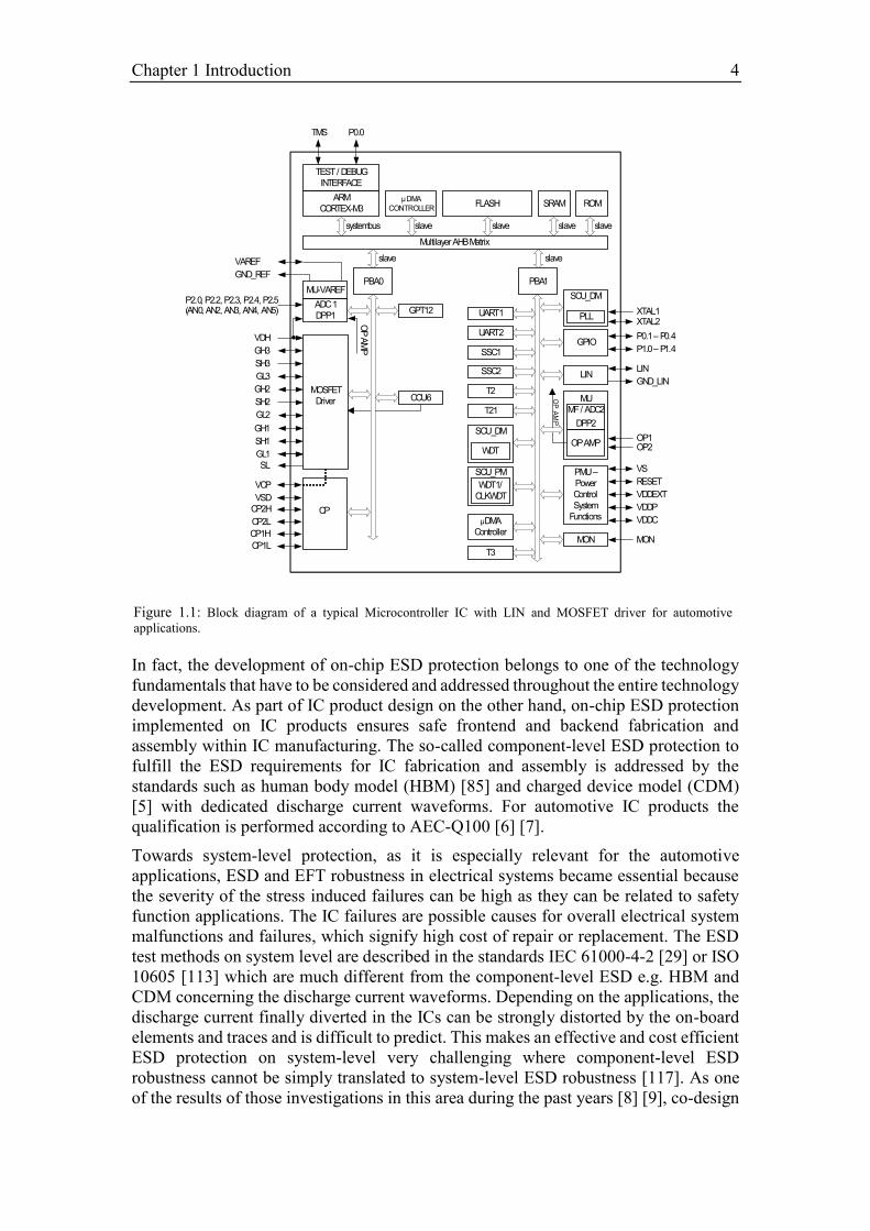
product development. Figure 1.1 illustrates the block diagram of a typical
microcontroller IC with integrated LIN transceiver and MOSFET driver for automotive
applications. Besides the high integration, high quality and robustness is a critical
prerequisite for competitive automotive IC products, especially as functional safety
(ISO 26262) [3] has gained nowadays crucial importance in the automotive industry.
In light of robust design of automotive IC products, the protection of ICs from damages
or functional upset caused by electrostatic discharge (ESD) or other electrical fast
transients (EFT) [4] has become one of the important and challenging tasks during the
IC and system development. ESD is the transient discharge of static charge, which can
arise from human handling or contact with machines. The high voltages result in large
electric fields and high current densities in the small devices, which can lead to
breakdown of insulators and thermal damage in the IC [52].
The ESD challenges have become more apparent by the high complexity of the IC
product features and the used smart power technologies. The increasingly higher
complexity of integrated function blocks on IC products is driven by the required
feature set and cost position demanded by automotive suppliers and car manufactures.
Chapter 1 Introduction 4
In fact, the development of on-chip ESD protection belongs to one of the technology
fundamentals that have to be considered and addressed throughout the entire technology
development. As part of IC product design on the other hand, on-chip ESD protection
implemented on IC products ensures safe frontend and backend fabrication and
assembly within IC manufacturing. The so-called component-level ESD protection to
fulfill the ESD requirements for IC fabrication and assembly is addressed by the
standards such as human body model (HBM) [85] and charged device model (CDM)
[5] with dedicated discharge current waveforms. For automotive IC products the
qualification is performed according to AEC-Q100 [6] [7].
Towards system-level protection, as it is especially relevant for the automotive
applications, ESD and EFT robustness in electrical systems became essential because
the severity of the stress induced failures can be high as they can be related to safety
function applications. The IC failures are possible causes for overall electrical system
malfunctions and failures, which signify high cost of repair or replacement. The ESD
test methods on system level are described in the standards IEC 61000-4-2 [29] or ISO
10605 [113] which are much different from the component-level ESD e.g. HBM and
CDM concerning the discharge current waveforms. Depending on the applications, the
discharge current finally diverted in the ICs can be strongly distorted by the on-board
elements and traces and is difficult to predict. This makes an effective and cost efficient
ESD protection on system-level very challenging where component-level ESD
robustness cannot be simply translated to system-level ESD robustness [117]. As one
of the results of those investigations in this area during the past years [8] [9], co-design
Figure 1.1: Block diagram of a typical Microcontroller IC with LIN and MOSFET driver for automotive
applications.
Chapter 1 Introduction 5
of on-chip and off-chip ESD protection published as “system-efficient ESD design”
(SEED) approach [10] provides a concept to enable system optimized ESD solution. An
effective and efficient ESD protection solution on system-level therefore requires deep
understanding of on-chip and off-chip ESD protection elements in terms of their
behaviors under various ESD stress conditions. Moreover, it requires strong technical
knowledge about the interaction between on-chip and off-chip protection elements.
Traditional on-chip ESD protection for IC focuses more on ESD device concept and
device parameter engineering for component-level ESD protection [50]. However, a
comprehensive ESD development approach with an overview of broad technical
relevance, not only for component-level but also for system-level protection has still
not been systematically studied and evaluated for automotive power technologies. The
scope of this work is hence to provide the insight of several key components of ESD
development with respect to high-voltage domains in smart power technologies. The
high-voltage applications in the context of this work aim at voltage classes typically
ranging from 10 V to 100 V whereas the advanced CMOS technologies focusing on
computing applications with 3.3 V as already an ultra-high voltage. On the other hand,
250 V for power discrete technologies can be considered as a low voltage for example
MOSFETs for the power supply switching applications.
Development of high-voltage ESD protection elements to fulfill both component-level
and system-level ESD encounters several major challenges. It is well known that the IC
hardware failures and their failure mechanisms caused by ESD or EFT events strongly
depend on the electrical signature of inrush pulses. The miscorrelation of system-level
and component-level ESD robustness has much to do with the different parameters like
rise-time, pulse duration, peak voltage and current, power and energy etc. [11]. In order
to uncover device characteristics and the influences of different stress conditions on the
devices under test, advanced measurement techniques are prerequisites that must be
well reproducible and precisely capture the devices’ behaviors. Commonly used
transmission line pulse [18] system requires an upgrade to provide definable rise-times,
source impedance and dedicated pulse shapes to enable advanced device
characterizations especially on wafer-level measurements. The developed test methods
in this work can find their applications at each ESD development stage.
The state-of-the-art high-voltage on-chip and off-chip device portfolios need to be
evaluated and benchmarked from many relevant aspects such as ESD performance and
footprint area associated with chip cost, responding time and triggering mechanisms
associated with protection effectiveness as well as application ranges concerning pulse
durations. Only if the advantages and disadvantages of each type of ESD protection
elements are well understood, a good trade-off can be made for optimized protection
scheme consisting co-design of on-chip and off-chip ESD protections that fulfills the
requirements. Beyond the ESD requirements, ESD protection must be successfully
implemented without affecting circuit functions is usually a challenging task. On the
contrary, functional devices such as DMOS transistors for driver applications can
inherently conduct ESD current that provides new opportunities for ESD device
development [55]. Hence new protection device concepts are often necessary to ensure
overall a good ESD design kit. In this work, design details of novel high-voltage on-
chip ESD protection elements are introduced and discussed.
Although the IC hard failures are mainly dielectric rupture or thermal runaway of
semiconductor as results, the fail mechanisms are rather manifold. Overvoltage and
overcurrent across and through the devices and structures depending on their amplitude
Chapter 1 Introduction 6
and duration can result in physical damage in different severity [12]. The damage can
occur in any devices and structures exposed directly or indirectly to the disturbances.
Dielectric breakdown mainly gate-oxide breakdown during ESD regarding time-
dependent dielectric breakdown (TDDB) has been extensively revealed in publications
e.g. [13]. On the other hand junction burnout including uniformed and non-uniformed
overheating of semiconductor devices under high current injection are investigated e.g.
in [14]. However for automotive power technologies, the failures modes which involve
interaction of protection and protected devices beyond the classical failure mechanisms
were not yet intensively investigated. Undiscovered failure modes should be anticipated
and considered during the ESD development and design. This work shows a detailed
investigation on a unique failure mode of ESD protection concept and respective
solutions.
As IC behaviors under system-level ESD stress conditions are essential, sophisticated
IC models that are useful for system-level ESD simulation and verification are
generally desired by system engineers [15]. The advanced modeling methodology
enables precise simulation that gives guidance of choosing adequate ESD solutions for
system applications. Compact modeling is often used for chip-level ESD simulation
and design [16]. In recent years, several compact modeling and mixed-mode simulation
approaches were introduced also for system-level ESD design [17]. As the failure levels
as well as the I-V characteristics of on-chip ESD protection elements can differ
significantly depending on the stress condition at IC pins on system level, it is believed
the behavior modeling approach introduced in this work offers easy-to-implement
simulation models which can precisely predict overall ESD robustness of a system for
a fairly wide application range of ESD and EFT stresses.
This work is structured as follows: Chapter 2 describes the used ESD testing techniques:
the rise-time filters designed for a TLP measurement system provide the possibility to
study in detail the turn-on time of different ESD protection elements. The so-called
human metal model (HMM) measurement system emulates ESD pulse of an IEC
61000-4-2 ESD generator that is used for device characterization both on wafer and
package-level. In Chapter 3, different on-chip ESD protection elements are studied in
terms of their protection levels and failure mechanisms. The high-voltage active clamps
were further optimized with advanced circuit design techniques achieving good balance
between size, ESD performance and effects on functional circuitry. The
characterization of ESD elements is then extended to off-chip elements discussed in
Chapter 4. The combined effectiveness of on-chip and off-chip elements is investigated
and understood by the advanced ESD modeling methodology which reproduces ESD
devices behavior depending on the energy level and time duration of in-rush pulses.
Chapter 2 ESD Testing Techniques 7
Chapter 2
ESD Testing Techniques
Well-developed testing techniques are essential for ESD investigations. Precise and
reliable test equipment can be used to verify ESD performance of studied structures,
diagnose ESD related problems and characterize devices features. Transmission line
pulse (TLP) systems count as one of the most powerful test equipment, which is
necessary for ESD problem shooting, verification and characterization of ESD concepts
and devices throughout the work. A fully functional TLP system provides electrical
pulses with definable rise-time and pulse duration. The pulse duration can be simply
adjusted with the length of the charge cable. The setup of the rise-time requires the
filtering techniques in high voltage and high current environment. This chapter provides
the design and the implementation of a set of rise-time filters, which belong to the major
hardware components in TLP system. Further, by modifying the hardware of the TLP
system, a so-called human metal model (HMM) tester both for wafer- and package level
measurements is developed enabling a new characterization method. It delivers system-
level ESD (also called IEC) like pulses into device under test (DUT). The HMM tester
enables easy and reliable characterization of ESD protection devices and circuits
compared to the traditional system-level ESD tests using a system-level ESD generator
according to ISO 10605. The results from the HMM tests and the system-level ESD
tests are comparable. The HMM tests provide much better measurement quality of the
transient voltage waveforms.
2.1 Rise-Time Filters of a TLP System
The integrated circuit (IC) industry has been using TLP testing equipment based on the
theory introduced by Maloney and Khurana [18] to characterize on-chip and off-chip
ESD protection structures and ESD protected circuits since 1985.
The most common ESD failures in ICs such as thermal runaway of metal
interconnections, junction burnout, dielectric ruptures in the ESD protection devices
and protected circuits depend heavily on the pulse energy. Thus their robustness and
especially the robustness of those thermally limited devices and circuits can be
characterized by setting the TLP pulse width and TLP current according to the Wunsch
Bell theory [19]. However, as many ESD failures are not induced by pulse energy but
Chapter 2 ESD Testing Techniques 8
rather by a high electric field such as voltage overshoots when ESD protections cannot
react sufficiently fast to the transient pulses, various TLP rise-times become very
important for the characterization and verification of the ESD hardness of DUTs.
Therefore, it is desired to design a set of rise-time filters [20] for the high power and
high frequency applications to achieve well-established TLP characterization in the
measurement setup.
Time domain systems often contain significant energy beyond the relation of the
bandwidth to the rise-time: 𝑡𝑟 = 0.35 𝑓𝐵𝑊⁄ [21]. 𝑓𝐵𝑊 denotes the bandwidth. Pulse
shaping by dimensioning the rise-time and bandwidth can be accomplished by simply
low pass filtering the output signal. Classical frequency domain filters such as
Butterworth and Chebyshev filters have inherently poor group delay characteristics that
cause jitter in the time domain by delaying parts of the high frequency data with respect
to low frequency.. Furthermore, a mismatched filter can result in multiple reflections in
the TLP system that can also deteriorate the pulse shape to unacceptable form. For the
purpose of building a qualified TLP system, the rise-time filters should have near
Gaussian roll-off characteristics, which is absorptive as wideband as possible both in
the pass- and stopband to meet the requirements. Since high voltage or current may
damage the components in the filters during the TLP testing, robust components should
be selected in the filter design.
A theoretical derivation and a simplified approach of such filters were published in [22]
and [23], respectively. The rise-time filters described in this section have the same
topology as in [23] but are based on completely different power levels. The rise-time
filters consist of the passive components RLC in an appropriate order to fulfill the
special demand of very fast TLP (vf-TLP) applications. In addition, a more precise
approximation of derivation and a more practical design flow using the lumped-element
approach and the microstrip approach are shown.
2.1.1 Rise-Time Filters Design
From the numerical derivations [22], the lossy transmission line represents a broadband
(all-pass) attenuator, with a frequency-invariant attenuation. Hence, based on the model
of a lossy transmission line, lumped-element ladder-network can be considered as the
fundamental structure of the rise-time filters. As approximation of the incomplete
Gaussian transmission line, the topology of lumped-element filters is used for the rise-
time filter design. Symmetrically, the filter shows absorption rather than reflection at
both ports and in both pass- and stopband.
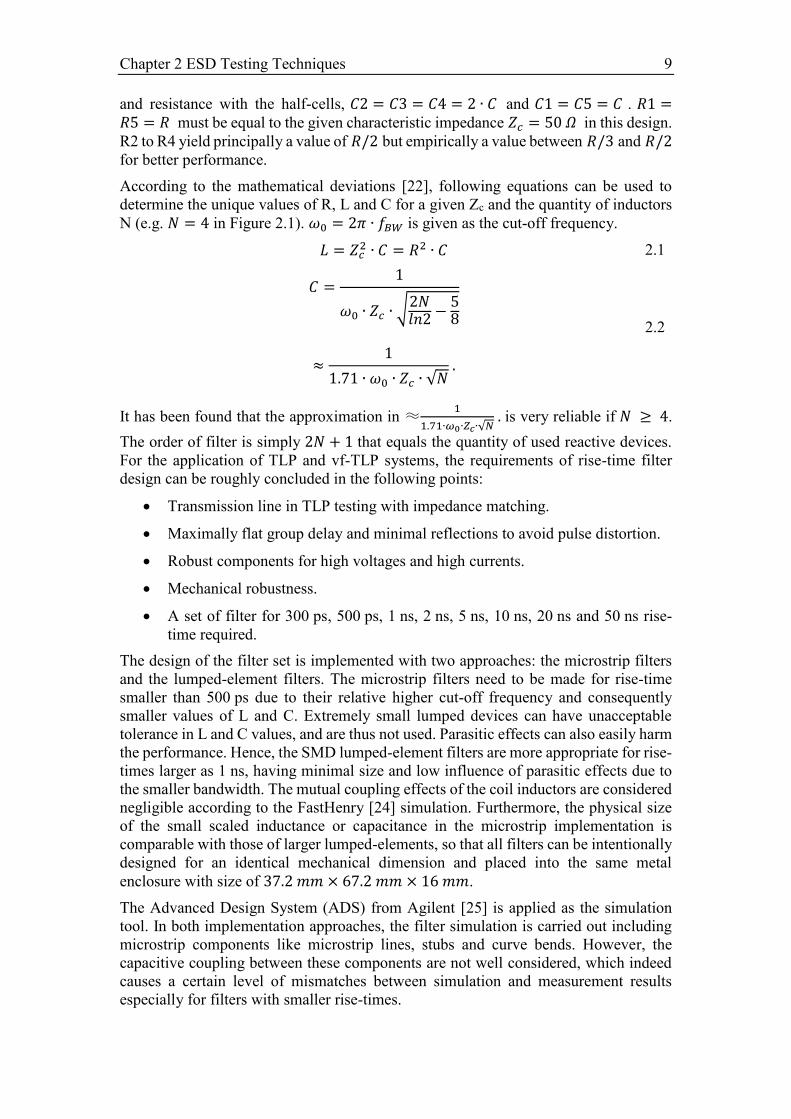
Figure 2.1 shows the topology of a 9th-order rise-time filter. The inductance values are
identical as 𝐿1 = 𝐿2 = 𝐿3 = 𝐿4 = 2 ∙ 𝐿. Due to superposition of parallel capacitance
Figure 2.1: Topology of a 9th-order rise-time filter.
50PulseInp ut
R1
C1 C2 C3 C4 C5
R2 R3 R4 R550PulseOutpu t
Chapter 2 ESD Testing Techniques 9
and resistance with the half-cells, 𝐶2 = 𝐶3 = 𝐶4 = 2 ∙ 𝐶 and 𝐶1 = 𝐶5 = 𝐶 . 𝑅1 =𝑅5 = 𝑅 must be equal to the given characteristic impedance 𝑍𝑐 = 50 𝛺 in this design.
R2 to R4 yield principally a value of 𝑅/2 but empirically a value between 𝑅/3 and 𝑅/2
for better performance.
According to the mathematical deviations [22], following equations can be used to
determine the unique values of R, L and C for a given Zc and the quantity of inductors
N (e.g. 𝑁 = 4 in Figure 2.1). 𝜔0 = 2𝜋 ∙ 𝑓𝐵𝑊 is given as the cut-off frequency.
𝐿 = 𝑍𝑐2 ∙ 𝐶 = 𝑅2 ∙ 𝐶 2.1
𝐶 =1
𝜔0 ∙ 𝑍𝑐 ∙ √2𝑁𝑙𝑛2
−58
≈1
1.71 ∙ 𝜔0 ∙ 𝑍𝑐 ∙ √𝑁 .
2.2
It has been found that the approximation in ≈1
1.71∙𝜔0∙𝑍𝑐∙√𝑁 . is very reliable if 𝑁 ≥ 4.
The order of filter is simply 2𝑁 + 1 that equals the quantity of used reactive devices.
For the application of TLP and vf-TLP systems, the requirements of rise-time filter
design can be roughly concluded in the following points:
Transmission line in TLP testing with impedance matching.
Maximally flat group delay and minimal reflections to avoid pulse distortion.
Robust components for high voltages and high currents.
Mechanical robustness.
A set of filter for 300 ps, 500 ps, 1 ns, 2 ns, 5 ns, 10 ns, 20 ns and 50 ns rise-
time required.
The design of the filter set is implemented with two approaches: the microstrip filters
and the lumped-element filters. The microstrip filters need to be made for rise-time
smaller than 500 ps due to their relative higher cut-off frequency and consequently
smaller values of L and C. Extremely small lumped devices can have unacceptable
tolerance in L and C values, and are thus not used. Parasitic effects can also easily harm
the performance. Hence, the SMD lumped-element filters are more appropriate for rise-
times larger as 1 ns, having minimal size and low influence of parasitic effects due to
the smaller bandwidth. The mutual coupling effects of the coil inductors are considered
negligible according to the FastHenry [24] simulation. Furthermore, the physical size
of the small scaled inductance or capacitance in the microstrip implementation is
comparable with those of larger lumped-elements, so that all filters can be intentionally
designed for an identical mechanical dimension and placed into the same metal
enclosure with size of 37.2 𝑚𝑚 × 67.2 𝑚𝑚 × 16 𝑚𝑚.
The Advanced Design System (ADS) from Agilent [25] is applied as the simulation
tool. In both implementation approaches, the filter simulation is carried out including
microstrip components like microstrip lines, stubs and curve bends. However, the
capacitive coupling between these components are not well considered, which indeed
causes a certain level of mismatches between simulation and measurement results
especially for filters with smaller rise-times.
Chapter 2 ESD Testing Techniques 10
All printed circuit board (PCB) layouts are designed using PADS Designer by Mentor
Graphics [26]. A 50 ns lumped-element filter and a 500 ps microstrip filter from the
series of the designed TLP rise-time filters are concretely described as examples.
2.1.2 Filter Implementation and Measurement Results
Rather than each specified rise-time of the filters, the main difference of the filter design
comes from two types of the implementation concepts: the lumped-element filters and
the microstrip filters. Thus for each type of the filters, one example is elaborately
introduced to present the design procedures and the evaluation of the measured results.
The optimized parameter settings of the other filters are also summarized.
2.1.2.1 50 ns Lumped-Element Filter
In general, using a high-order near-Gaussian low pass filter can improve the
performance by lowering the reflection in the stopband. Limited by the physical size of
the filters, a 9th order (𝑁 = 4) structure drawn in Figure 2.1is a good compromise to
fulfill the design requirements. Starting from 𝑡𝑟 = 50 𝑛𝑠, ω0 is simply 7 MHz. With the
given characteristic impedance Zc=50 Ω, the total values of the RLC can be readily
calculated using 2.1 and 2.2 as 50 Ω, 334 nH and 134 pF, respectively.
The coil inductor produced by Coilcraft [27] 132_20SM has the inductance of 538 nH
that is comparable with 2∙L in this filter design. Rather than 25 Ω, R2 to R4 is designed
between 18 Ω and 22 Ω to achieve better group delay performance. In addition, the S-
parameter models of the inductors are used in parameter sweep simulations in order to
determine the value of R and C for the optimal performance.
A prototype of the filter is developed on the PCB material ROGERS 4003C. The
substrate has a relative permittivity εr of 3.38 and a thickness of 1.524 mm. The
microstrip interconnections are included in the filter simulation as well. High Q and
high voltage multilayer capacitors are chosen in order to ensure the ruggedness of
components during TLP testing. The ATC [28] capacitor 100C131JW2500X 130 pF is
used as C1, C5. 100C271JW2500X with the value of 270 pF is applied as C2, C3 and
C4. All of the capacitors can work perfectly up to 2500 V DC that is sufficiently robust
for the filter stressed by high voltage pulses with very short pulse width. Instead of high
power resistors, high frequency specified metal layer resistors with small parasitic
inductance are desired for the filter design. SMD resistors, type Yageo RC1206 with
51 Ω, 0.25 W are used for R1 and R5. Also, R2, R3 and R4 are implemented with 20 Ω.
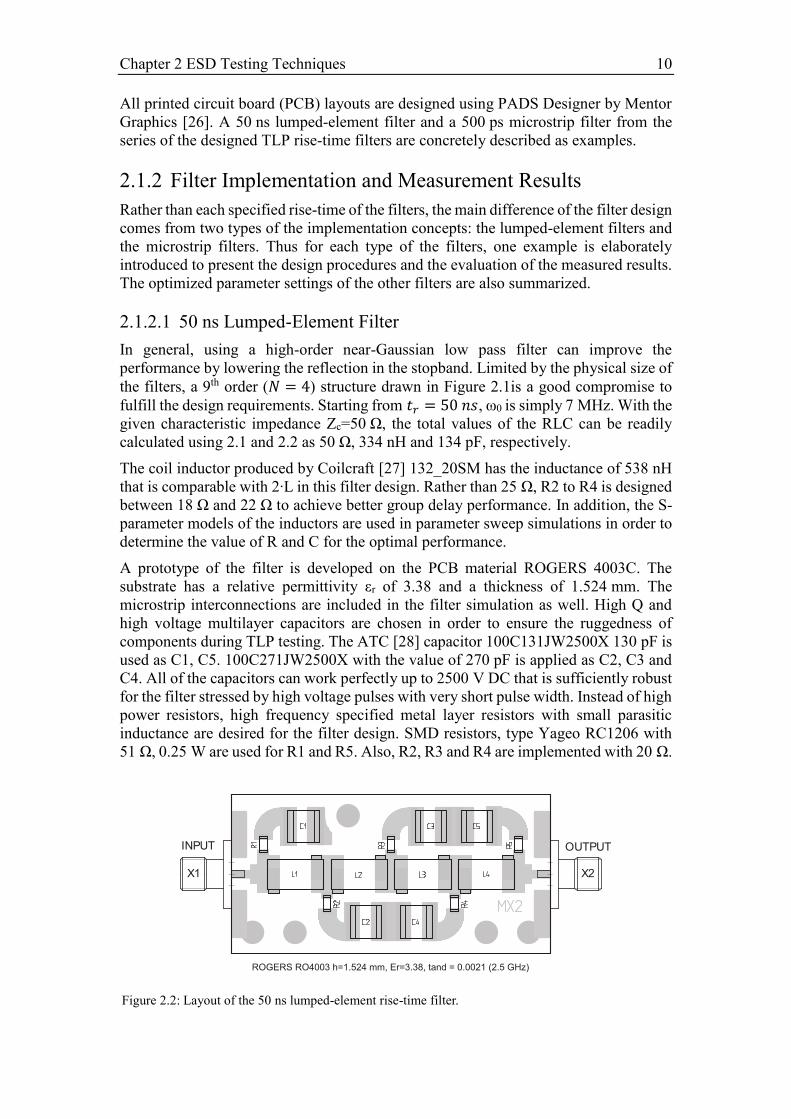
Figure 2.2: Layout of the 50 ns lumped-element rise-time filter.
INPUT
X1 X2
OUTPUT
Chapter 2 ESD Testing Techniques 11
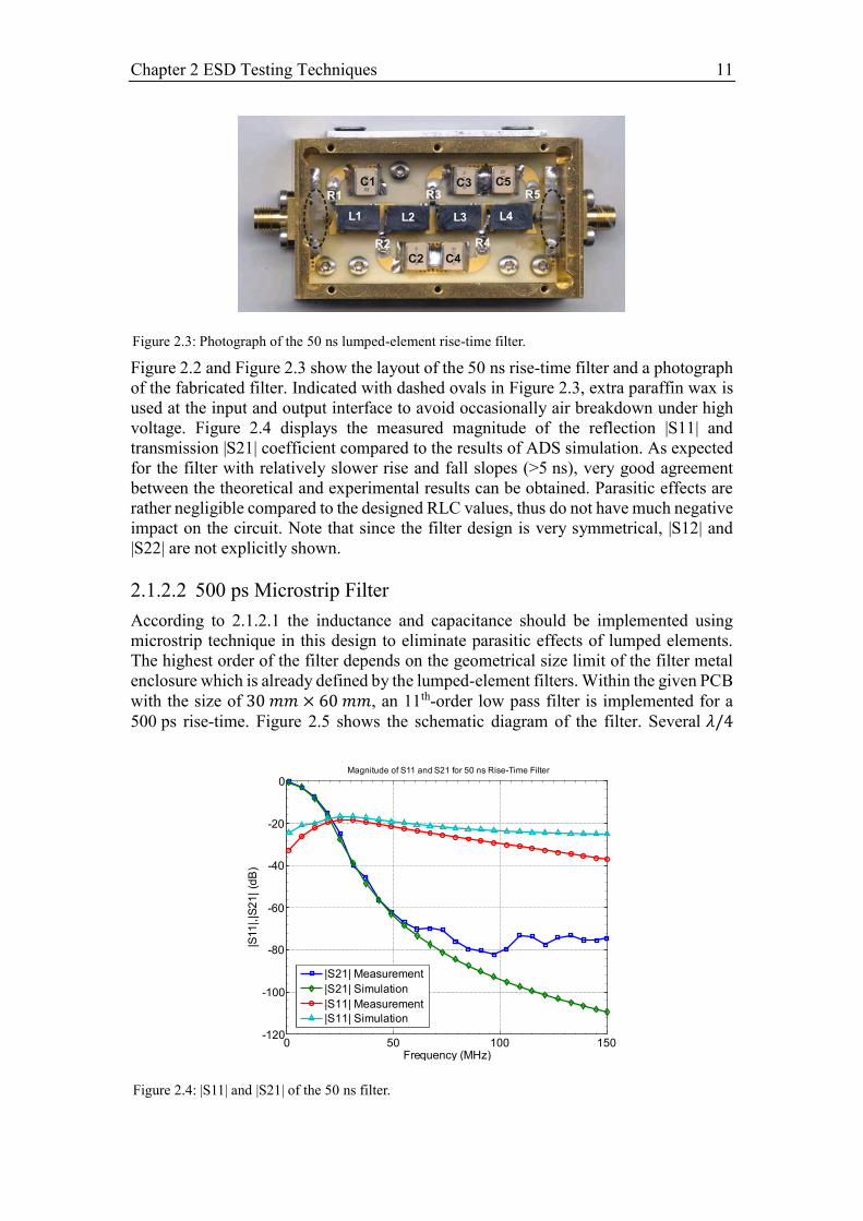
Figure 2.2 and Figure 2.3 show the layout of the 50 ns rise-time filter and a photograph
of the fabricated filter. Indicated with dashed ovals in Figure 2.3, extra paraffin wax is
used at the input and output interface to avoid occasionally air breakdown under high
voltage. Figure 2.4 displays the measured magnitude of the reflection |S11| and
transmission |S21| coefficient compared to the results of ADS simulation. As expected
for the filter with relatively slower rise and fall slopes (>5 ns), very good agreement
between the theoretical and experimental results can be obtained. Parasitic effects are
rather negligible compared to the designed RLC values, thus do not have much negative
impact on the circuit. Note that since the filter design is very symmetrical, |S12| and
|S22| are not explicitly shown.
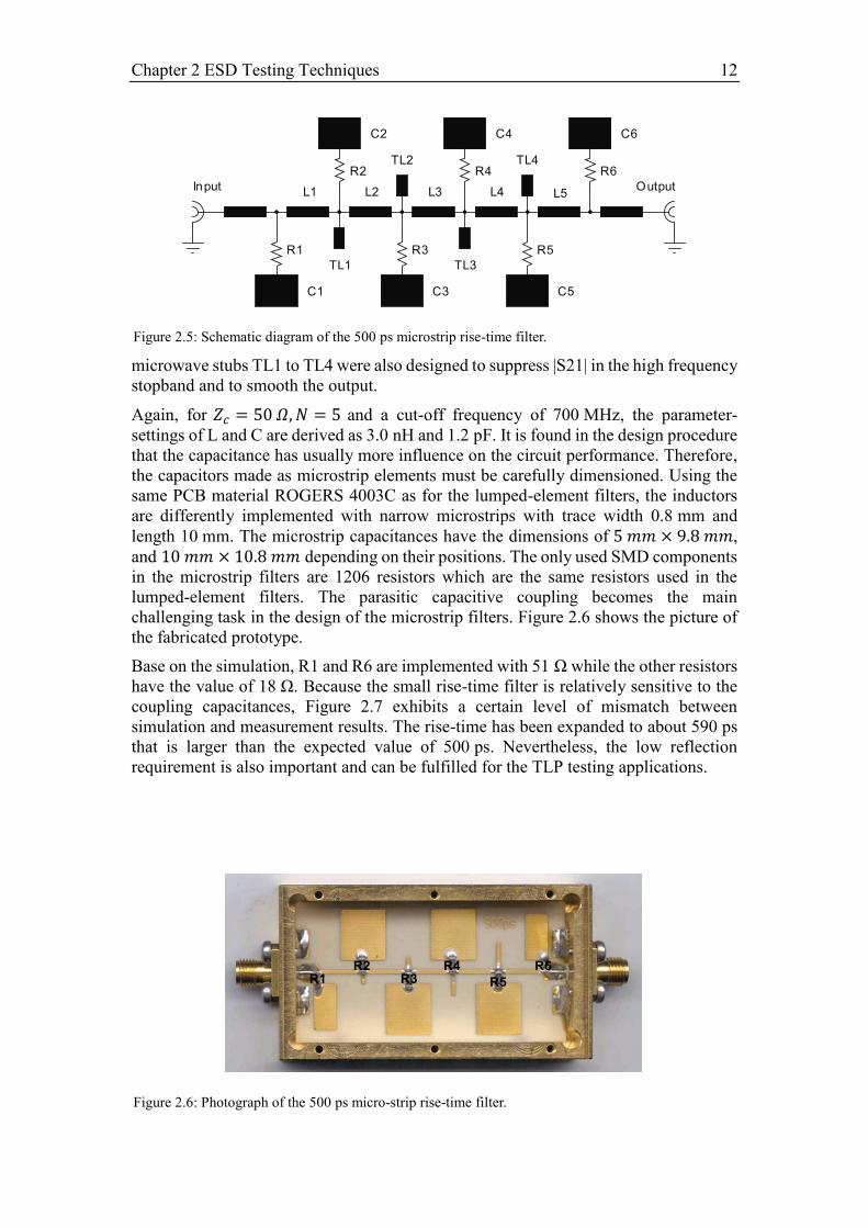
2.1.2.2 500 ps Microstrip Filter
According to 2.1.2.1 the inductance and capacitance should be implemented using
microstrip technique in this design to eliminate parasitic effects of lumped elements.
The highest order of the filter depends on the geometrical size limit of the filter metal
enclosure which is already defined by the lumped-element filters. Within the given PCB
with the size of 30 𝑚𝑚 × 60 𝑚𝑚, an 11th-order low pass filter is implemented for a
500 ps rise-time. Figure 2.5 shows the schematic diagram of the filter. Several 𝜆/4
Figure 2.4: |S11| and |S21| of the 50 ns filter.
0 50 100 150-120
-100
-80
-60
-40
-20
0
Frequency (MHz)
|S11
|,|S
21
| (d
B)
Magnitude of S11 and S21 for 50 ns Rise-Time Filter
|S21| Measurement
|S21| Simulation
|S11| Measurement
|S11| Simulation
Figure 2.3: Photograph of the 50 ns lumped-element rise-time filter.
C1
L1 L2 L3 L4
C2 C4
C3 C5R1
R2
R3
R4
R5
Chapter 2 ESD Testing Techniques 12
microwave stubs TL1 to TL4 were also designed to suppress |S21| in the high frequency
stopband and to smooth the output.
Again, for 𝑍𝑐 = 50 𝛺, 𝑁 = 5 and a cut-off frequency of 700 MHz, the parameter-
settings of L and C are derived as 3.0 nH and 1.2 pF. It is found in the design procedure
that the capacitance has usually more influence on the circuit performance. Therefore,
the capacitors made as microstrip elements must be carefully dimensioned. Using the
same PCB material ROGERS 4003C as for the lumped-element filters, the inductors
are differently implemented with narrow microstrips with trace width 0.8 mm and
length 10 mm. The microstrip capacitances have the dimensions of 5 𝑚𝑚 × 9.8 𝑚𝑚,
and 10 𝑚𝑚 × 10.8 𝑚𝑚 depending on their positions. The only used SMD components
in the microstrip filters are 1206 resistors which are the same resistors used in the
lumped-element filters. The parasitic capacitive coupling becomes the main
challenging task in the design of the microstrip filters. Figure 2.6 shows the picture of
the fabricated prototype.
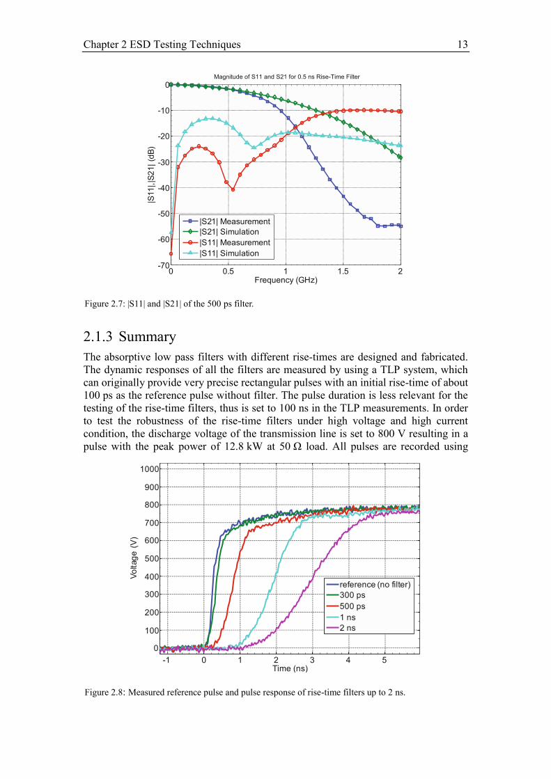
Base on the simulation, R1 and R6 are implemented with 51 Ω while the other resistors
have the value of 18 Ω. Because the small rise-time filter is relatively sensitive to the
coupling capacitances, Figure 2.7 exhibits a certain level of mismatch between
simulation and measurement results. The rise-time has been expanded to about 590 ps
that is larger than the expected value of 500 ps. Nevertheless, the low reflection
requirement is also important and can be fulfilled for the TLP testing applications.
Figure 2.5: Schematic diagram of the 500 ps microstrip rise-time filter.
R1
R2 R4 R6
R3 R5
C2 C4 C6
C1 C3 C5
tuptuOtupnI
TL1
TL2
TL3
TL4
L1 L2 L3 L5L4
Figure 2.6: Photograph of the 500 ps micro-strip rise-time filter.
R1R2
R3R4
R5
R6
Chapter 2 ESD Testing Techniques 13
2.1.3 Summary
The absorptive low pass filters with different rise-times are designed and fabricated.
The dynamic responses of all the filters are measured by using a TLP system, which
can originally provide very precise rectangular pulses with an initial rise-time of about
100 ps as the reference pulse without filter. The pulse duration is less relevant for the
testing of the rise-time filters, thus is set to 100 ns in the TLP measurements. In order
to test the robustness of the rise-time filters under high voltage and high current
condition, the discharge voltage of the transmission line is set to 800 V resulting in a
pulse with the peak power of 12.8 kW at 50 Ω load. All pulses are recorded using
Figure 2.8: Measured reference pulse and pulse response of rise-time filters up to 2 ns.
-1 0 1 2 3 4 5
0
100
200
300
400
500
600
700
800
900
1000
Time (ns)
Vo
ltag
e(V
)
reference (no filter)
300 ps
500 ps
1 ns
2 ns
Figure 2.7: |S11| and |S21| of the 500 ps filter.
0 0.5 1 1.5 2-70
-60
-50
-40
-30
-20
-10
0
Frequency (GHz)
|S11
|,|S
21
| (d
B)
|S21| Measurement
|S21| Simulation
|S11| Measurement
|S11| Simulation
Chapter 2 ESD Testing Techniques 14
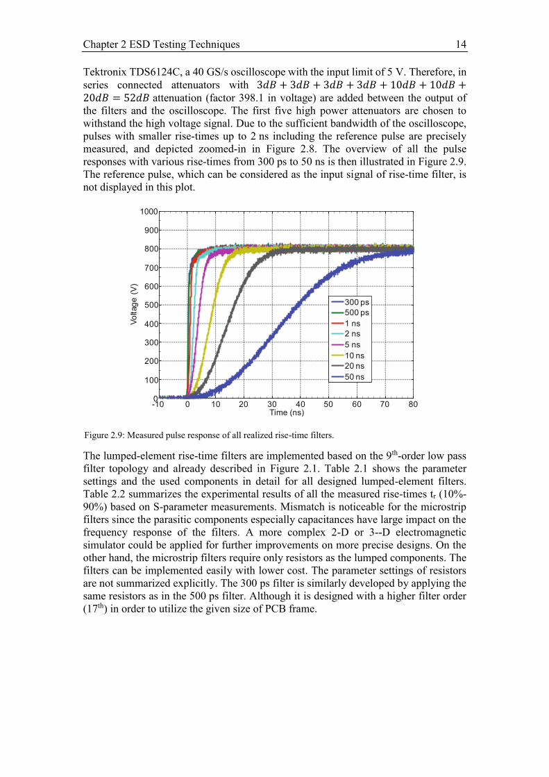
Tektronix TDS6124C, a 40 GS/s oscilloscope with the input limit of 5 V. Therefore, in
series connected attenuators with 3𝑑𝐵 + 3𝑑𝐵 + 3𝑑𝐵 + 3𝑑𝐵 + 10𝑑𝐵 + 10𝑑𝐵 +20𝑑𝐵 = 52𝑑𝐵 attenuation (factor 398.1 in voltage) are added between the output of
the filters and the oscilloscope. The first five high power attenuators are chosen to
withstand the high voltage signal. Due to the sufficient bandwidth of the oscilloscope,
pulses with smaller rise-times up to 2 ns including the reference pulse are precisely
measured, and depicted zoomed-in in Figure 2.8. The overview of all the pulse
responses with various rise-times from 300 ps to 50 ns is then illustrated in Figure 2.9.
The reference pulse, which can be considered as the input signal of rise-time filter, is
not displayed in this plot.
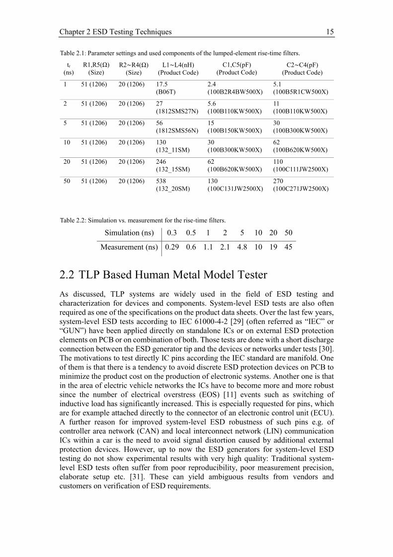
The lumped-element rise-time filters are implemented based on the 9th-order low pass
filter topology and already described in Figure 2.1. Table 2.1 shows the parameter
settings and the used components in detail for all designed lumped-element filters.
Table 2.2 summarizes the experimental results of all the measured rise-times tr (10%-
90%) based on S-parameter measurements. Mismatch is noticeable for the microstrip
filters since the parasitic components especially capacitances have large impact on the
frequency response of the filters. A more complex 2-D or 3--D electromagnetic
simulator could be applied for further improvements on more precise designs. On the
other hand, the microstrip filters require only resistors as the lumped components. The
filters can be implemented easily with lower cost. The parameter settings of resistors
are not summarized explicitly. The 300 ps filter is similarly developed by applying the
same resistors as in the 500 ps filter. Although it is designed with a higher filter order
(17th) in order to utilize the given size of PCB frame.
Figure 2.9: Measured pulse response of all realized rise-time filters.
-10 0 10 20 30 40 50 60 70 800
100
200
300
400
500
600
700
800
900
Time (ns)
Vo
ltag
e(V
)
300 ps
500 ps
1 ns
2 ns
5 ns
10 ns
20 ns
50 ns
Chapter 2 ESD Testing Techniques 15
2.2 TLP Based Human Metal Model Tester
As discussed, TLP systems are widely used in the field of ESD testing and
characterization for devices and components. System-level ESD tests are also often
required as one of the specifications on the product data sheets. Over the last few years,
system-level ESD tests according to IEC 61000-4-2 [29] (often referred as “IEC” or
“GUN”) have been applied directly on standalone ICs or on external ESD protection
elements on PCB or on combination of both. Those tests are done with a short discharge
connection between the ESD generator tip and the devices or networks under tests [30].
The motivations to test directly IC pins according the IEC standard are manifold. One
of them is that there is a tendency to avoid discrete ESD protection devices on PCB to
minimize the product cost on the production of electronic systems. Another one is that
in the area of electric vehicle networks the ICs have to become more and more robust
since the number of electrical overstress (EOS) [11] events such as switching of
inductive load has significantly increased. This is especially requested for pins, which
are for example attached directly to the connector of an electronic control unit (ECU).
A further reason for improved system-level ESD robustness of such pins e.g. of
controller area network (CAN) and local interconnect network (LIN) communication
ICs within a car is the need to avoid signal distortion caused by additional external
protection devices. However, up to now the ESD generators for system-level ESD
testing do not show experimental results with very high quality: Traditional system-
level ESD tests often suffer from poor reproducibility, poor measurement precision,
elaborate setup etc. [31]. These can yield ambiguous results from vendors and
customers on verification of ESD requirements.
Table 2.1: Parameter settings and used components of the lumped-element rise-time filters.
tr
(ns)
R1,R5(Ω)
(Size) R2∼R4(Ω)
(Size)
L1∼L4(nH)
(Product Code)
C1,C5(pF)
(Product Code) C2∼C4(pF)
(Product Code)
1 51 (1206) 20 (1206) 17.5
(B06T)
2.4
(100B2R4BW500X)
5.1
(100B5R1CW500X)
2 51 (1206) 20 (1206) 27
(1812SMS27N)
5.6
(100B110KW500X)
11
(100B110KW500X)
5 51 (1206) 20 (1206) 56
(1812SMS56N)
15
(100B150KW500X)
30
(100B300KW500X)
10 51 (1206) 20 (1206) 130
(132_11SM)
30
(100B300KW500X)
62
(100B620KW500X)
20 51 (1206) 20 (1206) 246
(132_15SM)
62
(100B620KW500X)
110
(100C111JW2500X)
50 51 (1206) 20 (1206) 538
(132_20SM)
130
(100C131JW2500X)
270
(100C271JW2500X)
Table 2.2: Simulation vs. measurement for the rise-time filters.
Simulation (ns) 0.3 0.5 1 2 5 10 20 50
Measurement (ns) 0.29 0.6 1.1 2.1 4.8 10 19 45
Chapter 2 ESD Testing Techniques 16
In order to improve this unsatisfied situation the so-called human metal model (HMM)
evaluation method has been discussed intensively in the standardization committee
SP5.6, ESDA [32]. HMM is a testing method which by definition is directly applied to
IC components. The current stress waveform of HMM is similar to the IEC 61000-4-2
one. Recent publications [33] [34] [35] reported that there is an alternative way to
generate IEC-like pulses by employing coaxial transmission lines, passive networks
and a proper rise-time filter. A wafer-level HMM tester with a non-coaxial approach is
also presented in [36] [37] to compare the impact of HMM and HBM stresses on on-
chip devices.
With all these considerations, a new HMM tester constructed based on TLP with the
coaxial transmission line approach is presented in this work with an accurate
measurement technique for recording voltage and current waveforms both on board-
and on wafer-level [38]. Several measurement setups for measuring transient
waveforms are introduced. Not only to describe the HMM tester, the goal is also to
validate this ESD testing technique for the application of high-voltage ESD
development. In the following sections, various DUTs are stressed both with the IEC
ESD generator and the HMM tester in order to compare the waveforms. Failure levels
regarding thermal and electrical damages of IC pins are determined in the experiments
by IEC and HMM for the comparison. Further, conditions of the usage of the HMM
tester for ESD tests are discussed. The attempt of applying the TLP based HMM
measurement technique on real system-level is also experimentally shown. The
advantages and limitations of the HMM method comparing to the IEC test on
components are given as well.
2.2.1 Measurement Setup of TLP based HMM
2.2.1.1 Pulse Generation of HMM Tester
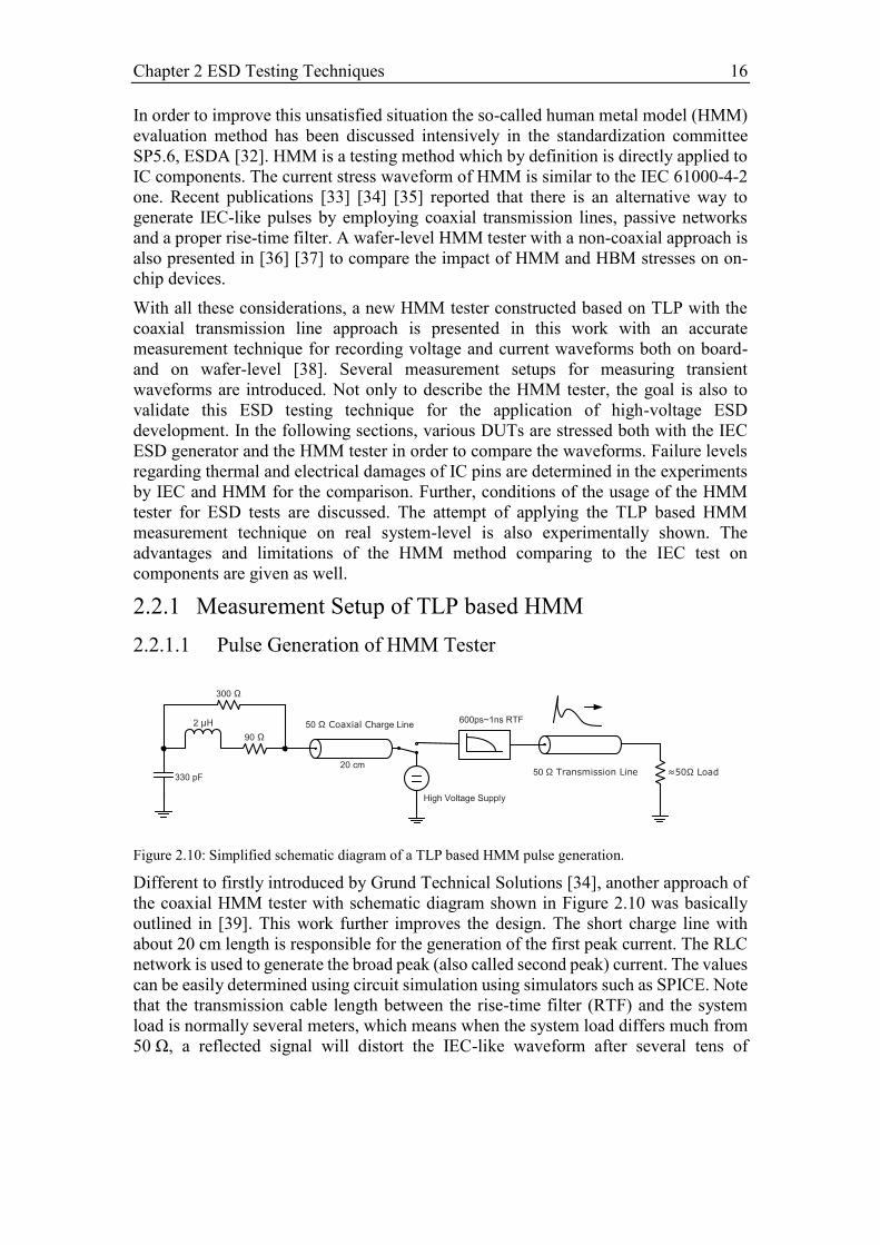
Different to firstly introduced by Grund Technical Solutions [34], another approach of
the coaxial HMM tester with schematic diagram shown in Figure 2.10 was basically
outlined in [39]. This work further improves the design. The short charge line with
about 20 cm length is responsible for the generation of the first peak current. The RLC
network is used to generate the broad peak (also called second peak) current. The values
can be easily determined using circuit simulation using simulators such as SPICE. Note
that the transmission cable length between the rise-time filter (RTF) and the system
load is normally several meters, which means when the system load differs much from
50 Ω, a reflected signal will distort the IEC-like waveform after several tens of
Figure 2.10: Simplified schematic diagram of a TLP based HMM pulse generation.
Chapter 2 ESD Testing Techniques 17
nanoseconds. Thus, to avoid the reflection and deliver an acceptable current waveform
to the DUT, nearly 50 Ω system load must be insured during HMM tests. The maximal
voltage on the 20 cm charge line is limited by the used TLP at 4 kV. This results in a
maximal peak current of 4 𝑘𝑉/2/50 𝛺 = 40 𝐴 corresponding to a discharge voltage
level of about 10 kV IEC pulse (peak current 37.5 A). High power attenuators usually
employed for the TLP pulse generation are completely removed in the HMM
measurement system to obtain highest possible stress levels.
Figure 2.12: Measured current waveforms at 10 kV IEC level using different pulse shaping circuits (a)
and (b) according to Figure 2.11. SPICE Simulation result referring to the schematic in Figure 2.10 is
also shown for comparison.
0 50 100 150−10
0
10
20
30
Cu
rre
nt
(A)
Time (ns)
pulse shaping (a)
pulse shaping (b)
simulation
I60ns
I30ns
Ifirst peak
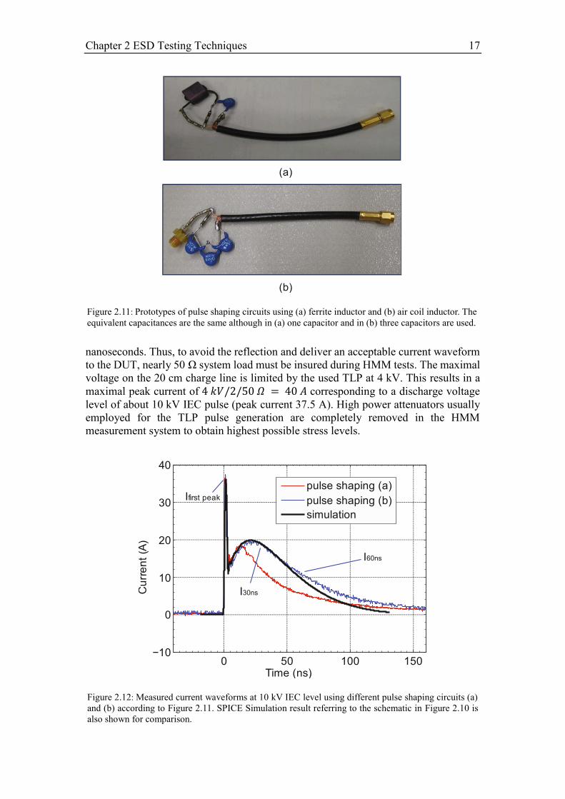
Figure 2.11: Prototypes of pulse shaping circuits using (a) ferrite inductor and (b) air coil inductor. The
equivalent capacitances are the same although in (a) one capacitor and in (b) three capacitors are used.
(a)
(b)
Chapter 2 ESD Testing Techniques 18
The main challenge of the implementation of HMM pulse shaping is in the RLC
network. Only by carefully choosing the passive elements, the current waveforms
delivered by the HMM tester can fit in with the IEC pulses. Figure 2.11 shows two
different implementations of the pulse shaping circuits. Main differences are the types
of inductors: one is ferrite the other is air coil inductor. Figure 2.12 gives the
comparison of the current pulses at 10 kV IEC level delivered using both pulse shaping
circuits. All current waveforms are recorded by a 10 GS/s oscilloscope. The ferrite
inductor experiences saturation effect when the current density is too high. It results in
the distortions in the waveforms, as the pulse shaping circuit cannot give the current
waveforms defined in IEC 61000-4-2 especially at higher current level. The air coil
inductor does not have such problem and the generated HMM pulses are very similar
to the IEC standard. The deviation from measured and simulated results at the end of
the pulse can be caused by the coupling of the parasitic capacitances and inductances.
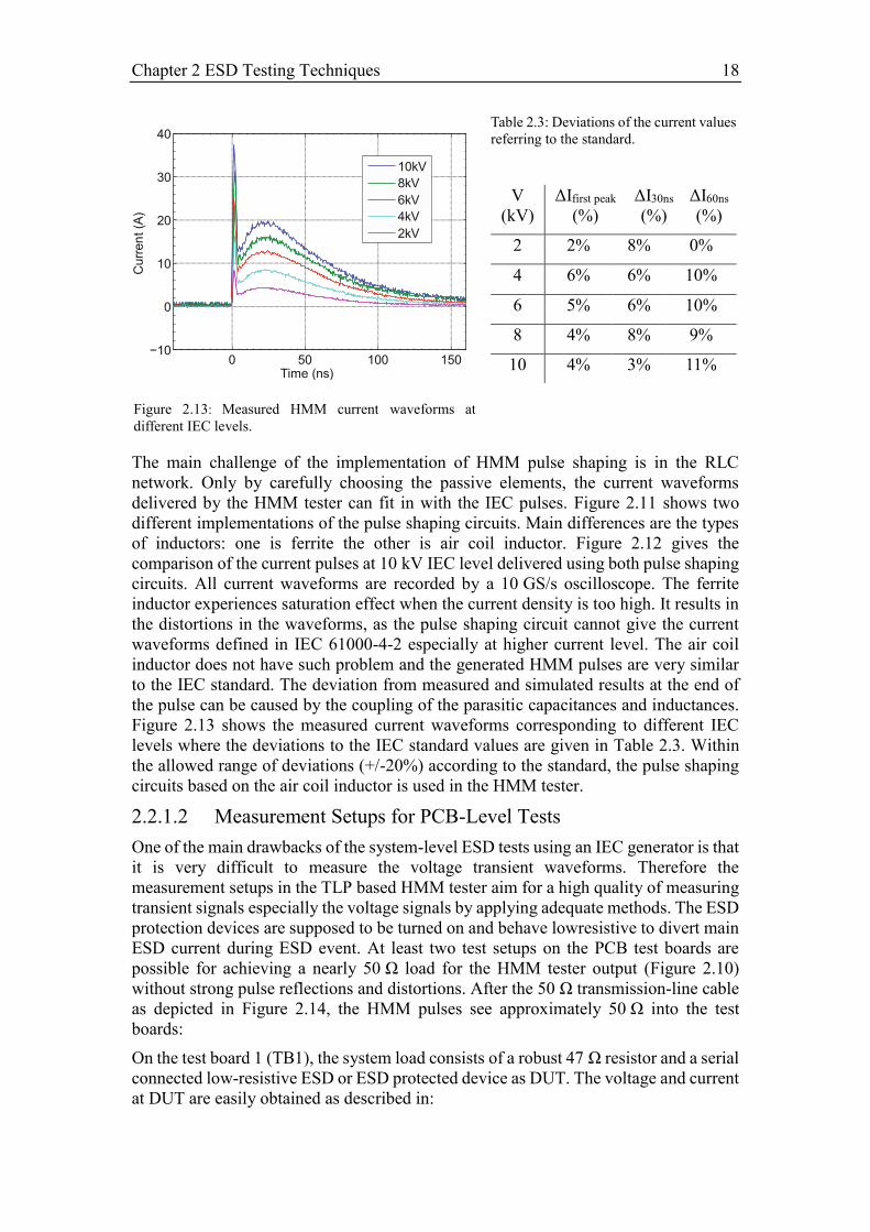
Figure 2.13 shows the measured current waveforms corresponding to different IEC
levels where the deviations to the IEC standard values are given in Table 2.3. Within
the allowed range of deviations (+/-20%) according to the standard, the pulse shaping
circuits based on the air coil inductor is used in the HMM tester.
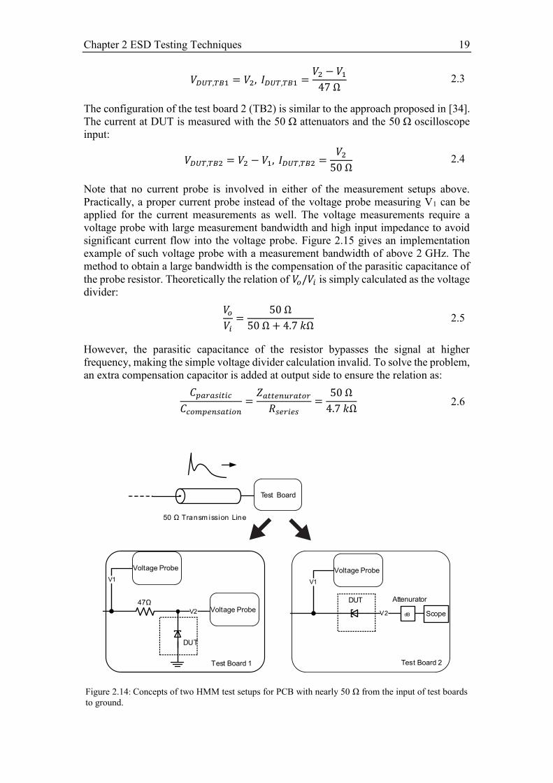
2.2.1.2 Measurement Setups for PCB-Level Tests
One of the main drawbacks of the system-level ESD tests using an IEC generator is that
it is very difficult to measure the voltage transient waveforms. Therefore the
measurement setups in the TLP based HMM tester aim for a high quality of measuring
transient signals especially the voltage signals by applying adequate methods. The ESD
protection devices are supposed to be turned on and behave lowresistive to divert main
ESD current during ESD event. At least two test setups on the PCB test boards are
possible for achieving a nearly 50 Ω load for the HMM tester output (Figure 2.10)
without strong pulse reflections and distortions. After the 50 Ω transmission-line cable
as depicted in Figure 2.14, the HMM pulses see approximately 50 Ω into the test
boards:
On the test board 1 (TB1), the system load consists of a robust 47 Ω resistor and a serial
connected low-resistive ESD or ESD protected device as DUT. The voltage and current
at DUT are easily obtained as described in:
Figure 2.13: Measured HMM current waveforms at
different IEC levels.
Table 2.3: Deviations of the current values
referring to the standard.
V
(kV)
ΔIfirst peak
(%)
ΔI30ns
(%)
ΔI60ns
(%)
2 2% 8% 0%
4 6% 6% 10%
6 5% 6% 10%
8 4% 8% 9%
10 4% 3% 11%
0 50 100 150−10
0
10
20
30
Curr
en
t (A
)
Time (ns)
10kV
8kV
6kV
4kV
2kV
Chapter 2 ESD Testing Techniques 19
𝑉𝐷𝑈𝑇,𝑇𝐵1 = 𝑉2, 𝐼𝐷𝑈𝑇,𝑇𝐵1 =𝑉2 − 𝑉1
47 Ω 2.3
The configuration of the test board 2 (TB2) is similar to the approach proposed in [34].
The current at DUT is measured with the 50 Ω attenuators and the 50 Ω oscilloscope
input:
𝑉𝐷𝑈𝑇,𝑇𝐵2 = 𝑉2 − 𝑉1, 𝐼𝐷𝑈𝑇,𝑇𝐵2 =𝑉2
50 Ω 2.4
Note that no current probe is involved in either of the measurement setups above.
Practically, a proper current probe instead of the voltage probe measuring V1 can be
applied for the current measurements as well. The voltage measurements require a
voltage probe with large measurement bandwidth and high input impedance to avoid
significant current flow into the voltage probe. Figure 2.15 gives an implementation
example of such voltage probe with a measurement bandwidth of above 2 GHz. The
method to obtain a large bandwidth is the compensation of the parasitic capacitance of
the probe resistor. Theoretically the relation of 𝑉𝑜/𝑉𝑖 is simply calculated as the voltage
divider:
𝑉𝑜
𝑉𝑖=
50 Ω
50 Ω + 4.7 𝑘Ω 2.5
However, the parasitic capacitance of the resistor bypasses the signal at higher
frequency, making the simple voltage divider calculation invalid. To solve the problem,
an extra compensation capacitor is added at output side to ensure the relation as:
𝐶𝑝𝑎𝑟𝑎𝑠𝑖𝑡𝑖𝑐
𝐶𝑐𝑜𝑚𝑝𝑒𝑛𝑠𝑎𝑡𝑖𝑜𝑛=
𝑍𝑎𝑡𝑡𝑒𝑛𝑢𝑟𝑎𝑡𝑜𝑟
𝑅𝑠𝑒𝑟𝑖𝑒𝑠=
50 Ω
4.7 𝑘Ω 2.6
Figure 2.14: Concepts of two HMM test setups for PCB with nearly 50 Ω from the input of test boards
to ground.
50 Ω Transm ission Line
Test Board
47Ω
DUT
Voltage Probe
V1
DUT
V1
dBV2V2 Voltage Probe
Voltage Probe
Test Board 1 Test Board 2
Scope
Attenurator
Chapter 2 ESD Testing Techniques 20
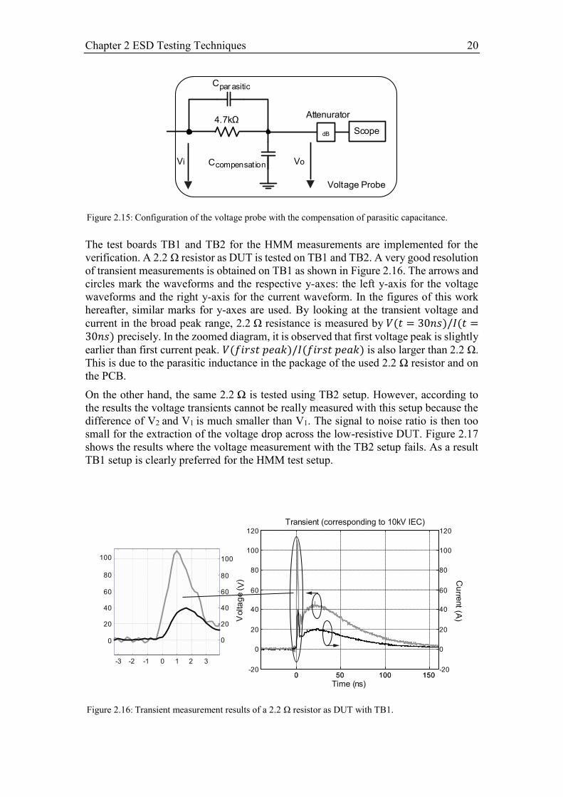
The test boards TB1 and TB2 for the HMM measurements are implemented for the
verification. A 2.2 Ω resistor as DUT is tested on TB1 and TB2. A very good resolution
of transient measurements is obtained on TB1 as shown in Figure 2.16. The arrows and
circles mark the waveforms and the respective y-axes: the left y-axis for the voltage
waveforms and the right y-axis for the current waveform. In the figures of this work
hereafter, similar marks for y-axes are used. By looking at the transient voltage and
current in the broad peak range, 2.2 Ω resistance is measured by 𝑉(𝑡 = 30𝑛𝑠)/𝐼(𝑡 =30𝑛𝑠) precisely. In the zoomed diagram, it is observed that first voltage peak is slightly
earlier than first current peak. 𝑉(𝑓𝑖𝑟𝑠𝑡 𝑝𝑒𝑎𝑘)/𝐼(𝑓𝑖𝑟𝑠𝑡 𝑝𝑒𝑎𝑘) is also larger than 2.2 Ω.
This is due to the parasitic inductance in the package of the used 2.2 Ω resistor and on
the PCB.
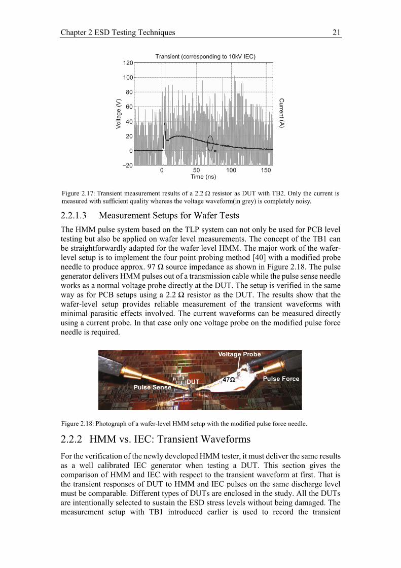
On the other hand, the same 2.2 Ω is tested using TB2 setup. However, according to
the results the voltage transients cannot be really measured with this setup because the
difference of V2 and V1 is much smaller than V1. The signal to noise ratio is then too
small for the extraction of the voltage drop across the low-resistive DUT. Figure 2.17
shows the results where the voltage measurement with the TB2 setup fails. As a result
TB1 setup is clearly preferred for the HMM test setup.
Figure 2.15: Configuration of the voltage probe with the compensation of parasitic capacitance.
Cpar asitic
4.7kΩ
Ccompensat ion
dB Scope
Voltage Probe
Attenurator
Vi Vo
Figure 2.16: Transient measurement results of a 2.2 Ω resistor as DUT with TB1.
0 50 100 150-20
0
20
40
60
80
100
120
Volta
ge
( V)
Time (ns)0 50 100 150
-20
0
20
40
60
80
100
120
rrt (A
)
0
20
40
60
80
100
0
20
40
60
80
100
-3 -2 -1 0 1 2 3
Chapter 2 ESD Testing Techniques 21
2.2.1.3 Measurement Setups for Wafer Tests
The HMM pulse system based on the TLP system can not only be used for PCB level
testing but also be applied on wafer level measurements. The concept of the TB1 can
be straightforwardly adapted for the wafer level HMM. The major work of the wafer-
level setup is to implement the four point probing method [40] with a modified probe
needle to produce approx. 97 Ω source impedance as shown in Figure 2.18. The pulse
generator delivers HMM pulses out of a transmission cable while the pulse sense needle
works as a normal voltage probe directly at the DUT. The setup is verified in the same
way as for PCB setups using a 2.2 Ω resistor as the DUT. The results show that the
wafer-level setup provides reliable measurement of the transient waveforms with
minimal parasitic effects involved. The current waveforms can be measured directly
using a current probe. In that case only one voltage probe on the modified pulse force
needle is required.
2.2.2 HMM vs. IEC: Transient Waveforms
For the verification of the newly developed HMM tester, it must deliver the same results
as a well calibrated IEC generator when testing a DUT. This section gives the
comparison of HMM and IEC with respect to the transient waveform at first. That is
the transient responses of DUT to HMM and IEC pulses on the same discharge level
must be comparable. Different types of DUTs are enclosed in the study. All the DUTs
are intentionally selected to sustain the ESD stress levels without being damaged. The
measurement setup with TB1 introduced earlier is used to record the transient
Figure 2.18: Photograph of a wafer-level HMM setup with the modified pulse force needle.
Pulse SenseDUT
Pulse Force47Ω
Voltage Probe
Figure 2.17: Transient measurement results of a 2.2 Ω resistor as DUT with TB2. Only the current is
measured with sufficient quality whereas the voltage waveform(in grey) is completely noisy.
0 50 100 150−20
0
20
40
60
80
100
120
Vo
ltag
e (
V)
Time (ns)
(A)
Chapter 2 ESD Testing Techniques 22
waveforms during the HMM tests. On the other hand, a current probe and a large ground
plane are employed in the common test setup of the IEC tests.
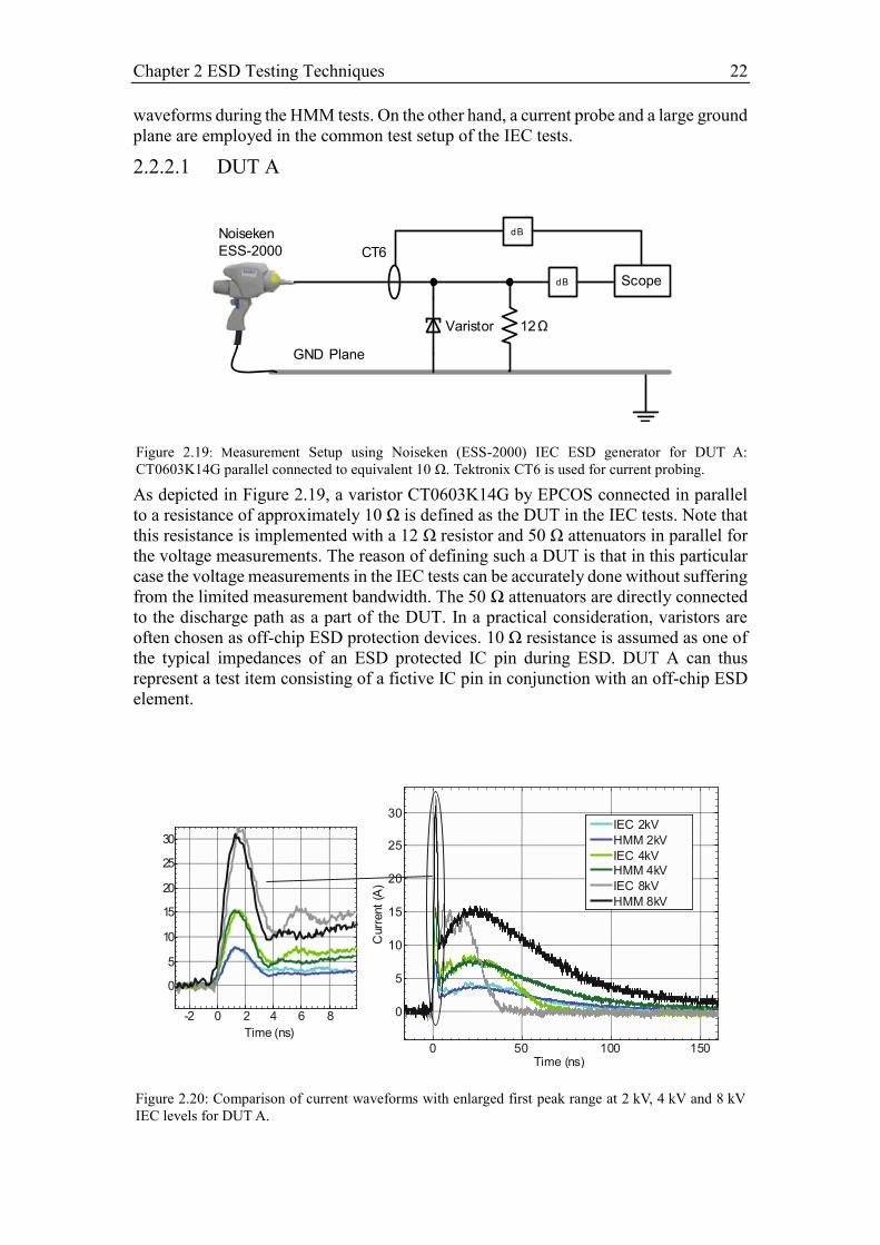
2.2.2.1 DUT A
As depicted in Figure 2.19, a varistor CT0603K14G by EPCOS connected in parallel
to a resistance of approximately 10 Ω is defined as the DUT in the IEC tests. Note that
this resistance is implemented with a 12 Ω resistor and 50 Ω attenuators in parallel for
the voltage measurements. The reason of defining such a DUT is that in this particular
case the voltage measurements in the IEC tests can be accurately done without suffering
from the limited measurement bandwidth. The 50 Ω attenuators are directly connected
to the discharge path as a part of the DUT. In a practical consideration, varistors are
often chosen as off-chip ESD protection devices. 10 Ω resistance is assumed as one of
the typical impedances of an ESD protected IC pin during ESD. DUT A can thus
represent a test item consisting of a fictive IC pin in conjunction with an off-chip ESD
element.
Figure 2.20: Comparison of current waveforms with enlarged first peak range at 2 kV, 4 kV and 8 kV
IEC levels for DUT A.
-2 0 2 4 6 8
0
5
10
15
20
25
30
0 50 100 150
0
5
10
15
20
25
30
Time (ns)
Curr
ent
(A)
IEC 2kV
HMM 2kV
IEC 4kVHMM 4kV
IEC 8kV
HMM 8kV
Time (ns)
Figure 2.19: Measurement Setup using Noiseken (ESS-2000) IEC ESD generator for DUT A:
CT0603K14G parallel connected to equivalent 10 Ω. Tektronix CT6 is used for current probing.
Varistor 12Ω
dB Scope
CT6
dB
GND Plane
Noiseken
ESS-2000
Chapter 2 ESD Testing Techniques 23
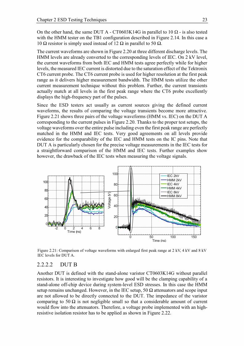
On the other hand, the same DUT A - CT0603K14G in parallel to 10 Ω - is also tested
with the HMM tester on the TB1 configuration described in Figure 2.14. In this case a
10 Ω resistor is simply used instead of 12 Ω in parallel to 50 Ω.
The current waveforms are shown in Figure 2.20 at three different discharge levels. The
HMM levels are already converted to the corresponding levels of IEC. On 2 kV level,
the current waveforms from both IEC and HMM tests agree perfectly while for higher
levels, the measured IEC current is distorted due to the saturation effect of the Tektronix
CT6 current probe. The CT6 current probe is used for higher resolution at the first peak
range as it delivers higher measurement bandwidth. The HMM tests utilize the other
current measurement technique without this problem. Further, the current transients
actually match at all levels in the first peak range where the CT6 probe excellently
displays the high-frequency part of the pulses.
Since the ESD testers act usually as current sources giving the defined current
waveforms, the results of comparing the voltage transients become more attractive.
Figure 2.21 shows three pairs of the voltage waveforms (HMM vs. IEC) on the DUT A
corresponding to the current pulses in Figure 2.20. Thanks to the proper test setups, the
voltage waveforms over the entire pulse including even the first peak range are perfectly
matched in the HMM and IEC tests. Very good agreements on all levels provide
evidence for the comparability of the IEC and HMM tests on the IC pins. Note that
DUT A is particularly chosen for the precise voltage measurements in the IEC tests for
a straightforward comparison of the HMM and IEC tests. Further examples show
however, the drawback of the IEC tests when measuring the voltage signals.
2.2.2.2 DUT B
Another DUT is defined with the stand-alone varistor CT0603K14G without parallel
resistors. It is interesting to investigate how good will be the clamping capability of a
stand-alone off-chip device during system-level ESD stresses. In this case the HMM
setup remains unchanged. However, in the IEC setup, 50 Ω attenuators and scope input
are not allowed to be directly connected to the DUT. The impedance of the varistor
comparing to 50 Ω is not negligible small so that a considerable amount of current
would flow into the attenuators. Therefore, a voltage probe implemented with an high-
resistive isolation resistor has to be applied as shown in Figure 2.22.
Figure 2.21: Comparison of voltage waveforms with enlarged first peak range at 2 kV, 4 kV and 8 kV
IEC levels for DUT A.
0 50 100 150
0
20
40
60
80
100
Time (ns)
Voltage
(V)
IEC 2kV
HMM 2kV
IEC 4kV
HMM 4kV
IEC 8kVHMM 8kV
-2 0 2 4 6 8
0
20
40
60
80
100
Time (ns)
Chapter 2 ESD Testing Techniques 24
The measured current waveforms are roughly the same as depicted in Figure 2.20
because both ESD generators exhibit nearly as current sources without being too much
affected by the DUTs. Figure 2.23 shows comparison of the voltage transients where
the HMM results show very clean waveforms and the IEC results instead display
oscillated waveforms due to the poor voltage measurement capability in the IEC setup.
The parasitic capacitor and inductor introduced by the isolation resistor have a big
impact resulting in test artifacts. The radiation and the coupling effect due to the IEC
generator have also negative influences. Nevertheless, a rough agreement of the voltage
waveforms from the HMM and IEC tests can still be found by the signal envelopes. In
this case details of the clamping behavior of the varistor is only visible in the HMM
tests.
2.2.2.3 DUT C
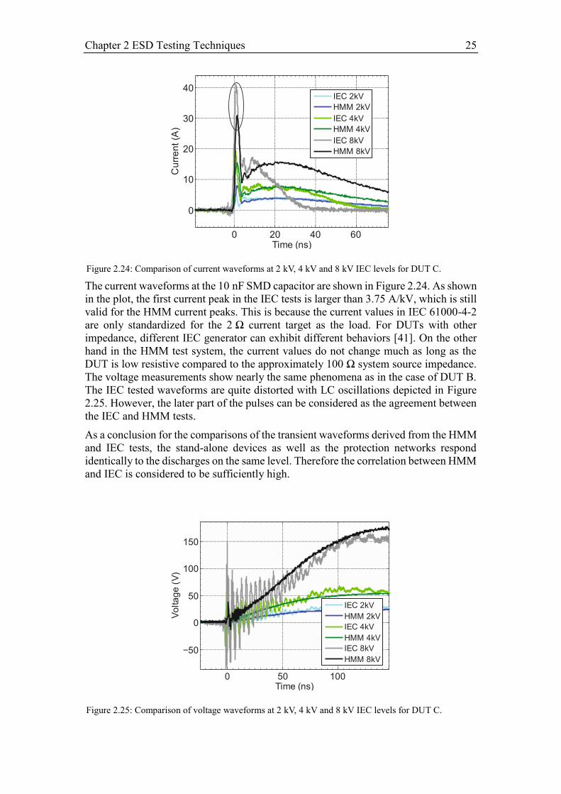
If allowed in the applications, capacitors are often used as very simple and effective
off-chip ESD protections against system-level ESD. A 10 nF capacitor 0805 X7R by
EPCOS is used as the third DUT example for the comparison of the transient current
and voltage waveforms in the HMM and IEC tests. Measurement configurations are
reused as depicted in Figure 2.14 and Figure 2.22 in HMM and IEC tests, respectively.
Figure 2.22: Measurement Setup using Noiseken (ESS-2000) IEC ESD generator for DUT B: stand-
alone CT0603K14G.
Varistor
dB Scope
CT6
dB
GND Plane
Noiseken
ESS-2000 R isolation
Figure 2.23: Comparison of voltage waveforms at 2 kV, 4 kV and 8 kV IEC levels for DUT B.
0 50 100 150
−50
0
50
100
150
200
Time (ns)
Vo
lta
ge
(V
)
IEC 2kV
HMM 2kV
IEC 4kV
HMM 4kV
IEC 8kV
HMM 8kV
Chapter 2 ESD Testing Techniques 25
The current waveforms at the 10 nF SMD capacitor are shown in Figure 2.24. As shown
in the plot, the first current peak in the IEC tests is larger than 3.75 A/kV, which is still
valid for the HMM current peaks. This is because the current values in IEC 61000-4-2
are only standardized for the 2 Ω current target as the load. For DUTs with other
impedance, different IEC generator can exhibit different behaviors [41]. On the other
hand in the HMM test system, the current values do not change much as long as the
DUT is low resistive compared to the approximately 100 Ω system source impedance.
The voltage measurements show nearly the same phenomena as in the case of DUT B.
The IEC tested waveforms are quite distorted with LC oscillations depicted in Figure
2.25. However, the later part of the pulses can be considered as the agreement between
the IEC and HMM tests.
As a conclusion for the comparisons of the transient waveforms derived from the HMM
and IEC tests, the stand-alone devices as well as the protection networks respond
identically to the discharges on the same level. Therefore the correlation between HMM
and IEC is considered to be sufficiently high.
Figure 2.24: Comparison of current waveforms at 2 kV, 4 kV and 8 kV IEC levels for DUT C.
0 20 40 60
0
10
20
30
40
Time (ns)
Cu
rre
nt
(A)
IEC 2kV
HMM 2kV
IEC 4kV
HMM 4kV
IEC 8kV
HMM 8kV
Figure 2.25: Comparison of voltage waveforms at 2 kV, 4 kV and 8 kV IEC levels for DUT C.
0 50 100
−50
0
50
100
150
Time (ns)
Vo
lta
ge
(V
)
IEC 2kV
HMM 2kV
IEC 4kV
HMM 4kV
IEC 8kV
HMM 8kV
Chapter 2 ESD Testing Techniques 26
2.2.3 HMM vs. IEC: Failure levels
The second part of comparing the HMM pulses and IEC pulses on the same DUT is to
verify the correlation of the failure levels of DUTs caused by both discharges. In
general, two main ESD failure mechanisms are associated with the thermal damages
and the electrically induced failures such as dielectric ruptures. In this section, two types
of failure mechanisms are involved in two DUTs which intend to cover a broad range
of the comparison on the failure levels.
2.2.3.1 Thermal Failure Levels
An ESD protected LIN transceiver chip is encapsulated in the plastic package P-DSO-
8 and used as the first DUT. The pin combination BUS vs. GND is designed to sustain
at least ±8 kV IEC system-level ESD stresses. It fails thermally in the end by reaching
a certain IEC stress level. A curve tracer as the failure detection is used in the IEC
testing. The DUT shows repeatable 10 kV system-level ESD hardness according to the
curve tracer. The failure root cause is estimated to be the thermal defects in the
protection device as the destructive heat generated by the ESD energy cannot be
dissipated within the pulse duration. However, this cannot be examined and proved
with lack of the voltage waveforms during the conventional IEC tests. On the contrary,
the HMM tester can provide decent transient voltage measurements. The HMM tests at
the LIN BUS pin are performed using the TB1 setup with a 25 V increment of charge
voltages. Also, a HMM hardness corresponding to 10 kV IEC level is measured. The
failure detection is done by the leakage current measurements. In the transient
waveforms, the thermal failure is clearly demonstrated at latter part of the destructive
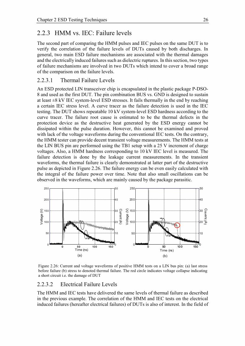
pulse as depicted in Figure 2.26. The failure energy can be even easily calculated with
the integral of the failure power over time. Note that also small oscillations can be
observed in the waveforms, which are mainly caused by the package parasitic.
2.2.3.2 Electrical Failure Levels
The HMM and IEC tests have delivered the same levels of thermal failure as described
in the previous example. The correlation of the HMM and IEC tests on the electrical
induced failures (hereafter electrical failures) of DUTs is also of interest. In the field of
Figure 2.26: Current and voltage waveforms of positive HMM tests on a LIN bus pin: (a) last stress
before failure (b) stress to denoted thermal failure. The red circle indicates voltage collapse indicating
a short circuit i.e. the damage of DUT
0 50 100 1500
50
100
150
200
250
Volta
ge
(V)
Time (ns)0 50 100 150
0
10
20
30
40
50
Curre
nt (A
)
0 50 10 0 1500
50
10 0
15 0
20 0
Voltage
(V)
Time (ns)
0 50 10 0 1500
10
20
30
40
rrt (
)
(a) (b)
Chapter 2 ESD Testing Techniques 27
on-chip ESD protections, actively controlled MOSFET – so-called active clamp - is
widely used as a type of ESD protection elements, as its principle is generally easy to
apply and relatively technology independent. The ESD capability of the active clamps
is often limited by the electrical safe operating area of the used MOSFET transistor.
The active clamp engages its robustness limit and is damaged when the electrical
parameters such as voltage and current density at the transistor exceed the critical values
during ESD even with very short pulse durations e.g. 5 ns. This means that in many
cases the failures of the active clamps are induced by the first peak of the system-level
ESD pulses. The high-voltage active clamps and their failure modes will be discussed
in detail in later chapters.
In the study of the HMM tester, several active clamps with different sizes are used as
DUTs which are all expected to have electrical failure levels. In the IEC tests, the test
structures are assembled in the plastic package LQFP-64 and stressed with a Schaffner
Figure 2.28: Voltage waveforms derived from the HMM test for a 25 V active clamp with electrically
induced damage denoted in the first peak range. The DUT fails at 6.8 A broad peak current
corresponding to 3.4 kV IEC level which is shown in Figure 2.29.
0 20 40 60 80−10
0
10
20
30
40
50
60
70
Vo
lta
ge
V(
)
Time ns( )
voltage: last stress pre-failure
voltage: stress to failure
destructive snapback
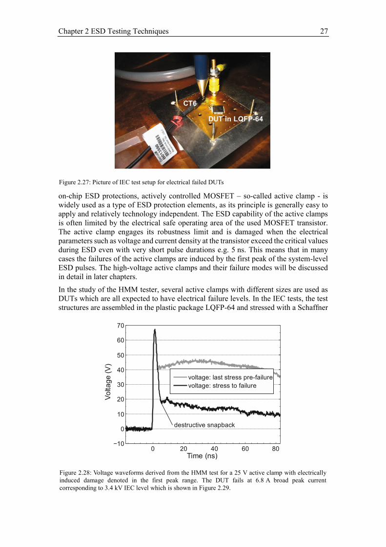
Figure 2.27: Picture of IEC test setup for electrical failed DUTs
DUT in LQFP-64
CT6
Chapter 2 ESD Testing Techniques 28
ESD generator, model NSG-438 150 pF/330 Ω. Current waveforms are measured by
CT6 current probe in the test setup shown in Figure 2.27. The HMM tests are performed
on the same structures with the TB1 setup but using CT6 for the current probing. Figure
2.28 depicts the waveforms of stresses pre- and post-failure for a 25 V active clamp A.
The electrically induced destructive snapback is clearly visible as the voltage collapses
at the beginning of the pulse. The spot leakage is also plotted indicating the failure
current level during the HMM test corresponding to about 3.4 kV IEC level. In the IEC
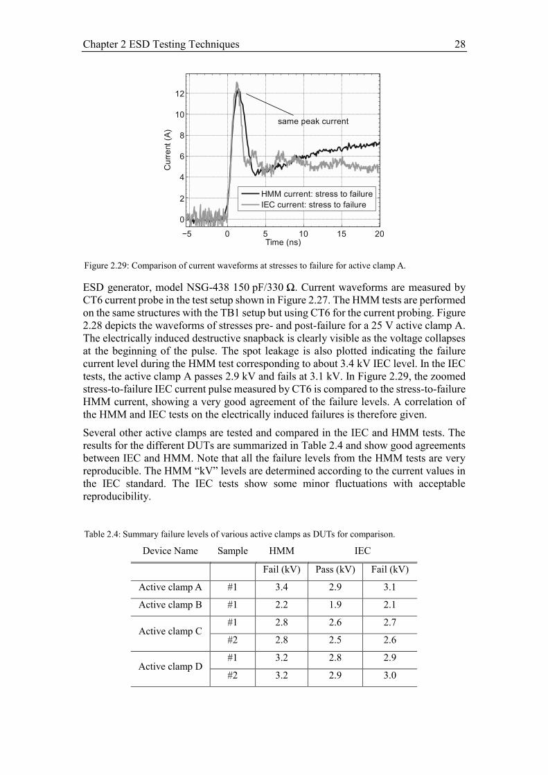
tests, the active clamp A passes 2.9 kV and fails at 3.1 kV. In Figure 2.29, the zoomed
stress-to-failure IEC current pulse measured by CT6 is compared to the stress-to-failure
HMM current, showing a very good agreement of the failure levels. A correlation of
the HMM and IEC tests on the electrically induced failures is therefore given.
Several other active clamps are tested and compared in the IEC and HMM tests. The
results for the different DUTs are summarized in Table 2.4 and show good agreements
between IEC and HMM. Note that all the failure levels from the HMM tests are very
reproducible. The HMM “kV” levels are determined according to the current values in
the IEC standard. The IEC tests show some minor fluctuations with acceptable
reproducibility.
Figure 2.29: Comparison of current waveforms at stresses to failure for active clamp A.
−5 0 5 10 15 20
0
2
4
6
8
10
12
Cu
rre
nt
(A)
Time (ns)
HMM current: stress to failure
IEC current: stress to failure
same peak current
Table 2.4: Summary failure levels of various active clamps as DUTs for comparison.
Device Name Sample HMM IEC
Fail (kV) Pass (kV) Fail (kV)
Active clamp A #1 3.4 2.9 3.1
Active clamp B #1 2.2 1.9 2.1
Active clamp C #1 2.8 2.6 2.7
#2 2.8 2.5 2.6
Active clamp D #1 3.2 2.8 2.9
#2 3.2 2.9 3.0
Chapter 2 ESD Testing Techniques 29
Above all, the correlation of the HMM and IEC tests on the failure levels is found. The
TLP based HMM tester provides a reliable test method which delivers the same results
as obtained in the traditional IEC system-level ESD tests for the devices and circuits
under test. The HMM tester further enables accurate voltage measurements and is easily
applicable for board or wafer-level tests.
2.2.4 Discussion and Summary
As already discussed earlier, to obtain reproducible and reliable HMM test result,
several conditions have to be fulfilled. The most important one is that the DUT must be
low resistive during the test. From the ESD protection point of view for IC components,
DUTs are in the majority of cases low resistive based on the consideration: The ESD
protection elements have the task to safely discharge ESD currents via a low-impedance
shunting path the ground. The DUT with high-impedance interface which can safely
limit the ESD current is straightforwardly ESD protected hence is not in focus of this
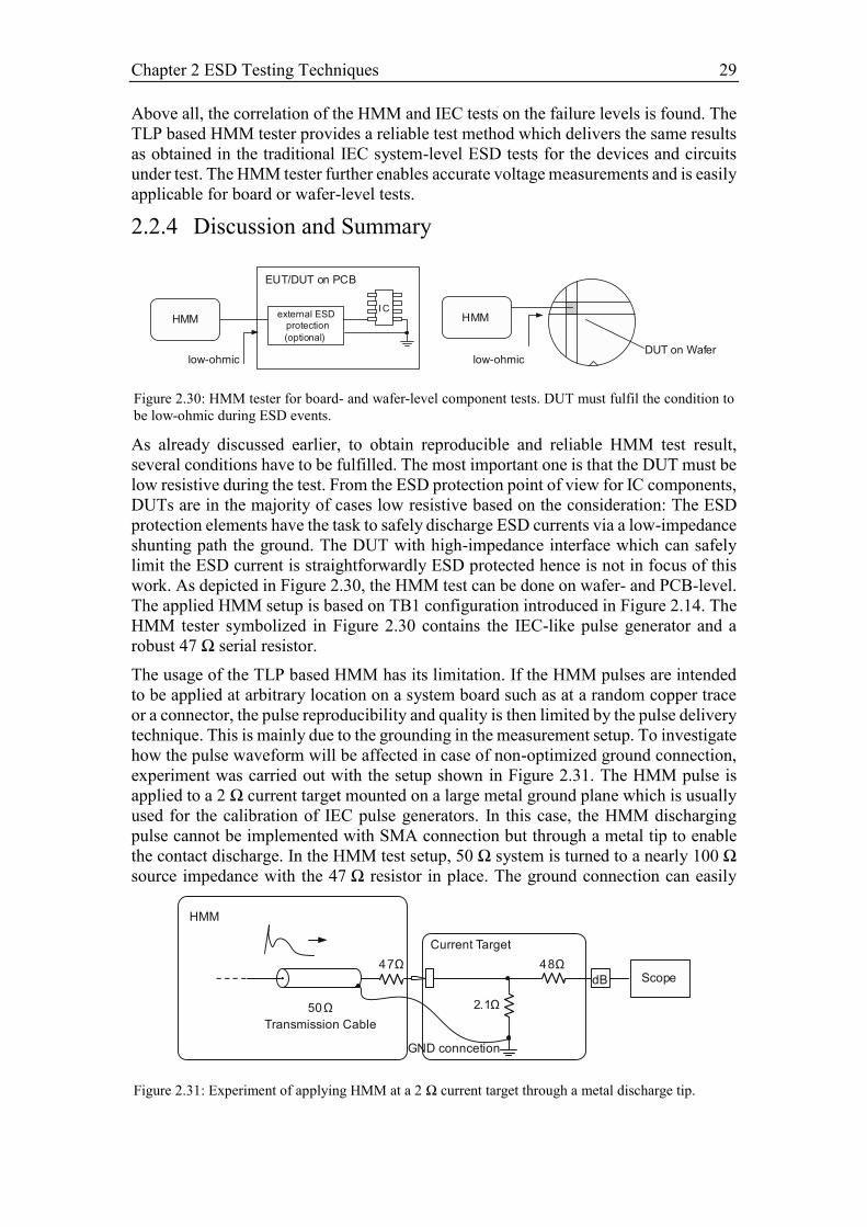
work. As depicted in Figure 2.30, the HMM test can be done on wafer- and PCB-level.
The applied HMM setup is based on TB1 configuration introduced in Figure 2.14. The
HMM tester symbolized in Figure 2.30 contains the IEC-like pulse generator and a
robust 47 Ω serial resistor.
The usage of the TLP based HMM has its limitation. If the HMM pulses are intended
to be applied at arbitrary location on a system board such as at a random copper trace
or a connector, the pulse reproducibility and quality is then limited by the pulse delivery
technique. This is mainly due to the grounding in the measurement setup. To investigate
how the pulse waveform will be affected in case of non-optimized ground connection,
experiment was carried out with the setup shown in Figure 2.31. The HMM pulse is
applied to a 2 Ω current target mounted on a large metal ground plane which is usually
used for the calibration of IEC pulse generators. In this case, the HMM discharging
pulse cannot be implemented with SMA connection but through a metal tip to enable
the contact discharge. In the HMM test setup, 50 Ω system is turned to a nearly 100 Ω
source impedance with the 47 Ω resistor in place. The ground connection can easily
Figure 2.30: HMM tester for board- and wafer-level component tests. DUT must fulfil the condition to
be low-ohmic during ESD events.
IC
(optional)
EUT/DUT on PCB
HMM HMM
DUT on Wafer
external ESD protection
low-ohmic low-ohmic
Figure 2.31: Experiment of applying HMM at a 2 Ω current target through a metal discharge tip.
2.1Ω
48Ω
dB
47ΩScope
50Ω
GND conncetion
Current Target
Transmission Cable
HMM
Chapter 2 ESD Testing Techniques 30
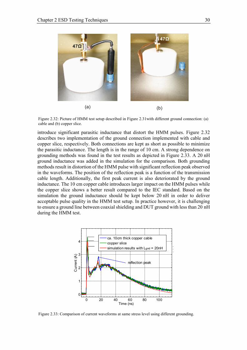
introduce significant parasitic inductance that distort the HMM pulses. Figure 2.32
describes two implementation of the ground connection implemented with cable and
copper slice, respectively. Both connections are kept as short as possible to minimize
the parasitic inductance. The length is in the range of 10 cm. A strong dependence on
grounding methods was found in the test results as depicted in Figure 2.33. A 20 nH
ground inductance was added in the simulation for the comparison. Both grounding
methods result in distortion of the HMM pulse with significant reflection peak observed
in the waveforms. The position of the reflection peak is a function of the transmission
cable length. Additionally, the first peak current is also deteriorated by the ground
inductance. The 10 cm copper cable introduces larger impact on the HMM pulses while
the copper slice shows a better result compared to the IEC standard. Based on the
simulation the ground inductance should be kept below 20 nH in order to deliver
acceptable pulse quality in the HMM test setup. In practice however, it is challenging
to ensure a ground line between coaxial shielding and DUT ground with less than 20 nH
during the HMM test.
Figure 2.32: Picture of HMM test setup described in Figure 2.31with different ground connection: (a)
cable and (b) copper slice.
(a) (b)
47Ω
47Ω
Figure 2.33: Comparison of current waveforms at same stress level using different grounding.
0 20 40 60 80 100
0
1
2
3
4
Time (ns)
Curr
ent
(A)
ca. 10cm thick copper cable
copper slice
simulation results with Lgnd = 20nH
reflection peak
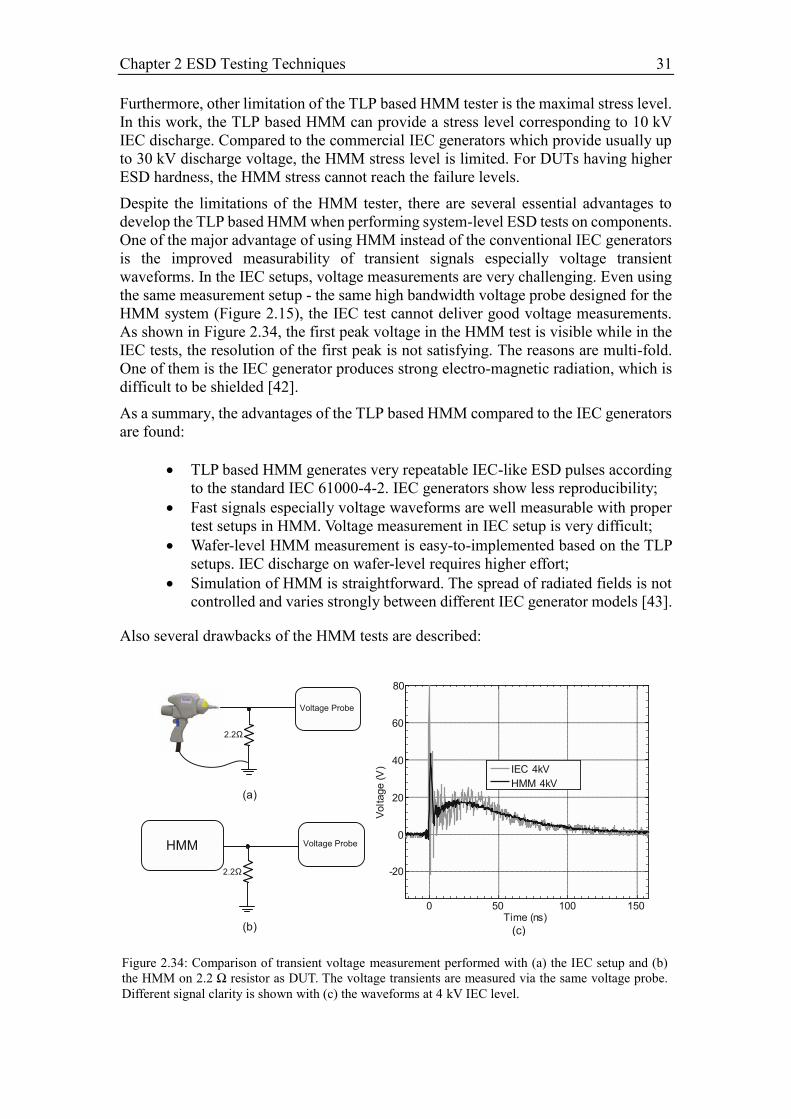
Chapter 2 ESD Testing Techniques 31
Furthermore, other limitation of the TLP based HMM tester is the maximal stress level.
In this work, the TLP based HMM can provide a stress level corresponding to 10 kV
IEC discharge. Compared to the commercial IEC generators which provide usually up
to 30 kV discharge voltage, the HMM stress level is limited. For DUTs having higher
ESD hardness, the HMM stress cannot reach the failure levels.
Despite the limitations of the HMM tester, there are several essential advantages to
develop the TLP based HMM when performing system-level ESD tests on components.
One of the major advantage of using HMM instead of the conventional IEC generators
is the improved measurability of transient signals especially voltage transient
waveforms. In the IEC setups, voltage measurements are very challenging. Even using
the same measurement setup - the same high bandwidth voltage probe designed for the
HMM system (Figure 2.15), the IEC test cannot deliver good voltage measurements.
As shown in Figure 2.34, the first peak voltage in the HMM test is visible while in the
IEC tests, the resolution of the first peak is not satisfying. The reasons are multi-fold.
One of them is the IEC generator produces strong electro-magnetic radiation, which is
difficult to be shielded [42].
As a summary, the advantages of the TLP based HMM compared to the IEC generators
are found:
TLP based HMM generates very repeatable IEC-like ESD pulses according
to the standard IEC 61000-4-2. IEC generators show less reproducibility;
Fast signals especially voltage waveforms are well measurable with proper
test setups in HMM. Voltage measurement in IEC setup is very difficult;
Wafer-level HMM measurement is easy-to-implemented based on the TLP
setups. IEC discharge on wafer-level requires higher effort;
Simulation of HMM is straightforward. The spread of radiated fields is not
controlled and varies strongly between different IEC generator models [43].
Also several drawbacks of the HMM tests are described:
Figure 2.34: Comparison of transient voltage measurement performed with (a) the IEC setup and (b)
the HMM on 2.2 Ω resistor as DUT. The voltage transients are measured via the same voltage probe.
Different signal clarity is shown with (c) the waveforms at 4 kV IEC level.
0 50 100 150
-20
0
20
40
60
Time (ns)
Voltage
(V) IEC 4kV
HMM 4kV
(b)
(a)
(c)
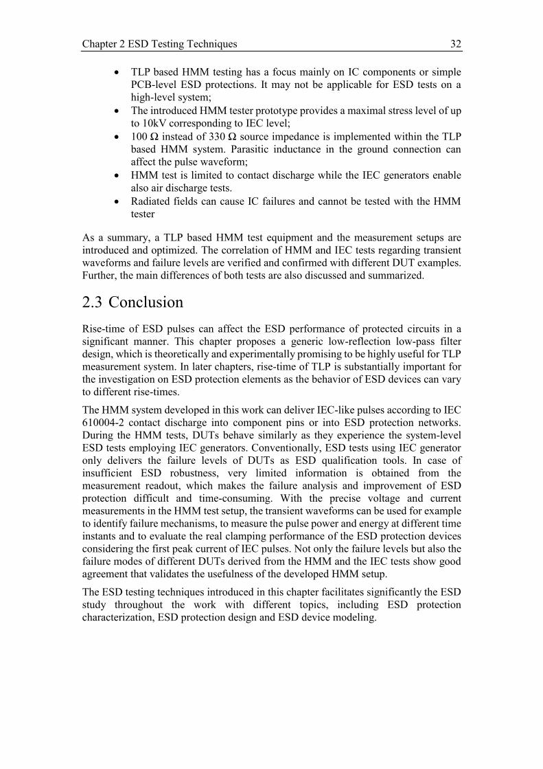
Chapter 2 ESD Testing Techniques 32
TLP based HMM testing has a focus mainly on IC components or simple
PCB-level ESD protections. It may not be applicable for ESD tests on a
high-level system;
The introduced HMM tester prototype provides a maximal stress level of up
to 10kV corresponding to IEC level;
100 Ω instead of 330 Ω source impedance is implemented within the TLP
based HMM system. Parasitic inductance in the ground connection can
affect the pulse waveform;
HMM test is limited to contact discharge while the IEC generators enable
also air discharge tests.
Radiated fields can cause IC failures and cannot be tested with the HMM
tester
As a summary, a TLP based HMM test equipment and the measurement setups are
introduced and optimized. The correlation of HMM and IEC tests regarding transient
waveforms and failure levels are verified and confirmed with different DUT examples.
Further, the main differences of both tests are also discussed and summarized.
2.3 Conclusion
Rise-time of ESD pulses can affect the ESD performance of protected circuits in a
significant manner. This chapter proposes a generic low-reflection low-pass filter
design, which is theoretically and experimentally promising to be highly useful for TLP
measurement system. In later chapters, rise-time of TLP is substantially important for
the investigation on ESD protection elements as the behavior of ESD devices can vary
to different rise-times.
The HMM system developed in this work can deliver IEC-like pulses according to IEC
610004-2 contact discharge into component pins or into ESD protection networks.
During the HMM tests, DUTs behave similarly as they experience the system-level
ESD tests employing IEC generators. Conventionally, ESD tests using IEC generator
only delivers the failure levels of DUTs as ESD qualification tools. In case of
insufficient ESD robustness, very limited information is obtained from the
measurement readout, which makes the failure analysis and improvement of ESD
protection difficult and time-consuming. With the precise voltage and current
measurements in the HMM test setup, the transient waveforms can be used for example
to identify failure mechanisms, to measure the pulse power and energy at different time
instants and to evaluate the real clamping performance of the ESD protection devices
considering the first peak current of IEC pulses. Not only the failure levels but also the
failure modes of different DUTs derived from the HMM and the IEC tests show good
agreement that validates the usefulness of the developed HMM setup.
The ESD testing techniques introduced in this chapter facilitates significantly the ESD
study throughout the work with different topics, including ESD protection
characterization, ESD protection design and ESD device modeling.
Chapter 3 Failure Levels, Criteria and Case Studies of On-Chip Protections 33
Chapter 3
Failure Levels, Criteria and Case Studies
of On-Chip Protections
High-voltage ESD chip-level design requires reliable protection elements. In the scope
of this chapter, three types of typical high-voltage on-chip ESD protection elements are
studied. Their failure levels and failure criteria are of enormous importance to establish
area efficient and protection effective design. Because nowadays, ESD protection for
IC products especially in high-voltage wafer technologies generally does not work with
“plug and play” of protection devices. Only if one understands deeply the differences
of ESD protection devices in terms of their advantages, disadvantages and their
interactions with protected devices and structures, effective protection can be designed.
Compared to low-voltage ESD protection concept high-voltage ESD devices are
inherently larger due to higher power dissipation (higher clamping voltage at specified
ESD current) requiring more silicon area or volume. Hence, the area efficiency of
overall ESD protection is often dominated by high-voltage ESD
In this work, three representative types of ESD devices including npn-bipolar transistor
(BJT), pn-diode and active controlled power MOSFET (hereafter active clamps) are
discussed in this chapter. Using TLP with different pulse durations and rise-times, the
device characteristics with respect to HBM, CDM as well as system-level ESD are
experimentally and comprehensively summarized. The root causes of devices’ failures
by reaching their inherent ESD capabilities are also studied in detail.
In addition to the ESD protection elements by themselves, the protected devices are
also combined with the ESD protection in the study to verify the on-chip ESD
protection effectiveness. Combining ESD protection and ESD protected devices is
usually named ESD concept and is a part of the ESD development. In this chapter,
diverse particular effects shown in the various ESD protection concepts are
demonstrated with assistance of device simulation. Based on the devices’
characteristics, the impact of the protection elements to the circuits being protected is
carefully evaluated. In order to improve the efficiency and effectiveness of the ESD
protections, advanced concept solutions and novel protection elements are developed
and investigated accordingly.
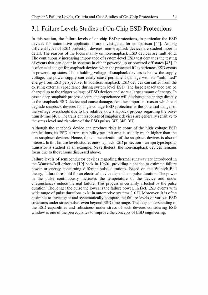
Chapter 3 Failure Levels, Criteria and Case Studies of On-Chip Protections 34
3.1 Failure Levels Studies of On-Chip ESD Protections
In this section, the failure levels of on-chip ESD protections, in particular the ESD
devices for automotive applications are investigated for comparison [44]. Among
different types of ESD protection devices, non-snapback devices are studied more in
detail. The reasons of the focus mainly on non-snapback ESD devices are multi-fold.
The continuously increasing importance of system-level ESD test demands the testing
of events that can occur in systems in either powered up or powered off states [45]. It
is of crucial danger for snapback devices when the protected IC experiences ESD events
in powered up states. If the holding voltage of snapback devices is below the supply
voltage, the power supply can easily cause permanent damage with its “unlimited”
energy from ESD perspective. In addition, snapback ESD devices can suffer from the
existing external capacitance during system level ESD. The large capacitance can be
charged up to the trigger voltage of ESD devices and store a large amount of energy. In
case a deep snapback process occurs, the capacitance will discharge the energy directly
to the snapback ESD device and cause damage. Another important reason which can
degrade snapback devices for high-voltage ESD protection is the potential danger of
the voltage overshoots due to the relative slow snapback process regarding the base-
transit-time [46]. The transient responses of snapback devices are generally sensitive to
the stress level and rise-time of the ESD pulses [47] [48] [67].
Although the snapback device can produce risks in some of the high voltage ESD
applications, its ESD current capability per unit area is usually much higher than the
non-snapback devices. Hence, the characterization of the snapback devices is also of
interest. In this failure levels studies one snapback ESD protection – an npn type bipolar
transistor is studied as an example. Nevertheless, the non-snapback devices remains
focus due to the reasons discussed above.
Failure levels of semiconductor devices regarding thermal runaway are introduced in
the Wunsch-Bell criterion [19] back in 1960s, providing a chance to estimate failure
power or energy concerning different pulse durations. Based on the Wunsch-Bell
theory, failure threshold for an electrical device depends on pulse duration. The power
in the pulse continuously increases the temperature of the device and under
circumstances induce thermal failure. This process is certainly affected by the pulse
duration. The longer the pulse the lower is the failure power. In fact, ESD events with
wide range of pulse durations exist in automotive systems [102]. Moreover, it is often
desirable to investigate and systematically compare the failure levels of various ESD
structures under stress pulses even beyond ESD time range. The deep understanding of
the ESD capabilities and robustness under stress of such devices considering ESD
window is one of the prerequisites to improve the concepts of ESD engineering.
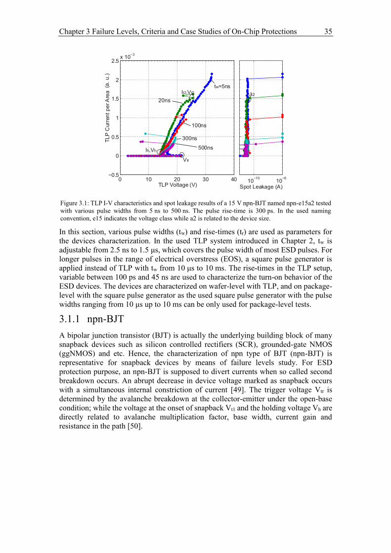
Chapter 3 Failure Levels, Criteria and Case Studies of On-Chip Protections 35
In this section, various pulse widths (tw) and rise-times (tr) are used as parameters for
the devices characterization. In the used TLP system introduced in Chapter 2, tw is
adjustable from 2.5 ns to 1.5 μs, which covers the pulse width of most ESD pulses. For
longer pulses in the range of electrical overstress (EOS), a square pulse generator is
applied instead of TLP with tw from 10 μs to 10 ms. The rise-times in the TLP setup,
variable between 100 ps and 45 ns are used to characterize the turn-on behavior of the
ESD devices. The devices are characterized on wafer-level with TLP, and on package-
level with the square pulse generator as the used square pulse generator with the pulse
widths ranging from 10 μs up to 10 ms can be only used for package-level tests.
3.1.1 npn-BJT
A bipolar junction transistor (BJT) is actually the underlying building block of many
snapback devices such as silicon controlled rectifiers (SCR), grounded-gate NMOS
(ggNMOS) and etc. Hence, the characterization of npn type of BJT (npn-BJT) is
representative for snapback devices by means of failure levels study. For ESD
protection purpose, an npn-BJT is supposed to divert currents when so called second
breakdown occurs. An abrupt decrease in device voltage marked as snapback occurs
with a simultaneous internal constriction of current [49]. The trigger voltage Vtr is
determined by the avalanche breakdown at the collector-emitter under the open-base
condition; while the voltage at the onset of snapback Vt1 and the holding voltage Vh are
directly related to avalanche multiplication factor, base width, current gain and
resistance in the path [50].
Figure 3.1: TLP I-V characteristics and spot leakage results of a 15 V npn-BJT named npn-e15a2 tested
with various pulse widths from 5 ns to 500 ns. The pulse rise-time is 300 ps. In the used naming
convention, e15 indicates the voltage class while a2 is related to the device size.
0 10 20 30 40−0.5
0
0.5
1
1.5
2
2.5x 10
−3
TLP Voltage (V)10
−10
Spot Leakage (A)
TL
PC
urr
en
t p
er A
rea
(a.
u.)
100ns
300ns
500ns
tw=5ns
20ns
It2,Vt2
Ih,Vh
Vtr
10−6
It2
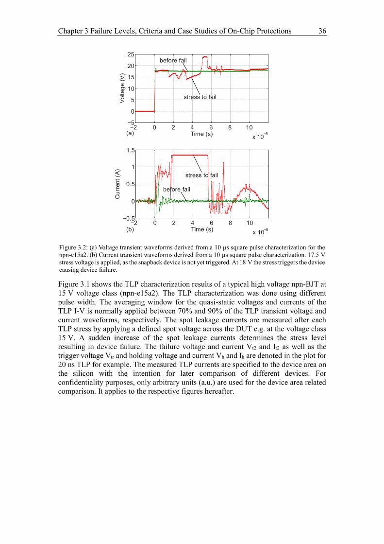
Chapter 3 Failure Levels, Criteria and Case Studies of On-Chip Protections 36
Figure 3.1 shows the TLP characterization results of a typical high voltage npn-BJT at
15 V voltage class (npn-e15a2). The TLP characterization was done using different
pulse width. The averaging window for the quasi-static voltages and currents of the
TLP I-V is normally applied between 70% and 90% of the TLP transient voltage and
current waveforms, respectively. The spot leakage currents are measured after each
TLP stress by applying a defined spot voltage across the DUT e.g. at the voltage class
15 V. A sudden increase of the spot leakage currents determines the stress level
resulting in device failure. The failure voltage and current Vt2 and It2 as well as the
trigger voltage Vtr and holding voltage and current Vh and Ih are denoted in the plot for
20 ns TLP for example. The measured TLP currents are specified to the device area on
the silicon with the intention for later comparison of different devices. For
confidentiality purposes, only arbitrary units (a.u.) are used for the device area related
comparison. It applies to the respective figures hereafter.
Figure 3.2: (a) Voltage transient waveforms derived from a 10 µs square pulse characterization for the
npn-e15a2. (b) Current transient waveforms derived from a 10 µs square pulse characterization. 17.5 V
stress voltage is applied, as the snapback device is not yet triggered. At 18 V the stress triggers the device
causing device failure.
−2 0 2 4 6 8 10
x 10−6
−0.5
0
0.5
1
1.5
Time (s)
Cu
rren
t (A
)
(b)
(a)−2 0 2 4 6 8 10
x 10−6
−5
0
5
10
15
20
Time (s)
Volta
ge
(V
)
stress to fail
before fail
stress to fail
before fail
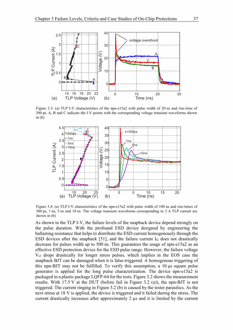
Chapter 3 Failure Levels, Criteria and Case Studies of On-Chip Protections 37
As shown in the TLP I-V, the failure levels of the snapback device depend strongly on
the pulse duration. With the profound ESD device designed by engineering the
ballasting resistance that helps to distribute the ESD current homogenously through the
ESD devices after the snapback [51], and the failure current It2 does not drastically
decrease for pulses width up to 500 ns. This guarantees the usage of npn-e15a2 as an
effective ESD protection device for the ESD pulse range. However, the failure voltage
Vt2 drops drastically for longer stress pulses, which implies in the EOS case the
snapback BJT can be damaged when it is false-triggered. A homogenous triggering of
this npn-BJT may not be fulfilled. To verify this assumption, a 10 μs square pulse
generator is applied for the long pulse characterization. The device npn-e15a2 is
packaged in a plastic package LQFP-64 for the tests. Figure 3.2 shows the measurement
results. With 17.5 V at the DUT (before fail in Figure 3.2 (a)), the npn-BJT is not
triggered. The current ringing in Figure 3.2 (b) is caused by the tester parasitics. As the
next stress at 18 V is applied, the device is triggered and it failed during the stress. The
current drastically increases after approximately 2 µs and it is limited by the current
Figure 3.4: (a) TLP I-V characteristics of the npn-e15a2 with pulse width of 100 ns and rise-times of
300 ps, 1 ns, 5 ns and 10 ns. The voltage transient waveforms corresponding to 2 A TLP current are
shown in (b)
0 5 10 15 20
0
5
10
15
20
25
30
35
40
Vo
ltag
e (
V)
Time (ns)15 20 25
0
0.5
1
1.5
2
2.5
3
3.5
4
TLP Voltage (V)(a) (b)
TL
P C
urr
en
t (A
)
10ns
5ns
1ns
t =300psr300ps
1ns
5ns
10ns
Figure 3.3: (a) TLP I-V characteristics of the npn-e15a2 with pulse width of 20 ns and rise-time of
300 ps. A, B and C indicate the I-V points with the corresponding voltage transient waveforms shown
in (b)
0 10 20 30
0
10
20
30
Volta
ge
(V
)Time (ns)
40
14 16 18 20 22
0
0.5
1
1.5
2
2.5
TLP Voltage (V)
AB
C
A
B
C
voltage overshoot
TL
P C
urr
en
t (A
)
(a) (b)
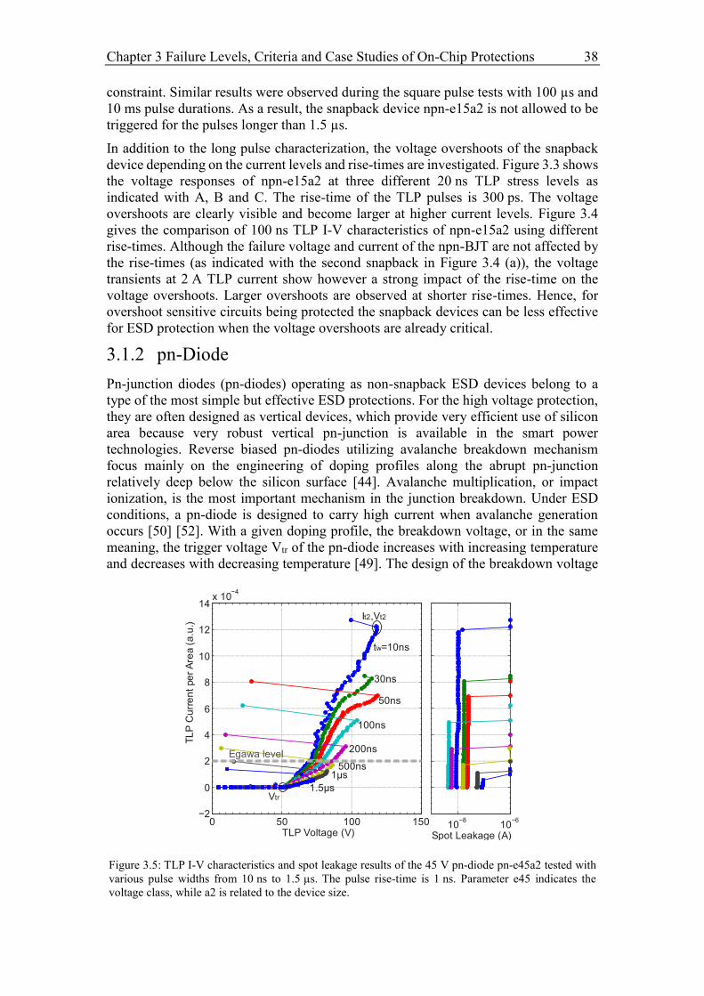
Chapter 3 Failure Levels, Criteria and Case Studies of On-Chip Protections 38
constraint. Similar results were observed during the square pulse tests with 100 µs and
10 ms pulse durations. As a result, the snapback device npn-e15a2 is not allowed to be
triggered for the pulses longer than 1.5 µs.
In addition to the long pulse characterization, the voltage overshoots of the snapback
device depending on the current levels and rise-times are investigated. Figure 3.3 shows
the voltage responses of npn-e15a2 at three different 20 ns TLP stress levels as
indicated with A, B and C. The rise-time of the TLP pulses is 300 ps. The voltage
overshoots are clearly visible and become larger at higher current levels. Figure 3.4
gives the comparison of 100 ns TLP I-V characteristics of npn-e15a2 using different
rise-times. Although the failure voltage and current of the npn-BJT are not affected by
the rise-times (as indicated with the second snapback in Figure 3.4 (a)), the voltage
transients at 2 A TLP current show however a strong impact of the rise-time on the
voltage overshoots. Larger overshoots are observed at shorter rise-times. Hence, for
overshoot sensitive circuits being protected the snapback devices can be less effective
for ESD protection when the voltage overshoots are already critical.
3.1.2 pn-Diode
Pn-junction diodes (pn-diodes) operating as non-snapback ESD devices belong to a
type of the most simple but effective ESD protections. For the high voltage protection,
they are often designed as vertical devices, which provide very efficient use of silicon
area because very robust vertical pn-junction is available in the smart power
technologies. Reverse biased pn-diodes utilizing avalanche breakdown mechanism
focus mainly on the engineering of doping profiles along the abrupt pn-junction
relatively deep below the silicon surface [44]. Avalanche multiplication, or impact
ionization, is the most important mechanism in the junction breakdown. Under ESD
conditions, a pn-diode is designed to carry high current when avalanche generation
occurs [50] [52]. With a given doping profile, the breakdown voltage, or in the same
meaning, the trigger voltage Vtr of the pn-diode increases with increasing temperature
and decreases with decreasing temperature [49]. The design of the breakdown voltage
Figure 3.5: TLP I-V characteristics and spot leakage results of the 45 V pn-diode pn-e45a2 tested with
various pulse widths from 10 ns to 1.5 µs. The pulse rise-time is 1 ns. Parameter e45 indicates the
voltage class, while a2 is related to the device size.
0 50 100 150−2
0
2
4
6
8
10
12
14x 10
TL
P C
urr
en
t pe
r A
rea
(a
.u.)
TLP Voltage (V)10
−810
−6
Spot Leakage (A)
100ns
200ns
500ns
tw=10ns
30ns
It2,Vt2
Vtr
50ns
1μs
1.5μs
Egawa level
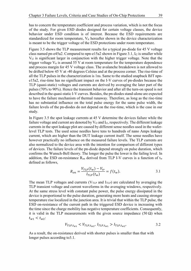
Chapter 3 Failure Levels, Criteria and Case Studies of On-Chip Protections 39
has to concern the temperature coefficient and process variation, which is not the focus
of the study. For given ESD diodes designed for certain voltage classes, the device
behavior under ESD condition is of interest. Because the ESD requirements are
standardized for room temperature, Vtr hereafter shown in the device characterization
is meant to be the trigger voltage of the ESD protections under room temperature.
Figure 3.5 shows the TLP measurement results for a typical pn-diode for 45 V voltage
class named pn-e45a2. Compared to npn-e15a2 shown in Figure 3.1, It2 is smaller while
Vt2 is significant larger in conjunction with the higher trigger voltage. Note that the
trigger voltage Vtr is around 55 V at room temperature for the temperature dependence
and process margin for 45 V voltage class. The avalanche breakdown is not allowed to
be drifted below 45 V at -40 degrees Celsius and at the process corner. The rise-time of
all the TLP pulses in the characterization is 1ns. Same to the studied snapback BJT npn-
e15a2, rise-time has no significant impact on the I-V curves of pn-diodes because the
TLP (quasi-static) voltages and currents are derived by averaging the later part of the
pulses (70% to 90%). Hence the transient behavior and after all the turn-on speed is not
described in the quasi-static I-V curves. Besides, the pn-diodes stand-alone are expected
to have the failure mechanism of thermal runaway. Therefore, as long as the rise-time
has no substantial influence on the total pulse energy for the same pulse width, the
failure levels of the pn-diodes do not depend on the rise-time, which is the case in our
study.
In Figure 3.5 the spot leakage currents at 45 V determine the devices failure while the
failure voltage and current are denoted by Vt2 and It2, respectively. The different leakage
currents in the spot leakage plot are caused by different sense needles used in the wafer-
level TLP tests. The used sense needles have tens to hundreds of nano Amps leakage
current, which are higher than the DUT leakage current itself. The sense needles have
however practically no influence on the measured failure levels. The TLP currents are
also normalized to the device area with the intention for comparison of different types
of devices. The failure levels of the pn-diode depend strongly on pulse duration, which
confirms the Wunsch-Bell theory. The longer the pulse the lower is the failing level. In
addition, the ESD on-resistance Ron derived from TLP I-V curves is a function of tw
defined as follows,
𝑅𝑜𝑛 =𝑉𝑇𝐿𝑃(𝑡𝑤) − 𝑉𝑡𝑟
𝐼𝑇𝐿𝑃(𝑡𝑤)= 𝑓(𝑡𝑤). 3.1
The mean TLP voltages and currents (VTLP and ITLP) are calculated by averaging the
TLP transient voltage and current waveforms in the averaging windows, respectively.
At the same stress level with constant pulse power, the pulse energy dissipated in the
device is proportional to the pulse duration, generating more heats and causing stronger
temperature rise localized in the junction area. It is trivial that within the TLP pulse, the
ESD on-resistance of the current path in the triggered ESD device is increasing with
the time since the charge mobility has negative temperature coefficients. Consequently,
it is valid in the TLP measurements with the given source impedance (50 Ω) when
𝑡𝑤1 < 𝑡𝑤2:
𝑉𝑇𝐿𝑃,𝑡𝑤1< 𝑉𝑇𝐿𝑃,𝑡𝑤2
, 𝐼𝑇𝐿𝑃,𝑡𝑤1> 𝐼𝑇𝐿𝑃,𝑡𝑤2
, 3.2
As a result, the on-resistance derived with shorter pulses is smaller than that with
longer pulses according to3.1.
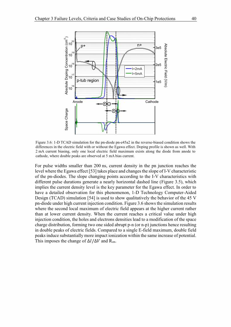
Chapter 3 Failure Levels, Criteria and Case Studies of On-Chip Protections 40
For pulse widths smaller than 200 ns, current density in the pn junction reaches the
level where the Egawa effect [53] takes place and changes the slope of I-V characteristic
of the pn-diodes. The slope changing points according to the I-V characteristics with
different pulse durations generate a nearly horizontal dashed line (Figure 3.5), which
implies the current density level is the key parameter for the Egawa effect. In order to
have a detailed observation for this phenomenon, 1-D Technology Computer-Aided
Design (TCAD) simulation [54] is used to show qualitatively the behavior of the 45 V
pn-diode under high current injection condition. Figure 3.6 shows the simulation results
where the second local maximum of electric field appears at the higher current rather
than at lower current density. When the current reaches a critical value under high
injection condition, the holes and electrons densities lead to a modification of the space
charge distribution, forming two one sided abrupt p-n (or n-p) junctions hence resulting
in double peaks of electric fields. Compared to a single E-field maximum, double field
peaks induce substantially more impact ionization within the same increase of potential.
This imposes the change of ∆𝐼/∆𝑉 and Ron.
Figure 3.6: 1-D TCAD simulation for the pn-diode pn-e45a2 in the reverse-biased condition shows the
differences in the electric field with or without the Egawa effect. Doping profile is shown as well. With
2 mA current biasing, only one local electric field maximum exists along the diode from anode to
cathode, where double peaks are observed at 5 mA bias current.
1016
1017
1018
1019
1020
1e5
2e5
3e5
Anode Cathode
Ab
so
lute
Do
pin
g C
on
ce
ntr
atio
n (
cm
)
-3
p+
p-tub region
n+
Sp
ace
Ch
arg
e
_+
_+
I=2mA
I=5mA
Chapter 3 Failure Levels, Criteria and Case Studies of On-Chip Protections 41
For ESD protection, pn-diodes can benefit from the Egawa effect, which lowers the
total on-resistance of the devices, resulting in improvement of on-chip ESD area
efficiency. In addition to pn-e45a2, many other pn-diodes implemented for two voltage
classes are also characterized using the similar TLP test method as introduced above.
If one simply linearizes the I-V curves by defining the device on-resistance Ron, dev
𝑅𝑜𝑛,𝑑𝑒𝑣 =𝑉𝑡2 − 𝑉𝑡𝑟
𝐼𝑡2, 3.3
with respect to the failure levels without concerning the change of Ron due to e.g. the
Egawa effect, the dependence of 𝑅𝑜𝑛,𝑑𝑒𝑣 ∙ 𝑎𝑟𝑒𝑎 product on the pulse duration can be
derived from the measurement results as depicted in Figure 3.7. As expected, the diodes
with the same breakdown voltage have nearly the same Ron, dev referring to unit area,
showing very good scalability. However, the pn-diodes for higher voltage classes have
to be designed larger to obtain the same on-resistance. The weak doping concentration
in p-tub region [55] for higher breakdown voltage increases the resistance in the current
path significantly. This results in 𝑅𝑜𝑛,𝑑𝑒𝑣 ∙ 𝑎𝑟𝑒𝑎 product of the 45 V devices with a
factor of approximately 1.8 comparing to the 25 V diodes.
In fact, in the high voltage applications the ESD design windows often have upper limits
of several tens of volts as constraints. Hence, very high Vt2 might not be in advantage
for an effective ESD design. Effective on-resistance Ron, eff in terms of ESD window
with defined maximal allowed voltage is a more practical measure, which can reduce
the area efficiency of pn-diodes. This issue will be addressed in the comparison of
various devices types in later sections.
Figure 3.7: 𝑅𝑜𝑛,𝑑𝑒𝑣 ∙ 𝑎𝑟𝑒𝑎 product versus pulse duration for two groups of pn-diodes in 25 V and 45 V
voltage classes. a1 to a4 denotes chip area of the devices with the relation a4≈1.33×a3≈2×a2≈4×a1.
100
101
102
103
104
10-2
10-1
10
Pulse Duration (ns)
Ron
,de
v •
Are
a(a
.u.)
factor 1.8
25V pn-diodes
45V pn-diodes
pn-e25a1
pn-e25a2pn-e25a3
pn-e25a4pn-e45a1
pn-e45a2pn-e45a3
pn-e45a4
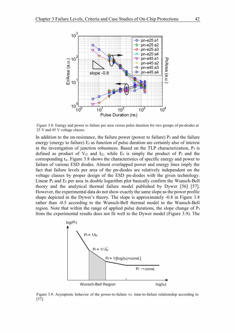
Chapter 3 Failure Levels, Criteria and Case Studies of On-Chip Protections 42
In addition to the on-resistance, the failure power (power to failure) Pf and the failure
energy (energy to failure) Ef as function of pulse duration are certainly also of interest
in the investigation of junction robustness. Based on the TLP characterization, Pf is
defined as product of Vt2 and It2, while Ef is simply the product of Pf and the
corresponding tw. Figure 3.8 shows the characteristics of specific energy and power to
failure of various ESD diodes. Almost overlapped power and energy lines imply the
fact that failure levels per area of the pn-diodes are relatively independent on the
voltage classes by proper design of the ESD pn-diodes with the given technology.
Linear Pf and Ef per area in double logarithm plot basically confirm the Wunsch-Bell
theory and the analytical thermal failure model published by Dywer [56] [57].
However, the experimental data do not show exactly the same slope as the power profile
shape depicted in the Dywer’s theory. The slope is approximately -0.8 in Figure 3.8
rather than -0.5 according to the Wunsch-Bell thermal model in the Wunsch-Bell
region. Note that within the range of applied pulse durations, the slope change of Pf
from the experimental results does not fit well to the Dywer model (Figure 3.9). The
Figure 3.8: Energy and power to failure per area versus pulse duration for two groups of pn-diodes at
25 V and 45 V voltage classes.
100
101
102
103 4
1010
0
101
102
10
Pulse Duration (ns)
Ef/A
rea
(a.u
.)P
f/Are
a (a
.u.)
slope -0.8
pn-e25 a1pn-e25 a2pn-e25 a3pn-e25 a4pn-e45 a1pn-e45 a2pn-e45 a3pn-e45 a4
Figure 3.9: Asymptotic behavior of the power-to-failure vs. time-to-failure relationship according to
[57].
Wunsch-Bell Region
Pf ≈ 1/tw
Pf ≈ 1/√tw
Pf ≈ 1/[log(tw)+const.]
Pf const.
f
log(tw)
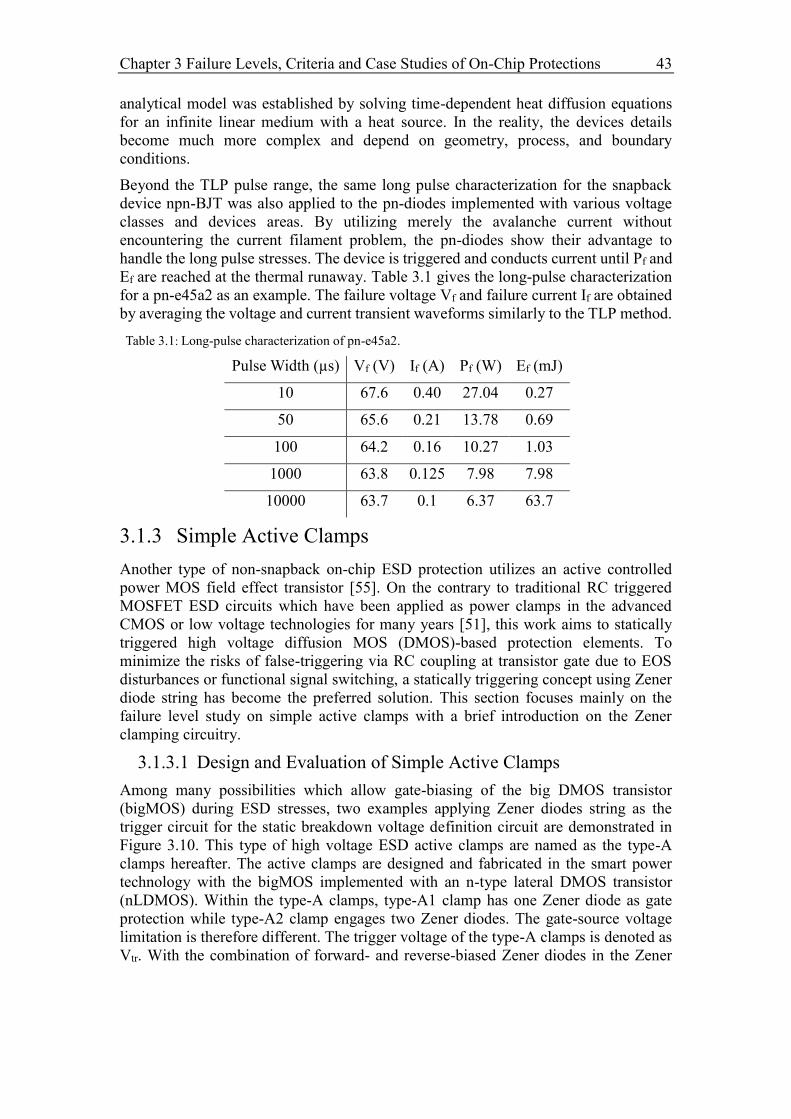
Chapter 3 Failure Levels, Criteria and Case Studies of On-Chip Protections 43
analytical model was established by solving time-dependent heat diffusion equations
for an infinite linear medium with a heat source. In the reality, the devices details
become much more complex and depend on geometry, process, and boundary
conditions.
Beyond the TLP pulse range, the same long pulse characterization for the snapback
device npn-BJT was also applied to the pn-diodes implemented with various voltage
classes and devices areas. By utilizing merely the avalanche current without
encountering the current filament problem, the pn-diodes show their advantage to
handle the long pulse stresses. The device is triggered and conducts current until Pf and
Ef are reached at the thermal runaway. Table 3.1 gives the long-pulse characterization
for a pn-e45a2 as an example. The failure voltage Vf and failure current If are obtained
by averaging the voltage and current transient waveforms similarly to the TLP method.
3.1.3 Simple Active Clamps
Another type of non-snapback on-chip ESD protection utilizes an active controlled
power MOS field effect transistor [55]. On the contrary to traditional RC triggered
MOSFET ESD circuits which have been applied as power clamps in the advanced
CMOS or low voltage technologies for many years [51], this work aims to statically
triggered high voltage diffusion MOS (DMOS)-based protection elements. To
minimize the risks of false-triggering via RC coupling at transistor gate due to EOS
disturbances or functional signal switching, a statically triggering concept using Zener
diode string has become the preferred solution. This section focuses mainly on the
failure level study on simple active clamps with a brief introduction on the Zener
clamping circuitry.
3.1.3.1 Design and Evaluation of Simple Active Clamps
Among many possibilities which allow gate-biasing of the big DMOS transistor
(bigMOS) during ESD stresses, two examples applying Zener diodes string as the
trigger circuit for the static breakdown voltage definition circuit are demonstrated in
Figure 3.10. This type of high voltage ESD active clamps are named as the type-A
clamps hereafter. The active clamps are designed and fabricated in the smart power
technology with the bigMOS implemented with an n-type lateral DMOS transistor
(nLDMOS). Within the type-A clamps, type-A1 clamp has one Zener diode as gate
protection while type-A2 clamp engages two Zener diodes. The gate-source voltage
limitation is therefore different. The trigger voltage of the type-A clamps is denoted as
Vtr. With the combination of forward- and reverse-biased Zener diodes in the Zener
Table 3.1: Long-pulse characterization of pn-e45a2.
Pulse Width (µs) Vf (V) If (A) Pf (W) Ef (mJ)
10 67.6 0.40 27.04 0.27
50 65.6 0.21 13.78 0.69
100 64.2 0.16 10.27 1.03
1000 63.8 0.125 7.98 7.98
10000 63.7 0.1 6.37 63.7
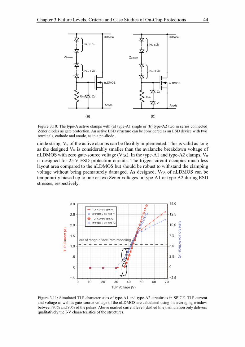
Chapter 3 Failure Levels, Criteria and Case Studies of On-Chip Protections 44
diode string, Vtr of the active clamps can be flexibly implemented. This is valid as long
as the designed Vtr is considerably smaller than the avalanche breakdown voltage of
nLDMOS with zero gate-source voltage (VGS). In the type-A1 and type-A2 clamps, Vtr
is designed for 25 V ESD protection circuits. The trigger circuit occupies much less
layout area compared to the nLDMOS but should be robust to withstand the clamping
voltage without being prematurely damaged. As designed, VGS of nLDMOS can be
temporarily biased up to one or two Zener voltages in type-A1 or type-A2 during ESD
stresses, respectively.
Figure 3.10: The type-A active clamps with (a) type-A1 single or (b) type-A2 two in series connected
Zener diodes as gate protection. An active ESD structure can be considered as an ESD device with two
terminals, cathode and anode, as in a pn-diode.
RGSn
ZD
nLDMOS
ZD,trigger
Nfor x ZD
Cathode
Anode
Nrev x ZD
ZD
RGSn ZD
nLDMOS
ZD,trigger
Nfor x ZD
Cathode
Anode
Nrev x ZD
(a) (b)
Figure 3.11: Simulated TLP characteristics of type-A1 and type-A2 circuitries in SPICE. TLP current
and voltage as well as gate-source voltage of the nLDMOS are calculated using the averaging window
between 70% and 90% of the pulses. Above marked current level (dashed line), simulation only delivers
qualitatively the I-V characteristics of the structures.
TLP Current, type-A1
averaged V GS, type-A1
TLP Current, type-A2
averaged V GS, type-A2
0 10 20 30 40 50
TLP Voltage (V)
60 70−.5
0
.5
1.0
1.5
2.0
2.5
3.0
TLP
Cu
rre
nt
(A)
−2.5
0
2.5
5.0
7.5
10.0
12.5
out of range of accurate modeling
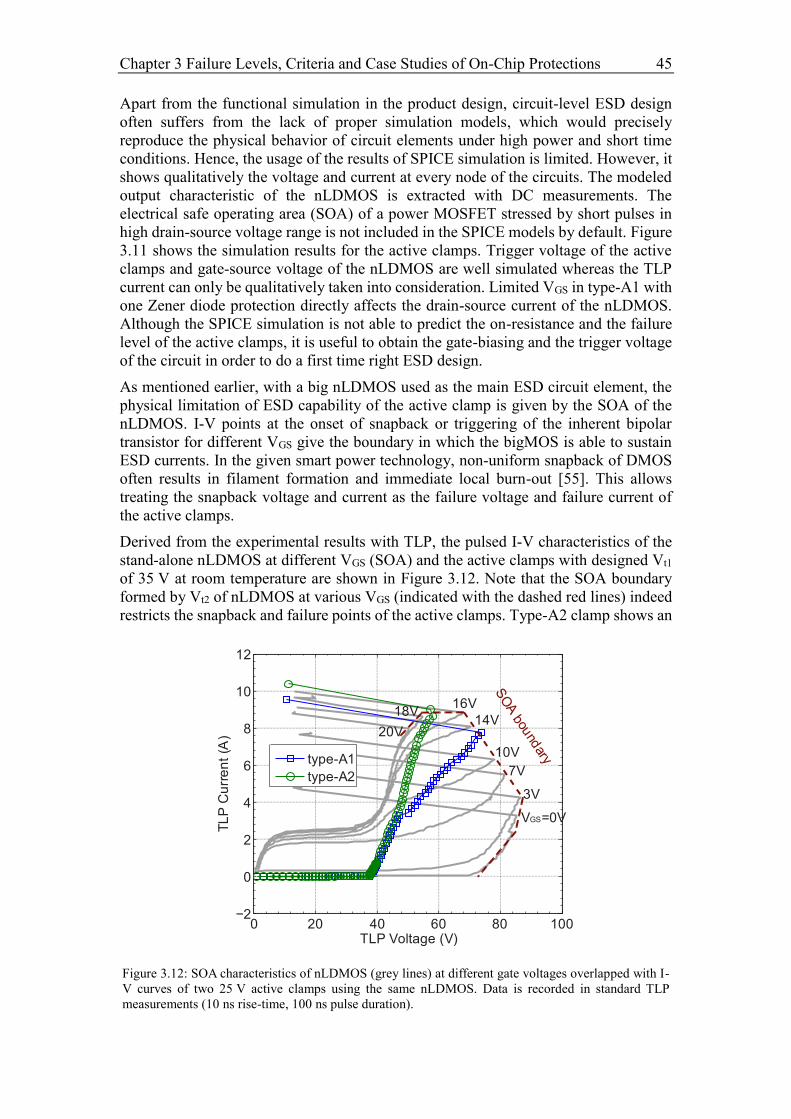
Chapter 3 Failure Levels, Criteria and Case Studies of On-Chip Protections 45
Apart from the functional simulation in the product design, circuit-level ESD design
often suffers from the lack of proper simulation models, which would precisely
reproduce the physical behavior of circuit elements under high power and short time
conditions. Hence, the usage of the results of SPICE simulation is limited. However, it
shows qualitatively the voltage and current at every node of the circuits. The modeled
output characteristic of the nLDMOS is extracted with DC measurements. The
electrical safe operating area (SOA) of a power MOSFET stressed by short pulses in
high drain-source voltage range is not included in the SPICE models by default. Figure
3.11 shows the simulation results for the active clamps. Trigger voltage of the active
clamps and gate-source voltage of the nLDMOS are well simulated whereas the TLP
current can only be qualitatively taken into consideration. Limited VGS in type-A1 with
one Zener diode protection directly affects the drain-source current of the nLDMOS.
Although the SPICE simulation is not able to predict the on-resistance and the failure
level of the active clamps, it is useful to obtain the gate-biasing and the trigger voltage
of the circuit in order to do a first time right ESD design.
As mentioned earlier, with a big nLDMOS used as the main ESD circuit element, the
physical limitation of ESD capability of the active clamp is given by the SOA of the
nLDMOS. I-V points at the onset of snapback or triggering of the inherent bipolar
transistor for different VGS give the boundary in which the bigMOS is able to sustain
ESD currents. In the given smart power technology, non-uniform snapback of DMOS
often results in filament formation and immediate local burn-out [55]. This allows
treating the snapback voltage and current as the failure voltage and failure current of
the active clamps.
Derived from the experimental results with TLP, the pulsed I-V characteristics of the
stand-alone nLDMOS at different VGS (SOA) and the active clamps with designed Vt1
of 35 V at room temperature are shown in Figure 3.12. Note that the SOA boundary
formed by Vt2 of nLDMOS at various VGS (indicated with the dashed red lines) indeed
restricts the snapback and failure points of the active clamps. Type-A2 clamp shows an
Figure 3.12: SOA characteristics of nLDMOS (grey lines) at different gate voltages overlapped with I-
V curves of two 25 V active clamps using the same nLDMOS. Data is recorded in standard TLP
measurements (10 ns rise-time, 100 ns pulse duration).
0 20 40 60 80 100−2
0
2
4
6
8
10
12
TL
P C
urr
en
t (A
)
TLP Voltage (V)
3V
V =0VGS
type-A1
type-A2
20V
18V16V
14V
10V
7V
SO
A bou
ndary
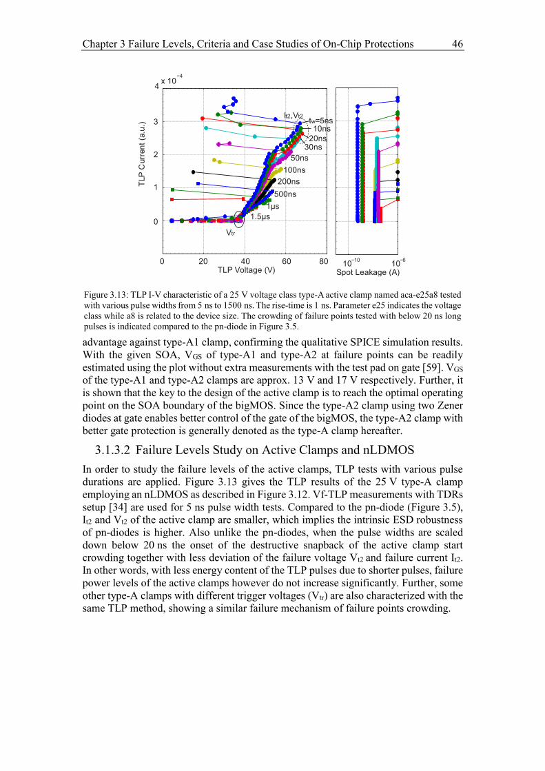
Chapter 3 Failure Levels, Criteria and Case Studies of On-Chip Protections 46
advantage against type-A1 clamp, confirming the qualitative SPICE simulation results.
With the given SOA, VGS of type-A1 and type-A2 at failure points can be readily
estimated using the plot without extra measurements with the test pad on gate [59]. VGS
of the type-A1 and type-A2 clamps are approx. 13 V and 17 V respectively. Further, it
is shown that the key to the design of the active clamp is to reach the optimal operating
point on the SOA boundary of the bigMOS. Since the type-A2 clamp using two Zener
diodes at gate enables better control of the gate of the bigMOS, the type-A2 clamp with
better gate protection is generally denoted as the type-A clamp hereafter.
3.1.3.2 Failure Levels Study on Active Clamps and nLDMOS
In order to study the failure levels of the active clamps, TLP tests with various pulse
durations are applied. Figure 3.13 gives the TLP results of the 25 V type-A clamp
employing an nLDMOS as described in Figure 3.12. Vf-TLP measurements with TDRs
setup [34] are used for 5 ns pulse width tests. Compared to the pn-diode (Figure 3.5),
It2 and Vt2 of the active clamp are smaller, which implies the intrinsic ESD robustness
of pn-diodes is higher. Also unlike the pn-diodes, when the pulse widths are scaled
down below 20 ns the onset of the destructive snapback of the active clamp start
crowding together with less deviation of the failure voltage Vt2 and failure current It2.
In other words, with less energy content of the TLP pulses due to shorter pulses, failure
power levels of the active clamps however do not increase significantly. Further, some
other type-A clamps with different trigger voltages (Vtr) are also characterized with the
same TLP method, showing a similar failure mechanism of failure points crowding.
Figure 3.13: TLP I-V characteristic of a 25 V voltage class type-A active clamp named aca-e25a8 tested
with various pulse widths from 5 ns to 1500 ns. The rise-time is 1 ns. Parameter e25 indicates the voltage
class while a8 is related to the device size. The crowding of failure points tested with below 20 ns long
pulses is indicated compared to the pn-diode in Figure 3.5.
30ns
50ns
tw=5ns10ns
20ns
100ns
200ns
500ns
1μs
1.5μs
Vtr
It2,Vt2
0 20 40 60TLP Voltage (V)
10−10
10−6
Spot Leakage (A)
80
0
1
2
3
4x 10
TLP
Curr
en
t (a
.u.)
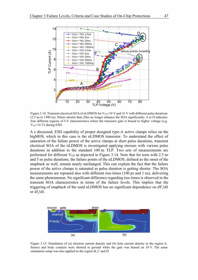
Chapter 3 Failure Levels, Criteria and Case Studies of On-Chip Protections 47
A s discussed, ESD capability of proper designed type-A active clamps relies on the
bigMOS, which in this case is the nLDMOS transistor. To understand the effect of
saturation of the failure power of the active clamps at short pulse durations, transient
electrical SOA of the nLDMOS is investigated applying stresses with various pulse
durations in addition to the standard 100 ns TLP. Two sets of measurements are
performed for different VGS as depicted in Figure 3.14. Note that for tests with 2.5 ns
and 5 ns pulse durations, the failure points of the nLDMOS, defined as the onset of the
snapback as well, remain nearly unchanged. This can explain the fact that the failure
power of the active clamps is saturated as pulse duration is getting shorter. The SOA
measurements are repeated also with different rise-times (100 ps and 1 ns), delivering
the same phenomenon. No significant difference regarding rise-times is observed in the
transient SOA characteristics in terms of the failure levels. This implies that the
triggering of snapback of the used nLDMOS has no significant dependence on 𝑑𝑉/𝑑𝑡
or 𝑑𝐼/𝑑𝑡.
Figure 3.15: Simulation of (a) electron current density and (b) hole current density in the region A.
Source and body contacts were shorted to ground while the gate was biased on 10 V. The same
simulation setup was also applied to the region B, C and D.
p-
n-epi
STIchannel n+
body
(a) (b)
Figure 3.14: Transient electrical SOA of nLDMOS for VGS=10 V and 16 V with different pulse durations
(2.5 ns to 1500 ns). Pulses shorter than 20ns no longer enhance the SOA significantly. A to D indicates
four different regions of I-V characteristics where the transistor gate is biased to higher voltage (e.g.
VGS=16 V) during ESD.
0 10 20 30 40 50 60 70 80
2
4
6
8
10
12
14
TL
PC
urr
en
t(A
)
TLP Voltage (V)
VGS = 16V, 2.5ns
VGS = 16V, 5ns
VGS = 16V, 20ns
VGS = 16V, 500ns
VGS = 16V, 1500ns
VGS = 10V, 2.5ns
VGS = 10V, 5ns
VGS = 10V, 20ns
VGS = 10V, 500ns
VGS = 10V, 1500ns
A
B
C
D
failure points crowding
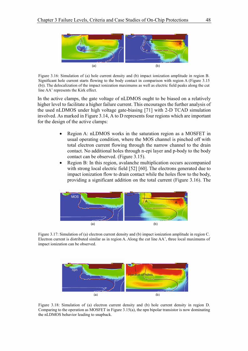
Chapter 3 Failure Levels, Criteria and Case Studies of On-Chip Protections 48
In the active clamps, the gate voltage of nLDMOS ought to be biased on a relatively
higher level to facilitate a higher failure current. This encourages the further analysis of
the used nLDMOS under high voltage gate-biasing [71] with 2-D TCAD simulation
involved. As marked in Figure 3.14, A to D represents four regions which are important
for the design of the active clamps:
Region A: nLDMOS works in the saturation region as a MOSFET in
usual operating condition, where the MOS channel is pinched off with
total electron current flowing through the narrow channel to the drain
contact. No additional holes through n-epi layer and p-body to the body
contact can be observed. (Figure 3.15).
Region B: In this region, avalanche multiplication occurs accompanied
with strong local electric field [52] [60]. The electrons generated due to
impact ionization flow to drain contact while the holes flow to the body,
providing a significant addition on the total current (Figure 3.16). The
Figure 3.18: Simulation of (a) electron current density and (b) hole current density in region D.
Comparing to the operation as MOSFET in Figure 3.15(a), the npn bipolar transistor is now dominating
the nLDMOS behavior leading to snapback.
(a) (b)
injection of holes
npn
Figure 3.17: Simulation of (a) electron current density and (b) impact ionization amplitude in region C.
Electron current is distributed similar as in region A. Along the cut line AA’, three local maximums of
impact ionization can be observed.
(a) (b)
A A’
MOS
Figure 3.16: Simulation of (a) hole current density and (b) impact ionization amplitude in region B.
Significant hole current starts flowing to the body contact in comparison with region A (Figure 3.15
(b)). The delocalization of the impact ionization maximums as well as electric field peaks along the cut
line AA’ represents the Kirk effect.
(a) (b)
A A’
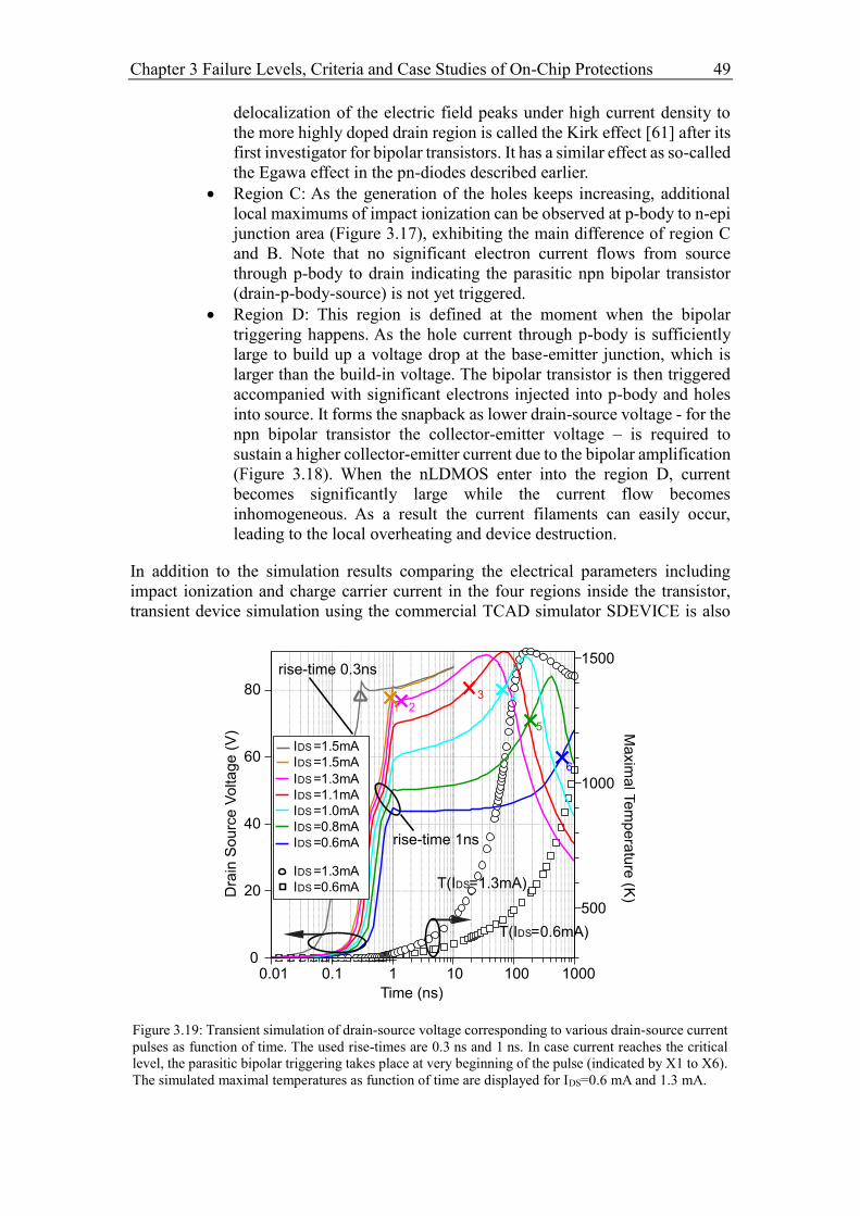
Chapter 3 Failure Levels, Criteria and Case Studies of On-Chip Protections 49
delocalization of the electric field peaks under high current density to
the more highly doped drain region is called the Kirk effect [61] after its
first investigator for bipolar transistors. It has a similar effect as so-called
the Egawa effect in the pn-diodes described earlier.
Region C: As the generation of the holes keeps increasing, additional
local maximums of impact ionization can be observed at p-body to n-epi
junction area (Figure 3.17), exhibiting the main difference of region C
and B. Note that no significant electron current flows from source
through p-body to drain indicating the parasitic npn bipolar transistor
(drain-p-body-source) is not yet triggered.
Region D: This region is defined at the moment when the bipolar
triggering happens. As the hole current through p-body is sufficiently
large to build up a voltage drop at the base-emitter junction, which is
larger than the build-in voltage. The bipolar transistor is then triggered
accompanied with significant electrons injected into p-body and holes
into source. It forms the snapback as lower drain-source voltage - for the
npn bipolar transistor the collector-emitter voltage – is required to
sustain a higher collector-emitter current due to the bipolar amplification
(Figure 3.18). When the nLDMOS enter into the region D, current
becomes significantly large while the current flow becomes
inhomogeneous. As a result the current filaments can easily occur,
leading to the local overheating and device destruction.
In addition to the simulation results comparing the electrical parameters including
impact ionization and charge carrier current in the four regions inside the transistor,
transient device simulation using the commercial TCAD simulator SDEVICE is also
Figure 3.19: Transient simulation of drain-source voltage corresponding to various drain-source current
pulses as function of time. The used rise-times are 0.3 ns and 1 ns. In case current reaches the critical
level, the parasitic bipolar triggering takes place at very beginning of the pulse (indicated by X1 to X6).
The simulated maximal temperatures as function of time are displayed for IDS=0.6 mA and 1.3 mA.
0
20
40
60
80
500
1000
1500
0.1 1 10 100 1000
Time (ns)
0.01
Dra
in S
ou
rce
Vo
lta
ge
(V
)
23 4
5
6
1
rise-time 0.3ns
rise-time 1ns
IDS =1.5mA
IDS =1.5mA
IDS =1.3mA
IDS =1.1mA
IDS =1.0mA
IDS =0.8mA
IDS =0.6mA
IDS =1.3mA
IDS =0.6mA
T(I =0.6mA)DS
T(I =1.3mA)DS
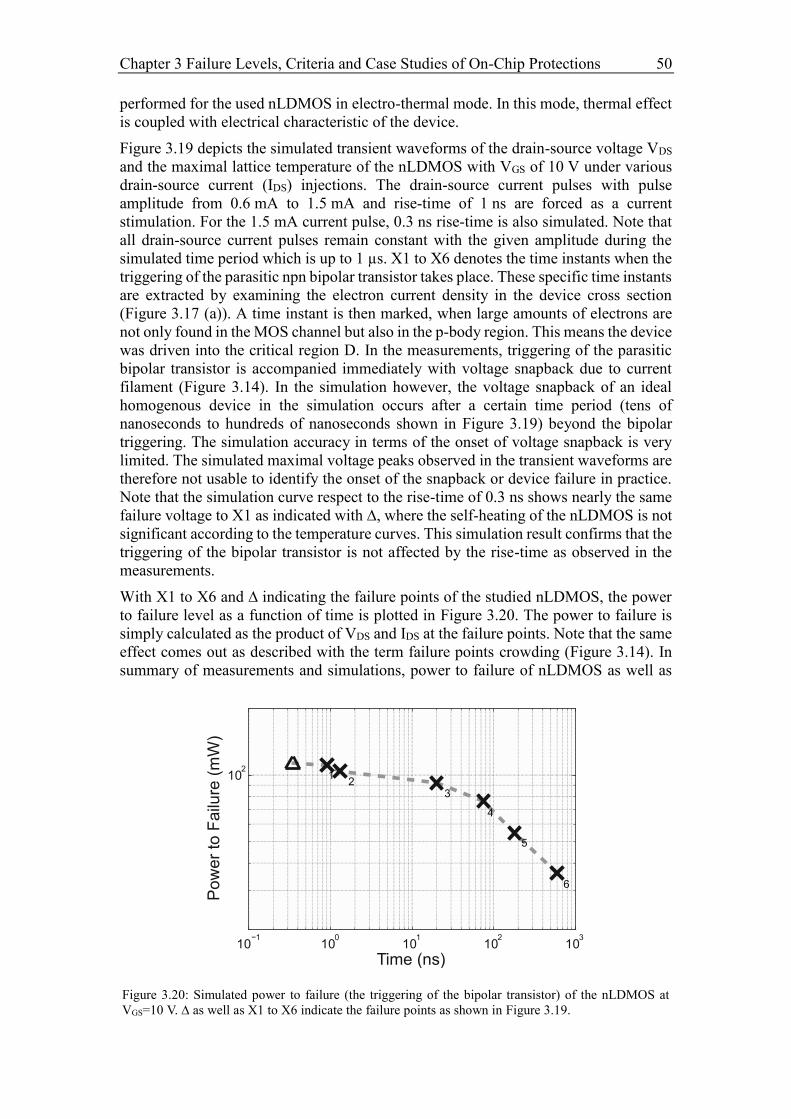
Chapter 3 Failure Levels, Criteria and Case Studies of On-Chip Protections 50
performed for the used nLDMOS in electro-thermal mode. In this mode, thermal effect
is coupled with electrical characteristic of the device.
Figure 3.19 depicts the simulated transient waveforms of the drain-source voltage VDS
and the maximal lattice temperature of the nLDMOS with VGS of 10 V under various
drain-source current (IDS) injections. The drain-source current pulses with pulse
amplitude from 0.6 mA to 1.5 mA and rise-time of 1 ns are forced as a current
stimulation. For the 1.5 mA current pulse, 0.3 ns rise-time is also simulated. Note that
all drain-source current pulses remain constant with the given amplitude during the
simulated time period which is up to 1 µs. X1 to X6 denotes the time instants when the
triggering of the parasitic npn bipolar transistor takes place. These specific time instants
are extracted by examining the electron current density in the device cross section
(Figure 3.17 (a)). A time instant is then marked, when large amounts of electrons are
not only found in the MOS channel but also in the p-body region. This means the device
was driven into the critical region D. In the measurements, triggering of the parasitic
bipolar transistor is accompanied immediately with voltage snapback due to current
filament (Figure 3.14). In the simulation however, the voltage snapback of an ideal
homogenous device in the simulation occurs after a certain time period (tens of
nanoseconds to hundreds of nanoseconds shown in Figure 3.19) beyond the bipolar
triggering. The simulation accuracy in terms of the onset of voltage snapback is very
limited. The simulated maximal voltage peaks observed in the transient waveforms are
therefore not usable to identify the onset of the snapback or device failure in practice.
Note that the simulation curve respect to the rise-time of 0.3 ns shows nearly the same
failure voltage to X1 as indicated with ∆, where the self-heating of the nLDMOS is not
significant according to the temperature curves. This simulation result confirms that the
triggering of the bipolar transistor is not affected by the rise-time as observed in the
measurements.
With X1 to X6 and ∆ indicating the failure points of the studied nLDMOS, the power
to failure level as a function of time is plotted in Figure 3.20. The power to failure is
simply calculated as the product of VDS and IDS at the failure points. Note that the same
effect comes out as described with the term failure points crowding (Figure 3.14). In
summary of measurements and simulations, power to failure of nLDMOS as well as
Figure 3.20: Simulated power to failure (the triggering of the bipolar transistor) of the nLDMOS at
VGS=10 V. ∆ as well as X1 to X6 indicate the failure points as shown in Figure 3.19.
10−1
100
101
102
103
102
Time (ns)
Po
we
r to
Fa
ilure
(m
W)
12
3
4
5
6
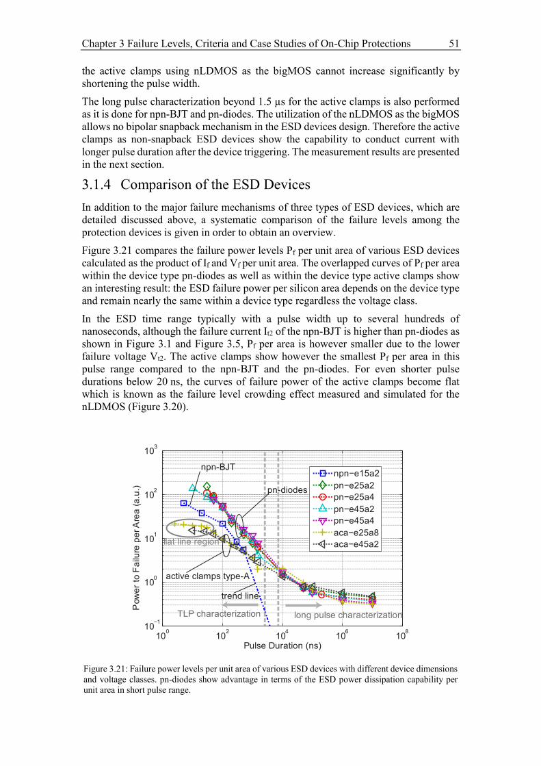
Chapter 3 Failure Levels, Criteria and Case Studies of On-Chip Protections 51
the active clamps using nLDMOS as the bigMOS cannot increase significantly by
shortening the pulse width.
The long pulse characterization beyond 1.5 µs for the active clamps is also performed
as it is done for npn-BJT and pn-diodes. The utilization of the nLDMOS as the bigMOS
allows no bipolar snapback mechanism in the ESD devices design. Therefore the active
clamps as non-snapback ESD devices show the capability to conduct current with
longer pulse duration after the device triggering. The measurement results are presented
in the next section.
3.1.4 Comparison of the ESD Devices
In addition to the major failure mechanisms of three types of ESD devices, which are
detailed discussed above, a systematic comparison of the failure levels among the
protection devices is given in order to obtain an overview.
Figure 3.21 compares the failure power levels Pf per unit area of various ESD devices
calculated as the product of If and Vf per unit area. The overlapped curves of Pf per area
within the device type pn-diodes as well as within the device type active clamps show
an interesting result: the ESD failure power per silicon area depends on the device type
and remain nearly the same within a device type regardless the voltage class.
In the ESD time range typically with a pulse width up to several hundreds of
nanoseconds, although the failure current It2 of the npn-BJT is higher than pn-diodes as
shown in Figure 3.1 and Figure 3.5, Pf per area is however smaller due to the lower
failure voltage Vt2. The active clamps show however the smallest Pf per area in this
pulse range compared to the npn-BJT and the pn-diodes. For even shorter pulse
durations below 20 ns, the curves of failure power of the active clamps become flat
which is known as the failure level crowding effect measured and simulated for the
nLDMOS (Figure 3.20).
Figure 3.21: Failure power levels per unit area of various ESD devices with different device dimensions
and voltage classes. pn-diodes show advantage in terms of the ESD power dissipation capability per
unit area in short pulse range.
100
102
104
106
108
10−1
100
101
102
10
Pulse Duration (ns)
Pow
er
to F
ailu
re p
er A
rea
(a
.u.)
npn−e15a2
pn−e25a2
pn−e25a4
pn−e45a2
pn−e45a4
aca−e25a8
aca−e45a2
active clamps type-A
npn-BJT
pn-diodes
TLP characterization
trend line
long pulse characterization
flat line region
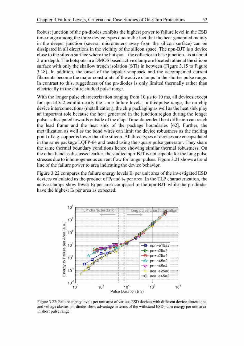
Chapter 3 Failure Levels, Criteria and Case Studies of On-Chip Protections 52
Robust junction of the pn-diodes exhibits the highest power to failure level in the ESD
time range among the three device types due to the fact that the heat generated mainly
in the deeper junction (several micrometers away from the silicon surface) can be
dissipated in all directions in the vicinity of the silicon space. The npn-BJT is a device
close to the silicon surface where the hotspot – the collector to base junction - is at about
2 µm depth. The hotspots in a DMOS based active clamp are located rather at the silicon
surface with only the shallow trench isolation (STI) in between (Figure 3.15 to Figure
3.18). In addition, the onset of the bipolar snapback and the accompanied current
filaments become the major constraints of the active clamps in the shorter pulse range.
In contrast to this, ruggedness of the pn-diodes is only limited thermally rather than
electrically in the entire studied pulse range.
With the longer pulse characterization ranging from 10 µs to 10 ms, all devices except
for npn-e15a2 exhibit nearly the same failure levels. In this pulse range, the on-chip
device interconnections (metallization), the chip packaging as well as the heat sink play
an important role because the heat generated in the junction region during the longer
pulse is dissipated towards outside of the chip. Time-dependent heat diffusion can reach
the lead frame and the heat sink of the package boundaries [62]. Further, the
metallization as well as the bond wires can limit the device robustness as the melting
point of e.g. copper is lower than the silicon. All three types of devices are encapsulated
in the same package LQFP-64 and tested using the square pulse generator. They share
the same thermal boundary conditions hence showing similar thermal robustness. On
the other hand as discussed earlier, the studied npn-BJT is not capable for the long pulse
stresses due to inhomogeneous current flow for longer pulses. Figure 3.21 shows a trend
line of the failure power to area indicating the device behavior.
Figure 3.22 compares the failure energy levels Ef per unit area of the investigated ESD
devices calculated as the product of Pf and tw per area. In the TLP characterization, the
active clamps show lower Ef per area compared to the npn-BJT while the pn-diodes
have the highest Ef per area as expected.
Figure 3.22: Failure energy levels per unit area of various ESD devices with different device dimensions
and voltage classes. pn-diodes show advantage in terms of the withstand ESD pulse energy per unit area
in short pulse range.
100
102
104
106
108
10−2
10−1
100
101
102
103
10
Pulse Duration (ns)
En
erg
y to
Failure
per
Are
a (
a.u
.)
npn−e15a2
pn−e25a2
pn−e25a4
pn−e45a2
pn−e45a4
aca−e25a8
aca−e45a2
TLP characterization long pulse characterization
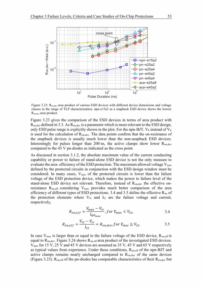
Chapter 3 Failure Levels, Criteria and Case Studies of On-Chip Protections 53
Figure 3.23 gives the comparison of the ESD devices in terms of area product with
Ron,dev defined in 3.3. As Ron,dev is a parameter which is more relevant to the ESD design,
only ESD pulse range is explicitly shown in the plot. For the npn-BJT, Vh instead of Vtr
is used for the calculation of Ron,dev. The data points confirm that the on-resistance of
the snapback devices is usually much lower than the non-snapback ESD devices.
Interestingly for pulses longer than 200 ns, the active clamps show lower Ron,dev
compared to the 45 V pn-diodes as indicated as the cross point.
As discussed in section 3.1.2, the absolute maximum value of the current conducting
capability or power to failure of stand-alone ESD device is not the only measure to
evaluate the area efficiency of the ESD protection. The maximum allowed voltage Vmax
defined by the protected circuits in conjunction with the ESD design window must be
considered. In many cases, Vmax of the protected circuits is lower than the failure
voltage of the ESD protection device, which makes the power to failure level of the
stand-alone ESD device not relevant. Therefore, instead of Ron,dev the effective on-
resistance Ron,eff considering Vmax provides much better comparison of the area
efficiency of different types of ESD protections. 3.4 and 3.5 define the effective Ron of
the protection elements where Vt2 and It2 are the failure voltage and current,
respectively,
𝑅𝑜𝑛,𝑒𝑓𝑓 =𝑉𝑚𝑎𝑥 − 𝑉𝑡𝑟
𝐼@𝑉𝑚𝑎𝑥
, 𝑓𝑜𝑟 𝑉𝑚𝑎𝑥 < 𝑉𝑡2, 3.4
𝑅𝑜𝑛,𝑒𝑓𝑓 =𝑉𝑡2 − 𝑉𝑡𝑟
𝐼𝑡2= 𝑅𝑜𝑛,𝑑𝑒𝑣, 𝑓𝑜𝑟 𝑉𝑚𝑎𝑥 ≥ 𝑉𝑡2. 3.5
In case Vmax is larger than or equal to the failure voltage of the ESD device, Ron,eff is
equal to Ron,dev. Figure 3.24 shows Ron,eff area product of the investigated ESD devices.
Vmax for 15 V, 25 V and 45 V devices are assumed as 35 V, 45 V and 65 V respectively
as typical values from experience. Under these conditions, Ron,eff of the npn-BJT and
active clamps remains nearly unchanged compared to Ron,dev of the same devices
(Figure 3.23). Ron,eff of the pn-diodes has comparable characteristics of their Ron,dev but
Figure 3.23: Ron,dev area product of various ESD devices with different device dimensions and voltage
classes in the range of TLP characterization. npn-e15a2 as a snapback ESD device shows the lowest
Ron,dev area product.
101
102
103
10−2
10−1
Pulse Duration (ns)
Ron
,de
v •
Are
a (
a.u
.)
npn−e15a2
pn−e25a2
pn−e25a4
pn−e45a2
pn−e45a4
aca−e25a8
aca−e45a2
cross point
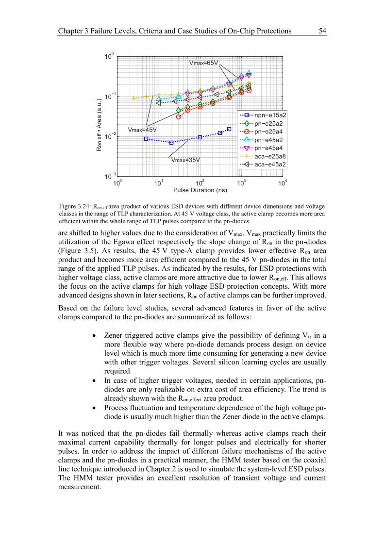
Chapter 3 Failure Levels, Criteria and Case Studies of On-Chip Protections 54
are shifted to higher values due to the consideration of Vmax. Vmax practically limits the
utilization of the Egawa effect respectively the slope change of Ron in the pn-diodes
(Figure 3.5). As results, the 45 V type-A clamp provides lower effective Ron area
product and becomes more area efficient compared to the 45 V pn-diodes in the total
range of the applied TLP pulses. As indicated by the results, for ESD protections with
higher voltage class, active clamps are more attractive due to lower Ron,eff. This allows
the focus on the active clamps for high voltage ESD protection concepts. With more
advanced designs shown in later sections, Ron of active clamps can be further improved.
Based on the failure level studies, several advanced features in favor of the active
clamps compared to the pn-diodes are summarized as follows:
Zener triggered active clamps give the possibility of defining Vtr in a
more flexible way where pn-diode demands process design on device
level which is much more time consuming for generating a new device
with other trigger voltages. Several silicon learning cycles are usually
required.
In case of higher trigger voltages, needed in certain applications, pn-
diodes are only realizable on extra cost of area efficiency. The trend is
already shown with the Ron,effect area product.
Process fluctuation and temperature dependence of the high voltage pn-
diode is usually much higher than the Zener diode in the active clamps.
It was noticed that the pn-diodes fail thermally whereas active clamps reach their
maximal current capability thermally for longer pulses and electrically for shorter
pulses. In order to address the impact of different failure mechanisms of the active
clamps and the pn-diodes in a practical manner, the HMM tester based on the coaxial
line technique introduced in Chapter 2 is used to simulate the system-level ESD pulses.
The HMM tester provides an excellent resolution of transient voltage and current
measurement.
Figure 3.24: Ron,eff area product of various ESD devices with different device dimensions and voltage
classes in the range of TLP characterization. At 45 V voltage class, the active clamp becomes more area
efficient within the whole range of TLP pulses compared to the pn-diodes.
100
101
102
103
104
10−3
10−2
10−1
10
Pulse Duration (ns)
npn−e15a2
pn−e25a2
pn−e25a4
pn−e45a2
pn−e45a4
aca−e25a8
aca−e45a2
Ro
n,e
ff •
Are
a (
a.u
.)
Vmax=65V
Vmax=45V
Vmax=35V
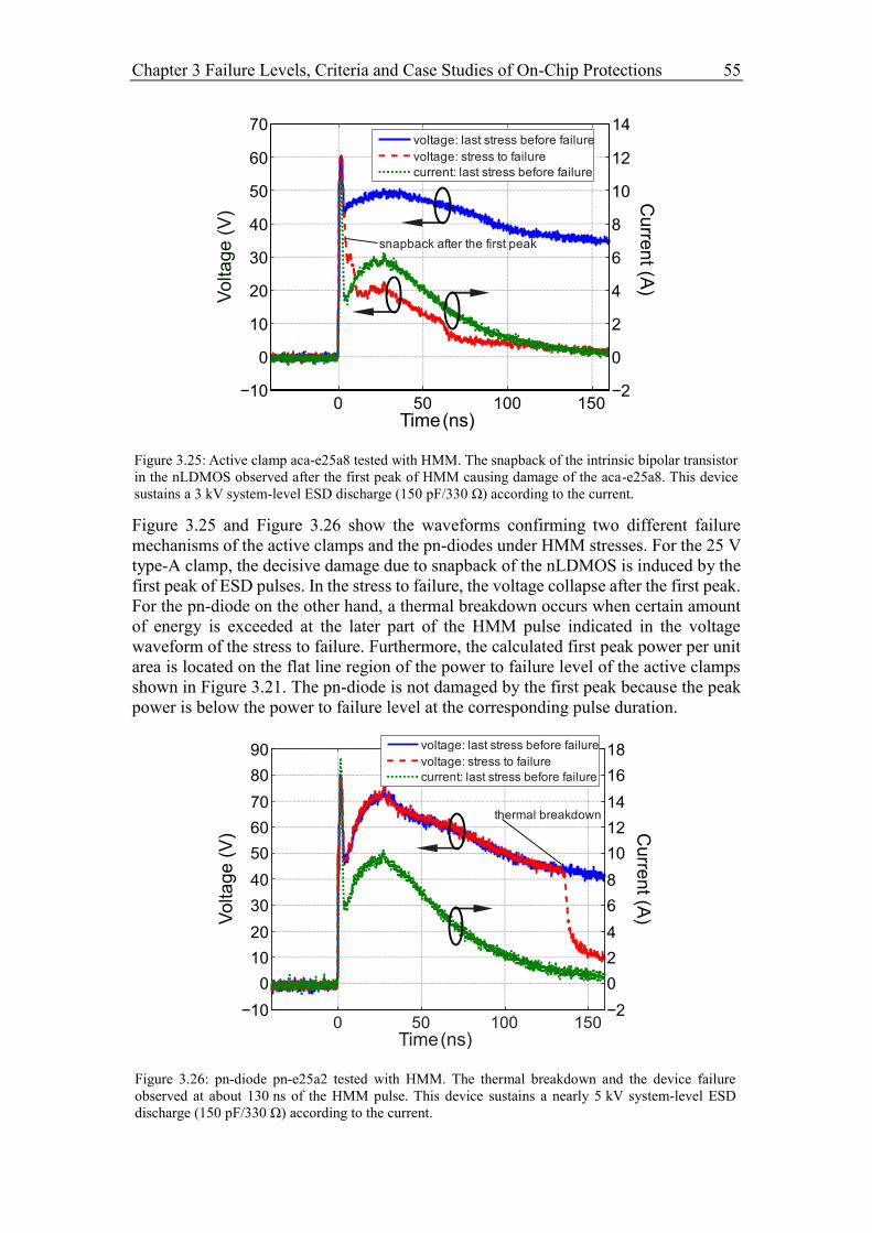
Chapter 3 Failure Levels, Criteria and Case Studies of On-Chip Protections 55
Figure 3.25 and Figure 3.26 show the waveforms confirming two different failure
mechanisms of the active clamps and the pn-diodes under HMM stresses. For the 25 V
type-A clamp, the decisive damage due to snapback of the nLDMOS is induced by the
first peak of ESD pulses. In the stress to failure, the voltage collapse after the first peak.
For the pn-diode on the other hand, a thermal breakdown occurs when certain amount
of energy is exceeded at the later part of the HMM pulse indicated in the voltage
waveform of the stress to failure. Furthermore, the calculated first peak power per unit
area is located on the flat line region of the power to failure level of the active clamps
shown in Figure 3.21. The pn-diode is not damaged by the first peak because the peak
power is below the power to failure level at the corresponding pulse duration.
Figure 3.26: pn-diode pn-e25a2 tested with HMM. The thermal breakdown and the device failure
observed at about 130 ns of the HMM pulse. This device sustains a nearly 5 kV system-level ESD
discharge (150 pF/330 Ω) according to the current.
0 50 100 150−10
0
10
20
30
40
50
60
70
80
90
Vo
lta
ge
(V
)
Time(ns)
−2
0
2
4
6
8
10
12
14
16
18
Cu
rren
t (A)
voltage: last stress before failure
voltage: stress to failure
current: last stress before failure
thermal breakdown
Figure 3.25: Active clamp aca-e25a8 tested with HMM. The snapback of the intrinsic bipolar transistor
in the nLDMOS observed after the first peak of HMM causing damage of the aca-e25a8. This device
sustains a 3 kV system-level ESD discharge (150 pF/330 Ω) according to the current.
0 50 100 150−10
0
10
20
30
40
50
60
Vo
lta
ge
(V
)
Time(ns)
−2
0
2
4
6
8
10
12
Cu
rren
t (A)
voltage: last stress before failure
voltage: stress to failure
current: last stress before failure
snapback after the first peak
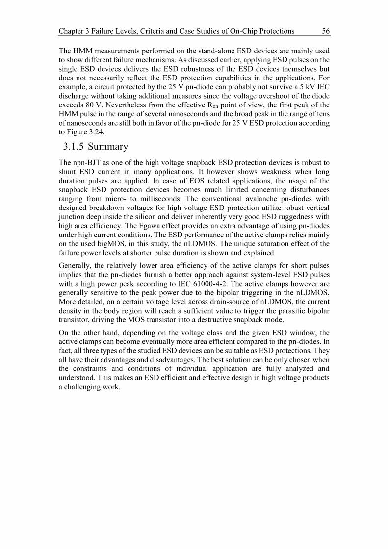
Chapter 3 Failure Levels, Criteria and Case Studies of On-Chip Protections 56
The HMM measurements performed on the stand-alone ESD devices are mainly used
to show different failure mechanisms. As discussed earlier, applying ESD pulses on the
single ESD devices delivers the ESD robustness of the ESD devices themselves but
does not necessarily reflect the ESD protection capabilities in the applications. For
example, a circuit protected by the 25 V pn-diode can probably not survive a 5 kV IEC
discharge without taking additional measures since the voltage overshoot of the diode
exceeds 80 V. Nevertheless from the effective Ron point of view, the first peak of the
HMM pulse in the range of several nanoseconds and the broad peak in the range of tens
of nanoseconds are still both in favor of the pn-diode for 25 V ESD protection according
to Figure 3.24.
3.1.5 Summary
The npn-BJT as one of the high voltage snapback ESD protection devices is robust to
shunt ESD current in many applications. It however shows weakness when long
duration pulses are applied. In case of EOS related applications, the usage of the
snapback ESD protection devices becomes much limited concerning disturbances
ranging from micro- to milliseconds. The conventional avalanche pn-diodes with
designed breakdown voltages for high voltage ESD protection utilize robust vertical
junction deep inside the silicon and deliver inherently very good ESD ruggedness with
high area efficiency. The Egawa effect provides an extra advantage of using pn-diodes
under high current conditions. The ESD performance of the active clamps relies mainly
on the used bigMOS, in this study, the nLDMOS. The unique saturation effect of the
failure power levels at shorter pulse duration is shown and explained
Generally, the relatively lower area efficiency of the active clamps for short pulses
implies that the pn-diodes furnish a better approach against system-level ESD pulses
with a high power peak according to IEC 61000-4-2. The active clamps however are
generally sensitive to the peak power due to the bipolar triggering in the nLDMOS.
More detailed, on a certain voltage level across drain-source of nLDMOS, the current
density in the body region will reach a sufficient value to trigger the parasitic bipolar
transistor, driving the MOS transistor into a destructive snapback mode.
On the other hand, depending on the voltage class and the given ESD window, the
active clamps can become eventually more area efficient compared to the pn-diodes. In
fact, all three types of the studied ESD devices can be suitable as ESD protections. They
all have their advantages and disadvantages. The best solution can be only chosen when
the constraints and conditions of individual application are fully analyzed and
understood. This makes an ESD efficient and effective design in high voltage products
a challenging work.
Chapter 3 Failure Levels, Criteria and Case Studies of On-Chip Protections 57
3.2 Case Studies for Failure Modes of ESD Protections
The failure level studies of the ESD protection devices discussed in the previous section
provide overview and give insight of protection efficiency in terms of respective device
parameters such as power to failure and effective on-resistance concerning device area.
However only considering protection device is a misconception. The ESD protection
effectiveness can be evaluated with the ESD robustness of the ESD protected circuits
consisting of the ESD protection and the protected circuits (also called monitoring
circuits in the test structures). In fact the effectiveness depends strongly on the
behaviors, in particular the failure modes of protected devices and structures. This
section discusses mainly from the perspective of ESD protection effectiveness. To
obtain high effectiveness, special concerns such as circuit configurations, impact of
voltage overshoots have to be well addressed and taken into account. As previously
introduced as an example, it is well known that the use of npn-BJT can be risky due to
its limited turn-on speed and the induced harmful voltage overshoots. On the contrary,
the following study uncovers an unique failure mode observed on LDMOS transistors
even protected by pn-diodes [63].
Voltage overshoots due to finite turn-on speed of ESD protection devices often show
negative impacts on ESD hardness and have become a matter of concern in design of
advanced CMOS circuits for years [47] [64]. Harmful overshoots are frequently
reported in low voltage technologies, mainly causing damages at thin gate-oxide. In the
field of high voltage ESD protection, breakdown of thick gate-oxide is normally not a
critical issue in ESD design. However, power transistors usually DMOS transistors are
believed to be inherently weak against ESD depending on device sizes [65] [66]. As
discussed in the previous section, as the voltage reaches the region in excess of the
electrical SOA, current filaments can occur at the onset of snapback accompanied with
the danger of locally thermal overload in DMOS devices. TLP within only several
nanoseconds pulse duration actually result in destructive lateral DMOS snapback in
case the critical voltage and current are reached.
To avoid the triggering of the parasitic bipolar transistor in the LDMOS transistor,
voltage clamping devices such as avalanche pn-diodes are usually applied and
connected in parallel to protect the weak LDMOS transistors with the upper limit of the
ESD window given by the snapback trigger voltage Vt2 which is destructive. Avalanche
pn-diodes as protection devices belong to static-triggered voltage clamps. Thus, the
robustness of a stand-alone pn-diode has no dependence on rise-time of the ESD pulse.
However, TLP tests surprisingly showed this type of on-chip protection concepts do
not provide the expected ESD hardness especially during the TLP tests with short rise-
times. Using npn-BJT as a snapback device also does not effectively protect the
LDMOS transistor.
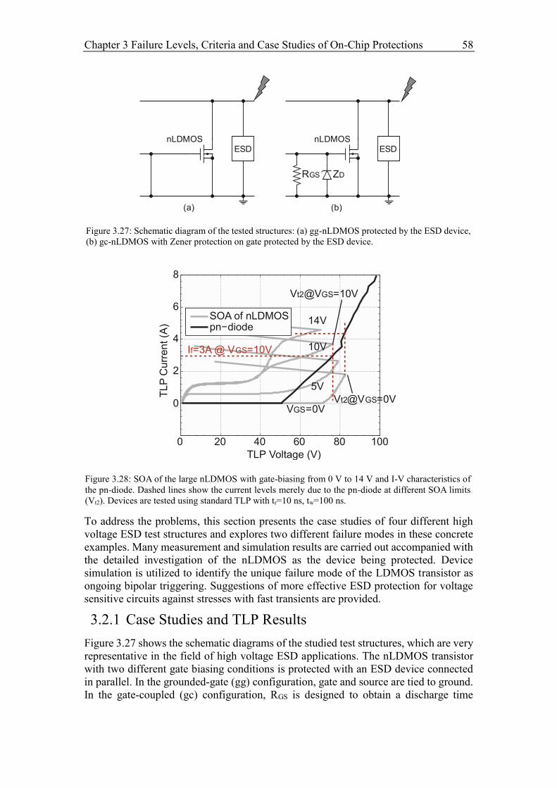
Chapter 3 Failure Levels, Criteria and Case Studies of On-Chip Protections 58
To address the problems, this section presents the case studies of four different high
voltage ESD test structures and explores two different failure modes in these concrete
examples. Many measurement and simulation results are carried out accompanied with
the detailed investigation of the nLDMOS as the device being protected. Device
simulation is utilized to identify the unique failure mode of the LDMOS transistor as
ongoing bipolar triggering. Suggestions of more effective ESD protection for voltage
sensitive circuits against stresses with fast transients are provided.
3.2.1 Case Studies and TLP Results
Figure 3.27 shows the schematic diagrams of the studied test structures, which are very
representative in the field of high voltage ESD applications. The nLDMOS transistor
with two different gate biasing conditions is protected with an ESD device connected
in parallel. In the grounded-gate (gg) configuration, gate and source are tied to ground.
In the gate-coupled (gc) configuration, RGS is designed to obtain a discharge time
Figure 3.28: SOA of the large nLDMOS with gate-biasing from 0 V to 14 V and I-V characteristics of
the pn-diode. Dashed lines show the current levels merely due to the pn-diode at different SOA limits
(Vt2). Devices are tested using standard TLP with tr=10 ns, tw=100 ns.
0 20 40 60 80 100
0
2
4
6
TL
P C
urr
en
t (A
)
TLP Voltage (V)
SOA of nLDMOSpn−diode
14V
5V
10V
Vt2@VGS=10V
Vt2@VGS=0VVGS=0V
If=3A @ VGS=10V
Figure 3.27: Schematic diagram of the tested structures: (a) gg-nLDMOS protected by the ESD device,
(b) gc-nLDMOS with Zener protection on gate protected by the ESD device.
ZDRGS
ESDnLDMOS nLDMOS
(a) (b)
ESD
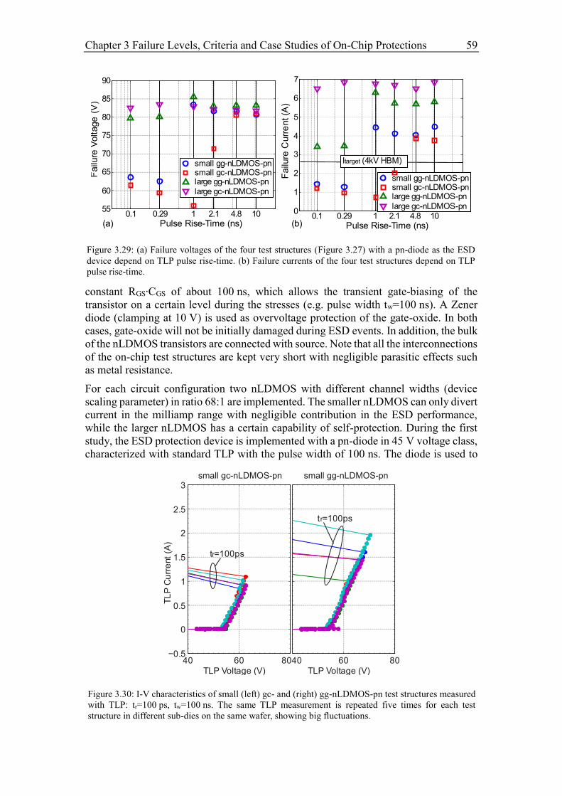
Chapter 3 Failure Levels, Criteria and Case Studies of On-Chip Protections 59
constant RGS∙CGS of about 100 ns, which allows the transient gate-biasing of the
transistor on a certain level during the stresses (e.g. pulse width tw=100 ns). A Zener
diode (clamping at 10 V) is used as overvoltage protection of the gate-oxide. In both
cases, gate-oxide will not be initially damaged during ESD events. In addition, the bulk
of the nLDMOS transistors are connected with source. Note that all the interconnections
of the on-chip test structures are kept very short with negligible parasitic effects such
as metal resistance.
For each circuit configuration two nLDMOS with different channel widths (device
scaling parameter) in ratio 68:1 are implemented. The smaller nLDMOS can only divert
current in the milliamp range with negligible contribution in the ESD performance,
while the larger nLDMOS has a certain capability of self-protection. During the first
study, the ESD protection device is implemented with a pn-diode in 45 V voltage class,
characterized with standard TLP with the pulse width of 100 ns. The diode is used to
Figure 3.30: I-V characteristics of small (left) gc- and (right) gg-nLDMOS-pn test structures measured
with TLP: tr=100 ps, tw=100 ns. The same TLP measurement is repeated five times for each test
structure in different sub-dies on the same wafer, showing big fluctuations.
40 60−0.5
0
0.5
1
1.5
2
2.5
3
TL
P C
urr
ent
(A)
TLP Voltage (V)40 60 80
TLP Voltage (V)80
tr=100ps
tr=100ps
Figure 3.29: (a) Failure voltages of the four test structures (Figure 3.27) with a pn-diode as the ESD
device depend on TLP pulse rise-time. (b) Failure currents of the four test structures depend on TLP
pulse rise-time.
0.1 0.29 1 2.1 4.8 1055
60
65
70
75
80
85
90
Pulse Rise-Time (ns)
Failu
reV
oltage
(V
)
small gg-nLDMOS-pnsmall gc-nLDMOS-pnlarge gg-nLDMOS-pnlarge gc-nLDMOS-pn
0.1 0.29 1 2.1 4.8 100
1
2
3
4
5
6
Pulse Rise-Time (ns)
Failu
reC
urr
ent (A
)
Itarget (4kV HBM)
small gg-nLDMOS-pnsmall gc-nLDMOS-pnlarge gg-nLDMOS-pnlarge gc-nLDMOS-pn
(a) (b)
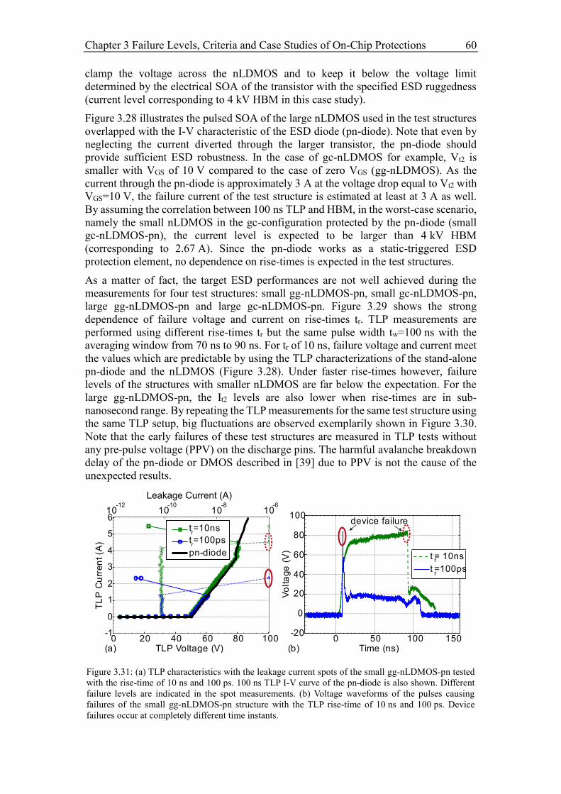
Chapter 3 Failure Levels, Criteria and Case Studies of On-Chip Protections 60
clamp the voltage across the nLDMOS and to keep it below the voltage limit
determined by the electrical SOA of the transistor with the specified ESD ruggedness
(current level corresponding to 4 kV HBM in this case study).
Figure 3.28 illustrates the pulsed SOA of the large nLDMOS used in the test structures
overlapped with the I-V characteristic of the ESD diode (pn-diode). Note that even by
neglecting the current diverted through the larger transistor, the pn-diode should
provide sufficient ESD robustness. In the case of gc-nLDMOS for example, Vt2 is
smaller with VGS of 10 V compared to the case of zero VGS (gg-nLDMOS). As the
current through the pn-diode is approximately 3 A at the voltage drop equal to Vt2 with
VGS=10 V, the failure current of the test structure is estimated at least at 3 A as well.
By assuming the correlation between 100 ns TLP and HBM, in the worst-case scenario,
namely the small nLDMOS in the gc-configuration protected by the pn-diode (small
gc-nLDMOS-pn), the current level is expected to be larger than 4 kV HBM
(corresponding to 2.67 A). Since the pn-diode works as a static-triggered ESD
protection element, no dependence on rise-times is expected in the test structures.
As a matter of fact, the target ESD performances are not well achieved during the
measurements for four test structures: small gg-nLDMOS-pn, small gc-nLDMOS-pn,
large gg-nLDMOS-pn and large gc-nLDMOS-pn. Figure 3.29 shows the strong
dependence of failure voltage and current on rise-times tr. TLP measurements are
performed using different rise-times tr but the same pulse width tw=100 ns with the
averaging window from 70 ns to 90 ns. For tr of 10 ns, failure voltage and current meet
the values which are predictable by using the TLP characterizations of the stand-alone
pn-diode and the nLDMOS (Figure 3.28). Under faster rise-times however, failure
levels of the structures with smaller nLDMOS are far below the expectation. For the
large gg-nLDMOS-pn, the It2 levels are also lower when rise-times are in sub-
nanosecond range. By repeating the TLP measurements for the same test structure using
the same TLP setup, big fluctuations are observed exemplarily shown in Figure 3.30.
Note that the early failures of these test structures are measured in TLP tests without
any pre-pulse voltage (PPV) on the discharge pins. The harmful avalanche breakdown
delay of the pn-diode or DMOS described in [39] due to PPV is not the cause of the
unexpected results.
Figure 3.31: (a) TLP characteristics with the leakage current spots of the small gg-nLDMOS-pn tested
with the rise-time of 10 ns and 100 ps. 100 ns TLP I-V curve of the pn-diode is also shown. Different
failure levels are indicated in the spot measurements. (b) Voltage waveforms of the pulses causing
failures of the small gg-nLDMOS-pn structure with the TLP rise-time of 10 ns and 100 ps. Device
failures occur at completely different time instants.
10-12
10-10
10-8
10-6
0 20 40 60 80 100-1
0
1
2
3
4
5
6
TLP Voltage (V)
TL
PC
urr
en
t(A
)
tr=10ns
tr=100ps
pn-diode
0 50 100 150-20
0
20
40
60
80
100
Vo
lta
ge
(V)
Time (ns)
t r = 10ns
tr
=100ps
device failure
(a) (b)
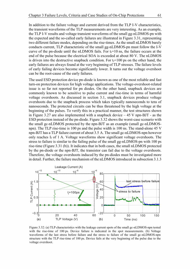
Chapter 3 Failure Levels, Criteria and Case Studies of On-Chip Protections 61
In addition to the failure voltage and current derived from the TLP I-V characteristics,
the transient waveforms of the TLP measurements are very interesting. As an example,
the TLP I-V results and voltage transient waveforms of the small gg-nLDMOS-pn with
the expected and the so-called early failures are illustrated in Figure 3.31, representing
two different failure modes, depending on the rise-times. As the small nLDMOS barely
conducts current, TLP characteristic of the small gg-nLDMOS-pn must follow the I-V
curve of the pn-diode until the nLDMOS fails. For tr=10 ns, the failure occurs at the
end of the pulse because the electrical SOA is exceeded at about 80 V. The nLDMOS
is driven into the destructive snapback condition. For tr=100 ps on the other hand, the
early failures are always found at the very beginning of TLP stresses. The failure levels
of early failing devices become significantly lower. It turns out the voltage overshoot
can be the root-cause of the early failures.
The used ESD protection device pn-diode is known as one of the most reliable and fast
turn-on protection devices for high voltage applications. The voltage-overshoot-related
issue is so far not reported for pn diodes. On the other hand, snapback devices are
commonly known to be sensitive to pulse current and rise-time in terms of harmful
voltage overshoots. As discussed in section 3.1, snapback devices produce voltage
overshoots due to the snapback process which takes typically nanoseconds to tens of
nanoseconds. The protected circuits can be thus threatened by the high voltage at the
beginning of the pulses. To verify this in a practical manner, the test structures shown
in Figure 3.27 are also implemented with a snapback device – 45 V npn-BJT - as the
ESD protection instead of the pn-diode. Figure 3.32 shows the worst-case scenario with
the small gc-nLDMOS protected by the npn-BJT as an example (small gc-nLDMOS-
npn). The TLP rise-time is 100 ps and the pulse width is 100 ns. The stand-alone 45 V
npn-BJT has a TLP failure current of about 3.5 A. The small gc-nLDMOS-npn however
only reaches If of 1 A. Voltage waveforms show significant voltage overshoots. The
stress to failure is similar to the failing pulse of the small gg-nLDMOS-pn with 100 ps
rise-time (Figure 3.31 (b)). It indicates that in both cases, the small nLDMOS protected
by the pn-diode or the npn-BJT, the transistor can fail due to the voltage overshoots.
Therefore, the voltage overshoots induced by the pn-diodes must be investigated more
in detail. Further, the failure mechanism of the nLDMOS introduced in subsection 3.1.3
Figure 3.32: (a) TLP characteristics with the leakage current spots of the small gc-nLDMOS-npn tested
with the rise-time of 100 ps. Device failure is indicated in the spot measurements. (b) Voltage
waveforms of the last stress before failure and the stress to failure of the small gc-nLDMOS-npn
structure with the TLP rise-time of 100 ps. Device fails at the very beginning of the pulse due to the
voltage overshoot.
0 20 40 60−0.5
0
0.5
1
1.5
TLP Voltage (V)
TL
P C
urr
en
t (A
)
10−12
10−10
10−8
10−6
0 50 100 150−20
0
20
40
60
80
Volta
ge
(V
)
Time (ns)
last stress before failure
stress to failuretr=100ps
(a) (b)
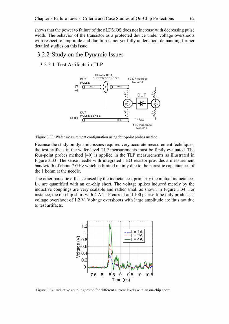
Chapter 3 Failure Levels, Criteria and Case Studies of On-Chip Protections 62
shows that the power to failure of the nLDMOS does not increase with decreasing pulse
width. The behavior of the transistor as a protected device under voltage overshoots
with respect to amplitude and duration is not yet fully understood, demanding further
detailed studies on this issue.
3.2.2 Study on the Dynamic Issues
3.2.2.1 Test Artifacts in TLP
Because the study on dynamic issues requires very accurate measurement techniques,
the test artifacts in the wafer-level TLP measurements must be firstly evaluated. The
four-point probes method [40] is applied in the TLP measurements as illustrated in
Figure 3.33. The sense needle with integrated 1 kΩ resistor provides a measurement
bandwidth of about 7 GHz which is limited mainly due to the parasitic capacitances of
the 1 kohm at the needle.
The other parasitic effects caused by the inductances, primarily the mutual inductances
LP, are quantified with an on-chip short. The voltage spikes induced merely by the
inductive couplings are very scalable and rather small as shown in Figure 3.34. For
instance, the on-chip short with 4 A TLP current and 100 ps rise-time only produces a
voltage overshoot of 1.2 V. Voltage overshoots with large amplitude are thus not due
to test artifacts.
Figure 3.33: Wafer measurement configuration using four-point probes method.
DUT
PULSE
DUT
PULSE SENSE
DUT
PULSE
DUT
PULSE SENSE
Tektronix CT-1
CURRENT SENSOR
DUT
1 kΩ P icoprobe
Model 10
PAD PAD
50 Ω P icoprobe
Model 10
1 k Ω50 Ω
50 Ω50 Ω
LP
LP
LP
LP
Scope
Figure 3.34: Inductive coupling tested for different current levels with an on-chip short.
7.5 8 8.5 9 9.5 10 10.5
0
0.2
0.4
0.6
0.8
1
1.2
Voltag
e(V
)
Time (ns)
I = 1AI = 2AI = 4A
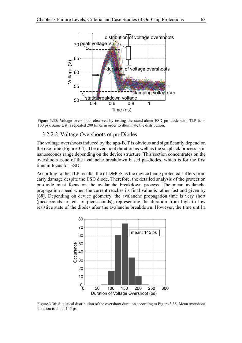
Chapter 3 Failure Levels, Criteria and Case Studies of On-Chip Protections 63
3.2.2.2 Voltage Overshoots of pn-Diodes
The voltage overshoots induced by the npn-BJT is obvious and significantly depend on
the rise-time (Figure 3.4). The overshoot duration as well as the snapback process is in
nanoseconds range depending on the device structure. This section concentrates on the
overshoots issue of the avalanche breakdown based pn-diodes, which is for the first
time in focus for ESD.
According to the TLP results, the nLDMOS as the device being protected suffers from
early damage despite the ESD diode. Therefore, the detailed analysis of the protection
pn-diode must focus on the avalanche breakdown process. The mean avalanche
propagation speed when the current reaches its final value is rather fast and given by
[68]. Depending on device geometry, the avalanche propagation time is very short
(picoseconds to tens of picoseconds), representing the duration from high to low
resistive state of the diodes after the avalanche breakdown. However, the time until a
Figure 3.36: Statistical distribution of the overshoot duration according to Figure 3.35. Mean overshoot
duration is about 145 ps.
0 50 100 150 200 250 3000
10
20
30
40
50
60
70
Duration of Voltage Overshoot (ps)
Occu
ren
ce
mean: 145 ps
Figure 3.35: Voltage overshoots observed by testing the stand-alone ESD pn-diode with TLP (tr =
100 ps). Same test is repeated 200 times in order to illuminate the distribution.
0.4 0.6 0.8 150
55
60
65
70
Vo
lta
ge
(V)
Time (ns)
duration of voltage overshoots
distribution of voltage overshoots
static breakdown voltageclamping voltage Vc
peak voltage Vp
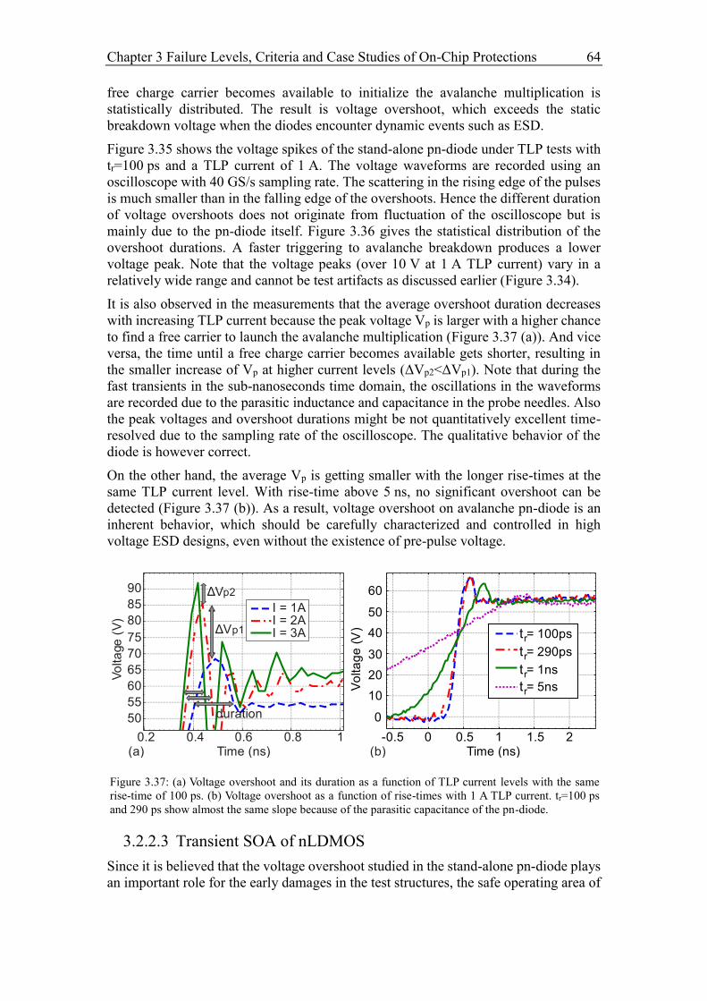
Chapter 3 Failure Levels, Criteria and Case Studies of On-Chip Protections 64
free charge carrier becomes available to initialize the avalanche multiplication is
statistically distributed. The result is voltage overshoot, which exceeds the static
breakdown voltage when the diodes encounter dynamic events such as ESD.
Figure 3.35 shows the voltage spikes of the stand-alone pn-diode under TLP tests with
tr=100 ps and a TLP current of 1 A. The voltage waveforms are recorded using an
oscilloscope with 40 GS/s sampling rate. The scattering in the rising edge of the pulses
is much smaller than in the falling edge of the overshoots. Hence the different duration
of voltage overshoots does not originate from fluctuation of the oscilloscope but is
mainly due to the pn-diode itself. Figure 3.36 gives the statistical distribution of the
overshoot durations. A faster triggering to avalanche breakdown produces a lower
voltage peak. Note that the voltage peaks (over 10 V at 1 A TLP current) vary in a
relatively wide range and cannot be test artifacts as discussed earlier (Figure 3.34).
It is also observed in the measurements that the average overshoot duration decreases
with increasing TLP current because the peak voltage Vp is larger with a higher chance
to find a free carrier to launch the avalanche multiplication (Figure 3.37 (a)). And vice
versa, the time until a free charge carrier becomes available gets shorter, resulting in
the smaller increase of Vp at higher current levels (ΔVp2<ΔVp1). Note that during the
fast transients in the sub-nanoseconds time domain, the oscillations in the waveforms
are recorded due to the parasitic inductance and capacitance in the probe needles. Also
the peak voltages and overshoot durations might be not quantitatively excellent time-
resolved due to the sampling rate of the oscilloscope. The qualitative behavior of the
diode is however correct.
On the other hand, the average Vp is getting smaller with the longer rise-times at the
same TLP current level. With rise-time above 5 ns, no significant overshoot can be
detected (Figure 3.37 (b)). As a result, voltage overshoot on avalanche pn-diode is an
inherent behavior, which should be carefully characterized and controlled in high
voltage ESD designs, even without the existence of pre-pulse voltage.
3.2.2.3 Transient SOA of nLDMOS
Since it is believed that the voltage overshoot studied in the stand-alone pn-diode plays
an important role for the early damages in the test structures, the safe operating area of
Figure 3.37: (a) Voltage overshoot and its duration as a function of TLP current levels with the same
rise-time of 100 ps. (b) Voltage overshoot as a function of rise-times with 1 A TLP current. tr=100 ps
and 290 ps show almost the same slope because of the parasitic capacitance of the pn-diode.
0.2 0.4 0.6 0.8 1
50
55
60
65
70
75
80
85
90
Vo
lta
ge
(V
)
Time (ns)
I = 1AI = 2AI = 3A
duration
ΔVp1
ΔVp2
-0.5 0 0.5 1 1.5 2
0
10
20
30
40
50
60
Vo
lta
ge
(V)
Time (ns)
tr = 100ps
tr = 290ps
tr = 1ns
tr = 5ns
(a) (b)
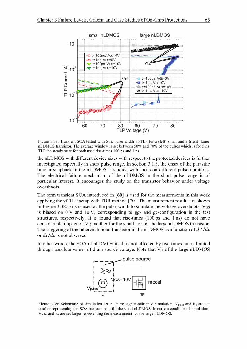
Chapter 3 Failure Levels, Criteria and Case Studies of On-Chip Protections 65
the nLDMOS with different device sizes with respect to the protected devices is further
investigated especially in short pulse range. In section 3.1.3, the onset of the parasitic
bipolar snapback in the nLDMOS is studied with focus on different pulse durations.
The electrical failure mechanism of the nLDMOS in the short pulse range is of
particular interest. It encourages the study on the transistor behavior under voltage
overshoots.
The term transient SOA introduced in [69] is used for the measurements in this work
applying the vf-TLP setup with TDR method [70]. The measurement results are shown
in Figure 3.38. 5 ns is used as the pulse width to simulate the voltage overshoots. VGS
is biased on 0 V and 10 V, corresponding to gg- and gc-configuration in the test
structures, respectively. It is found that rise-times (100 ps and 1 ns) do not have
considerable impact on Vt2, neither for the small nor for the large nLDMOS transistor.
The triggering of the inherent bipolar transistor in the nLDMOS as a function of 𝑑𝑉/𝑑𝑡
or 𝑑𝐼/𝑑𝑡 is not observed.
In other words, the SOA of nLDMOS itself is not affected by rise-times but is limited
through absolute values of drain-source voltage. Note that Vt2 of the large nLDMOS
Figure 3.38: Transient SOA tested with 5 ns pulse width vf-TLP for a (left) small and a (right) large
nLDMOS transistor. The average window is set between 50% and 70% of the pulses which is for 5 ns
TLP the steady state for both used rise-times 100 ps and 1 ns.
60 70 8010
−2
10−1
100
101
60 70 80
tr=100ps, VGS=0V
tr=1ns, VGS=0Vtr=100ps, VGS=10Vtr=1ns, VGS=10V
tr=100ps, VGS=0V
tr=1ns, VGS=0V
tr=100ps, VGS=10Vtr=1ns, VGS=10V
Vt2
Vt2T
LP
Cu
rre
nt
(A)
TLP Voltage (V)
Figure 3.39: Schematic of simulation setup. In voltage conditioned simulation, Vpulse and Rs are set
smaller representing the SOA measurement for the small nLDMOS. In current conditioned simulation,
Vpulse and Rs are set larger representing the measurement for the large nLDMOS.
VGS=10Vmodel
RS
Vpulse
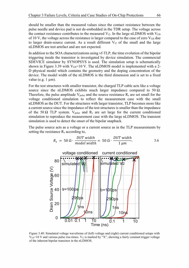
Chapter 3 Failure Levels, Criteria and Case Studies of On-Chip Protections 66
should be smaller than the measured values since the contact resistance between the
pulse needle and device pad is not de-embedded in the TDR setup. The voltage across
the contact resistance contributes to the measured Vt2. In the large nLDMOS with VGS
of 10 V, the voltage across the resistance is larger compared to the case of zero VGS due
to larger drain-source current. As a result different Vt2 of the small and the large
nLDMOS are test artefact and are not expected.
In addition to the SOA characterizations using vf-TLP, the time evolution of the bipolar
triggering inside the transistor is investigated by device simulation. The commercial
SDEVICE simulator by SYNOPSYS is used. The simulation setup is schematically
shown in Figure 3.39 with VGS=10 V. The nLDMOS model is implemented with a 2-
D physical model which contains the geometry and the doping concentration of the
device. The model width of the nLDMOS is the third dimension and is set to a fixed
value (e.g. 1 µm).
For the test structures with smaller transistor, the charged TLP cable acts like a voltage
source since the nLDMOS exhibits much larger impedance compared to 50 Ω.
Therefore, the pulse amplitude Vpulse and the source resistance Rs are set small for the
voltage conditioned simulation to reflect the measurement case with the small
nLDMOS as the DUT. For the structures with larger transistor, TLP becomes more like
a current source since the impedance of the test structures is smaller than the impedance
of the 50 Ω TLP system. Vpulse and Rs are set large for the current conditioned
simulation to reproduce the measurement case with the large nLDMOS. The transient
simulation is used to detect the onset of the bipolar snapback.
The pulse source acts as a voltage or a current source as in the TLP measurements by
setting the resistance Rs according to,
𝑅𝑠 = 50 Ω ∙ 𝐷𝑈𝑇 𝑤𝑖𝑑𝑡ℎ
𝑚𝑜𝑑𝑒𝑙 𝑤𝑖𝑑𝑡ℎ= 50 Ω ∙
𝐷𝑈𝑇 𝑤𝑖𝑑𝑡ℎ
1 µ𝑚. 3.6
Figure 3.40: Simulated voltage waveforms of (left) voltage and (right) current conditioned setups with
VGS=10 V and various pulse rise-times. Vt2 is marked by “X”, showing a fairly constant trigger voltage
of the inherent bipolar transistor in the nLDMOS.
0.01 0.1 1 10Time (ns)
0
20
40
60
80
Dra
in S
ou
rce
Vo
lta
ge
(V
)
0.1 1 10
simulated Vt2
10ns
1ns
290ps
tr=100ps
simulated Vt2
10ns
1ns
290ps
tr=100ps
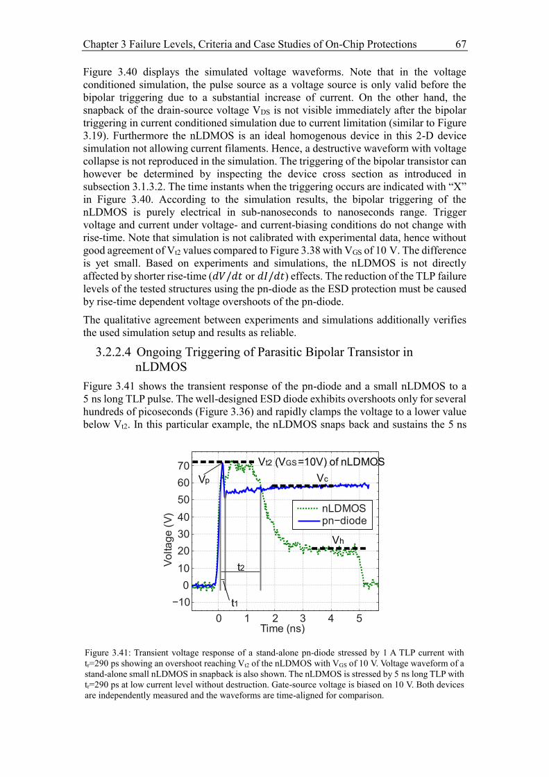
Chapter 3 Failure Levels, Criteria and Case Studies of On-Chip Protections 67
Figure 3.40 displays the simulated voltage waveforms. Note that in the voltage
conditioned simulation, the pulse source as a voltage source is only valid before the
bipolar triggering due to a substantial increase of current. On the other hand, the
snapback of the drain-source voltage VDS is not visible immediately after the bipolar
triggering in current conditioned simulation due to current limitation (similar to Figure
3.19). Furthermore the nLDMOS is an ideal homogenous device in this 2-D device
simulation not allowing current filaments. Hence, a destructive waveform with voltage
collapse is not reproduced in the simulation. The triggering of the bipolar transistor can
however be determined by inspecting the device cross section as introduced in
subsection 3.1.3.2. The time instants when the triggering occurs are indicated with “X”
in Figure 3.40. According to the simulation results, the bipolar triggering of the
nLDMOS is purely electrical in sub-nanoseconds to nanoseconds range. Trigger
voltage and current under voltage- and current-biasing conditions do not change with
rise-time. Note that simulation is not calibrated with experimental data, hence without
good agreement of Vt2 values compared to Figure 3.38 with VGS of 10 V. The difference
is yet small. Based on experiments and simulations, the nLDMOS is not directly
affected by shorter rise-time (𝑑𝑉/𝑑𝑡 or 𝑑𝐼/𝑑𝑡) effects. The reduction of the TLP failure
levels of the tested structures using the pn-diode as the ESD protection must be caused
by rise-time dependent voltage overshoots of the pn-diode.
The qualitative agreement between experiments and simulations additionally verifies
the used simulation setup and results as reliable.
3.2.2.4 Ongoing Triggering of Parasitic Bipolar Transistor in
nLDMOS
Figure 3.41 shows the transient response of the pn-diode and a small nLDMOS to a
5 ns long TLP pulse. The well-designed ESD diode exhibits overshoots only for several
hundreds of picoseconds (Figure 3.36) and rapidly clamps the voltage to a lower value
below Vt2. In this particular example, the nLDMOS snaps back and sustains the 5 ns
Figure 3.41: Transient voltage response of a stand-alone pn-diode stressed by 1 A TLP current with
tr=290 ps showing an overshoot reaching Vt2 of the nLDMOS with VGS of 10 V. Voltage waveform of a
stand-alone small nLDMOS in snapback is also shown. The nLDMOS is stressed by 5 ns long TLP with
tr=290 ps at low current level without destruction. Gate-source voltage is biased on 10 V. Both devices
are independently measured and the waveforms are time-aligned for comparison.
0 1 2 3 4 5
−10
0
10
20
30
40
50
60
70
Vo
lta
ge
(V
)
Time (ns)
nLDMOSpn−diode
Vc
Vh
t1
t2
Vt2 (VGS=10V) of nLDMOS
Vp
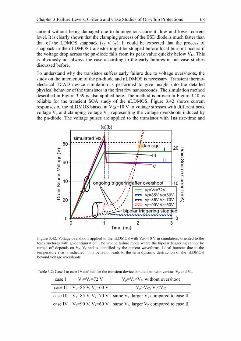
Chapter 3 Failure Levels, Criteria and Case Studies of On-Chip Protections 68
current without being damaged due to homogenous current flow and lower current
level. It is clearly shown that the clamping process of the ESD diode is much faster than
that of the LDMOS snapback (𝑡1 < 𝑡2 ). It could be expected that the process of
snapback in the nLDMOS transistor might be stopped before local burnout occurs if
the voltage drop across the pn-diode falls from its peak value quickly below Vt2. This
is obviously not always the case according to the early failures in our case studies
discussed before.
To understand why the transistor suffers early failure due to voltage overshoots, the
study on the interaction of the pn-diode and nLDMOS is necessary. Transient thermo-
electrical TCAD device simulation is performed to give insight into the detailed
physical behavior of the transistor in the first few nanoseconds. The simulation method
described in Figure 3.39 is also applied here. The method is proven in Figure 3.40 as
reliable for the transient SOA study of the nLDMOS. Figure 3.42 shows current
responses of the nLDMOS biased at VGS=10 V to voltage stresses with different peak
voltage Vp and clamping voltage Vc, representing the voltage overshoots induced by
the pn-diode. The voltage pulses are applied to the transistor with 1ns rise-time and
Figure 3.42: Voltage overshoots applied to the nLDMOS with VGS=10 V in simulation, oriented to the
test structures with gc-configuration. The unique failure mode where the bipolar triggering cannot be
turned off depends on Vp, Vc and is identified by the current waveforms. Local burnout due to the
temperature rise is indicated. This behavior leads to the term dynamic destruction of the nLDMOS
beyond voltage overshoots.
0
20
40
60
80
Time (ns)
Dra
in S
ou
rce
Vo
lta
ge
(V
)
0
10
20
1 2 30
ongoing triggeringafter overshoot
bipolar triggering stopped
simulated Vt2
II
I
III
IV
V =V =72Vp c
V =85V V =60Vp c
V =85V V =70Vp c
V =90V V =60Vp c
damage
Table 3.2: Case I to case IV defined for the transient device simulations with various Vp and Vc.
case I Vp=Vc=72 V Vp=Vc<Vt2 without overshoot
case II Vp=85 V, Vc=60 V Vp>Vt2, Vc<Vt2
case III Vp=85 V, Vc=70 V same Vp, larger Vc compared to case II
case IV Vp=90 V, Vc=60 V same Vc, larger Vp compared to case II
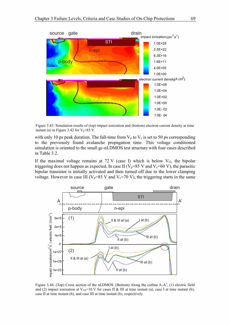
Chapter 3 Failure Levels, Criteria and Case Studies of On-Chip Protections 69
with only 10 ps peak duration. The fall-time from Vp to Vc is set to 50 ps corresponding
to the previously found avalanche propagation time. This voltage conditioned
simulation is oriented to the small gc-nLDMOS test structure with four cases described
in Table 3.2.
If the maximal voltage remains at 72 V (case I) which is below Vt2, the bipolar
triggering does not happen as expected. In case II (Vp=85 V and Vc=60 V), the parasitic
bipolar transistor is initially activated and then turned off due to the lower clamping
voltage. However in case III (Vp=85 V and Vc=70 V), the triggering starts in the same
Figure 3.44: (Top) Cross section of the nLDMOS. (Bottom) Along the cutline A-A’, (1) electric field
and (2) impact ionization at VGS=10 V for cases II & III at time instant (a), case I at time instant (b),
case II at time instant (b), and case III at time instant (b), respectively.
p-body n-epi
STIA A’
0
1e+5
2e+5
3e+5
1e+23
1e+25
1e+27(cm
s
)-3
imp
act
ion
iza
tion
-1
(Vcm
)
ele
ctr
ic fie
ld-1
II & III at (a)
II at (b)III at (b)
II & III at (a)
II at (b)
III at (b)
(1)
(2)
I at (b)
I at (b)
Figure 3.43: Simulation results of (top) impact ionization and (bottom) electron current density at time
instant (a) in Figure 3.42 for Vp=85 V.
STI
p-body
n-epi
(A cm )
1.0E+06
1.0E+04
1.0E+02
1.0E+00
1.0E- 02
1.0E- 04
(cm-3
s )
1.0E+28
2.5E+22
6.3E+16
1.6E+11
4.0E+05
1.0E+00
electron current density
impact ionization -1
-2
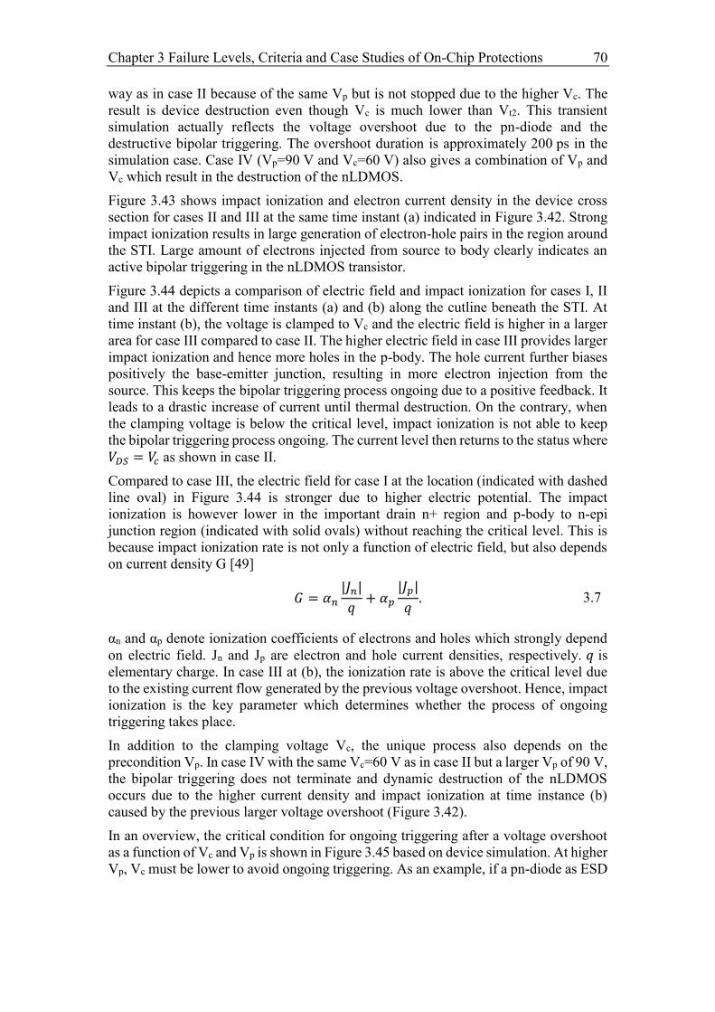
Chapter 3 Failure Levels, Criteria and Case Studies of On-Chip Protections 70
way as in case II because of the same Vp but is not stopped due to the higher Vc. The
result is device destruction even though Vc is much lower than Vt2. This transient
simulation actually reflects the voltage overshoot due to the pn-diode and the
destructive bipolar triggering. The overshoot duration is approximately 200 ps in the
simulation case. Case IV (Vp=90 V and Vc=60 V) also gives a combination of Vp and
Vc which result in the destruction of the nLDMOS.
Figure 3.43 shows impact ionization and electron current density in the device cross
section for cases II and III at the same time instant (a) indicated in Figure 3.42. Strong
impact ionization results in large generation of electron-hole pairs in the region around
the STI. Large amount of electrons injected from source to body clearly indicates an
active bipolar triggering in the nLDMOS transistor.
Figure 3.44 depicts a comparison of electric field and impact ionization for cases I, II
and III at the different time instants (a) and (b) along the cutline beneath the STI. At
time instant (b), the voltage is clamped to Vc and the electric field is higher in a larger
area for case III compared to case II. The higher electric field in case III provides larger
impact ionization and hence more holes in the p-body. The hole current further biases
positively the base-emitter junction, resulting in more electron injection from the
source. This keeps the bipolar triggering process ongoing due to a positive feedback. It
leads to a drastic increase of current until thermal destruction. On the contrary, when
the clamping voltage is below the critical level, impact ionization is not able to keep
the bipolar triggering process ongoing. The current level then returns to the status where
𝑉𝐷𝑆 = 𝑉𝑐 as shown in case II.
Compared to case III, the electric field for case I at the location (indicated with dashed
line oval) in Figure 3.44 is stronger due to higher electric potential. The impact
ionization is however lower in the important drain n+ region and p-body to n-epi
junction region (indicated with solid ovals) without reaching the critical level. This is
because impact ionization rate is not only a function of electric field, but also depends
on current density G [49]
𝐺 = 𝛼𝑛
|𝐽𝑛|
𝑞+ 𝛼𝑝
|𝐽𝑝|
𝑞. 3.7
αn and αp denote ionization coefficients of electrons and holes which strongly depend
on electric field. Jn and Jp are electron and hole current densities, respectively. 𝑞 is
elementary charge. In case III at (b), the ionization rate is above the critical level due
to the existing current flow generated by the previous voltage overshoot. Hence, impact
ionization is the key parameter which determines whether the process of ongoing
triggering takes place.
In addition to the clamping voltage Vc, the unique process also depends on the
precondition Vp. In case IV with the same Vc=60 V as in case II but a larger Vp of 90 V,
the bipolar triggering does not terminate and dynamic destruction of the nLDMOS
occurs due to the higher current density and impact ionization at time instance (b)
caused by the previous larger voltage overshoot (Figure 3.42).
In an overview, the critical condition for ongoing triggering after a voltage overshoot
as a function of Vc and Vp is shown in Figure 3.45 based on device simulation. At higher
Vp, Vc must be lower to avoid ongoing triggering. As an example, if a pn-diode as ESD
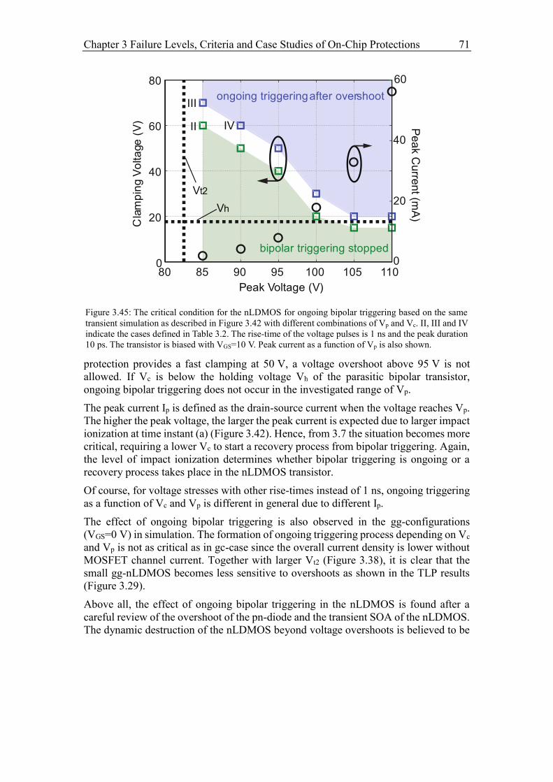
Chapter 3 Failure Levels, Criteria and Case Studies of On-Chip Protections 71
protection provides a fast clamping at 50 V, a voltage overshoot above 95 V is not
allowed. If Vc is below the holding voltage Vh of the parasitic bipolar transistor,
ongoing bipolar triggering does not occur in the investigated range of Vp.
The peak current Ip is defined as the drain-source current when the voltage reaches Vp.
The higher the peak voltage, the larger the peak current is expected due to larger impact
ionization at time instant (a) (Figure 3.42). Hence, from 3.7 the situation becomes more
critical, requiring a lower Vc to start a recovery process from bipolar triggering. Again,
the level of impact ionization determines whether bipolar triggering is ongoing or a
recovery process takes place in the nLDMOS transistor.
Of course, for voltage stresses with other rise-times instead of 1 ns, ongoing triggering
as a function of Vc and Vp is different in general due to different Ip.
The effect of ongoing bipolar triggering is also observed in the gg-configurations
(VGS=0 V) in simulation. The formation of ongoing triggering process depending on Vc
and Vp is not as critical as in gc-case since the overall current density is lower without
MOSFET channel current. Together with larger Vt2 (Figure 3.38), it is clear that the
small gg-nLDMOS becomes less sensitive to overshoots as shown in the TLP results
(Figure 3.29).
Above all, the effect of ongoing bipolar triggering in the nLDMOS is found after a
careful review of the overshoot of the pn-diode and the transient SOA of the nLDMOS.
The dynamic destruction of the nLDMOS beyond voltage overshoots is believed to be
Figure 3.45: The critical condition for the nLDMOS for ongoing bipolar triggering based on the same
transient simulation as described in Figure 3.42 with different combinations of Vp and Vc. II, III and IV
indicate the cases defined in Table 3.2. The rise-time of the voltage pulses is 1 ns and the peak duration
10 ps. The transistor is biased with VGS=10 V. Peak current as a function of Vp is also shown.
80 85 90 95 100 105 1100
20
40
60
80
0
20
40
Vt2
bipolar triggering stopped
ongoing triggeringafter overshoot
Vh
Cla
mp
ing
Vo
lta
ge
(V
)
Peak Voltage (V)
III
II IV
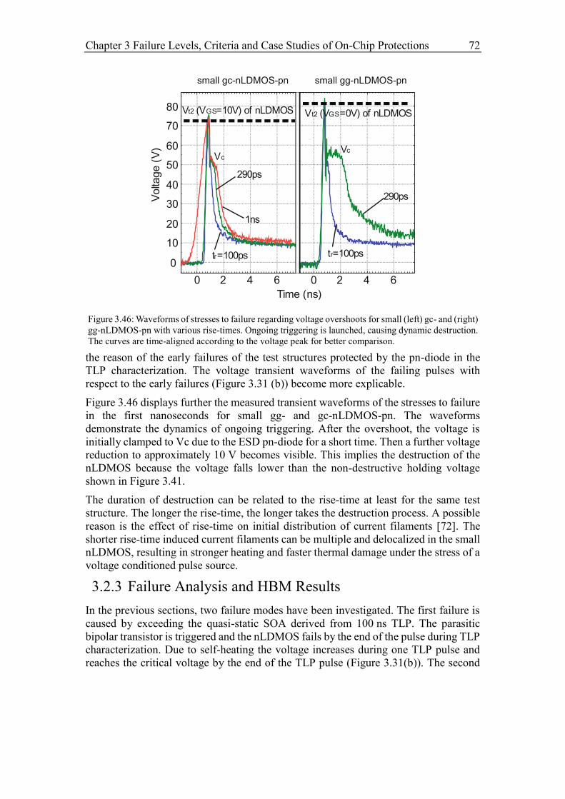
Chapter 3 Failure Levels, Criteria and Case Studies of On-Chip Protections 72
the reason of the early failures of the test structures protected by the pn-diode in the
TLP characterization. The voltage transient waveforms of the failing pulses with
respect to the early failures (Figure 3.31 (b)) become more explicable.
Figure 3.46 displays further the measured transient waveforms of the stresses to failure
in the first nanoseconds for small gg- and gc-nLDMOS-pn. The waveforms
demonstrate the dynamics of ongoing triggering. After the overshoot, the voltage is
initially clamped to Vc due to the ESD pn-diode for a short time. Then a further voltage
reduction to approximately 10 V becomes visible. This implies the destruction of the
nLDMOS because the voltage falls lower than the non-destructive holding voltage
shown in Figure 3.41.
The duration of destruction can be related to the rise-time at least for the same test
structure. The longer the rise-time, the longer takes the destruction process. A possible
reason is the effect of rise-time on initial distribution of current filaments [72]. The
shorter rise-time induced current filaments can be multiple and delocalized in the small
nLDMOS, resulting in stronger heating and faster thermal damage under the stress of a
voltage conditioned pulse source.
3.2.3 Failure Analysis and HBM Results
In the previous sections, two failure modes have been investigated. The first failure is
caused by exceeding the quasi-static SOA derived from 100 ns TLP. The parasitic
bipolar transistor is triggered and the nLDMOS fails by the end of the pulse during TLP
characterization. Due to self-heating the voltage increases during one TLP pulse and
reaches the critical voltage by the end of the TLP pulse (Figure 3.31(b)). The second
Figure 3.46: Waveforms of stresses to failure regarding voltage overshoots for small (left) gc- and (right)
gg-nLDMOS-pn with various rise-times. Ongoing triggering is launched, causing dynamic destruction.
The curves are time-aligned according to the voltage peak for better comparison.
0 2 4 6
0
10
20
30
40
50
60
70
80
Volta
ge (
V)
Time (ns)
tr=100ps
290ps
1ns
Vc
tr=100ps
290ps
0 2 4 6
Vt2 (VGS=0V) of nLDMOS
Vc
Vt2 (VGS=10V) of nLDMOS
Chapter 3 Failure Levels, Criteria and Case Studies of On-Chip Protections 73
failure of the nLDMOS is induced by the voltage overshoots of the ESD protection
device. The peak voltage is larger than the trigger voltage for the parasitic bipolar
transistor while the clamping voltage is not sufficiently low. As a result, the nLDMOS
is damaged due to the effect of ongoing bipolar triggering at the beginning of the pulse.
Although the failures are based on quite different mechanisms, they both can be lead
back to the snapback of the parasitic bipolar transistor. After the snapback, the
remaining pulse delivers enough energy and finally results in a thermal destruction of
the silicon due to current filaments and Joule heating. To confirm this theory, two
samples stressed by TLP have been analyzed in the failure analysis, one sample with
an expected and the other with an early damage in the configuration small gc-
nLDMOS-pn. Figure 3.47 shows the results: the damages of both failure modes are
located in the nLDMOS without any substantial difference.
In addition to the TLP characterization, standardized HBM tests have been performed
to observe the HBM robustness of the pn-diode protected test structures. The studied
structures are encapsulated in LQFP plastic package with 64 pins. The measurements
are finished on a KeyTek ZapMaster HBM tester. In order to avoid PPV effects reported
in [39] [73] [74] which can interfere with the test results, a 10 kΩ shunt resistor is
connected to the HBM discharge pin and the reference ground pin.
Table 3.3 shows the test results for the four test structures. Several samples of each test
structure have been HBM stressed. All structures passed at least 3.5 kV HBM level.
The critical problem found in the TLP characterization with very short rise-times in
sub-nanosecond range was not observed. The failure current of about 1 A shown in
Figure 3.29 (b) did not agree on the lowest fail-level in the HBM tests. It is believed
that parasitic capacitance in the HBM tester, test board, socket and package modulates
the voltage rise-time to a relative longer range.
Figure 3.47: Failure analysis of (left) expected and (right) early damage in the test structure small gc-
nLDMOS-pn caused by 100 ns TLP tests. Both pictures show the final result of thermal runaway in the
nLDMOS.
pn-diode
nLDMOS
RGS
Zener diode
expected damage early damage
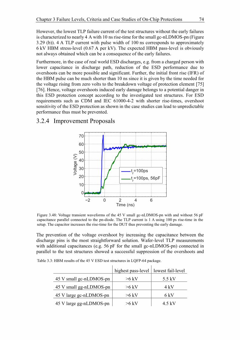
Chapter 3 Failure Levels, Criteria and Case Studies of On-Chip Protections 74
However, the lowest TLP failure current of the test structures without the early failures
is characterized to nearly 4 A with 10 ns rise-time for the small gc-nLDMOS-pn (Figure
3.29 (b)). 4 A TLP current with pulse width of 100 ns corresponds to approximately
6 kV HBM stress-level (0.67 A per kV). The expected HBM pass-level is obviously
not always obtained which can be a consequence of the early failures.
Furthermore, in the case of real world ESD discharges, e.g. from a charged person with
lower capacitance in discharge path, reduction of the ESD performance due to
overshoots can be more possible and significant. Further, the initial front rise (IFR) of
the HBM pulse can be much shorter than 10 ns since it is given by the time needed for
the voltage rising from zero volts to the breakdown voltage of protection element [75]
[76]. Hence, voltage overshoots induced early damage belongs to a potential danger in
this ESD protection concept according to the investigated test structures. For ESD
requirements such as CDM and IEC 61000-4-2 with shorter rise-times, overshoot
sensitivity of the ESD protection as shown in the case studies can lead to unpredictable
performance thus must be prevented.
3.2.4 Improvement Proposals
The prevention of the voltage overshoot by increasing the capacitance between the
discharge pins is the most straightforward solution. Wafer-level TLP measurements
with additional capacitances (e.g. 56 pF for the small gc-nLDMOS-pn) connected in
parallel to the test structures showed a successful suppression of the overshoots and
Table 3.3: HBM results of the 45 V ESD test structures in LQFP-64 package.
highest pass-level lowest fail-level
45 V small gc-nLDMOS-pn >6 kV 5.5 kV
45 V small gg-nLDMOS-pn >6 kV 4 kV
45 V large gc-nLDMOS-pn >6 kV 6 kV
45 V large gg-nLDMOS-pn >6 kV 4.5 kV
Figure 3.48: Voltage transient waveforms of the 45 V small gc-nLDMOS-pn with and without 56 pF
capacitance parallel connected to the pn-diode. The TLP current is 1 A using 100 ps rise-time in the
setup. The capacitor increases the rise-time for the DUT thus preventing the early damage.
−2 0 2 4 6
0
10
20
30
40
50
60
70
Vo
ltag
e (
V)
Time (ns)
tr=100ps
tr=100ps, 56pF
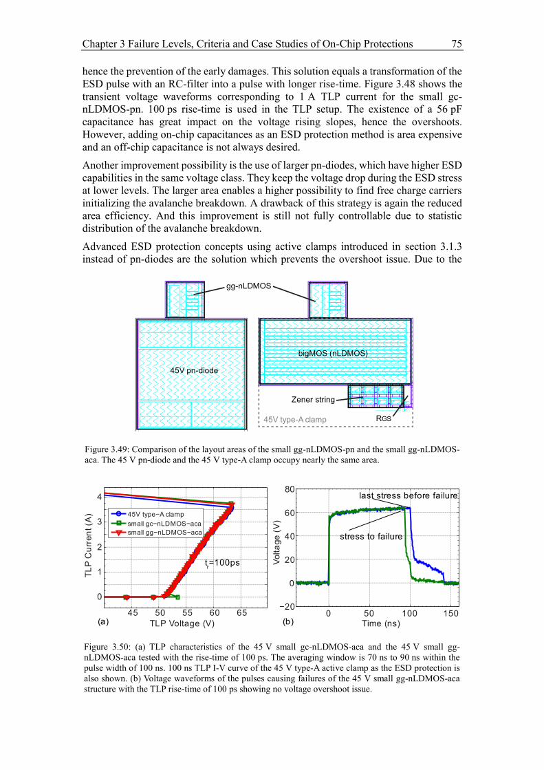
Chapter 3 Failure Levels, Criteria and Case Studies of On-Chip Protections 75
hence the prevention of the early damages. This solution equals a transformation of the
ESD pulse with an RC-filter into a pulse with longer rise-time. Figure 3.48 shows the
transient voltage waveforms corresponding to 1 A TLP current for the small gc-
nLDMOS-pn. 100 ps rise-time is used in the TLP setup. The existence of a 56 pF
capacitance has great impact on the voltage rising slopes, hence the overshoots.
However, adding on-chip capacitances as an ESD protection method is area expensive
and an off-chip capacitance is not always desired.
Another improvement possibility is the use of larger pn-diodes, which have higher ESD
capabilities in the same voltage class. They keep the voltage drop during the ESD stress
at lower levels. The larger area enables a higher possibility to find free charge carriers
initializing the avalanche breakdown. A drawback of this strategy is again the reduced
area efficiency. And this improvement is still not fully controllable due to statistic
distribution of the avalanche breakdown.
Advanced ESD protection concepts using active clamps introduced in section 3.1.3
instead of pn-diodes are the solution which prevents the overshoot issue. Due to the
Figure 3.49: Comparison of the layout areas of the small gg-nLDMOS-pn and the small gg-nLDMOS-
aca. The 45 V pn-diode and the 45 V type-A clamp occupy nearly the same area.
gg-nLDMOS
45V pn-diode
bigMOS (nLDMOS)
Zener string
RGS 45V type-A clamp
Figure 3.50: (a) TLP characteristics of the 45 V small gc-nLDMOS-aca and the 45 V small gg-
nLDMOS-aca tested with the rise-time of 100 ps. The averaging window is 70 ns to 90 ns within the
pulse width of 100 ns. 100 ns TLP I-V curve of the 45 V type-A active clamp as the ESD protection is
also shown. (b) Voltage waveforms of the pulses causing failures of the 45 V small gg-nLDMOS-aca
structure with the TLP rise-time of 100 ps showing no voltage overshoot issue.
0 50 100 150−20
0
20
40
60
Volta
ge
(V
)
Time (ns)
45 50 55 60 65
0
1
2
3
4
TLP Voltage (V)
TL
P C
urr
en
t (A
) 45V type−A clamp
small gc−nLDMOS−aca
small gg−nLDMOS−acastress to failure
last stress before failure
tr=100ps
(a) (b)
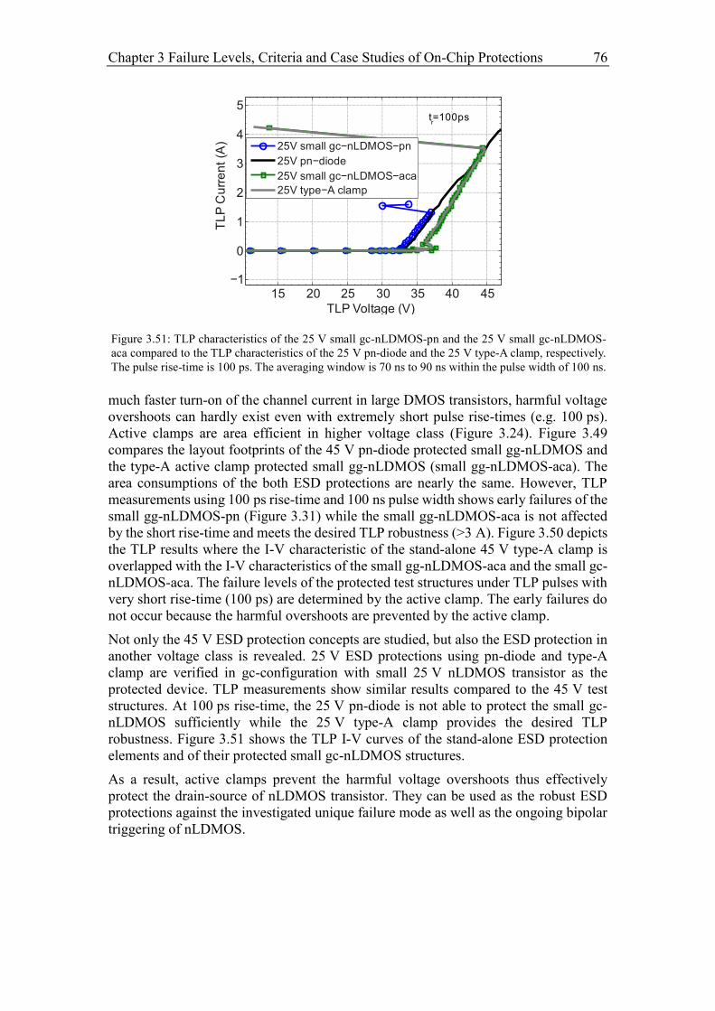
Chapter 3 Failure Levels, Criteria and Case Studies of On-Chip Protections 76
much faster turn-on of the channel current in large DMOS transistors, harmful voltage
overshoots can hardly exist even with extremely short pulse rise-times (e.g. 100 ps).
Active clamps are area efficient in higher voltage class (Figure 3.24). Figure 3.49
compares the layout footprints of the 45 V pn-diode protected small gg-nLDMOS and
the type-A active clamp protected small gg-nLDMOS (small gg-nLDMOS-aca). The
area consumptions of the both ESD protections are nearly the same. However, TLP
measurements using 100 ps rise-time and 100 ns pulse width shows early failures of the
small gg-nLDMOS-pn (Figure 3.31) while the small gg-nLDMOS-aca is not affected
by the short rise-time and meets the desired TLP robustness (>3 A). Figure 3.50 depicts
the TLP results where the I-V characteristic of the stand-alone 45 V type-A clamp is
overlapped with the I-V characteristics of the small gg-nLDMOS-aca and the small gc-
nLDMOS-aca. The failure levels of the protected test structures under TLP pulses with
very short rise-time (100 ps) are determined by the active clamp. The early failures do
not occur because the harmful overshoots are prevented by the active clamp.
Not only the 45 V ESD protection concepts are studied, but also the ESD protection in
another voltage class is revealed. 25 V ESD protections using pn-diode and type-A
clamp are verified in gc-configuration with small 25 V nLDMOS transistor as the
protected device. TLP measurements show similar results compared to the 45 V test
structures. At 100 ps rise-time, the 25 V pn-diode is not able to protect the small gc-
nLDMOS sufficiently while the 25 V type-A clamp provides the desired TLP
robustness. Figure 3.51 shows the TLP I-V curves of the stand-alone ESD protection
elements and of their protected small gc-nLDMOS structures.
As a result, active clamps prevent the harmful voltage overshoots thus effectively
protect the drain-source of nLDMOS transistor. They can be used as the robust ESD
protections against the investigated unique failure mode as well as the ongoing bipolar
triggering of nLDMOS.
Figure 3.51: TLP characteristics of the 25 V small gc-nLDMOS-pn and the 25 V small gc-nLDMOS-
aca compared to the TLP characteristics of the 25 V pn-diode and the 25 V type-A clamp, respectively.
The pulse rise-time is 100 ps. The averaging window is 70 ns to 90 ns within the pulse width of 100 ns.
15 20 25 30 35 40 45−1
0
1
2
3
4
5
TLP Voltage (V)
TL
P C
urr
en
t (A
) 25V small gc−nLDMOS−pn
25V pn−diode
25V small gc−nLDMOS−aca
25V type−A clamp
tr=100ps
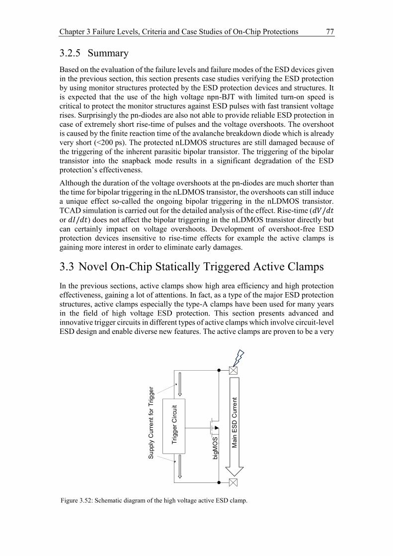
Chapter 3 Failure Levels, Criteria and Case Studies of On-Chip Protections 77
3.2.5 Summary
Based on the evaluation of the failure levels and failure modes of the ESD devices given
in the previous section, this section presents case studies verifying the ESD protection
by using monitor structures protected by the ESD protection devices and structures. It
is expected that the use of the high voltage npn-BJT with limited turn-on speed is
critical to protect the monitor structures against ESD pulses with fast transient voltage
rises. Surprisingly the pn-diodes are also not able to provide reliable ESD protection in
case of extremely short rise-time of pulses and the voltage overshoots. The overshoot
is caused by the finite reaction time of the avalanche breakdown diode which is already
very short (<200 ps). The protected nLDMOS structures are still damaged because of
the triggering of the inherent parasitic bipolar transistor. The triggering of the bipolar
transistor into the snapback mode results in a significant degradation of the ESD
protection’s effectiveness.
Although the duration of the voltage overshoots at the pn-diodes are much shorter than
the time for bipolar triggering in the nLDMOS transistor, the overshoots can still induce
a unique effect so-called the ongoing bipolar triggering in the nLDMOS transistor.
TCAD simulation is carried out for the detailed analysis of the effect. Rise-time (𝑑𝑉/𝑑𝑡
or 𝑑𝐼/𝑑𝑡) does not affect the bipolar triggering in the nLDMOS transistor directly but
can certainly impact on voltage overshoots. Development of overshoot-free ESD
protection devices insensitive to rise-time effects for example the active clamps is
gaining more interest in order to eliminate early damages.
3.3 Novel On-Chip Statically Triggered Active Clamps
In the previous sections, active clamps show high area efficiency and high protection
effectiveness, gaining a lot of attentions. In fact, as a type of the major ESD protection
structures, active clamps especially the type-A clamps have been used for many years
in the field of high voltage ESD protection. This section presents advanced and
innovative trigger circuits in different types of active clamps which involve circuit-level
ESD design and enable diverse new features. The active clamps are proven to be a very
Figure 3.52: Schematic diagram of the high voltage active ESD clamp.
Tri
gg
er
Cir
cuit
Main
ES
DC
urr
ent
Su
pply
Curr
ent
for
Trig
ge
r
big
MO
S
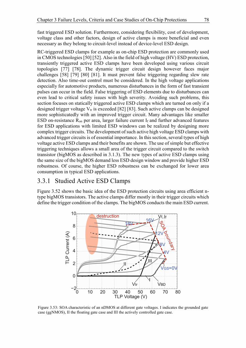
Chapter 3 Failure Levels, Criteria and Case Studies of On-Chip Protections 78
fast triggered ESD solution. Furthermore, considering flexibility, cost of development,
voltage class and other factors, design of active clamps is more beneficial and even
necessary as they belong to circuit-level instead of device-level ESD design.
RC-triggered ESD clamps for example as on-chip ESD protection are commonly used
in CMOS technologies [50] [52]. Also in the field of high voltage (HV) ESD protection,
transiently triggered active ESD clamps have been developed using various circuit
topologies [77] [78]. The dynamic trigger circuit design however faces major
challenges [58] [79] [80] [81]. It must prevent false triggering regarding slew rate
detection. Also time-out control must be considered. In the high voltage applications
especially for automotive products, numerous disturbances in the form of fast transient
pulses can occur in the field. False triggering of ESD elements due to disturbances can
even lead to critical safety issues with high severity. Avoiding such problems, this
section focuses on statically triggered active ESD clamps which are turned on only if a
designed trigger voltage Vtr is exceeded [82] [83]. Such active clamps can be designed
more sophisticatedly with an improved trigger circuit. Many advantages like smaller
ESD on-resistance Ron per area, larger failure current If and further advanced features
for ESD applications with limited ESD windows can be realized by designing more
complex trigger circuits. The development of such active high voltage ESD clamps with
advanced trigger circuits is of essential importance. In this section, several types of high
voltage active ESD clamps and their benefits are shown. The use of simple but effective
triggering techniques allows a small area of the trigger circuit compared to the switch
transistor (bigMOS as described in 3.1.3). The new types of active ESD clamps using
the same size of the bigMOS demand less ESD design window and provide higher ESD
robustness. Of course, the higher ESD robustness can be exchanged for lower area
consumption in typical ESD applications.
3.3.1 Studied Active ESD Clamps
Figure 3.52 shows the basic idea of the ESD protection circuits using area efficient n-
type bigMOS transistors. The active clamps differ mostly in their trigger circuits which
define the trigger condition of the clamps. The bigMOS conducts the main ESD current.
Figure 3.53: SOA characteristic of an nDMOS at different gate voltages. I indicates the grounded gate
case (ggNMOS), II the floating gate case and III the actively controlled gate case.
0 10 20 30 40 50 60 70 80−2
0
2
4
6
8
TL
P C
urr
en
t (A
)
TLP Voltage (V)
VGS=0V
4V
8V
12V
16V18V
destruction
I
IIIII
Vtr
Vf, If
VBD
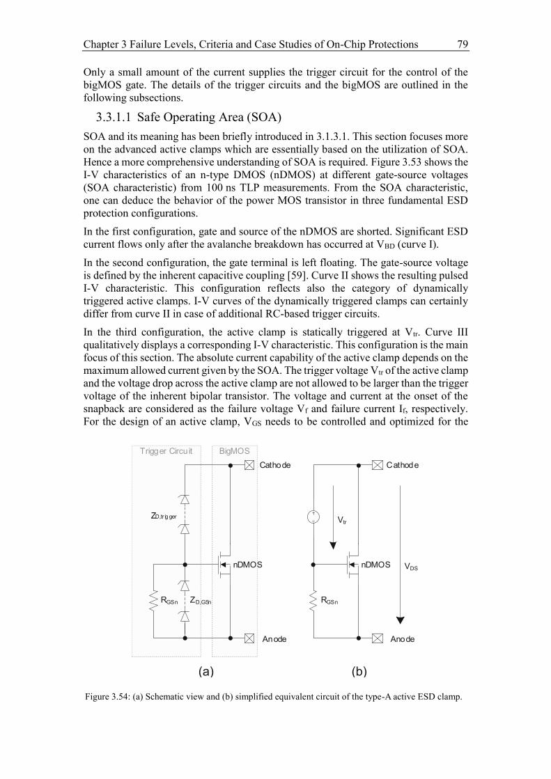
Chapter 3 Failure Levels, Criteria and Case Studies of On-Chip Protections 79
Only a small amount of the current supplies the trigger circuit for the control of the
bigMOS gate. The details of the trigger circuits and the bigMOS are outlined in the
following subsections.
3.3.1.1 Safe Operating Area (SOA)
SOA and its meaning has been briefly introduced in 3.1.3.1. This section focuses more
on the advanced active clamps which are essentially based on the utilization of SOA.
Hence a more comprehensive understanding of SOA is required. Figure 3.53 shows the
I-V characteristics of an n-type DMOS (nDMOS) at different gate-source voltages
(SOA characteristic) from 100 ns TLP measurements. From the SOA characteristic,
one can deduce the behavior of the power MOS transistor in three fundamental ESD
protection configurations.
In the first configuration, gate and source of the nDMOS are shorted. Significant ESD
current flows only after the avalanche breakdown has occurred at VBD (curve I).
In the second configuration, the gate terminal is left floating. The gate-source voltage
is defined by the inherent capacitive coupling [59]. Curve II shows the resulting pulsed
I-V characteristic. This configuration reflects also the category of dynamically
triggered active clamps. I-V curves of the dynamically triggered clamps can certainly
differ from curve II in case of additional RC-based trigger circuits.
In the third configuration, the active clamp is statically triggered at Vtr. Curve III
qualitatively displays a corresponding I-V characteristic. This configuration is the main
focus of this section. The absolute current capability of the active clamp depends on the
maximum allowed current given by the SOA. The trigger voltage Vtr of the active clamp
and the voltage drop across the active clamp are not allowed to be larger than the trigger
voltage of the inherent bipolar transistor. The voltage and current at the onset of the
snapback are considered as the failure voltage Vf and failure current If, respectively.
For the design of an active clamp, VGS needs to be controlled and optimized for the
Figure 3.54: (a) Schematic view and (b) simplified equivalent circuit of the type-A active ESD clamp.
Trigger Circuit BigMOS
Cathode
Anode
nDMOS
ZD,GSnRGSn
ZD,tr ig ger
(a) (b)
Cathode
Anode
nDMOS
RGSn
VDS
Vtr
Chapter 3 Failure Levels, Criteria and Case Studies of On-Chip Protections 80
ideal utilization of the bigMOS, i.e. for reaching the maximal failing current If,max. In
this particular example, VGS between 16 V and 18 V grants the maximal failing current.
Major efforts have been spent to the design of the trigger circuit based on these
considerations.
3.3.1.2 Type-A Clamp
The state-of-the-art statically triggered active clamp has been introduced in section
3.1.3. This clamp including the trigger circuit is depicted in Figure 3.54 (a) again which
is similar to the schematic shown in Figure 3.10. The type-A clamp comprises two
circuit parts according to the basic idea in Figure 3.52. The bigMOS transistor, usually
an nDMOS in power technologies, serves as the protective device in the circuit
conducting the ESD current from cathode to anode. The cathode and anode indicate
both terminals of the active clamp. They are also the two terminals of the inherent body
diode (bulk-drain pn-diode) of the source-bulk shorted nDMOS transistor. The trigger
circuit aims to control VGS of the nDMOS. The Zener string ZD,trigger defines Vtr at which
the active clamp is switched to conducting or non-conducting state. The Zener
protection ZD,GSn prevents the overdriving of the nDMOS. The bias resistor RGSn
provides a defined gate-source discharge time constant for VDS < Vtr, and on the other
hand maintains the designed gate-source voltage if the active clamp is in conducting
state. Note that in general the Zener string can consist of forward biased diodes and
reverse biased Zener diodes in order to achieve the desired total breakdown voltage of
the string (Vtr) in 0.7 V steps – the forward voltage at room temperature. Also the gate-
source voltage can be limited in this type of Zener string.
The type-A active clamp works well in many cases as shown in the previous sections.
However the achievable lowest Ron of the type-A circuit depends mainly on the size of
the nDMOS. Figure 3.54 (b) depicts the ideal behavior of the type-A clamp by
neglecting the resistance of the Zener diodes when conducting current. Vtr is therefore
constant under this assumption. The nDMOS works in the ESD case with
approximately a linear large-signal gain Gm in the transistor saturation region. It is
∆𝑉𝐷𝑆 = ∆(𝑉𝐷𝑆 − 𝑉𝑡𝑟) = ∆𝑉𝐺𝑆 = ∆(𝑉𝐺𝑆 − 𝑉𝑡ℎ), 3.8
where Vth as a constant is the threshold voltage of the nDMOS. The Ron of the type-A
clamp is then calculated by
𝑅𝑜𝑛 =∆𝑉𝐷𝑆
∆𝐼𝐷𝑆=
∆𝑉𝐷𝑆
∆(𝑉𝐺𝑆 − 𝑉𝑡ℎ) ∙ 𝐺𝑚=
1
𝐺𝑚. 3.9
Gm depends only on the nDMOS size which determines the Ron of the type-A clamp. It
implies that at the failing point given by the SOA (Figure 3.53), VGS of the nDMOS
cannot be larger than (Vf-Vtr). Depending on the DMOS SOA and the desired Vtr, the
optimal VGS may not be reachable with a type-A clamp.
3.3.1.3 Type-B Clamp
To improve the VGS control, an amplification stage is implemented in the type-B active
clamp which is schematically shown in Figure 3.55 (a). Compared to the type-A clamp,
the trigger circuitry of the type-B clamp employs again a Zener string as the trigger
voltage definition but a p-type DMOS transistor (pDMOS) as the current source driving
the nDMOS during the ESD stress. Optional Zener protection diodes ZD,GSn and ZD,GSp
protect the nDMOS and pDMOS transistors from overvoltage at the gate.
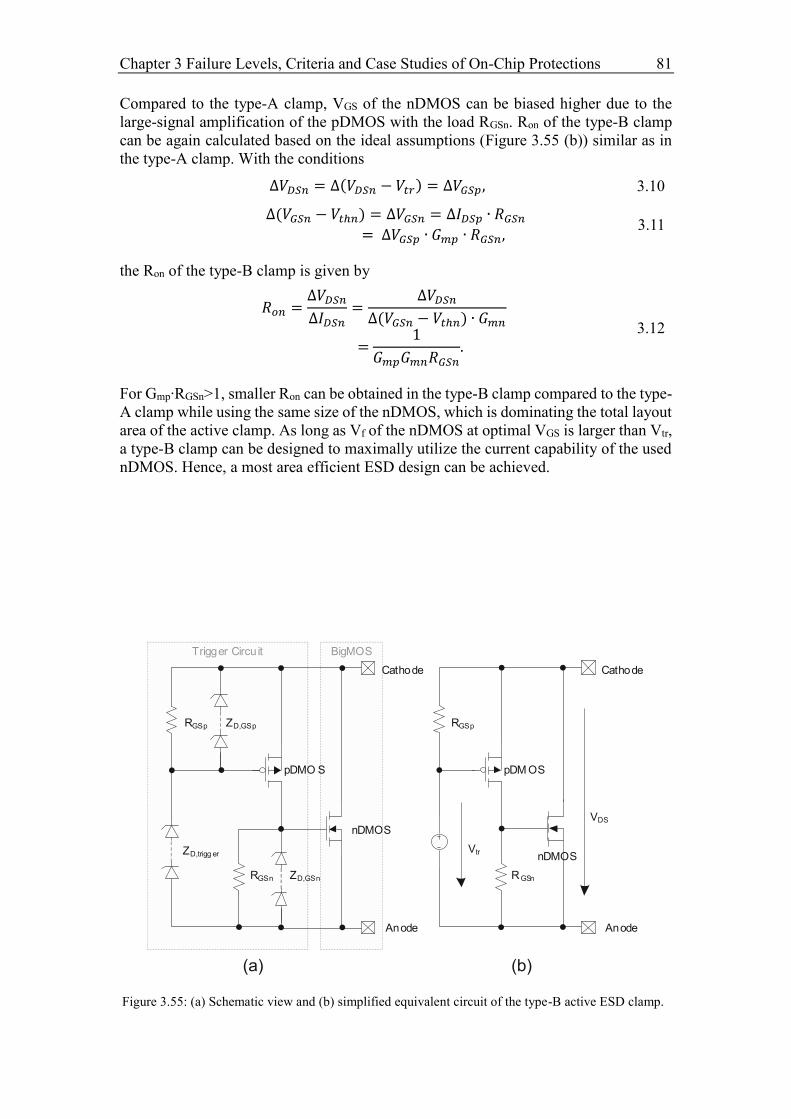
Chapter 3 Failure Levels, Criteria and Case Studies of On-Chip Protections 81
Compared to the type-A clamp, VGS of the nDMOS can be biased higher due to the
large-signal amplification of the pDMOS with the load RGSn. Ron of the type-B clamp
can be again calculated based on the ideal assumptions (Figure 3.55 (b)) similar as in
the type-A clamp. With the conditions
∆𝑉𝐷𝑆𝑛 = ∆(𝑉𝐷𝑆𝑛 − 𝑉𝑡𝑟) = ∆𝑉𝐺𝑆𝑝, 3.10
∆(𝑉𝐺𝑆𝑛 − 𝑉𝑡ℎ𝑛) = ∆𝑉𝐺𝑆𝑛 = ∆𝐼𝐷𝑆𝑝 ∙ 𝑅𝐺𝑆𝑛
= ∆𝑉𝐺𝑆𝑝 ∙ 𝐺𝑚𝑝 ∙ 𝑅𝐺𝑆𝑛, 3.11
the Ron of the type-B clamp is given by
𝑅𝑜𝑛 =∆𝑉𝐷𝑆𝑛
∆𝐼𝐷𝑆𝑛=
∆𝑉𝐷𝑆𝑛
∆(𝑉𝐺𝑆𝑛 − 𝑉𝑡ℎ𝑛) ∙ 𝐺𝑚𝑛
=1
𝐺𝑚𝑝𝐺𝑚𝑛𝑅𝐺𝑆𝑛.
3.12
For Gmp∙RGSn>1, smaller Ron can be obtained in the type-B clamp compared to the type-
A clamp while using the same size of the nDMOS, which is dominating the total layout
area of the active clamp. As long as Vf of the nDMOS at optimal VGS is larger than Vtr,
a type-B clamp can be designed to maximally utilize the current capability of the used
nDMOS. Hence, a most area efficient ESD design can be achieved.
Figure 3.55: (a) Schematic view and (b) simplified equivalent circuit of the type-B active ESD clamp.
BigMOSTrigger Circu it
Cathode
Anode
nDMOS
ZD,GSnRGSn
ZD,GSpRGSp
pDMO S
(a) (b)
Cathode
Anode
RGSn
RGSp
pDM OS
ZD,trigg er
VDS
VtrnDMOS
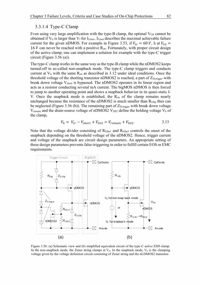
Chapter 3 Failure Levels, Criteria and Case Studies of On-Chip Protections 82
3.3.1.4 Type-C Clamp
Even using very large amplification with the type-B clamp, the optimal VGS cannot be
obtained if Vtr is larger than Vf for If,max. If,max describes the maximal achievable failure
current for the given nDMOS. For example in Figure 3.53, if 𝑉𝑡𝑟 = 60 𝑉, If at 𝑉𝐺𝑆 =16 𝑉 can never be reached with a positive Ron. Fortunately, with proper circuit design
of the active clamp, one can implement a solution for example with the type-C trigger
circuit (Figure 3.56 (a)).
The type-C clamp works in the same way as the type-B clamp while the nDMOS2 keeps
turned-off in so-called non-snapback mode. The type-C clamp triggers and conducts
current at Vtr with the same Ron as described in 3.12 under ideal conditions. Once the
threshold voltage of the shorting transistor nDMOS2 is reached, a part of ZD,trigger with
break down voltage Vshort is bypassed. The nDMOS2 operates in its linear region and
acts as a resistor conducting several mA current. The bigMOS nDMOS is then forced
to jump to another operating point and shows a snapback behavior in its quasi-static I-
V. Once the snapback mode is established, the Ron of the clamp remains nearly
unchanged because the resistance of the nDMOS2 is much smaller than RGSp thus can
be neglected (Figure 3.56 (b)). The remaining part of ZD,trigger with break down voltage
Vremain and the drain-source voltage of nDMOS2 VDS2 define the holding voltage Vh of
the clamp,
𝑉ℎ = 𝑉𝑡𝑟 − 𝑉𝑠ℎ𝑜𝑟𝑡 + 𝑉𝐷𝑆2 = 𝑉𝑟𝑒𝑚𝑎𝑖𝑛 + 𝑉𝐷𝑆2. 3.13
Note that the voltage divider consisting of RGSn1 and RGSn2 controls the onset of the
snapback depending on the threshold voltage of the nDMOS2. Hence, trigger current
and voltage of the snapback are circuit design parameters. An appropriate setting of
these design parameters prevents false-triggering in order to fulfill certain EOS or EMC
requirements.
Figure 3.56: (a) Schematic view and (b) simplified equivalent circuit of the type-C active ESD clamp.
In the non-snapback mode, the Zener string clamps at Vtr. In the snapback mode, Vh is the clamping
voltage given by the voltage definition circuit consisting of Zener string and the nLDMOS2 transistor.
BigMOSTrigger Circui t
Cathode
Anode
nDMOS
ZD,GSn
RGSn1
ZD, GSpRGSp
pDMOS
ZD,trigg er
RGSn 2nDMOS2
Cathode
Anode
nDMOS
RG Sn1
RGSp
pDMOS
+RGSn2
V for non-snap back modetr
V for snapbac k modeh
or
VDS
(a) (b)
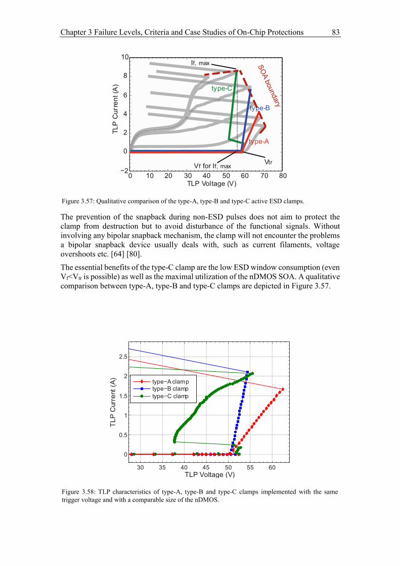
Chapter 3 Failure Levels, Criteria and Case Studies of On-Chip Protections 83
The prevention of the snapback during non-ESD pulses does not aim to protect the
clamp from destruction but to avoid disturbance of the functional signals. Without
involving any bipolar snapback mechanism, the clamp will not encounter the problems
a bipolar snapback device usually deals with, such as current filaments, voltage
overshoots etc. [64] [80].
The essential benefits of the type-C clamp are the low ESD window consumption (even
Vf<Vtr is possible) as well as the maximal utilization of the nDMOS SOA. A qualitative
comparison between type-A, type-B and type-C clamps are depicted in Figure 3.57.
Figure 3.57: Qualitative comparison of the type-A, type-B and type-C active ESD clamps.
0 10 20 30 40 50 60 70 80−2
0
2
4
6
8
TL
P C
urr
en
t (A
)
TLP Voltage (V)
type-A
type-B
type-C
If, max
Vf for If, maxVtr
Figure 3.58: TLP characteristics of type-A, type-B and type-C clamps implemented with the same
trigger voltage and with a comparable size of the nDMOS.
30 35 40 45 50 55 60
0
0.5
1
1.5
2
2.5
TL
P C
urr
ent
(A)
TLP Voltage (V)
type−B clamptype−A clamp
type−C clamp
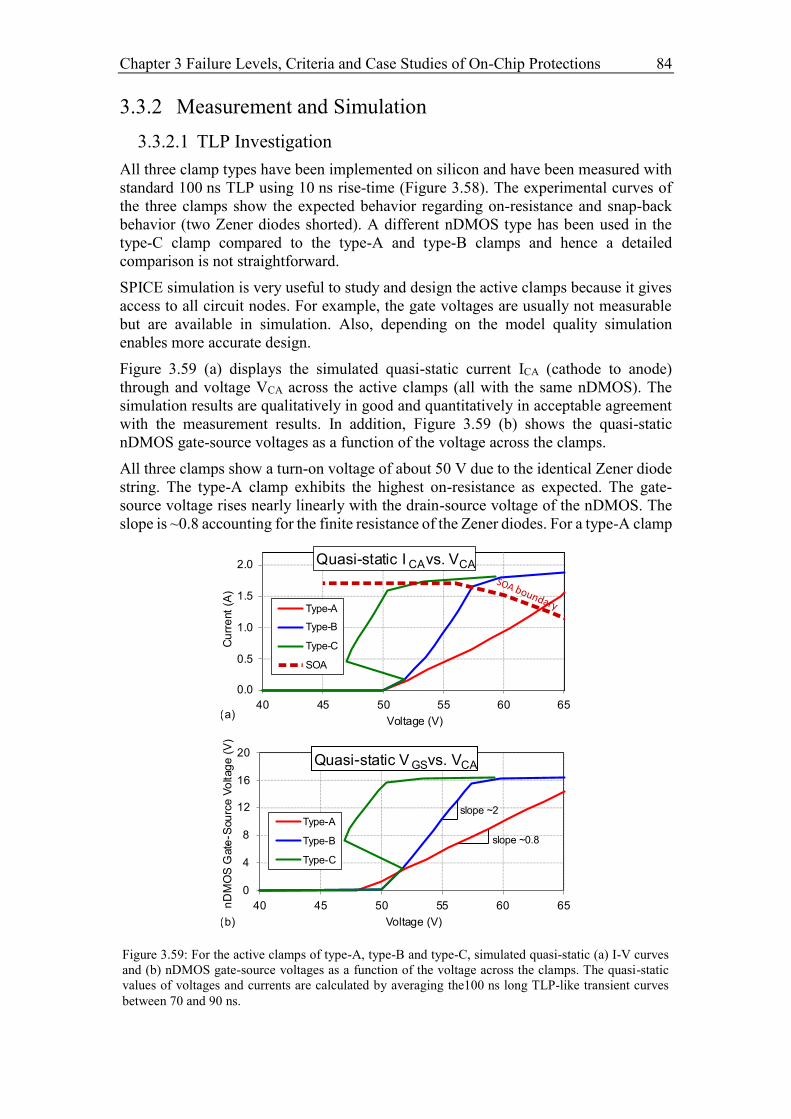
Chapter 3 Failure Levels, Criteria and Case Studies of On-Chip Protections 84
3.3.2 Measurement and Simulation
3.3.2.1 TLP Investigation
All three clamp types have been implemented on silicon and have been measured with
standard 100 ns TLP using 10 ns rise-time (Figure 3.58). The experimental curves of
the three clamps show the expected behavior regarding on-resistance and snap-back
behavior (two Zener diodes shorted). A different nDMOS type has been used in the
type-C clamp compared to the type-A and type-B clamps and hence a detailed
comparison is not straightforward.
SPICE simulation is very useful to study and design the active clamps because it gives
access to all circuit nodes. For example, the gate voltages are usually not measurable
but are available in simulation. Also, depending on the model quality simulation
enables more accurate design.
Figure 3.59 (a) displays the simulated quasi-static current ICA (cathode to anode)
through and voltage VCA across the active clamps (all with the same nDMOS). The
simulation results are qualitatively in good and quantitatively in acceptable agreement
with the measurement results. In addition, Figure 3.59 (b) shows the quasi-static
nDMOS gate-source voltages as a function of the voltage across the clamps.
All three clamps show a turn-on voltage of about 50 V due to the identical Zener diode
string. The type-A clamp exhibits the highest on-resistance as expected. The gate-
source voltage rises nearly linearly with the drain-source voltage of the nDMOS. The
slope is ~0.8 accounting for the finite resistance of the Zener diodes. For a type-A clamp
Figure 3.59: For the active clamps of type-A, type-B and type-C, simulated quasi-static (a) I-V curves
and (b) nDMOS gate-source voltages as a function of the voltage across the clamps. The quasi-static
values of voltages and currents are calculated by averaging the100 ns long TLP-like transient curves
between 70 and 90 ns.
0.0
0.5
1.0
1.5
2.0
40 45 50 55 60 65
Cu
rre
nt
(A)
Voltage (V)
Quasi-static I CAvs. VCA
Type-A
Type-B
Type-C
SOA
0
4
8
12
16
20
40 45 50 55 60 65nD
MO
SG
ate
--
Sou
rce
Vo
ltag
e(V
)
Voltage (V)
Quasi-static V GSvs. VCA
Type-A
Type-B
Type-C
(a)
(b)
slope ~2
slope ~0.8
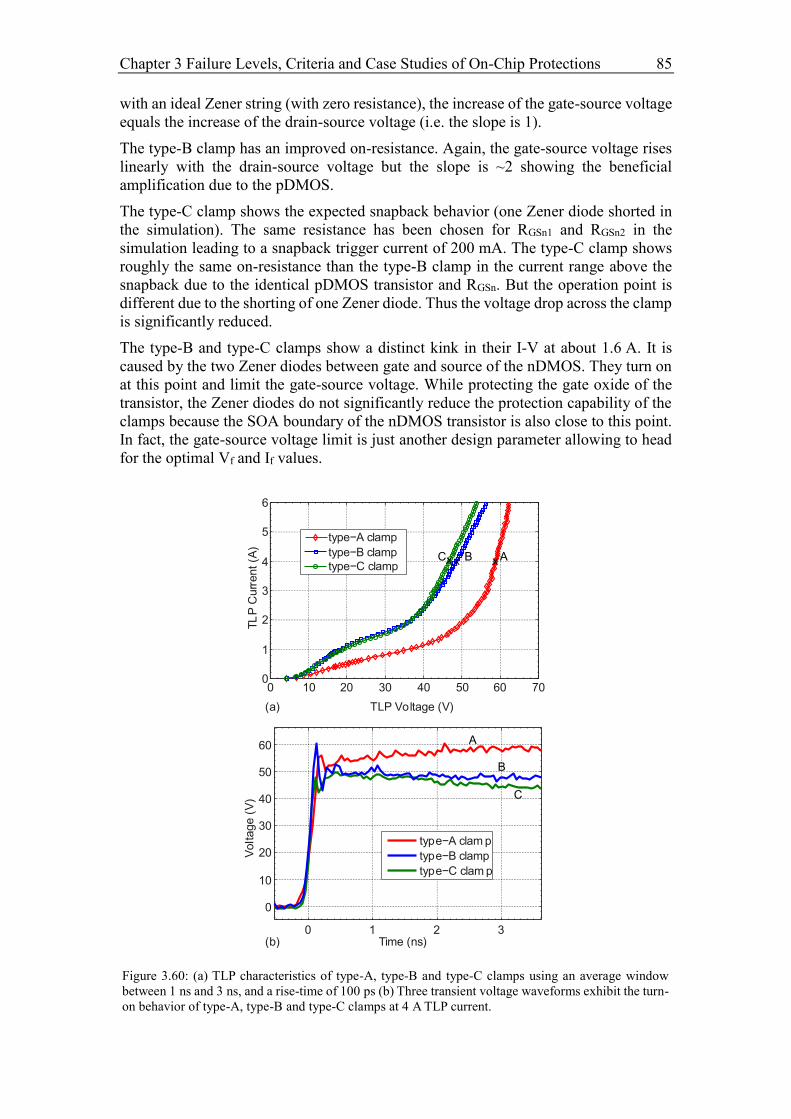
Chapter 3 Failure Levels, Criteria and Case Studies of On-Chip Protections 85
with an ideal Zener string (with zero resistance), the increase of the gate-source voltage
equals the increase of the drain-source voltage (i.e. the slope is 1).
The type-B clamp has an improved on-resistance. Again, the gate-source voltage rises
linearly with the drain-source voltage but the slope is ~2 showing the beneficial
amplification due to the pDMOS.
The type-C clamp shows the expected snapback behavior (one Zener diode shorted in
the simulation). The same resistance has been chosen for RGSn1 and RGSn2 in the
simulation leading to a snapback trigger current of 200 mA. The type-C clamp shows
roughly the same on-resistance than the type-B clamp in the current range above the
snapback due to the identical pDMOS transistor and RGSn. But the operation point is
different due to the shorting of one Zener diode. Thus the voltage drop across the clamp
is significantly reduced.
The type-B and type-C clamps show a distinct kink in their I-V at about 1.6 A. It is
caused by the two Zener diodes between gate and source of the nDMOS. They turn on
at this point and limit the gate-source voltage. While protecting the gate oxide of the
transistor, the Zener diodes do not significantly reduce the protection capability of the
clamps because the SOA boundary of the nDMOS transistor is also close to this point.
In fact, the gate-source voltage limit is just another design parameter allowing to head
for the optimal Vf and If values.
Figure 3.60: (a) TLP characteristics of type-A, type-B and type-C clamps using an average window
between 1 ns and 3 ns, and a rise-time of 100 ps (b) Three transient voltage waveforms exhibit the turn-
on behavior of type-A, type-B and type-C clamps at 4 A TLP current.
0 10 20 30 40 50 60 700
1
2
3
4
5
TLP Voltage (V)
TL
P C
urr
ent (A
)
type−A clamp
type−B clamp
type−C clamp
0 1 2 3
0
10
20
30
40
50
60
Voltage (
V)
Time (ns)
type−A clam p
type−B clamp
type−C clam p
(a)
(b)
ABCxx x
A
B
C
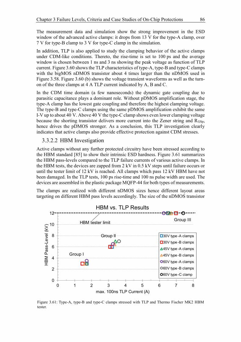
Chapter 3 Failure Levels, Criteria and Case Studies of On-Chip Protections 86
The measurement data and simulation show the strong improvement in the ESD
window of the advanced active clamps: it drops from 13 V for the type-A clamp, over
7 V for type-B clamp to 3 V for type-C clamp in the simulation.
In addition, TLP is also applied to study the clamping behavior of the active clamps
under CDM-like conditions. Thereto, the rise-time is set to 100 ps and the average
window is chosen between 1 ns and 3 ns showing the peak voltage as function of TLP
current. Figure 3.60 shows the TLP characteristics of type-A, type-B and type-C clamps
with the bigMOS nDMOS transistor about 4 times larger than the nDMOS used in
Figure 3.58. Figure 3.60 (b) shows the voltage transient waveforms as well as the turn-
on of the three clamps at 4 A TLP current indicated by A, B and C.
In the CDM time domain (a few nanoseconds) the dynamic gate coupling due to
parasitic capacitance plays a dominant role. Without pDMOS amplification stage, the
type-A clamp has the lowest gate coupling and therefore the highest clamping voltage.
The type-B and type-C clamps using the same pDMOS amplification exhibit the same
I-V up to about 40 V. Above 40 V the type-C clamp shows even lower clamping voltage
because the shorting transistor delivers more current into the Zener string and RGSp,
hence drives the pDMOS stronger. As a conclusion, this TLP investigation clearly
indicates that active clamps also provide effective protection against CDM stresses.
3.3.2.2 HBM Investigation
Active clamps without any further protected circuitry have been stressed according to
the HBM standard [85] to show their intrinsic ESD hardness. Figure 3.61 summarizes
the HBM pass-levels compared to the TLP failure currents of various active clamps. In
the HBM tests, the devices are zapped from 2 kV in 0.5 kV steps until failure occurs or
until the tester limit of 12 kV is reached. All clamps which pass 12 kV HBM have not
been damaged. In the TLP tests, 100 ps rise-time and 100 ns pulse width are used. The
devices are assembled in the plastic package MQFP-44 for both types of measurements.
The clamps are realized with different nDMOS sizes hence different layout areas
targeting on different HBM pass levels accordingly. The size of the nDMOS transistor
Figure 3.61: Type-A, type-B and type-C clamps stressed with TLP and Thermo Fischer MK2 HBM
tester.
0
2
4
6
8
10
12
0 1 2 3 4 5 6 7 8
HB
MP
ass-L
evel (k
V)
max. 100ns TLP Current (A)
30V type -A clamps
30V type -B clamps
45V type -A clamps
45V type -B clamps
60V type -A clamps
60V type -B clamps
Group I
Group II
Group III HBM tester limit
60V type -C clamp
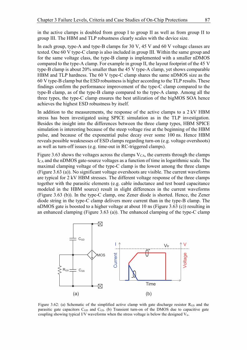
Chapter 3 Failure Levels, Criteria and Case Studies of On-Chip Protections 87
in the active clamps is doubled from group I to group II as well as from group II to
group III. The HBM and TLP robustness clearly scales with the device size.
In each group, type-A and type-B clamps for 30 V, 45 V and 60 V voltage classes are
tested. One 60 V type-C clamp is also included in group III. Within the same group and
for the same voltage class, the type-B clamp is implemented with a smaller nDMOS
compared to the type-A clamp. For example in group II, the layout footprint of the 45 V
type-B clamp is about 20% smaller than the 45 V type-A clamp, yet shows comparable
HBM and TLP hardness. The 60 V type-C clamp shares the same nDMOS size as the
60 V type-B clamp but the ESD robustness is higher according to the TLP results. These
findings confirm the performance improvement of the type-C clamp compared to the
type-B clamp, as of the type-B clamp compared to the type-A clamp. Among all the
three types, the type-C clamp ensures the best utilization of the bigMOS SOA hence
achieves the highest ESD robustness by itself.
In addition to the measurements, the response of the active clamps to a 2 kV HBM
stress has been investigated using SPICE simulation as in the TLP investigation.
Besides the insight into the differences between the three clamp types, HBM SPICE
simulation is interesting because of the steep voltage rise at the beginning of the HBM
pulse, and because of the exponential pulse decay over some 100 ns. Hence HBM
reveals possible weaknesses of ESD clamps regarding turn-on (e.g. voltage overshoots)
as well as turn-off issues (e.g. time-out in RC-triggered clamps).
Figure 3.63 shows the voltages across the clamps VCA, the currents through the clamps
ICA and the nDMOS gate-source voltages as a function of time in logarithmic scale. The
maximal clamping voltage of the type-C clamp is the lowest among the three clamps
(Figure 3.63 (a)). No significant voltage overshoots are visible. The current waveforms
are typical for 2 kV HBM stresses. The different voltage response of the three clamps
together with the parasitic elements (e.g. cable inductance and test board capacitance
modeled in the HBM source) result in slight differences in the current waveforms
(Figure 3.63 (b)). In the type-C clamp, one Zener diode is shorted. Hence, the Zener
diode string in the type-C clamp delivers more current than in the type-B clamp. The
nDMOS gate is boosted to a higher voltage at about 10 ns (Figure 3.63 (c)) resulting in
an enhanced clamping (Figure 3.63 (a)). The enhanced clamping of the type-C clamp
Figure 3.62: (a) Schematic of the simplified active clamp with gate discharge resistor RGS and the
parasitic gate capacitors CGD and CGS. (b) Transient turn-on of the DMOS due to capacitive gate
coupling showing typical I/V waveforms when the stress voltage is below the designed Vtr.
MOS
RGS
(a)
VI
Time
Vtr
(b)
CGD
CGS
Curr
en
t
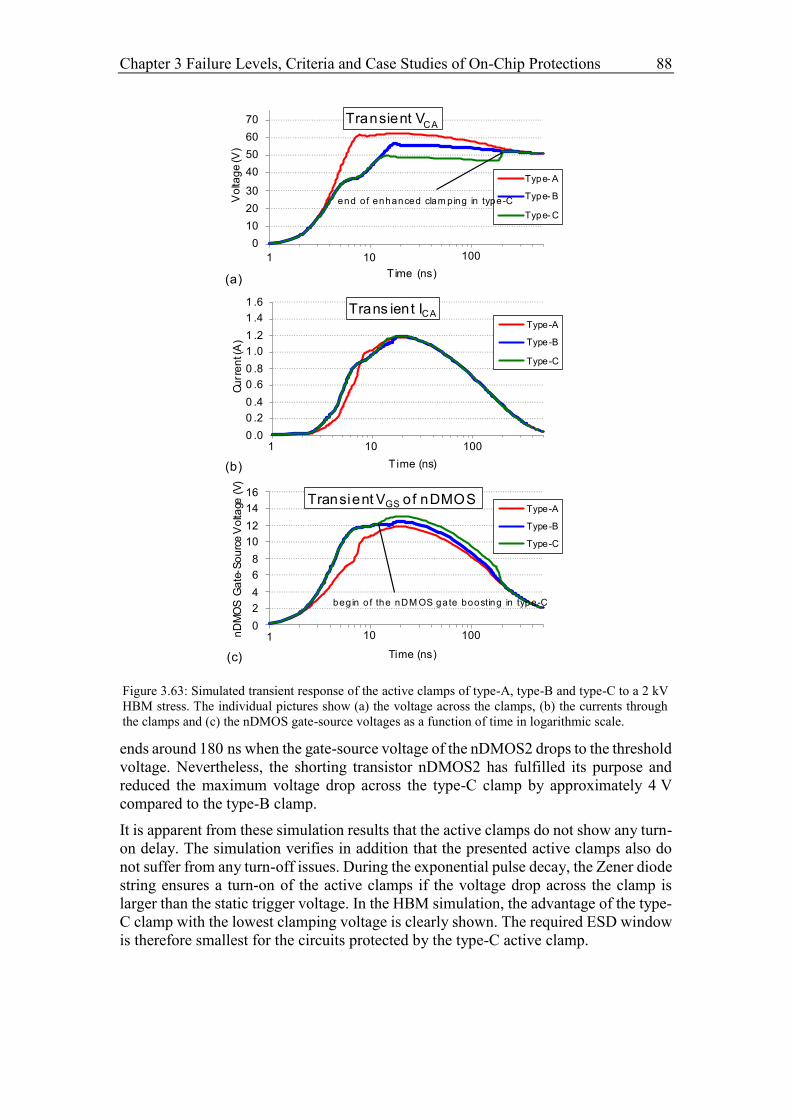
Chapter 3 Failure Levels, Criteria and Case Studies of On-Chip Protections 88
ends around 180 ns when the gate-source voltage of the nDMOS2 drops to the threshold
voltage. Nevertheless, the shorting transistor nDMOS2 has fulfilled its purpose and
reduced the maximum voltage drop across the type-C clamp by approximately 4 V
compared to the type-B clamp.
It is apparent from these simulation results that the active clamps do not show any turn-
on delay. The simulation verifies in addition that the presented active clamps also do
not suffer from any turn-off issues. During the exponential pulse decay, the Zener diode
string ensures a turn-on of the active clamps if the voltage drop across the clamp is
larger than the static trigger voltage. In the HBM simulation, the advantage of the type-
C clamp with the lowest clamping voltage is clearly shown. The required ESD window
is therefore smallest for the circuits protected by the type-C active clamp.
Figure 3.63: Simulated transient response of the active clamps of type-A, type-B and type-C to a 2 kV
HBM stress. The individual pictures show (a) the voltage across the clamps, (b) the currents through
the clamps and (c) the nDMOS gate-source voltages as a function of time in logarithmic scale.
0
2
4
6
8
10
12
14
16
nD
MO
SG
ate
-So
urc
eV
olta
ge(V
)
Time (ns)
Transient VGS of nDMOSType-A
Type-B
Type-C
0
10
20
30
40
50
60
70
1 10 100
Vo
ltag
e(V
)
T ime (ns)
Transient VCA
Type- A
Type- B
Type- C
0 .0
0 .2
0 .4
0 .6
0 .8
1 .0
1 .2
1 .4
1 .6
Cu
rre
nt(
A)
T ime (ns)
Trans ient ICAType-A
Type-B
Type-C
(a)
(b)
(c)
end of enhanced clam ping in type-C
begin o f the nDM OS gate boosting in type-C
1 10 100
1 10 100
Chapter 3 Failure Levels, Criteria and Case Studies of On-Chip Protections 89
3.3.3 Discussion
3.3.3.1 Capacitive Coupling Effects
All active clamps and in general the switch based ESD protections encounter parasitic
capacitive coupling effects. The bigMOS conducts current for a certain time period
under normal operation due to fast switching. Also for the statically triggered active
clamps, the transient turn-on of the nDMOS due to the capacitive gate coupling leads
to significant current flow as exemplarily depicted in Figure 3.62 for a rectangular
pulse. This behavior is preferred for ESD performance as shown in Figure 3.63. It might
however limit the usage of active clamps for I/O or supply protection with functional
steep voltage rise requirements or severe EMC specifications.
The impact of the capacitive coupling effect is reduced by shortening the gate discharge
time. For the studied active clamps, the gate discharge time constant is a function of the
parasitic MOS capacitance and the gate-source resistance RGS. Adding additional
capacitance in parallel with CGS to change the capacitive divider would be an expensive
solution. The straightforward solution is the reduction of RGS.
This however affects directly the Ron during ESD as the resistance of the Zener string
is not negligible. As a countermeasure, a larger pDMOS can be employed in the type-
B clamp to compensate the effect of the small RGSn. According to 3.12, the same Ron is
achieved if
𝐺𝑚𝑝′ ∙ 𝑅𝐺𝑆𝑛′ = 𝐺𝑚𝑝 ∙ 𝑅𝐺𝑆𝑛. 3.14
RGSn’ and Gmp’ describe the reduced RGSn and enlarged pDMOS, respectively.
However, the pDMOS also has the capacitive gate coupling effect delivering increased
current to RGSn at steep voltage rise. Therefore only increasing pDMOS size is not
efficient enough to overcome the capacitive gate coupling without affecting Ron.
A more advanced solution applies the two-stage amplification as displayed in Figure
3.64. It shows a two-stage type-B clamp (named type-B2 clamp). The nDMOS3 of the
second stage boosts VGSp and hence the drain current of the pDMOS. With similar
assumptions as used in 3.12,
𝑅𝑜𝑛 =1
𝐺𝑚𝑛3𝐺𝑚𝑝𝐺𝑚𝑛𝑅𝐺𝑆𝑝𝑅𝐺𝑆𝑛. 3.15
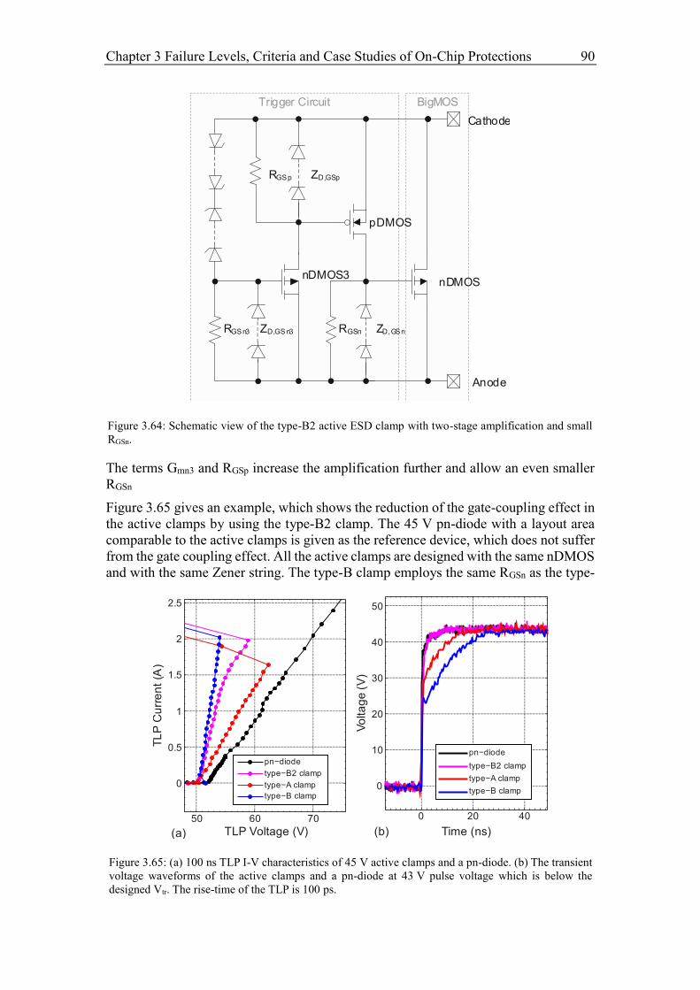
Chapter 3 Failure Levels, Criteria and Case Studies of On-Chip Protections 90
The terms Gmn3 and RGSp increase the amplification further and allow an even smaller
RGSn
Figure 3.65 gives an example, which shows the reduction of the gate-coupling effect in
the active clamps by using the type-B2 clamp. The 45 V pn-diode with a layout area
comparable to the active clamps is given as the reference device, which does not suffer
from the gate coupling effect. All the active clamps are designed with the same nDMOS
and with the same Zener string. The type-B clamp employs the same RGSn as the type-
Figure 3.64: Schematic view of the type-B2 active ESD clamp with two-stage amplification and small
RGSn.
BigMOSTrigger Circuit
Cathode
Anode
nDMOS
ZD,GSnRGSn
ZD,GSpRGSp
pDMOS
nDMOS3
ZD,GSn3RGSn3
Figure 3.65: (a) 100 ns TLP I-V characteristics of 45 V active clamps and a pn-diode. (b) The transient
voltage waveforms of the active clamps and a pn-diode at 43 V pulse voltage which is below the
designed Vtr. The rise-time of the TLP is 100 ps.
50 60 70
0
0.5
1
1.5
2
2.5
TLP Voltage (V)
TL
P C
urr
en
t (A
)
pn−diode
type−B2 clamp
type−A clamp
type−B clamp
0 20 40
0
10
20
30
40
50
Vo
lta
ge (
V)
Time (ns)
pn−diode
type−B2 clamp
type−A clamp
type−B clamp
(a) (b)
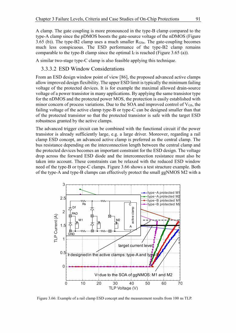
Chapter 3 Failure Levels, Criteria and Case Studies of On-Chip Protections 91
A clamp. The gate coupling is more pronounced in the type-B clamp compared to the
type-A clamp since the pDMOS boosts the gate-source voltage of the nDMOS (Figure
3.65 (b)). The type-B2 clamp uses a much smaller RGSn. The gate-coupling becomes
much less conspicuous. The ESD performance of the type-B2 clamp remains
comparable to the type-B clamp since the optimal If is reached (Figure 3.65 (a)).
A similar two-stage type-C clamp is also feasible applying this technique.
3.3.3.2 ESD Window Considerations
From an ESD design window point of view [86], the proposed advanced active clamps
allow improved design flexibility. The upper ESD limit is typically the minimum failing
voltage of the protected devices. It is for example the maximal allowed drain-source
voltage of a power transistor in many applications. By applying the same transistor type
for the nDMOS and the protected power MOS, the protection is easily established with
minor concern of process variations. Due to the SOA and improved control of VGS, the
failing voltage of the active clamp type-B or type-C can be designed smaller than that
of the protected transistor so that the protected transistor is safe with the target ESD
robustness granted by the active clamps.
The advanced trigger circuit can be combined with the functional circuit if the power
transistor is already sufficiently large, e.g. a large driver. Moreover, regarding a rail
clamp ESD concept, an advanced active clamp is preferred as the central clamp. The
bus resistance depending on the interconnection length between the central clamp and
the protected devices becomes an important constraint for the ESD design. The voltage
drop across the forward ESD diode and the interconnection resistance must also be
taken into account. These constraints can be relaxed with the reduced ESD window
need of the type-B or type-C clamps. Figure 3.66 shows a test structure example. Both
of the type-A and type-B clamps can effectively protect the small ggNMOS M2 with a
Figure 3.66: Example of a rail clamp ESD concept and the measurement results from 100 ns TLP.
0 10 20 30 40 50 60 70
0
0.5
1
1.5
2
2.5
TL
P C
urr
en
t (A
)
TLP Voltage (V)
type−A protected M1type−A protected M2
type−B protected M1type−B protected M2
M1
DfC
A
M2
ac
tive c
lam
p
Rs
If designed in the active clamps: type-A and type-B
V f due to the SOA of ggNMOS: M1 and M2
PAD
GND
target current level
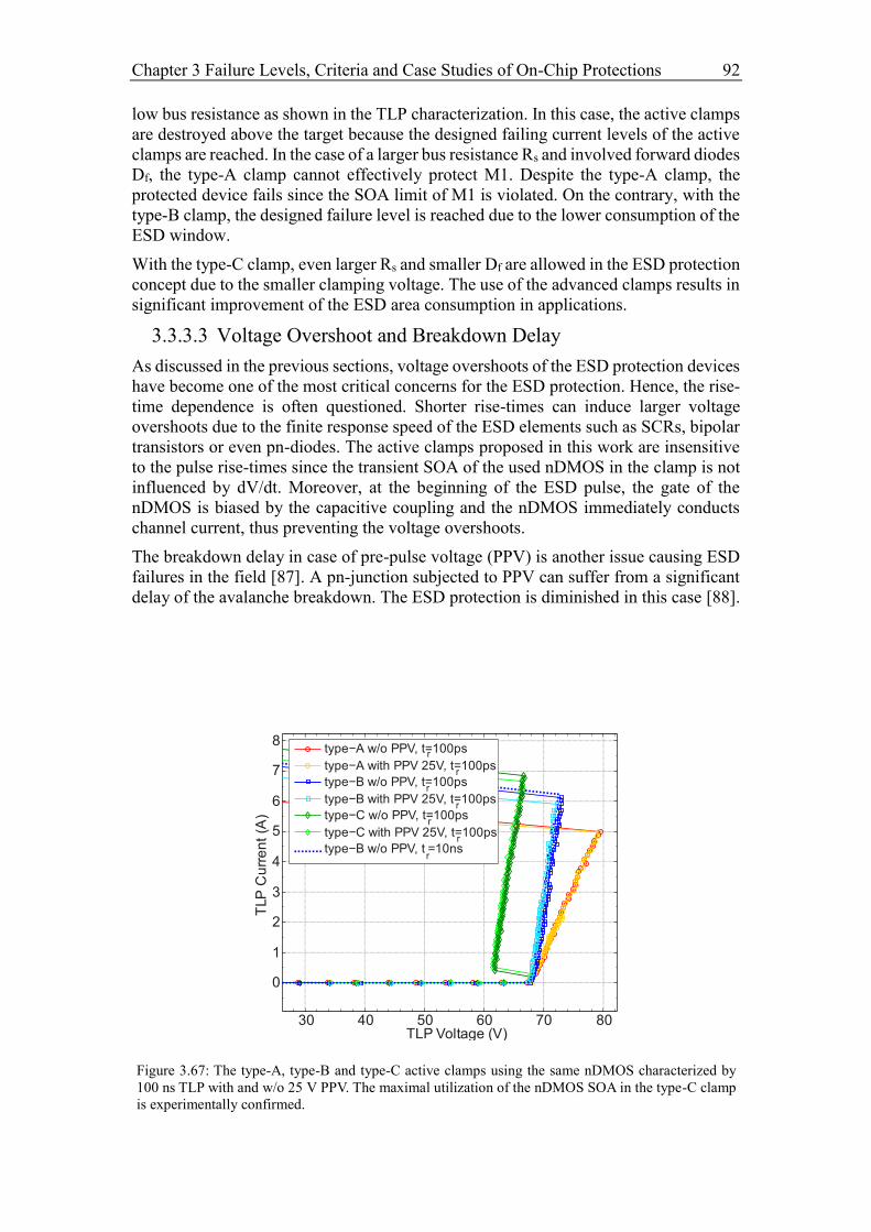
Chapter 3 Failure Levels, Criteria and Case Studies of On-Chip Protections 92
low bus resistance as shown in the TLP characterization. In this case, the active clamps
are destroyed above the target because the designed failing current levels of the active
clamps are reached. In the case of a larger bus resistance Rs and involved forward diodes
Df, the type-A clamp cannot effectively protect M1. Despite the type-A clamp, the
protected device fails since the SOA limit of M1 is violated. On the contrary, with the
type-B clamp, the designed failure level is reached due to the lower consumption of the
ESD window.
With the type-C clamp, even larger Rs and smaller Df are allowed in the ESD protection
concept due to the smaller clamping voltage. The use of the advanced clamps results in
significant improvement of the ESD area consumption in applications.
3.3.3.3 Voltage Overshoot and Breakdown Delay
As discussed in the previous sections, voltage overshoots of the ESD protection devices
have become one of the most critical concerns for the ESD protection. Hence, the rise-
time dependence is often questioned. Shorter rise-times can induce larger voltage
overshoots due to the finite response speed of the ESD elements such as SCRs, bipolar
transistors or even pn-diodes. The active clamps proposed in this work are insensitive
to the pulse rise-times since the transient SOA of the used nDMOS in the clamp is not
influenced by dV/dt. Moreover, at the beginning of the ESD pulse, the gate of the
nDMOS is biased by the capacitive coupling and the nDMOS immediately conducts
channel current, thus preventing the voltage overshoots.
The breakdown delay in case of pre-pulse voltage (PPV) is another issue causing ESD
failures in the field [87]. A pn-junction subjected to PPV can suffer from a significant
delay of the avalanche breakdown. The ESD protection is diminished in this case [88].
Figure 3.67: The type-A, type-B and type-C active clamps using the same nDMOS characterized by
100 ns TLP with and w/o 25 V PPV. The maximal utilization of the nDMOS SOA in the type-C clamp
is experimentally confirmed.
30 40 50 60 70 80
0
1
2
3
4
5
6
7
8
TLP
Cu
rre
nt
(A)
TLP Voltage (V)
type−A w/o PPV, t=100ps
type−A with PPV 25V, t=100ps
type−B w/o PPV, t=100ps
type−B with PPV 25V, t=100ps
type−C w/o PPV, t=100ps
type−C with PPV 25V, t=100ps
type−B w/o PPV, tr=10ns
r
r
r
r
r
r
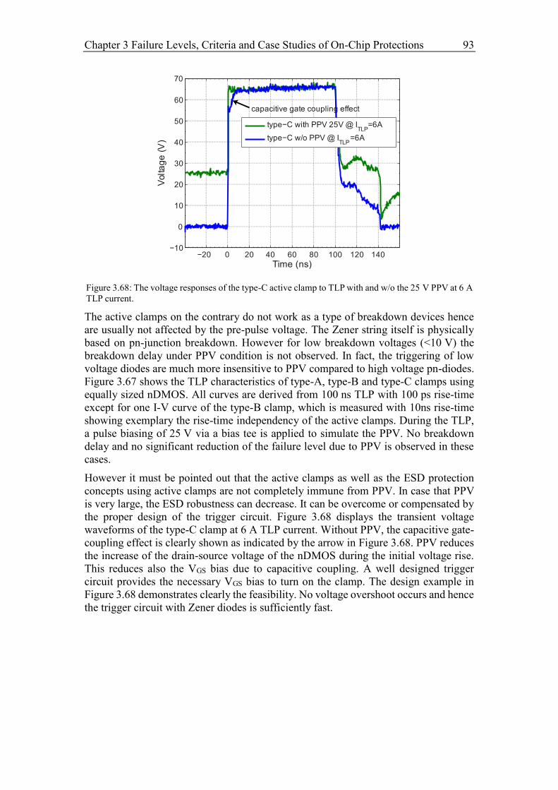
Chapter 3 Failure Levels, Criteria and Case Studies of On-Chip Protections 93
The active clamps on the contrary do not work as a type of breakdown devices hence
are usually not affected by the pre-pulse voltage. The Zener string itself is physically
based on pn-junction breakdown. However for low breakdown voltages (<10 V) the
breakdown delay under PPV condition is not observed. In fact, the triggering of low
voltage diodes are much more insensitive to PPV compared to high voltage pn-diodes.
Figure 3.67 shows the TLP characteristics of type-A, type-B and type-C clamps using
equally sized nDMOS. All curves are derived from 100 ns TLP with 100 ps rise-time
except for one I-V curve of the type-B clamp, which is measured with 10ns rise-time
showing exemplary the rise-time independency of the active clamps. During the TLP,
a pulse biasing of 25 V via a bias tee is applied to simulate the PPV. No breakdown
delay and no significant reduction of the failure level due to PPV is observed in these
cases.
However it must be pointed out that the active clamps as well as the ESD protection
concepts using active clamps are not completely immune from PPV. In case that PPV
is very large, the ESD robustness can decrease. It can be overcome or compensated by
the proper design of the trigger circuit. Figure 3.68 displays the transient voltage
waveforms of the type-C clamp at 6 A TLP current. Without PPV, the capacitive gate-
coupling effect is clearly shown as indicated by the arrow in Figure 3.68. PPV reduces
the increase of the drain-source voltage of the nDMOS during the initial voltage rise.
This reduces also the VGS bias due to capacitive coupling. A well designed trigger
circuit provides the necessary VGS bias to turn on the clamp. The design example in
Figure 3.68 demonstrates clearly the feasibility. No voltage overshoot occurs and hence
the trigger circuit with Zener diodes is sufficiently fast.
Figure 3.68: The voltage responses of the type-C active clamp to TLP with and w/o the 25 V PPV at 6 A
TLP current.
−20 0 20 40 60 80 100 120 140−10
0
10
20
30
40
50
60
Volta
ge
(V
)
Time (ns)
type−C with PPV 25V @ ITLP
=6A
type−C w/o PPV @ ITLP
=6A
capacitive gate coupling effect
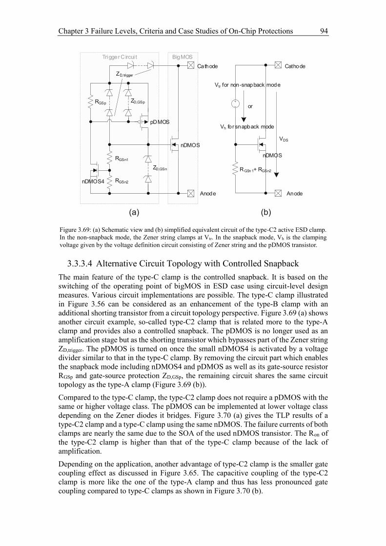
Chapter 3 Failure Levels, Criteria and Case Studies of On-Chip Protections 94
3.3.3.4 Alternative Circuit Topology with Controlled Snapback
The main feature of the type-C clamp is the controlled snapback. It is based on the
switching of the operating point of bigMOS in ESD case using circuit-level design
measures. Various circuit implementations are possible. The type-C clamp illustrated
in Figure 3.56 can be considered as an enhancement of the type-B clamp with an
additional shorting transistor from a circuit topology perspective. Figure 3.69 (a) shows
another circuit example, so-called type-C2 clamp that is related more to the type-A
clamp and provides also a controlled snapback. The pDMOS is no longer used as an
amplification stage but as the shorting transistor which bypasses part of the Zener string
ZD,trigger. The pDMOS is turned on once the small nDMOS4 is activated by a voltage
divider similar to that in the type-C clamp. By removing the circuit part which enables
the snapback mode including nDMOS4 and pDMOS as well as its gate-source resistor
RGSp and gate-source protection ZD,GSp, the remaining circuit shares the same circuit
topology as the type-A clamp (Figure 3.69 (b)).
Compared to the type-C clamp, the type-C2 clamp does not require a pDMOS with the
same or higher voltage class. The pDMOS can be implemented at lower voltage class
depending on the Zener diodes it bridges. Figure 3.70 (a) gives the TLP results of a
type-C2 clamp and a type-C clamp using the same nDMOS. The failure currents of both
clamps are nearly the same due to the SOA of the used nDMOS transistor. The Ron of
the type-C2 clamp is higher than that of the type-C clamp because of the lack of
amplification.
Depending on the application, another advantage of type-C2 clamp is the smaller gate
coupling effect as discussed in Figure 3.65. The capacitive coupling of the type-C2
clamp is more like the one of the type-A clamp and thus has less pronounced gate
coupling compared to type-C clamps as shown in Figure 3.70 (b).
Figure 3.69: (a) Schematic view and (b) simplified equivalent circuit of the type-C2 active ESD clamp.
In the non-snapback mode, the Zener string clamps at Vtr. In the snapback mode, Vh is the clamping
voltage given by the voltage definition circuit consisting of Zener string and the pDMOS transistor.
BigMOSTrigger Circui t
Cathode
Anode
nDMOS
ZD,GSn
RGSn2
(a) (b)
Cathode
Anode
RGSn 1+ RGSn2
VDS
Vtr for non-snapback mode
nDMOS
nDMOS4
ZD,GSpRGSp
ZD, trigger
RGSn1
pDMOSVh for snapback mode
or
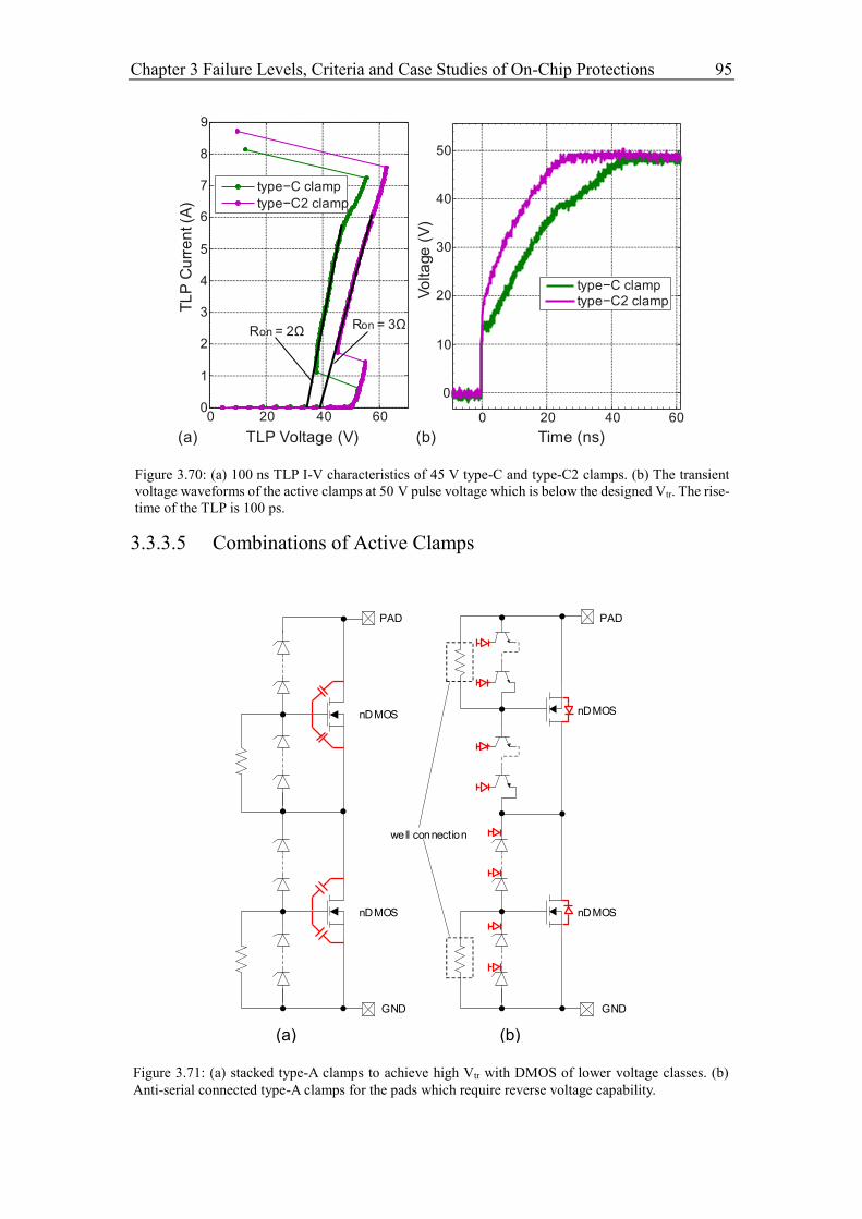
Chapter 3 Failure Levels, Criteria and Case Studies of On-Chip Protections 95
3.3.3.5 Combinations of Active Clamps
Figure 3.70: (a) 100 ns TLP I-V characteristics of 45 V type-C and type-C2 clamps. (b) The transient
voltage waveforms of the active clamps at 50 V pulse voltage which is below the designed Vtr. The rise-
time of the TLP is 100 ps.
TLP Voltage (V) Time (ns)(a) (b)
0 20 40 600
1
2
3
4
5
6
7
8
TL
P C
urr
en
t (A
)type−C clamp
type−C2 clamp
0 20 40 60
0
10
20
30
40
50
Vo
lta
ge
(V
)
type−C clamptype−C2 clamp
Ron = 2ΩRon = 3Ω
Figure 3.71: (a) stacked type-A clamps to achieve high Vtr with DMOS of lower voltage classes. (b)
Anti-serial connected type-A clamps for the pads which require reverse voltage capability.
nDMOS
nDMOS
nDMOS
nDMOS
(a) (b)
well connection
PAD
GND
PAD
GND
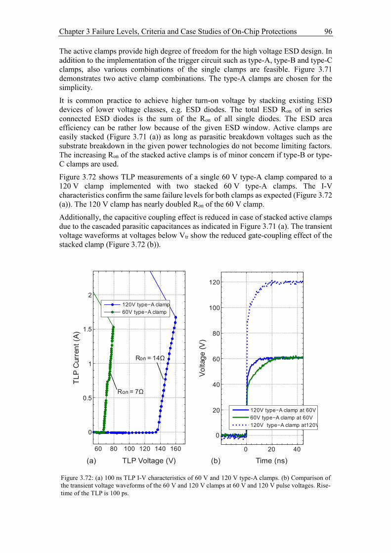
Chapter 3 Failure Levels, Criteria and Case Studies of On-Chip Protections 96
The active clamps provide high degree of freedom for the high voltage ESD design. In
addition to the implementation of the trigger circuit such as type-A, type-B and type-C
clamps, also various combinations of the single clamps are feasible. Figure 3.71
demonstrates two active clamp combinations. The type-A clamps are chosen for the
simplicity.
It is common practice to achieve higher turn-on voltage by stacking existing ESD
devices of lower voltage classes, e.g. ESD diodes. The total ESD Ron of in series
connected ESD diodes is the sum of the Ron of all single diodes. The ESD area
efficiency can be rather low because of the given ESD window. Active clamps are
easily stacked (Figure 3.71 (a)) as long as parasitic breakdown voltages such as the
substrate breakdown in the given power technologies do not become limiting factors.
The increasing Ron of the stacked active clamps is of minor concern if type-B or type-
C clamps are used.
Figure 3.72 shows TLP measurements of a single 60 V type-A clamp compared to a
120 V clamp implemented with two stacked 60 V type-A clamps. The I-V
characteristics confirm the same failure levels for both clamps as expected (Figure 3.72
(a)). The 120 V clamp has nearly doubled Ron of the 60 V clamp.
Additionally, the capacitive coupling effect is reduced in case of stacked active clamps
due to the cascaded parasitic capacitances as indicated in Figure 3.71 (a). The transient
voltage waveforms at voltages below Vtr show the reduced gate-coupling effect of the
stacked clamp (Figure 3.72 (b)).
Figure 3.72: (a) 100 ns TLP I-V characteristics of 60 V and 120 V type-A clamps. (b) Comparison of
the transient voltage waveforms of the 60 V and 120 V clamps at 60 V and 120 V pulse voltages. Rise-
time of the TLP is 100 ps.
60 80 100 120 140 160
0
0.5
1
1.5
2
TLP Voltage (V)
TL
P C
urr
en
t (A
)
120V type−A clamp
60V type−A clamp
0 20 40
0
20
40
60
80
100
120
Vo
ltag
e (
V)
Time (ns)
120V type−A clamp at 60V
60V type−A clamp at 60V
120V type−A clamp at120V
Ron = 7Ω
Ron = 14Ω
(a) (b)
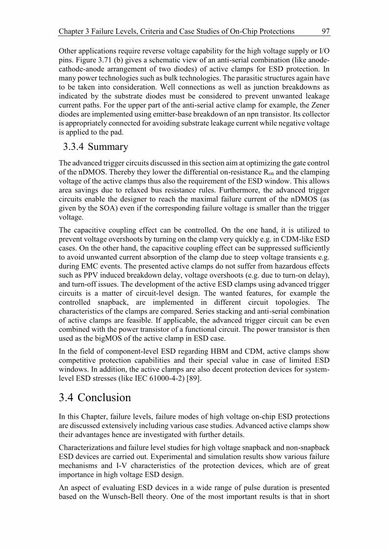
Chapter 3 Failure Levels, Criteria and Case Studies of On-Chip Protections 97
Other applications require reverse voltage capability for the high voltage supply or I/O
pins. Figure 3.71 (b) gives a schematic view of an anti-serial combination (like anode-
cathode-anode arrangement of two diodes) of active clamps for ESD protection. In
many power technologies such as bulk technologies. The parasitic structures again have
to be taken into consideration. Well connections as well as junction breakdowns as
indicated by the substrate diodes must be considered to prevent unwanted leakage
current paths. For the upper part of the anti-serial active clamp for example, the Zener
diodes are implemented using emitter-base breakdown of an npn transistor. Its collector
is appropriately connected for avoiding substrate leakage current while negative voltage
is applied to the pad.
3.3.4 Summary
The advanced trigger circuits discussed in this section aim at optimizing the gate control
of the nDMOS. Thereby they lower the differential on-resistance Ron and the clamping
voltage of the active clamps thus also the requirement of the ESD window. This allows
area savings due to relaxed bus resistance rules. Furthermore, the advanced trigger
circuits enable the designer to reach the maximal failure current of the nDMOS (as
given by the SOA) even if the corresponding failure voltage is smaller than the trigger
voltage.
The capacitive coupling effect can be controlled. On the one hand, it is utilized to
prevent voltage overshoots by turning on the clamp very quickly e.g. in CDM-like ESD
cases. On the other hand, the capacitive coupling effect can be suppressed sufficiently
to avoid unwanted current absorption of the clamp due to steep voltage transients e.g.
during EMC events. The presented active clamps do not suffer from hazardous effects
such as PPV induced breakdown delay, voltage overshoots (e.g. due to turn-on delay),
and turn-off issues. The development of the active ESD clamps using advanced trigger
circuits is a matter of circuit-level design. The wanted features, for example the
controlled snapback, are implemented in different circuit topologies. The
characteristics of the clamps are compared. Series stacking and anti-serial combination
of active clamps are feasible. If applicable, the advanced trigger circuit can be even
combined with the power transistor of a functional circuit. The power transistor is then
used as the bigMOS of the active clamp in ESD case.
In the field of component-level ESD regarding HBM and CDM, active clamps show
competitive protection capabilities and their special value in case of limited ESD
windows. In addition, the active clamps are also decent protection devices for system-
level ESD stresses (like IEC 61000-4-2) [89].
3.4 Conclusion
In this Chapter, failure levels, failure modes of high voltage on-chip ESD protections
are discussed extensively including various case studies. Advanced active clamps show
their advantages hence are investigated with further details.
Characterizations and failure level studies for high voltage snapback and non-snapback
ESD devices are carried out. Experimental and simulation results show various failure
mechanisms and I-V characteristics of the protection devices, which are of great
importance in high voltage ESD design.
An aspect of evaluating ESD devices in a wide range of pulse duration is presented
based on the Wunsch-Bell theory. One of the most important results is that in short
Chapter 3 Failure Levels, Criteria and Case Studies of On-Chip Protections 98
pulse ranges the DMOS transistors as well as the active clamps suffer from electrical
failure mechanism rather than a thermal one. Based on the systematic comparison
showing the drawbacks and advantages of the various ESD devices, it suggests proper
decisions on ESD concepts according to the applications.
It was found in the case studies that voltage overshoots due to fast transients can lead
to ongoing bipolar triggering in high voltage LDMOS transistors. This even happens
due to the overvoltage caused by the finite reaction time of the avalanche breakdown
diode, which is much shorter than the transition time for bipolar triggering in the
nLDMOS transistor in the monitor structures. TCAD simulation is used to understand
the unique effect called ongoing bipolar triggering. Improvement solutions are given
clearly showing the benefit of the active clamps.
As the ESD protection concept using the high voltage active clamps draws more
attention, the active clamps are designed with advanced trigger circuits enabling many
sophisticated features and improving the on-chip ESD protection with high degree of
freedom in ESD design. The active clamps significantly reduce the development effort
of ESD protection devices because all relevant parameters are accessible by circuit
design and do not necessarily require any process development.
Chapter 4 Concept for System-Level ESD Protection 99
Chapter 4
Concept for System-Level ESD Protection
System-level ESD protection has gained more and more attention especially in the field
of automotive applications where the safety is of great importance in the criteria of the
products. Instead of implementation of system-level ESD protection only on chip-level
which is in many cases of high cost or even not applicable, the co-design of system-
level ESD protection both on chip and on printed circuit board (PCB) is the one of the
main challenges for system ESD designers. This Chapter provides several basic
concepts and introduces behavior modeling methodologies which improve the system-
level ESD design.
Different high-voltage on-chip ESD devices and protection approaches are
characterized, compared and further developed in Chapter 3. In the scope of this
Chapter, off-chip (external) ESD devices as a part of system-level ESD co-design are
characterized also with TLP system, but with a different focus compared to on-chip
ESD protections. In addition they are verified directly using the IEC 61000-4-2 ESD
generator showing their clamping behaviors. Behavior modeling of on-chip and off-
chip ESD elements aiming at system-level efficient design using ESD simulation is
discussed. Particularly for the on-chip ESD protection, the so-called Wunsch-Bell
characterization based modeling methodology gives the possibility to simplify the
model complexity, yet improve the simulation accuracy by reproducing the self-heating
effect in the on-chip devices susceptible to ESD.
4.1 Characterization and Systematic Evaluation of
External ESD Protection Elements
ESD tests on system level according to IEC 61000-4-2 or ISO 10605 play today an
important role in the electronic release process of components and systems. To fulfill
ESD specifications, external protection elements are often used to protect the
semiconductor devices on the PCBs against system-level ESD. Different types of
external protection elements are possibly employed for ESD protection in system.
However the required protection effectiveness cannot always be achieved. Although
the external device descriptions in the datasheets are not wrong in general, the ESD test
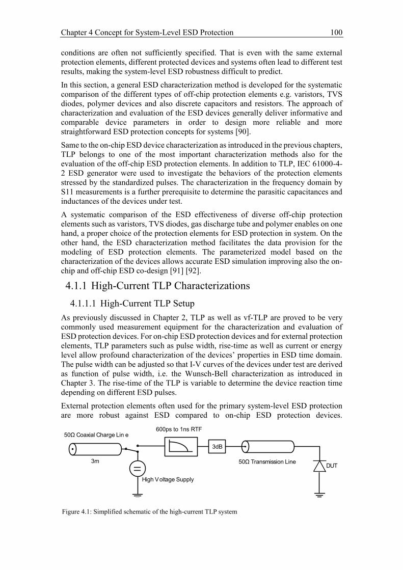
Chapter 4 Concept for System-Level ESD Protection 100
conditions are often not sufficiently specified. That is even with the same external
protection elements, different protected devices and systems often lead to different test
results, making the system-level ESD robustness difficult to predict.
In this section, a general ESD characterization method is developed for the systematic
comparison of the different types of off-chip protection elements e.g. varistors, TVS
diodes, polymer devices and also discrete capacitors and resistors. The approach of
characterization and evaluation of the ESD devices generally deliver informative and
comparable device parameters in order to design more reliable and more
straightforward ESD protection concepts for systems [90].
Same to the on-chip ESD device characterization as introduced in the previous chapters,
TLP belongs to one of the most important characterization methods also for the
evaluation of the off-chip ESD protection elements. In addition to TLP, IEC 61000-4-
2 ESD generator were used to investigate the behaviors of the protection elements
stressed by the standardized pulses. The characterization in the frequency domain by
S11 measurements is a further prerequisite to determine the parasitic capacitances and
inductances of the devices under test.
A systematic comparison of the ESD effectiveness of diverse off-chip protection
elements such as varistors, TVS diodes, gas discharge tube and polymer enables on one
hand, a proper choice of the protection elements for ESD protection in system. On the
other hand, the ESD characterization method facilitates the data provision for the
modeling of ESD protection elements. The parameterized model based on the
characterization of the devices allows accurate ESD simulation improving also the on-
chip and off-chip ESD co-design [91] [92].
4.1.1 High-Current TLP Characterizations
4.1.1.1 High-Current TLP Setup
As previously discussed in Chapter 2, TLP as well as vf-TLP are proved to be very
commonly used measurement equipment for the characterization and evaluation of
ESD protection devices. For on-chip ESD protection devices and for external protection
elements, TLP parameters such as pulse width, rise-time as well as current or energy
level allow profound characterization of the devices’ properties in ESD time domain.
The pulse width can be adjusted so that I-V curves of the devices under test are derived
as function of pulse width, i.e. the Wunsch-Bell characterization as introduced in
Chapter 3. The rise-time of the TLP is variable to determine the device reaction time
depending on different ESD pulses.
External protection elements often used for the primary system-level ESD protection
are more robust against ESD compared to on-chip ESD protection devices.
Figure 4.1: Simplified schematic of the high-current TLP system
3m
50Ω Coaxial Charge Lin e
High Voltage Supply
50Ω Transmission LineDUT
3dB
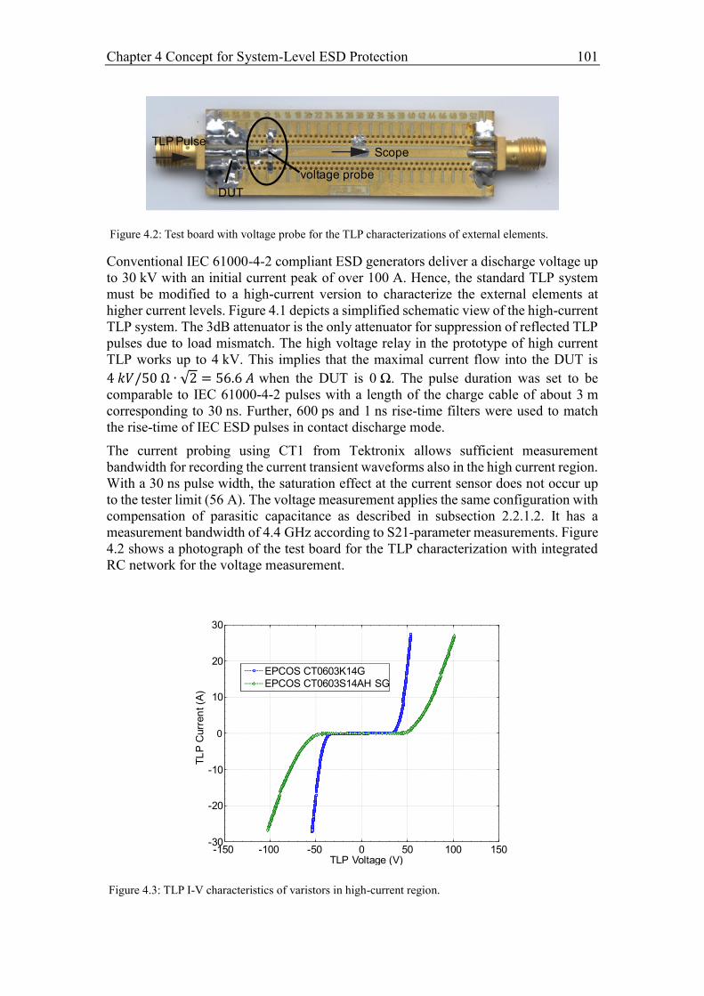
Chapter 4 Concept for System-Level ESD Protection 101
Conventional IEC 61000-4-2 compliant ESD generators deliver a discharge voltage up
to 30 kV with an initial current peak of over 100 A. Hence, the standard TLP system
must be modified to a high-current version to characterize the external elements at
higher current levels. Figure 4.1 depicts a simplified schematic view of the high-current
TLP system. The 3dB attenuator is the only attenuator for suppression of reflected TLP
pulses due to load mismatch. The high voltage relay in the prototype of high current
TLP works up to 4 kV. This implies that the maximal current flow into the DUT is
4 𝑘𝑉/50 Ω ∙ √2 = 56.6 𝐴 when the DUT is 0 Ω. The pulse duration was set to be
comparable to IEC 61000-4-2 pulses with a length of the charge cable of about 3 m
corresponding to 30 ns. Further, 600 ps and 1 ns rise-time filters were used to match
the rise-time of IEC ESD pulses in contact discharge mode.
The current probing using CT1 from Tektronix allows sufficient measurement
bandwidth for recording the current transient waveforms also in the high current region.
With a 30 ns pulse width, the saturation effect at the current sensor does not occur up
to the tester limit (56 A). The voltage measurement applies the same configuration with
compensation of parasitic capacitance as described in subsection 2.2.1.2. It has a
measurement bandwidth of 4.4 GHz according to S21-parameter measurements. Figure
4.2 shows a photograph of the test board for the TLP characterization with integrated
RC network for the voltage measurement.
Figure 4.3: TLP I-V characteristics of varistors in high-current region.
-150 -100 -50 0 50 100 150-30
-20
-10
0
10
20
TLP Voltage (V)
TL
P C
urr
en
t (A
)
EPCOS CT0603K14G
EPCOS CT0603S14AH SG
Figure 4.2: Test board with voltage probe for the TLP characterizations of external elements.
TLP PulseScope
voltage probe
DUT
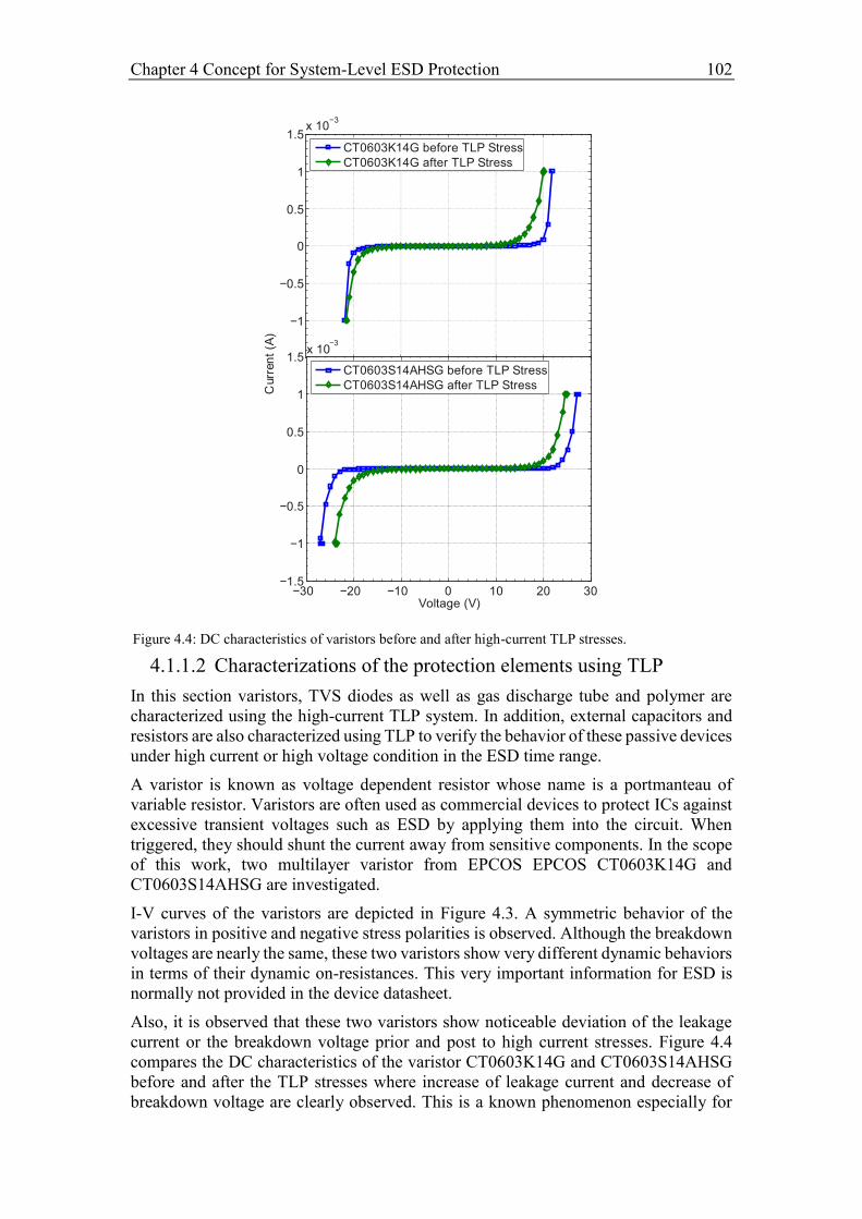
Chapter 4 Concept for System-Level ESD Protection 102
4.1.1.2 Characterizations of the protection elements using TLP
In this section varistors, TVS diodes as well as gas discharge tube and polymer are
characterized using the high-current TLP system. In addition, external capacitors and
resistors are also characterized using TLP to verify the behavior of these passive devices
under high current or high voltage condition in the ESD time range.
A varistor is known as voltage dependent resistor whose name is a portmanteau of
variable resistor. Varistors are often used as commercial devices to protect ICs against
excessive transient voltages such as ESD by applying them into the circuit. When
triggered, they should shunt the current away from sensitive components. In the scope
of this work, two multilayer varistor from EPCOS EPCOS CT0603K14G and
CT0603S14AHSG are investigated.
I-V curves of the varistors are depicted in Figure 4.3. A symmetric behavior of the
varistors in positive and negative stress polarities is observed. Although the breakdown
voltages are nearly the same, these two varistors show very different dynamic behaviors
in terms of their dynamic on-resistances. This very important information for ESD is
normally not provided in the device datasheet.
Also, it is observed that these two varistors show noticeable deviation of the leakage
current or the breakdown voltage prior and post to high current stresses. Figure 4.4
compares the DC characteristics of the varistor CT0603K14G and CT0603S14AHSG
before and after the TLP stresses where increase of leakage current and decrease of
breakdown voltage are clearly observed. This is a known phenomenon especially for
Figure 4.4: DC characteristics of varistors before and after high-current TLP stresses.
−1
−0.5
0
0.5
1
1.5x 10
Curr
en
t (A
)
CT0603K14G before TLP Stress
CT0603K14G after TLP Stress
−30 −20 −10 0 10 20 30−1.5
−1
−0.5
0
0.5
1
1.5x 10
−3
Voltage (V)
CT0603S14AHSG before TLP Stress
CT0603S14AHSG after TLP Stress
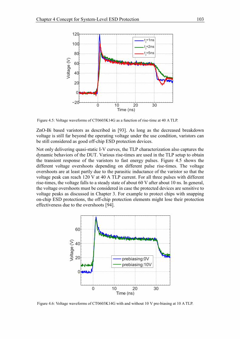
Chapter 4 Concept for System-Level ESD Protection 103
ZnO-Bi based varistors as described in [93]. As long as the decreased breakdown
voltage is still far beyond the operating voltage under the use condition, varistors can
be still considered as good off-chip ESD protection devices.
Not only delivering quasi-static I-V curves, the TLP characterization also captures the
dynamic behaviors of the DUT. Various rise-times are used in the TLP setup to obtain
the transient response of the varistors to fast energy pulses. Figure 4.5 shows the
different voltage overshoots depending on different pulse rise-times. The voltage
overshoots are at least partly due to the parasitic inductance of the varistor so that the
voltage peak can reach 120 V at 40 A TLP current. For all three pulses with different
rise-times, the voltage falls to a steady state of about 60 V after about 10 ns. In general,
the voltage overshoots must be considered in case the protected devices are sensitive to
voltage peaks as discussed in Chapter 3. For example to protect chips with snapping
on-chip ESD protections, the off-chip protection elements might lose their protection
effectiveness due to the overshoots [94].
Figure 4.6: Voltage waveforms of CT0603K14G with and without 10 V pre-biasing at 10 A TLP.
0 10 20 30
0
20
40
60
Time (ns)
Vo
lta
ge
(V
)
prebiasing:0V
prebiasing:10V
Figure 4.5: Voltage waveforms of CT0603K14G as a function of rise-time at 40 A TLP.
0 10 20 30−20
0
20
40
60
80
100
Volta
ge
(V
)
Time (ns)
tr=1ns
tr=2ns
tr=5ns
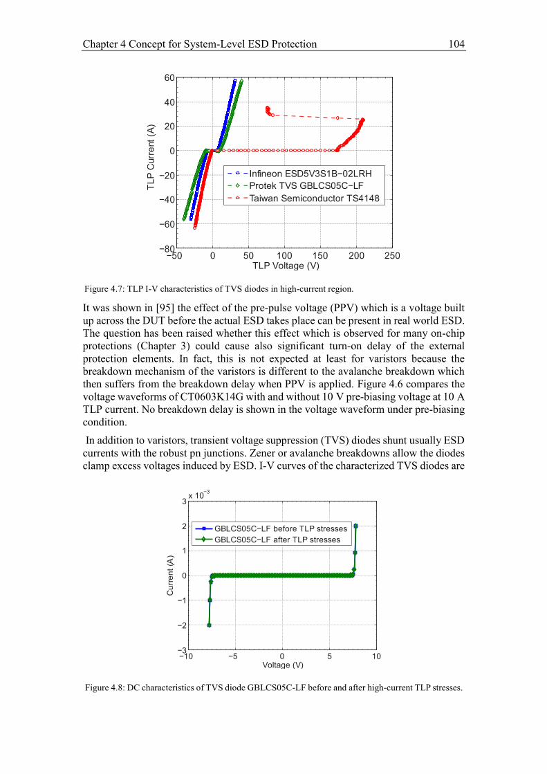
Chapter 4 Concept for System-Level ESD Protection 104
It was shown in [95] the effect of the pre-pulse voltage (PPV) which is a voltage built
up across the DUT before the actual ESD takes place can be present in real world ESD.
The question has been raised whether this effect which is observed for many on-chip
protections (Chapter 3) could cause also significant turn-on delay of the external
protection elements. In fact, this is not expected at least for varistors because the
breakdown mechanism of the varistors is different to the avalanche breakdown which
then suffers from the breakdown delay when PPV is applied. Figure 4.6 compares the
voltage waveforms of CT0603K14G with and without 10 V pre-biasing voltage at 10 A
TLP current. No breakdown delay is shown in the voltage waveform under pre-biasing
condition.
In addition to varistors, transient voltage suppression (TVS) diodes shunt usually ESD
currents with the robust pn junctions. Zener or avalanche breakdowns allow the diodes
clamp excess voltages induced by ESD. I-V curves of the characterized TVS diodes are
Figure 4.8: DC characteristics of TVS diode GBLCS05C-LF before and after high-current TLP stresses.
−10 −5 0 5 10−3
−2
−1
0
1
2
3x 10
Voltage (V)
Cu
rre
nt
(A)
GBLCS05C−LF before TLP stresses
GBLCS05C−LF after TLP stresses
Figure 4.7: TLP I-V characteristics of TVS diodes in high-current region.
−50 0 50 100 150 200 250−80
−60
−40
−20
0
20
40
TLP Voltage (V)
TL
P C
urr
ent
(A)
Infineon ESD5V3S1B−02LRH
Protek TVS GBLCS05C−LF
Taiwan Semiconductor TS4148
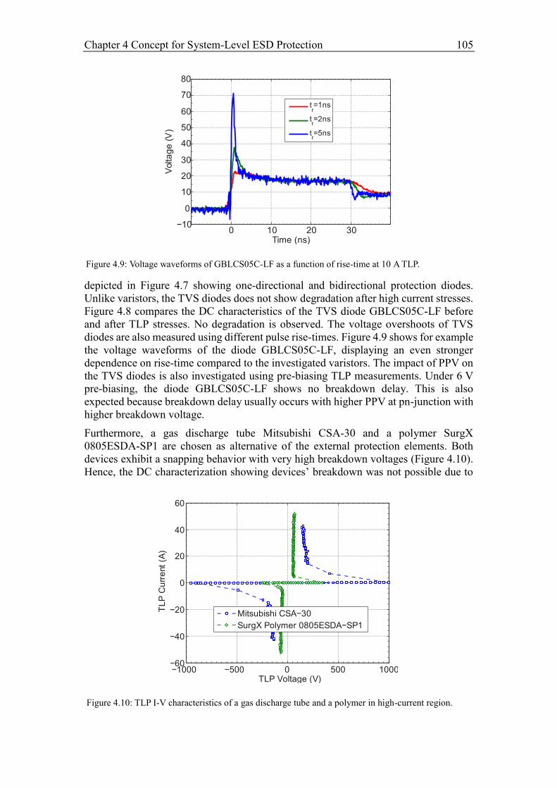
Chapter 4 Concept for System-Level ESD Protection 105
depicted in Figure 4.7 showing one-directional and bidirectional protection diodes.
Unlike varistors, the TVS diodes does not show degradation after high current stresses.
Figure 4.8 compares the DC characteristics of the TVS diode GBLCS05C-LF before
and after TLP stresses. No degradation is observed. The voltage overshoots of TVS
diodes are also measured using different pulse rise-times. Figure 4.9 shows for example
the voltage waveforms of the diode GBLCS05C-LF, displaying an even stronger
dependence on rise-time compared to the investigated varistors. The impact of PPV on
the TVS diodes is also investigated using pre-biasing TLP measurements. Under 6 V
pre-biasing, the diode GBLCS05C-LF shows no breakdown delay. This is also
expected because breakdown delay usually occurs with higher PPV at pn-junction with
higher breakdown voltage.
Furthermore, a gas discharge tube Mitsubishi CSA-30 and a polymer SurgX
0805ESDA-SP1 are chosen as alternative of the external protection elements. Both
devices exhibit a snapping behavior with very high breakdown voltages (Figure 4.10).
Hence, the DC characterization showing devices’ breakdown was not possible due to
Figure 4.10: TLP I-V characteristics of a gas discharge tube and a polymer in high-current region.
−1000 −500 0 500 1000−60
−40
−20
0
20
40
TLP Voltage (V)
TL
P C
urr
ent
(A)
Mitsubishi CSA−30
SurgX Polymer 0805ESDA−SP1
Figure 4.9: Voltage waveforms of GBLCS05C-LF as a function of rise-time at 10 A TLP.
0 10 20 30−10
0
10
20
30
40
50
60
70
Volta
ge
(V
)
Time (ns)
tr=1ns
tr=2ns
tr=5ns
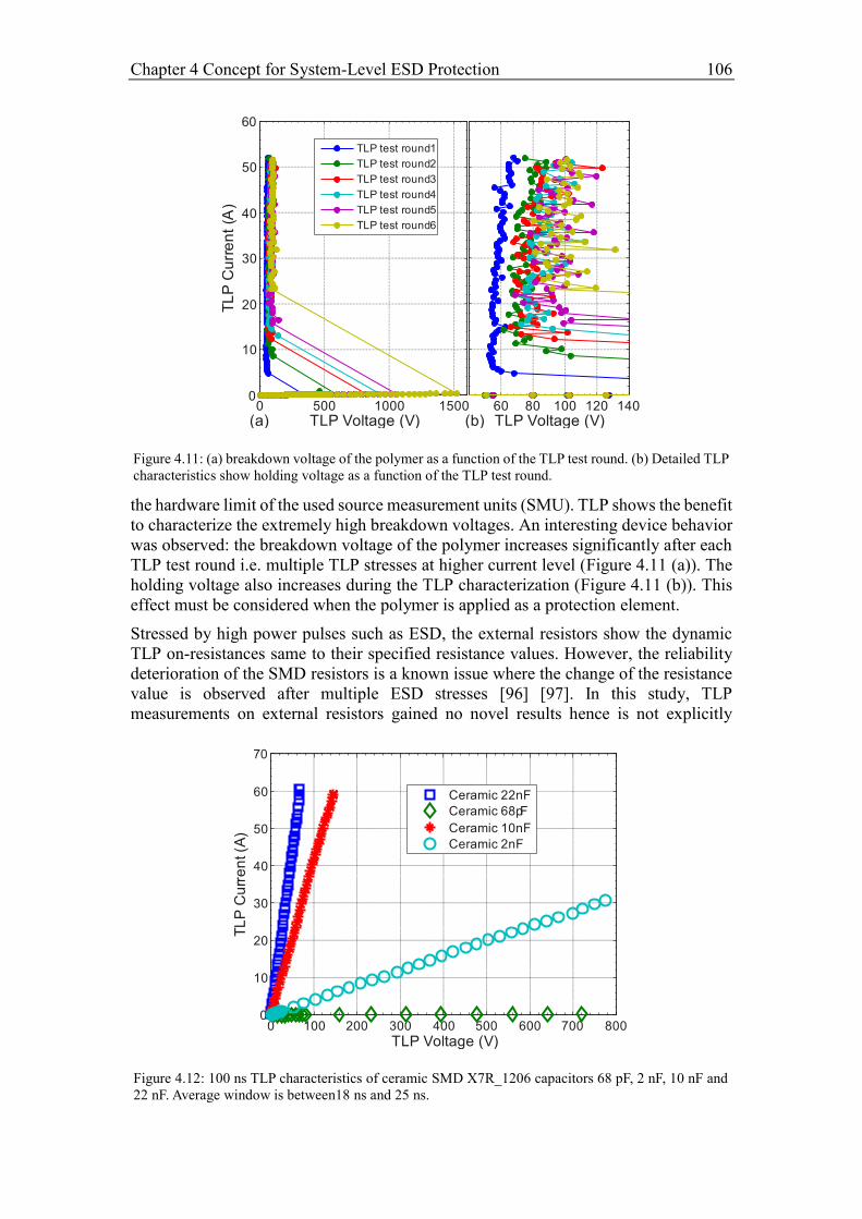
Chapter 4 Concept for System-Level ESD Protection 106
the hardware limit of the used source measurement units (SMU). TLP shows the benefit
to characterize the extremely high breakdown voltages. An interesting device behavior
was observed: the breakdown voltage of the polymer increases significantly after each
TLP test round i.e. multiple TLP stresses at higher current level (Figure 4.11 (a)). The
holding voltage also increases during the TLP characterization (Figure 4.11 (b)). This
effect must be considered when the polymer is applied as a protection element.
Stressed by high power pulses such as ESD, the external resistors show the dynamic
TLP on-resistances same to their specified resistance values. However, the reliability
deterioration of the SMD resistors is a known issue where the change of the resistance
value is observed after multiple ESD stresses [96] [97]. In this study, TLP
measurements on external resistors gained no novel results hence is not explicitly
Figure 4.12: 100 ns TLP characteristics of ceramic SMD X7R_1206 capacitors 68 pF, 2 nF, 10 nF and
22 nF. Average window is between18 ns and 25 ns.
0 100 200 300 400 500 600 700 8000
10
20
30
40
50
60
TL
P C
urr
en
t (A
)
TLP Voltage (V)
Ceramic 22nF
Ceramic 68pF
Ceramic 10nF
Ceramic 2nF
Figure 4.11: (a) breakdown voltage of the polymer as a function of the TLP test round. (b) Detailed TLP
characteristics show holding voltage as a function of the TLP test round.
0 500 1000 15000
10
20
30
40
50
TL
P C
urr
en
t (A
)
TLP Voltage (V)
TLP test round1
TLP test round2
TLP test round3
TLP test round4
TLP test round5
TLP test round6
60 80 100 120 140TLP Voltage (V)(b)(a)
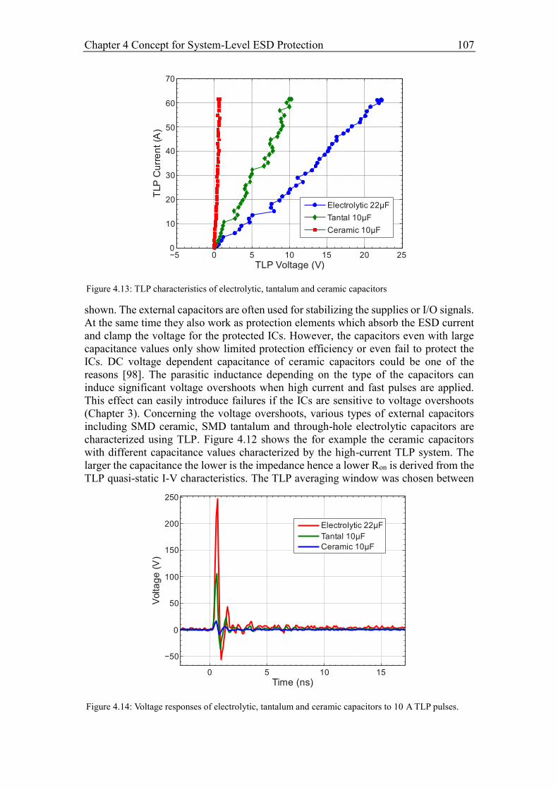
Chapter 4 Concept for System-Level ESD Protection 107
shown. The external capacitors are often used for stabilizing the supplies or I/O signals.
At the same time they also work as protection elements which absorb the ESD current
and clamp the voltage for the protected ICs. However, the capacitors even with large
capacitance values only show limited protection efficiency or even fail to protect the
ICs. DC voltage dependent capacitance of ceramic capacitors could be one of the
reasons [98]. The parasitic inductance depending on the type of the capacitors can
induce significant voltage overshoots when high current and fast pulses are applied.
This effect can easily introduce failures if the ICs are sensitive to voltage overshoots
(Chapter 3). Concerning the voltage overshoots, various types of external capacitors
including SMD ceramic, SMD tantalum and through-hole electrolytic capacitors are
characterized using TLP. Figure 4.12 shows the for example the ceramic capacitors
with different capacitance values characterized by the high-current TLP system. The
larger the capacitance the lower is the impedance hence a lower Ron is derived from the
TLP quasi-static I-V characteristics. The TLP averaging window was chosen between
Figure 4.14: Voltage responses of electrolytic, tantalum and ceramic capacitors to 10 A TLP pulses.
0 5 10 15
−50
0
50
100
150
200
Volta
ge
(V
)
Time (ns)
Electrolytic 22μF
Tantal 10μF
Ceramic 10μF
Figure 4.13: TLP characteristics of electrolytic, tantalum and ceramic capacitors
−5 0 5 10 15 20 250
10
20
30
40
50
60
TLP
Cu
rre
nt
(A)
TLP Voltage (V)
Electrolytic 22μF
Tantal 10μF
Ceramic 10μF
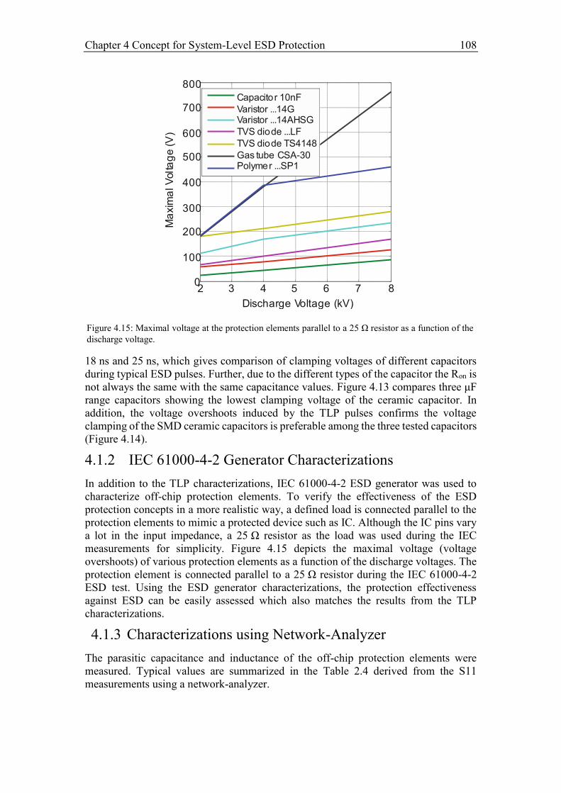
Chapter 4 Concept for System-Level ESD Protection 108
18 ns and 25 ns, which gives comparison of clamping voltages of different capacitors
during typical ESD pulses. Further, due to the different types of the capacitor the Ron is
not always the same with the same capacitance values. Figure 4.13 compares three μF
range capacitors showing the lowest clamping voltage of the ceramic capacitor. In
addition, the voltage overshoots induced by the TLP pulses confirms the voltage
clamping of the SMD ceramic capacitors is preferable among the three tested capacitors
(Figure 4.14).
4.1.2 IEC 61000-4-2 Generator Characterizations
In addition to the TLP characterizations, IEC 61000-4-2 ESD generator was used to
characterize off-chip protection elements. To verify the effectiveness of the ESD
protection concepts in a more realistic way, a defined load is connected parallel to the
protection elements to mimic a protected device such as IC. Although the IC pins vary
a lot in the input impedance, a 25 Ω resistor as the load was used during the IEC
measurements for simplicity. Figure 4.15 depicts the maximal voltage (voltage
overshoots) of various protection elements as a function of the discharge voltages. The
protection element is connected parallel to a 25 Ω resistor during the IEC 61000-4-2
ESD test. Using the ESD generator characterizations, the protection effectiveness
against ESD can be easily assessed which also matches the results from the TLP
characterizations.
4.1.3 Characterizations using Network-Analyzer
The parasitic capacitance and inductance of the off-chip protection elements were
measured. Typical values are summarized in the Table 2.4 derived from the S11
measurements using a network-analyzer.
Figure 4.15: Maximal voltage at the protection elements parallel to a 25 Ω resistor as a function of the
discharge voltage.
Discharge Voltage (kV)
2 3 4 5 6 7 8
Ma
xim
al V
olta
ge (
V)
0
100
200
300
400
500
600
700
800
Capacitor 10nF
Varistor ...14GVaristor ...14AHSG
TVS diode ...LF
TVS diode TS4148
Gas tube CSA-30Polymer ...SP1
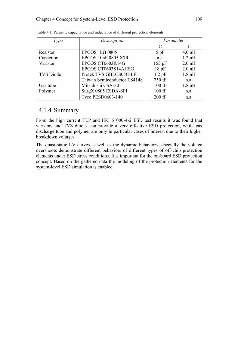
Chapter 4 Concept for System-Level ESD Protection 109
4.1.4 Summary
From the high current TLP and IEC 61000-4-2 ESD test results it was found that
varistors and TVS diodes can provide a very effective ESD protection, while gas
discharge tube and polymer are only in particular cases of interest due to their higher
breakdown voltages.
The quasi-static I-V curves as well as the dynamic behaviors especially the voltage
overshoots demonstrate different behaviors of different types of off-chip protection
elements under ESD stress conditions. It is important for the on-board ESD protection
concept. Based on the gathered data the modeling of the protection elements for the
system-level ESD simulation is enabled.
Table 4.1: Parasitic capacitance and inductance of different protection elements.
Type Description Parameter
C L
Resistor EPCOS 1kΩ 0805 5 pF 4.0 nH
Capacitor EPCOS 10nF 0805 X7R n.a. 1.2 nH
Varistor EPCOS CT0603K14G 155 pF 2.0 nH
EPCOS CT0603S14AHSG 18 pF 2.0 nH
TVS Diode Protek TVS GBLCS05C-LF 1.2 pF 1.8 nH
Taiwan Semiconductor TS4148 750 fF n.a.
Gas tube Mitsubishi CSA-30 100 fF 1.8 nH
Polymer SurgX 0805 ESDA-SPI 100 fF n.a.
Tyco PESD0603-140 200 fF n.a.
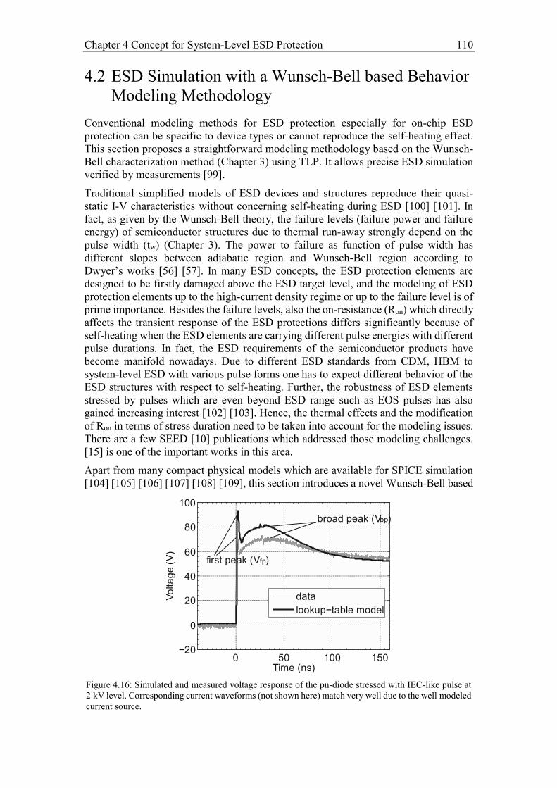
Chapter 4 Concept for System-Level ESD Protection 110
4.2 ESD Simulation with a Wunsch-Bell based Behavior
Modeling Methodology
Conventional modeling methods for ESD protection especially for on-chip ESD
protection can be specific to device types or cannot reproduce the self-heating effect.
This section proposes a straightforward modeling methodology based on the Wunsch-
Bell characterization method (Chapter 3) using TLP. It allows precise ESD simulation
verified by measurements [99].
Traditional simplified models of ESD devices and structures reproduce their quasi-
static I-V characteristics without concerning self-heating during ESD [100] [101]. In
fact, as given by the Wunsch-Bell theory, the failure levels (failure power and failure
energy) of semiconductor structures due to thermal run-away strongly depend on the
pulse width (tw) (Chapter 3). The power to failure as function of pulse width has
different slopes between adiabatic region and Wunsch-Bell region according to
Dwyer’s works [56] [57]. In many ESD concepts, the ESD protection elements are
designed to be firstly damaged above the ESD target level, and the modeling of ESD
protection elements up to the high-current density regime or up to the failure level is of
prime importance. Besides the failure levels, also the on-resistance (Ron) which directly
affects the transient response of the ESD protections differs significantly because of
self-heating when the ESD elements are carrying different pulse energies with different
pulse durations. In fact, the ESD requirements of the semiconductor products have
become manifold nowadays. Due to different ESD standards from CDM, HBM to
system-level ESD with various pulse forms one has to expect different behavior of the
ESD structures with respect to self-heating. Further, the robustness of ESD elements
stressed by pulses which are even beyond ESD range such as EOS pulses has also
gained increasing interest [102] [103]. Hence, the thermal effects and the modification
of Ron in terms of stress duration need to be taken into account for the modeling issues.
There are a few SEED [10] publications which addressed those modeling challenges.
[15] is one of the important works in this area.
Apart from many compact physical models which are available for SPICE simulation
[104] [105] [106] [107] [108] [109], this section introduces a novel Wunsch-Bell based
Figure 4.16: Simulated and measured voltage response of the pn-diode stressed with IEC-like pulse at
2 kV level. Corresponding current waveforms (not shown here) match very well due to the well modeled
current source.
0 50 100 150−20
0
20
40
60
80
Vo
lta
ge (
V)
Time (ns)
data
lookup−table model
broad peak (Vbp)
first peak (Vfp)
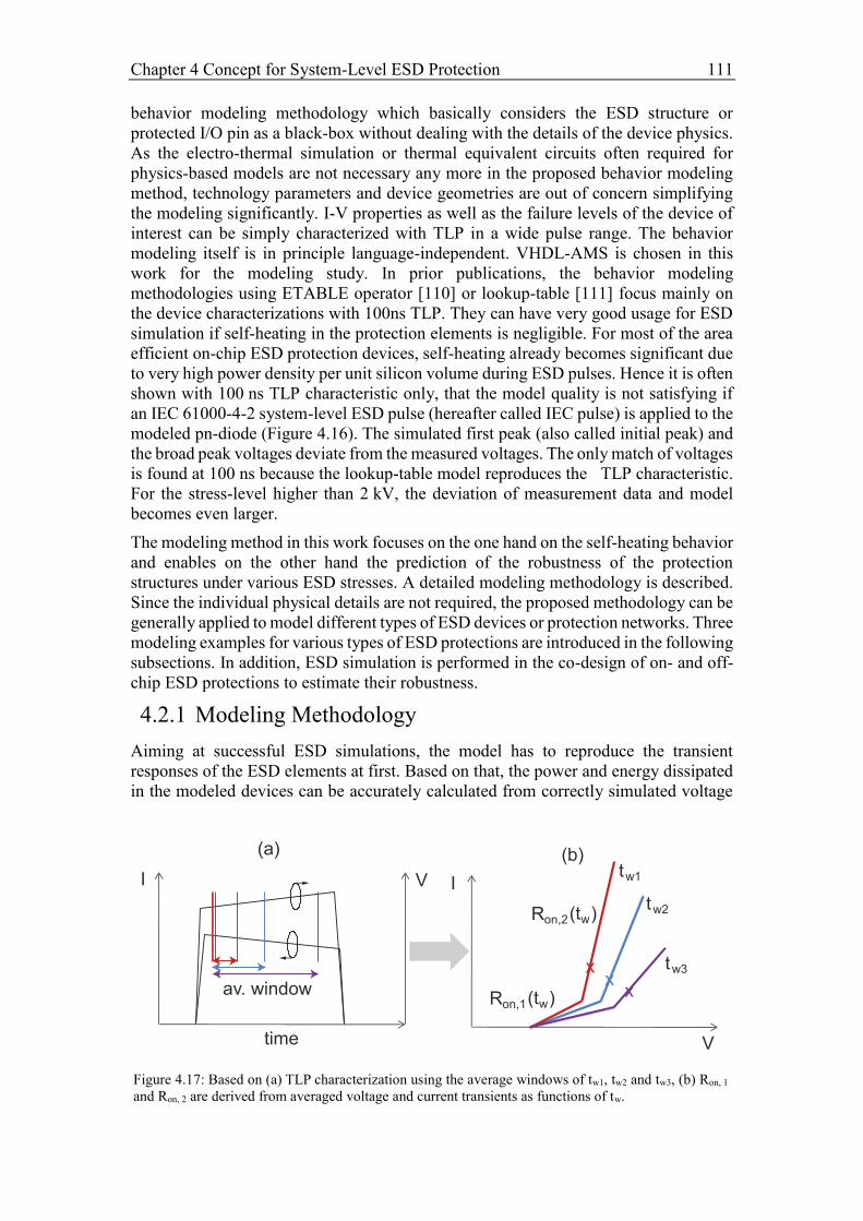
Chapter 4 Concept for System-Level ESD Protection 111
behavior modeling methodology which basically considers the ESD structure or
protected I/O pin as a black-box without dealing with the details of the device physics.
As the electro-thermal simulation or thermal equivalent circuits often required for
physics-based models are not necessary any more in the proposed behavior modeling
method, technology parameters and device geometries are out of concern simplifying
the modeling significantly. I-V properties as well as the failure levels of the device of
interest can be simply characterized with TLP in a wide pulse range. The behavior
modeling itself is in principle language-independent. VHDL-AMS is chosen in this
work for the modeling study. In prior publications, the behavior modeling
methodologies using ETABLE operator [110] or lookup-table [111] focus mainly on
the device characterizations with 100ns TLP. They can have very good usage for ESD
simulation if self-heating in the protection elements is negligible. For most of the area
efficient on-chip ESD protection devices, self-heating already becomes significant due
to very high power density per unit silicon volume during ESD pulses. Hence it is often
shown with 100 ns TLP characteristic only, that the model quality is not satisfying if
an IEC 61000-4-2 system-level ESD pulse (hereafter called IEC pulse) is applied to the
modeled pn-diode (Figure 4.16). The simulated first peak (also called initial peak) and
the broad peak voltages deviate from the measured voltages. The only match of voltages
is found at 100 ns because the lookup-table model reproduces the TLP characteristic.
For the stress-level higher than 2 kV, the deviation of measurement data and model
becomes even larger.
The modeling method in this work focuses on the one hand on the self-heating behavior
and enables on the other hand the prediction of the robustness of the protection
structures under various ESD stresses. A detailed modeling methodology is described.
Since the individual physical details are not required, the proposed methodology can be
generally applied to model different types of ESD devices or protection networks. Three
modeling examples for various types of ESD protections are introduced in the following
subsections. In addition, ESD simulation is performed in the co-design of on- and off-
chip ESD protections to estimate their robustness.
4.2.1 Modeling Methodology
Aiming at successful ESD simulations, the model has to reproduce the transient
responses of the ESD elements at first. Based on that, the power and energy dissipated
in the modeled devices can be accurately calculated from correctly simulated voltage
Figure 4.17: Based on (a) TLP characterization using the average windows of tw1, tw2 and tw3, (b) Ron, 1
and Ron, 2 are derived from averaged voltage and current transients as functions of tw.
tw1
tw2
tw3
V
IVI
time
av. windowR on,1
(b)
(t )w
R on,2(t )w
x
xx
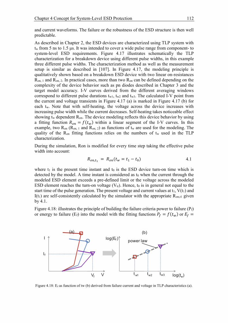
Chapter 4 Concept for System-Level ESD Protection 112
and current waveforms. The failure or the robustness of the ESD structure is then well
predictable.
As described in Chapter 2, the ESD devices are characterized using TLP system with
tw from 5 ns to 1.5 μs. It was intended to cover a wide pulse range from component- to
system-level ESD requirements. Figure 4.17 illustrates schematically the TLP
characterization for a breakdown device using different pulse widths, in this example
three different pulse widths. The characterization method as well as the measurement
setup is similar as described in [107]. In Figure 4.17, the modeling principle is
qualitatively shown based on a breakdown ESD device with two linear on-resistances
Ron, 1 and Ron, 2. In practical cases, more than two Ron can be defined depending on the
complexity of the device behavior such as pn diodes described in Chapter 3 and the
target model accuracy. I-V curves derived from the different averaging windows
correspond to different pulse durations tw1, tw2 and tw3. The calculated I-V point from
the current and voltage transients in Figure 4.17 (a) is marked in Figure 4.17 (b) for
each tw. Note that with self-heating, the voltage across the device increases with
increasing pulse width while the current decreases. Self-heating takes noticeable effect
showing tw dependent Ron. The device modeling reflects this device behavior by using
a fitting function 𝑅𝑜𝑛 = 𝑓(𝑡𝑤) within a linear segment of the I-V curves. In this
example, two Ron (Ron, 1 and Ron, 2) as functions of tw are used for the modeling. The
quality of the Ron fitting functions relies on the numbers of tw used in the TLP
characterization.
During the simulation, Ron is modified for every time step taking the effective pulse
width into account:
𝑅𝑜𝑛,𝑡1 = 𝑅𝑜𝑛(𝑡𝑤 = 𝑡1 − 𝑡0) 4.1
where t1 is the present time instant and t0 is the ESD device turn-on time which is
detected by the model. A time instant is considered as t0 when the current through the
modeled ESD element exceeds a pre-defined limit or the voltage across the modeled
ESD element reaches the turn-on voltage (Vtr). Hence, t0 is in general not equal to the
start time of the pulse generation. The present voltage and current values at t1, V(t1) and
I(t1) are self-consistently calculated by the simulator with the appropriate Ron,t1 given
by 4.1.
Figure 4.18: illustrates the principle of building the failure criteria power to failure (Pf)
or energy to failure (Ef) into the model with the fitting functions 𝑃𝑓 = 𝑓(𝑡𝑤) or 𝐸𝑓 =
Figure 4.18: Ef as function of tw (b) derived from failure current and voltage in TLP characteristics (a).
V
I
t w1 tw2 tw3
log(E )f
log(t )
(b)
Vf
If
w
power law
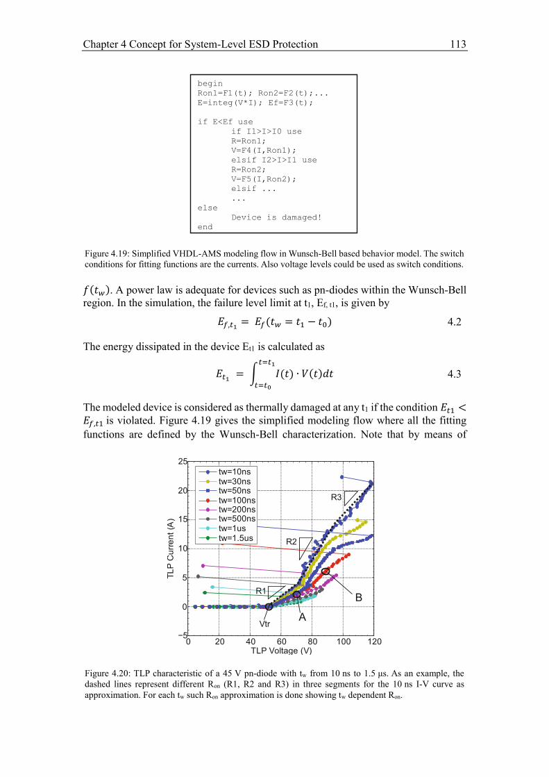
Chapter 4 Concept for System-Level ESD Protection 113
𝑓(𝑡𝑤). A power law is adequate for devices such as pn-diodes within the Wunsch-Bell
region. In the simulation, the failure level limit at t1, Ef, t1, is given by
𝐸𝑓,𝑡1= 𝐸𝑓(𝑡𝑤 = 𝑡1 − 𝑡0) 4.2
The energy dissipated in the device Et1 is calculated as
𝐸𝑡1 = ∫ 𝐼(𝑡) ∙ 𝑉(𝑡)𝑑𝑡
𝑡=𝑡1
𝑡=𝑡0
4.3
The modeled device is considered as thermally damaged at any t1 if the condition 𝐸𝑡1 <𝐸𝑓,𝑡1 is violated. Figure 4.19 gives the simplified modeling flow where all the fitting
functions are defined by the Wunsch-Bell characterization. Note that by means of
Figure 4.19: Simplified VHDL-AMS modeling flow in Wunsch-Bell based behavior model. The switch
conditions for fitting functions are the currents. Also voltage levels could be used as switch conditions.
Figure 4.20: TLP characteristic of a 45 V pn-diode with tw from 10 ns to 1.5 μs. As an example, the
dashed lines represent different Ron (R1, R2 and R3) in three segments for the 10 ns I-V curve as
approximation. For each tw such Ron approximation is done showing tw dependent Ron.
0 20 40 60 80 100 120−5
0
5
10
15
20
TL
P C
urr
en
t (A
)
TLP Voltage (V)
tw=10ns
tw=1.5us
tw=100ns
tw=1us
tw=200ns
tw=30ns
tw=500ns
tw=50ns
Vtr
R2
R1
R3
A
B
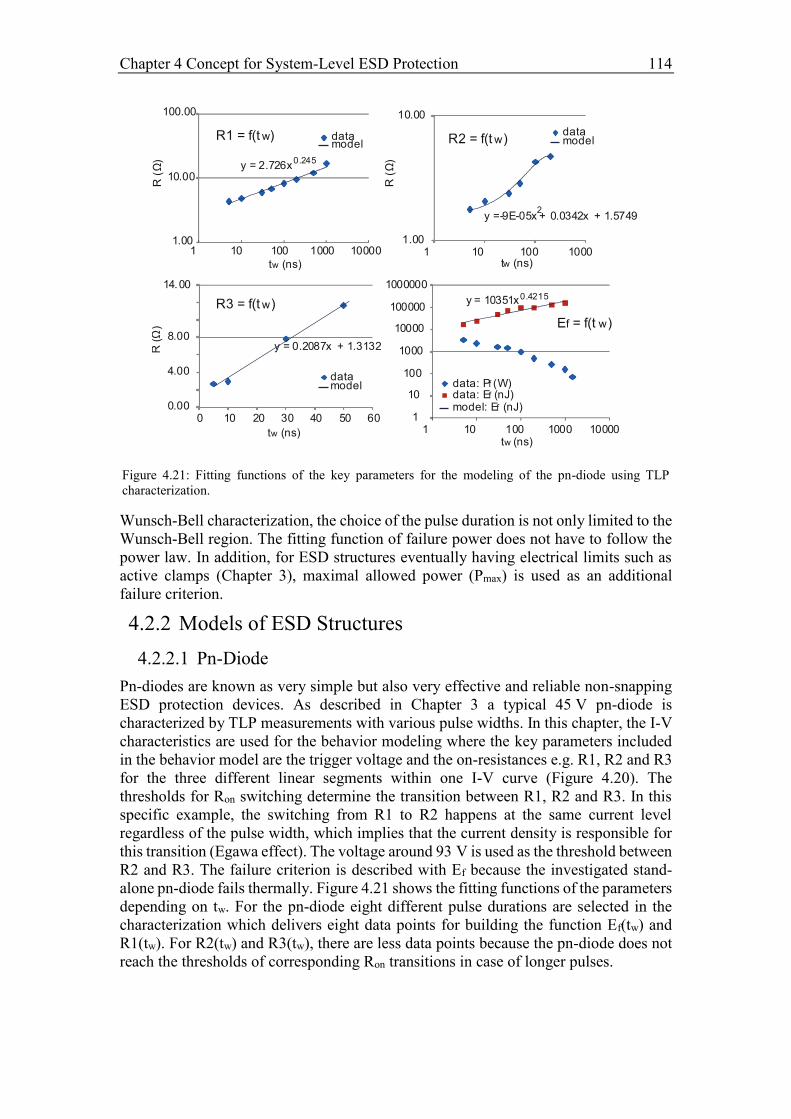
Chapter 4 Concept for System-Level ESD Protection 114
Wunsch-Bell characterization, the choice of the pulse duration is not only limited to the
Wunsch-Bell region. The fitting function of failure power does not have to follow the
power law. In addition, for ESD structures eventually having electrical limits such as
active clamps (Chapter 3), maximal allowed power (Pmax) is used as an additional
failure criterion.
4.2.2 Models of ESD Structures
4.2.2.1 Pn-Diode
Pn-diodes are known as very simple but also very effective and reliable non-snapping
ESD protection devices. As described in Chapter 3 a typical 45 V pn-diode is
characterized by TLP measurements with various pulse widths. In this chapter, the I-V
characteristics are used for the behavior modeling where the key parameters included
in the behavior model are the trigger voltage and the on-resistances e.g. R1, R2 and R3
for the three different linear segments within one I-V curve (Figure 4.20). The
thresholds for Ron switching determine the transition between R1, R2 and R3. In this
specific example, the switching from R1 to R2 happens at the same current level
regardless of the pulse width, which implies that the current density is responsible for
this transition (Egawa effect). The voltage around 93 V is used as the threshold between
R2 and R3. The failure criterion is described with Ef because the investigated stand-
alone pn-diode fails thermally. Figure 4.21 shows the fitting functions of the parameters
depending on tw. For the pn-diode eight different pulse durations are selected in the
characterization which delivers eight data points for building the function Ef(tw) and
R1(tw). For R2(tw) and R3(tw), there are less data points because the pn-diode does not
reach the thresholds of corresponding Ron transitions in case of longer pulses.
Figure 4.21: Fitting functions of the key parameters for the modeling of the pn-diode using TLP
characterization.
y = 2.726x0.245
1.00
10.00
1 10 100 1000 10000
datamodel
R1 = f(t w)
tw (ns)
R (
Ω)
y =-9E-05x2+ 0.0342x + 1.5749
1.00
10.00
1 10 100 1000
datamodel
y = 0.2087x + 1.3132
0.00
4.00
8.00
14.00
0 10 20 30 40 50 60
datamodel
y = 10351x0.4215
1
10
100
1000
10000
100000
1000000
1 10 100 1000 10000
data: Pf (W)data: Ef (nJ)model: Ef (nJ)
R2 = f(t w)
tw (ns)
R (
Ω)
R3 = f(t w)
tw (ns)
R (
Ω) Ef = f(t w)
tw (ns)
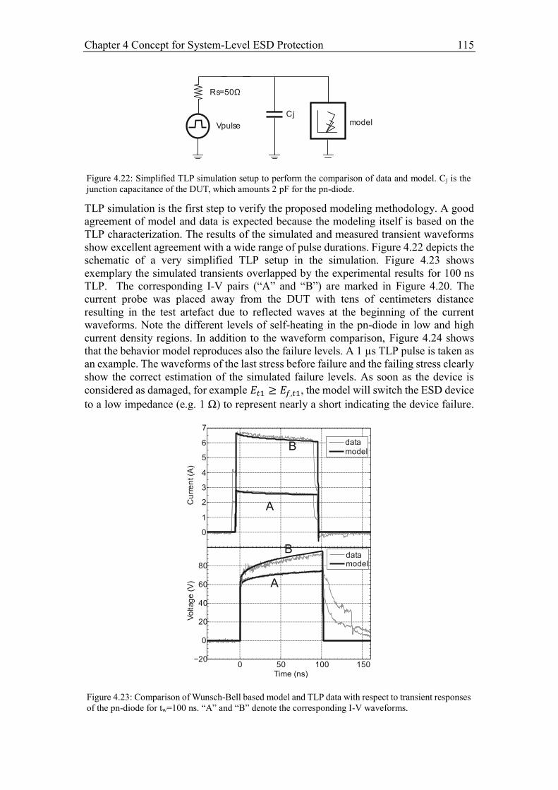
Chapter 4 Concept for System-Level ESD Protection 115
TLP simulation is the first step to verify the proposed modeling methodology. A good
agreement of model and data is expected because the modeling itself is based on the
TLP characterization. The results of the simulated and measured transient waveforms
show excellent agreement with a wide range of pulse durations. Figure 4.22 depicts the
schematic of a very simplified TLP setup in the simulation. Figure 4.23 shows
exemplary the simulated transients overlapped by the experimental results for 100 ns
TLP. The corresponding I-V pairs (“A” and “B”) are marked in Figure 4.20. The
current probe was placed away from the DUT with tens of centimeters distance
resulting in the test artefact due to reflected waves at the beginning of the current
waveforms. Note the different levels of self-heating in the pn-diode in low and high
current density regions. In addition to the waveform comparison, Figure 4.24 shows
that the behavior model reproduces also the failure levels. A 1 µs TLP pulse is taken as
an example. The waveforms of the last stress before failure and the failing stress clearly
show the correct estimation of the simulated failure levels. As soon as the device is
considered as damaged, for example 𝐸𝑡1 ≥ 𝐸𝑓,𝑡1, the model will switch the ESD device
to a low impedance (e.g. 1 Ω) to represent nearly a short indicating the device failure.
Figure 4.23: Comparison of Wunsch-Bell based model and TLP data with respect to transient responses
of the pn-diode for tw=100 ns. “A” and “B” denote the corresponding I-V waveforms.
0
1
2
3
4
5
6
Cu
rre
nt (A
)
datamodel
0 50 100 150−20
0
20
40
60
80
Vo
ltag
e (
V)
Time (ns)
datamodel
A
A
B
B
Figure 4.22: Simplified TLP simulation setup to perform the comparison of data and model. Cj is the
junction capacitance of the DUT, which amounts 2 pF for the pn-diode.
model
Rs=50Ω
Vpulse
Cj
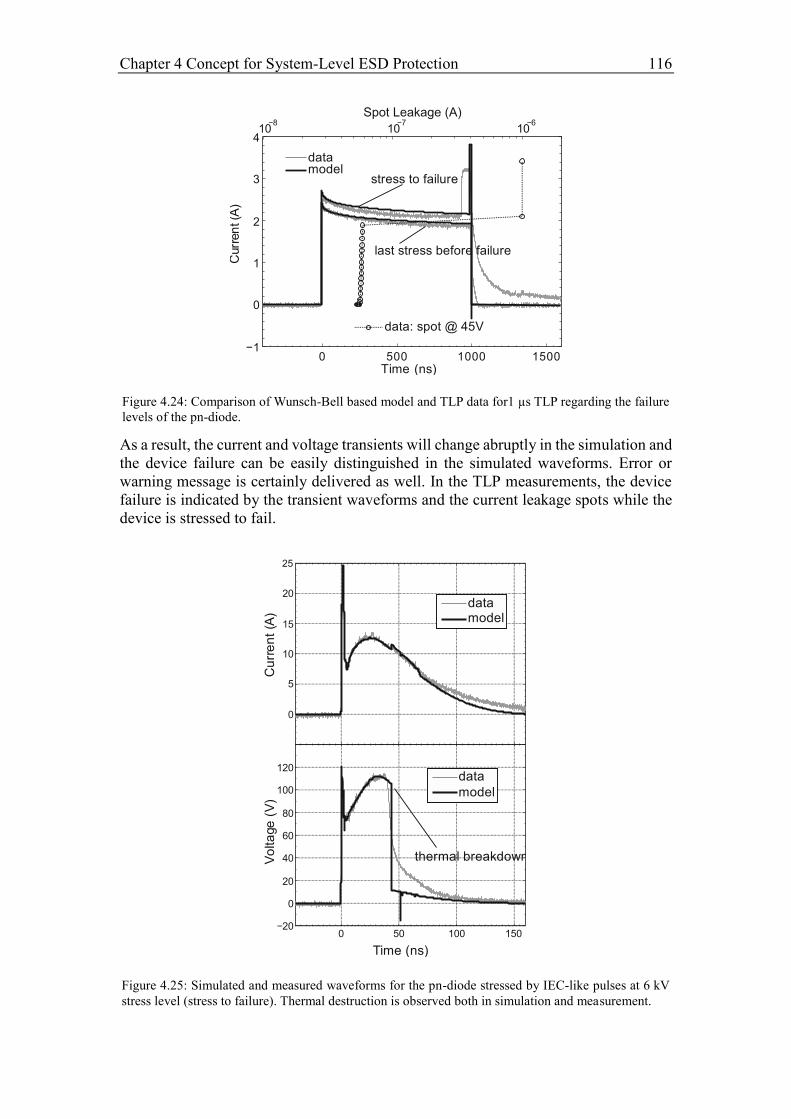
Chapter 4 Concept for System-Level ESD Protection 116
As a result, the current and voltage transients will change abruptly in the simulation and
the device failure can be easily distinguished in the simulated waveforms. Error or
warning message is certainly delivered as well. In the TLP measurements, the device
failure is indicated by the transient waveforms and the current leakage spots while the
device is stressed to fail.
Figure 4.25: Simulated and measured waveforms for the pn-diode stressed by IEC-like pulses at 6 kV
stress level (stress to failure). Thermal destruction is observed both in simulation and measurement.
0 50 100 150−20
0
20
40
60
80
100
120
0
5
10
15
20
Cu
rre
nt
(A)
Vo
lta
ge
(V
)
Time (ns)
data
model
datamodel
thermal breakdown
Figure 4.24: Comparison of Wunsch-Bell based model and TLP data for1 µs TLP regarding the failure
levels of the pn-diode.
0 500 1000 1500−1
0
1
2
3
4
Curr
en
t (A
)
Time (ns)
10−8
10−7
10−6
data: spot @ 45V
stress to failure
last stress before failure
datamodel
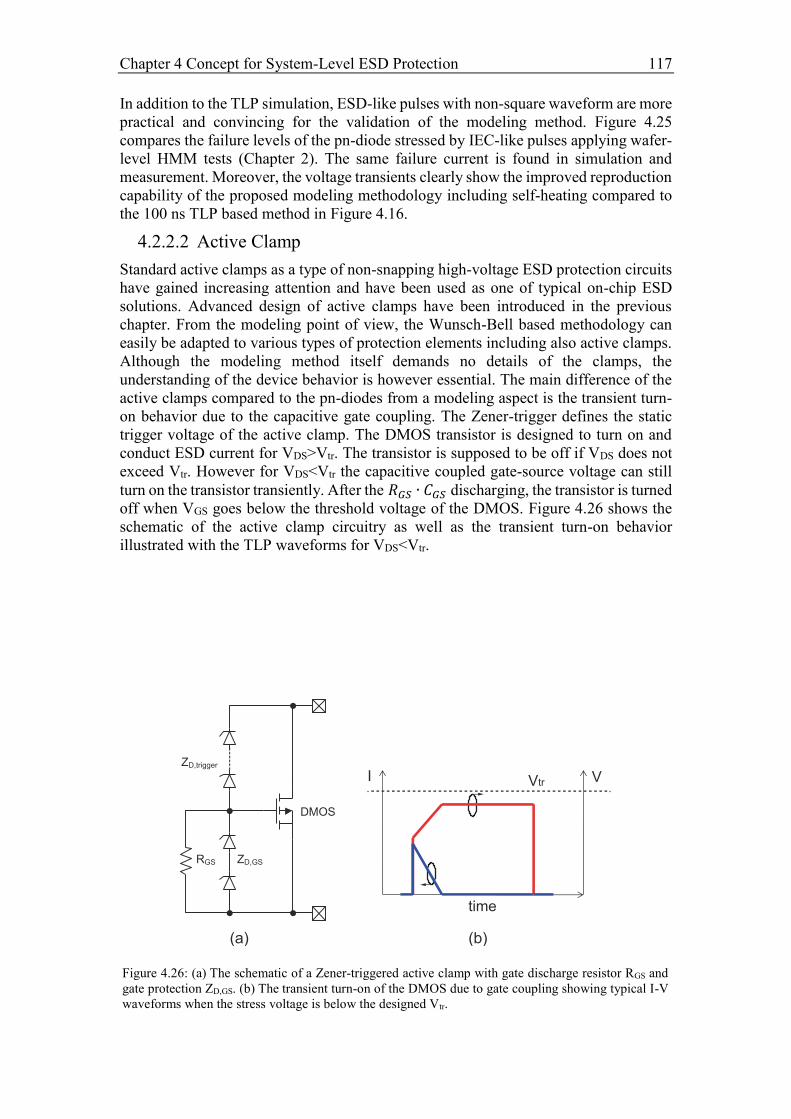
Chapter 4 Concept for System-Level ESD Protection 117
In addition to the TLP simulation, ESD-like pulses with non-square waveform are more
practical and convincing for the validation of the modeling method. Figure 4.25
compares the failure levels of the pn-diode stressed by IEC-like pulses applying wafer-
level HMM tests (Chapter 2). The same failure current is found in simulation and
measurement. Moreover, the voltage transients clearly show the improved reproduction
capability of the proposed modeling methodology including self-heating compared to
the 100 ns TLP based method in Figure 4.16.
4.2.2.2 Active Clamp
Standard active clamps as a type of non-snapping high-voltage ESD protection circuits
have gained increasing attention and have been used as one of typical on-chip ESD
solutions. Advanced design of active clamps have been introduced in the previous
chapter. From the modeling point of view, the Wunsch-Bell based methodology can
easily be adapted to various types of protection elements including also active clamps.
Although the modeling method itself demands no details of the clamps, the
understanding of the device behavior is however essential. The main difference of the
active clamps compared to the pn-diodes from a modeling aspect is the transient turn-
on behavior due to the capacitive gate coupling. The Zener-trigger defines the static
trigger voltage of the active clamp. The DMOS transistor is designed to turn on and
conduct ESD current for VDS>Vtr. The transistor is supposed to be off if VDS does not
exceed Vtr. However for VDS<Vtr the capacitive coupled gate-source voltage can still
turn on the transistor transiently. After the 𝑅𝐺𝑆 ∙ 𝐶𝐺𝑆 discharging, the transistor is turned
off when VGS goes below the threshold voltage of the DMOS. Figure 4.26 shows the
schematic of the active clamp circuitry as well as the transient turn-on behavior
illustrated with the TLP waveforms for VDS<Vtr.
Figure 4.26: (a) The schematic of a Zener-triggered active clamp with gate discharge resistor RGS and
gate protection ZD,GS. (b) The transient turn-on of the DMOS due to gate coupling showing typical I-V
waveforms when the stress voltage is below the designed Vtr.
DMOS
ZD,GSRGS
ZD,trigger
(a)
VI
time
Vtr
(b)
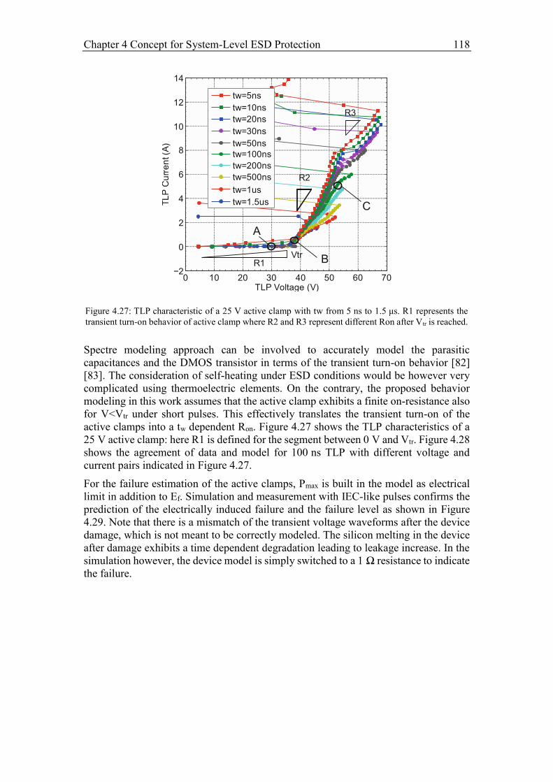
Chapter 4 Concept for System-Level ESD Protection 118
Spectre modeling approach can be involved to accurately model the parasitic
capacitances and the DMOS transistor in terms of the transient turn-on behavior [82]
[83]. The consideration of self-heating under ESD conditions would be however very
complicated using thermoelectric elements. On the contrary, the proposed behavior
modeling in this work assumes that the active clamp exhibits a finite on-resistance also
for V<Vtr under short pulses. This effectively translates the transient turn-on of the
active clamps into a tw dependent Ron. Figure 4.27 shows the TLP characteristics of a
25 V active clamp: here R1 is defined for the segment between 0 V and Vtr. Figure 4.28
shows the agreement of data and model for 100 ns TLP with different voltage and
current pairs indicated in Figure 4.27.
For the failure estimation of the active clamps, Pmax is built in the model as electrical
limit in addition to Ef. Simulation and measurement with IEC-like pulses confirms the
prediction of the electrically induced failure and the failure level as shown in Figure
4.29. Note that there is a mismatch of the transient voltage waveforms after the device
damage, which is not meant to be correctly modeled. The silicon melting in the device
after damage exhibits a time dependent degradation leading to leakage increase. In the
simulation however, the device model is simply switched to a 1 Ω resistance to indicate
the failure.
Figure 4.27: TLP characteristic of a 25 V active clamp with tw from 5 ns to 1.5 μs. R1 represents the
transient turn-on behavior of active clamp where R2 and R3 represent different Ron after Vtr is reached.
0 10 20 30 40 50 60 70−2
0
2
4
6
8
10
12
TL
P C
urr
en
t (A
)
TLP Voltage (V)
tw=1.5us
tw=100ns
tw=1us
tw=200ns
tw=30ns
tw=500ns
tw=50ns
tw=20ns
tw=10ns
tw=5ns
R2
R3
R1Vtr
A
B
C
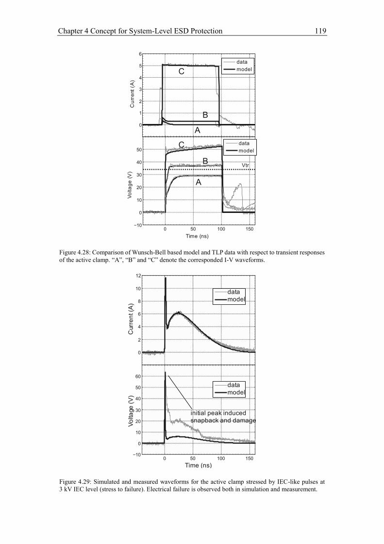
Chapter 4 Concept for System-Level ESD Protection 119
Figure 4.29: Simulated and measured waveforms for the active clamp stressed by IEC-like pulses at
3 kV IEC level (stress to failure). Electrical failure is observed both in simulation and measurement.
0
2
4
6
8
10
0 50 100 150−10
0
10
20
30
40
50
60
datamodel
datamodel
Curr
en
t (A
)V
olta
ge
(V
)
Time (ns)
initial peak inducedsnapback and damage
Figure 4.28: Comparison of Wunsch-Bell based model and TLP data with respect to transient responses
of the active clamp. “A”, “B” and “C” denote the corresponded I-V waveforms.
0
1
2
3
4
5
0 50 100 150−10
0
10
20
30
40
50
Cu
rre
nt
(A)
Vo
lta
ge
(V
)
Time (ns)
data
model
data
model
Vtr
A
B
A
B
C
C
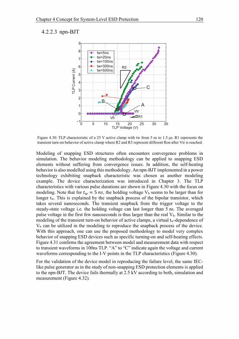
Chapter 4 Concept for System-Level ESD Protection 120
4.2.2.3 npn-BJT
Modeling of snapping ESD structures often encounters convergence problems in
simulation. The behavior modeling methodology can be applied to snapping ESD
elements without suffering from convergence issues. In addition, the self-heating
behavior is also modelled using this methodology. An npn-BJT implemented in a power
technology exhibiting snapback characteristic was chosen as another modeling
example. The device characterization was introduced in Chapter 3. The TLP
characteristics with various pulse durations are shown in Figure 4.30 with the focus on
modeling. Note that for 𝑡𝑤 = 5 𝑛𝑠, the holding voltage Vh seems to be larger than for
longer tw. This is explained by the snapback process of the bipolar transistor, which
takes several nanoseconds. The transient snapback from the trigger voltage to the
steady-state voltage i.e. the holding voltage can last longer than 5 ns. The averaged
pulse voltage in the first few nanoseconds is thus larger than the real Vh. Similar to the
modeling of the transient turn-on behavior of active clamps, a virtual tw-dependence of
Vh can be utilized in the modeling to reproduce the snapback process of the device.
With this approach, one can use the proposed methodology to model very complex
behavior of snapping ESD devices such as specific turning-on and self-heating effects.
Figure 4.31 confirms the agreement between model and measurement data with respect
to transient waveforms in 100ns TLP. “A” to “C” indicate again the voltage and current
waveforms corresponding to the I-V points in the TLP characteristics (Figure 4.30).
For the validation of the device model in reproducing the failure level, the same IEC-
like pulse generator as in the study of non-snapping ESD protection elements is applied
to the npn-BJT. The device fails thermally at 2.5 kV according to both, simulation and
measurement (Figure 4.32).
Figure 4.30: TLP characteristic of a 25 V active clamp with tw from 5 ns to 1.5 μs. R1 represents the
transient turn-on behavior of active clamp where R2 and R3 represent different Ron after Vtr is reached.
0 5 10 15 20 25 30 35−1
0
1
2
3
4
5
6
7
8
TL
P C
urr
en
t (A
)
TLP Voltage (V)
tw=100nstw=20ns
tw=300nstw=500ns
tw=5ns
R1
R2
Vh
Vtr
AB
C
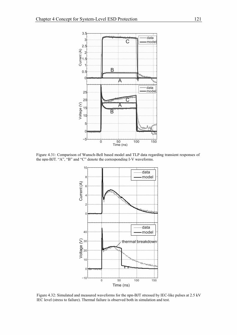
Chapter 4 Concept for System-Level ESD Protection 121
Figure 4.32: Simulated and measured waveforms for the npn-BJT stressed by IEC-like pulses at 2.5 kV
IEC level (stress to failure). Thermal failure is observed both in simulation and test.
0
2
4
6
8
0 50 100 150−10
0
10
20
30
40
data
model
data
model
Cu
rre
nt (A
)V
oltag
e (
V)
Time (ns)
thermal breakdown
Figure 4.31: Comparison of Wunsch-Bell based model and TLP data regarding transient responses of
the npn-BJT. “A”, “B” and “C” denote the corresponding I-V waveforms.
0
0.5
1
1.5
2
2.5
3
Cu
rren
t (A
)
datamodel
A
B
C
0 50 100 150−5
0
5
10
15
20
25
Volta
ge (
V)
Time (ns)
datamodel
A
B
C
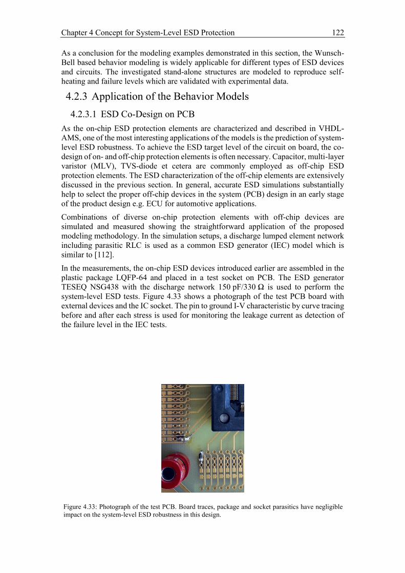
Chapter 4 Concept for System-Level ESD Protection 122
As a conclusion for the modeling examples demonstrated in this section, the Wunsch-
Bell based behavior modeling is widely applicable for different types of ESD devices
and circuits. The investigated stand-alone structures are modeled to reproduce self-
heating and failure levels which are validated with experimental data.
4.2.3 Application of the Behavior Models
4.2.3.1 ESD Co-Design on PCB
As the on-chip ESD protection elements are characterized and described in VHDL-
AMS, one of the most interesting applications of the models is the prediction of system-
level ESD robustness. To achieve the ESD target level of the circuit on board, the co-
design of on- and off-chip protection elements is often necessary. Capacitor, multi-layer
varistor (MLV), TVS-diode et cetera are commonly employed as off-chip ESD
protection elements. The ESD characterization of the off-chip elements are extensively
discussed in the previous section. In general, accurate ESD simulations substantially
help to select the proper off-chip devices in the system (PCB) design in an early stage
of the product design e.g. ECU for automotive applications.
Combinations of diverse on-chip protection elements with off-chip devices are
simulated and measured showing the straightforward application of the proposed
modeling methodology. In the simulation setups, a discharge lumped element network
including parasitic RLC is used as a common ESD generator (IEC) model which is
similar to [112].
In the measurements, the on-chip ESD devices introduced earlier are assembled in the
plastic package LQFP-64 and placed in a test socket on PCB. The ESD generator
TESEQ NSG438 with the discharge network 150 pF/330 Ω is used to perform the
system-level ESD tests. Figure 4.33 shows a photograph of the test PCB board with
external devices and the IC socket. The pin to ground I-V characteristic by curve tracing
before and after each stress is used for monitoring the leakage current as detection of
the failure level in the IEC tests.
Figure 4.33: Photograph of the test PCB. Board traces, package and socket parasitics have negligible
impact on the system-level ESD robustness in this design.
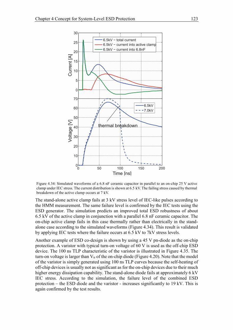
Chapter 4 Concept for System-Level ESD Protection 123
The stand-alone active clamp fails at 3 kV stress level of IEC-like pulses according to
the HMM measurement. The same failure level is confirmed by the IEC tests using the
ESD generator. The simulation predicts an improved total ESD robustness of about
6.5 kV of the active clamp in conjunction with a parallel 6.8 nF ceramic capacitor. The
on-chip active clamp fails in this case thermally rather than electrically in the stand-
alone case according to the simulated waveforms (Figure 4.34). This result is validated
by applying IEC tests where the failure occurs at 6.5 kV to 7kV stress levels.
Another example of ESD co-design is shown by using a 45 V pn-diode as the on-chip
protection. A varistor with typical turn-on voltage of 60 V is used as the off-chip ESD
device. The 100 ns TLP characteristic of the varistor is illustrated in Figure 4.35. The
turn-on voltage is larger than Vtr of the on-chip diode (Figure 4.20). Note that the model
of the varistor is simply generated using 100 ns TLP curves because the self-heating of
off-chip devices is usually not as significant as for the on-chip devices due to their much
higher energy dissipation capability. The stand-alone diode fails at approximately 6 kV
IEC stress. According to the simulation, the failure level of the combined ESD
protection – the ESD diode and the varistor - increases significantly to 19 kV. This is
again confirmed by the test results.
Figure 4.34: Simulated waveforms of a 6.8 nF ceramic capacitor in parallel to an on-chip 25 V active
clamp under IEC stress. The current distribution is shown at 6.5 kV. The failing stress caused by thermal
breakdown of the active clamp occurs at 7 kV.
0
5
10
15
20
25
Cu
rre
nt
[A]
6.5kV − total current
6.5kV − current into active clamp
6.5kV − current into 6.8nF
0 50 100 150 2000
10
20
30
40
50
60
70
Time [ns]
Vo
lta
ge
[V
]
6.5kV
7.0kV
thermal breakdown
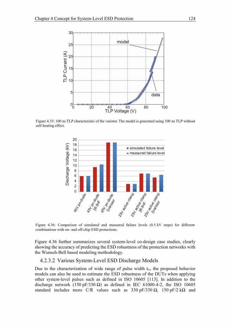
Chapter 4 Concept for System-Level ESD Protection 124
Figure 4.36 further summarizes several system-level co-design case studies, clearly
showing the accuracy of predicting the ESD robustness of the protection networks with
the Wunsch-Bell based modeling methodology.
4.2.3.2 Various System-Level ESD Discharge Models
Due to the characterization of wide range of pulse width tw, the proposed behavior
models can also be used to estimate the ESD robustness of the DUTs when applying
other system-level pulses such as defined in ISO 10605 [113]. In addition to the
discharge network (150 pF/330 Ω) as defined in IEC 61000-4-2, the ISO 10605
standard includes more C/R values such as 330 pF/330 Ω, 150 pF/2 kΩ and
Figure 4.36: Comparison of simulated and measured failure levels (0.5 kV steps) for different
combinations with on- and off-chip ESD protections.
0
2
4
6
8
10
12
14
16
18
20
45V
pn-
dio
de
45V
pn-d
iode
||6.8
nF45V
pn-d
iode
||var
isto
r
25V
activ
ecl
amp
25V
activ
ecl
amp
||6.8
nF25V
activ
ecl
amp
||var
isto
r
Dis
ch
arg
eV
olta
ge
(kV
)
simulated failure level
measured failure level
Figure 4.35: 100 ns TLP characteristic of the varistor. The model is generated using 100 ns TLP without
self-heating effect.
0 20 40 60 80 1000
5
10
15
20
25
TLP Voltage (V)
TL
P C
urr
en
t (A
)
model
data
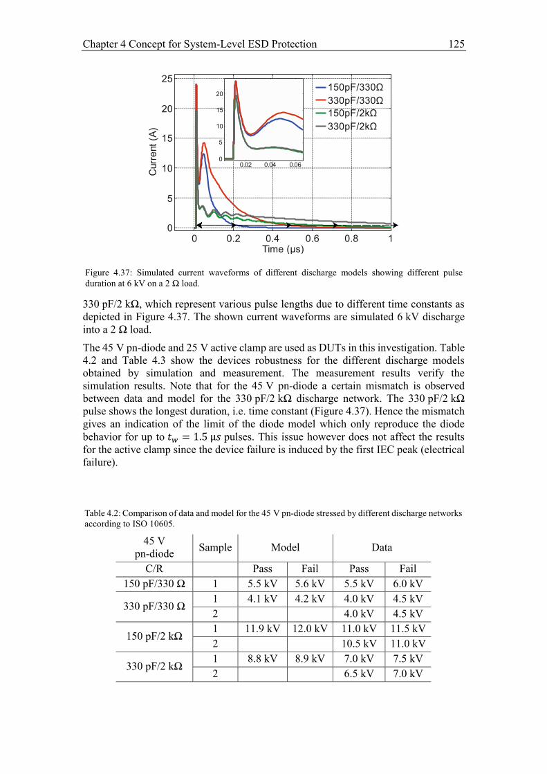
Chapter 4 Concept for System-Level ESD Protection 125
330 pF/2 kΩ, which represent various pulse lengths due to different time constants as
depicted in Figure 4.37. The shown current waveforms are simulated 6 kV discharge
into a 2 Ω load.
The 45 V pn-diode and 25 V active clamp are used as DUTs in this investigation. Table
4.2 and Table 4.3 show the devices robustness for the different discharge models
obtained by simulation and measurement. The measurement results verify the
simulation results. Note that for the 45 V pn-diode a certain mismatch is observed
between data and model for the 330 pF/2 kΩ discharge network. The 330 pF/2 kΩ
pulse shows the longest duration, i.e. time constant (Figure 4.37). Hence the mismatch
gives an indication of the limit of the diode model which only reproduce the diode
behavior for up to 𝑡𝑤 = 1.5 µ𝑠 pulses. This issue however does not affect the results
for the active clamp since the device failure is induced by the first IEC peak (electrical
failure).
Figure 4.37: Simulated current waveforms of different discharge models showing different pulse
duration at 6 kV on a 2 Ω load.
0 0.2 0.4 0.6 0.8 10
5
10
15
20
25
Time (µs)
Curr
ent
(A)
150pF/330Ω
330pF/330Ω
150pF/2kΩ
330pF/2kΩ
0.02 0.04 0.060
5
10
15
20
Table 4.2: Comparison of data and model for the 45 V pn-diode stressed by different discharge networks
according to ISO 10605.
45 V
pn-diode Sample Model Data
C/R Pass Fail Pass Fail
150 pF/330 Ω 1 5.5 kV 5.6 kV 5.5 kV 6.0 kV
330 pF/330 Ω 1 4.1 kV 4.2 kV 4.0 kV 4.5 kV
2 4.0 kV 4.5 kV
150 pF/2 kΩ 1 11.9 kV 12.0 kV 11.0 kV 11.5 kV
2 10.5 kV 11.0 kV
330 pF/2 kΩ 1 8.8 kV 8.9 kV 7.0 kV 7.5 kV
2 6.5 kV 7.0 kV
Chapter 4 Concept for System-Level ESD Protection 126
4.2.4 Summary
The presented behavior modeling method is portable and easy-to-implement. Good
correlations between silicon measurements and simulations have been achieved
validating the methodology and the models. Details of the application examples
including system-level ESD co-design and impact of different pulses on the robustness
of the ESD devices are given. During the Wunsch-Bell characterization a wafer-level
TLP setup is used which minimizes parasitic effects. In the system-level tests, the
parasitic of the used test PCB, package and socket in the case studies has no significant
impact on the simulation results. The robustness of the on-chip in conjunction with the
off-chip devices is simulated and validated by the measurement results.
The main advantage of the proposed modeling methodology is the behavior description
based on the profound TLP measurements. It avoids the emulation of physical
parameters or circuit details, which can be complicated. The presented methodology
easily allows generalizing the modeling method to different types of ESD protection
elements. On the other hand however, the main drawback of the proposed behavior
model is also due to the lack of the physical basis. The self-heating effect is obtained
with the fitting function 𝑅𝑜𝑛 = 𝑓(𝑡𝑤) which is derived from the TLP tests. In the real
applications, the ESD pulse waveforms differ usually a lot from the rectangular TLP
pulses. Fortunately, most of the real-world ESD pulses exhibit an exponential decay,
where at the long tale of the pulse the current level is low enough so that the self-heating
is not significant anymore. The inaccuracy of the Ron estimation for this pulse part is
therefore negligible.
The application range of the proposed behavior modeling can be extended. In this study,
the model is valid up to pulse length of 1.5 µs. An extended characterization up to the
milliseconds range would enable the simulation of the robustness of protected devices
and circuits stressed by electrical fast transient (EFT) or disturbances such as defined
in ISO 7637 [114] [115] [116]. Moreover, for on-chip ESD design, with the ESD
window given by the circuits being protected, different types of protection schemes can
be simulated using the introduced modeling method to achieve the optimal design
considering the area consumption and target robustness. The underestimation of the
ESD device capability due to models without self-heating can lead to ESD overdesign
and must be avoided with a cost efficient design.
Table 4.3: Comparison of data and model for the 25 V active clamp stressed by different discharge
networks according to ISO 10605.
25 V
active clamp Sample Model Data
C/R Pass Fail Pass Fail
150 pF/330 Ω 1 2.7 kV 2.8 kV 2.5 kV 3.0 kV
330 pF/330 Ω 1 2.7 kV 2.8 kV 2.5 kV 3.0 kV
2 2.5 kV 3.0 kV
150 pF/2 kΩ 1 3.4 kV 3.5 kV 2.5 kV 3.0 kV
2 3.0 kV 3.5 kV
330 pF/2 kΩ 1 3.4 kV 3.5 kV 3.0 kV 3.5 kV
2 3.0 kV 3.5 kV
Chapter 4 Concept for System-Level ESD Protection 127
4.3 Conclusion
The traditional characteristics of the off-chip protection devices provided in their data
sheets are based on the data measured under DC or surge pulse conditions, which are
only of limited usefulness for the evaluation of their ESD protection capabilities. In this
Chapter, the off-chip protection devices including resistors, capacitors, varistors and
other voltage limiting elements are characterized in the ESD time and power domain.
With the presented characterization methods, on one hand the devices’ behavior such
as voltage overshoots and device degradation under ESD conditions is shown, which
give a first instruction suggesting the proper ESD protection depending on the
applications. On the other hand, the characterization of the protection devices enables
the ESD modeling which is of essential importance for the ESD design on the module
or PCB level.
The characterization of the off-chip protection is important. The same characterization
methods can be also applied to the on-chip protection in an extended way. Because of
cost reasons, the on-chip protection devices are usually only capable of limited ESD
power and show more significant self-heating effects compared to the off-chip
protection devices. It requires a more sophisticated modeling methodology to reproduce
the devices’ behaviors for ESD simulation. The presented modeling methodology is
developed based on the so-called Wunsch-Bell characterization for DUT measured
using various pulse widths. Using Ron modulation, failure power and failure energy
criteria, the transient response as well as the failure level of the different types of on-
chip ESD protection devices are reproduced in the ESD simulation. With the help of
the off-chip device’s models, representative ESD co-design investigations are carried
out, showing agreement of the measurement and simulation results. The described ESD
modeling methodology enables further data exchange between semiconductor vendor,
Tier1 and OEM without concerning sensitive IP sharing. The ESD model is generated
using a black-box approach.
Chapter 5 Conclusion and Outlook 128
Chapter 5
Conclusion and Outlook
This work has presented a variety of on-chip high-voltage ESD protection elements and
their characterizations in a smart power technology that is used for automotive and
industrial IC products with wide portfolios. The so-called Wunsch-Bell characterization
– pulse length dependent failure levels - for typical on-chip ESD protection elements
on different device concepts is systematically applied that not only enables detailed
investigation and understanding of device failure mechanisms during ESD or longer
disturbance pulses. The unique failure mode that was studied and understood in detail
for the lateral DMOS transistors received large interest in the industry-wide ESD
community.
The work also opens up a way of thinking in how efficient ESD protection and co-
design of on-chip and on-board at system-level can be made. Only 100 ns TLP based
IC characteristics cannot sufficiently provide required information that can predict the
failure levels especially when the pulse shape and length is significantly different to
ESD pulses like HBM. In the applications, e.g. in production of electronic components,
it is the case that a large variety of disturbance pulses exist. Hence, the pulse length
dependent models are essential for accurate ESD or EOS simulation. The modeling
methodology not only can be used for system-level simulation and co-design, but also
can be used for IC level ESD or ISO7637 protection concept design. In the follow-up
studies, the modeling methodology is further improved to a more generic method that
on one hand makes ESD or EOS troubleshooting much easier, and on the other hand
even enables more requirements driven IC protection design in pre-silicon phase [118]
[119] [120] [121].
In this work, different on-chip protection device concepts are compared concerning
their failure levels and failure mechanisms. It shows advantage and disadvantage of
each device concept. The knowledge is necessary for developing high performance
protection devices and for choosing adequate device for protection depending on
requirements. The novel high-voltage active clamps published as an invited paper on
IEEE Transaction on Device and Materials Reliability [83] gains follow-up study and
application even in the advanced CMOS world. Regarding the high-voltage active
clamps that are more sophisticated clamps can be developed in the upcoming power
Chapter 5 Conclusion and Outlook 129
technologies with more advanced features, e.g. snapback clamps with self-switched-off
capability.
ESD measurement technique and equipment is always a challenge as ESD pulses are
high power and very fast pulses. In this work, several useful measurement methods e.g.
rise-time filter and HMM tester are developed that enable advanced characterization
and testing of protection devices. As new requirements and special device physical
effects will be more and more discovered, ESD measurement technique is one of the
important development areas in the modern ESD protection engineering.
Overall, an inside-out study of ESD and EOS protection has been presented in this
work. From the exploration of detailed device-level physical phenomenon to the
consideration of system-level protection optimization aspect, this work gives a brief
overview of ESD protection in a smart power technology that supports further studies
in this area of knowledge.

List of Abbreviations 130
List of Abbreviations
AEC. Automotive Electronics Council
bigMOS. big DMOS transistor
BJT. Bipolar Junction Transistor
CAN. Controller Area Network
CDM. Charged Device Model
DMOS. Double-diffused MOSFET
DUT. Device Under Test
ECU. Electronic Control Unit
EFT. Electrical Fast Transients
EOS. Electrical Overstress
ESD. Electrostatic Discharge
ESDA. EOS/ESD Association
gc-nLDMOS. gate-coupled nLDMOS
gg-nLDMOS. grounded-gate nLDMOS
ggNMOS. grounded-gate NMOS
HBM. Human Body Model
HMM. Human Metal Model
I/O. Input/Output
IC. Integrated Circuit
IEC. International Electrotechnical Commission
IFR. Initial Front Rise
ISO. International Organization for Standardization
LED. Light-Emitting Diode

List of Abbreviations 131
LIN. Local Interconnect Network
LQFP. Low Profile Quad Flat Package
MLV. Multi-Layer Varistor
MOSFET. Metal-Oxide-Semiconductor Field-Effect Transistor
nDMOS. n-type DMOS
nLDMOS. n-type Lateral DMOS
PCB. Printed Circuit Board
pDMOS. p-type DMOS
PPV. Pre-Pulse Voltage
SCR. Silicon Controlled Rectifiers
SEED. System-Efficient ESD Design
SMA. SubMiniature version A
SMD. Surface-Mounted Device
SMU. Source Measurement Units
SOA. electrical Safe Operating Area
STI. Shallow Trench Isolation
TCAD. Technology Computer-Aided Design
TDDB. Time-Dependent Dielectric Breakdown
TDR. Time-Domain Reflectometry
TLP. Transmission Line Pulse
TVS. Transient Voltage Suppressor
Bibliography 132
Bibliography
[1] H. Wallentowitz and K. Reif, Handbuch Kraftfahrzeugelektronik, 2. Auflage,
Vieweg+Teubner Verlag, 2011.
[2] R. Rudolf, et al. “Automotive 130 nm Smart-Power-Technology including
embedded Flash Functionality,” in Proc. ISPSD, 2011.
[3] ISO 26262-1: 2011(E) “Road vehicles — Functional safety — Part 1:
Vocabulary.”
[4] IEC 61000-4-4: 2012(E) “Electromagnetic compatibility (EMC) – Part 4-4:
Testing and measurement techniques – Electrical fast transient/burst immunity
test.”
[5] ESDA/JEDEC “Joint Standard for Electrostatic Discharge Sensitivity Testing –
Charged Device Model (CDM) – Device Level,” ANSI/ESDA/JEDEC JS-001-
2014.
[6] AEC-Q100-002 Rev-E “Human Body Model (HBM) Electrostatic Discharge
Test,” Automotive Electronics Council, 2013.
[7] AEC-Q100-011 Rev-C1 “Charged Device Model (CDM) Electrostatic Discharge
Test,” Automotive Electronics Council, 2013.
[8] C. Reiman et al. “Practical Methodology for the Extraction of SEED Models,” in
Proc. EOS/ESD Symposium, 2015.
[9] T. Li, et al. “An application of utilizing the system-efficient-ESD-design (SEED)
concept to analyze an LED protection circuit of a cell phone,” in Proc. IEEE
International Symposium on Electromagnetic Compatibility (EMC), 2012.
[10] White Paper 3: “System Level ESD Part II: Implementation of Effective ESD
Robust Designs,” Industry Council on ESD Target Levels, 2012.
[11] White Paper 4: “Understanding Electrical Overstress,” Industry Council on ESD
Target Levels, 2016.
Bibiliography 133
[12] W. Stadler, et al. “From the ESD robustness of Products to the System ESD
Robustness,” in Proc. EOS/ESD Symposium, 2004.
[13] A. Ille, et al. “Reliability aspects of gate oxide under ESD pulse stress,” in
Microelectronics Reliability 49, pp. 1407–1416, 2009.
[14] G. Boselli, “On High Injection Mechanisms in Semiconductor Devices under
ESD Conditions,” Dissertation, 2001.
[15] S. Scheier, et al. “Simulation of ESD Thermal Failures and Protection Strategies
on System Level,” in IEEE Transactions on Electromagnetic Compatibility vol.
57, no. 6, pp. 1309‐1319, 2015.
[16] M. Mergens, “On-Chip ESD Protection in Integrated Circuits: Device Physics,
Modeling, Circuit Simulation,” Dissertation, published by Hartung-Gorre Verlag,
2001.
[17] V. Vashchenko and M. Scholz, System Level ESD Protection, Springer
International Publishing, 2014.
[18] T. Maloney and N. Khurana, “Transmission Line Pulsing Techniques for Circuit
Modeling of ESD Phenomena,” in Proc. EOS/ESD Symposium, pp. 49-54, 1985.
[19] D.C. Wunsch and R.R. Bell, “Determination of threshold failure levels of
semiconductor diodes and transistors due to pulse voltages,” in IEEE Trans. Nuc.
Sci., NS-15 244-259, 1968.
[20] Y. Cao, et al. “Rise-Time Filter Design for Transmission-Line Pulse Measurement
Systems,” in German Microwave Conference (GeMiC), pp. 1-4, 2009.
[21] H. Johnson, “High-Speed Digital Design,” Prentice-Hall PTR, 1993.
[22] A. R. Djordjevic, et al. “On a Class of Low-Reflection Transmission-Line Quasi-
Gaussian Low Pass Filters and Their Lumped-Element Approximations,” in IEEE
Trans. on Microwave Theory and Techniques, vol. 51, pp. 871–877, 2003.
[23] J. Breitbarth, et al. “Absorptive Near-Gaussian Low Pass Filter Design with
Applications in the Time and Frequency Domain,” in IEEE Microwave
Symposium Digest, MTT-S International, vol. 3, pp. 1303–1306, 2004.
[24] http://www.fastfieldsolvers.com
[25] http://www.agilent.com/
[26] http://www.mentor.com/
[27] http://www.coilcraft.com/
[28] http://www.atceramics.com/
[29] IEC/EN 61000-4-2: 2008 “Electromagnetic compatibility (EMC) - Part 4-2:
Testing and measurement techniques - Electrostatic discharge immunity test”,
IEC International Standard.
[30] W. Stadler, et al. “From the ESD Robustness of Products to the System ESD
Robustness,” in Proc. EOS/ESD Symposium, pp. 67–74, 2004.
Bibiliography 134
[31] S. Frei, et al. “Packaging- und Handling-Prüfungen nach ISO 10605: Wie
vergleichbar sind Prüfungen mit unterschiedlichen ESD Generatoren?” in ESD
Forum e.V., pp. 89–97, 2007.
[32] http://www.esda.org
[33] E. Grund, et al. “ESD Testing of Devices by Delivering the IEC 61000-4-2
Current Pulse through a Transmission Line”, in ESD Forum e.V., 2007.
[34] E. Grund, et al. “Delivering IEC 61000-4-2 Current Pulses through Transmission
Lines at 100 and 330ohm System Impedances,” in Proc. EOS/ESD Symposium,
pp. 132–141, 2008.
[35] K. Muhonen, et al. “Failure Detection with HMM Waveforms,” in Proc.
EOS/ESD Symposium, 2009.
[36] M. Scholz, et al. “On-wafer Human Metal Model – system-level ESD stress on
component level”, in Proc. RCJ EOS/ESD/EMC Symposium, pp. 91-97, 2008.
[37] M. Scholz, et al. “On-Wafer Human Metal Model Measurements for Sys-tem-
Level ESD Analysis,” in Proc. EOS/ESD Symposium, 2009.
[38] Y. Cao, et al. “A TLP-based Human Metal Model ESD-Generator for Device
Qualification according to IEC 61000-4-2,” in APEMC Symposium, 2010.
[39] D. Johnsson et al. “Avalanche Breakdown Delay in High-Voltage p-n Junctions
Caused by Pre-Pulse Voltage from IEC 61000-4-2 ESD Generators,” in IEEE
Transactions on Device and Materials Reliability, Volume 9, No. 3, pp. 412-418,
2009.
[40] E. Grund, “VF-TLP wafer level performance based on probe needle con-
figuration”, in ESD Forum e.V., pp. 127-136, 2005.
[41] F. zur Nieden, et al. “Vergleich von ESD-System-Level Testmethoden für
Packaging und Handling,” in ESD Forum e.V., 2009.
[42] M. Honda, “Measurement of ESD-gun Radiated Fields,” in Proc. EOS/ESD
Symposium, pp. 323–327, 2007.
[43] K. Wang, et al. “Characterization of Human Metal ESD reference discharge event
and correlation of generator parameters to failure levels – part II: Correlation of
generator parameters to failure levels”, in IEEE Trans. EMC, Vol. 46, No. 4, pp.
505–511, 2004.
[44] Y. Cao et al., “A Failure Levels Study of Non-Snapback ESD Devices for
Automotive Applications,” in Proc. IEEE IRPS, 2010.
[45] SP5.6-2008, “Electrostatic discharge sensitivity testing - human metal model
(HMM),” in ESDA Tech. Rep., 2009.
[46] D. A. Neamen, an Introduction to Semiconductor Devices, 1st.ed. McGraw-Hill
Companies, Inc., 2006.
[47] K. Esmark et al., “Transient Behavior of SCRs during ESD Pulses,” in Proc. IEEE
IRPS, pp. 247-253, 2008.
Bibiliography 135
[48] D. Linten et al., “Extreme Voltage and Current Overshoots in HV Snapback
Devices during HBM ESD Stress,” in Proc. EOS/ESD Symposium, 2008.
[49] S. M. Sze and Kwok K. Ng, Physics of Semiconductor Device, 3rd.ed. New
Jersey, USA: John Wiley & Sons, Inc., 2007.
[50] A. Z. H. Wang, On-Chip ESD Protection for Integrated Circuits – An IC Design
Perspective, Massachusetts, USA: Kluwer Academic Publishers, 2002.
[51] K. Esmark, “Device Simulation of ESD Protection Elements,” Dissertation, pp.
60-69, 2001.
[52] A. Amerasekera and C. Duvvury, ESD in Silicon Integrated Circuits, 2rd ed. West
Sussex, England: John Wiley & Sons, Ltd, 2002.
[53] H. Egawa, “Avalanche characteristics and failure mechanism of high voltage
diodes,” in IEEE Transactions on Electron Devices, Volume 13, Issue 11, pp.754
– 758, 1966.
[54] http://www.synopsys.com/tools/tcad/
[55] M. Mergens et al, “ESD Protection Considerations in Advanced High- Voltage
Technologies for Automotive,” in Proc. EOS/ESD Symposium, pp. 54-63, 2006.
[56] V. Dwyer. A. Franklin and D. Campbell, “Thermal Failure in Semiconductor
Devices,” in Solid-State Electronics. Vol. 33. No. 5. pp. 553-560, 1990.
[57] V. Dwyer. A. Franklin and D. Campbell, “Electrostatic Discharge Thermal Failure
in Semiconductor Devices,” in IEEE Transactions on Electron Devices, Volume
37 No. 11, pp. 2381-2387, 1990.
[58] M. Stockinger et al, “Boosted and Distributed Rail Clamp Networks for ESD
Protection in Advanced CMOS Technologies,” in Proc. EOS/ESD Symposium,
2003.
[59] J. Willemen et al, “A TLP-Based Characterization Method for Transient Gate
Biasing of MOS Devices in High-Voltage Technologies,” in Proc. EOS/ESD
Symposium, 2010.
[60] M. Denison, “Single Stress Save Operating Area of DMOS Transistors integrated
in Smart Power Technologies,” Dissertation, pp. 40-47, published by Shaker
Verlag, 2004.
[61] C.T. Kirk, Jr., “A theory of transistor cut-off frequency (ft) fall-off at high current
densities”, in IRE Transactions on Electron Devices, Volume ED-9, pp. 164 –
174, Mar. 1962.
[62] U. Glaser, “Complex ESD Protection Elements and Issues in Deca-nanometre
CMOS Technologies,” Dissertation, pp. 18-21, published by Hartung-Gorre
Verlag, 2007.
[63] Y. Cao et al., “On the Dynamic Destruction of LDMOS Transistors beyond
Voltage Overshoots in High Voltage ESD,” in Proc. EOS/ESD Symposium, 2010.
Bibiliography 136
[64] T. Smedes et al., “Harmful Voltage Overshoots Due to Turn-On Behavior of ESD
Protections during Fast Transients”, in Proc. EOS/ESD Symposium, pp. 357-
365., 2007.
[65] Y. Chung et al., “Snapback Breakdown Dynamics and ESD Susceptibility of
LDMOS”, in Proc. IEEE IRPS, pp. 352-355, 2006.
[66] M. Mergens et al., “Analysis of lateral DMOS power devices under ESD stress
conditions”, IEEE Transactions on Electron Devices, Volume 47, Issue 11, Nov.
2000, pp. 2128-2137.
[67] V. Vashchenko et al., “Voltage Overshoot Study in 20V DeMOS-SCR Devices”,
in Proc. EOS/ESD Symposium, 2007.
[68] A. Lacaita et al., “Observation of avalanche propagation by multiplication
assisted diffusion in p-n junctions”, in Appl. Phys. Lett. 57(5), 1990, pp. 489-491.
[69] J. Liou et al., “Transient Safe Operating Area (TSOA) Definition for ESD
Applications”, in Proc. EOS/ESD Symposium 2009.
[70] H.A. Gieser et al., “Survey on very fast TLP and ultra-fast repetitive Pulsing for
Characterization in the CDM-Domain”, in Proc. IEEE IRPS 2007, pp. 324-333.
[71] S. Reggiani et al., “Explanation of the Rugged LDMOS Behavior by Means of
Numerical Analysis”, in IEEE Transactions on Electron Devices, Vol. 56, No. 11,
pp. 2811-2818, November 2009.
[72] D. Pogany et al., “Nonlinear dynamics approach in modeling of the on-state-
spreading-related voltage and current transients in 90nm CMOS silicon
controlled rectifiers”, in Proc. IEDM 2009.
[73] J. Barth et al., “Voltages Before and After Current in HBM Testers and Real
HBM”, in Proc. EOS/ESD Symposium 2005.
[74] R. Ashton et al., “Pre Pulse Voltage in the Human Body Model”, in Proc.
EOS/ESD Symposium 2006, pp. 326-334.
[75] J. Barth et al., “Correlation Considerations: Real HBM to TLP and HBM Testers”,
in Proc. EOS/ESD Symposium 2001, pp. 453-460.
[76] J. Barth et al., “Correlation Considerations II: Real HBM to HBM Testers”, in
Proc. EOS/ESD Symposium 2002, pp.155-162.
[77] O. Quittard et al., “ESD Protection for High-Voltage CMOS Technologies,” in
Proc. EOS/ESD Symposium 2006.
[78] G. Notermans et al., “Designing HV Active Clamps for HBM Robustness,” in
Proc. EOS/ESD Symposium 2007.
[79] J. Smith et al., “A MOSFET Power Supply Clamp with Feedback Enhanced
Triggering for ESD protection in Advanced CMOS Technologies,” in Proc.
EOS/ESD Symposium 2003.
[80] A. Gerdemann et al., “When Good Trigger Circuits Go Bad: A Case History,” in
Proc. EOS/ESD Symposium 2011.
Bibiliography 137
[81] J. Li et al., “A compact, timed-shutoff, MOSFET-based power clamp for on-chip
ESD protection,” in Proc. EOS/ESD Symposium 2004.
[82] Y. Cao et al., “Statically Triggered Active ESD Clamps for High-Voltage
Applications,” in Proc. EOS/ESD Symposium 2012.
[83] Y. Cao et al., “Novel Active ESD Clamps for High-Voltage Applications,” in
IEEE Transactions on Device and Materials Reliability, Volume 13, Issue 2, June
2013, pp. 388-397.
[84] A. Gendron et al., “New High Voltage ESD Protection Devices Based on Bipolar
Transistors for Automotive Applications,” in Proc. EOS/ESD Symposium 2011.
[85] ESDA/JEDEC “Joint Standard for Electrostatic Discharge Sensitivity Testing –
Human Body Model (HBM) – Component Level”, ANSI/ESDA/JEDEC JS-001-
2017.
[86] F. Roger et al., “Process variation aware ESD Design Window considerations on
a 0.18μm Analog, Mixed Signal High Voltage Technology,” in Proc. EOS/ESD
Symposium 2011.
[87] D. Johnsson et al., “Avalanche Breakdown Delay in ESD Protection Diodes”,
IEEE Transactions on Electron Devices, Volume 57, No. 10, Sep. 2010, pp. 2470-
2476.
[88] Y. Cao et al. "ESD troubleshooting using multi-level TLP," in Proc. EOS/ESD
Symposium 2014.
[89] A. Rupp et al., “Active Clamp Design for On-Chip GUN Protection”, in Proc.
EOS/ESD Symposium 2015.
[90] Y. Cao et al.,“ Charakterisierung und systematische Bewertung von externen ESD
Schutzelementen”, EMV-Düsseldorf, Germany, 2010.
[91] B. Arndt et al., “ Modellierung und Simulation von ESD-Schutzelementen mit
VHDL-AMS”, EMV-Düsseldorf, Germany, 2010
[92] B. Arndt et al., “ Simulationsbasierte Analyse von ESD Schutzelementen auf
Systemebene”, ESD-Forum 2009, Berlin, Germany, 2009.
[93] http://www.joinset.com/catalog/s28-35_whatsvaristor.pdf, Technical Note,
Joinset.
[94] M. Scholz et al., “Mixed-Mode Simulations for Power-on ESD Analysis”, in
Proc. EOS/ESD Symposium 2012.
[95] D. Johnsson et al., “Pre-Pulse Voltage from IEC 61000-4-2 Generators, the
Hidden Threat”, in ESD Forum e.V., 2009.
[96] “Resistor Sensitivity to Electrostatic Discharge (ESD)”, Technical Note, Vishay
foil resistors.
[97] “Surface Mount Resistors,” Technical Note, Panasonic Corporation.
[98] “J. Cain, “Comparison of Multilayer Ceramic and Tantalum Capacitors”,
Technical Information, AVX Corporation.
Bibiliography 138
[99] Y. Cao et al., “ESD Simulation with Wunsch-Bell based Behavior Modeling
Methodology,” in Proc. EOS/ESD Symposium, 2011.
[100] W. Li et al., “A Scalable Verilog-A Modeling Method for ESD Protection
Devices,” in Proc. EOS/ESD Symposium, 2010, pp. 1A. 1-10.
[101] M. Mayerhofer et al., “ESD Review Methodology using Transient Simulations
on Circuit Level and its Application for JEDEC/ESDA HBM and IEC 61000-4-2
Pulses in Automotive Circuits,” in Proc. ESD Forum e.V., 2009, pp. 129-139.
[102] B. Deutschmann, et al., “Robustness of ESD Protection Structures against
Automotive Transient Disturbances,” in Proc. APEMC, 2010.
[103] F. Magrini et al., “Correlation between System Level Robustness and TLP Results
of ESD Devices,” in IEW, 2011.
[104] H. Wolf et al., “Pulsed Characterization of a reverse biased pn-Junction for ESD
HBM Simulation.” Microelectronics and Reliability, Vol. 36, Issues 11-12, pp.
1711-1714, 1996.
[105] C. Torres et al., “Modular, Portable, and Easily Simulated ESD Protection
Networks for Advanced CMOS Technologies,” in Proc. EOS/ESD Symposium,
2001.
[106] M. Khazhinsky et al., “ESD Protection for Advanced CMOS SOI Technologies,”
in Proc. EOS/ESD Symposium, 2005.
[107] M. Stockinger et al., “Characterization and Modeling of Three CMOS Diode
Structures in the CDM to HBM Timeframe,” in Proc. EOS/ESD Symposium,
2006.
[108] L. Lou et al., “An Improved Compact Model of Silicon-Controlled Rectifier
(SCR) for Electrostatic Discharge (ESD) Applications,” IEEE Transactions on
Electron Devices, Vol. 55, pp. 3517-3524, 2008.
[109] J. Willemen et al., “Characterization and Modeling of Transient Device Behavior
under CDM ESD Stress,” in Proc. EOS/ESD Symposium, 2003.
[110] F. Lafon et al., “ESD Analysis Methodology - From IC Behavior to PCB
Prediction,” in Proc. EMC Compo, 2007, pp. 941-947.
[111] B. Arndt et al., “Simulation based Analysis of ESD Protection Elements on
System Level,” in IEW, 2010.
[112] H. Baumgärtner and R. Gärtner „ESD-Elektrostatische Entladungen, Ein
Zuverlässigkeitsproblem in der Elektronikindustrie“, R. Oldenbourg Verlag
München Wien 1997, ISBN: 3-486-23803-5
[113] ISO 10605: 2008 “Road vehicles -- Test methods for electrical disturbances from
electrostatic discharge”.
[114] ISO 7637-1:2002(E) “Road vehicles –Electrical disturbances from conduction
and coupling – Part 1: Definitions and general considerations,” Second edition
2002-03-15, www.iso.ch
Bibiliography 139
[115] ISO 7637-2:2004(E) “Road vehicles –Electrical disturbances from conduction
and coupling – Part 2: Electrical transient conduction along supply lines only,”
Second edition 2004-06-15, www.iso.ch
[116] ISO 7637-3:1995(E) “Road vehicles — Electrical disturbance by conduction and
coupling — Part 3: Vehicles with nominal 12 V, 24 V or 42 V supply voltage -
Electrical transient transmission by capacitive and inductive coupling via lines
other than supply lines,”
[117] White Paper 3: “System Level ESD Part I: Common Misconceptions and
Recommended Basic Approaches,” Industry Council on ESD Target Levels, 2010
[118] M. Ammer et al., “How to Build a Generic Model of Complete ICs for System
ESD and Electrical Stress Simulation,” in Proc. EOS/ESD Symposium, 2017.
[119] M. Ammer et al., “Simulation of System Level ESD Robustness using Advanced
Behavioral IC Models under Consideration of PCB Parasitics,” in ESD Forum
e.V., 2017.
[120] M. Ammer et al., “Modeling the Transient Behavior of MOS-Transistors during
ESD and Disturbance Pulses in a System with a Generic Black Box Approach,”
in Proc. EOS/ESD Symposium, 2018.
[121] M. Ammer et al., “Bringing the SEED Approach to the Next Level: Generating
IC Models for System ESD and Electrical Stress Simulation out of Design Data,”
IEEE Transaction on Electromagnetic Compatibility, January 2019.
List of Own Publications 140
List of Own Publications
1. V. Issakov, D. Johnsson, Y. Cao, M. Mayerhofer, M. Tiebout, W. Simbürger, and
L. Maurer, “ESD Concept for High-Frequency Circuits,” in Electrical
Overstress/ Electrostatic Discharge (EOSESD) Symposium, Tucson, USA, pp.
3A.4-1 - 3A.4-7, September 2008.
2. Y. Cao, W. Simbürger and D. Johnsson, “Rise-Time Filter Design for
Transmission-Line Pulse Measurement Systems,” in German Microwave
Conference (GeMiC), pp. 1-4, Munich, Germany, March 2009.
3. B. Arndt, F. zur Nieden, Y. Cao, S. Frei, F. Müller and J. Edenhofer,
“Simulationsbasierte Analyse von ESD-Schutzelementen auf Systemebene,” in
ESD Forum e.V., pp. 1-8, Berlin, Germany, December 2009.
4. Y. Cao, B. Arndt, F. zur Nieden, M. Stecher and S. Frei, “Charakterisierung und
systematische Bewertung von externen ESD Schutzelementen,“ in
Internationale Fachmesse und Kongress für Elektromagnetische Verträglichkeit
(EMV), pp. 561-568, Düsseldorf, Germany, March 2010.
5. B. Arndt, F. zur Nieden, Y. Cao, J. Edenhofer and S. Frei, “Modellierung und
Simulation von ESD-Schutzelementen mit VHDL-AMS,“ in Internationale
Fachmesse und Kongress für Elektromagnetische Verträglichkeit (EMV), pp.
313-320, Düsseldorf, Germany, March 2010.
6. F. zur Nieden, B. Arndt, F. Kremer, Y. Cao, J. Edenhofer and S. Frei,
“Vergleichbarkeit von ESD-Prüfungen auf IC- und Systemebene oder welchen
Einfluss hat eine Reduzierung der IC-ESD-Festigkeit auf die Systemfestigkeit?“
in Internationale Fachmesse und Kongress für Elektromagnetische
Verträglichkeit (EMV), pp. 247-255, Düsseldorf, Germany, March 2010.
7. Y. Cao, D. Johnsson, B. Arndt and M. Stecher, “A TLP-based Human Metal
Model ESD-Generator for Device Qualification according to IEC 61000-4-2,”
in Asia-Pacific Symposium on Electromagnetic Compatibility & Technical
Exhibition on EMC RF/Microwave Measurement & Instrumentation
(APEMC), pp. 1-4, Beijing, China, April 2010.
List of Own Publications 141
8. B. Deutschmann, F. Magrini and Y. Cao, “Robustness of ESD Protection
Structures against Automotive Transient Disturbances,” in Asia-Pacific
Symposium on Electromagnetic Compatibility & Technical Exhibition on EMC
RF/Microwave Measurement & Instrumentation (APEMC), pp. 1-4, Beijing,
China, April 2010.
9. Y. Cao, U. Glaser, S. Frei and M. Stecher, “A Failure Levels Study of Non-
Snapback ESD Devices for Automotive Applications,” in IEEE International
Reliability Physics Symposium (IRPS), pp. 458-465, Anaheim, USA, May
2010.
10. Y. Cao, U. Glaser, A. Podgaynaya, J. Willemen, S. Frei and M. Stecher, “Impact
of Voltage Overshoots on ESD Protection Effectiveness for High Voltage
Applications,” in 4th Annual International Electrostatic Discharge Workshop
(IEW), Tutzing, Germany, May 2010.
11. W. Stadler, T. Brodbeck, J. Niemesheim, R. Gärtner, H. Gossner, W. Simbürger,
D. Johnsson, M. Stecher and Y. Cao, “IC Characterization for ESD System: Is
the Human Metal Model the Right Approach?” in 4th Annual International
Electrostatic Discharge Workshop (IEW), Tutzing, Germany, May 2010.
12. Y. Cao, U. Glaser, H. Gietler, Patent DE 10201003006A1, US 20110304940
“Protection circuit”
13. B. Arndt, F. Mueller, J. Edenhofer, F. zur Nieden, Y. Cao and S. Frei,
“Simulation Based Analysis of ESD Protection Elements on System-level,” in
4th Annual International Electrostatic Discharge Workshop (IEW), Tutzing,
Germany, May 2010.
14. J. Willemen, D. Johnsson, Y. Cao and M. Stecher, “A TLP-Based
Characterization Method for Transient Gate Biasing of MOS Devices in High-
Voltage Technologies,” in Electrical Overstress/ Electrostatic Discharge
(EOSESD) Symposium, pp. 239-248, Reno, USA, October 2010.
15. Y. Cao, U. Glaser, J. Willemen, S. Frei and M. Stecher, “On the Dynamic
Destruction of LDMOS Transistors beyond Voltage Overshoots in High Voltage
ESD,” in Electrical Overstress/ Electrostatic Discharge (EOSESD) Symposium,
pp. 283-292, Reno, USA, October 2010, Best Paper Award.
16. Y. Cao, U. Glaser, J. Willemen, F. Magrini, M. Mayerhofer, S. Frei and M.
Stecher, “A Wunsch-Bell based Behavior Model for On-Chip ESD Devices,” in
5th Annual International Electrostatic Discharge Workshop (IEW), Lake Tahoe,
USA, May 2011.
17. F. Magrini, Y. Cao, B. Deutschmann and M. Mayerhofer, “Correlation between
System Level Robustness and TLP Results of ESD Devices,” in 5th Annual
International Electrostatic Discharge Workshop (IEW), Lake Tahoe, USA, May
2011.
18. Y. Cao, U. Glaser, J. Willemen, F. Magrini, M. Mayerhofer, S. Frei and M.
Stecher, “ESD Simulation with Wunsch-Bell based Behavior Modeling
Methodology,” in Electrical Overstress/ Electrostatic Discharge (EOSESD)
Symposium, Anaheim, USA, September 2011, Best Paper and Best Student
Paper Award.
List of Own Publications 142
19. Y. Cao and U. Glaser, “Statically Triggered Active ESD Clamps for High-
Voltage Applications,” in Electrical Overstress/ Electrostatic Discharge
(EOSESD) Symposium, Tucson, USA, September 2012.
20. Y. Cao and U. Glaser, “Novel Active ESD Clamps for High-Voltage
Applications,” IEEE Transactions on Device and Materials Reliability, VOL.
13, NO. 2, June 2013.
21. J. Willemen, Y. Cao, J. Lebon, M. Mayerhofer and U. Glaser, “Photon
Accelerated Turn-on of High-Voltage ESD Diode Breakdown,” in Electrical
Overstress/ Electrostatic Discharge (EOSESD) Symposium, Las Vegas, USA,
September 2013.
22. M. Mayerhofer, F. Magrini and Y. Cao, “Pulsed System Level Stress
Considerations for On-Chip Protection Design beyond ESD by Automotive
Examples,” in ESD Forum e.V., Berlin, Germany, November 2013.
23. M. Mayerhofer, F. Magrini and Y. Cao, “Pitfalls by applying pulsed EMC &
ESD System Level Stress Requirements to On-Chip Protection Design by
Automotive Examples,” in International Conference and Exhibition Smart
Systems Integration, Vienna, Austria, May 2014.
24. M. Mayerhofer, F. Magrini and Y. Cao, “Wunsch-Bell Based Area Estimation
beyond ESD Stress,” in 8th Annual International Electrostatic Discharge
Workshop (IEW), Villard de Lans, France, May 2014
25. U. Glaser, J. Lebon, Y. Cao and J. Willemen, “TLP Failure Level Extraction
despite Reflected Waves,” in Electrical Overstress/ Electrostatic Discharge
(EOSESD) Symposium, Tucson, USA, September 2014.
26. Y. Cao, “ESD Troubleshooting Using Multi-level TLP,” in Electrical
Overstress/ Electrostatic Discharge (EOSESD) Symposium, Tucson, USA,
September 2014.
27. A. Rupp, U. Glaser and Y. Cao, „Active Clamp Design for On-Chip GUN
Protection”, in Electrical Overstress/ Electrostatic Discharge (EOSESD)
Symposium, Reno, USA, September 2015.
28. J. Willemen, M. Mayerhofer, U. Glaser, Y. Cao, A. Meiser, M. Hell, M. Stecher
and J. Lebon, Patent US 9263619 B2, “Semiconductor component and method
of triggering avalanche breakdown”
29. Y. Cao, A. Rupp and U. Glaser, Patent US 9225163 B2, “Combined ESD active
clamp for cascaded voltage pins”
30. J. Willemen, M. Mayerhofer, U. Glaser, Y. Cao, A. Meiser, M. Hell, M. Stecher
and J. Lebon, Patent application 20150249078, “Integrated circuit having an
ESD protection structure and photon source”
31. A. Rupp, Y. Cao and U. Glaser, Patent application 20150207313, “Noise-
tolerant active clamp with ESD protection capability in power up mode”
32. M. Ammer, K. Esmark, A. Rupp, F. zur Nieden, Y. Cao, M. Sauter and L.
Maurer, “Advanced Behavior Modeling of ICs for System-ESD Simulation
List of Own Publications 143
with Destruction Limits in SPICE,” in 11th Annual International Electrostatic
Discharge Workshop (IEW), Tahoe City, USA, May 2017.
33. M. Ammer, K. Esmark, F. zur Nieden, A. Rupp, Y. Cao, M. Sauter and L.
Maurer, “How to Build a Generic Model of Complete ICs for System ESD and
Electrical Stress Simulation,” in Electrical Overstress/ Electrostatic Discharge
(EOSESD) Symposium, Tucson, USA, September 2017.
34. M. Ammer, K. Esmark, F. zur Nieden, A. Rupp, Y. Cao, M. Sauter and L.
Maurer, “Simulation of System Level ESD Robustness using Advanced
Behavioral IC Models under Consideration of PCB Parasitics,” in ESD Forum
e.V., Munich, Germany, October 2017.
35. M. Ammer, A. Rupp, Y. Cao, C. Russ, M. Sauter and L. Maurer, “Modeling the
Transient Behavior of MOS-Transistors during ESD and Disturbance Pulses in
a System with a Generic Black Box Approach,” in Electrical Overstress/
Electrostatic Discharge (EOSESD) Symposium, Reno, USA, September 2018.
36. M. Ammer, Y. Cao, A. Rupp, M. Sauter and L. Maurer, “Bringing the SEED
Approach to the Next Level: Generating IC Models for System ESD and
Electrical Stress Simulation out of Design Data,” IEEE Transaction on
Electromagnetic Compatibility, January 2019.