esd susceptibility characterization of an eut by using 3d esd scanning system
TRANSCRIPT

ESD Susceptibility Characterization of an EUT by Using 3D ESD Scanning System
Kai Wang, Jayong Koo, Giorgi Muchaidze, Dr. David J. Pommerenke
Electromagnetic Compatibility Lab, University of Missouri-Rolla
Abstract
Electrostatic Discharges (ESD) can lead to soft-errors (e.g., bit-errors, wrong resets etc.) in digital electronics. The use of lower threshold voltages and faster I/O in-creases the sensitivity. In the analysis of ESD problems, an exact knowledge of the affected Pins and Nets is essen-tial for an optimal solution. In this paper, a three dimen-sional ESD scanning system which has been developed to record the ESD susceptibility map for printed circuit board is presented and the mechanisms that the ESD event couples into the digital devices is studied. The ESD susceptibility of a fast CMOS EUT is characterized by generating the susceptibility map of the EUT. A series of measurements of the noise coupled into a sensitive trace and pin during an ESD soft error event are presented.
Keywords Susceptibility map, ESD scanning, TLP, ESD soft error.
I. INTRODUCTION
The class of problems this paper treats is ESD soft-error problems. A typical ESD system problem scenario is as follows: ESD is discharged to the outside of a system. Upon discharge, the ESD current distributes on the sys-tem. It is associated with a strong electromagnetic field that can couple through apertures, cables and slots into the enclosure. There it induces voltages and currents. These voltages or currents lead to bit-errors, wrong instructions or even a system crash.
ESD Susceptibility (Sensitivity) is a measure of the sus-ceptibility (sensitivity) of an item to ESD disturbance. Susceptibility or sensitivity is defined as the level of ESD that produces abnormal function, such that the item fails to perform the normal operation.
To improve the robustness of high-speed digital device to the ESD soft error disturbance, it is important to locate the disturbed traces or Pins. A 3D ESD susceptibility scanner [1] has been developed that allows the quantifica-tion of noise sensitivity of PCBs. In this paper, the ESD susceptibility of a comprehensive fast CMOS digital sys-tem is characterized by using this scanner. In part II, different ESD pulse injection methods used in the ESD susceptibility scanning system are described. The characterization of ESD probes is presented and the cou-pling mechanisms are discussed. The ESD susceptibility
map of a fast CMOS system is presented in part III. In part IV, the measurements of coupled noises in the sensi-tive traces of the CMOS are presented and the reason for the ESD disturbance on the test system is discussed.
II. The ESD pulse injection method
ESD susceptibility scanning is a method to determine which line is causing a system upset during ESD or other immunity testing. To identify susceptible lines, one can subject only a small area of an electronic system such as a single board, connector, cable or trace on a PCB, or the lead frame of an IC to transient fields of ESD event. These transient fields will couple into the part of the sys-tem and may cause an upset. The upset and the phenom-ena, which causes it, may or may not be the same as the one which has been observed during the standard ESD test. By carefully observing the system performance an educated guess is possible, if an effect, detected during susceptibility scanning is the same as the one seen in the standard test.
The ESD scanning system has the following components:
Three dimensional positioner; High voltage pulse genera-tor (TLP, transmission line pulse generator); Position me-ter and probe mounting station; ESD pulse injection probes.
The high voltage pulse generator is a TLP (transmission line pulse generator), which is connected to a high voltage power supply. The TLP uses a relay to initiate the dis-charge. It charges a 50 ohm cable while the relay is off and produces a high voltage impulse with about 900 ps rise-time (10-90%, 500ps 20-80%) at the output of the 50 ohm output cable. The maximal charge voltage is 5000V. The pulse length can be changed by adjust the transmis-sion line length and usually a few nanoseconds are suffi-cient for ESD testing purpose. TLP ESD testing has the following advantages over ESD simulator testing:
• The voltage and current are well defined • The fields produced are not as complex as the
fields and radiation produced by ESD simulators • Near field probing of the boards is possible
0-7803-9380-5/05/$20.00 ©2005 IEEE. 350
0 50 100 150 200-50
0
50
100
150
200
Time [ns]
V
39 40 42 44 45
0
20
100
180
Time [ns]
Figure 1: The output of the high voltage transmission line pulse generator. The rise time of the rectangular pulse is 900 ps. The data shown was taken at 400V charge voltage. The maximum charge voltage is 5000 V. The measurement has been performed using a TDS7404 oscil-loscope (4GHz bandwidth, 20G Sa/s). The fall time has been increased to distinguish polarity effects if the cou-pling from the TLP to the system follows a derivative function (e.g., inductive coupling).
Narrow Pulse Probe
A different pulse generator is used to inject narrow pulses of short rise time. A transmission line or a PCB patch is charged and discharged via a mercury wetted relay. The relay has been modified to improve the pulse shape and pulse repeatability. The mercury relay is small, which allows the pulse generation to be done close to the probes to reduce the effect of cable losses on the rise time.
0 0.2 0.4 0.6 0.8 1 1.2 1.4 1.6 1.8 2-0.4-0.2
0
0.20.40.60.8
1
1.21.41.6
Time [ns]
Vol
tage
on
trace
[V]
Figure 2: The output of the narrow pulse generator measured into a 50 Ohm trace terminated at both ends. The generator can provide up to 30V pulses.
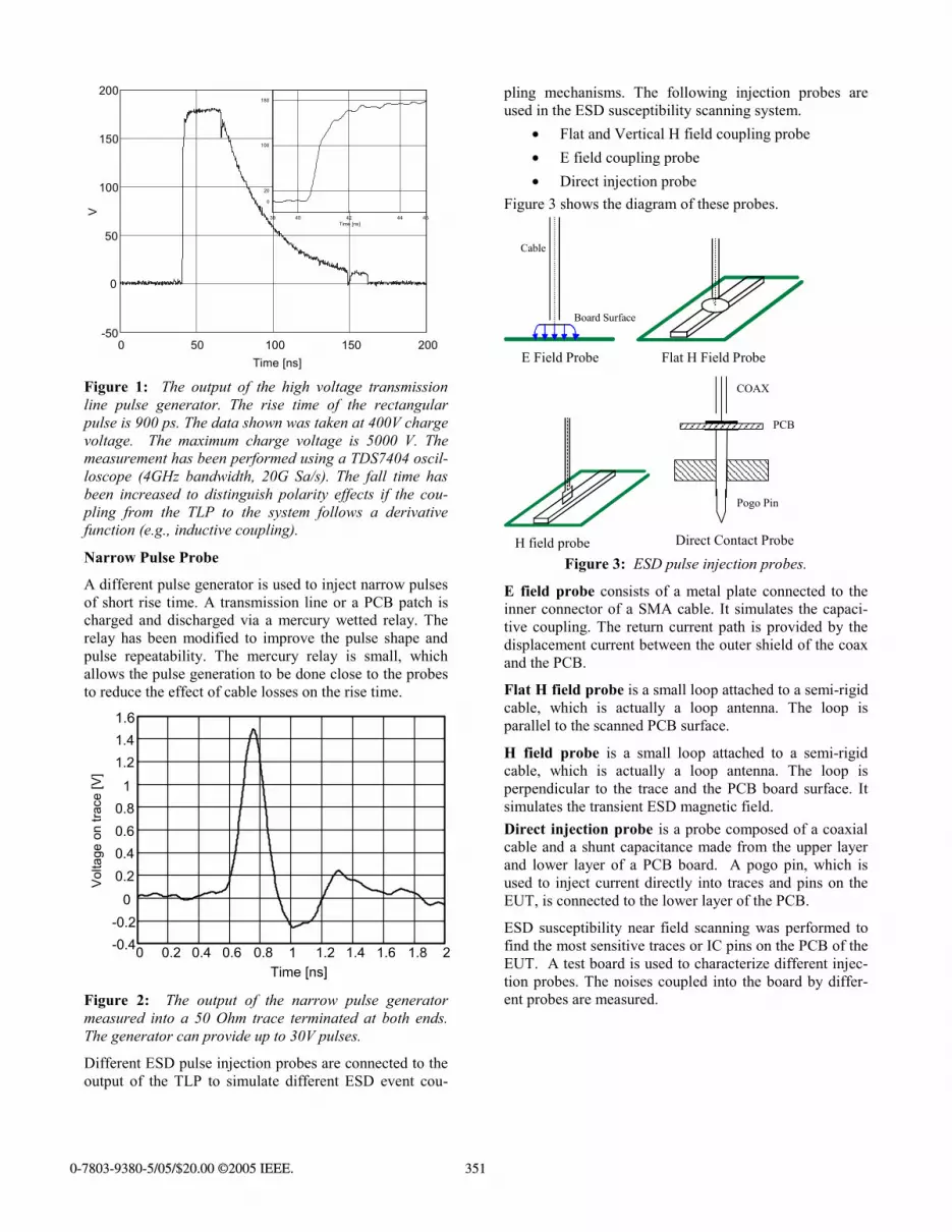
Different ESD pulse injection probes are connected to the output of the TLP to simulate different ESD event cou-
pling mechanisms. The following injection probes are used in the ESD susceptibility scanning system.
• Flat and Vertical H field coupling probe • E field coupling probe • Direct injection probe
Figure 3 shows the diagram of these probes.
Board Surface
Cable
PCB
COAX
Pogo Pin
Figure 3: ESD pulse injection probes.
E field probe consists of a metal plate connected to the inner connector of a SMA cable. It simulates the capaci-tive coupling. The return current path is provided by the displacement current between the outer shield of the coax and the PCB.
Flat H field probe is a small loop attached to a semi-rigid cable, which is actually a loop antenna. The loop is parallel to the scanned PCB surface.
H field probe is a small loop attached to a semi-rigid cable, which is actually a loop antenna. The loop is perpendicular to the trace and the PCB board surface. It simulates the transient ESD magnetic field. Direct injection probe is a probe composed of a coaxial cable and a shunt capacitance made from the upper layer and lower layer of a PCB board. A pogo pin, which is used to inject current directly into traces and pins on the EUT, is connected to the lower layer of the PCB.
ESD susceptibility near field scanning was performed to find the most sensitive traces or IC pins on the PCB of the EUT. A test board is used to characterize different injec-tion probes. The noises coupled into the board by differ-ent probes are measured.
E Field Probe Flat H Field Probe
H field probe Direct Contact Probe
0-7803-9380-5/05/$20.00 ©2005 IEEE. 351

Figure 4: The test board used to measure the voltage induced and current injected. The PCB trace dimensions are as follows: Length = 4 inches, Height over the ground plane = 10 mil, Trace width = 18 mil, Copper thickness = ½ oz = 0.675 mil. The test board, which is used to characterize the ESD pulse injection probes, is shown in figure 4. It has a thin 50 ohm impedance controlled trace across the board with SMA connectors at both ends. One connector is con-nected to an oscilloscope input channel 1 using a 50 ohm cable and the other end is also connected to an oscillo-scope input channel 2 with 50 Ohm input impedance. A 20 dB attenuator is used as the 50 ohm load. The pulse from the TLP is applied to the H field probe and the noise signal measured at the two oscilloscope channels are re-corded.
The measurement setup The H field probe orienta-
tion Figure 5 shows the characterization the of H field probe. The coupling between the H field probe and the trace has two components: Electrical field coupling (Capacitive coupling) and Magnetic field coupling (Inductive cou-pling) which should dominate. The data in figure 5 shows the mixed coupling mechanism of the H field probe. Figure 6 shows the characterization of the direct injection probe. The pogo pin, which is shown in figure 3, is at-tached to the measured trace. A rectangular pulse from the TLP is applied to the direct contact probe.
2 6 10 14-1
-0.5
0
0.5
1
1.5
Time [ns]
V
Channel1
Channel2
Figure 5: Measured noise voltage coupled by the H field probe. The charge voltage to the TLP is set to 400V.
36 40 44 48 52
0
4
8
12
16
Time [ns]
V
Measured SPICE Simulation
Figure 6: Measured noise voltage coupled by direct con-tact probe. The charge voltage to the TLP is set to 400V. The dotted line is a simulation result of the capacitive direct contact coupling. Note: The noise in the simulation is caused by using a measured waveform as excitation.
Figure 7: The simplified SPICE model of the direct con-tact probe. The data in figure 6 clearly shows the capacitive coupling mechanism of the direct contact probe.
0-7803-9380-5/05/$20.00 ©2005 IEEE. 352

III. The ESD susceptibility map of a fast CMOS EUT
The ESD susceptibility scanner, which is shown in figure 8 has been developed [1] such that allows the quantifica-tion of noise sensitivity of PCBs. The aim of the system and research is to automatically identify the ESD sensitive Pins and Nets of the EUT in non-destructive ESD failure testing. This allows testing the effect of different I/O structures, IC technologies and on-board filter structures, all to avoid soft errors.
The concept of field mapping is widely used for studying electromagnetic emissions from PCB [2]. ESD Suscepti-bility mapping results are similar to emission maps. The values shown (e.g. indicated by color or height) on a sus-ceptibility map give the lowest ESD failure level that lead to a system malfunction. Often, they are scaled in pulse generator setting, not in induced voltages. Peaks (or red color) in the map indicate the points which are most sus-ceptible to the ESD event. The fast rising pulse is applied to the ESD scanning probe and the probe is moved to the surface of the EUT. The operational status of the EUT is monitored by the soft-ware and any soft-failure of the EUT is recorded to gener-ate the ESD susceptibility map of that EUT.
Figure 8: 3D ESD Scanning System.
The size of the EUT tested in this paper was 220 mm x 220 mm. The procedure to characterize the ESD suscepti-bility of an EUT is as follows: 1. Using different probes, scans are performed at larger
scan resolution and higher scan speeds. An initial ESD susceptibility map is generated.
2. Sensitive areas are analyzed using smaller probes and finer scan resolution.
3. The sensitive traces are analyzed and voltage measur-ing probes are attached to the trace to capture the volt-ages while injecting into the traces.
4. Analyze the electrical function of the net to improving its performance either by filtering, re-routing etc.
Typical results are shown in the following figures.
0
50
100
150
200
250
150
200
250
300
350
400
0
5000
1000
1500
2000
2500
3000
3500
4000
4500
5000
Figure 9: ESD susceptibility map of an EUT, scan area: 220mm x 220 mm. Figure 9 shows the three dimension view of the general SD sensitive areas of the EUT obtained by using a large E field probe (7mm diameter), using 8 mm scan resolution.
Figure 10: ESD susceptibility map of the EUT. Figure 10 is the two dimensional view of the ESD suscep-tibility map of the EUT obtained by using a loop probe. To identify the ESD sensitive traces and nets of the EUT, more scanning with fine resolution is required. For exam-ple, a small H field probe, direct injection probe and the narrow pulse probe were used to scan the sensitive area No.1 shown in figure 10. Three sensitive nets have been identified in area No.1 and are shown in figure 11. It is interesting to note that 3 nets are more than 10x as sensi-tive than any other net on the board. This indicates that shielding is not a very effective way to improve this board, as only very few traces are sensitive.
1
0-7803-9380-5/05/$20.00 ©2005 IEEE. 353

Figure 11: Three ESD sensitive nets of the EUT.
IV. The measurements of coupled noises in the sensi-tive traces As shown is figure 11, three ESD sensitive traces of the EUT in scan area No.1 have been identified. To under-stand the ESD soft failure mechanism the noise voltage needs to be known. Figure 12 is a combination of a susceptibility map and a circuit used for measuring the trace. A 500 Ohm SMT resistor is attached to the sensitive trace. It connects via a 50 Ohm cable to an oscilloscope, forming a 1:11 voltage divider. By carefully keeping the dimensions small, mul-tiple GHz bandwidths can be achieved. The measured voltage at an ESD discharge event is shown in figure 13 and figure 14.
5 10 15 20 25
5
10
15
20
25
500 OhmCable
Ground Connection
Oscilloscope
Figure 12: The setup to measure the noise voltages.
0 4 8 12
-1
0
1
2
Time [ns]
V
Figure 13: Noise voltage measured on an ESD sensitive trace when an ESD soft error event occurs. TLP input voltage is set to 2300 V.
-1 0 2 4 6 8-1
0
1
2
3
4
Time [ns]
Vol
tage
on
trace
[V]
approx. threshold
Figure 14: Noise voltage measured on an ESD sensitive trace when an ESD soft error event occurs using the nar-row pulse pulser as noise source. The data line selected for measurements has a logic high level of 2.4V. It briefly goes below the threshold level leading to a bit error. As this line is a status line, there is no functional need for reacting that fast. Data as the one shown in figure 14 is a basis for simulating the IC input response based on semiconductor I/O models. They help provide a soft-error characterization of an IC input that can aid a circuit designer in identifying traces that need special treatment, e.g. filtering or shielded routing.
0-7803-9380-5/05/$20.00 ©2005 IEEE. 354

5 10 15 20 25 30 35 40
5
10
15
20
25
30
35
40
1000
1500
2000
2500
3000
3500
4000
4500
Figure 15: ESD susceptibility map of a fast CMOS IC 1, scan area: 80 mm x 80 mm.
Figure 16: ESD susceptibility map of a fast CMOS IC 2, scan area: 40 mm x 40 mm. The data shown in figures 15 and 16 show scanning re-sults using 0.2mm resolution. It is worth noticing that the most sensitive area of the scan shown in figure 16 is above the IC. In this case the direct coupling to the IC might dominate the system performance.
Conclusion
A three dimensional ESD scan system is developed to test the ESD sensitivity for digital devices. ESD susceptibility maps of a fast CMOS EUT are recorded for different types of pulse excitations and coupling mechanisms. The coupled noise in ESD sensitive traces are measured when an ESD soft error event occurs. This allows the identifica-tion of sensitive nets and enables us to capture voltage waveforms at the input of ICs at levels leading to a logical
error. This type of information is used to improve IC, PCB and system design.
REFERENCES [1] Kai Wang; Dr. Pommerenke; Jian Min,Zhang; Ramachandran Chundru; “The PCB level ESD immunity study by using 3 Dimension ESD Scan system”, Electro-magnetic Compatibility, 2004 IEEE International Sympo-sium on, [2 ] Kevin P.Slattery, James P.Muccioli, Terry North, ‘Measuring the radiated Emissions from a Family of mi-croprocessors using a 1-GHz TEM Cell’ IEEE transac-tions on electromagnetic compatibility, VOL.41, NO.2 MAY 1999 [3] K. Wang, D. Pommerenke, R. Chundru, J. Huang, K. Xiao, P. Ilavarasan, and M. Schaffer ‘ Impact of ESD Generator Parameters on Failure Level in Fast CMOS System’, Proc. of the 2003 IEEE International Sympo-sium on Electromagnetic Compatibility, Boston, MA, August 2003, pp. 52-57. [4] Pommerenke, D., ‘ESD: What has been achieved, what is less well understood?’, Proc.13th Int. Zurich Symp. Technical Exhibition Electromagnetic Compatibil-ity, Zurich, Switzerland, Feb.16-18, 1999,pp.77-82 [5] Ken Hall, ‘Tests with different IEC 801.2 simulators have different results’, EOS/ESD Symposium, Sept. 1994, Las Vegas, NV [6] Hugh Hyatt, ‘The impact of voluntary vs. legal ESD standards’, ITEM 1998 (The international journal of EMC), R&B Enterprises, Inc. [7] K.Hall, D.McCarthy, D.Dale, D.Smith, J.Nuebel, J.Barth, H.Hyatt, ‘Steps taken to deterime why different IEC 61000-4-2 ESD generators producer different re-sults’, Int. ZurichSymp. on EMC, 1997, pp. 105-108 [8] IEC 61000-4-2,‘Electromagnetic compatibility (EMC) - Part 4-2: Testing and measurement techniques - Electrostatic discharge immunity test’, EN 61000-4-2:1995, Amendment 1:1998, Amendment 2: 200 [9] J.Maas, W.Rhoades, “The ANSI ESD standard over-coming the deficiencies of world wide ESD standards’, IEEE Int. Symp. on EMC 1998, pp.1078-1084 [10] J.Maas, D.Pratt, ‘A study of the repeatability of elec-trostatic discharge simulators’, IEEE Int. Symp. on EMC, 1990, pp.265-269
0-7803-9380-5/05/$20.00 ©2005 IEEE. 355