an efficient graph-based algorithm for esd current path analysis
TRANSCRIPT
IEEE TRANSACTIONS ON COMPUTER-AIDED DESIGN OF INTEGRATED CIRCUITS AND SYSTEMS, VOL. 27, NO. 8, AUGUST 2008 1363
An Efficient Graph-Based Algorithmfor ESD Current Path Analysis
Chih-Hung Liu, Hung-Yi Liu, Chung-Wei Lin, Szu-Jui Chou, Yao-Wen Chang, Member, IEEE,Sy-Yen Kuo, Shih-Yi Yuan, and Yu-Wei Chen
Abstract—The electrostatic discharge (ESD) problem has be-come a challenging reliability issue in nanometer-circuit design.High voltages that resulted from ESD might cause high currentdensities in a small device and burn it out, so on-chip protectioncircuits for IC pads are required. To reduce the design cost, theprotection circuit should be added only for the IC pads with anESD current path, which causes the ESD current path analysisproblem. In this paper, we first introduce the analysis problemfor ESD protection in circuit design. We then model the circuitas a constraint graph, decompose the ESD connected components(ECCs) linked with the pads, and apply breadth-first search (BFS)to identify the ECCs in each constraint graph and, thus, the cur-rent paths. Experimental results show that our algorithm can veryefficiently and economically detect all ESD paths. For example,our algorithm can detect all ESD paths in a circuit with more than1.3 million vertices in 1.39 s and consume only 44-MB memory ona 3.0-GHz Intel Pentium 4 PC. To the best of our knowledge, ouralgorithm is the first point tool available to the public for the ESDanalysis.
Index Terms—Analysis, electrostatic discharge (ESD), graphsearch, network flow, reliability.
I. INTRODUCTION
THE PHENOMENON of electrostatic discharge (ESD)exists everywhere in our daily life, such as a standing hair
or an electric shock by a doorknob. It occurs when an elec-trostatic voltage develops and discharges as a current impulse.Although ESD only induces a little discomfort to humans, it can
Manuscript received August 21, 2007; revised January 13, 2008. This workwas supported in part by Incentia Design Systems and in part by the NationalScience Council of Taiwan under Grant NSC 96-2221-E-002-023, Grant NSC96-2628-E-002-248-MY3, Grant NSC 96-2628-E-002-249-MY3, and GrantNSC 96-2221-E-002-245. This paper was recommended by Associate EditorD. Z. Pan.
C.-H. Liu is with the Graduate Institute of Electronics Engineering, NationalTaiwan University, Taipei 106, Taiwan, R.O.C.
H.-Y. Liu and C.-W. Lin were with the Graduate Institute of ElectronicsEngineering, National Taiwan University, Taipei 106, Taiwan, R.O.C. They arecurrently serving in the military in R.O.C.
S.-J. Chou is with the Implementation Group, Synopsys Taiwan Ltd.,Taipei 110, Taiwan, R.O.C.
Y.-W. Chang is with the Graduate Institute of Electronics Engineeringand the Department of Electrical Engineering, National Taiwan University,Taipei 106, Taiwan, R.O.C. (e-mail: [email protected]).
S.-Y. Kuo is with the Department of Electrical Engineering, National TaiwanUniversity, Taipei 106, Taiwan, R.O.C. (e-mail: [email protected]).
S.-Y. Yuan is with the Department of Communications Engineering, FengChia University, Taichung 407, Taiwan, R.O.C.
Y.-W. Chen is with the Design and Development Department, FaradayTechnology Corp., Hsinchu 300, Taiwan, R.O.C.
Color versions of one or more of the figures in this paper are available onlineat http://ieeexplore.ieee.org.
Digital Object Identifier 10.1109/TCAD.2008.925779
cause great damage in semiconductor fabrication. In a practicalsituation, ESD often occurs between two or more deviceswith different electrostatic potentials, and the current impulsesgenerated by ESD may break circuits and burn devices out. Forexample, for a 0.13-µm CMOS device designed for operationat 1.2 V, the voltage drop across a 2-Ω power bus exceeds 20 Vand burns out the ultrathin gate oxides [2]. As the processtechnology enters the nanometer era, device size has continuedto shrink, and the breakdown voltage of the thin-oxide devicesis usually less than 5 V, making the ESD damage occur easilyand difficult to prevent [3]. As a result, the prevention of ESDbecomes one of the major concerns for IC reliability.
There are many solutions to the ESD problem [2], examplesof which are the use of antistatic coatings to prevent staticcharge generation in wafers, the use of shielded materials toprevent ESD resulted from human handling, and the implemen-tation of protection circuits within the chip. For the three widelyused ESD discharge models [4], [5], we can categorize theminto two major classes.
1) Human body model/machine model (HBM/MM): Anexternal voltage induces a discharge current through apair of pads.
2) Charged device model (CDM): The charge is accumu-lated on the chip itself and then discharged through asingle pad.
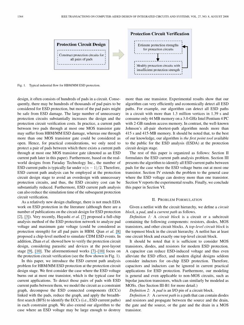
In HBM/MM, if there exists a current path with very lowimpedance between two pads, this path will suffer a large ESDcurrent, and some devices on this path could be burnt out. As aresult, to protect an IC chip from the HBM/MM ESD damage,a protection circuit for a pair of pads needs to: 1) provide alow impedance path between the two pads to safely discharge alarge ESD current and 2) clamp the pad voltage between themto a sufficiently low level [6]. In practice, an industrial flow toprotect the HBM/MM ESD damage is typically divided intotwo stages, i.e., design and verification, as shown in Fig. 1. Forprotection circuit design, we construct protection circuits forpairs of pads; for protection circuit verification, we estimatethe protection strengths (i.e., ESD sensitivity levels) for thedesigned protection circuits and then modify the circuits withinsufficient protection strengths. Here, a protection circuit couldbe a back-to-back diode with low impedance, and a protectionstrength estimation could be performed by some simulation-based methods [7].
However, if protection circuits are constructed for all pairsof n pads, we would need n(n − 1)/2 protection circuits at theprotection circuit design stage. For a modern system-on-chip
0278-0070/$25.00 © 2008 IEEE
1364 IEEE TRANSACTIONS ON COMPUTER-AIDED DESIGN OF INTEGRATED CIRCUITS AND SYSTEMS, VOL. 27, NO. 8, AUGUST 2008
Fig. 1. Typical industrial flow for HBM/MM ESD protection.
design, it often consists of hundreds of pads in a circuit. Conse-quently, there may be hundreds of thousands of pad pairs to beconsidered for ESD protection, but most of the pad pairs mightbe safe from ESD damage. The large number of unnecessaryprotection circuits substantially increases the design and theprotection circuit verification costs. In practice, a current pathbetween two pads through at most one MOS transistor gatemay suffer from HBM/MM ESD damage, whereas one throughmore than one MOS transistor gate could be considered asopen. Hence, for practical considerations, we only need toprotect a pair of pads between which there exists a current paththrough at most one MOS transistor gate (denoted as an ESDcurrent path later in this paper). Furthermore, based on the real-world designs from Faraday Technology Inc., the number ofESD current paths is typically far under n(n − 1)/2. Therefore,ESD current path analysis can be employed at the protectioncircuit design stage to avoid an overdesign with unnecessaryprotection circuits, and thus, the ESD circuitry cost can besubstantially reduced. Furthermore, ESD current path analysiscan also reduce the simulation time of the subsequent protectioncircuit verification.
As a relatively new design challenge, there is not much EDAwork on ESD protection in the literature (although there are anumber of publications on the circuit design for ESD protection[2], [3]). Very recently, Hayashi et al. [7] proposed a full-chipanalysis method of the ESD protection network to analyze padvoltage and maximum gate voltage (could be considered asprotection strength) for all pad pairs in HBM. Qian et al. [8]proposed a chip-level method to simulate CDM ESD events. Inaddition, Zhan et al. showed how to verify the protection circuitdesign, considering parasitic and devices at the post-layoutstage [9], [10]. The aforementioned works [7]–[10] focus onthe protection circuit verification (see the flow shown in Fig. 1).
In this paper, we introduce the ESD current path analysisproblem for HBM/MM ESD protection at the protection circuitdesign stage. We first consider the case where the ESD voltageburns out at most one transistor, which is the typical case forcurrent applications. To detect those pairs of pads with ESDcurrent paths between them, we model the circuit as a constraintgraph, decompose the ESD connected components (ECCs)linked with the pads, reduce the graph, and apply the breadth-first search (BFS) to identify the ECCs (i.e., ESD current paths)in each constraint graph. We also extend our algorithm to thecase where an ESD voltage may be large enough to destroy
more than one transistor. Experimental results show that ouralgorithm can very efficiently and economically detect all ESDpaths. For example, our algorithm can detect all ESD pathsin a circuit with more than 1.3 million vertices in 1.39 s andconsume only 44 MB memory on a 3.0-GHz Intel Pentium 4 PCwith 2-GB random access memory. In contrast, the well-knownJohnson’s all-pair shortest-path algorithm needs more than415 s and 415-MB memory. It should be noted that, to the bestof our knowledge, our algorithm is the first point tool availableto the public for the ESD analysis (ESDA) at the protectioncircuit design stage.
The rest of this paper is organized as follows: Section IIformulates the ESD current path analysis problem. Section IIIpresents the algorithm to identify all ESD current paths betweenpads for the case where the ESD voltage burns out at most onetransistor. Section IV extends the problem to the general casewhere the ESD voltage can destroy more than one transistor.Section V reports the experimental results. Finally, we concludethis paper in Section VI.
II. PROBLEM FORMULATION
Given a netlist with the circuit hierarchy, we define a circuitblock, a pad, and a current path as follows.Definition 1: A circuit block is a circuit or a subcircuit
containing the following components: resistors, diodes, MOStransistors, and other circuit blocks. A top-level circuit block isthe topmost block in the circuit hierarchy. A netlist has at leastone circuit block and exactly one top-level circuit block.
It should be noted that it is sufficient to consider MOStransistors, diodes, and resistors for modern ESD protection.A capacitor can reduce ESD-induced voltage and thus evenalleviate the ESD effect, and modern digital designs seldomconsider inductors for on-chip ESD protection. Therefore,capacitors and inductors can be ignored in current practicalapplications for ESD protection. Furthermore, our modelingis general and even applicable to non-MOS circuits, such asbipolar junction transistors, which can similarly be modeled asMOSs. (See Section III-B1 for more detail.)Definition 2: A pad is an I/O pin of a circuit block.Definition 3: A current path is a path that can contain diodes
and resistors and propagate between the source and the drain,the gate and the source, or the gate and the drain in a MOStransistor.
LIU et al.: EFFICIENT GRAPH-BASED ALGORITHM FOR ESD CURRENT PATH ANALYSIS 1365
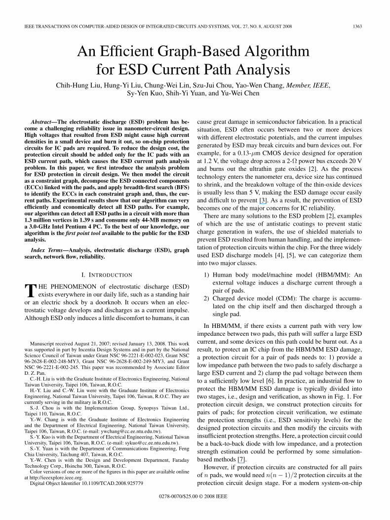
Fig. 2. Sample netlist and its ESD paths denoted by the dotted lines.
As mentioned in Section I, devices on a current path throughat most one MOS transistor gate could be burnt out underan HBM/MM ESD event. We define an ESD current path asfollows:Definition 4: An ESD current path is a current path that
propagates between the gate and the source or the gate and thedrain of a MOS transistor at most once.
Our objective is to detect all pairs of pads that need protectioncircuits for the practical consideration. Therefore, we do notconsider an ESD current path between two pads with anotherpad on the path. This is because, if an ESD current pathbetween two pads includes other pads, there could be redundantprotection circuits. For instance, assuming that there is a padp2 in the ESD current path from p1 to p3, it is clear that thereexist ESD current paths from p1 to p2 and from p2 to p3;that is, there are protection circuits for the pad pairs (p1, p2)and (p2, p3). As a result, an external voltage from p1 to p3
could be discharged through the protection circuits for (p1, p2)and (p2, p3), implying that the protection circuit for (p1, p3) isredundant. Considering practical circuit operations, we furtherdefine an ESD path as follows.
Definition 5: An ESD path is an ESD current path passingthrough no other intermediate pads, except the two terminalpads of the path.
Note that the ESD path is undirected since we can ignore thedirection of current by using a symmetric back-to-back diode toprotect an ESD path. With the aforementioned definitions, wecan formulate the addressed problem given here.
• The ESDA Problem: Given a netlist with circuit hierarchy,find every pair of pads with an ESD path between them forESD circuit protection.
For example, as shown in Fig. 2, an ESD current can propa-gate from A to VCC and GND through a MOS transistor. How-ever, the current cannot propagate from A to B according to thedefinition that an ESD path includes at most one gate–source orgate–drain path. Therefore, there are, in total, five pairs of padsbetween which there is an ESD path: (A, VCC), (A, GND), (B,VCC3A), (B, GND), and (VCC, GND).
Fig. 3. Flowchart of the proposed approach.
III. ALGORITHM
As shown in Fig. 3, a bottom–up approach is proposed toexploit the circuit hierarchy. For a hierarchical circuit, a high-level circuit block could embed low-level circuit blocks throughcircuit references. Since the low-level circuit blocks may befrequently referenced, it is inefficient to top–down (recursively)process each subcircuit block once it is referenced. Therefore,we shall apply a bottom–up circuit block processing orderingto speed up the processing (see Section III-A).Definition 6: A primitive circuit block is defined as a circuit
block that references no subcircuit block or the subcircuitblocks whose ESD paths have been detected.
For a primitive circuit block, detecting its ESD paths isdifferent from the traditional reachability problem [11], due tothe ESD path definition (see Definition 5). In this paper, wefirst model a primitive circuit block as a constraint graph (seeSection III-B1). Given a constraint graph, the ECCs in the graphare decomposed (see Section III-B2). After that, the stage ofpad matching detects all the ESD paths of the primitive circuitblock (see Section III-B3). Finally, we prove the correctness ofour algorithm.
A. Circuit Block Processing Ordering
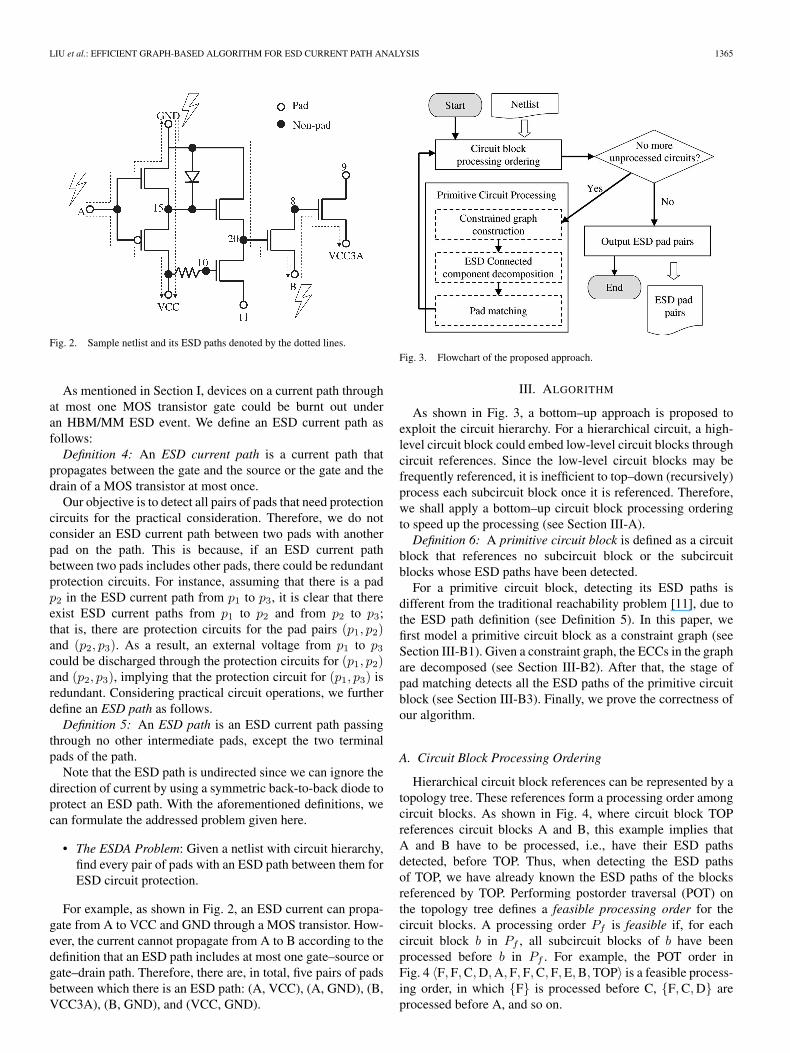
Hierarchical circuit block references can be represented by atopology tree. These references form a processing order amongcircuit blocks. As shown in Fig. 4, where circuit block TOPreferences circuit blocks A and B, this example implies thatA and B have to be processed, i.e., have their ESD pathsdetected, before TOP. Thus, when detecting the ESD pathsof TOP, we have already known the ESD paths of the blocksreferenced by TOP. Performing postorder traversal (POT) onthe topology tree defines a feasible processing order for thecircuit blocks. A processing order Pf is feasible if, for eachcircuit block b in Pf , all subcircuit blocks of b have beenprocessed before b in Pf . For example, the POT order inFig. 4 〈F, F, C, D, A, F, F, C, F, E, B, TOP〉 is a feasible process-ing order, in which F is processed before C, F, C, D areprocessed before A, and so on.
1366 IEEE TRANSACTIONS ON COMPUTER-AIDED DESIGN OF INTEGRATED CIRCUITS AND SYSTEMS, VOL. 27, NO. 8, AUGUST 2008
Fig. 4. Hierarchical-circuit topology tree example. The nodes and edgesrepresent circuit blocks and circuit block references, respectively. In thisexample, TOP references A and B, A references C and D, and so on. The dottedline traverses the tree in a postorder, i.e., 〈F, F, C, D, A, F, F, C, F, E, B, TOP〉.The dashed line traverses the tree in a postorder with redundancy removal,i.e., 〈F, C, D, A, E, B, TOP〉, in which the gray nodes are redundant (alreadyvisited).
However, since a subcircuit block can repeatedly be refer-enced, it is not necessary to detect its ESD paths whenever itis referenced. As illustrated in Fig. 4, performing POT withredundancy removal on the topology tree defines an irredun-dant processing order for the circuit blocks. A processing orderPi is irredundant if Pi is feasible and each circuit block bappears in Pi exactly once. In the topology tree example,the processing order 〈F, C, D, A, E, B, TOP〉 is an irredundantorder. To remove the redundancy during POT, we establish ahash table saving processed circuit blocks and their ESD pathsthat have been detected, for the redundancy check and for theESD path lookup. Thus, we can efficiently detect all ESD pathsbottom–up in the top-level circuit block.
B. Primitive Circuit Processing
A primitive circuit block references no subcircuit block orsubcircuit blocks whose ESD paths have been detected (seeDefinition 6). The following three stages process a primitivecircuit block:
1) constraint graph construction: modeling of the netlist de-scribing the primitive circuit block as a constraint graph;
2) ECC decomposition (ECCD): detection of all ECCslinked with the pad vertices of the constraint graph;
3) pad matching: pairing of the pads bridging the ESD pathsaccording to the connection of the detected ECCs.
1) Constraint Graph Construction: A constraint graphmodels the device interconnection in a primitive circuit block.Physical device terminals (connections) are modeled as graphvertices (edges). There are two types of vertices as follows:
1) pad vertex (p-vertex), which represents the pad of theprimitive circuit block;
2) nonpad vertex (np-vertex), which represents all the deviceterminals, except the pads.
Edges are also classified into two categories as follows:
1) constrained edge (c-edge), which can be involved in anESD path at most once;
2) nonconstrained edge (nc-edge), which has no occurrencelimit appearing in an ESD path.
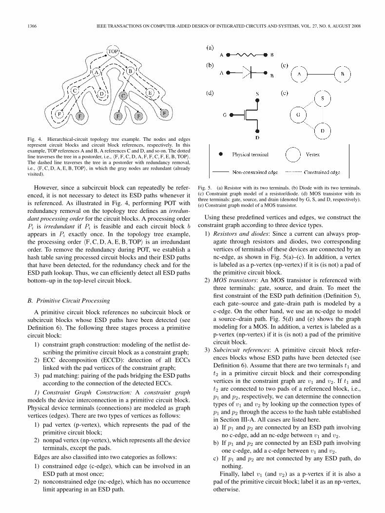
Fig. 5. (a) Resistor with its two terminals. (b) Diode with its two terminals.(c) Constraint graph model of a resistor/diode. (d) MOS transistor with itsthree terminals: gate, source, and drain (denoted by G, S, and D, respectively).(e) Constraint graph model of a MOS transistor.
Using these predefined vertices and edges, we construct theconstraint graph according to three device types.
1) Resistors and diodes: Since a current can always prop-agate through resistors and diodes, two correspondingvertices of terminals of these devices are connected by annc-edge, as shown in Fig. 5(a)–(c). In addition, a vertexis labeled as a p-vertex (np-vertex) if it is (is not) a pad ofthe primitive circuit block.
2) MOS transistors: An MOS transistor is referenced withthree terminals: gate, source, and drain. To meet thefirst constraint of the ESD path definition (Definition 5),each gate–source and gate–drain path is modeled by ac-edge. On the other hand, we use an nc-edge to modela source–drain path. Fig. 5(d) and (e) shows the graphmodeling for a MOS. In addition, a vertex is labeled as ap-vertex (np-vertex) if it is (is not) a pad of the primitivecircuit block.
3) Subcircuit references: A primitive circuit block refer-ences blocks whose ESD paths have been detected (seeDefinition 6). Assume that there are two terminals t1 andt2 in a primitive circuit block and their correspondingvertices in the constraint graph are v1 and v2. If t1 andt2 are connected to two pads of a referenced block, i.e.,p1 and p2, respectively, we can determine the connectiontypes of v1 and v2 by looking up the connection types ofp1 and p2 through the access to the hash table establishedin Section III-A. All cases are listed here.a) If p1 and p2 are connected by an ESD path involving
no c-edge, add an nc-edge between v1 and v2.b) If p1 and p2 are connected by an ESD path involving
one c-edge, add a c-edge between v1 and v2.c) If p1 and p2 are not connected by any ESD path, do
nothing.Finally, label v1 (and v2) as a p-vertex if it is also a
pad of the primitive circuit block; label it as an np-vertex,otherwise.
LIU et al.: EFFICIENT GRAPH-BASED ALGORITHM FOR ESD CURRENT PATH ANALYSIS 1367
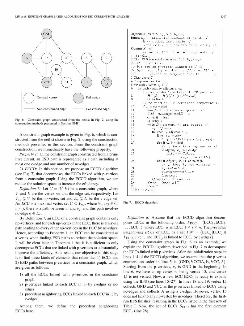
Fig. 6. Constraint graph constructed from the netlist in Fig. 2, using theconstruction methods presented in Section III-B1.
A constraint graph example is given in Fig. 6, which is con-structed from the netlist shown in Fig. 2, using the constructionmethods presented in this section. From the constraint graphconstruction, we immediately have the following property.Property 1: In the constraint graph constructed from a prim-
itive circuit, an ESD path is represented as a path including atmost one c-edge and any number of nc-edges.2) ECCD: In this section, we propose an ECCD algorithm
(see Fig. 7) that decomposes the ECCs linked with p-verticesfrom a constraint graph. Using the ECCD algorithm, we canreduce the solution space to increase the efficiency.Definition 7: Let G = (V,E) be a constraint graph, where
V and E are the vertex set and the edge set, respectively. LetVnp ⊆ V be the np-vertex set and Ec ⊆ E be the c-edge set.An ECC is a maximal vertex set C ⊆ Vnp, where ∀vi, vj ∈ C,i = j, there is a path between vi and vj , and this path involvesno edge e ∈ Ec.
By Definition 7, an ECC of a constraint graph contains onlynp-vertices, and for each np-vertex in the ECC, there is always apath leading to every other np-vertices in the ECC by nc-edges.Hence, according to Property 1, an ECC can be considered asa vertex when finding ESD paths to reduce the solution space.It will be clear later in Theorem 1 that it is sufficient to onlydecompose ECCs that are linked with p-vertices to substantiallyimprove the efficiency. As a result, our objective in this stageis to find three kinds of elements that relate the: 1) ECCs and2) ESD paths between p-vertices in a constraint graph, whichare given as follows:
1) all the ECCs linked with p-vertices in the constraintgraph;
2) p-vertices linked to each ECC in 1) by c-edges or nc-edges;
3) precedent neighboring ECCs linked to each ECC in 1) byc-edges.
Among them, we define the precedent neighboringECCs here.
Fig. 7. ECCD algorithm.
Definition 8: Assume that the ECCD algorithm decom-poses ECCs in the following order: PECC = 〈ECC1, ECC2,. . . , ECCn〉, where ECCi is an ECC, 1 ≤ i ≤ n. The precedentneighboring ECCs of ECCi is a set PN i = ECCj |ECCj ∈PECC, j < i, and ECCj is linked to ECCi by c-edges.
Using the constraint graph in Fig. 6 as an example, weexplain the ECCD algorithm described in Fig. 7 to decomposethe ECCs linked with p-vertices. After the initialization steps inlines 1–4 of the ECCD algorithm, we assume that the p-vertexenumeration order in line 5 is 〈GND, VCC3A,B, VCC,A〉.Starting from the p-vertices, vp is GND in the beginning. Inline 6, we have an np-vertex vi being vertex 15, and vertex15 is not visited. Now, a new ECC ECC1 is ready to expandusing the BFS (see lines 15–27). In lines 18 and 19, vertex 15collects GND and VCC as the p-vertices linked to ECC1 usingnc-edges and collects A using a c-edge. However, vertex 15does not link to any np-vertex by nc-edges. Therefore, the first-run BFS finishes, resulting in the ECC1 listed in the first row ofTable I. Now, the set of ECCs SECC has the first elementECC1 (line 28).
1368 IEEE TRANSACTIONS ON COMPUTER-AIDED DESIGN OF INTEGRATED CIRCUITS AND SYSTEMS, VOL. 27, NO. 8, AUGUST 2008
TABLE IECCS DECOMPOSED FROM THE CONSTRAINT GRAPH IN FIG. 6 USING THE ECCD ALGORITHM,
ASSUMING THAT THE DECOMPOSITION ORDER IS 〈ECC1, ECC2, ECC3, ECC4, ECC5〉
Back to line 6, vi has another choice, i.e., vertex 20, expand-ing another ECC ECC2. During the BFS of ECC2, vertex 20collects GND as the p-vertex linked to ECC2 using an nc-edgeand collects B using a c-edge. In addition, vertex 20 collectsa precedent neighboring ECC ECC1 by visiting vertex 15(lines 20–22). On the other hand, vertex 20 also visits the np-vertex, i.e., vertex 11, trying to expand ECC2 and to collectmore p-vertices and more precedent neighboring ECCs. Afterthe second BFS run finishes, the resulting ECC2 is united to theset SECC. To this point, p-vertex GND cannot further expand.
Similar to the aforementioned steps, VCC3A, B, and VCCdetect the ECCs ECC3, ECC4, and ECC5, respectively. How-ever, p-vertex A detects no ECC since all the np-vertices havebeen visited. Finally, the ECCD algorithm returns the set of theECCs detected from the given constraint graph. In this exam-ple, SECC = ECC1, ECC2, ECC3, ECC4, ECC5, and all therelated information is listed in Table I.
Since all the np-vertices in the constraint graph G = (V,E)are visited no more than once—an np-vertex surrounded byseveral levels of c-edges may never be visited—the ECCDalgorithm performs all the needed BFSs in O(|V | + |E|) time.Because a p-vertex p is added to the Vp of an ECC C onlywhen p is linked to a visited np-vertex of C (see lines 18–19),it implies that, for each p-vertex, the number of times to addit to the Vps of the ECCs is bounded by its degree. Thus, theECCD collects p-vertices in O(|E|) time for all Vps during theBFSs. On the other hand, the number of collecting precedentneighboring ECCs is bounded by O(|E|) during the BFSs sincean ECC C1 is added to the PN of ECC C2 via c-edge (v1, v2)only when both v1 and v2 have been visited (see lines 20–22),where PN is the set of precedent neighboring ECCs. Thus, theECCD collects precedent neighboring ECCs in O(|E|) time forall visited np-vertices via c-edges. Overall, the time complexityof the ECCD algorithm is O(|V | + |E|).
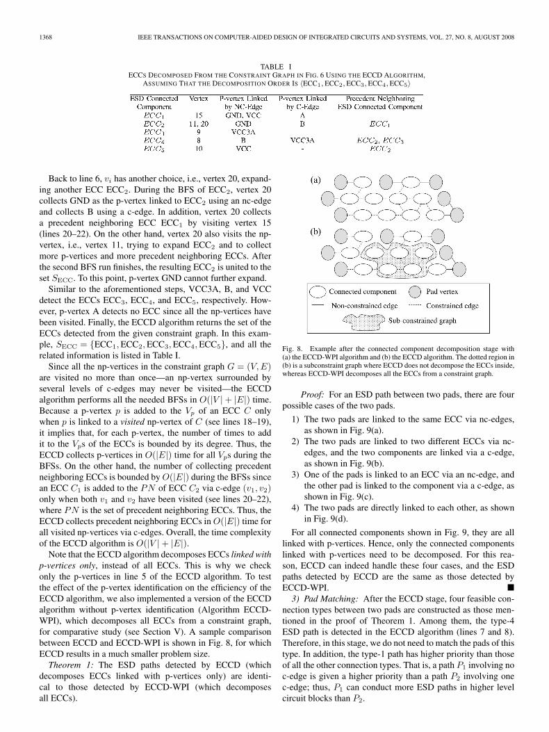
Note that the ECCD algorithm decomposes ECCs linked withp-vertices only, instead of all ECCs. This is why we checkonly the p-vertices in line 5 of the ECCD algorithm. To testthe effect of the p-vertex identification on the efficiency of theECCD algorithm, we also implemented a version of the ECCDalgorithm without p-vertex identification (Algorithm ECCD-WPI), which decomposes all ECCs from a constraint graph,for comparative study (see Section V). A sample comparisonbetween ECCD and ECCD-WPI is shown in Fig. 8, for whichECCD results in a much smaller problem size.Theorem 1: The ESD paths detected by ECCD (which
decomposes ECCs linked with p-vertices only) are identi-cal to those detected by ECCD-WPI (which decomposesall ECCs).
Fig. 8. Example after the connected component decomposition stage with(a) the ECCD-WPI algorithm and (b) the ECCD algorithm. The dotted region in(b) is a subconstraint graph where ECCD does not decompose the ECCs inside,whereas ECCD-WPI decomposes all the ECCs from a constraint graph.
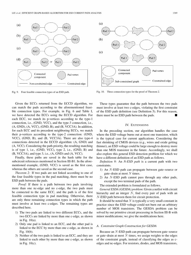
Proof: For an ESD path between two pads, there are fourpossible cases of the two pads.
1) The two pads are linked to the same ECC via nc-edges,as shown in Fig. 9(a).
2) The two pads are linked to two different ECCs via nc-edges, and the two components are linked via a c-edge,as shown in Fig. 9(b).
3) One of the pads is linked to an ECC via an nc-edge, andthe other pad is linked to the component via a c-edge, asshown in Fig. 9(c).
4) The two pads are directly linked to each other, as shownin Fig. 9(d).
For all connected components shown in Fig. 9, they are alllinked with p-vertices. Hence, only the connected componentslinked with p-vertices need to be decomposed. For this rea-son, ECCD can indeed handle these four cases, and the ESDpaths detected by ECCD are the same as those detected byECCD-WPI. 3) Pad Matching: After the ECCD stage, four feasible con-
nection types between two pads are constructed as those men-tioned in the proof of Theorem 1. Among them, the type-4ESD path is detected in the ECCD algorithm (lines 7 and 8).Therefore, in this stage, we do not need to match the pads of thistype. In addition, the type-1 path has higher priority than thoseof all the other connection types. That is, a path P1 involving noc-edge is given a higher priority than a path P2 involving onec-edge; thus, P1 can conduct more ESD paths in higher levelcircuit blocks than P2.
LIU et al.: EFFICIENT GRAPH-BASED ALGORITHM FOR ESD CURRENT PATH ANALYSIS 1369
Fig. 9. Four feasible connection types of an ESD path.
Given the ECCs returned from the ECCD algorithm, wecan match the pads according to the aforementioned feasi-ble connection types. For example, in Fig. 6 and Table I,we have detected the ECCs using the ECCD algorithm. Foreach ECC, we match its p-vertices according to the type-1connection, i.e., (GND, VCC), and the type-3 connection, i.e.,(A, GND), (A, VCC), (GND, B), and (B, VCC3A). In addition,for each ECC and its precedent neighboring ECCs, we matchtheir p-vertices according to the type-2 connection: (GND,VCC), (GND, B), and (B, VCC3A). There are also type-4connections detected in the ECCD algorithm: (A, GND) and(A, VCC). Considering the path priority, the resulting matchingis of type 1, i.e., (GND, VCC), type 2, i.e., (GND, B) and(B, VCC3A), and type 3, i.e., (A, GND) and (A, VCC).
Finally, these paths are saved in the hash table for thesubcircuit references mentioned in Section III-B1. In the afore-mentioned example, (GND, VCC) is saved as the first case,whereas the others are saved as the second case.Theorem 2: If two pads are not linked according to one of
the four feasible types in the pad matching, there must be noESD path between the pads.
Proof: If there is a path between two pads involvingmore than one nc-edge and no c-edge, the two pads mustbe connected to the same ECC, and the path is of the firstfeasible connection type in pad matching. Otherwise, thereare only three remaining connection types in which the pathmust involve at least two c-edges. The remaining types aredescribed here.
1) The two pads are linked to two different ECCs, and thetwo ECCs are linked by more than one c-edge, as shownin Fig. 10(a).
2) Only one pad is linked to an ECC, and the other pad islinked to the ECC by more than one c-edge, as shown inFig. 10(b).
3) Neither of the two pads is linked to an ECC, and they arelinked to each other by more than one c-edge, as shownin Fig. 10(c).
Fig. 10. Three connection types for the proof of Theorem 2.
These types guarantee that the path between the two padsmust involve at least two c-edges, violating the first constraintof the ESD path definition (see Definition 5). For this reason,there must be no ESD path between the pads.
IV. EXTENSIONS
In the preceding section, our algorithm handles the casewhere the ESD voltage burns out at most one transistor, whichis the typical case for current applications. Considering thefast shrinking of CMOS devices (e.g., wires and oxide gettingthinner), an ESD voltage could be large enough to destroy morethan one MOS transistor in the future. Accordingly, we shallalso explore this general ESD detection problem for which wehave a different definition of an ESD path as follows.Definition 9: An N-ESD path is a current path with two
constraints.1) An N -ESD path can propagate between gate–source or
gate–drain at most N times.2) An N -ESD path cannot pass through any other pads,
except the two terminal pads of the path.The extended problem is formulated as follows.General ESDA (GESDA) problem: Given a netlist with circuit
hierarchy and an integer N , find every pair of pads with anN -ESD path between them for circuit protection.
It should be noted that N is typically a very small constant inpractice since the ESD voltage could not burn out an arbitrarynumber of MOS transistors. The GESDA problem can besolved by our primitive circuit processing in Section III-B withminor modifications; we give the modifications here.
A. Constraint Graph Construction for GESDA
Because an N -ESD path can propagate between gate–sourceor gate–drain at most N times, we assign weights to the edgesof the constraint graph, instead of classifying the edges as c-edges and nc-edges. For resistors, diodes, and MOS transistors,
1370 IEEE TRANSACTIONS ON COMPUTER-AIDED DESIGN OF INTEGRATED CIRCUITS AND SYSTEMS, VOL. 27, NO. 8, AUGUST 2008
Fig. 11. (a) Resistor with its two terminals. (b) Diode with its two terminals.(c) Constraint graph model of a resistor/diode. (d) MOS transistor with itsthree terminals: gate, source, and drain (denoted by G, S, and D, respectively).(e) Constraint graph model of a MOS transistor.
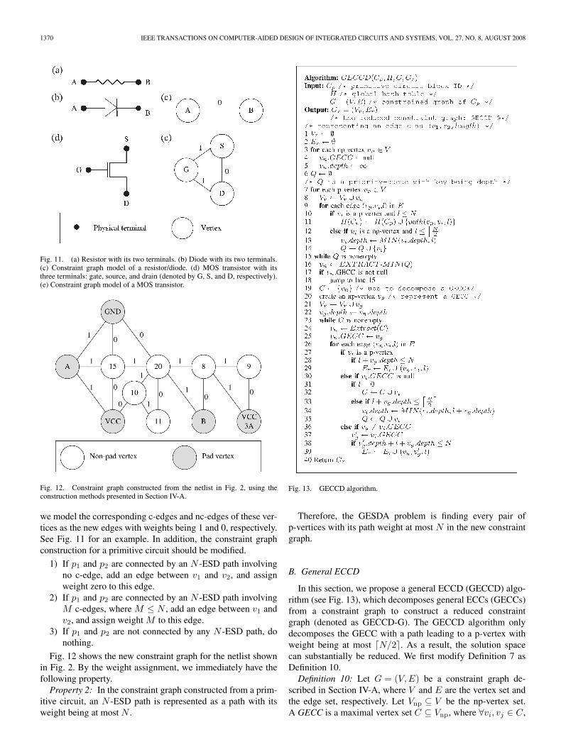
Fig. 12. Constraint graph constructed from the netlist in Fig. 2, using theconstruction methods presented in Section IV-A.
we model the corresponding c-edges and nc-edges of these ver-tices as the new edges with weights being 1 and 0, respectively.See Fig. 11 for an example. In addition, the constraint graphconstruction for a primitive circuit should be modified.
1) If p1 and p2 are connected by an N -ESD path involvingno c-edge, add an edge between v1 and v2, and assignweight zero to this edge.
2) If p1 and p2 are connected by an N -ESD path involvingM c-edges, where M ≤ N , add an edge between v1 andv2, and assign weight M to this edge.
3) If p1 and p2 are not connected by any N -ESD path, donothing.
Fig. 12 shows the new constraint graph for the netlist shownin Fig. 2. By the weight assignment, we immediately have thefollowing property.Property 2: In the constraint graph constructed from a prim-
itive circuit, an N -ESD path is represented as a path with itsweight being at most N .
Fig. 13. GECCD algorithm.
Therefore, the GESDA problem is finding every pair ofp-vertices with its path weight at most N in the new constraintgraph.
B. General ECCD
In this section, we propose a general ECCD (GECCD) algo-rithm (see Fig. 13), which decomposes general ECCs (GECCs)from a constraint graph to construct a reduced constraintgraph (denoted as GECCD-G). The GECCD algorithm onlydecomposes the GECC with a path leading to a p-vertex withweight being at most N/2. As a result, the solution spacecan substantially be reduced. We first modify Definition 7 asDefinition 10.Definition 10: Let G = (V,E) be a constraint graph de-
scribed in Section IV-A, where V and E are the vertex set andthe edge set, respectively. Let Vnp ⊆ V be the np-vertex set.A GECC is a maximal vertex set C ⊆ Vnp, where ∀vi, vj ∈ C,
LIU et al.: EFFICIENT GRAPH-BASED ALGORITHM FOR ESD CURRENT PATH ANALYSIS 1371
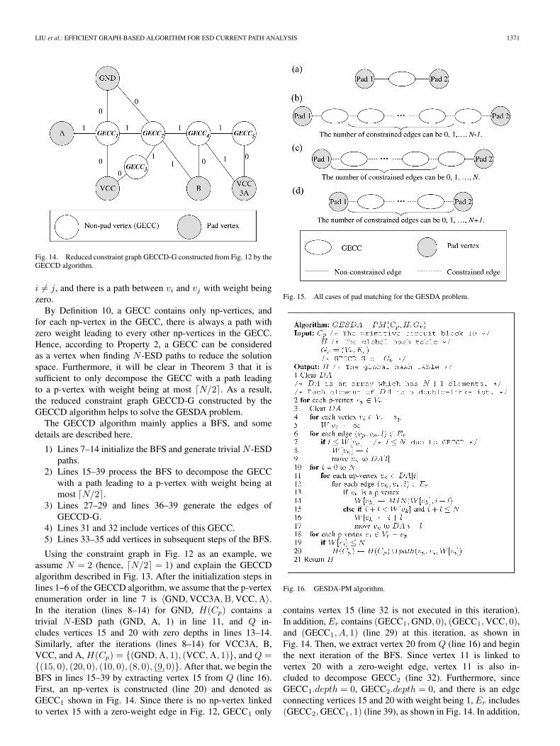
Fig. 14. Reduced constraint graph GECCD-G constructed from Fig. 12 by theGECCD algorithm.
i = j, and there is a path between vi and vj with weight beingzero.
By Definition 10, a GECC contains only np-vertices, andfor each np-vertex in the GECC, there is always a path withzero weight leading to every other np-vertices in the GECC.Hence, according to Property 2, a GECC can be consideredas a vertex when finding N -ESD paths to reduce the solutionspace. Furthermore, it will be clear in Theorem 3 that it issufficient to only decompose the GECC with a path leadingto a p-vertex with weight being at most N/2. As a result,the reduced constraint graph GECCD-G constructed by theGECCD algorithm helps to solve the GESDA problem.
The GECCD algorithm mainly applies a BFS, and somedetails are described here.
1) Lines 7–14 initialize the BFS and generate trivial N -ESDpaths.
2) Lines 15–39 process the BFS to decompose the GECCwith a path leading to a p-vertex with weight being atmost N/2.
3) Lines 27–29 and lines 36–39 generate the edges ofGECCD-G.
4) Lines 31 and 32 include vertices of this GECC.5) Lines 33–35 add vertices in subsequent steps of the BFS.
Using the constraint graph in Fig. 12 as an example, weassume N = 2 (hence, N/2 = 1) and explain the GECCDalgorithm described in Fig. 13. After the initialization steps inlines 1–6 of the GECCD algorithm, we assume that the p-vertexenumeration order in line 7 is 〈GND, VCC3A,B, VCC,A〉.In the iteration (lines 8–14) for GND, H(Cp) contains atrivial N -ESD path (GND, A, 1) in line 11, and Q in-cludes vertices 15 and 20 with zero depths in lines 13–14.Similarly, after the iterations (lines 8–14) for VCC3A, B,VCC, and A, H(Cp) = (GND,A, 1), (VCC,A, 1), and Q =(15, 0), (20, 0), (10, 0), (8, 0), (9, 0). After that, we begin theBFS in lines 15–39 by extracting vertex 15 from Q (line 16).First, an np-vertex is constructed (line 20) and denoted asGECC1 shown in Fig. 14. Since there is no np-vertex linkedto vertex 15 with a zero-weight edge in Fig. 12, GECC1 only
Fig. 15. All cases of pad matching for the GESDA problem.
Fig. 16. GESDA-PM algorithm.
contains vertex 15 (line 32 is not executed in this iteration).In addition, Er contains (GECC1, GND, 0), (GECC1, VCC, 0),and (GECC1, A, 1) (line 29) at this iteration, as shown inFig. 14. Then, we extract vertex 20 from Q (line 16) and beginthe next iteration of the BFS. Since vertex 11 is linked tovertex 20 with a zero-weight edge, vertex 11 is also in-cluded to decompose GECC2 (line 32). Furthermore, sinceGECC1.depth = 0, GECC2.depth = 0, and there is an edgeconnecting vertices 15 and 20 with weight being 1, Er includes(GECC2, GECC1, 1) (line 39), as shown in Fig. 14. In addition,
1372 IEEE TRANSACTIONS ON COMPUTER-AIDED DESIGN OF INTEGRATED CIRCUITS AND SYSTEMS, VOL. 27, NO. 8, AUGUST 2008
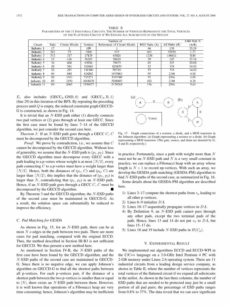
TABLE IIPARAMETERS OF THE 11 INDUSTRIAL CIRCUITS. THE NUMBER OF VERTICES REPRESENTS THE TOTAL VERTICES
OF THE FLATTENED CIRCUIT IF WE EXPAND ALL SUBCIRCUITS IN THE NETLIST
Er also includes (GECC2, GND, 0) and (GECC2,B, 1)(line 29) in this iteration of the BFS. By repeating the precedingprocess until Q is empty, the reduced constraint graph GECCD-G is constructed, as shown in Fig. 14.
It is trivial that an N -ESD path either (1) directly connectstwo pad vertices or (2) goes through at least one GECC. Sincethe first case must be found by lines 7–14 of the GECCDalgorithm, we just consider the second case here.Theorem 3: If an N -ESD path goes through a GECC C, C
must be decomposed by the GECCD algorithm.Proof: We prove by contradiction, i.e., we assume that C
cannot be decomposed by the GECCD algorithm. Without lossof generality, we assume that the N -ESD path is (p1, p2). Sincethe GECCD algorithm must decompose every GECC with apath leading to a p-vertex whose weight is at most N/2, everypath connecting C to a p-vertex must have a weight larger thanN/2. Hence, both the distances of (p1, C) and (p2, C) arelarger than N/2; this implies that the distance of (p1, p2) islarger than N , contradicting that (p1, p2) is an N -ESD path.Hence, if an N -ESD path goes through a GECC C, C must bedecomposed by the GECCD algorithm.
By Theorem 3 and the GECCD algorithm, the N -ESD pathsof the second case must be maintained in GECCD-G. Asa result, the solution space can substantially be reduced toimprove the efficiency.
C. Pad Matching for GESDA
As shown in Fig. 15, for an N -ESD path, there can be atmost N c-edges in the path between two pads. There are morecases for pad matching, compared with the original ECCD.Thus, the method described in Section III-B3 is not sufficientfor GECCD. We thus present a new method here.
As mentioned in Section IV-B, the N -ESD paths of thefirst case have been found by the GECCD algorithm, and theN -ESD paths of the second case are maintained in GECCD-G. Since there is no negative edge, we can apply Johnson’salgorithm on GECCD-G to find all the shortest paths betweenall p-vertices. For each p-vertices pair, if the distance of ashortest path between the two p-vertices is smaller than or equalto |N |, there exists an N -ESD path between them. However,it is well known that operations of a Fibonacci heap are verytime consuming; hence, Johnson’s algorithm may be inefficient
Fig. 17. Graph connections of a resistor, a diode, and a MOS transistor inthe Johnson algorithm. (a) Graph representing a resistor or a diode. (b) Graphrepresenting a MOS transistor. (The gate, source, and drain are denoted by G,S and D, respectively.)
in practice. Fortunately, since a path with weight more than Nmust not be an N -ESD path and N is a very small constant inpractice, we can replace a Fibonacci heap with an array whoselength is N + 1 to record np-vertices. With such an array, wedevelop the GESDA path-matching (GESDA-PM) algorithm tofind N -ESD paths of the second case, as summarized in Fig. 16.
Some details about the GESDA-PM algorithm are describedhere.
1) Lines 3–17 compute the shortest paths from vp leading toall other p-vertices.
2) Lines 6–9 initialize DA.3) Lines 10–17 sequentially propagate vertices in DA.4) By Definition 9, an N -ESD path cannot pass through
any other pads, except the two terminal pads of thepath. Hence, lines 13 and 14 do not put vk to DA, butlines 15–17 do.
5) Lines 18 and 19 include N -ESD paths in H(Cp).
V. EXPERIMENTAL RESULT
We implemented our algorithms ECCD and ECCD-WPI inthe C/C++ language on a 3.0-GHz Intel Pentium 4 PC with2-GB memory under Linux 2.6 operating system. There are 11industrial circuits from a leading design service company, asshown in Table II, where the number of vertices represents thetotal vertices of the flattened circuit if we expand all subcircuitsin the netlist. As shown in the last three columns, the number ofESD paths that are needed to be protected may just be a smallportion of all pad pairs; the percentage of ESD paths rangesfrom 0.8% to 37%. The data reveal that we can save significant
LIU et al.: EFFICIENT GRAPH-BASED ALGORITHM FOR ESD CURRENT PATH ANALYSIS 1373
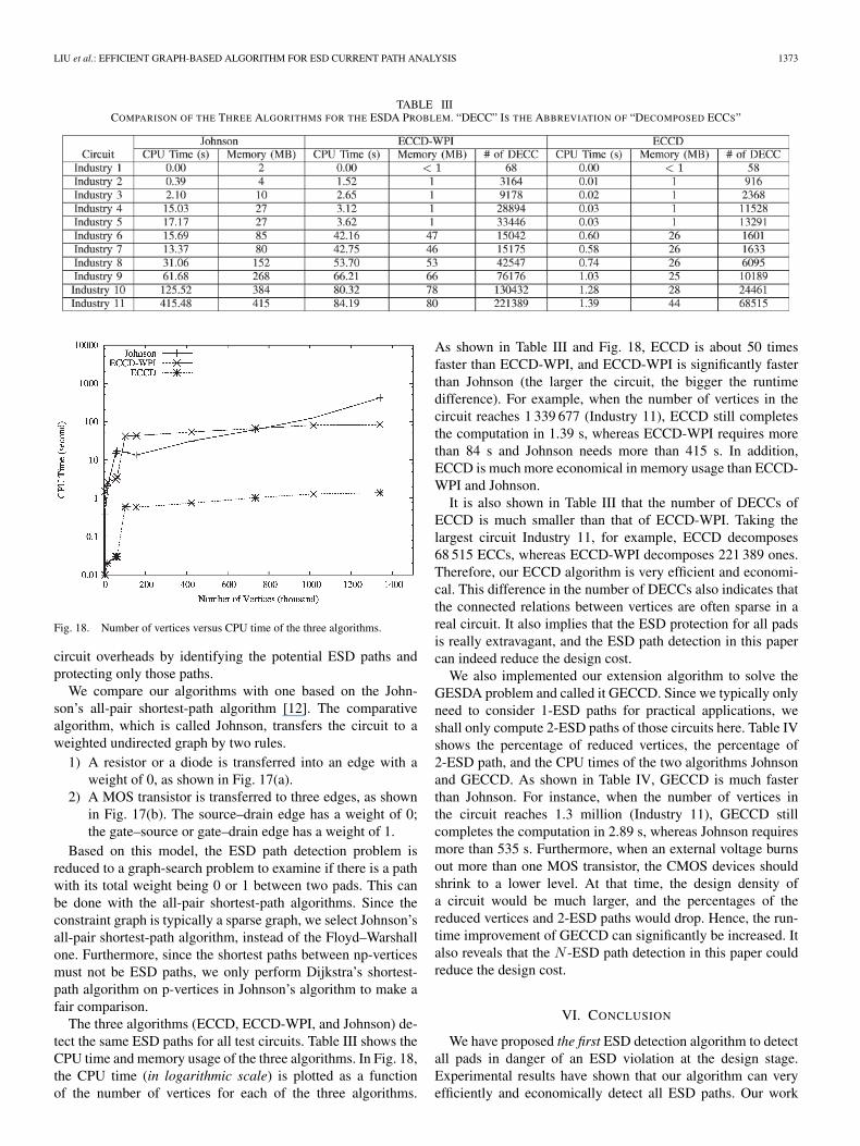
TABLE IIICOMPARISON OF THE THREE ALGORITHMS FOR THE ESDA PROBLEM. “DECC” IS THE ABBREVIATION OF “DECOMPOSED ECCS”
Fig. 18. Number of vertices versus CPU time of the three algorithms.
circuit overheads by identifying the potential ESD paths andprotecting only those paths.
We compare our algorithms with one based on the John-son’s all-pair shortest-path algorithm [12]. The comparativealgorithm, which is called Johnson, transfers the circuit to aweighted undirected graph by two rules.
1) A resistor or a diode is transferred into an edge with aweight of 0, as shown in Fig. 17(a).
2) A MOS transistor is transferred to three edges, as shownin Fig. 17(b). The source–drain edge has a weight of 0;the gate–source or gate–drain edge has a weight of 1.
Based on this model, the ESD path detection problem isreduced to a graph-search problem to examine if there is a pathwith its total weight being 0 or 1 between two pads. This canbe done with the all-pair shortest-path algorithms. Since theconstraint graph is typically a sparse graph, we select Johnson’sall-pair shortest-path algorithm, instead of the Floyd–Warshallone. Furthermore, since the shortest paths between np-verticesmust not be ESD paths, we only perform Dijkstra’s shortest-path algorithm on p-vertices in Johnson’s algorithm to make afair comparison.
The three algorithms (ECCD, ECCD-WPI, and Johnson) de-tect the same ESD paths for all test circuits. Table III shows theCPU time and memory usage of the three algorithms. In Fig. 18,the CPU time (in logarithmic scale) is plotted as a functionof the number of vertices for each of the three algorithms.
As shown in Table III and Fig. 18, ECCD is about 50 timesfaster than ECCD-WPI, and ECCD-WPI is significantly fasterthan Johnson (the larger the circuit, the bigger the runtimedifference). For example, when the number of vertices in thecircuit reaches 1 339 677 (Industry 11), ECCD still completesthe computation in 1.39 s, whereas ECCD-WPI requires morethan 84 s and Johnson needs more than 415 s. In addition,ECCD is much more economical in memory usage than ECCD-WPI and Johnson.
It is also shown in Table III that the number of DECCs ofECCD is much smaller than that of ECCD-WPI. Taking thelargest circuit Industry 11, for example, ECCD decomposes68 515 ECCs, whereas ECCD-WPI decomposes 221 389 ones.Therefore, our ECCD algorithm is very efficient and economi-cal. This difference in the number of DECCs also indicates thatthe connected relations between vertices are often sparse in areal circuit. It also implies that the ESD protection for all padsis really extravagant, and the ESD path detection in this papercan indeed reduce the design cost.
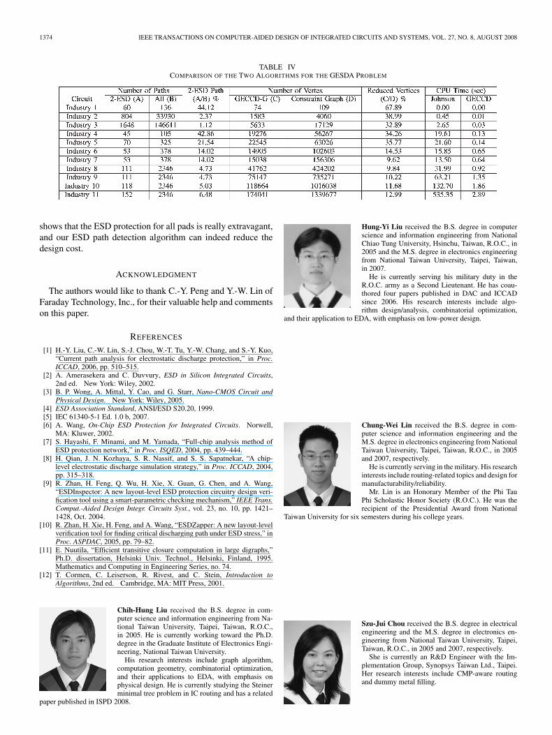
We also implemented our extension algorithm to solve theGESDA problem and called it GECCD. Since we typically onlyneed to consider 1-ESD paths for practical applications, weshall only compute 2-ESD paths of those circuits here. Table IVshows the percentage of reduced vertices, the percentage of2-ESD path, and the CPU times of the two algorithms Johnsonand GECCD. As shown in Table IV, GECCD is much fasterthan Johnson. For instance, when the number of vertices inthe circuit reaches 1.3 million (Industry 11), GECCD stillcompletes the computation in 2.89 s, whereas Johnson requiresmore than 535 s. Furthermore, when an external voltage burnsout more than one MOS transistor, the CMOS devices shouldshrink to a lower level. At that time, the design density ofa circuit would be much larger, and the percentages of thereduced vertices and 2-ESD paths would drop. Hence, the run-time improvement of GECCD can significantly be increased. Italso reveals that the N -ESD path detection in this paper couldreduce the design cost.
VI. CONCLUSION
We have proposed the first ESD detection algorithm to detectall pads in danger of an ESD violation at the design stage.Experimental results have shown that our algorithm can veryefficiently and economically detect all ESD paths. Our work
1374 IEEE TRANSACTIONS ON COMPUTER-AIDED DESIGN OF INTEGRATED CIRCUITS AND SYSTEMS, VOL. 27, NO. 8, AUGUST 2008
TABLE IVCOMPARISON OF THE TWO ALGORITHMS FOR THE GESDA PROBLEM
shows that the ESD protection for all pads is really extravagant,and our ESD path detection algorithm can indeed reduce thedesign cost.
ACKNOWLEDGMENT
The authors would like to thank C.-Y. Peng and Y.-W. Lin ofFaraday Technology, Inc., for their valuable help and commentson this paper.
REFERENCES
[1] H.-Y. Liu, C.-W. Lin, S.-J. Chou, W.-T. Tu, Y.-W. Chang, and S.-Y. Kuo,“Current path analysis for electrostatic discharge protection,” in Proc.ICCAD, 2006, pp. 510–515.
[2] A. Amerasekera and C. Duvvury, ESD in Silicon Integrated Circuits,2nd ed. New York: Wiley, 2002.
[3] B. P. Wong, A. Mittal, Y. Cao, and G. Starr, Nano-CMOS Circuit andPhysical Design. New York: Wiley, 2005.
[4] ESD Association Standard, ANSI/ESD S20.20, 1999.[5] IEC 61340-5-1 Ed. 1.0 b, 2007.[6] A. Wang, On-Chip ESD Protection for Integrated Circuits. Norwell,
MA: Kluwer, 2002.[7] S. Hayashi, F. Minami, and M. Yamada, “Full-chip analysis method of
ESD protection network,” in Proc. ISQED, 2004, pp. 439–444.[8] H. Qian, J. N. Kozhaya, S. R. Nassif, and S. S. Sapatnekar, “A chip-
level electrostatic discharge simulation strategy,” in Proc. ICCAD, 2004,pp. 315–318.
[9] R. Zhan, H. Feng, Q. Wu, H. Xie, X. Guan, G. Chen, and A. Wang,“ESDInspector: A new layout-level ESD protection circuitry design veri-fication tool using a smart-parametric checking mechanism,” IEEE Trans.Comput.-Aided Design Integr. Circuits Syst., vol. 23, no. 10, pp. 1421–1428, Oct. 2004.
[10] R. Zhan, H. Xie, H. Feng, and A. Wang, “ESDZapper: A new layout-levelverification tool for finding critical discharging path under ESD stress,” inProc. ASPDAC, 2005, pp. 79–82.
[11] E. Nuutila, “Efficient transitive closure computation in large digraphs,”Ph.D. dissertation, Helsinki Univ. Technol., Helsinki, Finland, 1995.Mathematics and Computing in Engineering Series, no. 74.
[12] T. Cormen, C. Leiserson, R. Rivest, and C. Stein, Introduction toAlgorithms, 2nd ed. Cambridge, MA: MIT Press, 2001.
Chih-Hung Liu received the B.S. degree in com-puter science and information engineering from Na-tional Taiwan University, Taipei, Taiwan, R.O.C.,in 2005. He is currently working toward the Ph.D.degree in the Graduate Institute of Electronics Engi-neering, National Taiwan University.
His research interests include graph algorithm,computation geometry, combinatorial optimization,and their applications to EDA, with emphasis onphysical design. He is currently studying the Steinerminimal tree problem in IC routing and has a related
paper published in ISPD 2008.
Hung-Yi Liu received the B.S. degree in computerscience and information engineering from NationalChiao Tung University, Hsinchu, Taiwan, R.O.C., in2005 and the M.S. degree in electronics engineeringfrom National Taiwan University, Taipei, Taiwan,in 2007.
He is currently serving his military duty in theR.O.C. army as a Second Lieutenant. He has coau-thored four papers published in DAC and ICCADsince 2006. His research interests include algo-rithm design/analysis, combinatorial optimization,
and their application to EDA, with emphasis on low-power design.
Chung-Wei Lin received the B.S. degree in com-puter science and information engineering and theM.S. degree in electronics engineering from NationalTaiwan University, Taipei, Taiwan, R.O.C., in 2005and 2007, respectively.
He is currently serving in the military. His researchinterests include routing-related topics and design formanufacturability/reliability.
Mr. Lin is an Honorary Member of the Phi TauPhi Scholastic Honor Society (R.O.C.). He was therecipient of the Presidential Award from National
Taiwan University for six semesters during his college years.
Szu-Jui Chou received the B.S. degree in electricalengineering and the M.S. degree in electronics en-gineering from National Taiwan University, Taipei,Taiwan, R.O.C., in 2005 and 2007, respectively.
She is currently an R&D Engineer with the Im-plementation Group, Synopsys Taiwan Ltd., Taipei.Her research interests include CMP-aware routingand dummy metal filling.
LIU et al.: EFFICIENT GRAPH-BASED ALGORITHM FOR ESD CURRENT PATH ANALYSIS 1375
Yao-Wen Chang (S’94–A’96–M’96) received theB.S. degree from National Taiwan University, Taipei,Taiwan, R.O.C., in 1988 and the M.S. and Ph.D.degrees from the University of Texas, Austin, in 1993and 1996, respectively, all in computer science.
He is currently a Professor with the Departmentof Electrical Engineering and the Graduate Instituteof Electronics Engineering, National Taiwan Univer-sity. He is also currently a Visiting Professor withWaseda University, Kitakyushu, Japan. He was withthe IBM T. J. Watson Research Center, Yorktown
Heights, NY, in the summer of 1994, and the faculty of National Chiao TungUniversity, Hsinchu, Taiwan, from 1996 to 2001. His current research interestsinclude VLSI physical design, design for manufacturability/reliability, anddesign automation for biochips. He has coauthored one book on routing andmore than 130 ACM/IEEE conference proceeding/journal papers and has beenworking closely with the industry on projects in these areas.
Dr. Chang is a member of the IEEE Circuits and Systems Society, ACM,and ACM/SIGDA. He is an Editor for the Journal of Information Science andEngineering. He is currently an Associate Editor for the IEEE TRANSACTIONS
ON COMPUTER-AIDED DESIGN OF INTEGRATED CIRCUITS AND SYSTEMS.He currently serves on the ICCAD Executive Committee, ACM/SIGDA Phys-ical Design Technical Committee, and the organizing committees of ISPD andFPT. He has served on the technical program committees of ASP-DAC (TopicChair), DAC, DATE, FPT (Program Co-Chair), GLSVLSI, ICCAD, ICCD,IECON (Topic Chair), ISPD, SOCC (Topic Chair), TENCON, VLSI-DAT(Topic Co-Chair), etc. He is currently an independent board director of GenesysLogic, Inc. and a member of the board of governors of Taiwan IC DesignSociety. He was a winner of the 2006 ACM ISPD Placement Contest and the2008 ACM ISPD Global Routing Contest; Best Paper Awards at ICCD-95and the 2007 VLSI Design/CAD Symposium; and 11 Best Paper AwardNominations from DAC (four times), ICCAD (twice), ISPD (twice), ACMTODAES, ASP-DAC, and ICCD. He has also been the recipient of manyawards for research performance, such as the 2007 Distinguished ResearchAward, the inaugural 2005 First-Class Principal Investigator Award, the 2004Dr. Wu Ta You Memorial Award from the National Science Council of Taiwan,and the 2004 MXIC Young Chair Professorship from the MXIC Corp.; and forexcellent teaching from National Taiwan University (four times) and NationalChiao Tung University.
Sy-Yen Kuo received the B.S. degree in electri-cal engineering from National Taiwan University,Taipei, Taiwan, R.O.C., in 1979, the M.S. degree inelectrical and computer engineering from the Uni-versity of California, Santa Barbara, in 1982, and thePh.D. degree in computer science from the Univer-sity of Illinois, Urbana, in 1987.
He is currently a Chair Professor and the Dean ofthe College of Electrical and Computer Engineering,National Taiwan University of Science and Technol-ogy, Taipei. He is also a Distinguished Professor with
the Department of Electrical Engineering, National Taiwan University, wherehe is currently taking a leave of absence and was the Chairman at the samedepartment from 2001 to 2004. He spent his sabbatical years as a VisitingProfessor with Department of the Computer Science and Engineering, ChineseUniversity of Hong Kong, from 2004 to 2005, and as a Visiting Researcherwith AT&T Labs-Research, Florham Park, NJ, from 1999 to 2000. He was theChairman of the Department of Computer Science and Information Engineer-ing, National Dong Hwa University, Hualien, Taiwan, from 1995 to 1998; afaculty member with the Department of Electrical and Computer Engineering,University of Arizona, Tucson, from 1988 to 1991; and an Engineer withFairchild Semiconductor, San Jose, CA, and Silvar-Lisco, Palo Alto, CA, from1982 to 1984. In 1989, he was a Summer Faculty Fellow with the Jet PropulsionLaboratory, California Institute of Technology, Pasadena. He has publishedmore than 290 papers in journals and conference proceedings. He is the holderof several patents. His current research interests include dependable systemsand networks, software reliability engineering, mobile computing, and reliablesensor networks.
Dr. Kuo is a Research Fellow of the National Science Council in Taiwan.He was the recipient of the Distinguished Research Award (1997–2005) fromthe National Science Council in Taiwan, the Best Paper Award at the 1996International Symposium on Software Reliability Engineering, the Best PaperAward in the simulation and test category at the 1986 IEEE/ACM DesignAutomation Conference, the National Science Foundation’s Research InitiationAward in 1989, and the IEEE/ACM Design Automation Scholarship in 1990and 1991.
Shih-Yi Yuan received the M.S. and Ph.D. degreesin electrical engineering from National Taiwan Uni-versity, Taipei, Taiwan, R.O.C., in 1993 and 1997,respectively.
In 2003, he joined the Department of Communica-tions Engineering, Feng Chia University, Taichung,Taiwan, as an Assistant Professor. He is also a mem-ber of the ICEMC Center, Feng Chia University.His research interests include driver design, ICEMCmodel building, and CAD tool design for EMCestimations.
Yu-Wei Chen received the B.S. degree in computerand information science from National Chiao TungUniversity, Hsinchu, Taiwan, R.O.C., and the Ph.D.degree in computer science from the University ofOklahoma, Norman.
Since 2001, he has been with the Design and De-velopment Department, Faraday Technology Corp.,Hsinchu, leading a team that researches and devel-ops in-house EDA tools and flows. Prior to joiningFaraday, he was a Member of Technical Staff withCadence, where he worked on various physical ver-
ification tools. His current research interests include test challenges of circuitlevel and physical design in nanometer technologies, automation of design andimplementation for multiple power domain IC designs, and quality in electronicdesign.