fundamentals of microwave and rf design
TRANSCRIPT

FUNDAMENTALS OF MICROWAVE AND RF DESIGN
Michael SteerNorth Carolina State University

Default Text

This text is disseminated via the Open Education Resource (OER) LibreTexts Project (https://LibreTexts.org) and like the hundredsof other texts available within this powerful platform, it is freely available for reading, printing and "consuming." Most, but not all,pages in the library have licenses that may allow individuals to make changes, save, and print this book. Carefullyconsult the applicable license(s) before pursuing such effects.
Instructors can adopt existing LibreTexts texts or Remix them to quickly build course-specific resources to meet the needs of theirstudents. Unlike traditional textbooks, LibreTexts’ web based origins allow powerful integration of advanced features and newtechnologies to support learning.
The LibreTexts mission is to unite students, faculty and scholars in a cooperative effort to develop an easy-to-use online platformfor the construction, customization, and dissemination of OER content to reduce the burdens of unreasonable textbook costs to ourstudents and society. The LibreTexts project is a multi-institutional collaborative venture to develop the next generation of open-access texts to improve postsecondary education at all levels of higher learning by developing an Open Access Resourceenvironment. The project currently consists of 14 independently operating and interconnected libraries that are constantly beingoptimized by students, faculty, and outside experts to supplant conventional paper-based books. These free textbook alternatives areorganized within a central environment that is both vertically (from advance to basic level) and horizontally (across different fields)integrated.
The LibreTexts libraries are Powered by MindTouch and are supported by the Department of Education Open Textbook PilotProject, the UC Davis Office of the Provost, the UC Davis Library, the California State University Affordable Learning SolutionsProgram, and Merlot. This material is based upon work supported by the National Science Foundation under Grant No. 1246120,1525057, and 1413739. Unless otherwise noted, LibreTexts content is licensed by CC BY-NC-SA 3.0.
Any opinions, findings, and conclusions or recommendations expressed in this material are those of the author(s) and do notnecessarily reflect the views of the National Science Foundation nor the US Department of Education.
Have questions or comments? For information about adoptions or adaptions contact [email protected]. More information on ouractivities can be found via Facebook (https://facebook.com/Libretexts), Twitter (https://twitter.com/libretexts), or our blog(http://Blog.Libretexts.org).
This text was compiled on 04/10/2022
®
1 4/10/2022
TABLE OF CONTENTSThe book series Microwave and RF Design is a comprehensive treatment of radio frequency (RF) and microwave design with a modern“systems-first” approach. A strong emphasis on design permeates the series with extensive case studies and design examples. Design isoriented towards cellular communications and microstrip design so that lessons learned can be applied to real-world design tasks. The booksin the Microwave and RF Design series are: Radio Systems (Volume 1), Transmission Lines (Volume 2), Networks (Volume 3), Modules(Volume 4), and Amplifiers and Oscillators (Volume 5).
1: INTRODUCTION TO MICROWAVE ENGINEERING1.1: RF AND MICROWAVE ENGINEERING1.2: RADIO ARCHITECTURE1.3: RF POWER CALCULATIONS1.4: SI UNITS1.5: SUMMARY1.6: REFERENCES1.7: EXERCISES
2: ANTENNAS AND THE RF LINK2.1: INTRODUCTION2.2: RF ANTENNAS2.3: RESONANT ANTENNAS2.4: TRAVELING-WAVE ANTENNAS2.5: ANTENNA PARAMETERS2.6: THE RF LINK2.7: EXERCISES2.8: ANTENNA ARRAY2.9: SUMMARY2.10: REFERENCES
3: TRANSMISSION LINES3.1: INTRODUCTION3.2: TRANSMISSION LINE THEORY3.3: THE LOSSLESS TERMINATED LINE3.4: SPECIAL CASES OF LOSSLESS TERMINATED LINES3.5: CIRCUIT MODELS OF TRANSMISSION LINES3.6: SUMMARY3.7: REFERENCES3.8: EXERCISES
4: PLANAR TRANSMISSION LINES4.1: INTRODUCTION4.2: SUBSTRATES4.3: PLANAR TRANSMISSION LINE STRUCTURES4.4: MICROSTRIP TRANSMISSION LINES4.5: MICROSTRIP DESIGN FORMULAS4.6: SUMMARY4.7: REFERENCES4.8: EXERCISES
5: EXTRAORDINARY TRANSMISSION LINE EFFECTS5.1: INTRODUCTION5.2: FREQUENCY-DEPENDENT CHARACTERISTICS5.3: MULTIMODING ON TRANSMISSION LINES5.4: MICROSTRIP OPERATING FREQUENCY LIMITATIONS5.5: SUMMARY

2 4/10/2022
5.6: REFERENCES5.7: EXERCISES
6: COUPLED LINES AND APPLICATIONS6.1: INTRODUCTION6.2: PHYSICS OF COUPLING6.3: LOW FREQUENCY CAPACITANCE MODEL OF COUPLED LINES6.4: SYMMETRIC COUPLED TRANSMISSION LINES6.5: DIRECTIONAL COUPLER6.6: SUMMARY6.7: REFERENCES6.8: EXERCISES
7: MICROWAVE NETWORK ANALYSIS7.1: INTRODUCTION7.2: TWO-PORT NETWORKS7.3: SCATTERING PARAMETERS7.4: RETURN LOSS, SUBSTITUTION LOSS, AND INSERTION LOSS7.5: SCATTERING PARAMETERS AND COUPLED LINES7.6: SUMMARY7.7: REFERENCES7.8: EXERCISES
8: GRAPHICAL NETWORK ANALYSIS8.1: INTRODUCTION8.2: POLAR REPRESENTATIONS OF SCATTERING PARAMETERS8.3: SMITH CHART8.4: SUMMARY8.5: REFERENCES8.6: EXERCISES
9: PASSIVE COMPONENTS9.1: INTRODUCTION9.2: Q FACTOR9.3: SURFACE-MOUNT COMPONENTS9.4: TERMINATIONS AND ATTENUATORS9.5: TRANSMISSION LINE STUBS AND DISCONTINUITIES9.6: MAGNETIC TRANSFORMERS9.7: REFERENCES9.8: EXERCISES9.9: BALUNS9.10: WILKINSON COMBINER AND DIVIDER9.11: SUMMARY
10: IMPEDANCE MATCHING10.1: INTRODUCTION10.2: MATCHING NETWORKS10.3: IMPEDANCE TRANSFORMING NETWORKS10.4: THE L MATCHING NETWORK10.5: DEALING WITH COMPLEX LOADS10.6: DEALING WITH COMPLEX LOADS10.7: SUMMARY10.8: REFERENCES10.9: EXERCISES10.10: IMPEDANCE MATCHING USING SMITH CHARTS10.11: DISTRIBUTED MATCHING10.12: MATCHING USING THE SMITH CHART
11: RF AND MICROWAVE MODULES

3 4/10/2022
11.1: INTRODUCTION TO MICROWAVE MODULES11.2: RF SYSTEM AS A CASCADE OF MODULES11.3: AMPLIFIERS11.4: FILTERS11.5: NOISE11.6: DIODES11.7: LOCAL OSCILLATOR11.8: FREQUENCY MULTIPLIER11.9: SUMMARY11.10: REFERENCES11.11: EXERCISES11.12: SWITCH11.13: FERRITE COMPONENTS- CIRCULATORS AND ISOLATORS11.14: MIXER
BACK MATTERINDEXINDEXGLOSSARY

1 4/10/2022
CHAPTER OVERVIEW1: INTRODUCTION TO MICROWAVE ENGINEERING
1.1: RF AND MICROWAVE ENGINEERING1.2: RADIO ARCHITECTURE1.3: RF POWER CALCULATIONS1.4: SI UNITS1.5: SUMMARY1.6: REFERENCES1.7: EXERCISES
Michael Steer 1.1.1 4/10/2022 https://eng.libretexts.org/@go/page/41250
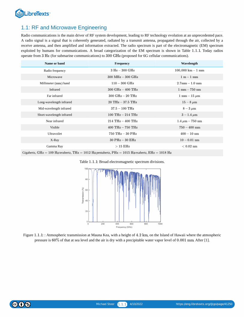
1.1: RF and Microwave EngineeringRadio communications is the main driver of RF system development, leading to RF technology evolution at an unprecedented pace.A radio signal is a signal that is coherently generated, radiated by a transmit antenna, propagated through the air, collected by areceive antenna, and then amplified and information extracted. The radio spectrum is part of the electromagnetic (EM) spectrumexploited by humans for communications. A broad categorization of the EM spectrum is shown in Table . Today radiosoperate from (for submarine communications) to (proposed for 6G cellular communications).
Name or band Frequency Wavelength
Radio frequency
Microwave
Millimeter ( ) band
Infrared
Far infrared
Long-wavelength infrared
Mid-wavelength infrared
Short-wavelength infrared
Near infrared
Visible
Ultravoilet
X-Ray
Gamma Ray
Gigahertz, ; terahertz, ; pentahertz, ; exahertz, .
Table : Broad electromagnetic spectrum divisions.
Figure : : Atmospheric transmission at Mauna Kea, with a height of , on the Island of Hawaii where the atmosphericpressure is of that at sea level and the air is dry with a precipitable water vapor level of . After [1].
1.1.1
3 Hz 300 GHz
3 Hz − 300 GHz 100,000 km − 1 mm
300 MHz − 300 GHz 1 m − 1 mm
mm 110 − 300 GHz 2.7mm − 1.0 mm
300 GHz − 400 THz 1 mm − 750 nm
300 GHz − 20 THz 1 mm − 15 μm
20 THz − 37.5 THz 15 − 8 μm
37.5 − 100 THz 8 − 3 μm
100 THz − 214 THz 3 − 1.4 μm
214 THz − 400 THz 1.4 μm − 750 nm
400 THz − 750 THz 750 − 400 mm
750 THz − 30 PHz 400 − 10 nm
30 PHz − 30 EHz 10 − 0.01 nm
> 15 EHz < 0.02 nm
GHz = 109 Hz THz = 1012 Hz PHz = 1015 Hz EHz = 1018 Hz
1.1.1
1.1.1 4.2 km
60% 0.001 mm
Michael Steer 1.1.2 4/10/2022 https://eng.libretexts.org/@go/page/41250
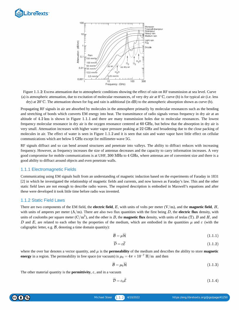
Figure : Excess attenuation due to atmospheric conditions showing the effect of rain on RF transmission at sea level. Curve(a) is atmospheric attenuation, due to excitation of molecular resonances, of very dry air at , curve (b) is for typical air (i.e. less
dry) at . The attenuation shown for fog and rain is additional (in ) to the atmospheric absorption shown as curve (b).
Propagating RF signals in air are absorbed by molecules in the atmosphere primarily by molecular resonances such as the bendingand stretching of bonds which converts EM energy into heat. The transmittance of radio signals versus frequency in dry air at analtitude of is shown in Figure and there are many transmission holes due to molecular resonances. The lowestfrequency molecular resonance in dry air is the oxygen resonance centered at , but below that the absorption in dry air isvery small. Attenuation increases with higher water vapor pressure peaking at and broadening due to the close packing ofmolecules in air. The effect of water is seen in Figure and it is seen that rain and water vapor have little effect on cellularcommunications which are below except for millimeter-wave 5G.
RF signals diffract and so can bend around structures and penetrate into valleys. The ability to diffract reduces with increasingfrequency. However, as frequency increases the size of antennas decreases and the capacity to carry information increases. A verygood compromise for mobile communications is at UHF, to , where antennas are of convenient size and there is agood ability to diffract around objects and even penetrate walls.
1.1.1 Electromagnetic Fields
Communicating using EM signals built from an understanding of magnetic induction based on the experiments of Faraday in 1831[2] in which he investigated the relationship of magnetic fields and currents, and now known as Faraday’s law. This and the otherstatic field laws are not enough to describe radio waves. The required description is embodied in Maxwell’s equations and afterthese were developed it took little time before radio was invented.
1.1.2 Static Field LawsThere are two components of the EM field, the electric field, , with units of volts per meter ( ), and the magnetic field, ,with units of amperes per meter ( ). There are also two flux quantities with the first being , the electric flux density, withunits of coulombs per square meter ( ), and the other is , the magnetic flux density, with units of teslas ( ). and , and
and , are related to each other by the properties of the medium, which are embodied in the quantities and (with thecaligraphic letter, e.g. , denoting a time domain quantity):
where the over bar denotes a vector quantity, and is the permeability of the medium and describes the ability to store magneticenergy in a region. The permeability in free space (or vacuum) is and then
The other material quantity is the permittivity, , and in a vacuum
1.1.2
C0∘
C20∘ dB
4.2 km 1.1.1
60 GHz
22 GHz
1.1.2
5 GHz
300 MHz 4 GHz
E V/m H
A/m D
C/m2 B T B H
D E μ ε
B
= μB¯¯
H¯ ¯¯
(1.1.1)
= εD¯ ¯¯
E¯
(1.1.2)
μ
= 4π× H/mμ0 10−7
=B¯¯
μ0H¯ ¯¯
(1.1.3)
ε
=D¯ ¯¯
ε0E¯
(1.1.4)
Michael Steer 1.1.3 4/10/2022 https://eng.libretexts.org/@go/page/41250
where is the permittivity of a vacuum. The relative permittivity, , the relative permeability, , aredefined as
Biot-Savart Law
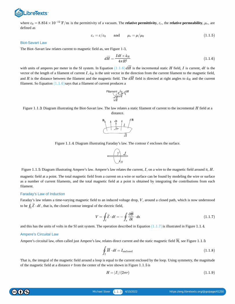
The Biot–Savart law relates current to magnetic field as, see Figure 1-3,
with units of amperes per meter in the SI system. In Equation is the incremental static field, is current, is thevector of the length of a filament of current , is the unit vector in the direction from the current filament to the magnetic field,and is the distance between the filament and the magnetic field. The field is directed at right angles to and the currentfilament. So Equation says that a filament of current produces a
Figure : Diagram illustrating the Biot-Savart law. The law relates a static filament of current to the incremental field at adistance.
Figure : Diagram illustrating Faraday’s law. The contour encloses the surface.
Figure : Diagram illustrating Ampere’s law. Ampere’s law relates the current, , on a wire to the magnetic field around it, .
magnetic field at a point. The total magnetic field from a current on a wire or surface can be found by modeling the wire or surfaceas a number of current filaments, and the total magnetic field at a point is obtained by integrating the contributions from eachfilament.
Faraday's Law of Induction
Faraday’s law relates a time-varying magnetic field to an induced voltage drop, , around a closed path, which is now understoodto be , that is, the closed contour integral of the electric field,
and this has the units of volts in the SI unit system. The operation described in Equation is illustrated in Figure .
Ampere's Circuital Law
Ampere’s circuital law, often called just Ampere’s law, relates direct current and the static magnetic field , see Figure :
That is, the integral of the magnetic field around a loop is equal to the current enclosed by the loop. Using symmetry, the magnitudeof the magnetic field at a distance from the center of the wire shown in Figure is
= 8.854 × F/mε0 10−12 εr μr
= ε/ and = μ/εr ε0 μr μ0 (1.1.5)
d =H¯ ¯¯¯ Idℓ × aR
4πR2(1.1.6)
(1.1.6)dH¯ ¯¯¯
H I dℓ
I aR
R dH¯ ¯¯¯ aR(1.1.6)
1.1.3 H
1.1.4 ℓ
1.1.5 I H
V
⋅ dℓ∮ℓE¯
V = ⋅ dℓ = − ⋅ ds∮ℓ
E¯ ∮
s
∂B¯¯
∂t(1.1.7)
(1.1.7) 1.1.4
H¯ ¯¯ 1.1.5
⋅ dℓ =∮ℓ
H¯ ¯¯¯ Ienclosed (1.1.8)
r 1.1.5
H = |I|/(2πr) (1.1.9)
Michael Steer 1.1.4 4/10/2022 https://eng.libretexts.org/@go/page/41250
Gauss's Law
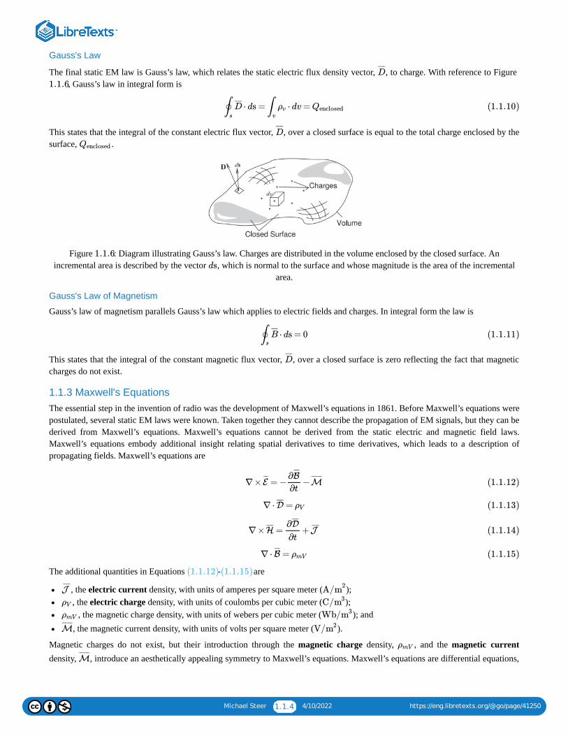
The final static EM law is Gauss’s law, which relates the static electric flux density vector, , to charge. With reference to Figure , Gauss’s law in integral form is
This states that the integral of the constant electric flux vector, , over a closed surface is equal to the total charge enclosed by thesurface, .
Figure : Diagram illustrating Gauss’s law. Charges are distributed in the volume enclosed by the closed surface. Anincremental area is described by the vector , which is normal to the surface and whose magnitude is the area of the incremental
area.
Gauss's Law of Magnetism
Gauss’s law of magnetism parallels Gauss’s law which applies to electric fields and charges. In integral form the law is
This states that the integral of the constant magnetic flux vector, , over a closed surface is zero reflecting the fact that magneticcharges do not exist.
1.1.3 Maxwell's EquationsThe essential step in the invention of radio was the development of Maxwell’s equations in 1861. Before Maxwell’s equations werepostulated, several static EM laws were known. Taken together they cannot describe the propagation of EM signals, but they can bederived from Maxwell’s equations. Maxwell’s equations cannot be derived from the static electric and magnetic field laws.Maxwell’s equations embody additional insight relating spatial derivatives to time derivatives, which leads to a description ofpropagating fields. Maxwell’s equations are
The additional quantities in Equations - are
, the electric current density, with units of amperes per square meter ( );, the electric charge density, with units of coulombs per cubic meter ( );
, the magnetic charge density, with units of webers per cubic meter ( ); and, the magnetic current density, with units of volts per square meter ( ).
Magnetic charges do not exist, but their introduction through the magnetic charge density, , and the magnetic currentdensity, , introduce an aesthetically appealing symmetry to Maxwell’s equations. Maxwell’s equations are differential equations,
D¯ ¯¯
1.1.6
⋅ ds = ⋅ dv=∮s
D¯ ¯¯ ∫v
ρv Qenclosed (1.1.10)
D¯ ¯¯
Qenclosed
1.1.6
ds
⋅ ds = 0∮s
B¯ ¯¯
(1.1.11)
D¯ ¯¯
∇ × = − −E¯ ∂B
¯¯
∂tM¯ ¯¯¯
(1.1.12)
∇ ⋅ =D¯ ¯¯ ρV (1.1.13)
∇ × = +H¯ ¯¯ ∂D¯ ¯¯
∂tJ¯ ¯¯ (1.1.14)
∇ ⋅ =B¯¯
ρmV (1.1.15)
(1.1.12) (1.1.15)
J¯ ¯¯
A/m2
ρV C/m3
ρmV Wb/m3
M¯ ¯¯¯
V/m2
ρmV
M¯ ¯¯¯
Michael Steer 1.1.5 4/10/2022 https://eng.libretexts.org/@go/page/41250
and as with most differential equations, their solution is obtained with particular boundary conditions, which in radio engineeringare imposed by conductors.
Maxwell’s equations have three types of derivatives. First, there is the time derivative, . Then there are two spatial derivatives,, called curl, capturing the way a field circulates spatially (or the amount that it curls up on itself), and , called the div
operator, describing the spreading-out of a
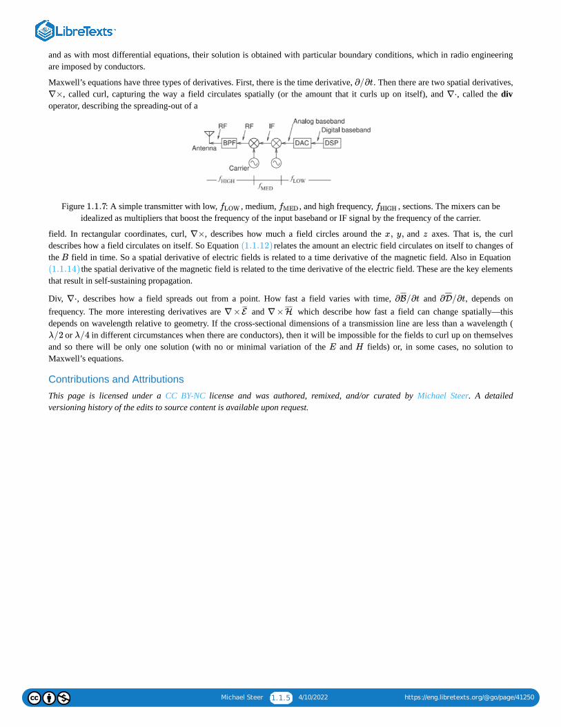
Figure : A simple transmitter with low, , medium, , and high frequency, , sections. The mixers can beidealized as multipliers that boost the frequency of the input baseband or IF signal by the frequency of the carrier.
field. In rectangular coordinates, curl, , describes how much a field circles around the and axes. That is, the curldescribes how a field circulates on itself. So Equation relates the amount an electric field circulates on itself to changes ofthe field in time. So a spatial derivative of electric fields is related to a time derivative of the magnetic field. Also in Equation
the spatial derivative of the magnetic field is related to the time derivative of the electric field. These are the key elementsthat result in self-sustaining propagation.
Div, , describes how a field spreads out from a point. How fast a field varies with time, and , depends onfrequency. The more interesting derivatives are and which describe how fast a field can change spatially—thisdepends on wavelength relative to geometry. If the cross-sectional dimensions of a transmission line are less than a wavelength (
or in different circumstances when there are conductors), then it will be impossible for the fields to curl up on themselvesand so there will be only one solution (with no or minimal variation of the and fields) or, in some cases, no solution toMaxwell’s equations.
Contributions and Attributions
This page is licensed under a CC BY-NC license and was authored, remixed, and/or curated by Michael Steer. A detailedversioning history of the edits to source content is available upon request.
∂/∂t
∇× ∇⋅
1.1.7 fLOW fMED fHIGH
∇× x, y, z
(1.1.12)
B
(1.1.14)
∇⋅ ∂ /∂tB¯¯
∂ /∂tD¯ ¯¯
∇ ×E¯ ∇ ×H¯ ¯¯
λ/2 λ/4
E H
Michael Steer 1.2.1 4/10/2022 https://eng.libretexts.org/@go/page/41251
1.2: Radio ArchitectureA radio device is comprised of reasonably well-defined units, see Figure 1.1.7. The analog baseband signal can have frequencycomponents that range from DC to many megahertz.
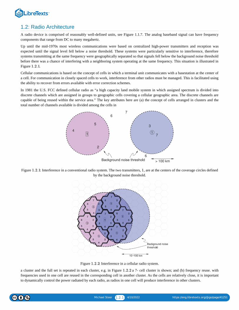
Up until the mid-1970s most wireless communications were based on centralized high-power transmitters and reception wasexpected until the signal level fell below a noise threshold. These systems were particularly sensitive to interference, thereforesystems transmitting at the same frequency were geographically separated so that signals fell below the background noise thresholdbefore there was a chance of interfering with a neighboring system operating at the same frequency. This situation is illustrated inFigure .
Cellular communications is based on the concept of cells in which a terminal unit communicates with a basestation at the center ofa cell. For communication in closely spaced cells to work, interference from other radios must be managed. This is facilitated usingthe ability to recover from errors available with error correction schemes.
In 1981 the U.S. FCC defined cellular radio as “a high capacity land mobile system in which assigned spectrum is divided intodiscrete channels which are assigned in groups to geographic cells covering a cellular geographic area. The discrete channels arecapable of being reused within the service area.” The key attributes here are (a) the concept of cells arranged in clusters and thetotal number of channels available is divided among the cells in
Figure : Interference in a conventional radio system. The two transmitters, , are at the centers of the coverage circles definedby the background noise threshold.
Figure : Interference in a cellular radio system.
a cluster and the full set is repeated in each cluster, e.g. in Figure a 7- cell cluster is shown; and (b) frequency reuse. withfrequencies used in one cell are reused in the corresponding cell in another cluster. As the cells are relatively close, it is importantto dynamically control the power radiated by each radio, as radios in one cell will produce interference in other clusters.
1.2.1
1.2.1 1
1.2.2
1.2.2

Michael Steer 1.2.2 4/10/2022 https://eng.libretexts.org/@go/page/41251
Achieving maximum frequency reuse is essential. In a cellular system, there is a radical departure in concept from this. Considerthe interference in a cellular system as shown in Figure . The signals in corresponding cells in different clusters interfere witheach other and the interference is much larger than that of the background noise. Error correction coding to correct errors resultingfrom interference.
Contributions and AttributionsThis page is licensed under a CC BY-NC license and was authored, remixed, and/or curated by Michael Steer. A detailedversioning history of the edits to source content is available upon request.
1.2.2
Michael Steer 1.3.1 4/10/2022 https://eng.libretexts.org/@go/page/41252
1.3: RF Power Calculations
1.3.1 RF Propagation
As an RF signal propagates away from a transmitter the power density reduces conserving the power in the EM wave. In the absence of obstacles andwithout atmospheric attenuation the total power passing through the surface of a sphere centered on a transmitter is equal to the power transmitted.Since the area of the sphere of radius is , the power density, e.g. in , at a distance drops off as . With obstacles the EM wave canbe further attenuated.
A signal is received at a distance from a transmitter and the received power drops off as . When , is received. What is when the received power is ?
Solution
The signal collected by the receiver is proportional to the power density of the EM signal. The received signal power where is aconstant. This leads to
1.3.2 Logarithm
A cellular phone can reliably receive a signal as small as and the signal to be transmitted could be . So the same circuitry can encountersignals differing in power by a factor of . To handle such a large range of signals a logarithmic scale is used.
Logarithms are used in RF engineering to express the ratio of powers using reasonable numbers. Logarithms are taken with respect to a base suchthat if , then . In engineering, is the same as , and is the same as and is called the natural logarithm (
). In physics and mathematics (and programs such as MATLAB) means , so be careful. Common formulas involvinglogarithms are given in Table .
Description Formula Example
Equivalence
Product
Ratio
Power
Root
Change of base
Table : Common logarithm formulas. In engineering and .
1.3.3 Decibels
RF signal levels are expressed in terms of the power of a signal. While power can be expressed in absolute terms, e.g. watts ( ), it is more useful touse a logarithmic scale. The ratio of two power levels and in bels ( ) is
where is a reference power. Here is the same as . Human senses have a logarithmic response and the minimum resolution tends tobe about , so it is most common to use decibels ( ); . Common designations are shown in Table . Also, isa very common power level in RF and microwave power circuits where the in refers to the reference. As well, is used, and thisis the power ratio with respect to with .
Bell units Decibel units
Table a: Common power designations (a) Reference powers,
Power ratio in
r 4πr2 W/m2 r 1/r2
Example : Signal Propagation1.3.1
r 1/r2 r = 1 km 100 nW r
100 fW
= k/Pr r2 k
= = = = ; r = = 1000 km(1 km)Pr
(r)Pr
100 nW
100 fW106 kr2
k(1 km)2
r2
( m103 )21012 m2− −−−−−
√ (1.3.1)
100 fW 1 W1013
b
x = by y = (x)logb log(x) (x)log10 ln(x) (x)loge
e = 2.71828 … log x lnx
1.3.1
y = (x)⟷ x =logb by log(1000) = 3 and = 1000103
(xy) = (x) + (y)logb logb logb log(0.13 ⋅ 978) = log(0.13) + log(978) = −0.8861 + 2.9
(x/y) = (x) − (y)logb logb logb ln(8/2) = ln(8) − ln(2) = 3 − 1 = 2
( ) = p (x)logb xp logb ln( ) = 2ln(3) = 2 ⋅ 1.0986 = 2.19732
( ) = (x)logb x−−
√p 1
plogb log( ) = log(20) = 0.433720
−−√3 1
3
(x) =logb
(x)logk
(b)logk
ln(100) = = = 6.644log(100)
log(2)2
0.30103
1.3.1 log x ≡ xlog10 lnx ≡ lo xg2
WP PREF B
P (B) = log( )P
PREF(1.3.2)
PREF log x xlog10
0.1 B dB 1 B = 10 dB 1.3.2 1 mW = 0 dBmm dBm 1 mW dBW
1 W 1 W = 0 dBW = 30 dBm
PREF
1 W BW dBW
1 mW = W10−3 Bm dBm
1 fW = W10−15 Bf dBf
1.3.2 PREF
dB
Michael Steer 1.3.2 4/10/2022 https://eng.libretexts.org/@go/page/41252
Power ratio in
Table b: Common power designations (b) Power ratios in decibels ( )
Power Absolute power
Table c: Common power designations (c) Powers in and watts
An amplifier has a power gain of . What is the power gain in decibels? If the input power is , what is the output power in ?
Solution
Power gain in decibels, .
The output power is .
A signal with a power of is applied to the input of an amplifier that increases the power of the signal by a factor of .
Figure
a. What is the input power in ?
b. What is the gain, , of the amplifier in ? The amplifier gain (by default this is power gain) is
c. What is the output power of the amplifier?
dB
10−6 −60
0.001 −30
0.1 −20
1 0
10 10
1000 30
106 60
1.3.2 dB
−120 dBM mW = W = 1 fW10−12 10−15
0 dBm 1 mW
10 dBm 10 mW
20 dBm 100 mW = 0.1 W
30 dBm 1000 mW = 1 W
40 dBm mW = 10 W104
50 dBm mW = 100 W105
−90 dBm mW = W = 1 pW10−9 10−12
−60 dBm mW = W = 1 nW10−6 10−9
−30 dBm 0.001 mW = 1 μW
−20 dBm 0.01 mW = 10 μW
−10 dBm 0.1 mW = 100 μW
1.3.2 dBm
Example : Power Gain1.3.2
1200 5 dBm dBm
= 10 log 1200 = 30.79 dBGdB
= + = 30.79 +5 = 35.79 dBmPout|dBm PdB Pin|dBm
Example : Gain Calculations1.3.3
2 mW 20
1.3.1
dBm
= 2 mW = 10 ⋅ log( ) = 10 ⋅ log(2) = 3.010 dBm ≈ 3.0 dBmPin2 mW
1 mW(1.3.3)
G dB
G = 20 = 10 ⋅ log(20) dB = 10 ⋅ 1.301 dB = 13.0 dB (1.3.4)
G = , and in decibels G = −Pout
Pin|dB Pout|dBm Pin|dBm (1.3.5)
Michael Steer 1.3.3 4/10/2022 https://eng.libretexts.org/@go/page/41252
Thus the output power in is
Note that and are dimensionless but they do have meaning; indicates a power ratio but refers to a power. Quantities in and one quantity in can be added or subtracted to yield , and the difference of two quantities in yields a power ratio in .
In Examples and two digits following the decimal point were used for the output power expressed in . This corresponds to animplied accuracy of about or significant digits of the absolute number. This level of precision is typical for the result of an engineeringcalculation.
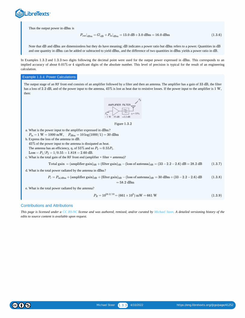
The output stage of an RF front end consists of an amplifier followed by a filter and then an antenna. The amplifier has a gain of , the filterhas a loss of , and of the power input to the antenna, is lost as heat due to resistive losses. If the power input to the amplifier is ,then:
Figure
a. What is the power input to the amplifier expressed in ?
b. Express the loss of the antenna in . of the power input to the antenna is dissipated as heat.
The antenna has an efficiency, , of and so . .
c. What is the total gain of the RF front end (amplifier + filter + antenna)?
d. What is the total power radiated by the antenna in ?
e. What is the total power radiated by the antenna?
Contributions and Attributions
This page is licensed under a CC BY-NC license and was authored, remixed, and/or curated by Michael Steer. A detailed versioning history of theedits to source content is available upon request.
dBm
= G + = 13.0 dB+3.0 dBm = 16.0 dBmPout|dBm |dB Pin|dBm (1.3.6)
dB dBm dB dBm dBdBm dBm dBm dB
1.3.2 1.3.3 dBm0.01% 4
Example : Power Calculations1.3.4
33 dB2.2 dB 45% 1 W
1.3.2
dBm= 1 W = 1000 mW, = 10 log(1000/1) = 30 dBmPin PdBm
dB45%
η 55% = 0.55P2 P1
Loss = / = 1/0.55 = 1.818 = 2.60 dBP1 P2
Total gain = (amplifier gain +(filter gain −(loss of antenna = (33 −2.2 −2.6) dB = 28.2 dB)dB )dB )dB (1.3.7)
dBm
= +(amplifier gain +(filter gain −(loss of antenna = 30 dBm +(33 −2.2 −2.6) dBPr Pin|dBm )dB )dB )dB
= 58.2 dBm
(1.3.8)
= = (661 × ) mW = 661 WPR 1058.2/10 103 (1.3.9)

Michael Steer 1.4.1 4/10/2022 https://eng.libretexts.org/@go/page/41253
1.4: SI UnitsThe main SI units used in microwave engineering are given in Table .
Symbols for units are written in upright roman font and are lowercase unless the symbol is derived from the name of a person.An exception is the use of for liter to avoid possible confusion with .
SI unit Name Usage In terms of fundamental units
ampere current (abbreviated as amp) Fundamental unit
candela luminous intensity Fundamental unit
coulomb charge
farad capacitance
gram weight
henry inductance
joule unit of energy
kelvin thermodynamic temperature Fundamental unit
kilogram SI fundamental unit Fundamental unit
meter length Fundamental unit
mole amount of substance Fundamental unit
newton unit of force
ohm resistance
pascal pressure
second time Fundamental unit
siemen admittance
volt voltage
watt power
Table : Main SI units used in RF and microwave engineering.
A space separates a value from the symbol for the unit (e.g., ). There is an exception for degrees, with the symbol , e.g. .
When SI units are multiplied a center dot is used. For example, newton meters is written . When a unit is derived from theratio of symbols then either a solidus ( ) or a negative exponent is used; the symbol for velocity (meters per second) is either or . The use of multiple solidi for a combination symbol is confusing and must be avoided. So the symbol for acceleration is
or and not .
Consider calculation of the thermal resistance of a rod of cross-sectional area and length :
If and , the thermal resistance is
1.4.1
L l
A
cd
C A ⋅ s
F ⋅ ⋅ ⋅kg−1 m−2 A−2 s4
g = kg/1000
H kg ⋅ ⋅ ⋅m2 A−2 s−2
J kg ⋅ ⋅m2 s−2
K
kg
m
mol
N kg ⋅ m ⋅ s−2
Ω kg ⋅ ⋅ ⋅m2 A−2 s−3
Pa kg ⋅ m−1s−2
s
S ⋅ ⋅ ⋅kg−1 m−2 A2 s3
V kg ⋅ ⋅ ⋅m2 A−1 s−3
W J ⋅ s−1
1.4.1
5.6 kg ∘
45∘
N ⋅ m
/ m/s
m ⋅ s−1
m ⋅ s−2 m/s2 m/s/s
A ℓ
=RTHℓ
kA(1.4.1)
A = 0.3 cm2 ℓ = 2 mm
RTH =(2 mm)
(237kW ⋅ ⋅ ) ⋅ (0.3 )m−1 K−1 cm2
=(2 ⋅ m)10−3
237 ⋅ ( ⋅ W ⋅ ⋅ ) ⋅ 0.3 ⋅ ( ⋅ m103 m−1 K−1 10−2 )2
= ⋅2 ⋅ 10−3
237 ⋅ ⋅ 0.3 ⋅103 10−4
m
W ⋅ ⋅ ⋅m−1 K−1 m2
= 2.813 × K⋅ = 281.3 μK/W10−4 W−1 (1.4.2)
Michael Steer 1.4.2 4/10/2022 https://eng.libretexts.org/@go/page/41253
This would be an error-prone calculation if the thermal conductivity was taken as .
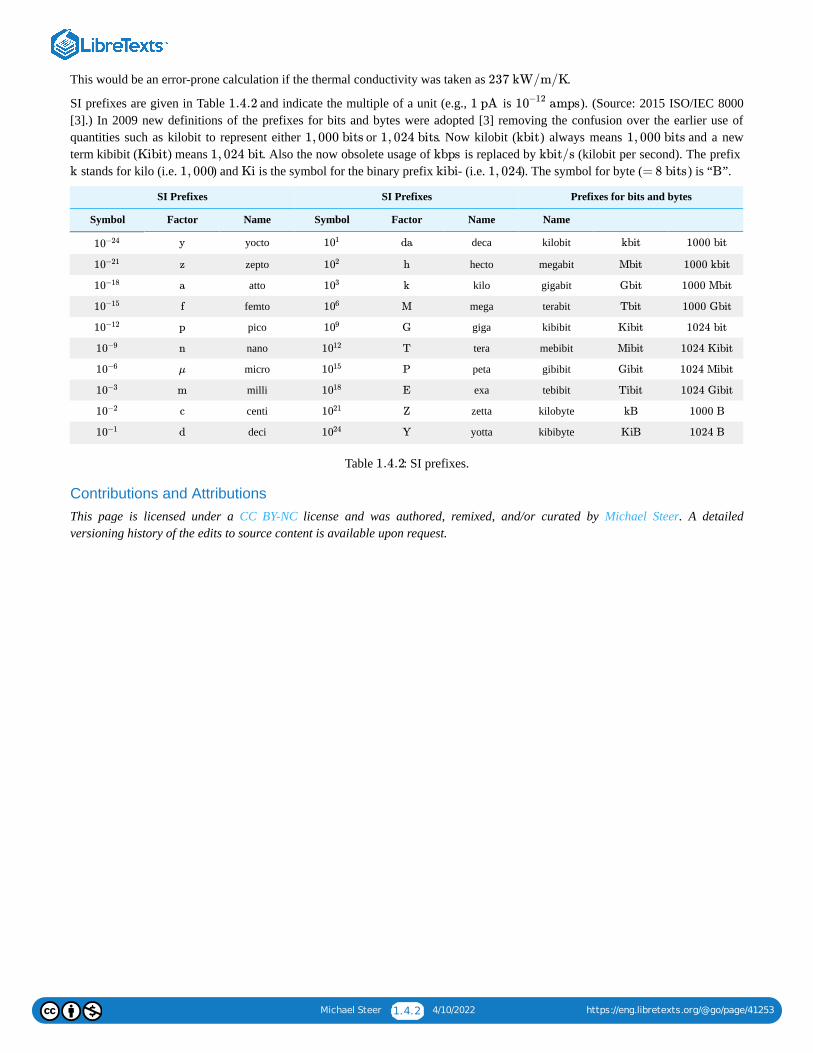
SI prefixes are given in Table and indicate the multiple of a unit (e.g., is ). (Source: 2015 ISO/IEC 8000[3].) In 2009 new definitions of the prefixes for bits and bytes were adopted [3] removing the confusion over the earlier use ofquantities such as kilobit to represent either or . Now kilobit ( ) always means and a newterm kibibit ( ) means . Also the now obsolete usage of is replaced by (kilobit per second). The prefix
stands for kilo (i.e. ) and is the symbol for the binary prefix - (i.e. ). The symbol for byte ( ) is “ ”.
SI Prefixes SI Prefixes Prefixes for bits and bytes
Symbol Factor Name Symbol Factor Name Name
yocto deca kilobit
zepto hecto megabit
atto kilo gigabit
femto mega terabit
pico giga kibibit
nano tera mebibit
micro peta gibibit
milli exa tebibit
centi zetta kilobyte
deci yotta kibibyte
Table : SI prefixes.
Contributions and AttributionsThis page is licensed under a CC BY-NC license and was authored, remixed, and/or curated by Michael Steer. A detailedversioning history of the edits to source content is available upon request.
237 kW/m/K
1.4.2 1 pA amps10−12
1, 000 bits 1, 024 bits kbit 1, 000 bits
Kibit 1, 024 bit kbps kbit/s
k 1, 000 Ki kibi 1, 024 = 8 bits B
10−24 y 101 da kbit 1000 bit
10−21 z 102 h Mbit 1000 kbit
10−18 a 103 k Gbit 1000 Mbit
10−15 f 106 M Tbit 1000 Gbit
10−12 p 109 G Kibit 1024 bit
10−9 n 1012 T Mibit 1024 Kibit
10−6 μ 1015 P Gibit 1024 Mibit
10−3 m 1018 E Tibit 1024 Gibit
10−2 c 1021 Z kB 1000 B
10−1 d 1024 Y KiB 1024 B
1.4.2

Michael Steer 1.5.1 4/10/2022 https://eng.libretexts.org/@go/page/41254
1.5: SummaryThe RF spectrum is used to support a tremendous range of applications, including voice and data communications, satellite-basednavigation, radar, weather radar, mapping, environmental monitoring, air traffic control, police radar, perimeter surveillance,automobile collision avoidance, and many military applications.
In RF and microwave engineering there are always considerable approximations made in design, partly because of necessarysimplifications that must be made in modeling, but also because many of the material properties required in a detailed design canonly be approximately known. Most RF and microwave design deals with frequency-selective circuits often relying on line lengthsthat have a length that is a particular fraction of a wavelength. Many designs can require frequency tolerances of as little as ,and filters can require even tighter tolerances. It is therefore impossible to design exactly. Measurements are required to validateand iterate designs. Conceptual understanding is essential; the designer must be able to relate measurements, which themselveshave errors, with computer simulations. The ability to design circuits with good tolerance to manufacturing variations and perhapscircuits that can be tuned by automatic equipment are skills developed by experienced designers.
Contributions and AttributionsThis page is licensed under a CC BY-NC license and was authored, remixed, and/or curated by Michael Steer. A detailedversioning history of the edits to source content is available upon request.
0.1%

Michael Steer 1.6.1 4/10/2022 https://eng.libretexts.org/@go/page/41255
1.6: References[1] “Atmospheric microwave transmittance at mauna kea, Wikipedia creative commons.”
[2] “IEEE Virtual Museum,” at http://www.ieee-virtual-museum.org Search term: ‘Faraday’.
[3] “ISO/IEC 8000,” intenational Standard Organization (ISO), International Electrotechnical Commission standard includingstandards on on letter symbols to be used in electrical technology. http://www.iso.org.
Contributions and Attributions
This page is licensed under a CC BY-NC license and was authored, remixed, and/or curated by Michael Steer. A detailedversioning history of the edits to source content is available upon request.

Michael Steer 1.7.1 4/10/2022 https://eng.libretexts.org/@go/page/41256
1.7: Exercises1. What is the wavelength in free space of a signal at ?2. Consider a monopole antenna that is a quarter of a wavelength long. How long is the antenna if it operates at ?3. Consider a monopole antenna that is a quarter of a wavelength long. How long is the antenna if it operates at ?4. Consider a monopole antenna that is a quarter of a wavelength long. How long is the antenna if it operates at ?5. A dipole antenna is half of a wavelength long. How long is the antenna at ?6. A dipole antenna is half of a wavelength long. How long is the antenna at ?7. A transmitter transmits an FM signal with a bandwidth of and the signal is received by a receiver at a distance from
the transmitter. When the signal power received by the receiver is . When the receiver moves further awayfrom the transmitter the power received drops off as . What is in kilometers when the received power is .[Parallels Example 1.3.1]
8. A transmitter transmits an AM signal with a bandwidth of and the signal is received by a receiver at a distance fromthe transmitter. When the signal power received is . When the receiver moves further away from thetransmitter the power received drops off as . What is in kilometers when the received power is equal to the received noisepower of ? [Parallels Example 1.3.1]
9. The logarithm to base of a number is (i.e., ). What is ?10. The natural logarithm of a number is (i.e., ). What is ?11. The logarithm to base of a number is (i.e., ). What is ?12. What is ?13. What is ?14. Without using a calculator evaluate log .15. A resistor has a sinusoidal voltage across it with a peak voltage of . The RF voltage is , where is the
radian frequency of the signal and is time.a. What is the power dissipated in the resistor in watts?b. What is the power dissipated in the resistor in ?
16. The power of an RF signal is . What is the power of the signal in ?17. The power of an RF signal is . What is the power of the signal in watts?18. An amplifier has a power gain of .
a. What is the power gain in decibels?b. If the input power is , what is the output power in ? [Parallels Example 1.3.2]
19. An amplifier has a power gain of . What is the power gain in decibels? [Parallels Example 1.3.2]20. A filter has a loss factor of . [Parallels Example 1.3.2]
a. What is the loss in decibels?b. What is the gain in decibels?
21. An amplifier has a power gain of . What is the power gain in ? [Parallels Example 1.3.2]22. An amplifier has a gain of . The input to the amplifier is a signal, what is the output power in ?23. An RF transmitter consists of an amplifier with a gain of , a filter with a loss of and then that is then followed by a
lossless transmit antenna. If the power input to the amplifier is , what is the total power radiated by the antenna in ?[Parallels Example 1.3.4]
24. The final stage of an RF transmitter consists of an amplifier with a gain of and a filter with a loss of that is thenfollowed by a transmit antenna that looses half of the RF power as heat. [Parallels Example 1.3.4]a. If the power input to the amplifier is , what is the total power radiated by the antenna in ?b. What is the radiated power in watts?
25. A -RF signal is applied to an amplifier that increases the power of the RF signal by a factor of . The amplifier isfollowed by a filter that losses half of the power as heat.a. What is the output power of the filter in watts?b. What is the output power of the filter in ?
26. The power of an RF signal at the output of a receive amplifier is and the noise power at the output is . What is theoutput signal-tonoise ratio in ?
4.5 GHz3 kHz500 MHz2 GHz
2 GHz1 THz
100 kHz r
r = 1 km 100 nW1/r2 r 100 pW
20 kHz r
r = 10 km 10 nW1/r2 r
1 pW2 x 0.38 (x) = 0.38log2 x
x 2.5 ln(x) = 2.5 x
2 x 3 (x) = 3log2 ( )log2 x−−
√2
(10)log3
(2)log4.5
{[ (3x) − (x)]}log3 log3
50 Ω 0.1 V 0.1 cos(ωt) ω
t
dBm
10 mW dBm40 dBm
2100
−5 dBm dBm
6100
1000 dB14 dB 1 mW dBm
20 dB 3 dB1 mW dBm
30 dB 2 dB
10 mW dBm
5 mW 200
dBW
1 μW 1 nWdB

Michael Steer 1.7.2 4/10/2022 https://eng.libretexts.org/@go/page/41256
27. The power of a received signal is and the received noise power is . In addition the level of the interfering signalis . What is the signal-to-noise ratio in ? Treat interference as if it is an additional noise signal.age gain of has aninput impedance of , a zero output impedance, and drives a load. What is the power gain of the amplifier?
28. A transmitter transmits an FM signal with a bandwidth of and the signal power received by a receiver is . Inthe same bandwidth as that of the signal the receiver receives of noise power. In decibels, what is the ratio of the signalpower to the noise power, i.e. the signal-to-noise ratio (SNR) received by the receiver?
29. An amplifier with a voltage gain of has an input resistance of and an output resistance of . What is the powergain of the amplifier in decibels? [Parallels Example 1.3.1]
30. An amplifier with a voltage gain of has an input resistance of and an output resistance of . What is the power gainof the amplifier in decibels? Explain why there is a power gain of more than even though the voltage gain is . [ParallelsExample 1.3.1]
31. An amplifier has a power gain of .a. What is the power gain in decibels?b. If the input power is , what is the output power in ? [Parallels Example 1.3.2]
32. An amplifier has a power gain of .
a. What is the power gain in decibels?b. If the input power is , what is the output power in ? [Parallels Example 1.3.2]
33. An amplifier has a voltage gain of and a current gain of .a. What is the power gain as an absolute number?b. What is the power gain in decibels?c. If the input power is , what is the output power in ?d. What is the output power in ?
34. An amplifier with input impedance and load impedance has a voltage gain of . What is the (power) gain indecibels?
35. An attenuator reduces the power level of a signal by . What is the (power) gain of the attenuator in decibels?
1.7.1 Exercises by Section
†challenging
1.7.2 Answers to Selected Exercises4.
12.
16. 17.
19.
22. 23. 24. (b)
Contributions and AttributionsThis page is licensed under a CC BY-NC license and was authored, remixed, and/or curated by Michael Steer. A detailedversioning history of the edits to source content is available upon request.
1 pW 200 fW100 fW dB 1
100 Ω 5 Ω100 kHz 100 nW
100 pW
20 100 Ω 50 Ω
1 100 Ω 5 Ω1 1
1900
−8 dBm dBm
20
−23 dBm dBm
10 100
−30 dBm dBmmW
50 Ω 50 Ω 100
75%
§1.21, 2, 3, 4, 5, 6, 7, 8
§1.39, 10, 11, 12, 13, 14, 15, 16, 1718, 19, 20, 21, 22, 23†, 24†, 25 † 26, 27, 28, 29, 30, 31, 32, 33, 34, 35
3.25 cm
2.096
10 dBm10 W
7.782 dB
1.30150.12 mW
3.162 W

1 4/10/2022
CHAPTER OVERVIEW2: ANTENNAS AND THE RF LINK
2.1: INTRODUCTION2.2: RF ANTENNAS2.3: RESONANT ANTENNAS2.4: TRAVELING-WAVE ANTENNAS2.5: ANTENNA PARAMETERS2.6: THE RF LINK2.7: EXERCISES2.8: ANTENNA ARRAY2.9: SUMMARY2.10: REFERENCES
Michael Steer 2.1.1 4/10/2022 https://eng.libretexts.org/@go/page/41257
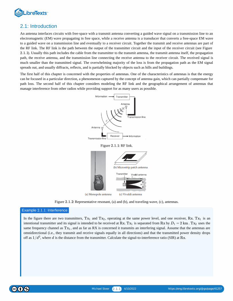
2.1: IntroductionAn antenna interfaces circuits with free-space with a transmit antenna converting a guided wave signal on a transmission line to anelectromagnetic (EM) wave propagating in free space, while a receive antenna is a transducer that converts a free-space EM waveto a guided wave on a transmission line and eventually to a receiver circuit. Together the transmit and receive antennas are part ofthe RF link. The RF link is the path between the output of the transmitter circuit and the input of the receiver circuit (see Figure
). Usually this path includes the cable from the transmitter to the transmit antenna, the transmit antenna itself, the propagationpath, the receive antenna, and the transmission line connecting the receive antenna to the receiver circuit. The received signal ismuch smaller than the transmitted signal. The overwhelming majority of the loss is from the propagation path as the EM signalspreads out, and usually diffracts, reflects, and is partially blocked by objects such as hills and buildings.
The first half of this chapter is concerned with the properties of antennas. One of the characteristics of antennas is that the energycan be focused in a particular direction, a phenomenon captured by the concept of antenna gain, which can partially compensate forpath loss. The second half of this chapter considers modeling the RF link and the geographical arrangement of antennas thatmanage interference from other radios while providing support for as many users as possible.
Figure : RF link.
Figure : Representative resonant, (a) and (b), and traveling-wave, (c), antennas.
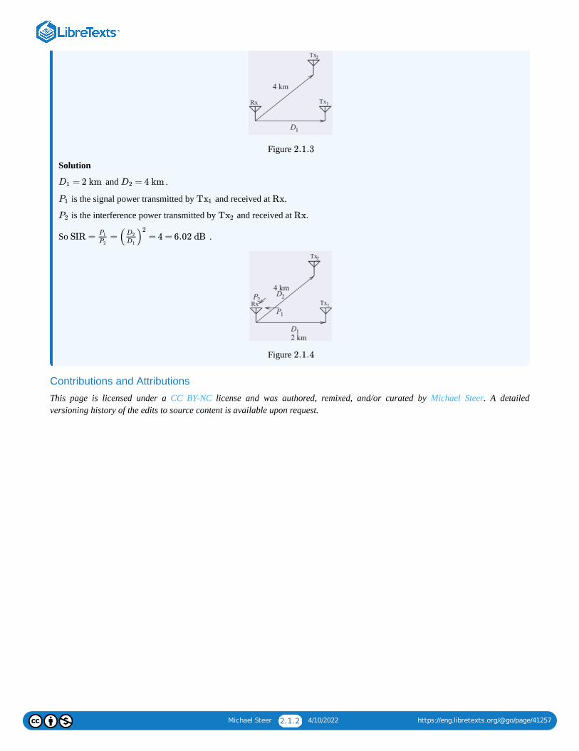
In the figure there are two transmitters, and , operating at the same power level, and one receiver, . is anintentional transmitter and its signal is intended to be received at . is separated from by . uses thesame frequency channel as , and as far as RX is concerned it transmits an interfering signal. Assume that the antennas areomnidirectional (i.e., they transmit and receive signals equally in all directions) and that the transmitted power density dropsoff as , where is the distance from the transmitter. Calculate the signal-to-interference ratio (SIR) at .
2.1.1
2.1.1
2.1.2
Example : Interference2.1.1
Tx1 Tx2 Rx Tx1
Rx Tx1 Rx = 2 kmD1 Tx2
Tx1
1/d2d Rx
Michael Steer 2.1.2 4/10/2022 https://eng.libretexts.org/@go/page/41257
Figure
Solution
and .
is the signal power transmitted by and received at .
is the interference power transmitted by and received at .
So .
Figure
Contributions and Attributions
This page is licensed under a CC BY-NC license and was authored, remixed, and/or curated by Michael Steer. A detailedversioning history of the edits to source content is available upon request.
2.1.3
= 2 kmD1 = 4 kmD2
P1 Tx1 Rx
P2 Tx2 Rx
SIR = = = 4 = 6.02 dBP1
P2( )D2
D1
2
2.1.4
Michael Steer 2.2.1 4/10/2022 https://eng.libretexts.org/@go/page/41258
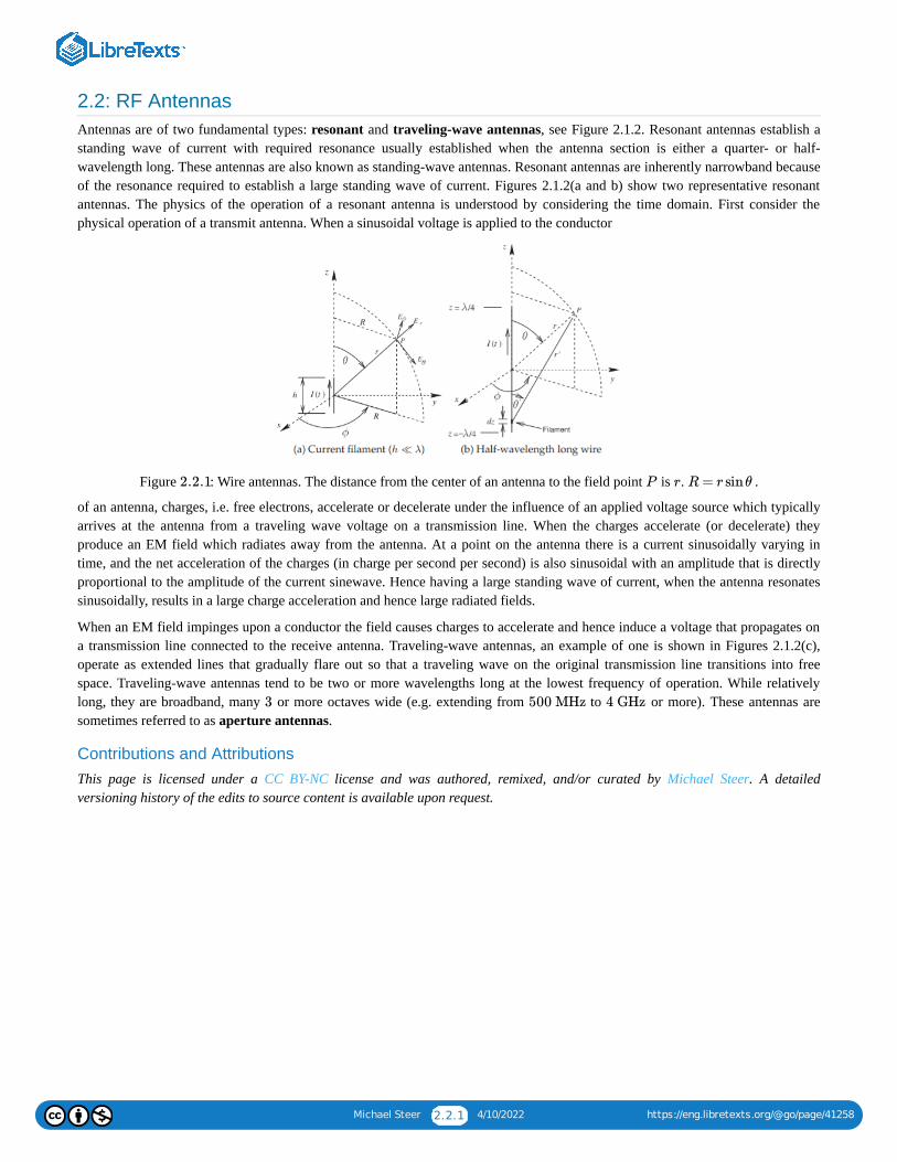
2.2: RF AntennasAntennas are of two fundamental types: resonant and traveling-wave antennas, see Figure 2.1.2. Resonant antennas establish astanding wave of current with required resonance usually established when the antenna section is either a quarter- or half-wavelength long. These antennas are also known as standing-wave antennas. Resonant antennas are inherently narrowband becauseof the resonance required to establish a large standing wave of current. Figures 2.1.2(a and b) show two representative resonantantennas. The physics of the operation of a resonant antenna is understood by considering the time domain. First consider thephysical operation of a transmit antenna. When a sinusoidal voltage is applied to the conductor
Figure : Wire antennas. The distance from the center of an antenna to the field point is . .
of an antenna, charges, i.e. free electrons, accelerate or decelerate under the influence of an applied voltage source which typicallyarrives at the antenna from a traveling wave voltage on a transmission line. When the charges accelerate (or decelerate) theyproduce an EM field which radiates away from the antenna. At a point on the antenna there is a current sinusoidally varying intime, and the net acceleration of the charges (in charge per second per second) is also sinusoidal with an amplitude that is directlyproportional to the amplitude of the current sinewave. Hence having a large standing wave of current, when the antenna resonatessinusoidally, results in a large charge acceleration and hence large radiated fields.
When an EM field impinges upon a conductor the field causes charges to accelerate and hence induce a voltage that propagates ona transmission line connected to the receive antenna. Traveling-wave antennas, an example of one is shown in Figures 2.1.2(c),operate as extended lines that gradually flare out so that a traveling wave on the original transmission line transitions into freespace. Traveling-wave antennas tend to be two or more wavelengths long at the lowest frequency of operation. While relativelylong, they are broadband, many or more octaves wide (e.g. extending from to or more). These antennas aresometimes referred to as aperture antennas.
Contributions and AttributionsThis page is licensed under a CC BY-NC license and was authored, remixed, and/or curated by Michael Steer. A detailedversioning history of the edits to source content is available upon request.
2.2.1 P r R = r sinθ
3 500 MHz 4 GHz
Michael Steer 2.3.1 4/10/2022 https://eng.libretexts.org/@go/page/41259
2.3: Resonant AntennasWith a resonant antenna the current on the antenna is directly related to the amplitude of the radiated EM field. Resonance ensuresthat the standing wave current on the antenna is high.
2.3.1 Radiation from a Current FilamentThe fields radiated by a resonant antenna are most conveniently calculated by considering the distribution of current on theantenna. The analysis begins by considering a short filament of current, see Figure 2.2.1(a). Considering the sinusoidal steady stateat radian frequency , the current on the filament with phase is , so that is the phasor ofthe current on the filament. The length of the filament is , but it has no other dimensions, that is, it is considered to be infinitelythin.
Resonant antennas are conveniently modeled as being made up of an array of current filaments with spacings and lengths being atiny fraction of a wavelength. Wire antennas are even simpler and can be considered to be a line of current filaments. Ramo,Whinnery, and Van Duzer [1] calculated the spherical EM fields at the point P with the spherical coordinates generated bythe -directed current filament centered at the origin in Figure 2.2.1. The total EM field components in phasor form are
where is the free-space characteristic impedance. The variable is called the wavenumber and . The terms describe the variation of the phase of the field as the field propagates away from the filament. Equations -
are the complete fields with the and dependence describing the near-field components. In the far field, i.e. , the components with and dependence become negligible and the field components left are the propagating
components and :
Now consider the fields in the plane normal to the filament, that is, with so that . The fields are now
and the wave impedance is
Note that the strength of the fields is directly proportional to the magnitude of the current. This proves to be very useful inunderstanding spurious radiation from microwave structures. Now , so
as expected. Thus an antenna can be viewed as having the inherent function of an impedance transformer converting from thelower characteristic impedance of a transmission line (often ) to the characteristic impedance of free space.
Further comments can be made about the propagating fields (Equation ). The EM field propagates in all directions exceptnot directly in line with the filament. For fixed , the amplitude of the propagating field increases sinusoidally with respect to until it is maximum in the direction normal to the filament.
The power radiated is obtained using the Poynting vector, which is the cross-product of the propagating electric and magneticfields. From this the time-average propagating power density is (with the SI units of )
ω χ I(t) = | | cos(ωt+χ)I0 = | |I0 I0 e−ȷχ
h
(ϕ, θ, r)z
= ( + ) sinθ, =Hϕ
hI0
4πe−ȷkr ȷk
r
1
r2Hϕ¯ ¯¯¯¯ Hϕϕ (2.3.1)
= ( + ) cosθ, =Er
hI0
rπe−ȷkr 2η
r2
2
ȷωε0r3Er¯ ¯¯¯ ErR (2.3.2)
= ( + + ) sinθ, =Eθ
hI0
4πe−ȷkr ȷωμ0
r
1
ȷωεr3
η
r2Eθ¯ ¯¯¯ Eθ θ (2.3.3)
η k k = 2π/λ = ω μ0ε0− −−−
√e−ȷkr (2.3.1)(2.3.3) 1/r2 1/r3
r ≫ λ 1/r2 1/r3
Hϕ Eθ
= ( ) sinθ, = 0, and = ( ) sinθHϕ
hI0
4πe−ȷkr ȷk
rEr Eθ
hI0
4πe−ȷkr ȷωμ0
r(2.3.4)
θ = π/2 radians sinθ = 1
= ( ) and = ( )Hϕ
hI0
4πe−ȷkr ȷk
rEθ
hI0
4πe−ȷkr ȷωμ0
r(2.3.5)
η = = =Eθ
Hϕ
hI0
4πe−ȷkr ȷωμ0
r( )
hI0
4πe−ȷkr ȷk
r
−1 ωμ0
k(2.3.6)
k = ω μ0ϵ0− −−−
√
η = = = 377 Ωωμ0
ω μ0ϵ0− −−−
√
μ0
ϵ0
−−−√ (2.3.7)
50 Ω 377 Ω
(2.3.4)r θ
W/m2
Michael Steer 2.3.2 4/10/2022 https://eng.libretexts.org/@go/page/41259
and the power density is proportional to . In Equation indicates that the real part is taken.
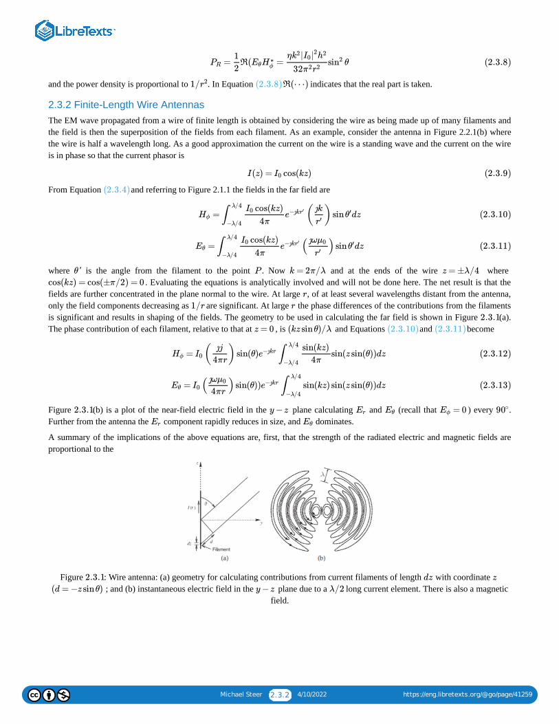
2.3.2 Finite-Length Wire AntennasThe EM wave propagated from a wire of finite length is obtained by considering the wire as being made up of many filaments andthe field is then the superposition of the fields from each filament. As an example, consider the antenna in Figure 2.2.1(b) wherethe wire is half a wavelength long. As a good approximation the current on the wire is a standing wave and the current on the wireis in phase so that the current phasor is
From Equation and referring to Figure 2.1.1 the fields in the far field are
where is the angle from the filament to the point . Now and at the ends of the wire where . Evaluating the equations is analytically involved and will not be done here. The net result is that the
fields are further concentrated in the plane normal to the wire. At large , of at least several wavelengths distant from the antenna,only the field components decreasing as are significant. At large the phase differences of the contributions from the filamentsis significant and results in shaping of the fields. The geometry to be used in calculating the far field is shown in Figure (a).The phase contribution of each filament, relative to that at , is and Equations and become
Figure (b) is a plot of the near-field electric field in the plane calculating and (recall that ) every .Further from the antenna the component rapidly reduces in size, and dominates.
A summary of the implications of the above equations are, first, that the strength of the radiated electric and magnetic fields areproportional to the
Figure : Wire antenna: (a) geometry for calculating contributions from current filaments of length with coordinate ; and (b) instantaneous electric field in the plane due to a long current element. There is also a magnetic
field.
= R( = θPR
1
2EθH ∗
ϕ
η |k2 I0|2h2
32π2r2sin2 (2.3.8)
1/r2 (2.3.8)R(⋯)
I(z) = cos(kz)I0 (2.3.9)
(2.3.4)
= ( ) sin dzHϕ ∫λ/4
−λ/4
cos(kz)I0
4πe−ȷkr′ ȷk
r′θ′ (2.3.10)
= ( ) sin dzEθ ∫λ/4
−λ/4
cos(kz)I0
4πe−ȷkr′ ȷωμ0
r′θ′ (2.3.11)
θ' P k = 2π/λ z = ±λ/4cos(kz) = cos(±π/2) = 0
r
1/r r
2.3.1z = 0 (kz sinθ)/λ (2.3.10) (2.3.11)
= ( ) sin(θ) sin(z sin(θ))dzHϕ I0ȷj
4πre−ȷkr ∫
λ/4
−λ/4
sin(kz)
4π(2.3.12)
= ( ) sin(θ)) sin(kz) sin(z sin(θ))dzEθ I0ȷωμ0
4πre−ȷkr ∫
λ/4
−λ/4(2.3.13)
2.3.1 y−z Er Eθ = 0Eϕ 90∘
Er Eθ
2.3.1 dz z
(d = −z sinθ) y−z λ/2
Michael Steer 2.3.3 4/10/2022 https://eng.libretexts.org/@go/page/41259
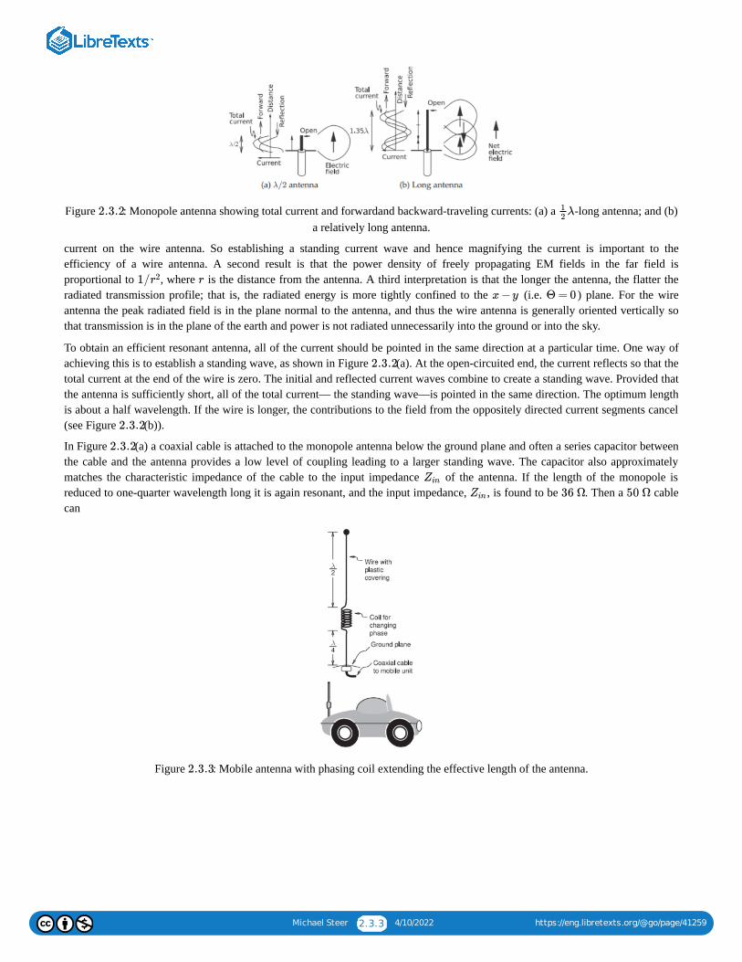
Figure : Monopole antenna showing total current and forwardand backward-traveling currents: (a) a -long antenna; and (b)a relatively long antenna.
current on the wire antenna. So establishing a standing current wave and hence magnifying the current is important to theefficiency of a wire antenna. A second result is that the power density of freely propagating EM fields in the far field isproportional to , where is the distance from the antenna. A third interpretation is that the longer the antenna, the flatter theradiated transmission profile; that is, the radiated energy is more tightly confined to the (i.e. ) plane. For the wireantenna the peak radiated field is in the plane normal to the antenna, and thus the wire antenna is generally oriented vertically sothat transmission is in the plane of the earth and power is not radiated unnecessarily into the ground or into the sky.
To obtain an efficient resonant antenna, all of the current should be pointed in the same direction at a particular time. One way ofachieving this is to establish a standing wave, as shown in Figure (a). At the open-circuited end, the current reflects so that thetotal current at the end of the wire is zero. The initial and reflected current waves combine to create a standing wave. Provided thatthe antenna is sufficiently short, all of the total current— the standing wave—is pointed in the same direction. The optimum lengthis about a half wavelength. If the wire is longer, the contributions to the field from the oppositely directed current segments cancel(see Figure (b)).
In Figure (a) a coaxial cable is attached to the monopole antenna below the ground plane and often a series capacitor betweenthe cable and the antenna provides a low level of coupling leading to a larger standing wave. The capacitor also approximatelymatches the characteristic impedance of the cable to the input impedance of the antenna. If the length of the monopole isreduced to one-quarter wavelength long it is again resonant, and the input impedance, , is found to be . Then a cablecan
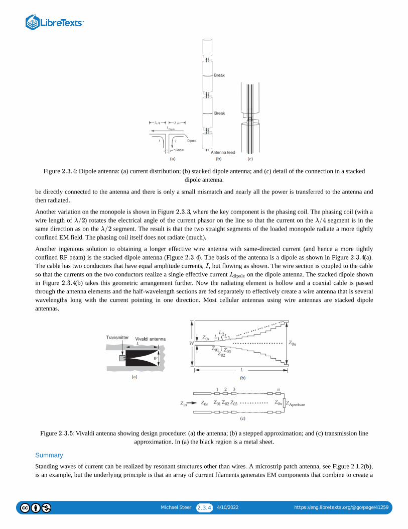
Figure : Mobile antenna with phasing coil extending the effective length of the antenna.
2.3.2 λ12
1/r2 r
x−y Θ = 0
2.3.2
2.3.2
2.3.2
Zin
Zin 36 Ω 50 Ω
2.3.3
Michael Steer 2.3.4 4/10/2022 https://eng.libretexts.org/@go/page/41259
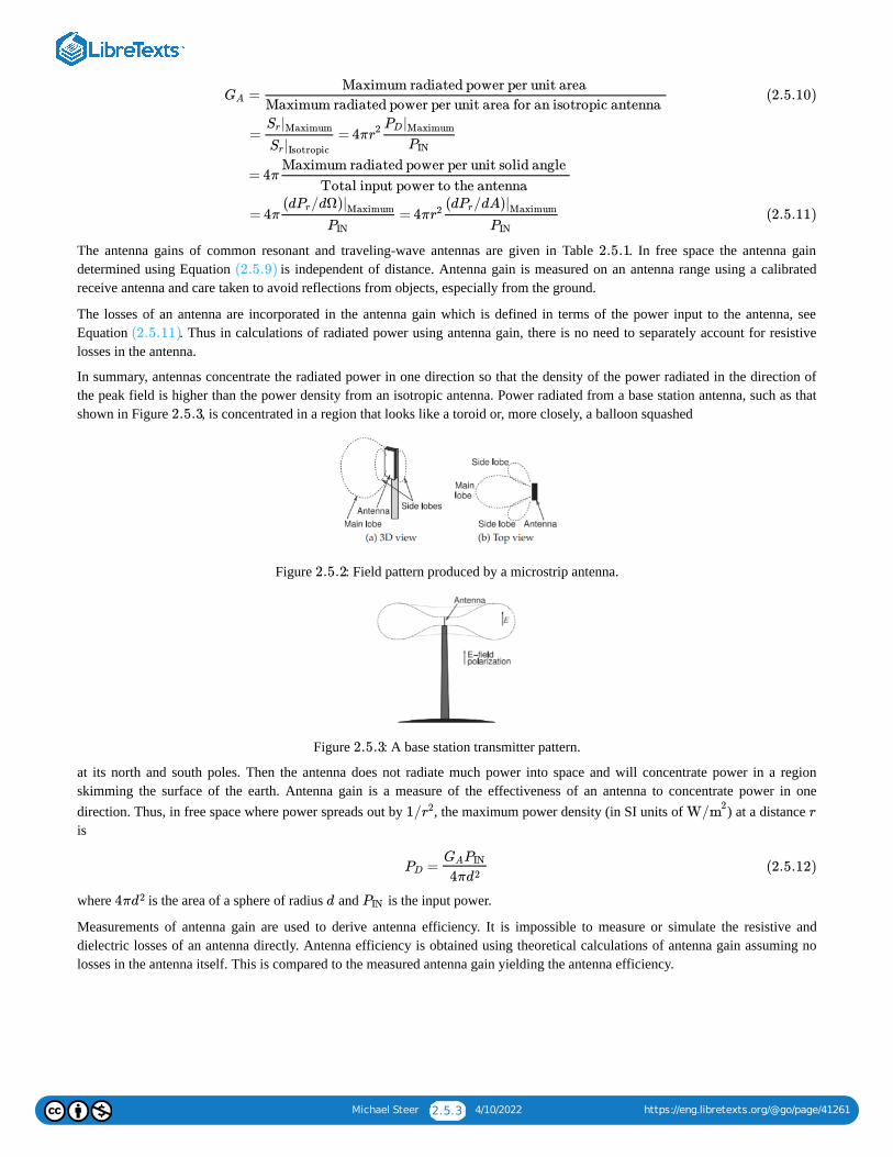
Figure : Dipole antenna: (a) current distribution; (b) stacked dipole antenna; and (c) detail of the connection in a stackeddipole antenna.
be directly connected to the antenna and there is only a small mismatch and nearly all the power is transferred to the antenna andthen radiated.
Another variation on the monopole is shown in Figure , where the key component is the phasing coil. The phasing coil (with awire length of ) rotates the electrical angle of the current phasor on the line so that the current on the segment is in thesame direction as on the segment. The result is that the two straight segments of the loaded monopole radiate a more tightlyconfined EM field. The phasing coil itself does not radiate (much).
Another ingenious solution to obtaining a longer effective wire antenna with same-directed current (and hence a more tightlyconfined RF beam) is the stacked dipole antenna (Figure ). The basis of the antenna is a dipole as shown in Figure (a).The cable has two conductors that have equal amplitude currents, , but flowing as shown. The wire section is coupled to the cableso that the currents on the two conductors realize a single effective current on the dipole antenna. The stacked dipole shownin Figure (b) takes this geometric arrangement further. Now the radiating element is hollow and a coaxial cable is passedthrough the antenna elements and the half-wavelength sections are fed separately to effectively create a wire antenna that is severalwavelengths long with the current pointing in one direction. Most cellular antennas using wire antennas are stacked dipoleantennas.
Figure : Vivaldi antenna showing design procedure: (a) the antenna; (b) a stepped approximation; and (c) transmission lineapproximation. In (a) the black region is a metal sheet.
Summary
Standing waves of current can be realized by resonant structures other than wires. A microstrip patch antenna, see Figure 2.1.2(b),is an example, but the underlying principle is that an array of current filaments generates EM components that combine to create a
2.3.4
2.3.3λ/2 λ/4
λ/2
2.3.4 2.3.4I
Idipole
2.3.4
2.3.5

Michael Steer 2.3.5 4/10/2022 https://eng.libretexts.org/@go/page/41259
propagating field. Resonant antennas are inherently narrowband because of the reliance on the establishment of a standing wave. Arelative bandwidth of is typical.
Contributions and AttributionsThis page is licensed under a CC BY-NC license and was authored, remixed, and/or curated by Michael Steer. A detailedversioning history of the edits to source content is available upon request.
5%– 10%

Michael Steer 2.4.1 4/10/2022 https://eng.libretexts.org/@go/page/41260
2.4: Traveling-Wave AntennasTraveling-wave antennas have the characteristics of broad bandwidth and large size. These antennas begin as a transmission linestructure that flares out slowly, providing a low reflection transition from a transmission line to free space. The bandwidth can bevery large and is primarily dependent on how gradual the transition is.
One of the more interesting traveling-wave antennas is the Vivaldi antenna of Figure 2.3.5(a). The Vivaldi antenna is an extensionof a slotline in which the fields are confined in the space between two metal sheets in the same plane. The slotline spacing increasesgradually in an exponential manner, much like that of a Vivaldi violin (from which it gets its name), over a distance of awavelength or more. A circuit model is shown in Figures 2.3.5(b and c) where the antenna is modeled as a cascade of manytransmission lines of slowly increasing characteristic impedance, . Since the progression is gradual there are low-levelreflections at the transmission line interfaces. The forward-traveling wave on the antenna continues to propagate with a negligiblereflected field. Eventually the slot opens sufficiently that the effective impedance of the slot is that of free space and the travelingwave continues to propagate in air.
The other traveling-wave antennas work similarly and all are at least a wavelength long, with the central concept being a gradualtaper from the characteristic impedance of the originating transmission line to free space. The final aperture is at least one-halfwavelength across so that the fields can curl on themselves (i.e. loop back on themselves) and are self-supporting as they leave theantenna.
Contributions and Attributions
This page is licensed under a CC BY-NC license and was authored, remixed, and/or curated by Michael Steer. A detailedversioning history of the edits to source content is available upon request.
Z0 Z0

Michael Steer 2.5.1 4/10/2022 https://eng.libretexts.org/@go/page/41261
2.5: Antenna ParametersThis section introduces a number of antenna metrics that are used to characterize antenna performance.
2.5.1 Radiation Density and Radiation IntensityAntennas do not radiate equally in all directions concentrating radiated power in one direction called the main (or major) lobe ofthe antenna. This focusing effect is called directivity. The power in a particular direction is characterized by the radiation densityand the radiation intensity metrics. The radiation density, , is the power per unit area with the SI units of , and will bemaximum in the main lobe. Referring to Figure with an antenna located at the center of the sphere of radius r and radiating atotal power is the incremental radiated power passing through the incremental shaded region of area, :
reduces with distance falling off as in free space. For a practical antenna will vary across the surface of the sphere. Thetotal power radiated is the closed integral over the surface of the sphere:
An alternative measure of power concentration is the radiation intensity which is in terms of the incremental solid angle subtended by so that and (with the SI units of or )
Isotropic Antenna
It is useful to reference the directivity of an antenna with respect to a fictitious isotropic antenna that has no loss and radiatesequally in all directions so that is only a function of . Then integrating over the surface of the sphere
Figure : Free-space spreading loss. The incremental power, , intercepted by the shaded region of incremental area isproportional to . The solid angle subtended by the shaded area is the incremental solid angle . The integral of over the
surface of the sphere, i.e. the area of the sphere is . The total solid angle subtended by the sphere is the integral of over thesphere and is steradians (or ).
yields the total radiated power
Since the isotropic antenna has no loss the power input to the antenna is equal to the power radiated . Thus for anisotropic antenna
Antenna Efficiency
Antenna efficiency, sometimes called the radiation efficiency, describes losses in an antenna principally due to resistive ( )losses. Resonant antennas work by creating a large current that is maximized through the generation of a standing wave at
Sr W/m2
2.5.1
,Pr Sr dPr dA
=Sr
dPr
dA(2.5.1)
Sr 1/r2 Sr
S
= d = dAPr ∮S
Pr ∮S
Sr (2.5.2)
U dΩ
dA dΩ = dA/r2 W/steradian W/sr
U = = =dPr
dΩ
dPr
dAr2 r2Sr (2.5.3)
Sr r
2.5.1 dPr dA
1/r2 dΩ dA
4πr2 dΩ
4π 4π sr
= d = dA = dA = 4π = 4πUPr|Isotropic ∮S
Pr ∮S
Sr Sr ∮S
Sr r2 (2.5.4)
PIN =Pr PIN
= =Sr
Pr
4πr2
PIN
4πr2(2.5.5)
U = =|Isotropic r2Sr
PIN
4πr2(2.5.6)
RI 2

Michael Steer 2.5.2 4/10/2022 https://eng.libretexts.org/@go/page/41261
resonance. There is a lot of current, and even just a little resistance results in substantial resistive loss. The power that is reflectedfrom the input of the antenna is usually small. The total radiated power (in all directions), , is the power input to the antenna lesslosses. The antenna efficiency, is therefore defined as
where is the power input to the antenna and and usually expressed as a percentage. Antenna efficiency is very close toone for many antennas, but can be for microstrip patch antennas.
Antenna loss refers to the same mechanism that gives rise to antenna efficiency. Thus an antenna with an antenna efficiency of has an antenna loss of . Generally losses are resistive due to loss and mismatch loss of the antenna that occurs when
the input impedance is not matched to the impedance of the cable connected to the antenna. Because of confusion with antennagain (they are not the opposite of each other) the use of the term ‘antenna loss’ is discouraged and instead ‘antenna efficiency’preferred.
2.5.2 Directivity and Antenna Gain
The directivity of an antenna, , is the ratio of the radiated power density to that of an isotropic antenna with the same totalradiated power :
where and refer to the actual antenna and the power densities and intensities are measured at the same distance from theantennas. For an actual antenna is dependent on the direction from the antenna, see Figure . The maximum value of willbe in the direction of the main lobe of the antenna and this is called directivity gain.
The focusing property of an antenna is characterized by comparing the radiated power density to that of an isotropic antenna withthe same input power. The antenna gain, , is the maximum value of when the power input to the antenna andthe isotropic antenna are the same:
Antenna Type Figure Gain ( ) Notes
Lossless isotropic antenna
dipole Resonant 2.3.4(a)
diameter parabolic dish Traveling —
Patch Resonant 2.1.2(b)
Vivaldi Traveling 2.1.2(c)
monopole on ground Resonant 2.3.2(a)
monopole on ground Resonant 2.3.2(a) Matching required
Table : Several antenna systems. for resonant antennas indicates that the antenna can be designed to have aninput impedance matching that of a feed cable. Traveling wave antennas are intrinsically matched.
Losses in the antenna are accounted for by the efficiency term .
In Equation is a gain factor and is often expressed in terms of decibels (taking times the of ) but (with ‘i’standing for ‘withrespect-to isotropic’) is used to indicate that it is not a power gain in the same sense as amplifier gain. insteadis the ratio of power densities for two different antennas. For example, an antenna that focuses power in one direction increasingthe peak radiated power density by a factor of relative to that of an isotropic antenna thus has an antenna gain of . Withcare can be often used in calculations of power as as with amplifier gain.
Since it is almost impossible to calculate internal antenna losses, antenna gain is invariably only measured. The input power to anantenna can be measured and the peak radiated power density, , measured in the far field at several wavelengths distant(at ). This is compared to the power density from an ideal isotropic antenna at the same distance with the same input power.Antenna gain is determined from
Pr
etaA
= /ηA Pr PIN (2.5.7)
PIN < 1ηA50%
50% 3 dB RI 2
D
Pr
D = =Sr
Sr|Isotropic
U
U|Isotropic
(2.5.8)
Sr U
D 2.5.2 D
GA D = /PIN Pr ηA
= max(D)GA ηA (2.5.9)
dBi
0
λ/2 2 = 73 ΩRin
3λ 38 = matchRin
9 = matchRin
10 = matchRin
λ/4 2 = 36 ΩRin
5/8λ 3
2.5.1 = matchRin
ηA
(2.5.9)GA 10 log GA dBi
GA
20 13 dBi
GA
PD|Maximum
r ≫ λ
Michael Steer 2.5.3 4/10/2022 https://eng.libretexts.org/@go/page/41261
The antenna gains of common resonant and traveling-wave antennas are given in Table . In free space the antenna gaindetermined using Equation is independent of distance. Antenna gain is measured on an antenna range using a calibratedreceive antenna and care taken to avoid reflections from objects, especially from the ground.
The losses of an antenna are incorporated in the antenna gain which is defined in terms of the power input to the antenna, seeEquation . Thus in calculations of radiated power using antenna gain, there is no need to separately account for resistivelosses in the antenna.
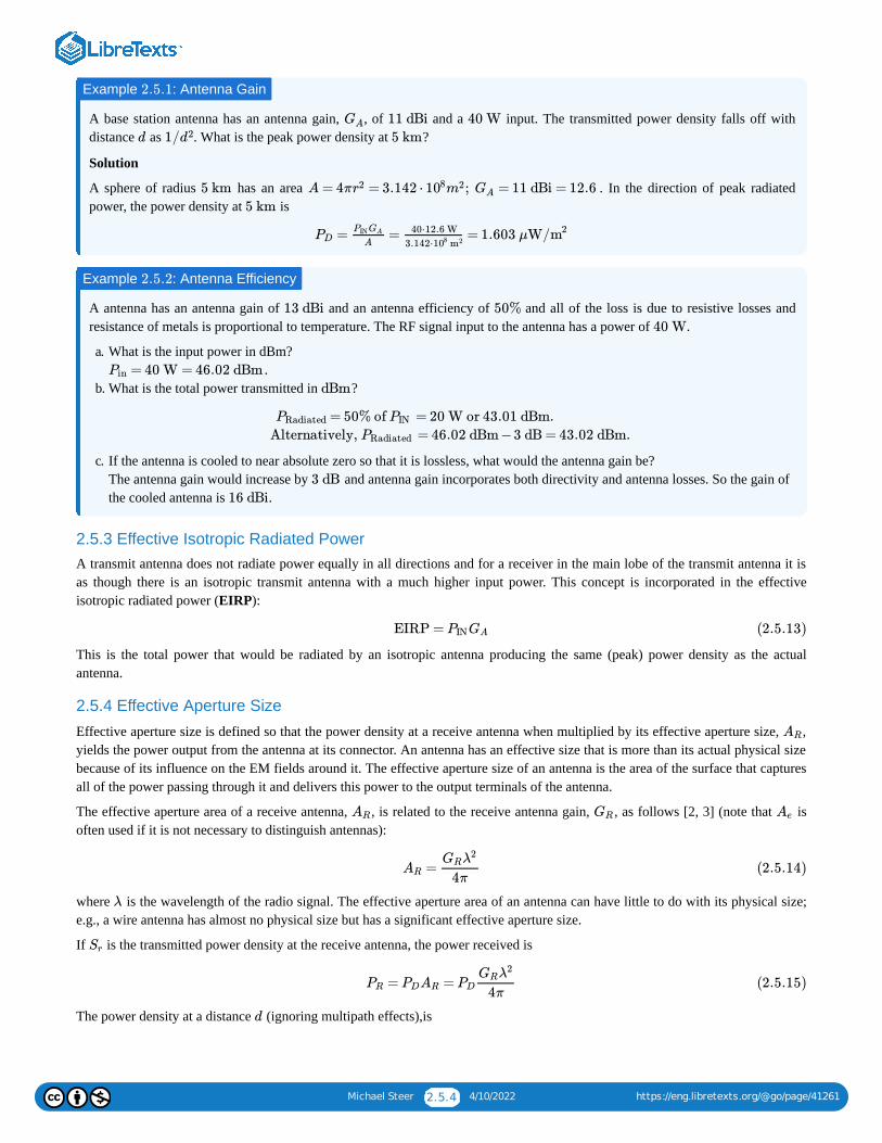
In summary, antennas concentrate the radiated power in one direction so that the density of the power radiated in the direction ofthe peak field is higher than the power density from an isotropic antenna. Power radiated from a base station antenna, such as thatshown in Figure , is concentrated in a region that looks like a toroid or, more closely, a balloon squashed
Figure : Field pattern produced by a microstrip antenna.
Figure : A base station transmitter pattern.
at its north and south poles. Then the antenna does not radiate much power into space and will concentrate power in a regionskimming the surface of the earth. Antenna gain is a measure of the effectiveness of an antenna to concentrate power in onedirection. Thus, in free space where power spreads out by , the maximum power density (in SI units of ) at a distance is
where is the area of a sphere of radius and is the input power.
Measurements of antenna gain are used to derive antenna efficiency. It is impossible to measure or simulate the resistive anddielectric losses of an antenna directly. Antenna efficiency is obtained using theoretical calculations of antenna gain assuming nolosses in the antenna itself. This is compared to the measured antenna gain yielding the antenna efficiency.
GA =Maximum radiated power per unit area
Maximum radiated power per unit area for an isotropic antenna
= = 4πSr|Maximum
Sr|Isotropic
r2 PD|Maximum
PIN
= 4πMaximum radiated power per unit solid angle
Total input power to the antenna
= 4π = 4π(d /dΩ)Pr |Maximum
PIN
r2(d /dA)Pr |Maximum
PIN
(2.5.10)
(2.5.11)
2.5.1
(2.5.9)
(2.5.11)
2.5.3
2.5.2
2.5.3
1/r2 W/m2
r
=PD
GAPIN
4πd2(2.5.12)
4πd2 d PIN
Michael Steer 2.5.4 4/10/2022 https://eng.libretexts.org/@go/page/41261
A base station antenna has an antenna gain, , of and a input. The transmitted power density falls off withdistance as . What is the peak power density at ?
Solution
A sphere of radius has an area . In the direction of peak radiatedpower, the power density at is
A antenna has an antenna gain of and an antenna efficiency of and all of the loss is due to resistive losses andresistance of metals is proportional to temperature. The RF signal input to the antenna has a power of .
a. What is the input power in dBm? .
b. What is the total power transmitted in ?
c. If the antenna is cooled to near absolute zero so that it is lossless, what would the antenna gain be? The antenna gain would increase by and antenna gain incorporates both directivity and antenna losses. So the gain ofthe cooled antenna is .
2.5.3 Effective Isotropic Radiated PowerA transmit antenna does not radiate power equally in all directions and for a receiver in the main lobe of the transmit antenna it isas though there is an isotropic transmit antenna with a much higher input power. This concept is incorporated in the effectiveisotropic radiated power (EIRP):
This is the total power that would be radiated by an isotropic antenna producing the same (peak) power density as the actualantenna.
2.5.4 Effective Aperture Size
Effective aperture size is defined so that the power density at a receive antenna when multiplied by its effective aperture size, ,yields the power output from the antenna at its connector. An antenna has an effective size that is more than its actual physical sizebecause of its influence on the EM fields around it. The effective aperture size of an antenna is the area of the surface that capturesall of the power passing through it and delivers this power to the output terminals of the antenna.
The effective aperture area of a receive antenna, , is related to the receive antenna gain, , as follows [2, 3] (note that isoften used if it is not necessary to distinguish antennas):
where is the wavelength of the radio signal. The effective aperture area of an antenna can have little to do with its physical size;e.g., a wire antenna has almost no physical size but has a significant effective aperture size.
If is the transmitted power density at the receive antenna, the power received is
The power density at a distance (ignoring multipath effects),is
Example : Antenna Gain2.5.1
GA 11 dBi 40 W
d 1/d2 5 km
5 km A = 4π = 3.142 ⋅ ; = 11 dBi = 12.6r2 108m2 GA
5 km
= = = 1.603 μPDPINGA
A
40⋅12.6 W
3.142⋅108 m2W/m2
Example : Antenna Efficiency2.5.2
13 dBi 50%
40 W
= 40 W = 46.02 dBmPin
dBm
= 50% of PRadiated PIN
Alternatively, PRadiated
= 20 W or 43.01 dBm.
= 46.02 dBm −3 dB = 43.02 dBm.
3 dB
16 dBi
EIRP = PINGA (2.5.13)
AR
AR GR Ae
=AR
GRλ2
4π(2.5.14)
λ
Sr
= =PR PDAR PD
GRλ2
4π(2.5.15)
d

Michael Steer 2.5.5 4/10/2022 https://eng.libretexts.org/@go/page/41261
where is the power input to the transmit antenna with antenna gain . The power delivered by the receive antenna is
2.5.5 SummaryThis section introduced several metrics for characterizing antennas:
In a point-to-point communication system, a parabolic receive antenna has an antenna gain of . If the signal is and the power density at the receive antenna is , what is the power at the output of the receive antenna connected tothe RF electronics?
Solution
The first step is determining the effective aperture area, , of the antenna. At . Note that . From Equation ,
Using Equation , the total power delivered to the RF receiver electronics (at theoutput of the receive antenna) is
Contributions and AttributionsThis page is licensed under a CC BY-NC license and was authored, remixed, and/or curated by Michael Steer. A detailedversioning history of the edits to source content is available upon request.
=Sr
PTGT
4πd2(2.5.16)
PT GT
= = =PR SrAR
PTGT
4πd2
GRλ2
4πPTGTGR( )
λ
4πd
2
(2.5.17)
Metric
Sr
U
ηA
D
GA
Ae
EIRP
Equation
(2.5.1)
(2.5.3)
(2.5.14)
(2.5.8)
(2.5.10)
(2.5.14)
(2.5.13)
Description
Radiated power density, W/m2
Radiation intensity W/sr
Antenna efficiency
Antenna directivity
Antenna gain, used with a transmit antenna
Effective aperture area, used with a receive antennaa
Equivalent isotropic radiated power
Example : Point-to-Point Communication2.5.3
60 dBi 60 GHz
1 pW/cm2
AR 60 GHz λ = 5 mm
= 60 dBi =GR 106 (2.5.14)
= = = 1.989AR
GRλ2
4π
⋅106 0.0052
4π m2 (2.5.18)
(2.5.15) = 1 = 10PD pW/cm2 nW/m2
= = 10 nW ⋅ ⋅ 1.989 = 19.89 nWPR PDAR m−2 m2 (2.5.19)
Michael Steer 2.6.1 4/10/2022 https://eng.libretexts.org/@go/page/41262
2.6: The RF LinkThe RF link is between a transmit antenna and a receive antenna. Sometimes the RF link includes the antenna, this will be clearfrom the context, but usually it includes the antennas. The principle source of link loss is the spreading out of the EM field as itpropagates. In the absence obstructions the power density reduces as , where is distance, and this is the line-of-sight (LOS)situation. In this section the propagation path is first described along with its impairments including propagation on multiple pathsbetween a transmit antenna and a receive antenna.
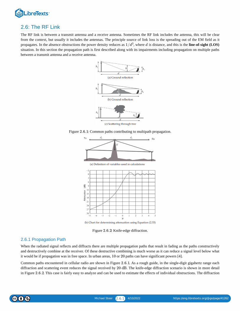
Figure : Common paths contributing to multipath propagation.
Figure : Knife-edge diffraction.
2.6.1 Propagation PathWhen the radiated signal reflects and diffracts there are multiple propagation paths that result in fading as the paths constructivelyand destructively combine at the receiver. Of these destructive combining is much worse as it can reduce a signal level below whatit would be if propagation was in free space. In urban areas, or paths can have significant powers [4].
Common paths encountered in cellular radio are shown in Figure . As a rough guide, in the single-digit gigahertz range eachdiffraction and scattering event reduces the signal received by . The knife-edge diffraction scenario is shown in more detailin Figure . This case is fairly easy to analyze and can be used to estimate the effects of individual obstructions. The diffraction
1/d2 d
2.6.1
2.6.2
10 20
2.6.1
20 dB
2.6.2
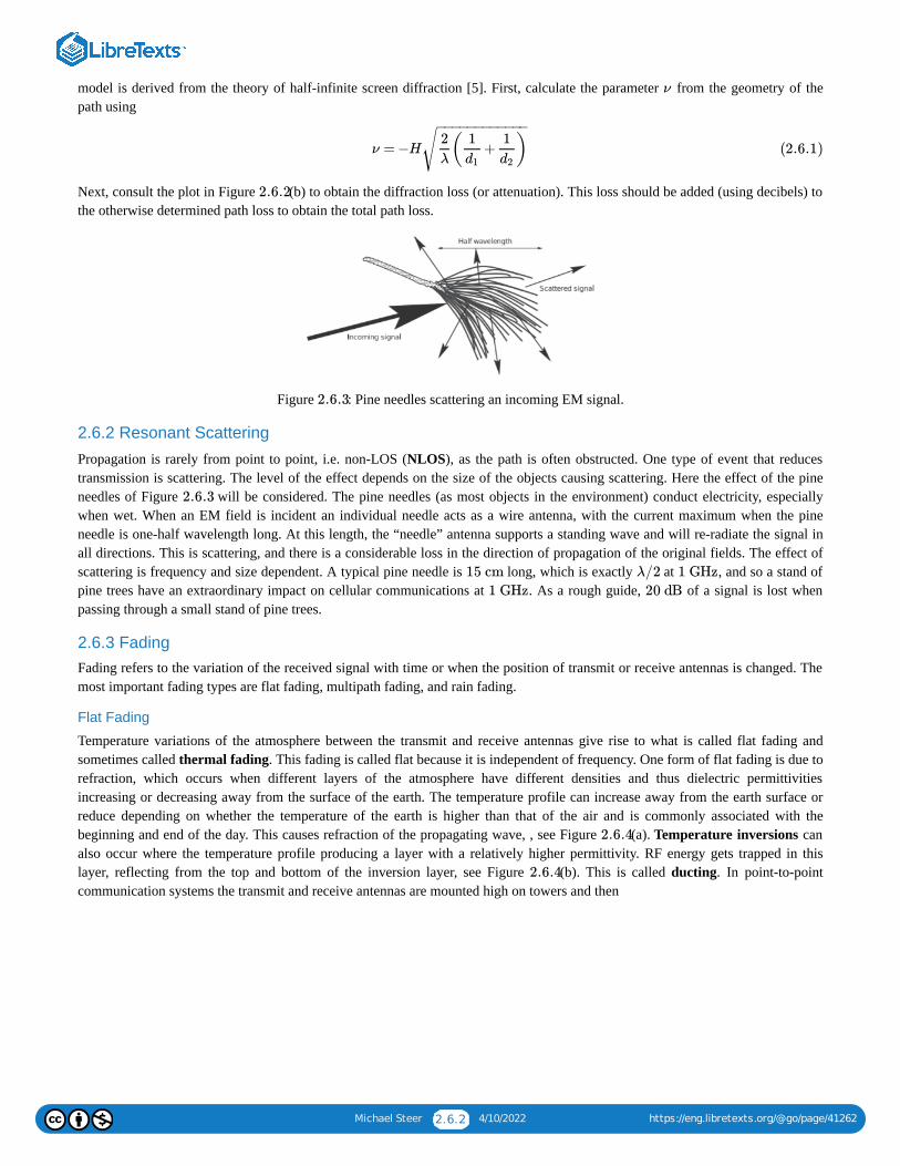
Michael Steer 2.6.2 4/10/2022 https://eng.libretexts.org/@go/page/41262
model is derived from the theory of half-infinite screen diffraction [5]. First, calculate the parameter from the geometry of thepath using
Next, consult the plot in Figure (b) to obtain the diffraction loss (or attenuation). This loss should be added (using decibels) tothe otherwise determined path loss to obtain the total path loss.
Figure : Pine needles scattering an incoming EM signal.
2.6.2 Resonant Scattering
Propagation is rarely from point to point, i.e. non-LOS (NLOS), as the path is often obstructed. One type of event that reducestransmission is scattering. The level of the effect depends on the size of the objects causing scattering. Here the effect of the pineneedles of Figure will be considered. The pine needles (as most objects in the environment) conduct electricity, especiallywhen wet. When an EM field is incident an individual needle acts as a wire antenna, with the current maximum when the pineneedle is one-half wavelength long. At this length, the “needle” antenna supports a standing wave and will re-radiate the signal inall directions. This is scattering, and there is a considerable loss in the direction of propagation of the original fields. The effect ofscattering is frequency and size dependent. A typical pine needle is long, which is exactly at , and so a stand ofpine trees have an extraordinary impact on cellular communications at . As a rough guide, of a signal is lost whenpassing through a small stand of pine trees.
2.6.3 FadingFading refers to the variation of the received signal with time or when the position of transmit or receive antennas is changed. Themost important fading types are flat fading, multipath fading, and rain fading.
Flat Fading
Temperature variations of the atmosphere between the transmit and receive antennas give rise to what is called flat fading andsometimes called thermal fading. This fading is called flat because it is independent of frequency. One form of flat fading is due torefraction, which occurs when different layers of the atmosphere have different densities and thus dielectric permittivitiesincreasing or decreasing away from the surface of the earth. The temperature profile can increase away from the earth surface orreduce depending on whether the temperature of the earth is higher than that of the air and is commonly associated with thebeginning and end of the day. This causes refraction of the propagating wave, , see Figure (a). Temperature inversions canalso occur where the temperature profile producing a layer with a relatively higher permittivity. RF energy gets trapped in thislayer, reflecting from the top and bottom of the inversion layer, see Figure (b). This is called ducting. In point-to-pointcommunication systems the transmit and receive antennas are mounted high on towers and then
ν
ν = −H ( + )2
λ
1
d1
1
d2
− −−−−−−−−−−−
√ (2.6.1)
2.6.2
2.6.3
2.6.3
15 cm λ/2 1 GHz
1 GHz 20 dB
2.6.4
2.6.4
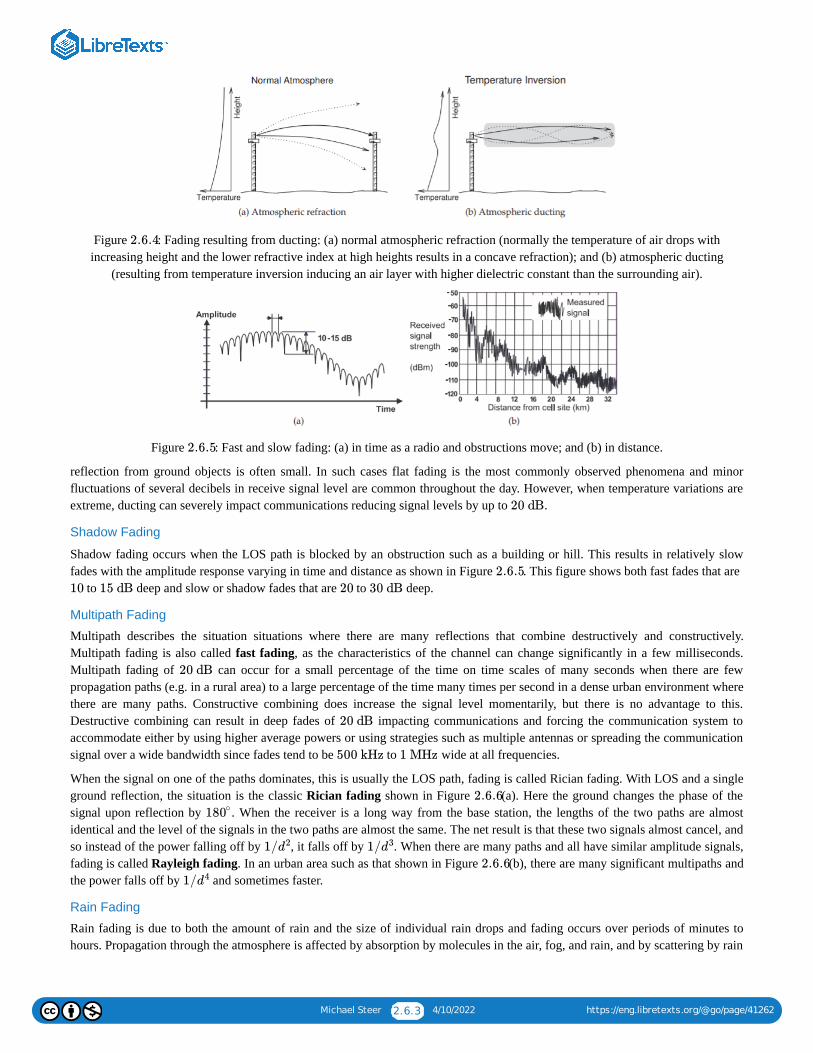
Michael Steer 2.6.3 4/10/2022 https://eng.libretexts.org/@go/page/41262
Figure : Fading resulting from ducting: (a) normal atmospheric refraction (normally the temperature of air drops withincreasing height and the lower refractive index at high heights results in a concave refraction); and (b) atmospheric ducting
(resulting from temperature inversion inducing an air layer with higher dielectric constant than the surrounding air).
Figure : Fast and slow fading: (a) in time as a radio and obstructions move; and (b) in distance.
reflection from ground objects is often small. In such cases flat fading is the most commonly observed phenomena and minorfluctuations of several decibels in receive signal level are common throughout the day. However, when temperature variations areextreme, ducting can severely impact communications reducing signal levels by up to .
Shadow Fading
Shadow fading occurs when the LOS path is blocked by an obstruction such as a building or hill. This results in relatively slowfades with the amplitude response varying in time and distance as shown in Figure . This figure shows both fast fades that are
to deep and slow or shadow fades that are to deep.
Multipath Fading
Multipath describes the situation situations where there are many reflections that combine destructively and constructively.Multipath fading is also called fast fading, as the characteristics of the channel can change significantly in a few milliseconds.Multipath fading of can occur for a small percentage of the time on time scales of many seconds when there are fewpropagation paths (e.g. in a rural area) to a large percentage of the time many times per second in a dense urban environment wherethere are many paths. Constructive combining does increase the signal level momentarily, but there is no advantage to this.Destructive combining can result in deep fades of impacting communications and forcing the communication system toaccommodate either by using higher average powers or using strategies such as multiple antennas or spreading the communicationsignal over a wide bandwidth since fades tend to be to wide at all frequencies.
When the signal on one of the paths dominates, this is usually the LOS path, fading is called Rician fading. With LOS and a singleground reflection, the situation is the classic Rician fading shown in Figure (a). Here the ground changes the phase of thesignal upon reflection by . When the receiver is a long way from the base station, the lengths of the two paths are almostidentical and the level of the signals in the two paths are almost the same. The net result is that these two signals almost cancel, andso instead of the power falling off by , it falls off by . When there are many paths and all have similar amplitude signals,fading is called Rayleigh fading. In an urban area such as that shown in Figure (b), there are many significant multipaths andthe power falls off by and sometimes faster.
Rain Fading
Rain fading is due to both the amount of rain and the size of individual rain drops and fading occurs over periods of minutes tohours. Propagation through the atmosphere is affected by absorption by molecules in the air, fog, and rain, and by scattering by rain
2.6.4
2.6.5
20 dB
2.6.5
10 15 dB 20 30 dB
20 dB
20 dB
500 kHz 1 MHz
2.6.6
180∘
1/d2 1/d3
2.6.6
1/d4
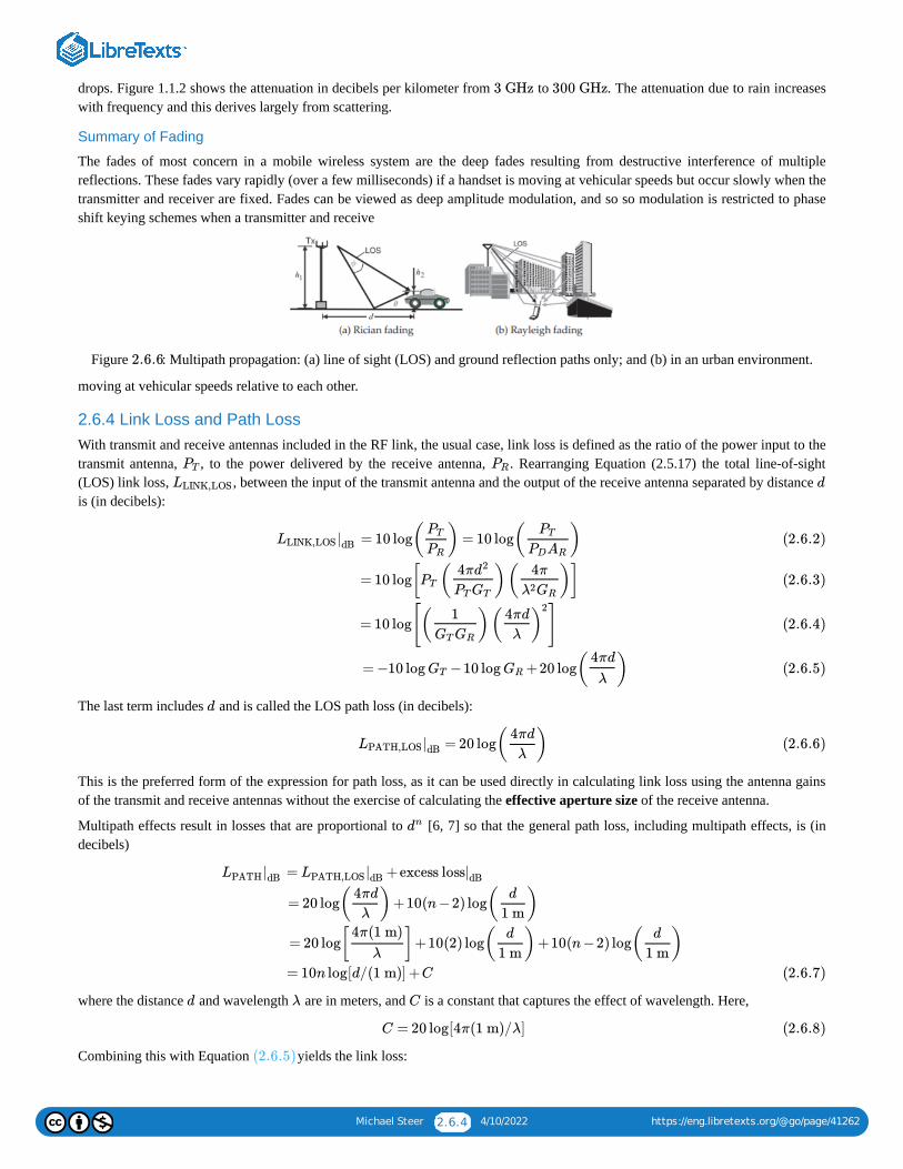
Michael Steer 2.6.4 4/10/2022 https://eng.libretexts.org/@go/page/41262
drops. Figure 1.1.2 shows the attenuation in decibels per kilometer from to . The attenuation due to rain increaseswith frequency and this derives largely from scattering.
Summary of Fading
The fades of most concern in a mobile wireless system are the deep fades resulting from destructive interference of multiplereflections. These fades vary rapidly (over a few milliseconds) if a handset is moving at vehicular speeds but occur slowly when thetransmitter and receiver are fixed. Fades can be viewed as deep amplitude modulation, and so so modulation is restricted to phaseshift keying schemes when a transmitter and receive
Figure : Multipath propagation: (a) line of sight (LOS) and ground reflection paths only; and (b) in an urban environment.
moving at vehicular speeds relative to each other.
2.6.4 Link Loss and Path LossWith transmit and receive antennas included in the RF link, the usual case, link loss is defined as the ratio of the power input to thetransmit antenna, , to the power delivered by the receive antenna, . Rearranging Equation (2.5.17) the total line-of-sight(LOS) link loss, , between the input of the transmit antenna and the output of the receive antenna separated by distance is (in decibels):
The last term includes and is called the LOS path loss (in decibels):
This is the preferred form of the expression for path loss, as it can be used directly in calculating link loss using the antenna gainsof the transmit and receive antennas without the exercise of calculating the effective aperture size of the receive antenna.
Multipath effects result in losses that are proportional to [6, 7] so that the general path loss, including multipath effects, is (indecibels)
where the distance and wavelength are in meters, and is a constant that captures the effect of wavelength. Here,
Combining this with Equation yields the link loss:
3 GHz 300 GHz
2.6.6
PT PR
LLINK,LOS d
LLINK,LOS |dB = 10 log( ) = 10 log( )PT
PR
PT
PDAR
= 10 log[ ( )( )]PT
4πd2
PTGT
4π
λ2GR
= 10 log[( ) ]1
GTGR
( )4πd
λ
2
= −10 log −10 log +20 log( )GT GR
4πd
λ
(2.6.2)
(2.6.3)
(2.6.4)
(2.6.5)
d
= 20 log( )LPATH,LOS |dB
4πd
λ(2.6.6)
dn
LPATH |dB = +excess lossLPATH,LOS |dB |dB
= 20 log( )+10(n−2) log( )4πd
λ
d
1 m
= 20 log[ ]+10(2) log( )+10(n−2) log( )4π(1 m)
λ
d
1 m
d
1 m
= 10n log[d/(1 m)] +C (2.6.7)
d λ C
C = 20 log[4π(1 m)/λ] (2.6.8)
(2.6.5)
Michael Steer 2.6.5 4/10/2022 https://eng.libretexts.org/@go/page/41262
A communication system uses a transmit antenna with an antenna gain of and a receive antenna with anantenna gain of . If the distance between the antennas is , what is the link loss if the power density reduces as
? The link loss here is between the input to the transmit antenna and the output from the receive antenna.
Solution
The link loss is provided by Equation ,
and comes from Equation , where . So
With and ,
In free space, radiated power density drops off with distance as . However, in a terrestrial environment there aremultiple paths between a transmitter and a receiver, with the dominant paths being the direct LOS path and the path involvingreflection off the ground. Reflection from the ground partially cancels the signal in the direct path, and in a semi-urbanenvironment results in an attenuation loss of per decade of distance (instead of the per decade of distance roll-offin free space). Consider a transmitter that has a power density of at a distance of from the transmitter.
a. The power density falls off as , where is distance and is an index. What is ?b. At what distance from the transmit antenna will the power density reach ?
Solution
a. Power drops off by per decade of distance. corresponds to a factor of . So, at distance , thepower density ( is a constant). At a decade of distance, , ,thus
b. At , . At a distance ,
2.6.5 Propagation Model in the Mobile EnvironmentRF propagation in the mobile environment cannot be accurately derived. Instead, a fit to measurements is often used. One of themodels is the Okumura–Hata model [8], which calculates the path loss as
where is the frequency (in ), is the distance between the base station and terminal (in ), is the effective height of thebase station antenna (in ), and is an environment correction factor ( in a dense urban area, in an urbanarea, in a suburban area, and in a rural area, for and ).
There are many propagation models for different frequency ranges and different environments. The considerable effort put intodeveloping reliable models is because being able to predict signal coverage is essential to efficient design of basestation layout.
= − − +10n log[d/(1 m)] +CLLINK |dB GT |dB GR|dB (2.6.9)
Example : Link Loss2.6.1
5.6 GHz GT 35 dB
GR 6 dB 200 m
1/d3
(2.6.9)
= − − +10n log[d/(1 m)] +CLLINK |dB GT GR
C (2.6.8) λ = 5.36 cm
C = 20 log( ) = 20 log( ) = 47.4 dB4π
λ
4π
0.0536
n = 3 d = 200 m
= −35 −6 +10 ⋅ 3 ⋅ log(200) +47.4 dB = 75.4 dBLLINK |dB
Example : Radiated Power Density2.6.2
d 1/d2
40 dB 20 dB
1 W/m2 1 m
1/dn d n n
1 μW ⋅ m−2
40 dB 40 dB 10, 000(= )104 d
(d) = k/PD dn k 10d (10d) = k/(10d = (d)/10000PD )n PD
= ; = 10, 000 ⇒ n = 4k
10ndn1
10, 000
k
dn10n
d = 1 m (1 m) = 1PD W/m2
x
(x) = 1 μ = = → = and so x = 31.6 mPD W/m2 k
x4m2 k
x4x4 1
10−6
= 69.55 +26.16 log f −13.82 logH +(44.9 −6.55 logH) ⋅ log d+cLPATH |(dB) (2.6.10)
f MHz d km H
m c c = 0 dB c = −5 dB
c = −10 dB c = −17 dB f = 1 GHz H = 1.5 m

Michael Steer 2.6.6 4/10/2022 https://eng.libretexts.org/@go/page/41262
Contributions and AttributionsThis page is licensed under a CC BY-NC license and was authored, remixed, and/or curated by Michael Steer. A detailedversioning history of the edits to source content is available upon request.

Michael Steer 2.7.1 4/10/2022 https://eng.libretexts.org/@go/page/41263
2.7: Exercises1. An antenna only radiates of the power input to it. The rest is lost as heat. What input power (in ) is required to radiate
?2. The output stage of an RF front end consists of an amplifier followed by a filter and then an antenna. The amplifier has a gain
of , the filter has a loss of , and of the power input to the antenna, is lost as heat due to resistive losses. If thepower input to the amplifier is , calculate the following:a. What is the power input to the amplifier in watts?b. Express the loss of the antenna in .c. What is the total gain of the RF front end (amplifier + filter)?d. What is the total power radiated by the antenna in ?e. What is the total power radiated by the antenna in ?
3. The output stage of an RF front end consists of an amplifier followed by a filter and then an antenna. The amplifier has a gainof , the filter has a loss of , and of the power input to the antenna, is lost as heat due to resistive losses. If thepower input to the amplifier is , calculate the following:a. What is the power input to the amplifier in watts?b. Express the loss of the antenna in decibels.c. What is the total gain of the RF front end (amplifier + filter)?d. What is the total power radiated by the antenna in ?e. What is the total power radiated by the antenna in milliwatts?
4. Thirty five percent of the power input to an antenna is lost as heat, what is the loss of the antenna in .5. Only of the power input to an antenna is radiated with the rest lost to dissipation in the antenna, what is the gain of the
antenna in ? (This is not the antenna gain.)6. The efficiency of an antenna is . If the power input to the antenna is what is the power radiated by the antenna in
?7. An antenna with an input of operates in free space and has an antenna gain of . What is the maximum power
density at from the antenna?8. A transmitter has an antenna with an antenna gain of , the resistive losses of the antenna are , and the power input to
the antenna is . What is the in watts?9. A transmitter has an antenna with an antenna gain of , the resistive losses of the antenna are , and the power input to
the antenna is . What is the in watts?10. An antenna with an antenna gain of radiates . What is the in watts? Assume that the antenna is
efficient.11. An antenna has an antenna gain of and a input signal. What is the in watts?12. An antenna with of input power has an antenna gain of and an antenna efficiency of and all of the loss is due
to resistive losses in the antenna. [Parallels Example 2.5.2]
a. How much power in is lost as heat in the antenna?b. How much power in is radiated by the antenna?c. What is the in ?
13. An antenna with an efficiency of has an antenna gain of and radiates . What is the in watts?14. An antenna with an efficiency of and an antenna gain of . If the power input to the antenna is ,
a. What is the total power in radiated by the antenna? (b) What is the in ?15. The output stage of an RF front end consists of an amplifier followed by a filter and then an antenna. The amplifier has a gain
of , the filter has a loss of , and of the power input to the antenna, is lost as heat due to resistive losses. If thepower input to the amplifier is , calculate the following:a. What is the power input to the amplifier in watts?b. Express the loss of the antenna in decibels.c. What is the total gain of the RF front end (amplifier + filter)?d. What is the total power radiated by the antenna in ?e. What is the total power radiated by the antenna in milliwatts?
45% dBm
30 dBm
27 dB 1.9 dB 35%
30 dBm
dB
dBm
mW
27 dB 1.9 dB 45%
30 dBm
dBm
dB
65%
dB
66% 10 W
dBm
1 W 12 dBi
100 m
10 dBi 50%
1 W EIRP
20 dBi 50%
100 mW EIRP
8 dBi 6.67 W EIRP 100%
10 dBi 40 W EIRP
5 W 20 dBi 25%
dBm
dBm
EIRP dBW
50% 12 dBi 100 W EIRP
75% 10 dBi 100 W
dBm EIRP dBm
27 dB 1.9 dB 45%
30 dBm
dBm

Michael Steer 2.7.2 4/10/2022 https://eng.libretexts.org/@go/page/41263
tic
tic
16. A communication system operating at includes a transmit antenna with an antenna gain of and a receiveantenna with an effective aperture area of . The distance between the two antennas is .a. What is the antenna gain of the receive antenna?b. If the input to the transmit antenna is , what is the power density at the receive antenna if the power falls off as ,
where is the distance from the transmit antenna?c. Thus what is the power delivered at the output of the receive antenna?
17. Consider a point-to-point communication system. Parabolic antennas are mounted high on a mast so that ground effects do notexist, thus power falls off as . The gain of the transmit antenna is and the gain of the receive antenna is .The distance between the antennas is . The effective area of the receive antenna is . If the power input to thetransmit antenna is , what is the power delivered at the output of the receive antenna?
18. Consider a point-to-point communication system. Parabolic antennas are mounted high on a mast so that groundeffects do not exist, thus power falls off as . The gain of the transmit antenna is and the gain of the receive antennais . The distance between the antennas is . If the power output from the receive antenna is , what is thepower input to the transmit antenna?
19. An antenna has an effective aperture area of . What is the antenna gain of the antenna at ?20. An antenna operating at has an antenna gain of . What is the effective aperture area of the antenna?21. A receive antenna has an antenna gain of . If the power density at the receive antenna is , what is
the power at the output of the antenna? [Parallels Example 2.6.2]22. Two identical antennas are used in a pointto-point communication system, each having a gain of . The system has an
operating frequency of and the antennas are at the top of masts tall. The RF link between the antennas consistsonly of the direct line-of-sight path.a. What is the effective aperture area of each antenna?b. How does the power density of the propagating signal rolloff with distance.c. If the separation of the transmit and receive antennas is , what is the path loss in decibels?d. If the separation of the transmit and receive antennas is , what is the link loss in decibels?
23. A transmitter and receiver operating at are at the same level, but the direct path between them is blocked by a buildingand the signal must diffract over the building for a communication link to be established. This is a classic knife-edge diffractionsituation. The transmit and receive antennas are each separated from the building by and the building is higher thanthe antennas (which are at the same height). Consider that the building is very thin. It has been found that the path loss can bedetermined by considering loss due to free-space propagation and loss due to diffraction over the knife edge.a. What is the additional attenuation (in decibels) due to diffraction?b. If the operating frequency is , what is the attenuation (in decibels) due to diffraction?c. If the operating frequency is , what is the attenuation (in decibels) due to diffraction?
24. A hill is from a transmit antenna and from a receive antenna. The receive and transmit antennas are at the sameheight and the hill is above the height of the antennas. What is the additional loss caused by diffraction over the top of thehill? Treat the hill as causing knifeedge diffraction and the operating frequency is .
25. Two identical antennas are used in a pointto-point communication system, each having a gain of . The system has anoperating frequency of and the antennas are at the top of masts tall. The RF link between the antennas consistsonly of the direct LOS path.
a. What is the effective aperture area of each antenna?b. How does the power density of the propagating signal rolloff with distance?c. If the separation of the transmit and receive antennas is , what is the path loss? Ignore atmospheric loss.
26. The three main cellular communication bands are centered around and . Compare these threebands in terms of multipath effects, diffraction around buildings, object (such as a wall) penetration, scattering from trees andparts of trees, and ability to follow the curvature of hills. Complete the table below with the relative attributes: high, medium,and low.
Characteristic
Multipath
Scattering
2.5 GHz 12 dBi
20 cm2 100 m
1 W 1/d2
d
1/d2 20 dBi 15 dBi
10 km 3 cm2
600 mW
28 GHz
1/d2 20 dBi
15 dBi 10 km 10 pW
20 cm2 2.5 GHz
28 GHz 50 dBi
15 GHz 20 dBi 1 nW/cm2
50 dBi
28 GHz 100 m
10 km
10 km
2 GHz
4 km 20 m
100 MHz
10 GHz
1 km 2 km
20 m
1 GHz
30 dBi
14 GHz 100 m
10 km
450 MHz, 900 MHz, 2 GHz
450 MHz 900 MHz 2 GHz

Michael Steer 2.7.3 4/10/2022 https://eng.libretexts.org/@go/page/41263
tic
tic
tic
tic
tic
Characteristic
Penetration
Following curvature
Range
Antenna size
Atmospheric loss
Table
27. Describe the difference in multipath effects in a central city area compared to multipath effects in a desert. Your descriptionshould be approximately lines long and not use a diagram
28. Wireless LAN systems can operate at and . Contrast with explanation the performance ofthese schemes inside a building in terms of range.
29. At the atmosphere strongly attenuates a signal. Discuss the origin of this and indicate an advantage and a disadvantage.30. Short answer questions. Each part requires a short paragraph of about five lines and a figure, where appropriate, to illustrate
your understanding.a. Cellular communications systems use two frequency bands to communicate between the basestation and the mobile unit.
The bands are generally separated by or so. Which band (higher or lower) is used for the downlink from thebasestation to the mobile unit and what are the reasons behind this choice?
b. Describe at least two types of interference in a cellular system from the perspective of a mobile handset.31. The three main cellular communication bands are centered around and . Compare these three
bands in terms of multipath effects, diffraction around buildings, object (such as a wall) penetration, scattering from trees andparts of trees, and the ability to follow the curvature of hills. Use a table and indicate the relative attributes: high, medium, andlow.
32. Describe Rayleigh fading in approximately lines and without using a diagram.33. In several sentences and using a diagram describe Rayleigh fading and the impact it has on radio communications.34. A transmitter and receiver operate at , are at the same level, and are separated by . The signal must diffract over
a building half way between the antennas that is higher than the direct path between the antennas. What is the attenuation(in decibels) due to diffraction?
35. A transmitter and receiver operate at , are at the same level, and are apart. The signal must diffract over abuilding that is half way between the antennas and is higher than the line between the antennas. What is the attenuation(in ) due to diffraction?
2.10.1 Exercises By Sectionchallenging
2.10.2 Answers to Selected Exercises2. (e)
16. 17.
Contributions and AttributionsThis page is licensed under a CC BY-NC license and was authored, remixed, and/or curated by Michael Steer. A detailedversioning history of the edits to source content is available upon request.
450 MHz 900 MHz 2 GHz
2.7.1
4
2.4 GHz, 5.6 GHz, 40 GHz 60 GHz
60 GHz
50 MHz
450 MHz, 900 MHz, 2 GHz
4
100 MHz 4 km
20 m
10 GHz 4 km
20 m
dB
†
§2.31†
§2.52†, 3†, 4, 5, 6†, 7†, 8†, 19, 10, 11, 12, 13, 14, 15, 16, 17, 18, 19, 20, 21
§2.622†, 23†, 24†, 25†, 27†, 28, 29, 30†, 31, 32, 33, 34, 35
53.23 dBm
0.251 μW
14.3 pW
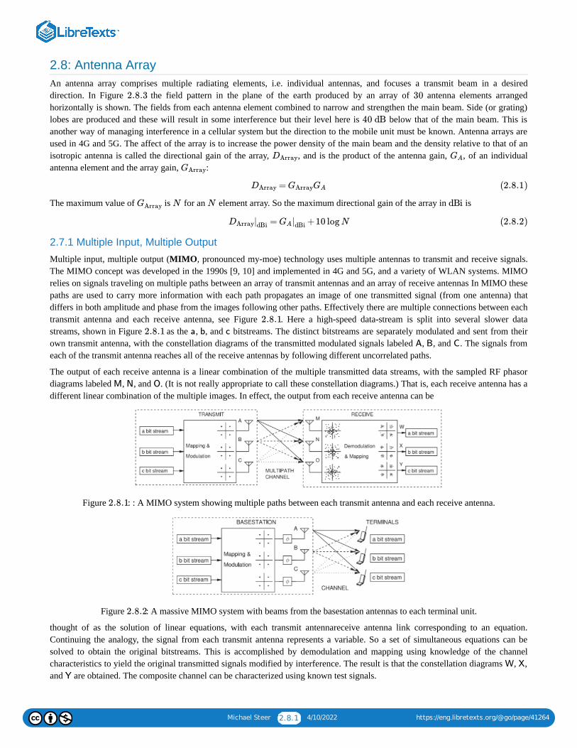
Michael Steer 2.8.1 4/10/2022 https://eng.libretexts.org/@go/page/41264
2.8: Antenna ArrayAn antenna array comprises multiple radiating elements, i.e. individual antennas, and focuses a transmit beam in a desireddirection. In Figure the field pattern in the plane of the earth produced by an array of antenna elements arrangedhorizontally is shown. The fields from each antenna element combined to narrow and strengthen the main beam. Side (or grating)lobes are produced and these will result in some interference but their level here is below that of the main beam. This isanother way of managing interference in a cellular system but the direction to the mobile unit must be known. Antenna arrays areused in 4G and 5G. The affect of the array is to increase the power density of the main beam and the density relative to that of anisotropic antenna is called the directional gain of the array, , and is the product of the antenna gain, , of an individualantenna element and the array gain, :
The maximum value of is for an element array. So the maximum directional gain of the array in is
2.7.1 Multiple Input, Multiple Output
Multiple input, multiple output (MIMO, pronounced my-moe) technology uses multiple antennas to transmit and receive signals.The MIMO concept was developed in the 1990s [9, 10] and implemented in 4G and 5G, and a variety of WLAN systems. MIMOrelies on signals traveling on multiple paths between an array of transmit antennas and an array of receive antennas In MIMO thesepaths are used to carry more information with each path propagates an image of one transmitted signal (from one antenna) thatdiffers in both amplitude and phase from the images following other paths. Effectively there are multiple connections between eachtransmit antenna and each receive antenna, see Figure . Here a high-speed data-stream is split into several slower datastreams, shown in Figure as the , , and bitstreams. The distinct bitstreams are separately modulated and sent from theirown transmit antenna, with the constellation diagrams of the transmitted modulated signals labeled , , and . The signals fromeach of the transmit antenna reaches all of the receive antennas by following different uncorrelated paths.
The output of each receive antenna is a linear combination of the multiple transmitted data streams, with the sampled RF phasordiagrams labeled , , and . (It is not really appropriate to call these constellation diagrams.) That is, each receive antenna has adifferent linear combination of the multiple images. In effect, the output from each receive antenna can be
Figure : : A MIMO system showing multiple paths between each transmit antenna and each receive antenna.
Figure : A massive MIMO system with beams from the basestation antennas to each terminal unit.
thought of as the solution of linear equations, with each transmit antennareceive antenna link corresponding to an equation.Continuing the analogy, the signal from each transmit antenna represents a variable. So a set of simultaneous equations can besolved to obtain the original bitstreams. This is accomplished by demodulation and mapping using knowledge of the channelcharacteristics to yield the original transmitted signals modified by interference. The result is that the constellation diagrams , ,and are obtained. The composite channel can be characterized using known test signals.
2.8.3 30
40 dB
DArray GA
GArray
=DArray GArrayGA (2.8.1)
GArray N N dBi
= +10 log NDArray|dBi GA|dBi (2.8.2)
2.8.1
2.8.1 a b c
A B C
M N O
2.8.1
2.8.2
W X
Y
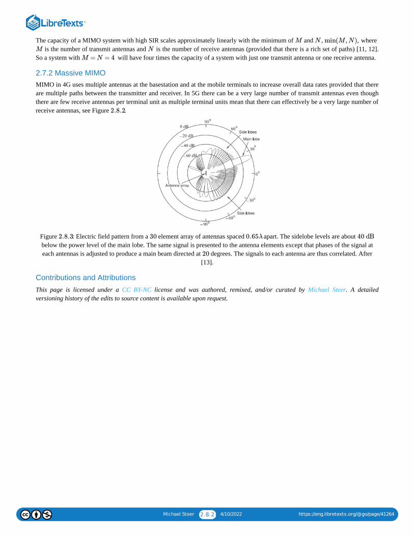
Michael Steer 2.8.2 4/10/2022 https://eng.libretexts.org/@go/page/41264
The capacity of a MIMO system with high SIR scales approximately linearly with the minimum of and , , where is the number of transmit antennas and is the number of receive antennas (provided that there is a rich set of paths) [11, 12].
So a system with will have four times the capacity of a system with just one transmit antenna or one receive antenna.
2.7.2 Massive MIMOMIMO in 4G uses multiple antennas at the basestation and at the mobile terminals to increase overall data rates provided that thereare multiple paths between the transmitter and receiver. In 5G there can be a very large number of transmit antennas even thoughthere are few receive antennas per terminal unit as multiple terminal units mean that there can effectively be a very large number ofreceive antennas, see Figure .
Figure : Electric field pattern from a element array of antennas spaced apart. The sidelobe levels are about below the power level of the main lobe. The same signal is presented to the antenna elements except that phases of the signal ateach antennas is adjusted to produce a main beam directed at degrees. The signals to each antenna are thus correlated. After
[13].
Contributions and Attributions
This page is licensed under a CC BY-NC license and was authored, remixed, and/or curated by Michael Steer. A detailedversioning history of the edits to source content is available upon request.
M N min(M , N)
M N
M = N = 4
2.8.2
2.8.3 30 0.65λ 40 dB
20

Michael Steer 2.9.1 4/10/2022 https://eng.libretexts.org/@go/page/41265
2.9: SummaryThis chapter discussed the impact of imperfections in the RF link from the output of the transmitter to the input of the receiver.Prior to cellular communications becoming so important, only the LOS communication path was considered and the impact offading, multiple reflections, and delay spread was regarded as detrimental. While many aspects of RF propagation are random,concepts and statistical models have been developed that enable design choices to be made that permit digital communicationsystems to operate in what would have been regarded as a hostile environment.
Contributions and AttributionsThis page is licensed under a CC BY-NC license and was authored, remixed, and/or curated by Michael Steer. A detailedversioning history of the edits to source content is available upon request.

Michael Steer 2.10.1 4/10/2022 https://eng.libretexts.org/@go/page/41266
2.10: References[1] S. Ramo, J. Whinnery, and T. Van Duzer, Fields and Waves in Communication Electronics. John Wiley & Sons, 1965.
[2] C. A. Balanis, “Antenna theory: A review,” Proc. IEEE, vol. 80, no. 1, pp. 7–23, 1992.
[3] C. Balanis, Antenna Theory: Analysis and Design. John Wiley & Sons, 2005.
[4] J. Doble, Introduction to Radio Propagation for Fixed and Mobile Communications. Norwood, MA, USA: Artech House, Inc.,1996.
[5] M. Born and E. Wolf, “Two-dimensional diffraction of a plane wave by a half-plane,,” in Principles of Optics: ElectromagneticTheory of Propagation, Interference, and Diffraction of Light, 7th ed. Cambridge University Press, 1999, section 11.5.
[6] J. Andersen, T. Rappaport, and S. Yoshida, “Propagation measurements and models for wireless communications channels,”IEEE Communications Magazine, vol. 33, no. 1, pp. 42–49, Jan. 1995.
[7] T. Sarkar, Z. Ji, K. Kim, A. Medouri, and M. Salazar-Palma, “A survey of various propagation models for mobilecommunication,” IEEE Antennas and Propagation Magazine, vol. 45, no. 3, pp. 51–82, Jun. 2003.
[8] J. Seybold, Introduction to RF Propagation. John Wiley & Sons, 2005.
[9] G. Foschini, “Layered space-time architecture for wireless communication in a environment when using multi-elementantennas,” Bell Labs Technical J., vol. 1, no. 2, pp. 41–59, Autumn 1996.
[10] G. Raleigh and J. Cioffi, “Spatio-temporal coding for wireless communications,” in Global Telecommunications Conf., 1996),vol. 3, Nov. 1996, pp. 1809–1814.
[11] A. Goldsmith, S. Jafar, N. Jindal, and S. Vishwanath, “Capacity limits of mimo channels,” IEEE J. on Selected Areas inCommunications, vol. 21, no. 5, pp. 684–702, Jun. 2003.
[12] D. Gesbert, M. Shafi, D. shan Shiu, P. Smith, and A. Naguib, “From theory to practice: an overview of mimo space-timecoded wireless systems,” IEEE J. on Selected Areas in Communications, vol. 21, no. 3, pp. 281–302, Apr. 2003.
[13] Phased array radiation pattern, Phased array radiation pattern.gif, By Maxter315 [CC BY-SA 4.0(creativecommons.org/licenses/bysa/4.0)], from Wikimedia Commons.
Contributions and Attributions
This page is licensed under a CC BY-NC license and was authored, remixed, and/or curated by Michael Steer. A detailedversioning history of the edits to source content is available upon request.

1 4/10/2022
CHAPTER OVERVIEW3: TRANSMISSION LINES
3.1: INTRODUCTION3.2: TRANSMISSION LINE THEORY3.3: THE LOSSLESS TERMINATED LINE3.4: SPECIAL CASES OF LOSSLESS TERMINATED LINES3.5: CIRCUIT MODELS OF TRANSMISSION LINES3.6: SUMMARY3.7: REFERENCES3.8: EXERCISES
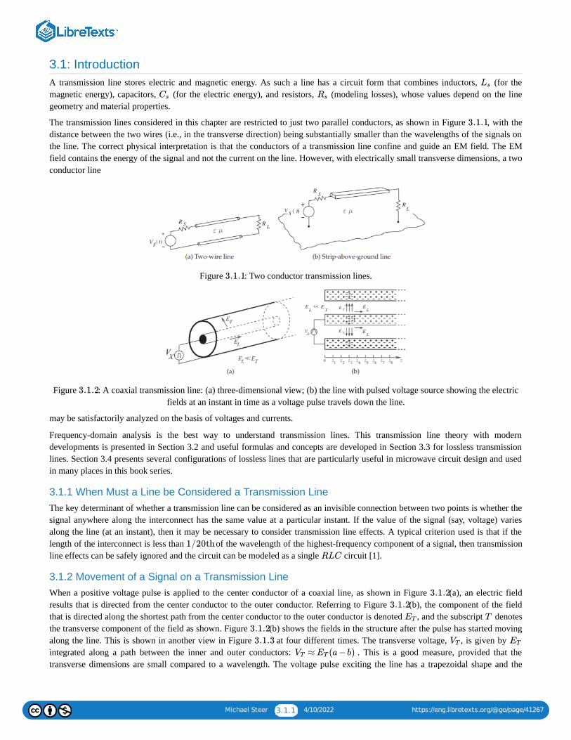
Michael Steer 3.1.1 4/10/2022 https://eng.libretexts.org/@go/page/41267
3.1: IntroductionA transmission line stores electric and magnetic energy. As such a line has a circuit form that combines inductors, (for themagnetic energy), capacitors, (for the electric energy), and resistors, (modeling losses), whose values depend on the linegeometry and material properties.
The transmission lines considered in this chapter are restricted to just two parallel conductors, as shown in Figure , with thedistance between the two wires (i.e., in the transverse direction) being substantially smaller than the wavelengths of the signals onthe line. The correct physical interpretation is that the conductors of a transmission line confine and guide an EM field. The EMfield contains the energy of the signal and not the current on the line. However, with electrically small transverse dimensions, a twoconductor line
Figure : Two conductor transmission lines.
Figure : A coaxial transmission line: (a) three-dimensional view; (b) the line with pulsed voltage source showing the electricfields at an instant in time as a voltage pulse travels down the line.
may be satisfactorily analyzed on the basis of voltages and currents.
Frequency-domain analysis is the best way to understand transmission lines. This transmission line theory with moderndevelopments is presented in Section 3.2 and useful formulas and concepts are developed in Section 3.3 for lossless transmissionlines. Section 3.4 presents several configurations of lossless lines that are particularly useful in microwave circuit design and usedin many places in this book series.
3.1.1 When Must a Line be Considered a Transmission LineThe key determinant of whether a transmission line can be considered as an invisible connection between two points is whether thesignal anywhere along the interconnect has the same value at a particular instant. If the value of the signal (say, voltage) variesalong the line (at an instant), then it may be necessary to consider transmission line effects. A typical criterion used is that if thelength of the interconnect is less than of the wavelength of the highest-frequency component of a signal, then transmissionline effects can be safely ignored and the circuit can be modeled as a single circuit [1].
3.1.2 Movement of a Signal on a Transmission LineWhen a positive voltage pulse is applied to the center conductor of a coaxial line, as shown in Figure (a), an electric fieldresults that is directed from the center conductor to the outer conductor. Referring to Figure (b), the component of the fieldthat is directed along the shortest path from the center conductor to the outer conductor is denoted , and the subscript denotesthe transverse component of the field as shown. Figure (b) shows the fields in the structure after the pulse has started movingalong the line. This is shown in another view in Figure at four different times. The transverse voltage, , is given by integrated along a path between the inner and outer conductors: . This is a good measure, provided that thetransverse dimensions are small compared to a wavelength. The voltage pulse exciting the line has a trapezoidal shape and the
Ls
Cs Rs
3.1.1
3.1.1
3.1.2
1/20thRLC
3.1.23.1.2
ET T
3.1.23.1.3 VT ET
≈ (a −b)VT ET
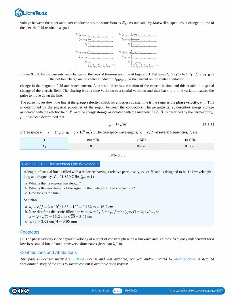
Michael Steer 3.1.2 4/10/2022 https://eng.libretexts.org/@go/page/41267
voltage between the inner and outer conductor has the same form as . As indicated by Maxwell’s equations, a change in time ofthe electric field results in a spatial
Figure : Fields, currents, and charges on the coaxial transmission line of Figure at times . isthe net free charge on the center conductor. is the current on the center conductor.
change in the magnetic field and hence current. As a result there is a variation of the current in time and this results in a spatialchange of the electric field. The chasing from a time variation to a spatial variation and then back to a time variation causes thepulse to move down the line.
The pulse moves down the line at the group velocity, which for a lossless coaxial line is the same as the phase velocity, . Thisis determined by the physical properties of the region between the conductors. The permittivity, , describes energy storageassociated with the electric field, , and the energy storage associated with the magnetic field, , is described by the permeability,
. It has been determined that
In free space . The free-space wavelengths, , at several frequencies, , are
Table
A length of coaxial line is filled with a dielectric having a relative permittivity, , of and is designed to be wavelengthlong at a frequency, , of .
a. What is the free-space wavelength?b. What is the wavelength of the signal in the dielectric-filled coaxial line?c. How long is the line?
Solution
a. b. Note that for a dielectric-filled line with , so
c.
Footnotes
[1] The phase velocity is the apparent velocity of a point of constant phase on a sinewave and is almost frequency independent for alow-loss coaxial line of small transverse dimensions (less than ).
Contributions and AttributionsThis page is licensed under a CC BY-NC license and was authored, remixed, and/or curated by Michael Steer. A detailedversioning history of the edits to source content is available upon request.
ET
3.1.3 3.1.2 > > >t4 t3 t2 t1 QCENTER
ICENTER
vp1
ε
E H
μ
= 1/vp με−−√ (3.1.1)
= c = 1/ = 3 × m/svp μ0ε0− −−−
√ 108 = c/fλ0 f
f 100 MHz 1 GHz 10 GHz
λ0 3 m 30 cm 3.0 cm
3.1.1
Example : Transmission Line Wavelength3.1.1
εr 20 1/4f 1.850 GHz ( = 1)μr
= c/f = 3 × /1.85 × = 0.162 m = 16.2 cmλ0 108 109
= 1, λ = /f = c/( f) = /μr vp εr−−
√ λ0 εr−−
√λ = / = 16.2 cm/ = 3.62 cmλ0 εr
−−√ 20
−−√
/4 = 3.62 cm/4 = 9.05 mmλg
λ/10
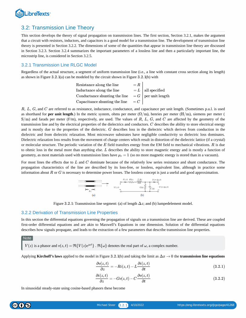
Michael Steer 3.2.1 4/10/2022 https://eng.libretexts.org/@go/page/41268
3.2: Transmission Line TheoryThis section develops the theory of signal propagation on transmission lines. The first section, Section 3.2.1, makes the argumentthat a circuit with resistors, inductors, and capacitors is a good model for a transmission line. The development of transmission linetheory is presented in Section 3.2.2. The dimensions of some of the quantities that appear in transmission line theory are discussedin Section 3.2.3. Section 3.2.4 summarizes the important parameters of a lossless line and then a particularly important line, themicrostrip line, is considered in Section 3.2.5.
3.2.1 Transmission Line RLGC ModelRegardless of the actual structure, a segment of uniform transmission line (i.e., a line with constant cross section along its length)as shown in Figure (a) can be modeled by the circuit shown in Figure (b) with
and are referred to as resistance, inductance, conductance, and capacitance per unit length. (Sometimes p.u.l. is usedas shorthand for per unit length.) In the metric system, ohms per meter ( ), henries per meter ( ), siemens per meter (
) and farads per meter (F/m), respectively, are used. The values of and are affected by the geometry of thetransmission line and by the electrical properties of the dielectrics and conductors. describes the ability to store electrical energyand is mostly due to the properties of the dielectric. describes loss in the dielectric which derives from conduction in thedielectric and from dielectric relaxation. Most microwave substrates have negligible conductivity so dielectric loss dominates.Dielectric relaxation loss results from the movement of charge centers which result in distortion of the dielectric lattice (if a crystal)or molecular structure. The periodic variation of the field transfers energy from the EM field to mechanical vibrations. is dueto ohmic loss in the metal more than anything else. describes the ability to store magnetic energy and is mostly a function ofgeometry, as most materials used with transmission lines have (so no more magnetic energy is stored than in a vacuum).
For most lines the effects due to and dominate because of the relatively low series resistance and shunt conductance. Thepropagation characteristics of the line are described by its loss-free, or lossless, equivalent line, although in practice someinformation about or is necessary to determine power losses. The lossless concept is just a useful and good approximation.
Figure : Transmission line segment: (a) of length ; and (b) lumpedelement model.
3.2.2 Derivation of Transmission Line PropertiesIn this section the differential equations governing the propagation of signals on a transmission line are derived. These are coupledfirst-order differential equations and are akin to Maxwell’s Equations in one dimension. Solution of the differential equationsdescribes how signals propagate, and leads to the extraction of a few parameters that describe transmission line properties.
is a phasor and . denotes the real part of , a complex number.
Applying Kirchoff’s laws applied to the model in Figure (b) and taking the limit as the transmission line equations
In sinusoidal steady-state using cosine-based phasors these become
3.2.1 3.2.1
Resistance along the line
Inductance along the line
Conductance shunting the line
Capacitance shunting the line
= R
= L
= G
= C
all specified
per unit length
R, L, G, C
Ω/m H/mS/m R, L, G, C
C
G
E R
L
= 1μr
L C
R G
3.2.1 Δz
Note
V (z) v(z, t) = R{V (z) }eȷωtR{ω} ω
3.2.1 Δx → 0
= −Ri(z, t) −L∂v(z, t)
∂z
∂i(z, t)
∂t(3.2.1)
= −Gv(z, t) −C∂i(z, t)
∂z
∂v(z, t)
∂t(3.2.2)

Michael Steer 3.2.2 4/10/2022 https://eng.libretexts.org/@go/page/41268
and
Eliminating in the above yields the wave equation for :
Similarly
where the propagation constant is
with SI units of and where is the attenuation coefficient and has units of nepers per meter ( ), and is the phase-change coefficient, or phase constant, and has units of radians per meter ( or ). Nepers and radians aredimensionless units, but serve as prompts for what is being referred to.
Equations and are second-order differential equations that have solutions of the form
and
The physical interpretation of these solutions is that and are forward-traveling waves(moving in the direction) and and are backward-traveling waves (moving in the direction). and are all phasors. Substituting Equation in Equation results in
Then from Equations and
The characteristic impedance is defined as
with the SI unit of ohms ( ). Equations and can be rewritten as
and
Converting back to the time domain:
= −(R+ ȷωL)I(z)dV (z)
dz(3.2.3)
= −(G+ ȷωC)V (z)dI(z)
dz(3.2.4)
I(z) V (z)
− V (z) = 0V (z)d2
dz2γ2 (3.2.5)
− I(z) = 0I(z)d2
dz2γ2 (3.2.6)
γ = α+ ȷβ = (R+ ȷωL)(G+ ȷωC)− −−−−−−−−−−−−−−−
√ (3.2.7)
m−1 α Np/m β
rad/m radians/m
(3.2.5) (3.2.6)
V (z) = +V +0 e−γz V −
0 eγz (3.2.8)
I(z) = +I+0 e−γz I−
0 eγz (3.2.9)
(z) =V + V +0 e−γz (z) =I+ I+
0 e−γz
+z (z) =V − V −0 eγz (z) =I− I−
0 eγz −z
V (z), , , I(z),V +0 V −
0 I+0 I−
0 (3.2.8) (3.2.3)
I(z) = [ − ]γ
R+ ȷωLV +
0 e−γz V −0 eγz (3.2.10)
(3.2.10) (3.2.9)
= and = (−I+0
γ
R+ ȷωLV +
0 I−0
γ
R+ ȷωLV −
0 (3.2.11)
= = = =Z0V +
0
I+0
−V −0
I−0
R+ ȷωL
γ
R+ ȷωL
G+ ȷωC
− −−−−−−−
√ (3.2.12)
Ω (3.2.8) (3.2.9)
V (z) = +V +0 e−γz V −
0 eγz (3.2.13)
I(z) = −V +
0
Z0e−γz
V −0
Z0eγz (3.2.14)
v(z, t) = | | cos(ωt−βz+ ) +| | cos(ωt+βz+ )V +0 φ+ e−αz V −
0 φ− eαz (3.2.15)
Michael Steer 3.2.3 4/10/2022 https://eng.libretexts.org/@go/page/41268
where and are phases of the forward- and backward-traveling waves, respectively. The phasors of the traveling voltagewaves are
The following quantities are defined:
where is the radian frequency and is the frequency with the SI units of hertz ( ). The wavenumber as defined hereis used in electromagnetics and where wave propagation is concerned. Considering one of the traveling waves, the phase velocityrefers to the apparent velocity of which a point of constant phase on the sinewave appears to move.
The important result here is that a voltage wave (and a current wave) can be defined on a transmission line. One more parameterneeds to be introduced: the group velocity,
The group velocity is the velocity of a modulated waveform’s envelope and describes how fast information propagates. It is thevelocity at which the energy (i.e. information) in the waveform moves. Thus group velocity can never be more than the speed oflight in a vacuum, . Phase velocity, however, can be more than . If the speed at which information moves varies with frequency,then a signal such as a pulse will spread out. Such a line is said to have dispersion. For a lossless, dispersionless line, the group andphase velocity are the same. If the phase velocity is frequency independent, then is linearly proportional to .
Electrical length is used in designs prior to establishing the physical length of a line. The electrical length is expressed either as afraction of a wavelength or in degrees (or radians), where a wavelength corresponds to (or ). If is its physicallength, the electrical length of the line in radians is .
A transmission line is long and at the operating frequency the phase constant is . What is the electricallength of the line?
Solution
The physical length of the line is . Then the electrical length of the line is . The electrical length can also be expressed in terms of wavelength noting that
corresponds to , which also corresponds to . Thus or .
A transmission line has the parameters , and .Consider a traveling wave at on the line.
a. What is the attenuation constant?b. What is the phase constant?c. What is the phase velocity?d. What is the characteristic impedance of the line?e. What is the group velocity?
φ+ φ−
(z) = | | and (z) = | |V +0
V +0
eȷφ+e−ȷβz V −
0V −
0eȷφ−
eȷβz (3.2.16)
Characteristic impedance:
Propagation constant:
Attenuation constant:
Phase constant:
Wavenumber:
Phase velocity:
Wavelength:
=Z0 (R+ ȷωL)(G+ ȷωC)− −−−−−−−−−−−−−−−
√
γ = (R+ ȷωL)(G+ ȷωC)− −−−−−−−−−−−−−−−
√
α = R {γ}
β = I{γ}
k = −ȷγ
= ω/βvp
λ = =2π
|γ|
2π
|k|
(3.2.17)
(3.2.18)
(3.2.19)
(3.2.20)
(3.2.21)
(3.2.22)
(3.2.23)
ω = 2πf f Hz k
=vg∂ω
∂β(3.2.24)
c c
β ω
360∘ 2π radians ℓβℓ
Example : Physical and Electrical Length3.2.1
10 cm β 30 rad/m
ℓ = 10 cm = 0.1 m= βℓ = (30 rad/m) ×0.1 m = 3 radiansℓe
360∘ 2π radians λ = (3 radians) = 3 ×360/(2π) =ℓe 171.9∘
= 3/(2π)λ = 0.477λℓe
Example : Parameters3.2.2 RLGC
RLGC R = 100 Ω/m, L = 80 nH/m, G= 1.6 S/m C = 200 pF/m2 GHz
Michael Steer 3.2.4 4/10/2022 https://eng.libretexts.org/@go/page/41268
Solution
a.
b. Phase constant: c. Phase velocity:
d. Note also that , which yields the same answer.
e. Group velocity:
Numerical derivatives will be used, thus . Now is already known at . At
, and so .
(Note that . Note that , and so the transmission line has dispersion.)
3.2.3 Dimensions of and
The SI unit of are inverse meters ( ) and the attenuation constant, , and the phase constant, , have, strictly speaking, thesame units. However, the convention is to introduce the dimensionless quantities Neper and radian to convey additionalinformation. Thus the attenuation constant has the units of Nepers per meter ( ) and the phase constant has the unitsradians per meter ( ). The unit Neper comes from the name of the symbol (written inupright font and not italics since it is a constant), which is called the Neper.
The name for e derives from John Napier, who developed the theory of logarithms [2]. is sometimes called Euler’s constant
The Neper is used in calculating transmission line signal levels, as in Equations and . The attenuation and phaseconstants are often separated and then the attenuation constant describes the decrease in signal amplitude as the signal travels downa transmission line. So when , where is the length of the line, the signal has decreased to of its original value, andthe power drops to of its original value. The decrease in signal level represents loss and the units of decibels per meter (
) are used with . So expressing as is the same as saying that theattenuation loss is . To convert from to multiply by . Thus .
In engineering and .
α : γ = α+ ȷβ = ; ω = 12.57 ⋅ rad/s(R+ ȷωL)(G+ ȷωC)− −−−−−−−−−−−−−−−
√ 109
γ = = (17.94 + ȷ51.85)(100 + ȷω ⋅ 80 ⋅ )(1.6 + ȷω200 × )10−9 10−12− −−−−−−−−−−−−−−−−−−−−−−−−−−−−−−−−
√ m−1
α = R {γ} = 17.94 Np/m
β = I{γ} = 51.85 rad/m
= = = = 2.42 × m/svpω
β
2πf
β
12.57 × rad⋅109 s−1
51.85rad ⋅ m−1108
= (R+ ȷωL)/γ = (100 + ȷω ⋅ 80 ⋅ )/(17.94 + ȷ51.85) = (17.9 + ȷ4.3)ΩZ0 10−9
=Z0 (R+ ȷωL)/(G+ ȷωC)− −−−−−−−−−−−−−−−−√
=vg∂ω
∂β|f=2 GHz
= Δω/Δβvg β 2 GHz1.9 GHz, γ = 17.884 + ȷ49.397 m−1 β = 49.397 rad/m
= = = 2.563 × m/svg2π(2 GHz −1.9 GHz)
β(2 GHz) −β(1.9 GHz)
2π(2 −1.9) Hz109
(51.85 −49.397) m−1108
Hz = s−1 ≠=vg vp
γ,α, β
γ m−1 α β
α Np/m β
rad/m e(= 2.7182818284590452354 …)
Note
e
(3.2.8) (3.2.9)
αℓ = 1 Np ℓ 1/e1/e2
dB/m 1 Np = 20 log e = 8.6858896381 dB α 1 Np/m8.6859 dB/m dB Np 0.1151 α = x dB/m = x×0.1151 Np/m
Note
log x ≡ xlog10 lnx ≡ xloge
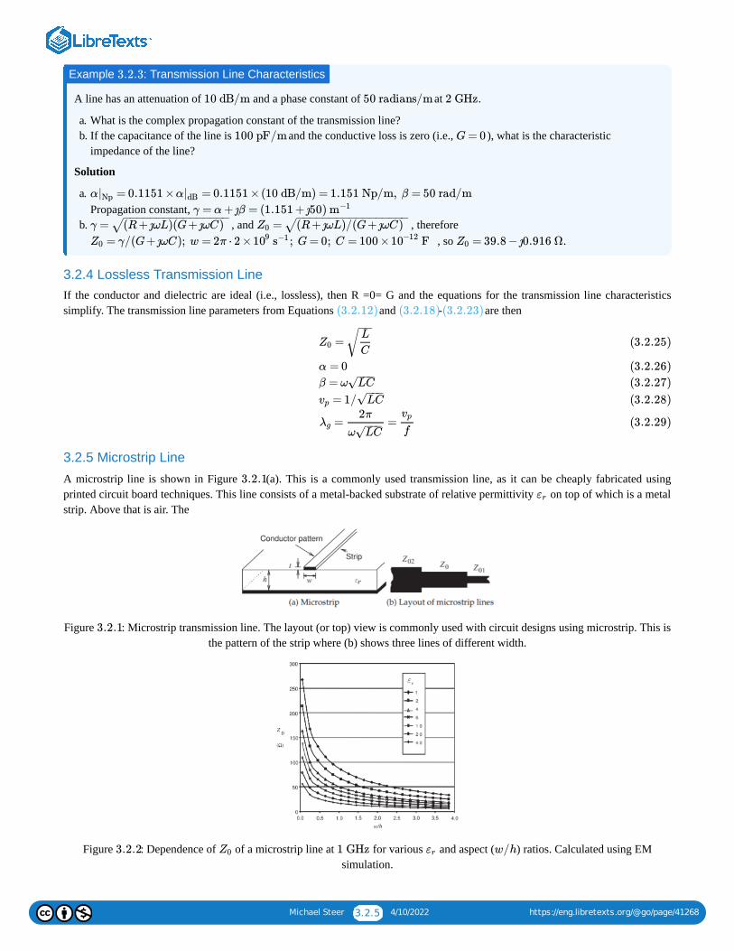
Michael Steer 3.2.5 4/10/2022 https://eng.libretexts.org/@go/page/41268
A line has an attenuation of and a phase constant of at .
a. What is the complex propagation constant of the transmission line?b. If the capacitance of the line is and the conductive loss is zero (i.e., ), what is the characteristic
impedance of the line?
Solution
a. Propagation constant,
b. , and , therefore , so .
3.2.4 Lossless Transmission LineIf the conductor and dielectric are ideal (i.e., lossless), then R =0= G and the equations for the transmission line characteristicssimplify. The transmission line parameters from Equations and - are then
3.2.5 Microstrip Line
A microstrip line is shown in Figure (a). This is a commonly used transmission line, as it can be cheaply fabricated usingprinted circuit board techniques. This line consists of a metal-backed substrate of relative permittivity on top of which is a metalstrip. Above that is air. The
Figure : Microstrip transmission line. The layout (or top) view is commonly used with circuit designs using microstrip. This isthe pattern of the strip where (b) shows three lines of different width.
Figure : Dependence of of a microstrip line at for various and aspect ( ) ratios. Calculated using EMsimulation.
Example : Transmission Line Characteristics3.2.3
10 dB/m 50 radians/m 2 GHz
100 pF/m G= 0
α = 0.1151 ×α = 0.1151 ×(10 dB/m) = 1.151 Np/m, β = 50 rad/m|Np |dB
γ = α+ ȷβ = (1.151 + ȷ50) m−1
γ = (R+ ȷωL)(G+ ȷωC)− −−−−−−−−−−−−−−−
√ =Z0 (R+ ȷωL)/(G+ ȷωC)− −−−−−−−−−−−−−−−−
√= γ/(G+ ȷωC); w = 2π ⋅ 2 × ; G= 0; C = 100 × FZ0 109 s−1 10−12 = 39.8 − ȷ0.916 ΩZ0
(3.2.12) (3.2.18) (3.2.23)
=Z0L
C
−−√
α = 0
β = ω LC−−−
√
= 1/vp LC−−−
√
= =λg2π
ω LC−−−
√
vp
f
(3.2.25)
(3.2.26)
(3.2.27)
(3.2.28)
(3.2.29)
3.2.1εr
3.2.1
3.2.2 Z0 1 GHz εr w/h
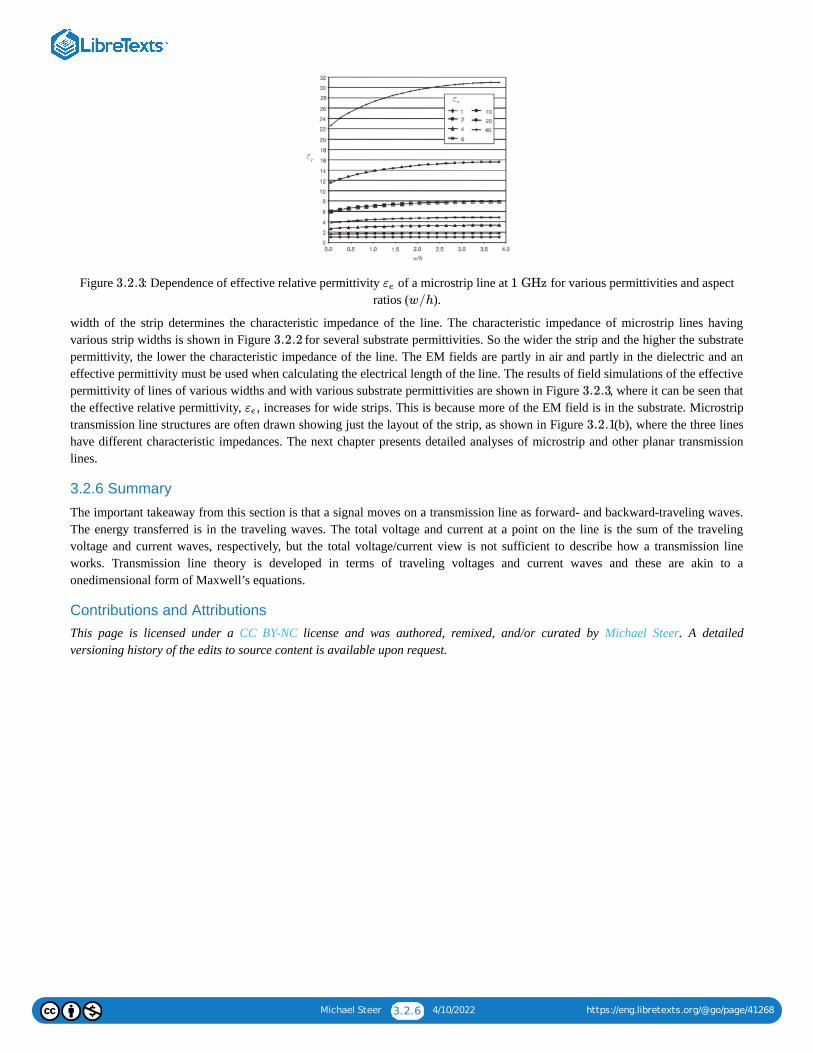
Michael Steer 3.2.6 4/10/2022 https://eng.libretexts.org/@go/page/41268
Figure : Dependence of effective relative permittivity of a microstrip line at for various permittivities and aspectratios ( ).
width of the strip determines the characteristic impedance of the line. The characteristic impedance of microstrip lines havingvarious strip widths is shown in Figure for several substrate permittivities. So the wider the strip and the higher the substratepermittivity, the lower the characteristic impedance of the line. The EM fields are partly in air and partly in the dielectric and aneffective permittivity must be used when calculating the electrical length of the line. The results of field simulations of the effectivepermittivity of lines of various widths and with various substrate permittivities are shown in Figure , where it can be seen thatthe effective relative permittivity, , increases for wide strips. This is because more of the EM field is in the substrate. Microstriptransmission line structures are often drawn showing just the layout of the strip, as shown in Figure (b), where the three lineshave different characteristic impedances. The next chapter presents detailed analyses of microstrip and other planar transmissionlines.
3.2.6 Summary
The important takeaway from this section is that a signal moves on a transmission line as forward- and backward-traveling waves.The energy transferred is in the traveling waves. The total voltage and current at a point on the line is the sum of the travelingvoltage and current waves, respectively, but the total voltage/current view is not sufficient to describe how a transmission lineworks. Transmission line theory is developed in terms of traveling voltages and current waves and these are akin to aonedimensional form of Maxwell’s equations.
Contributions and AttributionsThis page is licensed under a CC BY-NC license and was authored, remixed, and/or curated by Michael Steer. A detailedversioning history of the edits to source content is available upon request.
3.2.3 εe 1 GHzw/h
3.2.2
3.2.3εe
3.2.1
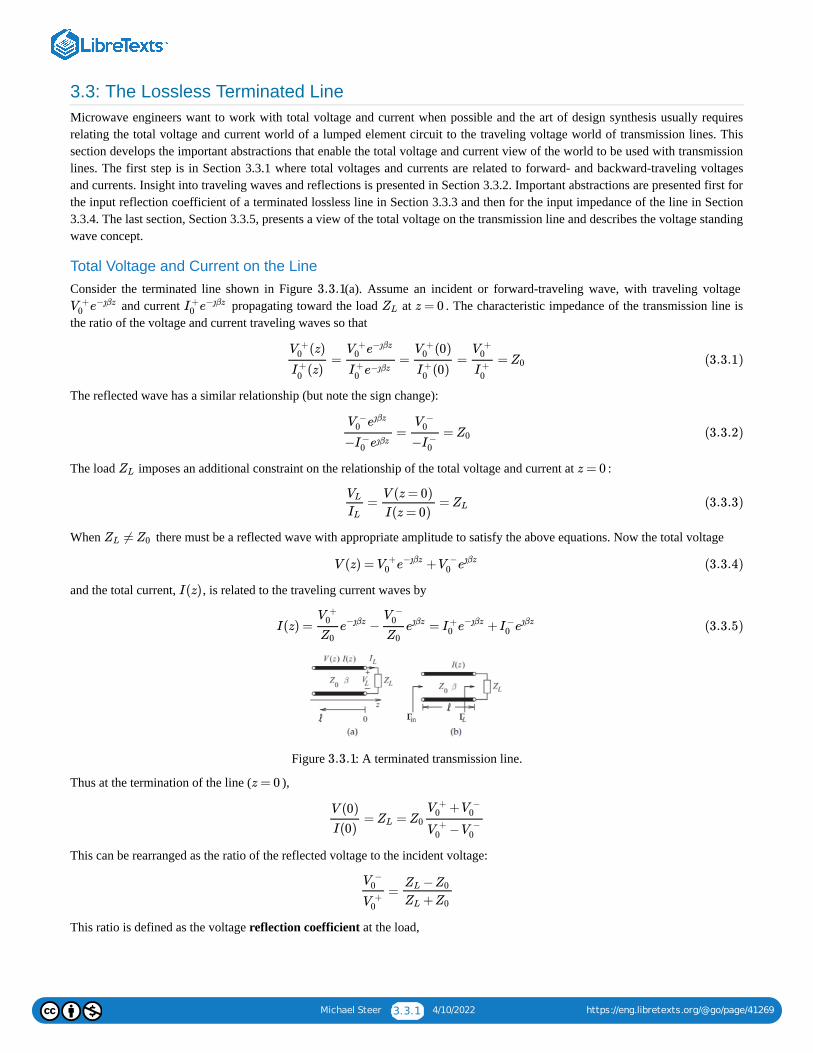
Michael Steer 3.3.1 4/10/2022 https://eng.libretexts.org/@go/page/41269
3.3: The Lossless Terminated LineMicrowave engineers want to work with total voltage and current when possible and the art of design synthesis usually requiresrelating the total voltage and current world of a lumped element circuit to the traveling voltage world of transmission lines. Thissection develops the important abstractions that enable the total voltage and current view of the world to be used with transmissionlines. The first step is in Section 3.3.1 where total voltages and currents are related to forward- and backward-traveling voltagesand currents. Insight into traveling waves and reflections is presented in Section 3.3.2. Important abstractions are presented first forthe input reflection coefficient of a terminated lossless line in Section 3.3.3 and then for the input impedance of the line in Section3.3.4. The last section, Section 3.3.5, presents a view of the total voltage on the transmission line and describes the voltage standingwave concept.
Total Voltage and Current on the LineConsider the terminated line shown in Figure (a). Assume an incident or forward-traveling wave, with traveling voltage
and current propagating toward the load at . The characteristic impedance of the transmission line isthe ratio of the voltage and current traveling waves so that
The reflected wave has a similar relationship (but note the sign change):
The load imposes an additional constraint on the relationship of the total voltage and current at :
When there must be a reflected wave with appropriate amplitude to satisfy the above equations. Now the total voltage
and the total current, , is related to the traveling current waves by
Figure : A terminated transmission line.
Thus at the termination of the line ( ),
This can be rearranged as the ratio of the reflected voltage to the incident voltage:
This ratio is defined as the voltage reflection coefficient at the load,
3.3.1
V +0 e−ȷβz I+
0 e−ȷβz ZL z = 0
= = = =(z)V +
0
(z)I+0
V +0 e−ȷβz
I+0e−ȷβz
(0)V +0
(0)I+0
V +0
I+0
Z0 (3.3.1)
= =V −
0 eȷβz
−I−0 eȷβz
V −0
−I−0
Z0 (3.3.2)
ZL z = 0
= =VL
IL
V (z = 0)
I(z = 0)ZL (3.3.3)
≠ZL Z0
V (z) = +V +0 e−ȷβz V −
0 eȷβz (3.3.4)
I(z)
I(z) = − = +V +
0
Z0e−ȷβz
V −0
Z0eȷβz I+
0 e−ȷβz I−0 eȷβz (3.3.5)
3.3.1
z = 0
= =V (0)
I(0)ZL Z0
+V +0 V −
0
−V +0 V −
0
=V −
0
V +0
−ZL Z0
+ZL Z0

Michael Steer 3.3.2 4/10/2022 https://eng.libretexts.org/@go/page/41269
That is, at the load
The relationship in Equation can be rewritten so that the input load impedance can be obtained from the reflectioncoefficient:
Similarly, the current reflection coefficient can be written as
The voltage reflection coefficient is used most of the time, so the reflection coefficient, , on its own refers to the voltage reflectioncoefficient, .
A lossless transmission line is terminated in an open circuit. What is the relationship between the forward- and backward-traveling voltage waves at the end of the line?
Solution
At the end of the line the total current is zero, so that and so
The forward- and backward traveling voltages and currents are related to the characteristic impedance by
Note the change in sign, as a result of the direction of propagation changing but the positive reference for current is in the samedirection. Substituting for at the termination,
Thus the total voltage at the end of the line, , is . Note that the total voltage at the end of the line istwice the incident (forward-traveling) voltage.
A load consists of a shunt connection of a capacitor of and a resistor of . The load terminates a lossless transmission line. The operating frequency is .
a. What is the impedance of the load?b. What is the normalized impedance of the load (normalized to of the line)?c. What is the reflection coefficient of the load?d. What is the current reflection coefficient of the load?
Solution
a.
b. c. This is the voltage reflection coefficient. .d. .
= = = =ΓL ΓVL
(0)V −0
(0)V +0
V −0
V +0
−ZL Z0
+ZL Z0(3.3.6)
=V −0 ΓLV
+0 (3.3.7)
(3.3.6)
=ZL Z0
1|ΓV
1 −ΓV(3.3.8)
= = = −ΓII−
0
I+0
− +ZL Z0
+ZL Z0ΓV (3.3.9)
Γ
= ΓΓV
Example : Forward- and Backward-Traveling Waves at an Open Circuit3.3.1
+ = 0I+ I−
= −I− I+ (3.3.10)
= / = − /Z0 V + I+ V − I− (3.3.11)
I−
= − / = − /(− ) =V + V −I+ I− V −I+ I+ V − (3.3.12)
VTOTAL + = 2V + V − V +
Example : Current Reflection Coefficient3.3.2
10 pF 60 Ω 50 Ω
5 GHz
Z0
C = 10 ⋅ F, R = 60 Ω; f = 5 ⋅ Hz; ω = 2πf ; = 50 Ω10−12 109 Z0
= R||C = (1/R+ ȷωC = 0.168 − ȷ3.174 ΩZL )−1
= / = 3.368 ⋅ − ȷ0.063zL ZL Z0 10−3
= ( −1)/( +1) = −0.985 − ȷ0.126 = 0.993∠ΓL zL zL 187.3∘
= − = 0.985 + ȷ0.126 = 0.993∠(187.3 −180 = 0.993∠ΓIL ΓL )∘ 7.3∘
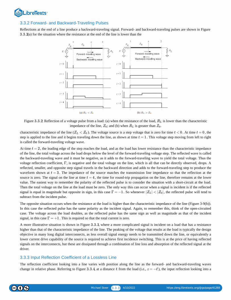
Michael Steer 3.3.3 4/10/2022 https://eng.libretexts.org/@go/page/41269
3.3.2 Forward- and Backward-Traveling PulsesReflections at the end of a line produce a backward-traveling signal. Forward- and backward-traveling pulses are shown in Figure
(a) for the situation where the resistance at the end of the line is lower than the
Figure : Reflection of a voltage pulse from a load: (a) when the resistance of the load, is lower than the characteristicimpedance of the line, ; and (b) when is greater than .
characteristic impedance of the line ( ). The voltage source is a step voltage that is zero for time . At time , thestep is applied to the line and it begins traveling down the line, as shown at time . This voltage step moving from left to rightis called the forward-traveling voltage wave.
At time , the leading edge of the step reaches the load, and as the load has lower resistance than the characteristic impedanceof the line, the total voltage across the load drops below the level of the forward-traveling voltage step. The reflected wave is calledthe backward-traveling wave and it must be negative, as it adds to the forward-traveling wave to yield the total voltage. Thus thevoltage reflection coefficient, , is negative and the total voltage on the line, which is all that can be directly observed, drops. Areflected, smaller, and opposite step signal travels in the backward direction and adds to the forward-traveling step to produce thewaveform shown at . The impedance of the source matches the transmission line impedance so that the reflection at thesource is zero. The signal on the line at time , the time for round-trip propagation on the line, therefore remains at the lowervalue. The easiest way to remember the polarity of the reflected pulse is to consider the situation with a short-circuit at the load.Then the total voltage on the line at the load must be zero. The only way this can occur when a signal is incident is if the reflectedsignal is equal in magnitude but opposite in sign, in this case . So whenever , the reflected pulse will tend tosubtract from the incident pulse.
The opposite situation occurs when the resistance at the load is higher than the characteristic impedance of the line (Figure 3-9(b)).In this case the reflected pulse has the same polarity as the incident signal. Again, to remember this, think of the open-circuitedcase. The voltage across the load doubles, as the reflected pulse has the same sign as well as magnitude as that of the incidentsignal, in this case . This is required so that the total current is zero.
A more illustrative situation is shown in Figure , where a more complicated signal is incident on a load that has a resistancehigher than that of the characteristic impedance of the line. The peaking of the voltage that results at the load is typically the designobjective in many long digital interconnects, as less overall signal energy needs to be transmitted down the line, or equivalently alower current drive capability of the source is required to achieve first incidence switching. This is at the price of having reflectedsignals on the interconnects, but these are dissipated through a combination of line loss and absorption of the reflected signal at thedriver.
3.3.3 Input Reflection Coefficient of a Lossless Line
The reflection coefficient looking into a line varies with position along the line as the forward- and backward-traveling waveschange in relative phase. Referring to Figure , at a distance ℓ from the load (i.e., ), the input reflection looking into a
3.3.2
3.3.2 RL
Z0 RL Z0
<ZL Z0 t < 0 t = 0
t = 1
t = 2
Γ
t = 3
t = 4
Γ = −1 | | < | |ZL Z0
Γ = +1
3.3.3
3.3.4 z = −ℓ
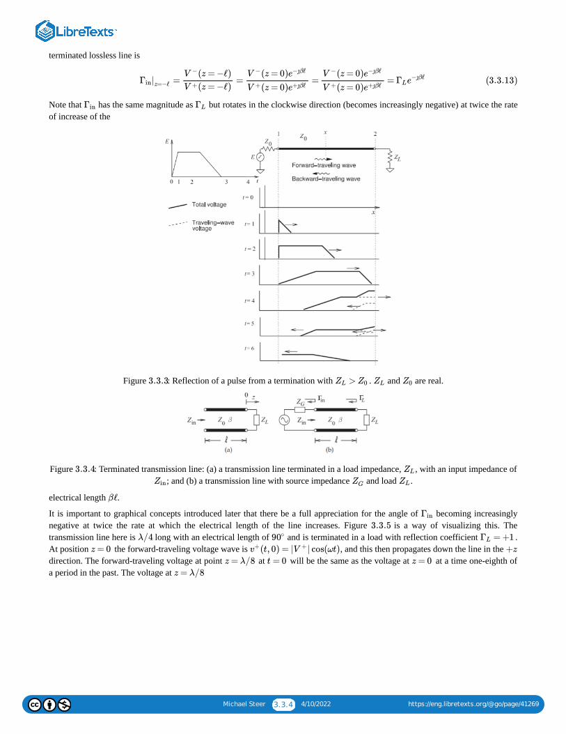
Michael Steer 3.3.4 4/10/2022 https://eng.libretexts.org/@go/page/41269
terminated lossless line is
Note that has the same magnitude as but rotates in the clockwise direction (becomes increasingly negative) at twice the rateof increase of the
Figure : Reflection of a pulse from a termination with . and are real.
Figure : Terminated transmission line: (a) a transmission line terminated in a load impedance, , with an input impedance of; and (b) a transmission line with source impedance and load .
electrical length .
It is important to graphical concepts introduced later that there be a full appreciation for the angle of becoming increasinglynegative at twice the rate at which the electrical length of the line increases. Figure is a way of visualizing this. Thetransmission line here is long with an electrical length of and is terminated in a load with reflection coefficient .At position the forward-traveling voltage wave is , and this then propagates down the line in the direction. The forward-traveling voltage at point at will be the same as the voltage at at a time one-eighth ofa period in the past. The voltage at
= = = =Γin|z=−ℓ
(z = −ℓ)V −
(z = −ℓ)V +
(z = 0)V − e−ȷβℓ
(z = 0)V + e+ȷβℓ
(z = 0)V − e−ȷβℓ
(z = 0)V + e+ȷβℓΓLe
−ȷβℓ (3.3.13)
Γin ΓL
3.3.3 >ZL Z0 ZL Z0
3.3.4 ZL
Zin ZG ZL
βℓ
Γin
3.3.5
λ/4 90∘ = +1ΓL
z = 0 (t, 0) = | | cos(ωt)v+ V + +z
z = λ/8 t = 0 z = 0
z = λ/8
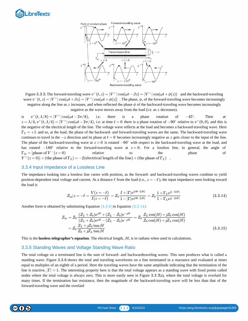
Michael Steer 3.3.5 4/10/2022 https://eng.libretexts.org/@go/page/41269
Figure : The forward-traveling wave and the backward-travelingwave . The phase, , of the forward-traveling wave becomes increasingly
negative along the line as increases, and when reflected the phase of the backward-traveling wave becomes increasinglynegative as the wave moves away from the load (i.e. as decreases).
is , i.e. there is a phase rotation of . Then at , i.e. at time there is a phase rotation of relative to , and this is
the negative of the electrical length of the line. The voltage wave reflects at the load and becomes a backward-traveling wave. Here and so, at the load, the phase of the backward- and forward-traveling waves are the same. The backward-traveling wave
continues to travel in the direction and its phase at becomes increasingly negative as gets closer to the input of the line.The phase of the backward-traveling wave at is rotated with respect to the backward-traveling wave at the load, andhas rotated relative to the forward-traveling wave at . For a lossless line, in general, the angle of
relative to the phase of .
3.3.4 Input Impedance of a Lossless Line
The impedance looking into a lossless line varies with position, as the forward- and backward-traveling waves combine to yieldposition-dependent total voltage and current. At a distance from the load (i.e., ), the input impedance seen looking towardthe load is
Another form is obtained by substituting Equation in Equation :
This is the lossless telegrapher’s equation. The electrical length, , is in radians when used in calculations.
3.3.5 Standing Waves and Voltage Standing Wave Ratio
The total voltage on a terminated line is the sum of forward- and backwardtraveling waves. This sum produces what is called astanding wave. Figure shows the total and traveling waveforms on a line terminated in a reactance and evaluated at timesequal to multiples of an eighth of a period. Here the traveling waves have the same amplitude indicating that the termination of theline is reactive, . The interesting property here is that the total voltage appears as a standing wave with fixed points callednodes where the total voltage is always zero. This is more easily seen in Figure (a), where the total voltage is overlaid formany times. If the termination has resistance, then the magnitude of the backward-traveling wave will be less than that of theforward-traveling wave and the overlaid
3.3.5 (t, z) = | | cos(ωt−βz) = | | cos(ωt+ϕ(z))v+ V + V +
(t, z) = | | cos(ωt+βz) = | | cos[ωt+ϕ(z)]v− V + V + ϕ
z ϕ
z
(t,λ/8) = | | cos(ωt−2π/8)v+ V + −45∘
z = λ/4, (t,λ/4) = | | cos(ωt−2π/4)v+ V + t = 0 −90∘ (0, 0)v+
= +1ΓL
−z t = 0 z
z = 0 −90∘
−180∘ z = 0
= [phase of (z = 0)Γin V −
(z = 0)] +(the phase of ) = −2(electrical length of the line) +(the phase of )V + ΓL ΓL
ℓ z = −ℓ
|z = −ℓ = = =Zin
V (z = −ℓ)
I(z = −ℓ)Z0
I +|Γ|eȷ(Θ−2βℓ)
1 −|Γ|eȷ(Θ−2βℓ)Z0
1 +ΓLeȷ(−2βℓ)
1 −ΓLeȷ(−2βℓ)(3.3.14)
(3.3.6) (3.3.14)
Zin = =Z0( + ) +( − )ZL Z0 eȷβℓ ZL Z0 e−ȷβℓ
( + ) −( − )ZL Z0 eȷβℓ ZL Z0 e−ȷβℓZ0
cos(βℓ) + ȷ cos(βℓ)ZL Z0
cos(βℓ) + ȷ cos(βℓ)Z0 ZL
= Z0+ ȷ tanβℓZL Z0
+ ȷ tanβℓZ0 ZL
(3.3.15)
βℓ
3.3.6
|Γ| = 1
3.3.7
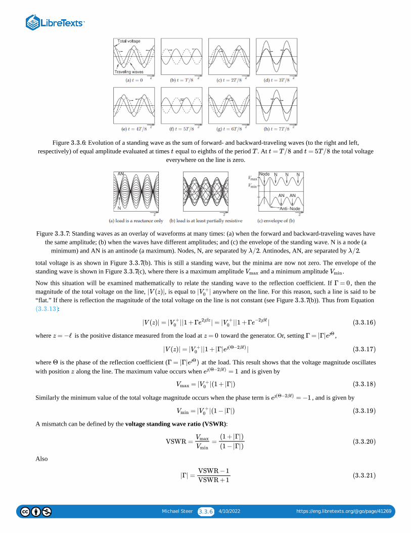
Michael Steer 3.3.6 4/10/2022 https://eng.libretexts.org/@go/page/41269
Figure : Evolution of a standing wave as the sum of forward- and backward-traveling waves (to the right and left,respectively) of equal amplitude evaluated at times equal to eighths of the period . At and the total voltage
everywhere on the line is zero.
Figure : Standing waves as an overlay of waveforms at many times: (a) when the forward and backward-traveling waves havethe same amplitude; (b) when the waves have different amplitudes; and (c) the envelope of the standing wave. N is a node (a
minimum) and AN is an antinode (a maximum). Nodes, N, are separated by . Antinodes, AN, are separated by .
total voltage is as shown in Figure (b). This is still a standing wave, but the minima are now not zero. The envelope of thestanding wave is shown in Figure (c), where there is a maximum amplitude and a minimum amplitude .
Now this situation will be examined mathematically to relate the standing wave to the reflection coefficient. If , then themagnitude of the total voltage on the line, , is equal to anywhere on the line. For this reason, such a line is said to be“flat.” If there is reflection the magnitude of the total voltage on the line is not constant (see Figure (b)). Thus from Equation
:
where is the positive distance measured from the load at toward the generator. Or, setting ,
where is the phase of the reflection coefficient ( at the load. This result shows that the voltage magnitude oscillateswith position along the line. The maximum value occurs when and is given by
Similarly the minimum value of the total voltage magnitude occurs when the phase term is , and is given by
A mismatch can be defined by the voltage standing wave ratio (VSWR):
Also
3.3.6
t T t = T/8 t = 5T/8
3.3.7
λ/2 λ/2
3.3.7
3.3.7 Vmax Vmin
Γ = 0
|V (z)| | |V +0
3.3.7
(3.3.13)
|V (z)| = | ||1 +Γ | = | ||1 +Γ |V +0 e2ȷβz V +
0 e−2ȷβℓ (3.3.16)
z = −ℓ z = 0 Γ = |Γ|eȷΘ
|V (z)| = | ||1 +|Γ| |V +0 eȷ(Θ−2βℓ) (3.3.17)
Θ Γ = |Γ| )eȷΘ
z = 1eȷ(Θ−2βℓ)
= | |(1 +|Γ|)Vmax V +0 (3.3.18)
= −1eȷ(Θ−2βℓ)
= | |(1 −|Γ|)Vmin V +0 (3.3.19)
VSWR = =Vmax
Vmin
(1 +|Γ|)
(1 −|Γ|)(3.3.20)
|Γ| =VSWR −1
VSWR +1(3.3.21)
Michael Steer 3.3.7 4/10/2022 https://eng.libretexts.org/@go/page/41269
Notice that in general is complex, but is necessarily always real and . For the matched condition, and , and the closer is to , the closer the load is to being matched to the line and the more power is
delivered to the load. The magnitude of the reflection coefficient on a line with a short-circuit or open-circuit load is , and in bothcases the is infinite.
To determine the position of the standing wave maximum, ℓmax, consider Equation and note that at the maximum
Here is the angle of the reflection coefficient at the load:
Thus the position of the voltage maxima, , normalized to wavelength is
Similarly the position of the voltage minima is (using Equation ):
After rearranging the terms,
Summarizing from Equations and :
1. The distance between two successive maxima is .2. The distance between two successive minima is .3. The distance between a maximum and an adjacent minimum is .4. From the measured the magnitude of the reflection coefficient can be found. From the measured the angle
of can be found. Then from the load impedance can be found.
In a similar manner to that above, the magnitude of the total current on the line is
Hence the standing wave current is maximum where the standing-wave voltage amplitude is minimum, and minimum where thestanding-wave voltage amplitude is maximum.
Now in Equation is a periodic function of with period and it varies between and , where
In Example 3.3.2 a load consisted of a capacitor of in shunt with a resistor of . The load terminated a lossless transmission line. The operating frequency is .
a. What is the SWR?b. What is the current standing wave ratio (ISWR)? (When SWR is used on its own it is assumed to refer to VSWR.)
Solution
a. From Example 3.3.2, and so
b. .
Γ VSWR 1 ≤ VSWR ≤ ∞
Γ = 0 VSWR = 1 VSWR 1
1
VSWR
(3.3.17)
Θ−2β = 2nπ, n = 0, 1, 2, …ℓmax (3.3.22)
Θ
Θ−2nπ = 22π
λgℓmax (3.3.23)
ℓmax
= ( −n) , n = 0, −1, −2, …ℓmax
λg
1
2
Θ
2π(3.3.24)
(3.3.17)
Θ−2β = (2n+1)πℓmin (3.3.25)
= ( −n+ ) , n = 0, −1, −2, …ℓmin
λg
1
2
Θ
2π
1
2(3.3.26)
(3.3.24) (3.3.26)
/2λg/2λg
/4λgVSWR |Γ| ℓmax Θ
Γ Γ
|I(ℓ)| = 1 −|Γ|| |V +
0
Z0
∣∣ eȷ(Θ−2βℓ) ∣∣ (3.3.27)
Zin (3.3.15) ℓ λ/2 Zmax Zmin
= = ×VSWR and = =ZmaxVmax
IminZ0 Zmin
Vmin
Imax
Z0
VSWR(3.3.28)
Example : Standing Wave Ratio3.3.3
10 pF 60 Ω 50 Ω
5 GHz
= 0.993∠ΓL 187.3∘
VSWR = = = 2851 +| |ΓL
1 −| |ΓL
1 +0.993
1 −0.993
ISWR = VSWR = 285

Michael Steer 3.3.8 4/10/2022 https://eng.libretexts.org/@go/page/41269
A load has an impedance and the system reference impedance, , is .
a. What is the reflection coefficient?b. What is the current reflection coefficient?c. What is the SWR?d. What is the ISWR?e. The power available from a source with a Thevenin equivalent impedance is . The source is connected
directly to the load, . Use the reflection coefficient to calculate the power delivered to .f. What is the total power absorbed by the Thevenin equivalent source impedance?g. Discuss the effect on power flow of inserting a lossless transmission line between the source and the load.
Solution
a. The voltage reflection coefficient is
b. The current reflection coefficient is
c. The SWR is the VSWR, so
d. The current SWR is .e. To determine the reflection coefficient of the load, begin by developing the Thevenin equivalent circuit of the load. The
power available from the source is , so the Thevenin equivalent circuit is
Figure The power reflected by the load is
and the power delivered to the load is
f. It is tempting to think that the power dissipated in is just . However, this is not correct. Instead, the current in must be determined and then the power dissipated in found. Let the current through be , and this iscomposed of forward and backward-traveling components:
where is the forward-traveling current wave. Thus
so , and
Example : Standing Waves3.3.4
= 45 + ȷ75 ΩZL Z0 100 Ω
100 Ω 1 mW
ZL ZL
100 Ω
ΓL = ( − )/( + ) = (45 + ȷ75 −100)/(45 + ȷ75 +100)ZL Z0 ZL Z0
= (93.0∠(2.204 rads))/(163.2∠(0.4773 rads))
= 0.570∠(1.726 rads0.570∠ = −0.0881 + ȷ0.653 =98.9∘ ΓV (3.3.29)
= − = 0.0881 − ȷ0.563 = 0.570∠( − ) = 0.570∠ΓI ΓV 98.9∘ 180∘ 81.1∘ (3.3.30)
SWR = VSWR = = = = 3.65Vmax
Vmin
1 +| |ΓV
1 −| |ΓV
1 +0.570
1 −0.570(3.3.31)
ISWR = VSWR
= 1 mWPA
3.3.8
= | | = 1 mW ⋅ (0.570 = 0.325 mWPR PA Γ2L )2
= (1 −| |) = 0.675 mWPD PA Γ2L
RTH PR RTH
RTH RTHcdot I
I = + = (1 + )I+ I− ΓI I+
I+
= | = | ×100 = 1 mW = WPA
1
2I+|2RTH
1
2I+|2 10−3
= 4.47 mAI+
Michael Steer 3.3.9 4/10/2022 https://eng.libretexts.org/@go/page/41269
The power dissipated in is
The circuit is that shown in part (e) and so the current in is the same as the current in . Thus the power delivered tothe load is due to the real part of :
g. Inserting a transmission line with the same characteristic impedance as the Thevenin equivalent impedance will have noeffect on power flow.
3.3.6 SummaryThis section related the physics of traveling voltage and current waves on lossless transmission lines to the total voltage and currentview. First the input reflection coefficient of a terminated lossless line was developed and from this the input impedance, which isthe ratio of total voltage and total current, derived. At any point along a line the amplitude of total voltage varies sinusoidally,tracing out a standing wave pattern along the line and yielding the metric which is the ratio of the maximum amplitude ofthe total voltage to the minimum amplitude of that voltage. This is an important metric that is often used to provide an indication ofhow good a match, i.e. how small the reflection is, with a indicating no reflection and a indicating totalreflection, i.e. a reflection coefficient magnitude of .
Contributions and AttributionsThis page is licensed under a CC BY-NC license and was authored, remixed, and/or curated by Michael Steer. A detailedversioning history of the edits to source content is available upon request.
I = (1 + ) = (1 +0.0881 − ȷ0.563) ×4.47 × A, |I| = 5.48 mAΓI I+ 10−3
RTH
= |I = (5.48 × −1.50 mWPTH1
2|2RTH
1
210−3)2RTH (3.3.32)
RTH ZL
ZL ZL
= | |R( ) = (5.48 × ×45 = 0.676 mWPD
1
2I 2 ZL
1
210−3)2 (3.3.33)
VSWR
VSWR = 1 VSWR = ∞
1
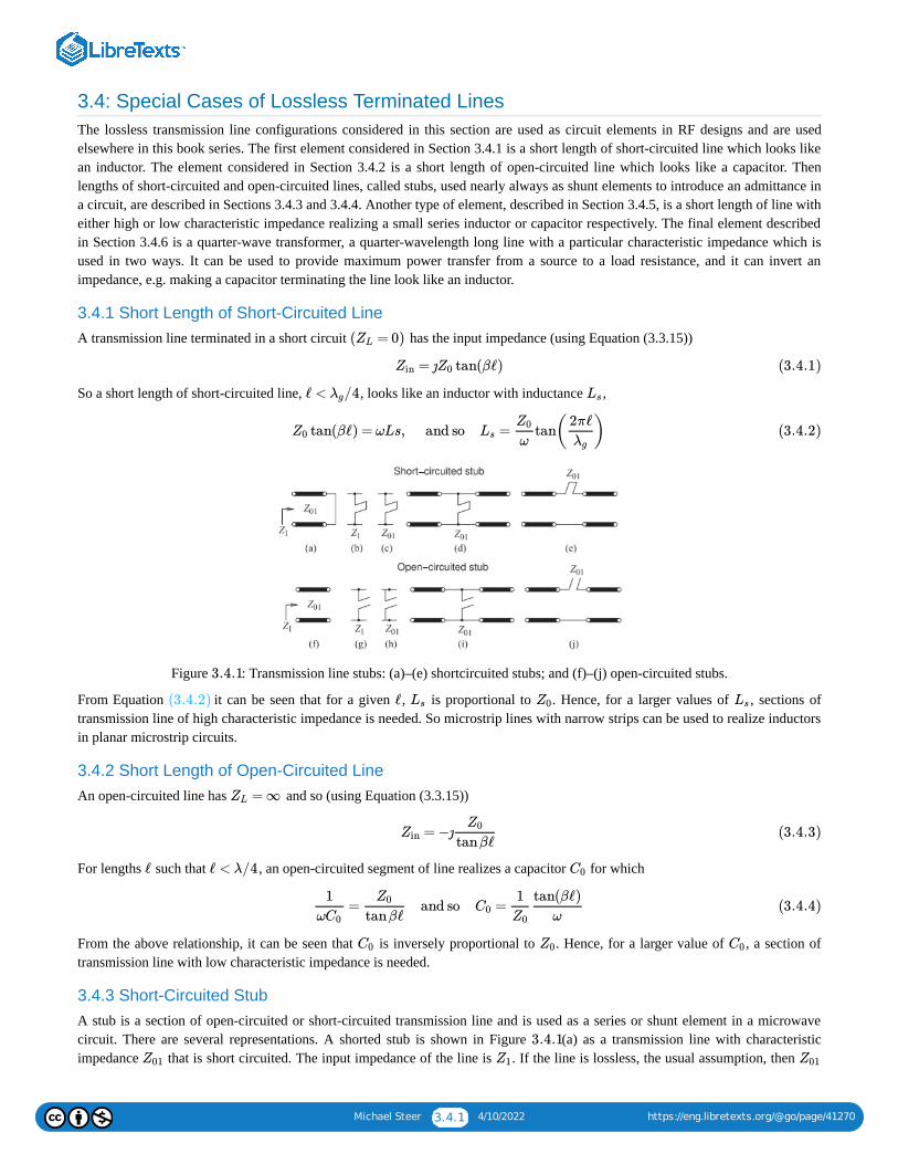
Michael Steer 3.4.1 4/10/2022 https://eng.libretexts.org/@go/page/41270
3.4: Special Cases of Lossless Terminated LinesThe lossless transmission line configurations considered in this section are used as circuit elements in RF designs and are usedelsewhere in this book series. The first element considered in Section 3.4.1 is a short length of short-circuited line which looks likean inductor. The element considered in Section 3.4.2 is a short length of open-circuited line which looks like a capacitor. Thenlengths of short-circuited and open-circuited lines, called stubs, used nearly always as shunt elements to introduce an admittance ina circuit, are described in Sections 3.4.3 and 3.4.4. Another type of element, described in Section 3.4.5, is a short length of line witheither high or low characteristic impedance realizing a small series inductor or capacitor respectively. The final element describedin Section 3.4.6 is a quarter-wave transformer, a quarter-wavelength long line with a particular characteristic impedance which isused in two ways. It can be used to provide maximum power transfer from a source to a load resistance, and it can invert animpedance, e.g. making a capacitor terminating the line look like an inductor.
3.4.1 Short Length of Short-Circuited LineA transmission line terminated in a short circuit has the input impedance (using Equation (3.3.15))
So a short length of short-circuited line, , looks like an inductor with inductance ,
Figure : Transmission line stubs: (a)–(e) shortcircuited stubs; and (f)–(j) open-circuited stubs.
From Equation it can be seen that for a given , is proportional to . Hence, for a larger values of , sections oftransmission line of high characteristic impedance is needed. So microstrip lines with narrow strips can be used to realize inductorsin planar microstrip circuits.
3.4.2 Short Length of Open-Circuited LineAn open-circuited line has and so (using Equation (3.3.15))
For lengths such that , an open-circuited segment of line realizes a capacitor for which
From the above relationship, it can be seen that is inversely proportional to . Hence, for a larger value of , a section oftransmission line with low characteristic impedance is needed.
3.4.3 Short-Circuited StubA stub is a section of open-circuited or short-circuited transmission line and is used as a series or shunt element in a microwavecircuit. There are several representations. A shorted stub is shown in Figure (a) as a transmission line with characteristicimpedance that is short circuited. The input impedance of the line is . If the line is lossless, the usual assumption, then
( = 0)ZL
= ȷ tan(βℓ)Zin Z0 (3.4.1)
ℓ < /4λg Ls
tan(βℓ) = ωLs, and so = tan( )Z0 Ls
Z0
ω
2πℓ
λg
(3.4.2)
3.4.1
(3.4.2) ℓ Ls Z0 Ls
= ∞ZL
= −ȷZinZ0
tanβℓ(3.4.3)
ℓ ℓ < λ/4 C0
= and so =1
ωC0
Z0
tanβℓC0
1
Z0
tan(βℓ)
ω(3.4.4)
C0 Z0 C0
3.4.1Z01 Z1 Z01
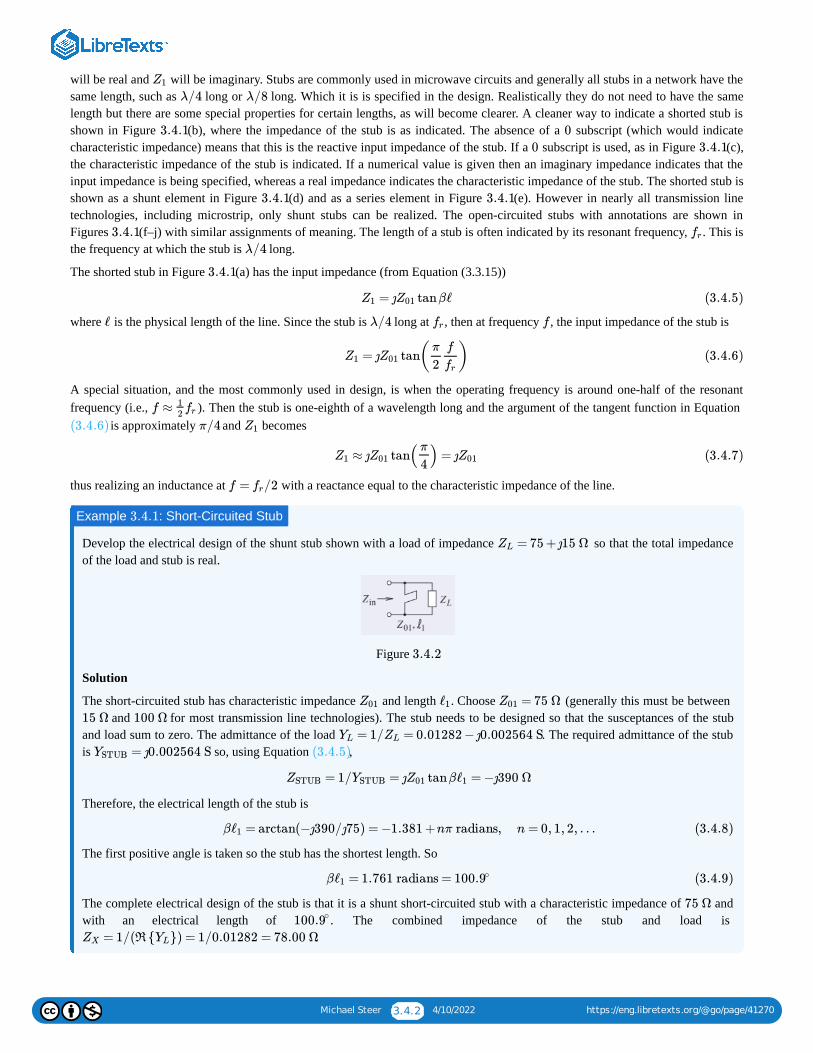
Michael Steer 3.4.2 4/10/2022 https://eng.libretexts.org/@go/page/41270
will be real and will be imaginary. Stubs are commonly used in microwave circuits and generally all stubs in a network have thesame length, such as long or long. Which it is is specified in the design. Realistically they do not need to have the samelength but there are some special properties for certain lengths, as will become clearer. A cleaner way to indicate a shorted stub isshown in Figure (b), where the impedance of the stub is as indicated. The absence of a subscript (which would indicatecharacteristic impedance) means that this is the reactive input impedance of the stub. If a subscript is used, as in Figure (c),the characteristic impedance of the stub is indicated. If a numerical value is given then an imaginary impedance indicates that theinput impedance is being specified, whereas a real impedance indicates the characteristic impedance of the stub. The shorted stub isshown as a shunt element in Figure (d) and as a series element in Figure (e). However in nearly all transmission linetechnologies, including microstrip, only shunt stubs can be realized. The open-circuited stubs with annotations are shown inFigures (f–j) with similar assignments of meaning. The length of a stub is often indicated by its resonant frequency, . This isthe frequency at which the stub is long.
The shorted stub in Figure (a) has the input impedance (from Equation (3.3.15))
where is the physical length of the line. Since the stub is long at , then at frequency , the input impedance of the stub is
A special situation, and the most commonly used in design, is when the operating frequency is around one-half of the resonantfrequency (i.e., ). Then the stub is one-eighth of a wavelength long and the argument of the tangent function in Equation
is approximately and becomes
thus realizing an inductance at with a reactance equal to the characteristic impedance of the line.
Develop the electrical design of the shunt stub shown with a load of impedance so that the total impedanceof the load and stub is real.
Figure
Solution
The short-circuited stub has characteristic impedance and length . Choose (generally this must be between and for most transmission line technologies). The stub needs to be designed so that the susceptances of the stub
and load sum to zero. The admittance of the load . The required admittance of the stubis so, using Equation ,
Therefore, the electrical length of the stub is
The first positive angle is taken so the stub has the shortest length. So
The complete electrical design of the stub is that it is a shunt short-circuited stub with a characteristic impedance of andwith an electrical length of . The combined impedance of the stub and load is
.
Z1
λ/4 λ/8
3.4.1 00 3.4.1
3.4.1 3.4.1
3.4.1 fr
λ/4
3.4.1
= ȷ tanβℓZ1 Z01 (3.4.5)
ℓ λ/4 fr f
= ȷ tan( )Z1 Z01π
2
f
fr
(3.4.6)
f ≈ 12
fr
(3.4.6) π/4 Z1
≈ ȷ tan( ) = ȷZ1 Z01π
4Z01 (3.4.7)
f = /2fr
Example : Short-Circuited Stub3.4.1
= 75 + ȷ15 ΩZL
3.4.2
Z01 ℓ1 = 75 ΩZ01
15 Ω 100 Ω= 1/ = 0.01282 − ȷ0.002564 SYL ZL
= ȷ0.002564 SYSTUB (3.4.5)
= 1/ = ȷ tanβ = −ȷ390 ΩZSTUB YSTUB Z01 ℓ1
β = arctan(−ȷ390/ȷ75) = −1.381 +nπ radians, n = 0, 1, 2, …ℓ1 (3.4.8)
β = 1.761 radians =ℓ1 100.9∘ (3.4.9)
75 Ω100.9∘
= 1/(R { }) = 1/0.01282 = 78.00 ΩZX YL
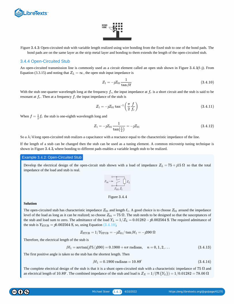
Michael Steer 3.4.3 4/10/2022 https://eng.libretexts.org/@go/page/41270
Figure : Open-circuited stub with variable length realized using wire bonding from the fixed stub to one of the bond pads. Thebond pads are on the same layer as the strip metal layer and bonding to them extends the length of the open-circuited stub.
3.4.4 Open-Circuited StubAn open-circuited transmission line is commonly used as a circuit element called an open stub shown in Figure (f–j). FromEquation (3.3.15) and noting that , the open stub input impedance is
With the stub one-quarter wavelength long at the frequency , the input impedance at is a short circuit and the stub is said to beresonant at . Then at a frequency , the input impedance of the stub is
When the stub is one-eighth wavelength long and
So a long open-circuited stub realizes a capacitance with a reactance equal to the characteristic impedance of the line.
If the length of a stub can be changed then the stub can be used as a tuning element. A common microstrip tuning technique isshown in Figure , where bonding to different pads enables a variable length stub to be realized.
Develop the electrical design of the open-circuit stub shown with a load of impedance so that the totalimpedance of the load and stub is real.
Figure
Solution
The open-circuited stub has characteristic impedance and length . A good choice is to choose around the impedancelevel of the load as long as it can be realized; so choose . The stub needs to be designed so that the susceptances ofthe stub and load sum to zero. The admittance of the load . The required admittance ofthe stub is , so, using Equation ,
Therefore, the electrical length of the stub is
The first positive angle is taken so the stub has the shortest length. Then
The complete electrical design of the stub is that it is a shunt open-circuited stub with a characteristic impedance of andan electrical length of . The combined impedance of the stub and load is .
3.4.3
3.4.1= ∞ZL
= −ȷZ1 Z011
tanβℓ(3.4.10)
fr fr
fr f
= −ȷ ( )Z1 Z01 tan−1 π
2
f
fr
(3.4.11)
f = 12
fr
= −ȷ = −ȷZ1 Z011
tan( )π
4
Z01 (3.4.12)
λ/4
3.4.3
Example : Open-Circuited Stub3.4.2
= 75 + ȷ15 ΩZL
3.4.4
Z01 ℓ1 Z01
= 75 ΩZ01
= 1/ = 0.01282 − ȷ0.002564 SYL ZL
= ȷ0.002564 SYSTUB (3.4.10)
= 1/ = −ȷ / tanβ = −ȷ390 ΩZSTUB YSTUB Z01 ℓ1
β = arctan(ȷ75/ȷ390) = 0.1900 +nπ radians, n = 0, 1, 2, …ℓ1 (3.4.13)
β = 0.1900 radians =ℓ1 10.89∘ (3.4.14)
75 Ω10.89∘ = 1/(R { }) = 1/0.01282 = 78.00 ΩZX YL
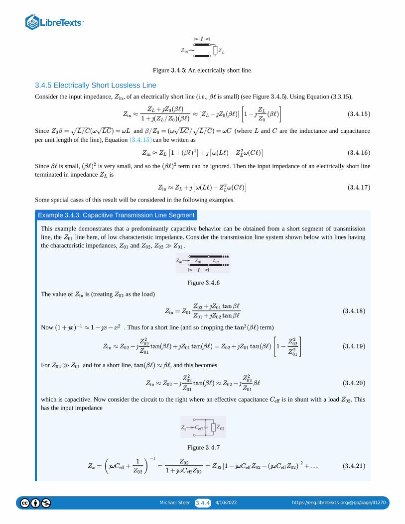
Michael Steer 3.4.4 4/10/2022 https://eng.libretexts.org/@go/page/41270
Figure : An electrically short line.
3.4.5 Electrically Short Lossless LineConsider the input impedance, , of an electrically short line (i.e., is small) (see Figure ). Using Equation (3.3.15),
Since and (where and are the inductance and capacitanceper unit length of the line), Equation can be written as
Since is small, is very small, and so the term can be ignored. Then the input impedance of an electrically short lineterminated in impedance is
Some special cases of this result will be considered in the following examples.
This example demonstrates that a predominantly capacitive behavior can be obtained from a short segment of transmissionline, the line here, of low characteristic impedance. Consider the transmission line system shown below with lines havingthe characteristic impedances, and , .
Figure
The value of is (treating as the load)
Now . Thus for a short line (and so dropping the term)
For and for a short line, , and this becomes
which is capacitive. Now consider the circuit to the right where an effective capacitance is in shunt with a load . Thishas the input impedance
Figure
3.4.5
Zin βℓ 3.4.5
≈ ≈ [ + ȷ (βℓ)] [1 − ȷ (βℓ)]Zin+ ȷ (βℓ)ZL Z0
1 + ȷ( / )(βℓ)ZL Z0ZL Z0
ZL
Z0(3.4.15)
β = (ω ) = ωLZ0 L/C− −−−
√ LC−−−
√ β/ = (ω / ) = ωCZ0 LC−−−
√ L/C− −−−
√ L C
(3.4.15)
≈ [1 +(βℓ ]+ ȷ[ω(Lℓ) − ω(Cℓ)]Zin ZL )2 Z2L (3.4.16)
βℓ (βℓ)2 (βℓ)2
ZL
≈ + ȷ[ω(Lℓ) − ω(Cℓ)]Zin ZL Z2L (3.4.17)
Example : Capacitive Transmission Line Segment3.4.3
Z01
Z01 Z02 ≫Z02 Z01
3.4.6
Zin Z02
=Zin Z01+ ȷ tanβℓZ02 Z01
+ ȷ tanβℓZ01 Z02(3.4.18)
(1 + ȷx ≈ 1 − ȷx −)−1 x2 (βℓ)tan2
≈ − ȷ tan(βℓ) + ȷ tan(βℓ) = + ȷ tan(βℓ)[1 − ]Zin Z02Z2
02
Z01Z01 Z02 Z01
Z202
Z201
(3.4.19)
≫Z02 Z01 tan(βℓ) ≈ βℓ
≈ − ȷ tan(βℓ) ≈ − ȷ βℓZin Z02Z2
02
Z01Z02
Z202
Z01(3.4.20)
Ceff Z02
3.4.7
= = = +…Zx (ȷω + )Ceff1
Z02
−1Z02
1 + ȷωCeffZ02Z02 [1 − ȷω −(ȷω )CeffZ02 CeffZ02
2(3.4.21)
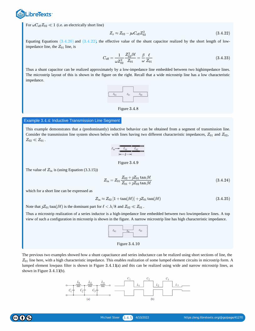
Michael Steer 3.4.5 4/10/2022 https://eng.libretexts.org/@go/page/41270
For (i.e. an electrically short line)
Equating Equations and , the effective value of the shunt capacitor realized by the short length of low-impedance line, the line, is
Thus a shunt capacitor can be realized approximately by a low-impedance line embedded between two highimpedance lines.The microstrip layout of this is shown in the figure on the right. Recall that a wide microstrip line has a low characteristicimpedance.
Figure
This example demonstrates that a (predominantly) inductive behavior can be obtained from a segment of transmission line.Consider the transmission line system shown below with lines having two different characteristic impedances, and ,
.
Figure
The value of is (using Equation (3.3.15))
which for a short line can be expressed as
Note that is the dominant part for and .
Thus a microstrip realization of a series inductor is a high-impedance line embedded between two lowimpedance lines. A topview of such a configuration in microstrip is shown in the figure. A narrow microstrip line has high characteristic impedance.
Figure
The previous two examples showed how a shunt capacitance and series inductance can be realized using short sections of line, the line here, with a high characteristic impedance. This enables realization of some lumped element circuits in microstrip form. A
lumped element lowpass filter is shown in Figure (a) and this can be realized using wide and narrow microstrip lines, asshown in Figure (b).
ω ≪ 1CeffZ02
≈ − ȷωZx Z02 CeffZ202 (3.4.22)
(3.4.20) (3.4.22)Z01
= =Ceff1
ωZ202
βℓZ202
Z01
β
ω
ℓ
Z01(3.4.23)
3.4.8
Example : Inductive Transmission Line Segment3.4.4
Z01 Z02
≪Z02 Z01
3.4.9
Zin
=Zin Z01+ ȷ tanβℓZ02 Z01
+ ȷ tanβℓZ01 Z02(3.4.24)
≈ [1 +tan(βℓ)] + ȷ tan(βℓ)Zin Z02 Z01 (3.4.25)
ȷ tan(βℓ)Z01 ℓ < λ/8 ≪Z02 Z01
3.4.10
Z01
3.4.113.4.11
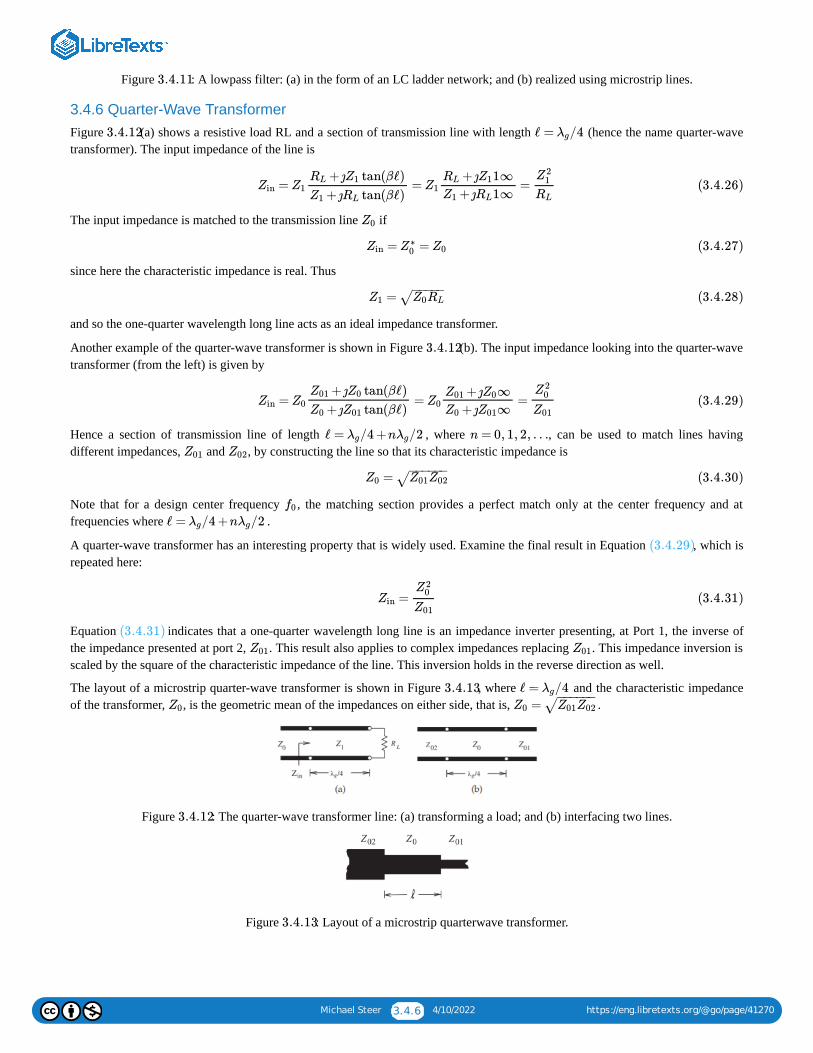
Michael Steer 3.4.6 4/10/2022 https://eng.libretexts.org/@go/page/41270
Figure : A lowpass filter: (a) in the form of an LC ladder network; and (b) realized using microstrip lines.
3.4.6 Quarter-Wave TransformerFigure (a) shows a resistive load RL and a section of transmission line with length (hence the name quarter-wavetransformer). The input impedance of the line is
The input impedance is matched to the transmission line if
since here the characteristic impedance is real. Thus
and so the one-quarter wavelength long line acts as an ideal impedance transformer.
Another example of the quarter-wave transformer is shown in Figure (b). The input impedance looking into the quarter-wavetransformer (from the left) is given by
Hence a section of transmission line of length , where , can be used to match lines havingdifferent impedances, and , by constructing the line so that its characteristic impedance is
Note that for a design center frequency , the matching section provides a perfect match only at the center frequency and atfrequencies where .
A quarter-wave transformer has an interesting property that is widely used. Examine the final result in Equation , which isrepeated here:
Equation indicates that a one-quarter wavelength long line is an impedance inverter presenting, at Port 1, the inverse ofthe impedance presented at port 2, . This result also applies to complex impedances replacing . This impedance inversion isscaled by the square of the characteristic impedance of the line. This inversion holds in the reverse direction as well.
The layout of a microstrip quarter-wave transformer is shown in Figure , where and the characteristic impedanceof the transformer, , is the geometric mean of the impedances on either side, that is, .
Figure : The quarter-wave transformer line: (a) transforming a load; and (b) interfacing two lines.
Figure : Layout of a microstrip quarterwave transformer.
3.4.11
3.4.12 ℓ = /4λg
= = =Zin Z1+ ȷ tan(βℓ)RL Z1
+ ȷ tan(βℓ)Z1 RL
Z1+ ȷ 1∞RL Z1
+ ȷ 1∞Z1 RL
Z21
RL
(3.4.26)
Z0
= =Zin Z∗0 Z0 (3.4.27)
=Z1 Z0RL− −−−−√ (3.4.28)
3.4.12
= = =Zin Z0+ ȷ tan(βℓ)Z01 Z0
+ ȷ tan(βℓ)Z0 Z01Z0
+ ȷ ∞Z01 Z0
+ ȷ ∞Z0 Z01
Z20
Z01(3.4.29)
ℓ = /4 +n /2λg λg n = 0, 1, 2, …Z01 Z02
=Z0 Z01Z02− −−−−−
√ (3.4.30)
f0
ℓ = /4 +n /2λg λg
(3.4.29)
=Zin
Z20
Z01(3.4.31)
(3.4.31)Z01 Z01
3.4.13 ℓ = /4λg
Z0 =Z0 Z01Z02− −−−−−
√
3.4.12
3.4.13

Michael Steer 3.4.7 4/10/2022 https://eng.libretexts.org/@go/page/41270
3.4.7 SummaryThe lossless transmission line configurations considered in this section are those most commonly used in microwave circuit design.It is important to note that the stub line is almost always used in shunt configuration to provide an admittance in a circuit. Mosttransmission line technologies, including coaxial lines and microstrip, only permit shunt stubs. The quarterwave transformer is aparticularly interesting element enabling maximum power transfer from a source to a load that may be different. An interestingfeature that is widely exploited is that the quarter-wave transformer inverts an impedance. For example, turning a small resistanceinto a large resistance, or even turning a small capacitor into a large inductance. These transformations are valid over a moderatebandwidth.
3.4.8 Summary
An earlier section developed the input reflection coefficient and input impedance of a lossless line. Several circuit elements basedon a a transmission line were introduced: stubs, short-sections of line have either high or low characteristic impedance, and thequarter-wave transformer.
Contributions and AttributionsThis page is licensed under a CC BY-NC license and was authored, remixed, and/or curated by Michael Steer. A detailedversioning history of the edits to source content is available upon request.
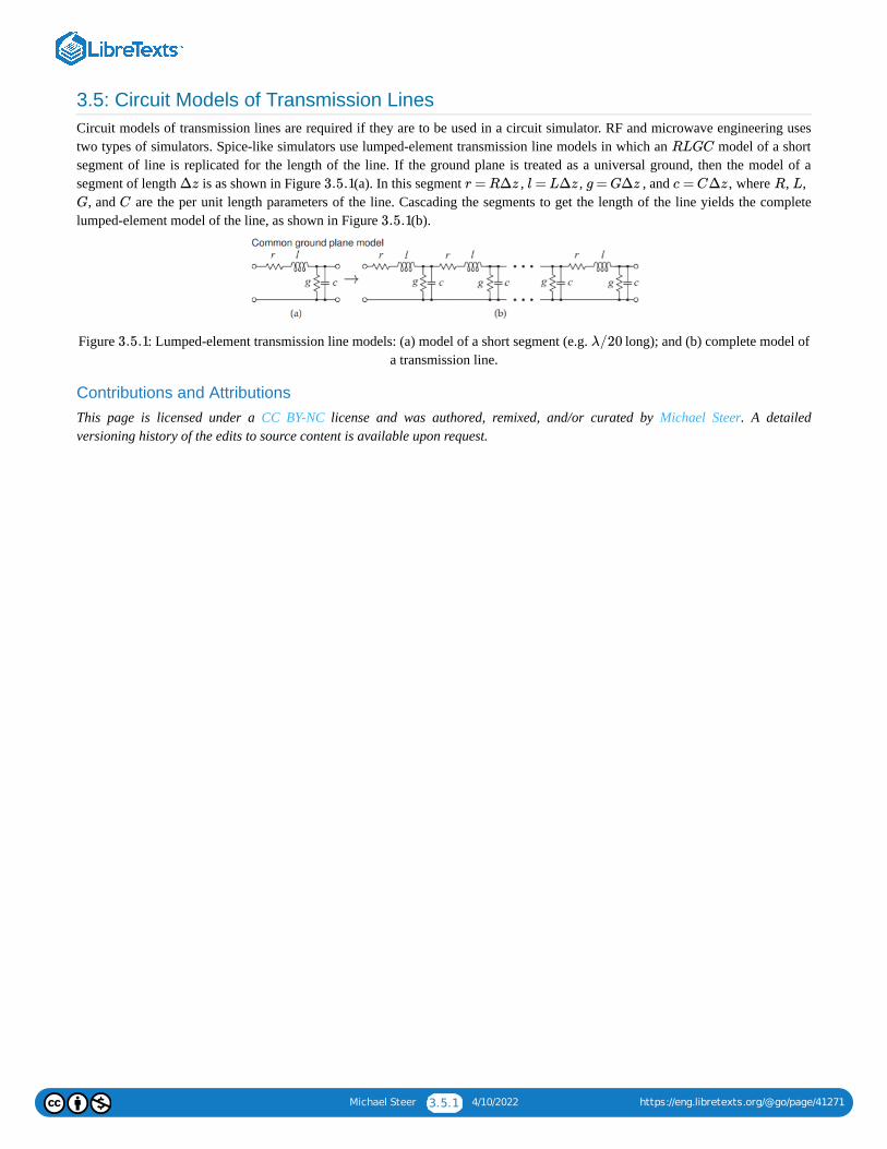
Michael Steer 3.5.1 4/10/2022 https://eng.libretexts.org/@go/page/41271
3.5: Circuit Models of Transmission LinesCircuit models of transmission lines are required if they are to be used in a circuit simulator. RF and microwave engineering usestwo types of simulators. Spice-like simulators use lumped-element transmission line models in which an model of a shortsegment of line is replicated for the length of the line. If the ground plane is treated as a universal ground, then the model of asegment of length is as shown in Figure (a). In this segment , , , and , where , ,
, and are the per unit length parameters of the line. Cascading the segments to get the length of the line yields the completelumped-element model of the line, as shown in Figure (b).
Figure : Lumped-element transmission line models: (a) model of a short segment (e.g. long); and (b) complete model ofa transmission line.
Contributions and AttributionsThis page is licensed under a CC BY-NC license and was authored, remixed, and/or curated by Michael Steer. A detailedversioning history of the edits to source content is available upon request.
RLGC
Δz 3.5.1 r = RΔz l = LΔz g = GΔz c = CΔz R L
G C
3.5.1
3.5.1 λ/20

Michael Steer 3.6.1 4/10/2022 https://eng.libretexts.org/@go/page/41272
3.6: SummaryIn this chapter a classical treatment of transmission lines was presented. Transmission lines are distributed elements and form thebasis of microwave circuits. A distinguishing feature is that they support forward- and backward-traveling waves and they can beused to implement circuit functions.
The most important of the formulas presented in this chapter are listed here. Reflection coefficients are referenced to an impedance , the load impedance is , and a line has a characteristic impedance , physical length , and propagation constant (or
electrical length in radians of where is the physical length of the line.
Contributions and AttributionsThis page is licensed under a CC BY-NC license and was authored, remixed, and/or curated by Michael Steer. A detailedversioning history of the edits to source content is available upon request.
Z0 ZL Z0 ℓ γ
βℓ ℓ
Reflection coefficient of a load
impedance ZL
Γ = = (3.3.6)ΓV −ZL ZREF
+ZL ZREF
Reflection coefficient in terms
of VSWR
|Γ| = (3.3.21)VSWR−1VSWR+1
Load impedance in terms of
reflection coefficient Γ
= (3.3.8)ZL ZREF1+Γ
1−Γ
Input impedance of a lossless
line
= (3.3.15)Zin Z0+ȷ tan βℓZL Z0
+ȷ tan βℓZ0 ZL
Input reflection coefficient of
a lossless line of length ℓ
= (3.3.13)Γin ΓLe−ȷ2βℓ
VSWR in terms of reflection
coefficient
VSWR = (3.3.20)(1+|Γ|)
(1−|Γ|)

Michael Steer 3.7.1 4/10/2022 https://eng.libretexts.org/@go/page/41273
3.7: References[1] T. Edwards and M. Steer, Foundations for Microstrip Circuit Design. John Wiley & Sons, 2016.
[2] C. Boyer and U. Merzbach, “Invention of logarithms,” in A History of Mathematics, 2nd ed. John Wiley & Sons, 1991.
Contributions and AttributionsThis page is licensed under a CC BY-NC license and was authored, remixed, and/or curated by Michael Steer. A detailedversioning history of the edits to source content is available upon request.

Michael Steer 3.8.1 4/10/2022 https://eng.libretexts.org/@go/page/41274
3.8: Exercises1. A coaxial line is short-circuited at one end and is filled with a dielectric with a relative permittivity of . [Parallels Example
3.1.1]a. What is the free-space wavelength at ?b. What is the wavelength in the dielectricfilled coaxial line at ?c. The first resonance of the coaxial resonator is at . What is the physical length of the resonator?
2. A transmission line has the following parameters: and .Consider a traveling wave on the transmission line with a frequency of . [Parallels Example 3.2.2]a. What is the attenuation constant?b. What is the phase constant?c. What is the phase velocity?d. What is the characteristic impedance of the line?e. What is the group velocity?
3. A transmission line has the per-unit length parameters and . Use a frequency of . [Parallels Example 3.2.2]
a. What is the phase velocity if ?b. What is the group velocity if ?c. If what is the phase velocity?d. If what is the group velocity?
4. A line is long and at the operating frequency the phase constant is . What is the electrical length of the line?[Parallels Example 3.2.1]
5. A coaxial transmission line is filled with lossy dielectric material with a relative permittivity of . If the line is air-filledit would have a characteristic impedance of . What is the input impedance of the line if it is long? Use reasonableapproximations. [Hint: Does the termination matter?]
6. A transmission line has the per unit length parameters .a. What is the propagation constant of the line at ?b. What is the characteristic impedance of the line at ?c. Plot the magnitude of the characteristic impedance versus frequency from to .
7. A line is long and at the phase constant is . What is the electrical length of the line in degrees?8. What is the electrical length of a line that is a quarter of a wavelength long,
a. in degrees?b. in radians?
9. A lossless transmission line has an inductance of and a capacitance of .
a. What is the characteristic impedance of the line?b. What is the phase velocity on the line at ?
10. A transmission line has an attenuation of and a phase constant of at . [Parallels Example 3.2.3]a. What is the complex propagation constant of the transmission line?b. If the capacitance of the line is and , what is the characteristic impedance of the line?
11. A very low-loss microstrip transmission line has the following per unit length parameters: and .
a. What is the characteristic impedance of the line if loss is ignored?b. What is the attenuation constant due to conductor loss?c. What is the attenuation constant due to dielectric loss?
12. A lossless transmission line carrying a signal has the following per unit length parameters: .
a. What is the attenuation constant?b. What is the phase constant?c. What is the phase velocity?
64
18 GHz
18 GHz
18 GHz
RLGC R = 100 Ω/m, L = 85 nH/m, G = 1 S/m, C = 150 pF/m
1 GHz
L = 85 nH/m, G = 1 S/m, C = 150 pF/m
1 GHz
R = 0 Ω/m
R = 0 Ω/m
R = 10 kΩ/m
R = 10 kΩ/m
10 cm β 40 rad/m
5 − ȷ0.2
100 Ω 1 km
R = 2 Ω/cm, L = 100 nH/m, G = 1 mS/M, C = 200 pF/m
5 GHz
5 GHz
100 MHz 10 GHz
20 cm 1 GHz β 20 rad/m
8 nH/cm 40 pF/cm
1 GHz
2 dB/m 25 radians/m 2 GHz
50 pF ⋅ m−1 G = 0
R = 2 Ω/m, L = 80 nH/m, C = 200 pF/m, G = 1 µS/m
1 GHz
L = 80 nH/m, C = 200 pF/m

Michael Steer 3.8.2 4/10/2022 https://eng.libretexts.org/@go/page/41274
d. What is the characteristic impedance of the line?13. A transmission line has a characteristic impedance and is terminated in a load with a reflection coefficient of . A
forward-traveling voltage wave on the line has a power of .1. How much power is reflected by the load?2. What is the power delivered to the load?
14. A transmission line has an attenuation of and a phase constant of at .a. What is the complex propagation constant of the transmission line?b. If the capacitance of the line is and , what is the complex characteristic impedance of the line?c. If the line is driven by a source modeled as an ideal voltage and a series impedance, what is the impedance of the source for
maximum transfer of power to the transmission line?d. If is delivered (i.e. in the forwardtraveling wave) to the transmission line by the generator, what is the power in the
forward-traveling wave on the line at from the generator?15. A lossless transmission line is driven by a generator having a Thevenin equivalent impedance of . The transmission
line is lossless, has a characteristic impedance of , and is infinitely long. The maximum power that can be delivered to aload attached to the generator is .a. What is the total (phasor) voltage at the input to the transmission line?b. What is the magnitude of the forwardtraveling voltage wave at the generator side of the line?c. What is the magnitude of the forwardtraveling current wave at the generator side of the line?
16. A transmission line is terminated in a short circuit. What is the ratio of the forward- and backward-traveling voltage waves atthe termination? [Parallels Example 3.3.1]
17. A transmission line is terminated in a load. What is the ratio of the forward- to the backward-traveling voltagewaves at the termination? [Parallels Example 3.3.1]
18. A transmission line is terminated in an open circuit. What is the ratio of the forwardto the backward-traveling voltagewaves at the termination? [Parallels Example 3.3.1]
19. A line has a characteristic impedance and is terminated in a load with a reflection coefficient of . A forward-travelingvoltage wave on the line has a power of .
a. How much power is reflected by the load?b. What is the power delivered to the load?
20. A load consists of a shunt connection of a capacitor of and a resistor of . The load terminates a lossless transmission line. The operating frequency is . [Parallels Example 3.3.2]a. What is the impedance of the load?b. What is the normalized impedance of the load (normalized to the characteristic impedance of the line)?c. What is the reflection coefficient of the load?d. What is the current reflection coefficient of the load?e. What is the standing wave ratio (SWR)?f. What is the current standing wave ratio (ISWR)?
21. An amplifier is connected to a load by a transmission line matched to the amplifier. If the SWR on the line is , whatpercentage of the available amplifier power is absorbed by the load?
22. A load has a reflection coefficient of when referred to . The load is at the end of a line with a characteristicimpedance.a. If the line has an electrical length of , what is the reflection coefficient calculated at the input of the line?b. What is the VSWR on the line?
23. A resistor in parallel with a capacitor terminates a transmission line. Calculate the SWR on the line at .
24. A lossless transmission line has a generator at one end and is terminated in . What is the VSWR on the line?25. A lossless line is driven by a generator. The line is terminated in a load that with a reflection coefficient (referred to
) of . What is the VSWR on the line?26. A load with a capacitor in parallel with a resistor terminates a line. The operating frequency is .
[Parallels Example 3.3.3]
a. What is the VSWR?
Z0 0.8∠45∘
1 dBm
0.2 dB/cm 50 radians/m 1 GHz
100 pF/m G = 0
1 W
2 m
1 GHz 50 Ω
75 Ω
2 W
50 Ω 40 Ω
50 Ω
Z0 0.8
1 W
10 pF 25 Ω 50 Ω
1 GHz
1.5
0.5 50 Ω 50 Ω
45∘
50 Ω
100 Ω 5 pF 100 Ω
2 GHz
50 Ω 50 Ω 100 Ω
75 Ω 75 Ω
50 Ω 0.5 + ȷ0.5
20 pF 50 Ω 25 Ω 5 GHz

Michael Steer 3.8.3 4/10/2022 https://eng.libretexts.org/@go/page/41274
b. What is ISWR?27. A load and the system reference impedance, , is . [Parallels Example 3.3.4]
a. What is the load reflection coefficient ?b. What is the current reflection coefficient?c. What is the VSWR on the line?d. What is the ISWR on the line?e. Now consider a source connected directly to the load. The source has a Thevenin equivalent impedance and an
available power of . Use to find the power delivered to .f. What is the total power absorbed by ?
28. A load of is to be matched to a transmission line with a characteristic impedance of . Use a quarter-wavetransformer. What is the characteristic impedance of the quarterwave transformer?
29. Determine the characteristic impedance of a quarter-wave transformer used to match a load of to a generator with aThevenin equivalent impedance of .
30. A transmission line is to be inserted between a line and a load so that there is maximum power transfer to the load at .a. How long is the inserted line in terms of wavelengths at ?b. What is the characteristic impedance of the line at ?
3.8.1 Exercises By Sectionchallenging, very challenging
3.8.2 Answers to Selected Exercises10.
29.
Contributions and AttributionsThis page is licensed under a CC BY-NC license and was authored, remixed, and/or curated by Michael Steer. A detailedversioning history of the edits to source content is available upon request.
= 55 − ȷ55 ΩZL Z0 50 Ω
ΓL
= 60 ΩZG
1 W ΓL ZL
ZG
100 Ω 50 Ω
50 Ω
75 Ω
5 Ω 50 Ω 50 Ω
20 GHz
20 GHz
20 GHz
† ‡
§3.11
§3.22†, 3, 4, 5, 6, 7, 8, 9, 10, 11, 12†, 13
§3.314†, 15, 16, 17, 18, 19†, 20†, 21†, 22, 23, 24, 25, 26, 27
§3.428, 29, 30
0.23 + ȷ25 m−1
61.2 Ω

1 4/10/2022
CHAPTER OVERVIEW4: PLANAR TRANSMISSION LINES
4.1: INTRODUCTION4.2: SUBSTRATES4.3: PLANAR TRANSMISSION LINE STRUCTURES4.4: MICROSTRIP TRANSMISSION LINES4.5: MICROSTRIP DESIGN FORMULAS4.6: SUMMARY4.7: REFERENCES4.8: EXERCISES
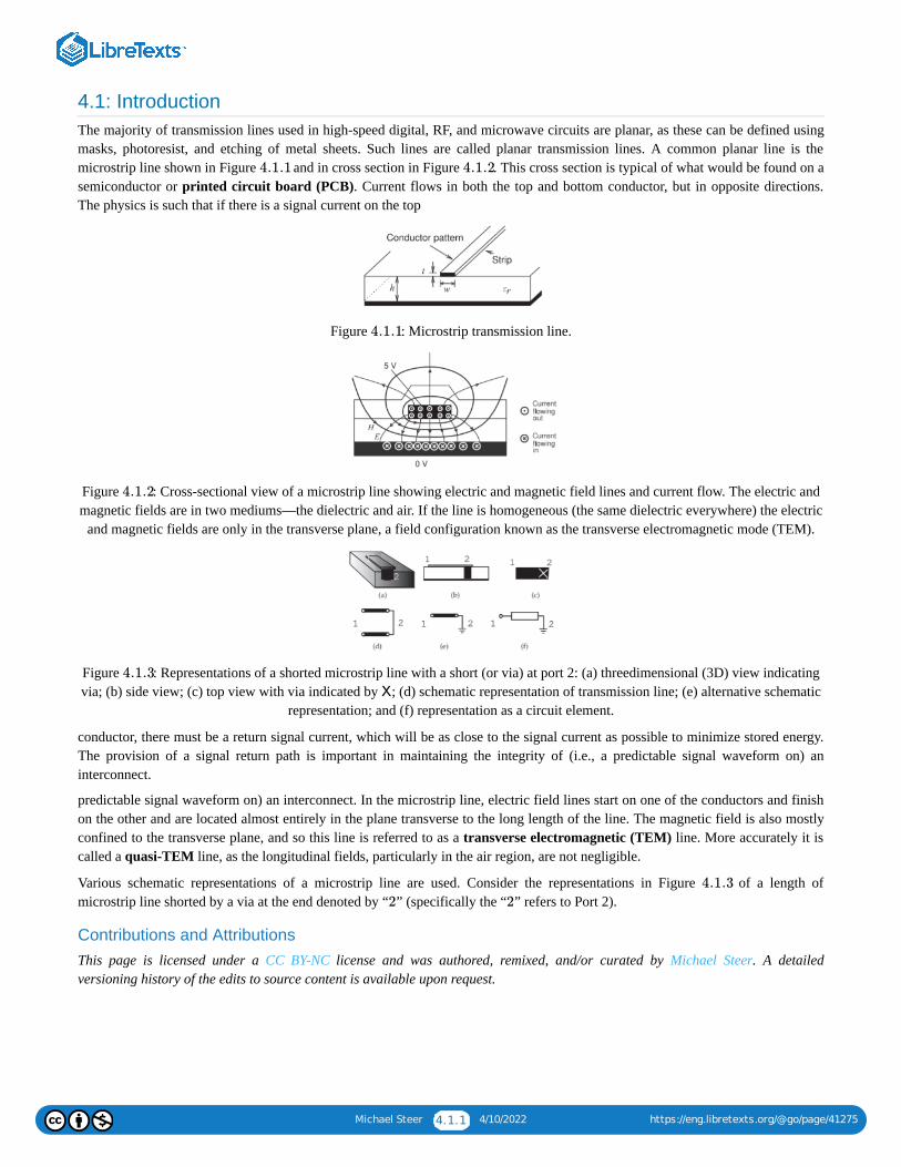
Michael Steer 4.1.1 4/10/2022 https://eng.libretexts.org/@go/page/41275
4.1: IntroductionThe majority of transmission lines used in high-speed digital, RF, and microwave circuits are planar, as these can be defined usingmasks, photoresist, and etching of metal sheets. Such lines are called planar transmission lines. A common planar line is themicrostrip line shown in Figure and in cross section in Figure . This cross section is typical of what would be found on asemiconductor or printed circuit board (PCB). Current flows in both the top and bottom conductor, but in opposite directions.The physics is such that if there is a signal current on the top
Figure : Microstrip transmission line.
Figure : Cross-sectional view of a microstrip line showing electric and magnetic field lines and current flow. The electric andmagnetic fields are in two mediums—the dielectric and air. If the line is homogeneous (the same dielectric everywhere) the electric
and magnetic fields are only in the transverse plane, a field configuration known as the transverse electromagnetic mode (TEM).
Figure : Representations of a shorted microstrip line with a short (or via) at port 2: (a) threedimensional (3D) view indicatingvia; (b) side view; (c) top view with via indicated by ; (d) schematic representation of transmission line; (e) alternative schematic
representation; and (f) representation as a circuit element.
conductor, there must be a return signal current, which will be as close to the signal current as possible to minimize stored energy.The provision of a signal return path is important in maintaining the integrity of (i.e., a predictable signal waveform on) aninterconnect.
predictable signal waveform on) an interconnect. In the microstrip line, electric field lines start on one of the conductors and finishon the other and are located almost entirely in the plane transverse to the long length of the line. The magnetic field is also mostlyconfined to the transverse plane, and so this line is referred to as a transverse electromagnetic (TEM) line. More accurately it iscalled a quasi-TEM line, as the longitudinal fields, particularly in the air region, are not negligible.
Various schematic representations of a microstrip line are used. Consider the representations in Figure of a length ofmicrostrip line shorted by a via at the end denoted by “ ” (specifically the “ ” refers to Port 2).
Contributions and AttributionsThis page is licensed under a CC BY-NC license and was authored, remixed, and/or curated by Michael Steer. A detailedversioning history of the edits to source content is available upon request.
4.1.1 4.1.2
4.1.1
4.1.2
4.1.3
X
4.1.3
2 2

Michael Steer 4.2.1 4/10/2022 https://eng.libretexts.org/@go/page/41276
4.2: SubstratesPlanar line design involves choosing both the transmission line structure to use and the substrate. In this section the electrical andmagnetic properties of substrate materials will be discussed.
4.2.1 Dielectric EffectWhen the fields are in more than one medium (a nonhomogeneous transmission line), as for the microstrip line, the effectiverelative permittivity, (or usually just ), is used. The characteristics of the line are then more or less the same as for thesame structure with a uniform dielectric of permittivity, . The changes with frequency as the proportion of energystored in the different regions changes. This effect is called dispersion and causes a pulse to spread out as the different frequencycomponents of a signal travel at different speeds.
4.2.2 Dielectric Loss Tangent, Loss in a dielectric comes from (a) dielectric damping (also called dielectric relaxation), and (b) conduction losses in thedielectric. Dielectric damping originates from the movement of charge centers resulting in vibration of the lattice and thus energy islost from the electric field. It is easy to see that this loss increases linearly with frequency and is zero at DC. In the frequencydomain loss is incorporating in an imaginary term in the permittivity:
If there is no dielectric damping loss, . The other type of loss is due to the movement of charge carriers in the dielectric. Theability to move charges
Material (at )
Air (dry)
Alumina,
Sapphire
Glass, typical
Polyimide
Quartz (fused)
FR4 circuit board
RT-duroid 5880
RT-duroid 6010
AT-1000
Si (high resistivity)
GaAs
InP
SiO (on-chip)
LTCC (typical, green tape(TM) 951)
Table : Properties of common substrate materials. The dielectric loss tangent is scaled. For example, for glass, istypically .
is described by the conductivity, , and this loss is independent of frequency. So the energy lost in the dielectric is proportional to and the energy stored in the electric field is proportional to . Thus a loss tangent, , is introduced:
Also the relative permittivity can be redefined as
εr,e =εe εr,e
=εeff εeε0 εeff
tan δ
ε = = − ȷ = ( − ȷ )εrε0 ε′ ε′′ ε0 ε′r ε′′
r (4.2.1)
= 0ε′′
tanδ104
10 GHz εr
≈ 0 1
99.5% 1 − 2 10.1
0.4 − 0.7 9.4, 11.6
20 5
50 3.2
1 3.8
100 4.3 − 4.5
5 − 15 2.16 − 2.24
10 − 60 10.2 − 10.7
20 10.0 − 13.0
10 − 100 11.9
6 12.85
10 12.4
2 — 4.0 − 4.2
15 7.8
4.2.1 tanδ
0.002
σ
ω +σε′′ ωε′ tanδ
tanδ =ω +σε′′
ωε′(4.2.2)

Michael Steer 4.2.2 4/10/2022 https://eng.libretexts.org/@go/page/41276
With the exception of silicon, the loss tangent is very small for dielectrics that are useful at RF and microwave frequencies and somost of the time
Thus
4.2.3 Magnetic Material Effect
Except for very special circumstances substrates used for microstrip lines are non magnetic so and the relativepermeability, , is defined so that
4.2.4 Substrates for Planar Transmission LinesThe properties of common substrate materials are given in Table . Crystal substrates have very good dimensional tolerancesand uniformity of electrical properties. Many other substrates have high surface roughness and electrical properties that can vary.For example, FR4 is the most common type of PCB substrate and is a weave of fiberglass embedded in resin. So the material is notuniform and there is an unpredictable localized variation in the proportion of resin and glass. High-performance microwave circuitboards have ceramic particles embedded in the resin.
Contributions and AttributionsThis page is licensed under a CC BY-NC license and was authored, remixed, and/or curated by Michael Steer. A detailedversioning history of the edits to source content is available upon request.
= − ȷ( + )εr ε′r ε′′
r
σ
ωε0(4.2.3)
| | ≈εr ε′r (4.2.4)
= − ȷ ( +σ/(ω )) ≈ (1 − ȷ tanδ)εr ε′r ε′′
r ε0 ε′r (4.2.5)
μ = μ0
μr
μ = μrμ0 (4.2.6)
4.2.1
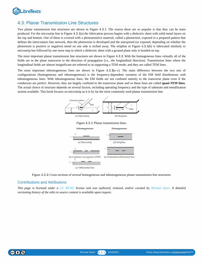
Michael Steer 4.3.1 4/10/2022 https://eng.libretexts.org/@go/page/41277
4.3: Planar Transmission Line StructuresTwo planar transmission line structures are shown in Figure . The reason these are so popular is that they can be massproduced. For the microstrip line in Figure (a) the fabrication process begins with a dielectric sheet with solid metal layers onthe top and bottom. One of these is covered with a photosensitive material, called a photoresist, exposed to a prepared pattern thatdefines the interconnect line network, then the photoresist is developed and the unexposed (or exposed, depending on whether thephotoresist is positive or negative) metal on one side is etched away. The stripline in Figure (b) is fabricated similarly tomicrostrip but followed by one more step in which a dielectric sheet with a ground plane only is bonded on top.
The most important planar transmission line structures are shown in Figure . With the homogeneous lines virtually all of thefields are in the plane transverse to the direction of propagation (i.e., the longitudinal direction). Transmission lines where thelongitudinal fields are almost insignificant are referred to as supporting a TEM mode, and they are called TEM lines.
The most important inhomogeneous lines are shown in Figure (a–c). The main difference between the two sets ofconfigurations (homogeneous and inhomogeneous) is the frequency-dependent variation of the EM field distributions withinhomogeneous lines. With inhomogeneous lines, the EM fields are not confined entirely to the transverse plane even if theconductors are perfect. However, they are largely confined to the transverse plane and so these lines are called quasi-TEM lines.The actual choice of structure depends on several factors, including operating frequency and the type of substrate and metallizationsystem available. This book focuses on microstrip as it is by far the most commonly used planar transmission line.
Figure : Planar transmission lines.
Figure : Cross sections of several homogeneous and inhomogeneous planar transmission line structures.
Contributions and AttributionsThis page is licensed under a CC BY-NC license and was authored, remixed, and/or curated by Michael Steer. A detailedversioning history of the edits to source content is available upon request.
4.3.1
4.3.1
4.3.1
4.3.2
4.3.2
4.3.1
4.3.2
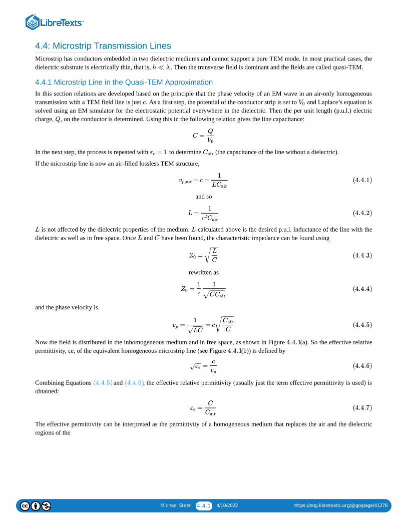
Michael Steer 4.4.1 4/10/2022 https://eng.libretexts.org/@go/page/41278
4.4: Microstrip Transmission LinesMicrostrip has conductors embedded in two dielectric mediums and cannot support a pure TEM mode. In most practical cases, thedielectric substrate is electrically thin, that is, . Then the transverse field is dominant and the fields are called quasi-TEM.
4.4.1 Microstrip Line in the Quasi-TEM ApproximationIn this section relations are developed based on the principle that the phase velocity of an EM wave in an air-only homogeneoustransmission with a TEM field line is just . As a first step, the potential of the conductor strip is set to and Laplace’s equation issolved using an EM simulator for the electrostatic potential everywhere in the dielectric. Then the per unit length (p.u.l.) electriccharge, , on the conductor is determined. Using this in the following relation gives the line capacitance:
In the next step, the process is repeated with to determine (the capacitance of the line without a dielectric).
If the microstrip line is now an air-filled lossless TEM structure,
and so
is not affected by the dielectric properties of the medium. calculated above is the desired p.u.l. inductance of the line with thedielectric as well as in free space. Once and have been found, the characteristic impedance can be found using
rewritten as
and the phase velocity is
Now the field is distributed in the inhomogeneous medium and in free space, as shown in Figure (a). So the effective relativepermittivity, εe, of the equivalent homogeneous microstrip line (see Figure (b)) is defined by
Combining Equations and , the effective relative permittivity (usually just the term effective permittivity is used) isobtained:
The effective permittivity can be interpreted as the permittivity of a homogeneous medium that replaces the air and the dielectricregions of the
h ≪ λ
c V0
Q
C =Q
V0
= 1εr Cair
= c =vp,air1
LCair(4.4.1)
L =1
c2Cair(4.4.2)
L L
L C
=Z0L
C
−−√ (4.4.3)
=Z01
c
1
CCair− −−−−
√(4.4.4)
= = cvp
1
LC−−−
√
Cair
C
− −−−√ (4.4.5)
4.4.14.4.1
=εe−−
√c
vp
(4.4.6)
(4.4.5) (4.4.6)
=εe
C
Cair(4.4.7)
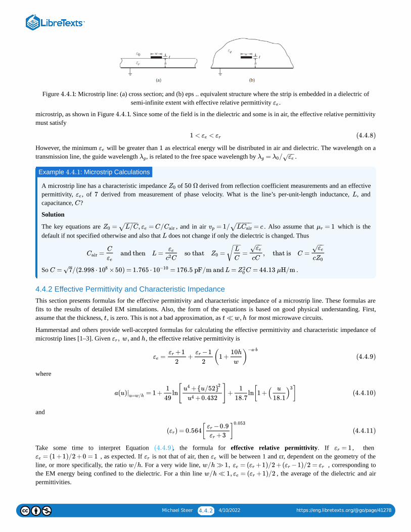
Michael Steer 4.4.2 4/10/2022 https://eng.libretexts.org/@go/page/41278
Figure : Microstrip line: (a) cross section; and (b) eps .. equivalent structure where the strip is embedded in a dielectric ofsemi-infinite extent with effective relative permittivity .
microstrip, as shown in Figure . Since some of the field is in the dielectric and some is in air, the effective relative permittivitymust satisfy
However, the minimum will be greater than as electrical energy will be distributed in air and dielectric. The wavelength on atransmission line, the guide wavelength , is related to the free space wavelength by .
A microstrip line has a characteristic impedance of derived from reflection coefficient measurements and an effectivepermittivity, , of derived from measurement of phase velocity. What is the line’s per-unit-length inductance, , andcapacitance, ?
Solution
The key equations are , and in air . Also assume that which is thedefault if not specified otherwise and also that does not change if only the dielectric is changed. Thus
So .
4.4.2 Effective Permittivity and Characteristic ImpedanceThis section presents formulas for the effective permittivity and characteristic impedance of a microstrip line. These formulas arefits to the results of detailed EM simulations. Also, the form of the equations is based on good physical understanding. First,assume that the thickness, , is zero. This is not a bad approximation, as for most microwave circuits.
Hammerstad and others provide well-accepted formulas for calculating the effective permittivity and characteristic impedance ofmicrostrip lines [1–3]. Given and , the effective relative permittivity is
where
and
Take some time to interpret Equation , the formula for effective relative permittivity. If , then , as expected. If is not that of air, then will be between 1 and εr, dependent on the geometry of the
line, or more specifically, the ratio . For a very wide line, , corresponding tothe EM energy being confined to the dielectric. For a thin line , the average of the dielectric and airpermittivities.
4.4.1εe
4.4.1
1 < <εe εr (4.4.8)
εe 1λg = /λg λ0 εe
−−√
Example : Microstrip Calculations4.4.1
Z0 50 Ωεe 7 L
C
= , = C/Z0 L/C− −−−
√ εe Cair = 1/ = cvp LCair− −−−−
√ = 1μr
L
= and then L = so that = = , that is C =CairC
εe
εe
Cc2Z0
L
C
−−√
εe−−
√
cC
εe−−
√
cZ0
C = /(2.998 ⋅ ×50) = 1.765 ⋅ = 176.5 pF/m and L = C = 44.13 μH/m7–
√ 108 10−10 Z20
t t ≪ w, h
, w,εr h
= +εe
+1εr
2
−1εr
2(1 + )
10h
w
−a⋅b
(4.4.9)
a(u) = 1 + ln[ ]+ ln[1 + ]|u=w/h
1
49
+u4 {u/52}2
+0.432u4
1
18.7( )
u
18.1
3(4.4.10)
( ) = 0.564εr [ ]−0.9εr
+3εr
0.053
(4.4.11)
(4.4.9) = 1εr
= (1 +1)/2 +0 = 1εe εr εe
w/h w/h ≫ 1, = ( +1)/2 +( −1)/2 =εe εr εr εr
w/h ≪ 1, = ( +1)/2εe εr
Michael Steer 4.4.3 4/10/2022 https://eng.libretexts.org/@go/page/41278
Mostly the term “effective permittivity” is used to mean effective relative permittivity (check the magnitude).
The characteristic impedance is given by
where the characteristic impedance of the microstrip line in free space is
and
The accuracy of Equation is better than for and . Also, the accuracy of Equation is better than for . Note that has a maximum value when w is small and a minimum value when w
is large.
Now consider the special case where is vanishingly small. Then has its minimum value:
This leads to an approximate (and convenient) form of Equation :
This approximation has its greatest error for low and high εr and narrow lines, , where the maximum error is . Again,Equation is used to calculate the characteristic impedance. The more exact analysis, represented by Equation , wasused to develop Table , which can be used in the design of microstrip.
The strip of a microstrip line has a width of and is fabricated on a lossless substrate that is thick and has arelative permittivity of .
a. What is the effective relative permittivity?b. What is the characteristic impedance?c. What is the propagation constant at ignoring any losses?
Solution
Use the formulas for effective permittivity, characteristic impedance, and attenuation constant from Section 4.4.2 with .
Figure
a.
From equations and ,
Note
=Z0Z01
εe−−
√(4.4.12)
= = 60 ln[ + ]Z01 Z0|( =1)εr
hF1
w1 +( )
2h
w
2− −−−−−−−−
√ (4.4.13)
= 6 +(2π −6)exp{−(30.666h/w }F1 )0.7528 (4.4.14)
(4.4.9) 0.2% 0.01 ≤ w/h ≤ 100 1 ≤ ≤ 128εr
(4.4.13) 0.1% w/h < 1000 Z0
w εe
= ( +1)εe
1
2εr (4.4.15)
(4.4.9)
= +εe
( +1)εr
2
( −1)εr
2
1
1 +12h/w− −−−−−−−√
(4.4.16)
w/h ≪ 1 1%(4.4.12) (4.4.9)
4.4.1
Example : Microstrip Characteristic Impedance Calculation4.4.2
600 μm 635 μm4.1
5 GHz
w = 600 μm; h = 635 μm; = 4.1; w/h = 600/635 = 0.945εr
4.4.2
= +εe
+1εr
2
−1εr
2(1 + )
10h
w
−a⋅b
(4.4.10) (4.4.11)
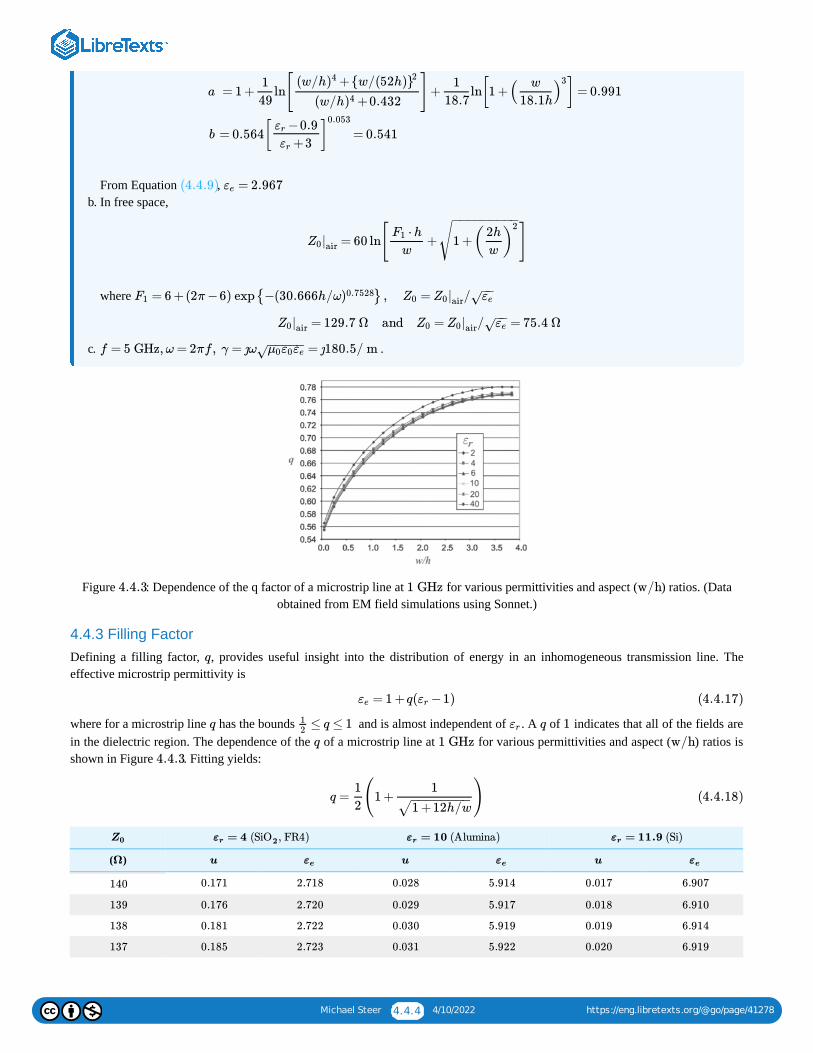
Michael Steer 4.4.4 4/10/2022 https://eng.libretexts.org/@go/page/41278
From Equation ,
b. In free space,
where
c. .
Figure : Dependence of the q factor of a microstrip line at for various permittivities and aspect ( ) ratios. (Dataobtained from EM field simulations using Sonnet.)
4.4.3 Filling FactorDefining a filling factor, , provides useful insight into the distribution of energy in an inhomogeneous transmission line. Theeffective microstrip permittivity is
where for a microstrip line has the bounds and is almost independent of . A of indicates that all of the fields arein the dielectric region. The dependence of the of a microstrip line at for various permittivities and aspect ( ) ratios isshown in Figure . Fitting yields:
( )
a
b
= 1 + ln[ ]+ ln[1 + ] = 0.9911
49
(w/h +)4 {w/(52h)}2
(w/h +0.432)4
1
18.7( )
w
18.1h
3
= 0.564 = 0.541[ ]−0.9εr
+3εr
0.053
(4.4.9) = 2.967εe
= 60 ln[ + ]Z0|air
⋅ hF1
w1 +( )
2h
w
2− −−−−−−−−
√
= 6 +(2π −6) exp{−(30.666h/ω } , = /F1 )0.7528 Z0 Z0|air εe−−
√
= 129.7 Ω and = / = 75.4 ΩZ0|air Z0 Z0|air εe−−
√
f = 5 GHz, ω = 2πf , γ = ȷω = ȷ180.5/ mμ0ε0εe− −−−−
√
4.4.3 1 GHz w/h
q
= 1 +q( −1)εe εr (4.4.17)
q ≤ q ≤ 112
εr q 1
q 1 GHz w/h4.4.3
q = (1 + )1
2
1
1 +12h/w− −−−−−−−
√(4.4.18)
Z0 = 4 , FR4)εr (SiO2
= 10 (Alumina)εr = 11.9 (Si)εr
Ω u εe u εe u εe
140 0.171 2.718 0.028 5.914 0.017 6.907
139 0.176 2.720 0.029 5.917 0.018 6.910
138 0.181 2.722 0.030 5.919 0.019 6.914
137 0.185 2.723 0.031 5.922 0.020 6.919
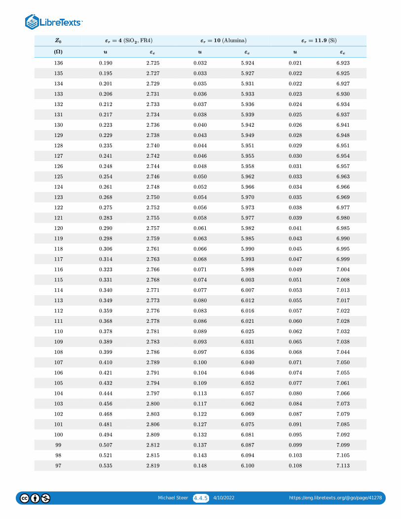
Michael Steer 4.4.5 4/10/2022 https://eng.libretexts.org/@go/page/41278
( )
Z0 = 4 , FR4)εr (SiO2
= 10 (Alumina)εr = 11.9 (Si)εr
Ω u εe u εe u εe
136 0.190 2.725 0.032 5.924 0.021 6.923
135 0.195 2.727 0.033 5.927 0.022 6.925
134 0.201 2.729 0.035 5.931 0.022 6.927
133 0.206 2.731 0.036 5.933 0.023 6.930
132 0.212 2.733 0.037 5.936 0.024 6.934
131 0.217 2.734 0.038 5.939 0.025 6.937
130 0.223 2.736 0.040 5.942 0.026 6.941
129 0.229 2.738 0.043 5.949 0.028 6.948
128 0.235 2.740 0.044 5.951 0.029 6.951
127 0.241 2.742 0.046 5.955 0.030 6.954
126 0.248 2.744 0.048 5.958 0.031 6.957
125 0.254 2.746 0.050 5.962 0.033 6.963
124 0.261 2.748 0.052 5.966 0.034 6.966
123 0.268 2.750 0.054 5.970 0.035 6.969
122 0.275 2.752 0.056 5.973 0.038 6.977
121 0.283 2.755 0.058 5.977 0.039 6.980
120 0.290 2.757 0.061 5.982 0.041 6.985
119 0.298 2.759 0.063 5.985 0.043 6.990
118 0.306 2.761 0.066 5.990 0.045 6.995
117 0.314 2.763 0.068 5.993 0.047 6.999
116 0.323 2.766 0.071 5.998 0.049 7.004
115 0.331 2.768 0.074 6.003 0.051 7.008
114 0.340 2.771 0.077 6.007 0.053 7.013
113 0.349 2.773 0.080 6.012 0.055 7.017
112 0.359 2.776 0.083 6.016 0.057 7.022
111 0.368 2.778 0.086 6.021 0.060 7.028
110 0.378 2.781 0.089 6.025 0.062 7.032
109 0.389 2.783 0.093 6.031 0.065 7.038
108 0.399 2.786 0.097 6.036 0.068 7.044
107 0.410 2.789 0.100 6.040 0.071 7.050
106 0.421 2.791 0.104 6.046 0.074 7.055
105 0.432 2.794 0.109 6.052 0.077 7.061
104 0.444 2.797 0.113 6.057 0.080 7.066
103 0.456 2.800 0.117 6.062 0.084 7.073
102 0.468 2.803 0.122 6.069 0.087 7.079
101 0.481 2.806 0.127 6.075 0.091 7.085
100 0.494 2.809 0.132 6.081 0.095 7.092
99 0.507 2.812 0.137 6.087 0.099 7.099
98 0.521 2.815 0.143 6.094 0.103 7.105
97 0.535 2.819 0.148 6.100 0.108 7.113
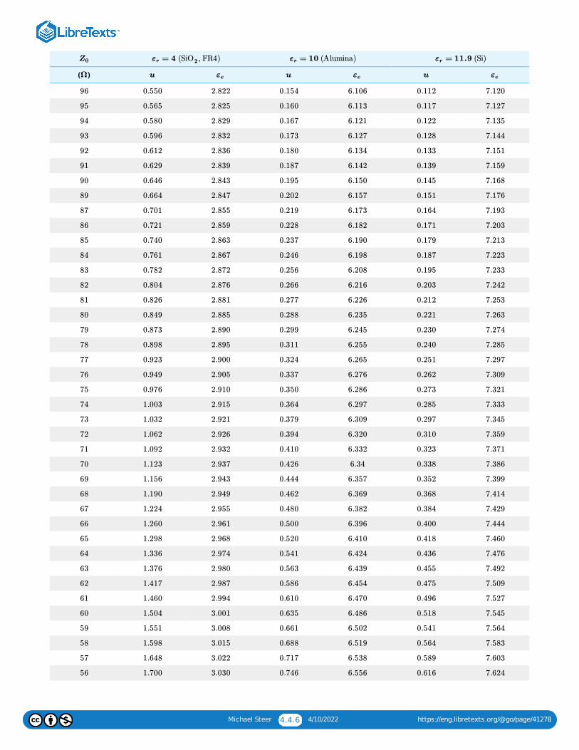
Michael Steer 4.4.6 4/10/2022 https://eng.libretexts.org/@go/page/41278
( )
Z0 = 4 , FR4)εr (SiO2
= 10 (Alumina)εr = 11.9 (Si)εr
Ω u εe u εe u εe
96 0.550 2.822 0.154 6.106 0.112 7.120
95 0.565 2.825 0.160 6.113 0.117 7.127
94 0.580 2.829 0.167 6.121 0.122 7.135
93 0.596 2.832 0.173 6.127 0.128 7.144
92 0.612 2.836 0.180 6.134 0.133 7.151
91 0.629 2.839 0.187 6.142 0.139 7.159
90 0.646 2.843 0.195 6.150 0.145 7.168
89 0.664 2.847 0.202 6.157 0.151 7.176
87 0.701 2.855 0.219 6.173 0.164 7.193
86 0.721 2.859 0.228 6.182 0.171 7.203
85 0.740 2.863 0.237 6.190 0.179 7.213
84 0.761 2.867 0.246 6.198 0.187 7.223
83 0.782 2.872 0.256 6.208 0.195 7.233
82 0.804 2.876 0.266 6.216 0.203 7.242
81 0.826 2.881 0.277 6.226 0.212 7.253
80 0.849 2.885 0.288 6.235 0.221 7.263
79 0.873 2.890 0.299 6.245 0.230 7.274
78 0.898 2.895 0.311 6.255 0.240 7.285
77 0.923 2.900 0.324 6.265 0.251 7.297
76 0.949 2.905 0.337 6.276 0.262 7.309
75 0.976 2.910 0.350 6.286 0.273 7.321
74 1.003 2.915 0.364 6.297 0.285 7.333
73 1.032 2.921 0.379 6.309 0.297 7.345
72 1.062 2.926 0.394 6.320 0.310 7.359
71 1.092 2.932 0.410 6.332 0.323 7.371
70 1.123 2.937 0.426 6.34 0.338 7.386
69 1.156 2.943 0.444 6.357 0.352 7.399
68 1.190 2.949 0.462 6.369 0.368 7.414
67 1.224 2.955 0.480 6.382 0.384 7.429
66 1.260 2.961 0.500 6.396 0.400 7.444
65 1.298 2.968 0.520 6.410 0.418 7.460
64 1.336 2.974 0.541 6.424 0.436 7.476
63 1.376 2.980 0.563 6.439 0.455 7.492
62 1.417 2.987 0.586 6.454 0.475 7.509
61 1.460 2.994 0.610 6.470 0.496 7.527
60 1.504 3.001 0.635 6.486 0.518 7.545
59 1.551 3.008 0.661 6.502 0.541 7.564
58 1.598 3.015 0.688 6.519 0.564 7.583
57 1.648 3.022 0.717 6.538 0.589 7.603
56 1.700 3.030 0.746 6.556 0.616 7.624
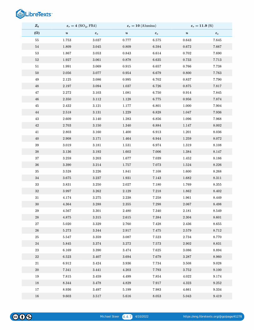
Michael Steer 4.4.7 4/10/2022 https://eng.libretexts.org/@go/page/41278
( )
Z0 = 4 , FR4)εr (SiO2
= 10 (Alumina)εr = 11.9 (Si)εr
Ω u εe u εe u εe
55 1.753 3.037 0.777 6.575 0.643 7.645
54 1.809 3.045 0.809 6.594 0.672 7.667
53 1.867 3.053 0.843 6.614 0.702 7.690
52 1.927 3.061 0.878 6.635 0.733 7.713
51 1.991 3.069 0.915 6.657 0.766 7.738
50 2.056 3.077 0.954 6.679 0.800 7.763
49 2.125 3.086 0.995 6.702 0.837 7.790
48 2.197 3.094 1.037 6.726 0.875 7.817
47 2.272 3.103 1.081 6.750 0.914 7.845
46 2.350 3.112 1.128 6.775 0.956 7.874
45 2.432 3.121 1.177 6.801 1.000 7.904
44 2.518 3.131 1.229 6.828 1.047 7.936
43 2.609 3.140 1.283 6.856 1.096 7.968
42 2.703 3.150 1.340 6.884 1.147 8.002
41 2.803 3.160 1.400 6.913 1.201 8.036
40 2.908 3.171 1.464 6.944 1.259 8.072
39 3.019 3.181 1.531 6.974 1.319 8.108
38 3.136 3.192 1.602 7.006 1.384 8.147
37 3.259 3.203 1.677 7.039 1.452 8.186
36 3.390 3.214 1.757 7.073 1.524 8.226
35 3.528 3.226 1.841 7.108 1.600 8.268
34 3.675 3.237 1.931 7.143 1.682 8.311
33 3.831 3.250 2.027 7.180 1.769 8.355
32 3.997 3.262 2.129 7.218 1.862 8.402
31 4.174 3.275 2.238 7.258 1.961 8.449
30 4.364 3.288 2.355 7.298 2.067 8.498
29 4.567 3.301 2.480 7.340 2.181 8.549
28 4.875 3.315 2.615 7.384 2.304 8.601
27 5.020 3.329 2.760 7.428 2.436 8.655
26 5.273 3.344 2.917 7.475 2.579 8.712
25 5.547 3.359 3.087 7.523 2.734 8.770
24 5.845 3.374 3.272 7.573 2.902 8.831
23 6.169 3.390 3.474 7.625 3.086 8.894
22 6.523 3.407 3.694 7.679 3.287 8.960
21 6.912 3.424 3.936 7.734 3.508 9.028
20 7.341 3.441 4.203 7.793 3.752 9.100
19 7.815 3.459 4.499 7.854 4.022 9.174
18 8.344 3.478 4.829 7.917 4.323 9.252
17 8.936 3.497 5.199 7.983 4.661 9.334
16 9.603 3.517 5.616 8.053 5.043 9.419

Michael Steer 4.4.8 4/10/2022 https://eng.libretexts.org/@go/page/41278
( )
Table : Microstrip line normalized width and effective permittivity, , for specified characteristic impedance .Data derived from the analysis in Section 4.4.2.
Contributions and AttributionsThis page is licensed under a CC BY-NC license and was authored, remixed, and/or curated by Michael Steer. A detailedversioning history of the edits to source content is available upon request.
Z0 = 4 , FR4)εr (SiO2
= 10 (Alumina)εr = 11.9 (Si)εr
Ω u εe u εe u εe
15 10.361 3.538 6.090 8.126 5.476 9.509
14 11.229 3.559 6.633 8.202 5.972 9.604
13 12.233 3.581 7.262 8.282 6.547 9.704
12 13.407 3.604 7.997 8.367 7.219 9.809
11 14.798 3.628 8.868 8.456 8.016 9.920
10 16.471 3.652 9.916 8.550 8.975 10.038
4.4.1 u(= w/h) εe Z0
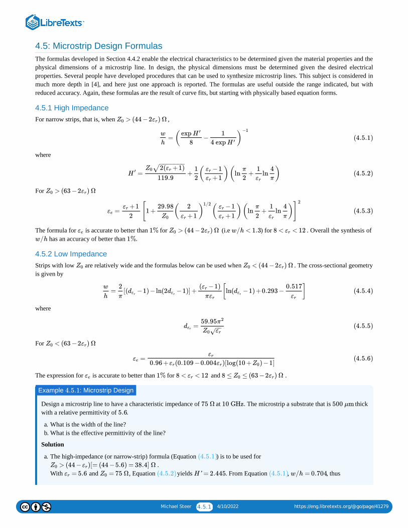
Michael Steer 4.5.1 4/10/2022 https://eng.libretexts.org/@go/page/41279
4.5: Microstrip Design FormulasThe formulas developed in Section 4.4.2 enable the electrical characteristics to be determined given the material properties and thephysical dimensions of a microstrip line. In design, the physical dimensions must be determined given the desired electricalproperties. Several people have developed procedures that can be used to synthesize microstrip lines. This subject is considered inmuch more depth in [4], and here just one approach is reported. The formulas are useful outside the range indicated, but withreduced accuracy. Again, these formulas are the result of curve fits, but starting with physically based equation forms.
4.5.1 High ImpedanceFor narrow strips, that is, when ,
where
For
The formula for is accurate to better than for (i.e ) for . Overall the synthesis of has an accuracy of better than .
4.5.2 Low ImpedanceStrips with low are relatively wide and the formulas below can be used when . The cross-sectional geometryis given by
where
For
The expression for is accurate to better than for and .
Design a microstrip line to have a characteristic impedance of at . The microstrip a substrate that is thickwith a relative permittivity of .
a. What is the width of the line?b. What is the effective permittivity of the line?
Solution
a. The high-impedance (or narrow-strip) formula (Equation ) is to be used for .
With and , Equation yields . From Equation , , thus
> (44 −2 ) ΩZ0 εr
=w
h( − )
exp H ′
8
1
4 exp H ′
−1
(4.5.1)
= + ( )(ln + ln )H ′Z0 2( +1)εr
− −−−−−−√
119.9
1
2
−1εr
+1εr
π
2
1
εr
4
π(4.5.2)
> (63 −2 ) ΩZ0 εr
=εe+1εr
2[1 + ( )(ln + ln )]
29.98
Z0( )
2
+1εr
1/2 −1εr
+1εr
π
2
1
εr
4
π
2
(4.5.3)
εe 1% > (44 −2 ) ΩZ0 εr w/h < 1.3 8 < < 12εrw/h 1%
Z0 < (44 −2 ) ΩZ0 εr
= [( −1) −ln(2 −1)] + [ln( −1) +0.293 − ]w
h
2
πdεr dεr
( −1)εr
πεrdεr
0.517
εr(4.5.4)
=dεr59.95π2
Z0 εr−−
√(4.5.5)
< (63 −2 ) ΩZ0 εr
=εeεr
0.96 + (0.109 −0.004 )[log(10 + ) −1]εr εr Z0(4.5.6)
εe 1% 8 < < 12εr 8 ≤ ≤ (63 −2 ) ΩZ0 εr
Example : Microstrip Design4.5.1
75 Ω 10 GHz 500 μm5.6
(4.5.1)> (44 − )[= (44 −5.6) = 38.4] ΩZ0 εr
= 5.6εr = 75 ΩZ0 (4.5.2) H' = 2.445 (4.5.1) w/h = 0.704

Michael Steer 4.5.2 4/10/2022 https://eng.libretexts.org/@go/page/41279
.b. The effective permittivity formula is Equation , and so .
Contributions and Attributions
This page is licensed under a CC BY-NC license and was authored, remixed, and/or curated by Michael Steer. A detailedversioning history of the edits to source content is available upon request.
w = w/h×h = 0.704 ×500 μm = 352 μm(4.5.3) = 3.82εe

Michael Steer 4.6.1 4/10/2022 https://eng.libretexts.org/@go/page/41280
4.6: SummaryThis chapter considered micostrip, the most important planar transmission line. At frequencies below , economics requirethat standard FR4 circuit boards be used. The weave of a conventional FR4 circuit board can be a significant fraction of criticaltransmission line dimensions and so affect electrical performance. Nonwoven substrates and sometimes hard substrates such asalumina ceramic, sapphire, or silicon crystal wafers are often required. These provide higher-dimensional tolerance than can beachieved using conventional woven FR4 substrates. In general, once a design has been optimized in fabrication so that the desiredelectrical characteristics are obtained, microwave circuits using planar transmission lines can be cheaply and repeatablymanufactured in volume.
Contributions and AttributionsThis page is licensed under a CC BY-NC license and was authored, remixed, and/or curated by Michael Steer. A detailedversioning history of the edits to source content is available upon request.
1 GHz

Michael Steer 4.7.1 4/10/2022 https://eng.libretexts.org/@go/page/41281
4.7: References[1] E. Hammerstad and O. Jensen, “Accurate models for microstrip computer-aided design,” in 1980 IEEE MTT-S Int. MicrowaveSymp. Digest, May 1980, pp. 407–409.
[2] E. Hammerstad and F. Bekkadal, “A microstrip handbook, ELAB Report STF44 A74169,” University of Trondheim, Norway,Tech. Rep., Feb. 1975.
[3] E. O. Hammerstad, “Equations for microstrip circuit design,” in 5th European Microwave Conf., Sep. 1975, pp. 268–272.
[4] T. Edwards and M. Steer, Foundations for Microstrip Circuit Design. John Wiley & Sons, 2016.
Contributions and AttributionsThis page is licensed under a CC BY-NC license and was authored, remixed, and/or curated by Michael Steer. A detailedversioning history of the edits to source content is available upon request.

Michael Steer 4.8.1 4/10/2022 https://eng.libretexts.org/@go/page/41282
4.8: Exercises1. A microstrip line on thick GaAs has a minimum and maximum strip widths of and respectively. What
is the range of characteristic impedances that can be used in design?2. A microstrip line with a substrate having a relative permittivity of has an effective permittivity of . What is the wavelength
of a signal propagating on the microstrip?3. A microstrip line has a width of and a substrate that is thick with a relative permittivity of . What is the
effective permittivity of the line?4. The strip of a microstrip has a width of and is fabricated on a lossless substrate that is thick and has a relative
permittivity of . [Parallels Example 4.4.2]a. What is the effective relative permittivity of the line?b. What is the characteristic impedance of the line?c. What is the propagation constant at ignoring any losses?d. If the strip has a resistance of and the ground plane resistance can be ignored, what is the attenuation constant of
the line at ?5. A microstrip line on a -thick silicon substrate has a width of . Use Table 4.4.1.
a. What is line’s effective permittivity.b. What is its characteristic impedance?
6. A -wide microstrip line on a thick alumina substrate. Use Table 4.4.1.
a. What is line’s effective permittivity.b. What is its characteristic impedance?
7. A microstrip line on a -thick FR4 substrate has a width of . Use Table 4.4.1.a. What is line’s effective permittivity.b. What is its characteristic impedance?
8. Consider a microstrip line on a substrate with a relative permittivity of and thickness of .a. What is the minimum effective permittivity of the microstrip line if there is no limit on the minimum or maximum width of
the strip?b. What is the maximum effective permittivity of the microstrip line if there is no limit on the minimum or maximum width of
the strip?9. A microstrip line has a width of and a substrate that is thick with a relative permittivity of . What is the
geometric filling factor of the line?10. The substrate of a microstrip line has a relative permittivity of but the calculated effective permittivity is . What is the
filling factor?11. A microstrip line has a strip width of and a substrate with a relative permittivity of and a thickness of .
What is the filling factor?12. A microstrip line has a strip width of and a substrate with a relative permittivity of and thickness of .
Determine the line’s filling factor and thus its effective relative permittivity.13. A microstrip line has a strip with a width of and the substrate which is thick and a relative permittivity of .
a. What is the filling factor, , of the line?b. What is the line’s effective relative permittivity?c. What is the characteristic impedance of the line?
14. An inhomogeneous transmission line is fabricated using a medium with a relative permittivity of and has an effectivepermittivity of . What is the fill factor ?
15. A microstrip technology uses a substrate with a relative permittivity of and thickness of . The minimum strip widthis . What is the highest characteristic impedance that can be achieved?
16. A microstrip transmission line has a characteristic impedance of , a strip resistance of , and a ground planeresistance of . The dielectric of the line is lossless.a. What is the total resistance of the line in ?b. What is the attenuation constant in ?c. What is the attenuation constant in ?
250 μm 50 μm 250 μm
10 8
10 GHz
500 μm 635 μm 20
250 μm 500 μm
2.3
3 GHz
0.5 Ω/cm
3 GHz
250 μm 200 μm
600 μm 500 μm
1 mm 0.497 mm
12 1 mm
1 mm 1 mm 20
16 12
250 μm 10 125 μm
250 μm 4 250 μm
100 μm 250 μm 8
q
10
7 q
10 400 μm
20 μm
75 Ω 5 Ω/m
5 Ω/m
Ω/m
Np/m
dB/cm

Michael Steer 4.8.2 4/10/2022 https://eng.libretexts.org/@go/page/41282
17. A microstrip line has a characteristic impedance of , a strip resistance of , and a ground plane resistance of .a. What is the total resistance of the line in ?b. What is the attenuation constant in ?c. What is the attenuation constant in ?
18. A microstrip line has -thick gold metallization for both the strip and ground plane. The strip has a width of andthe substrate is thick.
a. What is the low frequency resistance (in ) of the strip?b. What is the low frequency resistance of the ground plane?c. What is the total low frequency resistance of the microstrip line?
19. A microstrip line has -thick gold metallization for both the strip and ground plane. The strip has a width of and the lossless substrate is thick.a. What is the low frequency resistance (in ) of the strip?b. What is the low frequency resistance of the ground plane?c. What is the total low frequency resistance of the microstrip line?d. What is the attenuation in of the line at low frequencies?
20. A microstrip line with a lossless substrate has a -wide strip with a sheet resistance of and the groundplane resistance can be ignored. What is the attenuation constant at ? [Parallels Example 4.4.1]
21. A microstrip line operating at has a substrate with a relative permittivity of and a loss tangent of . It has acharacteristic impedance of and an effective permittivity of .a. What is the conductance of the line in ?b. What is the attenuation constant in ?c. What is the attenuation constant in ?
22. A microstrip line has the per unit length parameters and , also at the substrate has aconductance of . The substrate loss is solely due to dielectric relaxation loss and there is no substrate conductiveloss. The resistances of the ground and strip are zero.a. What is at ?b. What is the magnitude of the characteristic impedance at ?c. What is the dielectric attenuation constant of the line at in ?
23. A microstrip line has the per unit length parameters and , also at the substrate has aconductance of . The substrate loss is solely due to dielectric relaxation loss and there is no substrate conductiveloss. The resistance of the strip is and the resistance of the ground plane is .a. What is the per unit length resistance of the microstrip line at ?b. What is the magnitude of the characteristic impedance at ?c. What is the conductive attenuation constant in ?d. What is the dielectric attenuation constant of the line at in ?
24. A microstrip line operating at has perfect metallization for both the strip and ground plane. The strip has a width of and the substrate is thick with a relative permittivity of and a loss tangent of .
a. What is the filling factor, , of the line?b. What is the line’s effective relative permittivity?c. What is the line’s attenuation in ?d. What is the line’s attenuation in ?
25. A microstrip line operating at has perfect metallization for both the strip and ground plane. The substrate has arelative permittivity of and a loss tangent of . Without the dielectric the line has a capacitance of .a. What is the line conductance in ?b. What is the line’s attenuation in ?c. What is the line’s attenuation in ?
26. Design a microstrip line having a characteristic impedance. The substrate has a permittivity of and is thick.The operating frequency is . You need to determine the width of the microstrip line.
50 Ω 10 Ω/m 3 Ω/m
Ω/m
Np/m
dB/cm
10 μm 125 μm
125 μm
Ω/m
50 Ω 10 μm 250 μm
250 μm
Ω/m
dB/m
50 Ω 0.5 mm 1.5 mΩ
1 GHz
10 GHz 10 0.005
50 Ω 7
S/m
Np/m
dB/cm
L = 2 nH/m C = 1 pF/m 10 GHz
G 0.001 S/m
G 1 GHz
1 GHz
1 GHz dB/m
L = 1 nH/m C = 1 pF/m 1 GHz
G 0.001 S/m
0.5 Ω/m 0.1 Ω/m
1 GHz
1 GHz
Np/m
1 GHz dB/m
2 GHz
250 μm 250 μm 10 0.001
q
Np/m
dB/m
50 Ω 1 GHz
10 0.001 100 pF/m
S/m
Np/m
dB/m
50 Ω 2.3 250 μm
18 GHz

Michael Steer 4.8.3 4/10/2022 https://eng.libretexts.org/@go/page/41282
27. Design a microstrip line to have a characteristic impedance of at . The substrate is thick with a relativepermittivity of . Ignore the thickness of the strip. [Parallels Example 4.5.1]a. What is the width of the line?b. What is the effective permittivity of the line?
28. Design a microstrip line to have a characteristic impedance of . The microstrip is to be constructed on a substrate that is thick with a relative permittivity of . [Parallels Example 4.5.1]
a. What is the width of the line? Ignore the thickness of the strip and frequency dependent effects.b. What is the effective permittivity of the line?
4.8.1 Exercises by Sectionchallenging
4.8.2 Answers to Selected Exercises3.
4. (c)
16. (c) 17. (a)
22. (b)
28. (b)
Contributions and Attributions
This page is licensed under a CC BY-NC license and was authored, remixed, and/or curated by Michael Steer. A detailedversioning history of the edits to source content is available upon request.
65 Ω 5 GHz 635 μm
9.8
20 Ω
1 mm 12
†
§4.41, 2, 3†, 4†, 5, 6, 7, 8, 9, 10, 11, 12, 13, 14, 15, 16, 17, 18, 19, 20, 21, 22†, 23†, 24, 25
§4.526†, 27†, 28†
12.75
ȷ84.1 m−1
0.579 dB/m
13 Ω/m
44.72 Ω
9.17

1 4/10/2022
CHAPTER OVERVIEW5: EXTRAORDINARY TRANSMISSION LINE EFFECTS
5.1: INTRODUCTION5.2: FREQUENCY-DEPENDENT CHARACTERISTICS5.3: MULTIMODING ON TRANSMISSION LINES5.4: MICROSTRIP OPERATING FREQUENCY LIMITATIONS5.5: SUMMARY5.6: REFERENCES5.7: EXERCISES

Michael Steer 5.1.1 4/10/2022 https://eng.libretexts.org/@go/page/41283
5.1: IntroductionPrevious chapters discussed the low-frequency operation of transmission lines. This chapter describes the origins of frequency-dependent behavior. Figure 5.2.1 shows the typical frequency dependence of a line’s parameters, and, except withsemiconductor substrates, is usually negligible. This is called dispersion and a typical example is the spreading out of a pulse,see Figure 5.2.2.
The major limitation on the dimensions and maximum operating frequency of a transmission line is determined by the originationof higher-order modes (i.e., orientations of the fields). Different modes on a transmission line travel at different velocities. Thus theproblem is that if a signal is split between two modes, then information sent from one end of the line will reach the other end in twopackets arriving at different times. Multimoding must always be avoided.
Contributions and AttributionsThis page is licensed under a CC BY-NC license and was authored, remixed, and/or curated by Michael Steer. A detailedversioning history of the edits to source content is available upon request.
RLGC
G
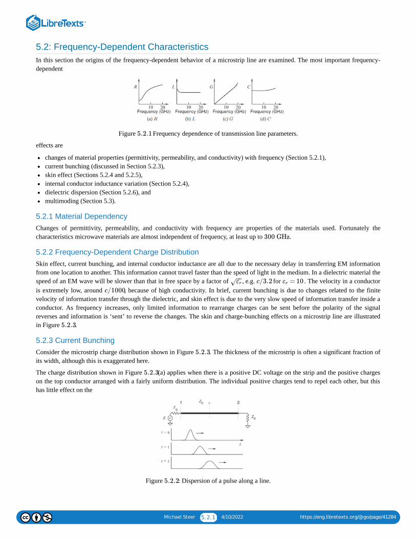
Michael Steer 5.2.1 4/10/2022 https://eng.libretexts.org/@go/page/41284
5.2: Frequency-Dependent CharacteristicsIn this section the origins of the frequency-dependent behavior of a microstrip line are examined. The most important frequency-dependent
Figure Frequency dependence of transmission line parameters.
effects are
changes of material properties (permittivity, permeability, and conductivity) with frequency (Section 5.2.1),current bunching (discussed in Section 5.2.3),skin effect (Sections 5.2.4 and 5.2.5),internal conductor inductance variation (Section 5.2.4),dielectric dispersion (Section 5.2.6), andmultimoding (Section 5.3).
5.2.1 Material DependencyChanges of permittivity, permeability, and conductivity with frequency are properties of the materials used. Fortunately thecharacteristics microwave materials are almost independent of frequency, at least up to .
5.2.2 Frequency-Dependent Charge DistributionSkin effect, current bunching, and internal conductor inductance are all due to the necessary delay in transferring EM informationfrom one location to another. This information cannot travel faster than the speed of light in the medium. In a dielectric material thespeed of an EM wave will be slower than that in free space by a factor of , e.g. for . The velocity in a conductoris extremely low, around , because of high conductivity. In brief, current bunching is due to changes related to the finitevelocity of information transfer through the dielectric, and skin effect is due to the very slow speed of information transfer inside aconductor. As frequency increases, only limited information to rearrange charges can be sent before the polarity of the signalreverses and information is ‘sent’ to reverse the changes. The skin and charge-bunching effects on a microstrip line are illustratedin Figure .
5.2.3 Current BunchingConsider the microstrip charge distribution shown in Figure . The thickness of the microstrip is often a significant fraction ofits width, although this is exaggerated here.
The charge distribution shown in Figure (a) applies when there is a positive DC voltage on the strip and the positive chargeson the top conductor arranged with a fairly uniform distribution. The individual positive charges tend to repel each other, but thishas little effect on the
Figure : Dispersion of a pulse along a line.
5.2.1
300 GHz
εr−−
√ c/3.2 = 10εr
c/1000
5.2.3
5.2.3
5.2.3
5.2.2
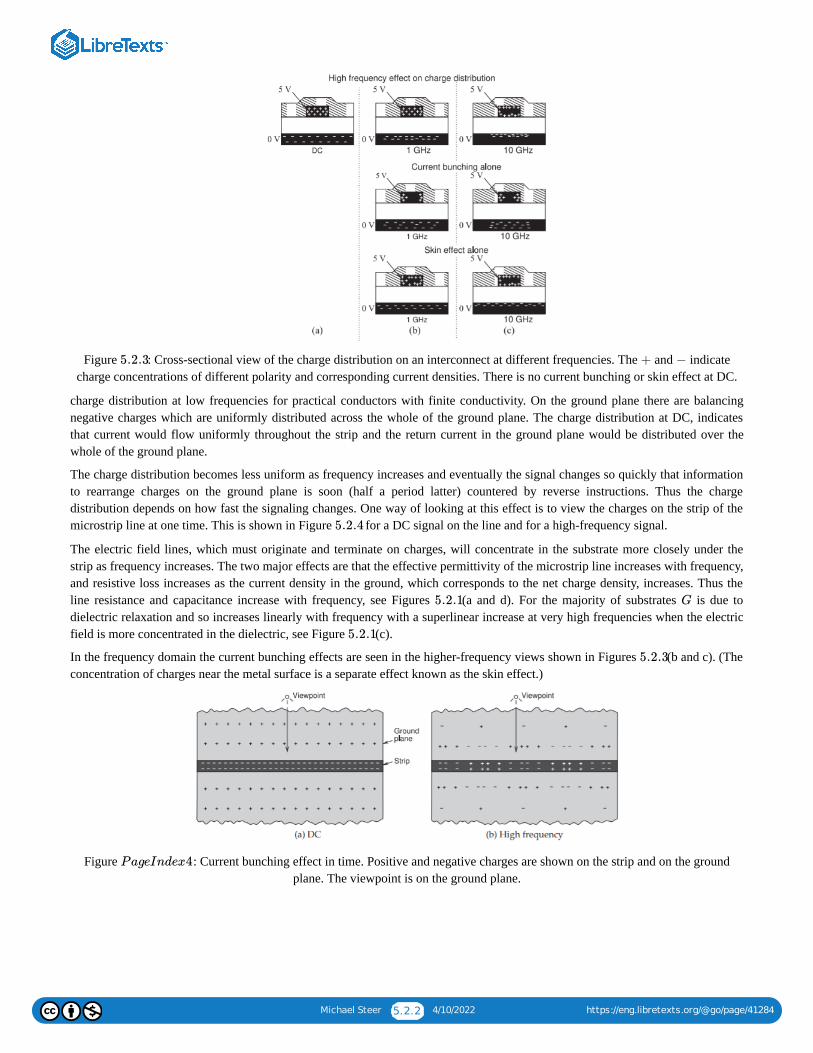
Michael Steer 5.2.2 4/10/2022 https://eng.libretexts.org/@go/page/41284
Figure : Cross-sectional view of the charge distribution on an interconnect at different frequencies. The and indicatecharge concentrations of different polarity and corresponding current densities. There is no current bunching or skin effect at DC.
charge distribution at low frequencies for practical conductors with finite conductivity. On the ground plane there are balancingnegative charges which are uniformly distributed across the whole of the ground plane. The charge distribution at DC, indicatesthat current would flow uniformly throughout the strip and the return current in the ground plane would be distributed over thewhole of the ground plane.
The charge distribution becomes less uniform as frequency increases and eventually the signal changes so quickly that informationto rearrange charges on the ground plane is soon (half a period latter) countered by reverse instructions. Thus the chargedistribution depends on how fast the signaling changes. One way of looking at this effect is to view the charges on the strip of themicrostrip line at one time. This is shown in Figure for a DC signal on the line and for a high-frequency signal.
The electric field lines, which must originate and terminate on charges, will concentrate in the substrate more closely under thestrip as frequency increases. The two major effects are that the effective permittivity of the microstrip line increases with frequency,and resistive loss increases as the current density in the ground, which corresponds to the net charge density, increases. Thus theline resistance and capacitance increase with frequency, see Figures (a and d). For the majority of substrates is due todielectric relaxation and so increases linearly with frequency with a superlinear increase at very high frequencies when the electricfield is more concentrated in the dielectric, see Figure (c).
In the frequency domain the current bunching effects are seen in the higher-frequency views shown in Figures (b and c). (Theconcentration of charges near the metal surface is a separate effect known as the skin effect.)
Figure : Current bunching effect in time. Positive and negative charges are shown on the strip and on the groundplane. The viewpoint is on the ground plane.
5.2.3 + −
5.2.4
5.2.1 G
5.2.1
5.2.3
PageIndex4
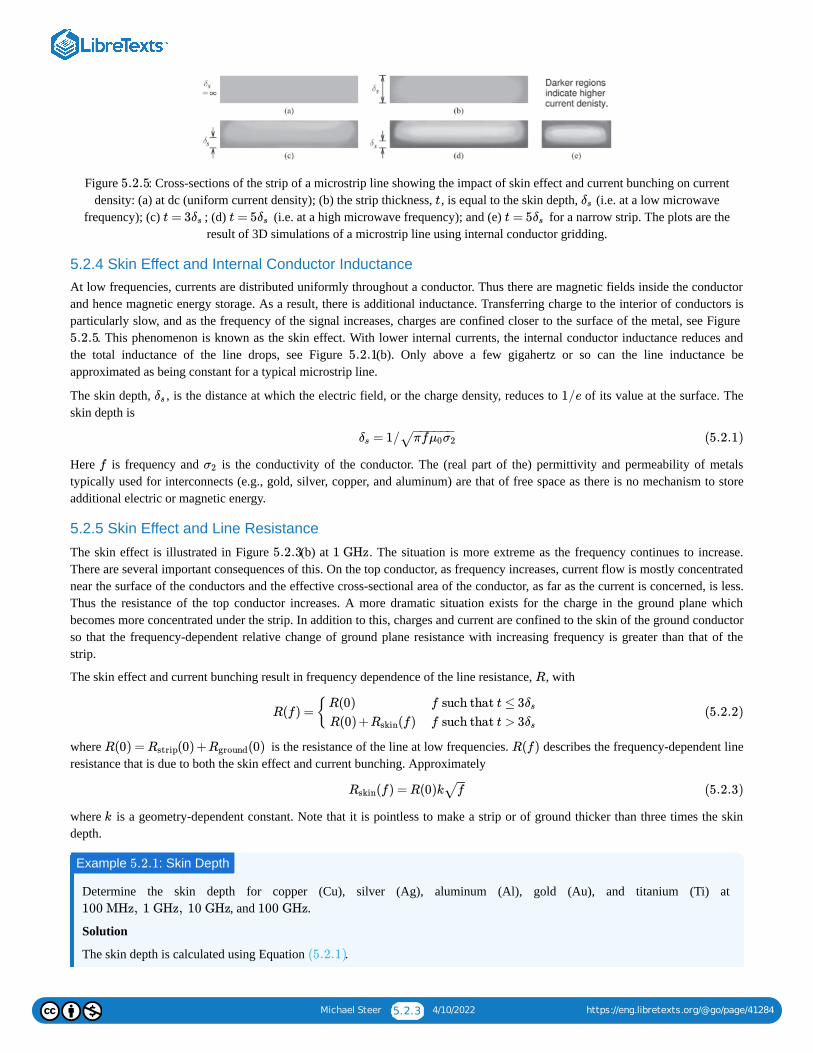
Michael Steer 5.2.3 4/10/2022 https://eng.libretexts.org/@go/page/41284
Figure : Cross-sections of the strip of a microstrip line showing the impact of skin effect and current bunching on currentdensity: (a) at dc (uniform current density); (b) the strip thickness, , is equal to the skin depth, (i.e. at a low microwave
frequency); (c) ; (d) (i.e. at a high microwave frequency); and (e) for a narrow strip. The plots are theresult of 3D simulations of a microstrip line using internal conductor gridding.
5.2.4 Skin Effect and Internal Conductor InductanceAt low frequencies, currents are distributed uniformly throughout a conductor. Thus there are magnetic fields inside the conductorand hence magnetic energy storage. As a result, there is additional inductance. Transferring charge to the interior of conductors isparticularly slow, and as the frequency of the signal increases, charges are confined closer to the surface of the metal, see Figure
. This phenomenon is known as the skin effect. With lower internal currents, the internal conductor inductance reduces andthe total inductance of the line drops, see Figure (b). Only above a few gigahertz or so can the line inductance beapproximated as being constant for a typical microstrip line.
The skin depth, , is the distance at which the electric field, or the charge density, reduces to of its value at the surface. Theskin depth is
Here is frequency and is the conductivity of the conductor. The (real part of the) permittivity and permeability of metalstypically used for interconnects (e.g., gold, silver, copper, and aluminum) are that of free space as there is no mechanism to storeadditional electric or magnetic energy.
5.2.5 Skin Effect and Line Resistance
The skin effect is illustrated in Figure (b) at . The situation is more extreme as the frequency continues to increase.There are several important consequences of this. On the top conductor, as frequency increases, current flow is mostly concentratednear the surface of the conductors and the effective cross-sectional area of the conductor, as far as the current is concerned, is less.Thus the resistance of the top conductor increases. A more dramatic situation exists for the charge in the ground plane whichbecomes more concentrated under the strip. In addition to this, charges and current are confined to the skin of the ground conductorso that the frequency-dependent relative change of ground plane resistance with increasing frequency is greater than that of thestrip.
The skin effect and current bunching result in frequency dependence of the line resistance, , with
where is the resistance of the line at low frequencies. describes the frequency-dependent lineresistance that is due to both the skin effect and current bunching. Approximately
where is a geometry-dependent constant. Note that it is pointless to make a strip or of ground thicker than three times the skindepth.
Determine the skin depth for copper (Cu), silver (Ag), aluminum (Al), gold (Au), and titanium (Ti) at , and .
Solution
The skin depth is calculated using Equation .
5.2.5t δs
t = 3δs t = 5δs t = 5δs
5.2.55.2.1
δs 1/e
= 1/δs πfμ0σ2− −−−−−
√ (5.2.1)
f σ2
5.2.3 1 GHz
R
R(f) = {R(0)
R(0) + (f)Rskin
f such that t ≤ 3δsf such that t > 3δs
(5.2.2)
R(0) = (0) + (0)Rstrip Rground R(f)
(f) = R(0)kRskin f−−
√ (5.2.3)
k
Example : Skin Depth5.2.1
100 MHz, 1 GHz, 10 GHz 100 GHz
(5.2.1)
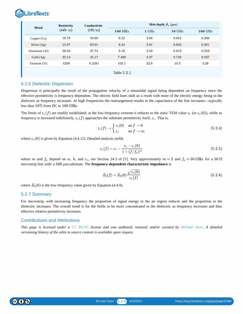
Michael Steer 5.2.4 4/10/2022 https://eng.libretexts.org/@go/page/41284
Metal Resistivity Conductivity Skin depth,
Copper (Cu)
Silver (Ag)
Aluminum (Al)
Gold (Ag)
Titanium (Ti)
Table
5.2.6 Dielectric DispersionDispersion is principally the result of the propagation velocity of a sinusoidal signal being dependent on frequency since theeffective permittivity is frequency-dependent. The electric field lines shift as a result with more of the electric energy being in thedielectric as frequency increases. At high frequencies the rearrangement results in the capacitance of the line increases—typicallyless than from DC to .
The limits of are readily established; at the low-frequency extreme it reduces to the static TEM value (or ), while asfrequency is increased indefinitely, approaches the substrate permittivity itself, . That is,
where is given by Equation (4.4.12). Detailed analysis yields
where and depend on and , see Section 24.3 of [1]. Very approximately and for a microstrip line with/ a substrate. The frequency-dependent characteristic impedance is
where is the low-frequency value given by Equation (4.4.9).
5.2.7 Summary
For microstrip, with increasing frequency the proportion of signal energy in the air region reduces and the proportion in thedielectric increases. The overall trend is for the fields to be more concentrated in the dielectric as frequency increases and thuseffective relative permittivity increases.
Contributions and AttributionsThis page is licensed under a CC BY-NC license and was authored, remixed, and/or curated by Michael Steer. A detailedversioning history of the edits to source content is available upon request.
(nΩ ⋅ m) (MS/m)
(μm)δs
100 MHz 1 GHz 10 GHz 100 GHz
16.78 59.60 6.52 2.06 0.652 0.206
15.87 63.01 6.34 2.01 0.634 0.201
26.50 37.74 8.19 2.59 0.819 0.259
22.14 45.17 7.489 2.37 0.749 0.237
4200 0.2381 103.1 32.6 10.3 3.26
5.2.1
10% 100 GHz
(f)εe εe (0)εe(f)εe εr
(f) → {εe(0)εe
εr
as f → 0
as f → ∞(5.2.4)
(0)εe
(f) = −εe εr− (0)εr εe
1 +(f/fa)m(5.2.5)
m fa w, h, εr m ≈ 2 ≈ 50 GHzfa 50 Ω500 μm
(f) = (0)Z0 Z0
(0)εe− −−−
√
(f)εe(5.2.6)
(0)Z0
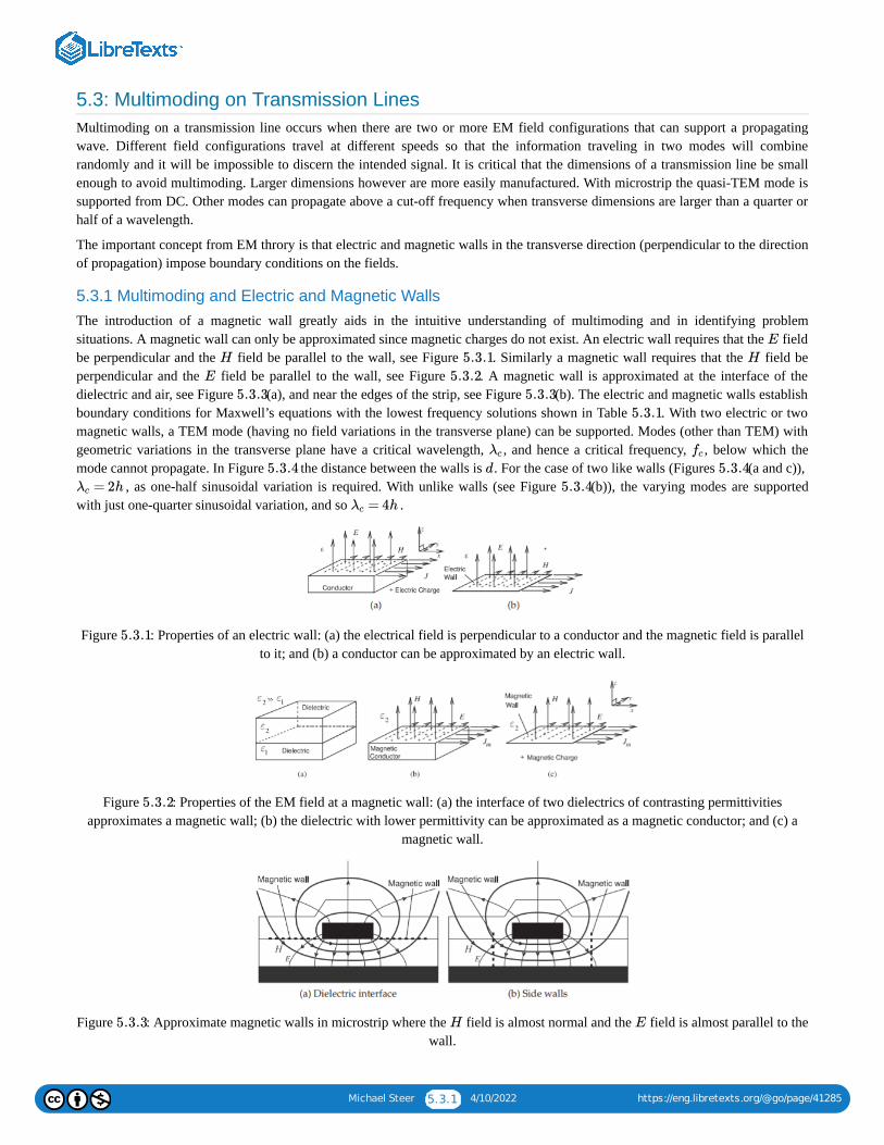
Michael Steer 5.3.1 4/10/2022 https://eng.libretexts.org/@go/page/41285
5.3: Multimoding on Transmission LinesMultimoding on a transmission line occurs when there are two or more EM field configurations that can support a propagatingwave. Different field configurations travel at different speeds so that the information traveling in two modes will combinerandomly and it will be impossible to discern the intended signal. It is critical that the dimensions of a transmission line be smallenough to avoid multimoding. Larger dimensions however are more easily manufactured. With microstrip the quasi-TEM mode issupported from DC. Other modes can propagate above a cut-off frequency when transverse dimensions are larger than a quarter orhalf of a wavelength.
The important concept from EM throry is that electric and magnetic walls in the transverse direction (perpendicular to the directionof propagation) impose boundary conditions on the fields.
5.3.1 Multimoding and Electric and Magnetic WallsThe introduction of a magnetic wall greatly aids in the intuitive understanding of multimoding and in identifying problemsituations. A magnetic wall can only be approximated since magnetic charges do not exist. An electric wall requires that the fieldbe perpendicular and the field be parallel to the wall, see Figure . Similarly a magnetic wall requires that the field beperpendicular and the field be parallel to the wall, see Figure . A magnetic wall is approximated at the interface of thedielectric and air, see Figure (a), and near the edges of the strip, see Figure (b). The electric and magnetic walls establishboundary conditions for Maxwell’s equations with the lowest frequency solutions shown in Table . With two electric or twomagnetic walls, a TEM mode (having no field variations in the transverse plane) can be supported. Modes (other than TEM) withgeometric variations in the transverse plane have a critical wavelength, , and hence a critical frequency, , below which themode cannot propagate. In Figure the distance between the walls is . For the case of two like walls (Figures (a and c)),
, as one-half sinusoidal variation is required. With unlike walls (see Figure (b)), the varying modes are supportedwith just one-quarter sinusoidal variation, and so .
Figure : Properties of an electric wall: (a) the electrical field is perpendicular to a conductor and the magnetic field is parallelto it; and (b) a conductor can be approximated by an electric wall.
Figure : Properties of the EM field at a magnetic wall: (a) the interface of two dielectrics of contrasting permittivitiesapproximates a magnetic wall; (b) the dielectric with lower permittivity can be approximated as a magnetic conductor; and (c) a
magnetic wall.
Figure : Approximate magnetic walls in microstrip where the field is almost normal and the field is almost parallel to thewall.
E
H 5.3.1 H
E 5.3.25.3.3 5.3.3
5.3.1
λc fc5.3.4 d 5.3.4
= 2hλc 5.3.4= 4hλc
5.3.1
5.3.2
5.3.3 H E
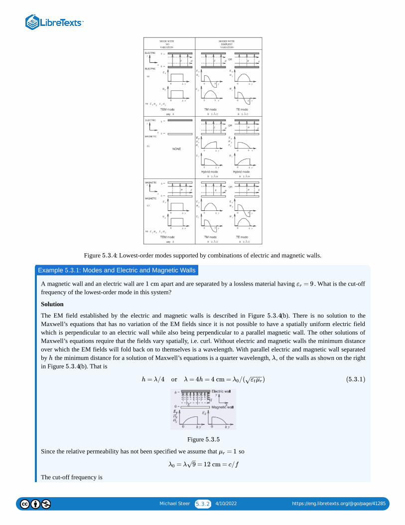
Michael Steer 5.3.2 4/10/2022 https://eng.libretexts.org/@go/page/41285
Figure : Lowest-order modes supported by combinations of electric and magnetic walls.
A magnetic wall and an electric wall are apart and are separated by a lossless material having . What is the cut-offfrequency of the lowest-order mode in this system?
Solution
The EM field established by the electric and magnetic walls is described in Figure (b). There is no solution to theMaxwell’s equations that has no variation of the EM fields since it is not possible to have a spatially uniform electric fieldwhich is perpendicular to an electric wall while also being perpendicular to a parallel magnetic wall. The other solutions ofMaxwell’s equations require that the fields vary spatially, i.e. curl. Without electric and magnetic walls the minimum distanceover which the EM fields will fold back on to themselves is a wavelength. With parallel electric and magnetic wall separatedby the minimum distance for a solution of Maxwell’s equations is a quarter wavelength, , of the walls as shown on the rightin Figure (b). That is
Figure
Since the relative permeability has not been specified we assume that so
The cut-off frequency is
5.3.4
Example : Modes and Electric and Magnetic Walls5.3.1
1 cm = 9εr
5.3.4
h λ
5.3.4
h = λ/4 or λ = 4h = 4 cm = /( )λ0 εtμr− −−−
√ (5.3.1)
5.3.5
= 1μr
= λ = 12 cm = c/fλ0 9–
√

Michael Steer 5.3.3 4/10/2022 https://eng.libretexts.org/@go/page/41285
Contributions and AttributionsThis page is licensed under a CC BY-NC license and was authored, remixed, and/or curated by Michael Steer. A detailedversioning history of the edits to source content is available upon request.
f = (2.998 × m/s)/(0.12 m)108
= 2.498 GHz (5.3.2)
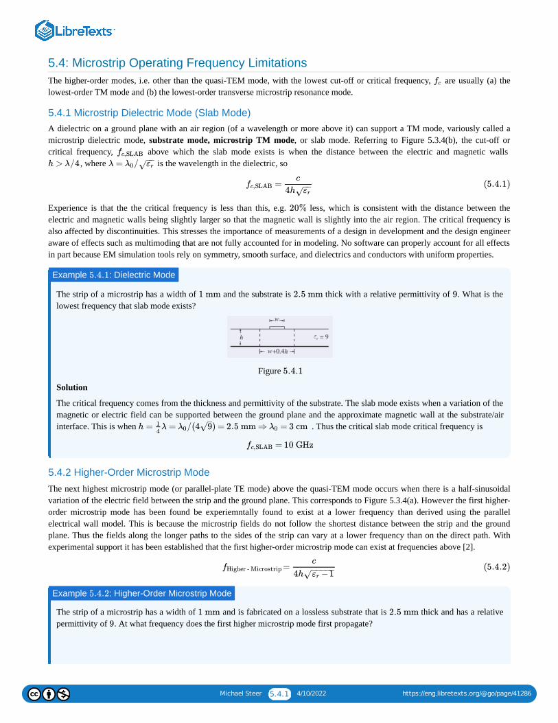
Michael Steer 5.4.1 4/10/2022 https://eng.libretexts.org/@go/page/41286
5.4: Microstrip Operating Frequency LimitationsThe higher-order modes, i.e. other than the quasi-TEM mode, with the lowest cut-off or critical frequency, are usually (a) thelowest-order TM mode and (b) the lowest-order transverse microstrip resonance mode.
5.4.1 Microstrip Dielectric Mode (Slab Mode)A dielectric on a ground plane with an air region (of a wavelength or more above it) can support a TM mode, variously called amicrostrip dielectric mode, substrate mode, microstrip TM mode, or slab mode. Referring to Figure 5.3.4(b), the cut-off orcritical frequency, above which the slab mode exists is when the distance between the electric and magnetic walls
, where is the wavelength in the dielectric, so
Experience is that the the critical frequency is less than this, e.g. less, which is consistent with the distance between theelectric and magnetic walls being slightly larger so that the magnetic wall is slightly into the air region. The critical frequency isalso affected by discontinuities. This stresses the importance of measurements of a design in development and the design engineeraware of effects such as multimoding that are not fully accounted for in modeling. No software can properly account for all effectsin part because EM simulation tools rely on symmetry, smooth surface, and dielectrics and conductors with uniform properties.
The strip of a microstrip has a width of and the substrate is thick with a relative permittivity of . What is thelowest frequency that slab mode exists?
Figure
Solution
The critical frequency comes from the thickness and permittivity of the substrate. The slab mode exists when a variation of themagnetic or electric field can be supported between the ground plane and the approximate magnetic wall at the substrate/airinterface. This is when . Thus the critical slab mode critical frequency is
5.4.2 Higher-Order Microstrip Mode
The next highest microstrip mode (or parallel-plate TE mode) above the quasi-TEM mode occurs when there is a half-sinusoidalvariation of the electric field between the strip and the ground plane. This corresponds to Figure 5.3.4(a). However the first higher-order microstrip mode has been found be experiemntally found to exist at a lower frequency than derived using the parallelelectrical wall model. This is because the microstrip fields do not follow the shortest distance between the strip and the groundplane. Thus the fields along the longer paths to the sides of the strip can vary at a lower frequency than on the direct path. Withexperimental support it has been established that the first higher-order microstrip mode can exist at frequencies above [2].
The strip of a microstrip has a width of and is fabricated on a lossless substrate that is thick and has a relativepermittivity of . At what frequency does the first higher microstrip mode first propagate?
fc
fc,SLAB
h > λ/4 λ = /λ0 εr−−
√
=fc,SLABc
4h εr−−
√(5.4.1)
20%
Example : Dielectric Mode5.4.1
1 mm 2.5 mm 9
5.4.1
h = λ = /(4 ) = 2.5 mm ⇒ = 3 cm14
λ0 9–
√ λ0
= 10 GHzfc,SLAB
=fHigher - Microstripc
4h −1εr− −−−−
√(5.4.2)
Example : Higher-Order Microstrip Mode5.4.2
1 mm 2.5 mm9
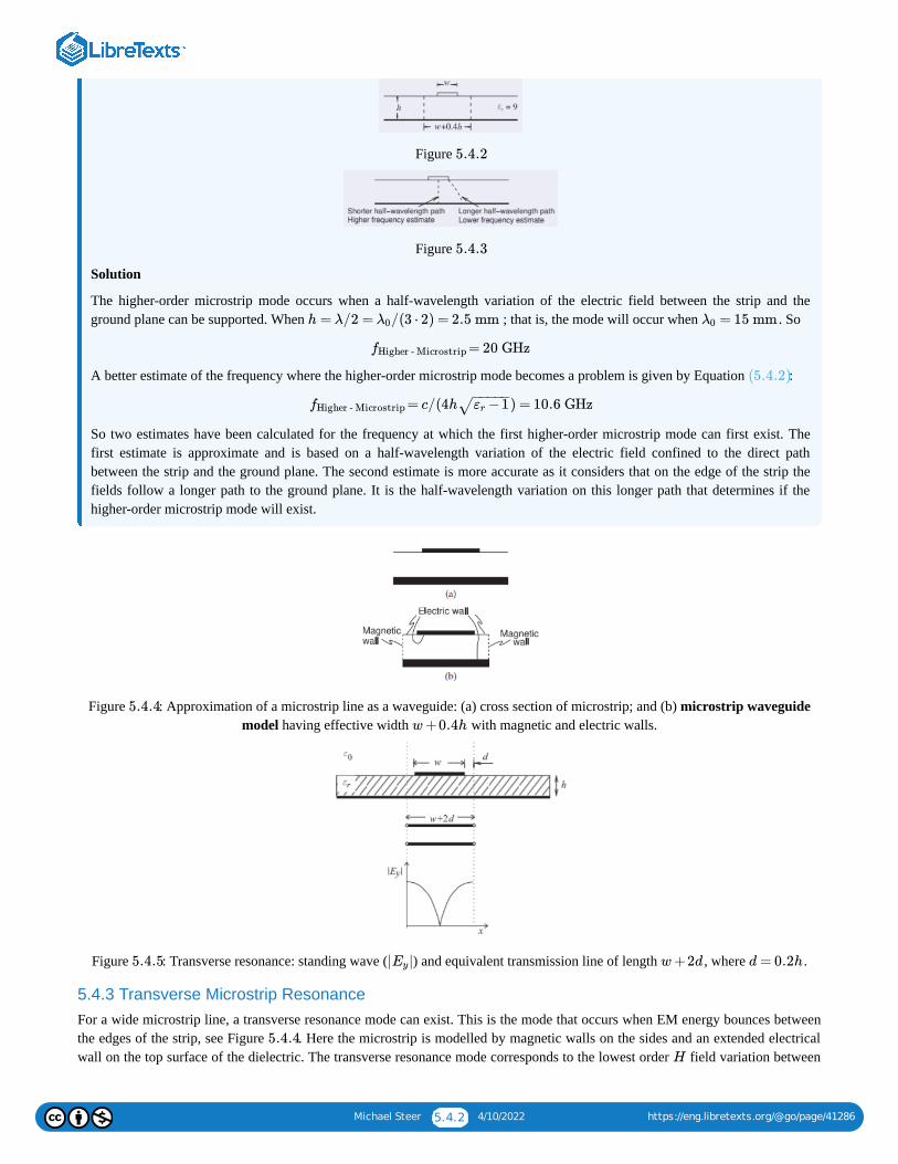
Michael Steer 5.4.2 4/10/2022 https://eng.libretexts.org/@go/page/41286
Figure
Figure
Solution
The higher-order microstrip mode occurs when a half-wavelength variation of the electric field between the strip and theground plane can be supported. When ; that is, the mode will occur when . So
A better estimate of the frequency where the higher-order microstrip mode becomes a problem is given by Equation :
So two estimates have been calculated for the frequency at which the first higher-order microstrip mode can first exist. Thefirst estimate is approximate and is based on a half-wavelength variation of the electric field confined to the direct pathbetween the strip and the ground plane. The second estimate is more accurate as it considers that on the edge of the strip thefields follow a longer path to the ground plane. It is the half-wavelength variation on this longer path that determines if thehigher-order microstrip mode will exist.
Figure : Approximation of a microstrip line as a waveguide: (a) cross section of microstrip; and (b) microstrip waveguidemodel having effective width with magnetic and electric walls.
Figure : Transverse resonance: standing wave ( ) and equivalent transmission line of length , where .
5.4.3 Transverse Microstrip ResonanceFor a wide microstrip line, a transverse resonance mode can exist. This is the mode that occurs when EM energy bounces betweenthe edges of the strip, see Figure . Here the microstrip is modelled by magnetic walls on the sides and an extended electricalwall on the top surface of the dielectric. The transverse resonance mode corresponds to the lowest order field variation between
5.4.2
5.4.3
h = λ/2 = /(3 ⋅ 2) = 2.5 mmλ0 = 15 mmλ0
= 20 GHzfHigher - Microstrip
(5.4.2)
= c/(4h ) = 10.6 GHzfHigher - Microstrip −1εr− −−−−
√
5.4.4w+0.4h
5.4.5 | |Ey w+2d d = 0.2h
5.4.4H
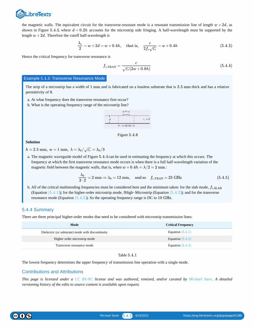
Michael Steer 5.4.3 4/10/2022 https://eng.libretexts.org/@go/page/41286
the magnetic walls. The equivalent circuit for the transverse-resonant mode is a resonant transmission line of length , asshown in Figure , where accounts for the microstrip side fringing. A half-wavelength must be supported by thelength . Therefore the cutoff half-wavelength is
Hence the critical frequency for transverse resonance is
The strip of a microstrip has a width of and is fabricated on a lossless substrate that is thick and has a relativepermittivity of .
a. At what frequency does the transverse resonance first occur?b. What is the operating frequency range of the microstrip line?
Figure
Solution
a. The magnetic waveguide model of Figure can be used in estimating the frequency at which this occurs. Thefrequency at which the first transverse resonance mode occurs is when there is a full half-wavelength variation of themagnetic field between the magnetic walls, that is, when :
b. All of the critical multimoding frequencies must be considered here and the minimum taken: for the slab mode, (Equation ); for the higher-order microstrip mode, fHigh−Microstrip (Equation ); and for the transverseresonance mode (Equation ). So the operating frequency range is DC to .
5.4.4 SummaryThere are three principal higher-order modes that need to be considered with microstrip transmission lines:
Mode Critical Frequency
Dielectric (or substrate) mode with discontinuity Equation
Higher order microstrip mode Equation
Transverse resonance mode Equation
Table
The lowest frequency determines the upper frequency of transmission line operation with a single mode.
Contributions and Attributions
This page is licensed under a CC BY-NC license and was authored, remixed, and/or curated by Michael Steer. A detailedversioning history of the edits to source content is available upon request.
w+2d5.4.5 d = 0.2h
w+2d
= w+2d = w+0.4h, that is, = w+0.4hλc
2
c
2fc εr−−
√(5.4.3)
=fc,TRANc
(2w+0.8h)εr−−
√(5.4.4)
Example : Transverse Resonance Mode5.4.3
1 mm 2.5 mm9
5.4.6
h = 2.5 mm, w = 1 mm, λ = / = /3λ0 εr−−
√ λ0
5.4.4
w+0.4h = λ/2 = 2 mm
= 2 mm ⇒ = 12 mm, and so = 25 GHzλ0
3 ⋅ 2λ0 fc,TRAN (5.4.5)
fc,SLAB
(5.4.1) (5.4.2)(5.4.5) 10 GHz
(5.4.1)
(5.4.2)
(5.4.4)
5.4.1

Michael Steer 5.5.1 4/10/2022 https://eng.libretexts.org/@go/page/41287
5.5: SummaryMicrostrip can support multiple modes, but most are cut off by keeping transverse dimensions small with respect to a wavelength.When it is possible for a second (or higher-order) mode to exist, whether that mode is generated depends on the couplingmechanism between modes. This coupling mechanism is a discontinuity, which of course is common if circuit structures are to beincorporated. A microwave designer must always be aware of frequency dependence and multimoding and choose dimensions toavoid their occurrence except when the use is intentional and controlled.
Contributions and AttributionsThis page is licensed under a CC BY-NC license and was authored, remixed, and/or curated by Michael Steer. A detailedversioning history of the edits to source content is available upon request.

Michael Steer 5.6.1 4/10/2022 https://eng.libretexts.org/@go/page/41288
5.6: References[1] M. Steer, Microwave and RF Design, Transmission Lines, 3rd ed. North Carolina State University, 2019.
[2] T. Edwards and M. Steer, Foundations for Microstrip Circuit Design. John Wiley & Sons, 2016.
Contributions and AttributionsThis page is licensed under a CC BY-NC license and was authored, remixed, and/or curated by Michael Steer. A detailedversioning history of the edits to source content is available upon request.

Michael Steer 5.7.1 4/10/2022 https://eng.libretexts.org/@go/page/41289
5.7: Exercises1. What is the skin depth on a copper microstrip line at ? Assume that the conductivity of the deposited copper forming
the strip is half that of bulk single-crystal copper. Use the data in Example 5.2.1.2. What is the skin depth on a silver microstrip line at ? Assume that the conductivity of the fabricated silver conductor is
that of bulk single-crystal silver. Use the data in Example 5.2.1.3. A magnetic wall and an electric wall are apart and are separated by a lossless material having a relative permittivity of
and a relative permeability of . What is the cut-off frequency of the lowest-order mode in this system?4. The strip of a microstrip has a width of and is fabricated on a lossless substrate that is thick and has a relative
permittivity of .a. Draw the microstrip waveguide model of the microstrip line. Put dimensions on your drawing.b. Sketch the electric field distribution of the first transverse resonance mode and calculate the frequency at which the
transverse resonance mode occurs.c. Sketch the electric field distribution of the first higher-order microstrip mode and calculate the frequency at which it occurs.d. Sketch the electric field distribution of the slab mode and calculate the frequency at which it occurs.
5. A microstrip line has a width of and is constructed on a substrate that is thick with a relative permittivity of .
a. Determine the frequency at which transverse resonance would first occur.b. When the dielectric is slightly less than onequarter wavelength in thickness the dielectric slab mode can be supported. Some
of the fields will appear in the air region as well as in the dielectric, extending the effective thickness of the dielectric.Ignoring the fields in the air (use a one-quarter wavelength criterion), at what frequency will the dielectric slab mode firstoccur?
6. The strip of a microstrip has a width of and uses a lossless substrate that is thick and has a relative permittivityof .
a. At what frequency will the first transverse resonance occur?b. At what frequency will the first higher-order microstrip mode occur?c. At what frequency will the slab mode occur?d. Identify the useful operating frequency range of the microstrip.
7. The strip of a microstrip has a width of and is fabricated on a lossless substrate that is thick and has a relativepermittivity of . [Parallels Examples 5.4.1, 5.4.2, and 5.4.3]a. At what frequency does the transverse resonance first occur?b. At what frequency does the first higherorder microstrip mode first propagate?c. At what frequency does the substrate (or slab) mode first occur?
8. The strip of a microstrip has a width of and uses a lossless substrate that is thick and has a relative permittivityof .a. At what frequency does the transverse resonance first occur?b. At what frequency does the first higherorder microstrip mode propagate?c. At what frequency does the substrate (or slab) mode first occur?d. What is the highest operating frequency of the microstrip?
9. A microstrip line has a strip width of and is fabricated on a substrate that is thick and has a relativepermittivity of .
a. Draw the microstrip waveguide model and indicate and calculate the dimensions of the model.b. Based only on the microstrip waveguide model, determine the frequency at which the first transverse resonance occurs?c. Based on the microstrip waveguide model, determine the frequency at which the first higher-order microstrip mode occurs?d. At what frequency will the slab mode occur? For this you cannot use the microstrip waveguide model.
10. A microstrip line has a strip width of and is fabricated on a substrate that is thick and has a relativepermittivity of .a. Define the properties of a magnetic wall.b. Identify two situations where a magnetic wall can be used in the analysis of a microstrip line; that is, give two situations
where a magnetic wall approximation can be used.
10 GHz
1 GHz
75%
2 cm 10
23
600 μm 1 mm
10
352 μm 500 μm
5.6
600 μm 635 μm
4.1
500 μm 635 μm
12
250 μm 300 μm
15
100 μm 150 μm
9
100 μm 150 μm
9

Michael Steer 5.7.2 4/10/2022 https://eng.libretexts.org/@go/page/41289
c. Draw the microstrip waveguide model and indicate and calculate the dimensions of the model.11. The strip of a microstrip line has a width of , and the microstrip substrate is thick and has a relative permittivity
of and relative permeability of .a. Draw the microstrip waveguide model and calculate the dimensions of the model. Clearly show the electric and magnetic
walls in the model.b. Use the microstrip waveguide model to calculate the cut off frequency of the transverse resonance mode?c. A substrate mode can also be excited but the cut off frequency of this mode cannot be calculated using the microstrip
waveguide model. Provide a brief description of the substrate mode and calculate the lowest frequency at which it can exist.
12. A microstrip technology uses a substrate with a relative permittivity of and thickness of . If the operating frequencyis , what is the maximum width of the strip from higher-order mode considerations.
13. A microstrip line operating at has a thick substrate with a relative permittivity of .a. Determine the maximum width of the strip from higher-order mode considerations. Consider the transverse resonance mode,
the higher-order microstrip mode, and the slab mode.b. Thus determine the minimum achievable characteristic impedance.
14. A microstrip line has a strip width of and is fabricated on a -thick lossless substrate with a relative permittivityof .a. Define the properties of a magnetic wall.b. Identify two situations where a magnetic wall can be used in determining multimoding on a microstrip line. That is, give
two locations where a magnetic wall approximation can be used.15. Two magnetic walls are separated by in a lossless material having a relative permittivity of and a relative permeability
of .
a. What is the wavelength of a signal in this material?b. Now consider a field variation, i.e. a mode and not constant, established by the magnetic walls. Describe this lowest order
field variation. That is how does the field vary or how does the field vary (one is sufficient)?c. What is the lowest frequency at which a field variation can be supported by those walls in the specified medium?
16. A microstrip line has a strip width of and a thick substrate with a relative permittivity of . At whatfrequency can the substrate mode first occur?
17. A microstrip line has a strip width of and a thick substrate with a relative permittivity of . At whatfrequency can a higherorder microstrip mode first propagate?
18. A microstrip line has a strip width of and a thick substrate with a relative permittivity of . At whatfrequency can transverse resonance first occur?
19. The strip of a microstrip line has a width of and the substrate is thick and has a relative permittivity of .a. Draw the effective waveguide model of a microstrip line with magnetic walls and an effective strip width, .b. What is the effective relative permittivity of the microstrip waveguide model?c. What is ?d. Can the lowest frequency at which the transverse resonance mode first occurs be determined from the microstrip waveguide
model?
5.7.1 Exercises by Sectionchallenging
5.7.2 Answers to Selected Exercises2. 3. 4. (c) 5. (c) to
0.5 mm 1 mm
9 1
10 400 μm
10 GHz
18 GHz 200 μm 20
100 μm 150 μm
9
1 mm 9
1
10 GHz
H E
250 μm 300 μm 15
250 μm 300 μm 15
250 μm 300 μm 15
200 μm 400 μm 4
weff
weff
†
§5.21, 2
§5.33
§5.44†, 5†, 6†, 7†, 8†, 9†, 10†, 11†, 12, 13, 14, 15, 16, 17, 18, 19
2.315 μm
247 MHz
25 GHz
DC 63.4 GHz

Michael Steer 5.7.3 4/10/2022 https://eng.libretexts.org/@go/page/41289
6. (d)
8.
11. (b)
Contributions and AttributionsThis page is licensed under a CC BY-NC license and was authored, remixed, and/or curated by Michael Steer. A detailedversioning history of the edits to source content is available upon request.
DC ≤ f ≤ 48.6 GHz
104.6 GHz
55.6 GHz

1 4/10/2022
CHAPTER OVERVIEW6: COUPLED LINES AND APPLICATIONS
6.1: INTRODUCTION6.2: PHYSICS OF COUPLING6.3: LOW FREQUENCY CAPACITANCE MODEL OF COUPLED LINES6.4: SYMMETRIC COUPLED TRANSMISSION LINES6.5: DIRECTIONAL COUPLER6.6: SUMMARY6.7: REFERENCES6.8: EXERCISES

Michael Steer 6.1.1 4/10/2022 https://eng.libretexts.org/@go/page/41290
6.1: IntroductionThis chapter describes what happens when two transmission lines are so close together that the fields produced by one line interferewith the other line. Then a portion of the signal energy on one line is transferred to the other resulting in coupling. For microstriplines the coupling reduces as the lines separate and usually the coupling is small enough to be ignored if the separation is at leastthree times the height of the strips. Transmission line coupling may be undesirable in many situations, but the phenomenon isexploited to realize many novel RF and microwave elements such as filters. A coupled pair of transmissions lines also enables theforward- and backward traveling waves on a line to be separately measured.
The chapter begins with a discussion of the physics of coupling which leads to the preferred description of propagation on a pair ofparallel coupled lines (PCLs) as supporting even and odd modes.
Contributions and AttributionsThis page is licensed under a CC BY-NC license and was authored, remixed, and/or curated by Michael Steer. A detailedversioning history of the edits to source content is available upon request.
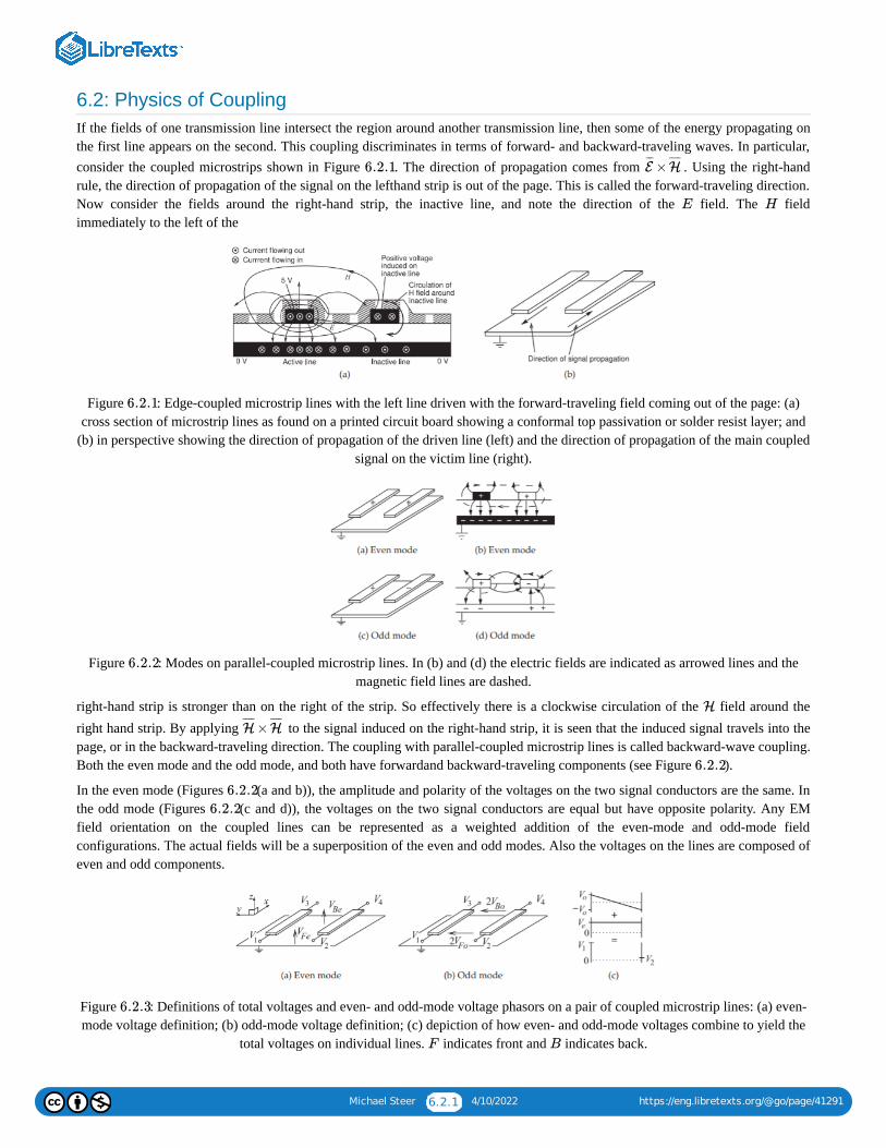
Michael Steer 6.2.1 4/10/2022 https://eng.libretexts.org/@go/page/41291
6.2: Physics of CouplingIf the fields of one transmission line intersect the region around another transmission line, then some of the energy propagating onthe first line appears on the second. This coupling discriminates in terms of forward- and backward-traveling waves. In particular,consider the coupled microstrips shown in Figure . The direction of propagation comes from . Using the right-handrule, the direction of propagation of the signal on the lefthand strip is out of the page. This is called the forward-traveling direction.Now consider the fields around the right-hand strip, the inactive line, and note the direction of the field. The fieldimmediately to the left of the
Figure : Edge-coupled microstrip lines with the left line driven with the forward-traveling field coming out of the page: (a)cross section of microstrip lines as found on a printed circuit board showing a conformal top passivation or solder resist layer; and
(b) in perspective showing the direction of propagation of the driven line (left) and the direction of propagation of the main coupledsignal on the victim line (right).
Figure : Modes on parallel-coupled microstrip lines. In (b) and (d) the electric fields are indicated as arrowed lines and themagnetic field lines are dashed.
right-hand strip is stronger than on the right of the strip. So effectively there is a clockwise circulation of the field around theright hand strip. By applying to the signal induced on the right-hand strip, it is seen that the induced signal travels into thepage, or in the backward-traveling direction. The coupling with parallel-coupled microstrip lines is called backward-wave coupling.Both the even mode and the odd mode, and both have forwardand backward-traveling components (see Figure ).
In the even mode (Figures (a and b)), the amplitude and polarity of the voltages on the two signal conductors are the same. Inthe odd mode (Figures (c and d)), the voltages on the two signal conductors are equal but have opposite polarity. Any EMfield orientation on the coupled lines can be represented as a weighted addition of the even-mode and odd-mode fieldconfigurations. The actual fields will be a superposition of the even and odd modes. Also the voltages on the lines are composed ofeven and odd components.
Figure : Definitions of total voltages and even- and odd-mode voltage phasors on a pair of coupled microstrip lines: (a) even-mode voltage definition; (b) odd-mode voltage definition; (c) depiction of how even- and odd-mode voltages combine to yield the
total voltages on individual lines. indicates front and indicates back.
6.2.1 ×E¯
H¯ ¯¯
E H
6.2.1
6.2.2
H
×H¯ ¯¯
H¯ ¯¯
6.2.2
6.2.2
6.2.2
6.2.3
F B
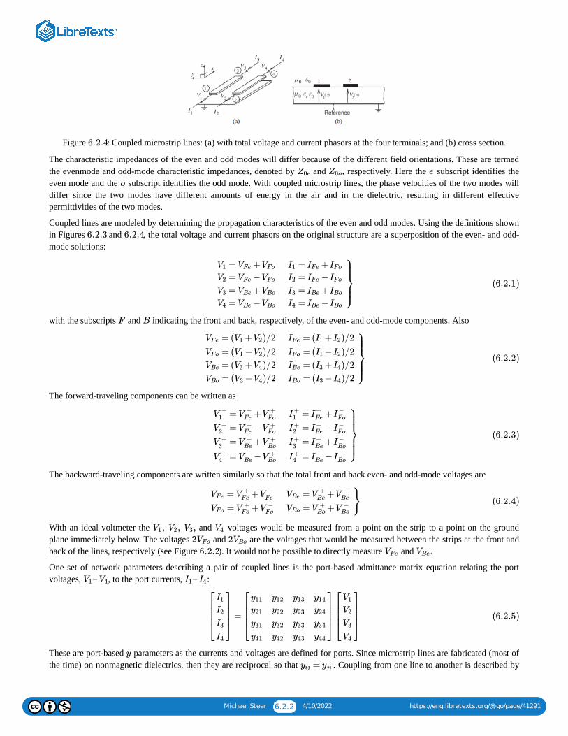
Michael Steer 6.2.2 4/10/2022 https://eng.libretexts.org/@go/page/41291
Figure : Coupled microstrip lines: (a) with total voltage and current phasors at the four terminals; and (b) cross section.
The characteristic impedances of the even and odd modes will differ because of the different field orientations. These are termedthe evenmode and odd-mode characteristic impedances, denoted by and , respectively. Here the subscript identifies theeven mode and the subscript identifies the odd mode. With coupled microstrip lines, the phase velocities of the two modes willdiffer since the two modes have different amounts of energy in the air and in the dielectric, resulting in different effectivepermittivities of the two modes.
Coupled lines are modeled by determining the propagation characteristics of the even and odd modes. Using the definitions shownin Figures and , the total voltage and current phasors on the original structure are a superposition of the even- and odd-mode solutions:
with the subscripts and indicating the front and back, respectively, of the even- and odd-mode components. Also
The forward-traveling components can be written as
The backward-traveling components are written similarly so that the total front and back even- and odd-mode voltages are
With an ideal voltmeter the and voltages would be measured from a point on the strip to a point on the groundplane immediately below. The voltages and are the voltages that would be measured between the strips at the front andback of the lines, respectively (see Figure ). It would not be possible to directly measure and .
One set of network parameters describing a pair of coupled lines is the port-based admittance matrix equation relating the portvoltages, , to the port currents, :
These are port-based parameters as the currents and voltages are defined for ports. Since microstrip lines are fabricated (most ofthe time) on nonmagnetic dielectrics, then they are reciprocal so that . Coupling from one line to another is described by
6.2.4
Z0e Z0o e
o
6.2.3 6.2.4
= +V1 VFe VFo
= −V2 VFe VFo
= +V3 VBe VBo
= −V4 VBe VBo
= +I1 IFe IFo
= −I2 IFe IFo
= +I3 IBe IBo
= −I4 IBe IBo
⎫
⎭
⎬
⎪⎪⎪
⎪⎪⎪
(6.2.1)
F B
= ( + )/2VFe V1 V2
= ( − )/2VFo V1 V2
= ( + )/2VBe V3 V4
= ( − )/2VBo V3 V4
= ( + )/2IFe I1 I2
= ( − )/2IFo I1 I2
= ( + )/2IBe I3 I4
= ( − )/2IBo I3 I4
⎫
⎭
⎬
⎪⎪⎪⎪
⎪⎪⎪⎪
(6.2.2)
= +V+
1 V+
Fe V+
Fo
= −V +2 V +
Fe V +Fo
= +V +3
V +Be
V +Bo
= −V +4 V +
Be V +Bo
= +I+1 I
+Fe I
−Fo
= −I +2 I +
Fe I −Fo
= +I +3
I +Be
I −Bo
= −I +4 I +
Be I −Bo
⎫
⎭
⎬
⎪⎪⎪⎪
⎪⎪⎪⎪
(6.2.3)
}= +VFe V
+Fe V
−Fe
= +VFo V +Fo V −
Fo
= +VBe V+
Be V−
Be
= +VBo V +Bo V −
Bo
(6.2.4)
, , ,V1 V2 V3 V4
2VFo 2VBo
6.2.2 VFe VBe
–V1 V4 –I1 I4
=
⎡
⎣
⎢⎢⎢
I1
I2
I3
I4
⎤
⎦
⎥⎥⎥
⎡
⎣
⎢⎢⎢
y11
y21
y31
y41
y12
y22
y32
y42
y13
y23
y33
y43
y14
y24
y34
y44
⎤
⎦
⎥⎥⎥
⎡
⎣
⎢⎢⎢
V1
V2
V3
V4
⎤
⎦
⎥⎥⎥
(6.2.5)
y
=yij yji

Michael Steer 6.2.3 4/10/2022 https://eng.libretexts.org/@go/page/41291
the terms and .
6.2.1 SummaryThe important concept introduced in this section is that fields and the propagating waves on a pair of parallel coupled lines can bedescribed as a combination of odd and even modes each of which has forward- and backward-wave versions.
Contributions and Attributions
This page is licensed under a CC BY-NC license and was authored, remixed, and/or curated by Michael Steer. A detailedversioning history of the edits to source content is available upon request.
(= )y12 y21 (= )y34 y43
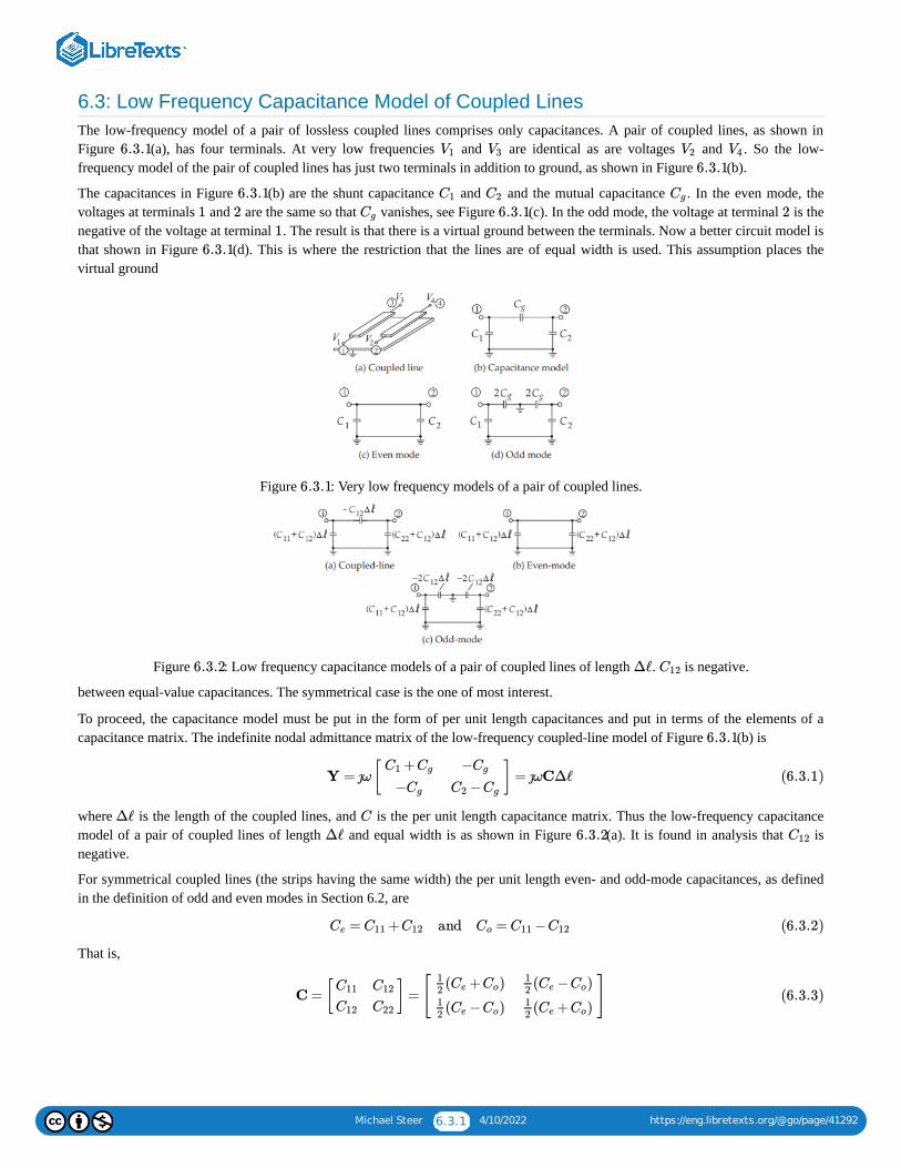
Michael Steer 6.3.1 4/10/2022 https://eng.libretexts.org/@go/page/41292
6.3: Low Frequency Capacitance Model of Coupled LinesThe low-frequency model of a pair of lossless coupled lines comprises only capacitances. A pair of coupled lines, as shown inFigure (a), has four terminals. At very low frequencies and are identical as are voltages and . So the low-frequency model of the pair of coupled lines has just two terminals in addition to ground, as shown in Figure (b).
The capacitances in Figure (b) are the shunt capacitance and and the mutual capacitance . In the even mode, thevoltages at terminals and are the same so that vanishes, see Figure (c). In the odd mode, the voltage at terminal is thenegative of the voltage at terminal . The result is that there is a virtual ground between the terminals. Now a better circuit model isthat shown in Figure (d). This is where the restriction that the lines are of equal width is used. This assumption places thevirtual ground
Figure : Very low frequency models of a pair of coupled lines.
Figure : Low frequency capacitance models of a pair of coupled lines of length . is negative.
between equal-value capacitances. The symmetrical case is the one of most interest.
To proceed, the capacitance model must be put in the form of per unit length capacitances and put in terms of the elements of acapacitance matrix. The indefinite nodal admittance matrix of the low-frequency coupled-line model of Figure (b) is
where is the length of the coupled lines, and is the per unit length capacitance matrix. Thus the low-frequency capacitancemodel of a pair of coupled lines of length and equal width is as shown in Figure (a). It is found in analysis that isnegative.
For symmetrical coupled lines (the strips having the same width) the per unit length even- and odd-mode capacitances, as definedin the definition of odd and even modes in Section 6.2, are
That is,
6.3.1 V1 V3 V2 V4
6.3.1
6.3.1 C1 C2 Cg
1 2 Cg 6.3.1 2
1
6.3.1
6.3.1
6.3.2 Δℓ C12
6.3.1
Y = ȷω[ ] = ȷωCΔℓ+C1 Cg
−Cg
−Cg
−C2 Cg
(6.3.1)
Δℓ C
Δℓ 6.3.2 C12
= + and = −Ce C11 C12 Co C11 C12 (6.3.2)
C = [ ] = [ ]C11
C12
C12
C22
( + )12
Ce Co
( − )12
Ce Co
( − )12
Ce Co
( + )12
Ce Co
(6.3.3)

Michael Steer 6.3.2 4/10/2022 https://eng.libretexts.org/@go/page/41292
Contributions and AttributionsThis page is licensed under a CC BY-NC license and was authored, remixed, and/or curated by Michael Steer. A detailedversioning history of the edits to source content is available upon request.
Michael Steer 6.4.1 4/10/2022 https://eng.libretexts.org/@go/page/41293
6.4: Symmetric Coupled Transmission LinesIn this section, even and odd modes are considered as defining independent transmission lines. The development is restricted to asymmetrical pair of coupled lines. Thus the strips have the same self-inductance, , and self-capacitance,
, where the subscript stands for “self.” and are the mutual inductance andcapacitance of the lines, and the subscript stands for “mutual.” The coupled transmission line equations are
The even mode is defined as the mode corresponding to both conductors being at the same potential and carrying the samecurrents:
The odd mode is defined as the mode corresponding to the conductors being at opposite potentials relative to the referenceconductor and carrying currents of equal amplitude but of opposite sign:
The characteristics of the two possible modes of the coupled transmission lines are now described. For the even mode, fromEquations and ,
which becomes
Similarly, using Equations and ,
which in turn becomes
Defining the even-mode inductance and capacitance, and , respectively, as
leads to the even-mode telegrapher’s equations:
and
From these, the even-mode characteristic impedance can be found,
= =Ls L11 L22
= =Cs C11 C22 s = =Lm L12 L21 = =Cm C12 C21
m
= −ȷω (x) − ȷω (x)d (x)V1
dxLsI1 LmI2 (6.4.1)
= −ȷω (x) − ȷω (x)d (x)V2
dxLmI1 LsI2 (6.4.2)
= −ȷω (x) − ȷω (x)d (x)I1
dxCsV1 CmV2 (6.4.3)
= −ȷω (x) − ȷω (x)d (x)I2
dxCmV1 CsV2 (6.4.4)
1
= = and = =V1 V2 V2 I1 I2 I2 (6.4.5)
2
= − = and = − =V1 V2 Vo I1 I2 Io (6.4.6)
(6.4.1) (6.4.2)
[ (x) + (x)] = −ȷω [ + ] [ (x) + (x)]d
dxV1 V2 Lm Ls I1 I2 (6.4.7)
= −ȷω( + ) (x)d (x)Ve
dxLs Lm Ie (6.4.8)
(6.4.3) (6.4.4)
[ (x) + (x)] = −ȷω( + ) [ (x) + (x)]d
dxI1 I2 Cs Cm V1 V2 (6.4.9)
= −ȷω( + ) (x)d (x)Ie
dxCs Cm Ve (6.4.10)
Le Ce
= + = + and = + = +Le Ls Lm L11 L12 Ce Cs Cm C11 C12 (6.4.11)
= −ȷω (x)d (x)Ve
dxLeIe (6.4.12)
= −ȷω (x)d (x)Ie
dxCeVe (6.4.13)

Michael Steer 6.4.2 4/10/2022 https://eng.libretexts.org/@go/page/41293
and also the even-mode phase velocity,
The characteristics of the odd-mode operation of the coupled transmission line can be determined in a similar procedure to thatused for the even mode. Using Equations – , the odd-mode telegrapher’s equations become
and
Defining and for the odd mode such that
then the odd-mode characteristic impedance is
and the odd-mode phase velocity is
Now for a sanity check. If the individual strips are widely separated, and will become very small and and will bealmost equal. As the strips become closer, and will become larger and and will diverge. This is as expected.
Footnotes[1] Here and .
[2] Here and .
Contributions and AttributionsThis page is licensed under a CC BY-NC license and was authored, remixed, and/or curated by Michael Steer. A detailedversioning history of the edits to source content is available upon request.
= =Z0eLe
Ce
−−−
√+Ls Lm
+Cs Cm
− −−−−−−−
√ (6.4.14)
=vpe1
LeCe
− −−−√
(6.4.15)
(6.4.1) (6.4.4)
= −ȷω( − ) (x)d (x)Vo
dxLs Lm Io (6.4.16)
= −ȷω( − ) (x)d (x)Io
dxCs Cm Vo (6.4.17)
Lo Co
= − = − and = − = −Lo Ls Lm L11 L12 Co Cs Cm C11 C12 (6.4.18)
= =Z0oLo
Co
−−−
√−Ls Lm
−Cs Cm
− −−−−−−−
√ (6.4.19)
=vpo1
LoCo− −−−
√(6.4.20)
Lm Cm Z0e Z0o
Lm Cm Z0e Z0o
= ( + )/2Ie I1 I2 = ( + )/2Ve V1 V2
= ( − )/2Io I1 I2 = ( − )/2Vo V1 V2
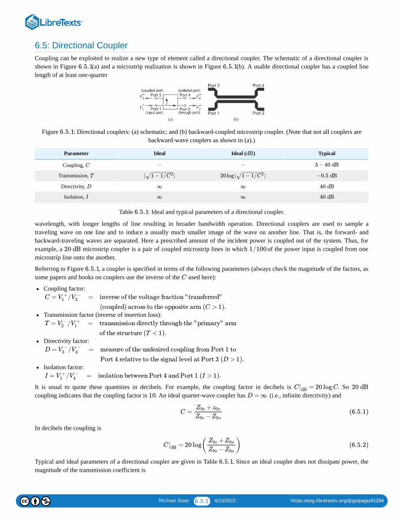
Michael Steer 6.5.1 4/10/2022 https://eng.libretexts.org/@go/page/41294
6.5: Directional CouplerCoupling can be exploited to realize a new type of element called a directional coupler. The schematic of a directional coupler isshown in Figure (a) and a microstrip realization is shown in Figure (b). A usable directional coupler has a coupled linelength of at least one-quarter
Figure : Directional couplers: (a) schematic; and (b) backward-coupled microstrip coupler. (Note that not all couplers arebackward-wave couplers as shown in (a).)
Parameter Ideal Ideal ( ) Typical
Coupling,
Transmission,
Directivity,
Isolation,
Table : Ideal and typical parameters of a directional coupler.
wavelength, with longer lengths of line resulting in broader bandwidth operation. Directional couplers are used to sample atraveling wave on one line and to induce a usually much smaller image of the wave on another line. That is, the forward- andbackward-traveling waves are separated. Here a prescribed amount of the incident power is coupled out of the system. Thus, forexample, a microstrip coupler is a pair of coupled microstrip lines in which of the power input is coupled from onemicrostrip line onto the another.
Referring to Figure , a coupler is specified in terms of the following parameters (always check the magnitude of the factors, assome papers and books on couplers use the inverse of the used here):
Coupling factor:
Transmission factor (inverse of insertion loss):
Directivity factor:
Isolation factor:
It is usual to quote these quantities in decibels. For example, the coupling factor in decibels is . So coupling indicates that the coupling factor is . An ideal quarter-wave coupler has (i.e., infinite directivity) and
In decibels the coupling is
Typical and ideal parameters of a directional coupler are given in Table . Since an ideal coupler does not dissipate power, themagnitude of the transmission coefficient is
6.5.1 6.5.1
6.5.1
dB
C − − 3 − 40 dB
T | |1 − 1/C 2− −−−−−−−√ 20log | |1 − 1/C 2− −−−−−−−
√ −0.5 dB
D ∞ ∞ 40 dB
I ∞ ∞ 40 dB
6.5.1
20 dB 1/100
6.5.1
C
C = /V+
1 V−
3 = inverse of the voltage fraction "transferred"
(coupled) across to the opposite arm (C > 1).
T = /V−
2 V+
1 = transmission directly through the "primary" arm
of the structure (T < 1).
D = /V−
3 V−
4 = measure of the undesired coupling from Port 1 to
Port 4 relative to the signal level at Port 3 (D > 1).
I = /V+
1 V−
4 = isolation between Port 4 and Port 1 (I > 1).
C = 20 log C|dB 20 dB
10 D = ∞
C =+Z0e z0o
−Z0e Z0o
(6.5.1)
C = 20 log( )|dB
+Z0e Z0o
−Z0e Z0o
(6.5.2)
6.5.1
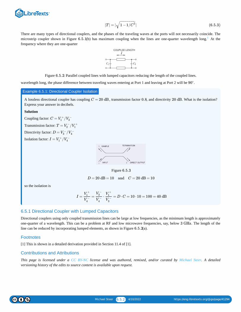
Michael Steer 6.5.2 4/10/2022 https://eng.libretexts.org/@go/page/41294
There are many types of directional couplers, and the phases of the traveling waves at the ports will not necessarily coincide. Themicrostrip coupler shown in Figure (b) has maximum coupling when the lines are one-quarter wavelength long. At thefrequency where they are one-quarter
Figure : Parallel coupled lines with lumped capacitors reducing the length of the coupled lines.
wavelength long, the phase difference between traveling waves entering at Port 1 and leaving at Port 2 will be .
A lossless directional coupler has coupling , transmission factor , and directivity . What is the isolation?Express your answer in decibels.
Solution
Coupling factor:
Transmission factor:
Directivity factor:
Isolation factor:
Figure
so the isolation is
6.5.1 Directional Coupler with Lumped Capacitors
Directional couplers using only coupled transmission lines can be large at low frequencies, as the minimum length is approximatelyone-quarter of a wavelength. This can be a problem at RF and low microwave frequencies, say, below . The length of theline can be reduced by incorporating lumped elements, as shown in Figure (a).
Footnotes[1] This is shown in a detailed derivation provided in Section 11.4 of [1].
Contributions and Attributions
This page is licensed under a CC BY-NC license and was authored, remixed, and/or curated by Michael Steer. A detailedversioning history of the edits to source content is available upon request.
|T | = | |1 −1/C2
− −−−−−−−√ (6.5.3)
6.5.1 1
6.5.2
90∘
Example : Directional Coupler Isolation6.5.1
C = 20 dB 0.8 20 dB
C = /V+
1 V−
3
T = /V−
2 V+
1
D = /V−
3 V−
4
I = /V+
1 V−
4
6.5.3
D = 20 dB = 10 and C = 20 dB = 10
I = = ⋅ = D ⋅ C = 10 ⋅ 10 = 100 = 40 dBV
+1
V−
4
V−
3
V−
4
V+
1
V−
3
3 GHz
6.5.2

Michael Steer 6.6.1 4/10/2022 https://eng.libretexts.org/@go/page/41295
6.6: SummaryCoupling from one transmission line to a nearby neighbor may often be undesirable. However, the coupling can be controlled andcoupled lines have become an important circuit component in distributed microwave circuits. The suite of microwave elements thatexploit distributed effects available to a microwave designer is surprisingly large. Coupled lines comprise a large proportion ofthese elements. This chapter concludes with an example of the broadband response of a pair of coupled microstrip lines.
Contributions and AttributionsThis page is licensed under a CC BY-NC license and was authored, remixed, and/or curated by Michael Steer. A detailedversioning history of the edits to source content is available upon request.

Michael Steer 6.7.1 4/10/2022 https://eng.libretexts.org/@go/page/41296
6.7: References[1] T. Edwards and M. Steer, Foundations for Microstrip Circuit Design. John Wiley & Sons, 2016.
Contributions and AttributionsThis page is licensed under a CC BY-NC license and was authored, remixed, and/or curated by Michael Steer. A detailedversioning history of the edits to source content is available upon request.

Michael Steer 6.8.1 4/10/2022 https://eng.libretexts.org/@go/page/41297
6.8: Exercises1. Consider the cross section of a coupled transmission line, as shown in Figure 6.2.1, with even and odd modes both traveling out
of the page.a. For an even mode on the coupled line, consider a phasor voltage of on each of the lines above the ground plane at .
Sketch the directed electric field in the transverse plane, i.e. show the direction of the electric field.b. For the even mode, sketch the directed magnetic fields in the transverse plane (the plane of the cross section).c. For an odd mode on the coupled line, consider a phasor voltage of on the left line and a phasor voltage of on
the right line. Sketch the directed electric fields in the transverse plane (the plane of the cross section).d. For the odd mode, sketch the directed magnetic fields in the transverse plane (the plane of the cross section).
2. An ideal directional coupler is lossless and there are no reflections at the ports. If the coupling factor is , what is the themagnitude of the transmission coefficient?
3. A directional coupler has the following characteristics: coupling factor , transmission factor , and directivity factor . Also, the coupler is matched so that there is no reflection at any of the ports. What is the isolation in decibels?
4. A lossy directional coupler is matched so that there is no reflection at any of the ports. The insertion loss (considering thethrough path) is . If is input to the directional coupler, what is the power in microwatts dissipated in the directionalcoupler? Ignore power leaving the isolated port.
5. A matched directional coupler has a coupling factor of , transmission factor , and directivity of . What is thepower dissipated in the directional coupler if the input power to Port 1 is .
6. Consider a pair of parallel microstrip lines separated by a spacing, , of .a. What happens to the coupling factor of the lines as s reduces?b. What happens to the system impedance as s reduces and no other dimensions change?c. In terms of wavelengths, what is the optimum length of the coupled lines for maximum coupling?
6.8.1 Exercises by Section
challenging
6.8.2 Answers to Selected Exercises2. 3. (b)
Contributions and Attributions
This page is licensed under a CC BY-NC license and was authored, remixed, and/or curated by Michael Steer. A detailedversioning history of the edits to source content is available upon request.
1 V 0 V
+1 V −1 V
10
C = 20 0.9
25 dB
6 dB
2 dB 1 mW
C 20 0.9 25 dB
1 W
s 100 μm
†
§6.21†
§6.52, 3, 4, 5, 6†
0.9950
187 mW

1 4/10/2022
CHAPTER OVERVIEW7: MICROWAVE NETWORK ANALYSIS
7.1: INTRODUCTION7.2: TWO-PORT NETWORKS7.3: SCATTERING PARAMETERS7.4: RETURN LOSS, SUBSTITUTION LOSS, AND INSERTION LOSS7.5: SCATTERING PARAMETERS AND COUPLED LINES7.6: SUMMARY7.7: REFERENCES7.8: EXERCISES

Michael Steer 7.1.1 4/10/2022 https://eng.libretexts.org/@go/page/41298
7.1: IntroductionAnalog circuits at frequencies up to a few tens of megahertz are characterized by admittances, impedances, voltages, and currents.Above these frequencies it is not possible to measure voltage, current, or impedance directly. It is better to use quantities such asvoltage reflection and transmission coefficients that can be quite readily measured and are related to power flow. As well, in RFand microwave circuit design the power of signals and of noise is always of interest. Thus there is a predisposition to focus onmeasurement parameters that are related to the reflection and transmission of power.
Scattering parameters, parameters, embody the effects of reflection and transmission. As will be seen, it is easy to convert theseto more familiar network parameters such as admittance and impedance parameters. In this chapter parameters will be definedand related to impedance and admittance parameters, then it will be demonstrated that the use of parameters helps in the designand interpretation of RF circuits. parameters have become the most important parameters for RF and microwave engineers andmany design methodologies have been developed around them.
This chapter presents microwave circuit theory which is based on the representation of distributed structures such as transmissionlines, and other structures that are too large to be considered to be dimensionless, by lumped element circuits.
Contributions and Attributions
This page is licensed under a CC BY-NC license and was authored, remixed, and/or curated by Michael Steer. A detailedversioning history of the edits to source content is available upon request.
S
S
S
S
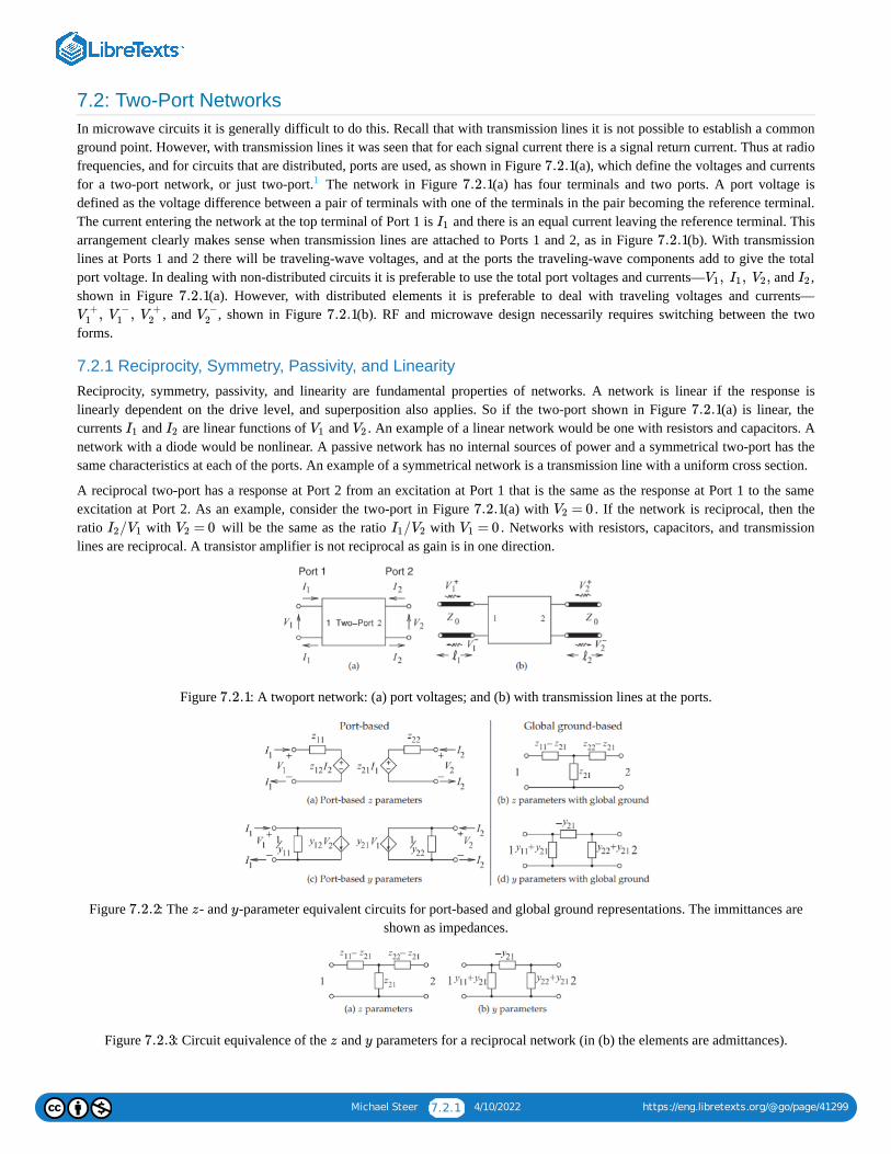
Michael Steer 7.2.1 4/10/2022 https://eng.libretexts.org/@go/page/41299
7.2: Two-Port NetworksIn microwave circuits it is generally difficult to do this. Recall that with transmission lines it is not possible to establish a commonground point. However, with transmission lines it was seen that for each signal current there is a signal return current. Thus at radiofrequencies, and for circuits that are distributed, ports are used, as shown in Figure (a), which define the voltages and currentsfor a two-port network, or just two-port. The network in Figure (a) has four terminals and two ports. A port voltage isdefined as the voltage difference between a pair of terminals with one of the terminals in the pair becoming the reference terminal.The current entering the network at the top terminal of Port 1 is and there is an equal current leaving the reference terminal. Thisarrangement clearly makes sense when transmission lines are attached to Ports 1 and 2, as in Figure (b). With transmissionlines at Ports 1 and 2 there will be traveling-wave voltages, and at the ports the traveling-wave components add to give the totalport voltage. In dealing with non-distributed circuits it is preferable to use the total port voltages and currents— and ,shown in Figure (a). However, with distributed elements it is preferable to deal with traveling voltages and currents—
, and , shown in Figure (b). RF and microwave design necessarily requires switching between the twoforms.
7.2.1 Reciprocity, Symmetry, Passivity, and LinearityReciprocity, symmetry, passivity, and linearity are fundamental properties of networks. A network is linear if the response islinearly dependent on the drive level, and superposition also applies. So if the two-port shown in Figure (a) is linear, thecurrents and are linear functions of and . An example of a linear network would be one with resistors and capacitors. Anetwork with a diode would be nonlinear. A passive network has no internal sources of power and a symmetrical two-port has thesame characteristics at each of the ports. An example of a symmetrical network is a transmission line with a uniform cross section.
A reciprocal two-port has a response at Port 2 from an excitation at Port 1 that is the same as the response at Port 1 to the sameexcitation at Port 2. As an example, consider the two-port in Figure (a) with . If the network is reciprocal, then theratio with will be the same as the ratio with . Networks with resistors, capacitors, and transmissionlines are reciprocal. A transistor amplifier is not reciprocal as gain is in one direction.
Figure : A twoport network: (a) port voltages; and (b) with transmission lines at the ports.
Figure : The - and -parameter equivalent circuits for port-based and global ground representations. The immittances areshown as impedances.
Figure : Circuit equivalence of the and parameters for a reciprocal network (in (b) the elements are admittances).
7.2.11 7.2.1
I1
7.2.1
, , ,V1 I1 V2 I2
7.2.1
, ,V+
1 V−
1 V+
2 V−
2 7.2.1
7.2.1
I1 I2 V1 V2
7.2.1 = 0V2
/I2 V1 = 0V2 /I1 V2 = 0V1
7.2.1
7.2.2 z y
7.2.3 z y
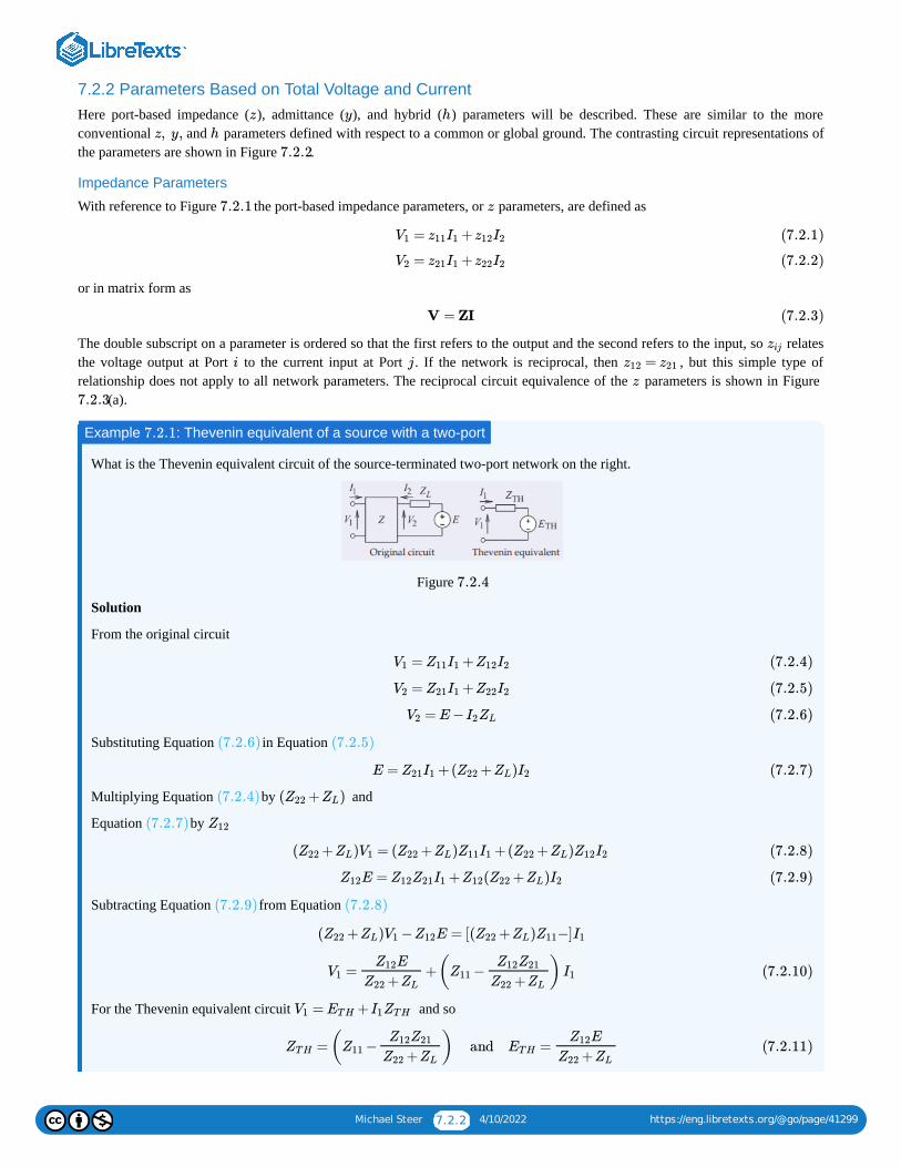
Michael Steer 7.2.2 4/10/2022 https://eng.libretexts.org/@go/page/41299
7.2.2 Parameters Based on Total Voltage and CurrentHere port-based impedance ( ), admittance ( ), and hybrid ( ) parameters will be described. These are similar to the moreconventional and parameters defined with respect to a common or global ground. The contrasting circuit representations ofthe parameters are shown in Figure .
Impedance Parameters
With reference to Figure the port-based impedance parameters, or parameters, are defined as
or in matrix form as
The double subscript on a parameter is ordered so that the first refers to the output and the second refers to the input, so relatesthe voltage output at Port to the current input at Port . If the network is reciprocal, then , but this simple type ofrelationship does not apply to all network parameters. The reciprocal circuit equivalence of the parameters is shown in Figure
(a).
What is the Thevenin equivalent circuit of the source-terminated two-port network on the right.
Figure
Solution
From the original circuit
Substituting Equation in Equation
Multiplying Equation by and
Equation by
Subtracting Equation from Equation
For the Thevenin equivalent circuit and so
z y h
z, y, h
7.2.2
7.2.1 z
= +V1 z11I1 z12I2 (7.2.1)
= +V2 z21I1 z22I2 (7.2.2)
V = ZI (7.2.3)
zij
i j =z12 z21
z
7.2.3
Example : Thevenin equivalent of a source with a two-port7.2.1
7.2.4
= +V1 Z11I1 Z12I2 (7.2.4)
= +V2 Z21I1 Z22I2 (7.2.5)
= E −V2 I2ZL (7.2.6)
(7.2.6) (7.2.5)
E = +( + )Z21I1 Z22 ZL I2 (7.2.7)
(7.2.4) ( + )Z22 ZL
(7.2.7) Z12
( + ) = ( + ) +( + )Z22 ZL V1 Z22 ZL Z11I1 Z22 ZL Z12I2 (7.2.8)
E = + ( + )Z12 Z12Z21I1 Z12 Z22 ZL I2 (7.2.9)
(7.2.9) (7.2.8)
( + ) − E = [( + ) −]Z22 ZL V1 Z12 Z22 ZL Z11 I1
= +( − )V1EZ12
+Z22 ZL
Z11Z12Z21
+Z22 ZL
I1 (7.2.10)
= +V1 ET H I1ZT H
=( − ) and =ZT H Z11Z12Z21
+Z22 ZL
ET H
EZ12
+Z22 ZL
(7.2.11)

Michael Steer 7.2.3 4/10/2022 https://eng.libretexts.org/@go/page/41299
Admittance Parameters
The port-based admittance parameters, or parameters, are defined as
or in matrix form as
Now, for reciprocity, and the circuit equivalence of the parameters is shown in Figure (b).
Footnotes[1] Even when the term “two-port” is used on its own, the hyphen is used, as it is referring to a two-port network.
Contributions and Attributions
This page is licensed under a CC BY-NC license and was authored, remixed, and/or curated by Michael Steer. A detailedversioning history of the edits to source content is available upon request.
y
= +I1 y11V1 y12V2 (7.2.12)
= +I2 y21V1 y22V2 (7.2.13)
I = YV (7.2.14)
=y12 y21 y 7.2.3
Michael Steer 7.3.1 4/10/2022 https://eng.libretexts.org/@go/page/41300
7.3: Scattering ParametersDirect measurement of the and parameters requires that the ports be terminated in either short or open circuits. For activecircuits this could result in undesired behavior, including oscillation or destruction. Also, at RF it is difficult to realize a good openor short. Since RF circuits are designed with close attention to maximum power transfer conditions, resistive terminations arepreferred, as these are closer to the actual operating conditions. Thus the effect of measurement errors will have less impact. This isthe way scattering parameters are measured.
The discussion of scattering parameters, parameters , begins by considering the reflection coefficient, which is the parameterof a one-port network.
7.3.1 Reflection CoefficientThe reflection coefficient, , of a load can be determined by separately measuring the forward- and backward-travelingvoltages on a transmission line terminated by the load:
Imagine between the source and the load that there is a line of characteristic impedance and with infinitesimal length, then atthe load is related to the impedance by
where is the characteristic impedance of the connecting transmission line. This can also be written as
where and . More completely, as defined above is called the voltage reflection coefficient sometimesdenoted .
Recall that the current reflection coefficient .
7.3.2 Two Port Parameters
Two-port parameters are defined in terms of traveling waves on transmission lines with real characteristic impedance attached to each of the ports of a network, see Figure 7.2.1(b):
where are the individual parameters. In matrix form
Individual parameters are determined by measuring the forward- and backward-traveling waves with loads at the ports. Sincethe load is it cannot reflect power and so , then
The remaining parameters are determined similarly and so S22 is found as
and the transmission parameter as
z y
S 1 S
Γ ΓL
Γ(x) =(x)V −
(x)V +(7.3.1)
Z0 Γ
ZL
Γ(0) =−ZL Z0
+ZL Z0(7.3.2)
Z0
Γ(0) =−Y0 YL
+Y0 YL
(7.3.3)
= 1/Y0 Z0 = 1/YL ZL Γ
ΓV
= −ΓI ΓV
S
S Z0
= +V −1 S11V +
1 S12V +2 (7.3.4)
= +V −2 S21V +
1 S22V +2 (7.3.5)
Sij S
[ ] = [ ][ ] = S [ ]V −
1
V −2
S11
S21
S12
S22
V +1
V +2
V +1
V +2
(7.3.6)
S Z0
Z0 = 0V +2
=S11
V −1
V +1
∣
∣∣
=0V +2
(7.3.7)
=S22
V −2
V +2
∣
∣∣
=0V +1
(7.3.8)
Michael Steer 7.3.2 4/10/2022 https://eng.libretexts.org/@go/page/41300
In terms of
Table : Two-port parameter conversion chart. The , and parameters are normalized to . and are the actualparameters.
In the reverse direction,
In the above is referred to as the normalization impedance or equivalently the reference impedance. In some circumstances is used to denote reference impedance to avoid possible confusion with a transmission line impedance that is not the same as
the reference impedance. The parameters here are also called normalized parameters, and the parameters are normalizedto the same real reference impedance at each port.
The relationships between the two-port parameters and the common network parameters are given in Table . It is interestingto note that . That is, the ratio of the forward to reverse parameters (at least for and parameters) are the same and this ratio is one for a reciprocal device. An parameter is a voltage ratio, so when it is expressed indecibels .
A reciprocal network has . If unit power flows into a two-port, a fraction, , is reflected and a further fraction, , is transmitted through the network.
What are the parameters of a attenuator?
Solution
An attenuator is shown with a system impedance of . An ideal attenuator has no reflection at each of the two ports when theattenuator is embedded in its system impedance. Thus . Since there is no reflection from the load or the source,this implies that .
Figure
Since this is a attenuator, the power delivered to the load impedance is below the power available from thesource, thus . The attenuator is reciprocal and so . Thus the parameters of the attenuatorare
=S21
V −2
V +1
∣
∣∣
=0V +2
(7.3.9)
S S
z
= =Z ′11 z11Z0 Z ′
12 z12Z0 = =Z ′21 z21Z0 Z ′
22 z22Z0
δz
S11
S12
S21
S22
= (1 + )(1 + ) −z11 z22 z12z21
= [( − 1)( + 1) − ]/z11 z22 z12z21 δz
= 2 /z12 δz
= 2 /z21 δz
= [( + 1)( − 1) − ]/z11 z22 z12z21 δz
δS
z11
z12
z21
z22
= (1 − )(1 − ) −S11 S22 S12S21
= [(1 + )(1 − ) + ]/S11 S22 S12S21 δS
= 2 /S12 δS
= 2 /S21 δS
= [(1 − )(1 + ) + ]/S11 S22 S12S21 δS
y
= / = /Y ′11 y11 Z0 Y ′
12 y12 Z0 = / = /Y ′21 y21 Z0 Y ′
22 y22 Z0
δy
S11
S12
S21
S22
= (1 + )(1 + ) −y11 y22 y12y21
= [(1 − )(1 + ) + ]/y11 y22 y12y21 δy
= −2 /y12 δy
= −2 /y21 δy
= [(1 + )(1 − ) + ]/y11 y22 y12y21 δy
δS
y11
y12
y21
y22
= (1 + )(1 + ) −S11 S22 S12S21
= [(1 − )(1 + ) + ]/S11 S22 S12S21 δS
= −2 /S12 δS
= −2 /S21 δS
= [(1 + )(1 − ) + ]/S11 S22 S12S21 δS
7.3.1 S z y Z0 Z' Y '
=S12
V −1
V +2
∣
∣∣
=0V +1
(7.3.10)
Z0
ZREF
S S S
S 7.3.1
/ = / = /S21 S12 z21 z12 y21 y12 S, z, y
S
= 20 log( )Sij | dB Sij
=S12 S21 |S11|2
|S21|2
Example : Two-Port Parameters7.3.1 S
S 30 dB
Z0
= 0 =Γin Γout
= 0 =S11 S22
7.3.1
30 dB Z0 30 dB
= −30 dB = 0.0316S21 =S12 S21 S
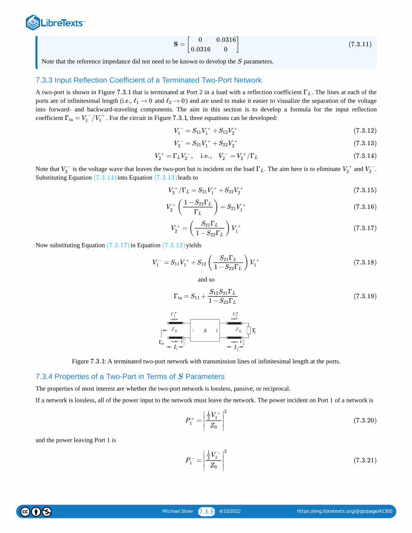
Michael Steer 7.3.3 4/10/2022 https://eng.libretexts.org/@go/page/41300
Note that the reference impedance did not need to be known to develop the parameters.
7.3.3 Input Reflection Coefficient of a Terminated Two-Port Network
A two-port is shown in Figure that is terminated at Port 2 in a load with a reflection coefficient . The lines at each of theports are of infinitesimal length (i.e., and ) and are used to make it easier to visualize the separation of the voltageinto forward- and backward-traveling components. The aim in this section is to develop a formula for the input reflectioncoefficient . For the circuit in Figure , three equations can be developed:
Note that is the voltage wave that leaves the two-port but is incident on the load . The aim here is to eliminate and .Substituting Equation into Equation leads to
Now substituting Equation in Equation yields
and so
Figure : A terminated two-port network with transmission lines of infinitesimal length at the ports.
7.3.4 Properties of a Two-Part in Terms of Parameters
The properties of most interest are whether the two-port network is lossless, passive, or reciprocal.
If a network is lossless, all of the power input to the network must leave the network. The power incident on Port 1 of a network is
and the power leaving Port 1 is
S = [ ]0
0.0316
0.0316
0(7.3.11)
S
7.3.1 ΓL
→ 0ℓ1 → 0ℓ2
= /Γin V −1 V +
1 7.3.1
= +V −1 S11V +
1 S12V +2 (7.3.12)
= +V −2 S21V +
1 S22V +2 (7.3.13)
= , i.e., = /V +2 ΓLV −
2 V −2 V +
2 ΓL (7.3.14)
V −2 ΓL V +
2 V −2
(7.3.14) (7.3.13)
/ = +V +2 ΓL S21V +
1 S22V +2 (7.3.15)
( ) =V +2
1 −S22ΓL
ΓL
S21V +1
(7.3.16)
=( )V +2
S21ΓL
1 −S22ΓL
V +1
(7.3.17)
(7.3.17) (7.3.12)
= + ( )V −1 S11V +
1 S12S21ΓL
1 −S22ΓL
V +1 (7.3.18)
= +Γin S11S12S21ΓL
1 −S22ΓL
(7.3.19)
7.3.1
S
=P +1
∣
∣
∣∣
12
V +1
Z0
∣
∣
∣∣
2
(7.3.20)
=P −1
∣
∣
∣∣
12
V −1
Z0
∣
∣
∣∣
2
(7.3.21)

Michael Steer 7.3.4 4/10/2022 https://eng.libretexts.org/@go/page/41300
This can be repeated for Port 2 and the factor appears in all expressions. So cancelling this factor, the condition for thenetwork to be lossless is
For a network to be passive, no more power can leave the network than enters it. So the condition for passivity is
Reciprocity requires that .
Footnotes
[1] For historical reasons a capital “S” is used when referring to parameters. For most other network parameters, lowercase isused (e.g., parameters for impedance parameters).
Contributions and AttributionsThis page is licensed under a CC BY-NC license and was authored, remixed, and/or curated by Michael Steer. A detailedversioning history of the edits to source content is available upon request.
/12
Z0
| + | = 1 and | +| = 1S11|2
S21|2
S12|2
S22|2
(7.3.22)
| +| ≤ 1 and | +| ≤ 1S11|2
S21|2
S12|2
S22|2
(7.3.23)
=S21 S12
S
z
Michael Steer 7.4.1 4/10/2022 https://eng.libretexts.org/@go/page/41301
7.4: Return Loss, Substitution Loss, and Insertion Loss
7.4.1 Return Loss
Return loss, also known as reflection loss, is a measure of the fraction of available power that is not delivered by a source to a load.If the power incident on a load is and the power reflected by the load is , then the return loss in decibels is [1, 2]
The better the load is matched to the source, the lower the reflected power and hence the higher the return loss. RL is a positivequantity if the reflected power is less than the incident power. If the load has a complex reflection coefficient , then
That is, the return loss is the negative of the reflection coefficient expressed in decibels [3].
When generalized to terminated two ports, the return loss is defined with respect to the input reflection coefficient of a terminatedtwo port [4]. The two port in Figure has the input reflection coefficient
where is the reflection coefficient of the load. Thus the return loss of a terminated two-port is
If the load is matched, i.e. (the system reference impedance), then
This return loss is also called the input return loss since the reflection coefficient is calculated at Port 1. The output return loss iscalculated looking into Port 2 of the two-port, where now the termination at Port 1 is just the source impedance.
7.4.2 Substitution Loss and Insertion LossThe substitution loss is the ratio of the power, , delivered to the load by an initial two-port identified by the leading superscript ‘’, and the power delivered to the load, , with a substituted final two-port identified by the leading superscript ‘ ’. In terms of
scattering parameters with reference impedances , the substitution loss in decibels is (using the results in [5] and noting that and are referred to )
Insertion loss is a special case of substitution loss with a particular type of initial two-port networks.
Insertion Loss with an Ideal Adaptor
Insertion loss is the substitution loss when the initial two-poort is a direct connection so (for no reflection), (for no loss in the adaptor and there is no phase shift), and (for reciprocity), insertion loss in decibels is,
using Equation :
Attenuation is defined as the insertion loss without source and load
Pi Pr
= 10 logRLdBPi
Pr
(7.4.1)
ρ
= 10 log = −20 log |ρ|RLdB
∣
∣∣
1
ρ2
∣
∣∣ (7.4.2)
7.4.1
= +Γin S11ΓLS12S21
(1 − )ΓLS22
(7.4.3)
ΓL
= −20 log | | = −20 log +RLdB Γin
∣
∣∣S11
ΓLS12S21
(1 − )ΓLS22
∣
∣∣ (7.4.4)
=ZL Z∗0
= −20 log | |RLdB S11 (7.4.5)
iPL
i f PL f
ZREF
ΓS ΓL ZREF
|dB = = 10 logLS
iPL
f PL
∣
∣∣
iS21
f S21
[(1 )(1 ) ]−f S11ΓS −f S22ΓL −f S12f S21ΓSΓL
[(1 )(1 )−i S11ΓS −i S22ΓL −i S12iS21ΓSΓL
∣
∣∣
2
(7.4.6)
= 0iS11 =i S22
= 1iS i12S21
iS12 =i S21
(7.4.6)
IL = 10 log|dB
⎡
⎣
∣
∣
∣∣
(1 )(1 )−f S11ΓS −f S22ΓL −f Sf12S21ΓSΓL
(1 − Γ)f S12 ΓS
∣
∣
∣∣
2⎤
⎦(7.4.7)
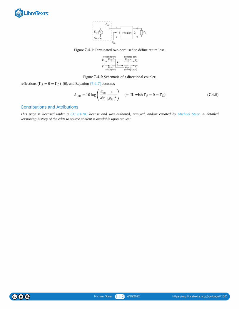
Michael Steer 7.4.2 4/10/2022 https://eng.libretexts.org/@go/page/41301
Figure : Terminated two-port used to define return loss.
Figure : Schematic of a directional coupler.
reflections [6], and Equation becomes
Contributions and Attributions
This page is licensed under a CC BY-NC license and was authored, remixed, and/or curated by Michael Steer. A detailedversioning history of the edits to source content is available upon request.
7.4.1
7.4.2
( = 0 = )ΓS ΓL (7.4.7)
A = 10 log( ) (= IL with = 0 = )|dB
Z02
Z01
1
|S21|2
ΓS ΓL (7.4.8)

Michael Steer 7.5.1 4/10/2022 https://eng.libretexts.org/@go/page/41302
7.5: Scattering Parameters and Coupled LinesDirectional couplers were described in Section 6.5, but without the use of parameters. A directional coupler with ports defined asin Figure 7-6, and with the ports matched (so that ), has the following scattering parameter matrix:
There are many types of directional couplers, and the phases of the traveling waves at the ports will not necessarily be in phase asEquation implies. When the phase difference between traveling waves entering at Port 1 and leaving at Port 2 is ,Equation becomes
A directional coupler has the following parameters:
a. What are the through (i.e., transmission) paths? Identify two paths. That is, identify the pairs of ports at the ends of thethrough paths. First note that the assignment of ports to a directional coupler is arbitrary. So the parameters need to be considered tofigure out how the ports are related. The parameters relate the forward-traveling waves to the backward-traveling wavesand this leads to the required understanding, thus
Writing the S parameters out this way makes it easier to identify the largest backward traveling waves for each of the inputsat Ports 1, 2, 3, and 4. The backward-traveling wave will leave the directional coupler and the inputs will be forward-traveling waves. Consider Port 1, the largest backward-traveling wave is at Port 2, and so Ports 1 and 2 define one of the through paths. Theother through path is between Ports 3 and 4. So the through paths are 1–2 and 3–4.
b. What is the coupled port for the signal entering Port 1? The coupled port is identified by the port with the largest backward-traveling signal not including the port at the other endof the through path. For Port 1 the coupled port is Port 4.
c. What is the coupling factor?
d. What is the isolated port for the signal entering Port 1? The isolated port is Port 3. The backward-traveling wave at this port is the smallest given an input at Port 1.
S
= 0 = = =S11 S22 S33 S44
S =
⎡
⎣
⎢⎢⎢⎢
0
T
1/C
1/I
T
0
1/I
1/C
1/C
1/I
0
T
1/I
1/C
T
0
⎤
⎦
⎥⎥⎥⎥(7.5.1)
(7.5.1) 90∘
(7.5.1)
S =
⎡
⎣
⎢⎢⎢⎢
0
−ȷT
1/C
1/I
−ȷT
0
1/I
1/C
1/C
1/I
0
−ȷT
1/I
1/C
−ȷT
0
⎤
⎦
⎥⎥⎥⎥(7.5.2)
Example : Identifying Ports of a Directional Coupler7.5.1
S
S =
⎡
⎣
⎢⎢⎢
0
0.9
0.001
0.1
0.9
0
0.1
0.001
0.001
0.1
0
0.9
0.1
0.001
0.9
0
⎤
⎦
⎥⎥⎥
S
S
= S =
⎡
⎣
⎢⎢⎢⎢
V−
1
V−
2
V−
3
V−
4
⎤
⎦
⎥⎥⎥⎥
⎡
⎣
⎢⎢⎢⎢
V+
1
V+
2
V+
3
V+
4
⎤
⎦
⎥⎥⎥⎥
⎡
⎣
⎢⎢⎢
0
0.9
0.001
0.1
0.9
0
0.1
0.001
0.001
0.1
0
0.9
0.1
0.001
0.9
0
⎤
⎦
⎥⎥⎥
⎡
⎣
⎢⎢⎢⎢
V+
1
V+
2
V+
3
V+
4
⎤
⎦
⎥⎥⎥⎥
C = = = 10 = 20 dBV
+1
V−
4
1
0.1
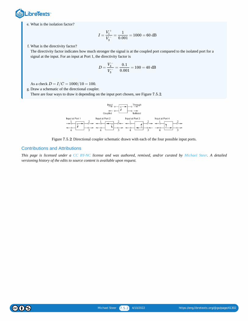
Michael Steer 7.5.2 4/10/2022 https://eng.libretexts.org/@go/page/41302
e. What is the isolation factor?
f. What is the directivity factor? The directivity factor indicates how much stronger the signal is at the coupled port compared to the isolated port for asignal at the input. For an input at Port 1, the directivity factor is
As a check .
g. Draw a schematic of the directional coupler. There are four ways to draw it depending on the input port chosen, see Figure .
Figure : Directional coupler schematic drawn with each of the four possible input ports.
Contributions and AttributionsThis page is licensed under a CC BY-NC license and was authored, remixed, and/or curated by Michael Steer. A detailedversioning history of the edits to source content is available upon request.
I = = = 1000 = 60 dBV
+1
V−
3
1
0.001
D = = = 100 = 40 dBV
−4
V−
3
0.1
0.001
D = I/C = 1000/10 = 100
7.5.2
7.5.2

Michael Steer 7.6.1 4/10/2022 https://eng.libretexts.org/@go/page/41303
7.6: SummaryThere are several network parameters used with RF and microwave circuits. Which is used depends on which makes the task ofvisualizing circuit operation more clear, which makes analyzing circuits more convenient, and which enables different circuits to bemade electrically equivalent.
Scattering parameters are parameters that are almost exclusively used by RF and microwave engineers. They describe power flowand traveling waves and are essential to describing distributed circuits. Much of RF and microwave engineering is concerned withmanaging the signal-to-noise power ratio and with power efficiency. It is therefore natural to work with parameters that directlyrelate to power flow. RF and microwave design is characterized by conceptual insight and it is essential to use parameters andgraphical representations that are close to the physical world. Scattering parameters have very natural graphical representations, aswill be seen in the next chapter.
Contributions and AttributionsThis page is licensed under a CC BY-NC license and was authored, remixed, and/or curated by Michael Steer. A detailedversioning history of the edits to source content is available upon request.

Michael Steer 7.7.1 4/10/2022 https://eng.libretexts.org/@go/page/41304
7.7: References[1] “Telecommunications: Glossary of Telecommunication Terms,” Federal Standard 1037C, U.S. General Services AdministrationInformation Technology Service, Aug. 7, 1996.
[2] T. S. Bird, “Definition and misuse of return loss [report of the trans. editor-inchief],” IEEE Antennas and PropagationMagazine, vol. 51, no. 2, pp. 166–167, Apr. 2009.
[3] IEEE, IEEE Standard Dictionary of Electrical and Electronic Engineering Terms, 4th ed. IEEE Press, 1988.
[4] T. Otoshi, “Maximum and minimum return losses from a passive two-port network terminated with a mismatched load,” IEEETrans. on Microwave Theory and Techniques, vol. 42, no. 5, pp. 787–792, May 1994.
[5] M. Steer, Microwave and RF Design, Networks, 3rd ed. North Carolina State University, 2019.
[6] R. Beatty, “Insertion loss concepts,” Proc. of the IEEE, vol. 52, no. 6, pp. 663–671, Jun. 1964.
Contributions and AttributionsThis page is licensed under a CC BY-NC license and was authored, remixed, and/or curated by Michael Steer. A detailedversioning history of the edits to source content is available upon request.

Michael Steer 7.8.1 4/10/2022 https://eng.libretexts.org/@go/page/41305
7.8: Exercises1. A load has a reflection coefficient of in a reference system. What is the reflection coefficient in a
reference system?2. The S parameters of a two-port are and .
Port 1 is connected to a source with an available power of and Port 2 is terminated in . What is the powerreflected from Port 1?
3. The scattering parameters of a certain two-port are and . The system reference impedance is .
a. Is the two-port reciprocal? Explain.b. Consider that Port 1 is connected to a source with an available power of . What is the power delivered to a
load placed at Port 2?c. What is the reflection coefficient of the load required for maximum power transfer at Port 2?
4. In characterizing a two-port, power could only be applied at Port 1. The signal reflected was measured and the signal at a load at Port 2 was also measured. This yielded two parameters referenced to : and .a. If the network is reciprocal, what is ?b. Is the two-port lossless?c. What is the power delivered into the load at Port 2 when the available power at Port 1 is ?
5. A matched lossless transmission line has a length of one-quarter wavelength. What are the scattering parameters of the two-port?
6. A connector has the scattering parameters and and the reference impedance is . What is the return loss in of the connector at Port 1 in a system?
7. The scattering parameters of an amplifier are and and the reference impedance is. If the amplifier is terminated at Port 2 in a resistance of , what is the return loss in at Port 1?
8. A two-port network has the scattering parameters and and the referenceimpedance is .
a. What is the return loss in of the connector at Port 1 in a system?b. Is the two-port reciprocal and why?
9. A two-port network has the scattering parameters and and the referenceimpedance is .a. What is the return loss in of the connector at Port 1 in a system?b. Is the two-port reciprocal and why?
10. A cable has the scattering parameters and . At Port 2 is a load and the parameters and reflection coefficients are referred to .a. What is the load’s reflection coefficient?b. What is the input reflection coefficient of the terminated cable?c. What is the return loss, at Port 1 and in , of the cable terminated in the load?
11. A cable has the scattering parameters and . What is the insertion loss ofthe cable if the source at Port 1 has a Thevenin impedance and the termination at Port 2 is ? Express your answer indecibels.
12. A long cable has the scattering parameters and . The cable is used in a system. Express your answers in decibels.
a. What is the return loss of the cable in the system? (Hint see Section sec:input:terminated:two:port and consider finding.]
b. What is the insertion loss of the cable in the system? Follow the procedure in Example 7.2.1.c. What is the return loss of the cable in a system?d. What is the insertion loss of the cable in a system?
13. A long cable has the scattering parameters and . The Theveninequivalent impedance of the source and terminating load impedances of the cable are . Express your answers in decibels.a. What is the return loss of the cable?
0.5 − ȷ0.1 75 Ω 50 Ω
50 Ω = 0.5 + ȷ0.5, = 0.95 + ȷ0.25, = 0.15 − ȷ0.05,S11 S12 S21 = 0.5 − ȷ0.5S22
50 Ω 1 W 50 Ω
= 0.5 + ȷ0.5, = 0.95 + ȷ0.25, = 0.15 − ȷ0.05,S11 S12 S21
= 0.5 − ȷ0.5S22 50 Ω
50 Ω 1 W 50 Ω
50 Ω
S 50 Ω = 0.3 − ȷ0.4S11 = 0.5S21
S12
50 Ω 0 dBm
= 0.05, = 0.9, = 0.9,S11 S21 S12 = 0.04S22
50 Ω dB 50 Ω
= 0.5, = 2., = 0.1,S11 S21 S12 = −0.2S22
50 Ω 25 Ω dB
= −0.5, = 0.9, = 0.8,S11 S21 S12 = 0.04S22
50 Ω
dB 50 Ω
= −0.2, = 0.8, = 0.7,S11 S21 S12 = 0.5S22
75 Ω
dB 75 Ω
= 0.1, = 0.7, = 0.7,S11 S21 S12 = 0.1S22 55 Ω S
50 Ω
dB
50 Ω = 0.05, = 0.5, = 0.5,S11 S21 S12 = 0.05S22
50 Ω 50 Ω
1 m 50 Ω = 0.1, = 0.7, = 0.7,S11 S21 S12 = 0.1S22
55 Ω
55 Ω
nZi
55 Ω
50 Ω
50 Ω
1 m 50 Ω = 0.05, = 0.5, = 0.5,S11 S21 S12 = 0.05S22
50 Ω
Michael Steer 7.8.2 4/10/2022 https://eng.libretexts.org/@go/page/41305
b. What is the insertion loss of the cable?14. A lossy directional coupler has the following parameters:
a. What are the through (transmission) paths (identify two paths)? That is, identify the pairs of ports at the ends of the throughpaths.
b. What is the coupling in decibels?c. What is the isolation in decibels?d. What is the directivity in decibels?
15. A directional coupler has the following characteristics: coupling factor , transmission factor , and directivity factor . Also, the coupler is matched so that .
a. What is the isolation factor in decibels?b. Determine the power dissipated in the directional coupler if the input power to Port 1 is .
16. A lossy directional coupler has the following parameters:
a. Which port is the input port (there could be more than one answer)?b. What is the coupling in decibels?c. What is the isolation in decibels?d. What is the directivity factor in decibels?
17. A directional coupler using coupled lines has a coupling factor of , a transmission factor of , and infinitedirectivity and isolation. The input port is Port 2 and the through port is Port 2. Write down the parameter matrix of thecoupler.
7.8.1 Exercises by Selectionchallenging
7.8.2 Answers to Selected Exercises1.
3. (d)
6.
12. (b)
15. (b) 16. (d)
Contributions and Attributions
This page is licensed under a CC BY-NC license and was authored, remixed, and/or curated by Michael Steer. A detailedversioning history of the edits to source content is available upon request.
50 Ω S
S =
⎡
⎣
⎢⎢⎢
0
−0.95ȷ
0.005
0.1
−0.95ȷ
0
0.1
0.005
0.005
0.1
0
−0.95ȷ
0.1
0.005
−0.95ȷ
0
⎤
⎦
⎥⎥⎥
C = 20 0.9
25 dB = 0 = = =S11 S22 S33 S44
1 W
50 Ω S
S =
⎡
⎣
⎢⎢⎢
0
0.25
−0.9ȷ
0.01
0.25
0
0.01
−0.9ȷ
−0.9ȷ
0.01
0
0.25
0.01
−0.9ȷ
0.25
0
⎤
⎦
⎥⎥⎥
3.38 −ȷ0.955
4 ×4S
†
§7.31, 2, 3†, 4†, 5†
§7.46, 7, 8, 9, 10, 11, 12†, 13
§7.514†, 15†, 16†, 17†
0.638 − ȷ0.079
50 + ȷ100 Ω
26 dB
2.99 dB
187 mW
28 dB

1 4/10/2022
CHAPTER OVERVIEW8: GRAPHICAL NETWORK ANALYSIS
8.1: INTRODUCTION8.2: POLAR REPRESENTATIONS OF SCATTERING PARAMETERS8.3: SMITH CHART8.4: SUMMARY8.5: REFERENCES8.6: EXERCISES

Michael Steer 8.1.1 4/10/2022 https://eng.libretexts.org/@go/page/41306
8.1: IntroductionThis chapter introduces the Smith chart, most widely used graphical technique for describing and solving problems using parameters. The Smith chart is an annotated polar plot of parameters and is one of the most powerful tools in RF and microwaveengineering and is used to present measured results, to conceptualize designs, and to intuitively solve problems involvingdistributed networks.
Contributions and AttributionsThis page is licensed under a CC BY-NC license and was authored, remixed, and/or curated by Michael Steer. A detailedversioning history of the edits to source content is available upon request.
S
S
Michael Steer 8.2.1 4/10/2022 https://eng.libretexts.org/@go/page/41307
8.2: Polar Representations of Scattering ParametersScattering parameters are most naturally represented in polar form with the square of the magnitude relating to power flow. In thissection a greater rationale for representing parameters on a polar plot is presented and this serves as the basis for a morecomplicated representation of parameters on a Smith chart to be described in the next section.
8.2.1 Shift of Reference Planes as a Parameter RotationA polar plot is a natural way to present parameters graphically. Adding additional lengths of the lines at each port rotates the parameters. Consider the two-port in Figure . Here the original two-port with scattering
Figure : A two-port with scattering parameter matrix augmented by lines at each port with the lines having the referencecharacteristic impedance and electrical length . The scattering parameter matrix of the augmented two-port is .
parameter matrix is augmented by lines at each port with each having a characteristic impedance equal to the referenceimpedance. The parameter matrix of the augmented two-port, , are the same as the original parameter matrix but phase-shifted. That is
The shift in reference planes simply rotates the parameters. This is one of the main reasons why parameters are commonlyplotted on a polar plot.
8.2.2 Polar Plot of Reflection CoefficientThe polar plot of reflection coefficient is simply the polar plot of a complex number. Figure 8.3.1 is used in plotting reflectioncoefficients and is a polar plot that has a radius of one. So a reflection coefficient with a magnitude of one is on the unit circle. Thecenter of the polar plot is zero so the reflection coefficient of a matched load, which is zero, is plotted at the center of the circle.Plotting a reflection coefficient on the polar plot enables convenient interpretation of the properties of a reflection. The graph hasadditional notation that enables easy plotting of an parameter on the graph. Conversely, the magnitude and phase of an parameter can be easily read from the graph. The horizontal label going from to is used in determining magnitude. The notationarranged on the outer perimeter of the polar plot is used to read off angle information. Notice the additional notation “ANGLE OFREFLECTION COEFFICIENT IN DEGREES” and the scale relates to the actual angle of the polar plot. Verify that the pointis just where one would expect it to be.
Figure 8.3.2 annotates the polar plot of reflection coefficient with real and imaginary axes and shows the location of the shortcircuit and open circuit points. Note that the reflection coefficient of an inductive impedance is in the top half of the polar plotwhile the reflection coefficient of a capacitive impedance is in the bottom half of the polar plot.
The nomograph shown in Figure 8.3.3 aids in interpretation of polar reflection coefficient plots. The nomograph relates thereflection coefficient (RFL. COEFFICIENT), ( was originally used instead of and is still used with the Smith chart); thereturn loss (RTN. LOSS) (in decibels); and the standing wave ratio (SWR); and the standing wave ratio (in decibels) as
. When printed together with the reflection coefficient polar plot (Figures 8.3.1 and 8.3.2 combined) the nomographis scaled properly, but it is expanded here so that it can be read more easily. So with the aid of a compass with one point on the zeropoint of the polar plot and the other at the reflection coefficient (as plotted on the polar plot), the magnitude of the reflectioncoefficient is captured. The compass can then be brought down to the nomograph to read ρ, the return loss, and VSWR directly.
Contributions and AttributionsThis page is licensed under a CC BY-NC license and was authored, remixed, and/or curated by Michael Steer. A detailedversioning history of the edits to source content is available upon request.
S
S
S
S S
8.2.1
8.2.1 S
Z0 θn S'
S
S S' S
= [ ] = [ ]S′
S ′11
S ′21
S ′12
S ′22
S11e−ȷ2Θ1
S21e−ȷ(Θ1+Θ2)
S12e−ȷ(Θ1+Θ2)
S22e−ȷ2Θ2(8.2.1)
S S
S S
0 1
90∘
ρ ρ Γ
20 log(SWR)
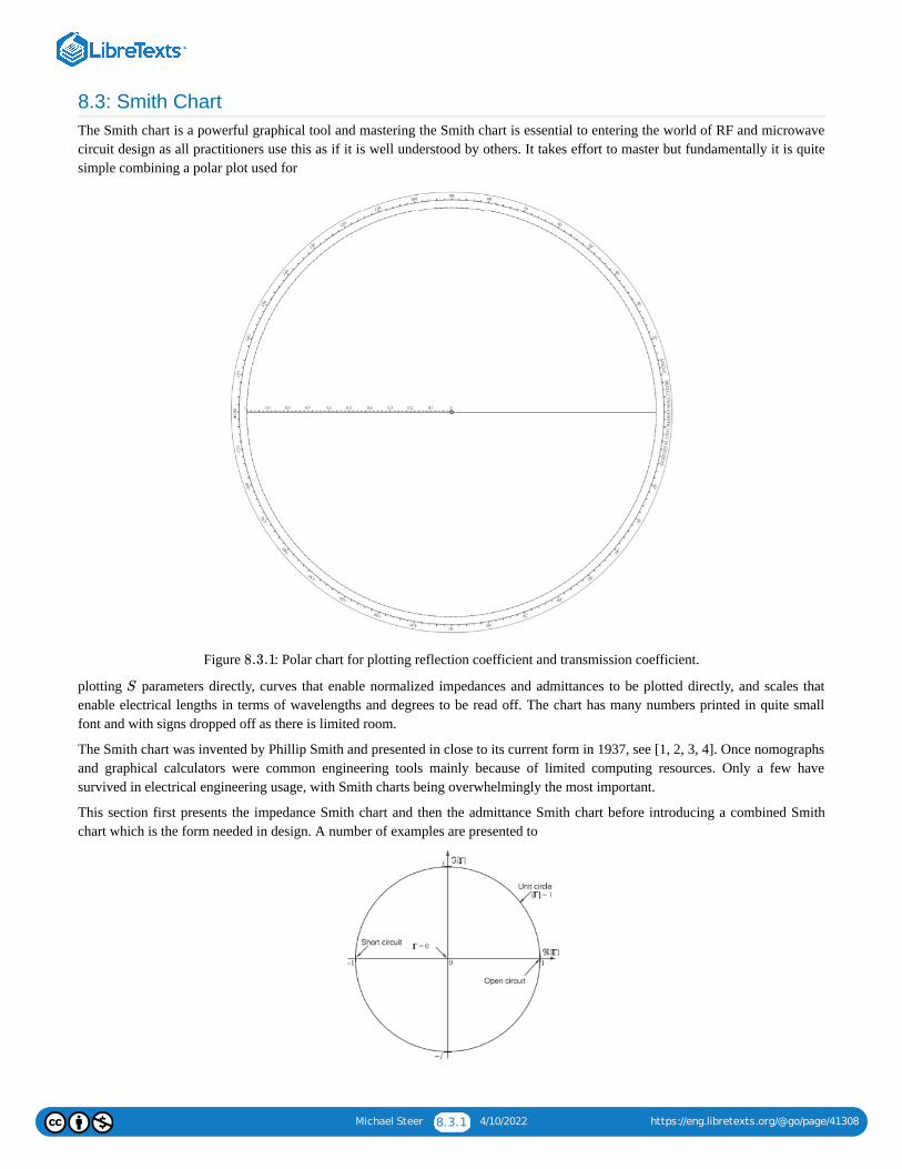
Michael Steer 8.3.1 4/10/2022 https://eng.libretexts.org/@go/page/41308
8.3: Smith ChartThe Smith chart is a powerful graphical tool and mastering the Smith chart is essential to entering the world of RF and microwavecircuit design as all practitioners use this as if it is well understood by others. It takes effort to master but fundamentally it is quitesimple combining a polar plot used for
Figure : Polar chart for plotting reflection coefficient and transmission coefficient.
plotting parameters directly, curves that enable normalized impedances and admittances to be plotted directly, and scales thatenable electrical lengths in terms of wavelengths and degrees to be read off. The chart has many numbers printed in quite smallfont and with signs dropped off as there is limited room.
The Smith chart was invented by Phillip Smith and presented in close to its current form in 1937, see [1, 2, 3, 4]. Once nomographsand graphical calculators were common engineering tools mainly because of limited computing resources. Only a few havesurvived in electrical engineering usage, with Smith charts being overwhelmingly the most important.
This section first presents the impedance Smith chart and then the admittance Smith chart before introducing a combined Smithchart which is the form needed in design. A number of examples are presented to
8.3.1
S
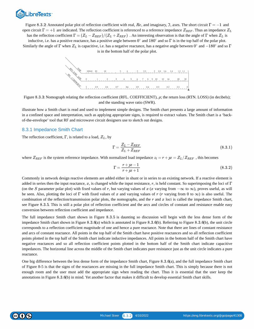
Michael Steer 8.3.2 4/10/2022 https://eng.libretexts.org/@go/page/41308
Figure : Annotated polar plot of reflection coefficient with real, , and imaginary, , axes. The short circuit andopen circuit are indicated. The reflection coefficient is referenced to a reference impedance . Thus an impedance
has the reflection coefficient . An interesting observation is that the angle of when isinductive, i.e. has a positive reactance, has a positive angle between and and so is in the top half of the polar plot.
Similarly the angle of when is capacitive, i.e. has a negative reactance, has a negative angle between and and so is in the bottom half of the polar plot.
Figure : Nomograph relating the reflection coefficient (RFL. COEFFICIENT), ; the return loss (RTN. LOSS) (in decibels);and the standing wave ratio (SWR).
illustrate how a Smith chart is read and used to implement simple designs. The Smith chart presents a large amount of informationin a confined space and interpretation, such as applying appropriate signs, is required to extract values. The Smith chart is a ‘back-of-the-envelope’ tool that RF and microwave circuit designers use to sketch out designs.
8.3.1 Impedance Smith Chart
The reflection coefficient, , is related to a load, , by
where is the system reference impedance. With normalized load impedance , this becomes
Commonly in network design reactive elements are added either in shunt or in series to an existing network. If a reactive element isadded in series then the input reactance, , is changed while the input resistance, , is held constant. So superimposing the loci of (on the parameter polar plot) with fixed values of , but varying values of ( varying from to ), proves useful, as willbe seen. Also, plotting the loci of with fixed values of and varying values of ( varying from to ) is also useful. Thecombination of the reflection/transmission polar plots, the nomographs, and the and loci is called the impedance Smith chart,see Figure . This is still a polar plot of reflection coefficient and the arcs and circles of constant and resistance enable easyconversion between reflection coefficient and impedance.
The full impedance Smith chart shown in Figure is daunting so discussion will begin with the less dense form of theimpedance Smith chart shown in Figure (a) which is annotated in Figure (b). Referring to Figure (b), the unit circlecorresponds to a reflection coefficient magnitude of one and hence a pure reactance. Note that there are lines of constant resistanceand arcs of constant reactance. All points in the top half of the Smith chart have positive reactances and so all reflection coefficientpoints plotted in the top half of the Smith chart indicate inductive impedances. All points in the bottom half of the Smith chart havenegative reactances and so all reflection coefficient points plotted in the bottom half of the Smith chart indicate capacitiveimpedances. The horizontal line across the middle of the Smith chart indicates pure resistance just as the unit circle indicates a purereactance.
One big difference between the less dense form of the impedance Smith chart, Figure (a), and the full impedance Smith chartof Figure 8-5 is that the signs of the reactances are missing in the full impedance Smith chart. This is simply because there is notenough room and the user must add the appropriate sign when reading the chart. Thus it is essential that the user keep theannotations in Figure (b) in mind. Yet another factor that makes it difficult to develop essential Smith chart skills.
8.3.2 Re I Γ = −1
Γ = +1 ZREF ZL
Γ = ( − )/( + )ZL ZREF ZL ZREF Γ ZL
0∘ 180∘ Γ
Γ ZL 0∘ −180∘ Γ
8.3.3 ρ
Γ ZL
Γ =−ZL ZREF
+ZL ZREF
(8.3.1)
ZREF = r+ ȷx = /zl ZL ZREF
Γ =r+ ȷx−1
r+ ȷx+1(8.3.2)
x r Γ
S r x x −∞ ∞
Γ x r r 0 ∞
r x
8.3.5
8.3.5
8.3.6 8.3.6 8.3.6
8.3.6
8.3.6
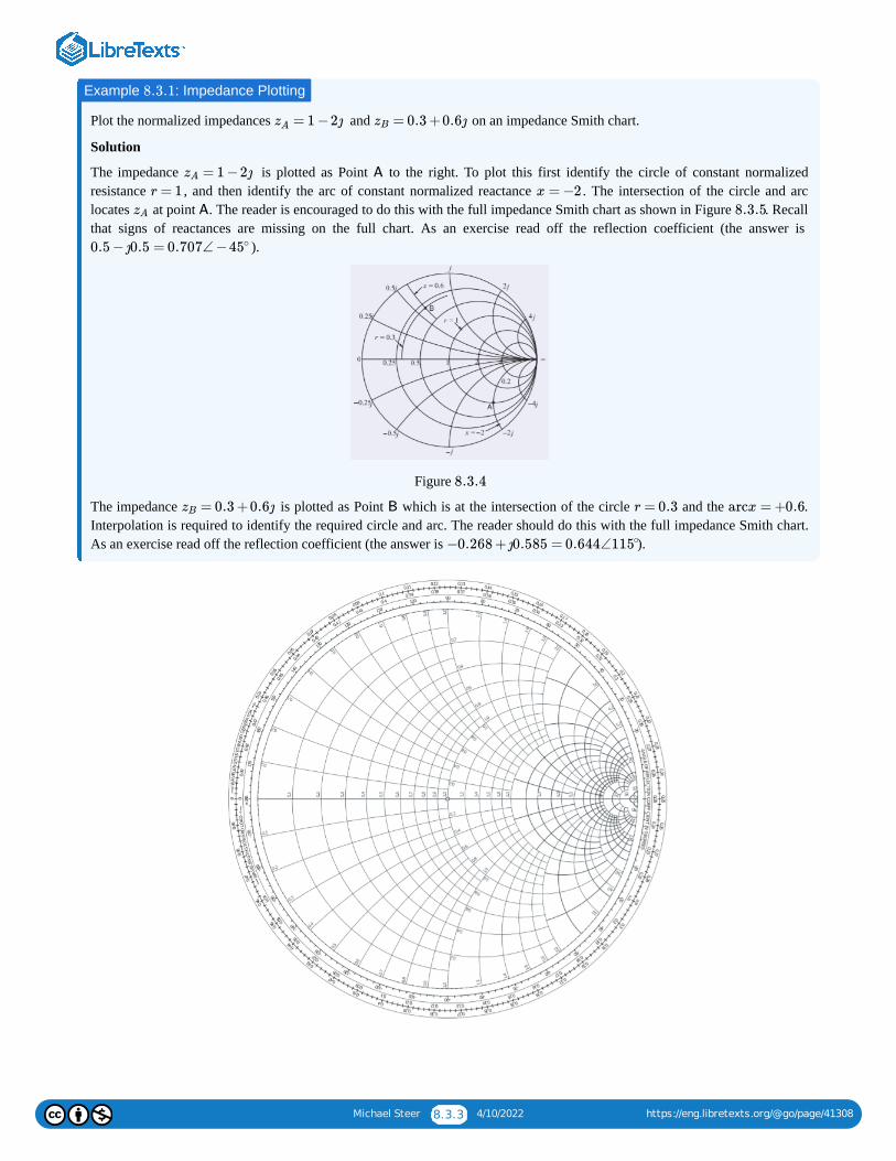
Michael Steer 8.3.3 4/10/2022 https://eng.libretexts.org/@go/page/41308
Plot the normalized impedances and on an impedance Smith chart.
Solution
The impedance is plotted as Point to the right. To plot this first identify the circle of constant normalizedresistance , and then identify the arc of constant normalized reactance . The intersection of the circle and arclocates at point . The reader is encouraged to do this with the full impedance Smith chart as shown in Figure . Recallthat signs of reactances are missing on the full chart. As an exercise read off the reflection coefficient (the answer is
).
Figure
The impedance is plotted as Point which is at the intersection of the circle and the .Interpolation is required to identify the required circle and arc. The reader should do this with the full impedance Smith chart.As an exercise read off the reflection coefficient (the answer is ).
Example : Impedance Plotting8.3.1
= 1 −2ȷzA = 0.3 +0.6ȷzB
= 1 −2ȷzA A
r = 1 x = −2
zA A 8.3.5
0.5 − ȷ0.5 = 0.707∠ −45∘
8.3.4
= 0.3 +0.6ȷzB B r = 0.3 arcx = +0.6
−0.268 + ȷ0.585 = 0.644∠115∘
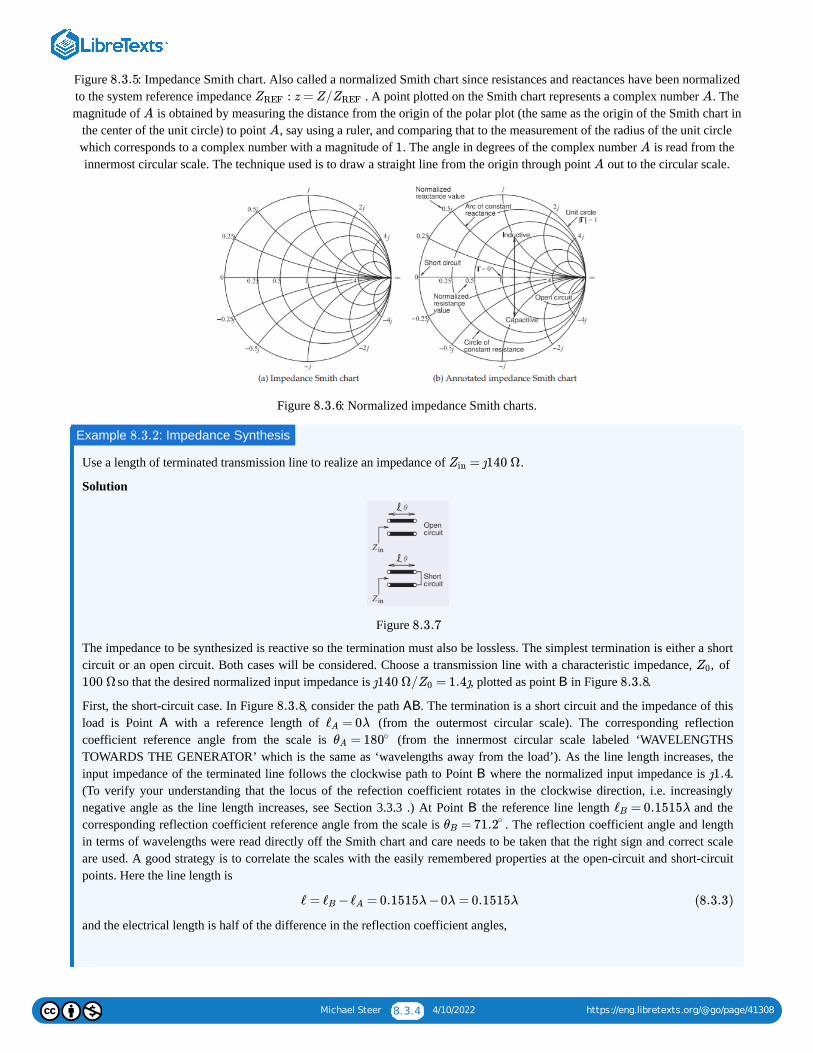
Michael Steer 8.3.4 4/10/2022 https://eng.libretexts.org/@go/page/41308
Figure : Impedance Smith chart. Also called a normalized Smith chart since resistances and reactances have been normalizedto the system reference impedance . A point plotted on the Smith chart represents a complex number . Themagnitude of is obtained by measuring the distance from the origin of the polar plot (the same as the origin of the Smith chart in
the center of the unit circle) to point , say using a ruler, and comparing that to the measurement of the radius of the unit circlewhich corresponds to a complex number with a magnitude of . The angle in degrees of the complex number is read from theinnermost circular scale. The technique used is to draw a straight line from the origin through point out to the circular scale.
Figure : Normalized impedance Smith charts.
Use a length of terminated transmission line to realize an impedance of .
Solution
Figure
The impedance to be synthesized is reactive so the termination must also be lossless. The simplest termination is either a shortcircuit or an open circuit. Both cases will be considered. Choose a transmission line with a characteristic impedance, , of
so that the desired normalized input impedance is , plotted as point in Figure .
First, the short-circuit case. In Figure , consider the path . The termination is a short circuit and the impedance of thisload is Point with a reference length of (from the outermost circular scale). The corresponding reflectioncoefficient reference angle from the scale is (from the innermost circular scale labeled ‘WAVELENGTHSTOWARDS THE GENERATOR’ which is the same as ‘wavelengths away from the load’). As the line length increases, theinput impedance of the terminated line follows the clockwise path to Point where the normalized input impedance is .(To verify your understanding that the locus of the refection coefficient rotates in the clockwise direction, i.e. increasinglynegative angle as the line length increases, see Section 3.3.3 .) At Point the reference line length and thecorresponding reflection coefficient reference angle from the scale is . The reflection coefficient angle and lengthin terms of wavelengths were read directly off the Smith chart and care needs to be taken that the right sign and correct scaleare used. A good strategy is to correlate the scales with the easily remembered properties at the open-circuit and short-circuitpoints. Here the line length is
and the electrical length is half of the difference in the reflection coefficient angles,
8.3.5
: z = Z/ZREF ZREF A
A
A
1 A
A
8.3.6
Example : Impedance Synthesis8.3.2
= ȷ140 ΩZin
8.3.7
Z0
100 Ω ȷ140 Ω/ = 1.4ȷZ0 B 8.3.8
8.3.8 AB
A = 0λℓA=θA 180∘
B ȷ1.4
B = 0.1515λℓB=θB 71.2∘
ℓ = − = 0.1515λ−0λ = 0.1515λℓB ℓA (8.3.3)
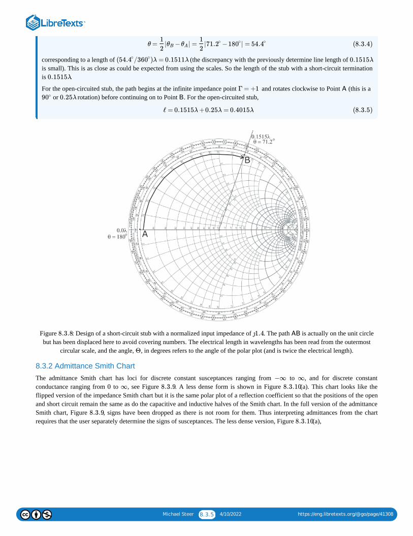
Michael Steer 8.3.5 4/10/2022 https://eng.libretexts.org/@go/page/41308
corresponding to a length of (the discrepancy with the previously determine line length of is small). This is as close as could be expected from using the scales. So the length of the stub with a short-circuit terminationis .
For the open-circuited stub, the path begins at the infinite impedance point and rotates clockwise to Point (this is a or rotation) before continuing on to Point . For the open-circuited stub,
Figure : Design of a short-circuit stub with a normalized input impedance of . The path is actually on the unit circlebut has been displaced here to avoid covering numbers. The electrical length in wavelengths has been read from the outermost
circular scale, and the angle, , in degrees refers to the angle of the polar plot (and is twice the electrical length).
8.3.2 Admittance Smith Chart
The admittance Smith chart has loci for discrete constant susceptances ranging from to , and for discrete constantconductance ranging from to , see Figure . A less dense form is shown in Figure (a). This chart looks like theflipped version of the impedance Smith chart but it is the same polar plot of a reflection coefficient so that the positions of the openand short circuit remain the same as do the capacitive and inductive halves of the Smith chart. In the full version of the admittanceSmith chart, Figure , signs have been dropped as there is not room for them. Thus interpreting admittances from the chartrequires that the user separately determine the signs of susceptances. The less dense version, Figure (a),
θ = | − | = | − | =1
2θB θA
1
271.2∘ 180∘ 54.4∘ (8.3.4)
( / )λ = 0.1511λ54.4∘ 360∘ 0.1515λ
0.1515λ
Γ = +1 A
90∘ 0.25λ B
ℓ = 0.1515λ+0.25λ = 0.4015λ (8.3.5)
8.3.8 ȷ1.4 AB
Θ
−∞ ∞
0 ∞ 8.3.9 8.3.10
8.3.9
8.3.10
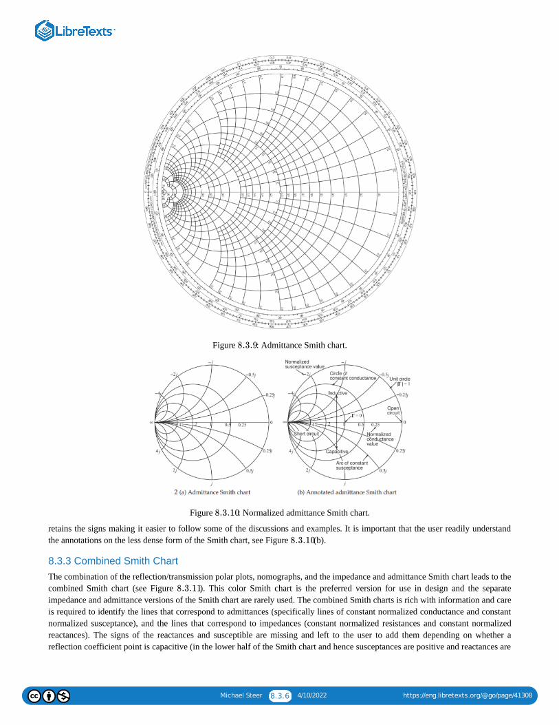
Michael Steer 8.3.6 4/10/2022 https://eng.libretexts.org/@go/page/41308
Figure : Admittance Smith chart.
Figure : Normalized admittance Smith chart.
retains the signs making it easier to follow some of the discussions and examples. It is important that the user readily understandthe annotations on the less dense form of the Smith chart, see Figure (b).
8.3.3 Combined Smith ChartThe combination of the reflection/transmission polar plots, nomographs, and the impedance and admittance Smith chart leads to thecombined Smith chart (see Figure ). This color Smith chart is the preferred version for use in design and the separateimpedance and admittance versions of the Smith chart are rarely used. The combined Smith charts is rich with information and careis required to identify the lines that correspond to admittances (specifically lines of constant normalized conductance and constantnormalized susceptance), and the lines that correspond to impedances (constant normalized resistances and constant normalizedreactances). The signs of the reactances and susceptible are missing and left to the user to add them depending on whether areflection coefficient point is capacitive (in the lower half of the Smith chart and hence susceptances are positive and reactances are
8.3.9
8.3.10
8.3.10
8.3.11
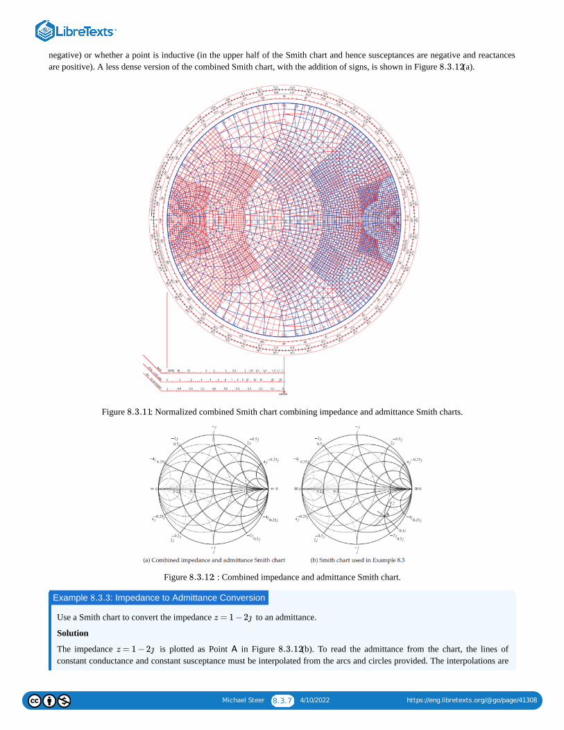
Michael Steer 8.3.7 4/10/2022 https://eng.libretexts.org/@go/page/41308
negative) or whether a point is inductive (in the upper half of the Smith chart and hence susceptances are negative and reactancesare positive). A less dense version of the combined Smith chart, with the addition of signs, is shown in Figure (a).
Figure : Normalized combined Smith chart combining impedance and admittance Smith charts.
Figure : : Combined impedance and admittance Smith chart.
Use a Smith chart to convert the impedance to an admittance.
Solution
The impedance is plotted as Point in Figure (b). To read the admittance from the chart, the lines ofconstant conductance and constant susceptance must be interpolated from the arcs and circles provided. The interpolations are
8.3.12
8.3.11
8.3.12
Example : Impedance to Admittance Conversion8.3.3
z = 1 −2ȷ
z = 1 −2ȷ A 8.3.12
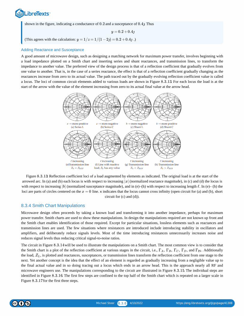
Michael Steer 8.3.8 4/10/2022 https://eng.libretexts.org/@go/page/41308
shown in the figure, indicating a conductance of and a susceptance of . Thus
(This agrees with the calculation: .)
Adding Reactance and Susceptance
A good amount of microwave design, such as designing a matching network for maximum power transfer, involves beginning witha load impedance plotted on a Smith chart and inserting series and shunt reactances, and transmission lines, to transform theimpedance to another value. The preferred view of the design process is that of a reflection coefficient that gradually evolves fromone value to another. That is, in the case of a series reactance, the effect is that of a reflection coefficient gradually changing as thereactances increase from zero to its actual value. The path traced out by the gradually evolving reflection coefficient value is calleda locus. The loci of common circuit elements added to various loads are shown in Figure . For each locus the load is at thestart of the arrow with the value of the element increasing from zero to its actual final value at the arrow head.
Figure : Reflection coefficient loci of a load augmented by elements as indicated. The original load is at the start of thearrowed arc. In (a) and (b) each locus is with respect to increasing (normalized reactance magnitude), in (c) and (d) the locus iswith respect to increasing (normalized susceptance magnitude), and in (e)–(h) with respect to increasing length . In (e)– (h) theloci are parts of circles centered on the line. indicates that the locus cannot cross infinity (open circuit for (a) and (b), short
circuit for (c) and (d)).
8.3.4 Smith Chart Manipulations
Microwave design often proceeds by taking a known load and transforming it into another impedance, perhaps for maximumpower transfer. Smith charts are used to show these manipulations. In design the manipulations required are not known up front andthe Smith chart enables identification of those required. Except for particular situations, lossless elements such as reactances andtransmission lines are used. The few situations where resistances are introduced include introducing stability in oscillators andamplifiers, and deliberately reduce signals levels. Most of the time introducing resistances unnecessarily increases noise andreduces signal levels thus reducing critical signal-to-noise ratios.
The circuit in Figure will be used to illustrate the manipulations on a Smith chart. The most common view is to consider thatthe Smith chart is a plot of the reflection coefficient at various stages in the circuit, i.e., and . Additionallythe load, , is plotted and reactances, susceptances, or transmission lines transform the reflection coefficient from one stage to thenext. Yet another concept is the idea that the effect of an element is regarded as gradually increasing from a negligible value up tothe final actual value and in so doing tracing out a locus which ends in an arrow head. This is the approach nearly all RF andmicrowave engineers use. The manipulations corresponding to the circuit are illustrated in Figure . The individual steps areidentified in Figure . The first few steps are confined to the top half of the Smith chart which is repeated on a larger scale inFigure for the first three steps.
0.2 0.4ȷ
y = 0.2 +0.4ȷ
y = 1/z = 1/(1 −2ȷ) = 0.2 +0.4ȷ
8.3.13
8.3.13
|x|
|b| ℓ
x = 0 x
8.3.14
, , , ,ΓA ΓB ΓC ΓD ΓIN
ZL
8.3.15
8.3.16
8.3.17
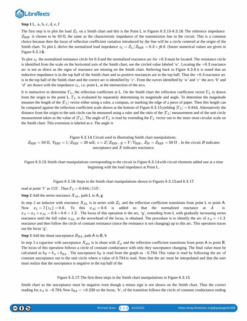
Michael Steer 8.3.9 4/10/2022 https://eng.libretexts.org/@go/page/41308
Step 1
The first step is to plot the load on a Smith chart and this is the Point in Figures – . The reference impedance is chosen to be , the same as the characteristic impedance of the transmission line in the circuit. This is a common
choice because then the locus of reflection coefficient variation introduced by the line will be a circle centered at the origin of theSmith chart. To plot derive the normalized load impedance (future numerical values are given inFigure ).
To plot the normalized resistance circle for and the normalized reactance arc for must be located. The resistance circleis identified from the scale on the horizontal axis of the Smith chart, see the circled value labeled ‘ ’. Locating the reactancearc is not as direct as the signs of reactance are missing on the Smith chart. Referring back to Figure it is noted that aninductive impedance is in the top half of the Smith chart and so positive reactances are in the top half. Thus the reactance arcis in the top half of the Smith chart and the correct arc is identified by ‘ ’. From the curves identified by ‘ ’ and ‘ ’ the arcs ‘ ’ and‘ ’ are drawn with the impedance , i.e. point , at the intersection of the arcs.
It is instructive to determine , the reflection coefficient at . On the Smith chart the reflection coefficient vector is drawnfrom the origin to the point . is evaluated by separately determining its magnitude and angle. To determine the magnitudemeasure the length of the vector either using a ruler, a compass, or marking the edge of a piece of paper. Then this length canbe compared against the reflection coefficient scale shown at the bottom of Figure yielding . Alternatively thedistance from the origin to the unit circle can be measured using a ruler and the ratio of the measurement and of the unit circlemeasurement taken as the value of . The angle of is read by extending the vector out to the inner most circular scale onthe Smith chart. This extension is labeled as e. The angle is
Figure : Circuit used in illustrating Smith chart manipulations. . In the circuit indicates
susceptance and indicates reactiance.
Figure : Smith chart manipulations corresponding to the circuit in Figure with circuit elements added one at a timebeginning with the load impedance at Point .
Figure : Steps in the Smith chart manipulations shown in Figures and .
read at point ‘f’ as . Thus .
Step 2 Add the series reactance , path to ,
In step 2 an inductor with reactance is in series with and the reflection coefficient transitions from point to point .Now . To this is added so that the normalized reactance at is
. The locus of this operation is the arc, ‘g’, extending from with gradually increasing seriesreactance until the full value , at the arrowhead of the locus, is obtained. The procedure is to identify the arc of reactance and then follow the circle of constant resistance (since the resistance is not changing) up to this arc. This operation tracesout the locus ’g’.
Step 3 Add the shunt susceptance , path to ,
In step 3 a capacitor with susceptance is in shunt with and the reflection coefficient transitions from point to point .The locus of this operation follows a circle of constant conductance with only they susceptance changing. The final value must becalculated as . The susceptance is read from the graph as . This value is read by following the arc ofconstant susceptance out to the unit circle where a value of is read. Note that the arc must be interpolated and that the usermust realize that the susceptance is negative in the top half of the
Figure : The first three steps in the Smith chart manipulations in Figure .
Smith chart so the susceptance must be negative even though a minus sign is not shown on the Smith chart. Thus the correctreading for is . Now so the locus, ‘h’, of the transition follows the circle of constant conductance ending
L, a, b, c, d, e, f
ZL L 8.3.15 8.3.16
ZREF 50 Ω
L = / = 0.3 + ȷ0.6zL ZL ZREF
8.3.14
zL 0.3 +0.3
a +0.3
8.3.6
+0.3
c a c b
d zL L
ΓL L ΓL
L ΓL
| |ΓL
8.3.15 | | = 0.644ΓL
| |ΓL
| |ΓL ΓL ΓL
8.3.14
= 50 Ω, = 1/ = 20 mS, z = Z/ , y = Y / , = = 50 ΩZREF YREF ZREF ZREF YREF ZIN ZREF B
X
8.3.15 8.3.14
L
8.3.16 8.3.15 8.3.17
115∘ = 0.644∠ΓL 115∘
XAL L A g
XAL ZL L A
= I{ } = 0.6xL zL = 0.6xAL A
= + = 0.6 +0.6 = 1.2xA xL xAL L
xAL = +1.2xA
BBA A B h
XBA ZA A B
= +bB bA bBA bB −0.784
0.784
8.3.17 8.3.15
xA −0.784 = +0.230bBA
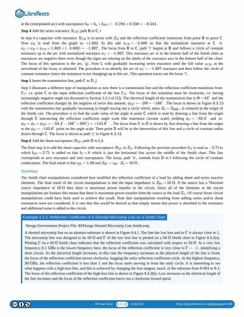
Michael Steer 8.3.10 4/10/2022 https://eng.libretexts.org/@go/page/41308
at the (interpolated arc) with susceptance .
Step 4 Add the series reactance , path to ,
In step 4 a capacitor with reactance is in series with and the reflection coefficient transitions from point to point .Now is read from the graph as . To this add so that the normalized reactance at is
. The locus from to , path ‘i’ begins at and follows a circle of constantresistance up to the arc with normalized reactance . This reactance arc is in the bottom half of the Smith chart asreactances are negative there even though the signs are missing on the labels of the reactance arcs in the bottom half of the chart.The locus of this operation is the arc, ‘g’, from with gradually increasing series reactance until the full value , at thearrowhead of the locus, is obtained. The procedure is to identify the arc of reactance and then follow the circle ofconstant resistance (since the resistance is not changing) up to this arc. This operation traces out the locus ’i’.
Step 5 Insert the transmission line, path to ,
Step 5 illustrates a different type of manipulation as now there is a transmission line and the reflection coefficient transitions from , i.e. point to the input reflection coefficient of the line . The locus of this transition must be clockwise, i.e. having
increasingly negative angle (as discussed in Section 3.3.3 of [5]). The electrical length of the transmission line is and thereflection coefficient changes by the negative of twice this amount, . The locus is drawn in Figure with the transmission line gradually increasing in length tracing out a circle which, since , is centered at the origin ofthe Smith cart. The procedure is to find the scale value of the angle at point which is read by drawing a line from the originthrough intersecting the reflection coefficient angle scale (the innermost circular scale) yielding and so
. The locus from to is drawn by first drawing a line from the originto the point on the angle scale. Then point will be at the intersection of this line and a circle of constant radiusdrawn through . The locus is shown as path ’j’ in Figure .
Step 6 Add the shunt susceptance , path to ,
The final step is to add the shunt capacitor with susceptance to . Following the previous procedure is read as towhich is added so that which is just the horizontal line across the middle of the Smith chart. This linecorresponds to zero reactance and zero susceptance. The locus, path ’k’, extends from to following the circle of constantconductance. The final result is that and .
Summary
The Smith chart manipulations considered here modified the reflection coefficient of a load by adding shunt and series reactiveelements. The final result of the circuit manipulations is that the input impedance is . If the source has a Theveninsource impedance of then there is maximum power transfer to the circuit. Since all of the elements in the circuitmanipulations are lossless this means that there is maximum power transfer from the source to the load . Of course fewer circuitmanipulations could have been used to achieve this result. Note that manipulations resulting from adding series and/or shuntresistances were not considered. It is rare that this would be desired as that simply means that power is absorbed in the resistanceand additional noise is added to the circuit.
Design Environment Project File: RFDesign Shorted Microstrip Line Smith.emp
A shorted microstrip line on an alumina substrate is shown in Figure 8.4.1. The line has low loss and so is always close to .The microstrip line was designed to be and of the low loss line is plotted on a Smith chart in Figure 8.4.2(a).Plotting on a Smith chart indicates that the reflection coefficient was calculated with respect to . At a very lowfrequency, is the lowest frequency here, the locus of the reflection coefficient is very close to , identifying ashort circuit. As the electrical length increases, in this case the frequency increases as the physical length of the line is fixed,the locus of the reflection coefficient moves clockwise, hugging the unity reflection coefficient circle. At the highest frequency,
, the reflection coefficient is less than and the locus starts moving in from the unity circle. It is interesting to seewhat happens with a high-loss line, and this is achieved by changing the loss tangent, , of the substrate from to .The locus of the reflection coefficient of the high-loss line is shown in Figure 8.4.2(b). Loss increases as the electrical length ofthe line increases and the locus of the reflection coefficient traces out a clockwise inward spiral.
= + = −0.784 +0.230 = −0.554bB ba bBA
XCB B C i
XCB ZB B C
xB +1.603 = −3.600xCB C
= + = 1.603 +(−3.600) = −1.997xC xB xCB B C B
= −1.997xC
L zCB= −1.997xC
C D j
ΓC C ΓD
Θ = 83∘
= −2Θ = −ϕDC 166∘ 8.3.15
=Z0 ZREF
C
C = −ϕC 50.4∘
= + = − − + ) = +ϕD ϕC ϕDC 50.4∘ 166∘ 360∘ 143.6∘ C D
= −ϕD 143.6∘ D
C 8.3.15
BID D I k
BID ZD bD −2.71
= 2.71bID = 0bID I
= 1.00zIN = ⋅ = 50 ΩZIN zIN Z0
= 50 ΩZIN
50 Ω
ZL
Example : Reflection Coefficient of a Shorted Microstrip Line on a Smith Chart8.3.4
Γ 1
50 Ω Γ 50 Ω
Γ 50 Ω 50 Ω
0.1 GHz Γ = −1
30 GHz 1
tanδ 0.001 0.1

Michael Steer 8.3.11 4/10/2022 https://eng.libretexts.org/@go/page/41308
8.3.5 An Alternative Admittance ChartDesign often requires switching between admittance and impedance. So it is convenient to use the colored combined Smith chartshown in Figure . Monochrome charts were once the only ones available and an impedance Smith chart was used foradmittance-based calculations provided that reflection coefficients were rotated by . This form of the Smith chart is not usednow and is very confusing.
8.3.6 Summary
The Smith chart is the most powerful of tools used in RF and Microwave Design. Design using Smith charts will be considered inother chapters but at this stage the reader should be totally conversant with the techniques described in this section.
Contributions and AttributionsThis page is licensed under a CC BY-NC license and was authored, remixed, and/or curated by Michael Steer. A detailedversioning history of the edits to source content is available upon request.
8.3.11
180∘
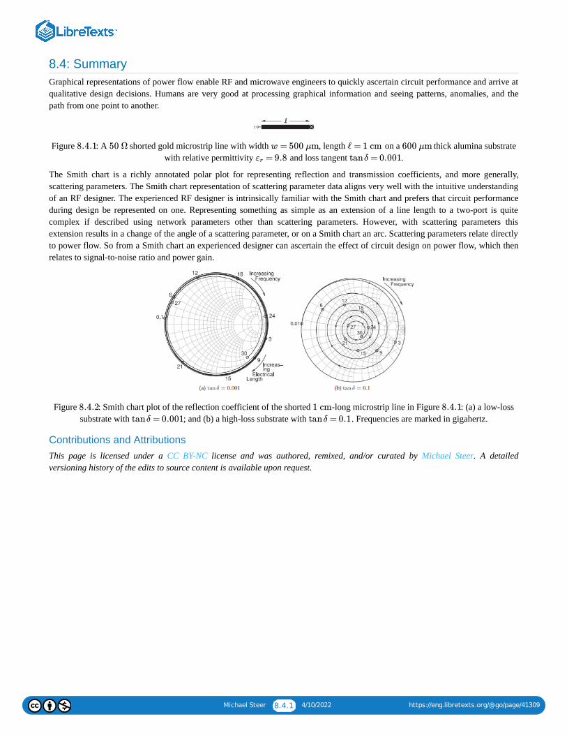
Michael Steer 8.4.1 4/10/2022 https://eng.libretexts.org/@go/page/41309
8.4: SummaryGraphical representations of power flow enable RF and microwave engineers to quickly ascertain circuit performance and arrive atqualitative design decisions. Humans are very good at processing graphical information and seeing patterns, anomalies, and thepath from one point to another.
Figure : A shorted gold microstrip line with width , length on a thick alumina substratewith relative permittivity and loss tangent .
The Smith chart is a richly annotated polar plot for representing reflection and transmission coefficients, and more generally,scattering parameters. The Smith chart representation of scattering parameter data aligns very well with the intuitive understandingof an RF designer. The experienced RF designer is intrinsically familiar with the Smith chart and prefers that circuit performanceduring design be represented on one. Representing something as simple as an extension of a line length to a two-port is quitecomplex if described using network parameters other than scattering parameters. However, with scattering parameters thisextension results in a change of the angle of a scattering parameter, or on a Smith chart an arc. Scattering parameters relate directlyto power flow. So from a Smith chart an experienced designer can ascertain the effect of circuit design on power flow, which thenrelates to signal-to-noise ratio and power gain.
Figure : Smith chart plot of the reflection coefficient of the shorted -long microstrip line in Figure : (a) a low-losssubstrate with ; and (b) a high-loss substrate with . Frequencies are marked in gigahertz.
Contributions and AttributionsThis page is licensed under a CC BY-NC license and was authored, remixed, and/or curated by Michael Steer. A detailedversioning history of the edits to source content is available upon request.
8.4.1 50 Ω w = 500 μm ℓ = 1 cm 600 μm
= 9.8εr tanδ = 0.001
8.4.2 1 cm 8.4.1
tanδ = 0.001 tanδ = 0.1

Michael Steer 8.5.1 4/10/2022 https://eng.libretexts.org/@go/page/41310
8.5: References[1] P. Smith, Electronic Applications of the Smith Chart: In Waveguide, Circuit, and Component Analysis. SciTech Publishing,2000.
[2] ——, “Transmission line calculator,” Electronics, 1939.
[3] ——, “An improved transmission-line calculator,” Electronics, 1944.
[4] ——, “R.F. transmission line nomographs,” Electronics, vol. 22, pp. 112–117, Feb. 1949.
[5] M. Steer, Microwave and RF Design, Transmission Lines, 3rd ed. North Carolina State University, 2019.
Contributions and Attributions
This page is licensed under a CC BY-NC license and was authored, remixed, and/or curated by Michael Steer. A detailedversioning history of the edits to source content is available upon request.

Michael Steer 8.6.1 4/10/2022 https://eng.libretexts.org/@go/page/41311
8.6: Exercises1. In the distribution of signals on a cable TV system a coaxial cable is used, with a loss of at . If a
subscriber disconnects a television set from the cable so that the load impedance looks like an open circuit, estimate the inputimpedance of the cable at and from the subscriber. An answer within is required. Estimate the error of youranswer. Indicate the input impedance on a Smith chart, drawing the locus of the input impedance as the line is increased inlength from nothing to . (Consider that the dielectric filling the line has .)
2. A resistive load has a reflection coefficient with a magnitude of . If a transmission line is placed in series with the load, on apolar plot sketch the locus of the input reflection coefficient looking into the input of the terminated line as the line increases inelectrical length from zero to . By reading the Smith chart, determine the normalized input impedance of the line when ithas an electrical length of .
3. A complex load has a reflection coefficient of . If a transmission line is placed in series with the load, on a polar plotsketch the locus of the input reflection coefficient looking into the input of the terminated line as the line increases in electricallength from zero to .
4. A resistive load has a reflection coefficient of . If a transmission line is placed in series with the load, on a polar plotsketch the locus of the input reflection coefficient looking into the input of the terminated line as the line increases in electricallength from to .
5. of a two-port is . If a transmission line is placed in series with Port 1, on a polar plot sketch the locus of of theaugmented twoport as the electrical length of the line increases from zero to .
6. A load has an impedance .a. What is the reflection coefficient, , of the load in a reference system?b. Plot the reflection coefficient on a polar plot of reflection coefficient.c. If a one-eighth wavelength long lossless transmission line is connected to the load, what is the reflection coefficient,
, looking into the transmission line? (Again, use the reference system.) Plot on the polar reflection coefficientplot of part (b). Clearly identify and on the plot.
d. On the Smith chart, identify the locus of as the length of the transmission line increases from to long. That is, onthe Smith chart, plot as the length of the transmission line varies.
7. A load has a reflection coefficient with a magnitude of . If a transmission line is placed in series with the load, on a polarplot sketch the locus of the input reflection coefficient looking into the input of the terminated line as the line increases inelectrical length from zero to . What is the normalized input impedance of the line when it has an electrical length of ?
8. A resistive load has a reflection coefficient with a magnitude of . If a transmission line is placed in series with the load, on apolar plot sketch the locus of the input reflection coefficient looking into the input of the terminated line as the line increases inelectrical length from zero to . By reading the Smith chart, determine the normalized input impedance of the line when ithas an electrical length of . Problems 9–15 refer to the normalized Smith chart in Figure with reference impedance and reflectioncoefficient , voltage reflection coefficient , current reflection coefficient , and normalized impedance andadmittance . should be given in magnitude-angle format.a. 9. What is at ?b. What is at ?c. What is at ?d. What is at ?e. What is at ?f. What is at ?g. What is at ?h. What is at ?i. What is at ?j. What is at ?a. 10. What is at ?b. What is at ?c. What is at ?d. What is at ?
75 Ω 0.1 dB/m 1 GHz
1 GHz 1 km 1%
1 km = 1εr
0.7
λ/2
π/2
0.5 + ȷ0.5
π/2
−0.5
0 3λ/8
S21 0.5 S21
λ/2
Z = 115 − ȷ20 Ω
ΓL 50 Ω
50 Ω
Γin 50 Ω Γin
Γin ΓL
Γin 0 λ/8
Γin
0.5
λ/2 λ/2
0.7
λ/4
λ/4
8.6.2 = 50 ΩZREF
Γ ΓV ΓI z = r + ȷx
y = g + ȷb Γ
ΓV A
ΓI A
r B
z C
y D
|Γ| F
b I
Γ P
Γ D
Γ T
z A
y I
z E
y Z

Michael Steer 8.6.2 4/10/2022 https://eng.libretexts.org/@go/page/41311
e. What is at ?f. What is at ?g. What is at ?h. What is at ?i. What is at ?j. What is at ?a. 11. What is at ?b. What is at ?c. What is at ?d. What is at ?e. What is at ?f. What is at ?g. What is at ?h. What is at ?i. What is at , label this ?j. Use the Smith chart to find of a -long line with load ?a. 12. What is at ?b. What is at ?c. What is at ?d. What is at ?e. What is at ?f. What is at ?g. What is at ?h. What is at ?i. What is at ?j. What is at ?
a. 13. What is at ?b. What is at ?c. What is at ?d. What is at ?e. What is at ?f. What is at ?g. What is at ?h. What is at ?i. What is at ?j. What is at ?a. 14. What is at ?b. What is at ?c. What is at ?d. What is at ?e. What is at ?f. What is at ?g. What is at ?h. What is at ?i. What is at , label this ?j. Using the Smith chart find of a - long line with load ?a. 15. What is at ?b. What is at ?c. What is at ?d. What is at ?e. What is at ?
y H
|Γ| W
b F
x K
Γ K
Γ R
y A
y I
z G
y O
y V
Γ B
x C
Γ G
z L zL
zin 50 Ωλ/8 zL
ΓV M
ΓI M
r W
z Y
y V
|Γ| B
b K
Γ V
Γ P
Γ N
z M
y K
z S
y R
g B
|Γ| F
b B
x I
Γ I
Γ Q
g M
r K
y S
z R
y Z
Γ W
x Y
Γ T
z O zO
zin 3λ/8 50 Ω zO
g P
y J
Γ L
z N
y S

Michael Steer 8.6.3 4/10/2022 https://eng.libretexts.org/@go/page/41311
f. What is at ?g. What is at ?h. What is at ?i. What is at ?j. What is at ?
16. 16. Design a short-circuited stub to realize a normalized susceptance of . Show the locus of the stub as its length increasesfrom zero to its final length. What is the minimum length of the stub in terms of wavelengths?
17. Design a short-circuited stub to realize a normalized susceptance of . Show the locus of the stub as its length increasesfrom zero to its final length. What is the minimum length of the stub in terms of wavelengths?
18. Design a short-circuited stub to realize a normalized susceptance of . Show the locus of the stub as its length increasesfrom zero to its final length. What is the minimum length of the stub in terms of wavelengths?
19. A transmission line is terminated in a load with a reflection coefficient, , normalized to , of . If at theinput of the line is , what is the minimum electrical length of the line in degrees.
20. An open-circuited transmission line has an input reflection coefficient with an angle of what is the electrical length ofthe line in degrees? If there is more than one answer provide at least two correct answers.
21. Repeat Example 8.3.1 using the full impedance Smith chart of Figure .22. Plot the normalized impedances and on the full impedance Smith
chart of Figure . [Parallels Example 8.3.1]23. A lossy transmission line is shorted at one end. The line loss is per wavelength. Note that since the line is lossy the
characteristic impedance will be complex, but close to , since it is only slightly lossy. There is no way to calculate theactual characteristic impedance with the information provided. That is, problems must be solved with small inconsistencies.Microwave engineers do the best they can in design and always rely on measurements to calibrate results.a. What is the reflection coefficient at the load (in this case the short)?b. Consider the input reflection coefficient, , at a distance from the load. Determine for going from to in
steps of .c. On a Smith chart plot the locus of from to .d. Calculate the input impedance, , when the line is long using the telegrapher’s equation.e. Repeat part (d) using a Smith chart.
24. In Figure the results of several different experiments are plotted on a Smith chart. Each experiment measured the inputreflection coefficient from a low frequency (denoted by a circle) to a high frequency (denoted by a square) of a one-port.Determine the load that was measured. The loads that were measured are one of those shown below.
Load Description
i An inductor
ii A capacitor
iii A reactive load at the end of a transmission line
iv A resistive load at the end of a transmission line
v A parallel connection of an inductor, a resistor, and a capacitor goingthrough resonance and with a transmission line offset
vi A series connection of a resistor, an inductor and a capacitor goingthrough resonance and with a transmission line offset
vii A series resistor and inductor
viii An unknown load and not one of the above
Table For each of the measurements below indicate the load or loads using the load identifier above (e.g., i, ii, etc.).a. What load(s) is indicated by curve ?b. What load(s) is indicated by curve ?c. What load(s) is indicated by curve ?d. What load(s) is indicated by curve ?
|Γ| U
ΓV X
ΓI X
g B
x I
2.15
−0.56
−2.2
75 Ω Γ 75 Ω 0.5∠45∘ Γ
0.5∠ −135∘
75 Ω 40∘
8.6.5
= 0.5 + ȷ0.5, = 0.5 + ȷ0.5,zA zA = 0.185 − ȷ1.05zB
8.6.5
50 Ω 2 dB
50 Ω
Γin ℓ Γin ℓ 0.1λ λ
0.1λ
Γin ℓ = 0 λ
Zin 3λ/8
8.6.1
8.6.1
A
B
C
D
Michael Steer 8.6.4 4/10/2022 https://eng.libretexts.org/@go/page/41311
e. What load(s) is indicated by curve ?f. What load(s) is indicated by curve ?
25. Design an open-circuited stub with an input impedance of . Use a transmission line with a characteristic impedance of . [Parallels Example 8.3.2]
26. Design a short-circuited stub with an input impedance of . Use a transmission line with a characteristic impedance of . [Parallels Example 8.3.2]
27. A load has an impedance .a. What is the reflection coefficient, , of the load in a reference system?b. If a one-quarter wavelength long transmission line is connected to the load, what is the reflection coefficient, ,
looking into the transmission line?c. Describe the locus of , as the length of the transmission line is varied from zero length to one-half wavelength long. Use
a Smith chart to illustrate your answer.
28. A network consists of a source with a Thevenin equivalent impedance of driving first a series reactance of followed by a one-eighth wavelength long transmission line with a characteristic impedance of and an element with areactive impedance of in shunt with a load having an impedance . This problem must be solvedgraphically and no credit will be given if this is not done.a. Draw the network.b. On a Smith chart, plot the locus of the reflection coefficient first for the load, then with the element in shunt, then looking
into the transmission line, and finally the series element. Use letters to identify each point on the Smith chart. Write downthe reflection coefficient at each point.
c. What is the impedance presented by the network to the source?
8.6.1 Exercises by Sectionchallenging
8.6.2 Answers to Selected Exercises1.
23. (c) ii & iii24. (d)
27. 28.
E
F
+ȷ75 Ω
75 Ω
−ȷ50 Ω
100 Ω
= 25 − ȷ100 ΩZL
ΓL 50 Ω
50 Ω Γin
Γin
50 Ω −50 Ω
40 Ω
ȷ25 Ω = 25 − ȷ50 ΩZL
†
§8.31, 2, 3, 4, 5, 6, 7, 8, 9, 10, 11, 12, 13, 14, 15, 16, 17, 18, 19, 20, 21, 22, 23†, 24†, 25†, 26†, 27†, 28†
=ΓIN 10−10
8.37 − ȷ49.3 Ω
0.825∠ −50.9∘
≈ 250 − ȷ41 Ω
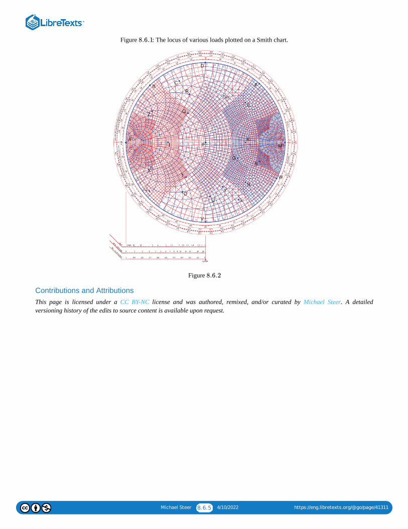
Michael Steer 8.6.5 4/10/2022 https://eng.libretexts.org/@go/page/41311
Figure : The locus of various loads plotted on a Smith chart.
Figure
Contributions and AttributionsThis page is licensed under a CC BY-NC license and was authored, remixed, and/or curated by Michael Steer. A detailedversioning history of the edits to source content is available upon request.
8.6.1
8.6.2

1 4/10/2022
CHAPTER OVERVIEW9: PASSIVE COMPONENTS
9.1: INTRODUCTION9.2: Q FACTOR9.3: SURFACE-MOUNT COMPONENTS9.4: TERMINATIONS AND ATTENUATORS9.5: TRANSMISSION LINE STUBS AND DISCONTINUITIES9.6: MAGNETIC TRANSFORMERS9.7: REFERENCES9.8: EXERCISES9.9: BALUNS9.10: WILKINSON COMBINER AND DIVIDER9.11: SUMMARY

Michael Steer 9.1.1 4/10/2022 https://eng.libretexts.org/@go/page/41312
9.1: IntroductionThis chapter introduces a wide variety of passive components. It is not possible to be comprehensive, as there is an enormouscatalog of microwave elements and scores of variations, and new concepts are introduced every year. At microwave frequenciesdistributed components can be constructed that have features with particular properties related to coupling, to traveling waves, andto storage of EM energy. Sometimes it is possible to develop lumped-element equivalents of the distributed elements by using theLC ladder model of a transmission line thus realizing lumped-element circuits that would be difficult to imagine otherwise.
Contributions and AttributionsThis page is licensed under a CC BY-NC license and was authored, remixed, and/or curated by Michael Steer. A detailedversioning history of the edits to source content is available upon request.
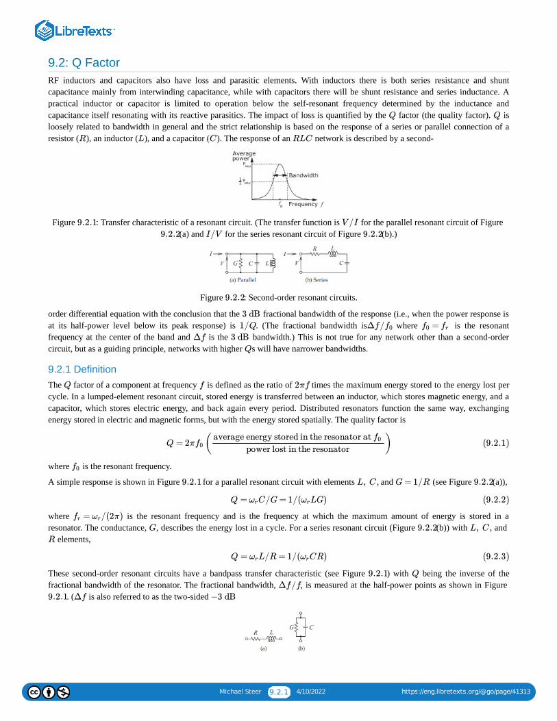
Michael Steer 9.2.1 4/10/2022 https://eng.libretexts.org/@go/page/41313
9.2: Q FactorRF inductors and capacitors also have loss and parasitic elements. With inductors there is both series resistance and shuntcapacitance mainly from interwinding capacitance, while with capacitors there will be shunt resistance and series inductance. Apractical inductor or capacitor is limited to operation below the self-resonant frequency determined by the inductance andcapacitance itself resonating with its reactive parasitics. The impact of loss is quantified by the factor (the quality factor). isloosely related to bandwidth in general and the strict relationship is based on the response of a series or parallel connection of aresistor ( ), an inductor ( ), and a capacitor ( ). The response of an network is described by a second-
Figure : Transfer characteristic of a resonant circuit. (The transfer function is for the parallel resonant circuit of Figure (a) and for the series resonant circuit of Figure (b).)
Figure : Second-order resonant circuits.
order differential equation with the conclusion that the fractional bandwidth of the response (i.e., when the power response isat its half-power level below its peak response) is . (The fractional bandwidth is where is the resonantfrequency at the center of the band and is the bandwidth.) This is not true for any network other than a second-ordercircuit, but as a guiding principle, networks with higher s will have narrower bandwidths.
9.2.1 DefinitionThe factor of a component at frequency is defined as the ratio of times the maximum energy stored to the energy lost percycle. In a lumped-element resonant circuit, stored energy is transferred between an inductor, which stores magnetic energy, and acapacitor, which stores electric energy, and back again every period. Distributed resonators function the same way, exchangingenergy stored in electric and magnetic forms, but with the energy stored spatially. The quality factor is
where is the resonant frequency.
A simple response is shown in Figure for a parallel resonant circuit with elements and (see Figure (a)),
where is the resonant frequency and is the frequency at which the maximum amount of energy is stored in aresonator. The conductance, , describes the energy lost in a cycle. For a series resonant circuit (Figure (b)) with and
elements,
These second-order resonant circuits have a bandpass transfer characteristic (see Figure ) with being the inverse of thefractional bandwidth of the resonator. The fractional bandwidth, , is measured at the half-power points as shown in Figure
. ( is also referred to as the two-sided
Q Q
R L C RLC
9.2.1 V /I
9.2.2 I/V 9.2.2
9.2.2
3 dB
1/Q Δf/f0 =f0 frΔf 3 dB
Q
Q f 2πf
Q = 2π ( )f0average energy stored in the resonator at f0
power lost in the resonator(9.2.1)
f0
9.2.1 L, C, G= 1/R 9.2.2
Q = C/G= 1/( LG)ωr ωr (9.2.2)
= /(2π)fr ωr
G 9.2.2 L, C,
R
Q = L/R = 1/( CR)ωr ωr (9.2.3)
9.2.1 Q
Δf/f
9.2.1 Δf −3 dB
Michael Steer 9.2.2 4/10/2022 https://eng.libretexts.org/@go/page/41313
Figure : Loss elements of practical inductors and capacitors: (a) an inductor has a series resistance ; and (b) for a capacitor,the dominant loss mechanism is a shunt conductance .
bandwith.) Then
Thus the is a measure of the sharpness of the bandpass frequency response. The determination of using the measurement ofbandwidth together with Equation is often not very precise, so another definition that uses the much more sensitive phasechange at resonance is preferred when measurements are being used. With being the phase (in radians) of the transfercharacteristic, the definition of is now
Equation is another equivalent definition of for parallel or series resonant circuits. It is meaningful to talkabout the of circuits other than three-element circuits, and then its meaning is always a ratio of the energy stored to theenergy dissipated per cycle. The of these structures can no longer be determined by bandwidth or by the rate of phase change.
9.2.2 of Lumped Elements
is also used to characterize the loss of lumped inductors and capacitors. Inductors have a series resistance , and the main lossmechanism of a capacitor is a shunt conductance (see Figure ).
The of an inductor at frequency with a series resistance and inductance is
Since is approximately constant with respect to frequency for an inductor, the will vary with frequency.
The of a capacitor with a shunt conductance and capacitance is
is due mainly to relaxation loss mechanisms of the dielectric of a capacitor and so varies linearly with frequency but also it isusually very small. Thus the of a capacitor is almost constant with respect to frequency. For microwave components
, and both are smaller than the of most transmission line networks. Thus, if the length of atransmission line is not too long for an application, transmission line networks are preferred. If lumped elements must be used, theuse of inductors should be minimized.
9.2.3 Loaded Factor
The of a component as defined in the previous section is called the unloaded . However, if a component is to be measuredor used in any way, it is necessary to couple energy in and out of it. The is reduced and thus the resonator bandwidth is increasedby the power lost to the external circuit so that the loaded , the that is measured, is
and
where is called the external . accounts for the power extracted from the resonant circuit. If the loading is kept very small,.
9.2.3 R
G= 1/R
Q = /Δffr (9.2.4)
Q Q
(9.2.4)
ϕ
Q
Q =ωr
2
∣
∣∣dϕ
dω
∣
∣∣ (9.2.5)
(9.2.5) Q RLC RLC
Q RLC
Q
Q
Q R
G 9.2.3
Q f = ω/(2π) R L
=QINDUCTORωL
R(9.2.6)
R Q
Q G C
=QCAPACITOR
ωC
G(9.2.7)
G
Q
≫QCAPACITOR QINDUCTOR Q
Q
Q Q, QU
Q
Q Q
QL = 2π ( )f0
average energy stored in the resonator at f0
power lost in the resonator and to the external circuit
=1
1/Q+1/QX
(9.2.8)
=QX ( − )1
QL
1
QU
−1
(9.2.9)
QX Q QL
≈QL QU

Michael Steer 9.2.3 4/10/2022 https://eng.libretexts.org/@go/page/41313
9.2.4 Summary of the Properties of In summary:
a. is properly defined and related to the energy stored in a resonator for a second-order network, one with two reactive elementsof opposite types.
b. is not well defined for networks with three or more reactive elements.c. It is only used (as defined or some approximation of it) for guiding the design.
Contributions and AttributionsThis page is licensed under a CC BY-NC license and was authored, remixed, and/or curated by Michael Steer. A detailedversioning history of the edits to source content is available upon request.
Q
Q
Q

Michael Steer 9.3.1 4/10/2022 https://eng.libretexts.org/@go/page/41314
9.3: Surface-Mount ComponentsThe majority of the RF and microwave design effort goes into developing modules and interconnecting modules on circuit boards.With these the most common type of component to use is a surface-mount component. Figure (a) shows a two-terminalelement, such as a resistor or capacitor, in the form of a surface-mount component. Figure (b and c) show the use of surface-mount components on a microwave circuit board.
A two-terminal surface-mount resistor or capacitor is commonly called a chip resistor or chip capacitor. These can be very small,and the smaller the component often the higher the operating frequency due to reduced parasitic capacitance or inductance.Common sizes of two-terminal chip components are listed in Table . The resonance when a chip capacitor (inductor) resonateswith the parasitic inductance (capacitance) is called self-resonance and the resonant frequency is called the self-resonancefrequency. Figure (a) shows an inductor in a surface-mount package and details are shown in Figure (b) and the inductoris useable as an inductor at a frequency backed-off from the SRF, see Table 9.4.1.
Figure : Circuit board showing the use of surface-mount components: (a) chip resistor or capacitor with metal terminals at thetwo ends; and (b) a populated RF microstrip circuit board of a tunable resonator [1]. The larger components have
dimensions . The shorting bar is a chip resistor.
Designation Size Metric Designation Size
9.3.1
9.3.1
9.3.1
9.3.2 9.3.2
9.3.1
5 GHz
1.6 mm ×0.8 mm 0 Ω
(inch × inch) (mm × mm)
01005 0.016 × 0.0079 0402 0.4 × 0.2
0201 0.024 × 0.012 0603 0.6 × 0.3
0402 0.039 × 0.020 1005 1.0 × 0.5
0603 0.063 × 0.031 1608 1.6 × 0.8
0805 0.079 × 0.049 2012 2.0 × 1.25
1008 0.098 × 0.079 2520 2.5 × 2.0
1206 0.13 × 0.063 3216 3.2 × 1.6
1210 0.13 × 0.098 3225 3.2 × 2.5
1806 0.18 × 0.063 4516 4.5 × 1.6
1812 0.18 × 0.13 4532 4.5 × 3.2
2010 0.20 × 0.098 5025 5.0 × 2.5
2512 0.25 × 0.13 6432 6.4 × 3.2
2920 0.29 × 0.20 – 7.4 × 5.1

Michael Steer 9.3.2 4/10/2022 https://eng.libretexts.org/@go/page/41314
Table : Sizes and designation of two-terminal surface mount components. Note the designation of a surface-mount componentrefers (approximately) to its dimensions in hundredths of an inch.
Figure : : Chip inductor: (a) in an 0603 surface-mount package; and (b) schematic showing sizes and pads to be provided on acircuit board ( ( ), ( ), ( ), ( ),
( ), ( ), ( ), and ( )). Copyright Coilcraft,Inc., used with permission [2].
Contributions and AttributionsThis page is licensed under a CC BY-NC license and was authored, remixed, and/or curated by Michael Steer. A detailedversioning history of the edits to source content is available upon request.
9.3.1
9.3.2
A= 64 mils 1.63 mm B= 33 mils 0.84 mm C = 24 mils 0.61 mm D= 13 mils 0.33 mm
E = 30 mils 0.76 mm F = 25 mils 0.64 mm G= 25 mils 0.64 mm H = 40 mils 1.02 mm
Michael Steer 9.4.1 4/10/2022 https://eng.libretexts.org/@go/page/41315
9.4: Terminations and Attenuators
9.4.1 Terminations
Terminations are used to completely absorb a forward-traveling wave and the reflection coefficient of a termination is ideally zero.If a transmission line has a resistive characteristic impedance , then terminating the line in a resistance will fullyabsorb the forward-traveling wave and there will be no reflection. The line is then said to be matched. At RF and microwavefrequencies some refinements to this simple circuit connection are required. On a transmission line the energy is contained in theEM fields. For the coaxial line, a simple resistive connection between the inner and outer conductors would not terminate the fieldsand there would be some reflection. Instead, coaxial line terminations generally comprise a disk of resistive material (see Figure
(a)). The total resistance of the disk from the inner to the outer conductor is the characteristic resistance of the line, however,the resistive material is distributed and so creates a good termination of the fields.
Terminations are a problem with microstrip, as the characteristic impedance varies with frequency, is in general complex, and thevias that would be required if a lumped resistor was used has appreciable inductance at frequencies above a few gigahertz. A high-quality termination is realized using a section of lossy line as shown in Figure (b). Here lossy material is deposited on top ofan open-circuited microstrip line. This increases the loss of the line appreciably without significantly affecting the characteristic
Table : Parameters of the inductors in Figure 9.3.2. is the nominal inductance, SRF is the self-resonance frequency, is the inductor’s series resistance, and is the maximum RMS current supported.
Component Symbol Alternate
Attenuator, fixed
Attenuator, balanced
Attenuator, unbalanced
Attenuator, variable
Attenuator, continuously variable
Attenuator, stepped variable
Table : IEEE standard symbols for attenuators [3].
impedance of the line. If the length of the lossy line is sufficiently long, say one wavelength, the forward-traveling wave will betotally absorbed and there will be no reflection. Tapering the lossy material, as shown in Figure (b), reduces the discontinuitybetween the lossless microstrip line and the lossy line by ensuring that some of the power in the forward-traveling wave isdissipated before the maximum impact of the lossy material occurs. Thus a matched termination is achieved without the use of avia.
=R0 Z0 R0
9.4.1
9.4.1
Lnom 900 MHz 1.7 GHz SRF RDC Imax
(nH) L (nH) Q L (nH) Q (GHz) (Ω) (mA)
1.0 0.98 39 0.99 58 16.0 0.045 1600
2.0 1.98 46 1.98 70 12.0 0.034 1900
5.1 5.12 68 5.18 93 5.50 0.050 1400
10 10.0 67 10.4 85 3.95 0.092 1100
20 20.2 67 21.6 80 2.90 0.175 760
56 59.4 54 75.4 48 1.75 0.700 420
9.4.1 Lnom
RDC Imax
9.4.2
9.4.1

Michael Steer 9.4.2 4/10/2022 https://eng.libretexts.org/@go/page/41315
9.4.2 AttenuatorsAn attenuator is a two-port network that reduces the amplitude of a signal and it does this by absorbing power and withoutdistorting the signal. The input and output of the attenuator are both matched, so there are no reflections. An attenuator may befixed, continuously variable, or discretely variable. The IEEE standard symbols for attenuators are shown in Table . When theattenuation is fixed, an attenuator is commonly called a pad. Balanced and unbalanced resistive pads are shown in Figures and together with their design equations. The attenuators in Figure are T or Tee attenuators, where is the systemimpedance to the left of the pad and is the system impedance to the right of the pad. The defining characteristic is that thereflection coefficient looking into the pad from the
Figure : Terminations: (a) coaxial line resistive termination; (b) microstrip matched load.
Figure : T (Tee) attenuator. is the (power) attenuation factor, e.g. a attenuator has .
If , then
Figure : Pi (Π) attenuator. is the (power) attenuation factor, e.g. a attenuator has .
If , then
If , then
9.4.29.4.2
9.4.3 9.4.2 Z01
Z02
9.4.1
9.4.2 K 3 dB K = = 1.995103/10
R1
R3
= =(K +1) −2Z01 KZ01Z02
− −−−−−−√
K −1R2
(K +1) −2Z02 KZ01Z02− −−−−−−
√
K −1
=2 KZ01Z02
− −−−−−−√
K −1(9.4.1)
= =Z01 Z02 Z0
= = ( ) and =R1 R2 Z0−1K
−−√
+1K−−
√R3
2Z0 K−−
√
K −1(9.4.2)
9.4.3 K 20 dB K = = 1001020/10
R1
R3
= =(K −1)Z01 Z02
−−−√
(K +1) −2Z02−−−
√ KZ01− −−−−
√R2
(K −1)Z02 Z01−−−√
(K +1) −2Z01−−−
√ KZ02− −−−−
√
=(K −1)
2
Z01Z02
K
− −−−−−√
(9.4.3)
(9.4.4)
= =Z01 Z02 Z0
= = ( ) and =R1 R2 Z0+1K
−−√
−1K−−
√R3
(K −1)Z0
2 K−−
√(9.4.5)
=R1 R2 = =Z01 Z02 Z0
= and K =Z0
R21R3
2 +R1 R3
− −−−−−−−
√ ( )+R1 Z0
−R1 Z0
2
(9.4.6)

Michael Steer 9.4.3 4/10/2022 https://eng.libretexts.org/@go/page/41315
left is zero when referred to . Similarly, the reflection coefficient looking into the right of the pad is zero with respect to .The attenuation factor is
In decibels, the attenuation is
If the left and right system impedances are different, then there is a minimum
Figure : Distributed attenuators. The attenuators in (c) have power handling ratings of and (left to right).Copyright 2012 Scientific Components Corporation d/b/a MiniCircuits, used with permission [4].
attenuation factor that can be achieved:
This limitation comes from the simultaneous requirement that the pad be matched. If there is a single system impedance, , then , and so any value of attenuation can be obtained.
Lumped attenuators are useful up to above which the size of resistive elements becomes large compared to a wavelength.Also, for planar circuits, vias are required, and these are undesirable from a manufacturing standpoint, and electrically they have asmall inductance. Fortunately attenuators can be realized using a lossy section of transmission line, as shown in Figure . Here,lossy material results in a section of line with a high-attenuation constant. Generally the lossy material has little effect on thecharacteristic impedance of the line, so there is little reflection at the input and output of the attenuator. Distributed attenuators canbe used at frequencies higher than lumped-element attenuators can, and they can be realized with any transmission line structure.
Design an unbalanced pad in a system.
Solution
There are two possible designs using resistive pads. These are the unbalanced Tee and Pi pads shown in Figures and . The Tee design will be chosen. The factor is
Since , Equation yields
The final design is
Z01 Z02
K =Power in
Power out(9.4.7)
K = 10 K = (Power in) −(Power out)|dB log10 |dBm |dBm (9.4.8)
9.4.4 2 W, 5 W 20 W
= −1 +2KMIN2Z01
Z02( )
Z01
Z02
Z01
−1Z02
− −−−−−−−−−−−−
√ (9.4.9)
= =Z0 Z01 Z02 = 1KMIN
10 GHz
9.4.4
Example : Pad Design9.4.1
20 dB 75 Ω
9.4.29.4.3 K
L = = = 10010(K /10)|dB 10(20/10) (9.4.10)
= = 75 ΩZ01 Z02 eqrefeq : 2
= = 75( ) = 75( ) = 61.4 ΩR1 R2−1100
−−−√
+1100−−−
√
9
11(9.4.11)
= = 150( ) = 15.2 ΩR32 ⋅ 75 100
−−−√
100 −1
10
99(9.4.12)
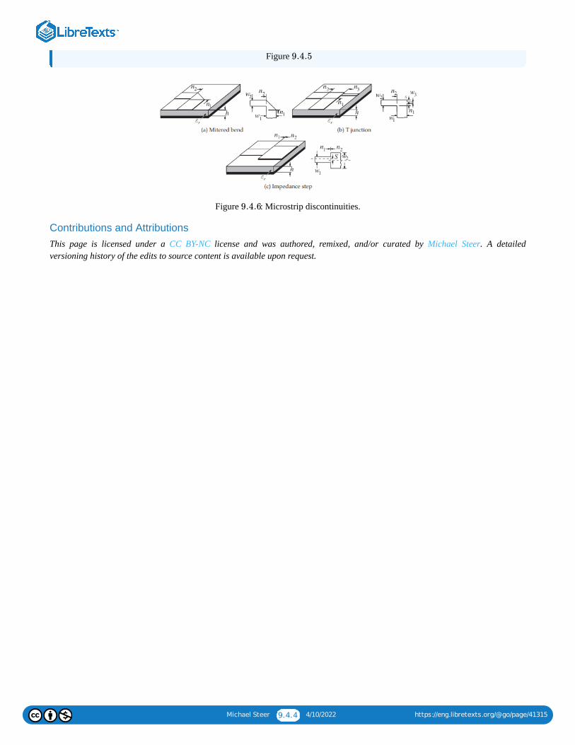
Michael Steer 9.4.4 4/10/2022 https://eng.libretexts.org/@go/page/41315
Figure
Figure : Microstrip discontinuities.
Contributions and AttributionsThis page is licensed under a CC BY-NC license and was authored, remixed, and/or curated by Michael Steer. A detailedversioning history of the edits to source content is available upon request.
9.4.5
9.4.6
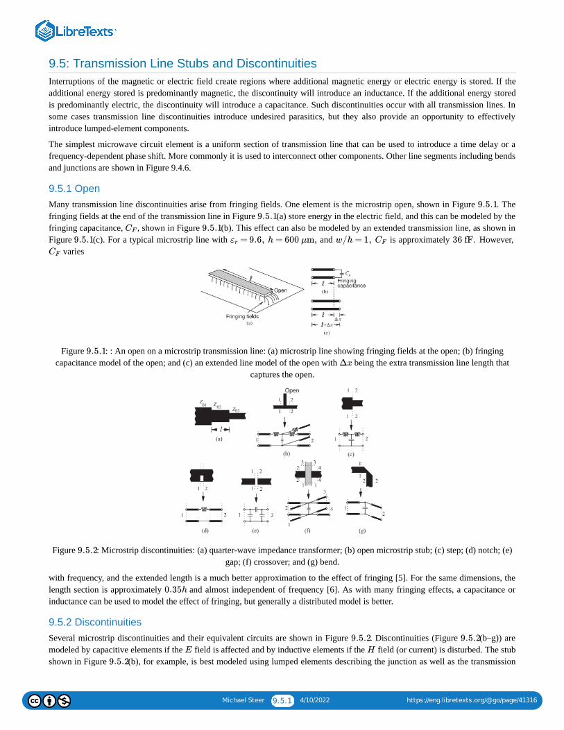
Michael Steer 9.5.1 4/10/2022 https://eng.libretexts.org/@go/page/41316
9.5: Transmission Line Stubs and DiscontinuitiesInterruptions of the magnetic or electric field create regions where additional magnetic energy or electric energy is stored. If theadditional energy stored is predominantly magnetic, the discontinuity will introduce an inductance. If the additional energy storedis predominantly electric, the discontinuity will introduce a capacitance. Such discontinuities occur with all transmission lines. Insome cases transmission line discontinuities introduce undesired parasitics, but they also provide an opportunity to effectivelyintroduce lumped-element components.
The simplest microwave circuit element is a uniform section of transmission line that can be used to introduce a time delay or afrequency-dependent phase shift. More commonly it is used to interconnect other components. Other line segments including bendsand junctions are shown in Figure 9.4.6.
9.5.1 OpenMany transmission line discontinuities arise from fringing fields. One element is the microstrip open, shown in Figure . Thefringing fields at the end of the transmission line in Figure (a) store energy in the electric field, and this can be modeled by thefringing capacitance, , shown in Figure (b). This effect can also be modeled by an extended transmission line, as shown inFigure (c). For a typical microstrip line with and is approximately . However,
varies
Figure : : An open on a microstrip transmission line: (a) microstrip line showing fringing fields at the open; (b) fringingcapacitance model of the open; and (c) an extended line model of the open with being the extra transmission line length that
captures the open.
Figure : Microstrip discontinuities: (a) quarter-wave impedance transformer; (b) open microstrip stub; (c) step; (d) notch; (e)gap; (f) crossover; and (g) bend.
with frequency, and the extended length is a much better approximation to the effect of fringing [5]. For the same dimensions, thelength section is approximately and almost independent of frequency [6]. As with many fringing effects, a capacitance orinductance can be used to model the effect of fringing, but generally a distributed model is better.
9.5.2 DiscontinuitiesSeveral microstrip discontinuities and their equivalent circuits are shown in Figure . Discontinuities (Figure (b–g)) aremodeled by capacitive elements if the field is affected and by inductive elements if the field (or current) is disturbed. The stubshown in Figure (b), for example, is best modeled using lumped elements describing the junction as well as the transmission
9.5.1
9.5.1
CF 9.5.1
9.5.1 = 9.6, h = 600 μm,εr w/h = 1, CF 36 fF
CF
9.5.1
Δx
9.5.2
0.35h
9.5.2 9.5.2
E H
9.5.2

Michael Steer 9.5.2 4/10/2022 https://eng.libretexts.org/@go/page/41316
line of the stub itself. Current bunches at the right angle bends from the through line to the stub. The current bunching leads toexcess energy being stored in the magnetic field, and hence an inductive effect. There is also excess charge storage in the parallelplate region bounded by the left- and right-hand through lines and the stub. This is modeled by a capacitance.
Figure : Microstrip stubs: (a) radial shunt-connected stub; (b) conventional shunt stub; and (c) butterfly radial stub.
9.5.3 Impedance Transformer
Impedance transformers interface two lines of different characteristic impedance. The smoothest transition and the one with thebroadest bandwidth is a tapered line. This element can be long and then a quarter-wave impedance transformer (see Figure
(a)) is sometimes used, although its bandwidth is relatively small and centered on the frequency at which . Ideally .
9.5.4 Planar Radial StubThe use of a radial stub (Figure (a)), as opposed to the conventional microstrip stub (Figure (b)), can improve thebandwidth of many microstrip circuits. A major advantage of a radial stub is that the input impedance presented to the through linehas broader bandwidth than that obtained with the conventional stub. When two shunt-connected radial stubs are introduced inparallel (i.e., one on each side of the microstrip feeder line) the resulting configuration is termed a “butterfly” stub (see Figure
(c)).
Contributions and AttributionsThis page is licensed under a CC BY-NC license and was authored, remixed, and/or curated by Michael Steer. A detailedversioning history of the edits to source content is available upon request.
9.5.3
9.5.2 l = /4λg
=Z0,2 Z0,1Z0,3− −−−−−
√
9.5.3 9.5.3
9.5.3
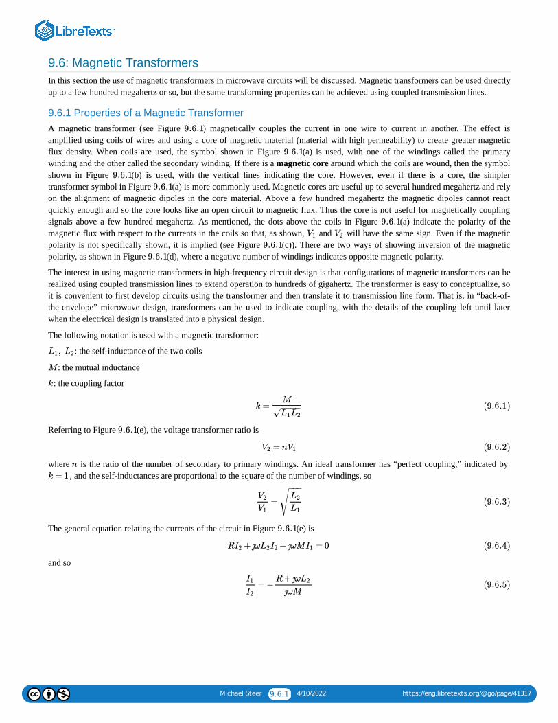
Michael Steer 9.6.1 4/10/2022 https://eng.libretexts.org/@go/page/41317
9.6: Magnetic TransformersIn this section the use of magnetic transformers in microwave circuits will be discussed. Magnetic transformers can be used directlyup to a few hundred megahertz or so, but the same transforming properties can be achieved using coupled transmission lines.
9.6.1 Properties of a Magnetic TransformerA magnetic transformer (see Figure ) magnetically couples the current in one wire to current in another. The effect isamplified using coils of wires and using a core of magnetic material (material with high permeability) to create greater magneticflux density. When coils are used, the symbol shown in Figure (a) is used, with one of the windings called the primarywinding and the other called the secondary winding. If there is a magnetic core around which the coils are wound, then the symbolshown in Figure (b) is used, with the vertical lines indicating the core. However, even if there is a core, the simplertransformer symbol in Figure (a) is more commonly used. Magnetic cores are useful up to several hundred megahertz and relyon the alignment of magnetic dipoles in the core material. Above a few hundred megahertz the magnetic dipoles cannot reactquickly enough and so the core looks like an open circuit to magnetic flux. Thus the core is not useful for magnetically couplingsignals above a few hundred megahertz. As mentioned, the dots above the coils in Figure (a) indicate the polarity of themagnetic flux with respect to the currents in the coils so that, as shown, and will have the same sign. Even if the magneticpolarity is not specifically shown, it is implied (see Figure (c)). There are two ways of showing inversion of the magneticpolarity, as shown in Figure (d), where a negative number of windings indicates opposite magnetic polarity.
The interest in using magnetic transformers in high-frequency circuit design is that configurations of magnetic transformers can berealized using coupled transmission lines to extend operation to hundreds of gigahertz. The transformer is easy to conceptualize, soit is convenient to first develop circuits using the transformer and then translate it to transmission line form. That is, in “back-of-the-envelope” microwave design, transformers can be used to indicate coupling, with the details of the coupling left until laterwhen the electrical design is translated into a physical design.
The following notation is used with a magnetic transformer:
: the self-inductance of the two coils
: the mutual inductance
: the coupling factor
Referring to Figure (e), the voltage transformer ratio is
where is the ratio of the number of secondary to primary windings. An ideal transformer has “perfect coupling,” indicated by , and the self-inductances are proportional to the square of the number of windings, so
The general equation relating the currents of the circuit in Figure (e) is
and so
9.6.1
9.6.1
9.6.19.6.1
9.6.1V1 V2
9.6.19.6.1
,L1 L2
M
k
k =M
L1L2− −−−
√(9.6.1)
9.6.1
= nV2 V1 (9.6.2)
n
k = 1
=V2
V1
L2
L1
−−−
√ (9.6.3)
9.6.1
R + ȷω + ȷωM = 0I2 L2I2 I1 (9.6.4)
= −I1
I2
R + ȷωL2
ȷωM(9.6.5)
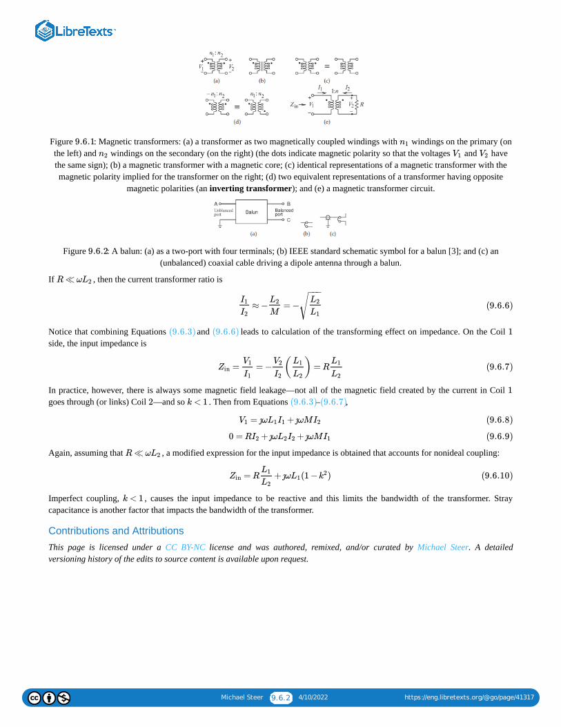
Michael Steer 9.6.2 4/10/2022 https://eng.libretexts.org/@go/page/41317
Figure : Magnetic transformers: (a) a transformer as two magnetically coupled windings with windings on the primary (onthe left) and windings on the secondary (on the right) (the dots indicate magnetic polarity so that the voltages and havethe same sign); (b) a magnetic transformer with a magnetic core; (c) identical representations of a magnetic transformer with themagnetic polarity implied for the transformer on the right; (d) two equivalent representations of a transformer having opposite
magnetic polarities (an inverting transformer); and (e) a magnetic transformer circuit.
Figure : A balun: (a) as a two-port with four terminals; (b) IEEE standard schematic symbol for a balun [3]; and (c) an(unbalanced) coaxial cable driving a dipole antenna through a balun.
If , then the current transformer ratio is
Notice that combining Equations and leads to calculation of the transforming effect on impedance. On the Coil side, the input impedance is
In practice, however, there is always some magnetic field leakage—not all of the magnetic field created by the current in Coil goes through (or links) Coil —and so . Then from Equations – ,
Again, assuming that , a modified expression for the input impedance is obtained that accounts for nonideal coupling:
Imperfect coupling, , causes the input impedance to be reactive and this limits the bandwidth of the transformer. Straycapacitance is another factor that impacts the bandwidth of the transformer.
Contributions and Attributions
This page is licensed under a CC BY-NC license and was authored, remixed, and/or curated by Michael Steer. A detailedversioning history of the edits to source content is available upon request.
9.6.1 n1
n2 V1 V2
9.6.2
R ≪ ωL2
≈ − = −I1
I2
L2
M
L2
L1
−−−
√ (9.6.6)
(9.6.3) (9.6.6) 1
= = − ( ) = RZinV1
I1
V2
I2
L1
L2
L1
L2(9.6.7)
12 k < 1 (9.6.3) (9.6.7)
= ȷω + ȷωMV1 L1I1 I2 (9.6.8)
0 = R + ȷω + ȷωMI2 L2I2 I1 (9.6.9)
R ≪ ωL2
= R + ȷω (1 − )ZinL1
L2L1 k
2 (9.6.10)
k < 1

Michael Steer 9.7.1 4/10/2022 https://eng.libretexts.org/@go/page/41318
9.7: References[1] A. Victor and M. Steer, “Reflection coefficient shaping of a 5-GHz voltage-tuned oscillator for improved tuning,” IEEE Trans.on Microwave Theory and Techniques, vol. 55, no. 12, pp. 2488–2494, Dec. 2007.
[2] http://www.coilcraft.com.
[3] IEEE Standard 315-1975, Graphic Symbols for Electrical and Electronics Diagrams (Including Reference Designation Letters),Adopted Sept. 1975, Reaffirmed Dec. 1993. Approved by American National Standards Institute, Jan. 1989. Approved adopted formandatory use, Department of Defense, United States of America, Oct. 1975. Approved by Canadian Standards Institute, Oct.1975.
[4] http://www.minicircuits.com.
[5] P. Katehi and N. Alexopoulos, “Frequencydependent characteristics of microstrip discontinuities in millimeter-wave integratedcircuits,” IEEE Trans. on Microwave Theory and Techniques, vol. 33, no. 10, pp. 1029–1035, Oct. 1985.
[6] T. Edwards and M. Steer, Foundations for Microstrip Circuit Design. John Wiley & Sons, 2016.
[7] R. Mongia, I. Bahl, and P. Bhartia, RF and Microwave Coupled-line Circuits. Artech House, 1999.
[8] W. Fathelbab and M. Steer, “Broadband network design,” in Multifunctional Adaptive Microwave Circuits and Systems, M.Steer and W. Palmer, Eds., 2008, ch. 8.
[9] I. Robertson and S. Lucyszyn, RFIC and MMIC Design and Technology. IEE, 2001, iEE Circuits, Devices and Systems Series.
[10] C. Goldsmith, A. Kikel, and N. Wilkens, “Synthesis of marchand baluns using multilayer microstrip structures,” Int. J. ofMicrowave & Millimeter-Wave Computer-Aided Eng, pp. 179–188, 1992.
[11] N. Marchand, “Transmission line conversion transformers,” Electronics, pp. 142–145, 1944.
[12] W. Fathelbab and M. Steer, “New classes of miniaturized planar marchand baluns,” IEEE Trans. on Microwave Theory andTechniques, vol. 53, no. 4, pp. 1211–1220, Apr. 2005.
[13] J. J. Cloete, “Graphs of circuit elements for the marchand balun,” Microwave Journal, vol. 24, no. 5, pp. 125–128, May 1981.
[14] E. Wilkinson, “An n-way hybrid power divider,” IRE Trans. on Microwave Theory and Techniques, vol. 8, no. 1, pp. 116–118,Jan. 1960.
[15] M. Steer, Microwave and RF Design, Transmission Lines, 3rd ed. North Carolina State University, 2019.
Contributions and AttributionsThis page is licensed under a CC BY-NC license and was authored, remixed, and/or curated by Michael Steer. A detailedversioning history of the edits to source content is available upon request.

Michael Steer 9.8.1 4/10/2022 https://eng.libretexts.org/@go/page/41319
9.8: Exercises1. A spiral inductor is modeled as an ideal inductor of in series with a resistor. What is the of the spiral inductor at
?2. Consider the design of a resistive T attenuator in a system. [Parallels Example 9.4.1]
a. Draw the topology of the attenuator.b. Write down the design equations.c. Complete the design of the attenuator.
3. Consider the design of a resistive Pi attenuator in a system. [Parallels Example 9.4.1]a. Draw the topology of the attenuator.b. Write down the design equations.c. Complete the design of the attenuator.
4. A attenuator in a system is ideally matched at both the input and output. Thus there are no reflections and thepower delivered to the load is reduced by from the applied power. If a signal is applied to the attenuator, how muchpower is dissipated in the attenuator?
5. A resistive Pi attenuator has shunt resistors of and a series resistor . What is the attenuation (indecibels) and the characteristic impedance of the attenuator?
6. Design a resistive Pi attenuator with an attenuation of in a system.7. Design a resistive Pi attenuator in a system.8. A resistive Pi attenuator has shunt resistors and a series resistor . What is the attenuation (in
decibels) and the system impedance of the attenuator?9. A balun can be realized using a wire-wound transformer, and by changing the number of windings on the transformer it is
possible to achieve impedance transformation as well as balanced-to-unbalanced functionality. A balun based on amagnetic transformer is required to achieve impedance transformation from an unbalanced impedance of to a balancedimpedance of . If there are windings on the balanced port of the balun transformer, how many windings are there onthe unbalanced port of the balun?
9.11.1 Exercises by Section
challenging
9.11.2 Answers to Selected Exercises1. 2. 3. 4.
Contributions and AttributionsThis page is licensed under a CC BY-NC license and was authored, remixed, and/or curated by Michael Steer. A detailedversioning history of the edits to source content is available upon request.
10 nH 5 Ω Q
1 GHz
50 dB 75 Ω
50 dB 75 Ω
20 dB 17 Ω
20 dB 5 W
= = 294 ΩR1 R2 = 17.4 ΩR3
10 dB 100 Ω
3 dB 50 Ω
= = 86.4 ΩR1 R2 = 350 ΩR3
500 MHz
50 Ω
200 Ω 20
†
§9.21, 2, 3, 4
§9.45†, 6, 7, 8†
§9.79†
12.57
= = 74.5 ΩR1 R2
75.48 Ω
4.95 W
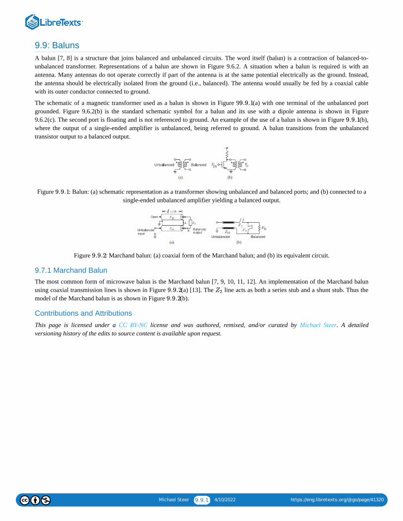
Michael Steer 9.9.1 4/10/2022 https://eng.libretexts.org/@go/page/41320
9.9: BalunsA balun [7, 8] is a structure that joins balanced and unbalanced circuits. The word itself (balun) is a contraction of balanced-to-unbalanced transformer. Representations of a balun are shown in Figure 9.6.2. A situation when a balun is required is with anantenna. Many antennas do not operate correctly if part of the antenna is at the same potential electrically as the ground. Instead,the antenna should be electrically isolated from the ground (i.e., balanced). The antenna would usually be fed by a coaxial cablewith its outer conductor connected to ground.
The schematic of a magnetic transformer used as a balun is shown in Figure 9 (a) with one terminal of the unbalanced portgrounded. Figure 9.6.2(b) is the standard schematic symbol for a balun and its use with a dipole antenna is shown in Figure9.6.2(c). The second port is floating and is not referenced to ground. An example of the use of a balun is shown in Figure (b),where the output of a single-ended amplifier is unbalanced, being referred to ground. A balun transitions from the unbalancedtransistor output to a balanced output.
Figure : Balun: (a) schematic representation as a transformer showing unbalanced and balanced ports; and (b) connected to asingle-ended unbalanced amplifier yielding a balanced output.
Figure : Marchand balun: (a) coaxial form of the Marchand balun; and (b) its equivalent circuit.
9.7.1 Marchand BalunThe most common form of microwave balun is the Marchand balun [7, 9, 10, 11, 12]. An implementation of the Marchand balunusing coaxial transmission lines is shown in Figure (a) [13]. The line acts as both a series stub and a shunt stub. Thus themodel of the Marchand balun is as shown in Figure (b).
Contributions and Attributions
This page is licensed under a CC BY-NC license and was authored, remixed, and/or curated by Michael Steer. A detailedversioning history of the edits to source content is available upon request.
9.9.1
9.9.1
9.9.1
9.9.2
9.9.2 Z2
9.9.2
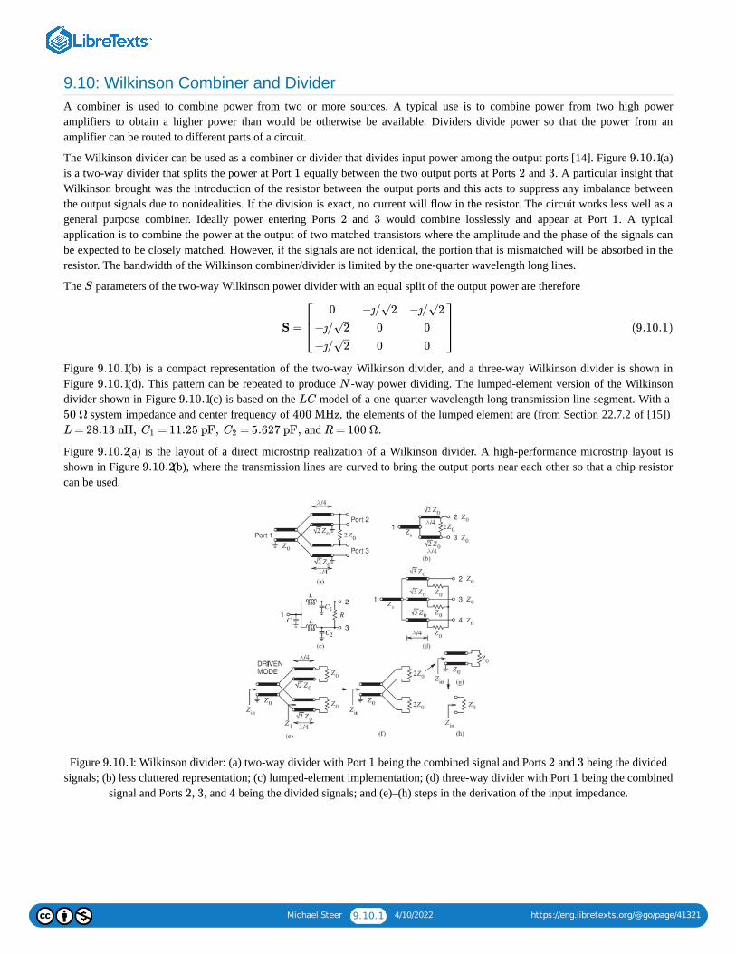
Michael Steer 9.10.1 4/10/2022 https://eng.libretexts.org/@go/page/41321
9.10: Wilkinson Combiner and DividerA combiner is used to combine power from two or more sources. A typical use is to combine power from two high poweramplifiers to obtain a higher power than would be otherwise be available. Dividers divide power so that the power from anamplifier can be routed to different parts of a circuit.
The Wilkinson divider can be used as a combiner or divider that divides input power among the output ports [14]. Figure (a)is a two-way divider that splits the power at Port equally between the two output ports at Ports and . A particular insight thatWilkinson brought was the introduction of the resistor between the output ports and this acts to suppress any imbalance betweenthe output signals due to nonidealities. If the division is exact, no current will flow in the resistor. The circuit works less well as ageneral purpose combiner. Ideally power entering Ports and would combine losslessly and appear at Port . A typicalapplication is to combine the power at the output of two matched transistors where the amplitude and the phase of the signals canbe expected to be closely matched. However, if the signals are not identical, the portion that is mismatched will be absorbed in theresistor. The bandwidth of the Wilkinson combiner/divider is limited by the one-quarter wavelength long lines.
The parameters of the two-way Wilkinson power divider with an equal split of the output power are therefore
Figure (b) is a compact representation of the two-way Wilkinson divider, and a three-way Wilkinson divider is shown inFigure (d). This pattern can be repeated to produce -way power dividing. The lumped-element version of the Wilkinsondivider shown in Figure (c) is based on the model of a one-quarter wavelength long transmission line segment. With a
system impedance and center frequency of , the elements of the lumped element are (from Section 22.7.2 of [15]) and .
Figure (a) is the layout of a direct microstrip realization of a Wilkinson divider. A high-performance microstrip layout isshown in Figure (b), where the transmission lines are curved to bring the output ports near each other so that a chip resistorcan be used.
Figure : Wilkinson divider: (a) two-way divider with Port being the combined signal and Ports and being the dividedsignals; (b) less cluttered representation; (c) lumped-element implementation; (d) three-way divider with Port being the combined
signal and Ports , , and being the divided signals; and (e)–(h) steps in the derivation of the input impedance.
9.10.11 2 3
2 3 1
S
S =⎡
⎣⎢
0
−ȷ/ 2–
√
−ȷ/ 2–
√
−ȷ/ 2–
√
0
0
−ȷ/ 2–
√
0
0
⎤
⎦⎥ (9.10.1)
9.10.19.10.1 N
9.10.1 LC
50 Ω 400 MHzL = 28.13 nH, = 11.25 pF, = 5.627 pF,C1 C2 R = 100 Ω
9.10.29.10.2
9.10.1 1 2 31
2 3 4
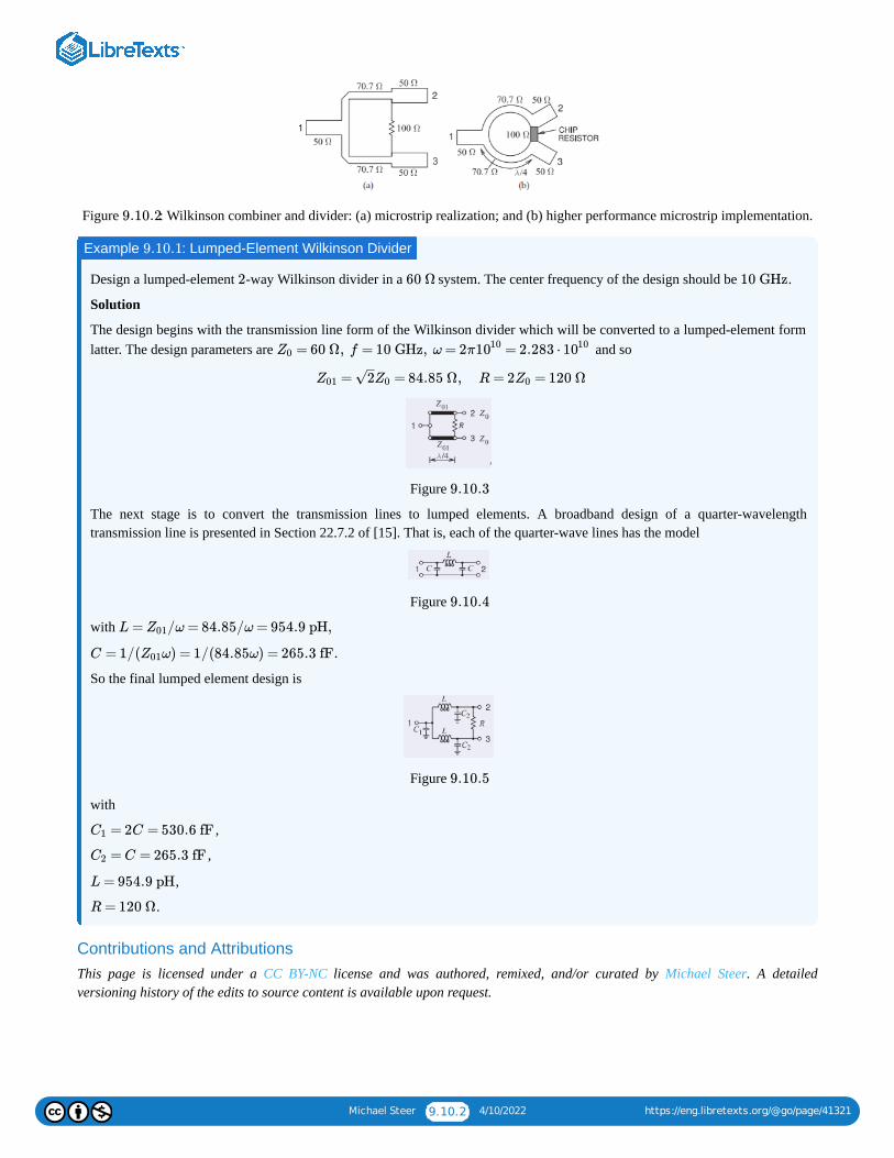
Michael Steer 9.10.2 4/10/2022 https://eng.libretexts.org/@go/page/41321
Figure : Wilkinson combiner and divider: (a) microstrip realization; and (b) higher performance microstrip implementation.
Design a lumped-element -way Wilkinson divider in a system. The center frequency of the design should be .
Solution
The design begins with the transmission line form of the Wilkinson divider which will be converted to a lumped-element formlatter. The design parameters are and so
Figure
The next stage is to convert the transmission lines to lumped elements. A broadband design of a quarter-wavelengthtransmission line is presented in Section 22.7.2 of [15]. That is, each of the quarter-wave lines has the model
Figure
with
So the final lumped element design is
Figure
with
,
,
,
.
Contributions and AttributionsThis page is licensed under a CC BY-NC license and was authored, remixed, and/or curated by Michael Steer. A detailedversioning history of the edits to source content is available upon request.
9.10.2
Example : Lumped-Element Wilkinson Divider9.10.1
2 60 Ω 10 GHz
= 60 Ω, f = 10 GHz, ω = 2π = 2.283 ⋅Z0 1010 1010
= = 84.85 Ω, R = 2 = 120 ΩZ01 2–
√ Z0 Z0
9.10.3
9.10.4
L = /ω = 84.85/ω = 954.9 pH,Z01
C = 1/( ω) = 1/(84.85ω) = 265.3 fF.Z01
9.10.5
= 2C = 530.6 fFC1
= C = 265.3 fFC2
L = 954.9 pH
R = 120 Ω

Michael Steer 9.11.1 4/10/2022 https://eng.libretexts.org/@go/page/41322
9.11: SummaryThis chapter introduced the richness of microwave components available to the RF designer. Microwave lumped-element and components are carefully constructed so that they function as intended up to or so. They are usually in surface-mountform so that they can be integrated in design while minimizing the parasitic effects introduced by leads. To a limited extent,transmission line discontinuities can be used as lumped elements. Even if the transmission line discontinuities are not specificallyintroduced for this purpose, their lumped-element equivalent circuits must be included in circuit analysis. Transmission line stubsare widely used to introduce capacitance and inductance in circuits. In most transmission line technologies only shunt stubs areavailable, and thus there is a strong preference for shunt elements in circuit designs.
Contributions and AttributionsThis page is licensed under a CC BY-NC license and was authored, remixed, and/or curated by Michael Steer. A detailedversioning history of the edits to source content is available upon request.
R, L,
C 10

1 4/10/2022
CHAPTER OVERVIEW10: IMPEDANCE MATCHING
10.1: INTRODUCTION10.2: MATCHING NETWORKS10.3: IMPEDANCE TRANSFORMING NETWORKS10.4: THE L MATCHING NETWORK10.5: DEALING WITH COMPLEX LOADS10.6: DEALING WITH COMPLEX LOADS10.7: SUMMARY10.8: REFERENCES10.9: EXERCISES10.10: IMPEDANCE MATCHING USING SMITH CHARTS10.11: DISTRIBUTED MATCHING10.12: MATCHING USING THE SMITH CHART

Michael Steer 10.1.1 4/10/2022 https://eng.libretexts.org/@go/page/41323
10.1: IntroductionThe maximum transfer of signal power is one of the prime objectives in RF and microwave circuit design. Power traverses anetwork from a source to a load generally through a sequence of two-port networks. Maximum power transfer requires that theThevenin equivalent impedance of a source be matched to the impedance seen from the source. That is, the source should bepresented with the complex conjugate of the source impedance. This is achieved by designing what is called a matching networkinserted between the source and load. Design of the matching network is called impedance matching.
Section 10.2 describes two common matching objectives. Then design approaches for impedance matching are presented first withan algorithmic approach in Sections 10.3–10.6 and then a graphical approach based on using a Smith chart in Sections 10.7 and10.9.
Contributions and AttributionsThis page is licensed under a CC BY-NC license and was authored, remixed, and/or curated by Michael Steer. A detailedversioning history of the edits to source content is available upon request.
Michael Steer 10.2.1 4/10/2022 https://eng.libretexts.org/@go/page/41324
10.2: Matching NetworksMatching networks are constructed using lossless elements such as lumped capacitors, lumped inductors and transmission lines andso have, ideally, no loss and introduce no additional noise. This section discusses matching objectives and the types of matchingnetworks.
Figure : A source with Thevenin equivalent impedance and load with impedance interfaced by a matching networkpresenting an impedance to the source.
10.2.1 Matching for Zero Reflection or for Maximum Power Transfer
With RF circuits the aim of matching is to achieve maximum power transfer. With reference to Figure the condition formaximum power transfer is which is equivalent to Γin = Γ∗ S. The proof is as follows:
and for maximum power transfer , so
If is real, and then the condition for maximum power transfer is
Thus, provided that is real, the condition for maximum power transfer in terms of reflection coefficients is or .
10.2.2 Types of Matching NetworksUp to a few gigahertz, lumped inductors and capacitors can be used in matching networks. Above a few gigahertz parasitics resultin selfresonance. Lumped elements are also lossy. Segments of transmission lines are also used in matching networks as the loss ofa transmission line component is always much less than the loss of a lumped inductor. However the length of a transmission linesegement is up to which is far too large to fit in consumer wireless products operating below a few gigahertz. An impedancematching network may consist of
a. Lumped elements only. These are the smallest networks, but have the most stringent limit on the maximum frequency ofoperation. The relatively high resistive loss of an inductor is the main limiting factor limiting performance. The self resonantfrequency of an inductor limits operation to low microwave frequencies.
b. Distributed elements (microstrip or other transmission line circuits) only. These have excellent performance, but their sizerestricts their use in systems to above a few gigahertz.
c. A hybrid design combining lumped and distributed elements, primarily small sections of lines with capacitors. These lines areshorter than in a design with distributed elements only, but the hybrid design has higher performance than a lumped-element-only design.
10.2.1 ZS ZL
Zin
10.2.1
=Zin Z∗S
=( )Γin−Zin ZREF
+Zin ZREF(10.2.1)
=Zin Z∗S
Γ∗in = = =
−Zin ZREF
+Zin ZREF( )
−Z∗S
ZREF
+Z∗S
ZREF
∗ ( −Z∗S
Z0)∗
( +Z∗S
Z0)∗
= = =( −Z∗
S)∗
Z∗REF
( +Z∗S
)∗ Z∗REF
−ZS Z∗REF
+ZS Z∗REF
ΓS (10.2.2)
ZREF =Z∗REF ZREF
= =Γ∗in
−ZS ZREF
+ZS ZREFΓS (10.2.3)
ZREF =Γ∗in ΓS
=Γin Γ∗S
λ/4

Michael Steer 10.2.2 4/10/2022 https://eng.libretexts.org/@go/page/41324
Figure : A transformer as a matching network. Port is on the left or primary side and Port is on the right or secondaryside.
Figure : Matching using a series reactance: (a) the series reactive element; and (b) its equivalent shunt circuit.
Contributions and AttributionsThis page is licensed under a CC BY-NC license and was authored, remixed, and/or curated by Michael Steer. A detailedversioning history of the edits to source content is available upon request.
10.2.2 1 2
10.2.2
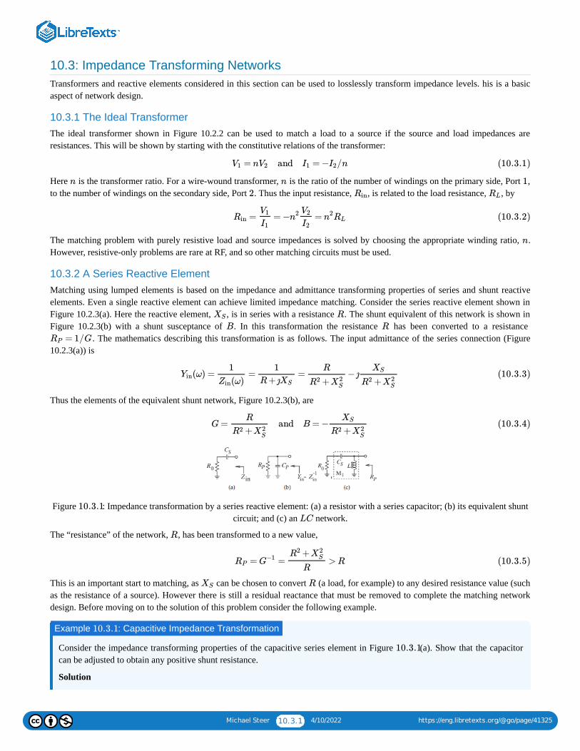
Michael Steer 10.3.1 4/10/2022 https://eng.libretexts.org/@go/page/41325
10.3: Impedance Transforming NetworksTransformers and reactive elements considered in this section can be used to losslessly transform impedance levels. his is a basicaspect of network design.
10.3.1 The Ideal TransformerThe ideal transformer shown in Figure 10.2.2 can be used to match a load to a source if the source and load impedances areresistances. This will be shown by starting with the constitutive relations of the transformer:
Here is the transformer ratio. For a wire-wound transformer, is the ratio of the number of windings on the primary side, Port ,to the number of windings on the secondary side, Port . Thus the input resistance, , is related to the load resistance, , by
The matching problem with purely resistive load and source impedances is solved by choosing the appropriate winding ratio, .However, resistive-only problems are rare at RF, and so other matching circuits must be used.
10.3.2 A Series Reactive ElementMatching using lumped elements is based on the impedance and admittance transforming properties of series and shunt reactiveelements. Even a single reactive element can achieve limited impedance matching. Consider the series reactive element shown inFigure 10.2.3(a). Here the reactive element, , is in series with a resistance . The shunt equivalent of this network is shown inFigure 10.2.3(b) with a shunt susceptance of . In this transformation the resistance has been converted to a resistance
. The mathematics describing this transformation is as follows. The input admittance of the series connection (Figure10.2.3(a)) is
Thus the elements of the equivalent shunt network, Figure 10.2.3(b), are
Figure : Impedance transformation by a series reactive element: (a) a resistor with a series capacitor; (b) its equivalent shuntcircuit; and (c) an network.
The “resistance” of the network, , has been transformed to a new value,
This is an important start to matching, as can be chosen to convert (a load, for example) to any desired resistance value (suchas the resistance of a source). However there is still a residual reactance that must be removed to complete the matching networkdesign. Before moving on to the solution of this problem consider the following example.
Consider the impedance transforming properties of the capacitive series element in Figure (a). Show that the capacitorcan be adjusted to obtain any positive shunt resistance.
Solution
= n and = − /nV1 V2 I1 I2 (10.3.1)
n n 1
2 Rin RL
= = − =RinV1
I1n
2 V2
I2n
2RL (10.3.2)
n
XS R
B R
= 1/GRP
(ω) = = = − ȷYin1
(ω)Zin
1
R+ ȷXS
R
+R2 X2S
XS
+R2 X2S
(10.3.3)
G= and B = −R
+R2 X2S
XS
+R2 X2S
(10.3.4)
10.3.1
LC
R
= = > RRP G−1
+R2
X2S
R(10.3.5)
XS R
Example : Capacitive Impedance Transformation10.3.1
10.3.1
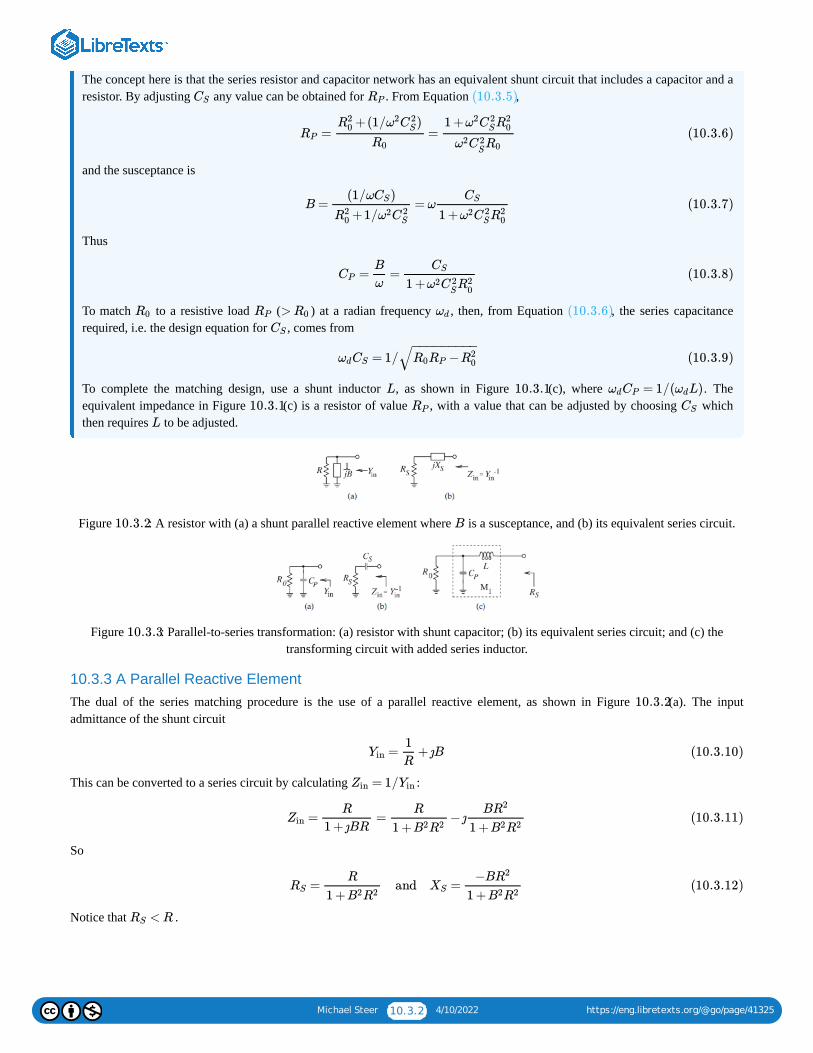
Michael Steer 10.3.2 4/10/2022 https://eng.libretexts.org/@go/page/41325
The concept here is that the series resistor and capacitor network has an equivalent shunt circuit that includes a capacitor and aresistor. By adjusting any value can be obtained for . From Equation ,
and the susceptance is
Thus
To match to a resistive load ( ) at a radian frequency , then, from Equation , the series capacitancerequired, i.e. the design equation for , comes from
To complete the matching design, use a shunt inductor , as shown in Figure (c), where . Theequivalent impedance in Figure (c) is a resistor of value , with a value that can be adjusted by choosing whichthen requires to be adjusted.
Figure : A resistor with (a) a shunt parallel reactive element where is a susceptance, and (b) its equivalent series circuit.
Figure : Parallel-to-series transformation: (a) resistor with shunt capacitor; (b) its equivalent series circuit; and (c) thetransforming circuit with added series inductor.
10.3.3 A Parallel Reactive ElementThe dual of the series matching procedure is the use of a parallel reactive element, as shown in Figure (a). The inputadmittance of the shunt circuit
This can be converted to a series circuit by calculating :
So
Notice that .
CS RP (10.3.5)
= =RP
+(1/ )R20 ω
2C
2S
R0
1 +ω2C
2SR
20
ω2C 2SR0
(10.3.6)
B = = ω(1/ω )CS
+1/R20 ω2C
2S
CS
1 +ω2C2SR
20
(10.3.7)
= =CP
B
ω
CS
1 +ω2C 2SR2
0
(10.3.8)
R0 RP > R0 ωd (10.3.6)
CS
= 1/ωdCS −R0RP R20
− −−−−−−−−√ (10.3.9)
L 10.3.1 = 1/( L)ωdCP ωd
10.3.1 RP CS
L
10.3.2 B
10.3.3
10.3.2
= + ȷBYin1
R(10.3.10)
= 1/Zin Yin
= = − ȷZinR
1 + ȷBR
R
1 +B2R2
BR2
1 +B2R2(10.3.11)
= and =RS
R
1 +B2R2XS
−BR2
1 +B2R2(10.3.12)
< RRS
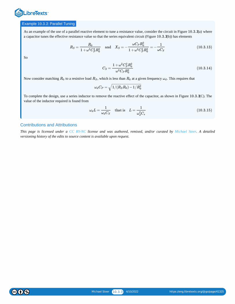
Michael Steer 10.3.3 4/10/2022 https://eng.libretexts.org/@go/page/41325
As an example of the use of a parallel reactive element to tune a resistance value, consider the circuit in Figure (a) wherea capacitor tunes the effective resistance value so that the series equivalent circuit (Figure (b)) has elements
So
Now consider matching to a resistive load , which is less than at a given frequency . This requires that
To complete the design, use a series inductor to remove the reactive effect of the capacitor, as shown in Figure (C). Thevalue of the inductor required is found from
Contributions and AttributionsThis page is licensed under a CC BY-NC license and was authored, remixed, and/or curated by Michael Steer. A detailedversioning history of the edits to source content is available upon request.
Example : Parallel Tuning10.3.2
10.3.3
10.3.3
= and = − = −RS
R0
1 +ω2C 2PR2
0
XS
ωCPR20
1 +ω2C 2PR2
0
1
ωCS
(10.3.13)
=CS
1 +ω2C
2PR
20
ω2CPR20
(10.3.14)
R0 RS R0 ωd
=ωdCP 1/( ) −1/RSR0 R20
− −−−−−−−−−−−−−√
10.3.3
L = that is L =ωd
1
ωdCS
1
ω2dCs
(10.3.15)
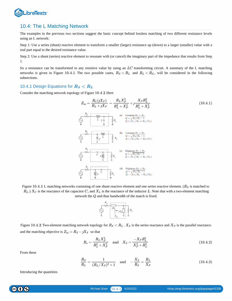
Michael Steer 10.4.1 4/10/2022 https://eng.libretexts.org/@go/page/41326
10.4: The L Matching NetworkThe examples in the previous two sections suggest the basic concept behind lossless matching of two different resistance levelsusing an L network:
Step 1: Use a series (shunt) reactive element to transform a smaller (larger) resistance up (down) to a larger (smaller) value with areal part equal to the desired resistance value.
Step 2: Use a shunt (series) reactive element to resonate with (or cancel) the imaginary part of the impedance that results from Step1.
So a resistance can be transformed to any resistive value by using an transforming circuit. A summary of the L matchingnetworks is given in Figure . The two possible cases, and , will be considered in the followingsubsections.
10.4.1 Design Equations for Consider the matching network topology of Figure . Here
Figure : L matching networks consisting of one shunt reactive element and one series reactive element. ( is matched to .) is the reactance of the capacitor , and is the reactance of the inductor . Note that with a two-element matching
network the and thus bandwidth of the match is fixed.
Figure : Two-element matching network topology for . is the series reactance and is the parallel reactance.
and the matching objective is so that
From these
Introducing the quantities
LC
10.4.1 <RS RL <RL RS
<RS RL
10.4.2
= = + ȷZin(ȷ )RL XP
+ ȷRL XP
RLX2P
+R2L X2
P
XP R2L
+R2L X2
P
(10.4.1)
10.4.1 RS
RL XC C XL L
Q
10.4.2 <RS RL XS XP
= − ȷZin RS XS
= and =Rs
RLX2P
+R2L X2
P
XS
−XP R2L
+X2P R2
L
(10.4.2)
= and − =RS
RL
1
( / +1RL XP )2
XS
RS
RL
XP
(10.4.3)
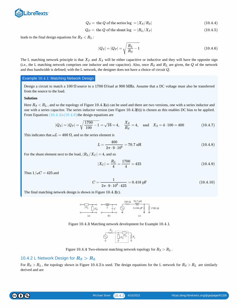
Michael Steer 10.4.2 4/10/2022 https://eng.libretexts.org/@go/page/41326
leads to the final design equations for :
The L matching network principle is that and will be either capacitive or inductive and they will have the opposite sign(i.e., the L matching network comprises one inductor and one capacitor). Also, once and are given, the of the networkand thus bandwidth is defined; with the L network, the designer does not have a choice of circuit .
Design a circuit to match a source to a load at . Assume that a DC voltage must also be transferredfrom the source to the load.
Solution
Here , and so the topology of Figure (a) can be used and there are two versions, one with a series inductor andone with a series capacitor. The series inductor version (see Figure (b)) is chosen as this enables DC bias to be applied.From Equations – the design equations are
This indicates that , and so the series element is
For the shunt element next to the load, , and so
Thus and
The final matching network design is shown in Figure (c).
Figure : Matching network development for Example .
Figure : Two-element matching network topology for .
10.4.2 L Network Design for For , the topology shown in Figure is used. The design equations for the L network for are similarlyderived and are
= the Q of the series leg = | / |QS XS RS (10.4.4)
= the Q of the shunt leg = | / |QP RL XP (10.4.5)
<RS RL
| | = | | =QS QP −1RL
RS
− −−−−−
√ (10.4.6)
XP XS
RS RL Q
Q
Example : Matching Network Design10.4.1
100 Ω 1700 Ω 900 MHz
<RS RL 10.4.310.4.3
(10.4.4) (10.4.6)
| | = | | = = = 4, = 4, and = 4 ⋅ 100 = 400QS QP −11700
100
− −−−−−−−√ 16
−−√
XS
RS
XS (10.4.7)
ωL = 400 Ω
L = = 70.7 nH400
2π ⋅ 9 ⋅ 108(10.4.8)
| / | = 4RL XC
| | = = = 425XC
RL
4
1700
4(10.4.9)
1/ωC = 425
C = = 0.416 pF1
2π ⋅ 9 ⋅ ⋅ 425108(10.4.10)
10.4.3
10.4.3 10.4.1
10.4.4 >RS RL
>RS RL
>RS RL 10.4.2 >RS RL
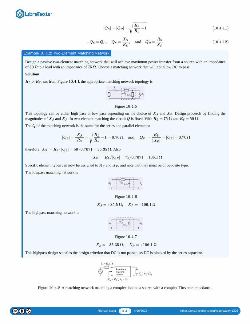
Michael Steer 10.4.3 4/10/2022 https://eng.libretexts.org/@go/page/41326
Design a passive two-element matching network that will achieve maximum power transfer from a source with an impedanceof to a load with an impedance of . Choose a matching network that will not allow DC to pass.
Solution
, so, from Figure , the appropriate matching network topology is
Figure
This topology can be either high pass or low pass depending on the choice of and . Design proceeds by finding themagnitudes of and . In two-element matching the circuit is fixed. With and .
The of the matching network is the same for the series and parallel elements:
therefore . Also
Specific element types can now be assigned to and , and note that they must be of opposite type.
The lowpass matching network is
Figure
The highpass matching network is
Figure
This highpass design satisfies the design criterion that DC is not passed, as DC is blocked by the series capacitor.
Figure : A matching network matching a complex load to a source with a complex Thevenin impedance.
| | = | | =QS QP −1RS
RL
− −−−−−
√ (10.4.11)
− = , = , and =QS QP QS
XS
RL
QP
RS
XP
(10.4.12)
Example : Two-Element Matching Network10.4.2
50 Ω 75 Ω
>RL RS 10.4.1
10.4.5
XS XP
XS XP Q = 75 ΩRL = 50 ΩRS
Q
| | = = = 0.7071 and | | = = | | = 0.7071QS
| |XS
RS
−1RL
RS
− −−−−−
√ QP
RL
| |XP
QS
| | = ⋅ | | = 50 ⋅ 0.7071 = 35.35 ΩXS RS QS
| | = /| | = 75/0.7071 = 106.1 ΩXP RL QP
XS XP
10.4.6
= +35.5 Ω, = −106.1 ΩXS XP
10.4.7
= −35.35 Ω, = +106.1 ΩXS XP
10.4.8

Michael Steer 10.4.4 4/10/2022 https://eng.libretexts.org/@go/page/41326
Contributions and AttributionsThis page is licensed under a CC BY-NC license and was authored, remixed, and/or curated by Michael Steer. A detailedversioning history of the edits to source content is available upon request.
Michael Steer 10.5.1 4/10/2022 https://eng.libretexts.org/@go/page/41327
10.5: Dealing with Complex LoadsThis section presents strategies for dealing with complex loads. In the algorithmic matching approach design proceeds first byignoring the complex load and source and then accounting for them either through topology choice or canceling their effect throughresonance.
10.5.1 MatchingInput and output impedances of transistors, mixers, antennas, etc., contain both resistive and reactive components. Thus a realisticimpedance matching problem looks like that shown in Figure 10.4.8. The matching approaches that were presented in the previoussections can be directly applied if and are treated as stray reactances that need to be either canceled or, ideally, used as partof the matching network. There are two basic approaches to handling complex impedances:
a. Absorption: Absorb source and load reactances into the impedance matching network itself. This is done through carefulplacement of each matching element such that capacitors are placed in parallel with source and load capacitances, and inductorsin series with source and load inductances. The stray values are then subtracted from the and values for the matchingnetwork calculated on the basis of the resistive parts of and only. The new (smaller) values, and , constitute theelements of the matching network. Sometimes it is necessary to perform a series-to-parallel, or parallel-to-series, conversion ofthe source or load impedances so that the reactive elements are in the correct series or shunt arrangement for absorption.
b. Resonance: Resonate source and load reactances with an equal and opposite reactance at the frequency of interest.
The presence of reactance in a load indicates energy storage, and therefore bandwidth limiting. In the above approaches to handlinga reactive load, the resonance approach could easily result in a narrowband matching solution. The major problem in matching isoften to obtain sufficient bandwidth. What is sufficient will vary depending on the application. To maximize bandwidth the generalgoal is to minimize the total energy storage. Roughly the total energy stored will be proportional to the sum of the magnitudes ofthe reactances in the circuit. Of course, the actual energy storage depends on the voltage and current levels, which will themselvesvary in the circuit. A good approach leading to large bandwidths is to incorporate the load reactance into the matching network.Thus the choice of appropriate matching network topology is critical. However, if the source and load reactance value is larger thanthe calculated matching network element value, then absorption on its own cannot be used. In this situation resonance must becombined with absorption. The majority of impedance matching designs are based on a combination of resonance and absorption.
For the configuration shown in Figure , design an impedance matching network that will block the flow of DC currentfrom the source to the load. The frequency of operation is . Design the matching network, neglecting the presence of the
capacitance at the load. Since , and from Figure 10.4.1, consider the topologies of Figures (a) and (b). The design criterion of blocking flow of DC from the source to the load narrows the choice to the
topology of Figure (b).
Solution
Step 1:
So . Reducing this gives
Similarly and so
Step 2:
Resonate the capacitor using an inductor in parallel:
XS XL
L C
ZS ZL L' C'
Example : Matching Network Design Using Resonance10.5.1
10.5.11 GHz
10 pF = 50 Ω < = 500 ΩRS RL
10.5.2 10.5.210.5.2
| | = = | | = = = 3 and =QS∣∣∣XS
RS
∣∣∣ QP
∣∣∣
RL
XP
∣∣∣ −1
RL
RS
− −−−−−
√ QP
RL
XP
(10.5.1)
= ωL = / = 500/3XP RL QP
ωL = , and so L = = 26.5 nH500
3
500
3 ×2π ×109(10.5.2)
− / = 3XS RS
= 3 or C = = = 1.06 pF1/(ωC)
RS
1
3ωRS
1
3 ×2π × ×50109(10.5.3)
10 pF
Michael Steer 10.5.2 4/10/2022 https://eng.libretexts.org/@go/page/41327
Thus Figure (c) is the required matching network. Two inductors are in parallel and the circuit can be simplified to thatshown in Figure , where
Figure : Matching problem considered in Example .
Figure : Matching network topology used in Example : a) and (b) topology; and (c) intermediate matching network.
Figure : Final matching network in Example .
Figure : Matching problem in Example .
Figure : Topologies referred to in Example .
For the source and load configurations shown in Figure , design a lowpass impedance matching network at .
Solution
Since , use the topology shown in Figure (a). For a lowpass response, the topology is that of Figure (b).Notice that absorption is the natural way of handling the at the source and the at the load. The design process is asfollows:
Step 1:
Design the matching network, neglecting the reactive elements at the source and load:
(ω = ω ×10 ×L′)−1 10−12 (10.5.4)
= = = 2.533 nHL′ 1
ω210−11
1
(2π ×)21018 10−11(10.5.5)
10.5.310.5.4
= (26.5 nH ∥ 2.533 nH) = nH = 2.312 nHLX
2.533 ×26.5
2.533 +26.5(10.5.6)
10.5.1 10.5.1
10.5.2 10.5.1
10.5.3 10.5.1
10.5.4 10.5.2
10.5.5 10.5.2
Example : Matching Network Design Using Resonance and Absorption10.5.2
10.5.4 f = 1 GHz
<RS RL 10.5.5 10.5.53 nH 5 pF
| | = | | = = = 3QS QP −1RL
RS
− −−−−−
√ 10 −1− −−−−√ (10.5.7)
= 3, = 3 ×100, ωL = 300 and L = = 47.75 nHXS
RS
XS
300
2π ×109(10.5.8)
Michael Steer 10.5.3 4/10/2022 https://eng.libretexts.org/@go/page/41327
This design is shown in Figure (a). This is the matching network that matches the source resistance to the load with the source and load reactances ignored.
Step 2:
Figure (b) is the interim matching solution. The source inductance is absorbed into the matching network, reducing therequired series inductance of the matching network. The capacitance of the load cannot be fully absorbed. The design for theresistance-only case requires a shunt capacitance of , but is available from the load. Thus there is an excesscapacitance of that must be resonated out by the inductance :
The final matching network design (Figure (c)) fully absorbs the source inductance into the matching network, but onlypartly absorbs the load capacitance.
Figure : Evolution of the matching network in Example : (a) matching network design considering only the source andload resistors; (b) matching network with the reactive parts of the source and load impedances included; and (c) final design.
Figure : Matching in stages: (a) matching network M matching to ; (b) without an explicit source; (c) two-stagematching with a virtual resistor ; (d) matching to ; and (e) matching to .
Contributions and AttributionsThis page is licensed under a CC BY-NC license and was authored, remixed, and/or curated by Michael Steer. A detailedversioning history of the edits to source content is available upon request.
= −3 and = −3 and C = = 0.477 pFRP
XP
1000
−(1/ωC)
3
1000 ×2π ×109(10.5.9)
10.5.6 100 Ω 1000 Ω
10.5.6
0.477 pF 5 pF4.523 pF L''
= ω4.523 × . So = = 5.600 nH1
ωL′′10−12 L′′ 1
(2π × ×4.523 ×)2 1018 10−12(10.5.10)
10.5.6
10.5.6 10.5.2
10.5.7 RS RL
RV RS RV RV RL
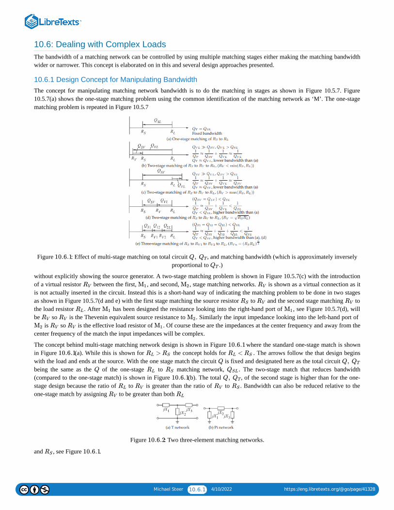
Michael Steer 10.6.1 4/10/2022 https://eng.libretexts.org/@go/page/41328
10.6: Dealing with Complex LoadsThe bandwidth of a matching network can be controlled by using multiple matching stages either making the matching bandwidthwider or narrower. This concept is elaborated on in this and several design approaches presented.
10.6.1 Design Concept for Manipulating BandwidthThe concept for manipulating matching network bandwidth is to do the matching in stages as shown in Figure 10.5.7. Figure10.5.7(a) shows the one-stage matching problem using the common identification of the matching network as ‘M’. The one-stagematching problem is repeated in Figure 10.5.7
Figure : Effect of multi-stage matching on total circuit , and matching bandwidth (which is approximately inverselyproportional to .)
without explicitly showing the source generator. A two-stage matching problem is shown in Figure 10.5.7(c) with the introductionof a virtual resistor between the first, , and second, , stage matching networks. is shown as a virtual connection as itis not actually inserted in the circuit. Instead this is a short-hand way of indicating the matching problem to be done in two stagesas shown in Figure 10.5.7(d and e) with the first stage matching the source resistor to and the second stage matching tothe load resistor . After has been designed the resistance looking into the right-hand port of , see Figure 10.5.7(d), willbe so is the Thevenin equivalent source resistance to . Similarly the input impedance looking into the left-hand port of
is so is the effective load resistor of . Of course these are the impedances at the center frequency and away from thecenter frequency of the match the input impedances will be complex.
The concept behind multi-stage matching network design is shown in Figure where the standard one-stage match is shownin Figure (a). While this is shown for the concept holds for . The arrows follow the that design beginswith the load and ends at the source. With the one stage match the circuit is fixed and designated here as the total circuit being the same as the of the one-stage to matching network, . The two-stage match that reduces bandwidth(compared to the one-stage match) is shown in Figure (b). The total , of the second stage is higher than for the one-stage design because the ratio of to is greater than the ratio of to . Bandwidth can also be reduced relative to theone-stage match by assigning to be greater than both
Figure : Two three-element matching networks.
and , see Figure .
10.6.1 Q, QT
QT
RV M1 M2 RV
RS RV RV
RL M1 M1
RV RV M2
M2 RV RV M1
10.6.1
10.6.1 >RL RS <RL RS
Q Q, QT
Q RL RS QSL
10.6.1 Q, QT
RL RV RV RS
RV RL
10.6.2
RS 10.6.1
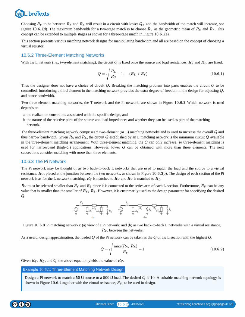
Michael Steer 10.6.2 4/10/2022 https://eng.libretexts.org/@go/page/41328
Choosing to be between and will result in a circuit with lower and the bandwidth of the match will increase, seeFigure (d). The maximum bandwidth for a two-stage match is to choose as the geometric mean of and . Thisconcept can be extended to multiple stages as shown for a three-stage match in Figure (e).
This section presents various matching network designs for manipulating bandwidth and all are based on the concept of choosing avirtual resistor.
10.6.2 Three-Element Matching Networks
With the L network (i.e., two-element matching), the circuit is fixed once the source and load resistances, and , are fixed:
Thus the designer does not have a choice of circuit . Breaking the matching problem into parts enables the circuit to becontrolled. Introducing a third element in the matching network provides the extra degree of freedom in the design for adjusting ,and hence bandwidth.
Two three-element matching networks, the T network and the Pi network, are shown in Figure . Which network is useddepends on
a. the realization constraints associated with the specific design, andb. the nature of the reactive parts of the source and load impedances and whether they can be used as part of the matching
network.
The three-element matching network comprises two-element (or L) matching networks and is used to increase the overall andthus narrow bandwidth. Given and , the circuit established by an L matching network is the minimum circuit availablein the three-element matching arrangement. With three-element matching, the can only increase, so three-element matching isused for narrowband (high- ) applications. However, lower can be obtained with more than three elements. The nextsubsections consider matching with more than three elements.
10.6.3 The Pi NetworkThe Pi network may be thought of as two back-to-back L networks that are used to match the load and the source to a virtualresistance, , placed at the junction between the two networks, as shown in Figure (b). The design of each section of the Pinetwork is as for the L network matching. is matched to and is matched to .
must be selected smaller than and since it is connected to the series arm of each L section. Furthermore, can be anyvalue that is smaller than the smaller of . However, it is customarily used as the design parameter for specifying the desired
.
Figure : Pi matching networks: (a) view of a Pi network; and (b) as two back-to-back L networks with a virtual resistance, , between the networks.
As a useful design approximation, the loaded of the Pi network can be taken as the of the L section with the highest :
Given and , the above equation yields the value of .
Design a Pi network to match a source to a load. The desired is . A suitable matching network topology isshown in Figure together with the virtual resistance, , to be used in design.
RV RS RL QT
10.6.1 RV RS RL
10.6.1
Q RS RL
Q = , ( > )−1RL
RS
− −−−−−
√ RL RS (10.6.1)
Q Q
Q
10.6.2
2 Q
RS RL Q Q
Q
Q Q
RV 10.6.3
RS RV RV RL
RV RS RL RV
,RS RL
Q
10.6.3
RV
Q Q Q
Q = −1max( , )RS RL
RV
− −−−−−−−−−−−−−−
√ (10.6.2)
, ,RS RL Q RV
Example : Three-Element Matching Network Design10.6.1
50 Ω 500 Ω Q 10
10.6.4 RV
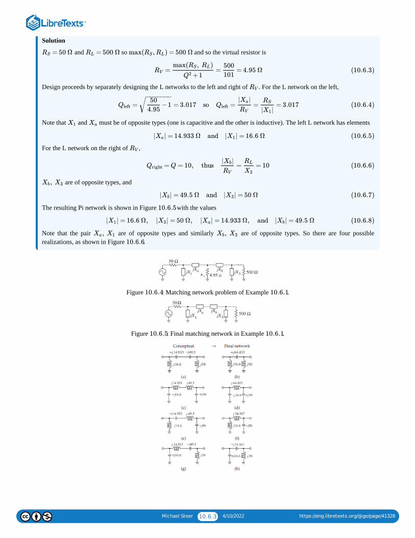
Michael Steer 10.6.3 4/10/2022 https://eng.libretexts.org/@go/page/41328
Solution
and so and so the virtual resistor is
Design proceeds by separately designing the L networks to the left and right of . For the L network on the left,
Note that and must be of opposite types (one is capacitive and the other is inductive). The left L network has elements
For the L network on the right of ,
are of opposite types, and
The resulting Pi network is shown in Figure with the values
Note that the pair are of opposite types and similarly are of opposite types. So there are four possiblerealizations, as shown in Figure .
Figure : Matching network problem of Example .
Figure : Final matching network in Example .
= 50 ΩRS = 500 ΩRL max( , ) = 500 ΩRS RL
= = = 4.95 ΩRV
max( , )RS RL
+1Q2
500
101(10.6.3)
RV
= = 3.017 so = = = 3.017Qleft −150
4.95
− −−−−−−√ Qleft
| |Xa
RV
RS
| |X1
(10.6.4)
X1 Xa
| | = 14.933 Ω and | | = 16.6 ΩXa X1 (10.6.5)
RV
= Q = 10, thus = = 10Qright| |Xb
RV
RL
X3
(10.6.6)
,Xb X3
| | = 49.5 Ω and | | = 50 ΩXb X3 (10.6.7)
10.6.5
| | = 16.6 Ω, | | = 50 Ω, | | = 14.933 Ω, and | | = 49.5 ΩX1 X3 Xa Xb (10.6.8)
,Xa X1 ,Xb X3
10.6.6
10.6.4 10.6.1
10.6.5 10.6.1
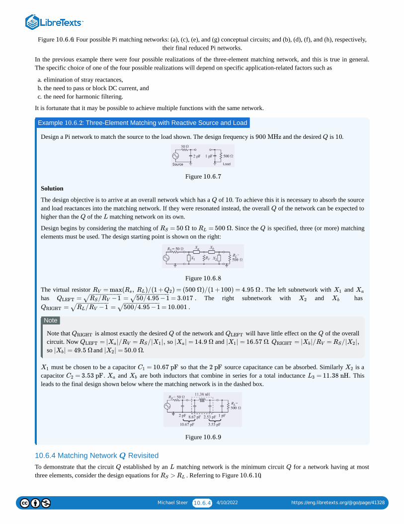
Michael Steer 10.6.4 4/10/2022 https://eng.libretexts.org/@go/page/41328
Figure : Four possible Pi matching networks: (a), (c), (e), and (g) conceptual circuits; and (b), (d), (f), and (h), respectively,their final reduced Pi networks.
In the previous example there were four possible realizations of the three-element matching network, and this is true in general.The specific choice of one of the four possible realizations will depend on specific application-related factors such as
a. elimination of stray reactances,b. the need to pass or block DC current, andc. the need for harmonic filtering.
It is fortunate that it may be possible to achieve multiple functions with the same network.
Design a Pi network to match the source to the load shown. The design frequency is and the desired is .
Figure
Solution
The design objective is to arrive at an overall network which has a of . To achieve this it is necessary to absorb the sourceand load reactances into the matching network. If they were resonated instead, the overall of the network can be expected tohigher than the of the matching network on its own.
Design begins by considering the matching of to . Since the is specified, three (or more) matchingelements must be used. The design starting point is shown on the right:
Figure
The virtual resistor . The left subnetwork with and has . The right subnetwork with and has
.
Note that is almost exactly the desired of the network and will have little effect on the of the overallcircuit. Now so and . so and .
must be chosen to be a capacitor so that the source capacitance can be absorbed. Similarly is acapacitor . and are both inductors that combine in series for a total inductance . Thisleads to the final design shown below where the matching network is in the dashed box.
Figure
10.6.4 Matching Network RevisitedTo demonstrate that the circuit established by an matching network is the minimum circuit for a network having at mostthree elements, consider the design equations for . Referring to Figure ,
10.6.6
Example : Three-Element Matching with Reactive Source and Load10.6.2
900 MHz Q 10
10.6.7
Q 10
Q
Q L
= 50 ΩRS = 500 ΩRL Q
10.6.8
= max( , )/(1 + ) = (500 Ω)/(1 +100) = 4.95 ΩRV Rs RL Q2 X1 Xa
= = = 3.017QLEFT / −1RS RV− −−−−−−−−
√ 50/4.95 −1− −−−−−−−−
√ X2 Xb
= = = 10.001QRIGHT / −1RL RV− −−−−−−−−
√ 500/4.95 −1− −−−−−−−−−
√
Note
QRIGHT Q QLEFT Q
= | |/ = /| |,QLEFT Xa RV RS X1 | | = 14.9 ΩXa | | = 16.57 ΩX1 = | |/ = /| |,QRIGHT Xb RV RS X2
| | = 49.5 ΩXb | | = 50.0 ΩX2
X1 = 10.67 pFC1 2 pF X2
= 3.53 pFC2 Xa Xb = 11.38 nHL3
10.6.9
Q
Q L Q
>RS RL 10.6.10
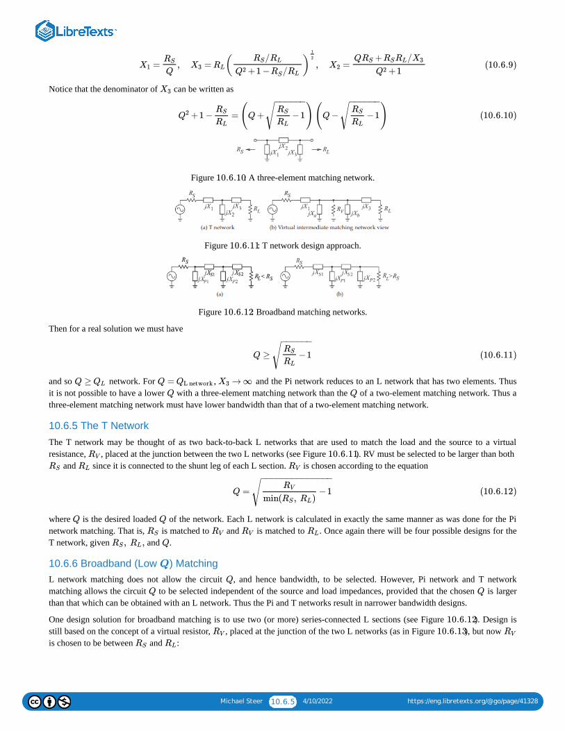
Michael Steer 10.6.5 4/10/2022 https://eng.libretexts.org/@go/page/41328
Notice that the denominator of can be written as
Figure : A three-element matching network.
Figure : T network design approach.
Figure : Broadband matching networks.
Then for a real solution we must have
and so network. For , and the Pi network reduces to an L network that has two elements. Thusit is not possible to have a lower with a three-element matching network than the of a two-element matching network. Thus athree-element matching network must have lower bandwidth than that of a two-element matching network.
10.6.5 The T Network
The T network may be thought of as two back-to-back L networks that are used to match the load and the source to a virtualresistance, , placed at the junction between the two L networks (see Figure ). RV must be selected to be larger than both
and since it is connected to the shunt leg of each L section. is chosen according to the equation
where is the desired loaded of the network. Each L network is calculated in exactly the same manner as was done for the Pinetwork matching. That is, is matched to and is matched to . Once again there will be four possible designs for theT network, given and .
10.6.6 Broadband (Low ) MatchingL network matching does not allow the circuit , and hence bandwidth, to be selected. However, Pi network and T networkmatching allows the circuit to be selected independent of the source and load impedances, provided that the chosen is largerthan that which can be obtained with an L network. Thus the Pi and T networks result in narrower bandwidth designs.
One design solution for broadband matching is to use two (or more) series-connected L sections (see Figure ). Design isstill based on the concept of a virtual resistor, , placed at the junction of the two L networks (as in Figure ), but now is chosen to be between and :
= , = , =X1RS
QX3 RL( )
/RS RL
+1 − /Q2 RS RL
1
2
X2
Q + /RS RSRL X3
+1Q2(10.6.9)
X3
+1 − = (Q + ) (Q − )Q2 RS
RL
−1RS
RL
− −−−−−
√ −1RS
RL
− −−−−−
√ (10.6.10)
10.6.10
10.6.11
10.6.12
Q ≥ −1RS
RL
− −−−−−
√ (10.6.11)
Q ≥ QL Q = QL network → ∞X3
Q Q
RV 10.6.11
RS RL RV
Q = −1RV
min( , )RS RL
− −−−−−−−−−−−−−
√ (10.6.12)
Q Q
RS RV RV RL
, ,RS RL Q
Q
Q
Q Q
10.6.12
RV 10.6.13 RV
RS RL

Michael Steer 10.6.6 4/10/2022 https://eng.libretexts.org/@go/page/41328
Figure : Matching network with two L networks.
Figure : Cascaded L networks for broadband matching.
where and . Then one of the two networks will have
The maximum bandwidth (minimum ) available is obtained when
That is, the maximum matching bandwidth is obtained when is the geometric mean of and :
Even wider bandwidths can be obtained by cascading more than two L networks, as shown in Figure . In this circuit
For optimum bandwidth the ratios should be equal,
and the is given by
If there are L networks used in the match, the maximum bandwidth will be obtained if the th virtual resistor is
Consider matching a source to a load using two L matching networks and designing for a of . How manymatching sections are required?
Solution
Here the approximate s achieved with a single L matching network and with an optimum two-section design are compared.For a single L network design
Now consider an optimum two-section design:
10.6.13
10.6.14
≤ ≤Rmin RV Rmax (10.6.13)
= min( , )Rmin RL RS = max( , )Rmax RL RS
= and the other =Q1 −1RV
Rmin
− −−−−−−−
√ Q2 −1Rmax
RV
− −−−−−−−
√ (10.6.14)
Q
= = =Q1 Q2 −1RV
Rmin
− −−−−−−−
√ −1Rmax
RV
− −−−−−−−
√ (10.6.15)
RV RS RL
=RV RLRS− −−−−
√ (10.6.16)
10.6.14
< < … < <RS RV1 RV2 RVn−1 RL (10.6.17)
= = = ⋯ =RV1
RS
RV2
RV1
RV3
RV2
RL
RVn−1
(10.6.18)
Q
Q = = = ⋯ =−1RV1
RS
− −−−−−−
√ −1RV2
R1
− −−−−−−
√ −1RL
RVn−1
− −−−−−−−
√ (10.6.19)
N i
= ( , i = 1, … , (N −1)RViRSRL)i/N (10.6.20)
Example : Two-Section Matching Network Design10.6.3
10 Ω 1000 Ω Q 3
Q
Q = = 9.95−1RL
RS
− −−−−−
√ (10.6.21)
Michael Steer 10.6.7 4/10/2022 https://eng.libretexts.org/@go/page/41328
Thus the is compared to the of an L section of . If the fractional bandwidth is inversely proportional to , then thebandwidth of the two-section design is times more than that of the L section.
Now consider how many sections are required to obtain a of :
For and , which rounds to , and three sections are required.
Contributions and Attributions
This page is licensed under a CC BY-NC license and was authored, remixed, and/or curated by Michael Steer. A detailedversioning history of the edits to source content is available upon request.
= ; = = = 3RV RSRL− −−−−
√ Q2 −1RL
RV
− −−−−−−
√ −1RL
RS
− −−
√
− −−−−−−−
⎷
(10.6.22)
Q 3 Q 9.95 Q
9.95/3 = 3.32
Q 2
(1 + )Q2
(1 +Q2)n
= = = … = ⇒RV1
RS
RV2
RV1
RL
RVn−1
= ⇒ n ln(1 + ) = ln ⇒ n =RL
RS
Q2 RL
RS
ln( / )RL RS
ln(1 + )Q2
(10.6.23)
(10.6.24)
Q = 2 / = 100, n = 2.86RL RS n = 3

Michael Steer 10.7.1 4/10/2022 https://eng.libretexts.org/@go/page/41329
10.7: SummaryThis chapter presented techniques for impedance matching that achieve maximum power transfer from a source to a load. Thesimplest matching network uses a series and a shunt element, a two-element matching network, to realize a single-frequency match.This type of impedance matching network uses lumped elements and can be used up to a few gigahertz. Performance is limited bythe self-resonant frequency of lumped elements and by their loss, particularly that of inductors. The shunt element can be replacedby a shunt stub, but in most transmission line technologies, including microstrip, the series element cannot be implemented as astub. Matching networks can also be realized using transmission line segments only, principally shunt stubs and cascadedtransmission lines. A tunable double-stub matching network, which uses two stubs separated by a transmission line, is standardequipment in microwave laboratories and facilitates matching of a circuit under development.
The bandwidth of a matching network is set by the maximum allowable reflection coefficient of the terminated network. Two-element matching nearly always results in a narrow match and for typical communications applications often achieves acceptablematching over bandwidths of only . The most significant determinant of the quality of the match that can be achieved is theratio of the source and load resistances, as well as the reactive energy storage of the source and load.
An important concept in matching network design is a technique for controlling bandwidth. The concept is based on matching to anintermediate resistance, typically designated as . Compared to a two-element network, increased bandwidth is obtained if isthe geometric mean of the source and load resistances. This new network consists of two two-element matching networks. If isgreater or less than both the source and load resistances, then the bandwidth of the matching network is reduced. The matchingnetwork synthesis problem can also be addressed using filter design techniques, and this enables simultaneous control over thequality and bandwidth of the match. It is always a good idea to have no more bandwidth in the system than is needed, as thisminimizes the propagation of noise.
Contributions and Attributions
This page is licensed under a CC BY-NC license and was authored, remixed, and/or curated by Michael Steer. A detailedversioning history of the edits to source content is available upon request.
1%– 3%
Rv Rv
Rv

Michael Steer 10.8.1 4/10/2022 https://eng.libretexts.org/@go/page/41330
10.8: References[1] R. Collins, Foundations for Microwave Engineering. McGraw Hill, 1966.
[2] M. Steer, Microwave and RF Design, Transmission Lines, 3rd ed. North Carolina State University, 2019.
Contributions and AttributionsThis page is licensed under a CC BY-NC license and was authored, remixed, and/or curated by Michael Steer. A detailedversioning history of the edits to source content is available upon request.

Michael Steer 10.9.1 4/10/2022 https://eng.libretexts.org/@go/page/41331
10.9: Exercises1. Consider the design of a magnetic transformer that will match the output resistance of a power amplifier (this is the source)
to a load. The secondary of the transformer is on the load side.a. What is the ratio of the number of primary turns to the number of secondary turns for ideal matching?b. If the transformer ratio could be implemented exactly (the ideal situation), what is the reflection coefficient normalized to
looking into the primary of the transformer with the load?c. What is the ideal return loss of the loaded transformer (looking into the primary)? Express your answer in .d. If there are secondary windings, how many primary windings are there in your design? Note that the number of
windings must be an integer. (This practical situation will be considered in the rest of the problem.)e. What is the input resistance of the transformer looking into the primary?f. What is the reflection coefficient normalized to looking into the primary of the transformer with the load?g. What is the actual return loss (in ) of the loaded transformer (looking into the primary)?h. If the maximum available power from the amplifier is , how much power (in ) is reflected at the input of the
transformer?i. Thus, how much power (in ) is delivered to the load ignoring loss in the transformer?
2. Consider the design of a magnetic transformer that will match a output resistance to the load presented by anamplifier. The secondary of the transformer is on the load (amplifier) side.a. What is the ratio of the number of primary turns to the number of secondary turns for ideal matching?b. If the transformer ratio could be implemented exactly (the ideal situation), what is the reflection coefficient normalized to
looking into the primary of the transformer with the load?c. What is the ideal return loss of the loaded transformer (looking into the primary)? Express your answer in .d. If there are secondary windings, how many primary windings are there in your design? Note that the number of windings
must be an integer? (This situation will be considered in the rest of the problem.)e. What is the input resistance of the transformer looking into the primary?f. What is the reflection coefficient normalized to looking into the primary of the loaded transformer?g. What is the actual return loss (in ) of the loaded transformer (looking into the primary)?h. If the maximum available power from the source is , how much power (in ) is reflected from the input of the
transformer?i. Thus, how much power (in ) is delivered to the amplifier ignoring loss in the transformer?
3. Consider the design of an L-matching network centered at that will match the output resistance of a power amplifier(this is the source) to a load. [Parallels Example 10.4.1 but note the DC blocking requirement below.]
a. What is the of the matching network?b. The matching network must block DC current. Draw the topology of the matching network.c. What is the reactance of the series element in the matching network?d. What is the reactance of the shunt element in the matching network?e. What is the value of the series element in the matching network?f. What is the value of the shunt element in the matching network?g. Draw and label the final design of your matching network including the source and load resistances.h. Approximately, what is the bandwidth of the matching network?
4. Consider the design of an L-matching network centered at that will match a source with a Thevenin resistance of to the input of an amplifier presenting a load resistance of to the matching network. [Parallels Example 10.4.2 but
note the DC blocking requirement below.]a. What is the of the matching network?b. The matching network must block DC current. Draw the topology of the matching network.c. What is the reactance of the series element in the matching network?d. What is the reactance of the shunt element in the matching network?e. What is the value of the series element in the matching network?f. What is the value of the shunt element in the matching network?g. Draw and label the final design of your matching network including the source and load resistance.h. Approximately, what is the bandwidth of the matching network?
3 Ω
50 Ω
3 Ω 50 Ω
dB
100
3 Ω 50 Ω
dB
20 dBm dBm
dBm
50 Ω 100 Ω
50 Ω
dB
20
50 Ω
dB
−10 dBm dBm
dBm
1 GHz 2 Ω
50 Ω
Q
3 dB
100 GHz
50 Ω 100 Ω
Q
3 dB

Michael Steer 10.9.2 4/10/2022 https://eng.libretexts.org/@go/page/41331
5. Design a Pi network to match the source configuration to the load configuration below. The design frequency is andthe desired is . [Parallels Example 10.6.2]
Figure
6. Design a Pi network to match the source configuration to the load configuration below. The design frequency is andthe desired is . [Parallels Example 10.6.2]
Figure
7. Develop the electrical design of an L-matching network to match the source to the load below.
Figure
8. Develop the electrical design of an L-matching network to match the source to the load below.
Figure
9. Design a lowpass lumped-element matching network to match the source and load shown below. The design frequency is . You must use a Smith Chart and clearly show your working and derivations. You must develop the final values of the
elements.
Figure
10. Consider the design of an L-matching network centered at that will match a source with a Thevenin resistance of to the input of an amplifier presenting a load resistance of to the matching network. [Parallels Example 10.4.2 but
note the DC blocking requirement below.]a. What is the of the matching network?b. The matching network must block DC current. Draw the topology of the matching network.c. What is the reactance of the series element in the matching network?d. What is the reactance of the shunt element in the matching network?e. What is the value of the series element in the matching network?f. What is the value of the shunt element in the matching network?g. Draw and label the final design of your matching network including the source and load resistance.h. Approximately, what is the bandwidth of the matching network?
11. Design a two-element matching network to interface a source with a Thevenin equivalent impedance to a load consistingof a capacitor in parallel with a resistor so that the load admittance is . Use the absorption method tohandle the reactive load.
12. Design a matching network to interface a source with a Thevenin equivalent impedance to a load consisting of a capacitorin parallel with a resistor so that the load admittance is .
900 MHz
Q 10
10.9.1
900 MHz
Q 10
10.9.2
10.9.3
10.9.4
1 GHz
10.9.5
100 GHz
50 Ω 200 Ω
Q
3 dB
25 Ω
= 0.02 + ȷ0.02 SYL
25 Ω
= 0.01 + ȷ0.01 SYL

Michael Steer 10.9.3 4/10/2022 https://eng.libretexts.org/@go/page/41331
a. If the complexity of the matching network is not limited, what is the minimum that could possibly be achieved in thecomplete network consisting of the matching network and the source and load impedances?
b. Outline the procedure for designing the matching network for maximum bandwidth if only four elements can be used in thenetwork. You do not need to design the network,
13. Design a Pi network to match the source configuration to the load configuration below. The design frequency is andthe desired is .
Figure
14. Design a passive matching network that will achieve maximum bandwidth matching from a source with an impedance of (typical of the output impedance of a power amplifier) to a load with an impedance of . The matching network can have amaximum of three reactive elements. You need only calculate reactances and not the capacitor and inductor values.
15. Design a passive matching network that will achieve maximum bandwidth matching from a source with an impedance of to a load with an impedance of . The matching network can have a maximum of four reactive elements. You need onlycalculate reactances and not the capacitor and inductor values.a. Will you use two, three, or four elements in your matching network?b. With a diagram, and perhaps equations, indicate the design procedure.c. Design the matching network. It is sufficient to use reactance values.
16. Design a passive matching network that will achieve maximum bandwidth matching from a source with an impedance of to a load with an impedance of . The matching network can have a maximum of four reactive elements. You need onlycalculate reactances and not the capacitor and inductor values.a. Will you use two, three, or four elements in your matching network?b. With a diagram and perhaps equations, indicate the design procedure.c. Design the matching network. It is sufficient to use reactance values.
17. Design a T network to match a source to a load. The desired loaded is .18. Repeat Example 10.3.2 with an inductor in series with the load. Show that the inductance can be adjusted to obtain any positive
shunt resistance value.19. Design a three-lumped-element matching network that interfaces a source with an impedance of to a load with an
impedance consisting of a resistor with an impedance of . The network must have a of .20. A two-port matching network is shown below with a generator and a load. The generator impedance is and the load
impedance is . Use a Smith chart to design the matching network.
Figure
a. What is the condition for maximum power transfer from the generator? Express your answer using impedances.b. What is the condition for maximum power transfer from the generator? Express your answer using reflection coefficients.c. What system reference impedance are you going to use to solve the problem?d. Plot on the Smith chart and label the point. (Remember to use impedance normalization if required.)e. Plot ZG on the Smith chart and label the point.f. Design a matching network using only transmission lines. Show your work on the Smith chart. You must express the
lengths of the lines in terms of electrical length (either degrees or wavelengths). Characteristic impedances of the lines arerequired. (You will therefore have a design that consists of one stub and one other length of transmission line.)
21. Use a lossless transmission line and a series reactive element to match a source with a Thevenin equivalent impedance of to a load of . (That is, use one transmission line and one series reactance only.)
a. Draw the matching network with the source and load.
Q
900 MHz
Q 10
10.9.6
2 Ω
50 Ω
20 Ω
125 Ω
60 Ω
5 Ω
50 Ω 1000 Ω Q 15
5 Ω
10 Ω Q 6
40 Ω
= 50 − ȷ20 ΩZL
10.9.7
ZL
25 + ȷ50 Ω 100 Ω

Michael Steer 10.9.4 4/10/2022 https://eng.libretexts.org/@go/page/41331
b. What is the value of the series reactance in the matching network (you can leave this in ohms)?c. What is the length and characteristic impedance of the transmission line?
22. Consider a load . Use the Smith chart to design a matching network consisting of only two transmission linesthat will match the load to a generator of .a. Draw the matching network with transmission lines. If you use a stub, it should be a short-circuited stub.b. Indicate your choice of characteristic impedance for your transmission lines. What is the normalized load impedance? What
is the normalized source impedance?c. Briefly outline the design procedure you will use. You will need to use Smith chart sketches.d. Plot the load and source on a Smith chart.e. Complete the design of the matching network, providing the lengths of the transmission lines.
23. A two-port matching network is shown below with a generator and a load. The generator impedance is and the loadimpedance is . Use a Smith chart to design the matching network.
Figure
a. What is the condition for maximum power transfer from the generator? Express your answer using impedances.b. What is the condition for maximum power transfer from the generator? Express your answer using reflection coefficients.c. What system reference impedance are you going to use to solve the problem?d. Plot on a Smith chart and label the point. (Remember to use impedance normalization if required.)e. Plot on a Smith chart and label the point.f. Design a matching network using only transmission lines and show your work on a Smith chart. You must express the
lengths of the lines in terms of electrical length (either degrees or wavelengths long). Characteristic impedances of thelines are required. (You will therefore have a design that consists of one stub and one other length of transmission line.)
24. Use a Smith chart to design a microstrip network to match a load to a source ). Usetransmission lines only and do not use short-circuited stubs. Use a reference impedance of .a. Draw the matching network problem labeling impedances and the impedance looking into the matching network from the
source as .b. What is the condition for maximum power transfer in terms of impedances?c. What is the condition for maximum power transfer in terms of reflection coefficients?d. Identify, i.e. draw, at least two suitable microstrip matching networks.e. Develop the electrical design of the matching network using the Smith chart using lines only. You only need do one
design.f. Draw the microstrip layout of the matching network identify critical parameters such characteristic impedances and
electrical length. Ensure that you identify which is the source side and which is the load side. You do not need to determinethe widths of the lies or their physical lengths.
25. Repeat exercise 24 but now with and ).26. Use a Smith chart to design a two-element lumped-element lossless matching network to interface a source with an admittance
to a load with admittance .27. Use a Smith chart to design a two-element lumped-element lossless matching network to interface a load to a
source .
10.12.1 Exercises by Sectionchallenging
= 80 + ȷ40 ΩZL
40 Ω
40 Ω
= 20 − ȷ50 ΩZL
10.9.8
ZL
ZG
= 100 − ȷ100 ΩZL = 34 − ȷ40 ΩZS
40 Ω
Z1
40 Ω
= 10 − ȷ40 ΩZL = 28 − ȷ28 ΩZS
= 6 − ȷ12 mSYS = 70 − ȷ50 mSYL
= 50 + ȷ50 ΩZL
= 10 ΩZS
†
§10.31, 2
§10.43, 4
§10.55, 6, 7, 8, 9, 10, 11†, 12†, 13†
§10.614†, 15†, 16†, 17†, 18†, 19†

Michael Steer 10.9.5 4/10/2022 https://eng.libretexts.org/@go/page/41331
10.12.2 Answers to Selected Exercises15. (c)
18.
20. (d) 21. (b)
23. (f) , -long line before load, , -long shorted stub
Contributions and AttributionsThis page is licensed under a CC BY-NC license and was authored, remixed, and/or curated by Michael Steer. A detailedversioning history of the edits to source content is available upon request.
§10.720†, 21†, 22†, 23†
§10.924, 25, 26, 27
Q = 1.22467
C = 1/( )ω2dLP
1.25 − ȷ0.5
−ȷ50 Ω
40 Ω 0.085λ 40 Ω 0.076λ
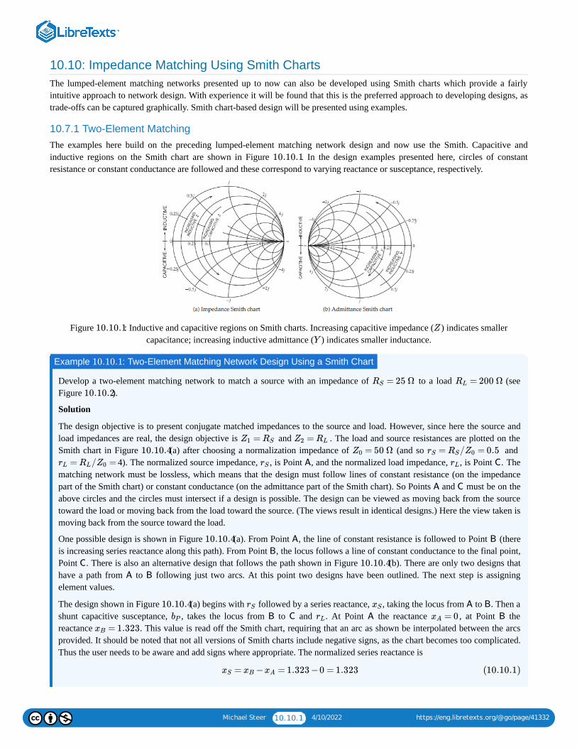
Michael Steer 10.10.1 4/10/2022 https://eng.libretexts.org/@go/page/41332
10.10: Impedance Matching Using Smith ChartsThe lumped-element matching networks presented up to now can also be developed using Smith charts which provide a fairlyintuitive approach to network design. With experience it will be found that this is the preferred approach to developing designs, astrade-offs can be captured graphically. Smith chart-based design will be presented using examples.
10.7.1 Two-Element MatchingThe examples here build on the preceding lumped-element matching network design and now use the Smith. Capacitive andinductive regions on the Smith chart are shown in Figure . In the design examples presented here, circles of constantresistance or constant conductance are followed and these correspond to varying reactance or susceptance, respectively.
Figure : Inductive and capacitive regions on Smith charts. Increasing capacitive impedance ( ) indicates smallercapacitance; increasing inductive admittance ( ) indicates smaller inductance.
Develop a two-element matching network to match a source with an impedance of to a load (seeFigure ).
Solution
The design objective is to present conjugate matched impedances to the source and load. However, since here the source andload impedances are real, the design objective is and . The load and source resistances are plotted on theSmith chart in Figure (a) after choosing a normalization impedance of (and so and
4). The normalized source impedance, , is Point , and the normalized load impedance, , is Point . Thematching network must be lossless, which means that the design must follow lines of constant resistance (on the impedancepart of the Smith chart) or constant conductance (on the admittance part of the Smith chart). So Points and must be on theabove circles and the circles must intersect if a design is possible. The design can be viewed as moving back from the sourcetoward the load or moving back from the load toward the source. (The views result in identical designs.) Here the view taken ismoving back from the source toward the load.
One possible design is shown in Figure (a). From Point , the line of constant resistance is followed to Point (thereis increasing series reactance along this path). From Point , the locus follows a line of constant conductance to the final point,Point . There is also an alternative design that follows the path shown in Figure (b). There are only two designs thathave a path from to following just two arcs. At this point two designs have been outlined. The next step is assigningelement values.
The design shown in Figure (a) begins with followed by a series reactance, , taking the locus from to . Then ashunt capacitive susceptance, , takes the locus from to and . At Point the reactance , at Point thereactance . This value is read off the Smith chart, requiring that an arc as shown be interpolated between the arcsprovided. It should be noted that not all versions of Smith charts include negative signs, as the chart becomes too complicated.Thus the user needs to be aware and add signs where appropriate. The normalized series reactance is
10.10.1
10.10.1 Z
Y
Example : Two-Element Matching Network Design Using a Smith Chart10.10.1
= 25 ΩRS = 200 ΩRL
10.10.2
=Z1 RS =Z2 RL
10.10.4 = 50 ΩZ0 = / = 0.5rS RS Z0
= / =rL RL Z0 rS A rL C
A C
10.10.4 A B
B
C 10.10.4
A B
10.10.4 rS xS A B
bP B C rL A = 0xA B
= 1.323xB
= − = 1.323 −0 = 1.323xS xB xA (10.10.1)
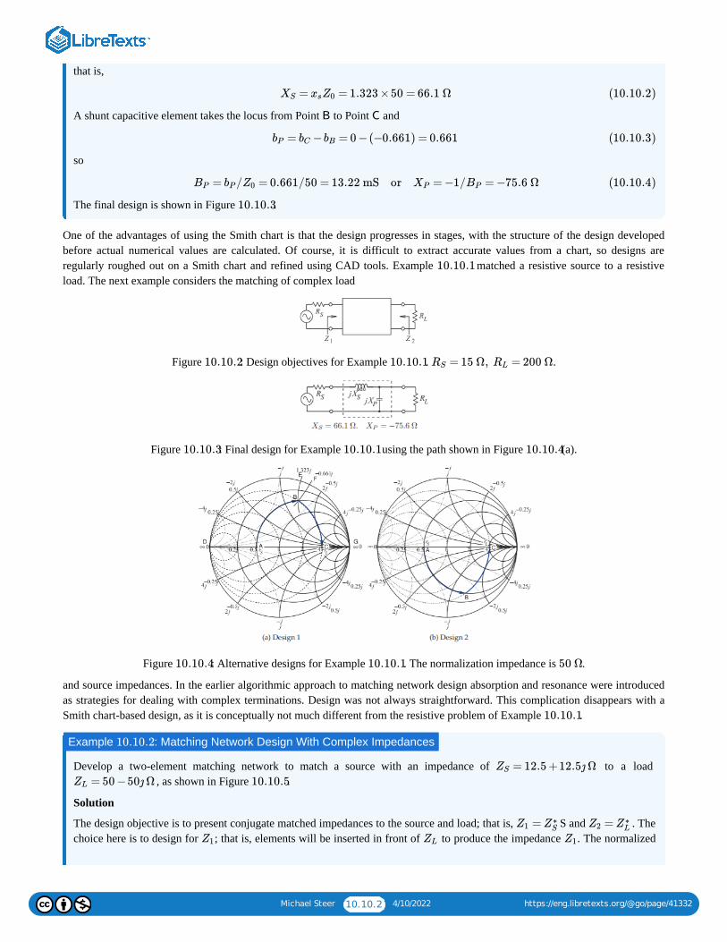
Michael Steer 10.10.2 4/10/2022 https://eng.libretexts.org/@go/page/41332
that is,
A shunt capacitive element takes the locus from Point to Point and
so
The final design is shown in Figure .
One of the advantages of using the Smith chart is that the design progresses in stages, with the structure of the design developedbefore actual numerical values are calculated. Of course, it is difficult to extract accurate values from a chart, so designs areregularly roughed out on a Smith chart and refined using CAD tools. Example matched a resistive source to a resistiveload. The next example considers the matching of complex load
Figure : Design objectives for Example . .
Figure : Final design for Example using the path shown in Figure (a).
Figure : Alternative designs for Example . The normalization impedance is .
and source impedances. In the earlier algorithmic approach to matching network design absorption and resonance were introducedas strategies for dealing with complex terminations. Design was not always straightforward. This complication disappears with aSmith chart-based design, as it is conceptually not much different from the resistive problem of Example .
Develop a two-element matching network to match a source with an impedance of to a load , as shown in Figure .
Solution
The design objective is to present conjugate matched impedances to the source and load; that is, S and . Thechoice here is to design for ; that is, elements will be inserted in front of to produce the impedance . The normalized
= = 1.323 ×50 = 66.1 ΩXS xsZ0 (10.10.2)
B C
= − = 0 −(−0.661) = 0.661bP bC bB (10.10.3)
= / = 0.661/50 = 13.22 mS or = −1/ = −75.6 ΩBP bP Z0 XP BP (10.10.4)
10.10.3
10.10.1
10.10.2 10.10.1 = 15 Ω, = 200 ΩRS RL
10.10.3 10.10.1 10.10.4
10.10.4 10.10.1 50 Ω
10.10.1
Example : Matching Network Design With Complex Impedances10.10.2
= 12.5 +12.5ȷ ΩZS
= 50 −50ȷ ΩZL 10.10.5
=Z1 Z∗S
=Z2 Z∗L
Z1 ZL Z1

Michael Steer 10.10.3 4/10/2022 https://eng.libretexts.org/@go/page/41332
source and load impedances are plotted in Figure (a) using a normalization impedance of , so (Point ) and (Point ).
The impedance to be synthesized is (Point ). The matching network must be lossless,which means that the lumped-element design must follow lines of constant resistance (on the impedance part of the Smithchart) or constant conductance (on the admittance part of the Smith chart). Points and must be on the above circles and thecircles must intersect if a design is possible.
The design can be viewed as moving back from the load impedance toward the conjugate of the source impedance. Thedirection of the impedance locus is important. One possible design is shown in Figure (a). From Point the line ofconstant conductance is followed to Point (there is increasing positive [i.e., capacitive] shunt susceptance along this path).From Point the locus follows a line of constant resistance to the final point, Point .
The design shown in Figure (a) begins with a shunt susceptance, , taking the locus from Point to Point and thena series inductive reactance, , taking the locus to Point . At Point the susceptance , at Point the susceptance
. This value is read off the Smith chart, requiring that an arc of constant susceptance, as shown, be interpolatedbetween the constant susceptance arcs provided. The normalized shunt susceptance is
that is,
A series reactive element takes the locus from Point to Point , so
so
The final design is shown in Figure .
There are only two designs that have a path from Point to Point following just two arcs. In Design 1, shown in Figure (a), Path is much shorter than Path for Design 2 shown in Figure (b). The path length is an
approximate indication of the total reactance required, and the higher the reactance, the greater the energy storage and hencethe narrower the bandwidth of the design. (The actual relative bandwidth depends on the voltage and current levels in thenetwork; the path length criteria, however, is an important rule of thumb.) Thus Design 1 can be expected to have a much
higher bandwidth than Design 2. Since designing broader bandwidth is usually an objective, a design requiring a shorter pathon a Smith chart is usually preferable.
Figure : Design objectives for Example .
10.10.6 = 50 ΩZ0
= / = 0.25 +0.25ȷzS ZS Z0 S = / = 1 − ȷzL ZL Z0 C
= / = = 0.25 −0.25ȷz1 Z1 Z0 z∗S
A
A C
10.10.6 C
B
B A
10.10.6 bP C B
xS A C = 0.5bC B
= 1.323bB
= − = 1.323 −05 = 0.823bP bB bC (10.10.5)
= / = 0.823/(50 Ω) = 16.5 mS or = −1/ = −60.8 ΩBP bP Z0 XP BP (10.10.6)
B A
= − = −0.25 −(−0.661) = 0.411xS xA xB (10.10.7)
= = 0.411 ×50 Ω = 20.6 ΩXS xSZ0 (10.10.8)
10.10.7
C A
10.10.6 CBA CHA 10.10.6
10.10.5 10.10.2
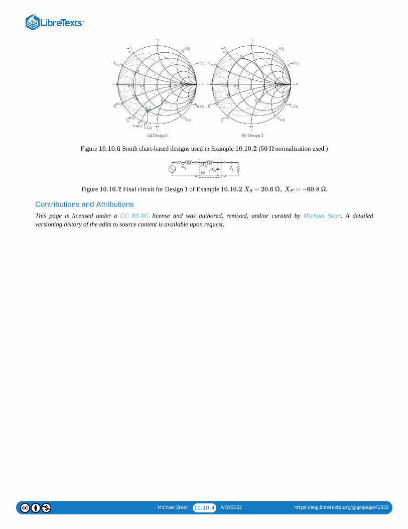
Michael Steer 10.10.4 4/10/2022 https://eng.libretexts.org/@go/page/41332
Figure : Smith chart-based designs used in Example . ( normalization used.)
Figure : Final circuit for Design 1 of Example . .
Contributions and AttributionsThis page is licensed under a CC BY-NC license and was authored, remixed, and/or curated by Michael Steer. A detailedversioning history of the edits to source content is available upon request.
10.10.6 10.10.2 50 Ω
10.10.7 10.10.2 = 20.6 Ω, = −60.8 ΩXS XP
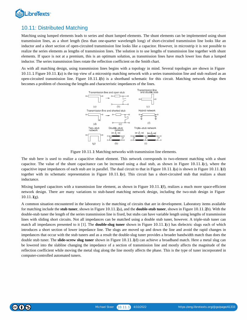
Michael Steer 10.11.1 4/10/2022 https://eng.libretexts.org/@go/page/41333
10.11: Distributed MatchingMatching using lumped elements leads to series and shunt lumped elements. The shunt elements can be implemented using shunttransmission lines, as a short length (less than one-quarter wavelength long) of short-circuited transmission line looks like aninductor and a short section of open-circuited transmission line looks like a capacitor. However, in microstrip it is not possible torealize the series elements as lengths of transmission lines. The solution is to use lengths of transmission line together with shuntelements. If space is not at a premium, this is an optimum solution, as transmission lines have much lower loss than a lumpedinductor. The series transmission lines rotate the reflection coefficient on the Smith chart.
As with all matching design, using transmission lines begins with a topology in mind. Several topologies are shown in Figure . Figure (a) is the top view of a microstrip matching network with a series transmission line and stub realized as an
open-circuited transmission line. Figure (b) is a shorthand schematic for this circuit. Matching network design thenbecomes a problem of choosing the lengths and characteristic impedances of the lines.
Figure : Matching networks with transmission line elements.
The stub here is used to realize a capacitive shunt element. This network corresponds to two-element matching with a shuntcapacitor. The value of the shunt capacitance can be increased using a dual stub, as shown in Figure (c), where thecapacitive input impedances of each stub are in parallel. The dual circuit to that in Figure (a) is shown in Figure (d)together with its schematic representation in Figure (e). This circuit has a short-circuited stub that realizes a shuntinductance.
Mixing lumped capacitors with a transmission line element, as shown in Figure (f), realizes a much more space-efficientnetwork design. There are many variations to stub-based matching network design, including the two-stub design in Figure
(g).
A common situation encountered in the laboratory is the matching of circuits that are in development. Laboratory items availablefor matching include the stub tuner, shown in Figure (a), and the double-stub tuner, shown in Figure (b). With thedouble-stub tuner the length of the series transmission line is fixed, but stubs can have variable length using lengths of transmissionlines with sliding short circuits. Not all impedances can be matched using a double stub tuner, however. A triple-stub tuner canmatch all impedances presented to it [1]. The double-slug tuner shown in Figure (c) has dielectric slugs each of whichintroduces a short section of lower impedance line. The slugs are moved up and down the line and avoid the rapid changes inimpedances that occur with the stub tuners and as a result the double-slug tuner provides a broader bandwidth match than does thedouble stub tuner. The slide-screw slug tuner shown in Figure (d) can achieve a broadband match. Here a metal slug canbe lowered into the slabline changing the impedance of a section of transmission line and mostly affects the magnitude of thereflection coefficient while moving the metal slug along the line mostly affects the phase. This is the type of tuner incorporated incomputer-controlled automated tuners.
10.11.1 10.11.1
10.11.1
10.11.1
10.11.1
10.11.1 10.11.1
10.11.1
10.11.1
10.11.1
10.11.2 10.11.2
10.11.1
10.11.1
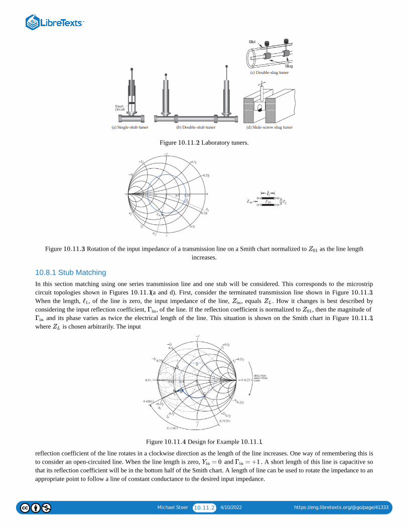
Michael Steer 10.11.2 4/10/2022 https://eng.libretexts.org/@go/page/41333
Figure : Laboratory tuners.
Figure : Rotation of the input impedance of a transmission line on a Smith chart normalized to as the line lengthincreases.
10.8.1 Stub MatchingIn this section matching using one series transmission line and one stub will be considered. This corresponds to the microstripcircuit topologies shown in Figures (a and d). First, consider the terminated transmission line shown in Figure .When the length, , of the line is zero, the input impedance of the line, , equals . How it changes is best described byconsidering the input reflection coefficient, , of the line. If the reflection coefficient is normalized to , then the magnitude of
and its phase varies as twice the electrical length of the line. This situation is shown on the Smith chart in Figure ,where is chosen arbitrarily. The input
Figure : Design for Example .
reflection coefficient of the line rotates in a clockwise direction as the length of the line increases. One way of remembering this isto consider an open-circuited line. When the line length is zero, and . A short length of this line is capacitive sothat its reflection coefficient will be in the bottom half of the Smith chart. A length of line can be used to rotate the impedance to anappropriate point to follow a line of constant conductance to the desired input impedance.
10.11.2
10.11.3 Z01
10.11.1 10.11.3
ℓ1 Zin ZL
Γin Z01
Γin 10.11.3
ZL
10.11.4 10.11.1
= 0Yin = +1Γin

Michael Steer 10.11.3 4/10/2022 https://eng.libretexts.org/@go/page/41333
Design a two-element matching network to match a source with an impedance to a load , as shown in Figure 10.7.5. This example repeats the design in Example 10.7.1, but now using a
transmission line.
Solution
As in Example 10.7.1, choose and the design path is from to , where .One possible design solution is indicated in Figure . The line length, (taking the locus from Point to Point ), is
and the normalized shunt susceptance, (taking the locus from Point to Point ), is
Thus . The final design is shown in Figure (a). The stub design of Figure (b)follows the procedure described in Example 6.5.1.
10.8.2 Hybrid Lumped-Distributed Matching
A lossless matching network can have transmission lines as well as inductors and capacitors. If the system reference ornormalization impedance is the characteristic impedance of a transmission line, then the locus of the input impedance (or reflectioncoefficient) of the line with respect to the length of
Figure : Single-stub matching network design of Example : (a) electrical design; and (b) electrical design with ashunt stub.
the line is an arc on a circle centered at the origin of the Smith chart. The direction of the arc is clockwise as the electrical length ofthe line moves away from the load. So a hybrid matching network is possible that combines a length of transmission line with alumped element (preferably a capacitor rather than an a inductor as the inductor would have a relatively lower ).
Contributions and AttributionsThis page is licensed under a CC BY-NC license and was authored, remixed, and/or curated by Michael Steer. A detailedversioning history of the edits to source content is available upon request.
Example : Matching Network Design With a Transmission Line and a Single Stub10.11.1
= 12.5 +12.5ȷ ΩZS
= 50 −50ȷ ΩZL
= 50 ΩZ0 = / = 1 − ȷzL ZL Z0 z∗s = 0.25 +0.25ȷzs
10.11.4 ℓ C B
ℓ = 0.4261λ −0.3125λ = 0.1136λ
bP B C
= − = 2 −1 = 1bP bA bB
= (−1/ ) ×50 Ω = −50 ΩXP bP 10.11.2 10.11.2
10.11.2 10.11.1
Q
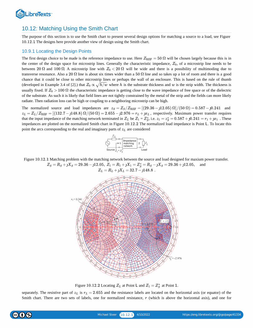
Michael Steer 10.12.1 4/10/2022 https://eng.libretexts.org/@go/page/41334
10.12: Matching Using the Smith ChartThe purpose of this section is to use the Smith chart to present several design options for matching a source to a load, see Figure
. The designs here provide another view of design using the Smith chart.
10.9.1 Locating the Design PointsThe first design choice to be made is the reference impedance to use. Here will be chosen largely because this is inthe center of the design space for microstrip lines. Generally the characteristic impedance, , of a microstrip line needs to bebetween and . A microstrip line with will be wide and there is a possibility of multimoding due totransverse resonance. Also a line is about six times wider than a line and so takes up a lot of room and there is a goodchance that it could be close to other microstrip lines or perhaps the wall of an enclosure. This is based on the rule of thumb(developed in Example 3.4 of [2].) that where is the substrate thickness and is the strip width. The thickness isusually fixed. If the characteristic impedance is getting close to the wave impedance of free space or of the dielectricof the substrate. As such it is likely that field lines are not tightly constrained by the metal of the strip and the fields can more likelyradiate. Then radiation loss can be high or coupling to a neighboring microstrip can be high.
The normalized source and load impedances are and , respectively. Maximum power transfer requires
that the input impedance of the matching network terminated in be = , i.e. . Theseimpedances are plotted on the normalized Smith chart in Figure . The normalized load impedance is Point . To locate thispoint the arcs corresponding to the real and imaginary parts of are considered
Figure : Matching problem with the matching network between the source and load designed for maxium power transfer. and
.
Figure : Locating at Point and at Point .
separately. The resistive part of is and the resistance labels are located on the horizontal axis (or equator) of theSmith chart. There are two sets of labels, one for normalized resistance, (which is above the horizontal axis), and one for
10.12.1
= 50 ΩZREF
Z0
20 Ω 100 Ω < 20 ΩZ0
20 Ω 50 Ω
∝Z0 h/w− −−−
√ h w
> 100 ΩZ0
= / = [(29.36 − ȷ12.05) Ω]/(50 Ω) = 0.587 − ȷ0.241zS ZS ZREF
= / = [(132.7 − ȷ148.8) Ω/(50 Ω) = 2.655 − ȷ2.976 = + ȷzL ZL ZREF rL xL
ZL Z1 Z∗S = = 0.587 + ȷ0.241 = + ȷz1 z∗
S r1 x1
10.12.2 L
zL
10.12.1
= + ȷ = 29.36 − ȷ12.05, = + ȷ = = − ȷ = 29.36 + ȷ12.05,ZS RS XS Z1 R1 X1 Z∗S
RS XS
= + ȷ = 32.7 − ȷ148.8ZL RL XL
10.12.2 ZL L =Z1 Z∗S 1
zL = 2.655rL
r

Michael Steer 10.12.2 4/10/2022 https://eng.libretexts.org/@go/page/41334
normalized conductance, (which is below the horizontal axis). The way to remember which is which is to realize that the infiniteimpedance point is at the (open circuit) location on the right of the graph. At the origin (center) of the Smith chart
and to the right of the center the values of should be greater than one. The closest labels to are and . There are five divisions so the unlabeled curves correspond to . The arc corresponding to mustbe interpolated and this interpolation is shown as the Path ‘a’.
The imaginary part of is . The labels for the arcs of constant reactance are given adjacent to the unit circle. Thereare two sets of labels, one for reactance and one for susceptance. To recall which is which, the point of infinite impedance can beused and the required reactance labels should increase towards the point. Recall that the Smith chart does not include signsof reactances (there is not enough room) so note must be made that positive reactances are in the top half of the Smith chart andnegative reactances are in the bottom half. Since is negative it will be in the bottom half of the Smith chart. The closest labelsare (this is actually ) and (this is actually ) so the arc for is interpolated as the Path ‘b’.Point , i.e. , is located at the intersection of Paths ‘a’ and‘b’. The normalized impedance is located similarly at Point byfinding the point of intersection of the , Path ‘c’, and the , Path ‘d’.
10.9.2 Design Options
By convention design follows a process of beginning with and adding series and shunt elements in front of it evolving theimpedance (or reflection coefficient) until the input impedance is . Two electrical designs are shown in Figure andthe corresponding lumped-element and microstrip topologies are shown in Figure . The subscript on the circuit elementscorrespond to the paths on the Smith chart in Figure . The designs will be elaborated in the following subsections.
10.9.3 Design 1, Hybrid DesignDesign 1 on its own is shown in Figure . The concept here is to use a transmission line and a shunt to go from the loadPoint to the Point . The reason why a shunt element is chosen and not a series element is that the shunt element can beimplemented as a stub line and a series element, i.e. a series stub, cannot be implemented in microstrip. A lumped element limits adesign to the low microwave range as losses become prohibitively large especially for inductors. Also if a microstrip line is goingto be used anyway then a decision has already been made that there is enough room to implement a transmission-line based designand so the shunt lumped element can reasonably be replaced by a stub.
Design follows trial and error. The first attempt, and the one that works here, is to draw a circle through centered on the origin atPoint . This circle describes a transmission line whose characteristic impedance is the same as the reference impedance of theSmith chart, here . The next step is to draw a circle of constant conductance through Point . The combination path from to1 needs to lie on these circles and the intermediate point will be where these circles intersect. One other constraint is that with atransmission line the locus (as the line length increases) of the input reflection coefficient of the line must rotate in the clockwisedirection. It is seen that there are two points of intersection and the first of these, at , is chosen in design. So the electrical designis defined by the directed Paths ‘g’ and ‘h’. Path ‘g’ defines the properties of the transmission line and Path ’h’ defines theproperties of the shunt element. As ‘h’ is directed towards the infinite inductive susceptance point, Path ‘h’ defines an inductor. Thetopology of this design is shown in Figure (a).
The characteristic impedance of the transmission line (defined by Path ‘g’) is and the electrical length of the line isdefined by the angle subtended by the arc ‘g’. The electrical length of the line is determined from
g
Γ = +1
r = 1 = g r r = 2.655rL r = 2.0
r = 3.0 2.2, 2.4, … r = 2.655
zL = −2.976xL
Γ = +1
xL
x = 2.0 −2.0 x = 3.0 −3.0 x = −2.976
L zL z1 1
= 0.587 arcr1 = +0.241 arcx1
zL
=z1 z∗s 10.12.3
10.12.4
10.12.3
10.12.5
L 1
L
O
50 Ω 1 L
A
10.12.4
= 50 ΩZ0g
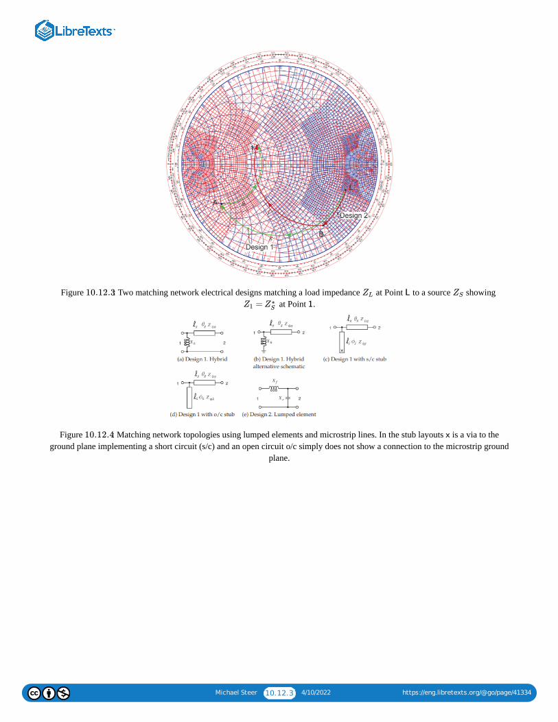
Michael Steer 10.12.3 4/10/2022 https://eng.libretexts.org/@go/page/41334
Figure : Two matching network electrical designs matching a load impedance at Point to a source showing at Point .
Figure : Matching network topologies using lumped elements and microstrip lines. In the stub layouts is a via to theground plane implementing a short circuit (s/c) and an open circuit o/c simply does not show a connection to the microstrip ground
plane.
10.12.3 ZL L ZS
=Z1 Z∗S 1
10.12.4 x
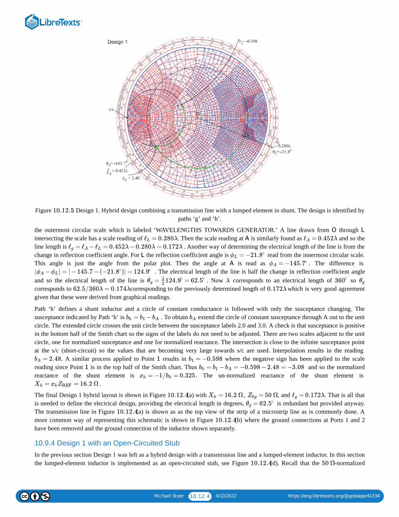
Michael Steer 10.12.4 4/10/2022 https://eng.libretexts.org/@go/page/41334
Figure : Design 1. Hybrid design combining a transmission line with a lumped element in shunt. The design is identified bypaths ‘g’ and ‘h’.
the outermost circular scale which is labeled ‘WAVELENGTHS TOWARDS GENERATOR.’ A line drawn from through intersecting the scale has a scale reading of . Then the scale reading at is similarly found as and so theline length is . Another way of determining the electrical length of the line is from thechange in reflection coefficient angle. For the reflection coefficient angle is read from the innermost circular scale.This angle is just the angle from the polar plot. Then the angle at is read as . The difference is
. The electrical length of the line is half the change in reflection coefficient angleand so the electrical length of the line is . Now corresponds to an electrical length of so corresponds to corresponding to the previously determined length of which is very good agreementgiven that these were derived from graphical readings.
Path ‘h’ defines a shunt inductor and a circle of constant conductance is followed with only the susceptance changing. Thesusceptance indicated by Path ‘h’ is . To obtain extend the circle of constant susceptance through A out to the unitcircle. The extended circle crosses the unit circle between the susceptance labels 2.0 and 3.0. A check is that susceptance is positivein the bottom half of the Smith chart so the signs of the labels do not need to be adjusted. There are two scales adjacent to the unitcircle, one for normalized susceptance and one for normalized reactance. The intersection is close to the infinite susceptance pointat the s/c (short-circuit) so the values that are becoming very large towards s/c are used. Interpolation results in the reading
. A similar process applied to Point results in where the negative sign has been applied to the scalereading since Point is in the top half of the Smith chart. Thus and so the normalizedreactance of the shunt element is . The un-normalized reactance of the shunt element is
.
The final Design 1 hybrid layout is shown in Figure (a) with , and . That is all thatis needed to define the electrical design, providing the electrical length in degrees, is redundant but provided anyway.The transmission line in Figure (a) is shown as as the top view of the strip of a microstrip line as is commonly done. Amore common way of representing this schematic is shown in Figure (b) where the ground connections at Ports 1 and 2have been removed and the ground connection of the inductor shown separately.
10.9.4 Design 1 with an Open-Circuited Stub
In the previous section Design 1 was left as a hybrid design with a transmission line and a lumped-element inductor. In this sectionthe lumped-element inductor is implemented as an open-circuited stub, see Figure (d). Recall that the -normalized
10.12.5
O L
= 0.280λℓL A = 0.452λℓA
= − = 0.452λ −0.280λ = 0.172λℓg ℓA ℓL
L = −ϕL 21.8∘
A = −ϕA 145.7∘
| − | = | −145.7 −(− )| =ϕA ϕL 21.8∘ 124.9∘
= =θg12
124.9∘ 62.5∘ λ 360∘ θg
62.5/360λ = 0.174λ 0.172λ
= −bh b1 bA bA
= 2.48bA 1 = −0.598b1
1 = − = −0.598 −2.48 = −3.08bh b1 bA
= −1/ = 0.325xh bh
= = 16.2 ΩXh xhZREF
10.12.4 = 16.2 Ω, = 50 ΩXh Z0g = 0.172λℓg
=θg 62.5∘
10.12.4
10.12.4
10.12.4 50 Ω
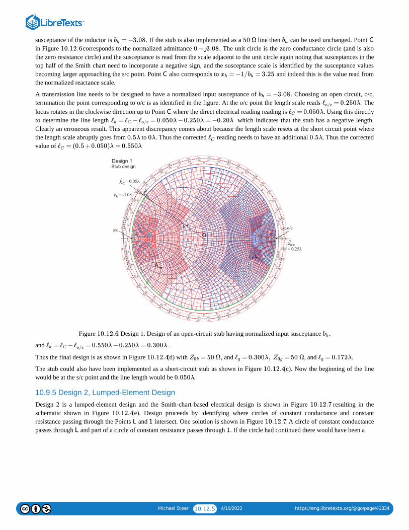
Michael Steer 10.12.5 4/10/2022 https://eng.libretexts.org/@go/page/41334
susceptance of the inductor is . If the stub is also implemented as a line then can be used unchanged. Point in Figure corresponds to the normalized admittance . The unit circle is the zero conductance circle (and is alsothe zero resistance circle) and the susceptance is read from the scale adjacent to the unit circle again noting that susceptances in thetop half of the Smith chart need to incorporate a negative sign, and the susceptance scale is identified by the susceptance valuesbecoming larger approaching the s/c point. Point also corresponds to and indeed this is the value read fromthe normalized reactance scale.
A transmission line needs to be designed to have a normalized input susceptance of . Choosing an open circuit, o/c,termination the point corresponding to o/c is as identified in the figure. At the o/c point the length scale reads . Thelocus rotates in the clockwise direction up to Point where the direct electrical reading reading is . Using this directlyto determine the line length which indicates that the stub has a negative length.Clearly an erroneous result. This apparent discrepancy comes about because the length scale resets at the short circuit point wherethe length scale abruptly goes from to . Thus the corrected reading needs to have an additional . Thus the correctedvalue of
Figure : Design 1. Design of an open-circuit stub having normalized input susceptance .
and .
Thus the final design is as shown in Figure (d) with , and , and .
The stub could also have been implemented as a short-circuit stub as shown in Figure (c). Now the beginning of the linewould be at the s/c point and the line length would be .
10.9.5 Design 2, Lumped-Element Design
Design 2 is a lumped-element design and the Smith-chart-based electrical design is shown in Figure resulting in theschematic shown in Figure (e). Design proceeds by identifying where circles of constant conductance and constantresistance passing through the Points and intersect. One solution is shown in Figure . A circle of constant conductancepasses through and part of a circle of constant resistance passes through . If the circle had continued there would have been a
= −3.08bh 50 Ω bh C
10.12.6 0 − ȷ3.08
C = −1/ = 3.25xh bh
= −3.08bh
= 0.250λℓo/c
C = 0.050λℓC
= − = 0.050λ −0.250λ = −0.20λℓk ℓC ℓo/c
0.5λ 0λ ℓC 0.5λ
= (0.5 +0.050)λ = 0.550λℓC
10.12.6 bh
= − = 0.550λ −0.250λ = 0.300λℓk ℓC ℓo/c
10.12.4 = 50 ΩZ0k = 0.300λ, = 50 Ωℓg Z0g = 0.172λℓg
10.12.4
0.050λ
10.12.7
10.12.4
L 1 10.12.7
L 1
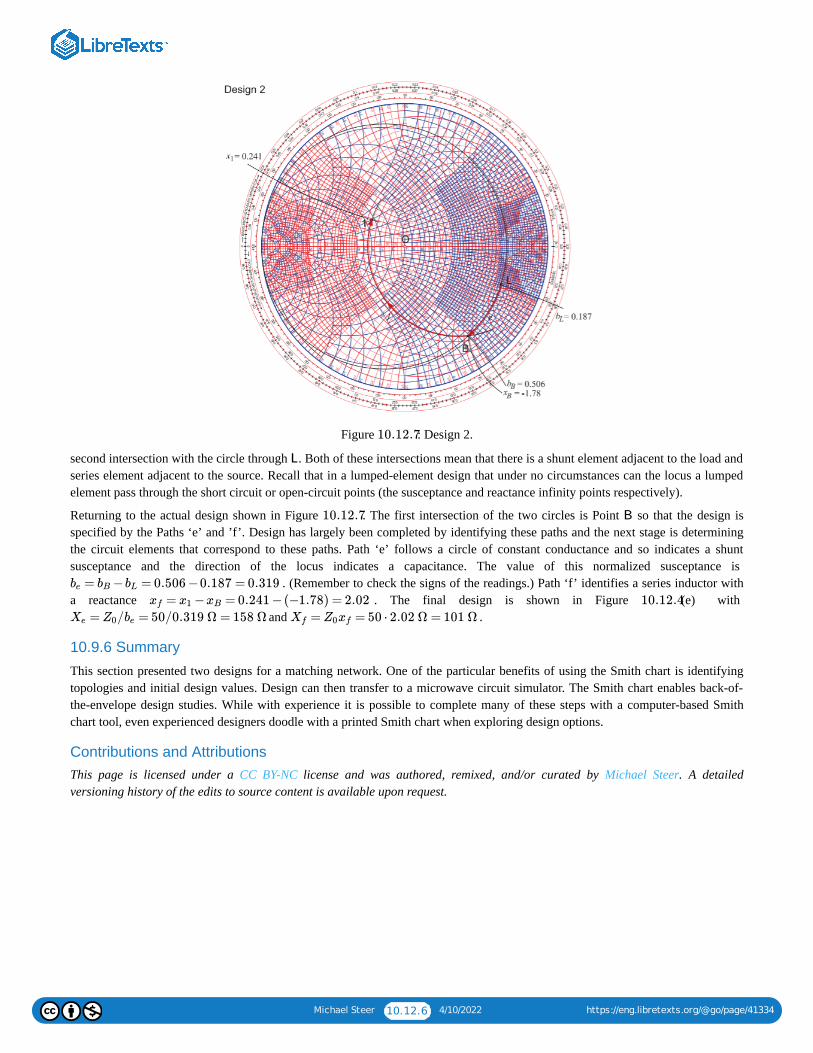
Michael Steer 10.12.6 4/10/2022 https://eng.libretexts.org/@go/page/41334
Figure : Design 2.
second intersection with the circle through . Both of these intersections mean that there is a shunt element adjacent to the load andseries element adjacent to the source. Recall that in a lumped-element design that under no circumstances can the locus a lumpedelement pass through the short circuit or open-circuit points (the susceptance and reactance infinity points respectively).
Returning to the actual design shown in Figure . The first intersection of the two circles is Point so that the design isspecified by the Paths ‘e’ and ’f’. Design has largely been completed by identifying these paths and the next stage is determiningthe circuit elements that correspond to these paths. Path ‘e’ follows a circle of constant conductance and so indicates a shuntsusceptance and the direction of the locus indicates a capacitance. The value of this normalized susceptance is
. (Remember to check the signs of the readings.) Path ‘f’ identifies a series inductor witha reactance . The final design is shown in Figure (e) with
and .
10.9.6 Summary
This section presented two designs for a matching network. One of the particular benefits of using the Smith chart is identifyingtopologies and initial design values. Design can then transfer to a microwave circuit simulator. The Smith chart enables back-of-the-envelope design studies. While with experience it is possible to complete many of these steps with a computer-based Smithchart tool, even experienced designers doodle with a printed Smith chart when exploring design options.
Contributions and AttributionsThis page is licensed under a CC BY-NC license and was authored, remixed, and/or curated by Michael Steer. A detailedversioning history of the edits to source content is available upon request.
10.12.7
L
10.12.7 B
= − = 0.506 −0.187 = 0.319be bB bL
= − = 0.241 −(−1.78) = 2.02xf x1 xB 10.12.4
= / = 50/0.319 Ω = 158 ΩXe Z0 be = = 50 ⋅ 2.02 Ω = 101 ΩXf Z0xf

1 4/10/2022
CHAPTER OVERVIEW11: RF AND MICROWAVE MODULES
11.1: INTRODUCTION TO MICROWAVE MODULES11.2: RF SYSTEM AS A CASCADE OF MODULES11.3: AMPLIFIERS11.4: FILTERS11.5: NOISE11.6: DIODES11.7: LOCAL OSCILLATOR11.8: FREQUENCY MULTIPLIER11.9: SUMMARY11.10: REFERENCES11.11: EXERCISES11.12: SWITCH11.13: FERRITE COMPONENTS- CIRCULATORS AND ISOLATORS11.14: MIXER

Michael Steer 11.1.1 4/10/2022 https://eng.libretexts.org/@go/page/41335
11.1: Introduction to Microwave ModulesMost microwave design uses modules such amplifiers, integrated circuits (ICs), filters, frequency multipliers, and passivecomponents to create systems. Economics necessitate that since modules are expensive to design that they be developed formultiple applications. In system design modules are chosen for their dynamic range, noise performance, DC power consumption,and cost. Foremost the system designer must have knowledge of available modules and be prepared to design a module itself if thisresults in competitive performance or better manages cost. Modules are interconnected by transmission lines, and bias settings andmatching networks must be designed. The system frequency plan must be developed that trades-off cost and performance whileminimizing interference. This chapter begins with examples of module usage and then develops metrics that characterizemicrowave modules. These include characterizations of nonlinear distortion, noise, and dynamic range.
Contributions and AttributionsThis page is licensed under a CC BY-NC license and was authored, remixed, and/or curated by Michael Steer. A detailedversioning history of the edits to source content is available upon request.

Michael Steer 11.2.1 4/10/2022 https://eng.libretexts.org/@go/page/41336
11.2: RF System as a Cascade of ModulesMost RF and microwave engineers work at the circuit board level and begin system design using modules. Some companiesdevelop some of their own proprietary modules, thus providing a competitive advantage, but still use many modules developed byothers. Examples of commercially available modules are shown in Figure 11.3.1. Modules can range in complexity from the simplesurface mount resistor of Figure 11.3.1(a) and the transformer of Figure 11.3.1(d), up to the mixer and synthesizer modules shownin Figure 11.3.1(b and c). Modules can have very good performance as it is cost effective to put considerable design effort into amodule that can be used in many applications and thus design costs shared.
Modules comprising a receiver are shown in Figure 11.3.2. Beginning with the bandpass filter after the antenna, each modulecontributes noise and nonlinear distortion. The system design objectives are generally to maximize dynamic range, the regionbetween the signal being sufficiently above the noise level to be detected but before nonlinear distortion introduces spurious signalsthat limit the detectability of signals. At the same time power consumption and time to market must be minimized.
11.2.1 A Receiver SubsystemAn example of a microwave subsystem is the receiver shown in Figure 11.3.3 with details of the frequency conversionsection shown in Figure 11.3.4. This subsystem is itself a module used in a point-to-point microwave link. The amplifier, frequencymultiplier, mixer, circulator, and waveguide adaptor modules are available as off-the-shelf components from companies thatspecialize in particular types of modules.
Contributions and Attributions
This page is licensed under a CC BY-NC license and was authored, remixed, and/or curated by Michael Steer. A detailedversioning history of the edits to source content is available upon request.
15 GHz
15 GHz

Michael Steer 11.3.1 4/10/2022 https://eng.libretexts.org/@go/page/41337
11.3: AmplifiersAmplifier modules must be optimized for low noise, moderate to high gain, high efficiency, stability, low distortion, and particularoutput power. Usually
Figure : Modules in surface-mount packages. Copyright Synergy Microwave Corporation, used with permission [1].
Figure : Receiver as a cascade of modules.
an application note provided by the amplifier module vendor indicates how to do this for their module. Amplifiers require input andoutput matching networks as shown in Figure . The DC bias control circuit is fairly standard and the lowpass filters (in thebias circuits) are often incorporated into the input and output matching networks. Manufacturers of amplifier modules providesubstantial information, including parameters and, in many cases, reference designs.
Some amplifier modules come with input and output matching networks embodied in the module package. Since matchingnetworks have limited bandwidth, incorporating them in the module sets the operating frequency range. Alternatively the designercan design the input and output matching networks and thus control the operating frequency.
Usually the module manufacturer provides a reference design and often
11.3.1
11.3.2
11.3.5
S
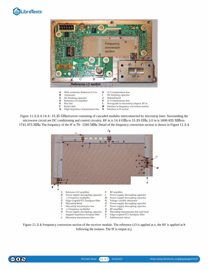
Michael Steer 11.3.2 4/10/2022 https://eng.libretexts.org/@go/page/41337
Figure : A receiver consisting of cascaded modules interconnected by microstrip lines. Surrounding themicrowave circuit are DC conditioning and control circuitry. RF in is to , LO in is to
. The frequency of the IF is . Detail of the frequency conversion section is shown in Figure .
Figure : Frequency conversion section of the receiver module. The reference LO is applied at , the RF is applied at following the isolator. The IF is output at .
11.3.3 14.4– 15.35 GHz
14.4 GHz 15.35 GHz 1600.625 MHz
1741.875 MHz 70– 1595 MHz 11.3.4
11.3.4 c h
j
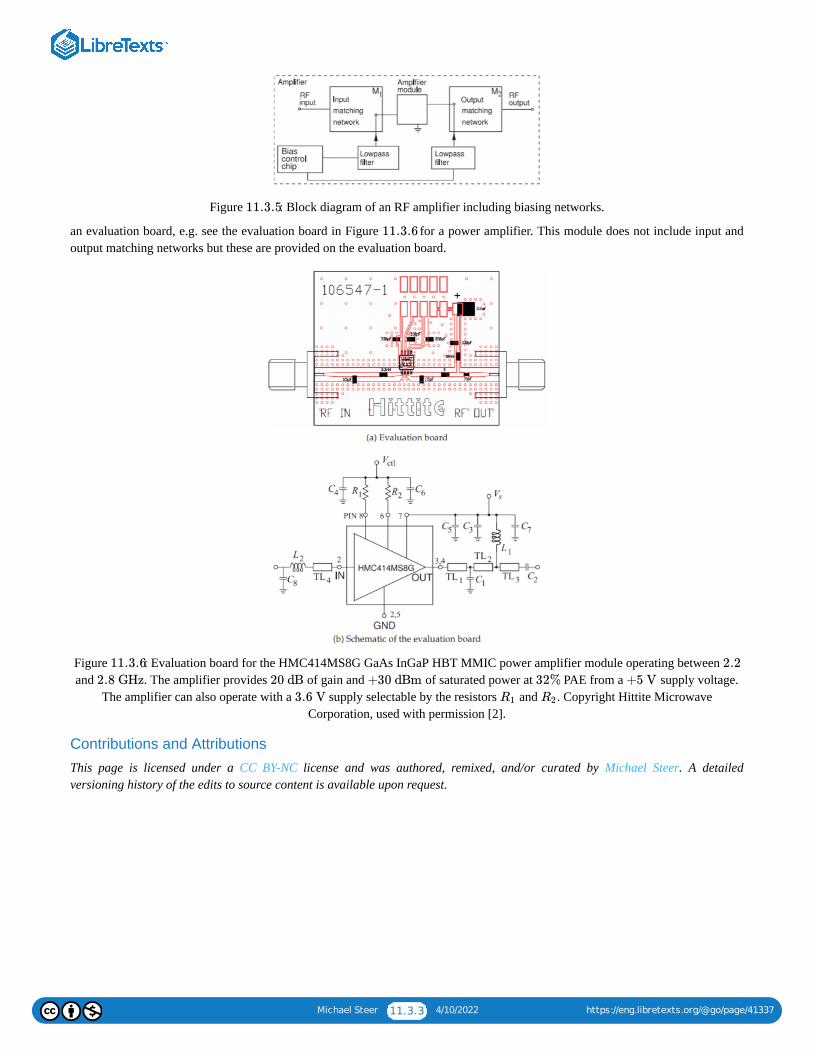
Michael Steer 11.3.3 4/10/2022 https://eng.libretexts.org/@go/page/41337
Figure : Block diagram of an RF amplifier including biasing networks.
an evaluation board, e.g. see the evaluation board in Figure for a power amplifier. This module does not include input andoutput matching networks but these are provided on the evaluation board.
Figure : Evaluation board for the HMC414MS8G GaAs InGaP HBT MMIC power amplifier module operating between and . The amplifier provides of gain and of saturated power at PAE from a supply voltage.
The amplifier can also operate with a supply selectable by the resistors and . Copyright Hittite MicrowaveCorporation, used with permission [2].
Contributions and Attributions
This page is licensed under a CC BY-NC license and was authored, remixed, and/or curated by Michael Steer. A detailedversioning history of the edits to source content is available upon request.
11.3.5
11.3.6
11.3.6 2.2
2.8 GHz 20 dB +30 dBm 32% +5 V
3.6 V R1 R2

Michael Steer 11.4.1 4/10/2022 https://eng.libretexts.org/@go/page/41338
11.4: FiltersA microwave filter can consist solely of lumped elements, solely of distributed elements, or a mix. Loss of lumped elements,particularly above a few gigahertz, means that the performance of distributed filters nearly always exceeds that of lumped-elementfilters. However, since the basic component of a distributed filter is a one-quarter wavelength long transmission line, distributedfilters can be prohibitively large below a few gigahertz. The basic types of responses required at RF as follows:
a. Lowpass—providing maximum power transfer at frequencies below the corner frequency, . See Figure 11.5.1(a).b. Highpass—passing signals at frequencies above . Below , transmission is blocked. See Figure 11.5.1(b).c. Bandpass—passing signals at frequencies between lower and upper corner frequencies (defining the passband) and blocking
transmission outside the band. This is the most common type. See Figure 11.5.1(c).d. Bandstop (or notch)—which blocks signals between lower and upper corner frequencies (defining the stopband). See Figure
11.5.1(d).e. Allpass—which equalizes a signal by adjusting the phase generally to correct for phase distortion elsewhere. See Figure
11.5.1(e).
In the passband, filters can be treated as though they are attenuators with typical losses, or attenuation, of for a largebasestation filter to for a miniature filter in a handset. Out-of-band losses are typically at least for a handset filter to
or more for a basestation filter.
Contributions and Attributions
This page is licensed under a CC BY-NC license and was authored, remixed, and/or curated by Michael Steer. A detailedversioning history of the edits to source content is available upon request.
f0
f0 f0
0.1 dB
3 dB 40 dB
120 dB
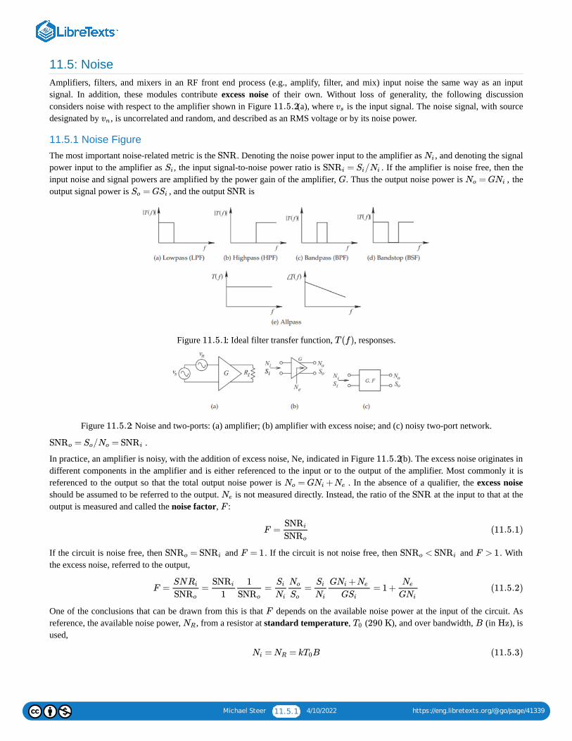
Michael Steer 11.5.1 4/10/2022 https://eng.libretexts.org/@go/page/41339
11.5: NoiseAmplifiers, filters, and mixers in an RF front end process (e.g., amplify, filter, and mix) input noise the same way as an inputsignal. In addition, these modules contribute excess noise of their own. Without loss of generality, the following discussionconsiders noise with respect to the amplifier shown in Figure (a), where is the input signal. The noise signal, with sourcedesignated by , is uncorrelated and random, and described as an RMS voltage or by its noise power.
11.5.1 Noise FigureThe most important noise-related metric is the . Denoting the noise power input to the amplifier as , and denoting the signalpower input to the amplifier as , the input signal-to-noise power ratio is . If the amplifier is noise free, then theinput noise and signal powers are amplified by the power gain of the amplifier, . Thus the output noise power is , theoutput signal power is , and the output is
Figure : Ideal filter transfer function, , responses.
Figure : Noise and two-ports: (a) amplifier; (b) amplifier with excess noise; and (c) noisy two-port network.
.
In practice, an amplifier is noisy, with the addition of excess noise, Ne, indicated in Figure (b). The excess noise originates indifferent components in the amplifier and is either referenced to the input or to the output of the amplifier. Most commonly it isreferenced to the output so that the total output noise power is . In the absence of a qualifier, the excess noiseshould be assumed to be referred to the output. is not measured directly. Instead, the ratio of the at the input to that at theoutput is measured and called the noise factor, :
If the circuit is noise free, then and . If the circuit is not noise free, then and . Withthe excess noise, referred to the output,
One of the conclusions that can be drawn from this is that depends on the available noise power at the input of the circuit. Asreference, the available noise power, , from a resistor at standard temperature, ( ), and over bandwidth, (in ), isused,
11.5.2 vs
vn
SNR Ni
Si = /SNRi Si Ni
G = GNo Ni
= GSo Si SNR
11.5.1 T (f)
11.5.2
= / =SNRo So No SNRi
11.5.2
= G +No Ni Ne
Ne SNR
F
F =SNRi
SNRo
(11.5.1)
=SNRo SNRi F = 1 <SNRo SNRi F > 1
F = = = = = 1 +SNRi
SNRo
SNRi
1
1
SNRo
Si
Ni
No
So
Si
Ni
G +Ni Ne
GSi
Ne
GNi
(11.5.2)
F
NR T0 290 K B Hz
= = k BNi NR T0 (11.5.3)
Michael Steer 11.5.2 4/10/2022 https://eng.libretexts.org/@go/page/41339
where is the Boltzmann constant. If the input of an amplifier is connected to this resistor and all of theavailable noise power is delivered to the amplifier, then
When expressed in decibels, the noise figure (NF) is used:
where the SNR is expressed in decibels. Rearranging Equation , the output-referred excess noise power is
Also from Equation , the output noise is
That is,
What is the noise figure of a attenuator in a system?
Solution
The appropriate circuit model to use in the analysis consists of the attenuator driven by a generator with a sourceimpedance, and the attenuator drives a load. Also, the input impedance of the terminated attenuator is , as is theimpedance looking into the output of the attenuator when it is connected to the source. The key point is that the noise comingfrom the source is the noise thermally generated in the source impedance, and this noise is equal to the noise that isdelivered to the load. So the input noise, , is equal to the output noise:
The input signal is attenuated by , so
and thus the noise factor is
and the noise figure is
That is, the noise figure of an attenuator (or a filter) is just the loss of the component. This is not true for amplifiers of course,as there are other sources of noise, and the output impedance of a transistor is not a thermal resistance.
11.5.2 Noise of a Cascaded System
Section 11.5.1 developed the noise factor and noise figure measures for a twoport. This can be generalized for a system.Considering the second stage of the cascade in Figure , the excess noise at the output of the second stage, due solely to thenoise generated internally in the second stage, is
Then the total noise power at the output of the two-stage cascade is
k(= 1.381 × J/K)10−23
F = 1 + = 1 +Ne
GNi
Ne
Gk BT0(11.5.4)
NF = 10 F = −log10 SNRi|dB SNRo|dB
(11.5.4)
= (F −1)Gk BNe T0 (11.5.5)
(11.5.4)
= G + = F GNo Ni Ne Ni (11.5.6)
= NF +G +No|dBm |dB Ni|dBm (11.5.7)
Example : Noise Figure of an Attenuator11.5.1
20 dB 50 Ω
50 Ω
50 Ω 50 Ω
50 Ω
Ni
=No Ni (11.5.8)
20 dB(= 100)
= /100So Si (11.5.9)
F = = = = 100SNRi
SNRo
Si
Ni
No
So
Si
Ni
Ni
/100Si
(11.5.10)
NF = 20 dB (11.5.11)
11.5.3
= ( −1)k BN2e F2 T0 G2 (11.5.12)
N2o = ( −1)k B +F2 T0 G2 No,1G2
= ( −1)k B + k BF2 T0 G2 F1 T0 G1G2 (11.5.13)

Michael Steer 11.5.3 4/10/2022 https://eng.libretexts.org/@go/page/41339
This assumes (correctly) that the excess noise added in one stage is uncorrelated to the other sources of noise. Thus noise powerscan be added. Generalizing this result the total system noise factor:
This equation is known as Friis’s formula [3].
Figure : Cascaded noisy two-ports.
Figure : Differential amplifier followed by a differential filter.
Consider the cascade of a differential amplifier and a filter shown in Figure .
a. What is the midband gain of the filter in decibels? Note that IL is insertion loss.b. What is the midband noise figure of the filter?c. The amplifier has a gain and a noise figure of . What is the overall gain of the cascade system in the
middle of the band?d. What is the noise factor of the cascade system?e. What is the noise figure of the cascade system?
Solution
a. , thus .b. For a passive element, .c. and , so .d. and . Using
Friis's formula
e. .
Consider a room-temperature ( ) two-stage amplifier where the first stage has a gain of and the second stage has again of . The noise figure of the first stage is and the second stage is . The amplifier has a bandwidth of
.
a. What is the noise power presented to the amplifier in ?b. What is the total gain of the amplifier?c. What is the total noise factor of the amplifier?d. What is the total noise figure of the amplifier?e. What is the noise power at the output of the amplifier in ?
Solution
= + + + +⋯F T F1−1F2
G1
−1F3
G1G2
−1F4
G1G2G3(11.5.14)
11.5.3
11.5.4
Example : Noise Figure of Cascaded Stages11.5.2
11.5.4
= 20 dBG1 2 dB
= 1/ILG2 = −3 dBG2
= IL = 3 dBNF2
= 20 dBG1 = −3 dBG2 = + = 17 dBGTOTAL G1|dB G2|dB
= = = 1.585, = = 1.995, = = 100,F1 10 /10NF1 102/10 F210 /10NF2 103/10 G1 1020/10 = = 0.5G2 10−3/10
= + = 1.585 + = 1.594FTOTAL F1−1F2
G1
1.995 −1
100(11.5.15)
= 10 ( ) = 10 (1.594) = 2.03 dBNFTOTAL log10 FTOTAL log10
Example : Noise Figure of a Two-Stage Amplifier11.5.3
C20∘ 10 dB
20 dB 3 dB 6 dB
10 MHz
10 MHz
10 MHz
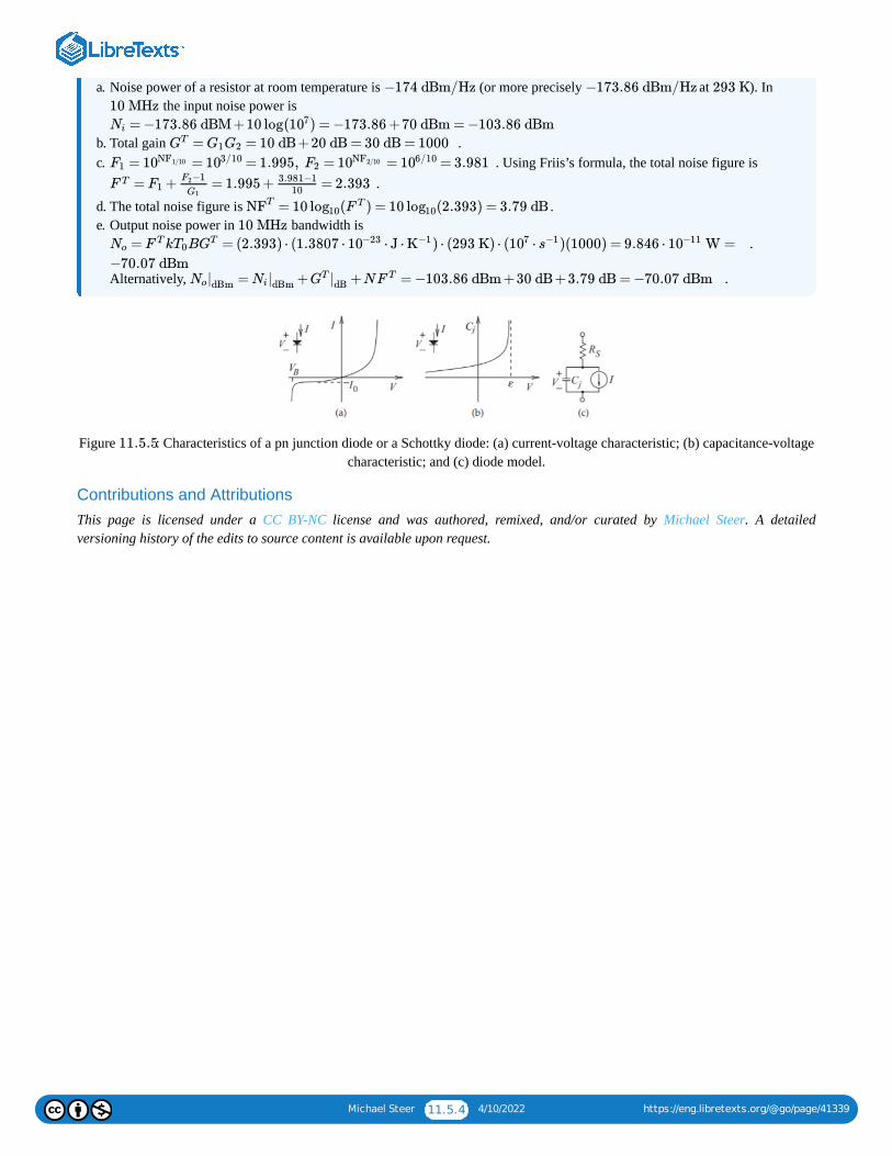
Michael Steer 11.5.4 4/10/2022 https://eng.libretexts.org/@go/page/41339
a. Noise power of a resistor at room temperature is (or more precisely at ). In the input noise power is
b. Total gain .c. . Using Friis’s formula, the total noise figure is
.
d. The total noise figure is .e. Output noise power in bandwidth is
.
Alternatively, .
Figure : Characteristics of a pn junction diode or a Schottky diode: (a) current-voltage characteristic; (b) capacitance-voltagecharacteristic; and (c) diode model.
Contributions and AttributionsThis page is licensed under a CC BY-NC license and was authored, remixed, and/or curated by Michael Steer. A detailedversioning history of the edits to source content is available upon request.
−174 dBm/Hz −173.86 dBm/Hz 293 K
10 MHz
= −173.86 dBM +10 log( ) = −173.86 +70 dBm = −103.86 dBmNi 107
= = 10 dB+20 dB = 30 dB = 1000GT G1G2
= = = 1.995, = = = 3.981F1 10NF1/10 103/10 F2 10NF2/10 106/10
= + = 1.995 + = 2.393F T F1−1F2
G1
3.981−110
= 10 ( ) = 10 (2.393) = 3.79 dBNFT log10 F T log10
10 MHz
= k B = (2.393) ⋅ (1.3807 ⋅ ⋅ J ⋅ ) ⋅ (293 K) ⋅ ( ⋅ )(1000) = 9.846 ⋅ W =No F T T0 GT 10−23 K−1 107 s−1 10−11
−70.07 dBm= + +N = −103.86 dBm +30 dB+3.79 dB = −70.07 dBmNo|dBm Ni|dBm GT |dB F T
11.5.5
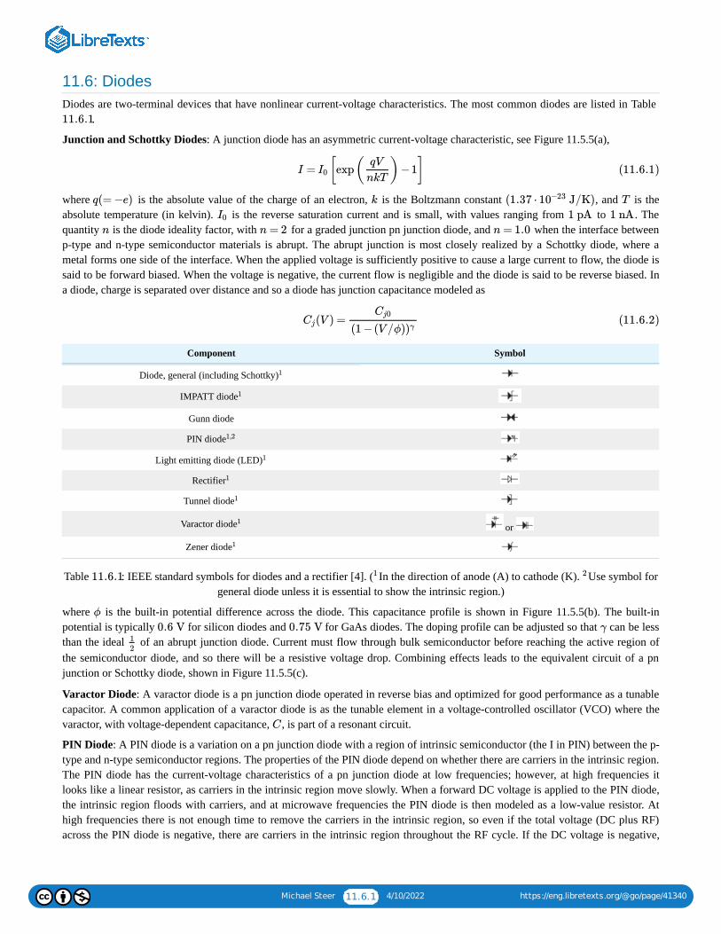
Michael Steer 11.6.1 4/10/2022 https://eng.libretexts.org/@go/page/41340
11.6: DiodesDiodes are two-terminal devices that have nonlinear current-voltage characteristics. The most common diodes are listed in Table
.
Junction and Schottky Diodes: A junction diode has an asymmetric current-voltage characteristic, see Figure 11.5.5(a),
where is the absolute value of the charge of an electron, is the Boltzmann constant , and is theabsolute temperature (in kelvin). is the reverse saturation current and is small, with values ranging from to . Thequantity is the diode ideality factor, with for a graded junction pn junction diode, and when the interface betweenp-type and n-type semiconductor materials is abrupt. The abrupt junction is most closely realized by a Schottky diode, where ametal forms one side of the interface. When the applied voltage is sufficiently positive to cause a large current to flow, the diode issaid to be forward biased. When the voltage is negative, the current flow is negligible and the diode is said to be reverse biased. Ina diode, charge is separated over distance and so a diode has junction capacitance modeled as
Component Symbol
Diode, general (including Schottky)
IMPATT diode
Gunn diode
PIN diode
Light emitting diode (LED)
Rectifier
Tunnel diode
Varactor diode or
Zener diode
Table : IEEE standard symbols for diodes and a rectifier [4]. ( In the direction of anode (A) to cathode (K). Use symbol forgeneral diode unless it is essential to show the intrinsic region.)
where is the built-in potential difference across the diode. This capacitance profile is shown in Figure 11.5.5(b). The built-inpotential is typically for silicon diodes and for GaAs diodes. The doping profile can be adjusted so that can be lessthan the ideal of an abrupt junction diode. Current must flow through bulk semiconductor before reaching the active region ofthe semiconductor diode, and so there will be a resistive voltage drop. Combining effects leads to the equivalent circuit of a pnjunction or Schottky diode, shown in Figure 11.5.5(c).
Varactor Diode: A varactor diode is a pn junction diode operated in reverse bias and optimized for good performance as a tunablecapacitor. A common application of a varactor diode is as the tunable element in a voltage-controlled oscillator (VCO) where thevaractor, with voltage-dependent capacitance, , is part of a resonant circuit.
PIN Diode: A PIN diode is a variation on a pn junction diode with a region of intrinsic semiconductor (the I in PIN) between the p-type and n-type semiconductor regions. The properties of the PIN diode depend on whether there are carriers in the intrinsic region.The PIN diode has the current-voltage characteristics of a pn junction diode at low frequencies; however, at high frequencies itlooks like a linear resistor, as carriers in the intrinsic region move slowly. When a forward DC voltage is applied to the PIN diode,the intrinsic region floods with carriers, and at microwave frequencies the PIN diode is then modeled as a low-value resistor. Athigh frequencies there is not enough time to remove the carriers in the intrinsic region, so even if the total voltage (DC plus RF)across the PIN diode is negative, there are carriers in the intrinsic region throughout the RF cycle. If the DC voltage is negative,
11.6.1
I = [exp( )−1]I0qV
nkT(11.6.1)
q(= −e) k (1.37 ⋅ J/K)10−23 T
I0 1 pA 1 nA
n n = 2 n = 1.0
(V ) =Cj
Cj0
(1 −(V /ϕ))γ(11.6.2)
1
1
1,2
1
1
1
1
1
11.6.1 1 2
ϕ
0.6 V 0.75 V γ12
C

Michael Steer 11.6.2 4/10/2022 https://eng.libretexts.org/@go/page/41340
carriers are removed from the intrinsic region and the diode looks like a large-value resistor at RF. The PIN diode is used as amicrowave switch controlled by a DC voltage.
Zener Diode: Zener diodes are pn junction or Schottky diodes that have been specially designed to have sharp reverse breakdowncharacteristics. They can be used to establish a voltage reference or, used as a limiter diode, to provide protection of more sensitivecircuitry. As a limiter, they are found in communication devices in a back-to-back configuration to limit the voltages that can beapplied to sensitive RF circuitry.
Contributions and Attributions
This page is licensed under a CC BY-NC license and was authored, remixed, and/or curated by Michael Steer. A detailedversioning history of the edits to source content is available upon request.
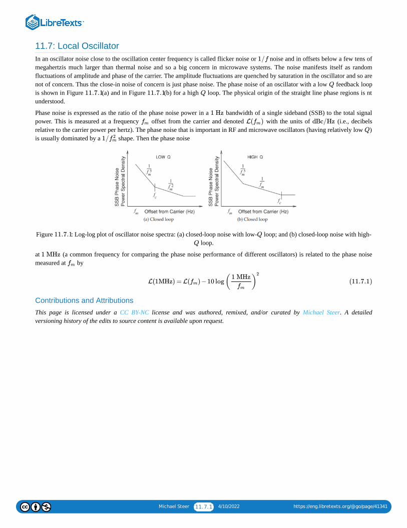
Michael Steer 11.7.1 4/10/2022 https://eng.libretexts.org/@go/page/41341
11.7: Local OscillatorIn an oscillator noise close to the oscillation center frequency is called flicker noise or noise and in offsets below a few tens ofmegahertzis much larger than thermal noise and so a big concern in microwave systems. The noise manifests itself as randomfluctuations of amplitude and phase of the carrier. The amplitude fluctuations are quenched by saturation in the oscillator and so arenot of concern. Thus the close-in noise of concern is just phase noise. The phase noise of an oscillator with a low feedback loopis shown in Figure (a) and in Figure (b) for a high loop. The physical origin of the straight line phase regions is ntunderstood.
Phase noise is expressed as the ratio of the phase noise power in a bandwidth of a single sideband (SSB) to the total signalpower. This is measured at a frequency offset from the carrier and denoted with the units of (i.e., decibelsrelative to the carrier power per hertz). The phase noise that is important in RF and microwave oscillators (having relatively low )is usually dominated by a shape. Then the phase noise
Figure : Log-log plot of oscillator noise spectra: (a) closed-loop noise with low- loop; and (b) closed-loop noise with high- loop.
at (a common frequency for comparing the phase noise performance of different oscillators) is related to the phase noisemeasured at by
Contributions and Attributions
This page is licensed under a CC BY-NC license and was authored, remixed, and/or curated by Michael Steer. A detailedversioning history of the edits to source content is available upon request.
1/f
Q
11.7.1 11.7.1 Q
1 Hz
fm L( )fm dBc/Hz
Q
1/f 2m
11.7.1 Q
Q
1 MHz
fm
L(1MHz) = L( ) −10 logfm ( )1 MHz
fm
2
(11.7.1)

Michael Steer 11.8.1 4/10/2022 https://eng.libretexts.org/@go/page/41342
11.8: Frequency MultiplierA microwave frequency multiplier uses a nonlinear element to generate harmonics and a bandpass filter selects the appropriateharmonic for the output, see Figure 11.12.1. If the input signal is
then the output at the harmonic is
Contributions and Attributions
This page is licensed under a CC BY-NC license and was authored, remixed, and/or curated by Michael Steer. A detailedversioning history of the edits to source content is available upon request.
x(t) = A cos( +ϕ)ωt (11.8.1)
n
y(t) = cos(n +nϕ)An ωt (11.8.2)

Michael Steer 11.9.1 4/10/2022 https://eng.libretexts.org/@go/page/41343
11.9: SummaryThe use of modules has become increasingly important in microwave engineering. A wide variety of passive and active modulesare available and high-performance systems can be realized enabling many microwave systems of low to medium volumes to berealized cost effectively and with stellar performance. Module vendors are encouraged by the market to develop competitivemodules that can be used in a wide variety of applications.
Figure : Frequency multiplier using a nonlinear tuned circuit.
Contributions and AttributionsThis page is licensed under a CC BY-NC license and was authored, remixed, and/or curated by Michael Steer. A detailedversioning history of the edits to source content is available upon request.
11.9.1

Michael Steer 11.10.1 4/10/2022 https://eng.libretexts.org/@go/page/41344
11.10: References[1] http://www.synergymwave.com.
[2] http://www.hittite.com.
[3] H. Friis, “Noise figures of radio receivers,” Proc. of the IRE, vol. 32, no. 7, pp. 419–422, Jul. 1944.
[4] IEEE Standard 315-1975, Graphic Symbols for Electrical and Electronics Diagrams (Including Reference Designation Letters),Adopted Sept. 1975, Reaffirmed Dec. 1993. Approved by American National Standards Institute, Jan. 1989. Approved adopted formandatory use, Department of Defense, United States of America, Oct. 1975. Approved by Canadian Standards Institute, Oct.1975.
Contributions and AttributionsThis page is licensed under a CC BY-NC license and was authored, remixed, and/or curated by Michael Steer. A detailedversioning history of the edits to source content is available upon request.
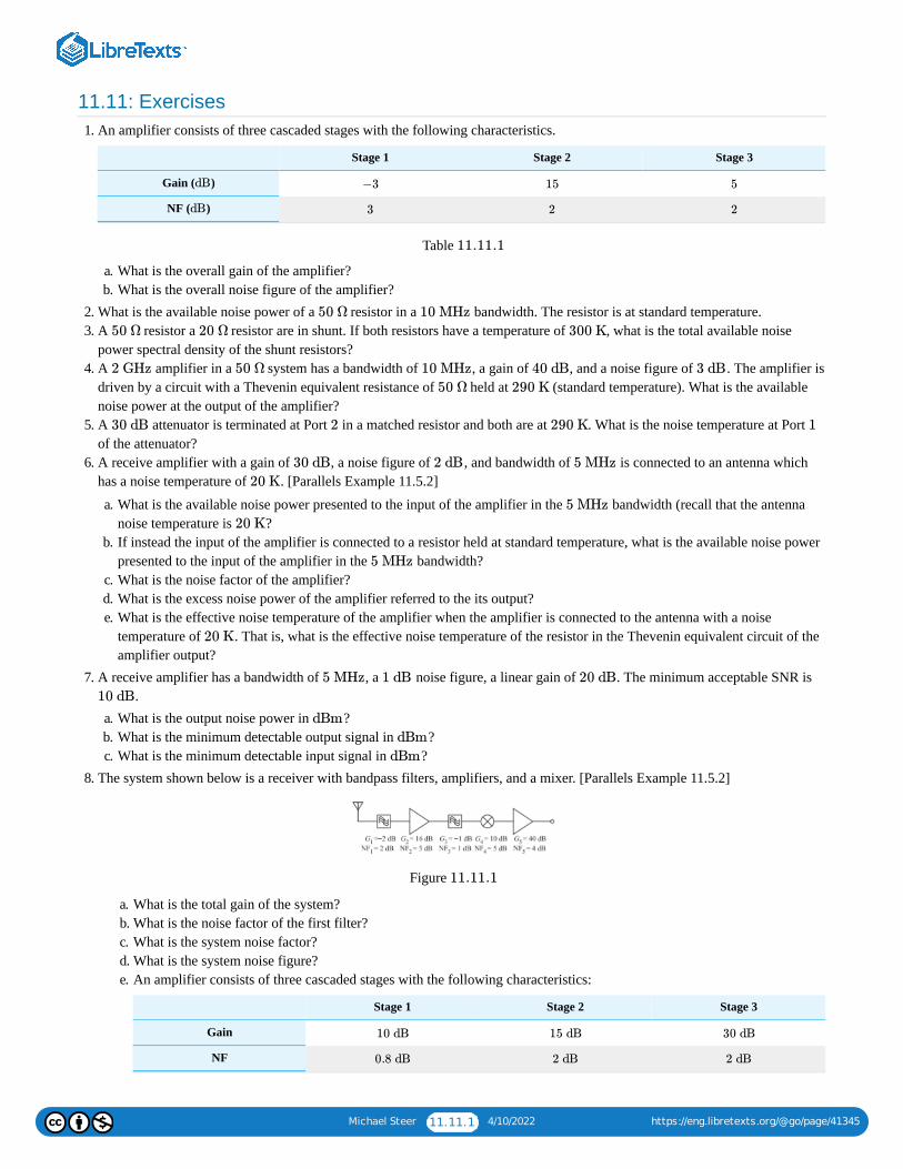
Michael Steer 11.11.1 4/10/2022 https://eng.libretexts.org/@go/page/41345
11.11: Exercises1. An amplifier consists of three cascaded stages with the following characteristics.
Stage 1 Stage 2 Stage 3
Gain ( )
NF ( )
Table
a. What is the overall gain of the amplifier?b. What is the overall noise figure of the amplifier?
2. What is the available noise power of a resistor in a bandwidth. The resistor is at standard temperature.3. A resistor a resistor are in shunt. If both resistors have a temperature of , what is the total available noise
power spectral density of the shunt resistors?4. A amplifier in a system has a bandwidth of , a gain of , and a noise figure of . The amplifier is
driven by a circuit with a Thevenin equivalent resistance of held at (standard temperature). What is the availablenoise power at the output of the amplifier?
5. A attenuator is terminated at Port in a matched resistor and both are at . What is the noise temperature at Port of the attenuator?
6. A receive amplifier with a gain of , a noise figure of , and bandwidth of is connected to an antenna whichhas a noise temperature of . [Parallels Example 11.5.2]
a. What is the available noise power presented to the input of the amplifier in the bandwidth (recall that the antennanoise temperature is ?
b. If instead the input of the amplifier is connected to a resistor held at standard temperature, what is the available noise powerpresented to the input of the amplifier in the bandwidth?
c. What is the noise factor of the amplifier?d. What is the excess noise power of the amplifier referred to the its output?e. What is the effective noise temperature of the amplifier when the amplifier is connected to the antenna with a noise
temperature of . That is, what is the effective noise temperature of the resistor in the Thevenin equivalent circuit of theamplifier output?
7. A receive amplifier has a bandwidth of , a noise figure, a linear gain of . The minimum acceptable SNR is .
a. What is the output noise power in ?b. What is the minimum detectable output signal in ?c. What is the minimum detectable input signal in ?
8. The system shown below is a receiver with bandpass filters, amplifiers, and a mixer. [Parallels Example 11.5.2]
Figure
a. What is the total gain of the system?b. What is the noise factor of the first filter?c. What is the system noise factor?d. What is the system noise figure?e. An amplifier consists of three cascaded stages with the following characteristics:
Stage 1 Stage 2 Stage 3
Gain
NF
dB −3 15 5
dB 3 2 2
11.11.1
50 Ω 10 MHz
50 Ω 20 Ω 300 K
2 GHz 50 Ω 10 MHz 40 dB 3 dB
50 Ω 290 K
30 dB 2 290 K 1
30 dB 2 dB 5 MHz
20 K
5 MHz
20 K
5 MHz
20 K
5 MHz 1 dB 20 dB
10 dB
dBm
dBm
dBm
11.11.1
10 dB 15 dB 30 dB
0.8 dB 2 dB 2 dB

Michael Steer 11.11.2 4/10/2022 https://eng.libretexts.org/@go/page/41345
Table What is the noise figure (NF) and gain of the cascade amplifier?
10. The first stage of a two-stage amplifier has a linear gain of and a noise figure if . The second stage has a gain of and a noise figure of .
a. What is the overall gain of the amplifier?b. What is the overall noise figure of the amplifier?
11. A subsystem consists of a matched filter with an insertion loss of then an amplifier with a gain of and a noisefigure, NF, of .a. What is the overall gain of the subsystem?b. What is NF of the filter?c. What is NF of the subsystem?
12. A subsystem consists of a matched amplifier with a gain of and a noise figure of , followed by a attenuator,and then another amplifier with a gain of and NF of .a. What is the overall gain of the subsystem?b. What is NF of the attenuator?c. What is NF of the subsystem?
13. A connector used in a system introduces a series resistance of . What is the insertion loss of the connector?14. A microwave switch is used in a system and has a on resistance. The reactive parasitics of the switch are negligible.
a. What is the insertion loss of the switch in the on state?b. What is the return loss of the switch in the on state?
15. A microwave switch is used in a system and has a on resistance. The reactive parasitics of the switch are negligible.a. What is the insertion loss of the switch in the on state?b. If the available power of the source is , what is the power dissipated by the switch?
16. A microwave switch is used at in a system and it has a on resistance and a off resistance. The reactiveparasitics of the switch are negligible.a. What is the insertion loss of the switch?b. What is the isolation of the switch (i.e., what is the insertion loss of the switch when it is in the off state)?
17. The RF front end of a communications unit consists of a switch, then an amplifier, and then a mixer. The switch has a loss of , the amplifier has a gain of , and the mixer has a conversion gain of . What is the overall gain of the
cascade?18. A three-port circulator has the parameters
Port is terminated in a matched load creating a two-port network.a. Find the parameters of the two-port.b. What is the return loss in at Port if Port is terminated in a matched load?c. What is the insertion loss in for a signal applied at Port and leaving at Port with matched source and load
impedances?d. What is the insertion loss in for a signal applied at Port and leaving at Port with matched source and load
impedances?19. Two isolators are used in cascade. Each isolator has an isolation of . The isolators are matched so that their input and
output reflection coefficients are zero. Determine the isolation of the cascaded isolator system?20. A three-port circulator in a system has the parameters
11.11.2
40 dB 3 dB
10 dB 5 dB
2 dB 20 dB
3 dB
20 dB 2 dB 2 dB
10 dB 3 dB
50 Ω 0.5 Ω
75 Ω 5 Ω
50 Ω 5 Ω
50 W
1 GHz 50 Ω 2 Ω 2 kΩ
0.5 dB 20 dB 3 dB
S
⎡
⎣⎢
0
20.5
0
0
0
0.5
0.5
0
0
⎤
⎦⎥
3
S
dB 1 2
dB 1 2
dB 2 1
20 dB
50 Ω S
⎡
⎣⎢
0.1
0.5
0.01
0.01
0.1
0.5
0.5
0.01
0.1
⎤
⎦⎥

Michael Steer 11.11.3 4/10/2022 https://eng.libretexts.org/@go/page/41345
If port is terminated in a matched load to create a two-port networka. Find the parameters of the two-port.b. What is the return loss in at Port if Port is terminated in ?c. What is the insertion loss in for a signal applied at Port and leaving at Port with source and load impedances?d. What is the insertion loss in for a signal applied at Port and leaving at Port with source and load impedances?e. What is is the name of this network?
21. A mixer in a receiver has a conversion loss of . If the applied RF signal has an available power of , what is theavailable power of the IF at the output of the mixer?
22. The RF signal applied to the input of a mixer has a power of and the output of the mixer at the IF has a power level of . What is the conversion loss of the mixer in decibels?
23. A mixer in a receiver has a conversion gain of . If the applied RF signal has a power of , what is the availablepower of the IF at the output of the mixer?
24. A mixer in a receiver has a conversion loss of . If the applied RF signal has a power of , what is the available powerof the IF at the output of the mixer?
25. The phase noise of an oscillator was measured as at offset. What is the normalized phase noise at offset, assuming that the phase noise power varies as the square of the inverse of frequency?
26. The phase noise of an oscillator was measured as at offset. What is the normalized phase noise at offset, assuming that the phase noise power varies inversely with frequency offset?
11.14.1 Exercises by Section
challenging,
11.14.2 Answers to Selected Exercises8. (d)
10. (b)
12. (b)
14. (b) 15. (a)
17.
19.
21.
23.
Contributions and Attributions
This page is licensed under a CC BY-NC license and was authored, remixed, and/or curated by Michael Steer. A detailedversioning history of the edits to source content is available upon request.
3
S
dB 1 2 50 Ω
dB 2 1 50 Ω
dB 1 2 50 Ω
16 dB 100 μW
1 nW
100 pW
10 dB 100 μW
6 dB 1 μW
−125 dBc/Hz 100 kHz
1 MHz
−125 dBc/Hz 100 kHz
1 MHz
†
§11.51, 2, 3, 4, 5, 6, 7, 8, 9, 10, 11, 12
§11.713, 14†, 15†, 16†, 17†
§11.818, 19, 20
§11.921, 22, 23, 24
§11.1025†, 26
5.17 dB
3 dB
60 dB
29.8 dB
0.424 dB
22.5 dB
40 dB
−26 dBm
0 dBm
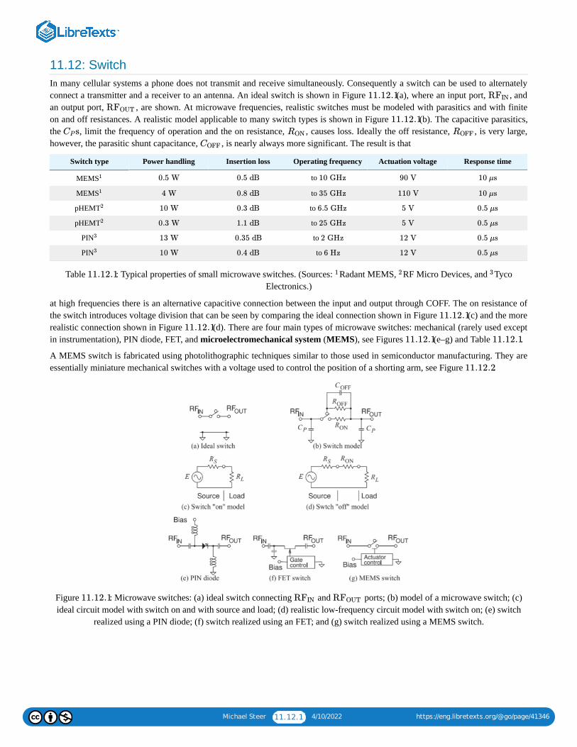
Michael Steer 11.12.1 4/10/2022 https://eng.libretexts.org/@go/page/41346
11.12: SwitchIn many cellular systems a phone does not transmit and receive simultaneously. Consequently a switch can be used to alternatelyconnect a transmitter and a receiver to an antenna. An ideal switch is shown in Figure (a), where an input port, , andan output port, , are shown. At microwave frequencies, realistic switches must be modeled with parasitics and with finiteon and off resistances. A realistic model applicable to many switch types is shown in Figure (b). The capacitive parasitics,the , limit the frequency of operation and the on resistance, , causes loss. Ideally the off resistance, , is very large,however, the parasitic shunt capacitance, , is nearly always more significant. The result is that
Switch type Power handling Insertion loss Operating frequency Actuation voltage Response time
MEMS to
MEMS to
pHEMT to
pHEMT to
PIN to
PIN to
Table : Typical properties of small microwave switches. (Sources: Radant MEMS, RF Micro Devices, and TycoElectronics.)
at high frequencies there is an alternative capacitive connection between the input and output through COFF. The on resistance ofthe switch introduces voltage division that can be seen by comparing the ideal connection shown in Figure (c) and the morerealistic connection shown in Figure (d). There are four main types of microwave switches: mechanical (rarely used exceptin instrumentation), PIN diode, FET, and microelectromechanical system (MEMS), see Figures (e–g) and Table .
A MEMS switch is fabricated using photolithographic techniques similar to those used in semiconductor manufacturing. They areessentially miniature mechanical switches with a voltage used to control the position of a shorting arm, see Figure .
Figure : Microwave switches: (a) ideal switch connecting and ports; (b) model of a microwave switch; (c)ideal circuit model with switch on and with source and load; (d) realistic low-frequency circuit model with switch on; (e) switch
realized using a PIN diode; (f) switch realized using an FET; and (g) switch realized using a MEMS switch.
11.12.1 RFIN
RFOUT
11.12.1
sCP RON ROFF
COFF
1 0.5 W 0.5 dB 10 GHz 90 V 10 μs
1 4 W 0.8 dB 35 GHz 110 V 10 μs
2 10 W 0.3 dB 6.5 GHz 5 V 0.5 μs
2 0.3 W 1.1 dB 25 GHz 5 V 0.5 μs
3 13 W 0.35 dB 2 GHz 12 V 0.5 μs
3 10 W 0.4 dB 6 Hz 12 V 0.5 μs
11.12.1 1 2 3
11.12.1
11.12.1
11.12.1 11.12.1
11.12.2
11.12.1 RFIN RFOUT
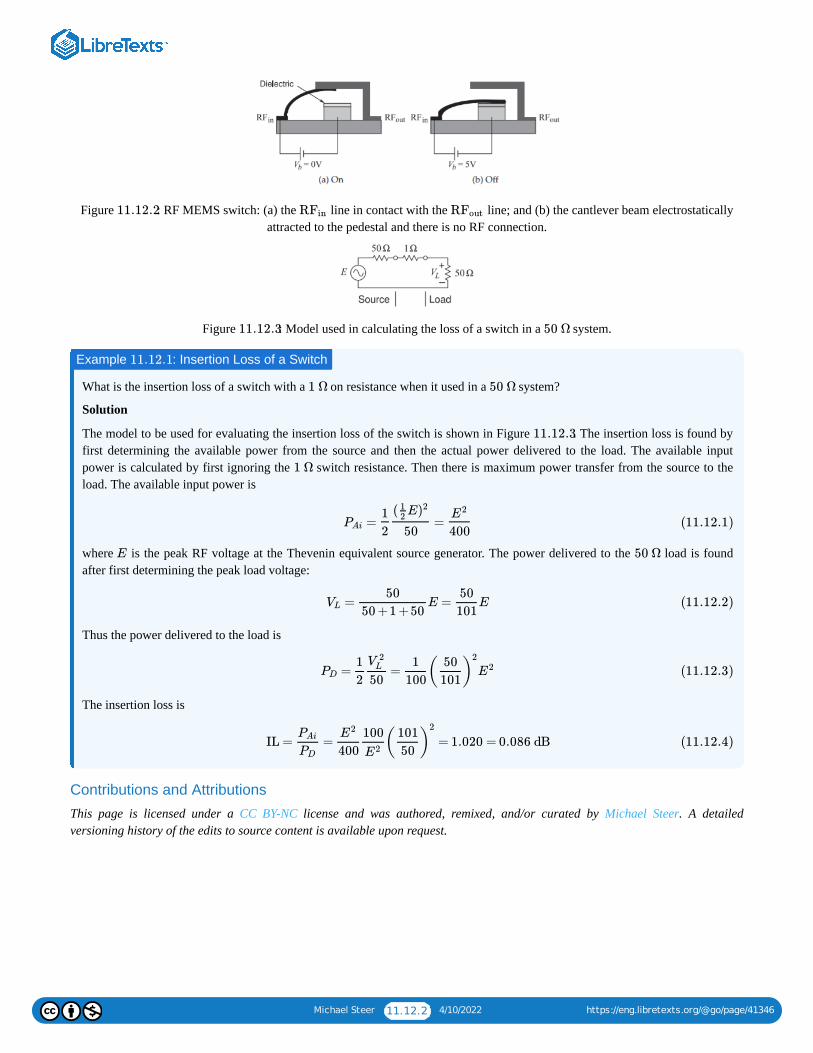
Michael Steer 11.12.2 4/10/2022 https://eng.libretexts.org/@go/page/41346
Figure : RF MEMS switch: (a) the line in contact with the line; and (b) the cantlever beam electrostaticallyattracted to the pedestal and there is no RF connection.
Figure : Model used in calculating the loss of a switch in a system.
What is the insertion loss of a switch with a on resistance when it used in a system?
Solution
The model to be used for evaluating the insertion loss of the switch is shown in Figure . The insertion loss is found byfirst determining the available power from the source and then the actual power delivered to the load. The available inputpower is calculated by first ignoring the switch resistance. Then there is maximum power transfer from the source to theload. The available input power is
where is the peak RF voltage at the Thevenin equivalent source generator. The power delivered to the load is foundafter first determining the peak load voltage:
Thus the power delivered to the load is
The insertion loss is
Contributions and Attributions
This page is licensed under a CC BY-NC license and was authored, remixed, and/or curated by Michael Steer. A detailedversioning history of the edits to source content is available upon request.
11.12.2 RFin RFout
11.12.3 50 Ω
Example : Insertion Loss of a Switch11.12.1
1 Ω 50 Ω
11.12.3
1 Ω
= =PAi
1
2
( E12
)2
50
E2
400(11.12.1)
E 50 Ω
= E = EVL
50
50 +1 +50
50
101(11.12.2)
= =PD
1
2
V 2L
50
1
100( )
50
101
2
E2 (11.12.3)
IL = = = 1.020 = 0.086 dBPAi
PD
E2
400
100
E2( )
101
50
2
(11.12.4)
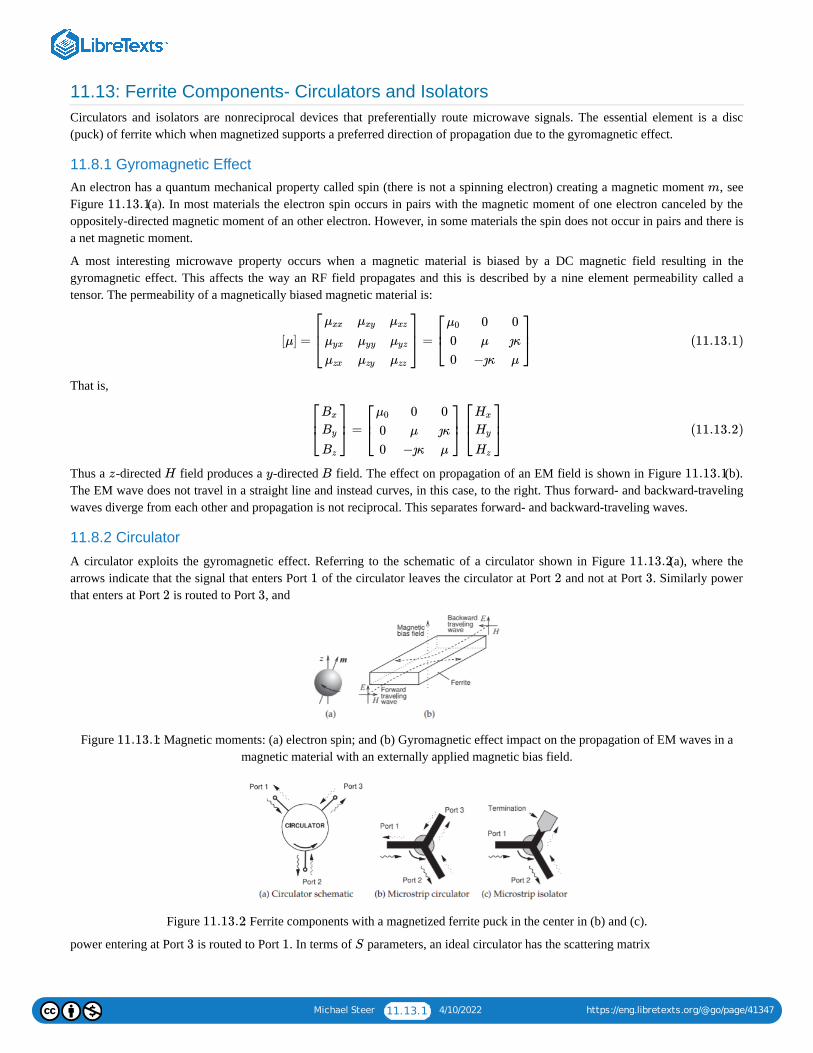
Michael Steer 11.13.1 4/10/2022 https://eng.libretexts.org/@go/page/41347
11.13: Ferrite Components- Circulators and IsolatorsCirculators and isolators are nonreciprocal devices that preferentially route microwave signals. The essential element is a disc(puck) of ferrite which when magnetized supports a preferred direction of propagation due to the gyromagnetic effect.
11.8.1 Gyromagnetic EffectAn electron has a quantum mechanical property called spin (there is not a spinning electron) creating a magnetic moment , seeFigure (a). In most materials the electron spin occurs in pairs with the magnetic moment of one electron canceled by theoppositely-directed magnetic moment of an other electron. However, in some materials the spin does not occur in pairs and there isa net magnetic moment.
A most interesting microwave property occurs when a magnetic material is biased by a DC magnetic field resulting in thegyromagnetic effect. This affects the way an RF field propagates and this is described by a nine element permeability called atensor. The permeability of a magnetically biased magnetic material is:
That is,
Thus a -directed field produces a -directed field. The effect on propagation of an EM field is shown in Figure (b).The EM wave does not travel in a straight line and instead curves, in this case, to the right. Thus forward- and backward-travelingwaves diverge from each other and propagation is not reciprocal. This separates forward- and backward-traveling waves.
11.8.2 Circulator
A circulator exploits the gyromagnetic effect. Referring to the schematic of a circulator shown in Figure (a), where thearrows indicate that the signal that enters Port of the circulator leaves the circulator at Port and not at Port . Similarly powerthat enters at Port is routed to Port , and
Figure : Magnetic moments: (a) electron spin; and (b) Gyromagnetic effect impact on the propagation of EM waves in amagnetic material with an externally applied magnetic bias field.
Figure : Ferrite components with a magnetized ferrite puck in the center in (b) and (c).
power entering at Port is routed to Port . In terms of parameters, an ideal circulator has the scattering matrix
m
11.13.1
[μ] = =⎡
⎣⎢
μxx
μyx
μzx
μxy
μyy
μzy
μxz
μyz
μzz
⎤
⎦⎥
⎡
⎣⎢
μ0
0
0
0
μ
−ȷκ
0
ȷκ
μ
⎤
⎦⎥ (11.13.1)
=⎡
⎣⎢
Bx
By
Bz
⎤
⎦⎥
⎡
⎣⎢
μ0
0
0
0
μ
−ȷκ
0
ȷκ
μ
⎤
⎦⎥⎡
⎣⎢
Hx
Hy
Hz
⎤
⎦⎥ (11.13.2)
z H y B 11.13.1
11.13.2
1 2 3
2 3
11.13.1
11.13.2
3 1 S

Michael Steer 11.13.2 4/10/2022 https://eng.libretexts.org/@go/page/41347
A microstrip circulator is shown in Figure (b), where a disc of magnetized ferrite can be placed on top of a microstrip Yjunction to realize a preferential direction of propagation of the EM fields. In the absence of the biasing magnetic field, thecirculation function does not occur.
11.8.3 Circulator IsolationThe isolation of a circulator is the insertion loss from what is the output port to the input port, i.e. in the reverse direction. Referringto the circulator in Figure (a), if port is the input port there are two output ports and so there are two isolations equal tothe return loss from port to port , and from port to port . The smaller of these is the quoted isolation. If this is an idealcirculator and port is perfectly matched, then the isolation would be infinite. Then the parameters of the circulator are
where is the transmission factor, is the reflection coefficient at the ports, and is the leakage.
11.8.4 Isolator
Isolators are devices that allow power flow in only one direction. Figures (c) and show microstrip isolators basedon three-port circulators. Power entering Port as a traveling wave is transferred to the ferrite and emerges at Port . Virtuallynone of the power emerges at Port . A traveling wave signal applied at Port appears at Port , where it is absorbed in atermination created by resistive material placed on top of the microstrip. The resistive material forms a lossy transmission line andno power is reflected. Thus power can travel from Port to Port , but not in the reverse direction.
Figure : A microstrip isolator operating from to . Isolator in (b) has the dimensions and is high. The isolator supports of forward and reverse power with an isolation of and insertion loss of .
Renaissance 2W9 series, copyright Renaissance Electronics Corporation, used with permission.
S = =⎡
⎣⎢
0
S21
0
0
0
S32
S13
0
0
⎤
⎦⎥
⎡
⎣⎢
0
1
0
0
0
1
1
0
0
⎤
⎦⎥ (11.13.3)
11.13.2
11.13.2 1
3 2 2 1
2 S
S = ≈⎡
⎣⎢
Γ
T
α
α
Γ
T
T
α
Γ
⎤
⎦⎥
⎡
⎣⎢
0
1
0
0
0
1
1
0
0
⎤
⎦⎥ (11.13.4)
T Γ α
11.13.2 11.13.3
1 2
3 2 3
1 2
11.13.3 29 31.5 GHz 5 mm ×6 mm
6 mm 2 W 18 dB 1 dB
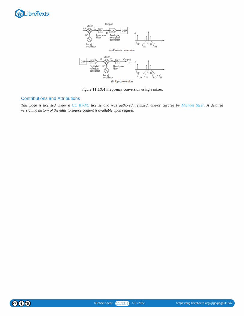
Michael Steer 11.13.3 4/10/2022 https://eng.libretexts.org/@go/page/41347
Figure : Frequency conversion using a mixer.
Contributions and AttributionsThis page is licensed under a CC BY-NC license and was authored, remixed, and/or curated by Michael Steer. A detailedversioning history of the edits to source content is available upon request.
11.13.4
Michael Steer 11.14.1 4/10/2022 https://eng.libretexts.org/@go/page/41348
11.14: MixerFrequency conversion or mixing is the process of converting information centered at one frequency (present in the form of amodulated carrier) to another frequency. The second frequency is either higher, in the case of frequency up-conversion, where it ismore easily transmitted; or lower when mixing is called frequency down-conversion, where it is more easily captured, see Figure11.8.4.
Conversion loss, : This is the ratio of the available power of the input signal, , to that of the output signal after mixing,:
A mixer has an LO of . The mixer is used to down-convert a signal at and has a conversion loss, of and an image rejection of . A signal is presented to the mixer at . What is the frequency and outputpower of the down-converted signal at the IF?
Solution
The IF is at . and from Equation the output power at IF of the intended signal is
Contributions and Attributions
This page is licensed under a CC BY-NC license and was authored, remixed, and/or curated by Michael Steer. A detailedversioning history of the edits to source content is available upon request.
LC (RF)Pin
(IF)Pout
=LC
(RF)Pin
(IF)Pout
(11.14.1)
Example : Mixer Calculations11.14.1
10 GHz 10.1 GHz Lc 3 dB
20 dB 100 nW 10.1 GHz
100 MHz = 3 dB = 2Lc (11.14.1)
= (RF)/ = 100 nW/2 = 50 nW = −43 dBmPout Pin Lc (11.14.2)

Michael Steer 1 4/10/2022 https://eng.libretexts.org/@go/page/41349
IndexLL network
10.4: The L Matching Network

1 4/10/2022 https://eng.libretexts.org/@go/page/41350
IndexLL network
10.4: The L Matching Network

1 4/10/2022 https://eng.libretexts.org/@go/page/41351
GlossarySample Word 1 | Sample Definition 1