functional unit, basic operational concepts, bus structures
TRANSCRIPT
UNIT I
Syllabus: Basic Structure Of Computers: Functional unit, Basic Operational concepts, Bus
structures, System Software, Performance, The history of computer development.
Computer: Computer is a fast electronic calculating machine that accepts digitized input information,
processing it according to a list of internally stored instructions and produces the resulting output
information. The list of instructions is called as a Computer program and the internal storage is called as
Computer memory.
Types of Languages: Just as humans use language to communicate, and different regions have different
languages, computers also have their own languages that are specific to them. Different kinds of languages
have been developed to perform different types of work on the computer. Basically, languages can be divided
into two categories according to how the computer understands them.
➢ Low-Level Languages: A language that corresponds directly to a specific machine. Low-level computer
languages are either machine codes or are very close them. A computer cannot understand instructions
given to it in high-level languages or in English. It can only understand and execute instructions given in
the form of machine language i.e. binary. There are two types of low-level languages:
• Machine Language: a language that is directly interpreted into the hardware. Machine language is
the lowest and most elementary level of programming language and was the first type of
programming language to be developed. Machine language is basically the only language that a
computer can understand and it is usually written in hex. It is represented inside the computer by a
string of binary digits (bits) 0 and 1. The symbol 0 stands for the absence of an electric pulse and the
1 stands for the presence of an electric pulse. Since a computer is capable of recognizing electric
signals, it understands machine language.
Advantages:
➢ Machine language makes fast and efficient use of the computer.
➢ It requires no translator to translate the code. It is directly understood by the computer.
Disadvantages:
➢ All operation codes have to be remembered
➢ All memory addresses have to be remembered.
➢ It is hard to amend or find errors in a program written in the machine language.
• Assembly Language: A slightly more user-friendly language that directly corresponds to machine
language. Assembly language was developed to overcome some of the many inconveniences of
machine language. This is another low-level but very important language in which operation codes
and operands are given in the form of alphanumeric symbols instead of 0’s and l’s.
These alphanumeric symbols are known as mnemonic codes and can combine in a maximum
of five-letter combinations e.g. ADD for addition, SUB for subtraction, START, LABEL etc.
Because of this feature, assembly language is also known as ‘Symbolic Programming Language.'
Advantages:
➢ Assembly language is easier to understand and use as compared to machine language.
➢ It is easy to locate and correct errors.
➢ It is easily modified.
Disadvantages:
➢ Like machine language, it is also machine dependent/specific.
➢ Since it is machine dependent, the programmer also needs to understand the hardware.
➢ High-Level Languages: Any language that is independent of the machine. High-level computer
languages use formats that are similar to English. The purpose of developing high-level languages was to
enable people to write programs easily, in their own native language environment (English).
High-level languages are basically symbolic languages that use English words and/or mathematical
symbols rather than mnemonic codes. Each instruction in the high-level language is translated into many
machine language instructions that the computer can understand.
Advantages:
o High-level languages are user-friendly
o They are easier to learn.
o They are easier to maintain
o A program written in a high-level language can be translated into many machine languages and can
run on any computer
o programs developed in a high-level language can be run on any computer text
Disadvantages:
o A high-level language has to be translated into the machine language by a translator, which takes up
time
Computer Types: Basing capacity, technology used and performance of computer, they are classified
into two types
→ According to computational ability
→ According to generation
According to computational ability (Based on Size, cost and performance):
There are mainly 4 types of computers. These include:
a) Micro computers
b) Mainframe computers
c) Mini computers
d) Super computer
a) Micro computers: -
Micro computers are the most common type of computers in existence today, whether at work in
school or on the desk at home. These computers include:
1. Desktop computer
2. Personal digital assistants (more commonly known as PDA's)
3. Palmtop computers
4. Laptop and notebook computers
Micro computers were the smallest, least powerful and least expensive of the computers of the time.
The first Micro computers could only perform one task at a time, while bigger computers ran multi-tasking
operating systems, and served multiple users. Referred to as a personal computer or "desktop computer",
Micro computers are generally meant to service one user (person) at a time. By the late 1990s, all personal
computers run a multi-tasking operating system, but are still intended for a single user.
b) Mainframe Computers :-
The term Mainframe computer was created to distinguish the traditional, large, institutional computer
intended to service multiple users from the smaller, single user machines. These computers are capable of
handling and processing very large amounts of data easily and quickly. A mainframe speed is so fast that it
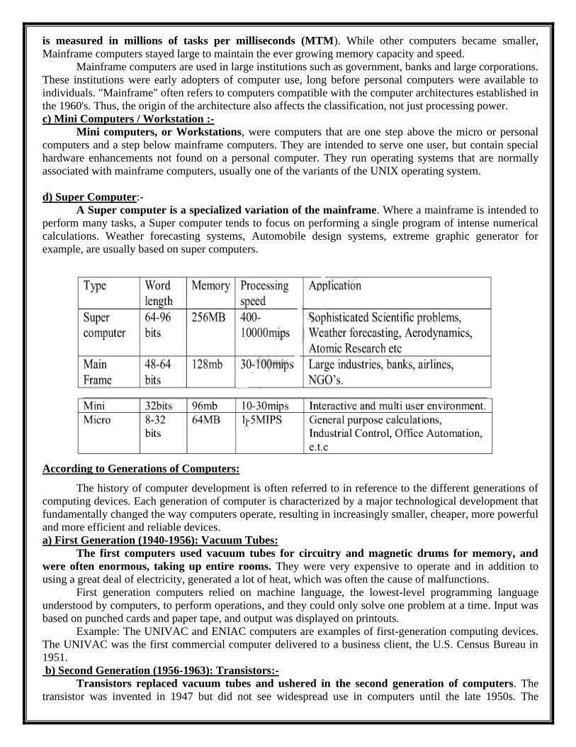
is measured in millions of tasks per milliseconds (MTM). While other computers became smaller,
Mainframe computers stayed large to maintain the ever growing memory capacity and speed.
Mainframe computers are used in large institutions such as government, banks and large corporations.
These institutions were early adopters of computer use, long before personal computers were available to
individuals. "Mainframe" often refers to computers compatible with the computer architectures established in
the 1960's. Thus, the origin of the architecture also affects the classification, not just processing power.
c) Mini Computers / Workstation :-
Mini computers, or Workstations, were computers that are one step above the micro or personal
computers and a step below mainframe computers. They are intended to serve one user, but contain special
hardware enhancements not found on a personal computer. They run operating systems that are normally
associated with mainframe computers, usually one of the variants of the UNIX operating system.
d) Super Computer:-
A Super computer is a specialized variation of the mainframe. Where a mainframe is intended to
perform many tasks, a Super computer tends to focus on performing a single program of intense numerical
calculations. Weather forecasting systems, Automobile design systems, extreme graphic generator for
example, are usually based on super computers.
According to Generations of Computers:
The history of computer development is often referred to in reference to the different generations of
computing devices. Each generation of computer is characterized by a major technological development that
fundamentally changed the way computers operate, resulting in increasingly smaller, cheaper, more powerful
and more efficient and reliable devices.
a) First Generation (1940-1956): Vacuum Tubes:
The first computers used vacuum tubes for circuitry and magnetic drums for memory, and
were often enormous, taking up entire rooms. They were very expensive to operate and in addition to
using a great deal of electricity, generated a lot of heat, which was often the cause of malfunctions.
First generation computers relied on machine language, the lowest-level programming language
understood by computers, to perform operations, and they could only solve one problem at a time. Input was
based on punched cards and paper tape, and output was displayed on printouts.
Example: The UNIVAC and ENIAC computers are examples of first-generation computing devices.
The UNIVAC was the first commercial computer delivered to a business client, the U.S. Census Bureau in
1951.
b) Second Generation (1956-1963): Transistors:-
Transistors replaced vacuum tubes and ushered in the second generation of computers. The
transistor was invented in 1947 but did not see widespread use in computers until the late 1950s. The
transistor was far superior to the vacuum tube, allowing computers to become smaller, faster, cheaper, more
energy-efficient and more reliable than their first-generation predecessors. Though the transistor still
generated a great deal of heat that subjected the computer to damage, it was a vast improvement over the
vacuum tube. Second-generation computers still relied on punched cards for input and printouts for output.
Second-generation computers moved from cryptic binary machine language to symbolic, or
assembly, languages, which allowed programmers to specify instructions in words. High-level programming
languages were also being developed at this time, such as early versions of COBOL and FORTRAN. These
were also the first computers that stored their instructions in their memory, which moved from a magnetic
drum to magnetic core technology.
The first computers of this generation were developed for the atomic energy industry.
c) Third Generation (1964-1971): Integrated Circuits
The development of the integrated circuit was the hallmark of the third generation of computers.
Transistors were miniaturized and placed on silicon chips, called semiconductors, which drastically increased
the speed and efficiency of computers.
Instead of punched cards and printouts, users interacted with third generation computers through
keyboards and monitors and interfaced with an operating system, which allowed the device to run many
different applications at one time with a central program that monitored the memory. Computers for the first
time became accessible to a mass audience because they were smaller and cheaper than their predecessors.
d) Fourth Generation (1971-Present): Microprocessors
The microprocessor brought the fourth generation of computers, as thousands of integrated circuits
were built onto a single silicon chip. What in the first generation filled an entire room could now fit in the
palm of the hand. The Intel 4004 chip, developed in 1971, located all the components of the computer—
from the central processing unit and memory to input/output controls—on a single chip.
In 1981 IBM introduced its first computer for the home user, and in 1984 Apple introduced the
Macintosh. Microprocessors also moved out of the realm of desktop computers and into many areas of life
as more and more everyday products began to use microprocessors.
As these small computers became more powerful, they could be linked together to form networks,
which eventually led to the development of the Internet. Fourth generation computers also saw the
development of GUIs, the mouse and handheld devices.
e) Fifth Generation (Present and Beyond): Artificial Intelligence)
Fifth generation computing devices, based on artificial intelligence, are still in development, though
there are some applications, such as voice recognition, that are being used today. The use of parallel
processing and superconductors is helping to make artificial intelligence a reality. Quantum computation and
molecular and nanotechnology will radically change the face of computers in years to come. The goal of
fifth-generation computing is to develop devices that respond to natural language input and are capable of
learning and self-organization.
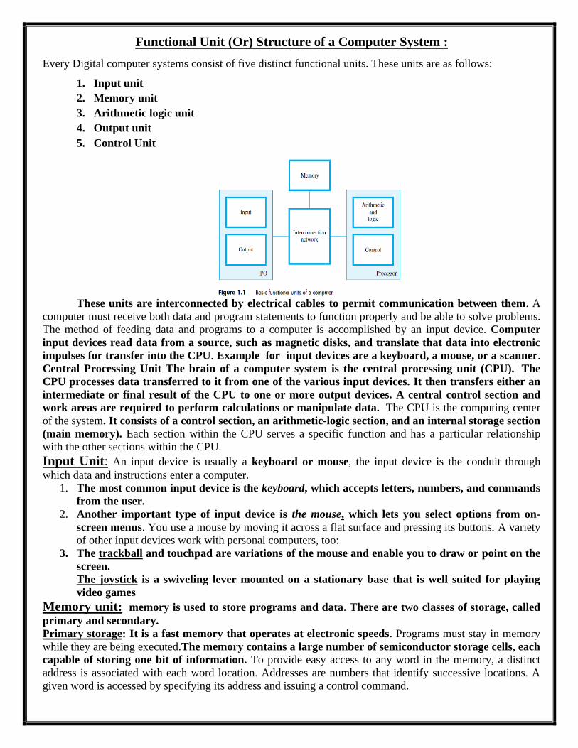
Functional Unit (Or) Structure of a Computer System :
Every Digital computer systems consist of five distinct functional units. These units are as follows:
1. Input unit
2. Memory unit
3. Arithmetic logic unit
4. Output unit
5. Control Unit
These units are interconnected by electrical cables to permit communication between them. A
computer must receive both data and program statements to function properly and be able to solve problems.
The method of feeding data and programs to a computer is accomplished by an input device. Computer
input devices read data from a source, such as magnetic disks, and translate that data into electronic
impulses for transfer into the CPU. Example for input devices are a keyboard, a mouse, or a scanner.
Central Processing Unit The brain of a computer system is the central processing unit (CPU). The
CPU processes data transferred to it from one of the various input devices. It then transfers either an
intermediate or final result of the CPU to one or more output devices. A central control section and
work areas are required to perform calculations or manipulate data. The CPU is the computing center
of the system. It consists of a control section, an arithmetic-logic section, and an internal storage section
(main memory). Each section within the CPU serves a specific function and has a particular relationship
with the other sections within the CPU.
Input Unit: An input device is usually a keyboard or mouse, the input device is the conduit through
which data and instructions enter a computer.
1. The most common input device is the keyboard, which accepts letters, numbers, and commands
from the user.
2. Another important type of input device is the mouse, which lets you select options from on-
screen menus. You use a mouse by moving it across a flat surface and pressing its buttons. A variety
of other input devices work with personal computers, too:
3. The trackball and touchpad are variations of the mouse and enable you to draw or point on the
screen.
The joystick is a swiveling lever mounted on a stationary base that is well suited for playing
video games
Memory unit: memory is used to store programs and data. There are two classes of storage, called
primary and secondary.
Primary storage: It is a fast memory that operates at electronic speeds. Programs must stay in memory
while they are being executed.The memory contains a large number of semiconductor storage cells, each
capable of storing one bit of information. To provide easy access to any word in the memory, a distinct
address is associated with each word location. Addresses are numbers that identify successive locations. A
given word is accessed by specifying its address and issuing a control command.
The number of bits in each word is referred as the word length of the computer. Typical word
lengths range from 16 to 64 bits.
Programs must reside in the memory during execution. Instructions and data can be written into the
memory or read out under the control of the processor.
1. Memory in which any location can be reached in a short and fixed amount of time after
specifying its address is called random access memory (RAM). 2. The time required to access one word is called the memory access time.
3. The small, fast, Ram units are called caches. They are tightly coupled with the processor and
are often contained on the same integrated circuit chip to achieve high performance.
4. The largest and slowest units are referred to as the main memory.
Secondary storage: Secondary storage is used when large amounts of data and many programs have
to be stored, particularly for information that is accessed infrequently.
Examples for secondary storage devices are Magnetic Disks, Tape and Optical disks.
Arithmetic-Logic Unit:- The arithmetic-logic section performs arithmetic operations, such as
addition, subtraction, multiplication, and division.
Arithmetic-Logic Unit usually called the ALU is a digital circuit that performs two types of
operations— arithmetic and logical.
Arithmetic operations are the fundamental mathematical operations consisting of addition,
subtraction, multiplication and division.
Logical operations consist of comparisons. That is, two pieces of data are compared to see whether
one is equal to, less than, or greater than the other. The ALU is a fundamental building block of the central
processing unit of a computer.
Out put Unit:- An output device is any piece of computer hardware equipment used to communicate the
results of data processing carried out by an information processing system (such as a computer) to the outside
world.
In computing, input/output, or I/O, refers to the communication between an information processing
system (such as a computer), and the outside world. Inputs are the signals or data sent to the system, and
outputs are the signals or data sent by the system to the outside.
Examples of output devices:
• Speaker
• Headphones
• Screen
• Printer
Control Unit: All activities inside the machine are directed and controlled by the control unit. Control
Unit is the part of the computer's central processing unit (CPU), which directs the operation of the
processor. A control unit works by receiving input information to which it converts into control signals,
which are then sent to the central processor
The Basic Operational Concepts of a Computer:-
1. The program contains of a list of instructions is stored in the memory.
2. Individual instructions are brought from the memory into the processor, which
execute the specified operations.
3. Data to be used as operands are also stored in the memory.
Add R1,R2,R3
In This instruction add is the operation perform on operands R1,R2 and place the result stored in R3.
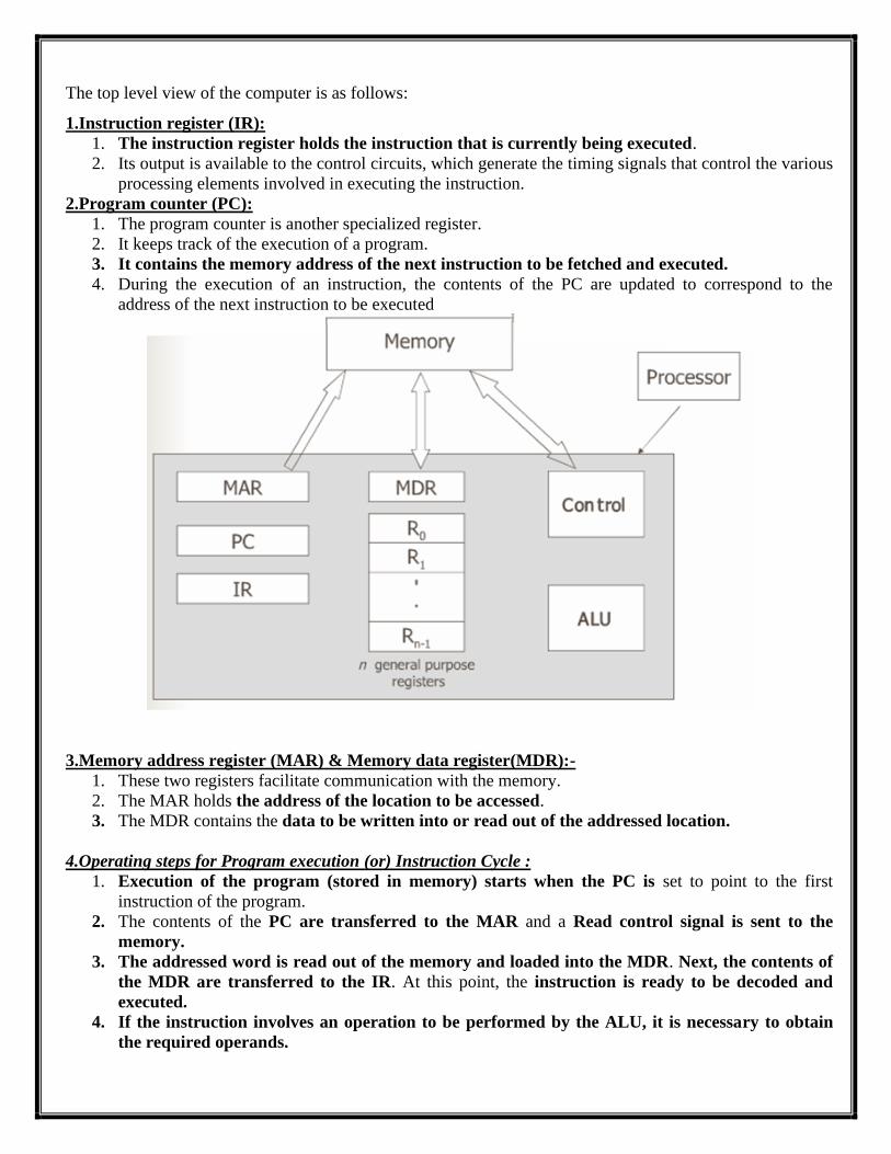
The top level view of the computer is as follows:
1.Instruction register (IR):
1. The instruction register holds the instruction that is currently being executed.
2. Its output is available to the control circuits, which generate the timing signals that control the various
processing elements involved in executing the instruction.
2.Program counter (PC):
1. The program counter is another specialized register.
2. It keeps track of the execution of a program.
3. It contains the memory address of the next instruction to be fetched and executed.
4. During the execution of an instruction, the contents of the PC are updated to correspond to the
address of the next instruction to be executed
3.Memory address register (MAR) & Memory data register(MDR):-
1. These two registers facilitate communication with the memory.
2. The MAR holds the address of the location to be accessed.
3. The MDR contains the data to be written into or read out of the addressed location.
4.Operating steps for Program execution (or) Instruction Cycle :
1. Execution of the program (stored in memory) starts when the PC is set to point to the first
instruction of the program.
2. The contents of the PC are transferred to the MAR and a Read control signal is sent to the
memory.
3. The addressed word is read out of the memory and loaded into the MDR. Next, the contents of
the MDR are transferred to the IR. At this point, the instruction is ready to be decoded and
executed.
4. If the instruction involves an operation to be performed by the ALU, it is necessary to obtain
the required operands.
5. If an operand resides in memory (it could also be in a general purpose register in the processor), it has
to be fetched by sending its address to the MAR and initiating a Read cycle.
6. When the operand has been read from the memory into the MDR, it is transferred from the MDR to
ALU.
7. After one or more operands are fetched in this way, the ALU can perform the desired operation.
8. If the result of the operation is to be stored in the memory, then the result is ent to the MDR.
9. The address of the location where the result is to be stored is sent to the MAR, and a write cycle is
initiated.
10. At some point during the execution of the current instruction, the contents of the PC are incremented
so that the PC pints to the next instruction to be executed.
11. Thus, as soon as the execution of the current instruction is completed, a new instruction fetch may be
started.
12. In addition to transferring data between the memory and the processor, the computer accepts data
from input devices and sends data to output devices. Thus, some machine instructions with the
ability to handle I/O transfers are provided.
Bus Structures:- 1. BUS:A group of lines(wires) that serves as a connecting path for several devices of a computer is
called a bus.
The following are different types of busses:
1. Address Bus 2. Data Bus 3. Control Bus
The Data bus Carries(transfer) data from one component (source) to other component
(destination) connected to it. The data bus consists of 8, 16, 32 or more parallel signal lines. The data
bus lines are bi-directional. This means that CPU can read data on these lines from memory or from a port, as
well as send data out on these lines to a memory location.
The Address bus is the set of lines that carry(transfer) address information about where in memory
the data is to be transferred to or from. It is an unidirectional bus. The address bus consists of 16, 20, 24 or
more parallel signal lines. On these lines CPU sends out the address of the memory location.
The Control Bus carries the Control and timing information. Including these three the following
are various types of busses. They are
System Bus: A System Bus is usually a combination of address bus, data bus, and control bus
respectively.
Internal Bus: The bus that operates only with the internal circuitary of the CPU.
External Bus: Buses which connects computer to external devices is nothing but external bus.
Back Plane: A Back Plane bus includes a row pf connectors into which system modules can be plugged in.
I/O Bus: The bus used by I/O devices to communicate with the CPU is usually reffered as I/O bus.
Synchronous Bus: While using Synchronous bus, data transmission between source and destination units
takes place in a given timeslot which is already known to these units.
Asynchronous Bus: In this case the data transmission is governed by a special concept. That is handshaking
control signals.
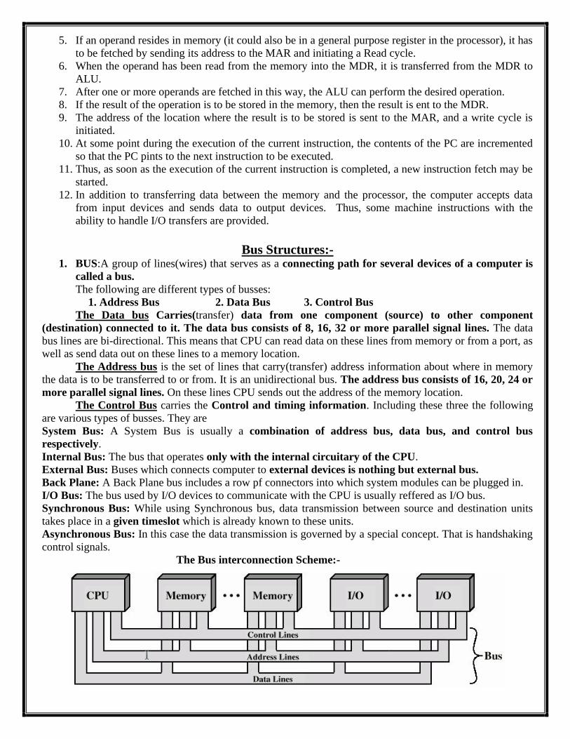
The Bus interconnection Scheme:-

Single bus structure :-
1. A group of lines(wires) that serves as a connecting path for several devices of a computer is called
a bus.
2. In addition to the lines that carry the data, the bus must have lines for address and control
purposes.
3. The simplest way to interconnect functional units is to use a single bus, as shown below.
4. All units are connected to this bus. Because the bus can be used for only one transfer at a time, only
two units can actively use the bus at any given time.
5. Bus control lines are used to arbitrate multiple requests for use of the bus.
ADVANTAGE:
Its is low cost and its flexibility for attaching peripheral devices
DISADVANTAGE:
low performance because at time only one transfer
Traditional / Multiple bus Structure: There is a local bus that connects the processor to cache memory and
that may support one or more local devices. There is also a cache memory controller that connects this cache
not only to this local bus but also to the system bus.
On the system, the bus is attached to the main memory modules. In this way, I/O transfers to and
from the main memory across the system bus do not interfere with the processor’s activity. An expansion bus
interface buffers data transfers between the system bus and the I/O controllers on the expansion bus.
Some typical I/O devices that might be attached to the expansion bus include: Network cards (LAN), SCSI
(Small Computer System Interface), Modem, Serial Com etc..
Advantages: better performance
Disadvantage: increased cost.
OUTPUT MEMORY PROCESSOR INPUT
Software:-
A total computer system includes both software and Hardware .
1. Hardware consists of physical components and all associated equipment.
2. Software refers to the collection programs that are written for the computer and writing a
program for a computer consists of specifying, directly or indirectly a sequence of machine
instructions.
3. The computer software consists of the instructions and data that the computer manipulates to perform
various data processing tasks.
Types:
1. Application software,
2. System software
System software: System software is used to run application software.
System software is a collection of programs that are executed as needed to perform functions such as
1. Receiving and interpreting user commands.
2. Entering and editing application programs and sorting them as files in secondary
storage devices.(Editor)
3. Managing the storage and retrieval of files in secondary storage devices.
4. Running standard application programs such as word processors, spread sheets, or
games, with data supplied by the user.
5. Controlling I/O units to receive input information and produce output results.
6. Translating programs from high level language to low level language.(Assemblers)
7. Linking and running user-written application program with existing standard
library routines, such as numerical computation packages.(Linker)
Application software: Application software allows end users to accomplish one or more specific (not
directly computer development related) tasks. Its usually written in high level languages, such as c ,c++, java.
Typical applications include:
• Word processing
• spreadsheet
• computer games
• databases
• industrial automation
• business software
• quantum chemistry and solid state physics software
• telecommunications (i.e., the internet and everything that flows on it)
• educational software
• medical software
• military software
• molecular modeling software
• image editing
• simulation software
• Decision making software
Compiler:- A compiler is a computer program (or set of programs) that transforms source code written in
a computer language (the source language) into another computer language (the target language, often
having a binary form known as object code). The most common reason for wanting to transform source
code is to create an executable program. The name "compiler" is primarily used for programs that translate
source code from a high-level programming language to a lower level language (e.g., assembly language or
machine code). A program that translates from a low level language to a higher level one is a decompiler. A
program that translates between high-level languages is usually called a language translator, source to
source translator
Linker: - Linker is a program in a system which helps to link a object modules of program into a
single object file. It performs the process of linking. Linker are also called link editors. Linking is process of
collecting and maintaining piece of code and data into a single file. Linker also link a particular module into
system library. It takes object modules from assembler as input and forms an executable file as output for
loader. Linking is performed at both compile time, when the source code is translated into machine code and
load time, when the program is loaded into memory by the loader. Linking is performed at the last step in
compiling a program.
Assembler: - An assembler is a program that converts assembly language into machine code. It takes
the basic commands and operations from assembly code and converts them into binary code that can
be recognized by a specific type of processor. Assemblers are similar to compilers in that they produce
executable code. However, assemblers are more simplistic since they only convert low-level code (assembly
language) to machine code. Since each assembly language is designed for a specific processor, assembling a
program is performed using a simple one-to-one mapping from assembly code to machine code.
Loader:- A loader is a major component of an operating system that ensures all necessary programs and
libraries are loaded, which is essential during the startup phase of running a program. It places the libraries
and programs into the main memory in order to prepare them for execution.
Performance
Performance: - The most important measure of the performance of a computer is how quickly it can
compute programs. The speed with which a computer executes programs is affected by the design of its
hardware and its machine language instructions. To represent the performance of a processor, we should
consider only the periods during which the processor is active.
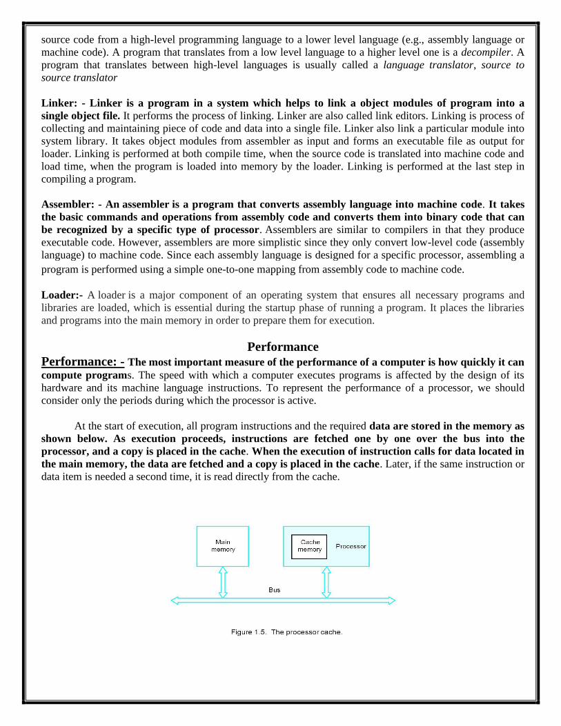
At the start of execution, all program instructions and the required data are stored in the memory as
shown below. As execution proceeds, instructions are fetched one by one over the bus into the
processor, and a copy is placed in the cache. When the execution of instruction calls for data located in
the main memory, the data are fetched and a copy is placed in the cache. Later, if the same instruction or
data item is needed a second time, it is read directly from the cache.

Computer performance is often described in terms of clock speed (usually in MHz or GHz). This
refers to the cycles per second of the main clock of the CPU. Performance of a computer depends on the
following factors.
a) Processor clock:-
1. Processor circuits are controlled by a timing signal called a clock. A clock is a microchip that
regulates speed and timing of all computer functions.
2. Clock Cycle is the speed of a computer processor, or CPU, which is the amount of time between two
pulses of an oscillator. Generally speaking, the higher number of pulses per second, the faster the
computer processor will be able to process information
3. CPU clock speed, or clock rate, is measured in Hertz — generally in gigahertz, or GHz. A
CPU's clock speed rate is a measure of how many clock cycles a CPU can perform per second
4. To execute a machine instruction, the processor divides the action to be performed into a sequence of
basic steps, such that each step can be completed in one clock cycle.
5. The length P of one clock cycle is an important parameter that affects processor performance.
6. Its inverse is the clock rate, R = 1/P, which is measured in cycles per second.
7. If the clock rate is 500(MHz) million cycles per second, then the corresponding clock period is 2
nanoseconds.
b) Basic performance equation:- The Performance Equation is a term used in computer science. It refers
to the calculation of the performance or speed of a central processing unit (CPU).
Basically the Basic Performance Equation [BPE] is an equation with 3 parameters which are
required for the calculation of "Basic Performance" of a given system. It is given by
T = (N*S)/R
Where 'T' is the processor time [Program Execution Time] required to execute a given program
written in some high level language .The compiler generates a machine language object program
corresponding to the source program.
'N' is the total number of steps required to complete program execution. 'N' is the actual number
of instruction executions, not necessarily equal to the total number of machine language instructions in the
object program. Some instructions are executed more than others (loops) and some are not executed at all
(conditions).
'S' is the average number of basic steps each instruction execution requires, where each basic
step is completed in one clock cycle. We say average as each instruction contains a variable number of steps
depending on the instruction.
'R' is the clock rate [In cycles per second]
c) Pipelining and Super scalar operation:-
1. A substantial improvement in performance can be achieved by overlapping the execution of
successive instructions, using a technique called pipelining.
2. Consider the instruction
3. Add R1, R2, R3
4. Which adds the contents of registers R1 and R2, and places the sum into R3
5. The contents of R1 and R2 are first transferred to the inputs of the ALU.
6. After the add operation is performed, the sum is transferred to R3.
7. Processor can read the next instruction from the memory while the addition operation is being
performed.
8. Then, if that instruction also uses the ALU, its operands can be transferred to the ALU inputs at the
same time that the result of add instruction is being transferred to R3.
9. Thus, pipelining increases the rate of executing instructions significantly.
d) Super scalar operation:-
1. A higher degree of concurrency can be achieved if multiple instruction pipelines are implemented in
the processor.
2. This means that multiple function units are used, creating parallel paths through which different
instructions can be executed in parallel.
3. With such an arrangement, it becomes possible to start the execution of several instructions in every
clock cycle.
4. This mode of execution is called super scalar operation.
e)Clock rate:-
1. There are two possibilities for increasing the clock rate, R.
2. First, improving the Integrated Circuit technology makes logic circuit faster, which reduces the
needed to complete a basic step. This allows the clock period, P, to be reduced and the clock rate, R,
to be increased.
3. Second, reducing the amount of processing done in one basic step also makes it possible to reduce the
clock period, P.
f)Instruction set: CISC and RISC:-
1. The terms CISC and RISC refer to design principles and techniques.
2. RISC: Reduced instruction set computers.
3. Simple instructions require a small number of basic steps to execute.
4. For a processor that has only simple instructions, a large number of instructions may by need to
perform a given programming task. This could lead to a large value of N and a small value for S.
5. It is much easier to implement efficient pipelining in processors with simple instruction sets.
6. CISC: Complex instruction set computers.
7. Complex instructions involve a large number of steps.
8. If individual instructions perform more complex operations, fewer instructions will be needed,
leading to a lower value of N and a larger value of S.
9. Complex instructions combined with pipelining would achieve good performance.
g)Optimizing Compiler:-
1. A compiler translates a high-level language program into a sequence of machine instructions.
2. To reduce N, we need to have a suitable machine instruction set and a compiler that makes good use
of it.
3. An optimizing compiler takes advantage of various features of the target processor to reduce the
product N * S.
4. The compiler may rearrange program instructions to achieve better performance.
h)Performance measurement:-
1. SPEC rating.
2. A nonprofit organization called” System Performance Evaluation Corporation” (SPEC) selects and
publishes representative application programs for different application domains.
3. The SPEC rating is computed as follows.
4. SPEC rating = Running time on the reference computer
Running time on the computer under test.
5. Thus SPEC rating of 50 means that the computer under test is 50 times faster than the reference
computer for these particular benchmarks.
6. The test is repeated for all the programs in the SPEC suite, and the geometric mean of the results is
computed.
7. Let SPEC, be the rating for program ‘i’ in the suite.
The overall SPEC rating for the computer is given by
Where n is the number of programs in the suite.
FREQUENTLY ASKED QUESTIONS
1. Discuss the generations of computers based on the development technologies used to fabricate the processors,
memories an I/O units. 2. What are the functional units of a computer system? Explain the way of handling information by each of
them. 3. “System software is responsible for coordination of all activities in a computing system”-Justify this statement
with the functionalities of it. 4. Write a short note on bus structures used in computer system. 5. Explain the importance of instruction set in measuring the performance of a computer system. 6. Discuss various computer types with their applications in real world environment. 7. What is the role of Processor clock, clock rate in the performance of computer system? Explain. 8. Suppose two numbers located in memory are to be added. What are the functional units of digital computer
system will carry out this? Explain how.
9. Define system software. 10. Mention different types of Bus structures. 11. Explain the structure of a computer system. 12. Write about logical structure of a simple personal computer. 13. Explain the organization of a computer system and its input-output processor. 14. Write differences between RISC and CISC.
UNIT-2
Syllabus: Machine Instruction and Programs: Instruction and Instruction sequencing:
Register Transfer notation, Assembly Language Notation, Basic Instruction types, Addressing Modes,
Basic Input / Output operations, the role of Stacks and queues in computer
programming equation. Component of instructions: logic instructions shift and rotate
instructions.
Instructions and Instruction Sequencing: computer programming consists of a sequence
of small steps, such as adding two numbers, testing for particular condition ,reading the
character from keyboard and sending a character to be displayed on screen.
A computer must have instructions capable of performing four types of operations:
1. Data transfers between the memory and the processor registers
2. Arithmetic and logic operations on data
3. Program sequencing and control
4. I/O transfers
Register Transfer Notation: It is used to transfer information from one location to other location inside
the computer. In RTN, source is always a value specified on right hand side of “ “. Destination is always a
processor register, specified on left hand side.
Syntax :
Register Source
The right hand side of RTN is always denotes a value and the left hand side is the name of a
location where the value is to be placed. Source can be processor register, I/O register, memory
location, but destination register is always a processor register. RTN uses square brackets to indicate
content of location. These braces are always placed only around the Source. For example,
1. R3 [ R1 ] + [ 23 ]
This operation that adds the contents of registers R1 and R2, and places their sum into register R3
2. R2 [LOC], means that the contents of memory location LOC are transferred into processor
register R2.
Assembly Language Notation: Assembly Language Notation is a type of notation which is used to
represent machine instructions and programs.
For example:
LOAD LOC, R2
a generic instruction that causes the transfer, from memory location LOC to processor
register R2, is specified by the statement
The contents of LOC are unchanged by the execution of this instruction, but the old contents of
register R2 are overwritten. The name Load is appropriate for this instruction, because the contents read from
a memory location are loaded into a processor register.
The second example :
ADD R4, R2, R3
Adding two numbers contained in processor registers R2 and R3 and placing their sum in R4
can be specified by the assembly-language statement
In this case, registers R2 and R3 hold the source operands, while R4 is the destination.
An instruction specifies an operation to be performed and the operands involved. In the above
examples, we used the English words Load and Add to denote the required operations. In the assembly-
language instructions of actual (commercial) processors, such operations are defined by using
mnemonics, which are typically abbreviations of the words describing the operations. For example, the
operation Load may be written as LD, while the operation Store, which transfers a word from a processor
register to the memory, may be written as STR or ST. Assembly languages for different processors often use
different mnemonics for a given operation.
Basic Instruction types:An instruction is of various lengths depending upon the number of addresses it
contains. Generally CPU organization is of three types on the basis of number of address fields:
• Single Accumulator organization
• General register organization
• Stack organization
1.In first organization operation is done involving a special register called accumulator.
2.In second on multiple registers are used for the computation purpose.
3.In third organization the work on stack basis operation due to which it does not contain any
address field. On the basis of number of addresses instructions are classified as:
Three address Instructions: This instruction has three operands(address fields) to
specify a register or a memory location.
• Syntax
: operation source1, source2,
EX: Add A, B, C [ C<-[A]+[B] )
Where A, B are called source operands, C is called destination operand.
• Two address Instructions: This instruction has two operands(address fields) to specify a
register or a memory location.
• Syntax : operation source , destination.
For example,
Add A, C ( C [ A ] + [ C ] )
• One address Instructions: This instruction has one operand (address field) to specify a
register or a memory location. This use a implied Accumulator(AC) Register for data
manipulation. One operand is in AC and other is in register or memory location. Implied means
that the CPU already know that one operand is in AC so there is no need to specify it. For
example,
LOAD A ( AC [ A ] )
ADD B ( AC [AC ] + [ B ] )
STORE C ( C [ AC ] )
• Zero address Instructions: This instruction has zero address fields. A stack based computer do
not use address field in instruction. It uses stack operations PUSH and POP to perform
operations. To evaluate a expression first it is converted to revere Polish Notation i.e. Post fix
Notation. For example,
Push A ( TOS [ A ])
Push B ( TOS [ B ])
Add ( TOS [ A ] + [ B ])
Pop C ( C [ TOS ] )
Example: evaluate X = ( A + B ) * ( C + D )
Three Address:
Add A, B, R1 ( R1 [ A ] + [ B ] )
Add C, D, R2 ( R2 [ C ] + [ D ] )
Mul R1, R2, X ( X [ R1 ] * [ R2 ] )
Two Address:
Move A, R1 ( R1 [ A ] )
Add B, R1 ( R1 [ R1 ] + [ B ])
Move C, R2 ( R2 [ C ] )
Add D, R2 ( R2 [ R2 ] + [ D ] )
Mul R1, R2 ( R2 [ R1 ] * [ R2 ] )
Move R2, X X [ R2 ]
One Address:
Load A ( AC [ A ] )
Add B ( AC [ AC ] + [ B ] )
Store T1 ( T1 [ AC ])
Load C ( AC [ C ])
Add D ( AC [ AC ] + [ D ])
Mul T1 ( AC [ AC ] * [ T1 ] )
Store X ( X [ AC ])
Zero address:
Push A ( TOS [ A ])
Push B ( TOS [ B ])
Add ( TOS [ A ] + [ B ])
Push C ( TOS [ C ])
Push D ( TOS [ D ])
Add ( TOS [ C ] + [ D ])
Mul ( TOS ( [ A ] + [ B ] ) * ([ C ] + [ D ] )
Pop X ( X [ A ] + [ B ] ) * ([ C ] + [ D ])
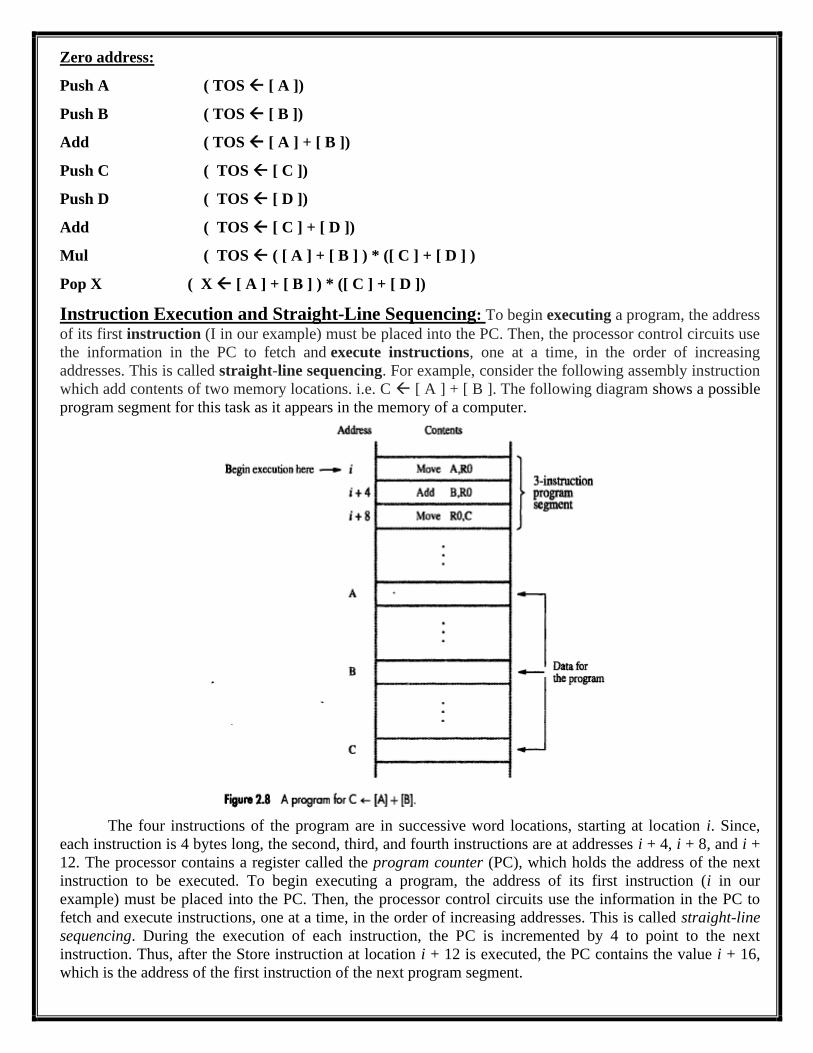
Instruction Execution and Straight-Line Sequencing: To begin executing a program, the address
of its first instruction (I in our example) must be placed into the PC. Then, the processor control circuits use
the information in the PC to fetch and execute instructions, one at a time, in the order of increasing
addresses. This is called straight-line sequencing. For example, consider the following assembly instruction
which add contents of two memory locations. i.e. C [ A ] + [ B ]. The following diagram shows a possible
program segment for this task as it appears in the memory of a computer.
The four instructions of the program are in successive word locations, starting at location i. Since,
each instruction is 4 bytes long, the second, third, and fourth instructions are at addresses i + 4, i + 8, and i +
12. The processor contains a register called the program counter (PC), which holds the address of the next
instruction to be executed. To begin executing a program, the address of its first instruction (i in our
example) must be placed into the PC. Then, the processor control circuits use the information in the PC to
fetch and execute instructions, one at a time, in the order of increasing addresses. This is called straight-line
sequencing. During the execution of each instruction, the PC is incremented by 4 to point to the next
instruction. Thus, after the Store instruction at location i + 12 is executed, the PC contains the value i + 16,
which is the address of the first instruction of the next program segment.
Executing a given instruction is a two-phase procedure. In the first phase, called instruction fetch, the
instruction is fetched from the memory location whose address is in the PC. This instruction is placed in the
instruction register (IR) in the processor. At the start of the second phase, called instruction execute, the
instruction in IR is examined to determine which operation is to be performed. The specified operation is
then performed by the processor. This involves a small number of steps such as fetching operands from the
memory or from processor registers, performing an arithmetic or logic operation, and storing the result in the
destination location. At some point during this two-phase procedure, the contents of the PC are advanced to
point to the next instruction. When the execute phase of an instruction is completed, the PC contains the
address of the next instruction, and a new instruction fetch phase can begin.
Branching: Normally, the instructions executed in linear fashion through the program, and the address of
the instructions is obtained from PC in the control unit. This sequence is interrupted when a branch
instruction is executed, at such a time the address field of the Branch instruction is inserted into the PC and
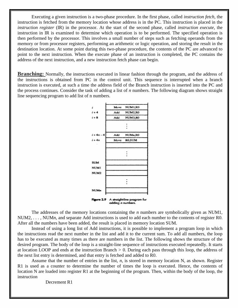
the process continues. Consider the task of adding a list of n numbers. The following diagram shows straight
line sequencing program to add list of n numbers.
The addresses of the memory locations containing the n numbers are symbolically given as NUM1,
NUM2, . . . , NUMn, and separate Add instructions is used to add each number to the contents of register R0.
After all the numbers have been added, the result is placed in memory location SUM.
Instead of using a long list of Add instructions, it is possible to implement a program loop in which
the instructions read the next number in the list and add it to the current sum. To add all numbers, the loop
has to be executed as many times as there are numbers in the list. The following shows the structure of the
desired program. The body of the loop is a straight-line sequence of instructions executed repeatedly. It starts
at location LOOP and ends at the instruction Branch > 0. During each pass through this loop, the address of
the next list entry is determined, and that entry is fetched and added to R0.
Assume that the number of entries in the list, n, is stored in memory location N, as shown. Register
R1 is used as a counter to determine the number of times the loop is executed. Hence, the contents of
location N are loaded into register R1 at the beginning of the program. Then, within the body of the loop, the
instruction
Decrement R1
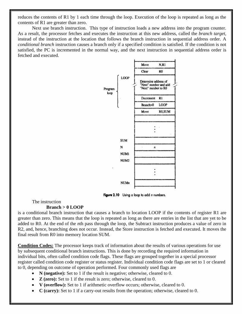
reduces the contents of R1 by 1 each time through the loop. Execution of the loop is repeated as long as the
contents of R1 are greater than zero.
Next use branch instruction. This type of instruction loads a new address into the program counter.
As a result, the processor fetches and executes the instruction at this new address, called the branch target,
instead of the instruction at the location that follows the branch instruction in sequential address order. A
conditional branch instruction causes a branch only if a specified condition is satisfied. If the condition is not
satisfied, the PC is incremented in the normal way, and the next instruction in sequential address order is
fetched and executed.
The instruction
Branch > 0 LOOP
is a conditional branch instruction that causes a branch to location LOOP if the contents of register R1 are
greater than zero. This means that the loop is repeated as long as there are entries in the list that are yet to be
added to R0. At the end of the nth pass through the loop, the Subtract instruction produces a value of zero in
R2, and, hence, branching does not occur. Instead, the Store instruction is fetched and executed. It moves the
final result from R0 into memory location SUM.
Condition Codes: The processor keeps track of information about the results of various operations for use
by subsequent conditional branch instructions. This is done by recording the required information in
individual bits, often called condition code flags. These flags are grouped together in a special processor
register called condition code register or status register. Individual condition code flags are set to 1 or cleared
to 0, depending on outcome of operation performed. Four commonly used flags are
• N (negative): Set to 1 if the result is negative; otherwise, cleared to 0.
• Z (zero): Set to 1 if the result is zero; otherwise, cleared to 0.
• V (overflow): Set to 1 if arithmetic overflow occurs; otherwise, cleared to 0.
• C (carry): Set to 1 if a carry-out results from the operation; otherwise, cleared to 0.
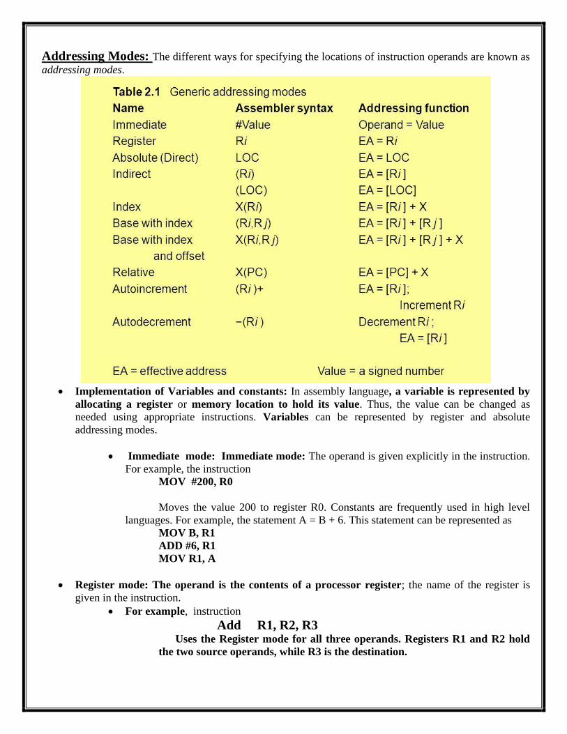
Addressing Modes: The different ways for specifying the locations of instruction operands are known as
addressing modes.
• Implementation of Variables and constants: In assembly language, a variable is represented by
allocating a register or memory location to hold its value. Thus, the value can be changed as
needed using appropriate instructions. Variables can be represented by register and absolute
addressing modes.
• Immediate mode: Immediate mode: The operand is given explicitly in the instruction.
For example, the instruction
MOV #200, R0
Moves the value 200 to register R0. Constants are frequently used in high level
languages. For example, the statement A = B + 6. This statement can be represented as
MOV B, R1
ADD #6, R1
MOV R1, A
• Register mode: The operand is the contents of a processor register; the name of the register is
given in the instruction.
• For example, instruction
Add R1, R2, R3 Uses the Register mode for all three operands. Registers R1 and R2 hold
the two source operands, while R3 is the destination.
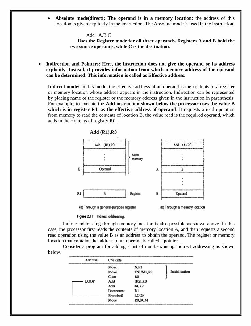
• Absolute mode(direct): The operand is in a memory location; the address of this
location is given explicitly in the instruction. The Absolute mode is used in the instruction
Add A,B,C
Uses the Register mode for all three operands. Registers A and B hold the
two source operands, while C is the destination.
• Indirection and Pointers: Here, the instruction does not give the operand or its address
explicitly. Instead, it provides information from which memory address of the operand
can be determined. This information is called as Effective address.
Indirect mode: In this mode, the effective address of an operand is the contents of a register
or memory location whose address appears in the instruction. Indirection can be represented
by placing name of the register or the memory address given in the instruction in parenthesis.
For example, to execute the Add instruction shown below the processor uses the value B
which is in register R1, as the effective address of operand. It requests a read operation
from memory to read the contents of location B. the value read is the required operand, which
adds to the contents of register R0.
Add (R1),R0
Indirect addressing through memory location is also possible as shown above. In this
case, the processor first reads the contents of memory location A, and then requests a second
read operation using the value B as an address to obtain the operand. The register or memory
location that contains the address of an operand is called a pointer.
Consider a program for adding a list of numbers using indirect addressing as shown
below.
Here, register R2 is used as a pointer to the numbers in the list, and the operands are
accessed indirectly through R2. The initialization section of the program loads the counter
value n from memory location N to R1 and uses the immediate addressing mode to place the
address value NUM1, which is the address of first number in the list, into R2. Then it clears
R0 to 0. The instruction ADD ( R2 ), R0 fetches the operand at location NUM1 and adds it ro
R0. The second ADD instruction adds 4 to the contents of the pointer R2, so that it will
contain the address value NUM2, when the above instruction is executed in the second pass
through the loop and son on.
Consider the C-language statement A = * B; where B is a pointer variable. This
statement may be compiled into
MOVE B, R1
MOVE ( R1 ), A
Using indirect addressing through memory, the same action can be achieved with
MOVE ( B ), A
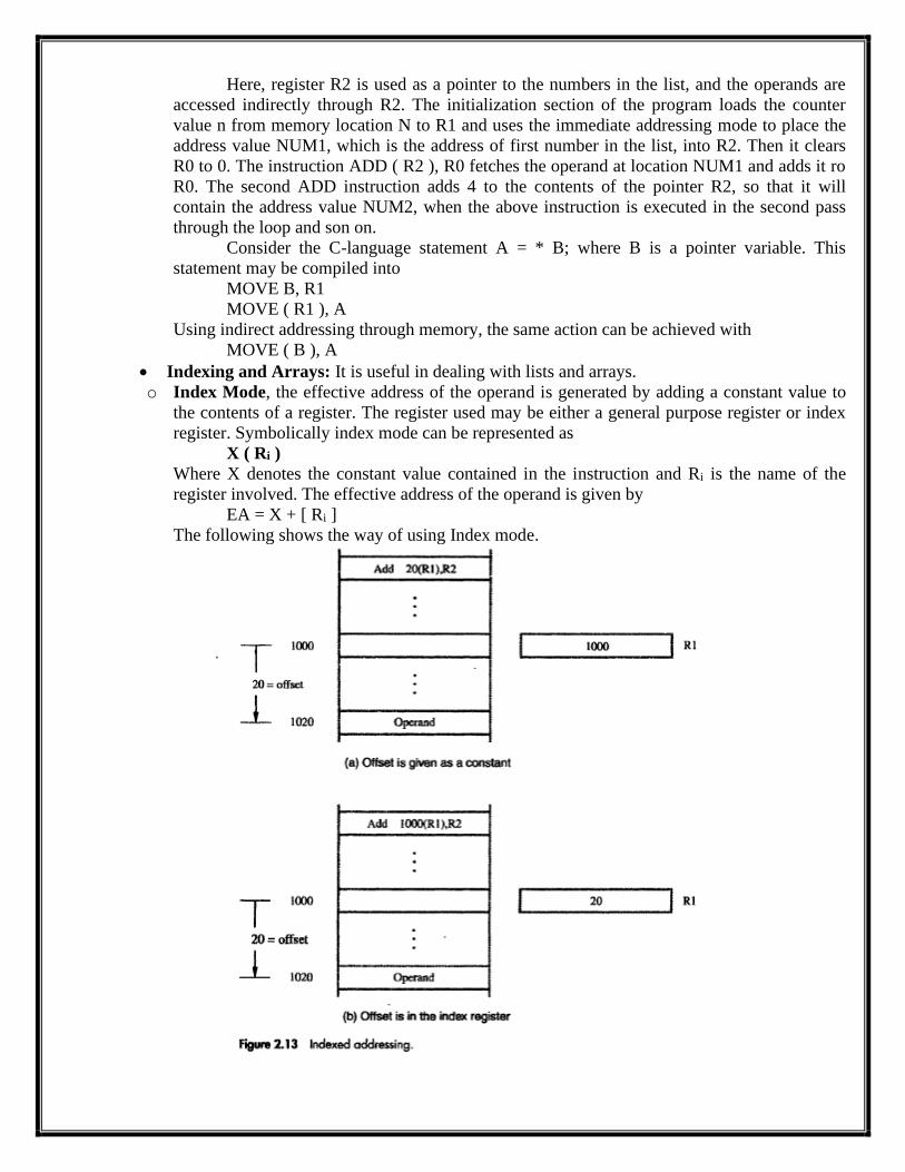
• Indexing and Arrays: It is useful in dealing with lists and arrays.
o Index Mode, the effective address of the operand is generated by adding a constant value to
the contents of a register. The register used may be either a general purpose register or index
register. Symbolically index mode can be represented as
X ( Ri )
Where X denotes the constant value contained in the instruction and Ri is the name of the
register involved. The effective address of the operand is given by
EA = X + [ Ri ]
The following shows the way of using Index mode.
In first case, the index register R1 contains the address of a memory location and the
value x defines an offset from this address to the location where the operand is found.
In second case, the constant X corresponds to a memory address and the contents of
the index register define the offset to the operand. In either case, the effective address is the
sum of two values: one is given explicitly in the instruction and the other is stored in a
register.
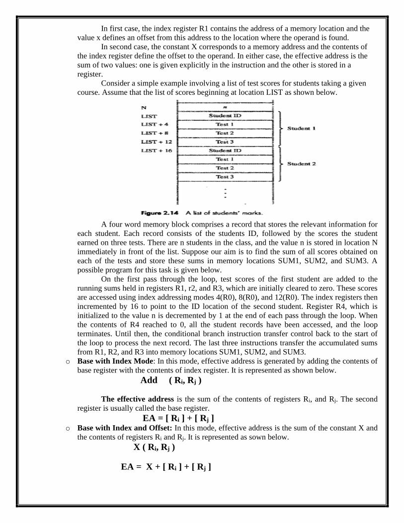
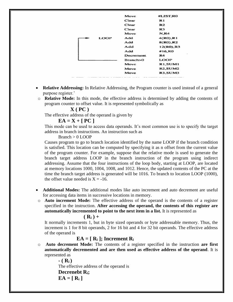
Consider a simple example involving a list of test scores for students taking a given
course. Assume that the list of scores beginning at location LIST as shown below.
A four word memory block comprises a record that stores the relevant information for
each student. Each record consists of the students ID, followed by the scores the student
earned on three tests. There are n students in the class, and the value n is stored in location N
immediately in front of the list. Suppose our aim is to find the sum of all scores obtained on
each of the tests and store these sums in memory locations SUM1, SUM2, and SUM3. A
possible program for this task is given below.
On the first pass through the loop, test scores of the first student are added to the
running sums held in registers R1, r2, and R3, which are initially cleared to zero. These scores
are accessed using index addressing modes 4(R0), 8(R0), and 12(R0). The index registers then
incremented by 16 to point to the ID location of the second student. Register R4, which is
initialized to the value n is decremented by 1 at the end of each pass through the loop. When
the contents of R4 reached to 0, all the student records have been accessed, and the loop
terminates. Until then, the conditional branch instruction transfer control back to the start of
the loop to process the next record. The last three instructions transfer the accumulated sums
from R1, R2, and R3 into memory locations SUM1, SUM2, and SUM3.
o Base with Index Mode: In this mode, effective address is generated by adding the contents of
base register with the contents of index register. It is represented as shown below.
Add ( Ri, Rj )
The effective address is the sum of the contents of registers Ri, and Rj. The second
register is usually called the base register.
EA = [ Ri ] + [ Rj ] o Base with Index and Offset: In this mode, effective address is the sum of the constant X and
the contents of registers Ri and Rj. It is represented as sown below.
X ( Ri, Rj )
EA = X + [ Ri ] + [ Rj ]
• Relative Addressing: In Relative Addressing, the Program counter is used instead of a general
purpose register.’
o Relative Mode: In this mode, the effective address is determined by adding the contents of
program counter to offset value. It is represented symbolically as
X ( PC ) The effective address of the operand is given by
EA = X + [ PC ] This mode can be used to access data operands. It’s most common use is to specify the target
address in branch instructions. An instruction such as
Branch > 0 LOOP
Causes program to go to branch location identified by the name LOOP if the branch condition
is satisfied. This location can be computed by specifying it as n offset from the current value
of the program counter. For example, suppose that the relative mode is used to generate the
branch target address LOOP in the branch instruction of the program using indirect
addressing. Assume that the four instructions of the loop body, starting at LOOP, are located
at memory locations 1000, 1004, 1008, and 1012. Hence, the updated contents of the PC at the
time the branch target address is generated will be 1016. To branch to location LOOP (1000),
the offset value needed is X = -16.
• Additional Modes: The additional modes like auto increment and auto decrement are useful
for accessing data items in successive locations in memory.
o Auto increment Mode: The effective address of the operand is the contents of a register
specified in the instruction. After accessing the operand, the contents of this register are
automatically incremented to point to the next item in a list. It is represented as
( Ri ) + It normally increments 1, but in byte sized operands or byte addressable memory. Thus, the
increment is 1 for 8 bit operands, 2 for 16 bit and 4 for 32 bit operands. The effective address
of the operand is
EA = [ Ri ]; Increment Ri o Auto decrement Mode: The contents of a register specified in the instruction are first
automatically decremented and are then used as effective address of the operand. It is
represented as
- ( Ri ) The effective address of the operand is
Decrenebt Ri;
EA = [ Ri ]
The following program describes how to use auto increment mode
Basic Input / Output Operations: Input / Output operations are essential which has a significant
effect on performance of a computer. An I/O device is connected to the interconnection network by using
a circuit, called the device interface, which provides the means for data transfer and for the exchange of
status and control information needed to facilitate the data transfers and govern the operation of the device.
The interface includes some registers that can be accessed by the processor.
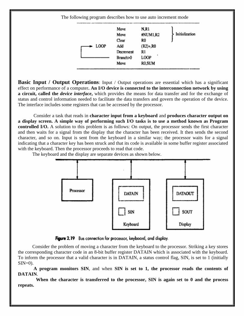
Consider a task that reads in character input from a keyboard and produces character output on
a display screen. A simple way of performing such I/O tasks is to use a method known as Program
controlled I/O. A solution to this problem is as follows: On output, the processor sends the first character
and then waits for a signal from the display that the character has been received. It then sends the second
character, and so on. Input is sent from the keyboard in a similar way; the processor waits for a signal
indicating that a character key has been struck and that its code is available in some buffer register associated
with the keyboard. Then the processor proceeds to read that code.
The keyboard and the display are separate devices as shown below.
Consider the problem of moving a character from the keyboard to the processor. Striking a key stores
the corresponding character code in an 8-bit buffer register DATAIN which is associated with the keyboard.
To inform the processor that a valid character is in DATAIN, a status control flag, SIN, is set to 1 (initially
SIN=0).
A program monitors SIN, and when SIN is set to 1, the processor reads the contents of
DATAIN.
When the character is transferred to the processor, SIN is again set to 0 and the process
repeats.
To transfer the characters from processor to display, a buffer register, DATAOUT, and a status
control flag, SOUT, are used.
When SOUT equals 1, the display is ready to receive a character. Under program control, the
processor monitors SOUT, and when SOUT is set to 1, the processor transfers a character code to
DATAOUT clears SOUT to 0; when the display device is ready to receive a second character, SOUT is again
set to 1.
The processor can monitor the keyboard status flag SIN and transfer a character from DATAIN to
register R1 by the following sequence of operations.
READWAIT Branch to READWAIT if SIN = 0
MOVE DATAIN, R1
The contents of the keyboard character buffer DATAIN can be transferred to processor
register instruction is
MoveByte DATAIN ,R1
An analogous sequence of operations is used for transferring output to display as shown below.
WRITEWAIT Branch to WRITEWAIT if SOUT = 0
MOVE R1, DATAOUT
The contents of the processor register R1 transferred to display buffer DATAOUT instruction
is
MoveByte R1,OUTDATA
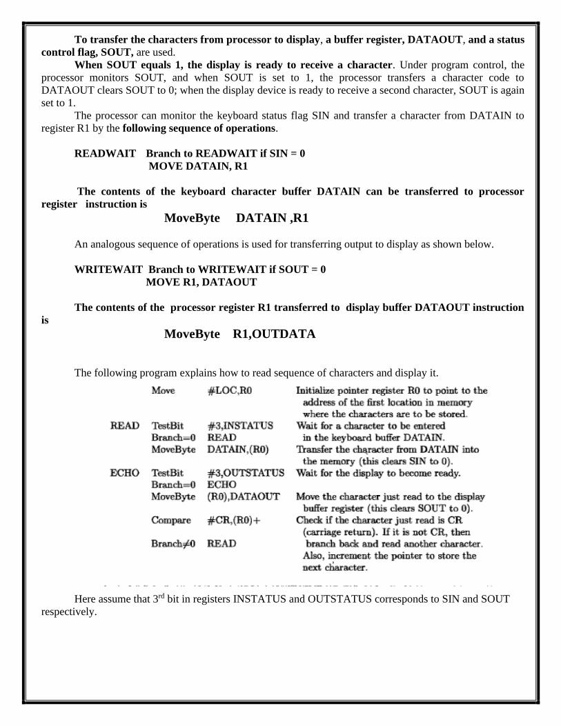
The following program explains how to read sequence of characters and display it.
Here assume that 3rd bit in registers INSTATUS and OUTSTATUS corresponds to SIN and SOUT
respectively.
The role of STACKS and QUEUES in computer programming equation: In order to
organize the control and information linkage between the main program and the subroutine, a data structure
called a stack is used. A stack is the list of data elements, usually words or bytes, with the accessing
restriction that elements can be added or removed at one end of the list only. This end is called as top of the
stack, and another end is called as bottom. The structure is sometimes referred as pushdown stack. Stack
follows Last-In-First-Out (LIFO) strategy, where elements inserted last will be the element removed first.
Two basic operations that can be performed on stack are PUSH and POP, which add and remove elements
from top of the stack respectively.
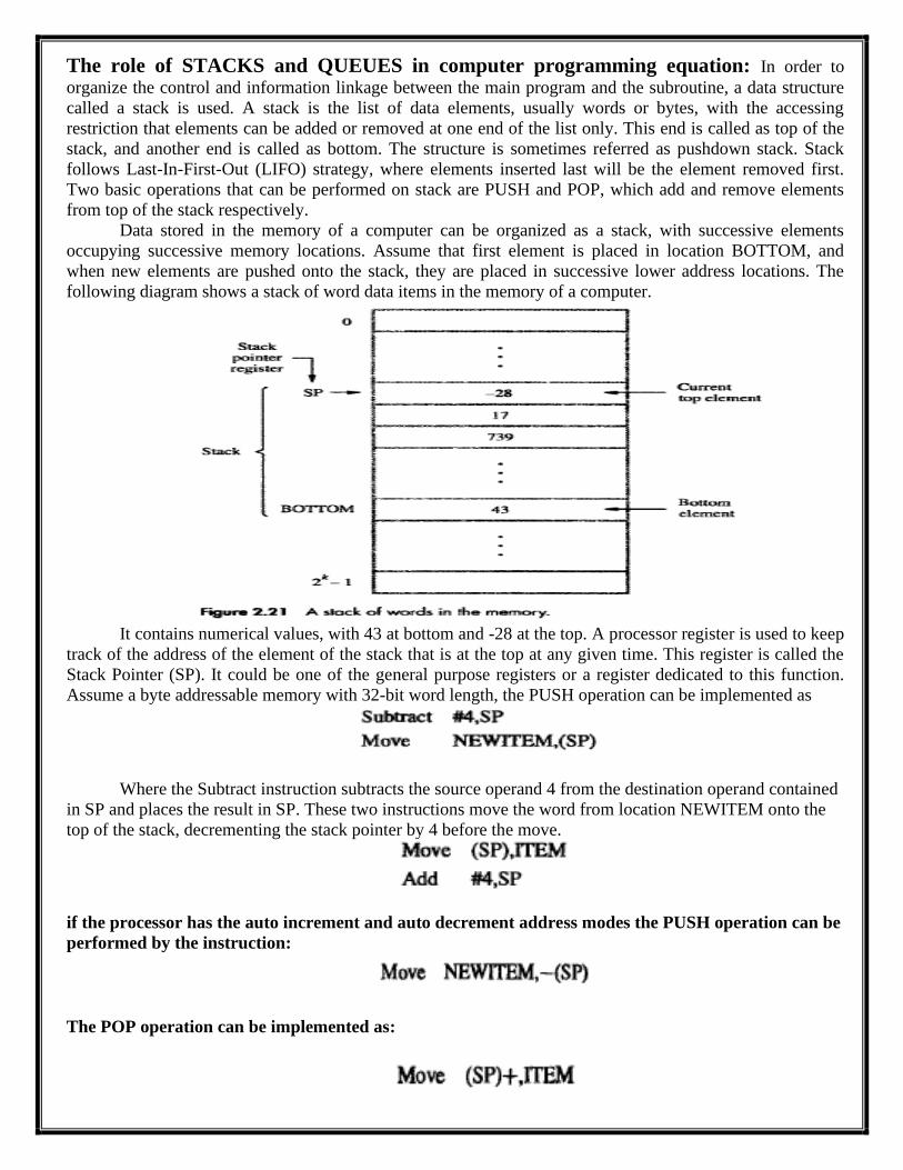
Data stored in the memory of a computer can be organized as a stack, with successive elements
occupying successive memory locations. Assume that first element is placed in location BOTTOM, and
when new elements are pushed onto the stack, they are placed in successive lower address locations. The
following diagram shows a stack of word data items in the memory of a computer.
It contains numerical values, with 43 at bottom and -28 at the top. A processor register is used to keep
track of the address of the element of the stack that is at the top at any given time. This register is called the
Stack Pointer (SP). It could be one of the general purpose registers or a register dedicated to this function.
Assume a byte addressable memory with 32-bit word length, the PUSH operation can be implemented as
Where the Subtract instruction subtracts the source operand 4 from the destination operand contained
in SP and places the result in SP. These two instructions move the word from location NEWITEM onto the
top of the stack, decrementing the stack pointer by 4 before the move.
if the processor has the auto increment and auto decrement address modes the PUSH operation can be
performed by the instruction:
The POP operation can be implemented as:
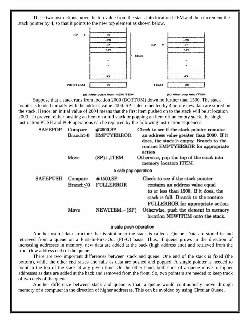
These two instructions move the top value from the stack into location ITEM and then increment the
stack pointer by 4, so that it points to the new top element as shown below.
Suppose that a stack runs from location 2000 (BOTTOM) down no further than 1500. The stack
pointer is loaded initially with the address value 2004. SP is decremented by 4 before new data are stored on
the stack. Hence, an initial value of 2004 means that the first item pushed on to the stack will be at location
2000. To prevent either pushing an item on a full stack or popping an item off an empty stack, the single
instruction PUSH and POP operations can be replaced by the following instruction sequences.
Another useful data structure that is similar to the stack is called a Queue. Data are stored in and
retrieved from a queue on a First-In-First-Out (FIFO) basis. Thus, if queue grows in the direction of
increasing addresses in memory, new data are added at the back (high address end) and retrieved from the
front (low address end) of the queue.
There are two important differences between stack and queue. One end of the stack is fixed (the
bottom), while the other end raises and falls as data are pushed and popped. A single pointer is needed to
point to the top of the stack at any given time. On the other hand, both ends of a queue move to higher
addresses as data are added at the back and removed from the front. So, two pointers are needed to keep track
of two ends of the queue.
Another difference between stack and queue is that, a queue would continuously move through
memory of a computer in the direction of higher addresses. This can be avoided by using Circular Queue.
Additional Instructions (Or) Component of Instructions: Additional Instructions (Or) Component of Instructions are two types
1.Logic Instructions
2.Shift and Rotate Instructions
Logic Instructions: Logic operations such as AND, OR, and NOT applied to individual bits, are the
basic building blocks of digital circuits. It is also useful to be able to perform logic operations in software.
For example,
1’s complement:
NOT dst
NOT dst complements all bits contained in the destination operand, changing 0’s to 1 and 1’s to 0.
2’s complement:
The following two instructions calculates 2’s complement of a number
NOT R0
ADD #1, R0
Many computers have a single instruction for 2’s complement..i.e. NEGATE R0
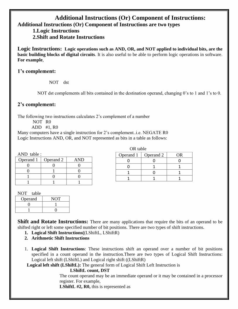
Logic Instructions AND, OR, and NOT represented as bits in a table as follows:
OR table
AND table :
Operand 1 Operand 2 AND
0 0 0
0 1 0
1 0 0
1 1 1
NOT table
Operand NOT
0 1
1 0
Shift and Rotate Instructions: There are many applications that require the bits of an operand to be
shifted right or left some specified number of bit positions. There are two types of shift instructions.
1. Logical Shift Instructions((LShiftL, LShiftR)
2. Arithmetic Shift Instructions
1. Logical Shift Instructions: These instructions shift an operand over a number of bit positions
specified in a count operand in the instruction.There are two types of Logical Shift Instructions:
Logical left shift (LShiftL) and Logical right shift ((LShiftR)
Logical left shift (LShiftL): The general form of Logical Shift Left Instruction is
LShiftL count, DST
The count operand may be an immediate operand or it may be contained in a processor
register. For example,
LShiftL #2, R0, this is represented as
Operand 1 Operand 2 OR
0 0 0
0 1 1
1 0 1
1 1 1
It shifts the contents of register R0 left by two positions. Vacated positions are filled
with 0’s.
o Logical right shift (LShiftR): The general form of Logical Shift Right Instruction is
LShiftR count, DST
The count operand may be an immediate operand or it may be contained in a processor
register. For example,
LShiftR #2, R0, this is represented as
It shifts the contents of register R0 right by two positions. Vacated positions are filled
with 0’s.
2. Arithmetic Shift Instructions: There are two types of Arithmetic Shift Instructions:
o Arithmetic Shift Left (AShiftL): A Left Arithmetic shifts a binary number by specified
number of positions towards left. The vacated positions are filled with 0’s. It can be
represented as
AShiftL count, DST
For example, AShiftL #2, R0 shifts contents of R0 by 2 positions and vacated
positions are filled with zeros as shown below.
o Arithmetic Shift Right (AShiftR): A Right Arithmetic shifts a binary number by specified
number of positions towards right. The vacated positions are filled with copies of the original
MSB bit. It can be represented as
AShiftR count, DST
For example, AShiftR #2, R0 shifts contents of R0 by 2 positions and vacated
positions are filled with copies of the original MSB bit as shown below.
Rotate Instructions: In shift operations, the bits shifted out of the operand are lost, except for the last bit
shifted out which is in the carry flag C. To preserve all bits, a set of rotate instructions can be used. They
move the bits that are shifted out of one end of the operand back into the other end. Different rotate
instructions are
1. Rotate Left without Carry
2. Rotate Left with Carry
3. Rotate Right without Carry
4. Rotate Right with Carry
They are represented as follows.
Digit-Packing Example:
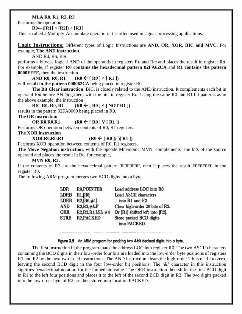
Consider a task which uses both shift and logic operations. Suppose two decimal digits represented in
ASCII code are located in memory at byte locations LOC and LOC + 1. Our goal is to represent each of
these digits in the 4-bit BCD code and store both of them in a single byte location PACKED. The result is
said to be in packed-BCD format.
To do this, extract the lower order 4 bits in LOC and LOC + 1 and concatenate them into the single
byte at PACKED as shown below.
Here, R0 is a pointer to the ASCII characters in memory, and use the registers R1 and R2 to develop
the BCD codes. MoveByte instruction transfers a byte between memory and a 32-bit processor register. The
And instruction is used to mask out all except the four rightmost bits in R2. Immediate operand $F,
interpreted as a 32-bit pattern, has 28 zero’s in most significant bit positions.
Vector Dot Product Program: Let A and B be two vectors of length n. Their dot product can be defined as
The following program computes dot product and storing it in memory location DOTPROD. The first
elements of each vector, A(0), and B(0), are stored at memory locations AVEC and BVEC.
Byte Sorting Program: Consider a program for sorting a list of bytes stored in memory into ascending
alphabetic order. Assume that the list consists of n bytes. Let the list stored in memory locations LIST
through LIST + n – 1, and let n be a 32-bit value stored at address N. To do this, use straight selection sort
algorithm. First, the largest number is found and placed at the end of the list in location LIST + n – 1. Then
the largest number in the remaining sub list of n – 1 numbers is placed at the end of the sub list in location
LIST + n – 2. The procedure is repeated until the list is sorted.
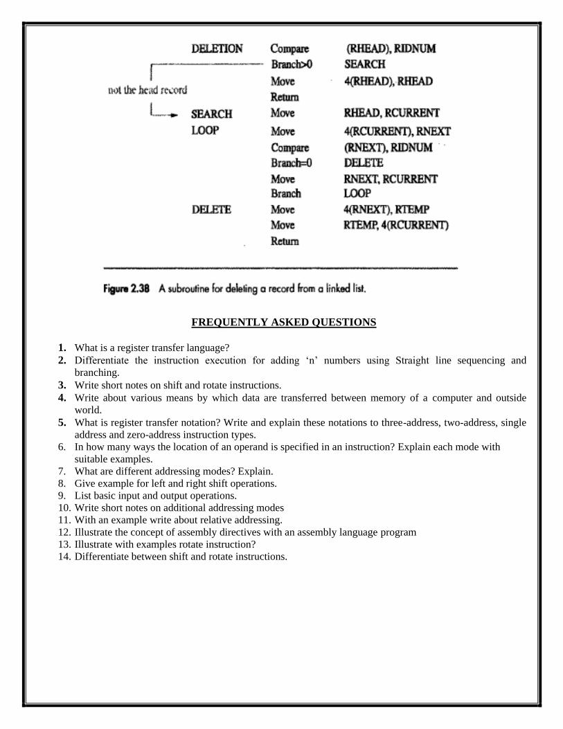
Linked Lists: Suppose to maintain list of student records in consecutive memory locations in increasing
order of student ID numbers, use a data structure called Linked List as shown below. To insert a record
between i and i+1, the link address in record i is coped into the link field in the new record and then the
address of the new record is written into the link field of record i. To delete record i, the address in its link
field is copied into the link field of record i-1.
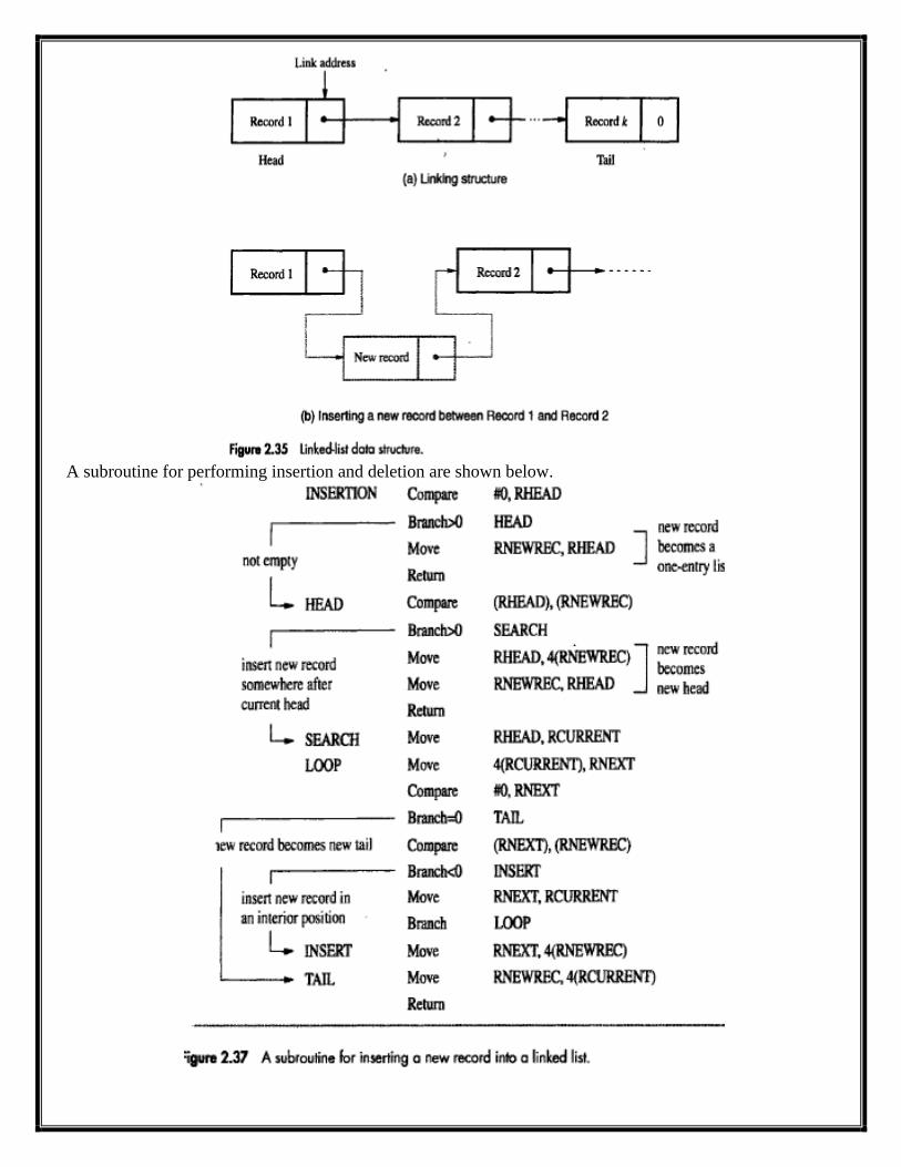
A subroutine for performing insertion and deletion are shown below.
FREQUENTLY ASKED QUESTIONS
1. What is a register transfer language?
2. Differentiate the instruction execution for adding ‘n’ numbers using Straight line sequencing and
branching.
3. Write short notes on shift and rotate instructions.
4. Write about various means by which data are transferred between memory of a computer and outside
world.
5. What is register transfer notation? Write and explain these notations to three-address, two-address, single
address and zero-address instruction types. 6. In how many ways the location of an operand is specified in an instruction? Explain each mode with
suitable examples.
7. What are different addressing modes? Explain.
8. Give example for left and right shift operations.
9. List basic input and output operations.
10. Write short notes on additional addressing modes
11. With an example write about relative addressing.
12. Illustrate the concept of assembly directives with an assembly language program
13. Illustrate with examples rotate instruction?
14. Differentiate between shift and rotate instructions.
UNIT – 3
Types of Instructions: Arithmetic and Logic Instructions, Branch Instructions,
Addressing modes, Input / Output Instructions.
Arithmetic and Logic Instructions: The ARM instruction set has a number of instructions for
arithmetic operations on operands that are either contained in the general-purpose registers or given as
immediate operands in the instruction itself. The basic assembly-language format for arithmetic and logic
instructions is shown below.
opcode Rd, Rn, Rm
where the operation specified by the opcode is performed on the source operands in general-purpose registers
Rn and Rm. The result is placed in destination register Rd.
Arithmetic Instructions: Different types of Arithmetic instructions are ADD, SUB, MUL and MLA.
For example, the instruction
ADD R0, R2, R4
performs the operation
R0←[R2] + [R4]
The instruction
SUB R0, R6, R5
performs the operation
R0←[R6] − [R5]
The second source operand can be specified in the immediate mode. Thus,
ADD R0, R3, #17
performs the operation
R0←[R3] + 17
The immediate operand is an 8-bit value contained in bits b7−0 of the encoded machine instruction. It is an
unsigned number in the range 0 to 255. The assembly language allows negative values to be used as
immediate operands. If the instruction
ADD R0, R3, #−17
is used in a program, the assembler replaces it with the instruction
SUB R0, R3, #17
When the second source operand is specified as the contents of a register, they can be shifted or rotated
before being used in the operation. Logical shift left (LSL), logical shift right (LSR), arithmetic shift right
(ASR), and rotate right (ROR). For example, the instruction
ADD R0, R1, R5, LSL #4
is executed as follows. The second source operand, which is contained in register R5, is shifted left 4 bit
positions (equivalent to [R5] × 16), then added to the contents of register R1. The sum is placed in register
R0. The carry bit, C, is not involved in these operations. The shift or rotation amount can also be specified as
the contents of a fourth register.
Two basic versions of a multiply instruction are provided. The first version multiplies the contents of
two registers and places the low-order 32-bits of the product in a third register. The high-order bits of the
product are discarded. If the operands are 2’s-complement numbers, and if their product can be represented
in 32 bits, then the retained low-order 32 bits of the product represent the correct result. For example, the
instruction
MUL R0, R1, R2
Performs the operation
R0←[R1] × [R2]
The second version of the basic Multiply instruction specifies a fourth register whose contents are
added to the product before the result is stored in the destination register. Hence, the instruction
MLA R0, R1, R2, R3
Performs the operation
R0←([R1] × [R2]) + [R3]
This is called a Multiply-Accumulate operation. It is often used in signal-processing applications.
Logic Instructions: Different types of Logic Instructions are AND, OR, XOR, BIC and MVC. For
example, The AND instruction
AND Rd, Rn, Rm
performs a bitwise logical AND of the operands in registers Rn and Rm and places the result in register Rd.
For example, if register R0 contains the hexadecimal pattern 02FA62CA and R1 contains the pattern
0000FFFF, then the instruction
AND R0, R0, R1 (R0 [ R0 ] ^ [ R1 ])
will result in the pattern 000062CA being placed in register R0.
The Bit Clear instruction, BIC, is closely related to the AND instruction. It complements each bit in
operand Rm before ANDing them with the bits in register Rn. Using the same R0 and R1 bit patterns as in
the above example, the instruction
BIC R0, R0, R1 (R0 [ R0 ] ^ [ NOT R1 ])
results in the pattern 02FA0000 being placed in R0.
The OR instruction
OR R0,R0,R1 (R0 [ R0 ] V [ R1 ])
Performs OR operation between contents of R0, R1 registers.
The XOR instruction
XOR R0,R0,R1 (R0 [ R0 ] [ R1 ])
Performs XOR operation between contents of R0, R1 registers.
The Move Negation instruction, with the opcode Mnemonic MVN, complements the bits of the source
operand and places the result in Rd. for example,
MVN R0, R3.
If the contents of R3 are the hexadecimal pattern 0F0F0F0F, then it places the result F0F0F0F0 in the
register R0.
The following ARM program merges two BCD digits into a byte.
The first instruction in the program loads the address LOC into register R0. The two ASCII characters
containing the BCD digits in their low-order four bits are loaded into the low-order byte positions of registers
R1 and R2 by the next two Load instructions. The AND instruction clears the high-order 2 bits of R2 to zero,
leaving the second BCD digit in the four low-order bit positions. The ‘&’ character in this instruction
signifies hexadecimal notation for the immediate value. The ORR instruction then shifts the first BCD digit
in R1 to the left four positions and places it to the left of the second BCD digit in R2. The two digits packed
into the low-order byte of R2 are then stored into location PACKED.
+
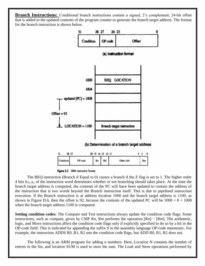
Branch Instructions: Conditional branch instructions contain a signed, 2’s complement, 24-bit offset
that is added to the updated contents of the program counter to generate the branch target address. The format
for the branch instruction is shown below.
The BEQ instruction (Branch if Equal to 0) causes a branch if the Z flag is set to 1. The higher order
4 bits b31-28, of the instruction word determines whether or not branching should takes place. At the time the
branch target address is computed, the contents of the PC will have been updated to contain the address of
the instruction that is two words beyond the Branch instruction itself. This is due to pipelined instruction
execution. If the Branch instruction is at address location 1000 and the branch target address is 1100, as
shown in Figure D.6, then the offset is 92, because the contents of the updated PC will be 1000 + 8 = 1008
when the branch target address 1100 is computed.
Setting condition codes: The Compare and Test instructions always update the condition code flags. Some
instructions, such as compare, given by CMP Rn, Rm performs the operation [Rn] − [Rm]. The arithmetic,
logic, and Move instructions affect the condition code flags only if explicitly specified to do so by a bit in the
OP-code field. This is indicated by appending the suffix S to the assembly language OP-code mnemonic. For
example, the instruction ADDS R0, R1, R2 sets the condition code flags, but ADD R0, R1, R2 does not.
The following is an ARM program for adding n numbers. Here, Location N contains the number of
entries in the list, and location SUM is used to store the sum. The Load and Store operations performed by
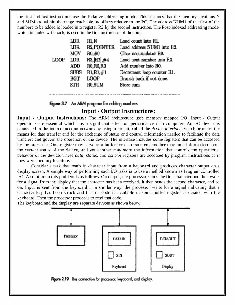
the first and last instructions use the Relative addressing mode. This assumes that the memory locations N
and SUM are within the range reachable by offsets relative to the PC. The address NUM1 of the first of the
numbers to be added is loaded into register R2 by the second instruction. The Post-indexed addressing mode,
which includes writeback, is used in the first instruction of the loop.
Input / Output Instructions:
Input / Output Instructions: The ARM architecture uses memory mapped I/O. Input / Output
operations are essential which has a significant effect on performance of a computer. An I/O device is
connected to the interconnection network by using a circuit, called the device interface, which provides the
means for data transfer and for the exchange of status and control information needed to facilitate the data
transfers and govern the operation of the device. The interface includes some registers that can be accessed
by the processor. One register may serve as a buffer for data transfers, another may hold information about
the current status of the device, and yet another may store the information that controls the operational
behavior of the device. These data, status, and control registers are accessed by program instructions as if
they were memory locations.
Consider a task that reads in character input from a keyboard and produces character output on a
display screen. A simple way of performing such I/O tasks is to use a method known as Program controlled
I/O. A solution to this problem is as follows: On output, the processor sends the first character and then waits
for a signal from the display that the character has been received. It then sends the second character, and so
on. Input is sent from the keyboard in a similar way; the processor waits for a signal indicating that a
character key has been struck and that its code is available in some buffer register associated with the
keyboard. Then the processor proceeds to read that code.
The keyboard and the display are separate devices as shown below.
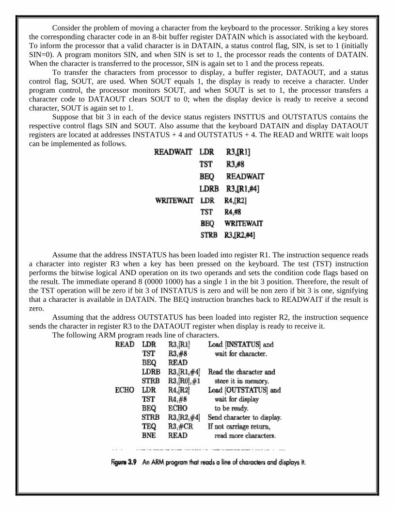
Consider the problem of moving a character from the keyboard to the processor. Striking a key stores
the corresponding character code in an 8-bit buffer register DATAIN which is associated with the keyboard.
To inform the processor that a valid character is in DATAIN, a status control flag, SIN, is set to 1 (initially
SIN=0). A program monitors SIN, and when SIN is set to 1, the processor reads the contents of DATAIN.
When the character is transferred to the processor, SIN is again set to 1 and the process repeats.
To transfer the characters from processor to display, a buffer register, DATAOUT, and a status
control flag, SOUT, are used. When SOUT equals 1, the display is ready to receive a character. Under
program control, the processor monitors SOUT, and when SOUT is set to 1, the processor transfers a
character code to DATAOUT clears SOUT to 0; when the display device is ready to receive a second
character, SOUT is again set to 1.
Suppose that bit 3 in each of the device status registers INSTTUS and OUTSTATUS contains the
respective control flags SIN and SOUT. Also assume that the keyboard DATAIN and display DATAOUT
registers are located at addresses INSTATUS + 4 and OUTSTATUS + 4. The READ and WRITE wait loops
can be implemented as follows.
Assume that the address INSTATUS has been loaded into register R1. The instruction sequence reads
a character into register R3 when a key has been pressed on the keyboard. The test (TST) instruction
performs the bitwise logical AND operation on its two operands and sets the condition code flags based on
the result. The immediate operand 8 (0000 1000) has a single 1 in the bit 3 position. Therefore, the result of
the TST operation will be zero if bit 3 of INSTATUS is zero and will be non zero if bit 3 is one, signifying
that a character is available in DATAIN. The BEQ instruction branches back to READWAIT if the result is
zero.
Assuming that the address OUTSTATUS has been loaded into register R2, the instruction sequence
sends the character in register R3 to the DATAOUT register when display is ready to receive it.
The following ARM program reads line of characters.
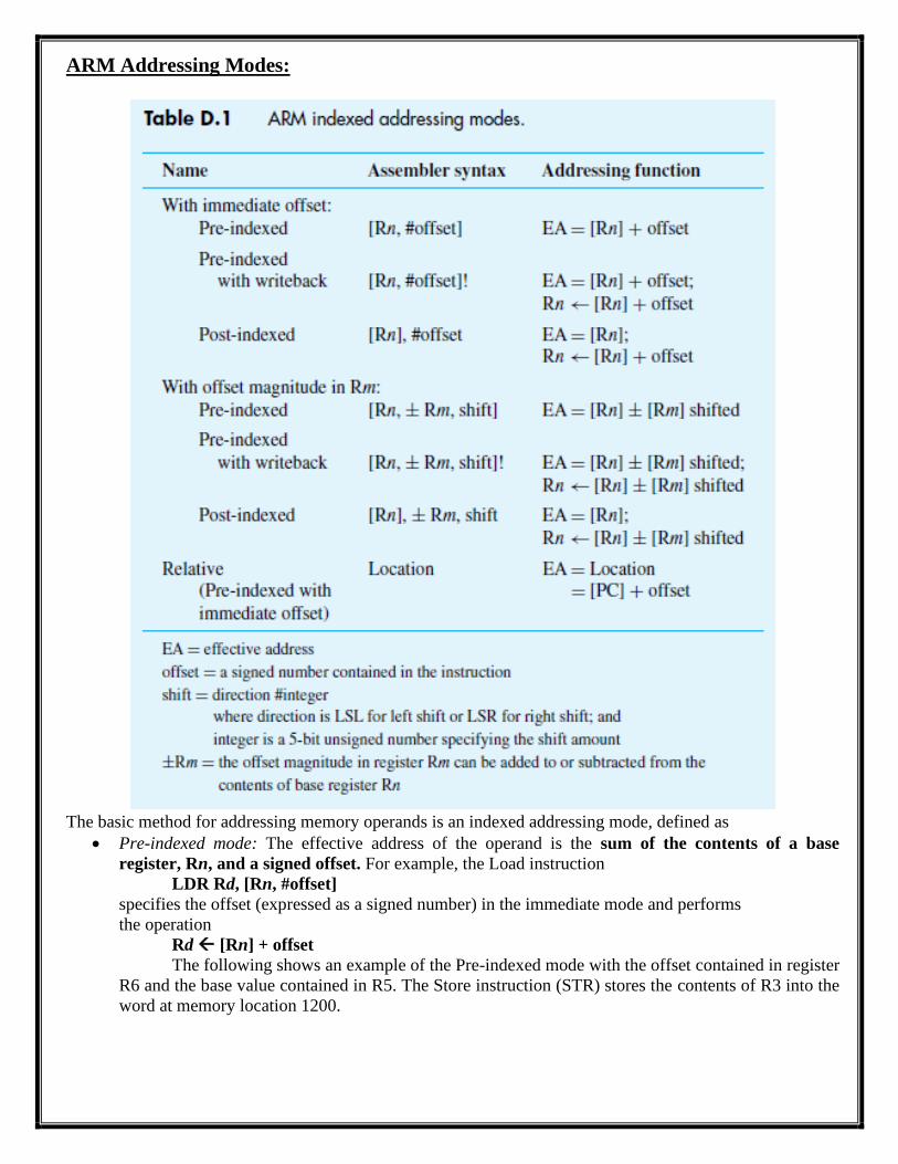
ARM Addressing Modes:
The basic method for addressing memory operands is an indexed addressing mode, defined as
• Pre-indexed mode: The effective address of the operand is the sum of the contents of a base
register, Rn, and a signed offset. For example, the Load instruction
LDR Rd, [Rn, #offset]
specifies the offset (expressed as a signed number) in the immediate mode and performs
the operation
Rd [Rn] + offset
The following shows an example of the Pre-indexed mode with the offset contained in register
R6 and the base value contained in R5. The Store instruction (STR) stores the contents of R3 into the
word at memory location 1200.
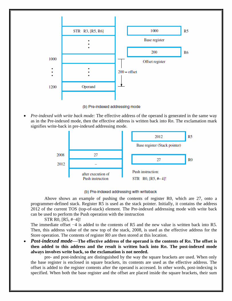
• Pre-indexed with write back mode: The effective address of the operand is generated in the same way
as in the Pre-indexed mode, then the effective address is written back into Rn. The exclamation mark
signifies write-back in pre-indexed addressing mode.
Above shows an example of pushing the contents of register R0, which are 27, onto a
programmer-defined stack. Register R5 is used as the stack pointer. Initially, it contains the address
2012 of the current TOS (top-of-stack) element. The Pre-indexed addressing mode with write back
can be used to perform the Push operation with the instruction
STR R0, [R5, #−4]!
The immediate offset −4 is added to the contents of R5 and the new value is written back into R5.
Then, this address value of the new top of the stack, 2008, is used as the effective address for the
Store operation. The contents of register R0 are then stored at this location.
• Post-indexed mode—The effective address of the operand is the contents of Rn. The offset is
then added to this address and the result is written back into Rn. The post-indexed mode
always involves write back, so the exclamation is not needed.
pre- and post-indexing are distinguished by the way the square brackets are used. When only
the base register is enclosed in square brackets, its contents are used as the effective address. The
offset is added to the register contents after the operand is accessed. In other words, post-indexing is
specified. When both the base register and the offset are placed inside the square brackets, their sum
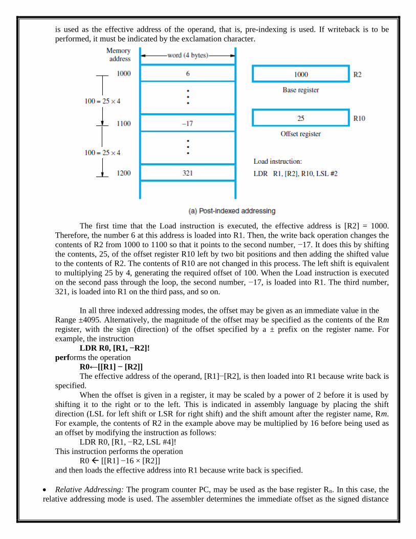
is used as the effective address of the operand, that is, pre-indexing is used. If writeback is to be
performed, it must be indicated by the exclamation character.
The first time that the Load instruction is executed, the effective address is [R2] = 1000.
Therefore, the number 6 at this address is loaded into R1. Then, the write back operation changes the
contents of R2 from 1000 to 1100 so that it points to the second number, −17. It does this by shifting
the contents, 25, of the offset register R10 left by two bit positions and then adding the shifted value
to the contents of R2. The contents of R10 are not changed in this process. The left shift is equivalent
to multiplying 25 by 4, generating the required offset of 100. When the Load instruction is executed
on the second pass through the loop, the second number, −17, is loaded into R1. The third number,
321, is loaded into R1 on the third pass, and so on.
In all three indexed addressing modes, the offset may be given as an immediate value in the
Range ±4095. Alternatively, the magnitude of the offset may be specified as the contents of the Rm
register, with the sign (direction) of the offset specified by a ± prefix on the register name. For
example, the instruction
LDR R0, [R1, −R2]!
performs the operation
R0←[[R1] − [R2]]
The effective address of the operand, [R1]−[R2], is then loaded into R1 because write back is
specified.
When the offset is given in a register, it may be scaled by a power of 2 before it is used by
shifting it to the right or to the left. This is indicated in assembly language by placing the shift
direction (LSL for left shift or LSR for right shift) and the shift amount after the register name, Rm.
For example, the contents of R2 in the example above may be multiplied by 16 before being used as
an offset by modifying the instruction as follows:
LDR R0, [R1, −R2, LSL #4]!
This instruction performs the operation
R0 [[R1] −16 × [R2]]
and then loads the effective address into R1 because write back is specified.
• Relative Addressing: The program counter PC, may be used as the base register Rn. In this case, the
relative addressing mode is used. The assembler determines the immediate offset as the signed distance
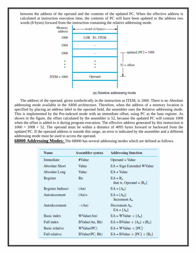
between the address of the operand and the contents of the updated PC. When the effective address is
calculated at instruction execution time, the contents of PC will have been updated to the address two
words (8 bytes) forward from the instruction containing the relative addressing mode.
The address of the operand, given symbolically in the instruction as ITEM, is 1060. There is no Absolute
addressing mode available in the ARM architecture. Therefore, when the address of a memory location is
specified by placing an address label in the operand field, the assembler uses the Relative addressing mode.
This is implemented by the Pre-indexed mode with an immediate offset, using PC as the base register. As
shown in the figure, the offset calculated by the assembler is 52, because the updated PC will contain 1008
when the offset is added to it during program execution. The effective address generated by this instruction is
1060 = 1008 + 52. The operand must be within a distance of 4095 bytes forward or backward from the
updated PC. If the operand address is outside this range, an error is indicated by the assembler and a different
addressing mode must be used to access the operand.
68000 Addressing Modes: The 68000 has several addressing modes which are defined as follows.
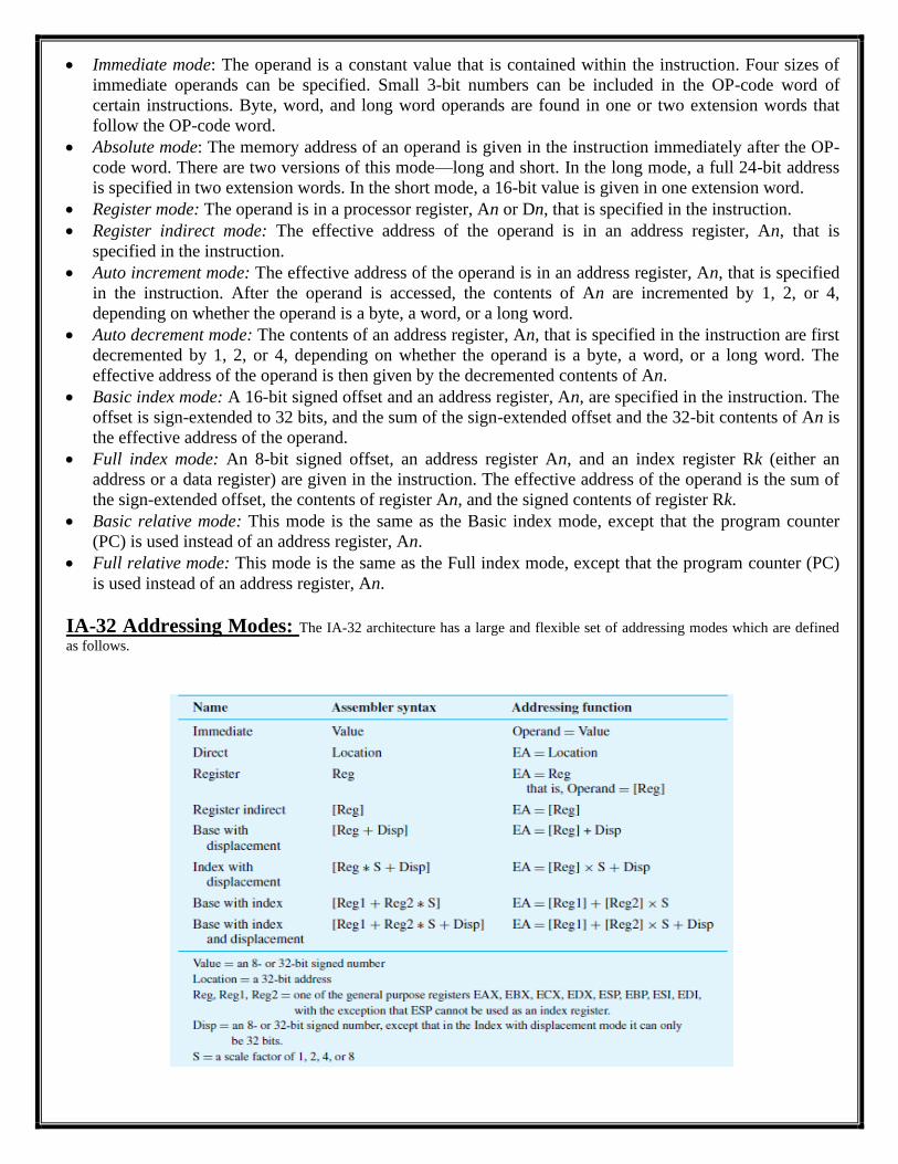
• Immediate mode: The operand is a constant value that is contained within the instruction. Four sizes of
immediate operands can be specified. Small 3-bit numbers can be included in the OP-code word of
certain instructions. Byte, word, and long word operands are found in one or two extension words that
follow the OP-code word.
• Absolute mode: The memory address of an operand is given in the instruction immediately after the OP-
code word. There are two versions of this mode—long and short. In the long mode, a full 24-bit address
is specified in two extension words. In the short mode, a 16-bit value is given in one extension word.
• Register mode: The operand is in a processor register, An or Dn, that is specified in the instruction.
• Register indirect mode: The effective address of the operand is in an address register, An, that is
specified in the instruction.
• Auto increment mode: The effective address of the operand is in an address register, An, that is specified
in the instruction. After the operand is accessed, the contents of An are incremented by 1, 2, or 4,
depending on whether the operand is a byte, a word, or a long word.
• Auto decrement mode: The contents of an address register, An, that is specified in the instruction are first
decremented by 1, 2, or 4, depending on whether the operand is a byte, a word, or a long word. The
effective address of the operand is then given by the decremented contents of An.
• Basic index mode: A 16-bit signed offset and an address register, An, are specified in the instruction. The
offset is sign-extended to 32 bits, and the sum of the sign-extended offset and the 32-bit contents of An is
the effective address of the operand.
• Full index mode: An 8-bit signed offset, an address register An, and an index register Rk (either an
address or a data register) are given in the instruction. The effective address of the operand is the sum of
the sign-extended offset, the contents of register An, and the signed contents of register Rk.
• Basic relative mode: This mode is the same as the Basic index mode, except that the program counter
(PC) is used instead of an address register, An.
• Full relative mode: This mode is the same as the Full index mode, except that the program counter (PC)
is used instead of an address register, An.
IA-32 Addressing Modes: The IA-32 architecture has a large and flexible set of addressing modes which are defined
as follows.

• Immediate mode: The operand is contained in the instruction. It is a signed 8-bit or 32-bit number,
with the length being specified by a bit in the opcode of the instruction. This bit is 0 for the short
version and 1 for the long version.
• Direct mode: The memory address of the operand is given by a 32-bit value in the instruction.
• Register mode: The operand is contained in one of the eight general-purpose registers specified in the
instruction.
• Register indirect mode: The memory address of the operand is contained in one of the eight general-
purpose registers specified in the instruction.
• Base with displacement mode: An 8-bit or 32-bit signed displacement and one of the eight general-
purpose registers to be used as a base register are specified in the instruction. The effective address of
the operand is the sum of the contents of the base register and the displacement.
• Index with displacement mode: A 32-bit signed displacement, one of the eight general purpose
registers to be used as an index register, and a scale factor of 1, 2, 4, or 8, are specified in the
instruction. To obtain the effective address of the operand, the contents of the index register are
multiplied by the scale factor and then added to the displacement.
• Base with index mode: Two of the eight general-purpose registers and a scale factor of 1, 2, 4, or 8,
are specified in the instruction. The registers are used as base and index registers. The effective
address of the operand is determined by first multiplying the contents of the index register by the
scale factor and then adding the result to the contents of the base register.
• Base with index and displacement mode: An 8-bit or 32-bit signed displacement, two of the eight
general-purpose registers, and a scale factor of 1, 2, 4, or 8, are specified in the instruction. The
registers are used as base and index registers. The effective address of the operand is determined by
first multiplying the contents of the index register by the scale factor and then adding the result to the
contents of the base register and the displacement.
FREQUENTLY ASKED QUESTIONS
1. Write about branch instruction and its significance?
2. Write about logic instruction and its significance.
3. Differentiate post-indexed and pre-indexed addressing with write back policy.
4. Differentiate relative and absolute addressing modes for branch instructions
5. What is the format of arithmetic instruction in assembly language? Elaborate variants of OP code in
it.
6. How to determine branch target address?
7. Write in detail, about register operands, immediate operands and shifted immediate operands of
arithmetic and logic instructions.
8. Discuss load/store instructions for multiple operands.
9. What are the conditional branch instructions? Explain each with an example
10. How to perform AND, OR, NAND, NOR and XOR logic instructions? Give example
11. Write the instruction format of ARM.