first-principles study of spintronic phenomena
TRANSCRIPT
THÈSE Pour obtenir le grade de
DOCTEUR DE L’UNIVERSITÉ DE GRENOBLE Spécialité : Physique
Arrêté ministériel : 7 août 2006 Présentée par
Hongxin YANG Thèse dirigée par Mairbek CHSHIEV préparée au sein du Laboratoire SPINTEC (UMR CEA/CNRS/UJF/Grenoble INP) dans l'École Doctorale de Physique
FIRST-PRINCIPLES STUDY OF SPINTRONIC PHENOMENA IN MAGNETIC TUNNEL JUNCTIONS AND GRAPHENE Thèse soutenue publiquement le 13 March 2012 devant le jury composé de :
M. Stefan BLÜGEL (Rapporteur) Prof., Peter Grünberg Institut & Institute for Advanced Simulation, Jülich M. Stefano SANVITO (Rapporteur) Prof., Trinity College, Dublin M. André THIAVILLE (Examinateur) D.R. CNRS, Laboratoire de Physique des Solides, Université Paris-sud, Orsay M. Alain SCHUHL Prof., Université Joseph-Fourier & Institut Néel, Grenoble Mme Claudine LACROIX (Examinateur) D.R. CNRS, Institut Néel, Grenoble M. Mairbek CHSHIEV (Directeur de Thèse) Prof., Université Joseph-Fourier & Spintec, Grenoble

Contents
1 General introduction 1
2 Interlayer Exchange Coupling (IEC) 92.1 Ab initio calculations of interlayer exchange coupling . . . . . . . . . . . 92.2 Interlayer exchange coupling in MgO-based magnetic tunnel junctions . . 11
2.2.1 Introduction . . . . . . . . . . . . . . . . . . . . . . . . . . . . . . 112.2.2 Calculation details . . . . . . . . . . . . . . . . . . . . . . . . . . 122.2.3 Structural Relaxation Effects on Interlayer Exchange Coupling . . 132.2.4 Oxidation Effects on Interlayer Exchange Coupling . . . . . . . . 152.2.5 Conclusion . . . . . . . . . . . . . . . . . . . . . . . . . . . . . . . 16
2.3 IEC in SrTiO3-based MTJs . . . . . . . . . . . . . . . . . . . . . . . . . 172.3.1 The choice of Co, Fe and SrTiO3 . . . . . . . . . . . . . . . . . . 172.3.2 Structure of Co(Fe)|STO|Co(Fe) MTJs and calculation details . . 172.3.3 Effects of ferromagnetic electrode on IEC . . . . . . . . . . . . . . 202.3.4 Effects of barrier on IEC . . . . . . . . . . . . . . . . . . . . . . . 222.3.5 Conclusion . . . . . . . . . . . . . . . . . . . . . . . . . . . . . . . 24
2.4 IEC in GaAs(ZnSe)-based MTJs . . . . . . . . . . . . . . . . . . . . . . . 252.4.1 Introduction . . . . . . . . . . . . . . . . . . . . . . . . . . . . . . 252.4.2 Interfacial structure of Fe/GaAs(ZnSe) . . . . . . . . . . . . . . . 252.4.3 Correlation between IEC and the band gap in barrier . . . . . . . 252.4.4 Conclusion . . . . . . . . . . . . . . . . . . . . . . . . . . . . . . . 29
2.5 Summary . . . . . . . . . . . . . . . . . . . . . . . . . . . . . . . . . . . 30
3 Spin-orbit coupling induced phenomena at FM|MgO interfaces 313.1 PMA at Fe(Co)|MgO interfaces . . . . . . . . . . . . . . . . . . . . . . . 33
3.1.1 Introduction to the PMA at interfaces . . . . . . . . . . . . . . . 333.1.2 Methodology and structures . . . . . . . . . . . . . . . . . . . . . 343.1.3 Results and discussion . . . . . . . . . . . . . . . . . . . . . . . . 353.1.4 Conclusion . . . . . . . . . . . . . . . . . . . . . . . . . . . . . . . 42
3.2 Correlation between Bloch state spin filtering and PMA . . . . . . . . . . 433.2.1 Introduction . . . . . . . . . . . . . . . . . . . . . . . . . . . . . . 433.2.2 Structures, results and discussion . . . . . . . . . . . . . . . . . . 433.2.3 Conclusion . . . . . . . . . . . . . . . . . . . . . . . . . . . . . . . 46
3.3 Summary . . . . . . . . . . . . . . . . . . . . . . . . . . . . . . . . . . . 47
II
4 Graphene on magnetic metal 494.1 Perpendicular Magnetic Anisotropy of Co on Gr . . . . . . . . . . . . . . 49
4.1.1 Introduction . . . . . . . . . . . . . . . . . . . . . . . . . . . . . . 494.1.2 Methodology . . . . . . . . . . . . . . . . . . . . . . . . . . . . . 494.1.3 Stability of epitaxial graphene on Co films . . . . . . . . . . . . . 504.1.4 Magnetic Anisotropy of Graphene/Co . . . . . . . . . . . . . . . . 51
4.2 Work Function of Graphene/Co . . . . . . . . . . . . . . . . . . . . . . . 564.3 Summary . . . . . . . . . . . . . . . . . . . . . . . . . . . . . . . . . . . 58
5 Graphene on magnetic insulator 595.1 Interest of graphene on magnetic insulator . . . . . . . . . . . . . . . . . 595.2 Calculation details and structures . . . . . . . . . . . . . . . . . . . . . . 605.3 Spin polarization of graphene on EuO . . . . . . . . . . . . . . . . . . . . 625.4 Tuning of Dirac Cone . . . . . . . . . . . . . . . . . . . . . . . . . . . . . 635.5 Magnetic order in graphene on EuO . . . . . . . . . . . . . . . . . . . . . 665.6 Summary and Perspective . . . . . . . . . . . . . . . . . . . . . . . . . . 69
6 Electronic and magnetic properties of graphene nanomeshes 706.1 Introduction . . . . . . . . . . . . . . . . . . . . . . . . . . . . . . . . . . 706.2 Methods . . . . . . . . . . . . . . . . . . . . . . . . . . . . . . . . . . . . 726.3 Model of graphene nanomeshes . . . . . . . . . . . . . . . . . . . . . . . 726.4 Results and discussions . . . . . . . . . . . . . . . . . . . . . . . . . . . . 726.5 Summary . . . . . . . . . . . . . . . . . . . . . . . . . . . . . . . . . . . 82
7 Conclusions 84
Chapter 1
General introduction
In recent decades, progress in fabrication and characterization of systems with reduceddimensionality has stimulated fundamental research on a wide range of quantumphenomena and has enabled development of nanomaterials with new functionalitiesrelated to new information technologies. The most remarkable event, in this context,is the discovery of giant magnetoresistance (GMR) in magnetic multilayered structuresin 1988 by the groups of A. Fert [BBF+88] and P. Grunberg [BGSZ89]. They observeda significant change in the resistance of multilayers when the magnetizations of adjacentferromagnetic layers separated by a nonmagnetic spacer were brought into alignmentby an applied magnetic field. This discovery opened new ways of exploring magneticproperties of materials by means of spin-dependent transport and generated a new fieldof research called spin electronics or spintronics [Ohn98, WAB+01, FBY+01a, BFC+02],which combines two traditional fields of physics: magnetism and electronics. In otherwords, it is not only the electron charge but also the electron spin that is used to operatea device. Spin is the intrinsic angular momentum of a particle which, in the case of theelectron, is characterized by a quantum number equal to 1/2 with two possible statescalled ”spin-up” and ”spin-down” (or ”majority” and ”minority”). In ferromagneticmaterials, the Coulomb interaction and Pauli exclusion principle cause a long-rangeordering of the unpaired up (or down) spins leading to the finite magnetic moment µ perunit volume (magnetization M) resulting from the difference of majority and minoritydensity of states (DOS). Furthermore, such inequality of the DOS for two spin states atthe Fermi surface leads to significantly different conductivities for the spin up and thespin down electrons as was demonstrated by A. Fert and I. Campbell in the late 1960s[CFP67, FC68]. Along with the existence of the long range interlayer coupling betweentwo ferromagnets separated by a nonmagnetic spacer [GSP+86], these observations werethe key steps in the discovery of GMR suggesting that the transport in ferromagneticmaterials is spin-dependent and can be considered within the two current model [Mot36].Giant magnetoresistance became the supreme manifestation of spin-dependent transportand was recognized by the award of the Nobel Prize 2007 to A. Fert and P. Grunberg.
The essential prerequisite of discovery of GMR is interlayer exchange coupling (IEC),which is one of the most fundamental phenomena in spintronics. The phenomenon hasbeen demonstrated in 1986 [GSP+86, MCK+86, SSR+86] between the magnetizations oftwo ferromangetic layers separated by a non-magnetic spacer. It is found that magnetscan interact from long distance through nonmangetic spacer to form either ferromagnetic
Chapter 1. General introduction 2
or antiferromangetic exchange coupling. Further research in these systems leads to thediscovery of GMR effect in 1988 [BBF+88, BGSZ89].
The initial explanation for the oscillatory interlayer exchange coupling was basedon the Ruderman-Kittel-Kasuya-Yosida (RKKY) indirect exchange which originallydescribed the coupling between two nuclear spins embedded in a degenerated electrongas. Its effective Hamiltonian can be represented by [Slo95],
Heff(ρ) =J2lcmeQ
4F (2Qd)Si · Sj
2π3~2, (1.1)
F (z) =zcosz − sinz
z4, (1.2)
where function F is proportional to the nonlocal susceptibility of the gas, d is the distancebetween local atom spins Si and Sj , Jlc represents the exchange integral between a localelectron and a conduction electron, me is the mass of electron, and Q is the Fermi vectorof the free electron gas. Summing Heff over atomic position i in one magnet and j inthe other one gives the coupling energy per unit area
W = −J1cosθ, (1.3)
where θ is the angle between the two magnetization vectors.The simple application of RKKY theory, where spin distribution within the
ferromagnetic layers is uniform and the spacer thickness was assumed to be able tovary continuously, yields a period Λ = λF/2 = 1ML, which is too short compared tothe experimental results [BC91a]. The generalized theory of RKKY interlayer exchangecoupling was proposed by P. Bruno and C. Chappert [BC91a, BC91b, BC92], where thecoupling was related in a physically transparent manner to the topological properties ofthe Fermi surface at the spacer material. Two key aspects in the interlayer exchangecoupling were addressed: (i) the interaction between a ferromagnetic layer and the hostconduction electrons, and (ii) the way the spin-polarization is propagated across the hostmaterial. The first aspect can actually be ascribed by using the basis of s-d(f) modelwhich is usually used to deal transition metal magnetic impurities.
By 1993, there were a number of theoretical models for interlayer exchange couplingproposed [Sti93, BC91a, BC91b, BC92, Slo95]. From that time on, a flourished oneand a half decades, a simple physical picture for interlayer exchange coupling hasevolved. Spin dependent reflection from the interfaces in multilayers leads to formation ofspin-dependent quantum well states. These quantum well states evolve in energy as thethickness of the spacer layer is varied. As these states pass through the Fermi energy, theyare filled or empty therefore changing the energy of the multilayer. These changes areperiodic because the quantum well states cross the Fermi energy with a period determinedby the Fermi surface of the spacer layer material. At critical points of this Fermi surface,many quantum well states have the same period giving a net oscillatory contribution tothe energy. Since the reflection is spin dependent, the energy depends on the relativeorientation of the layer magnetizations, i.e., there is an energy difference between paralleland antiparallel alignment of the magnetizations. This energy difference is indeed theinterlayer exchange coupling. It has oscillatory contributions with periods determined bythe critical spanning vectors of the spacer layer Fermi surface and strengths determinedby the spin-dependent reflection at the interfaces.
Chapter 1. General introduction 3
The advent of GMR has renewed the interest in spin dependent tunneling [Jul75]across semiconductors and insulators and led to demonstrations of high tunnelmagnetoresistance ratios (TMR) at room temperature [MKWM95, MT95] in magnetictunnel junctions (MTJs). MTJs consist of two ferromagnetic (FM) electrodes separatedby an insulating barrier have been objects of great interest from both fundamental andapplied perspectives. High sensitivity to magnetic fields makes these structures goodcandidates for hard drive magnetoresistive read heads, logic devices and magnetic randomaccess memories [PRS+99, TCD+99, IHL+07]. Various aspects have been addressed, boththeoretically and experimentally, regarding spin dependent properties in MTJs such asthe role of disorder and impurities at the interfaces between ferromagnetic and oxidelayers, the impact of the junction composition on TMR ratio, temperature dependenceof the latter, etc. [TP98, TP99, SWN99, LSK+00, LSKdJ00, DTBF+99a, DTBF+99b,BFC+02, BBVD02, VBBD01, DCT+01, DGC+03, DHC+04, TML03].
A major breakthrough in the area of spin-dependent tunneling was the prediction ofextremely high tunnel magnetoresistance ratios for certain epitaxially grown magnetictunnel junctions [MZBW99, BZSM01, MU01, WMZ+02]. This prediction was based ona spin filtering effect that may arise from the symmetry of the wave functions. At theFermi energies of bcc Fe, bcc Co and CoFeB, there is a difference in the symmetries ofwave functions between the majority and minority spin channels. Specifically there isa ∆1 Bloch state for the majority, but not for the minority. For some insulating andsemiconducting materials, states with this ∆1 symmetry will decay much more slowlythan states with different symmetries due to the presence of corresponding evanescentstates in the band gap [BZSM01, MU01, DMW+02, BZV+05, VCB06]. In other words,an insulator separating two ferromagnetic electrodes should not be viewed as a simplebarrier and electron tunneling cannot be accurately described in the framework of theJulliere model [Jul75]. Recent experiments [PKP+04, YNF+04, Ike08] largely confirmedpredictions made by W. H. Butler et al. [BZSM01] and J. Mathon et al. [MU01] forMgO based tunnel junctions. So far the record values of TMR ratio on MgO-based MTJsreached 600% at room temperature [LHI+07]. This discovery also has a large impact onthe technologies of MRAM and of read sensors for hard drives.
In contrast to the case of a metal spacer, much fewer investigations have beendevoted to interlayer exchange coupling across nonmetallic spacer layers [TBHL92,Bru95, FML+92, CMW96, KCE+97, EKS99, GBB+01]. The interest has been stronglyenforced with the observation of antiferromagnetic interlayer exchange coupling in 2002in Fe|MgO|Fe crystalline magnetic tunnel junctions (MTJs) by J. Faure-Vincent andcoauthors who reported IEC values up to -0.26 mJ/m2 for thin MgO layer thicknesses[FVTB+02]. The AF IEC phenomenon across the insulator was initially explainedusing the free electron model for pure tunneling [FVTB+02, Slo89] and the resonanttunneling mechanism due to the presence of localized impurity or defect states in theinsulating barrier layer [ZTV05, ZVVT06]. For instance, it was shown from first-principlescalculations that oxygen vacancies located in the middle of the MgO layer as wellas interfacial oxygen [WAMS08] cause the IEC to be AF for MgO thicknesses below0.8 nm [KYV+06, ZVVT06]. In recent experiments, Chiang et al. [CWT+09] investigatedthe role of interfacial oxidation on the IEC in Fe|MgO|Fe MTJs and found that oxidationconditions can strongly affect the character of the IEC for MgO thicknesses below 1 nm.They observed that for MgO thicknesses up to 0.6 nm both under- and overoxidized
Chapter 1. General introduction 4
junctions show AF IEC which is much stronger in case of under-oxidation. However, theIEC becomes FM in case of overoxidized samples for MgO thicknesses larger than 0.6 nm(∼ 3 monolayers). So far, the explanation for IEC across the over- and under-oxidizedMgO interface structures is in a well agreement with experimental results, whereas therehave been inconsistencies between the experimentally observed AF IEC [FVTB+02] andfirst-principles calculated FM IEC in pure Fe|MgO|Fe MTJs [KYV+06, ZVVT06].
In this thesis, we revisited interlayer exchange coupling in Fe|MgO|Fe MTJsand investigated this phenomenon in Chapter 2, where the effects of structuralrelaxation and oxidation conditions on interlayer exchange coupling are presented fromfirst-principles and tight-binding model calculations. In addition, we extend the studyof IEC to some other structures with semicondutors separating ferromagnets to have ageneral view of IEC across insulating spacers.
Another very interesting spintronic phenomenon observed in MTJs is theperpendicular magnetic anisotropy (PMA). Monso et al. have shown that PMA could beobserved at Co(Fe)|MOx interfaces (M=Ta, Mg, Al, Ru etc.) [MRA+02, RAD+03] in spiteof the weak spin-orbit interaction in the system. Large PMA values up to 1 to 2 erg/cm2
have been reported, which are comparable or even larger than the PMA values observed atCo|Pt or Co|Pd interfaces [GLW+06, JJKdB95]. This result is quite general and has beenobserved in both crystalline (MgO) or amorphous (AlOx) barriers, using both naturalor plasma oxidation [LHA+07, MDL+08, MPV+08]. Especially, recent experimentsreported large PMA values of 1.3 erg/cm2 at CoFeB|MgO structures [IMY+10, EKI+10].Furthermore, it has been experimentally demonstrated that there is a strong correlationbetween PMA and TMR maximum values obtained at the same optimal oxidation andannealing conditions [NRD+10].
Even though the experiments show such surprisingly large PMA values and theoptimized PMA and TMR maximum at the same oxidation conditions, the understandingof this correlation is not clear. The works on the mechanism of the large PMA atFe|MgO interfaces are of particular interest. The paper by Nakamura et al used a singlelayer of Fe on MgO to explore the electric field induced magnetic anisotropy [NAI+10].They reported that an ideal abrupt Fe|MgO interface gives rise to a large out-of-planemagnetic anisotropy due to weak Fe-O hybridization at the interface, but the anisotropyswitching by an applied electric field is found to be difficult to achieve. Instead, theexistence of an interfacial FeO layer plays a key role in demonstrating the anisotropyswitching that accompanies an electric-field-induced displacement of Fe atoms on theinterfacial FeO layer. For PMA at thicker Fe layers on MgO (001) surface, M. K. Niranjanet al. have calculated the magnetoelectric effects originating from the influence of anexternal electric field on magnetic properties of the Fe|MgO(001) interface [NDJT10].They have shown that the effect on the interface magnetization and magnetocrystallineanisotropy can be substantially enhanced if the electric field is applied across a dielectricmaterial with a large dielectric constant. They predict the effect of electric field on theinterface magnetocrystalline anisotropy due to the change in the relative occupancy ofthe 3d-orbitals of Fe atoms at the Fe|MgO interface. However, the PMA mechanismat Fe|MgO interfaces is not clear enough. In particularly, there is no reports aboutthe correlation between PMA and TMR, even though in experiments by L.E. Nistorand coauthors. It was shown that the anisotropy reaches its maximum in the optimaloxidation conditions [NRD+10].
Chapter 1. General introduction 5
We will devote the Chapter 3 to investigate mechanisms of magnetic anisotropy atFe|MgO and Co|MgO interfaces, and will understand them in terms of correlation betweenBloch states symmetry based spin-filtering and PMA in MgO-based MTJs.
Starting fromChapter 4, we will work on another novel branch of spintronics, namelygraphene-based spintronics [FBY+01b, WAB+01, HMP+12]. We will start from PMAat Co|graphene interfaces. Furthermore, magnetic behavior and work function of Cosurfaces due to graphene coverage will also be investigated.
Graphene is a very interesting material because it is a real realized two dimensionalsheet of carbon atoms in a honeycomb lattice, known as the thinnest material in theuniverse, can be rolled up to form carbon nanotube, or stacked to form graphite,exhibiting many unique properties. For example, its charge carriers exhibit giantintrinsic mobility, have zero effective mass, and can travel for micrometers withoutscattering at room temperature. Graphene can sustain current densities six orders ofmagnitude higher than that of copper, shows record thermal conductivity and stiffness, isimpermeable to gases, and reconciles such conflicting qualities as brittleness and ductility.Electron transport in graphene is described by a Dirac-like equation, which allows theinvestigation of relativistic quantum phenomena in a benchtop experiment [CNGP+09,Gei09, DSAHR11]. For groundbreaking experiments regarding the two-dimensionalmaterial graphene, the Nobel Prize in physcis was awarded to A. Geim and K. Novoselovin 2010.
In addition to its promising properties for electronics, graphene is also very attractivefor spintronics [FBY+01b, WAB+01], this is due to expected very long spin lifetimesthank to its intrinsic weak spin-orbit coupling and hyperfine interaction, which allows forthe spin population to remain spin polarized even over long channel lengths. Also, recentstudies have shown spin transport in graphene to be tunable by an electrically controlledback gate [HMP+12].
Another useful feature is that graphene is only one atom thick, and therefore thesurface is extremely sensitive to whatever is lying on top of it. It therefore becomespossible to chemically dope the surface to probe the electrical and spin propertiesof graphene in ways not possible (or very hard) in other systems. Furthermore,as graphene is a nearly ideal two-dimensional system, it provides many interestingphenomena from the point of view of fundamental physics research such as the (fractionaland integer) Quantum Hall Effect (FQHE and IQHE) and ’tabletop’ relativisticphysics [DSD+09, BGS+09, NGM+05, ZLB+12]. Combining these advantages, grapheneis an extremely interesting material in the field and opens a new direction for spintronics.For example, exciting spin-dependent effects have been observed or predicted, noticeablyin graphene-based non-local spin valve devices: efficient spin injection [TJP+07a], aquest for controlling spin injection in graphene [TJP+07b, HWP+09, HPM+10, YBV+11],and spin-filtering [SCL06b]. In particular, FM|graphene|FM epitaxial stacks withhigh magnetoresistance [KGK+07] and low resistance area product [YP09] attractedconsiderable attention in this respect.
Not only spin transport but also spin polarization in graphene is a topic of intenseinterest. Two-dimensional nature of graphene is again appealing, that is in thisaspect, due to shaped nanoribbons and nanomeshes whose edges may intrinsically carryspin-polarized currents (states) [SCL06b, BZJ+10]. Graphene may also be insertedbetween two planar ferromagnets to build giant magnetoresistance junctions operated
Chapter 1. General introduction 6
in a current perpendicular to the plane configuration, with neither too low (like forgiant magnetoresistance) nor too high (like for tunnel magnetoresistance) resistance-areaproduct, and with extremely thin spacers [KGK+07, YP09]. The magnetoresistive effectoutlined in the latter proposal calls for the availability of epitaxial FM|graphene|FMtrilayers, due to the importance of band matching with graphene [GKB+08]. Thisrequires that epitaxial graphene be prepared on ferromagnetic supports, which wasdemonstrated years ago [ON97], and also requires the development of epitaxial twodimensional ferromagnetic layers on top of graphene.
Therefore such layers may serve as building blocks in a number of spintronics setupsbeyond the scope of magnetoresistive junctions. For instance, a large Rashba field maydevelop in an ultrathin two dimensional metallic ferromagnetic layer sandwiched betweengraphene and another metal layer of a heavy element such as gold, due to a strongout-of-plane electron potential gradient resulting from the structural inversion asymmetryimposed by the two distinct interfaces [VSBS+08, RVSB+09, GDM+11].
Beyond the magnetic metal, with magnetic insulating substrates to inducemagnetization in graphene is also interesting. This is basically due to the requirementsof some devices for spin-polarization and band gap opening. As one knows, thatsemiconducting devices rely on the gap because it is the gap that allows a semiconductorto be switched from conducting to insulating. In principle, the larger the gap the betterfor application since it insures a large on to off ratio for switching devices. Therefore,for graphene-based electronic applications, to open a gap is crucial. One way to opena gap in graphene is using confined structures, e.g. graphene nanoribbon and graphenenonomeshes [SCL06b, BZJ+10]. Indeed, a graphene ribbon with a width of 1 nm hastheoretically a band gap of nearly 1 eV. An energy gap of this magnitude is good enoughfor electronic applications, but the size scale of 1 nm is in the range of fabrication limit.In the sense of size scale, graphene nanomeshes may help to solve the problem [BZJ+10].Another solution to obtain large scale opened-gap graphene is using insulating substrate,the very famous one is using 4H- or 6H-SiC substrate. But other insulating substrates arealso intensively investigated, for example, Al2O3, MgO, SiO2, BN and GaAs. While, inthe field of spintronics, if one wants to induce magnetism and a gap, one choice turns tothe insulating magnetic substrates. As for magnetic insulating materials there are NiO,EuO, EuS, FeO, FeCo2O4 and Fe3O4 etc., here, considering the lattice mismatch, we willchoose EuO as substrate. The spin-polarization in graphene caused by EuO substratewill be addressed in Chapter 5 and a tunable Dirac cone in graphene, as well as anunusual magnetic order in graphene will also be presented in the chapter.
We will next devote our efforts (Chapter 6) to another fundamental phenomenon ofgraphene-spintronics, the intrinsic magnetism of graphene.
From experimental side, there are still debates about the magnetism in graphene,especially regarding the atomic-scale defects induced magnetism. Here atomic-scaledefects include vacancies, chemisorbed species, grain boundaries etc. [YH07, Yaz08,Yaz10, PFP+08, FPBJ09, ZZZ+09, LFM+04, HZP10, CYL08, SNT+12]. It is indeedparticularly difficult to achieve a precise experimental characterization of those defects,where the control of their density, positioning, or chemical reactivity seems aninsurmountable challenge, jeopardizing a further use of magnetic properties in realdevices. As for graphene nanoribbon, the half-metal property has been proposed fora long time [SCL06b], but its application is still far away. This is due to the scale
Chapter 1. General introduction 7
limitation (by tearing it into ribbons of less than 10 nm in width) and the zigzag-edgerequirements, as well as difficulty to produce scalable arrays of devices.
Therefore, more easy controllable graphene-based materials are necessary. Fromthis point of view, the recently reported graphene nanomesh may become one of thesolutions [BZJ+10]. Jingwei Bai and co-workers constructed their devices using techniquesborrowed from, and therefore compatible with, large scale semiconductor fabrication. Alayer of graphene was coated with protective silica upon which lay a polystyrene film witha hexagonal array of cylindrical pores. Bombarding this with reactive ions transferredthe pattern into the silica. A mesh was then created by placing the device when a voltagewas applied across the contacts.
Since this material is recently realized in experiments [Gev10], the origin of theband gap is still unclear. Furthermore, the magnetic properties have not been yet wellstudied. InChapter 6, we systematically investigate the magnetic properties of graphenenanomeshes as a function their shape and size.
The manuscript is organized as following:In Chapter 1, I give a general introduction of spintronic phenenomena investigated
during my Ph.D studies.Chapter 2 is devoted to the interlayer exchange coupling in MgO-, SrTiO3-, and
GaAs(ZnSe)-based magnetic tunnel junctions.In Chapter 3, perpendicular magnetic anisotropy at Fe|MgO and Co|MgO interfaces
is investigated.Chapter 4 is devoted to the same phenomenon at Co|graphene interfaces.In Chapter 5, the magnetic properties including (i) spin-polarization, (ii) tunning
Dirac point and (iii) magnetic ordering in graphene induced by the magnetic insulatorproximity effect are studied.
InChapter 6, we investigate the possibility to obtain intrinsic magnetism in graphenenanomeshes.
Finally, in Chapter 7, we give conclusions of this work.

Chapter 2
Interlayer Exchange Coupling (IEC)
2.1 Ab initio calculations of interlayer exchange
coupling
When two ferromagnetic layers are separated by a non-magnetic spacer layer, one mayexpect, generally, two types of coupling, i.e. Ruderman-Kittel-Kasuya-Yosida (RKKY)type coupling, which is oscillatory [RK54, Kas56, Yos57], and nonoscillatory type withexponentially decrease as a function of the spacer thickness. The oscillatory exchangecoupling was initially demonstrated in experiments in 1986 [GSP+86, MCK+86, SSR+86].Subsequent discoveries in these systems, including giant magnetoresistance (GMR)[BBF+88, BGSZ89], led to an explosion in measurements and theories for more thantwo decades after its first observation [Yaf94, FGB+95, JS95, Sti99, Bru99]. Unlike theintense research devoted to the interlayer exchange coupling (IEC) across metallic layers,investigations of interlayer exchange coupling across nonmetallic spacer layers were seldomstudied. One of the pioneered studies was by Toscano et al. [TBHL92], who studied thecoupling of Fe films separated by amorphous Si. A striking feature is that the coupling, incontrast to the case of a metal spacer, increases with increasing temperature [FDD+93].Since the beginning of this century, boosted by the giant tunnel magnetoresistance (TMR)predicted by Butler in 2001 in MgO-based magnetic tunnel junctions(MTJ) [BZSM01]and observed in 2004 [YNF+04, PKP+04], interlayer exchange coupling across large gapinsulating spacers has been intensively studied [FVTB+02].
The interlayer exchange coupling can be expressed in its simplest form,
E
A= −Jm1 · m2, (2.1)
which is called bilinear or Heisenberg energy expression because the energy per area(A) is linear in the directions of both magnetizations mi. With this definition of thecoupling, positive values of the constant J favor parallel alignment of the magnetizations,whereas negative values favor antiparallel alignment. There are essentially two classesof approaches to calculate coupling constant: total energy calculations and modelcalculations. From equation (2.1), the interlayer coupling constant is given by thedifference in energy between the antiparallel alignment of the magnetizations and the
Chapter 2. Interlayer Exchange Coupling (IEC) 10
parallel alignment
J =Eanti − Epara
2A. (2.2)
The idea of the total energy calculations is to compute the energy differencebetween two configurations of parallel and antiparallel alignment of the magnetizations inneighboring magnetic layers. This can be done either within semiempirical tight-bindingmodels or ab initio schemes. Although it is very simple and straightforward in principle,this kind of approach is actually very difficult because the energy difference between thetwo configurations is usually in order of 10−4 ∼ 10−2 eV, whereas the total energy isof order 102∼4 eV. This makes the numerical convergence of the calculations a seriousproblem. Especially for the ab initio calculations, very precious K-point and cut offenergy should be considered to use.
In this Chapter, we systematically investigate the interlayer exchange coupling inMgO-based magnetic tunnel junctions. In particular, we clarify the impact of relaxationand oxidation conditions on interlayer exchange coupling.
Chapter 2. Interlayer Exchange Coupling (IEC) 11
2.2 Interlayer exchange coupling in MgO-based
magnetic tunnel junctions
We demonstrate from first principles the effects of structural relaxation and interfacialoxidations on interlayer exchange coupling (IEC) in crystalline Fe|MgO|Fe magnetictunnel junctions (MTJ). It is shown that the IEC becomes antiferromagnetic forthe relaxed structure in contrast to ferromagnetic for unrelaxed Fe|MgO|Fe MTJs.Furthermore, we show that the antiferromagnetic IEC is strongly enhanced in thepresence of oxygen vacancies while it is decreased by overoxidation and may even becomeferromagnetic for sufficiently high oxygen concentration at the Fe|MgO interface. Theseresults are supported using a tight-binding model and provide an explanation for recentexperimental studies.
2.2.1 Introduction
Since its first observation in Fe|Cr|Fe layered structures [GSP+86], interlayer exchangecoupling (IEC) has been a subject of major interest to the spintronic community,both from fundamental and applications points of view [HB05]. This interest wasstrongly enhanced when antiferromagnetic (AF) IEC between ferromagnetic (FM) layersacross an insulator was found in Fe|MgO|Fe crystalline magnetic tunnel junctions(MTJs) [FVTB+02]. Experimentally observed values for the IEC may reach up to -0.26erg/cm2 for thin MgO layer thicknesses[FVTB+02, KYV+06]. The AF IEC phenomenonwas initially explained using the free electron model for pure tunnelling [FVTB+02, Slo89]and the resonant tunnelling mechanism due to the presence of localized impurity or defectstates in the insulating barrier layer [ZTV05, ZVVT06]. For instance, it was shown fromfirst principles that oxygen vacancies located in the middle of the MgO layer as wellas interfacial oxygen [WAMS08] cause the IEC to be AF for MgO thicknesses below0.8 nm [KYV+06, ZVVT06]. In a recent experiment, Chiang et al. [CWT+09] investigatedthe role of interfacial oxidation on the IEC in Fe|MgO|Fe MTJs and found that oxidationconditions can strongly affect the character of the IEC for MgO thicknesses below 1 nm.They observed that for MgO thicknesses up to 0.6 nm both under- and overoxidizedjunctions show AF IEC which is much stronger in case of underoxidation. However, theIEC becomes FM in case of overoxidized samples for MgO thicknesses larger than 0.6 nm(∼ 3 monolayers(ML)).
Motivated by these observations and desiring to elucidate the impact of oxidationconditions on the nature of the IEC in single crystal MTJs, we performed systematic abinitio studies of (i) the influence of oxygen impurities and vacancies and (ii) the effects ofstructural relaxation on the IEC. We found that oxygen vacancies cause strong AF IECin agreement with previous theoretical [KYV+06, ZVVT06] and experimental [KYV+06,CWT+09] studies. Furthermore, interfacial oxidation decreases the AF IEC and may evenlead to FM IEC depending on the interfacial oxygen concentration. Most importantly,we theoretically demonstrate that the full structural relaxation of pure Fe|MgO|Fe MTJsmay lead to AF IEC.
Chapter 2. Interlayer Exchange Coupling (IEC) 12
����
�����
�����
�����
����
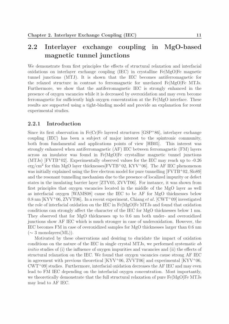
Fig. 2.1 : 2×2 supercell of [Fe5(MgO)5]2 used for the calculations of additional oxygen locatedat the Fe|MgO interface and oxygen vacancy (grey ball). Red ball is Fe, green ball is oxygenand orange ball is Mg.
Table 2.1: Interlayer distances (A) of [Fe5(MgO)x]2. Unrelaxed results are taken fromRef.[BZSM01], the values of Fe10(MgO)6 are taken from Ref.[FBA+09].
Structures dFe1 dFe2 dFe-O dMgO1 dMgO2[Fe5(MgO)2]2 1.252 1.405 2.115 2.149[Fe5(MgO)3]2 1.240 1.398 2.101 2.099 2.099[Fe5(MgO)4]2 1.236 1.395 2.097 2.099 2.120[Fe5(MgO)5]2 1.231 1.392 2.092 2.094 2.111Unrelaxed 1.433 1.433 2.160 2.026 2.026Fe10(MgO)6(GGA) 1.350 1.427 2.219 2.219 2.177Fe10(MgO)6(LSDA) 1.120 1.343 2.002 2.130 2.119
2.2.2 Calculation details
We carried out first-principles calculations by using the Vienna ab initio simulationpackage (VASP) [KH93, KF96b, KF96a]. In our calculations, the electron-coreinteractions were described by the projector augmented wave method for thepseudopotentials [Blo94, KJ99], and the exchange correlation energy was obtained withinthe generalized gradient approximation [WP91]. The cutoff energies for the plane wavebasis set used to expand the Kohn-Sham orbitals were 400 eV for the ionic relaxationsand 500 eV for the subsequent self-consistent FM (AF) energy calculations.
To calculate the IEC, one needs the total energies for parallel and antiparallelstructures, respectively. Thus, we constructed periodic supercells of Fe|MgO|Fe|MgOcomprising thicknesses between 2 and 5 MLs for MgO layers with the thickness of theFe layers kept equal to 5 MLs. The lateral cell size accommodated 4 Fe, 4 Mg and 4 Oper layer or 8 Fe, 8 Mg, and 8 O per layer [Figure 2.1]. The Monkhorst-Pack scheme wasused for the Brillouin zone integration [MP76]. A 21×21×1 k-point mesh was sufficientto ensure good convergence in the total energy differences. Full structural relaxations inshape and volume were performed ensuring that the Hellmann-Feynman forces acting onions were less than 10−3 eV/A.
Chapter 2. Interlayer Exchange Coupling (IEC) 13
2.88
2.92
2.96
La
ttice
(Ang
stro
m)
Fe5[M
gO] 2
MgO
Fe5[M
gO] 3
Fe5[M
gO] 4
Fe5[M
gO] 5
Fe
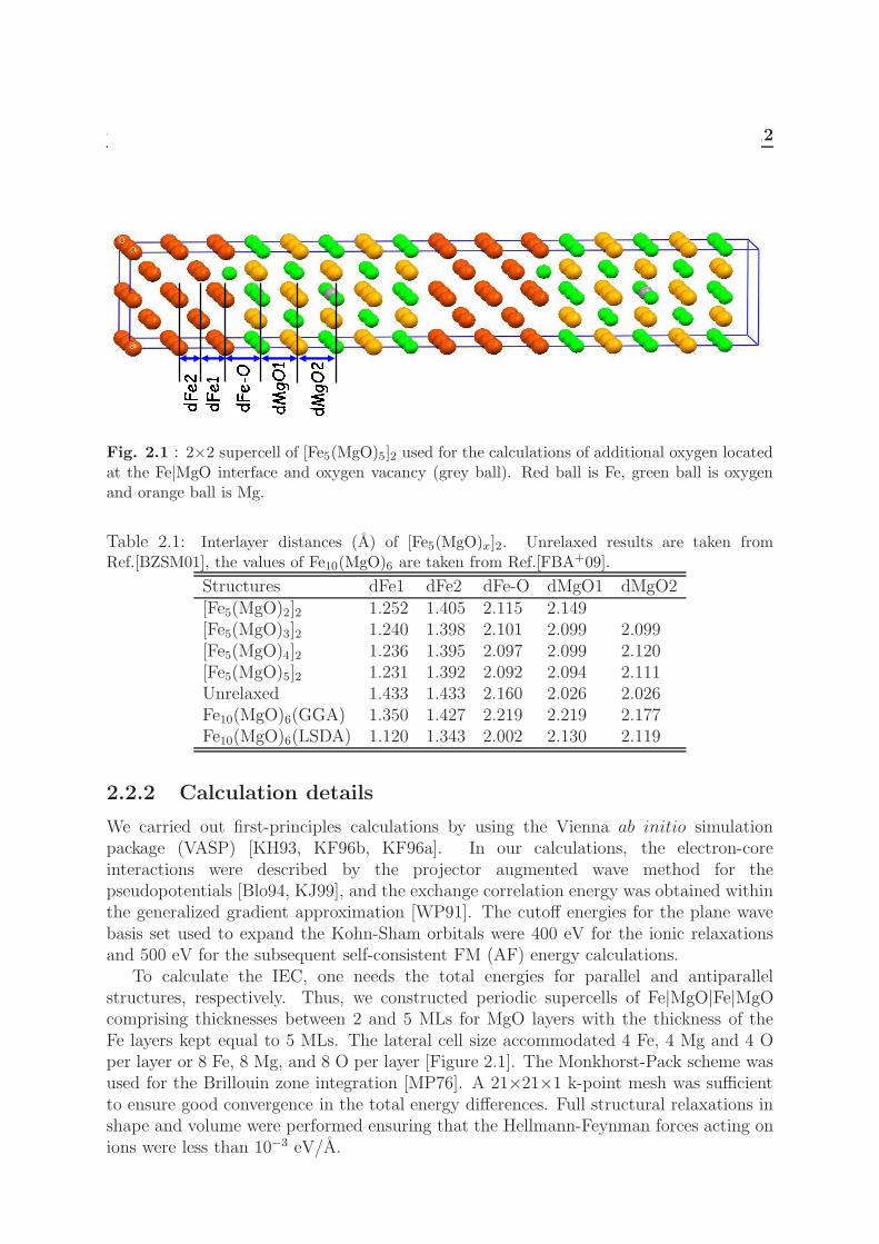
Fig. 2.2 : In plane lattice constant of [Fe5(MgO)x]2 as a funciton of MgO thickness.
The IEC constant J across one barrier region and normalized by the lateral area (A)ofthe computational cell is defined as
J =EAP −EP
4A, (2.3)
where EP and EAP represent total energies for parallel and anti-parallel alignmentsof adjacent Fe layer magnetizations, respectively. To ensure an accurate value for J ,calculations were performed in three steps. First, we relaxed the structure with parallelalignment of Fe slabs magnetizations. Next, we calculated the total energy EP (EAP ) forFM (AF) configuration with the relaxed structure. Finally, the strength of the IEC wascalculated using formula (2.3).
2.2.3 Structural Relaxation Effects on Interlayer Exchange
Coupling
We begin by describing the results of the structural relaxation of the “pure” structure,i. e. with no vacancies and/or additional oxygen. The longitudional interatomic distancesalong the out-of-plane (001) direction are summarized in Table 2.1. One can notethat the interlayer distances within Fe are strongly decreased compared to unrelaxedstructures used in Ref. [BZSM01]. Furthermore, the distances between the first andsecond interfacial Fe layers (dFe1) are shorter than the distances between the second andthird ones (dFe2). This is consistent with previous results for Fe10(MgO)6 [FBA
+09] andcan be attributed to the formation of the interface. At the same time, the thicknessesof MgO slabs are less affected compared to unrelaxed structures, but the MgO interlayerdistances are still shorter around the Fe|MgO interface compared to those within thebulk. Finally, the interfacial Fe-O distances are found to be slightly shorter comparedto unrelaxed distances (2.16 A) or bulk FeO (2.154 A) [MPK+01] and fall betweenvalues obtained within GGA and LSDA approximations in Fe10(MgO)6 [FBA+09] (seeTable 2.1). The slight discrepancies between aforementioned interlayer distances andthose reported in Ref. [FBA+09] within GGA aproximation are due to full structural
Chapter 2. Interlayer Exchange Coupling (IEC) 14
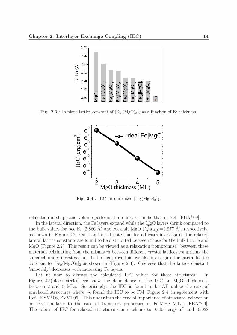
Fig. 2.3 : In plane lattice constant of [Fex(MgO)3]2 as a funciton of Fe thickness.
2 3 4 5e-4e-3e-2e-1e0e1e2
MgO thickness (ML)
IEC
(erg
/cm
2 ) ideal Fe|MgO
Fig. 2.4 : IEC for unrelaxed [Fe5(MgO)x]2.
relaxation in shape and volume performed in our case unlike that in Ref. [FBA+09].In the lateral direction, the Fe layers expand while the MgO layers shrink compared to
the bulk values for bcc Fe (2.866 A) and rocksalt MgO (√22aMgO=2.977 A), respectively,
as shown in Figure 2.2. One can indeed note that for all cases investigated the relaxedlateral lattice constants are found to be distributed between those for the bulk bcc Fe andMgO (Figure 2.2). This result can be viewed as a relaxation“compromise” between thesematerials originating from the mismatch between different crystal lattices comprising thesupercell under investigation. To further prove this, we also investigate the lateral latticeconstant for Fex(MgO)3]2 as shown in (Figure 2.3). One sees that the lattice constant’smoothly’ decreases with increasing Fe layers.
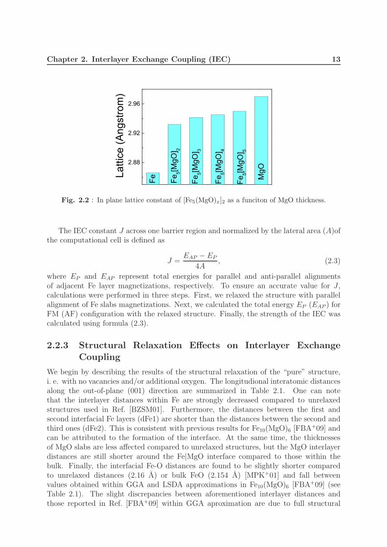
Let us now to discuss the calculated IEC values for these structures. InFigure 2.5(black circles) we show the dependence of the IEC on MgO thicknessesbetween 2 and 5 MLs. Surprisingly, the IEC is found to be AF unlike the case ofunrelaxed structures where we found the IEC to be FM [Figure 2.4] in agreement withRef. [KYV+06, ZVVT06]. This underlines the crucial importance of structural relaxationon IEC similarly to the case of transport properties in Fe|MgO MTJs [FBA+09].The values of IEC for relaxed structures can reach up to -0.406 erg/cm2 and -0.038
Chapter 2. Interlayer Exchange Coupling (IEC) 15
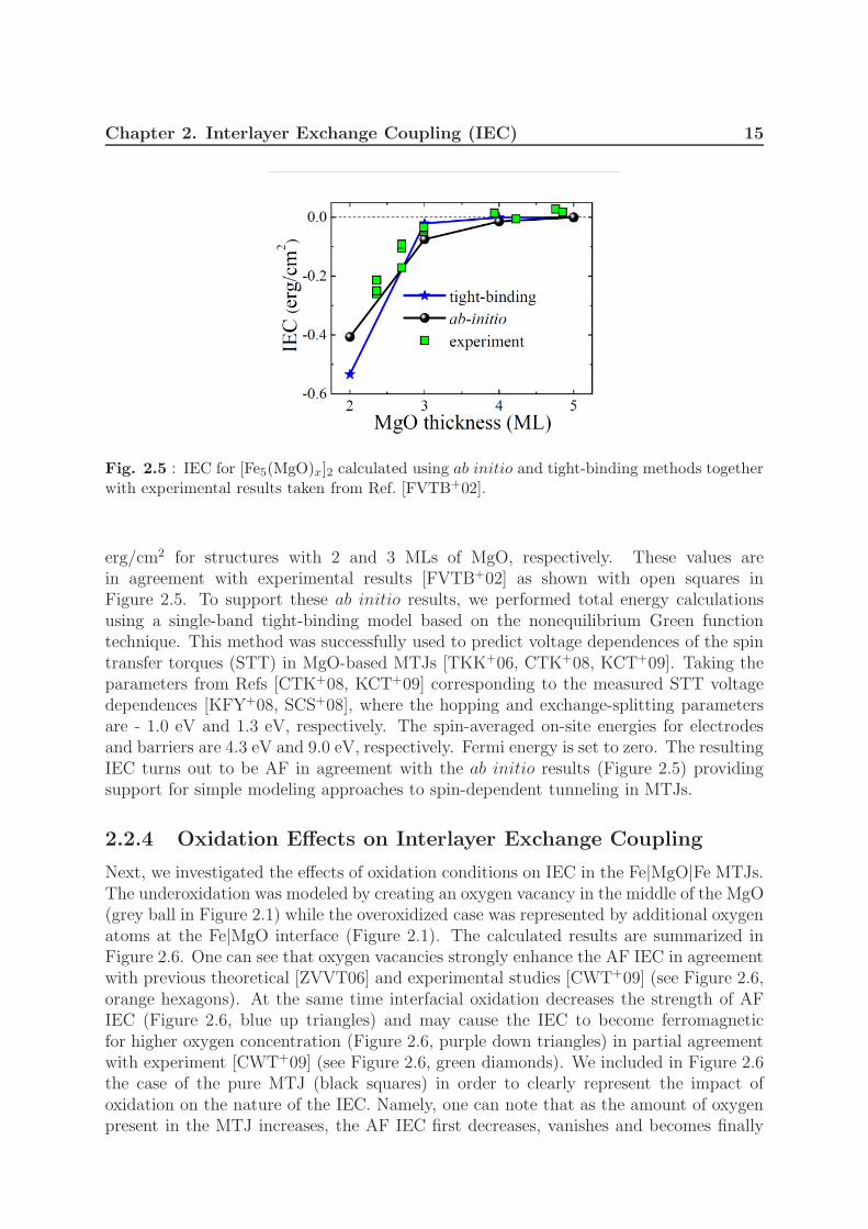
Fig. 2.5 : IEC for [Fe5(MgO)x]2 calculated using ab initio and tight-binding methods togetherwith experimental results taken from Ref. [FVTB+02].
erg/cm2 for structures with 2 and 3 MLs of MgO, respectively. These values arein agreement with experimental results [FVTB+02] as shown with open squares inFigure 2.5. To support these ab initio results, we performed total energy calculationsusing a single-band tight-binding model based on the nonequilibrium Green functiontechnique. This method was successfully used to predict voltage dependences of the spintransfer torques (STT) in MgO-based MTJs [TKK+06, CTK+08, KCT+09]. Taking theparameters from Refs [CTK+08, KCT+09] corresponding to the measured STT voltagedependences [KFY+08, SCS+08], where the hopping and exchange-splitting parametersare - 1.0 eV and 1.3 eV, respectively. The spin-averaged on-site energies for electrodesand barriers are 4.3 eV and 9.0 eV, respectively. Fermi energy is set to zero. The resultingIEC turns out to be AF in agreement with the ab initio results (Figure 2.5) providingsupport for simple modeling approaches to spin-dependent tunneling in MTJs.
2.2.4 Oxidation Effects on Interlayer Exchange Coupling
Next, we investigated the effects of oxidation conditions on IEC in the Fe|MgO|Fe MTJs.The underoxidation was modeled by creating an oxygen vacancy in the middle of the MgO(grey ball in Figure 2.1) while the overoxidized case was represented by additional oxygenatoms at the Fe|MgO interface (Figure 2.1). The calculated results are summarized inFigure 2.6. One can see that oxygen vacancies strongly enhance the AF IEC in agreementwith previous theoretical [ZVVT06] and experimental studies [CWT+09] (see Figure 2.6,orange hexagons). At the same time interfacial oxidation decreases the strength of AFIEC (Figure 2.6, blue up triangles) and may cause the IEC to become ferromagneticfor higher oxygen concentration (Figure 2.6, purple down triangles) in partial agreementwith experiment [CWT+09] (see Figure 2.6, green diamonds). We included in Figure 2.6the case of the pure MTJ (black squares) in order to clearly represent the impact ofoxidation on the nature of the IEC. Namely, one can note that as the amount of oxygenpresent in the MTJ increases, the AF IEC first decreases, vanishes and becomes finally
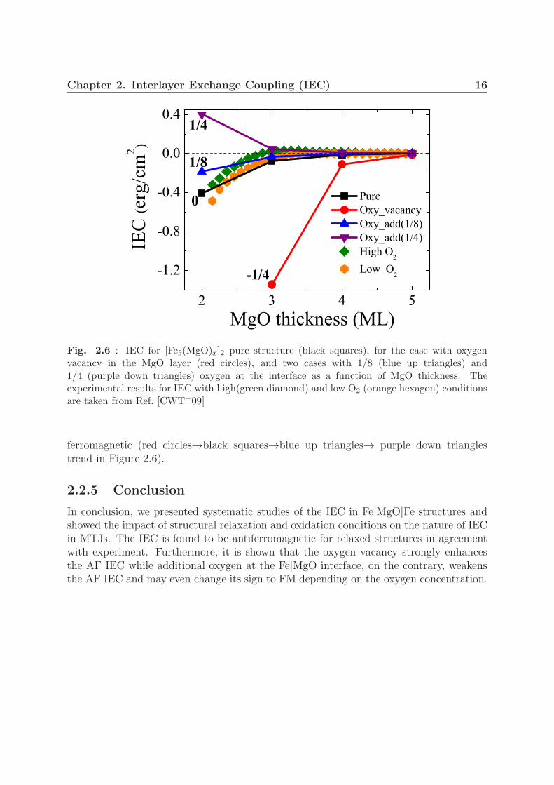
Chapter 2. Interlayer Exchange Coupling (IEC) 16
2 3 4 5
-1.2
-0.8
-0.4
0.0
0.4
Pure Oxy_vacancy Oxy_add(1/8) Oxy_add(1/4) High O2 Low O2
MgO thickness (ML)
IEC
(erg
/cm
2 )
-1/4
0
1/8
1/4
Fig. 2.6 : IEC for [Fe5(MgO)x]2 pure structure (black squares), for the case with oxygenvacancy in the MgO layer (red circles), and two cases with 1/8 (blue up triangles) and1/4 (purple down triangles) oxygen at the interface as a function of MgO thickness. Theexperimental results for IEC with high(green diamond) and low O2 (orange hexagon) conditionsare taken from Ref. [CWT+09]
ferromagnetic (red circles→black squares→blue up triangles→ purple down trianglestrend in Figure 2.6).
2.2.5 Conclusion
In conclusion, we presented systematic studies of the IEC in Fe|MgO|Fe structures andshowed the impact of structural relaxation and oxidation conditions on the nature of IECin MTJs. The IEC is found to be antiferromagnetic for relaxed structures in agreementwith experiment. Furthermore, it is shown that the oxygen vacancy strongly enhancesthe AF IEC while additional oxygen at the Fe|MgO interface, on the contrary, weakensthe AF IEC and may even change its sign to FM depending on the oxygen concentration.
Chapter 2. Interlayer Exchange Coupling (IEC) 17
2.3 IEC in SrTiO3-based MTJs
In this section, the effect of ferromagnetic electrode compositions and barrier layerproperties are demonstrated from first principles to have a crucial impact on interlayerexchange coupling (IEC) in crystalline Co(Fe)/SrTiO3/Co(Fe) magnetic tunnel junctions.It is shown that the IEC can be varied from antiferromangtic to ferromagnetic by eitherchanging the Co and Fe alloy ratio in the electrodes or the band gap of the barrier.
2.3.1 The choice of Co, Fe and SrTiO3
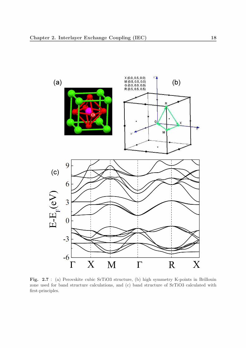
Ground state of Strontium Titanate oxide (SrTiO3 in short of STO) is a pervoskite cubicstructure as shown in Figure 2.7(a). In our first-principles calculations, the band gapof STO is about 1.8 eV, as shown in Fig2.7(c), which is underestimated compared toexperiments (experimentally determined indirect band gap energy of 3.25 eV, while thedirect band gap energy is 3.75 eV), which is much lower than MgO (7.4 eV). In practice,this means that the tunnel barrier can be much thicker with the same Resistance × Area(RA) as MgO. Furthermore, STO deposited by ion beam sputtering exhibits outstandinglow crystallization temperature at 260◦C which contrasts with 650◦C when deposited byRF sputtering. This makes ion beam sputtering STO compatible with usual magneticelectrodes.
Experimentally, in 1996 Lu et al. reported a TMR of 85% at 4 K inLSMO/STO/LSMO junctions [LLG+96]. Later, in 2003, Bowen et al. showed a TMR of1800% at 4K for the same kind of structure [BBB+03].
At the same time, ab initio calculations indicated a high TMR at room temperaturewith epitaxial Co(bcc)|SrTiO3|Co(bcc) junctions [VBS+05]. With CoFe as electrode,the experimental attempt was realized by Coey et al. in 2009 based on sputteredSTO MTJs [OC09]. The authors compared the results between MgO and STO MTJsdeposited by RF sputtering. They reported a TMR of 2.25% at room temperature inCoFeB/STO/CoFeB based MTJs after annealing at 325◦. Recent experiments of Spintecreported that the TMR can reach up to 13% [HVC+].
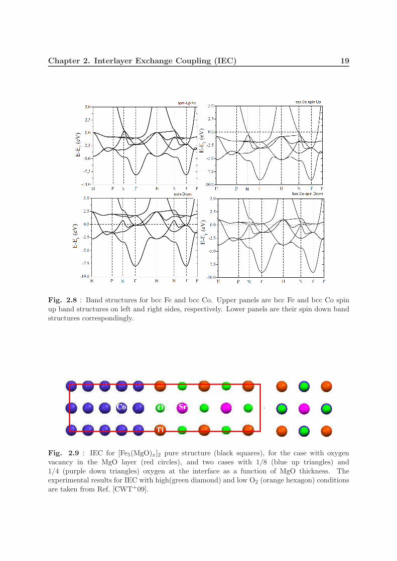
Similar to the case of Fe|MgO magnetic tunnel junctions, interlayer exchange couplingbehavior in SrTiO3 based MTJs is thus very interesting to address. Considering similarBloch states spin-filtering in bcc Fe and bcc Co [Figure 2.8], here we investigate interlayerexchange coupling behavior in MTJs with Fe, Co and their mixed alloy as electrode andwith SrTiO3 as barrier spacer.
2.3.2 Structure of Co(Fe)|STO|Co(Fe) MTJs and calculation
details
For the first-principles calculations, we again used the Vienna ab initio simulation package(VASP) [KH93, KF96b, KF96a]. In our calculations, the electron-core interactions weredescribed by the projector augmented wave method for the pseudopotentials [Blo94,KJ99], and the exchange correlation energy was obtained within the generalized gradientapproximation [WP91]. The cutoff energies for the plane wave basis set used to expandthe Kohn-Sham orbitals were 500 eV for the ionic relaxations and for the subsequentself-consistent FM (AF) energy calculations. The Monkhorst-Pack scheme was used for
Chapter 2. Interlayer Exchange Coupling (IEC) 18
�
(a) (b)
(c)
Fig. 2.7 : (a) Perovskite cubic SrTiO3 structure, (b) high symmetry K-points in Brillouinzone used for band structure calculations, and (c) band structure of SrTiO3 calculated withfirst-principles.
Chapter 2. Interlayer Exchange Coupling (IEC) 19
Fig. 2.8 : Band structures for bcc Fe and bcc Co. Upper panels are bcc Fe and bcc Co spinup band structures on left and right sides, respectively. Lower panels are their spin down bandstructures correspondingly.
��
��
���
Fig. 2.9 : IEC for [Fe5(MgO)x]2 pure structure (black squares), for the case with oxygenvacancy in the MgO layer (red circles), and two cases with 1/8 (blue up triangles) and1/4 (purple down triangles) oxygen at the interface as a function of MgO thickness. Theexperimental results for IEC with high(green diamond) and low O2 (orange hexagon) conditionsare taken from Ref. [CWT+09].
Chapter 2. Interlayer Exchange Coupling (IEC) 20
Fig. 2.10 : In plane lattice constant of [Fe5(STO)x]2 as a function of STO thickness.
the Brillouin zone integration, and we have used a 19 × 19 × 3 k-point mesh is sufficient toensure a good convergence in the total energy differences in order to ensure the small IECvalues are not affected by k-point convergence. Similar to the previous work in FeMgO,we constructed periodic supercells of Co(Fe)|STO|Co(Fe)|STO comprising thicknessesbetween 3 and 9 MLs for STO layers with the thickness of the Co(Fe) layers kept equalto 5 MLs. Full structural relaxations in shape and volume were performed ensuringthat the Hellmann-Feynman forces acting on ions were less than 10−3 eV/A. To furtherinvestigate the IEC as a function of band gap of STO, we used GGA+U methods, whereU is added on Ti, we change U values from 3 to 7 eV to vary the band gap of the insulatingbarrier.
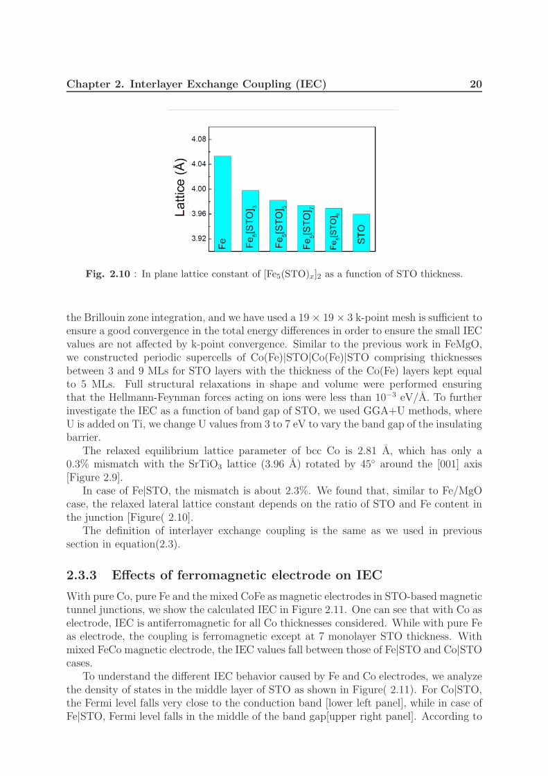
The relaxed equilibrium lattice parameter of bcc Co is 2.81 A, which has only a0.3% mismatch with the SrTiO3 lattice (3.96 A) rotated by 45◦ around the [001] axis[Figure 2.9].
In case of Fe|STO, the mismatch is about 2.3%. We found that, similar to Fe/MgOcase, the relaxed lateral lattice constant depends on the ratio of STO and Fe content inthe junction [Figure( 2.10].
The definition of interlayer exchange coupling is the same as we used in previoussection in equation(2.3).
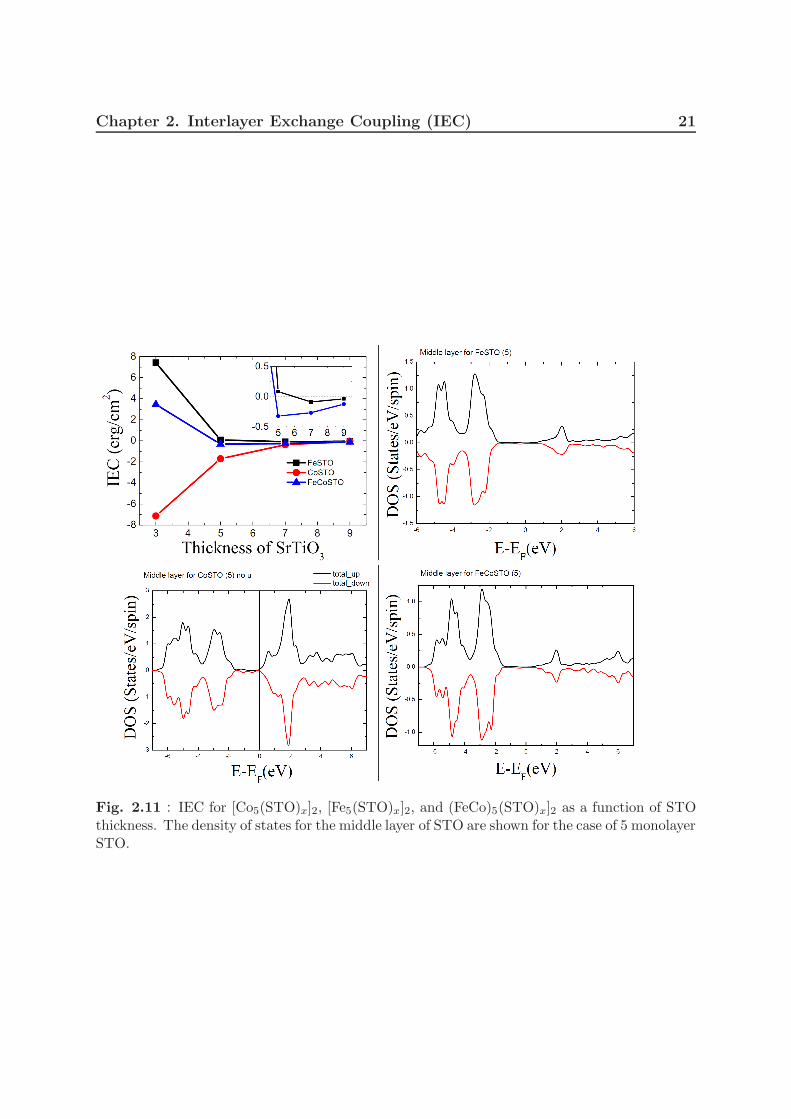
2.3.3 Effects of ferromagnetic electrode on IEC
With pure Co, pure Fe and the mixed CoFe as magnetic electrodes in STO-based magnetictunnel junctions, we show the calculated IEC in Figure 2.11. One can see that with Co aselectrode, IEC is antiferromagnetic for all Co thicknesses considered. While with pure Feas electrode, the coupling is ferromagnetic except at 7 monolayer STO thickness. Withmixed FeCo magnetic electrode, the IEC values fall between those of Fe|STO and Co|STOcases.
To understand the different IEC behavior caused by Fe and Co electrodes, we analyzethe density of states in the middle layer of STO as shown in Figure( 2.11). For Co|STO,the Fermi level falls very close to the conduction band [lower left panel], while in case ofFe|STO, Fermi level falls in the middle of the band gap[upper right panel]. According to
Chapter 2. Interlayer Exchange Coupling (IEC) 21
Fig. 2.11 : IEC for [Co5(STO)x]2, [Fe5(STO)x]2, and (FeCo)5(STO)x]2 as a function of STOthickness. The density of states for the middle layer of STO are shown for the case of 5 monolayerSTO.
Chapter 2. Interlayer Exchange Coupling (IEC) 22
the free electron model by P. Bruno [Bru95] or by J. C. Slonczewski [Slo93], in the caseof an insulating spacer, the sign of the coupling at large spacer thicknesses is determinedby the values of Fermi wave vectors in spacer |kF |, and in magnetic electrodes, k↑F andk↓F . when
|kF |2 < k↑Fk↓F , (2.4)
the coupling is antiferromagnetic, while for
|kF |2 > k↑Fk↓F , (2.5)
the coupling becomes ferromagnetic. It is hard to estimate the values of k↑F and k↓F fromour first-principles calculations, but the value of
kF = i√
2m(U − ǫF ), (2.6)
is related to the energy from the bottom of barrier conduction band to the Fermi level.Since Fermi level almost touches the conduction band in Co5(STO)7 case, |kF |2 is close tozero giving a value smaller than k↑Fk
↓F . Therefore, the IEC should be antiferromagnetic.
In case of Co5(STO)7, since the Fermi level falls in the middle of the band gap, thusU -ǫF becomes large, which may cause the square of |kF | larger than k↑Fk↓F and leading toferromagnetic coupling across STO barrier.
2.3.4 Effects of barrier on IEC
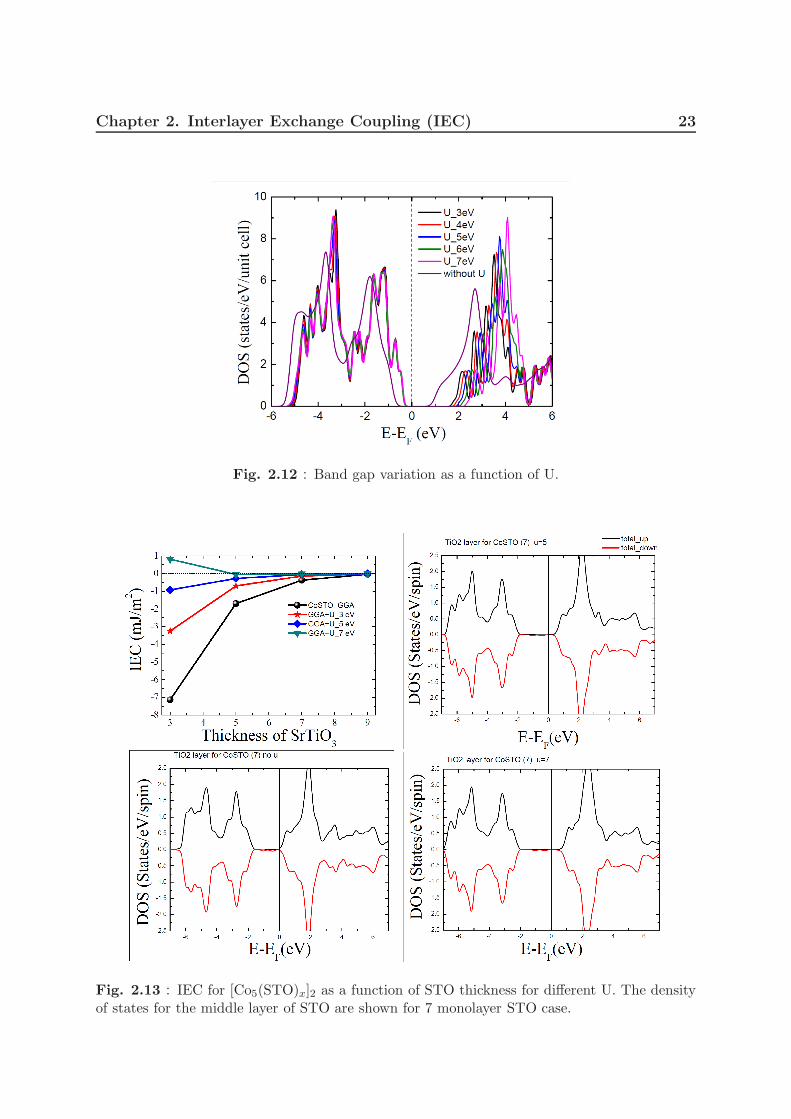
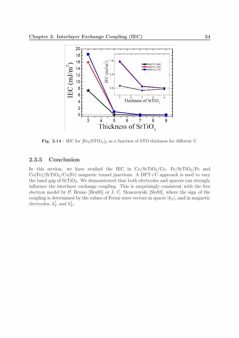
As we have just seen, the exchange coupling strongly depends on the Fermi levelposition and the band gap of insulating spacer. It is known that the DFT calculationsunderestimate the band gap of STO. To get the correct band gap, one option would beusing GW corrections. The GW approach, however, is very time consuming. So weemployed DFT+U methods to correct the band gap. Even though the band gap fromDFT+U is less accurate compared to GW corrections, the advantage of DFT+U is thefast calculation and tunable U. We show the calculated density of states for different Uvalues in bulk SrTiO3 structure in Figure 2.12. One can see that with increasing of U,the band gap is increasing and can reach up to 2.5 eV when U is set to 7 eV.
In order to see the IEC variation as a function of band gap, we choose the valuesof U equal to 3, 5 and 7 eV. The calculated IEC as a function of STO thicknesses fordifferent band gaps tuned by parameter U in Co|STO magnetic tunnel junction is shownin Figure( 2.13). One can see a clear trend of decreasing of AF IEC with increasing ofU. When U is big enough, the coupling can even change its sign to ferromagnetic. Theeffects of U on insulating spacer is analyzed in Figure( 2.13) for 7 monolayers of STOcases. With increasing of U, the band gap in the spacer is increasing as seen from thedensity of states in the TiO2 layer in the middle of spacer. Here the sign change of IECis similar to the aforementioned analysis. Since the value of |kF |2 is increasing with U,the coupling becomes ferromagnetic when the value of |kF |2 is larger than k↑Fk
↓F .
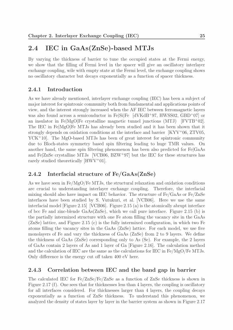
For the case of Fe/STO, the coupling becomes ferromagnetic for all thicknessesconsidered [Figure 2.14]. At the same time the values of IEC are quite similar for Uset to 5 and 7 eV.
Chapter 2. Interlayer Exchange Coupling (IEC) 23
Fig. 2.12 : Band gap variation as a function of U.
Fig. 2.13 : IEC for [Co5(STO)x]2 as a function of STO thickness for different U. The densityof states for the middle layer of STO are shown for 7 monolayer STO case.
Chapter 2. Interlayer Exchange Coupling (IEC) 24
Fig. 2.14 : IEC for [Fe5(STO)x]2 as a function of STO thickness for different U.
2.3.5 Conclusion
In this section, we have studied the IEC in Co/SrTiO3/Co, Fe/SrTiO3/Fe andCo(Fe)/SrTiO3/Co(Fe) magnetic tunnel junctions. A DFT+U approach is used to varythe band gap of SrTiO3. We demonstrated that both electrodes and spacers can stronglyinfluence the interlayer exchange coupling. This is surprisingly consistent with the freeelectron model by P. Bruno [Bru95] or J. C. Slonczewski [Slo93], where the sign of thecoupling is determined by the values of Fermi wave vectors in spacer |kF |, and in magneticelectrodes, k↑F and k↓F .
Chapter 2. Interlayer Exchange Coupling (IEC) 25
2.4 IEC in GaAs(ZnSe)-based MTJs
By varying the thickness of barrier to tune the occupied states at the Fermi energy,we show that the filling of Fermi level in the spacer will give an oscillatory interlayerexchange coupling, wile with empty state at the Fermi level, the exchange coupling showsno oscillatory character but decays exponentially as a function of spacer thickness.
2.4.1 Introduction
As we have already mentioned, interlayer exchange coupling (IEC) has been a subject ofmajor interest for spintronic community both from fundamental and applications points ofview, and the interest strongly increased when the AF IEC between ferromagnetic layerswas also found across a semiconductor in Fe|Si|Fe [dVKdB+97, HWSS02, GBD+07] oran insulator in Fe|MgO|Fe crystalline magnetic tunnel junctions (MTJ) [FVTB+02].The IEC in Fe|MgO|Fe MTJs has already been studied and it has been shown that itstrongly depends on oxidation conditions at the interface and barrier [KYV+06, ZTV05,YCK+10]. The MgO-based MTJs has been of great interest for spintronic communitydue to Bloch-states symmetry based spin filtering leading to huge TMR values. Onanother hand, the same spin filtering phenomenon has been also predicted for Fe|GaAsand Fe|ZnSe crystalline MTJs [VCB06, BZW+97] but the IEC for these structures hasrarely studied theoretically [HWV+01].
2.4.2 Interfacial structure of Fe/GaAs(ZnSe)
As we have seen in Fe/MgO/Fe MTJs, the structural relaxation and oxidation conditionsare crucial to understanding interlayer exchange coupling. Therefore, the interfacialmixing should also have impact on IEC behavior. The structure of Fe/GaAs or Fe/ZnSeinterfaces have been studied by S. Vutukuri, et al. [VCB06]. Here we use the sameinterfacial model [Figure 2.15] [VCB06]. Figure 2.15 (a) is the atomically abrupt interfaceof bcc Fe and zinc-blende GaAs(ZnSe), which we call pure interface. Figure 2.15 (b) isthe partially intermixed structure with one Fe atom filling the vacancy site in the GaAs(ZnSe) lattice, and Figure 2.15 (c) is the fully intermixed configuration, in which two Featoms filling the vacancy sites in the GaAs (ZnSe) lattice. For each model, we use fivemonolayers of Fe and vary the thickness of GaAs (ZnSe) from 2 to 9 layers. We definethe thickness of GaAs (ZnSe) corresponding only to As (Se). For example, the 2 layersof GaAs contain 2 layers of As and 1 layer of Ga [Figure 2.16]. The calculation methodand the calculation of IEC are the same as the calculations for IEC in Fe/MgO/Fe MTJs.Only difference is the energy cut off taken 400 eV here.
2.4.3 Correlation between IEC and the band gap in barrier
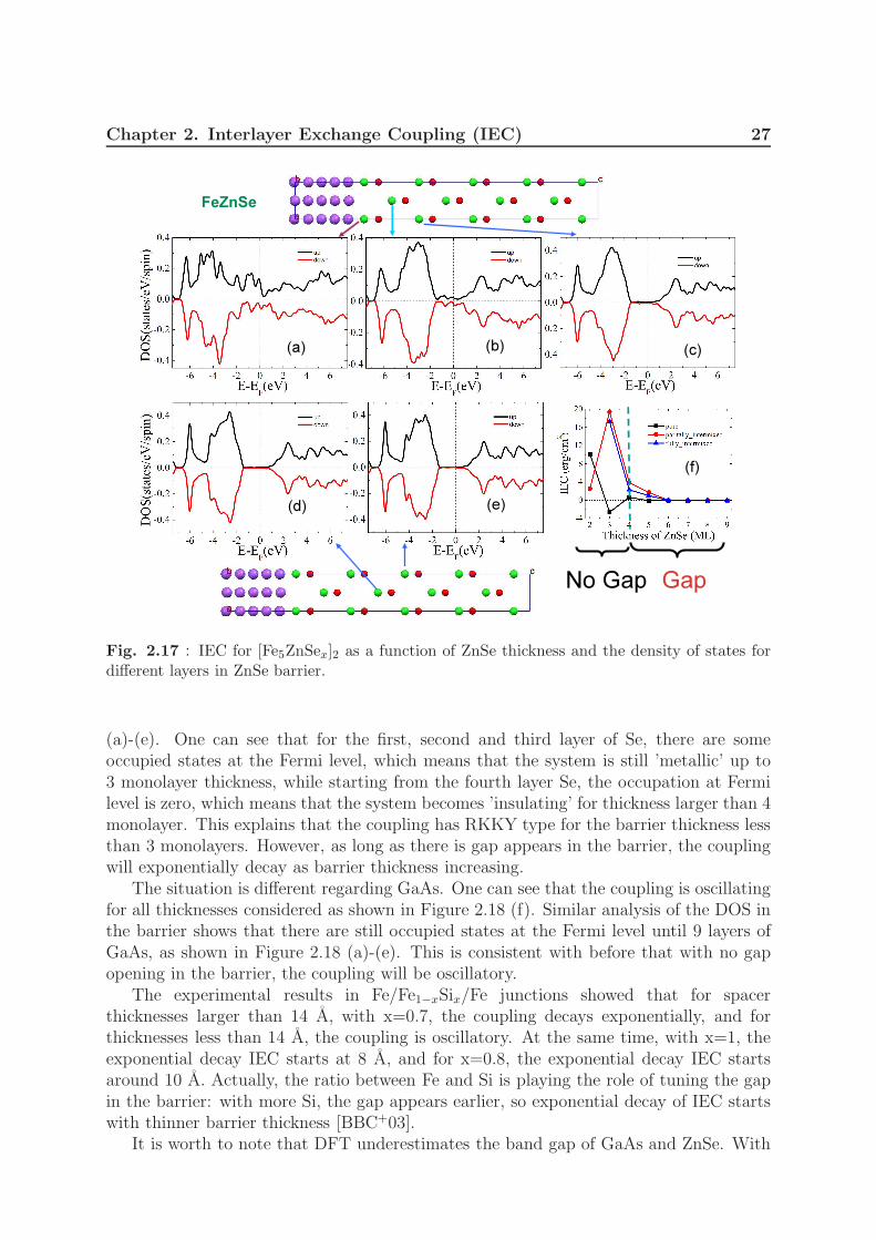
The calculated IEC for Fe/ZnSe/Fe/ZnSe as a function of ZnSe thickness is shown inFigure 2.17 (f). One sees that for thicknesses less than 4 layers, the coupling is oscillatoryfor all interfaces considered. For thicknesses larger than 4 layers, the coupling decaysexponentially as a function of ZnSe thickness. To understand this phenomenon, weanalyzed the density of states layer by layer in the barrier system as shown in Figure 2.17
Chapter 2. Interlayer Exchange Coupling (IEC) 26
(b)
Fe
As (Se)
Ga (Zn)
(a) (c)
Fig. 2.15 : Interfacial structures of Fe/GaAs(ZnSe) for (a) pure, (b) partially-intermixed, and(c) fully-intermixed interfaces.
GaAs/ZnSe
Fe
Vary thickness of GaAs/ZnSe
��
��
Fig. 2.16 : Schematic structure for calculation of IEC as a function of barrier thickness inFe/GaAs(ZnSe)/Fe MTJs.
Chapter 2. Interlayer Exchange Coupling (IEC) 27
FeZnSe
No Gap Gap
(a) (b) (c)
(d) (e)
(f)
Fig. 2.17 : IEC for [Fe5ZnSex]2 as a function of ZnSe thickness and the density of states fordifferent layers in ZnSe barrier.
(a)-(e). One can see that for the first, second and third layer of Se, there are someoccupied states at the Fermi level, which means that the system is still ’metallic’ up to3 monolayer thickness, while starting from the fourth layer Se, the occupation at Fermilevel is zero, which means that the system becomes ’insulating’ for thickness larger than 4monolayer. This explains that the coupling has RKKY type for the barrier thickness lessthan 3 monolayers. However, as long as there is gap appears in the barrier, the couplingwill exponentially decay as barrier thickness increasing.
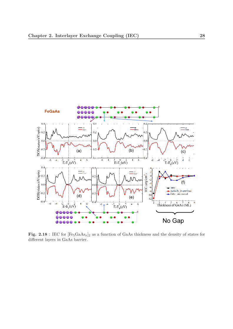
The situation is different regarding GaAs. One can see that the coupling is oscillatingfor all thicknesses considered as shown in Figure 2.18 (f). Similar analysis of the DOS inthe barrier shows that there are still occupied states at the Fermi level until 9 layers ofGaAs, as shown in Figure 2.18 (a)-(e). This is consistent with before that with no gapopening in the barrier, the coupling will be oscillatory.
The experimental results in Fe/Fe1−xSix/Fe junctions showed that for spacerthicknesses larger than 14 A, with x=0.7, the coupling decays exponentially, and forthicknesses less than 14 A, the coupling is oscillatory. At the same time, with x=1, theexponential decay IEC starts at 8 A, and for x=0.8, the exponential decay IEC startsaround 10 A. Actually, the ratio between Fe and Si is playing the role of tuning the gapin the barrier: with more Si, the gap appears earlier, so exponential decay of IEC startswith thinner barrier thickness [BBC+03].
It is worth to note that DFT underestimates the band gap of GaAs and ZnSe. With
Chapter 2. Interlayer Exchange Coupling (IEC) 28
FeGaAs
No Gap
(a) (b) (c)
(d) (e)
(f)
Fig. 2.18 : IEC for [Fe5GaAsx]2 as a function of GaAs thickness and the density of states fordifferent layers in GaAs barrier.
Chapter 2. Interlayer Exchange Coupling (IEC) 29
our calculation with GGA as exchange potential, the band gap of GaAs is 0.57 eVcompared to 1.53 eV in experiments. For ZnSe, GGA gives a gap of 1.68 eV comparedto the experimental value of 2.82 eV. For the correct band gap calculation, one may useGW corrections where the gaps of GaAs and ZnSe are 1.55 eV and 2.84 eV which arealmost the same as experiments [SMK07].
Even though the band gap is not correctly estimated, the relation between IEC andband gap in the barrier should not change: when there are states occupying Fermi levelthe coupling will be oscillatory; when there is a gap in the barrier, the coupling willexponentially decay as a function of barrier thickness.
2.4.4 Conclusion
In conclusion, we have shown a general picture for the interlayer exchange couplingbehavior related to the presence of states at Fermi level. When Fermi level in the spaceris not empty, the coupling will show a RKKY-like oscillatory character. Empty states atFermi energy will lead to decay of IEC as a function of barrier thickness.
Chapter 2. Interlayer Exchange Coupling (IEC) 30
2.5 Summary
In this Chapter, we investigated the interlayer exchange coupling in Fe|MgO|Fe magnetictunnel junctions. We showed that the interlayer exchange coupling across fully optimizedpure Fe|MgO|Fe magnetic tunnel junctions is antiferromagnetic, and decays as a functionof MgO thickness, which is in a good agreement with experimental results. Furthermore,a general trend of interlayer exchange coupling related to the oxidation conditions is given.The underoxidized structure enhances the antiferromagnetic coupling, in agreement withprevious work, whereas overoxidization decreases it, and may even change the sign ofinterlayer exchange coupling to ferromagnetic, depending the oxygen concentration atinterfaces.
Furthermore, we have investigated the interlayer exchange coupling in MTJs acrossSrTiO3, GaAs and ZnSe spacers. In case of SrTiO3-based MTJs, by changing theelectrodes and barrier band gap (via the DFT+U approach) to vary the Fermi levelposition, we found a general relation between the sign of IEC and the Fermi level positionin the band gap. This can be explained by the models of P. Bruno [Bru95] or J. C.Slonczewski [Slo93]. In case of GaAs and ZnSe having different band gap but the samecrystal structure, oscillatory or exponentially decay IEC depends on the presence orabsence of occupied states at the Fermi level within the spacer.
Chapter 3
Spin-orbit coupling inducedphenomena at FM|MgO interfaces
It is well known from special relativity that the motion of an electron (a particle) inan electric field results in a kinematic effect in which part of the electric field is seenas a magnetic field in the electron’s rest frame [Jac98]. The interaction of the electronspin with the electric field is called the spin-orbit interaction (SOI) or spin-orbit coupling(SOC), which has the general form,
HSO =~
4m20c
2p · (σ ×∇V) (3.1)
where m0 is the free electron mass, c is the velocity of light, σ is a vector whichcomponents are the Pauli matrices, and V is the electric potential. In equation(3.1), prepresents the canonical momentum. In presence of an external magnetic field B=∇×A,p should be replaced by the kinetic momentum P=p+eA. In the case of atoms, forexample, the spin-orbit interaction refers to the interaction of the electron spin with theaverage Coulomb field of the nuclei and other electrons. In the case of crystal, spin-orbitinteraction is determined by the interaction of the electron spin with the average electricfield corresponding to the periodic crystal potential.
With SOI, Bloch states can be written as [Ell54],
ψk,n↑(r) = [akn(r) |↑> +bkn(r) |↓>]eik·r, (3.2)
ψk,n↓(r) = [a⋆−kn(r) |↓> −b⋆−kn(r) |↑>]eik·r (3.3)
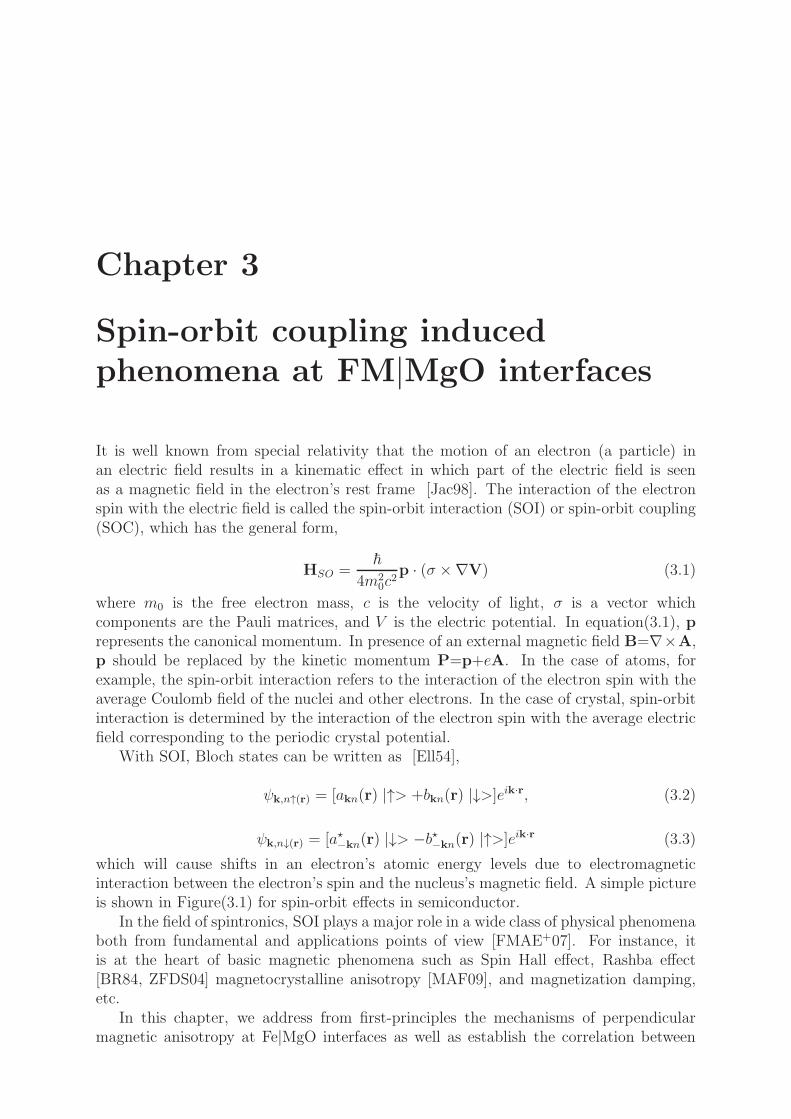
which will cause shifts in an electron’s atomic energy levels due to electromagneticinteraction between the electron’s spin and the nucleus’s magnetic field. A simple pictureis shown in Figure(3.1) for spin-orbit effects in semiconductor.
In the field of spintronics, SOI plays a major role in a wide class of physical phenomenaboth from fundamental and applications points of view [FMAE+07]. For instance, itis at the heart of basic magnetic phenomena such as Spin Hall effect, Rashba effect[BR84, ZFDS04] magnetocrystalline anisotropy [MAF09], and magnetization damping,etc.
In this chapter, we address from first-principles the mechanisms of perpendicularmagnetic anisotropy at Fe|MgO interfaces as well as establish the correlation between
Chapter 3. Spin-orbit coupling induced phenomena at FM|MgO interfaces32
��������������������������������������������������������������������������������������������������������������������������������������������������������������������������������������������������������������������������������������������������������������������������������������������������������������������������������������������������������������������������������������������������������������������������������������������������������������������������������������������������������������������������������������������������������������������������������������������������������������������������������������������������������������������������������������������������������������������������������������������������������������������������������������������������������������������������������������������������������������������������������������������������������������������������������������������������������������������������������������������������������������������������������������������������������������������������
��������������������������������������������������������������������������������������������������������������������������������������������������������������������������������������������������������������������������������������������������������������������������������������������������������������������������������������������������������������������������������������������������������������������������������������������������������������������������������������������������������������������������������������������������������������������������������������������������������������������������������������������������������������������������������������������������������������������������������������������������������������������������������������������������������������������������������������������������������������������������������������������������������������������������������������������������������������������������������������������������������������������������������������������������������������������������
antibonding
orbitals of 2
antibonding
orbitals of 1
bonding
orbitals of 2
bonding
orbitals of 1
2
1
Fig. 3.1 : Schematics of the evolution of the atomic orbitals 1 and 2 into valence and conductionbands in a semiconductor.
Bloch states symmetry-based spin filtering and perpendicular magnetic anisotropy(PMA).
Chapter 3. Spin-orbit coupling induced phenomena at FM|MgO interfaces33
3.1 PMA at Fe(Co)|MgO interfaces
The perpendicular magnetic anisotropy arising at the interface between ferromagnetictransition metals and metallic oxides was investigated via first-principles calculations. Inthis section very large values of PMA, up to 3 erg/cm2, at Fe|MgO interfaces are reported,in agreement with recent experiments. The origin of PMA is attributed to overlapbetween O-pz and transition metal dz2 orbitals hybridized with dxz(yz) orbitals withstronger spin-orbit coupling-induced splitting around the Fermi level for perpendicularmagnetization orientation. Furthermore, it is shown that the PMA value weakens in thecase of over- or under-oxidation due to the fact that oxygen pz and transition metaldz2 orbital overlap is strongly affected by disorder, in agreement with experimentalobservations in magnetic tunnel junctions.
3.1.1 Introduction to the PMA at interfaces
Controlling SOI strength at the interface between ferromagnetic (FM) and non-magneticlayers represents an outstanding challenge for advancement of transport and magneticproperties of spintronic magnetic devices, such as perpendicular Magnetic TunnelJunctions [MIP+09, KSO+08, DCR+08, PPJ+08, LKL05, NRAD09, YCD+11] (p-MTJs)and tunneling anisotropic magnetoresistive (TAMR) systems [GJY+07, PWW+08].Recently, electric field control of interfacial magnetic anisotropy has attracted muchattention as well [SMN+09, NAI+10]. Traditionally, interfaces between magneticand heavy non-magnetic transition metals such as Co|Pt [NKS+98], Co|Pd [CMS85,DdJdB87], Co|Au [WWS+94] have been used to obtain perpendicular magneticanisotropy. It has been shown that the onset of the PMA at these interfaces isrelated to an increase of the orbital momentum of Co [WWS+94] due to the stronghybridization between the 3d orbitals of the transition metal and the 5d orbitals ofheavy metal [NKS+98]. This hybridization enhances the energy splitting betweenthe Co 3dz2 and 3dx2−y2 orbitals and induces a charge transfer between the twolayers [Bru89, DKS94a, KYA92]. As a result, the combination between SOI andhybridization-induced charge transfer leads to the PMA. Thus, the presence of a heavynon-magnetic layer (Pt, Pd, Au, W, Mo) was believed to be essential to obtain largePMA.
However, Monso et al have shown that PMA could be observed also at Co(Fe)|MOxinterfaces (M=Ta, Mg, Al, Ru etc.) [MRA+02, RAD+03] in spite of the weak SOIat the interface. Surprisingly large PMA values up to 1 to 2 erg/cm2 have beenreported, which are comparable or even larger than the PMA observed at Co|Pt or Co|Pdinterfaces [GLW+06, JJKdB95]. This result is quite general and has been observed inboth crystalline (MgO) or amorphous (AlOx) barriers, using both natural or plasmaoxidation [LHA+07, MDL+08, MPV+08]. The PMA could be dramatically improvedunder annealing [MPV+08, RMD+09a, NRAD09] and X-ray Photoemission Spectroscopyhas demonstrated that the PMA could be correlated without ambiguity with the presenceof oxygen atoms at the interface [LHA+07, MPV+08]. In fact, a correlation betweenPMA and oxidation conditions have been demonstrated for a wide range of FM|MOxincluding those based on CoxFe1−x, thus indicating that the phenomenon is quite generalat interfaces between magnetic transition metals and oxygen terminated oxides. These
Chapter 3. Spin-orbit coupling induced phenomena at FM|MgO interfaces34
(a) (b) (c)
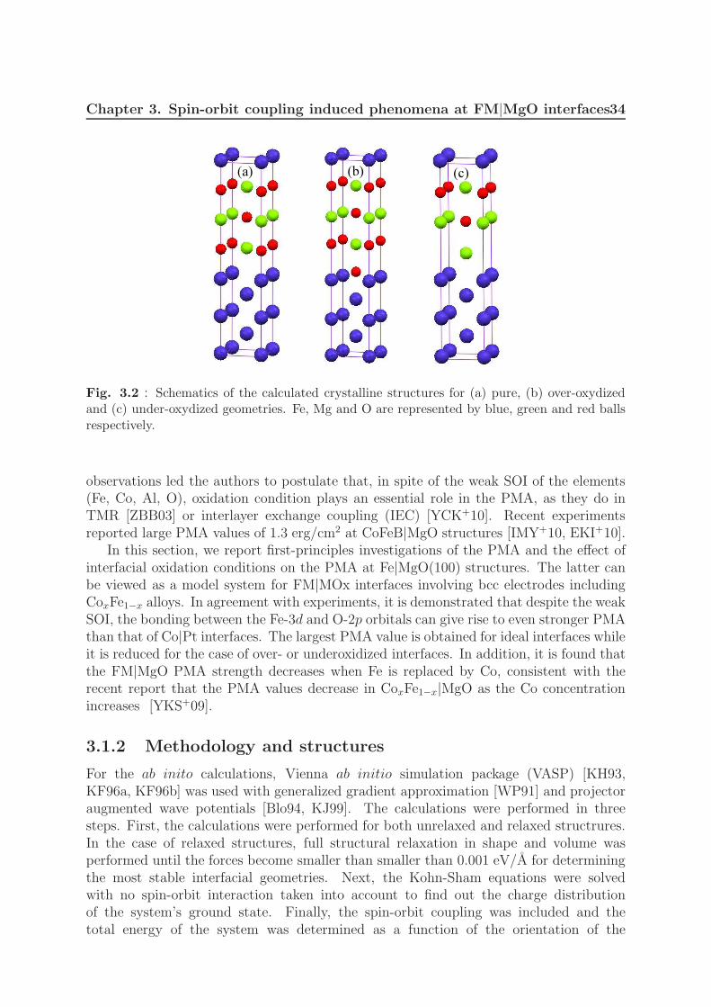
Fig. 3.2 : Schematics of the calculated crystalline structures for (a) pure, (b) over-oxydizedand (c) under-oxydized geometries. Fe, Mg and O are represented by blue, green and red ballsrespectively.
observations led the authors to postulate that, in spite of the weak SOI of the elements(Fe, Co, Al, O), oxidation condition plays an essential role in the PMA, as they do inTMR [ZBB03] or interlayer exchange coupling (IEC) [YCK+10]. Recent experimentsreported large PMA values of 1.3 erg/cm2 at CoFeB|MgO structures [IMY+10, EKI+10].
In this section, we report first-principles investigations of the PMA and the effect ofinterfacial oxidation conditions on the PMA at Fe|MgO(100) structures. The latter canbe viewed as a model system for FM|MOx interfaces involving bcc electrodes includingCoxFe1−x alloys. In agreement with experiments, it is demonstrated that despite the weakSOI, the bonding between the Fe-3d and O-2p orbitals can give rise to even stronger PMAthan that of Co|Pt interfaces. The largest PMA value is obtained for ideal interfaces whileit is reduced for the case of over- or underoxidized interfaces. In addition, it is found thatthe FM|MgO PMA strength decreases when Fe is replaced by Co, consistent with therecent report that the PMA values decrease in CoxFe1−x|MgO as the Co concentrationincreases [YKS+09].
3.1.2 Methodology and structures
For the ab inito calculations, Vienna ab initio simulation package (VASP) [KH93,KF96a, KF96b] was used with generalized gradient approximation [WP91] and projectoraugmented wave potentials [Blo94, KJ99]. The calculations were performed in threesteps. First, the calculations were performed for both unrelaxed and relaxed structrures.In the case of relaxed structures, full structural relaxation in shape and volume wasperformed until the forces become smaller than smaller than 0.001 eV/A for determiningthe most stable interfacial geometries. Next, the Kohn-Sham equations were solvedwith no spin-orbit interaction taken into account to find out the charge distributionof the system’s ground state. Finally, the spin-orbit coupling was included and thetotal energy of the system was determined as a function of the orientation of the
Chapter 3. Spin-orbit coupling induced phenomena at FM|MgO interfaces35
0 30 60 90
-74.3356
-74.3355
-74.3354
-74.3353
-74.3352
-74.3351
-74.3350
-74.3349 E sin2( )
E (e
V/un
it ce
ll)
(degree)
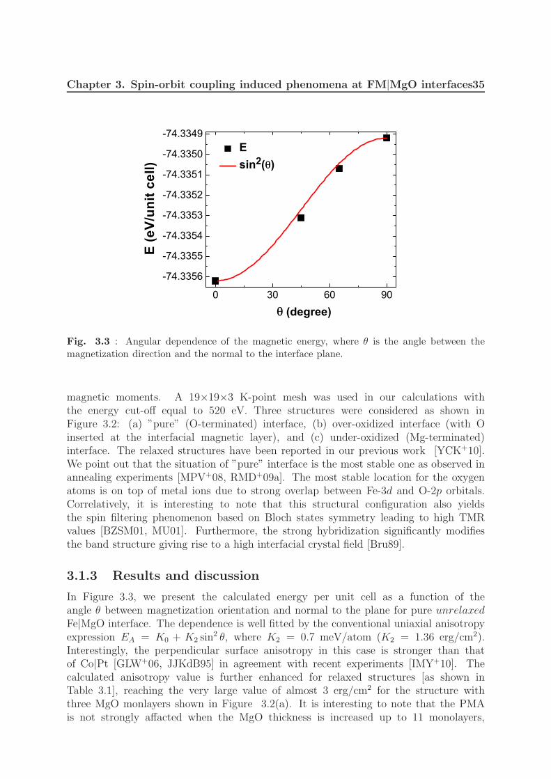
Fig. 3.3 : Angular dependence of the magnetic energy, where θ is the angle between themagnetization direction and the normal to the interface plane.
magnetic moments. A 19×19×3 K-point mesh was used in our calculations withthe energy cut-off equal to 520 eV. Three structures were considered as shown inFigure 3.2: (a) ”pure” (O-terminated) interface, (b) over-oxidized interface (with Oinserted at the interfacial magnetic layer), and (c) under-oxidized (Mg-terminated)interface. The relaxed structures have been reported in our previous work [YCK+10].We point out that the situation of ”pure” interface is the most stable one as observed inannealing experiments [MPV+08, RMD+09a]. The most stable location for the oxygenatoms is on top of metal ions due to strong overlap between Fe-3d and O-2p orbitals.Correlatively, it is interesting to note that this structural configuration also yieldsthe spin filtering phenomenon based on Bloch states symmetry leading to high TMRvalues [BZSM01, MU01]. Furthermore, the strong hybridization significantly modifiesthe band structure giving rise to a high interfacial crystal field [Bru89].
3.1.3 Results and discussion
In Figure 3.3, we present the calculated energy per unit cell as a function of theangle θ between magnetization orientation and normal to the plane for pure unrelaxedFe|MgO interface. The dependence is well fitted by the conventional uniaxial anisotropyexpression EA = K0 + K2 sin
2 θ, where K2 = 0.7 meV/atom (K2 = 1.36 erg/cm2).Interestingly, the perpendicular surface anisotropy in this case is stronger than thatof Co|Pt [GLW+06, JJKdB95] in agreement with recent experiments [IMY+10]. Thecalculated anisotropy value is further enhanced for relaxed structures [as shown inTable 3.1], reaching the very large value of almost 3 erg/cm2 for the structure withthree MgO monlayers shown in Figure 3.2(a). It is interesting to note that the PMAis not strongly affacted when the MgO thickness is increased up to 11 monolayers,
Chapter 3. Spin-orbit coupling induced phenomena at FM|MgO interfaces36
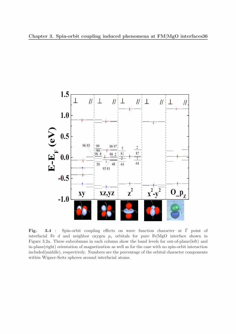
Fig. 3.4 : Spin-orbit coupling effects on wave function character at Γ point ofinterfacial Fe d and neighbor oxygen pz orbitals for pure Fe|MgO interface shown inFigure 3.2a. Three subcolumns in each column show the band levels for out-of-plane(left) andin-plane(right) orientation of magnetization as well as for the case with no spin-orbit interactionincluded(middle), respectively. Numbers are the percentage of the orbital character componentswithin Wigner-Seitz spheres around interfacial atoms.
Chapter 3. Spin-orbit coupling induced phenomena at FM|MgO interfaces37
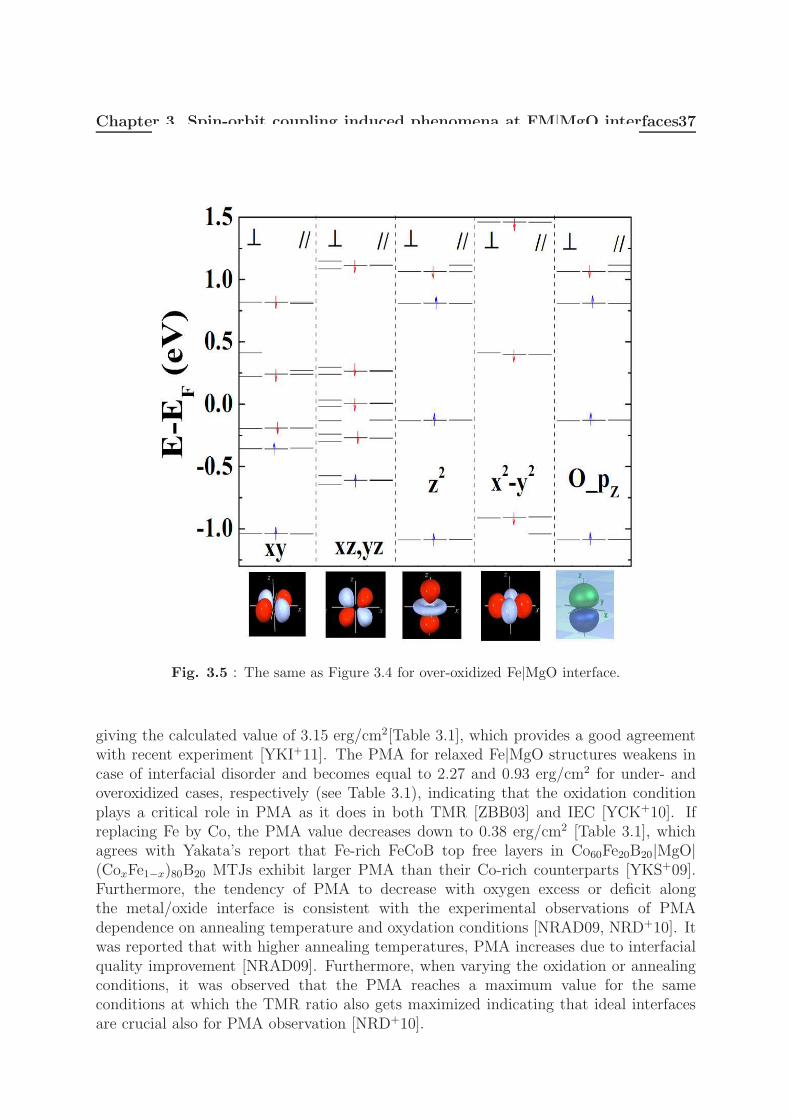
Fig. 3.5 : The same as Figure 3.4 for over-oxidized Fe|MgO interface.
giving the calculated value of 3.15 erg/cm2[Table 3.1], which provides a good agreementwith recent experiment [YKI+11]. The PMA for relaxed Fe|MgO structures weakens incase of interfacial disorder and becomes equal to 2.27 and 0.93 erg/cm2 for under- andoveroxidized cases, respectively (see Table 3.1), indicating that the oxidation conditionplays a critical role in PMA as it does in both TMR [ZBB03] and IEC [YCK+10]. Ifreplacing Fe by Co, the PMA value decreases down to 0.38 erg/cm2 [Table 3.1], whichagrees with Yakata’s report that Fe-rich FeCoB top free layers in Co60Fe20B20|MgO|(CoxFe1−x)80B20 MTJs exhibit larger PMA than their Co-rich counterparts [YKS+09].Furthermore, the tendency of PMA to decrease with oxygen excess or deficit alongthe metal/oxide interface is consistent with the experimental observations of PMAdependence on annealing temperature and oxydation conditions [NRAD09, NRD+10]. Itwas reported that with higher annealing temperatures, PMA increases due to interfacialquality improvement [NRAD09]. Furthermore, when varying the oxidation or annealingconditions, it was observed that the PMA reaches a maximum value for the sameconditions at which the TMR ratio also gets maximized indicating that ideal interfacesare crucial also for PMA observation [NRD+10].
Chapter 3. Spin-orbit coupling induced phenomena at FM|MgO interfaces38
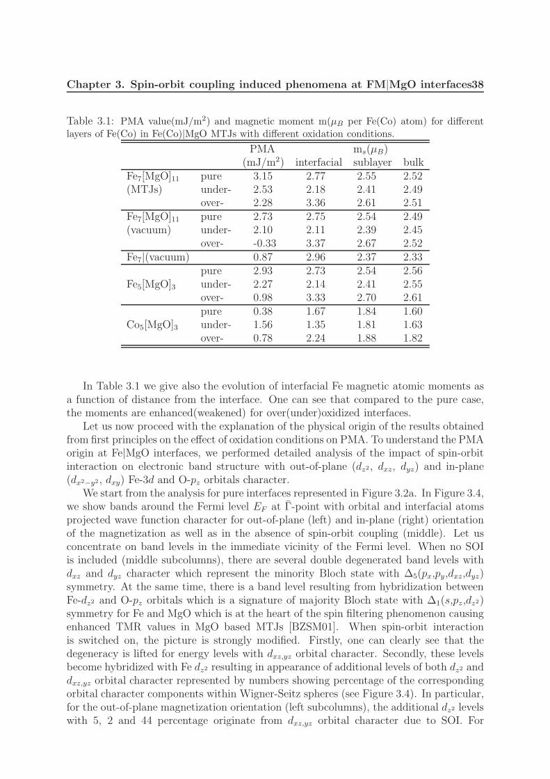
Table 3.1: PMA value(mJ/m2) and magnetic moment m(µB per Fe(Co) atom) for differentlayers of Fe(Co) in Fe(Co)|MgO MTJs with different oxidation conditions.
PMA ms(µB)(mJ/m2) interfacial sublayer bulk
Fe7[MgO]11 pure 3.15 2.77 2.55 2.52(MTJs) under- 2.53 2.18 2.41 2.49
over- 2.28 3.36 2.61 2.51Fe7[MgO]11 pure 2.73 2.75 2.54 2.49(vacuum) under- 2.10 2.11 2.39 2.45
over- -0.33 3.37 2.67 2.52Fe7|(vacuum) 0.87 2.96 2.37 2.33
pure 2.93 2.73 2.54 2.56Fe5[MgO]3 under- 2.27 2.14 2.41 2.55
over- 0.98 3.33 2.70 2.61pure 0.38 1.67 1.84 1.60
Co5[MgO]3 under- 1.56 1.35 1.81 1.63over- 0.78 2.24 1.88 1.82
In Table 3.1 we give also the evolution of interfacial Fe magnetic atomic moments asa function of distance from the interface. One can see that compared to the pure case,the moments are enhanced(weakened) for over(under)oxidized interfaces.
Let us now proceed with the explanation of the physical origin of the results obtainedfrom first principles on the effect of oxidation conditions on PMA. To understand the PMAorigin at Fe|MgO interfaces, we performed detailed analysis of the impact of spin-orbitinteraction on electronic band structure with out-of-plane (dz2, dxz, dyz) and in-plane(dx2−y2 , dxy) Fe-3d and O-pz orbitals character.
We start from the analysis for pure interfaces represented in Figure 3.2a. In Figure 3.4,we show bands around the Fermi level EF at Γ-point with orbital and interfacial atomsprojected wave function character for out-of-plane (left) and in-plane (right) orientationof the magnetization as well as in the absence of spin-orbit coupling (middle). Let usconcentrate on band levels in the immediate vicinity of the Fermi level. When no SOIis included (middle subcolumns), there are several double degenerated band levels withdxz and dyz character which represent the minority Bloch state with ∆5(px,py,dxz,dyz)symmetry. At the same time, there is a band level resulting from hybridization betweenFe-dz2 and O-pz orbitals which is a signature of majority Bloch state with ∆1(s,pz,dz2)symmetry for Fe and MgO which is at the heart of the spin filtering phenomenon causingenhanced TMR values in MgO based MTJs [BZSM01]. When spin-orbit interactionis switched on, the picture is strongly modified. Firstly, one can clearly see that thedegeneracy is lifted for energy levels with dxz,yz orbital character. Secondly, these levelsbecome hybridized with Fe dz2 resulting in appearance of additional levels of both dz2 anddxz,yz orbital character represented by numbers showing percentage of the correspondingorbital character components within Wigner-Seitz spheres (see Figure 3.4). In particular,for the out-of-plane magnetization orientation (left subcolumns), the additional dz2 levelswith 5, 2 and 44 percentage originate from dxz,yz orbital character due to SOI. For
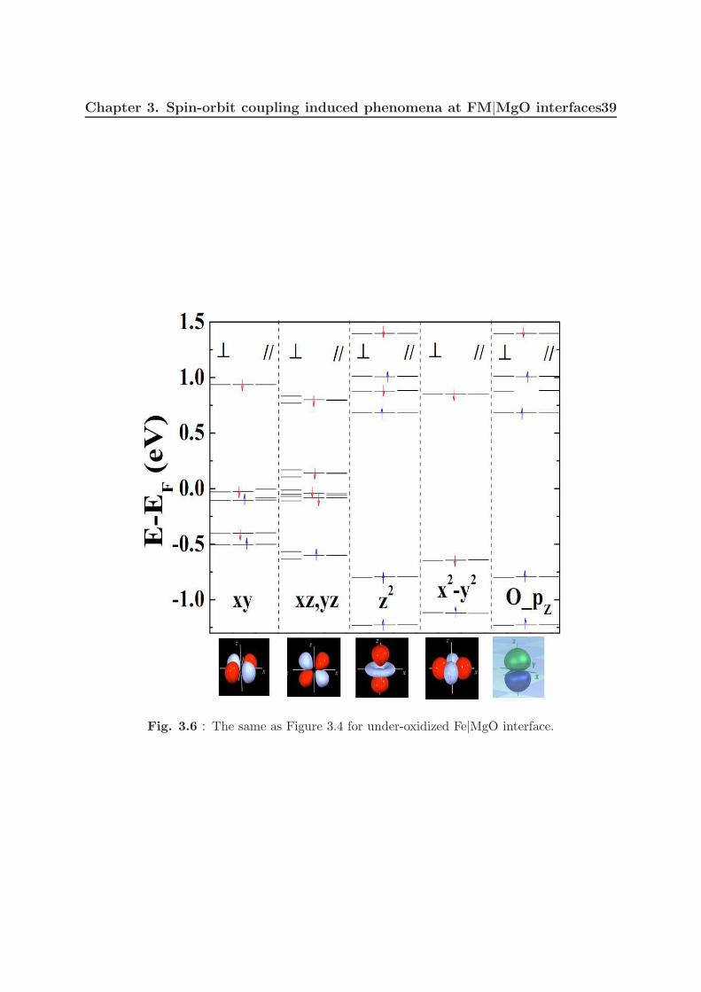
Chapter 3. Spin-orbit coupling induced phenomena at FM|MgO interfaces39
Fig. 3.6 : The same as Figure 3.4 for under-oxidized Fe|MgO interface.
Chapter 3. Spin-orbit coupling induced phenomena at FM|MgO interfaces40
the same reason, the additional dxz,yz band with 8 percents comes from dz2 orbital.Furthermore, since the Fe-dz2 orbital has already been hybridized with O-pz being a partof the ∆1 Bloch state, the additional energy levels with O-pz character also appearedwith SOI switched on. All this mechanism can be seen as the spin-orbit induced mixingbetween majority ∆1 and minority ∆5 Bloch states which, of note, may affect observationof predicted high TMR ratios in MTJs [VRS+10]. Finally, the hybridized band levels withdz2, dxz, dyz and pz character are lower in energy with a larger splitting for out-of-planemagnetization orientation compared to the in-plane one as clearly seen in left and rightsubcolumns in Figure 3.4, respectively. Thus, the lift of degeneracy of dxz and dyz orbitals,combined with hybridizations between dxz,yz and dz2, Fe-dz2 and O-pz orbitals is at theorigin of perpendicular magnetic anisotropy for pure Fe|MgO interfaces. This result showsthat the out-of-plane components of dxz,yz orbitals plays a crucial role for PMA similarlyto Co|Pd interfaces [WWF93].
Next, we proceed with the same analysis for under- and over-oxidized Fe|MgOinterfaces represented in Figure 3.2(b) and (c), respectively. As shown in Figure 3.5 forthe case with an additional oxygen located at the Fe|MgO interface (Figure 3.2(b)), spinorbit coupling lifts again the degeneracy for states with dxz,yz causing stronger splittingand deeper level position for out-of-plane orientation of magnetization compared to thein-plane one. However, the number of mixed states with both Fe-dz2 and O-pz orbitals isreduced due to local charge redistribution induced by additional oxygen atoms [ZBB03].Since dz2 and pz orbital hybridization which is one of the main causes for PMA is notsplitted, the anisotropy is significantly reduced.
A different picture occurs in case of underoxidized Fe|MgO interface represented inFigure 3.2(c). As shown in Figure 3.6, the Fe-dz2 and O-pz components around theFermi-level are now absent. As a result, the degeneracy lift induced by spin-orbitinteraction for states with dxz,yz character is now solely responsible for the PMA. Sincethe splitting of these dxz,yz orbitals is still relatively strong and higher for out-of-planemagnetization orientation compared to the in-plane one, anisotropy values are highercompared to over-oxidized case but lower compared to the ideal Fe|MgO interfaces. Thus,the PMA reaches its maximum for ideal interfaces.
When no SOI is included (middle subcolumns in Figure 3.10, the band level resultingfrom hybridization between Fe-dz2 and O-pz orbitals is present. The double degeneratedbands with ∆5 symmetry related to minority Fe are also present close to the Fermi level.When spin-orbit interaction is switched on, the degeneracy is lifted and majority ∆1
and minority ∆5 are mixed up producing bands with both symmetry characters. As aresult, band levels with dz2, dxz(yz) and pz character split around the Fermi level and thissplitting is larger and the lowest band deeper for out-of-plane magnetization orientationas clearly seen in left and right subcolumns in Figure 3.10 (b), respectively. Thus, the liftof degeneracy of dxz and dyz orbitals, combning the hybridization between dxz(yz) anddz2, as well as their mixing with Fe-dz2 and O-pz orbitals are at origin of perpendicularmagnetic anisotropy for pure Fe|MgO interfaces
For Co|MgO case, the anisotropy value is reduced to 0.38 mJ/m2 [shown in Table 3.1].To understand this, we did the same band spectrum analysis for Co|MgO interface[Figure 3.7(a)]. For comparison, we plot the band spectra of Fe|MgO in Figure 3.7(b).One can see that SOI lifts the degeneracy for states with dxz(yz) causing stronger splittingand deeper level position in case of out-of-plane orientation of magnetization compared
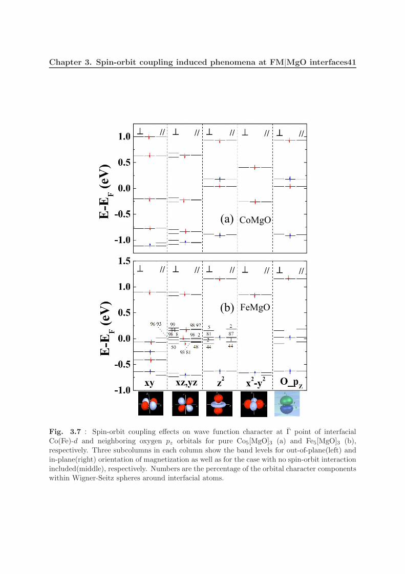
Chapter 3. Spin-orbit coupling induced phenomena at FM|MgO interfaces41
(a)
(b)
CoMgO
FeMgO
Fig. 3.7 : Spin-orbit coupling effects on wave function character at Γ point of interfacialCo(Fe)-d and neighboring oxygen pz orbitals for pure Co5[MgO]3 (a) and Fe5[MgO]3 (b),respectively. Three subcolumns in each column show the band levels for out-of-plane(left) andin-plane(right) orientation of magnetization as well as for the case with no spin-orbit interactionincluded(middle), respectively. Numbers are the percentage of the orbital character componentswithin Wigner-Seitz spheres around interfacial atoms.
Chapter 3. Spin-orbit coupling induced phenomena at FM|MgO interfaces42
to the in-plane one. However, these states are far away to the Fermi level and are nothybridized with Co-dz2 and O-pz orbitals, as well as there is no splitting of dz2 and pzorbitals, thus the perpendicular magnetic anisotropy is significantly reduced compared tothat of Fe|MgO interfaces.
3.1.4 Conclusion
In conclusion, we presented ab initio studies of perpendicular magnetic anisotropy atFe|MgO and Co|MgO interfaces as a function of the oxygen content along the interface.The PMA values are higher in the case of pure at Fe|MgO interfaces in agreement withrecent experimental studies [IMY+10, NRD+10] and may reach up to 3 erg/cm2 forrelaxed interfaces. The origin of the large PMA is ascribed to combination of severalfactors: the degeneracy lift of out-of-plane 3d orbitals, hybridizations between ∆1(dz2)and ∆5-like(dxz and dyz) 3d orbitals induced by spin-orbit interactions and hybridizationsbetween Fe-3d and O-2p orbitals at the interface between the transition metal andthe insulator. The PMA amplitude degrades in the case of over- or underoxidizedinterfaces in agreement with recent experiments [NRAD09, NRD+10]. This is due tothe impact of splitting(disappearing) of ∆1-like hybridized states around the Fermi levelin presence(absence) of additional oxygen atom. In addition, the PMA value is lower inthe case of Co|MgO interface, which agrees with experiment that Fe-rich CoxFe1−xB|MgOstructures have larger PMA than their Co-rich counterparts [YKS+09].
Chapter 3. Spin-orbit coupling induced phenomena at FM|MgO interfaces43
3.2 Correlation between Bloch state spin filtering
and PMA
In this section, we used much thicker MgO spacers and magnetic electrodes to study thecorrelation between Bloch state spin filtering and perpendicular magnetic anisotropy. InFe(Co)|MgO|Fe(Co) MTJs, the TMR ratio will reach its maximum in case of interfaceis ideal, this is also true for the perpendicular magnetic anisotropy. The mechanismresponsible for these phenomena is studied. From the band structure analysis we explicitlydemonstrate the main contribution to the PMA originates from the ∆ symmetry bands,which are well-known to be responsible for the Bloch state symmetry based spin filteringleading to large TMR ratios.
3.2.1 Introduction
We have mentioned in Chapter 1 that MgO-based magnetic tunnel junctions madea breakthrough for spintronic applications [MZBW99, BZSM01, MU01, WMZ+02,PKP+04, YNF+04, Ike08, LHI+07]. The mechanism responsible for large TMR ratioin Fe|MgO, Co|MgO, or FeCoB|MgO is the Bloch-states-symmetry-based spin filteringeffect [BZSM01, MU01, DMW+02, BZV+05, VCB06], where the ∆ symmetry bands playthe crucial role.
Besides large PMA at FM|MgO interfaces, it was also demonstrated experimentallythat there is a strong correlation between PMA and TMR maxima, i.e. they are obtainedat the same optimal oxidation and annealing conditions [NRD+10].
In this section, we report systematic studies of the correlation between PMA and TMRin terms of oxidation conditions and provide with underlying mechanisms responsible forsuch correlation.
3.2.2 Structures, results and discussion
The calculations are the same as in the first section of this Chapter. But the structureshere are MTJs with 7 monolayers of Fe and 11 monolayers of MgO as shown in Figure 3.8for (a) ”pure” (O-terminated) interface, (b) over-oxidized interface (with O inserted atthe interfacial magnetic layer), and (c) under-oxidized (Mg-terminated) interface.
In order to understand the correlation between PMA and TMR, we have plottedthe wave function character of ∆1 Bloch state as a function of the position across thesupercells used for PMA calculations for the Fe5[MgO]3 [Figure 3.9] and Fe7[MgO]11[Figure 3.10], respectively. One can clearly see that the ∆1 decay rate is strongly enhancedin the case of overoxidized interface compared to the ideal one. There is no ∆1 bandaround the Fermi level for underoxidized case as demonstrated above. This explainswhy both PMA and TMR reach their maximum values in a correlated way as observedexperimentally [NRD+10], this maximum being reached for ideal interfaces.
The reason for TMR ratio decreasing in case of overoxidized Fe|MgO|Fe magnetictunnel junctions has been discussed by Zhang, et al. [ZBB03], where the additionaloxygen at Fe|MgO interface weakens the overlap between O-Pz and Fe-dz2. That isconsistent with our analysis above that with additional oxygen at Fe|MgO interface, ∆1
symmetry bands are strongly affected.
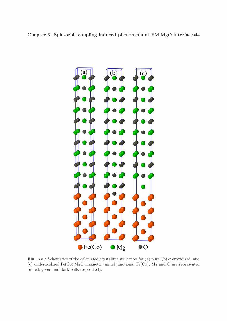
Chapter 3. Spin-orbit coupling induced phenomena at FM|MgO interfaces44
Fe(Co) Mg O
(a) (b) (c)
Fig. 3.8 : Schematics of the calculated crystalline structures for (a) pure, (b) overoxidized, and(c) underoxidized Fe(Co)|MgO magnetic tunnel junctions. Fe(Co), Mg and O are representedby red, green and dark balls respectively.
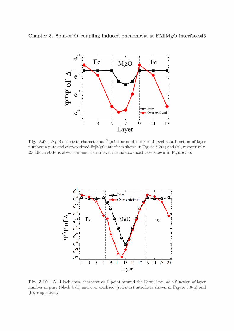
Chapter 3. Spin-orbit coupling induced phenomena at FM|MgO interfaces45
1 3 5 7 9 11 13
e-4
e-3
e-2
e-1
of
Layer
Pure Over-oxidized
Fe MgO Fe
Fig. 3.9 : ∆1 Bloch state character at Γ-point around the Fermi level as a function of layernumber in pure and over-oxidized Fe|MgO interfaces shown in Figure 3.2(a) and (b), respectively.∆1 Bloch state is absent around Fermi level in underoxidized case shown in Figure 3.6.
Fig. 3.10 : ∆1 Bloch state character at Γ-point around the Fermi level as a function of layernumber in pure (black ball) and over-oxidized (red star) interfaces shown in Figure 3.8(a) and(b), respectively.
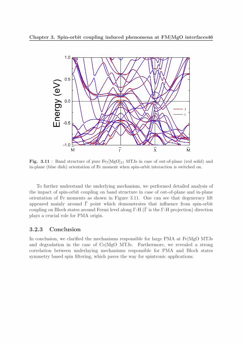
Chapter 3. Spin-orbit coupling induced phenomena at FM|MgO interfaces46
Fig. 3.11 : Band structure of pure Fe7[MgO]11 MTJs in case of out-of-plane (red solid) andin-plane (blue dish) orientation of Fe moment when spin-orbit interaction is switched on.
To further understand the underlying mechanism, we performed detailed analysis ofthe impact of spin-orbit coupling on band structure in case of out-of-plane and in-planeorientation of Fe moments as shown in Figure 3.11. One can see that degeneracy liftappeared mainly around Γ point which demonstrates that influence from spin-orbitcoupling on Bloch states around Fermi level along Γ-H (Γ is the Γ-H projection) directionplays a crucial role for PMA origin.
3.2.3 Conclusion
In conclusion, we clarified the mechanisms responsible for large PMA at Fe|MgO MTJsand degradation in the case of Co|MgO MTJs. Furthermore, we revealed a strongcorrelation between underlaying mechanisms responsible for PMA and Bloch statessymmetry based spin filtering, which paves the way for spintronic applications.
Chapter 3. Spin-orbit coupling induced phenomena at FM|MgO interfaces47
3.3 Summary
In this chapter, we first studied the mechanisms responsible for the large largeperpendicular magnetic anisotropy at Fe|MgO interfaces in view of Bloch statessymmetry-based band spectra analysis. We showed that the PMA are mainly causedby: (i) the spin-orbit coupling with out-of-plane quantization orientation axis causeslarger splitting for the degenerated ∆5 [dxz(yz)] symmetric orbitals compared to those incase of SOC with in-plane quantization orientation axis; (ii) the hybridization betweendz2 and dxz(yz) enhances the effect from degeneracy lift of ∆5 symmetric orbitals; and (iii)the hybridization between Fe-3dz2 and O-2pz orbitals further enhances the effect from (ii).Indeed, this also explains the weakening of the PMA in case of contaminated Fe|MgOinterfaces.
Next, we demonstrated a correlation between Bloch states symmetry based spinfiltering and PMA. It shows that PMA and TMR can reach their maximum in caseof ideal interfacial junctions, the underlying mechanism responsible for this is unveiled:both PMA and TMR origin from the same Bloch states.

Chapter 4
Graphene on magnetic metal
4.1 Perpendicular Magnetic Anisotropy of Co on Gr
As discussed in previous chapter, interfaces between magnetic and heavy non-magnetictransition metals such as Co|Pt [NKS+98], Co|Pd [CMS85, DdJdB87], andCo|Au [WWS+94] are used to obtain perpendicular magnetic anisotropy (PMA). Sincehexagonal close packed (hcp) or face centered cubic (fcc) Co crystal lattices have verysmall mismatch with graphene, plus graphene has so many unique properties, here weinvestigate the PMA of Graphene|Co system. Furthermore, we provided a comparisonstudy of the work function between graphene|Co to vacuum|Co interfaces. It is foundthat the graphene|Co interface strongly decrease the work function of vacuum|Co system,which are in a good agreement with experimental results.
4.1.1 Introduction
As we have mentioned in the general introduction, graphene has so many promisingproperties [CNGP+09, Gei09, DSAHR11] and has been proposed for spintronicsdevices. The application of graphene into spintronics therefore forms a new branch oftopics, named graphene-based spintronics or graphene spintronics. One fundamentalresearch of graphene spintronics is to induce spin-polarization in graphene by usingsubstrates [KGK+07, TJP+07a, YP09, TJP+07b, HWP+09, HPM+10, YBV+11]. Wellstudied metal substrates are Co and Ni [VSBS+08, WRH+10, RVSB+09, VVKBY+10].This is because graphene and Co or Ni has a very small lattice constant mismatch. Eventhough, Co|graphene system has been intensive studied, one very interesting topic, themagnetic anisotropy at Co|graphene interfaces is seldom studied [VVKBY+10].
In this chapter, we study the role of graphene on PMA and work function behavioron Co surfaces.
4.1.2 Methodology
We used again the Vienna ab initio simulation package (VASP) [KH93, KF96b, KF96a]with the generalized gradient approximation (Perdew-Burke-Ernzerhof) [KJ99] andprojector augmented wave potentials [Blo94]. The calculations were performed intwo steps. First, out-of-plane structural relaxation was allowed and the Kohn-Sham
Chapter 4. Graphene on magnetic metal 50
(b) AB(a) fcc Co (c) BC (d) AC
4.38 4.132.102 2.103
Fig. 4.1 : Top view (upper panels) and side view (lower panels) of calculated crystallinestructures for (a) pure fcc Co film, (b) Graphene on top of AB sites, AB-Gr|Co(fcc),(c) Graphene on top of BC sites, BC-Gr|Co(fcc), and (d) Graphene on top of AC sites,AC-Gr|Co(fcc) structures. Co atoms in the 1st(A site), 2nd(B site) and 3rd(C site) layersare represented with blue, red and green balls, respectively. Carbon atoms are indicated withgray balls. The distances between graphene and Co substrates are labeled.
equations solved with no spin-orbit interaction taken into account for determining themost favourable adsorption geometry of graphene on Co. Then the spin-orbit couplingwas included and the total energy of the system was determined as a function of theorientation of the magnetic moments. The k-point mesh used in all calculations is15×15×1. The energy cutoff was set to 520 eV. The atomic structures are relaxed untilthe forces are smaller than 0.001 eV/A. For the anisotropy calculations, the total energiesare converged to 10−7 eV.
4.1.3 Stability of epitaxial graphene on Co films
Let us start from the possible structures and their stabilities for graphene on Co films.Co can form hcp, fcc and bcc crystal structures. Among these, hcp structure is theground phase, while bcc structure is not stable and it is not of good match with graphenehoneycomb lattice. In this chapter, we consider only Co fcc and hcp structures.
When graphene is formed on thick (more than three layers) Co substrates, thesubstrate can have fcc or hcp structure. According to the symmetry of stacking, thereare three high symmetry structures as shown in Figure 4.1 and Figure 4.2 for fcc and hcpsubstrates, respectively, where the two carbon atoms of graphene are located on top offcc Co lattice A and B, B and C, or A and C sites. For two monolayer of Co substrate,there is only hcp stacking possibility.
As shown in Table 4.1, for three monolayers of Co films with 12 Co atoms/cell, fccstructure is less stable compared to hcp one with energy higher about 0.087 eV/cell. Wesee clearly that the energy difference between fcc and hcp structures is so tiny, less than
Chapter 4. Graphene on magnetic metal 51
2.112.093.833.95
(b) AB(a) hcp Co (c) BC (d) AC
Fig. 4.2 : Top view (upper panels) and side view (lower panels) of calculated crystallinestructures for (a) pure hcp Co film, (b) Graphene on top of AB sites, AB-Gr|Co(hcp),(c) Graphene on top of BC sites, BC-Gr|Co(hcp), and (d) Graphene on top of AC sites,AC-Gr|Co(hcp) structures. Co atoms in the 1st and 3rd (A site) are represented by blue balls,those in the 2nd(B site) layers are represented with red balls. Carbon atoms are indicated withgray balls. The distances between graphene and Co substrates are labeled.
8 meV/atom, which is negligible at room temperature (corresponding to 26 meV).When Co substrates are covered with graphene, the most stable structure is
AC-Gr|Co(hcp) as shown in Figure 4.2(d). But the energy difference betweenAC-Gr|Co(hcp) and AB-Gr|Co(hcp) is very tiny (0.01 eV/cell) for 12 cobalt and 8 carbonatoms per cell. For AC-Gr|Co(hcp) and BC-Gr|Co(hcp), the energy difference is a littlebit large, 0.26 eV/cell. The stability can also be deducted from the distance betweengraphene and Co substrate shown in Figure 4.1 and Figure 4.2. For graphene on top ofBC sites, the interaction is so weak between graphene and Co, and the distance is moreor less around 4 A. While for graphene on top of AC or AB sites, the distance is about2.1 A.
Overall, one can see that total energies of AC and AB structures for both hcp andfcc Co substrates are so close, and at room temperature, the difference can be neglected.
4.1.4 Magnetic Anisotropy of Graphene/Co
Now, let us discuss the magnetic anisotropy energy (MAE) of these films, whichdetermines the easy axis of magnetization. The same as was discussed in Chapter 3,in a uniaxial system, the density of MAE can be described to first order as
E = Ksin2θ (4.1)
with K in units of Jm−3. Here θ is the direction of magnetization with respect to thenormal to the layers. Positive values of K mean PMA, while negative values mean
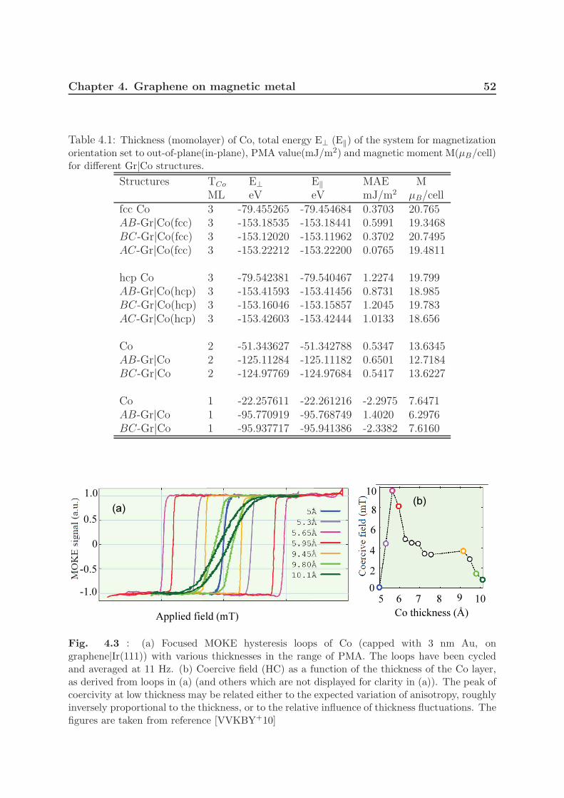
Chapter 4. Graphene on magnetic metal 52
Table 4.1: Thickness (momolayer) of Co, total energy E⊥ (E‖) of the system for magnetizationorientation set to out-of-plane(in-plane), PMA value(mJ/m2) and magnetic moment M(µB/cell)for different Gr|Co structures.
Structures TCo E⊥ E‖ MAE MML eV eV mJ/m2 µB/cell
fcc Co 3 -79.455265 -79.454684 0.3703 20.765AB-Gr|Co(fcc) 3 -153.18535 -153.18441 0.5991 19.3468BC-Gr|Co(fcc) 3 -153.12020 -153.11962 0.3702 20.7495AC-Gr|Co(fcc) 3 -153.22212 -153.22200 0.0765 19.4811
hcp Co 3 -79.542381 -79.540467 1.2274 19.799AB-Gr|Co(hcp) 3 -153.41593 -153.41456 0.8731 18.985BC-Gr|Co(hcp) 3 -153.16046 -153.15857 1.2045 19.783AC-Gr|Co(hcp) 3 -153.42603 -153.42444 1.0133 18.656
Co 2 -51.343627 -51.342788 0.5347 13.6345AB-Gr|Co 2 -125.11284 -125.11182 0.6501 12.7184BC-Gr|Co 2 -124.97769 -124.97684 0.5417 13.6227
Co 1 -22.257611 -22.261216 -2.2975 7.6471AB-Gr|Co 1 -95.770919 -95.768749 1.4020 6.2976BC-Gr|Co 1 -95.937717 -95.941386 -2.3382 7.6160
1.0
-1.0
-0.5
0
0.5
10
2
4
6
8
05 6 7 8 9 10
Co thickness (Å)Applied field (mT)
(a)(b)
Fig. 4.3 : (a) Focused MOKE hysteresis loops of Co (capped with 3 nm Au, ongraphene|Ir(111)) with various thicknesses in the range of PMA. The loops have been cycledand averaged at 11 Hz. (b) Coercive field (HC) as a function of the thickness of the Co layer,as derived from loops in (a) (and others which are not displayed for clarity in (a)). The peak ofcoercivity at low thickness may be related either to the expected variation of anisotropy, roughlyinversely proportional to the thickness, or to the relative influence of thickness fluctuations. Thefigures are taken from reference [VVKBY+10]
Chapter 4. Graphene on magnetic metal 53
alignment of magnetization in the plane of the layers.In experiments, hysteresis loops provide evidence for PMA in the range of thickness t∈
[0.5-1] nm (figure 4.3). In this range, the remanence is complete, i.e. the magnetizationremains fully perpendicular to the film plane after the external field has been set back tozero. Let us recall that for most magnetic films the magnetization is strongly constrainedto lie in-the-plane, due to the negative contribution to the MAE of the magnetostaticenergy
EShape = −µM2s /2 (4.2)
which would arise in the case of perpendicular magnetization. An effective PMA may beachieved only for selected cases where the magnetostatic energy is overcome by positivecontributions to the MAE. Here we leave aside those cases where positive contributionsarise from bulk magnetocrystalline anisotropy such as for intermetallics 4f − 3d, FePt,CoPt, etc, because we focus on ultrathin films to highlight interfacial effects withgraphene. In ultrathin films, positive contributions to the MAE may arise from interfaceand/or magneto-elastic effects. As both terms decay typically like 1/t, PMA is restrictedto thicknesses typically below 1-3 nm. Known ultrathin stackings with PMA are eitherall metal based [JBdBdV96] or more recently metal oxide based [RMD+09b, IMY+10].
Combining with extraordinary Hall effect (EHE) measurements, the magneticanisotropy is estimated around 0.185± 0.025 mJ/m2 for the 0.7 nm thick Co layer.While recent experimental results show that PMA can be persisted with more than 50monolayers of Co thickness [LHHW11].
In our calculations, we find that the anisotropy of Co films strongly depends on thecrystal structure and the thickness of Co. As shown in Table 4.1, for three monolayers ofCo, hcp structure gives more than 3 times larger PMA than that of fcc one. This is ina very well agreement with previous calculations for free standing Co films [DKS94b].With the coverage of graphene, AB-Gr|Co(fcc) structure gives almost double the PMAof pure Co, but AC-Gr|Co(fcc) structure decreases the PMA almost to the in plane one.As for BC-Gr|Co(fcc) structure, the PMA is almost the same as that of pure fcc Co dueto very weak interaction between graphene and Co, which can not create much impacton Co orbitals. For hcp structure, with 3 layers of Co film, graphene coverage does notimprove the PMA of Co. But for two monolayers of Co, graphene does enhance the PMAfrom 0.53 mJ/m2 of pure Co to 0.65 mJ/m2 of AB-Gr|Co. More interestingly, anisotropyof single Co layer is known to be in plane [DKS94b]. In our calculation, the in-planeanisotropy of single layer of Co is about -2.3 mJ/m2. According to reference [DKS94b],the in-plane anisotropy of one layer of Co is about -1.6 meV. If we assume the energy isper one Co atom, then the anisotropy is about -4.07 mJ/m2, if we assumes -1.6 meV per2 Co, (we assume 2 Co atoms because one hcp Co unit cell contains 2 atoms) then theanisotropy is about -2.04 mJ/m2. In all cases, the order and the sign of anisotropy arein good agreement. Unlike graphene on thick Co films, with the coverage of graphene onone single Co layer, graphene has strong influence on anisotropy which even changes thesign from in-plane to out-of-plane. The value of PMA is also very large, 1.4 mJ/m2, evenlarger than for pure 3 layers of hcp Co (1.2 mJ/m2).
In addition to the effects on PMA, graphene also causes the reduction of magneticmoment of Co at the interface, as shown in [see Table 4.1]. With the presence of graphene,AB-Gr|Co and AC-Gr|Co structures, both fcc and hcp stacking, Co magnetic moments
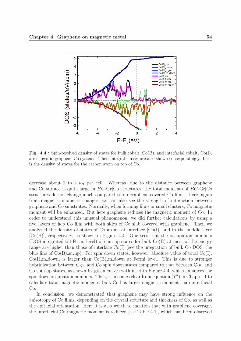
Chapter 4. Graphene on magnetic metal 54
Fig. 4.4 : Spin-resolved density of states for bulk cobalt, Co(B), and interfacial cobalt, Co(I),are shown in graphene|Co systems. Their integral curves are also shown correspondingly. Insetis the density of states for the carbon atom on top of Co.
decrease about 1 to 2 νB per cell. Whereas, due to the distance between grapheneand Co surface is quite large in BC-Gr|Co structures, the total moments of BC-Gr|Costructures do not change much compared to no graphene covered Co films. Here, againfrom magnetic moments changes, we can also see the strength of interaction betweengraphene and Co substrates. Normally, when forming films or small clusters, Co magneticmoment will be enhanced. But here graphene reduces the magnetic moment of Co. Inorder to understand this unusual phenomenon, we did further calculations by using afive layers of hcp Co film with both sides of Co slab covered with graphene. Then weanalyzed the density of states of Co atoms at interface [Co(I)] and in the middle layer[Co(B)], respectively, as shown in Figure 4.4. One sees that the occupation numbers(DOS integrated till Fermi level) of spin up states for bulk Co(B) at most of the energyrange are higher than those of interface Co(I) (see the integration of bulk Co DOS: theblue line of Co(B) m up). For spin down states, however, absolute value of total Co(I),Co(I) m down, is larger than Co(B) m down at Fermi level. This is due to strongerhybridization between C-pz and Co spin down states compared to that between C-pz andCo spin up states, as shown by green curves with inset in Figure 4.4, which enhances thespin down occupation numbers. Thus, it becomes clear from equation (??) in Chapter 1 tocalculate total magnetic moments, bulk Co has larger magnetic moment than interfacialCo.
In conclusion, we demonstrated that graphene may have strong influence on theanisotropy of Co films, depending on the crystal structure and thickness of Co, as well asthe epitaxial orientation. Here it is also worth to mention that with graphene coverage,the interfacial Co magnetic moment is reduced [see Table 4.1], which has been observed

Chapter 4. Graphene on magnetic metal 55
in experiment [VVSC+11].
Chapter 4. Graphene on magnetic metal 56
4.2 Work Function of Graphene/Co
In solid-state physics, the work function is defined as the minimum energy neededto remove an electron from a solid to a point immediately outside the solid surface,namely the energy needed to move an electron from the Fermi level into vacuum. Here”immediately” means that the final electron position is far from the surface on the atomicscale but still close to the solid on the macroscopic scale.
The work function is important for design of the metal-semiconductor junction inSchottky diodes or vacuum tubes. Similarly, the work function is a very importantparameter for the application of graphene. In this section, we investigate the impact ofgraphene on work function of Co films.
In the first section of this chapter, we have seen that interaction between grapheneand hcp or fcc Co films strongly depends on the epitaxial orientation. But the crystalstructures of fcc or hcp actually have no much difference. The energy difference is lessthan 0.2 eV for 12 Co and 8 carbon atoms per cell. Since the work function is of orderof eV, here we consider the most stable case of hcp Co substrate.
As shown in Figure 4.5, we considered AB-Gr|Co(hcp), BC-Gr|Co(hcp) andAC-Gr|Co(hcp) structures, where Co films contain 5 layers for symmetric structures,while it contains 4 layers of Co for asymmetric case. The position of Co and graphenelayers are represented with black and grey balls, respectively. Fermi level is normalized tozero eV. In symmetric structures [Figure 4.5(a),(b) and(c)], the solid black lines indicatethe electrostatic potential of pure hcp Co films, and the dashed red lines representthe electrostatic potential of Gr|Co|Gr structure. In asymmetric case, left hand sideis the vacuum/graphene/Co potential, and right hand side is the Co|Vacuum potential,respectively. For pure hcp Co films, the work function is about 4.9 eV, which is veryclose to experimental value of 5 eV. With asymmetric Gr|Co|Vacuum structure, the workfunction is a little bit smaller with value of 4.53 eV compared to that of the symmetriccase.
When covered with graphene, the work function of Co is strongly reduced as shownin Figure 4.5. For AB-Gr|Co(hcp) and AC-Gr|Co(hcp) structures, the work functionsdecrease to 3.5 and 3.6 eV, respectively. For BC-Gr|Co(hcp) structure, as we havementioned before, the interaction between graphene and substrate is very weak andthe work function is not influenced much, giving 10 orders smaller than those ofAB-Gr|Co(hcp) and AC-Gr|Co(hcp) structures. For the asymmetric structure, where weused only 4 monolayers of Co, the reduction of work function due to graphene coverageis estimated to be about 0.9 eV.
In experiments, using spin-polarized low-energy electron microscopy (SPLEEM), N.Rougemaille et al obsered that the work function is reduced about 0.83 eV due to thecoverage of graphene [CNR+]. This reduction is much larger compared with conventionalmetal or molecule contacts.
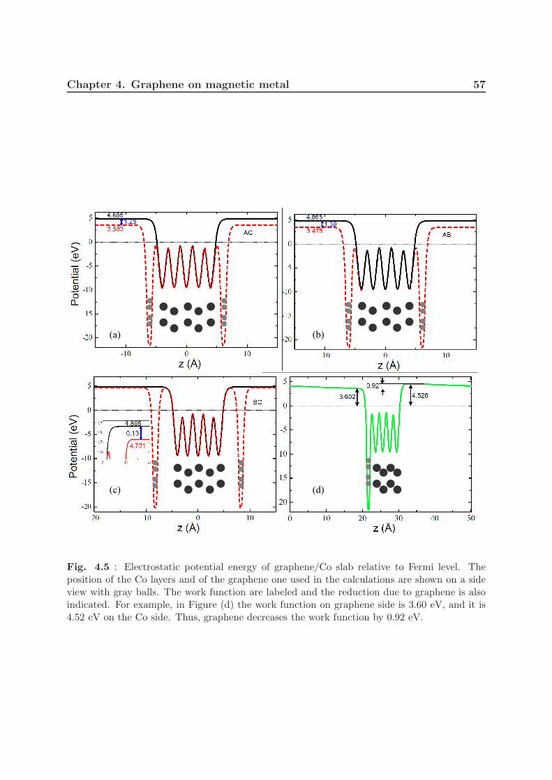
Chapter 4. Graphene on magnetic metal 57
(a) (b)
(c) (d)
Fig. 4.5 : Electrostatic potential energy of graphene/Co slab relative to Fermi level. Theposition of the Co layers and of the graphene one used in the calculations are shown on a sideview with gray balls. The work function are labeled and the reduction due to graphene is alsoindicated. For example, in Figure (d) the work function on graphene side is 3.60 eV, and it is4.52 eV on the Co side. Thus, graphene decreases the work function by 0.92 eV.
Chapter 4. Graphene on magnetic metal 58
4.3 Summary
In this Chapter, we have studied the impact of graphene on Co film properties. We showedthat for thick Co films with graphene coverage the perpendicular magnetic anisotropy ispreserved, which has been proved by experiments. Moreover, in case of a single layer ofCo film, graphene coverage can switch the anisotropy from in-plane to out-of-plane with alarge PMA value. Furthermore, we demonstrated that the graphene can strongly reducethe work function of Co surface which is also in a good agreement with experiments.Finally, the reduction of magnetic moment of interfacial Co is presented and explained,providing a good agreement with observations as well.
Chapter 5
Graphene on magnetic insulator
In this chapter, the spin-polarization of graphene on EuO substrate is investigated. Weshow that an average spin-polarization about 12 % could be obtained. Moreover, with ashifting of Fermi level, much larger spin-polarization of 100 % may be attained. It is alsodemonstrated that Dirac cone in graphene could be tuned by the substrate. Finally anunusual magnetic order is unveiled in graphene layer.
5.1 Interest of graphene on magnetic insulator
Semiconducting devices rely on the gap because it is the gap that allows a semiconductorto be switched from conducting to insulating. In principle, the larger the gap the betterfor application since it insures a large on/off ratio for switching devices. Therefore, forgraphene-based electronic applications, we have to find ways to make graphene open agap. One way to open a gap in graphene is using confined structures, e.g. graphenenanoribbon and graphene nonomesh [SCL06b, BZJ+10]. Indeed, a graphene ribbon witha width of 1 nm has theoretically a band gap of nearly 1 eV. An energy gap of thismagnitude is good enough for electronic applications, but the size scale of 1 nm is in therange of fabrication limit. In the sense of size scale, graphene nanomeshes may help tosolve the problem [BZJ+10]. Another solution to obtain large scale opened-gap grapheneis using insulating substrate, the very famous one is using 4H- or 6H-SiC substrate. Butother insulating substrates are also intensively investigated, for example, Al2O3, MgO,SiO2, BN and GaAs.
In parallel to semiconductor applications, graphene is also believed to have intensivepotential applications for spintronics. For graphene-based spintronics, one may say toinduce magnetism is as important as to open a band gap in graphene-based electronics.Just like in semicondutor applications, the approaches to open a gap in graphene are alsoused to induce magnetism, e.g. half-metallic zigzag graphene nanoribbon and graphenenanomeshes, as well as using a substrate. However, the substrates used to inducemagnetism are mainly metals, like Co and Ni [VSBS+08, WRH+10, RVSB+09, GKB+08].The properties of these epitaxial films have been extensively studied, however since thesefilm are grown on conducting substrates, they have little electronic applications potentialwhich requires insulating substrates. Thus, to epitaxially grow graphene on insulatingmagnetic substrates becomes critical for spintronic applications.
As for magnetic insulating materials there are NiO, EuO, EuS, and Fe3O4 etc.
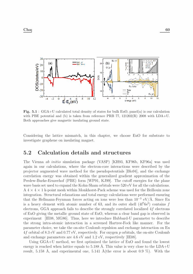
Chapter 5. Graphene on magnetic insulator 60
(a) (b)
Fig. 5.1 : GGA+U calculated total density of states for bulk EuO, panel(a) is our calculationwith PBE potential and (b) is taken from reference PRB 77, 121202(R) 2008 with LDA+U.Both approaches give magnetic insulating ground state.
Considering the lattice mismatch, in this chapter, we choose EuO for substrate toinvestigate graphene on insulating magnet.
5.2 Calculation details and structures
The Vienna ab initio simulation package (VASP) [KH93, KF96b, KF96a] was usedagain in our calculations, where the electron-core interactions were described by theprojector augmented wave method for the pseudopotentials [Blo94], and the exchangecorrelation energy was obtained within the generalized gradient approximation of thePerdew-Burke-Ernzerhof (PBE) form [WP91, KJ99]. The cutoff energies for the planewave basis set used to expand the Kohn-Sham orbitals were 520 eV for all the calculations.A 4 × 4 × 1 k-point mesh within Monkhorst-Pack scheme was used for the Brillouin zoneintegration. Structural relaxations and total energy calculations were performed ensuringthat the Hellmann-Feynman forces acting on ions were less than 10−3 eV/A. Since Euis a heavy element with atomic number of 63, and its outer shell (4f76s2) contains felectrons, GGA approach fails to describe the strongly correlated localized 4f electronsof EuO giving the metallic ground state of EuO, whereas a clear band gap is observed inexperiment [IE08, MG86]. Thus, here we introduce Hubbard-U parameter to describethe strong intra-atomic interaction in a screened Hartree-Fock like manner. For theparameter choice, we take the on-site Coulomb repulsion and exchange interaction on Eu4f orbital of 8.3 eV and 0.77 eV, respectively. For oxygen p orbitals, the on-site Coulomband exchange parameters are 4.6 eV and 1.2 eV, respectively [IE08].
Using GGA+U method, we first optimized the lattice of EuO and found the lowestenergy is reached when lattice equals to 5.188 A. This value is very close to the LDA+Uresult, 5.158 A, and experimental one, 5.141 A(the error is about 0.9 %). With the
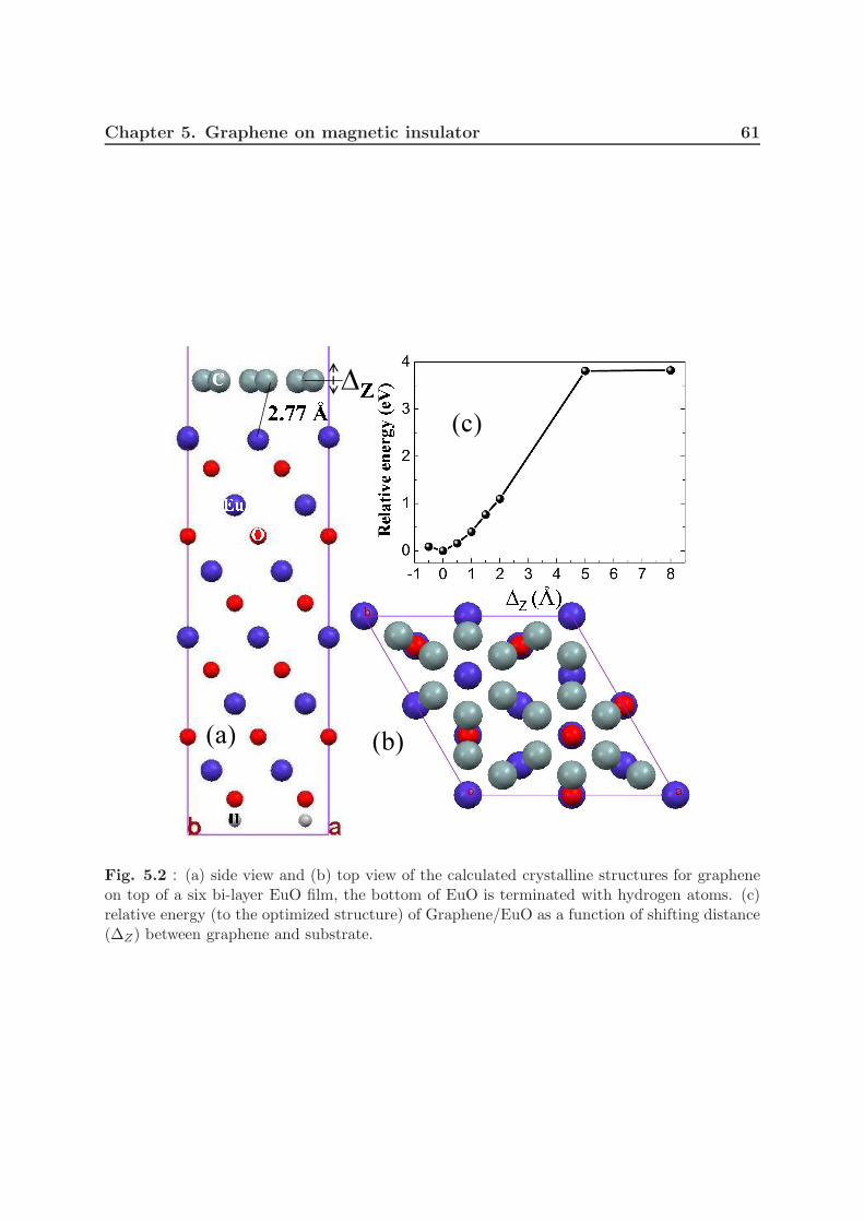
Chapter 5. Graphene on magnetic insulator 61
���� �
(a) (b)
��
�
�
�
∆
� � �
(c)
������������������
Fig. 5.2 : (a) side view and (b) top view of the calculated crystalline structures for grapheneon top of a six bi-layer EuO film, the bottom of EuO is terminated with hydrogen atoms. (c)relative energy (to the optimized structure) of Graphene/EuO as a function of shifting distance(∆Z) between graphene and substrate.
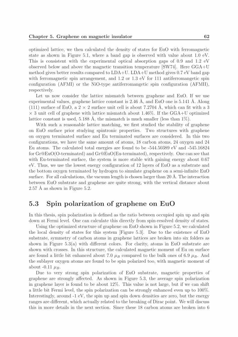
Chapter 5. Graphene on magnetic insulator 62
optimized lattice, we then calculated the density of states for EuO with ferromagneticstate as shown in Figure 5.1, where a band gap is observed with value about 1.0 eV.This is consistent with the experimental optical absorption gaps of 0.9 and 1.2 eVobserved below and above the magnetic transition temperature [SW74]. Here GGA+Umethod gives better results compared to LDA+U. LDA+U method gives 0.7 eV band gapwith ferromagnetic spin arrangement, and 1.2 or 1.3 eV for 111 antiferromangetic spinconfiguration (AFMI) or the NiO-type antiferromangetic spin configuration (AFMII),respectively.
Let us now consider the lattice mismatch between graphene and EuO. If we useexperimental values, graphene lattice constant is 2.46 A, and EuO one is 5.141 A. Along(111) surface of EuO, a 2 × 2 surface unit cell is about 7.2704 A, which can fit with a 3× 3 unit cell of graphene with lattice mismatch about 1.46%. If the GGA+U optimizedlattice constant is used, 5.188 A, the mismatch is much smaller (less than 1%).
With such a reasonable lattice matching, we first studied the stability of grapheneon EuO surface prior studying spintronic properties. Two structures with grapheneon oxygen terminated surface and Eu terminated surfaces are considered. In this twoconfigurations, we have the same amount of atoms, 18 carbon atoms, 24 oxygen and 24Eu atoms. The calculated total energies are found to be -544.50389 eV and -545.16824for Gr@EuO(O-terminated) and Gr@EuO(Eu-terminated), respectively. One can see thatwith Eu-terminated surface, the system is more stable with gaining energy about 0.67eV. Thus, we use the lowest energy configuration of 12 layers of EuO as a substrate andthe bottom oxygen terminated by hydrogen to simulate graphene on a semi-infinite EuOsurface. For all calculations, the vacuum length is chosen larger than 20 A. The interactionbetween EuO substrate and graphene are quite strong, with the vertical distance about2.57 A as shown in Figure 5.2.
5.3 Spin polarization of graphene on EuO
In this thesis, spin polarization is defined as the ratio between occupied spin up and spindown at Fermi level. One can calculate this directly from spin-resolved density of states.
Using the optimized structure of graphene on EuO shown in Figure 5.2, we calculatedthe local density of states for this system [Figure 5.3]. Due to the existence of EuOsubstrate, symmetry of carbon atoms in graphene lattices are broken into six folders asshown in Figure 5.3(a) with different colors. For clarity, atoms in EuO substrate areshown with crosses. In this structure, the calculated magnetic moment of Eu on surfaceare found a little bit enhanced about 7.0 µB compared to the bulk ones of 6.9 µB. Andthe sublayer oxygen atoms are found to be spin polarized too, with magnetic moment ofabout -0.11 µB.
Due to very strong spin polarization of EuO substrate, magnetic properties ofgraphene are strongly affected. As shown in Figure 5.3, the average spin polarizationin graphene layer is found to be about 12%. This value is not large, but if we can shifta little bit Fermi level, the spin polarization can be strongly enhanced even up to 100%.Interestingly, around -1 eV, the spin up and spin down densities are zero, but the energyranges are different, which actually related to the breaking of Dirac point. We will discussthis in more details in the next section. Since these 18 carbon atoms are broken into 6
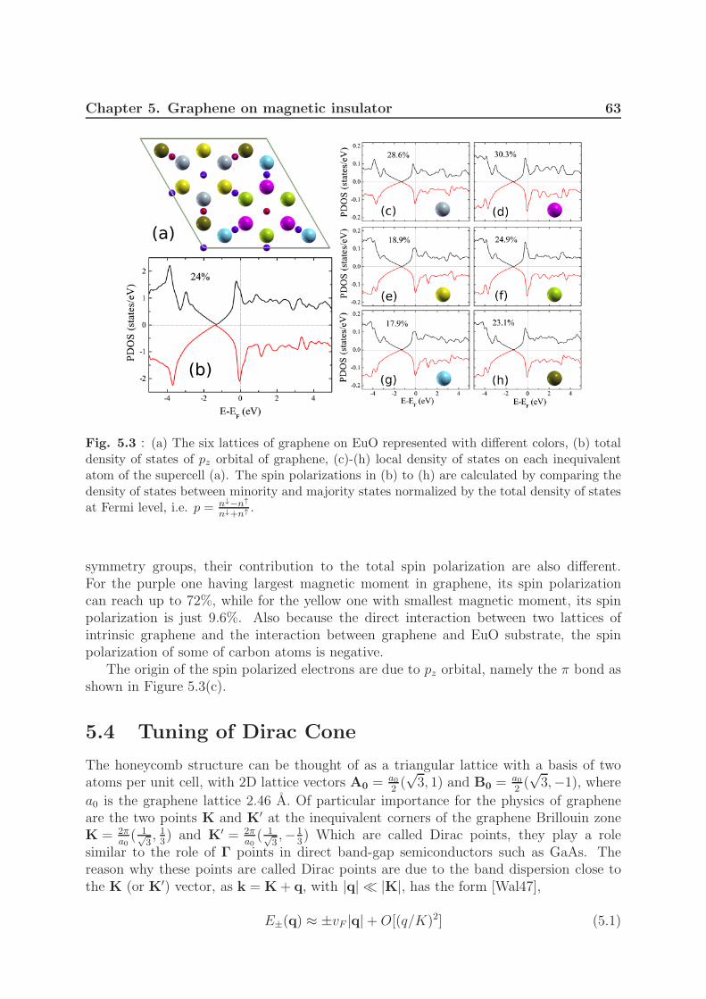
Chapter 5. Graphene on magnetic insulator 63
Fig. 5.3 : (a) The six lattices of graphene on EuO represented with different colors, (b) totaldensity of states of pz orbital of graphene, (c)-(h) local density of states on each inequivalentatom of the supercell (a). The spin polarizations in (b) to (h) are calculated by comparing thedensity of states between minority and majority states normalized by the total density of statesat Fermi level, i.e. p = n↓−n↑
n↓+n↑ .
symmetry groups, their contribution to the total spin polarization are also different.For the purple one having largest magnetic moment in graphene, its spin polarizationcan reach up to 72%, while for the yellow one with smallest magnetic moment, its spinpolarization is just 9.6%. Also because the direct interaction between two lattices ofintrinsic graphene and the interaction between graphene and EuO substrate, the spinpolarization of some of carbon atoms is negative.
The origin of the spin polarized electrons are due to pz orbital, namely the π bond asshown in Figure 5.3(c).
5.4 Tuning of Dirac Cone
The honeycomb structure can be thought of as a triangular lattice with a basis of twoatoms per unit cell, with 2D lattice vectors A0 = a0
2(√3, 1) and B0 = a0
2(√3,−1), where
a0 is the graphene lattice 2.46 A. Of particular importance for the physics of grapheneare the two points K and K′ at the inequivalent corners of the graphene Brillouin zoneK = 2π
a0( 1√
3, 13) and K′ = 2π
a0( 1√
3,−1
3) Which are called Dirac points, they play a role
similar to the role of Γ points in direct band-gap semiconductors such as GaAs. Thereason why these points are called Dirac points are due to the band dispersion close tothe K (or K′) vector, as k = K+ q, with |q| ≪ |K|, has the form [Wal47],
E±(q) ≈ ±vF |q|+O[(q/K)2] (5.1)
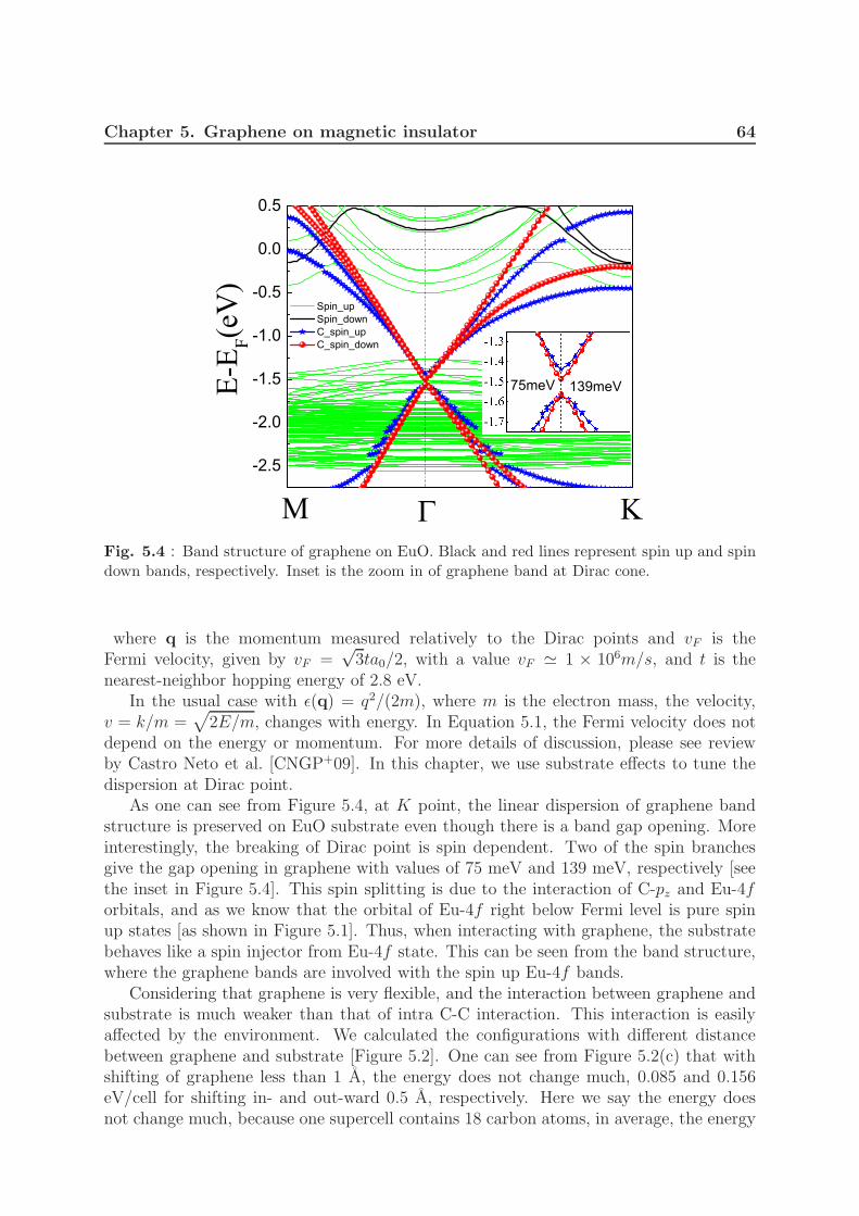
Chapter 5. Graphene on magnetic insulator 64
-2.5
-2.0
-1.5
-1.0
-0.5
0.0
0.5
Spin_up Spin_down C_spin_up C_spin_down
E-E F(eV)
139meV75meV
Fig. 5.4 : Band structure of graphene on EuO. Black and red lines represent spin up and spindown bands, respectively. Inset is the zoom in of graphene band at Dirac cone.
where q is the momentum measured relatively to the Dirac points and vF is theFermi velocity, given by vF =
√3ta0/2, with a value vF ≃ 1 × 10⁶m/s, and t is the
nearest-neighbor hopping energy of 2.8 eV.In the usual case with ǫ(q) = q2/(2m), where m is the electron mass, the velocity,
v = k/m =√
2E/m, changes with energy. In Equation 5.1, the Fermi velocity does notdepend on the energy or momentum. For more details of discussion, please see reviewby Castro Neto et al. [CNGP+09]. In this chapter, we use substrate effects to tune thedispersion at Dirac point.
As one can see from Figure 5.4, at K point, the linear dispersion of graphene bandstructure is preserved on EuO substrate even though there is a band gap opening. Moreinterestingly, the breaking of Dirac point is spin dependent. Two of the spin branchesgive the gap opening in graphene with values of 75 meV and 139 meV, respectively [seethe inset in Figure 5.4]. This spin splitting is due to the interaction of C-pz and Eu-4forbitals, and as we know that the orbital of Eu-4f right below Fermi level is pure spinup states [as shown in Figure 5.1]. Thus, when interacting with graphene, the substratebehaves like a spin injector from Eu-4f state. This can be seen from the band structure,where the graphene bands are involved with the spin up Eu-4f bands.
Considering that graphene is very flexible, and the interaction between graphene andsubstrate is much weaker than that of intra C-C interaction. This interaction is easilyaffected by the environment. We calculated the configurations with different distancebetween graphene and substrate [Figure 5.2]. One can see from Figure 5.2(c) that withshifting of graphene less than 1 A, the energy does not change much, 0.085 and 0.156eV/cell for shifting in- and out-ward 0.5 A, respectively. Here we say the energy doesnot change much, because one supercell contains 18 carbon atoms, in average, the energy
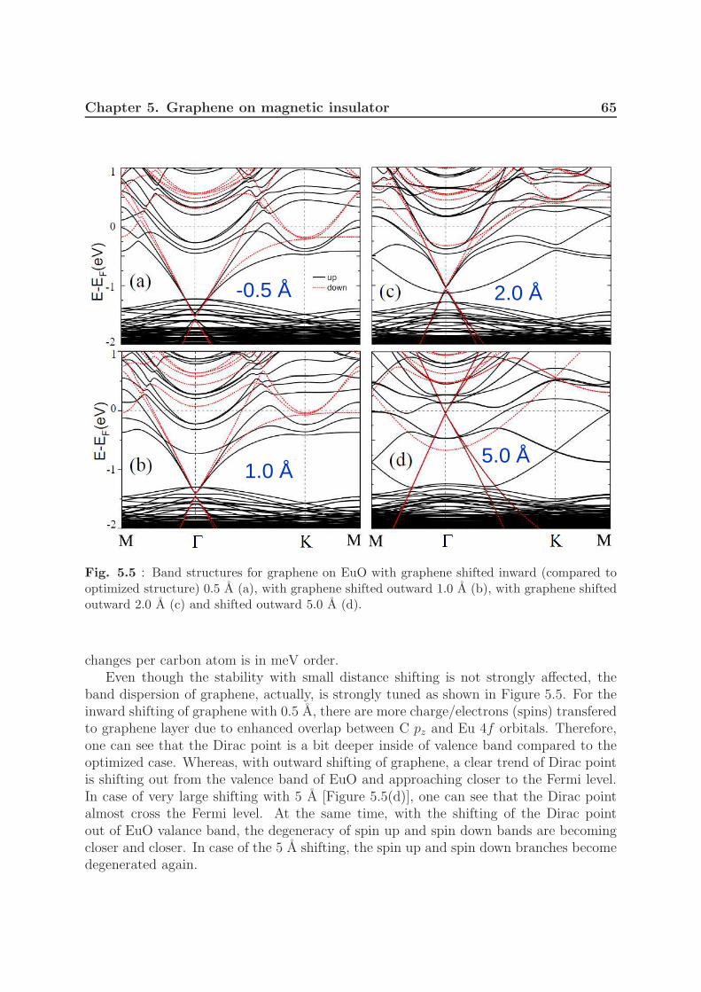
Chapter 5. Graphene on magnetic insulator 65
-0.5 Å
1.0 Å5.0 Å
2.0 Å
Fig. 5.5 : Band structures for graphene on EuO with graphene shifted inward (compared tooptimized structure) 0.5 A (a), with graphene shifted outward 1.0 A (b), with graphene shiftedoutward 2.0 A (c) and shifted outward 5.0 A (d).
changes per carbon atom is in meV order.Even though the stability with small distance shifting is not strongly affected, the
band dispersion of graphene, actually, is strongly tuned as shown in Figure 5.5. For theinward shifting of graphene with 0.5 A, there are more charge/electrons (spins) transferedto graphene layer due to enhanced overlap between C pz and Eu 4f orbitals. Therefore,one can see that the Dirac point is a bit deeper inside of valence band compared to theoptimized case. Whereas, with outward shifting of graphene, a clear trend of Dirac pointis shifting out from the valence band of EuO and approaching closer to the Fermi level.In case of very large shifting with 5 A [Figure 5.5(d)], one can see that the Dirac pointalmost cross the Fermi level. At the same time, with the shifting of the Dirac pointout of EuO valance band, the degeneracy of spin up and spin down bands are becomingcloser and closer. In case of the 5 A shifting, the spin up and spin down branches becomedegenerated again.
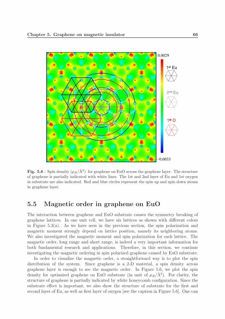
Chapter 5. Graphene on magnetic insulator 66
0.0029
−0.0033
1�� Eu
2�� Eu
1�� O
Fig. 5.6 : Spin density (µB/A2) for graphene on EuO across the graphene layer. The structure
of graphene is partially indicated with white lines. The 1st and 2nd layer of Eu and 1st oxygenin substrate are also indicated. Red and blue circles represent the spin up and spin down atomsin graphene layer.
5.5 Magnetic order in graphene on EuO
The interaction between graphene and EuO substrate causes the symmetry breaking ofgraphene lattices. In one unit cell, we have six lattices as shown with different colorsin Figure 5.3(a). As we have seen in the previous section, the spin polarization andmagnetic moment strongly depend on lattice position, namely its neighboring atoms.We also investigated the magnetic moment and spin polarization for each lattice. Themagnetic order, long range and short range, is indeed a very important information forboth fundamental research and applications. Therefore, in this section, we continueinvestigating the magnetic ordering in spin polarized graphene caused by EuO substrate.
In order to visualize the magnetic order, a straightforward way is to plot the spindistribution of the system. Since graphene is a 2-D material, a spin density acrossgraphene layer is enough to see the magnetic order. In Figure 5.6, we plot the spindensity for optimized graphene on EuO substrate (in unit of µB/A
2). For clarity, thestructure of graphene is partially indicated by white honeycomb configuration. Since thesubstrate effect is important, we also show the structure of substrate for the first andsecond layer of Eu, as well as first layer of oxygen [see the caption in Figure 5.6]. One can
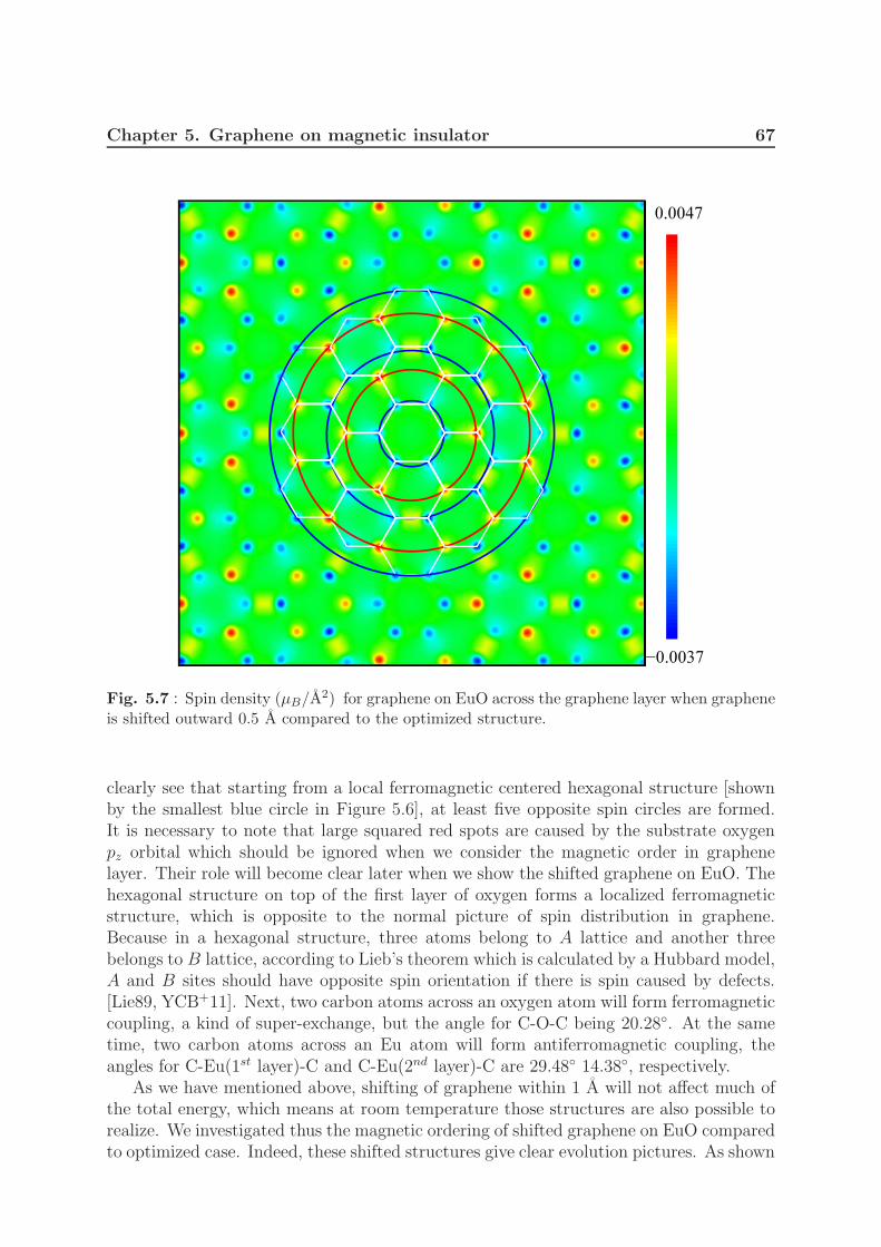
Chapter 5. Graphene on magnetic insulator 67
0.0047
−0.0037
Fig. 5.7 : Spin density (µB/A2) for graphene on EuO across the graphene layer when graphene
is shifted outward 0.5 A compared to the optimized structure.
clearly see that starting from a local ferromagnetic centered hexagonal structure [shownby the smallest blue circle in Figure 5.6], at least five opposite spin circles are formed.It is necessary to note that large squared red spots are caused by the substrate oxygenpz orbital which should be ignored when we consider the magnetic order in graphenelayer. Their role will become clear later when we show the shifted graphene on EuO. Thehexagonal structure on top of the first layer of oxygen forms a localized ferromagneticstructure, which is opposite to the normal picture of spin distribution in graphene.Because in a hexagonal structure, three atoms belong to A lattice and another threebelongs to B lattice, according to Lieb’s theorem which is calculated by a Hubbard model,A and B sites should have opposite spin orientation if there is spin caused by defects.[Lie89, YCB+11]. Next, two carbon atoms across an oxygen atom will form ferromagneticcoupling, a kind of super-exchange, but the angle for C-O-C being 20.28◦. At the sametime, two carbon atoms across an Eu atom will form antiferromagnetic coupling, theangles for C-Eu(1st layer)-C and C-Eu(2nd layer)-C are 29.48◦ 14.38◦, respectively.
As we have mentioned above, shifting of graphene within 1 A will not affect much ofthe total energy, which means at room temperature those structures are also possible torealize. We investigated thus the magnetic ordering of shifted graphene on EuO comparedto optimized case. Indeed, these shifted structures give clear evolution pictures. As shown
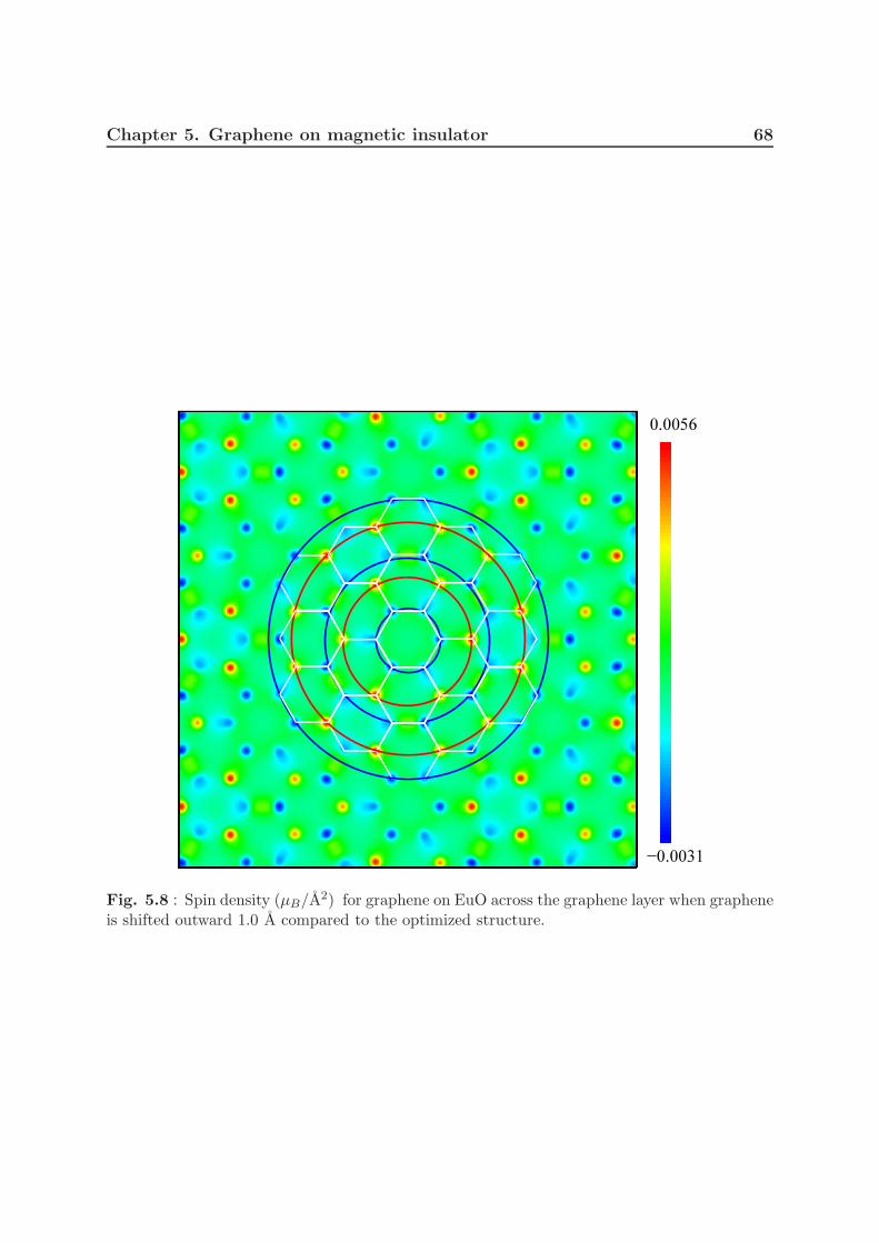
Chapter 5. Graphene on magnetic insulator 68
0.0056
−0.0031
Fig. 5.8 : Spin density (µB/A2) for graphene on EuO across the graphene layer when graphene
is shifted outward 1.0 A compared to the optimized structure.
Chapter 5. Graphene on magnetic insulator 69
in Figure 5.7, the spin distribution for graphene shifted outward with 0.5 A compared tothat of the optimized case. Similar to the tuning of Dirac cone, where with the outwardshifting of graphene, the interaction between graphene and EuO becomes weaker and thedegeneracy splitting between spin up and spin down bands becomes smaller, as well asthe Dirac cone moves out of EuO valance band to Fermi level. For the spin distribution,we see that even with very small shifting of graphene, 0.5 A, it is clear that the red squarespots become weaker compared to small yellow square ones. It actually also reflects thatthe overlap between graphene and EuO orbtials is becoming weaker. More clearly, forthe case with graphene shifted outward by 1.0 A [Figure 5.8], the large square red spotsin optimized case or the yellow square spots in Figure 5.7 are almost invisible. However,in both of the 0.5 A and 1.0 A shifting cases, the magnetic order does not change andthe pattern is still preserved as in optimized case.
5.6 Summary and Perspective
With a very good lattice matching between graphene and rock salt EuO (111) surface,we investigated the spin polarization of graphene and its magnetic order induced by EuOproximity. EuO substrate breaks a bipartite lattice of graphene into six ones. At the sametime, graphene becomes magnetic due to strong magnetization of EuO which behaveslike a spin injector. Therefore, it is straightforward that the magnetization of carbonatoms of graphene should depend on their positions on EuO, which leads to an unusualmagnetic order in graphene. This magnetic order is still unclear. Nevertheless, both spinpolarization and magnetic order reported should lead to many interesting phenomena.For instance, the substrate induced magnetic moment in graphene may lead to strongeranomalous Hall effect, the gap opening in graphene may provide a root to semiconductingapplications. And the difference gap opened at Dirac point for spin up and spin downis also very exciting for spintronics. Furthermore, the unusual magnetic order may servefor realizing spin frustration structures or even spin density wave investigations.
Chapter 6
Electronic and magnetic propertiesof graphene nanomeshes
In this Chapter, we explore the electronic and magnetic properties of graphenenanomeshes (GNM), a regular network of large vacancies, produced either by lithographyor nanoimprint. When removing an equal number of A and B sites of the graphenebipartite lattice, the nanomesh made mostly of zigzag (armchair) -type edges exhibitantiferromagnetic (spin unpolarized) states. In contrast, in situations of sublatticesymmetry breaking, stable ferri(o)magnetic states are obtained. For hydrogen-passivatednanomesh, the formation energy is dramatically decreased, and ground state is foundto strongly depend on the vacancies shape and size. For triangular-shaped holes, theobtained net magnetic moments increase with the number difference of removed A andB sites in agreement with Lieb’s theorem for even A + B. For odd A + B triangularmeshes and all cases of nontriangular nanomeshes, including the one with even A +B, Lieb’s theorem does not hold anymore, which can be partially attributed to theintroduction of armchair edges. In addition, large triangular-shaped GNMs could beas robust as nontriangular GNMs, providing a possible solution to overcome one of thecrucial challenges for the sp magnetism. Finally, significant exchange-splitting values aslarge as 0.5 eV can be obtained for highly asymmetric structures evidencing the potentialof GNM for room-temperature carbon-based spintronics. These results demonstratethat a turn from zero-dimensional graphene nanoflakes throughout one-dimensionalgraphene nanoribbons with zigzag edges to GNM breaks localization of unpairedelectrons and provides deviation from the rules based on Lieb’s theorem. Suchdelocalization of the electrons leads the switch of the ground state of a system froman antiferromagnetic narrow gap insulator discussed for graphene nanoribons to aferromagnetic or nonmagnetic metal.
6.1 Introduction
Two-dimensional graphene has emerged as a natural candidate for developing ”beyondCMOS” nanoelectronics [NGM+04, NGM+05, ZTSK05, BSL+06, GN07, IK07]. Inaddition to the reported huge charge mobilities, the weak intrinsic spin-orbit couplingin carbon-based sp2 structures [HGB06, YYQ+07] could potentially allow for verylarge (micron long) spin diffusion lengths. These features, together with the other
Chapter 6. Electronic and magnetic properties of graphene nanomeshes 71
”semi-conductor like” properties of graphene, make graphene-based spintronic deviceshighly promising [FBY+01b, WAB+01] and have triggered a quest for controlling spininjection in graphene [TJP+07b, HWP+09, HPM+10, YBV+11]. Many routes havebeen attempted to induce magnetism by proximity effect or inject spins from magneticelectrodes [DSA+10]. Another, more intrinsic, possibility is shaping the geometry ofgraphene by designing graphene nanoribbons with zigzag edges [SCL06a, YPS+07]. Thishas been found to induce localized edge magnetic states which can serve as a conceptuallynew building block for spintronics [SCL06b, BFD07, WAB+08, MFP09, YH07, Yaz08,Yaz10, FP07, PFB08, SNT+12].
The existence of intrinsic magnetism driven by atomic-scale defects (such as vacancies,chemisorbed species, grain boundaries,etc.) has also been suggested theoretically [YH07,Yaz08, Yaz10, PFP+08, FPBJ09, ZZZ+09, LFM+04, HZP10, CYL08, SNT+12]. However,as we have mentioned in the general introduction, the magnetism in graphene remainsfiercely debated on the experimental side [ESH+03, CKF09b, MMJP+10, UBGG10,OEA+10, SNR+10]. The reason may be due to that it is very difficult to obtain a preciseexperimental characterization of those defects. Additionally, the absence of a true energygap in two-dimensional graphene limits the elaboration of active graphene-based devicesand circuits with standard semiconductor technologies.
Another route to make graphene magnetic is either chemisorption of odd number ofadatoms or functional groups [YH07, Yaz08, Yaz10, Bou10, BK11], or using magnetism onzigzag edges [SCL06b, YK08, CKF09a, ET09]. In the first case the stability of magneticconfigurations at room temperature can be easily destroyed by the migration of adatomswith turning the system into nonmagnetic configuration [Bou10, BK11]. In contrast tothe adatom based magnetism edge [CKF09a, ET09] and vacancy [BKK11] magnetismin graphite is stable at room temperature. But herewith localization of the magneticmoments on the edges provides formation of the antiferromagnetic (AFM) exchangeinteractions between two edges [SCL06b].
The case of graphene nanoribbons obey Lieb’s theorem because the localizedelectrons on one edge belong to sublattice A and localized electrons from other edgeto sublattice B. Magnetism on the edges of graphene nanoflakes is also describedby this theorem [YWMK08, WYMK09]. Electron localization plays an importantrole in the different many-body effects on graphene edges [CR09, Fer07] and bulkgraphene [WG05, HHDS07]. Understanding the nature of the electron localizationand delocalization in graphene and related systems is necessary not only for controland manipulation of magnetism in studied compounds but also for the development ofknowledge about systems with strongly correlated electrons.
Graphene nanomesh (further GNM) is the intermediate compound between graphenenanoribbons with localized electrons on zigzag edges and perfect bulk graphene withdelocalized electrons. The fabrication of GNM, using block copolymer lithography andoffering versatility in varying periodicities and neck widths down to 5 nm [BZJ+10],could circumvent the hurdles. Indeed, such technique allows a scalable engineering ofsuperlattices of large graphene vacancies whose density, shape and distribution can becontrolled down to the nanoscale. Additionally, GNM-based field-effect transistors wereshown to withstand current densities two orders of magnitudes larger than individualgraphene nanoribbon devices, with comparable on/off ratio and easily tunable by varyingthe neck width. Moreover, in accordance to the well-established Lieb’s theorem [Lie89],
Chapter 6. Electronic and magnetic properties of graphene nanomeshes 72
the possibility to control inner edge structures [SYZ+11] of nanomesh vacancies couldenable a true control of intrinsic magnetic properties.
In this chapter, we present first-principles calculations of electronic and magneticproperties of graphene nanomeshes, and found that by varying the shape, different typesof intrinsic ferrimagnetic comment states can be obtained with clear identification ofoptimal conditions.
6.2 Methods
First-principles calculations were performed again using Vienna ab initio simulationpackage (VASP) [KH93, KF96a, KF96b] based on density functional theory (DFT) withgeneralized gradient approximation (GGA) for exchange correlation potential. We haveused projected augmented wave method (PAW) [Blo94] with the Perdew-Becke-Erzenhof(PBE) parametrization [PBE96] potentials to describe the core electrons of carbon.Periodic 6 by 6 unit cells were used to simulate non-passivated GNM structures as shownin Figure 6.1, whereas periodic 8 by 8 unit cells were used to simulate H-passivatedGNM structures. The kinetic cutoff energies for the plane wave basis set used toexpand the Kohn-Sham orbitals were 520 eV for the self-consistent energy calculations.Methfessel-Paxton method [MP89] is used with a broading width of 0.2 eV for the partialoccupancy smearing calculations. A 9 × 9 × 1 k-point mesh was sufficient to ensure goodconvergence in the total energy differences. The structural relaxations were performedensuring that the Hellmann-Feynman forces acting on ions were less than 10−3 eV/A.
6.3 Model of graphene nanomeshes
A GNM can be formed by either removing atoms centered of a six ring structure[Figure 6.1(a,b,c)] or centered of one carbon atom [Figure 6.1(d)], which either leadto form GNM with balanced or unbalanced number of removed A and B sites. For thesake of clarity, we label those structures according to their shapes and put the number ofremoved A and B site atoms as a subscript. For instance, the structure of Figure 6.1(a)named C3:3, corresponds to a Circle hole shape GNM with 3:3 denoting 3 A and 3 B atomsremoved from perfect graphene. The superscript H is used for hydrogen-passivated GNM.
6.4 Results and discussions
For C3:3 structure [Figure 6.1(a)], we find that the configuration with opposite spinorientation [Figure 6.3] between adjacent edge C atoms is energetically favored incomparison with the configuration with parallel spins between edge atoms of twosublattices represented by the blue and red color in Figure 6.1. The total energycalculations reveal quite large magnetic interaction energies. For instance, the energydifference between ferromagnetic (FM) spin-polarized and paramagnetic (PM) state isfound to be 0.129 eV per edge atom. The spin configuration is further stabilized by 0.093eV per edge atom as a result of the antiferromagnetic (AF) coupling between neighboringatoms with magnetic moment of 0.48 µB per edge atom for each spin on each sublattice
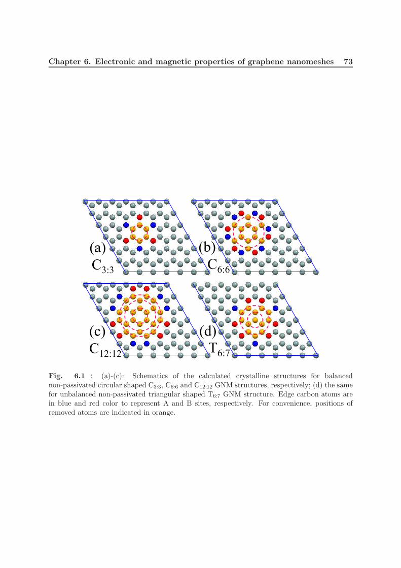
Chapter 6. Electronic and magnetic properties of graphene nanomeshes 73
(d)(c)
(b)
C3:3 C6:6
C12:12 T6:7
(a)
Fig. 6.1 : (a)-(c): Schematics of the calculated crystalline structures for balancednon-passivated circular shaped C3:3, C6:6 and C12:12 GNM structures, respectively; (d) the samefor unbalanced non-passivated triangular shaped T6:7 GNM structure. Edge carbon atoms arein blue and red color to represent A and B sites, respectively. For convenience, positions ofremoved atoms are indicated in orange.
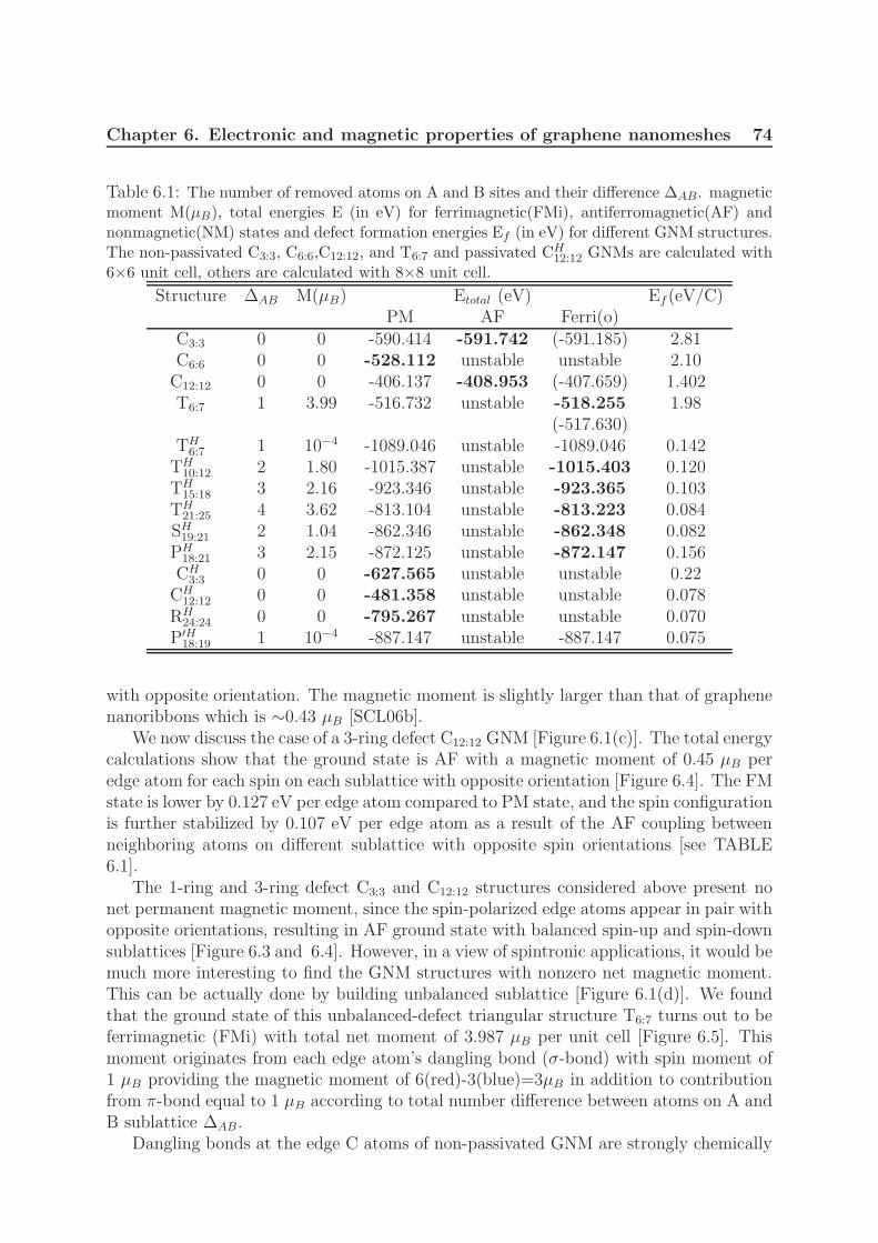
Chapter 6. Electronic and magnetic properties of graphene nanomeshes 74
Table 6.1: The number of removed atoms on A and B sites and their difference ∆AB. magneticmoment M(µB), total energies E (in eV) for ferrimagnetic(FMi), antiferromagnetic(AF) andnonmagnetic(NM) states and defect formation energies Ef (in eV) for different GNM structures.The non-passivated C3:3, C6:6,C12:12, and T6:7 and passivated CH
12:12 GNMs are calculated with6×6 unit cell, others are calculated with 8×8 unit cell.
Structure ∆AB M(µB) Etotal (eV) Ef (eV/C)PM AF Ferri(o)
C3:3 0 0 -590.414 -591.742 (-591.185) 2.81C6:6 0 0 -528.112 unstable unstable 2.10C12:12 0 0 -406.137 -408.953 (-407.659) 1.402T6:7 1 3.99 -516.732 unstable -518.255 1.98
(-517.630)TH
6:7 1 10−4 -1089.046 unstable -1089.046 0.142TH
10:12 2 1.80 -1015.387 unstable -1015.403 0.120TH
15:18 3 2.16 -923.346 unstable -923.365 0.103TH
21:25 4 3.62 -813.104 unstable -813.223 0.084SH19:21 2 1.04 -862.346 unstable -862.348 0.082
PH18:21 3 2.15 -872.125 unstable -872.147 0.156CH
3:3 0 0 -627.565 unstable unstable 0.22CH
12:12 0 0 -481.358 unstable unstable 0.078RH
24:24 0 0 -795.267 unstable unstable 0.070P′H18:19 1 10−4 -887.147 unstable -887.147 0.075
with opposite orientation. The magnetic moment is slightly larger than that of graphenenanoribbons which is ∼0.43 µB [SCL06b].
We now discuss the case of a 3-ring defect C12:12 GNM [Figure 6.1(c)]. The total energycalculations show that the ground state is AF with a magnetic moment of 0.45 µB peredge atom for each spin on each sublattice with opposite orientation [Figure 6.4]. The FMstate is lower by 0.127 eV per edge atom compared to PM state, and the spin configurationis further stabilized by 0.107 eV per edge atom as a result of the AF coupling betweenneighboring atoms on different sublattice with opposite spin orientations [see TABLE6.1].
The 1-ring and 3-ring defect C3:3 and C12:12 structures considered above present nonet permanent magnetic moment, since the spin-polarized edge atoms appear in pair withopposite orientations, resulting in AF ground state with balanced spin-up and spin-downsublattices [Figure 6.3 and 6.4]. However, in a view of spintronic applications, it would bemuch more interesting to find the GNM structures with nonzero net magnetic moment.This can be actually done by building unbalanced sublattice [Figure 6.1(d)]. We foundthat the ground state of this unbalanced-defect triangular structure T6:7 turns out to beferrimagnetic (FMi) with total net moment of 3.987 µB per unit cell [Figure 6.5]. Thismoment originates from each edge atom’s dangling bond (σ-bond) with spin moment of1 µB providing the magnetic moment of 6(red)-3(blue)=3µB in addition to contributionfrom π-bond equal to 1 µB according to total number difference between atoms on A andB sublattice ∆AB.
Dangling bonds at the edge C atoms of non-passivated GNM are strongly chemically
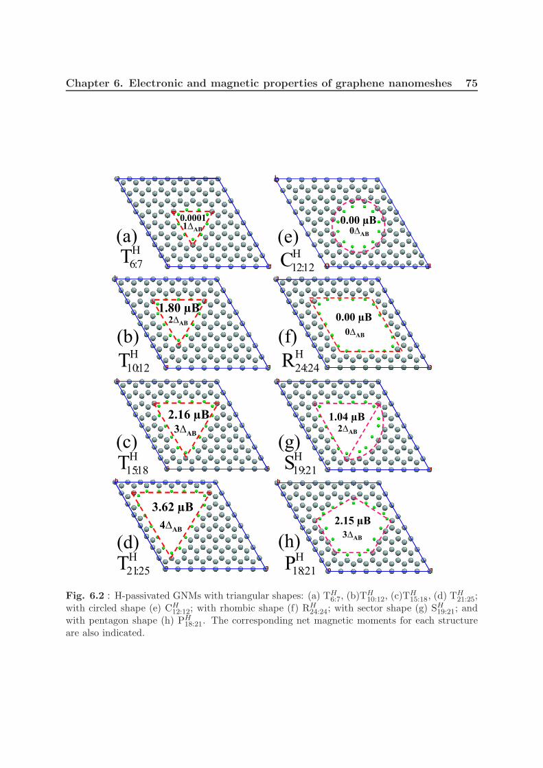
Chapter 6. Electronic and magnetic properties of graphene nanomeshes 75
2.15 µB
3∆AB
1.04 µB2∆AB
0.00 µB
0∆AB
o
b
a
0.00 µB0∆AB
3.62 µB
4∆AB
1.80 µB2∆AB
3∆AB
2.16 µB
0.00011∆AB
(a)
(f)(b)
(e)
(h)(d)
(g)(c)
H
12:21CH
7:6T
H
12:10TH
24:24R
H
18:15TH
21:19S
H
25:21TH
21:18P
Fig. 6.2 : H-passivated GNMs with triangular shapes: (a) TH6:7, (b)T
H10:12, (c)T
H15:18, (d) T
H21:25;
with circled shape (e) CH12:12; with rhombic shape (f) RH
24:24; with sector shape (g) SH19:21; andwith pentagon shape (h) PH
18:21. The corresponding net magnetic moments for each structureare also indicated.
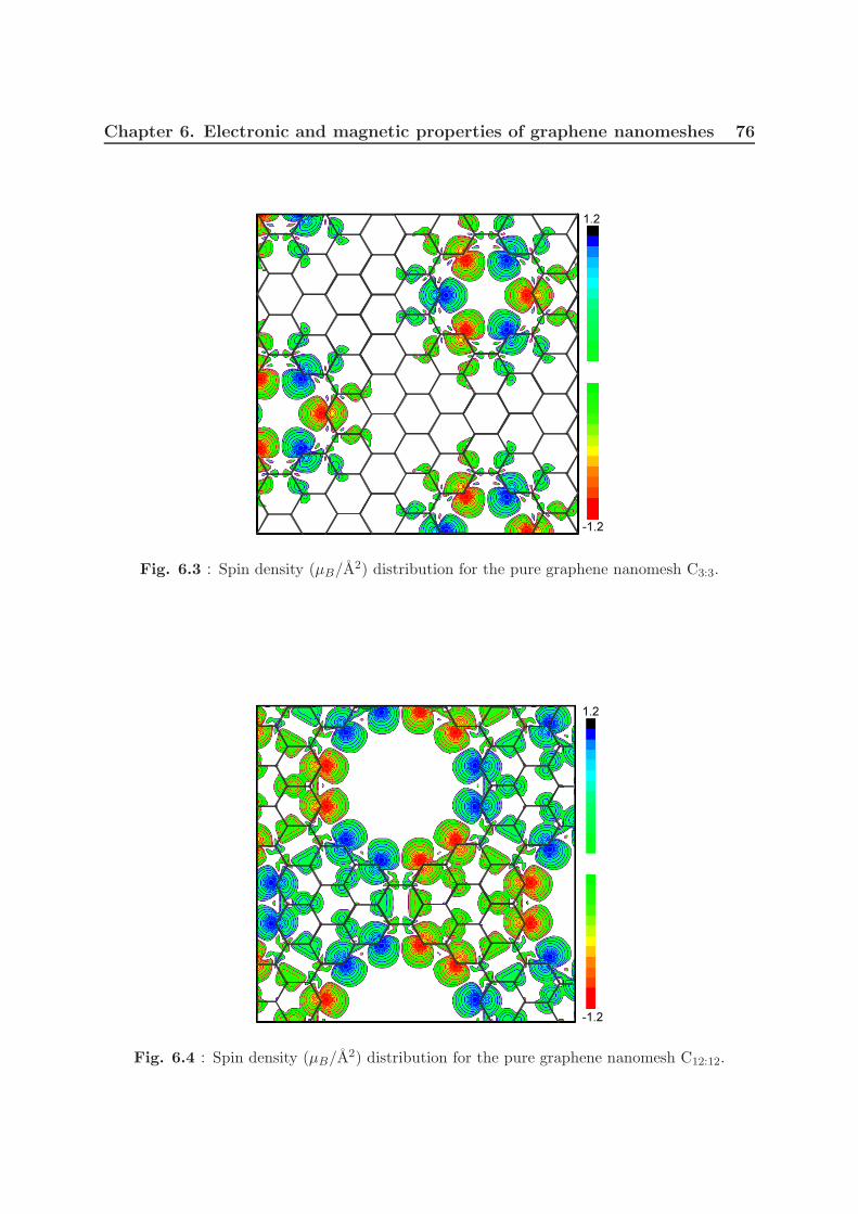
Chapter 6. Electronic and magnetic properties of graphene nanomeshes 76
-1.2
1.2
Fig. 6.3 : Spin density (µB/A2) distribution for the pure graphene nanomesh C3:3.
1.2
-1.2
Fig. 6.4 : Spin density (µB/A2) distribution for the pure graphene nanomesh C12:12.
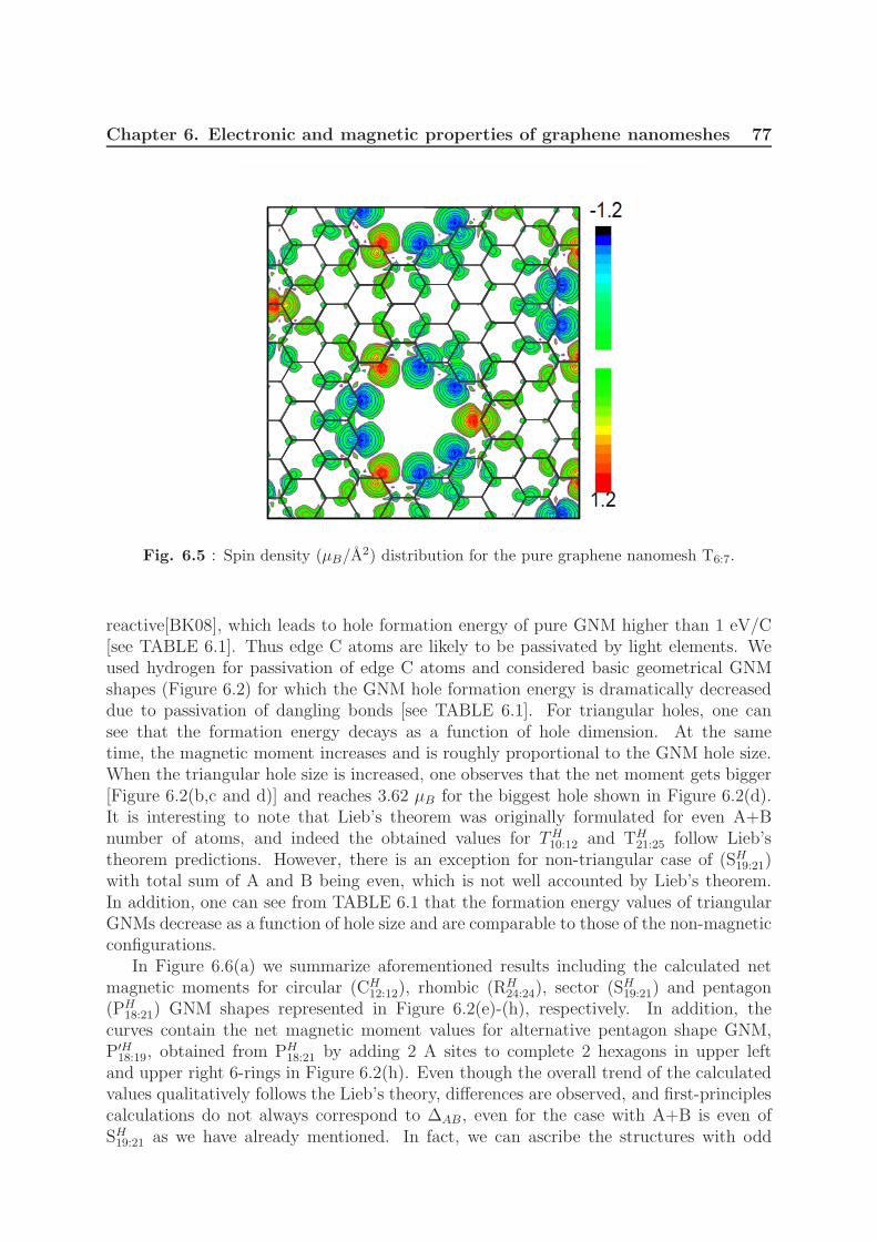
Chapter 6. Electronic and magnetic properties of graphene nanomeshes 77
Fig. 6.5 : Spin density (µB/A2) distribution for the pure graphene nanomesh T6:7.
reactive[BK08], which leads to hole formation energy of pure GNM higher than 1 eV/C[see TABLE 6.1]. Thus edge C atoms are likely to be passivated by light elements. Weused hydrogen for passivation of edge C atoms and considered basic geometrical GNMshapes (Figure 6.2) for which the GNM hole formation energy is dramatically decreaseddue to passivation of dangling bonds [see TABLE 6.1]. For triangular holes, one cansee that the formation energy decays as a function of hole dimension. At the sametime, the magnetic moment increases and is roughly proportional to the GNM hole size.When the triangular hole size is increased, one observes that the net moment gets bigger[Figure 6.2(b,c and d)] and reaches 3.62 µB for the biggest hole shown in Figure 6.2(d).It is interesting to note that Lieb’s theorem was originally formulated for even A+Bnumber of atoms, and indeed the obtained values for TH
10:12 and TH21:25 follow Lieb’s
theorem predictions. However, there is an exception for non-triangular case of (SH19:21)
with total sum of A and B being even, which is not well accounted by Lieb’s theorem.In addition, one can see from TABLE 6.1 that the formation energy values of triangularGNMs decrease as a function of hole size and are comparable to those of the non-magneticconfigurations.
In Figure 6.6(a) we summarize aforementioned results including the calculated netmagnetic moments for circular (CH
12:12), rhombic (RH24:24), sector (SH
19:21) and pentagon(PH
18:21) GNM shapes represented in Figure 6.2(e)-(h), respectively. In addition, thecurves contain the net magnetic moment values for alternative pentagon shape GNM,P′H18:19, obtained from PH
18:21 by adding 2 A sites to complete 2 hexagons in upper leftand upper right 6-rings in Figure 6.2(h). Even though the overall trend of the calculatedvalues qualitatively follows the Lieb’s theory, differences are observed, and first-principlescalculations do not always correspond to ∆AB, even for the case with A+B is even ofSH19:21 as we have already mentioned. In fact, we can ascribe the structures with odd
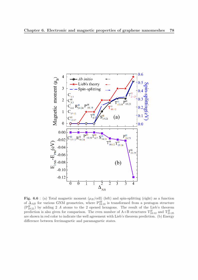
Chapter 6. Electronic and magnetic properties of graphene nanomeshes 78
(a)
(b)
Fig. 6.6 : (a) Total magnetic moment (µB/cell) (left) and spin-splitting (right) as a functionof ∆AB for various GNM geometries, where P′H
18:19 is transformed from a pentagon structure(PH
18:21) by adding 2 A atoms to the 2 opened hexagons. The result of the Lieb’s theoremprediction is also given for comparison. The even number of A+B structures TH
10:12 and TH21:25
are shown in red color to indicate the well agreement with Lieb’s theorem prediction. (b) Energydifference between ferrimagnetic and paramagnetic states.
Chapter 6. Electronic and magnetic properties of graphene nanomeshes 79
number of A+B atoms, i.e. TH6:7, P
′H18:19, T
H15:18, P
H18:21 as well as sector shape SH
19:21 GNMsto intermediate regime between nonmagnetic and highly magnetic regimes. This regimeprovides a root towards design of magnetic GNM supermeshes. It is worth to note thatthe possible mechanism for the deviation from the Lieb’s theorem of the moment valuefor the sector shape GNM SH
19:21 compared to TH10:12 where A+B is even for both, could
be attributed to larger amount of armchair edges (not favorable for moment formation)in SH
19:21 structure.To further elucidate the origin of magnetism in GNM structures, we compute the total
and partial density of states (DOS) for considered GNMs. Figure 6.7(a)-(d) give the totalDOS for triangular shape GNMs shown in Figure 6.2(a)-(d), respectively. The exchangesplitting between majority and minority spins mainly originates from pz orbitals, asclearly seen from Figure 6.7(c′) where the projected density of states (pDOS) on edgeatoms for TH
15:18 is plotted. More interestingly, exchange splitting and energy differencesbetween FM and PM states also increase with ∆AB following the same trend as the netmagnetic moment [see Figure 6.6(a) and (b)], reaching values of 0.5 eV and 0.12 eV,respectively. These large exchange splitting values suggest that the magnetism couldbe preserved at room temperature which look very promising for room temperaturegraphene spintronics developments. Density of states of structures like TH
10:12 provideswith the evidence for the presence of localized electrons on the zigzag edges similar tothe perfect GNR [SCL06b]. The smearing of the pz peak and increase of the numberof states at the Fermi level (metallization) suggest the electron delocalization on edgesand switch from AFM to FM configuration similar to the case of partially oxidizedgraphite edges [BMdSK11]. We have plotted the spin density figures for the localized anddelocalized cases for illustrate dramatic changes in localization of electrons with vanishingof pseudogap in density of states (see Figure 6.8).The cause of such delocalization ofthe unpaired electrons on the edges of GNM holes can be attributed to combination ofsublattice degeneracy breaking and deviation from the perfect shapes of the graphenenanoribbon.
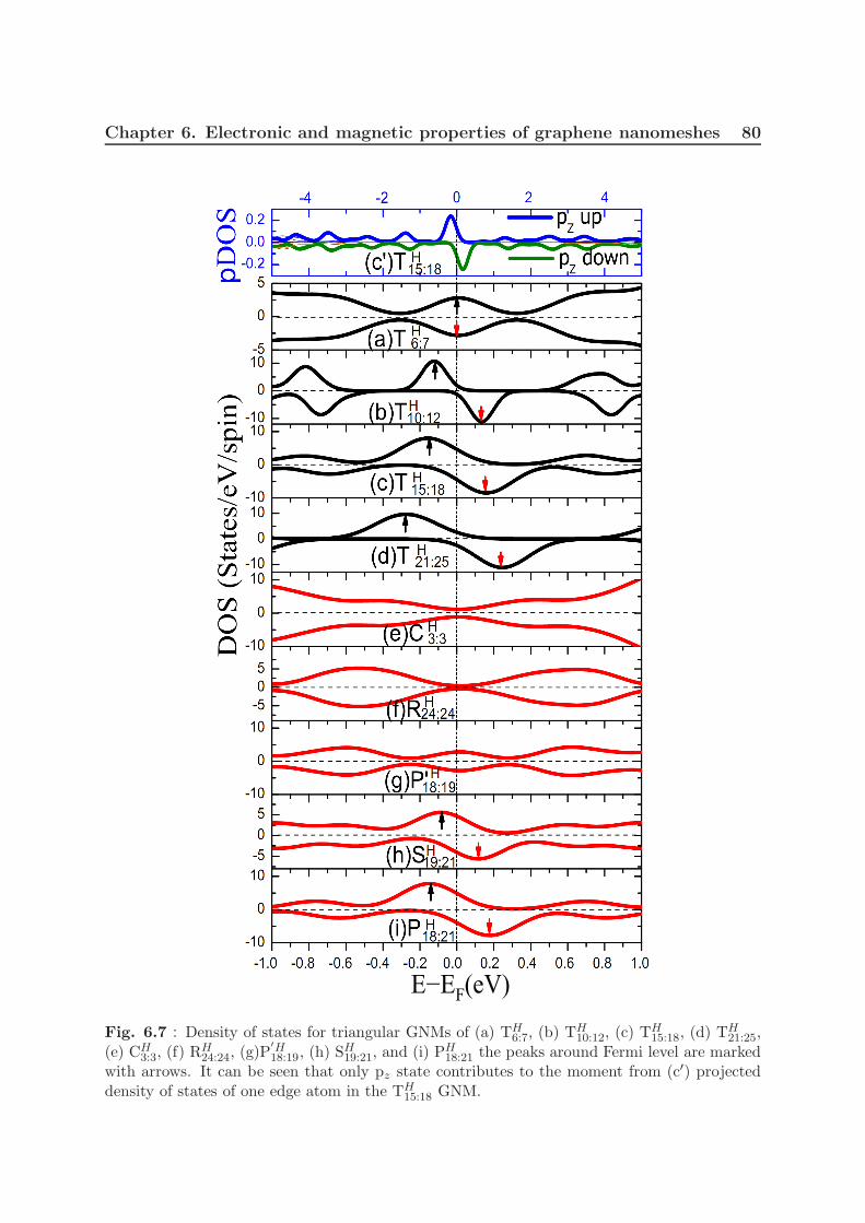
Chapter 6. Electronic and magnetic properties of graphene nanomeshes 80
E−EF(eV)
Fig. 6.7 : Density of states for triangular GNMs of (a) TH6:7, (b) T
H10:12, (c) T
H15:18, (d) T
H21:25,
(e) CH3:3, (f) R
H24:24, (g)P
′H18:19, (h) S
H19:21, and (i) PH
18:21 the peaks around Fermi level are markedwith arrows. It can be seen that only pz state contributes to the moment from (c′) projecteddensity of states of one edge atom in the TH
15:18 GNM.
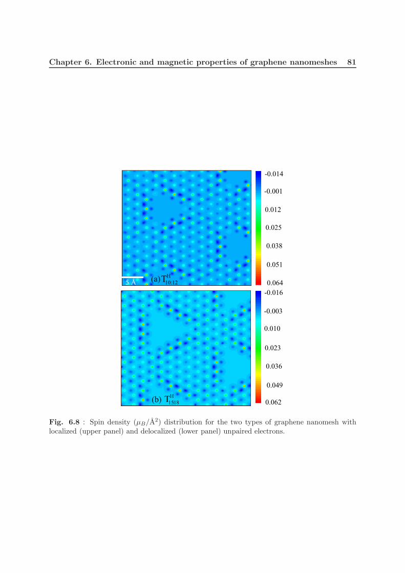
Chapter 6. Electronic and magnetic properties of graphene nanomeshes 81
-0.014
-0.001
0.012
0.025
0.038
0.051
0.064
-0.016
-0.003
0.010
0.023
0.036
0.049
0.062
5 Å (a) H10:12T
H18:15T(b)
Fig. 6.8 : Spin density (µB/A2) distribution for the two types of graphene nanomesh with
localized (upper panel) and delocalized (lower panel) unpaired electrons.
Chapter 6. Electronic and magnetic properties of graphene nanomeshes 82
6.5 Summary
In conclusion, in this chapter we investigated electronic and magnetic properties ingraphene nanomeshes with different geometries using first-principles calculations. Fornon-passivated GNM with ∆AB = 0, stable non-magnetic states are found for armchairedge termination, while zigzag edge terminations result in antiferromagnetic groundstates. These localized magnetic moments however vanish when all edge C-atoms arehydrogen-passivated. In sharp contrast, when ∆AB 6= 0, stable ferri(o)magnetic statesare induced with net moment up to 4 µB (per 6 × 6 unit cell) originating from danglingbonds of edge atoms. Furthermore, for hydrogen-passivated GNM, the formation energyis dramatically decreased, and ground state is found to strongly depend on the vacanciesshape and size. Our calculations reveal the existence of three magnetic regimes whichdepend on ∆AB: (i) highly magnetic GNMs obeying Lieb’s theorem corresponding totriangular shaped holes with even A+B; (ii) GNMs with quenched magnetic state dueto complete chemical bond reconstruction with ∆AB = 1 and trivially nonmagnetic statewith ∆AB = 0; and (iii) GNMs following intermediate regime between magnetic andquenched magnetic states, i.e. triangular GNMs with odd A+B and more complicatedstructures including both even (e.g. sector shaped GNM) and odd (e.g. pentagonshaped GNM) A+B. We show that large triangular GNMs could be as robust asnon-triangular GNMs providing possible solution to overcome one of crucial challengesfor the sp-magnetism. Moreover, significant exchange splitting values as large as ∼ 0.5 eVcan be obtained for highly asymmetric structures evidencing the potential of graphenenanomesh for room temperature carbon based spintronics.

Chapter 7
Conclusions
In this thesis, we have investigated spintronic phenomena in magnetic tunnel junctionsand graphene-based systems.
The phenomena investigated included interlayer exchange coupling in magnetic tunneljunctions, perpendicular magnetic anisotropy at Fe(Co)|MgO and graphene|Co interfaces,intrinsic magnetism in graphene nanomeshes, magnetic insulator proximity inducedspin-polarization, tunable Dirac cone and unusual magnetic ordering in graphene.
For magnetic tunnel junctions, a long debated interlayer exchange coupling behavior inFe|MgO|Fe tunnel junctions has been systematically investigated and resolved. Namely,it was believed that AF IEC is caused by the presence of oxygen vacancies. We haveshown that in pure Fe|MgO|Fe MTJs, the coupling may become antiferromagneticin the fully optimized system by complete structural relaxation. Furthermore, it isdemonstrated that the oxidation conditions have a strong impact on the behavior ofinterlayer exchange coupling. Namely, the antiferromagnetic IEC is strongly enhancedin the presence of oxygen vacancies while it is decreased by overoxidation and may evenbecome ferromagnetic for sufficiently high oxygen concentration at the Fe|MgO interface.
Next, we studied and clarified the origin of large perpendicular magnetic anisotropyat Fe|MgO interfaces. We provided the explanation for the PMA by the band spectraanalysis with the presence of spin-orbit coupling and showed that the PMA are mainlycaused by: (i) the spin-orbit coupling with out-of-plane quantization orientation axiscausing larger splitting for the degenerated ∆5 [dxz(yz)] symmetric orbitals compared tothose in case of SOC with in-plane quantization orientation axis; (ii) the hybridizationbetween dz2 and dxz(yz) which enhances the effect from degeneracy lift of ∆5 symmetricorbitals; and (iii) the hybridization between Fe-3dz2 and O-2pz orbitals which furtherenhances the effect from (ii). We also explains the weakening of the PMA in case ofcontaminated Fe|MgO interfaces.
Furthermore, we showed that PMA and TMR can reach their maxima for pureFe|MgO interfaces. This is due to the fact that the most important contribution to PMAoriginates from ∆ bands (especially the ∆1 band) which are also responsible for the Blochstates symmetry-based spin filtering causing large TMR ratios. This correlation furtherproves the potential of MgO-based magnetic tunnel junctions for realizing next-generationhigh-density non-volatile memory and logic chips with high thermal stability and lowcritical current for current-induced magnetization switching in magnetic tunnel junctionswith ferromagnetic electrodes.
Chapter 7. Conclusions 85
We have also investigated the magnetocrystalline anisotropy at ferromagnetic metaland graphene interfaces, such as graphene on Co, where the lattices match very well inthe system. Our calculations showed that for Co films thicker than three monolayers, thePMA can be preserved. This is in agreement with experimental results showing that thePMA can be preserved for 2-7 monolayers of Co thickness. Recent experiments show alsothat the PMA may even be observed for 50 monolayers in Co/Graphite systems, which isvery promising. Even though, in our calculations, graphene does not improve the PMAof thicker Co films, for a single layer of Co film, with graphene coverage, the easy axisswitches to out-of-plane with PMA values larger than that of Co/Pt interface. In theCo/Graphene system, we also saw the reduction of magnetic moment and work function,which are in good agreement with experiments.
We also investigated the proximity effects from magnetic insulator EuO on grapheneelectronic and magnetic properties. The average spin-polarization of around 12%have been found. At the same time when tuning the Fermi energy, much largerspin-polarization including half metallic state may be obtained. Furthermore, we showedthe possibility to tune Dirac cone in graphene by placing graphene on EuO surface atdifferent distances. Finally, an unusual magnetic order is found in graphene on EuOsubstrate. We saw that EuO is a very promising substrate to inject spin into grapheneand can cause so many interesting phenomena.
Besides to the substrates caused magnetism, we also studied the possibility of inducingintrinsic magnetism in recently realized graphene nonomesh structures. We showedthat the shape and size of nanomesh have strong influence on the magnetism. Fortriangular-shaped holes, the obtained net magnetic moments increase with the numberdifference of removed A and B sites in agreement with Lieb’s theorem for even A + B. Forodd A + B triangular meshes and all cases of nontriangular nanomeshes, including the onewith even A + B, Lieb’s theorem does not hold anymore, which can be partially attributedto the introduction of armchair edges. In addition, large triangular-shaped GNMs couldbe as robust as nontriangular GNMs, providing a possible solution to overcome one of thecrucial challenges for the sp magnetism. Finally, the calculated large exchange-splittingvalues suggest the potential of GNM for room-temperature carbon-based spintronics.
Bibliography
[BBB+03] M. Bowen, M. Bibes, A. Barthelemy, J.-P. Contour, A. Anane,Y. Lemaitre, and A. Fert. Nearly total spin polarization in lasrmnofromtunneling experiments. Applied Physics Letters, 82(2):233–235, 2003.
[BBC+03] D E Burgler, M Buchmeier, S Cramm, S Eisebitt, R R Gareev,P Grunberg, C L Jia, L L Pohlmann, R Schreiber, M Siegel, Y L Qin,and A Zimina. Exchange coupling of ferromagnetic films across metallicand semiconducting interlayers. Journal of Physics: Condensed Matter,15(5):S443, 2003.
[BBF+88] M. N. Baibich, J. M. Broto, A. Fert, F. Nguyen Van Dau, F. Petroff,P. Etienne, G. Creuzet, A. Friederich, and J. Chazelas. Giantmagnetoresistance of (001)fe/(001)cr magnetic superlattices. Phys. Rev.Lett., 61:2472–2475, Nov 1988.
[BBVD02] D. Bagrets, A. Bagrets, A. Vedyayev, and B. Dieny. Influence ofs − d interfacial scattering on the magnetoresistance of magnetic tunneljunctions. Phys. Rev. B, 65:064430, Jan 2002.
[BC91a] P. Bruno and C. Chappert. Oscillatory coupling between ferromagneticlayers separated by a nonmagnetic metal spacer. Phys. Rev. Lett.,67:1602–1605, Sep 1991.
[BC91b] P. Bruno and C. Chappert. Oscillatory coupling between ferromagneticlayers separated by a nonmagnetic metal spacer. Phys. Rev. Lett.,67:2592–2592, Oct 1991.
[BC92] P. Bruno and C. Chappert. Ruderman-kittel theory of oscillatory interlayerexchange coupling. Phys. Rev. B, 46:261–270, Jul 1992.
[BFC+02] A. Barthelemy, A. Fert, J-P. Contour, M. Bowen, V. Cros, J.M. De Teresa,A. Hamzic, J.C. Faini, J.M. George, J. Grollier, F. Montaigne, F. Pailloux,F. Petroff, and C. Vouille. Magnetoresistance and spin electronics. Journalof Magnetism and Magnetic Materials, 242-245, Part 1(0):68 – 76, 2002.
[BFD07] L. Brey, H. A. Fertig, and S. Das Sarma. Diluted GrapheneAntiferromagnet. Physical Review Letters, 99(11):116802, September 2007.
[BGS+09] Kirill I. Bolotin, Fereshte Ghahari, Michael D. Shulman, Horst L. Stormer,and Philip Kim. Observation of the fractional quantum hall effect ingraphene. nature, 462:196, 2009.
BIBLIOGRAPHY 87
[BGSZ89] G. Binasch, P. Grunberg, F. Saurenbach, and W. Zinn. Enhancedmagnetoresistance in layered magnetic structures with antiferromagneticinterlayer exchange. Phys. Rev. B, 39:4828–4830, Mar 1989.
[BK08] D. W. Boukhvalov and M. I. Katsnelson. Chemical Functionalization ofGraphene with Defects. Nano Letters, 8:4373–4379, December 2008.
[BK11] Danil W. Boukhvalov and Mikhail I. Katsnelson. sp-electron magneticclusters with a large spin in graphene. ACS Nano, 5(4):2440–2446, 2011.
[BKK11] Florian Banhart, Jani Kotakoski, and Arkady V. Krasheninnikov.Structural defects in graphene. ACS Nano, 5(1):26–41, 2011.
[Blo94] P. E. Blochl. Projector augmented-wave method. Phys. Rev. B,50:17953–17979, Dec 1994.
[BMdSK11] D. W. Boukhvalov, S. Moehlecke, R. R. da Silva, and Y. Kopelevich. Effectof oxygen adsorption on magnetic properties of graphite. Phys. Rev. B,83(23):233408, June 2011.
[Bou10] D. W. Boukhvalov. Modeling of hydrogen and hydroxyl group migrationon graphene. Phys. Chem. Chem. Phys., 12:15367, 2010.
[BR84] Yu A Bychkov and E I Rashba. Oscillatory effects and the magneticsusceptibility of carriers in inversion layers. Journal of Physics C: SolidState Physics, 17(33):6039, 1984.
[Bru89] Patrick Bruno. Tight-binding approach to the orbital magnetic momentand magnetocrystalline anisotropy of transition-metal monolayers. Phys.Rev. B, 39:865–868, Jan 1989.
[Bru95] P. Bruno. Theory of interlayer magnetic coupling. Phys. Rev. B,52:411–439, Jul 1995.
[Bru99] P Bruno. Theory of interlayer exchange interactions in magneticmultilayers. Journal of Physics: Condensed Matter, 11(48):9403, 1999.
[BSL+06] Claire Berger, Zhimin Song, Xuebin Li, Xiaosong Wu, Nate Brown, CecileNaud, Didier Mayou, Tianbo Li, Joanna Hass, Alexei N. Marchenkov,Edward H. Conrad, Phillip N. First, and Walt A. de Heer. Electronicconfinement and coherence in patterned epitaxial graphene. Science,312(5777):1191–1196, 2006.
[BZJ+10] J. Bai, X. Zhong, S. Jiang, Y. Huang, and X. Duan. Graphene nanomesh.Nature Nanotechnology, 5:190–194, March 2010.
[BZSM01] W. H. Butler, X.-G. Zhang, T. C. Schulthess, and J. M. MacLaren.Spin-dependent tunneling conductance of Fe|MgO|Fe sandwiches. Phys.Rev. B, 63:054416, Jan 2001.
BIBLIOGRAPHY 88
[BZV+05] WH Butler, XG Zhang, S Vutukuri, M Chshiev, and TC Schulthess.Theory of tunneling magnetoresistance for epitaxial systems. IEEETRANSACTIONS ON MAGNETICS, 41:2645, 2005.
[BZW+97] W. H. Butler, X.-G. Zhang, Xindong Wang, Jan van Ek, and J. M.MacLaren. Electronic structure of fm—semiconductor—fm spin tunnelingstructures. Journal of Applied Physics, 81(8):5518–5520, 1997.
[CFP67] I A CAMPBELL, A FERT, and A R POMEROY. Evidence for 2 currentconduction iron. Philosophical Magazine, 15:977, 1967.
[CKF09a] J. Cervenka, M. I. Katsnelson, and C. F. J. Flipse. Room-temperatureferromagnetism in graphite driven by two-dimensional networks of pointdefects. nature physics, 5:840, 2009.
[CKF09b] J. Cervenka, M. I. Katsnelson, and C. F. J. Flipse. Room-temperatureferromagnetism in graphite driven by two-dimensional networks of pointdefects. Nature Physics, 5:840–844, November 2009.
[CMS85] P. F. Carcia, A. D. Meinhaldt, and A. Suna. Perpendicular magneticanisotropy in pd/co thin film layered structures. Applied Physics Letters,47(2):178–180, 1985.
[CMW96] A. Chaiken, R. P. Michel, and M. A. Wall. Structure and magnetismof fe/si multilayers grown by ion-beam sputtering. Phys. Rev. B,53:5518–5529, Mar 1996.
[CNGP+09] A. H. Castro Neto, F. Guinea, N. M. R. Peres, K. S. Novoselov, and A. K.Geim. The electronic properties of graphene. Rev. Mod. Phys., 81:109–162,Jan 2009.
[CNR+] Johann Coraux, Alpha T. NDiaye, Nicolas Rougemaille, Chi Vo-Van,Amina Kimouche, Hong-Xin Yang, Mairbek Chshiev, Nedjma Bendiab,Olivier Fruchart, , and Andrea K. Schmid. Growth, structure andmagnetism of cobalt thin films intercalated between graphene and iridium.to be published.
[CR09] A. Cresti and S. Roche. Range and correlation effects in edge disorderedgraphene nanoribbons. New Journal of Physics, 11(9):095004, September2009.
[CTK+08] M. Chshiev, I. Theodonis, A. Kalitsov, N. Kioussis, and W.H. Butler.Voltage dependence of spin transfer torque in magnetic tunnel junctions.Magnetics, IEEE Transactions on, 44(11):2543 –2546, nov. 2008.
[CWT+09] Y. F. Chiang, Jared J. I. Wong, X. Tan, Yan Li, K. Pi, W. H. Wang,H. W. K. Tom, and R. K. Kawakami. Oxidation-induced biquadraticcoupling in co/fe/mgo/fe(001). Phys. Rev. B, 79:184410, May 2009.
BIBLIOGRAPHY 89
[CYL08] L. Chen, D. Yu, and F. Liu. Magnetism in nanopatterned graphite film.Applied Physics Letters, 93(22):223106, December 2008.
[DCR+08] C. Ducruet, B. Carvello, B. Rodmacq, S. Auffret, G. Gaudin, andB. Dieny. Magnetoresistance in co/pt based magnetic tunnel junctions without-of-plane magnetization. Journal of Applied Physics, 103(7):07A918,2008.
[DCT+01] T. Dimopoulos, V. Da Costa, C. Tiusan, K. Ounadjela, and H. A. M.van den Berg. Interfacial phenomena related to the fabrication of thin aloxide tunnel barriers and their thermal evolution. Applied Physics Letters,79(19):3110–3112, 2001.
[DdJdB87] H.J.G. Draaisma, W.J.M. de Jonge, and F.J.A. den Broeder. Magneticinterface anisotropy in pd/co and pd/fe multilayers. Journal of Magnetismand Magnetic Materials, 66(3):351 – 355, 1987.
[DGC+03] T. Dimopoulos, G. Gieres, S. Colis, J. Wecker, Y. Luo, and K. Samwer.Magnetic tunnel junctions with yttrium oxide barrier. Applied PhysicsLetters, 83(16):3338–3340, 2003.
[DHC+04] T. Dimopoulos, Y. Henry, V. Da Costa, C. Tiusan, and K. Ounadjela.Influence of barrier overoxidation and annealing on the inelasticspin-dependent tunneling in alo[sub x]-based junctions. Journal of AppliedPhysics, 95(11):6936–6938, 2004.
[DKS94a] G. H. O. Daalderop, P. J. Kelly, and M. F. H. Schuurmans. Magneticanisotropy of a free-standing co monolayer and of multilayers which containco monolayers. Phys. Rev. B, 50:9989–10003, Oct 1994.
[DKS94b] G. H. O. Daalderop, P. J. Kelly, and M. F. H. Schuurmans. Magneticanisotropy of a free-standing co monolayer and of multilayers which containco monolayers. Phys. Rev. B, 50:9989–10003, Oct 1994.
[DMW+02] P.H. Dederichs, Ph. Mavropoulos, O. Wunnicke, N. Papanikolaou,V. Bellini, R. Zeller, V. Drchal, and J. Kudrnovsky. Importance of complexband structure and resonant states for tunneling. Journal of Magnetismand Magnetic Materials, 240:108 – 113, 2002. ¡ce:title¿4th InternationalSymposium on Metallic Multilayers¡/ce:title¿.
[DSA+10] B. Dlubak, P. Seneor, A. Anane, C. Barraud, C. Deranlot, D. Deneuve,B. Servet, R. Mattana, F. Petroff, and A. Fert. Are alo and mgo tunnelbarriers suitable for spin injection in graphene? Applied Physics Letters,97(9):092502, August 2010.
[DSAHR11] S. Das Sarma, Shaffique Adam, E. H. Hwang, and Enrico Rossi. Electronictransport in two-dimensional graphene. Rev. Mod. Phys., 83:407–470, May2011.
BIBLIOGRAPHY 90
[DSD+09] Xu Du, Ivan Skachko, Fabian Duerr, Adina Luican, and Eva Y. Andrei.Fractional quantum hall effect and insulating phase of dirac electrons ingraphene. Nature, 462:192, 2009.
[DTBF+99a] J. M. De Teresa, A. Barthelemy, A.lamy, A. Fert, J. P. Contour,R. Lyonnet, F. Montaigne, P. Seneor, and A. Vaures. Inverse tunnelmagnetoresistance incosrtio3la0.7sr0.3mno3: New ideas on spin-polarizedtunneling. Phys. Rev. Lett., 82:4288–4291, May 1999.
[DTBF+99b] Jose Maria De Teresa, Agnes Barthelemy, Albert Fert, Jean PierreContour, Francois Montaigne, and Pierre Seneor. Role of metal-oxideinterface in determining the spin polarization of magnetic tunnel junctions.Science, 286(5439):507–509, 1999.
[dVKdB+97] J. J. de Vries, J. Kohlhepp, F. J. A. den Broeder, R. Coehoorn,R. Jungblut, A. Reinders, and W. J. M. de Jonge. Exponential dependenceof the interlayer exchange coupling on the spacer thickness in mbe-grownfe/sife/fe sandwiches. Phys. Rev. Lett., 78:3023–3026, Apr 1997.
[EKI+10] M. Endo, S. Kanai, S. Ikeda, F. Matsukura, and H. Ohno. Electric-fieldeffects on thickness dependent magnetic anisotropy of sputteredmgocofebta structures. Applied Physics Letters, 96(21):212503, 2010.
[EKS99] Yasushi Endo, Osamu Kitakami, and Yutaka Shimada. Interlayer couplingin fesi superlattices. Phys. Rev. B, 59:4279–4286, Feb 1999.
[Ell54] R. J. Elliott. Theory of the effect of spin-orbit coupling on magneticresonance in some semiconductors. Phys. Rev., 96:266–279, Oct 1954.
[ESH+03] P. Esquinazi, D. Spemann, R. Hohne, A. Setzer, K.-H. Han, and T. Butz.Induced Magnetic Ordering by Proton Irradiation in Graphite. PhysicalReview Letters, 91(22):227201, November 2003.
[ET09] T. Enoki and K. Takai. The edge state of nanographene and the magnetismof the edge-state spins. Solid State Communications, 149:1144–1150, July2009.
[FBA+09] Xiaobing Feng, O. Bengone, M. Alouani, S. Lebegue, I. Rungger, andS. Sanvito. Effects of structural relaxation on calculations of the interfaceand transport properties of fe/mgo(001) tunnel junctions. Phys. Rev. B,79:174414, May 2009.
[FBY+01a] A. Fert, A. Barthelemy, J.Ben Youssef, J.-P. Contour, V. Cros, J.M. DeTeresa, A. Hamzic, J.M. George, G. Faini, J. Grollier, H. Jaffres, H. LeGall, F. Montaigne, F. Pailloux, and F. Petroff. Review of recent resultson spin polarized tunneling and magnetic switching by spin injection.Materials Science and Engineering: B, 84:1 – 9, 2001.
BIBLIOGRAPHY 91
[FBY+01b] A. Fert, A. Barthelemy, J.Ben Youssef, J.-P. Contour, V. Cros, J.M. DeTeresa, A. Hamzic, J.M. George, G. Faini, J. Grollier, H. Jaffres, H. LeGall, F. Montaigne, F. Pailloux, and F. Petroff. Review of recent resultson spin polarized tunneling and magnetic switching by spin injection.Materials Science and Engineering: B, 84(1-2):1 – 9, 2001.
[FC68] A. Fert and I. A. Campbell. Two-current conduction in nickel. Phys. Rev.Lett., 21:1190–1192, Oct 1968.
[FDD+93] R. F. C. Farrow, B. Dieny, M. Donath, A. Fert, and B. D. Hermsmeier,editors. Magnetism and Structure in Systems of Reduced Dimensions.Plenum Press, New York, 1993.
[Fer07] A. C. Ferrari. Raman spectroscopy of graphene and graphite: Disorder,electron phonon coupling, doping and nonadiabatic effects. Solid StateCommunications, 143:47–57, July 2007.
[FGB+95] A. Fert, P. Grunberg, A. Barthelemy, F. Petroff, and W. Zinn.Layered magnetic structures: interlayer exchange coupling and giantmagnetoresistance. Journal of Magnetism and Magnetic Materials,140-144, Part 1(0):1 – 8, 1995.
[FMAE+07] J. Fabian, A. Matos-Abiague, C. Ertler, P. Stano, and I. Zutic.Semiconductor spintronics. Acta Phys. Slov, 57:565, 2007.
[FML+92] Eric E. Fullerton, J.E. Mattson, S.R. Lee, C.H. Sowers, Y.Y. Huang,G. Felcher, S.D. Bader, and F.T. Parker. Non-oscillatory antiferromagneticcoupling in sputtered fe/si superlattices. Journal of Magnetism andMagnetic Materials, 117(3):L301 – L306, 1992.
[FP07] J. Fernandez-Rossier and J. J. Palacios. Magnetism in GrapheneNanoislands. Physical Review Letters, 99(17):177204, October 2007.
[FPBJ09] J. A. Furst, T. G. Pedersen, M. Brandbyge, and A.-P. Jauho. Densityfunctional study of graphene antidot lattices: Roles of geometricalrelaxation and spin. Phys. Rev. B, 80(11):115117, September 2009.
[FVTB+02] J. Faure-Vincent, C. Tiusan, C. Bellouard, E. Popova, M. Hehn,F. Montaigne, and A. Schuhl. Interlayer magnetic coupling interactionsof two ferromagnetic layers by spin polarized tunneling. Phys. Rev. Lett.,89:107206, Aug 2002.
[GBB+01] R. R. Gareev, D. E. Burgler, M. Buchmeier, D. Olligs, R. Schreiber, andP. Grunberg. Metallic-type oscillatory interlayer exchange coupling acrossan epitaxial fesi spacer. Phys. Rev. Lett., 87:157202, Sep 2001.
[GBD+07] P. Grunberg, D.E. Burgler, H. Dassow, A.D. Rata, and C.M. Schneider.Spin-transfer phenomena in layered magnetic structures: Physicalphenomena and materials aspects. Acta Materialia, 55(4):1171 – 1182,2007.
BIBLIOGRAPHY 92
[GDM+11] Isabella Gierz, Jan Hugo Dil, Fabian Meier, Bartosz Slomski, JuergOsterwalder, Juergen Henk, Roland Winkler, Christian R. Ast, and KernKlaus. Spin and angular resolved photoemission experiments on epitaxialgraphene. arXiv, 1004:1573, 2011.
[Gei09] A K Geim. Graphene: Status and prospects. Science, 324:1530, 2009.
[Gev10] David Gevaus. graphene switched on. Nature physics, 6:1620, 2010.
[GJY+07] Li Gao, Xin Jiang, See-Hun Yang, J. D. Burton, Evgeny Y. Tsymbal,and Stuart S. P. Parkin. Bias voltage dependence of tunneling anisotropicmagnetoresistance in magnetic tunnel junctions with mgo and al2o3 tunnelbarriers. Phys. Rev. Lett., 99:226602, Nov 2007.
[GKB+08] G. Giovannetti, P. A. Khomyakov, G. Brocks, V. M. Karpan, J. van denBrink, and P. J. Kelly. Doping graphene with metal contacts. Phys. Rev.Lett., 101:026803, Jul 2008.
[GLW+06] Vickie W. Guo, Bin Lu, Xiaowei Wu, Ganping Ju, Bogdan Valcu, andDieter Weller. A survey of anisotropy measurement techniques and study ofthickness effect on interfacial and volume anisotropies in co/pt multilayermedia. Journal of Applied Physics, 99(8):08E918, 2006.
[GN07] A. K. Geim and K. S. Novoselov. The rise of graphene. Nature Materials,6:183–191, March 2007.
[GSP+86] P. Grunberg, R. Schreiber, Y. Pang, M. B. Brodsky, and H. Sowers.Layered magnetic structures: Evidence for antiferromagnetic coupling offe layers across cr interlayers. Phys. Rev. Lett., 57:2442–2445, Nov 1986.
[HB05] B. Heinrich and J. A. C. Bland, editors. Ultrathin Magnetic Structures III.Springer, 2005.
[HGB06] D. Huertas-Hernando, F. Guinea, and A. Brataas. Spin-orbit coupling incurved graphene, fullerenes, nanotubes, and nanotube caps. Phys. Rev. B,74(15):155426, October 2006.
[HHDS07] E. H. Hwang, Ben Yu-Kuang Hu, and S. Das Sarma. notitle. Phys. Rev.Lett., 99:226801, Nov 2007.
[HMP+12] Wei Han, K.M. McCreary, K. Pi, W.H. Wang, Yan Li, H. Wen, J.R. Chen,and R.K. Kawakami. Spin transport and relaxation in graphene. Journalof Magnetism and Magnetic Materials, 324(4):369 – 381, 2012.
[HPM+10] W. Han, K. Pi, K. M. McCreary, Y. Li, J. J. I. Wong, A. G. Swartz, andR. K. Kawakami. Tunneling Spin Injection into Single Layer Graphene.Physical Review Letters, 105(16):167202, October 2010.
BIBLIOGRAPHY 93
[HVC+] E.M.J. Hassen, B. Viala, M.C. Cyrille, M. Cartier, O. Redon,B. Belhadji, H. X. Yang, J. P. Velev, M. Chshiev, and P. Lima.Room-temperature magnetoresistance in cofeb/srtio3/cofeb magnetictunnel junctions deposited by ion beam sputtering. to be published.
[HWP+09] W. Han, W. H. Wang, K. Pi, K. M. McCreary, W. Bao, Y. Li, F. Miao,C. N. Lau, and R. K. Kawakami. Electron-Hole Asymmetry of SpinInjection and Transport in Single-Layer Graphene. Physical ReviewLetters, 102(13):137205, April 2009.
[HWSS02] H. C. Herper, P. Weinberger, L. Szunyogh, and C. Sommers. Interlayerexchange coupling and perpendicular electric transport in fe/si/fe trilayers.Phys. Rev. B, 66:064426, Aug 2002.
[HWV+01] H. C. Herper, P. Weinberger, A. Vernes, L. Szunyogh, and C. Sommers.Electric transport in fe/znse/fe heterostructures. Phys. Rev. B, 64:184442,Oct 2001.
[HZP10] H. Y. He, Y. Zhang, and B. C. Pan. Tuning electronic structure of graphenevia tailoring structure: Theoretical study. Journal of Applied Physics,107(11):114322, 2010.
[IE08] N. J. C. Ingle and I. S. Elfimov. Influence of epitaxial strain on theferromagnetic semiconductor EuO: First-principles calculations. Phys.Rev. B, 77:121202, Mar 2008.
[IHL+07] S. Ikeda, J. Hayakawa, Young Min Lee, F. Matsukura, Y. Ohno, T. Hanyu,and H. Ohno. Magnetic tunnel junctions for spintronic memories andbeyond. Electron Devices, IEEE Transactions on, 54(5):991 –1002, may2007.
[IK07] Mikhail I. and Katsnelson. Graphene: carbon in two dimensions. MaterialsToday, 10(1-2):20 – 27, 2007.
[Ike08] S. Ikeda. Tunnel magnetoresistance of diffusion in cofeb/mgo/cofebpseudo-spin-valves annealed at high temperature. Applied Physics Letters,93:082508, 2008.
[IMY+10] S. Ikeda, K. Miura, H. Yamamoto, K. Mizunuma, H. D. Gan,M. Endo, S. Kanai, J. Hayakawa, F. Matsukura, and H. Ohno. Aperpendicular-anisotropy cofebmgo magnetic tunnel junction. Nat Mater,9:721, 2010.
[Jac98] J. D. Jackson. Classical Electrodynamics. Wiley, New York, 1998.
[JBdBdV96] M T Johnson, P J H Bloemen, F J A den Broeder, and J J de Vries.Magnetic anisotropy in metallic multilayers. Reports on Progress inPhysics, 59(11):1409, 1996.
BIBLIOGRAPHY 94
[JJKdB95] M.T. Johnson, R. Jungblut, P.J. Kelly, and F.J.A. den Broeder.Perpendicular magnetic anisotropy of multilayers: recent insights. Journalof Magnetism and Magnetic Materials, 148(1-2):118 – 124, 1995.
[JS95] J.C. and Slonczewski. Overview of interlayer exchange theory. Journal ofMagnetism and Magnetic Materials, 150(1):13 – 24, 1995.
[Jul75] M. Julliere. Tunneling between ferromagnetic films. Physics Letters A,54:225, 1975.
[Kas56] Tadao Kasuya. A theory of metallic ferro- and antiferromagnetism onzener’s model. Progress of Theoretical Physics, 16(1):45–57, 1956.
[KCE+97] R. Klasges, C. Carbone, W. Eberhardt, C. Pampuch, O. Rader, T. Kachel,and W. Gudat. Formation of a ferromagnetic silicide at the fe/si(100)interface. Phys. Rev. B, 56:10801–10804, Nov 1997.
[KCT+09] Alan Kalitsov, Mairbek Chshiev, Ioannis Theodonis, Nicholas Kioussis,and W. H. Butler. Spin-transfer torque in magnetic tunnel junctions.Phys. Rev. B, 79:174416, May 2009.
[KF96a] G. Kress and J. Furthmuller. Efficiency of ab-initio total energycalculations for metals and semiconductors using a plane-wave basis set.Computational Materials Science, 6(1):15 – 50, 1996.
[KF96b] G. Kresse and J. Furthmuller. Efficient iterative schemes for ab initiototal-energy calculations using a plane-wave basis set. Phys. Rev. B,54:11169–11186, Oct 1996.
[KFY+08] Hitoshi Kubota, Akio Fukushima, Kay Yakushiji, Taro Nagahama,Shinji Yuasa, Koji Ando, Hiroki Maehara, Yoshinori Nagamine, KojiTsunekawa, David D. Djayaprawira, Naoki Watanabe, and YoshishigeSuzuki. Quantitative measurement of voltage dependence of spin-transfertorque in mgo-based magnetic tunnel junctions. Nature Physics, 4:37,2008.
[KGK+07] V. M. Karpan, G. Giovannetti, P. A. Khomyakov, M. Talanana, A. A.Starikov, M. Zwierzycki, J. van den Brink, G. Brocks, and P. J. Kelly.Graphite and graphene as perfect spin filters. Phys. Rev. Lett., 99:176602,Oct 2007.
[KH93] G. Kresse and J. Hafner. Ab initio molecular dynamics for liquid metals.Phys. Rev. B, 47:558–561, Jan 1993.
[KJ99] G. Kresse and D. Joubert. From ultrasoft pseudopotentials to the projectoraugmented-wave method. Phys. Rev. B, 59:1758–1775, Jan 1999.
[KSO+08] Gukcheon Kim, Yuya Sakuraba, Mikihiko Oogane, Yasuo Ando, andTerunobu Miyazaki. Tunneling magnetoresistance of magnetic tunneljunctions using perpendicular magnetization l1[sub 0]-copt electrodes.Applied Physics Letters, 92(17):172502, 2008.
BIBLIOGRAPHY 95
[KYA92] Kentaro Kyuno, Ryoichi Yamamoto, and Setsuro Asano. Theoretical studyon the magnetocrystalline anisotropy of x/co(x=pd, pt, cu, ag, au) multilayers. Journal of the Physical Society ofJapan, 61(6):2099–2103, 1992.
[KYV+06] T. Katayama, S. Yuasa, J. Velve, M. Ye. Zhuravlev, S. S. Jaswal, andE. Y. Tsymbal. Interlayer exchange coupling in fe/mgo/fe magnetic tunneljunctions. Applied Physics Letters, 89(11):112503, 2006.
[LFM+04] P. O. Lehtinen, A. S. Foster, Y. Ma, A. V. Krasheninnikov, and R. M.Nieminen. Irradiation-Induced Magnetism in Graphite: A DensityFunctional Study. Physical Review Letters, 93(18):187202, October 2004.
[LHA+07] D. Lacour, M. Hehn, M. Alnot, F. Montaigne, F. Greullet, G. Lengaigne,O. Lenoble, S. Robert, and A. Schuhl. Magnetic properties of postoxidizedpt/co/al layers with perpendicular anisotropy. Applied Physics Letters,90(19):192506, 2007.
[LHHW11] Wen-Chin Lin, Ya-Yun Huang, Tsung-Ying Ho, and Chih-HsiungWang. Stable canted magnetization in co thin films on highly orientedpyrolytic graphite induced by template defects. Applied Physics Letters,99(17):172502, 2011.
[LHI+07] Y. M. Lee, J. Hayakawa, S. Ikeda, F. Matsukura, and H. Ohno.Effect of electrode composition on the tunnel magnetoresistance ofpseudo-spin-valve magnetic tunnel junction with a mgo tunnel barrier.Applied Physics Letters, 90(21):212507, 2007.
[Lie89] E. H. Lieb. Two theorems on the Hubbard model. Physical Review Letters,62:1201–1204, March 1989.
[LKL05] Dongwon Lim, Sungdong Kim, and Seong-Rae Lee. Magnetoresistancebehavior of a magnetic tunnel junction with perpendicularly magnetizedco/pd multilayers. Journal of Applied Physics, 97(10):10C902, 2005.
[LLG+96] Yu Lu, X. W. Li, G. Q. Gong, Gang Xiao, A. Gupta, P. Lecoeur, J. Z.Sun, Y. Y. Wang, and V. P. Dravid. Large magnetotunneling effect atlow magnetic fields in micrometer-scale epitaxial la0.67sr0.33mno3 tunneljunctions. Phys. Rev. B, 54:R8357–R8360, Sep 1996.
[LSK+00] P. LeClair, H. J. M. Swagten, J. T. Kohlhepp, R. J. M. van de Veerdonk,and W. J. M. de Jonge. Apparent spin polarization decay in cu-dustedcoa2o3co tunnel junctions. Phys. Rev. Lett., 84:2933–2936, Mar 2000.
[LSKdJ00] P. LeClair, H. J. M. Swagten, J. T. Kohlhepp, and W. J. M. de Jonge.Tunnel conductance as a probe of spin polarization decay in cu dustedco/al2o3/co tunnel junctions. Applied Physics Letters, 76(25):3783–3785,2000.
BIBLIOGRAPHY 96
[MAF09] A. Matos-Abiague and J. Fabian. Anisotropic tunneling magnetoresistanceand tunneling anisotropic magnetoresistance: Spin-orbit coupling inmagnetic tunnel junctions. Phys. Rev. B, 79:155303, Apr 2009.
[MCK+86] C. F. Majkrzak, J. W. Cable, J. Kwo, M. Hong, D. B. McWhan, Y. Yafet,J. V. Waszczak, and C. Vettier. Observation of a magnetic antiphasedomain structure with long-range order in a synthetic gd-y superlattice.Phys. Rev. Lett., 56:2700–2703, Jun 1986.
[MDL+08] A. Manchon, C. Ducruet, L. Lombard, S. Auffret, B. Rodmacq, B. Dieny,S. Pizzini, J. Vogel, V. Uhlır, M. Hochstrasser, and G. Panaccione.Analysis of oxygen induced anisotropy crossover in pt/co/mox trilayers.Journal of Applied Physics, 104(4):043914, 2008.
[MFP09] F. Munoz-Rojas, J. Fernandez-Rossier, and J. J. Palacios. GiantMagnetoresistance in Ultrasmall Graphene Based Devices. Physical ReviewLetters, 102(13):136810, April 2009.
[MG86] A Mauger and C Godart. The magnetic, optical, and transport propertiesof representatives of a class of magnetic semiconductors: The europiumchalcogenides. Physics Reports, 141(23):51 – 176, 1986.
[MIP+09] K. Mizunuma, S. Ikeda, J. H. Park, H. Yamamoto, H. Gan, K. Miura,H. Hasegawa, J. Hayakawa, F. Matsukura, and H. Ohno. Mgobarrier-perpendicular magnetic tunnel junctions with cofe/pd multilayersand ferromagnetic insertion layers. Applied Physics Letters, 95(23):232516,2009.
[MKWM95] J. S. Moodera, Lisa R. Kinder, Terrilyn M. Wong, and R. Meservey. Largemagnetoresistance at room temperature in ferromagnetic thin film tunneljunctions. Phys. Rev. Lett., 74:3273–3276, Apr 1995.
[MMJP+10] D. Martınez-Martın, M. Jaafar, R. Perez, J. Gomez-Herrero, andA. Asenjo. Upper Bound for the Magnetic Force Gradient in Graphite.Physical Review Letters, 105(25):257203, December 2010.
[Mot36] N F Mott. The electrical conductivity of transition metals. Proceedingsof the Royal Society of London. Series A, Mathematical and PhysicalSciences. Royal Society of London, 1936.
[MP76] Hendrik J. Monkhorst and James D. Pack. Special points for brillouin-zoneintegrations. Phys. Rev. B, 13:5188–5192, Jun 1976.
[MP89] M. Methfessel and A. T. Paxton. High-precision sampling forBrillouin-zone integration in metals. Phys. Rev. B, 40:3616–3621, August1989.
[MPK+01] H. L. Meyerheim, R. Popescu, J. Kirschner, N. Jedrecy,M. Sauvage-Simkin, B. Heinrich, and R. Pinchaux. Geometricaland compositional structure at metal-oxide interfaces: Mgo on fe(001).Phys. Rev. Lett., 87:076102, Jul 2001.
BIBLIOGRAPHY 97
[MPV+08] A. Manchon, S. Pizzini, J. Vogel, V. Uhlir, L. Lombard, C. Ducruet,S. Auffret, B. Rodmacq, B. Dieny, M. Hochstrasser, and G. Panaccione.X-ray analysis of oxygen-induced perpendicular magnetic anisotropy intrilayers. Journal of Magnetism and Magnetic Materials, 320(13):1889 –1892, 2008.
[MRA+02] S. Monso, B. Rodmacq, S. Auffret, G. Casali, F. Fettar, B. Gilles, B. Dieny,and P. Boyer. Crossover from in-plane to perpendicular anisotropy inpt/cofe/alo sandwiches as a function of al oxidation: A very accuratecontrol of the oxidation of tunnel barriers. Applied Physics Letters,80(22):4157–4159, 2002.
[MT95] T. Miyazaki and N. Tezuka. Tmr in al2o3. J. Magn. Magn. Mater., 139:231,1995.
[MU01] J. Mathon and A. Umerski. Theory of tunneling magnetoresistance of anepitaxial fe/mgo/fe(001) junction. Phys. Rev. B, 63:220403, May 2001.
[MZBW99] J. M. MacLaren, X.-G. Zhang, W. H. Butler, and Xindong Wang. Layerkkr approach to bloch-wave transmission and reflection: Application tospin-dependent tunneling. Phys. Rev. B, 59:5470–5478, Feb 1999.
[NAI+10] Kohji Nakamura, Toru Akiyama, Tomonori Ito, M. Weinert, and A. J.Freeman. Role of an interfacial feo layer in the electric-field-drivenswitching of magnetocrystalline anisotropy at the fe/mgo interface. Phys.Rev. B, 81:220409, Jun 2010.
[NDJT10] Manish K. Niranjan, Chun-Gang Duan, Sitaram S. Jaswal, and Evgeny Y.Tsymbal. Electric field effect on magnetization at the fe/mgo(001)interface. Applied Physics Letters, 96(22):222504, 2010.
[NGM+04] K. S. Novoselov, A. K. Geim, S. V. Morozov, D. Jiang, Y. Zhang, S. V.Dubonos, I. V. Grigorieva, and A. A. Firsov. Electric field effect inatomically thin carbon films. Science, 306(5696):666–669, 2004.
[NGM+05] K. S. Novoselov, A. K. Geim, S. V. Morozov, D. Jiang, M. I. Katsnelson,I. V. Grigorieva, S. V. Dubonos, and A. A. Firsov. Two-dimensional gasof massless dirac fermions in graphene. Nature, 438:197, 2005.
[NKS+98] N. Nakajima, T. Koide, T. Shidara, H. Miyauchi, H. Fukutani, A. Fujimori,K. Iio, T. Katayama, M. Nyvlt, and Y. Suzuki. Perpendicular magneticanisotropy caused by interfacial hybridization via enhanced orbitalmoment in Co/Pt multilayers: Magnetic circular x-ray dichroism study.Phys. Rev. Lett., 81:5229–5232, Dec 1998.
[NRAD09] L. E. Nistor, B. Rodmacq, S. Auffret, and B. Dieny. Pt/co/oxideand oxide/co/pt electrodes for perpendicular magnetic tunnel junctions.Applied Physics Letters, 94(1):012512, 2009.
BIBLIOGRAPHY 98
[NRD+10] L.E. Nistor, B. Rodmacq, C. Ducruet, C. Portemont, I.L. Prejbeanu,and B. Dieny. Correlation between perpendicular anisotropy andmagnetoresistance in magnetic tunnel junctions. Magnetics, IEEETransactions on, 46(6):1412 –1415, june 2010.
[OC09] Kaan Oguz and J.M.D. Coey. Room-temperature magnetoresistance incofeb/sto/cofeb magnetic tunnel junctions. Journal of Magnetism andMagnetic Materials, 321(8):1009 – 1011, 2009.
[OEA+10] H. Ohldag, P. Esquinazi, E. Arenholz, D. Spemann, M. Rothermel,A. Setzer, and T. Butz. The role of hydrogen in room-temperatureferromagnetism at graphite surfaces. New Journal of Physics,12(12):123012, December 2010.
[Ohn98] H Ohno. Making nonmagnetic semiconductors ferromagnetic. Science,,281:951–956, 1998.
[ON97] Chuhei Oshima and Ayato Nagashima. Ultra-thin epitaxial films ofgraphite and hexagonal boron nitride on solid surfaces. Journal of Physics:Condensed Matter, 9(1):1, 1997.
[PBE96] J. P. Perdew, K. Burke, and M. Ernzerhof. Generalized gradientapproximation made simple. Physical Review Letters, 77:3865–3868, 1996.
[PFB08] J. J. Palacios, J. Fernandez-Rossier, and L. Brey. Vacancy-inducedmagnetism in graphene and graphene ribbons. Phys. Rev. B,77(19):195428, May 2008.
[PFP+08] T. G. Pedersen, C. Flindt, J. Pedersen, N. A. Mortensen, A.-P. Jauho,and K. Pedersen. Graphene Antidot Lattices: Designed Defects and SpinQubits. Physical Review Letters, 100(13):136804, April 2008.
[PKP+04] Stuart S. P. Parkin, Christian Kaiser, Alex Panchula, Philip M. Rice,Brian Hughes, Mahesh Samant, and See-Hun Yang. Giant tunnellingmagnetoresistance at room temperature with mgo (100) tunnel barriers.Nat Mater, 3:862, 2004.
[PPJ+08] Jeong-Heon Park, Chando Park, Taehee Jeong, Matthew T. Moneck,Noel T. Nufer, and Jian-Gang Zhu. Co/pt multilayer based magnetictunnel junctions using perpendicular magnetic anisotropy. Journal ofApplied Physics, 103(7):07A917, 2008.
[PRS+99] S. S. P. Parkin, K. P. Roche, M. G. Samant, P. M. Rice, R. B. Beyers,R. E. Scheuerlein, E. J. O’Sullivan, S. L. Brown, J. Bucchigano, D. W.Abraham, Yu Lu, M. Rooks, P. L. Trouilloud, R. A. Wanner, and W. J.Gallagher. Exchange-biased magnetic tunnel junctions and application tononvolatile magnetic random access memory (invited). Journal of AppliedPhysics, 85(8):5828–5833, 1999.
BIBLIOGRAPHY 99
[PWW+08] B. G. Park, J. Wunderlich, D. A. Williams, S. J. Joo, K. Y. Jung, K. H.Shin, K. Olejnik, A. B. Shick, and T. Jungwirth. Tunneling anisotropicmagnetoresistance in multilayer-copt. Phys. Rev. Lett., 100:087204, Feb2008.
[RAD+03] B. Rodmacq, S. Auffret, B. Dieny, S. Monso, and P. Boyer. Crossoversfrom in-plane to perpendicular anisotropy in magnetic tunnel junctions asa function of the barrier degree of oxidation. Journal of Applied Physics,93(10):7513–7515, 2003.
[RK54] M. A. Ruderman and C. Kittel. Indirect exchange coupling of nuclearmagnetic moments by conduction electrons. Phys. Rev., 96:99–102, Oct1954.
[RMD+09a] B. Rodmacq, A. Manchon, C. Ducruet, S. Auffret, and B. Dieny.Influence of thermal annealing on the perpendicular magnetic anisotropyof pt/co/alox trilayers. Phys. Rev. B, 79:024423, Jan 2009.
[RMD+09b] B. Rodmacq, A. Manchon, C. Ducruet, S. Auffret, and B. Dieny.Influence of thermal annealing on the perpendicular magnetic anisotropyof pt/co/alox trilayers. Phys. Rev. B, 79:024423, Jan 2009.
[RVSB+09] O. Rader, A. Varykhalov, J. Sanchez-Barriga, D. Marchenko, A. Rybkin,and A. M. Shikin. Is there a rashba effect in graphene on 3d ferromagnets.Phys. Rev. Lett., 102:057602, Feb 2009.
[SCL06a] Y.-W. Son, M. L. Cohen, and S. G. Louie. Energy Gaps in GrapheneNanoribbons. Physical Review Letters, 97(21):216803, November 2006.
[SCL06b] Y.-W. Son, M. L. Cohen, and S. G. Louie. Half metallic graphenenanoribbons. nature, 444:347–349, November 2006.
[SCS+08] J. C. Sankey, Y.-T. Cui, J. Z. Sun, J. C. Slonczewski, R. A. Buhrman, andD. C. Ralph. Measurement of the spin-transfer-torque vector in magnetictunnel junctions. Nature Physics, 4:67, 2008.
[Slo89] J. C. Slonczewski. Conductance and exchange coupling of two ferromagnetsseparated by a tunneling barrier. Phys. Rev. B, 39:6995–7002, Apr 1989.
[Slo93] J. C. Slonczewski. Mechanism of interlayer exchange in magneticmultilayers. Journal of Magnetism and Magnetic Materials, 126:374 –379, 1993.
[Slo95] J. C. Slonczewski. Overview of interlayer exchange theory. Journal ofMagnetism and magnetic materials, 150:13, 1995.
[SMK07] M. Shishkin, M. Marsman, and G. Kresse. Accurate quasiparticle spectrafrom self-consistent GW calculations with vertex corrections. Phys. Rev.Lett., 99:246403, Dec 2007.
BIBLIOGRAPHY 100
[SMN+09] Yoichi Shiota, Takuto Maruyama, Takayuki Nozaki, Teruya Shinjo,Masashi Shiraishi, and Yoshishige Suzuki. Voltage-assisted magnetizationswitching in ultrathin fe80co20 alloy layers. Applied Physics Express,2(6):063001, 2009.
[SNR+10] M. Sepioni, R. R. Nair, S. Rablen, J. Narayanan, F. Tuna, R. Winpenny,A. K. Geim, and I. V. Grigorieva. Limits on Intrinsic Magnetism inGraphene. Physical Review Letters, 105(20):207205, November 2010.
[SNT+12] T. Shimizu, J. Nakamura, K. Tada, Y. Yagi, and J. Haruyama.Magnetoresistance oscillations arising from edge-localized electronsin low-defect graphene antidot-lattices. Applied Physics Letters,100(2):023104, 2012.
[SSR+86] M. B. Salamon, Shantanu Sinha, J. J. Rhyne, J. E. Cunningham, Ross W.Erwin, Julie Borchers, and C. P. Flynn. Long-range incommensuratemagnetic order in a dy-y multilayer. Phys. Rev. Lett., 56:259–262, Jan1986.
[Sti93] M. D. Stiles. Exchange coupling in magnetic heterostructures. Phys. Rev.B, 48:7238–7258, Sep 1993.
[Sti99] M. D. Stiles. Interlayer exchange coupling. Journal of Magnetism andMagnetic Materials, 200(1-3):322 – 337, 1999.
[SW74] J. Schoenes and P. Wachter. Exchange optics in gd-doped euo. Phys. Rev.B, 9:3097–3105, Apr 1974.
[SWN99] Manish Sharma, Shan X. Wang, and Janice H. Nickel. Inversion of spinpolarization and tunneling magnetoresistance in spin-dependent tunnelingjunctions. Phys. Rev. Lett., 82:616–619, Jan 1999.
[SYZ+11] Zhiwen Shi, Rong Yang, Lianchang Zhang, Yi Wang, Donghua Liu,Dongxia Shi, Enge Wang, and Guangyu Zhang. Patterning graphenewith zigzag edges by self-aligned anisotropic etching. Advanced Materials,23(27):3061–3065, 2011.
[TBHL92] S. Toscano, B. Briner, H. Hopster, and M. Landolt. Exchange-couplingbetween ferromagnets through a non-metallic amorphous spacer-layer.Journal of Magnetism and Magnetic Materials, 114(1-2):L6 – L10, 1992.
[TCD+99] S. Tehrani, E. Chen, M. Durlam, M. DeHerrera, J. M. Slaughter, J. Shi,and G. Kerszykowski. High density submicron magnetoresistive randomaccess memory (invited). Journal of Applied Physics, 85(8):5822–5827,1999.
[TJP+07a] Nikolaos Tombros, Csaba Jozsa, Mihaita Popinciuc, Harry T. Jonkman,and Bart J. van Wees. Electronic spin transport and spin precession insingle graphene layers at room temperature. Nature, 448:571, 2007.
BIBLIOGRAPHY 101
[TJP+07b] Nikolaos Tombros, Csaba Jozsa, Mihaita Popinciuc, Harry T. Jonkman,and Bart J. van Wees. Electronic spin transport and spin precession insingle graphene layers at room temperature. Nature, 448:571, 2007.
[TKK+06] Ioannis Theodonis, Nicholas Kioussis, Alan Kalitsov, Mairbek Chshiev,and W. H. Butler. Anomalous bias dependence of spin torque in magnetictunnel junctions. Phys. Rev. Lett., 97:237205, Dec 2006.
[TML03] Evgeny Y Tsymbal, Oleg N Mryasov, and Patrick R LeClair.Spin-dependent tunnelling in magnetic tunnel junctions. Journal ofPhysics: Condensed Matter, 15(4):R109, 2003.
[TP98] E. Yu. Tsymbal and D. G. Pettifor. Spin-polarized electron tunnelingacross a disordered insulator. Phys. Rev. B, 58:432–437, Jul 1998.
[TP99] E. Yu. Tsymbal and D. G. Pettifor. The influence of impurities withinthe barrier on tunneling magnetoresistance. Journal of Applied Physics,85(8):5801–5803, 1999.
[UBGG10] M. M. Ugeda, I. Brihuega, F. Guinea, and J. M. Gomez-Rodrıguez.Missing Atom as a Source of Carbon Magnetism. Physical Review Letters,104(9):096804, March 2010.
[VBBD01] A. Vedyayev, D. Bagrets, A. Bagrets, and B. Dieny. Resonantspin-dependent tunneling in spin-valve junctions in the presence ofparamagnetic impurities. Phys. Rev. B, 63:064429, Jan 2001.
[VBS+05] J. P. Velev, K. D. Belashchenko, D. A. Stewart, M. van Schilfgaarde, S. S.Jaswal, and E. Y. Tsymbal. Negative spin polarization and large tunnelingmagnetoresistance in epitaxial Co|srtio3|Co magnetic tunnel junctions.Phys. Rev. Lett., 95:216601, Nov 2005.
[VCB06] S. Vutukuri, M. Chshiev, and W. H. Butler. Spin-dependent tunnelingin fm—semiconductor—fm structures. Journal of Applied Physics,99(8):08K302, 2006.
[VRS+10] A. Vedyaev, N. Ryzhanova, N. Strelkov, M. Chshiev, and B. Dieny. Atwo-band model of spin-polarized transport in fe/cr/mgo/fe magnetictunnel junctions. Journal of Applied Physics, 107(9):09C720, 2010.
[VSBS+08] A. Varykhalov, J. Sanchez-Barriga, A. M. Shikin, C. Biswas, E. Vescovo,A. Rybkin, D. Marchenko, and O. Rader. Electronic and magneticproperties of quasifreestanding graphene on ni. Phys. Rev. Lett.,101:157601, Oct 2008.
[VVKBY+10] Chi Vo-Van, Zoukaa Kassir-Bodon, Hongxin Yang, Johann Coraux, JanVogel, Stefania Pizzini, Pascale Bayle-Guillemaud, Mairbek Chshiev,Laurent Ranno, ValA c©rie Guisset, Philippe David, Violaine Salvador, andOlivier Fruchart. Ultrathin epitaxial cobalt films on graphene for spintronicinvestigations and applications. New Journal of Physics, 12(10):103040,2010.
BIBLIOGRAPHY 102
[VVSC+11] Chi Vo-Van, Stefan Schumacher, Johann Coraux, Violetta Sessi, OlivierFruchart, Nick B. Brookes, Philippe Ohresser, and Thomas Michely.Magnetism of cobalt nanoclusters on graphene on iridium. Applied PhysicsLetters, 99(14):142504, 2011.
[WAB+01] S. A. Wolf, D. D. Awschalom, R. A. Buhrman, J. M. Daughton,S. von Molnar, M. L. Roukes, A. Y. Chtchelkanova, and D. M. Treger.Spintronics: A spin-based electronics vision for the future. Science,294:1488–1495, November 2001.
[WAB+08] M. Wimmer, I. Adagideli, S. Berber, D. Tomanek, and K. Richter. Spincurrents in rough graphene nanoribbons: Universal fluctuations and spininjection. Physical Review Letters, 100(17):177207, May 2008.
[Wal47] P. R. Wallace. The band theory of graphite. Phys. Rev., 71:622–634, May1947.
[WAMS08] Han-Chun Wu, S. K. Arora, O. N. Mryasov, and I. V. Shvets.Antiferromagnetic interlayer exchange coupling between fe3o4 layersacross a nonmagnetic mgo dielectric layer. Applied Physics Letters,92(18):182502, 2008.
[WG05] S. Wang and M. Grifoni. Helicity and Electron-Correlation Effects onTransport Properties of Double-Walled Carbon Nanotubes. PhysicalReview Letters, 95(26):266802, December 2005.
[WMZ+02] O. Wunnicke, Ph. Mavropoulos, R. Zeller, P. H. Dederichs, andD. Grundler. Ballistic spin injection from fe(001) into znse and gaas. Phys.Rev. B, 65:241306, May 2002.
[WP91] Yue Wang and John P. Perdew. Correlation hole of the spin-polarizedelectron gas, with exact small-wave-vector and high-density scaling. Phys.Rev. B, 44:13298–13307, Dec 1991.
[WRH+10] M. Weser, Y. Rehder, K. Horn, M. Sicot, M. Fonin, A. B. Preobrajenski,E. N. Voloshina, E. Goering, and Yu. S. Dedkov. Induced magnetism ofcarbon atoms at the graphene/ni(111) interface. Applied Physics Letters,96(1):012504, 2010.
[WWF93] Ding-sheng Wang, Ruqian Wu, and A. J. Freeman. Magnetocrystallineanisotropy of co-pd interfaces. Phys. Rev. B, 48:15886–15892, Dec 1993.
[WWS+94] D. Weller, Y. Wu, J. Stohr, M. G. Samant, B. D. Hermsmeier, andC. Chappert. Orbital magnetic moments of co in multilayers withperpendicular magnetic anisotropy. Phys. Rev. B, 49:12888–12896, May1994.
[WYMK09] Wei L. Wang, Oleg V. Yazyev, Sheng Meng, and Efthimios Kaxiras.Topological frustration in graphene nanoflakes: Magnetic order and spinlogic devices. Phys. Rev. Lett., 102:157201, Apr 2009.
BIBLIOGRAPHY 103
[Yaf94] Y. Yafet, editor. Magnetic Multilayers. World Scientific, Singapore, 1994.
[Yaz08] O. V. Yazyev. Magnetism in Disordered Graphene and IrradiatedGraphite. Physical Review Letters, 101(3):037203, July 2008.
[Yaz10] O. V. Yazyev. Emergence of magnetism in graphene materials andnanostructures. Reports on Progress in Physics, 73(5):056501, May 2010.
[YBV+11] T.-Y. Yang, J. Balakrishnan, F. Volmer, A. Avsar, M. Jaiswal, J. Samm,S. R. Ali, A. Pachoud, M. Zeng, M. Popinciuc, G. Guntherodt,B. Beschoten, and B. ozyilmaz. Observation of Long Spin-RelaxationTimes in Bilayer Graphene at Room Temperature. Physical Review Letters,107(4):047206, July 2011.
[YCB+11] Hong-Xin Yang, Mairbek Chshiev, Danil W. Boukhvalov, Xavier Waintal,and Stephan Roche. Inducing and optimizing magnetism in graphenenanomeshes. Phys. Rev. B, 84:214404, Dec 2011.
[YCD+11] H. X. Yang, M. Chshiev, B. Dieny, J. H. Lee, A. Manchon, and K. H. Shin.First-principles investigation of the very large perpendicular magneticanisotropy at fe|mgo and co|mgo interfaces. Phys. Rev. B, 84:054401, Aug2011.
[YCK+10] H. X. Yang, M. Chshiev, A. Kalitsov, A. Schuhl, and W. H. Butler.Effect of structural relaxation and oxidation conditions on interlayerexchange coupling in femgofe tunnel junctions. Applied Physics Letters,96(26):262509, 2010.
[YH07] O. V. Yazyev and L. Helm. Defect-induced magnetism in graphene. Phys.Rev. B, 75(12):125408, March 2007.
[YK08] O. V. Yazyev and M. I. Katsnelson. Magnetic correlations at grapheneedges: Basis for novel spintronics devices. Physical Review Letters,100(4):047209, February 2008.
[YKI+11] M. Yamanouchi, R. Koizumi, S. Ikeda, H. Sato, K. Mizunuma, K. Miura,H. D. Gan, F. Matsukura, and H. Ohno. Dependence of magneticanisotropy on mgo thickness and buffer layer in co[sub 20]fe[sub 60]b[sub20]-mgo structure. Journal of Applied Physics, 109(7):07C712, 2011.
[YKS+09] S Yakata, H Kubota, Y Suzuki, K Yakushiji, A Fukushima, S Yuasa, andK Ando. Influence of perpendicular magnetic anisotropy on spin-transferswitching current in cofeb/mgo/cofeb magnetic tunnel junctions. Journalof Applied Physics, 105(7):07D131, 2009.
[YNF+04] Shinji Yuasa, Taro Nagahama, Akio Fukushima, Yoshishige Suzuki, andKoji Ando. Giant room-temperature magnetoresistance in single-crystalfe/mgo/fe magnetic tunnel junctions. Nat Mater, 3:868, 2004.
BIBLIOGRAPHY 104
[Yos57] Kei Yosida. Magnetic properties of cu-mn alloys. Phys. Rev., 106:893–898,Jun 1957.
[YP09] Oleg V. Yazyev and Alfredo Pasquarello. Magnetoresistive junctionsbased on epitaxial graphene and hexagonal boron nitride. Phys. Rev. B,80:035408, Jul 2009.
[YPS+07] L. Yang, C.-H. Park, Y.-W. Son, M. L. Cohen, and S. G. Louie.Quasiparticle energies and band gaps in graphene nanoribbons. PhysicalReview Letters, 99(18):186801, November 2007.
[YWMK08] Oleg V. Yazyev, Wei L. Wang, Sheng Meng, and Efthimios Kaxiras.Comment on graphene nanoflakes with large spin: Broken-symmetrystates. Nano Letters, 8(2):766–766, 2008. PMID: 18205428.
[YYQ+07] Y. Yao, F. Ye, X.-L. Qi, S.-C. Zhang, and Z. Fang. Spin-orbit gapof graphene: First-principles calculations. Phys. Rev. B, 75(4):041401,January 2007.
[ZBB03] X.-G. Zhang, W. H. Butler, and Amrit Bandyopadhyay. Effects ofthe iron-oxide layer in fe-feo-mgo-fe tunneling junctions. Phys. Rev. B,68:092402, Sep 2003.
[ZFDS04] Igor Zutic, Jaroslav Fabian, and S. Das Sarma. Spintronics: Fundamentalsand applications. Rev. Mod. Phys., 76:323–410, Apr 2004.
[ZLB+12] Hongbin Zhang, Cesar Lazo, Stefan Blugel, Stefan Heinze, and YuriyMokrousov. Electrically tunable quantum anomalous hall effect ingraphene decorated by 5d transition-metal adatoms. Phys. Rev. Lett.,108:056802, Feb 2012.
[ZTSK05] Y. Zhang, Y.-W. Tan, H. L. Stormer, and P. Kim. Experimentalobservation of the quantum hall effect and berry’s phase in graphene.Nature(London), 438:201–204, November 2005.
[ZTV05] M. Ye. Zhuravlev, E. Y. Tsymbal, and A. V. Vedyayev. Impurity-assistedinterlayer exchange coupling across a tunnel barrier. Phys. Rev. Lett.,94:026806, Jan 2005.
[ZVVT06] M. Ye. Zhuravlev, J. Velve, A.V. Vedyayev, and E.Y. Tsymbal. Effectof oxygen vacancies on interlayer exchange coupling in femgofe tunneljunctions. Journal of Magnetism and Magnetic Materials, 300(1):e277 –e280, 2006.
[ZZZ+09] X. H. Zheng, G. R. Zhang, Z. Zeng, V. M. Garcia-Suarez, and C. J.Lambert. Effects of antidots on the transport properties of graphenenanoribbons. Phys. Rev. B, 80(7):075413, August 2009.
CURRICULUM VITAE
Hongxin Yang Personal Information: Family name Yang First name Hongxin Work address Université Paris-sud,
Laboratoire de physique des solides Bâtiment 510, Centre Universitaire 91405 ORSAY Cedex, France
Phone 33-1691-55372 (office) 33-6520-97886 (mobile)
E-mail [email protected], [email protected]
Academic History and Education: 04-2012~now Laboratoire de physique des solides, Université Paris-sud,
Post-doctoral research fellow
Advisor: Dr. Andre Thiaville Topic: first-principles study of Dzyaloshinskii-Moriya interaction for domain wall motion
03/2009~03/2012 SPINTEC, UMR CEA/CNRS/UJF/Grenoble INP, Grenoble, France
Ph.D, Theoretical Condensed Matter Physics
Advisor: Prof. Mairbek Chshiev Jury: Stefan Blugel, Stefano Sanvito, Alain Schuhl, Andre Thiaville and Claudine Lacroix.
Thesis: First-Principles Study of Spintronic Phenomena in Magnetic Tunnel Junctions and Graphene
04/2006~02/2009 Laboratory of Condensed Matter Theory and Materials Computation Institute of Physics, Chinese Academy of Sciences, China
Engineer and research assistant Advisor: Prof. Zhong Fang
Project: first-principles study of hydrogen storage 09/2003~07/2004 State Key Laboratory for Superhard Materials, Jilin University, China and 07/2004~07/2006 Laboratory for Nano- and Micro-fabrication, Institute of Physics, Chinese Academy
of Sciences, China M.S. Condensed Matter Physics
Advisor: Prof. Changzhi Gu
Thesis: First-Principles Study of Steps, Molecular Adsorption and Oxygenation on Diamond (001) Surfaces
09/1999~07/2003 Department of Physics, Jilin University, China B. S. Physics Advisor: Prof. Zengsun Jin Thesis: Chemical Vapor Deposition of Large Area and Thick Diamond Films Award:
Chinese government award for outstanding students abroad (2011) Simulation approaches:
* First-principles calculations: VASP, Quantum Espresso, FLEUR * Tight binding * Micromagnetics: oommf
Languages:
* English: read, write, understand, usual and scientific conversation * Chinese: native language * French : a little bit
Publication List
Hongxin Yang
1. Giant Spin Hall Effect Induced by Skew Scattering from Bismuth Impurities inside Thin Film CuBi Alloys Y. Niimi, Y. Kawanishi, D. H. Wei, C. Derahlot, H. X. Yang, M. Chshiev, T. Valet, A. Fert, and Y. Otani Phys. Rev. Lett. In production, (2012)
2. Air-Protected Epitaxial Graphene/Ferromagnet Hybrids Prepared by Facile Intercalation J. Coraux,A. N’Diaye, N. Rougemaille, C. Vo-Van, A. Kimouche, H.-X. Yang, M. Chshiev, N. Bendiab, O. Fruchar, A. Schmid J. Phys. Chem. Lett. 3, 2059 (2012)
3. Room temperature magnetoresistance in CoFeB/SrTiO3/CoFeB magnetic tunnel junctions deposited by ion beam sputtering E. M. J. Hassen, B. Viala, M. C. Cyrille, M. Cartier, O. Redon, P. Lima, B. Belhadji, H. X. Yang, J. Velev, and M. Chshiev
J. Appl. Phys. 111, 07C727 (2012)
4. Inducing and optimizing of magnetism in graphene nanomeshes
H.-X. Yang, M. Chshiev, D. W. Boukhvalov, X. Waintal, and S. Roche Phys. Rev. B 84, 214404 (2011)
5. * Ferromagnetism in hydrogenated graphene nanopore arrays
K. Tade, J. Haruyama, H. X. Yang, M. Chshiev, T. Matsui, and H. Fukuyama Phys. Rev. Lett. 107, 217203 (2011) * Erratum: Phys. Rev. Lett. 108, 119901 (2012) 6. First-principles investigation of the very large perpendicular magnetic anisotropy at Fe|MgO and
Co|MgO interfaces H. X. Yang, J. H. Lee, M. Chshiev, A. Manchon, K. H. Shin, and B. Dieny Phys. Rev. B 84, 054401 (2011) 7. Effect of structural relaxation and oxidation conditions on interlayer exchange coupling in
Fe|MgO|Fe tunnel junctions H. X. Yang, M. Chshiev, A. Kalitsov, A. Schuhl, and W. H. Butler Appl. Phys. Lett. 96, 262509 (2010)
8. Ultrathin epitaxial cobalt films on graphene for spintronic investigations and applications C. Vo-Van, Z. Kassir-Bodon, H. X. Yang, J. Coraux, J. Vogel, S. Pizzini, P. Bayle-Guillemaud, M. Chshiev, L. Ranno, V. Santonacci, P. David, V. Salvador and O. Fruchart
New J. Phys. 12, 103040 (2010) 9. The metallicity of B-doped diamond surface by first-principles study
C. Lu, Z. L. Wang, L. F. Xu, H. X. Yang, J. J. Li, and C. Z. Gu Diam. Relat. Mater. 19, 824-828 (2010)
10. Stable hydroxyl network on diamond (0 0 1) via first-principles and MD investigation H. X. Yang, L. F. Xu, C. Z. Gu, Z. Fang, S. B. Zhang, and M. Chshiev Surf. Sci. 603, 3035-3040 (2009) 11. Bond Counting Rule for Carbon and Its Application to the Roughness of Diamond (001) H. X. Yang, L. F. Xu, Z. Fang, C. Z. Gu, and S. B. Zhang Phys. Rev. Lett. 100, 026101 (2008) 12. First-principles study of oxygenated diamond (001) surfaces with and without hydrogen
H. Yang, L. Xu, C. Gu , and S. B. Zhang Appl. Surf. Sci. 253, 4260-4266 (2007) 13. The superconductivity in boron-doped polycrystalline diamond thick films Z. L. Wang, Q. Luo, L. W. Liu, C. Y. Li, H. X. Yang, H. F. Yang, J. J. Li, X. Y. Lu, Z. S. Jin, L. Lu, and C. Z. Gu Diam. Relat. Mater. 15, 659-663 (2006) 14. NiSi Film Synthesized by Isochronal Annealing in the Magnetron Sputtering System
S.-L. Yue, Q. Luo, C.-Y. Shi, H.-X. Yang, Q. Wang, P. Xu, and C.-Z. Gu Chinese Phys. Lett. 23, 678-681 (2006) 15. Ab initio study of molecular adsorption on hydrogenated diamond (001) surfaces
H. X. Young, Y. Yu, L. F. Xu, and C. Z. Gu J. Phys.: conference series 29, 145-149 (2006)
Preprint: 16. Spin-orbit coupling effect by minority interface resonance states in single-crystal magnetic tunnel
junctions Y. Lu, H. X. Yang, C. Tiusan, M. Hehn, M. Chshiev, C. Bellouard, B. Kierren, G. Lengaigne, A. Duluard, D. Lacour, and F. Montaigne
Phys. Rev. Lett. under review (2012) 17. Magnetic insulators-induced proximity effects in graphene: spin filtering and exchange splitting
gaps H. X. Yang, A. Hallal, D. Terrade, X. Wainatl, S. Roche, and M. Chshiev Phys. Rev. Lett. under review (2012) 18. First-principles justification of correlation between perpendicular magnetic anisotropy and Bloch
states spin filtering in MgO-based tunnel junctions H. X. Yang, M. Chshiev, and B. Dieny To be submitted 19. Interlayer exchange coupling in FM|SrTiO3|FM tunnel junctions H. X. Yang, B. Belhadji, J. Velev, and M. Chshiev In prep.
Conference Activities 1. Ab-initio justification of correlation between perpendicular magnetic anisotropy and Bloch
states spin filtering in MgO-based tunnel junctions (Talk) H. X. Yang (presenter), M. Chshiev, and B. Dieny 56th Annual Conference on Magnetism & Magnetic Materials October 30–November 3, 2011 Scottsdale, Arizona, USA, CC-05
2. Inducing Magnetism in Graphene Nanomesh (Talk) Hongxin Yang (presenter), Mair Chshiev, Danil W. Boukhvalov, Xavier Waintal, Stephan Roche 56th Annual Conference on Magnetism & Magnetic Materials October 30–November 3, 2011 Scottsdale, Arizona, USA, BE-12
3. First-principles study of Interlayer Exchange Coupling in Co|SrTiO3|Co Magnetic Tunnel Junctions (Poster) H. X. Yang, B. Belhadji (presenter), J. Velev and M. Chshiev 56th Annual Conference on Magnetism & Magnetic Materials October 30–November 3, 2011 Scottsdale, Arizona, USA, FP-11
4. Mechanisms of Perpendicular Magnetic Anisotropy at Co(Fe)|MgO interfaces (Invited talk) H. Yang, J. H. Lee, M. Chshiev (presenter), A. Manchon, K.-H. Shin, and B. Dieny Moscow International Symposium on Magnetism, Aug. 21-25, 2011, Moscow, Russia, 23RP-A-3
5. Nature of perpendicular magnetic anisotropy at Fe|MgO and Co|MgO interfaces from first-principles (Poster) H. Yang (presenter), J. H. Lee, M. Chshiev, A. Manchon, K.-H. Shin, and B. Dieny
2011 INTERMAG Conference, April 25-29, Taipei, China, FQ-11
6. Shape induced Magnetic Moment in Graphene Nanomesh (Talk) H. X. Yang, M. Chshiev (presenter), X. Waintal, S. Roche Graphene Week 2011: Fundamental Science of Graphene and Applications of Graphene-Based Devices, April 24-29, 2011, Universitätszentrum Obergurgl, Austria
7. First-principles investigation of the very large Perpendicular Magnetic Anisotropy at Fe|MgO interfaces (Talk) H. X. Yang, J. H. Lee, M. Chshiev (presenter), A. Manchon, L. Nistor, K. H. Shin and B. Dieny Recent Trends in Nanomagnetism, Spintronics and their Applications (RTNSA), May 31 - June 4, 2011, Ordizia, Spain
8. Shape induced Magnetic Moment in Graphene Nanomesh from First-Principles (Poster)
H. X. Yang (presenter), M. Chshiev, X. Waintal, S. Roche, 2011 Graphene@IMAGINENANO, April 11-14, 2011, Bilbao, Spain
9. Mechanisms of Perpendicular Magnetic Anisotropy at Fe(001)|MgO(001) Interfaces (Talk) H. X. Yang, J. H. Lee, M. Chshiev (presenter), A. Manchon, K. H. Shin and B. Dieny 2011 NanoSpain@IMAGINENANO, April 11-14, 2011, Bilbao, Spain
10. Effects of shape and edge-passivation on magnetic moments in graphene nanomeshes by first-principles investigation (Talk) Hongxin Yang (presenter) and Mairbek Chshiev 2011 APS March Meeting, March 21-25, 2011, Dallas, TX, USA, T31.9
11. Effect of occupation numbers on exchange coupling in low dimensional magnetic
nanostructures (Talk) D. Terrade, H. X. Yang, A. Kalitsov, L. Nistor, M. Chshiev (presenter), B. Dieny 2011 APS March Meeting, March 21-25, 2011, Dallas, TX, USA, B19.12
12. Perpendicular magnetic anisotropy of ultrathin epitaxial cobalt films on graphene (Talk) C. Vo-Van, Z. Kassir-Bodon, H. X. Yang, C. Johann (presenter), J. Vogel, S. Pizzini, P. Bayle-Guillemaud, M. Chsiev, L. Ranno, V. Santonacci, P. David, V. Salvador, O. Fruchart 55th Conference on Magnetism and Magnetic Materials, November 14-18, 2010, Atlanta, GA, USA, CE-05
13. Oscillatory interlayer exchange coupling in Fe|GaAs|Fe and Fe|ZnSe|Fe tunnel junctions from first-principles calculations (Talk) H. X. Yang (presenter), M. Chshiev, A. Kalitsov, A. Schuhl, B. Dieny 55th Conference on Magnetism and Magnetic Materials, November 14-18, 2010, Atlanta, GA, USA, CB-09
14. Effect of occupation numbers on Interlayer Exchange Coupling (Talk)
D. Terrade, A. Kalitsov, H. X.Yang, M. Chshiev (presenter), X. Waintal, C. Baraduc, B. Dieny 55th Conference on Magnetism and Magnetic Materials, November 14-18, 2010, Atlanta, GA, USA, CB-08
15. Highly stable calcium coated graphene nanoribbon for highly capacity molecular hydrogen storage (Poster) H. X. Yang (presenter), Yiyang Sun, L. F. Xu, Z. Fang, S. B. Zhang, and M. Chshiev Graphene International School 2010, Oct. 11-23, Corsica, France.
16. Mechanism of magnetotransport properties modulation via interfacial electronic structure in single crystal Fe-MgO-Fe tunnel junctions (Poster) C. Tiusan, H. X. Yang (presenter), M. Chshiev, F. Greullet, C. Bellouard, Y. Lu, F. Montaigne and M. Hehn Colloque Louis Néel, Albé (France), March 30-April 02, 2010, P-ES-3
17. Effect of oxidation conditions on interlayer exchange coupling in Fe/MgO/Fe MTJs from first-principles and tight-binding approaches (Poster) H. X. Yang (presenter), M. Chshiev, A. Kalitsov, A. Schuhl and W.H. Butler Colloque Louis Néel, Albé (France), March 30-April 02, 2010, P-TMM-24
18. Effect of oxidation on interlayer exchange coupling in Fe|MgO|Fe tunnel junctions (Poster) H. X. Yang, M. Chshiev (presenter), A. Kalitsov, A. Schuhl and W.H. Butler 2010 APS March Meeting, March 15–19, 2010, Portland, OR, USA, S1.00121
19. Mechanism of magnetotransport properties modulation via interfacial electronic structure in single crystal Fe-MgO-Fe tunnel junctions (Poster) C. Tiusan, H. X. Yang (presenter), M. Chshiev, F. Greullet, C. Bellouard, Y. Lu, F. Montaigne and M. Hehn 11th Joint MMM/InterMag Conference, Washington, DC, Jan. 18-22, 2010, EV-07
20. Effect of oxidation conditions on interlayer exchange coupling in Fe|MgO|Fe tunnel
junctions from first-principles and tight-binding approaches (Talk) H. X. Yang (presenter), M. Chshiev, A. Kalitsov, A. Schuhl and W.H. Butler 11th Joint MMM/InterMag Conference, Washington, DC, Jan. 18-22, 2010, FB-08
21. First-principles study of surface reconstruction on diamond (001) surface (Talk)
H. X. Yang (presenter), L. F. Xu, Z. Fang, C. Z. Gu, and S. B. Zhang Autumn Meeting of Chinese Physical Society 2007, Nanjing, China, 2007
ACKNOWLEDGEMENTS
I would like to thank my PhD advisors, professor Mairbek Chshiev for supporting me
during these past three years. I will forever be thankful to him! First, he has provided insightful and fruitful discussions, comments and advices about
research. When discussing with him, you can feel his solid background on physics and mathematics! That surely benefits me a lot! I am very grateful to Mair for his scientific advice and knowledge and many insightful discussions and suggestions. He is my primary resource for getting my science questions answered. It is one of the joys to discuss with him! And as long as we were working in the lab, we would have at least a discussion about research. I roughly estimated that we may have close to one thousand times discussion in the past three years! That surely expanded my view of science, my understanding of research! More important is that during all the discussions, even though sometimes we may have different opinions, Mair always had enough patience to explain or to listen.
Second, Mair has been always so supportive and has given me the freedom to pursue various projects without objection.
Third, Mair sent me to many conferences, and that did help me a lot to know what is going on from colleagues all over the world! Also Mair introduced me to many great researchers, which also expanded my research social life and made me love physics more and more!
Moreover, Mair helped a lot for my living life in France, since I do not speak French. It is one of the luckiest things to have a great Ph.D advisor, and I did have! I am also very grateful to Dr. Bernard Dieny for his scientific advice, knowledge and
many insightful discussions and suggestions, and his modest and kindness as well! I also thank my collaborator, Dr. Alan Kalitsov, for his help and teaching while he
was a postdoc in the group. He’s a great theorist and has taught me a lot for tight binding calculations! Wish my old friend all the best in the US!
I would like to thank Prof. Stephan Roche as well! I met professor Roche during the
2010 ElecMol conference, but actually before that I’ve read his pioneer review paper on carbon nanotube published on review of modern physics. We started the collaboration since a discussion about graphene nanomeshes! He immediately gave us an advice to the explanation for magnetic moment on different nanomesh structures. He is so energetic and has a great passion on science! He is also very kind and very gentle to everyone!

I thank all the members of the group: Braham Belhadji, Ali Hallal and Demien Terrade and my collaborators all over the world in addition to the aforementioned: Prof. William. H. Butler, Prof. Alain Schuhl, Dr. Xavier Waintal, Dr. O. Fruchart, Dr. J. Coraux, Prof. A. Manchon, Dr. J. H. Lee, Dr. D. W. Boukhvalov, Dr. Zhong Fang, Dr. Changzhi Gu, Dr. Lifang Xu, Dr. Chao Lu, Emilie. M. J. Hassen, and Prof. Shengbai Zhang.
I also would like to thank my friends in spintec Dr. Mihai Miron, Dr. Gilles Gaudin,
Dr. Lavinia Nistor, Dr. Claire Baraduc, Dr. Ursula Ebels, Prof. Liliana Prejbeanu-Buda, Dr. Guillaume Prenat, Dr. Olivier Boulle, Dr. Wei Guo, Emilie Jue, Daria, Helga, Bertrand, Juan, Sylvain, Elmer, Perrine, Jiafeng, Mario, Maria, Ioana, Noel, Alex, Lara, Felipe, Michael, Gor, Emiline, Adrien, Julian, Thomas, Christophe, Abhijit, Marc, and Pierre-Yves.
I would like also thank the football team in cea, it is a great enjoyment to play football
with those lazy guys or else I could not pass anyone so easily. This thesis was funded by nanosciences foundation and has been done in Spintec. I would like to thank the help from the director of Spintec, Dr.Jean-Pierre Nozieres,
the human resource assitant Catherine Broisin and Rachel Mauduit! I also would like to thank the help from nanosciecnes foundation: Dr. Alain Fontaine,
Dr. Roland Herino, Dr. Marie-Anne Carré, Stéphanie Monfront, Maud Dayez, and Fériel Kouiten
At the end, thank my parents for their encouragement and support, thank my brother
and his wife and my nephew Xirui. I would like dedicate this thesis to my wife, Manyun, and my son, Xilin, for their
constant support and unconditional love.