fabrication of inverse opal oxide structures for efficient light
TRANSCRIPT
Division of Solid State PhysicsUppsala University
Fabrication of inverse opal oxidestructures for efficient light
harvesting
Delphine Misao LebrunMay 2014


“The wise man does not seek enlightenment, he waits for it. So while I waswaiting it occurred to me that seeking perplexity might be more fun.” Lu-Tze
in Thief of Time by Terry Pratchett

Contents
1 Introduction . . . . . . . . . . . . . . . . . . . . . . . . . . . . . . . . . . . . . . . . . . . . . . . . . . . . . . . . . . . . . . . . . . . . . . . . . . . . . . . . . . . . . . . . . . . . . . . . . . 9
2 Photonic band gap materials . . . . . . . . . . . . . . . . . . . . . . . . . . . . . . . . . . . . . . . . . . . . . . . . . . . . . . . . . . . . . . . . . . . . . 122.1 Light and materials . . . . . . . . . . . . . . . . . . . . . . . . . . . . . . . . . . . . . . . . . . . . . . . . . . . . . . . . . . . . . . . . . . . . . . . . 12
2.1.1 Theory . . . . . . . . . . . . . . . . . . . . . . . . . . . . . . . . . . . . . . . . . . . . . . . . . . . . . . . . . . . . . . . . . . . . . . . . . . . . . . 122.1.2 Formalism . . . . . . . . . . . . . . . . . . . . . . . . . . . . . . . . . . . . . . . . . . . . . . . . . . . . . . . . . . . . . . . . . . . . . . . . 14
2.2 Photonic band structures . . . . . . . . . . . . . . . . . . . . . . . . . . . . . . . . . . . . . . . . . . . . . . . . . . . . . . . . . . . . . . . . 162.2.1 Reciprocal space . . . . . . . . . . . . . . . . . . . . . . . . . . . . . . . . . . . . . . . . . . . . . . . . . . . . . . . . . . . . . . 162.2.2 Band theory . . . . . . . . . . . . . . . . . . . . . . . . . . . . . . . . . . . . . . . . . . . . . . . . . . . . . . . . . . . . . . . . . . . . . . 17
2.3 Structural gap . . . . . . . . . . . . . . . . . . . . . . . . . . . . . . . . . . . . . . . . . . . . . . . . . . . . . . . . . . . . . . . . . . . . . . . . . . . . . . . . . 182.3.1 Band gap: definition . . . . . . . . . . . . . . . . . . . . . . . . . . . . . . . . . . . . . . . . . . . . . . . . . . . . . . . . 182.3.2 Photonic band gap . . . . . . . . . . . . . . . . . . . . . . . . . . . . . . . . . . . . . . . . . . . . . . . . . . . . . . . . . . . 19
2.4 Inverse opals . . . . . . . . . . . . . . . . . . . . . . . . . . . . . . . . . . . . . . . . . . . . . . . . . . . . . . . . . . . . . . . . . . . . . . . . . . . . . . . . . . . 202.4.1 Band theory . . . . . . . . . . . . . . . . . . . . . . . . . . . . . . . . . . . . . . . . . . . . . . . . . . . . . . . . . . . . . . . . . . . . . . 202.4.2 Characteristics . . . . . . . . . . . . . . . . . . . . . . . . . . . . . . . . . . . . . . . . . . . . . . . . . . . . . . . . . . . . . . . . . . 202.4.3 Simulations . . . . . . . . . . . . . . . . . . . . . . . . . . . . . . . . . . . . . . . . . . . . . . . . . . . . . . . . . . . . . . . . . . . . . . 21
3 Green nanotechnologies . . . . . . . . . . . . . . . . . . . . . . . . . . . . . . . . . . . . . . . . . . . . . . . . . . . . . . . . . . . . . . . . . . . . . . . . . . . . 223.1 Solar cells . . . . . . . . . . . . . . . . . . . . . . . . . . . . . . . . . . . . . . . . . . . . . . . . . . . . . . . . . . . . . . . . . . . . . . . . . . . . . . . . . . . . . . . 223.2 Nanoplasmonics . . . . . . . . . . . . . . . . . . . . . . . . . . . . . . . . . . . . . . . . . . . . . . . . . . . . . . . . . . . . . . . . . . . . . . . . . . . . . 243.3 Photocatalysis . . . . . . . . . . . . . . . . . . . . . . . . . . . . . . . . . . . . . . . . . . . . . . . . . . . . . . . . . . . . . . . . . . . . . . . . . . . . . . . . . 24
3.3.1 Principles . . . . . . . . . . . . . . . . . . . . . . . . . . . . . . . . . . . . . . . . . . . . . . . . . . . . . . . . . . . . . . . . . . . . . . . . . . 253.3.2 Air and water cleaning . . . . . . . . . . . . . . . . . . . . . . . . . . . . . . . . . . . . . . . . . . . . . . . . . . . . 263.3.3 Metal oxides description . . . . . . . . . . . . . . . . . . . . . . . . . . . . . . . . . . . . . . . . . . . . . . . . . 27
4 Experimental conditions . . . . . . . . . . . . . . . . . . . . . . . . . . . . . . . . . . . . . . . . . . . . . . . . . . . . . . . . . . . . . . . . . . . . . . . . . . . 294.1 Instruments . . . . . . . . . . . . . . . . . . . . . . . . . . . . . . . . . . . . . . . . . . . . . . . . . . . . . . . . . . . . . . . . . . . . . . . . . . . . . . . . . . . . . 29
4.1.1 Electron microscopy . . . . . . . . . . . . . . . . . . . . . . . . . . . . . . . . . . . . . . . . . . . . . . . . . . . . . . . . 294.1.2 X-ray Photoelectron Spectroscopy . . . . . . . . . . . . . . . . . . . . . . . . . . . . . . . . . 314.1.3 X-Ray Diffraction . . . . . . . . . . . . . . . . . . . . . . . . . . . . . . . . . . . . . . . . . . . . . . . . . . . . . . . . . . . . 324.1.4 UV-VIS spectrophotometry . . . . . . . . . . . . . . . . . . . . . . . . . . . . . . . . . . . . . . . . . . . . 324.1.5 Atomic Layer Deposition . . . . . . . . . . . . . . . . . . . . . . . . . . . . . . . . . . . . . . . . . . . . . . . . 354.1.6 Other tools . . . . . . . . . . . . . . . . . . . . . . . . . . . . . . . . . . . . . . . . . . . . . . . . . . . . . . . . . . . . . . . . . . . . . . . . 37
4.2 Experimental setup . . . . . . . . . . . . . . . . . . . . . . . . . . . . . . . . . . . . . . . . . . . . . . . . . . . . . . . . . . . . . . . . . . . . . . . . . 384.2.1 Materials . . . . . . . . . . . . . . . . . . . . . . . . . . . . . . . . . . . . . . . . . . . . . . . . . . . . . . . . . . . . . . . . . . . . . . . . . . . 384.2.2 Vizualisation . . . . . . . . . . . . . . . . . . . . . . . . . . . . . . . . . . . . . . . . . . . . . . . . . . . . . . . . . . . . . . . . . . . . 39
5 Results . . . . . . . . . . . . . . . . . . . . . . . . . . . . . . . . . . . . . . . . . . . . . . . . . . . . . . . . . . . . . . . . . . . . . . . . . . . . . . . . . . . . . . . . . . . . . . . . . . . . . . . . 425.1 Overview of inverse opal fabrication . . . . . . . . . . . . . . . . . . . . . . . . . . . . . . . . . . . . . . . . . . . . 42
5.1.1 Step 1: Sample preparation . . . . . . . . . . . . . . . . . . . . . . . . . . . . . . . . . . . . . . . . . . . . . 42

5.1.2 Step 2: Opal creation . . . . . . . . . . . . . . . . . . . . . . . . . . . . . . . . . . . . . . . . . . . . . . . . . . . . . . . 425.1.3 Step 3: Inverse Opal creation . . . . . . . . . . . . . . . . . . . . . . . . . . . . . . . . . . . . . . . . . . 44
5.2 Results regarding opals . . . . . . . . . . . . . . . . . . . . . . . . . . . . . . . . . . . . . . . . . . . . . . . . . . . . . . . . . . . . . . . . . 465.2.1 Fabrication . . . . . . . . . . . . . . . . . . . . . . . . . . . . . . . . . . . . . . . . . . . . . . . . . . . . . . . . . . . . . . . . . . . . . . . 465.2.2 Structural characteristics . . . . . . . . . . . . . . . . . . . . . . . . . . . . . . . . . . . . . . . . . . . . . . . . . 485.2.3 Optical measurements . . . . . . . . . . . . . . . . . . . . . . . . . . . . . . . . . . . . . . . . . . . . . . . . . . . . . 49
5.3 Alumina Inverse Opals . . . . . . . . . . . . . . . . . . . . . . . . . . . . . . . . . . . . . . . . . . . . . . . . . . . . . . . . . . . . . . . . . . 565.3.1 Fabrication . . . . . . . . . . . . . . . . . . . . . . . . . . . . . . . . . . . . . . . . . . . . . . . . . . . . . . . . . . . . . . . . . . . . . . . 575.3.2 Gold nanoparticle impregnation . . . . . . . . . . . . . . . . . . . . . . . . . . . . . . . . . . . . . 585.3.3 Optical measurements . . . . . . . . . . . . . . . . . . . . . . . . . . . . . . . . . . . . . . . . . . . . . . . . . . . . . 59
5.4 Alumina/Titania Inverse Opals . . . . . . . . . . . . . . . . . . . . . . . . . . . . . . . . . . . . . . . . . . . . . . . . . . . . . . 615.4.1 Fabrication . . . . . . . . . . . . . . . . . . . . . . . . . . . . . . . . . . . . . . . . . . . . . . . . . . . . . . . . . . . . . . . . . . . . . . . 615.4.2 Optical measurements . . . . . . . . . . . . . . . . . . . . . . . . . . . . . . . . . . . . . . . . . . . . . . . . . . . . . 61
6 Discussion . . . . . . . . . . . . . . . . . . . . . . . . . . . . . . . . . . . . . . . . . . . . . . . . . . . . . . . . . . . . . . . . . . . . . . . . . . . . . . . . . . . . . . . . . . . . . . . . . . 636.1 Opals . . . . . . . . . . . . . . . . . . . . . . . . . . . . . . . . . . . . . . . . . . . . . . . . . . . . . . . . . . . . . . . . . . . . . . . . . . . . . . . . . . . . . . . . . . . . . . . 636.2 Alumina Inverse Opals . . . . . . . . . . . . . . . . . . . . . . . . . . . . . . . . . . . . . . . . . . . . . . . . . . . . . . . . . . . . . . . . . . 66
6.2.1 Bragg-Snell law . . . . . . . . . . . . . . . . . . . . . . . . . . . . . . . . . . . . . . . . . . . . . . . . . . . . . . . . . . . . . . . 666.2.2 Simulations . . . . . . . . . . . . . . . . . . . . . . . . . . . . . . . . . . . . . . . . . . . . . . . . . . . . . . . . . . . . . . . . . . . . . . 686.2.3 Summary . . . . . . . . . . . . . . . . . . . . . . . . . . . . . . . . . . . . . . . . . . . . . . . . . . . . . . . . . . . . . . . . . . . . . . . . . . 69
6.3 Alumina/Titania Inverse Opals . . . . . . . . . . . . . . . . . . . . . . . . . . . . . . . . . . . . . . . . . . . . . . . . . . . . . . 696.3.1 Optical properties . . . . . . . . . . . . . . . . . . . . . . . . . . . . . . . . . . . . . . . . . . . . . . . . . . . . . . . . . . . . 696.3.2 Simulations . . . . . . . . . . . . . . . . . . . . . . . . . . . . . . . . . . . . . . . . . . . . . . . . . . . . . . . . . . . . . . . . . . . . . . 696.3.3 Summary . . . . . . . . . . . . . . . . . . . . . . . . . . . . . . . . . . . . . . . . . . . . . . . . . . . . . . . . . . . . . . . . . . . . . . . . . . 71
7 Conclusions . . . . . . . . . . . . . . . . . . . . . . . . . . . . . . . . . . . . . . . . . . . . . . . . . . . . . . . . . . . . . . . . . . . . . . . . . . . . . . . . . . . . . . . . . . . . . . . . 73
8 Outlook and Future work . . . . . . . . . . . . . . . . . . . . . . . . . . . . . . . . . . . . . . . . . . . . . . . . . . . . . . . . . . . . . . . . . . . . . . . . . . 75
References . . . . . . . . . . . . . . . . . . . . . . . . . . . . . . . . . . . . . . . . . . . . . . . . . . . . . . . . . . . . . . . . . . . . . . . . . . . . . . . . . . . . . . . . . . . . . . . . . . . . . . . . 80
Definitions
Green nanotechnology: application of scientific knowledge to manipulate andcontrol matter in the nanoscale in order to make use of size-and structure-dependent properties and phenomena, as distinct from those associated withindividual atoms or molecules or with bulk materials[1].Oxidation/Reduction: chemical process where the oxidation state is changed(loss/gain of electrons).Catalysis: a process in which a substance (a catalyst), through intimate inter-action(s) with the reactant(s) and through a lower energy pathway, acceleratesan otherwise thermodynamically favored but kinetically slow reaction withthe catalyst fully regenerated quantitatively at the conclusion of the catalyticcycle[2].Photocatalysis: the acceleration of a photoreaction by the action of a catalyst[2].Photoreaction:a chemical reaction caused by absorption of ultraviolet, visible,or infrared radiation[2].
Abbreviations
• Polystyrene Spheres: PS• Metal Oxide: MO• Multi-layer: ML• photonic band gap: PBG• fast Fourier transform: FFT• non available: n.a.• simulation: simul.• experimental: exp.• time: t
Acronyms
• face-cubic centered: fcc• Ultra-Violet: UV• Infra-Red: IR• Scanning Electron Micro-
scope: SEM• Atomic Layer Deposition:
ALD• Finite Difference in Time
Domain: FDTD
7

1. Introduction
It is often difficult to explain and describe to a general audience the work onwhich this thesis is based. It is even difficult sometimes to explain it to a fellowscientist. But there is something relatively easy to say regarding this work: wewant to enhance the utilization of light which can be used in photocatalysisto clean air and water. The development of our society requires an increasingamount of energy and natural resources, which leads to increasing environ-mental pollution. Both air and water are essential to our own basic survivaland yet the extent of their pollution has only be assessed recently[3].To help remedy this growing problem, new uses of old materials are beingdiscovered and experimented on. In photocatalysis the most famous materialis titanium dioxide (TiO2); used as a pigment, it has had a renewal of interestsince the famous experiment of Japanese researchers K. Honda and A. Fu-jishima [4]. Their attempt to use TiO2 electrode for water splitting in 1972started a fervent and feverish battery of experiments on titanium dioxide. It isnowadays the incontestable grail of photocatalysis.
Photocatalysis is the use of light to help a chemical reaction happen, via a cata-lyst. By definition, a catalyst is a material which facilitates a chemical reactionwithout being consumed itself. TiO2 has advantageous photocatalytic proper-ties: it has a band gap wide enough to be able to reduce or oxidize numerousspecies, among them water, dioxygen but also most of the NOX gases emittedby fossil fuel combustion. It is heterogenous as it exchanges electrons andholes with chemisorb species at its surface in a different aggregation state, andit is photocatalyst because it absorbs photons to gain the necessary energy tohelp chemical bond breaking. Most metal oxides used as photocatalysts havea wide band gap, usually requiring ultra-violet (UV) light to excite the photo-catalyst. It is, however, not an ideal situation, since the sun and atmosphereon earth make visible light the most abundant light at sea level. UV light isgreatly absorbed by our ozone (O3) but is very energetic, so these materialscan still be used as photocatalysts. But there is always a problem of efficiencythat is encountered for any renewable source exploitation: to be able to com-pensate for costs of fabrication, installation and maintenance, the efficiency ofour material should reach a threshold. This is unfortunately impossible withraw material. It is, however, possible to increase the light absorption (withdopants), to increase the efficiency (with nanoparticles), or to combine dif-ferent properties and try to modify them. It is the last aspect that this work
9
focuses on, with the aim of understanding better how the structure should pro-vide a key to increase metal oxides efficiency in photocatalysis. This is whywe are changing the structure of the metal oxides to create photonic crystalstructures.
A photonic crystal is a curious phenomenon born from the interaction of lightwith matter. By ordering two dielectrics, with a wavelength close to the light,it is possible to create preferential light propagation paths and to create a se-lection of wavelengths allowed to enter the material. There are different formsof photonic crystals, with different applications and materials. Their exis-tence and utility was theoretically, and later experimentally, demonstrated byS. John[5] and E. Yablonovitch[6, 7] in the beginning of the 90s. These or-dered structures show a similar behavior for photons as electrons in a semicon-ductor. A photonic band structure can be measured and simulated, which hintsat the existence of a photonic band gap (PBG). A PBG is a range in wavelengththat is forbidden inside the material. All photons within this range would betotally reflected back by the material. Contrary to electronic bands, photonicbands do not translate as occupied or unoccupied states but as lower and higherphoton energies. They are also created not by one material but by the contrastof two: it is necessary to regularly combine a high and a low refractive in-dex material. It has been shown[8, 9] that only certain structures (face-cubiccentered) are able to create a complete PBG. A complete PBG will exhibit anentire prohibition of the light in all directions in the entire material. To thiscondition, the necessity to have a refractive index difference larger than 2[10]and a low disorder factor in the material[11] should be added. These pointsare important for the fabrication process and lead to our samples.
In this project, we created and analyzed artificial inverse opal of metal oxides.Opals are natural photonic crystals, as biological insects or birds with thesestructural colors[12] (peon’s feather, Morpho Rethenor’s wing...)reveal. Anopal is a hexagonal or cubic close-packed hydrated form of silica. It is easyto reproduce opals with nano-beads of polystyrene, silica or even Polymethyl-methacrylate (PMMA) using self-assembly[13]. Self-assembly can be usedbecause of the energetically favored fcc close-packing of spheres[14]. It istherefore easy to fill the voids between the beads with a metal oxide and toremove these sacrificial beads. Removing the original beads, we obtain aninverse opal. Inverse opals are similar to a honeycomb: walls of metal oxidesare regularly spaced between adjacent pockets of air or water. Air has a lowrefractive index of 1 and water of 1.4. It is necessary to use a metal oxide witha refractive index higher than 2 to obtain a complete PBG. But why take allthe trouble to create inverse opals?
10
The PBG is not a clear and perfect wall against which light is reflected, at theedges of the PBG, the group velocity of light decreases[15]. This decrease willallow light near the band edge to spend more time in the material, increasingby its presence the probability of being absorbed by the material. Differentengineering of the PBG position is required regarding the type of electronicband gap. For a direct electronic band gap material, such as ZnO, the PBGshould correspond so that the recombination rate between electron-hole pairsis reduced. For an indirect electronic band gap material, such as TiO2, thehigh energy edge of the PBG should be slightly shifted (few meV) below thevalence band, so that more electron-hole pairs are created. All our work isthen focus in fabricating and understanding metal oxide inverse opals to beused as photocatalysts[16].
We first present briefly the theoretical aspects of photonic crystals and then thepotential applications for environmental and ecological purposes. The mainpart of this work is divided into two parts: experimental review and resultsand discussion.
11
2. Photonic band gap materials
2.1 Light and materialsThe relationship between light and matter has always given rise to intricatephenomena and has been subjected to lengthy research. From the use of amirror to experimentation with femtoseconds light pulses, photonic interac-tions are the basis of important knowledge and applications.
2.1.1 TheorySince the acceptance and proof of the duality of light[17, 18], as wave andparticles, mathematical models have help us predict the behaviour of lightwith matter. In our work, we use the interaction of light with a combination oftwo dielectrics.
Material: dielectricsDielectrics are materials that do not conduct electricity like metals, but thatcan be polarized in the presence of an electric field. The absence of conduc-tivity reveals the presence of an electronic band gap. We use air and water asone of the low refractive index materials and we use a metal oxide as the highrefractive index material.Metal oxides are very common on earth, since they are derived from an oxi-dation of a metal. As such, they do possess an electronic band gap: a valenceband, situated below the gap, forms the possible and filled states for the elec-trons in the material, and a conduction band, situated above the gap, formsthe possible and unfilled states. This band gap prevents the material fromconducting electricity. But it is possible for the material to conduct electronswithin the conduction band if they are excited from the valence band. To pro-mote an electron to an empty state, this electron needs to absorb energy that isequal or superior to the band gap. For metal oxides, their band gap is usuallybetween 1eV to 5eV, which corresponds to around 1240nm to 250nm wave-length range. As visible light covers 400nm to 800nm, we can see that metaloxides can absorb near UV, visible and IR light, depending on the size of theirband gap.
Light absorptionPhoton absorption has a varied cross-section depending on the material, lightwavelength and polarization. The absorption of a photon is local and very
12
fast[19] (femtosecond domain) and involves a transition of an electron orphonon to a higher energy level. The small momentum of photons impliesthat no change of momentum occurs if an electron absorbs light, as the mo-mentum of electrons is much greater than that of a photon. With this extraenergy, the electrons are then in an excited state.Several phenomena can happen after the absorption of light by an electron:creation of an electron-hole pair and its separation, creation of an electron-hole pair and its recombination and finally trapping of the electron in an inter-mediate state. Depending on the material, the recombination rate will be high(direct band gap material) or the creation of an electron-hole pair low (indirectband gap material). A hole is like a positive version of an electron and it isconsidered as a particle and conducts in the valence band. Both electrons andholes are mobile and this is how charges can conduct in metal oxides. Therecombination of an electron and a hole will produce a photon whose energywill match the excess energy. It is possible to add dopants in a material, whichcreates an intermediate possible state within the band gap and can thereforeallow the material to absorb smaller energies.Direct band gap materials have a high probability of light absorption and cre-ation of electron-hole pairs. This is unfortunately accompanied by a highrecombination rate. Indirect band gap materials have a lower probability ofsuccessful light absorption. Due to the shape of their band gap, an extra par-ticipant is required for an electron to absorb a photon. In fact, electrons inindirect band gap material need both extra energy and momentum to reach anexcited state. As we have stated earlier, the momentum of light is not enoughfor an electron. Phonons on the contrary have similar momentum. Phononsare collective oscillations of the atoms in the material and are often treated asquasi-particles. To be promoted to the conduction band of an indirect band gapmaterial, an electron needs to absorb both photon and phonon. This is why theprobability of light absorption is lower than that of a direct band gap material.The advantage is reciprocal: the recombination rate is also lower than that ofa direct band gap material.
Refractive indexThe refractive index (n) of a material is a dimensionless quantity that reflectsthe speed of light within the material. It also characterizes how the waves aredirected at the boundaries of two materials with different refractive indices.In a vacuum, nothing impedes light propagation and the speed of light is theconstant c (c = 2.997 ·108m/s). To evaluate the behaviour of light waves in amaterial, light speed in the material is compared to c. The higher n the slowerthe light is in the material and the more refracted it becomes.
13

2.1.2 FormalismAttempts to formalize light-matter interactions lead to the well-known Maxwell’sequations.
MaxwellMaxwell has derived four fundamental equations. By convention, a bold sym-bol is a vector.
∇ ·D = ρ (2.1)
∇ ·B = 0 (2.2)
∇×E =−∂B∂ t
(2.3)
∇×H = J+∂D∂ t
(2.4)
with D the displacement field, ρ the total charge density, B the magnetic field,E the electric field, H the magnetizing field and J the current density.Simplifications of this system of equation can be done by considering thatno current sources are available (J = 0) and that no net charge densities onthe scale of a wavelength are present (ρ = 0). It is possible to combine allequations to obtain a single equation with only D and E.
∇2E = µ0
∂ 2D∂ t2 (2.5)
with µ0 the permeability in vacuum.There is a relationship between E and D involving the wave frequency ω:
D(ω) = ε0ε(ω)E(ω) (2.6)
where ε0 is the permittivity of light in vacuum and ε the relative permittivityinside the material.Combining the two last equations, we obtain the wave equation:
∇2E = µ0µε0ε(ω)
∂ 2E∂ t2 (2.7)
with µ the relative permeability, equal to 1 at optical frequencies.The solution to this equation is complex plane waves:
E(r, t) = E0ei(k•r−ω·t) (2.8)
with E0 the amplitude and k the wave vector.By combining equation 2.7 and 2.8, it is possible to derive a relationship be-tween the frequency and the wave vector, a dispersion relation:
ω2 =
c2k2
ε(ω)(2.9)
14
ε(ω) is also known as the complex dielectric function.It is easy to see that if the dielectric function varies with frequency, so does therefractive index n. In an inhomogeneous material and periodically modulated,the dispersion is different depending not only on the frequency of the light butalso on the direction of symmetry in the material. Therefore, the refractiveindex n is the square root of the complex ε and the wave number k is a vector.
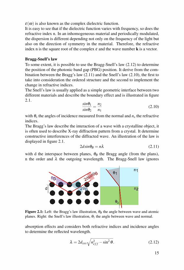
Bragg-Snell’s lawTo some extent, it is possible to use the Bragg-Snell’s law (2.12) to determinethe position of the photonic band gap (PBG) position. It derive from the com-bination between the Bragg’s law (2.11) and the Snell’s law (2.10), the first totake into consideration the ordered structure and the second to implement thechange in refractive indices.The Snell’s law is usually applied as a simple geometric interface between twodifferent materials and describe the boundary effect and is illustrated in figure2.1.
sinθ1
sinθ2=
n2
n1(2.10)
with θx the angles of incidence measured from the normal and nx the refractiveindices.The Bragg’s law describe the interaction of a wave with a crystalline object, itis often used to describe X-ray diffraction pattern from a crystal. It determineconstructive interferences of the diffracted wave. An illustration of the law isdisplayed in figure 2.1.
2dsinθB = nλ (2.11)
with d the interspace between planes, θB the Bragg angle (from the plans),n the order and λ the outgoing wavelength. The Bragg-Snell law ignores
Figure 2.1: Left: the Bragg’s law illustration, θB the angle between wave and atomicplanes. Right: the Snell’s law illustration, θ1 the angle between wave and normal.
absorption effects and considers both refractive indices and incidence anglesto determine the reflected wavelength.
λ = 2dxxx
√n2
e f f − sin2θ . (2.12)
15

In the case that the close-packed (111) planes are parallel to the top interface:
d111 = D×√
23, (2.13)
with D the periodicity or lattice constant, dxxx the interspace between planes,ne f f the refractive index of the whole structure and θ the angle of incidenceonto the surface of the material (from the normal). An illustrated version ofthe Bragg-Snell law is shown in figure 2.2. Light is refracted at the surface ofthe material and diffracted inside the material.The expression of ne f f can be easily interpreted in the case of two materialswith a real refractive index in the considered range of calculation. It is howeverdifficult for multi-layered materials and/or for material with absorption (witha complex refractive index).
Figure 2.2: Some of the interferences will be constructive while some will be destruc-tive. Equation 2.12 determines the constructive interference.
2.2 Photonic band structuresPhotonic crystals are a particular phenomenon of light-matter interaction. Byalternating two dielectrics periodically, it is possible to create conditions onthe light propagation[20]. The light propagation can be described mathemat-ically in the reciprocal space and forms bands of allowed propagation in thestructure. We now describe the reciprocal space and the band theory.
2.2.1 Reciprocal spaceReciprocal space is a convenient mathematical space corresponding to theFourier transform of real space. In solid state physics, it is usual to define
16
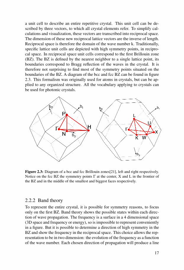
a unit cell to describe an entire repetitive crystal. This unit cell can be de-scribed by three vectors, to which all crystal elements refer. To simplify cal-culations and visualization, these vectors are transcribed into reciprocal space.The dimension of these new reciprocal lattice vectors are the inverse of length.Reciprocal space is therefore the domain of the wave number k. Traditionally,specific lattice unit cells are depicted with high symmetry points, in recipro-cal space. In reciprocal space unit cells correspond to the first Brillouin zone(BZ). The BZ is defined by the nearest neighbor to a single lattice point, itsboundaries correspond to Bragg reflection of the waves in the crystal. It istherefore not surprising to find most of the symmetry points situated on theboundaries of the BZ. A diagram of the bcc and fcc BZ can be found in figure2.3. This formalism was originally used for atoms in crystals, but can be ap-plied to any organized structure. All the vocabulary applying to crystals canbe used for photonic crystals.
Figure 2.3: Diagram of a bcc and fcc Brillouin zones[21], left and right respectively.Notice on the fcc BZ the symmetry points Γ at the center, X and L in the frontier ofthe BZ and in the middle of the smallest and biggest faces respectively.
2.2.2 Band theoryTo represent the entire crystal, it is possible for symmetry reasons, to focusonly on the first BZ. Band theory shows the possible states within each direc-tion of wave propagation. The frequency is a surface in a 4 dimensional space(3D space and frequency or energy), so is impossible to represent convenientlyin a figure. But it is possible to determine a direction of high symmetry in theBZ and show the frequency in the reciprocal space. This choice allows the rep-resentation to be in two dimension: the evolution of the frequency as a functionof the wave number. Each chosen direction of propagation will produce a line
17

in the graph of ω(K). To create a band structure, different directions are cho-sen and each line is added to the graph, forming bands of allowed states. Fora photonic material, the band diagram represents the dispersion relation. Anexample of a simulated band structure of an alumina inverse opal is presentedin figure 2.4, with a partial PBG identified in green at 313nm.
Figure 2.4: Simulated band structure of an alumina inverse opal with 160nm perid-iocity. The partial PBG is marked with a thick green band at a/λ = 0.72
2.3 Structural gap2.3.1 Band gap: definitionUsually, by definition, a band gap is an electronic band gap found in semicon-ductors and insulators. It represents a range in energy forbidden in the entirecrystal for all electrons and delimits the difference between occupied states (orvalence band) and unoccupied states (or conduction band). In a band structurethe gap appears as an absence of bands. It is possible of course to have localgaps, which do not extend in all directions. What about a photonic band gap?A photonic band gap would appear similar in a photonic band structure: anabsence of bands. But the energy gap, corresponding to a wavelength gap,does not define occupied states and unoccupied states. The signification ofa photonic band gap is that photons with an energy within the PBG cannotpenetrate inside the material.
18
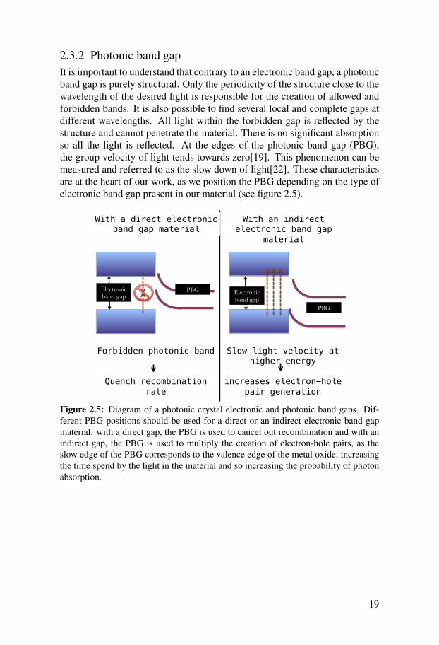
2.3.2 Photonic band gapIt is important to understand that contrary to an electronic band gap, a photonicband gap is purely structural. Only the periodicity of the structure close to thewavelength of the desired light is responsible for the creation of allowed andforbidden bands. It is also possible to find several local and complete gaps atdifferent wavelengths. All light within the forbidden gap is reflected by thestructure and cannot penetrate the material. There is no significant absorptionso all the light is reflected. At the edges of the photonic band gap (PBG),the group velocity of light tends towards zero[19]. This phenomenon can bemeasured and referred to as the slow down of light[22]. These characteristicsare at the heart of our work, as we position the PBG depending on the type ofelectronic band gap present in our material (see figure 2.5).
With a direct electronic band gap material !
With an indirect electronic band gap
material !
Forbidden photonic band !!!
Quench recombination rate !
Slow light velocity at higher energy !
!increases electron-hole
pair generation !
PBG
PBG
Electronic band gap
Electronic band gap
Figure 2.5: Diagram of a photonic crystal electronic and photonic band gaps. Dif-ferent PBG positions should be used for a direct or an indirect electronic band gapmaterial: with a direct gap, the PBG is used to cancel out recombination and with anindirect gap, the PBG is used to multiply the creation of electron-hole pairs, as theslow edge of the PBG corresponds to the valence edge of the metal oxide, increasingthe time spend by the light in the material and so increasing the probability of photonabsorption.
19
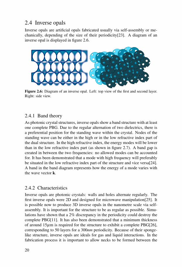
2.4 Inverse opalsInverse opals are artificial opals fabricated usually via self-assembly or me-chanically, depending of the size of their periodicity[23]. A diagram of aninverse opal is displayed in figure 2.6.
Figure 2.6: Diagram of an inverse opal. Left: top view of the first and second layer.Right: side view.
2.4.1 Band theoryAs photonic crystal structures, inverse opals show a band structure with at leastone complete PBG. Due to the regular alternation of two dielectrics, there isa preferential position for the standing wave within the crystal. Nodes of thestanding wave can be either in the high or in the low refractive index part ofthe dual structure. In the high refractive index, the energy modes will be lowerthan in the low refractive index part (as shown in figure 2.7). A band gap iscreated in between the two frequencies: no allowed modes can be accountedfor. It has been demonstrated that a mode with high frequency will preferablybe situated in the low refractive index part of the structure and vice versa[24].A band in the band diagram represents how the energy of a mode varies withthe wave vector k.
2.4.2 CharacteristicsInverse opals are photonic crystals: walls and holes alternate regularly. Thefirst inverse opals were 2D and designed for microwave manipulation[25]. Itis possible now to produce 3D inverse opals in the nanometre scale via self-assembly. It is important for the structure to be as regular as possible. Simu-lations have shown that a 2% discrepancy in the periodicity could destroy thecomplete PBG[11]. It has also been demonstrated that a minimum thicknessof around 15µm is required for the structure to exhibit a complete PBG[26],corresponding to 50 layers for a 300nm periodicity. Because of their sponge-like structure, inverse opals are ideals for gas and liquid interactions. In thefabrication process it is important to allow necks to be formed between the
20
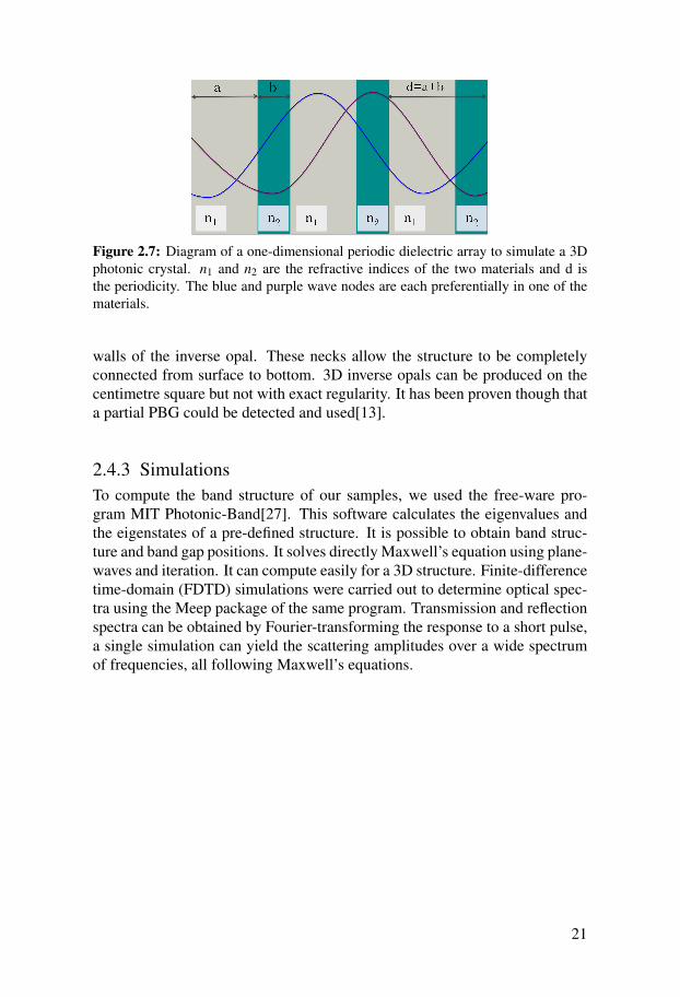
Figure 2.7: Diagram of a one-dimensional periodic dielectric array to simulate a 3Dphotonic crystal. n1 and n2 are the refractive indices of the two materials and d isthe periodicity. The blue and purple wave nodes are each preferentially in one of thematerials.
walls of the inverse opal. These necks allow the structure to be completelyconnected from surface to bottom. 3D inverse opals can be produced on thecentimetre square but not with exact regularity. It has been proven though thata partial PBG could be detected and used[13].
2.4.3 SimulationsTo compute the band structure of our samples, we used the free-ware pro-gram MIT Photonic-Band[27]. This software calculates the eigenvalues andthe eigenstates of a pre-defined structure. It is possible to obtain band struc-ture and band gap positions. It solves directly Maxwell’s equation using plane-waves and iteration. It can compute easily for a 3D structure. Finite-differencetime-domain (FDTD) simulations were carried out to determine optical spec-tra using the Meep package of the same program. Transmission and reflectionspectra can be obtained by Fourier-transforming the response to a short pulse,a single simulation can yield the scattering amplitudes over a wide spectrumof frequencies, all following Maxwell’s equations.
21
3. Green nanotechnologies
Nanotechnologies have not only increased our comprehension of materials butexpanded their limitations. In the nano-world, surface is the key factor, whichis related to size. As the size decreases, the surface increases for a reducedvolume. Size effects are very important for the use of nano-objects in newtechnologies. There is tremendous research link to the size and the effect ofthe size of a material. How many atoms is it necessary to aggregate to obtain ananoparticle of metal? Why can a nanoparticle absorb a different wavelengththan the macroscopic lump of the same material? It is that fundamental tounderstand that not only do nanoparticles exist naturally, but that also theiruse has been demonstrated as far back as in the Roman Empire (The Lycurguscup[28]). It is then comprehensible that green nanotechnologies were bornfrom nanotechnologies . Concerning itself with nano (dwarf in latin), greennanotechnologies are oriented towards renewable energy and ecological solu-tions to pollution problems. As nanoparticles are often versatile, inexpensiveand natural, their applications are broad and omnipresent. Above all, artificialinverse opals have been integrated in this vast research topic.
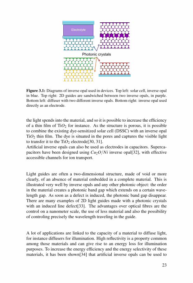
3.1 Solar cellsIs it really necessary to recall how important solar cell research is to our so-ciety? With an increasing population and an increase in energy consumption,harvesting an unlimited energy source is of extreme importance. Solar cellsare unfortunately not as efficient in converting the source of energy (the sun) topower as fossils oils or nuclear power. Research is focusing on increasing theefficiency of solar modules and reaching an efficiency of above 30%[29]. Nat-urally, inverse opals, as back-reflectors or as electrodes, have been integratedin this effort (see figure 3.1).
Back-reflectors are a layer used as a mirror for the light in a solar cell: the lightthat passes trough the solar cell and that does not participate in the making ofelectron-hole pairs (into the working of the solar cell), can be reflected backinto the solar cell and has another chance to be absorbed by it. The principle israther simple, it is sufficient to match the photonic band gap to the absorptionedge of the solar cell.By tuning the inverse opal photonic band gap it is possible to increase the time
22
Electrolyte
Photonic crystals
Figure 3.1: Diagrams of inverse opal used in devices. Top left: solar cell, inverse opalin blue. Top right: 2D guides are sandwiched between two inverse opals, in purple.Bottom left: diffuser with two different inverse opals. Bottom right: inverse opal useddirectly as an electrode.
the light spends into the material, and so it is possible to increase the efficiencyof a thin film of TiO2 for instance. As the structure is porous, it is possibleto combine the existing dye-sensitized solar cell (DSSC) with an inverse opalTiO2 thin film. The dye is situated in the pores and captures the visible lightto transfer it to the TiO2 electrode[30, 31].Artificial inverse opals can also be used as electrodes in capacitors. Superca-pacitors have been designed using Cu2O/Ni inverse opal[32], with effectiveaccessible channels for ion transport.
Light guides are often a two-dimensional structure, made of void or moreclearly, of an absence of material embedded in a complete material. This isillustrated very well by inverse opals and any other photonic object: the orderin the material creates a photonic band gap which extends on a certain wave-length gap. As soon as a defect is induced, the photonic band gap disappear.There are many examples of 2D light guides made with a photonic crystalswith an induced line defect[33]. The advantages over optical fibres are thecontrol on a nanometer scale, the use of less material and also the possibilityof controling precisely the wavelength traveling in the guide.
A lot of applications are linked to the capacity of a material to diffuse light,for instance diffusers for illumination. High reflectivity is a property commonamong those materials and can give rise to an energy loss for illuminationpurposes. To increase the energy efficiency and the energy selectivity of thesematerials, it has been shown[34] that artificial inverse opals can be used to
23

trap the reflected light by combining two different photonic crystals, thus it ispossible to confine the back- scattered light and reduce the energy loss in theback direction.
3.2 NanoplasmonicsPlasmonic is a phenomenon held only by metals since it involves free elec-trons. Plasmons are quasi-particles created in a metal when their rather freeelectrons oscillate as a whole. These oscillations are often induced by light.Nanoplasmonics deals, unsurprisingly, with the plasmonic effects appearingin nano-objects[35].
A collective oscillation of electrons forms a plasmon: it is possible to obtainvolume plasmons and surface plasmons. Surface plasmons can be initiatedby a less energetic light and are the most commonly used in nanoplasmonics.Plasmons enhance any effect induced by the light absorption. It is thereforepossible to observe the effect of surface plasmons from few nanoparticles.This enhancement provides key features for electronic applications and forresearch.
Gold nanoparticles can be synthetized chemically and rather easily, with dif-ferent size and shape[36]. The fabrication process was known in the RomanEmpire, as we have seen with the Lythurgis cup, but the knowledge of proper-ties and control of the material are more recent. Gold is a fascinating material,not only for its social value, but also for its plasmons. Gold nanoparticlescreate plasmons with visible light, which enhances visible light absorption.These properties can be used to increase the efficiency of a light absorber andgold nanoparticles have been used in solar cells and also in photocatalysts[37].They are easy to handle and easy to fabricate, non pollutant and it is not nec-essary to use a large volume.
3.3 PhotocatalysisPhotocatalysis is the ideal solution to most of our pollution problems. It useslight as an energy source to facilitate chemical reactions without the use ofanother external energy source (like heat or electricity). Catalytic materialsprovide support in a chemical reaction but are not consumed in the reaction.Most of the photocatalysts that have been investigated to date, are metal ox-ides. Since the intensity of the solar spectrum at earth level occurs in theUV-vis-near IR region, the ideal photocatalyst should absorb visible light or
24
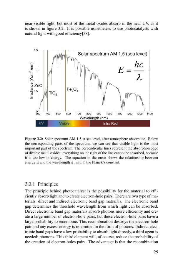
near-visible light, but most of the metal oxides absorb in the near UV, as itis shown in figure 3.2. It is possible nonetheless to use photocatalysts withnatural light with good efficiency[38].
Fe2O3 TiO2
ZnO
Visible Infra Red UV
E = hc!
Figure 3.2: Solar spectrum AM 1.5 at sea level, after atmosphere absorption. Belowthe corresponding parts of the spectrum, we can see that visible light is the mostimportant part of the spectrum. The perpendicular lines represent the absorption edgeof diverse metal oxides: everything on the right of the line cannot be absorbed, becauseit is too low in energy. The equation in the onset shows the relationship betweenenergy E and the wavelength λ , with h the Planck’s constant.
3.3.1 PrinciplesThe principle behind photocatalyst is the possibility for the material to effi-ciently absorb light and to create electron-hole pairs. There are two type of ma-terials: direct and indirect electronic band gap materials. The electronic bandgap determines the threshold wavelength from which light can be absorbed.Direct electronic band gap materials absorb photons more efficiently and cre-ate a large number of electron-hole pairs, but these electron-hole pairs have alarge probability to recombine. This recombination destroys the electron-holepair and any excess energy is re-emitted in the form of photons. Indirect elec-tronic band gaps have a low probability to absorb light directly, a third agent isneeded: phonons. This third element will, of course, reduce the probability ofthe creation of electron-holes pairs. The advantage is that the recombination
25
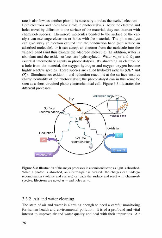
rate is also low, as another phonon is necessary to relax the excited electron.Both electrons and holes have a role in photocatalysis. After the electron andholes travel by diffusion to the surface of the material, they can interact withchemisorb species. Chemisorb molecules bonded to the surface of the cat-alyst can exchange electrons or holes with the material. The photocatalystcan give away an electron excited into the conduction band (and reduce anadsorbed molecule), or it can accept an electron from the molecule into thevalence band (and thus oxidize the adsorbed molecule). In addition, water isabundant and the oxide surfaces are hydroxylated. Water vapor and O2 areessential intermediary agents in photocatalysis. By absorbing an electron ora hole from the material, the oxygen-hydrogen and oxygen-oxygen becomehighly reactive species. These species are called hydroxyl radicals (OH• andO•
2). Simultaneous oxidation and reduction reactions at the surface ensurescharge neutrality of the photocatalyst; the photocatalyst can in this sense beseen as a short-circuited photo-electrochemical cell. Figure 3.3 illustrates thedifferent processes.
Figure 3.3: Illustration of the major processes in a semiconductor, as light is absorbed.When a photon is absorbed, an electron-pair is created: the charges can undergorecombination (volume and surface) or reach the surface and react with chemisorbspecies. Electrons are noted as − and holes as +.
3.3.2 Air and water cleaningThe state of air and water is alarming enough to need a careful monitoringfor human health and environmental pollution. It is of a profound and vitalinterest to improve air and water quality and deal with their impurities. Air
26

pollution is today a major cause of adverse health effects. Water is an es-sential part of our life and a shortage of drinkable water is a real and presentproblem for a lot of people. This is why it is important to search for newways to treat water and air and reduce pollutants. It has been shown[38–40]that photocatalysis can be used to oxidize virtually all organic compounds intoharmless products and eventually into just water, CO2 and trace mineral acids.In fact, TiO2 photocatalysts have a higher red-ox potential than, for example,H2O2 and ozone treatment. In addition, photocatalysts have been shown tohave beneficial anti-bacterial properties, and can be used for disinfection, andsterilization of surfaces
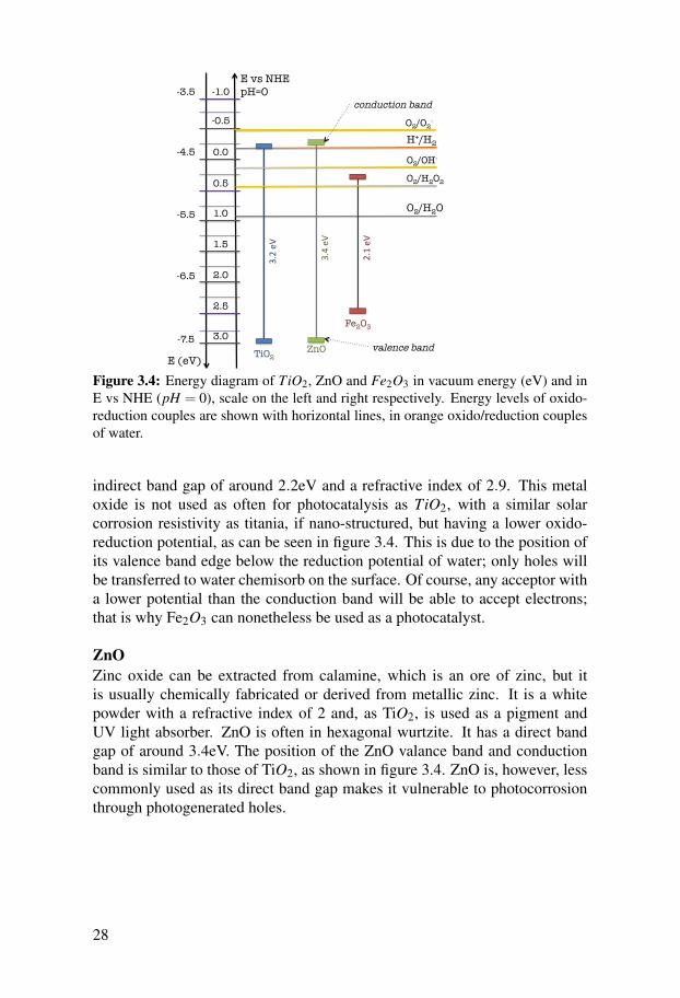
3.3.3 Metal oxides descriptionTiO2Titanium dioxide is a natural mineral that can be extracted from ilmenite(FeTiO3) and is a wide-band gap n-type semiconductor. The appearance ofTiO2 powder is white and has a very low density. As the refractive index ofthis metal oxide is high (2.5), it has been used as a pigment in paint, food, cos-metics and toothpaste. It is also used in suncreams for its capacity to absorbUV light. Some other applications can be associated to this capacity, notablyits photocatalytic effect[41]. Titanium dioxide can be found in three differentmain crystallographic forms, the anatase form being the most use in photo-catalysis, since it has been shown[41–43] to have a higher activity than therutile form. Both forms are similar, and can be described as chains of TiO6 oc-tahedra, but oxygen-titanium distances are shorter and titanium-titanium dis-tance are longer for the anatase form. This affects the band structure of themetal oxide and therefore the band gap. Anatase TiO2 has an indirect bandgap of around 3.2eV. It is possible to dope with metals, such as Pt or N, toincrease the light absorption of the photocatalyst in the visible range.As shown in figure 3.4, the electronic band edges of titanium dioxide are ide-ally placed: the valence band is situated below the oxidation potential of waterwhile the conduction band is just above the reduction potential of water. Sincewater plays a major role in the photocatalytic process, it can be seen from theenergy diagram that TiO2 has a strong photocatalytic effect. The reduction po-tential (H+/H2) is just below the conduction band and the oxidation potential(O2/H2O) is above the valence band of anatase.
Fe2O3Iron (|||) oxide is one of the main oxides of iron which can be found naturallyin hematite. The colour of Fe2O3 powder is deep red, therefore, it is alsoused as a pigment (for instance in Falu red paint). But most commonly it isused for steel and iron industrial production. The only phase that is used as aphotocatalyst is the α −Fe2O3, which is rhombohedral corundum. It has an
27
0.5
1.0
0.0
1.5
2.0
2.5
3.0
-0.5
-1.0 -3.5
-4.5
-5.5
-6.5
-7.5
E (eV)
E vs NHE pH=0
H+/H2
O2/H2O
TiO2 ZnO
Fe2O3
O2/OH-
O2/H2O2
O2/O2-
3.2 eV
3.4 eV
2.1 eV
valence band
conduction band
Figure 3.4: Energy diagram of TiO2, ZnO and Fe2O3 in vacuum energy (eV) and inE vs NHE (pH = 0), scale on the left and right respectively. Energy levels of oxido-reduction couples are shown with horizontal lines, in orange oxido/reduction couplesof water.
indirect band gap of around 2.2eV and a refractive index of 2.9. This metaloxide is not used as often for photocatalysis as TiO2, with a similar solarcorrosion resistivity as titania, if nano-structured, but having a lower oxido-reduction potential, as can be seen in figure 3.4. This is due to the position ofits valence band edge below the reduction potential of water; only holes willbe transferred to water chemisorb on the surface. Of course, any acceptor witha lower potential than the conduction band will be able to accept electrons;that is why Fe2O3 can nonetheless be used as a photocatalyst.
ZnOZinc oxide can be extracted from calamine, which is an ore of zinc, but itis usually chemically fabricated or derived from metallic zinc. It is a whitepowder with a refractive index of 2 and, as TiO2, is used as a pigment andUV light absorber. ZnO is often in hexagonal wurtzite. It has a direct bandgap of around 3.4eV. The position of the ZnO valance band and conductionband is similar to those of TiO2, as shown in figure 3.4. ZnO is, however, lesscommonly used as its direct band gap makes it vulnerable to photocorrosionthrough photogenerated holes.
28
4. Experimental conditions
4.1 Instruments4.1.1 Electron microscopy
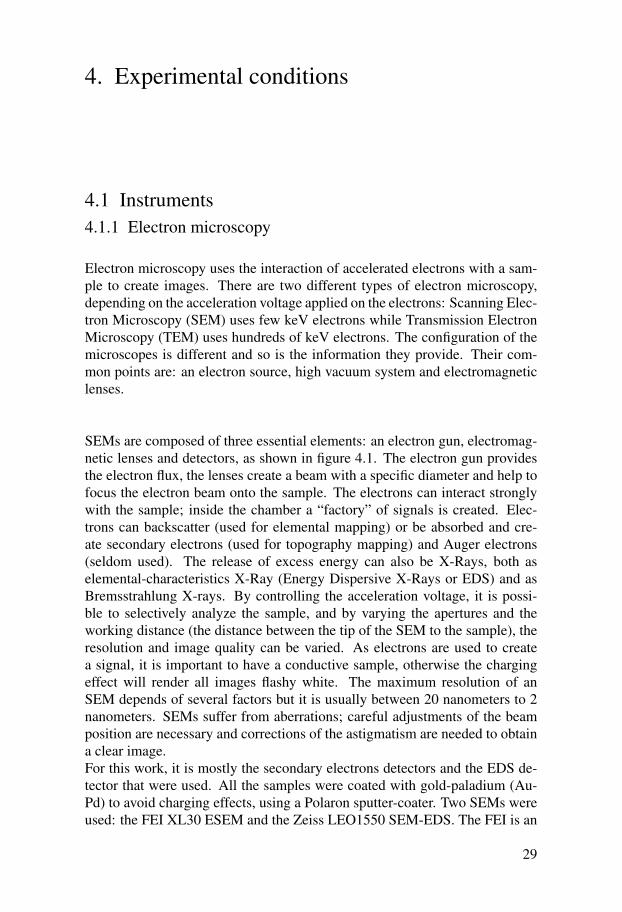
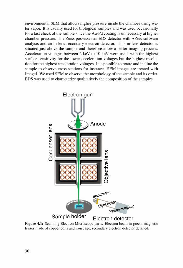
Electron microscopy uses the interaction of accelerated electrons with a sam-ple to create images. There are two different types of electron microscopy,depending on the acceleration voltage applied on the electrons: Scanning Elec-tron Microscopy (SEM) uses few keV electrons while Transmission ElectronMicroscopy (TEM) uses hundreds of keV electrons. The configuration of themicroscopes is different and so is the information they provide. Their com-mon points are: an electron source, high vacuum system and electromagneticlenses.
SEMs are composed of three essential elements: an electron gun, electromag-netic lenses and detectors, as shown in figure 4.1. The electron gun providesthe electron flux, the lenses create a beam with a specific diameter and help tofocus the electron beam onto the sample. The electrons can interact stronglywith the sample; inside the chamber a “factory” of signals is created. Elec-trons can backscatter (used for elemental mapping) or be absorbed and cre-ate secondary electrons (used for topography mapping) and Auger electrons(seldom used). The release of excess energy can also be X-Rays, both aselemental-characteristics X-Ray (Energy Dispersive X-Rays or EDS) and asBremsstrahlung X-rays. By controlling the acceleration voltage, it is possi-ble to selectively analyze the sample, and by varying the apertures and theworking distance (the distance between the tip of the SEM to the sample), theresolution and image quality can be varied. As electrons are used to createa signal, it is important to have a conductive sample, otherwise the chargingeffect will render all images flashy white. The maximum resolution of anSEM depends of several factors but it is usually between 20 nanometers to 2nanometers. SEMs suffer from aberrations; careful adjustments of the beamposition are necessary and corrections of the astigmatism are needed to obtaina clear image.For this work, it is mostly the secondary electrons detectors and the EDS de-tector that were used. All the samples were coated with gold-paladium (Au-Pd) to avoid charging effects, using a Polaron sputter-coater. Two SEMs wereused: the FEI XL30 ESEM and the Zeiss LEO1550 SEM-EDS. The FEI is an
29
environmental SEM that allows higher pressure inside the chamber using wa-ter vapor. It is usually used for biological samples and was used occasionallyfor a fast check of the sample since the Au-Pd coating is unnecessary at higherchamber pressure. The Zeiss possesses an EDS detector with AZtec softwareanalysis and an in-lens secondary electron detector. This in-lens detector issituated just above the sample and therefore allow a better imaging process.Acceleration voltages between 2 keV to 10 keV were used, with the highestsurface sensitivity for the lower acceleration voltages but the highest resolu-tion for the highest acceleration voltages. It is possible to rotate and incline thesample to observe cross-sections for instance. SEM images are treated withImageJ. We used SEM to observe the morphology of the sample and its order.EDS was used to characterize qualitatively the composition of the samples.
Figure 4.1: Scanning Electron Microscope parts. Electron beam in green, magneticlenses made of copper coils and iron cage, secondary electron detector detailed.
30
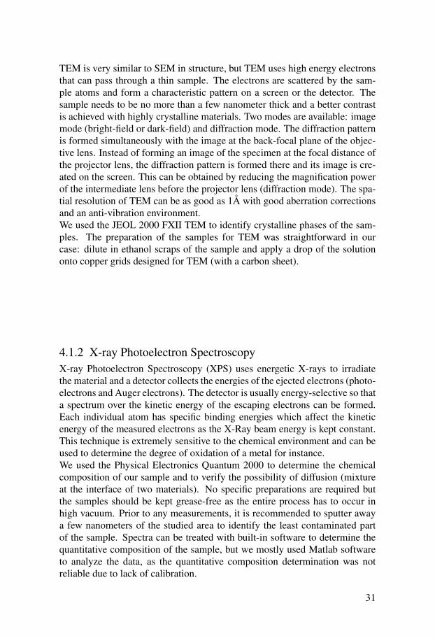
TEM is very similar to SEM in structure, but TEM uses high energy electronsthat can pass through a thin sample. The electrons are scattered by the sam-ple atoms and form a characteristic pattern on a screen or the detector. Thesample needs to be no more than a few nanometer thick and a better contrastis achieved with highly crystalline materials. Two modes are available: imagemode (bright-field or dark-field) and diffraction mode. The diffraction patternis formed simultaneously with the image at the back-focal plane of the objec-tive lens. Instead of forming an image of the specimen at the focal distance ofthe projector lens, the diffraction pattern is formed there and its image is cre-ated on the screen. This can be obtained by reducing the magnification powerof the intermediate lens before the projector lens (diffraction mode). The spa-tial resolution of TEM can be as good as 1Å with good aberration correctionsand an anti-vibration environment.We used the JEOL 2000 FXII TEM to identify crystalline phases of the sam-ples. The preparation of the samples for TEM was straightforward in ourcase: dilute in ethanol scraps of the sample and apply a drop of the solutiononto copper grids designed for TEM (with a carbon sheet).
4.1.2 X-ray Photoelectron SpectroscopyX-ray Photoelectron Spectroscopy (XPS) uses energetic X-rays to irradiatethe material and a detector collects the energies of the ejected electrons (photo-electrons and Auger electrons). The detector is usually energy-selective so thata spectrum over the kinetic energy of the escaping electrons can be formed.Each individual atom has specific binding energies which affect the kineticenergy of the measured electrons as the X-Ray beam energy is kept constant.This technique is extremely sensitive to the chemical environment and can beused to determine the degree of oxidation of a metal for instance.We used the Physical Electronics Quantum 2000 to determine the chemicalcomposition of our sample and to verify the possibility of diffusion (mixtureat the interface of two materials). No specific preparations are required butthe samples should be kept grease-free as the entire process has to occur inhigh vacuum. Prior to any measurements, it is recommended to sputter awaya few nanometers of the studied area to identify the least contaminated partof the sample. Spectra can be treated with built-in software to determine thequantitative composition of the sample, but we mostly used Matlab softwareto analyze the data, as the quantitative composition determination was notreliable due to lack of calibration.
31
4.1.3 X-Ray DiffractionX-Ray Diffraction (XRD) is the process by which X-rays are sent towards thesample, penetrate the sample and are deviated out of the sample in reflectionwith a characteristic angle. X-rays with a characteristic wavelength can beused to scan the various angles at which they are reflected by the sample. Ifthe sample is non-crystalline, features will be broad so that the XRD spectrumhas broad peaks. If the sample is crystalline, however, atomic planes with spe-cific orientation and specific atom species are repeated periodically and createan enhancement of the reflected X-ray at a particular angle. To obtain a highsignal from a thin film, it is usually the grazing incidence XRD configurationthat is used.SIEMENS D5000 is a grazing incidence XRD with a theta-2theta configura-tion, which means that the angle theta between the X-Ray source and the sam-ple defines the simultaneous position of the detector. As the sample rotatesan angle of theta, the detector position shifts an angle of 2-theta, followingBragg’s law of diffraction (equation4.1).
λ = 2dsinθ (4.1)
with λ the X-ray wavelength, d the space between two lattice planes and θ theangle between the incident light and the scattering planes. XRD was used todetermine if the samples were crystalline and what type of crystal phases theyrepresented. Built-in software can be used to treat the spectra and search thedata-bank of XRD spectra to identify species and crystalline phases.
4.1.4 UV-VIS spectrophotometry
Fast and non-intrusive, ultra-violet and visible light spectrophotometry is animportant experimental setup for our work. The principle of the experimentis very simple: light is incident onto a sample and either transmitted light orreflected light is recorded. The spectrophotometer can either use a specific in-cident wavelength or detect a specific wavelength. Spectra of intensity versuswavelength are recorded. It is possible to obtain information of structure andcomposition via these spectra. A background or reference spectrum must berecorded to obtain correct sample spectra. Total light coming from the sam-ple can be divided into two categories: specular/regular light and diffuse light.Specular light is light reflected at the same angle as the angle of incidence, reg-ular light is light transmitted through the sample without change of direction,while diffuse light is light originating from surface roughness and scatteringcentres in random directions, both in reflection and transmission. If the sumof the total light measured in transmission and in reflection is not equal to theincoming light, then the sample absorbs part of the light. Optical properties
32
of materials are very useful for characterising a sample; it is possible, for in-stance, to calculate the absorption coefficient. Two different setups were usedon our samples: a classic UV-VIS spectrophotometer with fixed light sourceand fixed sample position and a home-made setup with fixed light source butmobile sample and detector. No specific preparations were required prior tothe measurements.
A Perkin Elmer Lambda900 was used as an everyday tool to verify the qual-ity of the samples. A diagram of the optical path is displayed in figure 4.2.The Lambda900 is equipped with an integrating sphere, so both total (white-coloured beam ending) and diffuse (dark-cone beam ending) can be recordedin transmission. A tungsten-halogen and a deuterium lamp were used to cre-ate illumination between 175 nm and 3300 nm. We used only the windowbetween 200 nm and 1300 nm, for our interest lay mostly in the visible lightpart of the spectrum. We use steps of 1 nm to scan the wavelength windowand a 5 mm diameter mask. Most of the spectra were recorded in transmis-sion only, both total and diffuse light. To plot a spectrum of a sample, it isimportant to treat the data first. Spectra were analyzed and plotted via Matlabsoftware.
33
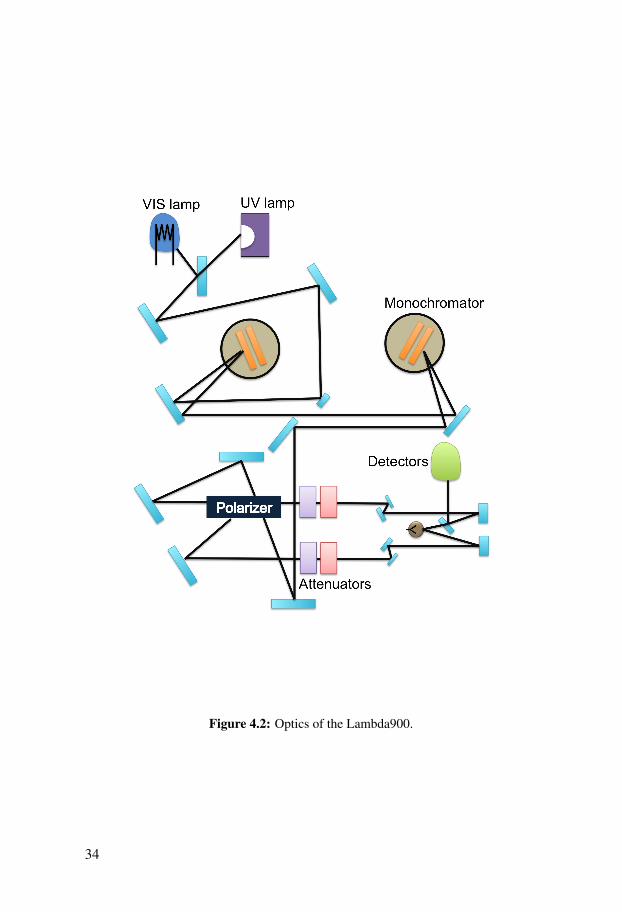
Figure 4.2: Optics of the Lambda900.
34
For the transmission mode:
Tspec = Stot −Sdi f f , (4.2)
with Tspec the regular transmission, Stot the signal of total transmitted light andSdi f f the signal of diffused light.For the reflection mode:
Rspec = (Stot −Sdi f f )∗ k, (4.3)
with Rspec the specular reflection, Stot the signal of total reflection, Sdi f f thesignal of diffused reflection and k a correction factor specific to the instru-ment.
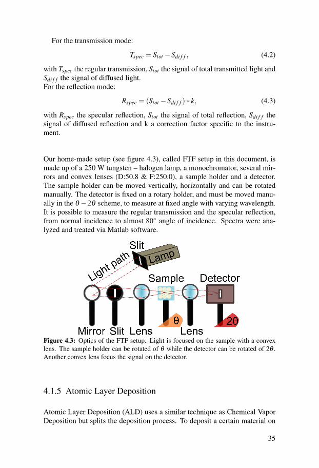
Our home-made setup (see figure 4.3), called FTF setup in this document, ismade up of a 250 W tungsten – halogen lamp, a monochromator, several mir-rors and convex lenses (D:50.8 & F:250.0), a sample holder and a detector.The sample holder can be moved vertically, horizontally and can be rotatedmanually. The detector is fixed on a rotary holder, and must be moved manu-ally in the θ −2θ scheme, to measure at fixed angle with varying wavelength.It is possible to measure the regular transmission and the specular reflection,from normal incidence to almost 80◦ angle of incidence. Spectra were ana-lyzed and treated via Matlab software.
Figure 4.3: Optics of the FTF setup. Light is focused on the sample with a convexlens. The sample holder can be rotated of θ while the detector can be rotated of 2θ .Another convex lens focus the signal on the detector.
4.1.5 Atomic Layer Deposition
Atomic Layer Deposition (ALD) uses a similar technique as Chemical VaporDeposition but splits the deposition process. To deposit a certain material on
35
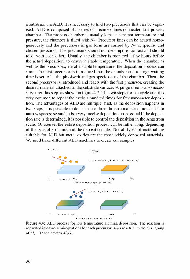
a substrate via ALD, it is necessary to find two precursors that can be vapor-ised. ALD is composed of a series of precursor lines connected to a processchamber. The process chamber is usually kept at constant temperature andpressure, the chamber is filled with N2. Precursor lines can be heated homo-geneously and the precursors in gas form are carried by N2 at specific andchosen pressures. The precursors should not decompose too fast and shouldreact with each other. Usually, the chamber is prepared a few hours beforethe actual deposition, to ensure a stable temperature. When the chamber aswell as the precursors, are at a stable temperature, the deposition process canstart. The first precursor is introduced into the chamber and a purge waitingtime is set to let the physisorb and gas species out of the chamber. Then, thesecond precursor is introduced and reacts with the first precursor, creating thedesired material attached to the substrate surface. A purge time is also neces-sary after this step, as shown in figure 4.7. The two steps form a cycle and it isvery common to repeat the cycle a hundred times for few nanometer deposi-tion. The advantages of ALD are multiple: first, as the deposition happens intwo steps, it is possible to deposit onto three dimensional structures and intonarrow spaces; second, it is a very precise deposition process and if the deposi-tion rate is determined, it is possible to control the deposition in the Ångströmscale. Of course, the entire deposition process can be rather long, dependingof the type of structure and the deposition rate. Not all types of material aresuitable for ALD but metal oxides are the most widely deposited materials.We used three different ALD machines to create our samples.
Figure 4.4: ALD process for low temperature alumina deposition. The reaction isseparated into two semi-equations for each precursor: H2O reacts with the CH3 groupof Al2 −O and creates Al2O3.
36
The Picosun Sunale (R-series) ALD was used to deposit Al2O3 at around70◦C. The precursors used were: Trimethylaluminum (TMA) and water (H2O).The deposition rate onto a flat substrate was around 1/cycle.
The BENEQ TFS 200 has six precursors lines and has both thermal and plasmaALD. It was used to deposit TiO2 at around 200◦C. The precursors used were:Titaniumtetrachloride (TiCl4) and water (H2O). The deposition cycle is de-tailed in table 4.1. The reaction scheme is not clearly defined yet, TiCl4 react-ing with surface OH is the generally accepted mechanism[44]. The depositionrate onto a flat substrate was around 0.8/cycle.
Table 4.1: A typical cycle used to deposit TiO2. The cycle is divided into two mainparts: TiCl4 and H2O introduction. The pulse time is doubled for water.
Precursors Carrier gas flow (sccm) Pulse time (s) Purge time (s)
TiCl4 600 0.25 20TiCl4 600 0.25 40
H2O 600 0.5 20H2O 600 0.5 40
The Picosun R200 is a ten-precursors ALD with substrate temperature up to500◦C. It was used to deposit Al2O3 at around 70◦C and TiO2 at around200◦C. The precursors used were: TMA and H2O, TiCl4 and H2O respec-tively. The deposition cycle for alumina is detailed in table 4.2. We used shortpulses of the same precursor to minimize the precursor consumption, takinginto consideration the close-packing of the 3D structure. Precursors need timeto flow in and out of the structure, but a long precursor pulse would create abigger deposition gradient, so repeated short pulses were used.
4.1.6 Other tools
Ion beam etching was used to remove hundreds of nanometers from the surfaceof the samples. The Oxford Instruments Plasma Technology Ionfab 300 Pluswas used with the parameters depicted in table 4.3
Two different ovens were used to prepare the samples. To evaporate water-based solutions onto the substrates, we used a Memmert UFB400 oven with a52800 cm3 chamber. To anneal and sinter, we used a Nabathern S17 oven withan around 3000 cm3 chamber.
37
Table 4.2: A typical cycle used to deposit Al2O3. Precursors are transported with acarrier gas in to the reaction chamber with a definite flow and time. Once the precursoris introduced, a purging time is necessary to remove un-reacted species before theintroduction of the next precursor.
Precursors Carrier gas flow (sccm) Pulse time (s) Purge time (s)
TMA 100 0.1 20TMA 100 0.1 20TMA 100 0.1 20TMA 100 0.1 60
H2O 200 0.1 20H2O 200 0.1 20H2O 200 0.1 20H2O 200 0.1 60
Table 4.3: Parameters used to remove Al2O3. The beam consists of argon ions, theplaten (sample holder) is cooled below room temperature and we used a beam neu-tralizer.
Acceleration voltage: 400V Beam voltage: 700V
Neutralizer current: 350mA Beam current: 300mA
Argon flow: 7sccm Chiller temperature: 15◦CPlaten angle : -20◦ He cooling flow: 30sccm
A profilometer was used to characterize the surface roughness and the aver-aged deposition thickness of the sample. The Bruker Dektak XT can be usedto create two-dimensional surface profile measurements with a 1Å vertical res-olution. The force applied by the stylus was set as low as possible (1 mg) andthe horizontal resolution was around 0.33µm/point.
4.2 Experimental setup4.2.1 MaterialsAll chemical were used as purchased. Substrates were always cleaned prior toany experiments (see table 4.4 for details). All bead suspensions were soni-cated in an ultra-sonic bath for at least 30 minutes before use.
We used several types of bead suspensions. Most of our work, however, fo-cused on polystyrene latex suspensions (see table 4.5 for details). All the sus-pensions were water-based and had volume concentrations of typically 10%.
38
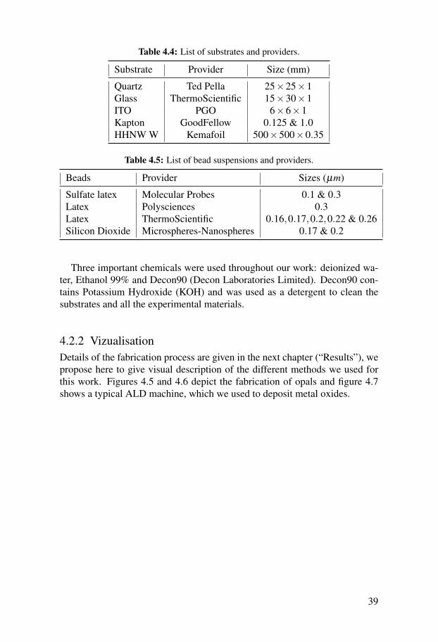
Table 4.4: List of substrates and providers.
Substrate Provider Size (mm)
Quartz Ted Pella 25×25×1Glass ThermoScientific 15×30×1ITO PGO 6×6×1Kapton GoodFellow 0.125 & 1.0HHNW W Kemafoil 500×500×0.35
Table 4.5: List of bead suspensions and providers.
Beads Provider Sizes (µm)
Sulfate latex Molecular Probes 0.1 & 0.3Latex Polysciences 0.3Latex ThermoScientific 0.16,0.17,0.2,0.22 & 0.26Silicon Dioxide Microspheres-Nanospheres 0.17 & 0.2
Three important chemicals were used throughout our work: deionized wa-ter, Ethanol 99% and Decon90 (Decon Laboratories Limited). Decon90 con-tains Potassium Hydroxide (KOH) and was used as a detergent to clean thesubstrates and all the experimental materials.
4.2.2 VizualisationDetails of the fabrication process are given in the next chapter (“Results”), wepropose here to give visual description of the different methods we used forthis work. Figures 4.5 and 4.6 depict the fabrication of opals and figure 4.7shows a typical ALD machine, which we used to deposit metal oxides.
39
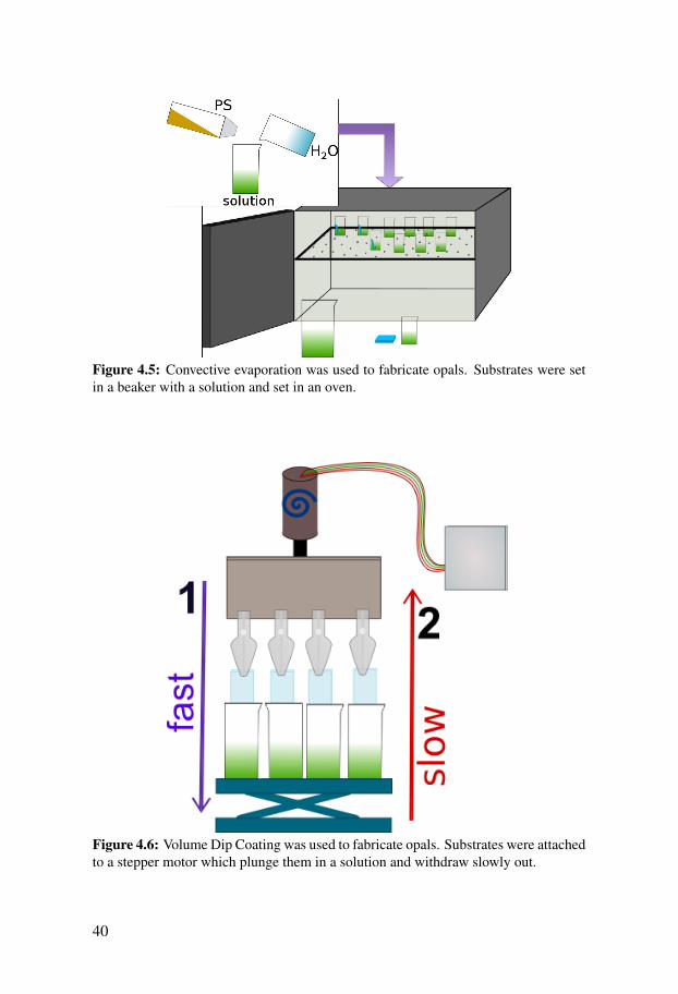
Figure 4.5: Convective evaporation was used to fabricate opals. Substrates were setin a beaker with a solution and set in an oven.
Figure 4.6: Volume Dip Coating was used to fabricate opals. Substrates were attachedto a stepper motor which plunge them in a solution and withdraw slowly out.
40
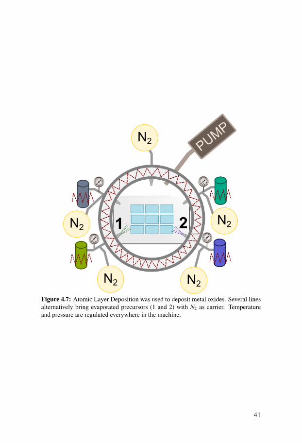
Figure 4.7: Atomic Layer Deposition was used to deposit metal oxides. Several linesalternatively bring evaporated precursors (1 and 2) with N2 as carrier. Temperatureand pressure are regulated everywhere in the machine.
41

5. Results
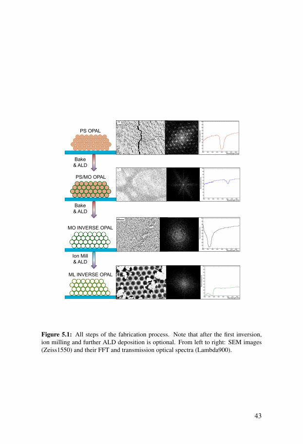
5.1 Overview of inverse opal fabricationThe fabrication of inverse opals can be described in three major steps: prepara-tion, opal fabrication and inverse opal finalisation. A visual summary is shownin figure 5.1.
5.1.1 Step 1: Sample preparationThe preparation of the substrates and solutions is always the same, regardlessof the type of substrate, bead suspension and deposition method. It is impor-tant first to ultra-sonicate the bead suspensions so that the coagulation riskis reduced. While bead suspensions are sonicated, it is possible to sonicatesubstrates in Decon90 diluted in deionized water, to make the surfaces hy-drophilic. After at least 15 minutes, the substrates were rinsed copiously withdeionized water and dried by air flow. Then, it is possible to prepare dilutedsolutions from the bead suspensions.All concentrations were defined as w/v% in g/mL according to equation 5.1:
w/v% =1
(1−Ww)ρw
+ Wwρp
×100, (5.1)
with Ww the weight ratio of polystyrene to latex, ρw the density of water andρp the density of polystyrene.Each preparation was design by the choice of volume concentration:
Volume =Volumetotal ×Desired(w/v%)
Original(w/v%). (5.2)
The solvent used can be deionized water, ethanol or a combination of both. Itis recommended to leave the diluted solution in the ultrasonic bath for at least15 minutes to ensure complete mixing.
5.1.2 Step 2: Opal creationThis method is used to grow artificial opals by self-assembly, a schematic viewof the method is displayed in figure 5.2. Convective evaporation occurs at adrying front between two phases: in our case, the water-based suspension and
42
ML INVERSE OPAL
PS OPAL
Bake & ALD
PS/MO OPAL
Bake & ALD
MO INVERSE OPAL
Ion Mill & ALD
300 340 380 420 460 500 540 580 620 660 700 740 780 8000
10
20
30
40
50
60
70
80
90
100
Wavelength (nm)
Tran
smis
sion
(%)
300 340 380 420 460 500 540 580 620 660 700 740 780 8000
10
20
30
40
50
60
70
80
90
100
Wavelength (nm)
Tran
smis
sion
(%)
300 340 380 420 460 500 540 580 620 660 700 740 780 8000
10
20
30
40
50
60
70
80
90
100
Wavelength (nm)Tr
ansm
issi
on(%
)
300 340 380 420 460 500 540 580 620 660 700 740 780 8000
10
20
30
40
50
60
70
80
90
100
Wavelength (nm)
Tran
smis
sion
(%)
Figure 5.1: All steps of the fabrication process. Note that after the first inversion,ion milling and further ALD deposition is optional. From left to right: SEM images(Zeiss1550) and their FFT and transmission optical spectra (Lambda900).
43
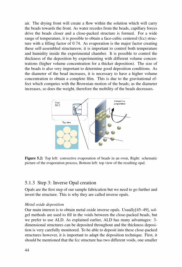
air. The drying front will create a flow within the solution which will carrythe beads towards the front. As water recedes from the beads, capillary forcesdrive the beads closer and a close-packed structure is formed. For a widerange of temperature, it is possible to obtain a face-cubic centered (fcc) struc-ture with a filling factor of 0.74. As evaporation is the major factor creatingthese self-assembled structuresw, it is important to control both temperatureand humidity inside the experimental chamber. It is possible to control thethickness of the deposition by experimenting with different volume concen-trations (higher volume concentration for a thicker deposition). The size ofthe beads is also very important to determine good deposition conditions. Asthe diameter of the bead increases, it is necessary to have a higher volumeconcentration to obtain a complete film. This is due to the gravitational ef-fect which competes with the Brownian motion of the beads; as the diameterincreases, so does the weight, therefore the mobility of the beads decreases.
Figure 5.2: Top left: convective evaporation of beads in an oven, Right: schematicpicture of the evaporation process, Bottom left: top view of the resulting opal.
5.1.3 Step 3: Inverse Opal creationOpals are the first step of our sample fabrication but we need to go further andinvert the structure. This is why they are called inverse opals.
Metal oxide depositionOur main interest is to obtain metal oxide inverse opals. Usually[45–49], sol-gel methods are used to fill in the voids between the close-packed beads, butwe prefer to use ALD. As explained earlier, ALD has many advantages: 3-dimensional structures can be deposited throughout and the thickness deposi-tion is very carefully monitored. To be able to deposit into these close-packedstructures however, it is important to adapt the deposition technique. First, itshould be mentioned that the fcc structure has two different voids, one smaller
44

in volume. This immediately limits the deposition thickness inside the struc-ture: as the smaller voids fill, the access to the structure gets blocked too.The theory has been advanced that around 8% of the bead diameter can bedeposited[50]. This is why our pulses were repeated several times and thepurge times were so long. To save chemicals during the deposition, the pre-cursors pulses were very short. All our depositions were amorphous and ho-mogeneous. The deposition rate was slightly lower than the deposition rate ona flat substrate, so the number of cycles was always slightly more numerousthan intended. A small deposition gradient could be observed if the precursorsdecomposed too fast or if the purge time was too short. If the number of cycleswas not carefully tuned, a film started to encapsulate the structure.
Annealing and Ion millingAs the deposited metal oxide is amorphous, it was necessary to anneal thesamples, which was a perfect occasion to remove the polystyrene beads. Weused the Nabathern S17 oven to bake away polystyrene latex with a predefinecycle: 1◦C/min to 100◦C for 1H30 and 0.3◦C/min to 450◦C for 10H00. Thecooling was not programed but the oven door was not opened until the temper-ature inside the chamber reached room temperature. To avoid creating furthercracks and deformations, we used a knife to scrape the side of the sample toallow the gasified polystyrene to escape the structure.Film deposition by ALD inevitably leads to the formation of a thin encapsu-lating layer on top of the opal structure, which obstructs efficient removal ofPS from the interior of the opal. To overcome this problem we employed ionbeam etching. The process itself was rather short as the etching rate of Al2O3for instance is about 70nm/min. It should be possible to use the ion millingprocess on the opal samples prior to removal of the beads. It is recommendedthat the sample is bake an hour after ion milling to smooth the surface.
Further depositions and impregnationMulti-deposition is straightforward with ALD but demands more preparationfor sol-based and sol-gel impregnations. The deposition of another metaloxide onto another metal oxide inverse opal is similar to the deposition onpolystyrene opals. The only point to notice is the possibility of variation inthe deposition rate, as both voids and substrate type change. From previouswork, it was possible to estimate that the deposition rate in this case shouldbe greater (wider pores and similar chemical affinity). In theory, it should bepossible to deposit as thick as half the diameter, but in reality, the size of thenecks between the voids left by the beads will determine the maximum depo-sition thickness. With ALD, it is possible to deposit alternatively thin layersof different metal oxides.
45
5.2 Results regarding opalsThere are several methods of deposition that can be achieved using convectiveevaporation[51–58]. We tried several methods and decided to focus on two:volume dip coating (VDC) and vertical convective evaporation in an oven.As the latter is faster and less bead-consuming, most of our samples werefabricated in an oven.
5.2.1 FabricationOvenIf possible all samples were set into the solutions with a small angle (less than10◦) to the wall of the beaker. The oven was set to 50◦C a few hours beforethe experiment started to ensure relative stable temperature, but it is importantto mention that the introduction of the beakers into the oven reduced the oventemperature by 10◦C, meaning that a stable temperature was not present forthe first 30 minutes of the experiment. Experiments were conducted between8 hours to 15 hours, depending on the volume introduced into the oven and thenumber of beakers (a 20 mL beaker evaporates faster than a 100 mL beaker).Some samples had depositions on both sides of the substrates so the back sidewas wiped cleaned with ethanol.To obtain stable and connected structures, at least in the case of polystyrenebeads, it is important to sinter them. The Nabathern S17 is generally usedwith a regular temperature cycle: 1◦C/min to 85◦C for 1H30. This sintering isessential, to create necks between the polystyrene spheres. These necks ensurethat sufficient nanometer-sized pores are present in the final sample.Usually, we used 20 mL solutions in 30 mL beakers and sometimes 30 mLsolutions in 50 mL beakers. It is possible of course to use a 100 mL solutionand a 7 cm wide substrate. We succeeded in obtaining organized films onrather large substrates.
It is interesting to note that the shape of the substrate does not influence thetype of deposition much: we have tried round quartz substrates, broken glasssubstrates and broken ITO substrates; all were successfully deposited. Com-mon points in the deposition process were seen for all types of substrates:there are stripe-like growths, suggesting an island-growing type, and there isa deposition thickness gradient as the solvent volume decreases (thick deposi-tion in the bottom of the substrate as the volume concentration of the solutionincreases). The stripes are either parallel or perpendicular to the water front.This was verified by depositing polystyrene beads onto two similar glass slides(70 ∗ 25 ∗ 1 mm), one standing on the shortest edge (25mm side), the otherstanding on the longest edge (70mm side). Both samples show stripes, but theshort-edge substrate had stripes parallel to the water front whereas the long-
46
edge substrate had stripes perpendicular to the water front. It is likely thatsurface tension was responsible for this preferential orientation.We have proof of island-growth from low volume concentration solutions,which creates a lack of beads during the deposition process. The samplesobtained were usually two to three layers thick and show islands of a hundredmicrometers squared. These islands are still close-packed ordered and a smallBragg peak can be measured if a few millimetre squared of the sample areprobed.
Volume Dip CoatingVolume Dip Coating (VDC) was also performed in parallel to the usual depo-sition method. A step motor link to a sample stage holder (4 positions) wasused in combination with a LabView program. The substrates were held inplace with clamps and plunged rapidly into beakers containing the desired so-lution. The next step was to withdraw the substrates slowly into a controlledatmosphere, which is performed by a continuous flow of N2. Most of theexperiments were performed at withdrawal speed below 5µm/s at room tem-perature.VDC was not used often, as it required more polystyrene and our prepara-tion setup is not complete. We need to investigate more in detail the optimumconditions for growing the best opal. We have tried two different approaches:slow withdrawal and oscillating withdrawal. The withdraw speed was variedfrom 0.5µm/s to 5µm/s: slower speeds were the best. The advantages ofVDC, in comparison to convective evaporation in an oven, is the possibilityof creating a uniform film along the entire substrate. We did not see (visu-ally or with profilometry) an important thickness gradient, as was in our ovenopals. VDC is therefore better for uniformity and control. We tried to havean oscillating mode, so that a lower concentrated solution could be used. Sofar, the oscillating mode does not work properly and we need to test severalparameters before obtaining results.We have only deposited polystyrene on quartz with VDC. It could be inter-esting to try silica beads and other types of substrate as well. The depositionconditions are more difficult to control. We disposed the VDC step-motor andsample holder inside a inflatable glove-box with a continuous N2 flow. Thetemperature varied with the time of the year, but it was mostly for humidityvariation considerations that we decided to use the glove-box bag. Unfortu-nately, by trying to control the humidity, we introduced a new variable: the gasflow. Again, we need more work to set the best working gas flow for a certainvolume of solution. For now, we need to work on withdrawal velocity andhumidity control. We did not focus as much on this setup as, even if the re-sults were somewhat more homogeneous as it is possible to deposit only foursamples at a time. The entire process is controlled by a LabView program,so an experiment can be run alone but then there is no record of temperature
47
and humidity variations. Better ways to use this setup could be imagined andmight been put into execution. All samples were sintered after deposition.
5.2.2 Structural characteristicsIn our process, it is inevitable[23, 51, 59–61], to see cracks appearing regu-larly on the samples. The domain size has been shown[62, 63] to depend onevaporation conditions. Domains are a hundred micrometers long and a tenthmicrometers wide and it appears also that time (manipulation) reduces the do-mains size. Figure 5.4 shows SEM images of PS opals. It can be seen that do-mains are created, but within the domains. Moiré patterns appear nonetheless.Moiré patterns are created when the observed sample possesses a grating-likepattern and optical interferences with the electron beam appear [64].Deposition on quartz, glass, ITO and Kapton was successful. We noticed thatKapton required more concentrated solutions and that the deposition was notas well fixed on the substrate. We were unsuccessful in depositing on Kemafoilfilms, which are hydrophilic plastic films, even after annealing or citric acidtreatment. This could show that a mere hydrophilic sample is not a sufficientcriterium for successful deposition. This question was investigated further bychecking the roughness difference between the substrates.We also tried to deposit polystyrene beads on: aluminium foil, photo-resistand PMMA thin film. Surprisingly, it was possible to deposit onto some partsof aluminium foil, but the foil was damaged during the deposition process. Itcould be interesting to try to deposit on an aluminium plate for electrophoresisuse. Some parts of the photo-resist were covered with organized beads, butmost of the substrate area was left empty or with very thick and patchy depo-sitions. This shows that the island growth hinders the deposition on too roughsamples (photo-resist film was made by spin-coating and was around 1 mi-crometre thick). Finally, spin-coated 200 nm thin films of PMMA onto quartzplates were used for the deposition process. The deposition was more uniformthan for the photo-resist, but only low concentrated solutions (0.1w/v%) gavepositive results. The Bragg peak looked similar to the samples on quartz only.This sample should give us the possibility of creating a free-standing structureafter the metal-oxide deposition.All samples were sintered after deposition. The island-growth like can pro-duce interesting periodic structures: if the PS concentration is too low or theevaporation too fast, a wave-like structure appear (stripes). We used the pro-filometer Dektak to monitor the surface of some of our samples. To measurethe periodicity of the stripes, we measured the distance from peak to peak inthe profilometry traces. As shown in figure 5.3 , the concentration influencedthe periodicity of the stripes. For the 200nm PS samples, the concentrationwas kept constant, the periodicity of the stripes was around 300nm for allthe four samples. For the 170nm PS samples, the concentration varied from
48
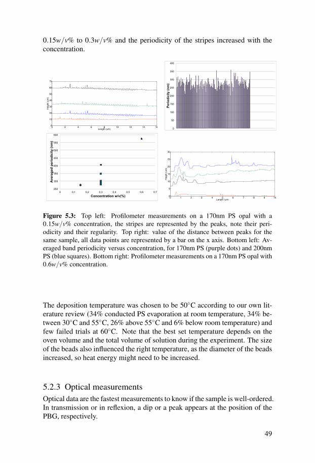
0.15w/v% to 0.3w/v% and the periodicity of the stripes increased with theconcentration.
0 2 4 6 8 10 12 14 160
10
20
30
40
50
60
70
Length (um)
He
igh
t (u
m)
0
50
100
150
200
250
300
350
400
Perio
dici
ty (n
m)
250
300
350
400
450
500
550
600
0 0,1 0,2 0,3 0,4 0,5 0,6 0,7
Aver
aged
per
iodi
city
(nm
)
Concentration w/v(%) 0 1 2 3 4 5 6 7 8 9 10
0
5
10
15
20
25
30
Length (um)
He
igh
t (u
m)
Figure 5.3: Top left: Profilometer measurements on a 170nm PS opal with a0.15w/v% concentration, the stripes are represented by the peaks, note their peri-odicity and their regularity. Top right: value of the distance between peaks for thesame sample, all data points are represented by a bar on the x axis. Bottom left: Av-eraged band periodicity versus concentration, for 170nm PS (purple dots) and 200nmPS (blue squares). Bottom right: Profilometer measurements on a 170nm PS opal with0.6w/v% concentration.
The deposition temperature was chosen to be 50◦C according to our own lit-erature review (34% conducted PS evaporation at room temperature, 34% be-tween 30◦C and 55◦C, 26% above 55◦C and 6% below room temperature) andfew failed trials at 60◦C. Note that the best set temperature depends on theoven volume and the total volume of solution during the experiment. The sizeof the beads also influenced the right temperature, as the diameter of the beadsincreased, so heat energy might need to be increased.
5.2.3 Optical measurementsOptical data are the fastest measurements to know if the sample is well-ordered.In transmission or in reflexion, a dip or a peak appears at the position of thePBG, respectively.
49
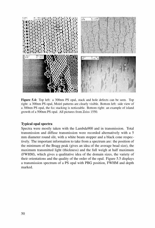
Figure 5.4: Top left: a 300nm PS opal, stack and hole defects can be seen. Topright: a 300nm PS opal, Moiré patterns are clearly visible. Bottom left: side view ofa 300nm PS opal, the fcc stacking is noticeable. Bottom right: an example of islandgrowth of a 500nm PS opal. All pictures from Zeiss 1550.
Typical opal spectraSpectra were mostly taken with the Lambda900 and in transmission. Totaltransmission and diffuse transmission were recorded alternatively with a 5mm diameter round slit, with a white beam stopper and a black cone respec-tively. The important information to take from a spectrum are: the position ofthe minimum of the Bragg peak (gives an idea of the average bead size), themaximum transmitted light (thickness) and the full weigh at half maximum(FWHM), which gives a qualitative idea of the domain sizes, the variety oftheir orientations and the quality of the order of the opal. Figure 5.5 displaysa transmission spectrum of a PS opal with PBG position, FWHM and depthmarked.
50
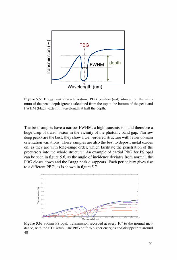
Tran
smis
sion
(%)
Wavelength (nm)
depth FWHM
PBG
Figure 5.5: Bragg peak characterisation: PBG position (red) situated on the mini-mum of the peak, depth (green) calculated from the top to the bottom of the peak andFWHM (black) extent in wavelength at half the depth.
The best samples have a narrow FWHM, a high transmission and therefore ahuge drop of transmission in the vicinity of the photonic band gap. Narrowdeep peaks are the best: they show a well-ordered structure with fewer domainorientation variations. These samples are also the best to deposit metal oxideson, as they are with long-range order, which facilitate the penetration of theprecursors into the whole structure. An example of partial PBG for PS opalcan be seen in figure 5.6, as the angle of incidence deviates from normal, thePBG closes down and the Bragg peak disappears. Each periodicity gives riseto a different PBG, as is shown in figure 5.7.
400 440 480 520 560 600 640 680 720 760 800 840 880 920 960 10000
10
20
30
40
50
60
70
80
90
100
Wavelength (nm)
Tra
nsm
issio
n (
%)
Figure 5.6: 300nm PS opal, transmission recorded at every 10◦ to the normal inci-dence, with the FTF setup. The PBG shift to higher energies and disappear at around40◦.
51
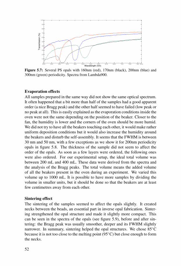
300 340 380 420 460 500 540 580 620 660 700 740 780 8000
10
20
30
40
50
60
70
80
90
100
Wavelength (nm)
Tra
nsm
issio
n (
%)
Figure 5.7: Several PS opals with 160nm (red), 170nm (black), 200nm (blue) and300nm (green) periodicity. Spectra from Lambda900.
Evaporation effectsAll samples prepared in the same way did not show the same optical spectrum.It often happened that a bit more than half of the samples had a good apparentorder (a nice Bragg peak) and the other half seemed to have failed (low peak orno peak at all). This is easily explained as the evaporation conditions inside theoven were not the same depending on the position of the beaker. Closer to thefan, the humidity is lower and the corners of the oven should be more humid.We did not try to have all the beakers touching each other, it would make ratheruniform deposition conditions but it would also increase the humidity aroundthe beakers and disturb the self-assembly. It seems that the FWHM is between30 nm and 50 nm, with a few exceptions as we show it for 200nm periodicityopals in figure 5.8. The thickness of the sample did not seem to affect theorder of the opals. As soon as a few layers were ordered, the following oneswere also ordered. For our experimental setup, the ideal total volume wasbetween 200 mL and 400 mL. These data were derived from the spectra andthe analysis of the Bragg peaks. The total volume means the added volumeof all the beakers present in the oven during an experiment. We varied thisvolume up to 1000 mL. It is possible to have more samples by dividing thevolume in smaller units, but it should be done so that the beakers are at leastfew centimetres away from each other.
Sintering effectThe sintering of the samples seemed to affect the opals slightly. It creatednecks between the beads, an essential part in inverse opal fabrication. Sinter-ing strengthened the opal structure and made it slightly more compact. Thiscan be seen in the spectra of the opals (see figure 5.9), before and after sin-tering: the Bragg peak was usually smoother, deeper and its FWHM slightlynarrower. In summary, sintering helped the opal structures. We chose 85◦Cbecause it is not too close to the melting point (95◦C) but close enough to formthe necks.
52
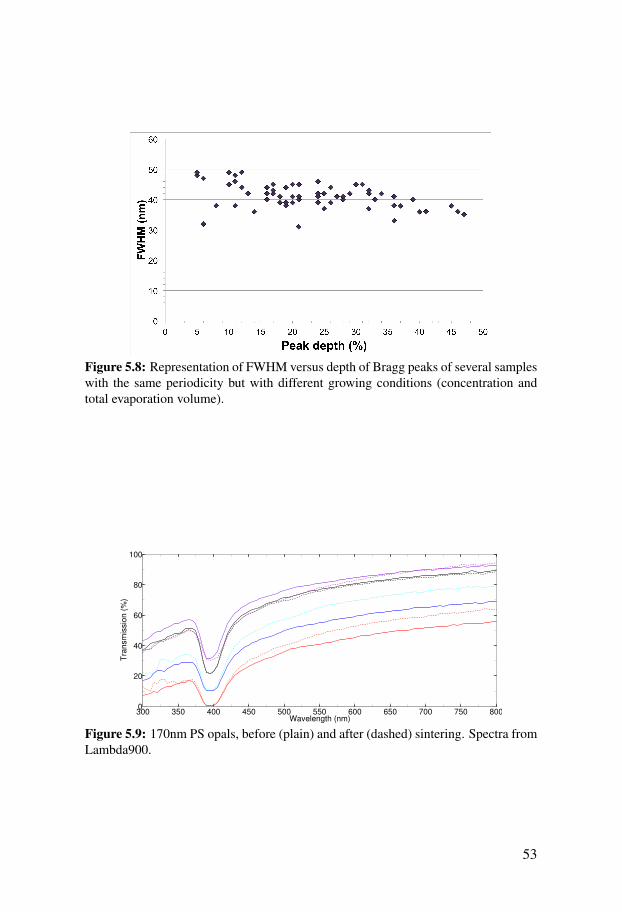
Figure 5.8: Representation of FWHM versus depth of Bragg peaks of several sampleswith the same periodicity but with different growing conditions (concentration andtotal evaporation volume).
300 350 400 450 500 550 600 650 700 750 8000
20
40
60
80
100
Wavelength (nm)
Tra
nsm
issio
n (
%)
Figure 5.9: 170nm PS opals, before (plain) and after (dashed) sintering. Spectra fromLambda900.
53
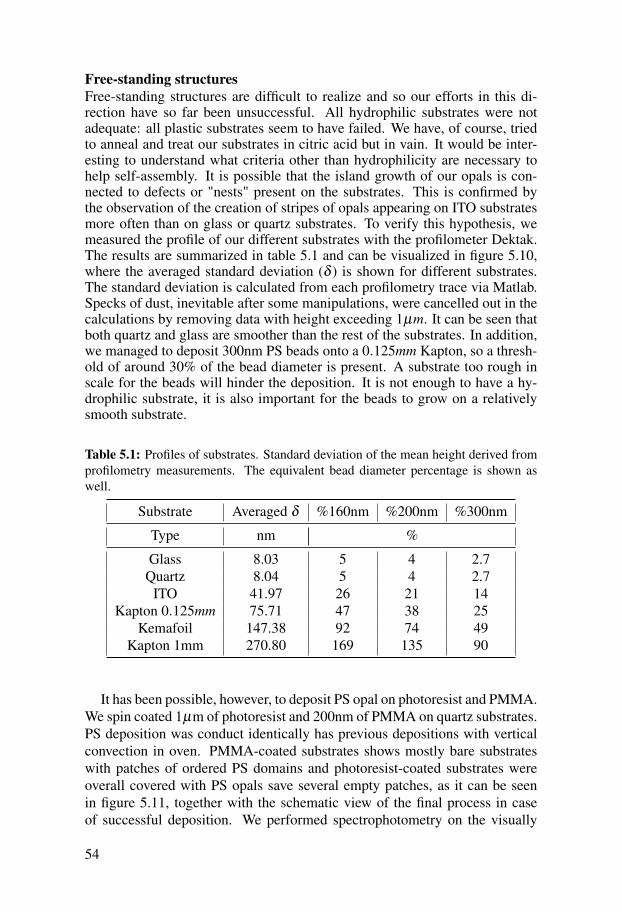
Free-standing structuresFree-standing structures are difficult to realize and so our efforts in this di-rection have so far been unsuccessful. All hydrophilic substrates were notadequate: all plastic substrates seem to have failed. We have, of course, triedto anneal and treat our substrates in citric acid but in vain. It would be inter-esting to understand what criteria other than hydrophilicity are necessary tohelp self-assembly. It is possible that the island growth of our opals is con-nected to defects or "nests" present on the substrates. This is confirmed bythe observation of the creation of stripes of opals appearing on ITO substratesmore often than on glass or quartz substrates. To verify this hypothesis, wemeasured the profile of our different substrates with the profilometer Dektak.The results are summarized in table 5.1 and can be visualized in figure 5.10,where the averaged standard deviation (δ ) is shown for different substrates.The standard deviation is calculated from each profilometry trace via Matlab.Specks of dust, inevitable after some manipulations, were cancelled out in thecalculations by removing data with height exceeding 1µm. It can be seen thatboth quartz and glass are smoother than the rest of the substrates. In addition,we managed to deposit 300nm PS beads onto a 0.125mm Kapton, so a thresh-old of around 30% of the bead diameter is present. A substrate too rough inscale for the beads will hinder the deposition. It is not enough to have a hy-drophilic substrate, it is also important for the beads to grow on a relativelysmooth substrate.
Table 5.1: Profiles of substrates. Standard deviation of the mean height derived fromprofilometry measurements. The equivalent bead diameter percentage is shown aswell.
Substrate Averaged δ %160nm %200nm %300nm
Type nm %
Glass 8.03 5 4 2.7Quartz 8.04 5 4 2.7
ITO 41.97 26 21 14Kapton 0.125mm 75.71 47 38 25
Kemafoil 147.38 92 74 49Kapton 1mm 270.80 169 135 90
It has been possible, however, to deposit PS opal on photoresist and PMMA.We spin coated 1µm of photoresist and 200nm of PMMA on quartz substrates.PS deposition was conduct identically has previous depositions with verticalconvection in oven. PMMA-coated substrates shows mostly bare substrateswith patches of ordered PS domains and photoresist-coated substrates wereoverall covered with PS opals save several empty patches, as it can be seenin figure 5.11, together with the schematic view of the final process in caseof successful deposition. We performed spectrophotometry on the visually
54
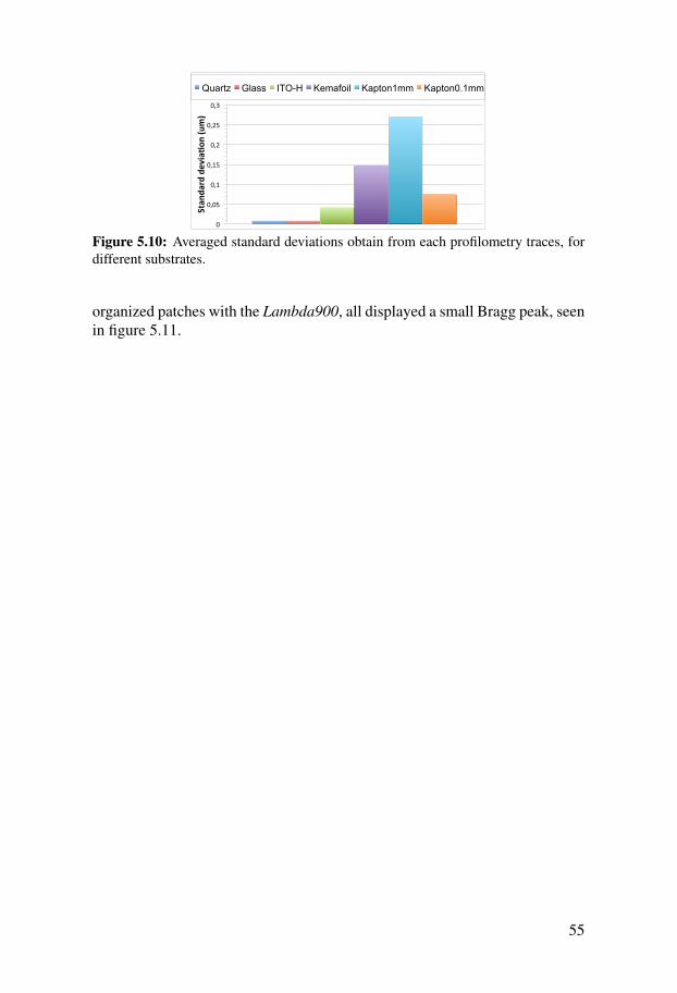
0
0,05
0,1
0,15
0,2
0,25
0,3
Stan
dard devia+o
n (um)
Quartz Glass ITO-H Kemafoil Kapton1mm Kapton0.1mm
Figure 5.10: Averaged standard deviations obtain from each profilometry traces, fordifferent substrates.
organized patches with the Lambda900, all displayed a small Bragg peak, seenin figure 5.11.
55
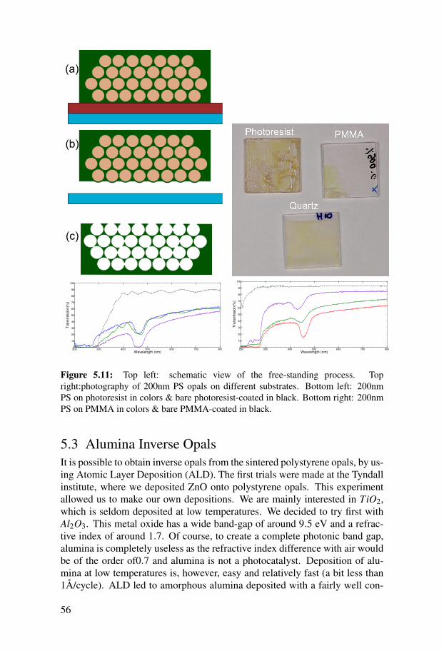
(a)
(b)
(c)
200 300 400 500 600 700 8000
10
20
30
40
50
60
70
80
90
100
Wavelength (nm)
Tra
nsm
issio
n(%
)
200 300 400 500 600 700 8000
10
20
30
40
50
60
70
80
90
100
Wavelength (nm)
Tra
nsm
issio
n(%
)
Figure 5.11: Top left: schematic view of the free-standing process. Topright:photography of 200nm PS opals on different substrates. Bottom left: 200nmPS on photoresist in colors & bare photoresist-coated in black. Bottom right: 200nmPS on PMMA in colors & bare PMMA-coated in black.
5.3 Alumina Inverse OpalsIt is possible to obtain inverse opals from the sintered polystyrene opals, by us-ing Atomic Layer Deposition (ALD). The first trials were made at the Tyndallinstitute, where we deposited ZnO onto polystyrene opals. This experimentallowed us to make our own depositions. We are mainly interested in TiO2,which is seldom deposited at low temperatures. We decided to try first withAl2O3. This metal oxide has a wide band-gap of around 9.5 eV and a refrac-tive index of around 1.7. Of course, to create a complete photonic band gap,alumina is completely useless as the refractive index difference with air wouldbe of the order of0.7 and alumina is not a photocatalyst. Deposition of alu-mina at low temperatures is, however, easy and relatively fast (a bit less than1Å/cycle). ALD led to amorphous alumina deposited with a fairly well con-
56
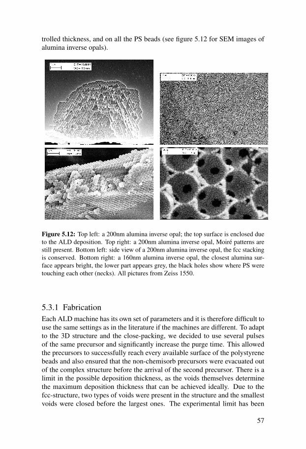
trolled thickness, and on all the PS beads (see figure 5.12 for SEM images ofalumina inverse opals).
Figure 5.12: Top left: a 200nm alumina inverse opal; the top surface is enclosed dueto the ALD deposition. Top right: a 200nm alumina inverse opal, Moiré patterns arestill present. Bottom left: side view of a 200nm alumina inverse opal, the fcc stackingis conserved. Bottom right: a 160nm alumina inverse opal, the closest alumina sur-face appears bright, the lower part appears grey, the black holes show where PS weretouching each other (necks). All pictures from Zeiss 1550.
5.3.1 FabricationEach ALD machine has its own set of parameters and it is therefore difficult touse the same settings as in the literature if the machines are different. To adaptto the 3D structure and the close-packing, we decided to use several pulsesof the same precursor and significantly increase the purge time. This allowedthe precursors to successfully reach every available surface of the polystyrenebeads and also ensured that the non-chemisorb precursors were evacuated outof the complex structure before the arrival of the second precursor. There is alimit in the possible deposition thickness, as the voids themselves determinethe maximum deposition thickness that can be achieved ideally. Due to thefcc-structure, two types of voids were present in the structure and the smallestvoids were closed before the largest ones. The experimental limit has been
57
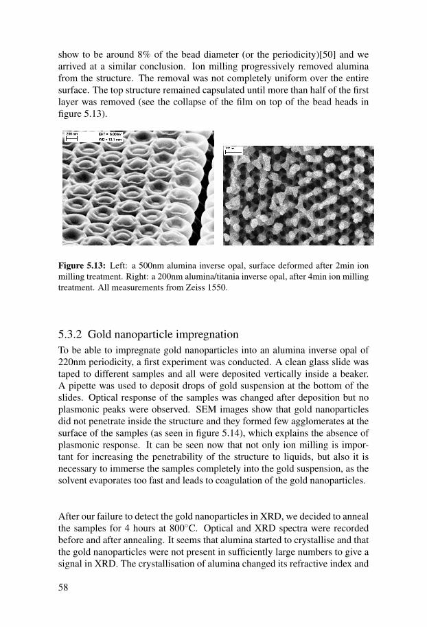
show to be around 8% of the bead diameter (or the periodicity)[50] and wearrived at a similar conclusion. Ion milling progressively removed aluminafrom the structure. The removal was not completely uniform over the entiresurface. The top structure remained capsulated until more than half of the firstlayer was removed (see the collapse of the film on top of the bead heads infigure 5.13).
Figure 5.13: Left: a 500nm alumina inverse opal, surface deformed after 2min ionmilling treatment. Right: a 200nm alumina/titania inverse opal, after 4min ion millingtreatment. All measurements from Zeiss 1550.
5.3.2 Gold nanoparticle impregnationTo be able to impregnate gold nanoparticles into an alumina inverse opal of220nm periodicity, a first experiment was conducted. A clean glass slide wastaped to different samples and all were deposited vertically inside a beaker.A pipette was used to deposit drops of gold suspension at the bottom of theslides. Optical response of the samples was changed after deposition but noplasmonic peaks were observed. SEM images show that gold nanoparticlesdid not penetrate inside the structure and they formed few agglomerates at thesurface of the samples (as seen in figure 5.14), which explains the absence ofplasmonic response. It can be seen now that not only ion milling is impor-tant for increasing the penetrability of the structure to liquids, but also it isnecessary to immerse the samples completely into the gold suspension, as thesolvent evaporates too fast and leads to coagulation of the gold nanoparticles.
After our failure to detect the gold nanoparticles in XRD, we decided to annealthe samples for 4 hours at 800◦C. Optical and XRD spectra were recordedbefore and after annealing. It seems that alumina started to crystallise and thatthe gold nanoparticles were not present in sufficiently large numbers to give asignal in XRD. The crystallisation of alumina changed its refractive index and
58
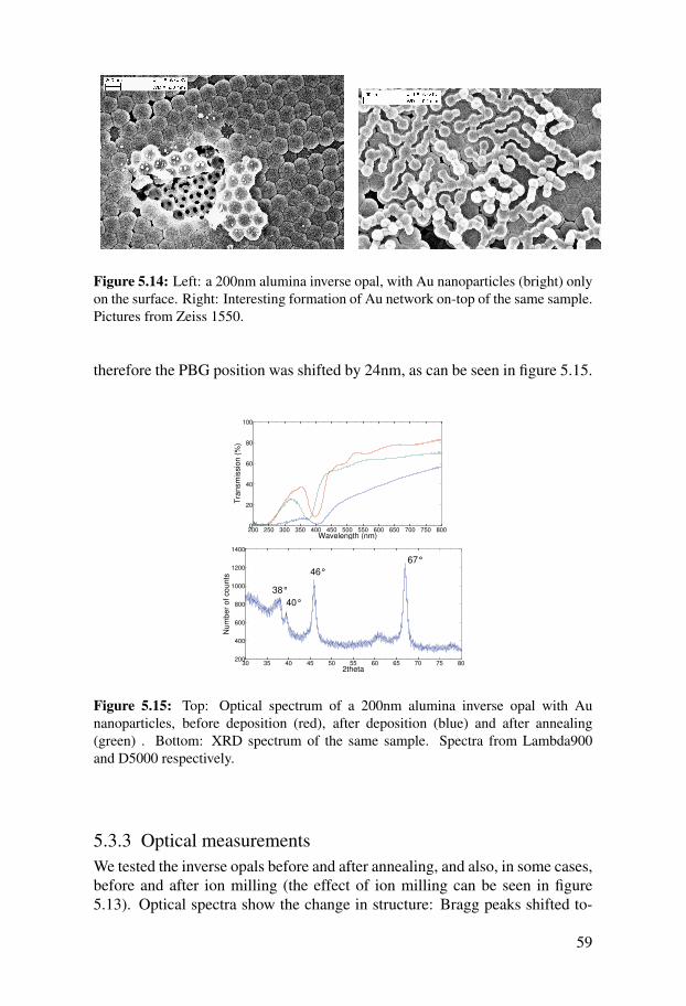
Figure 5.14: Left: a 200nm alumina inverse opal, with Au nanoparticles (bright) onlyon the surface. Right: Interesting formation of Au network on-top of the same sample.Pictures from Zeiss 1550.
therefore the PBG position was shifted by 24nm, as can be seen in figure 5.15.
200 250 300 350 400 450 500 550 600 650 700 750 8000
20
40
60
80
100
Wavelength (nm)
Tra
nsm
issio
n (
%)
30 35 40 45 50 55 60 65 70 75 80200
400
600
800
1000
1200
1400
2theta
Num
ber
of counts
40°
38°
46°
67°
Figure 5.15: Top: Optical spectrum of a 200nm alumina inverse opal with Aunanoparticles, before deposition (red), after deposition (blue) and after annealing(green) . Bottom: XRD spectrum of the same sample. Spectra from Lambda900and D5000 respectively.
5.3.3 Optical measurementsWe tested the inverse opals before and after annealing, and also, in some cases,before and after ion milling (the effect of ion milling can be seen in figure5.13). Optical spectra show the change in structure: Bragg peaks shifted to-
59
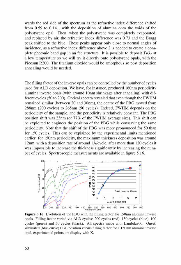
wards the red side of the spectrum as the refractive index difference shiftedfrom 0.59 to 0.14 , with the deposition of alumina onto the voids of thepolystyrene opal. Then, when the polystyrene was completely evaporated,and replaced by air, the refractive index difference was 0.73 and the Braggpeak shifted to the blue. These peaks appear only close to normal angles ofincidence, as a refractive index difference above 2 is needed to create a com-plete photonic band gap in an fcc structure. It is possible to deposit TiO2 ata low temperature so we will try it directly onto polystyrene opals, with thePicosun R200. The titanium dioxide would be amorphous so post depositionannealing would be needed.
The filling factor of the inverse opals can be controlled by the number of cyclesused for ALD deposition. We have, for instance, produced 160nm periodicityalumina inverse opals (with around 10nm shrinkage after annealing) with dif-ferent cycles (50 to 200). Optical spectra revealed that even though the FWHMremained similar (between 20 and 30nm), the centre of the PBG moved from288nm (200 cycles) to 265nm (50 cycles). Indeed, FWHM depends on theperiodicity of the sample, and the periodicity is relatively constant. The PBGposition shift was 23nm (or 77% of the FWHM average size). This shift canbe exploited to engineer the position of the PBG while conserving the sameperiodicity. Note that the shift of the PBG was more pronounced for 50 thanfor 150 cycles. This can be explained by the experimental limits mentionedearlier: for 150nm periodicity, the maximum thickness deposition was around12nm, with a deposition rate of around 1Å/cycle, after more than 120 cycles itwas impossible to increase the thickness significantly by increasing the num-ber of cycles. Spectroscopic measurements are available in figure 5.16.
200 240 280 320 360 400 440 480 520 560 600 640 680 720 760 8000
20
40
60
80
100
Wavelength (nm)
Transmission(%
)
Figure 5.16: Evolution of the PBG with the filling factor for 150nm alumina inverseopals. Filling factor varied via ALD cycles: 200 cycles (red), 150 cycles (blue), 100cycles (green) and 50 cycles (black). All spectra made with Lambda900. Onset:simulated (blue curve) PBG position versus filling factor for a 150nm alumina inverseopal, experimental points are display with X.
60
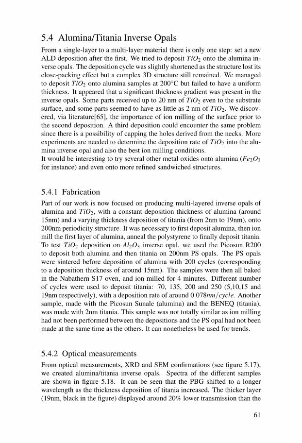
5.4 Alumina/Titania Inverse OpalsFrom a single-layer to a multi-layer material there is only one step: set a newALD deposition after the first. We tried to deposit TiO2 onto the alumina in-verse opals. The deposition cycle was slightly shortened as the structure lost itsclose-packing effect but a complex 3D structure still remained. We managedto deposit TiO2 onto alumina samples at 200◦C but failed to have a uniformthickness. It appeared that a significant thickness gradient was present in theinverse opals. Some parts received up to 20 nm of TiO2 even to the substratesurface, and some parts seemed to have as little as 2 nm of TiO2. We discov-ered, via literature[65], the importance of ion milling of the surface prior tothe second deposition. A third deposition could encounter the same problemsince there is a possibility of capping the holes derived from the necks. Moreexperiments are needed to determine the deposition rate of TiO2 into the alu-mina inverse opal and also the best ion milling conditions.It would be interesting to try several other metal oxides onto alumina (Fe2O3for instance) and even onto more refined sandwiched structures.
5.4.1 FabricationPart of our work is now focused on producing multi-layered inverse opals ofalumina and TiO2, with a constant deposition thickness of alumina (around15nm) and a varying thickness deposition of titania (from 2nm to 19nm), onto200nm periodicity structure. It was necessary to first deposit alumina, then ionmill the first layer of alumina, anneal the polystyrene to finally deposit titania.To test TiO2 deposition on Al2O3 inverse opal, we used the Picosun R200to deposit both alumina and then titania on 200nm PS opals. The PS opalswere sintered before deposition of alumina with 200 cycles (correspondingto a deposition thickness of around 15nm). The samples were then all bakedin the Nabathern S17 oven, and ion milled for 4 minutes. Different numberof cycles were used to deposit titania: 70, 135, 200 and 250 (5,10,15 and19nm respectively), with a deposition rate of around 0.078nm/cycle. Anothersample, made with the Picosun Sunale (alumina) and the BENEQ (titania),was made with 2nm titania. This sample was not totally similar as ion millinghad not been performed between the depositions and the PS opal had not beenmade at the same time as the others. It can nonetheless be used for trends.
5.4.2 Optical measurementsFrom optical measurements, XRD and SEM confirmations (see figure 5.17),we created alumina/titania inverse opals. Spectra of the different samplesare shown in figure 5.18. It can be seen that the PBG shifted to a longerwavelength as the thickness deposition of titania increased. The thicker layer(19nm, black in the figure) displayed around 20% lower transmission than the
61
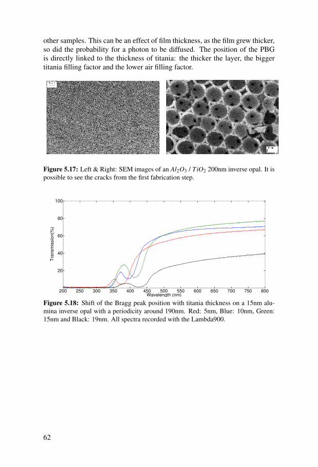
other samples. This can be an effect of film thickness, as the film grew thicker,so did the probability for a photon to be diffused. The position of the PBGis directly linked to the thickness of titania: the thicker the layer, the biggertitania filling factor and the lower air filling factor.
Figure 5.17: Left & Right: SEM images of an Al2O3 / TiO2 200nm inverse opal. It ispossible to see the cracks from the first fabrication step.
200 250 300 350 400 450 500 550 600 650 700 750 800
20
40
60
80
100
Wavelength (nm)
Tra
nsm
issio
n(%
)
Figure 5.18: Shift of the Bragg peak position with titania thickness on a 15nm alu-mina inverse opal with a periodicity around 190nm. Red: 5nm, Blue: 10nm, Green:15nm and Black: 19nm. All spectra recorded with the Lambda900.
62

6. Discussion
6.1 OpalsThe order of our opal structures was rather extended as our optical data werecollected over a 20mm2 area and showed deep and narrow Bragg peaks. Theinversion of our opals conserved the original order as long as enough materialwas deposited. From SEM images, it was possible to see that samples withfewer material possessed more defects in the walls. In addition, a gradient inthickness within the walls could influence the broadening of the Bragg peak.Cracks in the opal structure seem inevitable in our experimental process sincethe drying front imposes a strain on the beads.
Simulations using the Bragg-Snell’s law were made for different PS opals (seefigure 6.1) and compared to experimental results. It seems that Bragg-Snellunderestimates slightly (around 10 nm) the position of the Bragg peaks, asis shown in table 6.1. This can be understood as the limit of the approxima-tion, as the experimental data are influenced by defaults in size distribution(influence on periodicity) and in fcc stacking (influence on the filling factors).
Table 6.1: Simulation versus experiment: Bragg peak position. Experimental dataare done over the indicated number of samples while the simulations imply an infinitesample. Experimental data are averaged over all the samples spectra. The periodicityis given by the diameter of the beads of the samples.
Number of samples Diameter Simulation Experiment Difference
total=145 nm
21 220 516 512 -470 200 469 460 -927 170 399 393 -627 160 375 370 -5
It is also possible to compare the position of the Bragg peak with the an-gle of incidence theta. Table 6.2 shows that, in this case Bragg-Snell givesBragg peak positions at higher energies (shorter wavelengths). Comparing theincreasing trends of PBG positions between simulated (20.2%) and experi-mental (19.4%) data shows that the trend of PBG position with angle is wellsupported by the simulation results. The Bragg peak position shifts to higherenergies as the angle of incidence increases. This can be explained as theaddition of new stacking plans encountered by the light.
63
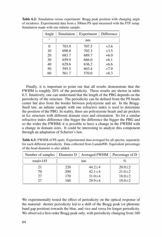
Table 6.2: Simulation versus experiment: Bragg peak position with changing angleof incidence. Experimental data from a 300nm PS opal measured with the FTF setup.Simulation made with one infinite sample.
Angle Simulation Experiment Difference◦ nm
0 703.9 707.5 +3.610 698.8 702.3 +3.520 683.7 689.7 +6.030 659.9 666.0 +6.140 629.6 636.2 +6.650 595.5 603.4 +7.960 561.7 570.0 +8.3
Finally, it is important to point out that all results demonstrate that theFWHM is roughly 20% of the periodicity. These results are shown in table6.3. Intuitively, one can understand that the length of the PBG depends on theperiodicity of the structure. The periodicity can be defined from the PS beadscenter but also from the border between polystyrene and air. In the Bragg-Snell law, an infinite sample with one refractive index is used to determinethe position of the PBG. In reality, there are polystyrene beads and air pocketsin fcc structure with different domain sizes and orientation. So for a similarrefractive index difference (the bigger the difference the bigger the PBG andso the wider the FWHM) it is possible to have a change in the FWHM witha change in domain sizes. It could be interesting to analyze this componentthrough an adaptation of Scherrer’s law.
Table 6.3: FWHM of PS opals. Experimental data averaged for all spectra, separatelyfor each different periodicity. Data collected from Lamda900. Equivalent percentageof the bead diameter is also added.
Number of samples Diameter D Averaged FWHM Percentage of D
total=145 nm %
21 220 44.2±4 20.0±270 200 42.1±4 21.0±227 170 31.0±4 18.0±227 160 29.9±4 19.0±2
We experimentally tested the effect of periodicity on the optical response ofthe material: shorter periodicity led to a shift of the Bragg peak (or photonicband gap position) towards the blue, and vice and versa for longer periodicity.We observed a first order Bragg peak only, with periodicity changing from 160
64
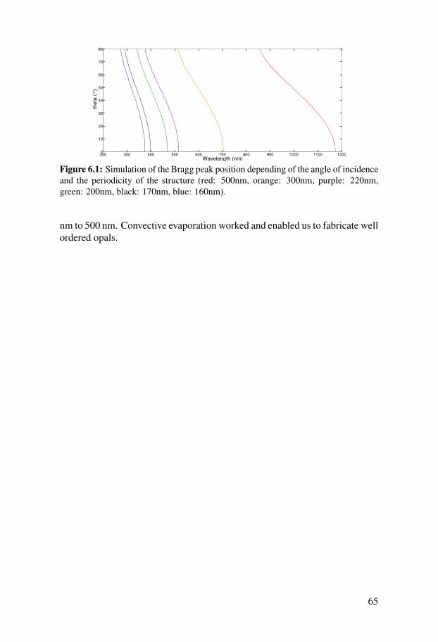
200 300 400 500 600 700 800 900 1000 1100 12000
10
20
30
40
50
60
70
80
Wavelength (nm)
th
eta
(°
)
Figure 6.1: Simulation of the Bragg peak position depending of the angle of incidenceand the periodicity of the structure (red: 500nm, orange: 300nm, purple: 220nm,green: 200nm, black: 170nm, blue: 160nm).
nm to 500 nm. Convective evaporation worked and enabled us to fabricate wellordered opals.
65

6.2 Alumina Inverse Opals6.2.1 Bragg-Snell lawThe materials used to fabricate the inverse opals have another influence onthe photonic band gap position: the film thickness. A certain film thicknesswill correspond to a certain filling factor. For a singe-layer inverse opal, it iseasy to calculate the filling factors. As a close-packed structure, the theoreticalrepartition for the filling factor is 0.74 and 0.26, for air and alumina respec-tively, if the entire voids are filled during the ALD deposition. We discoveredthat this was not the case, small voids were left even if the number of cycleswas increased. Literature has set the values of the voids to be 0.02[66]; so thefilling factor values for an inverse opal are:0.76 and 0.24, for air and aluminarespectively. It is then possible to assume linearity between the value of thefilling factor and corresponding thickness. This allows us to have an estimateof the Bragg peak position depending of the number of ALD cycles.
We saw a blue shift of the Bragg peak position as the number of cycles de-creased and as the deposition thickness of alumina decreased (figure 5.16).The transmission also increased, as the thickness of the alumina decreased.This can be understood with the help of the Bragg-Snell equation. Indeed,we saw that the position of the PBG depended onto several factors, one ofwhich was the filling factor. The filling factor of a fully-filled fcc structure isvisualized in figure 6.2.
We analyzed different types of alumina inverse opals, with different peri-odicity and filling factors (film thickness). Table 6.4 shows the compari-son between simulated data and experimental results for 160nm periodicityPS/Al2O3 opals and Al2O3 inverse opals. It can be seen that the number ofcycles (film thickness) had an impact on the position of the Bragg peak andit was predicted with the Bragg-Snell equation. However, the position of thePBG was not well predicted for the Al2O3 inverse opals: the predicted positionwas always at lower energies (longer wavelength) than the experimental one,by almost 15 nm. The PBG position of the opals (both PS and PS/Al2O3),seemed to be better, with around 5 nm discrepancy for both. If we considereda shrinkage of the original periodicity during the transformation from opal toinverse opal, it was possible to obtain better simulation results. A shrinkage ofaround 6% was used and the new comparison is shown in table 6.5. This time,the Bragg-Snell simulation seems more in agreement with experimental data,with an averaged 7nm discrepancy.
We did a similar analysis on other alumina inverse opals. Taking into con-sideration a small shrinkage on the last step of the sample preparation seemedto improve the prediction accuracy of our simulations. It is again important toremember that we did not take the refractive index changes along the wave-length into consideration. But in the area of concern (200 to 800nm), alumina
66

Figure 6.2: Top right: filling factor of a classical fcc with beads and air, Top left:filling factor of an ALD deposited MO onto the beads, Bottom right: inverse opalwith MO1 and air, Bottom left: inverse opal with MO2, MO1 and air. The fillingfactor of MO2 and air depends on the deposited thicknesses.
67
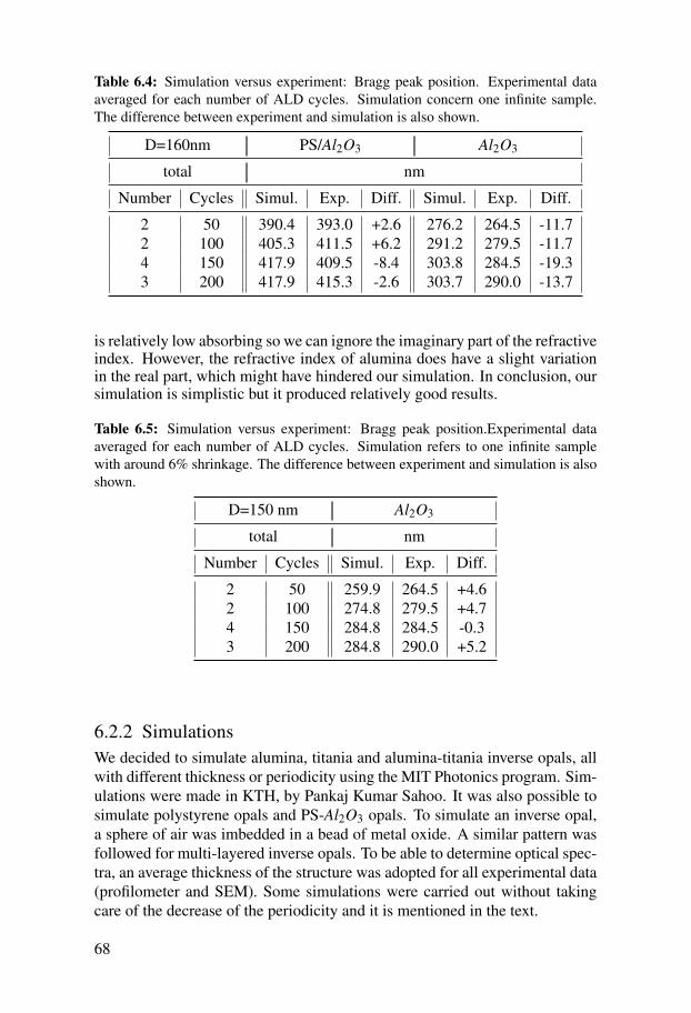
Table 6.4: Simulation versus experiment: Bragg peak position. Experimental dataaveraged for each number of ALD cycles. Simulation concern one infinite sample.The difference between experiment and simulation is also shown.
D=160nm PS/Al2O3 Al2O3
total nm
Number Cycles Simul. Exp. Diff. Simul. Exp. Diff.
2 50 390.4 393.0 +2.6 276.2 264.5 -11.72 100 405.3 411.5 +6.2 291.2 279.5 -11.74 150 417.9 409.5 -8.4 303.8 284.5 -19.33 200 417.9 415.3 -2.6 303.7 290.0 -13.7
is relatively low absorbing so we can ignore the imaginary part of the refractiveindex. However, the refractive index of alumina does have a slight variationin the real part, which might have hindered our simulation. In conclusion, oursimulation is simplistic but it produced relatively good results.
Table 6.5: Simulation versus experiment: Bragg peak position.Experimental dataaveraged for each number of ALD cycles. Simulation refers to one infinite samplewith around 6% shrinkage. The difference between experiment and simulation is alsoshown.
D=150 nm Al2O3
total nm
Number Cycles Simul. Exp. Diff.
2 50 259.9 264.5 +4.62 100 274.8 279.5 +4.74 150 284.8 284.5 -0.33 200 284.8 290.0 +5.2
6.2.2 SimulationsWe decided to simulate alumina, titania and alumina-titania inverse opals, allwith different thickness or periodicity using the MIT Photonics program. Sim-ulations were made in KTH, by Pankaj Kumar Sahoo. It was also possible tosimulate polystyrene opals and PS-Al2O3 opals. To simulate an inverse opal,a sphere of air was imbedded in a bead of metal oxide. A similar pattern wasfollowed for multi-layered inverse opals. To be able to determine optical spec-tra, an average thickness of the structure was adopted for all experimental data(profilometer and SEM). Some simulations were carried out without takingcare of the decrease of the periodicity and it is mentioned in the text.
68
6.2.3 SummaryOptical response from an alumina inverse opal can easily be simulated usingthe Bragg-Snell equation. It is important, however, to consider the shrinkageof the structure during the fabrication process, to explain the experimentalPBG shift. To obtain band structure simulation, it is better to use the MITPhotonics program.
6.3 Alumina/Titania Inverse Opals6.3.1 Optical propertiesThe position of the photonic band gap can be engineered by two means: theperiodicity of the structure and the materials used to build the structure. Ourprocess kept the photonic crystallinity at all the fabrication stages, as can beseen in figure 6.3: Bragg peaks appeared on transmission spectra after all thefabrication stages.
300 340 380 420 460 500 540 580 620 660 700 740 780 8000
10
20
30
40
50
60
70
80
90
100
Wavelength (nm)
Tra
nsm
issio
n(%
)
Figure 6.3: All the processes of inverse opal fabrication are displayed for a 200nmperiodicity structure: PS opal (red), PS/alumina opal (blue), alumina inverse opal(black) and alumina/titania inverse opal (green), before ion milling. All spectra madewith Lambda900.
6.3.2 SimulationsTo compare with MIT Photonics simulated data, we analyzed the PBG posi-tion, as well as the depth of the dip and its FWHM. A resumé of the averageddata is shown in table 6.6, showing the comparison between simulated andexperimental PBG position of alumina/titania inverse opal.
It can be seen that the trends predicted are followed, but on a slower scale.The shift of the PDB position is less important than predicted but in the samedirection (lower energies). The increase of the FWHM is also present but notsignificantly, in contradiction to predictions. Also, the deposition thicknessof titania might be over-estimated, as XRD and EDS spectra show very low
69

Table 6.6: Measured and calculated features of inverse opal optical responses. A200nm PS opal deposited with around 15nm alumina deposition, inverted and differenttitania thicknesses deposition applied. Percentage of the PBG shift and the increase ofthe FWHM, from the original alumina inverse opal data, are also added.
Al2O3/TiO2 samples Compared to Al2O3
TiO2 PBG position (nm) % PBG shift × FWHM
thickness (nm) simul. exp. simul. exp. simul. exp.
2 378.5 365.0 6 4.0 1.5 0.95 412.5 376.5 15 11.5 2.0 0.810 466 391.5 30 16.3 2.3 1.015 n.a. 412.5 n.a. 21.5 n.a. 1.219 n.a. 425.0 n.a. 24.6 n.a. 1.2
signal for titania. It can be seen that the simulated PBG position for 5nm titaniathickness is similar to the experimental one for a number of cycles sufficient todeposit 15nm. A more detailed analysis of the deposition thickness is neededto corrode simulations and experiments.
A rather good agreement with simulated and experimental data was found.It is rather impressive, as all structures produced are unique (cracks position,thickness difference, defects) and we have averaged many parameters. Sim-ulations allowed us to demonstrate the existence of shrinkage at the sinteringof the PS opals, which had already been demonstrated by others (see [31]). Ithelped us to predict the position of the PBG and its shape for multi-layeredsamples, which was impossible to predict via the simplified Bragg-Snell law.It can be seen that simulations using original PS beads diameter slightly over-estimate the position of the PBG (see table 6.7). The discrepancy is larger alsofor alumina inverse opals, due to the difference in filling factor added to theshrinkage of the PS beads.
Simulations are an essential part of our sample fabrication: to engineer prop-erly our inverse opals, we needed to estimate before hand the filling factorneeded for a specific periodicity. For instance, we knew the probable positionof the PBG for a 15nm alumina inverse opal with different titania thicknesses(see figure 6.4). The PBG is red shifted and wider with increasing titania fill-ing factor. We will continue to simulate band structure and optical spectraprior to the fabrication of our samples.
70

Table 6.7: Comparison between simulations and experimental data for two differentvalues of periodicity. 160nm and 200nm PS beads with 200 ALD cycles. No shrinkagetaken into consideration. Band diagram from MIT Photonics and FDTD from Meepcalculations. Note that shrinkage has not been taken into consideration for aluminainverse opal.
Type Band diagram (nm) FDTD (nm) Experimental (nm)
160 nm PS beads
PS opal 373.5 375.3 370.0PS/alumina opal 424.6 425.35 415.0
Alumina inverse opal 312.9 313.5 290.0
200 nm PS beads
PS opal 467.5 469.8 460.0PS/alumina opal 530.8 531.6 507.0
Alumina inverse opal 391.2 392.2 342.0
6.3.3 SummaryInverse opals created with self-assembly and ALD are easy to make and easyto manipulate. Our samples show a PBG at all stages of fabrication. We areable to produce roughly the desired thickness and to cover square centimetresof substrates. The use of ALD, however, imposes the use of ion milling, asthe entire surface of the beads is covered and creates a continuous film on topof the hollow structure. This could be easily solved if free-standing structurescould be created, as removing the substrate would directly reveal the hollowstructure. Our samples are very versatile. We can produce a multi-layeredstructure, we can add nanoparticles inside it and we would be able to use sol-gel if need be (to deposit tungsten trioxide).
71
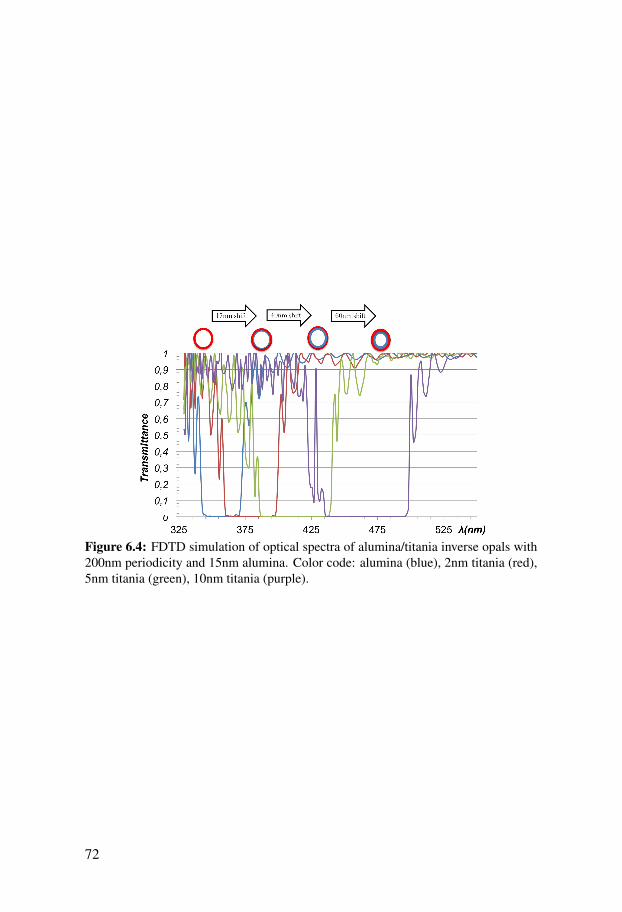
Figure 6.4: FDTD simulation of optical spectra of alumina/titania inverse opals with200nm periodicity and 15nm alumina. Color code: alumina (blue), 2nm titania (red),5nm titania (green), 10nm titania (purple).
72
7. Conclusions
As the reader can see, our work is only at a beginning stage, and we havestarted to gather important results, which will help us to go further in ourresearch.
We have experimentally examined all stages of inverse opal fabrication. Wewere able to determine that polystyrene opals were suitable for our purposeand that self-assembly works. Our opals are rather well ordered and can coverareas of the order of square centimetres on different type of substrates. Thesteps to fabricate an inverse opal from a PS opal were then fixed by trial anderror: deposition of a metal oxide using ALD, ion milling of the first layer andannealing of the PS together with crystallization of the metal oxide. We madeZnO, Al2O3, and Al2O3/TiO2 inverse opals.The use of metal oxide seems to render the structure sturdy. All metal oxidescannot be deposited via ALD but sol-gel should be able to be employed afterdeposition of alumina. Alumina is the easiest metal oxide to use, as its deposi-tion window temperature is wide. The deposition rate is rather similar(slightlylower) onto a PS 3D structure than onto a flat silicon wafer. Zinc oxide is alsovery easy to deposit and successfully deposited at low temperature. However,its sensitivity to photocorrosion makes it less attractive than titania. Titaniumdioxide was deposited only at high temperatures and onto amorphous alumina.The crystallisation to anatase form was obtained after the ALD process. Thedeposition at low temperature[67] should be tested on PS beads, this couldallow us to produce TiO2 inverse opals and compare them to Al2O3/TiO2 in-verse opals.
We have successfully created well ordered PS opals and were able to transformthem into metal oxide inverse opals with similar features. We have also shownthe importance of thickness control and the versatility of our structures. Thedeposition of titanium dioxide onto alumina inverse opal has been done andsimulations have been derived accordingly. Polystyrene opals exhibit an in-complete PBG, but that extended nonetheless around 30 degrees from the nor-mal incidence. At the moment, our inverse opals follow the same behaviour.This is because our inverse opals are made of alumina and air. The refractiveindex difference is too low to produce a complete PBG. For our Al2O3/TiO2inverse opal, we did not have time to perform angle resolved measurements. It
73

is possible that too little titania thickness could reduce the averaged refractiveindex and destroy the complete PBG. Further simulations and experiments areneeded to answer these questions.
74
8. Outlook and Future work
As an important ground-breaking work, this text may have lead to more ques-tions than answers, but this allows us to focus now on the next steps of ourresearch.To help us build our samples, we used simulated data. These simu-lations hold the key to properly engineering our inverse opals, and will be themost important tool in our work. To analyze our samples, optical determina-tion of the PBG and its state (complete or not) and FTIR measurements will becarried out systematically. SEM images are also important to have an idea ofthe local structure and the size of the domains. Other types of measurements(EDS, XRD, profilometry) should be added for each new experiment.
Multi-layerMulti-layered structures are of great interest: combining different light ab-sorbers, reducing the use of material and introducing interfaces are among themost obvious. It would be intriguing to combine ZnO with TiO2, as ZnO eas-ily generates electron-holes but is sensitive to photocorrosion. We could alsocontinue to study the Al2O3/TiO2 multi-layered samples, as alumina shouldpresent a good sturdy skeleton. It will be essential to create appropriate sim-ulations to partly understand the phenomena produced by these multi-layeredinverse opals.
PlasmonicsPlasmonics is of course a promising route to enhance light absorption andto increase the activity of our structures. It is important now to be able tointroduce gold nanoparticles into our structures, and an effort should be madeto proceed in a complete set of experiments dealing with the effect of theplasmon on the photonic crystal.
Band structureTo understand the interaction of light with the artificial inverse opals, simu-lations and measurements of different band structures of similar materials areneeded. It is also the main interest of this work: to measure and assess theband structure of our samples and the correlation with their effectiveness inphotocatalysis.
PhotocatalysisOur desire to improve the photocatalytic activity of existing metal oxides isthe main thread of our research. By understanding our structures and by en-hancing their best characteristics, we would like to increase their efficiency atcleaning air and water. Photocatalysis is the final goal of our work.
75
Annick Schnepf
Taha Ahmed
Dag Ivar Thörnelöf
_ Richard Squibb
Aur
élie
n D
emill
y
Rol
and
Len
ain
Ber
tran
d Ph
ilipp
e
Joe
_
oush
Anand Srinivasan B
ing
Cai
Vancho Kocevski
Mig
uel A
rviz
u E
rik Ö
stm
an
Stel
la K
ioko
Zareh Topalian
Ieva Bidermane
I m
ade
calli
gram
s so
I c
ould
th
anks
eve
ryon
e!
Wha
t is
this
?!
76
Miakel Andersson
Claes-Göran Granqvist
Yuxia Ji
Shuyi Li
David L
ingfors
Christopher Lundgren
Roland Mathieu
Joakim Munkhammar
Gunnar Niklasson
Anil Kumar Puri
Carl-Gustaf Ribbing
Arne R
oos
Lars Ö
sterlund
Hiroaki Kobayashi
Jiří Henych
Jan-Åke Gustafsson
Vassilios Kapaklis
Olivier Donzel-Gargand
Giuseppe Muscas
77
Alexander Edström
Carla Terschlüsen
Tomas Edvinsson
Gunnar Westin
Fredric Ericson Mat
thia
s H
uld
Mal
in Jo
hans
son
Andreas Lindblad
Mel
anie
Muc
ke
Jenn
ifer
Che
n
Serk
an A
kans
el Andreas Mattson
Sujit
Koo
tala
Erwin Alhassan
Sofia
Kas
sel
- H
ugo
Lev
ard
Alexandra Maquet
Pascal Lebrun
Stina Thörnelöf
Fabien LeJeune -
Dav
id M
ende
s
And
rea
Pala
ia
Alexander Edström
Li Caldeira Balkeståhl
Manou Deneuvelle
Dav
id G
oldz
ahl
Car
olin
e et
Pie
rre
Véronique Lebrun
Ann
ica
Nils
son
Véronique Dartiguelongue
Rom
ain
Mar
chio
ri
Rém
i Mae
vere
E
rwin
Alh
assa
n
Julie
n Pi
zzle
Maéva
Pascal Tran Binh
78
Rimantas Brucas
Umut Cindemir
Bengt Götesson
José Montero Amenedo Per Nodblad
Peter Svedlindh
Carlos Triana
Marie-Thévie Thean Sarah Abouhari
Sandrine Molla
Henri H
ay _
Mats T
hörnelöf G
uillaume L
efebvre *
Philippe Lebrun
Joseph Bear
Isabelle LebruN
Carla
lüsen
79
References
[1] C.-G. S. Granqvist and G. B. Smith, Green Nanotechnology: Solutions forSustainability and Energy in the Built Environment. CRC Press, 2010.
[2] N. Serpone and A. Emeline, “Suggested terms and definitions in photocatalysisand radiocatalysis,” Int. J. Photoenergy, vol. 4, no. 3, pp. 91–131, 2002.
[3] IPCC, “CLIMATE CHANGE 2013: The Physical Science Basis,” tech. rep.,Intergovernmental Panel on Climate Change, 2013.
[4] A. Fujishima and K. Honda, “Electrochemical photolysis of water at asemiconductor electrode.,” Nature, vol. 238, pp. 37–38, 1972.
[5] S. John, “Strong localization of photons in certain disordered dielectricsuperlattices,” Phys. Rev. Lett., vol. 58, no. 23, p. 2486, 1987.
[6] E. Yablonovitch, “Photonic band-gap structures,” J. Opt. Soc. Am. B, vol. 10,p. 283, Feb. 1993.
[7] E. Yablonovitch, “Photonic crystals,” J. Mod. Opt., vol. 41, no. 2, pp. 173–194,1994.
[8] A. Moroz, “Three-Dimensional Complete Photonic-Band-gap Structures in theVisible,” Phys. Rev. Lett., vol. 83, pp. 5274–5277, Dec. 1999.
[9] J. D. Joannopoulos, R. D. Meade, and J. N. Winn, Photonic crystals : moldingthe flow of light. Princeton, N.J. : Princeton Univ. Press, cop. 1995, 2008 ed.,1995.
[10] K.-M. Ho, C. T. Chan, and C. M. Soukoulis, “Existence of a photonic gap inperiodic dielectric structures,” Phys. Rev. Lett., vol. 65, no. 25, pp. 3152–3155,1990.
[11] Z.-Y. Li and Z.-Q. Zhang, “Fragility of photonic band gaps in inverse-opalphotonic crystals,” Phys. Rev. B, vol. 62, pp. 1516–1519, July 2000.
[12] J. J. Xu and Z. Guo, “Biomimetic photonic materials with tunable structuralcolors.,” J. Colloid Interface Sci., vol. 406, pp. 1–17, Sept. 2013.
[13] G. Subramanian, V. N. Manoharan, J. D. Thorne, and D. J. Pine, “OrderedMacroporous Materials by Colloidal Assembly : A Possible Route to PhotonicBandgap Materials,” Adv. Mater., vol. 11, no. 15, pp. 1261–1265, 1999.
[14] H. Zhang, R.-g. Duan, F. Li, Q. Tang, and W.-c. Li, “Microscopy evidence ofthe face-centered cubic arrangement of monodisperse polystyrene nanospheres,”Mater. Des., vol. 28, pp. 1045–1049, Jan. 2007.
[15] A. Imhof, W. L. Vos, R. Sprik, and A. Lagendijk, “Large Dispersive Effects nearthe Band Edges of Photonic Crystals,” Phys. Rev. Lett., vol. 83, pp. 2942–2945,Oct. 1999.
[16] J. I. L. Chen, G. von Freymann, S. Y. Choi, V. Kitaev, and G. A. Ozin,“Amplified Photochemistry with Slow Photons,” Adv. Mater., vol. 18,pp. 1915–1919, July 2006.
[17] L.-V. De Broglie, “De Broglie’s theory of the quantum and the Dopplerprinciple,” Nature, vol. 114, no. 2854, pp. 51–52, 1924.
80
[18] M. Planck, “Über die Natur der Wärmestrahlung,” Ann. Phys., vol. 378, no. 3-4,pp. 272–288, 1924.
[19] P. T. C. So, C. Y. Dong, K. M. Berland, T. French, and E. Gratton,“Time-Resolved Stimulated-Emission and Transient-Absorption Microscopyand Spectroscopy,” in Top. Fluoresc. Spectrosc. (J. R. Lakowicz, ed.), ch. 5,pp. 427–469, Springer US, 2002.
[20] S. Satpathy, Z. Zhang, and M. R. Salehpour, “Theory of Photon Bands inThree-Dimensional Periodic Dielectric Structures,” Phys. Rev. Lett., vol. 64,no. 11, pp. 1239–1242, 1990.
[21] W. Setyawan and S. Curtarolo, “High-throughput electronic band structurecalculations: Challenges and tools,” Comput. Mater. Sci., vol. 49, pp. 299–312,Aug. 2010.
[22] J. I. L. Chen, G. von Freymann, S. Y. Choi, V. Kitaev, and G. A. Ozin, “Slowphotons in the fast lane in chemistry,” J. Mater. Chem., vol. 18, no. 4, p. 369,2008.
[23] C. López, “Materials Aspects of Photonic Crystals,” Adv. Mater., vol. 15,pp. 1679–1704, Oct. 2003.
[24] A. Rung, Numerical Studies of Energy Gaps in Photonic Crystals. PhD thesis,Uppsala University, 2005.
[25] S. L. McCall, P. M. Platzmann, R. Dalichaouch, D. Smith, and S. Schultz,“Microwave propagation in two-dimensional dielectric lattices,” Phys. Rev.Lett., vol. 67, no. 15, pp. 2017–2020, 1991.
[26] J. I. L. Chen, Amplified Photochemistry with Slow Photons. PhD thesis,University of Toronto, 2009.
[27] J. D. Joannopoulos, “Ab Initio Physics,” 2014.[28] I. Freestone, N. Meeks, M. Sax, and C. Higgitt, “The Lycurgus Cup: A Roman
nanotechnology,” Gold Bull., vol. 40, no. 4, p. 270, 2007.[29] M. Green and K. Emery, “Solar cell efficiency tables (version 39),” Prog.
Photovolt Res. Appl., vol. 20, pp. 12–20, 2012.[30] L. Liu, S. K. Karuturi, L. T. Su, and A. I. Y. Tok, “TiO2 inverse-opal electrode
fabricated by atomic layer deposition for dye-sensitized solar cell applications,”Energy Environ. Sci., vol. 4, no. 1, p. 209, 2011.
[31] L. I. Halaoui, N. M. Abrams, and T. E. Mallouk, “Increasing the conversionefficiency of dye-sensitized TiO2 photoelectrochemical cells by coupling tophotonic crystals.,” J. Phys. Chem. B, vol. 109, pp. 6334–42, Apr. 2005.
[32] M.-J. Deng, C.-Z. Song, P.-J. Ho, C.-C. Wang, J.-M. Chen, and K.-T. Lu,“Three-dimensionally ordered macroporous Cu2O/Ni inverse opal electrodesfor electrochemical supercapacitors.,” Phys. Chem. Chem. Phys., vol. 15,pp. 7479–83, May 2013.
[33] I. B. Burgess, J. Aizenberg, and M. Loncar, “Creating bio-inspired hierarchical3D-2D photonic stacks via planar lithography on self-assembled inverse opals.,”Bioinspir. Biomim., vol. 8, p. 045004, Dec. 2013.
[34] B. Ding, M. Bardosova, I. Povey, M. E. Pemble, and S. G. Romanov,“Engineered Light Scattering in Colloidal Photonic Heterocrystals,” Adv. Funct.Mater., vol. 20, pp. 853–860, Mar. 2010.
[35] M. Pelton and G. W. Bryant, Introduction to Metal-Nanoparticles Plasmonics.Wiley, 2013.
81
[36] Y. Chen, X. Gu, C.-G. Nie, Z.-Y. Jiang, Z.-X. Xie, and C.-J. Lin, “Shapecontrolled growth of gold nanoparticles by a solution synthesis,” Chem.Commun., vol. 1, no. 33, p. 4181, 2005.
[37] M. Haruta, “Novel catalysis of gold deposited on metal oxides,” Catal. Surv.from Asia, vol. 1, pp. 61–73, 1997.
[38] M. A. Fox and M. T. Dulay, “Heterogeneous Photocatalysis,” Chem. Rev.,vol. 93, pp. 341–357, 1995.
[39] E. Pelizzetti and C. Minero, “MECHANISM OF THE PHOTO-OXIDATIVEDEGRADATION OF ORGANIC POLLUTANTS OVER TiO2 PARTICLES,”Electrochim. Acta, vol. 38, no. 1, pp. 47–55, 1993.
[40] A. Mills and S. Le Hunte, “An overview of semiconductor photocatalysis,” J.Photochem. Photobiol. A Chem., vol. 108, pp. 1–35, 1997.
[41] A. L. Linsebigler, G. Lu, and J. T. J. Yates, “Photocatalysis on TiO2 Surfaces:Principles, Mechanisms, and Selected Results,” Chem. Rev., vol. 95,pp. 735–758, 1995.
[42] K. M. Glassford and J. R. Chelikowsky, “Structural and electronic properties oftitanium dioxide,” Phys. Rev. B, vol. 46, no. 3, p. 1284, 1992.
[43] S.-D. Mo and W. Y. Ching, “Electronic and optical properties of three phases oftitanium dioxide: Rutile, anatase, and brookite,” Phys. Rev. B, vol. 51, no. 19,pp. 13023–13032, 1995.
[44] J. Leem, I. Park, Y. Li, W. Zhou, Z. Jin, S. Shin, and Y.-s. Min, “Role of HCl inAtomic Layer Deposition of TiO2 Thin Films from Titanium Tetrachloride andWater,” Bull. Korean Chem. Soc., vol. 35, no. 4, pp. 1195–1201, 2014.
[45] Y. Jin, Y. Zhu, X. Yang, C. Wei, and C. Li, “Fabrication and characterization ofcerium doped titania inverse opal by sol gel method,” Mater. Chem. Phys.,vol. 106, pp. 209–214, Dec. 2007.
[46] X. Huang, Z. Yang, L. Sun, Q. Xie, B. Li, J. Zhou, and L. Li, “Synthesis andcharacterization of potassium bismuth titanate inverse opal photonic crystals bysol gel technique,” Mater. Chem. Phys., vol. 114, pp. 23–25, Mar. 2009.
[47] V. Abramova and A. Sinitskii, “Large scale ZnO inverse opal films fabricated bya sol gel technique,” Superlattices Microstruct., vol. 45, pp. 624–629, June2009.
[48] W. Liu, B. Zou, J. Zhao, and H. Cui, “Optimizing sol gel infiltration for thefabrication of high-quality titania inverse opal and its photocatalytic activity,”Thin Solid Films, vol. 518, pp. 4923–4927, June 2010.
[49] D. Ge, L. Yang, Z. Fan, J. Zhao, and Y. Li, “Effect of templates on inverse opalsfabricated through annular self assembly sol gel method,” Mater. Chem. Phys.,vol. 130, pp. 59–62, Oct. 2011.
[50] E. Graugnard, J. S. King, D. P. Gaillot, and C. J. Summers, “Sacrificial-LayerAtomic Layer Deposition for Fabrication of Non-Close-Packed Inverse-OpalPhotonic Crystals,” Adv. Funct. Mater., vol. 16, pp. 1187–1196, June 2006.
[51] L. M. Goldenberg, J. Wagner, J. Stumpe, B.-R. Paulke, and E. Goernitz,“Ordered arrays of large latex particles organised by vertical deposition,” Mater.Sci. Eng. C, vol. 22, pp. 405–408, 2002.
[52] S. H. Im, Y. T. Lim, D. J. Suh, and O. O. Park, “Three-DimensionalSelf-Assembly of Colloids at a Water-Air Interface: A Novel Technique for theFabrication of Photonic Bandgap Crystals,” Adv. Mater., vol. 14, no. 19,
82
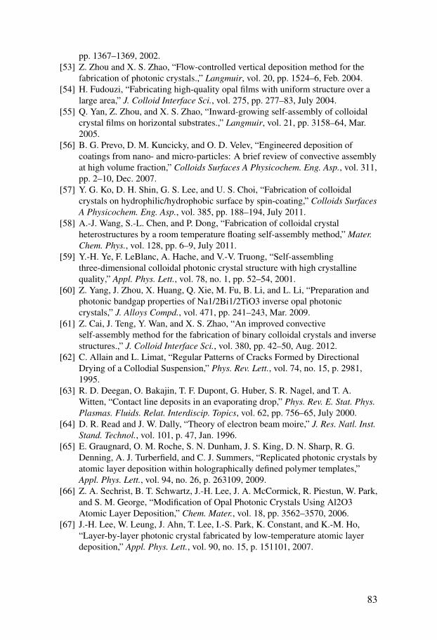
pp. 1367–1369, 2002.[53] Z. Zhou and X. S. Zhao, “Flow-controlled vertical deposition method for the
fabrication of photonic crystals.,” Langmuir, vol. 20, pp. 1524–6, Feb. 2004.[54] H. Fudouzi, “Fabricating high-quality opal films with uniform structure over a
large area,” J. Colloid Interface Sci., vol. 275, pp. 277–83, July 2004.[55] Q. Yan, Z. Zhou, and X. S. Zhao, “Inward-growing self-assembly of colloidal
crystal films on horizontal substrates.,” Langmuir, vol. 21, pp. 3158–64, Mar.2005.
[56] B. G. Prevo, D. M. Kuncicky, and O. D. Velev, “Engineered deposition ofcoatings from nano- and micro-particles: A brief review of convective assemblyat high volume fraction,” Colloids Surfaces A Physicochem. Eng. Asp., vol. 311,pp. 2–10, Dec. 2007.
[57] Y. G. Ko, D. H. Shin, G. S. Lee, and U. S. Choi, “Fabrication of colloidalcrystals on hydrophilic/hydrophobic surface by spin-coating,” Colloids SurfacesA Physicochem. Eng. Asp., vol. 385, pp. 188–194, July 2011.
[58] A.-J. Wang, S.-L. Chen, and P. Dong, “Fabrication of colloidal crystalheterostructures by a room temperature floating self-assembly method,” Mater.Chem. Phys., vol. 128, pp. 6–9, July 2011.
[59] Y.-H. Ye, F. LeBlanc, A. Hache, and V.-V. Truong, “Self-assemblingthree-dimensional colloidal photonic crystal structure with high crystallinequality,” Appl. Phys. Lett., vol. 78, no. 1, pp. 52–54, 2001.
[60] Z. Yang, J. Zhou, X. Huang, Q. Xie, M. Fu, B. Li, and L. Li, “Preparation andphotonic bandgap properties of Na1/2Bi1/2TiO3 inverse opal photoniccrystals,” J. Alloys Compd., vol. 471, pp. 241–243, Mar. 2009.
[61] Z. Cai, J. Teng, Y. Wan, and X. S. Zhao, “An improved convectiveself-assembly method for the fabrication of binary colloidal crystals and inversestructures.,” J. Colloid Interface Sci., vol. 380, pp. 42–50, Aug. 2012.
[62] C. Allain and L. Limat, “Regular Patterns of Cracks Formed by DirectionalDrying of a Collodial Suspension,” Phys. Rev. Lett., vol. 74, no. 15, p. 2981,1995.
[63] R. D. Deegan, O. Bakajin, T. F. Dupont, G. Huber, S. R. Nagel, and T. A.Witten, “Contact line deposits in an evaporating drop,” Phys. Rev. E. Stat. Phys.Plasmas. Fluids. Relat. Interdiscip. Topics, vol. 62, pp. 756–65, July 2000.
[64] D. R. Read and J. W. Dally, “Theory of electron beam moire,” J. Res. Natl. Inst.Stand. Technol., vol. 101, p. 47, Jan. 1996.
[65] E. Graugnard, O. M. Roche, S. N. Dunham, J. S. King, D. N. Sharp, R. G.Denning, A. J. Turberfield, and C. J. Summers, “Replicated photonic crystals byatomic layer deposition within holographically defined polymer templates,”Appl. Phys. Lett., vol. 94, no. 26, p. 263109, 2009.
[66] Z. A. Sechrist, B. T. Schwartz, J.-H. Lee, J. A. McCormick, R. Piestun, W. Park,and S. M. George, “Modification of Opal Photonic Crystals Using Al2O3Atomic Layer Deposition,” Chem. Mater., vol. 18, pp. 3562–3570, 2006.
[67] J.-H. Lee, W. Leung, J. Ahn, T. Lee, I.-S. Park, K. Constant, and K.-M. Ho,“Layer-by-layer photonic crystal fabricated by low-temperature atomic layerdeposition,” Appl. Phys. Lett., vol. 90, no. 15, p. 151101, 2007.
83