fabrication and characterizations of large homoepitaxial single crystal diamond grown by dc arc...
TRANSCRIPT
Diamond & Related Materials 30 (2012) 77–84
Contents lists available at SciVerse ScienceDirect
Diamond & Related Materials
j ourna l homepage: www.e lsev ie r .com/ locate /d iamond
Fabrication and characterizations of large homoepitaxial single crystal diamondgrown by DC arc plasma jet CVD☆
L.F. Hei ⁎, J. Liu, C.M. Li, J.H. Song, W.Z. Tang, F.X. LuUniversity of Science and Technology Beijing, 100083, Beijing, PR China
☆ Originally presented at the International Conference of⁎ Corresponding author.
E-mail address: [email protected] (L.F. Hei).
0925-9635/$ – see front matter © 2012 Elsevier B.V. Allhttp://dx.doi.org/10.1016/j.diamond.2012.10.002
a b s t r a c t
a r t i c l e i n f oAvailable online 24 October 2012
Keywords:Single crystal growthHomoepitaxyOptical propertiesDC arc plasma jet
Homoepitaxial diamond layers have been grown on HPHT synthetic type Ib (100) single crystal diamond platesbrazed on aΦ65 mmMoholder using a commercial type 30 kWdc arc plasma jet CVDwith rotating arc root andoperating at gas recyclingmode with gas mixture of Ar/H2/CH4. The effects of substrate temperature and CH4/H2
ratio on the surface morphology, the growth rate and the quality of the synthesized diamond have been studiedusing optical microscopy and Raman spectroscopy. The growth rate up to 17.4 μm/h has been obtained in thesingle crystal diamond sample deposited at 1000 °C with CH4/H2=0.813%, exhibiting relatively smooth surfacemorphologywith the typical feature of step-flow growth, without any non-epitaxial diamond crystallites. Underthe optimum synthesis conditions, large size (7.5 mm×7.5 mm) polished freestanding single crystal diamondplate up to 1.03 mm thickness has been produced and characterized by UV–vis–IR absorption, photolu-minescence and Raman spectroscopy, as well as high-resolution X-ray diffraction. It was demonstrated thatthe quality of the as-grown CVD single crystal diamond was close to that of the natural type IIa single crystal di-amond. It was shown that the epitaxial growth of high quality CVD single crystal diamonds could be achievedover the entire Φ65 mm Mo holder on which a large quantity of CVD single crystal diamonds could be grownsimultaneously. This is of economical importance in the development of high power DC arc plasma jet CVD sys-tems for fabricating large size, high quality CVD single crystal diamond.
© 2012 Elsevier B.V. All rights reserved.
1. Introduction
Over the past decade, single crystal diamond produced by chemi-cal vapor deposition (CVD) process has drawn considerable attentionworldwide and becomes an active research topic in recent years.Single crystal CVD diamond with growth rate up to 150 μm/h canbe obtained by microwave plasma CVD (MPCVD) [1,2], and thatopens the door to its industrial application. High value of electronand hole mobility and very long carrier lifetime exhibiting in highpurity single crystal CVD diamond represent a major step towardthe realization of viable diamond electronic devices (e.g. the wide-band-gap semiconductor and the photoconductive switches) [3,4].The concentration of nitrogen-vacancy (NV) center in single crystalCVD diamond can be controlled during its growth and subsequentlylow-pressure/high-temperature (LPHT) annealing [5], which mayhave important implication for quantum computing applications[6,7]. Vickers indentation tests have revealed that high-pressure/high-temperature (HPHT) annealed single-crystal CVD diamondpossesses ultra-high hardness and superior fracture toughness [8].Therefore, it can be adopted to fabricate diamond anvil cell (DAC)for high pressure research and cutting tools for precision machining
Diamond and Carbon Materials.
rights reserved.
under severe working conditions [9,10]. Thick and optically clearsingle-crystal diamond layers prepared by CVD have shown to bepotentially suitable for the fabrication of gem stones [10,11].
Because of its stable conditions and reproducible sample quality[12], MPCVD has been adapted to deposit high-quality large singlecrystal CVD diamond in almost all the current reports. High purity(impurities in the ppb level [13] and dislocation density below106 cm−2 [3,14]), large-sized single crystal diamond (with weightup to 10 ct [11] and size up to 1 in. [15]) can be deposited byMPCVD method. Compared with MPCVD, the early reported dc arcjetCVD needed to improve its stability [16] and reduce its high residualstress in deposited diamond film due to thermal shock [17]. Despitethe advantage of this technique, as pointed out by Cappelli [18], thehigh enthalpy arcjet flow can lead to full decomposition of reactantgas and efficient delivery of atomic hydrogen and related radicals tothe substrate. For this reason dc arcjet has been generally consideredunsuitable for growth of large size high quality single crystaldiamond. However, large area uniformity and relatively high qualitydiamond film deposition were demonstrated by high power dc arcplasma jet with rotating arc root and operating at gas recyclingmode [19,20], and the average power density over the Φ65 mm Moholder of our 30 kW arcjet at relatively low pressure of 4–7 kPa is300 W/cm2, which is almost the same as the MPCVD at high pressureof 30–40 kPa [21], where the size of the plasma ball is only 1 in. indiameter under the pressure of 160 Torr (21 kPa) [1]. It is reasonable
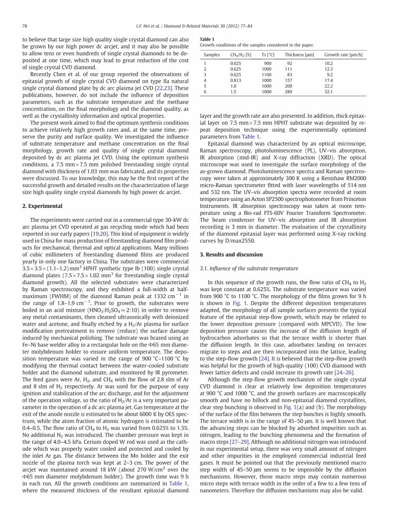
Table 1Growth conditions of the samples considered in the paper.
Samples CH4/H2 [%] Ts [°C] Thickness [μm] Growth rate [μm/h]
1 0.625 900 92 10.22 0.625 1000 111 12.33 0.625 1100 83 9.24 0.813 1000 157 17.45 1.0 1000 200 22.26 1.5 1000 289 32.1
78 L.F. Hei et al. / Diamond & Related Materials 30 (2012) 77–84
to believe that large size high quality single crystal diamond can alsobe grown by our high power dc arcjet, and it may also be possibleto allow tens or even hundreds of single crystal diamonds to be de-posited at one time, which may lead to great reduction of the costof single crystal CVD diamond.
Recently Chen et al. of our group reported the observations ofepitaxial growth of single crystal CVD diamond on type IIa naturalsingle crystal diamond plate by dc arc plasma jet CVD [22,23]. Thesepublications, however, do not include the influence of depositionparameters, such as the substrate temperature and the methaneconcentration, on the final morphology and the diamond quality, aswell as the crystallinity information and optical properties.
The present work aimed to find the optimum synthesis conditionsto achieve relatively high growth rates and, at the same time, pre-serve the purity and surface quality. We investigated the influenceof substrate temperature and methane concentration on the finalmorphology, growth rate and quality of single crystal diamonddeposited by dc arc plasma jet CVD. Using the optimum synthesisconditions, a 7.5 mm×7.5 mm polished freestanding single crystaldiamond with thickness of 1.03 mmwas fabricated, and its propertieswere discussed. To our knowledge, this may be the first report of thesuccessful growth and detailed results on the characterization of largesize high quality single crystal diamonds by high power dc arcjet.
2. Experimental
The experiments were carried out in a commercial type 30-kW dcarc plasma jet CVD operated at gas recycling mode which had beenreported in our early papers [19,20]. This kind of equipment is widelyused in China for mass production of freestanding diamond film prod-ucts for mechanical, thermal and optical applications. Many millionsof cubic millimeters of freestanding diamond films are producedyearly in only one factory in China. The substrates were commercial3.5×3.5×(1.1–1.2)mm3 HPHT synthetic type Ib (100) single crystaldiamond plates (7.5×7.5×1.02 mm3 for freestanding single crystaldiamond growth). All the selected substrates were characterizedby Raman spectroscopy, and they exhibited a full-width at half-maximum (FWHM) of the diamond Raman peak at 1332 cm−1 inthe range of 1.8–1.9 cm−1. Prior to growth, the substrates wereboiled in an acid mixture (HNO3:H2SO4=2:10) in order to removeany metal contaminants, then cleaned ultrasonically with deionizedwater and acetone, and finally etched by a H2/Ar plasma for surfacemodification pretreatment to remove (reduce) the surface damageinduced by mechanical polishing. The substrate was brazed using anFe–Ni base welder alloy in a rectangular hole on the Φ65 mm diame-ter molybdenum holder to ensure uniform temperature. The depo-sition temperature was varied in the range of 900 °C–1100 °C bymodifying the thermal contact between the water-cooled substrateholder and the diamond substrate, and monitored by IR pyrometer.The feed gases were Ar, H2, and CH4 with the flow of 2.8 slm of Arand 8 slm of H2 respectively. Ar was used for the purpose of easyignition and stabilization of the arc discharge, and for the adjustmentof the operation voltage, so the ratio of H2/Ar is a very important pa-rameter in the operation of a dc arc plasma jet. Gas temperature at theexit of the anode nozzle is estimated to be about 6000 K by OES spec-trum, while the atom fraction of atomic hydrogen is estimated to be0.4–0.5. The flow ratio of CH4 to H2 was varied from 0.625% to 1.5%.No additional N2 was introduced. The chamber pressure was kept inthe range of 4.0–4.5 kPa. Cerium doped W rod was used as the cath-ode which was properly water cooled and protected and cooled bythe inlet Ar gas. The distance between the Mo holder and the exitnozzle of the plasma torch was kept at 2–3 cm. The power of thearcjet was maintained around 18 kW (about 270 W/cm2 over theΦ65 mm diameter molybdenum holder). The growth time was 9 hin each run. All the growth conditions are summarized in Table 1,where the measured thickness of the resultant epitaxial diamond
layer and the growth rate are also presented. In addition, thick epitax-ial layer on 7.5 mm×7.5 mm HPHT substrate was deposited by re-peat deposition technique using the experimentally optimizedparameters from Table 1.
Epitaxial diamond was characterized by an optical microscope,Raman spectroscopy, photoluminescence (PL), UV–vis absorption,IR absorption (mid-IR) and X-ray diffraction (XRD). The opticalmicroscope was used to investigate the surface morphology of theas-grown diamond. Photoluminescence spectra and Raman spectros-copy were taken at approximately 300 K using a Renishaw RM2000micro-Raman spectrometer fitted with laser wavelengths of 514 nmand 532 nm. The UV–vis absorption spectra were recorded at roomtemperature using an Acton SP2500 spectrophotometer from PrincetonInstruments. IR absorption spectroscopy was taken at room tem-perature using a Bio-rad FTS-60V Fourier Transform Spectrometer.The beam condenser for UV–vis absorption and IR absorptionrecording is 3 mm in diameter. The evaluation of the crystallinityof the diamond epitaxial layer was performed using X-ray rockingcurves by D/max2550.
3. Results and discussion
3.1. Influence of the substrate temperature
In this sequence of the growth runs, the flow ratio of CH4 to H2
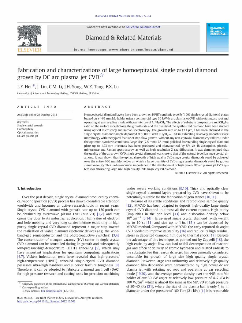
was kept constant at 0.625%. The substrate temperature was variedfrom 900 °C to 1100 °C. The morphology of the films grown for 9 his shown in Fig. 1. Despite the different deposition temperaturesadapted, the morphology of all sample surfaces presents the typicalfeature of the epitaxial step-flow growth, which may be related tothe lower deposition pressure (compared with MPCVD). The lowdeposition pressure causes the increase of the diffusion length ofhydrocarbon adsorbates so that the terrace width is shorter thanthe diffusion length. In this case, adsorbates landing on terracesmigrate to steps and are then incorporated into the lattice, leadingto the step-flow growth [24]. It is believed that the step-flow growthwas helpful for the growth of high-quality (100) CVD diamond withfewer lattice defects and could increase its growth rate [24–26].
Although the step-flow growth mechanism of the single crystalCVD diamond is clear at relatively low deposition temperaturesat 900 °C and 1000 °C, and the growth surfaces are macroscopicallysmooth and have no hillock and non-epitaxial diamond crystallites,clear step bunching is observed in Fig. 1(a) and (b). The morphologyof the surface of the film between the step bunches is highly smooth.The terrace width is in the range of 45–50 μm. It is well known thatthe advancing steps can be blocked by adsorbed impurities such asnitrogen, leading to the bunching phenomena and the formation ofmacro steps [27–29]. Although no additional nitrogen was introducedin our experimental setup, there was very small amount of nitrogenand other impurities in the employed commercial industrial feedgases. It must be pointed out that the previously mentioned macrostep width of 45–50 μm seems to be impossible by the diffusionmechanisms. However, those macro steps may contain numerousmicro steps with terrace width in the order of a few to a few tens ofnanometers. Therefore the diffusion mechanisms may also be valid.
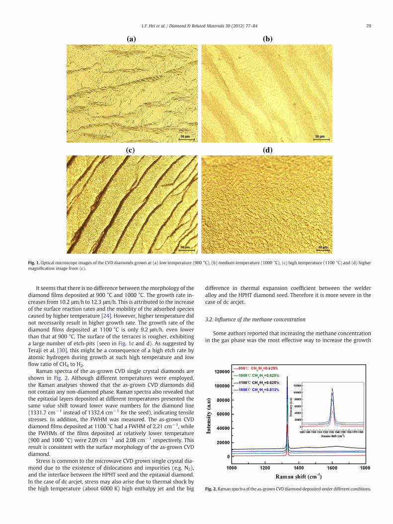
Fig. 1. Optical microscope images of the CVD diamonds grown at (a) low temperature (900 °C), (b) medium temperature (1000 °C), (c) high temperature (1100 °C) and (d) highermagnification image from (c).
Fig. 2. Raman spectra of the as-grownCVD diamond deposited under different conditions.
79L.F. Hei et al. / Diamond & Related Materials 30 (2012) 77–84
It seems that there is no difference between the morphology of thediamond films deposited at 900 °C and 1000 °C. The growth rate in-creases from 10.2 μm/h to 12.3 μm/h. This is attributed to the increaseof the surface reaction rates and the mobility of the adsorbed speciescaused by higher temperature [24]. However, higher temperature didnot necessarily result in higher growth rate. The growth rate of thediamond films deposited at 1100 °C is only 9.2 μm/h, even lowerthan that at 900 °C. The surface of the terraces is rougher, exhibitinga large number of etch-pits (seen in Fig. 1c and d). As suggested byTeraji et al. [30], this might be a consequence of a high etch rate byatomic hydrogen during growth at such high temperature and lowflow ratio of CH4 to H2.
Raman spectra of the as-grown CVD single crystal diamonds areshown in Fig. 2. Although different temperatures were employed,the Raman analyses showed that the as-grown CVD diamonds didnot contain any non-diamond phase. Raman spectra also revealed thatthe epitaxial layers deposited at different temperatures presented thesame value shift toward lower wave numbers for the diamond line(1331.7 cm−1 instead of 1332.4 cm−1 for the seed), indicating tensilestresses. In addition, the FWHM was measured. The as-grown CVDdiamond films deposited at 1100 °C had a FWHM of 2.21 cm−1, whilethe FWHMs of the films deposited at relatively lower temperature(900 and 1000 °C) were 2.09 cm−1 and 2.08 cm−1 respectively. Thisresult is consistent with the surface morphology of the as-grown CVDdiamond.
Stress is common to the microwave CVD grown single crystal dia-mond due to the existence of dislocations and impurities (e.g. N2),and the interface between the HPHT seed and the epitaxial diamond.In the case of dc arcjet, stress may also arise due to thermal shock bythe high temperature (about 6000 K) high enthalpy jet and the big
difference in thermal expansion coefficient between the welderalloy and the HPHT diamond seed. Therefore it is more severe in thecase of dc arcjet.
3.2. Influence of the methane concentration
Some authors reported that increasing the methane concentrationin the gas phase was the most effective way to increase the growth
80 L.F. Hei et al. / Diamond & Related Materials 30 (2012) 77–84
rate of single crystal diamond by MPCVD [25,30]. However, highmethane concentration can cause random growth, or even non-epitaxial growth, resulting in poor quality of single crystal diamond[24]. In our study, different flow ratios of CH4 to H2 were used toevaluate its influence on the film morphology, quality and growthrate.
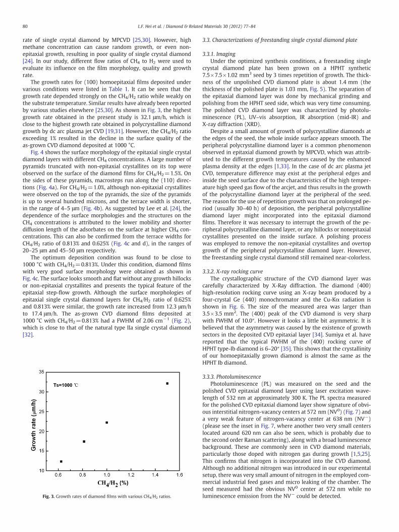
The growth rates for (100) homoepitaxial films deposited undervarious conditions were listed in Table 1. It can be seen that thegrowth rate depended strongly on the CH4/H2 ratio while weakly onthe substrate temperature. Similar results have already been reportedby various studies elsewhere [25,30]. As shown in Fig. 3, the highestgrowth rate obtained in the present study is 32.1 μm/h, which isclose to the highest growth rate obtained in polycrystalline diamondgrowth by dc arc plasma jet CVD [19,31]. However, the CH4/H2 ratioexceeding 1% resulted in the decline in the surface quality of theas-grown CVD diamond deposited at 1000 °C.
Fig. 4 shows the surface morphology of the epitaxial single crystaldiamond layers with different CH4 concentrations. A large number ofpyramids truncated with non-epitaxial crystallites on its top wereobserved on the surface of the diamond films for CH4/H2=1.5%. Onthe sides of these pyramids, macrosteps run along the (110) direc-tions (Fig. 4a). For CH4/H2=1.0%, although non-epitaxial crystalliteswere observed on the top of the pyramids, the size of the pyramidsis up to several hundred microns, and the terrace width is shorter,in the range of 4–5 μm (Fig. 4b). As suggested by Lee et al. [24], thedependence of the surface morphologies and the structures on theCH4 concentrations is attributed to the lower mobility and shorterdiffusion length of the adsorbates on the surface at higher CH4 con-centrations. This can also be confirmed from the terrace widths forCH4/H2 ratio of 0.813% and 0.625% (Fig. 4c and d), in the ranges of20–25 μm and 45–50 μm respectively.
The optimum deposition condition was found to be close to1000 °C with CH4/H2=0.813%. Under this condition, diamond filmswith very good surface morphology were obtained as shown inFig. 4c. The surface looks smooth and flat without any growth hillocksor non-epitaxial crystallites and presents the typical feature of theepitaxial step-flow growth. Although the surface morphologies ofepitaxial single crystal diamond layers for CH4/H2 ratio of 0.625%and 0.813% were similar, the growth rate increased from 12.3 μm/hto 17.4 μm/h. The as-grown CVD diamond films deposited at1000 °C with CH4/H2=0.813% had a FWHM of 2.06 cm−1 (Fig. 2),which is close to that of the natural type IIa single crystal diamond[32].
Fig. 3. Growth rates of diamond films with various CH4/H2 ratios.
3.3. Characterizations of freestanding single crystal diamond plate
3.3.1. ImagingUnder the optimized synthesis conditions, a freestanding single
crystal diamond plate has been grown on a HPHT synthetic7.5×7.5×1.02 mm3 seed by 3 times repetition of growth. The thick-ness of the unpolished CVD diamond plate is about 1.4 mm (thethickness of the polished plate is 1.03 mm, Fig. 5). The separation ofthe epitaxial diamond layer was done by mechanical grinding andpolishing from the HPHT seed side, which was very time consuming.The polished CVD diamond layer was characterized by photolu-minescence (PL), UV–vis absorption, IR absorption (mid-IR) andX-ray diffraction (XRD).
Despite a small amount of growth of polycrystalline diamonds atthe edges of the seed, the whole inside surface appears smooth. Theperipheral polycrystalline diamond layer is a common phenomenonobserved in epitaxial diamond growth by MPCVD, which was attrib-uted to the different growth temperatures caused by the enhancedplasma density at the edges [1,33]. In the case of dc arc plasma jetCVD, temperature difference may exist at the peripheral edges andinside the seed surface due to the characteristics of the high temper-ature high speed gas flow of the arcjet, and thus results in the growthof the polycrystalline diamond layer at the peripheral of the seed.The reason for the use of repetition growth was that on prolonged pe-riod (usually 30–40 h) of deposition, the peripheral polycrystallinediamond layer might incorporated into the epitaxial diamondfilms. Therefore it was necessary to interrupt the growth of the pe-ripheral polycrystalline diamond layer, or any hillocks or nonepitaxialcrystallites presented on the inside surface. A polishing processwas employed to remove the non-epitaxial crystallites and overtopgrowth of the peripheral polycrystalline diamond layer. However,the freestanding single crystal diamond still remained near-colorless.
3.3.2. X-ray rocking curveThe crystallographic structure of the CVD diamond layer was
carefully characterized by X-Ray diffraction. The diamond (400)high-resolution rocking curve using an X-ray beam produced by afour-crystal Ge (440) monochromator and the Cu-Kα radiation isshown in Fig. 6. The size of the measured area was larger than3.5×3.5 mm2. The (400) peak of the CVD diamond is very sharpwith FWHM of 10.0″. However it looks a little bit asymmetric. It isbelieved that the asymmetry was caused by the existence of growthsectors in the deposited CVD epitaxial layer [34]. Sumiya et al. havereported that the typical FWHM of the (400) rocking curve ofHPHT type-Ib diamond is 6–20″ [35]. This shows that the crystallinityof our homoepitaxially grown diamond is almost the same as theHPHT Ib diamond.
3.3.3. PhotoluminescencePhotoluminescence (PL) was measured on the seed and the
polished CVD epitaxial diamond layer using laser excitation wave-length of 532 nm at approximately 300 K. The PL spectra measuredfor the polished CVD epitaxial diamond layer show signature of obvi-ous interstitial nitrogen-vacancy centers at 572 nm (NV0) (Fig. 7) anda very weak feature of nitrogen-vacancy center at 638 nm (NV−)(please see the inset in Fig. 7, where another two very small centerslocated around 620 nm can also be seen, which is probably due tothe second order Raman scattering), along with a broad luminescencebackground. These are commonly seen in CVD diamond materials,particularly those doped with nitrogen gas during growth [1,5,25].This confirms that nitrogen is incorporated into the CVD diamond.Although no additional nitrogen was introduced in our experimentalsetup, there was very small amount of nitrogen in the employed com-mercial industrial feed gases and micro leaking of the chamber. Theseed measured had the obvious NV0 center at 572 nm while noluminescence emission from the NV− could be detected.
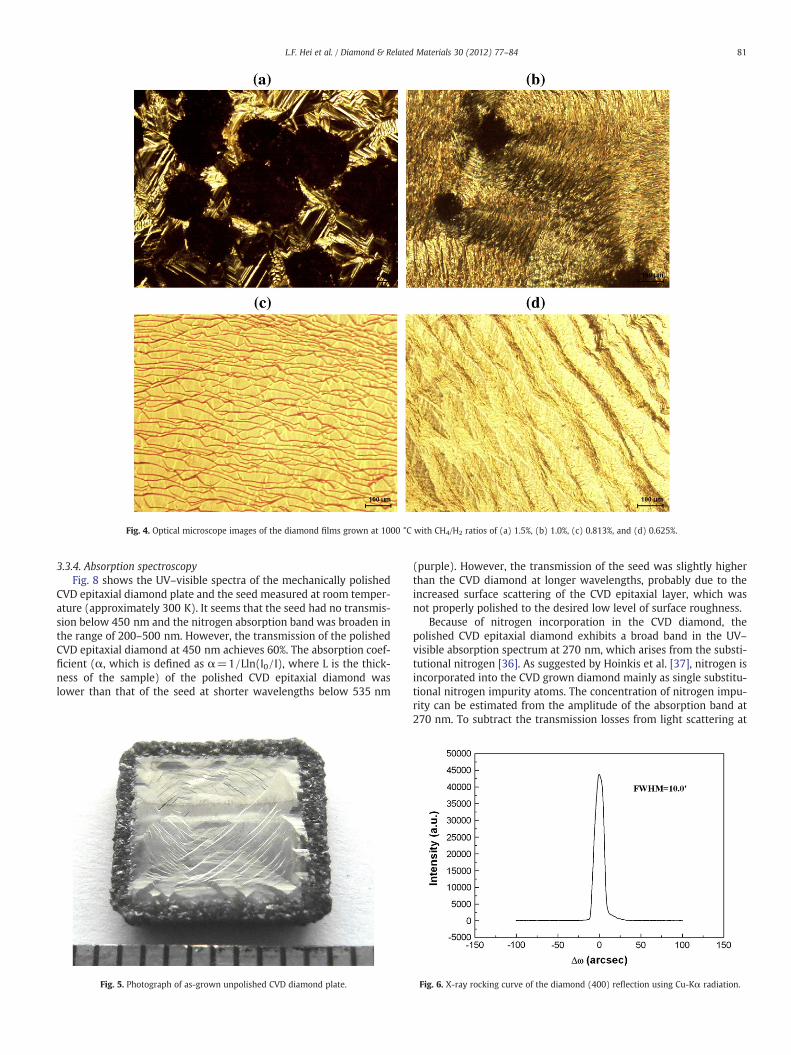
Fig. 4. Optical microscope images of the diamond films grown at 1000 °C with CH4/H2 ratios of (a) 1.5%, (b) 1.0%, (c) 0.813%, and (d) 0.625%.
81L.F. Hei et al. / Diamond & Related Materials 30 (2012) 77–84
3.3.4. Absorption spectroscopyFig. 8 shows the UV–visible spectra of the mechanically polished
CVD epitaxial diamond plate and the seed measured at room temper-ature (approximately 300 K). It seems that the seed had no transmis-sion below 450 nm and the nitrogen absorption band was broaden inthe range of 200–500 nm. However, the transmission of the polishedCVD epitaxial diamond at 450 nm achieves 60%. The absorption coef-ficient (α, which is defined as α=1/Lln(I0/ I), where L is the thick-ness of the sample) of the polished CVD epitaxial diamond waslower than that of the seed at shorter wavelengths below 535 nm
Fig. 5. Photograph of as-grown unpolished CVD diamond plate.
(purple). However, the transmission of the seed was slightly higherthan the CVD diamond at longer wavelengths, probably due to theincreased surface scattering of the CVD epitaxial layer, which wasnot properly polished to the desired low level of surface roughness.
Because of nitrogen incorporation in the CVD diamond, thepolished CVD epitaxial diamond exhibits a broad band in the UV–visible absorption spectrum at 270 nm, which arises from the substi-tutional nitrogen [36]. As suggested by Hoinkis et al. [37], nitrogen isincorporated into the CVD grown diamond mainly as single substitu-tional nitrogen impurity atoms. The concentration of nitrogen impu-rity can be estimated from the amplitude of the absorption band at270 nm. To subtract the transmission losses from light scattering at
Fig. 6. X-ray rocking curve of the diamond (400) reflection using Cu-Kα radiation.
Fig. 7. Photoluminescence spectra of the polished CVD epitaxial diamond layer and theseed measured at 300 K with 532 nm laser excitation.
82 L.F. Hei et al. / Diamond & Related Materials 30 (2012) 77–84
the surface roughness and defect-induced absorption bands causedby other types of nitrogen impurities, the absorbance was fittedwith a third order polynomial approximation (Fig. 8b, dotted line)as suggested by Nistor [38]. The concentration of nitrogen in theCVD epitaxial diamond was estimated to be approximately 7.6 ppm(0.56 ppm×13.5 cm−1 [39]).
To further characterize the optical property of the CVD epitaxialdiamond, absorption spectrum of the seed and polished CVD diamondin the IR spectral range of 4000–400 cm−1 was measured at roomtemperature with a beam condenser of 3 mm in diameter. Theabsorption coefficients of the CVD diamond are lower than that ofthe seed for all of the wavelengths (Fig. 9a). It can be seen that verystrong absorption peaks at 1130 cm−1, 1282 cm−1, 1344 cm−1
attributed to nitrogen impurities with a broadened peak at 840 cm−1
present in the HPHT synthetic diamond seed. However, for the CVDepitaxial diamond layer, beyond the intrinsic multi-phonon absorptionbands between 4000 and 1500 cm−1, the nitrogen related peaksstrongly declined. Only the weaker features at 1130 cm−1 and1344 cm−1 can be seen, and the peak at 1282 cm−1 and 840 cm−1
disappears (Fig. 9b). The results are consistent with that obtained byUV–visible spectra at 270 nm (Fig. 8b).
Both PL and UV–vis–IR spectrum clearly show that certain amountof nitrogen (ppm level) did exist in our epitaxial diamond layer. Themain reason is that the industrial grade hydrogen was used, whichmay contain considerable amount of impurities (mainly nitrogen
Fig. 8. UV–vis spectra of the polished CVD epitaxial diamond and the seed measured at roospectral absorption (solid line) and a base line fitted with a third order polynomial (dotted
(≦6000 ppm) and oxygen (≦3750 ppm), and water vapor and others(≦250 ppm)). Another reason may be the gas recycling adopted byour 30 kW dc arc plasma jet, which may lead to accumulation of theimpurities (mainly nitrogen) that came from the vacuum leakageand the industrial grade hydrogen. For this reason, it is rather hardto reduce the incorporated nitrogen level down below 1 ppm eventhough high purity hydrogen is used, as proved by our previouswork on optical quality freestanding diamond films [20]. For thisreason, a smaller (10 kW) dc arcjet system working at blow downmode (no gas recycling) has already been designed and is under con-struction, and it is hoped that it could reduce the incorporated nitro-gen down to ppb level by using high purity source gases.
It is worth mentioning that the growth rate of 17.4 μm/h wasobtainable over the entire Φ65 mm Mo holder surface, which couldbe converted to a mass growth rate of 1 ct/h, demonstrating the eco-nomical potential of the dc arc plasma jet CVD as compared with theMPCVDmethod. An example for multiple growths is shown in Fig. 10,where it can be seen that two 6 mm×6 mm and 5 mm×5 mm singlecrystal diamonds are simultaneously grown together with the sur-rounding polycrystalline diamond film on the top of the Φ65 mmMo holder. The uniformity of the polycrystalline diamond film is a di-rect proof of the temperature uniformity. Actually the temperaturedifference between the two crystals was recorded as less than 5 °C.The deposition time was 44 h. It can also be seen that the peripheralpolycrystalline diamond layer is higher than the epitaxial layer witha tendency to intervene the epitaxial growth, and there are a fewpyramids (hillocks) in the surface of the as grown 6 mm×6 mmdiamond, which should be removed by mechanical polishing beforethe next growth as stated before.
4. Summary
In this paper, we have investigated the effects of the substratetemperature and methane concentration on the final morphology,growth rate and quality of single crystal diamond deposited by dcarc plasma jet CVD with rotating arc root and operating at gasrecycling mode. The growth rate depended strongly on the CH4/H2
ratio while weakly on the substrate temperature. The growth rateup to 17.4 μm/h was obtained for the single crystal diamond sampledeposited at 1000 °C with CH4/H2=0.813%, with no degradation inquality as measured by Raman spectra.
It must be pointed out that the growth rate of 17.4 μm/h for thesingle crystal diamond growth by dc arc plasma jet CVD was obtain-able over the entire Φ65 mm area of the Mo holder, which couldbe converted to a mass growth rate of 1 ct/h, demonstrating the
m temperature (a) transmission, (b) absorption coefficient. Inset shows the apparentline) for CVD diamond.
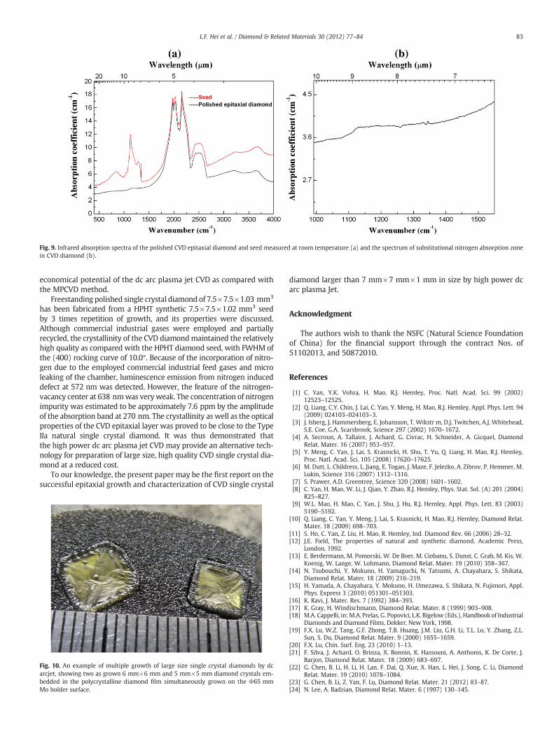
Fig. 9. Infrared absorption spectra of the polished CVD epitaxial diamond and seed measured at room temperature (a) and the spectrum of substitutional nitrogen absorption zonein CVD diamond (b).
83L.F. Hei et al. / Diamond & Related Materials 30 (2012) 77–84
economical potential of the dc arc plasma jet CVD as compared withthe MPCVD method.
Freestanding polished single crystal diamond of 7.5×7.5×1.03 mm3
has been fabricated from a HPHT synthetic 7.5×7.5×1.02 mm3 seedby 3 times repetition of growth, and its properties were discussed.Although commercial industrial gases were employed and partiallyrecycled, the crystallinity of the CVD diamondmaintained the relativelyhigh quality as compared with the HPHT diamond seed, with FWHM ofthe (400) rocking curve of 10.0″. Because of the incorporation of nitro-gen due to the employed commercial industrial feed gases and microleaking of the chamber, luminescence emission from nitrogen induceddefect at 572 nm was detected. However, the feature of the nitrogen-vacancy center at 638 nmwas veryweak. The concentration of nitrogenimpurity was estimated to be approximately 7.6 ppm by the amplitudeof the absorption band at 270 nm. The crystallinity as well as the opticalproperties of the CVD epitaxial layer was proved to be close to the TypeIIa natural single crystal diamond. It was thus demonstrated thatthe high power dc arc plasma jet CVD may provide an alternative tech-nology for preparation of large size, high quality CVD single crystal dia-mond at a reduced cost.
To our knowledge, the present paper may be the first report on thesuccessful epitaxial growth and characterization of CVD single crystal
Fig. 10. An example of multiple growth of large size single crystal diamonds by dcarcjet, showing two as grown 6 mm×6 mm and 5 mm×5 mm diamond crystals em-bedded in the polycrystalline diamond film simultaneously grown on the Φ65 mmMo holder surface.
diamond larger than 7 mm×7 mm×1 mm in size by high power dcarc plasma Jet.
Acknowledgment
The authors wish to thank the NSFC (Natural Science Foundationof China) for the financial support through the contract Nos. of51102013, and 50872010.
References
[1] C. Yan, Y.K. Vohra, H. Mao, R.J. Hemley, Proc. Natl. Acad. Sci. 99 (2002)12523–12525.
[2] Q. Liang, C.Y. Chin, J. Lai, C. Yan, Y. Meng, H. Mao, R.J. Hemley, Appl. Phys. Lett. 94(2009) 024103–024103–3.
[3] J. Isberg, J. Hammersberg, E. Johansson, T. Wikstr m, D.J. Twitchen, A.J. Whitehead,S.E. Coe, G.A. Scarsbrook, Science 297 (2002) 1670–1672.
[4] A. Secroun, A. Tallaire, J. Achard, G. Civrac, H. Schneider, A. Gicquel, DiamondRelat. Mater. 16 (2007) 953–957.
[5] Y. Meng, C. Yan, J. Lai, S. Krasnicki, H. Shu, T. Yu, Q. Liang, H. Mao, R.J. Hemley,Proc. Natl. Acad. Sci. 105 (2008) 17620–17625.
[6] M. Dutt, L. Childress, L. Jiang, E. Togan, J. Maze, F. Jelezko, A. Zibrov, P. Hemmer, M.Lukin, Science 316 (2007) 1312–1316.
[7] S. Prawer, A.D. Greentree, Science 320 (2008) 1601–1602.[8] C. Yan, H. Mao, W. Li, J. Qian, Y. Zhao, R.J. Hemley, Phys. Stat. Sol. (A) 201 (2004)
R25–R27.[9] W.L. Mao, H. Mao, C. Yan, J. Shu, J. Hu, R.J. Hemley, Appl. Phys. Lett. 83 (2003)
5190–5192.[10] Q. Liang, C. Yan, Y. Meng, J. Lai, S. Krasnicki, H. Mao, R.J. Hemley, Diamond Relat.
Mater. 18 (2009) 698–703.[11] S. Ho, C. Yan, Z. Liu, H. Mao, R. Hemley, Ind. Diamond Rev. 66 (2006) 28–32.[12] J.E. Field, The properties of natural and synthetic diamond, Academic Press,
London, 1992.[13] E. Berdermann, M. Pomorski, W. De Boer, M. Ciobanu, S. Dunst, C. Grah, M. Kis, W.
Koenig, W. Lange, W. Lohmann, Diamond Relat. Mater. 19 (2010) 358–367.[14] N. Tsubouchi, Y. Mokuno, H. Yamaguchi, N. Tatsumi, A. Chayahara, S. Shikata,
Diamond Relat. Mater. 18 (2009) 216–219.[15] H. Yamada, A. Chayahara, Y. Mokuno, H. Umezawa, S. Shikata, N. Fujimori, Appl.
Phys. Express 3 (2010) 051301–051303.[16] K. Ravi, J. Mater. Res. 7 (1992) 384–393.[17] K. Gray, H. Windischmann, Diamond Relat. Mater. 8 (1999) 903–908.[18] M.A. Cappelli, in: M.A. Prelas, G. Popovici, L.K. Bigelow (Eds.), Handbook of Industrial
Diamonds and Diamond Films, Dekker, New York, 1998.[19] F.X. Lu, W.Z. Tang, G.F. Zhong, T.B. Huang, J.M. Liu, G.H. Li, T.L. Lo, Y. Zhang, Z.L.
Sun, S. Du, Diamond Relat. Mater. 9 (2000) 1655–1659.[20] F.X. Lu, Chin. Surf. Eng. 23 (2010) 1–13.[21] F. Silva, J. Achard, O. Brinza, X. Bonnin, K. Hassouni, A. Anthonis, K. De Corte, J.
Barjon, Diamond Relat. Mater. 18 (2009) 683–697.[22] G. Chen, B. Li, H. Li, H. Lan, F. Dai, Q. Xue, X. Han, L. Hei, J. Song, C. Li, Diamond
Relat. Mater. 19 (2010) 1078–1084.[23] G. Chen, B. Li, Z. Yan, F. Lu, Diamond Relat. Mater. 21 (2012) 83–87.[24] N. Lee, A. Badzian, Diamond Relat. Mater. 6 (1997) 130–145.

84 L.F. Hei et al. / Diamond & Related Materials 30 (2012) 77–84
[25] J. Achard, A. Tallaire, R. Sussmann, F. Silva, A. Gicquel, J. Cryst. Growth 284 (2005)396–405.
[26] A. Chayahara, Y. Mokuno, Y. Horino, Y. Takasu, H. Kato, H. Yoshikawa, N. Fujimori,Diamond Relat. Mater. 13 (2004) 1954–1958.
[27] W. Van Enckevort, A. Van der Berg, K. Kreuwel, A. Derksen, M. Couto, J. Cryst.Growth 166 (1996) 156–161.
[28] W. Van Enckevort, A. Van Den Berg, J. Cryst. Growth 183 (1998) 441–455.[29] F. De Theije, J. Schermer, W. Van Enckevort, Diamond Relat. Mater. 9 (2000)
1439–1449.[30] T. Teraji, S. Mitani, T. Ito, Phys. Stat. Sol. (A) 198 (2003) 395–406.[31] H. Guo, Z. Sun, Q. He, S. Du, X. Wu, Z. Wang, X. Liu, Y. Cai, X. Diao, G. Li, Diamond
Relat. Mater. 9 (2000) 1673–1677.[32] D. Kirillov, G. Reynolds, Appl. Phys. Lett. 65 (1994) 1641–1643.[33] Y. Mokuno, A. Chayahara, Y. Soda, Y. Horino, N. Fujimori, Diamond Relat. Mater.
14 (2005) 1743–1746.
[34] A. Muchnikov, A. Vikharev, A. Gorbachev, D. Radishev, V. Blank, S. Terentiev,Diamond Relat. Mater. 19 (2010) 432–436.
[35] H. Sumiya, N. Toda, Y. Nishibayashi, S. Satoh, J. Cryst. Growth 178 (1997)485–498.
[36] S. Charles, J. Butler, B. Feygelson, M. Newton, D. Carroll, J. Steeds, H. Darwish, C.S.Yan, H. Mao, R. Hemley, Phys. stat. sol. (a) 201 (2004) 2473–2485.
[37] M. Hoinkis, E. Weber, M. Landstrass, M. Plano, S. Han, D. Kania, Appl. Phys. Lett. 59(1991) 1870–1871.
[38] S. Nistor, M. Stefan, V. Ralchenko, A. Khomich, D. Schoemaker, J. Appl. Phys. 87(2000) 8741–8746.
[39] A. Khomich, V. Ralchenko, A. Smolin, V. Migulin, S. Pimenov, I. Vlasov, V. Konov,J. Chem. Vap. Depos. 5 (1997) 361–369.