fabrication and characterization of au/si heterojunction solar cell
TRANSCRIPT
Asian Journal of Applied Science and Engineering ISSN 2305-915X(p); 2307-9584(e)
Asian Business Consortium | AJASE ● Dec 2014 ● Vol 3 ● Issue 9 Page 34
Fabrication and Characterization of Au/Si
Heterojunction Solar Cell
Iman Hameed Khudayer
Associate Professor, Department of Physics, College of Education for Pure Science, University of Baghdad, Iraq
ARTICLE INFO ABSTRACT Volume 3 Number 5/2014 Issue 9 DOI Prefix: 10.15590/ajase/ Received: Sep 21, 2014 Accepted: Dec 03, 2014 Revised: Dec 05, 2014 Published: Jan 04, 2015 E-mail for correspondence: [email protected]
The n-type Au thin films of 500nm thickness was evaporated by thermal evaporation method on p-type silicon wafer of [111] direction to formed Au/Si heterojunction solar cell. The AC conductivity, C-V and I-V characteristics of fabricated c-Au/Si diffusion heterojunction-(HJ) solar cell, has been studied. The first methods demonstrated that the AC conductivity due to with diffusion-tunneling mechanism, while the second show that, the heterojunction profile is abrupt, the heterojunction parameters have been played out, such as the depletion width, built-in voltage, and concentration. And finally the third one show that the c-Au/Si HJ has rectification properties, and the solar cell yielded an open circuit voltage of (Vic) 0.4V, short circuit current (Isc) of 2.01May, fill factor (F.F) of 0.085 and ƞ% =7. 19. Keywords: Au thin films, C-V and I-V characteristics, Au/ Si heterojunction, solar cell parameters
Source of Support: Nil, Conflict of Interest: Declared.
How to Cite: Khudayer IH. 2014. Fabrication and Characterization of Au/Si Heterojunction Solar Cell Asian Journal
of Applied Science and Engineering, 3, 34-44.
This article is is licensed under a Creative Commons Attribution-NonCommercial 4.0 International License. Attribution-NonCommercial (CC BY-NC) license lets others remix, tweak, and build upon work non-commercially, and
although the new works must also acknowledge & be non-commercial.
INTRODUCTION
etal-semiconductor interfaces have been studied extensively owing to their variety of interesting properties that are both scientifically and technologically significant. The Au/Si interface has been of interest due to the possible application as a metal-
Si contact in integrated circuit devices. As Au atoms diffuse very fast and serve as deep-trap centers in Si, Au/Si contacts have been found unsuitable for this purpose. But the interface is of interest for fundamental reasons. Though gold is usually considered as a
M
Asian Journal of Applied Science and Engineering ISSN 2305-915X(p); 2307-9584(e)
Asian Business Consortium | AJASE ● Dec 2014 ● Vol 3 ● Issue 9 Page 35
nonreactive stable noble metal, it has been described to be very reactive on Si surfaces, even at room temperature (Sundaravel etel, 1999; Hong etel, 2005; and Bokhonov & Korchagin, 2000). Beginning in the early 1970s, the gold-silicon interface has been extensively investigated using various surface techniques to understand its crystallographic, chemical, and electronic properties. Despite the Au/Si contact being unsuitable for applications in integrated circuit devices due to the rapid dispersion of Au atoms and their bass-trap center formation in Si, the study of thin gold films on Si still raises interesting questions. Regions of interest include the supposed Au-Si reaction at room temperature (RT) and the critical gold coverage necessary to induce it, the diffusion of sin through Au layers even for thick deposits, and related properties such as the source and construction of electronic states at the interface. A non-exhaustive list of the techniques used, individually or combined, includes low-energy electron diffraction (LEED), Auger electron spectroscopy (AES), MeV ion backscattering, electron-energy-loss spectroscopy (EELS), x-ray photoelectron spectroscopy (XPS), ultraviolet photoelectron spectroscopy (UPS), photoemission yield spectroscopy, soft x-ray photoelectron spectroscopy, scanning tunneling microscopy (STM), x-ray standing wave, and transmission electron microscopy (TEM) (Hazra, 2007; Landry etel, 1997).
EXPERIMENTAL PARTS
Thin films of high purity Au 99.99% have been deposited on silicon by thermal evaporation technique at room temperature, in a high vacuum system of (3x10⁻⁶) Torr using the Edward coating unit model (E 306) from molybdenum boat, the distance between the boat and the substrate was about 15 cm. Film thickness was about (500±50) nm at R.T (300 K) with a deposition rate (1.5 nm/Sec) to form a heterojunction solar cell. Ohmic contacts are made on both Au thin films and Si substrate by depositing of Al films through certain mask. X-ray Diffraction (XRD): was used to the position and intensity of diffracted intensity spectra versus Bragg's angle, gives information on the crystal structure such as phase crystalline, polycrystalline, amorphous, grain size, and lattice parameter. The inter planer distance d (kl) for different planes was measured by Bragg's law (Blackmore, 1974): 2dsinθ=n (1) The structures of the alloy and deposited films have been examined by XRD methods using the Siemens x-ray diffractometer system. The capacitance of the heterojunction is measured as a function of the bias voltage in reverse bias in the range (from 0 to -2) Volt with different values of frequency in the range 105-3x10⁶ Hz uses model 4274A and 4275A multi-frequency LRC meter. In addition, a convenient formalism to investigate the frequency behavior of conductivity is based on the power law relation proposed by Jonscher (Ertuğrul, 2012): (𝜔) = 𝜎dc + 𝜎ac = 𝜎dc + 𝐴𝜔𝑠 (2) Where, (𝜔) is the total conductivity. The first term is the temperature-dependent (frequency-independent) DC conductivity and relates to the drift mobility of the electric charge carriers. The second term represents the frequency and temperature dependent ac conductivity (𝜎ac) and is attributed to the dielectric relaxation caused by the localized
Asian Journal of Applied Science and Engineering ISSN 2305-915X(p); 2307-9584(e)
Asian Business Consortium | AJASE ● Dec 2014 ● Vol 3 ● Issue 9 Page 36
electric charge carriers. Is a temperature-dependent constant and 𝑠 is the power law frequency exponent which generally varies between 0 and one (Ertuğrul, 2012). Capacitance voltage measurements can be manipulated to yield a number of parameters such as: type of the junction (abrupt or graded), built-in voltage (VD) was obtained from the intercept at (1/C2) =0 by extrapolating the curve to the voltage axis. Carrier concentration and the width of the junction (depletion layer) can be deduced from the following equation (Grove, 1976):
W =∈s
∈o (3)
Where, Co is the capacitance at zero biasing voltage, and
∈𝐬=∈𝐧∈𝐩
∈𝐧+∈𝐩 (4)
Where Єs is the semiconductor permittivity for the two semiconductor materials. The concentration of the carrier was calculated from the relation (Milnes & Feucht, 1972): 1
C2=
2 ∈1NA 1+∈2ND 2
qND 2NA 1∈1∈2 VD − Va (5)
Where [2 (Є1NA1+ Є2ND2)/qND2NA1Є1 Є2] represent the slope, NA1 and ND2 are the accepter and donor concentrations, and Є1, Є2 are the dielectric constant of p-type and n-type semiconductor respectively. VD is the built-in potential, Va is the applied voltage. I-V characteristics have been practiced through the dark current-potential measurement for Au/Si, which, carried out using applying a voltage to the sample from a stabilized d.c fine power supply. The current going through the device was evaluated utilizing a digital electrometer (Keithley 616). The bias voltage was varied (0-1.5) Volt in the case of forward and reverse bias. From the plot of the dark forward current as a function of bias voltage, the ideality factor was determined from the relation (Sharma & Purohil, 1974 ):
𝛽 =𝑞
𝑘𝐵𝑇
𝑉
𝑙𝑛 𝐼𝑓 𝐼𝑆1 (6)
The tunneling constant Ą was deduced from the equation:
A =dln
IfIs 2
dV (7)
The ideality factor (β) and the saturation current (Is) can be used to determine the theoretical value of the zero-bias resistance (Ro) of the photodiode using a simple formula (Wenus etel, 2003):
𝑅𝑜 =𝛽𝐾𝑇
𝑞𝐼𝑠-- (8)
While the rectification factor (RF) was calculated according to the following equation (Sze, 1981):
R. F =IF
IR for V≥3kT/q (9)
In the light condition, the optoelectronic measurements of heterojunction were made, the samples were exposed to halogen lamp at an intensity equal to (1000) W/m2.
Asian Journal of Applied Science and Engineering ISSN 2305-915X(p); 2307-9584(e)
Asian Business Consortium | AJASE ● Dec 2014 ● Vol 3 ● Issue 9 Page 37
In the absence of recombination or generation of carriers in the depletion region, JR is voltage independent and is equal to the short-circuit photocurrent density (JSC) (Dereniak & Crowe, 1992). The open-circuit voltage Vic across the heterojunction (i.e. for J=0) can process in terms of JR and JS as follows:
Vic =kB T
eln (1+JR
JS )
(10)
The fill factor is defined as:
𝑭. 𝑭 =𝑽𝒎𝑰𝒎
𝑽𝒐𝒄𝑰𝒔𝒄 (11)
Where: VmIm present the maximum power Pm.
𝜼 =𝑷𝒎
𝑷𝒊𝒏𝒙𝟏𝟎𝟎% (12)
RESULTS AND DISCUSSION
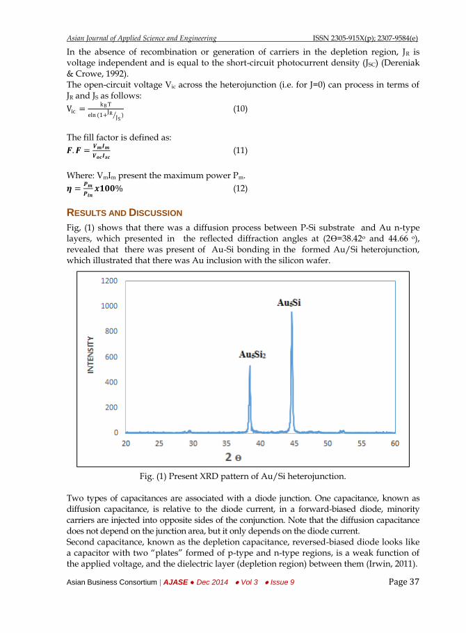
Fig, (1) shows that there was a diffusion process between P-Si substrate and Au n-type layers, which presented in the reflected diffraction angles at (2Ɵ=38.42o and 44.66 o), revealed that there was present of Au-Si bonding in the formed Au/Si heterojunction, which illustrated that there was Au inclusion with the silicon wafer.
Fig. (1) Present XRD pattern of Au/Si heterojunction.
Two types of capacitances are associated with a diode junction. One capacitance, known as diffusion capacitance, is relative to the diode current, in a forward-biased diode, minority carriers are injected into opposite sides of the conjunction. Note that the diffusion capacitance does not depend on the junction area, but it only depends on the diode current. Second capacitance, known as the depletion capacitance, reversed-biased diode looks like a capacitor with two “plates” formed of p-type and n-type regions, is a weak function of the applied voltage, and the dielectric layer (depletion region) between them (Irwin, 2011).
Asian Journal of Applied Science and Engineering ISSN 2305-915X(p); 2307-9584(e)
Asian Business Consortium | AJASE ● Dec 2014 ● Vol 3 ● Issue 9 Page 38
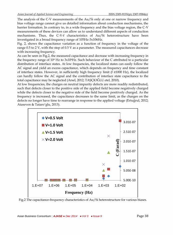
The analysis of the C-V measurements of the Au/Si only at one or narrow frequency and bias voltage range cannot give us detailed information about conduction mechanisms, the barrier formation. In contrary to, in a wide frequency and the bias voltage region, the C-V measurements of these devices can allow us to understand different aspects of conduction mechanisms. Thus, the C-V-f characteristics of Au/Si heterostructure have been investigated in a broad frequency range of 105Hz-3x10⁶Hz. Fig. 2, shows the capacitance variation as a function of frequency in the voltage of the range 0.5 to 2 V, with the step of 0.5 V as a parameter. The measured capacitances decrease with increasing frequency. As can be seen in Fig.2, the measured capacitance and decrease with increasing frequency in the frequency range of 104 Hz to 3x10⁶Hz. Such behaviour of the C attributed to a particular distribution of interface states. At low frequencies, the localized states can easily follow the AC signal and yield an excess capacitance, which depends on frequency and time constant of interface states. However, in sufficiently high frequency limit (f ≥1000 Hz), the localized can hardly follow the AC signal and the contribution of interface state capacitance to the total capacitance may be neglected (Arsel, 2012; TAġÇIOĞLU etel, 2010). At low frequencies, the charges on neutral impurity defects are more readily redistributed, such that defects closer to the positive side of the applied field become negatively charged while the defects closer to the negative side of the field become positively charged. As the frequency is increased, the capacitance decreases to the same limit, as the charges on the defects no longer have time to rearrange in response to the applied voltage (Ertuğrul, 2012; Ataseven & Tataro˘glu, 2013).
Fig.2 The capacitance-frequency characteristics of Au/Si heterostructure for various biases.
5.00E-10
5.05E-08
1.01E-07
1.51E-07
2.01E-07
2.51E-07
3.01E-07
1.E+021.E+031.E+041.E+051.E+061.E+07
C (
Fara
d)
Frequency (Hz)
V=0.5 Volt
V=1.0 Volt
V=1.5 Volt
V=2.0 Volt
Asian Journal of Applied Science and Engineering ISSN 2305-915X(p); 2307-9584(e)
Asian Business Consortium | AJASE ● Dec 2014 ● Vol 3 ● Issue 9 Page 39
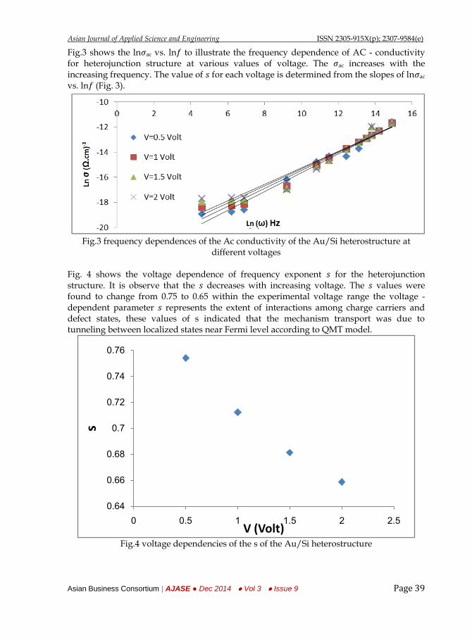
Fig.3 shows the ln𝜎ac vs. ln𝑓 to illustrate the frequency dependence of AC - conductivity for heterojunction structure at various values of voltage. The 𝜎ac increases with the increasing frequency. The value of 𝑠 for each voltage is determined from the slopes of ln𝜎ac vs. ln𝑓 (Fig. 3).
Fig.3 frequency dependences of the Ac conductivity of the Au/Si heterostructure at
different voltages
Fig. 4 shows the voltage dependence of frequency exponent 𝑠 for the heterojunction structure. It is observe that the 𝑠 decreases with increasing voltage. The 𝑠 values were found to change from 0.75 to 0.65 within the experimental voltage range the voltage -dependent parameter 𝑠 represents the extent of interactions among charge carriers and defect states, these values of s indicated that the mechanism transport was due to tunneling between localized states near Fermi level according to QMT model.
Fig.4 voltage dependencies of the s of the Au/Si heterostructure
0.64
0.66
0.68
0.7
0.72
0.74
0.76
0 0.5 1 1.5 2 2.5
s
V (Volt)
Asian Journal of Applied Science and Engineering ISSN 2305-915X(p); 2307-9584(e)
Asian Business Consortium | AJASE ● Dec 2014 ● Vol 3 ● Issue 9 Page 40
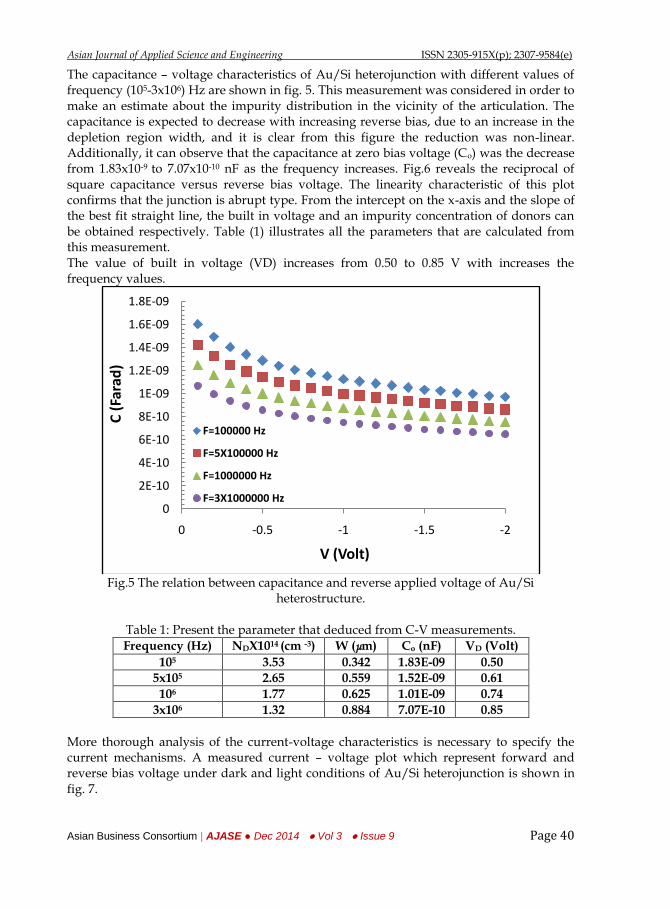
The capacitance – voltage characteristics of Au/Si heterojunction with different values of frequency (105-3x10⁶) Hz are shown in fig. 5. This measurement was considered in order to make an estimate about the impurity distribution in the vicinity of the articulation. The capacitance is expected to decrease with increasing reverse bias, due to an increase in the depletion region width, and it is clear from this figure the reduction was non-linear. Additionally, it can observe that the capacitance at zero bias voltage (Co) was the decrease from 1.83x10⁻⁹ to 7.07x10⁻¹⁰ nF as the frequency increases. Fig.6 reveals the reciprocal of square capacitance versus reverse bias voltage. The linearity characteristic of this plot confirms that the junction is abrupt type. From the intercept on the x-axis and the slope of the best fit straight line, the built in voltage and an impurity concentration of donors can be obtained respectively. Table (1) illustrates all the parameters that are calculated from this measurement. The value of built in voltage (VD) increases from 0.50 to 0.85 V with increases the frequency values.
Fig.5 The relation between capacitance and reverse applied voltage of Au/Si
heterostructure.
Table 1: Present the parameter that deduced from C-V measurements.
Frequency (Hz) NDX1014 (cm -3) W (μm) Co (nF) VD (Volt)
105 3.53 0.342 1.83E-09 0.50
5x10⁵ 2.65 0.559 1.52E-09 0.61
106 1.77 0.625 1.01E-09 0.74
3x10⁶ 1.32 0.884 7.07E-10 0.85
More thorough analysis of the current-voltage characteristics is necessary to specify the current mechanisms. A measured current – voltage plot which represent forward and reverse bias voltage under dark and light conditions of Au/Si heterojunction is shown in fig. 7.
0
2E-10
4E-10
6E-10
8E-10
1E-09
1.2E-09
1.4E-09
1.6E-09
1.8E-09
-2-1.5-1-0.50
C (
Fara
d)
V (Volt)
F=100000 Hz
F=5X100000 Hz
F=1000000 Hz
F=3X1000000 Hz
Asian Journal of Applied Science and Engineering ISSN 2305-915X(p); 2307-9584(e)
Asian Business Consortium | AJASE ● Dec 2014 ● Vol 3 ● Issue 9 Page 41
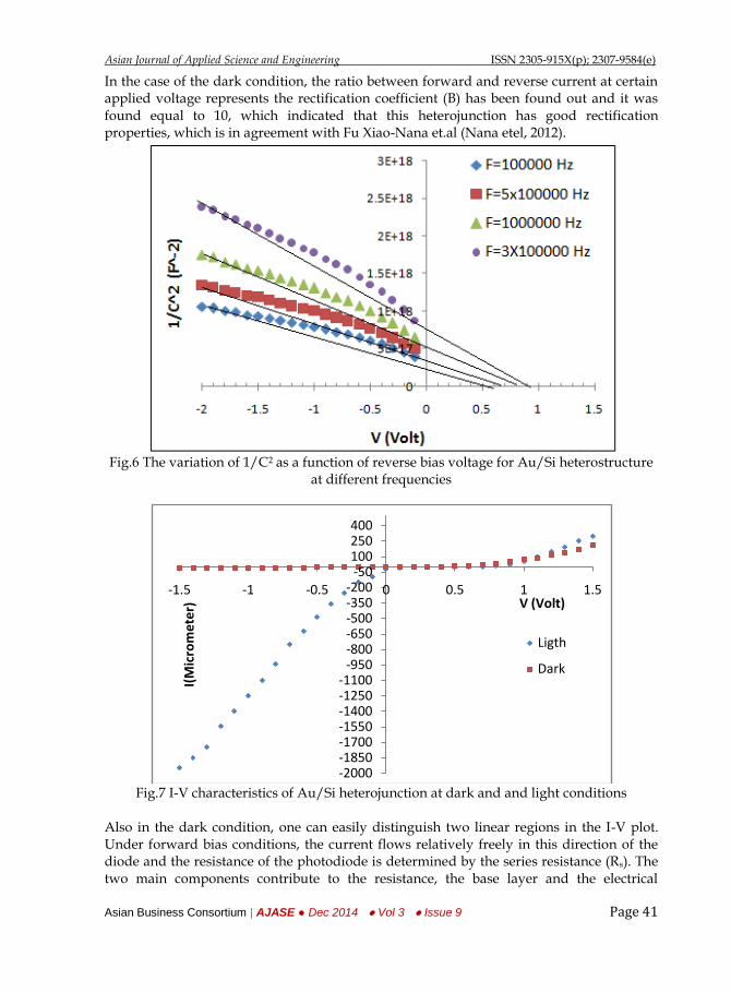
In the case of the dark condition, the ratio between forward and reverse current at certain applied voltage represents the rectification coefficient (B) has been found out and it was found equal to 10, which indicated that this heterojunction has good rectification properties, which is in agreement with Fu Xiao-Nana et.al (Nana etel, 2012).
Fig.6 The variation of 1/C2 as a function of reverse bias voltage for Au/Si heterostructure
at different frequencies
Fig.7 I-V characteristics of Au/Si heterojunction at dark and and light conditions
Also in the dark condition, one can easily distinguish two linear regions in the I-V plot. Under forward bias conditions, the current flows relatively freely in this direction of the diode and the resistance of the photodiode is determined by the series resistance (Rs). The two main components contribute to the resistance, the base layer and the electrical
-2000-1850-1700-1550-1400-1250-1100-950-800-650-500-350-200-50100250400
-1.5 -1 -0.5 0 0.5 1 1.5
I(M
icro
me
ter) V (Volt)
Ligth
Dark
Asian Journal of Applied Science and Engineering ISSN 2305-915X(p); 2307-9584(e)
Asian Business Consortium | AJASE ● Dec 2014 ● Vol 3 ● Issue 9 Page 42
contacts). In the reverse bias region, really low current flows, the influence of shunt resistance (Rs), which is usually similar to the max value, predominates. The main source of the shunt resistance is a surface leakage current connected with the passivation of the junction (Wenus etel, 2003). In general the forward dark current is generated due to the flow of majority carriers and the applied voltage injects majority carriers, which leads to decrease the value of built in potential, and decrease the width of the depletion layer. The majority and minority carrier concentration is higher than the intrinsic carrier
concentration (ni), i.e np > ni2
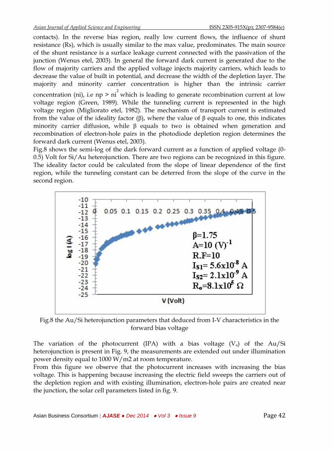
which is leading to generate recombination current at low voltage region (Green, 1989). While the tunneling current is represented in the high voltage region (Migliorato etel, 1982). The mechanism of transport current is estimated from the value of the ideality factor (β), where the value of β equals to one, this indicates minority carrier diffusion, while β equals to two is obtained when generation and recombination of electron-hole pairs in the photodiode depletion region determines the forward dark current (Wenus etel, 2003). Fig.8 shows the semi-log of the dark forward current as a function of applied voltage (0-0.5) Volt for Si/Au heterojunction. There are two regions can be recognized in this figure. The ideality factor could be calculated from the slope of linear dependence of the first region, while the tunneling constant can be deterred from the slope of the curve in the second region.
Fig.8 the Au/Si heterojunction parameters that deduced from I-V characteristics in the
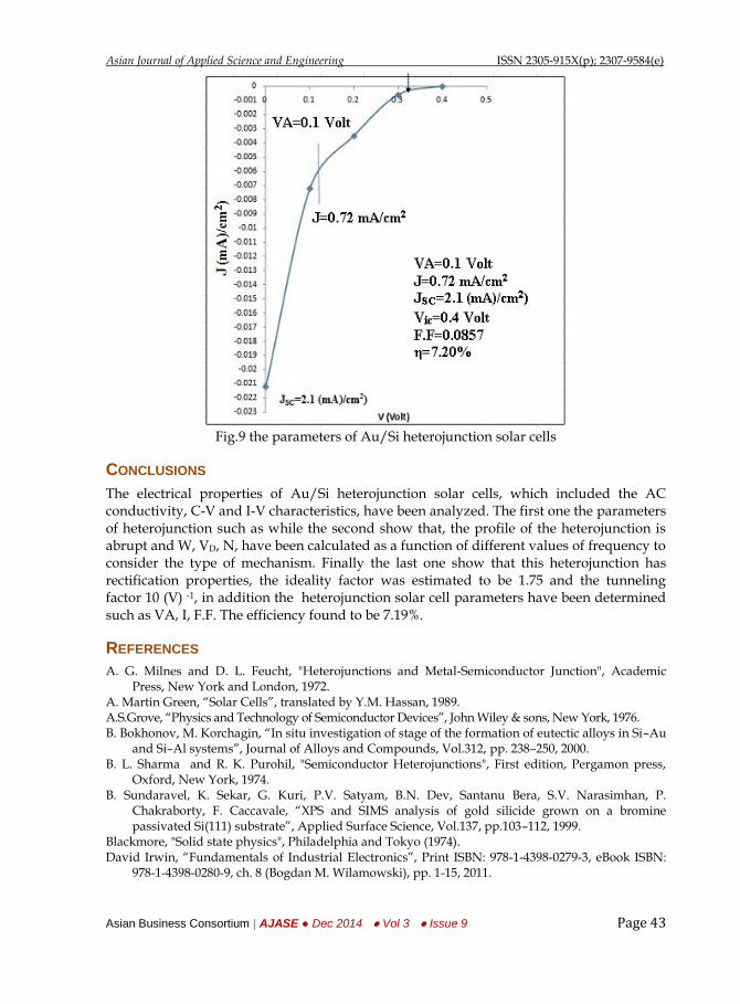
forward bias voltage The variation of the photocurrent (IPA) with a bias voltage (Va) of the Au/Si heterojunction is present in Fig. 9, the measurements are extended out under illumination power density equal to 1000 W/m2 at room temperature. From this figure we observe that the photocurrent increases with increasing the bias voltage. This is happening because increasing the electric field sweeps the carriers out of the depletion region and with existing illumination, electron-hole pairs are created near the junction, the solar cell parameters listed in fig. 9.
Asian Journal of Applied Science and Engineering ISSN 2305-915X(p); 2307-9584(e)
Asian Business Consortium | AJASE ● Dec 2014 ● Vol 3 ● Issue 9 Page 43
Fig.9 the parameters of Au/Si heterojunction solar cells
CONCLUSIONS
The electrical properties of Au/Si heterojunction solar cells, which included the AC conductivity, C-V and I-V characteristics, have been analyzed. The first one the parameters of heterojunction such as while the second show that, the profile of the heterojunction is abrupt and W, VD, N, have been calculated as a function of different values of frequency to consider the type of mechanism. Finally the last one show that this heterojunction has rectification properties, the ideality factor was estimated to be 1.75 and the tunneling factor 10 (V) -1, in addition the heterojunction solar cell parameters have been determined such as VA, I, F.F. The efficiency found to be 7.19%.
REFERENCES
A. G. Milnes and D. L. Feucht, "Heterojunctions and Metal-Semiconductor Junction", Academic Press, New York and London, 1972.
A. Martin Green, “Solar Cells”, translated by Y.M. Hassan, 1989. A.S.Grove, “Physics and Technology of Semiconductor Devices”, John Wiley & sons, New York, 1976. B. Bokhonov, M. Korchagin, “In situ investigation of stage of the formation of eutectic alloys in Si–Au
and Si–Al systems”, Journal of Alloys and Compounds, Vol.312, pp. 238–250, 2000. B. L. Sharma and R. K. Purohil, "Semiconductor Heterojunctions", First edition, Pergamon press,
Oxford, New York, 1974. B. Sundaravel, K. Sekar, G. Kuri, P.V. Satyam, B.N. Dev, Santanu Bera, S.V. Narasimhan, P.
Chakraborty, F. Caccavale, “XPS and SIMS analysis of gold silicide grown on a bromine passivated Si(111) substrate”, Applied Surface Science, Vol.137, pp.103–112, 1999.
Blackmore, "Solid state physics", Philadelphia and Tokyo (1974). David Irwin, “Fundamentals of Industrial Electronics”, Print ISBN: 978-1-4398-0279-3, eBook ISBN:
978-1-4398-0280-9, ch. 8 (Bogdan M. Wilamowski), pp. 1-15, 2011.
Asian Journal of Applied Science and Engineering ISSN 2305-915X(p); 2307-9584(e)
Asian Business Consortium | AJASE ● Dec 2014 ● Vol 3 ● Issue 9 Page 44
E. Landry, D. Grozea, C. Collazo-Davila, and L. D. Marks, “UHV high-resolution electron microscopy and chemical analysis of room-temperature Au deposition on Si.(001).-2x1”, PHYSICAL REVIEW B, Vol. 55, No. 12, pp.7910-7916, 1997.
Eustace L.Dereniak and Devon G.Crowe, "Optical Radiation Detectors ", Jone Wiley and Sons, York London, 1992.
Fu Xiao-Nana, Cheng Li-Naa, Luo Yan-Wei & Li Xin-Jiang, “I-V Characteristic of Au/Si-NPA and Si-NPA”, Integrated Ferroelectrics: An International Journal, Vol.135, Issue 1, pp. 1-7, 2012.
Ġ. TAġÇIOĞLU, H. USLU, Y. ġAFAK, E. ÖZBAY, "Frequency dependent electrical characteristics of (Ni/Au)/AlGaN/AlN/GaN heterostructures", Optoelectronics and Advanced Materials– Rapid Communications, Vol. 4, No. 6, pp. 859 – 862, 2010.
Ġsmail Arsel1," On The Profile Of Frequency Dependent Series Resistance And Interface States In Al/TiO2/p-Si (MIS) Structures", Batman University Journal of Life Sciences, Vol.2, No.1, 2012.
J. K. Ball and S. Hazra, “Interfacial role in room-temperature diffusion of Au into Si substrates”, PHYSICAL REVIEW, Vol. B 75, pp. 1-6, 2007.
J. Wenus, J.Rutkowski, and A.Rogalski, "Analysis of VLWIR HgCdTe photodiode performance", Opto-Electronics Review, Vol.11, No.2, pp.143-149, 2003.
P. Migliorato, R. Farrow, A. Dean and G. Williams," CdTe/ HgCdTe indium diffused photodiodes", Infrared Phys., Vol.22, pp.331-336, 1982.
R. Ertuğrul, A. Tataroğlu,"Influence of Temperature and Frequency on Dielectric Permittivity and AC Conductivity of Au/SnO2/n-Si (MOS) Structures", CHIN. PHYS. LETT. Vol. 29, No. 7, 2012.
S. M. Sze, “physics of Semiconductor Devices", 2nd
edition, Jon Wiley and Sons, NewYork, 1981. T. Ataseven and A. Tataro˘glu, "Temperature-dependent dielectric properties of Au/Si3N4/n-Si
(metal insulator semiconductor) structures", Chin. Phys. B, Vol. 22, No. 11, 2013. Yap Siew Hong, W. Mahmood Mat Yunus, Mohd. Maar Mohsin and Zainal Abidin Talib, “Carrier
Transport and I-V Characteristic of Au/Si Silicides Using Open Photoacoustic Cell and Four Point-probe Techniques”, Solid State Science and Technology, Vol. 13, No. 1 & 2, pp. 287-295, 2005.
-- 0 –

Asian Journal of Applied Science and Engineering ISSN 2305-915X(p); 2307-9584(e)
Asian Business Consortium | AJASE ● Dec 2014 ● Vol 3 ● Issue 9 Page 45
Asian Journal of Applied Science and Engineering
(Multidisciplinary peer reviewed international journal) ISSN: 2305-915X (print); 2307-9584 (Online)
ICV 5.20; SJIF 2.607; UIF 2.0476
Open Access Philosophy Under Open Access Philosophy, AJASE will not charge for the
access of its journals. This will ensure that a large percentage of
students, scholars, researchers and practitioners will be able to
benefit from the research published through ABC journals.
Moreover, this process will also enable authors’ papers to receive a
higher ranking. A greater number of people being able to access
and consequently refer to papers will mean a higher citations and
Impact Factor for ABC journals. Following are advantages of Open
Access Philosophy:
1. The full text of all issues of AJASE is freely available to anyone,
online.
2. Your research work will be indexed and abstracted in the internationally
reputed databases and search engines immediately after publication.
3. Open Access increases the number of downloads, page views, citations etc.
increasing the rate of dissemination of your research work manifold.
4. It is inferred from past researches that the papers published under "Open
Access Philosophy" are four times more likely to be cited than the papers
published under "Non-Open Access Philosophy"
Peer Review Policy
Paperless, web-based peer review system, professional and helpful suggestions from reviewers. Articles in this
journal have undergone a rigorous blind peer review system, based on initial editor screening and involving in-
country and international refereeing, ensures that articles meet the highest standards of quality. Most ABC
journals have ISSN with IMPACT FACTORS. It facilitates our scholars, researchers, scientists, professors,
corporates, governmental research agencies, librarians etc., in a more positive way in their research proceedings.
Faster Turnaround Time
Many journals take many months, even years to publish research. By the time papers are published, often they become
outdated. AJASE publishes papers in the shortest possible time, without compromising on quality. This will ensure that
the latest research is published, allowing readers to gain maximum benefit. We provide feedback instantaneously and
furnish details of the outcome within about 5 - 6 working days of submission of your research paper. This enables
research scholars to use their time effectively on the actual research rather than on the follow ups.
Strong International network & Collaboration
We have exposure to wide range of industries across geographies and worldwide connect through international
colleagues and thereby the recognition. We work in collaboration with extremely creditable companies, academic
institutions, reputed publication units, government bodies and research firms. By publishing with us, you join ABC
Global Research Community of 50,000 scientists / researchers.
For Details- go through the link: www.ajase.weebly.com
Asian Journal of Applied Science and Engineering ISSN 2305-915X(p); 2307-9584(e)
Asian Business Consortium | AJASE ● Dec 2014 ● Vol 3 ● Issue 9 Page 46
Off Pantai Dalam, Kuala Lampur, Malaysia
Road # 4, Shyamoli, Dhaka-1207, Bangladesh
3900 Woodhue Place, Alexandria, VA 22309, USA www.abcreorg.weebly.com / www.abcjournals.net
Asian Business Consortium (ABC) is a multi-disciplinary research, training, publishing, digital library supporting and service house. Though founded in 2010 as the Business and Computing organization of Asia, it was reconstituted as the ABC in 2011. It has been working for creating and nurturing talents in USA, Malaysia and Bangladesh since its inception. The objectives of consortium are solely centered round the welfare and humane attitude of the founders who enthusiastically took up this noble cause and materialized it with a view to promote research and educational activities for the encouragement of scholars to develop their knowledge, to publish their analysis oriented scientific researches in international Journals, books, the task of organizing workshops, seminars, conferences, training, personality development programs and allied services. In addition to research activities, ABC provides a good number of scholarships to the poor and meritorious students at various levels of education throughout the world. It plays an important role in the field of research by funding research projects and publishing the research papers. This consortium will unquestionably become the mouth-piece of the dark horses and unacknowledged scholar whose endowed and commendable contributions shall be provided an outlet keeping in mind the greater good of the larger society of the world. ABC runs the following international referred journals for creating a platform to share the thoughts of professionals, scholars and academicians throughout the world.
ABC Publications (ABC Journals)
Asian Accounting and Auditing Advancement (4A Journal)
Asian Business Review (ABR)
Asian Journal of Applied Sciences and Engineering (AJASE)
Global Disclosure of Economics and Business (GDEB)
ABC Journal of Advanced Research (ABC-JAR)
International Journal of Reciprocal Symmetry and Theoretical Physics (IJRSTP)
American Journal of Trade and Policy (AJTP)
Asian Journal of Humanity, Art and Literature (AJHAL)
Malaysian Journal of Medical and Biological Research (MJMBR)
Asia Pacific Journal of Energy and Environment (APJEE)
Engineering International (EI)
ABC Research Alert (Online) Each journal home page provides specific information for potential authors and subscribers. Open access policy, the quick review process, rich editorial boards and quality publications have already made ABC Journals unique. ABC Journals are published under the direct supervisions of renowned academicians of the world. Collaboration in Conference: ABC considers high-quality conference papers for publication. Please contact us for detailed information. Collaboration in Publishing: If you like to start writing a book, propose a new journal or advertise in ABC journals, please feel free to contact us.