exploiting nanoroughness on holographically patterned three-dimensional photonic crystals
TRANSCRIPT
www.afm-journal.de
FULL
PAPER
2980
www.MaterialsViews.com
Jie Li , Guanquan Liang , Xuelian Zhu , and Shu Yang *
Exploiting Nanoroughness on Holographically Patterned Three-Dimensional Photonic Crystals
The fabrication of three-dimensional (3D) diamond photonic crystals with controllable nanoroughness (≤120 nm) on the surface from epoxy-functional-ized cyclohexyl polyhedral oligomeric silsesquioxanes (POSS) is reported. The nanoroughness is generated on the 3D network due to microphase separa-tion of the polymer chain segments in a nonsolvent during the rinsing step in holographic lithography process. The degree of roughness can be tuned by the crosslinking density of the polymer network, which is dependent on the loading of photoacid generators, the exposure dosage, and the choice of developer and rinsing solvent. Because the nanoroughness size is small, it does not affect the photonic band gap position of the photonic crystal in the infrared region. The combination of periodic microstructure and nanoroughness, however, offers new opportunities to realize superhydrophobicity and enhanced dye adsorption in addition to the photon management in the 3D photonic crystal.
1. Introduction
The colorful display exhibited in butterfl y wings, beetle scales, and opals, [ 1–6 ] due to the structural coloration has attracted signifi cant attention in research. Structural color is typically caused by the interference, diffraction, or scattering of light by arrays of trans-parent materials, such as multiple thin layers, grating, and par-ticles of a size comparable with the wavelength of light. Light is strongly refl ected by constructive interference between refl ections from the different interfaces of a stack of thin fi lms of alternately high and low refractive index. When the periodic modulation of refractive index is arranged in three dimensions, interference of the light waves leads to complete stop bands or photonic band gaps (PBG), where the light of a particular wavelength is totally refl ected in a photonic crystal. [ 7,8 ] Photonic crystals are of interest for a wide range of applications, including ultra-high-bandwidth integrated optical circuits, lasing, sensing, spectroscopy, and pulse shaping. Besides photonic crystals, three-dimensional (3D) periodic microstructures are of interest as phononic crystals, [ 9,10 ] solar cell electrodes, [ 11–13 ] and catalyst support. [ 14 ]
In Nature, bio-organisms often possess hierarchical archi-tecture with multiple functions. For example, it is discovered that Morpho butterfl y wings, which are known for their bril-liant blue color as a result of quasi-multilayer interference, are
© 2012 WILEY-VCH Verlag GmbH & Co. KGaA, Weinheiwileyonlinelibrary.com
DOI: 10.1002/adfm.201200013
J. Li , Dr. G. Liang , Dr. X. Zhu , Prof. S. Yang Department of Materials Science and Engineering University of Pennsylvania 3231 Walnut Street, Philadelphia, PA 19104, USA E-mail: [email protected]
also superhydrophobic due to the nano-roughness appeared on top of the multi-layers. [ 15 ] Dual-scale roughness has been found essential to the superhydrohpobic, self-cleaning natural surfaces, such as lotus leaves, [ 16 ] gecko feet hairs [ 17 ] and water strider legs. [ 18 ] It is suggested that nano-roughness enhances the non-wettability, especially when the feature size of the microstrucutres is large and the asperity is small. [ 19–23 ] Along with the nanorough-ness is the enlarged surface area, which is highly desirable to improve the absorption of functional nanomaterials (e.g., dye mol-ecules, nanoparticles, quantum dots, and biomolecules) for potential applications, including solar cells, batteries and catalyst support, bio-imaging, and chemical, gas and biosensors. [ 12–14 , 24–26 ]
Several functional, multi-scaled periodic structures have been reported, including dual-scale colloidal assembly as superhydrophobic synthetic opals, [ 15 ] 3D periodic micro-structures with internal nanopatterns generated by truncated multi-prism arrays for biosensing, [ 27 ] and surface functional-ized diatoms as gas sensors, [ 25 , 28 ] and hierarchical TiO 2 elec-trode templated from colloidal assembly on a holographically patterned 3D microstructures for dye sensitized solar cells (DSSCs). [ 13 ] These methods, however, often require sophis-ticated chemical reactions and nano- and microfabrication processes to introduce nanoroughness onto the microstruc-tures. Here, we exploit microphase separation of crosslinked polymer chains from nonsolvents to generate nanoroughness ( ≤ 120 nm) on holographically patterned diamond photonic crys-tals. The degree of nanoroughness can be controlled by tuning the crosslinking density of the polymer network via changing the loading of photoacid generators and exposure dosage, and the choice of solvent. The nanoroughness does not alter the photonic bandgap position in the infrared region. We show that the combination of periodic microstructure and nanoroughness could offer new opportunities to realize superhydrophobicity and enhanced dye adsorption on the 3D photonic crystals.
2. Results and Discussion
2.1. 3D Microfabrication and Formation of Nanoroughness on 3D Structures
The diamond photonic crystal (see Figure 1 a) was fabricated by holographic lithography (HL) using dual-beam quadruple expo-sure method described before. [ 29 ] The fabrication steps involved
m Adv. Funct. Mater. 2012, 22, 2980–2986
FULL P
APER
www.afm-journal.dewww.MaterialsViews.com
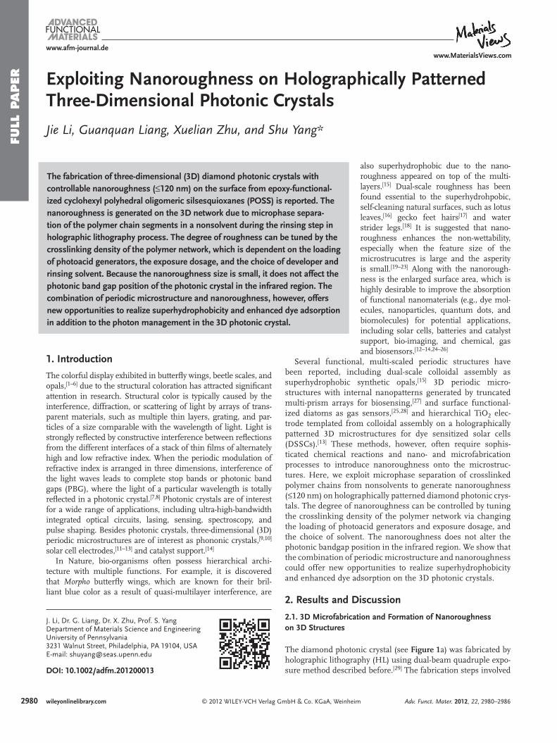
Figure 1 . Diamond photonic crystals of variable degrees of nanoroughness from epoxy-POSS. a) Top-view SEM image. b,c) Schematics of photoresist chains swollen in a good solvent (b) or collapsed in a nonsolvent (c) within a mesh. d) Chemical structure of epoxy-POSS. e,f) Cross-sectional SEM images of the diamond structures developed in PGMEA and rinsed in IA (e) and ethanol (f), followed by critical point drying in the same solvent. g,h) Cross-sectional SEM images of the diamond structures developed in GBL and rinsed in IA (g) and ethanol (h), followed by critical point drying in the same solvent. i) Cross-sectional SEM image of the diamond structure developed in GBL, rinsed in DI water and dried in air. Scale bar: 2 μ m.
spin-coating, pre-exposure bake, exposure, post-exposure bake (PEB), development, solvent rinsing and critical-point drying (CPD). In our study, we used epoxy functionalized cyclohexyl polyhedral oligomeric silsesquioxane (epoxy-POSS) as the nega-tive-tone photoresist (Figure 1 d), which crosslinked in the light exposed regions after PEB. [ 30 ] The fi lm was then immersed in a developer to remove the uncrosslinked and lightly crosslinked regions, leaving a 3D microporous structure. The micro-porosity is determined by the solvency of the developer and the crosslinking density of the exposed regions. Organic solvents, including propylene glycol methyl ether acetate (PGMEA) and γ -butyrolactone (GBL) have been widely used as developers for negative-tone epoxy resists. However, they are not very miscible with liquid CO 2 in the CPD process, which is commonly used to prevent pattern collapse of highly porous 3D microstructures.
© 2012 WILEY-VCH Verlag GAdv. Funct. Mater. 2012, 22, 2980–2986
Therefore, the freshly developed samples were transferred to a liquid CO 2 compatible solvent, isoamyl acetate (IA) or ethanol, as the rinsing solvent before CPD.
A closer look of the samples showed that while the surface of the diamond crystals rinsed in IA were generally smooth regard-less of the developer (see Figure 1 e,g), those rinsed in ethanol had spongy nanoroughness appeared on the skeletons (Figure 1 f,h). The nanoroughness size ranged from 40-120 nm as measured by AFM (see Figure S1 and Table S1, Supporting Information). The highest degree of porosity, although the nanofeature size appeared smaller, was observed when the 3D structure was developed in GBL, followed by rinsing in water and dried in air (Figure 1 i). The relationship between the degree of nanorough-ness and the combination of developer and rinsing solvent was summarized in Table 1 .
2981wileyonlinelibrary.commbH & Co. KGaA, Weinheim
FULL
PAPER
2982
www.afm-journal.dewww.MaterialsViews.com
Table 1. Summary of observed surface roughness on 3D diamond struc-tures from different solvents used in development, rinsing and critical point drying process.
Developer Rinsing solvent
Critical point drying
Observed surface roughness
Corresponding SEM image in Figure 1
PGMEA IA Yes Smooth (e)
PGMEA Ethanol Yes Rough (f)
GBL IA Yes Smooth (g)
GBL Ethanol Yes Rough (h)
GBL Water No Very rough (i)
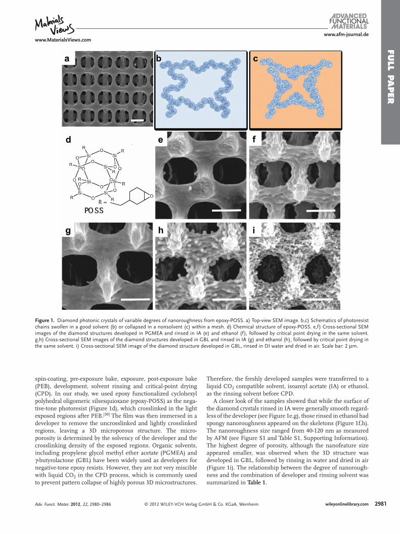
Table 2. Hansen solubility parameters of epoxy-POSS and different organic solvents. a)
δ d (MPa 1/2 ) δ p (MPa 1/2 ) δ h (MPa 1/2 ) δ (MPa 1/2 )
Epoxy-POSS a) 17.7 - - 19.2
PGMEA 15.6 5.6 9.8 19.3
GBL 19.0 16.6 7.4 26.2
IA 15.3 3.1 7.0 17.2
Ethanol 15.8 8.8 19.4 26.6
Water 15.5 16.0 42.4 47.9
a) Solubility parameters of solvents were obtained from ref. [33], that of epoxy-POSS was calculated from the organic component to approximate the whole molecule using group contribution method. [ 34 ]
2.2. Mechanism of Nanoroughness FormationThese results clearly indicate that the processing conditions, spe-cifi cally, the rinsing solvent, plays an important role to the nano-morphology appeared on the 3D microstructures. It is expected that in a good solvent, polymer chains swell with an extended chain conformation (see schematics in Figure 1 b) but phase separate in a nonsolvent. If polymer chains are crosslinked, the mesh size, which is proportional to the molecular weight between crosslink points, M c , that determines the network swellability or phase separation domain size in a nonsolvent. At a given crosslinking density, the M c is fi xed. Thus, in a nonsol-vent the polymer chain segments between crosslink points can only locally aggregate within a mesh to minimize the interac-tion with the nonsolvent (Figure 1 c), leading to the formation of nanoporous structures instead of collapsing the whole net-work. We believe that this explains why the 3D microstructure is maintained even at a very high degree of nanoporosity when rinsed in water and dried in air. Previously, similar strategies have been reported to create highly porous superhydrophobic coatings, for example, by evaporation a hot solution of isotactic polypropylene dissolved a mixture of good solvent and non-solvent, [ 31 ] and by freezing electrospinned polymer fi bers in a liquid nitrogen bath, inducing a phase separation between the polymer and the solvent. [ 32 ]
In our system, the epoxy-POSS is soluble in both PGMEA and GBL. Therefore, the rinsing solvent should be mainly responsible for the appearance of nanoroughness on 3D micro-structure. When the swollen polymer network after develop-ment was transferred to a good solvent, such as IA, for rinsing, polymer chains maintained their extended chain conformation, resulting in smooth surface after CPD. In contrast, if the rising solvent was a nonsolvent, such as ethanol or water, the swollen polymer chains rapidly microphase separated from the nonsol-vent. From nanoroughness data (see Figure 1 h vs. i), it is clear that water is a much poorer nonsolvent than ethanol.
To support our reasoning on the solvency effect, we esti-mated the polymer-solvent interactions using the Hansen solu-bility parameters [ 33 ] (see Table 2 ). The Flory-Huggins polymer-solvent interaction parameter ( χ ) can be expressed as,
χ = V (δ1 − δ2)
RT (1)
where V is the molar volume of the solvent, δ is the solubility parameter, R is the gas constant, T is the absolute temperature.
wileyonlinelibrary.com © 2012 WILEY-VCH Verlag G
The difference between the two solubility parameters can be further written as
(δ1 − δ2)2 = (δd2 − δd1)2 + (δp2 − δp1)2 + (δh2 − δh1)2 (2)
where δ d is the energy from dispersion bonds between mol-ecules, δ p is the energy from polar bonds between molecules, and δ h is the energy from hydrogen bonds between molecules. The larger the value of ( δ 1 − δ 2 ) 2 , the less compatible between the polymer and solvent. The epoxy POSS is an organic-inor-ganic hybrid material. Here we calculated the solubility param-eter from the organic component of the epoxy POSS, which is mainly responsible to the interaction with an organic solvent, to approximate the whole molecule using group contribution method. [ 34 ]
As seen in Table 2 , PGMEA ( δ = 19.3 MPa 1/2 ) and IA ( δ = 17.2 MPa 1/2 ) have similar solubility parameters as that of the epoxy-POSS ( δ = 19.2 MPa 1/2 ), while GBL ( δ = 26.2 MPa 1/2 ) and ethanol ( δ = 26.6 MPa 1/2 ) have much larger solubility param-eters, suggesting that GBL and ethanol are relatively poor sol-vents of epoxy-POSS. However, in experiments we observed that GBL could dissolve the epoxy-POSS rather well. We note that the δ h value, the energy term from hydrogen bonding, of GBL is much smaller than that of ethanol, 7.4 vs. 19.4 MPa 1/2 , but close to that of PGMEA and ethanol, which may contribute to the affi nity of epoxy POSS in GBL. Nevertheless, GBL was not as good solvent as PGMEA. Further supporting this is the observed larger nanoroughness from the sample developed in GBL (Figure 1 h) vs. PGMEA (Figure 1 f) using the same rinsing solvent, ethanol. As for water, the solubility parameter ( δ = 47.9 MPa 1/2 ) is far larger than that of the epoxy-POSS, making it a very poor solvent, in agreement with the observed highest degree of nanoporosity in 3D skeletons. Further supporting the solvency effect is that when we resoaked the rough samples (see Figure 1 f,h) in the respective developer, PGMEA or GBL, overnight, followed by CPD drying, the rough surface became smooth, presumably that the collapsed chains were restored within the crosslinked network.
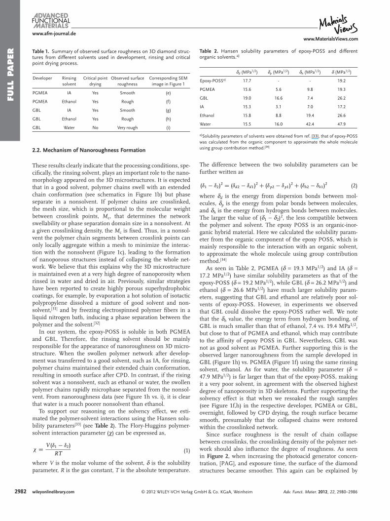
Since surface roughness is the result of chain collapse between crosslinks, the crosslinking density of the polymer net-work should also infl uence the degree of roughness. As seen in Figure 2 , when increasing the photoacid generator concen-tration, [PAG], and exposure time, the surface of the diamond structures became smoother. This again can be explained by
mbH & Co. KGaA, Weinheim Adv. Funct. Mater. 2012, 22, 2980–2986
FULL P
APER
www.afm-journal.dewww.MaterialsViews.com
Figure 2 . Surface roughness on epoxy-POSS diamond structures as a function of chain crosslinking density. The samples were developed in GBL and rinsed in ethanol, followed by critical point drying. a,b) Schematics of the collapsed polymer chains in a poor solvent at a low (a) and high (b) crosslinked density. c) Photoacid generator concentration [PAG] = 0.3 wt%, exposure time of 0.6s. d–f) [PAG] = 1.0 wt%, exposure time: d) 0.25 s, e) 0.30 s, and f) 0.35 s.
the polymer chain morphology between crosslinks. As [PAG] increases or exposure time increases, the number of photo-acids generated is increased, thus, the crosslinking den-sity is increased and the M c or mesh size is decreased (see Figure 2 a,b). In a nonsolvent, the available chain segments for collapsing out of solvent are dramatically decreased. When the crosslinking density was suffi ciently high, the surface of the 3D microstructure became smooth (Figure 2 f).
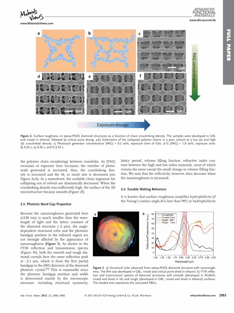
Figure 3 . a) Structural color observed from epoxy-POSS diamond structure with nanorough-ness. The fi lm was developed in GBL, rinsed and critical point dried in ethanol. b) FTIR refl ec-tion and transmission spectra of diamond structures with smooth (developed in PGMEA, rinsed and dried in IA) and rough (developed in GBL, rinsed and dried in ethanol) surfaces. The shaded area represents the calculated PBGs.
2.3. Photonic Band Gap Properties
Because the nanoroughness generated here ( ≤ 120 nm) is much smaller than the wave-length of light and the lattice constant of the diamond structure ( ∼ 2 μ m), the angle-dependent structural color and the photonic bandgap position in the infrared region are not strongly affected by the appearance of nanoroughness ( Figure 3 ). As shown in the FTIR refl ection and transmission spectra (Figure 3 b), both the smooth and rough dia-mond crystals have the same refl ection peak at ∼ 2.1 μ m, which is from the fi rst partial bandgap in the [001] direction of the diamond photonic crystal. [ 29 ] This is reasonable since the photonic bandgap position and width is determined mainly by the microscopic structure, including structural symmetry,
© 2012 WILEY-VCH Verlag GmAdv. Funct. Mater. 2012, 22, 2980–2986
lattice period, volume fi lling fraction, refractive index con-trast between the high and low index materials, most of which remain the same except the small change in volume fi lling frac-tion. We note that the refl ectivity, however, does decrease when the nanoroughness is increased.
2.4. Tunable Wetting Behaviors
It is known that surface roughness amplifi es hydrophilicity (if the Young’s contact angle, θ is less than 90 o ) or hydrophobicity
2983wileyonlinelibrary.combH & Co. KGaA, Weinheim
FULL
PAPER
29
www.afm-journal.dewww.MaterialsViews.com
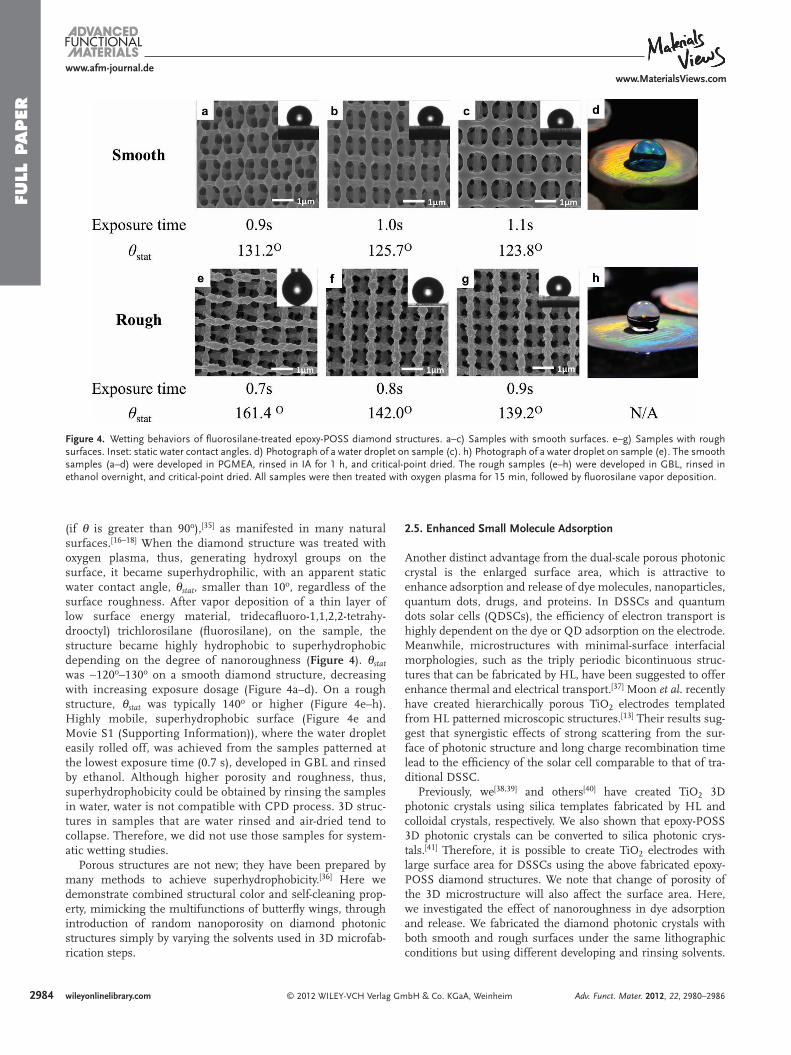
Figure 4 . Wetting behaviors of fl uorosilane-treated epoxy-POSS diamond structures. a–c) Samples with smooth surfaces. e–g) Samples with rough surfaces. Inset: static water contact angles. d) Photograph of a water droplet on sample (c). h) Photograph of a water droplet on sample (e). The smooth samples (a–d) were developed in PGMEA, rinsed in IA for 1 h, and critical-point dried. The rough samples (e–h) were developed in GBL, rinsed in ethanol overnight, and critical-point dried. All samples were then treated with oxygen plasma for 15 min, followed by fl uorosilane vapor deposition.
(if θ is greater than 90 o ), [ 35 ] as manifested in many natural surfaces. [ 16–18 ] When the diamond structure was treated with oxygen plasma, thus, generating hydroxyl groups on the surface, it became superhydrophilic, with an apparent static water contact angle, θ stat , smaller than 10 o , regardless of the surface roughness. After vapor deposition of a thin layer of low surface energy material, tridecafl uoro-1,1,2,2-tetrahy-drooctyl) trichlorosilane (fl uorosilane), on the sample, the structure became highly hydrophobic to superhydrophobic depending on the degree of nanoroughness ( Figure 4 ). θ stat was ∼ 120 o –130 o on a smooth diamond structure, decreasing with increasing exposure dosage (Figure 4 a–d). On a rough structure, θ stat was typically 140 o or higher (Figure 4 e–h). Highly mobile, superhydrophobic surface (Figure 4 e and Movie S1 (Supporting Information)), where the water droplet easily rolled off, was achieved from the samples patterned at the lowest exposure time (0.7 s), developed in GBL and rinsed by ethanol. Although higher porosity and roughness, thus, superhydrophobicity could be obtained by rinsing the samples in water, water is not compatible with CPD process. 3D struc-tures in samples that are water rinsed and air-dried tend to collapse. Therefore, we did not use those samples for system-atic wetting studies.
Porous structures are not new; they have been prepared by many methods to achieve superhydrophobicity. [ 36 ] Here we demonstrate combined structural color and self-cleaning prop-erty, mimicking the multifunctions of butterfl y wings, through introduction of random nanoporosity on diamond photonic structures simply by varying the solvents used in 3D microfab-rication steps.
84 wileyonlinelibrary.com © 2012 WILEY-VCH Verlag
2.5. Enhanced Small Molecule Adsorption
Another distinct advantage from the dual-scale porous photo nic crystal is the enlarged surface area, which is attractive to enhance adsorption and release of dye molecules, nanoparticles, quantum dots, drugs, and proteins. In DSSCs and quantum dots solar cells (QDSCs), the effi ciency of electron transport is highly dependent on the dye or QD adsorption on the electrode. Meanwhile, microstructures with minimal-surface interfacial morphologies, such as the triply periodic bicontinuous struc-tures that can be fabricated by HL, have been suggested to offer enhance thermal and electrical transport. [ 37 ] Moon et al . recently have created hierarchically porous TiO 2 electrodes templated from HL patterned microscopic structures. [ 13 ] Their results sug-gest that synergistic effects of strong scattering from the sur-face of photonic structure and long charge recombination time lead to the effi ciency of the solar cell comparable to that of tra-ditional DSSC.
Previously, we [ 38,39 ] and others [ 40 ] have created TiO 2 3D photonic crystals using silica templates fabricated by HL and colloidal crystals, respectively. We also shown that epoxy-POSS 3D photonic crystals can be converted to silica photonic crys-tals. [ 41 ] Therefore, it is possible to create TiO 2 electrodes with large surface area for DSSCs using the above fabricated epoxy-POSS diamond structures. We note that change of porosity of the 3D microstructure will also affect the surface area. Here, we investigated the effect of nanoroughness in dye adsorption and release. We fabricated the diamond photonic crystals with both smooth and rough surfaces under the same lithographic conditions but using different developing and rinsing solvents.
GmbH & Co. KGaA, Weinheim Adv. Funct. Mater. 2012, 22, 2980–2986
FULL P
APER
www.afm-journal.dewww.MaterialsViews.com
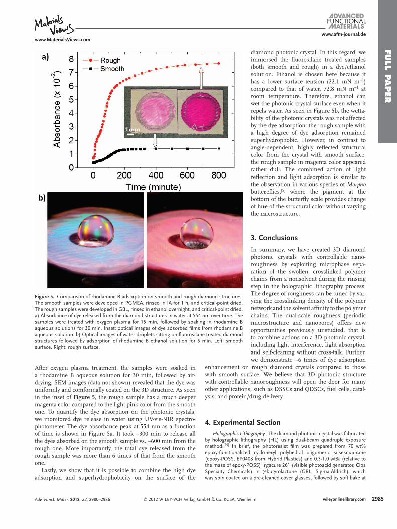
Figure 5 . Comparison of rhodamine B adsorption on smooth and rough diamond structures. The smooth samples were developed in PGMEA, rinsed in IA for 1 h, and critical-point dried. The rough samples were developed in GBL, rinsed in ethanol overnight, and critical-point dried. a) Absorbance of dye released from the diamond structures in water at 554 nm over time. The samples were treated with oxygen plasma for 15 min, followed by soaking in rhodamine B aqueous solutions for 30 min. Inset: optical images of dye adsorbed fi lms from rhodamine B aqueous solution. b) Optical images of water droplets sitting on fl uorosilane treated diamond structures followed by adsorption of rhodamine B ethanol solution for 5 min. Left: smooth surface. Right: rough surface.
After oxygen plasma treatment, the samples were soaked in a rhodamine B aqueous solution for 30 min, followed by air-drying. SEM images (data not shown) revealed that the dye was uniformly and comformally coated on the 3D structure. As seen in the inset of Figure 5 , the rough sample has a much deeper magenta color compared to the light pink color from the smooth one. To quantify the dye absorption on the photonic crystals, we monitored dye release in water using UV-vis-NIR spectro-photometer. The dye absorbance peak at 554 nm as a function of time is shown in Figure 5 a. It took ∼ 300 min to release all the dyes absorbed on the smooth sample vs. ∼ 600 min from the rough one. More importantly, the total dye released from the rough sample was more than 6 times of that from the smooth one.
Lastly, we show that it is possible to combine the high dye adsorption and superhydrophobicity on the surface of the
© 2012 WILEY-VCH Verlag GmbH & Co. KGaA, WeinAdv. Funct. Mater. 2012, 22, 2980–2986
diamond photonic crystal. In this regard, we immersed the fl uorosilane treated samples (both smooth and rough) in a dye/ethanol solution. Ethanol is chosen here because it has a lower surface tension (22.1 mN m − 1 ) compared to that of water, 72.8 mN m − 1 at room temperature. Therefore, ethanol can wet the photonic crystal surface even when it repels water. As seen in Figure 5 b, the wetta-bility of the photonic crystals was not affected by the dye adsorption: the rough sample with a high degree of dye adsorption remained superhydrophobic. However, in contrast to angle-dependent, highly refl ected structural color from the crystal with smooth surface, the rough sample in magenta color appeared rather dull. The combined action of light refl ection and light adsorption is similar to the observation in various species of Morpho butterefl ies, [ 5 ] where the pigment at the bottom of the butterfl y scale provides change of hue of the structural color without varying the microstructure.
3. Conclusions
In summary, we have created 3D diamond photonic crystals with controllable nano-roughness by exploiting microphase sepa-ration of the swollen, crosslinked polymer chains from a nonsolvent during the rinsing step in the holographic lithography process. The degree of roughness can be tuned by var-ying the crosslinking density of the polymer network and the solvent affi nity to the polymer chains. The dual-scale roughness (periodic microstructure and nanopores) offers new opportunities previously unstudied, that is to combine actions on a 3D photonic crystal, including light interference, light absorption and self-cleaning without cross-talk. Further, we demonstrate ∼ 6 times of dye adsorption
enhancement on rough diamond crystals compared to those with smooth surface. We believe that 3D photonic structure with controllable nanoroughness will open the door for many other applications, such as DSSCs and QDSCs, fuel cells, catal-ysis, and protein/drug delivery.
4. Experimental Section Holographic Lithography : The diamond photonic crystal was fabricated
by holographic lithography (HL) using dual-beam quadruple exposure method. [ 29 ] In brief, the photoresist fi lm was prepared from 70 wt% epoxy-functionalized cyclohexyl polyhedral oligomeric silsesquioxane (epoxy-POSS, EP0408 from Hybrid Plastics) and 0.3-1.0 wt% (relative to the mass of epoxy-POSS) Irgacure 261 (visible photoacid generator, Ciba Specialty Chemicals) in γ -butyrolactone (GBL, Sigma-Aldrich), which was spin coated on a pre-cleaned cover glasses, followed by soft bake at
2985wileyonlinelibrary.comheim
FULL
PAPER
2986
www.afm-journal.dewww.MaterialsViews.com
[ 1 ] M. Srinivasarao , Chem. Rev. 1999 , 99 , 1935 . [ 2 ] A. R. Parker , J. Opt. A 2000 , 2 , R15 . [ 3 ] A. R. Parker , V. L. Welch , D. Driver , N. Martini , Nature 2003 , 426 ,
786 . [ 4 ] P. Vukusic , J. R. Sambles , Nature 2003 , 424 , 852 . [ 5 ] S. Kinoshita , S. Yoshioka , ChemPhysChem 2005 , 6 , 1442 .
50 ° C for 40 min and 95 ° C for 2 min, respectively. The fi lm was exposed to a diode-pumped Nd:YVO 4 laser ( λ = 532 nm, Verdi-6, Coherent) with 1.0 W laser input for 0.25 s to 1.1 s each time, and was rotated 90 ° after each exposure using a motorized rotation stage (PRM1-Z7E, Thorlabs). After exposure, the fi lm was post-exposure baked (PEB) at 50 ° C for 20 min to crosslink the exposed regions, followed by development in propylene glycol monomethyl ether acetate (PGMEA, Sigma-Aldrich) or GBL for 1 h. Before drying in CO 2 supercritical point dryer (SAMDRI®-PVT-3D, Tousimis), the wet samples were rinsed in isoamyl acetate (IA, Sigma-Aldrich) for 1h or in ethanol (Fisher Scientifi c) overnight.
Surface Hydrophobilization : Diamond structures were treated by oxygen plasma (Harrick Plasma Cleaner PDC-001) for 15 min to generate hydroxyl groups on surface, followed by vapor deposition of (tridecafl uoro-1,1,2,2-tetrahydrooctyl) trichlorosilane (fl uorosilane, 0.1 mL, Gelest. Inc) in a vacuum desiccator for 1 h.
Dye Adsorption : Hydrophilic surfaces: Samples with various surface roughness were treated with oxygen plasma for 15 min, then soaked in 0.005wt% rhodamine B (Sigma Aldrich) aqueous solution for 30 min and air dried. Then these two samples were placed into separate cuvettes containing of 3.5 mL DI water to release the absorbed dye, which was monitored by UV-vis-NIR Spectrophotometer (Varian Cary 5000). Hydrophobic surfaces: Oxygen plasma treated samples were passivated with fl uorosilane, followed by soaking in 0.005wt% rhodamine B ethanol solution for 5 min.
Characterization : SEM images were taken from FEI Strata DB235 Focused Ion Beam (FIB) system and the cross-sectional images were taken from samples milled by the Gallium ion beam. The refl ection and transmission spectra were acquired by FT-IR spectrometer (Nicolet 8700, equipped with Nicolet continuum infrared microscope) in the [001] direction at the same location of the sample. The refl ection spectra were measured using an Au mirror as reference. The aperture size was 60 μ m × 60 μ m. Static water contact angles were measured by ramé-hart standard automated goniometer (Model 200). The static contact angle was measured from a 3.0 μ L water droplet averaged over three different spots on each sample.
Supporting Information Supporting Information is available from the Wiley Online Library or from the author.
Acknowledgements J.L. and G.L. contributed equally to this work. The research is supported in part by the Offi ce of Naval Research (ONR), Grant # N00014-05-0303, the National Science Foundation (NSF)/CAREER award, DMR-0548070. Penn Regional Nanotech facility (PRFN) is acknowledged for access SEM. The authors are grateful to Mr. Felice Macera for helping with the photographs.
Received: January 2, 2012 Revised: February 28, 2012
Published online: April 16, 2012
wileyonlinelibrary.com © 2012 WILEY-VCH Verlag G
[ 6 ] F. Marlow Muldarisnur , P. Sharifi , R. Brinkmann , C. Mendive , Angew. Chem. Int. Ed. 2009 , 48 , 6212 .
[ 7 ] E. Yablonovitch , Phys. Rev. Lett. 1987 , 58 , 2059 . [ 8 ] S. John , Phys. Rev. Lett. 1987 , 58 , 2486 . [ 9 ] S. X. Yang , J. H. Page , Z. Y. Liu , M. L. Cowan , C. T. Chan , P. Sheng ,
Phys. Rev. Lett. 2004 , 93 . [ 10 ] T. Gorishnyy , C. K. Ullal , M. Maldovan , G. Fytas , E. L. Thomas , Phys.
Rev. Lett. 2005 , 94 , 4 . [ 11 ] W. M. Jin , J. H. Shin , C. Y. Cho , J. H. Kang , J. H. Park , J. H. Moon ,
ACS Appl. Mater. Interfaces 2010 , 2 , 2970 . [ 12 ] E. S. Kwak , W. Lee , N. G. Park , J. Kim , H. Lee , Adv. Funct. Mater.
2009 , 19 , 1093 . [ 13 ] C. Y. Cho , J. H. Moon , Adv. Mater. 2011 , 23 , 2971 . [ 14 ] K. Keizer , H. Verweij , Chemtech 1996 , 26 , 37 . [ 15 ] Z. Z. Gu , H. Uetsuka , K. Takahashi , R. Nakajima , H. Onishi ,
A. Fujishima , O. Sato , Angew. Chem. Int. Ed. 2003 , 42 , 894 . [ 16 ] W. Barthlott , C. Neinhuis , Planta 1997 , 202 , 1 . [ 17 ] K. Autumn , Y. A. Liang , S. T. Hsieh , W. Zesch , W. P. Chan ,
T. W. Kenny , R. Fearing , R. J. Full , Nature 2000 , 405 , 681 . [ 18 ] X. F. Gao , L. Jiang , Nature 2004 , 432 , 36 . [ 19 ] T. Onda , S. Shibuichi , N. Satoh , K. Tsujii , Langmuir 1996 , 12 ,
2125 . [ 20 ] D. Öner , T. J. McCarthy , Langmuir 2000 , 16 , 7777 . [ 21 ] L. C. Gao , T. J. McCarthy , Langmuir 2006 , 22 , 2966 . [ 22 ] H. E. Jeong , S. H. Lee , J. K. Kim , K. Y. Suh , Langmuir 2006 , 22 ,
1640 . [ 23 ] R. G. Karunakaran , C. H. Lu , Z. H. Zhang , S. Yang , Langmuir 2011 ,
27 , 4594 . [ 24 ] T. Lebeau , J. M. Robert , Appl. Microbiol. Biotechnol. 2003 , 60 , 624 . [ 25 ] Z. H. Bao , M. R. Weatherspoon , S. Shian , Y. Cai , P. D. Graham ,
S. M. Allan , G. Ahmad, M. B. Dickerson , B. C. Church , Z. T. Kang , H. W. Abernathy Iii , C. J. Summers , M. L Liu , K. H. Sandhage , Nature 2007 , 446 , 172 .
[ 26 ] A. Setaro , S. Lettieri , P. Maddalena , L. De Stefano , Appl. Phys. Lett. 2007 , 91 , 051921 .
[ 27 ] S. K. Lee , H. S. Park , G. R. Yi , J. H. Moon , S. M. Yang , Angew. Chem. Int. Ed. 2009 , 48 , 7000 .
[ 28 ] H. E. Townley , K. L. Woon , F. P. Payne , H. White-Cooper , A. R. Parker , Nanotechnology 2007 , 18 .
[ 29 ] G. Q. Liang , X. L. Zhu , Y. G. Xu , J. Li , S. Yang , Adv. Mater. 2010 , 22 , 4524 .
[ 30 ] J. H. Moon , J. S. Seo , Y. G. Xu , S. Yang , J. Mater. Chem. 2009 , 19 , 4687 .
[ 31 ] H. Y. Erbil , A. L. Demirel , Y. Avci , O. Mert , Science 2003 , 299 , 1377 .
[ 32 ] J. T. McCann , M. Marquez , Y. Xia , J. Am. Chem. Soc. 2006 , 128 , 1436 .
[ 33 ] C. M. Hansen , Hansen Solubility Parameters: A User’s Handbook , CRC Press , Boca Raton, FL 2000 .
[ 34 ] D.W. van Krevelen , P.H. Hoftyzer , Properties of Polymers.Correlations with Chemical Structures , Elsevier , New York 1972 .
[ 35 ] R. N. Wenzel , Ind. Eng. Chem. 1936 , 28 , 988 . [ 36 ] X. Chen, L. H. Wang , Y. Q. Wen , Y. Q. Zhang , J. X. Wang , Y. L. Song ,
L. Jiang , D. B. Zhu , J. Mater. Chem. 2008 , 18 , 2262 . [ 37 ] H. Y. Chen , Y. Kwon, K. Thornton, Scr. Mater. 2009 , 61 , 52 . [ 38 ] J. H. Moon , Y. G. Xu , Y. P. Dan , S. M. Yang , A. T. Johnson , S. Yang,
Adv. Mater. 2007 , 19 , 1510 . [ 39 ] Y. Xu, X. Zhu, Y. Dan, J. H. Moon , V. W. Chen , A. T. Johnson ,
J. W. Perry , S. Yang, Chem. Mater. 2008 , 20 , 1816 . [ 40 ] B. Hatton , L. Mishchenko , S. Davis , K. H. Sandhage , J. Aizenberg ,
Proc. Natl. Acad. Sci. USA 2010 , 107 , 10354 . [ 41 ] Y. A. Xu , X. L. Zhu , S. Yang , ACS Nano 2009 , 3 , 3251 .
mbH & Co. KGaA, Weinheim Adv. Funct. Mater. 2012, 22, 2980–2986