electrostatic carrier doping of gdtio3/srtio3 interfaces
TRANSCRIPT
1
Electrostatic carrier doping of GdTiO3/SrTiO3 interfaces
Pouya Moetakef1, Tyler A. Cain1, Daniel G. Ouellette2, Jack Y. Zhang1, Dmitri O.
Klenov3, Anderson Janotti1, Chris G. Van de Walle1, Siddharth Rajan4, S. James
Allen2, and Susanne Stemmer1
1 Materials Department, University of California, Santa Barbara, California, 93106-5050,
USA
2 Department of Physics, University of California, Santa Barbara, California, 93106-9530,
USA
3 FEI, Achtseweg Noord 5, 5651 GG Eindhoven, Netherlands
4 Department of Electrical and Computer Engineering, The Ohio State University,
Columbus, OH 43210 USA

2
Abstract
Heterostructures and superlattices consisting of a prototype Mott insulator, GdTiO3, and
the band insulator SrTiO3 are grown by molecular beam epitaxy and show intrinsic
electronic reconstruction, approximately ½ electron per surface unit cell at each
GdTiO3/SrTiO3 interface. The sheet carrier densities in all structures containing more
than one unit cell of SrTiO3 are independent of layer thicknesses and growth sequences,
indicating that the mobile carriers are in a high concentration, two-dimensional electron
gas bound to the interface. These carrier densities closely meet the electrostatic
requirements for compensating the fixed charge at these polar interfaces. Based on the
experimental results, insights into interfacial band alignments, charge distribution and the
influence of different electrostatic boundary conditions are obtained.
3
Two-dimensional electron gases (2DEGs) at interfaces between Mott insulators
and band insulators have attracted significant attention because of unique properties, such
as strong electron correlations, superconductivity or magnetism [1-7]. Furthermore,
interfaces between the band insulator SrTiO3 and the rare earth titanates (RTiO3, where R
is a trivalent rare earth ion), which are Mott insulators, exhibit a fixed polar charge. In
particular, R3+O2- and Ti3+O24- layers alternate along the (001) surface normal of RTiO3
[8], carrying formal +1 and -1 charges, respectively, which causes a diverging
electrostatic surface energy due to the non-zero dipole moment on the RO-TiO2 units. At
the interface, these transition to a sequence of neutral layers, Sr2+O2- and Ti4+O24-, of non-
polar (001) SrTiO3. The fixed interfacial charge can be compensated by a 2DEG,
residing in the bands of the Mott and/or band insulator and bound to the interface by the
fixed charge [9,10]. In the absence of any other charge compensation, defects, interfacial
mixing, roughness and nonstoichiometry [11-13], the interface is expected to form an
extremely high-density 2DEG on the order of 3×1014 cm-2, as given by e 2S , where S is
the surface unit cell area and e the elementary charge. The nature and spatial distribution
of charge carriers are of paramount importance for the properties of these heterostructures.
To date, attention has focused on LaAlO3/SrTiO3 and LaTiO3/SrTiO3 interfaces
grown by pulsed laser deposition [1,14-16]. Results from electrical transport
measurements vary significantly; in particular, LaAlO3/SrTiO3 interfaces show carrier
densities that are an order of magnitude less than predicted from intrinsic electronic
reconstruction [17-19]. Compensating mobile electrons are easily accessible for
RTiO3/SrTiO3 structures, as can be visualized by considering the atomically sharp
interface as a 50:50 mixture of RTiO3 and SrTiO3, which has the required free electron
4
density [20]. Transport and optical measurements of LaTiO3/SrTiO3 interfaces reveal
densities close to those expected for electronic reconstruction [16,21], but interpretation
is complicated by conduction by non-interfacial carriers from both substrates and films
[15,16]; LaTiO3 films reported in the literature are often metallic [22]. This Letter
reports on transport measurements of the 2DEGs at GdTiO3/SrTiO3 interfaces
(electronically analogous to LaTiO3/SrTiO3 [23,24]) grown by molecular beam epitaxy
(MBE) that exhibit an interfacial density with values that are essentially those predicted
by electronic reconstruction. Theoretical band offsets between the conduction bands of
SrTiO3 and GdTiO3 are used to model the spatial extent of the 2DEG.
The vastly different oxygen pressures required to obtain insulating SrTiO3 and
GdTiO3 layers present an experimental challenge: high oxygen pressure is needed for
insulating SrTiO3, while GdTiO3 films need to be grown under low oxygen pressure
conditions to avoid metallic conductivity or formation of pyrochlore [25,26]. We use
(001) surfaces of (LaAlO3)0.3(Sr2AlTaO6)0.7 (LSAT) as substrates to avoid substrate
conduction. All layers and superlattices were grown by MBE. SrTiO3 was grown by co-
deposition [27], whereas GdTiO3 was grown by shuttered growth, supplying alternating
monolayer doses of Gd and Ti tetra isopropoxide (TTIP), which supplied both Ti and
oxygen. No additional oxygen was supplied [28]. For GdTiO3 on SrTiO3, growths were
started and terminated with a TiO2 layer. All layers and superlattices were coherently
strained to the LSAT [29]. Aberration-corrected scanning transmission electron
microscopy (FEI Titan G2 ChemiSTEM) was used to characterize the atomic structure of
GdTiO3/SrTiO3 interfaces. Longitudinal and Hall resistivity were measured in Van der
Pauw geometry using a Physical Properties Measurement System (Quantum Design
5
PPMS). Ohmic contacts were 300 nm Au/20 nm Ni/40 nm Al for SrTiO3 top layers and
300 nm Au/50 nm Ti for GdTiO3 top layers. The top layer was Au for wire bonding with
an Au wire.
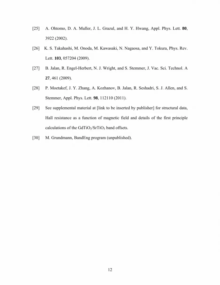
The sheet resistances of GdTiO3 grown directly on LSAT and of GdTiO3 grown
on SrTiO3 buffer layers with different thicknesses are shown in Fig. 1(a). The GdTiO3
film on LSAT with no SrTiO3 buffer layer is insulating. While too resistive for
meaningful Hall measurements, the Seebeck coefficient was measured and is positive (p-
type), as found for stoichiometric GdTiO3 [23]. All bilayers are n-type and metallic if the
SrTiO3 thickness exceeded one unit cell (0.4 nm). Even the bilayer with one unit cell
SrTiO3 already exhibits a remarkable drop in resistance. The localized behavior for this
sample is expected as the sheet resistance exceeds the critical Mott value (~10 kΩ/).
The sheet resistance should decrease with increasing SrTiO3 thickness if the conductivity
is due to the oxygen deficient SrTiO3. The constant sheet resistance for SrTiO3 layers
thicker than 20 nm indicates that it arises from a space charge layer of constant thickness
and carrier density at the interface. The Hall resistance as a function of magnetic field B
was linear and n-type down to the lowest temperatures [29], in contrast to LaTiO3/SrTiO3
[15,16]. All of the electrons contributing to the Hall resistance satisfy μB <<1 .
Although more than one subband with different mobility may be occupied, the Hall
coefficient ( RH ) is converted to an effective sheet density by nS =1 eRH , where e is the
elementary charge. Figure 1(b) shows that nS is constant, ~ 3.5×1014 cm-2, for all
bilayers, even for extremely thin SrTiO3. Thus there is little trapping at the LSAT/SrTiO3
interface, at least on a scale of ~ 3×1014 cm-2. A similar result is obtained when the
GdTiO3 thickness is varied. The mobility increases with SrTiO3 thickness [Fig. 1(b)].
6
Thus the decrease in sheet resistance for SrTiO3 layers between 0.4 nm and 20 nm is due
to an increase in mobility, not a change in sheet carrier concentration. The results are
consistent with an interfacial mobile space charge layer of constant thickness with a sheet
charge density of ~ 3×1014 cm-2. This carrier density closely corresponds to the ½
electron per surface unit cell required to compensate for the polar discontinuity at the
interface.
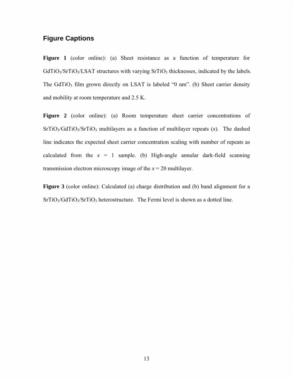
To further confirm the results, multilayer samples were investigated. Figure 2(a)
shows the sheet carrier density for (SrTiO3/GdTiO3/SrTiO3)x superlattices on LSAT as a
function of the number of repeats x, each containing two GdTiO3/SrTiO3 interfaces. If
each repeat contributes the same sheet carrier density as the x = 1 trilayer, then the sheet
density should scale as shown by the dashed line. The experimental results closely
follow the dashed line, independent of GdTiO3 or SrTiO3 thicknesses. The total carrier
sheet density is not proportional to the total Gd in the superlattice nor is it proportional to
the Gd concentration. It is proportional to the number of interfaces. The constant sheet
carrier density per interface excludes interfacial intermixing as the source of the charge
carriers, because the charge carrier density in this case should strongly dependent on the
precise interfacial composition [20]. Figure 2(b) shows a high-angle annular dark-field
scanning transmission electron microscopy (HAADF/STEM) image of the sample with
x = 20. Thicker sample regions appear to show intermixing of about one monolayer, but
observation of thinner regions [29] shows that the interface contains short steps, which
overlap along the beam direction. Thus the interfaces are locally atomically abrupt.
Comparison of sheet carrier densities of the x = 1 multilayer (two GdTiO3/SrTiO3
interfaces) with that of the GdTiO3/SrTiO3/LSAT structures (one interface) of Fig. 1(b),
7
shows that the sheet carrier concentration of the multilayer is slightly less than twice that
of a single interface. This is likely due to different electrostatic boundary conditions for
GdTiO3/SrTiO3 and SrTiO3/GdTiO3 interfaces.
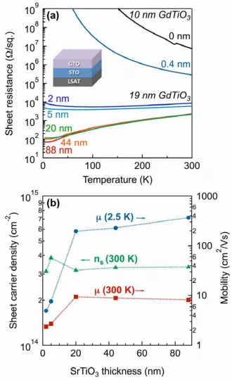
The interfacial space charge can be understood by noting that the fixed polar
charge at the interface must be neutralized by negative space charge, mobile or fixed, and
dictated by the available quantum states in the presence of the selfconsistent electrostatic
fields/potentials. The SrTiO3 is n-type (oxygen deficient) and GdTiO3 is p-type. The
fixed polar charge can be neutralized by an accumulation layer in the SrTiO3, a hole
depletion layer (negatively charged acceptors) in the GdTiO3 and an inversion layer in
the GdTiO3. The mobile charge is close to that required to compensate the fixed polar
charge at the interface: thus hole depletion in the GdTiO3 is not sufficient to siphon off
significant numbers of electrons from the mobile space charge. The interface may share
the mobile charge between the SrTiO3 and the GdTiO3. The relatively strong temperature
dependence of the electron mobility [Fig. 1(b)] and the absence of an anomalous Hall
effect, potentially caused by the ferrimagnetism in the GdTiO3, indicate that mobile
charge is largely found on the SrTiO3 side and that the conduction band alignment favors
SrTiO3 accumulation. Because SrTiO3 has the larger band gap, the band line-up must be
of type II (staggered). First principle calculations confirm this [29]. The mobile charge
distribution and band bending are modeled using a self consistent Poisson-Schrödinger
solver [30], as shown in Fig. 3, using band lineups from first-principle calculations [29], a
fixed interface charge of 3.4 × 1014 cm-2 (modeled as a 0.2 nm layer with fully ionized
dopants), an electron effective mass of 1 m0, a 6-fold degeneracy of the conduction band,
and dielectric constants of SrTiO3 and GdTiO3 of 300 and 30, respectively. The
8
interfacial positive charge induces a high-density 2DEG. A deep quantum well is formed
[Fig. 3(b)], but there is overflow of the electrons into the GdTiO3. Despite the high
effective mass/density of states, the high electron density drives the Fermi level above the
SrTiO3 conduction band minimum by approximately 0.7 eV, which is greater than the
assumed conduction band offset. The GdTiO3 conduction band is therefore near the
Fermi level near the interface and the polar charges inverts the p-type GdTiO3 (NA =
3×1019 cm-3), making it effectively n-type. From the simulations, the spatial extent of the
quantum confined electron gas is ~ 3 nm. We note that the superlattice with only 4 nm
SrTiO3 is best described as a quantum well rather than two distinct interface space charge
layers, yet the total electron density appears fixed by the polarization charge.
The model supports experimental observations, namely that the mobile space
charge density at the GdTiO3/SrTiO3 interface is perturbed very little by the LSAT even
for small separations and that the transport is dominated by one carrier type. The
electrical transport measurements indicate that the different 2DEG regions in multi-layer
structures are not isolated, which may have been expected since the GdTiO3 layers are p-
type. Most importantly, the very tight binding of the electrons to the interface should
allow for exploration of quantum and strong correlation effects. Figure 3 is based on an
effective mass model that assumes slowly varying envelope wave functions. The
wavefunctions are derived from d-bands that are likely better described by tight binding
Hamiltonians with rapid spatial variations, far from the approximations used in
conventional semiconductor heterostructures. Appropriate models need to be developed,
especially those that also include electron correlations.

9
P.M. and J.Y.Z. were supported through awards from the U.S. National Science
Foundation (Grant No. DMR-1006640) and DOE Basic Energy Sciences (Grant No.
DEFG02-02ER45994). T.A.C. was supported through the Center for Energy Efficient
Materials, an Energy Frontier Research Center funded by the DOE (Award Number DE-
SC0001009). S.S., S.J.A. and D.G.O. acknowledge support through a MURI program of
the Army Research Office (Grant No. W911-NF-09-1-0398). The work made use of the
UCSB Nanofabrication Facility, a part of the NSF-funded NNIN network.

10
References
[1] A. Ohtomo, D. A. Muller, J. L. Grazul, and H. Y. Hwang, Nature 419, 378 (2002).
[2] S. Okamoto and A. J. Millis, Nature 428, 630 (2004).
[3] C. Yoshida, H. Tamura, A. Yoshida, Y. Kataoka, N. Fujimaki, and N. Yokoyama,
Jpn. J. Appl. Phys. Part 1 35, 5691 (1996).
[4] S. e. Smadici, P. Abbamonte, A. Bhattacharya, X. Zhai, B. Jiang, A. Rusydi, J. N.
Eckstein, S. D. Bader, and J.-M. Zuo, Phys. Rev. Lett. 99, 196404 (2007).
[5] J. Garcia-Barriocanal, F. Y. Bruno, A. Rivera-Calzada, Z. Sefrioui, N. M. Nemes,
M. Garcia-Hernandez, J. Rubio-Zuazo, G. R. Castro, M. Varela, S. J. Pennycook,
Carlos Leon, and J. Santamaria, Adv. Mater. 22, 627 (2010).
[6] J. Garcia-Barriocanal, J. C. Cezar, F. Y. Bruno, P. Thakur, N. B. Brookes, C.
Utfeld, A. Rivera-Calzada, S. R. Giblin, J. W. Taylor, J. A. Duffy, S. B. Dugdale,
T. Nakamura, K. Kodama, C. Leon, S. Okamoto, and J. Santamaria, Nature
Commun. 1, 82 (2010).
[7] Z. S. Popovic and S. Satpathy, Phys. Rev. Lett. 94, 176805 (2005).
[8] Pseudocubic notation is used here for the orthorhombic RTiO3.
[9] G. A. Baraff, J. A. Appelbaum, and D. R. Hamann, Phys. Rev. Lett. 38, 237
(1977).
[10] W. A. Harrison, E. A. Kraut, J. R. Waldrop, and R. W. Grant, Phys. Rev. B 18,
4402 (1978).
[11] S. A. Chambers, Surf. Sci. 605, 1133 (2011).
[12] D. G. Schlom and J. Mannhart, Nat. Mater. 10, 168 (2011).
11
[13] D. O. Klenov, D. G. Schlom, H. Li, and S. Stemmer, Jpn. J. Appl. Phys. Part 2 44,
L617 (2005).
[14] J. Mannhart, D. H. A. Blank, H. Y. Hwang, A. J. Millis, and J. M. Triscone, MRS
Bulletin 33, 1027 (2008).
[15] R. Ohtsuka, M. Matvejeff, K. Nishio, R. Takahashi, and M. Lippmaa, Appl. Phys.
Lett. 96, 192111 (2010).
[16] J. S. Kim, S. S. A. Seo, M. F. Chisholm, R. K. Kremer, H. U. Habermeier, B.
Keimer, and H. N. Lee, Phys. Rev. B 82, 201407 (2010).
[17] M. Huijben, A. Brinkman, G. Koster, G. Rijnders, H. Hilgenkamp, and D. H. A.
Blank, Adv. Mater. 21, 1665 (2009).
[18] A. D. Caviglia, S. Gariglio, N. Reyren, D. Jaccard, T. Schneider, M. Gabay, S.
Thiel, G. Hammerl, J. Mannhart, and J. M. Triscone, Nature 456, 624 (2008).
[19] S. Thiel, G. Hammerl, A. Schmehl, C. W. Schneider, and J. Mannhart, Science
313, 1942 (2006).
[20] Y. Tokura, Y. Taguchi, Y. Okada, Y. Fujishima, T. Arima, K. Kumagai, and Y.
Iye, Phys. Rev. Lett. 70, 2126 (1993).
[21] S. S. A. Seo, W. S. Choi, H. N. Lee, L. Yu, K. W. Kim, C. Bernhard, and T. W.
Noh, Phys. Rev. Lett. 99, 266801 (2007).
[22] A. Schmehl, F. Lichtenberg, H. Bielefeldt, J. Mannhart, and D. G. Schlom, Appl.
Phys. Lett. 82, 3077 (2003).
[23] H. D. Zhou and J. B. Goodenough, J. Phys.: Condens. Matter 17, 7395 (2005).
[24] D. A. Crandles, T. Timusk, J. D. Garrett, and J. E. Greedan, Physica C 201, 407
(1992).
12
[25] A. Ohtomo, D. A. Muller, J. L. Grazul, and H. Y. Hwang, Appl. Phys. Lett. 80,
3922 (2002).
[26] K. S. Takahashi, M. Onoda, M. Kawasaki, N. Nagaosa, and Y. Tokura, Phys. Rev.
Lett. 103, 057204 (2009).
[27] B. Jalan, R. Engel-Herbert, N. J. Wright, and S. Stemmer, J. Vac. Sci. Technol. A
27, 461 (2009).
[28] P. Moetakef, J. Y. Zhang, A. Kozhanov, B. Jalan, R. Seshadri, S. J. Allen, and S.
Stemmer, Appl. Phys. Lett. 98, 112110 (2011).
[29] See supplemental material at [link to be inserted by publisher] for structural data,
Hall resistance as a function of magnetic field and details of the first principle
calculations of the GdTiO3/SrTiO3 band offsets.
[30] M. Grundmann, BandEng program (unpublished).
13
Figure Captions
Figure 1 (color online): (a) Sheet resistance as a function of temperature for
GdTiO3/SrTiO3/LSAT structures with varying SrTiO3 thicknesses, indicated by the labels.
The GdTiO3 film grown directly on LSAT is labeled “0 nm”. (b) Sheet carrier density
and mobility at room temperature and 2.5 K.
Figure 2 (color online): (a) Room temperature sheet carrier concentrations of
SrTiO3/GdTiO3/SrTiO3 multilayers as a function of multilayer repeats (x). The dashed
line indicates the expected sheet carrier concentration scaling with number of repeats as
calculated from the x = 1 sample. (b) High-angle annular dark-field scanning
transmission electron microscopy image of the x = 20 multilayer.
Figure 3 (color online): Calculated (a) charge distribution and (b) band alignment for a
SrTiO3/GdTiO3/SrTiO3 heterostructure. The Fermi level is shown as a dotted line.


1
Supplementary information: Electrostatic carrier doping of GdTiO3/SrTiO3 interfaces
Pouya Moetakef1, Tyler Cain1, Daniel G. Ouellette2, Jack Y. Zhang1, Dmitri O. Klenov3, Anderson Janotti1, Chris G. Van de Walle1, Siddharth Rajan4, S. James Allen2, and Susanne Stemmer1 1 Materials Department, University of California, Santa Barbara, California, 93106-5050, USA. 2 Department of Physics, University of California, Santa Barbara, California, 93106-9530, USA. 3 FEI, Achtseweg Noord 5, 5651 GG Eindhoven, Netherlands. 4 Department of Electrical and Computer Engineering, The Ohio State University, Columbus, OH 43210, USA. Representative structural data from films and superlattices Representative structural data from GdTiO3/SrTiO3 samples are shown below. Figure S1 shows a x-ray reciprocal space map around the 103 LSAT substrate reflection of a (GdTiO3/SrTiO3)10 superlattice with 2 nm GdTiO3 and 8 nm SrTiO3 layers. The substrate and superlattice peaks have the same in-plane lattice spacing, indicating that the superlattice is coherently strained to the substrate.
Figure S1. Reciprocal space map of a (GdTiO3/SrTiO3)10 superlattice around
the 103 reflection of the LSAT substrate. Figure S2 shows a radial x-ray scan of the (GdTiO3/SrTiO3)10 superlattice, showing the superlattice reflections.

2
Figure S2. High-resolution radial x-ray diffraction scan showing the 200 LSAT reflection and the superlattice reflections from a (GdTiO3/SrTiO3)10 superlattice.
Figure S3 shows reflection high-energy electron diffraction (RHEED) oscillations during the shuttered growth of a GdTiO3 film on LSAT and RHEED patterns of the GdTiO3 film surface after growth. Figure S4 show the corresponding RHEED data for SrTiO3 film growth. The streaky RHEED patterns indicate atomically flat surfaces, consistent with the layer-by-layer growth mode. The 4× surface reconstruction (see arrows) observed along [110] of SrTiO3 is a reliable indicator of cation stoichiometry [1].
Figure S3. (left) RHEED oscillations during shuttered growth of a GdTiO3 film on LSAT (no SrTiO3 buffer layer). (right) RHEED patterns of the surface of a 19 nm thick GdTiO3 film grown on 2 nm SrTiO3 on LSAT. The directions are given in the cubic notation of the LSAT substrate.
3
Figure S4. (left) RHEED oscillations during growth of SrTiO3 on LSAT. (right) RHEED pattern of the surface of a 60 nm thick SrTiO3 film grown on LSAT.
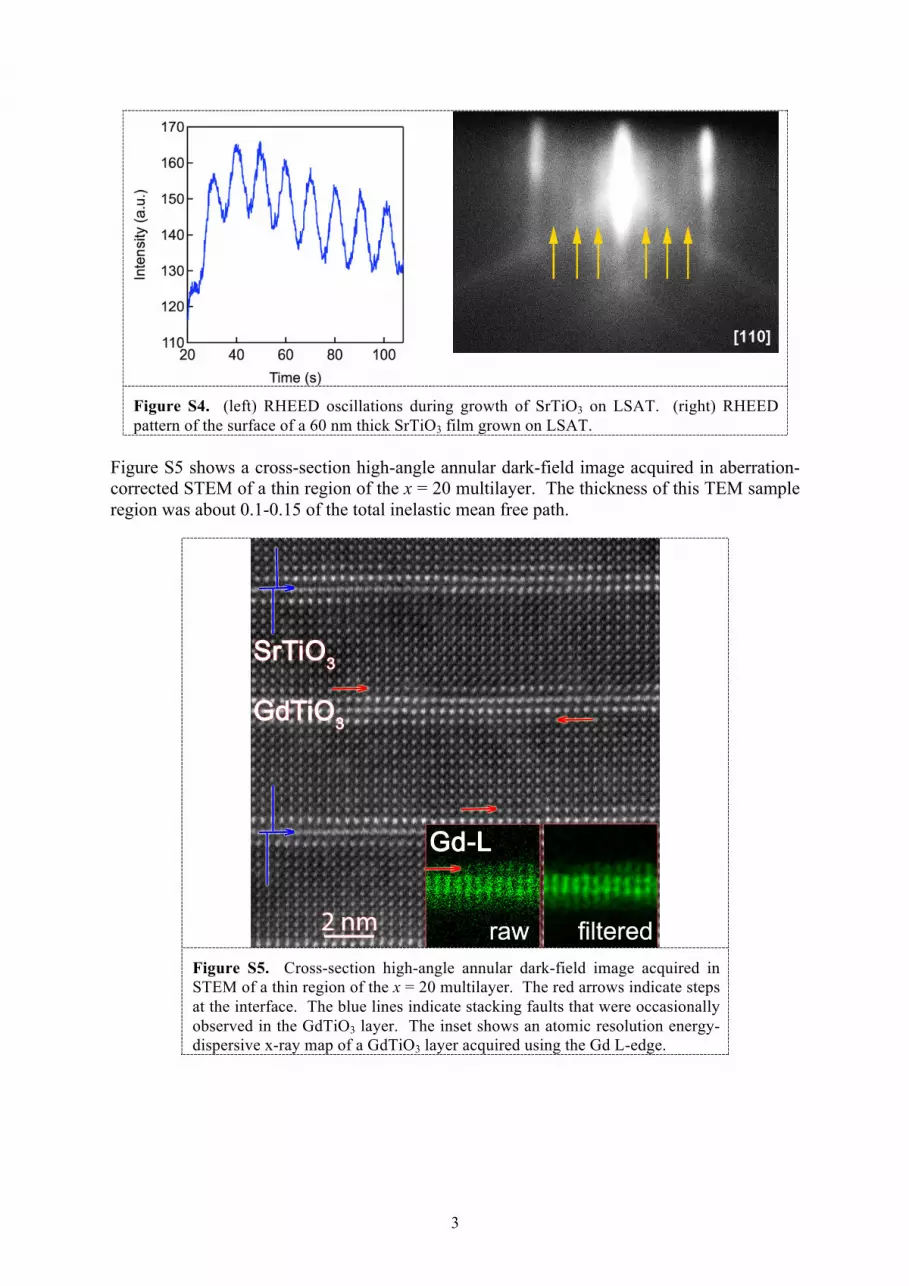
Figure S5 shows a cross-section high-angle annular dark-field image acquired in aberration-corrected STEM of a thin region of the x = 20 multilayer. The thickness of this TEM sample region was about 0.1-0.15 of the total inelastic mean free path.
Figure S5. Cross-section high-angle annular dark-field image acquired in STEM of a thin region of the x = 20 multilayer. The red arrows indicate steps at the interface. The blue lines indicate stacking faults that were occasionally observed in the GdTiO3 layer. The inset shows an atomic resolution energy-dispersive x-ray map of a GdTiO3 layer acquired using the Gd L-edge.
4
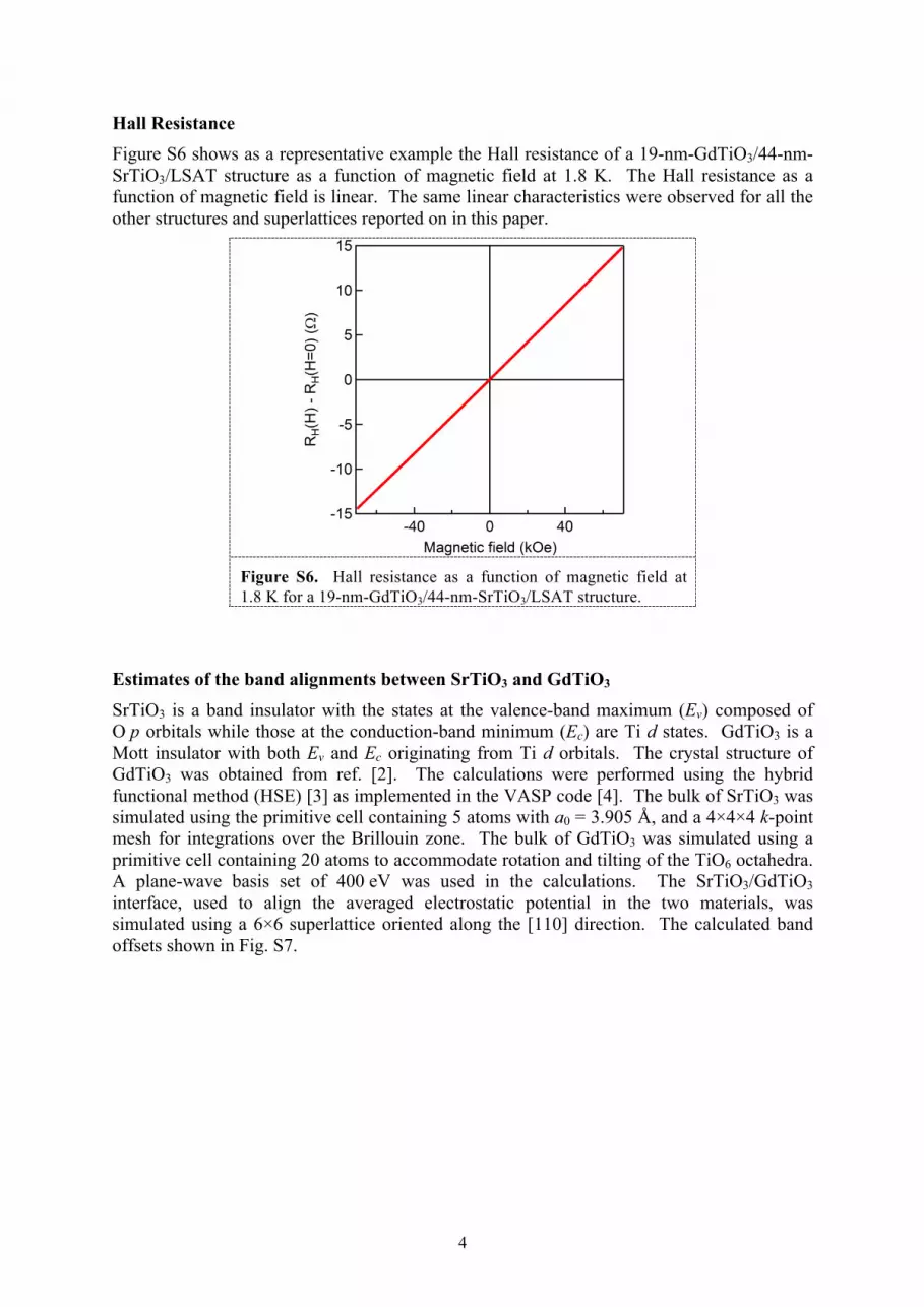
Hall Resistance Figure S6 shows as a representative example the Hall resistance of a 19-nm-GdTiO3/44-nm-SrTiO3/LSAT structure as a function of magnetic field at 1.8 K. The Hall resistance as a function of magnetic field is linear. The same linear characteristics were observed for all the other structures and superlattices reported on in this paper.
Figure S6. Hall resistance as a function of magnetic field at 1.8 K for a 19-nm-GdTiO3/44-nm-SrTiO3/LSAT structure.
Estimates of the band alignments between SrTiO3 and GdTiO3
SrTiO3 is a band insulator with the states at the valence-band maximum (Ev) composed of O p orbitals while those at the conduction-band minimum (Ec) are Ti d states. GdTiO3 is a Mott insulator with both Ev and Ec originating from Ti d orbitals. The crystal structure of GdTiO3 was obtained from ref. [2]. The calculations were performed using the hybrid functional method (HSE) [3] as implemented in the VASP code [4]. The bulk of SrTiO3 was simulated using the primitive cell containing 5 atoms with a0 = 3.905 Å, and a 4×4×4 k-point mesh for integrations over the Brillouin zone. The bulk of GdTiO3 was simulated using a primitive cell containing 20 atoms to accommodate rotation and tilting of the TiO6 octahedra. A plane-wave basis set of 400 eV was used in the calculations. The SrTiO3/GdTiO3 interface, used to align the averaged electrostatic potential in the two materials, was simulated using a 6×6 superlattice oriented along the [110] direction. The calculated band offsets shown in Fig. S7.

5
Figure S7. Calculated band offsets across a SrTiO3/GdTiO3 interface.
References [1] B. Jalan, R. Engel-Herbert, N. J. Wright, and S. Stemmer, J. Vac. Sci. Technol. A 27,
461 (2009). [2] A. C. Komarek, H. Roth, M. Cwik, W.-D. Stein, J. Baier, M. Kriener, F. Bourée, T.
Lorenz, and M. Braden, Phys. Rev. B 75, 224402 (2007). [3] J. Heyd, G. E. Scuseria, and M. Ernzerhof, J. Chem. Phys. 118, 8207 (2003); erratum:
J. Chem. Phys. 124, 219906 (2006). [4] G. Kresse and J. Furthmüller, Phys. Rev. B 54, 11169 (1996); G. Kresse and J.
Furthmüller, Comput. Mat. Sci. 6, 15 (1996).