doping effects in organic low-dimensional conducting
TRANSCRIPT

UNIVERSITY OF CALIFORNIA RIVERSIDE
Doping Effects in Organic Low-Dimensional Conducting Materials and their Opto-Electronic Applications
A Dissertation submitted in partial satisfaction of the requirements for the degree of
Doctor of Philosophy
in
Chemistry
by
Dejan Stekovic
December 2018
Dissertation Committee:
Dr. Mikhail E. Iktis, Co-Chairperson Dr. Eric L. Chronister, Co-Chairperson Dr. Richard J. Hooley Dr. Matthew P. Conley

Copyright by Dejan Stekovic
2018

The Dissertation of Dejan Stekovic is approved:
Committee Co- Chairperson
Committee Co-Chairperson
University of California, Riverside

iv
ACKNOWLEDGMENTS
Throughout my life and my academic career, I have been fortunate
enough to have many people support me. Without them I would not have been
able to make it this far. First and foremost, I would like to thank my mother,
father, and sister for their support throughout the years no matter the scenario. I
could not have made it to this point without you.
During my time at UCR I have been influenced by several great scientists.
I would like to thank Robert C. Haddon for first allowing me to join the group. You
showed me how a scientist thinks and always had time to discuss our projects.
The scientific community was lucky to have you. I thank Mikhail E. Itkis for taking
up the advisor role after Dr. Haddon’s passing. Thank you for all that you have
taught me and your patience as I learned about fields new to me, I have learned
a lot from you. I would also like to thank Dr. Eric L. Chronister for also acting as
an advisor and allowing me to continue Dr. Haddon’s research.
I thank the many group members I’ve had throughout the years. Dr. Pradip
Bag for teaching me synthetic organic chemistry and how to grow crystals as well
as providing useful advice. Dr. Sushanta K. Pal for also helping to teach me
about neutral radical crystals. Dr. Elena Haddon for teaching me about carbon
nanotubes and allowing me to have first-hand experience at Carbon Solutions. I
thank my fellow graduate students Guanghui Li, Wangxiang Li, Mingguang Chen,
Basim Arkook, and Matthew Moser for their contributions to my projects for
helping me to understand the science behind it all.

v
Portions of the dissertation are adapted with permission from the following
references:
Chapter 2: Stekovic, D.; Arkook, B.; Li, G.; Li, W.; Bekyarova, E.; Itkis,
M.E., High Modulation Speed, Depth, and Coloration Efficiency of Carbon
Nanotube Thin Film Electrochromic Device Achieved by Counter Electrode
Impedance Matching Adv. Mat. Inter. 2018, 5, 1800861.
Chapter 3: Bag, P.; Itkis, M.E.; Stekovic, D.; Pal, S.K.; Tham,F.S.;
Haddon, R.C., Band Structure Engineering by Substitutional Doping in Solid-
State Solutions of [5-Me-PLY(O, O)]2B(1–x)Bex Radical Crystals J. Am. Chem.
Soc. 2015, 137, 10000-10008.
Chapter 4: Stekovic, D.; Bag, P.; Shankhari, P.; Fokwa, B.P.T.; Itkis, M.E.,
Effect of Substitution on the Hysteretic Phase Transition in a Bistable Phenalenyl
Based Neutral Radical Molecular Conductor Under Review.
Chapter 6: Stekovic, D; Itkis, M.E., Phenalenyl Based Neutral Radical as a
Novel Electrochromic Material Modulating Visible to Short-Wave Infrared Light
Under Review.

vi
ABSTRACT OF THE DISSERTATION
Doping Effects in Organic Low-Dimensional Conducting Materials and their Opto-Electronic Applications
by
Dejan Stekovic
Doctor of Philosophy, Graduate Program in Chemistry University of California, Riverside, December 2018
Dr. Mikhail E. Itkis, Dr. Eric L. Chronister, Co-Chairpersons
The field of materials science has produced a variety of valuable products
and technologies defining modern day civilization. While still dominated by
inorganic materials, the field of organic electronics opens new technological
opportunities and the access to a new class of complementary materials. Being
carbon based, organic electronic materials are abundant and environment
friendly, often made with low temperature processing compatible with existing
inorganic materials, and highly tunable for specific optical and electronic
properties. These properties have helped enable the use of organic electronic
materials throughout a wide range of products. Some of these include organic
light emitting diodes (OLEDs) for electronic displays and lighting, organic field
effect transistors (OFETs) for device control and computing, and organic

vii
photovoltaics (OPVs) for energy generation among other uses. With their wide
range of uses, the study of organic electronic materials is of high importance.
In this work, we examine both highly studied and relatively new low-
dimensional materials. Since their discovery in 1991, single-walled carbon
nanotubes (SWNTs) have seen much interest due to their unique electronic and
optical properties. Here we design all-SWNT electrochromic devices capable of
modulating incoming light with fast response times (few milliseconds). The
mechanism behind the device is explored through the view of an electric double
layer capacitor (EDLC) and reveals important clues for the design of fast
electrochromic devices.
Also explored here is the substitutional doping of phenalenyl based
radical molecular conductors. Through the use of substitutional doping most
commonly used in silicon-based semiconductors, we demonstrate the
enhancement of the electrical conductivity of some molecular conductors and
modification of their magnetic properties. We also explored the possibility of
using the substitutional doping to control a hysteretic phase transition and related
bistable state in another phenalenyl based radical molecular conductor. Finally,
the phenalenyl based radicals are incorporated into an electrochromic device
which is able to modulate both visible and short-wave infrared light thus opening
a novel pathway for development of a new class electrochromic materials for
smart window applications.

viii
Table of Contents
Chapter 1: Introduction to Organic Electronic Materials ....................................... 1
1.2 Introduction to Carbon Nanotubes .............................................................. 2
1.3 Introduction to Phenalenyl Based Neutral Radical Conductors ................... 4
1.4: Electrical Conductivity of Phenalenyl Based Neutral Radical Crystals ....... 8
1.5: Structural Motifs in Phenalenyl Based Neutral Radical Conductors ......... 10
1.4: Introduction to Doping: ............................................................................. 12
1.5: References ............................................................................................... 16
Chapter 2: Carbon Nanotube Electro-Optical Devices ....................................... 20
2.1: Introduction to Opto-Electronic Devices ................................................... 20
2.2: Electro-Optical Properties of Carbon Nanotube Thin Films: ..................... 21
2.3: SWNT Thin Film Electrochromic Devices ................................................ 24
2.4: Fast, High Modulation Depth, Carbon Nanotube Based Electrochromics 27
2.5: Understanding the Mechanism Behind the SWNT Thin Film Electrochromic Cell ......................................................................................... 32
2.6: Coloration Efficiency ................................................................................ 45
2.7: Effects of Counter Electrode Type ........................................................... 46
2.8: Effects of Offset Counter Electrodes: ....................................................... 48
2.9: Expansion to MWIR and LWIR ................................................................ 49
2.10: Conclusions ........................................................................................... 51
2.11: Experimental and Supplementary Information ....................................... 52
2.12: References ............................................................................................. 57
Chapter 3: Effects of Substitutional Doping on the Conductivity of a Phenalenyl Based Neutral Radical Conductor ...................................................................... 61
3.1: Introduction .............................................................................................. 61
3.2: Introduction to Substitutional Doping in [5-Me]2B ..................................... 62
3.3: Host and Dopant Crystal Structures ......................................................... 63
3.4: Electrochemical Properties of Host and Dopant ....................................... 68
3.5: Effects of Doping on Crystal Structure ..................................................... 69
3.6: Effects of Doping on Electrical Conductivity ............................................. 71
3.7: Effects of Doping on Magnetic Properties ................................................ 74
3.8: Conclusion ............................................................................................... 75
3.9: Experimental ............................................................................................ 75

ix
3.10: References ............................................................................................. 81
Chapter 4: Effect of Substitution on the Hysteretic Phase Transition in a Bistable Phenalenyl Based Neutral Radical Molecular Conductor ................................... 83
4.1: Introduction .............................................................................................. 83
4.2: Hysteretic Phase Transition in [Bu]2B with Bistability in the Vicinity of Room Temperature ......................................................................................... 84
4.3: Synthesis and Crystallization of Substitutional Doped [Bu]2B1-xBex ......... 87
4.4 Host and Dopant Structure Comparison ................................................... 88
4.5: Crystal Structures in Doped [Bu]2B1-xBex Solid Solutions ......................... 91
4.6: Magnetic Properties of Solid Solutions [Bu]2B1-xBex ................................. 93
4.7: Electrical Conductivity of Solid Solutions [Bu]2B1-xBex ............................. 99
4.8: Model of Substitutional Doping in [Bu]2B1-xBex ....................................... 101
4.9: Conclusion ............................................................................................. 102
4.10: Experimental and Supplementary Information ..................................... 103
4.11: References: .......................................................................................... 109
Chapter 5: Towards Energy Matched Substitutional Doping ............................ 112
5.1: Introduction ............................................................................................ 112
5.2: Synthesis of [DZPLY]2Be ....................................................................... 113
5.3: Reactivity of DZPLY ............................................................................... 115
5.4: Electrochemical Properties of [DZPLY]2Be ............................................ 117
5.5: Structure of [DZPLY]2Be ........................................................................ 119
5.6: Substitutional Doping with [DZPLY]2Be .................................................. 122
5.7: Conclusion ............................................................................................. 125
5.8: Experimental and Supplementary Information ....................................... 125
5.9: References ............................................................................................. 130
Chapter 6: Neutral Radicals as Novel Transmissive to Black Electrochromic Materials in the Visible and SWIR Range ......................................................... 131
6.1: Introduction ............................................................................................ 131
6.2: Overview of Electrochromic Properties of Phenalenyl Based Neutral Radical Conductors ....................................................................................... 132
6.3: Modulation of Visible Light in Electrochromic Cells Containing [Bu]2B ... 132
6.4: Modulation of Short-Wave Infrared Light in Electrochromic Cells Containing [Bu]2B .......................................................................................... 138
6.5: Conclusion ............................................................................................. 141

x
6.6: Experimental .......................................................................................... 142
6.7: References ............................................................................................. 144

xi
List of Figures
Figure 1.1: Examples of organic electronic materials. (left) Polymers; polyacetylene, poly(3-alkythiophene), and polyfluorene. (Middle) Small molecules; rubrene, and tetracyanoquinodimethane (TCNQ). Other; C60 (fullerene) and graphene (small section).
Figure 1.2: A graphene sheet (double bonds excluded for clarity) is wrapped into a SWNT. The chiral indices determine the diameter and electronic properties of the nanotube. Since n- m = 0 the resultant nanotube is metallic for this example of a (5,5) SWNT.
Figure 1.3: Filtration method to form SWNT thin films. (left) Solutions of SC- and MT-SWNTs are (middle) filtered through a membrane to form a film. These films can be transferred onto various substrates, (right) in this case glass.
Figure 1.4: Phenalenyl in its cation (left), neutral radical (middle), and anionic (right) state along with accompanying orbitals.
Figure 1.5: An H-cell is used to grow crystals of phenalenyl based neutral radical conductors. (left) The round bottoms are filled with the precursor cation (red-brown colored solution) and a chemical reductant (yellow solution). The cell is inverted and within a few days to a week crystal are grown at the frit (black color).
Figure 1.6: Examples of phenalenyl based neutral radical conductors (R = various alkyl chains, E = sulfur or selenium)
Figure 1.7: Bistability in a butyl substituted phenalenyl based neutral radical conductor being shown in the (left to right) magnetic, electrical conductivity and optical properties.43
Figure 1.8: (a) Band structure of a phenalenyl based neutral radical conductor predicting a metallic compound; (b) Arrhenius plot of the conductivity as a function of temperature showing semiconductor behavior and (c) the band gap created by the on-site coulomb correlation energy explaining the semiconducting properties.35,46
Figure 1.9: Common packing motifs and their magnetic properties in terms of spin per molecules as a function of temperature. (left) Dimeric motif, with short intradimer spacing and large interdimer spacing, displaying antiferromagnetic coupling. (middle) RVB motif, with equal intermolecular contacts less than 3.4 Å and temperature-independent Pauli paramagnetism. (right) Monomeric motif with

xii
large intermolecular spacing (>3.4 Å) displaying 1 Curie spin per molecule over all temperature ranges.
Figure 1.10: (Left) Intrinsic silicon, (middle) p-type silicon, and (right) n-type silicon and their associated band structures.
Figure 2.1: Schematic of an electrochromic device in its (left) bleached and (right) colored state.
Figure 2.2: (a) Band diagrams for SC- and MT-SWNTs showing interband transitions and (b) corresponding absorptions shown in thin films.
Figure 2.3: (left) Band diagram of SC-SWNTs showing suppression/regeneration of the interband transitions through gating and the (right) resultant absorbance spectra showing the modulation of absorbance from gating.
Figure 2.4: (a) Schematic of the all-SWNT device with increasing thickness of the SC-SWNT layer to increase light modulation. (b) Modulation bandwidth as a function of SC-SWNT film thickness. (c) Frequency dependencies of the amplitude of electro-optical modulation as a function of SC-SWNT film thickness. (d) Oscilloscope traces of the SWNT electrochromic cell with various thickness of the SC-SWNT film.
Figure 2.5: (a) Schematic of device with increasing MT-SWNT film thickness. (b) Bandwidth as a function of MT-SWNT film thickness for various SC-SWNT film thicknesses. (c) Frequency dependencies of 440 nm SC-SWNT films with various MT-SWNT counter electrodes. (d) Corresponding oscilloscope trances at 10 Hz showing regeneration of the square wave.
Figure 2.6: (a) Transmittance spectra of the bleached (dashed lines) and colored (solid lines) states of various thicknesses of SC-SWNTs. (b) Corresponding modulation depth at ~1870 nm. (c) Transmittance spectra at the center of the S11 transition located at 1770 nm and (d) corresponding response time.
Figure 2.7: (a) Schematic of an unbalanced SWNT cell with only unbalanced local net charges shown. (b) Simplified equivalent circuit of cell and (c) the expected potential drop.
Figure 2.8: Schematics of devices containing additional potential probes with a thicker (a,b) SC-SWNT and (c,d) MT-SWNT electrode and the resultant potential drops and oscilloscope traces.
Figure 2.9: Optimal applied potential as a function of MT-SWNT:SC-SWNT electrode thickness.

xiii
Figure 2.10: Specific capacitance of a SC-SWNT electrode as a function of voltage and (b) its voltage derivative obtained from ac impedance measurements at different excitation frequencies.
Figure 2.11: Specific capacitance of a MT-SWNT electrode as a function of voltage and (b) its voltage derivative obtained from ac impedance measurements at different excitation frequencies.
Figure 2.12: Capacitance as a function of frequency for SC- and MT-SWNT electrodes.
Figure 2.13: (a) Chronoamperometry, (b)transient transmittance spectra and (c) coloration efficiency of SC-SWNT electrochromic devices
Figure 2.14: (a) Frequency dependencies and (b) oscilloscope traces of devices made with MT-SWNT and graphene counter electrodes with matching sheet resistances.
Figure 2.15: (a) Schematic of offset device with (b) resultant oscilloscope traces. (c) Frequency dependencies as a function of position and its (d) transmittance data.
Figure 2.16: (a) Transmittance spectra of [C6mim][PF6] in the SWIR to LWIR range. (b) Device schematic with a BaF2 substrate, gold electrodes and SC-SWNT (brown) and MT-SWNT (green) thin films, the IL and encapsulation layer is not shown. (c) Transmittance spectra of the SC-SWNT thin film as a function of applied voltage in the SWIR to LWIR range.
Figure 2.17: Typical device configuration.
Figure 2.18: Offset device configuration. Figure 2.19: Absorption Spectra of SC- and MT-SWNT aqueous solutions used.
Figure 2.20: (a) Transmittance and (b) absorbance spectra of various SC-SWNT films used.
Figure 2.21: Electrochemical impedance spectroscopy of a 120 nm SC-SWNT/120 nm Mt-SWNT electrochromic device. (a) Nyquist plot showing linearity in the low frequency and the characteristic (inset) semi-circle at high frequencies. (b) Bode magnitude plot. (c) Bode angle plot reaching ~85° at low frequencies.

xiv
Figure 3.1: The structure and magnetic properties of [5-Me]2B.
Figure 3.2: Drawings of [5-Me]2Be and an overview of the doping co-crystallization. (TFAB = tetrakis[3,5-bis(trifluoromethyl)phenyl]borate)
Figure 3.3: Pictures of crystals and molecule crystal structure of host (left) [5-Me]2B and dopant (right) [5-Me]2Be.
Figure 3.4: 1-D chains of [5-Me]2B in perpendicular views (a and b).
Figure 3.5: Dimeric structure of [5-Me]2Be showing perpendicular views of dimers with no well overlapped neighbors.
Figure 3.6: Perpendicular views of PLY-PLY interactions involving (a) six and (b) 2 spin bearing carbons.
Figure 3.7: PLY-PLY interaction in [5-Me]2Be.
Figure 3.8: Cyclic voltammograms of (a) [5-Me]2B and (b) [5-Me]2Be.
Figure 3.9: Effects of doping on unit cell parameter and bandwidth as a function of dopant concentration (x).
Figure 3.10: Effects of doping on the PLY-PLY interaction. Figure 3.11: Effect of doping on electrical conductivity as a (a) function of temperature. (b) Room temperature conductivity and (c) activation energy as a function of doping concentration. The inset shows a zoomed in picture when x >0.25.
Figure 3.12: (a) Fraction of Curie Spin as a function of temperature at various dopant concentrations and (b) the fraction of Curie Spin at room temperature as a function of doping concentration.
Figure 3.13: Thermal ellipsoids of (left) [5-Me]2B and (right) [5-Me]2Be.
Figure 4.1: The structure of [Bu]2B.
Figure 4.2: (a) Fraction of Curie Spin as a function of temperature around the phase transition of [Bu]2B and (b) a diagram of the phase transition.
Figure 4.3: The co-crystallization procedure for substitutional doping: The cationic precursor of [Bu]2B is combined with the dopant, [Bu]2Be, and a

xv
reductant (tetrakis(dimethylamino)ethylene (TDAE)) is added to grow solid solutions of [Bu]2B1-xBex.
Figure 4.4: Pictures of crystals of (a) [Bu]2B, (b) lightly doped [Bu]2B1-xBex, (c) heavily doped [Bu]2B1-xBex and (d) [Bu]2Be. The scale bars are 1 mm.
Figure 4.5: Perpendicular views of [Bu]2B dimers in its (a, b) low spin and (c, d) high spin states showing interfacial distances and high degree of overlap between spin-bearing carbons shown in green. (e-h) Views of [Bu]2Be crystal interactions showing larger interfacial distances and little to no overlap of spin-bearing carbons shown in green.
Figure 4.6: Powder X-ray diffraction data of solid solutions of [Bu]2B1-xBex showing the transition of the structure from that of the host ([Bu]2B) to that of the dopant ([Bu]2Be).
Figure 4.7: Temperature dependent fraction of Curie spin per molecule as a function of doping level x. (a) Lightly substituted [Bu]2B1-xBex: Compression of the height of the hysteresis loop with increasing doping; (b) Expanded view of the hysteresis loop above room temperature for lightly substituted [Bu]2B1-xBex
showing no phase transition; (d) Events of reverse hysteresis loop at x~6%.
Figure 4.8: (a) Height and (b) width of the hysteretic loop as a function of doping. (c) Curie spin per molecule of the high spin (HS) and low spin (LS) states as a function of doping. (d) Curie spin per molecule at 150 K as a function of doping.
Figure 4.9: Conductivity of doped neutral radical conductors. (a) Zoomed in view of the transition showing a lowering of conductivity as doping is increased and an eventual elimination of the hysteretic phase transition. (b) Arrhenius plot of temperature dependencies of electrical conductivity of various solid solutions of [Bu]2B1-xBex in a wide temperature range.
Figure 4.10: Effects of substitution on [Bu]2B1-xBex solid solutions. (left) With no doping (red) dimers of [Bu]2B form 2 electron bonds canceling out their spin, at light substitution levels (yellow) some of these are now 1 electron bonds but the [Bu]B2 structure is retained. (Right) At heavy substitution levels [Bu]2B1-xBex
adopts the structure of [Bu]2Be and the spins are non-interacting.
Figure 4.11: Powder X-ray diffraction patterns for the compounds [Bu]2B (top) and [Bu]2Be (bottom). The green vertical lines represent calculated peak positions for the respective compounds obtained from their single crystal data. The most prominent peaks were located below 2Ɵ = 30 degree and hence the peak matching was performed only upto 2Ɵ = 30 degree. The full diffraction patterns (in the range 2Ɵ = 3-65 degrees are shown in insets).

xvi
Figure 4.12: Thermal ellipsoids of (left) [Bu]2B and (right) [Bu]2Be.
Figure 5.1: Structure of (left) DZPLY and its beryllium complex, (right) [DZPLY]2Be.
Figure 5.2: (a) NMR spectra of the three products from the reaction of DZPLY and butylamine. (b) Proposed structure of the second fraction. (c) Proposed structure of the first and third fraction.
Figure 5.3: (a) CV of [PLY]2B and [PLY]2Be.2 (b) Differential pulse voltammetry of [DZPLY]2Be.
Figure 5.4: Energy differences in the SOMO to LUMO transition of the previous dopant and the new, energy matched dopant.
Figure 5.5: Structure of molecules of the radical [PLY]2B and dopants [PLY]2Be and [DZPLY]2Be.
Figure 5.6: 1-D chains found in the crystal structure of [PLY]2B and [PLY]2Be and the dimers found in [DZPLY]2Be.
Figure 5.7: Interfacial overlap in radical [PLY]2B and dopants [PLY]2Be and [DZPLY]2Be.
Figure 5.8: Pictures of [PLY]2B doped with [DZPLY]2Be.
Figure 5.9: Conductivity measurements of doped crystals and (inset) a picture of a crystal wired for measurement.
Figure 5.10: Thermal ellipsoids of [DZPLY]2Be.
Figure 6.1: (a) Cationic and neutral radical structure of [Bu]2B. Change of color between cationic and neutral radical states of [Bu]2B in (b,c) solid state and (d,e) in solution pictures.
Figure 6.2: Electrochemistry of electrochromic device operations. (left) At an applied potential, [PLY(O,NBu)]2B+ is reduced to the neutral radical [PLY(O,NBu)]2B (1 electron reduction) while hydroquinone is oxidized to 1,4-benzoquinone (2 electron oxidation) resulting in a black state. (Right) When no potential is applied (0V) [PLY(O,NBu)]2B and 1,4-benzoquinone diffuse and [PLY(O,NBu)]2B is oxidized to [PLY(O,NBu)]2B+ while 1,4-benzoquinone is reduced to hydroquinone (transmissive state).

xvii
Figure 6.3: Electrochromic properties of [NBu]2B in an ITO-glass sandwich structure. (a) Pictures of the devices in clear and black state. (b) Accompanying transmittance spectra.
Figure 6.4: (a) Cycling response at 575 nm and (b) the expanded pulse shape showing corresponding response times.
Figure 6.5: Transmittance spectra of device, ITO on glass in the range of interest (400-1000 nm). (b) Transmittance spectra of glass and ITO on glass showing high absorption of ITO above 1200 nm.
Figure 6.6: Transmittance spectra of MT-SWNT films on glass.
Figure 6.7: (a) Pictures of the [Bu]2B device utilizing MT-SWNT thin film electrodes and (b) the corresponding transmittance spectra in the transparent and opaque state.
Figure 6.8: (a) Transmittance spectra of propylene carbonate between 2 glass slides and (b) the spectra of devices in Figure 6.6 with the contribution of propylene carbonate subtracted out.
Figure 6.9: (a) Cycling response of device at 2000 nm and (b) corresponding response time.

xviii
List of Tables Table 3.1: X-ray crystallographic data of [5-Me]2Be and [5-Me]2B. Table 4.1: X-ray crystallographic data of [Bu]2Be and [Bu]2B (100K and 360K). [Bu]2B data taken from literature. Table 4.2. Lattice parameters obtained from powder X-ray diffraction peak matching. Table 5.1: X-ray crystallographic data of [DZPLY]2Be.

xix
List of Schemes Scheme 5.1: (top) Synthesis of pyrimidines from 1,3-diketones and amidines. (bottom) Proposed retrosynthesis of DZPLY from naphthazarin. Scheme 5.2: Synthesis of [DZPLY]2Be from 1,5-dinitronaphthalene. 1,5-dinitronaphthalene is reacted with fuming sulfuric acid and elemental sulfur to produce amino-naphthazarin. Amino-naphthazarin is then reacted with formamide in acetic acid to form DZPLY which is then reacted with beryllium acetylacetonate to give the final product, [DZPLY]2Be.

1
Chapter 1: Introduction to Organic Electronic Materials
1.1: Introduction
The field of materials science has produced many products that make up
the technology that helps to define modern day civilization. While still dominated
by inorganic materials, the field of organic electronic materials provides some
advantages as well as complementary materials. Being carbon based, organic
electronic materials are abundant, made with low temperature processing,
compatible with existing inorganic materials and highly tunable for specific optical
and electronic properties. These properties have helped enable the use of
organic electronic materials throughout a wide range of products. Some of these
include organic light emitting diodes (OLEDs)1 for electronic displays and lighting,
organic field effect transistors (OFETs)2 for device control and computing, and
organic photovoltaics (OPVs)3 for energy generation among other uses. With
their wide range of uses, the study of organic electronic materials is of high
importance.
Organic electronic materials generally fall into one of three categories;
polymers, small molecules, and other materials. Polymers are large
macromolecules made up of repeating subunits and while they have many
advantages, will not be covered here. Small molecule based organic electronic
materials are highly tunable through synthetic organic chemistry and, as the
name implies, made up of small organic molecules. The other category generally
includes allotropes of carbon, such as graphene, fullerenes and carbon

2
nanotubes. Figure 1.1 shows some examples of all three types of organic
electronic materials.
1.2 Introduction to Carbon Nanotubes
Carbon nanotubes (CNTs), as the name implies, are tubes of sp2
hybridized carbon. They are often thought of as rolled up sheets of graphene (a
flat plane of sp2 hybridized carbon) and are 1-dimensional (1D) conductors.
Since their discovery in 1991, CNTs have drawn much attention.4 While CNTs
can be either single-walled (SWNTs) or multi-walled (MWNTs), we will focus on
SWNTs. SWNTs possess many exemplary properties such as high mechanical
strength5,6 and high thermal conductivity7,8 along with unique optical9,10 and
electronic11 properties. The optical and electronic properties of SWNTs are
determined by their chiral indices (m,n) (Figure 1.2). The chiral indices determine
both the diameter and the electronic properties of the SWNT. SWNTs are
Figure 2.1: Examples of organic electronic materials. (left) Polymers; polyacetylene, poly(3-alkythiophene), and polyfluorene. (Middle) Small molecules; rubrene, and tetracyanoquinodimethane (TCNQ). Other; C60 (fullerene) and graphene (small section).

3
classified as armchair if n = m, zigzag if either m or n is zero, or chiral (other n
and m values). SWNTs are metallic (MT-SWNTs) if the absolute value of n – m is
a multiple of 3 or zero. Otherwise, the SWNTs are classified as semiconducting
SWNTs (SC-SWNTs). MT-SWNTs, as the name implies, are metallic in nature
and thus have no bandgap. On the other hand, SC-SWNTs, have a bandgap that
is inversely proportional to their diameter.12-14
Figure 1.2: A graphene sheet (double bonds excluded for clarity) is wrapped into a SWNT. The chiral indices determine the diameter and electronic properties of the nanotube. Since n- m = 0 the resultant nanotube is metallic for this example of a (5,5) SWNT.
Another advantage of SWNTs is the ability to easily form thin films. These
thin films have more macroscopic uses than individual nanotubes and have a
better ease of use.15 There are a number of ways to generate SWNT thin films
such as drop casting, spray coating, and filtration. Figure 1.3 demonstrates the
vacuum filtration method. A solution of suspended SWNTs is filtered through a
membrane. After this the semi-transparent films can be transferred onto various
substrates, in this case glass. As can be seen from the figure, SC-SWNTs have a
n = 5
m = 5
a1
a2
T
T
5,5 armchair
(metallic)

4
brownish color while MT-SWNTs have a blue-green color with the color
difference originated from their different visible absorption spectra.
Figure 1.3: Filtration method to form SWNT thin films. (left) Solutions of SC- and MT-SWNTs are (middle) filtered through a membrane to form a film. These films can be transferred onto various substrates, (right) in this case glass.
Due to their unique properties, CNTs have been explored for a number of
uses including field effect transistors,16 semi-transparent electrodes,15 drug
delivery,17 strong composite materials,18 sensors,19 solar cells,20 hydrogen
storage,21 supercapacitors,22 batteries,23 and many others.
1.3 Introduction to Phenalenyl Based Neutral Radical Conductors
As discussed above, another group of organic electronic materials are
composed of small molecules. A special subset of these materials, pioneered by
R.C. Haddon, are classified as neutral radical conductors.24 Since the discovery
of a long lived radical in triphenylmethyl, much effort has gone into studying their
reactivity as well as their properties as materials.25 These small molecules
contain an unpaired electron, i.e. radical, as the charge carrier for conduction.
While there are a number of neutral radical conductors,26-29 we will focus on
those derived from phenalenyl. Phenalenyl is composed of ~3 benzene rings
fused together in a triangle like shape. Phenalenyl is an odd alternant

5
hydrocarbon (OAH). Like other alternant hydrocarbons, phenalenyl has
symmetrical bonding and antibonding orbitals. However, since phenalenyl has an
odd number of carbons, it has an additional nonbonding orbital located in
between the two. This nonbonding orbital can be empty (cation), singly occupied
(radical), or doubly occupied (anion). Due to the orbital being nonbonding, these
three states cause little change in the structure and thus should make good
conductors (Figure 1.4).24,30
Figure 1.4: Phenalenyl in its cation (left), neutral radical (middle), and anionic (right) state along with accompanying orbitals.

6
While phenalenyl should in theory make a good conductor, a large
problem arises as the phenalenyl neutral radicals can partner up and sigma-
dimerize. This leads to the decomposition of phenalenyl and a resulting insulating
state.31,32 To circumvent this issue, two molecules of a derivative of phenalenyl
(9-hydroxyl-phenalenone) can be spiro-conjugated through a bridging boron. This
leads to a compound that (generally) does not undergo sigma-dimerization and
contains a quarter filled band structure.33,34
While phenalenyl based conductors we first proposed in 1975, it wasn’t
until 1999 that the first example was reported.35 One of the more difficult tasks
was the crystallization of the radical. During synthesis, the compounds are
created as the cationic salts. Thus, to crystallize the neutral radicals the cationic
salts must be reduced then crystallized. The final solution was the use of
specially created H-cells in which the cationic salt would be filled in one side, and
a chemical reductant in the other. When the cell is inverted the reductant slowly
diffuses through the glass frit resulting in reduction and crystal growth at the frit
(Figure 1.5).

7
Figure 1.5: An H-cell is used to grow crystals of phenalenyl based neutral radical conductors. (left) The round bottoms are filled with the precursor cation (red-brown colored solution) and a chemical reductant (yellow solution). The cell is inverted and within a few days to a week crystal are grown at the frit (black color).
Since the first crystallization of a phenalenyl-based neutral radical
molecular conductor a number of others have also been synthesized,
crystallized, and characterized with many possessing unique properties. Some
examples are shown in Figure 1.6.36-42
Figure 1.6: Examples of phenalenyl based neutral radical conductors (R = various alkyl chains, E = sulfur or selenium)

8
One of the most interesting is the butyl-substituted compound presented in
Figure 1.6, far left (R = butyl). This compound shows a bistability in the form of a
hysteretic phase transition that occurs in the magnetism, electrical conductivity
and the optical properties of the material. This material and its phase transition,
along with the manipulation of it, is explored further in Chapter 4.36,43-45
Figure 1.7: Bistability in a butyl substituted phenalenyl based neutral radical conductor being shown in the (left to right) magnetic, electrical conductivity and optical properties
1.4: Electrical Conductivity of Phenalenyl Based Neutral Radical Crystals
One of the major motivations for the construction and study of neutral
radical conductors is the discovery of a molecular metal.24 One characteristic of a
metal is high conductivity and a decrease of conductivity as temperature is
increased while semiconductors possess intermediate conductivities and an
increase of conductivity as temperature is increased. This is explained through
the band structure of both metals and semiconductors. Metals possess no band
gap at the Fermi level, and thus electrons and holes are free to move throughout
the material. In such a case, an increase in temperature results in more
molecular vibrations that scatter free carriers through electron-phonon
interaction, decreasing the free carriers mean free path and thus reducing the

9
conductivity of the metals. Semiconductors possess a band gap and thus
electrons and holes are not free to move throughout the material at low
temperatures. In order to conduct, semiconductors require thermal excitation of
valence electrons into the conduction band to form free charge carriers. Thus, as
temperature is increased, more electrons are excited, and conductivity is
increased.
While neutral radical conductors were predicted to behave as molecular
metals, thus far all phenalenyl based neutral radical conductors have behaved as
semiconductors. Figure 1.8a shows the band structure calculations of a
phenalenyl based neutral radical conductor conducted by Robert Haddon.35,46 In
the quarter filled band structure (bandwidth, W~0.5eV), there is a finite density of
states at the Fermi level, and thus the material would be predicted to behave as
a metal. However, Figure 1.8b shows the conductivity of a phenalenyl based
neutral radical conductor, and it can be seen that the conductivity (0.05 S/cm) is
relatively low and increases with increasing temperature. Thus, the material is
behaving as a semiconductor. The explanation for this is the limitation of the tight
binding approximation used in the band structure calculations; it does not take
into account electron-electron interactions. In order to conduct, a phenalenyl
molecule must, at some point, contain a filled nonbonding orbital. The electrons
in this filled nonbonding orbital repel one another (on site coulombic correlation
energy, U) creating a band gap resulting in a semiconducting material (Figure
1.8c). The on-site coulombic correlation energy can be estimated through cyclic

10
voltammetry and is related to the band gap of the material. The band gap of the
material can also be estimated from the activation energy and optical
measurements, however, their relation to one another in phenalenyl based
neutral radical conductors is complicated and poorly understood. It is suggested
that the transition of a Mott insulator to a metallic state is controlled by the
bandwidth (W) -coulombic correlation energy (U) ratio (W/U).35,46 However, a
strategy of maximizing W and reducing U has yet to result in a metallic
state.35,46,47
Figure 1.8: (a) Band structure of a phenalenyl based neutral radical conductor predicting a metallic compound; (b) Arrhenius plot of the conductivity as a function of temperature showing semiconductor behavior and (c) the band gap created by the on-site coulomb correlation energy explaining the semiconducting properties.35,46
1.5: Structural Motifs in Phenalenyl Based Neutral Radical Conductors
The phenalenyl neutral radicals were discussed above in terms of single
molecules, while their solid state properties are heavily influenced by their
intermolecular interactions which are mostly controlled through their crystal
packing structure. Phenalenyl based neutral radical conductors pack in one of 3
a) b) c)

11
general motifs; dimeric, resonating valence bond and monomeric (Figure 1.9).
The first packing motif, dimeric, consists of dimers of neutral radicals. These
dimers pancake-bond to one another and, as a result, contain short intradimer
interactions which are shorter than the van der Waals distance of carbon-carbon
bonds (<3.4 Å). As a result of their pi-dimerization, the spins pair
antiferromagnetically into singlet low spin (LS) state which results in magnetism
similar to simple diamagnetic molecules (spin per molecule equal to zero over all
temperature ranges) (Figure 1.9 left).36,43,48
The second, and arguably most interesting case, is that of the resonating
valence bond (RVB) motif. Initially proposed by Anderson and Pauling,49-51 it was
first built as a model to explain superconductivity in cuprates. The name draws
inspiration from the resonating bonds found in benzene, in which the equal bond
distances of the six carbons are explained as the combination of 2 resonance
structures with alternating double bonds. Similar to benzene, neutral radical
crystals with RVB structures have intermolecular distances which are equal and
less than the van der Waals distance of carbon-carbon bonds (<3.4 Å). These
compounds contain temperature-independent Pauli paramagnetism, which is
characteristic of a metal and is manifested as an increase in spin per molecule as
temperature is increased. Neutral radicals with RVB packing motifs often display
the highest conductivities.33,42,46,48
The final motif, monomeric, is usually made up of molecules with bulky
substituents. Here the intermolecular distances are often large (>3.4 Å) and the

12
spins on each molecule are noninteracting, or independent. As a result, magnetic
measurements in this case show one Curie spin per molecule over wide
temperature ranges (until low temperatures, where long distance interactions
often cause antiferromagnetic pairing).35,52
Figure 1.9: Common packing motifs and their magnetic properties in terms of spin per molecules as a function of temperature. (left) Dimeric motif, with short intradimer spacing and large interdimer spacing, displaying antiferromagnetic coupling. (middle) RVB motif, with equal intermolecular contacts less than 3.4 Å and temperature-independent Pauli paramagnetism. (right) Monomeric motif with large intermolecular spacing (>3.4 Å) displaying 1 Curie spin per molecule over all temperature ranges.
1.4: Introduction to Doping:
Despite the first phenalenyl-based neutral radicals being conductors, it
was importance to find a way to enhance their electrical conductivity. One
advantage of semiconducting materials is that their properties can be controlled,
often times through doping.53 Non-doped semiconductors, i.e. intrinsic
semiconductors, often have low conductivities and thus dopants must be
introduced to increase the conductivities for most practical purposes. Electrical
conduction is the process of charge moving throughout a material. In most
0
1
Spin
per
Mole
cule
Temperature
0
1
Spin
per
Mole
cule
Temperature
0
1
Spin
per
Mole
cule
Temperature
Dimeric Resonating Valence Bond Monomeric

13
intrinsic semiconductors, few electrons are able to be thermally excited from the
valence band to the conduction band due to the band gap in between being
relatively large and thus the number of available charges that can move
throughout the material (free carrier concentration) is quite low resulting in a low
conductivity. Doping refers to the addition of impurities into a material to augment
the electrical, optical, and structural properties.
One of the most popular examples of doping is the substitutional doping
found in extrinsic silicon which helps form the basis of modern day computers.
Substitutional doping refers to the replacement of a host with that of a dopant.
Silicon, a group 4 element, can be doped with group 3 or group 5 elements.
Since group 3 elements, such as boron, contain one less electron in their valence
shell than silicon, they insert holes (positive charge carriers) into the lattice and
produce p-type semiconductors. On the other hand, group 5 elements, such as
phosphorous, contain one more electron in their valence shell than silicon and
thus insert electrons (negative charge carriers) into the lattice and produce n-type
semiconductors. An example of substitutional doping found in silicon is shown in
Figure 1.10.

14
Figure 1.10: (Left) Intrinsic silicon, (middle) p-type silicon, and (right) n-type silicon and their associated band structures.
While substitutional doping is often found in inorganic semiconductors,
interstitial doping, in the form of chemical or electrochemical, is more often used
in organic semiconductors, particularly polymers. As opposed to substitutional
doping, where the dopant takes the place of the host, interstitial doping refers to
the addition of impurities into open spaces surrounding the host. Common
examples of interstitial chemical doping include the intercalation of alkali metals
such as lithium. Due to the low electronegativity of alkali metals, they will donate
their electron to the conduction band of the material thus producing n-type
semiconducting materials. Popular examples of this include the superconducting
alkali doped C60 fullerenes54 and semiconducting alkali doped polyacetylene.55
P-type
SiSi Si
SiSi Si
SiSi Si
SiSi Si
PSi Si
SiSi Si
SiSi Si
BSi Si
SiSi Si
Valence Band
Conduction Band
Band Gap
Intrinsic N-type

15
Since the earth’s atmosphere is oxidizing, it can produce interstitially chemically
doped p-type materials. Interstitial doping can be further controlled through
electrochemical doping, often seen in electrochromic devices.56 Here the
semiconducting material is placed on an electrode, with a counter electrode
opposite and electrolyte in between for charge balance. When a potential is
applied to the polymer, electrons or holes can be injected from the electrode to
the material thus n- or p-type doping it with the opposite charge electrolyte
occupying interstitial sites for charge balance. This process is further explored in
Chapter 2 for a case of carbon nanotubes.
This dissertation is organized in the following way. Chapter 2 discusses
the field of electrochromic materials with SWNTs as an example and discusses
how electrochemical doping is used to control their optical properties. Chapter 3
and 4 focus on neutral radical conductors and the effects of substitutional doping
on them. Chapter 5 lays the foundation towards more effective, energy matched
dopants. Chapter 6 shows how phenalenyl based molecules, much like SWNTs,
also contain very interesting electrochromic properties.

16
1.5: References
1) Kulkarni, A. P.; Tonzola, C. J.; Babel, A.; Jenekhe, S. A. Chem. Mater. 2004, 16, 4556. 2) Yamashita, Y. Sci. Technol. Adv. Mater. 2009, 10. 3) Lin, Y. Z.; Li, Y. F.; Zhan, X. W. Chem. Soc. Rev. 2012, 41, 4245. 4) Iijima, S. Nature 1991, 354, 56. 5) Treacy, M. M. J.; Ebbsen, T. W.; Gibson, J. M. Nature 1996, 381, 678. 6) Wong, E. W.; Sheehan, P. E.; Lieber, C. M. Science 1997, 277, 1971. 7) Hone, J.; Whitney, M.; Piskoti, C.; Zettl, A. Physical Review B 1999, 59, R2514. 8) Itkis, M. E.; Borondics, F.; Yu, A.; Haddon, R. C. Nano Lett. 2007, 7, 900. 9) Wang, F.; Itkis, M. E.; Bekyarova, E.; Haddon, R. C. Nat. Photonics 2013, 7, 459. 10) Itkis, M. E.; Niyogi, S.; Meng, M.; Hamon, M.; Hu, H.; Haddon, R. C. Nano Lett. 2002, 2, 155. 11) Javey, A.; Guo, J.; Wang, Q.; Lundstrom, M.; Dai, H. Nature 2003, 424, 654. 12) Carbon Nanotubes: Synthesis, Structure, Properties and Applications; Dresselhaus, M. S.; Dresselhaus, G.; Avouris, P., Eds.; Springer-Verlag: Berlin, 2001; Vol. 80. 13) Wildoer, J. W. G.; Venema, L. C.; Rinzler, A. G.; Smalley, R. E.; Dekker, C. Nature (London) 1998, 391, 59. 14) Odom, T. W.; Huang, J.-L.; Kim, P.; Lieber, C. M. Nature (London) 1998, 391, 62. 15) Wu, Z.; Chen, Z.; Du, X.; Logan, J. M.; Sippel, J.; Nikolou, M.; Kamaras, K.; Reynolds, J. R.; Tanner, D. B.; Hebard, A. F.; Rinzler, A. G. Science 2004, 305, 1273.

17
16) Tans, S. J.; Verschueren, A. R. M.; Dekker, C. Nature 1998, 393, 49. 17) Hampel, S.; Kunze, D.; Haase, D.; Kramer, K.; Rauschenbach, M.; Ritscbel, M.; Leonbardt, A.; Thomas, J.; Oswald, S.; Hoffmann, V.; Buechner, B. Nanomedicine 2008, 3, 175. 18) Coleman, J. N.; Khan, U.; Gun'ko, Y. K. Adv. Mater. 2006, 18, 1. 19) Bekyarova, E.; Davis, M.; Burch, T.; Itkis, M. E.; Zhao, B.; Sunshine, S.; Haddon, R. C. J. Phys. Chem. B 2004, 108, 19717. 20) Rowell, M. W.; Topinka, M. A.; McGehee, M. D.; Prall, H. J.; Dennler, G.; Sariciftci, N. S.; Hu, L. B.; Gruner, G. Appl. Phys. Lett. 2006, 88, 233506. 21) Dillon, A. C.; Jones, K. M.; Bekkedahl, T. A.; Kiang, C. H.; Bethune, D. S.; Heben, M. J. Nature 1997, 386, 377. 22) Frackowiak, E.; Beguin, F. Carbon 2001, 39, 937. 23) Landi, B. J.; Ganter, M. J.; Cress, C. D.; DiLeo, R. A.; Raffaelle, R. P. Energy Environ. Sci. 2009, 2, 638. 24) Haddon, R. C. Nature 1975, 256, 394. 25) Gomberg, M. J. Am. Chem. Soc. 1900, 22, 757. 26) Tian, D.; Winter, S. M.; Mailman, A.; Wong, J. W. L.; Yong, W. J.; Yamaguchi, H.; Jia, Y. T.; Tse, J. S.; Desgreniers, S.; Secco, R. A.; Julian, S. R.; Jin, C. Q.; Mito, M.; Ohishi, Y.; Oakley, R. T. J. Am. Chem. Soc. 2015, 137, 14136. 27) Yu, X.; Mailman, A.; Lekin, K.; Assoud, A.; Robertson, C. M.; Noll, B. C.; Campana, C. F.; Howard, J. A. K.; Dube, P. A.; Oakley, R. T. J. Am. Chem. Soc. 2012, 2264 28) Kubo, T. Chem. Lett. 2015, 44, 111. 29) Tian, Y.; Uchida, K.; Kurata, H.; Hirao, Y.; Nishiuchi, T.; Kubo, T. J. Am. Chem. Soc. 2014, 136, 12784. 30) Uchida, K.; Kubo, T. J Syn. Org. Chem. JPN 2016, 74, 1069. 31) Uchida, K.; Ito, S.; Nakano, M.; Abe, M.; Kubo, T. J. Am. Chem. Soc. 2016, 138, 2399.

18
32) Small, D.; Rosokha, S. V.; Kochi, J. K.; Head-Gordon, M. J. Phys. Chem. A 2005, 109, 11261. 33) Bag, P.; Itkis, M. E.; Pal, S. K.; Donnadieu, B.; Tham, F. S.; Park, H.; Schleuter, J. A.; Siegrist, T.; Haddon, R. C. J. Am. Chem. Soc. 2010, 132, 2684. 34) Liao, P.; Itkis, M. E.; Oakley, R. T.; Tham, F. S.; Haddon, R. C. J. Am. Chem. Soc. 2004, 126, 14297. 35) Chi, X.; Itkis, M. E.; Patrick, B. O.; Barclay, T. M.; Reed, R. W.; Oakley, R. T.; Cordes, A. W.; Haddon, R. C. J. Am. Chem. Soc. 1999, 121, 10395. 36) Chi, X.; Itkis, M. E.; Kirschbaum, K.; Pinkerton, A. A.; Oakley, R. T.; Cordes, A. W.; Haddon, R. C. J. Am. Chem. Soc. 2001, 123, 4041. 37) Bag, P.; Pal, S. K.; Itkis, M. E.; Sarkar, A.; Tham, F. S.; Donnadieu, B.; Haddon, R. C. J. Am. Chem. Soc 2013, 135, 12936. 38) Bag, P.; Itkis, M. E.; Pal, S. K.; Bekyarova, E.; Donnadieu, B.; Haddon, R. C. Crystals 2012, 2, 446 39) Sarkar, A.; Pal, S. K.; Itkis, M. E.; Tham, F. S.; Haddon, R. C. J. Mater. Chem. 2012, 22, 8245. 40) Sarkar, A.; Pal, S. K.; Itkis, M. E.; Liao, P.; Tham, F. S.; Donnadieu, B.; Haddon, R. C. Chem. Mater. 2009, 21, 2226 41) Pal, S. K.; Itkis, M. E.; Tham, F. S.; Reed, R. W.; Oakley, R. T.; Haddon, R. J. Am. Chem. Soc. 2008, 130, 3942 42) Pal, S. K.; Itkis, M. E.; Tham, F. S.; Reed, R. W.; Oakley, R. T.; Haddon, R. C. Science 2005, 309, 281. 43) Itkis, M. E.; Chi, X.; Cordes, A. W.; Haddon, R. C. Science 2002, 296, 1443. 44) Fumanal, M.; Mota, F.; Novoa, J. J.; Ribas-Arino, J. J. Am. Chem. Soc. 2015, 137, 12843. 45) Fumanal, M.; Novoa, J. J.; Ribas-Arino, J. Chem. Eur. J. 2017, 23, 7772.

19
46) Mandal, S. K.; Samanta, S.; Itkis, M. E.; Jensen, D. W.; Reed, R. W.; Oakley, R. T.; Tham, F. S.; Donnadieu, B.; Haddon, R. C. J. Am. Chem. Soc. 2006, 128, 1982. 47) Pal, S. K.; Itkis, M. E.; Reed, R. W.; Oakley, R. T.; Cordes, A. W.; Tham, F. S.; Siegrist, T.; Haddon, R. C. J. Am. Chem. Soc. 2004, 126, 1478. 48) Pal, S. K.; Itkis, M. E.; Tham, F. S.; Reed, R. W.; Oakley, R. T.; Donnadieu, B.; Haddon, R. C. J. Am. Chem. Soc. 2007, 129, 7163. 49) Anderson, P. W. Mater. Res. Bull. 1973, 8, 153. 50) Anderson, P. W. Science 1987, 235, 1196. 51) Pauling, L. Nature 1948, 161, 1019. 52) Mandal, S. K.; Itkis, M. E.; Chi, X.; Samanta, S.; Lidsky, D.; Reed, R. W.; Oakley, R. T.; Tham, F. S.; Haddon, R. C. J. Am. Chem. Soc. 2005, 127, 8185. 53) Sze, S. M. Physics of Semiconductor Devices; Wiley: New York, 1981. 54) Hebard, A. F.; Rosseinsky, M. J.; Haddon, R. C.; Murphy, D. W.; Glarum, S. H.; Palstra, T. T. M.; Ramirez, A. P.; Kortan, A. R. Nature 1991, 350, 600 55) Jow, T. R.; Shacklette, L. W. J. Electrochem. Soc. 1988, 135, 541. 56) Beaujuge, P. M.; Reynolds, J. R. Chem. Rev. 2010, 110, 268.

20
Chapter 2: Carbon Nanotube Electro-Optical Devices
2.1: Introduction to Opto-Electronic Devices
Opto-electronic materials are those which can change their optical
properties upon the application of an external electric field. Electrochromic
devices1 are a subclass of electro-optical devices and many are based on
electrochemical capacitor designs which use electrochemical doping to control
the optical properties of the material as discussed in Chapter 1. Figure 2.1 shows
a diagram of a typical electrochromic device. In between clear substrates are
transparent conductive electrodes, an ion storage layer on one side and
electrochromic material on the other with an electrolyte in between. Upon
application of a potential, the ions diffuse towards their oppositely charged
electrodes and dope the electrochromic material. In response, the electrochromic
material goes from a bleached to colored state or vice-versa.
Figure 2.1: Schematic of an electrochromic device in its (left) bleached and (right) colored state.
+-
+-
Incoming Light+
-
+-
---
-
+
++
+

21
The uses of such materials range from smart windows,2,3 wearable
electronics, artificial reconfigurable camouflage4-6 and electro-optical shutters7
among many others.8,9 For example, smart windows would reduce energy costs
of buildings by providing natural heating in their bleached state and block
incoming heat from light in their colored state. Wearable electronics could display
information when needed and be transparent when not in use.
The most explored component of electrochromic devices is the electro-
optical materials themselves. Different materials can vary in the spectral range in
which they can modulate, the degree to which they can modulate, and the
response times of the devices. Depending on the particular use, some properties
are more important than others. For example, in smart windows the spectral
range and degree of modulation are very important while slow response times
are acceptable.2,3 Electrochromic devices are a good match for this as their
response times are generally in the tens to hundreds of seconds,10 but some
nanostructured materials are able to achieve response times in the millisecond
range.11-13 For other uses, such as electro-optical shutters, all three (range,
modulation, speed) are important and thus the optimization of these parameters
is receiving attention.1
2.2: Electro-Optical Properties of Carbon Nanotube Thin Films:
Carbon nanotubes, due to their unique electronic properties, have
garnered interest for use in electrochromic devices. The requirement for
transparent conductive layers has been the main push for CNTs in

22
electrochromic devices. The transparent electrodes are typically made of indium
tin oxide (ITO) due to its high conductivity and transparency. However, the rising
cost of ITO had incentivized exploring other materials. One of the explored
alternatives are CNT thin films. Due to their high conductivity and easy to form
thin films, as discussed in Chapter 1, they have been successfully used as
transparent electrodes in both rigid and flexible electrochromic devices as well as
other electronics.14,15 Recently, metallic (MT-) SWNTs have also been used as
the active electrochromic layer. It was shown that MT-SWNT thin films could act
as both the conductive and electrochromic layer simultaneously, modulating
visible light to go from green or pink films to yellow. Like many other
electrochromic materials, the MT-SWNT showed slow response times on the
order of seconds.16
As previously discussed, both semiconducting (SC-) SWNTs and MT-
SWNTs have interesting optical properties, some of which have been explored in
electrochromic devices as discussed above. Like many other properties of
SWNTs, the optical properties are also controlled by the chirality and diameter of
the SWNTs. In the visible-near infrared spectral range SC-SWNTs have two
main absorption bands related to the electronic transitions (labeled S11 and S22)
between the pairs of van Hove singularity peaks in the valence and the
conduction band, while MT-SWNTs have one (labeled M11) (Figure 2.2).

23
Figure 2.2: (a) Band diagrams for SC- and MT-SWNTs showing interband transitions and (b) corresponding absorptions shown in thin films.
These interband transitions can be modulated by both solid state and
electrolyte-controlled gating (electrochemical doping). By applying an electric
field to the SWNTs the position of the Fermi level, which controls the
concentration of electrons and holes in the valence and conduction bands, can
be adjusted. The interband transitions absorb most when the valence band is
completely filled and the conduction band is empty. Both p- and n-doping will
suppress the transition. Figure 2.3 shows the modulation of the Fermi level and
its effect on the absorbance spectra of a thin film of SC-SWNTs.17-22 It should be
noted that the optical properties are directly tied in with the electrical
(conductivity) properties which are used for the development of the SWNT-based
field-effect transistors (FETs) which have some advantages as compared to the
current day silicon-based FETs.23
5000 7500 10000 12500 15000 17500 20000
0.00
0.05
0.10
0.15
0.20
0.25
0.30
0.35
0.40667 5001000
Wavelength (nm)
M11
S22
AB
S
Wavenumber (cm-1)
SC-SWNT
MT-SWNT
S11
2000a) b)

24
Figure 2.3: (left) Band diagram of SC-SWNTs showing suppression/regeneration of the interband transitions through gating and the (right) resultant absorbance spectra showing the modulation of absorbance from gating.
2.3: SWNT Thin Film Electrochromic Devices
Recent work in our group has produced an all-SWNT thin film
electrochromic device where the active electrochromic layer was a thin film of
SC-SWNTs with a MT-SWNT thin film counter electrode and ionic liquid
electrolyte (Figure 2.4a).24 Ionic liquids (ILs) were used as the electrolyte as they
can lead to an accumulation of high charge carrier density at the IL – solid
material interface. The advantage of using SC-SWNTs is that the S11 transition
occurs around 1800 nm which is in the range of fiber optic communication bands
as well as some other uses.25,26 With the spectral range being determined by the
material used, the response time and light modulation was explored. Modulation
depth (MD) is used to quantify the amount of light modulation and is defined as:27

25
𝑀𝐷 = 10 log𝑇𝐵𝐿
𝑇𝐶𝑂𝐿
Where TBL is the transmittance in the bleached state and Tcol is the
transmittance in the colored state. With very thin films on the order of a few tens
of nanometers the devices showed MD of ~3-4 dB. The devices also showed
very fast switching times on the order of a few milliseconds. To achieve higher
MD the thicknesses of the electrochromic SC-SWNT thin films were increased.
With increasing film thicknesses, MD of ~6 dB (~4 times modulation of
transmittance) was reached, however, a significant slowdown of the response
time was observed with a response time increasing to over 30 ms.(ref) In order to
develop a competitive, highly efficient electrochromic device, higher depths of
modulation are required without sacrificing the response time. However, past
research did not provide a pathway for maintaining the speed of operation for
thicker SWNT thin film devices as the increasing response time was originally
attributed to the increasing diffusion time of the ions when the thickness of the
SC-SWNT film increases.24
The research presented in this dissertation started with the further
increase of the thickness of the electrochromic SC-SWNT thin film layer in order
to achieve MD exceeding 10 dB, and to find a way to maintain the fast speed of
response. The response time of the device can be observed in terms of its
bandwidth (BW), which is defined as the frequency f(50%) at which the amplitude
of the response is decreased by 50%.27 As shown in Figure 2.4 b,c the
bandwidth decreases from 135 Hz to 5.5 Hz for the 72 nm and 440 nm thick SC-

26
SWNT films respectively. This slowdown is also shown in the profile of the
response as it goes from square-wave to triangular as shown in figure 2.4d.
Figure 2.4: (a) Schematic of the all-SWNT device with increasing thickness of the SC-SWNT layer to increase light modulation. (b) Modulation bandwidth as a function of SC-SWNT film thickness. (c) Frequency dependencies of the amplitude of electro-optical modulation as a function of SC-SWNT film thickness. (d) Oscilloscope traces of the SWNT electrochromic cell with various thickness of the SC-SWNT film.
As previously discussed, the optical properties of SC-SWNTs are determined
by their chirality and diameter. In our previous reports, SC-SWNTs of a wide
diameter range were used (1.2-1.7 nm), resulting in a relatively broad absorption
0 50 100 150 200
0 50 100 150 200
0 50 100 150 200
440 nmtSC=
Time (ms)
72 nm
tSC=
220 nm
tSC=
Ele
ctr
o-O
ptical R
espo
nse
(A
rb. U
nits)
1 10 100 1000
0
20
40
60
80
100
tSC=tSC=
f(50%) f(50%)
220 nm
tMT=20 nm (constant)
tSC=72 nm
440 nm
Mo
du
latio
n A
mp
litu
de
(%
)
Frequency (Hz)
f(50%)
(a) (b)
(c) (d)
TIR (V)
V
Increasing thicknessof SC-SWNT film
MT-SWNTthin film
Ionic Liquid
Ionic Liquid
0 100 200 300 400 5000
20
40
60
80
100
120
140
Mo
du
latio
n B
an
dw
idth
(H
z)
SC-SWNT film thickness (nm)

27
range. Very recently, it was shown that by using sorted SC-SWNTs of very
narrow diameter distribution and, ultimately, of single chirality, electrochromic
notch filters are able to be constructed. In that work, a lateral configuration in
which both the electrochromic layer and the SWNT counter-electrode were
positioned on the same substrate was used and while very high modulation
depths were reached (up to 43 dB), the device showed very slow response times
from 200 ms for very thin films to over 20 seconds for thicker films.28 Compared
to our response times of a few milliseconds these devices were on the order of
100 to 10,000 times slower. This large difference in device response time,
combined with the potential uses of such devices if faster response times could
be achieved, demanded further study.
2.4: Fast, High Modulation Depth, Carbon Nanotube Based Electrochromics
While much effort has been given to various types and designs of materials
for the electrochromic electrodes, the counter electrode is often ignored, and the
use of platinum wire is not uncommon.16,29,30 Through serendipity (accidental
formation of a thicker MT-SWNT than intended), it was found that increasing the
thickness of the MT-SWNT counter electrode helps remedy the slowdown of the
devices as the active SC-SWNT layer is thickened. It was a counter-intuitive
result as the slowdown of the response was originally associated with slower
diffusion into the thicker SWNT layer. Based on this initial observation a new
strategy on improving response time was developed. Figure 2.5 illustrates this
strategy and the results. Figure 2.5a shows a schematic of the device with an

28
increase of the thickness of MT-SWNT counter electrode for fixed thickness of
SC-SWNT electrochromic layer. As can be seen in Figure 2.5b, the bandwidth
(speed) of the devices increases as the MT-SWNT is made thicker until a
saturation point is reached after which an increase in the thickness of the MT-
SWNT has no effect. Figure 2.5c shows the frequency dependencies of devices
with 440 nm thick SC-SWNT films and various thicknesses of MT-SWNT films. It
can be seen that the bandwidth is increased from ~ 10 Hz with the previous
device configuration to ~110 Hz with the thicker MT-SWNT counter electrode.
Figure 2.5d shows the corresponding oscilloscope traces at 10 Hz square-wave
voltage modulation where the square shape is restored with thicker counter
electrode films.

29
Figure 2.5: (a) Schematic of device with increasing MT-SWNT film thickness. (b) Bandwidth as a function of MT-SWNT film thickness for various SC-SWNT film thicknesses. (c) Frequency dependencies of 440 nm SC-SWNT films with various MT-SWNT counter electrodes. (d) Corresponding oscilloscope trances at 10 Hz showing regeneration of the square wave.
Along with fast devices, high modulation depths are also desired. Figure
2.6a shows the transmittance spectra of the bleached and colored states of
various thicknesses of SC-SWNT thin films. As can be seen, thicker films of SC-
SWNT darken both the bleached and colored state. Figure 2.6b shows
modulation depth as a function of SC-SWNT film thickness and is linear
TIR (V)
V
SC-SWNT film Increasing thicknessof MT-SWNT film
Ionic Liquid
Ionic Liquid
0 50 100 150 200
0 50 100 150 200
0 50 100 150 200
240 nm
tMT =
Time (ms)
20 nm
tMT =
50 nm
tMT =
Ele
ctr
o-O
ptical R
espo
nse
(A
rb. U
nits)
0 40 80 120 160 200 240 280 320 3600
50
100
150
200
250
tSC=440 nm
tSC=220 nm
Mo
du
latio
n B
an
dw
idth
(H
z)
MT-SWNT film thickness (nm)
tSC= 110 nm
1 10 100 1000
0
20
40
60
80
100
tMT=tMT=
tSC=440nm (constant)
f(50%) f(50%)
50 nm
20 nm
Mo
du
latio
n A
mp
litu
de
(%
)
Frequency (Hz)
f(50%)=110 Hz
tMT=240nm
(a) (b)
(c) (d)

30
approaching 20 dB indicating that higher modulation levels could be achieved by
further thickening the film which is significantly higher than the previously
reported 3-6 dB with accompanying slower response times.24 The modulation
data in Figure 2.6b were taken with a fast InGaAs photodiode with a central
wavelength of 1870 nm. However, the center of the S11 transition is at 1770 nm.
Figure 2.6c shows the transmittance data taken using Cary 5000 monochromator
with relatively slow data acquisition system. The observed transmittances at
bleached and colored states are 45.9% and 0.44%, respectively, resulting in MD
value 10*Log(45.9/0.44) exceeding 20 dB. Figure 2.6d shows an oscilloscope
trace of the electrochromic switching showing response times of 3.2 ms to reach
63% of the signal and 6.5 ms to reach 90% of the original signal.

31
Figure 2.6: (a) Transmittance spectra of the bleached (dashed lines) and colored (solid lines) states of various thicknesses of SC-SWNTs. (b) Corresponding modulation depth at ~1870 nm. (c) Transmittance spectra at the center of the S11 transition located at 1770 nm and (d) corresponding response time.
From the above, we have shown that it is possible to achieve modulation
depths of 20 dB by increasing the thickness of the SC-SWNT layer while
maintaining the millisecond response time through counter electrode thickness.
These results point to the importance of the counter electrode matching for
improving dynamics of the electrochromic cell.
0 5 10 15 200
10
20
30
40
50
0.44%
% T
ransm
itta
nce
Time (s)
45.9%
30 40 50 60 70 80
0
20
40
60
80
100
6.5 ms (90%)
Ele
ctr
om
od
ula
tion (
%)
Time (ms)
3.2 ms (63%)
0 100 200 300 400 5000
5
10
15
20
Modula
tion D
epth
(dB
)
SC-SWNT Film Thickness (nm)1200 1400 1600 1800 2000 2200 24000
20
40
60
80
100
BL
COL
BL
COL
BL
COL
tSC
=72 nm
220 nm
% T
ran
sm
itta
nce
Wavelength (nm)
440 nm
(a) (b)
(c) (d)

32
2.5: Understanding the Mechanism Behind the SWNT Thin Film
Electrochromic Cell
To better understand the above findings, the SWNT electrochromic
cell can be seen as a supercapacitor with two in series electric double layer
capacitors (EDLC)31-34 as shown in Figure 2.7a,b. Figure 2.7a shows only the
unbalanced local net charge within the SWNT thin film electrodes and in the bulk
IL inter-electrode space. Two EDLCs are formed at the 3D boundary of the IL-
SWNT interface. Under no applied potential, the ionic liquid fills this interface with
a net neutral charge. As a potential is applied across the cell, the ionic liquid
polarization is initiated through ion diffusion controlled be the local electric field at
the SWNT-IL interface. The Helmholtz layer,35 which is the IL-SWNT interface, is
where most of the potential drop occurs as presented in Figure 2.7c. In the case
of one SWNT electrode being thinner than the other, the corresponding electric
double layer capacitances of the two electrodes will be uneven as shown in
Figure 2.7b. In this simplified representation, the electrochromic cell is modeled
as two connected in series capacitors and thus the voltage drop at each
capacitor is inversely proportional to their capacitance. This leads to a large
potential drop at the thinner electrode as it has a lower capacitance and a smaller
potential drop at the thicker, higher capacitance electrode as presented in Figure
2.7c.

33
Figure 2.7: (a) Schematic of an unbalanced SWNT cell with only unbalanced local net charges shown. (b) Simplified equivalent circuit of cell and (c) the expected potential drop.
The interfaces between ILs and both nonporous and porous electrodes
have been rigorously studied and share some similarities to classical pictures of
organic electrolyte-solid electrode interface polarization processes.36-38 Under no
applied potential, the SWNT 3D nanoporous thin film and ionic liquid can be
considered as two interpenetrating heterogeneous media,39 with all pores filled
with an equal number of cations and anions. When a potential is applied, the
local electric field drives an exchange of ions of opposite sign between individual
pores within the SWNT film and the bulk of the ionic liquid. This 3D interface
contains a large volume of intra-bundle and inter-bundle space which allows for a
large surface area of contact between the SC-SWNTs and IL. In this interface, a
(a)
(b)
(c)
VCSCCMT
VMT
VSC
VIL
x
V(x)
V

34
crowding mechanism of the ionic liquid occurs in which the electrode is covered
by a layer of ionic liquid of the opposite charge.40-42 Thus, a thicker SWNT layer
with a higher surface area can accommodate a higher concentration of net
charge in the IL-SWNT interface than that of a thinner SWNT layer. However, ion
polarization requires the same total charge of opposite signs being accumulated
at opposite electrodes. In the case of an unbalanced cell, the thinner SWNT
electrode will have a portion of its net charge distributed in the diffuse layer in the
IL bulk as opposed to the IL-SWNT interface and this would require a larger
spread of the electric field and a larger potential drop as discussed above. Thus,
the thicker film would contain a smaller portion of the potential drop which results
in a smaller electric field polarizing the IL and a resultant slower response.
To experimentally test the above model, electrochemical cells with
additional potential probes inserted near each electrode were constructed. These
probes allow monitoring of the potential drops in the vicinity of each electrode
and in the inter-electrode ionic liquid space in a dynamic mode as the device is
switched between the bleached and colored states. Figure 2.8a,c show
schematics of such devices with either a thicker SC-SWNT (Figure 2.8a) or MT-
SWNT (Figure 2.8c) electrode. Figure 2.8b shows the potential drops across the
various electrodes in the case of a thinner MT-SWNT electrode. Here it can be
clearly seen that the thinner MT-SWNT electrode experiences a significantly
higher potential drop than the thicker SC-SWNT electrode with little potential
drop occurring in the IL bulk in the inter-electrode space. In this case the device

35
was very sluggish as can be seen in the lower panel of Figure 2.8b with switching
times of over 50 ms. Meanwhile, Figure 2.8d shows the potential drops in the
case of a thicker MT-SWNT and thinner SC-SWNT electrode. Here the larger
potential drop occurs on the electrochromic SC-SWNT electrode which results in
a faster device with a response time of a few milliseconds as shown in the lower
panel of Figure 2.8d.

36
Figure 2.8: Schematics of devices containing additional potential probes with a thicker (a,b) SC-SWNT and (c,d) MT-SWNT electrode and the resultant potential drops and oscilloscope traces.
The above helps to explain the slow electrochromic response in the case
of asymmetric devices whose SC-SWNT electrode is thicker than the MT-SWNT
counter-electrode. In such a case, the potential drop at the SC-SWNT EDLC is a
smaller portion of the overall potential across the cell which results in a smaller
-100 -50 0 50 100
-100 -50 0 50 100
-2
-1
0
1
MTMT
MT
SCSC
SC
Po
ten
itia
l (V
)
1
4
2-3MT
SC
1
4
2-3
1
4
2-31
4
2-3
12-3
4
EO
Response
(arb
. units)
Time (ms)-100 -50 0 50 100
-100 -50 0 50 100
-2
-1
0
1
2
MTMT
MT
SCSC
SCSC
Po
ten
itia
l (V
)
1
4
3
2MTMT
SC
1
4
3
2
1
4
3
2
SCSC
1
4
32
1
4
32
EO
Response
(arb
. units)
Time (ms)
SC-SWNTsMT-SWNTs
Ionic Liquid
VSCVILVMT
1 2 3 4
SC-SWNTsMT-SWNTs
Ionic Liquid
VSCVILVMT1 2 3 4(a)
(b)
(c)
(d)

37
electric field which is the driving force of the ion exchange in the SC-SWNT
electrode. This slower ion diffusion then leads to a slower modulation of the
charge states within the SC-SWNTs and thus a slower electro-optical response.
In the opposite case where the SC-SWNT electrode is significantly thinner, the
SC-SWNT will experience a larger portion of the applied potential resulting in a
higher electric field thus driving faster ion diffusion resulting in faster
electrochromic cell switching times. This is further evidenced by the optimal
potential applied for various SC-SWNT:MT-SWNT thickness ratios as shown in
Figure 2.9. The SC-SWNTs are being modulated from their intrinsic to the p-
doped states (Figure 2.3) and the optimum potential to do so is dependent on the
SC-SWNT:MT-SWNT thickness ratio. When the MT-SWNT is significantly thinner
a larger potential is required as most of the potential drop occurs on the MT-
SWNT and when the SC-SWNT is significantly thinner a smaller potential is
required as most of the potential drop occurs on the SC-SWNT as previously
discussed (Figure 2.8).

38
1:10 1:1 10:10.0
0.5
1.0
1.5
2.0
2.5
Optim
al V
oltage (
V)
Thickness Ratio: MT-SWNT to SC-SWNT
Figure 2.9: Optimal applied potential as a function of MT-SWNT:SC-SWNT electrode thickness.
The above discussion considers a simplified model in which the main
factor of the cell is simply the thickness of each electrode. However, the picture is
more complex as the types of electrodes used are different (MT- vs SC-SWNTs)
and thus each should be studied individually. A complete description of the ac
impedances of the electrochromic cells include a number of resistors and
capacitors in series and in parallel to the two EDLCs corresponding to the
resistances of the electrodes, inter-electrode spaces, and leakage resistances
results in a very complex model.43 Thus, we use a simplified model where the
equivalent circuit of the electrochromic cell can be represented by two connected
in series EDLCs as previously shown in Figure 2.7b. Here the voltage (V) and

39
time (t) dependent equivalent total capacitance (CT) can be described by the
following:
𝐶𝑇(𝑉, 𝑡) =(𝐶𝑆𝐶(𝑈𝑆𝐶(𝑡))) × (𝐶𝑀𝑇(𝑈𝑀𝑇(𝑡)))
(𝐶𝑆𝐶(𝑈𝑆𝐶(𝑡))) + (𝐶𝑀𝑇(𝑈𝑀𝑇(𝑡)))
where CSC and CMT correspond to the capacitance of the SC-SWNT and MT-
SWNT EDLCs respectively, which are controlled by the time-dependent potential
drops USC(t) and UMT(t) on the SC-SWNT and MT-SWNT EDLCs respectively.
However, even for this simplified description, the electrochromic cell impedance
becomes very complicated because of the voltage dependences of the quantum
capacitances of the SC-SWNT and MT-SWNT layers controlled by time and
polarity dependent distributions of the electrical potential across the
electrochromic cell.
In the case of a very unbalanced cell, say CSC>>CMT , the imaginary
portion of the cell impedance will be defined by the smaller of the two
capacitances and the total measured capacitance of the cell (CT) will be roughly
equal to CSC. So, to measure of the individual electrode, for example, CSC, an
unbalanced cell may be used. These measurements are in some sense
equivalent to half-cell studies in batteries when the properties of one specific
electrode, cathode or anode, need to be evaluated. In a recent report, the Pt
counter-electrode shaped in the form of long multi-loop coils of Pt wire were
utilized,22 but such a coiled electrode is not compatible with the small (20 μL)
volume of our compact electrochromic cell. Another alternative is a Pt film as a

40
flat counter-electrode, but our evaluation shows that the equivalent high
capacitance counter-electrode, on the basis of a plain Pt film, would require
unpractically large Pt electrode area 50 times larger than the area of our SC-
SWNT film when taking into account the high surface area of the SWNT film.
Instead, we utilized a high surface area thick MT-SWNT film as the best counter-
electrode option to measure the specific capacitance of the SC-SWNT films.
Figure 2.10a presents the ac impedance measurements of the
capacitance component in terms of specific capacitance of an unbalanced cell
where the SC-SWNT electrode thickness is more than ten times the thickness of
the MT-SWNT electrode. In ac impedance measurements the cell is swept from -
-3V to +2.5 V while applying an overlaid ac excitation (5mV) at various
frequencies (1 to 100 Hz). The resulted CSC(V) dependences show a relatively
flat region of the width of ~0.7 eV corresponding to the Fermi level position within
the bandgap of SC-SWNTs surrounded by the regions of capacitance growth due
to the increase of the quantum capacitance component as the Fermi level
crosses the van Hove singularities associated with 1D density of states of SC-
SWNTs as shown in Figure 2.2. To better visualize these regions, figure 2.10b
presents the derivative (dCSC(V)/dV) which shows four characteristic maximums
which most likely correspond to the 1st and 2nd pair of van Hove singularities in
the valence band (VB), S1VB and S2VB, and conduction band (CB), S1CB and
S2CB.22 The relatively high specific capacitance of SWNT film is provided by its
high geometrical capacitance associated with the high surface area of 3D SWNT

41
network and a unique additional contribution of quantum capacitance associated
with quantum states of 1D SWNTs.44 However it is lower than the value expected
for the superionic regime when the ion size and the pore diameters are
matching.36,45 Low frequency values of capacitance and the overall shape of C(V)
dependence is consistent with the data reported recently by the Iwasa group.22
Because of the small (μL) volume of our cell we were not able to accommodate
an optimal type of reference electrode, such as Ag/Ag+, typically utilized in
electrochemical studies, so the energy positions in C(V) features may be shifted
by a few tenths of a volt from the exact positions in the density of states of the
SC-SWNTs.
Figure 2.10: Specific capacitance of a SC-SWNT electrode as a function of voltage and (b) its voltage derivative obtained from ac impedance measurements at different excitation frequencies.
Similar measurements were done for the MT-SWNT electrodes in which
the cell was made up of a thin MT-SWNT electrode and ten times thicker MT-
SWNT counter electrode. A thick MT-SWNT electrode was chosen instead of a
-3 -2 -1 0 1 2 3
10
20
30
401 Hz
10 Hz
Spe
cific
Cap
acitance (
F/g
)
Potential (V)
100 Hz
(a)
-3 -2 -1 0 1 2 3
0.0
0.2
0.4
0.6
S2CB
S1CB
S2VB
dC
/dV
(arb
. units)
Potential (V)
100 HzS1VB
(b)

42
thick SC-SWNT counter electrode in order to exclude S11 and S22 interfering
features originating from the counter-electrode to the overall impedance. Figure
2.11 shows the resulted specific capacitance (Figure 2.11a) data along with the
voltage derivative (Figure 2.11b). Both show features consistent with filling of the
subbands corresponding to the pair of van Hove singularities in the valence and
conduction band of MT-SWNTs.22 Despite an expected energy independent finite
density of states between the pair of 1st van Hove singularities we observed
some increase of specific capacitance of MT-SWNTs with the shift of Fermi level
from the midgap position.
Figure 2.11: Specific capacitance of a MT-SWNT electrode as a function of voltage and (b) its voltage derivative obtained from ac impedance measurements at different excitation frequencies.
Both SC-SWNTs and MT-SWNTs are p-doped due to well-known SWNT
environmental sensitivity46 resulting in a shift of the midgap position towards
positive voltage. The frequency dependences (ac modulation at different
frequencies) of the midgap point specific capacitances for SC- and MT-SWNT
-3 -2 -1 0 1 2 310
15
20
25
30
35
50 Hz
Sp
ecific
Ca
pa
cita
nce
(F
/g)
Potential (V)
10 Hz1 Hz
100 Hz
-3 -2 -1 0 1 2 3
0.0
0.2
0.4
0.6
M1CB
dC
/dV
(a
rb.
un
its)
Potential (V)
100 Hz
M1VB
(a) (b)

43
electrodes are presented in Figure 2.12. With decreasing frequency, the shapes
of C(V) dependence for both SC- and MT-SWNT electrodes presented in Figures
2.10a and 2.11a remain mostly unchanged, but the values of specific
capacitance in both cases increase as ion exchange corresponding to less
accessible sites within the 3D SWNT network became involved in the
charge/discharge processes with increasing available time. The specific
capacitance value of MT-SWNT film at low voltages, corresponding to the Fermi
level position between the subbands associated with the 1st pair of van Hove
singularities, is approximately 1.5-2 times higher than in case of SC-SWNTs due
to a finite density of states in MT-SWNTs at the Fermi level. It correlates with the
observation that approximately half of SC-SWNT electrode thickness is sufficient
for the thickness of MT-SWNT counter-electrode in order to achieve the optimal
impedance balance resulting in highest modulation bandwidth and shortest
response time.

44
1 10 1000
5
10
15
20
25
Ca
pa
cita
nce
(F
/g)
Frequency (Hz)
SC-SWNTs
MT-SWNTs
Figure 2.12: Capacitance as a function of frequency for SC- and MT-SWNT electrodes.
The balancing of the electrode and counter-electrode had been previously
found to be important in electrochemical device design with an example being
asymmetric supercapacitors.43,47 While much research focuses on the design of
the working electrode, the counter electrode has been paid significantly less
attention. Recently however, there have been reports that demonstrated that the
optimization of the counter-electrode can lower operating voltages, improve
device stability, and decrease switching times in electrochromic cells which our
results support.29,30

45
2.6: Coloration Efficiency
As discussed above, the SWNT based electrochromic device displays
high modulation accompanied by very fast response times. Another parameter by
which electrochromic devices are judged is their coloration efficiency (CE) which
is defined as the change in optical density (ΔOD) per change in charge (Q)
which can be calculated from the following:48
𝐶𝐸 = ∆𝑂𝐷
∆𝑄=
log (𝑇𝐵𝐿/𝑇𝐶𝑂𝐿)
∆𝑄
Figure 2.13a shows the chronoamperometry while Figure 2.13b shows the
corresponding change in transmittance to a 10 Hz square-wave voltage
modulation for two balanced cells with SC-SWNT thicknesses of 110 and 220nm.
From these datasets, the coloration efficiency is determined from the slope of the
linear portion of the optical density vs charge density as presented in Figure
2.13c. The CE for both devices exceeds 1800 cm2/C. Typically used metal oxides
range in 50-100 cm2/C with response times of seconds to tens of seconds49-51
while some can reach as high 450 cm2/C in state of the art aluminum doped zinc
oxide nanocrystals with response times of 60-70 ms.13 The typical CE values for
organic polymer based electrochromic cells are in the range of a few hundred
cm2/C with response times from a few seconds to sub- second,52-57 while the
highest CE value of ~5400 cm2/C was reported with a response time of 150 ms.58
Faster response times, in the range of 6-30 ms,11,12 were reported, but without
estimation of CE or modulation depth. The observed high coloration efficiency of
the SWNT-based electrochromic cell is largely due to the SC-SWNT bleaching

46
mechanism which does not involve reduction-oxidation processes in the
electrochromic material, but only refilling of the subbands originated from van
Hove singularities of 1D SC-SWNTs. By integrating the current density and
normalizing it to the mass of SC-SWNTs per cm2 (9 and 18 μg) an average
charge density of 42.8 Coulombs/g is found which corresponds to 0.0054
e/carbon. These values correspond to the amount of charge required for the
switching from the bleached to colored state and are in agreement with the
values reported in the literature.22
Figure 2.13: (a) Chronoamperometry, (b)transient transmittance spectra and (c) coloration efficiency of SC-SWNT electrochromic devices
2.7: Effects of Counter Electrode Type
Thus far we have ascribed the restoration of the electrochromic cell
response time with the increasing capacitance of thick MT-SWNT counter-
electrodes. However, it could also be argued that the restoration of the response
time arises from the decreased sheet resistance from thickening the MT-SWNT
as high sheet resistances have been shown to degrade the performance of
devices such as supercapacitors and batteries.43 To test the effects of sheet
resistance versus capacitance two different counter electrodes were tested using
0 50 100 150 200
-0.15
-0.10
-0.05
0.00
0.05
0.10
0.15
0.20
Curr
en
t D
en
sity (
A/c
m2)
Time (ms)
110 nm
220 nm
-100 -50 0 50 1000
20
40
60
80
100
% T
ransm
itan
ce
Time (ms)
110 nm
220 nm
0.0 0.1 0.2 0.3 0.4 0.5 0.6 0.70.0
0.1
0.2
0.3
0.4
0.5
0.6
CE = 1850 cm2/C
Optica
l D
enis
ty
Charge Density (mC/cm2)
110 nm
220nm
CE = 1860 cm2/C
(a) (c)(b)

47
the same thickness of SC-SWNT electrodes. One counter electrode was made
up of a single layer of graphene while the other was made up of a 120 nm thick
MT-SWNT thin film. Both counter electrodes have similar sheet resistances (~
700 ), but very different capacitances. Figure 2.14 shows the corresponding
frequency dependencies of the electrochromic response for both device as well
as the oscilloscope traces of the transmittance modulation. It can be seen that
the MT-SWNT counter electrode device shows about a tenfold higher increase in
bandwidth and more square-like oscilloscope traces. This indicates that the high
surface area of the MT-SWNTs counter-electrode layer and resulting high
electrochemical capacitance are responsible for the fast response times of the
devices as opposed to its sheet resistance. The sheet resistance may be more
important for significantly thinner films, especially near the percolation threshold.
Figure 2.14: (a) Frequency dependencies and (b) oscilloscope traces of devices made with MT-SWNT and graphene counter electrodes with matching sheet resistances.
1 10 100 1000 10000
0
20
40
60
80
100
f(50%)=18 Hz
Mt-SWNT CE
Graphene CE
Ou
tpu
t (%
)
Frequency (Hz)
f(50%)=200 Hz
0 50 100 150 200
0 50 100 150 200
Mt-SWNT CE
Time (ms)
Graphene CEEle
ctr
o-O
ptica
l R
espo
nse
(
Arb
. U
nits)
(a) (b)

48
2.8: Effects of Offset Counter Electrodes:
As thus far demonstrated, matching the capacitance of the two electrodes
by increasing the thickness of the MT-SWNT counter electrode is an important
factor in the fast response times of the devices. However, while the MT-SWNTs
are mostly transparent at the 1800 nm wavelength of discussion, they do cause
some losses of transmittance. For example, with a 200 nm thick MT-SWNT there
is approximately a 10% loss of transmittance in the bleached state (some of this
has to do with a small amount (~1%) of SC-SWNTs in the MT-SWNT
solution/film). To combat this loss in transmittance, a device in which the MT-
SWNT counter electrode is offset from the electrochromic MT-SWNT electrode
was designed as shown in Figure 2.15. Here the MT-SWNT counter-electrode
covers only some area of the SC-SWNT film allowing for measurements of
overlapped and nonoverlapped sections. As can be seen from the oscilloscope
traces in Figure 2.15b, the overlapped sections display a more square-like shape
while going further from the electrodes results in a more triangular type shape.
Figure 2.15c shows the frequency dependencies which show a sharp drop off in
bandwidth even in areas directly next to (but not overlapped) the MT-SWNT
counter electrodes. Figure 2.15d shows that using thinner MT-SWNT electrodes
does increase the transparency of the bleached state in case of no overlap, but is
unfortunately accompanied by a tenfold decrease in bandwidth. This slowdown is
likely associated with the weakening of the electric field as the separation of the
electrodes is increased. This effect likely explains the slower response times of

49
the previously discussed notch filters with two electrodes placed on the same
substrate.28 Thus, a vertical design configuration with overlapping matched
electrodes is optimal.
Figure 2.15: (a) Schematic of offset device with (b) resultant oscilloscope traces. (c) Frequency dependencies as a function of position and its (d) transmittance data.
2.9: Expansion to MWIR and LWIR
We have shown the ability of SC-SWNTs to modulate light at the S11 peak,
however, close observation of low energy edge of the S11 (>2000 nm, Figure 2.3)
provides a hint that the doping process could affect the transmittance at longer
wavelengths.59 The applications in the spectral range of mid-wave infrared
(MWIR,3-8 um) and long-wave infrared (LWIR, 8-14 um) are plentiful. For
example, MWIR is used in heat seeking missiles while the LWIR is used for
thermal imaging.60,61 Thus, the ability to modulate MWIR and LWIR radiation
SC-SWNTsMT-SWNTs
1
-100 -50 0 50 100
#1
#2
#3
Ele
ctr
o-O
ptical R
esp
on
se
(arb
.un
its)
#4
#5
Time (ms)1 2 3 4 5
0
20
40
60
80
100
120
0
10
20
30
40
50
60
Ba
nd
wid
th (
Hz)
Position #
Band-
width
TCOLT
ran
sm
issio
n (
%)
TBL
5
3
2
4
(a) (b) (c)
(d)
1 10 100 1000
0
20
40
60
80
100
f (50%)=5.5 Hz f (50%)=110 Hz
1
2
3
4
5
Mo
du
latio
n (
%)
Frequency (Hz)

50
could have numerous applications for military and civilian purposes.
Unfortunately, the current device design is unsuitable for the MWIR and LWIR
ranges. As previously discussed, an electrochromic device must have all
transparent components other than the switchable electrochromic material. To
remedy this, the glass substrates are substituted with transparent barium fluoride
(BaF2) substrates. The ionic liquid electrolytes also absorb in these ranges but,
are a necessary component of the device. To help alleviate this, a number of
ionic liquids were studied in thin layers (~0.01 mm) to minimize absorbance.
[C6mim][PF6] (1-hexyl-3-methylimidazolium hexafluorophosphate) was found to
have the least amount of interfering features (Figure 2.16a). To study the effects
on the SC-SWNTs without interference from the MT-SWNTs a horizontal device
structure was used (Figure 2.16b) with the ionic liquid and encapsulating
substrate not shown. Figure 2.16c shows the transmittance spectra from 1 to 14
μm which encapsulates the short-wave infrared (SWIR, 0.7-3 um) all the way to
the LWIR. Here the absorbance of the device and ionic liquid are baselined out
and thus the spectra show only the effects of the electrochromic SC-SWNT thin
film. The device shows a MWIR modulation from ~85% to ~30% and a LWIR
modulation of ~80% to ~15%. While further studies have yet to be carried out
due to material and time constraints, the initial results are positive. Future work
could look at the elimination of the absorbing electrolyte for a more transmissive,
possibly solid-state electrolyte.

51
Figure 2.16: (a) Transmittance spectra of [C6mim][PF6] in the SWIR to LWIR range. (b) Device schematic with a BaF2 substrate, gold electrodes and SC-SWNT (brown) and MT-SWNT (green) thin films, the IL and encapsulation layer is not shown. (c) Transmittance spectra of the SC-SWNT thin film as a function of applied voltage in the SWIR to LWIR range.
2.10: Conclusions
In conclusion, we have developed electrochromic devices with SC-SWNT
films as active electrochromic layers and MT-SWNT counter electrodes which
serve as both transparent conducting electrodes and ion storage layers. Through
balancing the of capacitances of the SC- and MT-SWNT electrodes we have
achieved a modulation depth of 20 dB with switching times of a few milliseconds
and a high coloration efficiency of 1800 cm2/C. The device mechanisms were
explored through consideration as an electric double layer capacitor. The
resulting balanced and vertically designed device allows for effective potential
distribution across the electrochromic cell maximizing the ion diffusion from the
SC-SWNT electrode as it switches from a bleached to colored state. This work
highlights the often-ignored importance of device design in electrochromic cells.
The MWIR and LWIR applications of SC-SWNTs were also explored.
(a) (c)
2 4 6 8 10 12 140
20
40
60
80
100
-2.5 V
2.0 V
-1.0 V
0 V
Tra
ns
mit
tan
ce
, %
Wavelength (m)
V= 1.0 V
MW
IR
SWIR
LWIR
2 4 6 8 10 12 140
20
40
60
80
100
120
Tra
nsm
itta
nce
(%
)
Wavelength (m)
(b)

52
2.11: Experimental and Supplementary Information
Figure 2.17 shows the configuration of the typical device design while
Figure 2.18 shows the configuration of the offset device related to sub-chapter
1.7 (Figure 2.15).
Figure 2.17: Typical device configuration.
Figure 2.18: Offset device configuration. Preparation of the electrochromic cell: Electrochromic and counter-
electrode layers of the SWNT-based electrochromic cells were made in the form
of semitransparent films of large diameter (diameters range 1.2-1.7 nm) 99%
separated SC-SWNTs (IsoNanotubes-S) and MT-SWNTs (IsoNanotube-M),
respectively, purchased from Nanointegris Inc. According to the manufacturer,
~25mm
~15mm
Substrate (Glass)
Electrodes
(SC/MT)-SWNT film4x5 mm
Frame SealChamber filled with IL
2 substrates (1 Mt-, 1 SC-SWNT) are placed perpendicular to each other with a frame seal
(0.25mm thick) as a spacer, the chamber is filled with ionic liquid
2mm
1mm
(Mt)-SWNT film3
mm
(SC)-SWNT film
9 mm
3 mm
Aperture: 1mm

53
purification and separation of SWNTs was conducted by density gradient
ultracentrifugation technique starting with electric arc discharge synthesized
SWNT material. The SWNT films were prepared by vacuum filtration of the
original dispersions of SC- and MT-SWNTs (spectra in Figure 2.19) and
transferred on glass substrates to bridge 2 mm gap between predeposited Ti(15
nm)/Pt(150 nm) electrodes. The thickness of the SC- and MT-SWNT films was
measured by Veeco Dektak 8 Profilometer. Taking into account the amount of
SWNT material per unit area of the filtration membrane utilized for the film
preparation the effective SWNT film density of 0.5±0.1 g/cm3 was obtained. The
effective thickness of the thinner films (outside of the Dektak measurement
range) was obtained by comparing their optical absorption at wavelength of
27500 cm-1 (364 nm, featureless part of the spectra) to the absorption of the thick
films at which Dektak thickness measurements were conducted as the optical
absorption is proportional to the amount of SWNT material per unit area of the
film. The glass substrates with two SWNT-based electrodes were sealed
together by an adhesive frame (Frame-SealTM, Bio-Rad Laboratories) of
thickness 250 μm with inner space filled with ionic liquid N,N-diethyl-N-(2-
methoxyethyl)-N-methylammonium bis- (trifluoromethylsulfonyl)-imide (DEME-
TFSI) purchased from IoLiTec Inc.

54
500 1000 1500 2000 2500
0.0
0.2
DI
wa
ter
abso
rption
M11
S22
Ab
so
rban
ce
Wavelength (nm)
Mt-SWNT (DI water)
SC-SWNT (DI water)
S11
DI
wa
ter
abso
rption
Figure 2.19: Absorption Spectra of SC- and MT-SWNT aqueous solutions used.
Spectroscopy and Electro-Optical Measurements: Transmission/Absorption
spectra of the SWNT thin film based electrochromic cells were measured as a
function of the voltage across the cell utilizing Cary 5000 UV-Vis-NIR
spectrophotometer (Agilent Technologies) with the DC gate voltage supplied by
Keithley model 617 source-meter. Dynamic properties of the electrochromic
response were studied utilizing infrared LED (Model 1800P, Thorlabs) as a
source of infrared radiation in the vicinity of wavelength 1800 nm closely
matching the maximum of the S11 absorption band of SC-SWNTs. A square-
wave voltage modulation was applied to the electrochromic cell utilizing an ultra-
low distortion function generator (Model DS360, Stanford Research Systems).
InGaAs photodiode (Model FD10D, Thorlabs) was utilized as a detector of the

55
electromodulated transmitted light with the output connected to the lock-in
amplifier (SRS 830, Stanford Research Systems) to measure the amplitude and
frequency dependence of the electrochromic response. The temporal traces of
the electrochromic response were captured by Tektronix TDS 1001C-EDU
oscilloscope connected to the ac output of the lock-in amplifier. The dynamic
potential distribution across the SWNT electrochromic cell presented in Figure
2.8e,g was measured by an oscilloscope (Tektronix TDS 1001C-EDU) with
different inputs of the oscilloscope measuring potentials at the probes 2, 3, and 4
in reference to the electrically grounded MT-SWNT film (Probe 1). Figure 2.20
shows the transmittance and absorbance spectra of various SC-SWNT films
used.
Figure 2.20: (a) Transmittance and (b) absorbance spectra of various SC-SWNT films used. Electrochemical Measurements: Chronoamperometry, cyclic voltammetry and
Electrochemical Impedance Spectroscopy measurements were performed on a
CHI 1140 electrochemical analyzer (CH Instruments Inc) in a 2-electrode
500 1000 1500 2000 2500
0
20
40
60
80
100
Tra
nsm
itta
nce %
Wavelength (nm)
72 nm
220 nm
440 nm
500 1000 1500 2000 2500
0.0
0.5
1.0
1.5
2.0
2.5
Absorb
an
ce
Wavelength (nm)
440 nm
220 nm
72 nm
(a) (b)

56
configuration. For chronoamperometry applied potentials of +1.9V and -1.3V for
the 55nm SC-SWNT device and +1.8V and -1.4V for the 110 nm SC-SWNT
device were used. AC impedance measurements were performed on a CHI
6203D electrochemical workstation (CH Instruments Inc) with 0.03 V increments,
0.005 V amplitude and varying AC frequencies. Figure 2.21 shows the EIS
spectroscopy of a balanced device.
Figure 2.21: Electrochemical impedance spectroscopy of a 120 nm SC-SWNT/120 nm Mt-SWNT electrochromic device. (a) Nyquist plot showing linearity in the low frequency and the characteristic (inset) semi-circle at high frequencies. (b) Bode magnitude plot. (c) Bode angle plot reaching ~85° at low frequencies.
0 10000 20000 30000 40000 50000
0
10000
20000
30000
40000
50000
-Z im
g (
Oh
m)
Z real (Ohm)
105 110 115
0
10
20
-Z im
g (
Ohm
)
Z real (Ohm)
10-1
100
101
102
103
104
105
0
10
20
30
40
50
60
70
80
90
-Phase A
ngle
(degre
e)
Frequency (Hz)10
-110
010
110
210
310
410
5
100
1000
10000
Z (
Ohm
)
Frequency (Hz)
(a)
(b) (c)

57
2.12: References
1) Wang, Y.; Runnerstrom, E. L.; Milliron, D. J. Annu. Rev. Chem. Biomol. Eng. 2016, 7, 283. 2) Granqvist, C. G. Thin Solid Films 2014, 564, 1. 3) Baetens, R.; Jelle, B. P.; Gustavsen, A. Sol. Energy Mater Sol. Cells 2010, 94, 87. 4) Phan, L.; Walkup, W. G.; Ordinario, D. D.; Karshalev, E.; Jocson, J. M.; Burke, A. M.; Gorodetsky, A. A. Adv. Mater. 2013, 25, 5621. 5) Morin, S. A.; Shepherd, R. F.; Kwok, S. W.; Stokes, A. A.; Nemiroski, A.; Whitesides, G. M. Science 2012, 337, 828. 6) Chou, H. H.; Nguyen, A.; Chortos, A.; To, J. W. F.; Lu, C.; Mei, J. G.; Kurosawa, T.; Bae, W. G.; Tok, J. B. H.; Bao, Z. A. Nat. Commun. 2015, 6. 7) Kim, G. W.; Kim, Y. C.; Ko, I. J.; Park, J. H.; Bae, H. W.; Lampande, R.; Kwon, J. H. Adv. Opt. Mater. 2018, 0, 1701382. 8) Bach, U.; Corr, D.; Lupo, D.; Pichot, F.; Ryan, M. Adv. Mater. 2002, 14, 845. 9) Deb, S. K. Sol. Energy Mater Sol. Cells 2008, 92, 245. 10) Mortimer, R. J.; Rosseinsky, D. R.; Monk, P. M. S., Eds Electrochromic Materials and Devices; Wiley-VCN Verlag GmbH & Co. KGaA: Weinheim, Germany, 2013. 11) Cho, S. I.; Kwon, W. J.; Choi, S.-J.; Kim, P.; Park, S.-A.; Kim, J.; Son, S. J.; Xiao, R.; Kim, S.-H.; Lee, S. B. Adv. Mater. 2005, 17, 171. 12) Jain, V.; Yochum, H. M.; Montazami, R.; Heflin, J. R. Appl. Phys. Lett. 2008, 92, 033304. 13) Garcia, G.; Buonsanti, R.; Llordes, A.; Runnerstrom, E. L.; Bergerud, A.; Milliron, D. J. Adv. Opt. Mater. 2013, 1, 215. 14) Wu, Z.; Chen, Z.; Du, X.; Logan, J. M.; Sippel, J.; Nikolou, M.; Kamaras, K.; Reynolds, J. R.; Tanner, D. B.; Hebard, A. F.; Rinzler, A. G. Science 2004, 305, 1273.

58
15) Layani, M.; Kamyshny, A.; Magdassi, S. Nanoscale 2014, 6, 5581. 16) Yanagi, K.; Moriya, R.; Yomogida, Y.; Takenobu, T.; Naitoh, Y.; Ishida, T.; Kataura, H.; Matsuda, K.; Maniwa, Y. Adv. Mater. 2011, 23, 2811. 17) Takenobu, T.; Murayama, Y.; Iwasa, Y. Appl. Phys. Lett. 2006, 89, 263510. 18) Takenobu, T.; Murayama, Y.; Shiraishi, M.; Iwasa, Y. Jpn. J. Appl. Phys. 2006, 45, L1190. 19) Wang, F.; Itkis, M. E.; Haddon, R. C. Nano Lett. 2010, 10, 937. 20) Wang, F.; Itkis, M. E.; Bekyarova, E.; Haddon, R. C. Nat. Photonics 2013, 7, 459. 21) Pekker, Á.; Kamarás, K. Phys. Rev. B 2011, 87, 075475(8). 22) Shimotani, H.; Tsuda, S.; Yuan, H.; Yomogida, Y.; Moriya, R.; Takenobu, T.; Yanagi, K.; Iwasa, Y. Adv. Funct. Mater. 2014, 24, 3305. 23) De Volder, M. F. L.; Tawfick, S. H.; Baughman, R. H.; Hart, A. J. Science 2013, 339, 535. 24) Moser, M. L.; Li, G.; Chen, M.; Bekyarova, E.; Itkis, M. E.; Haddon, R. C. Nano Lett. 2016, 19, 5386. 25) Agrawal, G. P. Fiber-Optic Communication System; 4th ed.; John Wiley & Sons: Rochester, 2010; Vol. 222. 26) Chernysheva, M.; Mou, C. B.; Arif, R.; AlAraimi, M.; Rummeli, M.; Turitsyn, S.; Rozhin, A. Sci. Rep. 2016, 6. 27) Reed, G. T.; Mashanovich, G.; Gardes, F. Y.; Thomson, D. J. Nat. Photon. 2010, 4, 518. 28) Berger, F. J.; Higgins, T. M.; Rother, M.; Graf, A.; Zakharko, Y.; Allard, S.; Matthiesen, M.; Gotthardt, J. M.; Schee, U.; Zaumseil, J. ACS App. Mater. Interfaces 2018, 10, 11135. 29) Shen, D. E.; Osterholm, A. M.; Reynolds, J. R. J. Mater. Chem. C 2015, 3, 9715.

59
30) Kim, Y.; Shin, H.; Han, M.; Seo, S.; Lee, W.; Na, J.; Park, C.; Kim, E. Adv. Funct. Mater. 2017, 27. 31) Bisri, S. Z.; Shimizu, S.; Nakano, M.; Iwasa, Y. Adv. Mater. 2017, 29, 1607054. 32) Ueno, K.; Shimotani, H.; Yuan, H.; Ye, J.; Kawasaki, M.; Iwasa, Y. J. Phys. Soc. Jpn. 2014, 83, 032001. 33) Ueno, K.; Nakamura, S.; Shimotani, H.; Ohtomo, A.; Kimura, N.; Nojima, T.; Aoki, H.; Iwasa, Y.; Kawasaki, M. Nat. Mat. 2008, 7, 855. 34) Ueno, K.; Nakamura, S.; Shimotani, H.; Yuan, H. T.; Kimura, N.; Nojima, T.; Aoki, H.; Iwasa, Y.; Kawasaki, M. Nature Nanotech. 2011, 6, 408. 35) Bockris, J. O. M.; Reddy, A. K. N.; Gamboa-Aldeco, M. Modern Electrochemistry 2A. Fundamentals of Electrodics; 2nd ed.; Plenum Publishing Corporation: New York, 1998; Vol. 1. 36) Kornyshev, A. A. J. Phys. Chem. B 2007, 111, 5545. 37) Mezger, M.; Schroder, H.; Reichert, H.; Schramm, S.; Okasinski, J. S.; Schoder, S.; Honkimaki, V.; Deutsch, M.; Ocko, B. M.; Ralston, J.; Rohwerder, M.; Stratmann, M.; Dosch, H. Science 2008, 322, 424. 38) Salanne, M. Top. Curr. Chem. 2017, 375. 39) Merlet, C.; Rotenberg, B.; Madden, P. A.; Taberna, P. L.; Simon, P.; Gogotsi, Y.; Salanne, M. Nat. Mater. 2012, 11, 306. 40) Largeot, C.; Portet, C.; Chmiola, J.; Taberna, P. L.; Gogotsi, Y.; Simon, P. J. Am. Chem. Soc. 2008, 130, 2730. 41) Shim, Y.; Kim, H. J. ACS Nano 2010, 4, 2345. 42) Bazant, M. Z.; Storey, B. D.; Kornyshev, A. A. Phys. Rev. Lett. 2011, 106. 43) Miller, J. M. Ultracapacitor Applications; 1 ed.; The Institution of Engineering and Technology: London, 2011; Vol. 59. 44) Liang, J.; Akinwande, D.; Wong, H. S. P. J. Appl. Phys. 2008, 104. 45) Kondrat, S.; Kornyshev, A. J. Phys. Condens. Matter 2011, 23.

60
46) Collins, P. G.; Bradley, K.; Ishigami, M.; Zettl, A. Science 2000, 287, 1801. 47) Cai, X. Y.; Lim, S. H.; Poh, C. K.; Lai, L. F.; Lin, J. Y.; Shen, Z. X. J. Power Sources 2015, 275, 298. 48) Cai, G. F.; Darmawan, P.; Cui, M. Q.; Wang, J. X.; Chen, J. W.; Magdassi, S.; Lee, P. S. Adv. Energy Mater. 2016, 6. 49) Gu, H. X.; Guo, C. S.; Zhang, S. H.; Bi, L. H.; Li, T. C.; Sun, T. D.; Liu, S. Q. ACS Nano 2018, 12, 559. 50) Luo, G.; Shen, L. Y.; Zheng, J. M.; Xu, C. Y. J. Mater. Chem. C 2017, 5. 51) Gillaspie, D. T.; Tenent, R. C.; Dillon, A. C. J. Mater. Chem. 2010, 20, 9585. 52) Gaupp, C. L.; Welsh, D. M.; Rauh, R. D.; Reynolds, J. R. Chem. Mater. 2002, 14, 3964. 53) Chen, X. H.; Qiao, W. Q.; Wang, Z. Y. RSC Adv. 2017, 7, 15521. 54) Sapp, S. A.; Sotzing, G. A.; Reynolds, J. R. Chem. Mater. 1998, 10, 2101. 55) Cummins, D.; Boschloo, G.; Ryan, M.; Corr, D.; Rao, S. N.; Fitzmaurice, D. J. Phys. Chem. B 2000, 104, 11449. 56) Argun, A. A.; Aubert, P. H.; Thompson, B. C.; Schwendeman, I.; Gaupp, C. L.; Hwang, J.; Pinto, N. J.; Tanner, D. B.; MacDiarmid, A. G.; Reynolds, J. R. Chem. Mater. 2004, 16, 4401. 57) Shin, H.; Seo, S.; Park, C.; Na, J.; Han, M.; Kim, E. Energy Environ. Sci. 2016, 9, 117. 58) Cirpan, A.; Argun, A. A.; Grenier, C. R. G.; Reeves, B. D.; Reynolds, J. R. J. Mater. Chem. 2003, 13, 2422. 59) Itkis, M. E.; Borondics, F.; Yu, A.; Haddon, R. C. Science 2006, 312, 413. 60) Henini, M.; Razeghi, M. Handbook of Infrared Detection Technologies; Elsevier Advanced Technology: Kidlington, Oxford, UK, 2002. 61) Rogalski, A. Infrared Detectors; 2 ed.; CRS Press: Boca Raton, Fl, USA, 2011.

61
Chapter 3: Effects of Substitutional Doping on the Conductivity of a
Phenalenyl Based Neutral Radical Conductor
3.1: Introduction
As discussed in chapter 1, neutral radical conductors have some of the
highest conductivities for intrinsic organic conductors. Amongst phenalenyl based
neutral radical conductors, those displaying the RVB motif have the highest
conductivities.1-3 One of these is the spiro-bis(5-methyl-1,9-oxido-
phenalenyl)boron radical ([5-Me]2B). Figure 1.1 shows the structure of [5-Me]2B
along with its temperature dependent spin per molecule magnetic properties,
which are commonly found in neutral radical conductors with resonating valence
bond (RVB) motifs. [5-Me]2B displays one of the highest conductivities for
phenalenyl based neutral radical conductors at 0.3 S/cm at 300 K.3
Figure 3.1: The structure and magnetic properties of [5-Me]2B.
As previously discussed, while the band structure of the compound may
predict metallic behavior, the on-site coulombic correlation energy (which can be
estimated from the CV, Figure 3.8a) creates a band gap which results in the

62
semiconducting behavior. One solution to this would be a lattice of phenalenyl
based molecules in which alternating molecules would either possess a radical or
not possess one, thus enabling electrical conductivity without the electron-
electron repulsions. Also discussed in chapter 1, the doping was used of to
increase the conductivities of semiconductors. While interstitial doping has
proven to be a successful way of increasing conductivity, substitutional doping
analogous to n- and p-type silicon is significantly less explored.4-7 The Haddon
research group had previously successfully shown the 1st example of the
substitutional doping with a phenalenyl based neutral radical conductor, the
concentration of dopant was limited.8 Thus, the effects of substitutional doping in
a RVB neutral organic radical conductor warranted further study, especially in the
case of a lattice comprised of 50% dopant.
3.2: Introduction to Substitutional Doping in [5-Me]2B
In the case of the substitutional doping of silicon, dopants are chosen from
neighboring groups in the periodic table, and would either have one more or one
less electron thus serving as n- or p-type dopants. In the case of our bis-boron
compounds, boron may be replaced with beryllium which contains one less
electron and thus should serve as a p-type dopant. Figure 3.2 shows the
structure of the dopant [5-Me]2Be and an overview of the doping co-
crystallization. As can be seen, the host and dopant only differ in the bridging
element, boron or beryllium, and thus their structures are predicted to be similar
allowing for effective substitutional doping. Solutions of [5-Me]2Be and the

63
precursor cation of [5-Me]2B are mixed together, the cation is reduced through
the use of a chemical reductant (tetrakis(dimethylamino)ethylene (TDAE)), and
solid solutions of various compositions are grown.
Figure 3.2: Drawings of [5-Me]2Be and an overview of the doping co-crystallization. (TFAB = tetrakis[3,5-bis(trifluoromethyl)phenyl]borate)
3.3: Host and Dopant Crystal Structures
In order to have effective substitutional doping, the dopant must
incorporate itself into the structure of the host. To evaluate the fit of the dopant
into the host structure the crystal structures were evaluated. Figure 3.3 shows
the structure of [5-Me]2B and [5-Me]2Be molecules along with pictures of their
crystals. [5-Me]2B, like all other phenalenyl based neutral radical conductors, is
black and opaque while [5-Me]2Be is an orange color, similar to the cationic
precursor of [5-Me]2B. The crystal structures of individual molecules of host and
dopant look similar. Both compounds show a spiro-conjugated structure with an
approximately 30° bend about the tetrahedral bridging atom. This bend is most

64
likely due to the presence of the methyl group which prevents complete overlap
with neighboring molecules due to steric hindrance as discussed further below.
Figure 3.3: Pictures of crystals and molecule crystal structure of host (left) [5-Me]2B and dopant (right) [5-Me]2Be.
As discussed in chapter 1, the intermolecular interactions in crystals of
neutral radicals often determine their properties. [5-Me]2B packs in a triclinic unit
cell (space group P-1, Z =2). The main feature of its crystal structure are 1-D
chains of PLY-PLY overlaps as shown in Figure 3.4 and thus [5-Me]2B is a quasi-
1-D material. These 1-D chains are a common theme in phenalenyl based
neutral radical conductors which demonstrate RVB packing motifs. The sister
compound without the methyl at the 5 position demonstrates complete symmetry
(1/2 molecule in asymmetric unit) and thus the 1-D chain is comprised of
completely same PLY-PLY interactions. In [5-Me]2B, steric hindrance of the

65
methyl with the bridging boron prevents this perfect symmetry. Instead the 1-D
chains are comprised of 2 separate types PLY-PLY interactions as shown in
Figure 3.4 and discussed in greater detail further below.
Figure 3.4: 1-D chains of [5-Me]2B in perpendicular views (a and b).
In stark contrast, [5-Me]2Be adopts a monoclinic unit cell (space group
P21/c, Z = 4), and exhibits a dimeric packing arrangement as shown in Figure
3.5. While there are PLY-PLY intradimer interactions, there are no obvious
interdimer interactions. This large difference in packing is ascribed to either the
presence or the absence of the radical.
a)
b)

66
Figure 3.5: Dimeric structure of [5-Me]2Be showing perpendicular views of dimers with no well overlapped neighbors.
As well as the overall packing structure (dimers vs 1-D chains), the PLY-
PLY interactions found in [5-Me]2B and [5-Me]2Be are also quite different. As
previously state [5-Me]2B contains 2 separate types of PLY-PLY interactions
within the 1-D chain. These interactions are pictured in Figure 3.6. Here the spin
bearing carbons (carbons on which the electrons in the non-bonding molecular
orbital reside) are colored blue and green for clarity. The first type of PLY-PLY
interaction (Figure 3.6a) is similar to the non-methyl containing sister compound
and demonstrates almost perfect overlap of spin bearing carbons. Additionally,
this PLY-PLY overlap has a short mean plane distance of 3.24 Å, significantly
shorter than that of the van der waals distance (3.4 Å). The other PLY-PLY
a)
b)

67
interaction, due to the presence of the methyl, adopts a slipped structure with
only 2 overlapped spin bearing carbons (Figure 3.6b). Even though this
interaction contains much less spin bearing carbon overlap, its interplanar
distance (3.29 Å) is still significantly shorter than the van der waals distance of
carbon.
Figure 3.6: Perpendicular views of PLY-PLY interactions involving (a) six and (b) 2 spin bearing carbons.
Meanwhile the dopant, [5-Me]2Be, only contains one type of PLY-PLY
interaction due to its dimeric structure. This interaction is pictured in Figure 3.7.
While there is significant PLY-PLY interaction, none of the 6 spin bearing
carbons are overlapped. This lack of overlap is not surprising as the orbital is
empty and thus would be predicted to have little to no effect. The interplanar
distance (3.37 Å) here is similar to the van der waals distance. These packing
a)
b)
3.29 Å
3.24 Å

68
motifs are ascribed to van der Waals dispersion forces which are still sufficient to
marinating pi-stacked structures even in the absences of a radical.9-11
Figure 3.7: PLY-PLY interaction in [5-Me]2Be.
In conclusion, while the host and dopant only differ in the bridging atom
and the presence/absence of a radical, the compounds show significantly
different crystal packing structures. [5-Me]2B demonstrates 1-D chains of 2
different PLY-PLY interactions with short intermolecular distances while [5-
Me]2Be packs as dimers with 1 PLY-PLY interaction that shows poor spin bearing
carbon overlap and a larger intermolecular distance.
3.4: Electrochemical Properties of Host and Dopant
Other than structure, another important factor is the electrochemical
properties of the host and dopant. Figure 3.8 shows the cyclic voltammograms of
[5-Me]2B and [5-Me]2Be. It can be seen that [5-Me]2B can be reduced from cation
to neutral radical at -0.36 V and to anion at -0.64 V resulting in a
disproportionation constant of 0.28 V (an estimate of the on-site coulombic
correlation energy). Meanwhile, the dopant ([5-Me]2Be) can be reduced from
neutral radical-lacking molecule to radical anion at -1.40 V and dianion at -1.69

69
V. Thus, the energy barrier for an electron to transfer from host to dopant can be
estimated as 1.04 V which is significantly higher than the energy required for the
disproportionation of 2 molecules of [5-Me]2B. It should be noted that these are
solution-based techniques and thus there are significant limitations to
comparisons of the solid-state properties. Overall these results would suggest
that [5-Me]2Be should be a poor dopant for [5-Me]2Be.
Figure 3.8: Cyclic voltammograms of (a) [5-Me]2B and (b) [5-Me]2Be.
3.5: Effects of Doping on Crystal Structure
Solid solutions of [5-Me]2B1-xBex were grown despite the differences in
their properties. Surprisingly, a full spectrum of dopant concentration was able to
be crystalized up to x = 0.59. This is most likely due to the strong pi-association
of pairs of PLY units which can possess one or two electrons,10,12-15 and thus
allows for the inclusion of the dopant. The inclusion of dopant exerted many
changes on the crystal structure of the solid solutions. Figure 3.9 summarizes
-2.0 -1.6 -1.2 -0.8
-4.0x10⁻⁶
-2.0x10⁻⁶
0.0
2.0x10⁻⁶
Cu
rre
nt
(A)
Potential (Volts vs SCE)
-1.2 -0.8 -0.4 0.0
-3x10⁻⁵
-2x10⁻⁵
-1x10⁻⁵
0
1x10⁻⁵
2x10⁻⁵
Cu
rre
nt
(A)
Potential (Volts vs SCE)
[5-Me]2B+
[5-Me]2B.
[5-Me]2B-
[5-Me]2Be
[5-Me]2Be.-
[5-Me]2Be2-
E11/2 = -0.36
E21/2 = -0.64
E11/2 = -1.40
E21/2 = -1.69
a) b)

70
these results in terms of the unit cell parameters and bandwidth of the solid
solutions as a function of dopant concentration. The largest change occurs at x =
0.1, where the solid solutions change crystal structure from that of the triclinic
host to that of the monoclinic dopant. This demonstrates the importance of the
radicals in the packing structure of neutral radical conductors.
0.0 0.2 0.4 0.6 0.8 1.0
0.4
0.8
1.2
1.6485
490
495
500
90
96
102
1086
8
10
12
14
[2]2B
[2]2Be
Ba
nd
Wid
th (
W, e
V)
x
M
ole
cu
lar
Vo
lum
e (
V/Z
,
3)
P-1 P21/c
Z = 2 Z = 4
An
gle
s (
o)
(c)
(d)
(b)
(a)
Triclinic Monoclinic, b/2a, b
, c (
)
a
b
c
Figure 3.9: Effects of doping on unit cell parameter and bandwidth as a function of dopant concentration (x).
While the overall structure of the solid solutions goes from the 1-D chain
structure of the host to the dimeric structure of the dopant, there are still some
differences between the solid solutions. Figure 3.10 shows the evolution of a

71
PLY-PLY interaction as doping is increased. At concentrations of x = 0.0 and
0.08 the overlap of the spin bearing carbons remains. After this the unit cell
changes and the PLY units begin to slip away from one another. This slippage is
not abrupt but occurs slowly as doping is increased. This can be seen in the
differences from x = 0.13 to x = 1 where the spin bearing carbon distance is
slowly increased. Overall, it can be seen that doping causes large changes in the
crystal structure of the solid solutions.
Figure 3.10: Effects of doping on the PLY-PLY interaction.
3.6: Effects of Doping on Electrical Conductivity
As previously stated, the main goal of substitutional doping here is an
increase in conductivity leading to a metallic or superconducting state. Figure

72
3.11 summarizes the effects of doping on the electrical conductivity of the solid
solutions. It can be seen in Figure 3.11a that the conductivity remains
semiconducting (positive temperature coefficient) throughout all doping
concentrations. Figure 3.11b shows the room temperature conductivity as a
function of doping. Here it can be seen that doping does in fact increase the
conductivity, with a maximum of double the original conductivity at x =0.09 from
0.3 to 0.6 S/cm. After this point, the crystal structure changes and the
conductivity starts falling. It is interesting to note that at concentrations of x = 0.13
the conductivity is equal to the conductivity of the original compound despite
switching from a 1-D chain structure to a dimeric structure. Figure 3.11c shows
the activation energy (slope of lines in Figure 3.11a). The activation energy is
related to the bandgap (about ½ the bandgap in intrinsic semiconductors), and it
can be seen that the activation energy is lowered and stays low throughout the
crystal structure change and does not increase until x = 0.4. This correlates well
with the PLY-PLY overlap shown in Figure 3.10 in which the full slippage does
not occur until concentrations greater than x = 0.26.

73
Figure 3.11: Effect of doping on electrical conductivity as a (a) function of temperature. (b) Room temperature conductivity and (c) activation energy as a function of doping concentration. The inset shows a zoomed in picture when x >0.25.
Overall, the increase in conductivity is quite surprising due to the
differences in the redox properties of the host and dopant. If viewed from the
silicon-based model of substitutional doping, this increase should not occur.
However, if viewed from the RVB model discussed in Chapter 1, these increases
are not as surprising as doping may disrupt the antiferromagnetic coupling
resulting in an increase in conductivity.16-18
0.0 0.1 0.2 0.3 0.4 0.5
0.0
0.2
0.4
0.6
(3
00
K),
S/c
m
x
4 6 8 10 12 1410
-10
10-8
10-6
10-4
10-2
100
x = 0.13
x = 0.49
x = 0.02
x = 0.08
x = 0.00
C
on
du
cti
vit
y (
S/c
m)
1000/T (K-1
)
x = 0.37
0.3 0.4 0.5
10-4
10-3
10-2
10-1
(3
00
K),
S/c
m
X
0.0 0.1 0.2 0.3 0.4 0.50.075
0.100
0.125
0.150
Ac
tiv
ati
on
En
erg
y (
eV
)
x
[5-Me]2B1-xBex
a) b)
c)

74
3.7: Effects of Doping on Magnetic Properties
Along with the electrical conductivity properties, substitutional doping of [5-
Me]2B was also found to have large effects on the magnetic properties of the
solid solutions. Figure 3.12a summarizes these changes as a function of
temperature at various doping concentrations, and Figure 3.12b summaries the
fraction of Curie spin at room temperature as a function of doping concentration.
Figure 3.12: (a) Fraction of Curie Spin as a function of temperature at various dopant concentrations and (b) the fraction of Curie Spin at room temperature as a function of doping concentration.
There are two main changes here. The first is the linear reduction in the
fraction of Curie Spin as doping is increased, which is an expected result for
replacing spin containing [5-Me]2B with spinless [5-Me]2Be. The second effect is
the reduction of temperature dependence of the Curie spin as a function of
temperature as seen in Figure 3.12a. This indicates that in the dimer state, the
dimers are made up of [5-Me]2B-[5-Me]2Be interactions which would contain one
0 50 100 150 200 250 300
0.0
0.1
0.2
0.3
0.4
0.5
0.6
0.7
x = 0.59
x = 1.00
x = 0.00
x = 0.13
Fra
cti
on
of
Cu
rie
Sp
in
Temperature (K)
x = 0.37
0.0 0.2 0.4 0.6 0.8 1.0
0.0
0.2
0.4
0.6
Fra
cti
on
of
Cu
rie S
pin
1 - x
P21/c P-1
[5-Me]2B1-xBex
a) b)

75
unpaired electron. This single electron dimer is analogous to the monomeric
structure as discussed in Chapter 1.
3.8: Conclusion
In conclusion, we have substitutionally doped a phenalenyl based neutral
radical conductor, [5-Me]2B, with its non-radical containing derivative, [5-Me]2Be,
which serves as a p-type dopant. We found that the doping increases the
conductivity of the solid solutions by a factor of 2 until the dopant causes severe
changes in the crystal structure. While the increase in conductivity is unexpected
based on the electrochemistry of the compounds when viewed through the
substitutionally doped silicon model, it is expected from the RVB model. The
doping also has large effects on the magnetic properties of the solid solutions,
causing them to behave more like monomeric compounds. These results
demonstrate a novel way to modify the properties of organic semiconducting
materials and while substitutional doping has proved effective, is still far from
being fully understood and warrants further investigation.
3.9: Experimental
Materials
All reactions and manipulations were carried out under an atmosphere of dry
argon using standard Schlenk and vacuum-line techniques or in argon filled
gloveboxes.The reagents 1.0M BCl3 solution in Hexane (Aldrich), Be(acac)2
(Aldrich), Tetrakis(dimethylamino)ethylene (TDAE) (TCI America) and Potassium

76
tetrakis(pentafluorophenyl)borate (K+TFAB-) (Boulder Scientific Company) were
used as received. [2]2B+TFAB- was synthesized according to literature
procedures3 and [2]2Be was synthesized by a modification of the original
procedure.19,20 Dry acetonitrile and chlorobenzene were purchased from Aldrich.
Cyclic voltammetric measurement were performed on a CH instrument using a Pt
disk electrode in dry acetonitrile under argon atmosphere with n-Bu4NPF6 as the
supporting electrolyte with a standard calomel reference electrode and the
ferrocenium/ferrocene couple was used as internal reference. ESI mass spectra
were recorded with an Agilent LCTOF (2006) machine with APCI/ESI ionization.
MALDI mass spectra were obtained on a Voyager-DE STR BioSpectrometry
Workstation mass spectrometer. NMR spectra were recorded on a Bruker 300
spectrometer. Elemental analyses and inductively coupled (ICP) mass
spectrometry analyses of the [5-Me]2B1-xBex samples (10 mg) were performed by
the Microanalysis Laboratory, University of Illinois, Urbana Champaign, IL.
Synthesis of [5-Me]2Be
Beryllium acetylactonate (1 mmol, 0.207 g) was added to a stirred THF (20 mL)
solution of 5-methyl-9-hydroxyphenalenone (2 mmol, 0.42 g)20 in an argon
atmosphere, and the mixture was stirred at 60 C for 2 days. The yellow solid
which deposited was filtered and washed with ether. Yield 0.32 g (75%). mp.
>350 C; 1H NMR (300 MHz, CDCl3): δ 8.13 (2H, d), 7.90 (dH, s), 7.24 (2H, d),

77
2.64 (3H, s) ppm; ESI-MS: m/z calcd. for C28H19O4Be [MH+], 428.1405, found
428.1425; Anal. Calcd. (found) for C28H18O4Be: C, 78.68 (78.55); H, 4.24 (4.30).
General Method of Synthesis and Crystallization of Doped Radicals [5-Me]2B1-
xBex
In a typical experiment (preparation of [5-Me]2B0.74Be0.26) which was conducted in
a glove box, a solution of 13 mg (3.04 x 10⁻⁵ mol) of [2]2Be in 10 mL dry
chlorobenzene was transferred to a vial containing 33.7 mg (3.04 x 10⁻⁵ mol) of
[2]2B+ TFAB-. To this homogeneous solution, a drop of TDAE was added, and the
vial was left undisturbed overnight. The black shining needle-shaped crystals (11
mg, yield 42%) which deposited on the walls of the vial were collected by filtration
and washed with acetonitrile. The beryllium content (x = 0.26) was established by
ICP analysis, and the compound was characterized by bulk magnetic
susceptibility, single crystal x-ray diffraction and four probe conductivity
measurements. Crystals with other beryllium compositions (x = 0.02, 0.03, 0.08,
0.13, 0.26, 0.37, 0.49 and 0.59) were synthesized and crystallized by similar
procedures.
X-ray Crystallography.
Full details of the crystallography are included in the literature. A black thin plate-
like fragment was used for the single crystal x-ray diffraction study of
[2]2B0.74Be0.26; the crystal was coated with paratone oil and mounted on a cryo-

78
loop glass fiber. X-ray intensity data were collected at 100(2) K on a Bruker
APEX2 platform-CCD x-ray diffractometer system (fine focus Mo-radiation, λ =
0.71073 Å, 50KV/35mA power). Absorption corrections were applied to the raw
intensity data using the SADABS program. Atomic coordinates, isotropic and
anisotropic displacement parameters of all the non-hydrogen atoms were refined
by means of a full matrix least-squares procedure on F2. The H-atoms were
included in the refinement in calculated positions riding on the atoms to which
they were attached.
Figure 3.13: Thermal ellipsoids of (left) [5-Me]2B and (right) [5-Me]2Be.
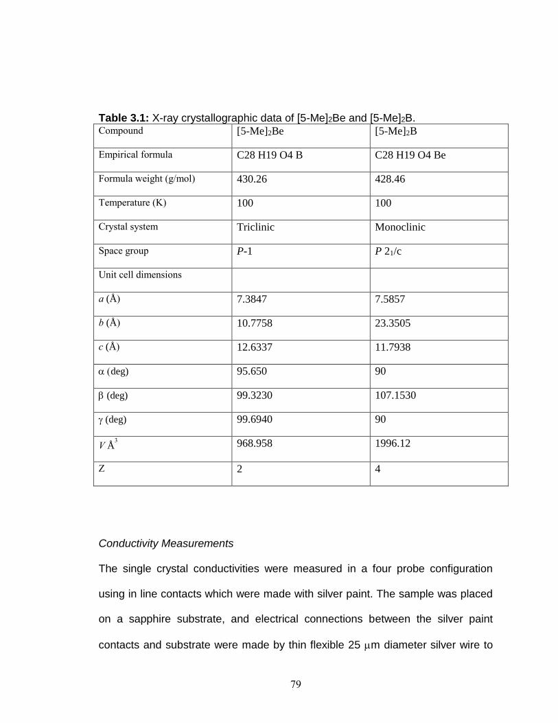
79
Table 3.1: X-ray crystallographic data of [5-Me]2Be and [5-Me]2B. Compound [5-Me]2Be [5-Me]2B
Empirical formula C28 H19 O4 B C28 H19 O4 Be
Formula weight (g/mol) 430.26 428.46
Temperature (K) 100 100
Crystal system Triclinic Monoclinic
Space group P-1 P 21/c
Unit cell dimensions
a (Å) 7.3847 7.5857
b (Å) 10.7758 23.3505
c (Å) 12.6337 11.7938
deg) 95.650 90
(deg) 99.3230 107.1530
(deg) 99.6940 90
V Å3 968.958 1996.12
Z 2 4
Conductivity Measurements
The single crystal conductivities were measured in a four probe configuration
using in line contacts which were made with silver paint. The sample was placed
on a sapphire substrate, and electrical connections between the silver paint
contacts and substrate were made by thin flexible 25 m diameter silver wire to

80
relieve mechanical stress during thermal cycling of the sample. The
conductivities were measured along the long axis of the crystals. The
conductivity was measured in a custom made helium variable temperature probe
using a Lake Shore 340 temperature controller in the temperature range 330 –
77K. A Keithley 236 unit was used as a voltage source and current meter, and
two 6517A Keithley electrometers were used to measure the voltage drop
between the potential leads in a four probe configuration in which the
instrumentation was driven with LabVIEW software.
Magnetic Susceptibility Measurements
The molar magnetic susceptibility of 10-15 mg samples of the crystalline powders
were measured by utilizing a Vibrating Sample Magnetometer in an EverCool-II
cryogen-free upgraded version of a Physical Property Measurement System
(Quantum Design International, USA) in a magnetic field of 1 Tesla over the
temperature range 330 – 4 K.

81
3.10: References
1) Pal, S. K.; Itkis, M. E.; Tham, F. S.; Reed, R. W.; Oakley, R. T.; Haddon, R. C. Science 2005, 309, 281. 2) Bag, P.; Itkis, M. E.; Pal, S. K.; Donnadieu, B.; Tham, F. S.; Park, H.; Schleuter, J. A.; Siegrist, T.; Haddon, R. C. J. Am. Chem. Soc. 2010, 132, 2684. 3) Mandal, S. K.; Samanta, S.; Itkis, M. E.; Jensen, D. W.; Reed, R. W.; Oakley, R. T.; Tham, F. S.; Donnadieu, B.; Haddon, R. C. J. Am. Chem. Soc. 2006, 128, 1982. 4) Porter III, W. W.; Vaid, T. P.; Rheingold, A. L. J. Am. Chem. Soc 2005, 127, 16559 5) Porter III, W. W.; Vaid, T. P. J. Mater. Chem. 2007, 17, 469 6) Bryan, C. D.; Cordes, A. W.; Haddon, R. C.; Hicks, R. G.; Kennepohl, D. K.; MacKinnon, C. D.; Oakley, R. T.; Palstra, T. T. M.; Perel, A. S.; Scott, S. R.; Schneemeyer, L. F.; Waszczak, J. V. J. Amer. Chem. Soc 1994, 116, 1205. 7) Seber, G.; Freitas, R. S.; Mague, J. T.; Paduan-Filho, A.; Gratens, X.; Bindilatti, V.; Oliveira, N. F.; Yoshioka, N.; Lahti, P. M. J. Am. Chem. Soc 2012, 134, 3825. 8) Pal, S. K.; Bag, P.; Itkis, M. E.; Tham, F. S.; Haddon, R. C. J. Am. Chem. Soc; 2014, 136, 14738. 9) Tian, Y.-H.; Sumpter, B. G.; Du, S.; Huang, J. 2015, 2318 10) Mota, F.; Miller, J. S.; Novoa, J. J. J. Am. Chem. Soc. 2009, 131, 7699. 11) Cui, Z.; Lischka, H.; Beneberu, H. Z.; Kertesz, M. J. Am. Chem. Soc 2014, 136, 5539 12) Small, D.; Zaitsev, V.; Jung, Y.; Rosokha, S. V.; Head-Gordon, M.; Kochi, J. K. J. Am. Chem. Soc. 2004, 126, 13850. 13) Small, D.; Rosokha, S. V.; Kochi, J. K.; Head-Gordon, M. J. Phys. Chem. A 2005, 109, 11261. 14) Suzuki, S.; Morita, Y.; Fukui, K.; Sato, K.; Shiomi, D.; Takui, T.; Nakasuji, K. J. Am. Chem. Soc. 2006, 128, 2530

82
15) Cui, Z. H.; Lischka, H.; Beneberu, H. Z.; Kertesz, M. J. Am. Chem. Soc. 2014, 136, 12958. 16) Anderson, P. W. Mater. Res. Bull. 1973, 8, 153. 17) Anderson, P. W. Science 1987, 235, 1196. 18) Pauling, L. Nature 1948, 161, 1019. 19) Haddon, R. C.; Chichester, S. V.; Marshall, J. H. Tetrahedron 1986, 42, 6293. 20) Haddon, R. C.; Rayford, R.; Hirani, A. M. J. Org. Chem 1981, 46, 4587.
83
Chapter 4: Effect of Substitution on the Hysteretic Phase Transition in a
Bistable Phenalenyl Based Neutral Radical Molecular Conductor
4.1: Introduction
In chapter 3 we showed how substitutional doping in neutral radical
conductors could increase the conductivity and alter the magnetic properties of
the materials. We also showed that this substitution has large effects on the
crystal structure of the solid solutions. While one purpose of substitutional doping
in inorganic semiconductors and materials is the enhancement of electrical
conductivity, another purpose is to augment other properties of the materials,
such as phase transitions. One of the most popular inorganic materials known for
its phase transition is vanadium oxide (VO2). VO2 experiences a phase transition
from its insulating monoclinic phase to a metallic rutile phase around 340 K
accompanied by large changes in its optical properties.1 Due to its potential uses,
control of this phase transition has been extensively studied.
One way to affect this transition is through substitutional doping. Scientists
have doped VO2 by switching out vanadium atoms for other metals such as
titanium, tungsten, and molybdenum among many others. Through this doping it
has been shown that the phase transition can be lowered to room temperature,
the width of the hysteretic loop can be decreases or completely eliminated, and
the phase transition itself can be completely suppressed.1-6 The results of these
studies and related work on the tuning of the VOx stoichiometry (x = 1.5-2.5)

84
have engineered the properties for uses in switching, sensing, smart windows,
and night vision applications.7-10
Considering the number of developed and potential applications of
bistable materials and materials with phase transitions in the vicinity of room
temperature, it would be interesting to apply substitutional doping on an organic
molecular conductor. The following is a study of the effects of substitutional
doping on the phase transition in phenalenyl based neutral radical conductor and
its near room temperature bistability.
4.2: Hysteretic Phase Transition in [Bu]2B with Bistability in the Vicinity of
Room Temperature
The structure of bis(9-N-butylamino-1-oxophenalene)boron ([Bu]2B) is
shown in Figure 4.1. While similiar to the neutral radical discussed in Chapter 3,
[5-Me]2B, this radical lacks the methyl group at the 5 position and contains a
butylamine at the 9 position as opposed to the oxygen.
Figure 4.1: The structure of [Bu]2B.

85
Since its first crystallization,11 [Bu]2B has garnered much attention due to
its near room temperature phase transition illustrated in Figure 4.2. It is one of
the very few organic compounds with bistability in the vicinity of room
temperature.12-16 At low temperatures, [Bu]2B forms dimeric pairs of molecules
with a pair of superimposed phenalenyl (SPLY) units and 2 non-superimposed
phenalenyl (NSPLY) units. The radicals pair antiferromagnetically into a low spin
(LS) state within the SPLY units in what can be described as a 2-electron
pancake bond with a short intradimer space (3.11Å). This results in a singlet
state and one in which the Curie Spin per molecule is temperature independent
and equal to ~0. This antiferromagnetic state is maintained until the temperature
is increased from ~200K as the electron wavefunction spreads throughout the
molecule and eventually occupy both the SPLY and NSPLY units equally. It
leads to the appearance of the temperature dependent fraction of Curie Spin per
molecule and an increase of the intradimer space to 3.27 Å. At temperatures
above ~325 K a high spin (HS) state in which the electrons are located on the
NSPLY is energetically favored, however there is a large energy barrier due to
the accompanying increase in unit cell size in part due to the increase in the
intradimer spacing but mostly from the increase in interdimer spacing and thus
the LS state is preserved. Then, at ~345 K the electrons rapidly migrate to the
NSPLY in which they are, for the most part, noninteracting and in a high spin
(HS) triplet state. This results in a monomeric type structure which is
accompanied by a large change in the unit cell dimensions as the intradimer

86
space is further increased to 3.38 Å, similar to the van der Waals distance of
carbon. At that instance, the interdimer spacing (C-H interaction) is increased
from 2.92Å to 3.16Å. Upon cooling, this HS state is maintained below the original
phase transition temperature of ~345 K until ~325 K and the material returns to
its energetically favorable LS state. As was discussed above, the resulted
hysteresis is due to the large energy barrier associated with a dramatic increase
in unit cell size in part due to the increase in the intradimer spacing but mostly
from the increase in interdimer spacing. In addition to the discussed magnetic
bistability, this phase transition manifests itself in the bistable electrical and
optical properties. Throughout this phase transition the monoclinic (P21/c) is
maintained.17,18
This phase transition has been studied extensively both experimentally
and computationally and further discussion can be found in the literature.11,17-24
Figure 4.2: (a) Fraction of Curie Spin as a function of temperature around the phase transition of [Bu]2B and (b) a diagram of the phase transition.
310 320 330 340 350 3600.0
0.2
0.4
0.6
0.8
1.0
Curie S
pin
Per
Mole
cule
Temperature (K)
HS
LS
a) b)

87
4.3: Synthesis and Crystallization of Substitutional Doped [Bu]2B1-xBex
Similar to the substitutional doping experiments in Chapter 3,25,26 [Bu]2B is
substitutionally doped with its non-radical containing counterpart, [Bu]2Be, to form
solid solutions of [Bu]2B1-xBex (Figure 4.3).
Figure 4.3: The co-crystallization procedure for substitutional doping: The cationic precursor of [Bu]2B is combined with the dopant, [Bu]2Be, and a reductant (tetrakis(dimethylamino)ethylene (TDAE)) is added to grow solid solutions of [Bu]2B1-xBex.
The first observed difference due to substitution is the morphology of the
solid solutions. Pure [Bu]2B appears as black block-like crystals (Figure 4.4a).
When substitution with [Bu]2Be is introduced the crystals elongate and grow
needle like (Figure 4.4b). Increasing the amount of [Bu]2Be results in the growth
of more needle like thinner crystals (Figure 4.4c). Thus, the presence or lack of
substitution can be determined by simply looking at the morphology of the
crystals. [Bu]2Be is a yellow-orange powder and can be crystalized into various
sizes (Figure 4.4d).

88
Figure 4.4: Pictures of crystals of (a) [Bu]2B, (b) lightly doped [Bu]2B1-xBex, (c) heavily doped [Bu]2B1-xBex and (d) [Bu]2Be. The scale bars are 1 mm.
4.4 Host and Dopant Structure Comparison
As it was shown in Chapter 3, the structure of the host and dopant are
important when it comes to substitutional doping experiments.
As established in earlier publications by Haddon research group, the
crystal packing of [Bu]2B corresponds to a P21/c space group.11,17 Figure 4.5
shows an interacting pair (dimer) of [Bu]2B molecules in 2 views perpendicular to
each other in their low spin, low temperature state and their high spin, high
temperature state. As can be seen in Figure 4.5a, the interfacial distance is
significantly lower (3.11 Å) than the van der Waals distance for a carbon-carbon
bond (3.4 Å), due to the presence of interfacial pancake bonding in the low spin
state.27,28 Figure 4.5c shows the same crystal in its high spin state. Here the

89
interfacial distance is increased (3.39 Å) to approximately the van der Waals
distance. This increase of interfacial distance is attributed to the movement of the
spin from the superimposed to non-superimposed phenalenyl as the crystal
transitions from its low spin to high spin state. Perpendicular views of both the
low and high spin states are presented in Figure 4.5b, d. Here the spin bearing
carbons are colored in green and it can be clearly seen that the pair of molecules
have a high degree of overlap in both the high and low spin states. Both of these
observations are attributed to the presence of a radical. This highly overlapped
and short distance interfacial interaction is responsible for the low spin state as
the radicals with opposite spin pair up.
In contrast, [Bu]2Be, introduced for the 1st time in this study, does not
contain a radical, packs in a P-1 space group, and contains 4 molecules in the
unit cell. The structure of [Bu]2Be (at 100 K) (Figure 4.5e-h) is dramatically
different than that of [Bu]2B, most likely due to its lack of spin. While [Bu]2B forms
dimers with short interfacial distances and has one interfacial interaction, no such
dimers in [Bu]2Be are observed. As can be seen in Figure 4.5e, g the interfacial
distances (3.39 Å, 3.33 Å) are significantly greater than that observed in the LS
state of [Bu]2B at the same temperature (100 K). Not only is the distance
increased, but the overlap of the spin bearing carbons is very poor as can be
seen in figure 4.5f, h, as none of them overlap (green). This is attributed to
[Bu]2Be not possessing a radical, and thus it is unable to form pancake bonds

90
between neighboring molecules which would shorten interfacial distances and
increase spin-bearing carbon overlap.
Figure 4.5: Perpendicular views of [Bu]2B dimers in its (a, b) low spin and (c, d) high spin states showing interfacial distances and high degree of overlap between spin-bearing carbons shown in green. (e-h) Views of [Bu]2Be crystal interactions showing larger interfacial distances and little to no overlap of spin-bearing carbons shown in green.

91
4.5: Crystal Structures in Doped [Bu]2B1-xBex Solid Solutions
In Chapter 3 the single crystal structures of solid solutions were solved,
however, this is a complicated task. The complete single crystal X-ray study of
crystal structures of pure [Bu]2B and [Bu]2Be were studied above. For solid
solutions of mixed composition, powder X-ray diffraction (pXRD) measurements
were taken. This allows for the exploration of the crystal structure in a
significantly less time and effort costly manner.
Figure 4.6 presents room temperature powder XRD data for pristine
[Bu]2B (x = 0) and [Bu]2Be (x = 1). It shows very distinct patterns corresponding
to different crystal packing in [Bu]2B and [Bu]2Be compounds with a set of major
peaks positioned at diffraction angles 2θ of 8.1, 10.4, 13.3 and 16.4 degrees for
the [Bu]2B compound (indicated with an asterisk symbol) and at 7.7, 12.1, 22.4
and 25.7 degrees for [Bu]2Be (indicated with a delta symbol). In addition, a group
of characteristic peaks is observed in the range of 2 θ of 20-25 degrees in the
case of [Bu]2B. Single crystal X-ray data for [Bu]2B and [Bu]2Be were utilized to
simulate powder XRD patterns and the good match can be found between
calculated and experimental powder XRD data as shown in Figure 4.11.
The modification of the powder XRD pattern of [Bu]2B1-xBex solid solutions
with increasing doping level is also presented in Figure 4.6. It can be clearly seen
that low substituted solid solutions (x<0.06) bear the same phase as pure [Bu]2B
with major peaks in powder XRD pattern remaining at 2 θ of 8.1, 10.4, 13.3 and
16.4 degrees. No additional peaks corresponding to the phase of [Bu]2Be are

92
observed. This indicates that [Bu]2Be is being incorporated into the crystal
structure of [Bu]2B. This observation is not surprising as it is known that the
presence of radicals plays a large role in the crystal structure, and other organic
radical compounds have shown that one electron is sufficient to form phenalenyl-
phenalenyl pancake bonds.28,29
Figure 4.6: Powder X-ray diffraction data of solid solutions of [Bu]2B1-xBex showing the transition of the structure from that of the host ([Bu]2B) to that of the dopant ([Bu]2Be).
Meanwhile, highly substituted solid solutions (x>0.06) match the phase of
pure [Bu]2Be with major peaks shifting to 2 θ of 7.7, 12.1, 22.4 and 25.7 degrees
and a disappearance of a group of characteristic peaks in the range of 2 θ of 20-

93
25 degrees associated with the [Bu]2B crystal packing. Even though the
concentration of substituent is significantly lower than that of the [Bu]2B host, its
presence is enough to completely alter the crystal packing structure. This
demonstrates the importance of the radical on the crystal structure. No unique
structure for the substituted solid solutions was observed which is consistent with
our previous studies.25 It seems as these substituted organic radical conductors
behave as binary systems, that is, they take the form of either the host or the
substitute. Thus, it is concluded that at low substitution levels the solid solutions
adopt the structure of [Bu]2B and thus undergo the phase transition while at high
substitution levels the solid solutions adopt the structure of [Bu]2Be.
4.6: Magnetic Properties of Solid Solutions [Bu]2B1-xBex
Figure 4.7 shows magnetic susceptibility data as a function of temperature
for different levels (x) of [Bu]2Be doping. As shown in Figure 4.7a the low
temperature value of Curie spin per molecule in undoped [Bu]2Be material (x = 0)
is approaching zero due to the antiferromagnetic coupling of two spins
associated with the low temperature dimer structure (Figure 4.2b). With
increasing temperature above 350 K a sharp phase transition to a high
temperature (HT) high spin (HS) state is observed with the effective spin (per
molecule) increasing to the value of 0.9, close to the one Curie spin per molecule
expected from the ensemble of non-interacting spins in neutral radical organic
molecular conductors when the dimer coupling is released (Figure 4.7a, b). With
decreasing temperature below 325 K a sharp transition to low temperature (LT),

94
low spin (LS) state is observed thus restoring the dimerized state and completing
the counterclockwise hysteresis loop. With an increasing level of doping the
amplitude of spin changes decreases with a complete disappearance of
hysteresis loop at concentration x > 6.3 % as shown in Figure 4.7c. However, in
the vicinity of this critical concentration, we observed a rare event of reversing
the hysteresis loop to the clockwise direction with an inverted relationship
between low temperature and high temperature spin values (Figure 4.7d). For
high substitution levels (x > 0.06) a weak temperature dependence of the
effective spin is observed (Figure 4.7c) resembling the behavior of monomeric
neutral radical conductors that contain bulky substituents with non-interacting
spins.30 At helium temperatures, the effective spin value decreases to ~0.1 level
as long-range antiferromagnetic interaction takes over with reducing thermal
fluctuations. Ultimately, no measurable paramagnetic contribution is observed in
the pure (x = 1) spinless [Bu]2Be compound as would be expected due to the
lack of a radical.

95
Figure 4.7: Temperature dependent fraction of Curie spin per molecule as a function of doping level x. (a) Lightly substituted [Bu]2B1-xBex: Compression of the height of the hysteresis loop with increasing doping; (b) Expanded view of the hysteresis loop above room temperature for lightly substituted [Bu]2B1-xBex
showing no phase transition; (d) Events of reverse hysteresis loop at x~6%.
Figure 4.8 presents an additional analysis of the evolution of the hysteretic
phase transition with increasing doping. It shows that while the height of the
hysteresis loop is reduced with increasing doping level (Figure 4.8a), the width of
the loop remains approximately constant at the level of 23.5±1 K (Figure 4.8b).
This is different from the case of vanadium oxide in which the width of the

96
hysteresis loop and temperature of phase transition modify significantly with
increasing doping concentration.1-6 The hysteresis loop height (Figure 4.8a)
collapses to zero at the critical level of doping in the vicinity of x ≈ 6%. As shown
in Figure 4.8c, both the decrease of the HS value and the increase of the LS
value contribute to diminishing the loop height, however, the spin value S after
the collapse, S=0.76 Curie spins/per molecule, is closer to the HS value
indicating suppression of dimerization with increasing doping. As shown in Figure
4.8d, well below phase transition temperature, at 150 K, the dimerized state is
very prominent for undoped [Bu]2B compound (x=0) showing an effective spin
value close to zero. However, with increasing doping the effective spin per
molecule at 150 K increases to 0.7 indicating a decoupling of the unpaired spins
in neighboring molecules.

97
Figure 4.8: (a) Height and (b) width of the hysteretic loop as a function of doping. (c) Curie spin per molecule of the high spin (HS) and low spin (LS) states as a function of doping. (d) Curie spin per molecule at 150 K as a function of doping.
These observations can be partially explained by the change of number of
the available spins with the introduction of a non-spin bearing molecule. When
substitution is increased, the hysteretic loop is compressed vertically: in HS state
maximum possible Curie spin per molecule decreases from 1 to (1-x) with the
introduction of x fraction of spin non-bearing [Bu]2Be molecules; in the LS state x
fraction of spin-bearing [Bu]2B molecules would not be able to find a pair to form
a dimer thus contributing to an increase of LS value. However, the observed
0 1 2 3 4 5 6 70
5
10
15
20
25
30
Loop W
idth
(K
)
x,%
0 1 2 3 4 5 6 7
0.2
0.4
0.6
0.8
1.0
LS (330K)Cu
rie
Sp
in p
er
mo
lecu
le
x, %
HS (330 K)
0 1 2 3 4 5 6 7
0.0
0.1
0.2
0.3
0.4
0.5
0.6
Lo
op
He
igh
t (s
pin
/mo
lecu
le)
x, %
0 1 2 3 4 5 6 7
0.0
0.2
0.4
0.6
0.8
1.0
Cu
rie
Sp
in @
15
0K
x, %
a) b)
c) d)

98
decrease of HS value and increase of LS value are stronger than what would be
expected from (1-x) and x contributions, respectively, taking into account low
concentrations x not exceeding 6% sufficient for the collapse of the phase
transition loop. More likely, some changes of the crystal structure with the
introduction of non-spin bearing substitutes at low concentrations are responsible
for the dramatic effect of substitutional doping on the hysteretic phase transition
in [Bu]2B molecular crystals.
The presence of hysteresis and bistable physical properties of undoped
[Bu]2B molecular crystals were originally ascribed to the existence of the energy
barrier for the transition between LT and HT polymorphs.17 Recently, the nature
of this energy barrier was investigated in a computational study by the Ribas-
Arino20,22 group and related to the gauche to anti conformational rearrangement
of the butyl groups attached to nitrogen atoms on both sides of the boron atom
accompanied by a significant expansion of the crystal in HT phase, followed by a
change of magnetic state from LS to HS. The study found that out of four
possible polymorphs LS(gauche), LS(anti), HS(gauche) and HS(anti) only
LS(gauche) and HS(anti) are thermodynamically stable at low and high
temperatures, respectively. Observation of a reverse hysteresis loop (Figure
4.7b, d) with the low temperature spin value exceeding high temperature spin
may manifest a situation when with increasing substitutional doping two other
polymorphs, LS(anti) and HS(gauche), are becoming thermodynamically

99
accessible. However, the rarity of the reverse hysteresis event complicates its
more detailed and conclusive study.
4.7: Electrical Conductivity of Solid Solutions [Bu]2B1-xBex
The phase transition in [Bu]2B is also observed in its electrical conductivity
measurements (Figure 4.9). During the phase transition, [Bu]2B goes from a
higher conductance LT, LS state to a more resistive HT, HS state. The more than
an order of magnitude increase of conductivity in LT, LS state was explained in a
computational study by Kertesz group by an analysis of the band splitting
originating from intramolecular spiroconjugation at the central boron atom, π-π
intermolecular interaction in the solid state due to dimer formation, and additional
band splitting due to the presence of two sets of dimers in the unit cell [Bu]2B
crystal resulting in different bandgaps in the LS and HS states.19,24 In some of the
warming-cooling cycles the whole conductivity change occurs instantaneously in
one step manifesting intrinsic 1st order character of the phase transition. It has
been suggested that conformational changes involve cooperative effects when
the rearrangement of one butyl group can reduce the potential barriers for
rearrangement of the neighboring butyl groups leading to the avalanche type
spreading of the conformational changes across the whole crystal.20 In some
other cycles the transition between ultimate high and low electrical conductivity
states happens in multiple steps which may be related to the expansion of the
volume of conformational changes from. domain to domain across the crystal. It
should be noted, that the 4-probe electrical measurements were conducted on

100
single crystals as compared to magnetic measurements conducted on the
ensemble of thousands of crystals. As a result, the magnetic measurements
always show relatively smooth transitions between LS and HS states with a width
of change ΔT of ~5 K due to averaging over slightly different positions of
hysteresis loop over thousands of individual crystals
While we have previously shown that substitution in radical conductors
can increase the conductance of the material, here we see the opposite result.
As can be seen in Figure 4.9, light substitution levels lower the conductance of
both the low and high spin state. Once the solid solutions are heavily substituted
they remain in their lower conductance, high spin state with no significant change
of activation energy. This result confirms the importance of the paired electrons
found in pancake bonding [Bu]2B-[Bu]2B dimers for increasing of electrical
conductivity.
Figure 4.9: Conductivity of doped neutral radical conductors. (a) Zoomed in view of the transition showing a lowering of conductivity as doping is increased and an
310 320 330 340 350 360 370
10-3
10-2
10-1
x = 0.23
x = 0.1
x = 0.05
x = 0.015
Co
ndu
ctivity (
S/c
m)
Temperature (K)
1
212
2 4 6 8 10 12 14
10-9
10-8
10-7
10-6
10-5
10-4
10-3
10-2
10-1
100
0.05
x=0.015
=0.13 eV
0.1
=0.16 eV
Conductivity (
S/c
m)
1000/T (K-1)
0.23
a) b)

101
eventual elimination of the hysteretic phase transition. (b) Arrhenius plot of temperature dependencies of electrical conductivity of various solid solutions of [Bu]2B1-xBex in a wide temperature range.
4.8: Model of Substitutional Doping in [Bu]2B1-xBex
When taking the above data into account, a model of the effects of
substituting [Bu]2B with [Bu]2Be can be envisioned. As summarized in Figure
4.10, a crystal of [Bu]2B is made up of pancake bonded [Bu]2B-[Bu]2B pairs
(Figure 4.10 (left, red)). When light substitution is done, the overlapped structure
of [Bu]2B is retained with some pairs containing a single electron [Bu]2B-[Bu]2Be
pancake bond resulting in a larger spin per molecule value in the low spin state
(Figure 4.10(left, yellow)). However, due to the presence of [Bu]2Be substitutes
the coherence of the crystal structure may also be suppressed resulting in the
decreasing size of the hysteresis loop to a higher degree than the percentage of
introduced spinless [Bu]2Be. At this stage there is still a sufficient amount of
radicals to maintain the structure of pure [Bu]2B. After the amount of substitution
is increased, the solid solution assumes the crystal structure of [Bu]2Be. At this
point, even though the amount of radical has been reduced by just 6%, the
dimers are no longer able to remain paired and the spins can be considered to
be non-interacting (Figure 4.10 (right)). It is interesting to again note that a
considerably small reduction in the available spin is able to alter the crystal
structure to such a high degree.

102
Figure 4.10: Effects of substitution on [Bu]2B1-xBex solid solutions. (left) With no doping (red) dimers of [Bu]2B form 2 electron bonds canceling out their spin, at light substitution levels (yellow) some of these are now 1 electron bonds but the [Bu]B2 structure is retained. (Right) At heavy substitution levels [Bu]2B1-xBex
adopts the structure of [Bu]2Be and the spins are non-interacting.
4.9: Conclusion
In conclusion, substitutional doping was applied to a bistable neutral
organic radical conductor [Bu]2B by utilizing a non-radical containing molecular
substitute [Bu]2Be, and solid solutions of [Bu]2B1-xBex were synthesized and
characterized in terms of crystal structure and physical properties. It was
observed that at the low doping level (x < 0.06) substituent [Bu]2Be molecules
are incorporated in the crystal structure of the host [Bu]2B compound stabilized
by phenalenyl-phenalenyl pancake bond formation. With increasing doping the
hysteretic phase transition is gradually suppressed in terms of reducing the
height, but conservation of the width of the hysteresis loop was observed through
magnetic susceptibility and electrical conductivity measurements. At relatively
low substitution level just above 6 percent the abrupt transformation of the crystal
0 100 200 3000.0
0.2
0.4
0.6
0.8
1.0C
urie S
pin
/ M
ole
cule
Temperature (K)0 100 200 300
0.0
0.2
0.4
0.6
0.8
1.0
Temperature (K)
No Substitution
Light Substitution
Heavy Substitution

103
structure to the one of pure [Bu]2Be crystal packing was observed in powder
XRD measurements accompanied by a complete collapse of the hysteresis loop.
Thus, in terms of crystal packing, these substituted organic radical conductors
behave as binary systems, that is, they take the form of either the host or the
substitute. It raises the possibility that one could modify an organic radical
conductor with various substituents, with each substituent resulting in a different
crystal structure and different properties, thus engineering one organic radical
conductor into a multitude of structurally different compounds. A variety of such
dopants can be bi-phenalenyl based molecules for better matching of the crystal
lattice of the [Bu]2B host with an interesting case of [Et]2B dopant which shows a
similar phase transition at lower temperature.11 By studying that one organic
radical conductor in its various crystal structures the structure-property
relationships could be revealed, perhaps, providing valuable hints of how to
design new bistable materials. Overall, this work demonstrates that the
substitution technique often used to control the properties of inorganic materials
can also be applied to bistable neutral radical organic conductors.
4.10: Experimental and Supplementary Information
Materials:
All reactions were done under a dry argon atmosphere using standard
Schlenk and vacuum-line techniques. The reagents 1.0 M BCl3 in hexane
(Aldrich), BeCl2 (Aldrich), tetrakis(dimethylamino)ethylene (TDAE, TCI America),
potassium tetraphenylborate (Aldrich), cinnamoyl chloride (TCI America), 2-

104
methoxynaphthalene (Alfa Aesar), triethylamine (Aldrich), toluene (Aldrich) and
dry acetonitrile (Aldrich) were used as received. [Bu]2B+ BPh4- was synthesized
according to literature procedures.11 ESI mass spectra were recorded with an
Agilent LCTOF (2006) instrument with APCI/ESI ionization. NMR Spectra were
collected on a Bruker 300 spectrometer. Elemental analysis and inductively
coupled plasma mass spectra (ICP-MS) of the [Bu]B1-xBex samples were
performed at the Microanalysis Laboratory at the University of Illionis, Urbana-
Champaign, IL.
Synthesis of [Bu]2Be:
Synthesis of [Bu]2Be followed a modified literature procedure.31 9-N-
butylamino-1-oxophenalene (1 mmol, 0.251 g) (synthesized by literature
procedure)11 and triethylamine (1.1 mmol, 0.101 g) were stirred in anhydrous
Toluene (40 mL) in an argon atmosphere at 90 °C before adding BeCl2 (0.5
mmol, 0.040 g). The reaction was allowed to stir overnight at 90 °C. The reaction
was allowed to cool, and a yellow solid was filtered, washed with methanol and
recrystallized from hot polyethylene carbonate. Yield 0.330 g (65%); mp > 350
°C; 1 H NMR (300 MHz, CD3CN, 25 °C) δ 8.07 (2H, d) 8.00 (2H, d) 7.89 (2H, d)
7.87 (2H, d) 7.47 (2H, t) 7.29 (2H, d) 7.21 (2H, d) 3.48 (2H, m) 3.22 (2H, m) 1.61
(2H, m) 1.50 (2H, m) 1.13 (4H, m) 0.65 (6H, m) ppm; ESI-MS m/z calcd for
C34H34N2O2Be [M+] 511.2742, found 511.2741. Anal. Calcd (found) for
C34H34O2N2Be: C, 79.80 (79.67); H, 6.70 (6.56); N 5.48 (5.41).
Crystallization of [Bu]B1-xBex:

105
In an invertible H-cell with a medium porosity frit is loaded in a glove box.
[Bu]B2+ BPh4- ( 1.15 x 10⁻⁴ mol, 100 mg) and [Bu]2Be (2.3 x 10⁻⁵ mol, 11.8
mg)are dissolved in 15 mL dry acetonitrile in a round bottom. In a separate round
bottom ~0.2 mL TDAE is dissolved in 16 mL dry acetonitrile. The round bottom
flasks are attached to the H-cell and the cell is inverted allowing the solutions to
mix at the frit. After ~1 week black crystals have grown onto the frit. The sample
is characterized by ICP analysis to find the solid solution composition
([Bu]B0.87Be0.13). Crystals of other compositions were grown using the same
method, varying the amount of [Bu]2Be used.
X-Ray Crystallography:
CCDC 1874726 contains the supplementary crystallographic data for
[Bu]2Be. These data are provided free of charge by the Cambridge
Crystallographic Data Centre. Structures of [Bu]2B are taken from the literature.17
Powder X-Ray Data:
Powder X-ray data of synthesized compounds were collected at room
temperature in the 2Ɵ range 3-65 degrees using a Rigaku MiniFlex 600
diffractometer with Cu-Kα1 radiation (λ = 1.54059 Å), image plate detector and
Ge monochromator. Silicon was used as standard. The diffractograms for host
and substitute compounds are shown in Figure 4.11. The patterns match well
with the calculated pattern obtained from the single crystal data. The unit cell
parameters obtained from the single crystal data and powder X-ray diffraction are
very close to each other. The obtained lattice parameters from the powder X-ray

106
diffraction peak matching are given below in Table 4.1. The lattice parameters
obtained from powder X-ray diffraction peak matching are shown in Table 4.2.
Figure 4.11: Powder X-ray diffraction patterns for the compounds [Bu]2B (top) and [Bu]2Be (bottom). The green vertical lines represent calculated peak positions for the respective compounds obtained from their single crystal data. The most prominent peaks were located below 2Ɵ = 30 degree and hence the peak matching was performed only upto 2Ɵ = 30 degree. The full diffraction patterns (in the range 2Ɵ = 3-65 degrees are shown in insets).

107
Figure 4.12: Thermal ellipsoids of (left) [Bu]2B and (right) [Bu]2Be. Table 4.1: X-ray crystallographic data of [Bu]2Be and [Bu]2B (100K and 360K). [Bu]2B data taken from literature. Compound [Bu]2Be [Bu]2B (100 K) [Bu]2B (360 K)
Empirical formula C34 H32 Be N2 O2 C34 H32 B N2 O2 C34 H32 B N2 O2
Formula weight
(g/mol)
509.62 511.44 511.44
Temperature (K) 100 100 360
Crystal system Triclinic Monoclinic Monoclinic
Space group P-1 P 21/c P 21/c
a (Å) 9.0726 8.9362 9.076
b (Å) 12.4697 12.1541 12.584
c (Å) 23.703 23.537 24.054
deg) 75.239 90.00 90.00
(deg) 83.744 100.913 96.268
(deg) 78.024 90.00 90.00
V Å3 2532.2 2510.16 2730.84
Z 4 4 4

108
Table 4.2. Lattice parameters obtained from powder X-ray diffraction peak matching.
Compound [Bu]2B [Bu]2Be
Space group P 21/c (no. 14) P -1 (no. 2)
a (Å) 9.084 9.096
b (Å) 12.315 12.557
c (Å) 24.062 23.930
α (degrees) - 74.678
β (degrees) 100.497 83.856
γ (degrees) - 79.172
Conductivity Measurements:
Single crystal temperature dependent four-probe electrical conductivity
measurements were conducted utilizing EverCool-II cryogen-free upgraded
version of the Physical Property Measurement System (PPMS, Quantum Design)
with-in house made insert for high resistance measurements. The neutral radical
crystals were positioned free on a sapphire substrate, and in-line contacts were
made with silver paint and four flexible 25 μm diameter platinum wires. This
flexible design allowed to reduce the mechanical stress on the crystals
associated with a mismatch of thermal expansions of the crystal and the
substrate. A Keithley 236 unit and two 6517 Keithley electrometers were used as
a current source and two potential probes, respectively, and the resistance vs
temperature data were acquired utilizing LabVIEW software.
Magnetic Susceptibility Measurements
Magnetic measurements of ~15 mg powdered samples were measured with a
vibrating sample magnetometer in an EverCool-II PPMS system in a 1 Tesla
magnetic field from 4K to 360K.

109
4.11: References:
1) Shao, Z. W.; Cao, X.; Luo, H. J.; Jin, P. NPG Asia Mater. 2018, 10. 2) Peng, Z. F.; Jiang, W.; Liu, H. J. Phys. Chem. C 2007, 111, 1119. 3) Wu, Z. P.; Miyashita, A.; Yamamoto, S.; Abe, H.; Nashiyama, I.; Narumi, K.; Naramoto, H. J. Appl. Phys. 1999, 86, 5311. 4) Burkhardt, W.; Christmann, T.; Franke, S.; Kriegseis, W.; Meister, D.; Meyer, B. K.; Niessner, W.; Schalch, D.; Scharmann, A. Thin Solid Films 2002, 402, 226. 5) Soltani, M.; Chaker, M.; Haddad, E.; Kruzelecky, R. V.; Margot, J. Appl. Phys. Lett. 2004, 85, 1958. 6) Peng, Z. F.; Wang, Y.; Du, Y. Y.; Lu, D.; Sun, D. Z. J. Alloys Compd. 2009, 480, 537. 7) Manning, T. D.; Parkin, I. P.; Pemble, M. E.; Sheel, D.; Vernardou, D. Chem. Mater. 2004, 16, 744. 8) Han, Y. H.; Choi, I. H.; Kang, H. K.; Park, J. Y.; Kim, K. T.; Shin, H. J.; Moon, S. Thin Solid Films 2003, 425, 260. 9) Rogalski, A. Infrared Detectors; 2 ed.; CRS Press: Boca Raton, Fl, USA, 2011. 10) Wang, B.; Lai, J. J.; Li, H.; Hu, H. M.; Chen, S. H. Infrared Phys. Technol. 2013, 57, 8. 11) Chi, X.; Itkis, M. E.; Kirschbaum, K.; Pinkerton, A. A.; Oakley, R. T.; Cordes, A. W.; Haddon, R. C. J. Am. Chem. Soc. 2001, 123, 4041. 12) Fujita, W.; Awaga, K. Science 1999, 286, 261. 13) Lekin, K.; Winter, S. M.; Downie, L. E.; Bao, X.; Tse, J. S.; Desgreniers, S.; Secco, R. A.; Dube, P. A.; Oakley, R. T. J. Am. Chem. Soc. 2010, 132, 16212 14) Brusso, J. L.; Clements, O. P.; Haddon, R. C.; Itkis, M. E.; Leitch, A. A.; Oakley, R. T.; Reed, R. W.; Richardson, J. F. J. Am. Chem. Soc. 2004, 126, 8256.

110
15) Hoshino, N.; Iijima, F.; Newton, G. N.; Yoshida, N.; Shiga, T.; Nojiri, H.; Nakao, A.; Kumai, R.; Murakami, Y.; Oshio, H. Nat. Chem. 2012, 4, 921. 16) Mitsumi, M.; Nishitani, T.; Yamasaki, S.; Shimada, N.; Komatsu, Y.; Toriumi, K.; Kitagawa, Y.; Okumura, M.; Miyazaki, Y.; Gorska, N.; Inaba, A.; Kanda, A.; Hanasaki, N. J. Am. Chem. Soc. 2014, 136, 7026. 17) Pal, S. K.; Bag, P.; Sarkar, A.; Chi, X. L.; Itkis, M. E.; Tham, F. S.; Donnadieu, B.; Haddon, R. C. J. Am. Chem. Soc. 2010, 132, 17258. 18) Itkis, M. E.; Chi, X.; Cordes, A. W.; Haddon, R. C. Science 2002, 296, 1443. 19) Huang, J.; Kertesz, M. J. Am. Chem. Soc. 2003, 125, 13334. 20) Fumanal, M.; Novoa, J. J.; Ribas-Arino, J. Chem. Eur. J. 2017, 23, 7772. 21) Jorge, G. A.; Kim, K. H.; Jaime, M.; Chi, X.; Hellman, F.; Itkis, M. E.; Mandal, S. K.; Haddon, R. C. AIP Conf. Proceedings 2006, 850, 1315. 22) Fumanal, M.; Mota, F.; Novoa, J. J.; Ribas-Arino, J. J. Am. Chem. Soc. 2015, 137, 12843. 23) Taniguchi, T.; Kawakami, T.; Yamaguchi, K. Polyhedron 2005, 24, 2274. 24) Huang, J. S.; Kertesz, M. J. Phys. Chem. A 2007, 111, 6304. 25) Bag, P.; Itkis, M. E.; Stekovic, D.; Pal, S. K.; Tham, F. S.; Haddon, R. C. J. Am. Chem. Soc. 2015, 137, 10000 26) Pal, S. K.; Bag, P.; Itkis, M. E.; Tham, F. S.; Haddon, R. C. J. Am. Chem. Soc. 2014, 136, 14738. 27) Cui, Z. H.; Lischka, H.; Beneberu, H. Z.; Kertesz, M. J. Am. Chem. Soc. 2014, 136, 12958. 28) Cui, Z.; Lischka, H.; Beneberu, H. Z.; Kertesz, M. J. Am. Chem. Soc. 2014, 136, 5539 29) Suzuki, S.; Morita, Y.; Fukui, K.; Sato, K.; Shiomi, D.; Takui, T.; Nakasuji, K. J. Am. Chem. Soc. 2006, 128, 2530 30) Chi, X.; Itkis, M. E.; Patrick, B. O.; Barclay, T. M.; Reed, R. W.; Oakley, R. T.; Cordes, A. W.; Haddon, R. C. J. Am. Chem. Soc. 1999, 121, 10395.

111
31) Haddon, R. C.; Chichester, S. V.; Marshall, J. H. Tetrahedron 1986, 42, 6293.

112
Chapter 5: Towards Energy Matched Substitutional Doping
5.1: Introduction
While Chapters 3 and 4 showed that substitutional doping in phenalenyl
based neutral radical conductors can be an effective way of modulating their
properties, there were still some limitations.1,2 Compared to silicon, which can be
doped to a metallic state, the increases of conductivity seen in Chapter 3 are
relatively small. As discussed in Chapter 1, an effective substitutional dopant
must both be able to be incorporated into the crystal structure of the host and be
electronically comparable to the host. While the crystal structures of our previous
dopant were quite different than that of the host, we have shown that the host is
able to incorporate at least a limited range of dopant without large changes in the
crystal structure. The second requirement, that of comparable electronic
properties in order to facilitate charge transfer, has yet to be solved.
As shown in Chapter 3, the energy levels of the SOMO of host, [5-Me]2B,
and the LUMO of the dopant, [5-Me]2Be, were greater than 1 V apart according
to the cyclic voltammogram data.1 To remedy this, a dopant with a lower lying
LUMO was envisioned. While adding substituents to the perimeter of an aromatic
system has been known to affect the energy levels, previous phenalenyl based
neutral radicals have shown this as a poor direction. The reason is that the
substituents interfere with the interfacial PLY-PLY interactions which have been
shown to play an important role in the conducting pathways.3 Thus, to lower the
LUMO of the dopant without interfering with the interfacial interactions, a dopant

113
in which two of the carbons are replaced with two more electronegative nitrogen
atoms was suggested. The proposed compound, 4,6-N,N-9-hydroxy-
phenalenone (DZPLY) and its beryllium complex ([DZPLY]2Be) is pictured in
Figure 5.1. This Chapter discusses the realization of the proposed concept.
Figure 5.1: Structure of (left) DZPLY and its beryllium complex, (right) [DZPLY]2Be.
5.2: Synthesis of [DZPLY]2Be
With its 1,3-diazine motif, DZPLY is reminiscent of pyrimidines.
Pyrimidines can be synthesized from 1,3 diketones and amidines as pictured in
Scheme 5.1 (top).4 With reported synthesis of naphthazarin (5,8-dihydroxy-1,4-
naphthoquinone), a simple retrosynthesis was envisioned (Scheme 5.1, bottom).
However, reaction of naphthazarin with various amidines resulted in complex

114
mixtures and no sign of the desired product. This was ascribed to the reactivity of
beta carbons in naphthazarin towards nucleophiles.
Scheme 5.1: (top) Synthesis of pyrimidines from 1,3-diketones and amidines. (bottom) Proposed retrosynthesis of DZPLY from naphthazarin.
To circumvent this issue, an amine substituted naphthazarin derivative, 5-
amino-8-hydroxy-,4-naphthoquinone (amino-naphthazarin), was envisioned to
act as the nucleophilic component thus avoiding the issue of reactivity at the beta
carbons. Amino-naphthazarin was synthesized from a modified literature
procedure.5,6 From here, amino-naphthazarin is reacted with formamide in acetic
acid to give DZPLY.7 This is then reacted with beryllium acetylacetonate to give
the target on interest, [DZPLY]2Be as shown in Scheme 5.2.

115
Scheme 5.2: Synthesis of [DZPLY]2Be from 1,5-dinitronaphthalene. 1,5-dinitronaphthalene is reacted with fuming sulfuric acid and elemental sulfur to produce amino-naphthazarin. Amino-naphthazarin is then reacted with formamide in acetic acid to form DZPLY which is then reacted with beryllium acetylacetonate to give the final product, [DZPLY]2Be.
5.3: Reactivity of DZPLY
The chemical reactivity of DZPLY was also explored and found to be
significantly different than that of PLY. Complexation of DZPLY with boron in
order to create radicals of [DZPLY]2B was unsuccessful, possibly due to the
aromatic nitrogen atoms. Chelation to beryllium using beryllium chloride (as done
with 9-amino-phenalenone derivatives) was also unsuccessful. The desired
beryllium complex was only formed through the use of beryllium acetylacetonate
(Scheme 5.2).
9-amino substituted derivatives of DZPLY were also explored. To
synthesize 9-amino derivatives of PLY, 9-hydroxy-phenalenone is stirred in a

116
solvent of the substituted amine at reflux overnight, and only the product is
observed. DZPLY was found to be much more reactive and stirring in solvent
with 2-3 equivalents of substituted amine at room temperature over the course of
a few hours resulted in the formation of 3 new products. Those products are
indicated by 3 new peaks around 9 ppm in the NMR spectra corresponding to the
aromatic hydrogen on the carbon in-between the two nitrogen atoms. Analysis
found 3 distinct products; two with masses of 324 g/mol, and one with a mass of
253 g/mol. Figure 5.2a shows the NMR spectra of the three Products. Fraction 2
was ascribed to the targeted product (Figure 5.2b) due to the upfield singlet and
4 pairs of aromatic doublets (one obscured by CHCl3 peak) and correct mass of
253 g/mol. Due to matching masses, the appearance of two butyl chains in the
NMR from 0-4 ppm, and consistent splitting as expected from the ring (1 singlet
around 9 ppm, 2 doublets, 1 lower shifted singlet) the structures of fraction 1 and
3 were ascribed to that shown in Figure 5.2c. Here, one R group is a butylamine
and the others are hydrogens (note: peaks around 3.5 ppm belong to the butyl
chain and are doublets of triplets, consistent with the literature).8 Further
exploration to determine the exact structures was not performed. Chelation of the
derivatives to boron and beryllium were unsuccessfully attempted, but not heavily
studied.

117
Figure 5.2: (a) NMR spectra of the three products from the reaction of DZPLY and butylamine. (b) Proposed structure of the targeted compound. (c) Proposed structure of the other two products.
Overall DZPLY was found to be more difficult to chelate, and more
reactive than PLY, most likely due to the addition of the aromatic nitrogen atoms.
5.4: Electrochemical Properties of [DZPLY]2Be
With the newly synthesized dopant in hand, its electrochemical properties
were investigated to determine its suitability. Figure 5.3 shows the differential
cyclic voltammetry of the original non-nitrogen containing host radical and
dopant2 along with the pulse voltammetry (DPV) of [DZPLY]2Be (DPV was
chosen over CV as the compound is not very soluble in acetonitrile).
Fraction 1
Fraction 2
Fraction 3
a)
b)
c)
XSolvent(DCM)

118
Figure 5.3: (a) CV of [PLY]2B and [PLY]2Be.2 (b) Differential pulse voltammetry of [DZPLY]2Be.
From the voltammograms, it can be seen that [DZPLY]2Be reduces to its
radical anion at -0.74 V and to its dianion at -1.02 V (vs SCE). Compared to the
respective reduction potentials of -1.39 V and -1.67 V this represents about a 1 V
shift towards zero. The potential of the reaction of interest, radical moving from
host to dopant, is also reduced from 1.03 V to 0.38 V (summarized in Figure 5.4).
While this energy gap is still large compared to the energy gaps found in doped
silicon, it is still a significant improvement.
-4.0x10⁻⁵
-2.0x10⁻⁵
0.0
2.0x10⁻⁵
-1.5 -1.0 -0.5 0.0
Curr
ent (A
)
E2
1/2 = -1.67
E1
1/2 = -1.39
E2
1/2 = -0.65
E1
1/2 = -0.36
Potential (Volts) vs. SCE
-1.5 -1.0 -0.5 0.0 0.5-3.0x10
-6
-2.5x10⁻⁶
-2.0x10⁻⁶
-1.5x10⁻⁶
-1.0x10⁻⁶
-5.0x10⁻⁷
0.0
Acetonitrile
E1/2
2-1 = -0.28 V
Ferrocene
Cu
rre
nt
(A)
Potential (Volt) vs. SCE
0.38 V
E1
1/2 = -0.74 VE
2
1/2 = -1.02 V
[DZPLY]2Be[PLY]2Be
[PLY]2B
a) b)

119
Figure 5.4: Energy differences in the SOMO to LUMO transition of the previous dopant and the new, energy matched dopant.
5.5: Structure of [DZPLY]2Be
With the electrochemistry of the new dopant showing an improvement, the
physical packing structure of the [DZPLY]2Be was also examined. Figure 5.5
shows the structure of a single molecule of radical [PLY]2B and dopants
[PLY]2Be2 and [DZPLY]2Be. Both [PLY]2B and [PLY]2Be pack in a C2/c space
group and contain half a molecule in the asymmetric unit while [DZPLY]2Be
packs ins in a P21/c space group with an entire molecule in the asymmetric unit.
[DZPLY]2Be also shows a bend in the interplanar angle between the two DZPLY
units as can be seen in Figure 5.5. Finally, as would be expected, the C-N bonds
in [DZPLY]2Be are shorter (~1.35 Å) than the C-C bonds (~1.40 Å) in the non-
nitrogen containing molecules.
E
[PLY]2Be LUMO
[PLY]2B SOMO
1.03 eV
Previous Doping
[PLY]2B SOMO
[DZPLY]2Be LUMO
0.38 eV
Energy Matched
Doping

120
Figure 5.5: Structure of molecules of the radical [PLY]2B and dopants [PLY]2Be and [DZPLY]2Be.
The intermolecular interactions found in the crystal structure of
[DZPLY]2Be are also quite different. As can be seen in Figure 5.6 both radical
[PLY]2B and dopant [PLY]2Be form 1-D chains. The main difference between the
host and dopant are the interfacial distance (3.18 Å for radical and 3.40 Å for
dopant) and the interchain distances (3.38 Å for radical and 5.15 Å for dopant).2
In contrast, [DZPLY]2Be packs as dimers with one PLY-PLY interfacial interaction
(3.35 Å) and the other PLYs containing no interfacial interactions.
[PLY]2B [PLY]2Be [DZPLY]2Be

121
Figure 5.6: 1-D chains found in the crystal structure of [PLY]2B and [PLY]2Be and the dimers found in [DZPLY]2Be.
The interfacial interactions are shown in Figure 5.7 in which the spin
bearing carbons are colored green (note: nitrogen atoms are not colored green
but would still be spin-bearing). All three molecules show good overlap with
[DZPLY]2Be showing the worst overlap. As a reminder, [PLY]2B and [PLY]2Be
have the same interactions on both PLYs of the molecules while [DZPLY]2Be
only shows interfacial overlap on one DZPLY unit.
[PLY]2B
[PLY]2Be
[DZPLY]2Be

122
Figure 5.7: Interfacial overlap in radical [PLY]2B and dopants [PLY]2Be and [DZPLY]2Be.
While [DZPLY]2Be shows significant differences in crystal structure than
the radical [PLY]2B, it still contains one good interfacial interaction and, as we
had shown in Chapters 3 and 4, host radicals can incorporate at least a limited
range of dopant concentrations in their structure before the changes become
drastic.
5.6: Substitutional Doping with [DZPLY]2Be
Growth of solid solutions containing [DZPLY]2Be proved to be extremely
difficult. The insolubility of [DZPLY]2Be in most solvents proved a significant
barrier. Figure 5.8 shows a few pictures of some of the (very) many crystals
grown containing radical [PLY]2B doped with [DZPLY]2Be. While previous pure
and doped radicals display flat, smooth surfaces, those doped with [DZPLY]2Be
become very jagged and rough. While some very large crystals were grown (>3
mm) their quality is very poor and appear to multi-crystalline (can be especially
[PLY]2B
[PLY]2Be
[DZPLY]2Be

123
seen in bottom left picture). Attempts at using other radicals proved
unsuccessful.
Figure 5.8: Pictures of [PLY]2B doped with [DZPLY]2Be.

124
Figure 5.9 shows some four probe electrical conductivity measurements
on doped systems along with a picture of a crystal wired for measurement (inset).
As can be seen the doped compounds either display a lower conductivity or no
change in conductivity from the original [PLY]2B radical. Whether this poor
conductivity is due to the doping of the radical or the resultant poor crystal
morphology is uncertain.
Figure 5.9: Conductivity measurements of doped crystals and (inset) a picture of a crystal wired for measurement.

125
5.7: Conclusion
In conclusion, an energy matched dopant, [DZPLY]2Be was synthesized
and characterized. The dopant was shown to possess a different structure that
contains a dimeric motif but still has an interfacial interaction. The dopant was
also found to be a better match electrochemically due to the electronegative
nitrogen atoms placed within the molecule. Unfortunately, solid solutions grown
with this dopant were of poor crystal quality and show no improvement of
electrical conductivity.
5.8: Experimental and Supplementary Information
5-amino-8-hydroxy-1,4-naphthoquinone (amino-naphthazarin):
5-amino-8-hydroxy-1,4-napthoquinone was synthesized by a modified literature
procedure.5 In a 500 mL round bottom equipped with a large stir bar, 1,5-
dinitronaphthalene is added (20 grams, 92 mmol). Concentrated H2SO4 (75 mL)
is slowly added. In a separate beaker, oleum (85 mL) is mixed with elemental
sulfur (10g, 313 mmol). The oleum/sulfur mixture is slowly added to the round
bottom over the course of ~1 hour while stirring. The reaction mixture is heated
overnight at 65° C with stirring. The reaction mixture is poured into a large (2L
beaker) containing ice and diluted using dH2O to 1.5 L. The mixture is filtered
through celite and extracted using dichloromethane using a liquid-liquid extractor.
The solvent is removed through rotary evaporation to yield 5.5 g (28 %) of a solid
purple powder. 1H NMR (300 MHz, DMSO-d6) δ 13.56 (1H, broad) 7.25 (1H, d)
7.15 (1H, d) 6.92 (2H, s) ppm.

126
4,6-N,N-9-Hydroxy-Phenalenone (DZPLY):
DZPLY was synthesized by a modified literature procedure.7 To a 500 mL round
bottom equipped with a large stir bar, acetic acid (250 mL) is stirred and heated
to a heavy reflux. Amino-naphthazarin is added (1g, 10.5 mmol). Over the course
of ~45 min excess formamide (~25 g, .56 mol) is added in ~5 mL portions. The
reaction is monitored through thin layer chromatography as a slow-moving yellow
(pdt) band forms. The reaction is removed from heat and diluted to ~ 0.5 L using
dH2O. The reaction is filtered and extracted using dichloromethane. Upon rotary
evaporation a dark solid is given. A yellow solid is recovered after column
chromatography on silica gel basified by triethylamine (1% triethylamine, 1%
Methanol/Chloroform up to 5% Methanol/chloroform). Yield 0.40 g (38%); 1H
NMR (300 MHz, CDCl3) δ 14.40 (1H, broad) 9.56 (1H, s) 8.17 (2H, d) 7.47 (2H,
d). ESI-MS m/z calcd for C11H6N2O2 [M+H] 199.050, found: 199.05.

127
[DZPLY]2Be:
In a 50 mL round bottom equipped with a small stir bar, 30 mL acetonitrile and
DZPLY (200 mg, 1 mmol) are added and stirred. The reaction is heated to 80 °C
and 2 eq. of Be(acac)2 (414 mg, 2 mmol) are added and the reaction is left to stir
overnight. The reaction is filtered, and the solid green precipitate is recrystallized
from a DCM/MeOH mixture to give dark green crystals. Yield 120 mg (60 %); 1H
NMR (300 MHz, CDCl3) δ 9.61 (1H, S) 8.29 (2H, d) 7.53 (2H, d). ESI-MS m/z
calcd for C22H120N4O4Be [M+H] 404.3588, found: 404.36.

128
Figure 5.10: Thermal ellipsoids of [DZPLY]2Be

129
Table 5.1: X-ray crystallographic data of [DZPLY]2Be. Compound [DZPLY]2Be
Empirical formula C28 H19 O4 B
Formula weight (g/mol) 430.26
Temperature (K) 100
Crystal system Monoclinic
Space group P-21/c
Unit cell dimensions
a (Å) 15.438
b (Å) 13.076
c (Å) 8.505
deg) 90
(deg) 101.339
(deg) 90
V Å3 1683.37
Z 4
Reaction of DZPLY and Butylamine:
In a 25 mL round bottom equipped with a magnetic stir bar, DZPLY (100 mg, 0.2
mmol) and n-butylamine (156mg, 0.6 mmol) are added and allowed to stir for ~6
hours. The solvent is removed via rotary evaporation and purified by column
chromatography (alumina, dichloromethane eluent) to give 3 fractions (1st fraction
mass 324 g/mol, 2nd fraction mas 254 g/mol, 3rd fraction mass 324).

130
5.9: References
1) Bag, P.; Itkis, M. E.; Stekovic, D.; Pal, S. K.; Tham, F. S.; Haddon, R. C. J. Am. Chem. Soc. 2015, 137, 10000 2) Pal, S. K.; Bag, P.; Itkis, M. E.; Tham, F. S.; Haddon, R. C. J. Am. Chem. Soc. 2014, 136, 14738. 3) Sarkar, A.; Pal, S. K.; Itkis, M. E.; Liao, P.; Tham, F. S.; Donnadieu, B.; Haddon, R. C. Chem. Mater. 2009, 21, 2226 4) Katritzky, A. R.; Yousaf, T. I. Can. J. Chem. 1986, 64, 2087. 5) Farina, F.; Martinez-Utrilla, R.; Paredas, M. C.; Stefani, V. Synthesis 1985, 781. 6) Bloom, S. M.; Dudek, G. O. Tetrahedron 1970, 26, 1267. 7) Stefanska, B.; Dzieduszycka, M.; Martelli, S.; Tarasiuk, J.; Bontemps-Gracz, M.; Borowski, E. J. Med. Chem. 1993, 36, 38. 8) Chi, X.; Itkis, M. E.; Kirschbaum, K.; Pinkerton, A. A.; Oakley, R. T.; Cordes, A. W.; Haddon, R. C. J. Am. Chem. Soc. 2001, 123, 4041.

131
Chapter 6: Neutral Radicals as Novel Transmissive to Black Electrochromic
Materials in the Visible and SWIR Range
6.1: Introduction
In Chapter 2 we discussed the electrochromic properties of carbon
nanotubes and possible applications which required fast response times. Other
applications of electrochromic materials have different requirements. One of the
most commonly proposed uses of electrochromic materials is use in smart
windows. Smart windows are able to switch from transmissive to opaque states
thus modulating the amount of light and energy passing through it. With an
estimated over 50% of total energy use in a building being attributed to cooling,
heating, and lighting, a significant energy savings can be achieved through
incorporation of electrochromic materials into smart windows.1-4
An ideal smart window would go from a transmissive to black state, thus
absorbing all visible light. The most common approach to this has been a
combination of polymers which display different colors but mixed together display
black and transmissive states.5-8 There are some single component materials
which show good transmissive to black electrochromic properties in the visible
range.9 However, even modulating the entire spectrum of visible light would not
be enough as approximately half of the energy emitted by the sun that reaches
the earth is from infrared range from 700 to 2500 nm (~short-wave infrared
(SWIR)).1 Thus, for truly energy saving smart windows, a materials must be able
to display transmissive and opaque states in both the visible and SWIR range.

132
6.2: Overview of Electrochromic Properties of Phenalenyl Based Neutral
Radical Conductors
As discussed in Chapters 3 and 4, phenalenyl based neutral radical
conductors are grown as shiny black crystals and the precursors are red-orange
compounds. As could also have been seen in the cyclic voltammograms, this
process is reversible.10 This is summarized in Figure 6.1, where [Bu]2B can be in
its red-orange cationic state and its black neutral radical state. As can be seen,
this occurs in both the solid and solution phase. This unique optical
transformation brings about questions about its potential use in electrochromic
cells.
Figure 6.1: (a) Cationic and neutral radical structure of [Bu]2B. Change of color between cationic and neutral radical states of [Bu]2B in (b,c) solid state and (d,e) in solution pictures.
6.3: Modulation of Visible Light in Electrochromic Cells Containing [Bu]2B
While the electrochromic cells in Chapter 2 had an electrochromic
component that was a thin film of SWNTs, here the electrochromic component
would be a small molecule. While very similar to the cells in Chapter 2,

133
electrochromic cells containing electrochromic redox active materials still work in
slightly different ways.
Figure 6.2 shows the proposed concept of the electrochemical mechanism
of such cell operations. Here the electrochromic material would be dissolved into
a solvent and combined with another material that undergoes the opposite redox
process. In our case, the electrochromic material will be reduced from a cation to
a neutral radical ([Bu]2B), thus the other material should be able to be oxidized.
Here hydroquinone will be selected due to its previously shown uses in the
electrochromic field.11 When a potential is applied (2V), the cation [Bu]2B+ is
expected to be reduced to the radical [Bu]2B, and thus the cell would experience
a change in color. On the opposite electrode, hydroquinone needs to be oxidized
to 1,4-benzoquinone. Then, when the device is turned off by decreasing the
potential to 0 V, the molecules would diffuse and interact with one another
recovering their original state with the cation [Bu]2B+ being reformed, and thus
the cell is expected to return to its original color. This type of cell operation has
been explored with viologens as the electrochromic small molecules changing
from clear to single colored states, 12,13 but never with neutral radical molecules.

134
Figure 6.2: Electrochemistry of electrochromic device operations. (left) At an applied potential, [PLY(O,NBu)]2B+ is reduced to the neutral radical [PLY(O,NBu)]2B (1 electron reduction) while hydroquinone is oxidized to 1,4-benzoquinone (2 electron oxidation) resulting in a black state. (Right) When no potential is applied (0V) [PLY(O,NBu)]2B and 1,4-benzoquinone diffuse and [PLY(O,NBu)]2B is oxidized to [PLY(O,NBu)]2B+ while 1,4-benzoquinone is reduced to hydroquinone (transmissive state).
To test the proposed concept experimentally with a case of phenalenyl
based molecules, a solution of [Bu]2B+ -BPh4 (tetraphenylborate) and
hydroquinone in propylene carbonate is placed between two indium tin oxide
(ITO) covered glass substrates to form an electrochromic cell. Upon application
of a potential between opposing ITO electrodes, cationic [PLY(O,NBu)]2B+ is
reduced to its neutral radical form and hydroquinone is oxidized to 1,4-
benzoquinone (Figure 6.2). The reduction of [PLY(O,NBu)]2B+ to the neutral
radical [PLY(O,NBu)]2B is visually observed through a change of the cell from a
yellow transmissive to a black state (Figure 6.3a). Figure 6.3b shows the visible
and partial near-IR range transmittance spectra of the device in its bleached and
Black State (2V)
1/2
1/2
+2H
e-e-
e-e-
a)
Transmissive State (0V)
1/2
1/2
+2H
b)

135
colored state. The bleached state shows relatively high transparency of ~ 65% at
wavelengths above 500 nm switching to transmittance of 10-30% in the black
state.
Figure 6.3: Electrochromic properties of [NBu]2B in an ITO-glass sandwich structure. (a) Pictures of the devices in clear and black state. (b) Accompanying transmittance spectra.
The cycling stability of the electrochromic cell was tested at 575 nm by
switching applied potentials between +2.0 V (60 seconds) and 0 V (60 seconds).
After several activation cycles at 575 nm the full amplitude of transmission (T)
modulation between the transmissive state (T ≈ 65%) and black state (T ≈ 18%)
has been achieved with the amplitude of modulation (T ≈ 47%) maintained at
least for 6000 s (50 cycles) (Figure 6.4a). The response time (τ), defined as the
time it takes for the device to reach 90% of its saturation signal, was evaluated at
the level of 20-30 seconds as shown in Figure 6.4b at 575 nm. The response
dynamics are controlled by the time required for the reduction of [NBu]2B (for
darkening) and the time required for the reduced [NBu]2B and oxidized

136
hydroquinone (benzoquinone) to diffuse and meet each other in order to
exchange charge (for bleaching) (Figure 6.2). The response time at the level of
20-30 s is acceptable for smart window applications and could possibly be
improved through device optimization.14
Figure 6.4: (a) Cycling response at 575 nm and (b) the expanded pulse shape showing corresponding response times.
Some loss of transmittance in the bleached state is partially due to the
contribution of two ITO covered glass substrates (Figure 6.5a) and can be
reduced by further device optimization. While modulating visible light is
important, for energy saving smart windows infrared light from 700-2500 nm (~
SWIR) must also be considered as it is responsible for approximately half of the
energy output from the sun that reaches the earth.1 Thus, an ideal smart window
would modulate both visible and short wave infrared (SWIR) light. Testing SWIR
light modulation using the above device is prevented by the strong absorption of
conducting ITO above wavelength of 1200 nm (Figure 6.5b).
0 1000 2000 3000 4000 5000 6000
0
20
40
60
80
100
Tra
nsm
itta
nce
(%
)
Time (sec)
575 nm
0 20 40 60 80 100 120 140 160
10
20
30
40
50
60
70
=
27 sec
=
20 sec
Tra
nsm
itta
nce
(%
)
Time (sec)
a) b)
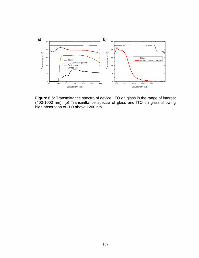
137
Figure 6.5: Transmittance spectra of device, ITO on glass in the range of interest (400-1000 nm). (b) Transmittance spectra of glass and ITO on glass showing high absorption of ITO above 1200 nm.
500 1000 1500 2000 2500 3000
0
20
40
60
80
100
Tra
nsm
itta
nce (
%)
Wavelength (nm)
Glass
ITO On Glass (1 layer)
400 500 600 700 800 900 1000
0
20
40
60
80
100T
ransm
itta
nce (
%)
Wavelength (nm)
Glass
ITO On Glass (1layer)
Device- 0V
Device- 2V
a) b)

138
6.4: Modulation of Short-Wave Infrared Light in Electrochromic Cells
Containing [Bu]2B
In order to expand the spectral range of electrochromic devices to the
SWIR range ITO must be replaced. Thus, in a new set of devices the ITO
conducting layers on both opposing electrodes were substituted with films of
metallic single-walled carbon nanotubes (MT-SWNTs).15,16 The metallic type of
SWNTs was selected because it has less interfering spectral features and lower
absorption in the SWIR spectral ranges than semiconducting SWNTs, and MT-
SWNT thin films provide very efficient transparent conductive layers at very low
thicknesses as shown in Figure 6.6. As can be seen this is a significant
improvement over ITO.
1000 1500 2000 2500
80
85
90
95
100
Glass
MT-SWNT Film #1 on Glass
MT-SWNT Film #2 on Glass
Tra
nsm
itta
nce (
%)
Wavelength (nm)
Figure 6.6: Transmittance spectra of MT-SWNT films on glass.

139
Figure 6.7a shows a picture of the device in its transmissive (0V) and
colored (2V) state and Figure 6.7b shows the corresponding transmittance
spectra. In the IR area of interest, 1000-2500 nm, the average transmittance in
the bleached and colored state is 64.9% and 24.0 %, respectively, demonstrating
a high degree of modulation (ΔT ≈ 41%).
Figure 6.7: (a) Pictures of the [Bu]2B device utilizing MT-SWNT thin film electrodes and (b) the corresponding transmittance spectra in the transparent and opaque state.
A significant amount of absorption in both the bleached and colored states
in the range from 1000-2500 nm is due to propylene carbonate, the solvent used
in the cell (Figure 6.8a). Figure 6.8b presents the transmittance spectra of the
device with the propylene carbonate subtracted out. It shows a significant
increase of the transparency of the bleached state if the losses due to solvent are
reduced along with an increased amplitude of the transmittance modulation (ΔT)
up to 70% at 2200 nm. Thus, using thinner cells with less solvent in the optical
path can improve the performance of the electrochromic cell as previously shown

140
in Chapter 2 with the LWIR devices. Even further improvement could be
achieved through the elimination of solvent through the design of a solid-state
device.
Figure 6.8: (a) Transmittance spectra of propylene carbonate between 2 glass slides and (b) the spectra of devices in Figure 6.6 with the contribution of propylene carbonate subtracted out.
1000 1500 2000 2500
0
20
40
60
80
100
Tra
nsm
itta
nce
(%
)
Wavelength (nm)
0V
2V
1000 1500 2000 2500
0
20
40
60
80
100
Propylene Carbonate
Between 2 Glass Slides
Tra
nsm
itta
nce
(%
)
Wavelength (nm)
a) b)

141
Figure 6.9 shows the cycling of the device over 6000 seconds (60
seconds at 2V, 60 seconds at 0V) and not much degradation is observed
showing that the electrochromic properties are reversible. The response time is
on the order of 10 seconds (Figure 6.9b), which is shorter than in case of the ITO
electrodes in agreement with our recent work on SWNT electrochromic cells.14
Figure 6.9: (a) Cycling response of device at 2000 nm and (b) corresponding response time.
6.5: Conclusion
We demonstrated that neutral radical small molecules, in particular [Bu]2B,
can be utilized as an electrochromic medium which can modulate both visible
and SWIR light. This unique property could allow the material to serve as part of
a smart window for energy conservation. While the devices showed good
modulation, they could be further improved through the design optimization
including the possibility of incorporation into a solid state device.
0 1000 2000 3000 4000 5000 6000
0
20
40
60
80
100
Tra
nsm
itta
nce
(%
)
Time (sec)
2000 nm
0 20 40 60 80 100 120 140 160
10
20
30
40
50
60
70
80
=
14 sec
Tra
nsm
itta
nce
(%
)
Time (sec)
=
13 sec
a) b)

142
6.6: Experimental
Materials: Propylene Carbonate and hydroquinone were used as received
(Sigma Aldrich).
Synthesis of [PLY(O,NBu)]2B: [PLY(O,NBu)]2B was synthesized as the cationic
salt ([PLY(O,NBu)]2B+ -BPh4) according to the literature.
Preparation of Electrochromic solution: 8 mg of [PLY(O,NBu)]2B+ -BPh4 (9.0 x 10-
6 mol) along with 2 mg hydroquinone (1.8 x 10⁻⁵ mol) was dissolved in 1 mL of
propylene carbonate.
ITO Sandwich Device preparation: The electrochromic solution is sandwiched
between two ITO coated glass slides (20 Ohm/sq, Thin Film Devices, Inc,
Anaheim, CA) and sealed utilizing double sided tape with 3.5 mm x 13 mm
rectangle cut aperture.
MT-SWNT Sandwich Device preparation: Similar to our previous report, the thin
MT-SWNT films (30 nm thick) were made utilizing vacuum filtration of the
dispersion of large diameter (1.2-1.7 nm) 99% separated (IsoNantube-M) metallic
SWNTs purchased from Nanointegris Inc. The films were transferred onto glass
substrates bridging a 2 mm gap between predeposited Ti(15nm/Pt(150 nm)
electrodes. On one substrate, an adhesive seal frame (0.25 mm thick) (Frame-
SealTM, Bio-Rad Laboratories) is placed. The cell is filled with electrochromic
solution and another matching MT-SWNT on glass substrate is placed overtop.
Spectroscopy/Electrochromic Measurements: Transmittance spectra were
recorded on a Cary 5000 UV-Vis Spectrophotometer (Agilent Technology). The

143
potential was applied using a model DS345 synthesized function generator
(Stanford Research Systems).

144
6.7: References
1) Khandelwal, H.; Schenning, A. P. H. J.; Debije, M. G. Adv. Energy Mater. 2017, 7. 2) Hsu, C. Y.; Zhang, J.; Sato, T.; Moriyama, S.; Higuchi, M. ACS App. Mater. Interfaces 2015, 7, 18266. 3) Granqvist, C. G. Thin Solid Films 2014, 564, 1. 4) Baetens, R.; Jelle, B. P.; Gustavsen, A. Sol. Energy Mater Sol. Cells 2010, 94, 87. 5) Shin, H.; Kim, Y.; Bhuvana, T.; Lee, J.; Yang, X.; Park, C.; Kim, E. ACS App. Mater. Interfaces 2012, 4, 185. 6) Zhang, Q.; Tsai, C. Y.; Abidin, T.; Jiang, J. C.; Shie, W. R.; Li, L. J.; Liaw, D. J. Polym. Chem. 2018, 9, 619. 7) Liu, H. S.; Pan, B. C.; Huang, D. C.; Kung, Y. R.; Leu, C. M.; Liou, G. S. NPG Asia Mater. 2017, 9. 8) Beaujuge, P. M.; Ellinger, S.; Reynolds, J. R. Nat. Mater. 2008, 7, 795. 9) Abraham, S.; Mangalath, S.; Sasikumar, D.; Joseph, J. Chem. Mater. 2017, 29, 9877. 10) Bag, P.; Itkis, M. E.; Stekovic, D.; Pal, S. K.; Tham, F. S.; Haddon, R. C. J. Am. Chem. Soc. 2015, 137, 10000 11) Palenzuela, J.; Vinuales, A.; Odriozola, I.; Cabanero, G.; Grande, H. J.; Ruiz, V. ACS App. Mater. Interfaces 2014, 6, 14562. 12) Moon, H. C.; Kim, C. H.; Lodge, T. P.; Frisbie, C. D. ACS App. Mater. Interfaces 2016, 8, 6252. 13) Alesanco, Y.; Vinuales, A.; Cabanero, G.; Rodriguez, J.; Tena-Zaera, R. ACS App. Mater. Interfaces 2016, 8, 29619. 14) Stekovic, D.; Arkook, B.; Li, G.; Li, W.; Bekyarova, E.; Itkis, M. E. Adv. Mater. Interfaces 2018, 1800861.

145
15) Wan, J. Y.; Xu, Y.; Ozdernir, B.; Xu, L.; Sushkov, A. B.; Yang, Z.; Yang, B.; Drew, D.; Barone, V.; Hu, L. B. ACS Nano 2017, 11, 788. 16) Vasilyeva, S. V.; Unur, E.; Walczak, R. M.; Donoghue, E. P.; Rinzler, A. G.; Reynolds, J. R. ACS App. Mater. Interfaces 2009, 1, 2288.