ee334 supplementary notes - usna
TRANSCRIPT
US Naval Academy EE334: Electrical Engineering II and IT Systems
Supplementary Notes
Spring 2012–2013

2
Last Revision: January 2013 CAPT Kevin W. Rudd, Ph.D.
3
Table of Contents Chapter 1: Counters and State Machine Design ........................................................................................... 6
1.1 Introduction ......................................................................................................................................... 6 1.2 Sequential Logic Modules Review ..................................................................................................... 6
1.2.1 Clocked SR Flip-Flop .................................................................................................................. 6 1.2.2 The D or Delay Flip-Flop ............................................................................................................ 8 1.2.3 JK and T Flip-Flops ..................................................................................................................... 9 1.2.4 Asynchronous Inputs ................................................................................................................. 11 1.2.5 Timing Diagrams for Interdependent Flip-Flops ...................................................................... 13
1.3 Counters ............................................................................................................................................ 14 1.3.1 Basic Concepts of Digital Counters .......................................................................................... 14 1.3.2 Ripple Counters ......................................................................................................................... 15 1.3.3 Synchronous Counters ............................................................................................................... 18
1.4 Counter Design ................................................................................................................................. 20 1.4.1 State Tables ............................................................................................................................... 21 1.4.2 Flip-Flop Excitation Tables ....................................................................................................... 22 1.4.3 State Table Implementation ....................................................................................................... 24 1.4.4 Additional State Machine Design Examples ............................................................................. 27
1.6 Homework Problems ........................................................................................................................ 30 Chapter 2: Digital and Analog Conversion ................................................................................................. 33
2.1 ADC and DAC Concepts .................................................................................................................. 33 2.2 Digital to Analog Conversion ........................................................................................................... 34 2.3 Analog to Digital Conversion ........................................................................................................... 36
2.3.1 The Comparator ......................................................................................................................... 37 2.3.2 Flash ADC ................................................................................................................................. 37
2.4 Homework Problems ........................................................................................................................ 41 Chapter 3: Introduction to Communications ............................................................................................... 42
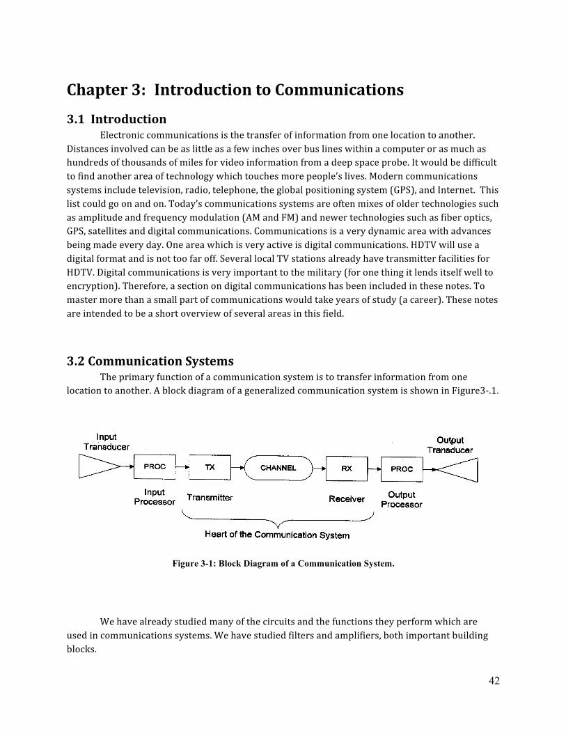
3.1 Introduction ....................................................................................................................................... 42 3.2 Communication Systems .................................................................................................................. 42
Chapter 4: Amplitude Modulation ............................................................................................................. 45 4.1 Introduction ....................................................................................................................................... 45 4.2 Amplitude Modulation (AM) ........................................................................................................... 46 4.3 AM Bandwidth ................................................................................................................................. 53 4.4 AM Power ......................................................................................................................................... 54 4.5 Frequency Division Multiplexing (FDM) ........................................................................................ 56 4.6 Homework Problems ........................................................................................................................ 58
Chapter 5: AM Demodulation .................................................................................................................... 63 5.1 Introduction ....................................................................................................................................... 63 5.2 Synchronous Demodulation .............................................................................................................. 63 5.3 Envelope Detection ........................................................................................................................... 65 5.4 Homework Problems ........................................................................................................................ 69
Chapter 6: AM Receivers ........................................................................................................................... 71 6.1 Introduction ....................................................................................................................................... 71 6.2 TRF Receiver .................................................................................................................................... 71 6.3 The Superheterodyne Receiver ......................................................................................................... 72 6.4 Homework Problems ........................................................................................................................ 79
Chapter 7: Frequency Modulation ............................................................................................................. 81
4
7.1 Introduction ....................................................................................................................................... 81 7.2 Description of the Modulation Process ............................................................................................. 81 7.3 FM Spectrum .................................................................................................................................... 83 7.4 Advantages and Disadvantages of FM ............................................................................................. 85 7.5 FM Receiver ..................................................................................................................................... 85 7.6 Homework Problems ........................................................................................................................ 91
Chapter 8: Noise in Communication .......................................................................................................... 93 8.1 Introduction ....................................................................................................................................... 93 8.2 Expressing Noise – SNR and Noise Ratio/Figure ............................................................................ 94 8.3 Sources of Noise - External Noise .................................................................................................... 96 8.4 Internal Noise .................................................................................................................................... 97 8.5 Overcoming Noise: Filtering .......................................................................................................... 100
Chapter 9: Digital Communications ........................................................................................................ 105 9.1 Introduction ..................................................................................................................................... 105 9.2 Pulse Code Modulation ................................................................................................................... 105
9.2.1 Sampling .................................................................................................................................. 106 9.2.2 Pulse Amplitude Modulation ................................................................................................... 107 9.2.3 Other Analog Pulse Modulation Schemes ............................................................................... 108 9.2.4 Quantization ............................................................................................................................ 109 9.2.5 Digital Encoding ...................................................................................................................... 110
9.3 Digital Receivers ............................................................................................................................ 113 9.4 Error Detection and Correction ...................................................................................................... 114 9.5 Channel Capacity ............................................................................................................................ 118 9.6 Time Division Multiplexing ........................................................................................................... 123 9.7 Homework Problems ...................................................................................................................... 126
Chapter 10: Networking Overview ........................................................................................................... 129 10.1 Introduction ................................................................................................................................... 129 10.2 Basic Networking Components .................................................................................................... 129 10.3 Networking Entities ...................................................................................................................... 129 10.4 Hardware and Software ................................................................................................................ 130 10.5 The OSI Model ............................................................................................................................. 131 10.6 Protocol Stacks ............................................................................................................................. 132
10.6.1 Communication Between Stacks ........................................................................................... 132 10.6.2 Encapsulation ........................................................................................................................ 132
10.7 The Physical Layer ....................................................................................................................... 134 10.7.1 The Data Link Layer ............................................................................................................. 134 10.7.2 The Network Layer ............................................................................................................... 135 10.7.3 Transport Layer ..................................................................................................................... 136 10.7.4 Session Layer ........................................................................................................................ 136 10.7.5 The Presentation Layer .......................................................................................................... 136 10.7.6 The Application Layer ........................................................................................................... 136
10.8 Physical Connection of a Network ............................................................................................... 137 Chapter 11: Network Hardware ................................................................................................................ 139
11.1 The Physical Layer ....................................................................................................................... 139 11.2 The Data Link Layer ..................................................................................................................... 146
11.2.1 The Data Link Layer ............................................................................................................. 148 11.2.2 Functions of the Data Link Layer .......................................................................................... 149 11.2.3 Data Link Layer Hardware .................................................................................................... 150 11.2.4 Layer 1 Hardware Revisited .................................................................................................. 151 11.2.5 Layer 2 Hardware .................................................................................................................. 151
11.3 The Network Layer ....................................................................................................................... 153
5
11.3.1 Routed versus Routing Protocol ............................................................................................ 154 11.3.2 TCP/IP ................................................................................................................................... 154 11.3.3 UDP ....................................................................................................................................... 155
Chapter 12: Internet and Addressing ........................................................................................................ 157 12.1 Introduction ................................................................................................................................... 157 12.2 IP Addresses ................................................................................................................................. 157
12.2.1 Classes of IP Addresses ......................................................................................................... 158 12.2.2 Reserved Host ID Numbers ................................................................................................... 161
12.3 Network Mask .............................................................................................................................. 162 Chapter 13: Subnetting .............................................................................................................................. 165
13.1 Introduction ................................................................................................................................... 165 13.2 Subnet Mask ................................................................................................................................. 165 13.3 Subnetting Example ...................................................................................................................... 168 13.4 Plan for growth ............................................................................................................................. 169
Appendix A: Frequency Spectra and Ideal Filtering ................................................................................ 171 A.1 Amplitude Spectrum ...................................................................................................................... 171 A.2 Ideal Filtering ................................................................................................................................. 172
Appendix B: A Typical CW Communication System .............................................................................. 177 B.1 Introduction .................................................................................................................................... 177 B.2 A Citizen Band (CB) Transceiver .................................................................................................. 177
Appendix C: The Channel ......................................................................................................................... 181 C.1 Introduction .................................................................................................................................... 181 C.2 Propagation of Signals in Free Space ............................................................................................ 182 C.3 Radio Waves .................................................................................................................................. 183 C.4 Propagation of Radio Waves .......................................................................................................... 184
C.4.1 Line of Sight (LOS) ................................................................................................................ 185 C.4.2 Surface Wave .......................................................................................................................... 185 C.4.3 Skywave .................................................................................................................................. 186 C.4.4 Forward Scatter ....................................................................................................................... 187 C.4.5 Summary ................................................................................................................................. 188
C.5 Multiple Path Propagation and Skip .............................................................................................. 189 Appendix D: Overview of the USNA SATCOM Communication System .............................................. 193
6
Chapter 1: Counters and State Machine Design 1.1 Introduction
Up until this point you have been studying combinational logic. The circuits you assemble out of AND, OR and NOT gates have definite limitations. Most notably, such circuits have no memory. Their output depends only on their present input. However, if you think about it, most complex computing functions require some level of memory. This requires moving beyond combinational logic to sequential logic. Sequential logic circuits have memory. This chapter begins by reviewing flip-‐flops, which are the building blocks for sequential logic.
Using sequential logic, we will then describe how to build a state machine, which is a system that consists of a finite number of states, the transitions between those states, and actions occurring as a result of being in or transitioning to a particular state. A traffic light controller is an example of a simple state machine. Your computer is a state machine, too. In fact, most systems can be described in terms of state machines. Counters are an important sub-‐category of state machines in which the states progress in a repeating pattern, so we’ll start there and then move on to more complex state machines.
1.2 Sequential Logic Modules Review Flip-‐flops are the fundamental building blocks from which counters and state machines are
made. Before entering into a discussion of counters and state machines, therefore, we need to review the behavior of these basic circuit blocks. We will review four basic types of flip-‐flops: the Clocked SR Flip-‐Flop, the D Flip-‐Flop, the JK Flip-‐Flop, and the T Flip-‐Flop.
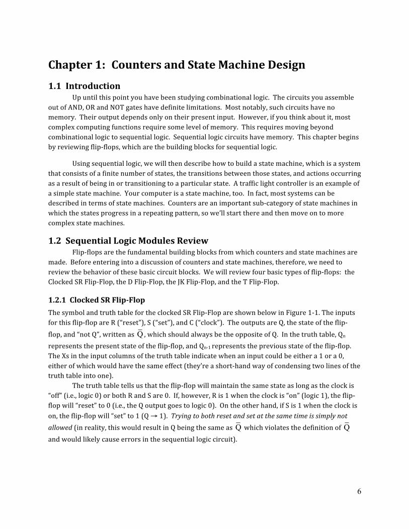
1.2.1 Clocked SR Flip-‐Flop The symbol and truth table for the clocked SR Flip-‐Flop are shown below in Figure 1-‐1. The inputs for this flip-‐flop are R (“reset”), S (“set”), and C (“clock”). The outputs are Q, the state of the flip-‐flop, and “not Q”, written as Q , which should always be the opposite of Q. In the truth table, Qn represents the present state of the flip-‐flop, and Qn-‐1 represents the previous state of the flip-‐flop. The Xs in the input columns of the truth table indicate when an input could be either a 1 or a 0, either of which would have the same effect (they’re a short-‐hand way of condensing two lines of the truth table into one).
The truth table tells us that the flip-‐flop will maintain the same state as long as the clock is “off” (i.e., logic 0) or both R and S are 0. If, however, R is 1 when the clock is “on” (logic 1), the flip-‐flop will “reset” to 0 (i.e., the Q output goes to logic 0). On the other hand, if S is 1 when the clock is on, the flip-‐flop will “set” to 1 (Q → 1). Trying to both reset and set at the same time is simply not allowed (in reality, this would result in Q being the same as Q which violates the definition of Q and would likely cause errors in the sequential logic circuit).
7
Figure 1-1: Symbol and truth table for clocked SR flip-flop
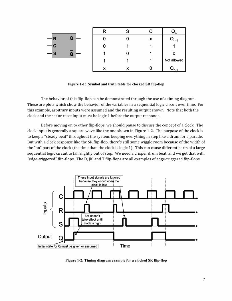
The behavior of this flip-‐flop can be demonstrated through the use of a timing diagram. These are plots which show the behavior of the variables in a sequential logic circuit over time. For this example, arbitrary inputs were assumed and the resulting output shown. Note that both the clock and the set or reset input must be logic 1 before the output responds.
Before moving on to other flip-‐flops, we should pause to discuss the concept of a clock. The clock input is generally a square wave like the one shown in Figure 1-‐2. The purpose of the clock is to keep a “steady beat” throughout the system, keeping everything in step like a drum for a parade. But with a clock response like the SR flip-‐flop, there’s still some wiggle room because of the width of the “on” part of the clock (the time that the clock is logic 1). This can cause different parts of a large sequential logic circuit to fall slightly out of step. We need a crisper drum beat, and we get that with “edge-‐triggered” flip-‐flops. The D, JK, and T flip-‐flops are all examples of edge-‐triggered flip-‐flops.
Figure 1-2: Timing diagram example for a clocked SR flip-flop
R
SC
Q
Q
R
SC
Q
Qn-10xx
Not allowed11101011110
Qn-1x00QnCSR
Qn-10xx
Not allowed11101011110
Qn-1x00QnCSR
Time
C
R
S
Q
Inpu
ts
Output
Initial state for Q must be given or assumed
Set doesn’t take effect until
clock is high
These input signals are ignored because they occur when the
clock is low
Time
C
R
S
Q
Inpu
ts
Output
Initial state for Q must be given or assumed
Set doesn’t take effect until
clock is high
These input signals are ignored because they occur when the
clock is low
8
1.2.2 The D or Delay Flip-‐Flop An edge-‐triggered flip-‐flop only responds to the other inputs at points when the clock is
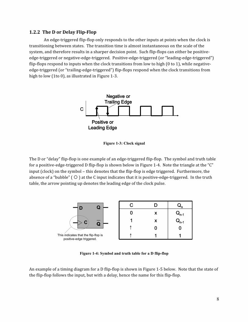
transitioning between states. The transition time is almost instantaneous on the scale of the system, and therefore results in a sharper decision point. Such flip-‐flops can either be positive-‐edge-‐triggered or negative-‐edge-‐triggered. Positive-‐edge-‐triggered (or “leading-‐edge-‐triggered”) flip-‐flops respond to inputs when the clock transitions from low to high (0 to 1), while negative-‐edge-‐triggered (or “trailing-‐edge-‐triggered”) flip-‐flops respond when the clock transitions from high to low (1to 0), as illustrated in Figure 1-‐3.
Figure 1-3: Clock signal
The D or “delay” flip-‐flop is one example of an edge-‐triggered flip-‐flop. The symbol and truth table for a positive-‐edge-‐triggered D flip-‐flop is shown below in Figure 1-‐4. Note the triangle at the “C” input (clock) on the symbol − this denotes that the flip-‐flop is edge triggered. Furthermore, the absence of a “bubble” ( � ) at the C input indicates that it is positive-‐edge-‐triggered. In the truth table, the arrow pointing up denotes the leading edge of the clock pulse.
Figure 1-4: Symbol and truth table for a D flip-flop
An example of a timing diagram for a D flip-‐flop is shown in Figure 1-‐5 below. Note that the state of the flip-‐flop follows the input, but with a delay, hence the name for this flip-‐flop.
C
Positive or Leading Edge
Negative or Trailing Edge
C
Positive or Leading Edge
Negative or Trailing Edge
Positive or Leading Edge
Negative or Trailing Edge
1100
Qn-1x1Qn-1x0QnDC
1100
Qn-1x1Qn-1x0QnDCD
C
Q
Q
D
C
Q
QQ↑
↑This indicates that the flip-flop is positive-edge triggered.
9
Figure 1-5: Example of a timing diagram for a D flip-flop
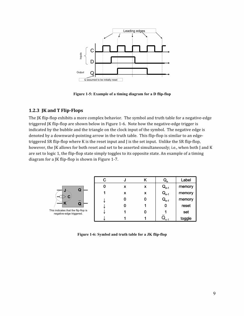
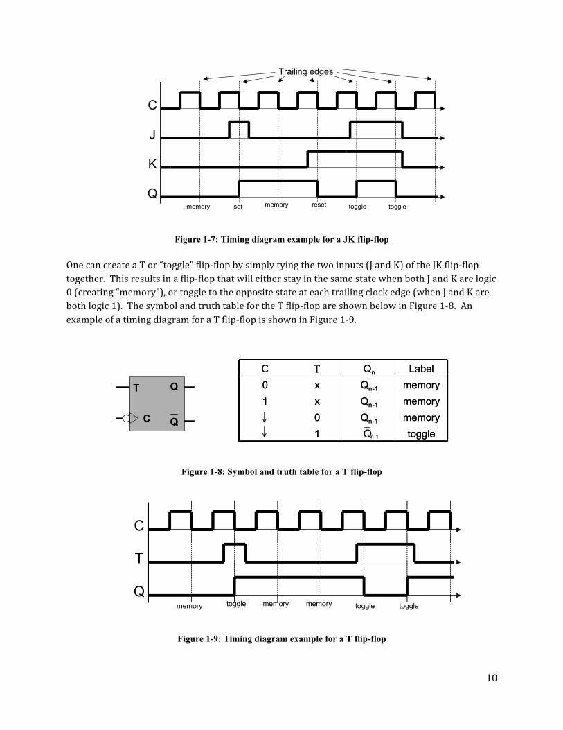
1.2.3 JK and T Flip-‐Flops The JK flip-‐flop exhibits a more complex behavior. The symbol and truth table for a negative-‐edge triggered JK flip-‐flop are shown below in Figure 1-‐6. Note how the negative-‐edge trigger is indicated by the bubble and the triangle on the clock input of the symbol. The negative edge is denoted by a downward-‐pointing arrow in the truth table. This flip-‐flop is similar to an edge-‐triggered SR flip-‐flop where K is the reset input and J is the set input. Unlike the SR flip-‐flop, however, the JK allows for both reset and set to be asserted simultaneously; i.e., when both J and K are set to logic 1, the flip-‐flop state simply toggles to its opposite state. An example of a timing diagram for a JK flip-‐flop is shown in Figure 1-‐7.
Figure 1-6: Symbol and truth table for a JK flip-flop
C
D
QQ assumed to be initially reset
Inpu
ts
Output
Leading edges
J
KC
Q
toggleset
resetmemorymemorymemory
Label
010
11101
Qn-100Qn-1xx1Qn-1xx0QnKJC
toggleset
resetmemorymemorymemory
Label
010
11101
Qn-100Qn-1xx1Qn-1xx0QnKJC
This indicates that the flip-flop is negative-edge triggered.
↓↓↓
↓ n-1Q
10
Figure 1-7: Timing diagram example for a JK flip-flop
One can create a T or “toggle” flip-‐flop by simply tying the two inputs (J and K) of the JK flip-‐flop together. This results in a flip-‐flop that will either stay in the same state when both J and K are logic 0 (creating “memory”), or toggle to the opposite state at each trailing clock edge (when J and K are both logic 1). The symbol and truth table for the T flip-‐flop are shown below in Figure 1-‐8. An example of a timing diagram for a T flip-‐flop is shown in Figure 1-‐9.
T
C
Q
Q Q ↓ ↓ n-1 Q
T
Q n - 1
Q n - 1
Q n - 1
Q n
toggle 1 memory 0 memory x 1 memory x 0 Label C
Q n - 1
Q n - 1
Q n - 1
Q n
toggle 1 memory 0 memory x 1 memory x 0 Label C
Figure 1-8: Symbol and truth table for a T flip-flop
Figure 1-9: Timing diagram example for a T flip-flop
C
J
K
Qmemory set resetmemory toggle toggle
Trailing edges
C
T
Qmemory memory toggle toggletoggle memory
11
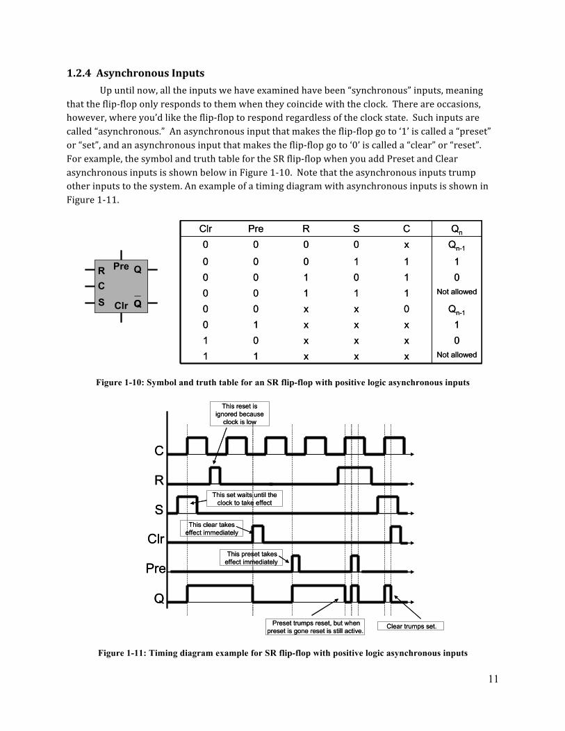
1.2.4 Asynchronous Inputs Up until now, all the inputs we have examined have been “synchronous” inputs, meaning
that the flip-‐flop only responds to them when they coincide with the clock. There are occasions, however, where you’d like the flip-‐flop to respond regardless of the clock state. Such inputs are called “asynchronous.” An asynchronous input that makes the flip-‐flop go to ‘1’ is called a “preset” or “set”, and an asynchronous input that makes the flip-‐flop go to ‘0’ is called a “clear” or “reset”. For example, the symbol and truth table for the SR flip-‐flop when you add Preset and Clear asynchronous inputs is shown below in Figure 1-‐10. Note that the asynchronous inputs trump other inputs to the system. An example of a timing diagram with asynchronous inputs is shown in Figure 1-‐11.
Figure 1-10: Symbol and truth table for an SR flip-flop with positive logic asynchronous inputs
Figure 1-11: Timing diagram example for SR flip-flop with positive logic asynchronous inputs
010100Not allowed11100
Qn-10xx00
Not allowedxxx110xxx011xxx10
0
0Clr
0
0Pre
1110
Qn-1x00QnCSR
010100Not allowed11100
Qn-10xx00
Not allowedxxx110xxx011xxx10
0
0Clr
0
0Pre
1110
Qn-1x00QnCSR
R
SC
Q
QClr
PreR
SC
Q
QQClr
Pre
C
R
S
Q
Clr
Pre
This reset is ignored because
clock is low
This set waits until the clock to take effect
This clear takes effect immediately
This preset takes effect immediately
Preset trumps reset, but when preset is gone reset is still active.
Clear trumps set.
C
R
S
Q
Clr
Pre
This reset is ignored because
clock is low
This set waits until the clock to take effect
This clear takes effect immediately
This preset takes effect immediately
Preset trumps reset, but when preset is gone reset is still active.
Clear trumps set.
12
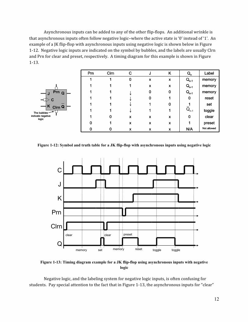
Asynchronous inputs can be added to any of the other flip-‐flops. An additional wrinkle is that asynchronous inputs often follow negative logic−where the active state is ‘0’ instead of ‘1’. An example of a JK flip-‐flop with asynchronous inputs using negative logic is shown below in Figure 1-‐12. Negative logic inputs are indicated on the symbol by bubbles, and the labels are usually Clrn and Prn for clear and preset, respectively. A timing diagram for this example is shown in Figure 1-‐13.
Figure 1-12: Symbol and truth table for a JK flip-flop with asynchronous inputs using negative logic
Figure 1-13: Timing diagram example for a JK flip-flop using asynchronous inputs with negative
logic
Negative logic, and the labeling system for negative logic inputs, is often confusing for students. Pay special attention to the fact that in Figure 1-‐13, the asynchronous inputs for “clear”
toggle1111clear0xxx01
preset1xxx100
11111
Prn
0
11111
Clrn
Not allowed
setreset
memorymemorymemory
Label
010
N/Axxx
101
Qn-100Qn-1xx1Qn-1xx0QnKJC
toggle1111clear0xxx01
preset1xxx100
11111
Prn
0
11111
Clrn
Not allowed
setreset
memorymemorymemory
Label
010
N/Axxx
101
Qn-100Qn-1xx1Qn-1xx0QnKJC
↓↓↓
↓ n-1Q
J
KC
Q
QThe bubbles
indicate negative logic
Clrn
PrnJ
KC
Q
QQThe bubbles
indicate negative logic
Clrn
Prn
C
J
K
Qmemory set resetmemory toggle toggle
Prn
Clrnpresetclearclear
13
(Clrn, meaning “clear-‐negative”) and “preset” (Prn) don’t affect the output Q while set to 1; they only affect the output when they go to 0. Device designers generally make several efforts to call attention to negative logic conditions. For instance, a single input such as Prn can be marked with a
bubble and labeled “ P rn ”, where the bubble, the “-‐n” suffix, and the overbar all serve as a reminder that the input uses negative logic. (These markers are not cumulative! All serve as a reminder; they do not cancel each other out.)
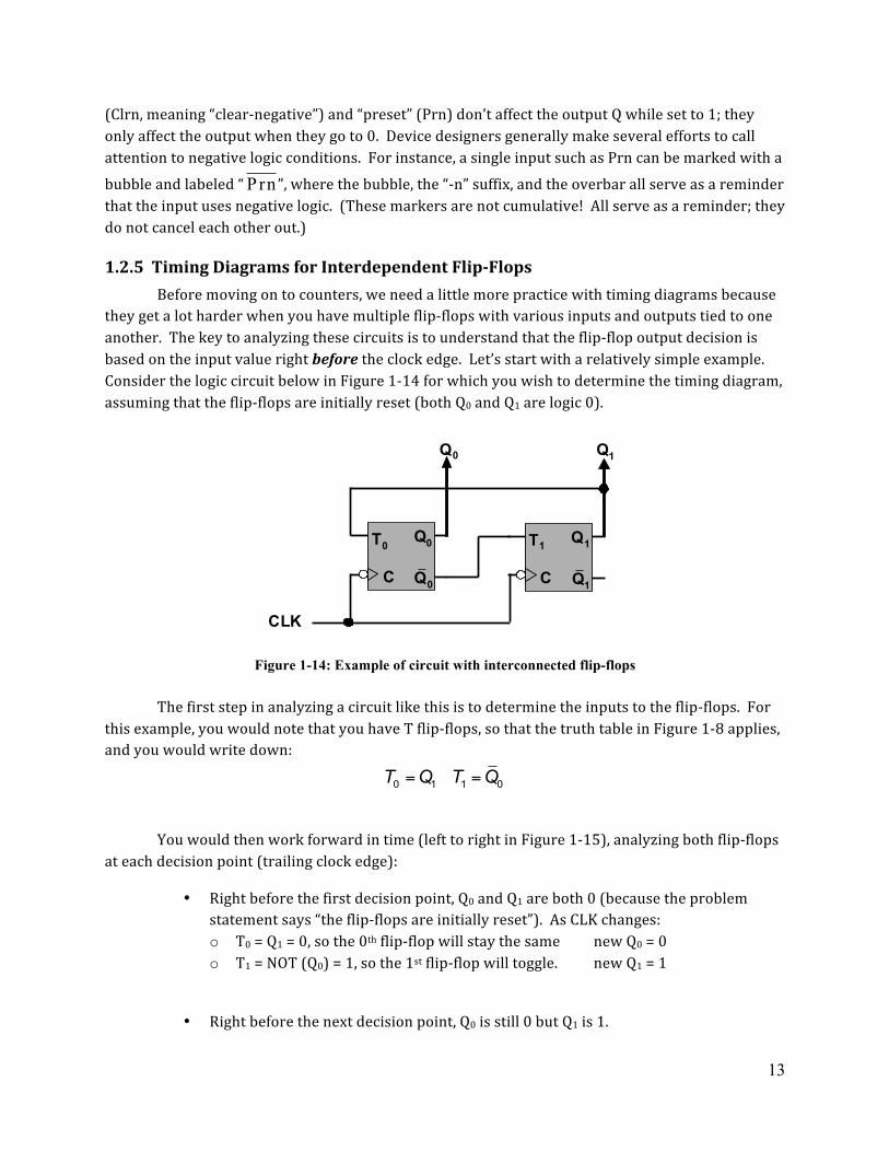
1.2.5 Timing Diagrams for Interdependent Flip-‐Flops Before moving on to counters, we need a little more practice with timing diagrams because
they get a lot harder when you have multiple flip-‐flops with various inputs and outputs tied to one another. The key to analyzing these circuits is to understand that the flip-‐flop output decision is based on the input value right before the clock edge. Let’s start with a relatively simple example. Consider the logic circuit below in Figure 1-‐14 for which you wish to determine the timing diagram, assuming that the flip-‐flops are initially reset (both Q0 and Q1 are logic 0).
Figure 1-14: Example of circuit with interconnected flip-flops The first step in analyzing a circuit like this is to determine the inputs to the flip-‐flops. For
this example, you would note that you have T flip-‐flops, so that the truth table in Figure 1-‐8 applies, and you would write down:
0 1 1 0T Q T Q= =
You would then work forward in time (left to right in Figure 1-‐15), analyzing both flip-‐flops at each decision point (trailing clock edge):
• Right before the first decision point, Q0 and Q1 are both 0 (because the problem statement says “the flip-‐flops are initially reset”). As CLK changes: o T0 = Q1 = 0, so the 0th flip-‐flop will stay the same new Q0 = 0 o T1 = NOT (Q0) = 1, so the 1st flip-‐flop will toggle. new Q1 = 1
• Right before the next decision point, Q0 is still 0 but Q1 is 1.
T0
C
Q0
Q0
T1
C
Q1
Q1
CLK
Q0 Q1
14
o T0 = Q1 = 1, so the 0th flip-‐flop will toggle. new Q0 = 1 o T1 = NOT (Q0) = 1, so the 1st flip-‐flop will toggle again. new Q1 = 0
• Right before the third decision point, Q0 is 1 and Q1 is 0. o T0 = Q1 = 0, so the 0th flip-‐flop will stay the same. new Q0 = 1 o T1 = NOT (Q0) = 0, so 1st flip-‐flop will stay the same. new Q1 = 0
This result is illustrated in the timing diagram below in Figure 1-‐15. Analyzing circuits like this takes a little practice. For another example, see the discussion of the mod-‐8 synchronous counter. There are also more opportunities in the problems at the end of the chapter. Such circuits are the basis for counters and state machines.
Figure 1-15: Timing diagram for interconnected flip-flop example
1.3 Counters
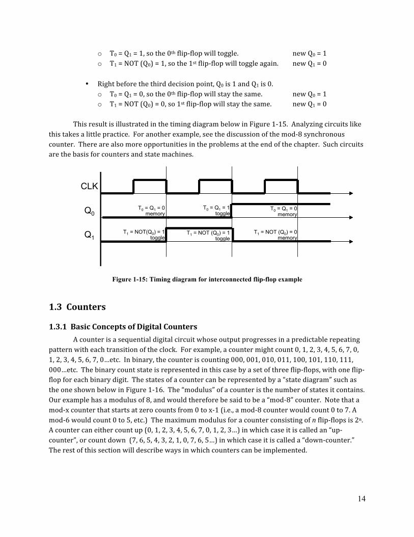
1.3.1 Basic Concepts of Digital Counters A counter is a sequential digital circuit whose output progresses in a predictable repeating pattern with each transition of the clock. For example, a counter might count 0, 1, 2, 3, 4, 5, 6, 7, 0, 1, 2, 3, 4, 5, 6, 7, 0…etc. In binary, the counter is counting 000, 001, 010, 011, 100, 101, 110, 111, 000…etc. The binary count state is represented in this case by a set of three flip-‐flops, with one flip-‐flop for each binary digit. The states of a counter can be represented by a “state diagram” such as the one shown below in Figure 1-‐16. The “modulus” of a counter is the number of states it contains. Our example has a modulus of 8, and would therefore be said to be a “mod-‐8” counter. Note that a mod-‐x counter that starts at zero counts from 0 to x-‐1 (i.e., a mod-‐8 counter would count 0 to 7. A mod-‐6 would count 0 to 5, etc.) The maximum modulus for a counter consisting of n flip-‐flops is 2n. A counter can either count up (0, 1, 2, 3, 4, 5, 6, 7, 0, 1, 2, 3…) in which case it is called an “up-‐counter”, or count down (7, 6, 5, 4, 3, 2, 1, 0, 7, 6, 5…) in which case it is called a “down-‐counter.” The rest of this section will describe ways in which counters can be implemented.
CLK
Q0
Q1
T0 = Q1 = 0memory
T1 = NOT(Q0) = 1toggle
T0 = Q1 = 1toggle
T1 = NOT (Q0) = 1toggle
T0 = Q1 = 0memory
T1 = NOT (Q0) = 0memory
15
Figure 1-16: State diagram for mod-8 up-counter which is counting 0,1,2,3,4,5,6,7,0,1,2,…
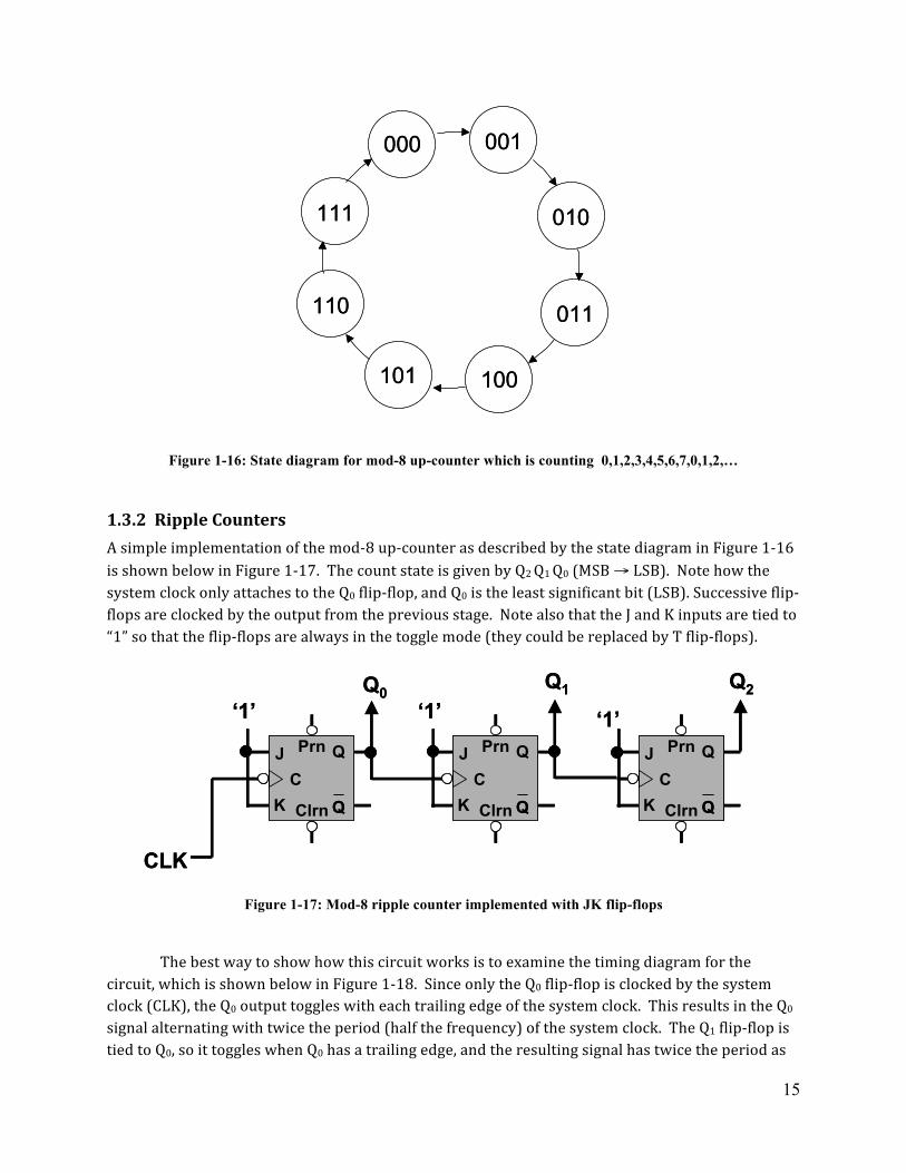
1.3.2 Ripple Counters A simple implementation of the mod-‐8 up-‐counter as described by the state diagram in Figure 1-‐16 is shown below in Figure 1-‐17. The count state is given by Q2 Q1 Q0 (MSB → LSB). Note how the system clock only attaches to the Q0 flip-‐flop, and Q0 is the least significant bit (LSB). Successive flip-‐flops are clocked by the output from the previous stage. Note also that the J and K inputs are tied to “1” so that the flip-‐flops are always in the toggle mode (they could be replaced by T flip-‐flops).
Figure 1-17: Mod-8 ripple counter implemented with JK flip-flops
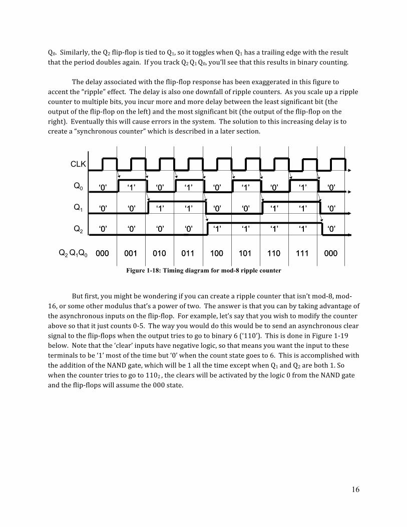
The best way to show how this circuit works is to examine the timing diagram for the circuit, which is shown below in Figure 1-‐18. Since only the Q0 flip-‐flop is clocked by the system clock (CLK), the Q0 output toggles with each trailing edge of the system clock. This results in the Q0 signal alternating with twice the period (half the frequency) of the system clock. The Q1 flip-‐flop is tied to Q0, so it toggles when Q0 has a trailing edge, and the resulting signal has twice the period as
000 001
010
011
100101
110
111
000 001
010
011
100101
110
111
J
KC
Q
QClrn
Prn J
KC
Q
QClrn
Prn J
KC
Q
QClrn
Prn
CLK
Q0 Q1 Q2‘1’ ‘1’ ‘1’
J
KC
Q
QClrn
PrnJ
KC
Q
QQClrn
Prn J
KC
Q
QClrn
PrnJ
KC
Q
QQClrn
Prn J
KC
Q
QClrn
PrnJ
KC
Q
QQClrn
Prn
CLK
Q0 Q1 Q2‘1’ ‘1’ ‘1’
16
Q0. Similarly, the Q2 flip-‐flop is tied to Q1, so it toggles when Q1 has a trailing edge with the result that the period doubles again. If you track Q2 Q1 Q0, you’ll see that this results in binary counting.
The delay associated with the flip-‐flop response has been exaggerated in this figure to
accent the “ripple” effect. The delay is also one downfall of ripple counters. As you scale up a ripple counter to multiple bits, you incur more and more delay between the least significant bit (the output of the flip-‐flop on the left) and the most significant bit (the output of the flip-‐flop on the right). Eventually this will cause errors in the system. The solution to this increasing delay is to create a “synchronous counter” which is described in a later section.
Figure 1-18: Timing diagram for mod-8 ripple counter
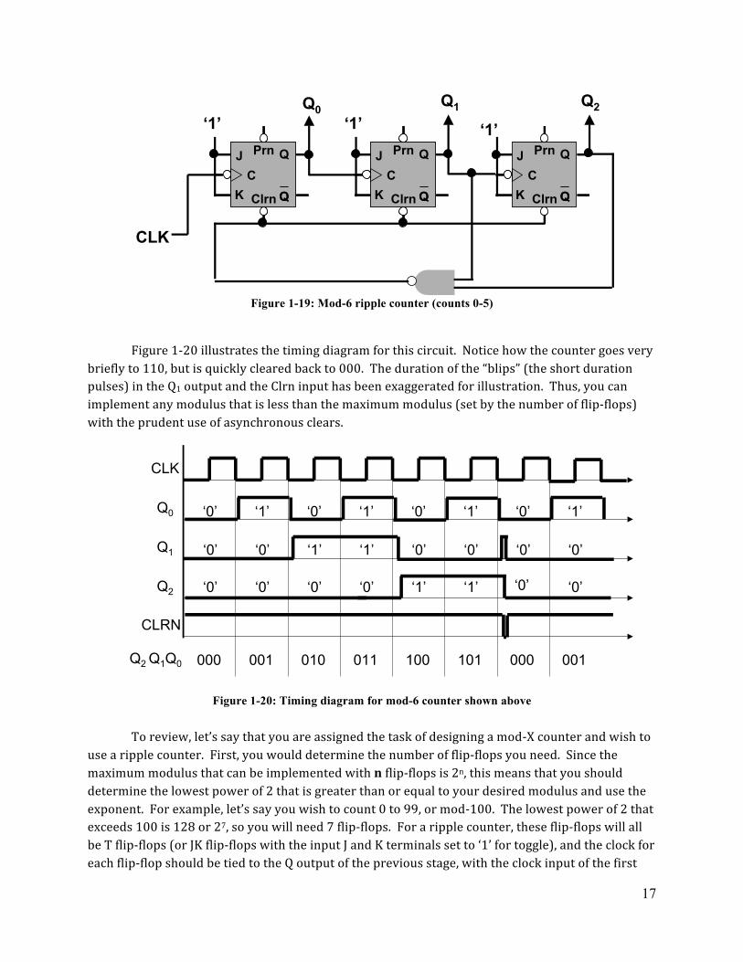
But first, you might be wondering if you can create a ripple counter that isn’t mod-‐8, mod-‐16, or some other modulus that’s a power of two. The answer is that you can by taking advantage of the asynchronous inputs on the flip-‐flop. For example, let’s say that you wish to modify the counter above so that it just counts 0-‐5. The way you would do this would be to send an asynchronous clear signal to the flip-‐flops when the output tries to go to binary 6 (‘110’). This is done in Figure 1-‐19 below. Note that the ‘clear’ inputs have negative logic, so that means you want the input to these terminals to be ‘1’ most of the time but ‘0’ when the count state goes to 6. This is accomplished with the addition of the NAND gate, which will be 1 all the time except when Q1 and Q2 are both 1. So when the counter tries to go to 1102 , the clears will be activated by the logic 0 from the NAND gate and the flip-‐flops will assume the 000 state.
CLK
Q0
Q1
Q2
Q2 Q1Q0
‘0’
‘0’
‘0’
000
‘0’
‘0’
‘0’
000
‘1’
‘0’
‘0’
001
‘1’
‘0’
‘0’
001
‘0’
‘1’
‘0’
010
‘0’
‘1’
‘0’
010
‘1’
‘1’
‘0’
011
‘1’
‘1’
‘0’
011
‘0’
‘0’
‘1’
100
‘0’
‘0’
‘1’
100
‘1’
‘0’
‘1’
101
‘1’
‘0’
‘1’
101
‘0’
‘1’
‘1’
110
‘0’
‘1’
‘1’
110
‘1’
‘1’
‘1’
111
‘1’
‘1’
‘1’
111
‘0’
‘0’
‘0’
000
‘0’
‘0’
‘0’
000
17
Figure 1-19: Mod-6 ripple counter (counts 0-5)
Figure 1-‐20 illustrates the timing diagram for this circuit. Notice how the counter goes very briefly to 110, but is quickly cleared back to 000. The duration of the “blips” (the short duration pulses) in the Q1 output and the Clrn input has been exaggerated for illustration. Thus, you can implement any modulus that is less than the maximum modulus (set by the number of flip-‐flops) with the prudent use of asynchronous clears.
Figure 1-20: Timing diagram for mod-6 counter shown above
To review, let’s say that you are assigned the task of designing a mod-‐X counter and wish to use a ripple counter. First, you would determine the number of flip-‐flops you need. Since the maximum modulus that can be implemented with n flip-‐flops is 2n, this means that you should determine the lowest power of 2 that is greater than or equal to your desired modulus and use the exponent. For example, let’s say you wish to count 0 to 99, or mod-‐100. The lowest power of 2 that exceeds 100 is 128 or 27, so you will need 7 flip-‐flops. For a ripple counter, these flip-‐flops will all be T flip-‐flops (or JK flip-‐flops with the input J and K terminals set to ‘1’ for toggle), and the clock for each flip-‐flop should be tied to the Q output of the previous stage, with the clock input of the first
J
KC
Q
QClrn
PrnJ
KC
Q
QQClrn
Prn J
KC
Q
QClrn
PrnJ
KC
Q
QQClrn
Prn J
KC
Q
QClrn
PrnJ
KC
Q
QQClrn
Prn
CLK
Q0 Q1 Q2‘1’ ‘1’ ‘1’
CLK
Q0
Q1
Q2
Q2 Q1Q0
‘0’
‘0’
‘0’
000
‘1’
‘0’
‘0’
001
‘0’
‘1’
‘0’
010
‘1’
‘1’
‘0’
011
‘0’
‘0’
‘1’
100
‘1’
‘0’
‘1’
101
‘0’
‘0’
‘0’
000
‘1’
‘0’
‘0’
001
CLRN
18
stage tied to the system clock. The first stage will always be your least significant bit, and the last your most significant bit.
Next, you need to figure out the logic for the clear so that the count stops where you want it.
For example, for a 0-‐99 counter, you want the flip-‐flops to all clear when the input reaches 10010, or 11001002. Assuming that your Clear inputs use negative logic, that means that you need an expression which is 1 most of the time, but 0 when you reach the count 1100100. This can be accomplished by a NAND gate with inputs that match the binary encoding of the clear point. For this example, you could use the following expression for CLRN:
( )6 5 4 3 2 1 0CLRN Q Q Q Q Q QQ=
In fact, you can simplify this expression a bit more, because since you plan to clear at
1100100, then you will never reach 1100101, 1100110, or 1100111, so you don’t care about the inputs that correspond to the digits to the right of the least significant ‘1’ in your clear point.1 Thus this expression can be further simplified to:
( )6 5 4 3 2CLRN Q Q Q Q Q=
Armed with this information, you could then build the circuit to implement your counter.
1.3.3 Synchronous Counters Ripple counters have problem of accumulated delay, which means they don’t scale well to
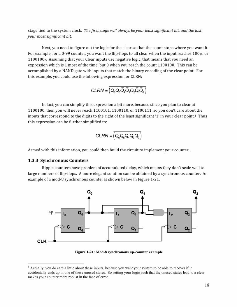
large numbers of flip-‐flops. A more elegant solution can be obtained by a synchronous counter. An example of a mod-‐8 synchronous counter is shown below in Figure 1-‐21.
Figure 1-21: Mod-8 synchronous up-counter example 1 Actually, you do care a little about these inputs, because you want your system to be able to recover if it accidentally ends up in one of these unused states. So setting your logic such that the unused states lead to a clear makes your counter more robust in the face of error.
T0
C
Q0
Q0
T1
C
Q1
Q1
T2
C
Q2
Q2
CLK
Q0 Q1 Q2
‘1’ T0
C
Q0
Q0Q0
T1
C
Q1
Q1Q1
T2
C
Q2
Q2Q2
CLK
Q0 Q1 Q2
‘1’
19
This circuit is called “synchronous” because all of the flip-‐flops are connected to the same clock signal. To convince you that this is a counter, let’s go through the analysis of the timing diagram using the same process as was previously introduced. First, you should note the expressions for the flip-‐flop inputs:
= = =0 1 0 2 0 11T T Q T QQ
Next, you would review the truth table for the T flip-‐flop, shown in Figure 1-‐8, which tells us that if T is 1 the output will toggle, and if T is 0 the output will stay the same. Then you would work forward in time, analyzing all three flip-‐flops at each decision point:
• At the first decision point, assuming the flip-‐flops are initially reset, Q0, Q1, and Q2 are all 0.
o T0 = 1, so the 0th flip-‐flop will toggle o T1 = Q0 = 0, so the 1st flip-‐flop will stay the same. o T2 = Q0Q1 = 0, so the 2nd flip-‐flop will stay the same.
• Right before the next decision point, Q0 is 1, while Q1 and Q2 are still 0.
o T0 = 1, so the 0th flip-‐flop will toggle o T1 = Q0 = 1, so the 1st flip-‐flop will toggle. o T2 = Q0Q1 = 0, so the 2nd flip-‐flop will stay the same.
• Right before the next decision point, Q0 is 0, Q1 is 1, and Q2 is still 0.
o T0 = 1, so the 0th flip-‐flop will toggle o T1 = Q0 = 0, so the 1st flip-‐flop will stay the same. o T2 = Q0Q1 = 0, so the 2nd flip-‐flop will stay the same.
• Right before the next decision point, Q0 is 1, Q1 is 1, and Q2 is still 0.
o T0 = 1, so the 0th flip-‐flop will toggle o T1 = Q0 = 1, so the 1st flip-‐flop will toggle. o T2 = Q0Q1 = 1, so the 2nd flip-‐flop will finally toggle.
The result is shown below in Figure 1-‐22.
20
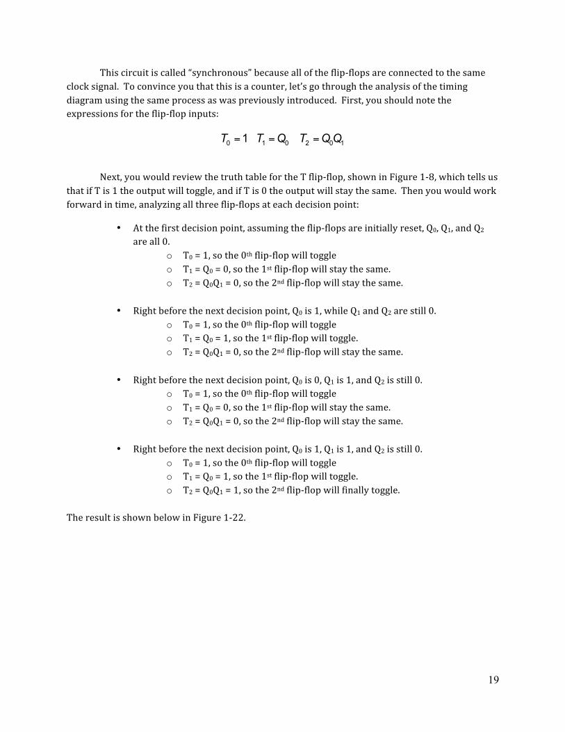
Figure 1-22: Timing diagram for mod-8 synchronous up-counter
Note that this counter no long exhibits the accumulated delay in the higher order digits, since all the flip-‐flops share the system clock. As with the ripple counter, this counter could be modified to a lower modulus with the use of the asynchronous clear inputs. However, there is a general method that can be used for a more elegant design. For that matter, the method described in the next section can be used to create any state machine.
1.4 Counter Design The focus of this section is the process by which one can design any state machine. We will
focus on the design of synchronous counters. In brief, the design process for a state machine is as follows:
• Define the problem. • Draw a state diagram for your system. • Make a “state table,” which lists all possible Present States (in binary order), the Next States
to which those states should transition, and the flip-‐flop inputs necessary to make those transitions happen.
• Use flip-‐flop “excitation tables” to determine the inputs required to make the desired transitions.
• Determine combinational logic expressions for all of the flip-‐flop inputs using the present state variables as inputs.
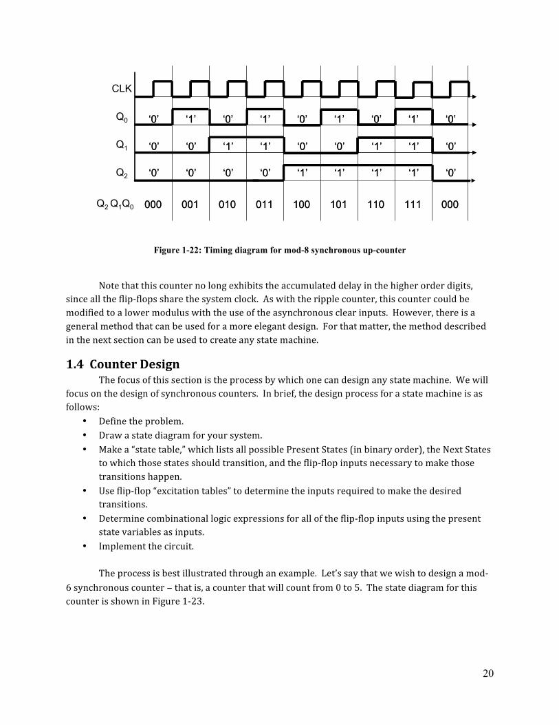
• Implement the circuit. The process is best illustrated through an example. Let’s say that we wish to design a mod-‐6 synchronous counter − that is, a counter that will count from 0 to 5. The state diagram for this counter is shown in Figure 1-‐23.
CLK
Q0
Q1
Q2
Q2 Q1Q0
‘0’
‘0’
‘0’
000
‘0’
‘0’
‘0’
000
‘1’
‘0’
‘0’
001
‘1’
‘0’
‘0’
001
‘0’
‘1’
‘0’
010
‘0’
‘1’
‘0’
010
‘1’
‘1’
‘0’
011
‘1’
‘1’
‘0’
011
‘0’
‘0’
‘1’
100
‘0’
‘0’
‘1’
100
‘1’
‘0’
‘1’
101
‘1’
‘0’
‘1’
101
‘0’
‘1’
‘1’
110
‘0’
‘1’
‘1’
110
‘1’
‘1’
‘1’
111
‘1’
‘1’
‘1’
111
‘0’
‘0’
‘0’
000
‘0’
‘0’
‘0’
000
21
Figure 1-23: State diagram for mod-6 counter design example
Furthermore, let’s say that you wish to build this state machine using T flip-‐flops (you could use any type). The next step is to construct the state table.
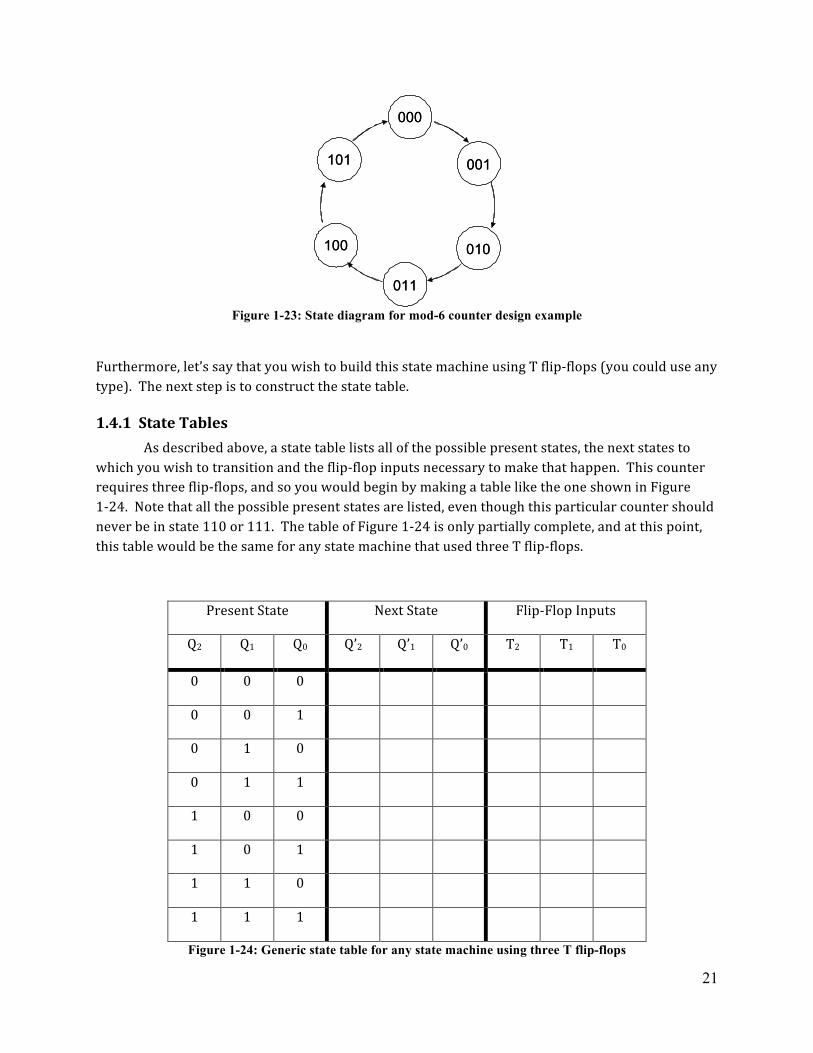
1.4.1 State Tables As described above, a state table lists all of the possible present states, the next states to which you wish to transition and the flip-‐flop inputs necessary to make that happen. This counter requires three flip-‐flops, and so you would begin by making a table like the one shown in Figure 1-‐24. Note that all the possible present states are listed, even though this particular counter should never be in state 110 or 111. The table of Figure 1-‐24 is only partially complete, and at this point, this table would be the same for any state machine that used three T flip-‐flops.
Present State Next State Flip-‐Flop Inputs
Q2 Q1 Q0 Q’2 Q’1 Q’0 T2 T1 T0
0 0 0
0 0 1
0 1 0
0 1 1
1 0 0
1 0 1
1 1 0
1 1 1
Figure 1-24: Generic state table for any state machine using three T flip-flops
000000
001001
010010
011011
100100
101101
22
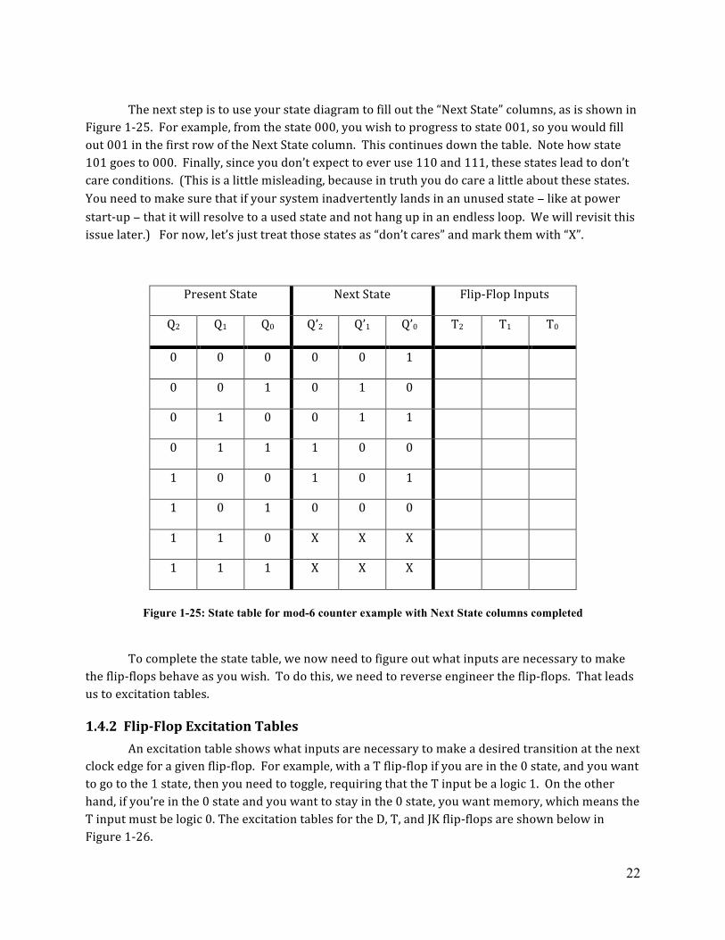
The next step is to use your state diagram to fill out the “Next State” columns, as is shown in Figure 1-‐25. For example, from the state 000, you wish to progress to state 001, so you would fill out 001 in the first row of the Next State column. This continues down the table. Note how state 101 goes to 000. Finally, since you don’t expect to ever use 110 and 111, these states lead to don’t care conditions. (This is a little misleading, because in truth you do care a little about these states. You need to make sure that if your system inadvertently lands in an unused state − like at power start-‐up − that it will resolve to a used state and not hang up in an endless loop. We will revisit this issue later.) For now, let’s just treat those states as “don’t cares” and mark them with “X”.
Present State Next State Flip-‐Flop Inputs
Q2 Q1 Q0 Q’2 Q’1 Q’0 T2 T1 T0
0 0 0 0 0 1
0 0 1 0 1 0
0 1 0 0 1 1
0 1 1 1 0 0
1 0 0 1 0 1
1 0 1 0 0 0
1 1 0 X X X
1 1 1 X X X
Figure 1-25: State table for mod-6 counter example with Next State columns completed
To complete the state table, we now need to figure out what inputs are necessary to make the flip-‐flops behave as you wish. To do this, we need to reverse engineer the flip-‐flops. That leads us to excitation tables.
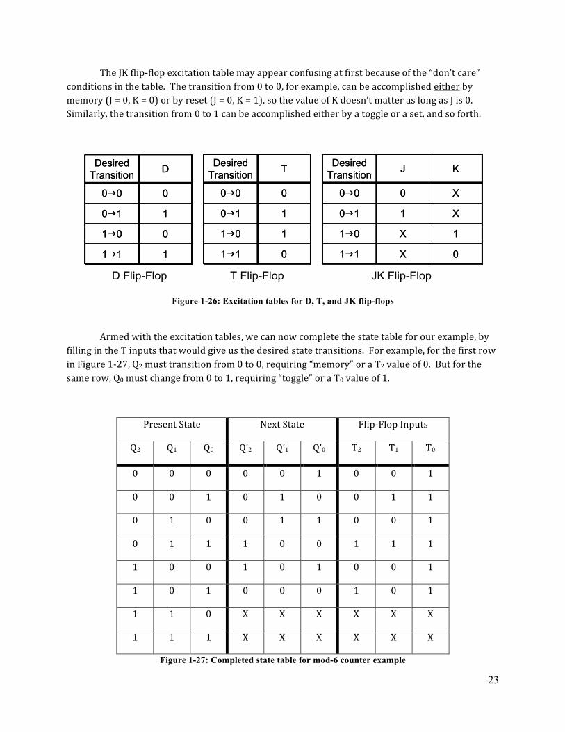
1.4.2 Flip-‐Flop Excitation Tables An excitation table shows what inputs are necessary to make a desired transition at the next
clock edge for a given flip-‐flop. For example, with a T flip-‐flop if you are in the 0 state, and you want to go to the 1 state, then you need to toggle, requiring that the T input be a logic 1. On the other hand, if you’re in the 0 state and you want to stay in the 0 state, you want memory, which means the T input must be logic 0. The excitation tables for the D, T, and JK flip-‐flops are shown below in Figure 1-‐26.
23
The JK flip-‐flop excitation table may appear confusing at first because of the “don’t care” conditions in the table. The transition from 0 to 0, for example, can be accomplished either by memory (J = 0, K = 0) or by reset (J = 0, K = 1), so the value of K doesn’t matter as long as J is 0. Similarly, the transition from 0 to 1 can be accomplished either by a toggle or a set, and so forth.
Figure 1-26: Excitation tables for D, T, and JK flip-flops
Armed with the excitation tables, we can now complete the state table for our example, by filling in the T inputs that would give us the desired state transitions. For example, for the first row in Figure 1-‐27, Q2 must transition from 0 to 0, requiring “memory” or a T2 value of 0. But for the same row, Q0 must change from 0 to 1, requiring “toggle” or a T0 value of 1.
Present State Next State Flip-‐Flop Inputs
Q2 Q1 Q0 Q’2 Q’1 Q’0 T2 T1 T0
0 0 0 0 0 1 0 0 1
0 0 1 0 1 0 0 1 1
0 1 0 0 1 1 0 0 1
0 1 1 1 0 0 1 1 1
1 0 0 1 0 1 0 0 1
1 0 1 0 0 0 1 0 1
1 1 0 X X X X X X
1 1 1 X X X X X X
Figure 1-27: Completed state table for mod-6 counter example
11g1
01g0
10g1
00g0
D Desired Transition
11g1
01g0
10g1
00g0
D Desired Transition
01g1
11g0
10g1
00g0
T Desired Transition
01g1
11g0
10g1
00g0
T Desired Transition
X
X
1
0
J
01g1
11g0
X0g1
X0g0
K Desired Transition
X
X
1
0
J
01g1
11g0
X0g1
X0g0
K Desired Transition
D Flip-Flop T Flip-Flop JK Flip-Flop
24
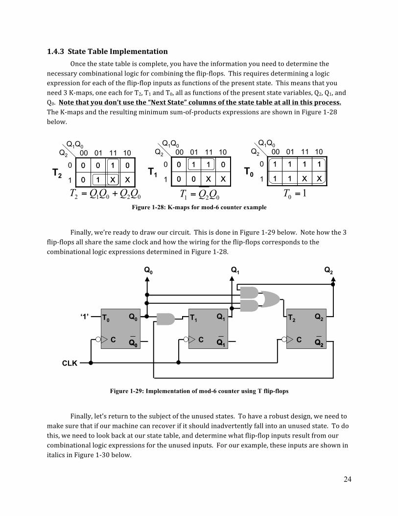
1.4.3 State Table Implementation Once the state table is complete, you have the information you need to determine the
necessary combinational logic for combining the flip-‐flops. This requires determining a logic expression for each of the flip-‐flop inputs as functions of the present state. This means that you need 3 K-‐maps, one each for T2, T1 and T0, all as functions of the present state variables, Q2, Q1, and Q0. Note that you don’t use the “Next State” columns of the state table at all in this process. The K-‐maps and the resulting minimum sum-‐of-‐products expressions are shown in Figure 1-‐28 below.
Figure 1-28: K-maps for mod-6 counter example
Finally, we’re ready to draw our circuit. This is done in Figure 1-‐29 below. Note how the 3 flip-‐flops all share the same clock and how the wiring for the flip-‐flops corresponds to the combinational logic expressions determined in Figure 1-‐28.
Figure 1-29: Implementation of mod-6 counter using T flip-flops
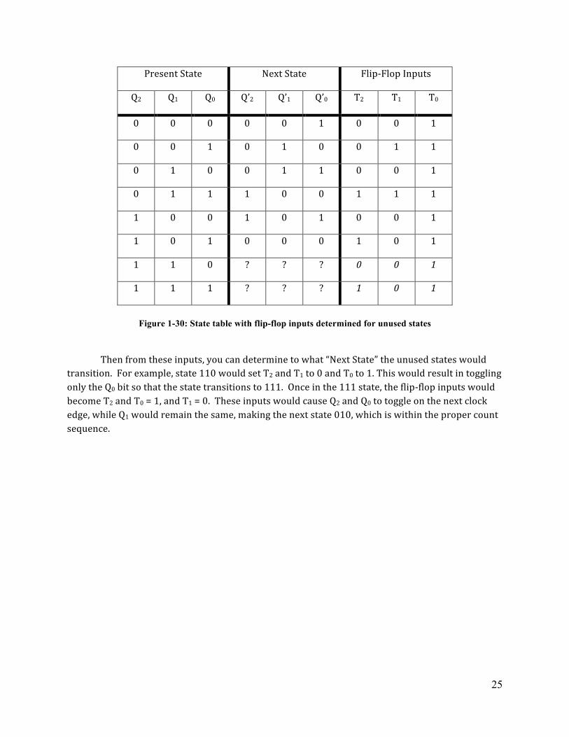
Finally, let’s return to the subject of the unused states. To have a robust design, we need to make sure that if our machine can recover if it should inadvertently fall into an unused state. To do this, we need to look back at our state table, and determine what flip-‐flop inputs result from our combinational logic expressions for the unused inputs. For our example, these inputs are shown in italics in Figure 1-‐30 below.
XX10
0100
XX10
0100
Q2Q1Q0
00 01 11 10
0
1T2 XX00
0110
XX00
0110
Q2Q1Q0
00 01 11 10
0
1T1 XX11
1111
XX11
1111
Q2Q1Q0
00 01 11 10
0
1T0
1 2 0T Q Q=2 1 0 2 0T QQ Q Q= + 0 1T =
T0
C
Q0
Q0Q0
T1
C
Q1
Q1Q1
T2
C
Q2
Q2Q2
CLK
Q0 Q1 Q2
‘1’
25
Present State Next State Flip-‐Flop Inputs
Q2 Q1 Q0 Q’2 Q’1 Q’0 T2 T1 T0
0 0 0 0 0 1 0 0 1
0 0 1 0 1 0 0 1 1
0 1 0 0 1 1 0 0 1
0 1 1 1 0 0 1 1 1
1 0 0 1 0 1 0 0 1
1 0 1 0 0 0 1 0 1
1 1 0 ? ? ? 0 0 1
1 1 1 ? ? ? 1 0 1
Figure 1-30: State table with flip-flop inputs determined for unused states
Then from these inputs, you can determine to what “Next State” the unused states would transition. For example, state 110 would set T2 and T1 to 0 and T0 to 1. This would result in toggling only the Q0 bit so that the state transitions to 111. Once in the 111 state, the flip-‐flop inputs would become T2 and T0 = 1, and T1 = 0. These inputs would cause Q2 and Q0 to toggle on the next clock edge, while Q1 would remain the same, making the next state 010, which is within the proper count sequence.
26
Present State Next State Flip-‐Flop Inputs
Q2 Q1 Q0 Q’2 Q’1 Q’0 T2 T1 T0
0 0 0 0 0 1 0 0 1
0 0 1 0 1 0 0 1 1
0 1 0 0 1 1 0 0 1
0 1 1 1 0 0 1 1 1
1 0 0 1 0 1 0 0 1
1 0 1 0 0 0 1 0 1
1 1 0 1 1 1 0 0 1
1 1 1 0 1 0 1 0 1
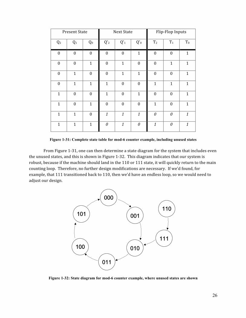
Figure 1-31: Complete state table for mod-6 counter example, including unused states
From Figure 1-‐31, one can then determine a state diagram for the system that includes even
the unused states, and this is shown in Figure 1-‐32. This diagram indicates that our system is robust, because if the machine should land in the 110 or 111 state, it will quickly return to the main counting loop. Therefore, no further design modifications are necessary. If we’d found, for example, that 111 transitioned back to 110, then we’d have an endless loop, so we would need to adjust our design.
Figure 1-32: State diagram for mod-6 counter example, where unused states are shown
000000
001001
010010
011011
100100
101101110110
111111
27
1.4.4 Additional State Machine Design Examples
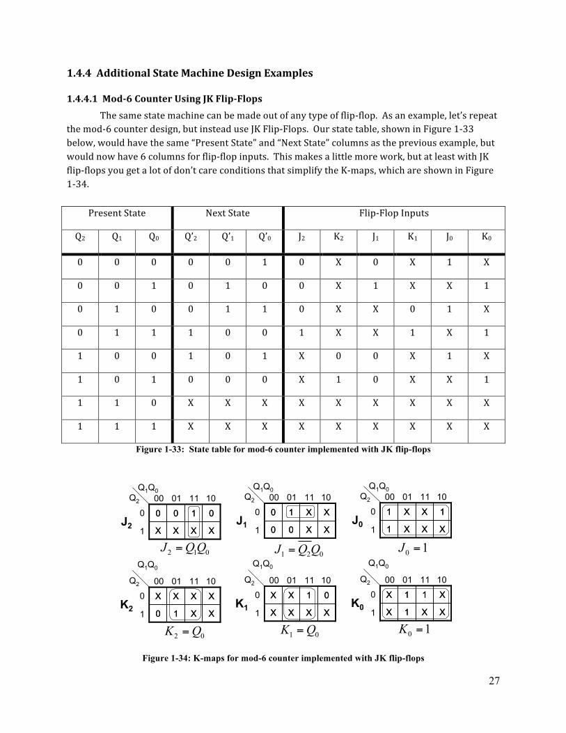
1.4.4.1 Mod-‐6 Counter Using JK Flip-‐Flops The same state machine can be made out of any type of flip-‐flop. As an example, let’s repeat
the mod-‐6 counter design, but instead use JK Flip-‐Flops. Our state table, shown in Figure 1-‐33 below, would have the same “Present State” and “Next State” columns as the previous example, but would now have 6 columns for flip-‐flop inputs. This makes a little more work, but at least with JK flip-‐flops you get a lot of don’t care conditions that simplify the K-‐maps, which are shown in Figure 1-‐34.
Present State Next State Flip-‐Flop Inputs
Q2 Q1 Q0 Q’2 Q’1 Q’0 J2 K2 J1 K1 J0 K0
0 0 0 0 0 1 0 X 0 X 1 X
0 0 1 0 1 0 0 X 1 X X 1
0 1 0 0 1 1 0 X X 0 1 X
0 1 1 1 0 0 1 X X 1 X 1
1 0 0 1 0 1 X 0 0 X 1 X
1 0 1 0 0 0 X 1 0 X X 1
1 1 0 X X X X X X X X X
1 1 1 X X X X X X X X X
Figure 1-33: State table for mod-6 counter implemented with JK flip-flops
Figure 1-34: K-maps for mod-6 counter implemented with JK flip-flops
XXXX
0100
XXXX
0100
Q2Q1Q0
00 01 11 10
0
1J2
XX10
XXXX
XX10
XXXX
Q2
Q1Q000 01 11 10
0
1K2
XX00
XX10
XX00
XX10
Q2Q1Q0
00 01 11 10
0
1J1
XXXX
01XX
XXXX
01XX
Q2
Q1Q000 01 11 10
0
1K1
XXX1
1XX1
XXX1
1XX1
Q2Q1Q0
00 01 11 10
0
1J0
XX1X
X11X
XX1X
X11X
Q2
Q1Q000 01 11 10
0
1K0
1 2 0J Q Q=2 1 0J QQ=
2 0K Q=
0 1J =
1 0K Q= 0 1K =
28
We leave it to the reader to complete the circuit design from this point. For more practice, let’s look at another state machine.
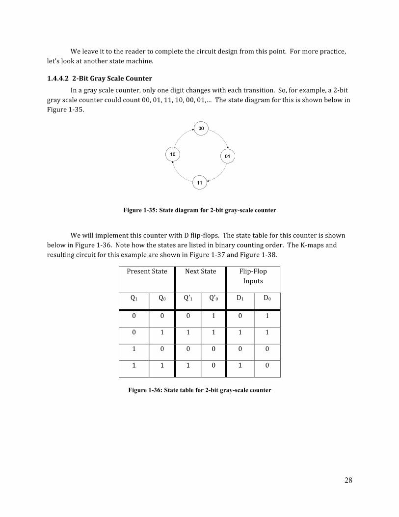
1.4.4.2 2-‐Bit Gray Scale Counter In a gray scale counter, only one digit changes with each transition. So, for example, a 2-‐bit
gray scale counter could count 00, 01, 11, 10, 00, 01,… The state diagram for this is shown below in Figure 1-‐35.
Figure 1-35: State diagram for 2-bit gray-scale counter
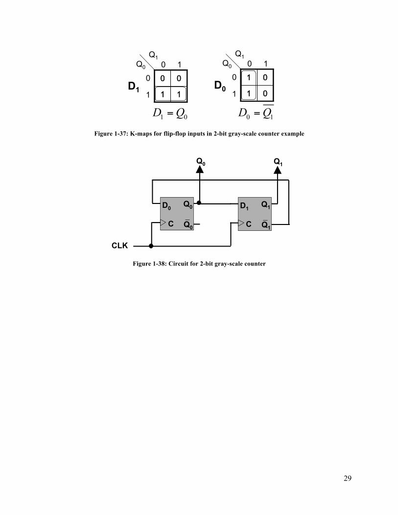
We will implement this counter with D flip-‐flops. The state table for this counter is shown below in Figure 1-‐36. Note how the states are listed in binary counting order. The K-‐maps and resulting circuit for this example are shown in Figure 1-‐37 and Figure 1-‐38.
Present State Next State Flip-‐Flop Inputs
Q1 Q0 Q’1 Q’0 D1 D0
0 0 0 1 0 1
0 1 1 1 1 1
1 0 0 0 0 0
1 1 1 0 1 0
Figure 1-36: State table for 2-bit gray-scale counter
0000
0101
1111
1010
29
Figure 1-37: K-maps for flip-flop inputs in 2-bit gray-scale counter example
Figure 1-38: Circuit for 2-bit gray-scale counter
11
00
11
00
Q0Q1
0 1
0
1D1
1 0D Q=
01
01
01
01
Q0Q1
0 1
0
1D0
0 1D Q=
D0
C
Q0
Q0
D1
C
Q1
Q1
CLK
Q0 Q1
30
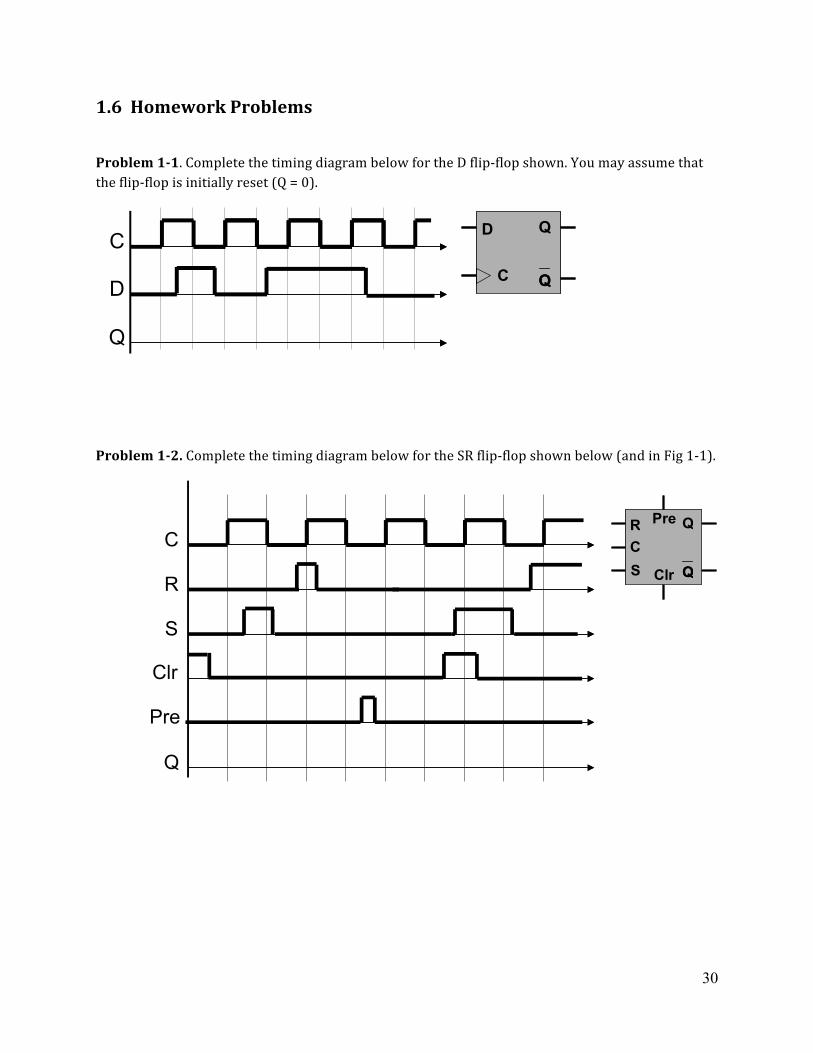
1.6 Homework Problems
Problem 1-‐1. Complete the timing diagram below for the D flip-‐flop shown. You may assume that the flip-‐flop is initially reset (Q = 0).
D
C
Q
Q
D
C
Q
Q Q
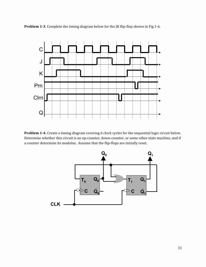
Problem 1-‐2. Complete the timing diagram below for the SR flip-‐flop shown below (and in Fig 1-‐1).
C
R
S
Q
Clr
Pre
C
D
Q
R
S C
Q
Q Clr
Pre R
S C
Q
Q Q Clr
Pre
31
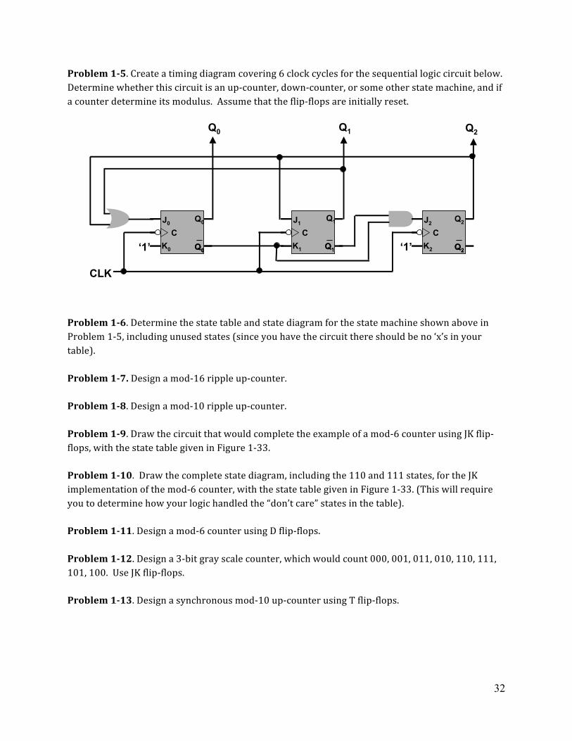
Problem 1-‐3. Complete the timing diagram below for the JK flip-‐flop shown in Fig 1-‐6.
Problem 1-‐4. Create a timing diagram covering 6 clock cycles for the sequential logic circuit below. Determine whether this circuit is an up-‐counter, down-‐counter, or some other state machine, and if a counter determine its modulus. Assume that the flip-‐flops are initially reset.
C
J
K
Q
Prn
Clrn
T0
C
Q0
Q0
T1
C
Q1
Q1
CLK
Q0 Q1
32
Problem 1-‐5. Create a timing diagram covering 6 clock cycles for the sequential logic circuit below. Determine whether this circuit is an up-‐counter, down-‐counter, or some other state machine, and if a counter determine its modulus. Assume that the flip-‐flops are initially reset.
Problem 1-‐6. Determine the state table and state diagram for the state machine shown above in Problem 1-‐5, including unused states (since you have the circuit there should be no ‘x’s in your table). Problem 1-‐7. Design a mod-‐16 ripple up-‐counter. Problem 1-‐8. Design a mod-‐10 ripple up-‐counter. Problem 1-‐9. Draw the circuit that would complete the example of a mod-‐6 counter using JK flip-‐flops, with the state table given in Figure 1-‐33. Problem 1-‐10. Draw the complete state diagram, including the 110 and 111 states, for the JK implementation of the mod-‐6 counter, with the state table given in Figure 1-‐33. (This will require you to determine how your logic handled the “don’t care” states in the table). Problem 1-‐11. Design a mod-‐6 counter using D flip-‐flops. Problem 1-‐12. Design a 3-‐bit gray scale counter, which would count 000, 001, 011, 010, 110, 111, 101, 100. Use JK flip-‐flops. Problem 1-‐13. Design a synchronous mod-‐10 up-‐counter using T flip-‐flops.
J0
K0
CQ0
Q0
J0
K0
CQ0
Q0Q0
CLK
Q0 Q1 Q2
‘1’
J1
K1
C
Q1
Q1
J1
K1
C
Q1
Q1Q1
J2
K2
CQ2
Q2
J2
K2
CQ2
Q2Q2‘1’
33
Chapter 2: Digital and Analog Conversion 2.1 ADC and DAC Concepts
By now you should have a sense of how analog and digital signals are different. An analog signal is a “real-‐world” signal. It can take on any value and can change continuously. A digital signal, on the other hand, is a stream of binary numbers. To convert an analog signal into a digital signal, the analog signal must first be sampled, then quantized, and then encoded as a binary number. The signal is then in a form where it can be stored (like on a compact disk) or manipulated using the digital system techniques you’ve already studied. To convert a digital signal back to an analog signal, the binary numbers making up the signal must be translated into an analog output voltage. The figure below illustrates these processes.
Figure 2-1: Illustration of ADC and DAC processes
Sampling is the first process involved in the conversion of an analog into a digital signal.
Sampling is the measurement of a signal at discrete and regular times. Hourly sampling of the temperature outside would result in a sequence of numbers, one for each hour. Usually the sample times are uniformly spaced. To avoid losing any information the samples have to be spaced closely enough together so that the shape of the analog input signal is not distorted or lost. Music stored in a CD would not sound very good if the sampling rate were 1 KHz.
How fast is fast enough? The Sampling Theorem states that to avoid loss of information, a
band limited signal must be sampled at a rate equal to or greater than twice the bandwidth of the
time
Signal (V)
ADC 011001110101001001010101011101010001
Signal (V)
DAC011001110101001001010101011101010001
timetime
34
signal. If we are dealing with a signal containing frequency components from about zero on up to some maximum frequency, fsig,max, then the sampling rate, fsample, must be equal to or greater than twice fsig,max.
,max2sample sigf f≥ (2.1)
This minimum rate is called the Nyquist rate, named after the engineer who investigated the mathematics of the sampling process. The theoretical limit is never really fast enough. For example, to make music CD recordings, the input signal, which has a maximum frequency of 20 KHz, is sampled at about 44 KHz.
Many signals have high frequency components that do not contain essential information but that can cause problems when sampling is done. The problem of aliasing occurs when the sampling rate is lower than twice the highest frequency of the signal. It results in high frequency components masquerading as lower frequency values and causing distortion. Musical instruments can create frequencies higher than 20 KHz which are not audible. To avoid aliasing problems, a music signal is first low pass filtered to remove any components greater than 20 KHz. (This filter is also called an anti-‐aliasing filter). This is what is meant by band limiting a signal. Filtering is used to remove all but a limited range of frequencies from a signal while preserving the essential information content. If all frequencies above about 3 KHz are removed from a person’s voice before telephone transmission, the voice remains both intelligible and recognizable although they may not sound exactly the same as in person.
Now let’s consider how the number of bits used to encode the signal affects the signal. Look
again at Figure 2-‐1. Can you see how the signal that emerged from the DAC is different from the original signal sent into the ADC? It’s blockier and would sound differently to your ear than the original signal. That ‘blockiness’ is called quantization noise, and it’s the inevitable result of limiting the signal to a finite number of voltage levels in the quantization process. The more voltage levels you allow in the system, the less quantization noise you will have and the closer the final signal will be to the original. You get more voltage levels by simply using more bits to encode each sample reading. Of course, the more bits you use and the faster you sample, then the larger the total bit rate for your signal becomes, making greater demands on your processing system and signal storage requirements. The bit rate for your system is the product of the sample rate and the number of bits for each sample.
2.2 Digital to Analog Conversion We’ll start with digital to analog conversion, because this process is more straightforward.
Let’s consider a system that converts an n-‐bit digital number into an analog signal that will range in value from va,min to va,max. With n bits, the number of levels in the system will be 2n, and the resolution, 𝛿𝑣 will be given by
,max ,min
2 1a a
n
v vvδ
−=
− (2.2)
35
Why is the denominator 2n-‐1 and not 2n? The key is that the resolution is the space between levels. Consider a 2-‐bit signal where ‘00’ will correspond to 0V, ‘01’ will correspond to 2V, ‘10’ will correspond to 4V and ‘11’ will correspond to 6V. There are four levels in this system (0, 2, 4, and 6 V) but the resolution is the full range divided by 3, or 2V.
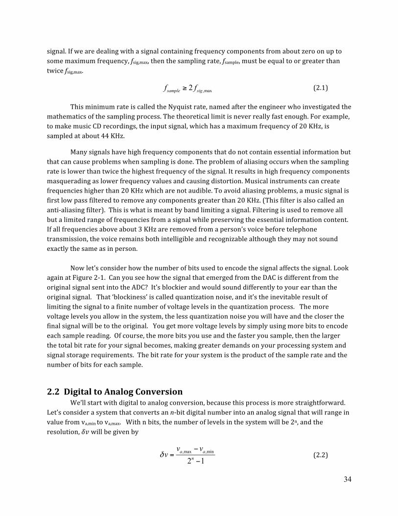
One circuit that can be used to implement a DAC is a weighted summing amplifier. An example of a 4-‐bit weighted summer DAC is shown in Figure 2-‐2 below. This circuit converts the 4-‐bit number given by b3b2b1b0 into a voltage. VHI is the voltage level corresponding to a high for the digital signal. Notice how the resistors in the input branches of the circuit progress by powers of two, with the largest input resistor corresponding to the least significant bit.
Figure 2-2: 4-Bit Weighted Summer DAC Analyzing this circuit, you would have the following equation for the output voltage (with
the powers of two explicitly written out for emphasis):
0 3 2 1 03 2 1 00 0 0 02 2 2 2F F F F
HIR R R Rv V b b b bR R R R
⎛ ⎞= − + + +⎜ ⎟
⎝ ⎠ (2.3)
Simplifying this expression,
( )3 2 1 00 3 2 1 0
0
2 2 2 2HI FV Rv b b b bR
= − + + + (2.4)
So the output voltage for this circuit is the decimal conversion of the binary number with a scale factor of –VHIRF/R0. The resolution for this DAC can be related to its component values as follows:
RF
R0
R0/2
R0/4
R0/8
+VHI
+VCC
-VEE
Vout
b2
b1
b3
b0
36
0
HI FV RvR
δ = (2.5)
As an example, imagine that you wish to convert a 4-‐bit digital signal into an analog voltage with a total range of 0 to –15 V, and that a logical ‘1’ in your digital system is represented by 5V. You would use (2.2) to determine the desired resolution:
4
0V ( 15V) 1V2 1
vδ − −= =
− (2.6)
Then you would choose values for the input resistors. For op-‐amp circuits, its best to keep all resistor values between 1 kΩ and 1 MΩ. A good choice here would be to set R0 to 80 kΩ, which makes the smallest resistor in the input branches 10 kΩ (for the b3 input). You would then use (2.5) to determine the necessary value for RF.
0 1V 80kΩ 16kΩ5VF
HI
v RRVδ ⋅ ⋅
= = = (2.7)
This circuit can be easily modified for fewer or more bits. For a 3-‐bit DAC, for example, you would remove the b2 branch of the circuit. Or for a 5-‐bit DAC you would add a branch for b4 with a resistor value of R0/16. In either case, the resolution is still given by (2.5). The output can also be inverted by a unity-‐gain, inverting amplifier if a positive output voltage is desired.
2.3 Analog to Digital Conversion How about the analog to digital conversion process? It turns out then when you consider
the process of going from analog to digital, the relationship between the step size and the full voltage range is given by:
,max ,min
2a a
n
v vvδ
−= (2.8)
Why the difference from the digital-‐to-‐analog process? Because when you are converting from analog to digital you are collapsing a voltage range into a single value. Let’s say you are converting an analog voltage ranging from 0 to 4 V into a 2-‐bit number. One approach would be to convert 0-‐1 V into 00, 1-‐2 V into 01, 2-‐3 V into 10, and 3-‐4 V into 11. Note that the maximum quantization error for this scheme is the same as the step size. A better approach is to offset the voltage levels by half a step size, so in this example 0-‐0.5 would convert to 00, 0.5-‐1.5 to 01, 1.5-‐2.5 to 10 and 2.5-‐4.0 to 11. The maximum quantization error for this scheme is still the step size, but for most of the voltage range, the quantization error is only half a step.
There are a number of methods used to convert analog to digital. Here we will look at a method used for high-‐speed conversion called “Flash ADC,” but there are many other ADC methods. First, however, we need to understand an op-‐amp circuit called a comparator.
37
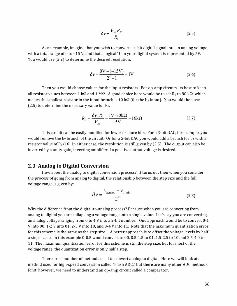
2.3.1 The Comparator A comparator is an op-‐amp operating without feedback. We are sometimes so used to op-‐
amps with negative feedback that we forget that the op-‐amp is really a very simple device, with the voltage transfer characteristic shown below in Figure 2-‐3. With negative feedback, you keep in the op-‐amp in the region where ε~ 0, but when you remove the feedback you no long place any constraints on ε.
Figure 2-3: A comparator is an op-amp operating without feedback. Its transfer function is shown on the right.
So, the comparator is actually a very basic A to D converter. It accepts an analog input, and outputs one of two values that are determined by the power supplies to the op-‐amp. The output of this circuit can be summarized as follows:
00
out S
out S
V VV V
ε
ε+
−
= >
= < (2.9)
VS+ and VS-‐ don’t need to be symmetric, so you can set VS+ to VHI for your logic system and VS-‐ to VLO, to create a 1-‐bit A/D converter. Comparators are used in most multiple-‐bit A/D converters as well, as we shall see in the Flash ADC.
2.3.2 Flash ADC Flash ADC is one of the fastest ADC techniques, because unlike other methods it is fully
parallel. We shall see, however, that this method does not easily scale to systems with many bits. A block diagram for a Flash ADC (this shows a 3-‐bit system) is shown in Figure 2-‐4 below.
VinVREF
Vout
VS+
VS-
+ε-
VS+
VS-
Vout
ε
38
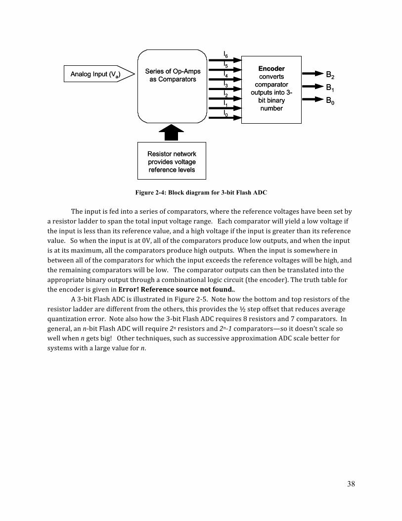
Figure 2-4: Block diagram for 3-bit Flash ADC The input is fed into a series of comparators, where the reference voltages have been set by
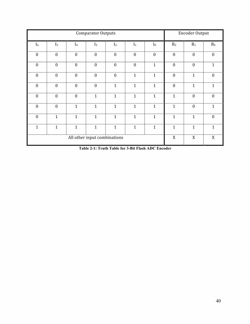
a resistor ladder to span the total input voltage range. Each comparator will yield a low voltage if the input is less than its reference value, and a high voltage if the input is greater than its reference value. So when the input is at 0V, all of the comparators produce low outputs, and when the input is at its maximum, all the comparators produce high outputs. When the input is somewhere in between all of the comparators for which the input exceeds the reference voltages will be high, and the remaining comparators will be low. The comparator outputs can then be translated into the appropriate binary output through a combinational logic circuit (the encoder). The truth table for the encoder is given in Error! Reference source not found..
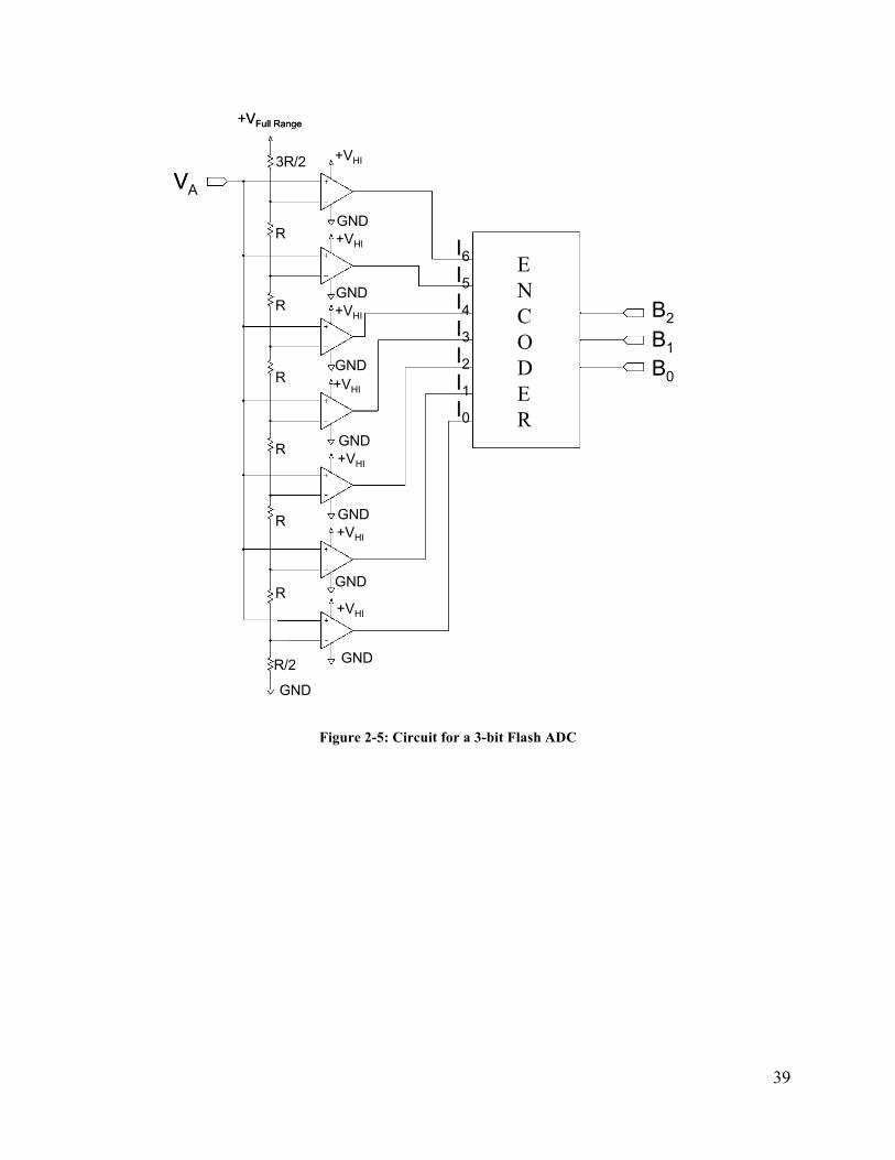
A 3-‐bit Flash ADC is illustrated in Figure 2-‐5. Note how the bottom and top resistors of the resistor ladder are different from the others, this provides the ½ step offset that reduces average quantization error. Note also how the 3-‐bit Flash ADC requires 8 resistors and 7 comparators. In general, an n-‐bit Flash ADC will require 2n resistors and 2n-‐1 comparators—so it doesn’t scale so well when n gets big! Other techniques, such as successive approximation ADC scale better for systems with a large value for n.
Analog Input (Va)Series of Op-Amps
as Comparators
Resistor network provides voltage reference levels
Encoderconverts
comparator outputs into 3-
bit binary number
B2
B1
B0
I6I5I4I3I2I1I0
Analog Input (Va)Series of Op-Amps
as Comparators
Resistor network provides voltage reference levels
Encoderconverts
comparator outputs into 3-
bit binary number
B2
B1
B0
I6I5I4I3I2I1I0
39
Figure 2-5: Circuit for a 3-bit Flash ADC
B2B1B0
VA
+VFull Range
+VHI
+VHIGND
+VHIGND
+VHIGND
+VHIGND
+VHIGND
+VHI
GND
GND
GND
I6I5I4I3I2I1I0
R
R
R
R
R
3R/2
R
R/2
ENCODER
B2B1B0
VA
+VFull Range
+VHI
+VHIGND
+VHIGND
+VHIGND
+VHIGND
+VHIGND
+VHI
GND
GND
GND
I6I5I4I3I2I1I0
R
R
R
R
R
3R/2
R
R/2
ENCODER
40
Comparator Outputs Encoder Output
I6 I5 I4 I3 I2 I1 I0 B2 B1 B0
0 0 0 0 0 0 0 0 0 0
0 0 0 0 0 0 1 0 0 1
0 0 0 0 0 1 1 0 1 0
0 0 0 0 1 1 1 0 1 1
0 0 0 1 1 1 1 1 0 0
0 0 1 1 1 1 1 1 0 1
0 1 1 1 1 1 1 1 1 0
1 1 1 1 1 1 1 1 1 1
All other input combinations X X X
Table 2-1: Truth Table for 3-Bit Flash ADC Encoder
41
2.4 Homework Problems Problem 2.1. Music for a CD is sampled at 44.1 kHz, with 16 bits for each sample.
a. What is the bit rate for a CD? b. How many bits are required to store a 2 minute song? c. If the capacity of a CD is 700 MB, how many minutes of music can be stored on a single
disk? d. If original analog audio signal had a range of 5V, what is the step size or maximum
quantization error, for the analog-‐to-‐digital conversion? Problem 2.2. In order to definitively answer the question about a tree falling in the forest with no one to hear it, Dr. Zen plans to record forest sounds. The frequencies generated by a falling tree range from nearly DC to 10 kHz, and Dr. Zen also plans to capture the gentle call of the birds, which can go as high as 15 kHz.
a. What sample frequency should Dr. Zen use? b. If he were to use an anti-‐aliasing filter at the input to his ADC (to prevent higher
frequency signals from interfering with his experiment), what should the cut-‐off frequency for that filter be?
Problem 2.3. Design a 3-‐bit DAC with a step-‐size of 1 V assuming a logic system where 5V is the logic high. What would be the output voltage range for this DAC? Problem 2.4. Design a 4-‐bit DAC with a step-‐size of 0.2 V assuming a logic system where 5V is the logic high. What would be the output voltage range for this DAC? Problem 2.5. How many resistors would be required for a 16-‐bit Flash ADC? How many comparators would be required? Problem 2.6 Design a 2-‐bit Flash ADC for an input voltage range of 5V. You can leave the encoder as a block. Problem 2.7. Design the combinational logic circuit for the encoder in problem 2.6. Problem 2.8. Look up the successive approximation ADC method on the web and describe how this technique works. Successive approximation ADCs are slower than Flash ADCs, but scale better to large bit systems.
42
Chapter 3: Introduction to Communications 3.1 Introduction Electronic communications is the transfer of information from one location to another. Distances involved can be as little as a few inches over bus lines within a computer or as much as hundreds of thousands of miles for video information from a deep space probe. It would be difficult to find another area of technology which touches more people’s lives. Modern communications systems include television, radio, telephone, the global positioning system (GPS), and Internet. This list could go on and on. Today’s communications systems are often mixes of older technologies such as amplitude and frequency modulation (AM and FM) and newer technologies such as fiber optics, GPS, satellites and digital communications. Communications is a very dynamic area with advances being made every day. One area which is very active is digital communications. HDTV will use a digital format and is not too far off. Several local TV stations already have transmitter facilities for HDTV. Digital communications is very important to the military (for one thing it lends itself well to encryption). Therefore, a section on digital communications has been included in these notes. To master more than a small part of communications would take years of study (a career). These notes are intended to be a short overview of several areas in this field.
3.2 Communication Systems The primary function of a communication system is to transfer information from one location to another. A block diagram of a generalized communication system is shown in Figure3-‐.1.
Figure 3-1: Block Diagram of a Communication System.
We have already studied many of the circuits and the functions they perform which are used in communications systems. We have studied filters and amplifiers, both important building blocks.
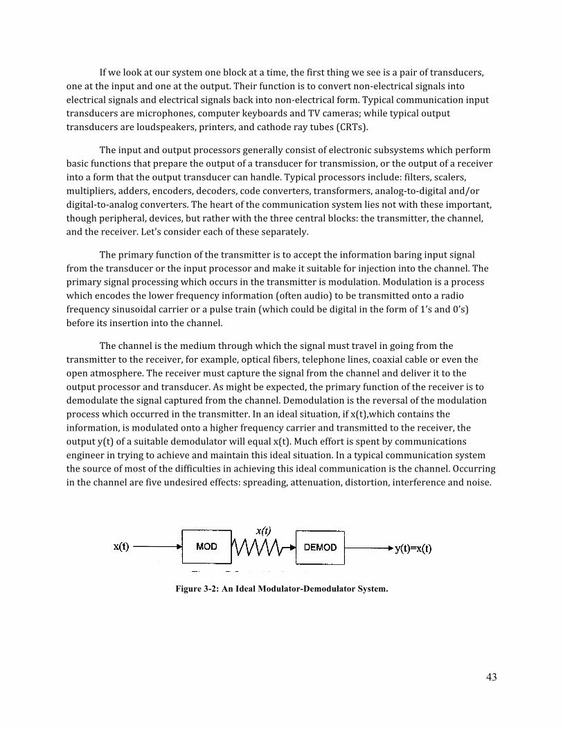
43
If we look at our system one block at a time, the first thing we see is a pair of transducers, one at the input and one at the output. Their function is to convert non-‐electrical signals into electrical signals and electrical signals back into non-‐electrical form. Typical communication input transducers are microphones, computer keyboards and TV cameras; while typical output transducers are loudspeakers, printers, and cathode ray tubes (CRTs).
The input and output processors generally consist of electronic subsystems which perform basic functions that prepare the output of a transducer for transmission, or the output of a receiver into a form that the output transducer can handle. Typical processors include: filters, scalers, multipliers, adders, encoders, decoders, code converters, transformers, analog-‐to-‐digital and/or digital-‐to-‐analog converters. The heart of the communication system lies not with these important, though peripheral, devices, but rather with the three central blocks: the transmitter, the channel, and the receiver. Let’s consider each of these separately.
The primary function of the transmitter is to accept the information baring input signal from the transducer or the input processor and make it suitable for injection into the channel. The primary signal processing which occurs in the transmitter is modulation. Modulation is a process which encodes the lower frequency information (often audio) to be transmitted onto a radio frequency sinusoidal carrier or a pulse train (which could be digital in the form of 1’s and 0’s) before its insertion into the channel.
The channel is the medium through which the signal must travel in going from the transmitter to the receiver, for example, optical fibers, telephone lines, coaxial cable or even the open atmosphere. The receiver must capture the signal from the channel and deliver it to the output processor and transducer. As might be expected, the primary function of the receiver is to demodulate the signal captured from the channel. Demodulation is the reversal of the modulation process which occurred in the transmitter. In an ideal situation, if x(t),which contains the information, is modulated onto a higher frequency carrier and transmitted to the receiver, the output y(t) of a suitable demodulator will equal x(t). Much effort is spent by communications engineer in trying to achieve and maintain this ideal situation. In a typical communication system the source of most of the difficulties in achieving this ideal communication is the channel. Occurring in the channel are five undesired effects: spreading, attenuation, distortion, interference and noise.
Figure 3-2: An Ideal Modulator-Demodulator System.

45
Chapter 4: Amplitude Modulation
4.1 Introduction When we transfer information from one system or subsystem to another we want the information to be transferred with accuracy and speed. An important technique has been developed and refined over the past 80 years or so which enables us to transfer information and recover it with considerable ease and accuracy. This technique, called modulation, is the process of superimposing low frequency (voice, music) information, or intelligence, onto a high frequency carrier.
The motivation for modulating a signal is primarily two-‐fold. One difficulty associated with signal transmission deals with practical antenna size. Suppose we want to transmit an audio signal the way an AM radio broadcast station does. The spectrum of x(t) would be from about 100 Hz to 5 KHz. It is this spectrum we wish to transmit if we wish to convey all the information of high and low frequencies to our listeners.
From physics we know that if we wish to transmit our signal efficiently, an antenna must be used whose length is about equal to the wavelength of the frequency we want to transmit. Wavelength, λ, and frequency, f, are related by λ= c/f, where c is the speed of light ( 83.10 m/s). So for our worst case of the 100 Hz signal, we would need an antenna 31.87.10 miles long! For the best case, the required length would still be 37 miles. This obviously is impractical.
The second difficulty deals with separating different stations. Suppose that antenna efficiency was not a problem. Once the Federal Communication Commission (FCC) granted a license to one radio station to transmit between 100 Hz and 5000 Hz (The frequency of 5 KHz corresponds to the highest note with, no harmonics, output from the highest pitched instrument the piccolo.), the entire practical audio spectrum would be used up. For example, suppose a second station was allowed to transmit its audio signal. Both stations would be transmitting signals between 100 Hz and 5000 Hz. Receiving antennas could not differentiate between the two and would receive them both. The result is that the sum of the two audio signals would be heard. Of course, if one signal was appreciably stronger than the other, the stronger signal would be heard and the weaker would only act as interference to the stronger. But suppose it was the weaker signal you were interested in. There would be no reasonable way to extract it from the garbled sum (Rush Limbaugh might drown out some good rock music!)
Modulation avoids both difficulties because a carrier frequency represents the center of the transmitted wave. In commercial AM radio stations this is around 1000 KHz (1 MHz). At this frequency a perfectly matched antenna is 984 feet long. This is still quite long, but we can reduce the antenna to one 500th or even one 1000th of its ideal size and make up the loss in signal strength with sufficient gain and selectivity. Furthermore even a bandwidth of max2 f , necessary for a double sideband transmission, is only 10 KHz wide and many stations can
be effectively transmitted side-‐by-‐side by simply placing their respective carriers at least 10 KHz apart. This process is called frequency division multiplexing (FDM). A single channel can accommodate multiple users if the frequency spectrum is divided up. In fact, the FCC, in regards to the commercial AM broadcast band which covers the electromagnetic spectrum from 535 KHz to 1705 KHz, allows stations to have maxf up to 5 KHz and
permits stations to be located 10 KHz apart.
46
4.2 Amplitude Modulation (AM) Amplitude modulation is a form of continuous wave modulation in which the amplitude of a sine wave of some specified frequency, called the carrier, is varied in accordance with the signal containing the information which may be voice or music. Another possibility is to vary the frequency of the carrier in accordance with the information signal. This form of modulation is called FM.
Amplitude modulation is the basis of much of our commercial and amateur broadcast communications. To understand how this technique operates, consider a sinusoidal signal given by
( ) cos( )c c cv t V tω= (4.1) This is called the carrier wave for reasons which will become clear shortly. cV is the amplitude of the
carrier signal and 2c cfω π= is the angular frequency of the carrier which is in the Radio Frequency (RF) band.
These frequencies are much higher than audio frequencies and are typically in the 1 MHz and above range such that 20cf ? KHz. In AM, the carrier is caused to carry information by changing the amplitude according to the
information signal. More specifically we shall write the amplitude of the carrier as follows:
( ) [ ( )]c cV t V kx t= + (4.2)
Where cV is the original carrier amplitude, and x(t) the original signal containing the information to be
transmitted, i.e. the modulating signal. The factor k is for scaling or amplification. Then the resultant modulated wave can be written as
( ) [ ( )]cos( )AM c cv t V kx t tω= + (4.3)
Since x(t) represents a real signal, such as music, it can be represented by an infinite series of sines and cosines, called Fourier components. A Fourier component corresponds to a pure note or a pure tone. It would sound like the signal broadcast by the emergency broadcast system on your radio. Let
( ) cos( ) cos( ) ( )m m m m mkx t kX t V t v tω ω= = = (4.4)
Where mX is the original amplitude of the information signal, which may need to be scaled up or down
by the factor k to allow us to utilize it effectively. We can then write:
( ) [ cos( )]cos( ) [1 cos( )]cos( )AM c m m c c m cv t V V t t V m t tω ω ω ω= + = + (4.5)
The ratio m
c
V mV
= is called the modulation index and indicates the extent of modulation. The time
domain representation of an amplitude modulated signal is shown in Figure 0-‐1.
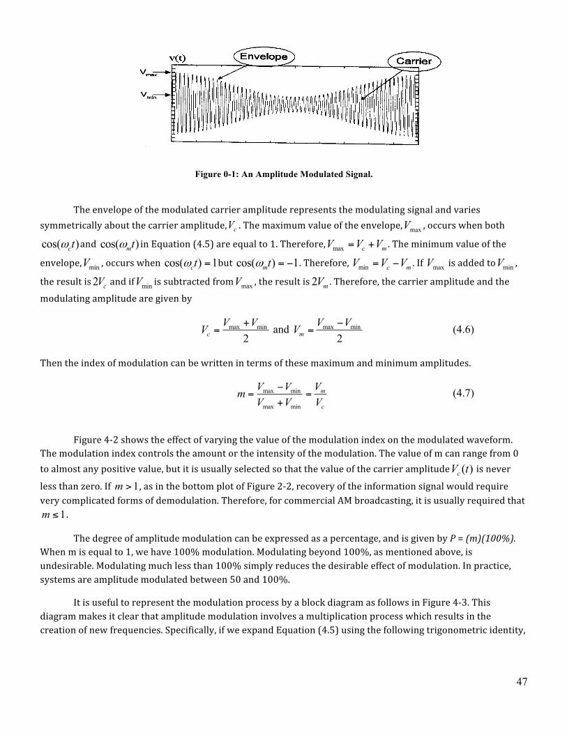
47
Figure 0-1: An Amplitude Modulated Signal.
The envelope of the modulated carrier amplitude represents the modulating signal and varies symmetrically about the carrier amplitude, cV . The maximum value of the envelope, maxV , occurs when both
cos( )ctω and cos( )mtω in Equation (4.5) are equal to 1. Therefore, max c mV V V= + . The minimum value of the
envelope, minV , occurs when cos( ) 1ctω = but cos( ) 1mtω = − . Therefore, min c mV V V= − . If maxV is added to minV ,
the result is 2 cV and if minV is subtracted from maxV , the result is 2 mV . Therefore, the carrier amplitude and the
modulating amplitude are given by
max min
2cV VV +
= and max min
2mV VV −
= (4.6)
Then the index of modulation can be written in terms of these maximum and minimum amplitudes.
max min
max min
m
c
V V VmV V V
−= =
+ (4.7)
Figure 4-‐2 shows the effect of varying the value of the modulation index on the modulated waveform. The modulation index controls the amount or the intensity of the modulation. The value of m can range from 0 to almost any positive value, but it is usually selected so that the value of the carrier amplitude ( )cV t is never less than zero. If 1m > , as in the bottom plot of Figure 2-‐2, recovery of the information signal would require very complicated forms of demodulation. Therefore, for commercial AM broadcasting, it is usually required that
1m ≤ .
The degree of amplitude modulation can be expressed as a percentage, and is given by P = (m)(100%). When m is equal to 1, we have 100% modulation. Modulating beyond 100%, as mentioned above, is undesirable. Modulating much less than 100% simply reduces the desirable effect of modulation. In practice, systems are amplitude modulated between 50 and 100%.
It is useful to represent the modulation process by a block diagram as follows in Figure 4-‐3. This diagram makes it clear that amplitude modulation involves a multiplication process which results in the creation of new frequencies. Specifically, if we expand Equation (4.5) using the following trigonometric identity,
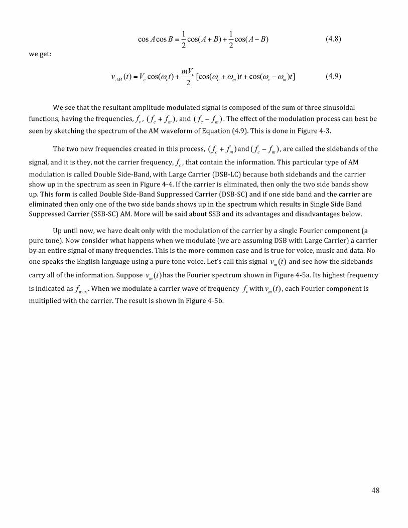
48
1 1cos cos cos( ) cos( )2 2
A B A B A B= + + − (4.8)
we get:
( ) cos( ) [cos( ) cos( ) ]2c
AM c c c m c mmVv t V t t tω ω ω ω ω= + + + − (4.9)
We see that the resultant amplitude modulated signal is composed of the sum of three sinusoidal functions, having the frequencies, cf , ( )c mf f+ , and ( )c mf f− . The effect of the modulation process can best be
seen by sketching the spectrum of the AM waveform of Equation (4.9). This is done in Figure 4-‐3.
The two new frequencies created in this process, ( )c mf f+ and ( )c mf f− , are called the sidebands of the
signal, and it is they, not the carrier frequency, cf , that contain the information. This particular type of AM modulation is called Double Side-‐Band, with Large Carrier (DSB-‐LC) because both sidebands and the carrier show up in the spectrum as seen in Figure 4-‐4. If the carrier is eliminated, then only the two side bands show up. This form is called Double Side-‐Band Suppressed Carrier (DSB-‐SC) and if one side band and the carrier are eliminated then only one of the two side bands shows up in the spectrum which results in Single Side Band Suppressed Carrier (SSB-‐SC) AM. More will be said about SSB and its advantages and disadvantages below.
Up until now, we have dealt only with the modulation of the carrier by a single Fourier component (a pure tone). Now consider what happens when we modulate (we are assuming DSB with Large Carrier) a carrier by an entire signal of many frequencies. This is the more common case and is true for voice, music and data. No one speaks the English language using a pure tone voice. Let’s call this signal ( )mv t and see how the sidebands carry all of the information. Suppose ( )mv t has the Fourier spectrum shown in Figure 4-‐5a. Its highest frequency is indicated as maxf . When we modulate a carrier wave of frequency cf with ( )mv t , each Fourier component is multiplied with the carrier. The result is shown in Figure 4-‐5b.
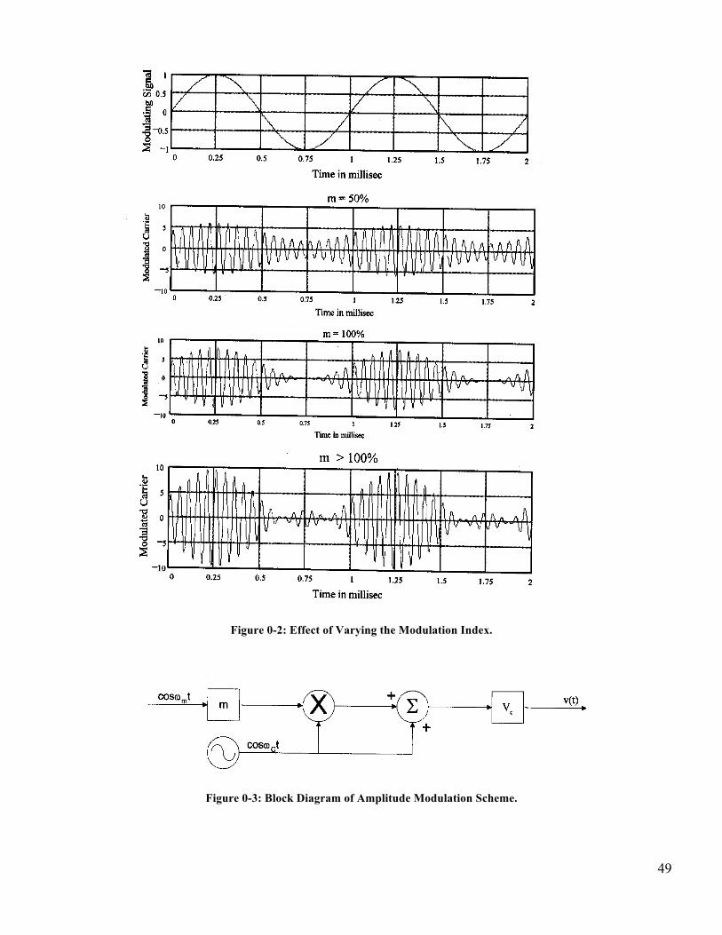
49
Figure 0-2: Effect of Varying the Modulation Index.
Figure 0-3: Block Diagram of Amplitude Modulation Scheme.
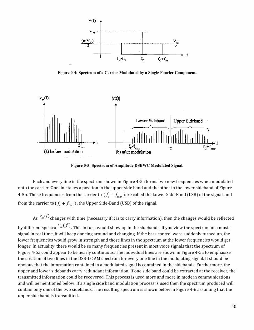
50
Figure 0-4: Spectrum of a Carrier Modulated by a Single Fourier Component.
Figure 0-5: Spectrum of Amplitude DSBWC Modulated Signal.
Each and every line in the spectrum shown in Figure 4-‐5a forms two new frequencies when modulated onto the carrier. One line takes a position in the upper side band and the other in the lower sideband of Figure 4-‐5b. Those frequencies from the carrier to max( )cf f− are called the Lower Side-‐Band (LSB) of the signal, and
from the carrier to max( )cf f+ , the Upper Side-‐Band (USB) of the signal.
As ( )mv t changes with time (necessary if it is to carry information), then the changes would be reflected
by different spectra ( )mv f . This in turn would show up in the sidebands. If you view the spectrum of a music signal in real time, it will keep dancing around and changing. If the bass control were suddenly turned up, the lower frequencies would grow in strength and those lines in the spectrum at the lower frequencies would get longer. In actuality, there would be so many frequencies present in most voice signals that the spectrum of Figure 4-‐5a could appear to be nearly continuous. The individual lines are shown in Figure 4-‐5a to emphasize the creation of two lines in the DSB-‐LC AM spectrum for every one line in the modulating signal. It should be obvious that the information contained in a modulated signal is contained in the sidebands. Furthermore, the upper and lower sidebands carry redundant information. If one side band could be extracted at the receiver, the transmitted information could be recovered. This process is used more and more in modern communications and will be mentioned below. If a single side band modulation process is used then the spectrum produced will contain only one of the two sidebands. The resulting spectrum is shown below in Figure 4-‐6 assuming that the upper side band is transmitted.
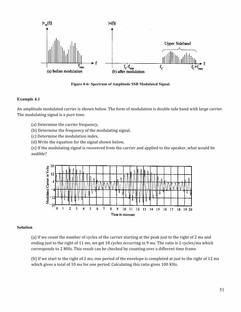
51
Figure 0-6: Spectrum of Amplitude SSB Modulated Signal.
Example 4.1
An amplitude modulated carrier is shown below. The form of modulation is double side band with large carrier. The modulating signal is a pure tone.
(a) Determine the carrier frequency, (b) Determine the frequency of the modulating signal, (c) Determine the modulation index, (d) Write the equation for the signal shown below, (e) If the modulating signal is recovered from the carrier and applied to the speaker, what would be audible?
Solution
(a) If we count the number of cycles of the carrier starting at the peak just to the right of 2 ms and ending just to the right of 11 ms, we get 18 cycles occurring in 9 ms. The ratio is 2 cycles/ms which corresponds to 2 MHz. This result can be checked by counting over a different time frame.
(b) If we start to the right of 2 ms, one period of the envelope is completed at just to the right of 12 ms which gives a total of 10 ms for one period. Calculating this ratio gives 100 KHz.
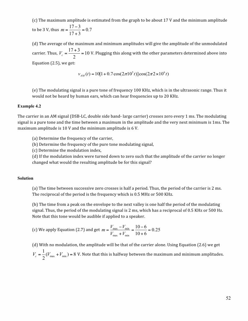
52
(c) The maximum amplitude is estimated from the graph to be about 17 V and the minimum amplitude
to be 3 V, thus 17 3 0.717 3
m −= =
+
(d) The average of the maximum and minimum amplitudes will give the amplitude of the unmodulated
carrier. Thus, 17 3 102cV+
= = V. Plugging this along with the other parameters determined above into
Equation (2.5), we get:
5 6( ) 10[1 0.7cos(2 10 )]cos(2 2 10 )AMv t t tπ π= + ×
(e) The modulating signal is a pure tone of frequency 100 KHz, which is in the ultrasonic range. Thus it would not be heard by human ears, which can hear frequencies up to 20 KHz.
Example 4.2
The carrier in an AM signal (DSB-‐LC, double side band-‐ large carrier) crosses zero every 1 ms. The modulating signal is a pure tone and the time between a maximum in the amplitude and the very next minimum is 1ms. The maximum amplitude is 10 V and the minimum amplitude is 6 V.
(a) Determine the frequency of the carrier, (b) Determine the frequency of the pure tone modulating signal, (c) Determine the modulation index, (d) If the modulation index were turned down to zero such that the amplitude of the carrier no longer changed what would the resulting amplitude be for this signal?
Solution
(a) The time between successive zero crosses is half a period. Thus, the period of the carrier is 2 ms. The reciprocal of the period is the frequency which is 0.5 MHz or 500 KHz.
(b) The time from a peak on the envelope to the next valley is one half the period of the modulating signal. Thus, the period of the modulating signal is 2 ms, which has a reciprocal of 0.5 KHz or 500 Hz. Note that this tone would be audible if applied to a speaker.
(c) We apply Equation (2.7) and get max min
max min
10 6 0.2510 6
V VmV V
− −= = =
+ +
(d) With no modulation, the amplitude will be that of the carrier alone. Using Equation (2.6) we get
max min1 ( ) 82cV V V= + = V. Note that this is halfway between the maximum and minimum amplitudes.
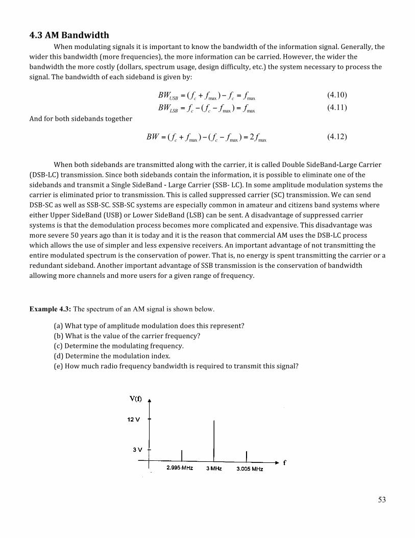
53
4.3 AM Bandwidth When modulating signals it is important to know the bandwidth of the information signal. Generally, the wider this bandwidth (more frequencies), the more information can be carried. However, the wider the bandwidth the more costly (dollars, spectrum usage, design difficulty, etc.) the system necessary to process the signal. The bandwidth of each sideband is given by:
max max( )USB c cBW f f f f= + − = (4.10) max max( )LSB c cBW f f f f= − − = (4.11)
And for both sidebands together
max max max( ) ( ) 2c cBW f f f f f= + − − = (4.12)
When both sidebands are transmitted along with the carrier, it is called Double SideBand-‐Large Carrier (DSB-‐LC) transmission. Since both sidebands contain the information, it is possible to eliminate one of the sidebands and transmit a Single SideBand -‐ Large Carrier (SSB-‐ LC). In some amplitude modulation systems the carrier is eliminated prior to transmission. This is called suppressed carrier (SC) transmission. We can send DSB-‐SC as well as SSB-‐SC. SSB-‐SC systems are especially common in amateur and citizens band systems where either Upper SideBand (USB) or Lower SideBand (LSB) can be sent. A disadvantage of suppressed carrier systems is that the demodulation process becomes more complicated and expensive. This disadvantage was more severe 50 years ago than it is today and it is the reason that commercial AM uses the DSB-‐LC process which allows the use of simpler and less expensive receivers. An important advantage of not transmitting the entire modulated spectrum is the conservation of power. That is, no energy is spent transmitting the carrier or a redundant sideband. Another important advantage of SSB transmission is the conservation of bandwidth allowing more channels and more users for a given range of frequency.
Example 4.3: The spectrum of an AM signal is shown below.
(a) What type of amplitude modulation does this represent? (b) What is the value of the carrier frequency? (c) Determine the modulating frequency. (d) Determine the modulation index. (e) How much radio frequency bandwidth is required to transmit this signal?
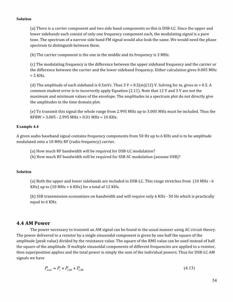
54
Solution
(a) There is a carrier component and two side band components so this is DSB-‐LC. Since the upper and lower sidebands each consist of only one frequency component each, the modulating signal is a pure tone. The spectrum of a narrow side band FM signal would also look the same. We would need the phase spectrum to distinguish between them.
(b) The carrier component is the one in the middle and its frequency is 3 MHz.
(c) The modulating frequency is the difference between the upper sideband frequency and the carrier or the difference between the carrier and the lower sideband frequency. Either calculation gives 0.005 MHz = 5 KHz.
(d) The amplitude of each sideband is 0.5mVc. Thus 3 V = 0.5(m)(12) V. Solving for m, gives m = 0.5. A common student error is to incorrectly apply Equation (2.11). Note that 12 V and 3 V are not the maximum and minimum values of the envelope. The amplitudes in a spectrum plot do not directly give the amplitudes in the time domain plot.
(e) To transmit this signal the whole range from 2.995 MHz up to 3.005 MHz must be included. Thus the RFBW = 3.005 -‐ 2.995 MHz = 0.01 MHz = 10 KHz.
Example 4.4
A given audio baseband signal contains frequency components from 50 Hz up to 6 KHz and is to be amplitude modulated onto a 10 MHz RF (radio frequency) carrier.
(a) How much RF bandwidth will be required for DSB-‐LC modulation? (b) How much RF bandwidth will be required for SSB-‐SC modulation (assume USB)?
Solution
(a) Both the upper and lower sidebands are included in DSB-‐LC. This range stretches from (10 MHz -‐ 6 KHz) up to (10 MHz + 6 KHz) for a total of 12 KHz.
(b) SSB transmission economizes on bandwidth and will require only 6 KHz -‐ 50 Hz which is practically equal to 6 KHz.
4.4 AM Power The power necessary to transmit an AM signal can be found in the usual manner using AC circuit theory. The power delivered to a resistor by a single sinusoidal component is given by one half the square of the amplitude (peak value) divided by the resistance value. The square of the RMS value can be used instead of half the square of the amplitude. If multiple sinusoidal components of different frequencies are applied to a resistor, then superposition applies and the total power is simply the sum of the individual powers. Thus for DSB-‐LC AM signals we have
total c LSB USBP P P P= + + (4.13)
55
An ideal antenna has a radiation resistance R, though an antenna transforms the electrical power into electromagnetic radiation instead of heat. If we assume a pure tone modulation, then the AM power transmitted by an antenna is:
2 2 2 2 2 2 2 2 2
12 4(2 ) 4(2 ) 4 4 2 2c c c
total c c c c c cV m V m V m m m mP P P P P P PR R R
⎛ ⎞= + + = + + = + = +⎜ ⎟
⎝ ⎠ (4.14)
For m = 1, the modulation is maximum and the amplitude of the sidebands is maximum. Under this condition, the power transmitted in the sidebands is maximum, and the total power is
32total cP P= (4.15)
The fraction of the total power sent in the carrier and in each side band is:
2 0.67 67%3
c
total
PP
= = = and
114 0.167 16.7%3 6
2
cLSB USB
total totalc
PP PP P P
= = = = = (4.16)
So even under the best conditions of 100% modulation, the power transmitted in each sideband is only 1/6 of the total power. The 2/3 of the total power used to transmit the carrier is a waste. Since the distance over which communications can be established is a function of the power in the sideband, communication over the same distance can be accomplished with SSB-‐SC as with DSB-‐LC but with 1/6 the power. Power can be conserved by suppressing the carrier and sometimes one of the sidebands. This also means that SSB-‐SC can be transmitted over longer distances than can DSB-‐LC for a given transmitter power. This makes SSB-‐SC attractive for portable transmitters.
Example 2.5: If the following AM signal is applied to an antenna having a radiation resistance of 50 W find the power in the carrier and in each side band and then the ratio of the power in the information part of the signal to the total.
7( ) 20[1 0.8cos(1000 )]cos(10 )AMv t t t= + V
Solution
The amplitude of the carrier is 20 V and the sideband amplitudes are each 0.5(0.8)(20) = 8 V. Thus, 20.5(20) 4
50cP = = W and 20.5(8) 0.64
50USB LSBP P= = = W. The sidebands are the information part of the signal
and have a total power of 2(.64) = 1.28 W while the total power is 4 + 1.28 = 5.28 W. This leads to a ratio of 1.28/5.28 = 0.2424 or 24.24%.
56
4.5 Frequency Division Multiplexing (FDM) As was discussed in section 1.3 one of the primary reasons to modulate low frequency information onto a high frequency carrier is that multiple channels are available. Many different carrier frequencies can be used to carry many different baseband information signals simultaneously through the same transmission medium be it free space or a coaxial cable. The AM or FM tuner has the capability of tuning to many different radio stations. In order to be able to separate different channels, they are arranged such that they do not overlap. They will certainly overlap in the time domain. The signals from many different radio stations will be present on an antenna at anyone time but they do not overlap in frequency. None of the frequency components from one station are normally allowed to overlap and interfere with those from another. This separation in frequency allows a receiver to use a band-‐pass filter to sort through and select just one station. Occasionally, when interference occurs it is because of overlap of frequency components from different stations. Perhaps a CB is broadcasting on an incorrect carrier. It is possible to multiplex several channels onto one transmitting antenna. This is shown in Figure 2-‐6. Here, three different baseband information signals 1( )x t , 2 ( )x t and 3( )x t with corresponding magnitude spectra 1( )x f , 2 ( )x f and 3( )x f are AM modulated onto three different carriers 1f ,
2f and 3f . The composite spectrum is also shown which includes some guard-‐band between each channel. The use of a guard-‐band makes separation of channels at the receiver easier since band-‐pass filters are not perfect. The shapes of each spectrum in Figure 2-‐6 are not meant to convey anything in particular about each signal. They are simply place holders for a range of frequencies and they do convey that each is band limited. That is, the frequency content of each is limited in range up to maxf .
Example 4.6
How many channels can be frequency division multiplexed between 20 MHz and 22 MHz using DSB-‐LC if
max 10f = KHz for each channel and a 2 KHz guard-‐band is to be maintained between the highest frequency of
any channel and the lowest frequency of the next higher channel. Assume that the frequency content of none of the channels is allowed to be less than 20 MHz or greater than 22 MHz. Repeat if SSB is used instead.
Solution
Starting at 20 MHz for DSB each channel plus associated guard-‐band requires max2 22f guardband+ = KHz of
bandwidth. If we divide 2 MHz by 22 KHz, we get 90.9, and so the answer is 90 channels. The upper frequencies of the 91st channel would go past 22 MHz. If SSB is used instead of DSB-‐LC then we get 2000 divided by 12 which gives166.6 and so the answer is 166 channels.
57
Figure 0-7: Composite Spectrum.
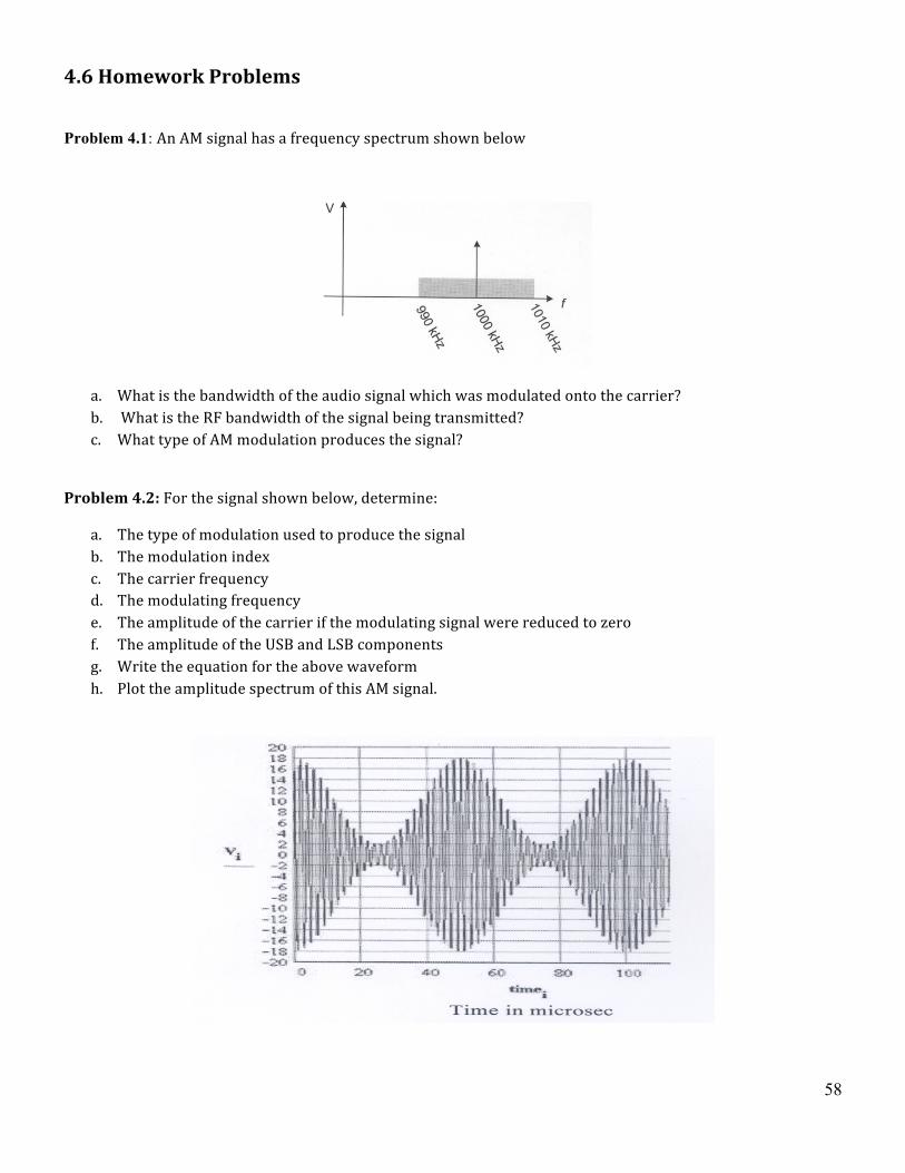
58
4.6 Homework Problems
Problem 4.1: An AM signal has a frequency spectrum shown below
a. What is the bandwidth of the audio signal which was modulated onto the carrier? b. What is the RF bandwidth of the signal being transmitted? c. What type of AM modulation produces the signal?
Problem 4.2: For the signal shown below, determine:
a. The type of modulation used to produce the signal b. The modulation index c. The carrier frequency d. The modulating frequency e. The amplitude of the carrier if the modulating signal were reduced to zero f. The amplitude of the USB and LSB components g. Write the equation for the above waveform h. Plot the amplitude spectrum of this AM signal.
59
Problem 4.3
A 235 KHz carrier is amplitude modulated (DSB-‐LC) by a 5 KHz pure tone. The un-‐modulated amplitude of the output was 250VRMS and the modulation index is 80%.
a. What are the lower and upper sideband frequencies? b. What is the amplitude of the upper sideband component in the frequency spectrum? c. If this AM signal is applied to an antenna which has a radiation resistance of 80 W, determine the total
power in the two side bands together and the power in the carrier. d. How much radio frequency bandwidth does this AM signal occupy?
Problem 4.4: An amplitude modulated waveform is given by the equation:
6 6 6( ) 100cos(1.130 10 ) 45cos(1.0986 10 ) 45cos(1.16 10 )AMv t t t t= × + × + × V
a. What is the percentage of modulation? b. For an RF filter to pass the waveform, what must its minimum bandwidth be? c. Sketch the envelope of the waveform.
Problem 4.5
Assuming AM DSB-‐LC modulation, determine the percentage modulation for each of the following conditions. The same carrier is used for each condition. Determine the peak value of that carrier.
Problem 4.6
A signal 6( ) 40{1 0.7cos(2 500 ) 0.5cos(2 800 )}cos(2 10 )AMv t t t tπ π π= + × + × × V contains not one but two
different modulating frequencies. Thus, there are two different indices of modulation.
a. Determine each index of modulation and the corresponding frequency that it goes with. b. Plot the magnitude spectrum and find the RF bandwidth. c. Use a computer plotting program to sketch the envelope.
Maximum Output Signal Peak-Peak Voltage
Minimum Output Signal Peak-Peak Voltage
a. 100 60
b. 125 35
c. 160 0
60
Problem 4.7 Given the spectrum of an AM signal shown below:
a. Determine the frequency of the modulating signal. b. Determine the RF bandwidth required to transmit this signal. c. Write the equation for this AM signal. d. If this AM signal is applied to an antenna that has a radiation resistance of 200 W find the fraction of the
total power in the information part of the signal.
Problem 4.8
A particular baseband audio signal has frequency components from 50 Hz to 8 KHz. Determine the range of frequencies present and the RF bandwidth for
a. DSB-‐LC b. SSB (Upper sideband) c. DSB-‐SC if the baseband signal is amplitude modulated onto a 2 MHz carrier.
Problem 4.9
When a certain DSB-‐LC AM signal (pure tone modulating signal) is applied to an antenna, 400 W are transmitted at the carrier frequency and 80 W in each of the two sidebands.
a. Determine the modulation index. b. If the amplitude of the un-‐modulated carrier remains the same but the modulation index is changed to
0.6 for the same antenna, find the power in the carrier and the two sidebands.
Problem 4.l 0
Given the total transmitted power in a DSB-‐LC AM wave is 3 KW when the modulation index is 0.7, how much total power should a SSB-‐SC wave contain in order to have the same power content as that contained in the two sidebands together of the DSB-‐LC wave?
61
Problem 4.11
Four different messages are to be transmitted simultaneously by the same antenna by using frequency division multiplexing with four different carriers. Each message has a frequency range from 100 Hz to 3 KHz and a guard-‐band of 2 KHz is to be inserted between adjacent channels to help prevent interference and make demultiplexing easier. If the lowest frequency carrier is 1 MHz, sketch the total magnitude spectrum transmitted by the antenna and find the total RF bandwidth for the Transmitter/Antenna. Assume DSB-‐ LC modulation for each channel.
Problem 4.12
Frequency division multiplexing is used in the communications system shown below in block diagram form.
a. Determine the highest frequency present at point A. b. Determine the lowest frequency present at point B. c. Find the range of frequencies present at points C and D. d. This system provides how much guard-‐band between the audio and instrumentation channels? e. Sketch the frequency spectrum at the output of the transmitter, using nominal amplitudes. f. What is the minimum bandwidth required for the amplifiers in the transmitter?

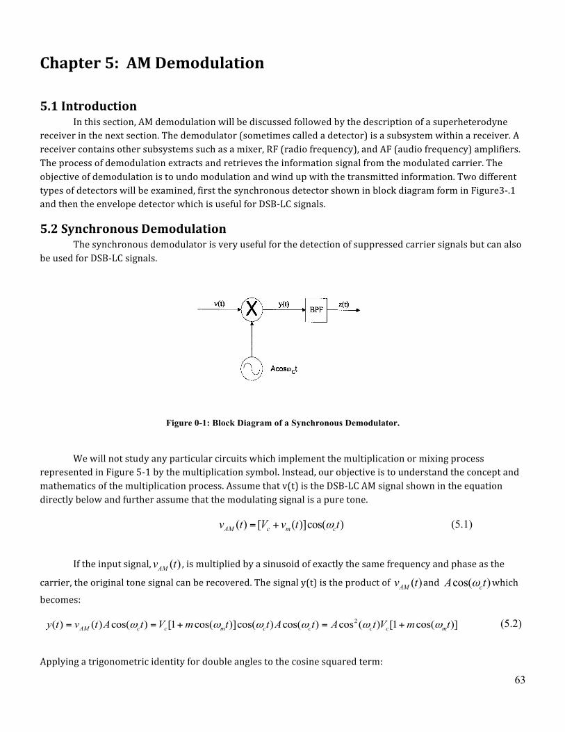
63
Chapter 5: AM Demodulation
5.1 Introduction In this section, AM demodulation will be discussed followed by the description of a superheterodyne receiver in the next section. The demodulator (sometimes called a detector) is a subsystem within a receiver. A receiver contains other subsystems such as a mixer, RF (radio frequency), and AF (audio frequency) amplifiers. The process of demodulation extracts and retrieves the information signal from the modulated carrier. The objective of demodulation is to undo modulation and wind up with the transmitted information. Two different types of detectors will be examined, first the synchronous detector shown in block diagram form in Figure3-‐.1 and then the envelope detector which is useful for DSB-‐LC signals.
5.2 Synchronous Demodulation The synchronous demodulator is very useful for the detection of suppressed carrier signals but can also be used for DSB-‐LC signals.
Figure 0-1: Block Diagram of a Synchronous Demodulator.
We will not study any particular circuits which implement the multiplication or mixing process represented in Figure 5-‐1 by the multiplication symbol. Instead, our objective is to understand the concept and mathematics of the multiplication process. Assume that v(t) is the DSB-‐LC AM signal shown in the equation directly below and further assume that the modulating signal is a pure tone.
( ) [ ( )]cos( )AM c m cv t V v t tω= + (5.1)
If the input signal, ( )AMv t , is multiplied by a sinusoid of exactly the same frequency and phase as the carrier, the original tone signal can be recovered. The signal y(t) is the product of ( )AMv t and cos( )cA tω which
becomes:
2( ) ( ) cos( ) [1 cos( )]cos( ) cos( ) cos ( ) [1 cos( )]AM c c m c c c c my t v t A t V m t t A t A t V m tω ω ω ω ω ω= = + = + (5.2)
Applying a trigonometric identity for double angles to the cosine squared term:
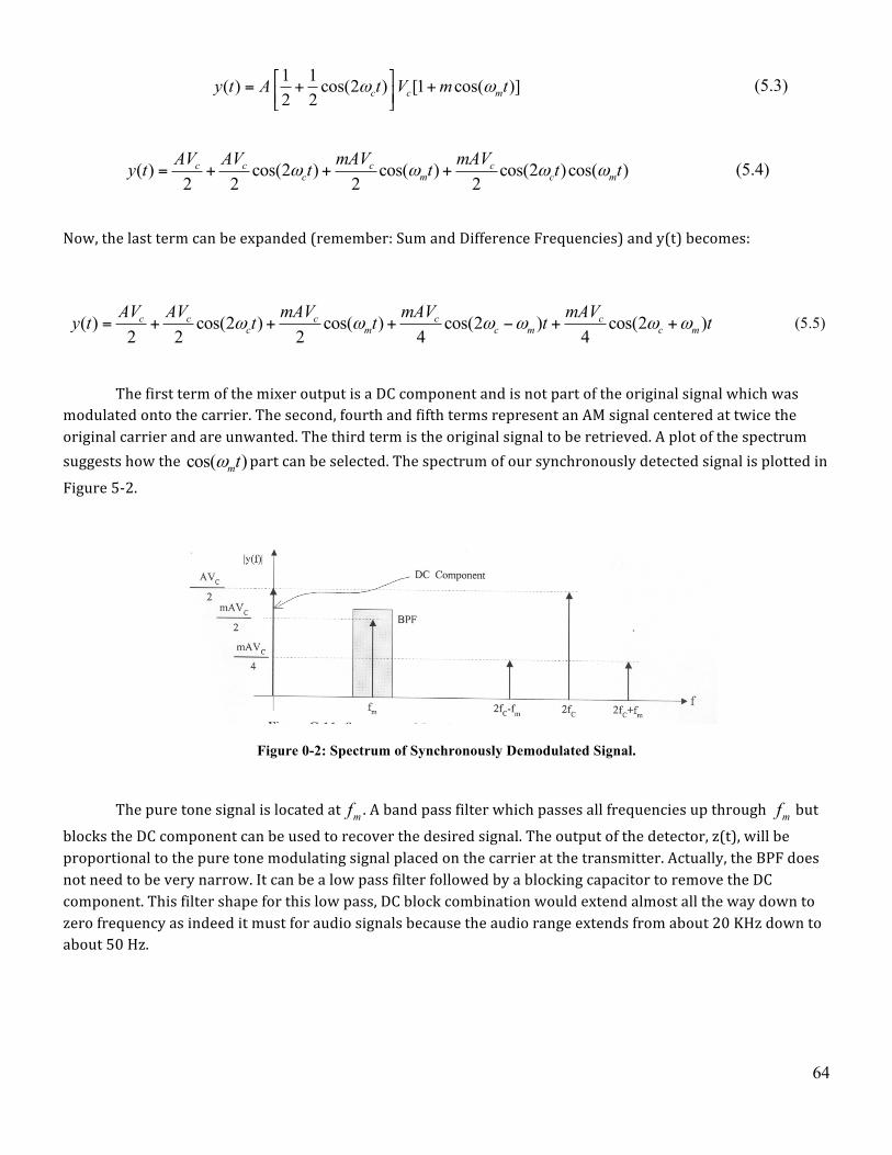
64
1 1( ) cos(2 ) [1 cos( )]2 2 c c my t A t V m tω ω⎡ ⎤= + +⎢ ⎥⎣ ⎦
(5.3)
( ) cos(2 ) cos( ) cos(2 )cos( )2 2 2 2c c c c
c m c mAV AV mAV mAVy t t t t tω ω ω ω= + + + (5.4)
Now, the last term can be expanded (remember: Sum and Difference Frequencies) and y(t) becomes:
( ) cos(2 ) cos( ) cos(2 ) cos(2 )2 2 2 4 4c c c c c
c m c m c mAV AV mAV mAV mAVy t t t t tω ω ω ω ω ω= + + + − + + (5.5)
The first term of the mixer output is a DC component and is not part of the original signal which was modulated onto the carrier. The second, fourth and fifth terms represent an AM signal centered at twice the original carrier and are unwanted. The third term is the original signal to be retrieved. A plot of the spectrum suggests how the cos( )mtω part can be selected. The spectrum of our synchronously detected signal is plotted in
Figure 5-‐2.
Figure 0-2: Spectrum of Synchronously Demodulated Signal.
The pure tone signal is located at mf . A band pass filter which passes all frequencies up through mf but blocks the DC component can be used to recover the desired signal. The output of the detector, z(t), will be proportional to the pure tone modulating signal placed on the carrier at the transmitter. Actually, the BPF does not need to be very narrow. It can be a low pass filter followed by a blocking capacitor to remove the DC component. This filter shape for this low pass, DC block combination would extend almost all the way down to zero frequency as indeed it must for audio signals because the audio range extends from about 20 KHz down to about 50 Hz.
65
The biggest difficulty with synchronous detection is the exact reproduction of the carrier at the location of the receiver. This method will not tolerate any error in phase or frequency of the reproduced carrier. This used to be a bigger problem than it is now with today’s modern integrated circuitry.
Envelope detection can be used for DSB-‐LC AM but not for suppressed carrier transmission. Envelope detectors (to be discussed below) are very inexpensive and easy to build. This is one reason that DSB-‐LC was chosen for the early commercial AM radio system. The home radio receiver had to be practical and inexpensive. The DSB-‐LC commercial AM system persists to this day. If a new commercial AM system were to be built from the ground up today, single side band signals would be used. As stated before, the simple and inexpensive envelope detector cannot be used for SSB transmission, but now, high quality synchronous detectors are cheap and easy to build thanks to more stable oscillators and phase locked loops. Most modern AM communications, such as citizen’s band, is by SSB transmission and uses synchronous detection. Let us consider what happens if v(t) in Figure3-‐.2 is a single side band signal. We will assume USB and pure tone modulation. Then, for( ) cos( )USB c mv t V tω ω= + , y(t) becomes:
( ) [cos( ) ] cos( )USB c m cy t V t A tω ω ω= + (5.6)
And which contains two frequency components, the sum and difference frequencies at (2 )c mω ω+ and mω .
Thus, y(t) can be rewritten as:
( ) cos(2 ) cos( )2 2USB USB
c m mAV AVy t t tω ω ω= + + (5.7)
The first component is at a high frequency and is unwanted. The second is proportional to the original modulating tone and is the part we want. A simple low pass filter will reject the high frequency component and retrieve the information signal. Synchronous detection will also work for LSB or DSB transmission when the carrier is suppressed. Of course the same synchronization problems are present as are for synchronous detection of DSB-‐LC but there are several benefits to be had with SSB-‐SC transmission. First, less bandwidth is used per channel and more channels can be frequency division multiplexed together than can be for DSB-‐LC. Also, no power is wasted in transmission of the carrier and more range can be achieved for a transmitter of the same size and power as a DSB-‐LC transmitter. These factors are important in portable and personal communications systems such as citizen’s band radio (CB).
5.3 Envelope Detection While synchronous demodulation is easy to understand mathematically, in practice it can be difficult to achieve. An oscillator in the receiver must exactly reproduce the sinusoidal carrier. Building a stable oscillator which is precisely tunable to the carrier frequency over a wide range of possible carriers can be difficult. The receiver oscillator must also be in precise phase alignment with the carrier or else significant loss of detected power will occur. Stability of the oscillator is required to avoid a station fading out over time. Nevertheless, many modern communications systems do use some form of synchronous detection in their demodulation schemes.
66
A common demodulation technique which is used for the demodulation of commercial AM is envelope detection. This is the simplest and most economical technique for detecting DSB-‐LC amplitude modulated waves. An envelope detector generally consists of a diode detector and an RC low-‐pass filter as shown in Figure 5-‐3.
In the discussion to follow the amplitude of x(t) is assumed to be much larger than the forward turn on voltage of the diode. We will assume that the diode is essentially ideal. This does bring up a practical point, however. If the signal directly from the antenna were used as input without any amplification, it would generally be too weak for the envelope detector to work properly.
Figure 0-3:Envelope Detector Circuit.
The envelope detector works as follows. During a positive half cycle of the input x(t), the capacitor charges up to the peak value of the carrier at that time. As the input signal falls below this value, the diode becomes reversed biased ( ( )cv t > input) and turns off. Until the next positive peak of x(t) comes along, the capacitor decays exponentially through the resistor. If the RC time constant is large enough, not much decay in capacitor voltage occurs before the next positive peak of x(t). At some point in time near the next positive peak the diode again becomes forward biased and the capacitor charges up to the new peak value. For the right RC time constant the result is a capacitor voltage which basically connects the peaks of the input and therefore yields the upper envelope of the DSB-‐LC AM signal. The detector output is shown in Figure 5-‐4 for several different RC time constants. As long as the modulation index remains below l00 % this upper envelope is the original modulating signal (plus some DC). If the time constant is too short, too much decay in the capacitor voltage will occur between peaks in the input and the output will be too jagged. Therefore, we want the time
constant to be much greater than the period of the carrier or 1c
c
RC Tf
=? . If the time constant is too long the
output will not follow the fastest variations in the envelope. The fastest variations in the envelope are due to the
highest frequency components in the modulating signal. Therefore we want ,min,max
1m
m
RC Tf
== where ,maxmf
is the maximum frequency of the modulating signal. It turns out that the geometric mean of these two periods is
a good choice, or ,maxc mRC TT= .
The most important attribute of an envelope detection system is that synchronization is never a problem. Envelope detection is also much simpler and cheaper than synchronous detection. The effect of change in value of the RC time constant is illustrated in Figure 5-‐4 below. In this diagram the output appears as a heavy black line. For the first case the approximation to the envelope is very good. For the second case the RC time constant is too long and the envelope changes too fast for the output of the detector circuit to follow. For the third case the time constant is too short and the output is too jagged. It should be pointed out that the carrier frequency is typically so high that many more cycles would appear than are shown in Figure 5-‐4, where the
67
period of the carrier is shown too long for clarity. Thus, any jagged edge appearing in the detector output is overemphasized in Figure 5-‐4. Also, any rough edges on the output can easily be smoothed by additional low pass filtering.
The output of the envelope detector of Figure 5-‐4 differs in another way from the original baseband signal. It has a DC component. Many baseband signals such as audio do not have any DC component. The DC component is easy to remove from the output of the envelope detector by simply following it with a capacitor which blocks DC current (potentially harmful to speakers). A blocking capacitor in series with the detector, along with the load (e.g. speakers), forms a high pass filter. The only requirement on this blocking capacitor is that its value must be chosen large enough to avoid attenuation of the lower audio frequency components (about 50 Hz).
Figure 0-4:Effect of RC Time-Constant on Diode Detector Output Voltage.
Example 5.1
The block diagram of an AM modulator is shown below. The signal x(t) is an information signal which has the spectrum shown. Baseband frequencies from 100 Hz up to 3 KHz are included in x(t). The carrier frequency is 5 MHz.
(a) Determine the type of AM modulation produced by this system. (b) Sketch the magnitude spectrum of the output of this modulator. (c) What type of AM detector is needed to retrieve x(t) from the AM signal? Characterize this detector.
Solution
(a) Note that this modulator is very similar to the DSB-‐LC modulator shown in Figure3-‐.3 except that the carrier itself is not added to the output of the multiplier. Thus, the carrier will not be included in y(t), only the upper and lower sidebands corresponding to x(t). The product circuit results in the sum and
68
difference frequencies for each and every component of x(t}. Therefore the type of AM modulation is double side band suppressed carrier, DSB-‐SC.
(b) The resulting spectrum which includes all the sum and difference frequencies is shown below.
(c) Because the carrier is missing we must use a synchronous detector like the one shown in Figure3-‐1. The local oscillator of this detector must be set at exactly 5 MHz and at the same cosine phase as the carrier. Because the carrier is suppressed in the AM signal, there will be no DC component in the output of the multiplier of the detector. Hence, the band pass filter can be replaced by a simple low pass filter with a cutoff frequency a little larger than 3 KHz. This points out a potential advantage of suppressed carrier transmission. If the baseband signal had information content down to zero frequency (DC) (this might be the case if the signal were originating from a transducer) then suppressed carrier AM transmission would be a better choice than large carrier because the demodulation process can use a low pass filter and therefore preserve any information down to 0 Hz.
Example 5.2
If the same information signal x(t) from Example 3.1 is modulated onto a 5 MHz carrier by a DSB-‐LC process, determine a suitable time constant for the envelope detector at the receiver.
Solution
The inverse of the carrier frequency is the carrier period and is equal to 0.2 ms and the inverse of 3 KHz, which is the highest frequency in the baseband, is 0.333 ms. The geometric mean of these two periods is
6 3(0.2 10 )(0.333 10 ) 8.165− −× × = ms. If we choose this as our RC time constant, it satisfies the criteria that it
be much greater than the period of the carrier and much smaller than the period for the highest frequency in the information signal.
Example 5.3
Given that 6 6 6( ) 10cos(2 10 ) 4cos(2 1.0002 10 ) 4cos(2 0.9998 10 )AMv t t t tπ π π= + × + × V is input to an envelope
detector, like the one shown in Figure3-‐3, what is the value of the DC content at the output of the detector? What size capacitor should be placed in series with the detector if the expected resistive load to the right of this capacitor is 10 KΩ and frequency content down to 50 Hz is to be preserved by the high pass filter which results from addition of the blocking capacitor?
Solution
Assuming an ideal diode in the detector, the DC level at the output will equal the carrier amplitude which, in this case, is 10 V (the average value of the envelope is equal to the carrier amplitude, see Equation (2.7). For a practical diode, the DC level will be a few tenths of a volt less. To choose a blocking capacitor properly, we must
have the cutoff frequency of the high pass filter approximately equal to12 (50)RC
π = . This results in
6
1 0.31810
Cπ
= = µF. Any value larger than this will do, so the requirement on the blocking capacitor is not
very difficult to meet.
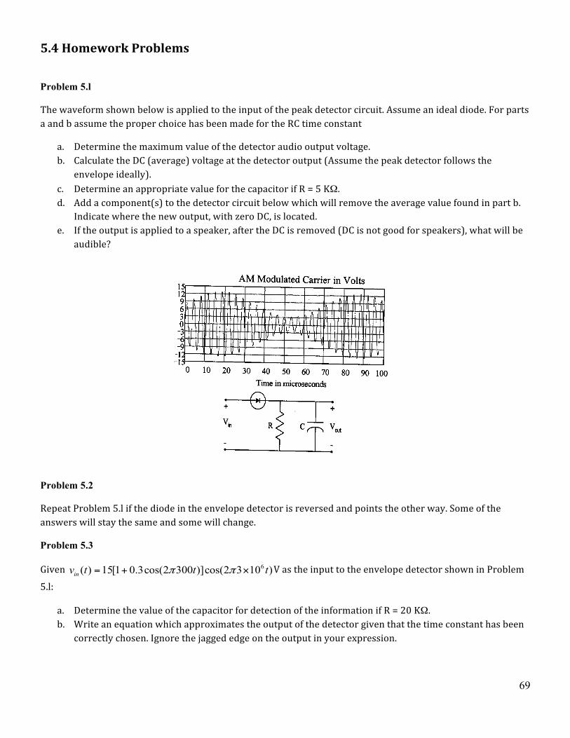
69
5.4 Homework Problems
Problem 5.l
The waveform shown below is applied to the input of the peak detector circuit. Assume an ideal diode. For parts a and b assume the proper choice has been made for the RC time constant
a. Determine the maximum value of the detector audio output voltage. b. Calculate the DC (average) voltage at the detector output (Assume the peak detector follows the
envelope ideally). c. Determine an appropriate value for the capacitor if R = 5 KΩ. d. Add a component(s) to the detector circuit below which will remove the average value found in part b.
Indicate where the new output, with zero DC, is located. e. If the output is applied to a speaker, after the DC is removed (DC is not good for speakers), what will be
audible?
Problem 5.2
Repeat Problem 5.l if the diode in the envelope detector is reversed and points the other way. Some of the answers will stay the same and some will change.
Problem 5.3
Given 6( ) 15[1 0.3cos(2 300 )]cos(2 3 10 )inv t t tπ π= + × V as the input to the envelope detector shown in Problem
5.l:
a. Determine the value of the capacitor for detection of the information if R = 20 KΩ. b. Write an equation which approximates the output of the detector given that the time constant has been
correctly chosen. Ignore the jagged edge on the output in your expression.
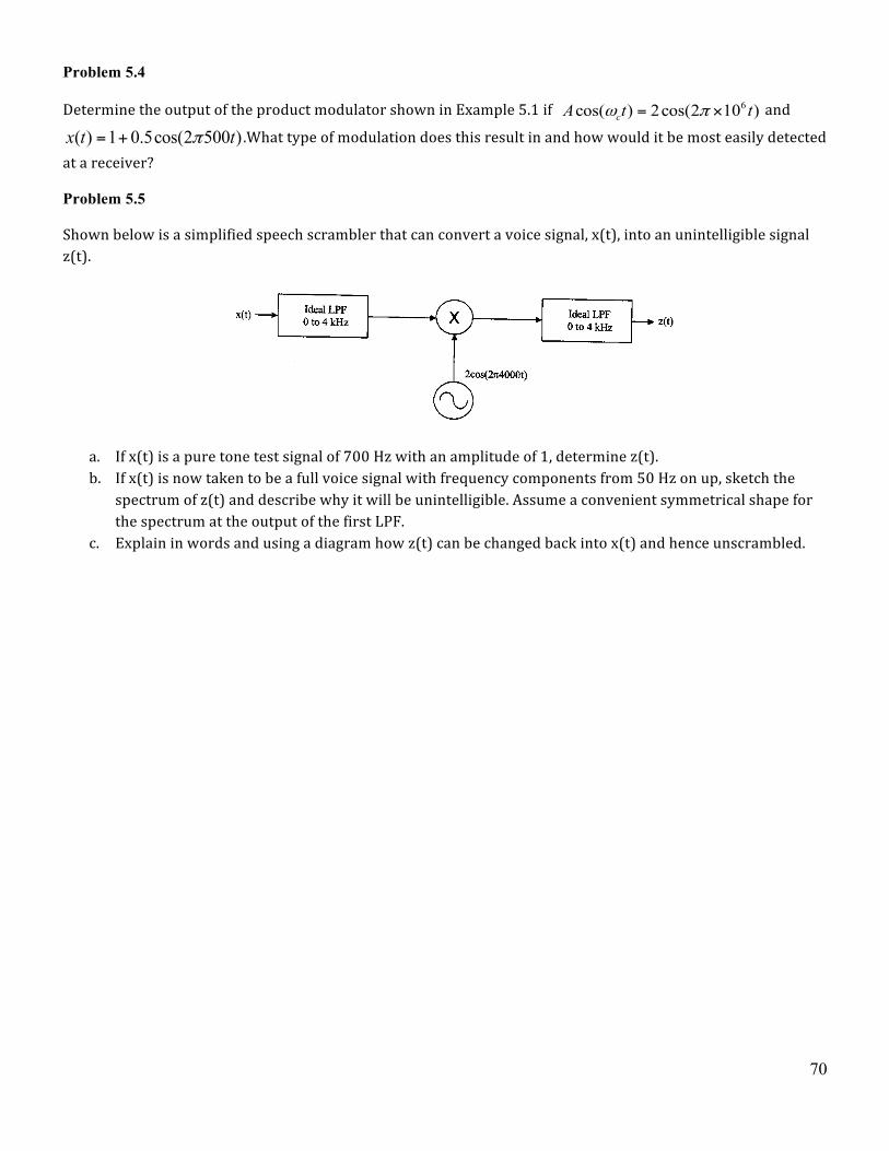
70
Problem 5.4
Determine the output of the product modulator shown in Example 5.1 if 6cos( ) 2cos(2 10 )cA t tω π= × and
( ) 1 0.5cos(2 500 )x t tπ= + .What type of modulation does this result in and how would it be most easily detected at a receiver?
Problem 5.5
Shown below is a simplified speech scrambler that can convert a voice signal, x(t), into an unintelligible signal z(t).
a. If x(t) is a pure tone test signal of 700 Hz with an amplitude of 1, determine z(t). b. If x(t) is now taken to be a full voice signal with frequency components from 50 Hz on up, sketch the
spectrum of z(t) and describe why it will be unintelligible. Assume a convenient symmetrical shape for the spectrum at the output of the first LPF.
c. Explain in words and using a diagram how z(t) can be changed back into x(t) and hence unscrambled.
71
Chapter 6: AM Receivers
6.1 Introduction Simply connecting an antenna to an envelope detector will not make a very good radio. The signal from the antenna would be very weak and unable to produce much if any sound from a speaker. This means that a good radio receiver requires amplification in addition to demodulation. Also, the signals from many stations are gathered at once by an antenna so that simply amplifying and then detecting would result in much interference between stations. A good radio must provide a method for selecting one and only one station at a time. This can be done by band pass filtering because commercial AM stations are frequency division multiplexed. Each station is assigned its own distinct carrier and the frequencies associated with each station are band-‐limited so that they don't overlap the frequencies of an adjacent station. Any good radio receiver must have the property of sensitivity, the ability to pull in weak signals, and the property of selectivity, the ability to select one station and reject the rest without any interference. Selectivity is provided by a band pass filter. It is useful to think of a band pass filter as a window, which if centered at the right location, will allow one particular station to pass through, but no others.
For a radio receiver to be useful, it must be tunable to different channels. If we think of a bandpass filter as a window, then one way to change to a different channel would be to move the window. This can be done by changing the center frequency of a bandpass filter. (For example, a knob can be turned that changes the value of a capacitor.) This type of tuning is used in a tuned-‐radio-‐frequency (TRF) receiver. To provide historical perspective and an alternative to the superheterodyne receiver, the TRF receiver will be discussed briefly. A problem with the TRF receiver is that it is difficult to build a high quality band pass filter at RF (very high) frequencies that is tunable (moveable window) over a wide range of carrier frequencies. The TRF receiver will work but there is a better solution. The superheterodyne receiver can provide superior sensitivity and selectivity. With this method, the window of the bandpass filter is kept fixed at the same frequency and stations are moved, one at a time, into this window by the process of mixing (multiplication). The process of mixing results in moving the locations of radio stations along the frequency axis. Outside the receiver each station has its same familiar carrier but inside the receiver a new “carrier” is produced by the frequency shift resulting from multiplication. Frequency shifting, by the multiplication of signals, is called heterodyning and is used in FM receivers and radar as well as AM receivers. The superheterodyne receiver is discussed in more detail in a separate section below.
6.2 TRF Receiver The block diagram of a tuned radio frequency receiver is shown in Figure 6-‐1. The signal picked up by the antenna is both amplified and filtered by several stages which are simultaneously tuned to a particular carrier. It is these stages which provide both the sensitivity and selectivity. An example of a spectrum input to the RF Amplifier/Filter is shown in Figure 6-‐2 in which the receiver is tuned to the station which is shown shaded at carrier cω . A small amount of guard-‐band is shown in Figure 6-‐2 in order that the sides of the filter
window can be seen. In practice no guard-‐band is provided for commercial AM and the filter sides are less ideal than portrayed in the diagram. How then is interference avoided? Typically radio stations that are assigned adjacent carrier frequencies are in different geographical locations. This keeps stations with adjacent carriers weak enough to minimize interference. Occasionally, under the right atmospheric conditions, stations located far away can skip off certain layers in the atmosphere and cause interference.
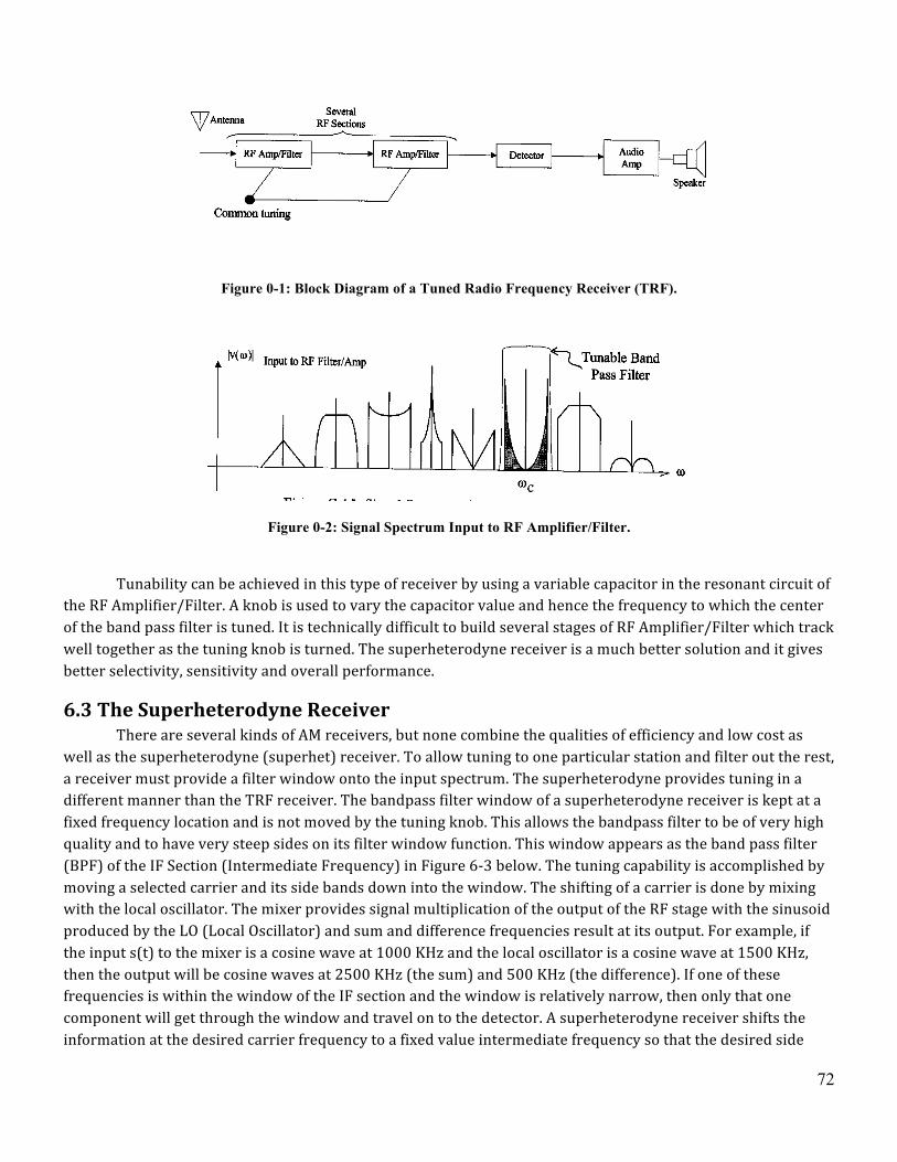
72
Figure 0-1: Block Diagram of a Tuned Radio Frequency Receiver (TRF).
Figure 0-2: Signal Spectrum Input to RF Amplifier/Filter.
Tunability can be achieved in this type of receiver by using a variable capacitor in the resonant circuit of the RF Amplifier/Filter. A knob is used to vary the capacitor value and hence the frequency to which the center of the band pass filter is tuned. It is technically difficult to build several stages of RF Amplifier/Filter which track well together as the tuning knob is turned. The superheterodyne receiver is a much better solution and it gives better selectivity, sensitivity and overall performance.
6.3 The Superheterodyne Receiver There are several kinds of AM receivers, but none combine the qualities of efficiency and low cost as well as the superheterodyne (superhet) receiver. To allow tuning to one particular station and filter out the rest, a receiver must provide a filter window onto the input spectrum. The superheterodyne provides tuning in a different manner than the TRF receiver. The bandpass filter window of a superheterodyne receiver is kept at a fixed frequency location and is not moved by the tuning knob. This allows the bandpass filter to be of very high quality and to have very steep sides on its filter window function. This window appears as the band pass filter (BPF) of the IF Section (Intermediate Frequency) in Figure 6-‐3 below. The tuning capability is accomplished by moving a selected carrier and its side bands down into the window. The shifting of a carrier is done by mixing with the local oscillator. The mixer provides signal multiplication of the output of the RF stage with the sinusoid produced by the LO (Local Oscillator) and sum and difference frequencies result at its output. For example, if the input s(t) to the mixer is a cosine wave at 1000 KHz and the local oscillator is a cosine wave at 1500 KHz, then the output will be cosine waves at 2500 KHz (the sum) and 500 KHz (the difference). If one of these frequencies is within the window of the IF section and the window is relatively narrow, then only that one component will get through the window and travel on to the detector. A superheterodyne receiver shifts the information at the desired carrier frequency to a fixed value intermediate frequency so that the desired side
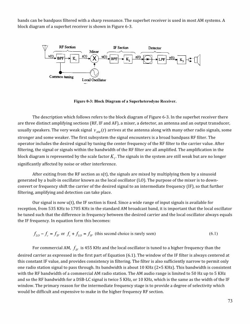
73
bands can be bandpass filtered with a sharp resonance. The superhet receiver is used in most AM systems. A block diagram of a superhet receiver is shown in Figure 6-‐3.
Figure 0-3: Block Diagram of a Superheterodyne Receiver.
The description which follows refers to the block diagram of Figure 6-‐3. In the superhet receiver there are three distinct amplifying sections (RF, IF and AF), a mixer, a detector, an antenna and an output transducer, usually speakers. The very weak signal ( )AMv t arrives at the antenna along with many other radio signals, some stronger and some weaker. The first subsystem the signal encounters is a broad bandpass RF filter. The operator includes the desired signal by tuning the center frequency of the RF filter to the carrier value. After filtering, the signal or signals within the bandwidth of the RF filter are all amplified. The amplification in the block diagram is represented by the scale factor 1K . The signals in the system are still weak but are no longer
significantly affected by noise or other interference.
After exiting from the RF section as s(t), the signals are mixed by multiplying them by a sinusoid generated by a built-‐in oscillator known as the local oscillator (LO). The purpose of the mixer is to down-‐convert or frequency shift the carrier of the desired signal to an intermediate frequency (IF), so that further filtering, amplifying and detection can take place.
Our signal is now u(t), the IF section is fixed. Since a wide range of input signals is available for reception, from 535 KHz to 1705 KHz in the standard AM broadcast band, it is important that the local oscillator be tuned such that the difference in frequency between the desired carrier and the local oscillator always equals the IF frequency. In equation form this becomes:
LO c IFf f f− = or c LO IFf f f+ = (this second choice is rarely seen) (6.1)
For commercial AM, IFf is 455 KHz and the local oscillator is tuned to a higher frequency than the
desired carrier as expressed in the first part of Equation (6.1). The window of the IF filter is always centered at this constant IF value, and provides consistency in filtering. The filter is also sufficiently narrow to permit only one radio station signal to pass through. Its bandwidth is about 10 KHz (2×5 KHz). This bandwidth is consistent with the RF bandwidth of a commercial AM radio station. The AM audio range is limited to 50 Hz up to 5 KHz and so the RF bandwidth for a DSB-‐LC signal is twice 5 KHz, or 10 KHz, which is the same as the width of the IF window. The primary reason for the intermediate frequency stage is to provide a degree of selectivity which would be difficult and expensive to make in the higher frequency RF section.
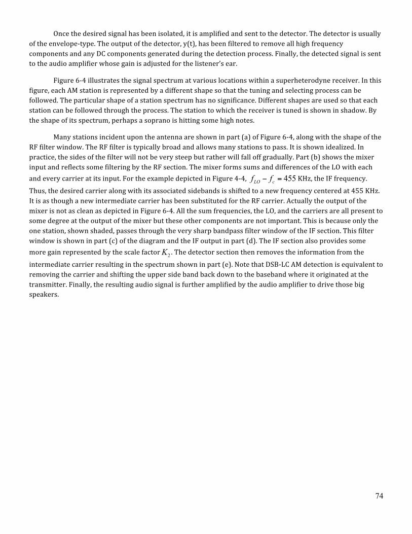
74
Once the desired signal has been isolated, it is amplified and sent to the detector. The detector is usually of the envelope-‐type. The output of the detector, y(t), has been filtered to remove all high frequency components and any DC components generated during the detection process. Finally, the detected signal is sent to the audio amplifier whose gain is adjusted for the listener’s ear.
Figure 6-‐4 illustrates the signal spectrum at various locations within a superheterodyne receiver. In this figure, each AM station is represented by a different shape so that the tuning and selecting process can be followed. The particular shape of a station spectrum has no significance. Different shapes are used so that each station can be followed through the process. The station to which the receiver is tuned is shown in shadow. By the shape of its spectrum, perhaps a soprano is hitting some high notes.
Many stations incident upon the antenna are shown in part (a) of Figure 6-‐4, along with the shape of the RF filter window. The RF filter is typically broad and allows many stations to pass. It is shown idealized. In practice, the sides of the filter will not be very steep but rather will fall off gradually. Part (b) shows the mixer input and reflects some filtering by the RF section. The mixer forms sums and differences of the LO with each and every carrier at its input. For the example depicted in Figure 4-‐4, 455LO cf f− = KHz, the IF frequency.
Thus, the desired carrier along with its associated sidebands is shifted to a new frequency centered at 455 KHz. It is as though a new intermediate carrier has been substituted for the RF carrier. Actually the output of the mixer is not as clean as depicted in Figure 6-‐4. All the sum frequencies, the LO, and the carriers are all present to some degree at the output of the mixer but these other components are not important. This is because only the one station, shown shaded, passes through the very sharp bandpass filter window of the IF section. This filter window is shown in part (c) of the diagram and the IF output in part (d). The IF section also provides some more gain represented by the scale factor 2K . The detector section then removes the information from the
intermediate carrier resulting in the spectrum shown in part (e). Note that DSB-‐LC AM detection is equivalent to removing the carrier and shifting the upper side band back down to the baseband where it originated at the transmitter. Finally, the resulting audio signal is further amplified by the audio amplifier to drive those big speakers.
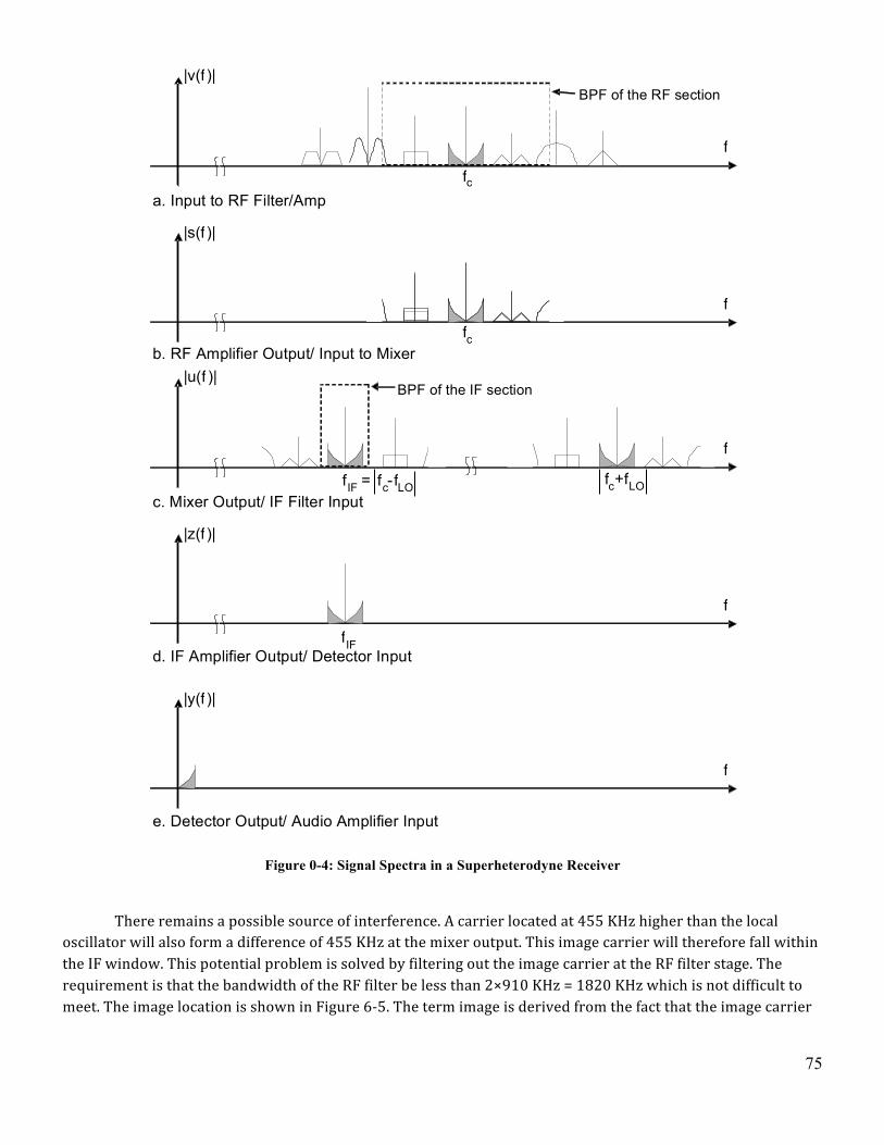
75
Figure 0-4: Signal Spectra in a Superheterodyne Receiver
There remains a possible source of interference. A carrier located at 455 KHz higher than the local oscillator will also form a difference of 455 KHz at the mixer output. This image carrier will therefore fall within the IF window. This potential problem is solved by filtering out the image carrier at the RF filter stage. The requirement is that the bandwidth of the RF filter be less than 2×910 KHz = 1820 KHz which is not difficult to meet. The image location is shown in Figure 6-‐5. The term image is derived from the fact that the image carrier
| v(f )|
f
a. Input to RF Filter/Amp f c
BPF of the RF section
| s(f )|
f
b. RF Amplifier Output/ Input to Mixer f c
| u(f )|
f
c. Mixer Output/ IF Filter Input f c +f LO
| z(f )|
f
d. IF Amplifier Output/ Detector Input
| y(f )|
f
e. Detector Output/ Audio Amplifier Input
f IF = f c - f LO
BPF of the IF section
f IF
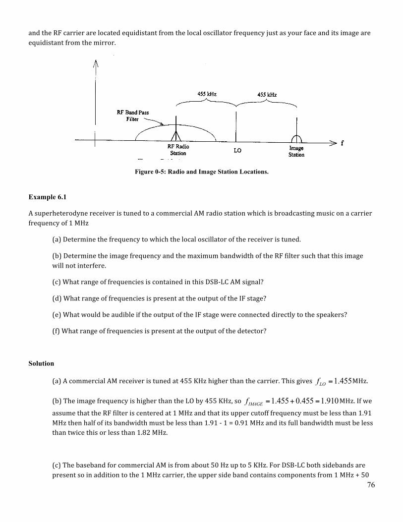
76
and the RF carrier are located equidistant from the local oscillator frequency just as your face and its image are equidistant from the mirror.
Figure 0-5: Radio and Image Station Locations.
Example 6.1
A superheterodyne receiver is tuned to a commercial AM radio station which is broadcasting music on a carrier frequency of 1 MHz
(a) Determine the frequency to which the local oscillator of the receiver is tuned.
(b) Determine the image frequency and the maximum bandwidth of the RF filter such that this image will not interfere.
(c) What range of frequencies is contained in this DSB-‐LC AM signal?
(d) What range of frequencies is present at the output of the IF stage?
(e) What would be audible if the output of the IF stage were connected directly to the speakers?
(f) What range of frequencies is present at the output of the detector?
Solution
(a) A commercial AM receiver is tuned at 455 KHz higher than the carrier. This gives 1.455LOf = MHz.
(b) The image frequency is higher than the LO by 455 KHz, so 1.455 0.455 1.910IMAGEf = + = MHz. If we
assume that the RF filter is centered at 1 MHz and that its upper cutoff frequency must be less than 1.91 MHz then half of its bandwidth must be less than 1.91 -‐ 1 = 0.91 MHz and its full bandwidth must be less than twice this or less than 1.82 MHz.
(c) The baseband for commercial AM is from about 50 Hz up to 5 KHz. For DSB-‐LC both sidebands are present so in addition to the 1 MHz carrier, the upper side band contains components from 1 MHz + 50
77
Hz up to 1 MHz + 5 KHz and the lower sideband contains frequency components from 1 MHz -‐ 5 KHz up to 1 MHz -‐ 50 Hz.
(d) The new carrier at the IF output is 455 KHz. In addition to the 455 KHz carrier there will be the upper side band ranging from 455 KHz + 50 Hz up to 460 KHz (455 + 5) and the lower side band ranging from 450 KHz (455 -‐ 5) up to 455 kHz -‐ 50 Hz.
(e) The listener would hear nothing because all the frequencies listed in part (d) are well above the audible range for humans, which ends at about 20 KHz.
(f) The original baseband, which was an audio signal containing components from 50 Hz up to 5 KHz, appears at the output of the detector.
Example 6.2
When the local oscillator of a superheterodyne receiver is adjusted to 1365 KHz, a 1000 Hz pure test tone is heard from the speakers, indicating that this commercial AM station is broadcasting a test signal.
(a) Determine the RF carrier frequency if the transmitter is a DSB-‐LC commercial transmitter.
(b) Determine the frequency spectrum of the signal at the output of the IF stage of the receiver.
Solution
(a) The local oscillator frequency is 455 KHz higher than the carrier, so
1365 455 910cf = − = KHz.
(b) For pure tone modulation (this is what is heard at the speaker output, so it must be what was modulated onto the carrier at the transmitter) each side band consists of only one component Therefore, the frequencies are 454 KHz, 455 KHz and 456 KHz.
Example 6.3
If the knob of a superheterodyne receiver is tuned to receive the station to the immediate right of the shaded station shown in Figure 6-‐4, draw the changes which will occur in the spectra of Figure 6-‐4.
Solution
The new station will now appear in the IF window and show up at the output of the detector as shown below.
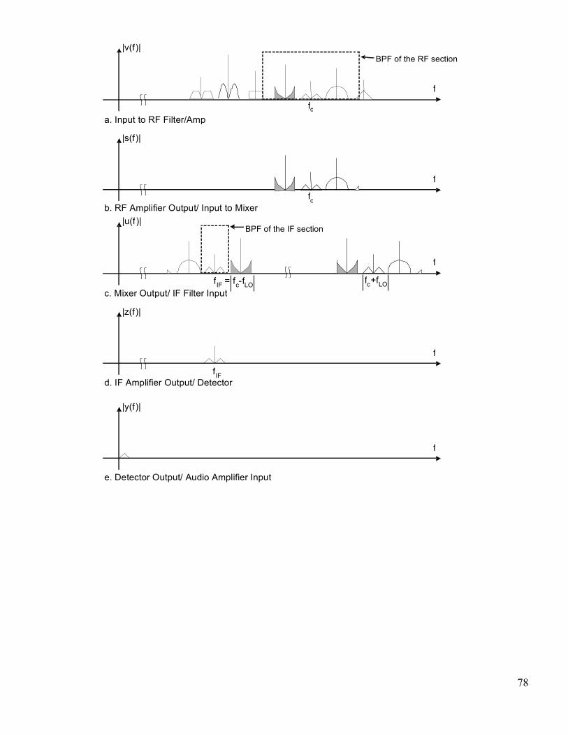
78
| v(f )|
f
a. Input to RF Filter/Amp f c
BPF of the RF section
| s(f )|
f
b. RF Amplifier Output/ Input to Mixer | u(f )|
f
c. Mixer Output/ IF Filter Input f c +f LO
| z(f )|
f
d. IF Amplifier Output/ Detector Input
| y(f )|
f
e. Detector Output/ Audio Amplifier Input
f IF = f c - f LO
BPF of the IF section
f IF
f c
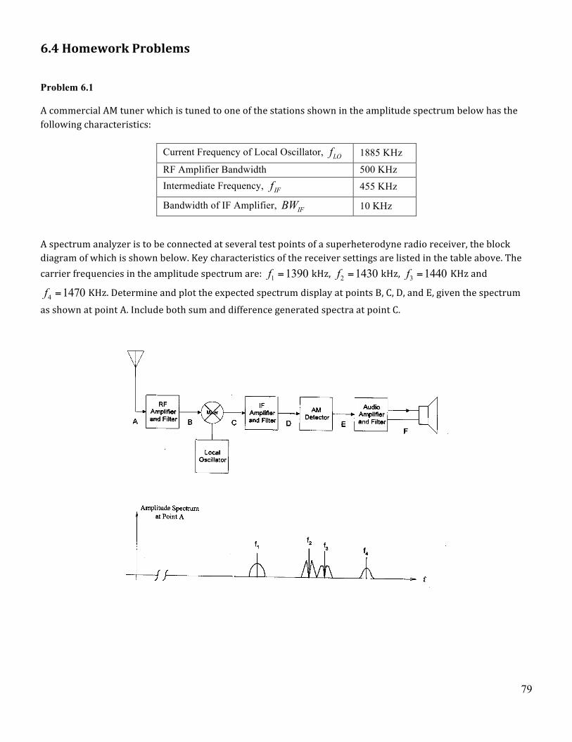
79
6.4 Homework Problems
Problem 6.1
A commercial AM tuner which is tuned to one of the stations shown in the amplitude spectrum below has the following characteristics:
A spectrum analyzer is to be connected at several test points of a superheterodyne radio receiver, the block diagram of which is shown below. Key characteristics of the receiver settings are listed in the table above. The carrier frequencies in the amplitude spectrum are: 1 1390f = kHz, 2 1430f = kHz, 3 1440f = KHz and
4 1470f = KHz. Determine and plot the expected spectrum display at points B, C, D, and E, given the spectrum
as shown at point A. Include both sum and difference generated spectra at point C.
Current Frequency of Local Oscillator, LOf 1885 KHz
RF Amplifier Bandwidth 500 KHz Intermediate Frequency, IFf 455 KHz
Bandwidth of IF Amplifier, IFBW 10 KHz
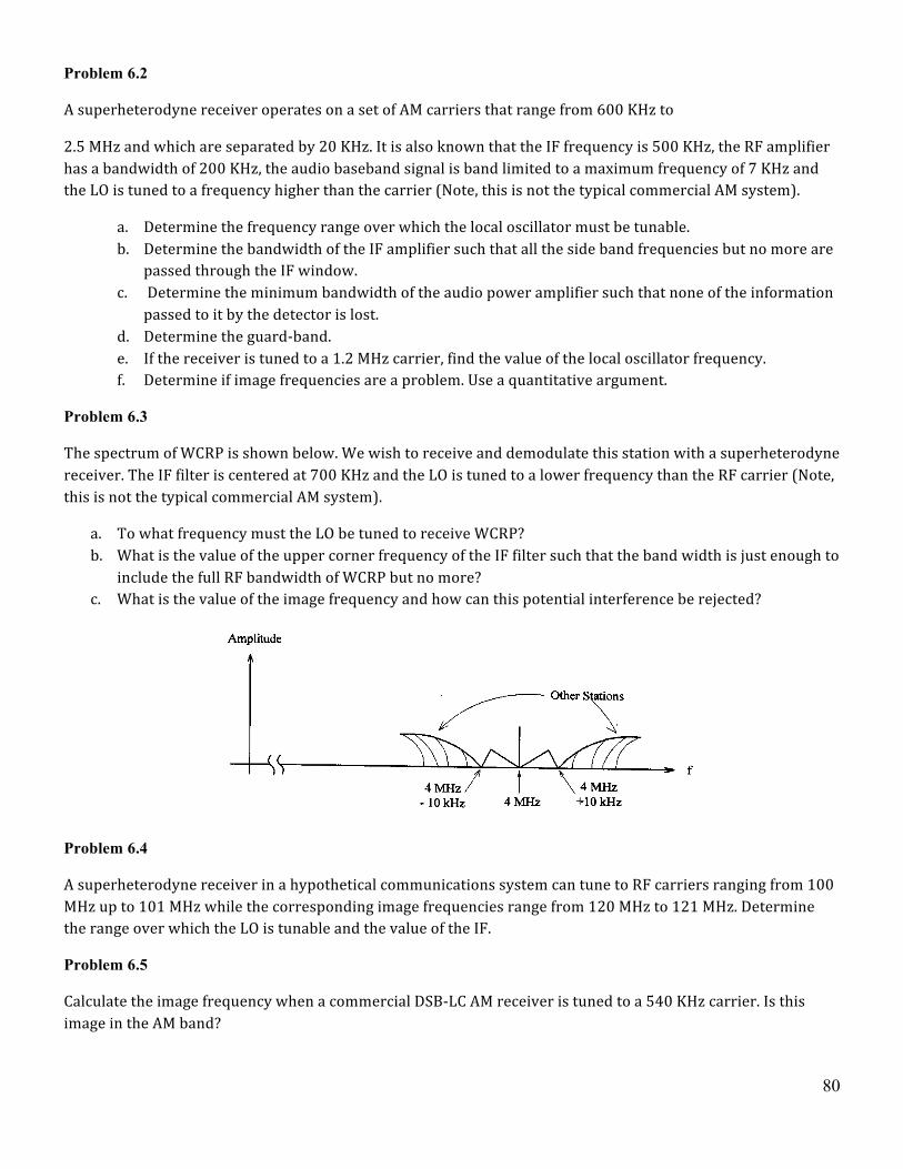
80
Problem 6.2
A superheterodyne receiver operates on a set of AM carriers that range from 600 KHz to
2.5 MHz and which are separated by 20 KHz. It is also known that the IF frequency is 500 KHz, the RF amplifier has a bandwidth of 200 KHz, the audio baseband signal is band limited to a maximum frequency of 7 KHz and the LO is tuned to a frequency higher than the carrier (Note, this is not the typical commercial AM system).
a. Determine the frequency range over which the local oscillator must be tunable. b. Determine the bandwidth of the IF amplifier such that all the side band frequencies but no more are
passed through the IF window. c. Determine the minimum bandwidth of the audio power amplifier such that none of the information
passed to it by the detector is lost. d. Determine the guard-‐band. e. If the receiver is tuned to a 1.2 MHz carrier, find the value of the local oscillator frequency. f. Determine if image frequencies are a problem. Use a quantitative argument.
Problem 6.3
The spectrum of WCRP is shown below. We wish to receive and demodulate this station with a superheterodyne receiver. The IF filter is centered at 700 KHz and the LO is tuned to a lower frequency than the RF carrier (Note, this is not the typical commercial AM system).
a. To what frequency must the LO be tuned to receive WCRP? b. What is the value of the upper corner frequency of the IF filter such that the band width is just enough to
include the full RF bandwidth of WCRP but no more? c. What is the value of the image frequency and how can this potential interference be rejected?
Problem 6.4
A superheterodyne receiver in a hypothetical communications system can tune to RF carriers ranging from 100 MHz up to 101 MHz while the corresponding image frequencies range from 120 MHz to 121 MHz. Determine the range over which the LO is tunable and the value of the IF.
Problem 6.5
Calculate the image frequency when a commercial DSB-‐LC AM receiver is tuned to a 540 KHz carrier. Is this image in the AM band?
81
Chapter 7: Frequency Modulation
7.1 Introduction So far we have investigated the effect of varying the amplitude of a sinusoidal carrier in order to transmit information. We know that it takes three quantities to specify a sinusoid: amplitude, frequency and phase. Modulation is defined as the process of varying some characteristic of the carrier wave in accordance with the instantaneous value of an input signal. Since a sinusoid has other parameters which can be varied, amplitude modulation is not the only means of modulating a sinusoidal carrier. The instantaneous frequency of the carrier can also be varied in accordance with the baseband information signal. This type of modulation is called frequency modulation or FM. It is possible to vary the phase angle instead, which results in PM which will not be discussed here. Suffice it to say that it is very similar to FM.
7.2 Description of the Modulation Process FM results when the frequency of the carrier is made to vary in response to an information signal. Let’s start with the carrier ( ) cos[ ( )]c cv t V tθ= , where normally ( ) ct tθ ω φ= + and the instantaneous angular
frequency is the time derivative of the angle, or( )( ) c
d ttdtθ
ω ω= = . (If you are driving your car at a constant
speed then the time derivative of your location is equal to that speed.)
When the carrier is frequency modulated, the instantaneous frequency becomes a function of time and dependent on the information signal and is given by ( ) ( )inst ct kx tω ω= + where ( )x t is the information signal and k is a conversion parameter resulting from the circuit which converts changes in the amplitude of the information signal into changes in the carrier frequency. Therefore, k has a unit of Hz/V. To make more progress in the analysis of FM we will assume pure tone modulation such that ( ) cos( )m mx t V tω= and the
instantaneous frequency becomes ( ) cos( ) cos( )inst c m m c mt kV t tω ω ω ω ω ω= + = +Δ where ωΔ is called the
frequency deviation and represents the amplitude of the changes in the carrier frequency.
The maximum value of the carrier is cω ω+Δ and the minimum value is cω ω−Δ and the carrier value
is right in between these two values. (Note, if we are measuring and discussing frequency in Hz rather than rad/s then f ’s replace theω ’s, remembering that 2 fω π= ). The result of frequency modulation by a square wave is shown below in Figure 5-‐1. When the square wave has its low value, the period of the carrier is maximum and its frequency minimum. When the square wave has its maximum value the period of the carrier is minimum and the frequency is maximum. The rate at which these changes to the carrier occur is the same as the frequency of the modulating signal. Stated in a different way, the length of time for the frequency to go through one complete cycle of change is the same as the period of the modulating signal. The amount of frequency change in the carrier is proportional to the strength of the modulating signal (its amplitude). For Figure 7-‐1 the difference between the maximum frequency and the minimum frequency is 2 ωΔ , twice the frequency deviation.
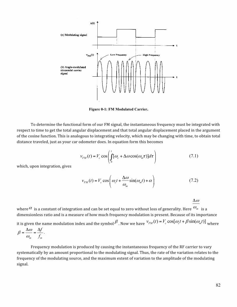
82
Figure 0-1: FM Modulated Carrier.
To determine the functional form of our FM signal, the instantaneous frequency must be integrated with respect to time to get the total angular displacement and that total angular displacement placed in the argument of the cosine function. This is analogous to integrating velocity, which may be changing with time, to obtain total distance traveled, just as your car odometer does. In equation form this becomes
0
( ) cos [ cos( )]t
FM c c mv t V dω ω ω τ τ⎛ ⎞
= +Δ⎜ ⎟⎝ ⎠∫ (7.1)
which, upon integration, gives
( ) cos sin( )FM c c mm
v t V t tωω ω α
ω⎛ ⎞Δ
= + +⎜ ⎟⎝ ⎠
(7.2)
whereα is a constant of integration and can be set equal to zero without loss of generality. Here m
ωωΔ
is a dimensionless ratio and is a measure of how much frequency modulation is present. Because of its importance
it is given the name modulation index and the symbol β . Now we have ( ) cos[ sin( )]FM c c mv t V t tω β ω= + where
m m
ff
ωβ
ωΔ Δ
= = .
Frequency modulation is produced by causing the instantaneous frequency of the RF carrier to vary systematically by an amount proportional to the modulating signal. Thus, the rate of the variation relates to the frequency of the modulating source, and the maximum extent of variation to the amplitude of the modulating signal.
83
One of the problems involved in describing FM is that there are several different frequencies to keep track of. So far, we have the instantaneous frequency, instf , the carrier frequency, cf , the modulating frequency,
mf , and the frequency deviation fΔ . Moreover, all of these must be distinguished from just plain frequency,
which is the independent variable in the frequency domain. If the modulation were turned down to zero the frequency of the sinusoid would be cf , the carrier frequency. As modulation is increased, the frequency of the wave changes back and forth, from high pitch to low pitch to high, etc. at a rate equal to the frequency of the modulating signal. The maximum amount by which the pitch changes, from the starting point of no modulation, is the frequency deviation, fΔ , and depends on the amplitude of the modulating signal.
7.3 FM Spectrum The equation for an FM signal, with pure tone modulation, looks formidable. The function involves the cosine of a sine. Advanced math and Fourier analysis can be used to find the spectrum of an FM signal. The details of the mathematics are beyond the scope of this course or these notes. When an FM wave is broken down to determine its spectral content, it turns out that there are theoretically an infinite number of sideband
frequencies and the amplitudes at these frequencies depend onm
ff
βΔ
= . This sounds a bit complicated but the
results can be summarized easily. The frequency components in an FM signal formed by the frequency modulation of a carrier by a pure tone (single frequency) are summarized below:
cf carrier
c mf f± first sideband (upper and lower)
2c mf f± second sideband (upper and lower)
3c mf f± third sideband (upper and lower)
…
c mf nf± nth sideband (upper and lower)
… and so on to infinity
An FM wave has infinitely many sidebands with only one frequency present in the information signal. For a more realistic multiple component modulating signal (music for example) the situation is even more complicated. Because of its many sidebands, we can anticipate that an FM wave will require a much larger transmission bandwidth than a comparable amplitude modulated wave.
Figure 7-‐2 illustrates several FM spectra and the dependence of the FM spectrum on β . By careful consideration of the relative amplitudes of the components as a function of β a useful rule has been developed which can estimate the total bandwidth of an FM signal. For a given modulation index, there is some frequency beyond which the sidebands can be neglected. For example, for 1β = , everything beyond the third sideband is insignificant. This means that although the FM signal theoretically contains infinitely many frequencies, there is
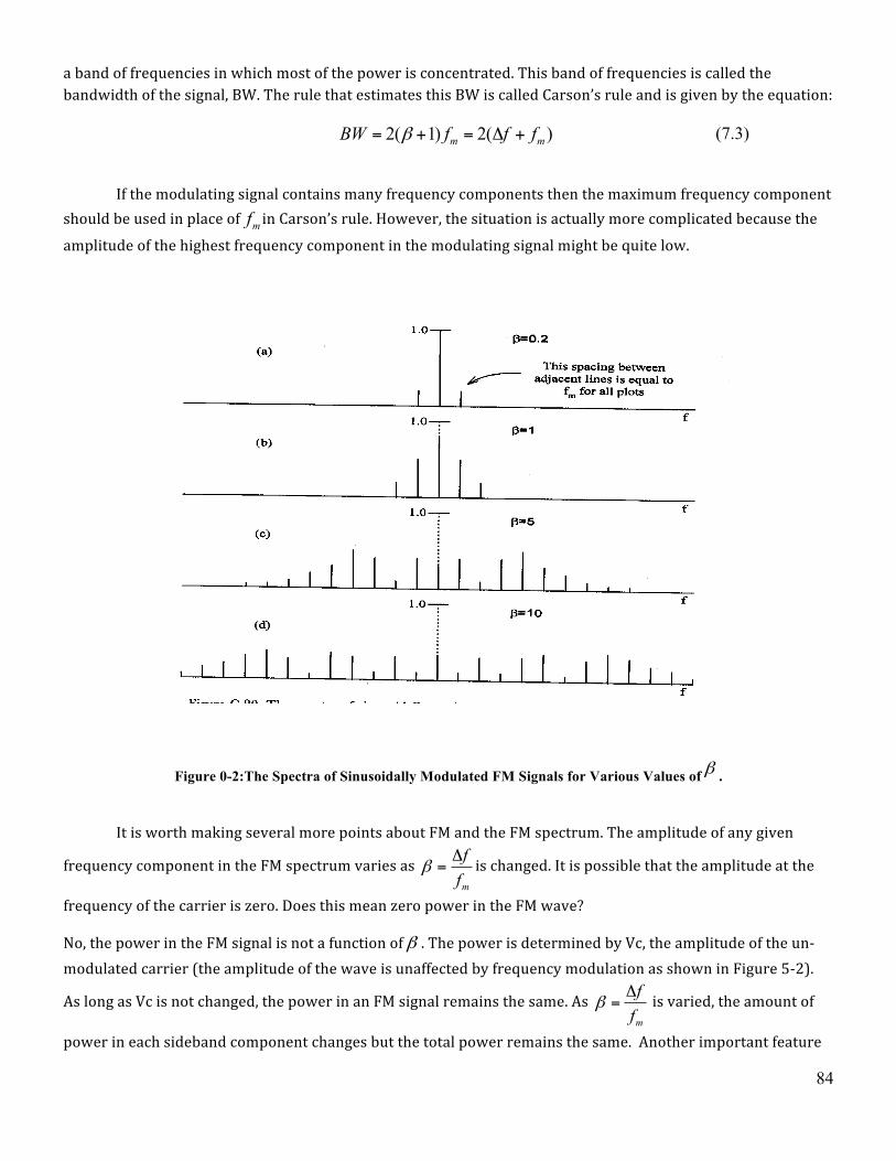
84
a band of frequencies in which most of the power is concentrated. This band of frequencies is called the bandwidth of the signal, BW. The rule that estimates this BW is called Carson’s rule and is given by the equation:
2( 1) 2( )m mBW f f fβ= + = Δ + (7.3)
If the modulating signal contains many frequency components then the maximum frequency component should be used in place of mf in Carson’s rule. However, the situation is actually more complicated because the amplitude of the highest frequency component in the modulating signal might be quite low.
Figure 0-2:The Spectra of Sinusoidally Modulated FM Signals for Various Values of β .
It is worth making several more points about FM and the FM spectrum. The amplitude of any given
frequency component in the FM spectrum varies as m
ff
βΔ
= is changed. It is possible that the amplitude at the
frequency of the carrier is zero. Does this mean zero power in the FM wave?
No, the power in the FM signal is not a function of β . The power is determined by Vc, the amplitude of the un-‐modulated carrier (the amplitude of the wave is unaffected by frequency modulation as shown in Figure 5-‐2).
As long as Vc is not changed, the power in an FM signal remains the same. As m
ff
βΔ
= is varied, the amount of
power in each sideband component changes but the total power remains the same. Another important feature
85
of an FM spectrum is the uniform spacing of the lines. Each line in Figure 7-‐2 is separated from its neighbor by
mf , the modulating frequency.
7.4 Advantages and Disadvantages of FM To conclude this section several advantages and disadvantages of FM compared to AM are listed.
1. The major advantages of FM are:
a) Superior performance in the presence of noise and interference.
b) Smaller geographic interference areas. That is, two FM stations can operate substantially closer without interference compared to two similar AM stations. This is because of the higher carrier frequencies used in commercial FM. Commercial AM carriers have more of a tendency to skip off layers in the Earth’s atmosphere.
c) Less power need be transmitted for same amount of power received compared to DSB-‐LC AM transmission.
2. The major disadvantages of FM are:
a) Up to 20 times more bandwidth is required.
b) FM systems are considerably more complicated.
c) FM is a very non-‐linear process making analysis of FM more difficult than that of AM.
In summary, you may recall from our discussion of AM that the two sidebands (USB and LSB) are redundant since the same information is contained in each. In fact, as we saw, single-‐sideband (SSB) modulation is based on the fact that anyone sideband contains all the necessary information. When we examine the sideband structure of an FM signal, especially a wide band FM signal, we find that the information is replicated many times over. FM is extremely redundant! But it is this redundancy which results in the outstanding noise rejection associated with FM systems. The magnitudes; frequencies and phases of all the sidebands are related to the carrier and to each other in a very specific manner. Because of this precise relationship, the sidebands are said to be coherent with each other and with the carrier. Noise, on the other hand, can be thought of as consisting of a very large collection of sinusoids, each with a random amplitude, frequency and phase.
The many components in the random distribution of noise cannot have the same special relationship to each other and to the carrier that an FM signal has. For this reason, an FM receiver can extract the intricate, but coherent, FM signal out of the incoherent noise much more readily than an AM receiver can extract its signal, which has only two sidebands. The price for the redundancy of the FM signal is increased signal bandwidth. This is in general true for all signal transfer systems. Redundancy improves transfer accuracy and reduces noise, but we pay with bandwidth. In other words we can trade bandwidth for performance or vice versa.
7.5 FM Receiver In order to demodulate the FM signal we need to have a device which produces an output whose amplitude is linearly proportional to the frequency of the input signal. We have already studied such a device. An RLC resonant circuit which has the amplitude response of a band pass filter can do the job provided the proper operating region of the filter is used.
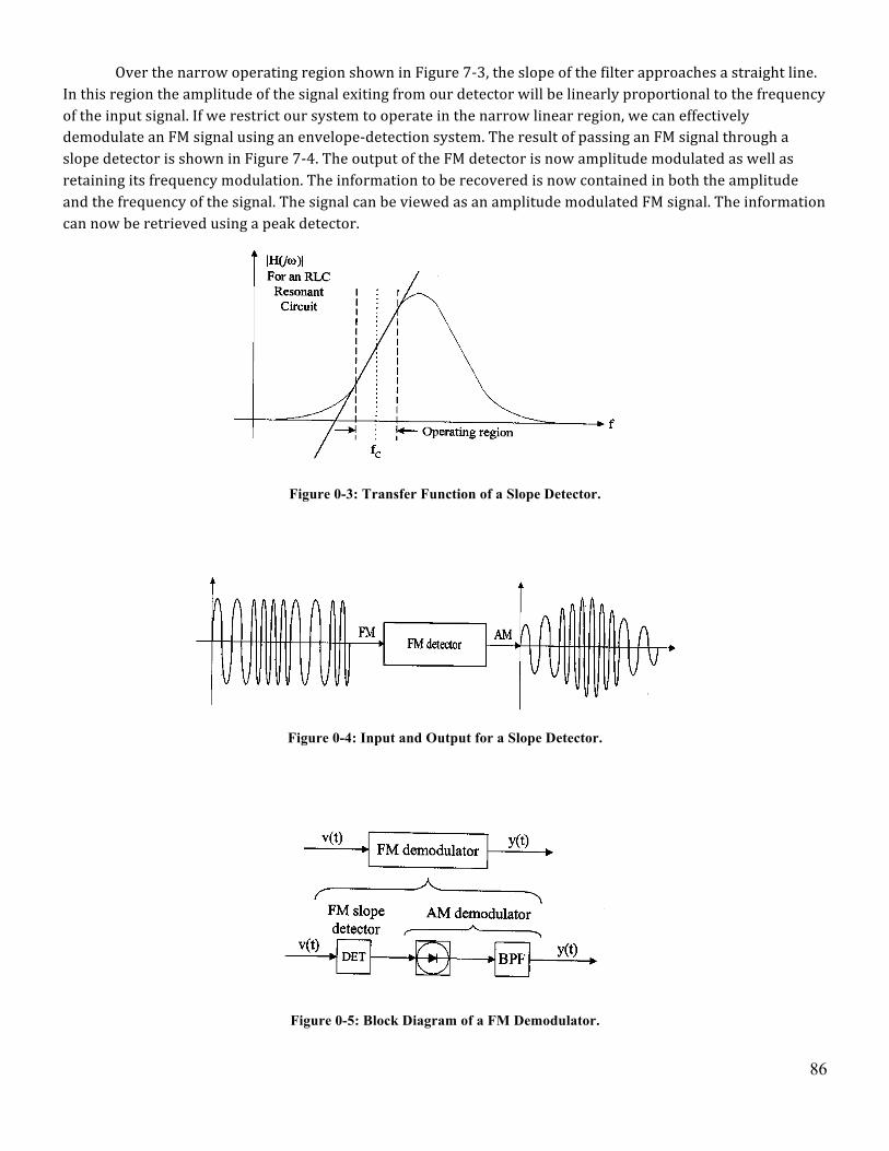
86
Over the narrow operating region shown in Figure 7-‐3, the slope of the filter approaches a straight line. In this region the amplitude of the signal exiting from our detector will be linearly proportional to the frequency of the input signal. If we restrict our system to operate in the narrow linear region, we can effectively demodulate an FM signal using an envelope-‐detection system. The result of passing an FM signal through a slope detector is shown in Figure 7-‐4. The output of the FM detector is now amplitude modulated as well as retaining its frequency modulation. The information to be recovered is now contained in both the amplitude and the frequency of the signal. The signal can be viewed as an amplitude modulated FM signal. The information can now be retrieved using a peak detector.
Figure 0-3: Transfer Function of a Slope Detector.
Figure 0-4: Input and Output for a Slope Detector.
Figure 0-5: Block Diagram of a FM Demodulator.
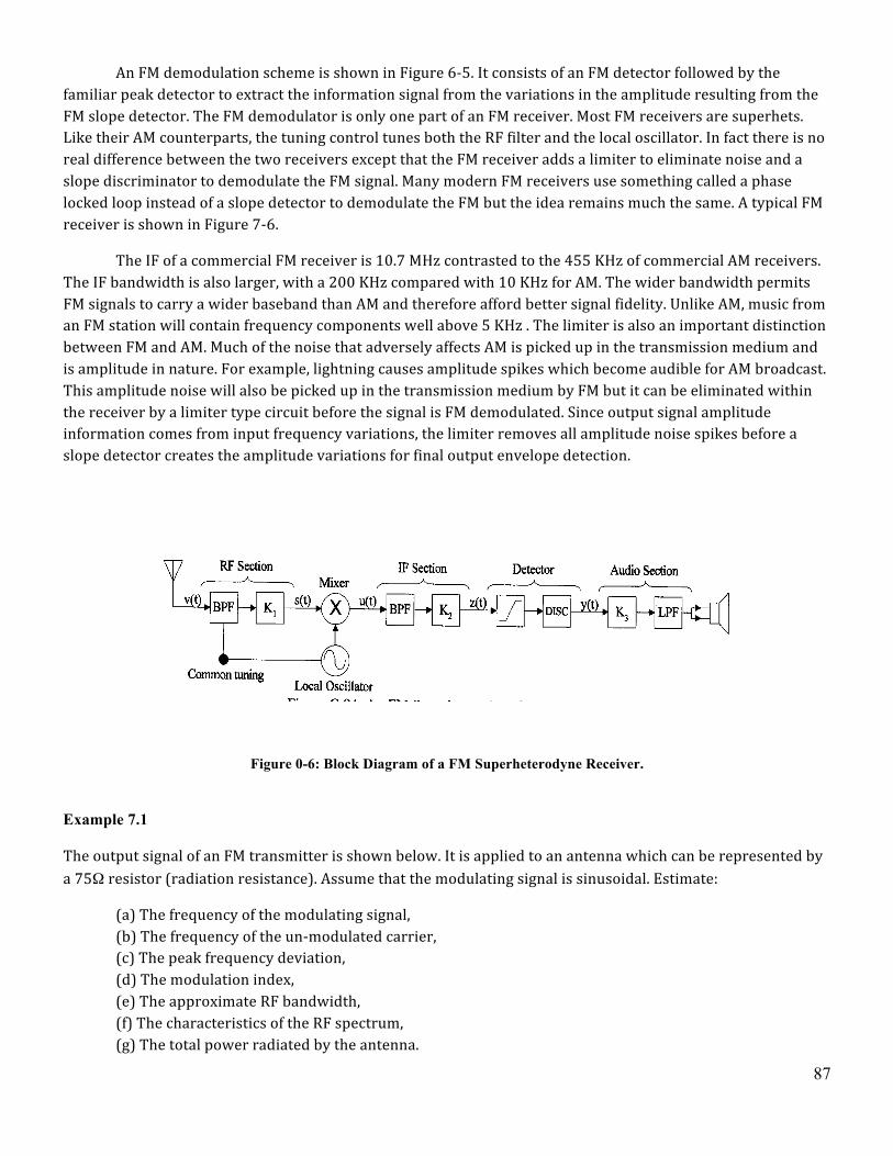
87
An FM demodulation scheme is shown in Figure 6-‐5. It consists of an FM detector followed by the familiar peak detector to extract the information signal from the variations in the amplitude resulting from the FM slope detector. The FM demodulator is only one part of an FM receiver. Most FM receivers are superhets. Like their AM counterparts, the tuning control tunes both the RF filter and the local oscillator. In fact there is no real difference between the two receivers except that the FM receiver adds a limiter to eliminate noise and a slope discriminator to demodulate the FM signal. Many modern FM receivers use something called a phase locked loop instead of a slope detector to demodulate the FM but the idea remains much the same. A typical FM receiver is shown in Figure 7-‐6.
The IF of a commercial FM receiver is 10.7 MHz contrasted to the 455 KHz of commercial AM receivers. The IF bandwidth is also larger, with a 200 KHz compared with 10 KHz for AM. The wider bandwidth permits FM signals to carry a wider baseband than AM and therefore afford better signal fidelity. Unlike AM, music from an FM station will contain frequency components well above 5 KHz . The limiter is also an important distinction between FM and AM. Much of the noise that adversely affects AM is picked up in the transmission medium and is amplitude in nature. For example, lightning causes amplitude spikes which become audible for AM broadcast. This amplitude noise will also be picked up in the transmission medium by FM but it can be eliminated within the receiver by a limiter type circuit before the signal is FM demodulated. Since output signal amplitude information comes from input frequency variations, the limiter removes all amplitude noise spikes before a slope detector creates the amplitude variations for final output envelope detection.
Figure 0-6: Block Diagram of a FM Superheterodyne Receiver.
Example 7.1
The output signal of an FM transmitter is shown below. It is applied to an antenna which can be represented by a 75Ω resistor (radiation resistance). Assume that the modulating signal is sinusoidal. Estimate:
(a) The frequency of the modulating signal, (b) The frequency of the un-‐modulated carrier, (c) The peak frequency deviation, (d) The modulation index, (e) The approximate RF bandwidth, (f) The characteristics of the RF spectrum, (g) The total power radiated by the antenna.
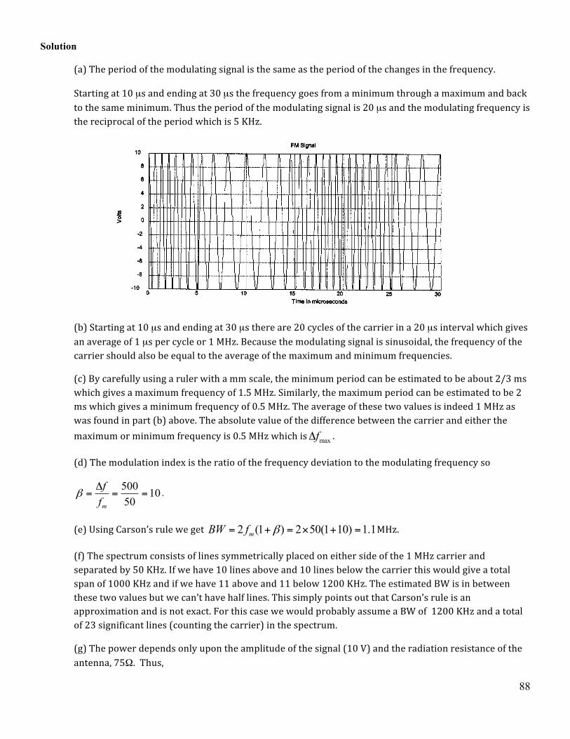
88
Solution
(a) The period of the modulating signal is the same as the period of the changes in the frequency.
Starting at 10 µs and ending at 30 µs the frequency goes from a minimum through a maximum and back to the same minimum. Thus the period of the modulating signal is 20 µs and the modulating frequency is the reciprocal of the period which is 5 KHz.
(b) Starting at 10 µs and ending at 30 µs there are 20 cycles of the carrier in a 20 µs interval which gives an average of 1 µs per cycle or 1 MHz. Because the modulating signal is sinusoidal, the frequency of the carrier should also be equal to the average of the maximum and minimum frequencies.
(c) By carefully using a ruler with a mm scale, the minimum period can be estimated to be about 2/3 ms which gives a maximum frequency of 1.5 MHz. Similarly, the maximum period can be estimated to be 2 ms which gives a minimum frequency of 0.5 MHz. The average of these two values is indeed 1 MHz as was found in part (b) above. The absolute value of the difference between the carrier and either the maximum or minimum frequency is 0.5 MHz which is maxfΔ .
(d) The modulation index is the ratio of the frequency deviation to the modulating frequency so
500 1050m
ff
βΔ
= = = .
(e) Using Carson’s rule we get 2 (1 ) 2 50(1 10) 1.1mBW f β= + = × + = MHz.
(f) The spectrum consists of lines symmetrically placed on either side of the 1 MHz carrier and separated by 50 KHz. If we have 10 lines above and 10 lines below the carrier this would give a total span of 1000 KHz and if we have 11 above and 11 below 1200 KHz. The estimated BW is in between these two values but we can’t have half lines. This simply points out that Carson’s rule is an approximation and is not exact. For this case we would probably assume a BW of 1200 KHz and a total of 23 significant lines (counting the carrier) in the spectrum.
(g) The power depends only upon the amplitude of the signal (10 V) and the radiation resistance of the antenna, 75Ω. Thus,
89
210 20.575 3
P = = W.
Example 7.2
A 100 MHz sinusoidal carrier is frequency modulated with a 3-‐KHz, 3-‐V peak sinusoid. If the modulator has a sensitivity of 2 KHz/V, determine:
(a) The amplitude of the frequency deviation of the carrier, (b) The modulation index, (c) The approximate signal bandwidth using Carson’s rule, (d) The expression as a function of time for the FM signal for a cosine carrier of 5 V peak. Assume the modulating signal is a cosine.
Solution
(a) The sensitivity of 2 KHz/V is the constant k which represents the conversion from modulating signal amplitude to carrier frequency deviation. To get the frequency deviation, we simply multiply this sensitivity by the amplitude of the modulating signal to get (2 / )(3 ) 6f KHz V V KHzΔ = = .
(b) The modulation index is the ratio of the frequency deviation to the modulating frequency so 6 23m
ff
βΔ
= = =
(c) Using Carson’s rule we get 2 (1 ) 2 3(1 2) 18mBW f β= + = × + = KHz.
(d) Filling in the values found above into the equation for an FM signal we get 8( ) 5cos[2 10 2sin(2 3000 )]FMv t t tπ π= × + × V.
Example 7.3
Measurements on an FM signal indicate a maximum period of 81.001 10−× s and a minimum period of 80.999 10−× s. The modulating signal is a 20 KHz pure tone.
(a) Determine the value of the carrier frequency,
(b) Find the value of the frequency deviation.
Solution
(a) The maximum frequency is the inverse of the minimum period which is max 8
1 100.10.999 10
f = =×
MHz and the minimum frequency is the inverse of the maximum period which min 8
1 99.91.001 10
f−
= =×MHz. The carrier is the average of these two frequencies which gives 100cf = MHz.
90
(b) The frequency deviation is max min 0.1c cf f f f− = − = MHz, which means 5β = .
91
7.6 Homework Problems
Problem 7.1
If the instantaneous carrier frequency is varied sinusoidally from a minimum value of 99.8 MHz to a maximum of 100.2 MHz by FM modulating the carrier with a 40 KHz, sinusoidal modulating signal, determine:
a. The modulation index b. The approximate bandwidth by use of Carson’s rule c. Sketch and label the amplitude spectrum
Problem 7.2
A 100 MHz carrier is modulated such that the value of the instantaneous frequency varies sinusoidally from 99.1 MHz to 100.1 MHz and the period of this variation is 0.05 ms.
a. What type of modulation is being used? b. Determine the frequency of the modulating signal being used. c. Determine the approximate RF bandwidth of the signal.
Problem 7.3
When a 93.4 MHz carrier is frequency modulated by a 4 KHz sine wave the resultant frequency deviation is 40 KHz.
a. Determine the highest and lowest frequencies attained by the modulated signal. b. Determine the modulation index. c. Determine the approximate bandwidth and sketch the frequency spectrum.
Problem 7.4
The FCC has allocated the range from 88 to 108 MHz for commercial FM broadcasting. The RF bandwidth allotted each station is 200 KHz.
a. How many stations can be assigned different carriers over the full FM band? b. Over what range must the local oscillator of an FM superheterodyne receiver be tunable if the LO is
tuned to a higher frequency than the carrier? c. Determine the maximum image frequency that could appear in the IF stage of an FM superheterodyne
receiver and the maximum BW of the RF amplifier such that this image is not a problem. d. Determine the minimum BW of the audio amplifier of a good FM superheterodyne receiver so that none
of the source audio content is lost.
Problem 7.5
When a carrier is frequency modulated by a 4 KHz sine wave the resulting FM signal has a maximum frequency of 106.218 MHz and a minimum frequency of 106.196 MHz.
a. Determine the carrier frequency. b. Determine the frequency deviation. c. Determine the approximate RF band width and sketch the spectrum.

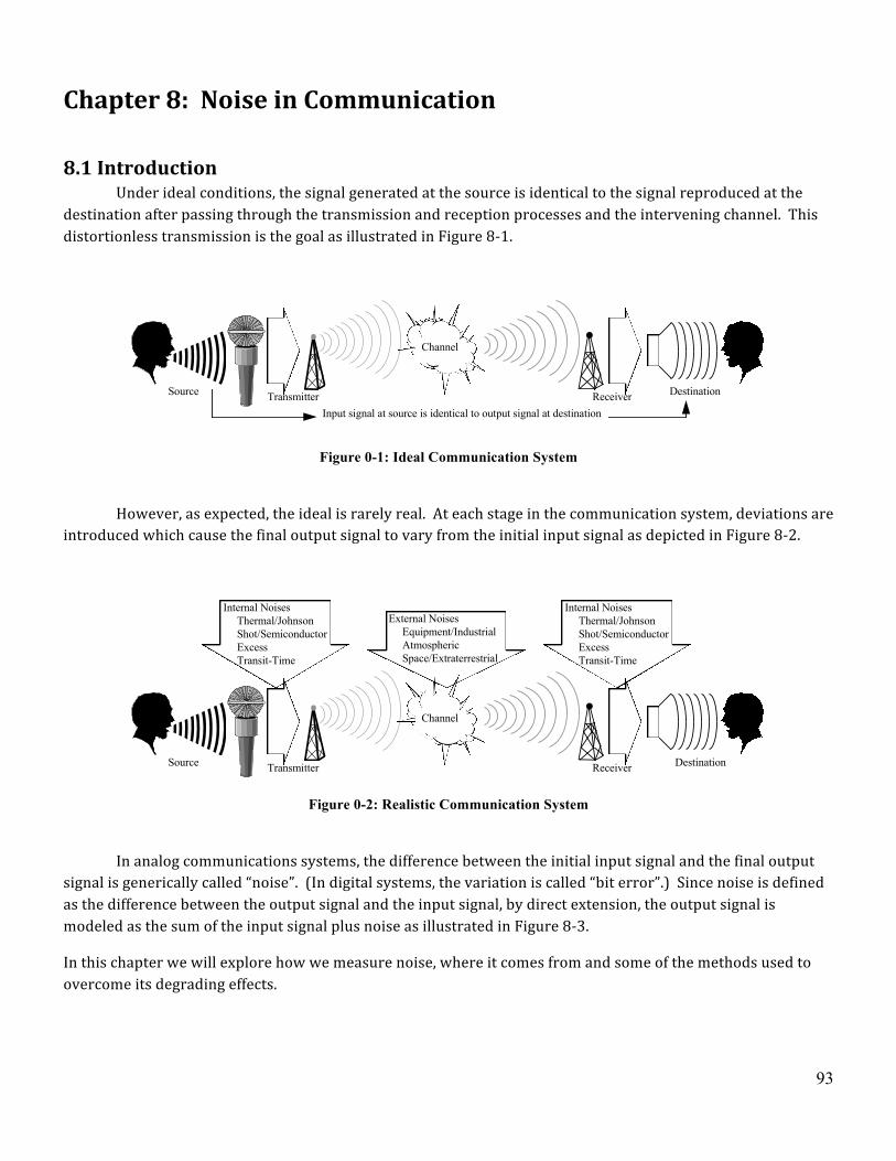
93
Chapter 8: Noise in Communication
8.1 Introduction Under ideal conditions, the signal generated at the source is identical to the signal reproduced at the destination after passing through the transmission and reception processes and the intervening channel. This distortionless transmission is the goal as illustrated in Figure 8-‐1.
Figure 0-1: Ideal Communication System
However, as expected, the ideal is rarely real. At each stage in the communication system, deviations are introduced which cause the final output signal to vary from the initial input signal as depicted in Figure 8-‐2.
Figure 0-2: Realistic Communication System
In analog communications systems, the difference between the initial input signal and the final output signal is generically called “noise”. (In digital systems, the variation is called “bit error”.) Since noise is defined as the difference between the output signal and the input signal, by direct extension, the output signal is modeled as the sum of the input signal plus noise as illustrated in Figure 8-‐3.
In this chapter we will explore how we measure noise, where it comes from and some of the methods used to overcome its degrading effects.
Transmitter ReceiverSource Destination
Channel
Input signal at source is identical to output signal at destination
Transmitter ReceiverSource Destination
Channel
External Noises Equipment/Industrial Atmospheric Space/Extraterrestrial
Internal Noises Thermal/Johnson Shot/Semiconductor Excess Transit-Time
Internal Noises Thermal/Johnson Shot/Semiconductor Excess Transit-Time
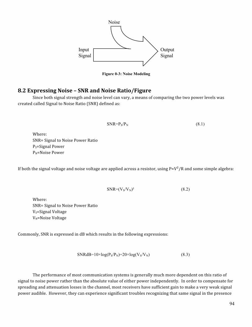
94
Figure 0-3: Noise Modeling
8.2 Expressing Noise – SNR and Noise Ratio/Figure Since both signal strength and noise level can vary, a means of comparing the two power levels was created called Signal to Noise Ratio (SNR) defined as:
SNR=PS/PN (8.1)
Where: SNR= Signal to Noise Power Ratio PS=Signal Power PN=Noise Power
If both the signal voltage and noise voltage are applied across a resistor, using P=V²/R and some simple algebra:
SNR=(VS/VN)² (8.2)
Where: SNR= Signal to Noise Power Ratio VS=Signal Voltage VN=Noise Voltage
Commonly, SNR is expressed in dB which results in the following expressions:
SNRdB=10×log(PS/PN)=20×log(VS/VN) (8.3)
The performance of most communication systems is generally much more dependent on this ratio of signal to noise power rather than the absolute value of either power independently. In order to compensate for spreading and attenuation losses in the channel, most receivers have sufficient gain to make a very weak signal power audible. However, they can experience significant troubles recognizing that same signal in the presence
OutputSignal
InputSignal
Noise
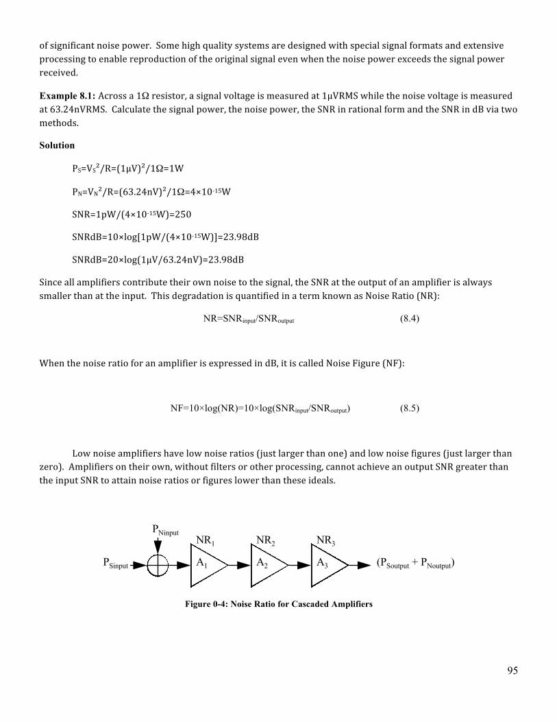
95
of significant noise power. Some high quality systems are designed with special signal formats and extensive processing to enable reproduction of the original signal even when the noise power exceeds the signal power received.
Example 8.1: Across a 1Ω resistor, a signal voltage is measured at 1µVRMS while the noise voltage is measured at 63.24nVRMS. Calculate the signal power, the noise power, the SNR in rational form and the SNR in dB via two methods.
Solution
PS=VS²/R=(1µV)²/1Ω=1W
PN=VN²/R=(63.24nV)²/1Ω=4×10-‐15W
SNR=1pW/(4×10-‐15W)=250
SNRdB=10×log[1pW/(4×10-‐15W)]=23.98dB
SNRdB=20×log(1µV/63.24nV)=23.98dB
Since all amplifiers contribute their own noise to the signal, the SNR at the output of an amplifier is always smaller than at the input. This degradation is quantified in a term known as Noise Ratio (NR):
NR=SNRinput/SNRoutput (8.4)
When the noise ratio for an amplifier is expressed in dB, it is called Noise Figure (NF):
NF=10×log(NR)=10×log(SNRinput/SNRoutput) (8.5)
Low noise amplifiers have low noise ratios (just larger than one) and low noise figures (just larger than zero). Amplifiers on their own, without filters or other processing, cannot achieve an output SNR greater than the input SNR to attain noise ratios or figures lower than these ideals.
Figure 0-4: Noise Ratio for Cascaded Amplifiers
PSinput
PNinput
A1
NR1
A2
NR2
A3
NR3
(PSoutput + PNoutput)
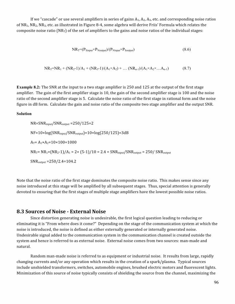
96
If we “cascade” or use several amplifiers in series of gains A1, A2, A3, etc. and corresponding noise ratios of NR1, NR2, NR3, etc. as illustrated in Figure 8-‐4, some algebra will derive Friis’ Formula which relates the composite noise ratio (NRT) of the set of amplifiers to the gains and noise ratios of the individual stages:
NRT=(PSinput×PNoutput)/(PNinput×PSoutput) (8.6)
NRT=NR1 + (NR2-1)/A1 + (NR3-1)/(A1×A2) + … (NRn-1)/(A1×A2×…An-1) (8.7)
Example 8.2: The SNR at the input to a two stage amplifier is 250 and 125 at the output of the first stage amplifier. The gain of the first amplifier stage is 10, the gain of the second amplifier stage is 100 and the noise ratio of the second amplifier stage is 5. Calculate the noise ratio of the first stage in rational form and the noise figure in dB form. Calculate the gain and noise ratio of the composite two stage amplifier and the output SNR.
Solution
NR=SNRinput/SNRoutput =250/125=2
NF=10×log(SNRinput/SNRoutput)=10×log(250/125)=3dB
AT= A1×A2=10×100=1000
NRT= NR1+(NR2-‐1)/A1 = 2+ (5-‐1)/10 = 2.4 = SNRinput/SNRoutput = 250/ SNRoutput
SNRoutput =250/2.4=104.2
Note that the noise ratio of the first stage dominates the composite noise ratio. This makes sense since any noise introduced at this stage will be amplified by all subsequent stages. Thus, special attention is generally devoted to ensuring that the first stages of multiple stage amplifiers have the lowest possible noise ratios.
8.3 Sources of Noise -‐ External Noise Since distortion generating noise is undesirable, the first logical question leading to reducing or eliminating it is “From where does it come?” Depending on the stage of the communication system at which the noise is introduced, the noise is defined as either externally generated or internally generated noise. Undesirable signal added to the communication system in the communication channel is created outside the system and hence is referred to as external noise. External noise comes from two sources: man-‐made and natural.
Random man-‐made noise is referred to as equipment or industrial noise. It results from large, rapidly changing currents and/or any operation which results in the creation of a spark/plasma. Typical sources include unshielded transformers, switches, automobile engines, brushed electric motors and fluorescent lights. Minimization of this source of noise typically consists of shielding the source from the channel, maximizing the
97
distance from the source to the communication systems elements and/or minimizing the time that the noise source and the communication system are operating simultaneously.
Non-‐random man-‐made noise is referred to as interference. It can be unintentional such as a radio station from a neighboring city experiencing just the right atmospheric conditions that its signal overwhelms the desired local station signal in a given location. It can be caused by capacitive, magnetic, radiative, or ground loop coupling which provides alternate signal paths into the receiver for signals other than the desired one. Man-‐made interference can also be intentional, in which case it is called “jamming”. Defeating interference is commonly done by removing undesired coupling paths, exploiting some unique characteristic of the desired signal to differentiate it from the interference or shifting the desired signal frequency away from the interfering signal frequency band.
Natural external noise originates from two primary sources: atmospheric and extraterrestrial. Atmospheric noise principally results from lightning, a very large spark or plasma. It creates a very large but short-‐lived noise spike over long distances at frequencies up to ~30MHz. It can be minimized by “noise blanking” or disabling the receiver until the large amplitude spike passes. Unfortunately, any signal sent during the spike is still lost.
Extraterrestrial noise comes from the sun and stars as the solar wind, solar flares, sun spots and cosmic radiation. It produces random voltages primarily in the 10MHz to 1.5GHz range. Extraterrestrial noise in the channel has to be filtered out in the manner to be described later in this chapter.
8.4 Internal Noise While external noise is introduced to the communication channel from sources outside the communication system, internal noise is contributed by the system components themselves. Internal noise is minimized by prudent engineering trade-‐offs in the design and operation of the communication system. There are four common sources of internal noise in most communication systems: thermal, shot, excess and transit-‐time.
Thermal noise, also known as Johnson or resistance noise, is induced by the random motion of electrons in resistors due to heat. Thermal noise is considered “white noise” in that its magnitude is the approximately same across the measurable spectrum. Consequently, the thermal noise effects observed are directly related to the frequency span over which the signal is studied. The open circuit noise voltage (VN) induced by this motion is a function of the prevalent temperature of the selected resistor, the bandwidth over which the noise is measured and the value of the resistor as given by Johnson’s Formula:
VN=(4kTBR)½ (8.8)
Where: VN=Noise Voltage k=Boltzman’s Constant=1.381×10-‐23J/ºK T=Temperature in ºK; (T[ºK]=T[ºC]+273.15; T0=290ºK~ room temperature) B=Bandwidth over which the noise is observed, in Hertz R=Resistance across which voltage is measured in Ω
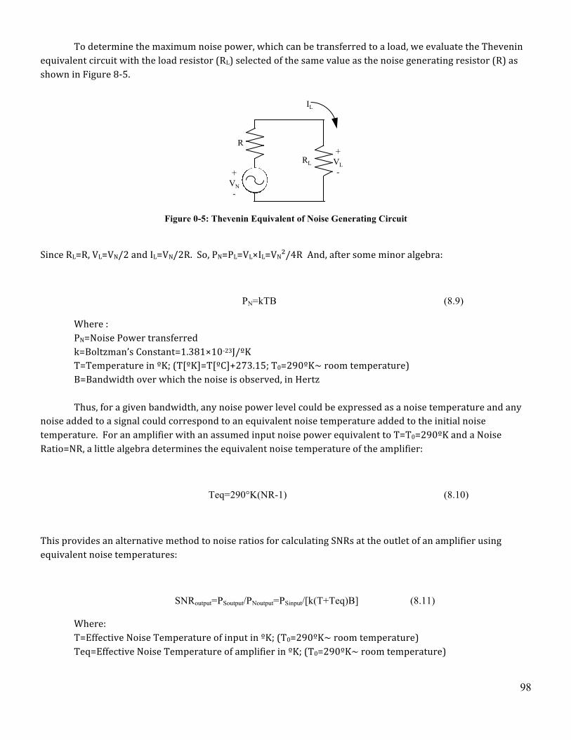
98
To determine the maximum noise power, which can be transferred to a load, we evaluate the Thevenin equivalent circuit with the load resistor (RL) selected of the same value as the noise generating resistor (R) as shown in Figure 8-‐5.
Figure 0-5: Thevenin Equivalent of Noise Generating Circuit
Since RL=R, VL=VN/2 and IL=VN/2R. So, PN=PL=VL×IL=VN²/4R And, after some minor algebra:
PN=kTB (8.9)
Where : PN=Noise Power transferred k=Boltzman’s Constant=1.381×10-‐23J/ºK T=Temperature in ºK; (T[ºK]=T[ºC]+273.15; T0=290ºK~ room temperature) B=Bandwidth over which the noise is observed, in Hertz
Thus, for a given bandwidth, any noise power level could be expressed as a noise temperature and any noise added to a signal could correspond to an equivalent noise temperature added to the initial noise temperature. For an amplifier with an assumed input noise power equivalent to T=T0=290ºK and a Noise Ratio=NR, a little algebra determines the equivalent noise temperature of the amplifier:
Teq=290°K(NR-1) (8.10)
This provides an alternative method to noise ratios for calculating SNRs at the outlet of an amplifier using equivalent noise temperatures:
SNRoutput=PSoutput/PNoutput=PSinput/[k(T+Teq)B] (8.11)
Where: T=Effective Noise Temperature of input in ºK; (T0=290ºK~ room temperature) Teq=Effective Noise Temperature of amplifier in ºK; (T0=290ºK~ room temperature)
+VN-
R
RL+VL-
IL
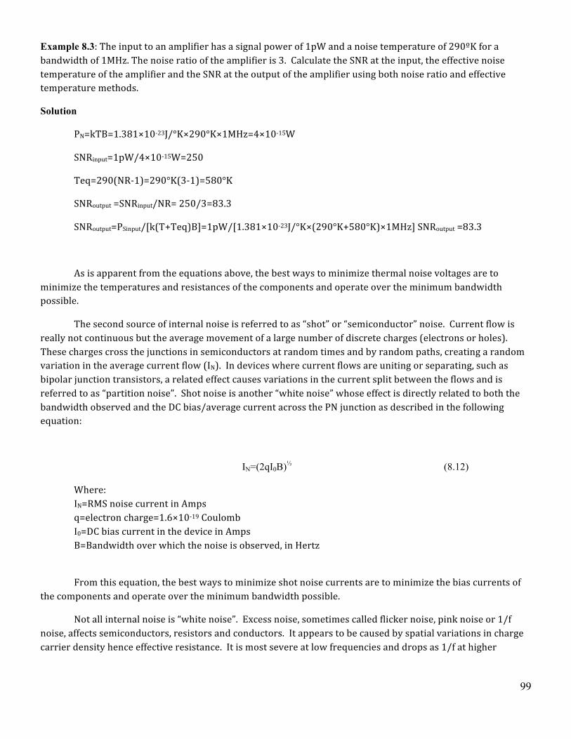
99
Example 8.3: The input to an amplifier has a signal power of 1pW and a noise temperature of 290ºK for a bandwidth of 1MHz. The noise ratio of the amplifier is 3. Calculate the SNR at the input, the effective noise temperature of the amplifier and the SNR at the output of the amplifier using both noise ratio and effective temperature methods.
Solution
PN=kTB=1.381×10-‐23J/°K×290°K×1MHz=4×10-‐15W
SNRinput=1pW/4×10-‐15W=250
Teq=290(NR-‐1)=290°K(3-‐1)=580°K
SNRoutput =SNRinput/NR= 250/3=83.3
SNRoutput=PSinput/[k(T+Teq)B]=1pW/[1.381×10-‐23J/°K×(290°K+580°K)×1MHz] SNRoutput =83.3
As is apparent from the equations above, the best ways to minimize thermal noise voltages are to minimize the temperatures and resistances of the components and operate over the minimum bandwidth possible.
The second source of internal noise is referred to as “shot” or “semiconductor” noise. Current flow is really not continuous but the average movement of a large number of discrete charges (electrons or holes). These charges cross the junctions in semiconductors at random times and by random paths, creating a random variation in the average current flow (IN). In devices where current flows are uniting or separating, such as bipolar junction transistors, a related effect causes variations in the current split between the flows and is referred to as “partition noise”. Shot noise is another “white noise” whose effect is directly related to both the bandwidth observed and the DC bias/average current across the PN junction as described in the following equation:
IN=(2qI0B)½ (8.12)
Where: IN=RMS noise current in Amps q=electron charge=1.6×10-‐19 Coulomb I0=DC bias current in the device in Amps B=Bandwidth over which the noise is observed, in Hertz
From this equation, the best ways to minimize shot noise currents are to minimize the bias currents of the components and operate over the minimum bandwidth possible.
Not all internal noise is “white noise”. Excess noise, sometimes called flicker noise, pink noise or 1/f noise, affects semiconductors, resistors and conductors. It appears to be caused by spatial variations in charge carrier density hence effective resistance. It is most severe at low frequencies and drops as 1/f at higher
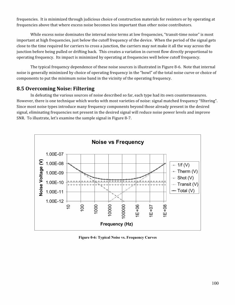
100
frequencies. It is minimized through judicious choice of construction materials for resistors or by operating at frequencies above that where excess noise becomes less important than other noise contributors.
While excess noise dominates the internal noise terms at low frequencies, “transit-‐time noise” is most important at high frequencies, just below the cutoff frequency of the device. When the period of the signal gets close to the time required for carriers to cross a junction, the carriers may not make it all the way across the junction before being pulled or drifting back. This creates a variation in current flow directly proportional to operating frequency. Its impact is minimized by operating at frequencies well below cutoff frequency.
The typical frequency dependence of these noise sources is illustrated in Figure 8-‐6. Note that internal noise is generally minimized by choice of operating frequency in the “bowl” of the total noise curve or choice of components to put the minimum noise band in the vicinity of the operating frequency.
8.5 Overcoming Noise: Filtering In defeating the various sources of noise described so far, each type had its own countermeasures. However, there is one technique which works with most varieties of noise: signal matched frequency “filtering”. Since most noise types introduce many frequency components beyond those already present in the desired signal, eliminating frequencies not present in the desired signal will reduce noise power levels and improve SNR. To illustrate, let’s examine the sample signal in Figure 8-‐7.
Figure 0-6: Typical Noise vs. Frequency Curves
Noise vs Frequency
1.00E-12
1.00E-11
1.00E-10
1.00E-09
1.00E-08
1.00E-07
10 100
1000
1000
0
1000
00
1E+0
6
1E+0
7
1E+0
8
Frequency (Hz)
Noi
se V
olta
ge (V
)
1/f (V)Therm (V)Shot (V)Transit (V)Total (V)
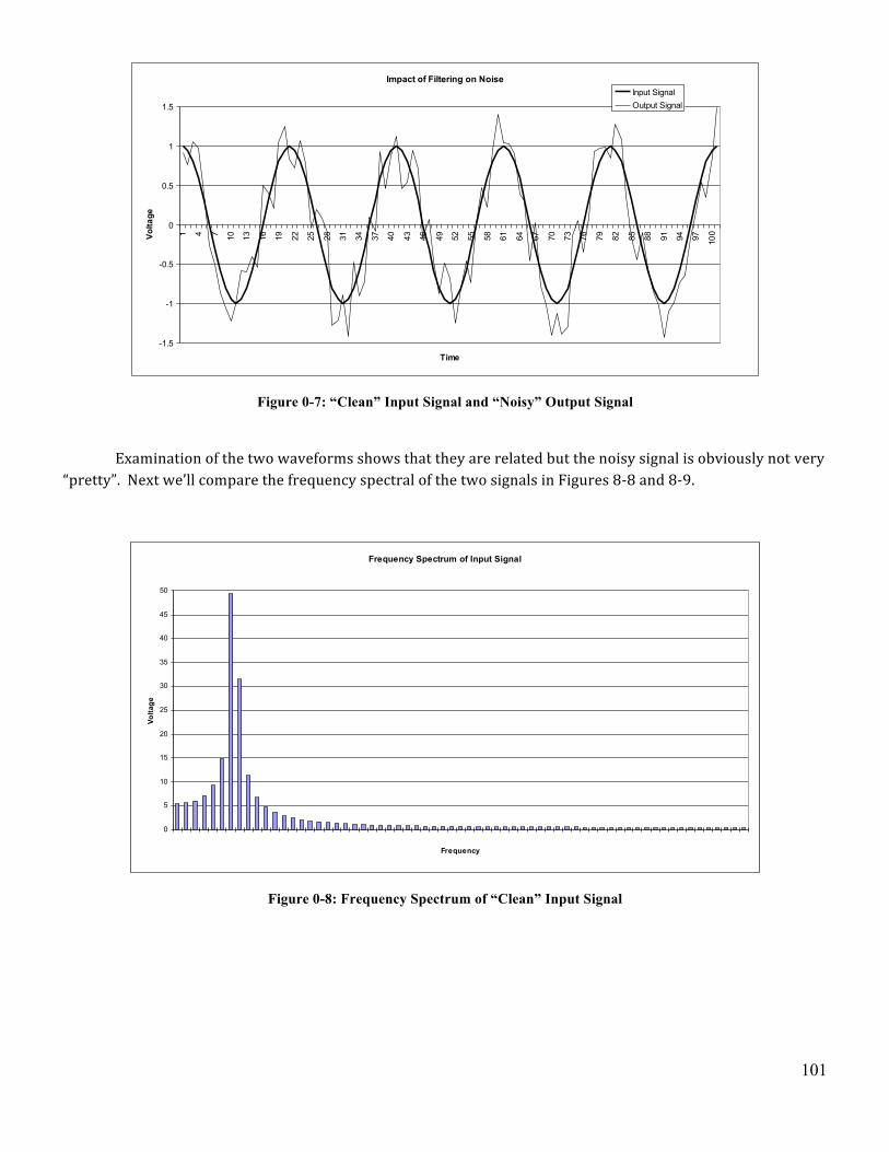
101
Figure 0-7: “Clean” Input Signal and “Noisy” Output Signal
Examination of the two waveforms shows that they are related but the noisy signal is obviously not very “pretty”. Next we’ll compare the frequency spectral of the two signals in Figures 8-‐8 and 8-‐9.
Figure 0-8: Frequency Spectrum of “Clean” Input Signal
Impact of Filtering on Noise
-1.5
-1
-0.5
0
0.5
1
1.5
1 4 7 10 13 16 19 22 25 28 31 34 37 40 43 46 49 52 55 58 61 64 67 70 73 76 79 82 85 88 91 94 97 100
Time
Volta
ge
Input SignalOutput Signal
Frequency Spectrum of Input Signal
0
5
10
15
20
25
30
35
40
45
50
1 3 5 7 9 11 13 15 17 19 21 23 25 27 29 31 33 35 37 39 41 43 45 47 49 51 53 55 57 59 61 63 65
Frequency
Volta
ge
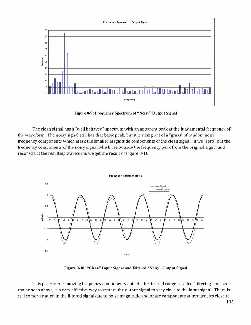
102
Figure 0-9: Frequency Spectrum of “Noisy” Output Signal
The clean signal has a “well behaved” spectrum with an apparent peak at the fundamental frequency of the waveform. The noisy signal still has that basic peak, but it is rising out of a “grass” of random noise frequency components which mask the smaller magnitude components of the clean signal. If we “zero” out the frequency components of the noisy signal which are outside the frequency peak from the original signal and reconstruct the resulting waveform, we get the result of Figure 8-‐10.
Figure 0-10: “Clean” Input Signal and Filtered “Noisy” Output Signal
This process of removing frequency components outside the desired range is called “filtering” and, as can be seen above, is a very effective way to restore the output signal to very close to the input signal. There is still some variation in the filtered signal due to noise magnitude and phase components at frequencies close to
Frequency Spectrum of Output Signal
0
5
10
15
20
25
30
35
40
45
50
1 3 5 7 9 11 13 15 17 19 21 23 25 27 29 31 33 35 37 39 41 43 45 47 49 51 53 55 57 59 61 63 65
Frequency
Volta
ge
Impact of Filtering on Noise
-1.5
-1
-0.5
0
0.5
1
1.5
1 4 7 10 13 16 19 22 25 28 31 34 37 40 43 46 49 52 55 58 61 64 67 70 73 76 79 82 85 88 91 94 97 100
Time
Volta
ge
Input SignalFiltered Output
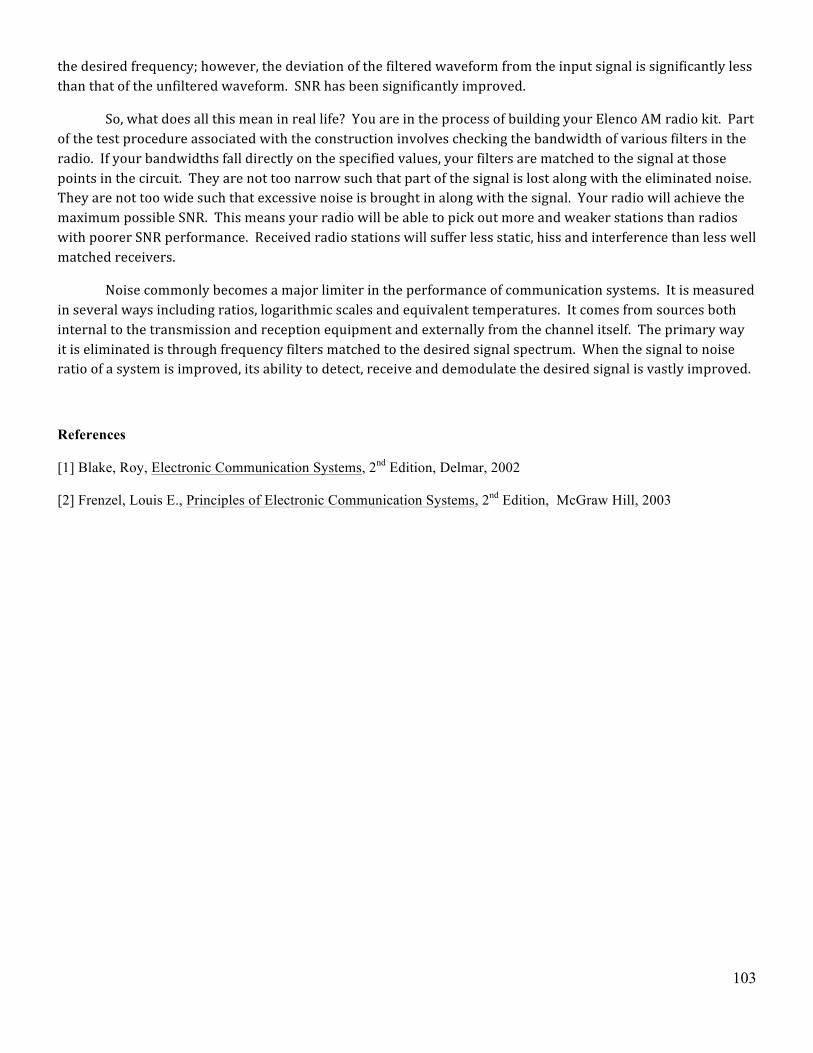
103
the desired frequency; however, the deviation of the filtered waveform from the input signal is significantly less than that of the unfiltered waveform. SNR has been significantly improved.
So, what does all this mean in real life? You are in the process of building your Elenco AM radio kit. Part of the test procedure associated with the construction involves checking the bandwidth of various filters in the radio. If your bandwidths fall directly on the specified values, your filters are matched to the signal at those points in the circuit. They are not too narrow such that part of the signal is lost along with the eliminated noise. They are not too wide such that excessive noise is brought in along with the signal. Your radio will achieve the maximum possible SNR. This means your radio will be able to pick out more and weaker stations than radios with poorer SNR performance. Received radio stations will suffer less static, hiss and interference than less well matched receivers.
Noise commonly becomes a major limiter in the performance of communication systems. It is measured in several ways including ratios, logarithmic scales and equivalent temperatures. It comes from sources both internal to the transmission and reception equipment and externally from the channel itself. The primary way it is eliminated is through frequency filters matched to the desired signal spectrum. When the signal to noise ratio of a system is improved, its ability to detect, receive and demodulate the desired signal is vastly improved.
References
[1] Blake, Roy, Electronic Communication Systems, 2nd Edition, Delmar, 2002
[2] Frenzel, Louis E., Principles of Electronic Communication Systems, 2nd Edition, McGraw Hill, 2003

105
Chapter 9: Digital Communications
9.1 Introduction The storage, processing, manipulation and transmission of information represented in digital form by l’s and 0’s has become more and more important. Music is stored in digital form on CD’s, digital computers are essential in business, engineering, entertainment and science. A few TV stations in the United States are already broadcasting high definition television, HDTV. The format for HDTV in the U.S. is digital. Much of the information traveling around the United States and the world is first converted into a digital form before transmission. Digital communications offer a number of advantages:
1. For long distance communications, the digital 1’s and 0’s can be reconstituted by intermediate repeater stations with essentially zero error. The digital format is more tolerant of noise and noise does not build up with increasing distance as it does with analog communications.
2. Much of the circuitry used for modulation and demodulation is digital which means that it is highly reliable and stable and can be easily fabricated on integrated circuits.
3. Information can easily be stored in digital form for later retrieval. For example, packets of information relayed by satellites can temporarily be stored until the satellite is over the intended recipient of the information.
4. Computers can easily manipulate and encrypt information in digital form. Secure communications is very important in the military and in business and industry.
5. Very efficient algorithms exist for the compression of digital information, for example, the jpeg and gif formats for pictures which are used on the Internet.
6. Digital codes exist for reducing the effects of noise and for detecting and correcting errors of transmission. For example, the use of the parity bit allows the receiver to detect certain errors and request a retransmission if desired.
Offsetting these advantages to some degree is the added complexity and comparatively larger bandwidth requirements of digital communications systems. However, modern integrated circuitry and modern digital computers make complexity much less an issue. We will discuss some of the concepts and subsystems of digital communications. Years of study are required for anything approaching complete mastery of the whole area. Many of the concepts and techniques involved in digital communications, such as analog-‐to-‐digital and digital-‐to-‐analog conversion and binary numbers and logic, are included elsewhere in this course. First we will look at the conversion of analog information into digital form, called pulse code modulation (PCM).
9.2 Pulse Code Modulation The process of pulse code modulation is summarized in Figure 9.1 as a block diagram. The elements of this process are illustrated in Figure 9.2 discussed below. It should be carefully studied for full understanding.
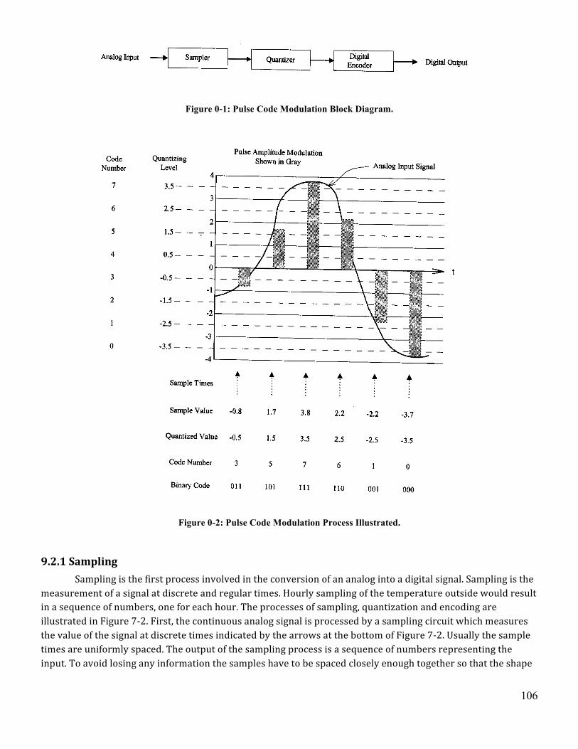
106
Figure 0-1: Pulse Code Modulation Block Diagram.
Figure 0-2: Pulse Code Modulation Process Illustrated.
9.2.1 Sampling Sampling is the first process involved in the conversion of an analog into a digital signal. Sampling is the measurement of a signal at discrete and regular times. Hourly sampling of the temperature outside would result in a sequence of numbers, one for each hour. The processes of sampling, quantization and encoding are illustrated in Figure 7-‐2. First, the continuous analog signal is processed by a sampling circuit which measures the value of the signal at discrete times indicated by the arrows at the bottom of Figure 7-‐2. Usually the sample times are uniformly spaced. The output of the sampling process is a sequence of numbers representing the input. To avoid losing any information the samples have to be spaced closely enough together so that the shape
107
of the analog input signal is not distorted or lost. The samples must be taken frequently enough to avoid loss of information. Music stored in a CD would not sound very good if the sampling rate were 1 KHz.
How fast is fast enough? The Sampling Theorem states that to avoid loss of information, a band limited signal must be sampled at a rate equal to or greater than twice the bandwidth of the signal. If an analog signal is sampled fast enough, the information can be retrieved by low pass filtering the sequence of samples. If we are dealing with a baseband signal containing frequency components from about zero on up to some maximum frequency, then the sampling rate must be equal to or greater than twice that maximum frequency.
An audio signal with frequency components from about 40 Hz up to about 20 KHz is an example of a baseband signal. High quality digital audio requires a minimum sampling rate of 340 10× samples/sec. If the signal of interest is a band-‐limited communications signal modulated onto a high frequency carrier, the minimum sampling rate, required to preserve the information content, is equal to twice the range of frequencies around the carrier. Thus, if the bandwidth of the information signal is 10 KHz and it is centered around a 100 MHz carrier, the minimum sampling rate is 20 KHz, not 2(100 MHz + 5 KHz). In equation form the Sampling Theorem translates to 2sampling Bandwidthf f≥ . This minimum rate is called the Nyquist rate, named after the
engineer who investigated the mathematics of the sampling process. The theoretical limit is never really fast enough. For example, to make music CD recordings, the input signal, which has a maximum frequency of 20 KHz, is sampled at about 44 KHz.
Many signals have high frequency components that do not contain essential information but that can cause problems when sampling is done. The problem of aliasing occurs when the sampling rate is lower than twice the highest frequency of the signal. It results in high frequency components masquerading as lower frequency values and causing distortion. Musical instruments can create frequencies higher than 20 KHz which are not audible. To avoid aliasing problems, a music signal is first low pass filtered to remove any components greater than 20 KHz. This is what is meant by band limiting a signal. Filtering is used to remove all but a limited range of frequencies from a signal while preserving the essential information content. If all frequencies above about 3 KHz are removed from a person’s voice before telephone transmission, the voice remains both intelligible and recognizable although they may not sound exactly the same as in person.
9.2.2 Pulse Amplitude Modulation Rectangular pulses, shown in gray, are located at each sample point in Figure 7-‐2. These gray pulses illustrate the idea of pulse amplitude modulation (PAM). Instead of transmitting the full analog signal, pulses of amplitudes proportional to the sample values are transmitted. One advantage of this technique is that the pulses from several different analog signals can be interleaved together and transmitted over the same line. In this way, each signal gets to time share the common resource of a transmission line. Time sharing in this way is called time division multiplexing (TDM). It can also be used to multiplex many digital channels together and will be discussed again below. The tops of the pulses in Figure 9-‐2 are shown as being flat. Ideally, the top of each pulse would follow the contour of the analog signal during the pulse interval. However, it is much easier to create flat top pulses using sample and hold circuitry. The distortion created by the flat tops is minimal at the receiver, especially if the pulses are of short duration.
Another issue with PAM is the amount of bandwidth required in the baseband to faithfully represent the pulses. If the band width is gradually reduced by low pass filtering, the pulses will first become more and more rounded until they are distorted to the point that information is lost. Band width becomes important with respect to the medium over which the pulses are transmitted. This medium might, for example, be wires that
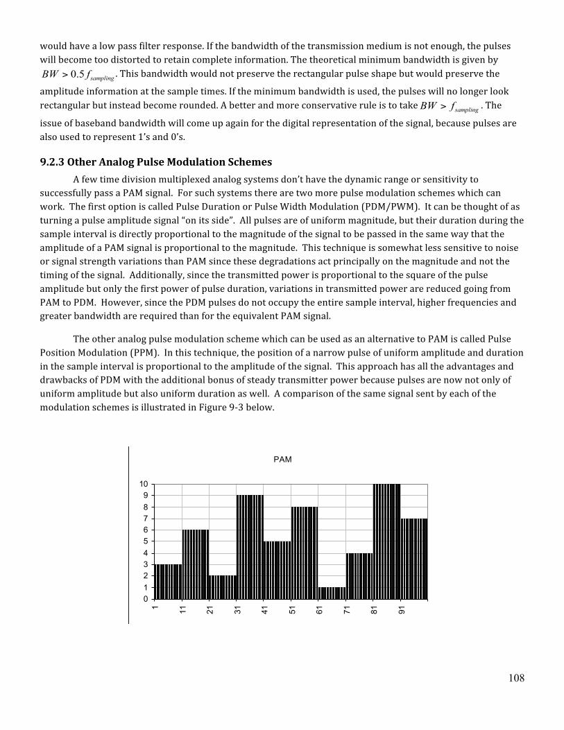
108
would have a low pass filter response. If the bandwidth of the transmission medium is not enough, the pulses will become too distorted to retain complete information. The theoretical minimum bandwidth is given by
0.5 samplingBW f> . This bandwidth would not preserve the rectangular pulse shape but would preserve the
amplitude information at the sample times. If the minimum bandwidth is used, the pulses will no longer look rectangular but instead become rounded. A better and more conservative rule is to take samplingBW f> . The
issue of baseband bandwidth will come up again for the digital representation of the signal, because pulses are also used to represent 1’s and 0’s.
9.2.3 Other Analog Pulse Modulation Schemes A few time division multiplexed analog systems don’t have the dynamic range or sensitivity to successfully pass a PAM signal. For such systems there are two more pulse modulation schemes which can work. The first option is called Pulse Duration or Pulse Width Modulation (PDM/PWM). It can be thought of as turning a pulse amplitude signal “on its side”. All pulses are of uniform magnitude, but their duration during the sample interval is directly proportional to the magnitude of the signal to be passed in the same way that the amplitude of a PAM signal is proportional to the magnitude. This technique is somewhat less sensitive to noise or signal strength variations than PAM since these degradations act principally on the magnitude and not the timing of the signal. Additionally, since the transmitted power is proportional to the square of the pulse amplitude but only the first power of pulse duration, variations in transmitted power are reduced going from PAM to PDM. However, since the PDM pulses do not occupy the entire sample interval, higher frequencies and greater bandwidth are required than for the equivalent PAM signal.
The other analog pulse modulation scheme which can be used as an alternative to PAM is called Pulse Position Modulation (PPM). In this technique, the position of a narrow pulse of uniform amplitude and duration in the sample interval is proportional to the amplitude of the signal. This approach has all the advantages and drawbacks of PDM with the additional bonus of steady transmitter power because pulses are now not only of uniform amplitude but also uniform duration as well. A comparison of the same signal sent by each of the modulation schemes is illustrated in Figure 9-‐3 below.
PAM
012345678910
1 11 21 31 41 51 61 71 81 91
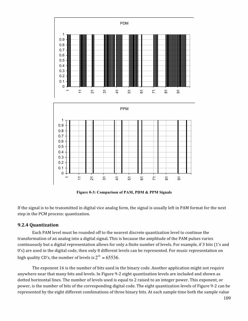
109
Figure 0-3: Comparison of PAM, PDM & PPM Signals
If the signal is to be transmitted in digital vice analog form, the signal is usually left in PAM format for the next step in the PCM process: quantization.
9.2.4 Quantization Each PAM level must be rounded off to the nearest discrete quantization level to continue the transformation of an analog into a digital signal. This is because the amplitude of the PAM pulses varies continuously but a digital representation allows for only a finite number of levels. For example, if 3 bits (1’s and 0’s) are used in the digital code, then only 8 different levels can be represented. For music representation on high quality CD’s, the number of levels is 162 65536= .
The exponent 16 is the number of bits used in the binary code. Another application might not require anywhere near that many bits and levels. In Figure 9-‐2 eight quantization levels are included and shown as dotted horizontal lines. The number of levels used is equal to 2 raised to an integer power. This exponent, or power, is the number of bits of the corresponding digital code. The eight quantization levels of Figure 9-‐2 can be represented by the eight different combinations of three binary bits. At each sample time both the sample value
PDM
00.10.20.30.40.50.60.70.80.91
1 11 21 31 41 51 61 71 81 91
PPM
00.10.20.30.40.50.60.70.80.91
1 11 21 31 41 51 61 71 81 91
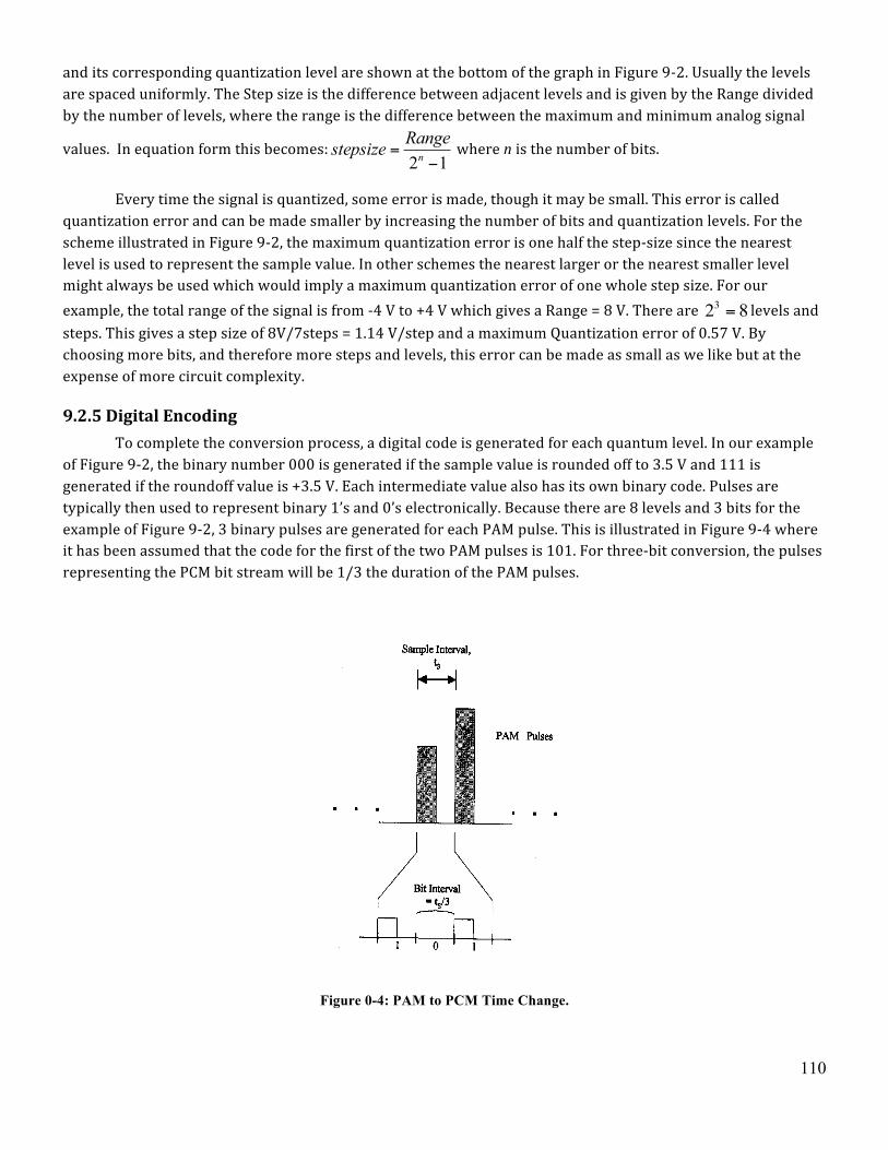
110
and its corresponding quantization level are shown at the bottom of the graph in Figure 9-‐2. Usually the levels are spaced uniformly. The Step size is the difference between adjacent levels and is given by the Range divided by the number of levels, where the range is the difference between the maximum and minimum analog signal
values. In equation form this becomes:2 1n
Rangestepsize =−
where n is the number of bits.
Every time the signal is quantized, some error is made, though it may be small. This error is called quantization error and can be made smaller by increasing the number of bits and quantization levels. For the scheme illustrated in Figure 9-‐2, the maximum quantization error is one half the step-‐size since the nearest level is used to represent the sample value. In other schemes the nearest larger or the nearest smaller level might always be used which would imply a maximum quantization error of one whole step size. For our example, the total range of the signal is from -‐4 V to +4 V which gives a Range = 8 V. There are 32 8= levels and steps. This gives a step size of 8V/7steps = 1.14 V/step and a maximum Quantization error of 0.57 V. By choosing more bits, and therefore more steps and levels, this error can be made as small as we like but at the expense of more circuit complexity.
9.2.5 Digital Encoding To complete the conversion process, a digital code is generated for each quantum level. In our example of Figure 9-‐2, the binary number 000 is generated if the sample value is rounded off to 3.5 V and 111 is generated if the roundoff value is +3.5 V. Each intermediate value also has its own binary code. Pulses are typically then used to represent binary 1’s and 0’s electronically. Because there are 8 levels and 3 bits for the example of Figure 9-‐2, 3 binary pulses are generated for each PAM pulse. This is illustrated in Figure 9-‐4 where it has been assumed that the code for the first of the two PAM pulses is 101. For three-‐bit conversion, the pulses representing the PCM bit stream will be 1/3 the duration of the PAM pulses.
Figure 0-4: PAM to PCM Time Change.
111
This means the PCM bit stream will require about 3 times the BW of the PAM signal or in the more general case of n-‐bit conversion, n times the PAM bandwidth. If a more precise conversion using more bits is required, then the number of pulses is n for each PAM pulse, where n is the number of bits. For 16-‐bit, CD music this is 16 pulses for every sample. More bits implies a greater baseband bandwidth requirement for the digital PCM signal. The pulses will be transmitted in some manner, such as directly over wires, or by modulation onto an RF carrier for transmission through the air, perhaps to a satellite. In either case, the required BW must be carefully considered. If direct transmission over wires is used, then these wires must have sufficient bandwidth to preserve enough of the pulse shape to maintain information, and if modulation onto an RF carrier is used, then the RF bandwidth required will depend on the baseband BW of the PCM bit stream. Since multiple pulses are being generated for each PAM pulse, their duration in time must be correspondingly shorter. PCM requires n times more BW than PAM. In equation form, BW > (number of bits)(fsamp1ing) for PCM. The increase in required bandwidth is the price to be paid for digital transmission of information. The benefits are those listed in the introduction such as better noise immunity.
Example 9.1
Determine the minimum baseband bandwidth required for 16 bit CD quality music.
Solution
Assuming a maximum frequency component of 20 KHz gives a sampling rate of about 44 KHz (slightly greater than the theoretical minimum). With 16 bits we get
BW > 16 x 44 KHz = 704 KHz, a very large baseband bandwidth compared to 20 KHz for the analog signal and this is for only one channel. If we want stereo and we time multiplex the two channels together, the BW requirement doubles.
Example 9.2
Determine the maximum quantization error for conversion of music into 16-‐bit PCM form if the input analog signal varies over the range of -‐1 V to + 1 V and the conversion takes place over that same range using the same scheme as illustrated in Figure 9-‐2.
Solution
The Range is 1 -‐ (-‐1) = 2 V and the number of steps is 162 65536= giving a step-‐size of 2V/65535 = 30.51 mV. The maximum quantization error is half the step-‐size, or 15.25 mV.
Example 9.3
Determine the dynamic range expressed in dB for CD music recordings. Refer to Figure 9-‐2.
Solution
The dynamic range is defined as the ratio of the greatest possible change in amplitude to the smallest. The total range (8 V in the case of Figure 9-‐2) is the largest possible change in the signal amplitude. The smallest possible change is the difference between adjacent levels. The number of steps is 2n and the size of one step is
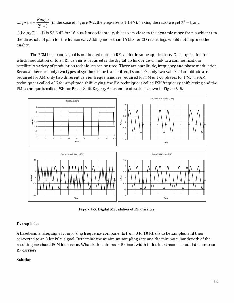
112
2 1n
Rangestepsize =−
(in the case of Figure 9-‐2, the step-‐size is 1.14 V). Taking the ratio we get 2 1n − , and
20 log(2 1)n× − is 96.3 dB for 16 bits. Not accidentally, this is very close to the dynamic range from a whisper to the threshold of pain for the human ear. Adding more than 16 bits for CD recordings would not improve the quality.
The PCM baseband signal is modulated onto an RF carrier in some applications. One application for which modulation onto an RF carrier is required is the digital up link or down link to a communications satellite. A variety of modulation techniques can be used. Three are amplitude, frequency and phase modulation. Because there are only two types of symbols to be transmitted, l’s and 0’s, only two values of amplitude are required for AM, only two different carrier frequencies are required for FM or two phases for PM. The AM technique is called ASK for amplitude shift keying, the FM technique is called FSK frequency shift keying and the PM technique is called PSK for Phase Shift Keying. An example of each is shown in Figure 9-‐5.
Figure 0-5: Digital Modulation of RF Carriers.
Example 9.4
A baseband analog signal comprising frequency components from 0 to 10 KHz is to be sampled and then converted to an 8 bit PCM signal. Determine the minimum sampling rate and the minimum bandwidth of the resulting baseband PCM bit stream. What is the minimum RF bandwidth if this bit stream is modulated onto an RF carrier?
Solution
Digital Baseband
0
0.2
0.4
0.6
0.8
1
1.2
1 11 21 31 41 51 61 71 81 91 101
Time
Voltage
Amplitude Shift Keying (ASK)
-1.5
-1
-0.5
0
0.5
1
1.5
1 11 21 31 41 51 61 71 81 91 101
Time
Voltage
Frequency Shift Keying (FSK)
-1.5
-1
-0.5
0
0.5
1
1.5
1 11 21 31 41 51 61 71 81 91 101
Time
Voltage
Phase Shift Keying (PSK)
-1.5
-1
-0.5
0
0.5
1
1.5
1 11 21 31 41 51 61 71 81 91 101
Time
Voltage
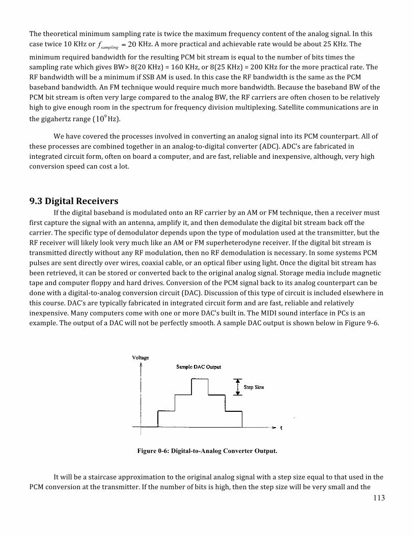
113
The theoretical minimum sampling rate is twice the maximum frequency content of the analog signal. In this case twice 10 KHz or 20samplingf = KHz. A more practical and achievable rate would be about 25 KHz. The
minimum required bandwidth for the resulting PCM bit stream is equal to the number of bits times the sampling rate which gives BW> 8(20 KHz) = 160 KHz, or 8(25 KHz) = 200 KHz for the more practical rate. The RF bandwidth will be a minimum if SSB AM is used. In this case the RF bandwidth is the same as the PCM baseband bandwidth. An FM technique would require much more bandwidth. Because the baseband BW of the PCM bit stream is often very large compared to the analog BW, the RF carriers are often chosen to be relatively high to give enough room in the spectrum for frequency division multiplexing. Satellite communications are in the gigahertz range ( 910 Hz).
We have covered the processes involved in converting an analog signal into its PCM counterpart. All of these processes are combined together in an analog-‐to-‐digital converter (ADC). ADC’s are fabricated in integrated circuit form, often on board a computer, and are fast, reliable and inexpensive, although, very high conversion speed can cost a lot.
9.3 Digital Receivers If the digital baseband is modulated onto an RF carrier by an AM or FM technique, then a receiver must first capture the signal with an antenna, amplify it, and then demodulate the digital bit stream back off the carrier. The specific type of demodulator depends upon the type of modulation used at the transmitter, but the RF receiver will likely look very much like an AM or FM superheterodyne receiver. If the digital bit stream is transmitted directly without any RF modulation, then no RF demodulation is necessary. In some systems PCM pulses are sent directly over wires, coaxial cable, or an optical fiber using light. Once the digital bit stream has been retrieved, it can be stored or converted back to the original analog signal. Storage media include magnetic tape and computer floppy and hard drives. Conversion of the PCM signal back to its analog counterpart can be done with a digital-‐to-‐analog conversion circuit (DAC). Discussion of this type of circuit is included elsewhere in this course. DAC’s are typically fabricated in integrated circuit form and are fast, reliable and relatively inexpensive. Many computers come with one or more DAC’s built in. The MIDI sound interface in PCs is an example. The output of a DAC will not be perfectly smooth. A sample DAC output is shown below in Figure 9-‐6.
Figure 0-6: Digital-to-Analog Converter Output.
It will be a staircase approximation to the original analog signal with a step size equal to that used in the PCM conversion at the transmitter. If the number of bits is high, then the step size will be very small and the
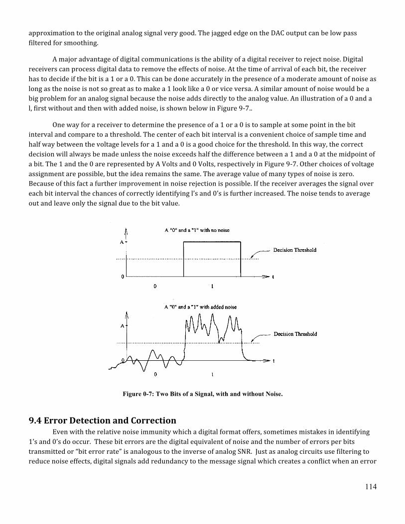
114
approximation to the original analog signal very good. The jagged edge on the DAC output can be low pass filtered for smoothing.
A major advantage of digital communications is the ability of a digital receiver to reject noise. Digital receivers can process digital data to remove the effects of noise. At the time of arrival of each bit, the receiver has to decide if the bit is a 1 or a 0. This can be done accurately in the presence of a moderate amount of noise as long as the noise is not so great as to make a 1 look like a 0 or vice versa. A similar amount of noise would be a big problem for an analog signal because the noise adds directly to the analog value. An illustration of a 0 and a l, first without and then with added noise, is shown below in Figure 9-‐7..
One way for a receiver to determine the presence of a 1 or a 0 is to sample at some point in the bit interval and compare to a threshold. The center of each bit interval is a convenient choice of sample time and half way between the voltage levels for a 1 and a 0 is a good choice for the threshold. In this way, the correct decision will always be made unless the noise exceeds half the difference between a 1 and a 0 at the midpoint of a bit. The 1 and the 0 are represented by A Volts and 0 Volts, respectively in Figure 9-‐7. Other choices of voltage assignment are possible, but the idea remains the same. The average value of many types of noise is zero. Because of this fact a further improvement in noise rejection is possible. If the receiver averages the signal over each bit interval the chances of correctly identifying l’s and 0’s is further increased. The noise tends to average out and leave only the signal due to the bit value.
Figure 0-7: Two Bits of a Signal, with and without Noise.
9.4 Error Detection and Correction Even with the relative noise immunity which a digital format offers, sometimes mistakes in identifying 1’s and 0’s do occur. These bit errors are the digital equivalent of noise and the number of errors per bits transmitted or “bit error rate” is analogous to the inverse of analog SNR. Just as analog circuits use filtering to reduce noise effects, digital signals add redundancy to the message signal which creates a conflict when an error
115
is present in either the original message or the redundancy. This redundancy can be used for one of two general approaches: simple error detection or forward error correction.
1. Simple error detection: For simple error detection, the basic approach is to send an automatic request for retransmission (ARQ) of the block of data in which an error is detected. Since the error detection code is providing a relatively simple function it can be relatively short resulting in few additional bits being transmitted unless an error is found. Disadvantages of this approach are that the entire block containing the error must be retransmitted and the receiver must transmit back to the originator of the message to get the corrected data block. If the receiver cannot transmit and errors cannot be tolerated, forward error correction is required. There are several techniques used to implement error detection:
a) Encoding methods: The format of the transmitted waveshape can help to identify bit errors, such as a “bipolar return to zero alternate mark inversion: encoding where successive “ones” in the sequence should have alternate polarities (+/-‐5V) and “zeros” are at 0V. If two successive “ones” are received with the same polarity, one is not a “one” or a “one” was missed between the two received.
b) Redundant transmission: This is conceptually the most simple means of error detection. Each block of data is transmitted twice. At the receiver, the blocks are compared and if found different, retransmission is requested. The primary disadvantage of this technique is that is sends, at best, 50% new information in each transmission, and less, if errors are actually detected. There are more efficient methods. c) Parity check: This method of error detection is both simple and efficient. It works by simply totaling the number of “1”s in a data block and adding a bit which makes the total, including the parity bit, the designated parity. For example, in an even parity system, if the seven bit sequence, “1011101”, is to be sent, an eighth parity bit of “1” is appended to the sequence to make the total number of “1”s in the sequence even. At the receiver, the eight bits are summed. If the result is an odd total, an error has been detected and the block is requested to be resent. At low bit error rates (number of incorrect bits received per total number of bits received), efficiency can be improved with longer sequences before appending the parity bit; however, then a longer block must be resent if an error is detected. One disadvantage of this relatively simple approach is that is only detects an odd number of errors in a sequence. To detect any number of errors in a sequence, a more complex method is required.
d) Cyclic redundancy check/checksum: One of the most effective and efficient means to detect multiple errors is called cyclic redundancy check, which treats the entire data block as one long binary number, divides it by a pre-‐selected fixed constant and transmits the remainder after the division along with the message. The receiver re-‐performs the division on the data block at the destination using the same fixed constant and compares the received and calculated remainders. In checksum, several blocks or sub-‐ blocks of data are added together then the cyclic redundancy check is performed on the result. The likelihood of one or more errors creating the same remainder is extremely remote, particularly with a judicious selection of the pre-‐selected constant. The primary disadvantage of this method is that it is somewhat calculation intensive.
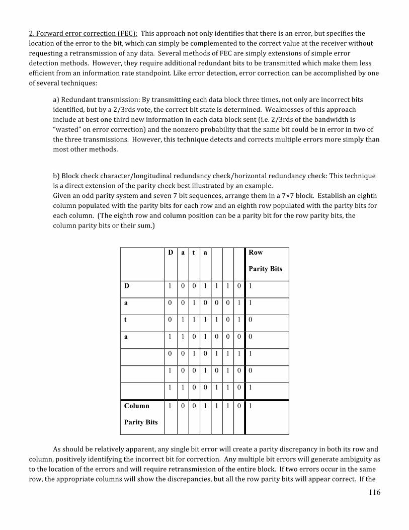
116
2. Forward error correction (FEC): This approach not only identifies that there is an error, but specifies the location of the error to the bit, which can simply be complemented to the correct value at the receiver without requesting a retransmission of any data. Several methods of FEC are simply extensions of simple error detection methods. However, they require additional redundant bits to be transmitted which make them less efficient from an information rate standpoint. Like error detection, error correction can be accomplished by one of several techniques:
a) Redundant transmission: By transmitting each data block three times, not only are incorrect bits identified, but by a 2/3rds vote, the correct bit state is determined. Weaknesses of this approach include at best one third new information in each data block sent (i.e. 2/3rds of the bandwidth is “wasted” on error correction) and the nonzero probability that the same bit could be in error in two of the three transmissions. However, this technique detects and corrects multiple errors more simply than most other methods.
b) Block check character/longitudinal redundancy check/horizontal redundancy check: This technique is a direct extension of the parity check best illustrated by an example. Given an odd parity system and seven 7 bit sequences, arrange them in a 7×7 block. Establish an eighth column populated with the parity bits for each row and an eighth row populated with the parity bits for each column. (The eighth row and column position can be a parity bit for the row parity bits, the column parity bits or their sum.)
D a t a Row
Parity Bits
D 1 0 0 1 1 1 0 1
a 0 0 1 0 0 0 1 1
t 0 1 1 1 1 0 1 0
a 1 1 0 1 0 0 0 0
0 0 1 0 1 1 1 1
1 0 0 1 0 1 0 0
1 1 0 0 1 1 0 1
Column
Parity Bits
1 0 0 1 1 1 0 1
As should be relatively apparent, any single bit error will create a parity discrepancy in both its row and column, positively identifying the incorrect bit for correction. Any multiple bit errors will generate ambiguity as to the location of the errors and will require retransmission of the entire block. If two errors occur in the same row, the appropriate columns will show the discrepancies, but all the row parity bits will appear correct. If the
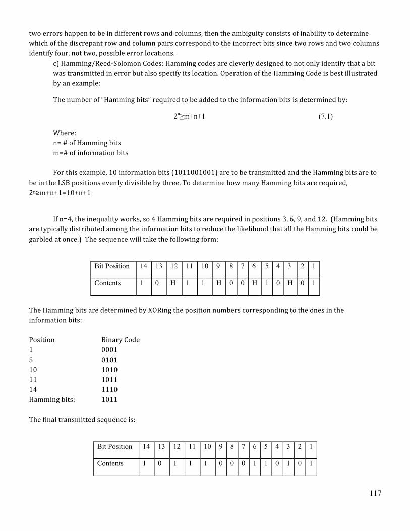
117
two errors happen to be in different rows and columns, then the ambiguity consists of inability to determine which of the discrepant row and column pairs correspond to the incorrect bits since two rows and two columns identify four, not two, possible error locations. c) Hamming/Reed-‐Solomon Codes: Hamming codes are cleverly designed to not only identify that a bit was transmitted in error but also specify its location. Operation of the Hamming Code is best illustrated by an example:
The number of “Hamming bits” required to be added to the information bits is determined by:
2n≥m+n+1 (7.1)
Where: n= # of Hamming bits m=# of information bits
For this example, 10 information bits (1011001001) are to be transmitted and the Hamming bits are to be in the LSB positions evenly divisible by three. To determine how many Hamming bits are required, 2n≥m+n+1=10+n+1
If n=4, the inequality works, so 4 Hamming bits are required in positions 3, 6, 9, and 12. (Hamming bits are typically distributed among the information bits to reduce the likelihood that all the Hamming bits could be garbled at once.) The sequence will take the following form:
Bit Position 14 13 12 11 10 9 8 7 6 5 4 3 2 1
Contents 1 0 H 1 1 H 0 0 H 1 0 H 0 1
The Hamming bits are determined by XORing the position numbers corresponding to the ones in the information bits: Position Binary Code 1 0001 5 0101 10 1010 11 1011 14 1110 Hamming bits: 1011 The final transmitted sequence is:
Bit Position 14 13 12 11 10 9 8 7 6 5 4 3 2 1
Contents 1 0 1 1 1 0 0 0 1 1 0 1 0 1
118
If the bits are transmitted without error, the receiver extracts the bits from the designated Hamming bits positions to XOR them with the position numbers corresponding to the ones in the information bits and confirm that there are no errors: Position Binary Code Hamming bits: 1011 1 0001 5 0101 10 1010 11 1011 14 1110 Error Position: 0000 (No errors) If, on the other hand, one bit is in error, say in position 4, the received sequence would be:
Bit Position 14 13 12 11 10 9 8 7 6 5 4 3 2 1
Contents 1 0 1 1 1 0 0 0 1 1 1 1 0 1
Repeating the extraction and XORing process produces:
Position Binary Code Hamming bits: 1011 1 0001 4 0100 5 0101 10 1010 11 1011 14 1110 Error Position: 0100 (Error in position 4) The bit in position 4 is complemented and the error free sequence is then processed. More complex Hamming and Reed-‐Solomon codes can detect and correct multiple errors, including in the coded bits themselves, but those codes are beyond the scope of this course.
9.5 Channel Capacity The entire purpose for any communication system is to get original information from one point to another. There are a number of factors which limit how fast this information can be transferred. Similar to analog systems, noise and bandwidth play their parts. Unique to digital systems, “overhead” and encoding also serve to limit information rate. We will discuss each of these factors in turn.
119
First, let’s start off with some definitions. Information is the “intelligence” which is desired to be transferred from one location to another and is the reason for the transmission in the first place. Ideally, it is completely unpredictable such that one part of the information message tells nothing about any other part. In binary digital systems, the unit of information is called a bit, a “1” or a “0”.
Data is different from information in that it includes “overhead” in addition to the baseline information. Such overhead can include “start” and “stop” bits to delineate data blocks/frames, error detection/correction codes, encryption codes, routing instructions, frame reassembly directions, frames re-‐transmitted due to errors or omissions, etc. The units for data are exactly the same as for information; however, no real digital communication system can achieve a data rate equal to its information rate, because all real systems have to include some overhead. In other words, data equals information plus overhead.
For the remainder of this chapter, we will discuss data and define Channel Capacity in terms of data rate. Some texts will use the terms information rate and data rate interchangeably, but you should recognize that the information rate you can push through a digital communication system will never reach, even under ideal conditions, the advertised Channel Capacity, a data rate which includes overhead added and needed by the system. The data rate which a digital channel can carry is determined by channel bandwidth in a manner similar to an analog system. Per Hartley’s Law, given sufficient time and/or channel bandwidth, any quantity of data can eventually be transferred:
I=ktB (9.2)
Where: I=amount of data to be sent [bits] k=a constant [bits/cycle] t=transmission time [sec] B=baseband channel bandwidth [Hz]
Since infinite time or bandwidth is rarely available, a typically more useful concept is the rate at which information can be sent over a channel also known as “channel data rate”:
R=I/t (9.3)
Where: R=data rate [bits/sec] I=amount of information to be sent [bits] t=transmission time [sec]
Rewriting Hartley’s Law with this new variable:
R=kB (9.4)
Where: R=data rate [bits/sec] k=a constant [bits/cycle] B=baseband channel bandwidth [Hz]
120
Since channel bandwidth is defined in the same way as for analog signals, the remaining mystery variable in this equation is “k”. Through the Shannon Limit, in a derivation beyond the scope of this course, the maximum practical value of “k” was determined to be a function of the channel signal to noise ratio (in rational, not dB form):
Rmax=C=B×log2(1+S/N) (9.5)
Where: R=data rate [bits/sec] C=Channel data rate Capacity [bits/sec] B=baseband channel bandwidth [Hz] S/N=signal-‐to-‐noise power ratio (not in dB) (S/N=10SNRdB/10)
Thus, the channel capacity is determined by the bandwidth available and the SNR experienced in the same way the analog channels require sufficient bandwidth and adequate noise margin to reproduce the original signal at the destination with the specified fidelity. While the bandwidth is typically fixed at system design, the SNR can varying greatly during operation based on environmental factors. Therefore, during initial design, a minimum expected SNR is set and used to determine the channel capacity. If the SNR experienced in operation falls below this assumed value, the channel capacity falls, the error rate in the channel climbs quickly and the system performance degrades rapidly.
Since SNRs in digital channels can be quite high, how do we design our data stream to take advantage of as much of the channel capacity as possible? Let’s go back to our variation of Hartley’s Law:
R=kB (9.4)
Where: R=data rate [bits/sec] k=a constant [bits/cycle] B=baseband channel bandwidth [Hz]
We need to redefine “k” in terms of the transmitted data stream. We’ll start with the simplest case: a straight binary signal transmitted in a sequence requiring the greatest possible channel bandwidth. The sequence requiring the greatest bandwidth (having the highest frequency components) would be one which simply alternated high and low (since any consecutive matching bits would change less frequently requiring less bandwidth). Figure 9-‐8 illustrates this limiting condition.
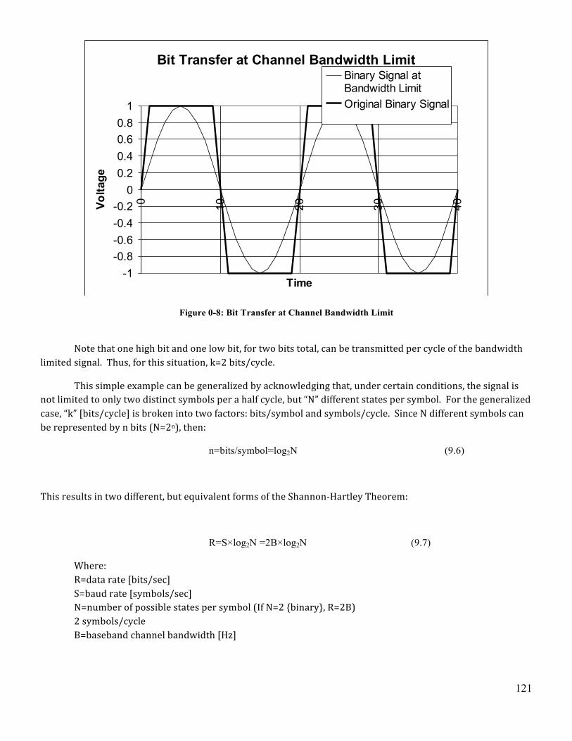
121
Figure 0-8: Bit Transfer at Channel Bandwidth Limit
Note that one high bit and one low bit, for two bits total, can be transmitted per cycle of the bandwidth limited signal. Thus, for this situation, k=2 bits/cycle.
This simple example can be generalized by acknowledging that, under certain conditions, the signal is not limited to only two distinct symbols per a half cycle, but “N” different states per symbol. For the generalized case, “k” [bits/cycle] is broken into two factors: bits/symbol and symbols/cycle. Since N different symbols can be represented by n bits (N=2n), then:
n=bits/symbol=log2N (9.6)
This results in two different, but equivalent forms of the Shannon-‐Hartley Theorem:
R=S×log2N =2B×log2N (9.7)
Where: R=data rate [bits/sec] S=baud rate [symbols/sec] N=number of possible states per symbol (If N=2 {binary}, R=2B) 2 symbols/cycle B=baseband channel bandwidth [Hz]
Bit Transfer at Channel Bandwidth Limit
-1-0.8-0.6-0.4-0.2
00.20.40.60.8
1
0 10 20 30 40
Time
Volta
ge
Binary Signal atBandwidth LimitOriginal Binary Signal
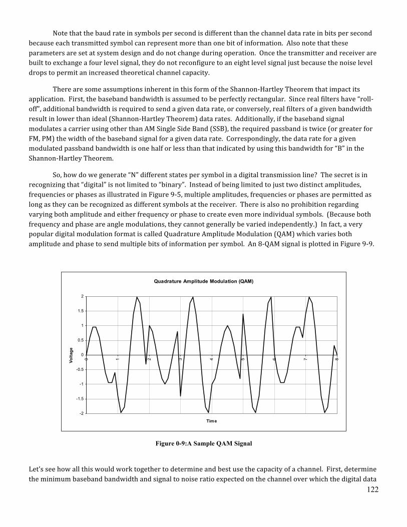
122
Note that the baud rate in symbols per second is different than the channel data rate in bits per second because each transmitted symbol can represent more than one bit of information. Also note that these parameters are set at system design and do not change during operation. Once the transmitter and receiver are built to exchange a four level signal, they do not reconfigure to an eight level signal just because the noise level drops to permit an increased theoretical channel capacity.
There are some assumptions inherent in this form of the Shannon-‐Hartley Theorem that impact its application. First, the baseband bandwidth is assumed to be perfectly rectangular. Since real filters have “roll-‐off”, additional bandwidth is required to send a given data rate, or conversely, real filters of a given bandwidth result in lower than ideal (Shannon-‐Hartley Theorem) data rates. Additionally, if the baseband signal modulates a carrier using other than AM Single Side Band (SSB), the required passband is twice (or greater for FM, PM) the width of the baseband signal for a given data rate. Correspondingly, the data rate for a given modulated passband bandwidth is one half or less than that indicated by using this bandwidth for “B” in the Shannon-‐Hartley Theorem.
So, how do we generate “N” different states per symbol in a digital transmission line? The secret is in recognizing that “digital” is not limited to “binary”. Instead of being limited to just two distinct amplitudes, frequencies or phases as illustrated in Figure 9-‐5, multiple amplitudes, frequencies or phases are permitted as long as they can be recognized as different symbols at the receiver. There is also no prohibition regarding varying both amplitude and either frequency or phase to create even more individual symbols. (Because both frequency and phase are angle modulations, they cannot generally be varied independently.) In fact, a very popular digital modulation format is called Quadrature Amplitude Modulation (QAM) which varies both amplitude and phase to send multiple bits of information per symbol. An 8-‐QAM signal is plotted in Figure 9-‐9.
Figure 0-9:A Sample QAM Signal
Let’s see how all this would work together to determine and best use the capacity of a channel. First, determine the minimum baseband bandwidth and signal to noise ratio expected on the channel over which the digital data
Quadrature Amplitude Modulation (QAM)
-2
-1.5
-1
-0.5
0
0.5
1
1.5
2
0 1 2 3 4 5 6 7 8
Time
Volta
ge
123
will be transferred. These establish the maximum channel data rate capacity using the Shannon Limit. Next, use this channel data rate, baseband bandwidth and any correction for band “roll-‐off” in the Shannon-‐Hartley Theorem to determine the whole number of different symbols which are needed to achieve this data rate. (Round down.) This is the number of symbols designed into the system modulation scheme and, when worked back through the Shannon-‐Hartley Theorem, gives the design channel data rate. To illustrate, let’s look at an example:
Example 9.5
A digital channel has a baseband bandwidth of 20KHz and a minimum expected SNR of 50dB. The digital encoding scheme is expected to be QAM with bits/symbol equal to an even power of 2. Assuming no filter roll-‐off corrections are required, determine the maximum channel capacity based on bandwidth and noise, the design form of QAM to be used (8-‐QAM [3 bits/symbol], 64-‐QAM [6 bits/symbol], etc.) and the expected maximum channel data rate.
Solution
SNR (rational form)=1050dB/10dB=105
From equation (7.5): C=B×log2(1+S/N)=20KHz×log2(100,001)bits/cycle=332Kbps
From equation (7.7): R=2B×log2N=332Kbps=2×20KHz×log2N;
Nmax=28.3=315.2 states/symbol;
Ndesign=28=256 states/symbol => 256-‐QAM [8 bits/symbol]
From equation (7.7): Rmax=2B×log2N=2×20KHz×log2256=320Kbps
9.6 Time Division Multiplexing AM and FM radio stations are frequency division multiplexed so that multiple stations can use the same transmission medium. This is done by assigning each station a different carrier and limiting the side band content of each station so that it does not overlap with its neighbors. Because radio stations are frequency division multiplexed, receivers can tune to individual stations by using filters. PCM digital signal format allows a different kind of multiplexing called time division multiplexing (TDM). Time division multiplexing is important because it allows the simultaneous use of a common resource, such as a telephone line or a satellite communications link, by multiple digital signals. The total number of channels multiplexed together can number in the 100’s or even 1000’s. A diagram of a TDM system is shown in Figure 9-‐10. Two PCM signals are shown time multiplexed together. This is done by first sending a bit from Signal A then a bit from Signal B and then back to A etc.
In this way bits from each signal become interleaved as they flow from the output of the multiplexer and into the transmission line. The bit format chosen for Figure 9-‐10 is called return to zero with a digital zero represented by zero volts. There are many other formats possible, some of which are more efficient in one way or another, but the choice for this figure is convenient for illustration.
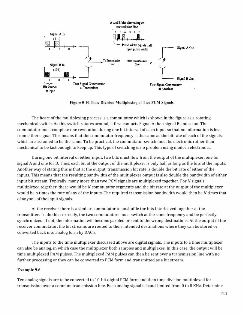
124
Figure 0-10:Time Division Multiplexing of Two PCM Signals.
The heart of the multiplexing process is a commutator which is shown in the figure as a rotating mechanical switch. As this switch rotates around, it first contacts Signal A then signal B and so on. The commutator must complete one revolution during one bit interval of each input so that no information is lost from either signal. This means that the commutator frequency is the same as the bit rate of each of the signals, which are assumed to be the same. To be practical, the commutator switch must be electronic rather than mechanical to be fast enough to keep up. This type of switching is no problem using modern electronics.
During one bit interval of either input, two bits must flow from the output of the multiplexer, one for signal A and one for B. Thus, each bit at the output of the multiplexer is only half as long as the bits at the inputs. Another way of stating this is that at the output, transmission bit rate is double the bit rate of either of the inputs. This means that the resulting bandwidth of the multiplexer output is also double the bandwidth of either input bit stream. Typically, many more than two PCM signals are multiplexed together. For N signals multiplexed together, there would be N commutator segments and the bit rate at the output of the multiplexer would be n times the rate of any of the inputs. The required transmission bandwidth would then be N times that of anyone of the input signals.
At the receiver there is a similar commutator to unshuffle the bits interleaved together at the transmitter. To do this correctly, the two commutators must switch at the same frequency and be perfectly synchronized. If not, the information will become garbled or sent to the wrong destinations. At the output of the receiver commutator, the bit streams are routed to their intended destinations where they can be stored or converted back into analog form by DAC’s.
The inputs to the time multiplexer discussed above are digital signals. The inputs to a time multiplexer can also be analog, in which case the multiplexer both samples and multiplexes. In this case, the output will be time multiplexed PAM pulses. The multiplexed PAM pulses can then be sent over a transmission line with no further processing or they can be converted to PCM form and transmitted as a bit stream.
Example 9.6
Ten analog signals are to be converted to 10-‐bit digital PCM form and then time division multiplexed for transmission over a common transmission line. Each analog signal is band-‐limited from 0 to 8 KHz. Determine
125
the bit rate for each input channel, the frequency of rotation of the commutator switch and the minimum bandwidth requirement for the transmission line.
Solution
From the sampling theorem, each signal must first be sampled at a minimum of 2 x 8 = 16 KHz and so we will pick a sampling rate of 20 KHz to be conservative. 10 bits will be generated for each signal, which gives a bit rate of l0x20 = 200 Kbits/s for each input. The required frequency of rotation of the commutator is the same as the bit rate of anyone input channel, so this becomes 200commutatorf = KHz. The required baseband bandwidth
for a single channel is the same as the PCM bit rate which is 200 KHz. For 10 channels, the requirement will be 10 times as much, or 10 200 2000outputBW = × = KHz = 2 MHz.
126
9.7 Homework Problems
Problem 9.l
The sampling rate used in the conversion of an analog signal to PCM is 20 KHz. The analog signal contains components of high enough frequency to cause aliasing problems. To avoid aliasing, the analog signal is low pass filtered before being sampled. What value should the cutoff frequency of the low pass filter have? Assume ideal filtering.
Problem 9.2
The quantization error for an analog signal, which varies between 0 and 5 V, is to be less than 1 mV when that signal is converted to PCM form. Find the minimum number of bits for the digital conversion. What is the value of the actual quantization error for that minimum number of bits? Assume use of the same conversion scheme as illustrated in Figure 9-‐1. How would your answers change if the scheme were modified such that the sample values were always rounded down to the next nearest quantization level?
Problem 9.3
Two analog signals each having frequency content from 0 to 4 KHz are frequency division multiplexed onto carriers at 10 KHz and 20 KHz by a DSB-‐SC AM process. The composite signal is then sampled and converted to a 10-‐bit digital signal. Determine the minimum sampling rate for the composite analog signal and the minimum transmission bandwidth for the PCM bit stream.
Problem 9.4
An analog signal which varies over the range -‐1 V to 1 V is to be converted to a 4-‐bit PCM signal. The input analog signal is band limited to the range 100 Hz to 1000 Hz.
a. Determine the minimum sampling rate for the conversion. b. Assuming the same conversion scheme as illustrated in Figure 9-‐1, determine the number of
quantization levels, the step size and the values for the minimum and maximum quantization levels. c. Find the maximum quantization error. d. Find the minimum transmission bandwidth for the resulting PCM signal.
Problem 9.5
Each of 20 analog audio signals of frequency content up to 10 KHz is first transformed into 11-‐bit digital form. The 20 PCM signals are then time division multiplexed together before transmission over a light fiber.
a. Determine the frequency of the transmitter commutator. b. Determine the minimum transmission bandwidth for the light fiber.
Problem 9.6
A binary channel with a bit rate of 28.8 Kbits/s is available for PCM voice transmission. Find appropriate values for the sampling rate and the number of bits for quantization if the maximum frequency content of the audio signal is 4 KHz.
127
Problem 9.7
An analog signal is quantized and transmitted using a PCM code. If each sample at the receiving end of the system must be known to within 4% of the Range of the input analog signal at the source, how many bits are required for each sample?

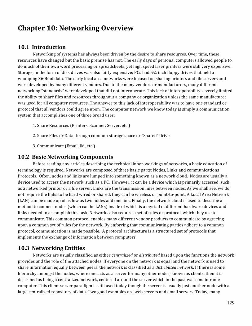
129
Chapter 10: Networking Overview
10.1 Introduction Networking of systems has always been driven by the desire to share resources. Over time, these resources have changed but the basic premise has not. The early days of personal computers allowed people to do much of their own word processing or spreadsheets, yet high speed laser printers were still very expensive. Storage, in the form of disk drives was also fairly expensive; PCs had 5¼ inch floppy drives that held a whopping 360K of data. The early local area networks were focused on sharing printers and file servers and were developed by many different vendors. Due to the many vendors or manufacturers, many different networking “standards” were developed that did not interoperate. This lack of interoperability severely limited the ability to share files and resources throughout a company or organization unless the same manufacturer was used for all computer resources. The answer to this lack of interoperability was to have one standard or protocol that all vendors could agree upon. The computer network we know today is simply a communication system that accomplishes one of three broad uses:
1. Share Resources (Printers, Scanner, Server, etc.)
2. Share Files or Data through common storage space or “Shared” drive
3. Communicate (Email, IM, etc.)
10.2 Basic Networking Components Before reading any articles describing the technical inner-‐workings of networks, a basic education of terminology is required. Networks are composed of three basic parts: Nodes, Links and communications Protocols. Often, nodes and links are lumped into something known as a network cloud. Nodes are usually a device used to access the network, such as a PC. However, it can be a device which is primarily accessed, such as a networked printer or a file server. Links are the transmission lines between nodes. As we shall see, we do not require the links to be hard wired or shared, they can be wireless or point-‐to-‐point. A Local Area Network (LAN) can be made up of as few as two nodes and one link. Finally, the network cloud is used to describe a method to connect nodes (which can be LANs) inside of which is a myriad of different hardware devices and links needed to accomplish this task. Networks also require a set of rules or protocol, which they use to communicate. This common protocol enables many different vendor products to communicate by agreeing upon a common set of rules for the network. By enforcing that communicating parties adhere to a common protocol, communication is made possible. A protocol architecture is a structured set of protocols that implements the exchange of information between computers.
10.3 Networking Entities Networks are usually classified as either centralized or distributed based upon the functions the network provides and the role of the attached nodes. If everyone on the network is equal and the network is used to share information equally between peers, the network is classified as a distributed network. If there is some hierarchy amongst the nodes, where one acts as a server for many other nodes, known as clients, then it is described as being a centralized network, centered around the server which in the past was a mainframe computer. This client-‐server paradigm is still used today though the server is usually just another node with a large centralized repository of data. Two good examples are web servers and email servers. Today, many
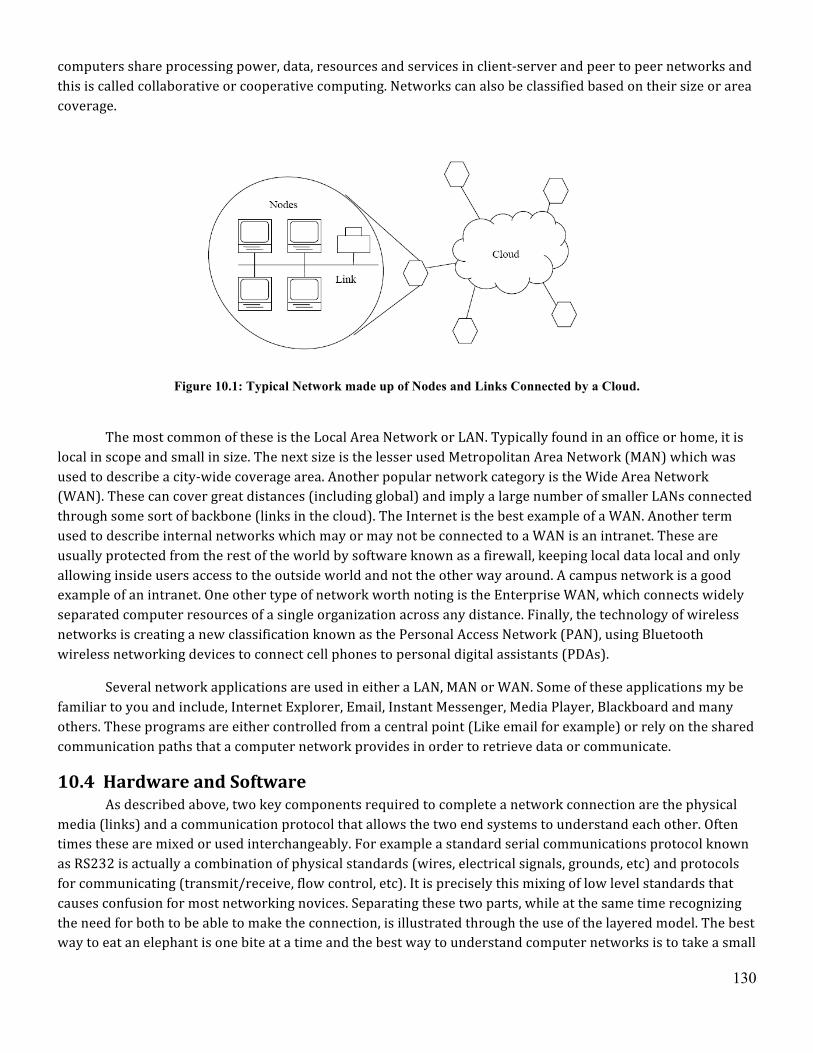
130
computers share processing power, data, resources and services in client-‐server and peer to peer networks and this is called collaborative or cooperative computing. Networks can also be classified based on their size or area coverage.
Figure 10.1: Typical Network made up of Nodes and Links Connected by a Cloud.
The most common of these is the Local Area Network or LAN. Typically found in an office or home, it is local in scope and small in size. The next size is the lesser used Metropolitan Area Network (MAN) which was used to describe a city-‐wide coverage area. Another popular network category is the Wide Area Network (WAN). These can cover great distances (including global) and imply a large number of smaller LANs connected through some sort of backbone (links in the cloud). The Internet is the best example of a WAN. Another term used to describe internal networks which may or may not be connected to a WAN is an intranet. These are usually protected from the rest of the world by software known as a firewall, keeping local data local and only allowing inside users access to the outside world and not the other way around. A campus network is a good example of an intranet. One other type of network worth noting is the Enterprise WAN, which connects widely separated computer resources of a single organization across any distance. Finally, the technology of wireless networks is creating a new classification known as the Personal Access Network (PAN), using Bluetooth wireless networking devices to connect cell phones to personal digital assistants (PDAs).
Several network applications are used in either a LAN, MAN or WAN. Some of these applications my be familiar to you and include, Internet Explorer, Email, Instant Messenger, Media Player, Blackboard and many others. These programs are either controlled from a central point (Like email for example) or rely on the shared communication paths that a computer network provides in order to retrieve data or communicate.
10.4 Hardware and Software As described above, two key components required to complete a network connection are the physical media (links) and a communication protocol that allows the two end systems to understand each other. Often times these are mixed or used interchangeably. For example a standard serial communications protocol known as RS232 is actually a combination of physical standards (wires, electrical signals, grounds, etc) and protocols for communicating (transmit/receive, flow control, etc). It is precisely this mixing of low level standards that causes confusion for most networking novices. Separating these two parts, while at the same time recognizing the need for both to be able to make the connection, is illustrated through the use of the layered model. The best way to eat an elephant is one bite at a time and the best way to understand computer networks is to take a small
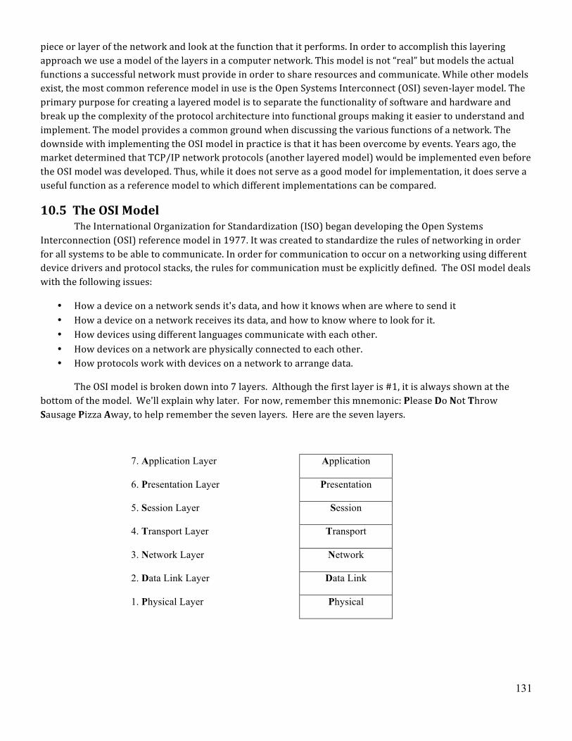
131
piece or layer of the network and look at the function that it performs. In order to accomplish this layering approach we use a model of the layers in a computer network. This model is not “real” but models the actual functions a successful network must provide in order to share resources and communicate. While other models exist, the most common reference model in use is the Open Systems Interconnect (OSI) seven-‐layer model. The primary purpose for creating a layered model is to separate the functionality of software and hardware and break up the complexity of the protocol architecture into functional groups making it easier to understand and implement. The model provides a common ground when discussing the various functions of a network. The downside with implementing the OSI model in practice is that it has been overcome by events. Years ago, the market determined that TCP/IP network protocols (another layered model) would be implemented even before the OSI model was developed. Thus, while it does not serve as a good model for implementation, it does serve a useful function as a reference model to which different implementations can be compared.
10.5 The OSI Model The International Organization for Standardization (ISO) began developing the Open Systems Interconnection (OSI) reference model in 1977. It was created to standardize the rules of networking in order for all systems to be able to communicate. In order for communication to occur on a networking using different device drivers and protocol stacks, the rules for communication must be explicitly defined. The OSI model deals with the following issues:
• How a device on a network sends it's data, and how it knows when are where to send it • How a device on a network receives its data, and how to know where to look for it. • How devices using different languages communicate with each other. • How devices on a network are physically connected to each other. • How protocols work with devices on a network to arrange data.
The OSI model is broken down into 7 layers. Although the first layer is #1, it is always shown at the bottom of the model. We'll explain why later. For now, remember this mnemonic: Please Do Not Throw Sausage Pizza Away, to help remember the seven layers. Here are the seven layers.
7. Application Layer Application
6. Presentation Layer Presentation
5. Session Layer Session
4. Transport Layer Transport
3. Network Layer Network
2. Data Link Layer Data Link
1. Physical Layer Physical
132
10.6 Protocol Stacks In order for each layer of the model to communicate with the levels above and below it, certain rules were developed. These rules are called Protocols, and each protocol provides a specific layer of the model with a specific set of tasks or services. Each layer of the model has its own set of protocols associated with it. When you have a set of protocols that create a complete OSI model, it is called a Protocol Stack. An example of a protocol stack is TCP/IP, the standard for communication over the internet, or Appletalk for Macintosh computers.
As stated before, protocols define how layers communicate with each other. Protocols specifically work with only the layer above and below them. They receive services from the protocol below, and provide services for the protocol above them, which limits the complexity of each layer by eliminating the need for each layer to understand the functions of all other layers. This order maintains a standard that is common to all forms of networking.
In order for two devices on a network to communicate, they must both be using the same protocol stack. Each protocol in a stack on one device must communicate with its equivalent stack, or peer, on the other device. This allows computers running different operating systems to communicate with each other easily, such as having Macintosh computers on a Windows NT network.
10.6.1 Communication Between Stacks When a message is sent from one machine to another, it travels down the protocol stack or layers of the model, and then up the layers of the stack on the other machine. As the data travels down the stack, it picks up headers from each layer. This is called encapsulation. Headers contain information that is read by the peer layer on the stack of the other computer. As the data travels up the levels of the peer computer, each header is removed by its equivalent protocol. These headers contain different information depending on the layer they receive the header from, but tell the peer layer important information, including packet size, frames, and datagrams.
10.6.2 Encapsulation Layering a protocol, like the ISO model, also implies that each layer is adding something to the one above or below. You can look at the layered model two ways, from the bottom up or the top down. When you view the model from the top down, you assume that the layers below you provide you with some type of service that you need to talk to another entity on the network. For example, all layers above the physical layer assume that some kind of physical connection exists. The physical layer is concerned with all aspects of transmitting and receiving data (bits) on the network media and several key characteristics are defined but the layers above could care less about the physical structure of the network or the mechanical and electrical specifications for using the medium. This is what is meant by “breaking up a complex problem into bite-‐size chunks.” Along the same lines, from the vantage point of the lower layers, the upper layers are relied upon to provide sufficient data in their headers so that the information can be delivered to the proper destination. You can think of the 7-‐layer OSI model as a diagram for mail delivery from the Postal Service. This diagram is created with extreme and almost ridiculous detail. Example 10.1
Count the layers for you to receive a letter via postal mail. The letter itself is the Data that is being sent (layer 6). The letter is then addressed to the person (layer 5) then the street and address is listed (layer 4), then
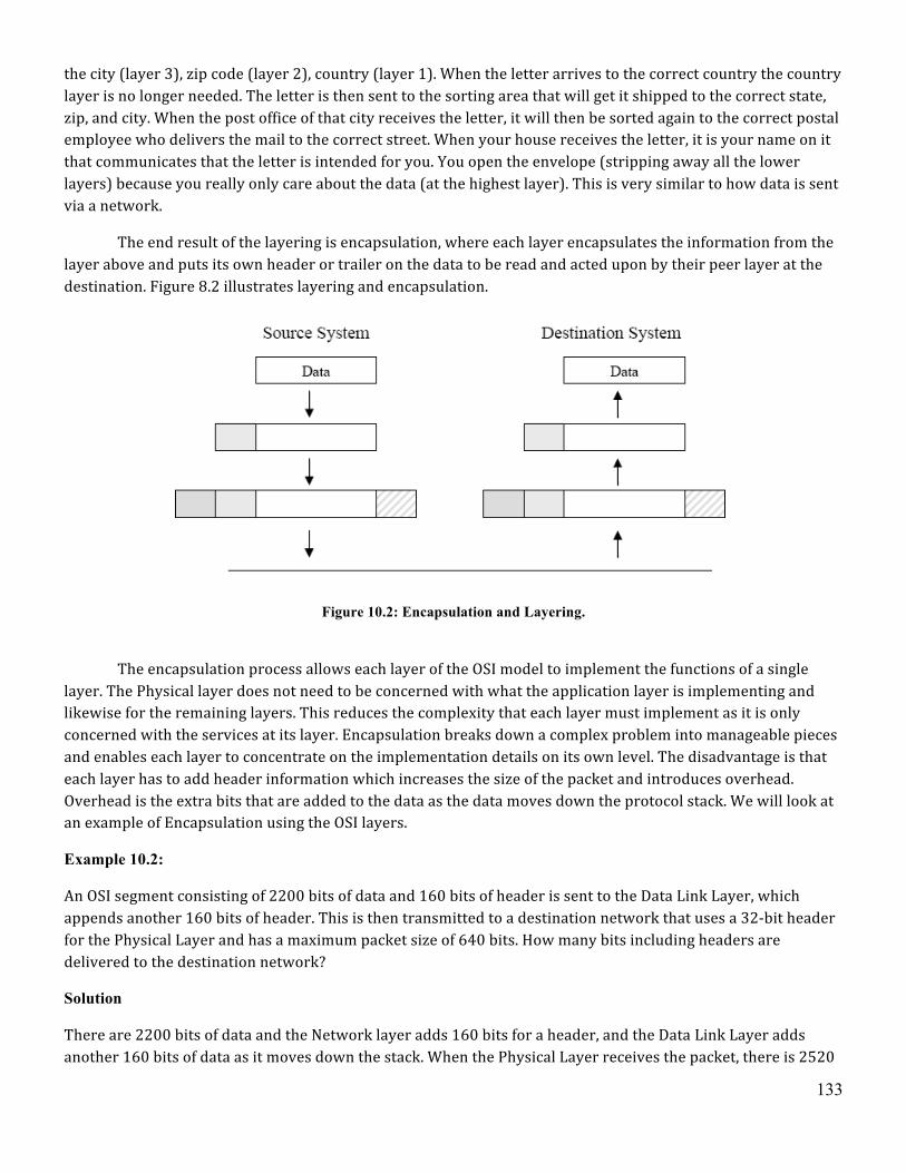
133
the city (layer 3), zip code (layer 2), country (layer 1). When the letter arrives to the correct country the country layer is no longer needed. The letter is then sent to the sorting area that will get it shipped to the correct state, zip, and city. When the post office of that city receives the letter, it will then be sorted again to the correct postal employee who delivers the mail to the correct street. When your house receives the letter, it is your name on it that communicates that the letter is intended for you. You open the envelope (stripping away all the lower layers) because you really only care about the data (at the highest layer). This is very similar to how data is sent via a network.
The end result of the layering is encapsulation, where each layer encapsulates the information from the layer above and puts its own header or trailer on the data to be read and acted upon by their peer layer at the destination. Figure 8.2 illustrates layering and encapsulation.
Figure 10.2: Encapsulation and Layering.
The encapsulation process allows each layer of the OSI model to implement the functions of a single layer. The Physical layer does not need to be concerned with what the application layer is implementing and likewise for the remaining layers. This reduces the complexity that each layer must implement as it is only concerned with the services at its layer. Encapsulation breaks down a complex problem into manageable pieces and enables each layer to concentrate on the implementation details on its own level. The disadvantage is that each layer has to add header information which increases the size of the packet and introduces overhead. Overhead is the extra bits that are added to the data as the data moves down the protocol stack. We will look at an example of Encapsulation using the OSI layers.
Example 10.2:
An OSI segment consisting of 2200 bits of data and 160 bits of header is sent to the Data Link Layer, which appends another 160 bits of header. This is then transmitted to a destination network that uses a 32-‐bit header for the Physical Layer and has a maximum packet size of 640 bits. How many bits including headers are delivered to the destination network?
Solution
There are 2200 bits of data and the Network layer adds 160 bits for a header, and the Data Link Layer adds another 160 bits of data as it moves down the stack. When the Physical Layer receives the packet, there is 2520
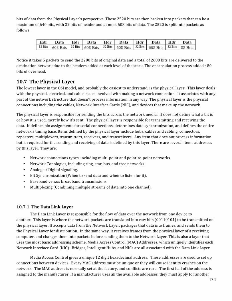
134
bits of data from the Physical Layer’s perspective. These 2520 bits are then broken into packets that can be a maximum of 640 bits, with 32 bits of header and at most 608 bits of data. The 2520 is split into packets as follows:
Notice it takes 5 packets to send the 2200 bits of original data and a total of 2680 bits are delivered to the destination network due to the headers added at each level of the stack. The encapsulation process added 480 bits of overhead.
10.7 The Physical Layer The lowest layer in the OSI model, and probably the easiest to understand, is the physical layer. This layer deals with the physical, electrical, and cable issues involved with making a network connection. It associates with any part of the network structure that doesn't process information in any way. The physical layer is the physical connections including the cables, Network Interface Cards (NIC), and devices that make up the network.
The physical layer is responsible for sending the bits across the network media. It does not define what a bit is or how it is used, merely how it's sent. The physical layer is responsible for transmitting and receiving the data. It defines pin assignments for serial connections, determines data synchronization, and defines the entire network's timing base. Items defined by the physical layer include hubs, cables and cabling, connectors, repeaters, multiplexers, transmitters, receivers, and transceivers. Any item that does not process information but is required for the sending and receiving of data is defined by this layer. There are several items addresses by this layer. They are:
• Network connections types, including multi-‐point and point-‐to-‐point networks. • Network Topologies, including ring, star, bus, and tree networks. • Analog or Digital signaling. • Bit Synchronization (When to send data and when to listen for it). • Baseband versus broadband transmissions. • Multiplexing (Combining multiple streams of data into one channel).
10.7.1 The Data Link Layer The Data Link Layer is responsible for the flow of data over the network from one device to another. This layer is where the network packets are translated into raw bits (00110101) to be transmitted on the physical layer. It accepts data from the Network Layer, packages that data into frames, and sends them to the Physical Layer for distribution. In the same way, it receives frames from the physical layer of a receiving computer, and changes them into packets before sending them to the Network Layer. This is also a layer that uses the most basic addressing scheme, Media Access Control (MAC) Addresses, which uniquely identifies each Network Interface Card (NIC). Bridges, Intelligent Hubs, and NICs are all associated with the Data Link Layer.
Media Access Control gives a unique 12 digit hexadecimal address. These addresses are used to set up connections between devices. Every MAC address must be unique or they will cause identity crashes on the network. The MAC address is normally set at the factory, and conflicts are rare. The first half of the address is assigned to the manufacturer. If a manufacturer uses all the available addresses, they must apply for another
135
address assignment. The rest of the address is determined by the manufacturer. Some may format parts of the address to match each different product. In the case of a conflict, the MAC address is user set-‐able.
Since the main purpose of a MAC address is to provide a unique identifier for each host this does not provide any means for routing or organizing the hosts that participate on a network. If we only had MAC addresses and no logical addresses (found in the Network Layer) all routers and switches would have to memorize all addresses available and the routes needed to get to the destination. This would make the Internet extremely slow and all network devices unbearably expensive because of the massive amounts of memory needed in creating routing tables. Not to mention when you would add a new PC to the internet, it would take a considerable amount of time for your MAC address and the path to your PC to propagate throughout the Internet. This means that there is a need for another layer of addressing to group machines together. The third layer is the Network Layer.
10.7.2 The Network Layer The third layer of the OSI model is the Network layer. The network layer is responsible for logical addressing (e.g. Internet Protocol, IP). It allows for grouping computers together unlike the MAC address where there may be no similarity from one MAC address to another. In a logical/IP address, the leading 3 Bytes identify the network and the remaining Bytes identify the host on that network. The IP address is “mapped” to a specific Network Interface Card (NIC) with a unique MAC address. Think of a MAC address as a person's driver's license number, it is just a number that is unique and different from anyone else's. Now think of an IP address as a person's mailing address. The mailing address groups people into zones by using the zip code, city, state, and street identifiers.
Thus, this layer is responsible for making routing decisions and forwards packets that are farther then one link away. By making the network layer responsible for this function, every other layer of the OSI model can send packets without dealing with where exactly the system happens to be on the network, whether it is 1 hop or 10 hops away. A hop is and intermediate connection in a string of connections that allow two nodes or devices to communicate.
In order to provide its services to the data link layer, it must convert the logical network address into physical machine addresses, and vice versa on the receiving computer. This is done so that no relaying, routing, or networking information must be processed by a level higher in the model then the Network level. Essentially, any function that doesn't provide an environment for executing user programs falls under this layer or lower.
Because of this restriction, all systems that have packets routed through their systems must provide the bottom three layers' services to all packets traveling through their systems. Thus, any routed packet must travel up the first three layers and then down those same three layers before being sent farther down the network. Routers and gateways are the principal users of this layer, and must fully comply with the network layer in order to complete routing duties.
When a network card receives a stream of bits over the network, it receives the data from the wires (the first layer), then the second layer is responsible for making sense of these random 1s and 0s. The second layer first checks the destination MAC address in the packet to make sure the data was intended for this computer. If the destination MAC address matches the MAC address of the network card, the packet is then sent to the computer's operating system, the rest of the layers (3 -‐ 7).
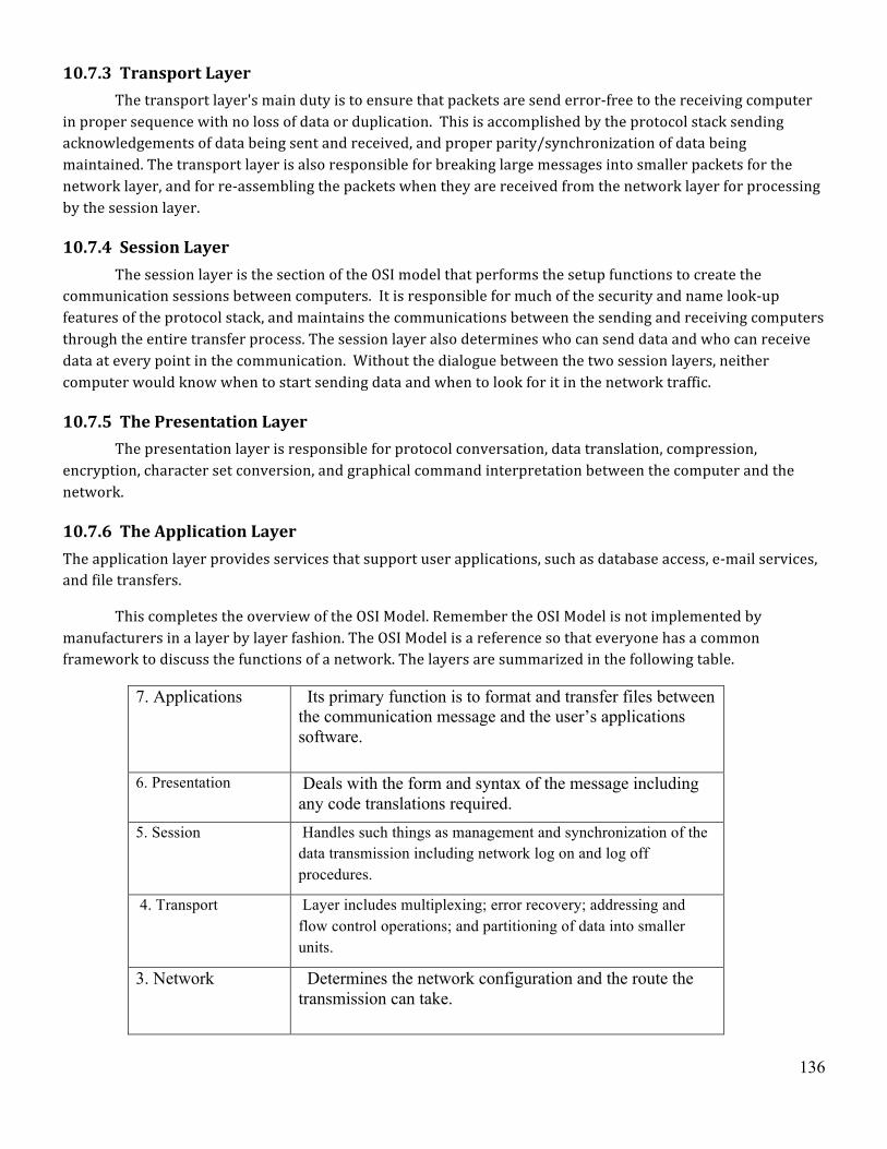
136
10.7.3 Transport Layer The transport layer's main duty is to ensure that packets are send error-‐free to the receiving computer in proper sequence with no loss of data or duplication. This is accomplished by the protocol stack sending acknowledgements of data being sent and received, and proper parity/synchronization of data being maintained. The transport layer is also responsible for breaking large messages into smaller packets for the network layer, and for re-‐assembling the packets when they are received from the network layer for processing by the session layer.
10.7.4 Session Layer The session layer is the section of the OSI model that performs the setup functions to create the communication sessions between computers. It is responsible for much of the security and name look-‐up features of the protocol stack, and maintains the communications between the sending and receiving computers through the entire transfer process. The session layer also determines who can send data and who can receive data at every point in the communication. Without the dialogue between the two session layers, neither computer would know when to start sending data and when to look for it in the network traffic.
10.7.5 The Presentation Layer The presentation layer is responsible for protocol conversation, data translation, compression, encryption, character set conversion, and graphical command interpretation between the computer and the network.
10.7.6 The Application Layer The application layer provides services that support user applications, such as database access, e-‐mail services, and file transfers.
This completes the overview of the OSI Model. Remember the OSI Model is not implemented by manufacturers in a layer by layer fashion. The OSI Model is a reference so that everyone has a common framework to discuss the functions of a network. The layers are summarized in the following table.
7. Applications Its primary function is to format and transfer files between the communication message and the user’s applications software.
6. Presentation Deals with the form and syntax of the message including any code translations required.
5. Session Handles such things as management and synchronization of the data transmission including network log on and log off procedures.
4. Transport Layer includes multiplexing; error recovery; addressing and flow control operations; and partitioning of data into smaller units.
3. Network Determines the network configuration and the route the transmission can take.
137
2. Data link Defines the framing information for the block of data and identifies any error detection and correction methods, as well as any synchronizing and control codes needed for communication.
1. Physical Layer Defines the physical connections and the electrical standards for the communication system.
10.8 Physical Connection of a Network There are two main physical connection components of a network, consisting of the network media and the network interface card (NIC).There are many forms of network media, but they fall into two distinct categories: Physical and Wireless. There are three major types of physical cabling. They are Coaxial, Twisted Pair, and Fiber Optics. They all share certain attributes, but differ in their uses.
Coaxial cabling is much like the cable used on cable television wiring, but has certain shielding and impedance properties that make it different from the coax used for TV. It is also sub-‐divided into two different categories; RG-‐8 and RG-‐58. They differ in their shielding, and therefore their methods of use.
Twisted Pair consists of pairs of wires that looks much like telephone cabling, but with a much different connection end. Again, there are two forms of Twisted Pair; UTP (Unshielded Twisted Pair) and STP (Shielded Twisted Pair). They also can differ on the number of pairs of wires used to connect, usually using either 2 or 4 pairs of wires.
Fiber Optic Cable is different from the other two forms of wiring. Instead of using electricity to send signals across the cable, it uses light. Depending on the Spectrum used, Fiber Optics is generally the fastest form of network cabling.
Wireless media consist of infra-‐red (IR), radio frequency (RF), microwave, and satellite systems. All these media forms share one common element; Instead of using a physical form of transfer, they use wave forms designed to flow through the air to send their signals.

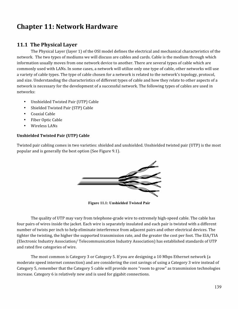
139
Chapter 11: Network Hardware
11.1 The Physical Layer The Physical Layer (layer 1) of the OSI model defines the electrical and mechanical characteristics of the network. The two types of mediums we will discuss are cables and cards. Cable is the medium through which information usually moves from one network device to another. There are several types of cable which are commonly used with LANs. In some cases, a network will utilize only one type of cable, other networks will use a variety of cable types. The type of cable chosen for a network is related to the network's topology, protocol, and size. Understanding the characteristics of different types of cable and how they relate to other aspects of a network is necessary for the development of a successful network. The following types of cables are used in networks:
• Unshielded Twisted Pair (UTP) Cable • Shielded Twisted Pair (STP) Cable • Coaxial Cable • Fiber Optic Cable • Wireless LANs
Unshielded Twisted Pair (UTP) Cable
Twisted pair cabling comes in two varieties: shielded and unshielded. Unshielded twisted pair (UTP) is the most popular and is generally the best option (See Figure 9.1).
Figure 11.1: Unshielded Twisted Pair
The quality of UTP may vary from telephone-‐grade wire to extremely high-‐speed cable. The cable has four pairs of wires inside the jacket. Each wire is separately insulated and each pair is twisted with a different number of twists per inch to help eliminate interference from adjacent pairs and other electrical devices. The tighter the twisting, the higher the supported transmission rate, and the greater the cost per foot. The EIA/TIA (Electronic Industry Association/ Telecommunication Industry Association) has established standards of UTP and rated five categories of wire.
The most common is Category 3 or Category 5. If you are designing a 10 Mbps Ethernet network (a moderate speed internet connection) and are considering the cost savings of using a Category 3 wire instead of Category 5, remember that the Category 5 cable will provide more “room to grow” as transmission technologies increase. Category 6 is relatively new and is used for gigabit connections.
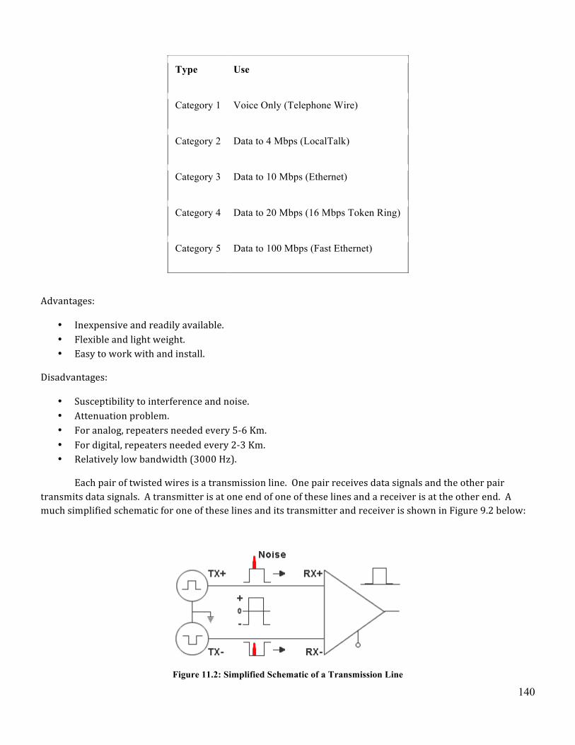
140
Advantages:
• Inexpensive and readily available. • Flexible and light weight. • Easy to work with and install.
Disadvantages:
• Susceptibility to interference and noise. • Attenuation problem. • For analog, repeaters needed every 5-‐6 Km. • For digital, repeaters needed every 2-‐3 Km. • Relatively low bandwidth (3000 Hz).
Each pair of twisted wires is a transmission line. One pair receives data signals and the other pair transmits data signals. A transmitter is at one end of one of these lines and a receiver is at the other end. A much simplified schematic for one of these lines and its transmitter and receiver is shown in Figure 9.2 below:
Figure 11.2: Simplified Schematic of a Transmission Line
Type Use
Category 1 Voice Only (Telephone Wire)
Category 2 Data to 4 Mbps (LocalTalk)
Category 3 Data to 10 Mbps (Ethernet)
Category 4 Data to 20 Mbps (16 Mbps Token Ring)
Category 5 Data to 100 Mbps (Fast Ethernet)
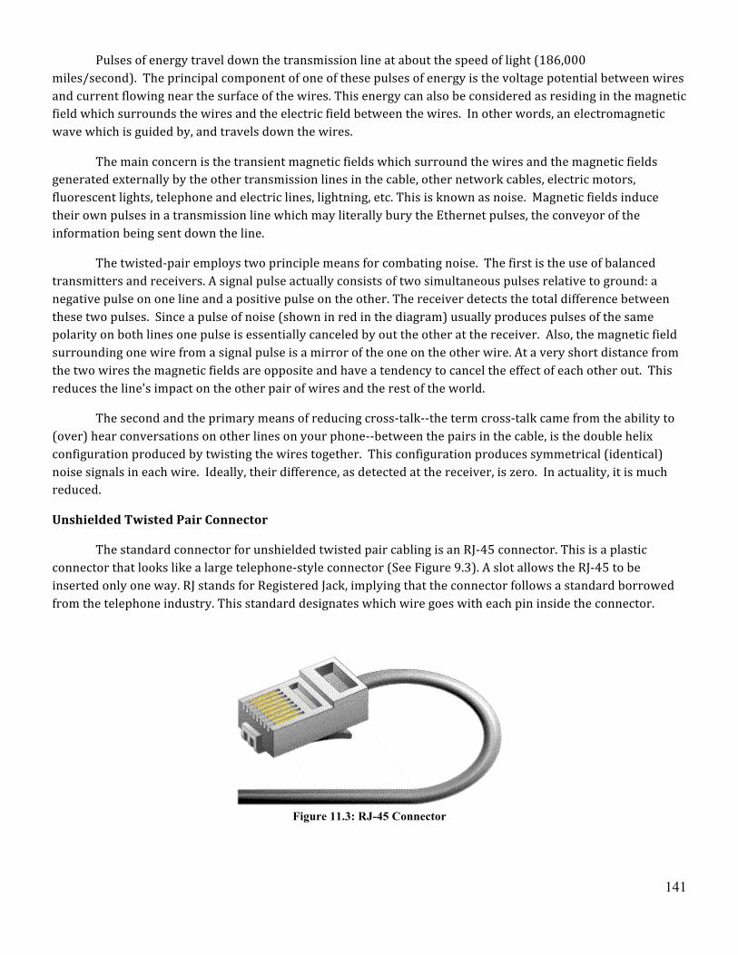
141
Pulses of energy travel down the transmission line at about the speed of light (186,000 miles/second). The principal component of one of these pulses of energy is the voltage potential between wires and current flowing near the surface of the wires. This energy can also be considered as residing in the magnetic field which surrounds the wires and the electric field between the wires. In other words, an electromagnetic wave which is guided by, and travels down the wires.
The main concern is the transient magnetic fields which surround the wires and the magnetic fields generated externally by the other transmission lines in the cable, other network cables, electric motors, fluorescent lights, telephone and electric lines, lightning, etc. This is known as noise. Magnetic fields induce their own pulses in a transmission line which may literally bury the Ethernet pulses, the conveyor of the information being sent down the line.
The twisted-‐pair employs two principle means for combating noise. The first is the use of balanced transmitters and receivers. A signal pulse actually consists of two simultaneous pulses relative to ground: a negative pulse on one line and a positive pulse on the other. The receiver detects the total difference between these two pulses. Since a pulse of noise (shown in red in the diagram) usually produces pulses of the same polarity on both lines one pulse is essentially canceled by out the other at the receiver. Also, the magnetic field surrounding one wire from a signal pulse is a mirror of the one on the other wire. At a very short distance from the two wires the magnetic fields are opposite and have a tendency to cancel the effect of each other out. This reduces the line's impact on the other pair of wires and the rest of the world.
The second and the primary means of reducing cross-‐talk-‐-‐the term cross-‐talk came from the ability to (over) hear conversations on other lines on your phone-‐-‐between the pairs in the cable, is the double helix configuration produced by twisting the wires together. This configuration produces symmetrical (identical) noise signals in each wire. Ideally, their difference, as detected at the receiver, is zero. In actuality, it is much reduced.
Unshielded Twisted Pair Connector
The standard connector for unshielded twisted pair cabling is an RJ-‐45 connector. This is a plastic connector that looks like a large telephone-‐style connector (See Figure 9.3). A slot allows the RJ-‐45 to be inserted only one way. RJ stands for Registered Jack, implying that the connector follows a standard borrowed from the telephone industry. This standard designates which wire goes with each pin inside the connector.
Figure 11.3: RJ-45 Connector
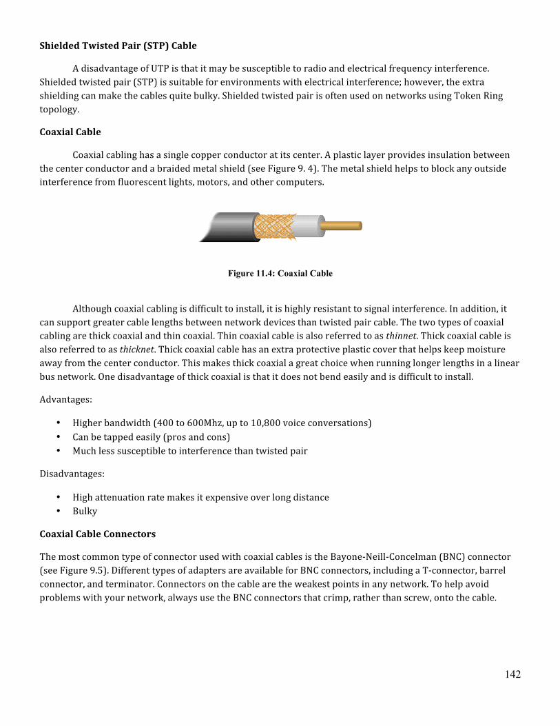
142
Shielded Twisted Pair (STP) Cable
A disadvantage of UTP is that it may be susceptible to radio and electrical frequency interference. Shielded twisted pair (STP) is suitable for environments with electrical interference; however, the extra shielding can make the cables quite bulky. Shielded twisted pair is often used on networks using Token Ring topology.
Coaxial Cable
Coaxial cabling has a single copper conductor at its center. A plastic layer provides insulation between the center conductor and a braided metal shield (see Figure 9. 4). The metal shield helps to block any outside interference from fluorescent lights, motors, and other computers.
Figure 11.4: Coaxial Cable
Although coaxial cabling is difficult to install, it is highly resistant to signal interference. In addition, it can support greater cable lengths between network devices than twisted pair cable. The two types of coaxial cabling are thick coaxial and thin coaxial. Thin coaxial cable is also referred to as thinnet. Thick coaxial cable is also referred to as thicknet. Thick coaxial cable has an extra protective plastic cover that helps keep moisture away from the center conductor. This makes thick coaxial a great choice when running longer lengths in a linear bus network. One disadvantage of thick coaxial is that it does not bend easily and is difficult to install.
Advantages:
• Higher bandwidth (400 to 600Mhz, up to 10,800 voice conversations) • Can be tapped easily (pros and cons) • Much less susceptible to interference than twisted pair
Disadvantages:
• High attenuation rate makes it expensive over long distance • Bulky
Coaxial Cable Connectors
The most common type of connector used with coaxial cables is the Bayone-‐Neill-‐Concelman (BNC) connector (see Figure 9.5). Different types of adapters are available for BNC connectors, including a T-‐connector, barrel connector, and terminator. Connectors on the cable are the weakest points in any network. To help avoid problems with your network, always use the BNC connectors that crimp, rather than screw, onto the cable.
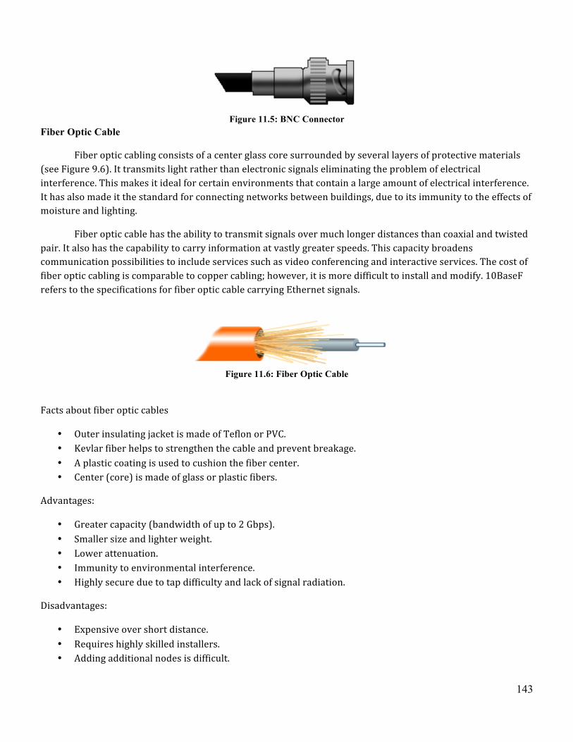
143
Figure 11.5: BNC Connector
Fiber Optic Cable
Fiber optic cabling consists of a center glass core surrounded by several layers of protective materials (see Figure 9.6). It transmits light rather than electronic signals eliminating the problem of electrical interference. This makes it ideal for certain environments that contain a large amount of electrical interference. It has also made it the standard for connecting networks between buildings, due to its immunity to the effects of moisture and lighting.
Fiber optic cable has the ability to transmit signals over much longer distances than coaxial and twisted pair. It also has the capability to carry information at vastly greater speeds. This capacity broadens communication possibilities to include services such as video conferencing and interactive services. The cost of fiber optic cabling is comparable to copper cabling; however, it is more difficult to install and modify. 10BaseF refers to the specifications for fiber optic cable carrying Ethernet signals.
Figure 11.6: Fiber Optic Cable
Facts about fiber optic cables
• Outer insulating jacket is made of Teflon or PVC. • Kevlar fiber helps to strengthen the cable and prevent breakage. • A plastic coating is used to cushion the fiber center. • Center (core) is made of glass or plastic fibers.
Advantages:
• Greater capacity (bandwidth of up to 2 Gbps). • Smaller size and lighter weight. • Lower attenuation. • Immunity to environmental interference. • Highly secure due to tap difficulty and lack of signal radiation.
Disadvantages:
• Expensive over short distance. • Requires highly skilled installers. • Adding additional nodes is difficult.
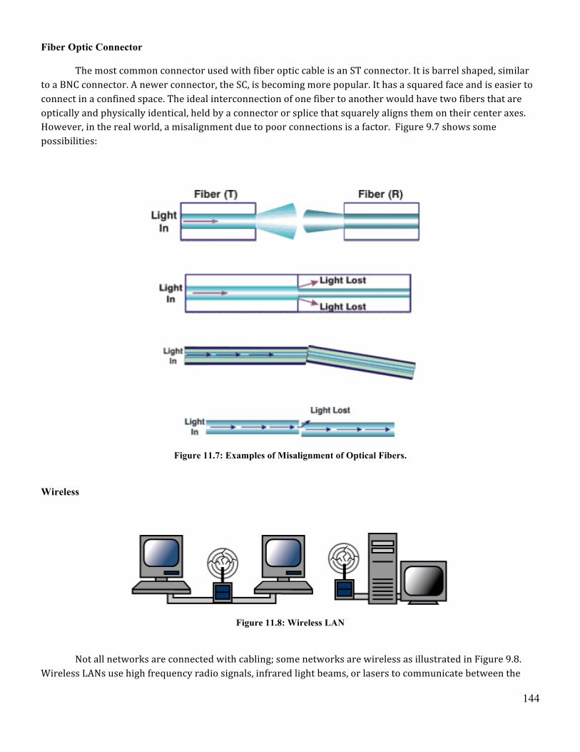
144
Fiber Optic Connector
The most common connector used with fiber optic cable is an ST connector. It is barrel shaped, similar to a BNC connector. A newer connector, the SC, is becoming more popular. It has a squared face and is easier to connect in a confined space. The ideal interconnection of one fiber to another would have two fibers that are optically and physically identical, held by a connector or splice that squarely aligns them on their center axes. However, in the real world, a misalignment due to poor connections is a factor. Figure 9.7 shows some possibilities:
Figure 11.7: Examples of Misalignment of Optical Fibers.
Wireless
Figure 11.8: Wireless LAN
Not all networks are connected with cabling; some networks are wireless as illustrated in Figure 9.8. Wireless LANs use high frequency radio signals, infrared light beams, or lasers to communicate between the
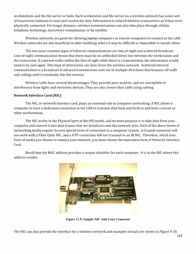
145
workstations and the file server or hubs. Each workstation and file server on a wireless network has some sort of transceiver/antenna to send and receive the data. Information is relayed between transceivers as if they were physically connected. For longer distance, wireless communications can also take place through cellular telephone technology, microwave transmission, or by satellite.
Wireless networks are great for allowing laptop computers or remote computers to connect to the LAN. Wireless networks are also beneficial in older buildings where it may be difficult or impossible to install cables.
The two most common types of infrared communications are line-‐of-‐sight and scattered broadcast. Line-‐of-‐sight communication means that there must be an unblocked direct line between the workstation and the transceiver. If a person walks within the line-‐of-‐sight while there is a transmission, the information would need to be sent again. This kind of obstruction can slow down the wireless network. Scattered infrared communication is a broadcast of infrared transmissions sent out in multiple directions that bounces off walls and ceilings until it eventually hits the receiver.
Wireless LANs have several disadvantages. They provide poor security, and are susceptible to interference from lights and electronic devices. They are also slower than LANs using cabling.
Network Interface Card (NIC)
The NIC, or network interface card, plays an essential role in computer networking. A NIC allows a computer to have a dedicated connection to the LAN to transmit data back and forth to and from a server or other workstations.
The NIC works in the Physical layer of the OSI model, and its main purpose is to take data from your computer and convert it into data frames that are broadcast onto the network wire. Each of the above forms of networking media require its own special form of connection to a computer system. A Coaxial connector will not work with a Fiber Optic NIC, and a UTP connection will not transmit to an IR NIC. Therefore, which ever form of media you choose to connect your network, you must choose the equivalent form of Network Interface Card.
Recall that the MAC address provides a unique identifier for each computer. It is in the NIC where this address resides.
Figure 11.9: Sample NIC with Coax Connector
The NIC can also provide the interface for a wireless network and examples of each are shown in Figure 9.10.
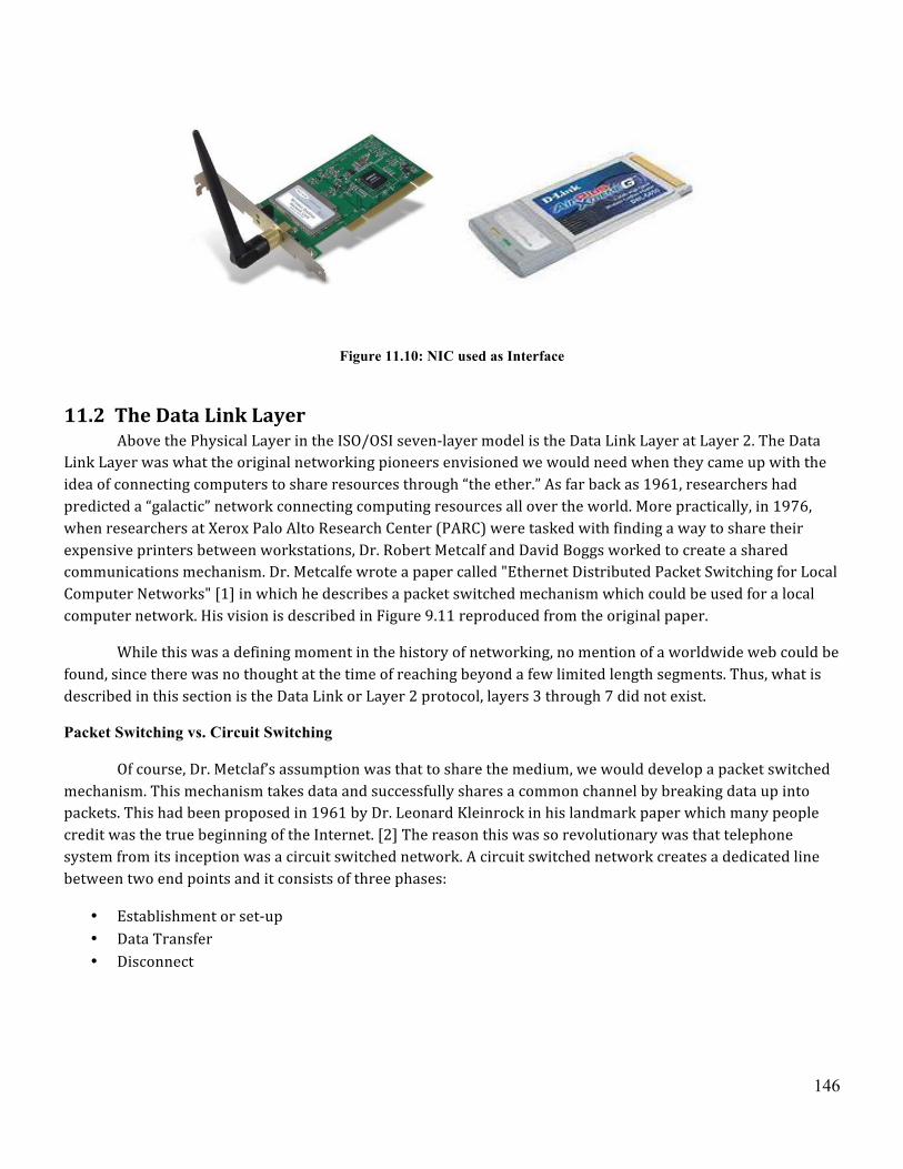
146
Figure 11.10: NIC used as Interface
11.2 The Data Link Layer Above the Physical Layer in the ISO/OSI seven-‐layer model is the Data Link Layer at Layer 2. The Data Link Layer was what the original networking pioneers envisioned we would need when they came up with the idea of connecting computers to share resources through “the ether.” As far back as 1961, researchers had predicted a “galactic” network connecting computing resources all over the world. More practically, in 1976, when researchers at Xerox Palo Alto Research Center (PARC) were tasked with finding a way to share their expensive printers between workstations, Dr. Robert Metcalf and David Boggs worked to create a shared communications mechanism. Dr. Metcalfe wrote a paper called "Ethernet Distributed Packet Switching for Local Computer Networks" [1] in which he describes a packet switched mechanism which could be used for a local computer network. His vision is described in Figure 9.11 reproduced from the original paper.
While this was a defining moment in the history of networking, no mention of a worldwide web could be found, since there was no thought at the time of reaching beyond a few limited length segments. Thus, what is described in this section is the Data Link or Layer 2 protocol, layers 3 through 7 did not exist.
Packet Switching vs. Circuit Switching
Of course, Dr. Metclaf’s assumption was that to share the medium, we would develop a packet switched mechanism. This mechanism takes data and successfully shares a common channel by breaking data up into packets. This had been proposed in 1961 by Dr. Leonard Kleinrock in his landmark paper which many people credit was the true beginning of the Internet. [2] The reason this was so revolutionary was that telephone system from its inception was a circuit switched network. A circuit switched network creates a dedicated line between two end points and it consists of three phases:
• Establishment or set-‐up • Data Transfer • Disconnect
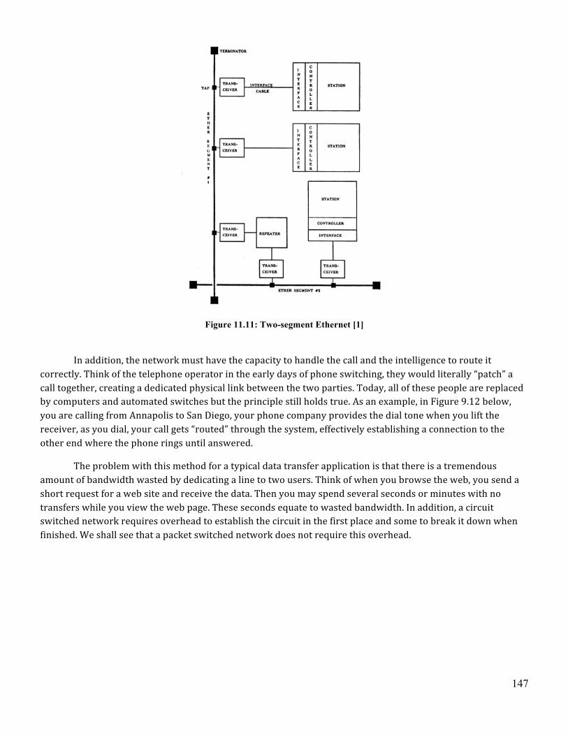
147
Figure 11.11: Two-segment Ethernet [1]
In addition, the network must have the capacity to handle the call and the intelligence to route it correctly. Think of the telephone operator in the early days of phone switching, they would literally “patch” a call together, creating a dedicated physical link between the two parties. Today, all of these people are replaced by computers and automated switches but the principle still holds true. As an example, in Figure 9.12 below, you are calling from Annapolis to San Diego, your phone company provides the dial tone when you lift the receiver, as you dial, your call gets “routed” through the system, effectively establishing a connection to the other end where the phone rings until answered.
The problem with this method for a typical data transfer application is that there is a tremendous amount of bandwidth wasted by dedicating a line to two users. Think of when you browse the web, you send a short request for a web site and receive the data. Then you may spend several seconds or minutes with no transfers while you view the web page. These seconds equate to wasted bandwidth. In addition, a circuit switched network requires overhead to establish the circuit in the first place and some to break it down when finished. We shall see that a packet switched network does not require this overhead.
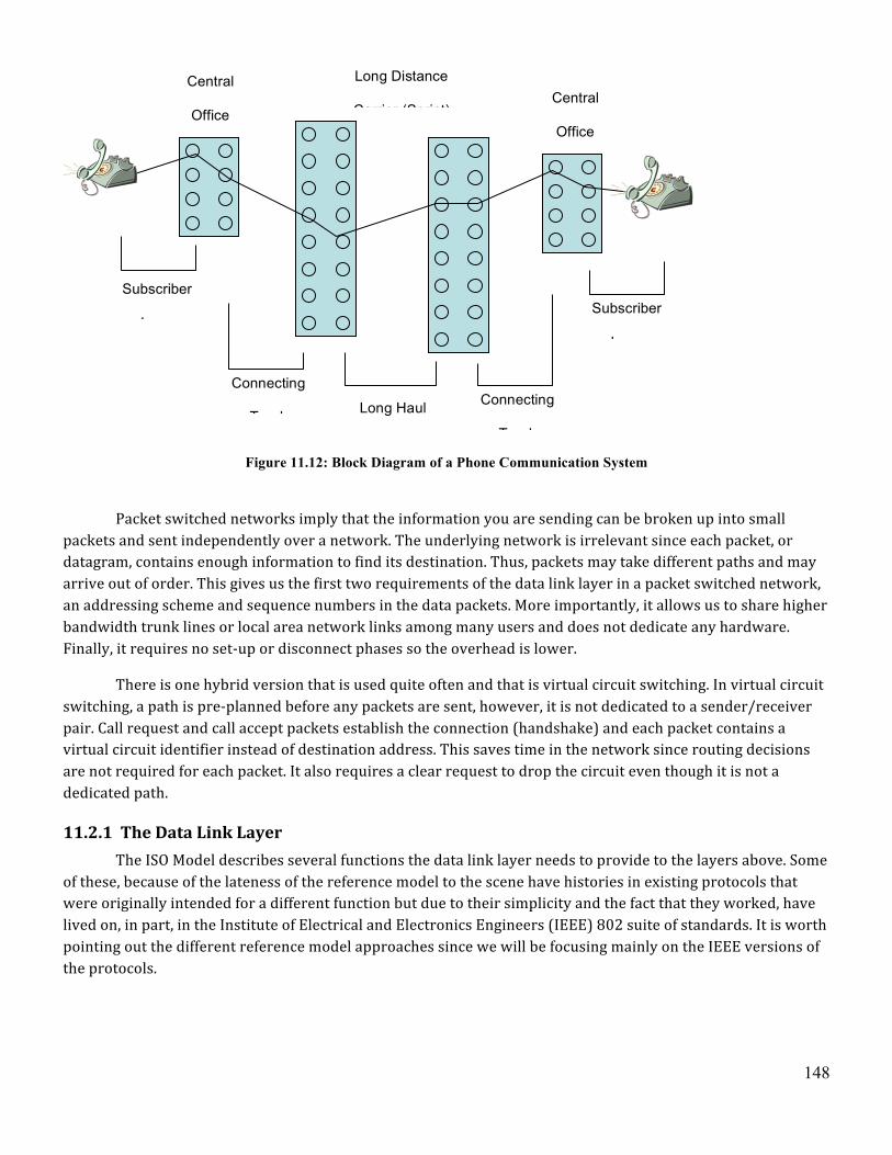
148
Figure 11.12: Block Diagram of a Phone Communication System
Packet switched networks imply that the information you are sending can be broken up into small packets and sent independently over a network. The underlying network is irrelevant since each packet, or datagram, contains enough information to find its destination. Thus, packets may take different paths and may arrive out of order. This gives us the first two requirements of the data link layer in a packet switched network, an addressing scheme and sequence numbers in the data packets. More importantly, it allows us to share higher bandwidth trunk lines or local area network links among many users and does not dedicate any hardware. Finally, it requires no set-‐up or disconnect phases so the overhead is lower.
There is one hybrid version that is used quite often and that is virtual circuit switching. In virtual circuit switching, a path is pre-‐planned before any packets are sent, however, it is not dedicated to a sender/receiver pair. Call request and call accept packets establish the connection (handshake) and each packet contains a virtual circuit identifier instead of destination address. This saves time in the network since routing decisions are not required for each packet. It also requires a clear request to drop the circuit even though it is not a dedicated path.
11.2.1 The Data Link Layer The ISO Model describes several functions the data link layer needs to provide to the layers above. Some of these, because of the lateness of the reference model to the scene have histories in existing protocols that were originally intended for a different function but due to their simplicity and the fact that they worked, have lived on, in part, in the Institute of Electrical and Electronics Engineers (IEEE) 802 suite of standards. It is worth pointing out the different reference model approaches since we will be focusing mainly on the IEEE versions of the protocols.
Central
Office
Long Distance
Carrier (Sprint) Central
Office
Subscriber
Loop Subscriber
Loop
Connecting
Trunk Connecting
Trunk
Long Haul
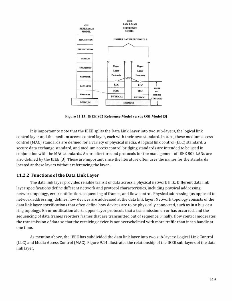
149
Figure 11.13: IEEE 802 Reference Model versus OSI Model [3]
It is important to note that the IEEE splits the Data Link Layer into two sub-‐layers, the logical link control layer and the medium access control layer, each with their own standard. In turn, these medium access control (MAC) standards are defined for a variety of physical media. A logical link control (LLC) standard, a secure data exchange standard, and medium access control bridging standards are intended to be used in conjunction with the MAC standards. An architecture and protocols for the management of IEEE 802 LANs are also defined by the IEEE [3]. These are important since the literature often uses the names for the standards located at these layers without referencing the layer.
11.2.2 Functions of the Data Link Layer The data link layer provides reliable transit of data across a physical network link. Different data link layer specifications define different network and protocol characteristics, including physical addressing, network topology, error notification, sequencing of frames, and flow control. Physical addressing (as opposed to network addressing) defines how devices are addressed at the data link layer. Network topology consists of the data link layer specifications that often define how devices are to be physically connected, such as in a bus or a ring topology. Error notification alerts upper-‐layer protocols that a transmission error has occurred, and the sequencing of data frames reorders frames that are transmitted out of sequence. Finally, flow control moderates the transmission of data so that the receiving device is not overwhelmed with more traffic than it can handle at one time.
As mention above, the IEEE has subdivided the data link layer into two sub-‐layers: Logical Link Control (LLC) and Media Access Control (MAC). Figure 9.14 illustrates the relationship of the IEEE sub-‐layers of the data link layer.
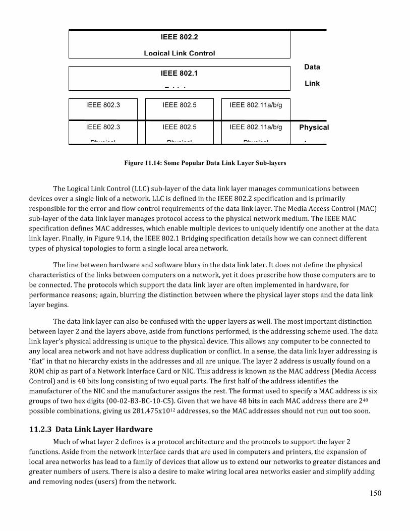
150
Figure 11.14: Some Popular Data Link Layer Sub-layers
The Logical Link Control (LLC) sub-‐layer of the data link layer manages communications between devices over a single link of a network. LLC is defined in the IEEE 802.2 specification and is primarily responsible for the error and flow control requirements of the data link layer. The Media Access Control (MAC) sub-‐layer of the data link layer manages protocol access to the physical network medium. The IEEE MAC specification defines MAC addresses, which enable multiple devices to uniquely identify one another at the data link layer. Finally, in Figure 9.14, the IEEE 802.1 Bridging specification details how we can connect different types of physical topologies to form a single local area network.
The line between hardware and software blurs in the data link later. It does not define the physical characteristics of the links between computers on a network, yet it does prescribe how those computers are to be connected. The protocols which support the data link layer are often implemented in hardware, for performance reasons; again, blurring the distinction between where the physical layer stops and the data link layer begins.
The data link layer can also be confused with the upper layers as well. The most important distinction between layer 2 and the layers above, aside from functions performed, is the addressing scheme used. The data link layer’s physical addressing is unique to the physical device. This allows any computer to be connected to any local area network and not have address duplication or conflict. In a sense, the data link layer addressing is “flat” in that no hierarchy exists in the addresses and all are unique. The layer 2 address is usually found on a ROM chip as part of a Network Interface Card or NIC. This address is known as the MAC address (Media Access Control) and is 48 bits long consisting of two equal parts. The first half of the address identifies the manufacturer of the NIC and the manufacturer assigns the rest. The format used to specify a MAC address is six groups of two hex digits (00-‐02-‐B3-‐BC-‐10-‐C5). Given that we have 48 bits in each MAC address there are 248 possible combinations, giving us 281.475x10¹² addresses, so the MAC addresses should not run out too soon.
11.2.3 Data Link Layer Hardware Much of what layer 2 defines is a protocol architecture and the protocols to support the layer 2 functions. Aside from the network interface cards that are used in computers and printers, the expansion of local area networks has lead to a family of devices that allow us to extend our networks to greater distances and greater numbers of users. There is also a desire to make wiring local area networks easier and simplify adding and removing nodes (users) from the network.
IEEE 802.2
Logical Link Control
IEEE 802.1
Bridging
IEEE 802.3
MAC - Ethernet
IEEE 802.5
MAC - Token Ring
IEEE 802.11a/b/g
MAC - Wireless IEEE 802.3
Physical
IEEE 802.5
Physical
IEEE 802.11a/b/g
Physical
Data
Link
Layer
Physical
Layer
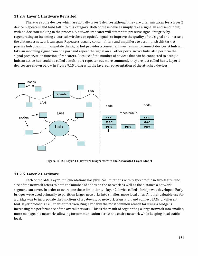
151
11.2.4 Layer 1 Hardware Revisited There are some devices which are actually layer 1 devices although they are often mistaken for a layer 2 device. Repeaters and hubs fall into this category. Both of these devices simply take a signal in and send it out, with no decision making in the process. A network repeater will attempt to preserve signal integrity by regenerating an incoming electrical, wireless or optical, signals to improve the quality of the signal and increase the distance a network can span. Repeaters usually contain filters and amplifiers to accomplish this task. A passive hub does not manipulate the signal but provides a convenient mechanism to connect devices. A hub will take an incoming signal from one port and repeat the signal on all other ports. Active hubs also perform the signal preservation function of repeaters. Because of the number of devices that can be connected to a single hub, an active hub could be called a multi-‐port repeater but more commonly they are just called hubs. Layer 1 devices are shown below in Figure 9.15 along with the layered representation of the attached devices.
Figure 11.15: Layer 1 Hardware Diagrams with the Associated Layer Model
11.2.5 Layer 2 Hardware Each of the MAC Layer implementations has physical limitations with respect to the network size. The size of the network refers to both the number of nodes on the network as well as the distance a network segment can cover. In order to overcome these limitations, a layer 2 device called a bridge was developed. Early bridges were used primarily to partition larger networks into smaller, more local ones. Another valuable use for a bridge was to incorporate the functions of a gateway, or network translator, and connect LANs of different MAC layer protocols, i.e. Ethernet to Token Ring. Probably the most common reason for using a bridge is increasing the performance of the overall network. This is the result of segmenting a large network into smaller, more manageable networks allowing for communication across the entire network while keeping local traffic local.
repeater
LAN
LAN
nodes
nodes
hub
LAN LLC MAC PHY PHY
LLC MAC PHY
node
NIC
node
NIC repeater/hub
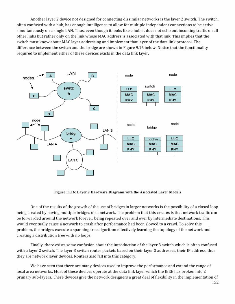
152
Another layer 2 device not designed for connecting dissimilar networks is the layer 2 switch. The switch, often confused with a hub, has enough intelligence to allow for multiple independent connections to be active simultaneously on a single LAN. Thus, even though it looks like a hub, it does not echo out incoming traffic on all other links but rather only on the link whose MAC address is associated with that link. This implies that the switch must know about MAC layer addressing and implement that layer of the data link protocol. The difference between the switch and the bridge are shown in Figure 9.16 below. Notice that the functionality required to implement either of these devices exists in the data link layer.
Figure 11.16: Layer 2 Hardware Diagrams with the Associated Layer Models
One of the results of the growth of the use of bridges in larger networks is the possibility of a closed loop being created by having multiple bridges on a network. The problem that this creates is that network traffic can be forwarded around the network forever, being repeated over and over by intermediate destinations. This would eventually cause a network to crash after performance had been slowed to a crawl. To solve this problem, the bridges execute a spanning tree algorithm effectively learning the topology of the network and creating a distribution tree with no loops.
Finally, there exists some confusion about the introduction of the layer 3 switch which is often confused with a layer 2 switch. The layer 3 switch routes packets based on their layer 3 addresses, their IP address, thus they are network layer devices. Routers also fall into this category.
We have seen that there are many devices used to improve the performance and extend the range of local area networks. Most of these devices operate at the data link layer which the IEEE has broken into 2 primary sub-‐layers. These devices give the network designers a great deal of flexibility in the implementation of
nodes
E
A B
C D
switch
LAN
bridge
LAN A
LAN B
nodes
LAN C
LLC MAC PHY PHY
LLC MAC PHY
node
NIC
node
NIC switch
MAC
LLC MAC PHY PHY
LLC MAC PHY
node
NIC
node
NIC bridge
MAC bridge
153
many different kinds of LAN protocols. The LLC sub-‐layer provides a common interface to the upper layers so that the network layer does not need to know what makes up the underlying topology or physical layer. This is a benefit of layering in networking, hiding the details of the lower layers from the upper layers while providing the same expected services that are required by the applications above.
11.3 The Network Layer A router is a computer networking device that forwards data packets toward their destinations through a process known as routing. Routing occurs at layer 3 of the OSI seven-‐layer model. Routing is most commonly associated with the Internet Protocol, although other less-‐popular routed protocols remain in use. In the original 1960s-‐era of routing, general-‐purpose computers served as routers. Although general-‐purpose computers can perform routing, modern high-‐speed routers are highly specialised computers, generally with extra hardware added to accelerate both common routing functions such as packet forwarding and specialised functions such as IPsec encryption.
Other changes also improve reliability, such as using battery rather than mains power, and using solid-‐state rather than magnetic storage. Modern routers have thus come to resemble telephone switches, whose technology they are currently converging with and may eventually replace. The first modern (dedicated, standalone) routers were the Fuzzball routers. A router must be connected to at least two networks, or it will have nothing to route. A special variety of router is the one-‐armed router used to route packets in a virtual LAN environment. In the case of a one-‐armed router the multiple attachments to different networks are all over the same physical link.
A router which connects end-‐users to the Internet is called Edge router: a router which serves to transmit data between other routers is called Core router. A router creates and/or maintains a table, called a “routing table” that stores the best routes to certain network destinations and the “routing metrics” associated with those routes. Routing is a core concept of the Internet and many other networks. Routing provides the means of discovering paths along which information (usually, but not always, packets) can be sent. Circuit-‐based networks, such as the voice telephone network, also perform routing, to find paths for calls through the network fabric.
Automatic routing makes networks autonomous. Such networks can use their routing to find the best route to deliver data to a destination; choices are made depending upon goals such as finding the shortest distances and the fastest links available through a choice of network connections. This allows the network to route around network failures and blockages, and can make many aspects of the day to day running of such networks automatic, and free from the need for human intervention
The actual process of passing logically addressed packets from their local subnetwork toward their ultimate destination is called forwarding. It is closely related to routing, in that routing tells the forwarding where to send packets, but they are logically completely separate. In large networks, packets may pass through many intermediary destinations before reaching their destination. Routing and forwarding both occur at layer 3 of the OSI seven-‐layer model.
Hubs and switches move data on what appears (to the connected computers) to be the local network, and are invisible to connected computers, while the router is explicitly visible to them. Knowing where to send packets requires knowledge of the structure of the network. In small networks, routing can be very simple, and is often configured by hand. In large networks the topology of the network can become complex, and may change constantly, making the problem of constructing the routing tables very complex. As routers can only recalculate the best routes very slowly relative to the rate of arrival of packets, routers keep a routing table that
154
maintains a record of only the best possible routes to certain network destinations and the routing metrics associated with those routes.
11.3.1 Routed versus Routing Protocol There is often confusion between routed protocol and routing protocol. A routed protocol is any network protocol that provides enough information in its network layer address to allow a packet to be forwarded from one host to another host based on the addressing scheme. Routed protocols define the format and use of the fields within a packet. Packets generally are conveyed from end system to end system. IP is an example of a routed protocol.
Routing protocols facilitate the exchange of routing information between networks, allowing routers to build routing tables dynamically. Traditional IP routing stays simple because it uses next-hop routing where the router only needs to consider where it sends the packet, and does not need to consider the subsequent path of the packet on the remaining hops. Although this dynamic routing can become very complex, it makes the Internet very flexible, and has allowed it to grow in size by more than eight orders of magnitude over the years since adopting IP in 1983. Routing algorithms use two basic technologies:
1. Telling the world who your neighbors are: link-‐state routing protocols such as OSPF. 2. Telling your neighbors what the world looks like to you: distance-‐vector routing protocols such as RIP.
There is also a third method called hybrid. Hybrid protocols, such as EIGRP, are a combination of link-‐state and distance-‐vector routing protocols. Hybrid protocols have rapid convergence (like link-‐state protocols) but use much less memory and processor power than link-‐state protocols. Hybrid protocols use distance-‐vectors for more accurate metrics and to determine the best path to destination.
A routing metric consists of any value used by routing algorithms to determine whether one route is superior to another. Metrics can cover such information as bandwidth, delay, hop count, path cost, load, MTU, reliability, and communication cost. The routing table stores only the best possible routes, while link-‐state or topological databases may store all other information. Depending on the relationship of the router relative to other autonomous systems, various classes of routing protocols exist:
1. Ad hoc network routing protocols appear in networks with no or little infrastructure. 2. Interior Gateway Protocols (IGPs) exchange routing information within a single autonomous system. 3. Exterior Gateway Protocols (EGPs) route between separate autonomous systems.
11.3.2 TCP/IP We have mentioned that several protocols or sets of rules are used to communicate over a computer network. Each of these protocols must accomplish several tasks such as encapsulation, fragmentation and reassembly, connection control, ordered delivery, flow control, error control, addressing, multiplexing and transmission services. Perhaps the most common of protocol used to accomplish these tasks is the Transmission Control Protocol / Internet Protocol or TCP/IP. TCP/IP is the communications protocol that hosts use to communicate over an internet and it establishes a virtual connection between a destination and source host. TCP/IP uses two protocols to accomplish this task, TCP and IP [4]. TCP enables two hosts to establish a connection and exchange data. TCP will guarantee the delivery of data and also guarantees that the packets will be delivered in the same order in which they were sent. Remember packets are sent through a network according to the best path. This “best path” choice does not guarantee that all packets will take the same path,
155
nor will they arrive in the same order they were sent. TCP has the job of ensuring that all the packets are received and put back into the correct order before they are passed up the protocol stack.
IP determines the format of the packets. The IP packet format will not be discussed in detail, but there are a total of 20 octets in an IP Version 4 packets. These bits are used to select the type of service, length of datagram, identification number, flags, time to live, next higher protocol, header checksum, and various address. The packet IP provides a function similar to the address on a postal letter. You write the address on the letter and put it in the mail box. You and the receiver know where it is sent from and to whom it is being sent, but the path is determined by someone else. That someone else is the routers in the network between the destination and the source. It is TCP/IP that establishes the connection between the destination and the source. TCP steps in and cuts the letter up into smaller pieces or packets and then sends them, ensures all the packets are received and put back into the proper order.
11.3.3 UDP UDP is another protocol used at the transport level. UDP provides a connectionless service for applications. UDP provides few error recovery services, unlike TCP. However, like TCP, UDP uses IP to route its packets throughout the internet. UDP is used when the arrival of a message is not absolutely critical. You may recall that from time to time your receive letters for current resident in your mailbox. The sender of this “junk mail” is not concerned that everyone receives the package they send. UDP is similar to the “current resident” mail and is often used to send broadcast messages over a network. A broadcast message is a message that is sent periodically to all hosts on the network in order to locate users and collect other data on the network. UDP messages are also used to request responses from nodes or to disseminate information. Another application of UDP is in the use of real-‐time applications. With real time applications, retransmitting and waiting for arrival of packets is not possible so TCP is not used for these applications. When real time data (voice or video) is routed a connectionless UDP protocol is used. If packets get dropped or fail to arrive the overall message is usually not corrupted beyond recognition.
References
[1] R Metcalf and D. Boggs, “Ethernet Distributed Packet Switching for Local Computer Networks,” Communications of the ACM, Vol. 19, No. 5, July 1976, pp. 395 – 404
[2] L. Kleinrock, "Information Flow in Large Communication Nets", RLE Quarterly Progress Report, July 1961.
[3] IEEE Standards for Local and Metropolitan Area Networks: Overview and Architecture, IEEE Computer Society, IEEE Standards Board Approved November 20, 1990
[4] www.webopedia.com).

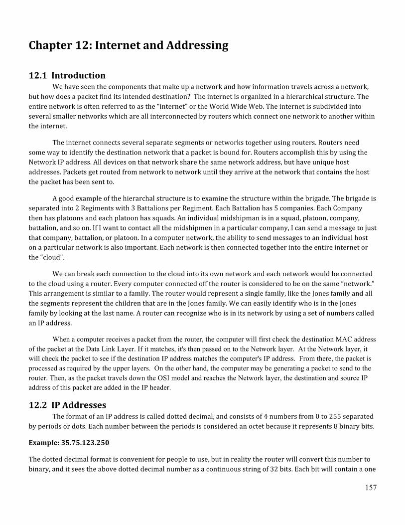
157
Chapter 12: Internet and Addressing
12.1 Introduction We have seen the components that make up a network and how information travels across a network, but how does a packet find its intended destination? The internet is organized in a hierarchical structure. The entire network is often referred to as the “internet” or the World Wide Web. The internet is subdivided into several smaller networks which are all interconnected by routers which connect one network to another within the internet.
The internet connects several separate segments or networks together using routers. Routers need some way to identify the destination network that a packet is bound for. Routers accomplish this by using the Network IP address. All devices on that network share the same network address, but have unique host addresses. Packets get routed from network to network until they arrive at the network that contains the host the packet has been sent to.
A good example of the hierarchal structure is to examine the structure within the brigade. The brigade is separated into 2 Regiments with 3 Battalions per Regiment. Each Battalion has 5 companies. Each Company then has platoons and each platoon has squads. An individual midshipman is in a squad, platoon, company, battalion, and so on. If I want to contact all the midshipmen in a particular company, I can send a message to just that company, battalion, or platoon. In a computer network, the ability to send messages to an individual host on a particular network is also important. Each network is then connected together into the entire internet or the “cloud”.
We can break each connection to the cloud into its own network and each network would be connected to the cloud using a router. Every computer connected off the router is considered to be on the same “network.” This arrangement is similar to a family. The router would represent a single family, like the Jones family and all the segments represent the children that are in the Jones family. We can easily identify who is in the Jones family by looking at the last name. A router can recognize who is in its network by using a set of numbers called an IP address.
When a computer receives a packet from the router, the computer will first check the destination MAC address of the packet at the Data Link Layer. If it matches, it's then passed on to the Network layer. At the Network layer, it will check the packet to see if the destination IP address matches the computer's IP address. From there, the packet is processed as required by the upper layers. On the other hand, the computer may be generating a packet to send to the router. Then, as the packet travels down the OSI model and reaches the Network layer, the destination and source IP address of this packet are added in the IP header.
12.2 IP Addresses The format of an IP address is called dotted decimal, and consists of 4 numbers from 0 to 255 separated by periods or dots. Each number between the periods is considered an octet because it represents 8 binary bits.
Example: 35.75.123.250
The dotted decimal format is convenient for people to use, but in reality the router will convert this number to binary, and it sees the above dotted decimal number as a continuous string of 32 bits. Each bit will contain a one
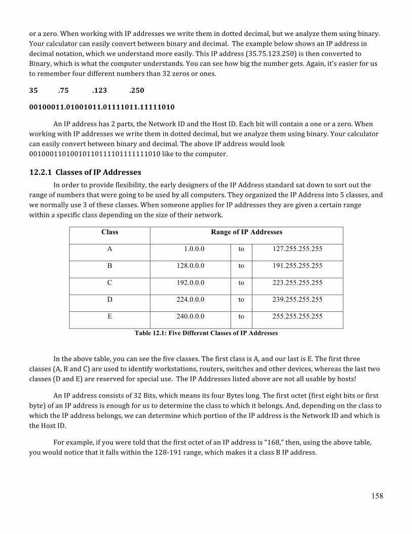
158
or a zero. When working with IP addresses we write them in dotted decimal, but we analyze them using binary. Your calculator can easily convert between binary and decimal. The example below shows an IP address in decimal notation, which we understand more easily. This IP address (35.75.123.250) is then converted to Binary, which is what the computer understands. You can see how big the number gets. Again, it's easier for us to remember four different numbers than 32 zeros or ones.
35 .75 .123 .250
00100011.01001011.01111011.11111010
An IP address has 2 parts, the Network ID and the Host ID. Each bit will contain a one or a zero. When working with IP addresses we write them in dotted decimal, but we analyze them using binary. Your calculator can easily convert between binary and decimal. The above IP address would look 00100011010010110111101111111010 like to the computer.
12.2.1 Classes of IP Addresses In order to provide flexibility, the early designers of the IP Address standard sat down to sort out the range of numbers that were going to be used by all computers. They organized the IP Address into 5 classes, and we normally use 3 of these classes. When someone applies for IP addresses they are given a certain range within a specific class depending on the size of their network.
Class Range of IP Addresses
A 1.0.0.0 to 127.255.255.255
B 128.0.0.0 to 191.255.255.255
C 192.0.0.0 to 223.255.255.255
D 224.0.0.0 to 239.255.255.255
E 240.0.0.0 to 255.255.255.255
Table 12.1: Five Different Classes of IP Addresses
In the above table, you can see the five classes. The first class is A, and our last is E. The first three classes (A, B and C) are used to identify workstations, routers, switches and other devices, whereas the last two classes (D and E) are reserved for special use. The IP Addresses listed above are not all usable by hosts!
An IP address consists of 32 Bits, which means its four Bytes long. The first octet (first eight bits or first byte) of an IP address is enough for us to determine the class to which it belongs. And, depending on the class to which the IP address belongs, we can determine which portion of the IP address is the Network ID and which is the Host ID.
For example, if you were told that the first octet of an IP address is “168,” then, using the above table, you would notice that it falls within the 128-‐191 range, which makes it a class B IP address.
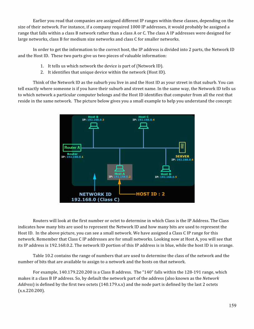
159
Earlier you read that companies are assigned different IP ranges within these classes, depending on the size of their network. For instance, if a company required 1000 IP addresses, it would probably be assigned a range that falls within a class B network rather than a class A or C. The class A IP addresses were designed for large networks, class B for medium size networks and class C for smaller networks.
In order to get the information to the correct host, the IP address is divided into 2 parts, the Network ID and the Host ID. These two parts give us two pieces of valuable information:
1. It tells us which network the device is part of (Network ID). 2. It identifies that unique device within the network (Host ID).
Think of the Network ID as the suburb you live in and the Host ID as your street in that suburb. You can tell exactly where someone is if you have their suburb and street name. In the same way, the Network ID tells us to which network a particular computer belongs and the Host ID identifies that computer from all the rest that reside in the same network. The picture below gives you a small example to help you understand the concept:
Routers will look at the first number or octet to determine in which Class is the IP Address. The Class indicates how many bits are used to represent the Network ID and how many bits are used to represent the Host ID. In the above picture, you can see a small network. We have assigned a Class C IP range for this network. Remember that Class C IP addresses are for small networks. Looking now at Host A, you will see that its IP address is 192.168.0.2. The network ID portion of this IP address is in blue, while the host ID is in orange.
Table 10.2 contains the range of numbers that are used to determine the class of the network and the number of bits that are available to assign to a network and the hosts on that network.
For example, 140.179.220.200 is a Class B address. The “140” falls within the 128-‐191 range, which makes it a class B IP address. So, by default the network part of the address (also known as the Network Address) is defined by the first two octets (140.179.x.x) and the node part is defined by the last 2 octets (x.x.220.200).
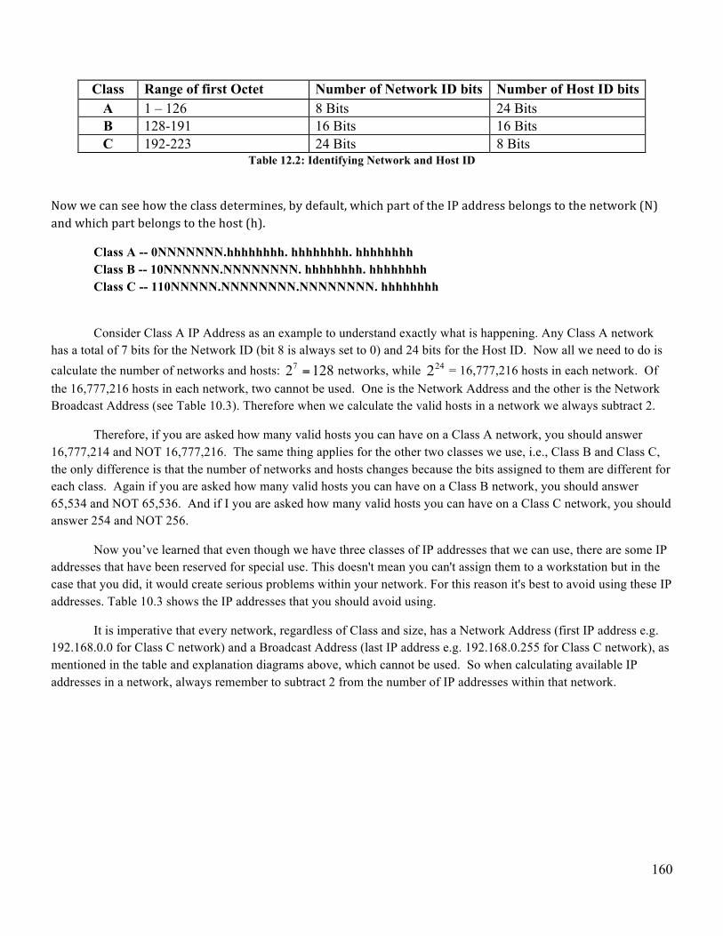
160
Class Range of first Octet Number of Network ID bits Number of Host ID bits A 1 – 126 8 Bits 24 Bits B 128-191 16 Bits 16 Bits C 192-223 24 Bits 8 Bits
Table 12.2: Identifying Network and Host ID
Now we can see how the class determines, by default, which part of the IP address belongs to the network (N) and which part belongs to the host (h).
Class A -- 0NNNNNNN.hhhhhhhh. hhhhhhhh. hhhhhhhh Class B -- 10NNNNNN.NNNNNNNN. hhhhhhhh. hhhhhhhh Class C -- 110NNNNN.NNNNNNNN.NNNNNNNN. hhhhhhhh
Consider Class A IP Address as an example to understand exactly what is happening. Any Class A network has a total of 7 bits for the Network ID (bit 8 is always set to 0) and 24 bits for the Host ID. Now all we need to do is calculate the number of networks and hosts: 72 128= networks, while 242 = 16,777,216 hosts in each network. Of the 16,777,216 hosts in each network, two cannot be used. One is the Network Address and the other is the Network Broadcast Address (see Table 10.3). Therefore when we calculate the valid hosts in a network we always subtract 2.
Therefore, if you are asked how many valid hosts you can have on a Class A network, you should answer 16,777,214 and NOT 16,777,216. The same thing applies for the other two classes we use, i.e., Class B and Class C, the only difference is that the number of networks and hosts changes because the bits assigned to them are different for each class. Again if you are asked how many valid hosts you can have on a Class B network, you should answer 65,534 and NOT 65,536. And if I you are asked how many valid hosts you can have on a Class C network, you should answer 254 and NOT 256.
Now you’ve learned that even though we have three classes of IP addresses that we can use, there are some IP addresses that have been reserved for special use. This doesn't mean you can't assign them to a workstation but in the case that you did, it would create serious problems within your network. For this reason it's best to avoid using these IP addresses. Table 10.3 shows the IP addresses that you should avoid using.
It is imperative that every network, regardless of Class and size, has a Network Address (first IP address e.g. 192.168.0.0 for Class C network) and a Broadcast Address (last IP address e.g. 192.168.0.255 for Class C network), as mentioned in the table and explanation diagrams above, which cannot be used. So when calculating available IP addresses in a network, always remember to subtract 2 from the number of IP addresses within that network.
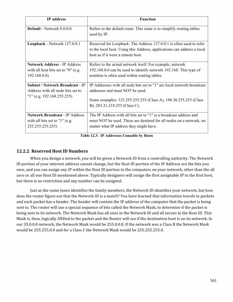
161
IP address Function
Default - Network 0.0.0.0 Refers to the default route. This route is to simplify routing tables used by IP.
Loopback - Network 127.0.0.1 Reserved for Loopback. The Address 127.0.0.1 is often used to refer to the local host. Using this Address, applications can address a local host as if it were a remote host.
Network Address - IP Address with all host bits set to "0" (e.g. 192.168.0.0)
Refers to the actual network itself. For example, network 192.168.0.0 can be used to identify network 192.168. This type of notation is often used within routing tables.
Subnet / Network Broadcast - IP Address with all node bits set to "1" (e.g. 192.168.255.255)
IP Addresses with all node bits set to "1" are local network broadcast addresses and must NOT be used.
Some examples: 125.255.255.255 (Class A), 190.30.255.255 (Class B), 203.31.218.255 (Class C).
Network Broadcast - IP Address with all bits set to "1" (e.g. 255.255.255.255)
The IP Address with all bits set to "1" is a broadcast address and must NOT be used. These are destined for all nodes on a network, no matter what IP address they might have.
Table 12.3: IP Addresses Unusable by Hosts
12.2.2 Reserved Host ID Numbers When you design a network, you will be given a Network ID from a controlling authority. The Network ID portion of your internet address cannot change, but the Host ID portion of the IP Address are the bits you own, and you can assign any IP within the Host ID portion to the computers on your network, other than the all zero or all one Host ID mentioned above. Typically designers will assign the first assignable IP to the first host, but there is no restriction and any number can be assigned.
Just as the name Jones identifies the family members, the Network ID identifies your network, but how does the router figure out that the Network ID is a match? You have learned that information travels in packets and each packet has a header. The header will contain the IP address of the computer that the packet is being sent to. The router will use a special sequence of bits called the Network Mask, to determine if the packet is being sent to its network. The Network Mask has all ones in the Network ID and all zeroes in the Host ID. This Mask is, then, logically ANDed to the packet and the Router will see if the destination host is on its network. In our 35.0.0.0 network, the Network Mask would be 255.0.0.0. If the network was a Class B the Network Mask would be 255.255.0.0 and for a Class C the Network Mask would be 255.255.255.0.
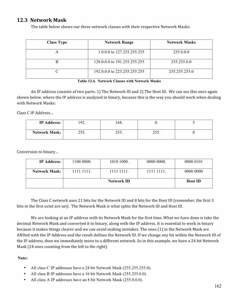
162
12.3 Network Mask The table below shows our three network classes with their respective Network Masks:
Class Type Network Range Network Masks
A 1.0.0.0 to 127.255.255.255 255.0.0.0
B 128.0.0.0 to 191.255.255.255 255.255.0.0
C 192.0.0.0 to 223.255.255.255 255.255.255.0
Table 12.4. Network Classes with Network Masks
An IP address consists of two parts: 1) The Network ID and 2) The Host ID. We can see this once again shown below, where the IP address is analyzed in binary, because this is the way you should work when dealing with Network Masks:
Class C IP Address…
IP Address: 192. 168. 0. 5
Network Mask: 255. 255. 255. 0
Conversion to binary…
IP Address: 1100 0000. 1010 1000. 0000 0000. 0000 0101
Network Mask: 1111 1111. 1111 1111. 1111 1111. 0000 0000
Network ID Host ID
The Class C network uses 21 bits for the Network ID and 8 bits for the Host ID (remember, the first 3 bits in the first octet are set). The Network Mask is what splits the Network ID and Host ID. We are looking at an IP address with its Network Mask for the first time. What we have done is take the decimal Network Mask and converted it to binary, along with the IP address. It is essential to work in binary because it makes things clearer and we can avoid making mistakes. The ones (1) in the Network Mask are ANDed with the IP Address and the result defines the Network ID. If we change any bit within the Network ID of the IP address, then we immediately move to a different network. So in this example, we have a 24 bit Network Mask (24 ones counting from the left to the right). Note:
• All class C IP addresses have a 24 bit Network Mask (255.255.255.0). • All class B IP addresses have a 16 bit Network Mask (255.255.0.0). • All class A IP addresses have an 8 bit Network Mask (255.0.0.0).

163
MAC Address versus IP Address
Recall the MAC address that was discussed earlier. The MAC address is a unique address that is assigned to the physical device. The IP Address is a logical address that is used to determine where in the network a host is located. As in the postal example, the state could be considered the Network, with the city the subnet and the individual person is the host in the network. The MAC address is like the Social Security Number that each person has. The SSN gives no information about where the person is located, but does uniquely identify that person. The MAC identifies the manufacturer and is has a unique number associated with it. The IP Address is used to find where the MAC is so that packets can be routed to the host.

165
Chapter 13: Subnetting
13.1 Introduction As the network grows, it becomes increasingly difficult to efficiently route all the traffic, since the router needs to keep track of all the hosts on its network. Let’s say that we have a simple MAN of two routers. When ever a packet is sent from one host to another on our network, the router will route the packet to the proper host. When the a packet is sent to a host connected to another router, the Network Mask will be used to determine the packet is not for our network and the router will send the packet over the communication link to the other network. If each router only has a few hosts connected to it, then the amount of packets that the router has to router is relatively small. As the network grows, this number of hosts gets quit large. For a class A network there could be 224 Hosts or close to 17 million. As a means to help the routers more efficiently route packets and manage the size of their router table, a technique called subnetting is used.
13.2 Subnet Mask When we subnet a network, we basically split it into smaller networks. By subnetting the network, we can partition it into as many smaller networks as we need. By default, all types of classes (A, B and C) have a Network Mask. However, a network mask other than the default can be used. This is called a Subnet Mask. The use of an IP address with a Subnet Mask other than the Network default results in the standard host bits (the Bits used to identify the HOST ID) being divided in to two parts: a Subnet ID and Host ID. Take the same IP address as above, and divide it further into a Subnet ID and Host ID, thus changing the default network mask:
Class C IP Address
IP Address: 192. 168. 0. 37
Network Mask: 255. 255. 255. 224
Conversion to binary…
IP Address: 1100 0000. 1010 1000. 0000 0000. 001 00101
Network Mask: 1111 1111. 1111 1111. 1111 1111. 111 00000
Network ID Subnet ID Host ID
Looking at the example above you will now notice that we have a Subnet ID, something that didn't exist before. As the example shows, we have borrowed three bits from the Host ID and used them to create a Subnet ID. Effectively we partitioned our Class C network into smaller networks.
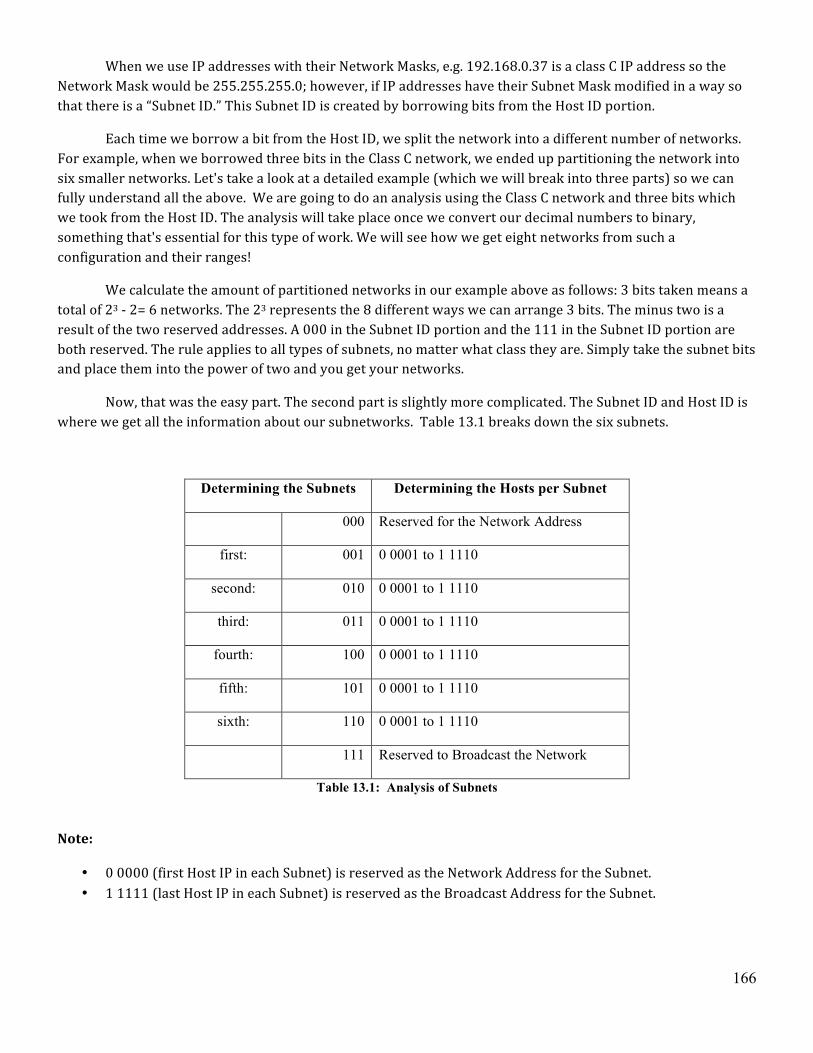
166
When we use IP addresses with their Network Masks, e.g. 192.168.0.37 is a class C IP address so the Network Mask would be 255.255.255.0; however, if IP addresses have their Subnet Mask modified in a way so that there is a “Subnet ID.” This Subnet ID is created by borrowing bits from the Host ID portion.
Each time we borrow a bit from the Host ID, we split the network into a different number of networks. For example, when we borrowed three bits in the Class C network, we ended up partitioning the network into six smaller networks. Let's take a look at a detailed example (which we will break into three parts) so we can fully understand all the above. We are going to do an analysis using the Class C network and three bits which we took from the Host ID. The analysis will take place once we convert our decimal numbers to binary, something that's essential for this type of work. We will see how we get eight networks from such a configuration and their ranges!
We calculate the amount of partitioned networks in our example above as follows: 3 bits taken means a total of 23 -‐ 2= 6 networks. The 23 represents the 8 different ways we can arrange 3 bits. The minus two is a result of the two reserved addresses. A 000 in the Subnet ID portion and the 111 in the Subnet ID portion are both reserved. The rule applies to all types of subnets, no matter what class they are. Simply take the subnet bits and place them into the power of two and you get your networks.
Now, that was the easy part. The second part is slightly more complicated. The Subnet ID and Host ID is where we get all the information about our subnetworks. Table 13.1 breaks down the six subnets.
Determining the Subnets Determining the Hosts per Subnet
000 Reserved for the Network Address
first: 001 0 0001 to 1 1110
second: 010 0 0001 to 1 1110
third: 011 0 0001 to 1 1110
fourth: 100 0 0001 to 1 1110
fifth: 101 0 0001 to 1 1110
sixth: 110 0 0001 to 1 1110
111 Reserved to Broadcast the Network
Table 13.1: Analysis of Subnets
Note:
• 0 0000 (first Host IP in each Subnet) is reserved as the Network Address for the Subnet. • 1 1111 (last Host IP in each Subnet) is reserved as the Broadcast Address for the Subnet.
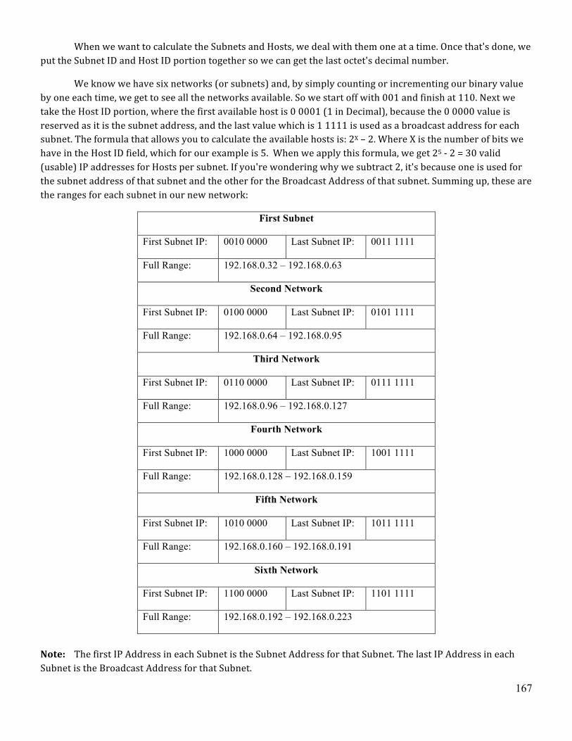
167
When we want to calculate the Subnets and Hosts, we deal with them one at a time. Once that's done, we put the Subnet ID and Host ID portion together so we can get the last octet's decimal number.
We know we have six networks (or subnets) and, by simply counting or incrementing our binary value by one each time, we get to see all the networks available. So we start off with 001 and finish at 110. Next we take the Host ID portion, where the first available host is 0 0001 (1 in Decimal), because the 0 0000 value is reserved as it is the subnet address, and the last value which is 1 1111 is used as a broadcast address for each subnet. The formula that allows you to calculate the available hosts is: 2X – 2. Where X is the number of bits we have in the Host ID field, which for our example is 5. When we apply this formula, we get 25 -‐ 2 = 30 valid (usable) IP addresses for Hosts per subnet. If you're wondering why we subtract 2, it's because one is used for the subnet address of that subnet and the other for the Broadcast Address of that subnet. Summing up, these are the ranges for each subnet in our new network:
First Subnet
First Subnet IP: 0010 0000 Last Subnet IP: 0011 1111
Full Range: 192.168.0.32 – 192.168.0.63
Second Network
First Subnet IP: 0100 0000 Last Subnet IP: 0101 1111
Full Range: 192.168.0.64 – 192.168.0.95
Third Network
First Subnet IP: 0110 0000 Last Subnet IP: 0111 1111
Full Range: 192.168.0.96 – 192.168.0.127
Fourth Network
First Subnet IP: 1000 0000 Last Subnet IP: 1001 1111
Full Range: 192.168.0.128 – 192.168.0.159
Fifth Network
First Subnet IP: 1010 0000 Last Subnet IP: 1011 1111
Full Range: 192.168.0.160 – 192.168.0.191
Sixth Network
First Subnet IP: 1100 0000 Last Subnet IP: 1101 1111
Full Range: 192.168.0.192 – 192.168.0.223
Note: The first IP Address in each Subnet is the Subnet Address for that Subnet. The last IP Address in each Subnet is the Broadcast Address for that Subnet.
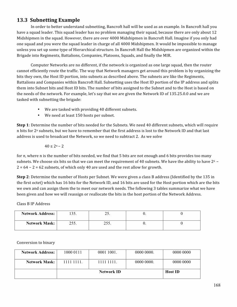
168
13.3 Subnetting Example In order to better understand subnetting, Bancroft hall will be used as an example. In Bancroft hall you have a squad leader. This squad leader has no problem managing their squad, because there are only about 12 Midshipmen in the squad. However, there are over 4000 Midshipmen in Bancroft Hall. Imagine if you only had one squad and you were the squad leader in charge of all 4000 Midshipmen. It would be impossible to manage unless you set up some type of Hierarchical structure. In Bancroft Hall the Midshipmen are organized within the Brigade into Regiments, Battalions, Companies, Platoons, Squads, and finally the MIR.
Computer Networks are no different, if the network is organized as one large squad, then the router cannot efficiently route the traffic. The way that Network managers get around this problem is by organizing the bits they own, the Host ID portion, into subnets as described above. The subnets are like the Regiments, Battalions and Companies within Bancroft Hall. Subnetting uses the Host ID portion of the IP address and splits them into Subnet bits and Host ID bits. The number of bits assigned to the Subnet and to the Host is based on the needs of the network. For example, let’s say that we are given the Network ID of 135.25.0.0 and we are tasked with subnetting the brigade:
• We are tasked with providing 40 different subnets. • We need at least 150 hosts per subnet.
Step 1: Determine the number of bits needed for the Subnets. We need 40 different subnets, which will require n bits for 2n subnets, but we have to remember that the first address is lost to the Network ID and that last address is used to broadcast the Network, so we need to subtract 2. As we solve
40 ≤ 2n − 2
for n, where n is the number of bits needed, we find that 5 bits are not enough and 6 bits provides too many subnets. We choose six bits so that we can meet the requirement of 40 subnets. We have the ability to have 26
−
2 = 64 − 2 = 62 subnets, of which only 40 are used and the rest allow for growth.
Step 2: Determine the number of Hosts per Subnet. We were given a class B address (Identified by the 135 in the first octet) which has 16 bits for the Network ID, and 16 bits are used for the Host portion which are the bits we own and can assign them the to meet our network needs. The following 3 tables summarize what we have been given and how we will reassign or reallocate the bits in the host portion of the Network Address.
Class B IP Address
Network Address: 135. 25. 0. 0
Network Mask: 255. 255. 0. 0
Conversion to binary
Network Address: 1000 0111 0001 1001. 0000 0000. 0000 0000
Network Mask: 1111 1111. 1111 1111. 0000 0000. 0000 0000
Network ID Host ID
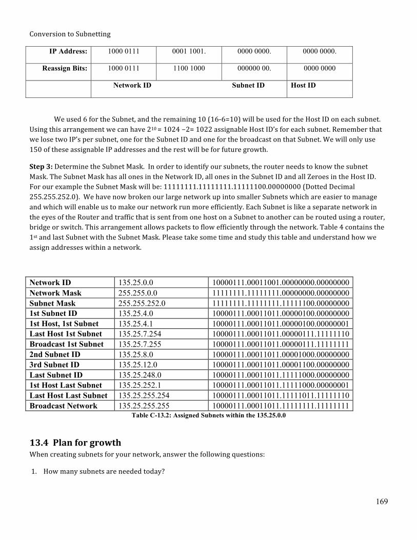
169
Conversion to Subnetting
IP Address: 1000 0111 0001 1001. 0000 0000. 0000 0000.
Reassign Bits: 1000 0111 1100 1000 000000 00. 0000 0000
Network ID Subnet ID Host ID
We used 6 for the Subnet, and the remaining 10 (16-‐6=10) will be used for the Host ID on each subnet. Using this arrangement we can have 210 = 1024 −2= 1022 assignable Host ID’s for each subnet. Remember that we lose two IP’s per subnet, one for the Subnet ID and one for the broadcast on that Subnet. We will only use 150 of these assignable IP addresses and the rest will be for future growth.
Step 3: Determine the Subnet Mask. In order to identify our subnets, the router needs to know the subnet Mask. The Subnet Mask has all ones in the Network ID, all ones in the Subnet ID and all Zeroes in the Host ID. For our example the Subnet Mask will be: 11111111.11111111.11111100.00000000 (Dotted Decimal 255.255.252.0). We have now broken our large network up into smaller Subnets which are easier to manage and which will enable us to make our network run more efficiently. Each Subnet is like a separate network in the eyes of the Router and traffic that is sent from one host on a Subnet to another can be routed using a router, bridge or switch. This arrangement allows packets to flow efficiently through the network. Table 4 contains the 1st and last Subnet with the Subnet Mask. Please take some time and study this table and understand how we assign addresses within a network.
Network ID 135.25.0.0 10000111.00011001.00000000.00000000 Network Mask 255.255.0.0 11111111.11111111.00000000.00000000 Subnet Mask 255.255.252.0 11111111.11111111.11111100.00000000 1st Subnet ID 135.25.4.0 10000111.00011011.00000100.00000000 1st Host, 1st Subnet 135.25.4.1 10000111.00011011.00000100.00000001 Last Host 1st Subnet 135.25.7.254 10000111.00011011.00000111.11111110 Broadcast 1st Subnet 135.25.7.255 10000111.00011011.00000111.11111111 2nd Subnet ID 135.25.8.0 10000111.00011011.00001000.00000000 3rd Subnet ID 135.25.12.0 10000111.00011011.00001100.00000000 Last Subnet ID 135.25.248.0 10000111.00011011.11111000.00000000 1st Host Last Subnet 135.25.252.1 10000111.00011011.11111000.00000001 Last Host Last Subnet 135.25.255.254 10000111.00011011.11111011.11111110 Broadcast Network 135.25.255.255 10000111.00011011.11111111.11111111
Table C-13.2: Assigned Subnets within the 135.25.0.0
13.4 Plan for growth When creating subnets for your network, answer the following questions:
1. How many subnets are needed today?
170
Calculate the maximum number of subnets required by rounding up the maximum number to the nearest power of two. For example, if an organization needs five subnets, 2 to the power of 2 or 4 will not provide enough subnet addressing space, so you must round up to 2 to the power of 3 = 8 subnets.
2. How many subnets are needed in the future?
You must plan for future growth. For example, if 9 subnets are required today, and you choose to provide for 2 to the power of 4 = 16 subnets, this might not be enough when the seventeenth subnet needs to be deployed. In this example, it might be wise to provide for more growth and select 2 to the power of 5 = 32 as the maximum number of subnets.
3. What is the maximum number of hosts on a given segment?
You must ensure that there are enough bits available to assign host addresses to the organization's largest subnet. If the largest subnet needs to support 40 host addresses today, 2 to the power of 5 = 32 will not provide enough host address space, so you would need to round up to 2 to the power of 6 = 64.
4. How many hosts will there be in the future?
Besides planning for additional subnets, you must also plan for more hosts to be added to each subnet in the future. Make sure the organization's address allocation provides enough bits to deploy the required subnet addressing plan. When developing subnets, Class C addresses present the greatest challenge because fewer bits are available to divide between subnet addresses and host addresses. If you accommodate too many subnets, there may be no room for additional hosts and growth in the future.
All the above points will help you succeed in creating a well-‐designed network which will have the ability to cater for any additional future requirements.
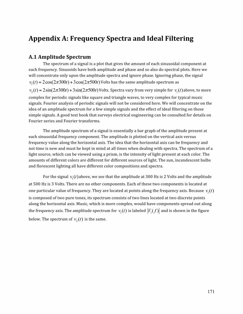
171
Appendix A: Frequency Spectra and Ideal Filtering
A.1 Amplitude Spectrum The spectrum of a signal is a plot that gives the amount of each sinusoidal component at each frequency. Sinusoids have both amplitude and phase and so also do spectral plots. Here we will concentrate only upon the amplitude spectra and ignore phase. Ignoring phase, the signal
1( ) 2cos(2 300 ) 3cos(2 500 )v t t tπ π= + Volts has the same amplitude spectrum as
2 ( ) 2sin(2 300 ) 3sin(2 500 )v t t tπ π= + Volts. Spectra vary from very simple for 1( )v t above, to more complex for periodic signals like square and triangle waves, to very complex for typical music signals. Fourier analysis of periodic signals will not be considered here. We will concentrate on the idea of an amplitude spectrum for a few simple signals and the effect of ideal filtering on those simple signals. A good text book that surveys electrical engineering can be consulted for details on Fourier series and Fourier transforms.
The amplitude spectrum of a signal is essentially a bar graph of the amplitude present at each sinusoidal frequency component. The amplitude is plotted on the vertical axis versus frequency value along the horizontal axis. The idea that the horizontal axis can be frequency and not time is new and must be kept in mind at all times when dealing with spectra. The spectrum of a light source, which can be viewed using a prism, is the intensity of light present at each color. The amounts of different colors are different for different sources of light. The sun, incandescent bulbs and florescent lighting all have different color compositions and spectra.
For the signal 1( )v t above, we see that the amplitude at 300 Hz is 2 Volts and the amplitude at 500 Hz is 3 Volts. There are no other components. Each of these two components is located at one particular value of frequency. They are located at points along the frequency axis. Because 1( )v t is composed of two pure tones, its spectrum consists of two lines located at two discrete points along the horizontal axis. Music, which is more complex, would have components spread out along the frequency axis. The amplitude spectrum for 1( )v t is labeled 1( )V f and is shown in the figure
below. The spectrum of 2 ( )v t is the same.
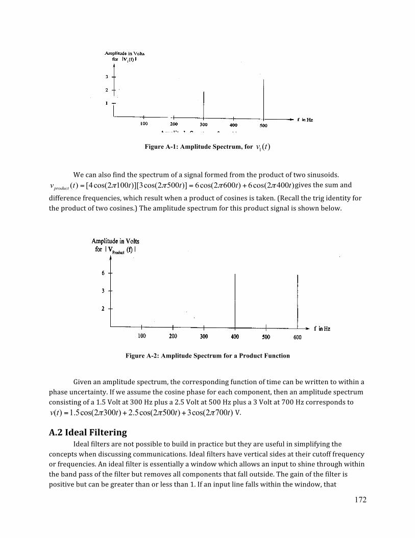
172
Figure A-1: Amplitude Spectrum, for 1( )v t
We can also find the spectrum of a signal formed from the product of two sinusoids. ( ) [4cos(2 100 )][3cos(2 500 )] 6cos(2 600 ) 6cos(2 400 )productv t t t t tπ π π π= = + gives the sum and
difference frequencies, which result when a product of cosines is taken. (Recall the trig identity for the product of two cosines.) The amplitude spectrum for this product signal is shown below.
Figure A-2: Amplitude Spectrum for a Product Function
Given an amplitude spectrum, the corresponding function of time can be written to within a phase uncertainty. If we assume the cosine phase for each component, then an amplitude spectrum consisting of a 1.5 Volt at 300 Hz plus a 2.5 Volt at 500 Hz plus a 3 Volt at 700 Hz corresponds to( ) 1.5cos(2 300 ) 2.5cos(2 500 ) 3cos(2 700 )v t t t tπ π π= + + V.
A.2 Ideal Filtering Ideal filters are not possible to build in practice but they are useful in simplifying the concepts when discussing communications. Ideal filters have vertical sides at their cutoff frequency or frequencies. An ideal filter is essentially a window which allows an input to shine through within the band pass of the filter but removes all components that fall outside. The gain of the filter is positive but can be greater than or less than 1. If an input line falls within the window, that
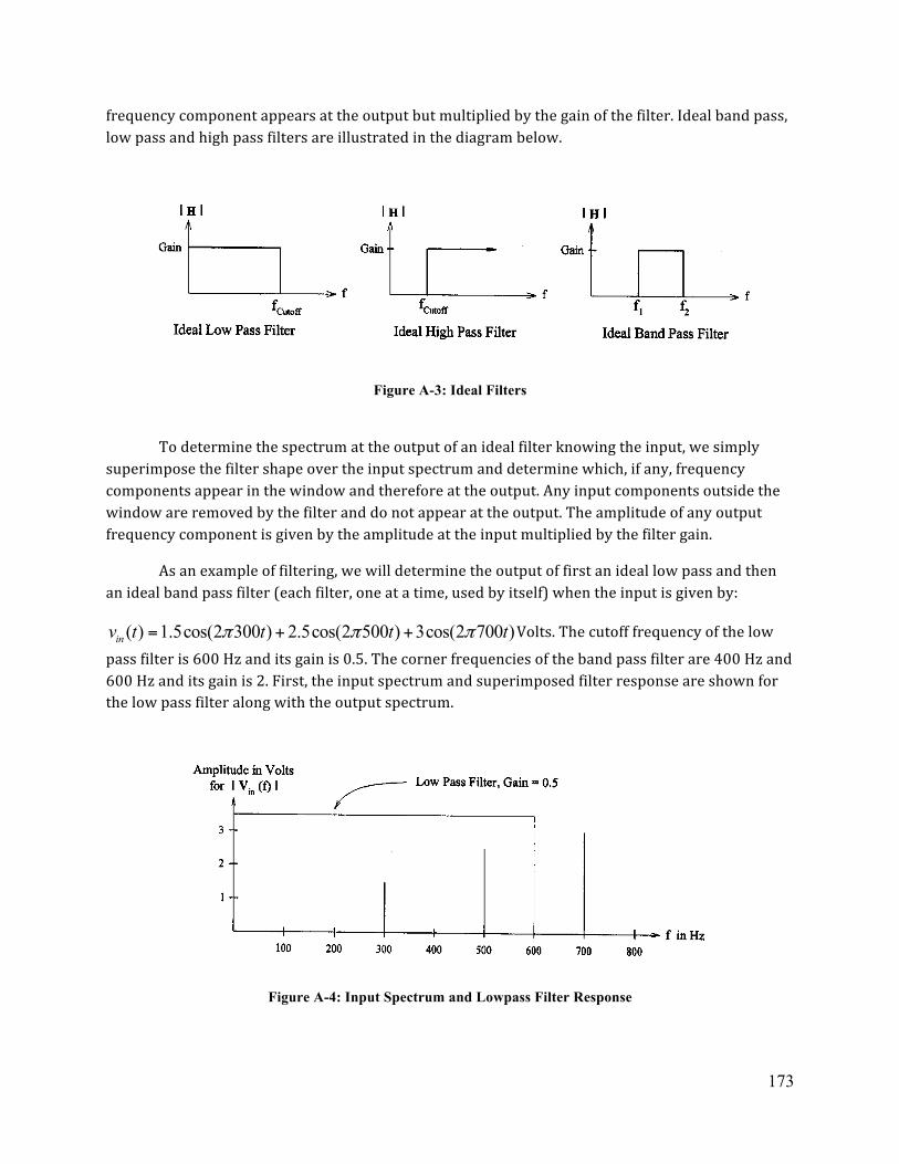
173
frequency component appears at the output but multiplied by the gain of the filter. Ideal band pass, low pass and high pass filters are illustrated in the diagram below.
Figure A-3: Ideal Filters
To determine the spectrum at the output of an ideal filter knowing the input, we simply superimpose the filter shape over the input spectrum and determine which, if any, frequency components appear in the window and therefore at the output. Any input components outside the window are removed by the filter and do not appear at the output. The amplitude of any output frequency component is given by the amplitude at the input multiplied by the filter gain.
As an example of filtering, we will determine the output of first an ideal low pass and then an ideal band pass filter (each filter, one at a time, used by itself) when the input is given by:
( ) 1.5cos(2 300 ) 2.5cos(2 500 ) 3cos(2 700 )inv t t t tπ π π= + + Volts. The cutoff frequency of the low
pass filter is 600 Hz and its gain is 0.5. The corner frequencies of the band pass filter are 400 Hz and 600 Hz and its gain is 2. First, the input spectrum and superimposed filter response are shown for the low pass filter along with the output spectrum.
Figure A-4: Input Spectrum and Lowpass Filter Response
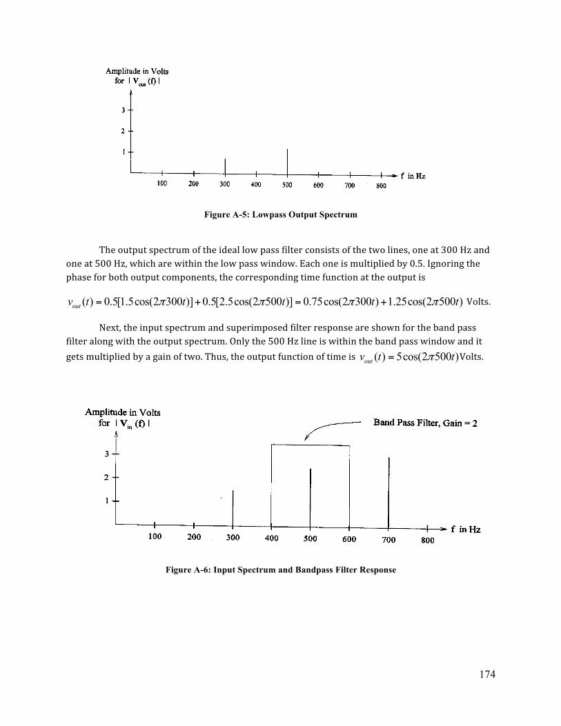
174
Figure A-5: Lowpass Output Spectrum
The output spectrum of the ideal low pass filter consists of the two lines, one at 300 Hz and one at 500 Hz, which are within the low pass window. Each one is multiplied by 0.5. Ignoring the phase for both output components, the corresponding time function at the output is
( ) 0.5[1.5cos(2 300 )] 0.5[2.5cos(2 500 )] 0.75cos(2 300 ) 1.25cos(2 500 )outv t t t t tπ π π π= + = + Volts.
Next, the input spectrum and superimposed filter response are shown for the band pass filter along with the output spectrum. Only the 500 Hz line is within the band pass window and it gets multiplied by a gain of two. Thus, the output function of time is ( ) 5cos(2 500 )outv t tπ= Volts.
Figure A-6: Input Spectrum and Bandpass Filter Response
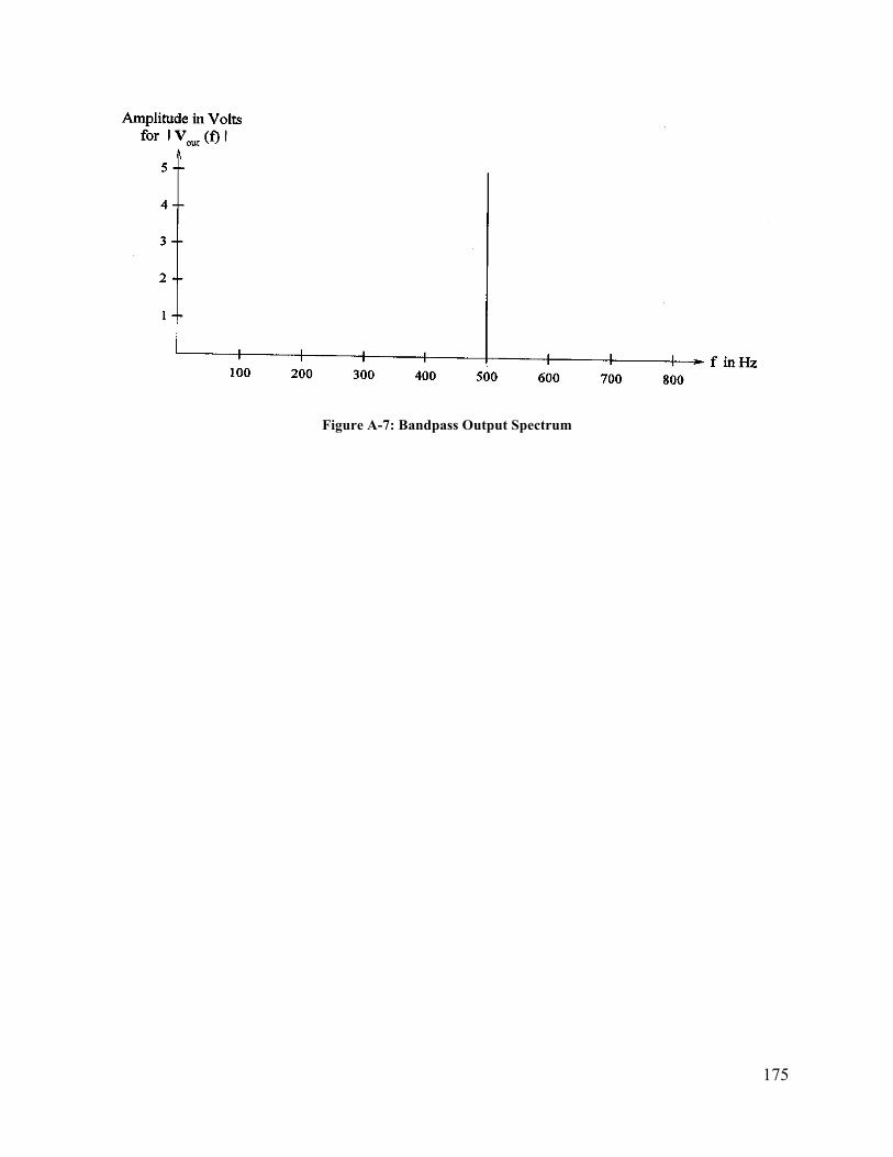
175
Figure A-7: Bandpass Output Spectrum

177
Appendix B: A Typical CW Communication System
B.1 Introduction We can think of a continuous wave (CW) transmitter, regardless of whether it is AM or FM, as a device which modulates a continuous wave carrier signal with an information signal. This modulated waveform is then coupled to the channel using an appropriate channel matching device. Figure B-‐1 shows a typical CW transmitter.
Figure B-1: A CW Transmitter
The key item in the transmitter is, of course, the modulator. Besides the modulator, an amplifier is necessary because most transmissions require high power levels if they are to travel any distance. For example, even the relatively low powered citizen’s band transmitters transmit 5 Watts. A local broadcast station may transmit a hundred thousand Watts! The amplified, modulated signal is now ready for transmission. To do so usually requires a channel matching device. Computers talk over telephone lines using a modem. A modem is a device which contains both a modulator and a demodulator. While radio and TV transmitters require an antenna to transmit, a light beam usually requires some type of collimating lens prior to entering a fiber optic channel.
At the other end of the channel we find the receiver. Basically a receiver is a device which extracts the signal from the channel and prepares it for delivery to the output processor and transducer. Since the received signal is modulated and usually very weak (attenuated) we would expect a receiver to contain an amplifier and demodulator.
B.2 A Citizen Band (CB) Transceiver The popularity of the citizen’s band has been made possible through low-‐cost, reliable, and portable equipment. The minimal licensing requirements, the 55 mph speed limit, and movies such as Smokey and the Bandit have also contributed to their popularity. The FCC has allocated a small portion of the 11 meter band to public use. The spectrum between 26.9 MHz and 27.3 MHz has been divided into 40 CB channels located 10 KHz apart
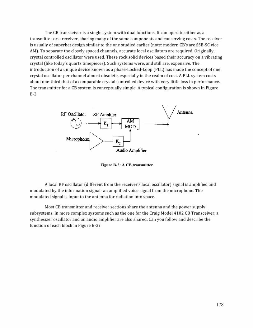
178
The CB transceiver is a single system with dual functions. It can operate either as a transmitter or a receiver, sharing many of the same components and conserving costs. The receiver is usually of superhet design similar to the one studied earlier (note: modern CB’s are SSB-‐SC vice AM). To separate the closely spaced channels, accurate local oscillators are required. Originally, crystal controlled oscillator were used. These rock solid devices based their accuracy on a vibrating crystal (like today’s quartz timepieces). Such systems were, and still are, expensive. The introduction of a unique device known as a phase-‐Locked-‐Loop (PLL) has made the concept of one crystal oscillator per channel almost obsolete, especially in the realm of cost. A PLL system costs about one-‐third that of a comparable crystal controlled device with very little loss in performance. The transmitter for a CB system is conceptually simple. A typical configuration is shown in Figure B-‐2.
Figure B-2: A CB transmitter
A local RF oscillator (different from the receiver’s local oscillator) signal is amplified and modulated by the information signal-‐ an amplified voice signal from the microphone. The modulated signal is input to the antenna for radiation into space.
Most CB transmitter and receiver sections share the antenna and the power supply subsystems. In more complex systems such as the one for the Craig Model 4102 CB Transceiver, a synthesizer oscillator and an audio amplifier are also shared. Can you follow and describe the function of each block in Figure B-‐3?
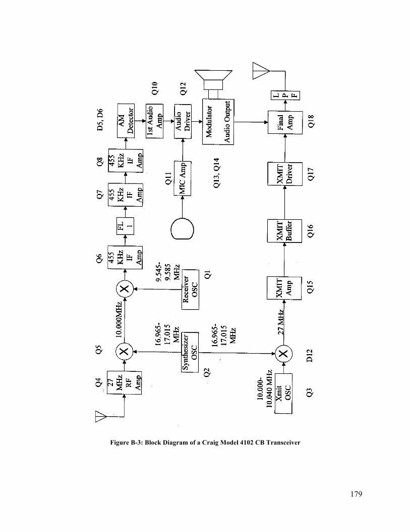
179
Figure B-3: Block Diagram of a Craig Model 4102 CB Transceiver

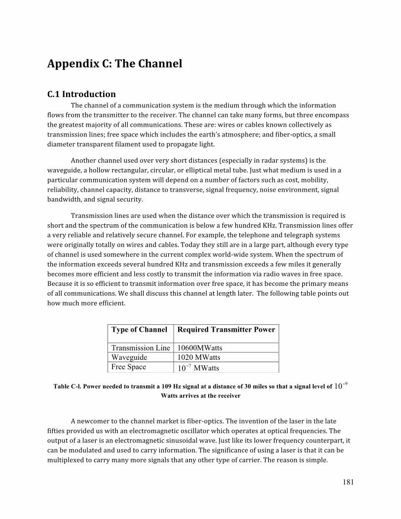
181
Appendix C: The Channel
C.1 Introduction The channel of a communication system is the medium through which the information flows from the transmitter to the receiver. The channel can take many forms, but three encompass the greatest majority of all communications. These are: wires or cables known collectively as transmission lines; free space which includes the earth’s atmosphere; and fiber-‐optics, a small diameter transparent filament used to propagate light.
Another channel used over very short distances (especially in radar systems) is the waveguide, a hollow rectangular, circular, or elliptical metal tube. Just what medium is used in a particular communication system will depend on a number of factors such as cost, mobility, reliability, channel capacity, distance to transverse, signal frequency, noise environment, signal bandwidth, and signal security.
Transmission lines are used when the distance over which the transmission is required is short and the spectrum of the communication is below a few hundred KHz. Transmission lines offer a very reliable and relatively secure channel. For example, the telephone and telegraph systems were originally totally on wires and cables. Today they still are in a large part, although every type of channel is used somewhere in the current complex world-‐wide system. When the spectrum of the information exceeds several hundred KHz and transmission exceeds a few miles it generally becomes more efficient and less costly to transmit the information via radio waves in free space. Because it is so efficient to transmit information over free space, it has become the primary means of all communications. We shall discuss this channel at length later. The following table points out how much more efficient.
Table C-l. Power needed to transmit a 109 Hz signal at a distance of 30 miles so that a signal level of 910− Watts arrives at the receiver
A newcomer to the channel market is fiber-‐optics. The invention of the laser in the late fifties provided us with an electromagnetic oscillator which operates at optical frequencies. The output of a laser is an electromagnetic sinusoidal wave. Just like its lower frequency counterpart, it can be modulated and used to carry information. The significance of using a laser is that it can be multiplexed to carry many more signals that any other type of carrier. The reason is simple.
Type of Channel
Required Transmitter Power
Transmission Line 10600MWatts Waveguide 1020 MWatts Free Space 710− MWatts
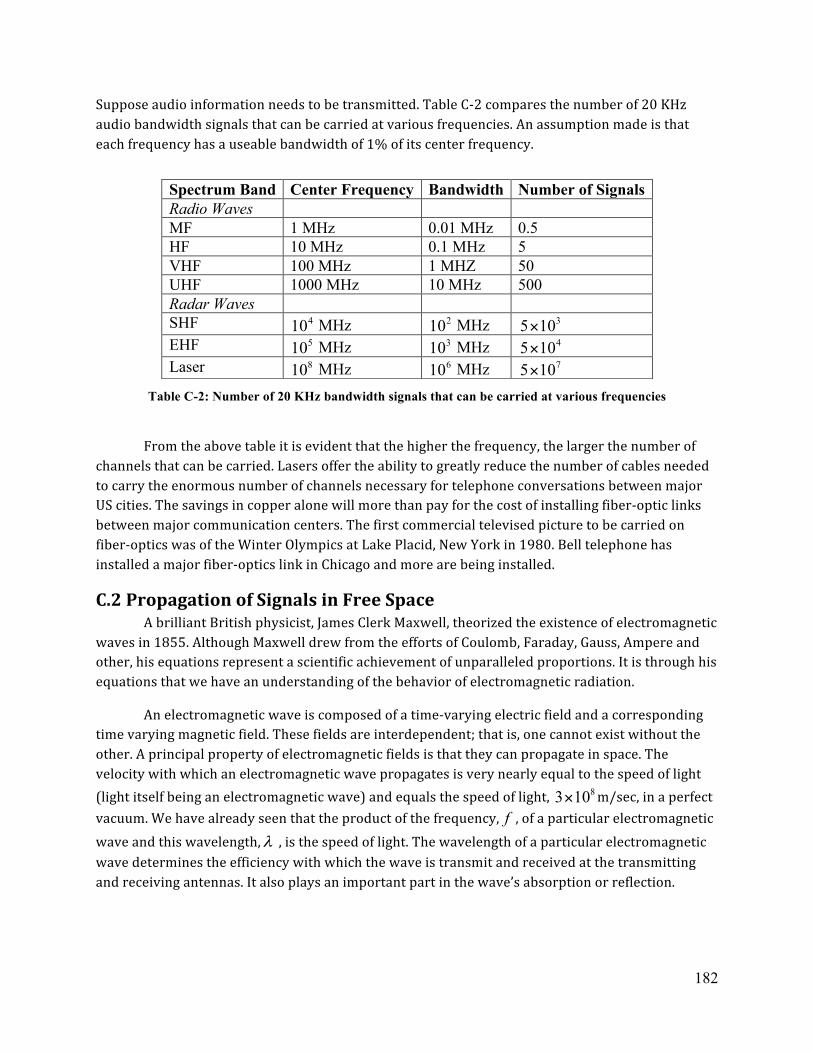
182
Suppose audio information needs to be transmitted. Table C-‐2 compares the number of 20 KHz audio bandwidth signals that can be carried at various frequencies. An assumption made is that each frequency has a useable bandwidth of 1% of its center frequency.
Table C-2: Number of 20 KHz bandwidth signals that can be carried at various frequencies
From the above table it is evident that the higher the frequency, the larger the number of channels that can be carried. Lasers offer the ability to greatly reduce the number of cables needed to carry the enormous number of channels necessary for telephone conversations between major US cities. The savings in copper alone will more than pay for the cost of installing fiber-‐optic links between major communication centers. The first commercial televised picture to be carried on fiber-‐optics was of the Winter Olympics at Lake Placid, New York in 1980. Bell telephone has installed a major fiber-‐optics link in Chicago and more are being installed.
C.2 Propagation of Signals in Free Space A brilliant British physicist, James Clerk Maxwell, theorized the existence of electromagnetic waves in 1855. Although Maxwell drew from the efforts of Coulomb, Faraday, Gauss, Ampere and other, his equations represent a scientific achievement of unparalleled proportions. It is through his equations that we have an understanding of the behavior of electromagnetic radiation.
An electromagnetic wave is composed of a time-‐varying electric field and a corresponding time varying magnetic field. These fields are interdependent; that is, one cannot exist without the other. A principal property of electromagnetic fields is that they can propagate in space. The velocity with which an electromagnetic wave propagates is very nearly equal to the speed of light (light itself being an electromagnetic wave) and equals the speed of light, 83 10× m/sec, in a perfect vacuum. We have already seen that the product of the frequency, f , of a particular electromagnetic wave and this wavelength,λ , is the speed of light. The wavelength of a particular electromagnetic wave determines the efficiency with which the wave is transmit and received at the transmitting and receiving antennas. It also plays an important part in the wave’s absorption or reflection.
Spectrum Band Center Frequency Bandwidth Number of Signals Radio Waves MF 1 MHz 0.01 MHz 0.5 HF 10 MHz 0.1 MHz 5 VHF 100 MHz 1 MHZ 50 UHF 1000 MHz 10 MHz 500 Radar Waves SHF 410 MHz 210 MHz 35 10× EHF 510 MHz 310 MHz 45 10× Laser 810 MHz 610 MHz 75 10×
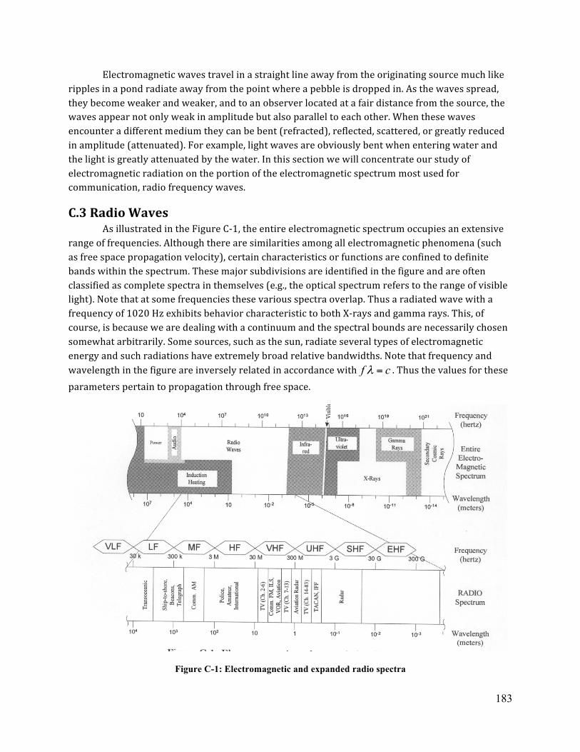
183
Electromagnetic waves travel in a straight line away from the originating source much like ripples in a pond radiate away from the point where a pebble is dropped in. As the waves spread, they become weaker and weaker, and to an observer located at a fair distance from the source, the waves appear not only weak in amplitude but also parallel to each other. When these waves encounter a different medium they can be bent (refracted), reflected, scattered, or greatly reduced in amplitude (attenuated). For example, light waves are obviously bent when entering water and the light is greatly attenuated by the water. In this section we will concentrate our study of electromagnetic radiation on the portion of the electromagnetic spectrum most used for communication, radio frequency waves.
C.3 Radio Waves As illustrated in the Figure C-‐1, the entire electromagnetic spectrum occupies an extensive range of frequencies. Although there are similarities among all electromagnetic phenomena (such as free space propagation velocity), certain characteristics or functions are confined to definite bands within the spectrum. These major subdivisions are identified in the figure and are often classified as complete spectra in themselves (e.g., the optical spectrum refers to the range of visible light). Note that at some frequencies these various spectra overlap. Thus a radiated wave with a frequency of 1020 Hz exhibits behavior characteristic to both X-‐rays and gamma rays. This, of course, is because we are dealing with a continuum and the spectral bounds are necessarily chosen somewhat arbitrarily. Some sources, such as the sun, radiate several types of electromagnetic energy and such radiations have extremely broad relative bandwidths. Note that frequency and wavelength in the figure are inversely related in accordance with f cλ = . Thus the values for these parameters pertain to propagation through free space.
Figure C-1: Electromagnetic and expanded radio spectra
184
In the study of signal propagation, our primary interest is in radio waves. These waves occupy that portion of the electromagnetic spectrum from 10 KHz to 1000 GHz (G = giga = 910 ). An expanded radio spectrum is also shown above. The ITU (International Telegraphic Union) designation of frequency bands and the frequency ranges for some of the more common uses of radio waves are indicated. Since the transmitted signal in a communication system usually has a narrow relative bandwidth, the propagation characteristics are determined almost exclusively by the carrier wave. Thus, in this section we will extend the properties of the carrier wave (such as frequency and wavelength) to the entire transmitted signal.
As a radio wave propagates over its transmission path, several things can alter it. It can be attenuated, reflected or scattered. Attenuation of a radiated signal is caused primarily by the spreading out of the wave as it propagates from its source. As a result, only a small fraction of the transmitted power is intercepted by a receiving antenna. Additionally, there is a small loss of signal power due to interaction of the wave with the medium through which the wave passes. If a wave strikes the boundary of a conductive medium, it may be reflected and/or refracted. Reflection of incident waves increases with the conductivity of the medium such that a perfect conductor results in total reflection. Ionized portions of the atmosphere are conductive and therefore can cause a radio wave to be reflected or refracted. Scattering of a propagating wave may also occur if there are non-‐homogeneities within the medium. The characteristics of both the medium and the radio wave determine whether the wave will be significantly altered by scattering, reflection, refraction, or attenuation. The most significant wave characteristic is the frequency. Likewise the direction of propagation may have to be considered since reflection and refraction are dependent upon the incident angle at which a wave strikes a conductive medium. A wave may reach a particular point by any of several paths. A wave can be reflected or refracted or scattered several times and arrive at the same point it may reach by line of sight (although the waves may arrive at slightly different times).
Within the earth’s atmosphere there are two regions or layers that greatly affect the propagation of radio waves. The first of these is the troposphere, which extends from the surface to about 33,000 feet. Clouds are formed and most weather phenomena occur in this region. Within the troposphere, there are sharp discontinuities in temperature, water vapor content and air density. The resulting blobs of air can scatter radio waves. The second region is the ionosphere, which consists of several ionized layers at heights between 30 and 250 miles. These ionized layers are formed by radiant energy from the sun and display variations in both ion density and height. Generally, the ionosphere is denser and lower during the day and in summer. At night and during the winter, ion density decreases whereas the bottom of the ionosphere rises. The ionosphere is also affected by sunspot activity which occurs in 11 year cycles. As might be expected, the ionosphere is quite unstable and is not uniform around the earth at anyone time. Since the ionosphere is a conducting medium, it may reflect and/or refract radio waves which strike it.
C.4 Propagation of Radio Waves The propagation characteristics of radio waves vary greatly from one frequency to another. This is not surprising when it is realized that wavelengths within the radio spectrum range from 30,000 meters (about 19 miles) to 0.3 millimeters (about 0.012 inches). There are four primary
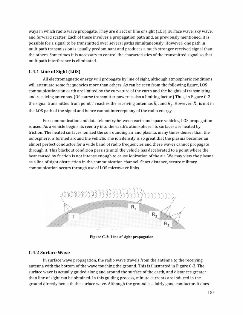
185
ways in which radio wave propagate. They are direct or line of sight (LOS), surface wave, sky wave, and forward scatter. Each of these involves a propagation path and, as previously mentioned, it is possible for a signal to be transmitted over several paths simultaneously. However, one path in multipath transmission is usually predominant and produces a much stronger received signal than the others. Sometimes it is necessary to control the characteristics of the transmitted signal so that multipath interference is eliminated.
C.4.1 Line of Sight (LOS) All electromagnetic energy will propagate by line of sight, although atmospheric conditions will attenuate some frequencies more than others. As can be seen from the following figure, LOS communications on earth are limited by the curvature of the earth and the heights of transmitting and receiving antennas. (Of course transmitter power is also a limiting factor.) Thus, in Figure C-‐2 the signal transmitted from point T reaches the receiving antennas 1R , and 2R . However, 3R is not in
the LOS path of the signal and hence cannot intercept any of the radio energy.
For communication and data telemetry between earth and space vehicles, LOS propagation is used. As a vehicle begins its reentry into the earth’s atmosphere, its surfaces are heated by friction. The heated surfaces ionized the surrounding air and plasma, many times denser than the ionosphere, is formed around the vehicle. The ion density is so great that the plasma becomes an almost perfect conductor for a wide band of radio frequencies and these waves cannot propagate through it. This blackout condition persists until the vehicle has decelerated to a point where the heat caused by friction is not intense enough to cause ionization of the air. We may view the plasma as a line of sight obstruction in the communication channel. Short distance, secure military communication occurs through use of LOS microwave links.
Figure C-2: Line of sight propagation
C.4.2 Surface Wave In surface wave propagation, the radio wave travels from the antenna to the receiving antenna with the bottom of the wave touching the ground. This is illustrated in Figure C-‐3. The surface wave is actually guided along and around the surface of the earth, and distances greater than line of sight can be obtained. In this guiding process, minute currents are induced in the ground directly beneath the surface wave. Although the ground is a fairly good conductor, it does
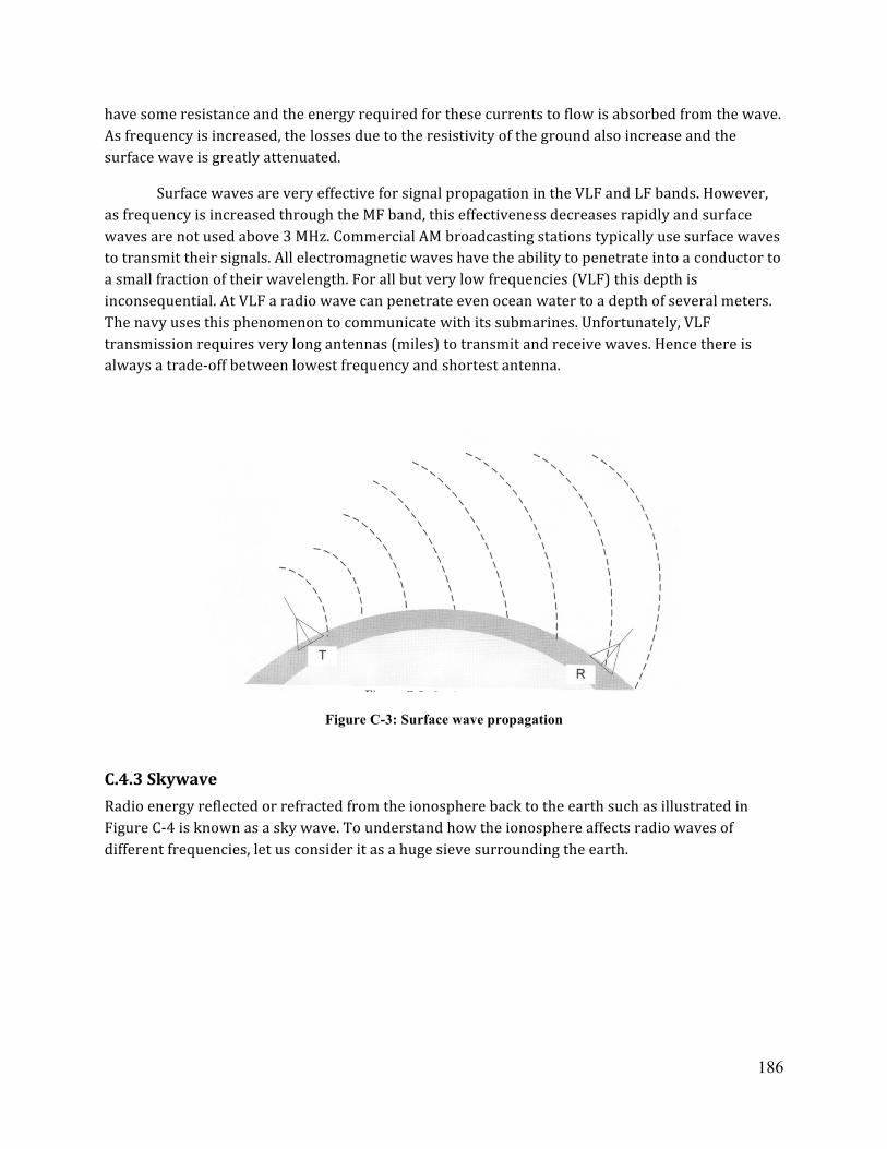
186
have some resistance and the energy required for these currents to flow is absorbed from the wave. As frequency is increased, the losses due to the resistivity of the ground also increase and the surface wave is greatly attenuated.
Surface waves are very effective for signal propagation in the VLF and LF bands. However, as frequency is increased through the MF band, this effectiveness decreases rapidly and surface waves are not used above 3 MHz. Commercial AM broadcasting stations typically use surface waves to transmit their signals. All electromagnetic waves have the ability to penetrate into a conductor to a small fraction of their wavelength. For all but very low frequencies (VLF) this depth is inconsequential. At VLF a radio wave can penetrate even ocean water to a depth of several meters. The navy uses this phenomenon to communicate with its submarines. Unfortunately, VLF transmission requires very long antennas (miles) to transmit and receive waves. Hence there is always a trade-‐off between lowest frequency and shortest antenna.
Figure C-3: Surface wave propagation
C.4.3 Skywave Radio energy reflected or refracted from the ionosphere back to the earth such as illustrated in Figure C-‐4 is known as a sky wave. To understand how the ionosphere affects radio waves of different frequencies, let us consider it as a huge sieve surrounding the earth.
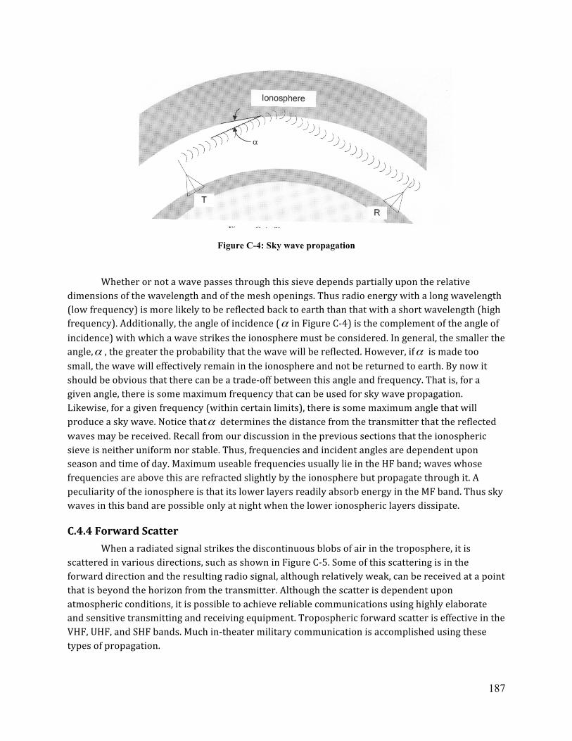
187
Figure C-4: Sky wave propagation
Whether or not a wave passes through this sieve depends partially upon the relative dimensions of the wavelength and of the mesh openings. Thus radio energy with a long wavelength (low frequency) is more likely to be reflected back to earth than that with a short wavelength (high frequency). Additionally, the angle of incidence (α in Figure C-‐4) is the complement of the angle of incidence) with which a wave strikes the ionosphere must be considered. In general, the smaller the angle,α , the greater the probability that the wave will be reflected. However, ifα is made too small, the wave will effectively remain in the ionosphere and not be returned to earth. By now it should be obvious that there can be a trade-‐off between this angle and frequency. That is, for a given angle, there is some maximum frequency that can be used for sky wave propagation. Likewise, for a given frequency (within certain limits), there is some maximum angle that will produce a sky wave. Notice thatα determines the distance from the transmitter that the reflected waves may be received. Recall from our discussion in the previous sections that the ionospheric sieve is neither uniform nor stable. Thus, frequencies and incident angles are dependent upon season and time of day. Maximum useable frequencies usually lie in the HF band; waves whose frequencies are above this are refracted slightly by the ionosphere but propagate through it. A peculiarity of the ionosphere is that its lower layers readily absorb energy in the MF band. Thus sky waves in this band are possible only at night when the lower ionospheric layers dissipate.
C.4.4 Forward Scatter When a radiated signal strikes the discontinuous blobs of air in the troposphere, it is scattered in various directions, such as shown in Figure C-‐5. Some of this scattering is in the forward direction and the resulting radio signal, although relatively weak, can be received at a point that is beyond the horizon from the transmitter. Although the scatter is dependent upon atmospheric conditions, it is possible to achieve reliable communications using highly elaborate and sensitive transmitting and receiving equipment. Tropospheric forward scatter is effective in the VHF, UHF, and SHF bands. Much in-‐theater military communication is accomplished using these types of propagation.
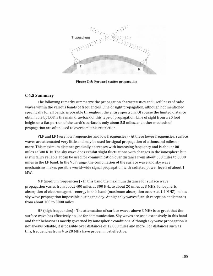
188
Figure C-5: Forward scatter propagation
C.4.5 Summary The following remarks summarize the propagation characteristics and usefulness of radio waves within the various bands of frequencies. Line of sight propagation, although not mentioned specifically for all bands, is possible throughout the entire spectrum. Of course the limited distance obtainable by LOS is the main drawback of this type of propagation. Line of sight from a 20 foot height on a flat portion of the earth’s surface is only about 5.5 miles, and other methods of propagation are often used to overcome this restriction.
VLF and LF (very low frequencies and low frequencies) -‐ At these lower frequencies, surface waves are attenuated very little and may be used for signal propagation of a thousand miles or more. This maximum distance gradually decreases with increasing frequency and is about 400 miles at 300 KHz. The sky wave does exhibit slight fluctuations with changes in the ionosphere but is still fairly reliable. It can be used for communication over distance from about 500 miles to 8000 miles in the LF band. In the VLF range, the combination of the surface wave and sky wave mechanisms makes possible world-‐wide signal propagation with radiated power levels of about 1 MW.
MF (medium frequencies) -‐ In this band the maximum distance for surface wave propagation varies from about 400 miles at 300 KHz to about 20 miles at 3 MHZ. Ionospheric absorption of electromagnetic energy in this band (maximum absorption occurs at 1.4 MHZ) makes sky wave propagation impossible during the day. At night sky waves furnish reception at distances from about 100 to 3000 miles.
HF (high frequencies) -‐ The attenuation of surface waves above 3 MHz is so great that the surface wave has effectively no use for communication. Sky waves are used extensively in this band and their behavior is mostly governed by ionospheric conditions. Although sky wave propagation is not always reliable, it is possible over distances of 12,000 miles and more. For distances such as this, frequencies from 4 to 20 MHz have proven most effective.
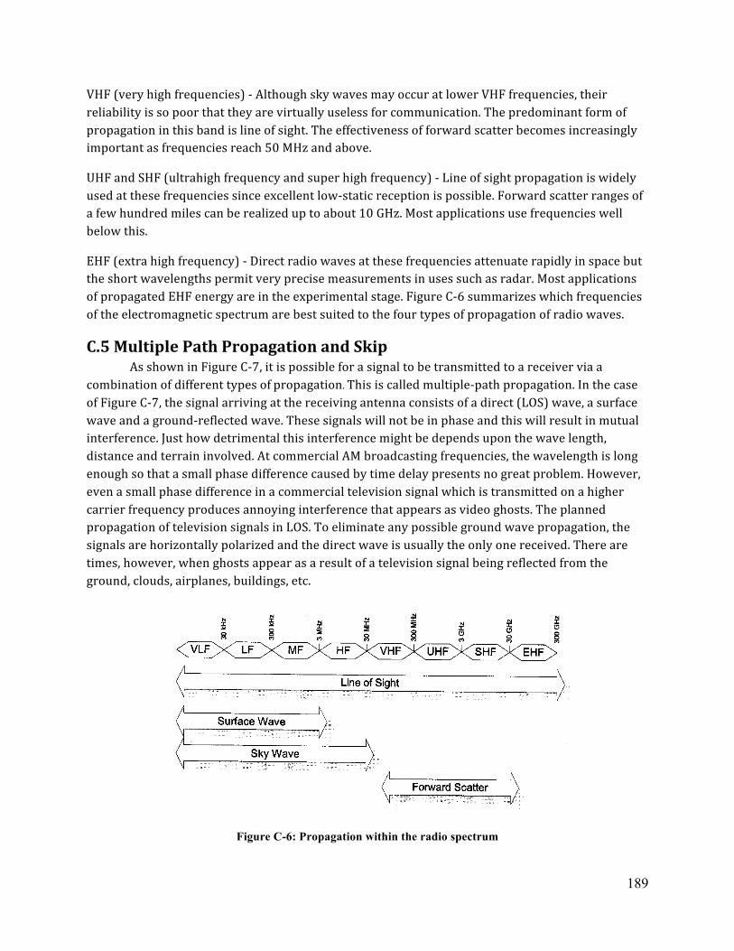
189
VHF (very high frequencies) -‐ Although sky waves may occur at lower VHF frequencies, their reliability is so poor that they are virtually useless for communication. The predominant form of propagation in this band is line of sight. The effectiveness of forward scatter becomes increasingly important as frequencies reach 50 MHz and above.
UHF and SHF (ultrahigh frequency and super high frequency) -‐ Line of sight propagation is widely used at these frequencies since excellent low-‐static reception is possible. Forward scatter ranges of a few hundred miles can be realized up to about 10 GHz. Most applications use frequencies well below this.
EHF (extra high frequency) -‐ Direct radio waves at these frequencies attenuate rapidly in space but the short wavelengths permit very precise measurements in uses such as radar. Most applications of propagated EHF energy are in the experimental stage. Figure C-‐6 summarizes which frequencies of the electromagnetic spectrum are best suited to the four types of propagation of radio waves.
C.5 Multiple Path Propagation and Skip As shown in Figure C-‐7, it is possible for a signal to be transmitted to a receiver via a combination of different types of propagation. This is called multiple-‐path propagation. In the case of Figure C-‐7, the signal arriving at the receiving antenna consists of a direct (LOS) wave, a surface wave and a ground-‐reflected wave. These signals will not be in phase and this will result in mutual interference. Just how detrimental this interference might be depends upon the wave length, distance and terrain involved. At commercial AM broadcasting frequencies, the wavelength is long enough so that a small phase difference caused by time delay presents no great problem. However, even a small phase difference in a commercial television signal which is transmitted on a higher carrier frequency produces annoying interference that appears as video ghosts. The planned propagation of television signals in LOS. To eliminate any possible ground wave propagation, the signals are horizontally polarized and the direct wave is usually the only one received. There are times, however, when ghosts appear as a result of a television signal being reflected from the ground, clouds, airplanes, buildings, etc.
Figure C-6: Propagation within the radio spectrum
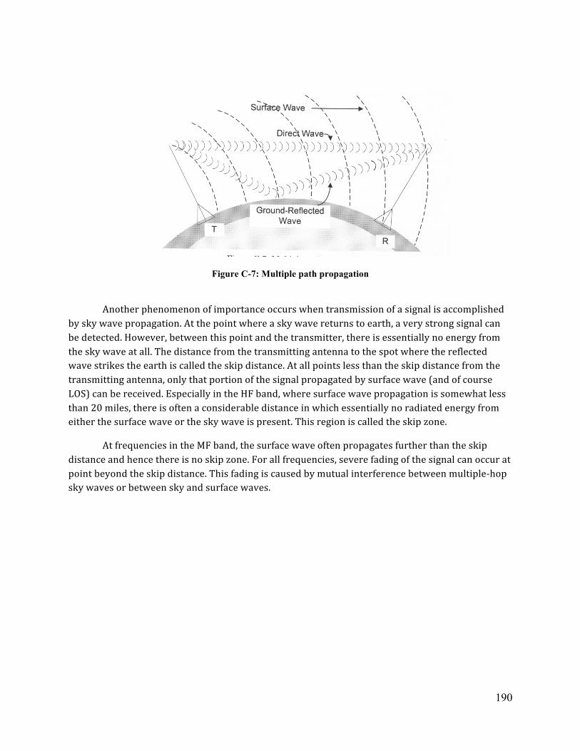
190
Figure C-7: Multiple path propagation
Another phenomenon of importance occurs when transmission of a signal is accomplished by sky wave propagation. At the point where a sky wave returns to earth, a very strong signal can be detected. However, between this point and the transmitter, there is essentially no energy from the sky wave at all. The distance from the transmitting antenna to the spot where the reflected wave strikes the earth is called the skip distance. At all points less than the skip distance from the transmitting antenna, only that portion of the signal propagated by surface wave (and of course LOS) can be received. Especially in the HF band, where surface wave propagation is somewhat less than 20 miles, there is often a considerable distance in which essentially no radiated energy from either the surface wave or the sky wave is present. This region is called the skip zone.
At frequencies in the MF band, the surface wave often propagates further than the skip distance and hence there is no skip zone. For all frequencies, severe fading of the signal can occur at point beyond the skip distance. This fading is caused by mutual interference between multiple-‐hop sky waves or between sky and surface waves.
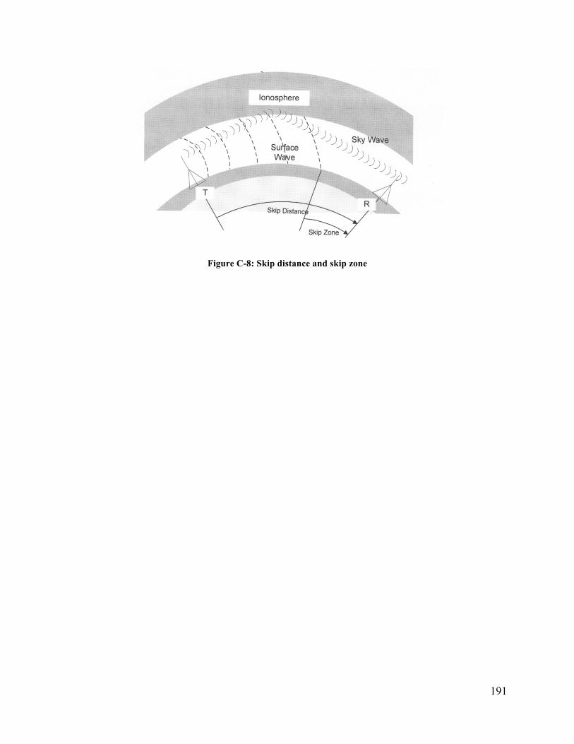
191
Figure C-8: Skip distance and skip zone

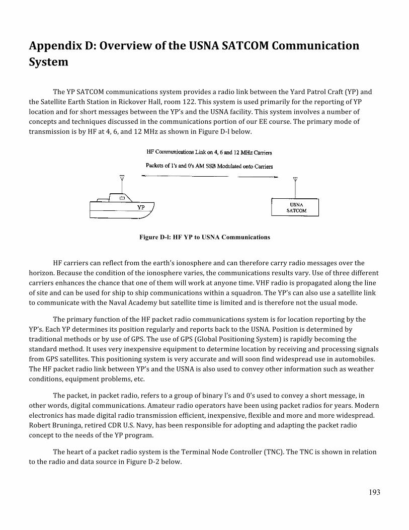
193
Appendix D: Overview of the USNA SATCOM Communication System
The YP SATCOM communications system provides a radio link between the Yard Patrol Craft (YP) and the Satellite Earth Station in Rickover Hall, room 122. This system is used primarily for the reporting of YP location and for short messages between the YP’s and the USNA facility. This system involves a number of concepts and techniques discussed in the communications portion of our EE course. The primary mode of transmission is by HF at 4, 6, and 12 MHz as shown in Figure D-‐l below.
Figure D-l: HF YP to USNA Communications
HF carriers can reflect from the earth’s ionosphere and can therefore carry radio messages over the horizon. Because the condition of the ionosphere varies, the communications results vary. Use of three different carriers enhances the chance that one of them will work at anyone time. VHF radio is propagated along the line of site and can be used for ship to ship communications within a squadron. The YP’s can also use a satellite link to communicate with the Naval Academy but satellite time is limited and is therefore not the usual mode.
The primary function of the HF packet radio communications system is for location reporting by the YP’s. Each YP determines its position regularly and reports back to the USNA. Position is determined by traditional methods or by use of GPS. The use of GPS (Global Positioning System) is rapidly becoming the standard method. It uses very inexpensive equipment to determine location by receiving and processing signals from GPS satellites. This positioning system is very accurate and will soon find widespread use in automobiles. The HF packet radio link between YP’s and the USNA is also used to convey other information such as weather conditions, equipment problems, etc.
The packet, in packet radio, refers to a group of binary l’s and 0’s used to convey a short message, in other words, digital communications. Amateur radio operators have been using packet radios for years. Modern electronics has made digital radio transmission efficient, inexpensive, flexible and more and more widespread. Robert Bruninga, retired CDR U.S. Navy, has been responsible for adopting and adapting the packet radio concept to the needs of the YP program.
The heart of a packet radio system is the Terminal Node Controller (TNC). The TNC is shown in relation to the radio and data source in Figure D-‐2 below.
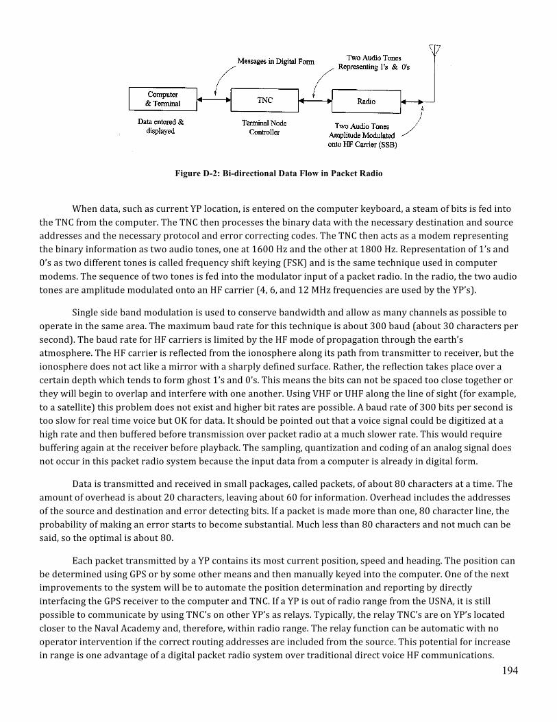
194
Figure D-2: Bi-directional Data Flow in Packet Radio
When data, such as current YP location, is entered on the computer keyboard, a steam of bits is fed into the TNC from the computer. The TNC then processes the binary data with the necessary destination and source addresses and the necessary protocol and error correcting codes. The TNC then acts as a modem representing the binary information as two audio tones, one at 1600 Hz and the other at 1800 Hz. Representation of 1’s and 0’s as two different tones is called frequency shift keying (FSK) and is the same technique used in computer modems. The sequence of two tones is fed into the modulator input of a packet radio. In the radio, the two audio tones are amplitude modulated onto an HF carrier (4, 6, and 12 MHz frequencies are used by the YP’s).
Single side band modulation is used to conserve bandwidth and allow as many channels as possible to operate in the same area. The maximum baud rate for this technique is about 300 baud (about 30 characters per second). The baud rate for HF carriers is limited by the HF mode of propagation through the earth’s atmosphere. The HF carrier is reflected from the ionosphere along its path from transmitter to receiver, but the ionosphere does not act like a mirror with a sharply defined surface. Rather, the reflection takes place over a certain depth which tends to form ghost 1’s and 0’s. This means the bits can not be spaced too close together or they will begin to overlap and interfere with one another. Using VHF or UHF along the line of sight (for example, to a satellite) this problem does not exist and higher bit rates are possible. A baud rate of 300 bits per second is too slow for real time voice but OK for data. It should be pointed out that a voice signal could be digitized at a high rate and then buffered before transmission over packet radio at a much slower rate. This would require buffering again at the receiver before playback. The sampling, quantization and coding of an analog signal does not occur in this packet radio system because the input data from a computer is already in digital form.
Data is transmitted and received in small packages, called packets, of about 80 characters at a time. The amount of overhead is about 20 characters, leaving about 60 for information. Overhead includes the addresses of the source and destination and error detecting bits. If a packet is made more than one, 80 character line, the probability of making an error starts to become substantial. Much less than 80 characters and not much can be said, so the optimal is about 80.
Each packet transmitted by a YP contains its most current position, speed and heading. The position can be determined using GPS or by some other means and then manually keyed into the computer. One of the next improvements to the system will be to automate the position determination and reporting by directly interfacing the GPS receiver to the computer and TNC. If a YP is out of radio range from the USNA, it is still possible to communicate by using TNC’s on other YP’s as relays. Typically, the relay TNC’s are on YP’s located closer to the Naval Academy and, therefore, within radio range. The relay function can be automatic with no operator intervention if the correct routing addresses are included from the source. This potential for increase in range is one advantage of a digital packet radio system over traditional direct voice HF communications.
195
When a YP is receiving a packet of information the process of transmission described above is reversed. The radio demodulates the two tones, representing binary data, from the HF carrier and passes them along to the TNC which in turn converts them into voltage levels which a computer can understand as 1’s and 0’s.
What does the TNC do and how does it do it? A TNC uses an on board microprocessor to keep track of all that is required. The computing power of a TNC confers many advantages to packet radio communication, such as error detection. A calculation is done on every packet received. If the answer is not correct, it means the data was probably corrupted and an acknowledgment of receipt is not sent back to the transmitter. This means the transmitter will try again until the packet is received error free. This is another advantage of packet radio. A complete description of the protocol used by a TNC is very long and complicated. Listed below are some of the functions performed by the TNC. I think you will begin to appreciate why a computer is needed inside the TNC.
1. The TNC must monitor both its data port connected to the terminal (is data going to be transmitted?) and its connection to the radio (is data being received?).
2. The TNC must check the addresses of all packets as they are received. Only those with the correct address will be processed. If the intended recipient is somewhere else, those packets must be ignored, but if a relay of a packet is requested, the TNC must determine that fact and then retransmit the packet to pass it along to its intended destination.
3. The TNC must acknowledge packets received correctly and complain about those in error. The TNC must send its own packets, keeping track of those that have been acknowledged and those that haven’t.
4. While it is transmitting, the TNC must know whom it is talking to and tell other TNC’s that it is busy, and to try again later.
5. The TNC must listen to the radio and wait to transmit if another signal is on the air.
These are some of the functions of the TNC in a packet radio system. Their descriptions above should give you a better idea of what packet radio is and how it works.