dispensed polymer waveguides and laser-fabricated couplers for optical interconnects on printed...
TRANSCRIPT
Dispensed polymer waveguides and laser-fabricatedcouplers for optical interconnects on printed circuit boards
Yongzhang Leng, Victor Yun, Lisa Lucas, Warren N. Herman, and Julius Goldhar
Optical interconnects can provide chip-to-chip data communication with much needed bandwidth as pro-cessor speed and density keep growing. Optical waveguides and couplers are essential components forimplementing optical interconnections. Techniques for directly dispensing polymer waveguides in laser-ablated trenches on printed circuit boards and for fabricating optical couplers are presented for quickprototype of optical interconnects. High-quality UV curable polymer waveguides were routinely fabricated.High-efficiency couplers, blazed grating couplers on sloped waveguides, sloped facet metal film couplers, andreflective-undercut facet couplers can be fabricated by using excimer laser ablation. © 2007 OpticalSociety of America
OCIS codes: 130.3120, 230.1950, 230.7370, 250.3140.
1. Introduction
Optical long-haul transmission revolutionized tele-communications and facilitated the transfer of a vastamount of information around the globe. Opticalethernet connections have increased the bandwidthfor data transfer between computers. However, datatransfer between chips on computer boards is mainlythrough electrical interconnects. With ever-increasingprocessor speed and density, the electrical interconnec-tions become the bottlenecks for data transmissionbetween chips. In high-speed electrical transmission,the parasitic resistance, capacitance, and inductancecause signal degradation through cross talk, reflection,and attenuation. The implementation of optical inter-connects on printed circuit (PC) boards can increasethe chip-to-chip transmission bandwidth by orders ofmagnitude. Various techniques are currently underdevelopment for this application.1–11 Jokerst et al.2,3
integrated optical interconnection into microsystemsby using thin-film heterogeneous integration. Chenet al.4–6 embedded both active and passive optical com-ponents in PC boards. Steenberge et al.10 used laser
ablation, which has been used to drill microvias inPC boards, to fabricate optical waveguides and el-ements for optical interconnections on PC boards.Our work in this area involves the development ofnew techniques for the fabrication of optical inter-connects on PC boards using directly dispensedhigh-quality UV curable polymer waveguides andlaser fabrication of input–output couplers to thesewaveguides. The main application of these tech-niques is for implementation of prototypes.11
High-quality optical waveguides are essentialcomponents for implementing optical chip-to-chipphotonic device integration. Optical interconnectsusing thin-film or polymer waveguides are usuallyfabricated by using lithography, which involves spincoating, baking, developing and�or dry etching (RIE).It is not practical to submit standard PC boards tothese processes, especially the baking process. Forrapid prototypes, the direct dispensing of UV curablepolymer waveguides and laser ablation fabricationcan be very useful. These processes can be operatedoutside a clean room, and the sample dimensions canbe many inches in length and width. Polymers thatadhere to most common surfaces and have differentindices of refraction are readily available.
Providing the means for coupling in and out of thewaveguides to other optical components such asdetectors and transmitters is a challenging task.High-efficiency grating couplers that can performthis function have been fabricated by using electronbeam lithography.12 This process requires nanofab-rication techniques and limits the choice of the op-tical waveguide material and the sample size. It is
The authors are with the Laboratory for Physical Sciences andthe Department of Electrical and Computer Engineering, Univer-sity of Maryland, College Park, Maryland 20740. Y. Leng’s e-mailaddress is [email protected].
Received 14 April 2006; revised 21 September 2006; accepted 26September 2006; posted 4 October 2006 (Doc. ID 69914); published17 January 2007.
0003-6935/07/040602-09$15.00/0© 2007 Optical Society of America
602 APPLIED OPTICS � Vol. 46, No. 4 � 1 February 2007
also incompatible with existing PC manufacturingprocesses. Here we demonstrate that laser ablationcan be utilized to directly fabricate gratings on poly-mer waveguides. This technique allows us to achievea smooth variation of the grating period. We can alsofabricate gratings with blaze angles and fabricatesloped profiles of waveguide ends for optimal in-coupling and outcoupling of the optical signal. Thesame fabrication setup was also used to produce simpleand efficient reflective couplers. This technique can beapplied to most polymer waveguide materials withstrong absorption at the 193 nm wavelength of an ArFexcimer laser.
2. Direct Dispensing of Optical Polymer Waveguides
Direct dispensing of UV curable optical polymerwaveguides was performed using a MICROPENModel 4000 direct writing and precision dispensingsystem. This dispensing system has a dynamic pencontrol feature that allows writing on cambered anduneven substrates. The dynamic pen control systemuniformly maintains the force that the pen tip applieson the dispensed material without actually touchingthe substrate. Therefore the dispensing head floatsover the substrate and can follow the terrain of thePC boards. UV curable polymers were dispensed outof the pen tip with a typical diameter of 50–150 �mand a typical dispensing speed of 5 mm�s.
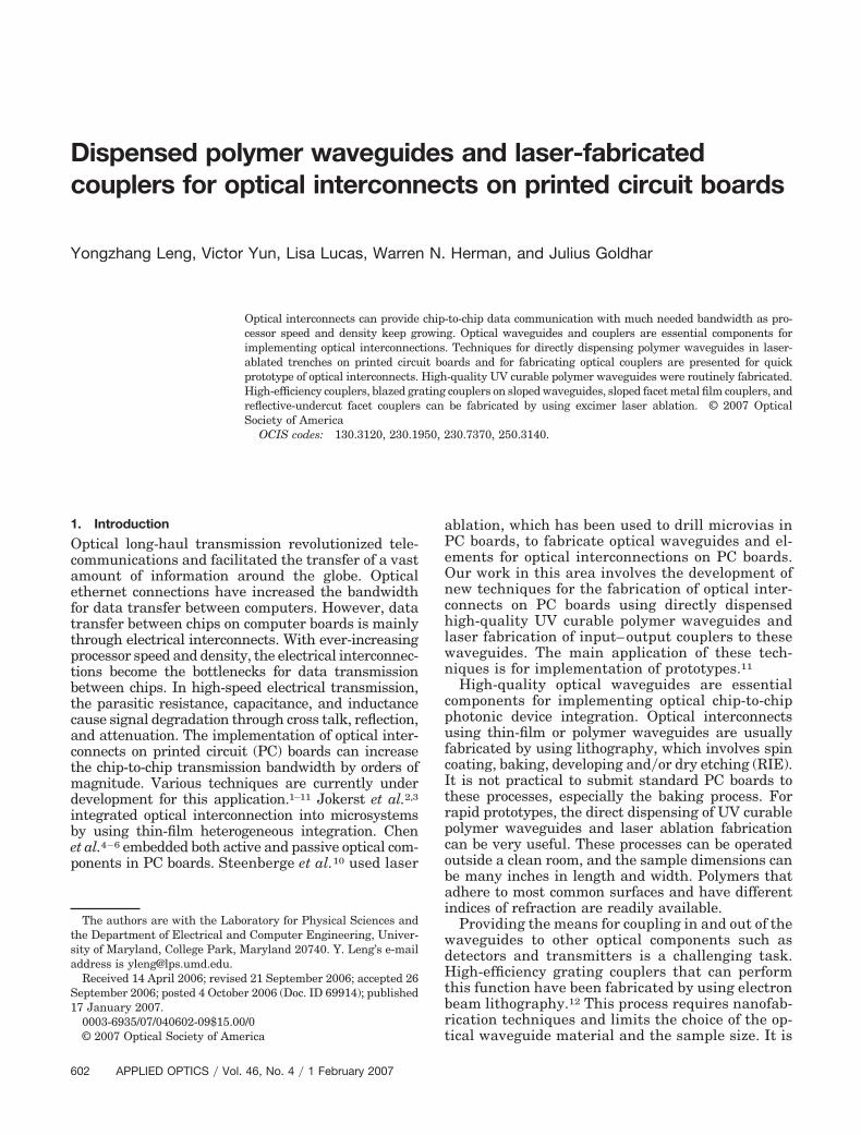
Figure 1(a) is an optical microscope picture of asimple directly dispensed two-layer polymer wave-guide. The bottom cladding layer was Epo-Tek Og134UV curable polymer13 with a low refractive indexclose to 1.42. Because Epo-Tek Og134 polymer has avery low viscosity of 100 cps, it spreads out to morethan 1 mm in width after being dispensed, whichcorresponds to the broader structure in Fig. 1(a). Thesmaller structure is a waveguide core from dispensedNorland 63 UV curable polymer14 with a refractiveindex of 1.56 and a viscosity of 2000 cps. The viscouswaveguide core layer maintained its profile after be-ing dispensed and was uniform along the waveguide.The scattering loss of this dispensed waveguideshould be very small. The waveguide profile, shownin Fig. 1(b), was measured using a Tencor (MountainView, California) Alpha-500 profilometer. The corelayer was approximately 250 �m wide and 16 �mthick with a parabolic profile. We expect this wave-guide to be multimode, but the light will propagatealong the central portion of the waveguide owing tothe lateral variation of the effective index of themodes.15 Figure 1(c) shows a typical propagatinghigh-order transverse mode pattern of this polymerwaveguide obtained from the numerical simulationby using a commercial waveguide mode solving soft-ware (Apollo Photonics, Burlington, Ontario, Canada,Optical Waveguide Mode Solvers Suite). The opticaltransmission properties of direct-dispensed polymerwaveguides were tested using 633 nm and 1.55 �moptical signals. The total loss at 633 nm, includingabsorption and scattering loss, was measured to be lessthan 0.1 dB�cm. The loss at 1.55 �m was greater
than 1 dB�cm, and the material absorption was re-sponsible for almost all of this loss.
There are two shortcomings of the waveguide shownin Fig. 1(a). The cladding layer has the tendency tospread out too much, and the exposed waveguide isvulnerable to damage from handling. These problemswere solved by prefabricating trenches on PC boardsby using ArF laser ablation before dispensing polymerwaveguides. The sidewalls then restrict the width ofthe low viscosity polymer waveguide cladding layer.The trenches bury the polymer waveguides under thesurface of the PC boards and improve the robustness ofthe polymer waveguides. The increased surface area ofthe laser-ablated trenches also helps to improve theadhesion of the dispensed UV curable polymer mate-rials.
For the laser ablation we use a Lambda PhysikOPTEX Pro ArF excimer laser that generates 10 mJ ofenergy per pulse. The laser beam has a dimension of6 mm � 3 mm, and the nominal pulse duration is 10ns. Both vertical and horizontal slits were used tolimit the excimer laser beam size. The vertical slit is1 mm wide, and the horizontal slit is 1 mm tall. Twoslits are located 40 mm apart from each other. A largeclear aperture �50 mm� fused silica triplet lens with afocal length of 112 mm and a small wavefront errorwas used to project a sharp image from one of the slits
Fig. 1. (Color online) (a) Microscope picture of a directly dis-pensed two-layer polymer waveguide, (b) waveguide cross-sectional profile from a profilometer, (c) high-order transversemode pattern of a multimode polymer waveguide from the numer-ical simulation by using the Optical Waveguide Mode Solver.
1 February 2007 � Vol. 46, No. 4 � APPLIED OPTICS 603
along the waveguide direction onto the PC boards onthe sample holder. The computer program will auto-matically adjust the position of the lens on the Z-axistranslation stage for proper imaging. When the Y-axis translation stage moves vertically, a sharp im-age of the vertical slit is projected onto the PC board,and the image of the horizontal slit is soft because itis out of focus. When the X-axis translation stagemoves horizontally, a sharp image of the horizontalslit is projected onto a PC board, and the image ofthe vertical slit is soft. The trenches were ablated bymultiple laser pulses while the translation stagemoves at a preset step size after each laser shot.The softer image of one slit ensures the sidewallsmoothness of the laser-ablated trenches without anoticeable stepwise structure. This imaging tech-nique will produce laser-ablated trenches with a side-wall roughness of much less than 0.2 �m along thewaveguide. The surface of the dispensed claddinglayer that forms the relevant interface with the coreis smoother than the ablated sidewall, and this inter-face makes a negligible contribution to the loss. Theenergy density on the PC board was approximately0.25 J�cm2, and the ArF laser rate of ablation of theconformal coating on PC boards was approximately0.2 �m per shot.
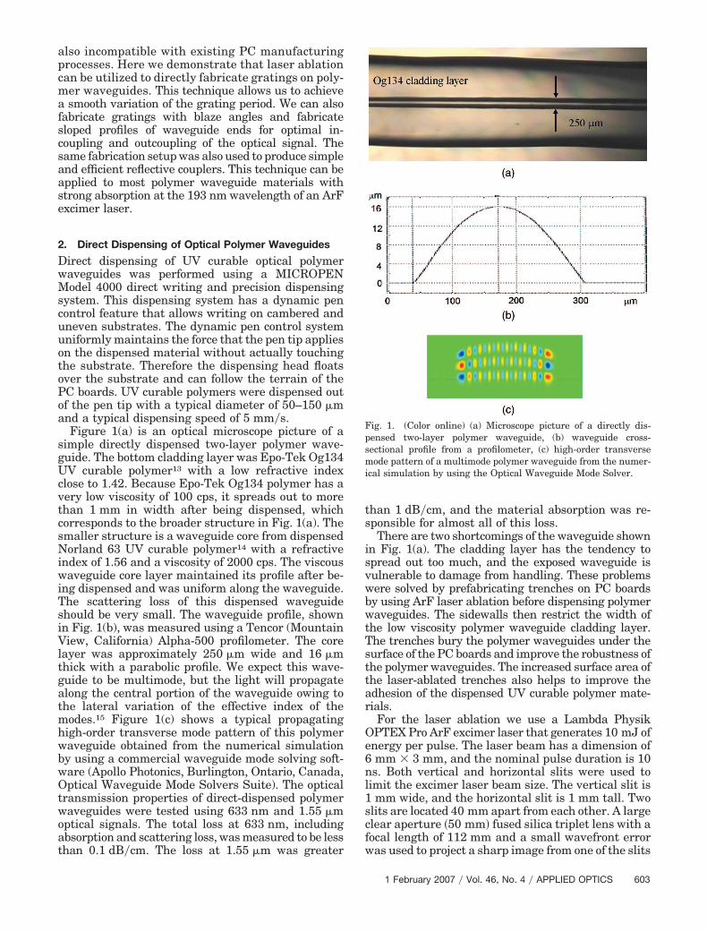
Figures 2(a)–2(c) show different fabrication stepsfor dispensing a waveguide inside a prefabricatedtrench together with corresponding profile curves.Figure 2(a) is a microscope picture of a typical laserfabricated trench on a PC board and the correspond-ing depth profile. This trench was 200 �m wide and16 �m deep. Figure 2(b) is a microscope picture ofa partially filled trench with a low index Epo-TekOg-134 cladding layer and the corresponding depthprofile. Figure 2(c) is a microscope picture of a high-index core layer and a low-index cladding polymerlayer inside the trench and the corresponding depthprofile. On some applications, a low-index layer wasalso dispensed afterward to protect the waveguidesfrom moisture, dust, and handling. We routinely fab-ricated straight and curved waveguides longer than10 cm. The stylus radius of the profilometer used forthese measurements is 1.5–2.5 �m, and the shankangle is 60°, which allows us to measure the trenchprofile as deep as 30 �m. Since the trenches are verywide for the stylus to reach the bottom of the groove,the displayed traces are very close to real depth pro-files.
3. Grating Couplers
A. Fabrication of Grating Couplers
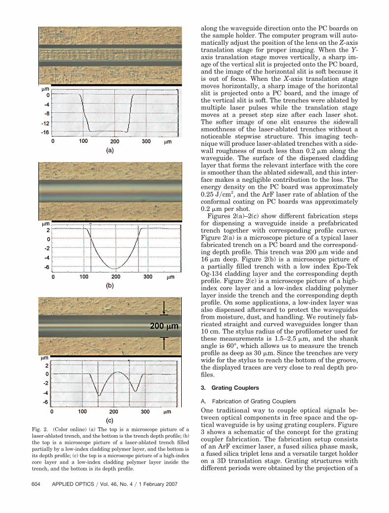
One traditional way to couple optical signals be-tween optical components in free space and the op-tical waveguide is by using grating couplers. Figure3 shows a schematic of the concept for the gratingcoupler fabrication. The fabrication setup consistsof an ArF excimer laser, a fused silica phase mask,a fused silica triplet lens and a versatile target holderon a 3D translation stage. Grating structures withdifferent periods were obtained by the projection of a
Fig. 2. (Color online) (a) The top is a microscope picture of alaser-ablated trench, and the bottom is the trench depth profile; (b)the top is a microscope picture of a laser-ablated trench filledpartially by a low-index cladding polymer layer, and the bottom isits depth profile; (c) the top is a microscope picture of a high-indexcore layer and a low-index cladding polymer layer inside thetrench, and the bottom is its depth profile.
604 APPLIED OPTICS � Vol. 46, No. 4 � 1 February 2007
fused silica phase mask with a period of 6.67 �mdirectly onto polymer films. The phase mask was de-signed to have a groove depth of ��2�n � 1� and tohave a minimum energy at zeroth diffraction order,where � is the ArF laser wavelength for ablatingpolymer gratings, and n is the refractive index of thefused silica window at 193 nm. For the fused silicaphase mask fabrication, a 1 �m thick layer of ArchChemicals OIR 906-10 positive photoresist was spincoated on a 1 in. (2.54 cm) diameter quartz plate witha thickness of 1 mm. We used a contact aligner totransfer an amplitude grating to the photoresist andetched the groove depth of the quartz phase mask to172 nm. After transmission, the laser beam segmentsfrom an adjacent groove and a ridge had a phasedifference of 180°. The phase mask’s zeroth orderdiffraction beam had less than 2% of the total inputbeam energy. The zeroth order diffraction beam wasblocked to prevent any larger period modulation ingrating groove depth due to the interference betweenthe zeroth order diffraction beam and the other dif-fraction beams. The aperture was used to limit thesize of the fabricated grating.
This grating fabrication technique allows a smoothvariation of the fabricated grating period with a singlephase mask by simply changing the demagnificationfactor, which is the ratio of the object distance to theimage distance. Gratings with deep grooves ��1 �m�were obtained using repetitive laser pulses becausethe ablation depth by multiple laser shots was addi-tive. The sample holder was designed so that it couldbe tilted by a preselected angle �. This allows asmooth adjustment of the sample holder to fabricategrating couplers with different geometric profiles.Blazed gratings at specific angles were fabricated byadjusting the angle of the sample holder with respectto the optical axis of the system.
For our dispensed polymer waveguide, the accep-tance angle for end coupling, which corresponds to themaximum angle for achieving total internal reflectioninside the waveguide, is approximately 30°. However,grating coupling into the waveguide involves a re-duction of the size of the optical beam by the ratio ofthe grating coupling region (which is approximately
200 �m) to waveguide thickness �10–20 �m�, with acorresponding increase in angular divergence. Thisconstraint reduces the input acceptance angle forgrating coupling to 2°. Longer grating couplers re-sult in unacceptably narrow acceptance angles. Un-fortunately, short gratings fabricated on top of thewaveguide have a low coupling efficiency of only a fewpercent. One way to increase the efficiency was toreshape the waveguide end with a preselected slopebefore writing the grating.
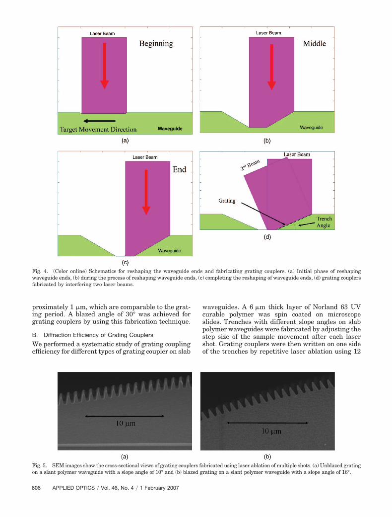
Figure 4 shows the schematics of procedures forreshaping the waveguide ends and fabricating grat-ing couplers. Allowing only one of the diffractionbeams to be projected with a sharp image onto thepolymer film and moving the sample at a predeter-mined step size after each laser shot, we can reshapethe waveguide ends to a desired slope by using laserablation. The slope angle � of a reshaped waveguideend depends on both the ablation rate �d of individ-ual laser shots and the step size �x of the translationstage, and tan � �d��x. Figure 4(a) shows theinitial phase of the reshaping of waveguide ends. Thetranslation stage moves to the left at a predeterminedstep size after each laser shot. Both the step size andthe image size of the slit determine the total fluenceon a given section of polymer film. Polymer wave-guide ends with different slope angles can be fabri-cated by adjusting the step size of the samplemovement and the laser energy density on the target.Figure 4(b) shows the dynamic reshaping processin progress, and Fig. 4(c) shows the completion ofwaveguide end reshaping. This fabrication processtakes approximately 500 laser shots at a repetitionrate of 10 shots�s. The typical energy density for thisprocess was approximately 0.1 J�cm2.
After the waveguide end had been reshaped, thegrating coupler was ablated onto one side of thetrench by letting both positive first-order and neg-ative first-order diffraction beams overlap and in-terfere with each other to form interference fringeson the polymer film, as shown in Fig. 4(d). Twelverepetitive laser shots were used for grating couplerfabrication. The peak energy density of the inter-ference fringes was approximately 0.5 J�cm2. Fol-lowing these procedures, we were able to fabricatethe grating couplers precisely on the slanted portionof the waveguide end by using the same laser abla-tion setup for both the sloped waveguide end and thegrating coupler fabrications. The technique workedwell on both slab waveguides and dispensed polymerwaveguides.
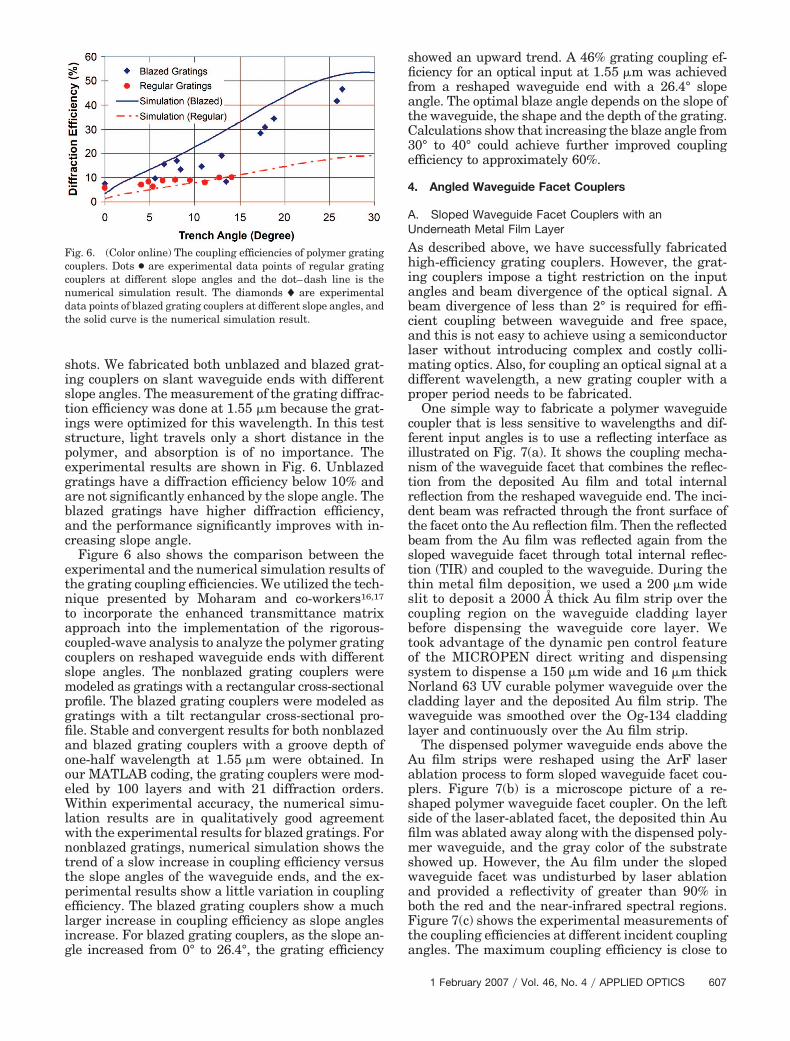
Figure 5 shows scanning electron microscope (SEM)images of the cross-sectional views of two differentgrating couplers fabricated by using laser ablationwith multiple shots. Figure 5(a) shows a nonblazedgrating on a slanted portion of a polymer waveguidewith a slope angle of 10°. The grating period was ap-proximately 0.94 �m. Figure 5(b) shows a blazedgrating on a slant polymer waveguide with a slopeangle of 16°. The grating period was approximately0.97 �m. The groove depths of these gratings are ap-
Fig. 3. (Color online) Schematic of the laser ablation setup forblazed polymer grating fabrication. Tilting the sample holder withrespect to the image plane produces laser-ablated gratings with ablazed profile.
1 February 2007 � Vol. 46, No. 4 � APPLIED OPTICS 605
proximately 1 �m, which are comparable to the grat-ing period. A blazed angle of 30° was achieved forgrating couplers by using this fabrication technique.
B. Diffraction Efficiency of Grating Couplers
We performed a systematic study of grating couplingefficiency for different types of grating coupler on slab
waveguides. A 6 �m thick layer of Norland 63 UVcurable polymer was spin coated on microscopeslides. Trenches with different slope angles on slabpolymer waveguides were fabricated by adjusting thestep size of the sample movement after each lasershot. Grating couplers were then written on one sideof the trenches by repetitive laser ablation using 12
Fig. 4. (Color online) Schematics for reshaping the waveguide ends and fabricating grating couplers. (a) Initial phase of reshapingwaveguide ends, (b) during the process of reshaping waveguide ends, (c) completing the reshaping of waveguide ends, (d) grating couplersfabricated by interfering two laser beams.
Fig. 5. SEM images show the cross-sectional views of grating couplers fabricated using laser ablation of multiple shots. (a) Unblazed gratingon a slant polymer waveguide with a slope angle of 10° and (b) blazed grating on a slant polymer waveguide with a slope angle of 16°.
606 APPLIED OPTICS � Vol. 46, No. 4 � 1 February 2007
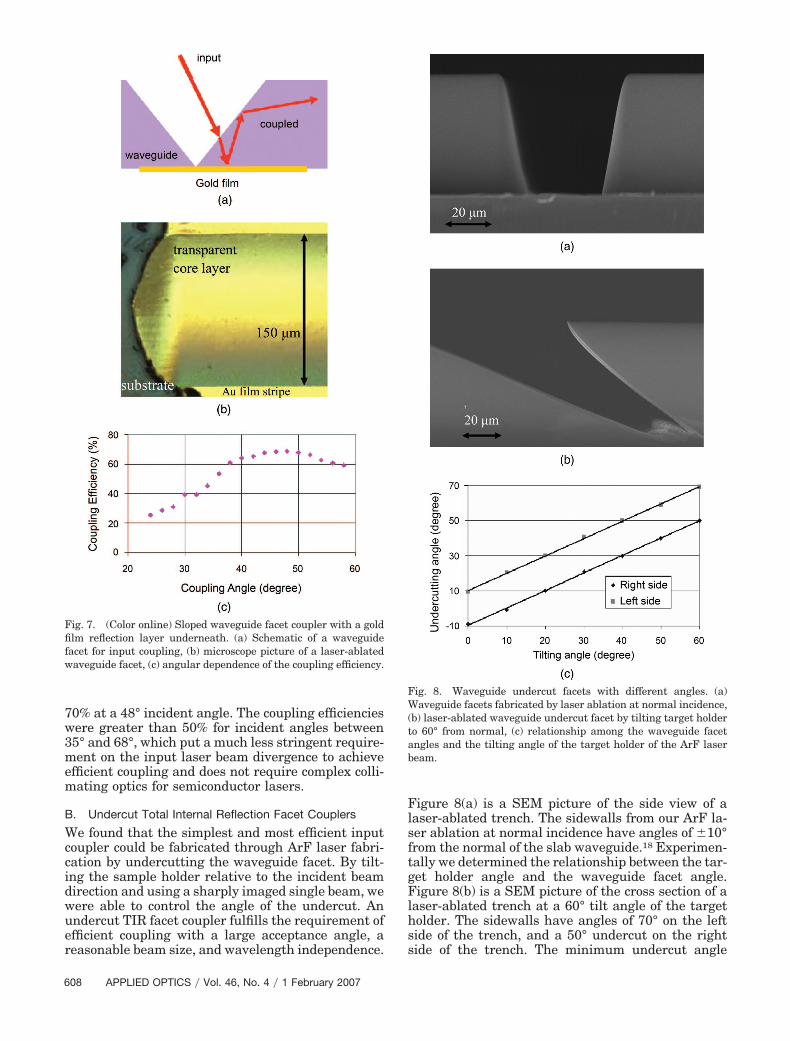
shots. We fabricated both unblazed and blazed grat-ing couplers on slant waveguide ends with differentslope angles. The measurement of the grating diffrac-tion efficiency was done at 1.55 �m because the grat-ings were optimized for this wavelength. In this teststructure, light travels only a short distance in thepolymer, and absorption is of no importance. Theexperimental results are shown in Fig. 6. Unblazedgratings have a diffraction efficiency below 10% andare not significantly enhanced by the slope angle. Theblazed gratings have higher diffraction efficiency,and the performance significantly improves with in-creasing slope angle.
Figure 6 also shows the comparison between theexperimental and the numerical simulation results ofthe grating coupling efficiencies. We utilized the tech-nique presented by Moharam and co-workers16,17
to incorporate the enhanced transmittance matrixapproach into the implementation of the rigorous-coupled-wave analysis to analyze the polymer gratingcouplers on reshaped waveguide ends with differentslope angles. The nonblazed grating couplers weremodeled as gratings with a rectangular cross-sectionalprofile. The blazed grating couplers were modeled asgratings with a tilt rectangular cross-sectional pro-file. Stable and convergent results for both nonblazedand blazed grating couplers with a groove depth ofone-half wavelength at 1.55 �m were obtained. Inour MATLAB coding, the grating couplers were mod-eled by 100 layers and with 21 diffraction orders.Within experimental accuracy, the numerical simu-lation results are in qualitatively good agreementwith the experimental results for blazed gratings. Fornonblazed gratings, numerical simulation shows thetrend of a slow increase in coupling efficiency versusthe slope angles of the waveguide ends, and the ex-perimental results show a little variation in couplingefficiency. The blazed grating couplers show a muchlarger increase in coupling efficiency as slope anglesincrease. For blazed grating couplers, as the slope an-gle increased from 0° to 26.4°, the grating efficiency
showed an upward trend. A 46% grating coupling ef-ficiency for an optical input at 1.55 �m was achievedfrom a reshaped waveguide end with a 26.4° slopeangle. The optimal blaze angle depends on the slope ofthe waveguide, the shape and the depth of the grating.Calculations show that increasing the blaze angle from30° to 40° could achieve further improved couplingefficiency to approximately 60%.
4. Angled Waveguide Facet Couplers
A. Sloped Waveguide Facet Couplers with anUnderneath Metal Film Layer
As described above, we have successfully fabricatedhigh-efficiency grating couplers. However, the grat-ing couplers impose a tight restriction on the inputangles and beam divergence of the optical signal. Abeam divergence of less than 2° is required for effi-cient coupling between waveguide and free space,and this is not easy to achieve using a semiconductorlaser without introducing complex and costly colli-mating optics. Also, for coupling an optical signal at adifferent wavelength, a new grating coupler with aproper period needs to be fabricated.
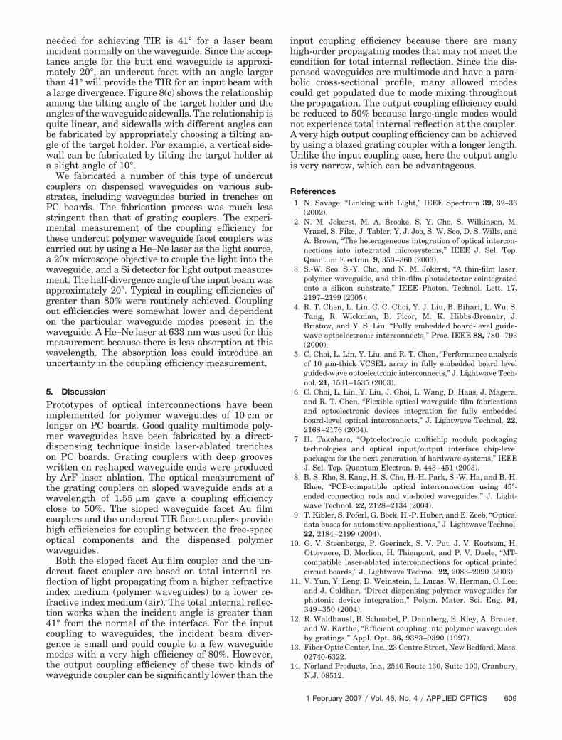
One simple way to fabricate a polymer waveguidecoupler that is less sensitive to wavelengths and dif-ferent input angles is to use a reflecting interface asillustrated on Fig. 7(a). It shows the coupling mecha-nism of the waveguide facet that combines the reflec-tion from the deposited Au film and total internalreflection from the reshaped waveguide end. The inci-dent beam was refracted through the front surface ofthe facet onto the Au reflection film. Then the reflectedbeam from the Au film was reflected again from thesloped waveguide facet through total internal reflec-tion (TIR) and coupled to the waveguide. During thethin metal film deposition, we used a 200 �m wideslit to deposit a 2000 Å thick Au film strip over thecoupling region on the waveguide cladding layerbefore dispensing the waveguide core layer. Wetook advantage of the dynamic pen control featureof the MICROPEN direct writing and dispensingsystem to dispense a 150 �m wide and 16 �m thickNorland 63 UV curable polymer waveguide over thecladding layer and the deposited Au film strip. Thewaveguide was smoothed over the Og-134 claddinglayer and continuously over the Au film strip.
The dispensed polymer waveguide ends above theAu film strips were reshaped using the ArF laserablation process to form sloped waveguide facet cou-plers. Figure 7(b) is a microscope picture of a re-shaped polymer waveguide facet coupler. On the leftside of the laser-ablated facet, the deposited thin Aufilm was ablated away along with the dispensed poly-mer waveguide, and the gray color of the substrateshowed up. However, the Au film under the slopedwaveguide facet was undisturbed by laser ablationand provided a reflectivity of greater than 90% inboth the red and the near-infrared spectral regions.Figure 7(c) shows the experimental measurements ofthe coupling efficiencies at different incident couplingangles. The maximum coupling efficiency is close to
Fig. 6. (Color online) The coupling efficiencies of polymer gratingcouplers. Dots ● are experimental data points of regular gratingcouplers at different slope angles and the dot–dash line is thenumerical simulation result. The diamonds � are experimentaldata points of blazed grating couplers at different slope angles, andthe solid curve is the numerical simulation result.
1 February 2007 � Vol. 46, No. 4 � APPLIED OPTICS 607
70% at a 48° incident angle. The coupling efficiencieswere greater than 50% for incident angles between35° and 68°, which put a much less stringent require-ment on the input laser beam divergence to achieveefficient coupling and does not require complex colli-mating optics for semiconductor lasers.
B. Undercut Total Internal Reflection Facet Couplers
We found that the simplest and most efficient inputcoupler could be fabricated through ArF laser fabri-cation by undercutting the waveguide facet. By tilt-ing the sample holder relative to the incident beamdirection and using a sharply imaged single beam, wewere able to control the angle of the undercut. Anundercut TIR facet coupler fulfills the requirement ofefficient coupling with a large acceptance angle, areasonable beam size, and wavelength independence.
Figure 8(a) is a SEM picture of the side view of alaser-ablated trench. The sidewalls from our ArF la-ser ablation at normal incidence have angles of 10°from the normal of the slab waveguide.18 Experimen-tally we determined the relationship between the tar-get holder angle and the waveguide facet angle.Figure 8(b) is a SEM picture of the cross section of alaser-ablated trench at a 60° tilt angle of the targetholder. The sidewalls have angles of 70° on the leftside of the trench, and a 50° undercut on the rightside of the trench. The minimum undercut angle
Fig. 7. (Color online) Sloped waveguide facet coupler with a goldfilm reflection layer underneath. (a) Schematic of a waveguidefacet for input coupling, (b) microscope picture of a laser-ablatedwaveguide facet, (c) angular dependence of the coupling efficiency.
Fig. 8. Waveguide undercut facets with different angles. (a)Waveguide facets fabricated by laser ablation at normal incidence,(b) laser-ablated waveguide undercut facet by tilting target holderto 60° from normal, (c) relationship among the waveguide facetangles and the tilting angle of the target holder of the ArF laserbeam.
608 APPLIED OPTICS � Vol. 46, No. 4 � 1 February 2007
needed for achieving TIR is 41° for a laser beamincident normally on the waveguide. Since the accep-tance angle for the butt end waveguide is approxi-mately 20°, an undercut facet with an angle largerthan 41° will provide the TIR for an input beam witha large divergence. Figure 8(c) shows the relationshipamong the tilting angle of the target holder and theangles of the waveguide sidewalls. The relationship isquite linear, and sidewalls with different angles canbe fabricated by appropriately choosing a tilting an-gle of the target holder. For example, a vertical side-wall can be fabricated by tilting the target holder ata slight angle of 10°.
We fabricated a number of this type of undercutcouplers on dispensed waveguides on various sub-strates, including waveguides buried in trenches onPC boards. The fabrication process was much lessstringent than that of grating couplers. The experi-mental measurement of the coupling efficiency forthese undercut polymer waveguide facet couplers wascarried out by using a He–Ne laser as the light source,a 20x microscope objective to couple the light into thewaveguide, and a Si detector for light output measure-ment. The half-divergence angle of the input beam wasapproximately 20°. Typical in-coupling efficiencies ofgreater than 80% were routinely achieved. Couplingout efficiencies were somewhat lower and dependenton the particular waveguide modes present in thewaveguide. A He–Ne laser at 633 nm was used for thismeasurement because there is less absorption at thiswavelength. The absorption loss could introduce anuncertainty in the coupling efficiency measurement.
5. Discussion
Prototypes of optical interconnections have beenimplemented for polymer waveguides of 10 cm orlonger on PC boards. Good quality multimode poly-mer waveguides have been fabricated by a direct-dispensing technique inside laser-ablated trencheson PC boards. Grating couplers with deep grooveswritten on reshaped waveguide ends were producedby ArF laser ablation. The optical measurement ofthe grating couplers on sloped waveguide ends at awavelength of 1.55 �m gave a coupling efficiencyclose to 50%. The sloped waveguide facet Au filmcouplers and the undercut TIR facet couplers providehigh efficiencies for coupling between the free-spaceoptical components and the dispensed polymerwaveguides.
Both the sloped facet Au film coupler and the un-dercut facet coupler are based on total internal re-flection of light propagating from a higher refractiveindex medium (polymer waveguides) to a lower re-fractive index medium (air). The total internal reflec-tion works when the incident angle is greater than41° from the normal of the interface. For the inputcoupling to waveguides, the incident beam diver-gence is small and could couple to a few waveguidemodes with a very high efficiency of 80%. However,the output coupling efficiency of these two kinds ofwaveguide coupler can be significantly lower than the
input coupling efficiency because there are manyhigh-order propagating modes that may not meet thecondition for total internal reflection. Since the dis-pensed waveguides are multimode and have a para-bolic cross-sectional profile, many allowed modescould get populated due to mode mixing throughoutthe propagation. The output coupling efficiency couldbe reduced to 50% because large-angle modes wouldnot experience total internal reflection at the coupler.A very high output coupling efficiency can be achievedby using a blazed grating coupler with a longer length.Unlike the input coupling case, here the output angleis very narrow, which can be advantageous.
References1. N. Savage, “Linking with Light,” IEEE Spectrum 39, 32–36
(2002).2. N. M. Jokerst, M. A. Brooke, S. Y. Cho, S. Wilkinson, M.
Vrazel, S. Fike, J. Tabler, Y. J. Joo, S. W. Seo, D. S. Wills, andA. Brown, “The heterogeneous integration of optical intercon-nections into integrated microsystems,” IEEE J. Sel. Top.Quantum Electron. 9, 350–360 (2003).
3. S.-W. Seo, S.-Y. Cho, and N. M. Jokerst, “A thin-film laser,polymer waveguide, and thin-film photodetector cointegratedonto a silicon substrate,” IEEE Photon. Technol. Lett. 17,2197–2199 (2005).
4. R. T. Chen, L. Lin, C. C. Choi, Y. J. Liu, B. Bihari, L. Wu, S.Tang, R. Wickman, B. Picor, M. K. Hibbs-Brenner, J.Bristow, and Y. S. Liu, “Fully embedded board-level guide-wave optoelectronic interconnects,” Proc. IEEE 88, 780–793(2000).
5. C. Choi, L. Lin, Y. Liu, and R. T. Chen, “Performance analysisof 10 �m-thick VCSEL array in fully embedded board levelguided-wave optoelectronic interconnects,” J. Lightwave Tech-nol. 21, 1531–1535 (2003).
6. C. Choi, L. Lin, Y. Liu, J. Choi, L. Wang, D. Haas, J. Magera,and R. T. Chen, “Flexible optical waveguide film fabricationsand optoelectronic devices integration for fully embeddedboard-level optical interconnects,” J. Lightwave Technol. 22,2168–2176 (2004).
7. H. Takahara, “Optoelectronic multichip module packagingtechnologies and optical input�output interface chip-levelpackages for the next generation of hardware systems,” IEEEJ. Sel. Top. Quantum Electron. 9, 443–451 (2003).
8. B. S. Rho, S. Kang, H. S. Cho, H.-H. Park, S.-W. Ha, and B.-H.Rhee, “PCB-compatible optical interconnection using 45°-ended connection rods and via-holed waveguides,” J. Light-wave Technol. 22, 2128–2134 (2004).
9. T. Kibler, S. Poferl, G. Böck, H.-P. Huber, and E. Zeeb, “Opticaldata buses for automotive applications,” J. Lightwave Technol.22, 2184–2199 (2004).
10. G. V. Steenberge, P. Geerinck, S. V. Put, J. V. Koetsem, H.Ottevaere, D. Morlion, H. Thienpont, and P. V. Daele, “MT-compatible laser-ablated interconnections for optical printedcircuit boards,” J. Lightwave Technol. 22, 2083–2090 (2003).
11. V. Yun, Y. Leng, D. Weinstein, L. Lucas, W. Herman, C. Lee,and J. Goldhar, “Direct dispensing polymer waveguides forphotonic device integration,” Polym. Mater. Sci. Eng. 91,349–350 (2004).
12. R. Waldhausl, B. Schnabel, P. Dannberg, E. Kley, A. Brauer,and W. Karthe, “Efficient coupling into polymer waveguidesby gratings,” Appl. Opt. 36, 9383–9390 (1997).
13. Fiber Optic Center, Inc., 23 Centre Street, New Bedford, Mass.02740-6322.
14. Norland Products, Inc., 2540 Route 130, Suite 100, Cranbury,N.J. 08512.
1 February 2007 � Vol. 46, No. 4 � APPLIED OPTICS 609

15. D. W. Boertjes, J. N. McMullin, and B. P. Keyworth, “Gradedeffective index planar polymer waveguides,” J. LightwaveTechnol. 14, 2714–2718 (1996).
16. M. G. Moharam, E. B. Grann, D. A. Pommet, and T. K.Gaylord, “Formulation for stable and efficient implementa-tion of the rigorous coupled-wave analysis of binary grat-ings,” J. Opt. Soc. Am. A 12, 1068–1076 (1995).
17. M. G. Moharam, E. B. Grann, D. A. Pommet, and T. K. Gaylord,“Stable implementation of the rigorous coupled-wave analysisfor surface-relief gratings: enhanced transmittance matrix ap-proach,” J. Opt. Soc. Am. A 12, 1077–1086 (1995).
18. C. Paterson, A. S. Holmes, and R. W. Smith, “Excimer laserablation of microstructures: A numerical model,” J. Appl.Phys. 86, 6538–6546 (1999).
610 APPLIED OPTICS � Vol. 46, No. 4 � 1 February 2007