development of vertical and tapered via etch for 3d through wafer interconnect technology
TRANSCRIPT

1-4244-0665-X/06/$20.00 ©2006 IEEE 22 2006 Electronics Packaging Technology Conference
Development of Vertical and Tapered Via Etch for 3D Through Wafer Interconnect Technology
Deniz Sabuncuoglu Tezcan, Koen De Munck, Nga Pham, Ole Luhn, Arno Aarts,
Piet De Moor, Kris Baert and Chris Van Hoof IMEC vzw
Kapeldreef 75 B-3001 Leuven Belgium [email protected], Tel: + 32 16 28 8741, Fax: + 32 16 28 1097
Abstract
Two types of dry silicon etch techniques are developed to cover two different areas of demand for interconnect technology: one for high aspect ratio (AR) vertical vias and one for tapered vias. Various sizes of vertical vias and trenches with diameters/widths ranging from 1-100 µm with an AR up to 50 are realized using Bosch Deep Reactive Ion Etch (DRIE) process. A linear model is applied to describe and to give physical insight in the Aspect Ratio Dependant Etch (ARDE) effect. The feasibility of the vertical vias as electrical interconnect is shown by isolating them from the substrate by silicon oxide and then filling with polysilicon. The tapered vias are typically post-processed on fabricated device wafers, making it inherently a more generic approach where diameter size can be large and low AR can be tolerated. Vias with a depth of ~100 µm and a diameter of ~50 µm at the bottom (though larger at top) are realized. Varying various etch parameters, slope angles of 70°-80° are realized to allow for conformal deposition of dielectric/seed materials on the sidewalls and to allow lithography within the via. Reactive Ion Etch (RIE) is used to fabricate sloped vias by simultaneously applying etch and passivation gasses. Negative angles on the via top and sidewall roughness are observed that introduce conformal coating problems and increased leakage currents. Smoothening techniques using maskless wet and dry silicon etching are investigated to overcome these problems.
1. Introduction Through silicon interconnect technology is one of the
critical and enabling technologies for 3D chip stacking. Making these interconnects requires the formation of vertical or tapered (sloped) vias in the silicon using typically (Deep) Reactive Ion Etching ((D)RIE).
In general two main approaches of 3D stacking exist which need through silicon interconnects: (i) 3D-"Stacked IC" (3D-SIC): the vertical high AR interconnects are processed post Front-End and prior to Back-End in a modified CMOS process. Using wafer bonding technology, a very high interconnect density is obtained (1000 or more interconnect/mm2) [1]. (ii) 3D-"Wafer level packaging" (3D-WLP): a wafer level packaging technology utilizing tapered vias through the thinned wafers, which allow direct stacking of wafers or dies. These 3D interconnects are processed post chip passivation and allow low to medium interconnect density (10-100 interconnect/mm2) [2].
This paper presents the development of silicon dry etching techniques for the realization of vias in each of these approaches.
2. Vertical High Aspect Ratio Vias
2.1. Experimental Vertical high AR vias and trenches are realized using
Bosch DRIE in two different diameter/width ranges: 5-100 µm and 1-10 µm. In the range of 5-100 µm several etchings are performed in a multiplexed ICP Adixen AMS100 SE. On different wafers, different etch times ranging from 20 to 173 minutes in steps of about 20 minutes are applied while keeping other etch parameters constant. Fig. 1 shows the cross-sectional view of such a row of vias, while in Fig. 2 a sample of the depth data, measured on trenches, is presented. The etch mask used consisted of a 1 µm thick silicon oxide with 14 µm thick SJR5740 resist on top. This mask is nearly completely consumed during via etching. As seen in Fig. 1 and Fig. 2, the depth of a plasma etched feature (via, trench,…) depends on the diameter size, an effect known as Aspect Ratio Dependant Etch (ARDE).
Fig. 1. Cross-sectional SEM view of a cleaved wafer with 5-100 µm diameter vias. Different etch depths for different vias are the result of ARDE.
0
200
400
600
0 20 40 60 80 100Measured trench width (µm)
Tren
ch d
epth
(µm
)
20min 100min 173min
Fig. 2. Trench depth versus measured trench width (5-100 µm width) showing ARDE for different etch times.
In the via width range of 1-10 µm, different etch tools are compared in terms of ARDE performance. Two multiplexed
23 2006 Electronics Packaging Technology Conference
DRIE tools, a Surface Technology System Inductive Coupled Plasma (STS-ICP) system and an Adixen AMS100 SE, and one RIE etcher from LAM are used to etch the same structures. The etch mask consists of 1 µm of TEOS and 2.5 µm IX845 resist. In all cases, after etching, the etch mask was nearly completely consumed.
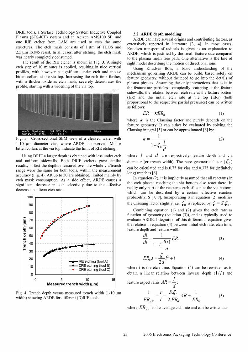
The result of the RIE etcher is shown in Fig. 3. A single etch step of 10 minutes is applied, resulting in nice vertical profiles, with however a significant under etch and mouse bitten collars at the via top. Increasing the etch time further, with a thicker oxide as etch mask, severely deteriorates the profile, starting with a widening of the via top.
Fig. 3. Cross-sectional SEM view of a cleaved wafer with 1-10 µm diameter vias, where ARDE is observed. Mouse bitten collars at the via top indicate the limit of RIE etching.
Using DRIE a larger depth is obtained with less under etch and uniform sidewalls. Both DRIE etchers gave similar results, in fact the depths measured over the whole via/trench range were the same for both tools, within the measurement accuracy (Fig. 4). AR up to 50 are obtained, limited mainly by etch mask consumption. As a side effect, ARDE causes a significant decrease in etch selectivity due to the effective decrease in silicon etch rate.
0
10
20
30
40
50
60
70
80
90
100
0 5 10 15Measured trench width (µm)
Tren
ch d
epth
(µm
)
RIE etching (tool A)DRIE etching (tool B)DRIE etching (tool C)
Fig. 4. Trench depth versus measured trench width (1-10 µm width) showing ARDE for different (D)RIE tools.
2.2. ARDE depth modeling: ARDE can have several origins and contributing factors, as
extensively reported in literature [3, 4]. In most cases, Knudsen transport of radicals is given as an explanation to ARDE, which is justified by the small feature size compared to the plasma mean free path. One alternative is the line of sight model describing the motion of directional ions.
Using Knudsen flow, a basic understanding of the mechanism governing ARDE can be build, based solely on feature geometry, without the need to go into the details of plasma physics. Assuming the only interactions that exist in the feature are particles isotropically scattering at the feature sidewalls, the relation between etch rate at the feature bottom (ER) and the initial etch rate at the top (ER0) (both proportional to the respective partial pressures) can be written as follows:
0ER ERκ= (1) where κ is the Clausing factor and purely depends on the feature geometry. It can either be evaluated by solving the Clausing integral [5] or can be approximated [6] by:
0
1
1 ld
κζ
=+
(2)
where l and d are respectively feature depth and via diameter (or trench width). The pure geometric factor ( 0ζ ) can be calculated and is 0.75 for vias and 0.375 for (infinitely long) trenches [6].
In equation (2), it is implicitly assumed that all reactants in the etch plasma reaching the via bottom also react there. In reality only part of the reactants etch silicon at the via bottom, which can be described by a certain effective reaction probability, S [7, 8]. Incorporating S in equation (2) modifies the Clausing factor slightly, i.e. 0ζ is replaced by 0.Sζ ζ= .
Combining equation (1) and (2) gives the etch rate as function of geometry (equation (3)), and is typically used to evaluate ARDE. Integration of this differential equation gives the relation in equation (4) between initial etch rate, etch time, feature depth and feature width:
01
( )1
dl ERl tdtd
ζ=
+ (3)
20.
2ER t l l
dζ= + (4)
where t is the etch time. Equation (4) can be rewritten as to obtain a linear relation between inverse depth (1/ l ) and
feature aspect ratio lARd
= :
0
0 0
1 . 12.AV
t S ARER l ER ER
ζ= = + (5)
where AVER is the average etch rate and can be written as:

24 2006 Electronics Packaging Technology Conference
00
1.12
AVER ERS ARζ=+
(6)
Similar to equation (3), equations (5) and (6) contain only two independent parameters related to the etching process,
0ER and S . However, contrary to equation (3), equations (5) and (6) do not require multiple etchings to analyze ARDE, providing features with different dimensions are present on the same wafer. Fitting the measured data to the linear equation (5), 0ER and S can be extracted.
Fig. 5 shows the measured data and fitted model in the diameter range of 5-100 µm for different diameters and etch times. The difference in slopes between vias and trenches originates mainly from a difference in geometric factor, 0ζ .
0
0.1
0.2
0.3
0.4
0.5
0.6
0.7
0.8
0.9
1
0 10 20 30 40 50Aspect ratio
1/ER
AV (
min
/µm
)
Vias 20minVias 100minVias 173minTrenches 20minTrenches 100minTrenches 173min
Fig. 5. Inverse average etch rate versus AR for trenches and vias (5-100 µm diameter/width).
0
1
2
3
4
5
6
7
0 50 100 150 200Etch time
ER0 (
µm/m
in)
ViasTrenches
Fig. 6. Initial etch rate versus etch time for vias and trenches of 5-100 µm diameter/width.
Both the derived initial etch rate, ER0 (Fig. 6), and the effective reaction probability, S (Fig. 7), are higher for the vias than for the trenches. That is, trenches appear to suffer less from ARDE compared to vias, although this needs further investigation.
0.00
0.10
0.20
0.30
0.40
0.50
0 50 100 150 200Etch time
S
Vias
Trenches
Fig. 7. Effective reaction probability versus etch time for vias and trenches of 5-100 µm diameter/width.
Features with different dimensions and the same AR can also be compared as shown in Fig. 8. The two ranges of trenches, 1-10 µm and 5-100 µm features, give the same tendency (proportional to the S parameter), when normalized to the initial etch rate. This observation is similar for vias and trenches. Deviations observed, especially for small feature sizes can be attributed to the limited accuracy on the AR measurement.
0
0,5
1
1,5
2
2,5
3
0 20 40 60Aspect ratio
ER0/E
R AV
1 to 10 µm RIE etching1 to 10 µm DRIE etching (recipe 1)5 to 100 µm DRIE etching (recipe 2)
Fig. 8. Inverse average etch rate normalized versus initial etch rate as function of AR. For different tools and feature dimensions, the same ARDE dependence is observed (shown here for trenches).
Comparing RIE and DRIE in Fig. 8 also shows the same result. The effect of ARDE is the same within measurement accuracy. On the other hand, the S parameters for vias and trenches again appear to be different (their ratio being typically between 1.5 and 2), possibly due to the significantly different etching mechanisms.
2.3. Feasibility of electrical interconnect: In order to show the feasibility of the smaller vias as
electrical interconnect, they are further processed. After removal of the remainder of the etch mask, an isolation layer of 20 nm thermal silicon oxide is grown with additionally 200 nm of TEOS on top. The TEOS is deposited till the bottom of the vias, with a very good step coverage. As a conductive material highly doped polysilicon is chosen (> 1x10¹⁹ at/cm3 Boron doped). The 2.2 µm polysilicon is CVD deposited, and

25 2006 Electronics Packaging Technology Conference
is enough to fill 4.4 µm vias (Fig. 9). Again, step coverage was very good, only a small void is observed in the center of the vias due to a larger deposition rate at the top of the trench (Fig. 10). Alternatively, as filling materials more conductive materials like copper or tungsten can be considered.
Fig. 9. Optical cross section of a row of circular vias with diameters of 1 till 10 µm, filled with 2.2 µm polysilicon.
Fig. 10. Optical cross section of a 3.4 µm wide trench in cross section showing a small void due to a larger deposition rate at the top of the trench.
Subsequently, the excess polysilicon on the wafer surface is removed using selective CMP with the isolating oxide as stop layer. Finally, an aluminum layer is deposited and patterned, allowing test structures to be electrically contacted. Capacitive measurements were performed on large arrays of parallel connected vias. As expected, a MOS capacitance (Fig. 11) is measured. Comparing measured capacitance in the accumulation region with the one calculated from the via geometry and oxide thickness gives a good match of 160fF / 1000 µm2 for all via sizes ranging from 1 to 10µm.
0
20
40
60
80
100
-4 -2 0 2 4 6 8
Applied voltage (V)
Cap
acity
(fF)
Fig. 11. Capacitive measurement of an array of 4.4µm diameter vias, normalized to one via, showing MOS capacitance behavior.
3. Tapered/Sloped Vias
3.1. Experimental: The sloped vias are designed to be post-processed on
fabricated device wafers, on the back side after wafer thinning down to 100 µm. The via bottom target diameter is 50 µm, while via top target is ~100 µm with a tapered profile (Fig. 12). Accordingly, a slope of 70°-80° angle is chosen to allow for patterning and deposition of different layers on the sidewalls and in the via without the risk of discontinuities or excessive thinning of the deposited layer [9].
Fig. 12. Schematic view of a tapered via.
The samples are prepared on 200 mm standard silicon wafers. A 15 µm thick resist of SPR220–7.0 is spun on wafers that act as soft mask. The pattern contains vias and trenches with diameters/widths ranging from 5-150 µm, although focus is put on the 50 µm vias. The sloped vias are realized by under etching the mask as shown in Fig. 12.
A Surface Technology System Inductive Coupled Plasma (STS-ICP) system is used in a special RIE mode by simultaneously applying etch and passivation gasses to achieve tapered profiles. SF6 is used as an etching gas and C4F8 as a passivation gas. A small amount of oxygen is also introduced in to the chamber.
3.2. Via shape control: A lot of etch parameters influence the etch rate and
sidewall structure. By changing different parameters the etch mechanism can become more isotropic or anisotropic, i.e. sidewall profile can be modified. Various parameters are investigated in terms of their effect on the etching profile, here we report and discuss only the significant ones. The most important parameters that affect the etching are:
· Exposed silicon area: The amount of exposed silicon area influences the etch rate and the uniformity of the structures. When the amount of exposed silicon increases the etch rate decreases, an effect known as loading. In this experiment, the exposed silicon is less than 5 %.
· Chamber pressure: The chamber pressure and flow rate influence the residence time of the gas in the chamber. The volatile gasses created during the chemical reaction have to be drained. If the residence time is too long the etch rate decreases since the etching gas is exhausted [10]. The pressure inside the chamber also affects the mean free path of the ions and electrons. By increasing pressure the mean free path is shorter and more collisions occur; then the etch mechanism is dominated by chemical reactions rather than physical reaction resulting in a more isotropic structure. In this experiment, the chamber pressure is kept constant at a relatively low level of 9.3 mTorr to preserve the anisotropic nature of the etching.

26 2006 Electronics Packaging Technology Conference
· Plate power: Increasing the plate power affects the ion energy. In first order, etching is expected to be more anisotropic. Therefore, in this study the plate power is kept at a high level of 25 W.
· Etching gas flow: Increasing SF6 flow increases the etch rate but the etching mechanism becomes more isotropic. In order to have a maximum etch rate in this experiment, we fixed SF6 flow rate to a reasonably high level of 260 sccm. Experiments with slightly reduced SF6 flow of 230 sccm did not show significant change in the etch rate and via shape.
· Chuck temperature: The etching process is exothermic and produces heat, which changes the selectivity to the masking material. Therefore, all etch experiments are done in steps of 15 min with 10 min flushes in between to sufficiently cool down the wafers and to increase the selectivity to photoresist.
Reducing chuck temperature increases both the etch rate and the sidewall angle, i.e. anisotropy. Fig. 13 shows the effect of chuck temperature on the shape of the via where two etchings, at 10°C and 20°C chuck temperature, are compared. The via top diameter is smaller for the lower temperature, indicating increased anisotropy. Table I gives the via parameters for these two etchings, where an increased depth or etch rate, is observed for the reduced temperature.
(a) 10°C (b) 20°C
Fig. 13. Effect of chuck temperature on the via shape.
Table I. Via parameters for different chuck temperatures. Chuck Temp 10°C 20°C Via depth 85 µm 81 µm Top diameter 89 µm 97 µm Etch time 120 min 120 min
· Coil power: Increasing coil power increases plasma density and effectively increases etch rate. Fig. 14 and Table II show the experimental results for two etchings using 500 W and 600 W coil powers. Etch rate increases by 0.1 µm/min with increased power, however the shape of the via top shows increased local isotropy.
(a) 500 W (b) 600 W Fig. 14. Effect of coil power on the via shape.
Table II. Via parameters for different coil powers. Coil Power 500 W 600 W Via depth 108 µm 134 µm Top diameter 122 µm 131 µm Etch time 105 min 105 min
· Passivation gas flow: Increasing the C4F8 flow increases the sidewall angle but lowers the etch rate. In our experiments, this parameter was found to be the most effective to tune the slope of the vias. As shown in Fig. 15, a slight increase in C4F8 flow from 150 sccm to 170 sccm significantly improves the sidewall angle and reduces the local isotropy at the via top. As expected, the data in Table III confirms that the etch rate is reduced due to increased passivation.
(a) 150 sccm (b) 170 sccm Fig. 15. Effect of C4F8 flow on the via shape.
Table III. Via parameters for different C4F8 flow. C4F8 flow 150 sccm 170 sccm Via depth 108 µm 100 µm Top diameter 122 µm 109 µm Etch time 105 min 105 min
The amount of oxygen in the chamber also influences the passivation. The oxygen oxidizes the carbon and in this way introduces isotropy into etching and increases the negative corner at the via top without changing the etch rate. Fig. 16 shows the effect of oxygen flow on the via shape for two different oxygen flows of 44 sccm and 66 sccm, verifying the above mentioned effects.
(a) 44 sccm O2 (b) 66 sccm O2
Fig. 16. Effect of oxygen flow on the via shape.
These results show that it is possible to achieve sloped angles ranging from 60º to 90º with this tool and technique. Passivation gas flow and chuck temperature effectively control the shape of the via sidewalls, for a fixed etching gas flow, plate power, and chamber pressure. Further, the etch rate and negative corners can be controlled by varying the coil power and oxygen flow, respectively.
89 µm 97 µm
Increased local isotropy
Increased sidewall angle
Increased negative angle

27 2006 Electronics Packaging Technology Conference
3.3. Smoothening: Negative angles on the via top and sidewall roughness
within the via are observed typically after tapered etching (Fig. 17), which can be a problem for subsequent processes. For example, it can cause pinholes in insulation layers and can potentially result in leakage currents due to sidewall defects [11]. Typically, the roughness at the top of the via is higher compared to the bottom; and it consists of a large ripple of about 3-4 µm. On the other hand, negative angles at the via top corner hinder the conformal coating of layers inside the via. To solve these problems, we propose smoothening techniques using maskless wet and dry silicon etching.
(a) (b)
Fig. 17. Example of (a) negative corner and (b) sidewall roughness.
Wet etch smoothening: Several silicon wet etch solutions were evaluated to
achieve the smoothening. Since the sidewall roughness is only about a couple of micron on the surface, a short dip in an etching solution is enough to remove this rough layer. In this paper, we present the results of three wet etch solutions: 1) two isotropic silicon wet etch solutions: HNA and poly etch; 2) one anisotropic etching solution KOH.
HNA is an isotropic etch solution that consists of Hydrofluoric (HF), Nitric acid (HNO3) and Acetic acid (CH3COOH). The silicon etch rate of this aggressive solution is rather high, 13 µm/min at room temperature. Fig. 18 shows the results of the HNA smoothening of a tapered via. After 15 seconds of etching, both the roughness and the negative corner are significantly removed. However the fast etch rate makes it difficult to control the smoothening. The etch selectivity of this solution to silicon oxide, aluminum, and resist is very low, which is typically undesirable for a 3D integration process.
(a) (b)
Fig. 18. Sidewall roughness and negative angle after 15 seconds of HNA smoothening.
A more controlled wet etch, which has a lower etch rate, is poly etch. The etchant is a mixture of water, HNO3, HF; and the silicon etch rate of the solution is about 350 nm/min. It has a high selectivity to silicon oxide (~17), but the selectivity to aluminum is not good (~0.7). Fig. 19(a) shows the result after 10 minutes of poly etch, where the roughness is smoothened
and the negative corner is almost gone. After 20 minutes, the negative corner is completely gone but the top diameter of the via is excessively enlarged.
Another alternative to lower the roughness is to smoothen the surface with potassium hydroxide (KOH). This etchant is a well known anisotropic etchant. Fig. 19(b) shows the result after 2 minutes 80ºC KOH etch where it is seen that the roughness is completely removed while negative corners remain. Moreover, the selectivity of KOH to silicon oxide is very high.
(a) (b)
Fig. 19. Sidewall roughness and negative angle: (a) after 10 minutes poly etch and (b) after 2 minutes KOH etch.
Dry etch smoothening An isotropic dry etch process is also studied. A pure SF6
plasma with low power is used in the STS-ICP etcher, the same tool used to etch the sloped vias. Fig. 20 shows the results of the 10 minutes dry etch where the roughness on the sidewall and negative corner at the via top are effectively reduced.
(a) (b)
Fig. 20. Effect of the smoothening by isotropic dry etching: (a) before and (b) after.
We believe that the best smoothening option is the dry etching since it can be done in the same dry etcher with the sloped vias and selectivity of this process to metals is very high, which is a requirement for a typical 3D integration process flow.
4. Conclusions In conclusion, two types of dry silicon etch techniques are
developed to cover two different areas of demand for interconnect technology: one for high AR vertical vias and one for tapered vias.
References 1. Swinnen, B. et al, “3D integration by Cu Cu thermo-
compression bonding of extremely thinned bulk-Si die containing 10 µm pitch through-Si vias,” Proc International Electron Devices Meeting (IEEE IEDM 2006), San Francisco, CA, December 2006 (accepted).
2. Beyne, E., “System driven approaches to 3D integration”, The 4th International Symposium on Microelectronics and Packaging, Seoul, S.Korea, September 2005.

28 2006 Electronics Packaging Technology Conference
3. Jansen, H. et al, “RIE lag in high aspect ratio trench etching of silicon”, Microelectronic Engineering, Vol.35, No.1-4 (Feb. 1997), pp. 45-50.
4. Gottscho, R. A. et al, “Microscopic uniformity in plasma etching”, Journal of Vacuum Science and Technology B, Vol.10, No.5 (Sept.-Oct. 1992), pp. 2133-2147.
5. Clausing, P., “The flow of highly rarified gases through tubes of arbitrary length”, Journal of Vacuum Science and Technology, Vol.8, No.5 (1971), pp. 636-646.
6. Dushman, S. et al, Scientific Foundations of Vacuum Technique (Wiley, New York, 1962).
7. Coburn, J. W. et al, “Conductance considerations in the reactive ion etching of high aspect ratio features”, Applied Physics Letters, Vol.55 (Dec. 1989), pp. 2730-2732.
8. Kiihamaki, J. et al, “Pattern shape effects and artefacts in deep silicon etching”, Journal of Vacuum Science and Technology A, Vol.17, No.4 (July 1999), pp.2280-2285.
9. Chambers, A.A., “Applications for silicon micromachining in advanced device packaging schemes”, International Wafer-Level Packaging Congress, San Jose, 2004.
10. Ashraf, H. et al, “Defining Conditions for the Etching of Silicon in an Inductive Coupled Plasma Reactor,” Proceedings of the Materials Research Society Fall Meeting, Boston, MA, Nov.-Dec. 1999.
11. Nagarajan, R. et al, “Development of a Novel Deep Silicon Tapered Via Etch Process for Through Silicon Interconnection in 3-D Integrated Systems,” Proc 56th Electronic Components and Technology Conference (IEEE ECTC 2006), San Diego, USA, May-June 2006.