design of metal interconnects for stretchable electronic circuits
TRANSCRIPT
Microelectronics Reliability 48 (2008) 825–832
Contents lists available at ScienceDirect
Microelectronics Reliability
journal homepage: www.elsevier .com/locate /microrel
Design of metal interconnects for stretchable electronic circuits
Mario Gonzalez a,*, Fabrice Axisa b, Mathieu Vanden Bulcke a, Dominique Brosteaux c, Bart Vandevelde a,Jan Vanfleteren b,c
a IMEC, IPSI/REMO, Kapeldreef 75, 3001 Leuven, Belgiumb TFCG Microsystems, IMEC, Gent-Zwijnaarde, Belgiumc ELIS – TFCG Microsystems, University of Ghent, Gent-Zwijnaarde, Belgium
a r t i c l e i n f o a b s t r a c t
Article history:Received 28 September 2007Received in revised form 29 January 2008Available online 5 June 2008
0026-2714/$ - see front matter � 2008 Elsevier Ltd. Adoi:10.1016/j.microrel.2008.03.025
* Corresponding author. Tel.: +32 16 28 86 02.E-mail address: [email protected] (M. Gonz
The trend of microelectronic products in the textile or medical field is toward higher functionality, min-iaturization, application of new materials and a necessity for deformable electronic circuits for improvingthe comfort control. In this work, the design of flexible and stretchable interconnections is presented.These interconnections are done by embedding sinuous electroplated metallic wires in a stretchable sub-strate material. A silicone material was chosen as substrate because of its low stiffness and high elonga-tion before break. Common metal conductors used in the electronic industry have very limited elasticranges; therefore a metallization design is crucial to allow stretchability of the conductors going up to100%.Different configurations were simulated and compared among them and based on these results, a horse-shoe like shape was suggested. This design allows a large deformation with the minimum stress concen-tration. Moreover, the damage in the metal is significantly reduced by applying narrow metallizationschemes. In this way, each conductor track has been split in four parallel lines of 15 lm and 15 lm spacein order to improve the mechanical performance without limiting the electrical characteristics.
� 2008 Elsevier Ltd. All rights reserved.
1. Introduction
Flexible and stretchable electronic circuits is a relatively newconcept aiming in a first instance at improving the comfort of con-sumer’s needs. This technology can also be used in many otherapplications where the ability to deform is an advantage or wherethe electronics should preferably take the shape of the object inwhich they are integrated. Some examples of this technology areskin mounted or implantable biomedical devices [1,2] where thecircuit must behave as the tissue itself and textile or wearable elec-tronics [3,4].
Traditional signal and power transmission lines in microelec-tronic systems are placed on rigid or at most flexible substrates,thus limiting the commercial applications to relatively small de-vices for optimal mobility and comfort. Stretchable electronic cir-cuits will integrate different components onto a compliantpolymer substrate that may be stretched once or many timesdepending on the application. One way to make these circuits isto place rigid or flexible components distributed over a polymersurface and then interconnect these components with a stretchableconnection. Nevertheless, one of the critical points in this technol-ogy is the reliability of the elastic interconnections. This is partic-ularly challenging given the relatively high and complex
ll rights reserved.
alez).
mechanical loading expected for these applications, i.e. bending,elongation and torsion.
Several technologies have been proposed in recent years such asintrinsic conductive polymers [5,6], pre-stressed metal conductors[7–9] or in plane patterned metal conductors [10,11]. Nowadays,metals are the best options to realize these interconnections be-cause of their high electrical performance and relatively low cost.However, in all cases, the main challenge is maintaining the integ-rity of the circuit during and after flexing or stretching thesubstrate.
In this work, a description of a molded interconnect device(MID) technology is given and the shape of metal interconnectionsis optimized by finite element analysis (FEA) to allow large defor-mations. The interconnection between two points will not be astraight line but a periodic undulating metal track. In this way asort of two-dimensional spring is obtained. As stretchable polymerwe use polydimethylsiloxanes (PDMS) because their low elasticmodulus and high stretchability. Moreover, PDMS has been usedin many medical implantable devices and also in electronics it isnot a new material [12].
As a first step, the 3D FEM simulations were used to compare theperformance of different shapes (sinus, ‘‘U” shape, half circles, ellip-tical and ‘‘horseshoe”) and identify the more promising structuresthat later will be mechanically tested and optimized. The outcomeof thermo-mechanical modeling is presented as a stress or straindistribution in the different parts of the structure. The quantification
826 M. Gonzalez et al. / Microelectronics Reliability 48 (2008) 825–832
of the stresses and strains is based on the substrate stiffness, thewidth of the metal track and the radius of curvature of theseconductors.
2. Sample preparation
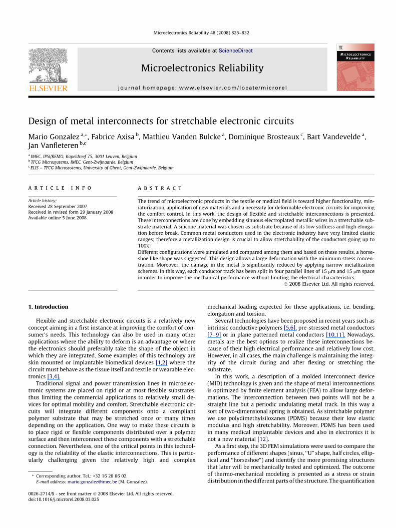
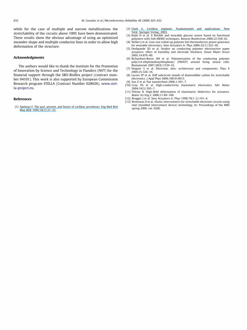
Fig. 1 outlines the sample fabrication. All processing is done onflexible but non-stretchable substrate which allows using conven-tional electroplating techniques. In a first instance, a photoresist isspin-coated on a copper foil and patterned, with the meanderingshape by UV-radiation. Then a 4 lm thick gold layer was electro-plated, followed by a 2 lm nickel layer to improve solderability.Gold was chosen as metal conductor to facilitate the separationof the sacrificial copper foil. However, other metals can be used ifan extra thin metal layer is applied on top of the copper foil. Beforeetching the copper foil, the conductors are encapsulated with 0.25or 0.5 mm thick elastic polymer. As elastic polymer material Silas-tic MDX4-4210 from Dow Corning had been chosen because it’s abiomedical grade silicone elastomer with a low Young’s modulusand high elongation (up to 470% from supplier datasheet). Moredetailed information about this processing was presented by Bros-teaux [13].
3. Preliminary elastic model
Even if simple conductor shapes like triangular or sinusoidal al-low higher deformations compared to a straight line, they presenta high concentration of stresses in some regions, giving rise to earlyfailures at fairly small deformations. Common metal conductors(Au, Cu, Ni, Pt) have very limited elastic ranges, therefore a design
Copper Foil
Photoresits
Metal
PDMSPDMS
1. Spin coat photoresist 2. Pattern Photoresist
3. Plate metal (Cu, Au, Pt, Ni)
4. Dissolve Photoresis t
5. Overmould PDMS6. Etch sacrificial copper foil
7. Invert sample and overmould PDMS
Fig. 1. Process sequence for metallic stretchable interconnections embedded inPDMS.
of an appropriate shape is crucial to allow stretchability of theconductors.
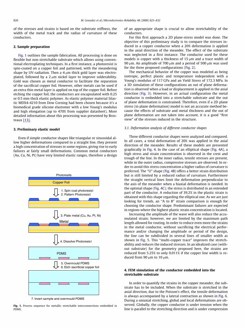
For this first approach a 2D plane-stress model was done. Theobjective of this preliminary study is to compare the stresses in-duced in a copper conductor when a 20% deformation is appliedin the axial direction of the meander. The effect of the substratewas neglected in a first instance. The conductor used for thesemodels is copper with a thickness of 15 lm and a trace width of90 lm. An amplitude of 700 lm and a period of 500 lm was usedfor the three proposed configurations (Fig. 2).
The mechanical behavior of the copper was modeled as beingisotropic, perfect plastic and temperature independent with aYoung’s modulus of 117 GPa and an Yield Stress of 172.3 MPa. Ina 3D simulation of these configurations an out of plane deforma-tion is observed when a load or displacement is applied in the axialdirection (Fig. 3). However, in an actual configuration the metalconductor is embedded into a stretchable substrate and the outof plane deformation is constrained. Therefore, even if a 2D planestress (in plane deformation) model is not an accurate method be-cause the effects of substrate and metal thickness and the out ofplane deformation are not taken into account, it is a good ‘‘firstview” of the stresses induced in the structure.
3.1. Deformation analysis of different conductor shapes
Three different conductor shapes were analyzed and compared.In all cases, a total deformation of 20% was applied in the axialdirection of the meander. Results of these models are presentedgraphically in Fig. 4. In the case of an elliptical shape (Fig. 4A), ahigh stress and strain concentration is observed in the crest andtrough of the line. In the inner radius, tensile stresses are present,while in the outer radius, compressive stresses are observed. In or-der to avoid this stress concentration a higher radius of curvature ispreferred. The ‘‘U” shape (Fig. 4B) offers a better strain distributionbut is still limited by a reduced radius of curvature. Furthermorethe straight vertical lines limit the deformation perpendicular tothe axis of the meander when a biaxial deformation is needed. Inthe optimal shape (Fig. 4C); the stress is distributed in an extendedpart of the conductor. A reduction of 39.2% in the plastic strain isobtained with this shape regarding the elliptical one. As we are justlooking for trends, an ‘‘A to B” strain comparison is enough forchoosing the conductor shape. Predominant failures are expectedin regions where the highest plastic strain concentration is located.
Increasing the amplitude of the wave will also reduce the accu-mulated strain; however, we are limited by the maximum pathlength allowed for routing. In order to reduce even more the strainsin the metal conductor, without sacrificing the electrical perfor-mance and/or changing the amplitude or period of the design,the line can be subdivided in several lines of smaller width asshown in Fig. 5. This ‘‘multi-copper trace” improves the stretch-ability and reduces the induced stresses. In an idealized case (with-out substrate) for the geometry proposed here, the strains arereduced from 5.25% to only 0.011% if the copper line width is re-duced from 90 lm to 10 lm.
4. FEM simulation of the conductor embedded into thestretchable substrate
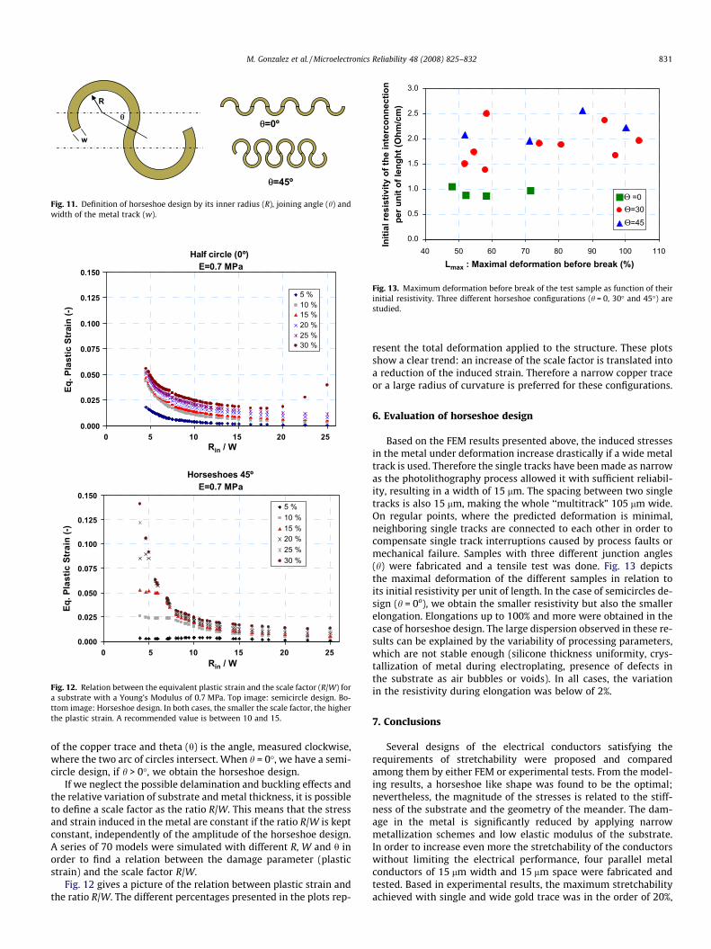
In order to quantify the strains in the copper meander, the sub-strate has to be included. When the substrate is stretched in theaxial direction, due to the Poisson’s effect, the tensile deformationis always accompanied by a lateral contraction as shown in Fig. 6.During a uniaxial stretching, global and local deformations are ob-served. Globally, the copper conductor is under tension when theline is parallel to the stretching direction and is under compression
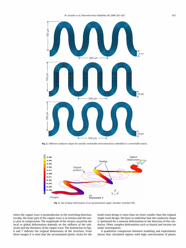
Fig. 2. Different conductor shapes for metallic stretchable interconnections embedded in a stretchable matrix.
Fig. 3. Out of plane deformation of an unconstrained copper meander stretched 20%.
M. Gonzalez et al. / Microelectronics Reliability 48 (2008) 825–832 827
when the copper trace is perpendicular to the stretching direction.Locally, the inner part of the copper trace is in tension and the out-er part in compression. The magnitude of the strains caused by thelocal or global deformation depends on the stiffness of the sub-strate and the thickness of the copper trace. The dashed line in Figs.6 and 7 indicate the original dimensions of the structure. Fromthese images it is seen that the accumulated plastic strain for the
multi-track design is more than six times smaller than the originalsingle track design. We have to underline that the conductor shapeis optimized for a uniaxial deformation in the direction of the con-ductor. Other complex deformation such as biaxial and torsion areunder investigation.
A qualitative comparison between modeling and experimentsshows that calculated regions with high concentration of plastic
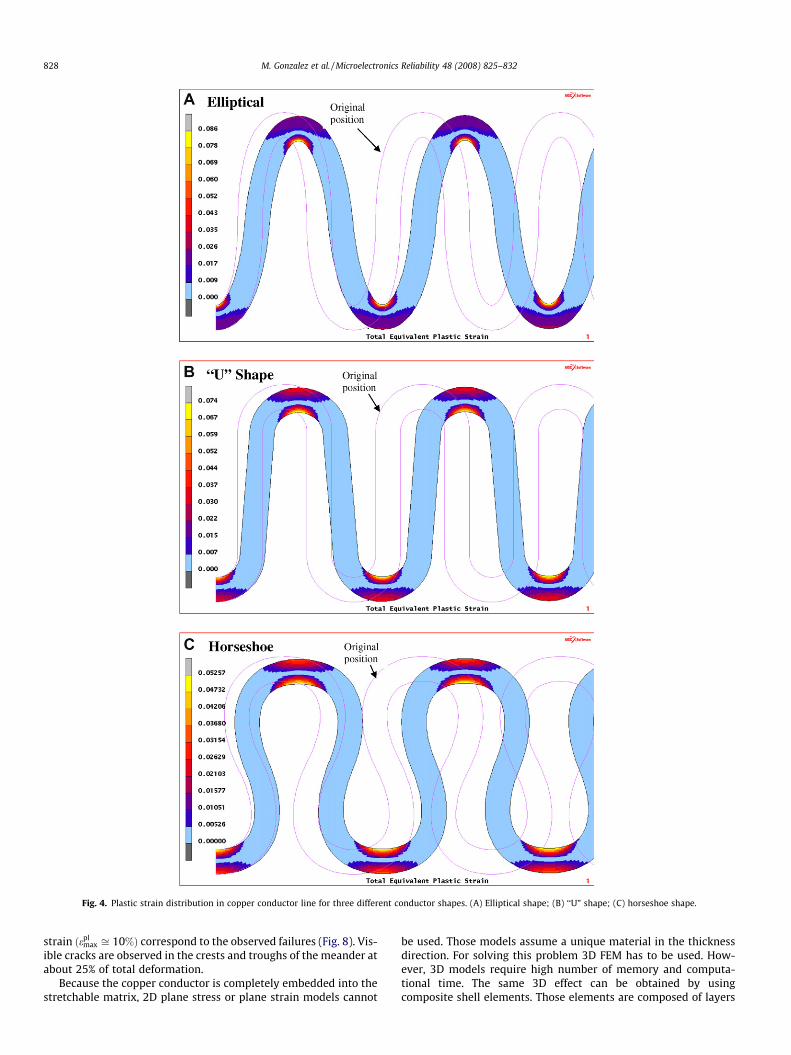
Fig. 4. Plastic strain distribution in copper conductor line for three different conductor shapes. (A) Elliptical shape; (B) ‘‘U” shape; (C) horseshoe shape.
828 M. Gonzalez et al. / Microelectronics Reliability 48 (2008) 825–832
strain ðeplmax ffi 10%Þ correspond to the observed failures (Fig. 8). Vis-
ible cracks are observed in the crests and troughs of the meander atabout 25% of total deformation.
Because the copper conductor is completely embedded into thestretchable matrix, 2D plane stress or plane strain models cannot
be used. Those models assume a unique material in the thicknessdirection. For solving this problem 3D FEM has to be used. How-ever, 3D models require high number of memory and computa-tional time. The same 3D effect can be obtained by usingcomposite shell elements. Those elements are composed of layers
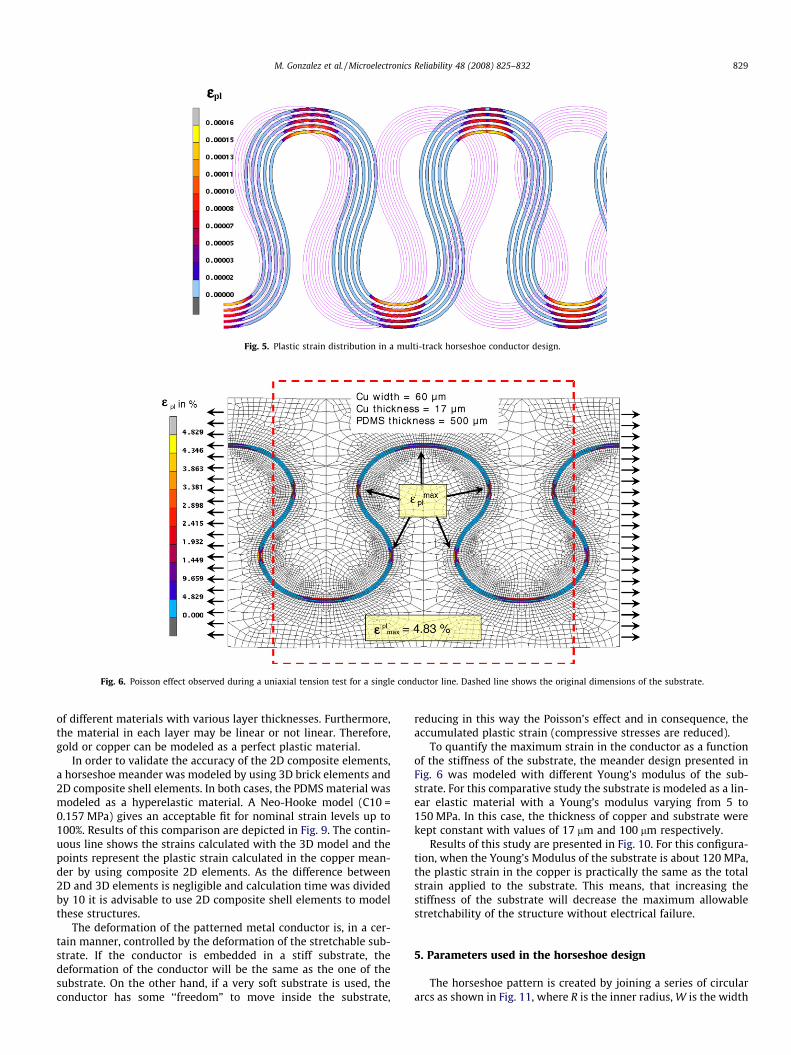
Fig. 5. Plastic strain distribution in a multi-track horseshoe conductor design.
Fig. 6. Poisson effect observed during a uniaxial tension test for a single conductor line. Dashed line shows the original dimensions of the substrate.
M. Gonzalez et al. / Microelectronics Reliability 48 (2008) 825–832 829
of different materials with various layer thicknesses. Furthermore,the material in each layer may be linear or not linear. Therefore,gold or copper can be modeled as a perfect plastic material.
In order to validate the accuracy of the 2D composite elements,a horseshoe meander was modeled by using 3D brick elements and2D composite shell elements. In both cases, the PDMS material wasmodeled as a hyperelastic material. A Neo-Hooke model (C10 =0.157 MPa) gives an acceptable fit for nominal strain levels up to100%. Results of this comparison are depicted in Fig. 9. The contin-uous line shows the strains calculated with the 3D model and thepoints represent the plastic strain calculated in the copper mean-der by using composite 2D elements. As the difference between2D and 3D elements is negligible and calculation time was dividedby 10 it is advisable to use 2D composite shell elements to modelthese structures.
The deformation of the patterned metal conductor is, in a cer-tain manner, controlled by the deformation of the stretchable sub-strate. If the conductor is embedded in a stiff substrate, thedeformation of the conductor will be the same as the one of thesubstrate. On the other hand, if a very soft substrate is used, theconductor has some ‘‘freedom” to move inside the substrate,
reducing in this way the Poisson’s effect and in consequence, theaccumulated plastic strain (compressive stresses are reduced).
To quantify the maximum strain in the conductor as a functionof the stiffness of the substrate, the meander design presented inFig. 6 was modeled with different Young’s modulus of the sub-strate. For this comparative study the substrate is modeled as a lin-ear elastic material with a Young’s modulus varying from 5 to150 MPa. In this case, the thickness of copper and substrate werekept constant with values of 17 lm and 100 lm respectively.
Results of this study are presented in Fig. 10. For this configura-tion, when the Young’s Modulus of the substrate is about 120 MPa,the plastic strain in the copper is practically the same as the totalstrain applied to the substrate. This means, that increasing thestiffness of the substrate will decrease the maximum allowablestretchability of the structure without electrical failure.
5. Parameters used in the horseshoe design
The horseshoe pattern is created by joining a series of circulararcs as shown in Fig. 11, where R is the inner radius, W is the width
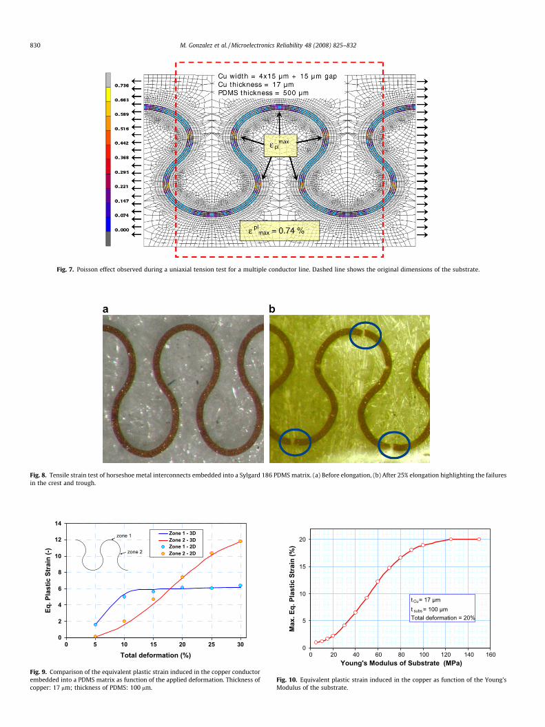
Fig. 7. Poisson effect observed during a uniaxial tension test for a multiple conductor line. Dashed line shows the original dimensions of the substrate.
Fig. 8. Tensile strain test of horseshoe metal interconnects embedded into a Sylgard 186 PDMS matrix. (a) Before elongation, (b) After 25% elongation highlighting the failuresin the crest and trough.
0
2
4
6
8
10
12
14
0 5 10 15 20 25 30
Total deformation (%)
Eq. P
last
ic S
trai
n (-)
Zone 1 - 3DZone 2 - 3DZone 1 - 2DZone 2 - 2D
zone 1
zone 2
Fig. 9. Comparison of the equivalent plastic strain induced in the copper conductorembedded into a PDMS matrix as function of the applied deformation. Thickness ofcopper: 17 lm; thickness of PDMS: 100 lm.
0
5
10
15
20
0 20 40 60 80 100 120 140 160Young's Modulus of Substrate (MPa)
Max
. Eq.
Pla
stic
Str
ain
(%)
t Cu = 17 µmt subs = 100 µmTotal deformation = 20%
Fig. 10. Equivalent plastic strain induced in the copper as function of the Young’sModulus of the substrate.
830 M. Gonzalez et al. / Microelectronics Reliability 48 (2008) 825–832
R
θ
w
θ=0º
θ=45º
Fig. 11. Definition of horseshoe design by its inner radius (R), joining angle (h) andwidth of the metal track (w).
Half circle (0º)E=0.7 MPa
0.000
0.025
0.050
0.075
0.100
0.125
0.150
0 5 10 15 20 25Rin / W
Eq. P
last
ic S
trai
n (-)
5 %10 % 15 %20 %25 %30 %
Horseshoes 45ºE=0.7 MPa
0.000
0.025
0.050
0.075
0.100
0.125
0.150
0 5 10 15 20 25Rin / W
Eq. P
last
ic S
trai
n (-)
5 %10 %15 %20 %25 %30 %
Fig. 12. Relation between the equivalent plastic strain and the scale factor (R/W) fora substrate with a Young’s Modulus of 0.7 MPa. Top image: semicircle design. Bo-ttom image: Horseshoe design. In both cases, the smaller the scale factor, the higherthe plastic strain. A recommended value is between 10 and 15.
0.0
0.5
1.0
1.5
2.0
2.5
3.0
40 50 60 70 80 90 100 110
Lmax : Maximal deformation before break (%)
Initi
al re
sist
ivity
of t
he in
terc
onne
ctio
n pe
r uni
t of l
engh
t (O
hm/c
m)
Θ=30Θ=45
Θ =0
Fig. 13. Maximum deformation before break of the test sample as function of theirinitial resistivity. Three different horseshoe configurations (h = 0, 30� and 45�) arestudied.
M. Gonzalez et al. / Microelectronics Reliability 48 (2008) 825–832 831
of the copper trace and theta (h) is the angle, measured clockwise,where the two arc of circles intersect. When h = 0�, we have a semi-circle design, if h > 0�, we obtain the horseshoe design.
If we neglect the possible delamination and buckling effects andthe relative variation of substrate and metal thickness, it is possibleto define a scale factor as the ratio R/W. This means that the stressand strain induced in the metal are constant if the ratio R/W is keptconstant, independently of the amplitude of the horseshoe design.A series of 70 models were simulated with different R, W and h inorder to find a relation between the damage parameter (plasticstrain) and the scale factor R/W.
Fig. 12 gives a picture of the relation between plastic strain andthe ratio R/W. The different percentages presented in the plots rep-
resent the total deformation applied to the structure. These plotsshow a clear trend: an increase of the scale factor is translated intoa reduction of the induced strain. Therefore a narrow copper traceor a large radius of curvature is preferred for these configurations.
6. Evaluation of horseshoe design
Based on the FEM results presented above, the induced stressesin the metal under deformation increase drastically if a wide metaltrack is used. Therefore the single tracks have been made as narrowas the photolithography process allowed it with sufficient reliabil-ity, resulting in a width of 15 lm. The spacing between two singletracks is also 15 lm, making the whole ‘‘multitrack” 105 lm wide.On regular points, where the predicted deformation is minimal,neighboring single tracks are connected to each other in order tocompensate single track interruptions caused by process faults ormechanical failure. Samples with three different junction angles(h) were fabricated and a tensile test was done. Fig. 13 depictsthe maximal deformation of the different samples in relation toits initial resistivity per unit of length. In the case of semicircles de-sign (h = 0o), we obtain the smaller resistivity but also the smallerelongation. Elongations up to 100% and more were obtained in thecase of horseshoe design. The large dispersion observed in these re-sults can be explained by the variability of processing parameters,which are not stable enough (silicone thickness uniformity, crys-tallization of metal during electroplating, presence of defects inthe substrate as air bubbles or voids). In all cases, the variationin the resistivity during elongation was below of 2%.
7. Conclusions
Several designs of the electrical conductors satisfying therequirements of stretchability were proposed and comparedamong them by either FEM or experimental tests. From the model-ing results, a horseshoe like shape was found to be the optimal;nevertheless, the magnitude of the stresses is related to the stiff-ness of the substrate and the geometry of the meander. The dam-age in the metal is significantly reduced by applying narrowmetallization schemes and low elastic modulus of the substrate.In order to increase even more the stretchability of the conductorswithout limiting the electrical performance, four parallel metalconductors of 15 lm width and 15 lm space were fabricated andtested. Based in experimental results, the maximum stretchabilityachieved with single and wide gold trace was in the order of 20%,
832 M. Gonzalez et al. / Microelectronics Reliability 48 (2008) 825–832
while for the case of multiple and narrow metallizations thestretchability of the circuits above 100% have been demonstrated.These results show the obvious advantage of using an optimizedmeander shape and multiple conductor lines in order to allow highdeformation of the structure.
Acknowledgments
The authors would like to thank the Institute for the Promotionof Innovation by Science and Technology in Flanders (IWT) for thefinancial support through the SBO-Bioflex project (contract num-ber 04101). This work is also supported by European CommissionResearch program STELLA (Contract Number 028026). www.stel-la-project.eu.
References
[1] Spelman F. The past, present, and future of cochlear prostheses. Eng Med BiolMag IEEE 1999;18(3):27–33.
[2] Clark G. Cochlear implants. Fundamentals and applications. NewYork: Springer Verlag; 2003.
[3] Kudo H et al. A flexible and wearable glucose sensor based on functionalpolymers with Soft-MEMS techniques. Biosens Bioelectron 2006;22:558–62.
[4] Weber J et al. Coin-size coiled-up polymer foil thermoelectric power generatorfor wearable electronics. Sens Actuators A: Phys 2006;32(1):325–30.
[5] Deshpande SD et al. Studies on conducting polymer electroactive paperactuators: effect of humidity and electrode thickness. Smart Mater Struct2005;14:876–80.
[6] Richardson-Burns SM et al. Polymerization of the conducting polymerpoly(3,4-ethylenedioxythiophene) (PEDOT) around living neural cells.Biomaterials 2007;28(8):1539–52.
[7] Wagner S et al. Electronic skin: architecture and components. Phys E2004;25:326–34.
[8] Lacour SP et al. Stiff subcircuit islands of diamondlike carbon for stretchableelectronics. J Appl Phys 2006;100:014913.
[9] Sun Z et al. Nat nanotechnol 2006;1:201–7.[10] Gray DS et al. High-conductivity elastomeric electronics. Adv Mater
2004;16(5):393–7.[11] Pelrine R. High-field deformation of elastomeric dielectrics for actuators.
Mater Sci Eng C 2000;11:89–100.[12] Brugger J et al. Sens Actuators A: Phys 1998;70(1–2):191–4.[13] Brosteaux D et al., Elastic interconnects for stretchable electronic circuits using
mid (moulded interconnect device) technology, In: Proceedings of the MRSspring 2006, vol. 926E.