deep submicron cmos technologies for the lhc experiments
TRANSCRIPT
IU( LLAR PHYSIC: II liPl
P R O C E E D I N G S S U P P L E M E N T S
ELSEVIER Nuclear Physics B (Proc. Suppl.) 78 (1999) 625-634 w-.vw.elsevie r. nl/locate/n pe
Deep submicron CMOS technologies for the LHC experiments
P. Jarron 1, G. Anelli 1, T. Calin 4, J. Cosculluela 4, M. Campbell 1, M. Delmastro 1'3, F. Faccio I , A. Giraldo 2 E. Heijne j , K. Kloukinas 1, M. Letheren ~, M. Nicolaidis 4, P. Moreira 1, A. Paccagnella 2, A. Marchioro 1 W. Snoeys 1, R. Velazco 4
CERN, 1211 Geneva 23, Switzerland 2 University of Padova University of Padova & INFN, via Marzolo 8, 35131 Padova, Italy 3 Supported by Associazione per 1o Sviluppo Scientifico e Tecnologico del Piemonte, Italy 4 TIMA/INPG Laboratory, 46 Avenue Felix Viallet, 38031 Grenoble, France
The harsh radiation environment at the Large Hadron Collider (LHC) requires radiation hard ASICs. This paper presents how a high tolerance for total ionizing dose can be obtained in commercial deep submicron technologies by using enclosed NMOS devices and guard rings. The method is explained, demonstrated on transistor and circuit level, and design implications are discussed. A model for the effective W/L of an enclosed transistor is given, a radiation-tolerant standard cell library is presented, and single event effects are discussed..
1 INTRODUCTION
The front end electronics in the detectors planned at the new accelerator at CERN, the Large Hadron Collider (LHC), will be subject to very high radiation levels : up to - 30 Mrad equivalent for ionizing dose, and about 1015 neutrons/cm 2. For several years, the High Energy Physics (HEP) community has studied and evaluated radiation hard technologies suitable for developing mixed-signal ASICs for the readout of these LHC experiments[ 1,2,3].
In the mean time, the market of radiation tolerant circuits for defense has shrunk considerably, and the Space community has started to use more Commercial-Off-The-Shelf (COTS) components rather than the more expensive and less advanced Hi- Rel components used in the past. This evolution and the fast growth of the semiconductor business in other areas has caused several semiconductor companies to abandon the radiation hard electronics market, and now only a very few companies in the world offer radiation-hard technologies suitable for LHC front- end ASICs.
Already in the early 80's irradiation measurements on MOS capacitors [4,5] showed a significant decrease of the radiation induced trapped charge in the oxide and interface states lbr oxides thinner than about 10 nm. Gate oxides in present day submicron CMOS technologies are in this range.
The market trend mentioned above, and these early results on thin oxide MOS capacitors were the motivation for us to investigate an alternative approach based on radiation-tolerant design techniques in deep submicron CMOS technology. By employing "enclosed" geometry and guard rings in the
layout of NMOS devices we eliminate the radiation- induced leakage paths along the edges of devices and between devices. Recent results [6,7,8,9,10,11,12] have confirmed the tremendous potential of this approach. In section 2 the approach is explained, transistor measurements are presented, and design implications discussed. In section 3 the modelling of a transistor laid out in enclosed geometry is investigated in more detail. In section 4 results on circuit demonstrators are presented. Section 5 discusses the newly designed digital library, and section 6 deals with single event effects. Thereafter conclusions are drawn and perspectives for the future are given.
DESIGN FOR RADIATION TOLERANCE IN DEEP SUBMICRON TECHNOLOGY
2.1 Radiation induced transistor threshold voltage shift
For CMOS technologies with minimum feature size above - lp.m, the threshold voltage shift which results from hole trapping in MOS gate oxides decreases as the square of the oxide thickness [13]. The 1970's CMOS technologies exhibited more than 1Volt of shift after l0 krad, whereas 0.5p.m technology exhibits a shift of less than 150 mV after 300 krad. As already pointed out, early measurements [4,5] on MOS capacitors indicated a sharp decrease (much sharper than the forementioned square law would indicate) in radiation induced trapped charge and interface states for oxides less than 10 nm thick. There it was suggested that tunnelling could be the mechanism behind this observation, because it would
0920-5632/99/$ - see front matter © 1999 Elsevier Science B.V. All rights reserved. PII S0920-5632(99)00615-5
626 R Jarron et al./Nuclear Physics B (Proc, Suppl.) 78 (1999) 625-634
dominate over other annealing mechanisms for thin oxides. In fact, a quantitative analysis of this is given in [14,15], and in [14] this analysis is then used to estimate the distribution of trapped charge. We have confirmed the early measurement results obtained on MOS capacitors by measuring transistors in different commercial CMOS processes with minimum feature sizes ranging from 0.5 ~m to 0.25 ~m [6,8,10,11 ].
2.2 Elimination of transistor leakage by using enclosed transistors and guard rings.
Drain1 Wel l /Su[ -
r c e l
6O
4O
20
-20
-40
i
- , - NMOS, t.=o 28] -60 -~ PMOS, L=0.28 J
1. E+03 I .E+04 I .E+05 I .E+06 I.E+07 Alealing
Total Dose [rad(SiOz)]
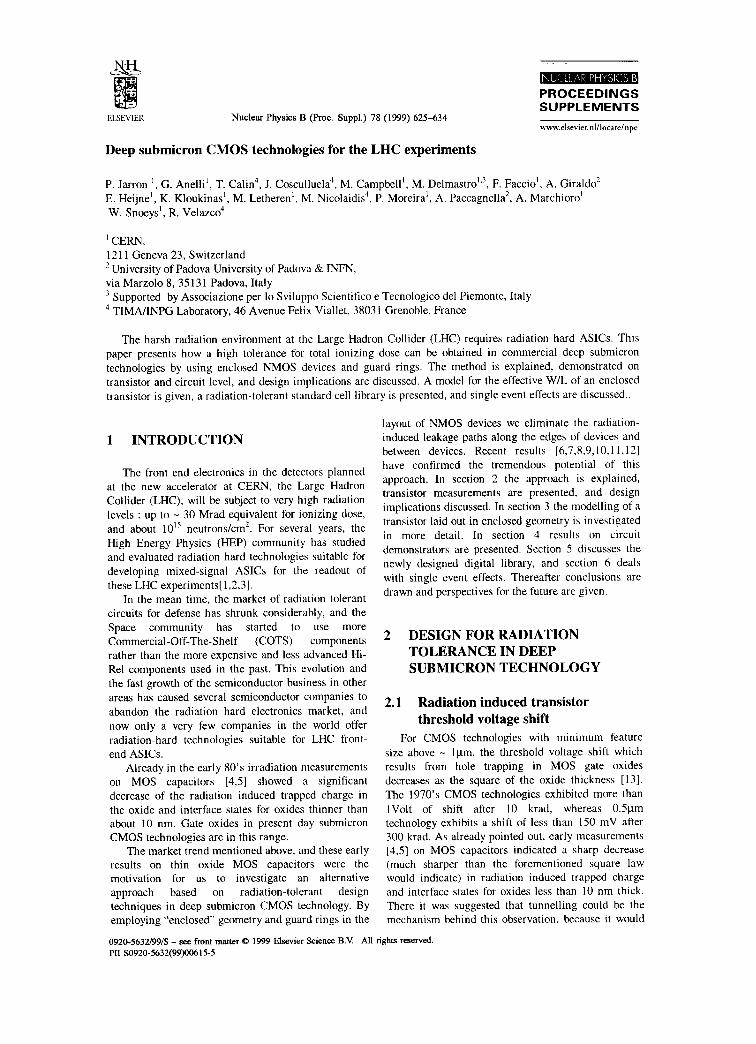
Figure 1. Threshold voltage shift of enclosed (see section 2.2.) NMOS and standard PMOS transistors as a function of the total dose for a 0.25 Ion technology. The white points represent the measurement after a 24 hour anneal at room temperature 05rst point) and after a subsequent one week anneal at 100 °C (last point).
Figure 1 shows the threshold voltage shift for NMOS and PMOS devices in a commercial 0.25 ~tm technology as a function of the total dose for an X-ray irradiation up to 30 Mrad (SiO2). Immediately after irradiation (black circles), the threshold voltage shift is less than 35mV for the NMOS, and about -70mV for the PMOS transistors. For a total dose of 10Mrad, these values are 15 and -30mV respectively. After the annealing (white circles), the threshold voltage shift increases to about 45mV for the NMOS and decreases to about -55mV for the PMOS. Devices were irradiated using the SEIFERT RP149 X-ray source at CERN. The produced X-ray spectrum has a peak at about I0 keV. The dose rate used for the irradiation varied between 20 and 30 krad(SiO2)/min. During irradiation and annealing, the bias was kept in the "worst case" condition. This means V~o,rce = V d r a i n =
V~ab = 0V and V~te = Vda = 2.5V for the NMOS, and all terminals grounded for the PMOS transistor.
trce2
Dra in2
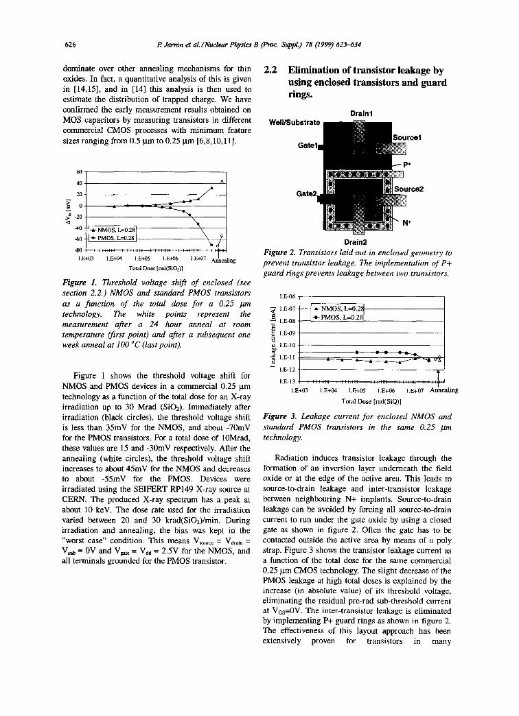
Figure 2. Transistors laid out in enclosed geometry to prevent transistor leakage. The implementation of P+ guard rings prevents leakage between two transistors.
I.E-06
~ I.E-07 "~--~-NMOS, L=0.2~
'~ I.E-08 | - o - PMOS, L=0.28 I
• ~ 1.E-09 g o I.E-I 0
-~ 1.E-11 _...-...---.....-~.~. _ ~ . ~ 4
1.E-12
I.E+03 1 .E+04 1 .E+05 1 .E+06 1.E+07 A! !ealing
Total Dose [rad(SiQ)]
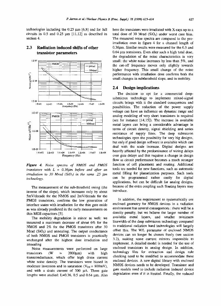
Figure 3. Leakage current for enclosed NMOS and standard PMOS transistors in the same 0.25 ~ technology.
Radiation induces transistor leakage through the formation of an inversion layer underneath the field oxide or at the edge of the active area. This leads to source-to-drain leakage and inter-transistor leakage between neighbouring N+ implants. Source-to-drain leakage can be avoided by forcing all source-to-drain current to run under the gate oxide by using a closed gate as shown in figure 2. Often the gate has to be contacted outside the active area by means of a poly strap. Figure 3 shows the transistor leakage current as a function of the total dose for the same commercial 0.25 ~tm CMOS technology. The slight decrease of the PMOS leakage at high total doses is explained by the increase (in absolute value) of its threshold voltage, eliminating the residual pre-rad sub-threshold current at Vcs=0V. The inter-transistor leakage is eliminated by implementing P+ guard rings as shown in figure 2. The effectiveness of this layout approach has been extensively proven for transistors in many
P. Jarron et al./Nuclear Physics B (Proc. Suppl.) 78 (1999) 625-634 6 2 7
technologies including the 0.25 Bm [6,8] and for full circuits in 0.5 and 0.25 [tm [11,12] as described in section 4.
2.3 Radiation induced shifts of other transistor parameters
I .E-07
C
~I.E-08 _~
NMOS - - p ~erad
,~'~, , --- 30Mrad
I .E-09 1 .E+02 I.E+03 I .E+04 1 .E+05 I .E+06 1 .E+07 1 ,E+08
Frequency (Hz)
1 .E-07
,. - -- 30Mrad I
>~I.E-08
Z "1
1 .E-09 1 .E+02 1 .E+03 1 .E+04 1 .E+05 1 .E+06 1 .E+07 1 .E+08
Frequency (Hz)
P M O S
Figure 4. Noise spectra of NMOS and PMOS transistors with L = 0.36p_m before and after an irradiation to 30 Mrad (Si02) in the same .25 tzm technology.
The measurement of the sub-threshold swing (the inverse of the slope), which increases only by about 5mV/decade for the NMOS and 2mV/decade for the PMOS transistors, confirms the low generation of interface states with irradiation for the thin gate oxide as was already predicted in the early measurements on thin MOS capacitors [5].
The mobility degradation is minor as well: we measured a maximum decrease of about 6% for the NMOS and 2% for the PMOS transistors after 30 Mrad (SIO2) and annealing. The output conductance of both NMOS and PMOS transistors is practically unchanged after the highest dose irradiation and annealing
Noise measurements were performed on large transistors (W = 20001.tm) with high transconductance, which offer high drain current white noise density. The transistors were biased in moderate inversion and in saturation (VDs = 800mV), and with a drain current of 500 ).tA. Three gate lengths were studied: L=0.36, 0.5 and 0.64 I.tm. Also
here the transistors were irradiated with X-rays up to a total dose of 30 Mrad (SiO2) under worst case bias. The measured noise spectra are compared to the pre- irradiation ones in figure 4 for a channel length of 0.36t.tm. Similar results were measured for the 0.5 and 0.64 I.tm transistors. Even after such a high total dose, the degradation of the noise characteristics is very small: the white noise increases by less than 5%, and the cut-off frequency moves only slightly towards higher frequency. This small change of the noise performance with irradiation dose confirms both the small changes in subthreshold slope, and in mobility.
2.4 Design implications The decision to opt for a commercial deep-
submicron technology to implement mixed-signal circuits brings with it the standard consquences and possibilities. The reduction of the power supply voltage can have an influence on dynamic range and analog modeling of very short transistors is required (see for instance [14,15]). The increase in available metal layers can bring a considerable advantage in terms of circuit density, signal shielding and series resistance of supply lines. The deep suhmicron technologies open the possibility for very big designs, hut only if good design software is available which can deal with the scale increase. Digital designs are heavily affected by the predominance of wiring delays over gate delays and this requires a change in design flow as circuit performance becomes a much stronger function of cell placement and routing. Additional tools are needed for new functions, such as automatic metal filling for planarization purposes. Such tools can be programmed rather easily for digital applications, but can be difficult for analog designs, because of the extra coupling such floating layers may introduce.
In addition, the requirement to systematically use enclosed geometry for NMOS devices in a radiation environment has several consequences : there will be a density penalty, but we believe the larger number of available metal layers, and smaller minimum linewidth of the deep submicron technology compared to traditional radiation hard technologies will largely offset this. The W/L parameter of enclosed NMOS devices can no longer be chosen freely (see section 3.2), making some current mirrors impossible to implement. A detailed model is needed for the use of enclosed transistors in analog design. In addition, technology files for extraction and design rule checking need to be modified to accommodate these enclosed devices. A new digital library with enclosed NMOS devices needs to be developed. Transistor and gate models need to include radiation induced device degradation even if it is limited. Finally, the reduced
628 P. Jarron et al./Nuclear Physics B (Proc. Suppl.) 78 (1999) 625-634
feature sizes in deep-submicron technologies make them sensitive to single event effects. Modeling of enclosed transistors, the development of a digital library, and single event effects are the subject of the following sections.
3 ENCLOSED TRANSISTOR MODELING
If the use of the enclosed geometry for the NMOS transistors eliminates radiation-induced leakage currents, their special shape does not constitute a common practice in VLSI design. Therefore, no effort has been conducted so far in modelling transistors with such shape. The absence of a convenient model, at least for the effective aspect ratio (W/L), poses a problem especially for analog design. The approximation for the aspect ratio proposed in [11] is based on the assumption of square equipotential lines under the gate and might lead to a 30-40% over- estimate. To solve this problem, we have developed a model to estimate the aspect ratio of the enclosed transistors.
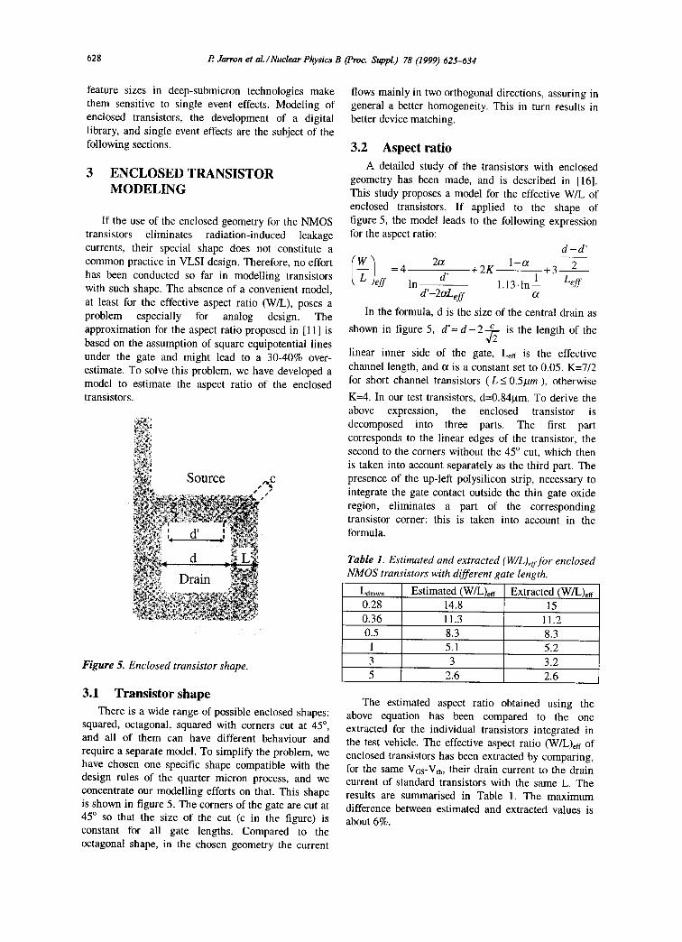
I , r ,5 Source ,%c s
Figure 5. Enclosed transistor shape.
3.1 Transistor shape There is a wide range of possible enclosed shapes:
squared, octagonal, squared with corners cut at 45 ° , and all of them can have different behaviour and require a separate model. To simplify the problem, we have chosen one specific shape compatible with the design rules of the quarter micron process, and we concentrate our modelling efforts on that. This shape is shown in figure 5. The corners of the gate are cut at 45 ° so that the size of the cut (c in the figure) is constant for all gate lengths. Compared to the octagonal shape, in the chosen geometry the current
flows mainly in two orthogonal directions, assuring in general a better homogeneity. This in turn results in better device matching.
3.2 Aspect ratio A detailed study of the transistors with enclosed
geometry has been made, and is described in [16]. This study proposes a model for the effective W/L of enclosed transistors. If applied to the shape of figure 5, the model leads to the following expression for the aspect ratio:
d - d '
( W 1 =4 2a . + 2 K 1-°~ ~_3..___~2 --L eff In d' 1.13.1n 1 Left
d '-2~r.Lef f a
In the formula, d is the size of the central drain as
shown in figure 5, d '=d-2- -~2 is the length of the
linear inner side of the gate, L~tr is the effective channel length, and a is a constant set to 0.05. K=7/2 for short channel transistors (L < 0.5/~m ), otherwise
K=4. In our test transistors, d=0.84gm. To derive the above expression, the enclosed transistor is decomposed into three parts. The first part corresponds to the linear edges of the transistor, the second to the corners without the 45 ° cut, which then is taken into account separately as the third part. The presence of the up-left polysilicon strip, necessary to integrate the gate contact outside the thin gate oxide region, eliminates a part of the corresponding transistor corner: this is taken into account in the formula.
Table 1. Estimated and extracted (W/L)~ for enclosed NMOS transistors with different gate length.
Ld~w. Estimated (W/L)eff Extracted (W/L)ea 0.28 14.8 15 0.36 11.3 11.2 0.5 8.3 8.3
1 5.1 5.2 3 3 3.2 5 2.6 2.6
The estimated aspect ratio obtained using the above equation has been compared to the one extracted for the individual transistors integrated in the test vehicle. The effective aspect ratio (W/L)eff of enclosed transistors has been extracted by comparing, for the same Vcs-Vth, their drain current to the drain current of standard transistors with the same L. The results are summarised in Table 1. The maximum difference between estimated and extracted values is about 6%.
P. Jarron et al./Nuclear Physics B (Proc. Suppl.) 78 (1999) 625-634 629
The expression for the aspect ratio can also be used for transistors designed by stretching in one or both directions the shape in figure 5 provided the corners are not modified. In that case, one just needs to add the contribution of the linear regions generated by the stretching. Transistors with aspect ratio as large as desired can be designed in this way.
However, the aspect ratio for an enclosed transistor can not be made arbitrarily small, As shown in table 1, the aspect ratio decreases when the gate length is increased. For a channel length close to 7gm, the dominant contribution to the transistor current comes from the gate corners. This corresponds to the second term in the above expression, which does not depend on the gate length. Therefore, the aspect ratio reaches a "saturation" value of about 2.3 for L~rawn=7l.tm. This important limitation lbr analog design is inherent to the use of enclosed transistor shapes.
3.3 Output conductance
Table 2. Output conductance for enclosed NMOS transistors o f different gate length. G,ti = inner diffusion as drain, Gjo = outer diffusion as drain. Difference = (G,ti-G,to)/ Gai. Measurements for Vas- Vth = 3 OOm V.
Ldraw n (gm) 0.28
Gdi (p.S) 11.09
Gdo (~tS) 9.62
Difference (%) 19
0.36 7.17 5.55 23 0.5 4.10 2.73 33
1 1.68 0.79 53 3 0.57 0.17 70 5 0.41 0.10 75
In an enclosed shape transistor, source and drain are not symmetric. The inner diffusion has a much smaller area, hence capacitance, than the outer one. As the gate perimeter is different in the inner or outer side, the transistor output conductance in saturation changes depending on whether the inner or outer diffusion is chosen as the drain. Measurements summarised in table2 show that the output conductance is lower when the outer diffusion acts as the transistor drain, and that this asymmetry increases with the gate length. This second trend is easily explained by the fact that the outer gate perimeter increases with the gate length, whilst the inner one does not.
This characteristic asymmetry of the enclosed NMOS should be taken into account for the choice of which of the two diffusions is the drain. In general, capacitive load and improved output conductance will have to be traded off against each other.
It is clear that the above is only the first step towards obtaining a full analog model for an enclosed
transistor. In addition, the formula for the effective W/L ratio only helps in the current voltage characteristic of the transistor, and cannot be used in combination with L to estimate the gate capacitance.
4 R A D I A T I O N T O L E R A N T C I R C U I T
D E M O N S T R A T O R S
The previous sections showed the promise of deep- submicron technologies for radiation tolerance at the transistor level. In addition, several circuits were designed to demonstrate the validity of the approach at circuit level.
4.1 Digital circuits Three shift registers were integrated in the quarter
micron test chip, primarily to study Single Event Effects (SEE), as described in section 6. Each shift register was made up of a number of identical D-Flip- Flop (FF) cells. One of the registers used a standard master-slave static architecture for the FFs, another one used a dynamic architecture, and the third one was static but implemented using a dedicated SEU- tolerant ("hard") design, The SEU-tolerant design was derived from previously proposed memory cells [17,18]. The size of the FF was 18x16 Bm 2 for the dynamic, 33x16 gm 2 for the standard static and 50x16 gm 2 for the "hard". The number of FFs was 2048 for the two static registers and 1024 for the dynamic design.
All the shift registers used radiation-tolerant layout practices: the NMOS and most of the PMOS devices were designed with enclosed geometry, and guard- rings surrounded the NMOS devices. All together, the three shift registers contained some 150,000 transistors, and occupied an area of about 2.7mm 2. The three shift registers have been irradiated with X-rays up to a total dose of 30 Mrad (SiOz), applying a supply voltage Vaa = 2V. The shift registers were continuously clocked at 1.25MHz during the irradiation, which was performed at a dose rate of 30 and 40krad/min,. No error was detected in the data propagation in any of the registers during the irradiation up to 30Mrad, and functionality was conserved during and after irradiation and annealing.
4.2 Mixed mode circuits Two pixel readout test chips were implemented
using the techniques described above to prove the validity of the approach for a full mixed mode circuit. The first [11] fabricated in a commercial 0.5 Bin CMOS technology, withstood ionizing radiation up to a dose of 600 krad to 1.7 Mrad depending on the type of radiation. Failure was ultimately caused by the cumulative effect of radiation induced transistor
630 R Jarron et al./Nuclear Physics B (Proc. Suppl.) 78 (1999) 625-634
threshold shifts which pushed a transistor in the signal path out of saturation severely reducing the signal gain. Transistor irradiation measurements indicate that without special layout precautions the chip would have died at about 50 krad due to excessive power consumption from radiation induced leakage.
After measurements confirmed that radiation induced transistor parameter shifts were sharply reduced for a commercial 0.25 Ixm CMOS technology, a second pixel readout demonstrator [12] was implemented in this technology. The circuit tolerated several tens of Mrads while maintaining full functionality.
These results demonstrate at the circuit level that, with the use of enclosed NMOS devices and guard rings in deep submicron commercial technologies, it is possible to design reliable ICs able to withstand high total doses. Comparison of the results for the 0.5 and 0.25 Itm test chip illustrates the significance of the improvement when going to a thinner gate oxide (from ~10 nm to ~5nm). In 0.25 I.tm the transistor threshold shifts become sufficiently small to no longer affect circuit performance.
5 R A D I A T I O N T O L E R A N T L I B R A R Y
® ~ x w ~ m l l m m l m m m w ~ l ~
I!ib irilli iHli ,'i i+:ii I iI! . , . . . . . . ~ . . . . . . . ~ ~ ' I ~ ~ :,
i i i i i ! i i i i i l i i i i< i i i r l !~ i i i ' i i i i f i i i i i l , : i i~ i i ; i i i i l
r! i ! !i
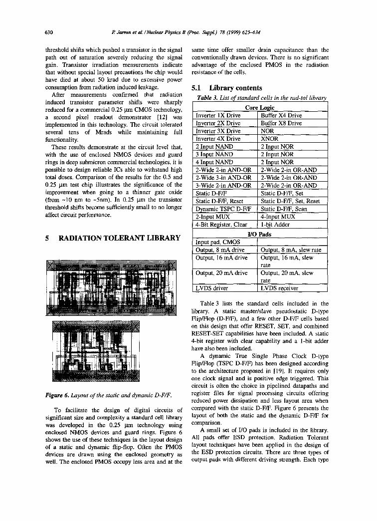
Figure 6. Layout of the static and dynamic D-F/F.
To facilitate the design of digital circuits of significant size and complexity a standard cell library was developed in the 0.25 ltm technology using enclosed NMOS devices and guard rings. Figure 6 shows the use of these techniques in the layout design of a static and dynamic flip-flop. Often the PMOS devices are drawn using the enclosed geometry as well. The enclosed PMOS occupy less area and at the
same time offer smaller drain capacitance than the conventionally drawn devices. There is no significant advantage of the enclosed PMOS in the radiation resistance of the cells.
5.1 Library contents Table 3. List of standard cells in the rad-tol librar
Core Logic Inverter IX Drive Buffer X4 Drive Inverter 2X Drive Buffer X8 Drive Inverter 3X Drive NOR Inverter 4X Drive XNOR 2 Input NAND 3 Input NAND 4 Input NAND 2-Wide 2-in AND-OR
2 Input NOR 2 Input NOR 2 Input NOR 2-Wide 2-in OR-AND
2-Wide 3-in AND-OR 2-Wide 2-in OR-AND 3-Wide 2-in AND-OR 2-Wide 2-in OR-AND Static D-F/F Static D-F/F, Set Static D-F/F, Reset Static D-F/F, Set, Reset
Static D-F/F, Scan D~pnamic TSPC D-F/F 2-Input MUX 4-Bit Register, Clear
I/O
4-Input MUX 1-bit Adder
Pads Input pad, CMOS Output, 8 mA drive Output, 16 mA drive
Output, 8 mA, slew rate Output, 16 mA, slew rate
Output, 20 mA drive Output, 20 mA, slew rate
LVDS driver LVDS receiver
Table 3 lists the standard cells included in the library. A static master/slave pseudostatic D-type Flip/Flop (D-F/F), and a few other D-F/F cells based on this design that offer RESET, SET, and combined RESET-SET capabilities have been included. A static 4-bit register with clear capability and a 1-bit adder have also been included.
A dynamic True Single Phase Clock D-type Flip/Flop (TSPC D-F/F) has been designed according to the architecture proposed in [19]. It requires only one clock signal and is positive edge triggered. This circuit is often the choice in pipelined datapaths and register files for signal processing circuits offering reduced power dissipation and less layout area when compared with the static D-F/F. Figure 6 presents the layout of both the static and the dynamic D-F/F for comparison.
A small set of I/O pads is included in the library. All pads offer ESD protection. Radiation Tolerant layout techniques have been applied in the design of the ESD protection circuits. There are three types of output pads with different driving strength. Each type
P. Jarron et al./Nuclear Physics B (Proc. Suppl.) 78 (1999) 625-634 631
has a standard version and a version with a slew rate control output.
A set of "glue cells" has also been developed to ease the design and enable the automated place & routing. These cells are: "cap cells" that close the guard-rings at both ends of the cell rows, corner cells for the chip power rings, power feed-through cells etc.
Special physical design verification rules have been added to check for inconsistencies in radiation- tolerant designs (openings in the guard-rings around n + diffusions etc). Special device extraction routines have been inserted in the extraction rules file that enable a more precise extraction of the (W/L) of the enclosed geometry transistors.
The implemented cells were characterised through SPICE simulations and Verilog timing models have been developed to enable digital circuit simulations.
5.2 Library performance The gate delay of an inverter in the library is
estimated from SPICE simulations to be 50 ps at 2.0 V (fan-out = 1). This gives an improvement in speed of about 5 times when compared to a currently available 0.8~tm technology.
The estimated power consumption in the library is estimated to be 0.t5 I.tW/MHz/gate (fan-out = 1), which is 26 times lower than what is achieved in a generic 0.8 ~tm technology. In order to reduce further the power consumption, wherever the system constraints allow us, we propose to use the library cells at 2.0 V rather than 2.5V, which is the nominal operating voltage of the technology. The technology can indeed easily operate logic blocks at 40 MHz down to a 1 V supply level.
Table 4. ~eed/Power trade-off at reduced VDD.
2.5 V 2.0 V
Tpd 36 ps 48 ps -25% Power 0.24 ~W/MHz 0.14~tW/MHz -42%
Table 4 shows the estimated propagation delay (Tpd) and the associated power dissipation of a simple inverter (F.O.=I) cell at 2.5 V and 2.0 V. The speed of the technology, even after a reduction of 25%, will still comfortably exceed the requirements for the circuit operation in the LHC environment. At the same time the power dissipation is almost halved at 2.0V, relaxing the power budget constrains for the detector front-end electronics. All the cells in the library have being characterised at a typical operating voltage of 2.0 V.
The area penalty that the radiation-tolerant techniques introduce in the library cells is estimated to be about 70%. For comparison a few different digital
cells were drawn, in the selected deep submicron technology, using both standard and radiation tolerant layout techniques. The area of the layout of each cell as well as the associated penalty in the area can be seen in table 5. The comparison shows that more complex cells incur higher area penalty.
Despite the area overhead, the gate density offered by the library is still 8 times higher when compared to a 0.81.tm standard cell technology.
Table 5. Area penalty due to radiation-tolerant design.
Standard Rad-Tol
Inverter 33.6 ~n 2 50.9 ~tm 2
NAND2 46.0 ttm 2 119.0 ttm 2
NOR?, 47.8 ~m 2 80.0 p.m 2
Static D-F/F 153.0 lam 2 533.1 ~m 2
Static D-F/F SR 188.1 ~tm 2 572.0 ~m 2
Penalty, 34 %
61%
41%
71%
75 %
A ring oscillator consisting of 1,280 minimum size inverter cells has been drawn on a 0.8~tm standard cell technology and on the 0.25 ~m technology using the radiation-tolerant standard cell library. Both designs were routed using 2 metal layers. The design in the 0.25 Ixm technology was found to be 7.9 times smaller than the one in 0.8 ~tm. The fact that the library features up to 5 levels of metal for wiring purposes, presents a great advantage for high density designs.
6 S I N G L E E V E N T E F F E C T S ( S E E )
Apart from total dose damage, ionizing radiation can also cause problems at the very moment when the ionization is generated by a single incoming particle, and these problems are generally known as Single Event Effects (SEE). The ionization charge can cause Single Event Latch-up (SEL) : a parasitic thyristor which normally is in the off state is turned on by the ionization and draws a large current. This current can be detrimental to the circuit, and even if it is not, the power to the circuit needs to be taken away to desactivate the thyristor. Another effect is Single Event Upset (SEU) : the ionization charge generated by the incoming radiation can be sufficiently large to significantly alter the voltage on an internal node of a flip-flop, and can corrupt the stored data.
Single Event Latchup and Single Event Upset measurements were performed at room temperature on the shift registers described in section 2.4.1 using a heavy ion-beam at the LBL (Lawrence Berkeley Laboratories, California) cyclotron. The LET (Linear Energy Transfer) could be changed from 3.2 to 89 MeVcmZmg -l.
632 P. Jarron et al./Nuclear Physics B (Proc. Suppl.) 78 (1999) 625-634
6.1 Single Event Latch-up (SEL) During the heavy ion irradiation, we constantly
monitored the total current consumption from the three shift registers. No SEL was observed during the whole irradiation program, at an applied supply voltage of 2.5V, up to the maximum LET available of 89 MeVcm2mg -1. As the systematic use of guard-rings decreases the latch-up sensitivity [20], the result obtained on the shift registers was expected.
A recent simulation study [21] has shown that the maximum energy deposition occurring with non- neglegible probability in the LHC radiation environment will correspond locally to a LET lower than 50 MeVcm2mg -1. This will happen in the very rare case of a nuclear interaction in the tungsten, which is often used in ICs for connection purposes between metal layers. Therefore, the measured threshold for SEL indicates that latch-up will not be a threat in LHC circuits designed using radiation tolerant layout practices.
6.2 Single Event Upset (SEU) The shift registers have been irradiated with heavy
ions under different conditions, applying a supply voltage Vdd = 2V. A first set of measurements was performed in what we call "un-clocked mode". A test pattern was written into the register (at 2.5 MHz), then the clock was stopped during a time interval ranging from 2 seconds to a few minutes, and finally the pattern was read out and compared with the original one: each difference was counted as a SEU. In this case, the write and read time was negligible compared to the storing time, and the circuits were working as "memory elements". The dynamic register always requires a clock to be functional, therefore it could not be measured in this mode.
During the second set of measurements, in what we call "clocked mode", the pattern was written and read continuously, and the comparison between data took place all the time. The clock was therefore applied throughout the test, at the constant frequency of 2.5 MHz.
6.2.1 U n - c l o c k e d m o d e
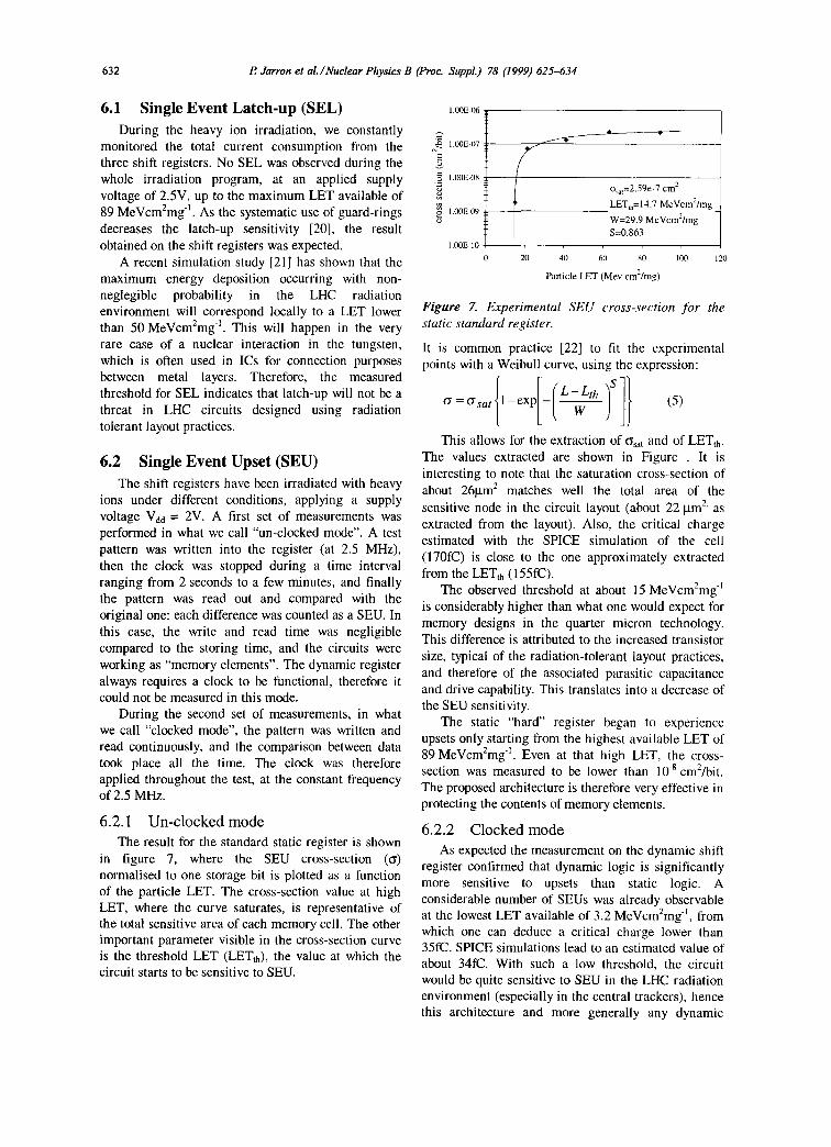
The result for the standard static register is shown in figure 7, where the SEU cross-section (~) normalised to one storage bit is plotted as a function of the particle LET. The cross-section value at high LET, where the curve saturates, is representative of the total sensitive area of each memory cell. The other important parameter visible in the cross-section curve is the threshold LET (LETth), the value at which the circuit starts to be sensitive to SEU.
1.(~)E4)6
~ 1.00E4)7
~ I .(XIE4)8
m ~ 1.00E-09
I.(DE- 10
o~,~t=2.59e-7 cm e
LETth=I 4.7 MeVcm2/mg
W=29.9 MeVcmZ/mg S=0.863
20 40 60 g0 I (X) 120
Particle LET (Mev cm2/mg)
Figure 7. Experimental SEU cross-section for the static standard register.
It is common practice [22] to fit the experimental points with a Weibull curve, using the expression:
~ = ~ s a t 1 - e x p - (5)
This allows for the extraction of ~s,t and of LETth. The values extracted are shown in Figure . It is interesting to note that the saturation cross-section of about 26gm 2 matches well the total area of the sensitive node in the circuit layout (about 22 gm 2' as extracted from the layout). Also, the critical charge estimated with the SPICE simulation of the cell (170fC) is close to the one approximately extracted from the LETth (155fC).
The observed threshold at about 15 MeVcm2mg -1 is considerably higher than what one would expect for memory designs in the quarter micron technology. This difference is attributed to the increased transistor size, typical of the radiation-tolerant layout practices, and therefore of the associated parasitic capacitance and drive capability. This translates into a decrease of the SEU sensitivity.
The static "hard" register began to experience upsets only starting from the highest available LET of 89 MeVcm2mg -~. Even at that high LET, the cross- section was measured to be lower than 10 .8 cm2/bit. The proposed architecture is therefore very effective in protecting the contents of memory elements.
6 .2.2 C locked mode
As expected the measurement on the dynamic shift register confirmed that dynamic logic is significantly more sensitive to upsets than static logic. A considerable number of SEUs was already observable at the lowest LET available of 3.2 MeVcm2mg ~, from which one can deduce a critical charge lower than 35fC. SPICE simulations lead to an estimated value of about 34fC. With such a low threshold, the circuit would be quite sensitive to SEU in the LHC radiation environment (especially in the central trackers), hence this architecture and more generally any dynamic
R Jarron et al./Nuclear Physics B (Proc. Suppl.) 78 (1999) 625-634 633
architecture is not advisable or should be used with great care.
In the clocked mode the static "hard" register also showed a considerable number of errors when the LET was increased to 5.6 MeVcm2mg-[ This is due to the particular architecture of the cell, which was designed as an un-clocked memory cell. During the write phase, the output node does not see any low resistance path to Vdd or Vss for half of the clock period. Therefore, this node can temporarily change its logic state if hit by an ionising particle. This change does not affect the cell itself, which shows the correct output at the end of the write cycle. Nevertheless, in the specific case of the shift register, the momentary corruption of the output presents the wrong data at the input of the next cell. As this happens during the write cycle, the wrong data is latched into the next cell, generating an upset.
7 C O N C L U S I O N
A design method has been presented to make commercial deep submicron technologies tolerant for total ionizing irradiation dose. Our measurements on devices and full mixed mode circuits confirm the validity of the approach. The radiation tolerance depends on the fundamental physics of tunneling in very thin oxides and the use of enclosed device geometry and guard-rings to eliminate leakage paths. The method is therefore independent of the detailed characteristics of a particular technology. Measurements confirm that this design technique also prevents Single Event Latchup. The probability of Single Event Upset is also reduced, and its impact can be minimized by using static registers or upset- tolerant circuit designs in critical functions.
Design in deep submicron technologies has imposed the use of some new design tools, and the radiation-tolerant design methodology has required us to develop special versions of the technology files for physical design rule checking and parasitic extraction. Simple analog models have been developed and a radiation-tolerant digital standard cell library has been designed.
Although these technologies offer very substahtial savings in manufacturing costs, the real cost of the ASICs must still take into account development and testing costs, which will dominate because of the relatively modest production volumes needed by the typical HEP application. However, by turning to deep submicron technologies an order of magnitude reduction in the power consumption of digital chips can be achieved. This could substantially simplify and reduce the cost of infrastructure equipment on the detectors.
REFERENCES
[1] RD9 final status report, A demonstrator analog signal processing circuit in a radiation hard SOI- CMOS technology, CERN/LHCC 97-1, (1997).
[2] RD20 Status report, Development of high resolution silicon strip detectors for experiments at high luminosity at LHC, CERN/LHCC 96-2, (1996).
[3] RD29 status report, DMILL, a mixed analog- digital radiation hard technology for high energy physics electronics, CERN/LHCC 97-15 (1997).
[4] N. Saks et al., Radiation Effects in MOS Capacitors with very thin oxides at 80K, IEEE Trans. Nucl. Science, Vol.31, p. 1249, 1984
[5] N. Saks et al., Generation of interlace states by ionizing radiation in very thin MOS oxides, IEEE-Transactions-on-Nuclear-Science, vol. 33, no.6, p. 1185-90, Dec. 1986.
[6] G. Anelli et al., Total dose behaviour of submicron and deep submicron CMOS technologies, Proceedings of the Third Workshop on Electronics for LHC Experiments, London, Sept. 97, page 139.
[7] F. Faccio et al., Estimate of the Single Event Upset (SEU) rate in CMS,.Proceedings of the Fourth Workshop on Electronics for LHC Experiments, Rome, Sept. 98, p. 119.
[8] A. Marchioro, Deep submicron technology for HEP, Proceedings of the Fourth Workshop on Electronics for LHC Experiments, Rome, Sept. 98, p.40.
[9] K. Kloukinas et al., Development of a radiation tolerant 2.0V standard cell library using a commercial deep submicron CMOS technology for the LHC experiments, Proceedings of the Fourth Workshop on Electronics for LHC Experiments, Rome, Sept. 98, p.574.
[10]P. Jarron, Radiation Tolerant Electronics for the LHC Experiments, Proceedings of the fourth Workshop on Electronics for LHC Experiments, Rome, Sept 98, p.7
[ l l ]W. Snoeys et al., Layout techniques to enhance the radiation tolerance of standard CMOS technologies demonstrated on a pixel readout chip. Presented at the 8th European Symposium on Semiconductor Detectors, Schloss Elmau, Germany, June 14-17. Submitted to Nuclear Instruments and Methods.
[12]M. Campbell et al., A Pixel Readout Chip tbr 10- 30 MRad in Standard 0.25mm CMOS, presented at the IEEE Nuclear Science Symposium, 10-14 Nov. 1998, submitted to IEEE Trans. Nucl. Sci.
634 P. Jarron et al./Nuclear Physics B (Proc. Suppl.) 78 (1999) 625-634
[13] P.V. Dressendorfer, Ionising radiation effects in MOS devices and circuits, Wiley New York, 1989
[14]T.R. Oldham et al., Spatial dependence of holes determined from tunnelling analysis and measured annealing, IEEE Trans. Nucl. Science, Vol.33, No.6, p.1203, December 1986.
[15]J.M. Benedetto et al., Hole removal in thin-gate MOSFETS by tunnelling, IEEE Trans. Nucl. Science, Vol.32, No.6, p.3916, December 1985.
[16]A. Giraldo, PhD thesis, Padova University, December 1998.
[17] R. Velazco et al., 2 CMOS Memory Cells Suitable for the Design of SEU-Tolerant VLSI Circuits, IEEE Trans. Nucl. Science, Vol.41, No.6, p.2229, December 1994.
[18] T. Calin et al., Upset Hardened Memory Design for Submicron CMOS Technology, IEEE Trans. Nucl. Science, Vol.43, No.6, p.2874, December 1996.
[19]J. Yuan, C. Svensson, New Single-Clock CMOS Latches and Flip-Flops with Improved Speed and Power Savings, IEEE Journal of Solid-State Circuits, Vol.32, No.l, Jan. 1997
[20] T. Aoki, Dynamics of heavy-ion-induced latchup in CMOS structure", IEEE Trans. El. Dev, Vol.35, No.l 1, p.1885, November 1988.
[21]F.Faccio, C.Detcheverry, M.Huhtinen, First evaluation of the Single Event Upset (SEU) risk for electronics in the CMS experiment, CERN CMS NOTE 1998/054 (1998).
[22]G.C. Messenger, M.S. Ash, Single Event Phenomena, Chapman & Hall, 1997.