dacx760 single-channel, 12 - texas instruments
TRANSCRIPT
DACx760 Single-Channel, 12- and 16-Bit Programmable Current and Voltage OutputDigital-to-Analog Converters for 4-mA to 20-mA Current-Loop Applications
1 Features• Current output: 4 mA to 20 mA;
0 mA to 20 mA; 0 mA to 24 mA• Voltage output:
– 0 V to 5 V; 0 V to 10 V; ±5 V; ±10 V– 0 V to 5.5 V; 0 V to 11 V; ±5.5 V; ±11 V
(10% overrange)• ±0.1% FSR total unadjusted error (TUE) maximum• DNL: ±1 LSB maximum• Simultaneous voltage and current output• Internal 5-V reference (10 ppm/°C, maximum)• Internal 4.6-V power-supply output• Reliability features:
– CRC check and watchdog timer– Thermal alarm– Open alarm, short current limit
• Wide temperature range: –40°C to 125°C• Packages: 6-mm × 6-mm 40-pin VQFN and 24-pin
HTSSOP
2 Applications• Analog output module• CPU (PLC controller)• HVAC valve and actuator control• Flow transmitter• Other sensor transmitter• Actuator
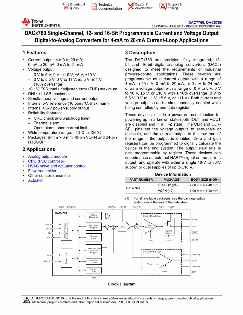
3 DescriptionThe DACx760 are precision, fully integrated, 12-bit and 16-bit digital-to-analog converters (DACs) designed to meet the requirements of industrial process-control applications. These devices are programmable as a current output with a range of 4 mA to 20 mA, 0 mA to 20 mA, or 0 mA to 24 mA; or as a voltage output with a range of 0 V to 5 V, 0 V to 10 V, ±5 V, or ±10 V with a 10% overrange (0 V to 5.5 V, 0 V to 11 V, ±5.5 V, or ±11 V). Both current and voltage outputs can be simultaneously enabled while being controlled by one data register.
These devices include a power-on-reset function for powering up in a known state (both IOUT and VOUT are disabled and in a Hi-Z state). The CLR and CLR-SEL pins set the voltage outputs to zero-scale or midscale, and the current output to the low end of the range if the output is enabled. Zero and gain registers can be programmed to digitally calibrate the device in the end system. The output slew rate is also programmable by register. These devices can superimpose an external HART® signal on the current output, and operate with either a single 10-V to 36-V supply, or dual supplies of up to ±18 V.
Device InformationPART NUMBER PACKAGE(1) BODY SIZE (NOM)
DACx760HTSSOP (24) 7.80 mm × 4.40 mm
VQFN (40) 6.00 mm × 6.00 mm
(1) For all available packages, see the package option addendum at the end of the data sheet.
DAC
GND
DACx760
AVDDDVDD-EN AVSSDVDD
Pre-Conditioning
CurrentSource
IENABLE ISET-RIGAIN
VGAIN
VENABLE
Current Output Stage
Voltage Output Stage
WatchdogTimer
Slew RateControl
User CalibrationGain/Offset
Register
DAC InputRegister
ThermalAlarm
InternalReference
SP
I S
hift
Re
gis
ter
Inp
ut
Co
ntr
ol L
og
icC
on
tro
l L
og
ic
CMP
–VSENSE
+VSENSE
VOUT
IOUT
ALARM
BOOST
REFOUT REFIN HART-IN
LATCH
SCLK
DIN
SDO
CLR
CLR-SEL
Block Diagram
DAC7760, DAC8760SBAS528D – JUNE 2013 – REVISED DECEMBER 2021
An IMPORTANT NOTICE at the end of this data sheet addresses availability, warranty, changes, use in safety-critical applications, intellectual property matters and other important disclaimers. PRODUCTION DATA.
Table of Contents1 Features............................................................................12 Applications..................................................................... 13 Description.......................................................................14 Revision History.............................................................. 25 Device Comparison Table...............................................36 Pin Configuration and Functions...................................37 Specifications.................................................................. 5
7.1 Absolute Maximum Ratings........................................ 57.2 ESD Ratings............................................................... 57.3 Recommended Operating Conditions.........................57.4 Thermal Information....................................................67.5 Electrical Characteristics.............................................67.6 Electrical Characteristics: AC....................................117.7 Timing Requirements: Write Mode............................127.8 Timing Requirements: Readback Mode....................127.9 Timing Diagrams.......................................................137.10 Typical Characteristics............................................ 14
8 Detailed Description......................................................278.1 Overview................................................................... 278.2 Functional Block Diagram......................................... 27
8.3 Feature Description...................................................288.4 Device Functional Modes..........................................378.5 Programming............................................................ 408.6 Register Maps...........................................................42
9 Application and Implementation.................................. 469.1 Application Information............................................. 469.2 Typical Application.................................................... 49
10 Power Supply Recommendations..............................5211 Layout...........................................................................53
11.1 Layout Guidelines................................................... 5311.2 Layout Example...................................................... 54
12 Device and Documentation Support..........................5512.1 Documentation Support.......................................... 5512.2 Receiving Notification of Documentation Updates..5512.3 Support Resources................................................. 5512.4 Trademarks.............................................................5512.5 Electrostatic Discharge Caution..............................5512.6 Glossary..................................................................55
13 Mechanical, Packaging, and Orderable Information.................................................................... 55
4 Revision HistoryNOTE: Page numbers for previous revisions may differ from page numbers in the current version.
Changes from Revision C (January 2018) to Revision D (December 2021) Page• Updated the numbering format for tables, figures, and cross-references throughout the document..................1• Changed CMP pin description in Pin Functions table to include 100-pF capacitance to ground....................... 3• Deleted Timing Requirements: Daisy-Chain Mode section and Daisy-Chain Mode Timing figure...................13• Added 100-pF capacitance to ground for larger external compensation capacitors in Voltage Output Stage
section.............................................................................................................................................................. 28• Deleted Power-Supply Sequence section........................................................................................................ 31• Deleted daisy-chain operation content from Watchdog Timer section..............................................................33• Deleted The DACx760 Shares the SPI Bus With Other Devices subsection from Watchdog Timer section... 33• Deleted daisy-chain operation content from Frame Error Checking section.................................................... 33• Added CRC fault software reset command of 0x96 to Frame Error Checking section.....................................33• Deleted The DACx760 Shares the SPI Bus With Other Devices subsection from Frame Error Checking
section.............................................................................................................................................................. 33• Changed duplicated 010 step-size from 0.125 to 0.25 in Table 8-3, Slew Rate Step-Size Options ................ 35• Added CRC fault reset command to Table 8-8, Write Address Functions ....................................................... 40• Deleted Daisy-Chain Operation section............................................................................................................41• Added Multiple Devices on the Bus section......................................................................................................41• Changed Command and Register Map table to delete daisy-chain operation content and add CRC fault reset
content.............................................................................................................................................................. 42• Changed DCEN to Reserved for DB3 in Table 8-17, Control Register ............................................................43• Added series resistance for supply and 100-pF capacitance from CMP to GND for Figure 9-3...................... 49• Added text on fast supply ramp, series resistance for power supply, and content from deleted Power-Supply
Sequence to the Power Supply Recommendations section............................................................................. 52• Added power supply series resistance and CMP capacitor to GND to Figure 11-1, Layout Example .............54
Changes from Revision B (June 2016) to Revision C (January 2018) Page• Added first sentence to second paragraph and added last paragraph to Frame Error Checking section........ 33• Added last paragraph to User Calibration section ........................................................................................... 34
DAC7760, DAC8760SBAS528D – JUNE 2013 – REVISED DECEMBER 2021 www.ti.com
2 Submit Document Feedback Copyright © 2021 Texas Instruments Incorporated
Product Folder Links: DAC7760 DAC8760
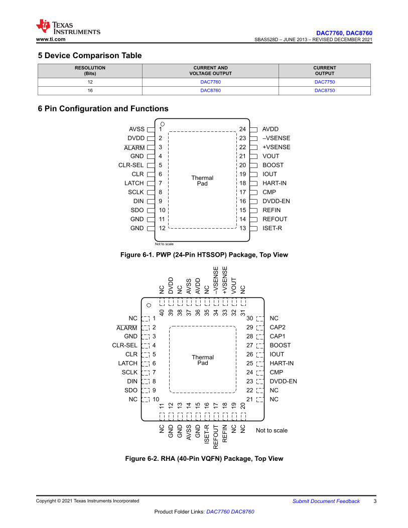
5 Device Comparison TableRESOLUTION
(Bits)CURRENT AND
VOLTAGE OUTPUTCURRENTOUTPUT
12 DAC7760 DAC7750
16 DAC8760 DAC8750
6 Pin Configuration and Functions
Not to scale
Thermal
Pad
1AVSS 24 AVDD
2DVDD 23 –VSENSE
3ALARM 22 +VSENSE
4GND 21 VOUT
5CLR-SEL 20 BOOST
6CLR 19 IOUT
7LATCH 18 HART-IN
8SCLK 17 CMP
9DIN 16 DVDD-EN
10SDO 15 REFIN
11GND 14 REFOUT
12GND 13 ISET-R
Figure 6-1. PWP (24-Pin HTSSOP) Package, Top View
Not to scale
Thermal
Pad
40
NC
11
NC
1NC 30 NC
39
DV
DD
12
GN
D
2ALARM 29 CAP2
38
NC
13
GN
D
3GND 28 CAP1
37
AV
SS
14
AV
SS
4CLR-SEL 27 BOOST
36
AV
DD
15
GN
D
5CLR 26 IOUT
35
NC
16
ISE
T-R
6LATCH 25 HART-IN
34
–V
SE
NS
E17
RE
FO
UT
7SCLK 24 CMP
33
+V
SE
NS
E18
RE
FIN
8DIN 23 DVDD-EN
32
VO
UT
19
NC
9SDO 22 NC
31
NC
20
NC
10NC 21 NC
Figure 6-2. RHA (40-Pin VQFN) Package, Top View
www.ti.comDAC7760, DAC8760
SBAS528D – JUNE 2013 – REVISED DECEMBER 2021
Copyright © 2021 Texas Instruments Incorporated Submit Document Feedback 3
Product Folder Links: DAC7760 DAC8760
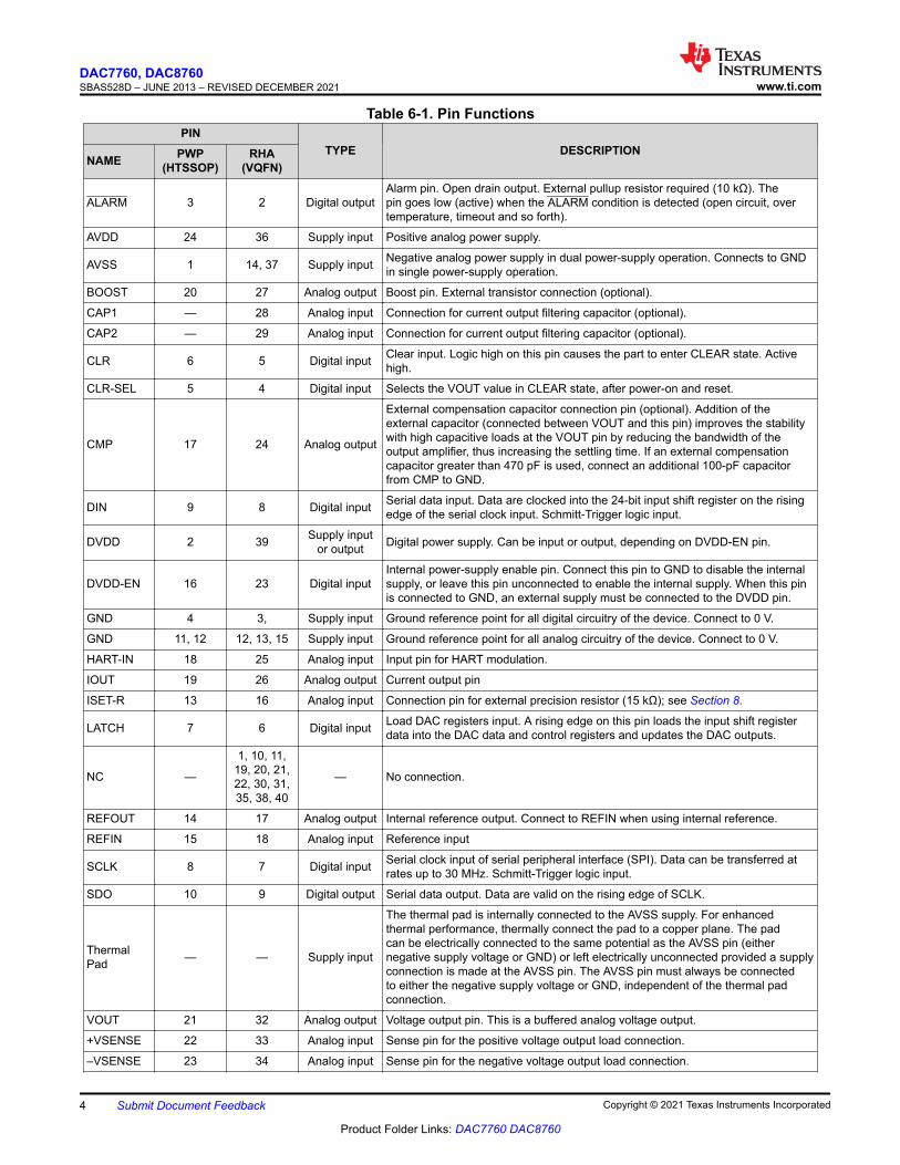
Table 6-1. Pin FunctionsPIN
TYPE DESCRIPTIONNAME PWP
(HTSSOP)RHA
(VQFN)
ALARM 3 2 Digital outputAlarm pin. Open drain output. External pullup resistor required (10 kΩ). The pin goes low (active) when the ALARM condition is detected (open circuit, over temperature, timeout and so forth).
AVDD 24 36 Supply input Positive analog power supply.
AVSS 1 14, 37 Supply input Negative analog power supply in dual power-supply operation. Connects to GND in single power-supply operation.
BOOST 20 27 Analog output Boost pin. External transistor connection (optional).
CAP1 — 28 Analog input Connection for current output filtering capacitor (optional).
CAP2 — 29 Analog input Connection for current output filtering capacitor (optional).
CLR 6 5 Digital input Clear input. Logic high on this pin causes the part to enter CLEAR state. Active high.
CLR-SEL 5 4 Digital input Selects the VOUT value in CLEAR state, after power-on and reset.
CMP 17 24 Analog output
External compensation capacitor connection pin (optional). Addition of the external capacitor (connected between VOUT and this pin) improves the stability with high capacitive loads at the VOUT pin by reducing the bandwidth of the output amplifier, thus increasing the settling time. If an external compensation capacitor greater than 470 pF is used, connect an additional 100-pF capacitor from CMP to GND.
DIN 9 8 Digital input Serial data input. Data are clocked into the 24-bit input shift register on the rising edge of the serial clock input. Schmitt-Trigger logic input.
DVDD 2 39 Supply input or output Digital power supply. Can be input or output, depending on DVDD-EN pin.
DVDD-EN 16 23 Digital inputInternal power-supply enable pin. Connect this pin to GND to disable the internal supply, or leave this pin unconnected to enable the internal supply. When this pin is connected to GND, an external supply must be connected to the DVDD pin.
GND 4 3, Supply input Ground reference point for all digital circuitry of the device. Connect to 0 V.
GND 11, 12 12, 13, 15 Supply input Ground reference point for all analog circuitry of the device. Connect to 0 V.
HART-IN 18 25 Analog input Input pin for HART modulation.
IOUT 19 26 Analog output Current output pin
ISET-R 13 16 Analog input Connection pin for external precision resistor (15 kΩ); see Section 8.
LATCH 7 6 Digital input Load DAC registers input. A rising edge on this pin loads the input shift register data into the DAC data and control registers and updates the DAC outputs.
NC —
1, 10, 11, 19, 20, 21, 22, 30, 31, 35, 38, 40
— No connection.
REFOUT 14 17 Analog output Internal reference output. Connect to REFIN when using internal reference.
REFIN 15 18 Analog input Reference input
SCLK 8 7 Digital input Serial clock input of serial peripheral interface (SPI). Data can be transferred at rates up to 30 MHz. Schmitt-Trigger logic input.
SDO 10 9 Digital output Serial data output. Data are valid on the rising edge of SCLK.
Thermal Pad — — Supply input
The thermal pad is internally connected to the AVSS supply. For enhanced thermal performance, thermally connect the pad to a copper plane. The pad can be electrically connected to the same potential as the AVSS pin (either negative supply voltage or GND) or left electrically unconnected provided a supply connection is made at the AVSS pin. The AVSS pin must always be connected to either the negative supply voltage or GND, independent of the thermal pad connection.
VOUT 21 32 Analog output Voltage output pin. This is a buffered analog voltage output.
+VSENSE 22 33 Analog input Sense pin for the positive voltage output load connection.
–VSENSE 23 34 Analog input Sense pin for the negative voltage output load connection.
DAC7760, DAC8760SBAS528D – JUNE 2013 – REVISED DECEMBER 2021 www.ti.com
4 Submit Document Feedback Copyright © 2021 Texas Instruments Incorporated
Product Folder Links: DAC7760 DAC8760
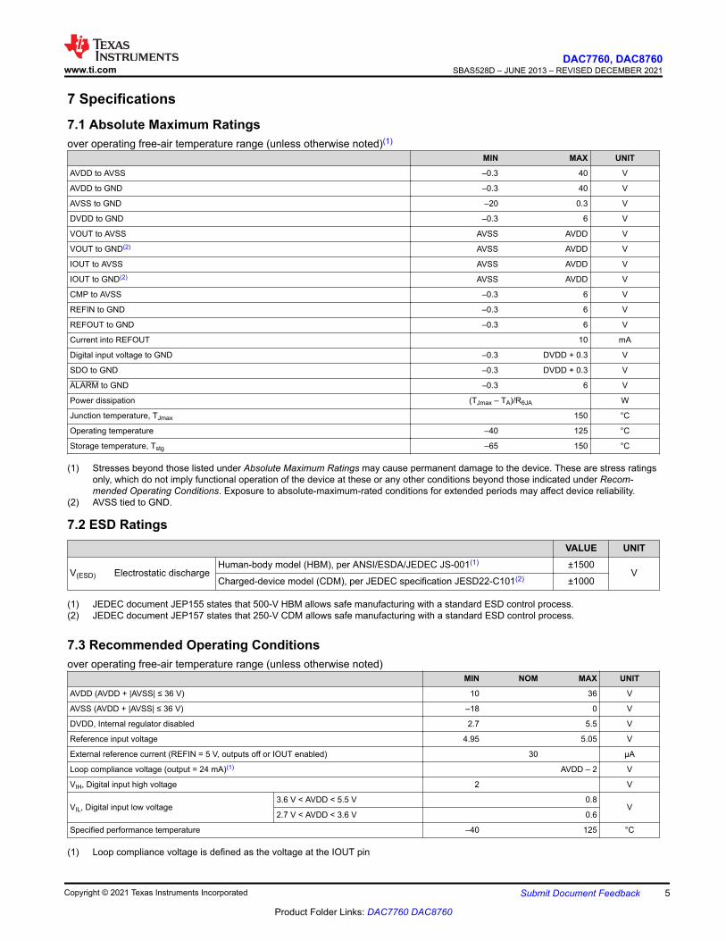
7 Specifications7.1 Absolute Maximum Ratingsover operating free-air temperature range (unless otherwise noted)(1)
MIN MAX UNIT
AVDD to AVSS –0.3 40 V
AVDD to GND –0.3 40 V
AVSS to GND –20 0.3 V
DVDD to GND –0.3 6 V
VOUT to AVSS AVSS AVDD V
VOUT to GND(2) AVSS AVDD V
IOUT to AVSS AVSS AVDD V
IOUT to GND(2) AVSS AVDD V
CMP to AVSS –0.3 6 V
REFIN to GND –0.3 6 V
REFOUT to GND –0.3 6 V
Current into REFOUT 10 mA
Digital input voltage to GND –0.3 DVDD + 0.3 V
SDO to GND –0.3 DVDD + 0.3 V
ALARM to GND –0.3 6 V
Power dissipation (TJmax – TA)/RθJA W
Junction temperature, TJmax 150 °C
Operating temperature –40 125 °C
Storage temperature, Tstg –65 150 °C
(1) Stresses beyond those listed under Absolute Maximum Ratings may cause permanent damage to the device. These are stress ratings only, which do not imply functional operation of the device at these or any other conditions beyond those indicated under Recom- mended Operating Conditions. Exposure to absolute-maximum-rated conditions for extended periods may affect device reliability.
(2) AVSS tied to GND.
7.2 ESD RatingsVALUE UNIT
V(ESD) Electrostatic dischargeHuman-body model (HBM), per ANSI/ESDA/JEDEC JS-001(1) ±1500
VCharged-device model (CDM), per JEDEC specification JESD22-C101(2) ±1000
(1) JEDEC document JEP155 states that 500-V HBM allows safe manufacturing with a standard ESD control process.(2) JEDEC document JEP157 states that 250-V CDM allows safe manufacturing with a standard ESD control process.
7.3 Recommended Operating Conditionsover operating free-air temperature range (unless otherwise noted)
MIN NOM MAX UNIT
AVDD (AVDD + |AVSS| ≤ 36 V) 10 36 V
AVSS (AVDD + |AVSS| ≤ 36 V) –18 0 V
DVDD, Internal regulator disabled 2.7 5.5 V
Reference input voltage 4.95 5.05 V
External reference current (REFIN = 5 V, outputs off or IOUT enabled) 30 µA
Loop compliance voltage (output = 24 mA)(1) AVDD – 2 V
VIH, Digital input high voltage 2 V
VIL, Digital input low voltage3.6 V < AVDD < 5.5 V 0.8
V2.7 V < AVDD < 3.6 V 0.6
Specified performance temperature –40 125 °C
(1) Loop compliance voltage is defined as the voltage at the IOUT pin
www.ti.comDAC7760, DAC8760
SBAS528D – JUNE 2013 – REVISED DECEMBER 2021
Copyright © 2021 Texas Instruments Incorporated Submit Document Feedback 5
Product Folder Links: DAC7760 DAC8760
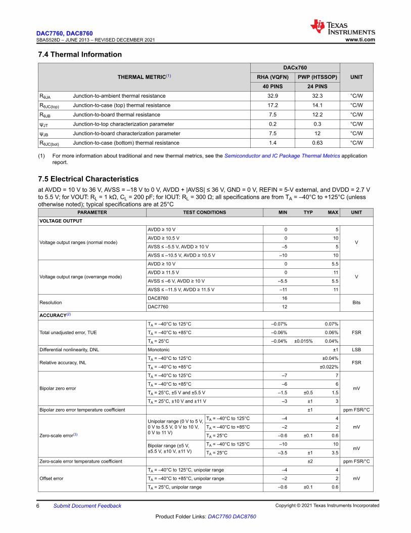
7.4 Thermal Information
THERMAL METRIC(1)
DACx760UNITRHA (VQFN) PWP (HTSSOP)
40 PINS 24 PINSRθJA Junction-to-ambient thermal resistance 32.9 32.3 °C/W
RθJC(top) Junction-to-case (top) thermal resistance 17.2 14.1 °C/W
RθJB Junction-to-board thermal resistance 7.5 12.2 °C/W
ψJT Junction-to-top characterization parameter 0.2 0.3 °C/W
ψJB Junction-to-board characterization parameter 7.5 12 °C/W
RθJC(bot) Junction-to-case (bottom) thermal resistance 1.4 0.63 °C/W
(1) For more information about traditional and new thermal metrics, see the Semiconductor and IC Package Thermal Metrics application report.
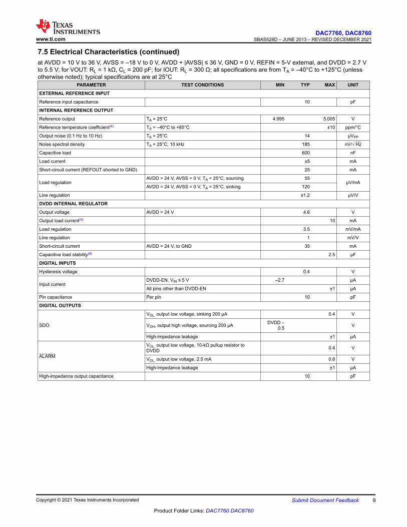
7.5 Electrical Characteristicsat AVDD = 10 V to 36 V, AVSS = –18 V to 0 V, AVDD + |AVSS| ≤ 36 V, GND = 0 V, REFIN = 5-V external, and DVDD = 2.7 V to 5.5 V; for VOUT: RL = 1 kΩ, CL = 200 pF; for IOUT: RL = 300 Ω; all specifications are from TA = –40°C to +125°C (unless otherwise noted); typical specifications are at 25°C
PARAMETER TEST CONDITIONS MIN TYP MAX UNIT
VOLTAGE OUTPUT
Voltage output ranges (normal mode)
AVDD ≥ 10 V 0 5
VAVDD ≥ 10.5 V 0 10
AVSS ≤ –5.5 V, AVDD ≥ 10 V –5 5
AVSS ≤ –10.5 V, AVDD ≥ 10.5 V –10 10
Voltage output range (overrange mode)
AVDD ≥ 10 V 0 5.5
VAVDD ≥ 11.5 V 0 11
AVSS ≤ –6 V, AVDD ≥ 10 V –5.5 5.5
AVSS ≤ –11.5 V, AVDD ≥ 11.5 V –11 11
ResolutionDAC8760 16
BitsDAC7760 12
ACCURACY(2)
Total unadjusted error, TUE
TA = –40°C to 125°C –0.07% 0.07%
FSRTA = –40°C to +85°C –0.06% 0.06%
TA = 25°C –0.04% ±0.015% 0.04%
Differential nonlinearity, DNL Monotonic ±1 LSB
Relative accuracy, INLTA = –40°C to 125°C ±0.04%
FSRTA = –40°C to +85°C ±0.022%
Bipolar zero error
TA = –40°C to 125°C –7 7
mVTA = –40°C to +85°C –6 6
TA = 25°C, ±5 V and ±5.5 V –1.5 ±0.5 1.5
TA = 25°C, ±10 V and ±11 V –3 ±1 3
Bipolar zero error temperature coefficient ±1 ppm FSR/°C
Zero-scale error(3)
Unipolar range (0 V to 5 V, 0 V to 5.5 V, 0 V to 10 V, 0 V to 11 V)
TA = –40°C to 125°C –4 4
mVTA = –40°C to +85°C –2 2
TA = 25°C –0.6 ±0.1 0.6
Bipolar range (±5 V, ±5.5 V, ±10 V, ±11 V)
TA = –40°C to 125°C –10 10mV
TA = 25°C –3.5 ±1 3.5
Zero-scale error temperature coefficient ±2 ppm FSR/°C
Offset error
TA = –40°C to 125°C, unipolar range –4 4
mVTA = –40°C to +85°C, unipolar range –2 2
TA = 25°C, unipolar range –0.6 ±0.1 0.6
DAC7760, DAC8760SBAS528D – JUNE 2013 – REVISED DECEMBER 2021 www.ti.com
6 Submit Document Feedback Copyright © 2021 Texas Instruments Incorporated
Product Folder Links: DAC7760 DAC8760
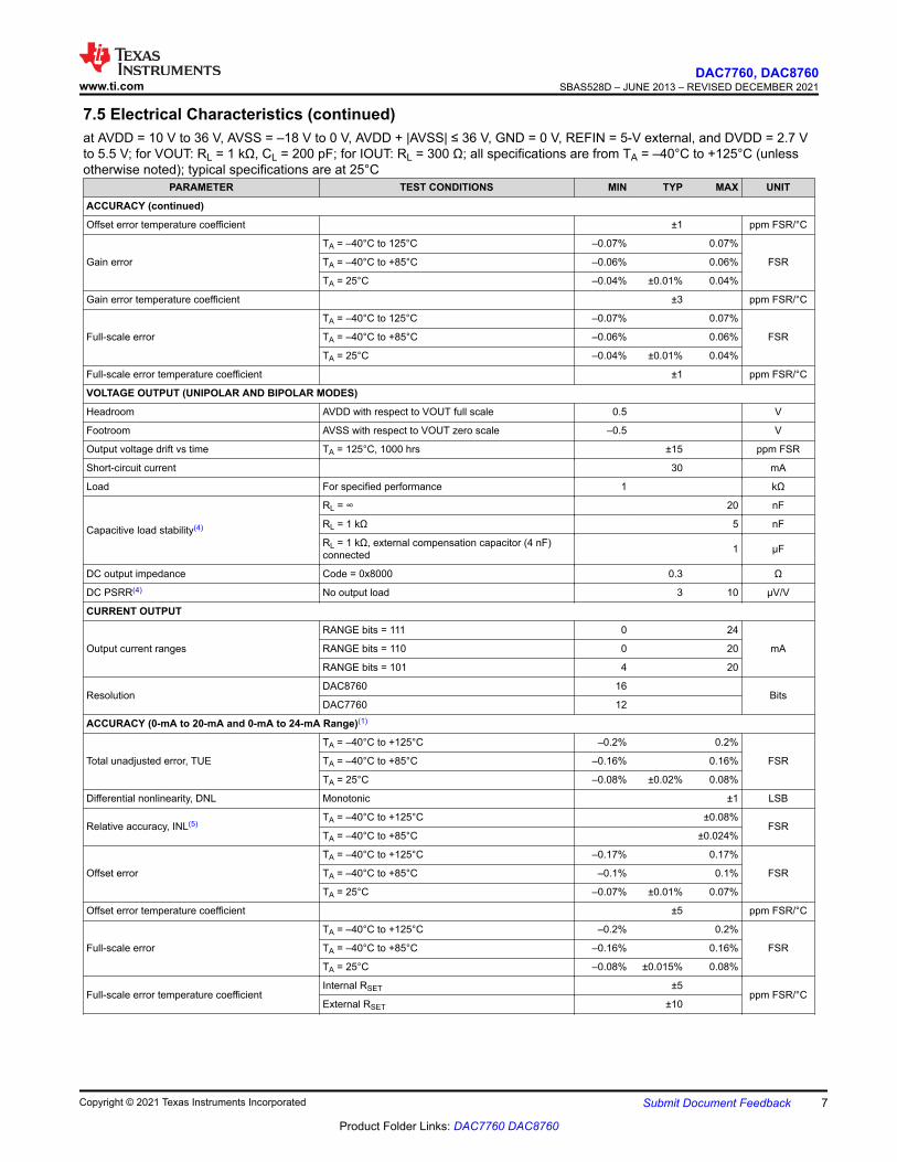
7.5 Electrical Characteristics (continued)at AVDD = 10 V to 36 V, AVSS = –18 V to 0 V, AVDD + |AVSS| ≤ 36 V, GND = 0 V, REFIN = 5-V external, and DVDD = 2.7 V to 5.5 V; for VOUT: RL = 1 kΩ, CL = 200 pF; for IOUT: RL = 300 Ω; all specifications are from TA = –40°C to +125°C (unless otherwise noted); typical specifications are at 25°C
PARAMETER TEST CONDITIONS MIN TYP MAX UNIT
ACCURACY (continued)
Offset error temperature coefficient ±1 ppm FSR/°C
Gain error
TA = –40°C to 125°C –0.07% 0.07%
FSRTA = –40°C to +85°C –0.06% 0.06%
TA = 25°C –0.04% ±0.01% 0.04%
Gain error temperature coefficient ±3 ppm FSR/°C
Full-scale error
TA = –40°C to 125°C –0.07% 0.07%
FSRTA = –40°C to +85°C –0.06% 0.06%
TA = 25°C –0.04% ±0.01% 0.04%
Full-scale error temperature coefficient ±1 ppm FSR/°C
VOLTAGE OUTPUT (UNIPOLAR AND BIPOLAR MODES)
Headroom AVDD with respect to VOUT full scale 0.5 V
Footroom AVSS with respect to VOUT zero scale –0.5 V
Output voltage drift vs time TA = 125°C, 1000 hrs ±15 ppm FSR
Short-circuit current 30 mA
Load For specified performance 1 kΩ
Capacitive load stability(4)
RL = ∞ 20 nF
RL = 1 kΩ 5 nF
RL = 1 kΩ, external compensation capacitor (4 nF) connected 1 µF
DC output impedance Code = 0x8000 0.3 Ω
DC PSRR(4) No output load 3 10 µV/V
CURRENT OUTPUT
Output current ranges
RANGE bits = 111 0 24
mARANGE bits = 110 0 20
RANGE bits = 101 4 20
ResolutionDAC8760 16
BitsDAC7760 12
ACCURACY (0-mA to 20-mA and 0-mA to 24-mA Range)(1)
Total unadjusted error, TUE
TA = –40°C to +125°C –0.2% 0.2%
FSRTA = –40°C to +85°C –0.16% 0.16%
TA = 25°C –0.08% ±0.02% 0.08%
Differential nonlinearity, DNL Monotonic ±1 LSB
Relative accuracy, INL(5)TA = –40°C to +125°C ±0.08%
FSRTA = –40°C to +85°C ±0.024%
Offset error
TA = –40°C to +125°C –0.17% 0.17%
FSRTA = –40°C to +85°C –0.1% 0.1%
TA = 25°C –0.07% ±0.01% 0.07%
Offset error temperature coefficient ±5 ppm FSR/°C
Full-scale error
TA = –40°C to +125°C –0.2% 0.2%
FSRTA = –40°C to +85°C –0.16% 0.16%
TA = 25°C –0.08% ±0.015% 0.08%
Full-scale error temperature coefficientInternal RSET ±5
ppm FSR/°CExternal RSET ±10
www.ti.comDAC7760, DAC8760
SBAS528D – JUNE 2013 – REVISED DECEMBER 2021
Copyright © 2021 Texas Instruments Incorporated Submit Document Feedback 7
Product Folder Links: DAC7760 DAC8760
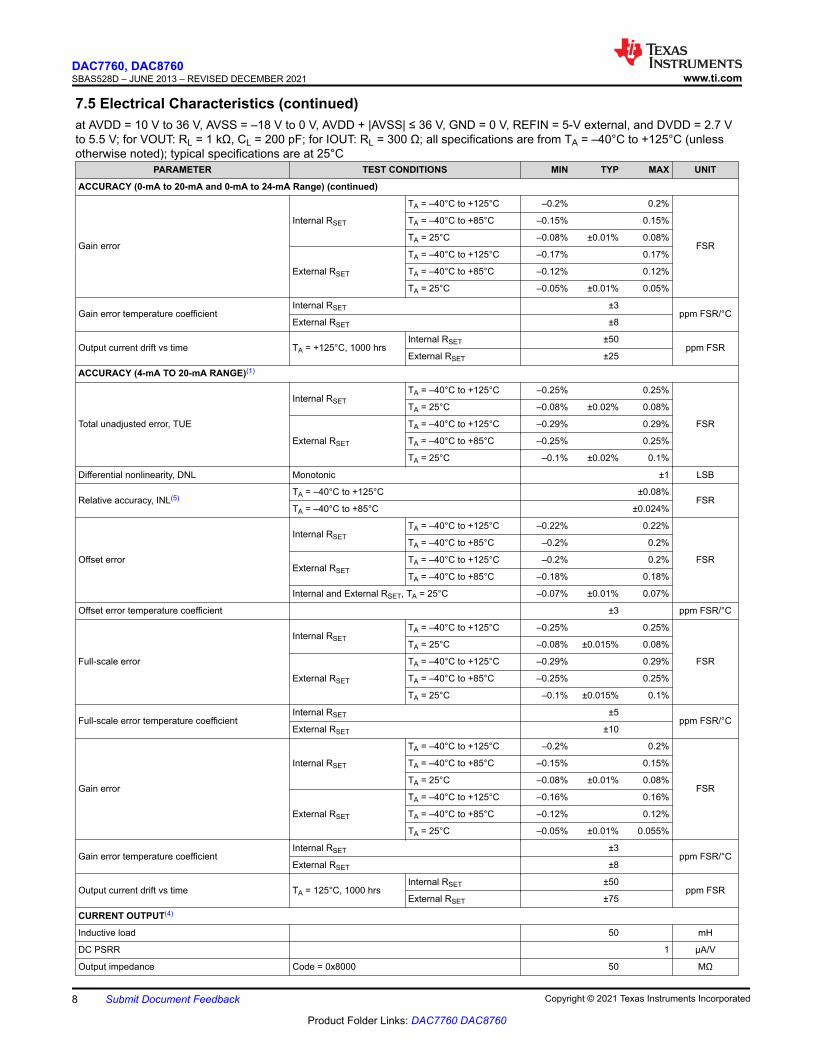
7.5 Electrical Characteristics (continued)at AVDD = 10 V to 36 V, AVSS = –18 V to 0 V, AVDD + |AVSS| ≤ 36 V, GND = 0 V, REFIN = 5-V external, and DVDD = 2.7 V to 5.5 V; for VOUT: RL = 1 kΩ, CL = 200 pF; for IOUT: RL = 300 Ω; all specifications are from TA = –40°C to +125°C (unless otherwise noted); typical specifications are at 25°C
PARAMETER TEST CONDITIONS MIN TYP MAX UNIT
ACCURACY (0-mA to 20-mA and 0-mA to 24-mA Range) (continued)
Gain error
Internal RSET
TA = –40°C to +125°C –0.2% 0.2%
FSR
TA = –40°C to +85°C –0.15% 0.15%
TA = 25°C –0.08% ±0.01% 0.08%
External RSET
TA = –40°C to +125°C –0.17% 0.17%
TA = –40°C to +85°C –0.12% 0.12%
TA = 25°C –0.05% ±0.01% 0.05%
Gain error temperature coefficientInternal RSET ±3
ppm FSR/°CExternal RSET ±8
Output current drift vs time TA = +125°C, 1000 hrsInternal RSET ±50
ppm FSRExternal RSET ±25
ACCURACY (4-mA TO 20-mA RANGE)(1)
Total unadjusted error, TUE
Internal RSETTA = –40°C to +125°C –0.25% 0.25%
FSR
TA = 25°C –0.08% ±0.02% 0.08%
External RSET
TA = –40°C to +125°C –0.29% 0.29%
TA = –40°C to +85°C –0.25% 0.25%
TA = 25°C –0.1% ±0.02% 0.1%
Differential nonlinearity, DNL Monotonic ±1 LSB
Relative accuracy, INL(5)TA = –40°C to +125°C ±0.08%
FSRTA = –40°C to +85°C ±0.024%
Offset error
Internal RSETTA = –40°C to +125°C –0.22% 0.22%
FSR
TA = –40°C to +85°C –0.2% 0.2%
External RSETTA = –40°C to +125°C –0.2% 0.2%
TA = –40°C to +85°C –0.18% 0.18%
Internal and External RSET, TA = 25°C –0.07% ±0.01% 0.07%
Offset error temperature coefficient ±3 ppm FSR/°C
Full-scale error
Internal RSETTA = –40°C to +125°C –0.25% 0.25%
FSR
TA = 25°C –0.08% ±0.015% 0.08%
External RSET
TA = –40°C to +125°C –0.29% 0.29%
TA = –40°C to +85°C –0.25% 0.25%
TA = 25°C –0.1% ±0.015% 0.1%
Full-scale error temperature coefficientInternal RSET ±5
ppm FSR/°CExternal RSET ±10
Gain error
Internal RSET
TA = –40°C to +125°C –0.2% 0.2%
FSR
TA = –40°C to +85°C –0.15% 0.15%
TA = 25°C –0.08% ±0.01% 0.08%
External RSET
TA = –40°C to +125°C –0.16% 0.16%
TA = –40°C to +85°C –0.12% 0.12%
TA = 25°C –0.05% ±0.01% 0.055%
Gain error temperature coefficientInternal RSET ±3
ppm FSR/°CExternal RSET ±8
Output current drift vs time TA = 125°C, 1000 hrsInternal RSET ±50
ppm FSRExternal RSET ±75
CURRENT OUTPUT(4)
Inductive load 50 mH
DC PSRR 1 µA/V
Output impedance Code = 0x8000 50 MΩ
DAC7760, DAC8760SBAS528D – JUNE 2013 – REVISED DECEMBER 2021 www.ti.com
8 Submit Document Feedback Copyright © 2021 Texas Instruments Incorporated
Product Folder Links: DAC7760 DAC8760
7.5 Electrical Characteristics (continued)at AVDD = 10 V to 36 V, AVSS = –18 V to 0 V, AVDD + |AVSS| ≤ 36 V, GND = 0 V, REFIN = 5-V external, and DVDD = 2.7 V to 5.5 V; for VOUT: RL = 1 kΩ, CL = 200 pF; for IOUT: RL = 300 Ω; all specifications are from TA = –40°C to +125°C (unless otherwise noted); typical specifications are at 25°C
PARAMETER TEST CONDITIONS MIN TYP MAX UNIT
EXTERNAL REFERENCE INPUT
Reference input capacitance 10 pF
INTERNAL REFERENCE OUTPUT
Reference output TA = 25°C 4.995 5.005 V
Reference temperature coefficient(4) TA = –40°C to +85°C ±10 ppm/°C
Output noise (0.1 Hz to 10 Hz) TA = 25°C 14 µVPP
Noise spectral density TA = 25°C, 10 kHz 185 nV/√ Hz
Capacitive load 600 nF
Load current ±5 mA
Short-circuit current (REFOUT shorted to GND) 25 mA
Load regulationAVDD = 24 V, AVSS = 0 V, TA = 25°C, sourcing 55
µV/mAAVDD = 24 V, AVSS = 0 V, TA = 25°C, sinking 120
Line regulation ±1.2 µV/V
DVDD INTERNAL REGULATOR
Output voltage AVDD = 24 V 4.6 V
Output load current(4) 10 mA
Load regulation 3.5 mV/mA
Line regulation 1 mV/V
Short-circuit current AVDD = 24 V, to GND 35 mA
Capacitive load stability(4) 2.5 µF
DIGITAL INPUTS
Hysteresis voltage 0.4 V
Input currentDVDD-EN, VIN ≤ 5 V –2.7 µA
All pins other than DVDD-EN ±1 µA
Pin capacitance Per pin 10 pF
DIGITAL OUTPUTS
SDO
VOL, output low voltage, sinking 200 µA 0.4 V
VOH, output high voltage, sourcing 200 µA DVDD – 0.5 V
High-impedance leakage ±1 µA
ALARM
VOL, output low voltage, 10-kΩ pullup resistor to DVDD 0.4 V
VOL, output low voltage, 2.5 mA 0.6 V
High-impedance leakage ±1 µA
High-impedance output capacitance 10 pF
www.ti.comDAC7760, DAC8760
SBAS528D – JUNE 2013 – REVISED DECEMBER 2021
Copyright © 2021 Texas Instruments Incorporated Submit Document Feedback 9
Product Folder Links: DAC7760 DAC8760
7.5 Electrical Characteristics (continued)at AVDD = 10 V to 36 V, AVSS = –18 V to 0 V, AVDD + |AVSS| ≤ 36 V, GND = 0 V, REFIN = 5-V external, and DVDD = 2.7 V to 5.5 V; for VOUT: RL = 1 kΩ, CL = 200 pF; for IOUT: RL = 300 Ω; all specifications are from TA = –40°C to +125°C (unless otherwise noted); typical specifications are at 25°C
PARAMETER TEST CONDITIONS MIN TYP MAX UNIT
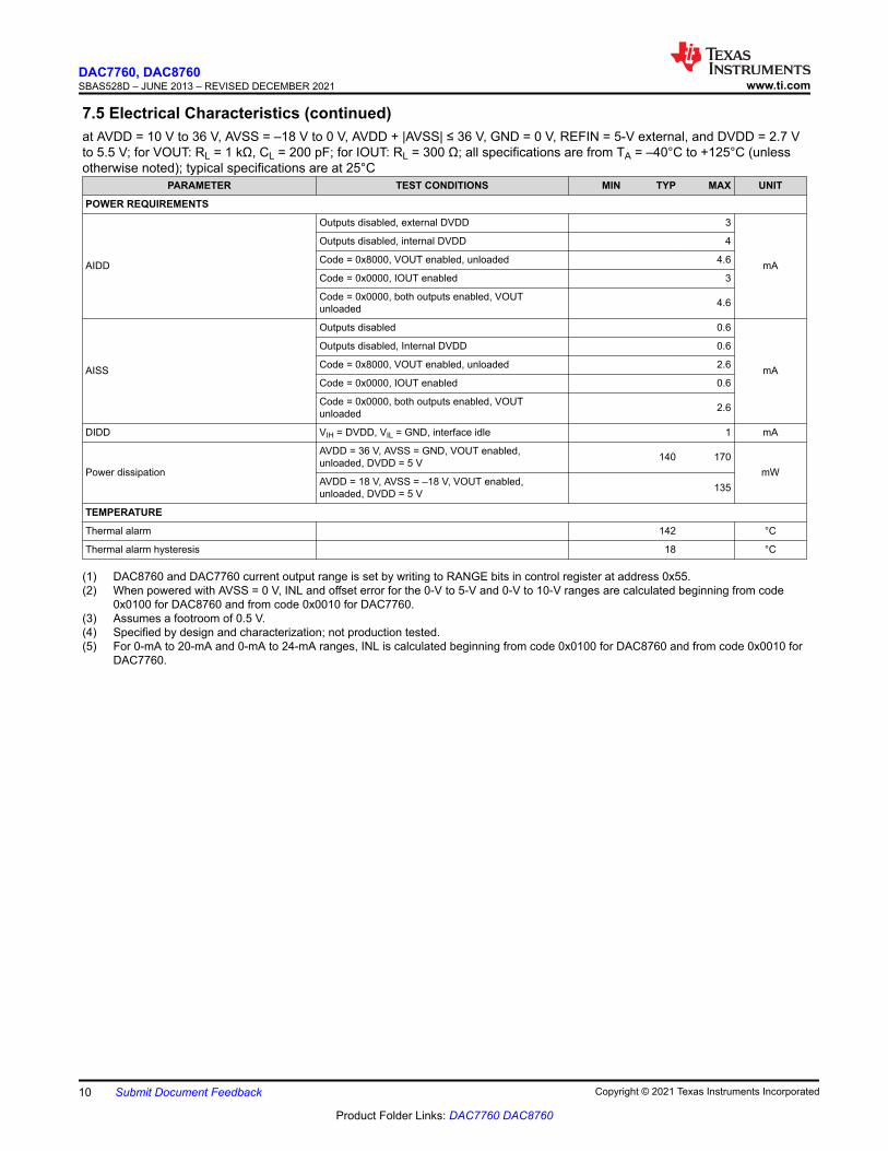
POWER REQUIREMENTS
AIDD
Outputs disabled, external DVDD 3
mA
Outputs disabled, internal DVDD 4
Code = 0x8000, VOUT enabled, unloaded 4.6
Code = 0x0000, IOUT enabled 3
Code = 0x0000, both outputs enabled, VOUT unloaded 4.6
AISS
Outputs disabled 0.6
mA
Outputs disabled, Internal DVDD 0.6
Code = 0x8000, VOUT enabled, unloaded 2.6
Code = 0x0000, IOUT enabled 0.6
Code = 0x0000, both outputs enabled, VOUT unloaded 2.6
DIDD VIH = DVDD, VIL = GND, interface idle 1 mA
Power dissipation
AVDD = 36 V, AVSS = GND, VOUT enabled, unloaded, DVDD = 5 V 140 170
mWAVDD = 18 V, AVSS = –18 V, VOUT enabled, unloaded, DVDD = 5 V 135
TEMPERATURE
Thermal alarm 142 °C
Thermal alarm hysteresis 18 °C
(1) DAC8760 and DAC7760 current output range is set by writing to RANGE bits in control register at address 0x55.(2) When powered with AVSS = 0 V, INL and offset error for the 0-V to 5-V and 0-V to 10-V ranges are calculated beginning from code
0x0100 for DAC8760 and from code 0x0010 for DAC7760.(3) Assumes a footroom of 0.5 V.(4) Specified by design and characterization; not production tested.(5) For 0-mA to 20-mA and 0-mA to 24-mA ranges, INL is calculated beginning from code 0x0100 for DAC8760 and from code 0x0010 for
DAC7760.
DAC7760, DAC8760SBAS528D – JUNE 2013 – REVISED DECEMBER 2021 www.ti.com
10 Submit Document Feedback Copyright © 2021 Texas Instruments Incorporated
Product Folder Links: DAC7760 DAC8760
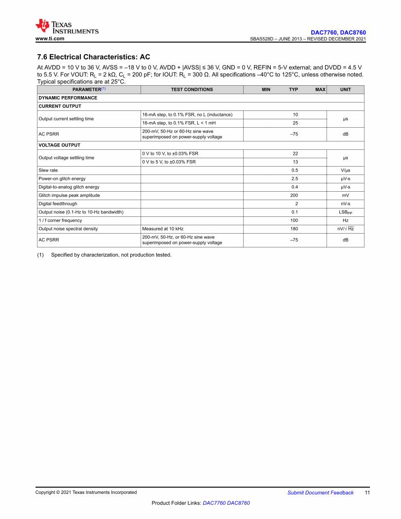
7.6 Electrical Characteristics: ACAt AVDD = 10 V to 36 V, AVSS = –18 V to 0 V, AVDD + |AVSS| ≤ 36 V, GND = 0 V, REFIN = 5-V external; and DVDD = 4.5 V to 5.5 V. For VOUT: RL = 2 kΩ, CL = 200 pF; for IOUT: RL = 300 Ω. All specifications –40°C to 125°C, unless otherwise noted. Typical specifications are at 25°C.
PARAMETER(1) TEST CONDITIONS MIN TYP MAX UNIT
DYNAMIC PERFORMANCE
CURRENT OUTPUT
Output current settling time16-mA step, to 0.1% FSR, no L (inductance) 10
µs16-mA step, to 0.1% FSR, L < 1 mH 25
AC PSRR 200-mV, 50-Hz or 60-Hz sine wave superimposed on power-supply voltage –75 dB
VOLTAGE OUTPUT
Output voltage settling time0 V to 10 V, to ±0.03% FSR 22
µs0 V to 5 V, to ±0.03% FSR 13
Slew rate 0.5 V/µs
Power-on glitch energy 2.5 µV-s
Digital-to-analog glitch energy 0.4 µV-s
Glitch impulse peak amplitude 200 mV
Digital feedthrough 2 nV-s
Output noise (0.1-Hz to 10-Hz bandwidth) 0.1 LSBPP
1 / f corner frequency 100 Hz
Output noise spectral density Measured at 10 kHz 180 nV/√ Hz
AC PSRR 200-mV, 50-Hz, or 60-Hz sine wave superimposed on power-supply voltage –75 dB
(1) Specified by characterization, not production tested.
www.ti.comDAC7760, DAC8760
SBAS528D – JUNE 2013 – REVISED DECEMBER 2021
Copyright © 2021 Texas Instruments Incorporated Submit Document Feedback 11
Product Folder Links: DAC7760 DAC8760
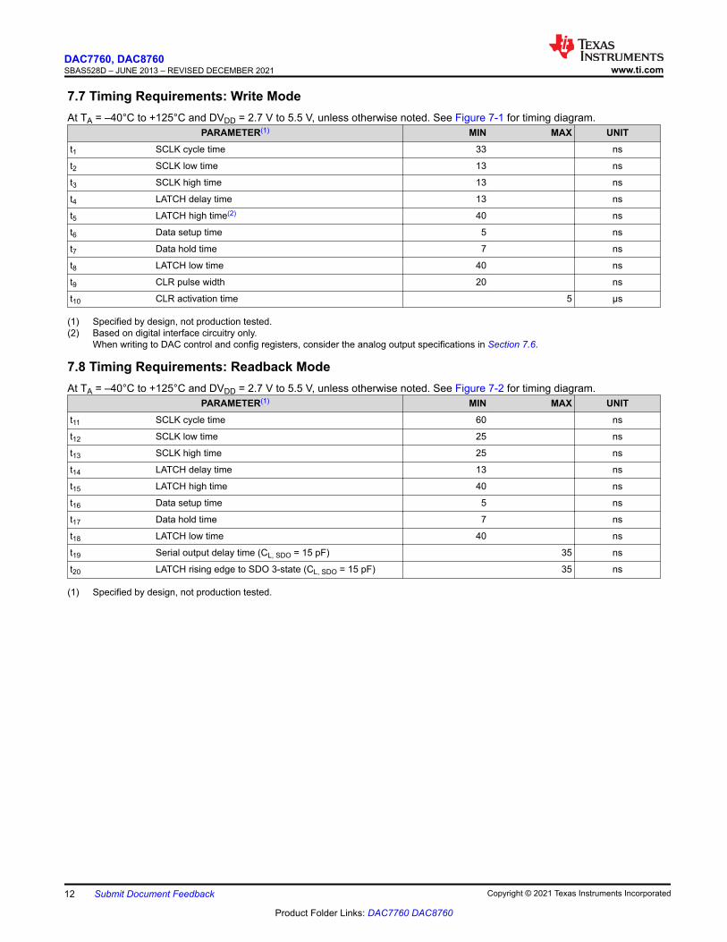
7.7 Timing Requirements: Write ModeAt TA = –40°C to +125°C and DVDD = 2.7 V to 5.5 V, unless otherwise noted. See Figure 7-1 for timing diagram.
PARAMETER(1) MIN MAX UNITt1 SCLK cycle time 33 ns
t2 SCLK low time 13 ns
t3 SCLK high time 13 ns
t4 LATCH delay time 13 ns
t5 LATCH high time(2) 40 ns
t6 Data setup time 5 ns
t7 Data hold time 7 ns
t8 LATCH low time 40 ns
t9 CLR pulse width 20 ns
t10 CLR activation time 5 μs
(1) Specified by design, not production tested.(2) Based on digital interface circuitry only.
When writing to DAC control and config registers, consider the analog output specifications in Section 7.6.
7.8 Timing Requirements: Readback ModeAt TA = –40°C to +125°C and DVDD = 2.7 V to 5.5 V, unless otherwise noted. See Figure 7-2 for timing diagram.
PARAMETER(1) MIN MAX UNITt11 SCLK cycle time 60 ns
t12 SCLK low time 25 ns
t13 SCLK high time 25 ns
t14 LATCH delay time 13 ns
t15 LATCH high time 40 ns
t16 Data setup time 5 ns
t17 Data hold time 7 ns
t18 LATCH low time 40 ns
t19 Serial output delay time (CL, SDO = 15 pF) 35 ns
t20 LATCH rising edge to SDO 3-state (CL, SDO = 15 pF) 35 ns
(1) Specified by design, not production tested.
DAC7760, DAC8760SBAS528D – JUNE 2013 – REVISED DECEMBER 2021 www.ti.com
12 Submit Document Feedback Copyright © 2021 Texas Instruments Incorporated
Product Folder Links: DAC7760 DAC8760
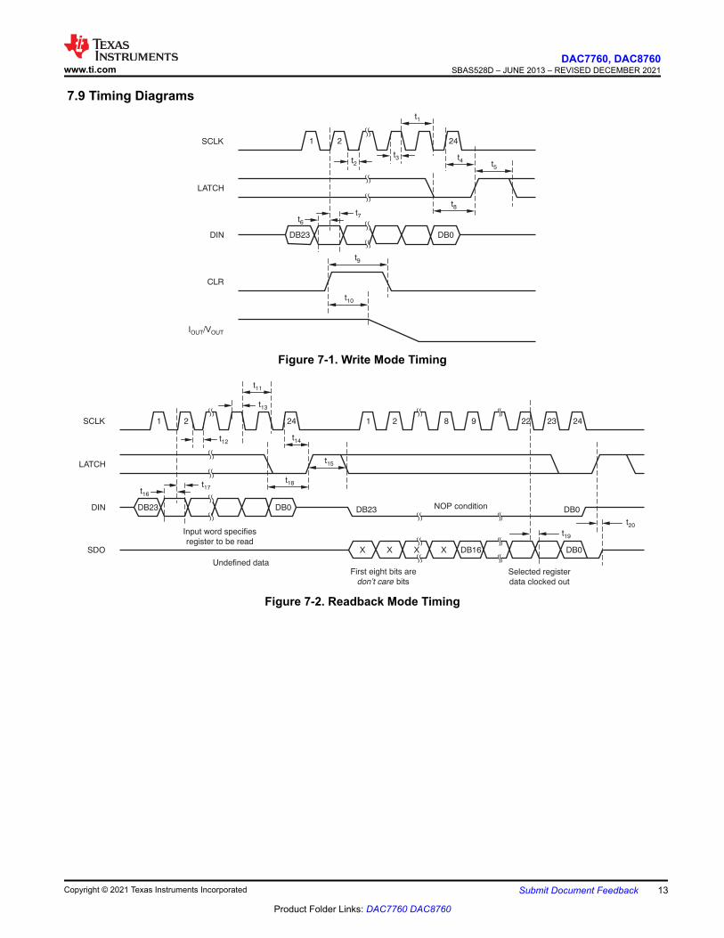
7.9 Timing Diagrams
SCLK
LATCH
DIN
CLR
I /VOUT OUT
1 2 24
DB23 DB0
t2
t7t6
t3 t4t5
t8
t10
t9
t1
Figure 7-1. Write Mode Timing
SCLK
LATCH
DIN
SDO
1 1 82 2 924 242322
DB23 DB23DB0 DB0
DB0DB16
t12
t17t16
t13
t14
t15
t18
t20
t19
t11
Input word specifies
register to be read
Undefined data
NOP condition
X X X X
First eight bits are
bitsdon’t care
Selected register
data clocked out
Figure 7-2. Readback Mode Timing
www.ti.comDAC7760, DAC8760
SBAS528D – JUNE 2013 – REVISED DECEMBER 2021
Copyright © 2021 Texas Instruments Incorporated Submit Document Feedback 13
Product Folder Links: DAC7760 DAC8760
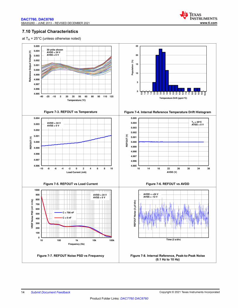
7.10 Typical Characteristicsat TA = 25°C (unless otherwise noted)
4.995
4.996
4.997
4.998
4.999
5.000
5.001
5.002
5.003
5.004
5.005
-40 -25 -10 5 20 35 50 65 80 95 110 125
Re
fere
nc
e O
utp
ut
Vo
lta
ge
(V
)
Temperature (oC) C003
30 units shown AVDD = 24 V AVSS = 0 V
Figure 7-3. REFOUT vs Temperature
0
5
10
15
20
25
0.0
1.0
1.0
1.5
2.0
2.5
3.0
3.5
4.0
4.5
5.0
5.5
6.0
6.5
7.0
7.5
8.0
8.5
9.0
9.5
10
.0
Po
pu
lati
on
(%
)
Temperature Drift (ppm/oC)
C002
Figure 7-4. Internal Reference Temperature Drift Histogram
4.996
4.997
4.998
4.999
5.000
5.001
5.002
5.003
5.004
-10 -8 -6 -4 -2 0 2 4 6 8 10
RE
FO
UT
(V
)
Load Current (mA) C001
AVDD = 24 V AVSS = 0 V
Figure 7-5. REFOUT vs Load Current
4.995
4.996
4.997
4.998
4.999
5.000
5.001
5.002
5.003
5.004
5.005
10 14 18 22 26 30 34 38
RE
FO
UT
(V
)
AVDD (V) C002
TA = 25oC AVSS = 0 V
Figure 7-6. REFOUT vs AVDD
0
100
200
300
400
500
600
700
800
900
1000
10 100 1k 10k 100k
VR
EF
No
ise
PS
D (
nV
/ rt
-Hz)
Frequency (Hz)
C = 700 nF
C = 0 nF
C006
AVDD = 24 V AVSS = 0 V
Figure 7-7. REFOUT Noise PSD vs Frequency
RE
FO
UT
No
ise
(2
µV
/div
)
Time (2 s/div)
C001
AVDD = +24 V AVSS = -12 V
Figure 7-8. Internal Reference, Peak-to-Peak Noise(0.1 Hz to 10 Hz)
DAC7760, DAC8760SBAS528D – JUNE 2013 – REVISED DECEMBER 2021 www.ti.com
14 Submit Document Feedback Copyright © 2021 Texas Instruments Incorporated
Product Folder Links: DAC7760 DAC8760
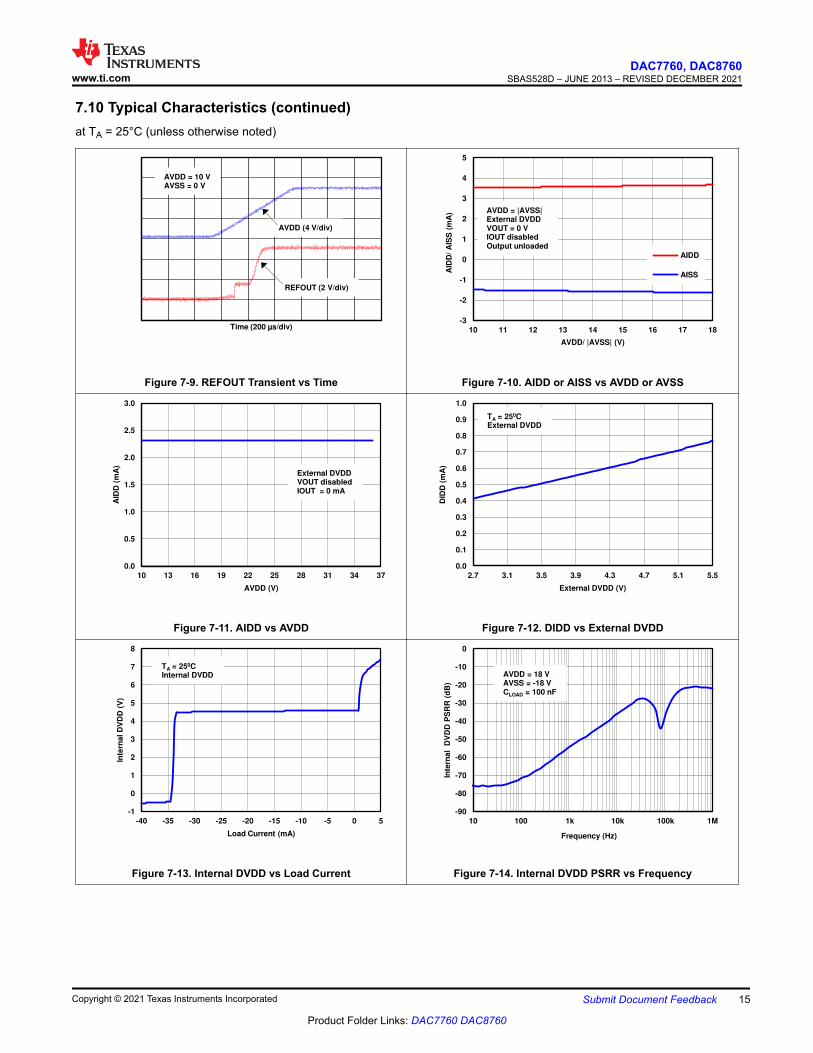
7.10 Typical Characteristics (continued)at TA = 25°C (unless otherwise noted)
Time (200 µs/div)
C002
REFOUT (2 V/div)
AVDD (4 V/div)
AVDD = 10 V AVSS = 0 V
Figure 7-9. REFOUT Transient vs Time
-3
-2
-1
0
1
2
3
4
5
10 11 12 13 14 15 16 17 18
AID
D/
AIS
S (
mA
)
AVDD/ |AVSS| (V)
AIDD
AISS
C003
AVDD = |AVSS| External DVDD VOUT = 0 V IOUT disabled Output unloaded
Figure 7-10. AIDD or AISS vs AVDD or AVSS
0.0
0.5
1.0
1.5
2.0
2.5
3.0
10 13 16 19 22 25 28 31 34 37
AID
D (
mA
)
AVDD (V) C004
External DVDD VOUT disabled IOUT = 0 mA
Figure 7-11. AIDD vs AVDD
0.0
0.1
0.2
0.3
0.4
0.5
0.6
0.7
0.8
0.9
1.0
2.7 3.1 3.5 3.9 4.3 4.7 5.1 5.5
DID
D (
mA
)
External DVDD (V) C001
TA = 250C External DVDD
Figure 7-12. DIDD vs External DVDD
-1
0
1
2
3
4
5
6
7
8
-40 -35 -30 -25 -20 -15 -10 -5 0 5
Inte
rna
l D
VD
D (
V)
Load Current (mA) C002
TA = 250C Internal DVDD
Figure 7-13. Internal DVDD vs Load Current
-90
-80
-70
-60
-50
-40
-30
-20
-10
0
10 100 1k 10k 100k 1M
Inte
rna
l D
VD
D P
SR
R (
dB
)
Frequency (Hz) C001
AVDD = 18 V AVSS = -18 V CLOAD = 100 nF
Figure 7-14. Internal DVDD PSRR vs Frequency
www.ti.comDAC7760, DAC8760
SBAS528D – JUNE 2013 – REVISED DECEMBER 2021
Copyright © 2021 Texas Instruments Incorporated Submit Document Feedback 15
Product Folder Links: DAC7760 DAC8760
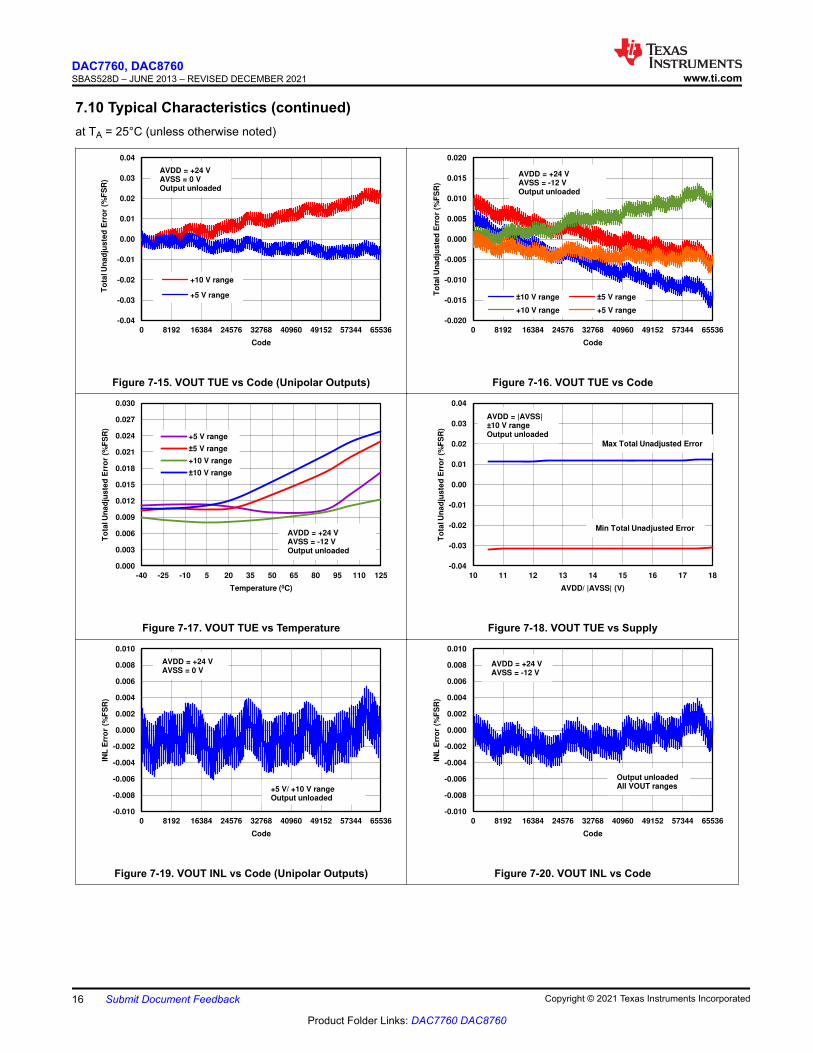
7.10 Typical Characteristics (continued)at TA = 25°C (unless otherwise noted)
-0.04
-0.03
-0.02
-0.01
0.00
0.01
0.02
0.03
0.04
0 8192 16384 24576 32768 40960 49152 57344 65536
To
tal U
na
dju
ste
d E
rro
r (%
FS
R)
Code
+10 V range
+5 V range
C003
AVDD = +24 V
AVSS = 0 V Output unloaded
Figure 7-15. VOUT TUE vs Code (Unipolar Outputs)
-0.020
-0.015
-0.010
-0.005
0.000
0.005
0.010
0.015
0.020
0 8192 16384 24576 32768 40960 49152 57344 65536
To
tal U
na
dju
ste
d E
rro
r (%
FS
R)
Code
10 V range 5 V range
+10 V range +5 V range
C003
AVDD = +24 V
AVSS = -12 V Output unloaded
Figure 7-16. VOUT TUE vs Code
0.000
0.003
0.006
0.009
0.012
0.015
0.018
0.021
0.024
0.027
0.030
-40 -25 -10 5 20 35 50 65 80 95 110 125
To
tal U
na
dju
ste
d E
rro
r (%
FS
R)
Temperature (0C)
+5 V range
5 V range
+10 V range
10 V range
C002
AVDD = +24 V AVSS = -12 V Output unloaded
Figure 7-17. VOUT TUE vs Temperature
-0.04
-0.03
-0.02
-0.01
0.00
0.01
0.02
0.03
0.04
10 11 12 13 14 15 16 17 18
To
tal U
na
dju
ste
d E
rro
r (%
FS
R)
AVDD/ |AVSS| (V) C002
Max Total Unadjusted Error
Min Total Unadjusted Error
AVDD = |AVSS| ±10 V range Output unloaded
Figure 7-18. VOUT TUE vs Supply
-0.010
-0.008
-0.006
-0.004
-0.002
0.000
0.002
0.004
0.006
0.008
0.010
0 8192 16384 24576 32768 40960 49152 57344 65536
INL
Err
or
(%F
SR
)
Code C001
AVDD = +24 V AVSS = 0 V
+5 V/ +10 V range Output unloaded
Figure 7-19. VOUT INL vs Code (Unipolar Outputs)
-0.010
-0.008
-0.006
-0.004
-0.002
0.000
0.002
0.004
0.006
0.008
0.010
0 8192 16384 24576 32768 40960 49152 57344 65536
INL
Err
or
(%F
SR
)
Code C001
AVDD = +24 V
AVSS = -12 V
Output unloaded
All VOUT ranges
Figure 7-20. VOUT INL vs Code
DAC7760, DAC8760SBAS528D – JUNE 2013 – REVISED DECEMBER 2021 www.ti.com
16 Submit Document Feedback Copyright © 2021 Texas Instruments Incorporated
Product Folder Links: DAC7760 DAC8760
7.10 Typical Characteristics (continued)at TA = 25°C (unless otherwise noted)
-0.008
-0.006
-0.004
-0.002
0.000
0.002
0.004
0.006
0.008
0.010
-40 -25 -10 5 20 35 50 65 80 95 110 125
INL
Err
or
(%F
SR
)
Temperature (0C) C002
AVDD = +24 V AVSS = -12 V Max INL
Min INL
Output unloaded All VOUT ranges
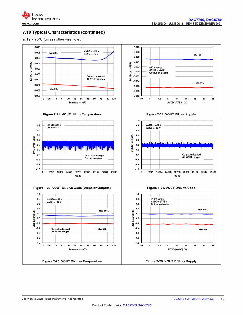
Figure 7-21. VOUT INL vs Temperature
-0.010
-0.008
-0.006
-0.004
-0.002
0.000
0.002
0.004
0.006
0.008
0.010
10 11 12 13 14 15 16 17 18
INL
Err
or
(%F
SR
)
AVDD/ |AVSS| (V) C001
Max INL
Min INL
±10 V range AVDD = |AVSS| Output unloaded
Figure 7-22. VOUT INL vs Supply
-1.0
-0.8
-0.6
-0.4
-0.2
0.0
0.2
0.4
0.6
0.8
1.0
0 8192 16384 24576 32768 40960 49152 57344 65536
DN
L E
rro
r (L
SB
)
Code C002
AVDD = 24 V
AVSS = 0 V
+5 V/ +10 V range Output unloaded
Figure 7-23. VOUT DNL vs Code (Unipolar Outputs)
-1.0
-0.8
-0.6
-0.4
-0.2
0.0
0.2
0.4
0.6
0.8
1.0
0 8192 16384 24576 32768 40960 49152 57344 65536
DN
L E
rro
r (L
SB
)
Code C002
AVDD = +24 V
AVSS = -12 V
Output unloaded All VOUT ranges
Figure 7-24. VOUT DNL vs Code
-1.0
-0.8
-0.6
-0.4
-0.2
0.0
0.2
0.4
0.6
0.8
1.0
-40 -25 -10 5 20 35 50 65 80 95 110 125
DN
L E
rro
r (L
SB
)
Temperature (0C) C003
AVDD = +24 V AVSS = -12 V
Max DNL
Min DNL Output unloaded All VOUT ranges
Figure 7-25. VOUT DNL vs Temperature
-1.0
-0.8
-0.6
-0.4
-0.2
0.0
0.2
0.4
0.6
0.8
1.0
10 11 12 13 14 15 16 17 18
DN
L E
rro
r (L
SB
)
AVDD/ |AVSS| (V) C009
Max DNL
Min DNL
±10 V range AVDD = |AVSS| Output unloaded
Figure 7-26. VOUT DNL vs Supply
www.ti.comDAC7760, DAC8760
SBAS528D – JUNE 2013 – REVISED DECEMBER 2021
Copyright © 2021 Texas Instruments Incorporated Submit Document Feedback 17
Product Folder Links: DAC7760 DAC8760
7.10 Typical Characteristics (continued)at TA = 25°C (unless otherwise noted)
-0.012
-0.010
-0.008
-0.006
-0.004
-0.002
0.000
0.002
0.004
-40 -25 -10 5 20 35 50 65 80 95 110 125
Fu
ll S
ca
le E
rro
r (%
FS
R)
Temperature (0C)
10 V range 5 V range
+10 V range +5 V range
C004
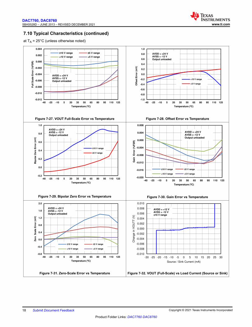
AVDD = +24 V AVSS = -12 V Output unloaded
Figure 7-27. VOUT Full-Scale Error vs Temperature
-1.0
-0.8
-0.6
-0.4
-0.2
0.0
0.2
0.4
0.6
0.8
1.0
-40 -25 -10 5 20 35 50 65 80 95 110 125
Off
se
t E
rro
r (m
V)
Temperature (0C)
+10 V range
+5 V range
C005
AVDD = +24 V AVSS = -12 V Output unloaded
Figure 7-28. Offset Error vs Temperature
-0.2
0.0
0.2
0.4
0.6
0.8
1.0
-40 -25 -10 5 20 35 50 65 80 95 110 125
Bip
ola
r Z
ero
Err
or
(mV
)
Temperature (0C)
10 V range
5 V range
C006
AVDD = +24 V AVSS = -12 V Output unloaded
Figure 7-29. Bipolar Zero Error vs Temperature
-0.020
-0.016
-0.012
-0.008
-0.004
0.000
0.004
0.008
-40 -25 -10 5 20 35 50 65 80 95 110 125
Ga
in E
rro
r (%
FS
R)
Temperature (0C)
10 V range 5 V range
+10 V range +5 V range
AVDD = +24 V AVSS = -12 V Output unloaded
C007
Figure 7-30. Gain Error vs Temperature
-0.8
-0.4
0.0
0.4
0.8
1.2
1.6
2.0
-40 -25 -10 5 20 35 50 65 80 95 110 125
Ze
ro S
ca
le E
rro
r (m
V)
Temperature (0C)
10 V range 5 V range
+10 V range +5 V range
C008
AVDD = +24 V AVSS = -12 V Output unloaded
Figure 7-31. Zero-Scale Error vs Temperature
-0.010
-0.008
-0.006
-0.004
-0.002
0.000
0.002
0.004
0.006
0.008
0.010
-30 -25 -20 -15 -10 -5 0 5 10 15 20 25 30
Change in V
OU
TT
(V
)
Source / Sink Current (mA) C010
AVDD = +12 V AVSS = -12 V ±10 V range
Figure 7-32. VOUT (Full-Scale) vs Load Current (Source or Sink)
DAC7760, DAC8760SBAS528D – JUNE 2013 – REVISED DECEMBER 2021 www.ti.com
18 Submit Document Feedback Copyright © 2021 Texas Instruments Incorporated
Product Folder Links: DAC7760 DAC8760
7.10 Typical Characteristics (continued)at TA = 25°C (unless otherwise noted)
-0.010
-0.008
-0.006
-0.004
-0.002
0.000
0.002
0.004
0.006
0.008
0.010
-25 -20 -15 -10 -5 0 5 10 15 20 25
Change in V
OU
TT
(V
)
Source / Sink Current (mA) C009
AVDD = +12 V AVSS = -12 V ±10 V range
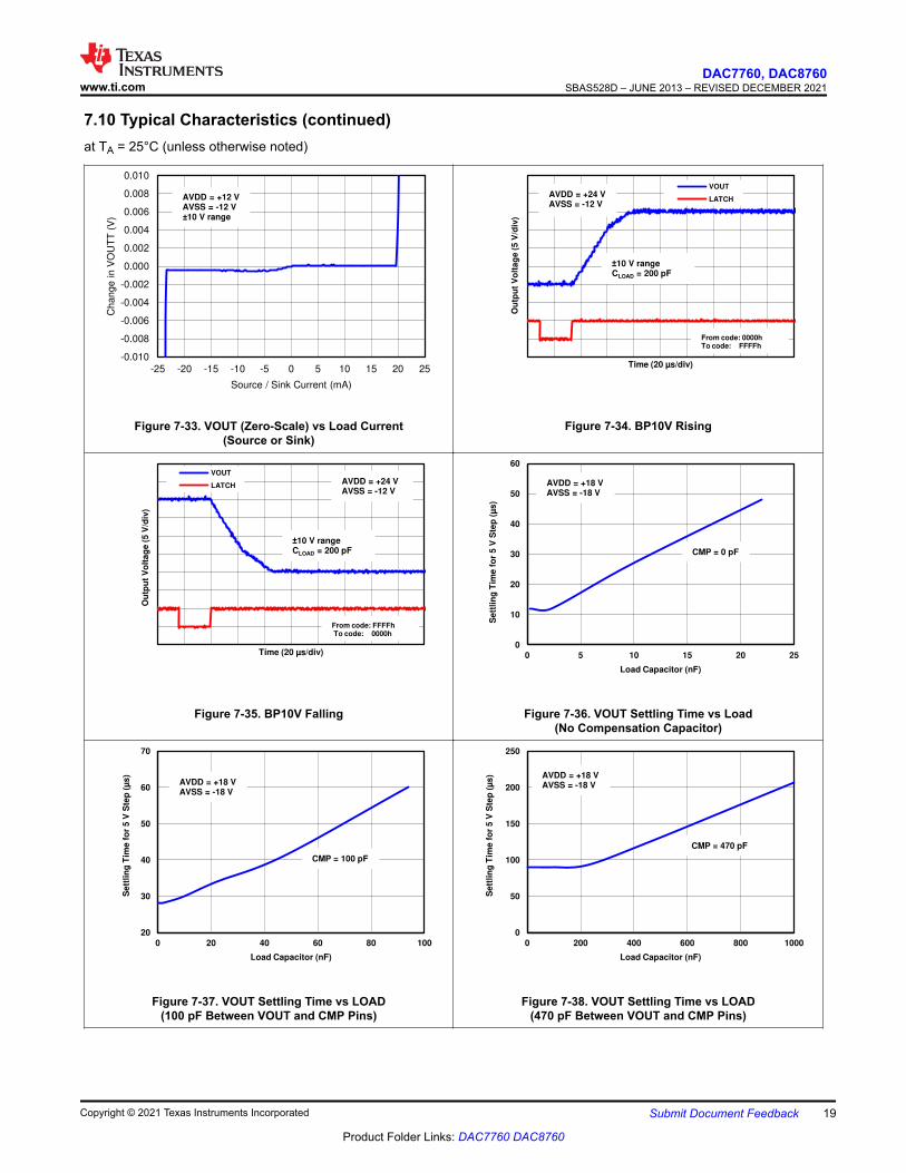
Figure 7-33. VOUT (Zero-Scale) vs Load Current(Source or Sink)
Ou
tpu
t V
olt
ag
e (
5 V
/div
)
Time (20 µs/div)
VOUT
LATCH
C001
AVDD = +24 V AVSS = -12 V
From code: 0000h To code: FFFFh
10 V range CLOAD = 200 pF
Figure 7-34. BP10V Rising
Ou
tpu
t V
olt
ag
e (
5 V
/div
)
Time (20 µs/div)
VOUT
LATCH
C001
AVDD = +24 V AVSS = -12 V
From code: FFFFh To code: 0000h
10 V range CLOAD = 200 pF
Figure 7-35. BP10V Falling
0
10
20
30
40
50
60
0 5 10 15 20 25
Se
ttli
ng
Tim
e f
or
5 V
Ste
p (
µs
)
Load Capacitor (nF) C001
AVDD = +18 V AVSS = -18 V
CMP = 0 pF
Figure 7-36. VOUT Settling Time vs Load(No Compensation Capacitor)
20
30
40
50
60
70
0 20 40 60 80 100
Se
ttli
ng
Tim
e f
or
5 V
Ste
p (
µs
)
Load Capacitor (nF) C002
AVDD = +18 V AVSS = -18 V
CMP = 100 pF
Figure 7-37. VOUT Settling Time vs LOAD(100 pF Between VOUT and CMP Pins)
0
50
100
150
200
250
0 200 400 600 800 1000
Se
ttli
ng
Tim
e f
or
5 V
Ste
p (
µs
)
Load Capacitor (nF) C003
AVDD = +18 V AVSS = -18 V
CMP = 470 pF
Figure 7-38. VOUT Settling Time vs LOAD(470 pF Between VOUT and CMP Pins)
www.ti.comDAC7760, DAC8760
SBAS528D – JUNE 2013 – REVISED DECEMBER 2021
Copyright © 2021 Texas Instruments Incorporated Submit Document Feedback 19
Product Folder Links: DAC7760 DAC8760
7.10 Typical Characteristics (continued)at TA = 25°C (unless otherwise noted)
Time (20 µs/div)
C001
VOUT (50 mV/div)
LOAD = 1 k // 200 pF
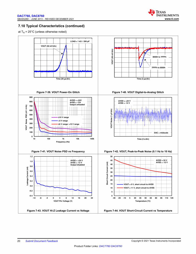
Figure 7-39. VOUT Power-On Glitch
VO
UT
(5
0 m
V/d
iv)
Time (3 µs/div)
C001
8000h to 7FFFh
7FFFh to 8000h
Figure 7-40. VOUT Digital-to-Analog Glitch
0
100
200
300
400
500
600
700
800
900
10 100 1k 10k 100k
VO
UT
N
ois
e P
SD
(n
V/
rt-H
z)
Frequency (Hz)
10 V range
+5 V range
5 V range/ +10 V range
C007
AVDD = +24V AVSS = -12V Output unloaded
Figure 7-41. VOUT Noise PSD vs Frequency
VO
UT
No
ise
(1
µV
/div
)
Time (2 s/div)
C002
AVDD = +24 V AVSS = -12 V
DAC = midscale
Figure 7-42. VOUT, Peak-to-Peak Noise (0.1 Hz to 10 Hz)
-0.4
-0.2
0.0
0.2
0.4
0.6
0.8
1.0
1.2
-12 -8 -4 0 4 8 12 16 20 24
Le
ak
ag
e C
urr
en
t (n
A)
VOUT Pin Voltage (V) C003
AVDD = +24 V AVSS = -12 V Output disabled
Figure 7-43. VOUT Hi-Z Leakage Current vs Voltage
0
5
10
15
20
25
30
35
40
45
50
-40 -25 -10 5 20 35 50 65 80 95 110 125
Sh
ort
Cir
cu
it C
urr
en
t (m
A)
Temperature (oC)
VOUT = 0 V, short circuit to AVDD
VOUT = 11 V, short circuit to AVSS
C001
AVDD = 24 V AVSS = -12 V
Figure 7-44. VOUT Short-Circuit Current vs Temperature
DAC7760, DAC8760SBAS528D – JUNE 2013 – REVISED DECEMBER 2021 www.ti.com
20 Submit Document Feedback Copyright © 2021 Texas Instruments Incorporated
Product Folder Links: DAC7760 DAC8760
7.10 Typical Characteristics (continued)at TA = 25°C (unless otherwise noted)
-90
-80
-70
-60
-50
-40
-30
-20
-10
0
10 100 1k 10k 100k 1M
VO
UT
PS
RR
(d
B)
Frequency (Hz)
+5 V range
10 V range
+10 V Range/ 5 V range
C001
AVDD = +18 V AVSS = -18 V Output unloaded
Figure 7-45. AVDD PSRR for VOUT
-0.25
-0.20
-0.15
-0.10
-0.05
0.00
0.05
0 8192 16384 24576 32768 40960 49152 57344 65536
To
tal U
na
dju
ste
d E
rro
r (%
FS
R)
Code
0 mA - 24 mA Internal RSET
0 mA - 24 mA Internal RSET, BOOST
0 mA - 24 mA External RSET
0 mA - 24 mA External RSET, BOOST
C009
AVDD = 24 V AVSS = 0 V RLOAD = 300
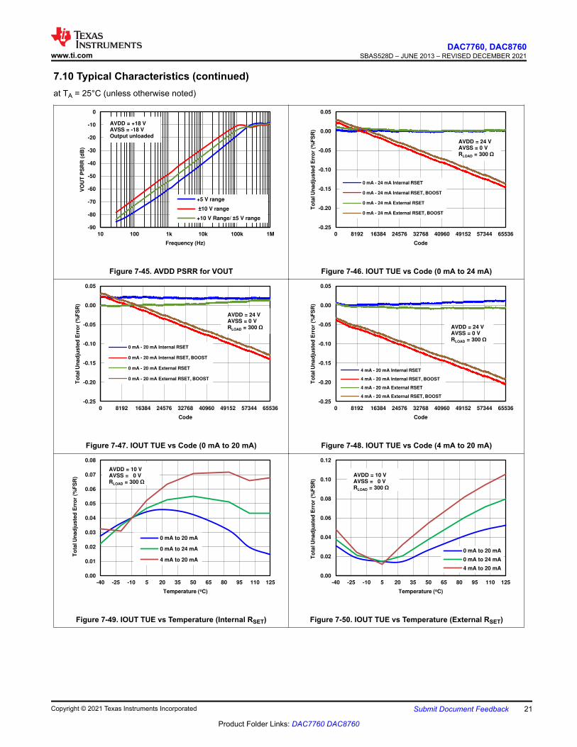
Figure 7-46. IOUT TUE vs Code (0 mA to 24 mA)
-0.25
-0.20
-0.15
-0.10
-0.05
0.00
0.05
0 8192 16384 24576 32768 40960 49152 57344 65536
To
tal U
na
dju
ste
d E
rro
r (%
FS
R)
Code
0 mA - 20 mA Internal RSET
0 mA - 20 mA Internal RSET, BOOST
0 mA - 20 mA External RSET
0 mA - 20 mA External RSET, BOOST
C006
AVDD = 24 V AVSS = 0 V RLOAD = 300
Figure 7-47. IOUT TUE vs Code (0 mA to 20 mA)
-0.25
-0.20
-0.15
-0.10
-0.05
0.00
0.05
0 8192 16384 24576 32768 40960 49152 57344 65536
To
tal U
na
dju
ste
d E
rro
r (%
FS
R)
Code
4 mA - 20 mA Internal RSET
4 mA - 20 mA Internal RSET, BOOST
4 mA - 20 mA External RSET
4 mA - 20 mA External RSET, BOOST
C003
AVDD = 24 V AVSS = 0 V RLOAD = 300
Figure 7-48. IOUT TUE vs Code (4 mA to 20 mA)
0.00
0.01
0.02
0.03
0.04
0.05
0.06
0.07
0.08
-40 -25 -10 5 20 35 50 65 80 95 110 125
To
tal U
na
dju
ste
d E
rro
r (%
FS
R)
Temperature (oC)
0 mA to 20 mA
0 mA to 24 mA
4 mA to 20 mA
C008
AVDD = 10 V AVSS = 0 V RLOAD = 300
Figure 7-49. IOUT TUE vs Temperature (Internal RSET)
0.00
0.02
0.04
0.06
0.08
0.10
0.12
-40 -25 -10 5 20 35 50 65 80 95 110 125
To
tal U
na
dju
ate
d E
rro
r (%
FS
R)
Temperature (oC)
0 mA to 20 mA
0 mA to 24 mA
4 mA to 20 mA
C009
AVDD = 10 V AVSS = 0 V RLOAD = 300
Figure 7-50. IOUT TUE vs Temperature (External RSET)
www.ti.comDAC7760, DAC8760
SBAS528D – JUNE 2013 – REVISED DECEMBER 2021
Copyright © 2021 Texas Instruments Incorporated Submit Document Feedback 21
Product Folder Links: DAC7760 DAC8760
7.10 Typical Characteristics (continued)at TA = 25°C (unless otherwise noted)
-0.01
0.00
0.01
0.02
0.03
0.04
0.05
10 14 18 22 26 30 34 38
To
tal U
na
dju
ste
d E
rro
r (%
FS
R)
AVDD (V) C006
Min Total Unadjusted Error
Max Total Unadjusted Error AVSS = 0 V RLOAD = 300 0 mA to 24 mA range
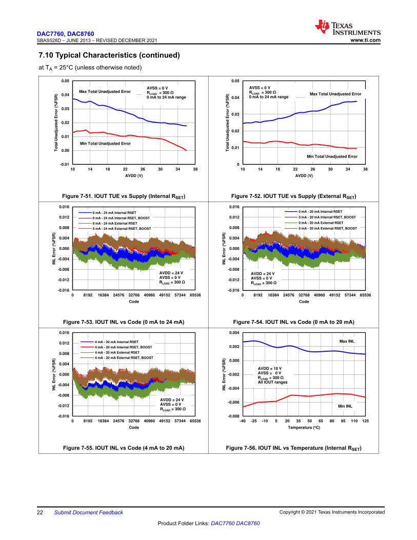
Figure 7-51. IOUT TUE vs Supply (Internal RSET)
0
0.01
0.02
0.03
0.04
0.05
10 14 18 22 26 30 34 38
To
tal U
na
dju
ste
d E
rro
r (%
FS
R)
AVDD (V) C005
Max Total Unadjusted Error
Min Total Unadjusted Error
AVSS = 0 V RLOAD = 300 0 mA to 24 mA range
Figure 7-52. IOUT TUE vs Supply (External RSET)
-0.016
-0.012
-0.008
-0.004
0.000
0.004
0.008
0.012
0.016
0 8192 16384 24576 32768 40960 49152 57344 65536
INL
Err
or
(%F
SR
)
Code
0 mA - 24 mA Internal RSET
0 mA - 24 mA Internal RSET, BOOST
0 mA - 24 mA External RSET
0 mA - 24 mA External RSET, BOOST
C007
AVDD = 24 V AVSS = 0 V RLOAD = 300
Figure 7-53. IOUT INL vs Code (0 mA to 24 mA)
-0.016
-0.012
-0.008
-0.004
0.000
0.004
0.008
0.012
0.016
0 8192 16384 24576 32768 40960 49152 57344 65536
INL
Err
or
(%F
SR
)
Code
0 mA - 20 mA Internal RSET
0 mA - 20 mA Internal RSET, BOOST
0 mA - 20 mA External RSET
0 mA - 20 mA External RSET, BOOST
C004
AVDD = 24 V AVSS = 0 V RLOAD = 300
Figure 7-54. IOUT INL vs Code (0 mA to 20 mA)
-0.016
-0.012
-0.008
-0.004
0.000
0.004
0.008
0.012
0.016
0 8192 16384 24576 32768 40960 49152 57344 65536
INL
Err
or
(%F
SR
)
Code
4 mA - 20 mA Internal RSET
4 mA - 20 mA Internal RSET, BOOST
4 mA - 20 mA External RSET
4 mA - 20 mA External RSET, BOOST
C001
AVDD = 24 V AVSS = 0 V RLOAD = 300
Figure 7-55. IOUT INL vs Code (4 mA to 20 mA)
-0.008
-0.006
-0.004
-0.002
0.000
0.002
0.004
-40 -25 -10 5 20 35 50 65 80 95 110 125
INL
Err
or
(%F
SR
)
Temperature (oC) C002
Max INL
Min INL
AVDD = 10 V AVSS = 0 V RLOAD = 300 All IOUT ranges
Figure 7-56. IOUT INL vs Temperature (Internal RSET)
DAC7760, DAC8760SBAS528D – JUNE 2013 – REVISED DECEMBER 2021 www.ti.com
22 Submit Document Feedback Copyright © 2021 Texas Instruments Incorporated
Product Folder Links: DAC7760 DAC8760
7.10 Typical Characteristics (continued)at TA = 25°C (unless otherwise noted)
-0.008
-0.006
-0.004
-0.002
0.000
0.002
0.004
-40 -25 -10 5 20 35 50 65 80 95 110 125
INL
Err
or
(%F
SR
)
Temperature (oC) C001
AVDD = 10 V AVSS = 0 V RLOAD = 300 All IOUT ranges
Max INL
Min INL
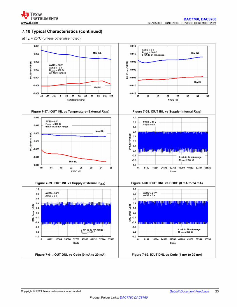
Figure 7-57. IOUT INL vs Temperature (External RSET)
-0.015
-0.010
-0.005
0.000
0.005
0.010
0.015
10 14 18 22 26 30 34 38
INL
Err
or
(%F
SR
)
AVDD (V) C004
AVSS = 0 V RLOAD = 300 0 mA to 24 mA range
Max INL
Min INL
Figure 7-58. IOUT INL vs Supply (Internal RSET)
-0.015
-0.010
-0.005
0.000
0.005
0.010
0.015
10 14 18 22 26 30 34 38
INL
Err
or
(% F
SR
)
AVDD (V) C003
Max INL
Min INL
AVSS = 0 V RLOAD = 300 0 mA to 24 mA range
Figure 7-59. IOUT INL vs Supply (External RSET)
-1.0
-0.8
-0.6
-0.4
-0.2
0.0
0.2
0.4
0.6
0.8
1.0
0 8192 16384 24576 32768 40960 49152 57344 65536
DN
L E
rro
r (L
SB
)
Code C008
AVDD = 24 V AVSS = 0 V
0 mA to 24 mA range RLOAD = 300
Figure 7-60. IOUT DNL vs CODE (0 mA to 24 mA)
-1.0
-0.8
-0.6
-0.4
-0.2
0.0
0.2
0.4
0.6
0.8
1.0
0 8192 16384 24576 32768 40960 49152 57344 65536
DN
L E
rro
r (L
SB
)
Code C005
AVDD = 24 V
AVSS = 0 V
0 mA to 20 mA range RLOAD = 300
Figure 7-61. IOUT DNL vs Code (0 mA to 20 mA)
-1.0
-0.8
-0.6
-0.4
-0.2
0.0
0.2
0.4
0.6
0.8
1.0
0 8192 16384 24576 32768 40960 49152 57344 65536
DN
L E
rro
r (L
SB
)
Code C002
AVDD = 24 V
AVSS = 0 V
4 mA to 20 mA range
RLOAD = 300
Figure 7-62. IOUT DNL vs Code (4 mA to 20 mA)
www.ti.comDAC7760, DAC8760
SBAS528D – JUNE 2013 – REVISED DECEMBER 2021
Copyright © 2021 Texas Instruments Incorporated Submit Document Feedback 23
Product Folder Links: DAC7760 DAC8760
7.10 Typical Characteristics (continued)at TA = 25°C (unless otherwise noted)
-1.0
-0.8
-0.6
-0.4
-0.2
0.0
0.2
0.4
0.6
0.8
1.0
-40 -25 -10 5 20 35 50 65 80 95 110 125
DN
L E
rro
r (L
SB
)
Temperature (oC) C010
AVDD = 10 V AVSS = 0 V RLOAD = 300 All IOUT ranges
Max DNL
Min DNL
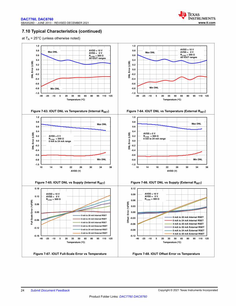
Figure 7-63. IOUT DNL vs Temperature (Internal RSET)
-1.0
-0.8
-0.6
-0.4
-0.2
0.0
0.2
0.4
0.6
0.8
1.0
-40 -25 -10 5 20 35 50 65 80 95 110 125
DN
L E
rro
r (L
SB
)
Temperature (oC) C011
Max DNL
AVDD = 10 V AVSS = 0 V RLOAD = 300 All IOUT ranges
Min DNL
Figure 7-64. IOUT DNL vs Temperature (External RSET)
-1.0
-0.8
-0.6
-0.4
-0.2
0.0
0.2
0.4
0.6
0.8
1.0
10 14 18 22 26 30 34 38
DN
L E
rro
r (L
SB
)
AVDD (V) C008
Max DNL
Min DNL
AVSS = 0 V RLOAD = 300 0 mA to 24 mA range
Figure 7-65. IOUT DNL vs Supply (Internal RSET)
-1.0
-0.8
-0.6
-0.4
-0.2
0.0
0.2
0.4
0.6
0.8
1.0
10 14 18 22 26 30 34 38
DN
L E
rro
r (L
SB
)
AVDD (V) C007
Max DNL
Min DNL
AVSS = 0 V RLOAD = 300 0 mA to 24 mA range
Figure 7-66. IOUT DNL vs Supply (External RSET)
-0.18
-0.12
-0.06
0.00
0.06
0.12
0.18
-40 -25 -10 5 20 35 50 65 80 95 110 125
Fu
ll S
ca
le E
rro
r (%
FS
R)
Temperature (oC)
0 mA to 20 mA Internal RSET
0 mA to 24 mA Internal RSET
4 mA to 20 mA Internal RSET
0 mA to 20 mA External RSET
0 mA to 24 mA External RSET
4 mA to 20 mA External RSET
C006
AVDD = 10 V AVSS = 0 V RLOAD = 300
Figure 7-67. IOUT Full-Scale Error vs Temperature
-0.12
-0.09
-0.06
-0.03
0.00
0.03
0.06
0.09
0.12
-40 -25 -10 5 20 35 50 65 80 95 110 125
Off
se
t E
rro
r (%
FS
R)
Temperature (oC)
0 mA to 20 mA Internal RSET
0 mA to 24 mA Internal RSET
4 mA to 20 mA Internal RSET
0 mA to 20 mA External RSET
0 mA to 24 mA External RSET
4 mA to 20 mA External RSET
C003
AVDD = 10 V AVSS = 0 V RLOAD = 300
Figure 7-68. IOUT Offset Error vs Temperature
DAC7760, DAC8760SBAS528D – JUNE 2013 – REVISED DECEMBER 2021 www.ti.com
24 Submit Document Feedback Copyright © 2021 Texas Instruments Incorporated
Product Folder Links: DAC7760 DAC8760
7.10 Typical Characteristics (continued)at TA = 25°C (unless otherwise noted)
-0.12
-0.09
-0.06
-0.03
0.00
0.03
0.06
0.09
0.12
-40 -25 -10 5 20 35 50 65 80 95 110 125
Ga
in E
rro
r (%
FS
R)
Temperature (oC)
0 mA to 20 mA Internal RSET
0 mA to 24 mA Internal RSET
4 mA to 20 mA Internal RSET
0 mA to 20 mA External RSET
0 mA to 24 mA External RSET
4 mA to 20 mA External RSET
C007
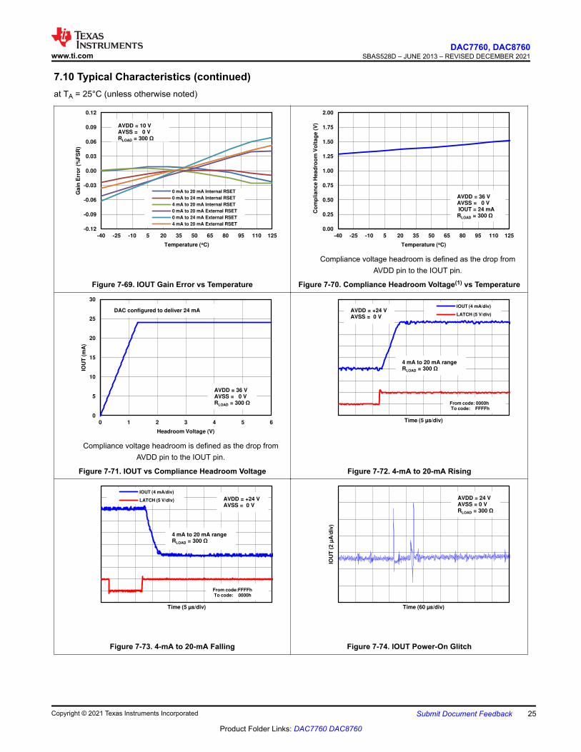
AVDD = 10 V AVSS = 0 V RLOAD = 300
Figure 7-69. IOUT Gain Error vs Temperature
0.00
0.25
0.50
0.75
1.00
1.25
1.50
1.75
2.00
-40 -25 -10 5 20 35 50 65 80 95 110 125
Co
mp
lia
nc
e H
ea
dro
om
Vo
lta
ge
(V
)
Temperature (oC) C004
AVDD = 36 V AVSS = 0 V IOUT = 24 mA RLOAD = 300
Compliance voltage headroom is defined as the drop from AVDD pin to the IOUT pin.
Figure 7-70. Compliance Headroom Voltage(1) vs Temperature
0
5
10
15
20
25
30
0 1 2 3 4 5 6
IOU
T (
mA
)
Headroom Voltage (V) C005
AVDD = 36 V AVSS = 0 V RLOAD = 300
DAC configured to deliver 24 mA
Compliance voltage headroom is defined as the drop from AVDD pin to the IOUT pin.
Figure 7-71. IOUT vs Compliance Headroom Voltage
Time (5 µs/div)
IOUT (4 mA/div)
LATCH (5 V/div)
C001
4 mA to 20 mA range RLOAD = 300
From code: 0000h To code: FFFFh
AVDD = +24 V AVSS = 0 V
Figure 7-72. 4-mA to 20-mA Rising
Time (5 µs/div)
IOUT (4 mA/div)
LATCH (5 V/div)
C001
AVDD = +24 V AVSS = 0 V
From code:FFFFh To code: 0000h
4 mA to 20 mA range RLOAD = 300
Figure 7-73. 4-mA to 20-mA Falling
IOU
T (
2 µ
A/d
iv)
Time (60 µs/div)
C001
AVDD = 24 V AVSS = 0 V RLOAD = 300
Figure 7-74. IOUT Power-On Glitch
www.ti.comDAC7760, DAC8760
SBAS528D – JUNE 2013 – REVISED DECEMBER 2021
Copyright © 2021 Texas Instruments Incorporated Submit Document Feedback 25
Product Folder Links: DAC7760 DAC8760
7.10 Typical Characteristics (continued)at TA = 25°C (unless otherwise noted)
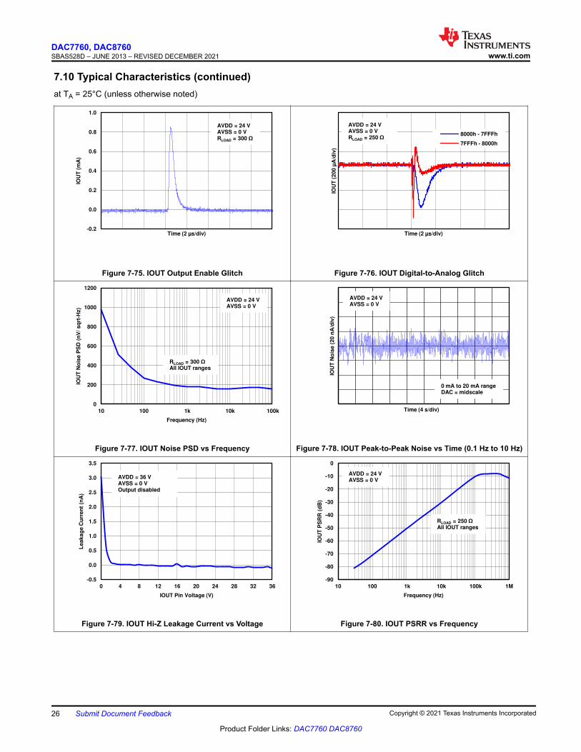
-0.2
0.0
0.2
0.4
0.6
0.8
1.0
IOU
T (
mA
)
Time (2 µs/div)
C002
AVDD = 24 V AVSS = 0 V RLOAD = 300
Figure 7-75. IOUT Output Enable Glitch
IOU
T (
20
0 µ
A/d
iv)
Time (2 µs/div)
8000h - 7FFFh
7FFFh - 8000h
C001
AVDD = 24 V AVSS = 0 V RLOAD = 250
Figure 7-76. IOUT Digital-to-Analog Glitch
0
200
400
600
800
1000
1200
10 100 1k 10k 100k
IOU
T N
ois
e P
SD
(n
V/
sq
rt-H
z)
Frequency (Hz) C003
AVDD = 24 V AVSS = 0 V
RLOAD = 300 All IOUT ranges
Figure 7-77. IOUT Noise PSD vs Frequency
IOU
T N
ois
e (
20
nA
/div
)
Time (4 s/div)
C002
0 mA to 20 mA range DAC = midscale
AVDD = 24 V AVSS = 0 V
Figure 7-78. IOUT Peak-to-Peak Noise vs Time (0.1 Hz to 10 Hz)
-0.5
0.0
0.5
1.0
1.5
2.0
2.5
3.0
3.5
0 4 8 12 16 20 24 28 32 36
Le
ak
ag
e C
urr
en
t (n
A)
IOUT Pin Voltage (V) C001
AVDD = 36 V AVSS = 0 V Output disabled
Figure 7-79. IOUT Hi-Z Leakage Current vs Voltage
-90
-80
-70
-60
-50
-40
-30
-20
-10
0
10 100 1k 10k 100k 1M
IOU
T P
SR
R (
dB
)
Frequency (Hz) C002
AVDD = 24 V AVSS = 0 V
RLOAD = 250 All IOUT ranges
Figure 7-80. IOUT PSRR vs Frequency
DAC7760, DAC8760SBAS528D – JUNE 2013 – REVISED DECEMBER 2021 www.ti.com
26 Submit Document Feedback Copyright © 2021 Texas Instruments Incorporated
Product Folder Links: DAC7760 DAC8760
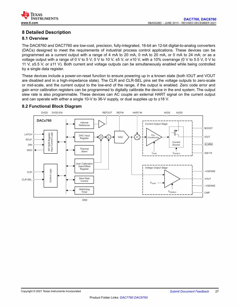
8 Detailed Description8.1 OverviewThe DAC8760 and DAC7760 are low-cost, precision, fully-integrated, 16-bit an 12-bit digital-to-analog converters (DACs) designed to meet the requirements of industrial process control applications. These devices can be programmed as a current output with a range of 4 mA to 20 mA, 0 mA to 20 mA, or 0 mA to 24 mA; or as a voltage output with a range of 0 V to 5 V, 0 V to 10 V, ±5 V, or ±10 V, with a 10% overrange (0 V to 5.5 V, 0 V to 11 V, ±5.5 V, or ±11 V). Both current and voltage outputs can be simultaneously enabled while being controlled by a single data register.
These devices include a power-on-reset function to ensure powering up in a known state (both IOUT and VOUT are disabled and in a high-impedance state). The CLR and CLR-SEL pins set the voltage outputs to zero-scale or mid-scale, and the current output to the low-end of the range, if the output is enabled. Zero code error and gain error calibration registers can be programmed to digitally calibrate the device in the end system. The output slew rate is also programmable. These devices can AC couple an external HART signal on the current output and can operate with either a single 10-V to 36-V supply, or dual supplies up to ±18 V.
8.2 Functional Block Diagram
DAC
GND
DACx760
AVDDDVDD-EN AVSSDVDD
Pre-Conditioning
CurrentSource
IENABLE ISET-RIGAIN
VGAIN
VENABLE
Current Output Stage
Voltage Output Stage
WatchdogTimer
Slew RateControl
User CalibrationGain/Offset
Register
DAC InputRegister
ThermalAlarm
InternalReference
SP
I S
hift
Re
gis
ter
Inp
ut
Co
ntr
ol L
og
icC
on
tro
l L
og
ic
CMP
–VSENSE
+VSENSE
VOUT
IOUT
ALARM
BOOST
REFOUT REFIN HART-IN
LATCH
SCLK
DIN
SDO
CLR
CLR-SEL
www.ti.comDAC7760, DAC8760
SBAS528D – JUNE 2013 – REVISED DECEMBER 2021
Copyright © 2021 Texas Instruments Incorporated Submit Document Feedback 27
Product Folder Links: DAC7760 DAC8760
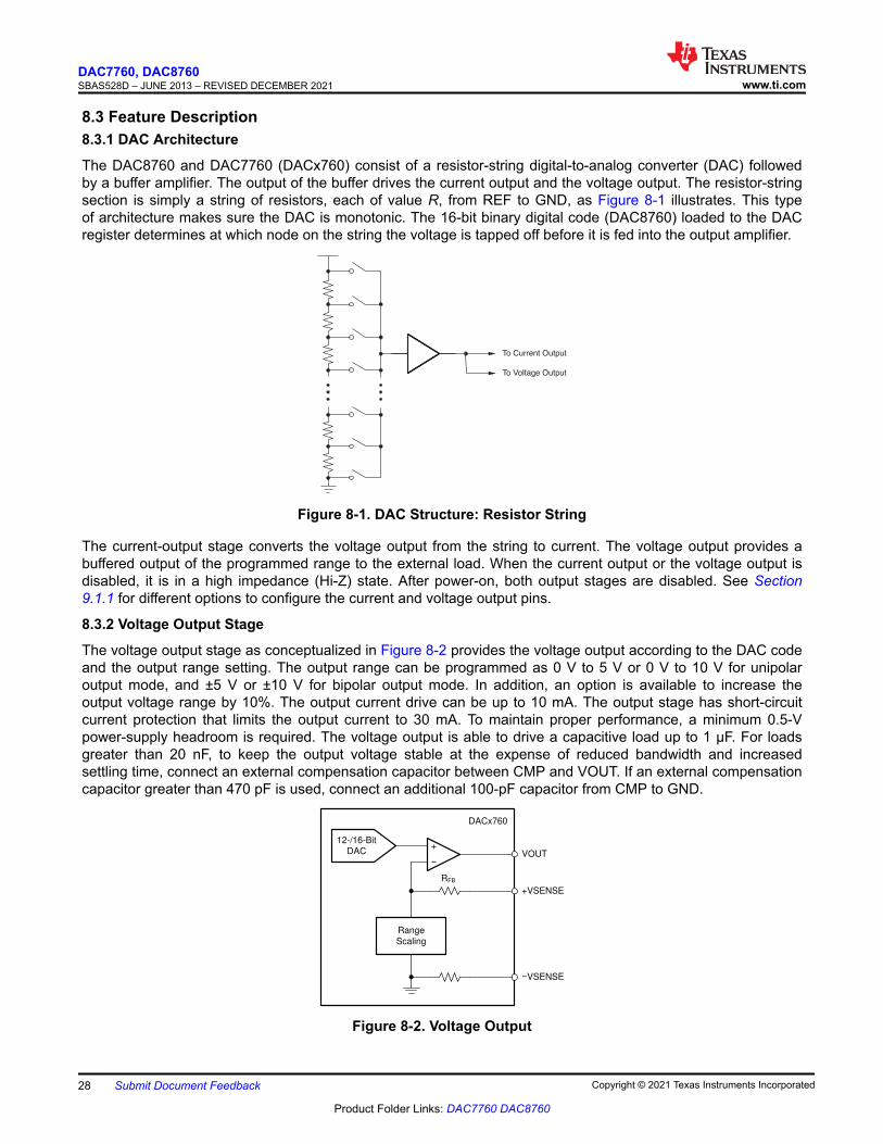
8.3 Feature Description8.3.1 DAC Architecture
The DAC8760 and DAC7760 (DACx760) consist of a resistor-string digital-to-analog converter (DAC) followed by a buffer amplifier. The output of the buffer drives the current output and the voltage output. The resistor-string section is simply a string of resistors, each of value R, from REF to GND, as Figure 8-1 illustrates. This type of architecture makes sure the DAC is monotonic. The 16-bit binary digital code (DAC8760) loaded to the DAC register determines at which node on the string the voltage is tapped off before it is fed into the output amplifier.
To Current Output
To Voltage Output
Figure 8-1. DAC Structure: Resistor String
The current-output stage converts the voltage output from the string to current. The voltage output provides a buffered output of the programmed range to the external load. When the current output or the voltage output is disabled, it is in a high impedance (Hi-Z) state. After power-on, both output stages are disabled. See Section 9.1.1 for different options to configure the current and voltage output pins.
8.3.2 Voltage Output Stage
The voltage output stage as conceptualized in Figure 8-2 provides the voltage output according to the DAC code and the output range setting. The output range can be programmed as 0 V to 5 V or 0 V to 10 V for unipolar output mode, and ±5 V or ±10 V for bipolar output mode. In addition, an option is available to increase the output voltage range by 10%. The output current drive can be up to 10 mA. The output stage has short-circuit current protection that limits the output current to 30 mA. To maintain proper performance, a minimum 0.5-V power-supply headroom is required. The voltage output is able to drive a capacitive load up to 1 µF. For loads greater than 20 nF, to keep the output voltage stable at the expense of reduced bandwidth and increased settling time, connect an external compensation capacitor between CMP and VOUT. If an external compensation capacitor greater than 470 pF is used, connect an additional 100-pF capacitor from CMP to GND.
+12-/16-Bit
DAC
DACx760
í
Range
Scaling
RFB
íVSENSE
+VSENSE
VOUT
Figure 8-2. Voltage Output
DAC7760, DAC8760SBAS528D – JUNE 2013 – REVISED DECEMBER 2021 www.ti.com
28 Submit Document Feedback Copyright © 2021 Texas Instruments Incorporated
Product Folder Links: DAC7760 DAC8760
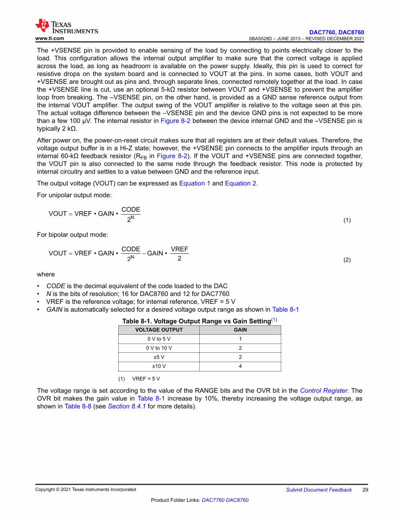
The +VSENSE pin is provided to enable sensing of the load by connecting to points electrically closer to the load. This configuration allows the internal output amplifier to make sure that the correct voltage is applied across the load, as long as headroom is available on the power supply. Ideally, this pin is used to correct for resistive drops on the system board and is connected to VOUT at the pins. In some cases, both VOUT and +VSENSE are brought out as pins and, through separate lines, connected remotely together at the load. In case the +VSENSE line is cut, use an optional 5-kΩ resistor between VOUT and +VSENSE to prevent the amplifier loop from breaking. The –VSENSE pin, on the other hand, is provided as a GND sense reference output from the internal VOUT amplifier. The output swing of the VOUT amplifier is relative to the voltage seen at this pin. The actual voltage difference between the –VSENSE pin and the device GND pins is not expected to be more than a few 100 µV. The internal resistor in Figure 8-2 between the device internal GND and the –VSENSE pin is typically 2 kΩ.
After power on, the power-on-reset circuit makes sure that all registers are at their default values. Therefore, the voltage output buffer is in a Hi-Z state; however, the +VSENSE pin connects to the amplifier inputs through an internal 60-kΩ feedback resistor (RFB in Figure 8-2). If the VOUT and +VSENSE pins are connected together, the VOUT pin is also connected to the same node through the feedback resistor. This node is protected by internal circuitry and settles to a value between GND and the reference input.
The output voltage (VOUT) can be expressed as Equation 1 and Equation 2.
For unipolar output mode:
N
CODEVOUT VREF • GAIN •
2
=
(1)
For bipolar output mode:
N
CODE VREFVOUT VREF • GAIN • GAIN •
22
= -
(2)
where
• CODE is the decimal equivalent of the code loaded to the DAC• N is the bits of resolution; 16 for DAC8760 and 12 for DAC7760• VREF is the reference voltage; for internal reference, VREF = 5 V• GAIN is automatically selected for a desired voltage output range as shown in Table 8-1
Table 8-1. Voltage Output Range vs Gain Setting(1)
VOLTAGE OUTPUT GAIN0 V to 5 V 1
0 V to 10 V 2
±5 V 2
±10 V 4
(1) VREF = 5 V
The voltage range is set according to the value of the RANGE bits and the OVR bit in the Control Register. The OVR bit makes the gain value in Table 8-1 increase by 10%, thereby increasing the voltage output range, as shown in Table 8-8 (see Section 8.4.1 for more details).
www.ti.comDAC7760, DAC8760
SBAS528D – JUNE 2013 – REVISED DECEMBER 2021
Copyright © 2021 Texas Instruments Incorporated Submit Document Feedback 29
Product Folder Links: DAC7760 DAC8760
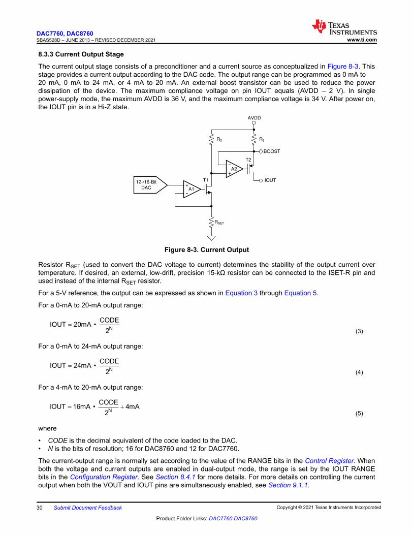
8.3.3 Current Output Stage
The current output stage consists of a preconditioner and a current source as conceptualized in Figure 8-3. This stage provides a current output according to the DAC code. The output range can be programmed as 0 mA to20 mA, 0 mA to 24 mA, or 4 mA to 20 mA. An external boost transistor can be used to reduce the power dissipation of the device. The maximum compliance voltage on pin IOUT equals (AVDD – 2 V). In single power-supply mode, the maximum AVDD is 36 V, and the maximum compliance voltage is 34 V. After power on, the IOUT pin is in a Hi-Z state.
+12-/16-BitBa_
DACBa_
RSET
R2
T1
A1
+
T2
A2
R3
í
í
IOUT
BOOST
AVDD
Figure 8-3. Current Output
Resistor RSET (used to convert the DAC voltage to current) determines the stability of the output current over temperature. If desired, an external, low-drift, precision 15-kΩ resistor can be connected to the ISET-R pin and used instead of the internal RSET resistor.
For a 5-V reference, the output can be expressed as shown in Equation 3 through Equation 5.
For a 0-mA to 20-mA output range:
N
CODEIOUT 20mA •
2
=
(3)
For a 0-mA to 24-mA output range:
N
CODEIOUT 24mA •
2
=
(4)
For a 4-mA to 20-mA output range:
N
CODEIOUT 16mA • 4mA
2
= +
(5)
where
• CODE is the decimal equivalent of the code loaded to the DAC.• N is the bits of resolution; 16 for DAC8760 and 12 for DAC7760.
The current-output range is normally set according to the value of the RANGE bits in the Control Register. When both the voltage and current outputs are enabled in dual-output mode, the range is set by the IOUT RANGE bits in the Configuration Register. See Section 8.4.1 for more details. For more details on controlling the current output when both the VOUT and IOUT pins are simultaneously enabled, see Section 9.1.1.
DAC7760, DAC8760SBAS528D – JUNE 2013 – REVISED DECEMBER 2021 www.ti.com
30 Submit Document Feedback Copyright © 2021 Texas Instruments Incorporated
Product Folder Links: DAC7760 DAC8760
8.3.4 Internal Reference
The DACx760 includes an integrated 5-V reference with a buffered output (REFOUT) capable of driving up to5 mA (source or sink) with an initial accuracy of ±5 mV (maximum) and a temperature drift coefficient of 10 ppm/°C (maximum).
8.3.5 Digital Power Supply
An internally generated 4.6-V supply capable of driving up to 10 mA can be output on DVDD by leaving the DVD-EN pin unconnected. This configuration simplifies the system power-supply design especially when an isolation barrier is required to cross and generate the digital supply. The internally generated supply can be used to drive isolation components used for the digital data lines and other miscellaneous components like references and temp sensors. See Figure 9-6 for an example application. If an external supply is preferred, the DVDD pin (which can be driven up to 5.5 V in this case) can be made into an input by tying DVDD-EN to GND (see Section 7.5 for detailed specifications).
8.3.6 DAC Clear
The DAC has an asynchronous clear function through the CLR pin, which is active-high and allows the voltage output to be cleared to either zero-scale code or midscale code. This action is user-selectable through the CLR-SEL pin or the CLRSEL bit of Table 8-17, as Table 8-2 describes. The CLR-SEL pin and CLRSEL register are ORed together. The current output clears to the bottom of its preprogrammed range. When the CLR signal returns to low, the output remains at the cleared value. The pre-clear value can be restored by pulsing the LATCH signal without clocking any data. A new value cannot be programmed until the CLR pin returns to low. Note that in dual-output mode, the value that the DAC data register is cleared to follows the settings for the voltage output mode.
Table 8-2. CLR-SEL Options
CLR-SELOUTPUT VALUE
UNIPOLAR OUTPUT RANGE BIPOLAR OUTPUT RANGE0 0 V 0 V
1 Midscale Negative full-scale
In addition to defining the output value for a clear operation, the CLRSEL bit and the CLR-SEL pin also define the default output value. During the selection of a new voltage range, the output value corresponds to the definitions given in Table 8-7. To avoid glitches on the output, disable the output by writing a 0 to the OUTEN bit of Table 8-17 before changing the voltage range. When the OUTEN bit is set to 1, the output goes to the default value as defined by the CLRSEL bit and the CLR-SEL pin.
8.3.7 Power-On Reset
The DACx760 incorporates two internal POR circuits for the DVDD and AVDD supplies. The DVDD and AVDD POR signals are ANDed together so that both supplies must be at their minimal specified values for the device to not be in a reset condition. These POR circuits initialize internal logic and registers as well as set the analog outputs to a known state while the device supplies are ramping. All registers are reset to their default values with the default value of the data register being determined by the CLR-SEL pin. The behavior of IOUT and VOUT is described in their respective sections. Typically the POR function can be ignored as long as the device supplies power up and maintain the specified minimum voltage levels. However, in the case of supply drop or brownout, the DACx760 can have an internal POR reset event or lose digital memory integrity. Figure 8-4 represents the threshold levels for the internal POR for both the DVDD and AVDD supplies.
www.ti.comDAC7760, DAC8760
SBAS528D – JUNE 2013 – REVISED DECEMBER 2021
Copyright © 2021 Texas Instruments Incorporated Submit Document Feedback 31
Product Folder Links: DAC7760 DAC8760
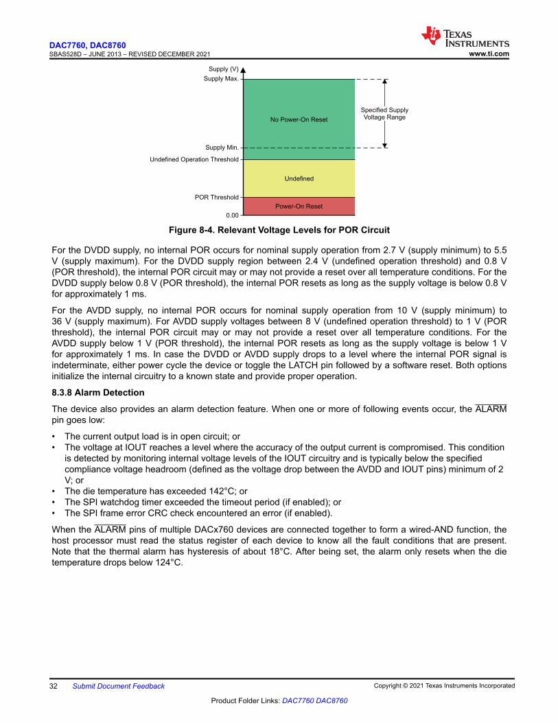
0.00
Supply (V)
Specified SupplyVoltage RangeNo Power-On Reset
Supply Max.
Supply Min.
Power-On Reset
POR Threshold
Undefined
Undefined Operation Threshold
Figure 8-4. Relevant Voltage Levels for POR Circuit
For the DVDD supply, no internal POR occurs for nominal supply operation from 2.7 V (supply minimum) to 5.5 V (supply maximum). For the DVDD supply region between 2.4 V (undefined operation threshold) and 0.8 V (POR threshold), the internal POR circuit may or may not provide a reset over all temperature conditions. For the DVDD supply below 0.8 V (POR threshold), the internal POR resets as long as the supply voltage is below 0.8 V for approximately 1 ms.
For the AVDD supply, no internal POR occurs for nominal supply operation from 10 V (supply minimum) to 36 V (supply maximum). For AVDD supply voltages between 8 V (undefined operation threshold) to 1 V (POR threshold), the internal POR circuit may or may not provide a reset over all temperature conditions. For the AVDD supply below 1 V (POR threshold), the internal POR resets as long as the supply voltage is below 1 V for approximately 1 ms. In case the DVDD or AVDD supply drops to a level where the internal POR signal is indeterminate, either power cycle the device or toggle the LATCH pin followed by a software reset. Both options initialize the internal circuitry to a known state and provide proper operation.
8.3.8 Alarm Detection
The device also provides an alarm detection feature. When one or more of following events occur, the ALARM pin goes low:
• The current output load is in open circuit; or• The voltage at IOUT reaches a level where the accuracy of the output current is compromised. This condition
is detected by monitoring internal voltage levels of the IOUT circuitry and is typically below the specified compliance voltage headroom (defined as the voltage drop between the AVDD and IOUT pins) minimum of 2 V; or
• The die temperature has exceeded 142°C; or• The SPI watchdog timer exceeded the timeout period (if enabled); or• The SPI frame error CRC check encountered an error (if enabled).
When the ALARM pins of multiple DACx760 devices are connected together to form a wired-AND function, the host processor must read the status register of each device to know all the fault conditions that are present. Note that the thermal alarm has hysteresis of about 18°C. After being set, the alarm only resets when the die temperature drops below 124°C.
DAC7760, DAC8760SBAS528D – JUNE 2013 – REVISED DECEMBER 2021 www.ti.com
32 Submit Document Feedback Copyright © 2021 Texas Instruments Incorporated
Product Folder Links: DAC7760 DAC8760
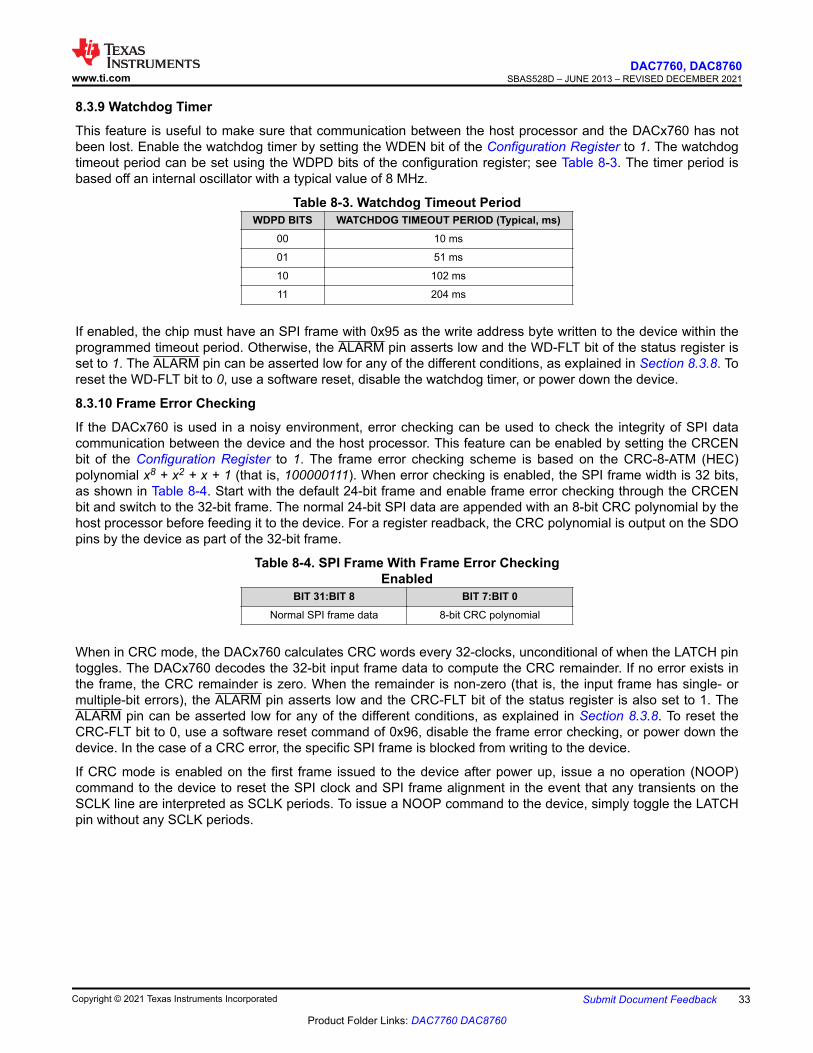
8.3.9 Watchdog Timer
This feature is useful to make sure that communication between the host processor and the DACx760 has not been lost. Enable the watchdog timer by setting the WDEN bit of the Configuration Register to 1. The watchdog timeout period can be set using the WDPD bits of the configuration register; see Table 8-3. The timer period is based off an internal oscillator with a typical value of 8 MHz.
Table 8-3. Watchdog Timeout PeriodWDPD BITS WATCHDOG TIMEOUT PERIOD (Typical, ms)
00 10 ms
01 51 ms
10 102 ms
11 204 ms
If enabled, the chip must have an SPI frame with 0x95 as the write address byte written to the device within the programmed timeout period. Otherwise, the ALARM pin asserts low and the WD-FLT bit of the status register is set to 1. The ALARM pin can be asserted low for any of the different conditions, as explained in Section 8.3.8. To reset the WD-FLT bit to 0, use a software reset, disable the watchdog timer, or power down the device.
8.3.10 Frame Error Checking
If the DACx760 is used in a noisy environment, error checking can be used to check the integrity of SPI data communication between the device and the host processor. This feature can be enabled by setting the CRCEN bit of the Configuration Register to 1. The frame error checking scheme is based on the CRC-8-ATM (HEC) polynomial x8 + x2 + x + 1 (that is, 100000111). When error checking is enabled, the SPI frame width is 32 bits, as shown in Table 8-4. Start with the default 24-bit frame and enable frame error checking through the CRCEN bit and switch to the 32-bit frame. The normal 24-bit SPI data are appended with an 8-bit CRC polynomial by the host processor before feeding it to the device. For a register readback, the CRC polynomial is output on the SDO pins by the device as part of the 32-bit frame.
Table 8-4. SPI Frame With Frame Error Checking Enabled
BIT 31:BIT 8 BIT 7:BIT 0Normal SPI frame data 8-bit CRC polynomial
When in CRC mode, the DACx760 calculates CRC words every 32-clocks, unconditional of when the LATCH pin toggles. The DACx760 decodes the 32-bit input frame data to compute the CRC remainder. If no error exists in the frame, the CRC remainder is zero. When the remainder is non-zero (that is, the input frame has single- or multiple-bit errors), the ALARM pin asserts low and the CRC-FLT bit of the status register is also set to 1. The ALARM pin can be asserted low for any of the different conditions, as explained in Section 8.3.8. To reset the CRC-FLT bit to 0, use a software reset command of 0x96, disable the frame error checking, or power down the device. In the case of a CRC error, the specific SPI frame is blocked from writing to the device.
If CRC mode is enabled on the first frame issued to the device after power up, issue a no operation (NOOP) command to the device to reset the SPI clock and SPI frame alignment in the event that any transients on the SCLK line are interpreted as SCLK periods. To issue a NOOP command to the device, simply toggle the LATCH pin without any SCLK periods.
www.ti.comDAC7760, DAC8760
SBAS528D – JUNE 2013 – REVISED DECEMBER 2021
Copyright © 2021 Texas Instruments Incorporated Submit Document Feedback 33
Product Folder Links: DAC7760 DAC8760
8.3.11 User Calibration
The device implements a user-calibration function to allow for trimming the system gain and zero errors. There is a gain calibration register and a zero calibration register; the DAC output is calibrated according to the value of these registers. The range of gain adjustment is typically ±50% of full-scale with 1 LSB per step. The gain register must be programmed to a value of 0x8000 to achieve the default gain of 1 because the power-on value of the register is 0x0000, which is equivalent to a gain of 0.5. The zero code adjustment is typically ±32,768 LSBs with 1 LSB per step. The input data format of the gain register is unsigned straight binary, and the input data format of the zero register is twos complement. The gain and offset calibration is described by Equation 6.
15
16
User _ GAIN 2CODE _ OUT CODE • User _ ZERO
2
+= +
(6)
where
• CODE is the decimal equivalent of the code loaded to the DAC data register at address 0x01.• N is the bits of resolution; 16 for DAC8760 and 12 for DAC7760.• User_ZERO is the signed 16-bit code in the zero register.• User_GAIN is the unsigned 16-bit code in the gain register.• CODE_OUT is the decimal equivalent of the code loaded to the DAC (limited between 0x0000 to 0xFFFF for
DAC8760 and 0x000 to 0xFFF for DAC7760).
This implementation is purely digital and the output is still limited by the programmed value at both ends of the voltage or current output range. In addition, remember that the correction only makes sense for endpoints inside of the true device end points. To correct more than just the actual device error (for example, a system offset), the valid range for the adjustment changes accordingly and must be taken into account. This range is set by the RANGE, OVR, DUAL OUTEN, and IOUT RANGE bits, as described in Section 8.4.1.
New calibration codes are only applied to subsequent writes of the DAC data register. Updating the calibration codes does not automatically update the DAC output. Additionally, before applying new DAC data, configure the calibration codes along with the slew rate control.
DAC7760, DAC8760SBAS528D – JUNE 2013 – REVISED DECEMBER 2021 www.ti.com
34 Submit Document Feedback Copyright © 2021 Texas Instruments Incorporated
Product Folder Links: DAC7760 DAC8760
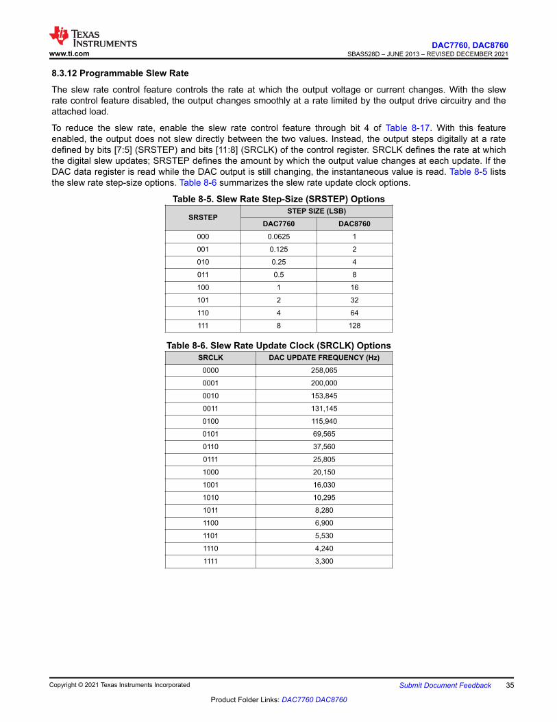
8.3.12 Programmable Slew Rate
The slew rate control feature controls the rate at which the output voltage or current changes. With the slew rate control feature disabled, the output changes smoothly at a rate limited by the output drive circuitry and the attached load.
To reduce the slew rate, enable the slew rate control feature through bit 4 of Table 8-17. With this feature enabled, the output does not slew directly between the two values. Instead, the output steps digitally at a rate defined by bits [7:5] (SRSTEP) and bits [11:8] (SRCLK) of the control register. SRCLK defines the rate at which the digital slew updates; SRSTEP defines the amount by which the output value changes at each update. If the DAC data register is read while the DAC output is still changing, the instantaneous value is read. Table 8-5 lists the slew rate step-size options. Table 8-6 summarizes the slew rate update clock options.
Table 8-5. Slew Rate Step-Size (SRSTEP) Options
SRSTEPSTEP SIZE (LSB)
DAC7760 DAC8760000 0.0625 1
001 0.125 2
010 0.25 4
011 0.5 8
100 1 16
101 2 32
110 4 64
111 8 128
Table 8-6. Slew Rate Update Clock (SRCLK) OptionsSRCLK DAC UPDATE FREQUENCY (Hz)
0000 258,065
0001 200,000
0010 153,845
0011 131,145
0100 115,940
0101 69,565
0110 37,560
0111 25,805
1000 20,150
1001 16,030
1010 10,295
1011 8,280
1100 6,900
1101 5,530
1110 4,240
1111 3,300
www.ti.comDAC7760, DAC8760
SBAS528D – JUNE 2013 – REVISED DECEMBER 2021
Copyright © 2021 Texas Instruments Incorporated Submit Document Feedback 35
Product Folder Links: DAC7760 DAC8760
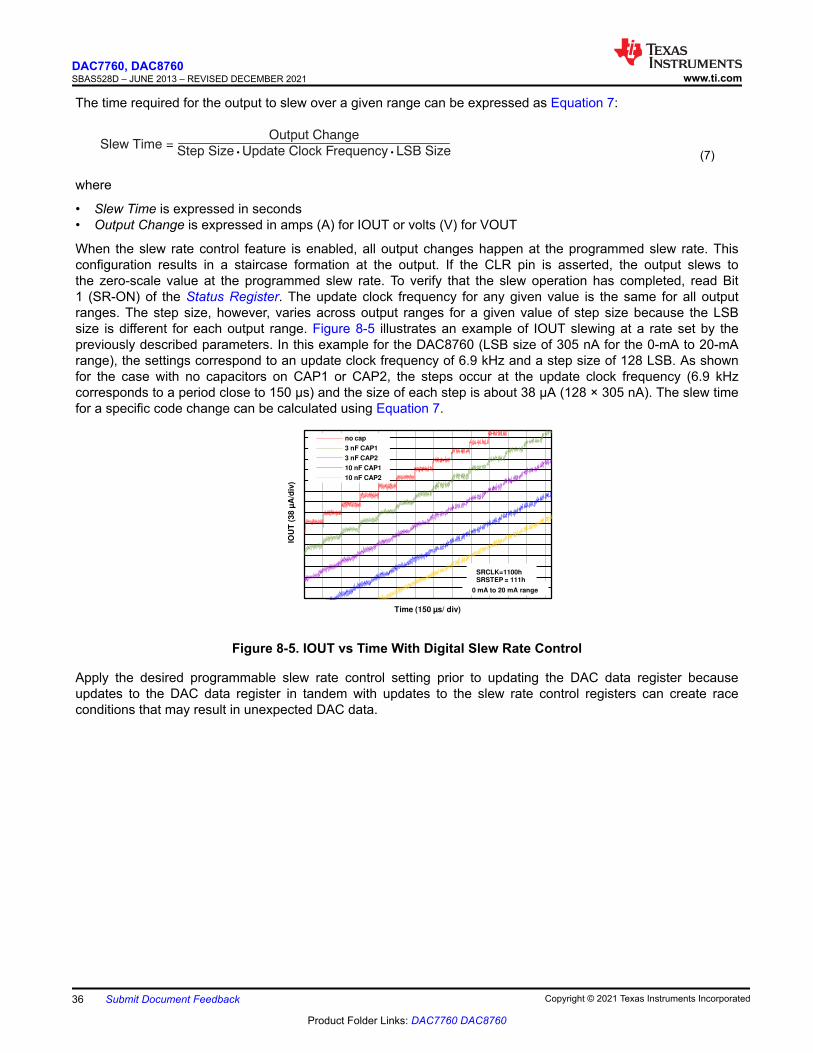
The time required for the output to slew over a given range can be expressed as Equation 7:
Slew Time =Output Change
Step Size Update Clock Frequency LSB Size· · (7)
where
• Slew Time is expressed in seconds• Output Change is expressed in amps (A) for IOUT or volts (V) for VOUT
When the slew rate control feature is enabled, all output changes happen at the programmed slew rate. This configuration results in a staircase formation at the output. If the CLR pin is asserted, the output slews to the zero-scale value at the programmed slew rate. To verify that the slew operation has completed, read Bit 1 (SR-ON) of the Status Register. The update clock frequency for any given value is the same for all output ranges. The step size, however, varies across output ranges for a given value of step size because the LSB size is different for each output range. Figure 8-5 illustrates an example of IOUT slewing at a rate set by the previously described parameters. In this example for the DAC8760 (LSB size of 305 nA for the 0-mA to 20-mA range), the settings correspond to an update clock frequency of 6.9 kHz and a step size of 128 LSB. As shown for the case with no capacitors on CAP1 or CAP2, the steps occur at the update clock frequency (6.9 kHz corresponds to a period close to 150 µs) and the size of each step is about 38 µA (128 × 305 nA). The slew time for a specific code change can be calculated using Equation 7.
IOU
T (
38
µA
/div
)
Time (150 µs/ div)
no cap
3 nF CAP1
3 nF CAP2
10 nF CAP1
10 nF CAP2
C001
0 mA to 20 mA range
SRCLK=1100h SRSTEP = 111h
Figure 8-5. IOUT vs Time With Digital Slew Rate Control
Apply the desired programmable slew rate control setting prior to updating the DAC data register because updates to the DAC data register in tandem with updates to the slew rate control registers can create race conditions that may result in unexpected DAC data.
DAC7760, DAC8760SBAS528D – JUNE 2013 – REVISED DECEMBER 2021 www.ti.com
36 Submit Document Feedback Copyright © 2021 Texas Instruments Incorporated
Product Folder Links: DAC7760 DAC8760
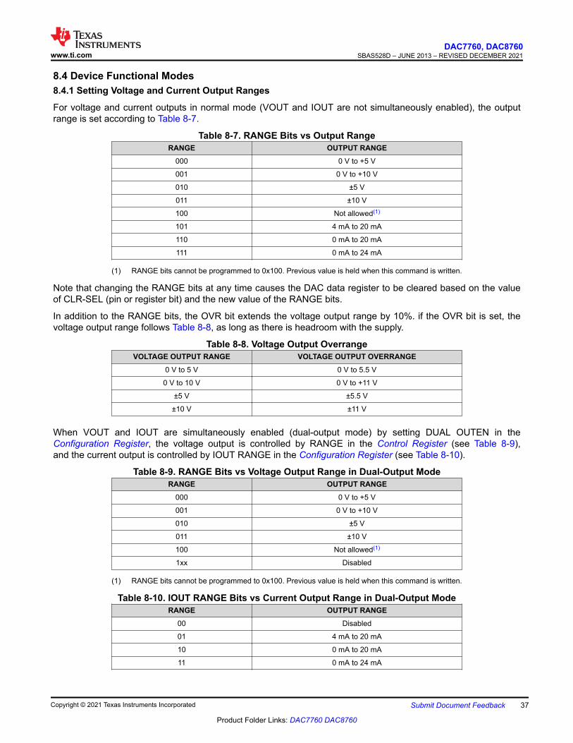
8.4 Device Functional Modes8.4.1 Setting Voltage and Current Output Ranges
For voltage and current outputs in normal mode (VOUT and IOUT are not simultaneously enabled), the output range is set according to Table 8-7.
Table 8-7. RANGE Bits vs Output RangeRANGE OUTPUT RANGE
000 0 V to +5 V
001 0 V to +10 V
010 ±5 V
011 ±10 V
100 Not allowed(1)
101 4 mA to 20 mA
110 0 mA to 20 mA
111 0 mA to 24 mA
(1) RANGE bits cannot be programmed to 0x100. Previous value is held when this command is written.
Note that changing the RANGE bits at any time causes the DAC data register to be cleared based on the value of CLR-SEL (pin or register bit) and the new value of the RANGE bits.
In addition to the RANGE bits, the OVR bit extends the voltage output range by 10%. if the OVR bit is set, the voltage output range follows Table 8-8, as long as there is headroom with the supply.
Table 8-8. Voltage Output OverrangeVOLTAGE OUTPUT RANGE VOLTAGE OUTPUT OVERRANGE
0 V to 5 V 0 V to 5.5 V
0 V to 10 V 0 V to +11 V
±5 V ±5.5 V
±10 V ±11 V
When VOUT and IOUT are simultaneously enabled (dual-output mode) by setting DUAL OUTEN in the Configuration Register, the voltage output is controlled by RANGE in the Control Register (see Table 8-9), and the current output is controlled by IOUT RANGE in the Configuration Register (see Table 8-10).
Table 8-9. RANGE Bits vs Voltage Output Range in Dual-Output ModeRANGE OUTPUT RANGE
000 0 V to +5 V
001 0 V to +10 V
010 ±5 V
011 ±10 V
100 Not allowed(1)
1xx Disabled
(1) RANGE bits cannot be programmed to 0x100. Previous value is held when this command is written.
Table 8-10. IOUT RANGE Bits vs Current Output Range in Dual-Output ModeRANGE OUTPUT RANGE
00 Disabled
01 4 mA to 20 mA
10 0 mA to 20 mA
11 0 mA to 24 mA
www.ti.comDAC7760, DAC8760
SBAS528D – JUNE 2013 – REVISED DECEMBER 2021
Copyright © 2021 Texas Instruments Incorporated Submit Document Feedback 37
Product Folder Links: DAC7760 DAC8760
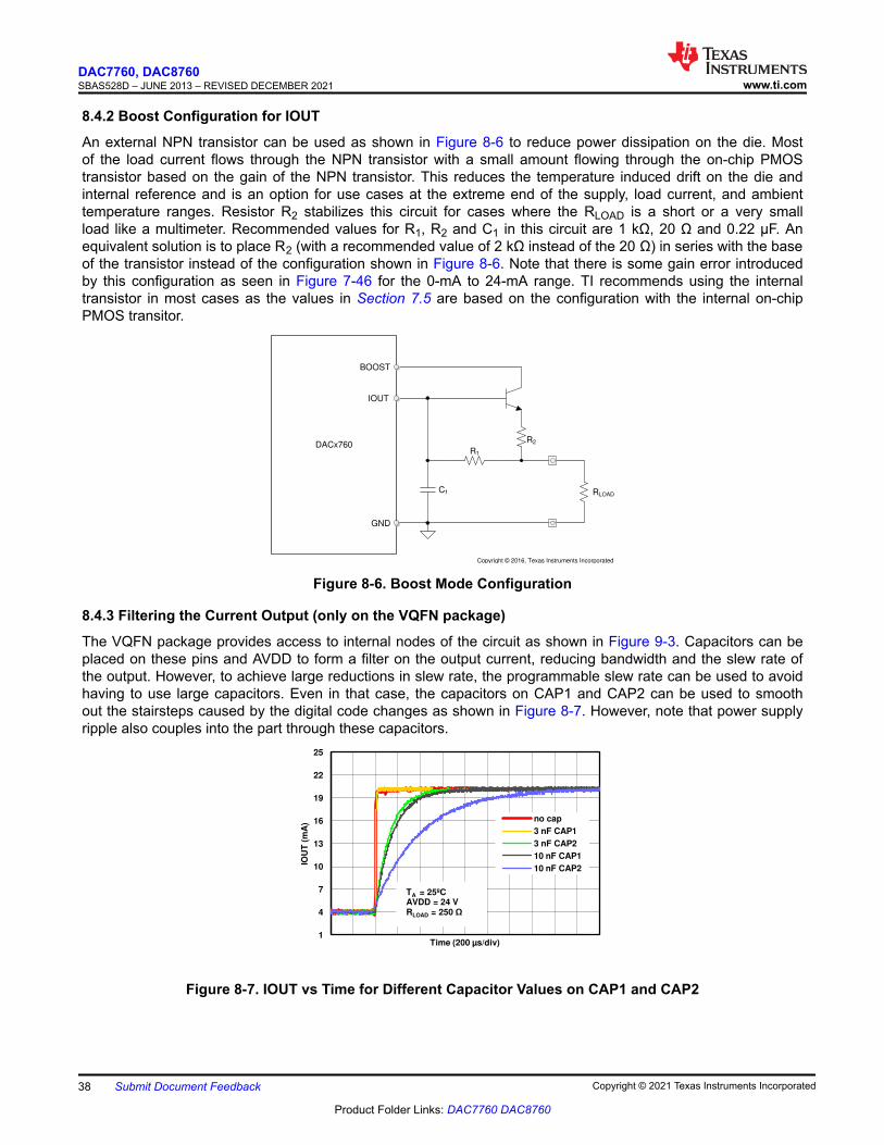
8.4.2 Boost Configuration for IOUT
An external NPN transistor can be used as shown in Figure 8-6 to reduce power dissipation on the die. Most of the load current flows through the NPN transistor with a small amount flowing through the on-chip PMOS transistor based on the gain of the NPN transistor. This reduces the temperature induced drift on the die and internal reference and is an option for use cases at the extreme end of the supply, load current, and ambient temperature ranges. Resistor R2 stabilizes this circuit for cases where the RLOAD is a short or a very small load like a multimeter. Recommended values for R1, R2 and C1 in this circuit are 1 kΩ, 20 Ω and 0.22 µF. An equivalent solution is to place R2 (with a recommended value of 2 kΩ instead of the 20 Ω) in series with the base of the transistor instead of the configuration shown in Figure 8-6. Note that there is some gain error introduced by this configuration as seen in Figure 7-46 for the 0-mA to 24-mA range. TI recommends using the internal transistor in most cases as the values in Section 7.5 are based on the configuration with the internal on-chip PMOS transitor.
R1
R2
RLOADC1
DACx760
BOOST
IOUT
GND
Copyright © 2016, Texas Instruments Incorporated
Figure 8-6. Boost Mode Configuration
8.4.3 Filtering the Current Output (only on the VQFN package)
The VQFN package provides access to internal nodes of the circuit as shown in Figure 9-3. Capacitors can be placed on these pins and AVDD to form a filter on the output current, reducing bandwidth and the slew rate of the output. However, to achieve large reductions in slew rate, the programmable slew rate can be used to avoid having to use large capacitors. Even in that case, the capacitors on CAP1 and CAP2 can be used to smooth out the stairsteps caused by the digital code changes as shown in Figure 8-7. However, note that power supply ripple also couples into the part through these capacitors.
1
4
7
10
13
16
19
22
25
IOU
T (
mA
)
Time (200 µs/div)
no cap
3 nF CAP1
3 nF CAP2
10 nF CAP1
10 nF CAP2
C001
TA = 25ºC AVDD = 24 V RLOAD = 250
Figure 8-7. IOUT vs Time for Different Capacitor Values on CAP1 and CAP2
DAC7760, DAC8760SBAS528D – JUNE 2013 – REVISED DECEMBER 2021 www.ti.com
38 Submit Document Feedback Copyright © 2021 Texas Instruments Incorporated
Product Folder Links: DAC7760 DAC8760
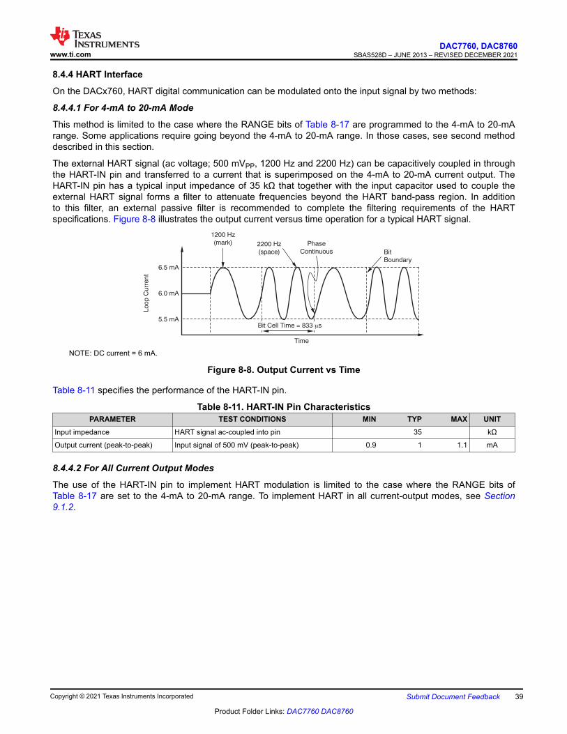
8.4.4 HART Interface
On the DACx760, HART digital communication can be modulated onto the input signal by two methods:
8.4.4.1 For 4-mA to 20-mA Mode
This method is limited to the case where the RANGE bits of Table 8-17 are programmed to the 4-mA to 20-mA range. Some applications require going beyond the 4-mA to 20-mA range. In those cases, see second method described in this section.
The external HART signal (ac voltage; 500 mVPP, 1200 Hz and 2200 Hz) can be capacitively coupled in through the HART-IN pin and transferred to a current that is superimposed on the 4-mA to 20-mA current output. The HART-IN pin has a typical input impedance of 35 kΩ that together with the input capacitor used to couple the external HART signal forms a filter to attenuate frequencies beyond the HART band-pass region. In addition to this filter, an external passive filter is recommended to complete the filtering requirements of the HART specifications. Figure 8-8 illustrates the output current versus time operation for a typical HART signal.
Bit
Boundary
Phase
Continuous2200 Hz
(space)
1200 Hz
(mark)
Time
5.5 mA
6.5 mA
6.0 mA
Loop C
urr
ent
Bit Cell Time = 833 sm
NOTE: DC current = 6 mA.
Figure 8-8. Output Current vs Time
Table 8-11 specifies the performance of the HART-IN pin.
Table 8-11. HART-IN Pin CharacteristicsPARAMETER TEST CONDITIONS MIN TYP MAX UNIT
Input impedance HART signal ac-coupled into pin 35 kΩ
Output current (peak-to-peak) Input signal of 500 mV (peak-to-peak) 0.9 1 1.1 mA
8.4.4.2 For All Current Output Modes
The use of the HART-IN pin to implement HART modulation is limited to the case where the RANGE bits of Table 8-17 are set to the 4-mA to 20-mA range. To implement HART in all current-output modes, see Section 9.1.2.
www.ti.comDAC7760, DAC8760
SBAS528D – JUNE 2013 – REVISED DECEMBER 2021
Copyright © 2021 Texas Instruments Incorporated Submit Document Feedback 39
Product Folder Links: DAC7760 DAC8760
8.5 Programming8.5.1 Serial Peripheral Interface (SPI)
The device is controlled over a versatile four-wire serial interface (SDI, SDO, SCLK, and LATCH) that operates at clock rates of up to 30 MHz and is compatible with SPI, QSPI, Microwire, and digital signal processing (DSP) standards. The SPI communication command consists of a write address byte and a data word for a total of 24 bits. The timing for the digital interface is shown in Figure 7-1 and Figure 7-2.
8.5.1.1 SPI Shift Register
The default frame is 24 bits wide (see Section 8.3.10 for 32-bit frame mode) and begins with the rising edge of SCLK that clocks in the MSB. The subsequent bits are latched on successive rising edges of SCLK. The default 24-bit input frame consists of an 8-bit address byte followed by a 16-bit data word as shown in Table 8-12.
Table 8-12. Default SPI FrameBIT 23:BIT 16 BIT 15:BIT 0Address byte Data word
The host processor must issue 24 bits before it issues a rising edge on the LATCH pin. Input data bits are clocked in regardless of the LATCH pin and are unconditionally latched on the rising edge of LATCH. By default, the SPI shift register resets to 000000h at power on or after a reset.
8.5.1.2 Write Operation
A write operation is accomplished when the address byte is set according to Table 8-13. For more information on the DACx760 registers, see Section 8.6.1.
Table 8-13. Write Address FunctionsADDRESS BYTE FUNCTION
0x00 No operation (NOP)
0x01 Write DAC Data register
0x02 Register read
0x55 Write control register
0x56 Write reset register
0x57 Write configuration register
0x58 Write DAC gain calibration register
0x59 Write DAC zero calibration register
0x95 Watchdog timer reset
0x96 CRC error reset
8.5.1.3 Read Operation
A read operation is accomplished when the address byte is 0x02. Follow the read operation with a no-operation (NOP) command to clock out an addressed register, as shown in Figure 7-2. To read from a register, the address byte and data word is as shown in Table 8-14. The read register value is output MSB first on SDO on successive falling edges of SCLK.
Table 8-14. Default SPI Frame for Register Read
ADDRESS BYTEDATA WORD
BIT 15:BIT 6 BIT 5:BIT 00x02 X (don't care) Register read address (see Table 8-15)
DAC7760, DAC8760SBAS528D – JUNE 2013 – REVISED DECEMBER 2021 www.ti.com
40 Submit Document Feedback Copyright © 2021 Texas Instruments Incorporated
Product Folder Links: DAC7760 DAC8760
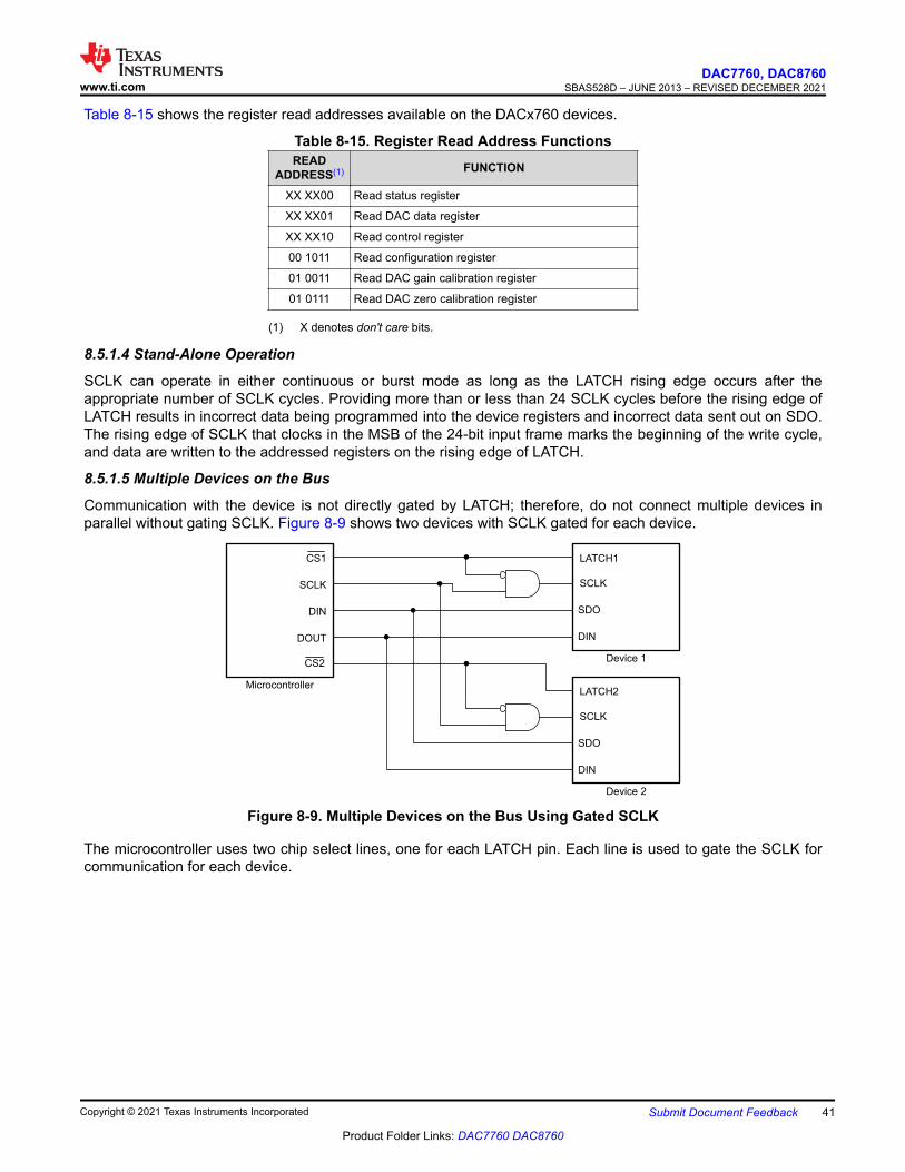
Table 8-15 shows the register read addresses available on the DACx760 devices.
Table 8-15. Register Read Address FunctionsREAD
ADDRESS(1) FUNCTION
XX XX00 Read status register
XX XX01 Read DAC data register
XX XX10 Read control register
00 1011 Read configuration register
01 0011 Read DAC gain calibration register
01 0111 Read DAC zero calibration register
(1) X denotes don't care bits.
8.5.1.4 Stand-Alone Operation
SCLK can operate in either continuous or burst mode as long as the LATCH rising edge occurs after the appropriate number of SCLK cycles. Providing more than or less than 24 SCLK cycles before the rising edge of LATCH results in incorrect data being programmed into the device registers and incorrect data sent out on SDO. The rising edge of SCLK that clocks in the MSB of the 24-bit input frame marks the beginning of the write cycle, and data are written to the addressed registers on the rising edge of LATCH.
8.5.1.5 Multiple Devices on the Bus
Communication with the device is not directly gated by LATCH; therefore, do not connect multiple devices in parallel without gating SCLK. Figure 8-9 shows two devices with SCLK gated for each device.
SCLK
DIN
DOUT
CS2
Microcontroller
CS1
Device 1
SCLK
LATCH1
SDO
DIN
Device 2
SCLK
LATCH2
SDO
DIN
Figure 8-9. Multiple Devices on the Bus Using Gated SCLK
The microcontroller uses two chip select lines, one for each LATCH pin. Each line is used to gate the SCLK for communication for each device.
www.ti.comDAC7760, DAC8760
SBAS528D – JUNE 2013 – REVISED DECEMBER 2021
Copyright © 2021 Texas Instruments Incorporated Submit Document Feedback 41
Product Folder Links: DAC7760 DAC8760
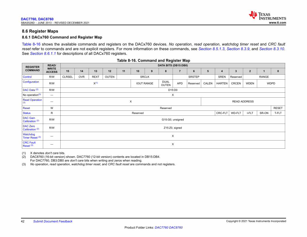
8.6 Register Maps8.6.1 DACx760 Command and Register Map
Table 8-16 shows the available commands and registers on the DACx760 devices. No operation, read operation, watchdog timer reset and CRC fault reset refer to commands and are not explicit registers. For more information on these commands, see Section 8.5.1.3, Section 8.3.9, and Section 8.3.10. See Section 8.6.1.1 for descriptions of all DACx760 registers.
Table 8-16. Command and Register MapREGISTER COMMAND
READ/WRITE
ACCESS
DATA BITS (DB15:DB0)
15 14 13 12 11 10 9 8 7 6 5 4 3 2 1 0
Control R/W CLRSEL OVR REXT OUTEN SRCLK SRSTEP SREN Reserved RANGE
Configuration R/W X(1) IOUT RANGE DUAL OUTEN APD Reserved CALEN HARTEN CRCEN WDEN WDPD
DAC Data (2) R/W D15:D0
No operation(3) — X
Read Operation (3) — X READ ADDRESS
Reset W Reserved RESET
Status R Reserved CRC-FLT WD-FLT I-FLT SR-ON T-FLT
DAC Gain Calibration (2) R/W G15:G0, unsigned
DAC Zero Calibration (2) R/W Z15:Z0, signed
Watchdog Timer Reset (3) — X
CRC Fault Reset (3) — X
(1) X denotes don't care bits.(2) DAC8760 (16-bit version) shown. DAC7760 (12-bit version) contents are located in DB15:DB4.
For DAC7760, DB3:DB0 are don't care bits when writing and zeros when reading.(3) No operation, read operation, watchdog timer reset, and CRC fault reset are commands and not registers.
DAC7760, DAC8760SBAS528D – JUNE 2013 – REVISED DECEMBER 2021 www.ti.com
42 Submit Document Feedback Copyright © 2021 Texas Instruments Incorporated
Product Folder Links: DAC7760 DAC8760
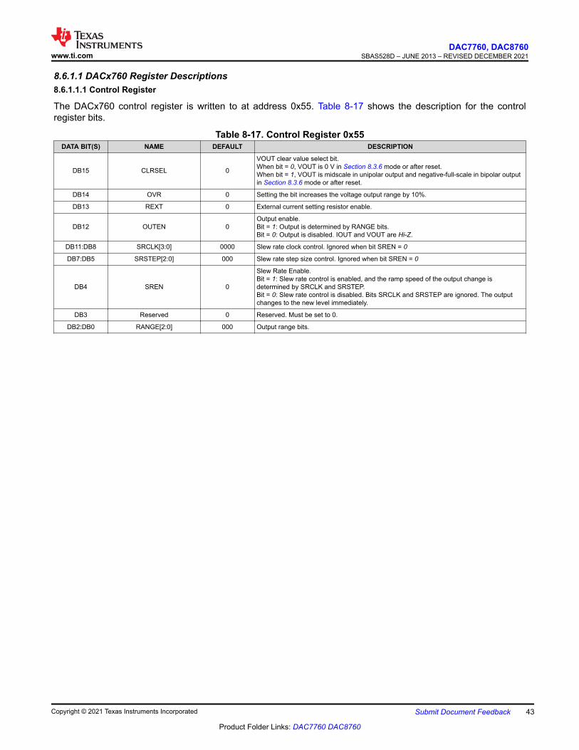
8.6.1.1 DACx760 Register Descriptions8.6.1.1.1 Control Register
The DACx760 control register is written to at address 0x55. Table 8-17 shows the description for the control register bits.
Table 8-17. Control Register 0x55DATA BIT(S) NAME DEFAULT DESCRIPTION
DB15 CLRSEL 0
VOUT clear value select bit.When bit = 0, VOUT is 0 V in Section 8.3.6 mode or after reset.When bit = 1, VOUT is midscale in unipolar output and negative-full-scale in bipolar output in Section 8.3.6 mode or after reset.
DB14 OVR 0 Setting the bit increases the voltage output range by 10%.
DB13 REXT 0 External current setting resistor enable.
DB12 OUTEN 0Output enable.Bit = 1: Output is determined by RANGE bits.Bit = 0: Output is disabled. IOUT and VOUT are Hi-Z.
DB11:DB8 SRCLK[3:0] 0000 Slew rate clock control. Ignored when bit SREN = 0
DB7:DB5 SRSTEP[2:0] 000 Slew rate step size control. Ignored when bit SREN = 0
DB4 SREN 0
Slew Rate Enable.Bit = 1: Slew rate control is enabled, and the ramp speed of the output change is determined by SRCLK and SRSTEP.Bit = 0: Slew rate control is disabled. Bits SRCLK and SRSTEP are ignored. The output changes to the new level immediately.
DB3 Reserved 0 Reserved. Must be set to 0.
DB2:DB0 RANGE[2:0] 000 Output range bits.
www.ti.comDAC7760, DAC8760
SBAS528D – JUNE 2013 – REVISED DECEMBER 2021
Copyright © 2021 Texas Instruments Incorporated Submit Document Feedback 43
Product Folder Links: DAC7760 DAC8760
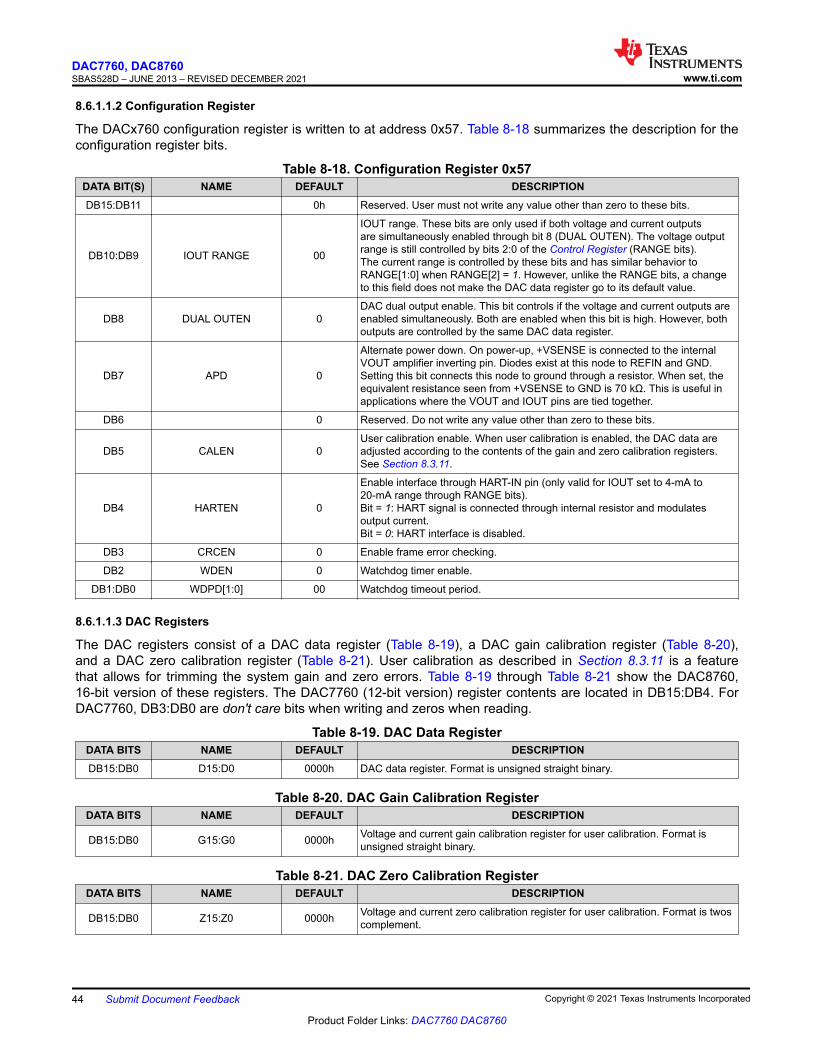
8.6.1.1.2 Configuration Register
The DACx760 configuration register is written to at address 0x57. Table 8-18 summarizes the description for the configuration register bits.
Table 8-18. Configuration Register 0x57DATA BIT(S) NAME DEFAULT DESCRIPTIONDB15:DB11 0h Reserved. User must not write any value other than zero to these bits.
DB10:DB9 IOUT RANGE 00
IOUT range. These bits are only used if both voltage and current outputs are simultaneously enabled through bit 8 (DUAL OUTEN). The voltage output range is still controlled by bits 2:0 of the Control Register (RANGE bits). The current range is controlled by these bits and has similar behavior to RANGE[1:0] when RANGE[2] = 1. However, unlike the RANGE bits, a change to this field does not make the DAC data register go to its default value.
DB8 DUAL OUTEN 0DAC dual output enable. This bit controls if the voltage and current outputs are enabled simultaneously. Both are enabled when this bit is high. However, both outputs are controlled by the same DAC data register.
DB7 APD 0
Alternate power down. On power-up, +VSENSE is connected to the internal VOUT amplifier inverting pin. Diodes exist at this node to REFIN and GND. Setting this bit connects this node to ground through a resistor. When set, the equivalent resistance seen from +VSENSE to GND is 70 kΩ. This is useful in applications where the VOUT and IOUT pins are tied together.
DB6 0 Reserved. Do not write any value other than zero to these bits.
DB5 CALEN 0User calibration enable. When user calibration is enabled, the DAC data are adjusted according to the contents of the gain and zero calibration registers. See Section 8.3.11.
DB4 HARTEN 0
Enable interface through HART-IN pin (only valid for IOUT set to 4-mA to 20-mA range through RANGE bits).Bit = 1: HART signal is connected through internal resistor and modulates output current.Bit = 0: HART interface is disabled.
DB3 CRCEN 0 Enable frame error checking.
DB2 WDEN 0 Watchdog timer enable.
DB1:DB0 WDPD[1:0] 00 Watchdog timeout period.
8.6.1.1.3 DAC Registers
The DAC registers consist of a DAC data register (Table 8-19), a DAC gain calibration register (Table 8-20), and a DAC zero calibration register (Table 8-21). User calibration as described in Section 8.3.11 is a feature that allows for trimming the system gain and zero errors. Table 8-19 through Table 8-21 show the DAC8760, 16-bit version of these registers. The DAC7760 (12-bit version) register contents are located in DB15:DB4. For DAC7760, DB3:DB0 are don't care bits when writing and zeros when reading.
Table 8-19. DAC Data RegisterDATA BITS NAME DEFAULT DESCRIPTIONDB15:DB0 D15:D0 0000h DAC data register. Format is unsigned straight binary.
Table 8-20. DAC Gain Calibration RegisterDATA BITS NAME DEFAULT DESCRIPTION
DB15:DB0 G15:G0 0000h Voltage and current gain calibration register for user calibration. Format is unsigned straight binary.
Table 8-21. DAC Zero Calibration RegisterDATA BITS NAME DEFAULT DESCRIPTION
DB15:DB0 Z15:Z0 0000h Voltage and current zero calibration register for user calibration. Format is twos complement.
DAC7760, DAC8760SBAS528D – JUNE 2013 – REVISED DECEMBER 2021 www.ti.com
44 Submit Document Feedback Copyright © 2021 Texas Instruments Incorporated
Product Folder Links: DAC7760 DAC8760
8.6.1.1.4 Reset Register
The DACx760 reset register is written to at address 0x56. Table 8-22 provides the description.
Table 8-22. Reset Register 0x56DATA BIT(S) NAME DEFAULT DESCRIPTION
DB15:DB1 0000h Reserved. Writing to these bits does not cause any change.
DB0 RESET 0Software reset bit. Writing 1 to the bit performs a software reset to reset all registers and the ALARM status to the respective power-on reset default value. After reset completes the RESET bit clears itself.
8.6.1.1.5 Status Register
This read-only register consists of four ALARM status bits (CRC-FLT, WD-FLT, I-FLT, and T-FLT) and bit SR-ON that shows the slew rate status.
The device continuously monitors the output and die temperature. When an alarm occurs, the corresponding ALARM status bit is set (1). Whenever an ALARM status bit is set, it remains set until the event that caused it is resolved. The ALARM bit can only be cleared by performing a software reset, or a power-on reset (by cycling power), or having the error condition resolved. These bits are reasserted if the ALARM condition continues to exist in the next monitoring cycle.
The ALARM bit goes to 0 when the error condition is resolved.
Table 8-23. Status RegisterDATA BIT(S) NAME DEFAULT DESCRIPTION
DB15:DB5 000h Reserved. Reading these bits returns 0.
DB4 CRC-FLT 0 Bit = 1 indicates CRC error on SPI frame.Bit = 0 indicates normal operation.
DB3 WD-FLT 0 Bit = 1 indicates watchdog timer timeout.Bit = 0 indicates normal operation.
DB2 I-FLT 0 Bit = 1 indicates Open Circuit or Compliance Voltage Violation in IOUT loading.Bit = 0 indicates IOUT load is at normal condition.
DB1 SR-ON 0 Bit = 1 when DAC code is slewing as determined by SRCLK and SRSTEP.Bit = 0 when DAC code is not slewing.
DB0 T-FLT 0 Bit = 1 indicates die temperature is over 142°C.Bit = 0 indicates die temperature is not over 142°C.
www.ti.comDAC7760, DAC8760
SBAS528D – JUNE 2013 – REVISED DECEMBER 2021
Copyright © 2021 Texas Instruments Incorporated Submit Document Feedback 45
Product Folder Links: DAC7760 DAC8760
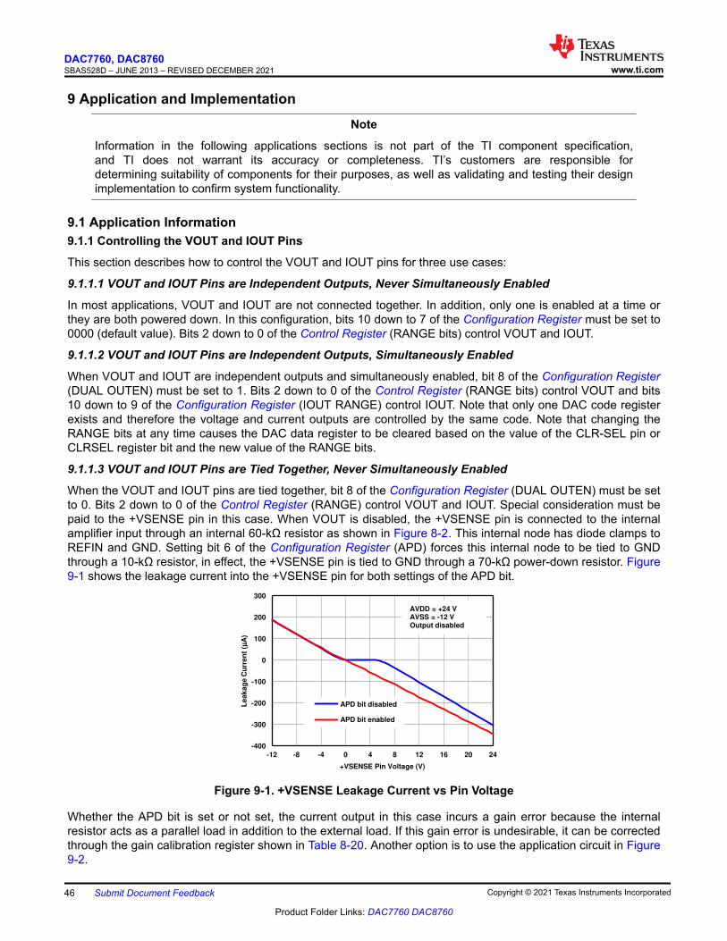
9 Application and ImplementationNote
Information in the following applications sections is not part of the TI component specification, and TI does not warrant its accuracy or completeness. TI’s customers are responsible for determining suitability of components for their purposes, as well as validating and testing their design implementation to confirm system functionality.
9.1 Application Information9.1.1 Controlling the VOUT and IOUT Pins
This section describes how to control the VOUT and IOUT pins for three use cases:
9.1.1.1 VOUT and IOUT Pins are Independent Outputs, Never Simultaneously Enabled
In most applications, VOUT and IOUT are not connected together. In addition, only one is enabled at a time or they are both powered down. In this configuration, bits 10 down to 7 of the Configuration Register must be set to 0000 (default value). Bits 2 down to 0 of the Control Register (RANGE bits) control VOUT and IOUT.
9.1.1.2 VOUT and IOUT Pins are Independent Outputs, Simultaneously Enabled
When VOUT and IOUT are independent outputs and simultaneously enabled, bit 8 of the Configuration Register (DUAL OUTEN) must be set to 1. Bits 2 down to 0 of the Control Register (RANGE bits) control VOUT and bits 10 down to 9 of the Configuration Register (IOUT RANGE) control IOUT. Note that only one DAC code register exists and therefore the voltage and current outputs are controlled by the same code. Note that changing the RANGE bits at any time causes the DAC data register to be cleared based on the value of the CLR-SEL pin or CLRSEL register bit and the new value of the RANGE bits.
9.1.1.3 VOUT and IOUT Pins are Tied Together, Never Simultaneously Enabled
When the VOUT and IOUT pins are tied together, bit 8 of the Configuration Register (DUAL OUTEN) must be set to 0. Bits 2 down to 0 of the Control Register (RANGE) control VOUT and IOUT. Special consideration must be paid to the +VSENSE pin in this case. When VOUT is disabled, the +VSENSE pin is connected to the internal amplifier input through an internal 60-kΩ resistor as shown in Figure 8-2. This internal node has diode clamps to REFIN and GND. Setting bit 6 of the Configuration Register (APD) forces this internal node to be tied to GND through a 10-kΩ resistor, in effect, the +VSENSE pin is tied to GND through a 70-kΩ power-down resistor. Figure 9-1 shows the leakage current into the +VSENSE pin for both settings of the APD bit.
-400
-300
-200
-100
0
100
200
300
-12 -8 -4 0 4 8 12 16 20 24
Le
ak
ag
e C
urr
en
t (µ
A)
+VSENSE Pin Voltage (V)
APD bit disabled
APD bit enabled
C002
AVDD = +24 V AVSS = -12 V Output disabled
Figure 9-1. +VSENSE Leakage Current vs Pin Voltage
Whether the APD bit is set or not set, the current output in this case incurs a gain error because the internal resistor acts as a parallel load in addition to the external load. If this gain error is undesirable, it can be corrected through the gain calibration register shown in Table 8-20. Another option is to use the application circuit in Figure 9-2.
DAC7760, DAC8760SBAS528D – JUNE 2013 – REVISED DECEMBER 2021 www.ti.com
46 Submit Document Feedback Copyright © 2021 Texas Instruments Incorporated
Product Folder Links: DAC7760 DAC8760
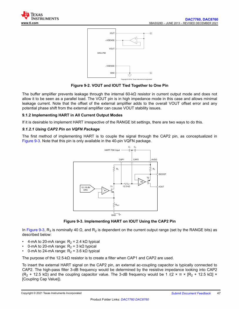
DACx760
IOUT
+VSENSE
GND
±VSENSE
VOUT
+
±
Copyright © 2016, Texas Instruments Incorporated
Figure 9-2. VOUT and IOUT Tied Together to One Pin
The buffer amplifier prevents leakage through the internal 60-kΩ resistor in current output mode and does not allow it to be seen as a parallel load. The VOUT pin is in high impedance mode in this case and allows minimal leakage current. Note that the offset of the external amplifier adds to the overall VOUT offset error and any potential phase shift from the external amplifier can cause VOUT stability issues.
9.1.2 Implementing HART in All Current Output Modes
If it is desirable to implement HART irrespective of the RANGE bit settings, there are two ways to do this.
9.1.2.1 Using CAP2 Pin on VQFN Package
The first method of implementing HART is to couple the signal through the CAP2 pin, as conceptualized in Figure 9-3. Note that this pin is only available in the 40-pin VQFN package.
+12-/16-BitBa_
DACBa_
RSET
R2
T1
A1
+
T2
A2
R3
í
í
12.5 k
HART FSK Input
C1 C2
CAP2CAP1 AVDD
GND
IOUT
BOOST
Figure 9-3. Implementing HART on IOUT Using the CAP2 Pin
In Figure 9-3, R3 is nominally 40 Ω, and R2 is dependent on the current output range (set by the RANGE bits) as described below:
• 4-mA to 20-mA range: R2 = 2.4 kΩ typical• 0-mA to 20-mA range: R2 = 3 kΩ typical• 0-mA to 24-mA range: R2 = 3.6 kΩ typical
The purpose of the 12.5-kΩ resistor is to create a filter when CAP1 and CAP2 are used.
To insert the external HART signal on the CAP2 pin, an external ac-coupling capacitor is typically connected to CAP2. The high-pass filter 3-dB frequency would be determined by the resistive impedance looking into CAP2 (R2 + 12.5 kΩ) and the coupling capacitor value. The 3-dB frequency would be 1 /(2 × π × [R2 + 12.5 kΩ] × [Coupling Cap Value]).
www.ti.comDAC7760, DAC8760
SBAS528D – JUNE 2013 – REVISED DECEMBER 2021
Copyright © 2021 Texas Instruments Incorporated Submit Document Feedback 47
Product Folder Links: DAC7760 DAC8760
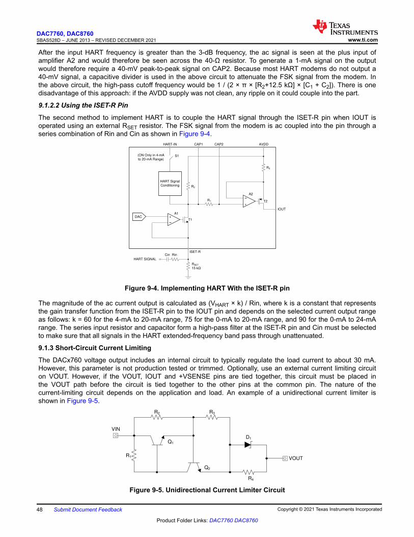
After the input HART frequency is greater than the 3-dB frequency, the ac signal is seen at the plus input of amplifier A2 and would therefore be seen across the 40-Ω resistor. To generate a 1-mA signal on the output would therefore require a 40-mV peak-to-peak signal on CAP2. Because most HART modems do not output a 40-mV signal, a capacitive divider is used in the above circuit to attenuate the FSK signal from the modem. In the above circuit, the high-pass cutoff frequency would be 1 / (2 × π × [R2+12.5 kΩ] × [C1 + C2]). There is one disadvantage of this approach: if the AVDD supply was not clean, any ripple on it could couple into the part.
9.1.2.2 Using the ISET-R Pin
The second method to implement HART is to couple the HART signal through the ISET-R pin when IOUT is operated using an external RSET resistor. The FSK signal from the modem is ac coupled into the pin through a series combination of Rin and Cin as shown in Figure 9-4.
T2
T1DAC
CAP1 CAP2 AVDD
IOUT
ISET-R
HART Signal
Conditioning
HART-IN
R1
R3
R2
(ON Only in 4-mA
to 20-mA Range)
Cin
HART SIGNAL
RSET
15 N
Rin
S1
+A1
+
A2
Figure 9-4. Implementing HART With the ISET-R pin
The magnitude of the ac current output is calculated as (VHART × k) / Rin, where k is a constant that represents the gain transfer function from the ISET-R pin to the IOUT pin and depends on the selected current output range as follows: k = 60 for the 4-mA to 20-mA range, 75 for the 0-mA to 20-mA range, and 90 for the 0-mA to 24-mA range. The series input resistor and capacitor form a high-pass filter at the ISET-R pin and Cin must be selected to make sure that all signals in the HART extended-frequency band pass through unattenuated.
9.1.3 Short-Circuit Current Limiting
The DACx760 voltage output includes an internal circuit to typically regulate the load current to about 30 mA. However, this parameter is not production tested or trimmed. Optionally, use an external current limiting circuit on VOUT. However, if the VOUT, IOUT and +VSENSE pins are tied together, this circuit must be placed in the VOUT path before the circuit is tied together to the other pins at the common pin. The nature of the current-limiting circuit depends on the application and load. An example of a unidirectional current limiter is shown in Figure 9-5.
R1
R2 R3
R4
D1
Q1
Q2
VIN
VOUT
Figure 9-5. Unidirectional Current Limiter Circuit
DAC7760, DAC8760SBAS528D – JUNE 2013 – REVISED DECEMBER 2021 www.ti.com
48 Submit Document Feedback Copyright © 2021 Texas Instruments Incorporated
Product Folder Links: DAC7760 DAC8760
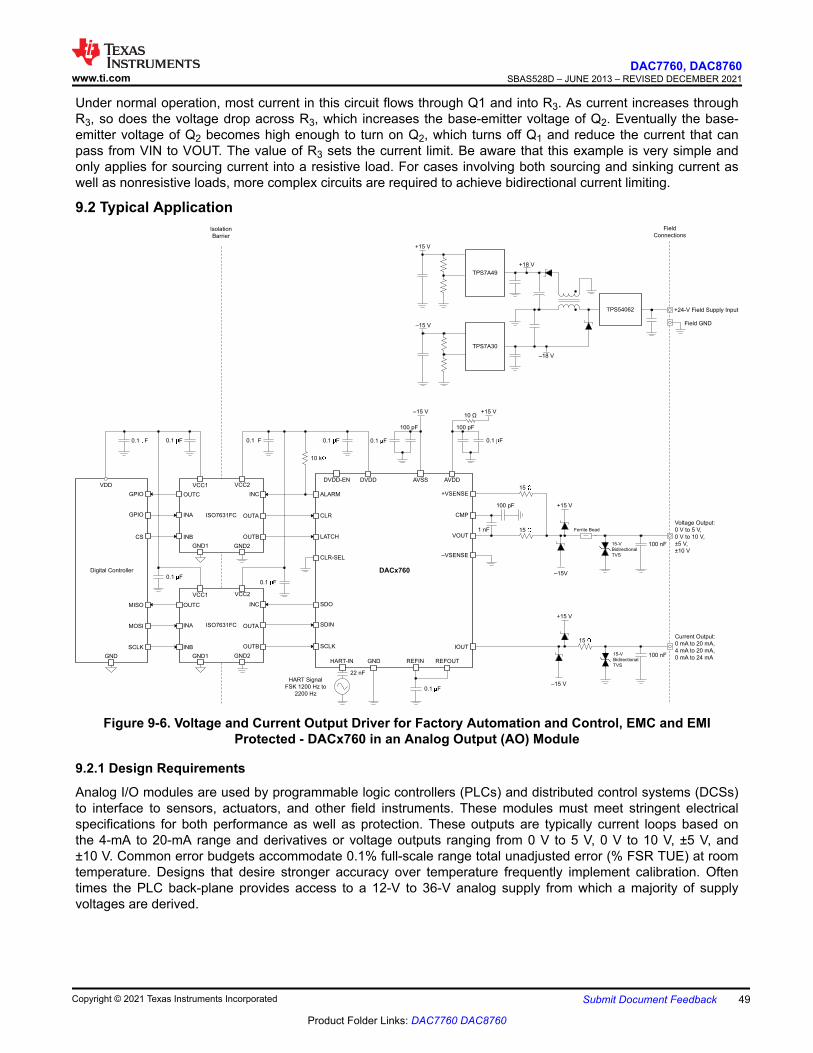
Under normal operation, most current in this circuit flows through Q1 and into R3. As current increases through R3, so does the voltage drop across R3, which increases the base-emitter voltage of Q2. Eventually the base-emitter voltage of Q2 becomes high enough to turn on Q2, which turns off Q1 and reduce the current that can pass from VIN to VOUT. The value of R3 sets the current limit. Be aware that this example is very simple and only applies for sourcing current into a resistive load. For cases involving both sourcing and sinking current as well as nonresistive loads, more complex circuits are required to achieve bidirectional current limiting.
9.2 Typical Application
ISO7631FC
DACx760
IOUT
Voltage Output:
0 V to 5 V,
0 V to 10 V,
±5 V,
±10 V
Current Output:
0 mA to 20 mA,
4 mA to 20 mA,
0 mA to 24 mA
+15 V
–15V
15-V
Bidirectional
TVS
+15 V
15-V
Bidirectional
TVS
Ferrite Bead
100 nF
100 nF
15
15
15
1 nF
–VSENSE
VOUT
CMP
+VSENSE
REFIN REFOUTGNDHART-IN
HART Signal
FSK 1200 Hz to
2200 Hz
AVSS AVDDDVDDDVDD-EN
+15 V–15 V
0.1 F
0.1 F
22 nF
100 pF
0.1 F
100 pF
0.1 F
SCLK
SDIN
SDO
CLR-SEL
LATCH
CLR
ALARM
10 k
INC
OUTA
OUTB
VCC2
GND2
0.1F
0.1 F
ISO7631FC
INC
OUTA
OUTB
VCC2
GND2
VCC1
GND1
OUTC
INA
INB
VCC1
GND1
OUTC
INA
INB
Digital Controller
GND
VDD
0.1 F0.1 F
0.1 F
SCLK
MOSI
MISO
CS
GPIO
GPIO
Isolation
Barrier
TPS54062 +24-V Field Supply Input
Field GND
+18 V
–18 V
TPS7A30
TPS7A49
–15 V
+15 V
Field
Connections
100 pF
–15 V
10 Ω
Figure 9-6. Voltage and Current Output Driver for Factory Automation and Control, EMC and EMI Protected - DACx760 in an Analog Output (AO) Module
9.2.1 Design Requirements
Analog I/O modules are used by programmable logic controllers (PLCs) and distributed control systems (DCSs) to interface to sensors, actuators, and other field instruments. These modules must meet stringent electrical specifications for both performance as well as protection. These outputs are typically current loops based on the 4-mA to 20-mA range and derivatives or voltage outputs ranging from 0 V to 5 V, 0 V to 10 V, ±5 V, and ±10 V. Common error budgets accommodate 0.1% full-scale range total unadjusted error (% FSR TUE) at room temperature. Designs that desire stronger accuracy over temperature frequently implement calibration. Often times the PLC back-plane provides access to a 12-V to 36-V analog supply from which a majority of supply voltages are derived.
www.ti.comDAC7760, DAC8760
SBAS528D – JUNE 2013 – REVISED DECEMBER 2021
Copyright © 2021 Texas Instruments Incorporated Submit Document Feedback 49
Product Folder Links: DAC7760 DAC8760
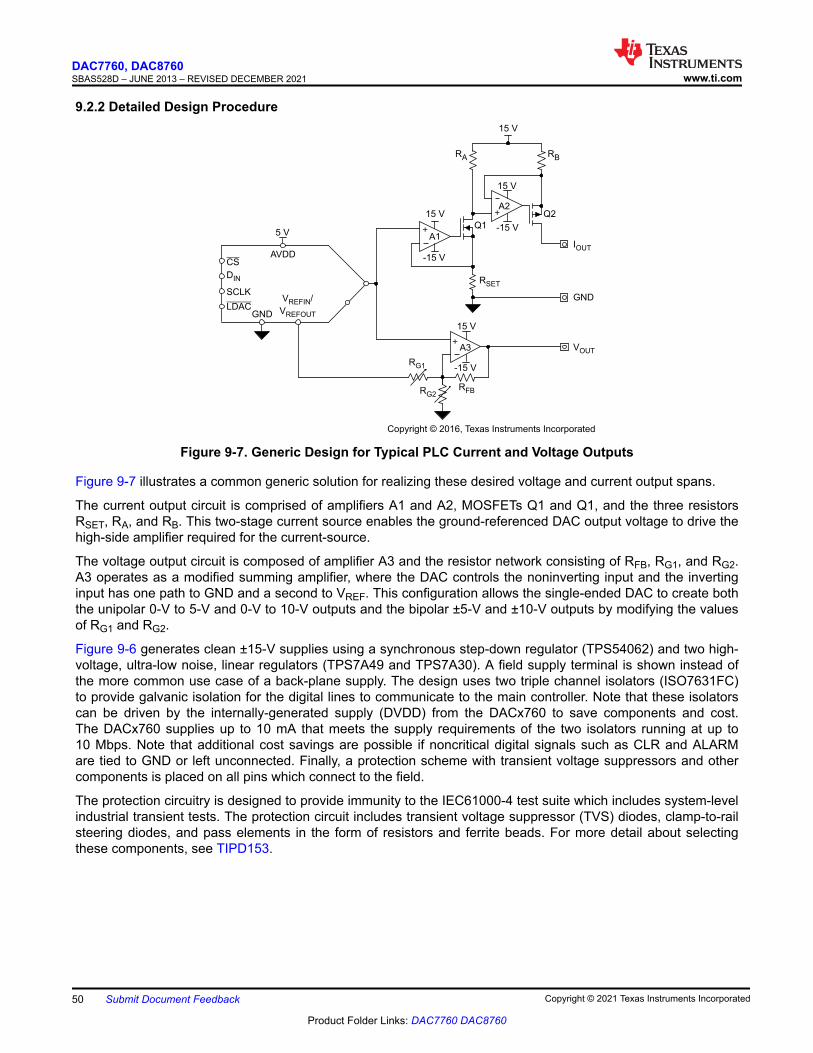
9.2.2 Detailed Design Procedure
IOUT
15 V
RA RB
RSET
Q1
Q2
A1
A2
VOUT
GND
A3
RFB
RG1
AVDD
V /
VREFIN
REFOUTGND
DIN
SCLK
CS
LDAC
15 V
-15 V
15 V
-15 V
15 V
-15 V
5 V
RG2
+
+
+
Copyright © 2016, Texas Instruments Incorporated
Figure 9-7. Generic Design for Typical PLC Current and Voltage Outputs
Figure 9-7 illustrates a common generic solution for realizing these desired voltage and current output spans.
The current output circuit is comprised of amplifiers A1 and A2, MOSFETs Q1 and Q1, and the three resistors RSET, RA, and RB. This two-stage current source enables the ground-referenced DAC output voltage to drive the high-side amplifier required for the current-source.
The voltage output circuit is composed of amplifier A3 and the resistor network consisting of RFB, RG1, and RG2. A3 operates as a modified summing amplifier, where the DAC controls the noninverting input and the inverting input has one path to GND and a second to VREF. This configuration allows the single-ended DAC to create both the unipolar 0-V to 5-V and 0-V to 10-V outputs and the bipolar ±5-V and ±10-V outputs by modifying the values of RG1 and RG2.
Figure 9-6 generates clean ±15-V supplies using a synchronous step-down regulator (TPS54062) and two high-voltage, ultra-low noise, linear regulators (TPS7A49 and TPS7A30). A field supply terminal is shown instead of the more common use case of a back-plane supply. The design uses two triple channel isolators (ISO7631FC) to provide galvanic isolation for the digital lines to communicate to the main controller. Note that these isolators can be driven by the internally-generated supply (DVDD) from the DACx760 to save components and cost. The DACx760 supplies up to 10 mA that meets the supply requirements of the two isolators running at up to 10 Mbps. Note that additional cost savings are possible if noncritical digital signals such as CLR and ALARM are tied to GND or left unconnected. Finally, a protection scheme with transient voltage suppressors and other components is placed on all pins which connect to the field.
The protection circuitry is designed to provide immunity to the IEC61000-4 test suite which includes system-level industrial transient tests. The protection circuit includes transient voltage suppressor (TVS) diodes, clamp-to-rail steering diodes, and pass elements in the form of resistors and ferrite beads. For more detail about selecting these components, see TIPD153.
DAC7760, DAC8760SBAS528D – JUNE 2013 – REVISED DECEMBER 2021 www.ti.com
50 Submit Document Feedback Copyright © 2021 Texas Instruments Incorporated
Product Folder Links: DAC7760 DAC8760
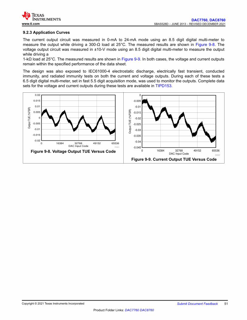
9.2.3 Application Curves
The current output circuit was measured in 0-mA to 24-mA mode using an 8.5 digit digital multi-meter to measure the output while driving a 300-Ω load at 25°C. The measured results are shown in Figure 9-8. The voltage output circuit was measured in ±10-V mode using an 8.5 digit digital multi-meter to measure the output while driving a1-kΩ load at 25°C. The measured results are shown in Figure 9-9. In both cases, the voltage and current outputs remain within the specified performance of the data sheet.
The design was also exposed to IEC61000-4 electrostatic discharge, electrically fast transient, conducted immunity, and radiated immunity tests on both the current and voltage outputs. During each of these tests a 6.5 digit digital multi-meter, set in fast 5.5 digit acquisition mode, was used to monitor the outputs. Complete data sets for the voltage and current outputs during these tests are available in TIPD153.
DAC Input Code
Outp
ut
TU
E (
%F
SR
)
0 16384 32768 49152 65536-0.02
-0.015
-0.01
-0.005
0
0.005
0.01
0.015
0.02
D001
Figure 9-8. Voltage Output TUE Versus CodeDAC Input Code
Outp
ut
TU
E (
%F
SR
)
0 16384 32768 49152 65536-0.045
-0.04
-0.035
-0.03
-0.025
-0.02
-0.015
-0.01
-0.005
0
D002
Figure 9-9. Current Output TUE Versus Code
www.ti.comDAC7760, DAC8760
SBAS528D – JUNE 2013 – REVISED DECEMBER 2021
Copyright © 2021 Texas Instruments Incorporated Submit Document Feedback 51
Product Folder Links: DAC7760 DAC8760
10 Power Supply RecommendationsThe DACx760 family operates within the specified single-supply range of 10 V to 36 V applied to the AVDD pin. The device also operates with the specified dual-supply range of 10 V to 18 V applied to AVDD, and 0 V to –18 V on AVSS, or any subsequent combination that does not exceed the maximum difference of 36 V between AVDD and AVSS. The digital supply, DVDD, operates within the specified supply range of 2.7 V to 5.5 V or is powered by the internal 4.6-V LDO.
Switching power supplies and DC/DC converters often have high-frequency glitches or spikes riding on the output voltage. In addition, digital components can create similar high frequency spikes. This noise can be easily coupled into the DAC output voltage or current through various paths between the power connections and analog output. To further reduce noise, include bulk and local decoupling capacitors.
CAUTIONDo not ramp the supplies for the DACx760 faster than 1 V/ns or damage may result to the device. To help reduce the supply ramp, use a 10-Ω series resistor from the analog supply to the device AVDD connection.
The DACx760 has internal power-on reset (POR) circuitry for both the digital DVDD and analog AVDD supplies. This circuitry makes sure that the internal logic and power-on state of the DAC power up to the proper state independent of the supply sequence. The recommended power-supply sequence is to first have the analog AVDD supply come up, followed by the digital DVDD supply. DVDD can come up first as long as AVDD ramps to at least 5 V within 50 μs. If neither condition can be satisfied, issue a software reset command using the SPI bus after both AVDD and DVDD are stable.
The current consumption on the AVDD and AVSS pins, the short-circuit current limit for the voltage output, and current ranges for the current output are listed in Section 7.5. The power supply must meet the requirements listed in Section 7.5.
DAC7760, DAC8760SBAS528D – JUNE 2013 – REVISED DECEMBER 2021 www.ti.com
52 Submit Document Feedback Copyright © 2021 Texas Instruments Incorporated
Product Folder Links: DAC7760 DAC8760
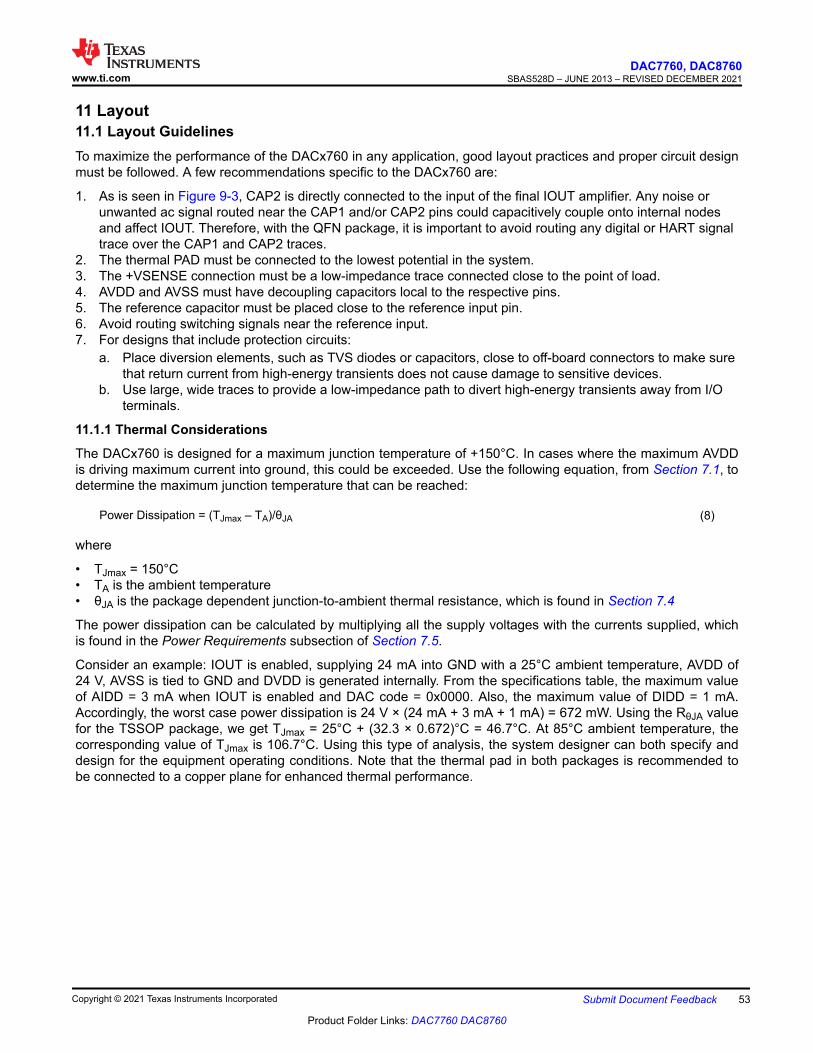
11 Layout11.1 Layout GuidelinesTo maximize the performance of the DACx760 in any application, good layout practices and proper circuit design must be followed. A few recommendations specific to the DACx760 are:
1. As is seen in Figure 9-3, CAP2 is directly connected to the input of the final IOUT amplifier. Any noise or unwanted ac signal routed near the CAP1 and/or CAP2 pins could capacitively couple onto internal nodes and affect IOUT. Therefore, with the QFN package, it is important to avoid routing any digital or HART signal trace over the CAP1 and CAP2 traces.
2. The thermal PAD must be connected to the lowest potential in the system.3. The +VSENSE connection must be a low-impedance trace connected close to the point of load.4. AVDD and AVSS must have decoupling capacitors local to the respective pins.5. The reference capacitor must be placed close to the reference input pin.6. Avoid routing switching signals near the reference input.7. For designs that include protection circuits:
a. Place diversion elements, such as TVS diodes or capacitors, close to off-board connectors to make sure that return current from high-energy transients does not cause damage to sensitive devices.
b. Use large, wide traces to provide a low-impedance path to divert high-energy transients away from I/O terminals.
11.1.1 Thermal Considerations
The DACx760 is designed for a maximum junction temperature of +150°C. In cases where the maximum AVDD is driving maximum current into ground, this could be exceeded. Use the following equation, from Section 7.1, to determine the maximum junction temperature that can be reached:
Power Dissipation = (TJmax – TA)/θJA (8)
where
• TJmax = 150°C• TA is the ambient temperature• θJA is the package dependent junction-to-ambient thermal resistance, which is found in Section 7.4
The power dissipation can be calculated by multiplying all the supply voltages with the currents supplied, which is found in the Power Requirements subsection of Section 7.5.
Consider an example: IOUT is enabled, supplying 24 mA into GND with a 25°C ambient temperature, AVDD of 24 V, AVSS is tied to GND and DVDD is generated internally. From the specifications table, the maximum value of AIDD = 3 mA when IOUT is enabled and DAC code = 0x0000. Also, the maximum value of DIDD = 1 mA. Accordingly, the worst case power dissipation is 24 V × (24 mA + 3 mA + 1 mA) = 672 mW. Using the RθJA value for the TSSOP package, we get TJmax = 25°C + (32.3 × 0.672)°C = 46.7°C. At 85°C ambient temperature, the corresponding value of TJmax is 106.7°C. Using this type of analysis, the system designer can both specify and design for the equipment operating conditions. Note that the thermal pad in both packages is recommended to be connected to a copper plane for enhanced thermal performance.
www.ti.comDAC7760, DAC8760
SBAS528D – JUNE 2013 – REVISED DECEMBER 2021
Copyright © 2021 Texas Instruments Incorporated Submit Document Feedback 53
Product Folder Links: DAC7760 DAC8760
11.2 Layout Example
Analog
Supply
Decoupling
0
GND AVDDAVSS
DVDD
Analog
Supply
Decoupling
External RSET
(Optional)
External
Boost Transistor
(Optional)
Q1
Digital I/O
CAP1 / CAP2
Capacitance
(Optional)
CMP
Capacitance
(Optional)
Analog Supply
Series Resistance
Digital
Supply
Decoupling
ALARM
Pull-up
Resistance
Reference
Capacitance
HART
Input
IOUT
VOUT
Figure 11-1. DACx760 Layout Example
DAC7760, DAC8760SBAS528D – JUNE 2013 – REVISED DECEMBER 2021 www.ti.com
54 Submit Document Feedback Copyright © 2021 Texas Instruments Incorporated
Product Folder Links: DAC7760 DAC8760
12 Device and Documentation Support12.1 Documentation Support12.1.1 Related Documentation
For related documentation see the following:
• Texas Instruments, Single-Channel Industrial Voltage & Current Output Driver, Isolated, EMC/EMI Tested Reference Design
• Texas Instruments, Implementing HART™ Communication with the DAC8760 Family
12.2 Receiving Notification of Documentation UpdatesTo receive notification of documentation updates, navigate to the device product folder on ti.com. Click on Subscribe to updates to register and receive a weekly digest of any product information that has changed. For change details, review the revision history included in any revised document.
12.3 Support ResourcesTI E2E™ support forums are an engineer's go-to source for fast, verified answers and design help — straight from the experts. Search existing answers or ask your own question to get the quick design help you need.
Linked content is provided "AS IS" by the respective contributors. They do not constitute TI specifications and do not necessarily reflect TI's views; see TI's Terms of Use.
12.4 TrademarksTI E2E™ is a trademark of Texas Instruments.HART® is a registered trademark of HART Communication Foundation.All trademarks are the property of their respective owners.12.5 Electrostatic Discharge Caution
This integrated circuit can be damaged by ESD. Texas Instruments recommends that all integrated circuits be handled with appropriate precautions. Failure to observe proper handling and installation procedures can cause damage.ESD damage can range from subtle performance degradation to complete device failure. Precision integrated circuits may be more susceptible to damage because very small parametric changes could cause the device not to meet its published specifications.
12.6 GlossaryTI Glossary This glossary lists and explains terms, acronyms, and definitions.
13 Mechanical, Packaging, and Orderable InformationThe following pages include mechanical, packaging, and orderable information. This information is the most current data available for the designated devices. This data is subject to change without notice and revision of this document. For browser-based versions of this data sheet, refer to the left-hand navigation.
www.ti.comDAC7760, DAC8760
SBAS528D – JUNE 2013 – REVISED DECEMBER 2021
Copyright © 2021 Texas Instruments Incorporated Submit Document Feedback 55
Product Folder Links: DAC7760 DAC8760
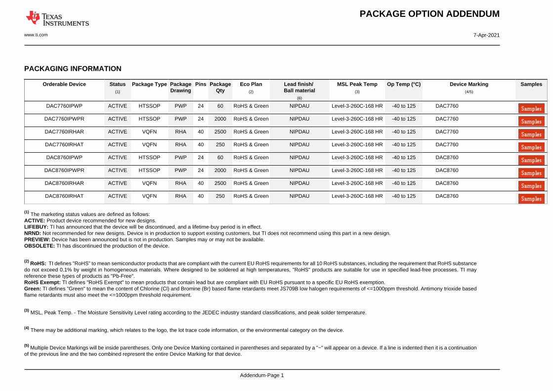
PACKAGE OPTION ADDENDUM
www.ti.com 7-Apr-2021
Addendum-Page 1
PACKAGING INFORMATION
Orderable Device Status(1)
Package Type PackageDrawing
Pins PackageQty
Eco Plan(2)
Lead finish/Ball material
(6)
MSL Peak Temp(3)
Op Temp (°C) Device Marking(4/5)
Samples
DAC7760IPWP ACTIVE HTSSOP PWP 24 60 RoHS & Green NIPDAU Level-3-260C-168 HR -40 to 125 DAC7760
DAC7760IPWPR ACTIVE HTSSOP PWP 24 2000 RoHS & Green NIPDAU Level-3-260C-168 HR -40 to 125 DAC7760
DAC7760IRHAR ACTIVE VQFN RHA 40 2500 RoHS & Green NIPDAU Level-3-260C-168 HR -40 to 125 DAC7760
DAC7760IRHAT ACTIVE VQFN RHA 40 250 RoHS & Green NIPDAU Level-3-260C-168 HR -40 to 125 DAC7760
DAC8760IPWP ACTIVE HTSSOP PWP 24 60 RoHS & Green NIPDAU Level-3-260C-168 HR -40 to 125 DAC8760
DAC8760IPWPR ACTIVE HTSSOP PWP 24 2000 RoHS & Green NIPDAU Level-3-260C-168 HR -40 to 125 DAC8760
DAC8760IRHAR ACTIVE VQFN RHA 40 2500 RoHS & Green NIPDAU Level-3-260C-168 HR -40 to 125 DAC8760
DAC8760IRHAT ACTIVE VQFN RHA 40 250 RoHS & Green NIPDAU Level-3-260C-168 HR -40 to 125 DAC8760
(1) The marketing status values are defined as follows:ACTIVE: Product device recommended for new designs.LIFEBUY: TI has announced that the device will be discontinued, and a lifetime-buy period is in effect.NRND: Not recommended for new designs. Device is in production to support existing customers, but TI does not recommend using this part in a new design.PREVIEW: Device has been announced but is not in production. Samples may or may not be available.OBSOLETE: TI has discontinued the production of the device.
(2) RoHS: TI defines "RoHS" to mean semiconductor products that are compliant with the current EU RoHS requirements for all 10 RoHS substances, including the requirement that RoHS substancedo not exceed 0.1% by weight in homogeneous materials. Where designed to be soldered at high temperatures, "RoHS" products are suitable for use in specified lead-free processes. TI mayreference these types of products as "Pb-Free".RoHS Exempt: TI defines "RoHS Exempt" to mean products that contain lead but are compliant with EU RoHS pursuant to a specific EU RoHS exemption.Green: TI defines "Green" to mean the content of Chlorine (Cl) and Bromine (Br) based flame retardants meet JS709B low halogen requirements of <=1000ppm threshold. Antimony trioxide basedflame retardants must also meet the <=1000ppm threshold requirement.
(3) MSL, Peak Temp. - The Moisture Sensitivity Level rating according to the JEDEC industry standard classifications, and peak solder temperature.
(4) There may be additional marking, which relates to the logo, the lot trace code information, or the environmental category on the device.
(5) Multiple Device Markings will be inside parentheses. Only one Device Marking contained in parentheses and separated by a "~" will appear on a device. If a line is indented then it is a continuationof the previous line and the two combined represent the entire Device Marking for that device.
PACKAGE OPTION ADDENDUM
www.ti.com 7-Apr-2021
Addendum-Page 2
(6) Lead finish/Ball material - Orderable Devices may have multiple material finish options. Finish options are separated by a vertical ruled line. Lead finish/Ball material values may wrap to twolines if the finish value exceeds the maximum column width.
Important Information and Disclaimer:The information provided on this page represents TI's knowledge and belief as of the date that it is provided. TI bases its knowledge and belief on informationprovided by third parties, and makes no representation or warranty as to the accuracy of such information. Efforts are underway to better integrate information from third parties. TI has taken andcontinues to take reasonable steps to provide representative and accurate information but may not have conducted destructive testing or chemical analysis on incoming materials and chemicals.TI and TI suppliers consider certain information to be proprietary, and thus CAS numbers and other limited information may not be available for release.
In no event shall TI's liability arising out of such information exceed the total purchase price of the TI part(s) at issue in this document sold by TI to Customer on an annual basis.
TAPE AND REEL INFORMATION
*All dimensions are nominal
Device PackageType
PackageDrawing
Pins SPQ ReelDiameter
(mm)
ReelWidth
W1 (mm)
A0(mm)
B0(mm)
K0(mm)
P1(mm)
W(mm)
Pin1Quadrant
DAC7760IPWPR HTSSOP PWP 24 2000 330.0 16.4 6.95 8.3 1.6 8.0 16.0 Q1
DAC7760IRHAR VQFN RHA 40 2500 330.0 16.4 6.3 6.3 1.1 12.0 16.0 Q2
DAC7760IRHAT VQFN RHA 40 250 180.0 16.4 6.3 6.3 1.1 12.0 16.0 Q2
DAC8760IPWPR HTSSOP PWP 24 2000 330.0 16.4 6.95 8.3 1.6 8.0 16.0 Q1
DAC8760IRHAR VQFN RHA 40 2500 330.0 16.4 6.3 6.3 1.1 12.0 16.0 Q2
DAC8760IRHAT VQFN RHA 40 250 180.0 16.4 6.3 6.3 1.1 12.0 16.0 Q2
PACKAGE MATERIALS INFORMATION
www.ti.com 5-Jan-2022
Pack Materials-Page 1
*All dimensions are nominal
Device Package Type Package Drawing Pins SPQ Length (mm) Width (mm) Height (mm)
DAC7760IPWPR HTSSOP PWP 24 2000 350.0 350.0 43.0
DAC7760IRHAR VQFN RHA 40 2500 367.0 367.0 38.0
DAC7760IRHAT VQFN RHA 40 250 210.0 185.0 35.0
DAC8760IPWPR HTSSOP PWP 24 2000 350.0 350.0 43.0
DAC8760IRHAR VQFN RHA 40 2500 367.0 367.0 38.0
DAC8760IRHAT VQFN RHA 40 250 210.0 185.0 35.0
PACKAGE MATERIALS INFORMATION
www.ti.com 5-Jan-2022
Pack Materials-Page 2
TUBE
*All dimensions are nominal
Device Package Name Package Type Pins SPQ L (mm) W (mm) T (µm) B (mm)
DAC7760IPWP PWP HTSSOP 24 60 530 10.2 3600 3.5
DAC8760IPWP PWP HTSSOP 24 60 530 10.2 3600 3.5
PACKAGE MATERIALS INFORMATION
www.ti.com 5-Jan-2022
Pack Materials-Page 3
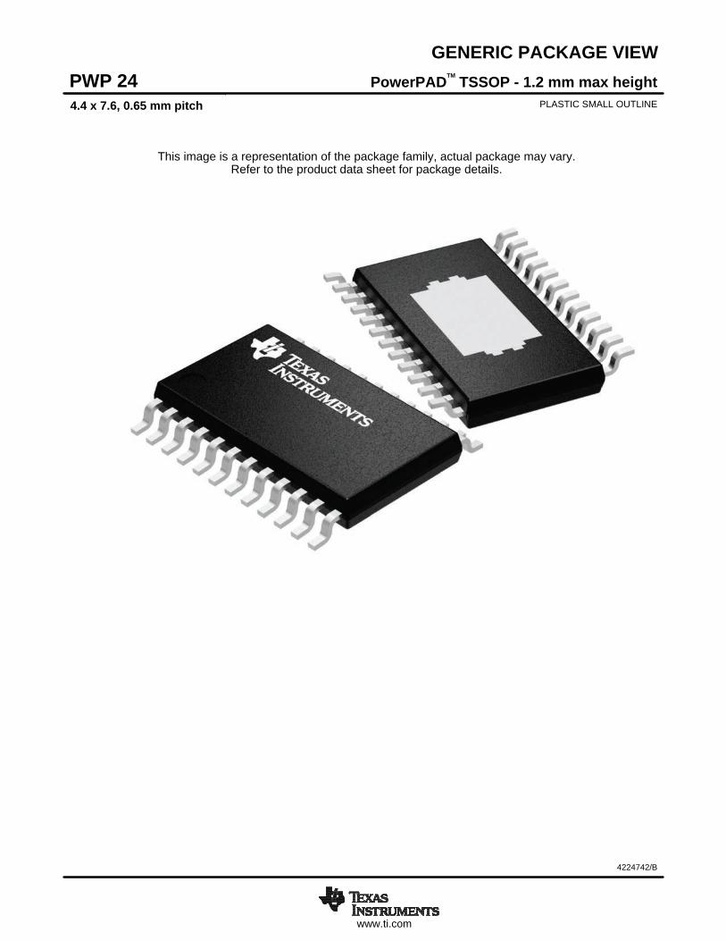
www.ti.com
GENERIC PACKAGE VIEW
This image is a representation of the package family, actual package may vary.Refer to the product data sheet for package details.
TSSOP - 1.2 mm max heightTMPowerPADPWP 24PLASTIC SMALL OUTLINE4.4 x 7.6, 0.65 mm pitch
4224742/B
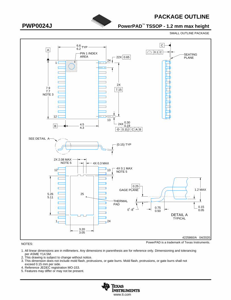
www.ti.com
PACKAGE OUTLINE
C
22X 0.65
2X7.15
24X 0.300.19
6.66.2 TYP
SEATINGPLANE
0.150.05
0.25GAGE PLANE
0 -8
1.2 MAX
2X 2.08 MAXNOTE 5
4X 0.1 MAXNOTE 5
5.265.11
3.203.05
B 4.54.3
A
7.97.7
NOTE 3
0.750.50
(0.15) TYP
4X 0.3 MAX
PowerPAD TSSOP - 1.2 mm max heightPWP0024JSMALL OUTLINE PACKAGE
4225860/A 04/2020
1
1213
24
0.1 C A B
PIN 1 INDEXAREA
SEE DETAIL A
0.1 C
NOTES: 1. All linear dimensions are in millimeters. Any dimensions in parenthesis are for reference only. Dimensioning and tolerancing per ASME Y14.5M. 2. This drawing is subject to change without notice. 3. This dimension does not include mold flash, protrusions, or gate burrs. Mold flash, protrusions, or gate burrs shall not exceed 0.15 mm per side. 4. Reference JEDEC registration MO-153.5. Features may differ or may not be present.
TM
PowerPAD is a trademark of Texas Instruments.
A 20DETAIL ATYPICAL
SCALE 2.000
THERMALPAD
1
12 13
24
25
www.ti.com
EXAMPLE BOARD LAYOUT
0.07 MAXALL AROUND
0.07 MINALL AROUND
24X (1.5)
24X (0.45)
22X (0.65)
(5.8)
(R0.05) TYP
(3.4)NOTE 9
(7.8)NOTE 9
(1.2) TYP
(1.2) TYP
( 0.2) TYPVIA
(3.2)
(5.26)
PowerPAD TSSOP - 1.2 mm max heightPWP0024JSMALL OUTLINE PACKAGE
4225860/A 04/2020
NOTES: (continued) 6. Publication IPC-7351 may have alternate designs. 7. Solder mask tolerances between and around signal pads can vary based on board fabrication site. 8. This package is designed to be soldered to a thermal pad on the board. For more information, see Texas Instruments literature numbers SLMA002 (www.ti.com/lit/slma002) and SLMA004 (www.ti.com/lit/slma004). 9. Size of metal pad may vary due to creepage requirement.10. Vias are optional depending on application, refer to device data sheet. It is recommended that vias under paste be filled, plugged or tented.
TM
LAND PATTERN EXAMPLEEXPOSED METAL SHOWN
SCALE: 8X
SYMM
SYMM
1
12 13
24
METAL COVEREDBY SOLDER MASK
SOLDER MASKDEFINED PAD
SEE DETAILS
25
15.000
METALSOLDER MASKOPENING
METAL UNDERSOLDER MASK
SOLDER MASKOPENING
EXPOSED METALEXPOSED METAL
SOLDER MASK DETAILS
NON-SOLDER MASKDEFINED
SOLDER MASKDEFINED
www.ti.com
EXAMPLE STENCIL DESIGN
24X (1.5)
24X (0.45)
22X (0.65)
(5.8)
(R0.05) TYP
(5.26)BASED ON
0.125 THICKSTENCIL
(3.2)BASED ON
0.125 THICKSTENCIL
PowerPAD TSSOP - 1.2 mm max heightPWP0024JSMALL OUTLINE PACKAGE
4225860/A 04/2020
2.70 X 4.450.1752.92 X 4.800.15
3.20 X 5.26 (SHOWN)0.1253.58 X 5.880.1
SOLDER STENCILOPENING
STENCILTHICKNESS
NOTES: (continued) 11. Laser cutting apertures with trapezoidal walls and rounded corners may offer better paste release. IPC-7525 may have alternate design recommendations. 12. Board assembly site may have different recommendations for stencil design.
TM
SOLDER PASTE EXAMPLEBASED ON 0.125 mm THICK STENCIL
SCALE: 8X
SYMM
SYMM
1
12 13
24
METAL COVEREDBY SOLDER MASK
SEE TABLE FORDIFFERENT OPENINGSFOR OTHER STENCILTHICKNESSES
25
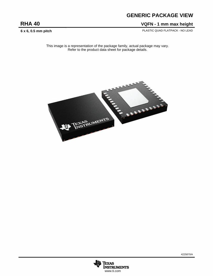
www.ti.com
GENERIC PACKAGE VIEW
This image is a representation of the package family, actual package may vary.Refer to the product data sheet for package details.
VQFN - 1 mm max heightRHA 40PLASTIC QUAD FLATPACK - NO LEAD6 x 6, 0.5 mm pitch
4225870/A
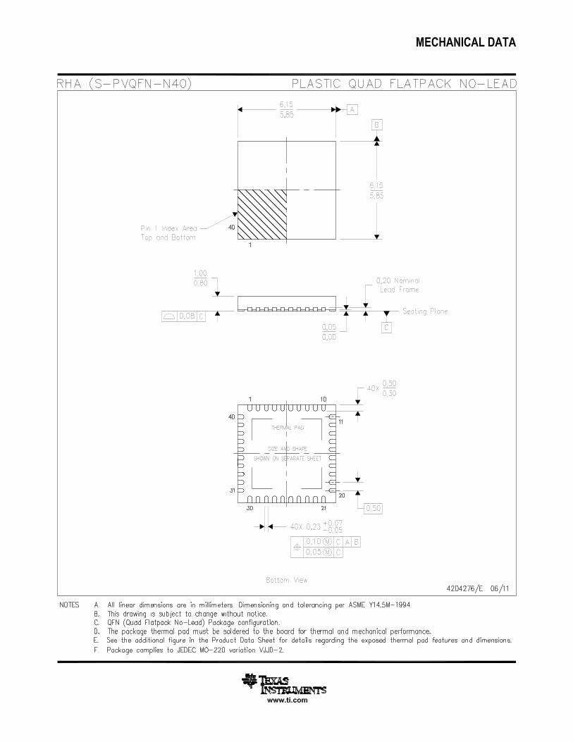
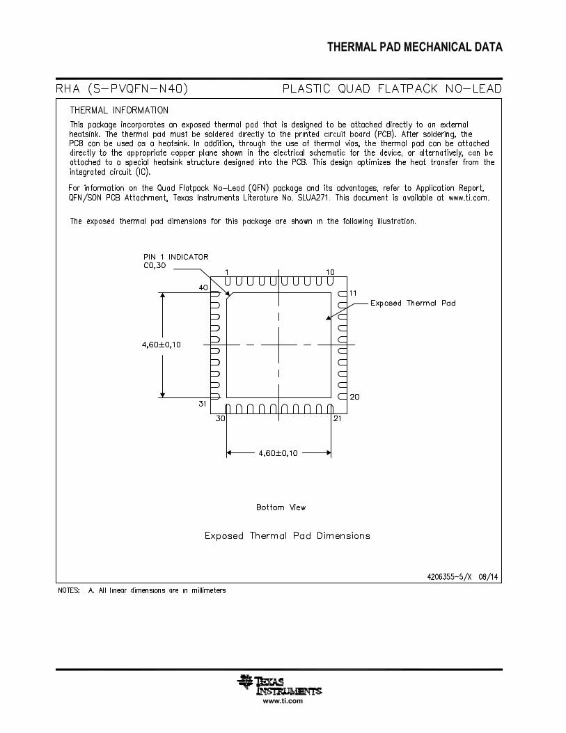
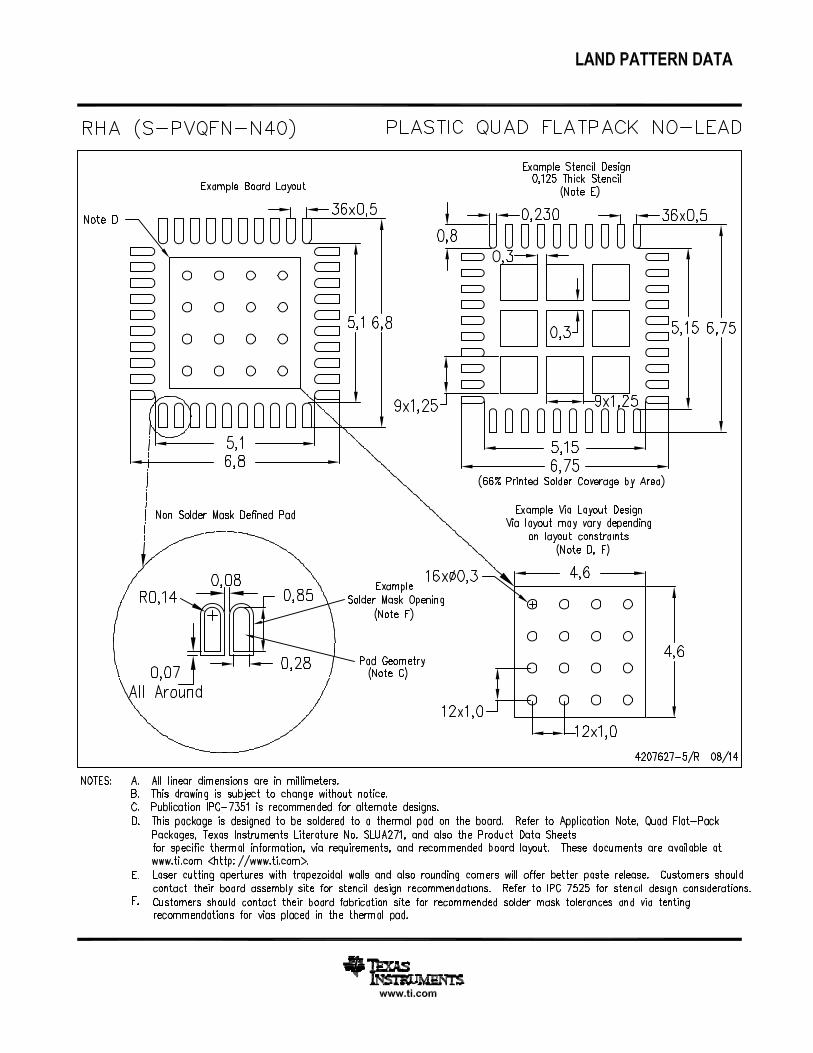
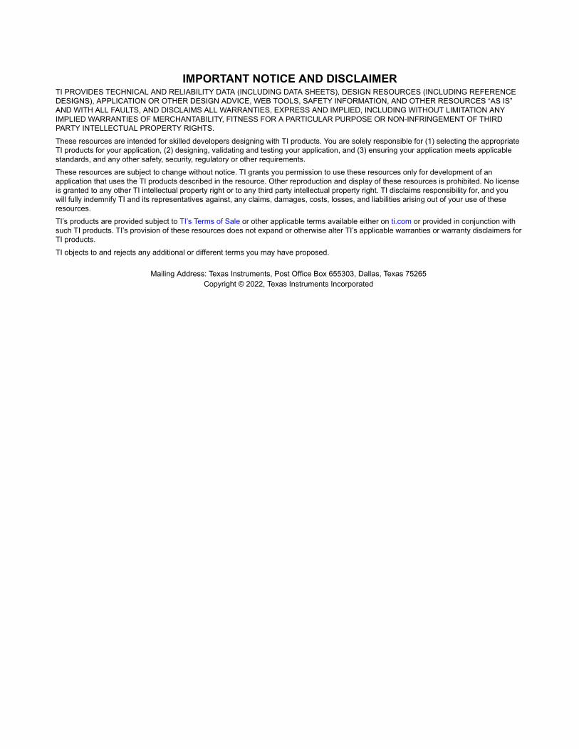
IMPORTANT NOTICE AND DISCLAIMERTI PROVIDES TECHNICAL AND RELIABILITY DATA (INCLUDING DATA SHEETS), DESIGN RESOURCES (INCLUDING REFERENCE DESIGNS), APPLICATION OR OTHER DESIGN ADVICE, WEB TOOLS, SAFETY INFORMATION, AND OTHER RESOURCES “AS IS” AND WITH ALL FAULTS, AND DISCLAIMS ALL WARRANTIES, EXPRESS AND IMPLIED, INCLUDING WITHOUT LIMITATION ANY IMPLIED WARRANTIES OF MERCHANTABILITY, FITNESS FOR A PARTICULAR PURPOSE OR NON-INFRINGEMENT OF THIRD PARTY INTELLECTUAL PROPERTY RIGHTS.These resources are intended for skilled developers designing with TI products. You are solely responsible for (1) selecting the appropriate TI products for your application, (2) designing, validating and testing your application, and (3) ensuring your application meets applicable standards, and any other safety, security, regulatory or other requirements.These resources are subject to change without notice. TI grants you permission to use these resources only for development of an application that uses the TI products described in the resource. Other reproduction and display of these resources is prohibited. No license is granted to any other TI intellectual property right or to any third party intellectual property right. TI disclaims responsibility for, and you will fully indemnify TI and its representatives against, any claims, damages, costs, losses, and liabilities arising out of your use of these resources.TI’s products are provided subject to TI’s Terms of Sale or other applicable terms available either on ti.com or provided in conjunction with such TI products. TI’s provision of these resources does not expand or otherwise alter TI’s applicable warranties or warranty disclaimers for TI products.TI objects to and rejects any additional or different terms you may have proposed. IMPORTANT NOTICE
Mailing Address: Texas Instruments, Post Office Box 655303, Dallas, Texas 75265Copyright © 2022, Texas Instruments Incorporated