high-speed differential line receiver - texas instruments
TRANSCRIPT
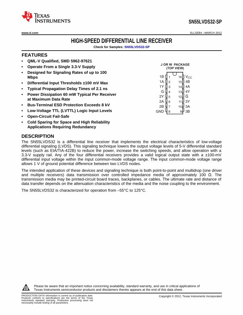
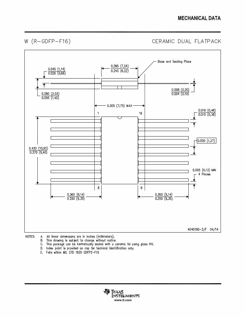
J OR W PACKAGE(TOP VIEW)
SN55LVDS32-SP
www.ti.com SLLSEB4 –MARCH 2012
HIGH-SPEED DIFFERENTIAL LINE RECEIVERCheck for Samples: SN55LVDS32-SP
1FEATURES• QML-V Qualified, SMD 5962-97621• Operate From a Single 3.3-V Supply• Designed for Signaling Rates of up to 100
Mbps• Differential Input Thresholds ±100 mV Max• Typical Propagation Delay Times of 2.1 ns• Power Dissipation 60 mW Typical Per Receiver
at Maximum Data Rate• Bus-Terminal ESD Protection Exceeds 8 kV• Low-Voltage TTL (LVTTL) Logic Input Levels• Open-Circuit Fail-Safe• Cold Sparing for Space and High Reliability
Applications Requiring Redundancy
DESCRIPTIONThe SN55LVDS32 is a differential line receiver that implements the electrical characteristics of low-voltagedifferential signaling (LVDS). This signaling technique lowers the output voltage levels of 5-V differential standardlevels (such as EIA/TIA-422B) to reduce the power, increase the switching speeds, and allow operation with a3.3-V supply rail. Any of the four differential receivers provides a valid logical output state with a ±100-mVdifferential input voltage within the input common-mode voltage range. The input common-mode voltage rangeallows 1 V of ground potential difference between two LVDS nodes.
The intended application of these devices and signaling technique is both point-to-point and multidrop (one driverand multiple receivers) data transmission over controlled impedance media of approximately 100 Ω. Thetransmission media may be printed-circuit board traces, backplanes, or cables. The ultimate rate and distance ofdata transfer depends on the attenuation characteristics of the media and the noise coupling to the environment.
The SN55LVDS32 is characterized for operation from –55°C to 125°C.
1
Please be aware that an important notice concerning availability, standard warranty, and use in critical applications ofTexas Instruments semiconductor products and disclaimers thereto appears at the end of this data sheet.
PRODUCTION DATA information is current as of publication date. Copyright © 2012, Texas Instruments IncorporatedProducts conform to specifications per the terms of the TexasInstruments standard warranty. Production processing does notnecessarily include testing of all parameters.
G
G
1A
1B
2A
2B
3A
3B
4A
4B
4
12
2
1
6
7
10
9
14
15
3
5
11
13
1Y
2Y
3Y
4Y
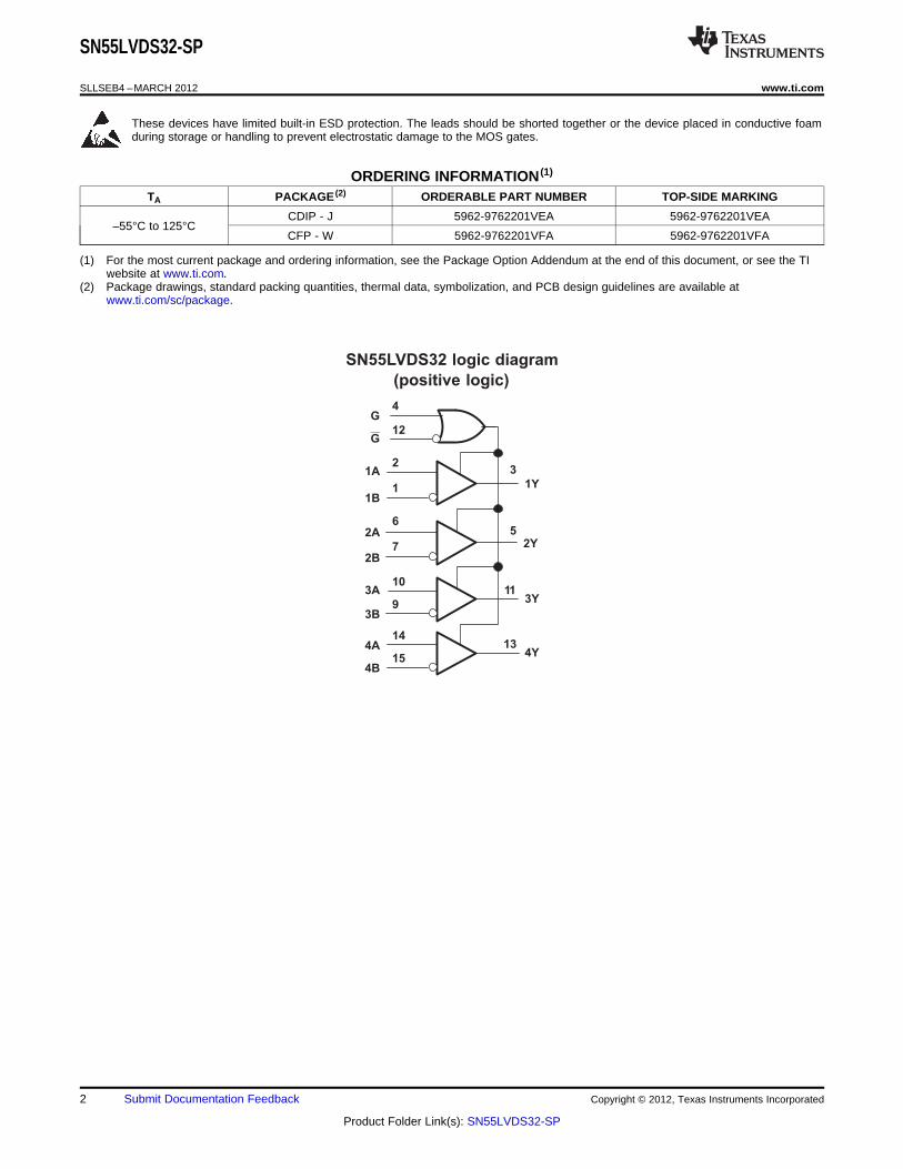
SN55LVDS32 logic diagram
(positive logic)
SN55LVDS32-SP
SLLSEB4 –MARCH 2012 www.ti.com
These devices have limited built-in ESD protection. The leads should be shorted together or the device placed in conductive foamduring storage or handling to prevent electrostatic damage to the MOS gates.
ORDERING INFORMATION (1)
TA PACKAGE (2) ORDERABLE PART NUMBER TOP-SIDE MARKING
CDIP - J 5962-9762201VEA 5962-9762201VEA–55°C to 125°C
CFP - W 5962-9762201VFA 5962-9762201VFA
(1) For the most current package and ordering information, see the Package Option Addendum at the end of this document, or see the TIwebsite at www.ti.com.
(2) Package drawings, standard packing quantities, thermal data, symbolization, and PCB design guidelines are available atwww.ti.com/sc/package.
xxx
2 Submit Documentation Feedback Copyright © 2012, Texas Instruments Incorporated
Product Folder Link(s): SN55LVDS32-SP
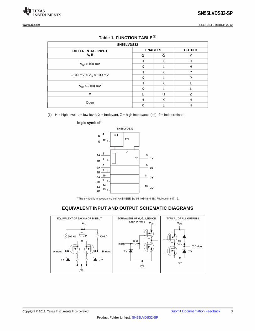
logic symbol†
EN
≥ 1G
G
1A
1B
2A
2B
3A
3B
4A
4B
3
5
11
13
1Y
2Y
3Y
4Y
4
12
2
1
6
7
10
9
14
15
† This symbol is in accordance with ANSI/IEEE Std 91-1984 and IEC Publication 617-12.
SN55LVDS32
300 kΩ300 kΩ
VCC
7 V 7 V
A Input B Input 7 V
50 Ω
VCC
Input
VCC
5Ω
7 V
Y Output
EQUIVALENT OF EACH A OR B INPUT EQUIVALENT OF G, G, 1,2EN OR
3,4EN INPUTS
TYPICAL OF ALL OUTPUTS
SN55LVDS32-SP
www.ti.com SLLSEB4 –MARCH 2012
Table 1. FUNCTION TABLE (1)
SN55LVDS32
ENABLES OUTPUTDIFFERENTIAL INPUTA, B G G Y
H X HVID ≥ 100 mV
X L H
H X ?–100 mV < VID ≤ 100 mV
X L ?
H X LVID ≤ –100 mV
X L L
X L H Z
H X HOpen
X L H
(1) H = high level, L = low level, X = irrelevant, Z = high impedance (off), ? = indeterminate
EQUIVALENT INPUT AND OUTPUT SCHEMATIC DIAGRAMS
Copyright © 2012, Texas Instruments Incorporated Submit Documentation Feedback 3
Product Folder Link(s): SN55LVDS32-SP
Max at VCC = 3 V
Max at VCC > 3.15 V
Min
1
0.5
00 0.1 0.2 0.3
-C
om
mo
n-M
od
eIn
pu
tV
olt
ag
eR
an
ge
-V
1.5
2
COMMON-MODE INPUT VOLTAGE RANGE
vs
DIFFERENTIAL INPUT VOLTAGE
2.5
0.4 0.5 0.6
VIC
VID - Differential Input Voltage - V
SN55LVDS32-SP
SLLSEB4 –MARCH 2012 www.ti.com
ABSOLUTE MAXIMUM RATINGS (1)
over operating free-air temperature range (unless otherwise noted)
UNIT
VCC Supply voltage range (2) –0.5 V to 4 V
VI Input voltage range Enables and output –0.5 V to VCC + 0.5 V
A or B –0.5 V to 4 V
Continuous total power dissipation See Dissipation RatingTable
Lead temperature 1,6 mm (1/16 inch) from case for 10 seconds 260°C
Tstg Storage temperature range –65°C to 150°C
(1) Stresses beyond those listed under absolute maximum ratings may cause permanent damage to the device. These are stress ratingsonly, and functional operation of the device at these or any other conditions beyond those indicated under recommended operatingconditions is not implied. Exposure to absolute-maximum-rated conditions for extended periods may affect device reliability.
(2) All voltages, except differential I/O bus voltages, are with respect to the network ground terminal.
DISSIPATION RATING TABLETA ≤ 25°C DERATING FACTOR (1) TA = 70°C TA = 85°C TA = 125°CPACKAGE POWER RATING ABOVE TA = 25°C POWER RATING POWER RATING POWER RATING
J 1375 mW 11 mW/°C 880 mW 715 mW 275 mW
W 1000 mW 8 mW/°C 640 mW 520 mW 200 mW
(1) This is the inverse of the junction-to-ambient thermal resistance when board-mounted and with no air flow.
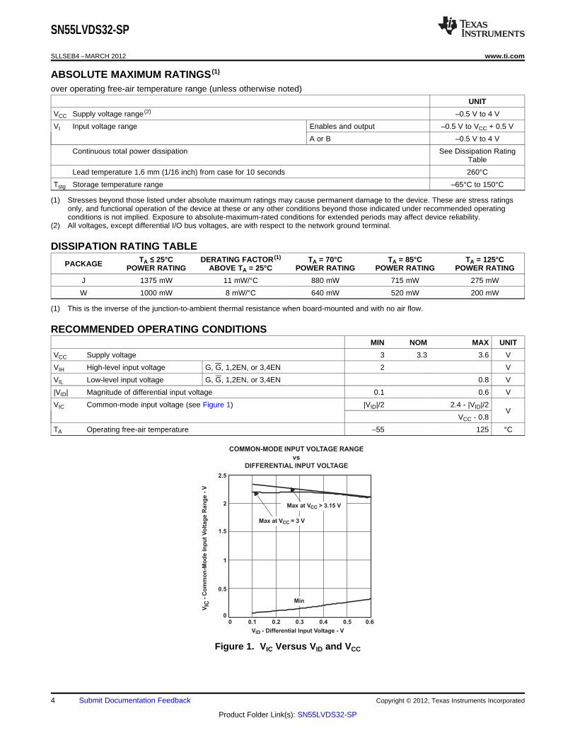
RECOMMENDED OPERATING CONDITIONSMIN NOM MAX UNIT
VCC Supply voltage 3 3.3 3.6 V
VIH High-level input voltage G, G, 1,2EN, or 3,4EN 2 V
VIL Low-level input voltage G, G, 1,2EN, or 3,4EN 0.8 V
|VID| Magnitude of differential input voltage 0.1 0.6 V
VIC Common-mode input voltage (see Figure 1) |VID|/2 2.4 - |VID|/2V
VCC - 0.8
TA Operating free-air temperature –55 125 °C
Figure 1. VIC Versus VID and VCC
4 Submit Documentation Feedback Copyright © 2012, Texas Instruments Incorporated
Product Folder Link(s): SN55LVDS32-SP
SN55LVDS32-SP
www.ti.com SLLSEB4 –MARCH 2012
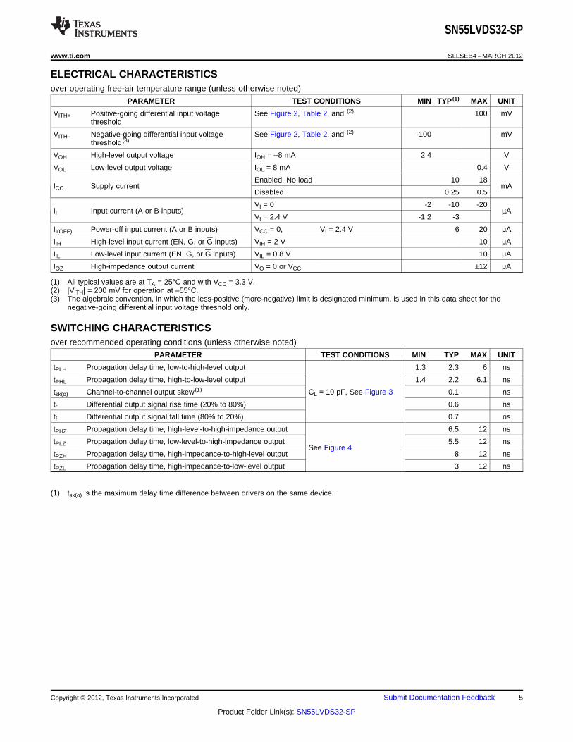
ELECTRICAL CHARACTERISTICSover operating free-air temperature range (unless otherwise noted)
PARAMETER TEST CONDITIONS MIN TYP (1) MAX UNIT
VITH+ Positive-going differential input voltage See Figure 2, Table 2, and (2) 100 mVthreshold
VITH– Negative-going differential input voltage See Figure 2, Table 2, and (2) -100 mVthreshold (3)
VOH High-level output voltage IOH = –8 mA 2.4 V
VOL Low-level output voltage IOL = 8 mA 0.4 V
Enabled, No load 10 18ICC Supply current mA
Disabled 0.25 0.5
VI = 0 -2 -10 -20II Input current (A or B inputs) µA
VI = 2.4 V -1.2 -3
II(OFF) Power-off input current (A or B inputs) VCC = 0, VI = 2.4 V 6 20 μA
IIH High-level input current (EN, G, or G inputs) VIH = 2 V 10 μA
IIL Low-level input current (EN, G, or G inputs) VIL = 0.8 V 10 μA
IOZ High-impedance output current VO = 0 or VCC ±12 μA
(1) All typical values are at TA = 25°C and with VCC = 3.3 V.(2) |VITH| = 200 mV for operation at –55°C.(3) The algebraic convention, in which the less-positive (more-negative) limit is designated minimum, is used in this data sheet for the
negative-going differential input voltage threshold only.
SWITCHING CHARACTERISTICSover recommended operating conditions (unless otherwise noted)
PARAMETER TEST CONDITIONS MIN TYP MAX UNIT
tPLH Propagation delay time, low-to-high-level output 1.3 2.3 6 ns
tPHL Propagation delay time, high-to-low-level output 1.4 2.2 6.1 ns
tsk(o) Channel-to-channel output skew (1) CL = 10 pF, See Figure 3 0.1 ns
tr Differential output signal rise time (20% to 80%) 0.6 ns
tf Differential output signal fall time (80% to 20%) 0.7 ns
tPHZ Propagation delay time, high-level-to-high-impedance output 6.5 12 ns
tPLZ Propagation delay time, low-level-to-high-impedance output 5.5 12 nsSee Figure 4
tPZH Propagation delay time, high-impedance-to-high-level output 8 12 ns
tPZL Propagation delay time, high-impedance-to-low-level output 3 12 ns
(1) tsk(o) is the maximum delay time difference between drivers on the same device.
Copyright © 2012, Texas Instruments Incorporated Submit Documentation Feedback 5
Product Folder Link(s): SN55LVDS32-SP
VID
A
B
Y
VOVIB
VIA
VIC(VIA + VIB)/2
SN55LVDS32-SP
SLLSEB4 –MARCH 2012 www.ti.com
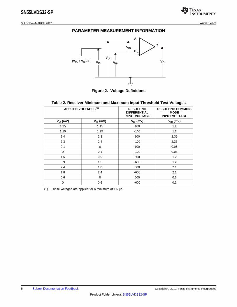
PARAMETER MEASUREMENT INFORMATION
Figure 2. Voltage Definitions
Table 2. Receiver Minimum and Maximum Input Threshold Test Voltages
APPLIED VOLTAGES (1) RESULTING RESULTING COMMON-DIFFERENTIAL MODE
INPUT VOLTAGE INPUT VOLTAGE
VIA (mV) VIB (mV) VID (mV) VIC (mV)
1.25 1.15 100 1.2
1.15 1.25 -100 1.2
2.4 2.3 100 2.35
2.3 2.4 -100 2.35
0.1 0 100 0.05
0 0.1 -100 0.05
1.5 0.9 600 1.2
0.9 1.5 -600 1.2
2.4 1.8 600 2.1
1.8 2.4 -600 2.1
0.6 0 600 0.3
0 0.6 -600 0.3
(1) These voltages are applied for a minimum of 1.5 µs.
6 Submit Documentation Feedback Copyright © 2012, Texas Instruments Incorporated
Product Folder Link(s): SN55LVDS32-SP
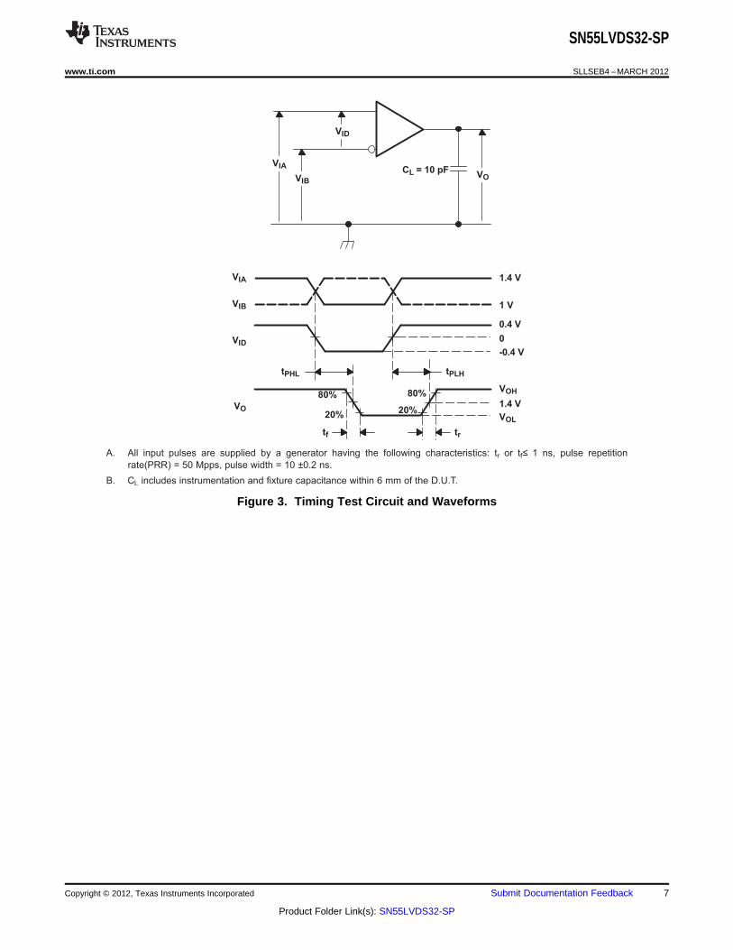
VID
VOVIB
VIACL = 10 pF
tPHL tPLH
t tf r
80%
20%
80%
20%
VIA
VIB
VID
VO
1.4 V
1 V
0.4 V
0
-0.4 V
VOH
1.4 V
VOL
A. All input pulses are supplied by a generator having the following characteristics: tr or tf≤ 1 ns, pulse repetition
rate(PRR) = 50 Mpps, pulse width = 10 ±0.2 ns.
B. CL includes instrumentation and fixture capacitance within 6 mm of the D.U.T.
SN55LVDS32-SP
www.ti.com SLLSEB4 –MARCH 2012
Figure 3. Timing Test Circuit and Waveforms
Copyright © 2012, Texas Instruments Incorporated Submit Documentation Feedback 7
Product Folder Link(s): SN55LVDS32-SP
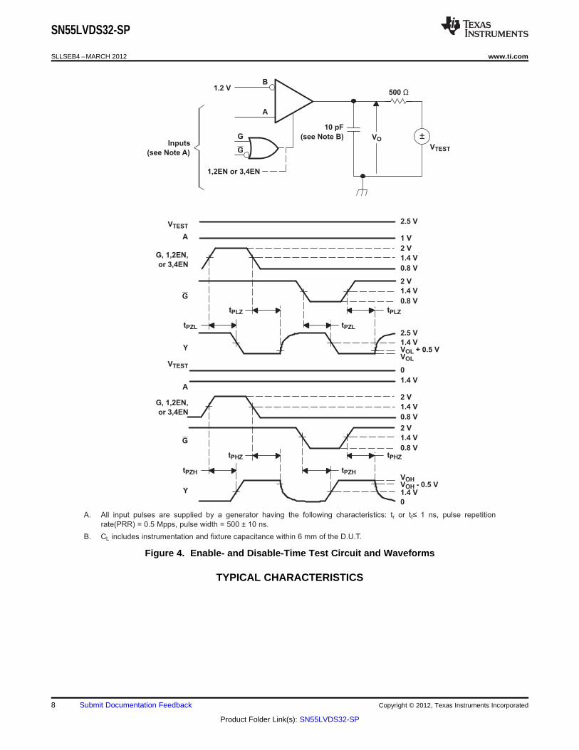
B
A
G
G
VO ±
500 Ω
VTEST
10 pF
(see Note B)
1.2 V
tPZL
tPLZ
tPZL
tPLZ
tPZH
tPHZ
tPZH
tPHZ
2.5 V
1 V
2 V
1.4 V
0.8 V
2 V
1.4 V
0.8 V
2.5 V
1.4 VVOL + 0.5 VVOL
0
1.4 V
2 V
1.4 V
0.8 V
2 V
1.4 V
0.8 V
VOHVOH - 0.5 V1.4 V
0
VTEST
A
G, 1,2EN,
or 3,4EN
G
Y
VTEST
A
G
Y
Inputs
(see Note A)
1,2EN or 3,4EN
G, 1,2EN,
or 3,4EN
A. All input pulses are supplied by a generator having the following characteristics: tr or tf≤ 1 ns, pulse repetition
rate(PRR) = 0.5 Mpps, pulse width = 500 ± 10 ns.
B. CL includes instrumentation and fixture capacitance within 6 mm of the D.U.T.
SN55LVDS32-SP
SLLSEB4 –MARCH 2012 www.ti.com
Figure 4. Enable- and Disable-Time Test Circuit and Waveforms
TYPICAL CHARACTERISTICS
8 Submit Documentation Feedback Copyright © 2012, Texas Instruments Incorporated
Product Folder Link(s): SN55LVDS32-SP
2.1
1.9
1.7
1.5−50 0 50
−L
ow
-to
-Hig
hP
rop
ag
ati
on
Dela
yT
ime
−n
s
2.3
2.5
2.7
100
T −A Free-Air Temperature − C°t P
LH
(D)
VCC = 3.3 V
VCC = 3 V
VCC = 3.6 V55
45
25
1550 100
65
75
f − Frequency − MHz
85
150 200
35
Four Receivers, Loaded
Per Figure 3, Switching
Simultaneously
VCC = 3.6 V
VCC = 3.3 V
VCC = 3 V
−S
up
ply
Cu
rren
t−
mA
(rm
s)
I CC
2.1
1.9
1.7
1.5−50 0 50
−H
igh
-to
-Lo
wP
rop
ag
ati
on
Dela
yT
ime
−n
s
2.3
2.5
2.7
100
t PH
L(D
)
T −A Free-Air Temperature − C°
VCC = 3.3 V
VCC = 3.6 V
VCC = 3 V
SN55LVDS32-SP
www.ti.com SLLSEB4 –MARCH 2012
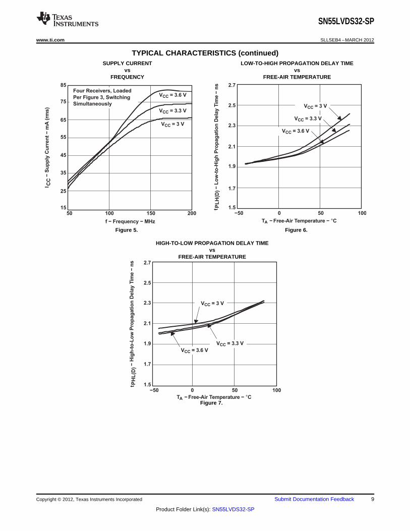
TYPICAL CHARACTERISTICS (continued)SUPPLY CURRENT LOW-TO-HIGH PROPAGATION DELAY TIME
vs vsFREQUENCY FREE-AIR TEMPERATURE
Figure 5. Figure 6.
HIGH-TO-LOW PROPAGATION DELAY TIMEvs
FREE-AIR TEMPERATURE
Figure 7.
Copyright © 2012, Texas Instruments Incorporated Submit Documentation Feedback 9
Product Folder Link(s): SN55LVDS32-SP
IOH − High-Level Output Current − mA
0.0
0.5
1.0
1.5
2.0
2.5
3.0
3.5
−60 −50 −40 −30 −20 −10 0
VO
H−
Hig
h-L
evelO
utp
ut
Vo
ltag
e−
V
IOL − Low-Level Output Current − mA
0.0
0.5
1.0
1.5
2.0
2.5
3.0
3.5
4.0
4.5
5.0
0 10 20 30 40 50 60 70 80O
LV
−L
ow
-LevelO
utp
ut
Vo
ltag
e−
V
SN55LVDS32-SP
SLLSEB4 –MARCH 2012 www.ti.com
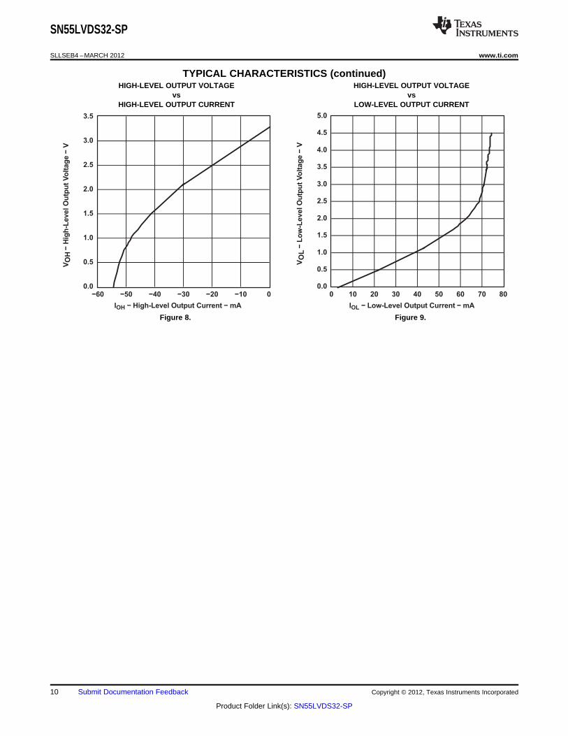
TYPICAL CHARACTERISTICS (continued)HIGH-LEVEL OUTPUT VOLTAGE HIGH-LEVEL OUTPUT VOLTAGE
vs vsHIGH-LEVEL OUTPUT CURRENT LOW-LEVEL OUTPUT CURRENT
Figure 8. Figure 9.
10 Submit Documentation Feedback Copyright © 2012, Texas Instruments Incorporated
Product Folder Link(s): SN55LVDS32-SP
Hewlett Packard HP6624ADC Power Supply
Bench Test Board
Agilent ParBERT(E4832A)
Tektronix TDS7404Real Time Scope
All Rx running at 100 Mbps; Channel 1: 1Y, Channel 2: 2Y; Channel 3: 3Y; Channel 4: 4Y
SN55LVDS32-SP
www.ti.com SLLSEB4 –MARCH 2012
APPLICATION INFORMATION
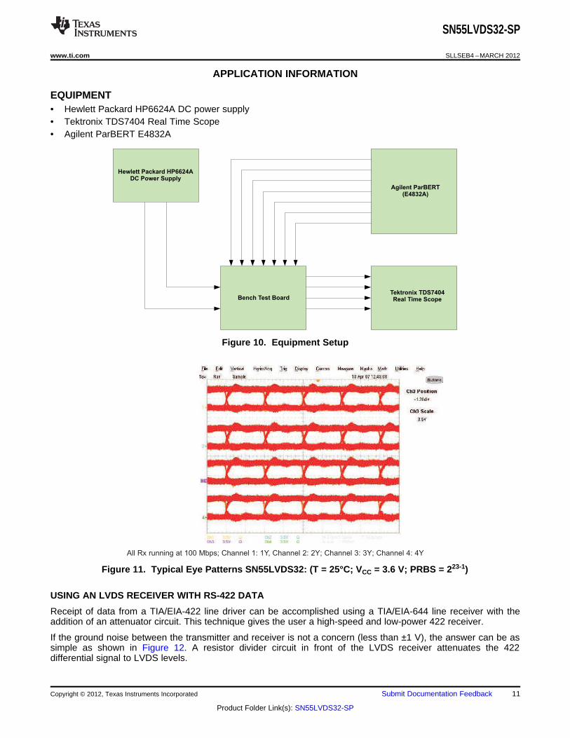
EQUIPMENT• Hewlett Packard HP6624A DC power supply• Tektronix TDS7404 Real Time Scope• Agilent ParBERT E4832A
Figure 10. Equipment Setup
Figure 11. Typical Eye Patterns SN55LVDS32: (T = 25°C; VCC = 3.6 V; PRBS = 223-1)
USING AN LVDS RECEIVER WITH RS-422 DATA
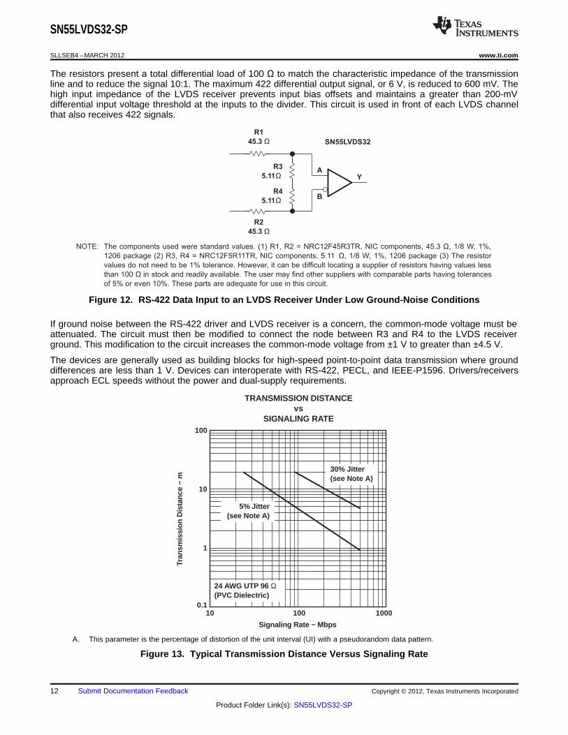
Receipt of data from a TIA/EIA-422 line driver can be accomplished using a TIA/EIA-644 line receiver with theaddition of an attenuator circuit. This technique gives the user a high-speed and low-power 422 receiver.
If the ground noise between the transmitter and receiver is not a concern (less than ±1 V), the answer can be assimple as shown in Figure 12. A resistor divider circuit in front of the LVDS receiver attenuates the 422differential signal to LVDS levels.
Copyright © 2012, Texas Instruments Incorporated Submit Documentation Feedback 11
Product Folder Link(s): SN55LVDS32-SP
R1
45.3 Ω
R2
45.3 Ω
R3
5.11Ω
R4
5.11Ω
A
B
Y
SN55LVDS32
NOTE: The components used were standard values. (1) R1, R2 = NRC12F45R3TR, NIC components, 45.3 Ω, 1/8 W, 1%,
1206 package (2) R3, R4 = NRC12F5R11TR, NIC components, 5.11 Ω, 1/8 W, 1%, 1206 package (3) The resistor
values do not need to be 1% tolerance. However, it can be difficult locating a supplier of resistors having values less
than 100 Ω in stock and readily available. The user may find other suppliers with comparable parts having tolerances
of 5% or even 10%. These parts are adequate for use in this circuit.
10
1
0.1
Tran
smis
sion
Dis
tanc
e −
m
100
Signaling Rate − Mbps
TRANSMISSION DISTANCEvs
SIGNALING RATE
10 100 1000
5% Jitter(see Note A)
30% Jitter(see Note A)
24 AWG UTP 96 Ω (PVC Dielectric)
SN55LVDS32-SP
SLLSEB4 –MARCH 2012 www.ti.com
The resistors present a total differential load of 100 Ω to match the characteristic impedance of the transmissionline and to reduce the signal 10:1. The maximum 422 differential output signal, or 6 V, is reduced to 600 mV. Thehigh input impedance of the LVDS receiver prevents input bias offsets and maintains a greater than 200-mVdifferential input voltage threshold at the inputs to the divider. This circuit is used in front of each LVDS channelthat also receives 422 signals.
Figure 12. RS-422 Data Input to an LVDS Receiver Under Low Ground-Noise Conditions
If ground noise between the RS-422 driver and LVDS receiver is a concern, the common-mode voltage must beattenuated. The circuit must then be modified to connect the node between R3 and R4 to the LVDS receiverground. This modification to the circuit increases the common-mode voltage from ±1 V to greater than ±4.5 V.
The devices are generally used as building blocks for high-speed point-to-point data transmission where grounddifferences are less than 1 V. Devices can interoperate with RS-422, PECL, and IEEE-P1596. Drivers/receiversapproach ECL speeds without the power and dual-supply requirements.
A. This parameter is the percentage of distortion of the unit interval (UI) with a pseudorandom data pattern.
Figure 13. Typical Transmission Distance Versus Signaling Rate
12 Submit Documentation Feedback Copyright © 2012, Texas Instruments Incorporated
Product Folder Link(s): SN55LVDS32-SP
1B
1A
1Y
G
2Y
2A
2B
GND
VCC
4B
4A
4Y
G
3Y
3A
3B
1
2
3
4
5
6
7
8
16
15
14
13
12
11
10
9
100 Ω
100 Ω
100 Ω
(see Note B)
100 Ω
3.3 V
0.1 µF
(see Note A)
0.001 µF
(see Note A)
VCC
See Note C
SN55LVDS32-SP
www.ti.com SLLSEB4 –MARCH 2012
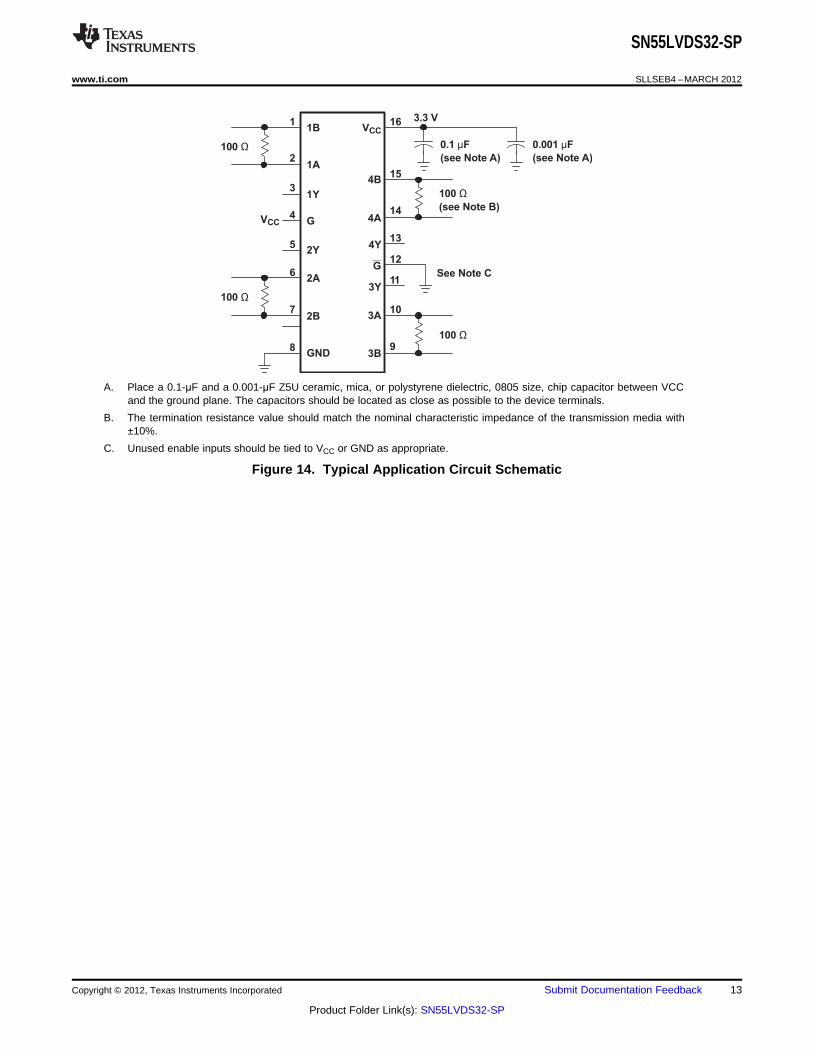
A. Place a 0.1-μF and a 0.001-μF Z5U ceramic, mica, or polystyrene dielectric, 0805 size, chip capacitor between VCCand the ground plane. The capacitors should be located as close as possible to the device terminals.
B. The termination resistance value should match the nominal characteristic impedance of the transmission media with±10%.
C. Unused enable inputs should be tied to VCC or GND as appropriate.
Figure 14. Typical Application Circuit Schematic
Copyright © 2012, Texas Instruments Incorporated Submit Documentation Feedback 13
Product Folder Link(s): SN55LVDS32-SP
1/4 ’LVDS31
’LVDS32
500 Ω
500 Ω
20 kΩ
20 kΩ
3.3 V
500 Ω
500 Ω
20 kΩ
20 kΩ
3.3 V
7 kΩ7 kΩ10 kΩ
3.3 kΩ
Twisted-Pair B Only
Strb/Data_TX
Strb/Data_Enable
Data/Strobe
1 Arb_RX
2 Arb_RX
Port_Status
Tp Bias onTwisted-Pair A
55 Ω
55 Ω
5 kΩ
VG onTwisted-Pair B
TP
TP
3.3 V
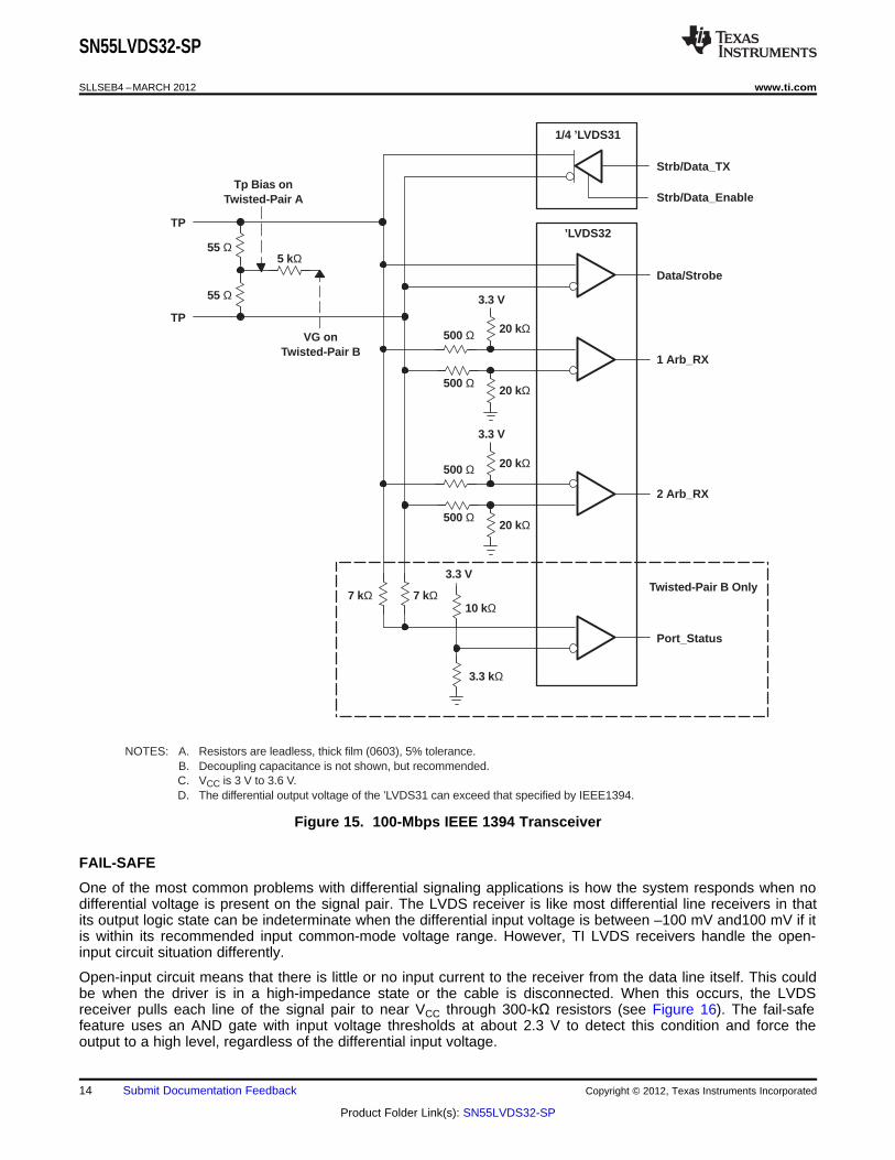
NOTES: A. Resistors are leadless, thick film (0603), 5% tolerance.B. Decoupling capacitance is not shown, but recommended.C. VCC is 3 V to 3.6 V.D. The differential output voltage of the ’LVDS31 can exceed that specified by IEEE1394.
SN55LVDS32-SP
SLLSEB4 –MARCH 2012 www.ti.com
Figure 15. 100-Mbps IEEE 1394 Transceiver
FAIL-SAFE
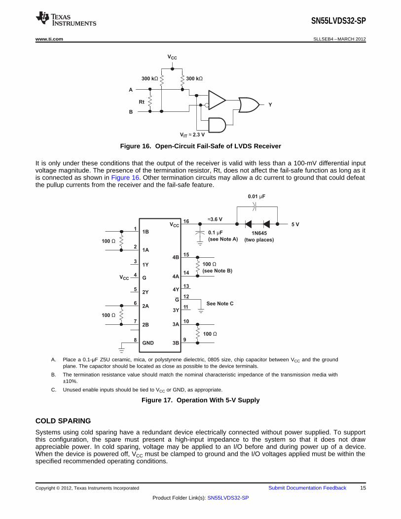
One of the most common problems with differential signaling applications is how the system responds when nodifferential voltage is present on the signal pair. The LVDS receiver is like most differential line receivers in thatits output logic state can be indeterminate when the differential input voltage is between –100 mV and100 mV if itis within its recommended input common-mode voltage range. However, TI LVDS receivers handle the open-input circuit situation differently.
Open-input circuit means that there is little or no input current to the receiver from the data line itself. This couldbe when the driver is in a high-impedance state or the cable is disconnected. When this occurs, the LVDSreceiver pulls each line of the signal pair to near VCC through 300-kΩ resistors (see Figure 16). The fail-safefeature uses an AND gate with input voltage thresholds at about 2.3 V to detect this condition and force theoutput to a high level, regardless of the differential input voltage.
14 Submit Documentation Feedback Copyright © 2012, Texas Instruments Incorporated
Product Folder Link(s): SN55LVDS32-SP
Rt
300 kΩ 300 kΩ
VCC
VIT ≈ 2.3 V
A
B
Y
1B
1A
1Y
G
2Y
2A
2B
GND
VCC
4B
4A
4Y
G
3Y
3A
3B
1
2
3
4
5
6
7
8
16
15
14
13
12
11
10
9
100 Ω
100 Ω
100 Ω
(see Note B)
100 Ω
VCC
See Note C
≈3.6 V
0.1 µF
(see Note A)1N645
(two places)
0.01 µF
5 V
SN55LVDS32-SP
www.ti.com SLLSEB4 –MARCH 2012
Figure 16. Open-Circuit Fail-Safe of LVDS Receiver
It is only under these conditions that the output of the receiver is valid with less than a 100-mV differential inputvoltage magnitude. The presence of the termination resistor, Rt, does not affect the fail-safe function as long as itis connected as shown in Figure 16. Other termination circuits may allow a dc current to ground that could defeatthe pullup currents from the receiver and the fail-safe feature.
A. Place a 0.1-μF Z5U ceramic, mica, or polystyrene dielectric, 0805 size, chip capacitor between VCC and the groundplane. The capacitor should be located as close as possible to the device terminals.
B. The termination resistance value should match the nominal characteristic impedance of the transmission media with±10%.
C. Unused enable inputs should be tied to VCC or GND, as appropriate.
Figure 17. Operation With 5-V Supply
COLD SPARING
Systems using cold sparing have a redundant device electrically connected without power supplied. To supportthis configuration, the spare must present a high-input impedance to the system so that it does not drawappreciable power. In cold sparing, voltage may be applied to an I/O before and during power up of a device.When the device is powered off, VCC must be clamped to ground and the I/O voltages applied must be within thespecified recommended operating conditions.
Copyright © 2012, Texas Instruments Incorporated Submit Documentation Feedback 15
Product Folder Link(s): SN55LVDS32-SP
SN55LVDS32-SP
SLLSEB4 –MARCH 2012 www.ti.com
RELATED INFORMATION
IBIS modeling is available for this device. Contact the local TI sales office or the TI Web site at www.ti.com formore information.
For more application guidelines, see the following documents:• Low-Voltage Differential Signaling Design Notes (SLLA014)• Interface Circuits for TIA/EIA-644 (LVDS) (SLLA038)• Reducing EMI With LVDS (SLLA030)• Slew Rate Control of LVDS Circuits (SLLA034)• Using an LVDS Receiver With RS-422 Data (SLLA031)
16 Submit Documentation Feedback Copyright © 2012, Texas Instruments Incorporated
Product Folder Link(s): SN55LVDS32-SP
PACKAGE OPTION ADDENDUM
www.ti.com 4-Feb-2021
Addendum-Page 1
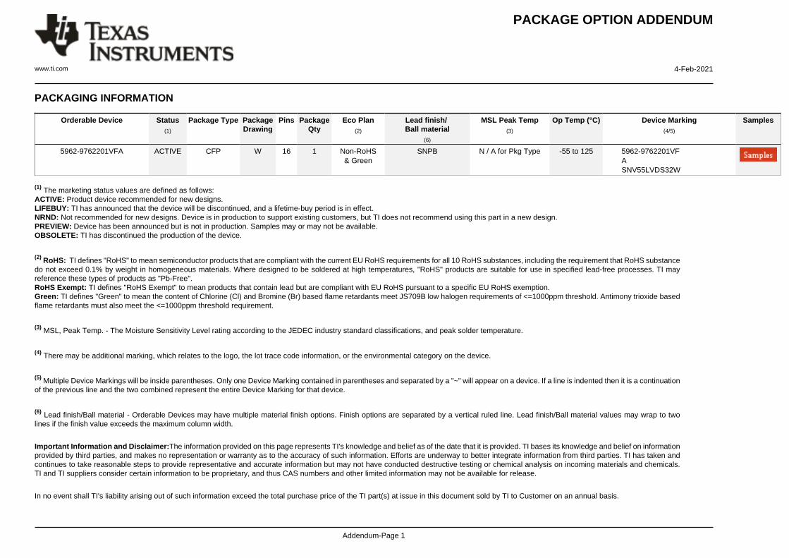
PACKAGING INFORMATION
Orderable Device Status(1)
Package Type PackageDrawing
Pins PackageQty
Eco Plan(2)
Lead finish/Ball material
(6)
MSL Peak Temp(3)
Op Temp (°C) Device Marking(4/5)
Samples
5962-9762201VFA ACTIVE CFP W 16 1 Non-RoHS& Green
SNPB N / A for Pkg Type -55 to 125 5962-9762201VFASNV55LVDS32W
(1) The marketing status values are defined as follows:ACTIVE: Product device recommended for new designs.LIFEBUY: TI has announced that the device will be discontinued, and a lifetime-buy period is in effect.NRND: Not recommended for new designs. Device is in production to support existing customers, but TI does not recommend using this part in a new design.PREVIEW: Device has been announced but is not in production. Samples may or may not be available.OBSOLETE: TI has discontinued the production of the device.
(2) RoHS: TI defines "RoHS" to mean semiconductor products that are compliant with the current EU RoHS requirements for all 10 RoHS substances, including the requirement that RoHS substancedo not exceed 0.1% by weight in homogeneous materials. Where designed to be soldered at high temperatures, "RoHS" products are suitable for use in specified lead-free processes. TI mayreference these types of products as "Pb-Free".RoHS Exempt: TI defines "RoHS Exempt" to mean products that contain lead but are compliant with EU RoHS pursuant to a specific EU RoHS exemption.Green: TI defines "Green" to mean the content of Chlorine (Cl) and Bromine (Br) based flame retardants meet JS709B low halogen requirements of <=1000ppm threshold. Antimony trioxide basedflame retardants must also meet the <=1000ppm threshold requirement.
(3) MSL, Peak Temp. - The Moisture Sensitivity Level rating according to the JEDEC industry standard classifications, and peak solder temperature.
(4) There may be additional marking, which relates to the logo, the lot trace code information, or the environmental category on the device.
(5) Multiple Device Markings will be inside parentheses. Only one Device Marking contained in parentheses and separated by a "~" will appear on a device. If a line is indented then it is a continuationof the previous line and the two combined represent the entire Device Marking for that device.
(6) Lead finish/Ball material - Orderable Devices may have multiple material finish options. Finish options are separated by a vertical ruled line. Lead finish/Ball material values may wrap to twolines if the finish value exceeds the maximum column width.
Important Information and Disclaimer:The information provided on this page represents TI's knowledge and belief as of the date that it is provided. TI bases its knowledge and belief on informationprovided by third parties, and makes no representation or warranty as to the accuracy of such information. Efforts are underway to better integrate information from third parties. TI has taken andcontinues to take reasonable steps to provide representative and accurate information but may not have conducted destructive testing or chemical analysis on incoming materials and chemicals.TI and TI suppliers consider certain information to be proprietary, and thus CAS numbers and other limited information may not be available for release.
In no event shall TI's liability arising out of such information exceed the total purchase price of the TI part(s) at issue in this document sold by TI to Customer on an annual basis.
PACKAGE OPTION ADDENDUM
www.ti.com 4-Feb-2021
Addendum-Page 2
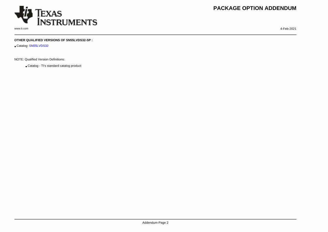
OTHER QUALIFIED VERSIONS OF SN55LVDS32-SP :
• Catalog: SN55LVDS32
NOTE: Qualified Version Definitions:
• Catalog - TI's standard catalog product
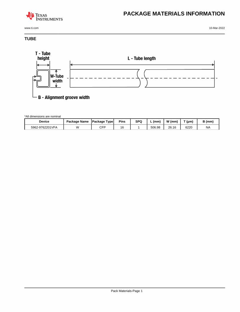
TUBE
*All dimensions are nominal
Device Package Name Package Type Pins SPQ L (mm) W (mm) T (µm) B (mm)
5962-9762201VFA W CFP 16 1 506.98 26.16 6220 NA
PACKAGE MATERIALS INFORMATION
www.ti.com 10-Mar-2022
Pack Materials-Page 1
IMPORTANT NOTICE AND DISCLAIMERTI PROVIDES TECHNICAL AND RELIABILITY DATA (INCLUDING DATA SHEETS), DESIGN RESOURCES (INCLUDING REFERENCE DESIGNS), APPLICATION OR OTHER DESIGN ADVICE, WEB TOOLS, SAFETY INFORMATION, AND OTHER RESOURCES “AS IS” AND WITH ALL FAULTS, AND DISCLAIMS ALL WARRANTIES, EXPRESS AND IMPLIED, INCLUDING WITHOUT LIMITATION ANY IMPLIED WARRANTIES OF MERCHANTABILITY, FITNESS FOR A PARTICULAR PURPOSE OR NON-INFRINGEMENT OF THIRD PARTY INTELLECTUAL PROPERTY RIGHTS.These resources are intended for skilled developers designing with TI products. You are solely responsible for (1) selecting the appropriate TI products for your application, (2) designing, validating and testing your application, and (3) ensuring your application meets applicable standards, and any other safety, security, regulatory or other requirements.These resources are subject to change without notice. TI grants you permission to use these resources only for development of an application that uses the TI products described in the resource. Other reproduction and display of these resources is prohibited. No license is granted to any other TI intellectual property right or to any third party intellectual property right. TI disclaims responsibility for, and you will fully indemnify TI and its representatives against, any claims, damages, costs, losses, and liabilities arising out of your use of these resources.TI’s products are provided subject to TI’s Terms of Sale or other applicable terms available either on ti.com or provided in conjunction with such TI products. TI’s provision of these resources does not expand or otherwise alter TI’s applicable warranties or warranty disclaimers for TI products.TI objects to and rejects any additional or different terms you may have proposed. IMPORTANT NOTICE
Mailing Address: Texas Instruments, Post Office Box 655303, Dallas, Texas 75265Copyright © 2022, Texas Instruments Incorporated