bq2515xevm user's guide (rev. a) - texas instruments
TRANSCRIPT

1SLUUBV0A–July 2018–Revised August 2019Submit Documentation Feedback
Copyright © 2018–2019, Texas Instruments Incorporated
BQ2515xEVM Evaluation Module
User's GuideSLUUBV0A–July 2018–Revised August 2019
BQ2515xEVM Evaluation Module
This user's guide provides detailed testing instructions for the BQ2515x evaluation module (EVM). Alsoincluded are descriptions of the necessary equipment, equipment setup, procedures, the printed-circuitboard layouts, schematics, and the bill of materials (BOM).
Throughout this user's guide, the abbreviations EVM, BQ2515xEVM, and the term evaluation module aresynonymous with the BQ2515x evaluation module, unless otherwise noted.
Contents1 Introduction ................................................................................................................... 2
1.1 EVM Features ....................................................................................................... 21.2 I/O Descriptions ..................................................................................................... 2
2 Test Summary................................................................................................................ 42.1 Equipment ........................................................................................................... 42.2 Charge Mode ........................................................................................................ 52.3 Ship Mode ........................................................................................................... 62.4 Warning .............................................................................................................. 62.5 Comparison Table .................................................................................................. 6
3 Board Layouts, Schematics, and Bill of Materials ....................................................................... 73.1 Board Layouts ....................................................................................................... 73.2 Schematics ......................................................................................................... 123.3 Bill of Materials .................................................................................................... 15
List of Figures
1 BQ2515xEVM Connections ............................................................................................... 32 Connections for Test Setup ................................................................................................ 53 BQStudio Software Tool .................................................................................................... 64 Top Overlay .................................................................................................................. 75 Top Layer ..................................................................................................................... 76 Signal Layer 1................................................................................................................ 87 Signal Layer 2................................................................................................................ 88 Bottom Layer ................................................................................................................. 99 Bottom Overlay............................................................................................................... 910 Top Solder Mask ........................................................................................................... 1011 Bottom Solder Mask ....................................................................................................... 1012 Drill Drawing ................................................................................................................ 1113 Board Dimensions.......................................................................................................... 1114 BQ2515xEVM Schematic ................................................................................................ 1215 BQ2515xEVM Jumper Connectors ..................................................................................... 1316 BQ2515xEVM Interface Connector ..................................................................................... 1317 User Menu Switches ....................................................................................................... 1418 LDO for Display/Other Peripherals....................................................................................... 14
List of Tables
1 Device Data Sheet........................................................................................................... 2
Introduction www.ti.com
2 SLUUBV0A–July 2018–Revised August 2019Submit Documentation Feedback
Copyright © 2018–2019, Texas Instruments Incorporated
BQ2515xEVM Evaluation Module
2 Jumper Connections ........................................................................................................ 23 Recommended Operating Conditions..................................................................................... 34 Comparison Table ........................................................................................................... 65 Bill of Materials ............................................................................................................. 15
TrademarksMicrosoft, Windows are registered trademarks of Microsoft Corporation.All other trademarks are the property of their respective owners.
1 IntroductionThe BQ2515xEVM is an evaluation kit for the BQ2515x integrated battery charge management IC. TheBQ2515x is an integrated battery charge management IC that integrates the most common functionsfor wearable devices: Linear charger, regulated output/ load switch, manual reset with timer, ADC andship mode function.
1.1 EVM FeaturesKey features of this EVM include:• 500mA Linear battery charger• I2C Configurable Battery Regulation Voltage with 0.5% Accuracy• Configurable Termination Current down to 0.5mA• Programmable thermal charging profile with configurable Hot, Warm, Cool and Cold thresholds• Power Path Management for powering the system and charging the battery• 10nA Ship Mode battery Iddq for longest shelf life• One I2C Configurable Load Switch or 150mA LDO Output• One Button Wake-up and Reset Input with Adjustable Timers• ADC Monitoring of Input voltage, Battery voltage, Charge current, Battery Thermistor• I2C Communication Control
See the device data sheet (SLUSD04) for detailed features and operation of the integrated circuit (IC).
Table 1. Device Data Sheet
Device Data SheetBQ25150 SLUSD04BQ25155 SLUSDO1
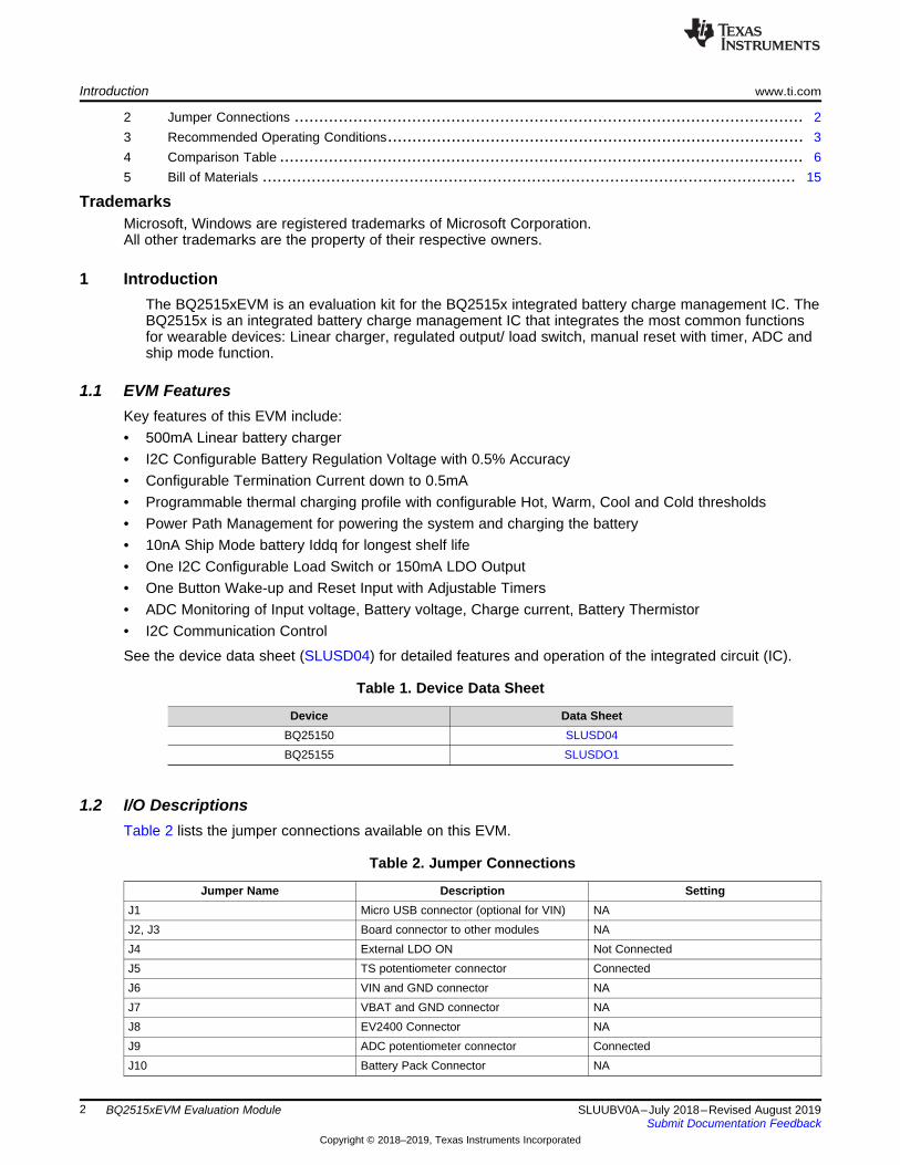
1.2 I/O DescriptionsTable 2 lists the jumper connections available on this EVM.
Table 2. Jumper Connections
Jumper Name Description SettingJ1 Micro USB connector (optional for VIN) NAJ2, J3 Board connector to other modules NAJ4 External LDO ON Not ConnectedJ5 TS potentiometer connector ConnectedJ6 VIN and GND connector NAJ7 VBAT and GND connector NAJ8 EV2400 Connector NAJ9 ADC potentiometer connector ConnectedJ10 Battery Pack Connector NA
VIN
VIO/VDD Connection
ChargeEnable/Disable
Low Power Mode /MR Push Button
EV2400 Connector
VBAT
www.ti.com Introduction
3SLUUBV0A–July 2018–Revised August 2019Submit Documentation Feedback
Copyright © 2018–2019, Texas Instruments Incorporated
BQ2515xEVM Evaluation Module
Table 2. Jumper Connections (continued)J11 VIO connector to VDD or 3p3V Connect VDD to VIOJ12 /LP connector to GPIO or VIO Connect /LP to VIOJ13 /CE connector ro GPIO or VIO Connect /CE to VIOJ14 Display connector for other modules NAJ15 PMID to VINLS connector ConnectedJ16 On board LED pullup to VDD or PMID Connected to PMIDJ17 I2C Pullup Connected
Table 3 lists the recommended operating conditions for this EVM.
Figure 1. BQ2515xEVM Connections
Table 3. Recommended Operating Conditions
Symbol Description MIN TYP MAX UnitSupply voltage, VVBUS Input voltage from AC adapter 5 20 VBattery voltage, VBAT in charge mode Voltage applied at VBAT terminal 4.2 VI BAT Fast charging current 0.5 A
Discharging current through internal MOSFET 1 ASupply current, IIN Maximum input current from AC adapter input 0.6 A

Test Summary www.ti.com
4 SLUUBV0A–July 2018–Revised August 2019Submit Documentation Feedback
Copyright © 2018–2019, Texas Instruments Incorporated
BQ2515xEVM Evaluation Module
2 Test Summary
2.1 EquipmentThis section includes a list of supplies required to perform tests on this EVM.1. Powersupply (PS#1), Powersupply (PS#2): Keithley 2400 Powersupply or equivalent2. SC#1- SC#3: 4 channel Oscilloscope3. Computer: A computer with at least one USB port and a USB cable4. PC communication interface:5. Software: Download bqStudio from Texas Instruments
Double click the Battery management studio installation file and then follow the installation steps. Thesoftware supports Microsoft® Windows® 7 and Windows 10 operating systems.
V
V
+
+±
±
SC#1
SC#2
V+±
SC#1
PS#1 PS#2
www.ti.com Test Summary
5SLUUBV0A–July 2018–Revised August 2019Submit Documentation Feedback
Copyright © 2018–2019, Texas Instruments Incorporated
BQ2515xEVM Evaluation Module
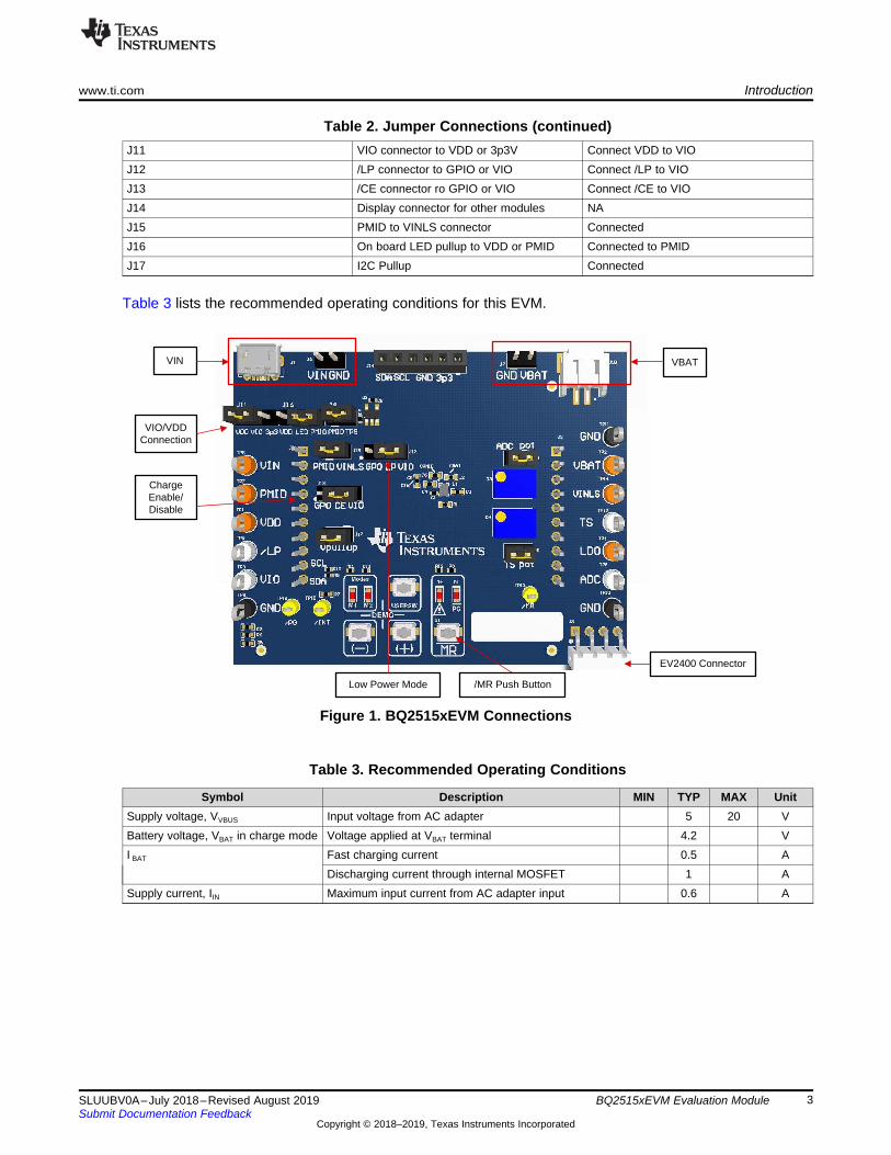
2.2 Charge ModeConnect the equipment as following:
Power supply PS#1: VIN of the BQ2515x at 5V
Power supply PS#2: VBAT of the BQ2515x at 3.7V
Scope channel SC#1: VIN
Scope channel SC#2: VPMID
Scope channel SC#3: VBAT
Turn ON the supply PS#2, then turn ON the supply PS#1. The VPMID will rise to the level of VIN. Thedevice will begin to charge as long as /CE pin jumper is disconnected(J13 being pulled off will result in thepulldown internal to the device, charge enabled) ,the TS is left at default configuration and there are noother faults.
To adjust the charge current or change other parameters, connect the EV2400 to the EVM and thenstartup BQStudio.
Select the Charger_ 1_00-bq25150.bqz from the Charger selection for the BQ25150EVM orcharger_1_00-bq25155.bqz from the charger selection for the BQ25155EVM. Click “Read Register” toread all the registers and navigate to the Field View to make changes.
Figure 2. Connections for Test Setup
Test Summary www.ti.com
6 SLUUBV0A–July 2018–Revised August 2019Submit Documentation Feedback
Copyright © 2018–2019, Texas Instruments Incorporated
BQ2515xEVM Evaluation Module
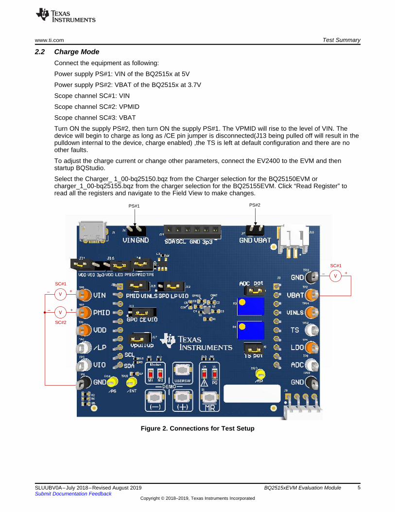
2.3 Ship ModeTo go to Ship Mode, turn OFF VIN (PS#1). Make sure /LP pin is connected to VIO(J12) and VIO isconnected to VDD through J11. Read all the registers and click the Shipmode Enable checkbox (Bit B7on register 0x35) to go to Ship Mode. You can know that you are in Ship Mode as the voltage on PMID(SC#2) will fall to 0V.
Figure 3. BQStudio Software Tool
2.4 WarningThe warning label indicates when there is a fault during communication with the MCU.
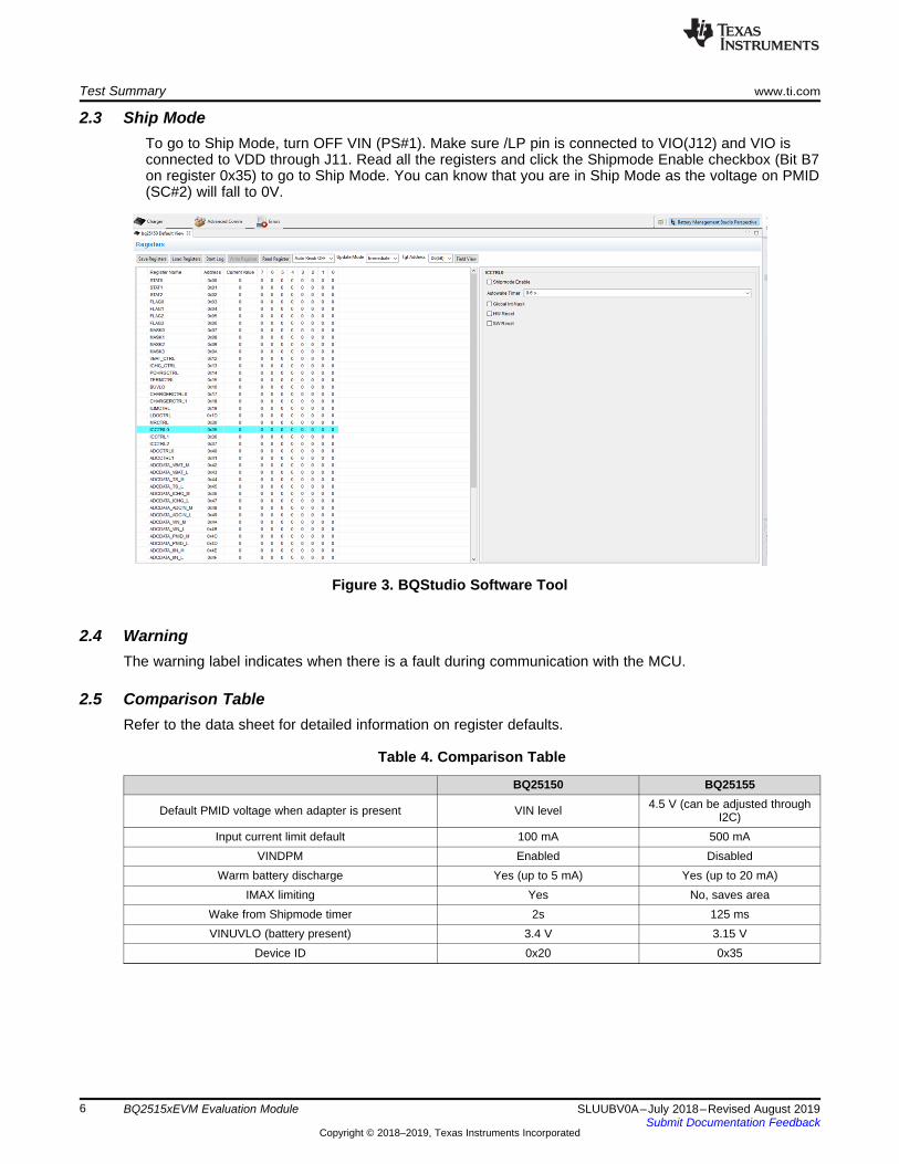
2.5 Comparison TableRefer to the data sheet for detailed information on register defaults.
Table 4. Comparison Table
BQ25150 BQ25155
Default PMID voltage when adapter is present VIN level 4.5 V (can be adjusted throughI2C)
Input current limit default 100 mA 500 mAVINDPM Enabled Disabled
Warm battery discharge Yes (up to 5 mA) Yes (up to 20 mA)IMAX limiting Yes No, saves area
Wake from Shipmode timer 2s 125 msVINUVLO (battery present) 3.4 V 3.15 V
Device ID 0x20 0x35
www.ti.com Board Layouts, Schematics, and Bill of Materials
7SLUUBV0A–July 2018–Revised August 2019Submit Documentation Feedback
Copyright © 2018–2019, Texas Instruments Incorporated
BQ2515xEVM Evaluation Module
3 Board Layouts, Schematics, and Bill of Materials
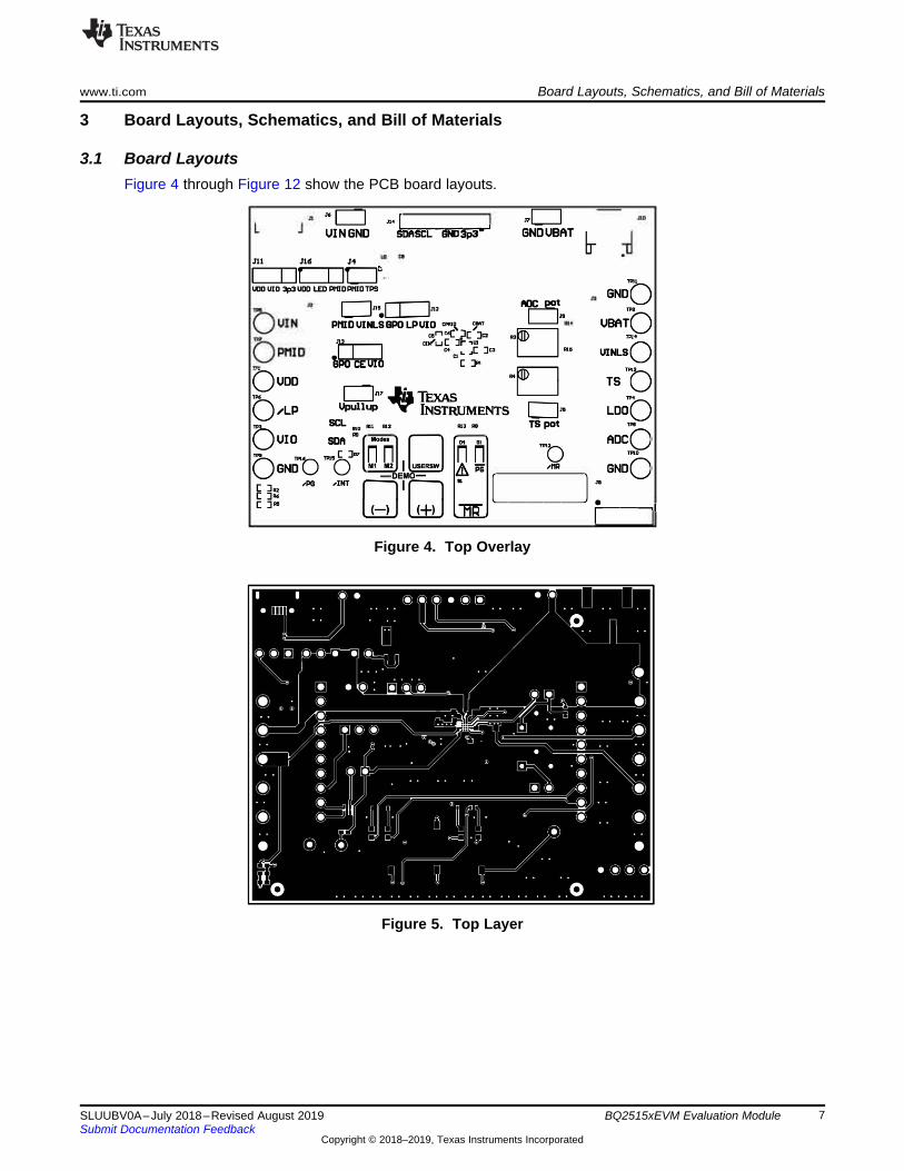
3.1 Board LayoutsFigure 4 through Figure 12 show the PCB board layouts.
Figure 4. Top Overlay
Figure 5. Top Layer
Board Layouts, Schematics, and Bill of Materials www.ti.com
8 SLUUBV0A–July 2018–Revised August 2019Submit Documentation Feedback
Copyright © 2018–2019, Texas Instruments Incorporated
BQ2515xEVM Evaluation Module
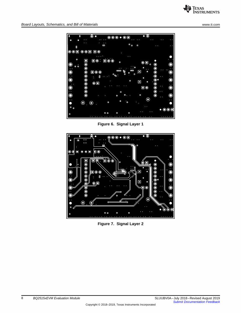
Figure 6. Signal Layer 1
Figure 7. Signal Layer 2
www.ti.com Board Layouts, Schematics, and Bill of Materials
9SLUUBV0A–July 2018–Revised August 2019Submit Documentation Feedback
Copyright © 2018–2019, Texas Instruments Incorporated
BQ2515xEVM Evaluation Module
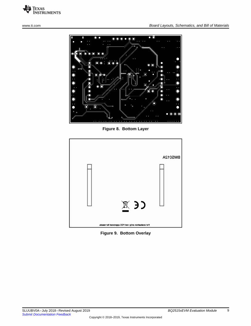
Figure 8. Bottom Layer
Figure 9. Bottom Overlay

Board Layouts, Schematics, and Bill of Materials www.ti.com
10 SLUUBV0A–July 2018–Revised August 2019Submit Documentation Feedback
Copyright © 2018–2019, Texas Instruments Incorporated
BQ2515xEVM Evaluation Module
Figure 10. Top Solder Mask
Figure 11. Bottom Solder Mask

www.ti.com Board Layouts, Schematics, and Bill of Materials
11SLUUBV0A–July 2018–Revised August 2019Submit Documentation Feedback
Copyright © 2018–2019, Texas Instruments Incorporated
BQ2515xEVM Evaluation Module
Figure 12. Drill Drawing
Figure 13. Board Dimensions

VIN
GND
1uFC4
4.7uFC6
PMID
VIO
1
2
3
4
5
6
7
8
9
10
11
J1
CONN_105017-0001GND GND
GND
GND
VINLS
TS
ADCIN
4.7uFC1
GND
2.2uF
C3
GND
VLDO
1uFC2
/LP
/PG
/INT
GND
GND
GND
VDD
TP9 TP10
TP1
TP3
TP7
TP5
TP8
ADCIN
VBATTP2
TP6
TP4
R3
SCL
/MR
/CE
GND
SDA
12
J9
BQ2515x Low Iq Battery Charger with Powerpath Management, LDO and ADC
TS
GND
R4
1
2
J5TP12
21
S1
Switch_PushButton
14.3kR2
DNP
TS
14.3kR5
DNP
VDD
/PG14.3kR6
DNP
INA1
PMIDA2
BATA3
GNDA4
PGB1
PMIDB2
BATB3
TSB4
CEC2
MRC1
IMAXC3
ADCINC4
VDDD1
INTD2
LPD3
LDOD4
VIOE1
SDAE2
SCLE3
VINLSE4
BQ25150YFPR
U1
0.1uF
C5
TP13
TP11
10.0kR1
10k
10k
+3p3V
14.3kR14
14.3kR15
Board Layouts, Schematics, and Bill of Materials www.ti.com
12 SLUUBV0A–July 2018–Revised August 2019Submit Documentation Feedback
Copyright © 2018–2019, Texas Instruments Incorporated
BQ2515xEVM Evaluation Module
3.2 SchematicsFigure 14 and Figure 16 show the schematics for the BQ2515x EVM.
Figure 14. BQ2515xEVM Schematic

J1.2
J1.3
J1.4
SW3
J1.6
J1.7
J1.8
GNDJ2.3
J2.4
J2.5
SW2
SW1
J2.8
J2.9
J2.10
5
4
1
2
3
6
7
8
9
10
J2
5
4
1
2
3
6
7
8
9
10
J3
Display RST
+3p3V
Interface Connector
/CE/LP
LED1LED2
SDASCL
/INTFault LED
123
J11
10kR10 10k
R9
VIO
VIO
VDD/LP
VIO
499
R81 2
D1
LTST-C190CKT
/PG
/INT
1 2 3J16
PMID
1
2
3
4
5
6
J14
GND
Display RST
M2
1 2
M1
J10
VBAT
GND
12
J7
VBAT
GND
4 123
J822/05/3041
GND
EV2400 I2C
Jumper Connections/ LEDs
+3p3V
VINLS
12
J15
PMID
/CE
J1
.7
J1
.8
1 2
D2
LTST-C190CKT
1 2
D3
LTST-C190CKT
499
R11
499
R12
GND
J2.8
J2.9
12
J6
VIN
GND
TP16
TP15
SCL
SDA
TP14
+3p3V
123
J13
VIO
123
J12
1
2
J17
VIO
SDASCL
SDA SCL
10.0kR7
VIO
1 2
D4
LTST-C190CKT499
R13J2.4
J2.3
www.ti.com Board Layouts, Schematics, and Bill of Materials
13SLUUBV0A–July 2018–Revised August 2019Submit Documentation Feedback
Copyright © 2018–2019, Texas Instruments Incorporated
BQ2515xEVM Evaluation Module
Figure 15. BQ2515xEVM Jumper Connectors
Figure 16. BQ2515xEVM Interface Connector

IN1
OUT5
EN3
2 4
GND
TPS78233DDCT
U21 2J4
PMID+3p3V
GND
1uFC7
1uFC8
LDO for Display/ Other peripherals
GND GND GND
21
SW1
Switch_PushButton
21
SW2
Switch_PushButton
21
SW3
Switch_PushButton
SW3SW2SW1
User Menu Switches
Board Layouts, Schematics, and Bill of Materials www.ti.com
14 SLUUBV0A–July 2018–Revised August 2019Submit Documentation Feedback
Copyright © 2018–2019, Texas Instruments Incorporated
BQ2515xEVM Evaluation Module
Figure 17. User Menu Switches
Figure 18. LDO for Display/Other Peripherals
www.ti.com Board Layouts, Schematics, and Bill of Materials
15SLUUBV0A–July 2018–Revised August 2019Submit Documentation Feedback
Copyright © 2018–2019, Texas Instruments Incorporated
BQ2515xEVM Evaluation Module
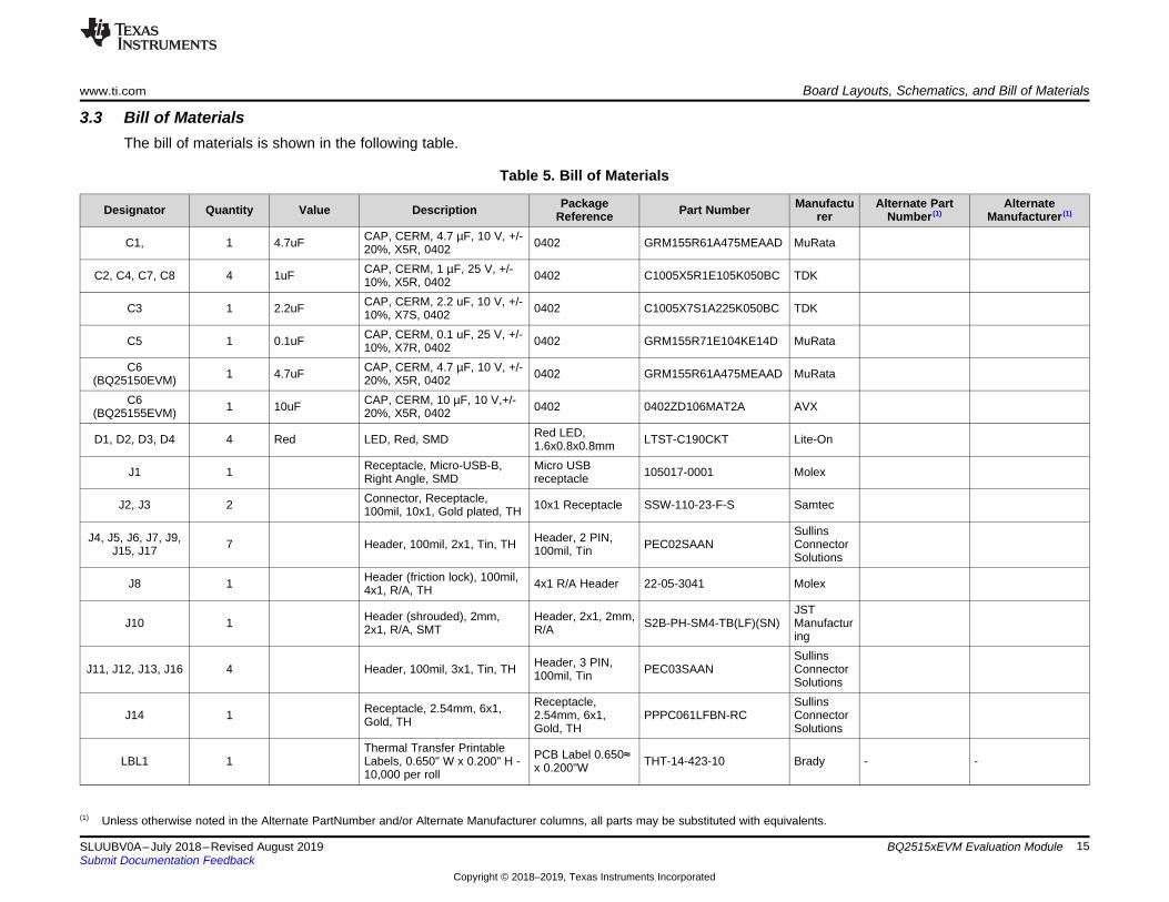
3.3 Bill of MaterialsThe bill of materials is shown in the following table.
(1) Unless otherwise noted in the Alternate PartNumber and/or Alternate Manufacturer columns, all parts may be substituted with equivalents.
Table 5. Bill of Materials
Designator Quantity Value Description PackageReference Part Number Manufactu
rerAlternate Part
Number (1)Alternate
Manufacturer (1)
C1, 1 4.7uF CAP, CERM, 4.7 µF, 10 V, +/-20%, X5R, 0402 0402 GRM155R61A475MEAAD MuRata
C2, C4, C7, C8 4 1uF CAP, CERM, 1 µF, 25 V, +/-10%, X5R, 0402 0402 C1005X5R1E105K050BC TDK
C3 1 2.2uF CAP, CERM, 2.2 uF, 10 V, +/-10%, X7S, 0402 0402 C1005X7S1A225K050BC TDK
C5 1 0.1uF CAP, CERM, 0.1 uF, 25 V, +/-10%, X7R, 0402 0402 GRM155R71E104KE14D MuRata
C6(BQ25150EVM) 1 4.7uF CAP, CERM, 4.7 µF, 10 V, +/-
20%, X5R, 0402 0402 GRM155R61A475MEAAD MuRata
C6(BQ25155EVM) 1 10uF CAP, CERM, 10 µF, 10 V,+/-
20%, X5R, 0402 0402 0402ZD106MAT2A AVX
D1, D2, D3, D4 4 Red LED, Red, SMD Red LED,1.6x0.8x0.8mm LTST-C190CKT Lite-On
J1 1 Receptacle, Micro-USB-B,Right Angle, SMD
Micro USBreceptacle 105017-0001 Molex
J2, J3 2 Connector, Receptacle,100mil, 10x1, Gold plated, TH 10x1 Receptacle SSW-110-23-F-S Samtec
J4, J5, J6, J7, J9,J15, J17 7 Header, 100mil, 2x1, Tin, TH Header, 2 PIN,
100mil, Tin PEC02SAANSullinsConnectorSolutions
J8 1 Header (friction lock), 100mil,4x1, R/A, TH 4x1 R/A Header 22-05-3041 Molex
J10 1 Header (shrouded), 2mm,2x1, R/A, SMT
Header, 2x1, 2mm,R/A S2B-PH-SM4-TB(LF)(SN)
JSTManufacturing
J11, J12, J13, J16 4 Header, 100mil, 3x1, Tin, TH Header, 3 PIN,100mil, Tin PEC03SAAN
SullinsConnectorSolutions
J14 1 Receptacle, 2.54mm, 6x1,Gold, TH
Receptacle,2.54mm, 6x1,Gold, TH
PPPC061LFBN-RCSullinsConnectorSolutions
LBL1 1Thermal Transfer PrintableLabels, 0.650" W x 0.200" H -10,000 per roll
PCB Label 0.650≈x 0.200"W THT-14-423-10 Brady - -

Board Layouts, Schematics, and Bill of Materials www.ti.com
16 SLUUBV0A–July 2018–Revised August 2019Submit Documentation Feedback
Copyright © 2018–2019, Texas Instruments Incorporated
BQ2515xEVM Evaluation Module
Table 5. Bill of Materials (continued)
Designator Quantity Value Description PackageReference Part Number Manufactu
rerAlternate Part
Number (1)Alternate
Manufacturer (1)
R1, R7 2 10.0kΩ RES, 10.0 k, 1%, 0.2 W, AEC-Q200 Grade 0, 0402 0402 ERJPA2F1002X Panasonic
R3, R4 2 10kΩ Trimmer, 10k ohm, 0.25W, TH 4.5x8x6.7mm 3266W-1-103LF Bourns
R8, R11, R12, R13 4 499Ω RES, 499, 1%, 0.063 W, 0402 0402 CRCW0402499RFKED Vishay-Dale
R9, R10 2 10kΩ RES, 10 k, 5%, 0.063 W,0402 0402 CRCW040210K0JNED Vishay-
DaleS1, SW1, SW2,
SW3 4 Switch, Tactile, SPST-NO,0.05A, 12V, SMT
Switch, 4.4x2x2.9mm TL1015AF160QG E-Switch
SH-J1, SH-J2, SH-J3, SH-J4, SH-J5,SH-J6, SH-J7, SH-
J8, SH-J9
9 1x2 Shunt, 100mil, Gold plated,Black Shunt SNT-100-BK-G Samtec 969102-0000-DA 3M
TP1, TP2, TP4,TP5, TP7, TP14 6 Test Point, Multipurpose,
Orange, TH
OrangeMultipurposeTestpoint
5013 Keystone
TP3, TP6, TP8,TP12 4 Test Point, Multipurpose,
White, TH
WhiteMultipurposeTestpoint
5012 Keystone
TP9, TP10, TP11 3 Test Point, Multipurpose,Black, TH
Black MultipurposeTestpoint 5011 Keystone
TP13, TP15, TP16 3 Test Point, Miniature, Yellow,TH
Yellow MiniatureTestpoint 5004 Keystone
U1(BQ25150EVM) 1 BQ25150YFP,
YFP0020ACAC (DSBGA-20) YFP0020ACAC BQ25150YFPRTexasInstruments
BQ25150YFPT Texas Instruments
U1(BQ25155EVM) 1 BQ25155, YFP0020ACAC
(DSBGA-20) YFP0020ACAC BQ25155YFPRTexasInstruments
BQ25155YFPT Texas Instruments
U2 1
Single Output LDO, 150 mA,Fixed 3.3 V Output, 2.2 to 5.5V Input, with 0.5 uA QuiescentCurrent, 5-pin SOT (DDC),-40 to 125 degC, Green(RoHS and no Sb/Br)
DDC0005A TPS78233DDCTTexasInstruments
FID1, FID2, FID3 0 Fiducial mark. There isnothing to buy or mount. Fiducial N/A N/A
R2, R5, R6 0 14.3k RES, 14.3 k, 1%, 0.063 W,0402 0402 CRCW040214K3FKED Vishay-
Dale

17SLUUBV0A–July 2018–Revised August 2019Submit Documentation Feedback
BQ2515xEVM Evaluation Module

Board Layouts, Schematics, and Bill of Materials www.ti.com
18 SLUUBV0A–July 2018–Revised August 2019Submit Documentation Feedback
Copyright © 2018–2019, Texas Instruments Incorporated
BQ2515xEVM Evaluation Module
IMPORTANT NOTICE AND DISCLAIMER
TI PROVIDES TECHNICAL AND RELIABILITY DATA (INCLUDING DATASHEETS), DESIGN RESOURCES (INCLUDING REFERENCEDESIGNS), APPLICATION OR OTHER DESIGN ADVICE, WEB TOOLS, SAFETY INFORMATION, AND OTHER RESOURCES “AS IS”AND WITH ALL FAULTS, AND DISCLAIMS ALL WARRANTIES, EXPRESS AND IMPLIED, INCLUDING WITHOUT LIMITATION ANYIMPLIED WARRANTIES OF MERCHANTABILITY, FITNESS FOR A PARTICULAR PURPOSE OR NON-INFRINGEMENT OF THIRDPARTY INTELLECTUAL PROPERTY RIGHTS.These resources are intended for skilled developers designing with TI products. You are solely responsible for (1) selecting the appropriateTI products for your application, (2) designing, validating and testing your application, and (3) ensuring your application meets applicablestandards, and any other safety, security, or other requirements. These resources are subject to change without notice. TI grants youpermission to use these resources only for development of an application that uses the TI products described in the resource. Otherreproduction and display of these resources is prohibited. No license is granted to any other TI intellectual property right or to any thirdparty intellectual property right. TI disclaims responsibility for, and you will fully indemnify TI and its representatives against, any claims,damages, costs, losses, and liabilities arising out of your use of these resources.TI’s products are provided subject to TI’s Terms of Sale (www.ti.com/legal/termsofsale.html) or other applicable terms available either onti.com or provided in conjunction with such TI products. TI’s provision of these resources does not expand or otherwise alter TI’s applicablewarranties or warranty disclaimers for TI products.
Mailing Address: Texas Instruments, Post Office Box 655303, Dallas, Texas 75265Copyright © 2019, Texas Instruments Incorporated

IMPORTANT NOTICE AND DISCLAIMERTI PROVIDES TECHNICAL AND RELIABILITY DATA (INCLUDING DATA SHEETS), DESIGN RESOURCES (INCLUDING REFERENCE DESIGNS), APPLICATION OR OTHER DESIGN ADVICE, WEB TOOLS, SAFETY INFORMATION, AND OTHER RESOURCES “AS IS” AND WITH ALL FAULTS, AND DISCLAIMS ALL WARRANTIES, EXPRESS AND IMPLIED, INCLUDING WITHOUT LIMITATION ANY IMPLIED WARRANTIES OF MERCHANTABILITY, FITNESS FOR A PARTICULAR PURPOSE OR NON-INFRINGEMENT OF THIRD PARTY INTELLECTUAL PROPERTY RIGHTS.These resources are intended for skilled developers designing with TI products. You are solely responsible for (1) selecting the appropriate TI products for your application, (2) designing, validating and testing your application, and (3) ensuring your application meets applicable standards, and any other safety, security, regulatory or other requirements.These resources are subject to change without notice. TI grants you permission to use these resources only for development of an application that uses the TI products described in the resource. Other reproduction and display of these resources is prohibited. No license is granted to any other TI intellectual property right or to any third party intellectual property right. TI disclaims responsibility for, and you will fully indemnify TI and its representatives against, any claims, damages, costs, losses, and liabilities arising out of your use of these resources.TI’s products are provided subject to TI’s Terms of Sale or other applicable terms available either on ti.com or provided in conjunction with such TI products. TI’s provision of these resources does not expand or otherwise alter TI’s applicable warranties or warranty disclaimers for TI products.TI objects to and rejects any additional or different terms you may have proposed. IMPORTANT NOTICE
Mailing Address: Texas Instruments, Post Office Box 655303, Dallas, Texas 75265Copyright © 2022, Texas Instruments Incorporated