display port 1:2 switch datasheet - texas instruments
TRANSCRIPT
1FEATURES APPLICATIONS
DESCRIPTION
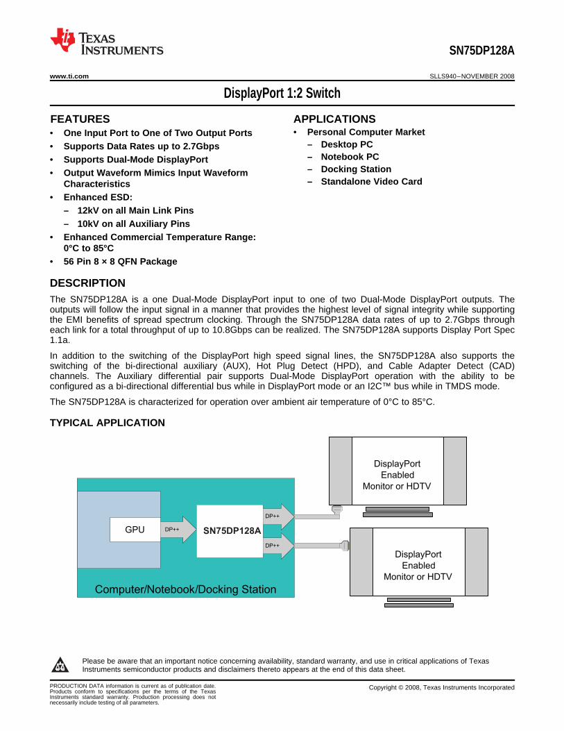
TYPICAL APPLICATION
Computer/Notebook/Docking Station
GPU DP++
DP++
DP++
DisplayPort
Enabled
Monitor or HDTV
DisplayPort
Enabled
Monitor or HDTV
SN75DP128A
SN75DP128A
www.ti.com............................................................................................................................................................................................ SLLS940–NOVEMBER 2008
DisplayPort 1:2 Switch
• Personal Computer Market• One Input Port to One of Two Output Ports– Desktop PC• Supports Data Rates up to 2.7Gbps– Notebook PC• Supports Dual-Mode DisplayPort– Docking Station• Output Waveform Mimics Input Waveform– Standalone Video CardCharacteristics
• Enhanced ESD:– 12kV on all Main Link Pins– 10kV on all Auxiliary Pins
• Enhanced Commercial Temperature Range:0°C to 85°C
• 56 Pin 8 × 8 QFN Package
The SN75DP128A is a one Dual-Mode DisplayPort input to one of two Dual-Mode DisplayPort outputs. Theoutputs will follow the input signal in a manner that provides the highest level of signal integrity while supportingthe EMI benefits of spread spectrum clocking. Through the SN75DP128A data rates of up to 2.7Gbps througheach link for a total throughput of up to 10.8Gbps can be realized. The SN75DP128A supports Display Port Spec1.1a.
In addition to the switching of the DisplayPort high speed signal lines, the SN75DP128A also supports theswitching of the bi-directional auxiliary (AUX), Hot Plug Detect (HPD), and Cable Adapter Detect (CAD)channels. The Auxiliary differential pair supports Dual-Mode DisplayPort operation with the ability to beconfigured as a bi-directional differential bus while in DisplayPort mode or an I2C™ bus while in TMDS mode.
The SN75DP128A is characterized for operation over ambient air temperature of 0°C to 85°C.
1
Please be aware that an important notice concerning availability, standard warranty, and use in critical applications of TexasInstruments semiconductor products and disclaimers thereto appears at the end of this data sheet.
PRODUCTION DATA information is current as of publication date. Copyright © 2008, Texas Instruments IncorporatedProducts conform to specifications per the terms of the TexasInstruments standard warranty. Production processing does notnecessarily include testing of all parameters.
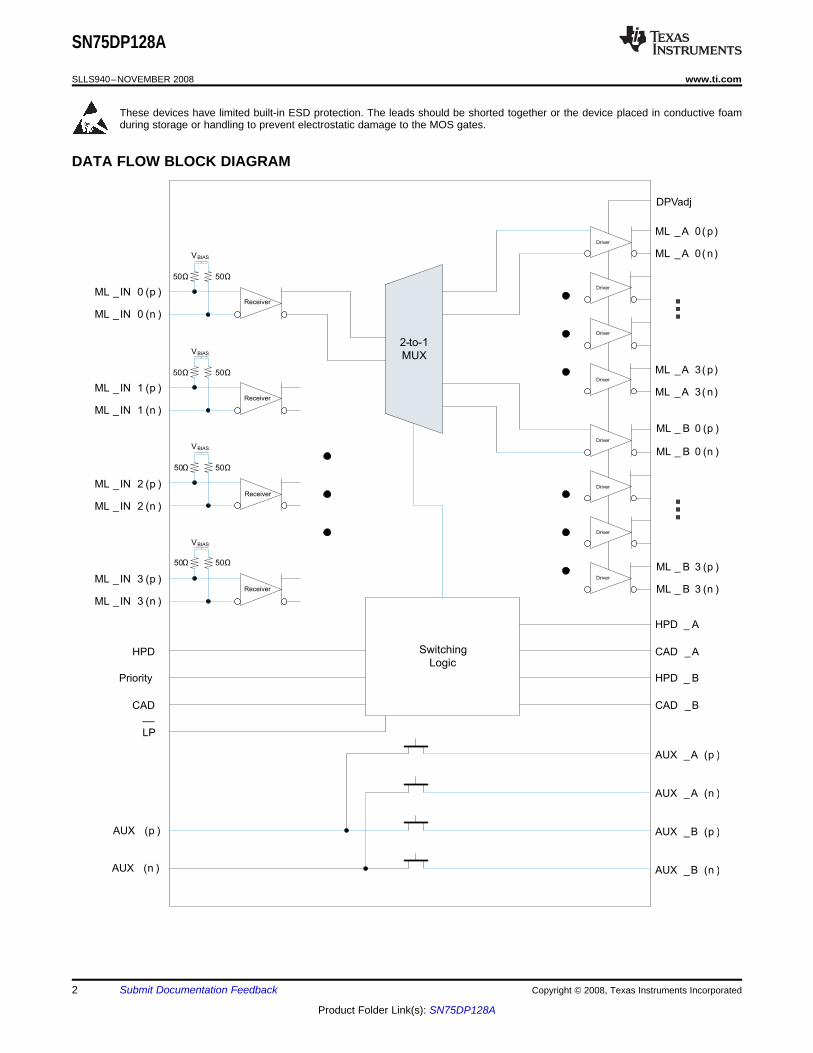
DATA FLOW BLOCK DIAGRAM
ML _ B 3 (p )
ML _ B 3 (n )
ML _ B 0 (p )
ML _ B 0 (n )
ML _IN 2 (p )
ML _IN 2 (n )
ML _IN 3 (n )
ML _IN 3 (p )
ML _IN 0 (p )
ML _IN 0 (n )
ML _IN 1 (p )
ML _IN 1 (n )
AUX (p )
AUX (n )
AUX _A (p )
AUX _A (n )
ML _A 0( n)
ML _A 0( p)
ML _A 3( p)
ML _A 3( n)
Receiver
50Ω 50Ω
VBIAS
AUX _B (p )
AUX _B (n )
Priority
HPD _ A
HPD _ B
HPD
CAD
CAD _A
Receiver
50Ω 50Ω
VBIAS
Receiver
50Ω 50Ω
VBIAS
Receiver
50Ω 50Ω
VBIAS
Driver
Driver
Driver
Driver
Driver
Driver
Driver
Driver
2-to-1
MUX
Switching
Logic
DPVadj
CAD _B__
LP
SN75DP128A
SLLS940–NOVEMBER 2008............................................................................................................................................................................................ www.ti.com
These devices have limited built-in ESD protection. The leads should be shorted together or the device placed in conductive foamduring storage or handling to prevent electrostatic damage to the MOS gates.
2 Submit Documentation Feedback Copyright © 2008, Texas Instruments Incorporated
Product Folder Link(s): SN75DP128A
AU
X(p
)
HP
D_B
ML_B 2(n)
ML_B 0(p)
LP
Pri
ori
ty
ML_
IN0(p
)
ML_B 3(n)
ML_B 1(p)
ML_
IN1(n
)
ML_
IN1(p
)
ML_
IN0(n
)
ML_
IN3(n
)
ML_
IN3(p
)
ML_
IN2(n
)
ML_
IN2(p
)
ML_B 3(p)
GN
D
VD
DML_B 1(n)
ML_B 2(p)
VD
D
GN
D
VDD
VD
D
AUX_A (p)
AUX_B (p)
VD
D
VDD
AUX_A (n)
CA
D_B
AU
X(n
)
GND
ML_B 0(n)
GN
D
GND
GND
VDD
1
24
23
22
21
20
19
18
17
16
15141312111098765432
25
26
34 33 32 31 30 2928
27
40 39 38 37 36 35
48
47
46
45
44
4342 41
53
56
55
54
52
51
50
49
HP
D
VD
D* 1
CA
D
HP
D_A
CA
D_A
GN
D
ML_A 3(n)
ML_A 3(p)
ML_A 2(n)
ML_A 2(p)
ML_A 1(n)
ML_A 1(p)
VDD
ML_A 0(n)
ML_A 0(p)
GND
AUX_B(n)
DP
Va
dj
SN75DP128A
SN75DP128A
www.ti.com............................................................................................................................................................................................ SLLS940–NOVEMBER 2008
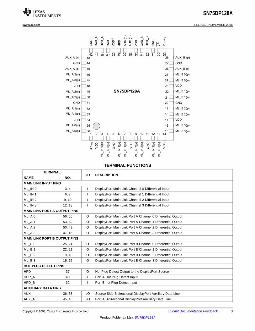
TERMINAL FUNCTIONSTERMINAL
I/O DESCRIPTIONNAME NO.MAIN LINK INPUT PINSML_IN 0 3, 4 I DisplayPort Main Link Channel 0 Differential InputML_IN 1 6, 7 I DisplayPort Main Link Channel 1 Differential InputML_IN 2 9, 10 I DisplayPort Main Link Channel 2 Differential InputML_IN 3 12, 13 I DisplayPort Main Link Channel 3 Differential InputMAIN LINK PORT A OUTPUT PINSML_A 0 56, 55 O DisplayPort Main Link Port A Channel 0 Differential OutputML_A 1 53, 52 O DisplayPort Main Link Port A Channel 1 Differential OutputML_A 2 50, 49 O DisplayPort Main Link Port A Channel 2 Differential OutputML_A 3 47, 46 O DisplayPort Main Link Port A Channel 3 Differential OutputMAIN LINK PORT B OUTPUT PINSML_B 0 25, 24 O DisplayPort Main Link Port B Channel 0 Differential OutputML_B 1 22, 21 O DisplayPort Main Link Port B Channel 1 Differential OutputML_B 2 19, 18 O DisplayPort Main Link Port B Channel 2 Differential OutputML_B 3 16, 15 O DisplayPort Main Link Port B Channel 3 Differential OutputHOT PLUG DETECT PINSHPD 37 O Hot Plug Detect Output to the DisplayPort SourceHDP_A 40 I Port A Hot Plug Detect InputHPD_B 32 I Port B hot Plug Detect InputAUXILIARY DATA PINSAUX 36, 35 I/O Source Side Bidirectional DisplayPort Auxiliary Data LineAUX_A 45, 43 I/O Port A Bidirectional DisplayPort Auxiliary Data Line
Copyright © 2008, Texas Instruments Incorporated Submit Documentation Feedback 3
Product Folder Link(s): SN75DP128A
SN75DP128A
SLLS940–NOVEMBER 2008............................................................................................................................................................................................ www.ti.com
TERMINAL FUNCTIONS (continued)TERMINAL
I/O DESCRIPTIONNAME NO.AUX_B 28, 26 I/O Port B Bidirectional DisplayPort Auxiliary Data LineCABLE ADAPTER DETECT PINSCAD 39 O Cable Adapter Detect Output to the DisplayPort SourceCAD_A 41 I Port A Cable Adapter Detect InputCAD_B 33 I Port B Cable Adapter Detect InputCONTROL PINSLP 30 I Low Power Select BarPriority 29 I Output Port Priority selectionDPVadj 1 I DisplayPort Main Link Output Gain AdjustmentSUPPLY and GROUND PINS
2, 8, 14, 17, 23,VDD Primary Supply Voltage34, 48, 54VDD*1 38 HPD and CAD Output Voltage
5, 11, 20, 27,GND Ground42, 44, 51
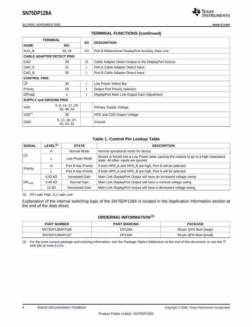
Table 1. Control Pin Lookup TableSIGNAL LEVEL (1) STATE DESCRIPTION
H Normal Mode Normal operational mode for deviceLP Device is forced into a Low Power state causing the outputs to go to a high impedanceL Low Power Mode state. All other inputs are ignored
H Port B has Priority If both HPD_A and HPD_B are high, Port B will be selectedPriority
L Port A has Priority If both HPD_A and HPD_B are high, Port A will be selected4.53 kΩ Increased Gain Main Link DisplayPort Output will have an increased voltage swing
DPVadj 6.49 kΩ Normal Gain Main Link DisplayPort Output will have a nominal voltage swing10 kΩ Decreased Gain Main Link DisplayPort Output will have a decreased voltage swing
(1) (H) Logic High; (L) Logic Low
Explanation of the internal switching logic of the SN75DP128A is located in the Application Information section atthe end of the data sheet.
ORDERING INFORMATION (1)
PART NUMBER PART MARKING PACKAGESN75DP128ARTQR DP128A 56-pin QFN Reel (large)SN75DP128ARTQT DP128A 56-pin QFN Reel (small)
(1) For the most current package and ordering information, see the Package Option Addendum at the end of this document, or see the TIweb site at www.ti.com.
4 Submit Documentation Feedback Copyright © 2008, Texas Instruments Incorporated
Product Folder Link(s): SN75DP128A
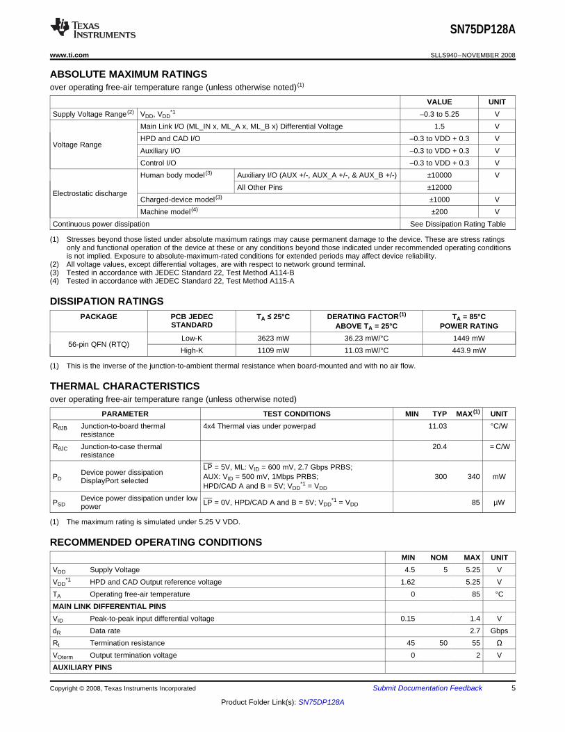
ABSOLUTE MAXIMUM RATINGS
DISSIPATION RATINGS
THERMAL CHARACTERISTICS
RECOMMENDED OPERATING CONDITIONS
SN75DP128A
www.ti.com............................................................................................................................................................................................ SLLS940–NOVEMBER 2008
over operating free-air temperature range (unless otherwise noted) (1)
VALUE UNITSupply Voltage Range (2) VDD, VDD
*1 –0.3 to 5.25 VMain Link I/O (ML_IN x, ML_A x, ML_B x) Differential Voltage 1.5 VHPD and CAD I/O –0.3 to VDD + 0.3 V
Voltage RangeAuxiliary I/O –0.3 to VDD + 0.3 VControl I/O –0.3 to VDD + 0.3 VHuman body model (3) Auxiliary I/O (AUX +/-, AUX_A +/-, & AUX_B +/-) ±10000 V
All Other Pins ±12000Electrostatic discharge
Charged-device model (3) ±1000 VMachine model (4) ±200 V
Continuous power dissipation See Dissipation Rating Table
(1) Stresses beyond those listed under absolute maximum ratings may cause permanent damage to the device. These are stress ratingsonly and functional operation of the device at these or any conditions beyond those indicated under recommended operating conditionsis not implied. Exposure to absolute-maximum-rated conditions for extended periods may affect device reliability.
(2) All voltage values, except differential voltages, are with respect to network ground terminal.(3) Tested in accordance with JEDEC Standard 22, Test Method A114-B(4) Tested in accordance with JEDEC Standard 22, Test Method A115-A
PACKAGE PCB JEDEC TA ≤ 25°C DERATING FACTOR (1) TA = 85°CSTANDARD ABOVE TA = 25°C POWER RATING
Low-K 3623 mW 36.23 mW/°C 1449 mW56-pin QFN (RTQ)
High-K 1109 mW 11.03 mW/°C 443.9 mW
(1) This is the inverse of the junction-to-ambient thermal resistance when board-mounted and with no air flow.
over operating free-air temperature range (unless otherwise noted)
PARAMETER TEST CONDITIONS MIN TYP MAX (1) UNITRθJB Junction-to-board thermal 4x4 Thermal vias under powerpad 11.03 °C/W
resistanceRθJC Junction-to-case thermal 20.4 =C/W
resistanceLP = 5V, ML: VID = 600 mV, 2.7 Gbps PRBS;
Device power dissipationPD AUX: VID = 500 mV, 1Mbps PRBS; 300 340 mWDisplayPort selectedHPD/CAD A and B = 5V; VDD
*1 = VDD
Device power dissipation under lowPSD LP = 0V, HPD/CAD A and B = 5V; VDD*1 = VDD 85 µWpower
(1) The maximum rating is simulated under 5.25 V VDD.
MIN NOM MAX UNITVDD Supply Voltage 4.5 5 5.25 VVDD
*1 HPD and CAD Output reference voltage 1.62 5.25 VTA Operating free-air temperature 0 85 °CMAIN LINK DIFFERENTIAL PINSVID Peak-to-peak input differential voltage 0.15 1.4 VdR Data rate 2.7 GbpsRt Termination resistance 45 50 55 ΩVOterm Output termination voltage 0 2 VAUXILIARY PINS
Copyright © 2008, Texas Instruments Incorporated Submit Documentation Feedback 5
Product Folder Link(s): SN75DP128A
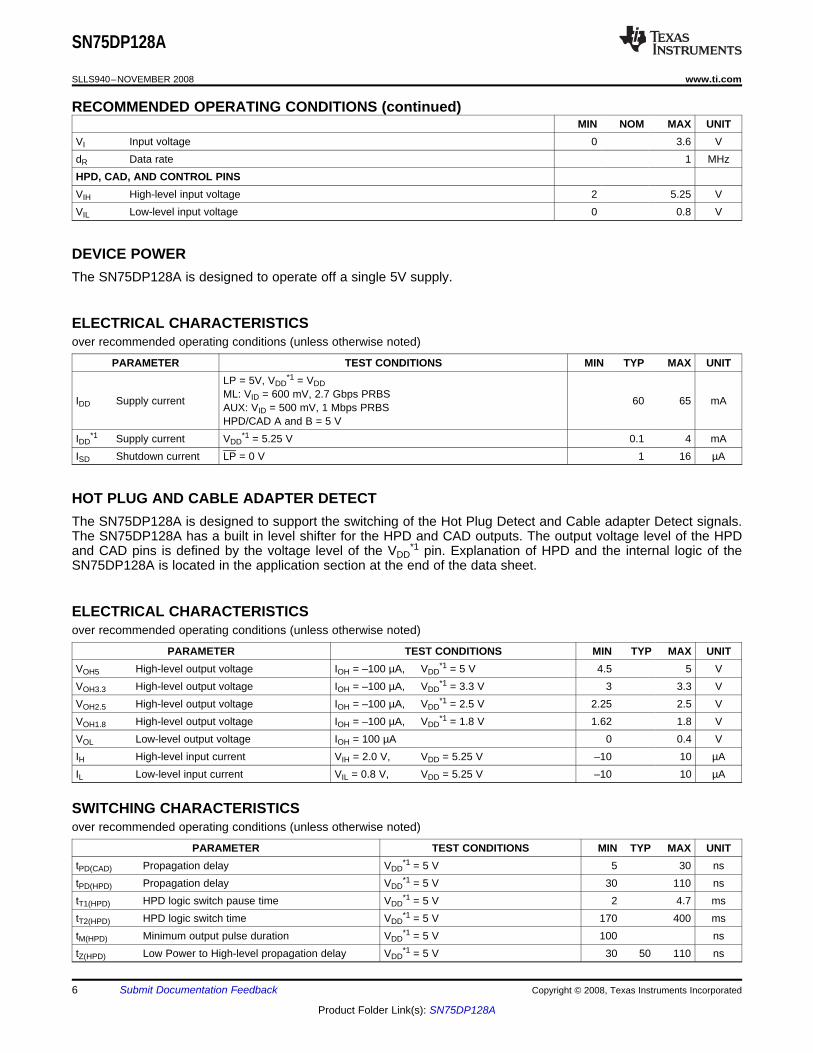
DEVICE POWER
ELECTRICAL CHARACTERISTICS
HOT PLUG AND CABLE ADAPTER DETECT
ELECTRICAL CHARACTERISTICS
SWITCHING CHARACTERISTICS
SN75DP128A
SLLS940–NOVEMBER 2008............................................................................................................................................................................................ www.ti.com
RECOMMENDED OPERATING CONDITIONS (continued)MIN NOM MAX UNIT
VI Input voltage 0 3.6 VdR Data rate 1 MHzHPD, CAD, AND CONTROL PINSVIH High-level input voltage 2 5.25 VVIL Low-level input voltage 0 0.8 V
The SN75DP128A is designed to operate off a single 5V supply.
over recommended operating conditions (unless otherwise noted)
PARAMETER TEST CONDITIONS MIN TYP MAX UNITLP = 5V, VDD
*1 = VDDML: VID = 600 mV, 2.7 Gbps PRBSIDD Supply current 60 65 mAAUX: VID = 500 mV, 1 Mbps PRBSHPD/CAD A and B = 5 V
IDD*1 Supply current VDD
*1 = 5.25 V 0.1 4 mAISD Shutdown current LP = 0 V 1 16 µA
The SN75DP128A is designed to support the switching of the Hot Plug Detect and Cable adapter Detect signals.The SN75DP128A has a built in level shifter for the HPD and CAD outputs. The output voltage level of the HPDand CAD pins is defined by the voltage level of the VDD
*1 pin. Explanation of HPD and the internal logic of theSN75DP128A is located in the application section at the end of the data sheet.
over recommended operating conditions (unless otherwise noted)
PARAMETER TEST CONDITIONS MIN TYP MAX UNITVOH5 High-level output voltage IOH = –100 µA, VDD
*1 = 5 V 4.5 5 VVOH3.3 High-level output voltage IOH = –100 µA, VDD
*1 = 3.3 V 3 3.3 VVOH2.5 High-level output voltage IOH = –100 µA, VDD
*1 = 2.5 V 2.25 2.5 VVOH1.8 High-level output voltage IOH = –100 µA, VDD
*1 = 1.8 V 1.62 1.8 VVOL Low-level output voltage IOH = 100 µA 0 0.4 VIH High-level input current VIH = 2.0 V, VDD = 5.25 V –10 10 µAIL Low-level input current VIL = 0.8 V, VDD = 5.25 V –10 10 µA
over recommended operating conditions (unless otherwise noted)
PARAMETER TEST CONDITIONS MIN TYP MAX UNITtPD(CAD) Propagation delay VDD
*1 = 5 V 5 30 nstPD(HPD) Propagation delay VDD
*1 = 5 V 30 110 nstT1(HPD) HPD logic switch pause time VDD
*1 = 5 V 2 4.7 mstT2(HPD) HPD logic switch time VDD
*1 = 5 V 170 400 mstM(HPD) Minimum output pulse duration VDD
*1 = 5 V 100 nstZ(HPD) Low Power to High-level propagation delay VDD
*1 = 5 V 30 50 110 ns
6 Submit Documentation Feedback Copyright © 2008, Texas Instruments Incorporated
Product Folder Link(s): SN75DP128A
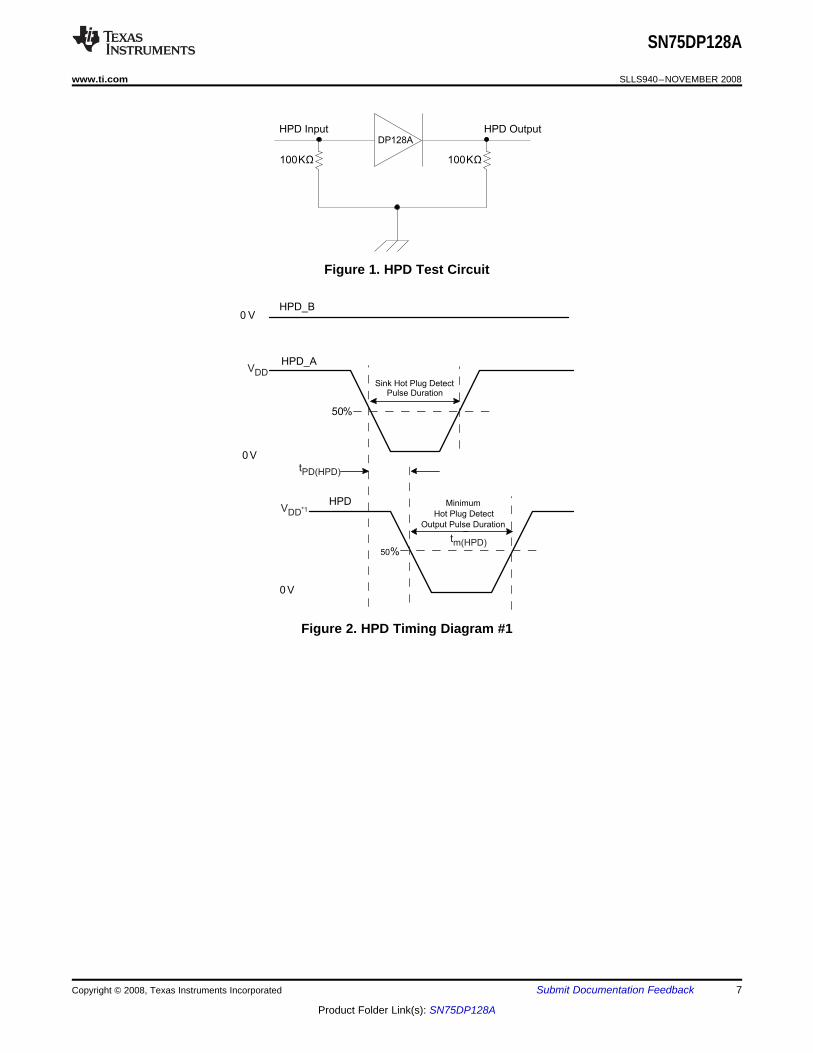
DP128A
100KΩ100KΩ
HPD Input HPD Output
0 V
Sink Hot Plug DetectPulse Duration
0 V
Minimum
Hot Plug Detect
Output Pulse Duration
HPD_A
HPD
0 VHPD_B
50%
50%
VDD
VDD*1
tPD(HPD)
tm(HPD)
SN75DP128A
www.ti.com............................................................................................................................................................................................ SLLS940–NOVEMBER 2008
Figure 1. HPD Test Circuit
Figure 2. HPD Timing Diagram #1
Copyright © 2008, Texas Instruments Incorporated Submit Documentation Feedback 7
Product Folder Link(s): SN75DP128A
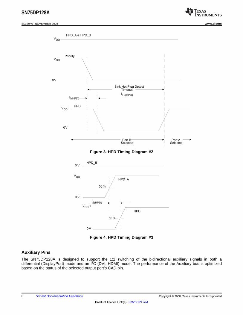
0V
Sink Hot Plug DetectTimeout
0V
Port BSelected
Port ASelected
HPD
PriorityVDD
VDD
HPD_A & HPD_B
VDD*1
t1(HPD)
tT2(HPD)
0 V
0V
HPD
0 VHPD_B
50 %
50 %
VDDHPD_A
VDD*1
tZ(HPD)
Auxiliary Pins
SN75DP128A
SLLS940–NOVEMBER 2008............................................................................................................................................................................................ www.ti.com
Figure 3. HPD Timing Diagram #2
Figure 4. HPD Timing Diagram #3
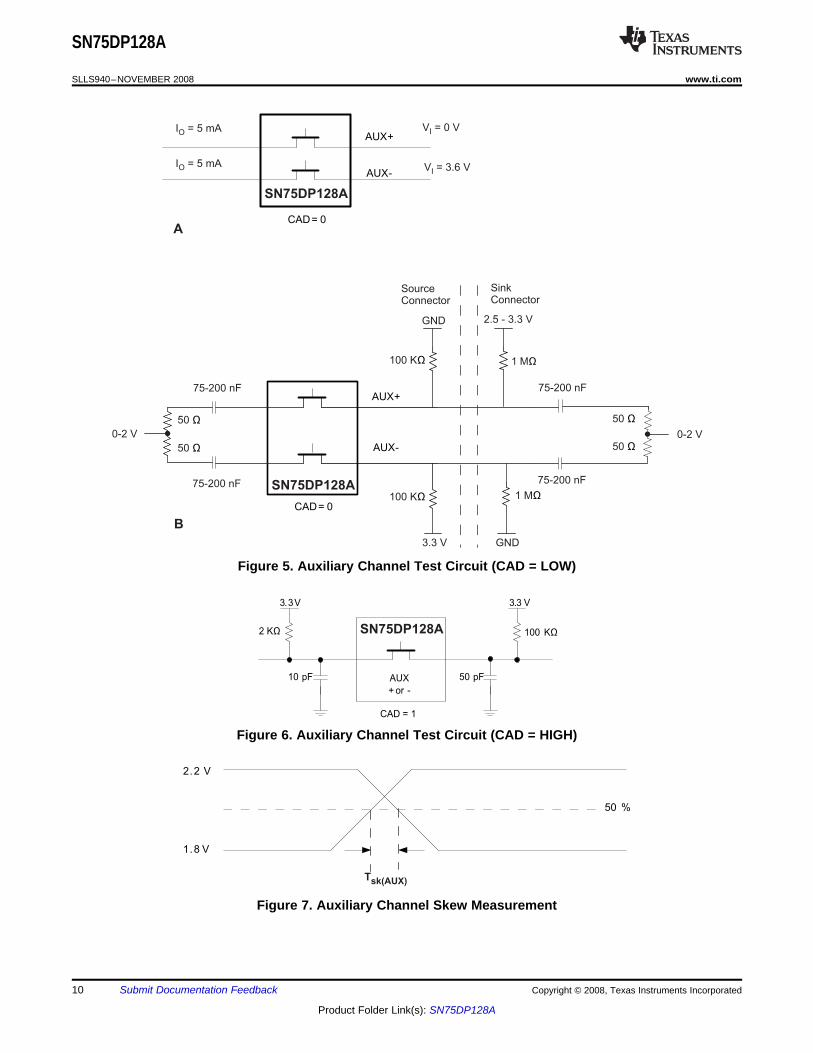
The SN75DP128A is designed to support the 1:2 switching of the bidirectional auxiliary signals in both adifferential (DisplayPort) mode and an I2C (DVI, HDMI) mode. The performance of the Auxiliary bus is optimizedbased on the status of the selected output port’s CAD pin.
8 Submit Documentation Feedback Copyright © 2008, Texas Instruments Incorporated
Product Folder Link(s): SN75DP128A
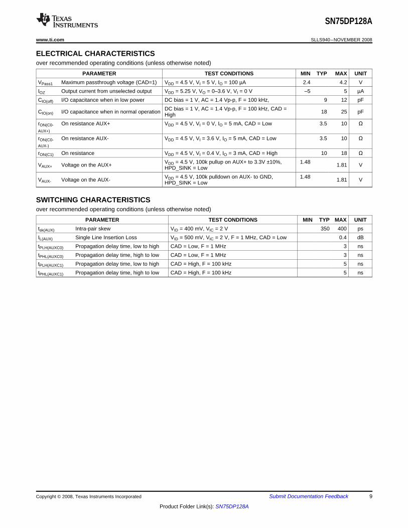
ELECTRICAL CHARACTERISTICS
SWITCHING CHARACTERISTICS
SN75DP128A
www.ti.com............................................................................................................................................................................................ SLLS940–NOVEMBER 2008
over recommended operating conditions (unless otherwise noted)
PARAMETER TEST CONDITIONS MIN TYP MAX UNITVPass1 Maximum passthrough voltage (CAD=1) VDD = 4.5 V, VI = 5 V, IO = 100 µA 2.4 4.2 VIOZ Output current from unselected output VDD = 5.25 V, VO = 0–3.6 V, VI = 0 V –5 5 µACIO(off) I/O capacitance when in low power DC bias = 1 V, AC = 1.4 Vp-p, F = 100 kHz, 9 12 pF
DC bias = 1 V, AC = 1.4 Vp-p, F = 100 kHz, CAD =CIO(on) I/O capacitance when in normal operation 18 25 pFHighrON(C0- On resistance AUX+ VDD = 4.5 V, VI = 0 V, IO = 5 mA, CAD = Low 3.5 10 ΩAUX+)
rON(C0- On resistance AUX- VDD = 4.5 V, VI = 3.6 V, IO = 5 mA, CAD = Low 3.5 10 ΩAUX-)
rON(C1) On resistance VDD = 4.5 V, VI = 0.4 V, IO = 3 mA, CAD = High 10 18 ΩVDD = 4.5 V, 100k pullup on AUX+ to 3.3V ±10%, 1.48VAUX+ Voltage on the AUX+ 1.81 VHPD_SINK = LowVDD = 4.5 V, 100k pulldown on AUX- to GND, 1.48VAUX- Voltage on the AUX- 1.81 VHPD_SINK = Low
over recommended operating conditions (unless otherwise noted)
PARAMETER TEST CONDITIONS MIN TYP MAX UNITtsk(AUX) Intra-pair skew VID = 400 mV, VIC = 2 V 350 400 psIL(AUX) Single Line Insertion Loss VID = 500 mV, VIC = 2 V, F = 1 MHz, CAD = Low 0.4 dBtPLH(AUXC0) Propagation delay time, low to high CAD = Low, F = 1 MHz 3 nstPHL(AUXC0) Propagation delay time, high to low CAD = Low, F = 1 MHz 3 nstPLH(AUXC1) Propagation delay time, low to high CAD = High, F = 100 kHz 5 nstPHL(AUXC1) Propagation delay time, high to low CAD = High, F = 100 kHz 5 ns
Copyright © 2008, Texas Instruments Incorporated Submit Documentation Feedback 9
Product Folder Link(s): SN75DP128A
CAD= 0
AUX+
AUX-
SN75DP128A
V = 0 VI
V = 3.6 VI
I = 5 mAO
I = 5 mAO
CAD= 0
AUX+
AUX-
SN75DP128A
0-2 V
Source
Connector
Sink
Connector
GND 2.5 - 3.3 V
1 MΩ
100 KΩ
50 Ω
50 Ω
50 Ω
50 Ω
1 MΩ
100 KΩ
0-2 V
75-200 nF
75-200 nF
75-200 nF
75-200 nF
A
B
3.3 V GND
AUX
+ or -
3.3 V
100 KΩ
3.3V
2 KΩ
10 pF 50 pF
CAD = 1
SN75DP128A
2.2 V
1.8 V
50 %
Tsk(AUX)
SN75DP128A
SLLS940–NOVEMBER 2008............................................................................................................................................................................................ www.ti.com
Figure 5. Auxiliary Channel Test Circuit (CAD = LOW)
Figure 6. Auxiliary Channel Test Circuit (CAD = HIGH)
Figure 7. Auxiliary Channel Skew Measurement
10 Submit Documentation Feedback Copyright © 2008, Texas Instruments Incorporated
Product Folder Link(s): SN75DP128A
2.2V
1.8V
0 V
0 VDifferentialAUX Input
DifferentialAUX Output
AUX Input
tPHL(AUXC0) tPLH(AUXC0)
AUXInput+ or -
AUXOutput+ or -
0 V
0 V
tPHL(AUXC1)tPLH(AUXC1)
3.6 V
3.6 V
1.8 V
1.8 V
Main Link Pins
ELECTRICAL CHARACTERISTICS
SN75DP128A
www.ti.com............................................................................................................................................................................................ SLLS940–NOVEMBER 2008
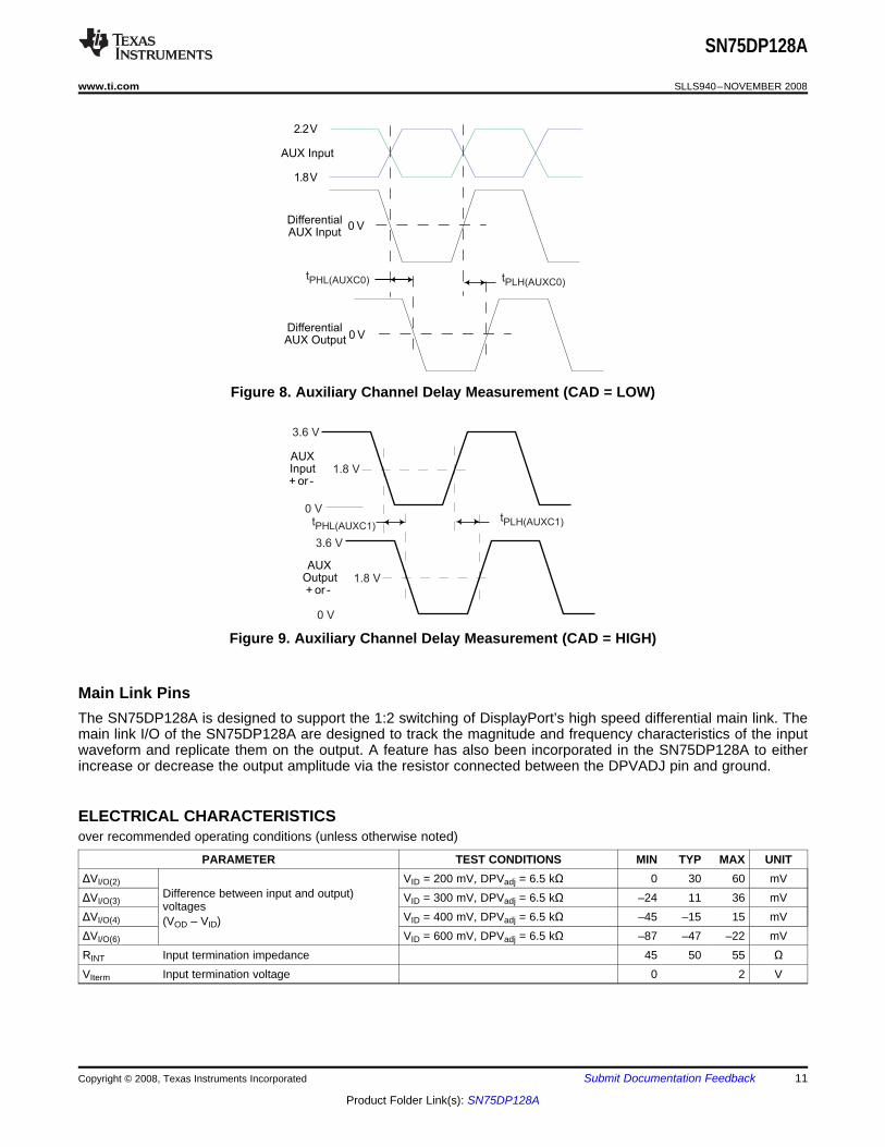
Figure 8. Auxiliary Channel Delay Measurement (CAD = LOW)
Figure 9. Auxiliary Channel Delay Measurement (CAD = HIGH)
The SN75DP128A is designed to support the 1:2 switching of DisplayPort’s high speed differential main link. Themain link I/O of the SN75DP128A are designed to track the magnitude and frequency characteristics of the inputwaveform and replicate them on the output. A feature has also been incorporated in the SN75DP128A to eitherincrease or decrease the output amplitude via the resistor connected between the DPVADJ pin and ground.
over recommended operating conditions (unless otherwise noted)
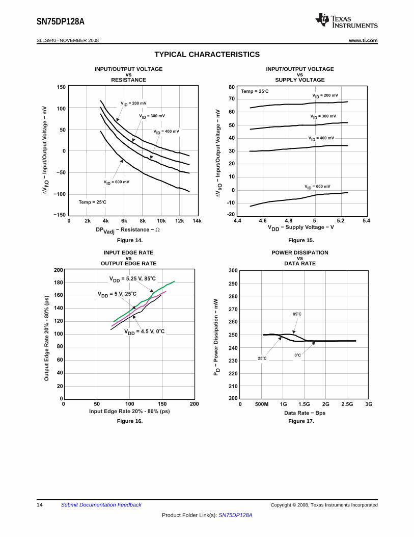
PARAMETER TEST CONDITIONS MIN TYP MAX UNITΔVI/O(2) VID = 200 mV, DPVadj = 6.5 kΩ 0 30 60 mV
Difference between input and output)ΔVI/O(3) VID = 300 mV, DPVadj = 6.5 kΩ –24 11 36 mVvoltages
ΔVI/O(4) VID = 400 mV, DPVadj = 6.5 kΩ –45 –15 15 mV(VOD – VID)ΔVI/O(6) VID = 600 mV, DPVadj = 6.5 kΩ –87 –47 –22 mVRINT Input termination impedance 45 50 55 ΩVIterm Input termination voltage 0 2 V
Copyright © 2008, Texas Instruments Incorporated Submit Documentation Feedback 11
Product Folder Link(s): SN75DP128A
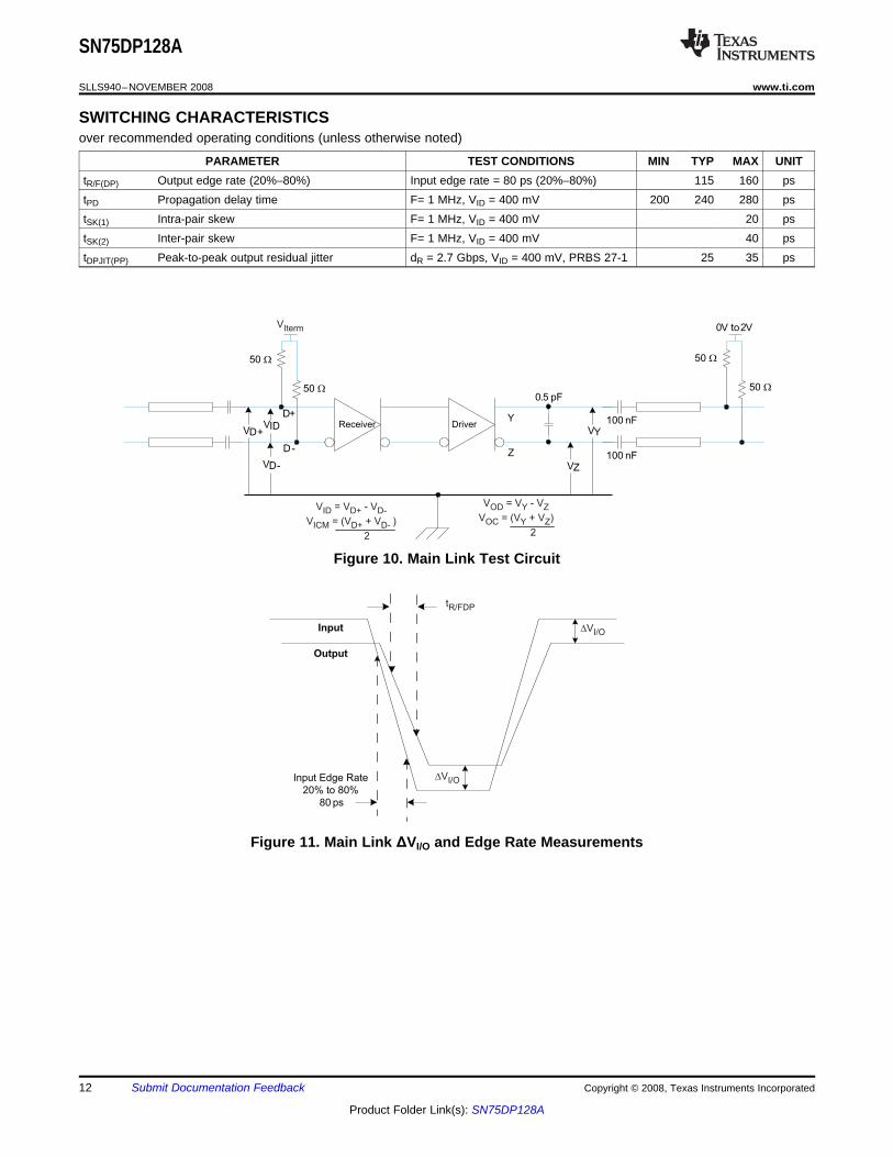
SWITCHING CHARACTERISTICS
Driver
50 W
ReceiverD+
D-
VD+
VD-
VID
0.5 pF
Y
Z
VY
VZ
100 nF
100 nF
0V to2VVIterm
50 W
50 W
50 W
V = V - V
V = (V + V )
2
ID D+ D-
ICM D+ D-
V = V - V
V = (V + V )
2
OD Y Z
OC Y Z
Output
Input
Input Edge Rate
20% to 80%
80 ps
tR/FDP
DVI/O
DVI/O
SN75DP128A
SLLS940–NOVEMBER 2008............................................................................................................................................................................................ www.ti.com
over recommended operating conditions (unless otherwise noted)
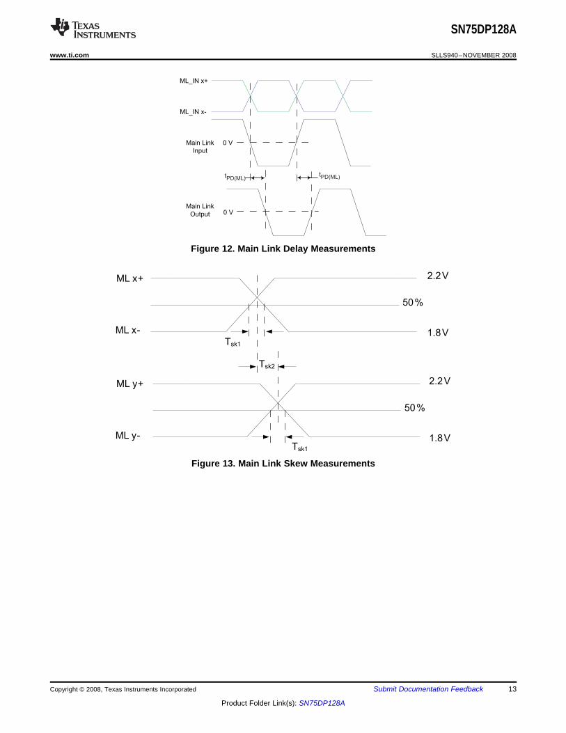
PARAMETER TEST CONDITIONS MIN TYP MAX UNITtR/F(DP) Output edge rate (20%–80%) Input edge rate = 80 ps (20%–80%) 115 160 pstPD Propagation delay time F= 1 MHz, VID = 400 mV 200 240 280 pstSK(1) Intra-pair skew F= 1 MHz, VID = 400 mV 20 pstSK(2) Inter-pair skew F= 1 MHz, VID = 400 mV 40 pstDPJIT(PP) Peak-to-peak output residual jitter dR = 2.7 Gbps, VID = 400 mV, PRBS 27-1 25 35 ps
Figure 10. Main Link Test Circuit
Figure 11. Main Link ΔVI/O and Edge Rate Measurements
12 Submit Documentation Feedback Copyright © 2008, Texas Instruments Incorporated
Product Folder Link(s): SN75DP128A
ML_IN x+
ML_IN x-
0 V
0 VMain Link
Input
Main Link
Output
tPD(ML)tPD(ML)
ML x+
ML x-
50%
Tsk1
2.2V
1.8V
50%
Tsk1
2.2V
1.8V
ML y+
ML y-
Tsk2
SN75DP128A
www.ti.com............................................................................................................................................................................................ SLLS940–NOVEMBER 2008
Figure 12. Main Link Delay Measurements
Figure 13. Main Link Skew Measurements
Copyright © 2008, Texas Instruments Incorporated Submit Documentation Feedback 13
Product Folder Link(s): SN75DP128A
TYPICAL CHARACTERISTICS
V − Supply VoltageDD − V
DV
−In
pu
t/O
utp
ut
Vo
ltag
e−
mV
I/O
-20
-10
0
10
20
30
40
50
60
70
80
4.4 4.6 4.8 5 5.2 5.4
V = 200 mVID
V = 300 mVID
V = 400 mVID
V = 600 mVID
Temp = 25 Co
−150
−100
−50
0
50
100
150
DP − ResistanceVadj − W
DV
−In
pu
t/O
utp
ut
Vo
ltag
e−
mV
I\O
0 10k 12k2k 4k 6k 8k 14k
V = 200 mVID
V = 300 mVID
V = 400 mVID
V = 600 mVID
Temp = 25 Co
Input Edge Rate 20% - 80% (ps)
Ou
tpu
t E
dg
e R
ate
20
% -
80
% (
ps
)
0
20
40
60
80
100
120
140
160
180
200
0 50 100 150 200
V = 5.25 V, 85 CDDo
V = 5 VDD , 25 Co
V = 4.5 VDD , 0 Co
200
210
230
260
270
280
300
Data Rate − Bps
P−
Po
we
r D
iss
ipa
tio
n−
mW
D
0 2G 2.5G500M 1G 1.5G 3G
85 Co
290
250
240
220
0 Co
25 Co
SN75DP128A
SLLS940–NOVEMBER 2008............................................................................................................................................................................................ www.ti.com
INPUT/OUTPUT VOLTAGE INPUT/OUTPUT VOLTAGEvs vs
RESISTANCE SUPPLY VOLTAGE
Figure 14. Figure 15.
INPUT EDGE RATE POWER DISSIPATIONvs vs
OUTPUT EDGE RATE DATA RATE
Figure 16. Figure 17.
14 Submit Documentation Feedback Copyright © 2008, Texas Instruments Incorporated
Product Folder Link(s): SN75DP128A
APPLICATION INFORMATION
SWITCHING LOGIC
LP
Priority
HPD_A
0
1
0
1
0
1
HPD_B
0
1
HPD_OUT
0
1
Channel A
Z
0
1
Channel B
0
1
HI-Z
HI-Z
SN75DP128A
www.ti.com............................................................................................................................................................................................ SLLS940–NOVEMBER 2008
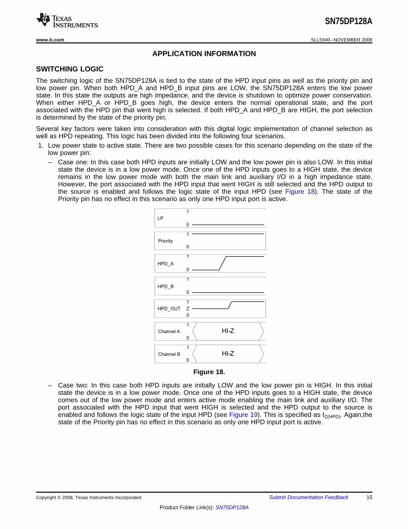
The switching logic of the SN75DP128A is tied to the state of the HPD input pins as well as the priority pin andlow power pin. When both HPD_A and HPD_B input pins are LOW, the SN75DP128A enters the low powerstate. In this state the outputs are high impedance, and the device is shutdown to optimize power conservation.When either HPD_A or HPD_B goes high, the device enters the normal operational state, and the portassociated with the HPD pin that went high is selected. If both HPD_A and HPD_B are HIGH, the port selectionis determined by the state of the priority pin.
Several key factors were taken into consideration with this digital logic implementation of channel selection aswell as HPD repeating. This logic has been divided into the following four scenarios.1. Low power state to active state. There are two possible cases for this scenario depending on the state of the
low power pin:– Case one: In this case both HPD inputs are initially LOW and the low power pin is also LOW. In this initial
state the device is in a low power mode. Once one of the HPD inputs goes to a HIGH state, the deviceremains in the low power mode with both the main link and auxiliary I/O in a high impedance state.However, the port associated with the HPD input that went HIGH is still selected and the HPD output tothe source is enabled and follows the logic state of the input HPD (see Figure 18). The state of thePriority pin has no effect in this scenario as only one HPD input port is active.
Figure 18.
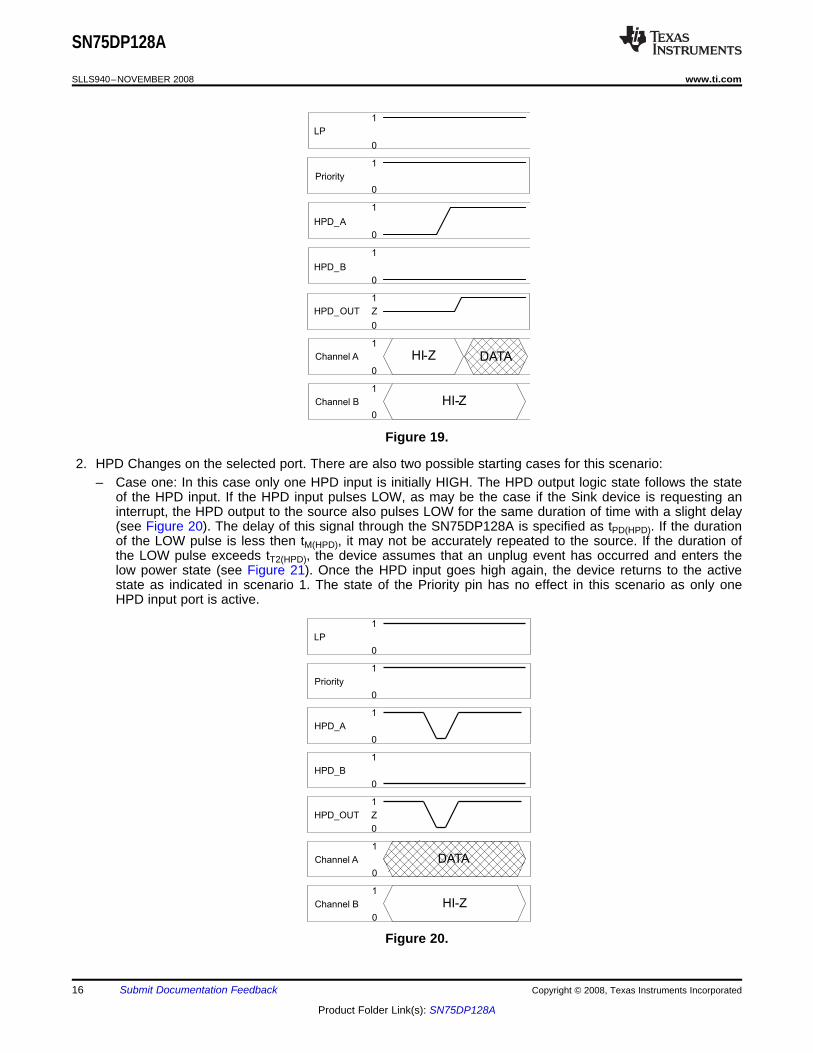
– Case two: In this case both HPD inputs are initially LOW and the low power pin is HIGH. In this initialstate the device is in a low power mode. Once one of the HPD inputs goes to a HIGH state, the devicecomes out of the low power mode and enters active mode enabling the main link and auxiliary I/O. Theport associated with the HPD input that went HIGH is selected and the HPD output to the source isenabled and follows the logic state of the input HPD (see Figure 19). This is specified as tZ(HPD). Again,thestate of the Priority pin has no effect in this scenario as only one HPD input port is active.
Copyright © 2008, Texas Instruments Incorporated Submit Documentation Feedback 15
Product Folder Link(s): SN75DP128A
LP
Priority
HPD_A
0
1
0
1
0
1
HPD_B
0
1
HPD_OUT
0
1
Channel A
Z
0
1
Channel B
0
1
HI-Z
HI-Z
DATA
LP
Priority
HPD_A
0
1
0
1
0
1
HPD_B
0
1
HPD_OUT
0
1
Channel A
Z
0
1
Channel B
0
1
HI-Z
DATA
SN75DP128A
SLLS940–NOVEMBER 2008............................................................................................................................................................................................ www.ti.com
Figure 19.
2. HPD Changes on the selected port. There are also two possible starting cases for this scenario:– Case one: In this case only one HPD input is initially HIGH. The HPD output logic state follows the state
of the HPD input. If the HPD input pulses LOW, as may be the case if the Sink device is requesting aninterrupt, the HPD output to the source also pulses LOW for the same duration of time with a slight delay(see Figure 20). The delay of this signal through the SN75DP128A is specified as tPD(HPD). If the durationof the LOW pulse is less then tM(HPD), it may not be accurately repeated to the source. If the duration ofthe LOW pulse exceeds tT2(HPD), the device assumes that an unplug event has occurred and enters thelow power state (see Figure 21). Once the HPD input goes high again, the device returns to the activestate as indicated in scenario 1. The state of the Priority pin has no effect in this scenario as only oneHPD input port is active.
Figure 20.
16 Submit Documentation Feedback Copyright © 2008, Texas Instruments Incorporated
Product Folder Link(s): SN75DP128A
LP
Priority
HPD_A
0
1
0
1
0
1
HPD_B
0
1
HPD_OUT
0
1
Channel A
Z
0
1
Channel B
0
1
HI-Z
HI-Z
DATA
LP
Priority
HPD_A
0
1
0
1
0
1
HPD_B
0
1
HPD_OUT
0
1
Channel A
Z
0
1
Channel B
0
1
HI-Z
DATA
SN75DP128A
www.ti.com............................................................................................................................................................................................ SLLS940–NOVEMBER 2008
Figure 21.
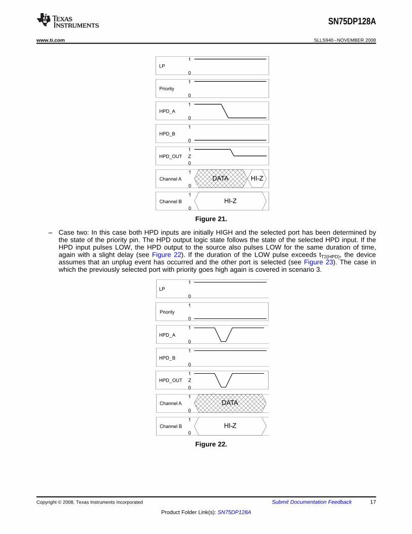
– Case two: In this case both HPD inputs are initially HIGH and the selected port has been determined bythe state of the priority pin. The HPD output logic state follows the state of the selected HPD input. If theHPD input pulses LOW, the HPD output to the source also pulses LOW for the same duration of time,again with a slight delay (see Figure 22). If the duration of the LOW pulse exceeds tT2(HPD), the deviceassumes that an unplug event has occurred and the other port is selected (see Figure 23). The case inwhich the previously selected port with priority goes high again is covered in scenario 3.
Figure 22.
Copyright © 2008, Texas Instruments Incorporated Submit Documentation Feedback 17
Product Folder Link(s): SN75DP128A
LP
Priority
HPD_A
0
1
0
1
0
1
HPD_B
0
1
HPD_OUT
0
1
Channel A
Z
0
1
Channel B
0
1
HI-Z
DATA HI-Z
DATA
LP
Priority
HPD_A
0
1
0
1
0
1
HPD_B
0
1
HPD_OUT
0
1
Channel A
Z
0
1
Channel B
0
1
HI-Z
DATA
SN75DP128A
SLLS940–NOVEMBER 2008............................................................................................................................................................................................ www.ti.com
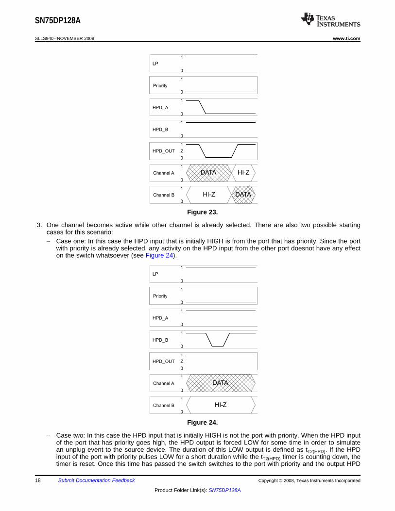
Figure 23.
3. One channel becomes active while other channel is already selected. There are also two possible startingcases for this scenario:– Case one: In this case the HPD input that is initially HIGH is from the port that has priority. Since the port
with priority is already selected, any activity on the HPD input from the other port doesnot have any effecton the switch whatsoever (see Figure 24).
Figure 24.
– Case two: In this case the HPD input that is initially HIGH is not the port with priority. When the HPD inputof the port that has priority goes high, the HPD output is forced LOW for some time in order to simulatean unplug event to the source device. The duration of this LOW output is defined as tT2(HPD). If the HPDinput of the port with priority pulses LOW for a short duration while the tT2(HPD) timer is counting down, thetimer is reset. Once this time has passed the switch switches to the port with priority and the output HPD
18 Submit Documentation Feedback Copyright © 2008, Texas Instruments Incorporated
Product Folder Link(s): SN75DP128A
LP
Priority
HPD_A
0
1
0
1
0
1
HPD_B
0
1
HPD_OUT
0
1
Channel A
Z
0
1
Channel B
0
1
HI-Z
DATA HI-Z
DATA
LP
Priority
HPD_A
0
1
0
1
0
1
HPD_B
0
1
HPD_OUT
0
1
Channel A
Z
0
1
Channel B
0
1
HI-Z
DATA
SN75DP128A
www.ti.com............................................................................................................................................................................................ SLLS940–NOVEMBER 2008
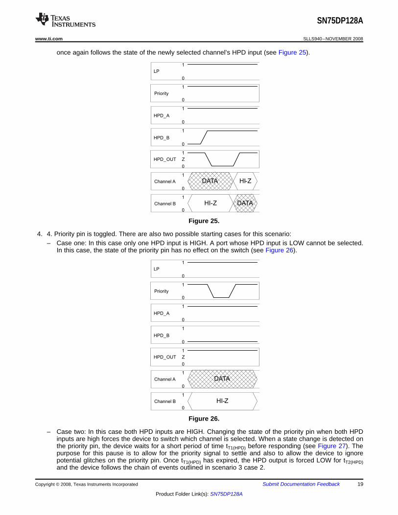
once again follows the state of the newly selected channel’s HPD input (see Figure 25).
Figure 25.
4. 4. Priority pin is toggled. There are also two possible starting cases for this scenario:– Case one: In this case only one HPD input is HIGH. A port whose HPD input is LOW cannot be selected.
In this case, the state of the priority pin has no effect on the switch (see Figure 26).
Figure 26.
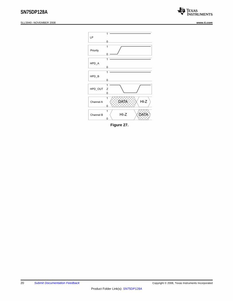
– Case two: In this case both HPD inputs are HIGH. Changing the state of the priority pin when both HPDinputs are high forces the device to switch which channel is selected. When a state change is detected onthe priority pin, the device waits for a short period of time tT1(HPD) before responding (see Figure 27). Thepurpose for this pause is to allow for the priority signal to settle and also to allow the device to ignorepotential glitches on the priority pin. Once tT1(HPD) has expired, the HPD output is forced LOW for tT2(HPD)and the device follows the chain of events outlined in scenario 3 case 2.
Copyright © 2008, Texas Instruments Incorporated Submit Documentation Feedback 19
Product Folder Link(s): SN75DP128A
LP
Priority
HPD_A
0
1
0
1
0
1
HPD_B
0
1
HPD_OUT
0
1
Channel A
Z
0
1
Channel B
0
1
HI-Z
DATA HI-Z
DATA
SN75DP128A
SLLS940–NOVEMBER 2008............................................................................................................................................................................................ www.ti.com
Figure 27.
20 Submit Documentation Feedback Copyright © 2008, Texas Instruments Incorporated
Product Folder Link(s): SN75DP128A
PACKAGE OPTION ADDENDUM
www.ti.com 10-Dec-2020
Addendum-Page 1
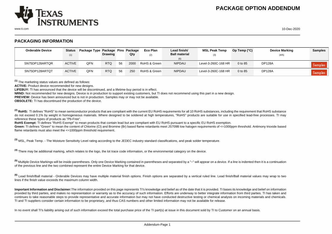
PACKAGING INFORMATION
Orderable Device Status(1)
Package Type PackageDrawing
Pins PackageQty
Eco Plan(2)
Lead finish/Ball material
(6)
MSL Peak Temp(3)
Op Temp (°C) Device Marking(4/5)
Samples
SN75DP128ARTQR ACTIVE QFN RTQ 56 2000 RoHS & Green NIPDAU Level-3-260C-168 HR 0 to 85 DP128A
SN75DP128ARTQT ACTIVE QFN RTQ 56 250 RoHS & Green NIPDAU Level-3-260C-168 HR 0 to 85 DP128A
(1) The marketing status values are defined as follows:ACTIVE: Product device recommended for new designs.LIFEBUY: TI has announced that the device will be discontinued, and a lifetime-buy period is in effect.NRND: Not recommended for new designs. Device is in production to support existing customers, but TI does not recommend using this part in a new design.PREVIEW: Device has been announced but is not in production. Samples may or may not be available.OBSOLETE: TI has discontinued the production of the device.
(2) RoHS: TI defines "RoHS" to mean semiconductor products that are compliant with the current EU RoHS requirements for all 10 RoHS substances, including the requirement that RoHS substancedo not exceed 0.1% by weight in homogeneous materials. Where designed to be soldered at high temperatures, "RoHS" products are suitable for use in specified lead-free processes. TI mayreference these types of products as "Pb-Free".RoHS Exempt: TI defines "RoHS Exempt" to mean products that contain lead but are compliant with EU RoHS pursuant to a specific EU RoHS exemption.Green: TI defines "Green" to mean the content of Chlorine (Cl) and Bromine (Br) based flame retardants meet JS709B low halogen requirements of <=1000ppm threshold. Antimony trioxide basedflame retardants must also meet the <=1000ppm threshold requirement.
(3) MSL, Peak Temp. - The Moisture Sensitivity Level rating according to the JEDEC industry standard classifications, and peak solder temperature.
(4) There may be additional marking, which relates to the logo, the lot trace code information, or the environmental category on the device.
(5) Multiple Device Markings will be inside parentheses. Only one Device Marking contained in parentheses and separated by a "~" will appear on a device. If a line is indented then it is a continuationof the previous line and the two combined represent the entire Device Marking for that device.
(6) Lead finish/Ball material - Orderable Devices may have multiple material finish options. Finish options are separated by a vertical ruled line. Lead finish/Ball material values may wrap to twolines if the finish value exceeds the maximum column width.
Important Information and Disclaimer:The information provided on this page represents TI's knowledge and belief as of the date that it is provided. TI bases its knowledge and belief on informationprovided by third parties, and makes no representation or warranty as to the accuracy of such information. Efforts are underway to better integrate information from third parties. TI has taken andcontinues to take reasonable steps to provide representative and accurate information but may not have conducted destructive testing or chemical analysis on incoming materials and chemicals.TI and TI suppliers consider certain information to be proprietary, and thus CAS numbers and other limited information may not be available for release.
In no event shall TI's liability arising out of such information exceed the total purchase price of the TI part(s) at issue in this document sold by TI to Customer on an annual basis.
PACKAGE OPTION ADDENDUM
www.ti.com 10-Dec-2020
Addendum-Page 2
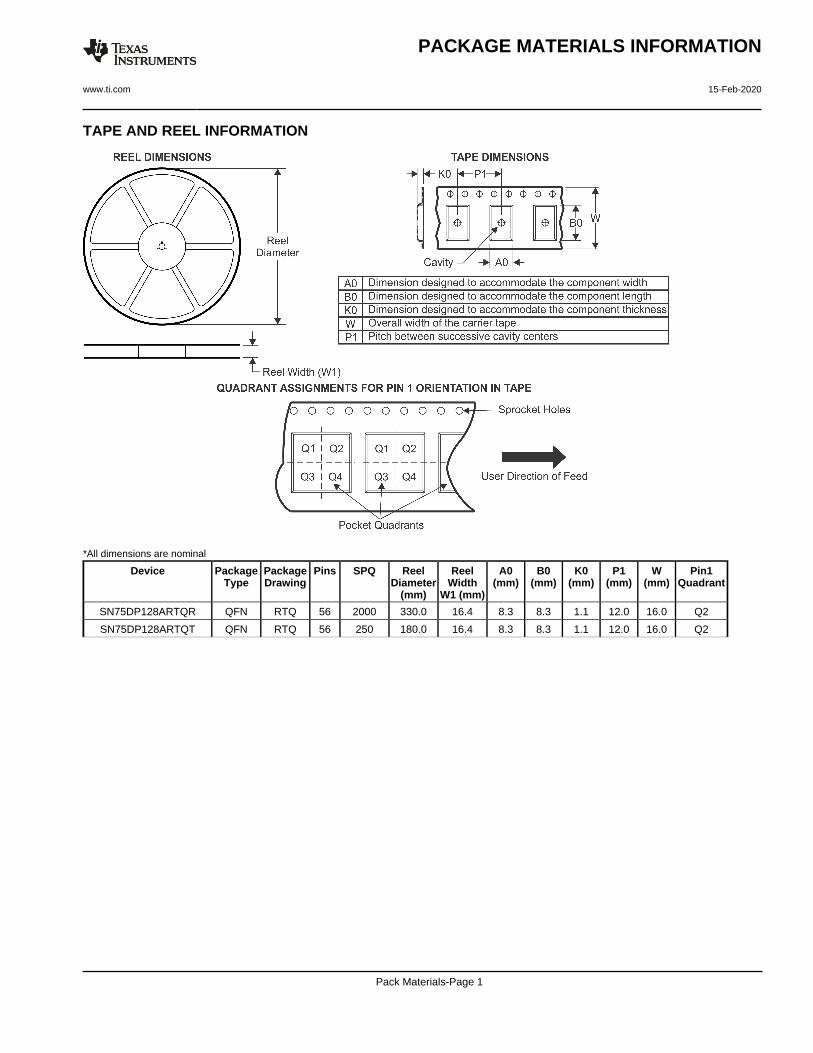
TAPE AND REEL INFORMATION
*All dimensions are nominal
Device PackageType
PackageDrawing
Pins SPQ ReelDiameter
(mm)
ReelWidth
W1 (mm)
A0(mm)
B0(mm)
K0(mm)
P1(mm)
W(mm)
Pin1Quadrant
SN75DP128ARTQR QFN RTQ 56 2000 330.0 16.4 8.3 8.3 1.1 12.0 16.0 Q2
SN75DP128ARTQT QFN RTQ 56 250 180.0 16.4 8.3 8.3 1.1 12.0 16.0 Q2
PACKAGE MATERIALS INFORMATION
www.ti.com 15-Feb-2020
Pack Materials-Page 1
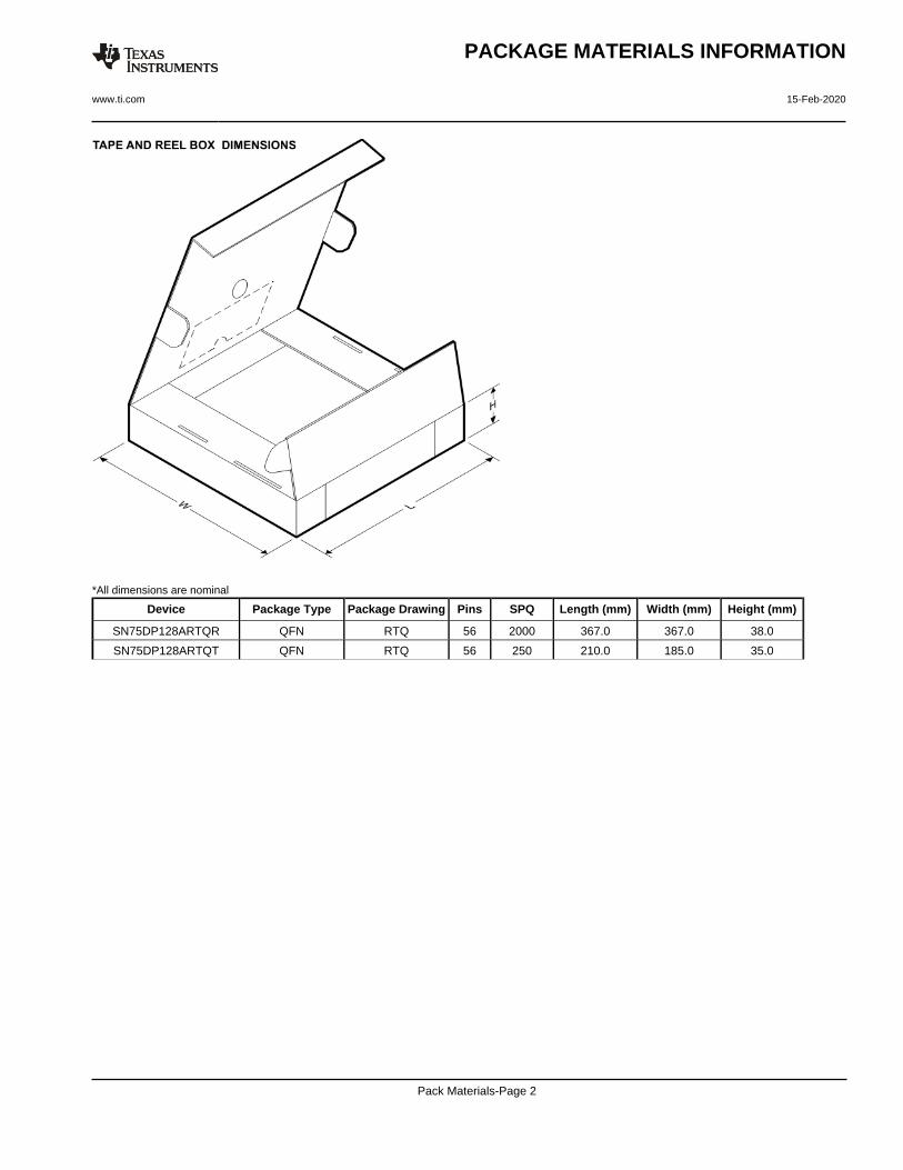
*All dimensions are nominal
Device Package Type Package Drawing Pins SPQ Length (mm) Width (mm) Height (mm)
SN75DP128ARTQR QFN RTQ 56 2000 367.0 367.0 38.0
SN75DP128ARTQT QFN RTQ 56 250 210.0 185.0 35.0
PACKAGE MATERIALS INFORMATION
www.ti.com 15-Feb-2020
Pack Materials-Page 2
www.ti.com
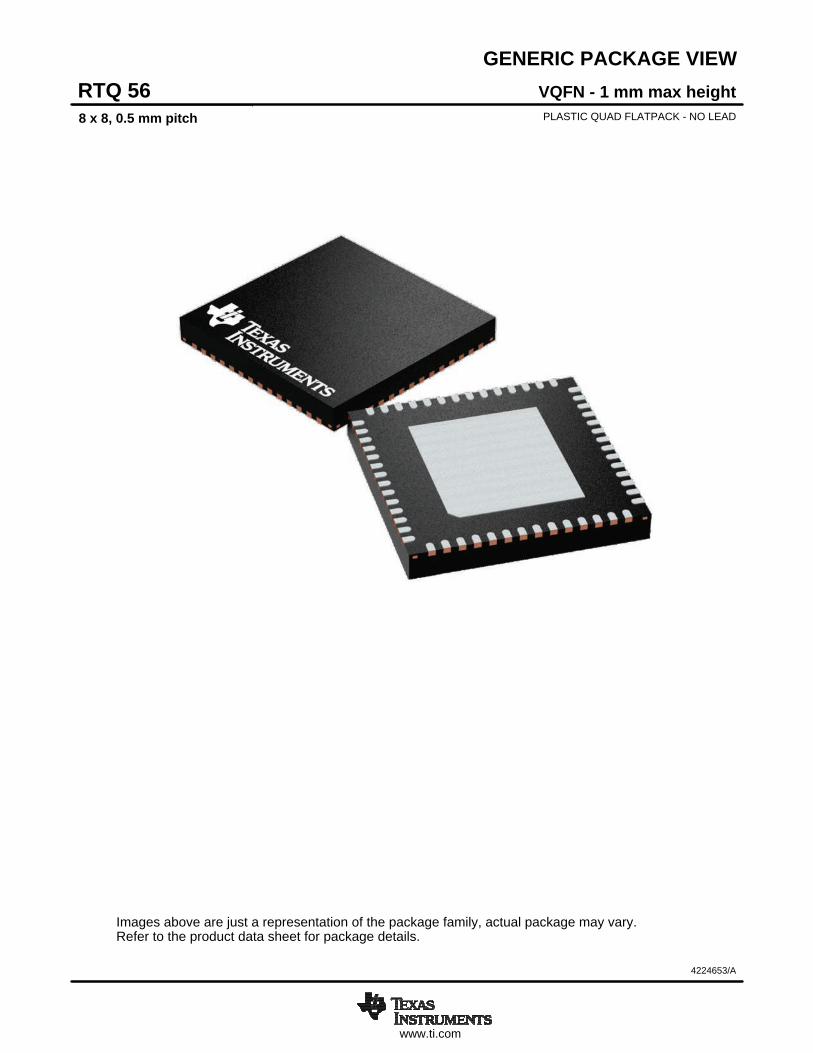
GENERIC PACKAGE VIEW
Images above are just a representation of the package family, actual package may vary.Refer to the product data sheet for package details.
VQFN - 1 mm max heightRTQ 56PLASTIC QUAD FLATPACK - NO LEAD8 x 8, 0.5 mm pitch
4224653/A
www.ti.com
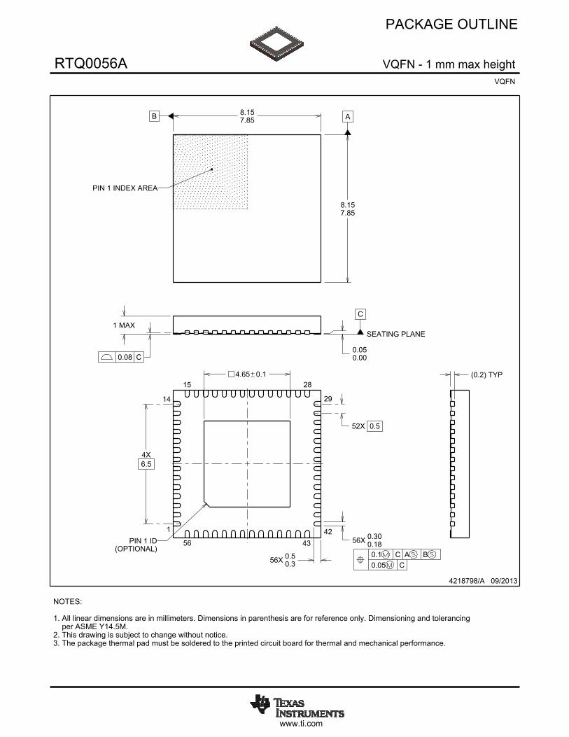
PACKAGE OUTLINE
C
56X 0.50.3
1 MAX
0.050.00
4.65 0.1
56X 0.300.18
52X 0.5
4X6.5
A
8.157.85
B 8.157.85
(0.2) TYP
4218798/A 09/2013
VQFN - 1 mm max heightRTQ0056AVQFN
PIN 1 INDEX AREA
SEATING PLANE
1
14 29
42
15 28
56 430.1 C A B0.05 C
(OPTIONAL)PIN 1 ID
NOTES: 1. All linear dimensions are in millimeters. Dimensions in parenthesis are for reference only. Dimensioning and tolerancing per ASME Y14.5M. 2. This drawing is subject to change without notice. 3. The package thermal pad must be soldered to the printed circuit board for thermal and mechanical performance.
0.08 C
SCALE 1.800
www.ti.com
EXAMPLE BOARD LAYOUT
(4.65)
0.07 MINALL AROUND
0.07 MAXALL AROUND
56X (0.6)
56X (0.24)
(7.8)
(7.8)
( ) TYPVIA
0.2
52X (0.5)
(1.49) TYP
(1.49)TYP
4X(1.33)
4X(1.33)
4218798/A 09/2013
VQFN - 1 mm max heightRTQ0056AVQFN
SYMMSEE DETAILS
1
15 28
29
42
SYMM
LAND PATTERN EXAMPLESCALE:10X
14
4356
NOTES: (continued) 4. This package is designed to be soldered to a thermal pad on the board. For more information, see QFN/SON PCB application report in literature No. SLUA271 (www.ti.com/lit/slua271).
SOLDER MASKOPENING
METAL
SOLDER MASKDEFINED
METAL
SOLDER MASKOPENING
SOLDER MASK DETAILS
NON SOLDER MASKDEFINED
(PREFERRED)
www.ti.com
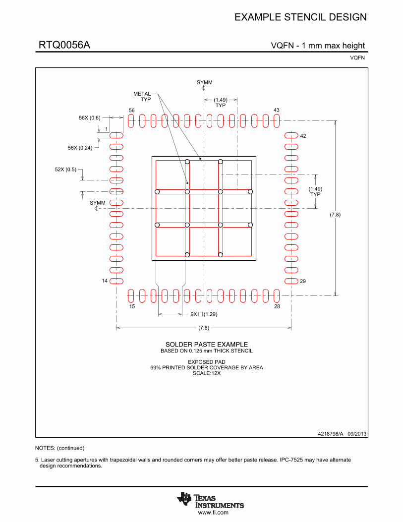
EXAMPLE STENCIL DESIGN
(7.8)
56X (0.6)
56X (0.24)
9X (1.29)
(7.8)
52X (0.5)
(1.49)TYP
(1.49)TYP
4218798/A 09/2013
VQFN - 1 mm max heightRTQ0056AVQFN
NOTES: (continued) 5. Laser cutting apertures with trapezoidal walls and rounded corners may offer better paste release. IPC-7525 may have alternate design recommendations.
SYMM
TYPMETAL
SOLDER PASTE EXAMPLEBASED ON 0.125 mm THICK STENCIL
EXPOSED PAD
69% PRINTED SOLDER COVERAGE BY AREASCALE:12X
1
SYMM
14
15 28
29
42
4356
IMPORTANT NOTICE AND DISCLAIMER
TI PROVIDES TECHNICAL AND RELIABILITY DATA (INCLUDING DATASHEETS), DESIGN RESOURCES (INCLUDING REFERENCE DESIGNS), APPLICATION OR OTHER DESIGN ADVICE, WEB TOOLS, SAFETY INFORMATION, AND OTHER RESOURCES “AS IS” AND WITH ALL FAULTS, AND DISCLAIMS ALL WARRANTIES, EXPRESS AND IMPLIED, INCLUDING WITHOUT LIMITATION ANY IMPLIED WARRANTIES OF MERCHANTABILITY, FITNESS FOR A PARTICULAR PURPOSE OR NON-INFRINGEMENT OF THIRD PARTY INTELLECTUAL PROPERTY RIGHTS.These resources are intended for skilled developers designing with TI products. You are solely responsible for (1) selecting the appropriate TI products for your application, (2) designing, validating and testing your application, and (3) ensuring your application meets applicable standards, and any other safety, security, or other requirements. These resources are subject to change without notice. TI grants you permission to use these resources only for development of an application that uses the TI products described in the resource. Other reproduction and display of these resources is prohibited. No license is granted to any other TI intellectual property right or to any third party intellectual property right. TI disclaims responsibility for, and you will fully indemnify TI and its representatives against, any claims, damages, costs, losses, and liabilities arising out of your use of these resources.TI’s products are provided subject to TI’s Terms of Sale (www.ti.com/legal/termsofsale.html) or other applicable terms available either on ti.com or provided in conjunction with such TI products. TI’s provision of these resources does not expand or otherwise alter TI’s applicable warranties or warranty disclaimers for TI products.
Mailing Address: Texas Instruments, Post Office Box 655303, Dallas, Texas 75265Copyright © 2020, Texas Instruments Incorporated