pl-2303hxd datasheet
TRANSCRIPT
PL-2303HX Edition (Chip Rev D) USB to Serial Bridge Controller
Product Datasheet
Document Revision: 1.3
Document Release: September 9, 2010
Prolific Technology Inc.
7F, No. 48, Sec. 3, Nan Kang Rd.
Nan Kang, Taipei 115, Taiwan, R.O.C.
Telephone: +886-2-2654-6363
Fax: +886-2-2654-6161
E-mail: [email protected]
Website: http://www.prolific.com.tw
Revised Date: September 9, 2010
ds_pl2303HXD_v1.3
PL-2303HX (Rev D) Product Datasheet - 2 - Document Version 1.3
Disclaimer All the information in this document is subject to change without prior notice. Prolific Technology Inc.
does not make any representations or any warranties (implied or otherwise) regarding the accuracy
and completeness of this document and shall in no event be liable for any loss of profit or any other
commercial damage, including but not limited to special, incidental, consequential, or other damages.
Trademarks
The Prolific logo is a registered trademark of Prolific Technology Inc. All brand names and product
names used in this document are trademarks or registered trademarks of their respective holders.
Copyrights
Copyright © 2010 Prolific Technology Inc., All rights reserved.
No part of this document may be reproduced or transmitted in any form by any means without the
express written permission of Prolific Technology Inc.
Revised Date: September 9, 2010
ds_pl2303HXD_v1.3
PL-2303HX (Rev D) Product Datasheet - 3 - Document Version 1.3
Revision History
Revision Description Date
1.3 Added Windows 7 Logo Driver Information
Modified Operating Temperature Characteristics
Modified Baud Rate Settings Table
September 9, 2010
1.2 Sec. 9.0: Modified DC & Temperature Characteristics June 27, 2008
1.1 Added Windows Vista and XP Logo Driver information
Added USB-IF Logo TID information
April 16, 2007
1.0B Sec. 4.2: Modified QFN diagram to add IC bottom PAD information
June 30, 2006
1.0A PL-2303HX (Chip Rev D) Datasheet – Formal Release November 23, 2005
Revised Date: September 9, 2010
ds_pl2303HXD_v1.3
PL-2303HX (Rev D) Product Datasheet - 4 - Document Version 1.3
Table of Contents
1.0 FEATURES........................................................................................................ 8
2.0 FUNCTIONAL BLOCK DIAGRAM .................................................................... 9
3.0 INTRODUCTION ............................................................................................. 10
4.0 PIN ASSIGNMENT OUTLINE ......................................................................... 11
4.1 SSOP28 Package .............................................................................................. 11
4.2 QFN32 Package................................................................................................. 12
5.0 PIN ASSIGNMENT & DESCRIPTION ............................................................. 13
5.1 SSOP28 Package .............................................................................................. 13
5.2 QFN32 Package................................................................................................. 14
6.0 USB STANDARD DESCRIPTORS ................................................................. 15
6.1 Device Descriptor ............................................................................................... 15
6.2 Configuration Descriptor ..................................................................................... 15
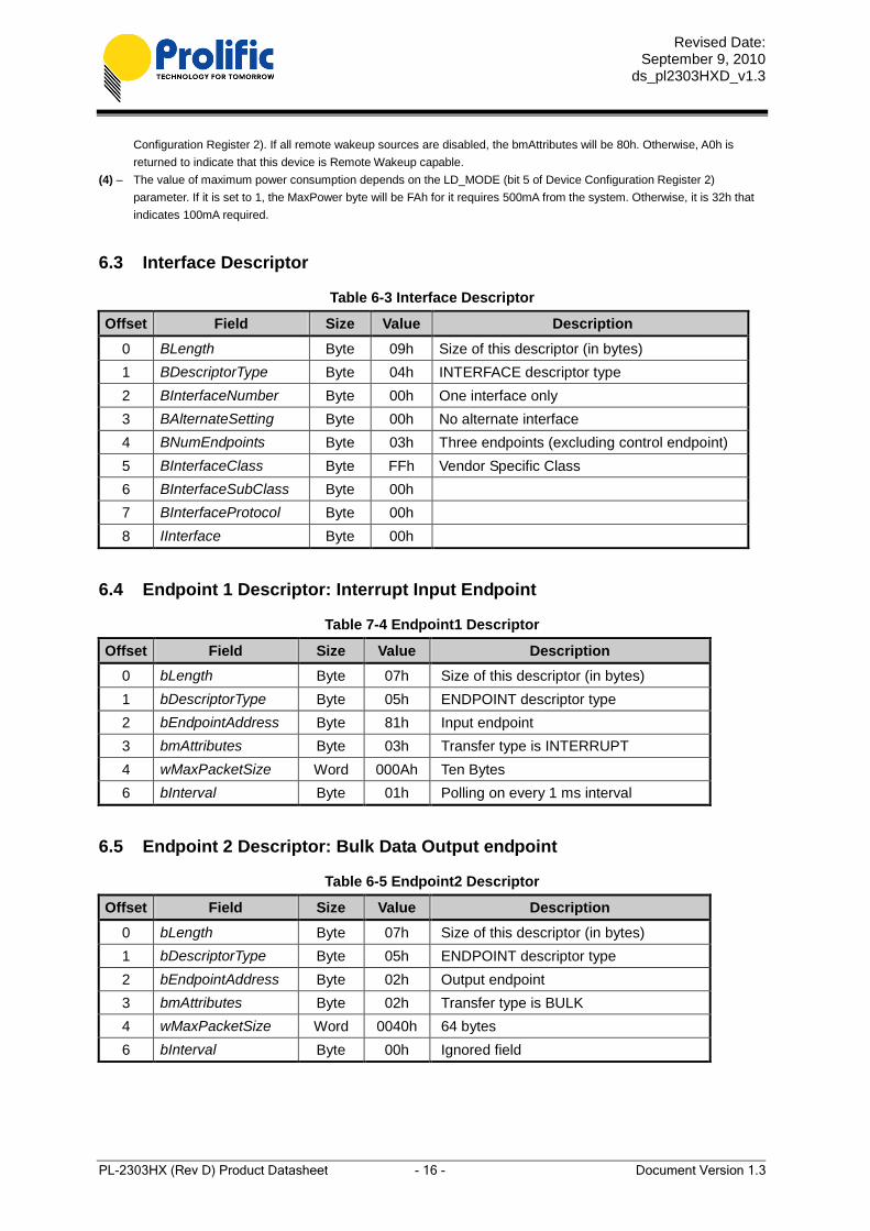
6.3 Interface Descriptor ............................................................................................ 16
6.4 Endpoint 1 Descriptor: Interrupt Input Endpoint .................................................. 16
6.5 Endpoint 2 Descriptor: Bulk Data Output endpoint.............................................. 16
6.6 Endpoint 3 Descriptor: Bulk Data Input endpoint ................................................ 17
6.7 String Descriptors ............................................................................................... 17
7.0 USB STANDARD REQUESTS ........................................................................ 18
8.0 DATA FORMATS & PROGRAMMABLE BAUD RATE GENERATOR ............ 19
9.0 DC & TEMPERATURE CHARACTERISTICS ................................................. 20
9.1 Absolute Maximum Ratings ................................................................................ 20
9.2 DC Characteristics ............................................................................................. 20
9.3 Clock Characteristics ......................................................................................... 21
9.4 Temperature Characteristics .............................................................................. 22
9.5 Leakage Current and Capacitance ..................................................................... 22
9.6 Power-On Reset................................................................................................. 22
10.0 OUTLINE DIAGRAM ........................................................................................ 23
10.1 SSOP28 Package .............................................................................................. 23
10.2 QFN32 Package................................................................................................. 24
Revised Date: September 9, 2010
ds_pl2303HXD_v1.3
PL-2303HX (Rev D) Product Datasheet - 5 - Document Version 1.3
11.0 REEL PACKING INFORMATION ..................................................................... 25
11.1 Carrier Tape (SSOP-28) ..................................................................................... 25
11.2 Reel Dimension ................................................................................................. 26
12.0 ORDERING INFORMATION ........................................................................... 26
Revised Date: September 9, 2010
ds_pl2303HXD_v1.3
PL-2303HX (Rev D) Product Datasheet - 6 - Document Version 1.3
List of Figures
Figure 2-1 Block Diagram of PL-2303HX (Rev D) ................................................................... 9
Figure 4-1 Pin Assignment Outline of PL-2303HX (Rev D) SSOP28 .................................... 11
Figure 4-2 Pin Assignment Outline of PL-2303HX (Rev D) QFN32 ....................................... 12
Figure 10-1 Power-On Reset Diagram .................................................................................. 22
Figure 10-1 Outline Diagram of PL-2303HX (Rev D) SSOP28 ............................................. 23
Figure 10-2 Outline Diagram of PL-2303HX (Rev D) QFN32 ................................................ 24
Figure 11-1a SSOP28 Carrier Tape ...................................................................................... 25
Figure 11-1b IC Reel Placements ......................................................................................... 25
Figure 11-2 Reel Dimension ................................................................................................. 26
List of Tables
Table 5-1 Pin Assignment & Description (SSOP28) .............................................................. 13
Table 5-2 Pin Assignment & Description (QFN32) ................................................................ 14
Table 6-1 Device Descriptor .................................................................................................. 15
Table 6-2 Configuration Descriptor ....................................................................................... 15
Table 6-3 Interface Descriptor ............................................................................................... 16
Table 7-4 Endpoint1 Descriptor............................................................................................. 16
Table 6-5 Endpoint2 Descriptor............................................................................................. 16
Table 6-6 Endpoint3 Descriptor............................................................................................. 17
Table 6-7a String Descriptor – Language ID ......................................................................... 17
Table 6-7b String Descriptor – Manufacturer ......................................................................... 17
Table 6-7c String Descriptor – Product ................................................................................. 18
Table 6-7d String Descriptor – Serial Number ....................................................................... 18
Table 8-1 Supported Data Formats ....................................................................................... 19
Table 8-2 Baud Rate Settings (Supported by Driver) ............................................................ 19
Table 9-1 Absolute Maximum Ratings ................................................................................... 20
Table 9-2a Operating Voltage and Suspend Current ............................................................. 20
Table 9-2b 3.3V I/O Pins ....................................................................................................... 20
Table 9-2c [email protected] Serial I/O Pins .......................................................................... 21
Table 9-2d [email protected] Serial I/O Pins .......................................................................... 21
Table 9-2e [email protected] Serial I/O Pins .......................................................................... 21
Table 9-3 Clock Characteristics ............................................................................................ 21
Table 9-4 Temperature Characteristics ................................................................................. 22
Table 9-5 Leakage Current and Capacitance ........................................................................ 22
Table 9-6 Power-On Reset ................................................................................................... 22

Revised Date: September 9, 2010
ds_pl2303HXD_v1.3
PL-2303HX (Rev D) Product Datasheet - 7 - Document Version 1.3
Table 10-1 Package Dimension ............................................................................................. 23
Table 11-2 Reel Part Number Information ............................................................................. 26
Table 12-1 Ordering Information ............................................................................................ 26
Revised Date: September 9, 2010
ds_pl2303HXD_v1.3
PL-2303HX (Rev D) Product Datasheet - 8 - Document Version 1.3
1.0 Features
Fully Compliant with USB Specification v2.0 (Full-Speed)
On Chip USB 1.1 transceiver, 5V3.3V regulator
On-chip 96MHz clock generator
Supports RS-422/RS-485 like serial interface (TXD, DTR_N, and RTS_N pins should be
externally pulled-up to 5V)
Supports RS232-like Serial Interface
o Full-duplex transmitter and receiver (TXD and RXD)
o Six MODEM control pins (RTS, CTS, DTR, DSR, DCD, and RI)
o 5, 6, 7 or 8 data bits
o Odd, Even, Mark, Space, or None parity mode
o One, one and a half, or two stop bits
o Parity error, frame error, and serial break detection
o Programmable baud rate from 75 bps to 12M bps
o External RS232 driver power down control
o Independent power source for serial interface
Extensive Flow Control Mechanism
o Adjustable high/low watermark level
o Automatic hardware flow control with CTS/RTS(1)
or DSR/DTR(2)
o Automatic software flow control with XON/XOFF
o Inbound data buffer overflow detection
Configurable 512-byte bi-directional data buffer
o 256-byte outbound buffer and 256-byte inbound buffer; or
o 128-byte outbound buffer and 384-byte inbound buffer
Supports remote wake-up from MODEM input signals
Four (4) General Purpose I/O (GP0, GP1, GP2, & GP3) pins & Four (4) Auxiliary General
Purpose I/O (RI_N, DSR_N, DCD_N, & CTS_N) pins.
On-chip OTP (One Time Programming) ROM for startup device configurations
Hardware backward compatible with PL-2303H
Provides drivers support for Windows, Mac OS, Linux, and WinCE
Windows 7, Vista, XP Certified Logo Drivers (x86 and x64)
USB-IF Logo Compliant with TID 40000100
Small footprint 28-pin SSOP or 32-pin QFN IC package
Notes:
(1) – CTS/RTS Hardware Flow Control supports either low-level active or high-level active.
(2) – For DSR/DTR Hardware Flow Control support, please contact Prolific FAE for more information.
Revised Date: September 9, 2010
ds_pl2303HXD_v1.3
PL-2303HX (Rev D) Product Datasheet - 9 - Document Version 1.3
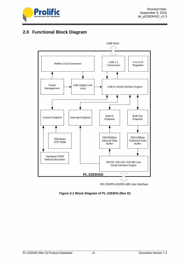
2.0 Functional Block Diagram
96MHz Clock GeneratorUSB 1.1
Transceiver
5 to 3.3V
Regulator
Power
Management
USB Digital Lock
LoopUSB to Serial Interface Engine
Control Endpoint Interrupt EndpointBulk-in
Endpoint
Bulk-Out
Endpoint
256/384Byte
Inbound Data
Buffer
256/128Byte
Outbound Data
Buffer
RS232 / RS-422 / RS-485 Like
Serial Interface Engine
256-Bytes
OTP ROM
Hardware ROM
Default Descriptor
PL-2303HXD
RS-232/RS-422/RS-485 Like Interface
USB Host
Figure 2-1 Block Diagram of PL-2303HX (Rev D)
Revised Date: September 9, 2010
ds_pl2303HXD_v1.3
PL-2303HX (Rev D) Product Datasheet - 10 - Document Version 1.3
3.0 Introduction
PL-2303HX provides a convenient solution for connecting an RS232-like full-duplex asynchronous
serial device to any Universal Serial Bus (USB) capable host. PL-2303HX highly compatible drivers
could simulate the traditional COM port on most operating systems allowing the existing applications
based on COM port to easily migrate and be made USB ready.
By taking advantage of USB bulk transfer mode, large data buffers, and automatic flow control,
PL-2303HX is capable of achieving higher throughput compared to traditional UART (Universal
Asynchronous Receiver Transmitter) ports. When real RS232 signaling is not required, baud rate
higher than 115200 bps could be used for even higher performance. The flexible baud rate generator of
PL-2303HX could be programmed to generate any rate between 75 bps to 12M bps.
PL-2303HX is exclusively designed for mobile and embedded solutions in mind, providing a small
footprint that could easily fit in to any connectors and handheld devices. With very small power
consumption in either operating or suspend mode, PL-2303HX is perfect for bus powered operation
with plenty of power left for the attached devices. Flexible signal level requirement on the RS232-like
serial port side also allows PL-2303HX to connect directly to any 3.3V~1.8V range devices.
Revised Date: September 9, 2010
ds_pl2303HXD_v1.3
PL-2303HX (Rev D) Product Datasheet - 11 - Document Version 1.3
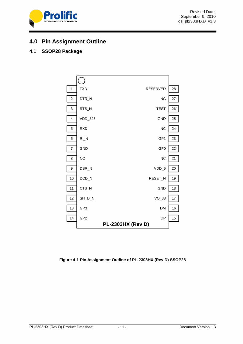
4.0 Pin Assignment Outline
4.1 SSOP28 Package
PL-2303HX (Rev D)
1 TXD
2 DTR_N
3 RTS_N
4 VDD_325
5 RXD
6 RI_N
7 GND
8 NC
9 DSR_N
10 DCD_N
11 CTS_N
12 SHTD_N
13 GP3
14 GP2
28RESERVED
27NC
26TEST
25GND
24NC
23GP1
22GP0
21NC
20VDD_5
19RESET_N
18GND
17VO_33
16DM
15DP
Figure 4-1 Pin Assignment Outline of PL-2303HX (Rev D) SSOP28
Revised Date: September 9, 2010
ds_pl2303HXD_v1.3
PL-2303HX (Rev D) Product Datasheet - 12 - Document Version 1.3
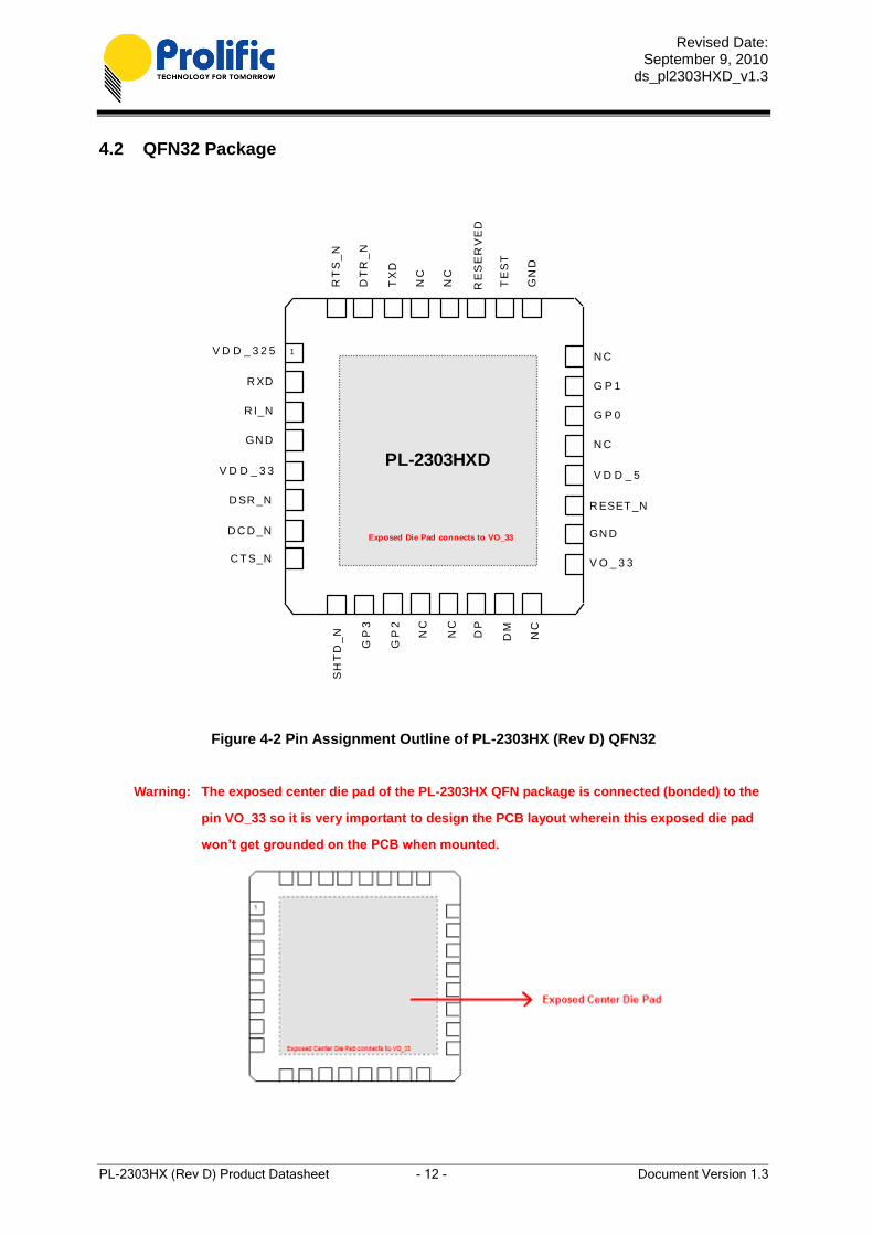
4.2 QFN32 Package
RT
S_
N
N C
GN DG
ND
TE
ST
RE
SE
RV
ED
NC
NC
TX
D
DT
R_
NV D D _ 3 2 5
R XD
R I_N
GN D
V D D _ 3 3
D SR _N
D C D _N
C T S_N
SH
TD
_N
GP
3
GP
2
NC
NC
DP
DM
NC
G P 1
G P 0
N C
V D D _ 5
R ESET _N
V O _ 3 3
PL-2303HXD
Exposed Die Pad connects to VO_33
1
Figure 4-2 Pin Assignment Outline of PL-2303HX (Rev D) QFN32
Warning: The exposed center die pad of the PL-2303HX QFN package is connected (bonded) to the
pin VO_33 so it is very important to design the PCB layout wherein this exposed die pad
won’t get grounded on the PCB when mounted.

Revised Date: September 9, 2010
ds_pl2303HXD_v1.3
PL-2303HX (Rev D) Product Datasheet - 13 - Document Version 1.3
5.0 Pin Assignment & Description
Pin Type Abbreviation:
I: Input O: Output B: Bidirectional I/O P: Power/Ground
5.1 SSOP28 Package
Table 5-1 Pin Assignment & Description (SSOP28)
Pin # Name Type Description
1 TXD O (1)
Serial Port (Transmitted Data)
2 DTR_N O (1)
Serial Port (Data Terminal Ready)
3 RTS_N O (1)
Serial Port (Request To Send)
4 VDD_325 P RS232 VDD. The power pin for the serial port signals. When the serial port is 3.3V, this should be 3.3V. When the serial port is 2.5V, this should be 2.5V. The range can be from 1.8V~3.3V.
5 RXD I (2)
Serial Port (Received Data)
6 RI_N B (2)
Serial Port (Ring Indicator); or Auxiliary General Purpose I/O Port when enabled
(7).
7 GND P Ground
8 NC - No Connection
9 DSR_N B (2)
Serial Port (Data Set Ready); or Auxiliary General Purpose I/O Port when enabled
(7).
10 DCD_N B (2)
Serial Port (Data Carrier Detect); or Auxiliary General Purpose I/O Port when enabled
(7).
11 CTS_N B (2)
Serial Port (Clear to Send); or Auxiliary General Purpose I/O Port when enabled
(7).
12 SHTD_N O (3)
RS232 Transceiver Shut Down Control
13 GP3 I/O Auxiliary GPIO Pin 3 (Default output high mode) (6)
14 GP2 I/O Auxiliary GPIO Pin 2 (Default output high mode) (6)
15 DP B USB Port D+ signal
16 DM B USB Port D- signal
17 VO_33 P Regulator Power Output, 3.3V
18 GND P Ground
19 RESET_N I (4)
External System Reset (Active Low)
20 VDD_5 P USB Port VBUS, 5V Power. (6.5V for OTPROM writing voltage).
21 NC - No Connection
22 GP0 B (5)
General Purpose I/O Pin 0
23 GP1 B (5)
General Purpose I/O Pin 1
24 NC - No Connection
25 GND - Ground
26 TEST I Test mode control
27 NC - No Connection
28 Reserved - Reserved pin (Must be floating)
Notes:
(1) – Tri-State, Output Pad. Level and Driving Capability decided by VDD_325.
(2) – Tri-State, CMOS Input/Output Pad with level shifter. Level and Driving Capability decided by VDD_325.
(3) – CMOS Output Pad.
(4) – CMOS Input Pad, 5V tolerant.
(5) – Tri-State, CMOS Input/Output Pad. (Default mode: Input)
(6) – Default output high mode; do not connect to ground.
(7) – Enabling Auxiliary GPIO requires special customized driver.

Revised Date: September 9, 2010
ds_pl2303HXD_v1.3
PL-2303HX (Rev D) Product Datasheet - 14 - Document Version 1.3
5.2 QFN32 Package
Table 5-2 Pin Assignment & Description (QFN32)
Pin # Name Type Description
1 VDD_325 P
RS232 VDD. The power pin for the serial port signals. When the serial port is 3.3V, this should be 3.3V. When the serial port is 2.5V, this should be 2.5V. The range can be from 1.8V~3.3V.
2 RXD I (2)
Serial Port (Received Data)
3 RI_N B (2)
Serial Port (Ring Indicator); or Auxiliary General Purpose I/O Port when enabled
(6).
4 GND P Ground
5 VDD_33 P Primary Power (3.3V)
6 DSR_N B (2)
Serial Port (Data Set Ready); or Auxiliary General Purpose I/O Port when enabled
(6).
7 DCD_N B (2)
Serial Port (Data Carrier Detect); or Auxiliary General Purpose I/O Port when enabled
(6).
8 CTS_N B (2)
Serial Port (Clear to Send); or Auxiliary General Purpose I/O Port when enabled
(6).
9 SHTD_N O (3)
RS232 Transceiver Shut Down Control
10 GP3 I/O Auxiliary GPIO Pin 3 (Default output high mode) (5)
11 GP2 I/O Auxiliary GPIO Pin 2 (Default output high mode) (5)
12 NC - No Connection
13 NC - No Connection
14 DP B USB Port D+ signal
15 DM B USB Port D- signal
16 NC - No Connection
17 VO_33 P Regulator Power Output, 3.3V
18 GND P Ground
19 RESET_N I External System Reset (Active Low)
20 VDD_5 P USB Port VBUS, 5V Power.
21 NC - No Connection
22 GP0 B (4)
General Purpose I/O Pin 0
23 GP1 B (4)
General Purpose I/O Pin 1
24 NC - No Connection
25 GND P Ground
26 TEST I Test mode control
27 Reserved - Reserved pin (Must be floating)
28 NC - No Connection
29 NC - No Connection
30 TXD O (1)
Serial Port (Transmitted Data)
31 DTR_N O (1)
Serial Port (Data Terminal Ready)
32 RTS_N O (1)
Serial Port (Request To Send)
IC Bottom PAD P Connects to VO_33 (Regulator Power Output, 3.3V)
Notes:
(1) – Tri-State, Output Pad. Level and Driving Capability decided by VDD_325.
(2) – Tri-State, CMOS Input/Output Pad with level shifter. Level and Driving Capability decided by VDD_325.
(3) – CMOS Output Pad.
(4) – Tri-State, CMOS Input/Output Pad. (Default mode: Input)
(5) – Default output high mode; do not connect to ground.
(6) – Enabling Auxiliary GPIO requires special customized driver.
Revised Date: September 9, 2010
ds_pl2303HXD_v1.3
PL-2303HX (Rev D) Product Datasheet - 15 - Document Version 1.3
6.0 USB Standard Descriptors
PL-2303HX supports one configuration with one interface and four endpoints. The descriptors are
basically stored in an internal hardware ROM. However, some fields could be optionally modified by
properly programmed on-chip OTPROM. The contents of all descriptors are shown in the following
sections and the format of OTPROM would be given in later chapter.
6.1 Device Descriptor
Table 6-1 Device Descriptor
Offset Field Size Value Description
0 bLength Byte 12h Size of this descriptor (in bytes)
1 bDescriptorType Byte 01h DEVICE descriptor type
2 bcdUSB Word 0110h USB Specification Release Number 1.1
4 bDeviceClass Byte 00h
5 bDeviceSubClass Byte 00h
6 bDeviceProtocol Byte 00h
7 bMaxPacketSize0 Byte 40h Maximum packet size for endpoint zero is 64
8 idVender Word 067Bh Vender ID (1)
10 idProduct Word 2303h Product ID (1)
12 bcdDevice Word 0400h Device Release Number (1)
14 iManufacturer Byte 01h Manufacturer string descriptor index
15 iProduct Byte 02h Product name string descriptor index
16 iSerialNumber Byte 00h/03h Serial number string descriptor index (2)
17 bNumConfigurations Byte 01h One configuration.
Notes:
(1) – The Vender ID, Product ID, and Device Release Number could be replaced by the contents of the on-chip OTPROM.
(2) – The serial number string descriptor index could be defined by the contents of the on-chip OTPROM. If specified, the index
will be 3 instead of 0.
6.2 Configuration Descriptor
Table 6-2 Configuration Descriptor
Offset Field Size Value Description
0 bLength Byte 09h Size of this descriptor (in bytes)
1 bDescriptorType Byte 02h CONFIGURATION descriptor type
2 wTotalLength Word 0027h Total length of data returned for this configuration.
4 bNumInterface Byte 01h One interface for this device.
5 bConfigurationValue Byte 01h
6 iConfiguration Byte 00h
7 bmAttributes Byte A0h/80h Characteristic attributes (3)
8 MaxPower Byte 32h/FAh Maximum power consumption (4)
Notes:
(3) – The Remote Wakeup attribute (bit 5) depends on the settings of the Remote Wakeup Enable (bit 0 to 4 of Device
Revised Date: September 9, 2010
ds_pl2303HXD_v1.3
PL-2303HX (Rev D) Product Datasheet - 16 - Document Version 1.3
Configuration Register 2). If all remote wakeup sources are disabled, the bmAttributes will be 80h. Otherwise, A0h is
returned to indicate that this device is Remote Wakeup capable.
(4) – The value of maximum power consumption depends on the LD_MODE (bit 5 of Device Configuration Register 2)
parameter. If it is set to 1, the MaxPower byte will be FAh for it requires 500mA from the system. Otherwise, it is 32h that
indicates 100mA required.
6.3 Interface Descriptor
Table 6-3 Interface Descriptor
Offset Field Size Value Description
0 BLength Byte 09h Size of this descriptor (in bytes)
1 BDescriptorType Byte 04h INTERFACE descriptor type
2 BInterfaceNumber Byte 00h One interface only
3 BAlternateSetting Byte 00h No alternate interface
4 BNumEndpoints Byte 03h Three endpoints (excluding control endpoint)
5 BInterfaceClass Byte FFh Vendor Specific Class
6 BInterfaceSubClass Byte 00h
7 BInterfaceProtocol Byte 00h
8 IInterface Byte 00h
6.4 Endpoint 1 Descriptor: Interrupt Input Endpoint
Table 7-4 Endpoint1 Descriptor
Offset Field Size Value Description
0 bLength Byte 07h Size of this descriptor (in bytes)
1 bDescriptorType Byte 05h ENDPOINT descriptor type
2 bEndpointAddress Byte 81h Input endpoint
3 bmAttributes Byte 03h Transfer type is INTERRUPT
4 wMaxPacketSize Word 000Ah Ten Bytes
6 bInterval Byte 01h Polling on every 1 ms interval
6.5 Endpoint 2 Descriptor: Bulk Data Output endpoint
Table 6-5 Endpoint2 Descriptor
Offset Field Size Value Description
0 bLength Byte 07h Size of this descriptor (in bytes)
1 bDescriptorType Byte 05h ENDPOINT descriptor type
2 bEndpointAddress Byte 02h Output endpoint
3 bmAttributes Byte 02h Transfer type is BULK
4 wMaxPacketSize Word 0040h 64 bytes
6 bInterval Byte 00h Ignored field
Revised Date: September 9, 2010
ds_pl2303HXD_v1.3
PL-2303HX (Rev D) Product Datasheet - 17 - Document Version 1.3
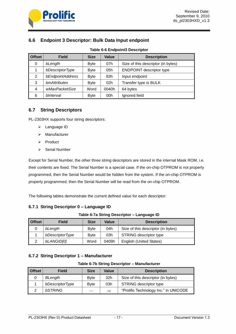
6.6 Endpoint 3 Descriptor: Bulk Data Input endpoint
Table 6-6 Endpoint3 Descriptor
Offset Field Size Value Description
0 bLength Byte 07h Size of this descriptor (in bytes)
1 bDescriptorType Byte 05h ENDPOINT descriptor type
2 bEndpointAddress Byte 83h Input endpoint
3 bmAttributes Byte 02h Transfer type is BULK
4 wMaxPacketSize Word 0040h 64 bytes
6 bInterval Byte 00h Ignored field
6.7 String Descriptors
PL-2303HX supports four string descriptors:
Language ID
Manufacturer
Product
Serial Number
Except for Serial Number, the other three string descriptors are stored in the internal Mask ROM, i.e.
their contents are fixed. The Serial Number is a special case. If the on-chip OTPROM is not properly
programmed, then the Serial Number would be hidden from the system. If the on-chip OTPROM is
properly programmed, then the Serial Number will be read from the on-chip OTPROM.
The following tables demonstrate the current defined value for each descriptor:
6.7.1 String Descriptor 0 – Language ID
Table 6-7a String Descriptor – Language ID
Offset Field Size Value Description
0 bLength Byte 04h Size of this descriptor (in bytes)
1 bDescriptorType Byte 03h STRING descriptor type
2 bLANGID[0] Word 0409h English (United States)
6.7.2 String Descriptor 1 – Manufacturer
Table 6-7b String Descriptor – Manufacturer
Offset Field Size Value Description
0 BLength Byte 32h Size of this descriptor (in bytes)
1 bDescriptorType Byte 03h STRING descriptor type
2 bSTRING “Prolific Technology Inc.” in UNICODE
Revised Date: September 9, 2010
ds_pl2303HXD_v1.3
PL-2303HX (Rev D) Product Datasheet - 18 - Document Version 1.3
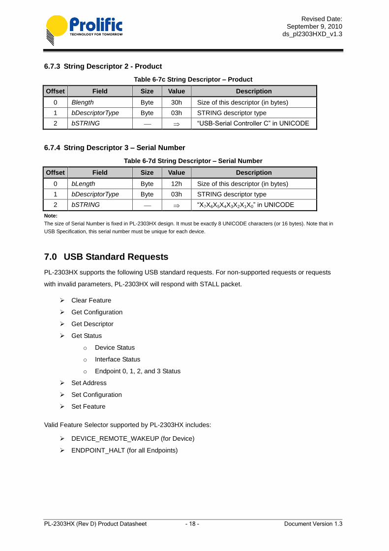
6.7.3 String Descriptor 2 - Product
Table 6-7c String Descriptor – Product
Offset Field Size Value Description
0 Blength Byte 30h Size of this descriptor (in bytes)
1 bDescriptorType Byte 03h STRING descriptor type
2 bSTRING “USB-Serial Controller C” in UNICODE
6.7.4 String Descriptor 3 – Serial Number
Table 6-7d String Descriptor – Serial Number
Offset Field Size Value Description
0 bLength Byte 12h Size of this descriptor (in bytes)
1 bDescriptorType Byte 03h STRING descriptor type
2 bSTRING “X7X6X5X4X3X2X1X0” in UNICODE
Note:
The size of Serial Number is fixed in PL-2303HX design. It must be exactly 8 UNICODE characters (or 16 bytes). Note that in
USB Specification, this serial number must be unique for each device.
7.0 USB Standard Requests
PL-2303HX supports the following USB standard requests. For non-supported requests or requests
with invalid parameters, PL-2303HX will respond with STALL packet.
Clear Feature
Get Configuration
Get Descriptor
Get Status
o Device Status
o Interface Status
o Endpoint 0, 1, 2, and 3 Status
Set Address
Set Configuration
Set Feature
Valid Feature Selector supported by PL-2303HX includes:
DEVICE_REMOTE_WAKEUP (for Device)
ENDPOINT_HALT (for all Endpoints)
Revised Date: September 9, 2010
ds_pl2303HXD_v1.3
PL-2303HX (Rev D) Product Datasheet - 19 - Document Version 1.3
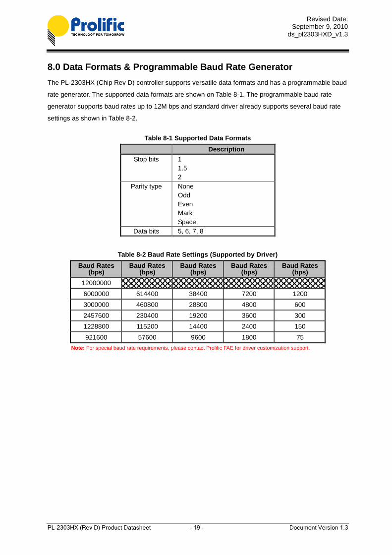
8.0 Data Formats & Programmable Baud Rate Generator
The PL-2303HX (Chip Rev D) controller supports versatile data formats and has a programmable baud
rate generator. The supported data formats are shown on Table 8-1. The programmable baud rate
generator supports baud rates up to 12M bps and standard driver already supports several baud rate
settings as shown in Table 8-2.
Table 8-1 Supported Data Formats
Description
Stop bits 1
1.5
2
Parity type None
Odd
Even
Mark
Space
Data bits 5, 6, 7, 8
Table 8-2 Baud Rate Settings (Supported by Driver)
Baud Rates (bps)
Baud Rates (bps)
Baud Rates (bps)
Baud Rates (bps)
Baud Rates (bps)
12000000
6000000 614400 38400 7200 1200
3000000 460800 28800 4800 600
2457600 230400 19200 3600 300
1228800 115200 14400 2400 150
921600 57600 9600 1800 75
Note: For special baud rate requirements, please contact Prolific FAE for driver customization support.
Revised Date: September 9, 2010
ds_pl2303HXD_v1.3
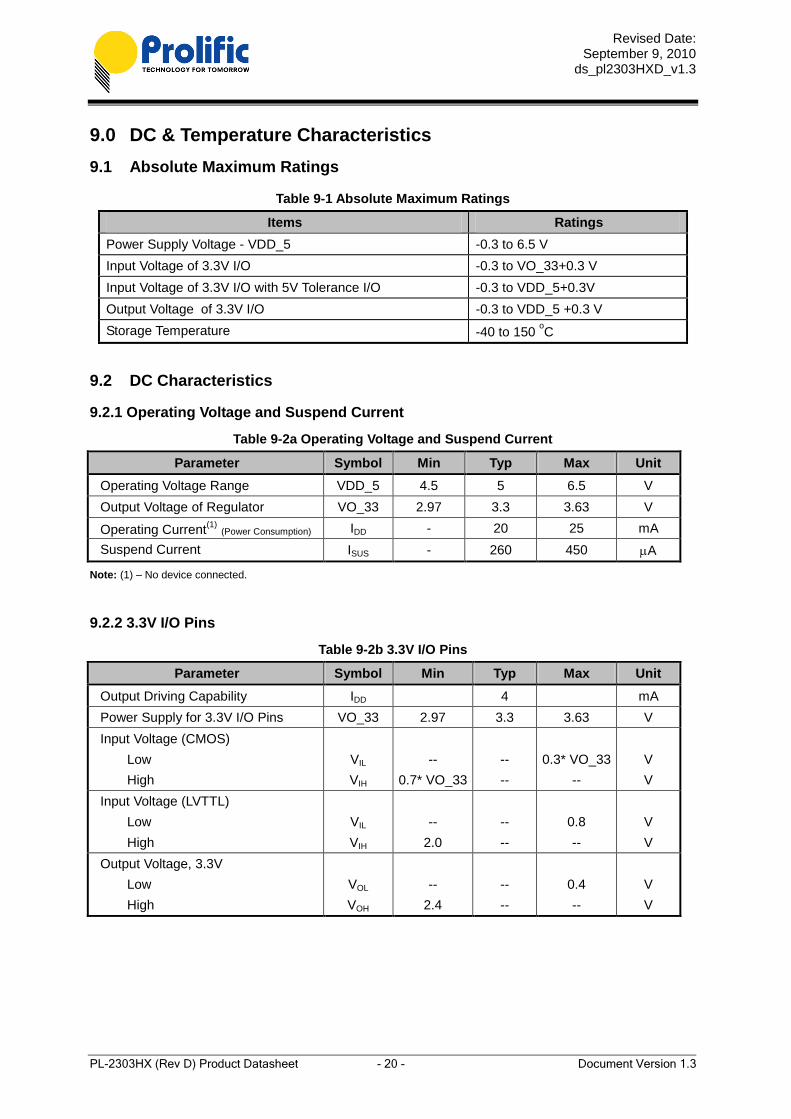
PL-2303HX (Rev D) Product Datasheet - 20 - Document Version 1.3
9.0 DC & Temperature Characteristics
9.1 Absolute Maximum Ratings
Table 9-1 Absolute Maximum Ratings
Items Ratings
Power Supply Voltage - VDD_5 -0.3 to 6.5 V
Input Voltage of 3.3V I/O -0.3 to VO_33+0.3 V
Input Voltage of 3.3V I/O with 5V Tolerance I/O -0.3 to VDD_5+0.3V
Output Voltage of 3.3V I/O -0.3 to VDD_5 +0.3 V
Storage Temperature -40 to 150 oC
9.2 DC Characteristics
9.2.1 Operating Voltage and Suspend Current
Table 9-2a Operating Voltage and Suspend Current
Parameter Symbol Min Typ Max Unit
Operating Voltage Range VDD_5 4.5 5 6.5 V
Output Voltage of Regulator VO_33 2.97 3.3 3.63 V
Operating Current(1) (Power Consumption) IDD - 20 25 mA
Suspend Current ISUS - 260 450 A
Note: (1) – No device connected.
9.2.2 3.3V I/O Pins
Table 9-2b 3.3V I/O Pins
Parameter Symbol Min Typ Max Unit
Output Driving Capability IDD 4 mA
Power Supply for 3.3V I/O Pins VO_33 2.97 3.3 3.63 V
Input Voltage (CMOS)
Low
High
VIL
VIH
--
0.7* VO_33
--
--
0.3* VO_33
--
V
V
Input Voltage (LVTTL)
Low
High
VIL
VIH
--
2.0
--
--
0.8
--
V
V
Output Voltage, 3.3V
Low
High
VOL
VOH
--
2.4
--
--
0.4
--
V
V
Revised Date: September 9, 2010
ds_pl2303HXD_v1.3
PL-2303HX (Rev D) Product Datasheet - 21 - Document Version 1.3
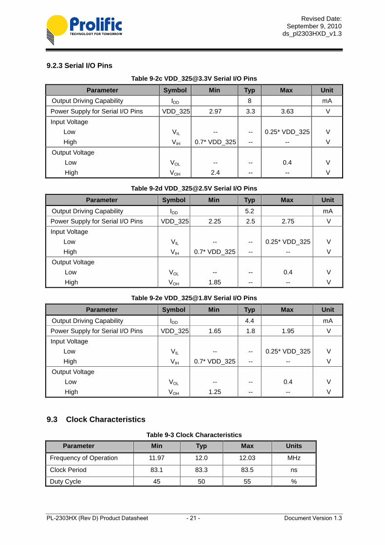
9.2.3 Serial I/O Pins
Table 9-2c [email protected] Serial I/O Pins
Parameter Symbol Min Typ Max Unit
Output Driving Capability IDD 8 mA
Power Supply for Serial I/O Pins VDD_325 2.97 3.3 3.63 V
Input Voltage
Low
High
VIL
VIH
--
0.7* VDD_325
--
--
0.25* VDD_325
--
V
V
Output Voltage
Low
High
VOL
VOH
--
2.4
--
--
0.4
--
V
V
Table 9-2d [email protected] Serial I/O Pins
Parameter Symbol Min Typ Max Unit
Output Driving Capability IDD 5.2 mA
Power Supply for Serial I/O Pins VDD_325 2.25 2.5 2.75 V
Input Voltage
Low
High
VIL
VIH
--
0.7* VDD_325
--
--
0.25* VDD_325
--
V
V
Output Voltage
Low
High
VOL
VOH
--
1.85
--
--
0.4
--
V
V
Table 9-2e [email protected] Serial I/O Pins
Parameter Symbol Min Typ Max Unit
Output Driving Capability IDD 4.4 mA
Power Supply for Serial I/O Pins VDD_325 1.65 1.8 1.95 V
Input Voltage
Low
High
VIL
VIH
--
0.7* VDD_325
--
--
0.25* VDD_325
--
V
V
Output Voltage
Low
High
VOL
VOH
--
1.25
--
--
0.4
--
V
V
9.3 Clock Characteristics
Table 9-3 Clock Characteristics
Parameter Min Typ Max Units
Frequency of Operation 11.97 12.0 12.03 MHz
Clock Period 83.1 83.3 83.5 ns
Duty Cycle 45 50 55 %

Revised Date: September 9, 2010
ds_pl2303HXD_v1.3
PL-2303HX (Rev D) Product Datasheet - 22 - Document Version 1.3
9.4 Temperature Characteristics
Table 9-4 Temperature Characteristics
Parameter Symbol Min Typ Max Unit
Operating Temperature -- -40
-- 85 o
C
Junction Operation Temperature TJ -40 25 105 oC
9.5 Leakage Current and Capacitance
Table 9-5 Leakage Current and Capacitance
Parameter Symbol Min Typ Max Unit
Input Leakage Current*1
IL -10 1 10 A
Tri-state Leakage Current Ioz -10 1 10 A
Input Capacitance CIN -- 2.8 -- pF
Output Capacitance COUT 2.7 -- 4.9 pF
Bi-directional Buffer Capacitance CBID 2.7 -- 4.9 pF
*1. No pull-up or pull-down resistor.
9.6 Power-On Reset
Figure 10-1 Power-On Reset Diagram
Table 9-6 Power-On Reset
Parameter Symbol FF@70oC
VO_33=3.63V
TT@25oC
VO_33=3.3V
SS@0oC
VO_33=2.97V
Unit
Output Delay Time Td 1.18 2.68 182.5 sec
Note: The delay time is simulated with VIN ramp of 1V/sec.
Revised Date: September 9, 2010
ds_pl2303HXD_v1.3
PL-2303HX (Rev D) Product Datasheet - 23 - Document Version 1.3
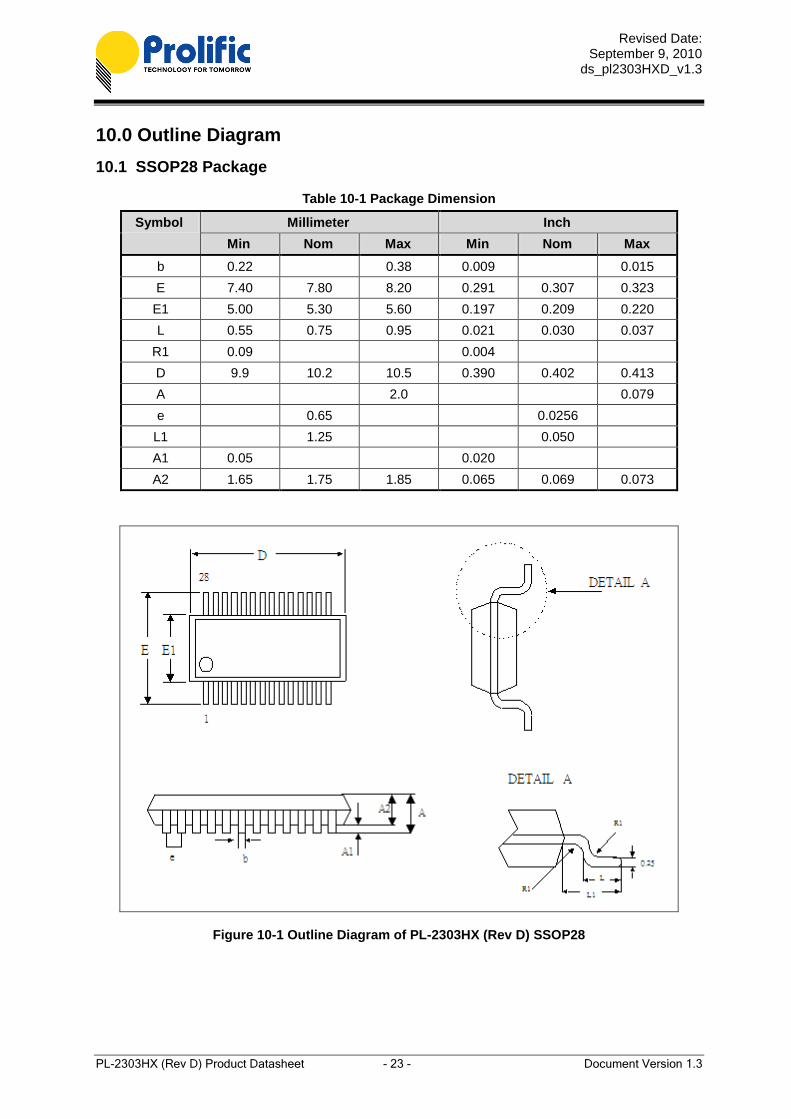
10.0 Outline Diagram
10.1 SSOP28 Package
Table 10-1 Package Dimension
Symbol Millimeter Inch
Min Nom Max Min Nom Max
b 0.22 0.38 0.009 0.015
E 7.40 7.80 8.20 0.291 0.307 0.323
E1 5.00 5.30 5.60 0.197 0.209 0.220
L 0.55 0.75 0.95 0.021 0.030 0.037
R1 0.09 0.004
D 9.9 10.2 10.5 0.390 0.402 0.413
A 2.0 0.079
e 0.65 0.0256
L1 1.25 0.050
A1 0.05 0.020
A2 1.65 1.75 1.85 0.065 0.069 0.073
Figure 10-1 Outline Diagram of PL-2303HX (Rev D) SSOP28

Revised Date: September 9, 2010
ds_pl2303HXD_v1.3
PL-2303HX (Rev D) Product Datasheet - 24 - Document Version 1.3
10.2 QFN32 Package
Figure 10-2 Outline Diagram of PL-2303HX (Rev D) QFN32
Revised Date: September 9, 2010
ds_pl2303HXD_v1.3
PL-2303HX (Rev D) Product Datasheet - 25 - Document Version 1.3
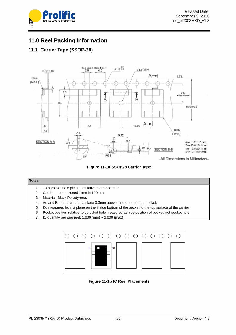
11.0 Reel Packing Information
11.1 Carrier Tape (SSOP-28)
Figure 11-1a SSOP28 Carrier Tape
Notes:
1. 10 sprocket hole pitch cumulative tolerance 0.2
2. Camber not to exceed 1mm in 100mm.
3. Material: Black Polystyrene.
4. Ao and Bo measured on a plane 0.3mm above the bottom of the pocket.
5. Ko measured from a plane on the inside bottom of the pocket to the top surface of the carrier.
6. Pocket position relative to sprocket hole measured as true position of pocket, not pocket hole.
7. IC quantity per one reel: 1,000 (min) ~ 2,000 (max)
Figure 11-1b IC Reel Placements
Revised Date: September 9, 2010
ds_pl2303HXD_v1.3
PL-2303HX (Rev D) Product Datasheet - 26 - Document Version 1.3
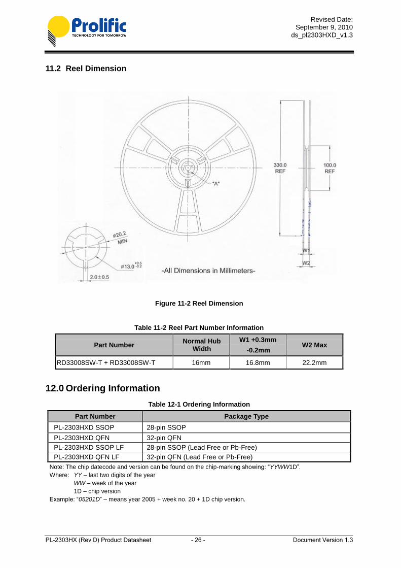
11.2 Reel Dimension
Figure 11-2 Reel Dimension
Table 11-2 Reel Part Number Information
Part Number Normal Hub
Width
W1 +0.3mm
-0.2mm W2 Max
RD33008SW-T + RD33008SW-T 16mm 16.8mm 22.2mm
12.0 Ordering Information
Table 12-1 Ordering Information
Part Number Package Type
PL-2303HXD SSOP 28-pin SSOP
PL-2303HXD QFN 32-pin QFN
PL-2303HXD SSOP LF 28-pin SSOP (Lead Free or Pb-Free)
PL-2303HXD QFN LF 32-pin QFN (Lead Free or Pb-Free)
Note: The chip datecode and version can be found on the chip-marking showing: “YYWW1D”.
Where: YY – last two digits of the year
WW – week of the year
1D – chip version
Example: “05201D” – means year 2005 + week no. 20 + 1D chip version.