avr32 ap7001 datasheet
TRANSCRIPT
Features• High Performance, Low Power AVR®32 32-Bit Microcontroller
– 210 DMIPS throughput at 150 MHz– 16 KB instruction cache and 16 KB data caches– Memory Management Unit enabling use of operating systems– Single-cycle RISC instruction set including SIMD and DSP instructions– Java Hardware Acceleration
• Pixel Co-Processor– Pixel Co-Processor for video acceleration through color-space conversion
(YUV<->RGB), image scaling and filtering, quarter pixel motion compensation• Multi-hierarchy bus system
– High-performance data transfers on separate buses for increased performance• Data Memories
– 32KBytes SRAM• External Memory Interface
– SDRAM, DataFlash™, SRAM, Multi Media Card (MMC), Secure Digital (SD), – Compact Flash, Smart Media, NAND Flash
• Direct Memory Access Controller– External Memory access without CPU intervention
• Interrupt Controller– Individually maskable Interrupts– Each interrupt request has a programmable priority and autovector address
• System Functions– Power and Clock Manager– Crystal Oscillator with Phase-Lock-Loop (PLL)– Watchdog Timer– Real-time Clock
• 6 Multifunction timer/counters – Three external clock inputs, I/O pins, PWM, capture and various counting
capabilities• 4 Universal Synchronous/Asynchronous Receiver/Transmitters (USART)
– 115.2 kbps IrDA Modulation and Demodulation– Hardware and software handshaking
• 3 Synchronous Serial Protocol controllers– Supports I2S, SPI and generic frame-based protocols
• Two-Wire Interface– Sequential Read/Write Operations, Philips’ I2C© compatible
• Image Sensor Interface– 12-bit Data Interface for CMOS cameras
• Universal Serial Bus (USB) 2.0 High Speed (480 Mbps) Device– On-chip Transceivers with physical interface
• 16-bit stereo audio bitstream DAC– Sample rates up to 50 kHz
• On-Chip Debug System– Nexus Class 3– Full speed, non-intrusive data and program trace– Runtime control and JTAG interface
• Package/Pins– AT32AP7001: 208-pin QFP/ 90 GPIO pins
• Power supplies– 1.65V to1.95V VDDCORE– 3.0V to 3.6V VDDIO
32015G-AVR32-09/09
AVR®32 32-bit Microcontroller
AT32AP7001
Preliminary
232015G–AVR32–09/09
AT32AP7001
1. Part Description
The AT32AP7001 is a complete System-on-chip application processor with an AVR32 RISCprocessor achieving 210 DMIPS running at 150 MHz. AVR32 is a high-performance 32-bit RISCmicroprocessor core, designed for cost-sensitive embedded applications, with particular empha-sis on low power consumption, high code density and high application performance.
AT32AP7001 implements a Memory Management Unit (MMU) and a flexible interrupt controllersupporting modern operating systems and real-time operating systems. The processor alsoincludes a rich set of DSP and SIMD instructions, specially designed for multimedia and telecomapplications.
AT32AP7001 incorporates SRAM memories on-chip for fast and secure access. For applica-tions requiring additional memory, external 16-bit SRAM is accessible. Additionally, an SDRAMcontroller provides off-chip volatile memory access as well as controllers for all industry standardoff-chip non-volatile memories, like Compact Flash, Multi Media Card (MMC), Secure Digital(SD)-card, SmartCard, NAND Flash and Atmel DataFlash™.
The Direct Memory Access controller for all the serial peripherals enables data transfer betweenmemories without processor intervention. This reduces the processor overhead when transfer-ring continuous and large data streams between modules in the MCU.
The Timer/Counters includes three identical 16-bit timer/counter channels. Each channel can beindependently programmed to perform a wide range of functions including frequency measure-ment, event counting, interval measurement, pulse generation, delay timing and pulse widthmodulation.
A pixel co-processor provides color space conversions for images and video, in addition to awide variety of hardware filter support
Synchronous Serial Controllers provide easy access to serial communication protocols, audiostandards like I2S and frame-based protocols.
The Java hardware acceleration implementation in AVR32 allows for a very high-speed Javabyte-code execution. AVR32 implements Java instructions in hardware, reusing the existingRISC data path, which allows for a near-zero hardware overhead and cost with a very highperformance.
The Image Sensor Interface supports cameras with up to 12-bit data buses.
PS2 connectivity is provided for standard input devices like mice and keyboards.
AT32AP7001 integrates a class 3 Nexus 2.0 On-Chip Debug (OCD) System, with non-intrusivereal-time trace, full-speed read/write memory access in addition to basic runtime control.
The C-compiler is closely linked to the architecture and is able to utilize code optimization fea-tures, both for size and speed.
332015G–AVR32–09/09
AT32AP7001
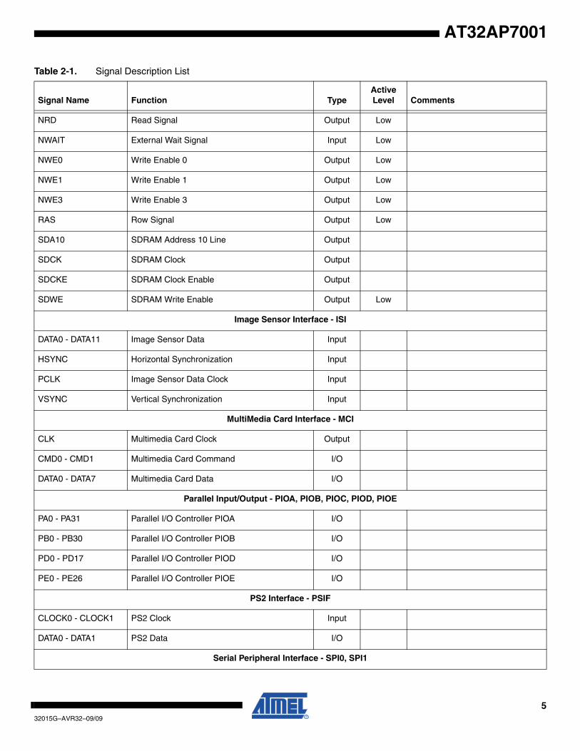
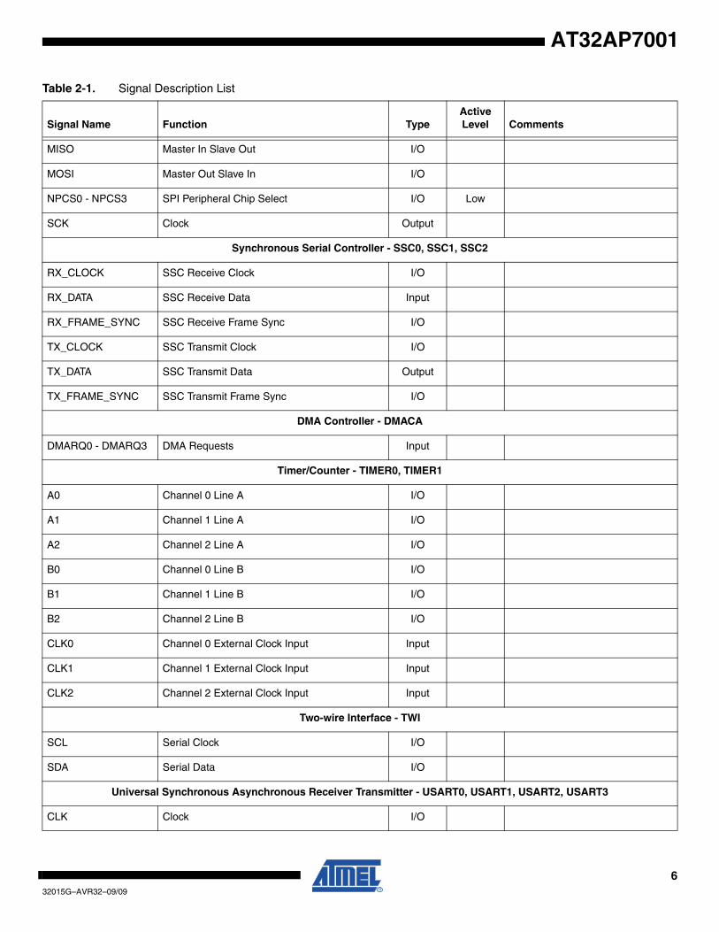
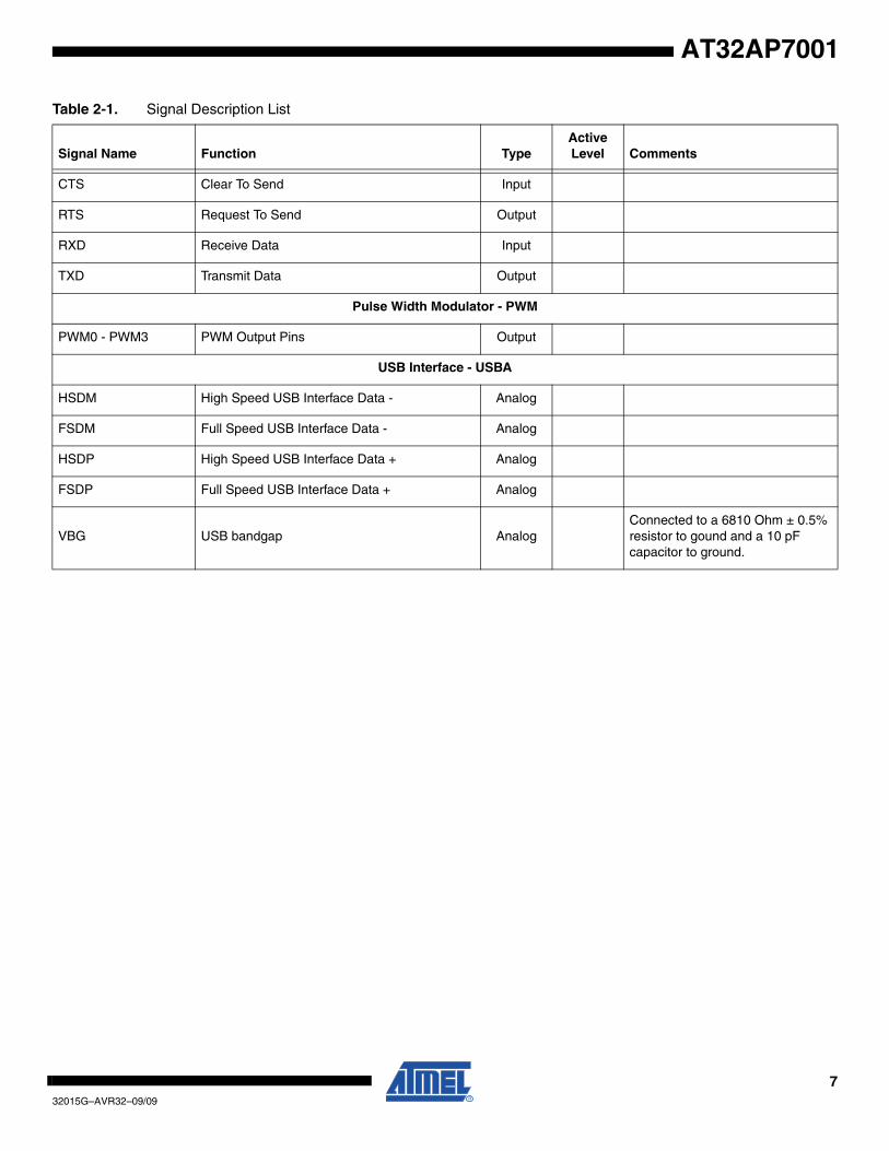
2. Signals Description
The following table gives details on the signal name classified by peripheral. The pinout multi-plexing of these signals is given in the Peripheral Muxing table in the Peripherals chapter.
Table 2-1. Signal Description List
Signal Name Function TypeActive Level Comments
Power
AVDDPLL PLL Power Supply Power 1.65 to 1.95 V
AVDDUSB USB Power Supply Power 1.65 to 1.95 V
AVDDOSC Oscillator Power Supply Power 1.65 to 1.95 V
VDDCORE Core Power Supply Power 1.65 to 1.95 V
VDDIO I/O Power Supply Power 3.0 to 3.6V
AGNDPLL PLL Ground Ground
AGNDUSB USB Ground Ground
AGNDOSC Oscillator Ground Ground
GND Ground Ground
Clocks, Oscillators, and PLL’s
XIN0, XIN1, XIN32 Crystal 0, 1, 32 Input Analog
XOUT0, XOUT1, XOUT32
Crystal 0, 1, 32 Output Analog
PLL0, PLL1 PLL 0,1 Filter Pin Analog
JTAG
TCK Test Clock Input
TDI Test Data In Input
TDO Test Data Out Output
TMS Test Mode Select Input
TRST_N Test Reset Input Low
Auxiliary Port - AUX
MCKO Trace Data Output Clock Output
MDO0 - MDO5 Trace Data Output Output
MSEO0 - MSEO1 Trace Frame Control Output
EVTI_N Event In Input Low
432015G–AVR32–09/09
AT32AP7001
EVTO_N Event Out Output Low
Power Manager - PM
GCLK0 - GCLK4 Generic Clock Pins Output
OSCEN_N Oscillator Enable Input Low
RESET_N Reset Pin Input Low
WAKE_N Wake Pin Input Low
External Interrupt Controller - EIC
EXTINT0 - EXTINT3 External Interrupt Pins Input
NMI_N Non-Maskable Interrupt Pin Input Low
AC97 Controller - AC97C
SCLK AC97 Clock Signal Input
SDI AC97 Receive Signal Output
SDO AC97 Transmit Signal Output
SYNC AC97 Frame Synchronization Signal Input
Audio Bitstream DAC - ABDAC
DATA0 - DATA1 D/A Data Out Output
DATAN0 - DATAN1 D/A Inverted Data Out Output
External Bus Interface - EBI
PX0 - PX53 I/O Controlled by EBI I/O
ADDR0 - ADDR25 Address Bus Output
CAS Column Signal Output Low
CFCE1 Compact Flash 1 Chip Enable Output Low
CFCE2 Compact Flash 2 Chip Enable Output Low
CFRNW Compact Flash Read Not Write Output
DATA0 - DATA31 Data Bus I/O
NANDOE NAND Flash Output Enable Output Low
NANDWE NAND Flash Write Enable Output Low
NCS0 - NCS5 Chip Select Output Low
Table 2-1. Signal Description List
Signal Name Function TypeActive Level Comments
532015G–AVR32–09/09
AT32AP7001
NRD Read Signal Output Low
NWAIT External Wait Signal Input Low
NWE0 Write Enable 0 Output Low
NWE1 Write Enable 1 Output Low
NWE3 Write Enable 3 Output Low
RAS Row Signal Output Low
SDA10 SDRAM Address 10 Line Output
SDCK SDRAM Clock Output
SDCKE SDRAM Clock Enable Output
SDWE SDRAM Write Enable Output Low
Image Sensor Interface - ISI
DATA0 - DATA11 Image Sensor Data Input
HSYNC Horizontal Synchronization Input
PCLK Image Sensor Data Clock Input
VSYNC Vertical Synchronization Input
MultiMedia Card Interface - MCI
CLK Multimedia Card Clock Output
CMD0 - CMD1 Multimedia Card Command I/O
DATA0 - DATA7 Multimedia Card Data I/O
Parallel Input/Output - PIOA, PIOB, PIOC, PIOD, PIOE
PA0 - PA31 Parallel I/O Controller PIOA I/O
PB0 - PB30 Parallel I/O Controller PIOB I/O
PD0 - PD17 Parallel I/O Controller PIOD I/O
PE0 - PE26 Parallel I/O Controller PIOE I/O
PS2 Interface - PSIF
CLOCK0 - CLOCK1 PS2 Clock Input
DATA0 - DATA1 PS2 Data I/O
Serial Peripheral Interface - SPI0, SPI1
Table 2-1. Signal Description List
Signal Name Function TypeActive Level Comments
632015G–AVR32–09/09
AT32AP7001
MISO Master In Slave Out I/O
MOSI Master Out Slave In I/O
NPCS0 - NPCS3 SPI Peripheral Chip Select I/O Low
SCK Clock Output
Synchronous Serial Controller - SSC0, SSC1, SSC2
RX_CLOCK SSC Receive Clock I/O
RX_DATA SSC Receive Data Input
RX_FRAME_SYNC SSC Receive Frame Sync I/O
TX_CLOCK SSC Transmit Clock I/O
TX_DATA SSC Transmit Data Output
TX_FRAME_SYNC SSC Transmit Frame Sync I/O
DMA Controller - DMACA
DMARQ0 - DMARQ3 DMA Requests Input
Timer/Counter - TIMER0, TIMER1
A0 Channel 0 Line A I/O
A1 Channel 1 Line A I/O
A2 Channel 2 Line A I/O
B0 Channel 0 Line B I/O
B1 Channel 1 Line B I/O
B2 Channel 2 Line B I/O
CLK0 Channel 0 External Clock Input Input
CLK1 Channel 1 External Clock Input Input
CLK2 Channel 2 External Clock Input Input
Two-wire Interface - TWI
SCL Serial Clock I/O
SDA Serial Data I/O
Universal Synchronous Asynchronous Receiver Transmitter - USART0, USART1, USART2, USART3
CLK Clock I/O
Table 2-1. Signal Description List
Signal Name Function TypeActive Level Comments
732015G–AVR32–09/09
AT32AP7001
CTS Clear To Send Input
RTS Request To Send Output
RXD Receive Data Input
TXD Transmit Data Output
Pulse Width Modulator - PWM
PWM0 - PWM3 PWM Output Pins Output
USB Interface - USBA
HSDM High Speed USB Interface Data - Analog
FSDM Full Speed USB Interface Data - Analog
HSDP High Speed USB Interface Data + Analog
FSDP Full Speed USB Interface Data + Analog
VBG USB bandgap AnalogConnected to a 6810 Ohm ± 0.5% resistor to gound and a 10 pF capacitor to ground.
Table 2-1. Signal Description List
Signal Name Function TypeActive Level Comments
832015G–AVR32–09/09
AT32AP7001
3. Power Considerations
3.1 Power Supplies
The AT32AP7001 has several types of power supply pins:
• VDDCORE pins: Power the core, memories, and peripherals. Voltage is 1.8V nominal.• VDDIO pins: Power I/O lines. Voltage is 3.3V nominal.• VDDPLL pin: Powers the PLL. Voltage is 1.8V nominal.• VDDUSB pin: Powers the USB. Voltage is 1.8V nominal.• VDDOSC pin: Powers the oscillators. Voltage is 1.8V nominal.
The ground pins GND are common to VDDCORE and VDDIO. The ground pin for VDDPLL isGNDPLL, and the GND pin for VDDOSC is GNDOSC.
See ”Electrical Characteristics” on page 796 for power consumption on the various supply pins.
3.2 Power Supply Connections
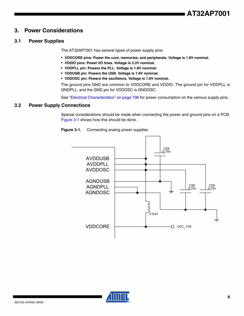
Special considerations should be made when connecting the power and ground pins on a PCB.Figure 3-1 shows how this should be done.
Figure 3-1. Connecting analog power supplies
AVDDUSBAVDDPLLAVDDOSC
AGNDUSBAGNDPLLAGNDOSC
VDDCORE VCC_1V8
3.3uH
C540.10u
C550.10u
C560.10u
932015G–AVR32–09/09
AT32AP7001
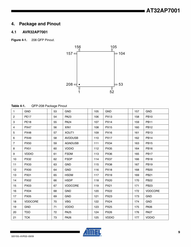
4. Package and Pinout
4.1 AVR32AP7001
Figure 4-1. 208 QFP Pinout.
1 52
53
104
105156
157
208
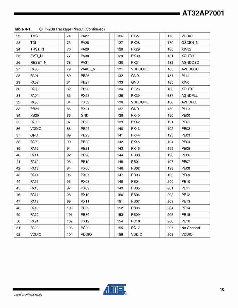
Table 4-1. QFP-208 Package Pinout
1 GND 53 GND 105 GND 157 GND
2 PE17 54 PA23 106 PX13 158 PB10
3 PE18 55 PA24 107 PX14 159 PB11
4 PX47 56 XIN1 108 PX15 160 PB12
5 PX48 57 XOUT1 109 PX16 161 PB13
6 PX49 58 AVDDUSB 110 PX17 162 PB14
7 PX50 59 AGNDUSB 111 PX34 163 PB15
8 PX51 60 VDDIO 112 PX35 164 PB16
9 VDDIO 61 FSDM 113 PX36 165 PB17
10 PX32 62 FSDP 114 PX37 166 PB18
11 PX33 63 GND 115 PX38 167 PB19
12 PX00 64 GND 116 PX18 168 PB20
13 PX01 65 HSDM 117 PX19 169 PB21
14 PX02 66 HSDP 118 PX20 170 PB22
15 PX03 67 VDDCORE 119 PX21 171 PB23
16 PX04 68 GND 120 PX22 172 VDDCORE
17 PX05 69 GND 121 PX23 173 GND
18 VDDCORE 70 VBG 122 PX24 174 GND
19 GND 71 VDDIO 123 PX25 175 PA06
20 TDO 72 PA25 124 PX26 176 PA07
21 TCK 73 PA26 125 VDDIO 177 VDDIO
1032015G–AVR32–09/09
AT32AP7001
22 TMS 74 PA27 126 PX27 178 VDDIO
23 TDI 75 PA28 127 PX28 179 OSCEN_N
24 TRST_N 76 PA29 128 PX29 180 XIN32
25 EVTI_N 77 PA30 129 PX30 181 XOUT32
26 RESET_N 78 PA31 130 PX31 182 AGNDOSC
27 PA00 79 WAKE_N 131 VDDCORE 183 AVDDOSC
28 PA01 80 PB26 132 GND 184 PLL1
29 PA02 81 PB27 133 GND 185 XIN0
30 PA03 82 PB28 134 PE26 186 XOUT0
31 PA04 83 PX53 135 PX39 187 AGNDPLL
32 PA05 84 PX52 136 VDDCORE 188 AVDDPLL
33 PB24 85 PX41 137 GND 189 PLL0
34 PB25 86 GND 138 PX40 190 PE00
35 PA08 87 PE25 139 PX42 191 PE01
36 VDDIO 88 PE24 140 PX43 192 PE02
37 GND 89 PE23 141 PX44 193 PE03
38 PA09 90 PE22 142 PX45 194 PE04
39 PA10 91 PE21 143 PX46 195 PE05
40 PA11 92 PE20 144 PB00 196 PE06
41 PA12 93 PE19 145 PB01 197 PE07
42 PA13 94 PX06 146 PB02 198 PE08
43 PA14 95 PX07 147 PB03 199 PE09
44 PA15 96 PX08 148 PB04 200 PE10
45 PA16 97 PX09 149 PB05 201 PE11
46 PA17 98 PX10 150 PB06 202 PE12
47 PA18 99 PX11 151 PB07 203 PE13
48 PA19 100 PB29 152 PB08 204 PE14
49 PA20 101 PB30 153 PB09 205 PE15
50 PA21 102 PX12 154 PC16 206 PE16
51 PA22 103 PC00 155 PC17 207 No Connect
52 VDDIO 104 VDDIO 156 VDDIO 208 VDDIO
Table 4-1. QFP-208 Package Pinout (Continued)
1132015G–AVR32–09/09
AT32AP7001
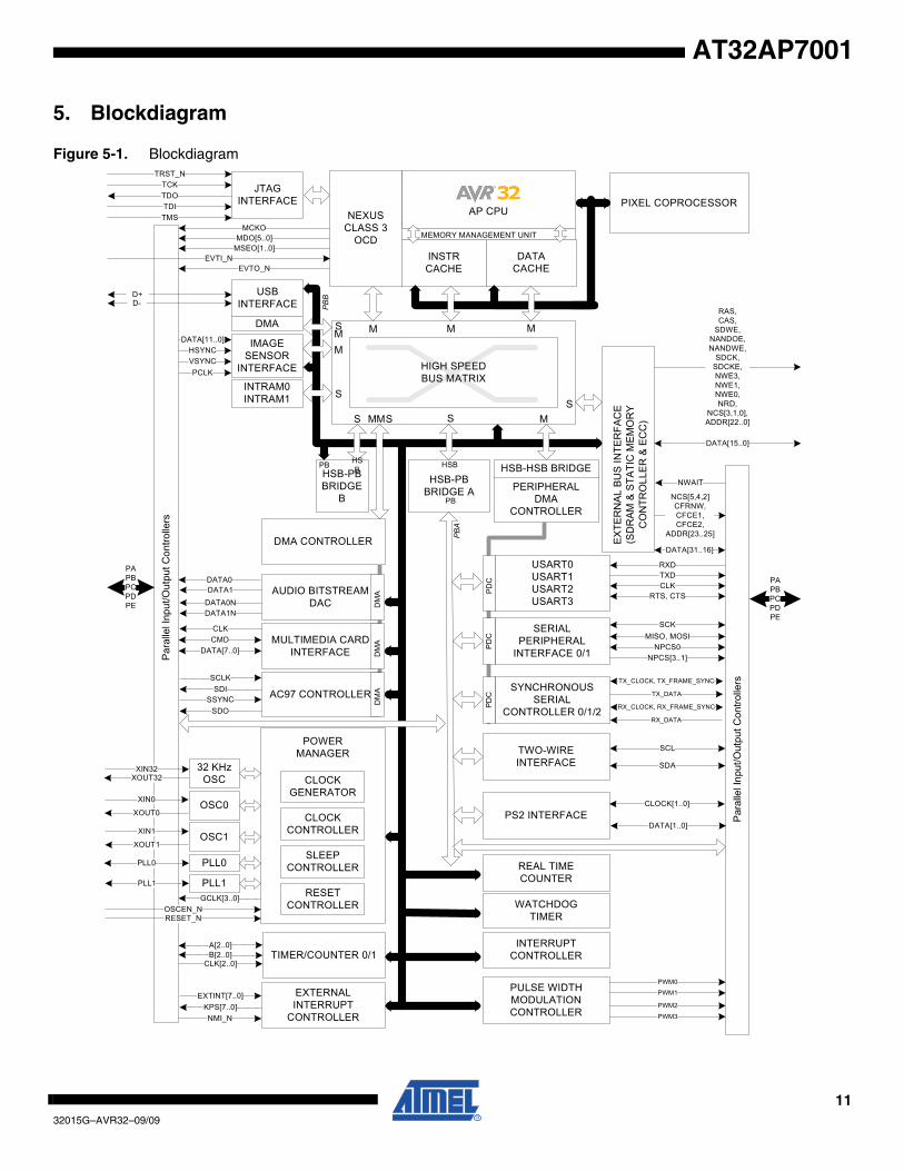
5. Blockdiagram
Figure 5-1. Blockdiagram
DATA[11..0]HSYNCVSYNCPCLK
AP CPUNEXUS CLASS 3
OCDINSTRCACHE
DATACACHE
TIMER/COUNTER 0/1INTERRUPT
CONTROLLER
REAL TIMECOUNTER
PERIPHERALDMA
CONTROLLER
INTRAM0INTRAM1
HSB-PB BRIDGE
B
HSB-PB BRIDGE A
S
M M M
S
SS
M
EXTERNAL INTERRUPT
CONTROLLER
HIGH SPEEDBUS MATRIX
Para
llel I
nput
/Out
put C
ontro
llers
PIXEL COPROCESSOR
Par
alle
l Inp
ut/O
utpu
t Con
trolle
rs
RESET_N
PAPBPCPDPE
A[2..0]B[2..0]
CLK[2..0]
EXTINT[7..0]KPS[7..0]NMI_N
GCLK[3..0]
XIN32XOUT32
XIN0
XOUT0
PAPBPCPDPE
EXTE
RN
AL B
US
INTE
RFA
CE
(SD
RAM
& S
TATI
C M
EMO
RY
CO
NTR
OLL
ER &
EC
C)
RAS, CAS,
SDWE,NANDOE,NANDWE,
SDCK,SDCKE,NWE3,NWE1,NWE0,NRD,
NCS[3,1,0],ADDR[22..0]
NCS[5,4,2]CFRNW,CFCE1,CFCE2,
ADDR[23..25]
NWAIT
DATA[15..0]
USB INTERFACE
DMA
D-D+
32 KHzOSC
OSC0
PLL0
PS2 INTERFACE
SERIAL PERIPHERAL
INTERFACE 0/1
TWO-WIREINTERFACE
PDC MISO, MOSI
NPCS[3..1]
SCL
SDA
USART0USART1USART2USART3
PDC
RXDTXDCLK
RTS, CTS
SYNCHRONOUSSERIAL
CONTROLLER 0/1/2
PDC
TX_CLOCK, TX_FRAME_SYNC
RX_DATA
TX_DATA
RX_CLOCK, RX_FRAME_SYNC
WATCHDOGTIMER
XIN1
XOUT1OSC1
PLL1
SCK
JTAGINTERFACE
MCKOMDO[5..0]
MSEO[1..0]EVTI_N
EVTO_N
TCKTDOTDITMS
POWER MANAGER
RESETCONTROLLER
SLEEPCONTROLLER
CLOCKCONTROLLER
CLOCKGENERATOR
CONFIGURATION REGISTERS BUS
MEMORY MANAGEMENT UNIT
PB
PB
HSBHSB
PBA
PBB
NPCS0
MS
CLOCK[1..0]
DATA[1..0]
HSB-HSB BRIDGE
TRST_N
DATA[31..16]
OSCEN_N
PLL0
PLL1
DMA CONTROLLER
SMM
AUDIO BITSTREAM DAC D
MA
MULTIMEDIA CARD INTERFACE D
MA
AC97 CONTROLLER
DM
A
SCLKSDI
SSYNCSDO
CLKCMD
DATA[7..0]
DATA0DATA1
DATA0NDATA1N
PULSE WIDTH MODULATION CONTROLLER
PWM0
PWM1
PWM2
PWM3
IMAGE SENSOR
INTERFACE
M
1232015G–AVR32–09/09
AT32AP7001
5.0.1 AVR32AP CPU
• 32-bit load/store AVR32B RISC architecture.– Up to 15 general-purpose 32-bit registers.– 32-bit Stack Pointer, Program Counter and Link Register reside in register file.– Fully orthogonal instruction set.– Privileged and unprivileged modes enabling efficient and secure Operating Systems.– Innovative instruction set together with variable instruction length ensuring industry leading
code density.– DSP extention with saturating arithmetic, and a wide variety of multiply instructions.– SIMD extention for media applications.
• 7 stage pipeline allows one instruction per clock cycle for most instructions.– Java Hardware Acceleration.– Byte, half-word, word and double word memory access.– Unaligned memory access.– Shadowed interrupt context for INT3 and multiple interrupt priority levels.– Dynamic branch prediction and return address stack for fast change-of-flow.– Coprocessor interface.
• Full MMU allows for operating systems with memory protection.• 16Kbyte Instruction and 16Kbyte data caches.
– Virtually indexed, physically tagged.– 4-way associative.– Write-through or write-back.
• Nexus Class 3 On-Chip Debug system.– Low-cost NanoTrace supported.
5.0.2 Pixel Coprocessor (PICO)
• Coprocessor coupled to the AVR32 CPU Core through the TCB Bus.– Coprocessor number one on the TCB bus.
• Three parallel Vector Multiplication Units (VMU) where each unit can:– Multiply three pixel components with three coefficients.– Add the products from the multiplications together.– Accumulate the result or add an offset to the sum of the products.
• Can be used for accelerating:– Image Color Space Conversion.
• Configurable Conversion Coefficients.• Supports packed and planar input and output formats.• Supports subsampled input color spaces (i.e 4:2:2, 4:2:0).
– Image filtering/scaling.• Configurable Filter Coefficients.• Throughput of one sample per cycle for a 9-tap FIR filter.• Can use the built-in accumulator to extend the FIR filter to more than 9-taps.• Can be used for bilinear/bicubic interpolations.
– MPEG-4/H.264 Quarter Pixel Motion Compensation.• Flexible input Pixel Selector.
– Can operate on numerous different image storage formats.• Flexible Output Pixel Inserter.
– Scales and saturates the results back to 8-bit pixel values.– Supports packed and planar output formats.
1332015G–AVR32–09/09
AT32AP7001
• Configurable coefficients with flexible fixed-point representation.
5.0.3 Debug and Test system
• IEEE1149.1 compliant JTAG and boundary scan• Direct memory access and programming capabilities through JTAG interface• Extensive On-Chip Debug features in compliance with IEEE-ISTO 5001-2003 (Nexus 2.0) Class 3• Auxiliary port for high-speed trace information• Hardware support for 6 Program and 2 data breakpoints• Unlimited number of software breakpoints supported• Advanced Program, Data, Ownership, and Watchpoint trace supported
5.0.4 DMA Controller
• 2 HSB Master Interfaces• 3 Channels• Software and Hardware Handshaking Interfaces
– 11 Hardware Handshaking Interfaces• Memory/Non-Memory Peripherals to Memory/Non-Memory Peripherals Transfer• Single-block DMA Transfer• Multi-block DMA Transfer
– Linked Lists– Auto-Reloading– Contiguous Blocks
• DMA Controller is Always the Flow Controller• Additional Features
– Scatter and Gather Operations– Channel Locking
– Bus Locking– FIFO Mode– Pseudo Fly-by Operation
5.0.5 Peripheral DMA Controller
• Transfers from/to peripheral to/from any memory space without intervention of the processor.• Next Pointer Support, forbids strong real-time constraints on buffer management.• Eighteen channels
– Two for each USART– Two for each Serial Synchronous Controller– Two for each Serial Peripheral Interface
5.0.6 Bus system
• HSB bus matrix with 10 Masters and 8 Slaves handled– Handles Requests from the CPU Icache, CPU Dcache, HSB bridge, HISI, USB 2.0 Controller,
DMA Controller 0, DMA Controller 1, and to internal SRAM 0, internal SRAM 1, PB A, PB B, EBI and, USB.
1432015G–AVR32–09/09
AT32AP7001
– Round-Robin Arbitration (three modes supported: no default master, last accessed default master, fixed default master)
– Burst Breaking with Slot Cycle Limit– One Address Decoder Provided per Master
• 2 Peripheral buses allowing each bus to run on different bus speeds.– PB A intended to run on low clock speeds, with peripherals connected to the PDC.– PB B intended to run on higher clock speeds, with peripherals connected to the DMACA.
• HSB-HSB Bridge providing a low-speed HSB bus running at the same speed as PBA– Allows PDC transfers between a low-speed PB bus and a bus matrix of higher clock speeds
An overview of the bus system is given in Figure 4-1 on page 1. All modules connected to thesame bus use the same clock, but the clock to each module can be individually shut off by thePower Manager. The figure identifies the number of master and slave interfaces of each moduleconnected to the HSB bus, and which DMA controller is connected to which peripheral.

1532015G–AVR32–09/09
AT32AP7001
6. I/O Line Considerations
6.1 JTAG pins
The TMS, TDI and TCK pins have pull-up resistors. TDO is an output, driven at up to VDDIO,and have no pull-up resistor. The TRST_N pin is used to initialize the embedded JTAG TAPController when asserted at a low level. It is a schmitt input and integrates permanent pull-upresistor to VDDIO, so that it can be left unconnected for normal operations.
6.2 WAKE_N pin
The WAKE_N pin is a schmitt trigger input integrating a permanent pull-up resistor to VDDIO.
6.3 RESET_N pin
The RESET_N pin is a schmitt input and integrates a permanent pull-up resistor to VDDIO. Asthe product integrates a power-on reset cell, the RESET_N pin can be left unconnected in caseno reset from the system needs to be applied to the product.
6.4 EVTI_N pin
The EVTI_N pin is a schmitt input and integrates a non-programmable pull-up resistor to VDDIO.
6.5 TWI pins
When these pins are used for TWI, the pins are open-drain outputs with slew-rate limitation andinputs with inputs with spike-filtering. When used as GPIO-pins or used for other peripherals, thepins have the same characteristics as PIO pins.
6.6 PIO pins
All the I/O lines integrate a programmable pull-up resistor. Programming of this pull-up resistor isperformed independently for each I/O line through the PIO Controllers. After reset, I/O linesdefault as inputs with pull-up resistors enabled, except when indicated otherwise in the column“Reset State” of the PIO Controller multiplexing tables.
1632015G–AVR32–09/09
AT32AP7001
7. AVR32 AP CPU
Rev.: 1.0.0.0
This chapter gives an overview of the AVR32 AP CPU. AVR32 AP is an implementation of theAVR32 architecture. A summary of the programming model, instruction set, caches and MMU ispresented. For further details, see the AVR32 Architecture Manual and the AVR32 AP TechnicalReference Manual.
7.1 AVR32 ArchitectureAVR32 is a new, high-performance 32-bit RISC microprocessor architecture, designed for cost-sensitive embedded applications, with particular emphasis on low power consumption and highcode density. In addition, the instruction set architecture has been tuned to allow a variety ofmicroarchitectures, enabling the AVR32 to be implemented as low-, mid- or high-performanceprocessors. AVR32 extends the AVR family into the world of 32- and 64-bit applications.
Through a quantitative approach, a large set of industry recognized benchmarks has been com-piled and analyzed to achieve the best code density in its class. In addition to lowering thememory requirements, a compact code size also contributes to the core’s low power characteris-tics. The processor supports byte and half-word data types without penalty in code size andperformance.
Memory load and store operations are provided for byte, half-word, word and double word datawith automatic sign- or zero extension of half-word and byte data.
In order to reduce code size to a minimum, some instructions have multiple addressing modes.As an example, instructions with immediates often have a compact format with a smaller imme-diate, and an extended format with a larger immediate. In this way, the compiler is able to usethe format giving the smallest code size.
Another feature of the instruction set is that frequently used instructions, like add, have a com-pact format with two operands as well as an extended format with three operands. The largerformat increases performance, allowing an addition and a data move in the same instruction in asingle cycle. Load and store instructions have several different formats in order to reduce codesize and speed up execution.
The register file is organized as sixteen 32-bit registers and includes the Program Counter, theLink Register, and the Stack Pointer. In addition, register R12 is designed to hold return valuesfrom function calls and is used implicitly by some instructions.
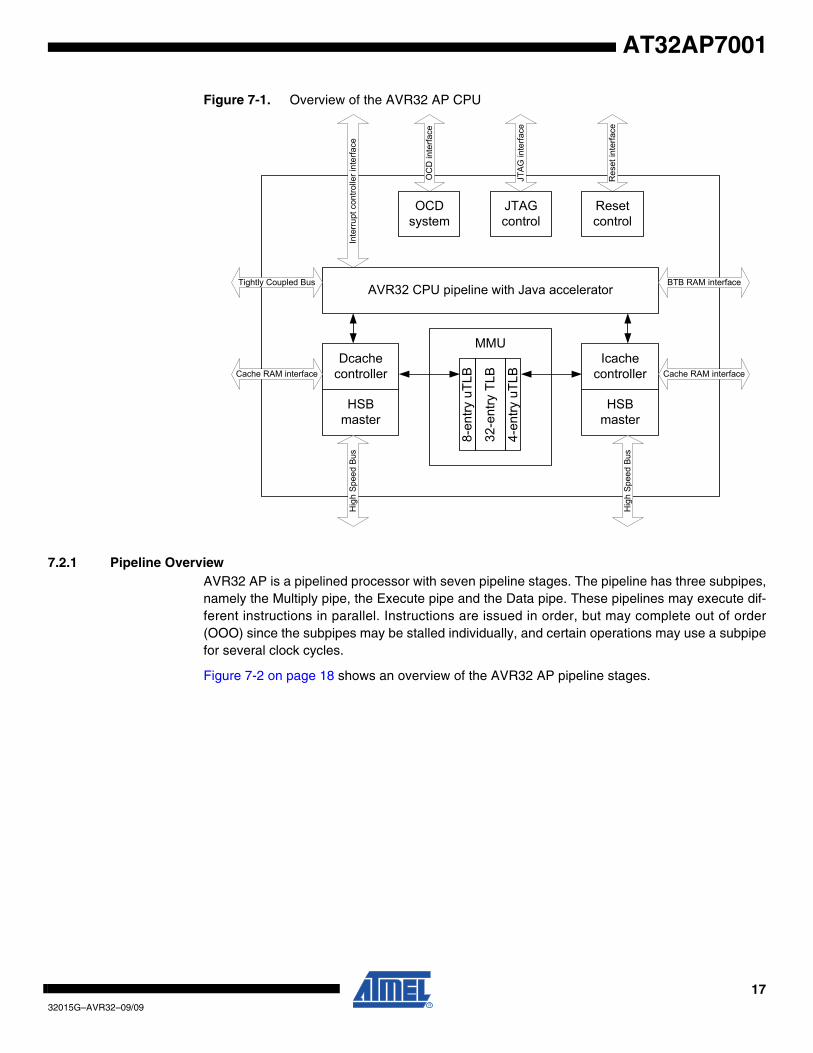
7.2 The AVR32 AP CPUAVR32 AP targets high-performance applications, and provides an advanced OCD system, effi-cient data and instruction caches, and a full MMU. Figure 7-1 on page 17 displays the contentsof AVR32 AP.
1732015G–AVR32–09/09
AT32AP7001
Figure 7-1. Overview of the AVR32 AP CPU
7.2.1 Pipeline OverviewAVR32 AP is a pipelined processor with seven pipeline stages. The pipeline has three subpipes,namely the Multiply pipe, the Execute pipe and the Data pipe. These pipelines may execute dif-ferent instructions in parallel. Instructions are issued in order, but may complete out of order(OOO) since the subpipes may be stalled individually, and certain operations may use a subpipefor several clock cycles.
Figure 7-2 on page 18 shows an overview of the AVR32 AP pipeline stages.
AVR32 CPU pipeline with Java accelerator
Dcache controller
HSB master
Icache controller
HSB master
32-e
ntry
TLB
8-en
try u
TLB
4-en
try u
TLB
MMUH
igh
Spee
d Bu
s
Hig
h Sp
eed
Bus
Cache RAM interfaceCache RAM interface
BTB RAM interfaceTightly Coupled Bus
OCD system
OC
D in
terfa
ce
Reset control
Res
et in
terfa
ce
Inte
rrupt
con
trolle
r int
erfa
ce
JTAG control
JTA
G in
terfa
ce
1832015G–AVR32–09/09
AT32AP7001
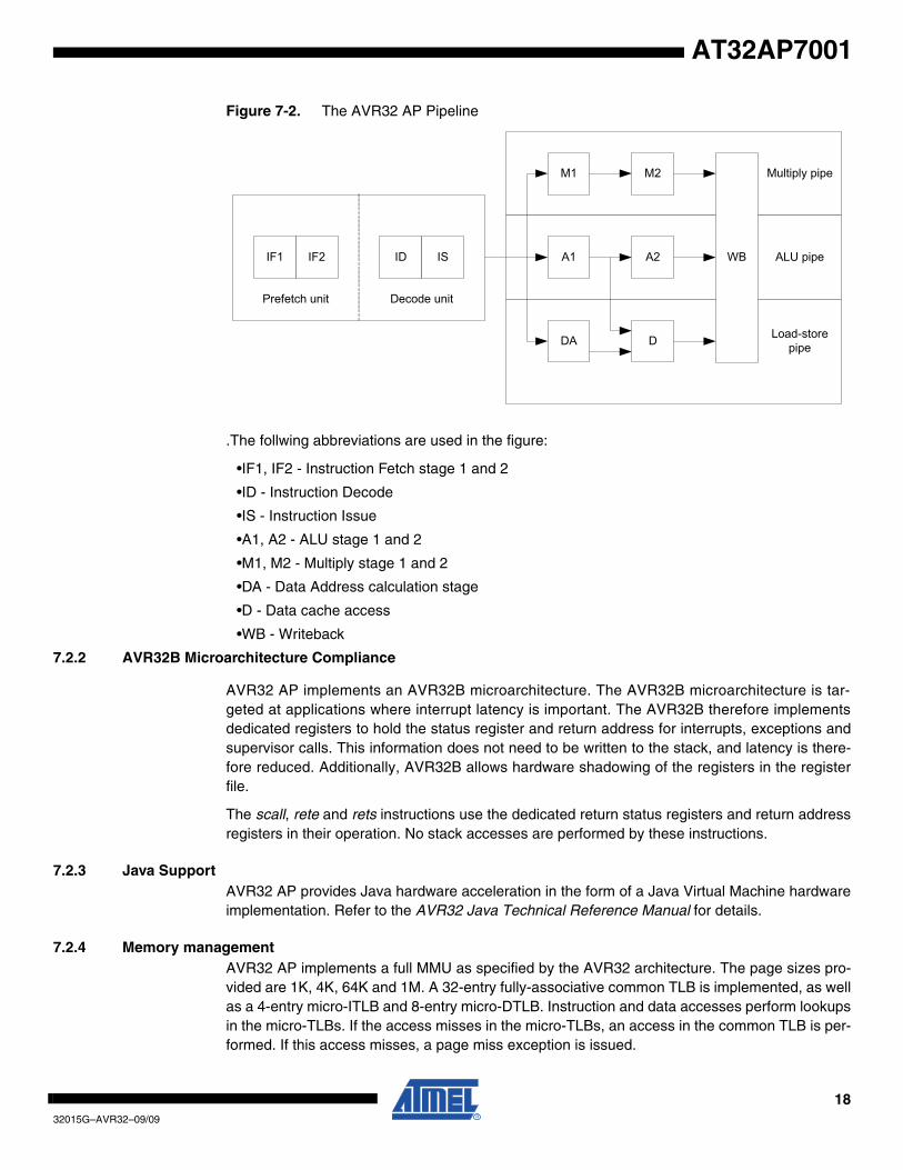
Figure 7-2. The AVR32 AP Pipeline
.The follwing abbreviations are used in the figure:
•IF1, IF2 - Instruction Fetch stage 1 and 2
•ID - Instruction Decode
•IS - Instruction Issue
•A1, A2 - ALU stage 1 and 2
•M1, M2 - Multiply stage 1 and 2
•DA - Data Address calculation stage
•D - Data cache access
•WB - Writeback
7.2.2 AVR32B Microarchitecture Compliance
AVR32 AP implements an AVR32B microarchitecture. The AVR32B microarchitecture is tar-geted at applications where interrupt latency is important. The AVR32B therefore implementsdedicated registers to hold the status register and return address for interrupts, exceptions andsupervisor calls. This information does not need to be written to the stack, and latency is there-fore reduced. Additionally, AVR32B allows hardware shadowing of the registers in the registerfile.
The scall, rete and rets instructions use the dedicated return status registers and return addressregisters in their operation. No stack accesses are performed by these instructions.
7.2.3 Java SupportAVR32 AP provides Java hardware acceleration in the form of a Java Virtual Machine hardwareimplementation. Refer to the AVR32 Java Technical Reference Manual for details.
7.2.4 Memory managementAVR32 AP implements a full MMU as specified by the AVR32 architecture. The page sizes pro-vided are 1K, 4K, 64K and 1M. A 32-entry fully-associative common TLB is implemented, as wellas a 4-entry micro-ITLB and 8-entry micro-DTLB. Instruction and data accesses perform lookupsin the micro-TLBs. If the access misses in the micro-TLBs, an access in the common TLB is per-formed. If this access misses, a page miss exception is issued.
IF2 ID IS A1
M1 M2
D
WB
Prefetch unit Decode unit
ALU pipe
Multiply pipe
Load-store pipeDA
A2IF1
1932015G–AVR32–09/09
AT32AP7001
7.2.5 Caches and write bufferAVR32 AP implements 16K data and 16K instruction caches. The caches are 4-way set asso-ciative. Each cache has a 32-bit System Bus master interface connecting it to the bus. Theinstruction cache has a 32-bit interface to the fetch pipeline stage, and the data cache has a 64-bit interface to the load-store pipeline. The caches use a least recently used allocate-on-read-miss replacement policy. The caches are virtually tagged, physically indexed, avoiding the needto flush them on task switch.
The caches provide locking on a per-line basis, allowing code and data to be permanentlylocked in the caches for timing-critical code. The data cache also allows prefetching of datausing the pref instruction.
Accesses to the instruction and data caches are tagged as cacheable or uncacheable on a per-page basis by the MMU. Data cache writes are tagged as write-through or writeback on a per-page basis by the MMU.
The data cache has a 32-byte combining write buffer, to avoid stalling the CPU when writing toexternal memory. Writes are tagged as bufferable or unbufferable on a per-page basis by theMMU. Bufferable writes to sequential addresses are placed in the buffer, allowing for example asequence of byte writes from the CPU to be combined into word transfers on the bus. A syncinstruction is provided to explicitly flush the write buffer.
7.2.6 Unaligned reference handlingAVR32 AP has hardware support for performing unaligned memory accesses. This will reducethe memory footprint needed by some applications, as well as speed up other applications oper-ating on unaligned data.
AVR32 AP is able to perform certain word-sized load and store instructions of any alignment,and word-aligned st.d and ld.d. Any other unaligned memory access will cause an MMU addressexception. All coprocessor memory access instructions require word-aligned pointers. Double-word-sized accesses with word-aligned pointers will automatically be performed as two word-sized accesses.
The following table shows the instructions with support for unaligned addresses. All otherinstructions require aligned addresses. Accessing an unaligned address may require severalclock cycles, refer to the AVR32 AP Technical Reference Manual for details.
Table 7-1. Instructions with unaligned reference support
Instruction Supported alignment
ld.w Any
st.w Any
lddsp Any
lddpc Any
stdsp Any
ld.d Word
st.d Word
All coprocessor memory access instruction Word
2032015G–AVR32–09/09
AT32AP7001
7.2.7 Unimplemented instructionsThe following instructions are unimplemented in AVR32 AP, and will cause an UnimplementedInstruction Exception if executed:
•mems
•memc
•memt
7.2.8 Exceptions and InterruptsAVR32 AP incorporates a powerful exception handling scheme. The different exceptionsources, like Illegal Op-code and external interrupt requests, have different priority levels, ensur-ing a well-defined behavior when multiple exceptions are received simultaneously. Additionally,pending exceptions of a higher priority class may preempt handling of ongoing exceptions of alower priority class. Each priority class has dedicated registers to keep the return address andstatus register thereby removing the need to perform time-consuming memory operations tosave this information.
There are four levels of external interrupt requests, all executing in their own context. The INT3context provides dedicated shadow registers ensuring low latency for these interrupts. An inter-rupt controller does the priority handling of the external interrupts and provides the autovectoroffset to the CPU.
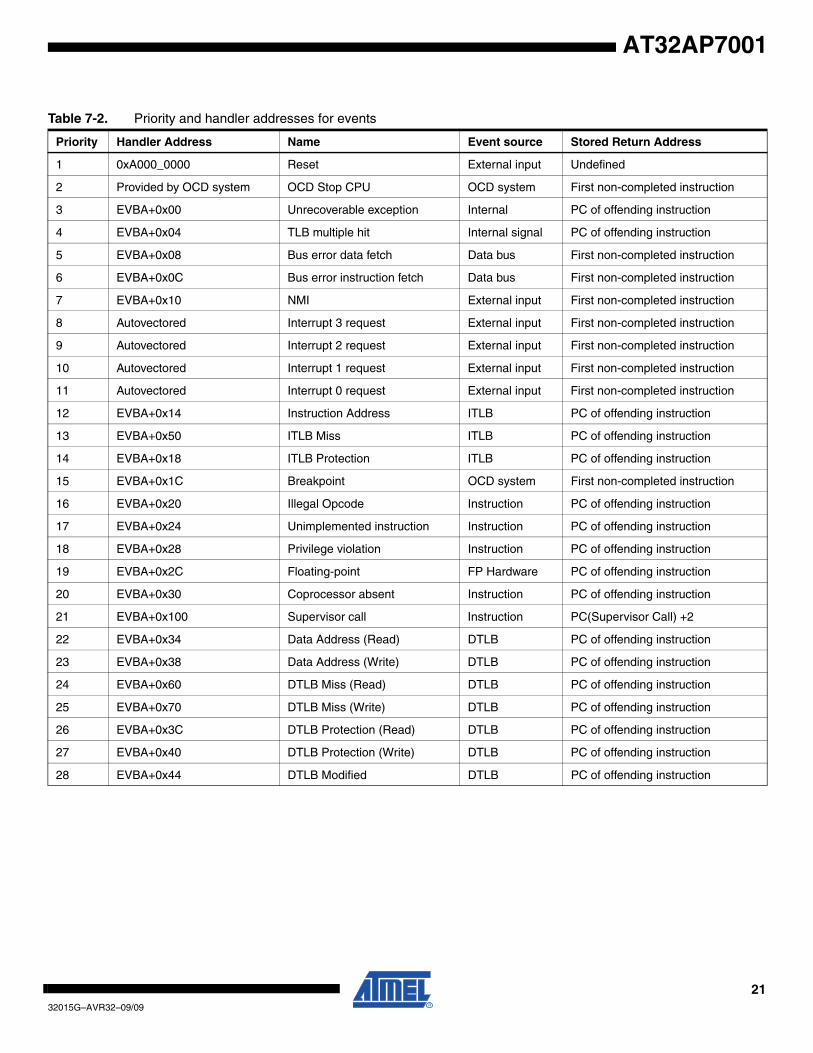
The addresses and priority of simultaneous events are shown in Table 7-2 on page 21.
2132015G–AVR32–09/09
AT32AP7001
Table 7-2. Priority and handler addresses for events
Priority Handler Address Name Event source Stored Return Address
1 0xA000_0000 Reset External input Undefined
2 Provided by OCD system OCD Stop CPU OCD system First non-completed instruction
3 EVBA+0x00 Unrecoverable exception Internal PC of offending instruction
4 EVBA+0x04 TLB multiple hit Internal signal PC of offending instruction
5 EVBA+0x08 Bus error data fetch Data bus First non-completed instruction
6 EVBA+0x0C Bus error instruction fetch Data bus First non-completed instruction
7 EVBA+0x10 NMI External input First non-completed instruction
8 Autovectored Interrupt 3 request External input First non-completed instruction
9 Autovectored Interrupt 2 request External input First non-completed instruction
10 Autovectored Interrupt 1 request External input First non-completed instruction
11 Autovectored Interrupt 0 request External input First non-completed instruction
12 EVBA+0x14 Instruction Address ITLB PC of offending instruction
13 EVBA+0x50 ITLB Miss ITLB PC of offending instruction
14 EVBA+0x18 ITLB Protection ITLB PC of offending instruction
15 EVBA+0x1C Breakpoint OCD system First non-completed instruction
16 EVBA+0x20 Illegal Opcode Instruction PC of offending instruction
17 EVBA+0x24 Unimplemented instruction Instruction PC of offending instruction
18 EVBA+0x28 Privilege violation Instruction PC of offending instruction
19 EVBA+0x2C Floating-point FP Hardware PC of offending instruction
20 EVBA+0x30 Coprocessor absent Instruction PC of offending instruction
21 EVBA+0x100 Supervisor call Instruction PC(Supervisor Call) +2
22 EVBA+0x34 Data Address (Read) DTLB PC of offending instruction
23 EVBA+0x38 Data Address (Write) DTLB PC of offending instruction
24 EVBA+0x60 DTLB Miss (Read) DTLB PC of offending instruction
25 EVBA+0x70 DTLB Miss (Write) DTLB PC of offending instruction
26 EVBA+0x3C DTLB Protection (Read) DTLB PC of offending instruction
27 EVBA+0x40 DTLB Protection (Write) DTLB PC of offending instruction
28 EVBA+0x44 DTLB Modified DTLB PC of offending instruction
2232015G–AVR32–09/09
AT32AP7001
7.3 Programming Model
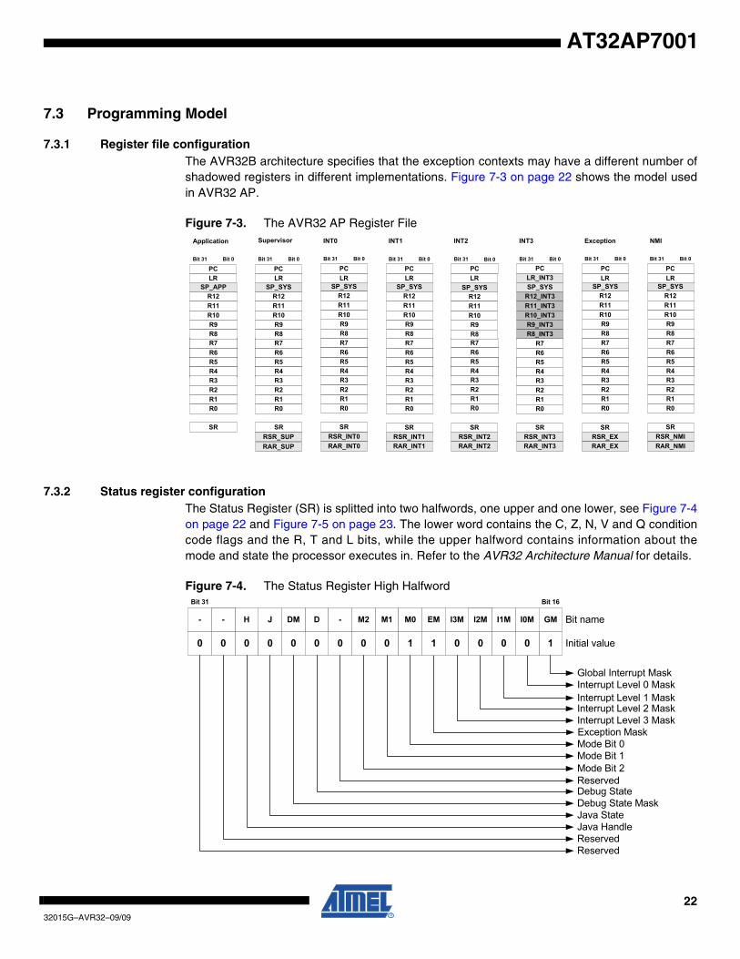
7.3.1 Register file configurationThe AVR32B architecture specifies that the exception contexts may have a different number ofshadowed registers in different implementations. Figure 7-3 on page 22 shows the model usedin AVR32 AP.
Figure 7-3. The AVR32 AP Register File
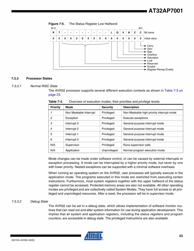
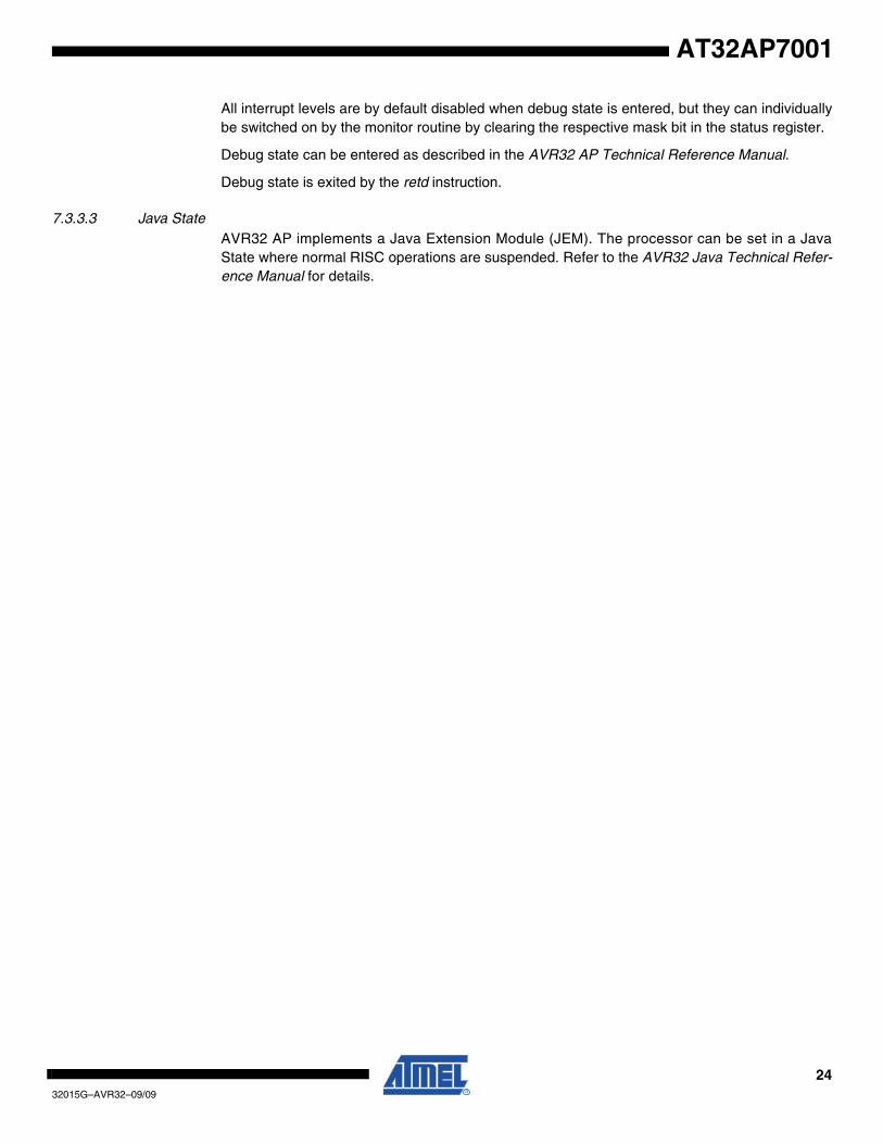
7.3.2 Status register configurationThe Status Register (SR) is splitted into two halfwords, one upper and one lower, see Figure 7-4on page 22 and Figure 7-5 on page 23. The lower word contains the C, Z, N, V and Q conditioncode flags and the R, T and L bits, while the upper halfword contains information about themode and state the processor executes in. Refer to the AVR32 Architecture Manual for details.
Figure 7-4. The Status Register High Halfword
Application
Bit 0
Supervisor
Bit 31
PC
SR
INT0PC
FINTPCINT1PC
SMPC
R7
R5R6
R4R3
R1R2
R0
Bit 0Bit 31
PC
SR
R12
INT0PC
FINTPCINT1PC
SMPC
R7
R5R6
R4
R11
R9R10
R8
R3
R1R2
R0
RSR_INT0SR
RSR_EXSR
SP_APP SP_SYS
RSR_NMISR
R12R11
R9R10
R8
Bit 0Bit 31
PC
INT0PC
FINTPCINT1PC
SMPC
R7
R5R6
R4R3
R1R2
R0
Bit 0Bit 31
PC
FINTPCSMPC
R7
R5R6
R4R3
R1R2
R0
Bit 0Bit 31
PCLR_INT3
R12_INT3R11_INT3
R9_INT3R10_INT3
R8_INT3
SP_SYS SP_SYS SP_SYSR12R11
R9R10
R8
Bit 0Bit 31
PC
INT0PC
FINTPCINT1PC
SMPC
R7
R5R6
R4R3
R1R2
R0
SP_SYSR12R11
R9R10
R8
Bit 0Bit 31
PC
INT0PC
FINTPCINT1PC
SMPC
R7
R5R6
R4R3
R1R2
R0
SP_SYSR12R11
R9R10
R8
Bit 0Bit 31
PC
INT0PC
FINTPCINT1PC
SMPC
R7
R5R6
R4R3
R1R2
R0
SP_SYSR12R11
R9R10
R8
RSR_INT1SR
RSR_INT2SR
RSR_INT3SR
INT0 INT1 INT2 INT3 Exception NMI
FINTPCSMPC
R7
R5R6
R4R3
R1R2
R0
R12R11
R9R10
R8
LR LR LR LR LR LR LR
RSR_SUPRAR_INT0 RAR_EX RAR_NMIRAR_INT1 RAR_INT2 RAR_INT3RAR_SUP
Bit 31
0 0 0
Bit 16
Interrupt Level 0 MaskInterrupt Level 1 Mask
Interrupt Level 3 MaskInterrupt Level 2 Mask
10 0 0 0 1 1 0 0 0 00 0
Reserved
FE I0M GMM1J D M0 EM I2MDM - M2LC1-
Initial value
Bit nameI1M
Mode Bit 0Mode Bit 1
H
Mode Bit 2ReservedDebug State
- I3M
Java State
Exception Mask
Global Interrupt Mask
Debug State Mask
Java HandleReserved
2332015G–AVR32–09/09
AT32AP7001
Figure 7-5. The Status Register Low Halfword
7.3.3 Processor States
7.3.3.1 Normal RISC StateThe AVR32 processor supports several different execution contexts as shown in Table 7-3 onpage 23.
Mode changes can be made under software control, or can be caused by external interrupts orexception processing. A mode can be interrupted by a higher priority mode, but never by onewith lower priority. Nested exceptions can be supported with a minimal software overhead.
When running an operating system on the AVR32, user processes will typically execute in theapplication mode. The programs executed in this mode are restricted from executing certaininstructions. Furthermore, most system registers together with the upper halfword of the statusregister cannot be accessed. Protected memory areas are also not available. All other operatingmodes are privileged and are collectively called System Modes. They have full access to all priv-ileged and unprivileged resources. After a reset, the processor will be in supervisor mode.
7.3.3.2 Debug StateThe AVR32 can be set in a debug state, which allows implementation of software monitor rou-tines that can read out and alter system information for use during application development. Thisimplies that all system and application registers, including the status registers and programcounters, are accessible in debug state. The privileged instructions are also available.
Bit 15 Bit 0
Reserved
CarryZeroSign
0 0 0 00000000000
- - --TR Bit name
Initial value0 0
L Q V N Z C-
OverflowSaturation
- - -
Lock
Register Remap EnableScratch
Table 7-3. Overview of execution modes, their priorities and privilege levels.
Priority Mode Security Description
1 Non Maskable Interrupt Privileged Non Maskable high priority interrupt mode
2 Exception Privileged Execute exceptions
3 Interrupt 3 Privileged General purpose interrupt mode
4 Interrupt 2 Privileged General purpose interrupt mode
5 Interrupt 1 Privileged General purpose interrupt mode
6 Interrupt 0 Privileged General purpose interrupt mode
N/A Supervisor Privileged Runs supervisor calls
N/A Application Unprivileged Normal program execution mode
2432015G–AVR32–09/09
AT32AP7001
All interrupt levels are by default disabled when debug state is entered, but they can individuallybe switched on by the monitor routine by clearing the respective mask bit in the status register.
Debug state can be entered as described in the AVR32 AP Technical Reference Manual.
Debug state is exited by the retd instruction.
7.3.3.3 Java StateAVR32 AP implements a Java Extension Module (JEM). The processor can be set in a JavaState where normal RISC operations are suspended. Refer to the AVR32 Java Technical Refer-ence Manual for details.

2532015G–AVR32–09/09
AT32AP7001
8. Pixel Coprocessor (PICO)
Rev.: 1.0.0.0
8.1 Features
• Coprocessor coupled to the AVR32 CPU Core through the TCB Bus.• Three parallel Vector Multiplication Units (VMU) where each unit can:
– Multiply three pixel components with three coefficients.– Add the products from the multiplications together.– Accumulate the result or add an offset to the sum of the products.
• Can be used for accelerating:– Image Color Space Conversion.
• Configurable Conversion Coefficients.• Supports packed and planar input and output formats.• Supports subsampled input color spaces (i.e 4:2:2, 4:2:0).
– Image filtering/scaling.• Configurable Filter Coefficients.• Throughput of one sample per cycle for a 9-tap FIR filter.• Can use the built-in accumulator to extend the FIR filter to more than 9-taps.• Can be used for bilinear/bicubic interpolations.
– MPEG-4/H.264 Quarter Pixel Motion Compensation.• Flexible input Pixel Selector.
– Can operate on numerous different image storage formats.• Flexible Output Pixel Inserter.
– Scales and saturates the results back to 8-bit pixel values.– Supports packed and planar output formats.
• Configurable coefficients with flexible fixed-point representation.
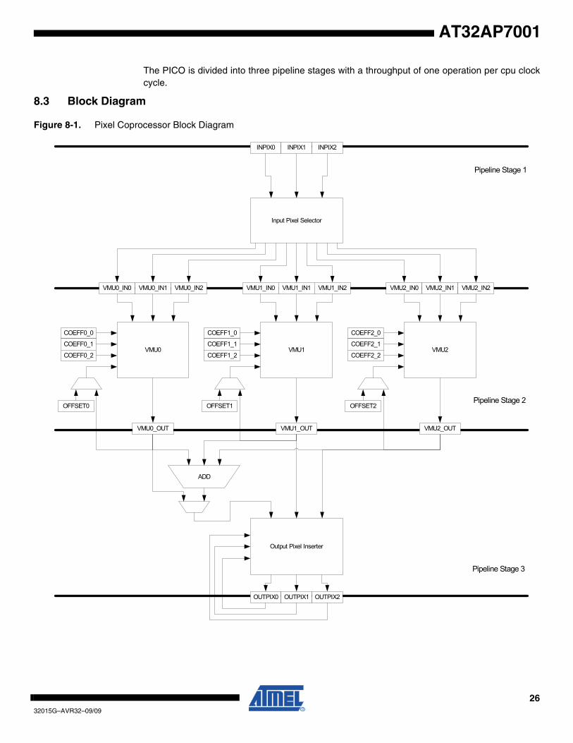
8.2 Description
The Pixel Coprocessor (PICO) is a coprocessor coupled to the AVR32 CPU through the TCB(Tightly Coupled Bus) interface. The PICO consists of three Vector Multiplication Units (VMU0,VMU1, VMU2), an Input Pixel Selector and an Output Pixel Inserter. Each VMU can perform avector multiplication of a 1x3 12-bit coefficient vector with a 3x1 8-bit pixel vector. In addition a12-bit offset can be added to the result of this vector multiplication.
The PICO can be used for transforming the pixel components in a given color space (i.e. RGB,YCrCb, YUV) to any other color space as long as the transformation is linear. The flexibility ofthe Input Pixel Selector and Output Pixel Insertion logic makes it easy to efficiently support dif-ferent pixel storage formats with regards to issues such as byte ordering of the colorcomponents, if the color components constituting an image are packed/interleaved or stored asseparate images or if any of the color components are subsampled.
The three Vector Multiplication Units can also be connected together to form one large vectormultiplier which can perform a vector multiplication of a 1x9 12-bit coefficient vector with a 9x1 8-bit pixel vector. This can be used to implement FIR filters, bilinear interpolations filters forsmoothing/scaling images etc. By allowing the outputs from the Vector Multiplication units toaccumulate it is also possible to extend the order of the filter to more than 9-taps.
The results from the VMUs are scaled and saturated back to unsigned 8-bit pixel values in theOutput Pixel Inserter.
2632015G–AVR32–09/09
AT32AP7001
The PICO is divided into three pipeline stages with a throughput of one operation per cpu clockcycle.
8.3 Block Diagram
Figure 8-1. Pixel Coprocessor Block Diagram
INPIX0
VMU0_OUT
Input Pixel Selector
VMU0
ADD
VMU0_IN0 VMU0_IN1 VMU0_IN2
INPIX1 INPIX2
COEFF0_0
COEFF0_1
COEFF0_2
OFFSET0
VMU1_OUT
VMU1
VMU1_IN0 VMU1_IN1 VMU1_IN2
COEFF1_0
COEFF1_1
COEFF1_2
OFFSET1
VMU2_OUT
VMU2
VMU2_IN0 VMU2_IN1 VMU2_IN2
COEFF2_0
COEFF2_1
COEFF2_2
OFFSET2
OUTPIX0 OUTPIX1 OUTPIX2
Output Pixel Inserter
Pipeline Stage 1
Pipeline Stage 2
Pipeline Stage 3
2732015G–AVR32–09/09
AT32AP7001
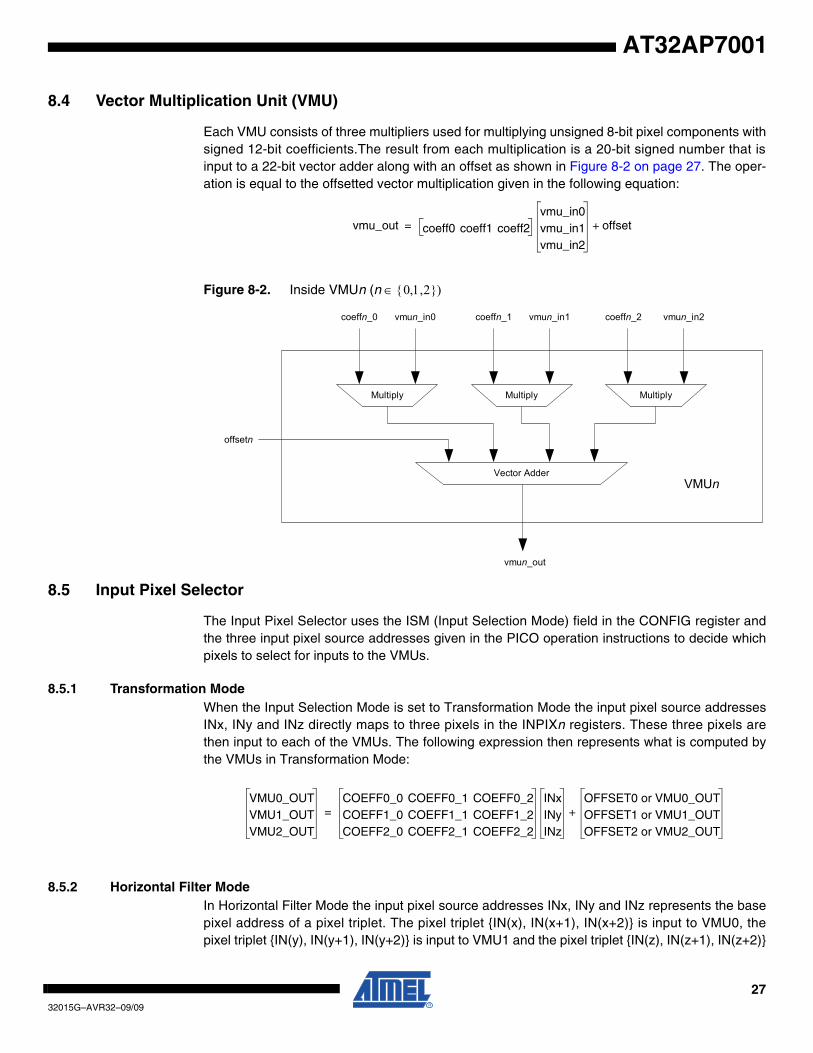
8.4 Vector Multiplication Unit (VMU)
Each VMU consists of three multipliers used for multiplying unsigned 8-bit pixel components withsigned 12-bit coefficients.The result from each multiplication is a 20-bit signed number that isinput to a 22-bit vector adder along with an offset as shown in Figure 8-2 on page 27. The oper-ation is equal to the offsetted vector multiplication given in the following equation:
Figure 8-2. Inside VMUn (n ∈ {0,1,2})
8.5 Input Pixel Selector
The Input Pixel Selector uses the ISM (Input Selection Mode) field in the CONFIG register andthe three input pixel source addresses given in the PICO operation instructions to decide whichpixels to select for inputs to the VMUs.
8.5.1 Transformation ModeWhen the Input Selection Mode is set to Transformation Mode the input pixel source addressesINx, INy and INz directly maps to three pixels in the INPIXn registers. These three pixels arethen input to each of the VMUs. The following expression then represents what is computed bythe VMUs in Transformation Mode:
8.5.2 Horizontal Filter ModeIn Horizontal Filter Mode the input pixel source addresses INx, INy and INz represents the basepixel address of a pixel triplet. The pixel triplet {IN(x), IN(x+1), IN(x+2)} is input to VMU0, thepixel triplet {IN(y), IN(y+1), IN(y+2)} is input to VMU1 and the pixel triplet {IN(z), IN(z+1), IN(z+2)}
vmu_out coeff0 coeff1 coeff2vmu_in0vmu_in1vmu_in2
offset+=
Multiply
Vector Adder
Multiply Multiply
VMUn
offsetn
coeffn_1 coeffn_2coeffn_0 vmun_in0 vmun_in1 vmun_in2
vmun_out
VMU0_OUTVMU1_OUTVMU2_OUT
COEFF0_0 COEFF0_1 COEFF0_2COEFF1_0 COEFF1_1 COEFF1_2COEFF2_0 COEFF2_1 COEFF2_2
INxINyINz
OFFSET0 or VMU0_OUTOFFSET1 or VMU1_OUTOFFSET2 or VMU2_OUT
+=
2832015G–AVR32–09/09
AT32AP7001
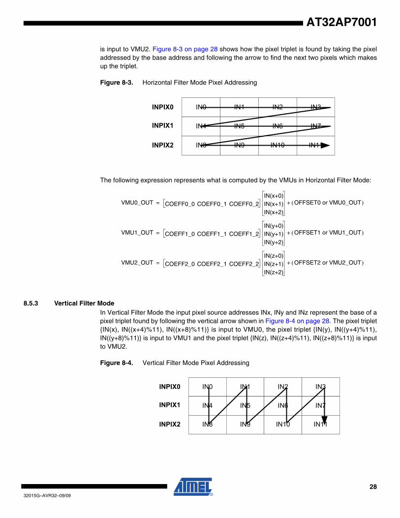
is input to VMU2. Figure 8-3 on page 28 shows how the pixel triplet is found by taking the pixeladdressed by the base address and following the arrow to find the next two pixels which makesup the triplet.
Figure 8-3. Horizontal Filter Mode Pixel Addressing
The following expression represents what is computed by the VMUs in Horizontal Filter Mode:
8.5.3 Vertical Filter ModeIn Vertical Filter Mode the input pixel source addresses INx, INy and INz represent the base of apixel triplet found by following the vertical arrow shown in Figure 8-4 on page 28. The pixel triplet{IN(x), IN((x+4)%11), IN((x+8)%11)} is input to VMU0, the pixel triplet {IN(y), IN((y+4)%11),IN((y+8)%11)} is input to VMU1 and the pixel triplet {IN(z), IN((z+4)%11), IN((z+8)%11)} is inputto VMU2.
Figure 8-4. Vertical Filter Mode Pixel Addressing
INPIX0 IN0 IN1 IN2 IN3
IN4 IN5 IN6 IN7
IN8 IN9 IN10 IN11
INPIX1
INPIX2
VMU0_OUT COEFF0_0 COEFF0_1 COEFF0_2IN(x+0)IN(x+1)IN(x+2)
OFFSET0 or VMU0_OUT( )+=
VMU1_OUT COEFF1_0 COEFF1_1 COEFF1_2IN(y+0)IN(y+1)IN(y+2)
OFFSET1 or VMU1_OUT( )+=
VMU2_OUT COEFF2_0 COEFF2_1 COEFF2_2IN(z+0)IN(z+1)IN(z+2)
OFFSET2 or VMU2_OUT( )+=
INPIX0 IN0 IN1 IN2 IN3
IN4 IN5 IN6 IN7
IN8 IN9 IN10 IN11
INPIX1
INPIX2

2932015G–AVR32–09/09
AT32AP7001
The following expression represents what is computed by the VMUs in Vertical Filter Mode:
8.6 Output Pixel Inserter
The Output Pixel Inserter uses the OIM (Output Insertion Mode) field in the CONFIG register andthe destination pixel address given in the PICO operation instructions to decide which three ofthe twelve possible OUTn pixels to write back the scaled and saturated results from the VMUsto. The 22-bit results from each VMU is first scaled by performing an arithmetical right shift byCOEFF_FRAC_BITS in order to remove the fractional part of the results and obtain the integerpart. The integer part is then saturated to an unsigned 8-bit number in the range 0 to 255.
8.6.1 Planar Insertion ModeIn Planar Insertion Mode the destination pixel address OUTd specifies which pixel in each of theregisters OUTPIX0, OUTPIX1 and OUTPIX2 will be updated. VMUn writes to OUTPIXn. Thiscan be seen in Figure 8-5 on page 29 and Table 8-2 on page 47. This mode is useful whentransforming from one color space to another where the resulting color components should bestored in separate images.
Figure 8-5. Planar Pixel Insertion
VMU0_OUT COEFF0_0 COEFF0_1 COEFF0_2IN((x+0)%11)IN((x+4)%11)IN((x+8)%11)
OFFSET0 or VMU0_OUT( )+=
VMU1_OUT COEFF1_0 COEFF1_1 COEFF1_2IN((y+0)%11)IN((y+4)%11)IN((y+8)%11)
OFFSET1 or VMU1_OUT( )+=
VMU2_OUT COEFF2_0 COEFF2_1 COEFF2_2IN((z+0)%11)IN((z+4)%11)IN((z+8)%11)
OFFSET2 or VMU2_OUT( )+=
OUTPIX0 OUT0 OUT1 OUT2 OUT3
OUT4 OUT5 OUT6 OUT7
OUT8 OUT9 OUT10 OUT11
OUTPIX1
OUTPIX2
d = 0 d = 2d = 1 d = 3
= VMU0
= VMU1
= VMU2
3032015G–AVR32–09/09
AT32AP7001
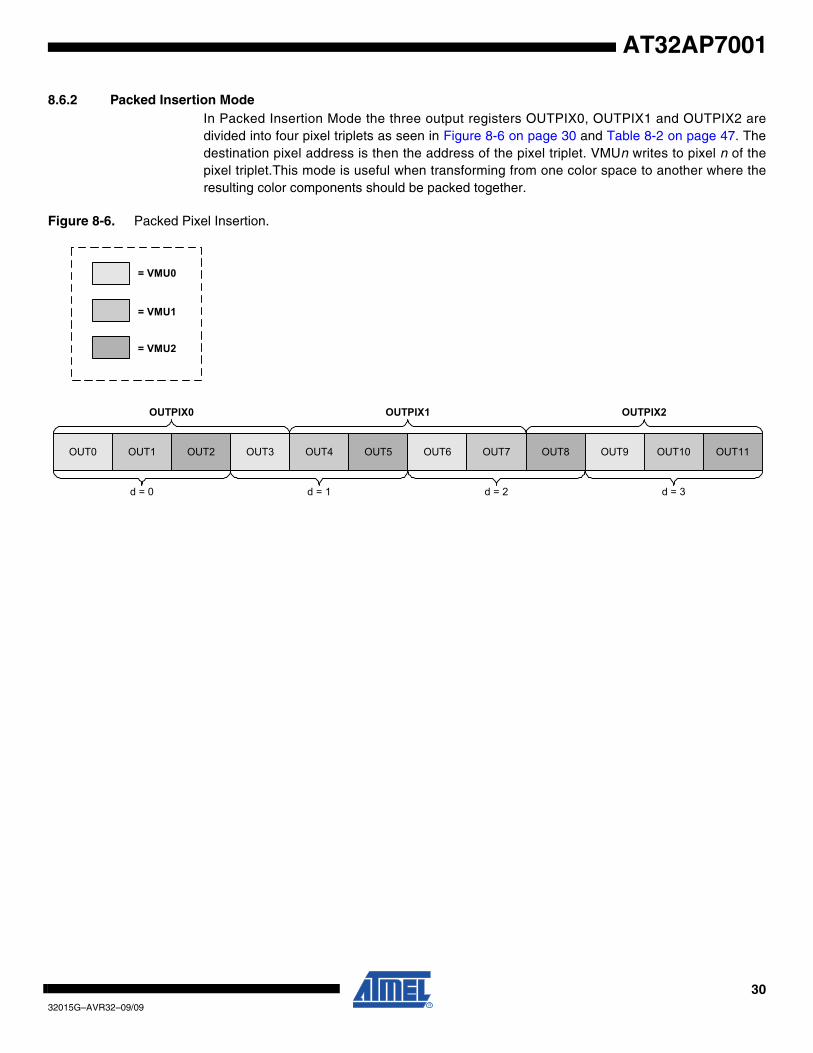
8.6.2 Packed Insertion ModeIn Packed Insertion Mode the three output registers OUTPIX0, OUTPIX1 and OUTPIX2 aredivided into four pixel triplets as seen in Figure 8-6 on page 30 and Table 8-2 on page 47. Thedestination pixel address is then the address of the pixel triplet. VMUn writes to pixel n of thepixel triplet.This mode is useful when transforming from one color space to another where theresulting color components should be packed together.
Figure 8-6. Packed Pixel Insertion.
OUTPIX0
OUT0 OUT1 OUT2 OUT3 OUT4 OUT5 OUT6 OUT7 OUT8 OUT9 OUT10 OUT11
d = 0 d = 1 d = 2 d = 3
OUTPIX1 OUTPIX2
= VMU0
= VMU1
= VMU2
3132015G–AVR32–09/09
AT32AP7001
8.7 User Interface
The PICO uses the TCB interface to communicate with the CPU and the user can read from orwrite to the PICO Register File by using the PICO load/store/move instructions which maps togeneric coprocessor instructions.
8.7.1 Register FileThe PICO register file can be accessed from the CPU by using the picomv.x, picold.x, picost.x,picoldm and picostm instructions.
Table 8-1. PICO Register File
Cp Reg # Register Name Access
cr0 Input Pixel Register 2 INPIX2 Read/Write
cr1 Input Pixel Register 1 INPIX1 Read/Write
cr2 Input Pixel Register 0 INPIX0 Read/Write
cr3 Output Pixel Register 2 OUTPIX2 Read Only
cr4 Output Pixel Register 1 OUTPIX1 Read Only
cr5 Output Pixel Register 0 OUTPIX0 Read Only
cr6 Coefficient Register A for VMU0 COEFF0_A Read/Write
cr7 Coefficient Register B for VMU0 COEFF0_B Read/Write
cr8 Coefficient Register A for VMU1 COEFF1_A Read/Write
cr9 Coefficient Register B for VMU1 COEFF1_B Read/Write
cr10 Coefficient Register A for VMU2 COEFF2_A Read/Write
cr11 Coefficient Register B for VMU2 COEFF2_B Read/Write
cr12 Output from VMU0 VMU0_OUT Read/Write
cr13 Output from VMU1 VMU1_OUT Read/Write
cr14 Output from VMU2 VMU2_OUT Read/Write
cr15 PICO Configuration Register CONFIG Read/Write
3232015G–AVR32–09/09
AT32AP7001
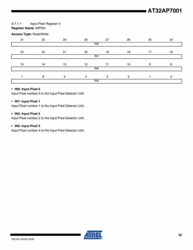
8.7.1.1 Input Pixel Register 0Register Name: INPIX0
Access Type: Read/Write
• IN0: Input Pixel 0Input Pixel number 0 to the Input Pixel Selector Unit.
• IN1: Input Pixel 1Input Pixel number 1 to the Input Pixel Selector Unit.
• IN2: Input Pixel 2Input Pixel number 2 to the Input Pixel Selector Unit.
• IN3: Input Pixel 3Input Pixel number 3 to the Input Pixel Selector Unit.
31 30 29 28 27 26 25 24IN0
23 22 21 20 19 18 17 16
IN1
15 14 13 12 11 10 9 8
IN2
7 6 5 4 3 2 1 0
IN3
3332015G–AVR32–09/09
AT32AP7001
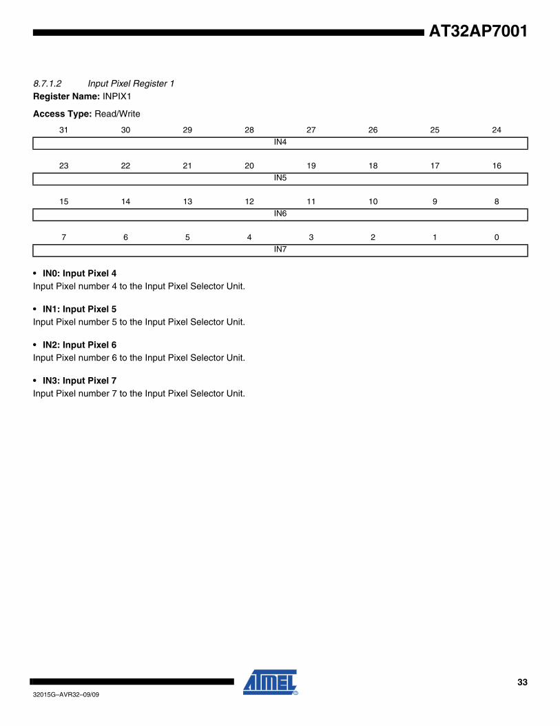
8.7.1.2 Input Pixel Register 1Register Name: INPIX1
Access Type: Read/Write
• IN0: Input Pixel 4Input Pixel number 4 to the Input Pixel Selector Unit.
• IN1: Input Pixel 5Input Pixel number 5 to the Input Pixel Selector Unit.
• IN2: Input Pixel 6Input Pixel number 6 to the Input Pixel Selector Unit.
• IN3: Input Pixel 7Input Pixel number 7 to the Input Pixel Selector Unit.
31 30 29 28 27 26 25 24
IN4
23 22 21 20 19 18 17 16IN5
15 14 13 12 11 10 9 8IN6
7 6 5 4 3 2 1 0IN7

3432015G–AVR32–09/09
AT32AP7001
8.7.1.3 Input Pixel Register 2Register Name: INPIX2
Access Type: Read/Write
• IN0: Input Pixel 8Input Pixel number 8 to the Input Pixel Selector Unit.
• IN1: Input Pixel 9Input Pixel number 9 to the Input Pixel Selector Unit.
• IN2: Input Pixel 10Input Pixel number 10 to the Input Pixel Selector Unit.
• IN3: Input Pixel 11Input Pixel number 11 to the Input Pixel Selector Unit.
31 30 29 28 27 26 25 24
IN8
23 22 21 20 19 18 17 16IN9
15 14 13 12 11 10 9 8IN10
7 6 5 4 3 2 1 0IN11
3532015G–AVR32–09/09
AT32AP7001
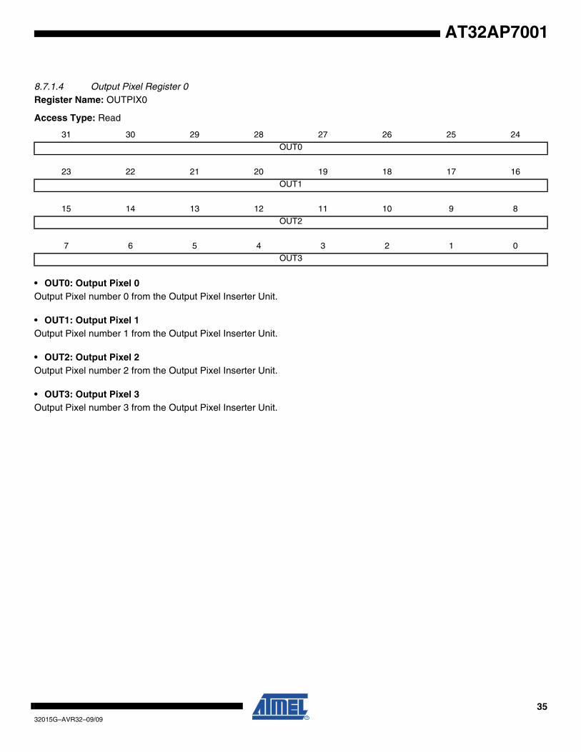
8.7.1.4 Output Pixel Register 0Register Name: OUTPIX0
Access Type: Read
• OUT0: Output Pixel 0Output Pixel number 0 from the Output Pixel Inserter Unit.
• OUT1: Output Pixel 1Output Pixel number 1 from the Output Pixel Inserter Unit.
• OUT2: Output Pixel 2Output Pixel number 2 from the Output Pixel Inserter Unit.
• OUT3: Output Pixel 3Output Pixel number 3 from the Output Pixel Inserter Unit.
31 30 29 28 27 26 25 24
OUT0
23 22 21 20 19 18 17 16OUT1
15 14 13 12 11 10 9 8OUT2
7 6 5 4 3 2 1 0OUT3

3632015G–AVR32–09/09
AT32AP7001
8.7.1.5 Output Pixel Register 1Register Name: OUTPIX1
Access Type: Read
• OUT4: Output Pixel 4Output Pixel number 4 from the Output Pixel Inserter Unit.
• OUT5: Output Pixel 5Output Pixel number 5 from the Output Pixel Inserter Unit.
• OUT6: Output Pixel 6Output Pixel number 6 from the Output Pixel Inserter Unit.
• OUT7: Output Pixel 7Output Pixel number 7 from the Output Pixel Inserter Unit.
31 30 29 28 27 26 25 24
OUT4
23 22 21 20 19 18 17 16OUT5
15 14 13 12 11 10 9 8OUT6
7 6 5 4 3 2 1 0OUT7

3732015G–AVR32–09/09
AT32AP7001
8.7.1.6 Output Pixel Register 2Register Name: OUTPIX2
Access Type: Read
• OUT8: Output Pixel 8Output Pixel number 8 from the Output Pixel Inserter Unit.
• OUT9: Output Pixel 9Output Pixel number 9 from the Output Pixel Inserter Unit.
• OUT10: Output Pixel 10Output Pixel number 10 from the Output Pixel Inserter Unit.
• OUT11: Output Pixel 11Output Pixel number 11 from the Output Pixel Inserter Unit.
31 30 29 28 27 26 25 24
OUT8
23 22 21 20 19 18 17 16OUT9
15 14 13 12 11 10 9 8OUT10
7 6 5 4 3 2 1 0OUT11

3832015G–AVR32–09/09
AT32AP7001
8.7.1.7 Coefficient Register A for VMU0Register Name: COEFF0_A
Access Type: Read/Write
• COEFF0_0: Coefficient 0 for VMU0Coefficient 0 input to VMU0. A signed 12-bit fixed-point number where the number of fractional bits is given by theCOEFF_FRAC_BITS field in the CONFIG register. The actual fractional number is equal to ,where the COEFF0_0 value is interpreted as a 2’s complement integer. When reading this register, COEFF0_0 is sign-extended to 16-bits in order to fill in the unused bits in the upper halfword of this register.
• COEFF0_1: Coefficient 1 for VMU0Coefficient 1 input to VMU0. A signed 12-bit fixed-point number where the number of fractional bits is given by theCOEFF_FRAC_BITS field in the CONFIG register. The actual fractional number is equal to ,where the COEFF0_1 value is interpreted as a 2’s complement integer. When reading this register, COEFF0_1 is sign-extended to 16-bits in order to fill in the unused bits in the lower halfword of this register.
31 30 29 28 27 26 25 24
- - - - COEFF0_0
23 22 21 20 19 18 17 16COEFF0_0
15 14 13 12 11 10 9 8- - - - COEFF0_1
7 6 5 4 3 2 1 0COEFF0_1
COEFF0_0 2COEFF_FRAC_BITS⁄
COEFF0_1 2COEFF_FRAC_BITS⁄

3932015G–AVR32–09/09
AT32AP7001
8.7.1.8 Coefficient Register B for VMU0Register Name: COEFF0_B
Access Type: Read/Write
• COEFF0_2: Coefficient 2 for VMU0Coefficient 2 input to VMU0. A signed 12-bit fixed-point number where the number of fractional bits is given by theCOEFF_FRAC_BITS field in the CONFIG register. The actual fractional number is equal to ,where the COEFF0_2 value is interpreted as a 2’s complement integer. When reading this register, COEFF0_2 is sign-extended to 16-bits in order to fill in the unused bits in the upper halfword of this register.
• OFFSET0: Offset for VMU0Offset input to VMU0 in case of non-accumulating operations. A signed 12-bit fixed-point number where the number of frac-tional bits is given by the OFFSET_FRAC_BITS field in the CONFIG register. The actual fractional number is equal to
, where the OFFSET0 value is interpreted as a 2’s complement integer. When reading this reg-ister, OFFSET0 is sign-extended to 16-bits in order to fill in the unused bits in the lower halfword of this register.
31 30 29 28 27 26 25 24
- - - - COEFF0_2
23 22 21 20 19 18 17 16COEFF0_2
15 14 13 12 11 10 9 8- - - - OFFSET0
7 6 5 4 3 2 1 0OFFSET0
COEFF0_2 2COEFF_FRAC_BITS⁄
OFFSET0 2OFFSET_FRAC_BITS⁄

4032015G–AVR32–09/09
AT32AP7001
8.7.1.9 Coefficient Register A for VMU1Register Name: COEFF1_A
Access Type: Read/Write
• COEFF1_0: Coefficient 0 for VMU1Coefficient 0 input to VMU1. A signed 12-bit fixed-point number where the number of fractional bits is given by theCOEFF_FRAC_BITS field in the CONFIG register. The actual fractional number is equal to ,where the COEFF1_0 value is interpreted as a 2’s complement integer. When reading this register, COEFF1_0 is sign-extended to 16-bits in order to fill in the unused bits in the upper halfword of this register.
• COEFF1_1: Coefficient 1 for VMU1Coefficient 1 input to VMU0. A signed 12-bit fixed-point number where the number of fractional bits is given by theCOEFF_FRAC_BITS field in the CONFIG register. The actual fractional number is equal to ,where the COEFF1_1 value is interpreted as a 2’s complement integer. When reading this register, COEFF1_1 is sign-extended to 16-bits in order to fill in the unused bits in the lower halfword of this register.
31 30 29 28 27 26 25 24
- - - - COEFF1_0
23 22 21 20 19 18 17 16COEFF1_0
15 14 13 12 11 10 9 8- - - - COEFF1_1
7 6 5 4 3 2 1 0COEFF1_1
COEFF1_0 2COEFF_FRAC_BITS⁄
COEFF1_1 2COEFF_FRAC_BITS⁄

4132015G–AVR32–09/09
AT32AP7001
8.7.1.10 Coefficient Register B for VMU1Register Name: COEFF1_B
Access Type: Read/Write
• COEFF1_2: Coefficient 2 for VMU1Coefficient 2 input to VMU1. A signed 12-bit fixed-point number where the number of fractional bits is given by theCOEFF_FRAC_BITS field in the CONFIG register. The actual fractional number is equal to ,where the COEFF1_2 value is interpreted as a 2’s complement integer. When reading this register, COEFF1_2 is sign-extended to 16-bits in order to fill in the unused bits in the upper halfword of this register.
• OFFSET1: Offset for VMU1Offset input to VMU1 in case of non-accumulating operations. A signed 12-bit fixed-point number where the number of frac-tional bits is given by the OFFSET_FRAC_BITS field in the CONFIG register. The actual fractional number is equal to
, where the OFFSET1 value is interpreted as a 2’s complement integer. When reading this reg-ister, OFFSET1 is sign-extended to 16-bits in order to fill in the unused bits in the lower halfword of this register.
31 30 29 28 27 26 25 24
- - - - COEFF1_2
23 22 21 20 19 18 17 16COEFF1_2
15 14 13 12 11 10 9 8- - - - OFFSET1
7 6 5 4 3 2 1 0OFFSET1
COEFF1_2 2COEFF_FRAC_BITS⁄
OFFSET1 2OFFSET_FRAC_BITS⁄
4232015G–AVR32–09/09
AT32AP7001
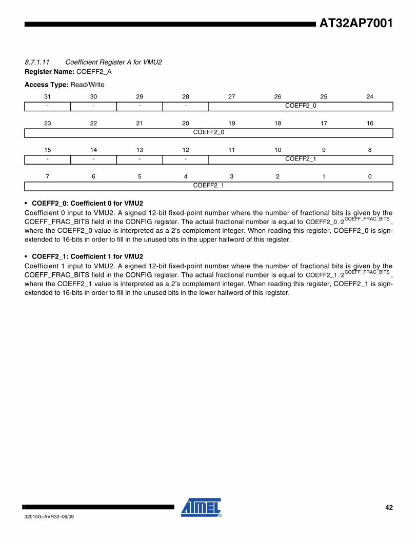
8.7.1.11 Coefficient Register A for VMU2Register Name: COEFF2_A
Access Type: Read/Write
• COEFF2_0: Coefficient 0 for VMU2Coefficient 0 input to VMU2. A signed 12-bit fixed-point number where the number of fractional bits is given by theCOEFF_FRAC_BITS field in the CONFIG register. The actual fractional number is equal to ,where the COEFF2_0 value is interpreted as a 2’s complement integer. When reading this register, COEFF2_0 is sign-extended to 16-bits in order to fill in the unused bits in the upper halfword of this register.
• COEFF2_1: Coefficient 1 for VMU2Coefficient 1 input to VMU2. A signed 12-bit fixed-point number where the number of fractional bits is given by theCOEFF_FRAC_BITS field in the CONFIG register. The actual fractional number is equal to ,where the COEFF2_1 value is interpreted as a 2’s complement integer. When reading this register, COEFF2_1 is sign-extended to 16-bits in order to fill in the unused bits in the lower halfword of this register.
31 30 29 28 27 26 25 24
- - - - COEFF2_0
23 22 21 20 19 18 17 16COEFF2_0
15 14 13 12 11 10 9 8- - - - COEFF2_1
7 6 5 4 3 2 1 0COEFF2_1
COEFF2_0 2COEFF_FRAC_BITS⁄
COEFF2_1 2COEFF_FRAC_BITS⁄
4332015G–AVR32–09/09
AT32AP7001
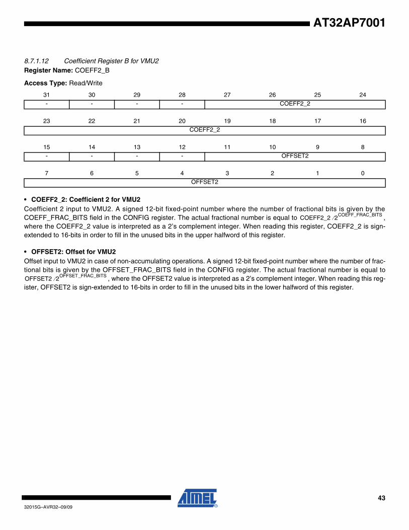
8.7.1.12 Coefficient Register B for VMU2Register Name: COEFF2_B
Access Type: Read/Write
• COEFF2_2: Coefficient 2 for VMU2Coefficient 2 input to VMU2. A signed 12-bit fixed-point number where the number of fractional bits is given by theCOEFF_FRAC_BITS field in the CONFIG register. The actual fractional number is equal to ,where the COEFF2_2 value is interpreted as a 2’s complement integer. When reading this register, COEFF2_2 is sign-extended to 16-bits in order to fill in the unused bits in the upper halfword of this register.
• OFFSET2: Offset for VMU2Offset input to VMU2 in case of non-accumulating operations. A signed 12-bit fixed-point number where the number of frac-tional bits is given by the OFFSET_FRAC_BITS field in the CONFIG register. The actual fractional number is equal to
, where the OFFSET2 value is interpreted as a 2’s complement integer. When reading this reg-ister, OFFSET2 is sign-extended to 16-bits in order to fill in the unused bits in the lower halfword of this register.
31 30 29 28 27 26 25 24
- - - - COEFF2_2
23 22 21 20 19 18 17 16COEFF2_2
15 14 13 12 11 10 9 8- - - - OFFSET2
7 6 5 4 3 2 1 0OFFSET2
COEFF2_2 2COEFF_FRAC_BITS⁄
OFFSET2 2OFFSET_FRAC_BITS⁄

4432015G–AVR32–09/09
AT32AP7001
8.7.1.13 VMU0 Output RegisterRegister Name: VMU0_OUT
Access Type: Read/Write
• VMU0_OUT: Output from VMU0This register is used for directly accessing the output from VMU0 or for setting the initial value of the accumulator for accu-mulating operations. The output from VMU0 is a signed 22-bit fixed-point number where the number of fractional bits aregiven by the COEFF_FRAC_BITS field in the CONFIG register. When reading this register the signed 22-bit value is sign-extended to 32-bits.
31 30 29 28 27 26 25 24
- - - - - - - -
23 22 21 20 19 18 17 16- - VMU0_OUT
15 14 13 12 11 10 9 8VMU0_OUT
7 6 5 4 3 2 1 0VMU0_OUT
4532015G–AVR32–09/09
AT32AP7001
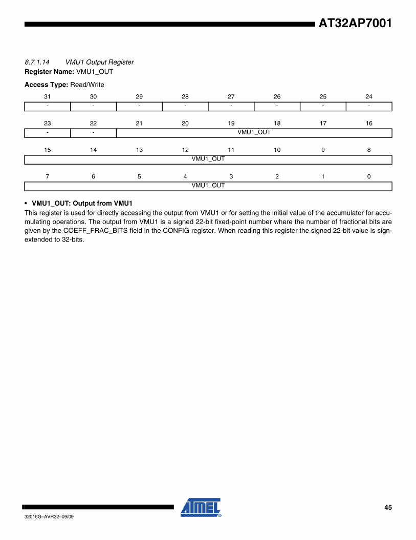
8.7.1.14 VMU1 Output RegisterRegister Name: VMU1_OUT
Access Type: Read/Write
• VMU1_OUT: Output from VMU1This register is used for directly accessing the output from VMU1 or for setting the initial value of the accumulator for accu-mulating operations. The output from VMU1 is a signed 22-bit fixed-point number where the number of fractional bits aregiven by the COEFF_FRAC_BITS field in the CONFIG register. When reading this register the signed 22-bit value is sign-extended to 32-bits.
31 30 29 28 27 26 25 24
- - - - - - - -
23 22 21 20 19 18 17 16- - VMU1_OUT
15 14 13 12 11 10 9 8VMU1_OUT
7 6 5 4 3 2 1 0VMU1_OUT

4632015G–AVR32–09/09
AT32AP7001
8.7.1.15 VMU2 Output RegisterRegister Name: VMU2_OUT
Access Type: Read/Write
• VMU2_OUT: Output from VMU2This register is used for directly accessing the output from VMU2 or for setting the initial value of the accumulator for accu-mulating operations. The output from VMU2 is a signed 22-bit fixed-point number where the number of fractional bits aregiven by the COEFF_FRAC_BITS field in the CONFIG register. When reading this register the signed 22-bit value is sign-extended to 32-bits.
31 30 29 28 27 26 25 24
- - - - - - - -
23 22 21 20 19 18 17 16- - VMU2_OUT
15 14 13 12 11 10 9 8VMU2_OUT
7 6 5 4 3 2 1 0VMU2_OUT
4732015G–AVR32–09/09
AT32AP7001
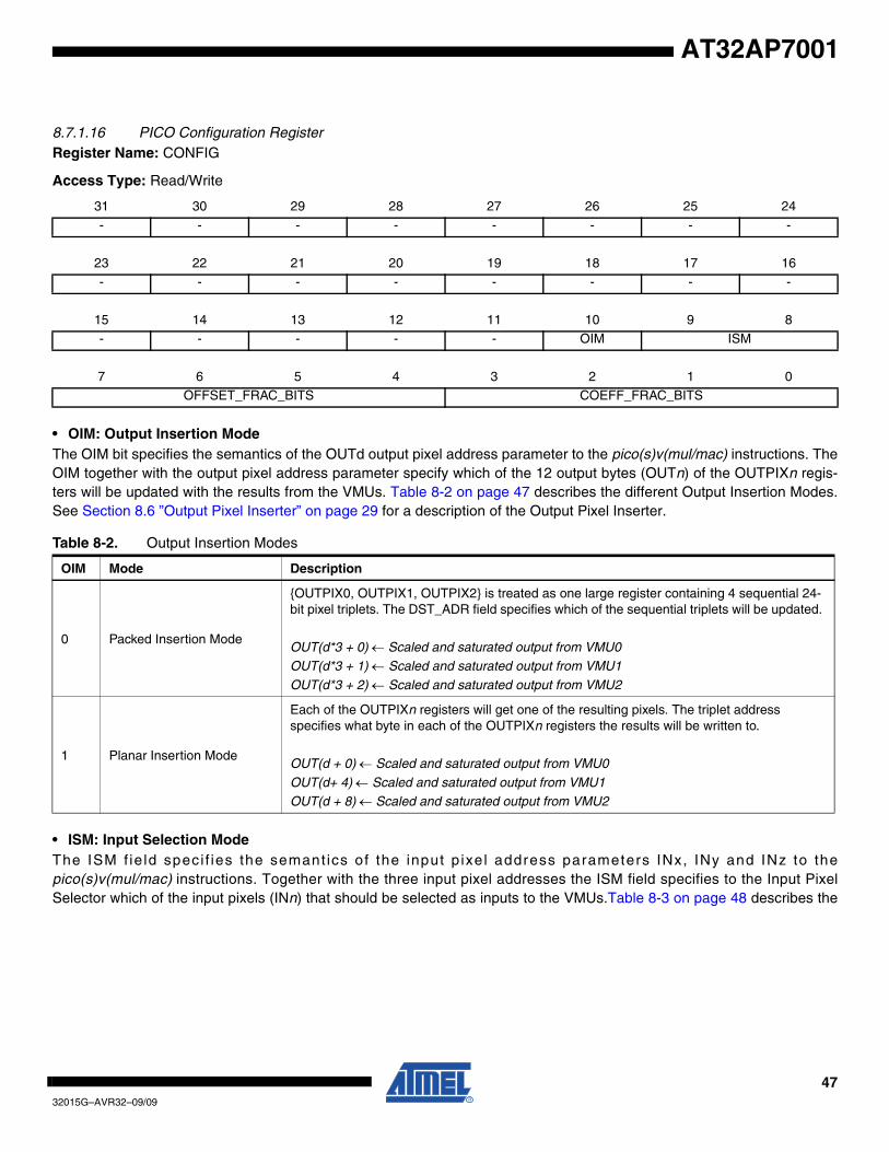
8.7.1.16 PICO Configuration RegisterRegister Name: CONFIG
Access Type: Read/Write
• OIM: Output Insertion ModeThe OIM bit specifies the semantics of the OUTd output pixel address parameter to the pico(s)v(mul/mac) instructions. TheOIM together with the output pixel address parameter specify which of the 12 output bytes (OUTn) of the OUTPIXn regis-ters will be updated with the results from the VMUs. Table 8-2 on page 47 describes the different Output Insertion Modes.See Section 8.6 ”Output Pixel Inserter” on page 29 for a description of the Output Pixel Inserter.
• ISM: Input Selection ModeThe ISM f ie ld speci f ies the semant ics of the input p ixe l address parameters INx, INy and INz to thepico(s)v(mul/mac) instructions. Together with the three input pixel addresses the ISM field specifies to the Input PixelSelector which of the input pixels (INn) that should be selected as inputs to the VMUs.Table 8-3 on page 48 describes the
31 30 29 28 27 26 25 24
- - - - - - - -
23 22 21 20 19 18 17 16- - - - - - - -
15 14 13 12 11 10 9 8- - - - - OIM ISM
7 6 5 4 3 2 1 0OFFSET_FRAC_BITS COEFF_FRAC_BITS
Table 8-2. Output Insertion Modes
OIM Mode Description
0 Packed Insertion Mode
{OUTPIX0, OUTPIX1, OUTPIX2} is treated as one large register containing 4 sequential 24-bit pixel triplets. The DST_ADR field specifies which of the sequential triplets will be updated.
OUT(d*3 + 0) ← Scaled and saturated output from VMU0OUT(d*3 + 1) ← Scaled and saturated output from VMU1
OUT(d*3 + 2) ← Scaled and saturated output from VMU2
1 Planar Insertion Mode
Each of the OUTPIXn registers will get one of the resulting pixels. The triplet address specifies what byte in each of the OUTPIXn registers the results will be written to.
OUT(d + 0) ← Scaled and saturated output from VMU0
OUT(d+ 4) ← Scaled and saturated output from VMU1OUT(d + 8) ← Scaled and saturated output from VMU2

4832015G–AVR32–09/09
AT32AP7001
different Input Selection Modes. See Section 8.5 ”Input Pixel Selector” on page 27 for a description of the Input Pixel
Selector.
• OFFSET_FRAC_BITS: Offset Fractional BitsSpecifies the number of fractional bits in the fixed-point offsets input to each VMU. Must be in the range from 0 toCOEFF_FRAC_BITS. Other values gives undefined results.This value is used for scaling the OFFSETn values beforebeing input to VMUn so that the offset will have the same fixed-point format as the outputs from the multiplication stagesbefore performing the vector addition in the VMU.
• COEFF_FRAC_BITS: Coefficient Fractional BitsSpecifies the number of fractional bits in the fixed-point coefficients input to each VMU. Must be in the range from 0 to 11,since at least one bit of the coefficient must be used for the sign. Other values gives undefined results.COEFF_FRAC_BITS is used in the Output Pixel Inserter to scale the fixed-point results from the VMUs back to unsigned 8-bit integers.
Table 8-3. Input Selection Modes
ISM Mode
0 0 Transformation ModeVMU0, VMU1 and VMU2 get the same pixel inputs. These three pixels can be freely selected from the INPIXn registers.
0 1 Horizontal Filter ModePixel triplets are selected for input to each of the VMUs by addressing horizontal pixel triplets from the INPIXn registers.
1 0 Vertical Filter ModePixel triplets are selected for input to each of the VMUs by addressing vertical pixel triplets from the INPIXn registers.
1 1 Reserved N.A
4932015G–AVR32–09/09
AT32AP7001
8.8 PICO Instructions
8.8.1 PICO Instructions Nomenclature
8.8.1.1 Registers and OperandsR{d, s, …} The uppercase ‘R’ denotes a 32-bit (word) register.
Rd The lowercase ‘d’ denotes the destination register number.
Rs The lowercase ‘s’ denotes the source register number.
Rb The lowercase ‘b’ denotes the base register number for indexed addressing modes.
Ri The lowercase ‘i’ denotes the index register number for indexed addressing modes.
Rp The lowercase ‘p’ denotes the pointer register number.
IN{x, y, z} The uppercase ‘IN’ denotes a pixel in the INPIXn registers.
INx The lowercase ‘x’ denotes the first input pixel number for the PICO operation instructions.
INy The lowercase ‘y’ denotes the second input pixel number for the PICO operation instructions.
INz The lowercase ‘z’ denotes the third input pixel number for the PICO operation instructions.
OUTd The uppercase ‘OUT’ denotes a pixel in the OUTPIXn registers.
OUTd The lowercase ‘d’ denotes the destination pixel number for the PICO operation instructions.
Pr PICO register. See Section 8.7.1 ”Register File” on page 31 for a complete list of registers.
PrHi:PrLo PICO register pair. Only register pairs corresponding to valid coprocessor double registers are valid. E.g. INPIX1:INPIX2 (cr1:cr0). The low part must correspond to an even coprocessor register numbern and the high part must then correspond to coprocessor register n+1. See Table 8-1 on page 31for a mapping between PICO register names and coprocessor register numbers.
PC Program Counter, equal to R15
LR Link Register, equal to R14
SP Stack Pointer, equal to R13
PICORegList Register List used in the picoldm and picostm instructions. See instruction description for whichregister combinations are allowed in the register list.
disp Displacement
sa Shift amount
[i] Denotes bit i in a immediate value. Example: imm6[4] denotes bit 4 in an 6-bit immediate value.
[i:j] Denotes bit i to j in an immediate value.
Some instructions access or use doubleword operands. These operands must be placed in two consecutive registeraddresses where the first register must be an even register. The even register contains the least significant part andthe odd register contains the most significant part. This ordering is reversed in comparison with how data isorganized in memory (where the most significant part would receive the lowest address) and is intentional.
5032015G–AVR32–09/09
AT32AP7001
The programmer is responsible for placing these operands in properly aligned register pairs. This is also specified inthe "Operands" section in the detailed description of each instruction. Failure to do so will result in an undefinedbehavior.
8.8.1.2 OperationsASR(x, n) SE(x, Bits(x) + n) >> n
SATSU(x, n) Signed to Unsigned Saturation ( x is treated as a signed value ):
If (x > (2n-1)) then (2n-1-1); elseif ( x < 0 ) then 0; else x;
SE(x, n) Sign Extend x to an n-bit value
8.8.1.3 Data Type Extensions.d Double (64-bit) operation.
.w Word (32-bit) operation.
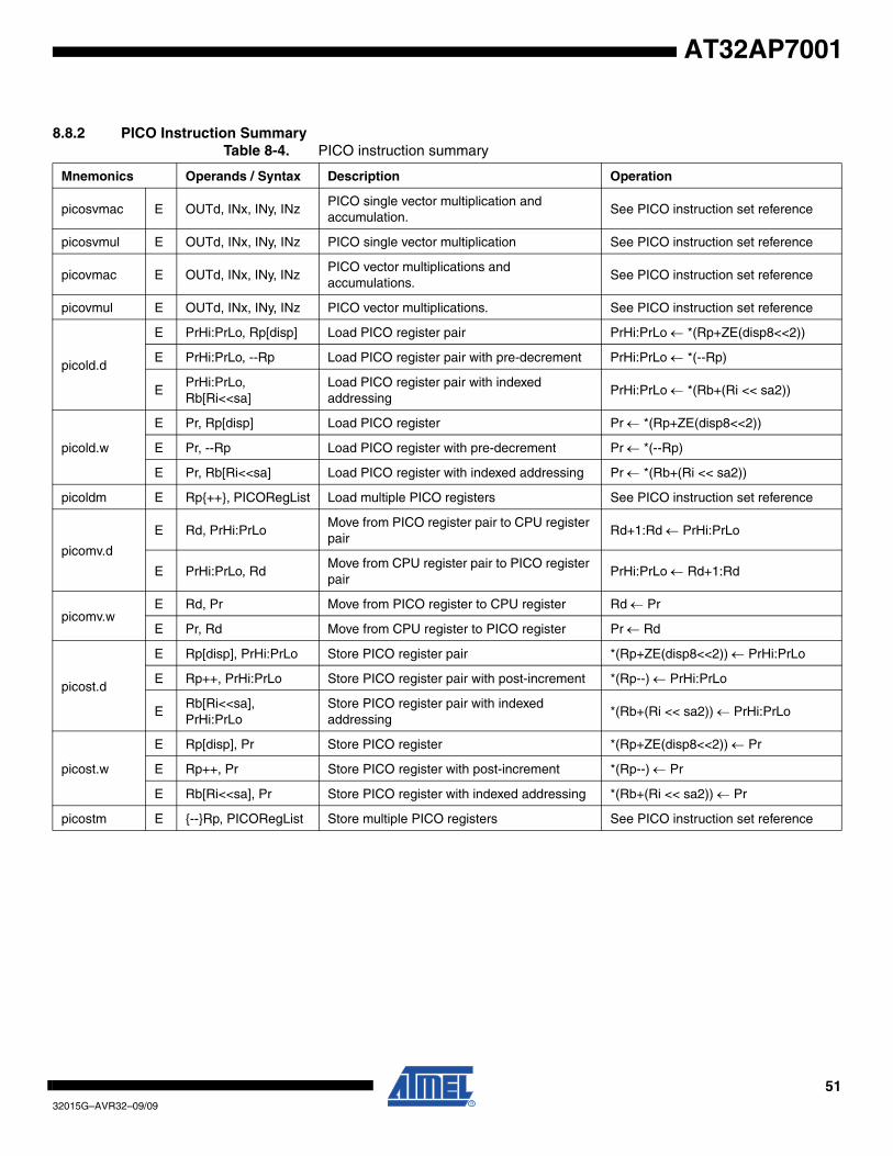
5132015G–AVR32–09/09
AT32AP7001
8.8.2 PICO Instruction SummaryTable 8-4. PICO instruction summary
Mnemonics Operands / Syntax Description Operation
picosvmac E OUTd, INx, INy, INzPICO single vector multiplication and accumulation.
See PICO instruction set reference
picosvmul E OUTd, INx, INy, INz PICO single vector multiplication See PICO instruction set reference
picovmac E OUTd, INx, INy, INzPICO vector multiplications and accumulations.
See PICO instruction set reference
picovmul E OUTd, INx, INy, INz PICO vector multiplications. See PICO instruction set reference
picold.d
E PrHi:PrLo, Rp[disp] Load PICO register pair PrHi:PrLo ← *(Rp+ZE(disp8<<2))
E PrHi:PrLo, --Rp Load PICO register pair with pre-decrement PrHi:PrLo ← *(--Rp)
EPrHi:PrLo, Rb[Ri<<sa]
Load PICO register pair with indexed addressing
PrHi:PrLo ← *(Rb+(Ri << sa2))
picold.w
E Pr, Rp[disp] Load PICO register Pr ← *(Rp+ZE(disp8<<2))
E Pr, --Rp Load PICO register with pre-decrement Pr ← *(--Rp)
E Pr, Rb[Ri<<sa] Load PICO register with indexed addressing Pr ← *(Rb+(Ri << sa2))
picoldm E Rp{++}, PICORegList Load multiple PICO registers See PICO instruction set reference
picomv.d
E Rd, PrHi:PrLoMove from PICO register pair to CPU register pair
Rd+1:Rd ← PrHi:PrLo
E PrHi:PrLo, RdMove from CPU register pair to PICO register pair
PrHi:PrLo ← Rd+1:Rd
picomv.wE Rd, Pr Move from PICO register to CPU register Rd ← Pr
E Pr, Rd Move from CPU register to PICO register Pr ← Rd
picost.d
E Rp[disp], PrHi:PrLo Store PICO register pair *(Rp+ZE(disp8<<2)) ← PrHi:PrLo
E Rp++, PrHi:PrLo Store PICO register pair with post-increment *(Rp--) ← PrHi:PrLo
ERb[Ri<<sa], PrHi:PrLo
Store PICO register pair with indexed addressing
*(Rb+(Ri << sa2)) ← PrHi:PrLo
picost.w
E Rp[disp], Pr Store PICO register *(Rp+ZE(disp8<<2)) ← Pr
E Rp++, Pr Store PICO register with post-increment *(Rp--) ← Pr
E Rb[Ri<<sa], Pr Store PICO register with indexed addressing *(Rb+(Ri << sa2)) ← Pr
picostm E {--}Rp, PICORegList Store multiple PICO registers See PICO instruction set reference
5232015G–AVR32–09/09
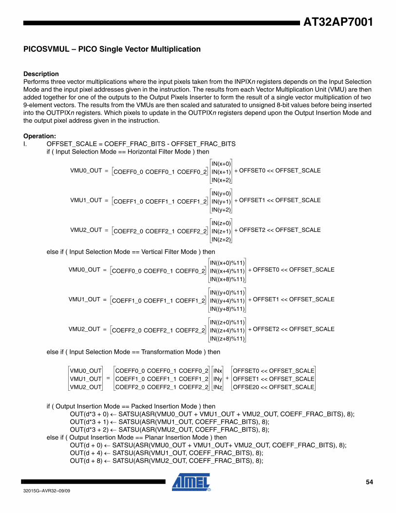
AT32AP7001
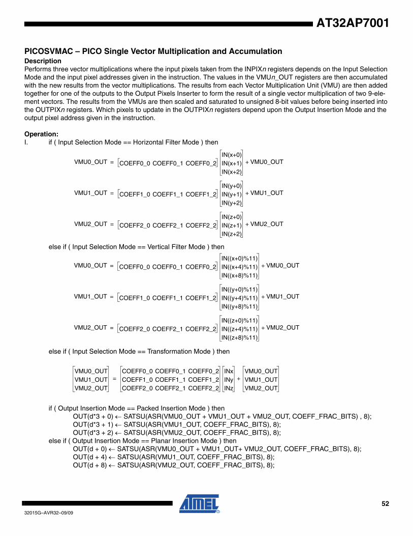
PICOSVMAC – PICO Single Vector Multiplication and AccumulationDescriptionPerforms three vector multiplications where the input pixels taken from the INPIXn registers depends on the Input Selection Mode and the input pixel addresses given in the instruction. The values in the VMUn_OUT registers are then accumulated with the new results from the vector multiplications. The results from each Vector Multiplication Unit (VMU) are then added together for one of the outputs to the Output Pixels Inserter to form the result of a single vector multiplication of two 9-ele-ment vectors. The results from the VMUs are then scaled and saturated to unsigned 8-bit values before being inserted into the OUTPIXn registers. Which pixels to update in the OUTPIXn registers depend upon the Output Insertion Mode and the output pixel address given in the instruction.
Operation:I. if ( Input Selection Mode == Horizontal Filter Mode ) then
else if ( Input Selection Mode == Vertical Filter Mode ) then
else if ( Input Selection Mode == Transformation Mode ) then
if ( Output Insertion Mode == Packed Insertion Mode ) thenOUT(d*3 + 0) ← SATSU(ASR(VMU0_OUT + VMU1_OUT + VMU2_OUT, COEFF_FRAC_BITS) , 8);OUT(d*3 + 1) ← SATSU(ASR(VMU1_OUT, COEFF_FRAC_BITS), 8);OUT(d*3 + 2) ← SATSU(ASR(VMU2_OUT, COEFF_FRAC_BITS), 8);
else if ( Output Insertion Mode == Planar Insertion Mode ) thenOUT(d + 0) ← SATSU(ASR(VMU0_OUT + VMU1_OUT+ VMU2_OUT, COEFF_FRAC_BITS), 8);OUT(d + 4) ← SATSU(ASR(VMU1_OUT, COEFF_FRAC_BITS), 8);OUT(d + 8) ← SATSU(ASR(VMU2_OUT, COEFF_FRAC_BITS), 8);
VMU0_OUT COEFF0_0 COEFF0_1 COEFF0_2IN(x+0)IN(x+1)IN(x+2)
VMU0_OUT+=
VMU1_OUT COEFF1_0 COEFF1_1 COEFF1_2IN(y+0)IN(y+1)IN(y+2)
VMU1_OUT+=
VMU2_OUT COEFF2_0 COEFF2_1 COEFF2_2IN(z+0)IN(z+1)IN(z+2)
VMU2_OUT+=
VMU0_OUT COEFF0_0 COEFF0_1 COEFF0_2IN((x+0)%11)IN((x+4)%11)IN((x+8)%11)
VMU0_OUT+=
VMU1_OUT COEFF1_0 COEFF1_1 COEFF1_2IN((y+0)%11)IN((y+4)%11)IN((y+8)%11)
VMU1_OUT+=
VMU2_OUT COEFF2_0 COEFF2_1 COEFF2_2IN((z+0)%11)IN((z+4)%11)IN((z+8)%11)
VMU2_OUT+=
VMU0_OUTVMU1_OUTVMU2_OUT
COEFF0_0 COEFF0_1 COEFF0_2COEFF1_0 COEFF1_1 COEFF1_2COEFF2_0 COEFF2_1 COEFF2_2
INxINyINz
VMU0_OUTVMU1_OUTVMU2_OUT
+=
5332015G–AVR32–09/09
AT32AP7001
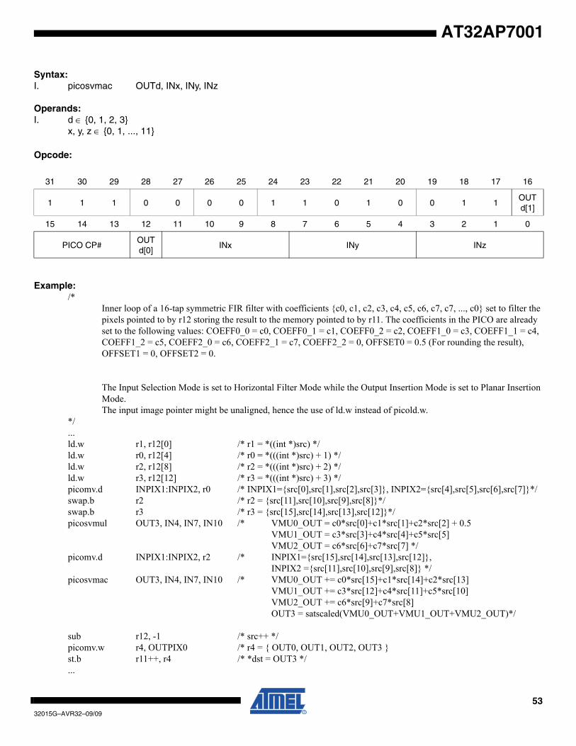
Syntax:I. picosvmac OUTd, INx, INy, INz
Operands:I. d ∈ {0, 1, 2, 3}
x, y, z ∈ {0, 1, ..., 11}
Opcode:
Example:/*
Inner loop of a 16-tap symmetric FIR filter with coefficients {c0, c1, c2, c3, c4, c5, c6, c7, c7, ..., c0} set to filter thepixels pointed to by r12 storing the result to the memory pointed to by r11. The coefficients in the PICO are alreadyset to the following values: COEFF0_0 = c0, COEFF0_1 = c1, COEFF0_2 = c2, COEFF1_0 = c3, COEFF1_1 = c4,COEFF1_2 = c5, COEFF2_0 = c6, COEFF2_1 = c7, COEFF2_2 = 0, OFFSET0 = 0.5 (For rounding the result),OFFSET1 = 0, OFFSET2 = 0.
The Input Selection Mode is set to Horizontal Filter Mode while the Output Insertion Mode is set to Planar InsertionMode.The input image pointer might be unaligned, hence the use of ld.w instead of picold.w.
*/...ld.w r1, r12[0] /* r1 = *((int *)src) */ld.w r0, r12[4] /* r0 = *(((int *)src) + 1) */ld.w r2, r12[8] /* r2 = *(((int *)src) + 2) */ld.w r3, r12[12] /* r3 = *(((int *)src) + 3) */picomv.d INPIX1:INPIX2, r0 /* INPIX1={src[0],src[1],src[2],src[3]}, INPIX2={src[4],src[5],src[6],src[7]}*/swap.b r2 /* r2 = {src[11],src[10],src[9],src[8]}*/swap.b r3 /* r3 = {src[15],src[14],src[13],src[12]}*/picosvmul OUT3, IN4, IN7, IN10 /* VMU0_OUT = c0*src[0]+c1*src[1]+c2*src[2] + 0.5
VMU1_OUT = c3*src[3]+c4*src[4]+c5*src[5] VMU2_OUT = c6*src[6]+c7*src[7] */
picomv.d INPIX1:INPIX2, r2 /* INPIX1={src[15],src[14],src[13],src[12]},INPIX2 ={src[11],src[10],src[9],src[8]} */
picosvmac OUT3, IN4, IN7, IN10 /* VMU0_OUT += c0*src[15]+c1*src[14]+c2*src[13] VMU1_OUT += c3*src[12]+c4*src[11]+c5*src[10]
VMU2_OUT += c6*src[9]+c7*src[8] OUT3 = satscaled(VMU0_OUT+VMU1_OUT+VMU2_OUT)*/
sub r12, -1 /* src++ */picomv.w r4, OUTPIX0 /* r4 = { OUT0, OUT1, OUT2, OUT3 }st.b r11++, r4 /* *dst = OUT3 */...
31 30 29 28 27 26 25 24 23 22 21 20 19 18 17 16
1 1 1 0 0 0 0 1 1 0 1 0 0 1 1OUTd[1]
15 14 13 12 11 10 9 8 7 6 5 4 3 2 1 0
PICO CP#OUTd[0]
INx INy INz
5432015G–AVR32–09/09
AT32AP7001
PICOSVMUL – PICO Single Vector Multiplication
DescriptionPerforms three vector multiplications where the input pixels taken from the INPIXn registers depends on the Input Selection Mode and the input pixel addresses given in the instruction. The results from each Vector Multiplication Unit (VMU) are then added together for one of the outputs to the Output Pixels Inserter to form the result of a single vector multiplication of two 9-element vectors. The results from the VMUs are then scaled and saturated to unsigned 8-bit values before being inserted into the OUTPIXn registers. Which pixels to update in the OUTPIXn registers depend upon the Output Insertion Mode and the output pixel address given in the instruction.
Operation:I. OFFSET_SCALE = COEFF_FRAC_BITS - OFFSET_FRAC_BITS
if ( Input Selection Mode == Horizontal Filter Mode ) then
else if ( Input Selection Mode == Vertical Filter Mode ) then
else if ( Input Selection Mode == Transformation Mode ) then
if ( Output Insertion Mode == Packed Insertion Mode ) thenOUT(d*3 + 0) ← SATSU(ASR(VMU0_OUT + VMU1_OUT + VMU2_OUT, COEFF_FRAC_BITS), 8);OUT(d*3 + 1) ← SATSU(ASR(VMU1_OUT, COEFF_FRAC_BITS), 8);OUT(d*3 + 2) ← SATSU(ASR(VMU2_OUT, COEFF_FRAC_BITS), 8);
else if ( Output Insertion Mode == Planar Insertion Mode ) thenOUT(d + 0) ← SATSU(ASR(VMU0_OUT + VMU1_OUT+ VMU2_OUT, COEFF_FRAC_BITS), 8);OUT(d + 4) ← SATSU(ASR(VMU1_OUT, COEFF_FRAC_BITS), 8);OUT(d + 8) ← SATSU(ASR(VMU2_OUT, COEFF_FRAC_BITS), 8);
VMU0_OUT COEFF0_0 COEFF0_1 COEFF0_2IN(x+0)IN(x+1)IN(x+2)
OFFSET0 << OFFSET_SCALE+=
VMU1_OUT COEFF1_0 COEFF1_1 COEFF1_2IN(y+0)IN(y+1)IN(y+2)
OFFSET1 << OFFSET_SCALE+=
VMU2_OUT COEFF2_0 COEFF2_1 COEFF2_2IN(z+0)IN(z+1)IN(z+2)
OFFSET2 << OFFSET_SCALE+=
VMU0_OUT COEFF0_0 COEFF0_1 COEFF0_2IN((x+0)%11)IN((x+4)%11)IN((x+8)%11)
OFFSET0 << OFFSET_SCALE+=
VMU1_OUT COEFF1_0 COEFF1_1 COEFF1_2IN((y+0)%11)IN((y+4)%11)IN((y+8)%11)
OFFSET1 << OFFSET_SCALE+=
VMU2_OUT COEFF2_0 COEFF2_1 COEFF2_2IN((z+0)%11)IN((z+4)%11)IN((z+8)%11)
OFFSET2 << OFFSET_SCALE+=
VMU0_OUTVMU1_OUTVMU2_OUT
COEFF0_0 COEFF0_1 COEFF0_2COEFF1_0 COEFF1_1 COEFF1_2COEFF2_0 COEFF2_1 COEFF2_2
INxINyINz
OFFSET0 << OFFSET_SCALEOFFSET1 << OFFSET_SCALEOFFSE20 << OFFSET_SCALE
+=
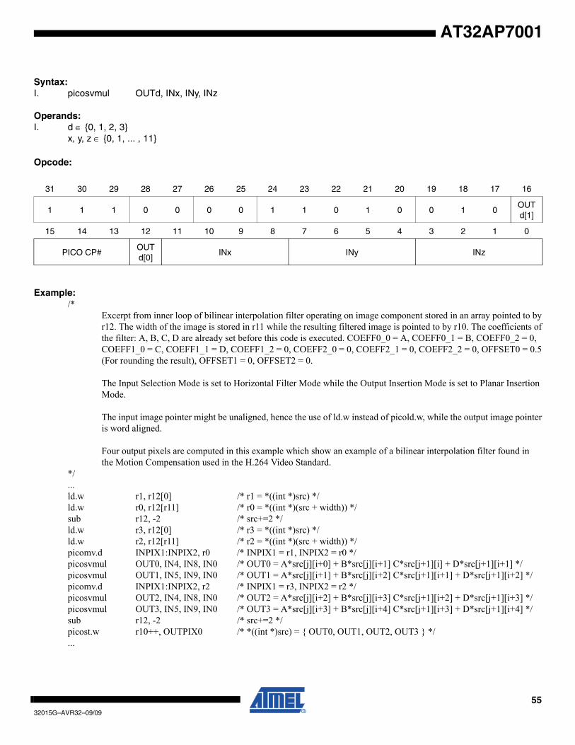
5532015G–AVR32–09/09
AT32AP7001
Syntax:I. picosvmul OUTd, INx, INy, INz
Operands:I. d ∈ {0, 1, 2, 3}
x, y, z ∈ {0, 1, ... , 11}
Opcode:
Example:/*
Excerpt from inner loop of bilinear interpolation filter operating on image component stored in an array pointed to byr12. The width of the image is stored in r11 while the resulting filtered image is pointed to by r10. The coefficients ofthe filter: A, B, C, D are already set before this code is executed. COEFF0_0 = A, COEFF0_1 = B, COEFF0_2 = 0,COEFF1_0 = C, COEFF1_1 = D, COEFF1_2 = 0, COEFF2_0 = 0, COEFF2_1 = 0, COEFF2_2 = 0, OFFSET0 = 0.5(For rounding the result), OFFSET1 = 0, OFFSET2 = 0.
The Input Selection Mode is set to Horizontal Filter Mode while the Output Insertion Mode is set to Planar InsertionMode.
The input image pointer might be unaligned, hence the use of ld.w instead of picold.w, while the output image pointeris word aligned.
Four output pixels are computed in this example which show an example of a bilinear interpolation filter found inthe Motion Compensation used in the H.264 Video Standard.
*/...ld.w r1, r12[0] /* r1 = *((int *)src) */ld.w r0, r12[r11] /* r0 = *((int *)(src + width)) */sub r12, -2 /* src+=2 */ld.w r3, r12[0] /* r3 = *((int *)src) */ld.w r2, r12[r11] /* r2 = *((int *)(src + width)) */picomv.d INPIX1:INPIX2, r0 /* INPIX1 = r1, INPIX2 = r0 */picosvmul OUT0, IN4, IN8, IN0 /* OUT0 = A*src[j][i+0] + B*src[j][i+1] C*src[j+1][i] + D*src[j+1][i+1] */picosvmul OUT1, IN5, IN9, IN0 /* OUT1 = A*src[j][i+1] + B*src[j][i+2] C*src[j+1][i+1] + D*src[j+1][i+2] */picomv.d INPIX1:INPIX2, r2 /* INPIX1 = r3, INPIX2 = r2 */picosvmul OUT2, IN4, IN8, IN0 /* OUT2 = A*src[j][i+2] + B*src[j][i+3] C*src[j+1][i+2] + D*src[j+1][i+3] */picosvmul OUT3, IN5, IN9, IN0 /* OUT3 = A*src[j][i+3] + B*src[j][i+4] C*src[j+1][i+3] + D*src[j+1][i+4] */sub r12, -2 /* src+=2 */picost.w r10++, OUTPIX0 /* *((int *)src) = { OUT0, OUT1, OUT2, OUT3 } */...
31 30 29 28 27 26 25 24 23 22 21 20 19 18 17 16
1 1 1 0 0 0 0 1 1 0 1 0 0 1 0OUTd[1]
15 14 13 12 11 10 9 8 7 6 5 4 3 2 1 0
PICO CP#OUTd[0]
INx INy INz
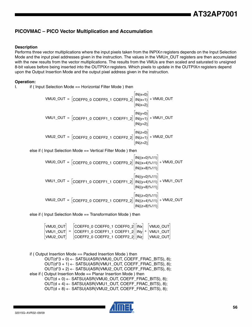
5632015G–AVR32–09/09
AT32AP7001
PICOVMAC – PICO Vector Multiplication and Accumulation
DescriptionPerforms three vector multiplications where the input pixels taken from the INPIXn registers depends on the Input Selection Mode and the input pixel addresses given in the instruction. The values in the VMUn_OUT registers are then accumulated with the new results from the vector multiplications. The results from the VMUs are then scaled and saturated to unsigned 8-bit values before being inserted into the OUTPIXn registers. Which pixels to update in the OUTPIXn registers depend upon the Output Insertion Mode and the output pixel address given in the instruction.
Operation:I. if ( Input Selection Mode == Horizontal Filter Mode ) then
else if ( Input Selection Mode == Vertical Filter Mode ) then
else if ( Input Selection Mode == Transformation Mode ) then
if ( Output Insertion Mode == Packed Insertion Mode ) thenOUT(d*3 + 0) ← SATSU(ASR(VMU0_OUT, COEFF_FRAC_BITS), 8);OUT(d*3 + 1) ← SATSU(ASR(VMU1_OUT, COEFF_FRAC_BITS), 8);OUT(d*3 + 2) ← SATSU(ASR(VMU2_OUT, COEFF_FRAC_BITS), 8);
else if ( Output Insertion Mode == Planar Insertion Mode ) thenOUT(d + 0) ← SATSU(ASR(VMU0_OUT, COEFF_FRAC_BITS), 8);OUT(d + 4) ← SATSU(ASR(VMU1_OUT, COEFF_FRAC_BITS), 8);OUT(d + 8) ← SATSU(ASR(VMU2_OUT, COEFF_FRAC_BITS), 8);
VMU0_OUT COEFF0_0 COEFF0_1 COEFF0_2IN(x+0)IN(x+1)IN(x+2)
VMU0_OUT+=
VMU1_OUT COEFF1_0 COEFF1_1 COEFF1_2IN(y+0)IN(y+1)IN(y+2)
VMU1_OUT+=
VMU2_OUT COEFF2_0 COEFF2_1 COEFF2_2IN(z+0)IN(z+1)IN(z+2)
VMU2_OUT+=
VMU0_OUT COEFF0_0 COEFF0_1 COEFF0_2IN((x+0)%11)IN((x+4)%11)IN((x+8)%11)
VMU0_OUT+=
VMU1_OUT COEFF1_0 COEFF1_1 COEFF1_2IN((y+0)%11)IN((y+4)%11)IN((y+8)%11)
VMU1_OUT+=
VMU2_OUT COEFF2_0 COEFF2_1 COEFF2_2IN((z+0)%11)IN((z+4)%11)IN((z+8)%11)
VMU2_OUT+=
VMU0_OUTVMU1_OUTVMU2_OUT
COEFF0_0 COEFF0_1 COEFF0_2COEFF1_0 COEFF1_1 COEFF1_2COEFF2_0 COEFF2_1 COEFF2_2
INxINyINz
VMU0_OUTVMU1_OUTVMU2_OUT
+=
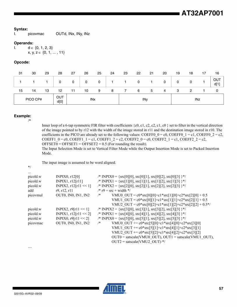
5732015G–AVR32–09/09
AT32AP7001
Syntax:I. picovmac OUTd, INx, INy, INz
Operands:I. d ∈ {0, 1, 2, 3}
x, y, z ∈ {0, 1, ... , 11}
Opcode:
Example:/*
Inner loop of a 6-tap symmetric FIR filter with coefficients {c0, c1, c2, c2, c1, c0 } set to filter in the vertical direction of the image pointed to by r12 with the width of the image stored in r11 and the destination image stored in r10. Thecoefficients in the PICO are already set to the following values: COEFF0_0 = c0, COEFF0_1 = c1, COEFF0_2 = c2,COEFF1_0 = c0, COEFF1_1 = c1, COEFF1_2 = c2, COEFF2_0 = c0, COEFF2_1 = c1, COEFF2_2 = c2, OFFSET0 = OFFSET1 = OFFSET2 = 0.5 (For rounding the result).The Input Selection Mode is set to Vertical Filter Mode while the Output Insertion Mode is set to Packed InsertionMode.
The input image is assumed to be word aligned.*/...picold.w INPIX0, r12[0] /* INPIX0 = {src[0][0], src[0][1], src[0][2], src[0][3] }*/picold.w INPIX1, r12[r11] /* INPIX1 = {src[1][0], src[1][1], src[1][2], src[1][3] }*/picold.w INPIX2, r12[r11 << 1] /* INPIX2 = {src[2][0], src[2][1], src[2][2], src[2][3] }*/add r9, r12, r11 /* r9 = src + width */picovmul OUT0, IN0, IN1, IN2 /* VMU0_OUT = c0*src[0][0]+c1*src[1][0]+c2*src[2][0] + 0.5
VMU1_OUT = c0*src[0][1]+c1*src[1][1]+c2*src[2][1] + 0.5VMU2_OUT = c0*src[0][2]+c1*src[1][2]+c2*src[2][2] + 0.5*/
picold.w INPIX2, r9[r11 << 1] /* INPIX2 = {src[3][0], src[3][1], src[3][2], src[3][3] }*/picold.w INPIX1, r12[r11 << 2] /* INPIX1 = {src[4][0], src[4][1], src[4][2], src[4][3] }*/picold.w INPIX0, r9[r11 << 2] /* INPIX0 = {src[5][0], src[5][1], src[5][2], src[5][3] }*/picovmac OUT0, IN0, IN1, IN2 /* VMU0_OUT += c0*src[5][0]+c1*src[4][0]+c2*src[3][0]
VMU1_OUT += c0*src[5][1]+c1*src[4][1]+c2*src[3][1] VMU2_OUT += c0*src[5][2]+c1*src[4][2]+c2*src[3][2] OUT0 = satscale(VMU0_OUT), OUT1 = satscale(VMU1_OUT),OUT2 = satscale(VMU2_OUT) */
....
31 30 29 28 27 26 25 24 23 22 21 20 19 18 17 16
1 1 1 0 0 0 0 1 1 0 1 0 0 0 1OUTd[1]
15 14 13 12 11 10 9 8 7 6 5 4 3 2 1 0
PICO CP#OUTd[0]
INx INy INz

5832015G–AVR32–09/09
AT32AP7001
PICOVMUL – PICO Vector Multiplication
DescriptionPerforms three vector multiplications where the input pixels taken from the INPIXn registers depends on the Input Selection Mode and the input pixel addresses given in the instruction. The results from the VMUs are then scaled and saturated to unsigned 8-bit values before being inserted into the OUTPIXn registers. Which pixels to update in the OUTPIXn registers depend upon the Output Insertion Mode and the output pixel address given in the instruction.
Operation:I. OFFSET_SCALE = COEFF_FRAC_BITS - OFFSET_FRAC_BITS
if ( Input Selection Mode == Horizontal Filter Mode ) then
else if ( Input Selection Mode == Vertical Filter Mode ) then
else if ( Input Selection Mode == Transformation Mode ) then
if ( Output Insertion Mode == Packed Insertion Mode ) thenOUT(d*3 + 0) ← SATSU(ASR(VMU0_OUT, COEFF_FRAC_BITS), 8);OUT(d*3 + 1) ← SATSU(ASR(VMU1_OUT, COEFF_FRAC_BITS), 8);OUT(d*3 + 2) ← SATSU(ASR(VMU2_OUT, COEFF_FRAC_BITS), 8);
else if ( Output Insertion Mode == Planar Insertion Mode ) thenOUT(d + 0) ← SATSU(ASR(VMU0_OUT, COEFF_FRAC_BITS), 8);OUT(d + 4) ← SATSU(ASR(VMU1_OUT, COEFF_FRAC_BITS), 8);OUT(d + 8) ← SATSU(ASR(VMU2_OUT, COEFF_FRAC_BITS), 8);
VMU0_OUT COEFF0_0 COEFF0_1 COEFF0_2IN(x+0)IN(x+1)IN(x+2)
OFFSET0 << OFFSET_SCALE+=
VMU1_OUT COEFF1_0 COEFF1_1 COEFF1_2IN(y+0)IN(y+1)IN(y+2)
OFFSET1 << OFFSET_SCALE+=
VMU2_OUT COEFF2_0 COEFF2_1 COEFF2_2IN(z+0)IN(z+1)IN(z+2)
OFFSET2 << OFFSET_SCALE+=
VMU0_OUT COEFF0_0 COEFF0_1 COEFF0_2IN((x+0)%11)IN((x+4)%11)IN((x+8)%11)
OFFSET0 << OFFSET_SCALE+=
VMU1_OUT COEFF1_0 COEFF1_1 COEFF1_2IN((y+0)%11)IN((y+4)%11)IN((y+8)%11)
OFFSET1 << OFFSET_SCALE+=
VMU2_OUT COEFF2_0 COEFF2_1 COEFF2_2IN((z+0)%11)IN((z+4)%11)IN((z+8)%11)
OFFSET2 << OFFSET_SCALE+=
VMU0_OUTVMU1_OUTVMU2_OUT
COEFF0_0 COEFF0_1 COEFF0_2COEFF1_0 COEFF1_1 COEFF1_2COEFF2_0 COEFF2_1 COEFF2_2
INxINyINz
OFFSET0 << OFFSET_SCALEOFFSET1 << OFFSET_SCALEOFFSE20 << OFFSET_SCALE
+=
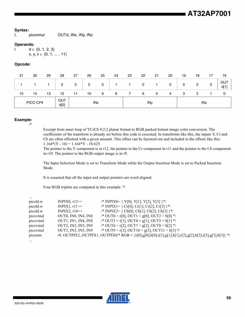
5932015G–AVR32–09/09
AT32AP7001
Syntax:I. picovmul OUTd, INx, INy, INz
Operands:I. d ∈ {0, 1, 2, 3}
x, y, z ∈ {0, 1, ... , 11}
Opcode:
Example:/*
Excerpt from inner loop of YCrCb 4:2:2 planar format to RGB packed format image color conversion. The coefficients of the transform is already set before this code is executed. In transforms like this, the inputs Y, Cr andCb are often offsetted with a given amount. This offset can be factored out and included in the offsets like this:1.164*(Y - 16) = 1.164*Y - 18.625. The pointer to the Y component is in r12, the pointer to the Cr component in r11 and the pointer to the Cb componentin r10. The pointer to the RGB output image is in r9.
The Input Selection Mode is set to Transform Mode while the Output Insertion Mode is set to Packed InsertionMode.
It is assumed that all the input and output pointers are word aligned.
Four RGB triplets are computed in this example. */
...picold.w INPIX0, r12++ /* INPIX0= { Y[0], Y[1], Y[2], Y[3] }*/picold.w INPIX1, r11++ /* INPIX1= { Cr[0], Cr[1], Cr[2], Cr[3] }*/picold.w INPIX2, r10++ /* INPIX2= { Cb[0], Cb[1], Cb[2], Cb[3] }*/picovmul OUT0, IN0, IN4, IN8 /* OUT0 = r[0], OUT1 = g[0], OUT2 = b[0] */picovmul OUT1, IN1, IN4, IN8 /* OUT3 = r[1], OUT4 = g[1], OUT5 = b[1] */picovmul OUT2, IN2, IN5, IN9 /* OUT6 = r[2], OUT7 = g[2], OUT8 = b[2] */picovmul OUT3, IN3, IN5, IN9 /* OUT9 = r[3], OUT10 = g[3], OUT11 = b[3] */picostm r9, OUTPIX2, OUTPIX1, OUTPIX0/* RGB = {r[0],g[0],b[0],r[1],g[1],b[1],r[2],g[2],b[2],r[3],g[3],b[3]} */...
31 30 29 28 27 26 25 24 23 22 21 20 19 18 17 16
1 1 1 0 0 0 0 1 1 0 1 0 0 0 0OUTd[1]
15 14 13 12 11 10 9 8 7 6 5 4 3 2 1 0
PICO CP#OUTd[0]
INx INy INz
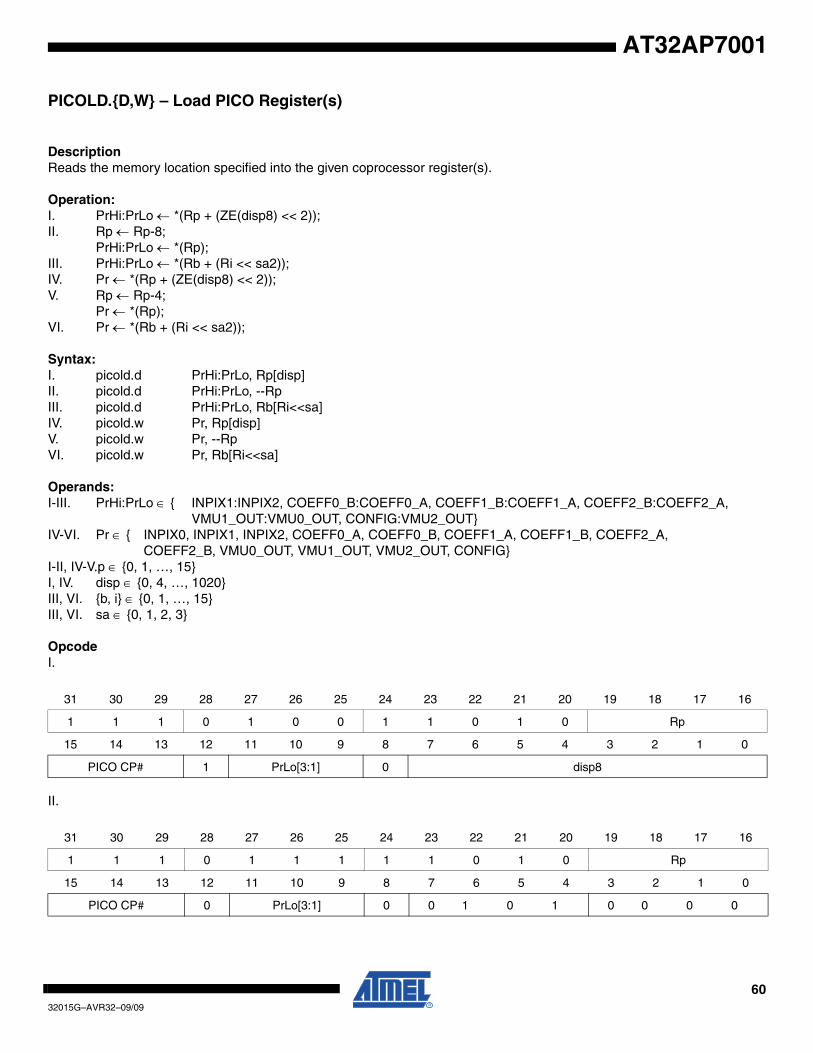
6032015G–AVR32–09/09
AT32AP7001
PICOLD.{D,W} – Load PICO Register(s)
DescriptionReads the memory location specified into the given coprocessor register(s).
Operation:I. PrHi:PrLo ← *(Rp + (ZE(disp8) << 2));II. Rp ← Rp-8;
PrHi:PrLo ← *(Rp);III. PrHi:PrLo ← *(Rb + (Ri << sa2));IV. Pr ← *(Rp + (ZE(disp8) << 2));V. Rp ← Rp-4;
Pr ← *(Rp);VI. Pr ← *(Rb + (Ri << sa2));
Syntax:I. picold.d PrHi:PrLo, Rp[disp]II. picold.d PrHi:PrLo, --RpIII. picold.d PrHi:PrLo, Rb[Ri<<sa]IV. picold.w Pr, Rp[disp]V. picold.w Pr, --RpVI. picold.w Pr, Rb[Ri<<sa]
Operands:I-III. PrHi:PrLo ∈ { INPIX1:INPIX2, COEFF0_B:COEFF0_A, COEFF1_B:COEFF1_A, COEFF2_B:COEFF2_A,
VMU1_OUT:VMU0_OUT, CONFIG:VMU2_OUT}IV-VI. Pr ∈ { INPIX0, INPIX1, INPIX2, COEFF0_A, COEFF0_B, COEFF1_A, COEFF1_B, COEFF2_A,
COEFF2_B, VMU0_OUT, VMU1_OUT, VMU2_OUT, CONFIG}I-II, IV-V.p ∈ {0, 1, …, 15}I, IV. disp ∈ {0, 4, …, 1020}III, VI. {b, i} ∈ {0, 1, …, 15}III, VI. sa ∈ {0, 1, 2, 3}
OpcodeI.
II.
31 30 29 28 27 26 25 24 23 22 21 20 19 18 17 16
1 1 1 0 1 0 0 1 1 0 1 0 Rp
15 14 13 12 11 10 9 8 7 6 5 4 3 2 1 0
PICO CP# 1 PrLo[3:1] 0 disp8
31 30 29 28 27 26 25 24 23 22 21 20 19 18 17 16
1 1 1 0 1 1 1 1 1 0 1 0 Rp
15 14 13 12 11 10 9 8 7 6 5 4 3 2 1 0
PICO CP# 0 PrLo[3:1] 0 0 1 0 1 0 0 0 0
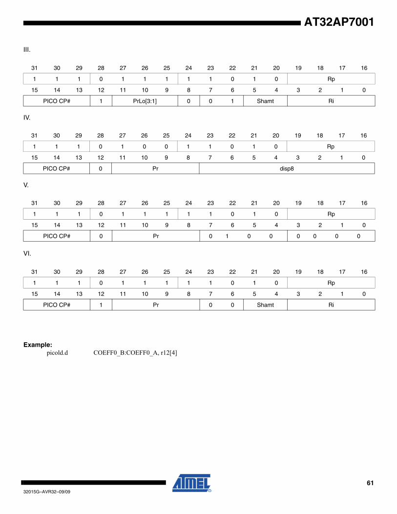
6132015G–AVR32–09/09
AT32AP7001
III.
IV.
V.
VI.
Example:picold.d COEFF0_B:COEFF0_A, r12[4]
31 30 29 28 27 26 25 24 23 22 21 20 19 18 17 16
1 1 1 0 1 1 1 1 1 0 1 0 Rp
15 14 13 12 11 10 9 8 7 6 5 4 3 2 1 0
PICO CP# 1 PrLo[3:1] 0 0 1 Shamt Ri
31 30 29 28 27 26 25 24 23 22 21 20 19 18 17 16
1 1 1 0 1 0 0 1 1 0 1 0 Rp
15 14 13 12 11 10 9 8 7 6 5 4 3 2 1 0
PICO CP# 0 Pr disp8
31 30 29 28 27 26 25 24 23 22 21 20 19 18 17 16
1 1 1 0 1 1 1 1 1 0 1 0 Rp
15 14 13 12 11 10 9 8 7 6 5 4 3 2 1 0
PICO CP# 0 Pr 0 1 0 0 0 0 0 0
31 30 29 28 27 26 25 24 23 22 21 20 19 18 17 16
1 1 1 0 1 1 1 1 1 0 1 0 Rp
15 14 13 12 11 10 9 8 7 6 5 4 3 2 1 0
PICO CP# 1 Pr 0 0 Shamt Ri
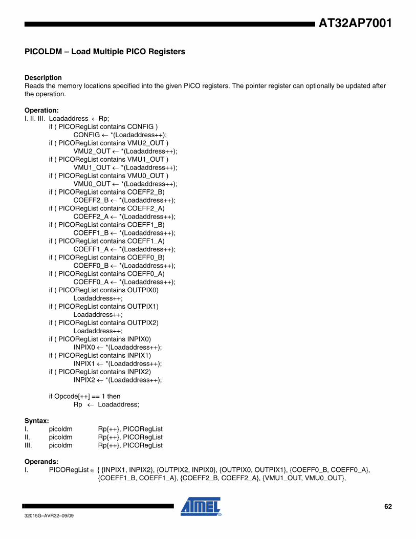
6232015G–AVR32–09/09
AT32AP7001
PICOLDM – Load Multiple PICO Registers
DescriptionReads the memory locations specified into the given PICO registers. The pointer register can optionally be updated after the operation.
Operation:I. II. III. Loadaddress ←Rp;
if ( PICORegList contains CONFIG )CONFIG ← *(Loadaddress++);
if ( PICORegList contains VMU2_OUT )VMU2_OUT ← *(Loadaddress++);
if ( PICORegList contains VMU1_OUT )VMU1_OUT ← *(Loadaddress++);
if ( PICORegList contains VMU0_OUT )VMU0_OUT ← *(Loadaddress++);
if ( PICORegList contains COEFF2_B)COEFF2_B ← *(Loadaddress++);
if ( PICORegList contains COEFF2_A)COEFF2_A ← *(Loadaddress++);
if ( PICORegList contains COEFF1_B)COEFF1_B ← *(Loadaddress++);
if ( PICORegList contains COEFF1_A)COEFF1_A ← *(Loadaddress++);
if ( PICORegList contains COEFF0_B)COEFF0_B ← *(Loadaddress++);
if ( PICORegList contains COEFF0_A)COEFF0_A ← *(Loadaddress++);
if ( PICORegList contains OUTPIX0)Loadaddress++;
if ( PICORegList contains OUTPIX1)Loadaddress++;
if ( PICORegList contains OUTPIX2)Loadaddress++;
if ( PICORegList contains INPIX0)INPIX0 ← *(Loadaddress++);
if ( PICORegList contains INPIX1)INPIX1 ← *(Loadaddress++);
if ( PICORegList contains INPIX2)INPIX2 ← *(Loadaddress++);
if Opcode[++] == 1 thenRp ← Loadaddress;
Syntax:I. picoldm Rp{++}, PICORegListII. picoldm Rp{++}, PICORegListIII. picoldm Rp{++}, PICORegList
Operands:I. PICORegList ∈ { {INPIX1, INPIX2}, {OUTPIX2, INPIX0}, {OUTPIX0, OUTPIX1}, {COEFF0_B, COEFF0_A},
{COEFF1_B, COEFF1_A}, {COEFF2_B, COEFF2_A}, {VMU1_OUT, VMU0_OUT},

6332015G–AVR32–09/09
AT32AP7001
{CONFIG, VMU2_OUT} }II. PICORegList ∈ { INPIX0, INPIX1, INPIX2, OUTPIX0, OUTPIX1, OUTPIX2, COEFF0_A, COEFF0_B }III. PICORegList ∈ { COEFF1_A, COEFF1_B, COEFF2_A,COEFF2_B, VMU0_OUT,VMU1_OUT,
VMU2_OUT, CONFIG, }I-III. p ∈ {0, 1, …, 15}
OpcodeI.
II.
III.
Example:I. picoldm r7++, COEFF0_A, COEFF0_B, COEFF1_A, COEFF1_B, COEFF2_A, COEFF2_BII. picoldm r0, INPIX0, INPIX1, INPIX2III. picoldm r12, VMU0_OUT, VMU1_OUT, VMU2_OUT
31 30 29 28 27 26 25 24 23 22 21 20 19 18 17 16
1 1 1 0 1 1 0 1 1 0 1 0 Rp
15 14 13 12 11 10 9 8 7 6 5 4 3 2 1 0
PICO CP# W 0 1 0 0 CONFIGVMU2_OUT
VMU1_OUTVMU0_OUT
COEFF2_BCOEFF2_A
COEFF1_BCOEFF1_A
COEFF0_BCOEFF0_A
OUTPIX0OUTPIX1
OUTPIX2INPIX0
INPIX1INPIX2
31 30 29 28 27 26 25 24 23 22 21 20 19 18 17 16
1 1 1 0 1 1 0 1 1 0 1 0 Rp
15 14 13 12 11 10 9 8 7 6 5 4 3 2 1 0
PICO CP# W 0 0 0 0 COEFF0_B COEFF0_A OUTPIX0 OUTPIX1 OUTPIX2 INPIX0 INPIX1 INPIX2
31 30 29 28 27 26 25 24 23 22 21 20 19 18 17 16
1 1 1 0 1 1 0 1 1 0 1 0 Rp
15 14 13 12 11 10 9 8 7 6 5 4 3 2 1 0
PICO CP# W 0 0 0 1 CONFIG VMU2_OUT VMU1_OUT VMU0_OUT COEFF2_B COEFF2_A COEFF1_B COEFF1_A
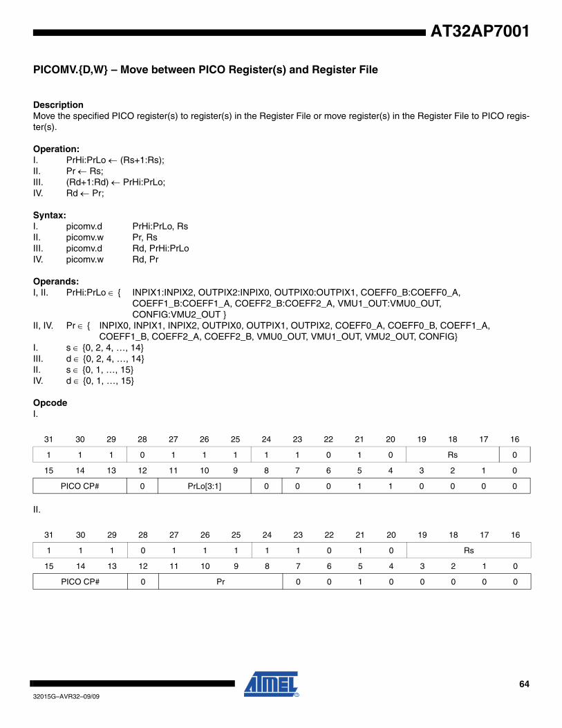
6432015G–AVR32–09/09
AT32AP7001
PICOMV.{D,W} – Move between PICO Register(s) and Register File
DescriptionMove the specified PICO register(s) to register(s) in the Register File or move register(s) in the Register File to PICO regis-ter(s).
Operation:I. PrHi:PrLo ← (Rs+1:Rs);II. Pr ← Rs;III. (Rd+1:Rd) ← PrHi:PrLo;IV. Rd ← Pr;
Syntax:I. picomv.d PrHi:PrLo, RsII. picomv.w Pr, RsIII. picomv.d Rd, PrHi:PrLoIV. picomv.w Rd, Pr
Operands:I, II. PrHi:PrLo ∈ { INPIX1:INPIX2, OUTPIX2:INPIX0, OUTPIX0:OUTPIX1, COEFF0_B:COEFF0_A,
COEFF1_B:COEFF1_A, COEFF2_B:COEFF2_A, VMU1_OUT:VMU0_OUT, CONFIG:VMU2_OUT }
II, IV. Pr ∈ { INPIX0, INPIX1, INPIX2, OUTPIX0, OUTPIX1, OUTPIX2, COEFF0_A, COEFF0_B, COEFF1_A,COEFF1_B, COEFF2_A, COEFF2_B, VMU0_OUT, VMU1_OUT, VMU2_OUT, CONFIG}
I. s ∈ {0, 2, 4, …, 14}III. d ∈ {0, 2, 4, …, 14}II. s ∈ {0, 1, …, 15}IV. d ∈ {0, 1, …, 15}
OpcodeI.
II.
31 30 29 28 27 26 25 24 23 22 21 20 19 18 17 16
1 1 1 0 1 1 1 1 1 0 1 0 Rs 0
15 14 13 12 11 10 9 8 7 6 5 4 3 2 1 0
PICO CP# 0 PrLo[3:1] 0 0 0 1 1 0 0 0 0
31 30 29 28 27 26 25 24 23 22 21 20 19 18 17 16
1 1 1 0 1 1 1 1 1 0 1 0 Rs
15 14 13 12 11 10 9 8 7 6 5 4 3 2 1 0
PICO CP# 0 Pr 0 0 1 0 0 0 0 0
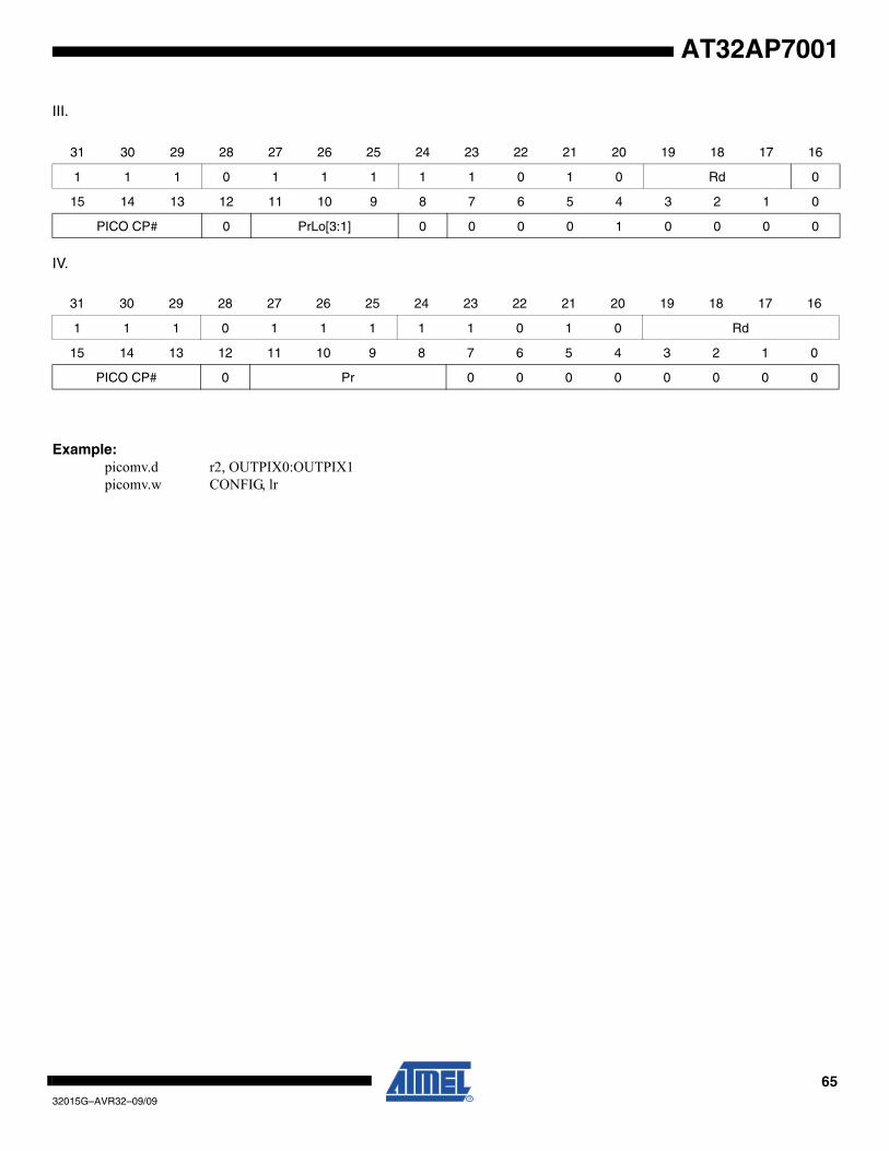
6532015G–AVR32–09/09
AT32AP7001
III.
IV.
Example:picomv.d r2, OUTPIX0:OUTPIX1picomv.w CONFIG, lr
31 30 29 28 27 26 25 24 23 22 21 20 19 18 17 16
1 1 1 0 1 1 1 1 1 0 1 0 Rd 0
15 14 13 12 11 10 9 8 7 6 5 4 3 2 1 0
PICO CP# 0 PrLo[3:1] 0 0 0 0 1 0 0 0 0
31 30 29 28 27 26 25 24 23 22 21 20 19 18 17 16
1 1 1 0 1 1 1 1 1 0 1 0 Rd
15 14 13 12 11 10 9 8 7 6 5 4 3 2 1 0
PICO CP# 0 Pr 0 0 0 0 0 0 0 0
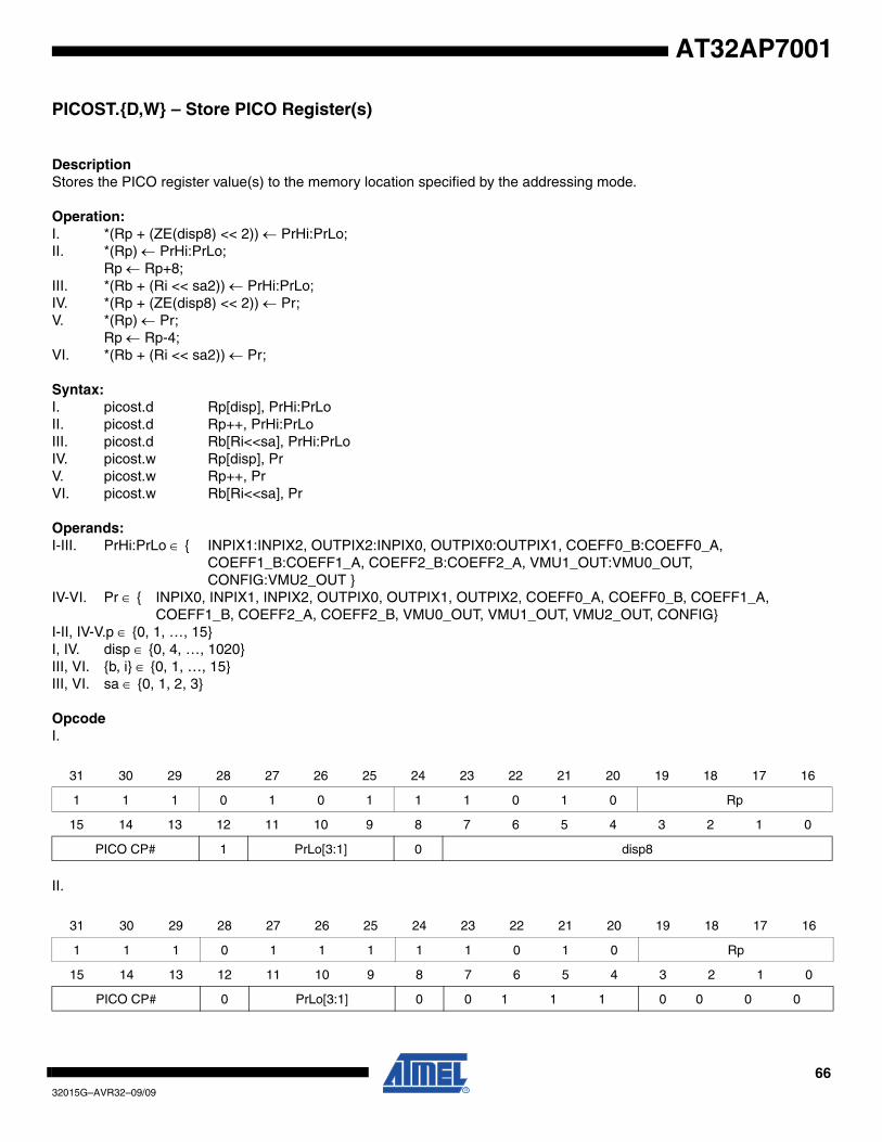
6632015G–AVR32–09/09
AT32AP7001
PICOST.{D,W} – Store PICO Register(s)
DescriptionStores the PICO register value(s) to the memory location specified by the addressing mode.
Operation:I. *(Rp + (ZE(disp8) << 2)) ← PrHi:PrLo;II. *(Rp) ← PrHi:PrLo;
Rp ← Rp+8;III. *(Rb + (Ri << sa2)) ← PrHi:PrLo;IV. *(Rp + (ZE(disp8) << 2)) ← Pr;V. *(Rp) ← Pr;
Rp ← Rp-4;VI. *(Rb + (Ri << sa2)) ← Pr;
Syntax:I. picost.d Rp[disp], PrHi:PrLo II. picost.d Rp++, PrHi:PrLo III. picost.d Rb[Ri<<sa], PrHi:PrLoIV. picost.w Rp[disp], Pr V. picost.w Rp++, Pr VI. picost.w Rb[Ri<<sa], Pr
Operands:I-III. PrHi:PrLo ∈ { INPIX1:INPIX2, OUTPIX2:INPIX0, OUTPIX0:OUTPIX1, COEFF0_B:COEFF0_A,
COEFF1_B:COEFF1_A, COEFF2_B:COEFF2_A, VMU1_OUT:VMU0_OUT, CONFIG:VMU2_OUT }
IV-VI. Pr ∈ { INPIX0, INPIX1, INPIX2, OUTPIX0, OUTPIX1, OUTPIX2, COEFF0_A, COEFF0_B, COEFF1_A,COEFF1_B, COEFF2_A, COEFF2_B, VMU0_OUT, VMU1_OUT, VMU2_OUT, CONFIG}
I-II, IV-V.p ∈ {0, 1, …, 15}I, IV. disp ∈ {0, 4, …, 1020}III, VI. {b, i} ∈ {0, 1, …, 15}III, VI. sa ∈ {0, 1, 2, 3}
OpcodeI.
II.
31 30 29 28 27 26 25 24 23 22 21 20 19 18 17 16
1 1 1 0 1 0 1 1 1 0 1 0 Rp
15 14 13 12 11 10 9 8 7 6 5 4 3 2 1 0
PICO CP# 1 PrLo[3:1] 0 disp8
31 30 29 28 27 26 25 24 23 22 21 20 19 18 17 16
1 1 1 0 1 1 1 1 1 0 1 0 Rp
15 14 13 12 11 10 9 8 7 6 5 4 3 2 1 0
PICO CP# 0 PrLo[3:1] 0 0 1 1 1 0 0 0 0
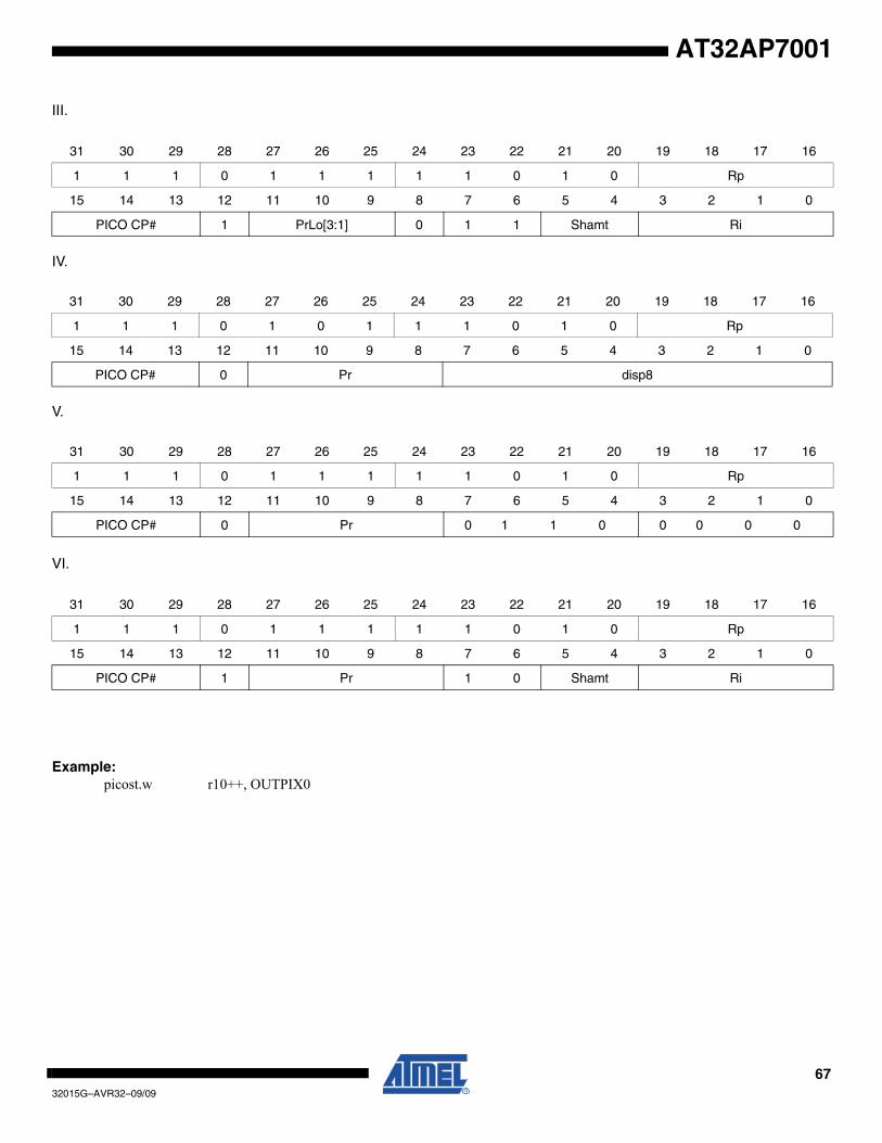
6732015G–AVR32–09/09
AT32AP7001
III.
IV.
V.
VI.
Example:picost.w r10++, OUTPIX0
31 30 29 28 27 26 25 24 23 22 21 20 19 18 17 16
1 1 1 0 1 1 1 1 1 0 1 0 Rp
15 14 13 12 11 10 9 8 7 6 5 4 3 2 1 0
PICO CP# 1 PrLo[3:1] 0 1 1 Shamt Ri
31 30 29 28 27 26 25 24 23 22 21 20 19 18 17 16
1 1 1 0 1 0 1 1 1 0 1 0 Rp
15 14 13 12 11 10 9 8 7 6 5 4 3 2 1 0
PICO CP# 0 Pr disp8
31 30 29 28 27 26 25 24 23 22 21 20 19 18 17 16
1 1 1 0 1 1 1 1 1 0 1 0 Rp
15 14 13 12 11 10 9 8 7 6 5 4 3 2 1 0
PICO CP# 0 Pr 0 1 1 0 0 0 0 0
31 30 29 28 27 26 25 24 23 22 21 20 19 18 17 16
1 1 1 0 1 1 1 1 1 0 1 0 Rp
15 14 13 12 11 10 9 8 7 6 5 4 3 2 1 0
PICO CP# 1 Pr 1 0 Shamt Ri
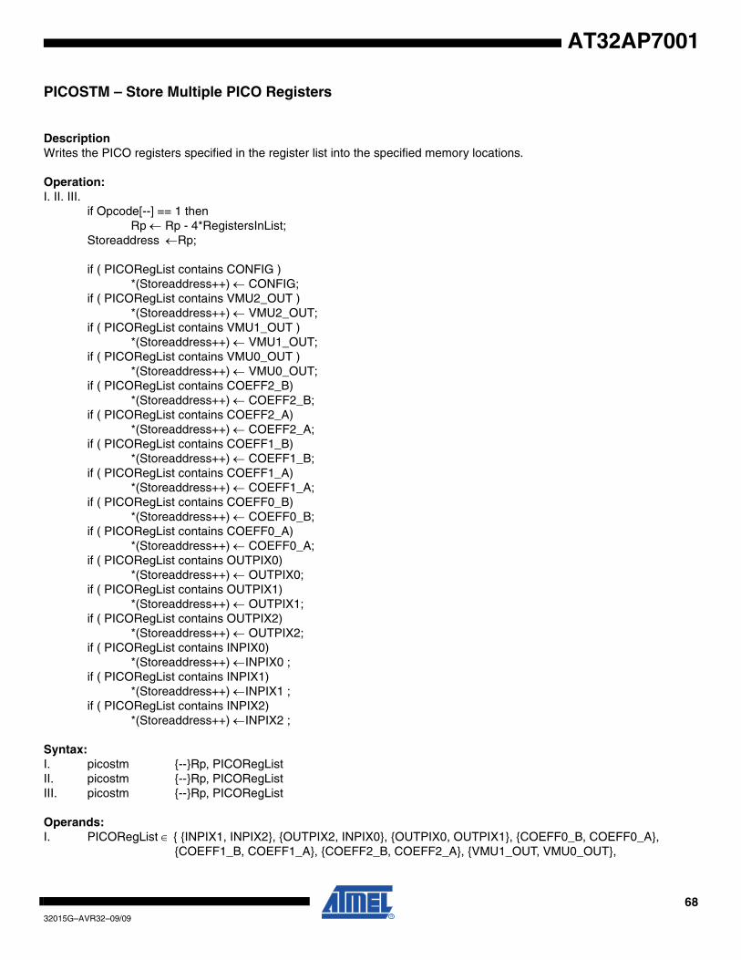
6832015G–AVR32–09/09
AT32AP7001
PICOSTM – Store Multiple PICO Registers
DescriptionWrites the PICO registers specified in the register list into the specified memory locations.
Operation:I. II. III.
if Opcode[--] == 1 thenRp ← Rp - 4*RegistersInList;
Storeaddress ←Rp;
if ( PICORegList contains CONFIG )*(Storeaddress++) ← CONFIG;
if ( PICORegList contains VMU2_OUT )*(Storeaddress++) ← VMU2_OUT;
if ( PICORegList contains VMU1_OUT )*(Storeaddress++) ← VMU1_OUT;
if ( PICORegList contains VMU0_OUT )*(Storeaddress++) ← VMU0_OUT;
if ( PICORegList contains COEFF2_B)*(Storeaddress++) ← COEFF2_B;
if ( PICORegList contains COEFF2_A)*(Storeaddress++) ← COEFF2_A;
if ( PICORegList contains COEFF1_B)*(Storeaddress++) ← COEFF1_B;
if ( PICORegList contains COEFF1_A)*(Storeaddress++) ← COEFF1_A;
if ( PICORegList contains COEFF0_B)*(Storeaddress++) ← COEFF0_B;
if ( PICORegList contains COEFF0_A)*(Storeaddress++) ← COEFF0_A;
if ( PICORegList contains OUTPIX0)*(Storeaddress++) ← OUTPIX0;
if ( PICORegList contains OUTPIX1)*(Storeaddress++) ← OUTPIX1;
if ( PICORegList contains OUTPIX2)*(Storeaddress++) ← OUTPIX2;
if ( PICORegList contains INPIX0)*(Storeaddress++) ←INPIX0 ;
if ( PICORegList contains INPIX1)*(Storeaddress++) ←INPIX1 ;
if ( PICORegList contains INPIX2)*(Storeaddress++) ←INPIX2 ;
Syntax:I. picostm {--}Rp, PICORegListII. picostm {--}Rp, PICORegListIII. picostm {--}Rp, PICORegList
Operands:I. PICORegList ∈ { {INPIX1, INPIX2}, {OUTPIX2, INPIX0}, {OUTPIX0, OUTPIX1}, {COEFF0_B, COEFF0_A},
{COEFF1_B, COEFF1_A}, {COEFF2_B, COEFF2_A}, {VMU1_OUT, VMU0_OUT},
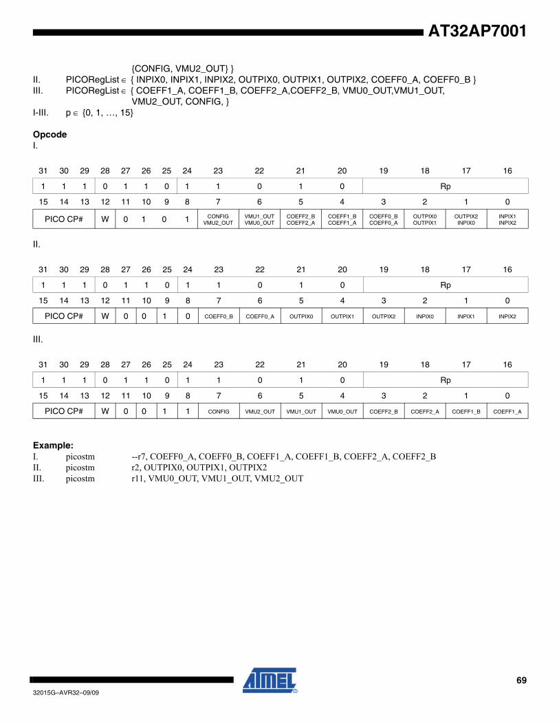
6932015G–AVR32–09/09
AT32AP7001
{CONFIG, VMU2_OUT} }II. PICORegList ∈ { INPIX0, INPIX1, INPIX2, OUTPIX0, OUTPIX1, OUTPIX2, COEFF0_A, COEFF0_B }III. PICORegList ∈ { COEFF1_A, COEFF1_B, COEFF2_A,COEFF2_B, VMU0_OUT,VMU1_OUT,
VMU2_OUT, CONFIG, }I-III. p ∈ {0, 1, …, 15}
OpcodeI.
II.
III.
Example:I. picostm --r7, COEFF0_A, COEFF0_B, COEFF1_A, COEFF1_B, COEFF2_A, COEFF2_BII. picostm r2, OUTPIX0, OUTPIX1, OUTPIX2III. picostm r11, VMU0_OUT, VMU1_OUT, VMU2_OUT
31 30 29 28 27 26 25 24 23 22 21 20 19 18 17 16
1 1 1 0 1 1 0 1 1 0 1 0 Rp
15 14 13 12 11 10 9 8 7 6 5 4 3 2 1 0
PICO CP# W 0 1 0 1 CONFIGVMU2_OUT
VMU1_OUTVMU0_OUT
COEFF2_BCOEFF2_A
COEFF1_BCOEFF1_A
COEFF0_BCOEFF0_A
OUTPIX0OUTPIX1
OUTPIX2INPIX0
INPIX1INPIX2
31 30 29 28 27 26 25 24 23 22 21 20 19 18 17 16
1 1 1 0 1 1 0 1 1 0 1 0 Rp
15 14 13 12 11 10 9 8 7 6 5 4 3 2 1 0
PICO CP# W 0 0 1 0 COEFF0_B COEFF0_A OUTPIX0 OUTPIX1 OUTPIX2 INPIX0 INPIX1 INPIX2
31 30 29 28 27 26 25 24 23 22 21 20 19 18 17 16
1 1 1 0 1 1 0 1 1 0 1 0 Rp
15 14 13 12 11 10 9 8 7 6 5 4 3 2 1 0
PICO CP# W 0 0 1 1 CONFIG VMU2_OUT VMU1_OUT VMU0_OUT COEFF2_B COEFF2_A COEFF1_B COEFF1_A
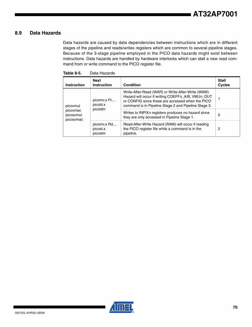
7032015G–AVR32–09/09
AT32AP7001
8.9 Data Hazards
Data hazards are caused by data dependencies between instructions which are in differentstages of the pipeline and reads/writes registers which are common to several pipeline stages.Because of the 3-stage pipeline employed in the PICO data hazards might exist betweeninstructions. Data hazards are handled by hardware interlocks which can stall a new read com-mand from or write command to the PICO register file.
Table 8-5. Data Hazards
InstructionNext Instruction Condition
Stall Cycles
picovmul picovmacpicosvmulpicosvmac
picomv.x Pr,...picold.x picoldm
Write-After-Read (WAR) or Write-After-Write (WAW) Hazard will occur if writing COEFFn_A/B, VMUn_OUT or CONFIG since these are accessed when the PICO command is in Pipeline Stage 2 and Pipeline Stage 3.
1
Writes to INPIXn registers produces no hazard since they are only accessed in Pipeline Stage 1.
0
picomv.x Rd,...picost.xpicostm
Read-After-Write Hazard (RAW) will occur if reading the PICO register file while a command is in the pipeline.
2
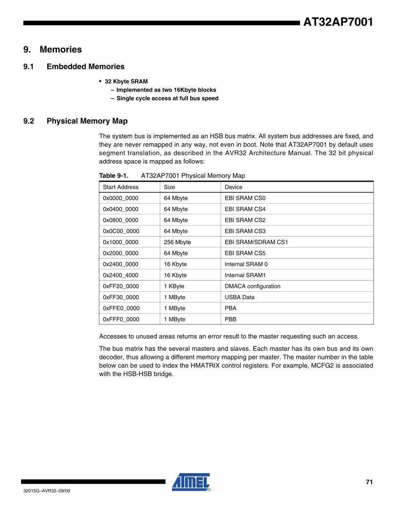
7132015G–AVR32–09/09
AT32AP7001
9. Memories
9.1 Embedded Memories
• 32 Kbyte SRAM– Implemented as two 16Kbyte blocks– Single cycle access at full bus speed
9.2 Physical Memory Map
The system bus is implemented as an HSB bus matrix. All system bus addresses are fixed, andthey are never remapped in any way, not even in boot. Note that AT32AP7001 by default usessegment translation, as described in the AVR32 Architecture Manual. The 32 bit physicaladdress space is mapped as follows:
Accesses to unused areas returns an error result to the master requesting such an access.
The bus matrix has the several masters and slaves. Each master has its own bus and its owndecoder, thus allowing a different memory mapping per master. The master number in the tablebelow can be used to index the HMATRIX control registers. For example, MCFG2 is associatedwith the HSB-HSB bridge.
Table 9-1. AT32AP7001 Physical Memory Map
Start Address Size Device
0x0000_0000 64 Mbyte EBI SRAM CS0
0x0400_0000 64 Mbyte EBI SRAM CS4
0x0800_0000 64 Mbyte EBI SRAM CS2
0x0C00_0000 64 Mbyte EBI SRAM CS3
0x1000_0000 256 Mbyte EBI SRAM/SDRAM CS1
0x2000_0000 64 Mbyte EBI SRAM CS5
0x2400_0000 16 Kbyte Internal SRAM 0
0x2400_4000 16 Kbyte Internal SRAM1
0xFF20_0000 1 KByte DMACA configuration
0xFF30_0000 1 MByte USBA Data
0xFFE0_0000 1 MByte PBA
0xFFF0_0000 1 MByte PBB
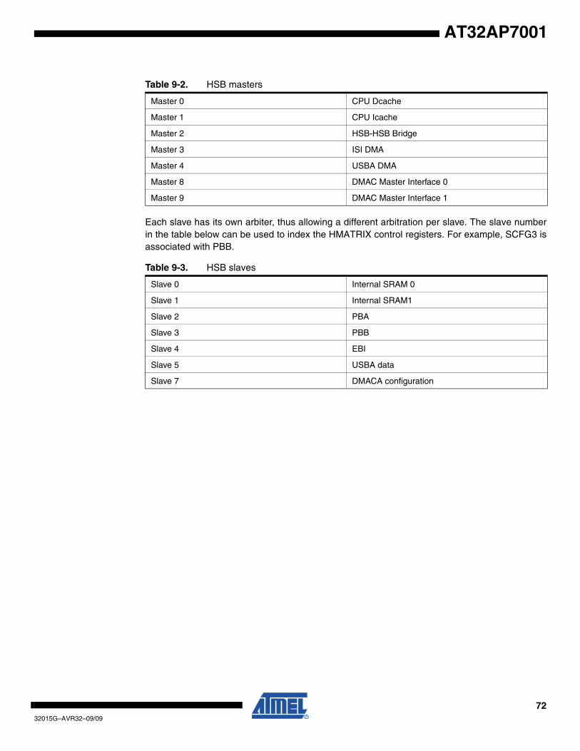
7232015G–AVR32–09/09
AT32AP7001
Each slave has its own arbiter, thus allowing a different arbitration per slave. The slave numberin the table below can be used to index the HMATRIX control registers. For example, SCFG3 isassociated with PBB.
Table 9-2. HSB masters
Master 0 CPU Dcache
Master 1 CPU Icache
Master 2 HSB-HSB Bridge
Master 3 ISI DMA
Master 4 USBA DMA
Master 8 DMAC Master Interface 0
Master 9 DMAC Master Interface 1
Table 9-3. HSB slaves
Slave 0 Internal SRAM 0
Slave 1 Internal SRAM1
Slave 2 PBA
Slave 3 PBB
Slave 4 EBI
Slave 5 USBA data
Slave 7 DMACA configuration
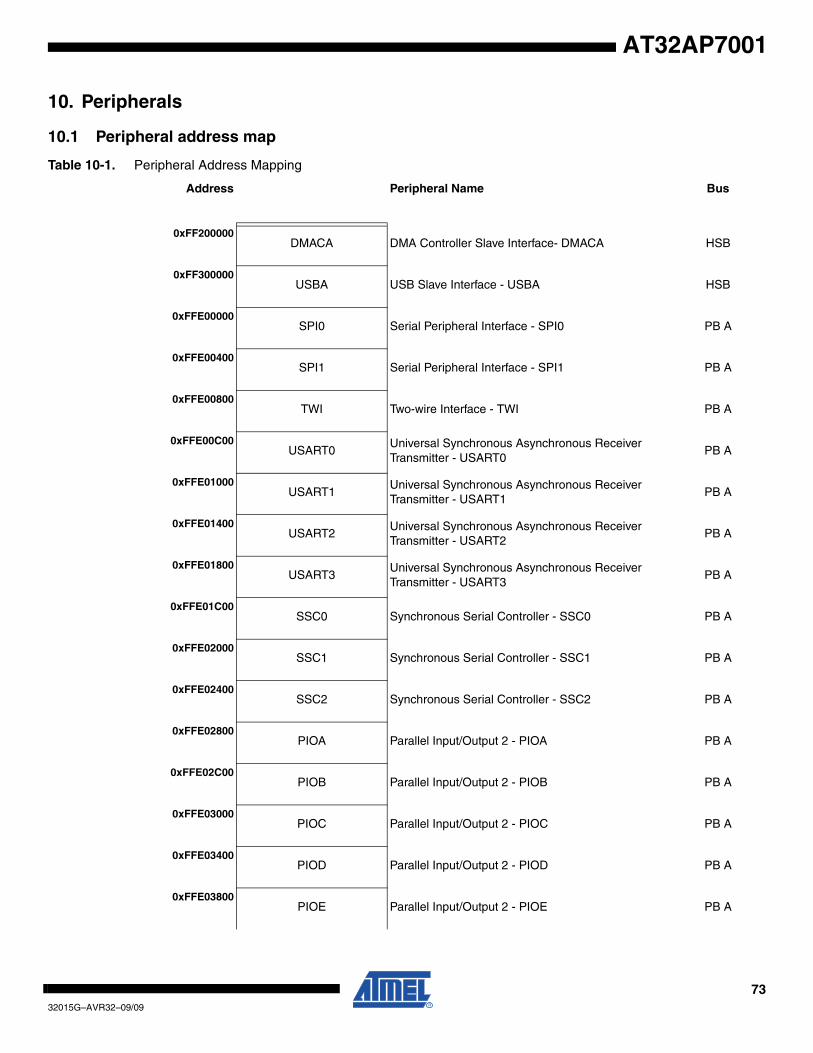
7332015G–AVR32–09/09
AT32AP7001
10. Peripherals
10.1 Peripheral address map
Table 10-1. Peripheral Address Mapping
Address Peripheral Name Bus
0xFF200000DMACA DMA Controller Slave Interface- DMACA HSB
0xFF300000USBA USB Slave Interface - USBA HSB
0xFFE00000SPI0 Serial Peripheral Interface - SPI0 PB A
0xFFE00400SPI1 Serial Peripheral Interface - SPI1 PB A
0xFFE00800TWI Two-wire Interface - TWI PB A
0xFFE00C00USART0
Universal Synchronous Asynchronous Receiver Transmitter - USART0
PB A
0xFFE01000USART1
Universal Synchronous Asynchronous Receiver Transmitter - USART1
PB A
0xFFE01400USART2
Universal Synchronous Asynchronous Receiver Transmitter - USART2
PB A
0xFFE01800USART3
Universal Synchronous Asynchronous Receiver Transmitter - USART3
PB A
0xFFE01C00SSC0 Synchronous Serial Controller - SSC0 PB A
0xFFE02000SSC1 Synchronous Serial Controller - SSC1 PB A
0xFFE02400SSC2 Synchronous Serial Controller - SSC2 PB A
0xFFE02800PIOA Parallel Input/Output 2 - PIOA PB A
0xFFE02C00PIOB Parallel Input/Output 2 - PIOB PB A
0xFFE03000PIOC Parallel Input/Output 2 - PIOC PB A
0xFFE03400PIOD Parallel Input/Output 2 - PIOD PB A
0xFFE03800PIOE Parallel Input/Output 2 - PIOE PB A
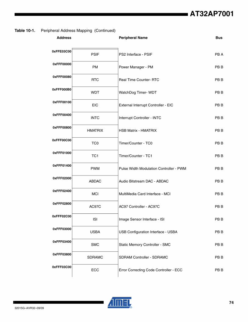
7432015G–AVR32–09/09
AT32AP7001
0xFFE03C00PSIF PS2 Interface - PSIF PB A
0xFFF00000PM Power Manager - PM PB B
0xFFF00080RTC Real Time Counter- RTC PB B
0xFFF000B0WDT WatchDog Timer- WDT PB B
0xFFF00100EIC External Interrupt Controller - EIC PB B
0xFFF00400INTC Interrupt Controller - INTC PB B
0xFFF00800HMATRIX HSB Matrix - HMATRIX PB B
0xFFF00C00TC0 Timer/Counter - TC0 PB B
0xFFF01000TC1 Timer/Counter - TC1 PB B
0xFFF01400PWM Pulse Width Modulation Controller - PWM PB B
0xFFF02000ABDAC Audio Bitstream DAC - ABDAC PB B
0xFFF02400MCI MultiMedia Card Interface - MCI PB B
0xFFF02800AC97C AC97 Controller - AC97C PB B
0xFFF02C00ISI Image Sensor Interface - ISI PB B
0xFFF03000USBA USB Configuration Interface - USBA PB B
0xFFF03400SMC Static Memory Controller - SMC PB B
0xFFF03800SDRAMC SDRAM Controller - SDRAMC PB B
0xFFF03C00ECC Error Correcting Code Controller - ECC PB B
Table 10-1. Peripheral Address Mapping (Continued)
Address Peripheral Name Bus
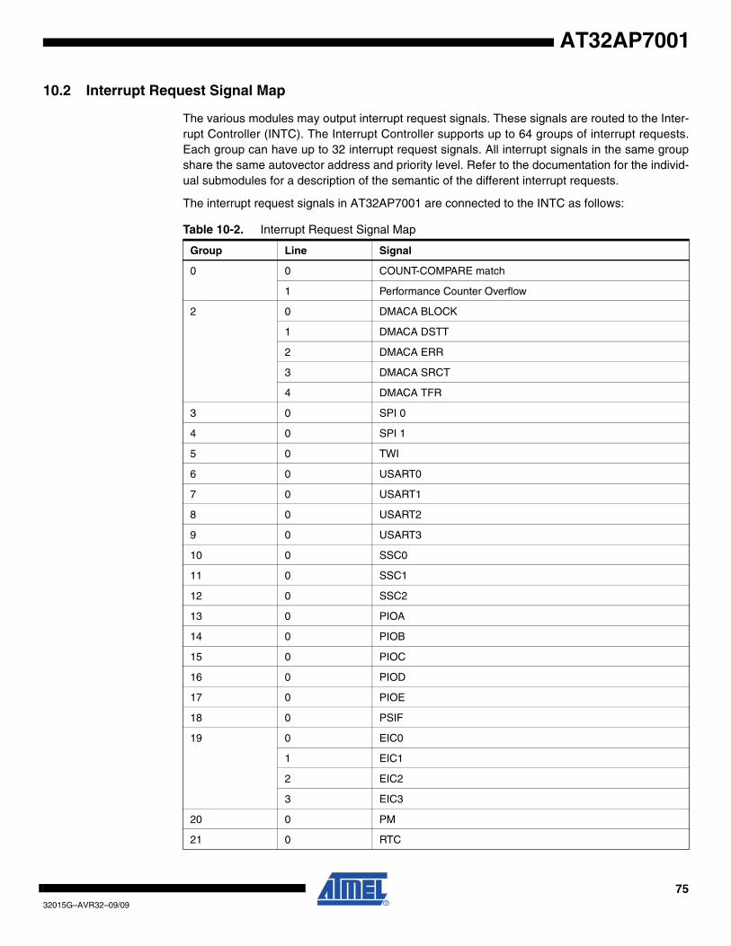
7532015G–AVR32–09/09
AT32AP7001
10.2 Interrupt Request Signal Map
The various modules may output interrupt request signals. These signals are routed to the Inter-rupt Controller (INTC). The Interrupt Controller supports up to 64 groups of interrupt requests.Each group can have up to 32 interrupt request signals. All interrupt signals in the same groupshare the same autovector address and priority level. Refer to the documentation for the individ-ual submodules for a description of the semantic of the different interrupt requests.
The interrupt request signals in AT32AP7001 are connected to the INTC as follows:
Table 10-2. Interrupt Request Signal Map
Group Line Signal
0 0 COUNT-COMPARE match
1 Performance Counter Overflow
2 0 DMACA BLOCK
1 DMACA DSTT
2 DMACA ERR
3 DMACA SRCT
4 DMACA TFR
3 0 SPI 0
4 0 SPI 1
5 0 TWI
6 0 USART0
7 0 USART1
8 0 USART2
9 0 USART3
10 0 SSC0
11 0 SSC1
12 0 SSC2
13 0 PIOA
14 0 PIOB
15 0 PIOC
16 0 PIOD
17 0 PIOE
18 0 PSIF
19 0 EIC0
1 EIC1
2 EIC2
3 EIC3
20 0 PM
21 0 RTC

7632015G–AVR32–09/09
AT32AP7001
10.3 DMACA Handshake Interface Map
The following table details the hardware handshake map between the DMACA and the peripher-als attached to it: :
22 0 TC00
1 TC01
2 TC02
23 0 TC10
1 TC11
2 TC12
24 0 PWM
27 0 ABDAC
28 0 MCI
29 0 AC97C
30 0 ISI
31 0 USBA
32 0 EBI
Table 10-2. Interrupt Request Signal Map
Group Line Signal
Table 10-3. Hardware Handshaking Connection
Request Hardware Handshaking Interface
MCI RX 0
MCI TX 1
ABDAC TX 2
AC97C CHANNEL A RX 3
AC97C CHANNEL A TX 4
AC97C CHANNEL B RX 5
AC97C CHANNEL B TX 6
EXTERNAL DMA REQUEST 0 7
EXTERNAL DMA REQUEST 1 8
EXTERNAL DMA REQUEST 2 9
EXTERNAL DMA REQUEST 3 10

7732015G–AVR32–09/09
AT32AP7001
10.4 Clock Connections
10.4.1 Timer/Counters
Each Timer/Counter channel can independently select an internal or external clock source for itscounter:
10.4.2 USARTs
Each USART can be connected to an internally divided clock:
Table 10-4. Timer/Counter clock connections
Timer/Counter Source Name Connection
0 Internal TIMER_CLOCK1 clk_osc32
TIMER_CLOCK2 clk_pbb / 4
TIMER_CLOCK3 clk_pbb / 8
TIMER_CLOCK4 clk_pbb / 16
TIMER_CLOCK5 clk_pbb / 32
External XC0 See Section 10.7
XC1
XC2
1 Internal TIMER_CLOCK1 clk_osc32
TIMER_CLOCK2 clk_pbb / 4
TIMER_CLOCK3 clk_pbb / 8
TIMER_CLOCK4 clk_pbb / 16
TIMER_CLOCK5 clk_pbb / 32
External XC0 See Section 10.7
XC1
XC2
Table 10-5. USART clock connections
USART Source Name Connection
0 Internal CLK_DIV clk_pba / 8
1
2
3

7832015G–AVR32–09/09
AT32AP7001
10.4.3 SPIs
Each SPI can be connected to an internally divided clock:
10.4.4 USBA
OSC1 is connected to the USB HS Phy and must be 12 MHz when using the USBA.
10.5 External Interrupt Pin Mapping
External interrupt requests are connected to the following pins::
10.6 Nexus OCD AUX port connections
If the OCD trace system is enabled, the trace system will take control over a number of pins, irre-spectively of the PIO configuration. Two different OCD trace pin mappings are possible,depending on the configuration of the OCD AXS register. For details, see the AVR32 AP Techni-cal Reference Manual.
Table 10-6. SPI clock connections
SPI Source Name Connection
0 Internal CLK_DIV clk_pba / 32
1
Table 10-7. External Interrupt Pin Mapping
Source Connection
NMI_N PB24
EXTINT0 PB25
EXTINT1 PB26
EXTINT2 PB27
EXTINT3 PB28
Table 10-8. Nexus OCD AUX port connections
Pin AXS=0 AXS=1
EVTI_N EVTI_N EVTI_N
MDO[5] PB09 PC18
MDO[4] PB08 PC14
MDO[3] PB07 PC12
MDO[2] PB06 PC11
MDO[1] PB05 PC06
MDO[0] PB04 PC05
EVTO_N PB03 PB28
MCKO PB02 PC02
MSEO[1] PB01 PC01
MSEO[0] PB00 PC00

7932015G–AVR32–09/09
AT32AP7001
10.7 Peripheral Multiplexing on IO lines
The AT32AP7001 features five PIO controllers, PIOA to PIOE, that multiplex the I/O lines of theperipheral set. Each PIO Controller controls up to thirty-two lines.
Each line can be assigned to one of two peripheral functions, A or B. The tables in the followingpages define how the I/O lines of the peripherals A and B are multiplexed on the PIOControllers.
Note that some output only peripheral functions might be duplicated within the tables.
10.7.1 PIO Controller A Multiplexing
Table 10-9. PIO Controller A Multiplexing
QFP208 I/O Line Peripheral A Peripheral B
27 PA00 SPI0 - MISO SSC1 - RX_FRAME_SYNC
28 PA01 SPI0 - MOSI SSC1 - TX_FRAME_SYNC
29 PA02 SPI0 - SCK SSC1 - TX_CLOCK
30 PA03 SPI0 - NPCS[0] SSC1 - RX_CLOCK
31 PA04 SPI0 - NPCS[1] SSC1 - TX_DATA
32 PA05 SPI0 - NPCS[2] SSC1 - RX_DATA
175 PA06 TWI - SDA USART0 - RTS
176 PA07 TWI - SCL USART0 - CTS
35 PA08 PSIF - CLOCK USART0 - RXD
38 PA09 PSIF - DATA USART0 - TXD
39 PA10 MCI - CLK USART0 - CLK
40 PA11 MCI - CMD TC0 - CLK0
41 PA12 MCI - DATA[0] TC0 - A0
42 PA13 MCI - DATA[1] TC0 - A1
43 PA14 MCI - DATA[2] TC0 - A2
44 PA15 MCI - DATA[3] TC0 - B0
45 PA16 USART1 - CLK TC0 - B1
46 PA17 USART1 - RXD TC0 - B2
47 PA18 USART1 - TXD TC0 - CLK2
48 PA19 USART1 - RTS TC0 - CLK1
49 PA20 USART1 - CTS SPI0 - NPCS[3]
50 PA21 SSC0 - RX_FRAME_SYNC PWM - PWM[2]
51 PA22 SSC0 - RX_CLOCK PWM - PWM[3]
54 PA23 SSC0 - TX_CLOCK TC1 - A0
55 PA24 SSC0 - TX_FRAME_SYNC TC1 - A1
72 PA25 SSC0 - TX_DATA TC1 - B0
73 PA26 SSC0 - RX_DATA TC1 - B1
74 PA27 SPI1 - NPCS[3] TC1 - CLK0
75 PA28 PWM - PWM[0] TC1 - A2
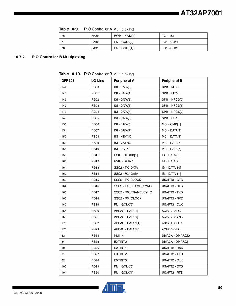
8032015G–AVR32–09/09
AT32AP7001
10.7.2 PIO Controller B Multiplexing
76 PA29 PWM - PWM[1] TC1 - B2
77 PA30 PM - GCLK[0] TC1 - CLK1
78 PA31 PM - GCLK[1] TC1 - CLK2
Table 10-9. PIO Controller A Multiplexing
Table 10-10. PIO Controller B Multiplexing
QFP208 I/O Line Peripheral A Peripheral B
144 PB00 ISI - DATA[0] SPI1 - MISO
145 PB01 ISI - DATA[1] SPI1 - MOSI
146 PB02 ISI - DATA[2] SPI1 - NPCS[0]
147 PB03 ISI - DATA[3] SPI1 - NPCS[1]
148 PB04 ISI - DATA[4] SPI1 - NPCS[2]
149 PB05 ISI - DATA[5] SPI1 - SCK
150 PB06 ISI - DATA[6] MCI - CMD[1]
151 PB07 ISI - DATA[7] MCI - DATA[4]
152 PB08 ISI - HSYNC MCI - DATA[5]
153 PB09 ISI - VSYNC MCI - DATA[6]
158 PB10 ISI - PCLK MCI - DATA[7]
159 PB11 PSIF - CLOCK[1] ISI - DATA[8]
160 PB12 PSIF - DATA[1] ISI - DATA[9]
161 PB13 SSC2 - TX_DATA ISI - DATA[10]
162 PB14 SSC2 - RX_DATA ISI - DATA[11]
163 PB15 SSC2 - TX_CLOCK USART3 - CTS
164 PB16 SSC2 - TX_FRAME_SYNC USART3 - RTS
165 PB17 SSC2 - RX_FRAME_SYNC USART3 - TXD
166 PB18 SSC2 - RX_CLOCK USART3 - RXD
167 PB19 PM - GCLK[2] USART3 - CLK
168 PB20 ABDAC - DATA[1] AC97C - SDO
169 PB21 ABDAC - DATA[0] AC97C - SYNC
170 PB22 ABDAC - DATAN[1] AC97C - SCLK
171 PB23 ABDAC - DATAN[0] AC97C - SDI
33 PB24 NMI_N DMACA - DMARQ[0]
34 PB25 EXTINT0 DMACA - DMARQ[1]
80 PB26 EXTINT1 USART2 - RXD
81 PB27 EXTINT2 USART2 - TXD
82 PB28 EXTINT3 USART2 - CLK
100 PB29 PM - GCLK[3] USART2 - CTS
101 PB30 PM - GCLK[4] USART2 - RTS

8132015G–AVR32–09/09
AT32AP7001
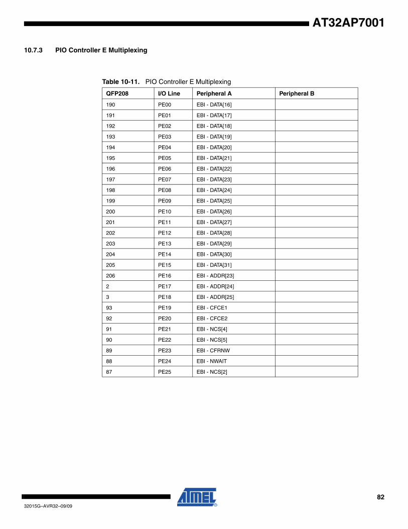
8232015G–AVR32–09/09
AT32AP7001
10.7.3 PIO Controller E Multiplexing
Table 10-11. PIO Controller E Multiplexing
QFP208 I/O Line Peripheral A Peripheral B
190 PE00 EBI - DATA[16]
191 PE01 EBI - DATA[17]
192 PE02 EBI - DATA[18]
193 PE03 EBI - DATA[19]
194 PE04 EBI - DATA[20]
195 PE05 EBI - DATA[21]
196 PE06 EBI - DATA[22]
197 PE07 EBI - DATA[23]
198 PE08 EBI - DATA[24]
199 PE09 EBI - DATA[25]
200 PE10 EBI - DATA[26]
201 PE11 EBI - DATA[27]
202 PE12 EBI - DATA[28]
203 PE13 EBI - DATA[29]
204 PE14 EBI - DATA[30]
205 PE15 EBI - DATA[31]
206 PE16 EBI - ADDR[23]
2 PE17 EBI - ADDR[24]
3 PE18 EBI - ADDR[25]
93 PE19 EBI - CFCE1
92 PE20 EBI - CFCE2
91 PE21 EBI - NCS[4]
90 PE22 EBI - NCS[5]
89 PE23 EBI - CFRNW
88 PE24 EBI - NWAIT
87 PE25 EBI - NCS[2]

8332015G–AVR32–09/09
AT32AP7001
10.7.4 IO Pins Without Multiplexing
Many of the external EBI pins are not controlled by the PIO modules, but directly driven by theEBI. These pins have programmable pullup resistors. These resistors are controlled by SpecialFunction Register 4 (SFR4) in the HMATRIX. The pullup on the lines multiplexed with PIO iscontrolled by the appropriate PIO control register.
This SFR can also control CompactFlash, SmartMedia or NandFlash Support, see the EBI chap-ter for details
10.7.4.1 HMatrix SFR4 EBI Control Register
Name: HMATRIX_SFR4
Access Type: Read/Write
• CS1A: Chip Select 1 Assignment 0 = Chip Select 1 is assigned to the Static Memory Controller.
1 = Chip Select 1 is assigned to the SDRAM Controller.
• CS3A: Chip Select 3 Assignment 0 = Chip Select 3 is only assigned to the Static Memory Controller and NCS3 behaves asdefined by the SMC.
1 = Chip Select 3 is assigned to the Static Memory Controller and the NAND Flash/SmartMediaLogic is activated.
• CS4A: Chip Select 4 Assignment 0 = Chip Select 4 is assigned to the Static Memory Controller and NCS4, NCS5 and NCS6behave as defined by the SMC.
1 = Chip Select 4 is assigned to the Static Memory Controller and the CompactFlash Logic isactivated.
• CS5A: Chip Select 5 Assignment 0 = Chip Select 5 is assigned to the Static Memory Controller and NCS4, NCS5 and NCS6behave as defined by the SMC.
1 = Chip Select 5 is assigned to the Static Memory Controller and the CompactFlash Logic isactivated.
31 30 29 28 27 26 25 24
– – – – – – – –
23 22 21 20 19 18 17 16
– – – – – – – –
15 14 13 12 11 10 9 8
– – – – – – – EBI_DBPUC
7 6 5 4 3 2 1 0
– – EBI_CS5A EBI_CS4A EBI_CS3A – EBI_CS1A -
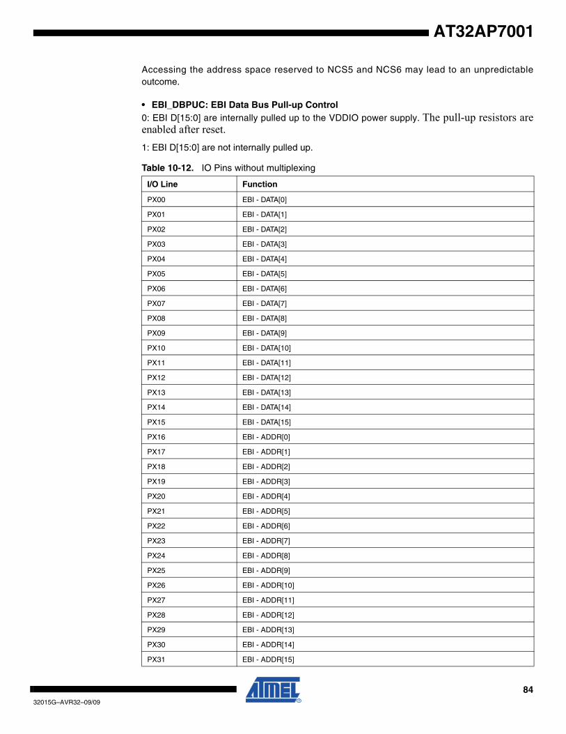
8432015G–AVR32–09/09
AT32AP7001
Accessing the address space reserved to NCS5 and NCS6 may lead to an unpredictableoutcome.
• EBI_DBPUC: EBI Data Bus Pull-up Control0: EBI D[15:0] are internally pulled up to the VDDIO power supply. The pull-up resistors areenabled after reset.1: EBI D[15:0] are not internally pulled up.
Table 10-12. IO Pins without multiplexing
I/O Line Function
PX00 EBI - DATA[0]
PX01 EBI - DATA[1]
PX02 EBI - DATA[2]
PX03 EBI - DATA[3]
PX04 EBI - DATA[4]
PX05 EBI - DATA[5]
PX06 EBI - DATA[6]
PX07 EBI - DATA[7]
PX08 EBI - DATA[8]
PX09 EBI - DATA[9]
PX10 EBI - DATA[10]
PX11 EBI - DATA[11]
PX12 EBI - DATA[12]
PX13 EBI - DATA[13]
PX14 EBI - DATA[14]
PX15 EBI - DATA[15]
PX16 EBI - ADDR[0]
PX17 EBI - ADDR[1]
PX18 EBI - ADDR[2]
PX19 EBI - ADDR[3]
PX20 EBI - ADDR[4]
PX21 EBI - ADDR[5]
PX22 EBI - ADDR[6]
PX23 EBI - ADDR[7]
PX24 EBI - ADDR[8]
PX25 EBI - ADDR[9]
PX26 EBI - ADDR[10]
PX27 EBI - ADDR[11]
PX28 EBI - ADDR[12]
PX29 EBI - ADDR[13]
PX30 EBI - ADDR[14]
PX31 EBI - ADDR[15]
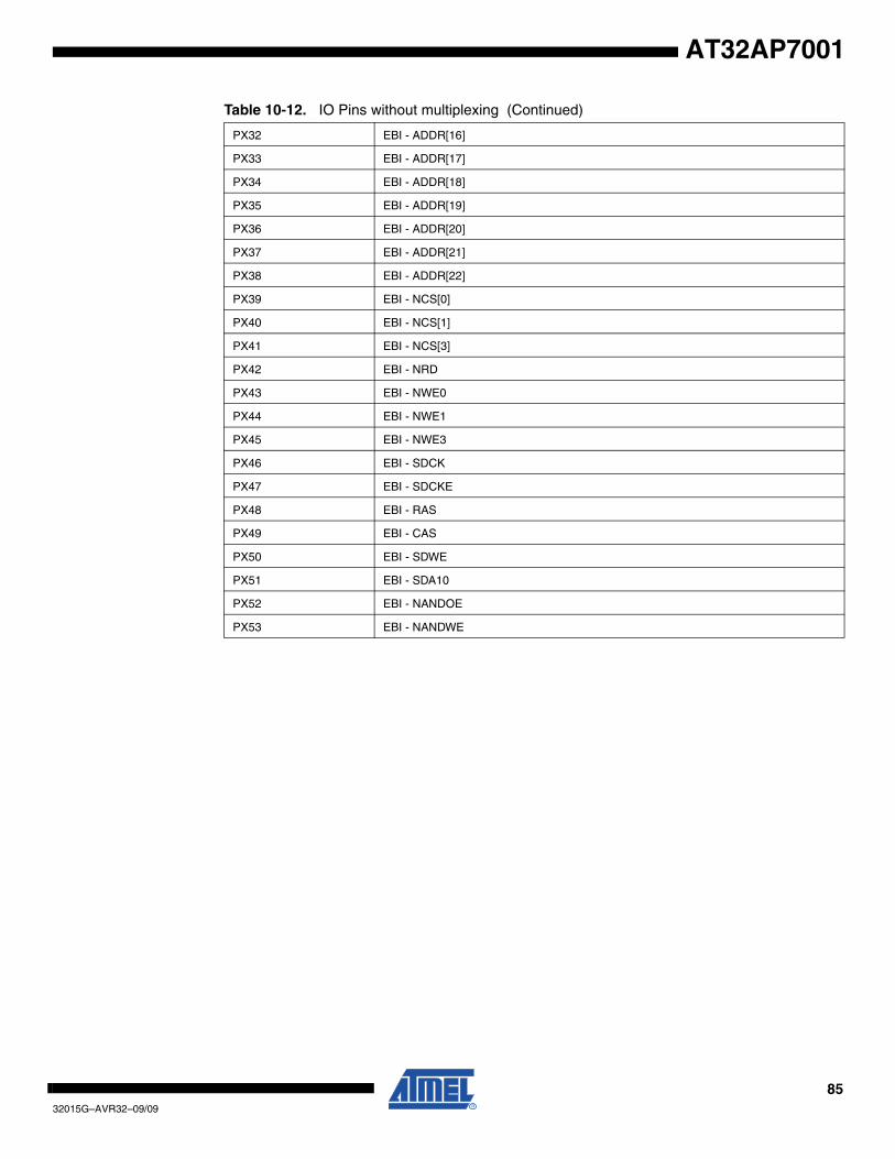
8532015G–AVR32–09/09
AT32AP7001
PX32 EBI - ADDR[16]
PX33 EBI - ADDR[17]
PX34 EBI - ADDR[18]
PX35 EBI - ADDR[19]
PX36 EBI - ADDR[20]
PX37 EBI - ADDR[21]
PX38 EBI - ADDR[22]
PX39 EBI - NCS[0]
PX40 EBI - NCS[1]
PX41 EBI - NCS[3]
PX42 EBI - NRD
PX43 EBI - NWE0
PX44 EBI - NWE1
PX45 EBI - NWE3
PX46 EBI - SDCK
PX47 EBI - SDCKE
PX48 EBI - RAS
PX49 EBI - CAS
PX50 EBI - SDWE
PX51 EBI - SDA10
PX52 EBI - NANDOE
PX53 EBI - NANDWE
Table 10-12. IO Pins without multiplexing (Continued)
8632015G–AVR32–09/09
AT32AP7001
10.8 Peripheral overview
10.8.1 External Bus Interface
• Optimized for Application Memory Space support• Integrates Three External Memory Controllers:
– Static Memory Controller– SDRAM Controller– ECC Controller
• Additional Logic for NAND Flash/SmartMediaTM and CompactFlashTM Support– SmartMedia support: 8-bit as well as 16-bit devices are supported– CompactFlash support: all modes (Attribute Memory, Common Memory, I/O, True IDE) are
supported but the signals _IOIS16 (I/O and True IDE modes) and _ATA SEL (True IDE mode) are not handled.
• Optimized External Bus:– 16- or 32-bit Data Bus– Up to 26-bit Address Bus, Up to 64-Mbytes Addressable– Optimized pin multiplexing to reduce latencies on External Memories
• Up to 6 Chip Selects, Configurable Assignment:– Static Memory Controller on NCS0– SDRAM Controller or Static Memory Controller on NCS1– Static Memory Controller on NCS2– Static Memory Controller on NCS3, Optional NAND Flash/SmartMediaTM Support– Static Memory Controller on NCS4 - NCS5, Optional CompactFlashTM Support
10.8.2 Static Memory Controller
• 6 Chip Selects Available• 64-Mbyte Address Space per Chip Select• 8-, 16- or 32-bit Data Bus• Word, Halfword, Byte Transfers• Byte Write or Byte Select Lines• Programmable Setup, Pulse And Hold Time for Read Signals per Chip Select• Programmable Setup, Pulse And Hold Time for Write Signals per Chip Select• Programmable Data Float Time per Chip Select• Compliant with LCD Module• External Wait Request• Automatic Switch to Slow Clock Mode • Asynchronous Read in Page Mode Supported: Page Size Ranges from 4 to 32 Bytes
10.8.3 SDRAM Controller
• Numerous Configurations Supported– 2K, 4K, 8K Row Address Memory Parts – SDRAM with Two or Four Internal Banks– SDRAM with 16- or 32-bit Data Path
• Programming Facilities– Word, Half-word, Byte Access– Automatic Page Break When Memory Boundary Has Been Reached– Multibank Ping-pong Access– Timing Parameters Specified by Software– Automatic Refresh Operation, Refresh Rate is Programmable
8732015G–AVR32–09/09
AT32AP7001
• Energy-saving Capabilities– Self-refresh, Power-down and Deep Power Modes Supported– Supports Mobile SDRAM Devices
• Error Detection– Refresh Error Interrupt
• SDRAM Power-up Initialization by Software• CAS Latency of 1, 2, 3 Supported• Auto Precharge Command Not Used
10.8.4 Error Corrected Code Controller
• Hardware Error Corrected Code (ECC) Generation– Detection and Correction by Software
• Supports NAND Flash and SmartMedia™ Devices with 8- or 16-bit Data Path.• Supports NAND Flash/SmartMedia with Page Sizes of 528, 1056, 2112 and 4224 Bytes, Specified
by Software
10.8.5 Serial Peripheral Interface
• Supports communication with serial external devices– Four chip selects with external decoder support allow communication with up to 15
peripherals– Serial memories, such as DataFlash™ and 3-wire EEPROMs– Serial peripherals, such as ADCs, DACs, CAN Controllers and Sensors– External co-processors
• Master or slave serial peripheral bus interface – 8- to 16-bit programmable data length per chip select – Programmable phase and polarity per chip select – Programmable transfer delays between consecutive transfers and between clock and data
per chip select – Programmable delay between consecutive transfers – Selectable mode fault detection
• Very fast transfers supported – Transfers with baud rates up to MCK – The chip select line may be left active to speed up transfers on the same device
10.8.6 Two-wire Interface
• Compatibility with standard two-wire serial memory • One, two or three bytes for slave address • Sequential read/write operations

8832015G–AVR32–09/09
AT32AP7001
10.8.7 USART
• Programmable Baud Rate Generator • 5- to 9-bit full-duplex synchronous or asynchronous serial communications
– 1, 1.5 or 2 stop bits in Asynchronous Mode or 1 or 2 stop bits in Synchronous Mode– Parity generation and error detection– Framing error detection, overrun error detection– MSB- or LSB-first – Optional break generation and detection – By 8 or by-16 over-sampling receiver frequency – Hardware handshaking RTS-CTS – Receiver time-out and transmitter timeguard – Optional Multi-drop Mode with address generation and detection– Optional Manchester Encoding
• RS485 with driver control signal • ISO7816, T = 0 or T = 1 Protocols for interfacing with smart cards
– NACK handling, error counter with repetition and iteration limit • IrDA modulation and demodulation
– Communication at up to 115.2 Kbps • Test Modes 46
– Remote Loopback, Local Loopback, Automatic Echo
10.8.8 Serial Synchronous Controller
• Provides serial synchronous communication links used in audio and telecom applications (with CODECs in Master or Slave Modes, I2S, TDM Buses, Magnetic Card Reader, etc.)
• Contains an independent receiver and transmitter and a common clock divider • Offers a configurable frame sync and data length • Receiver and transmitter can be programmed to start automatically or on detection of different
event on the frame sync signal • Receiver and transmitter include a data signal, a clock signal and a frame synchronization signal
10.8.9 AC97 Controller
• Compatible with AC97 Component Specification V2.2 • Capable to Interface with a Single Analog Front end • Three independent RX Channels and three independent TX Channels
– One RX and one TX channel dedicated to the AC97 Analog Front end control– One RX and one TX channel for data transfers, connected to the DMACA– One RX and one TX channel for data transfers, connected to the DMACA
• Time Slot Assigner allowing to assign up to 12 time slots to a channel • Channels support mono or stereo up to 20 bit sample length - Variable sampling rate AC97 Codec
Interface (48KHz and below)
8932015G–AVR32–09/09
AT32AP7001
10.8.10 Audio Bitstream DAC
• Digital Stereo DAC• Oversampled D/A conversion architecture
– Oversampling ratio fixed 128x– FIR equalization filter– Digital interpolation filter: Comb4– 3rd Order Sigma-Delta D/A converters
• Digital bitstream outputs• Parallel interface• Connected to DMA Controller for background transfer without CPU intervention
10.8.11 Timer Counter
• Three 16-bit Timer Counter Channels • Wide range of functions including:
– Frequency Measurement– Event Counting– Interval Measurement– Pulse Generation– Delay Timing– Pulse Width Modulation– Up/down Capabilities
• Each channel is user-configurable and contains:– Three external clock inputs– Five internal clock inputs– Two multi-purpose input/output signals
• Two global registers that act on all three TC Channels
10.8.12 Pulse Width Modulation Controller
• 4 channels, one 16-bit counter per channel• Common clock generator, providing Thirteen Different Clocks
– A Modulo n counter providing eleven clocks– Two independent Linear Dividers working on modulo n counter outputs
• Independent channel programming – Independent Enable Disable Commands– Independent Clock– Independent Period and Duty Cycle, with Double Bufferization– Programmable selection of the output waveform polarity– Programmable center or left aligned output waveform

9032015G–AVR32–09/09
AT32AP7001
10.8.13 MultiMedia Card Interface
• 2 double-channel MultiMedia Card Interface, allowing concurrent transfers with 2 cards • Compatibility with MultiMedia Card Specification Version 2.2 • Compatibility with SD Memory Card Specification Version 1.0 • Compatibility with SDIO Specification Version V1.0. • Cards clock rate up to Master Clock divided by 2 • Embedded power management to slow down clock rate when not used • Each MCI has two slot, each supporting
– One slot for one MultiMediaCard bus (up to 30 cards) or– One SD Memory Card
• Support for stream, block and multi-block data read and write
10.8.14 PS/2 Interface
• Peripheral Bus slave• PS/2 Host• Receive and transmit capability• Parity generation and error detection• Overrun error detection
10.8.15 USB Interface
• Supports Hi (480Mbps) and Full (12Mbps) speed communication• Compatible with the USB 2.0 specification• UTMI Compliant• 7 Endpoints• Embedded Dual-port RAM for Endpoints• Suspend/Resume Logic (Command of UTMI)• Up to Three Memory Banks for Endpoints (Not for Control Endpoint)• 4 KBytes of DPRAM
•10.8.16 Image Sensor Interface
• ITU-R BT. 601/656 8-bit mode external interface support • Support for ITU-R BT.656-4 SAV and EAV synchronization • Vertical and horizontal resolutions up to 2048 x 2048 • Preview Path up to 640*480 • Support for packed data formatting for YCbCr 4:2:2 formats • Preview scaler to generate smaller size image 50 • Programmable frame capture rate
9132015G–AVR32–09/09
AT32AP7001
11. Power Manager (PM)
Rev: 1.0.2.8
11.1 Features
• Controls oscillators and PLLs• Generates clocks and resets for digital logic• Supports 2 high-speed crystal oscillators• Supports 2 PLLs• Supports 32KHz ultra-low power oscillator• On-the fly frequency change of CPU, HSB, and PB frequency• Sleep modes allow simple disabling of logic clocks, PLL’s and oscillators• Module-level clock gating through maskable peripheral clocks• Wake-up from interrupts or external pin• Generic clocks with wide frequency range provided• Automatic identification of reset sources
11.2 Description
The Power Manager (PM) controls the oscillators, PLL’s, and generates the clocks and resets inthe device. The PM controls two fast crystal oscillators, as well as two PLL’s, which can multiplythe clock from either oscillator to provide higher frequencies. Additionally, a low-power 32KHzoscillator is used to generate a slow clock for real-time counters.
The provided clocks are divided into synchronous and generic clocks. The synchronous clocksare used to clock the main digital logic in the device, namely the CPU, and the modules andperipherals connected to the HSB, PBA, and PBB buses. The generic clocks are asynchronousclocks, which can be tuned precisely within a wide frequency range, which makes them suitablefor peripherals that require specific frequencies, such as timers and communication modules.
The PM also contains advanced power-saving features, allowing the user to optimize the powerconsumption for an application. The synchronous clocks are divided into four clock domains, forthe CPU, and modules on the HSB, PBA, and PBB buses. The four clocks can run at differentspeeds, so the user can save power by running peripherals at a relatively low clock, while main-taining a high CPU performance. Additionally, the clocks can be independently changed on-thefly, without halting any peripherals. This enables the user to adjust the speed of the CPU andmemories to the dynamic load of the application, without disturbing or re-configuring activeperipherals.
Each module also has a separate clock, enabling the user to switch off the clock for inactivemodules, to save further power. Additionally, clocks and oscillators can be automaticallyswithced off during idle periods by using the sleep instruction on the CPU. The system will returnto normal on occurence of interrupts or an event on the WAKE_N pin.
The Power Manager also cointains a Reset Controller, which collects all possible reset sources,generates hard and soft resets, and allows the reset source to be identifed by software.
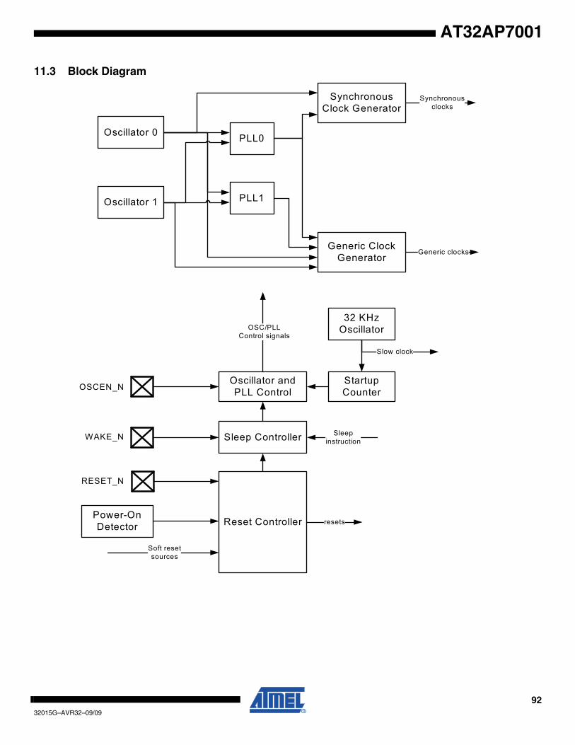
9232015G–AVR32–09/09
AT32AP7001
11.3 Block Diagram
Sleep Controller
Oscillator and PLL Control
PLL0
PLL1
Synchronous Clock Generator
Generic Clock Generator
Reset Controller
Oscillator 0
Oscillator 1
32 KHz Oscillator
Startup Counter
Slow clock
Sleepinstruction
OSCEN_N
WAKE_N
RESET_N
Power-On Detector
Soft resetsources
resets
Generic clocks
Synchronousclocks
OSC/PLLControl signals
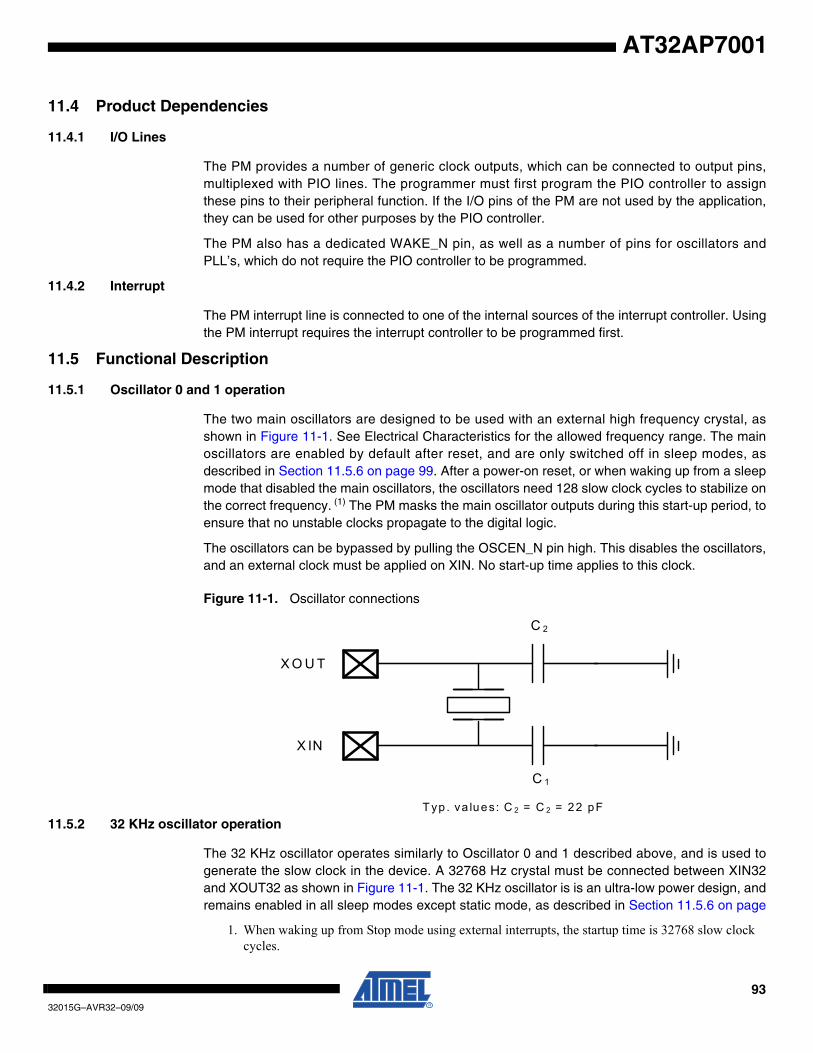
9332015G–AVR32–09/09
AT32AP7001
11.4 Product Dependencies
11.4.1 I/O Lines
The PM provides a number of generic clock outputs, which can be connected to output pins,multiplexed with PIO lines. The programmer must first program the PIO controller to assignthese pins to their peripheral function. If the I/O pins of the PM are not used by the application,they can be used for other purposes by the PIO controller.
The PM also has a dedicated WAKE_N pin, as well as a number of pins for oscillators andPLL’s, which do not require the PIO controller to be programmed.
11.4.2 Interrupt
The PM interrupt line is connected to one of the internal sources of the interrupt controller. Usingthe PM interrupt requires the interrupt controller to be programmed first.
11.5 Functional Description
11.5.1 Oscillator 0 and 1 operation
The two main oscillators are designed to be used with an external high frequency crystal, asshown in Figure 11-1. See Electrical Characteristics for the allowed frequency range. The mainoscillators are enabled by default after reset, and are only switched off in sleep modes, asdescribed in Section 11.5.6 on page 99. After a power-on reset, or when waking up from a sleepmode that disabled the main oscillators, the oscillators need 128 slow clock cycles to stabilize onthe correct frequency. (1) The PM masks the main oscillator outputs during this start-up period, toensure that no unstable clocks propagate to the digital logic.
The oscillators can be bypassed by pulling the OSCEN_N pin high. This disables the oscillators,and an external clock must be applied on XIN. No start-up time applies to this clock.
Figure 11-1. Oscillator connections
11.5.2 32 KHz oscillator operation
The 32 KHz oscillator operates similarly to Oscillator 0 and 1 described above, and is used togenerate the slow clock in the device. A 32768 Hz crystal must be connected between XIN32and XOUT32 as shown in Figure 11-1. The 32 KHz oscillator is is an ultra-low power design, andremains enabled in all sleep modes except static mode, as described in Section 11.5.6 on page
1. When waking up from Stop mode using external interrupts, the startup time is 32768 slow clock cycles.
X IN
X O U T
C 2
C 1
T yp . va lues: C 2 = C 2 = 22 pF

9432015G–AVR32–09/09
AT32AP7001
99. The oscillator has a rather long start-up time of 32768 clock cycles, and no clocks will begenerated in the device during this start-up time.
Note that in static sleep mode the startup counter will start at the negedge of reset and not at theposedge.
Pulling OSCEN_N high will also disable the 32 KHz oscillator, and a 32 KHz clock must beapplied on the XIN32 pin. No start-up time applies to this clock.
11.5.3 PLL operation
The device contains two PLL’s, PLL0 and PLL1. These are disabled by default, but can beenabled to provide high frequency source clocks for synchronous or generic clocks. The PLL’scan take either Oscillator 0 or 1 as clock source. Each PLL has an input divider, which dividesthe source clock, creating the reference clock for the PLL. The PLL output is divided by a user-defined factor, and the PLL compares the resulting clock to the reference clock. The PLL willadjust its output frequency until the two compared clocks are equal, thus locking the output fre-quency to a multiple of the reference clock frequency.
When the PLL is switched on, or when changing the clock source or multiplication or divisionfactor for the PLL, the PLL is unlocked and the output frequency is undefined. The PLL clock forthe digital logic is automatically masked when the PLL is unlocked, to prevent connected digitallogic from receiving a too high frequency and thus become unstable.
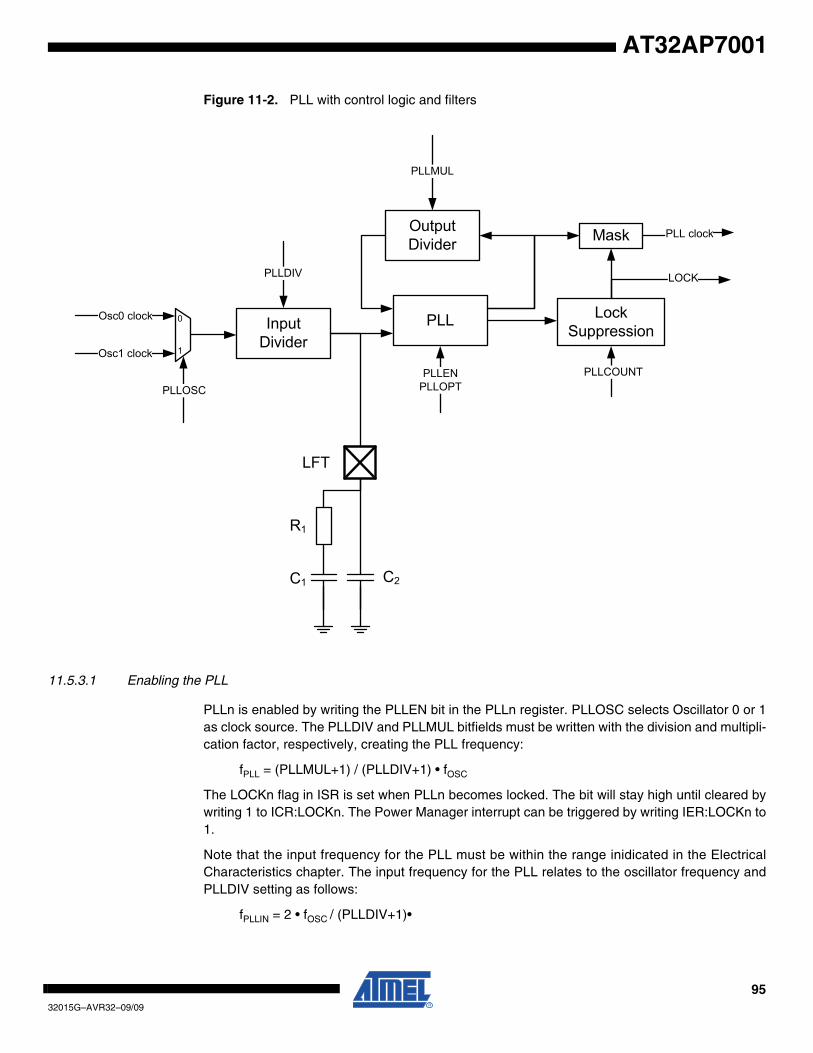
9532015G–AVR32–09/09
AT32AP7001
Figure 11-2. PLL with control logic and filters
11.5.3.1 Enabling the PLL
PLLn is enabled by writing the PLLEN bit in the PLLn register. PLLOSC selects Oscillator 0 or 1as clock source. The PLLDIV and PLLMUL bitfields must be written with the division and multipli-cation factor, respectively, creating the PLL frequency:
fPLL = (PLLMUL+1) / (PLLDIV+1) • fOSC
The LOCKn flag in ISR is set when PLLn becomes locked. The bit will stay high until cleared bywriting 1 to ICR:LOCKn. The Power Manager interrupt can be triggered by writing IER:LOCKn to1.
Note that the input frequency for the PLL must be within the range inidicated in the ElectricalCharacteristics chapter. The input frequency for the PLL relates to the oscillator frequency andPLLDIV setting as follows:
fPLLIN = 2 • fOSC / (PLLDIV+1)•
PLL
Output Divider
Input Divider
LFT
0
1
Osc0 clock
Osc1 clock
PLLOSCPLLEN
PLLOPT
PLLMUL
PLLDIV
Lock Suppression
PLLCOUNT
LOCK
Mask PLL clock
C1
R1
C2
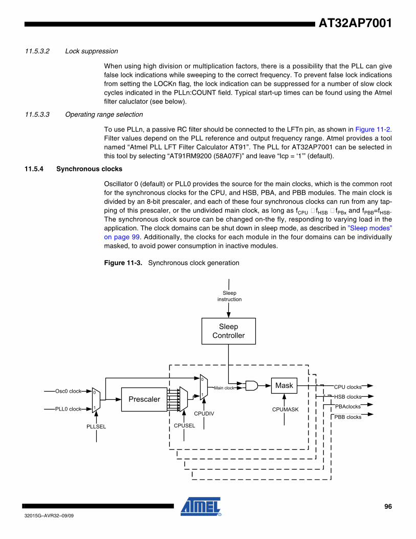
9632015G–AVR32–09/09
AT32AP7001
11.5.3.2 Lock suppression
When using high division or multiplication factors, there is a possibility that the PLL can givefalse lock indications while sweeping to the correct frequency. To prevent false lock indicationsfrom setting the LOCKn flag, the lock indication can be suppressed for a number of slow clockcycles indicated in the PLLn:COUNT field. Typical start-up times can be found using the Atmelfilter caluclator (see below).
11.5.3.3 Operating range selection
To use PLLn, a passive RC filter should be connected to the LFTn pin, as shown in Figure 11-2.Filter values depend on the PLL reference and output frequency range. Atmel provides a toolnamed “Atmel PLL LFT Filter Calculator AT91”. The PLL for AT32AP7001 can be selected inthis tool by selecting “AT91RM9200 (58A07F)” and leave “Icp = ‘1’” (default).
11.5.4 Synchronous clocks
Oscillator 0 (default) or PLL0 provides the source for the main clocks, which is the common rootfor the synchronous clocks for the CPU, and HSB, PBA, and PBB modules. The main clock isdivided by an 8-bit prescaler, and each of these four synchronous clocks can run from any tap-ping of this prescaler, or the undivided main clock, as long as fCPU fHSB fPBx and fPBB=fHSB.The synchronous clock source can be changed on-the fly, responding to varying load in theapplication. The clock domains can be shut down in sleep mode, as described in ”Sleep modes”on page 99. Additionally, the clocks for each module in the four domains can be individuallymasked, to avoid power consumption in inactive modules.
Figure 11-3. Synchronous clock generation
Mask
Prescaler0
1
Osc0 clock
PLL0 clock
PLLSEL
0
1
CPUSEL
CPUDIV
Main clock
Sleep Controller
CPUMASK
CPU clocks
HSB clocks
PBAclocks
PBB clocks
Sleepinstruction
9732015G–AVR32–09/09
AT32AP7001
11.5.4.1 Selecting PLL or oscillator for the main clock
The common main clock can be connected to Oscillator 0 or PLL0. By default, the main clock willbe connected to the Oscillator 0 output. The user can connect the main clock to the PLL0 outputby writing the PLLSEL bit in the Main Clock Control Register (MCCTRL) to 1. This must only bedone after PLL0 has been enabled, otherwise a deadlock will occur. Care should also be takenthat the new frequency of the synchronous clocks does not exceed the maximum frequency foreach clock domain.
11.5.4.2 Selecting synchronous clock division ratio
The main clock feeds an 8-bit prescaler, which can be used to generate the synchronous clocks.By default, the synchronous clocks run on the undivided main clock. The user can select a pres-caler division for the CPU clock by writing CKSEL:CPUDIV to 1 and CPUSEL to the prescalingvalue, resulting in a CPU clock frequency:
fCPU = fmain / 2(CPUSEL+1)
Similarly, the clock for HSB, PBA, and PBB can be divided by writing their respective bitfields.To ensure correct operation, frequencies must be selected so that fCPU fHSB fPBA,B. Also, fre-quencies must never exceed the specified maximum frequency for each clock domain.
CKSEL can be written without halting or disabling peripheral modules. Writing CKSEL allows anew clock setting to be written to all synchronous clocks at the same time. It is possible to keepone or more clocks unchanged by writing the same value a before to the xxxDIV and xxxSEL bit-fields. This way, it is possible to e.g. scale CPU and HSB speed according to the requiredperformance, while keeping the PBA and PBB frequency constant.
11.5.4.3 Clock Ready flag
There is a slight delay from CKSEL is written and the new clock setting becomes effective. Dur-ing this interval, the Clock Ready (CKRDY) flag in ISR will read as 0. If IER:CKRDY is written to1, the Power Manager interrupt can be triggered when the new clock setting is effective. CKSELmust not be re-written while CKRDY is 0, or the system may become unstable or hang.
11.5.5 Peripheral clock masking
By default, the clock for all modules are enabled, regardless of which modules are actually beingused. It is possible to disable the clock for a module in the CPU, HSB, PBA, or PBB clockdomain by writing the corresponding bit in the Clock Mask register (CPU/HSB/PBA/PBB) to 0.When a module is not clocked, it will cease operation, and its registers cannot be read or written.The module can be re-enabled later by writing the corresponding mask bit to 1.
A module may be connected to several clock domains, in which case it will have several maskbits.
Table 11-1 contains a list of implemented maskable clocks.
11.5.5.1 Cautionary note
Note that clocks should only be switched off if it is certain that the module will not be used.Switching off the clock for the internal RAM will cause a problem if the stack is mapped there.Switching off the clock to the Power Manager (PM), which contains the mask registers, or thecorresponding PB bridge, will make it impossible to write the mask registers again. In this case,they can only be re-enabled by a system reset.

9832015G–AVR32–09/09
AT32AP7001
11.5.5.2 Mask Ready flag
Due to synchronization in the clock generator, there is a slight delay from a mask register is writ-ten until the new mask setting goes into effect. When clearing mask bits, this delay can usuallybe ignored. However, when setting mask bits, the registers in the corresponding module mustnot be written until the clock has actually be re-enabled. The status flag MSKRDY in ISR pro-vides the required mask status information. When writing either mask register with any value,this bit is cleared. The bit is set when the clocks have been enabled and disabled according tothe new mask setting. Optionally, the Power Manager interrupt can be enabled by writing theMSKRDY bit in IER.
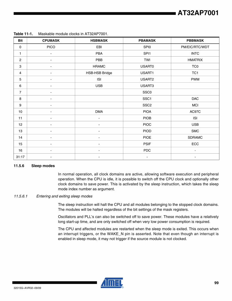
9932015G–AVR32–09/09
AT32AP7001
11.5.6 Sleep modes
In normal operation, all clock domains are active, allowing software execution and peripheraloperation. When the CPU is idle, it is possible to switch off the CPU clock and optionally otherclock domains to save power. This is activated by the sleep instruction, which takes the sleepmode index number as argument.
11.5.6.1 Entering and exiting sleep modes
The sleep instruction will halt the CPU and all modules belonging to the stopped clock domains.The modules will be halted regardless of the bit settings of the mask registers.
Oscillators and PLL’s can also be switched off to save power. These modules have a relativelylong start-up time, and are only switched off when very low power consumption is required.
The CPU and affected modules are restarted when the sleep mode is exited. This occurs whenan interrupt triggers, or the WAKE_N pin is asserted. Note that even though an interrupt isenabled in sleep mode, it may not trigger if the source module is not clocked.
Table 11-1. Maskable module clocks in AT32AP7001.
Bit CPUMASK HSBMASK PBAMASK PBBMASK
0 PICO EBI SPI0 PM/EIC/RTC/WDT
1 - PBA SPI1 INTC
2 - PBB TWI HMATRIX
3 - HRAMC USART0 TC0
4 - HSB-HSB Bridge USART1 TC1
5 - ISI USART2 PWM
6 - USB USART3
7 - SSC0
8 - SSC1 DAC
9 - SSC2 MCI
10 - DMA PIOA AC97C
11 - - PIOB ISI
12 - - PIOC USB
13 - - PIOD SMC
14 - - PIOE SDRAMC
15 - - PSIF ECC
16 - - PDC -
31:17 - - - -

10032015G–AVR32–09/09
AT32AP7001
11.5.6.2 Supported sleep modes
The following sleep modes are supported. These are detailed in Table 11-2.
•Idle: The CPU is stopped, the rest of the chip is operating. Wake-up sources are any interrupt,or WAKE_N pin.
•Frozen: The CPU and HSB modules are stopped, peripherals are operating. Wake-up sourcesare any interrupt from PB modules, or WAKE_N pin.
•Standby: All synchronous clocks are stopped, but oscillators and PLL’s are running, allowingquick wake-up to normal mode. Wake-up sources are RTC or external interrupt, or WAKE_Npin.
•Stop: As Standby, but Oscillator 0 and 1, and the PLL’s are stopped. 32 KHz oscillator andRTC/WDT still operates. Wake-up sources are RTC or external interrupt, or WAKE_N pin.
•Static: All oscillators and clocks are stopped. Wake-up sources are external interrupt orWAKE_N pin.•
11.5.6.3 Precautions when entering sleep mode
Modules communicating with external circuits should normally be disabled before entering asleep mode that will stop the module operation. This prevents erratic behavior when entering orexiting sleep mode. Please refer to the relevant module documentation for recommendedactions.
Communication between the synchronous clock domains is disturbed when entering and exitingsleep modes. This means that bus transactions are not allowed between clock domains affectedby the sleep mode. The system may hang if the bus clocks are stopped in the middle of a bustransaction.
The CPU and caches are automatically stopped in a safe state to ensure that all CPU bus oper-ations are complete when the sleep mode goes into effect. Thus, when entering Idle mode, nofurther action is necessary.
When entering a deeper sleep mode than Idle mode, all other HSB masters must be stoppedbefore entering the sleep mode. Also, if there is a chance that any PB write operations areincomplete, the CPU should perform a read operation from any register on the PB bus beforeexecuting the sleep instruction. This will stall the CPU while waiting for any pending PB opera-tions to complete.
The Power manager will normally turn of all debug related clocks in the system in the static sleepmode, making i t impossible for a debugger to communicate with the system. If a
Table 11-2. Sleep modes
Index Sleep Mode CPU HSBPBA,B + GCLK
Osc0,1 + PLL0,1
Osc32 + RTC/WDT
0 Idle Off On On On On
1 Frozen Off Off On On On
2 Standby Off Off Off On On
3 Stop Off Off Off Off On
5 Static Off Off Off Off Off
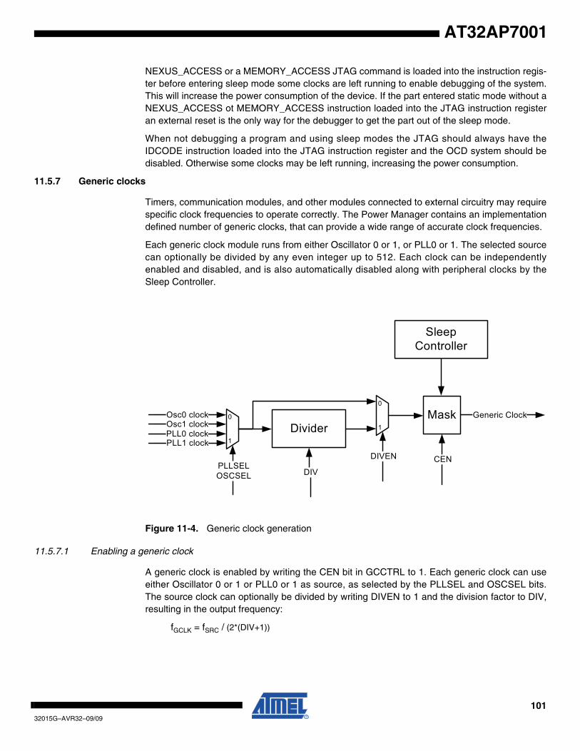
10132015G–AVR32–09/09
AT32AP7001
NEXUS_ACCESS or a MEMORY_ACCESS JTAG command is loaded into the instruction regis-ter before entering sleep mode some clocks are left running to enable debugging of the system.This will increase the power consumption of the device. If the part entered static mode without aNEXUS_ACCESS ot MEMORY_ACCESS instruction loaded into the JTAG instruction registeran external reset is the only way for the debugger to get the part out of the sleep mode.
When not debugging a program and using sleep modes the JTAG should always have theIDCODE instruction loaded into the JTAG instruction register and the OCD system should bedisabled. Otherwise some clocks may be left running, increasing the power consumption.
11.5.7 Generic clocks
Timers, communication modules, and other modules connected to external circuitry may requirespecific clock frequencies to operate correctly. The Power Manager contains an implementationdefined number of generic clocks, that can provide a wide range of accurate clock frequencies.
Each generic clock module runs from either Oscillator 0 or 1, or PLL0 or 1. The selected sourcecan optionally be divided by any even integer up to 512. Each clock can be independentlyenabled and disabled, and is also automatically disabled along with peripheral clocks by theSleep Controller.
Figure 11-4. Generic clock generation
11.5.7.1 Enabling a generic clock
A generic clock is enabled by writing the CEN bit in GCCTRL to 1. Each generic clock can useeither Oscillator 0 or 1 or PLL0 or 1 as source, as selected by the PLLSEL and OSCSEL bits.The source clock can optionally be divided by writing DIVEN to 1 and the division factor to DIV,resulting in the output frequency:
fGCLK = fSRC / (2*(DIV+1))
Divider0
1
Osc0 clock
PLL0 clock
PLLSELOSCSEL
Osc1 clock
PLL1 clock
Generic Clock
DIV
0
1
DIVEN
Mask
CEN
Sleep Controller
10232015G–AVR32–09/09
AT32AP7001
11.5.7.2 Disabling a generic clock
The generic clock can be disabled by writing CEN to 0 or entering a sleep mode that disablesthe PB clocks. In either case, the generic clock will be switched off on the first falling edge afterthe disabling event, to ensure that no glitches occur. If CEN is written to 0, the bit will still read as1 until the next falling edge occurs, and the clock is actually switched off. When writing CEN to 0,the other bits in GCCTRL should not be changed until CEN reads as 0, to avoid glitches on thegeneric clock.
When the clock is disabled, both the prescaler and output are reset.
11.5.7.3 Changing clock frequency
When changing generic clock frequency by writing GCCTRL, the clock should be switched off bythe procedure above, before being re-enabled with the new clock source or division setting. Thisprevents glitches during the transition.
11.5.7.4 Generic clock implementation
In AT32AP7001, there are 8 generic clocks. These are allocated to different functions as shownin Table 11-3.
11.5.8 Divided PB clocks
The clock generator in the Power Manager provides divided PBA and PBB clocks for use byperipherals that require a prescaled PB clock. This is described in the documentation for the rel-evant modules.
The divided clocks are not directly maskable, but are stopped in sleep modes where the PBclocks are stopped.
11.5.9 Debug operation
During a debug session, the user may need to halt the system to inspect memory and CPU reg-isters. The clocks normally keep running during this debug operation, but some peripherals mayrequire the clocks to be stopped, e.g. to prevent timer overflow, which would cause the programto fail. For this reason, peripherals on the PBA and PBB buses may use “debug qualified” PBclocks. This is described in the documentation for the relevant modules. The divided PB clocksare always debug qualified clocks.
Table 11-3. Generic clock allocation
Clock number Function
0 GCLK0 pin
1 GCLK1 pin
2 GCLK2 pin
3 GCLK3 pin
4 GCLK4 pin
5 Reserved for internal use
6 DAC

10332015G–AVR32–09/09
AT32AP7001
Debug qualified PB clocks are stopped during debug operation. The debug system can option-ally keep these clocks running during the debug operation. This is described in thedocumentation for the On-Chip Debug system.
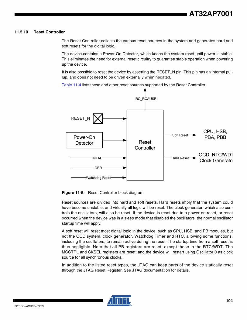
10432015G–AVR32–09/09
AT32AP7001
11.5.10 Reset Controller
The Reset Controller collects the various reset sources in the system and generates hard andsoft resets for the digital logic.
The device contains a Power-On Detector, which keeps the system reset until power is stable.This eliminates the need for external reset circuitry to guarantee stable operation when poweringup the device.
It is also possible to reset the device by asserting the RESET_N pin. This pin has an internal pul-lup, and does not need to be driven externally when negated.
Table 11-4 lists these and other reset sources supported by the Reset Controller.
Figure 11-5. Reset Controller block diagram
Reset sources are divided into hard and soft resets. Hard resets imply that the system couldhave become unstable, and virtually all logic will be reset. The clock generator, which also con-trols the oscillators, will also be reset. If the device is reset due to a power-on reset, or resetoccurred when the device was in a sleep mode that disabled the oscillators, the normal oscillatorstartup time will apply.
A soft reset will reset most digital logic in the device, such as CPU, HSB, and PB modules, butnot the OCD system, clock generator, Watchdog Timer and RTC, allowing some functions,including the oscillators, to remain active during the reset. The startup time from a soft reset isthus negligible. Note that all PB registers are reset, except those in the RTC/WDT. TheMCCTRL and CKSEL registers are reset, and the device will restart using Oscillator 0 as clocksource for all synchronous clocks.
In addition to the listed reset types, the JTAG can keep parts of the device statically resetthrough the JTAG Reset Register. See JTAG documentation for details.
NTAE
ResetController
RESET_N
Power-On Detector
DBR
Watchdog Reset
RC_RCAUSE
Hard Reset
Soft ResetCPU, HSB, PBA, PBB
OCD, RTC/WDTClock Generato
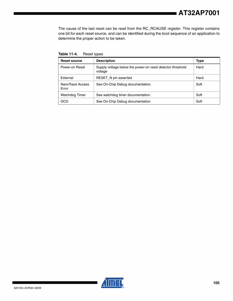
10532015G–AVR32–09/09
AT32AP7001
The cause of the last reset can be read from the RC_RCAUSE register. This register containsone bit for each reset source, and can be identified during the boot sequence of an application todetermine the proper action to be taken.
Table 11-4. Reset types
Reset source Description Type
Power-on Reset Supply voltage below the power-on reset detector threshold voltage
Hard
External RESET_N pin asserted Hard
NanoTrace Access Error
See On-Chip Debug documentation. Soft
Watchdog Timer See watchdog timer documentation. Soft
OCD See On-Chip Debug documentation Soft
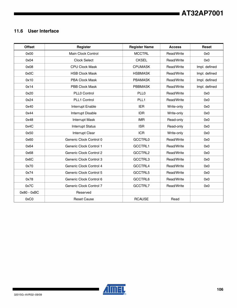
10632015G–AVR32–09/09
AT32AP7001
11.6 User Interface
Offset Register Register Name Access Reset
0x00 Main Clock Control MCCTRL Read/Write 0x0
0x04 Clock Select CKSEL Read/Write 0x0
0x08 CPU Clock Mask CPUMASK Read/Write Impl. defined
0x0C HSB Clock Mask HSBMASK Read/Write Impl. defined
0x10 PBA Clock Mask PBAMASK Read/Write Impl. defined
0x14 PBB Clock Mask PBBMASK Read/Write Impl. defined
0x20 PLL0 Control PLL0 Read/Write 0x0
0x24 PLL1 Control PLL1 Read/Write 0x0
0x40 Interrupt Enable IER Write-only 0x0
0x44 Interrupt Disable IDR Write-only 0x0
0x48 Interrupt Mask IMR Read-only 0x0
0x4C Interrupt Status ISR Read-only 0x0
0x50 Interrupt Clear ICR Write-only 0x0
0x60 Generic Clock Control 0 GCCTRL0 Read/Write 0x0
0x64 Generic Clock Control 1 GCCTRL1 Read/Write 0x0
0x68 Generic Clock Control 2 GCCTRL2 Read/Write 0x0
0x6C Generic Clock Control 3 GCCTRL3 Read/Write 0x0
0x70 Generic Clock Control 4 GCCTRL4 Read/Write 0x0
0x74 Generic Clock Control 5 GCCTRL5 Read/Write 0x0
0x78 Generic Clock Control 6 GCCTRL6 Read/Write 0x0
0x7C Generic Clock Control 7 GCCTRL7 Read/Write 0x0
0x80 - 0xBC Reserved
0xC0 Reset Cause RCAUSE Read

10732015G–AVR32–09/09
AT32AP7001
11.6.1 Main Clock Control
Name: MCCTRL
Access Type: Read/Write
• PLLSEL: PLL Select0: Oscillator 0 is source for the main clock1: PLL0 is source for the main clock
31 30 29 28 27 26 25 24
- - - - - - - -
23 22 21 20 19 18 17 16
- - - - - - - -
15 14 13 12 11 10 9 8
- - - - - - - -
7 6 5 4 3 2 1 0
- - - - - - PLLSEL -
10832015G–AVR32–09/09
AT32AP7001
11.6.2 Clock Select
Name: CKSEL
Access Type: Read/Write
• PBBDIV, PBBSEL: PBB Division and Clock SelectPBBDIV = 0: PBB clock equals main clock.PBBDIV = 1: PBB clock equals main clock divided by 2(PBBSEL+1).
• PBADIV, PBASEL: PBA Division and Clock SelectPBADIV = 0: PBA clock equals main clock.PBADIV = 1: PBA clock equals main clock divided by 2(PBASEL+1).
• HSBDIV, HSBSEL: HSB Division and Clock SelectHSBDIV = 0: HSB clock equals main clock.HSBDIV = 1: HSB clock equals main clock divided by 2(HSBSEL+1).
• CPUDIV, CPUSEL: CPU Division and Clock SelectCPUDIV = 0: CPU clock equals main clock.CPUDIV = 1: CPUclock equals main clock divided by 2(CPUSEL+1).
Note that if xxxDIV is written to 0, xxxSEL should also be written to 0 to ensure correct operation.
Also note that writing this register clears ISR:CKRDY. The register must not be re-written until CKRDY goes high.
31 30 29 28 27 26 25 24
PBBDIV - - - - PBBSEL
23 22 21 20 19 18 17 16
PBADIV - - - - PBASEL
15 14 13 12 11 10 9 8
HSBDIV - - - - HSBSEL
7 6 5 4 3 2 1 0
CPUDIV - - - - CPUSEL
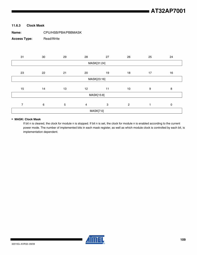
10932015G–AVR32–09/09
AT32AP7001
11.6.3 Clock Mask
Name: CPU/HSB/PBA/PBBMASK
Access Type: Read/Write
• MASK: Clock MaskIf bit n is cleared, the clock for module n is stopped. If bit n is set, the clock for module n is enabled according to the current
power mode. The number of implemented bits in each mask register, as well as which module clock is controlled by each bit, is
implementation dependent.
31 30 29 28 27 26 25 24
MASK[31:24]
23 22 21 20 19 18 17 16
MASK[23:16]
15 14 13 12 11 10 9 8
MASK[15:8]
7 6 5 4 3 2 1 0
MASK[7:0]
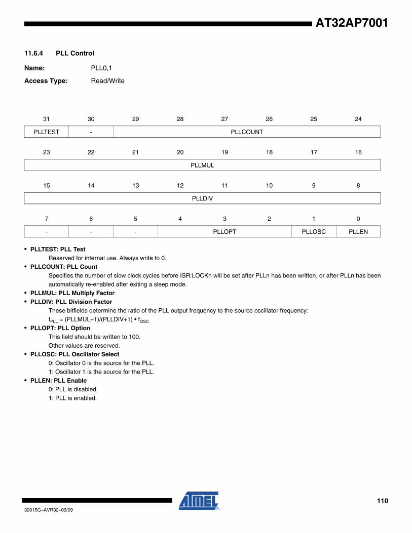
11032015G–AVR32–09/09
AT32AP7001
11.6.4 PLL Control
Name: PLL0,1
Access Type: Read/Write
• PLLTEST: PLL TestReserved for internal use. Always write to 0.
• PLLCOUNT: PLL CountSpecifies the number of slow clock cycles before ISR:LOCKn will be set after PLLn has been written, or after PLLn has been automatically re-enabled after exiting a sleep mode.
• PLLMUL: PLL Multiply Factor• PLLDIV: PLL Division Factor
These bitfields determine the ratio of the PLL output frequency to the source oscillator frequency:
fPLL = (PLLMUL+1)/(PLLDIV+1) • fOSC
• PLLOPT: PLL OptionThis field should be written to 100.
Other values are reserved.
• PLLOSC: PLL Oscillator Select0: Oscillator 0 is the source for the PLL.
1: Oscillator 1 is the source for the PLL.
• PLLEN: PLL Enable0: PLL is disabled.
1: PLL is enabled.
31 30 29 28 27 26 25 24
PLLTEST - PLLCOUNT
23 22 21 20 19 18 17 16
PLLMUL
15 14 13 12 11 10 9 8
PLLDIV
7 6 5 4 3 2 1 0
- - - PLLOPT PLLOSC PLLEN
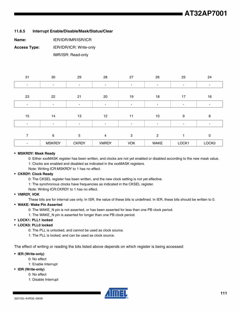
11132015G–AVR32–09/09
AT32AP7001
11.6.5 Interrupt Enable/Disable/Mask/Status/Clear
Name: IER/IDR/IMR/ISR/ICR
Access Type: IER/IDR/ICR: Write-only
IMR/ISR: Read-only
• MSKRDY: Mask Ready0: Either xxxMASK register has been written, and clocks are not yet enabled or disabled according to the new mask value.
1: Clocks are enabled and disabled as indicated in the xxxMASK registers.Note: Writing ICR:MSKRDY to 1 has no effect.
• CKRDY: Clock Ready0: The CKSEL register has been written, and the new clock setting is not yet effective.1: The synchronous clocks have frequencies as indicated in the CKSEL register.
Note: Writing ICR:CKRDY to 1 has no effect.
• VMRDY, VOKThese bits are for internal use only. In ISR, the value of these bits is undefined. In IER, these bits should be written to 0.
• WAKE: Wake Pin Asserted0: The WAKE_N pin is not asserted, or has been asserted for less than one PB clock period.1: The WAKE_N pin is asserted for longer than one PB clock period.
• LOCK1: PLL1 locked• LOCK0: PLL0 locked
0: The PLL is unlocked, and cannot be used as clock source.
1: The PLL is locked, and can be used as clock source.
The effect of writing or reading the bits listed above depends on which register is being accessed:
• IER (Write-only)0: No effect
1: Enable Interrupt
• IDR (Write-only)0: No effect
1: Disable Interrupt
31 30 29 28 27 26 25 24
- - - - - - - -
23 22 21 20 19 18 17 16
- - - - - - - -
15 14 13 12 11 10 9 8
- - - - - - - -
7 6 5 4 3 2 1 0
- MSKRDY CKRDY VMRDY VOK WAKE LOCK1 LOCK0

11232015G–AVR32–09/09
AT32AP7001
• IMR (Read-only)0: Interrupt is disabled
1: Interrupt is enabled
• ISR (Read-only)0: An interrupt event has occurred
1: An interrupt even has not occurred
• ICR (Write-only)0: No effect1: Clear interrupt event

11332015G–AVR32–09/09
AT32AP7001
11.6.6 Generic Clock Control
Name: GCCTRL0... GCCTRL7
Access Type: Read/Write
There is one GCCTRL register per generic clock in the design.
• DIV: Division Factor• DIVEN: Divide Enable
0: The generic clock equals the undivided source clock.1: The generic clock equals the source clock divided by 2*(DIV+1).
• CEN: Clock Enable0: Clock is stopped.1: Clock is running.
• PLLSEL: PLL Select0: Oscillator is source for the generic clock.1: PLL is source for the generic clock.
• OSCSEL: Oscillator Select0: Oscillator (or PLL) 0 is source for the generic clock.1: Oscillator (or PLL) 1is source for the generic clock.
31 30 29 28 27 26 25 24
- - - - - - - -
23 22 21 20 19 18 17 16
- - - - - - - -
15 14 13 12 11 10 9 8
DIV[7:0]
7 6 5 4 3 2 1 0
- - - DIVEN - CEN PLLSEL OSCSEL
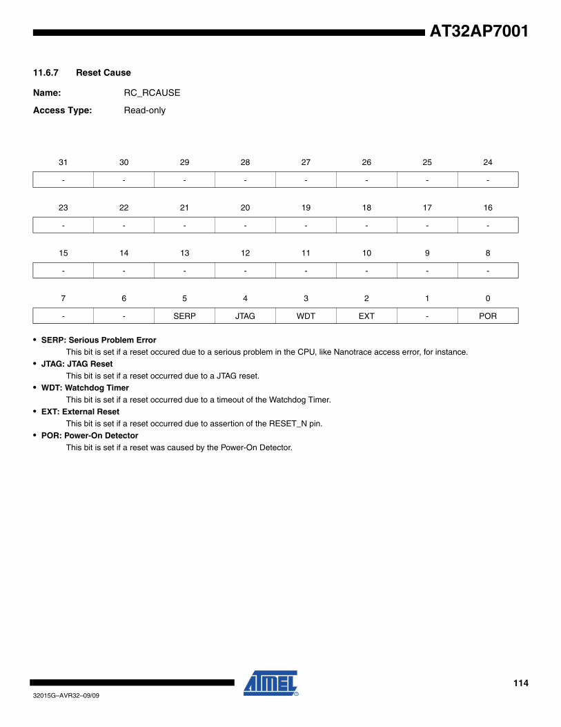
11432015G–AVR32–09/09
AT32AP7001
11.6.7 Reset Cause
Name: RC_RCAUSE
Access Type: Read-only
• SERP: Serious Problem ErrorThis bit is set if a reset occured due to a serious problem in the CPU, like Nanotrace access error, for instance.
• JTAG: JTAG ResetThis bit is set if a reset occurred due to a JTAG reset.
• WDT: Watchdog TimerThis bit is set if a reset occurred due to a timeout of the Watchdog Timer.
• EXT: External ResetThis bit is set if a reset occurred due to assertion of the RESET_N pin.
• POR: Power-On DetectorThis bit is set if a reset was caused by the Power-On Detector.
31 30 29 28 27 26 25 24
- - - - - - - -
23 22 21 20 19 18 17 16
- - - - - - - -
15 14 13 12 11 10 9 8
- - - - - - - -
7 6 5 4 3 2 1 0
- - SERP JTAG WDT EXT - POR
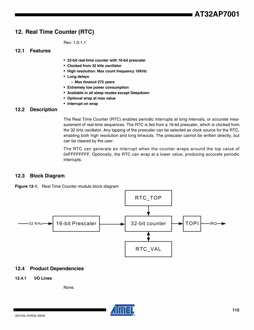
11532015G–AVR32–09/09
AT32AP7001
12. Real Time Counter (RTC)
Rev: 1.0.1.1
12.1 Features
• 32-bit real-time counter with 16-bit prescaler• Clocked from 32 kHz oscillator• High resolution: Max count frequency 16KHz• Long delays
– Max timeout 272 years• Extremely low power consumption• Available in all sleep modes except Deepdown• Optional wrap at max value• Interrupt on wrap
12.2 Description
The Real Time Counter (RTC) enables periodic interrupts at long intervals, or accurate mea-surement of real-time sequences. The RTC is fed from a 16-bit prescaler, which is clocked fromthe 32 kHz oscillator. Any tapping of the prescaler can be selected as clock source for the RTC,enabling both high resolution and long timeouts. The prescaler cannot be written directly, butcan be cleared by the user.
The RTC can generate an interrupt when the counter wraps around the top value of0xFFFFFFFF. Optionally, the RTC can wrap at a lower value, producing accurate periodicinterrupts.
12.3 Block Diagram
Figure 12-1. Real Time Counter module block diagram
12.4 Product Dependencies
12.4.1 I/O Lines
None.
16-bit Prescaler32 KHz 32-bit counter
RTC_VAL
RTC_TOP
TOPI IRQ
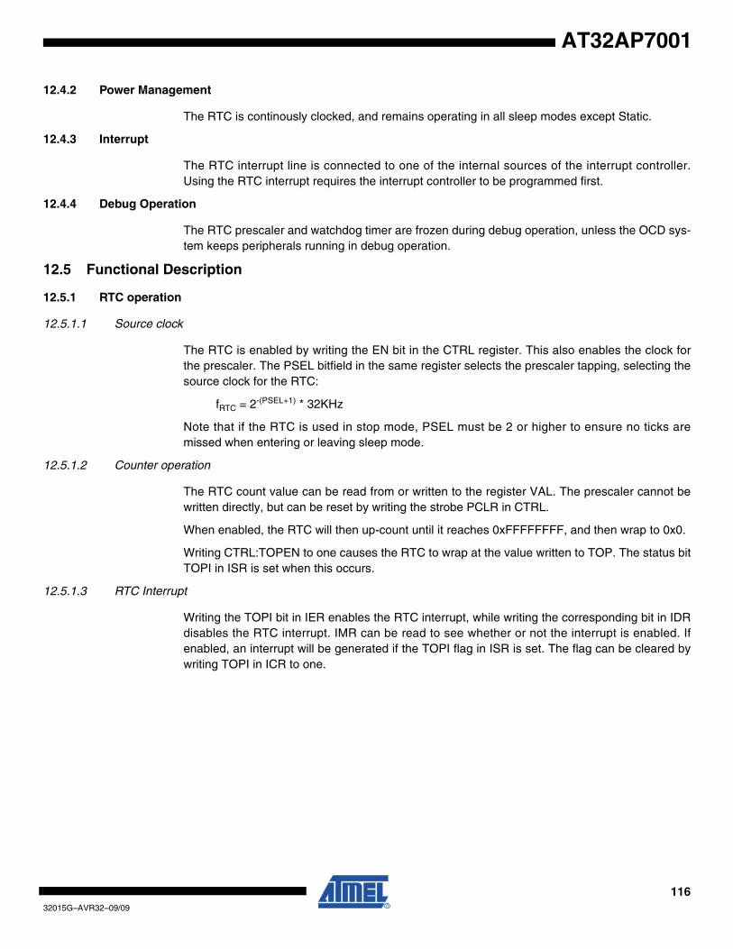
11632015G–AVR32–09/09
AT32AP7001
12.4.2 Power Management
The RTC is continously clocked, and remains operating in all sleep modes except Static.
12.4.3 Interrupt
The RTC interrupt line is connected to one of the internal sources of the interrupt controller.Using the RTC interrupt requires the interrupt controller to be programmed first.
12.4.4 Debug Operation
The RTC prescaler and watchdog timer are frozen during debug operation, unless the OCD sys-tem keeps peripherals running in debug operation.
12.5 Functional Description
12.5.1 RTC operation
12.5.1.1 Source clock
The RTC is enabled by writing the EN bit in the CTRL register. This also enables the clock forthe prescaler. The PSEL bitfield in the same register selects the prescaler tapping, selecting thesource clock for the RTC:
fRTC = 2-(PSEL+1) * 32KHz
Note that if the RTC is used in stop mode, PSEL must be 2 or higher to ensure no ticks aremissed when entering or leaving sleep mode.
12.5.1.2 Counter operation
The RTC count value can be read from or written to the register VAL. The prescaler cannot bewritten directly, but can be reset by writing the strobe PCLR in CTRL.
When enabled, the RTC will then up-count until it reaches 0xFFFFFFFF, and then wrap to 0x0.
Writing CTRL:TOPEN to one causes the RTC to wrap at the value written to TOP. The status bitTOPI in ISR is set when this occurs.
12.5.1.3 RTC Interrupt
Writing the TOPI bit in IER enables the RTC interrupt, while writing the corresponding bit in IDRdisables the RTC interrupt. IMR can be read to see whether or not the interrupt is enabled. Ifenabled, an interrupt will be generated if the TOPI flag in ISR is set. The flag can be cleared bywriting TOPI in ICR to one.
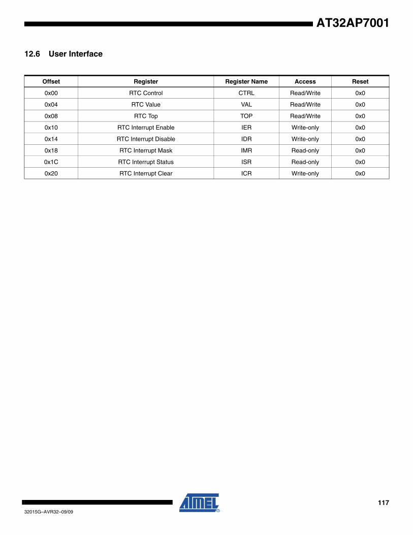
11732015G–AVR32–09/09
AT32AP7001
12.6 User Interface
Offset Register Register Name Access Reset
0x00 RTC Control CTRL Read/Write 0x0
0x04 RTC Value VAL Read/Write 0x0
0x08 RTC Top TOP Read/Write 0x0
0x10 RTC Interrupt Enable IER Write-only 0x0
0x14 RTC Interrupt Disable IDR Write-only 0x0
0x18 RTC Interrupt Mask IMR Read-only 0x0
0x1C RTC Interrupt Status ISR Read-only 0x0
0x20 RTC Interrupt Clear ICR Write-only 0x0
11832015G–AVR32–09/09
AT32AP7001
12.6.1 RTC Control
Name: CTRL
Access Type: Read/Write
• PSEL: Prescale SelectSelects prescaler bit PSEL as source clock for the RTC.
• TOPEN: Top Enable0: RTC wraps at 0xFFFFFFFF
1: RTC wraps at RTC_TOP• PCLR: Prescaler Clear
Writing this strobe clears the prescaler. Note that this also resets the watchdog timer.
• EN: Enable0: RTC is disabled
1: RTC is enabled
31 30 29 28 27 26 25 24
- - - - - - - -
23 22 21 20 19 18 17 16
- - - - - - - -
15 14 13 12 11 10 9 8
- - - - PSEL[3:0]
7 6 5 4 3 2 1 0
- - - - - TOPEN PCLR EN
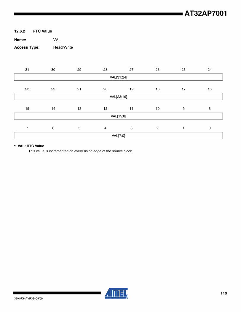
11932015G–AVR32–09/09
AT32AP7001
12.6.2 RTC Value
Name: VAL
Access Type: Read/Write
• VAL: RTC ValueThis value is incremented on every rising edge of the source clock.
31 30 29 28 27 26 25 24
VAL[31:24]
23 22 21 20 19 18 17 16
VAL[23:16]
15 14 13 12 11 10 9 8
VAL[15:8]
7 6 5 4 3 2 1 0
VAL[7:0]
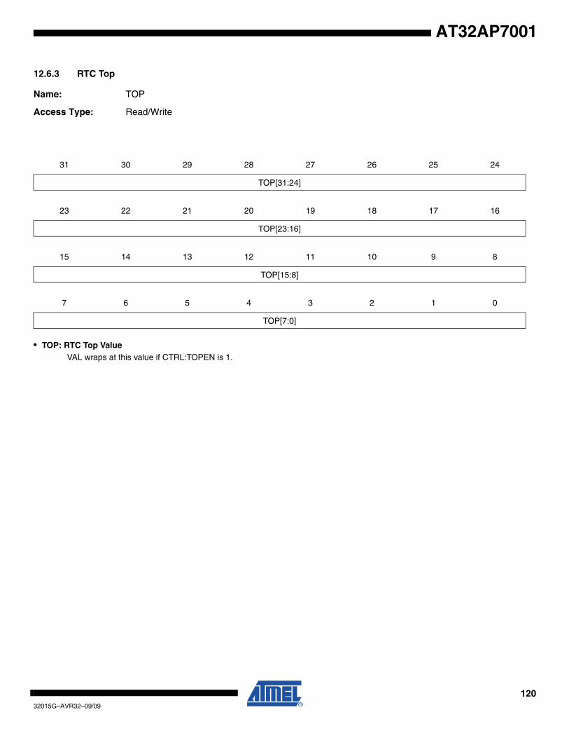
12032015G–AVR32–09/09
AT32AP7001
12.6.3 RTC Top
Name: TOP
Access Type: Read/Write
• TOP: RTC Top ValueVAL wraps at this value if CTRL:TOPEN is 1.
31 30 29 28 27 26 25 24
TOP[31:24]
23 22 21 20 19 18 17 16
TOP[23:16]
15 14 13 12 11 10 9 8
TOP[15:8]
7 6 5 4 3 2 1 0
TOP[7:0]
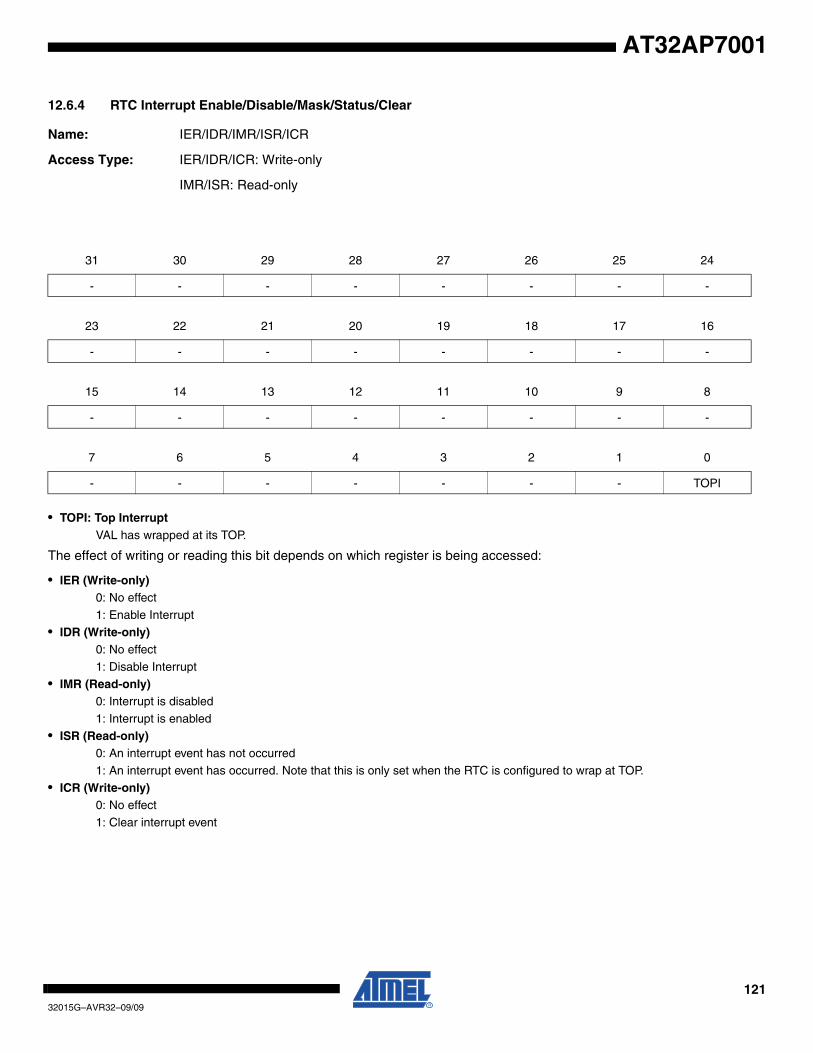
12132015G–AVR32–09/09
AT32AP7001
12.6.4 RTC Interrupt Enable/Disable/Mask/Status/Clear
Name: IER/IDR/IMR/ISR/ICR
Access Type: IER/IDR/ICR: Write-only
IMR/ISR: Read-only
• TOPI: Top InterruptVAL has wrapped at its TOP.
The effect of writing or reading this bit depends on which register is being accessed:
• IER (Write-only)0: No effect
1: Enable Interrupt
• IDR (Write-only)0: No effect
1: Disable Interrupt
• IMR (Read-only)0: Interrupt is disabled
1: Interrupt is enabled
• ISR (Read-only)0: An interrupt event has not occurred
1: An interrupt event has occurred. Note that this is only set when the RTC is configured to wrap at TOP.
• ICR (Write-only)0: No effect
1: Clear interrupt event
31 30 29 28 27 26 25 24
- - - - - - - -
23 22 21 20 19 18 17 16
- - - - - - - -
15 14 13 12 11 10 9 8
- - - - - - - -
7 6 5 4 3 2 1 0
- - - - - - - TOPI
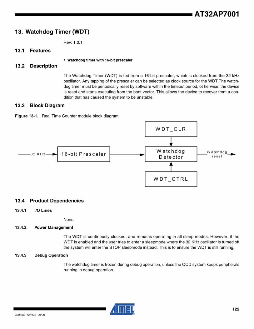
12232015G–AVR32–09/09
AT32AP7001
13. Watchdog Timer (WDT)
Rev: 1.0.1
13.1 Features
• Watchdog timer with 16-bit prescaler
13.2 Description
The Watchdog Timer (WDT) is fed from a 16-bit prescaler, which is clocked from the 32 kHzoscillator. Any tapping of the prescaler can be selected as clock source for the WDT.The watch-dog timer must be periodically reset by software within the timeout period, ot herwise, the deviceis reset and starts executing from the boot vector. This allows the device to recover from a con-dition that has caused the system to be unstable.
13.3 Block Diagram
Figure 13-1. Real Time Counter module block diagram
13.4 Product Dependencies
13.4.1 I/O Lines
None
13.4.2 Power Management
The WDT is continously clocked, and remains operating in all sleep modes. However, if theWDT is enabled and the user tries to enter a sleepmode where the 32 KHz oscillator is turned offthe system will enter the STOP sleepmode instead. This is to ensure the WDT is still running.
13.4.3 Debug Operation
The watchdog timer is frozen during debug operation, unless the OCD system keeps peripheralsrunning in debug operation.
1 6 -b it P re s c a le r3 2 K H z
W D T _ C L R
W a tc h d o g D e te c to r
W D T _ C T R L
W a tc h d o gre s e t
12332015G–AVR32–09/09
AT32AP7001
13.5 Functional Description
13.5.1 Watchdog Timer
The WDT is enabled by writing the EN bit in the CTRL register. This also enables the clock forthe prescaler. The PSEL bitfield in the same register selects the watchdog timeout period:
TWDT = 2(PSEL+1) * 30.518μs
To avoid accidental disabling of the watchdog, the CTRL register must be written twice, first withthe KEY field set to 0x55, then 0xAA without changing the other bitfields. Failure to do so willcause the write operation to be ignored, and CTRL does not change value.
The CLR register must be written with any value with regular intervals shorter than the watchdogtimeout period. Otherwise, the device will receive a soft reset, and the code will start executingfrom the boot vector.
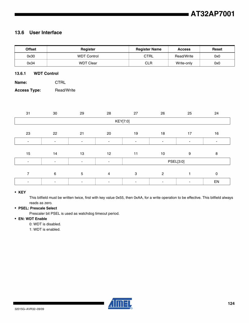
12432015G–AVR32–09/09
AT32AP7001
13.6 User Interface
13.6.1 WDT Control
Name: CTRL
Access Type: Read/Write
• KEYThis bitfield must be written twice, first with key value 0x55, then 0xAA, for a write operation to be effective. This bitfield always reads as zero.
• PSEL: Prescale SelectPrescaler bit PSEL is used as watchdog timeout period.
• EN: WDT Enable0: WDT is disabled.
1: WDT is enabled.
Offset Register Register Name Access Reset
0x30 WDT Control CTRL Read/Write 0x0
0x34 WDT Clear CLR Write-only 0x0
31 30 29 28 27 26 25 24
KEY[7:0]
23 22 21 20 19 18 17 16
- - - - - - - -
15 14 13 12 11 10 9 8
- - - - PSEL[3:0]
7 6 5 4 3 2 1 0
- - - - - - - EN

12532015G–AVR32–09/09
AT32AP7001
13.6.2 WDT Clear
Name: CLR
Access Type: Write-only
When the watchdog timer is enabled, this register must be periodically written, with any value, within the watchdog timeoutperiod, to prevent a watchdog reset.
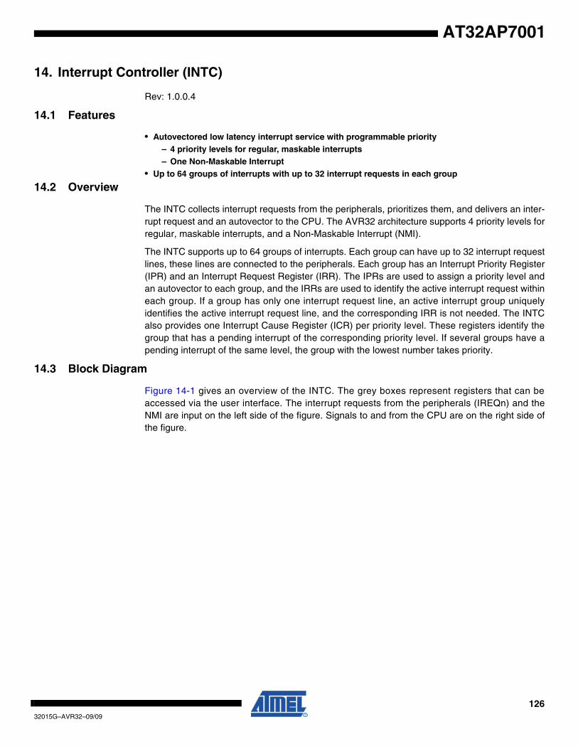
12632015G–AVR32–09/09
AT32AP7001
14. Interrupt Controller (INTC)
Rev: 1.0.0.4
14.1 Features
• Autovectored low latency interrupt service with programmable priority– 4 priority levels for regular, maskable interrupts– One Non-Maskable Interrupt
• Up to 64 groups of interrupts with up to 32 interrupt requests in each group
14.2 Overview
The INTC collects interrupt requests from the peripherals, prioritizes them, and delivers an inter-rupt request and an autovector to the CPU. The AVR32 architecture supports 4 priority levels forregular, maskable interrupts, and a Non-Maskable Interrupt (NMI).
The INTC supports up to 64 groups of interrupts. Each group can have up to 32 interrupt requestlines, these lines are connected to the peripherals. Each group has an Interrupt Priority Register(IPR) and an Interrupt Request Register (IRR). The IPRs are used to assign a priority level andan autovector to each group, and the IRRs are used to identify the active interrupt request withineach group. If a group has only one interrupt request line, an active interrupt group uniquelyidentifies the active interrupt request line, and the corresponding IRR is not needed. The INTCalso provides one Interrupt Cause Register (ICR) per priority level. These registers identify thegroup that has a pending interrupt of the corresponding priority level. If several groups have apending interrupt of the same level, the group with the lowest number takes priority.
14.3 Block Diagram
Figure 14-1 gives an overview of the INTC. The grey boxes represent registers that can beaccessed via the user interface. The interrupt requests from the peripherals (IREQn) and theNMI are input on the left side of the figure. Signals to and from the CPU are on the right side ofthe figure.
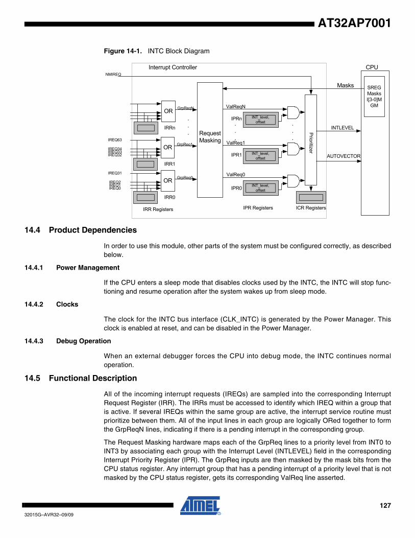
12732015G–AVR32–09/09
AT32AP7001
Figure 14-1. INTC Block Diagram
14.4 Product Dependencies
In order to use this module, other parts of the system must be configured correctly, as describedbelow.
14.4.1 Power Management
If the CPU enters a sleep mode that disables clocks used by the INTC, the INTC will stop func-tioning and resume operation after the system wakes up from sleep mode.
14.4.2 Clocks
The clock for the INTC bus interface (CLK_INTC) is generated by the Power Manager. Thisclock is enabled at reset, and can be disabled in the Power Manager.
14.4.3 Debug Operation
When an external debugger forces the CPU into debug mode, the INTC continues normaloperation.
14.5 Functional Description
All of the incoming interrupt requests (IREQs) are sampled into the corresponding InterruptRequest Register (IRR). The IRRs must be accessed to identify which IREQ within a group thatis active. If several IREQs within the same group are active, the interrupt service routine mustprioritize between them. All of the input lines in each group are logically ORed together to formthe GrpReqN lines, indicating if there is a pending interrupt in the corresponding group.
The Request Masking hardware maps each of the GrpReq lines to a priority level from INT0 toINT3 by associating each group with the Interrupt Level (INTLEVEL) field in the correspondingInterrupt Priority Register (IPR). The GrpReq inputs are then masked by the mask bits from theCPU status register. Any interrupt group that has a pending interrupt of a priority level that is notmasked by the CPU status register, gets its corresponding ValReq line asserted.
Request Masking
ORIREQ0IREQ1IREQ2
IREQ31GrpReq0
Masks SREG MasksI[3-0]M
GM
INTLEVEL
AUTOVECTOR
Prioritizer
CPUInterrupt Controller
OR GrpReqN
NMIREQ
ORIREQ32IREQ33IREQ34
IREQ63GrpReq1
IRR Registers IPR Registers ICR Registers
INT_level, offset
INT_level, offset
INT_level, offset
IPR0
IPR1
IPRn
IRR0
IRR1
IRRn
ValReq0
ValReq1
ValReqN
.
.
....
.
.
.
12832015G–AVR32–09/09
AT32AP7001
Masking of the interrupt requests is done based on five interrupt mask bits of the CPU statusregister, namely Interrupt Level 3 Mask (I3M) to Interrupt Level 0 Mask (I0M), and Global Inter-rupt Mask (GM). An interrupt request is masked if either the GM or the corresponding interruptlevel mask bit is set.
The Prioritizer hardware uses the ValReq lines and the INTLEVEL field in the IPRs to select thepending interrupt of the highest priority. If an NMI interrupt request is pending, it automaticallygets the highest priority of any pending interrupt. If several interrupt groups of the highest pend-ing interrupt level have pending interrupts, the interrupt group with the highest number isselected.
The INTLEVEL and handler autovector offset (AUTOVECTOR) of the selected interrupt aretransmitted to the CPU for interrupt handling and context switching. The CPU does not need toknow which interrupt is requesting handling, but only the level and the offset of the handleraddress. The IRR registers contain the interrupt request lines of the groups and can be read viauser interface registers for checking which interrupts of the group are actually active.
14.5.1 Non-Maskable Interrupts
A NMI request has priority over all other interrupt requests. NMI has a dedicated exception vec-tor address defined by the AVR32 architecture, so AUTOVECTOR is undefined whenINTLEVEL indicates that an NMI is pending.
14.5.2 CPU Response
When the CPU receives an interrupt request it checks if any other exceptions are pending. If noexceptions of higher priority are pending, interrupt handling is initiated. When initiating interrupthandling, the corresponding interrupt mask bit is set automatically for this and lower levels in sta-tus register. E.g, if an interrupt of level 3 is approved for handling, the interrupt mask bits I3M,I2M, I1M, and I0M are set in status register. If an interrupt of level 1 is approved, the maskingbits I1M and I0M are set in status register. The handler address is calculated by addingAUTOVECTOR to the CPU system register Exception Vector Base Address (EVBA). The CPUwill then jump to the calculated address and start executing the interrupt handler.
Setting the interrupt mask bits prevents the interrupts from the same and lower levels to bepassed through the interrupt controller. Setting of the same level mask bit prevents also multiplerequests of the same interrupt to happen.
It is the responsibility of the handler software to clear the interrupt request that caused the inter-rupt before returning from the interrupt handler. If the conditions that caused the interrupt are notcleared, the interrupt request remains active.
14.5.3 Clearing an Interrupt Request
Clearing of the interrupt request is done by writing to registers in the corresponding peripheralmodule, which then clears the corresponding NMIREQ/IREQ signal.
The recommended way of clearing an interrupt request is a store operation to the controllingperipheral register, followed by a dummy load operation from the same register. This causes apipeline stall, which prevents the interrupt from accidentally re-triggering in case the handler isexited and the interrupt mask is cleared before the interrupt request is cleared.
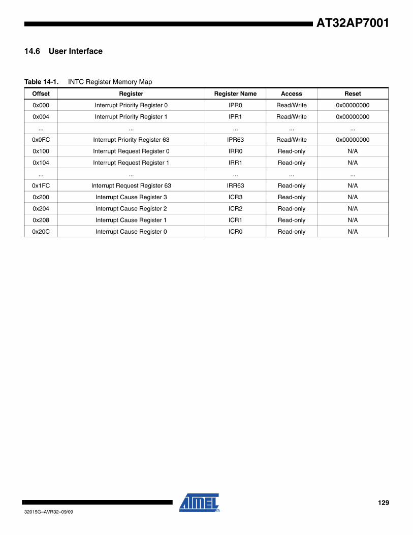
12932015G–AVR32–09/09
AT32AP7001
14.6 User Interface
Table 14-1. INTC Register Memory Map
Offset Register Register Name Access Reset
0x000 Interrupt Priority Register 0 IPR0 Read/Write 0x00000000
0x004 Interrupt Priority Register 1 IPR1 Read/Write 0x00000000
... ... ... ... ...
0x0FC Interrupt Priority Register 63 IPR63 Read/Write 0x00000000
0x100 Interrupt Request Register 0 IRR0 Read-only N/A
0x104 Interrupt Request Register 1 IRR1 Read-only N/A
... ... ... ... ...
0x1FC Interrupt Request Register 63 IRR63 Read-only N/A
0x200 Interrupt Cause Register 3 ICR3 Read-only N/A
0x204 Interrupt Cause Register 2 ICR2 Read-only N/A
0x208 Interrupt Cause Register 1 ICR1 Read-only N/A
0x20C Interrupt Cause Register 0 ICR0 Read-only N/A
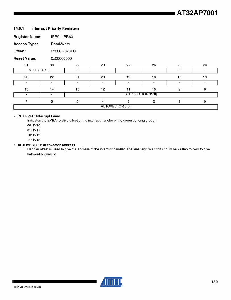
13032015G–AVR32–09/09
AT32AP7001
14.6.1 Interrupt Priority Registers
Register Name: IPR0...IPR63
Access Type: Read/Write
Offset: 0x000 - 0x0FC
Reset Value: 0x00000000
• INTLEVEL: Interrupt LevelIndicates the EVBA-relative offset of the interrupt handler of the corresponding group:
00: INT001: INT1
10: INT2
11: INT3• AUTOVECTOR: Autovector Address
Handler offset is used to give the address of the interrupt handler. The least significant bit should be written to zero to give halfword alignment.
31 30 29 28 27 26 25 24INTLEVEL[1:0] - - - - - -
23 22 21 20 19 18 17 16
- - - - - - - -
15 14 13 12 11 10 9 8
- - AUTOVECTOR[13:8]
7 6 5 4 3 2 1 0AUTOVECTOR[7:0]
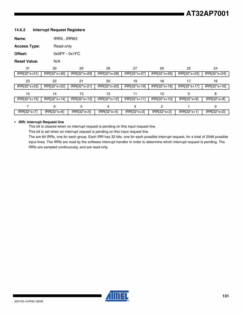
13132015G–AVR32–09/09
AT32AP7001
14.6.2 Interrupt Request Registers
Name: IRR0...IRR63
Access Type: Read-only
Offset: 0x0FF - 0x1FC
Reset Value: N/A
• IRR: Interrupt Request lineThis bit is cleared when no interrupt request is pending on this input request line.
This bit is set when an interrupt request is pending on this input request line.The are 64 IRRs, one for each group. Each IRR has 32 bits, one for each possible interrupt request, for a total of 2048 possible
input lines. The IRRs are read by the software interrupt handler in order to determine which interrupt request is pending. The
IRRs are sampled continuously, and are read-only.
31 30 29 28 27 26 25 24IRR[32*x+31] IRR[32*x+30] IRR[32*x+29] IRR[32*x+28] IRR[32*x+27] IRR[32*x+26] IRR[32*x+25] IRR[32*x+24]
23 22 21 20 19 18 17 16
IRR[32*x+23] IRR[32*x+22] IRR[32*x+21] IRR[32*x+20] IRR[32*x+19] IRR[32*x+18] IRR[32*x+17] IRR[32*x+16]
15 14 13 12 11 10 9 8
IRR[32*x+15] IRR[32*x+14] IRR[32*x+13] IRR[32*x+12] IRR[32*x+11] IRR[32*x+10] IRR[32*x+9] IRR[32*x+8]
7 6 5 4 3 2 1 0IRR[32*x+7] IRR[32*x+6] IRR[32*x+5] IRR[32*x+4] IRR[32*x+3] IRR[32*x+2] IRR[32*x+1] IRR[32*x+0]
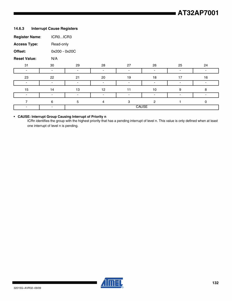
13232015G–AVR32–09/09
AT32AP7001
14.6.3 Interrupt Cause Registers
Register Name: ICR0...ICR3
Access Type: Read-only
Offset: 0x200 - 0x20C
Reset Value: N/A
• CAUSE: Interrupt Group Causing Interrupt of Priority nICRn identifies the group with the highest priority that has a pending interrupt of level n. This value is only defined when at least
one interrupt of level n is pending.
31 30 29 28 27 26 25 24- - - - - - - -
23 22 21 20 19 18 17 16
- - - - - - - -
15 14 13 12 11 10 9 8
- - - - - - - -
7 6 5 4 3 2 1 0- - CAUSE
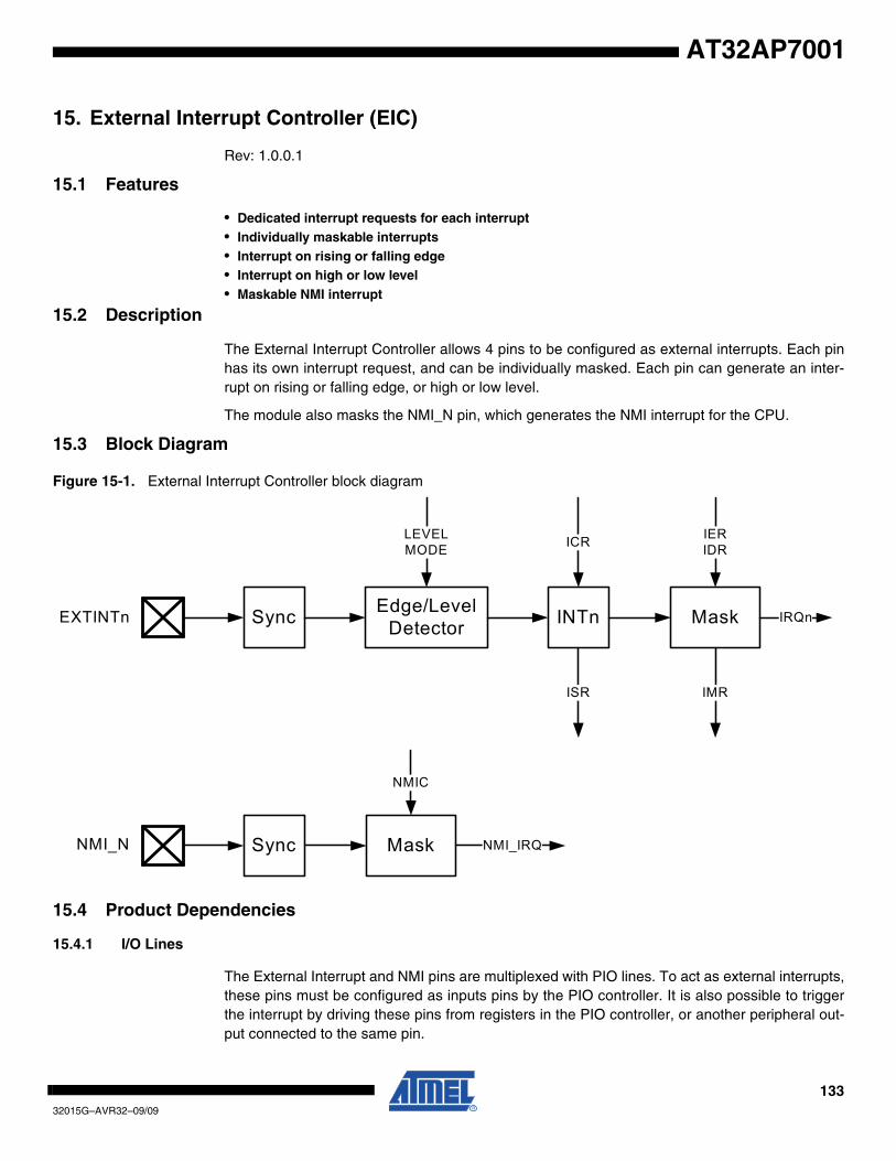
13332015G–AVR32–09/09
AT32AP7001
15. External Interrupt Controller (EIC)
Rev: 1.0.0.1
15.1 Features
• Dedicated interrupt requests for each interrupt• Individually maskable interrupts• Interrupt on rising or falling edge• Interrupt on high or low level• Maskable NMI interrupt
15.2 Description
The External Interrupt Controller allows 4 pins to be configured as external interrupts. Each pinhas its own interrupt request, and can be individually masked. Each pin can generate an inter-rupt on rising or falling edge, or high or low level.
The module also masks the NMI_N pin, which generates the NMI interrupt for the CPU.
15.3 Block Diagram
Figure 15-1. External Interrupt Controller block diagram
15.4 Product Dependencies
15.4.1 I/O Lines
The External Interrupt and NMI pins are multiplexed with PIO lines. To act as external interrupts,these pins must be configured as inputs pins by the PIO controller. It is also possible to triggerthe interrupt by driving these pins from registers in the PIO controller, or another peripheral out-put connected to the same pin.
Sync Edge/Level Detector Mask IRQnEXTINTn INTn
LEVELMODE
IERIDRICR
ISR IMR
NMI_N Sync Mask NMI_IRQ
NMIC
13432015G–AVR32–09/09
AT32AP7001
15.4.2 Power Management
Edge triggered interrupts are available in all sleep modes except Deepdown. Level triggeredinterrupts and the NMI interrupt are available in all sleep modes.
15.4.3 Interrupt
The EIC interrupt lines are connected to internal sources of the interrupt controller. Using theExternal Interrutps requires the interrupt controller to be programmed first.
Using the Non-Maskable Interrupt does not require the interrupt controller to be programmed.
15.5 Functional Description
15.5.1 External Interrupts
Each external interrupt pin EXTINTn can be configured to produce an interrupt on rising or fall-ing edge, or high or low level. External interrupts are configured by the MODE, EDGE, andLEVEL registers. Each interrupt n has a bit INTn in each of these registers.
Similarly, each interrupt has a corresponding bit in each of the interrupt control and status regis-ters. Writing 1 to the INTn strobe in IER enables the external interrupt on pin EXTINTn, whilewriting 1 to INTn in IDR disables the external interrupt. IMR can be read to check which inter-rupts are enabled. When the interrupt triggers, the corresponding bit in ISR will be set. For edgetriggered interrupts, the flag remains set until the corresponding strobe bit in ICR is written to 1.For level triggered interrupts, the flag remains set for as long as the interrupt condition is presenton the pin.
Writing INTn in MODE to 0 enables edge triggered interrupts, while writing the bit to 1 enableslevel triggered interrupts.
If EXTINTn is configured as an edge triggered interrupt, writing INTn in EDGE to 0 will trigger theinterrupt on falling edge, while writing the bit to 1 will trigger the interrupt on rising edge.
If EXTINTn is configured as a level triggered interrupt, writing INTn in LEVEL to 0 will trigger theinterrupt on low level, while writing the bit to 1 will trigger the interrupt on high level.
15.5.1.1 Synchronization of external interrupts
The pin value of the EXTINTn pins is normally synchronized to the CPU clock, so spikes shorterthan a CPU clock cycle are not guaranteed to produce an interrupt. In Stop mode, spikes shorterthan a 32KHz clock cycle are not guaranteed to produce an interrupt. In Deepdown mode, onlyunsynchronized level interrupts remain active, and any short spike on this interrupt will wake upthe device.
15.5.2 NMI Control
The Non-Maskable Interrupt of the CPU is connected to the NMI_N pin through masking logic inthe External Interrupt Controller. This masking ensures that the NMI will not trigger before theCPU has been set up to handle interrupts. Writing the EN bit in the NMIC register enables theNMI interrupt, while writing EN to 0 disables the NMI interrupt. When enabled, the interrupt trig-gers whenever the NMI_N pin is negated.
The NMI_N pin is synchronized the same way as external level interrupts.
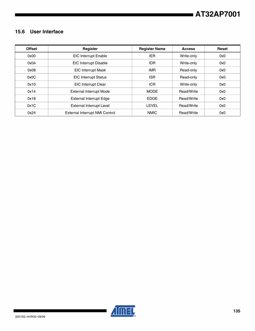
13532015G–AVR32–09/09
AT32AP7001
15.6 User Interface
Offset Register Register Name Access Reset
0x00 EIC Interrupt Enable IER Write-only 0x0
0x04 EIC Interrupt Disable IDR Write-only 0x0
0x08 EIC Interrupt Mask IMR Read-only 0x0
0x0C EIC Interrupt Status ISR Read-only 0x0
0x10 EIC Interrupt Clear ICR Write-only 0x0
0x14 External Interrupt Mode MODE Read/Write 0x0
0x18 External Interrupt Edge EDGE Read/Write 0x0
0x1C External Interrupt Level LEVEL Read/Write 0x0
0x24 External Interrupt NMI Control NMIC Read/Write 0x0
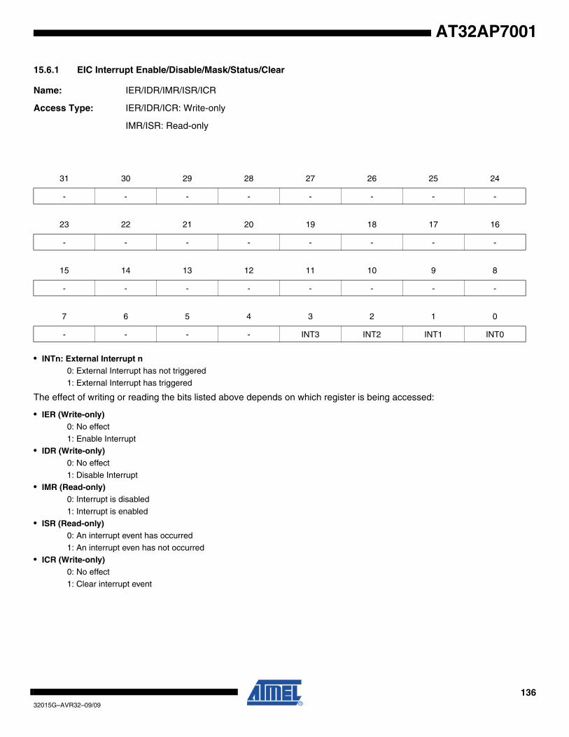
13632015G–AVR32–09/09
AT32AP7001
15.6.1 EIC Interrupt Enable/Disable/Mask/Status/Clear
Name: IER/IDR/IMR/ISR/ICR
Access Type: IER/IDR/ICR: Write-only
IMR/ISR: Read-only
• INTn: External Interrupt n0: External Interrupt has not triggered
1: External Interrupt has triggered
The effect of writing or reading the bits listed above depends on which register is being accessed:
• IER (Write-only)0: No effect
1: Enable Interrupt
• IDR (Write-only)0: No effect
1: Disable Interrupt
• IMR (Read-only)0: Interrupt is disabled
1: Interrupt is enabled
• ISR (Read-only)0: An interrupt event has occurred
1: An interrupt even has not occurred
• ICR (Write-only)0: No effect
1: Clear interrupt event
31 30 29 28 27 26 25 24
- - - - - - - -
23 22 21 20 19 18 17 16
- - - - - - - -
15 14 13 12 11 10 9 8
- - - - - - - -
7 6 5 4 3 2 1 0
- - - - INT3 INT2 INT1 INT0
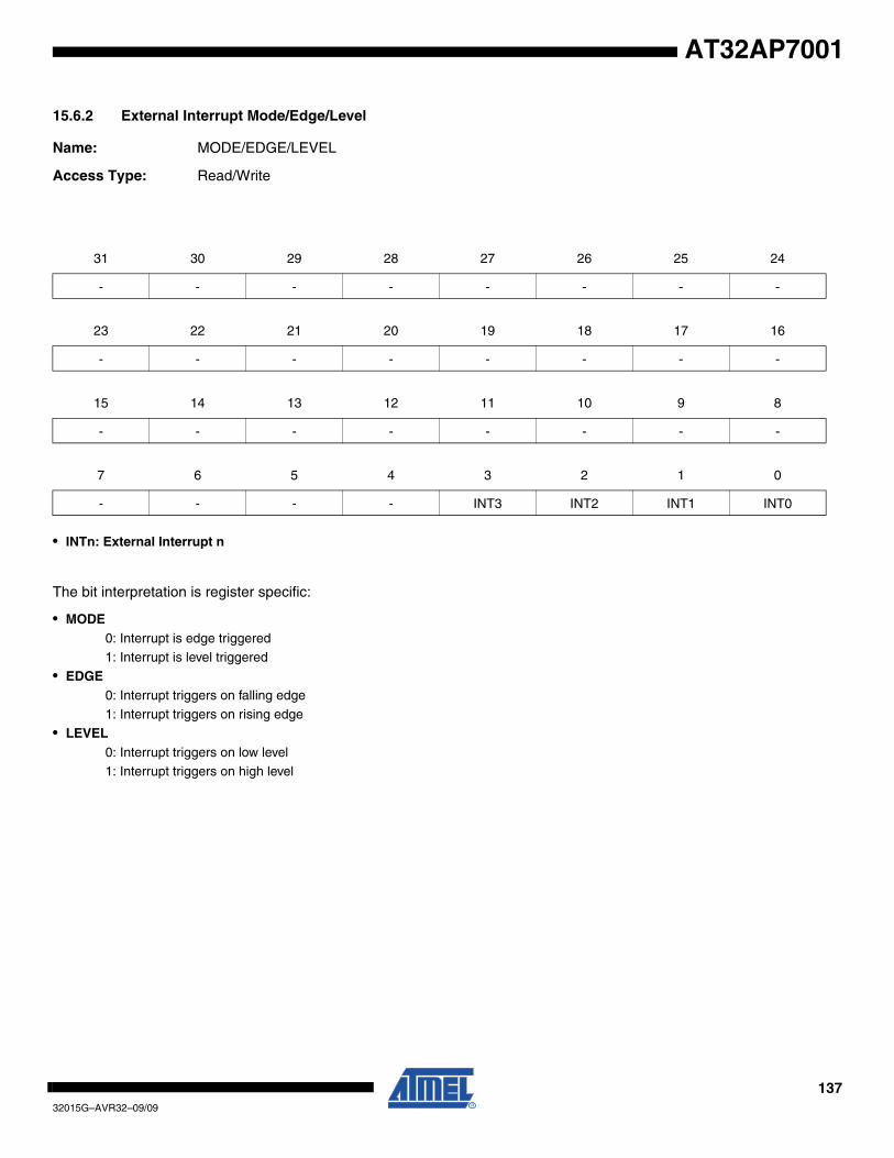
13732015G–AVR32–09/09
AT32AP7001
15.6.2 External Interrupt Mode/Edge/Level
Name: MODE/EDGE/LEVEL
Access Type: Read/Write
• INTn: External Interrupt n
The bit interpretation is register specific:
• MODE0: Interrupt is edge triggered1: Interrupt is level triggered
• EDGE0: Interrupt triggers on falling edge1: Interrupt triggers on rising edge
• LEVEL0: Interrupt triggers on low level1: Interrupt triggers on high level
31 30 29 28 27 26 25 24
- - - - - - - -
23 22 21 20 19 18 17 16
- - - - - - - -
15 14 13 12 11 10 9 8
- - - - - - - -
7 6 5 4 3 2 1 0
- - - - INT3 INT2 INT1 INT0

13832015G–AVR32–09/09
AT32AP7001
15.6.3 NMI Control
Name: NMIC
Access Type: Read/Write
• EN: Enable0: NMI disabled. Asserting the NMI pin does not generate an NMI request.1: NMI enabled. Asserting the NMI pin generate an NMI request.
31 30 29 28 27 26 25 24
- - - - - - - -
23 22 21 20 19 18 17 16
- - - - - - - -
15 14 13 12 11 10 9 8
- - - - - - - -
7 6 5 4 3 2 1 0
- - - - - - - EN
13932015G–AVR32–09/09
AT32AP7001
16. HSB Bus Matrix (HMATRIX)
Rev: 2.0.0.2
16.1 Features
• User Interface on peripheral bus• Configurable Number of Masters (Up to sixteen)• Configurable Number of Slaves (Up to sixteen)• One Decoder for Each Master• Three Different Memory Mappings for Each Master (Internal and External boot, Remap)• One Remap Function for Each Master• Programmable Arbitration for Each Slave
– Round-Robin– Fixed Priority
• Programmable Default Master for Each Slave– No Default Master– Last Accessed Default Master– Fixed Default Master
• One Cycle Latency for the First Access of a Burst• Zero Cycle Latency for Default Master• One Special Function Register for Each Slave (Not dedicated)
16.2 Overview
The Bus Matrix implements a multi-layer bus structure, that enables parallel access pathsbetween multiple High Speed Bus (HSB) masters and slaves in a system, thus increasing theoverall bandwidth. The Bus Matrix interconnects up to 16 HSB Masters to up to 16 HSB Slaves.The normal latency to connect a master to a slave is one cycle except for the default master ofthe accessed slave which is connected directly (zero cycle latency). The Bus Matrix provides 16Special Function Registers (SFR) that allow the Bus Matrix to support application specificfeatures.
16.3 Product Dependencies
In order to use this module, other parts of the system must be configured correctly, as describedbelow.
16.3.1 Clocks
The clock for the HMATRIX bus interface (CLK_HMATRIX) is generated by the Power Manager.This clock is enabled at reset, and can be disabled in the Power Manager. It is recommended todisable the HMATRIX before disabling the clock, to avoid freezing the HMATRIX in an undefinedstate.
16.4 Functional Description
16.4.1 Memory Mapping
The Bus Matrix provides one decoder for every HSB Master Interface. The decoder offers eachHSB Master several memory mappings. In fact, depending on the product, each memory area
14032015G–AVR32–09/09
AT32AP7001
may be assigned to several slaves. Booting at the same address while using different HSBslaves (i.e. external RAM, internal ROM or internal Flash, etc.) becomes possible.
The Bus Matrix user interface provides Master Remap Control Register (MRCR) that performsremap action for every master independently.
16.4.2 Special Bus Granting Mechanism
The Bus Matrix provides some speculative bus granting techniques in order to anticipate accessrequests from some masters. This mechanism reduces latency at first access of a burst or singletransfer. This bus granting mechanism sets a different default master for every slave.
At the end of the current access, if no other request is pending, the slave remains connected toits associated default master. A slave can be associated with three kinds of default masters: nodefault master, last access master and fixed default master.
16.4.2.1 No Default Master
At the end of the current access, if no other request is pending, the slave is disconnected fromall masters. No Default Master suits low-power mode.
16.4.2.2 Last Access Master
At the end of the current access, if no other request is pending, the slave remains connected tothe last master that performed an access request.
16.4.2.3 Fixed Default Master
At the end of the current access, if no other request is pending, the slave connects to its fixeddefault master. Unlike last access master, the fixed master does not change unless the usermodifies it by a software action (field FIXED_DEFMSTR of the related SCFG).
To change from one kind of default master to another, the Bus Matrix user interface provides theSlave Configuration Registers, one for each slave, that set a default master for each slave. TheSlave Configuration Register contains two fields: DEFMSTR_TYPE and FIXED_DEFMSTR. The2-bit DEFMSTR_TYPE field selects the default master type (no default, last access master, fixeddefault master), whereas the 4-bit FIXED_DEFMSTR field selects a fixed default master pro-vided that DEFMSTR_TYPE is set to fixed default master. Please refer to the Bus Matrix userinterface description.
16.4.3 Arbitration
The Bus Matrix provides an arbitration mechanism that reduces latency when conflict casesoccur, i.e. when two or more masters try to access the same slave at the same time. One arbiterper HSB slave is provided, thus arbitrating each slave differently.
The Bus Matrix provides the user with the possibility of choosing between 2 arbitration types foreach slave:
1. Round-Robin Arbitration (default)
2. Fixed Priority Arbitration
This choice is made via the field ARBT of the Slave Configuration Registers (SCFG).
Each algorithm may be complemented by selecting a default master configuration for eachslave.
14132015G–AVR32–09/09
AT32AP7001
When a re-arbitration must be done, specific conditions apply. See Section 16.4.3.1 ”ArbitrationRules” on page 141.
16.4.3.1 Arbitration Rules
Each arbiter has the ability to arbitrate between two or more different master requests. In orderto avoid burst breaking and also to provide the maximum throughput for slave interfaces, arbitra-tion may only take place during the following cycles:
1. Idle Cycles: When a slave is not connected to any master or is connected to a master which is not currently accessing it.
2. Single Cycles: When a slave is currently doing a single access.
3. End of Burst Cycles: When the current cycle is the last cycle of a burst transfer. For defined length burst, predicted end of burst matches the size of the transfer but is man-aged differently for undefined length burst. See Section “•” on page 141.
4. Slot Cycle Limit: When the slot cycle counter has reached the limit value indicating that the current master access is too long and must be broken. See Section “•” on page 141.
• Undefined Length Burst Arbitration
In order to avoid long slave handling during undefined length bursts (INCR), the Bus Matrix pro-vides specific logic in order to re-arbitrate before the end of the INCR transfer. A predicted endof burst is used as a defined length burst transfer and can be selected from among the followingfive possibilities:
1. Infinite: No predicted end of burst is generated and therefore INCR burst transfer will never be broken.
2. One beat bursts: Predicted end of burst is generated at each single transfer inside the INCP transfer.
3. Four beat bursts: Predicted end of burst is generated at the end of each four beat bound-ary inside INCR transfer.
4. Eight beat bursts: Predicted end of burst is generated at the end of each eight beat boundary inside INCR transfer.
5. Sixteen beat bursts: Predicted end of burst is generated at the end of each sixteen beat boundary inside INCR transfer.
This selection can be done through the field ULBT of the Master Configuration Registers(MCFG).
• Slot Cycle Limit Arbitration
The Bus Matrix contains specific logic to break long accesses, such as very long bursts on avery slow slave (e.g., an external low speed memory). At the beginning of the burst access, acounter is loaded with the value previously written in the SLOT_CYCLE field of the related SlaveConfiguration Register (SCFG) and decreased at each clock cycle. When the counter reacheszero, the arbiter has the ability to re-arbitrate at the end of the current byte, half word or wordtransfer.
14232015G–AVR32–09/09
AT32AP7001
16.4.3.2 Round-Robin Arbitration
This algorithm allows the Bus Matrix arbiters to dispatch the requests from different masters tothe same slave in a round-robin manner. If two or more master requests arise at the same time,the master with the lowest number is first serviced, then the others are serviced in a round-robinmanner.
There are three round-robin algorithms implemented:
1. Round-Robin arbitration without default master
2. Round-Robin arbitration with last default master
3. Round-Robin arbitration with fixed default master
• Round-Robin Arbitration without Default Master
This is the main algorithm used by Bus Matrix arbiters. It allows the Bus Matrix to dispatchrequests from different masters to the same slave in a pure round-robin manner. At the end ofthe current access, if no other request is pending, the slave is disconnected from all masters.This configuration incurs one latency cycle for the first access of a burst. Arbitration withoutdefault master can be used for masters that perform significant bursts.
• Round-Robin Arbitration with Last Default Master
This is a biased round-robin algorithm used by Bus Matrix arbiters. It allows the Bus Matrix toremove the one latency cycle for the last master that accessed the slave. In fact, at the end ofthe current transfer, if no other master request is pending, the slave remains connected to thelast master that performed the access. Other non privileged masters still get one latency cycle ifthey want to access the same slave. This technique can be used for masters that mainly performsingle accesses.
• Round-Robin Arbitration with Fixed Default Master
This is another biased round-robin algorithm. It allows the Bus Matrix arbiters to remove the onelatency cycle for the fixed default master per slave. At the end of the current access, the slaveremains connected to its fixed default master. Every request attempted by this fixed default mas-ter will not cause any latency whereas other non privileged masters will still get one latencycycle. This technique can be used for masters that mainly perform single accesses.
16.4.3.3 Fixed Priority Arbitration
This algorithm allows the Bus Matrix arbiters to dispatch the requests from different masters tothe same slave by using the fixed priority defined by the user. If two or more master requests areactive at the same time, the master with the highest priority number is serviced first. If two ormore master requests with the same priority are active at the same time, the master with thehighest number is serviced first.
For each slave, the priority of each master may be defined through the Priority Registers forSlaves (PRAS and PRBS).
16.4.4 Slave and Master assignation
The index number assigned to Bus Matrix slaves and masters are described in Memorieschapter.
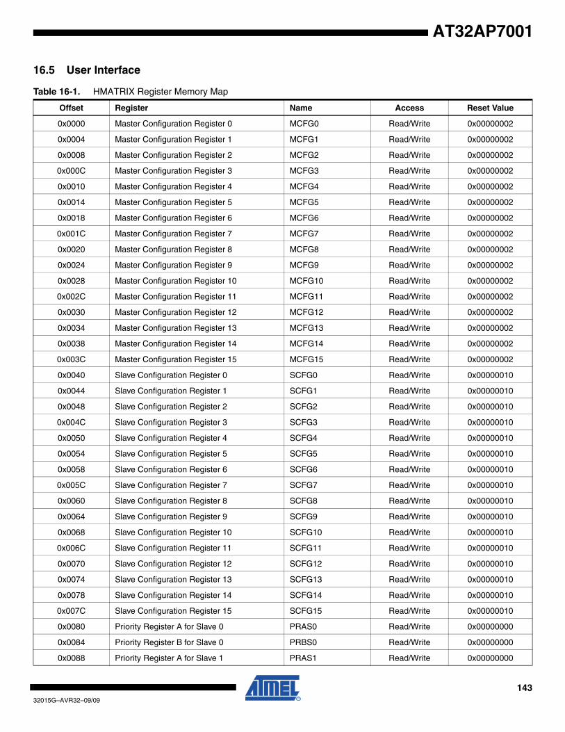
14332015G–AVR32–09/09
AT32AP7001
16.5 User Interface
Table 16-1. HMATRIX Register Memory Map
Offset Register Name Access Reset Value
0x0000 Master Configuration Register 0 MCFG0 Read/Write 0x00000002
0x0004 Master Configuration Register 1 MCFG1 Read/Write 0x00000002
0x0008 Master Configuration Register 2 MCFG2 Read/Write 0x00000002
0x000C Master Configuration Register 3 MCFG3 Read/Write 0x00000002
0x0010 Master Configuration Register 4 MCFG4 Read/Write 0x00000002
0x0014 Master Configuration Register 5 MCFG5 Read/Write 0x00000002
0x0018 Master Configuration Register 6 MCFG6 Read/Write 0x00000002
0x001C Master Configuration Register 7 MCFG7 Read/Write 0x00000002
0x0020 Master Configuration Register 8 MCFG8 Read/Write 0x00000002
0x0024 Master Configuration Register 9 MCFG9 Read/Write 0x00000002
0x0028 Master Configuration Register 10 MCFG10 Read/Write 0x00000002
0x002C Master Configuration Register 11 MCFG11 Read/Write 0x00000002
0x0030 Master Configuration Register 12 MCFG12 Read/Write 0x00000002
0x0034 Master Configuration Register 13 MCFG13 Read/Write 0x00000002
0x0038 Master Configuration Register 14 MCFG14 Read/Write 0x00000002
0x003C Master Configuration Register 15 MCFG15 Read/Write 0x00000002
0x0040 Slave Configuration Register 0 SCFG0 Read/Write 0x00000010
0x0044 Slave Configuration Register 1 SCFG1 Read/Write 0x00000010
0x0048 Slave Configuration Register 2 SCFG2 Read/Write 0x00000010
0x004C Slave Configuration Register 3 SCFG3 Read/Write 0x00000010
0x0050 Slave Configuration Register 4 SCFG4 Read/Write 0x00000010
0x0054 Slave Configuration Register 5 SCFG5 Read/Write 0x00000010
0x0058 Slave Configuration Register 6 SCFG6 Read/Write 0x00000010
0x005C Slave Configuration Register 7 SCFG7 Read/Write 0x00000010
0x0060 Slave Configuration Register 8 SCFG8 Read/Write 0x00000010
0x0064 Slave Configuration Register 9 SCFG9 Read/Write 0x00000010
0x0068 Slave Configuration Register 10 SCFG10 Read/Write 0x00000010
0x006C Slave Configuration Register 11 SCFG11 Read/Write 0x00000010
0x0070 Slave Configuration Register 12 SCFG12 Read/Write 0x00000010
0x0074 Slave Configuration Register 13 SCFG13 Read/Write 0x00000010
0x0078 Slave Configuration Register 14 SCFG14 Read/Write 0x00000010
0x007C Slave Configuration Register 15 SCFG15 Read/Write 0x00000010
0x0080 Priority Register A for Slave 0 PRAS0 Read/Write 0x00000000
0x0084 Priority Register B for Slave 0 PRBS0 Read/Write 0x00000000
0x0088 Priority Register A for Slave 1 PRAS1 Read/Write 0x00000000
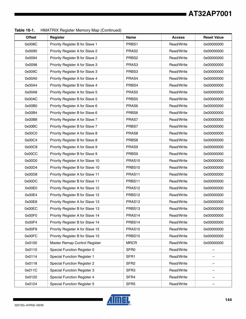
14432015G–AVR32–09/09
AT32AP7001
0x008C Priority Register B for Slave 1 PRBS1 Read/Write 0x00000000
0x0090 Priority Register A for Slave 2 PRAS2 Read/Write 0x00000000
0x0094 Priority Register B for Slave 2 PRBS2 Read/Write 0x00000000
0x0098 Priority Register A for Slave 3 PRAS3 Read/Write 0x00000000
0x009C Priority Register B for Slave 3 PRBS3 Read/Write 0x00000000
0x00A0 Priority Register A for Slave 4 PRAS4 Read/Write 0x00000000
0x00A4 Priority Register B for Slave 4 PRBS4 Read/Write 0x00000000
0x00A8 Priority Register A for Slave 5 PRAS5 Read/Write 0x00000000
0x00AC Priority Register B for Slave 5 PRBS5 Read/Write 0x00000000
0x00B0 Priority Register A for Slave 6 PRAS6 Read/Write 0x00000000
0x00B4 Priority Register B for Slave 6 PRBS6 Read/Write 0x00000000
0x00B8 Priority Register A for Slave 7 PRAS7 Read/Write 0x00000000
0x00BC Priority Register B for Slave 7 PRBS7 Read/Write 0x00000000
0x00C0 Priority Register A for Slave 8 PRAS8 Read/Write 0x00000000
0x00C4 Priority Register B for Slave 8 PRBS8 Read/Write 0x00000000
0x00C8 Priority Register A for Slave 9 PRAS9 Read/Write 0x00000000
0x00CC Priority Register B for Slave 9 PRBS9 Read/Write 0x00000000
0x00D0 Priority Register A for Slave 10 PRAS10 Read/Write 0x00000000
0x00D4 Priority Register B for Slave 10 PRBS10 Read/Write 0x00000000
0x00D8 Priority Register A for Slave 11 PRAS11 Read/Write 0x00000000
0x00DC Priority Register B for Slave 11 PRBS11 Read/Write 0x00000000
0x00E0 Priority Register A for Slave 12 PRAS12 Read/Write 0x00000000
0x00E4 Priority Register B for Slave 12 PRBS12 Read/Write 0x00000000
0x00E8 Priority Register A for Slave 13 PRAS13 Read/Write 0x00000000
0x00EC Priority Register B for Slave 13 PRBS13 Read/Write 0x00000000
0x00F0 Priority Register A for Slave 14 PRAS14 Read/Write 0x00000000
0x00F4 Priority Register B for Slave 14 PRBS14 Read/Write 0x00000000
0x00F8 Priority Register A for Slave 15 PRAS15 Read/Write 0x00000000
0x00FC Priority Register B for Slave 15 PRBS15 Read/Write 0x00000000
0x0100 Master Remap Control Register MRCR Read/Write 0x00000000
0x0110 Special Function Register 0 SFR0 Read/Write –
0x0114 Special Function Register 1 SFR1 Read/Write –
0x0118 Special Function Register 2 SFR2 Read/Write –
0x011C Special Function Register 3 SFR3 Read/Write –
0x0120 Special Function Register 4 SFR4 Read/Write –
0x0124 Special Function Register 5 SFR5 Read/Write –
Table 16-1. HMATRIX Register Memory Map (Continued)
Offset Register Name Access Reset Value
14532015G–AVR32–09/09
AT32AP7001
0x0128 Special Function Register 6 SFR6 Read/Write –
0x012C Special Function Register 7 SFR7 Read/Write –
0x0130 Special Function Register 8 SFR8 Read/Write –
0x0134 Special Function Register 9 SFR9 Read/Write –
0x0138 Special Function Register 10 SFR10 Read/Write –
0x013C Special Function Register 11 SFR11 Read/Write –
0x0140 Special Function Register 12 SFR12 Read/Write –
0x0144 Special Function Register 13 SFR13 Read/Write –
0x0148 Special Function Register 14 SFR14 Read/Write –
0x014C Special Function Register 15 SFR15 Read/Write –
Table 16-1. HMATRIX Register Memory Map (Continued)
Offset Register Name Access Reset Value
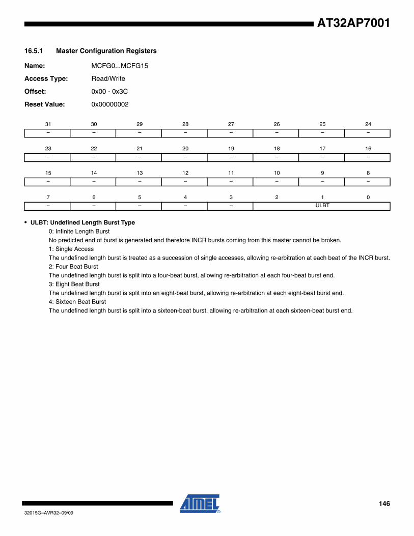
14632015G–AVR32–09/09
AT32AP7001
16.5.1 Master Configuration Registers
Name: MCFG0...MCFG15
Access Type: Read/Write
Offset: 0x00 - 0x3C
Reset Value: 0x00000002
• ULBT: Undefined Length Burst Type0: Infinite Length Burst
No predicted end of burst is generated and therefore INCR bursts coming from this master cannot be broken.1: Single Access
The undefined length burst is treated as a succession of single accesses, allowing re-arbitration at each beat of the INCR burst.
2: Four Beat Burst The undefined length burst is split into a four-beat burst, allowing re-arbitration at each four-beat burst end.
3: Eight Beat Burst
The undefined length burst is split into an eight-beat burst, allowing re-arbitration at each eight-beat burst end.4: Sixteen Beat Burst
The undefined length burst is split into a sixteen-beat burst, allowing re-arbitration at each sixteen-beat burst end.
31 30 29 28 27 26 25 24
– – – – – – – –
23 22 21 20 19 18 17 16
– – – – – – – –
15 14 13 12 11 10 9 8
– – – – – – – –
7 6 5 4 3 2 1 0
– – – – – ULBT
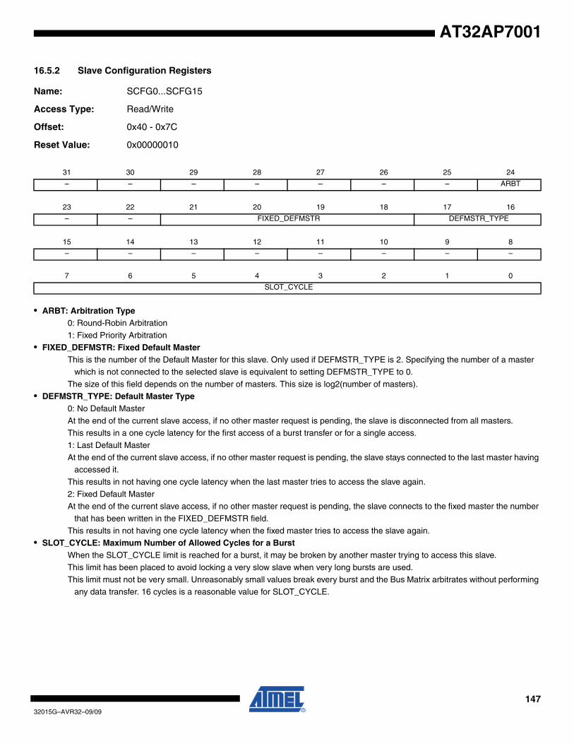
14732015G–AVR32–09/09
AT32AP7001
16.5.2 Slave Configuration Registers
Name: SCFG0...SCFG15
Access Type: Read/Write
Offset: 0x40 - 0x7C
Reset Value: 0x00000010
• ARBT: Arbitration Type0: Round-Robin Arbitration
1: Fixed Priority Arbitration
• FIXED_DEFMSTR: Fixed Default MasterThis is the number of the Default Master for this slave. Only used if DEFMSTR_TYPE is 2. Specifying the number of a master
which is not connected to the selected slave is equivalent to setting DEFMSTR_TYPE to 0.
The size of this field depends on the number of masters. This size is log2(number of masters).• DEFMSTR_TYPE: Default Master Type
0: No Default Master
At the end of the current slave access, if no other master request is pending, the slave is disconnected from all masters.This results in a one cycle latency for the first access of a burst transfer or for a single access.
1: Last Default Master
At the end of the current slave access, if no other master request is pending, the slave stays connected to the last master having accessed it.
This results in not having one cycle latency when the last master tries to access the slave again.
2: Fixed Default MasterAt the end of the current slave access, if no other master request is pending, the slave connects to the fixed master the number
that has been written in the FIXED_DEFMSTR field.
This results in not having one cycle latency when the fixed master tries to access the slave again.• SLOT_CYCLE: Maximum Number of Allowed Cycles for a Burst
When the SLOT_CYCLE limit is reached for a burst, it may be broken by another master trying to access this slave.
This limit has been placed to avoid locking a very slow slave when very long bursts are used.This limit must not be very small. Unreasonably small values break every burst and the Bus Matrix arbitrates without performing
any data transfer. 16 cycles is a reasonable value for SLOT_CYCLE.
31 30 29 28 27 26 25 24
– – – – – – – ARBT
23 22 21 20 19 18 17 16
– – FIXED_DEFMSTR DEFMSTR_TYPE
15 14 13 12 11 10 9 8
– – – – – – – –
7 6 5 4 3 2 1 0
SLOT_CYCLE

14832015G–AVR32–09/09
AT32AP7001
16.5.3 Bus Matrix Priority Registers A For Slaves
Name: PRAS0...PRAS15
Access Type: Read/Write
Offset: -
Reset Value: 0x00000000
• MxPR: Master x PriorityFixed priority of Master x for accessing the selected slave. The higher the number, the higher the priority.
31 30 29 28 27 26 25 24
M7PR M6PR
23 22 21 20 19 18 17 16
M5PR M4PR
15 14 13 12 11 10 9 8
M3PR M2PR
7 6 5 4 3 2 1 0
M1PR M0PR
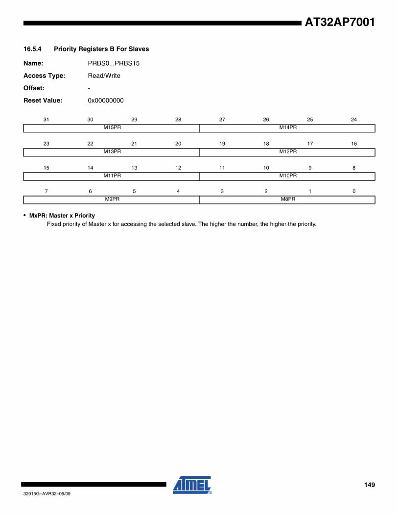
14932015G–AVR32–09/09
AT32AP7001
16.5.4 Priority Registers B For Slaves
Name: PRBS0...PRBS15
Access Type: Read/Write
Offset: -
Reset Value: 0x00000000
• MxPR: Master x PriorityFixed priority of Master x for accessing the selected slave. The higher the number, the higher the priority.
31 30 29 28 27 26 25 24
M15PR M14PR
23 22 21 20 19 18 17 16
M13PR M12PR
15 14 13 12 11 10 9 8
M11PR M10PR
7 6 5 4 3 2 1 0
M9PR M8PR

15032015G–AVR32–09/09
AT32AP7001
16.5.5 Master Remap Control Register
Name: MRCR
Access Type: Read/Write
Offset: 0x100
Reset Value: 0x00000000
• RCB: Remap Command Bit for Master x0: Disable remapped address decoding for the selected Master
1: Enable remapped address decoding for the selected Master
31 30 29 28 27 26 25 24
– – – – – – – –
23 22 21 20 19 18 17 16
– – – – – – – –
15 14 13 12 11 10 9 8
RCB15 RCB14 RCB13 RCB12 RCB11 RCB10 RCB9 RCB8
7 6 5 4 3 2 1 0
RCB7 RCB6 RCB5 RCB4 RCB3 RCB2 RCB1 RCB0
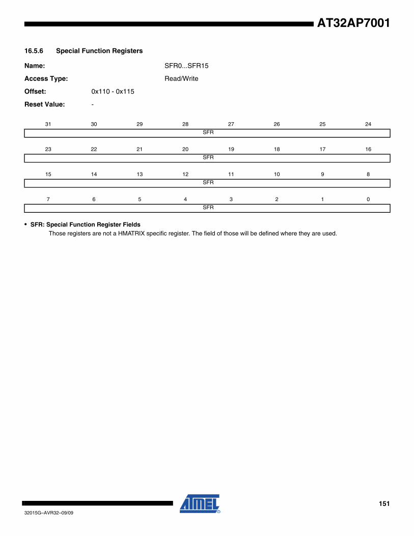
15132015G–AVR32–09/09
AT32AP7001
16.5.6 Special Function Registers
Name: SFR0...SFR15
Access Type: Read/Write
Offset: 0x110 - 0x115
Reset Value: -
• SFR: Special Function Register FieldsThose registers are not a HMATRIX specific register. The field of those will be defined where they are used.
31 30 29 28 27 26 25 24
SFR
23 22 21 20 19 18 17 16
SFR
15 14 13 12 11 10 9 8
SFR
7 6 5 4 3 2 1 0
SFR
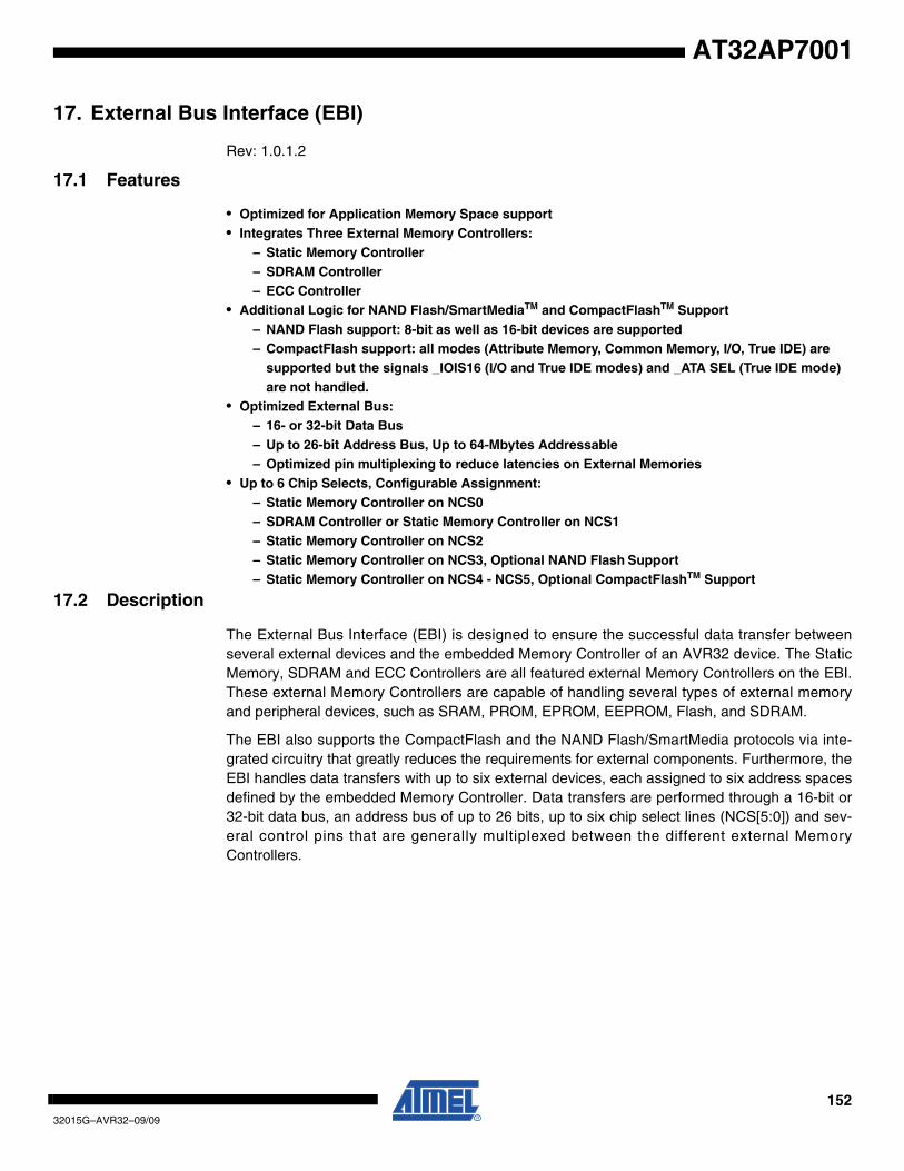
15232015G–AVR32–09/09
AT32AP7001
17. External Bus Interface (EBI)
Rev: 1.0.1.2
17.1 Features
• Optimized for Application Memory Space support• Integrates Three External Memory Controllers:
– Static Memory Controller– SDRAM Controller– ECC Controller
• Additional Logic for NAND Flash/SmartMediaTM and CompactFlashTM Support– NAND Flash support: 8-bit as well as 16-bit devices are supported– CompactFlash support: all modes (Attribute Memory, Common Memory, I/O, True IDE) are
supported but the signals _IOIS16 (I/O and True IDE modes) and _ATA SEL (True IDE mode) are not handled.
• Optimized External Bus:– 16- or 32-bit Data Bus– Up to 26-bit Address Bus, Up to 64-Mbytes Addressable– Optimized pin multiplexing to reduce latencies on External Memories
• Up to 6 Chip Selects, Configurable Assignment:– Static Memory Controller on NCS0– SDRAM Controller or Static Memory Controller on NCS1– Static Memory Controller on NCS2– Static Memory Controller on NCS3, Optional NAND Flash Support– Static Memory Controller on NCS4 - NCS5, Optional CompactFlashTM Support
17.2 Description
The External Bus Interface (EBI) is designed to ensure the successful data transfer betweenseveral external devices and the embedded Memory Controller of an AVR32 device. The StaticMemory, SDRAM and ECC Controllers are all featured external Memory Controllers on the EBI.These external Memory Controllers are capable of handling several types of external memoryand peripheral devices, such as SRAM, PROM, EPROM, EEPROM, Flash, and SDRAM.
The EBI also supports the CompactFlash and the NAND Flash/SmartMedia protocols via inte-grated circuitry that greatly reduces the requirements for external components. Furthermore, theEBI handles data transfers with up to six external devices, each assigned to six address spacesdefined by the embedded Memory Controller. Data transfers are performed through a 16-bit or32-bit data bus, an address bus of up to 26 bits, up to six chip select lines (NCS[5:0]) and sev-eral control pins that are generally multiplexed between the different external MemoryControllers.
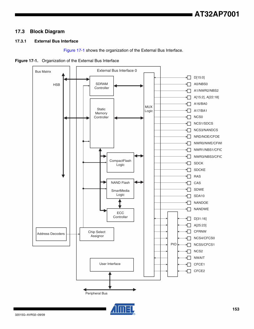
15332015G–AVR32–09/09
AT32AP7001
17.3 Block Diagram
17.3.1 External Bus Interface
Figure 17-1 shows the organization of the External Bus Interface.
Figure 17-1. Organization of the External Bus Interface
External Bus Interface 0
D[15:0]
A[15:2], A[22:18]
PIO
MUXLogic
User Interface
Chip Select Assignor
StaticMemory
Controller
SDRAMController
Bus Matrix
Peripheral Bus
HSB
Address Decoders
A16/BA0
A0/NBS0
A1/NWR2/NBS2
A17/BA1
NCS0
NCS3/NANDCS
NRD/NOE/CFOE
NCS1/SDCS
NWR0/NWE/CFWE
NWR1/NBS1/CFIO
NWR3/NBS3/CFIO
SDCK
SDCKE
RAS
CAS
SDWE
D[31:16]
A[25:23]
CFRNW
NCS4/CFCS0
NCS5/CFCS1
NCS2
CFCE1
CFCE2
NWAIT
SDA10
NANDOE
NANDWE
NAND Flash
SmartMediaLogic
CompactFlashLogic
ECCController

15432015G–AVR32–09/09
AT32AP7001

15532015G–AVR32–09/09
AT32AP7001
17.4 I/O Lines Description
Table 17-1. EBI I/O Lines Description
Name Function Type Active Level
EBI
D0 - D31 Data Bus I/O
A0 - A25 Address Bus Output
NWAIT External Wait Signal Input Low
SMC
NCS0 - NCS5 Chip Select Lines Output Low
NWR0 - NWR3 Write Signals Output Low
NOE Output Enable Output Low
NRD Read Signal Output Low
NWE Write Enable Output Low
NBS0 - NBS3 Byte Mask Signals Output Low
EBI for CompactFlash Support
CFCE1 - CFCE2 CompactFlash Chip Enable Output Low
CFOE CompactFlash Output Enable Output Low
CFWE CompactFlash Write Enable Output Low
CFIOR CompactFlash I/O Read Signal Output Low
CFIOW CompactFlash I/O Write Signal Output Low
CFRNW CompactFlash Read Not Write Signal Output
CFCS0 - CFCS1 CompactFlash Chip Select Lines Output Low
EBI for NAND Flash/SmartMedia Support
NANDCS NAND Flash Chip Select Line Output Low
NANDOE NAND Flash Output Enable Output Low
NANDWE NAND Flash Write Enable Output Low
SDRAM Controller
SDCK SDRAM Clock Output
SDCKE SDRAM Clock Enable Output High
SDCS SDRAM Controller Chip Select Line Output Low
BA0 - BA1 Bank Select Output
SDWE SDRAM Write Enable Output Low
RAS - CAS Row and Column Signal Output Low
NWR0 - NWR3 Write Signals Output Low
NBS0 - NBS3 Byte Mask Signals Output Low
SDA10 SDRAM Address 10 Line Output
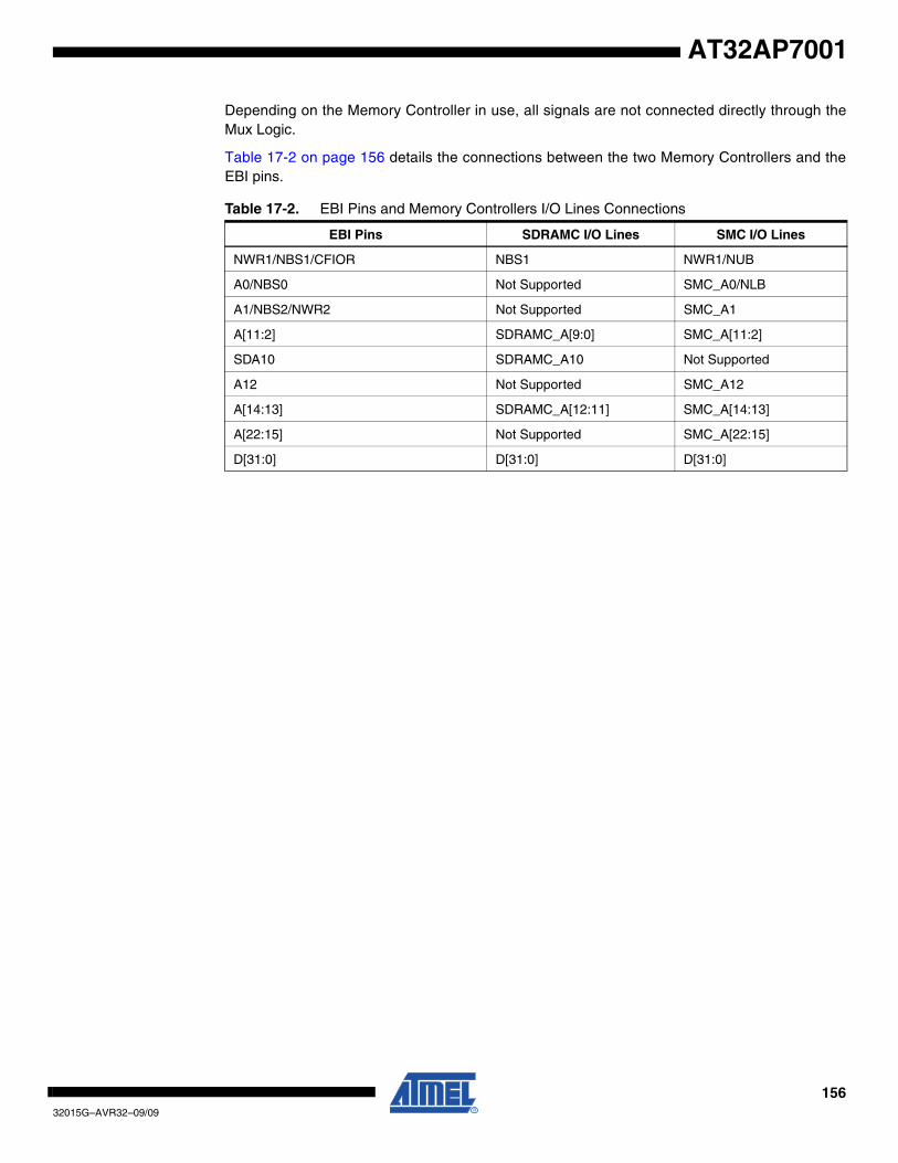
15632015G–AVR32–09/09
AT32AP7001
Depending on the Memory Controller in use, all signals are not connected directly through theMux Logic.
Table 17-2 on page 156 details the connections between the two Memory Controllers and theEBI pins.
Table 17-2. EBI Pins and Memory Controllers I/O Lines Connections
EBI Pins SDRAMC I/O Lines SMC I/O Lines
NWR1/NBS1/CFIOR NBS1 NWR1/NUB
A0/NBS0 Not Supported SMC_A0/NLB
A1/NBS2/NWR2 Not Supported SMC_A1
A[11:2] SDRAMC_A[9:0] SMC_A[11:2]
SDA10 SDRAMC_A10 Not Supported
A12 Not Supported SMC_A12
A[14:13] SDRAMC_A[12:11] SMC_A[14:13]
A[22:15] Not Supported SMC_A[22:15]
D[31:0] D[31:0] D[31:0]
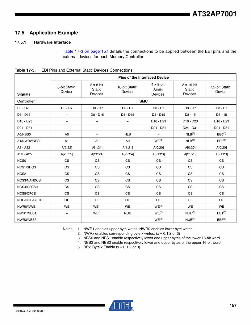
15732015G–AVR32–09/09
AT32AP7001
17.5 Application Example
17.5.1 Hardware Interface
Table 17-3 on page 157 details the connections to be applied between the EBI pins and theexternal devices for each Memory Controller.
Notes: 1. NWR1 enables upper byte writes. NWR0 enables lower byte writes.2. NWRx enables corresponding byte x writes. (x = 0,1,2 or 3)3. NBS0 and NBS1 enable respectively lower and upper bytes of the lower 16-bit word.4. NBS2 and NBS3 enable respectively lower and upper bytes of the upper 16-bit word.5. BEx: Byte x Enable (x = 0,1,2 or 3)
Table 17-3. EBI Pins and External Static Devices Connections
Signals
Pins of the Interfaced Device
8-bit StaticDevice
2 x 8-bitStatic
Devices
16-bit StaticDevice
4 x 8-bit
StaticDevices
2 x 16-bitStatic
Devices
32-bit StaticDevice
Controller SMC
D0 - D7 D0 - D7 D0 - D7 D0 - D7 D0 - D7 D0 - D7 D0 - D7
D8 - D15 – D8 - D15 D8 - D15 D8 - D15 D8 - 15 D8 - 15
D16 - D23 – – – D16 - D23 D16 - D23 D16 - D23
D24 - D31 – – – D24 - D31 D24 - D31 D24 - D31
A0/NBS0 A0 – NLB – NLB(3) BE0(5)
A1/NWR2/NBS2 A1 A0 A0 WE(2) NLB(4) BE2(5)
A2 - A22 A[2:22] A[1:21] A[1:21] A[0:20] A[0:20] A[0:20]
A23 - A25 A[23:25] A[22:24] A[22:24] A[21:23] A[21:23] A[21:23]
NCS0 CS CS CS CS CS CS
NCS1/SDCS CS CS CS CS CS CS
NCS2 CS CS CS CS CS CS
NCS3/NANDCS CS CS CS CS CS CS
NCS4/CFCS0 CS CS CS CS CS CS
NCS5/CFCS1 CS CS CS CS CS CS
NRD/NOE/CFOE OE OE OE OE OE OE
NWR0/NWE WE WE(1) WE WE(2) WE WE
NWR1/NBS1 – WE(1) NUB WE(2) NUB(3) BE1(5)
NWR3/NBS3 – – – WE(2) NUB(4) BE3(5)
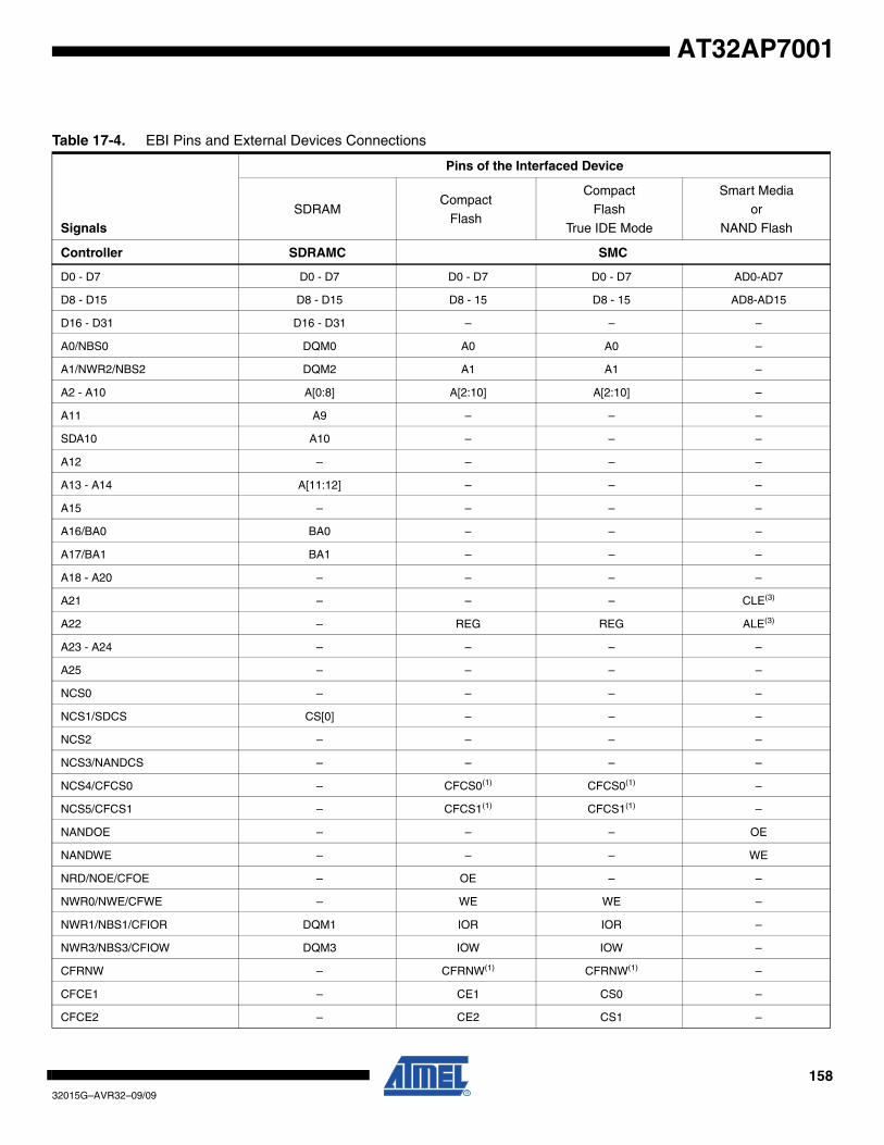
15832015G–AVR32–09/09
AT32AP7001
Table 17-4. EBI Pins and External Devices Connections
Signals
Pins of the Interfaced Device
SDRAMCompact
Flash
CompactFlash
True IDE Mode
Smart Mediaor
NAND Flash
Controller SDRAMC SMC
D0 - D7 D0 - D7 D0 - D7 D0 - D7 AD0-AD7
D8 - D15 D8 - D15 D8 - 15 D8 - 15 AD8-AD15
D16 - D31 D16 - D31 – – –
A0/NBS0 DQM0 A0 A0 –
A1/NWR2/NBS2 DQM2 A1 A1 –
A2 - A10 A[0:8] A[2:10] A[2:10] –
A11 A9 – – –
SDA10 A10 – – –
A12 – – – –
A13 - A14 A[11:12] – – –
A15 – – – –
A16/BA0 BA0 – – –
A17/BA1 BA1 – – –
A18 - A20 – – – –
A21 – – – CLE(3)
A22 – REG REG ALE(3)
A23 - A24 – – – –
A25 – – – –
NCS0 – – – –
NCS1/SDCS CS[0] – – –
NCS2 – – – –
NCS3/NANDCS – – – –
NCS4/CFCS0 – CFCS0(1) CFCS0(1) –
NCS5/CFCS1 – CFCS1(1) CFCS1(1) –
NANDOE – – – OE
NANDWE – – – WE
NRD/NOE/CFOE – OE – –
NWR0/NWE/CFWE – WE WE –
NWR1/NBS1/CFIOR DQM1 IOR IOR –
NWR3/NBS3/CFIOW DQM3 IOW IOW –
CFRNW – CFRNW(1) CFRNW(1) –
CFCE1 – CE1 CS0 –
CFCE2 – CE2 CS1 –

15932015G–AVR32–09/09
AT32AP7001
Note: 1. Not directly connected to the CompactFlash slot. Permits the control of the bidirectional buffer between the EBI data bus and the CompactFlash slot.
2. Any PIO line.3. The CLE and ALE signals of the NAND Flash device may be driven by any address bit. For
details, see ”SmartMedia and NAND Flash Support” on page 166.4.
SDCK CLK – – –
SDCKE CKE – – –
RAS RAS – – –
CAS CAS – – –
SDWE WE – – –
NWAIT – WAIT WAIT –
Pxx(2) – CD1 or CD2 CD1 or CD2 –
Pxx(2) – – – CE
Pxx(2) – – – RDY
Table 17-4. EBI Pins and External Devices Connections (Continued)
Signals
Pins of the Interfaced Device
SDRAMCompact
Flash
Compact
FlashTrue IDE Mode
Smart Media
orNAND Flash
Controller SDRAMC SMC

16032015G–AVR32–09/09
AT32AP7001
17.5.2 Connection Examples
Figure 17-2 shows an example of connections between the EBI and external devices.
Figure 17-2. EBI Connections to Memory Devices
EBI
D0-D31
A2-A15
RASCAS
SDCKSDCKESDWE
A0/NBS0
2M x 8SDRAM
D0-D7
A0-A9, A11
RASCAS
CLKCKEWE
DQM
CS
BA0BA1
NWR1/NBS1A1/NWR2/NBS2
NWR3/NBS3
NCS1/SDCS
D0-D7 D8-D15
A16/BA0A17/BA1A18-A25
A10
SDA10
SDA10A2-A11, A13
NCS0
NCS2NCS3NCS4NCS5
A16/BA0A17/BA1
2M x 8SDRAM
D0-D7
A0-A9, A11
RASCAS
CLKCKEWE
DQM
CS
BA0BA1
A10 SDA10A2-A11, A13
A16/BA0A17/BA1
2M x 8SDRAM
D0-D7
A0-A9, A11
RASCAS
CLKCKEWE
DQM
CS
BA0BA1
D16-D23 D24-D31
A10 SDA10A2-A11, A13
A16/BA0A17/BA1
2M x 8SDRAM
D0-D7
A0-A9, A11
RASCAS
CLKCKEWE
DQM
CS
BA0BA1
A10SDA10A2-A11, A13
A16/BA0A17/BA1
NBS0 NBS1
NBS3NBS2
NRD/NOENWR0/NWE
128K x 8SRAM
128K x 8SRAM
D0-D7 D0-D7A0-A16 A0-A16A1-A17 A1-A17
CS CS
OEWE
D0-D7 D8-D15
OEWENRD/NOE
A0/NWR0/NBS0NRD/NOE
NWR1/NBS1
SDWE
SDWESDWE
SDWE
16132015G–AVR32–09/09
AT32AP7001
17.6 Product Dependencies
17.6.1 I/O Lines
The pins used for interfacing the External Bus Interface may be multiplexed with the PIO lines.The programmer must first program the PIO controller to assign the External Bus Interface pinsto their peripheral function. If I/O lines of the External Bus Interface are not used by the applica-tion, they can be used for other purposes by the PIO Controller.
17.7 Functional Description
The EBI transfers data between the internal HSB Bus (handled by the HMatrix) and the externalmemories or peripheral devices. It controls the waveforms and the parameters of the externaladdress, data and control busses and is composed of the following elements:
• The Static Memory Controller (SMC)
• The SDRAM Controller (SDRAMC)
• The ECC Controller (ECC)
• A chip select assignment feature that assigns an HSB address space to the external devices
• A multiplex controller circuit that shares the pins between the different Memory Controllers
• Programmable CompactFlash support logic
• Programmable SmartMedia and NAND Flash support logic
17.7.1 Bus Multiplexing
The EBI offers a complete set of control signals that share the 32-bit data lines, the addresslines of up to 26 bits and the control signals through a multiplex logic operating in function of thememory area requests.
Multiplexing is specifically organized in order to guarantee the maintenance of the address andoutput control lines at a stable state while no external access is being performed. Multiplexing isalso designed to respect the data float times defined in the Memory Controllers. Furthermore,refresh cycles of the SDRAM are executed independently by the SDRAM Controller withoutdelaying the other external Memory Controller accesses.
17.7.2 Pull-up Control
A specific HMATRIX_SFR register in the Matrix User Interface permit enabling of on-chip pull-upresistors on the data bus lines not multiplexed with the PIO Controller lines. For details on thisregister, refer to the Peripherals Section. The pull-up resistors are enabled after reset. Settingthe EBI_DBPUC bit disables the pull-up resistors on lines not muxed with PIO. Enabling the pull-up resistor on lines multiplexed with PIO lines can be performed by programming the appropri-ate PIO controller.
17.7.3 Static Memory Controller
For information on the Static Memory Controller, refer to the Static Memory Controller Section.
17.7.4 SDRAM Controller
For information on the SDRAM Controller, refer to the SDRAM Section.
17.7.5 ECC Controller
For information on the ECC Controller, refer to the ECC Section.
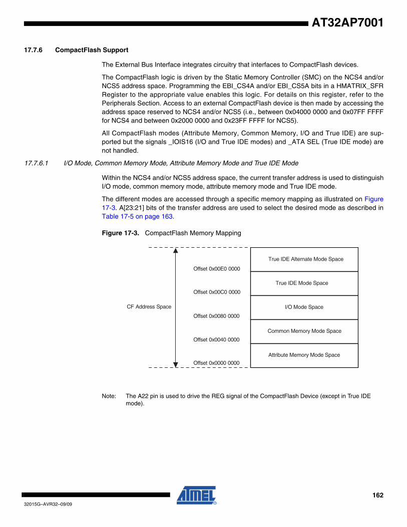
16232015G–AVR32–09/09
AT32AP7001
17.7.6 CompactFlash Support
The External Bus Interface integrates circuitry that interfaces to CompactFlash devices.
The CompactFlash logic is driven by the Static Memory Controller (SMC) on the NCS4 and/orNCS5 address space. Programming the EBI_CS4A and/or EBI_CS5A bits in a HMATRIX_SFRRegister to the appropriate value enables this logic. For details on this register, refer to thePeripherals Section. Access to an external CompactFlash device is then made by accessing theaddress space reserved to NCS4 and/or NCS5 (i.e., between 0x04000 0000 and 0x07FF FFFFfor NCS4 and between 0x2000 0000 and 0x23FF FFFF for NCS5).
All CompactFlash modes (Attribute Memory, Common Memory, I/O and True IDE) are sup-ported but the signals _IOIS16 (I/O and True IDE modes) and _ATA SEL (True IDE mode) arenot handled.
17.7.6.1 I/O Mode, Common Memory Mode, Attribute Memory Mode and True IDE Mode
Within the NCS4 and/or NCS5 address space, the current transfer address is used to distinguishI/O mode, common memory mode, attribute memory mode and True IDE mode.
The different modes are accessed through a specific memory mapping as illustrated on Figure17-3. A[23:21] bits of the transfer address are used to select the desired mode as described inTable 17-5 on page 163.
Figure 17-3. CompactFlash Memory Mapping
Note: The A22 pin is used to drive the REG signal of the CompactFlash Device (except in True IDE mode).
CF Address Space
Attribute Memory Mode Space
Common Memory Mode Space
I/O Mode Space
True IDE Mode Space
True IDE Alternate Mode Space
Offset 0x00E0 0000
Offset 0x00C0 0000
Offset 0x0080 0000
Offset 0x0040 0000
Offset 0x0000 0000
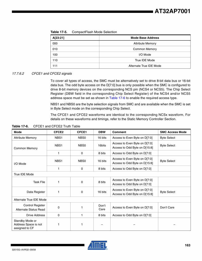
16332015G–AVR32–09/09
AT32AP7001
17.7.6.2 CFCE1 and CFCE2 signals
To cover all types of access, the SMC must be alternatively set to drive 8-bit data bus or 16-bitdata bus. The odd byte access on the D[7:0] bus is only possible when the SMC is configured todrive 8-bit memory devices on the corresponding NCS pin (NCS4 or NCS5). The Chip SelectRegister (DBW field in the corresponding Chip Select Register) of the NCS4 and/or NCS5address space must be set as shown in Table 17-6 to enable the required access type.
NBS1 and NBS0 are the byte selection signals from SMC and are available when the SMC is setin Byte Select mode on the corresponding Chip Select.
The CFCE1 and CFCE2 waveforms are identical to the corresponding NCSx waveform. Fordetails on these waveforms and timings, refer to the Static Memory Controller Section.
Table 17-5. CompactFlash Mode Selection
A[23:21] Mode Base Address
000 Attribute Memory
010 Common Memory
100 I/O Mode
110 True IDE Mode
111 Alternate True IDE Mode
Table 17-6. CFCE1 and CFCE2 Truth Table
Mode CFCE2 CFCE1 DBW Comment SMC Access Mode
Attribute Memory NBS1 NBS0 16 bits Access to Even Byte on D[7:0] Byte Select
Common MemoryNBS1 NBS0 16bits
Access to Even Byte on D[7:0]
Access to Odd Byte on D[15:8]Byte Select
1 0 8 bits Access to Odd Byte on D[7:0]
I/O ModeNBS1 NBS0 16 bits
Access to Even Byte on D[7:0]
Access to Odd Byte on D[15:8]Byte Select
1 0 8 bits Access to Odd Byte on D[7:0]
True IDE Mode
Task File 1 0 8 bitsAccess to Even Byte on D[7:0]
Access to Odd Byte on D[7:0]
Data Register 1 0 16 bitsAccess to Even Byte on D[7:0]
Access to Odd Byte on D[15:8]Byte Select
Alternate True IDE Mode
Control Register
Alternate Status Read0 1
Don’t Care
Access to Even Byte on D[7:0] Don’t Care
Drive Address 0 1 8 bits Access to Odd Byte on D[7:0]
Standby Mode or Address Space is not assigned to CF
1 1 – – –
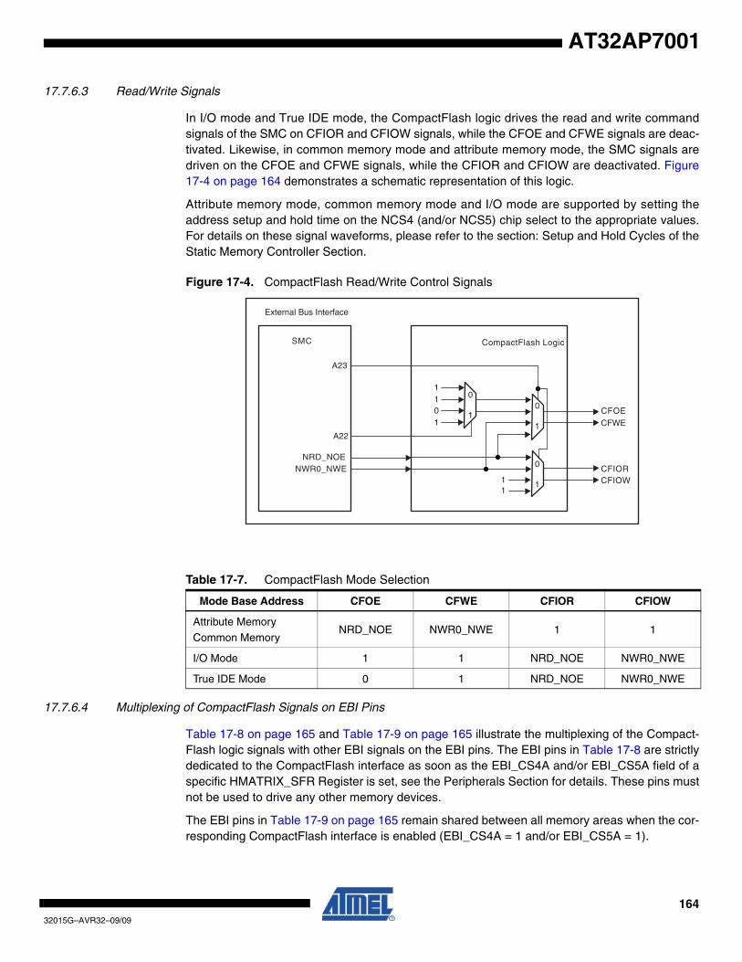
16432015G–AVR32–09/09
AT32AP7001
17.7.6.3 Read/Write Signals
In I/O mode and True IDE mode, the CompactFlash logic drives the read and write commandsignals of the SMC on CFIOR and CFIOW signals, while the CFOE and CFWE signals are deac-tivated. Likewise, in common memory mode and attribute memory mode, the SMC signals aredriven on the CFOE and CFWE signals, while the CFIOR and CFIOW are deactivated. Figure17-4 on page 164 demonstrates a schematic representation of this logic.
Attribute memory mode, common memory mode and I/O mode are supported by setting theaddress setup and hold time on the NCS4 (and/or NCS5) chip select to the appropriate values.For details on these signal waveforms, please refer to the section: Setup and Hold Cycles of theStatic Memory Controller Section.
Figure 17-4. CompactFlash Read/Write Control Signals
17.7.6.4 Multiplexing of CompactFlash Signals on EBI Pins
Table 17-8 on page 165 and Table 17-9 on page 165 illustrate the multiplexing of the Compact-Flash logic signals with other EBI signals on the EBI pins. The EBI pins in Table 17-8 are strictlydedicated to the CompactFlash interface as soon as the EBI_CS4A and/or EBI_CS5A field of aspecific HMATRIX_SFR Register is set, see the Peripherals Section for details. These pins mustnot be used to drive any other memory devices.
The EBI pins in Table 17-9 on page 165 remain shared between all memory areas when the cor-responding CompactFlash interface is enabled (EBI_CS4A = 1 and/or EBI_CS5A = 1).
Table 17-7. CompactFlash Mode Selection
Mode Base Address CFOE CFWE CFIOR CFIOW
Attribute Memory
Common MemoryNRD_NOE NWR0_NWE 1 1
I/O Mode 1 1 NRD_NOE NWR0_NWE
True IDE Mode 0 1 NRD_NOE NWR0_NWE
SMC
NRD_NOENWR0_NWE
A23
CFIORCFIOW
CFOECFWE
11
CompactFlash Logic
External Bus Interface
11
10
A22
1
0
1
0
1
0

16532015G–AVR32–09/09
AT32AP7001
17.7.6.5 Application Example
Figure 17-5 on page 166 illustrates an example of a CompactFlash application. CFCS0 andCFRNW signals are not directly connected to the CompactFlash slot 0, but do control the direc-tion and the output enable of the buffers between the EBI and the CompactFlash Device. Thetiming of the CFCS0 signal is identical to the NCS4 signal. Moreover, the CFRNW signalremains valid throughout the transfer, as does the address bus. The CompactFlash _WAIT sig-nal is connected to the NWAIT input of the Static Memory Controller. For details on thesewaveforms and timings, refer to the Static Memory Controller Section.
Table 17-8. Dedicated CompactFlash Interface Multiplexing
PinsCompactFlash Signals EBI Signals
CS4A = 1 CS5A = 1 CS4A = 0 CS5A = 0
NCS4/CFCS0 CFCS0 NCS4
NCS5/CFCS1 CFCS1 NCS5
Table 17-9. Shared CompactFlash Interface Multiplexing
Pins
Access to CompactFlash Device
Access to Other EBI Devices
CompactFlash Signals EBI Signals
NOE/NRD/CFOE CFOE NRD/NOE
NWR0/NWE/CFWE CFWE NWR0/NWE
NWR1/NBS1/CFIOR CFIOR NWR1/NBS1
NWR3/NBS3/CFIOW CFIOW NWR3/NBS3
A25/CFRNW CFRNW A25
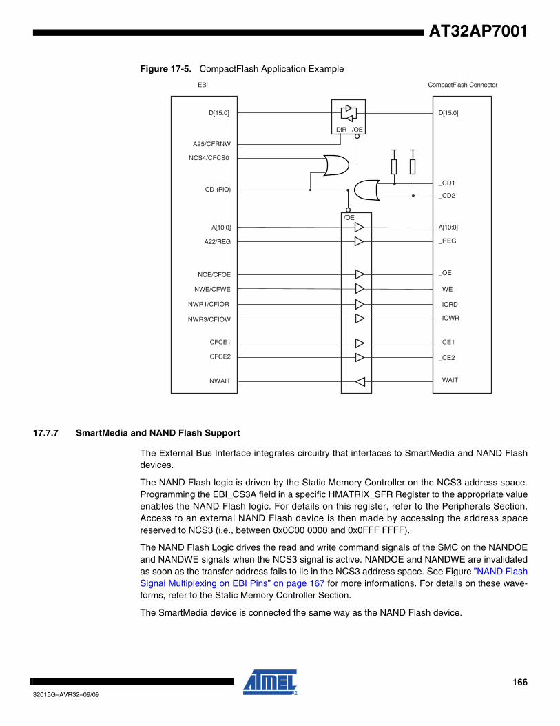
16632015G–AVR32–09/09
AT32AP7001
Figure 17-5. CompactFlash Application Example
17.7.7 SmartMedia and NAND Flash Support
The External Bus Interface integrates circuitry that interfaces to SmartMedia and NAND Flashdevices.
The NAND Flash logic is driven by the Static Memory Controller on the NCS3 address space.Programming the EBI_CS3A field in a specific HMATRIX_SFR Register to the appropriate valueenables the NAND Flash logic. For details on this register, refer to the Peripherals Section.Access to an external NAND Flash device is then made by accessing the address spacereserved to NCS3 (i.e., between 0x0C00 0000 and 0x0FFF FFFF).
The NAND Flash Logic drives the read and write command signals of the SMC on the NANDOEand NANDWE signals when the NCS3 signal is active. NANDOE and NANDWE are invalidatedas soon as the transfer address fails to lie in the NCS3 address space. See Figure ”NAND FlashSignal Multiplexing on EBI Pins” on page 167 for more informations. For details on these wave-forms, refer to the Static Memory Controller Section.
The SmartMedia device is connected the same way as the NAND Flash device.
CompactFlash ConnectorEBI
D[15:0]
/OEDIR
_CD1
_CD2
/OE
D[15:0]
A25/CFRNW
NCS4/CFCS0
CD (PIO)
A[10:0]
A22/REG
NOE/CFOE
A[10:0]
_REG
_OE
_WE
_IORD
_IOWR
_CE1
_CE2
NWE/CFWE
NWR1/CFIOR
NWR3/CFIOW
CFCE1
CFCE2
_WAITNWAIT
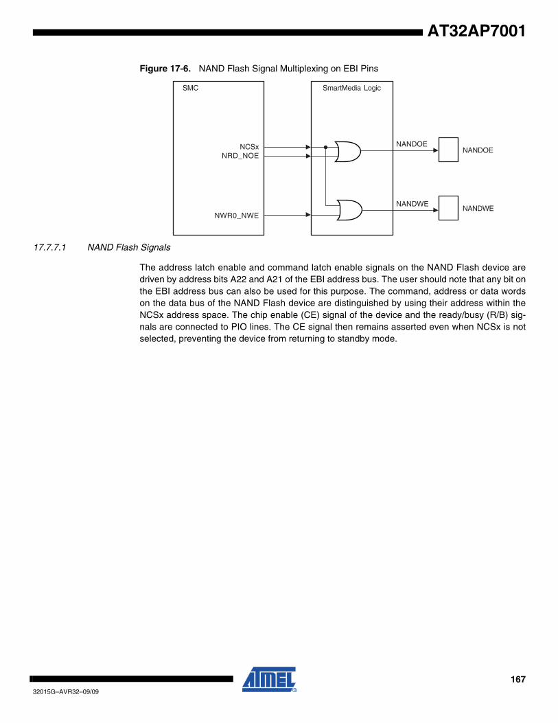
16732015G–AVR32–09/09
AT32AP7001
Figure 17-6. NAND Flash Signal Multiplexing on EBI Pins
17.7.7.1 NAND Flash Signals
The address latch enable and command latch enable signals on the NAND Flash device aredriven by address bits A22 and A21 of the EBI address bus. The user should note that any bit onthe EBI address bus can also be used for this purpose. The command, address or data wordson the data bus of the NAND Flash device are distinguished by using their address within theNCSx address space. The chip enable (CE) signal of the device and the ready/busy (R/B) sig-nals are connected to PIO lines. The CE signal then remains asserted even when NCSx is notselected, preventing the device from returning to standby mode.
SMC
NRD_NOE
NWR0_NWE
NANDOE
NANDWE
SmartMedia Logic
NCSx
NANDWE
NANDOE

16832015G–AVR32–09/09
AT32AP7001
Figure 17-7. NAND Flash Application Example
Note: The External Bus Interfaces is also able to support 16-bits devices.
D[7:0]
ALE
NANDWE
NANDOENOE
NWE
A[22:21]
CLE
AD[7:0]
PIO R/B
EBI
CE
SmartMedia
PIO
NCSx/NANDCS Not Connected
16932015G–AVR32–09/09
AT32AP7001
18. DMA Controller (DMACA)
Rev: 2.0.0.6
18.1 Features
• 2 HSB Master Interfaces• 3 Channels• Software and Hardware Handshaking Interfaces
– 11 Hardware Handshaking Interfaces• Memory/Non-Memory Peripherals to Memory/Non-Memory Peripherals Transfer• Single-block DMA Transfer• Multi-block DMA Transfer
– Linked Lists– Auto-Reloading– Contiguous Blocks
• DMA Controller is Always the Flow Controller• Additional Features
– Scatter and Gather Operations– Channel Locking
– Bus Locking– FIFO Mode– Pseudo Fly-by Operation
18.2 Overview
The DMA Controller (DMACA) is an HSB-central DMA controller core that transfers data from asource peripheral to a destination peripheral over one or more System Bus. One channel isrequired for each source/destination pair. In the most basic configuration, the DMACA has onemaster interface and one channel. The master interface reads the data from a source and writesit to a destination. Two System Bus transfers are required for each DMA data transfer. This isalso known as a dual-access transfer.
The DMACA is programmed via the HSB slave interface.
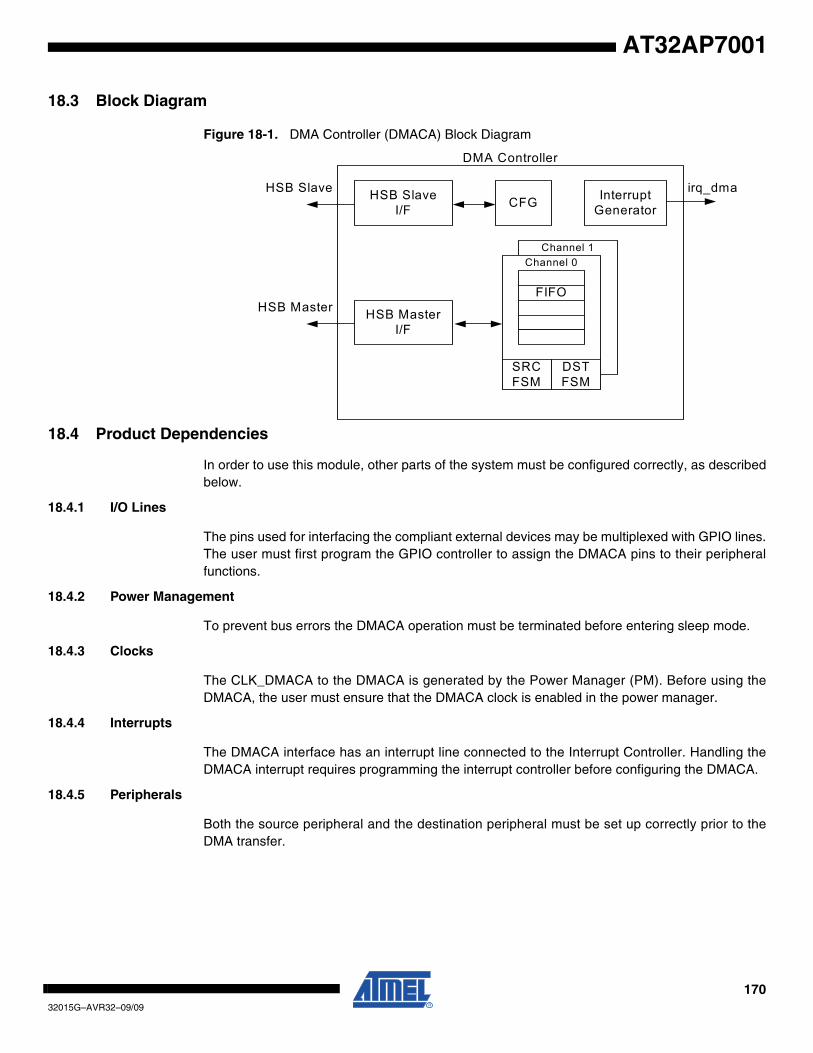
17032015G–AVR32–09/09
AT32AP7001
18.3 Block Diagram
Figure 18-1. DMA Controller (DMACA) Block Diagram
18.4 Product Dependencies
In order to use this module, other parts of the system must be configured correctly, as describedbelow.
18.4.1 I/O Lines
The pins used for interfacing the compliant external devices may be multiplexed with GPIO lines.The user must first program the GPIO controller to assign the DMACA pins to their peripheralfunctions.
18.4.2 Power Management
To prevent bus errors the DMACA operation must be terminated before entering sleep mode.
18.4.3 Clocks
The CLK_DMACA to the DMACA is generated by the Power Manager (PM). Before using theDMACA, the user must ensure that the DMACA clock is enabled in the power manager.
18.4.4 Interrupts
The DMACA interface has an interrupt line connected to the Interrupt Controller. Handling theDMACA interrupt requires programming the interrupt controller before configuring the DMACA.
18.4.5 Peripherals
Both the source peripheral and the destination peripheral must be set up correctly prior to theDMA transfer.
HSB Slave I/F
HSB Master I/F
CFG Interrupt Generator
FIFO
Channel 0
SRC FSM
DST FSM
Channel 1
DMA Controller
irq_dmaHSB Slave
HSB Master
17132015G–AVR32–09/09
AT32AP7001
18.5 Functional Description
18.5.1 Basic Definitions
Source peripheral: Device on a System Bus layer from where the DMACA reads data, which isthen stored in the channel FIFO. The source peripheral teams up with a destination peripheral toform a channel.
Destination peripheral: Device to which the DMACA writes the stored data from the FIFO (pre-viously read from the source peripheral).
Memory: Source or destination that is always “ready” for a DMA transfer and does not require ahandshaking interface to interact with the DMACA. A peripheral should be assigned as memoryonly if it does not insert more than 16 wait states. If more than 16 wait states are required, thenthe peripheral should use a handshaking interface (the default if the peripheral is not pro-grammed to be memory) in order to signal when it is ready to accept or supply data.
Channel: Read/write datapath between a source peripheral on one configured System Buslayer and a destination peripheral on the same or different System Bus layer that occurs throughthe channel FIFO. If the source peripheral is not memory, then a source handshaking interfaceis assigned to the channel. If the destination peripheral is not memory, then a destination hand-shaking interface is assigned to the channel. Source and destination handshaking interfaces canbe assigned dynamically by programming the channel registers.
Master interface: DMACA is a master on the HSB bus reading data from the source and writingit to the destination over the HSB bus.
Slave interface: The HSB interface over which the DMACA is programmed. The slave interfacein practice could be on the same layer as any of the master interfaces or on a separate layer.
Handshaking interface: A set of signal registers that conform to a protocol and handshakebetween the DMACA and source or destination peripheral to control the transfer of a single orburst transaction between them. This interface is used to request, acknowledge, and control aDMACA transaction. A channel can receive a request through one of three types of handshakinginterface: hardware, software, or peripheral interrupt.
Hardware handshaking interface: Uses hardware signals to control the transfer of a single orburst transaction between the DMACA and the source or destination peripheral.
Software handshaking interface: Uses software registers to control the transfer of a single orburst transaction between the DMACA and the source or destination peripheral. No specialDMACA handshaking signals are needed on the I/O of the peripheral. This mode is useful forinterfacing an existing peripheral to the DMACA without modifying it.
Peripheral interrupt handshaking interface: A simple use of the hardware handshaking inter-face. In this mode, the interrupt line from the peripheral is tied to the dma_req input of thehardware handshaking interface. Other interface signals are ignored.
Flow controller: The device (either the DMACA or source/destination peripheral) that deter-mines the length of and terminates a DMA block transfer. If the length of a block is known beforeenabling the channel, then the DMACA should be programmed as the flow controller. If thelength of a block is not known prior to enabling the channel, the source or destination peripheralneeds to terminate a block transfer. In this mode, the peripheral is the flow controller.
Flow control mode (CFGx.FCMODE): Special mode that only applies when the destinationperipheral is the flow controller. It controls the pre-fetching of data from the source peripheral.
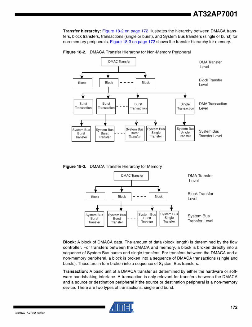
17232015G–AVR32–09/09
AT32AP7001
Transfer hierarchy: Figure 18-2 on page 172 illustrates the hierarchy between DMACA trans-fers, block transfers, transactions (single or burst), and System Bus transfers (single or burst) fornon-memory peripherals. Figure 18-3 on page 172 shows the transfer hierarchy for memory.
Figure 18-2. DMACA Transfer Hierarchy for Non-Memory Peripheral
Figure 18-3. DMACA Transfer Hierarchy for Memory
Block: A block of DMACA data. The amount of data (block length) is determined by the flowcontroller. For transfers between the DMACA and memory, a block is broken directly into asequence of System Bus bursts and single transfers. For transfers between the DMACA and anon-memory peripheral, a block is broken into a sequence of DMACA transactions (single andbursts). These are in turn broken into a sequence of System Bus transfers.
Transaction: A basic unit of a DMACA transfer as determined by either the hardware or soft-ware handshaking interface. A transaction is only relevant for transfers between the DMACAand a source or destination peripheral if the source or destination peripheral is a non-memorydevice. There are two types of transactions: single and burst.
DMAC Transfer DMA Transfer Level
Block Block BlockBlock Transfer Level
BurstTransaction
BurstTransaction
BurstTransaction
SingleTransaction
DMA Transaction Level
BurstTransfer
System BusBurst
Transfer
System BusBurst
Transfer
System BusSingle
Transfer
System BusSystem BusTransfer Level
SingleTransfer
System Bus
DMAC Transfer DMA Transfer Level
Block Block BlockBlock Transfer Level
BurstTransfer
System BusBurst
Transfer
System BusBurst
Transfer
System BusSingle
Transfer
System Bus System BusTransfer Level
17332015G–AVR32–09/09
AT32AP7001
– Single transaction: The length of a single transaction is always 1 and is converted to a single System Bus transfer.
– Burst transaction: The length of a burst transaction is programmed into the DMACA. The burst transaction is converted into a sequence of System Bus bursts and single transfers. DMACA executes each burst transfer by performing incremental bursts that are no longer than the maximum System Bus burst size set. The burst transaction length is under program control and normally bears some relationship to the FIFO sizes in the DMACA and in the source and destination peripherals.
DMA transfer: Software controls the number of blocks in a DMACA transfer. Once the DMAtransfer has completed, then hardware within the DMACA disables the channel and can gener-ate an interrupt to signal the completion of the DMA transfer. You can then re-program thechannel for a new DMA transfer.
Single-block DMA transfer: Consists of a single block.
Multi-block DMA transfer: A DMA transfer may consist of multiple DMACA blocks. Multi-blockDMA transfers are supported through block chaining (linked list pointers), auto-reloading ofchannel registers, and contiguous blocks. The source and destination can independently selectwhich method to use.
– Linked lists (block chaining) – A linked list pointer (LLP) points to the location in system memory where the next linked list item (LLI) exists. The LLI is a set of registers that describe the next block (block descriptor) and an LLP register. The DMACA fetches the LLI at the beginning of every block when block chaining is enabled.
– Auto-reloading – The DMACA automatically reloads the channel registers at the end of each block to the value when the channel was first enabled.
– Contiguous blocks – Where the address between successive blocks is selected to be a continuation from the end of the previous block.
Scatter: Relevant to destination transfers within a block. The destination System Bus address isincremented or decremented by a programmed amount -the scatter increment- when a scatterboundary is reached. The destination System Bus address is incremented or decremented bythe value stored in the destination scatter increment (DSRx.DSI) field, multiplied by the numberof bytes in a single HSB transfer to the destination (decoded value of CTLx.DST_TR_WIDTH)/8.The number of destination transfers between successive scatter boundaries is programmed intothe Destination Scatter Count (DSC) field of the DSRx register.
Scatter is enabled by writing a ‘1’ to the CTLx.DST_SCATTER_EN bit. The CTLx.DINC fielddetermines if the address is incremented, decremented or remains fixed when a scatter bound-ary is reached. If the CTLx.DINC field indicates a fixed-address control throughout a DMAtransfer, then the CTLx.DST_SCATTER_EN bit is ignored, and the scatter feature is automati-cally disabled.
Gather: Relevant to source transfers within a block. The source System Bus address is incre-mented or decremented by a programmed amount when a gather boundary is reached. Thenumber of System Bus transfers between successive gather boundaries is programmed into theSource Gather Count (SGRx.SGC) field. The source address is incremented or decremented bythe value stored in the source gather increment (SGRx.SGI) field multiplied by the number ofbytes in a single HSB transfer from the source -(decoded value of CTLx.SRC_TR_WIDTH)/8 -when a gather boundary is reached.
Gather is enabled by writing a ‘1’ to the CTLx.SRC_GATHER_EN bit. The CTLx.SINC fielddetermines if the address is incremented, decremented or remains fixed when a gather bound-

17432015G–AVR32–09/09
AT32AP7001
ary is reached. If the CTLx.SINC field indicates a fixed-address control throughout a DMAtransfer, then the CTLx.SRC_GATHER_EN bit is ignored and the gather feature is automaticallydisabled.
Note: For multi-block transfers, the counters that keep track of the number of transfer left toreach a gather/scatter boundary are re-initialized to the source gather count (SGRx.SGC) anddestination scatter count (DSRx.DSC), respectively, at the start of each block transfer.
Figure 18-4. Destination Scatter Transfer
D11
D10
D9
D8
D7
D6
D5
D4
D3
D2
D1
D0
0 x 080
System Memory
A0 + 0x218
A0 + 0x210
A0 + 0x208
A0 + 0x200
A0 + 0x118
A0 + 0x110
A0 + 0x108
A0 + 0x100
Scatter Increment
A0 + 0x018
A0 + 0x010
A0 + 0x008
A0
Scatter Increment0 x 080
Scatter Boundary A0 + 0x220
Scatter Boundary A0 + 0x120
Scatter Boundary A0 + 0x020
Data Stream
d0 d1 d2 d3 d4 d5 d6 d7 d8 d9 d10 d11
d11
d8
d7
d4
d3
d0
DSR.DSI * 8 = 0x80 (Scatter Increment in bytes)
CTLx.DST_TR_WIDTH = 3'b011 (64bit/8 = 8 bytes)DSR.DSI = 16DSR.DSC = 4
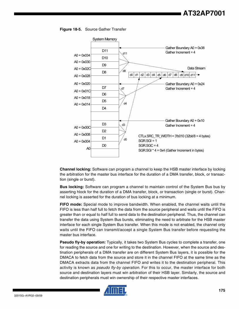
17532015G–AVR32–09/09
AT32AP7001
Figure 18-5. Source Gather Transfer
Channel locking: Software can program a channel to keep the HSB master interface by lockingthe arbitration for the master bus interface for the duration of a DMA transfer, block, or transac-tion (single or burst).
Bus locking: Software can program a channel to maintain control of the System Bus bus byasserting hlock for the duration of a DMA transfer, block, or transaction (single or burst). Chan-nel locking is asserted for the duration of bus locking at a minimum.
FIFO mode: Special mode to improve bandwidth. When enabled, the channel waits until theFIFO is less than half full to fetch the data from the source peripheral and waits until the FIFO isgreater than or equal to half full to send data to the destination peripheral. Thus, the channel cantransfer the data using System Bus bursts, eliminating the need to arbitrate for the HSB masterinterface for each single System Bus transfer. When this mode is not enabled, the channel onlywaits until the FIFO can transmit/accept a single System Bus transfer before requesting themaster bus interface.
Pseudo fly-by operation: Typically, it takes two System Bus cycles to complete a transfer, onefor reading the source and one for writing to the destination. However, when the source and des-tination peripherals of a DMA transfer are on different System Bus layers, it is possible for theDMACA to fetch data from the source and store it in the channel FIFO at the same time as theDMACA extracts data from the channel FIFO and writes it to the destination peripheral. Thisactivity is known as pseudo fly-by operation. For this to occur, the master interface for bothsource and destination layers must win arbitration of their HSB layer. Similarly, the source anddestination peripherals must win ownership of their respective master interfaces.
D11
D10
D9
D8
System Memory
A0 + 0x034
A0 + 0x030
A0 + 0x02C
A0 + 0x028
d11
d8
d7
d4
A0 + 0x020
A0 + 0x01C
A0 + 0x018
A0 + 0x014
D7
D6
D5
D4
D3
D2
D1
D0
A0 + 0x00C
A0 + 0x008
A0 + 0x004
A0
d3
d0
Gather Boundary A0 + 0x24Gather Increment = 4
Data Stream
d0 d1 d2 d3 d4 d5 d6 d7 d8 d9 d10 d11
Gather Boundary A0 + 0x38Gather Increment = 4
Gather Boundary A0 + 0x10Gather Increment = 4
SGR.SGI * 4 = 0x4 (Gather Increment in bytes)
CTLx.SRC_TR_WIDTH = 3'b010 (32bit/8 = 4 bytes)SGR.SGI = 1SGR.SGC = 4
17632015G–AVR32–09/09
AT32AP7001
18.6 Arbitration for HSB Master Interface
Each DMACA channel has two request lines that request ownership of a particular master businterface: channel source and channel destination request lines.
Source and destination arbitrate separately for the bus. Once a source/destination statemachine gains ownership of the master bus interface and the master bus interface has owner-ship of the HSB bus, then HSB transfers can proceed between the peripheral and the DMACA.
An arbitration scheme decides which of the request lines (2 * DMAH_NUM_CHANNELS) isgranted the particular master bus interface. Each channel has a programmable priority. Arequest for the master bus interface can be made at any time, but is granted only after the cur-rent HSB transfer (burst or single) has completed. Therefore, if the master interface istransferring data for a lower priority channel and a higher priority channel requests service, thenthe master interface will complete the current burst for the lower priority channel before switch-ing to transfer data for the higher priority channel.
If only one request line is active at the highest priority level, then the request with the highest pri-ority wins ownership of the HSB master bus interface; it is not necessary for the priority levels tobe unique.
If more than one request is active at the highest requesting priority, then these competingrequests proceed to a second tier of arbitration:
If equal priority requests occur, then the lower-numbered channel is granted.
In other words, if a peripheral request attached to Channel 7 and a peripheral request attachedto Channel 8 have the same priority, then the peripheral attached to Channel 7 is granted first.
18.7 Memory Peripherals
Figure 18-3 on page 172 shows the DMA transfer hierarchy of the DMACA for a memory periph-eral. There is no handshaking interface with the DMACA, and therefore the memory peripheralcan never be a flow controller. Once the channel is enabled, the transfer proceeds immediatelywithout waiting for a transaction request. The alternative to not having a transaction-level hand-shaking interface is to allow the DMACA to attempt System Bus transfers to the peripheral oncethe channel is enabled. If the peripheral slave cannot accept these System Bus transfers, itinserts wait states onto the bus until it is ready; it is not recommended that more than 16 waitstates be inserted onto the bus. By using the handshaking interface, the peripheral can signal tothe DMACA that it is ready to transmit/receive data, and then the DMACA can access theperipheral without the peripheral inserting wait states onto the bus.
18.8 Handshaking Interface
Handshaking interfaces are used at the transaction level to control the flow of single or bursttransactions. The operation of the handshaking interface is different and depends on whetherthe peripheral or the DMACA is the flow controller.
The peripheral uses the handshaking interface to indicate to the DMACA that it is ready to trans-fer/accept data over the System Bus. A non-memory peripheral can request a DMA transferthrough the DMACA using one of two handshaking interfaces:
• Hardware handshaking
• Software handshaking
17732015G–AVR32–09/09
AT32AP7001
Software selects between the hardware or software handshaking interface on a per-channelbasis. Software handshaking is accomplished through memory-mapped registers, while hard-ware handshaking is accomplished using a dedicated handshaking interface.
18.8.1 Software Handshaking
When the slave peripheral requires the DMACA to perform a DMA transaction, it communicatesthis request by sending an interrupt to the CPU or interrupt controller.
The interrupt service routine then uses the software registers to initiate and control a DMA trans-action. These software registers are used to implement the software handshaking interface.
The HS_SEL_SRC/HS_SEL_DST bit in the CFGx channel configuration register must be set toenable software handshaking.
When the peripheral is not the flow controller, then the last transaction registers LstSrcReg andLstDstReg are not used, and the values in these registers are ignored.
18.8.1.1 Burst Transactions
Writing a 1 to the ReqSrcReg[x]/ReqDstReg[x] register is always interpreted as a burst transac-tion request, where x is the channel number. However, in order for a burst transaction request tostart, software must write a 1 to the SglReqSrcReg[x]/SglReqDstReg[x] register.
You can write a 1 to the SglReqSrcReg[x]/SglReqDstReg[x] and ReqSrcReg[x]/ReqDstReg[x]registers in any order, but both registers must be asserted in order to initiate a burst transaction.Upon completion of the burst transaction, the hardware clears the SglReqSrcReg[x]/SglReqD-stReg[x] and ReqSrcReg[x]/ReqDstReg[x] registers.
18.8.1.2 Single Transactions
Writing a 1 to the SglReqSrcReg/SglReqDstReg initiates a single transaction. Upon completionof the single transaction, both the SglReqSrcReg/SglReqDstReg and ReqSrcReg/ReqDstRegbits are cleared by hardware. Therefore, writing a 1 to the ReqSrcReg/ReqDstReg is ignoredwhile a single transaction has been initiated, and the requested burst transaction is not serviced.
Again, writing a 1 to the ReqSrcReg/ReqDstReg register is always a burst transaction request.However, in order for a burst transaction request to start, the corresponding channel bit in theSglReqSrcReg/SglReqDstReg must be asserted. Therefore, to ensure that a burst transaction isserviced, you must write a 1 to the ReqSrcReg/ReqDstReg before writing a 1 to the SglReqSr-cReg/SglReqDstReg register.
Software can poll the relevant channel bit in the SglReqSrcReg/ SglReqDstReg and ReqSr-cReg/ReqDstReg registers. When both are 0, then either the requested burst or singletransaction has completed. Alternatively, the IntSrcTran or IntDstTran interrupts can be enabledand unmasked in order to generate an interrupt when the requested source or destination trans-action has completed.
Note: The transaction-complete interrupts are triggered when both single and burst transactions are complete. The same transaction-complete interrupt is used for both single and burst transactions.
18.8.2 Hardware Handshaking
There are 11 hardware handshaking interfaces between the DMACA and peripherals. Refer tothe module configuration chapter for the device-specific mapping of these interfaces.

17832015G–AVR32–09/09
AT32AP7001
18.8.2.1 External DMA Request Definition
When an external slave peripheral requires the DMACA to perform DMA transactions, it commu-nicates its request by asserting the external nDMAREQx signal. This signal is resynchronized toensure a proper functionality (see ”External DMA Request Timing” on page 178).
The external nDMAREQx signal should be asserted when the source threshold level is reached.After resynchronization, the rising edge of dma_req starts the transfer. An external DMAACKxacknowledge signal is also provided to indicate when the DMA transfer has completed. Theperipheral should de-assert the DMA request signal when DMAACKx is asserted.
The external nDMAREQx signal must be de-asserted after the last transfer and re-assertedagain before a new transaction starts.
For a source FIFO, an active edge should be triggered on nDMAREQx when the source FIFOexceeds a watermark level. For a destination FIFO, an active edge should be triggered onnDMAREQx when the destination FIFO drops below the watermark level.
The source transaction length, CTLx.SRC_MSIZE, and destination transaction length,CTLx.DEST_MSIZE, must be set according to watermark levels on the source/destinationperipherals.
Figure 18-6. External DMA Request Timing
18.9 DMACA Transfer Types
A DMA transfer may consist of single or multi-block transfers. On successive blocks of a multi-block transfer, the SARx/DARx register in the DMACA is reprogrammed using either of the fol-lowing methods:
• Block chaining using linked lists
• Auto-reloading
• Contiguous address between blocks
On successive blocks of a multi-block transfer, the CTLx register in the DMACA is re-pro-grammed using either of the following methods:
• Block chaining using linked lists
• Auto-reloading
When block chaining, using linked lists is the multi-block method of choice, and on successiveblocks, the LLPx register in the DMACA is re-programmed using the following method:
DMA Transfers DMA Transfers
Hclk
nDMAREQx
dma_req
dma_ack
DMA Transfers
DMA Transaction

17932015G–AVR32–09/09
AT32AP7001
• Block chaining using linked lists
A block descriptor (LLI) consists of following registers, SARx, DARx, LLPx, CTL. These regis-ters, along with the CFGx register, are used by the DMACA to set up and describe the blocktransfer.
18.9.1 Multi-block Transfers
18.9.1.1 Block Chaining Using Linked Lists
In this case, the DMACA re-programs the channel registers prior to the start of each block byfetching the block descriptor for that block from system memory. This is known as an LLI update.
DMACA block chaining is supported by using a Linked List Pointer register (LLPx) that stores theaddress in memory of the next linked list item. Each LLI (block descriptor) contains the corre-sponding block descriptor (SARx, DARx, LLPx, CTLx).
To set up block chaining, a sequence of linked lists must be programmed in memory.
The SARx, DARx, LLPx and CTLx registers are fetched from system memory on an LLI update.The updated contents of the CTLx register are written back to memory on block completion. Fig-ure 18-7 on page 179 shows how to use chained linked lists in memory to define multi-blocktransfers using block chaining.
The Linked List multi-block transfers is initiated by programming LLPx with LLPx(0) (LLI(0) baseaddress) and CTLx with CTLx.LLP_S_EN and CTLx.LLP_D_EN.
Figure 18-7. Multi-block Transfer Using Linked Lists
System Memory
SARx
DARx
LLPx(1)
CTLx[31..0]
CTLx[63..32]
SARx
DARx
LLPx(2)
CTLx[31..0]
CTLx[63..32]
LLPx(0)LLPx(2)
LLPx(1)
LLI(0) LLI(1)
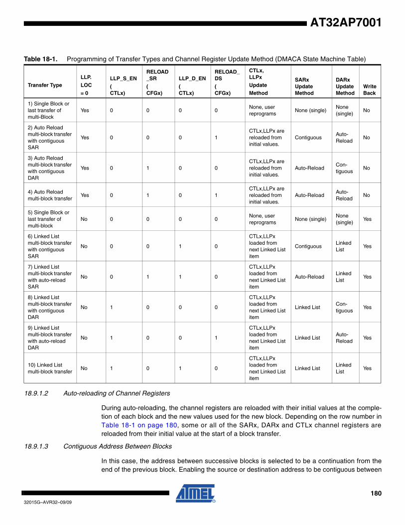
18032015G–AVR32–09/09
AT32AP7001
18.9.1.2 Auto-reloading of Channel Registers
During auto-reloading, the channel registers are reloaded with their initial values at the comple-tion of each block and the new values used for the new block. Depending on the row number inTable 18-1 on page 180, some or all of the SARx, DARx and CTLx channel registers arereloaded from their initial value at the start of a block transfer.
18.9.1.3 Contiguous Address Between Blocks
In this case, the address between successive blocks is selected to be a continuation from theend of the previous block. Enabling the source or destination address to be contiguous between
Table 18-1. Programming of Transfer Types and Channel Register Update Method (DMACA State Machine Table)
Transfer Type
LLP.
LOC
= 0
LLP_S_EN
(CTLx)
RELOAD_SR
(CFGx)
LLP_D_EN
(CTLx)
RELOAD_DS
(CFGx)
CTLx,LLPx
Update
Method
SARx Update Method
DARx Update Method
WriteBack
1) Single Block or last transfer of multi-Block
Yes 0 0 0 0None, user reprograms
None (single)None (single)
No
2) Auto Reload multi-block transfer with contiguous SAR
Yes 0 0 0 1CTLx,LLPx are reloaded from initial values.
ContiguousAuto-Reload
No
3) Auto Reload multi-block transfer with contiguous DAR
Yes 0 1 0 0CTLx,LLPx are reloaded from initial values.
Auto-ReloadCon-tiguous
No
4) Auto Reload multi-block transfer
Yes 0 1 0 1CTLx,LLPx are reloaded from initial values.
Auto-ReloadAuto-Reload
No
5) Single Block or last transfer of multi-block
No 0 0 0 0None, user reprograms
None (single)None (single)
Yes
6) Linked List multi-block transfer with contiguous SAR
No 0 0 1 0
CTLx,LLPx loaded from next Linked List item
ContiguousLinked List
Yes
7) Linked List multi-block transfer with auto-reload SAR
No 0 1 1 0
CTLx,LLPx loaded from next Linked List item
Auto-ReloadLinked List
Yes
8) Linked List multi-block transfer with contiguous DAR
No 1 0 0 0
CTLx,LLPx loaded from next Linked List item
Linked ListCon-tiguous
Yes
9) Linked List multi-block transfer with auto-reload DAR
No 1 0 0 1
CTLx,LLPx loaded from next Linked List item
Linked ListAuto-Reload
Yes
10) Linked List multi-block transfer
No 1 0 1 0
CTLx,LLPx loaded from next Linked List item
Linked ListLinked List
Yes
18132015G–AVR32–09/09
AT32AP7001
blocks is a function of CTLx.LLP_S_EN, CFGx.RELOAD_SR, CTLx.LLP_D_EN, andCFGx.RELOAD_DS registers (see Figure 18-1 on page 170).
Note: Both SARx and DARx updates cannot be selected to be contiguous. If this functionality is required, the size of the Block Transfer (CTLx.BLOCK_TS) must be increased. If this is at the max-imum value, use Row 10 of Table 18-1 on page 180 and setup the LLI.SARx address of the block descriptor to be equal to the end SARx address of the previous block. Similarly, setup the LLI.DARx address of the block descriptor to be equal to the end DARx address of the previous block.
18.9.1.4 Suspension of Transfers Between Blocks
At the end of every block transfer, an end of block interrupt is asserted if:
• interrupts are enabled, CTLx.INT_EN = 1
• the channel block interrupt is unmasked, MaskBlock[n] = 0, where n is the channel number.
Note: The block complete interrupt is generated at the completion of the block transfer to the destination.
For rows 6, 8, and 10 of Table 18-1 on page 180, the DMA transfer does not stall between blocktransfers. For example, at the end of block N, the DMACA automatically proceeds to block N + 1.
For rows 2, 3, 4, 7, and 9 of Table 18-1 on page 180 (SARx and/or DARx auto-reloaded betweenblock transfers), the DMA transfer automatically stalls after the end of block. Interrupt is assertedif the end of block interrupt is enabled and unmasked.
The DMACA does not proceed to the next block transfer until a write to the block interrupt clearregister, ClearBlock[n], is performed by software. This clears the channel block completeinterrupt.
For rows 2, 3, 4, 7, and 9 of Table 18-1 on page 180 (SARx and/or DARx auto-reloaded betweenblock transfers), the DMA transfer does not stall if either:
• interrupts are disabled, CTLx.INT_EN = 0, or
• the channel block interrupt is masked, MaskBlock[n] = 1, where n is the channel number.
Channel suspension between blocks is used to ensure that the end of block ISR (interrupt ser-vice routine) of the next-to-last block is serviced before the start of the final block commences.This ensures that the ISR has cleared the CFGx.RELOAD_SR and/or CFGx.RELOAD_DS bitsbefore complet ion of the f inal block. The reload bi ts CFGx.RELOAD_SR and/orCFGx.RELOAD_DS should be cleared in the ‘end of block ISR’ for the next-to-last blocktransfer.
18.9.2 Ending Multi-block Transfers
All multi-block transfers must end as shown in either Row 1 or Row 5 of Table 18-1 on page 180.At the end of every block transfer, the DMACA samples the row number, and if the DMACA is inRow 1 or Row 5 state, then the previous block transferred was the last block and the DMA trans-fer is terminated.
Note: Row 1 and Row 5 are used for single block transfers or terminating multiblock transfers. Ending in Row 5 state enables status fetch for the last block. Ending in Row 1 state disables status fetch for the last block.
For rows 2,3 and 4 of Table 18-1 on page 180, (LLPx = 0 and CFGx.RELOAD_SR and/orCFGx.RELOAD_DS is set ) , mul t i -b lock DMA t ransfers cont inue unt i l both theCFGx.RELOAD_SR and CFGx.RELOAD_DS registers are cleared by software. They should be
18232015G–AVR32–09/09
AT32AP7001
programmed to zero in the end of block interrupt service routine that services the next-to-lastblock transfer. This puts the DMACA into Row 1 state.
For rows 6, 8, and 10 (both CFGx.RELOAD_SR and CFGx.RELOAD_DS cleared) the user mustsetup the last block descriptor in memory such that both LLI.CTLx.LLP_S_EN andLLI.CTLx.LLP_D_EN are zero. If the LLI.LLPx register of the last block descriptor in memory isnon-zero, then the DMA transfer is terminated in Row 5. If the LLI.LLPx register of the last blockdescriptor in memory is zero, then the DMA transfer is terminated in Row 1.
For rows 7 and 9, the end-of-block interrupt service routine that services the next-to-last blocktransfer should clear the CFGx.RELOAD_SR and CFGx.RELOAD_DS reload bits. The lastblock descriptor in memory should be set up so that both the LLI.CTLx.LLP_S_EN andLLI.CTLx.LLP_D_EN are zero. If the LLI.LLPx register of the last block descriptor in memory isnon-zero, then the DMA transfer is terminated in Row 5. If the LLI.LLPx register of the last blockdescriptor in memory is zero, then the DMA transfer is terminated in Row 1.
Note: The only allowed transitions between the rows of Table 18-1 on page 180are from any row into row 1 or row 5. As already stated, a transition into row 1 or row 5 is used to terminate the DMA transfer. All other transitions between rows are not allowed. Software must ensure that illegal tran-sitions between rows do not occur between blocks of a multi-block transfer. For example, if block N is in row 10 then the only allowed rows for block N + 1 are rows 10, 5 or 1.
18.10 Programming a Channel
Three registers, the LLPx, the CTLx and CFGx, need to be programmed to set up whether singleor multi-block transfers take place, and which type of multi-block transfer is used. The differenttransfer types are shown in Table 18-1 on page 180.
The “Update Method” column indicates where the values of SARx, DARx, CTLx, and LLPx areobtained for the next block transfer when multi-block DMACA transfers are enabled.
Note: In Table 18-1 on page 180, all other combinations of LLPx.LOC = 0, CTLx.LLP_S_EN, CFGx.RELOAD_SR, CTLx.LLP_D_EN, and CFGx.RELOAD_DS are illegal, and causes indeter-minate or erroneous behavior.
18.10.1 Programming Examples
18.10.1.1 Single-block Transfer (Row 1)
Row 5 in Table 18-1 on page 180 is also a single block transfer.
1. Read the Channel Enable register to choose a free (disabled) channel.
2. Clear any pending interrupts on the channel from the previous DMA transfer by writing to the Interrupt Clear registers: ClearTfr, ClearBlock, ClearSrcTran, ClearDstTran, ClearErr. Reading the Interrupt Raw Status and Interrupt Status registers confirms that all inter-rupts have been cleared.
3. Program the following channel registers:
a. Write the starting source address in the SARx register for channel x.
b. Write the starting destination address in the DARx register for channel x.
c. Program CTLx and CFGx according to Row 1 as shown in Table 18-1 on page 180. Program the LLPx register with ‘0’.
d. Write the control information for the DMA transfer in the CTLx register for channel x. For example, in the register, you can program the following:
– i. Set up the transfer type (memory or non-memory peripheral for source and destination) and flow control device by programming the TT_FC of the CTLx register.
18332015G–AVR32–09/09
AT32AP7001
– ii. Set up the transfer characteristics, such as:
– Transfer width for the source in the SRC_TR_WIDTH field.
– Transfer width for the destination in the DST_TR_WIDTH field.
– Source master layer in the SMS field where source resides.
– Destination master layer in the DMS field where destination resides.
– Incrementing/decrementing or fixed address for source in SINC field.
– Incrementing/decrementing or fixed address for destination in DINC field.
e. Write the channel configuration information into the CFGx register for channel x.
– i. Designate the handshaking interface type (hardware or software) for the source and destination peripherals. This is not required for memory. This step requires programming the HS_SEL_SRC/HS_SEL_DST bits, respectively. Writing a ‘0’ activates the hardware handshaking interface to handle source/destination requests. Writing a ‘1’ activates the software handshaking interface to handle source/destination requests.
– ii. If the hardware handshaking interface is activated for the source or destination peripheral, assign a handshaking interface to the source and destination peripheral. This requires programming the SRC_PER and DEST_PER bits, respectively.
4. After the DMACA selected channel has been programmed, enable the channel by writing a ‘1’ to the ChEnReg.CH_EN bit. Make sure that bit 0 of the DmaCfgReg register is enabled.
5. Source and destination request single and burst DMA transactions to transfer the block of data (assuming non-memory peripherals). The DMACA acknowledges at the completion of every transaction (burst and single) in the block and carry out the block transfer.
6. Once the transfer completes, hardware sets the interrupts and disables the channel. At this time you can either respond to the Block Complete or Transfer Complete interrupts, or poll for the Channel Enable (ChEnReg.CH_EN) bit until it is cleared by hardware, to detect when the transfer is complete.
18.10.1.2 Multi-block Transfer with Linked List for Source and Linked List for Destination (Row 10)
1. Read the Channel Enable register to choose a free (disabled) channel.
2. Set up the chain of Linked List Items (otherwise known as block descriptors) in memory. Write the control information in the LLI.CTLx register location of the block descriptor for each LLI in memory (see Figure 18-7 on page 179) for channel x. For example, in the register, you can program the following:
a. Set up the transfer type (memory or non-memory peripheral for source and destina-tion) and flow control device by programming the TT_FC of the CTLx register.
b. Set up the transfer characteristics, such as:
– i. Transfer width for the source in the SRC_TR_WIDTH field.
– ii. Transfer width for the destination in the DST_TR_WIDTH field.
– iii. Source master layer in the SMS field where source resides.
– iv. Destination master layer in the DMS field where destination resides.
– v. Incrementing/decrementing or fixed address for source in SINC field.
– vi. Incrementing/decrementing or fixed address for destination DINC field.
3. Write the channel configuration information into the CFGx register for channel x.
a. Designate the handshaking interface type (hardware or software) for the source and destination peripherals. This is not required for memory. This step requires program-
18432015G–AVR32–09/09
AT32AP7001
ming the HS_SEL_SRC/HS_SEL_DST bits, respectively. Writing a ‘0’ activates the hardware handshaking interface to handle source/destination requests for the spe-cific channel. Writing a ‘1’ activates the software handshaking interface to handle source/destination requests.
b. If the hardware handshaking interface is activated for the source or destination peripheral, assign the handshaking interface to the source and destination periph-eral. This requires programming the SRC_PER and DEST_PER bits, respectively.
4. Make sure that the LLI.CTLx register locations of all LLI entries in memory (except the last) are set as shown in Row 10 of Table 18-1 on page 180. The LLI.CTLx register of the last Linked List Item must be set as described in Row 1 or Row 5 of Table 18-1 on page 180. Figure 18-9 on page 186 shows a Linked List example with two list items.
5. Make sure that the LLI.LLPx register locations of all LLI entries in memory (except the last) are non-zero and point to the base address of the next Linked List Item.
6. Make sure that the LLI.SARx/LLI.DARx register locations of all LLI entries in memory point to the start source/destination block address preceding that LLI fetch.
7. Make sure that the LLI.CTLx.DONE field of the LLI.CTLx register locations of all LLI entries in memory are cleared.
8. Clear any pending interrupts on the channel from the previous DMA transfer by writing to the Interrupt Clear registers: ClearTfr, ClearBlock, ClearSrcTran, ClearDstTran, ClearErr. Reading the Interrupt Raw Status and Interrupt Status registers confirms that all inter-rupts have been cleared.
9. Program the CTLx, CFGx registers according to Row 10 as shown in Table 18-1 on page 180.
10. Program the LLPx register with LLPx(0), the pointer to the first Linked List item.
11. Finally, enable the channel by writing a ‘1’ to the ChEnReg.CH_EN bit. The transfer is performed.
12. The DMACA fetches the first LLI from the location pointed to by LLPx(0). Note: The LLI.SARx, LLI. DARx, LLI.LLPx and LLI.CTLx registers are fetched. The DMACA automati-
cally reprograms the SARx, DARx, LLPx and CTLx channel registers from the LLPx(0).
13. Source and destination request single and burst DMA transactions to transfer the block of data (assuming non-memory peripheral). The DMACA acknowledges at the completion of every transaction (burst and single) in the block and carry out the block transfer.
Note: Table 18-1 on page 180
14. The DMACA does not wait for the block interrupt to be cleared, but continues fetching the next LLI from the memory location pointed to by current LLPx register and automatically reprograms the SARx, DARx, LLPx and CTLx channel registers. The DMA transfer con-tinues until the DMACA determines that the CTLx and LLPx registers at the end of a block transfer match that described in Row 1 or Row 5 of Table 18-1 on page 180. The DMACA then knows that the previous block transferred was the last block in the DMA transfer. The DMA transfer might look like that shown in Figure 18-8 on page 185.
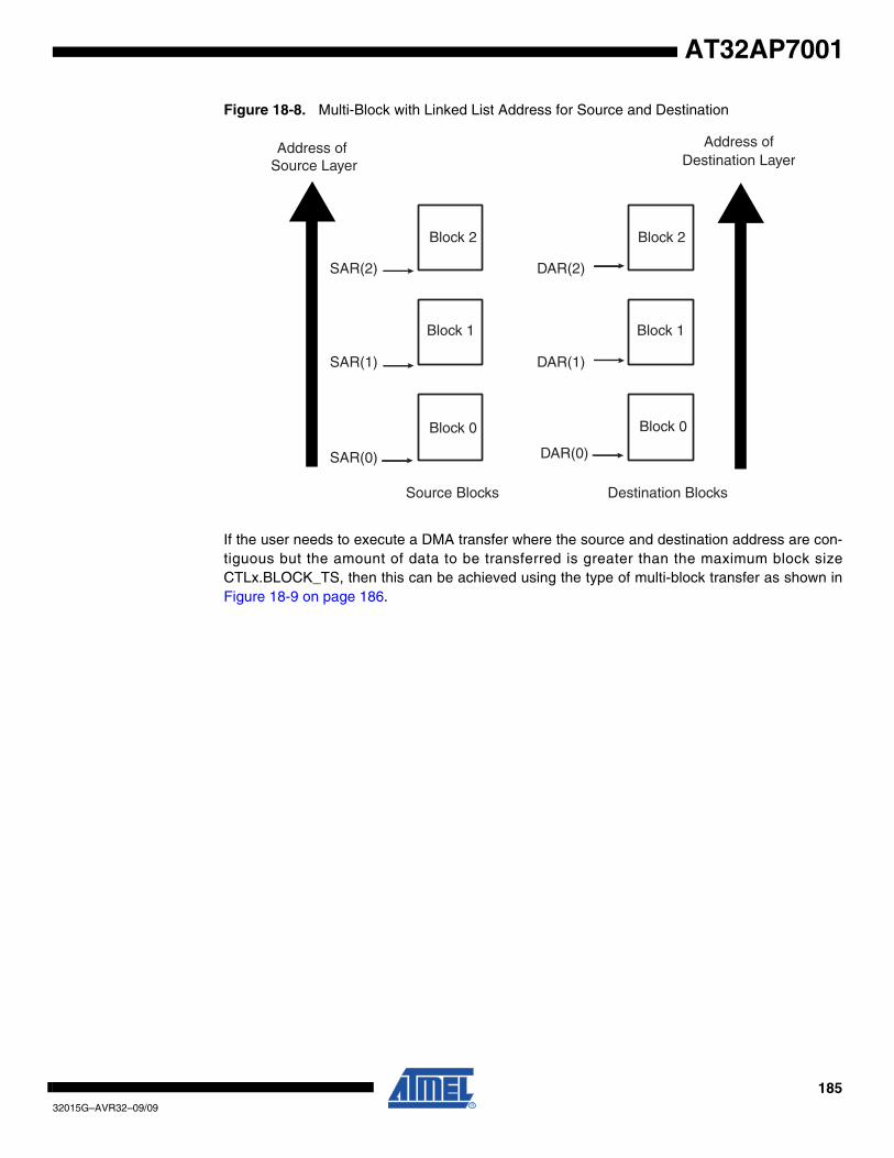
18532015G–AVR32–09/09
AT32AP7001
Figure 18-8. Multi-Block with Linked List Address for Source and Destination
If the user needs to execute a DMA transfer where the source and destination address are con-tiguous but the amount of data to be transferred is greater than the maximum block sizeCTLx.BLOCK_TS, then this can be achieved using the type of multi-block transfer as shown inFigure 18-9 on page 186.
SAR(2)
SAR(1)
SAR(0)
DAR(2)
DAR(1)
DAR(0)
Block 2
Block 1
Block 0 Block 0
Block 1
Block 2
Address of Source Layer
Address ofDestination Layer
Source Blocks Destination Blocks
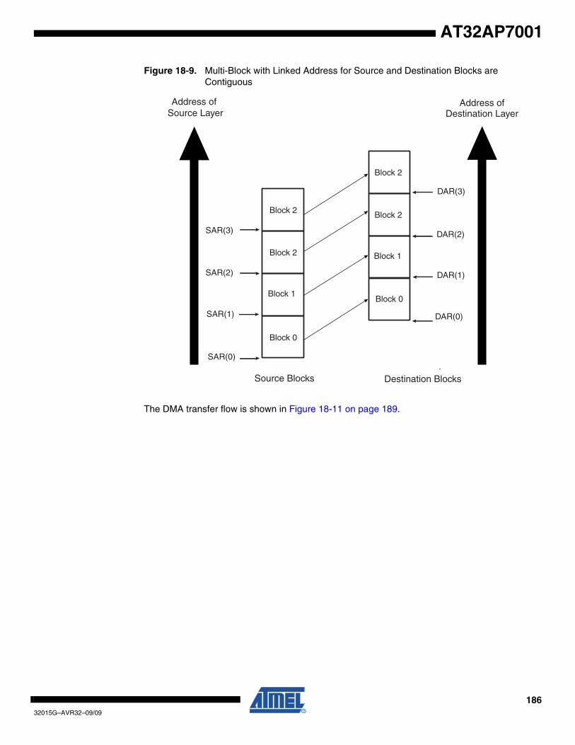
18632015G–AVR32–09/09
AT32AP7001
Figure 18-9. Multi-Block with Linked Address for Source and Destination Blocks are Contiguous
The DMA transfer flow is shown in Figure 18-11 on page 189.
SAR(2)
SAR(1)
SAR(0)
DAR(2)
DAR(1)
DAR(0)
Block 2
Block 1
Block 0
Block 0
Block 1
Block 2
Address of Source Layer
Address ofDestination Layer
Source Blocks Destination Blocks
SAR(3)
Block 2
DAR(3)
Block 2
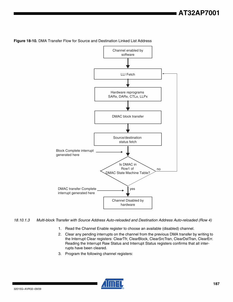
18732015G–AVR32–09/09
AT32AP7001
Figure 18-10. DMA Transfer Flow for Source and Destination Linked List Address
18.10.1.3 Multi-block Transfer with Source Address Auto-reloaded and Destination Address Auto-reloaded (Row 4)
1. Read the Channel Enable register to choose an available (disabled) channel.
2. Clear any pending interrupts on the channel from the previous DMA transfer by writing to the Interrupt Clear registers: ClearTfr, ClearBlock, ClearSrcTran, ClearDstTran, ClearErr. Reading the Interrupt Raw Status and Interrupt Status registers confirms that all inter-rupts have been cleared.
3. Program the following channel registers:
Channel enabled bysoftware
LLI Fetch
Hardware reprograms SARx, DARx, CTLx, LLPx
DMAC block transfer
Source/destination status fetch
Is DMAC inRow1 of
DMAC State Machine Table?
Channel Disabled byhardware
Block Complete interruptgenerated here
DMAC transfer Complete interrupt generated here
yes
no
18832015G–AVR32–09/09
AT32AP7001
a. Write the starting source address in the SARx register for channel x.
b. Write the starting destination address in the DARx register for channel x.
c. Program CTLx and CFGx according to Row 4 as shown in Table 18-1 on page 180. Program the LLPx register with ‘0’.
d. Write the control information for the DMA transfer in the CTLx register for channel x. For example, in the register, you can program the following:
– i. Set up the transfer type (memory or non-memory peripheral for source and destination) and flow control device by programming the TT_FC of the CTLx register.
– ii. Set up the transfer characteristics, such as:
– Transfer width for the source in the SRC_TR_WIDTH field.
– Transfer width for the destination in the DST_TR_WIDTH field.
– Source master layer in the SMS field where source resides.
– Destination master layer in the DMS field where destination resides.
– Incrementing/decrementing or fixed address for source in SINC field.
– Incrementing/decrementing or fixed address for destination in DINC field.
e. Write the channel configuration information into the CFGx register for channel x. Ensure that the reload bits, CFGx. RELOAD_SR and CFGx.RELOAD_DS are enabled.
– i. Designate the handshaking interface type (hardware or software) for the source and destination peripherals. This is not required for memory. This step requires programming the HS_SEL_SRC/HS_SEL_DST bits, respectively. Writing a ‘0’ activates the hardware handshaking interface to handle source/destination requests for the specific channel. Writing a ‘1’ activates the software handshaking interface to handle source/destination requests.
– ii. If the hardware handshaking interface is activated for the source or destination peripheral, assign handshaking interface to the source and destination peripheral. This requires programming the SRC_PER and DEST_PER bits, respectively.
4. After the DMACA selected channel has been programmed, enable the channel by writing a ‘1’ to the ChEnReg.CH_EN bit. Make sure that bit 0 of the DmaCfgReg register is enabled.
5. Source and destination request single and burst DMACA transactions to transfer the block of data (assuming non-memory peripherals). The DMACA acknowledges on com-pletion of each burst/single transaction and carry out the block transfer.
6. When the block transfer has completed, the DMACA reloads the SARx, DARx and CTLx registers. Hardware sets the Block Complete interrupt. The DMACA then samples the row number as shown in Table 18-1 on page 180. If the DMACA is in Row 1, then the DMA transfer has completed. Hardware sets the transfer complete interrupt and disables the channel. So you can either respond to the Block Complete or Transfer Complete interrupts, or poll for the Channel Enable (ChEnReg.CH_EN) bit until it is disabled, to detect when the transfer is complete. If the DMACA is not in Row 1, the next step is performed.
7. The DMA transfer proceeds as follows:
a. If interrupts are enabled (CTLx.INT_EN = 1) and the block complete interrupt is un-masked (MaskBlock[x] = 1’b1, where x is the channel number) hardware sets the block complete interrupt when the block transfer has completed. It then stalls until the block complete interrupt is cleared by software. If the next block is to be the last block in the DMA transfer, then the block complete ISR (interrupt service routine) should
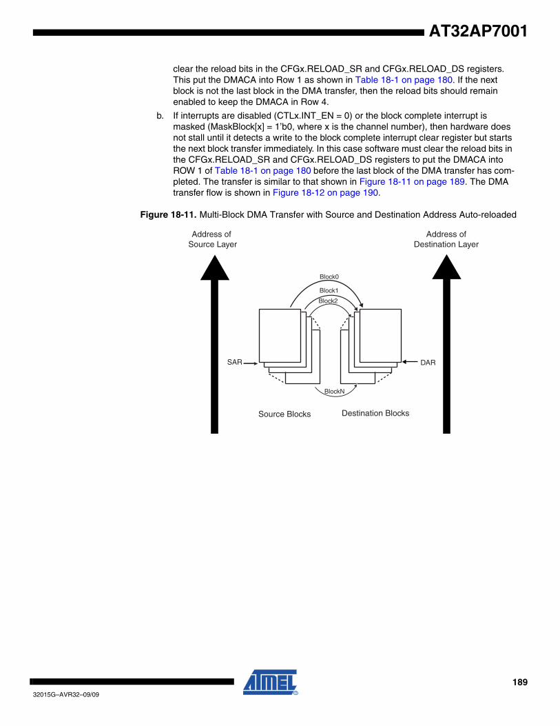
18932015G–AVR32–09/09
AT32AP7001
clear the reload bits in the CFGx.RELOAD_SR and CFGx.RELOAD_DS registers. This put the DMACA into Row 1 as shown in Table 18-1 on page 180. If the next block is not the last block in the DMA transfer, then the reload bits should remain enabled to keep the DMACA in Row 4.
b. If interrupts are disabled (CTLx.INT_EN = 0) or the block complete interrupt is masked (MaskBlock[x] = 1’b0, where x is the channel number), then hardware does not stall until it detects a write to the block complete interrupt clear register but starts the next block transfer immediately. In this case software must clear the reload bits in the CFGx.RELOAD_SR and CFGx.RELOAD_DS registers to put the DMACA into ROW 1 of Table 18-1 on page 180 before the last block of the DMA transfer has com-pleted. The transfer is similar to that shown in Figure 18-11 on page 189. The DMA transfer flow is shown in Figure 18-12 on page 190.
Figure 18-11. Multi-Block DMA Transfer with Source and Destination Address Auto-reloaded
Address of Source Layer
Address ofDestination Layer
Source Blocks Destination Blocks
BlockN
Block2
Block1
Block0
SAR DAR
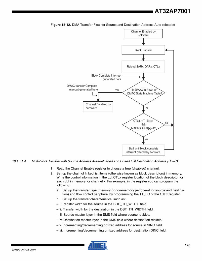
19032015G–AVR32–09/09
AT32AP7001
Figure 18-12. DMA Transfer Flow for Source and Destination Address Auto-reloaded
18.10.1.4 Multi-block Transfer with Source Address Auto-reloaded and Linked List Destination Address (Row7)
1. Read the Channel Enable register to choose a free (disabled) channel.
2. Set up the chain of linked list items (otherwise known as block descriptors) in memory. Write the control information in the LLI.CTLx register location of the block descriptor for each LLI in memory for channel x. For example, in the register you can program the following:
a. Set up the transfer type (memory or non-memory peripheral for source and destina-tion) and flow control peripheral by programming the TT_FC of the CTLx register.
b. Set up the transfer characteristics, such as:
– i. Transfer width for the source in the SRC_TR_WIDTH field.
– ii. Transfer width for the destination in the DST_TR_WIDTH field.
– iii. Source master layer in the SMS field where source resides.
– iv. Destination master layer in the DMS field where destination resides.
– v. Incrementing/decrementing or fixed address for source in SINC field.
– vi. Incrementing/decrementing or fixed address for destination DINC field.
Channel Enabled bysoftware
Block Transfer
Reload SARx, DARx, CTLx
Channel Disabled byhardware
Block Complete interruptgenerated here
DMAC transfer Complete interrupt generated here yes
no
yes
Stall until block completeinterrupt cleared by software
CTLx.INT_EN=1&&
MASKBLOCK[x]=1?
no
Is DMAC in Row1 of DMAC State Machine Table?
19132015G–AVR32–09/09
AT32AP7001
3. Write the starting source address in the SARx register for channel x.Note: The values in the LLI.SARx register locations of each of the Linked List Items (LLIs) setup up in
memory, although fetched during a LLI fetch, are not used.
4. Write the channel configuration information into the CFGx register for channel x.
a. Designate the handshaking interface type (hardware or software) for the source and destination peripherals. This is not required for memory. This step requires program-ming the HS_SEL_SRC/HS_SEL_DST bits, respectively. Writing a ‘0’ activates the hardware handshaking interface to handle source/destination requests for the spe-cific channel. Writing a ‘1’ activates the software handshaking interface source/destination requests.
b. If the hardware handshaking interface is activated for the source or destination peripheral, assign handshaking interface to the source and destination peripheral. This requires programming the SRC_PER and DEST_PER bits, respectively.
5. Make sure that the LLI.CTLx register locations of all LLIs in memory (except the last) are set as shown in Row 7 of Table 18-1 on page 180 while the LLI.CTLx register of the last Linked List item must be set as described in Row 1 or Row 5 of Table 18-1 on page 180. Figure 18-7 on page 179 shows a Linked List example with two list items.
6. Make sure that the LLI.LLPx register locations of all LLIs in memory (except the last) are non-zero and point to the next Linked List Item.
7. Make sure that the LLI.DARx register location of all LLIs in memory point to the start des-tination block address proceeding that LLI fetch.
8. Make sure that the LLI.CTLx.DONE field of the LLI.CTLx register locations of all LLIs in memory is cleared.
9. Clear any pending interrupts on the channel from the previous DMA transfer by writing to the Interrupt Clear registers: ClearTfr, ClearBlock, ClearSrcTran, ClearDstTran, ClearErr. Reading the Interrupt Raw Status and Interrupt Status registers confirms that all inter-rupts have been cleared.
10. Program the CTLx, CFGx registers according to Row 7 as shown in Table 18-1 on page 180.
11. Program the LLPx register with LLPx(0), the pointer to the first Linked List item.
12. Finally, enable the channel by writing a ‘1’ to the ChEnReg.CH_EN bit. The transfer is performed. Make sure that bit 0 of the DmaCfgReg register is enabled.
13. The DMACA fetches the first LLI from the location pointed to by LLPx(0).Note: The LLI.SARx, LLI.DARx, LLI. LLPx and LLI.CTLx registers are fetched. The LLI.SARx register
although fetched is not used.
14. Source and destination request single and burst DMACA transactions to transfer the block of data (assuming non-memory peripherals). DMACA acknowledges at the comple-tion of every transaction (burst and single) in the block and carry out the block transfer.
15. Table 18-1 on page 180The DMACA reloads the SARx register from the initial value. Hardware sets the block complete interrupt. The DMACA samples the row number as shown in Table 18-1 on page 180. If the DMACA is in Row 1 or 5, then the DMA transfer has completed. Hardware sets the transfer complete interrupt and disables the channel. You can either respond to the Block Complete or Transfer Complete interrupts, or poll for the Channel Enable (ChEnReg.CH_EN) bit until it is cleared by hardware, to detect when the transfer is complete. If the DMACA is not in Row 1 or 5 as shown in Table 18-1 on page 180 the following steps are performed.
16. The DMA transfer proceeds as follows:
a. If interrupts are enabled (CTLx.INT_EN = 1) and the block complete interrupt is un-masked (MaskBlock[x] = 1’b1, where x is the channel number) hardware sets the block complete interrupt when the block transfer has completed. It then stalls until the
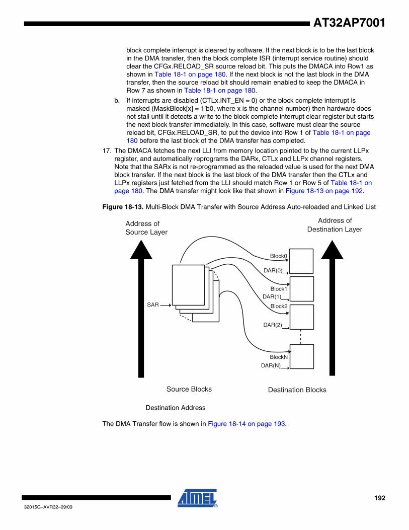
19232015G–AVR32–09/09
AT32AP7001
block complete interrupt is cleared by software. If the next block is to be the last block in the DMA transfer, then the block complete ISR (interrupt service routine) should clear the CFGx.RELOAD_SR source reload bit. This puts the DMACA into Row1 as shown in Table 18-1 on page 180. If the next block is not the last block in the DMA transfer, then the source reload bit should remain enabled to keep the DMACA in Row 7 as shown in Table 18-1 on page 180.
b. If interrupts are disabled (CTLx.INT_EN = 0) or the block complete interrupt is masked (MaskBlock[x] = 1’b0, where x is the channel number) then hardware does not stall until it detects a write to the block complete interrupt clear register but starts the next block transfer immediately. In this case, software must clear the source reload bit, CFGx.RELOAD_SR, to put the device into Row 1 of Table 18-1 on page 180 before the last block of the DMA transfer has completed.
17. The DMACA fetches the next LLI from memory location pointed to by the current LLPx register, and automatically reprograms the DARx, CTLx and LLPx channel registers. Note that the SARx is not re-programmed as the reloaded value is used for the next DMA block transfer. If the next block is the last block of the DMA transfer then the CTLx and LLPx registers just fetched from the LLI should match Row 1 or Row 5 of Table 18-1 on page 180. The DMA transfer might look like that shown in Figure 18-13 on page 192.
Figure 18-13. Multi-Block DMA Transfer with Source Address Auto-reloaded and Linked List
Destination Address
The DMA Transfer flow is shown in Figure 18-14 on page 193.
Address of Source Layer
Address ofDestination Layer
Source Blocks Destination Blocks
SAR
Block0
Block1
Block2
BlockN
DAR(N)
DAR(1)
DAR(0)
DAR(2)

19332015G–AVR32–09/09
AT32AP7001
Figure 18-14. DMA Transfer Flow for Source Address Auto-reloaded and Linked List Destina-tion Address
Channel Enabled bysoftware
LLI Fetch
yes
no
no
yes
Hardware reprograms DARx, CTLx, LLPx
DMAC block transfer
Source/destination status fetch
Reload SARx
Block Complete interruptgenerated here
DMAC Transfer Complete interrupt generated here
Channel Disabled byhardware
CTLx.INT_EN=1 &&
MASKBLOCK[X]=1 ?
Stall until block interruptCleared by hardware
Is DMAC inRow1 or Row5 of
DMAC State Machine Table?

19432015G–AVR32–09/09
AT32AP7001
18.10.1.5 Multi-block Transfer with Source Address Auto-reloaded and Contiguous Destination Address (Row 3)
1. Read the Channel Enable register to choose a free (disabled) channel.
2. Clear any pending interrupts on the channel from the previous DMA transfer by writing a ‘1’ to the Interrupt Clear registers: ClearTfr, ClearBlock, ClearSrcTran, ClearDstTran, ClearErr. Reading the Interrupt Raw Status and Interrupt Status registers confirms that all interrupts have been cleared.
3. Program the following channel registers:
a. Write the starting source address in the SARx register for channel x.
b. Write the starting destination address in the DARx register for channel x.
c. Program CTLx and CFGx according to Row 3 as shown in Table 18-1 on page 180. Program the LLPx register with ‘0’.
d. Write the control information for the DMA transfer in the CTLx register for channel x. For example, in this register, you can program the following:
– i. Set up the transfer type (memory or non-memory peripheral for source and destination) and flow control device by programming the TT_FC of the CTLx register.
– ii. Set up the transfer characteristics, such as:
– Transfer width for the source in the SRC_TR_WIDTH field.
– Transfer width for the destination in the DST_TR_WIDTH field.
– Source master layer in the SMS field where source resides.
– Destination master layer in the DMS field where destination resides.
– Incrementing/decrementing or fixed address for source in SINC field.
– Incrementing/decrementing or fixed address for destination in DINC field.
e. Write the channel configuration information into the CFGx register for channel x.
– i. Designate the handshaking interface type (hardware or software) for the source and destination peripherals. This is not required for memory. This step requires programming the HS_SEL_SRC/HS_SEL_DST bits, respectively. Writing a ‘0’ activates the hardware handshaking interface to handle source/destination requests for the specific channel. Writing a ‘1’ activates the software handshaking interface to handle source/destination requests.
– ii. If the hardware handshaking interface is activated for the source or destination peripheral, assign handshaking interface to the source and destination peripheral. This requires programming the SRC_PER and DEST_PER bits, respectively.
4. After the DMACA channel has been programmed, enable the channel by writing a ‘1’ to the ChEnReg.CH_EN bit. Make sure that bit 0 of the DmaCfgReg register is enabled.
5. Source and destination request single and burst DMACA transactions to transfer the block of data (assuming non-memory peripherals). The DMACA acknowledges at the completion of every transaction (burst and single) in the block and carries out the block transfer.
6. When the block transfer has completed, the DMACA reloads the SARx register. The DARx register remains unchanged. Hardware sets the block complete interrupt. The DMACA then samples the row number as shown in Table 18-1 on page 180. If the DMACA is in Row 1, then the DMA transfer has completed. Hardware sets the transfer complete interrupt and disables the channel. So you can either respond to the Block Complete or Transfer Complete interrupts, or poll for the Channel Enable (ChEn-
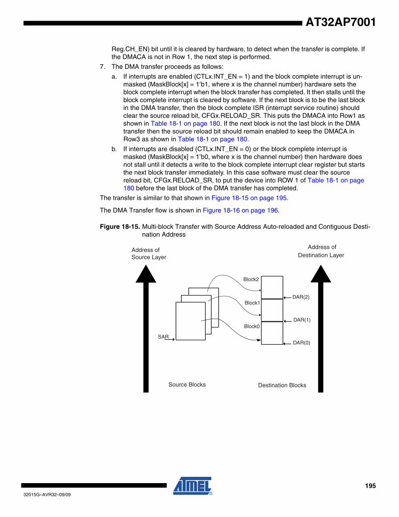
19532015G–AVR32–09/09
AT32AP7001
Reg.CH_EN) bit until it is cleared by hardware, to detect when the transfer is complete. If the DMACA is not in Row 1, the next step is performed.
7. The DMA transfer proceeds as follows:
a. If interrupts are enabled (CTLx.INT_EN = 1) and the block complete interrupt is un-masked (MaskBlock[x] = 1’b1, where x is the channel number) hardware sets the block complete interrupt when the block transfer has completed. It then stalls until the block complete interrupt is cleared by software. If the next block is to be the last block in the DMA transfer, then the block complete ISR (interrupt service routine) should clear the source reload bit, CFGx.RELOAD_SR. This puts the DMACA into Row1 as shown in Table 18-1 on page 180. If the next block is not the last block in the DMA transfer then the source reload bit should remain enabled to keep the DMACA in Row3 as shown in Table 18-1 on page 180.
b. If interrupts are disabled (CTLx.INT_EN = 0) or the block complete interrupt is masked (MaskBlock[x] = 1’b0, where x is the channel number) then hardware does not stall until it detects a write to the block complete interrupt clear register but starts the next block transfer immediately. In this case software must clear the source reload bit, CFGx.RELOAD_SR, to put the device into ROW 1 of Table 18-1 on page 180 before the last block of the DMA transfer has completed.
The transfer is similar to that shown in Figure 18-15 on page 195.
The DMA Transfer flow is shown in Figure 18-16 on page 196.
Figure 18-15. Multi-block Transfer with Source Address Auto-reloaded and Contiguous Desti-nation Address
Address of Source Layer
Address ofDestination Layer
Source Blocks Destination Blocks
SAR
Block0
Block1
Block2
DAR(1)
DAR(0)
DAR(2)
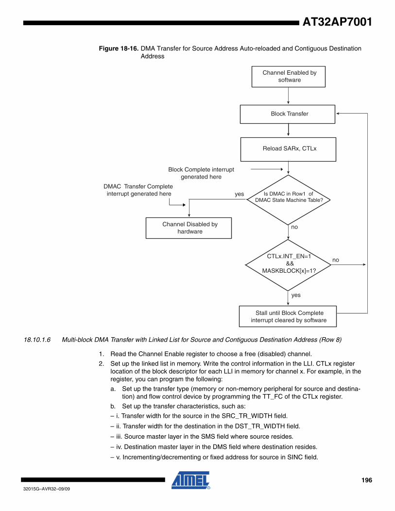
19632015G–AVR32–09/09
AT32AP7001
Figure 18-16. DMA Transfer for Source Address Auto-reloaded and Contiguous Destination Address
18.10.1.6 Multi-block DMA Transfer with Linked List for Source and Contiguous Destination Address (Row 8)
1. Read the Channel Enable register to choose a free (disabled) channel.
2. Set up the linked list in memory. Write the control information in the LLI. CTLx register location of the block descriptor for each LLI in memory for channel x. For example, in the register, you can program the following:
a. Set up the transfer type (memory or non-memory peripheral for source and destina-tion) and flow control device by programming the TT_FC of the CTLx register.
b. Set up the transfer characteristics, such as:
– i. Transfer width for the source in the SRC_TR_WIDTH field.
– ii. Transfer width for the destination in the DST_TR_WIDTH field.
– iii. Source master layer in the SMS field where source resides.
– iv. Destination master layer in the DMS field where destination resides.
– v. Incrementing/decrementing or fixed address for source in SINC field.
Channel Enabled bysoftware
Block Transfer
Reload SARx, CTLx
Channel Disabled byhardware
Block Complete interruptgenerated here
DMAC Transfer Complete interrupt generated here yes
no
no
yes
Stall until Block Completeinterrupt cleared by software
CTLx.INT_EN=1&&
MASKBLOCK[x]=1?
Is DMAC in Row1 of DMAC State Machine Table?
19732015G–AVR32–09/09
AT32AP7001
– vi. Incrementing/decrementing or fixed address for destination DINC field.
3. Write the starting destination address in the DARx register for channel x.Note: The values in the LLI.DARx register location of each Linked List Item (LLI) in memory, although
fetched during an LLI fetch, are not used.
4. Write the channel configuration information into the CFGx register for channel x.
a. Designate the handshaking interface type (hardware or software) for the source and destination peripherals. This is not required for memory. This step requires program-ming the HS_SEL_SRC/HS_SEL_DST bits, respectively. Writing a ‘0’ activates the hardware handshaking interface to handle source/destination requests for the spe-cific channel. Writing a ‘1’ activates the software handshaking interface to handle source/destination requests.
b. If the hardware handshaking interface is activated for the source or destination peripheral, assign handshaking interface to the source and destination peripherals. This requires programming the SRC_PER and DEST_PER bits, respectively.
5. Make sure that all LLI.CTLx register locations of the LLI (except the last) are set as shown in Row 8 of Table 18-1 on page 180, while the LLI.CTLx register of the last Linked List item must be set as described in Row 1 or Row 5 of Table 18-1 on page 180. Figure 18-7 on page 179 shows a Linked List example with two list items.
6. Make sure that the LLI.LLPx register locations of all LLIs in memory (except the last) are non-zero and point to the next Linked List Item.
7. Make sure that the LLI.SARx register location of all LLIs in memory point to the start source block address proceeding that LLI fetch.
8. Make sure that the LLI.CTLx.DONE field of the LLI.CTLx register locations of all LLIs in memory is cleared.
9. Clear any pending interrupts on the channel from the previous DMA transfer by writing a ‘1’ to the Interrupt Clear registers: ClearTfr, ClearBlock, ClearSrcTran, ClearDstTran, ClearErr. Reading the Interrupt Raw Status and Interrupt Status registers confirms that all interrupts have been cleared.
10. Program the CTLx, CFGx registers according to Row 8 as shown in Table 18-1 on page 180
11. Program the LLPx register with LLPx(0), the pointer to the first Linked List item.
12. Finally, enable the channel by writing a ‘1’ to the ChEnReg.CH_EN bit. The transfer is performed. Make sure that bit 0 of the DmaCfgReg register is enabled.
13. The DMACA fetches the first LLI from the location pointed to by LLPx(0). Note: The LLI.SARx, LLI.DARx, LLI.LLPx and LLI.CTLx registers are fetched. The LLI.DARx register
location of the LLI although fetched is not used. The DARx register in the DMACA remains unchanged.
14. Source and destination requests single and burst DMACA transactions to transfer the block of data (assuming non-memory peripherals). The DMACA acknowledges at the completion of every transaction (burst and single) in the block and carry out the block transfer.
Note:
15. The DMACA does not wait for the block interrupt to be cleared, but continues and fetches the next LLI from the memory location pointed to by current LLPx register and automati-cally reprograms the SARx, CTLx and LLPx channel registers. The DARx register is left unchanged. The DMA transfer continues until the DMACA samples the CTLx and LLPx registers at the end of a block transfer match that described in Row 1 or Row 5 of Table 18-1 on page 180. The DMACA then knows that the previous block transferred was the last block in the DMA transfer.
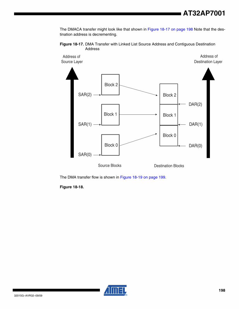
19832015G–AVR32–09/09
AT32AP7001
The DMACA transfer might look like that shown in Figure 18-17 on page 198 Note that the des-tination address is decrementing.
Figure 18-17. DMA Transfer with Linked List Source Address and Contiguous Destination Address
The DMA transfer flow is shown in Figure 18-19 on page 199.
Figure 18-18.
SAR(2)
SAR(1)
SAR(0)
DAR(2)
DAR(1)
DAR(0)
Block 2
Block 1
Block 0
Block 0
Block 1
Block 2
Address of Source Layer
Address ofDestination Layer
Source Blocks Destination Blocks
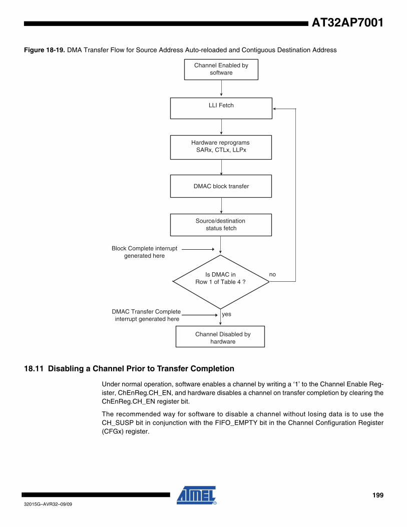
19932015G–AVR32–09/09
AT32AP7001
Figure 18-19. DMA Transfer Flow for Source Address Auto-reloaded and Contiguous Destination Address
18.11 Disabling a Channel Prior to Transfer Completion
Under normal operation, software enables a channel by writing a ‘1’ to the Channel Enable Reg-ister, ChEnReg.CH_EN, and hardware disables a channel on transfer completion by clearing theChEnReg.CH_EN register bit.
The recommended way for software to disable a channel without losing data is to use theCH_SUSP bit in conjunction with the FIFO_EMPTY bit in the Channel Configuration Register(CFGx) register.
Channel Enabled bysoftware
LLI Fetch
Hardware reprograms SARx, CTLx, LLPx
DMAC block transfer
Source/destination status fetch
Is DMAC inRow 1 of Table 4 ?
Channel Disabled byhardware
Block Complete interruptgenerated here
DMAC Transfer Complete interrupt generated here
yes
no
20032015G–AVR32–09/09
AT32AP7001
1. If software wishes to disable a channel prior to the DMA transfer completion, then it can set the CFGx.CH_SUSP bit to tell the DMACA to halt all transfers from the source periph-eral. Therefore, the channel FIFO receives no new data.
2. Software can now poll the CFGx.FIFO_EMPTY bit until it indicates that the channel FIFO is empty.
3. The ChEnReg.CH_EN bit can then be cleared by software once the channel FIFO is empty.
When CTLx.SRC_TR_WIDTH is less than CTLx.DST_TR_WIDTH and the CFGx.CH_SUSP bitis high, the CFGx.FIFO_EMPTY is asserted once the contents of the FIFO do not permit a singleword of CTLx.DST_TR_WIDTH to be formed. However, there may still be data in the channelFIFO but not enough to form a single transfer of CTLx.DST_TR_WIDTH width. In this configura-tion, once the channel is disabled, the remaining data in the channel FIFO are not transferred tothe destination peripheral. It is permitted to remove the channel from the suspension state bywriting a ‘0’ to the CFGx.CH_SUSP register. The DMA transfer completes in the normal manner.
Note: If a channel is disabled by software, an active single or burst transaction is not guaranteed to receive an acknowledgement.
18.11.1 Abnormal Transfer Termination
A DMACA DMA transfer may be terminated abruptly by software by clearing the channel enablebit, ChEnReg.CH_EN. This does not mean that the channel is disabled immediately after theChEnReg.CH_EN bit is cleared over the HSB slave interface. Consider this as a request to dis-able the channel. The ChEnReg.CH_EN must be polled and then it must be confirmed that thechannel is disabled by reading back 0. A case where the channel is not be disabled after a chan-nel disable request is where either the source or destination has received a split or retryresponse. The DMACA must keep re-attempting the transfer to the system HADDR that origi-nally received the split or retry response until an OKAY response is returned. To do otherwise isan System Bus protocol violation.
Software may terminate all channels abruptly by clearing the global enable bit in the DMACAConfiguration Register (DmaCfgReg[0]). Again, this does not mean that all channels are dis-abled immediately after the DmaCfgReg[0] is cleared over the HSB slave interface. Considerthis as a request to disable all channels. The ChEnReg must be polled and then it must be con-firmed that all channels are disabled by reading back ‘0’.
Note: If the channel enable bit is cleared while there is data in the channel FIFO, this data is not sent to the destination peripheral and is not present when the channel is re-enabled. For read sensitive source peripherals such as a source FIFO this data is therefore lost. When the source is not a read sensitive device (i.e., memory), disabling a channel without waiting for the channel FIFO to empty may be acceptable as the data is available from the source peripheral upon request and is not lost.
Note: If a channel is disabled by software, an active single or burst transaction is not guaranteed to receive an acknowledgement.
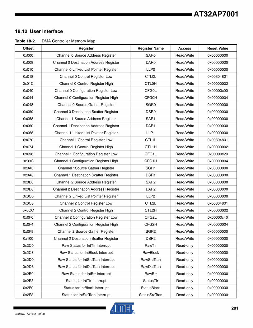
20132015G–AVR32–09/09
AT32AP7001
18.12 User Interface
Table 18-2. DMA Controller Memory Map
Offset Register Register Name Access Reset Value
0x000 Channel 0 Source Address Register SAR0 Read/Write 0x00000000
0x008 Channel 0 Destination Address Register DAR0 Read/Write 0x00000000
0x010 Channel 0 Linked List Pointer Register LLP0 Read/Write 0x00000000
0x018 Channel 0 Control Register Low CTL0L Read/Write 0x00304801
0x01C Channel 0 Control Register High CTL0H Read/Write 0x00000002
0x040 Channel 0 Configuration Register Low CFG0L Read/Write 0x00000c00
0x044 Channel 0 Configuration Register High CFG0H Read/Write 0x00000004
0x048 Channel 0 Source Gather Register SGR0 Read/Write 0x00000000
0x050 Channel 0 Destination Scatter Register DSR0 Read/Write 0x00000000
0x058 Channel 1 Source Address Register SAR1 Read/Write 0x00000000
0x060 Channel 1 Destination Address Register DAR1 Read/Write 0x00000000
0x068 Channel 1 Linked List Pointer Register LLP1 Read/Write 0x00000000
0x070 Channel 1 Control Register Low CTL1L Read/Write 0x00304801
0x074 Channel 1 Control Register High CTL1H Read/Write 0x00000002
0x098 Channel 1 Configuration Register Low CFG1L Read/Write 0x00000c20
0x09C Channel 1 Configuration Register High CFG1H Read/Write 0x00000004
0x0A0 Channel 1Source Gather Register SGR1 Read/Write 0x00000000
0x0A8 Channel 1 Destination Scatter Register DSR1 Read/Write 0x00000000
0x0B0 Channel 2 Source Address Register SAR2 Read/Write 0x00000000
0x0B8 Channel 2 Destination Address Register DAR2 Read/Write 0x00000000
0x0C0 Channel 2 Linked List Pointer Register LLP2 Read/Write 0x00000000
0x0C8 Channel 2 Control Register Low CTL2L Read/Write 0x00304801
0x0CC Channel 2 Control Register High CTL2H Read/Write 0x00000002
0x0F0 Channel 2 Configuration Register Low CFG2L Read/Write 0x00000c40
0x0F4 Channel 2 Configuration Register High CFG2H Read/Write 0x00000004
0x0F8 Channel 2 Source Gather Register SGR2 Read/Write 0x00000000
0x100 Channel 2 Destination Scatter Register DSR2 Read/Write 0x00000000
0x2C0 Raw Status for IntTfr Interrupt RawTfr Read-only 0x00000000
0x2C8 Raw Status for IntBlock Interrupt RawBlock Read-only 0x00000000
0x2D0 Raw Status for IntSrcTran Interrupt RawSrcTran Read-only 0x00000000
0x2D8 Raw Status for IntDstTran Interrupt RawDstTran Read-only 0x00000000
0x2E0 Raw Status for IntErr Interrupt RawErr Read-only 0x00000000
0x2E8 Status for IntTfr Interrupt StatusTfr Read-only 0x00000000
0x2F0 Status for IntBlock Interrupt StatusBlock Read-only 0x00000000
0x2F8 Status for IntSrcTran Interrupt StatusSrcTran Read-only 0x00000000

20232015G–AVR32–09/09
AT32AP7001
0x300 Status for IntDstTran Interrupt StatusDstTran Read-only 0x00000000
0x308 Status for IntErr Interrupt StatusErr Read-only 0x00000000
0x310 Mask for IntTfr Interrupt MaskTfr Read/Write 0x00000000
0x318 Mask for IntBlock Interrupt MaskBlock Read/Write 0x00000000
0x320 Mask for IntSrcTran Interrupt MaskSrcTran Read/Write 0x00000000
0x328 Mask for IntDstTran Interrupt MaskDstTran Read/Write 0x00000000
0x330 Mask for IntErr Interrupt MaskErr Read/Write 0x00000000
0x338 Clear for IntTfr Interrupt ClearTfr Write-only 0x00000000
0x340 Clear for IntBlock Interrupt ClearBlock Write-only 0x00000000
0x348 Clear for IntSrcTran Interrupt ClearSrcTran Write-only 0x00000000
0x350 Clear for IntDstTran Interrupt ClearDstTran Write-only 0x00000000
0x358 Clear for IntErr Interrupt ClearErr Write-only 0x00000000
0x360 Status for each interrupt type StatusInt Read-only 0x00000000
0x368 Source Software Transaction Request Register ReqSrcReg Read/Write 0x00000000
0x370 Destination Software Transaction Request Register ReqDstReg Read/Write 0x00000000
0x378 Single Source Transaction Request Register SglReqSrcReg Read/Write 0x00000000
0x380 Single Destination Transaction Request Register SglReqDstReg Read/Write 0x00000000
0x388 Last Source Transaction Request Register LstSrcReg Read/Write 0x00000000
0x390 Last Destination Transaction Request Register LstDstReg Read/Write 0x00000000
0x398 DMA Configuration Register DmaCfgReg Read/Write 0x00000000
0x3A0 DMA Channel Enable Register ChEnReg Read/Write 0x00000000
0x3F8 DMA Component ID Register Low DmaCompIdRegL Read-only 0x44571110
0x3FC DMA Component ID Register High DmaCompIdRegH Read-only 0x3230362A
Table 18-2. DMA Controller Memory Map (Continued)
Offset Register Register Name Access Reset Value
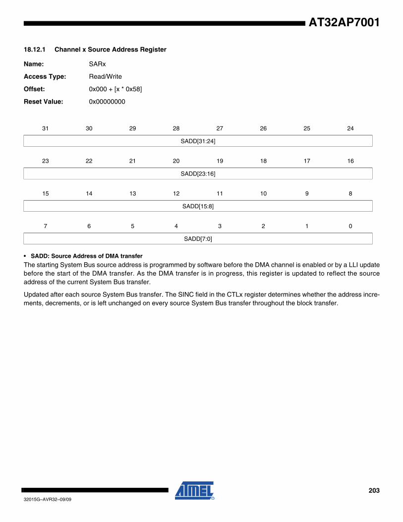
20332015G–AVR32–09/09
AT32AP7001
18.12.1 Channel x Source Address Register
Name: SARx
Access Type: Read/Write
Offset: 0x000 + [x * 0x58]
Reset Value: 0x00000000
• SADD: Source Address of DMA transfer
The starting System Bus source address is programmed by software before the DMA channel is enabled or by a LLI updatebefore the start of the DMA transfer. As the DMA transfer is in progress, this register is updated to reflect the sourceaddress of the current System Bus transfer.
Updated after each source System Bus transfer. The SINC field in the CTLx register determines whether the address incre-ments, decrements, or is left unchanged on every source System Bus transfer throughout the block transfer.
31 30 29 28 27 26 25 24
SADD[31:24]
23 22 21 20 19 18 17 16
SADD[23:16]
15 14 13 12 11 10 9 8
SADD[15:8]
7 6 5 4 3 2 1 0
SADD[7:0]

20432015G–AVR32–09/09
AT32AP7001
18.12.2 Channel x Destination Address Register
Name: DARx
Access Type: Read/Write
Offset: 0x008 + [x * 0x58]
Reset Value: 0x00000000
• DADD: Destination Address of DMA transfer
The starting System Bus destination address is programmed by software before the DMA channel is enabled or by a LLIupdate before the start of the DMA transfer. As the DMA transfer is in progress, this register is updated to reflect the desti-nation address of the current System Bus transfer.
Updated after each destination System Bus transfer. The DINC field in the CTLx register determines whether the addressincrements, decrements or is left unchanged on every destination System Bus transfer throughout the block transfer.
31 30 29 28 27 26 25 24
DADD[31:24]
23 22 21 20 19 18 17 16
DADD[23:16]
15 14 13 12 11 10 9 8
DADD[15:8]
7 6 5 4 3 2 1 0
DADD[7:0]
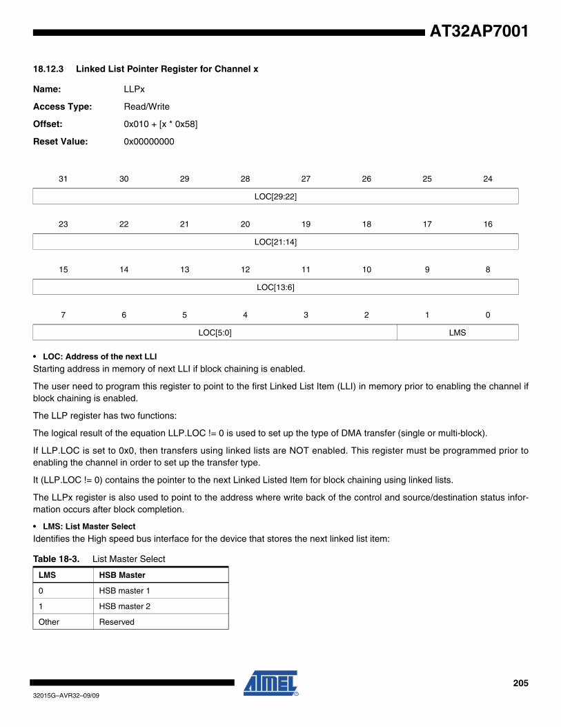
20532015G–AVR32–09/09
AT32AP7001
18.12.3 Linked List Pointer Register for Channel x
Name: LLPx
Access Type: Read/Write
Offset: 0x010 + [x * 0x58]
Reset Value: 0x00000000
• LOC: Address of the next LLI
Starting address in memory of next LLI if block chaining is enabled.
The user need to program this register to point to the first Linked List Item (LLI) in memory prior to enabling the channel ifblock chaining is enabled.
The LLP register has two functions:
The logical result of the equation LLP.LOC != 0 is used to set up the type of DMA transfer (single or multi-block).
If LLP.LOC is set to 0x0, then transfers using linked lists are NOT enabled. This register must be programmed prior toenabling the channel in order to set up the transfer type.
It (LLP.LOC != 0) contains the pointer to the next Linked Listed Item for block chaining using linked lists.
The LLPx register is also used to point to the address where write back of the control and source/destination status infor-mation occurs after block completion.
• LMS: List Master Select
Identifies the High speed bus interface for the device that stores the next linked list item:
31 30 29 28 27 26 25 24
LOC[29:22]
23 22 21 20 19 18 17 16
LOC[21:14]
15 14 13 12 11 10 9 8
LOC[13:6]
7 6 5 4 3 2 1 0
LOC[5:0] LMS
Table 18-3. List Master Select
LMS HSB Master
0 HSB master 1
1 HSB master 2
Other Reserved
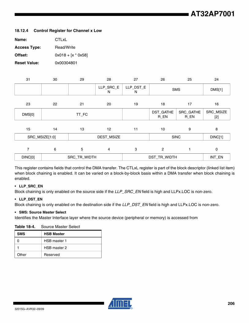
20632015G–AVR32–09/09
AT32AP7001
18.12.4 Control Register for Channel x Low
Name: CTLxL
Access Type: Read/Write
Offset: 0x018 + [x * 0x58]
Reset Value: 0x00304801
This register contains fields that control the DMA transfer. The CTLxL register is part of the block descriptor (linked list item)when block chaining is enabled. It can be varied on a block-by-block basis within a DMA transfer when block chaining isenabled.
• LLP_SRC_EN
Block chaining is only enabled on the source side if the LLP_SRC_EN field is high and LLPx.LOC is non-zero.
• LLP_DST_EN
Block chaining is only enabled on the destination side if the LLP_DST_EN field is high and LLPx.LOC is non-zero.
• SMS: Source Master Select
Identifies the Master Interface layer where the source device (peripheral or memory) is accessed from
31 30 29 28 27 26 25 24
LLP_SRC_EN
LLP_DST_EN
SMS DMS[1]
23 22 21 20 19 18 17 16
DMS[0] TT_FCDST_GATHE
R_ENSRC_GATHE
R_ENSRC_MSIZE
[2]
15 14 13 12 11 10 9 8
SRC_MSIZE[1:0] DEST_MSIZE SINC DINC[1]
7 6 5 4 3 2 1 0
DINC[0] SRC_TR_WIDTH DST_TR_WIDTH INT_EN
Table 18-4. Source Master Select
SMS HSB Master
0 HSB master 1
1 HSB master 2
Other Reserved

20732015G–AVR32–09/09
AT32AP7001
• DMS: Destination Master Select
Identifies the Master Interface layer where the destination device (peripheral or memory) resides
• TT_FC: Transfer Type and Flow Control
The four following transfer types are supported:
• Memory to Memory, Memory to Peripheral, Peripheral to Memory and Peripheral to Peripheral.
The DMACA is always the Flow Controller.
• DST_SCATTER_EN: Destination Scatter Enable0 = Scatter disabled1 = Scatter enabled
Scatter on the destination side is applicable only when the CTLx.DINC bit indicates an incrementing or decrementingaddress control.
Important note: This bit is only implemented for channel 1, not for channels 0 and 2.• SRC_GATHER_EN: Source Gather Enable
0 = Gather disabled1 = Gather enabled
Gather on the source side is applicable only when the CTLx.SINC bit indicates an incrementing or decrementing addresscontrol.
Important note: This bit is only implemented for channel 1, not for channels 0 and 2.• SRC_MSIZE: Source Burst Transaction Length
Number of data items, each of width CTLx.SRC_TR_WIDTH, to be read from the source every time a source burst transac-tion request is made from either the corresponding hardware or software handshaking interface.
Table 18-5. Destination Master Select
DMS HSB Master
0 HSB master 1
1 HSB master 2
Other Reserved
TT_FC Transfer Type Flow Controller
000 Memory to Memory DMACA
001 Memory to Peripheral DMACA
010 Peripheral to Memory DMACA
011 Peripheral to Peripheral DMACA
Other Reserved Reserved
SRC_MSIZE Size (items number)
0 1
1 4
2 8
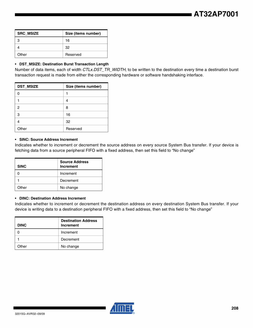
20832015G–AVR32–09/09
AT32AP7001
• DST_MSIZE: Destination Burst Transaction Length
Number of data items, each of width CTLx.DST_TR_WIDTH, to be written to the destination every time a destination bursttransaction request is made from either the corresponding hardware or software handshaking interface.
• SINC: Source Address Increment
Indicates whether to increment or decrement the source address on every source System Bus transfer. If your device isfetching data from a source peripheral FIFO with a fixed address, then set this field to “No change”
• DINC: Destination Address Increment
Indicates whether to increment or decrement the destination address on every destination System Bus transfer. If yourdevice is writing data to a destination peripheral FIFO with a fixed address, then set this field to “No change”
3 16
4 32
Other Reserved
DST_MSIZE Size (items number)
0 1
1 4
2 8
3 16
4 32
Other Reserved
SINCSource Address Increment
0 Increment
1 Decrement
Other No change
DINCDestination Address Increment
0 Increment
1 Decrement
Other No change
SRC_MSIZE Size (items number)
20932015G–AVR32–09/09
AT32AP7001
• SRT_TR_WIDTH: Source Transfer Width• DSC_TR_WIDTH: Destination Transfer Width
• INT_EN: Interrupt Enable Bit
If set, then all five interrupt generating sources are enabled.
SRC_TR_WIDTH/DST_TR_WIDTH Size (bits)
0 8
1 16
2 32
Other Reserved
21032015G–AVR32–09/09
AT32AP7001
18.12.5 Control Register for Channel x High
Name: CTLxH
Access Type: Read/Write
Offset: 0x01C + [x * 0x58]
Reset Value: 0x00000002
• DONE: Done Bit
Software can poll this bit to see when a block transfer is complete
• BLOCK_TS: Block Transfer Size
When the DMACA is flow controller, this field is written by the user before the channel is enabled to indicate the block size.
The number programmed into BLOCK_TS indicates the total number of single transactions to perform for every blocktransfer, unless the transfer is already in progress, in which case the value of BLOCK_TS indicates the number of singletransactions that have been performed so far.
The width of the single transaction is determined by CTLx.SRC_TR_WIDTH.
31 30 29 28 27 26 25 24
- - - - - - - -
23 22 21 20 19 18 17 16
- - - - - - - -
15 14 13 12 11 10 9 8
- - - DONE BLOCK_TS[11:8]
7 6 5 4 3 2 1 0
BLOCK_TS[7:0]
21132015G–AVR32–09/09
AT32AP7001
18.12.6 Configuration Register for Channel x Low
Name: CFGxL
Access Type: Read/Write
Offset: 0x040 + [x * 0x58]
• Reset Value: 0x00000C00 + [x * 0x20]
• RELOAD_DST: Automatic Destination Reload
The DARx register can be automatically reloaded from its initial value at the end of every block for multi-block transfers. Anew block transfer is then initiated.
• RELOAD_SRC: Automatic Source Reload
The SARx register can be automatically reloaded from its initial value at the end of every block for multi-block transfers. Anew block transfer is then initiated.
• SRC_HS_POL: Source Handshaking Interface Polarity0 = Active high
1 = Active low• DST_HS_POL: Destination Handshaking Interface Polarity
0 = Active high1 = Active low
• HS_SEL_SRC: Source Software or Hardware Handshaking Select
This register selects which of the handshaking interfaces, hardware or software, is active for source requests on thischannel.
0 = Hardware handshaking interface. Software-initiated transaction requests are ignored.
1 = Software handshaking interface. Hardware-initiated transaction requests are ignored.
If the source peripheral is memory, then this bit is ignored.
• HS_SEL_DST: Destination Software or Hardware Handshaking Select
This register selects which of the handshaking interfaces, hardware or software, is active for destination requests on thischannel.
31 30 29 28 27 26 25 24
RELOAD_DST
RELOAD_SRC
- - - - - -
23 22 21 20 19 18 17 16
- - - - SRC_HS_POL
DST_HS_POL
- -
15 14 13 12 11 10 9 8
- - HS_SEL_SRC
HS_SEL_DST
FIFO_EMPTY
CH_SUSP
7 6 5 4 3 2 1 0
CH_PRIOR - - - - -
21232015G–AVR32–09/09
AT32AP7001
0 = Hardware handshaking interface. Software-initiated transaction requests are ignored.1 = Software handshaking interface. Hardware Initiated transaction requests are ignored.
If the destination peripheral is memory, then this bit is ignored.
• FIFO_EMPTY
Indicates if there is data left in the channel's FIFO. Can be used in conjunction with CFGx.CH_SUSP to cleanly disable achannel.
1 = Channel's FIFO empty
0 = Channel's FIFO not empty
• CH_SUSP: Channel Suspend
Suspends all DMA data transfers from the source until this bit is cleared. There is no guarantee that the current transactionwill complete. Can also be used in conjunction with CFGx.FIFO_EMPTY to cleanly disable a channel without losing anydata.
0 = Not Suspended.
1 = Suspend. Suspend DMA transfer from the source.
• CH_PRIOR: Channel priority
A priority of 7 is the highest priority, and 0 is the lowest. This field must be programmed within the following range [0, x-1].
A programmed value outside this range causes erroneous behavior.
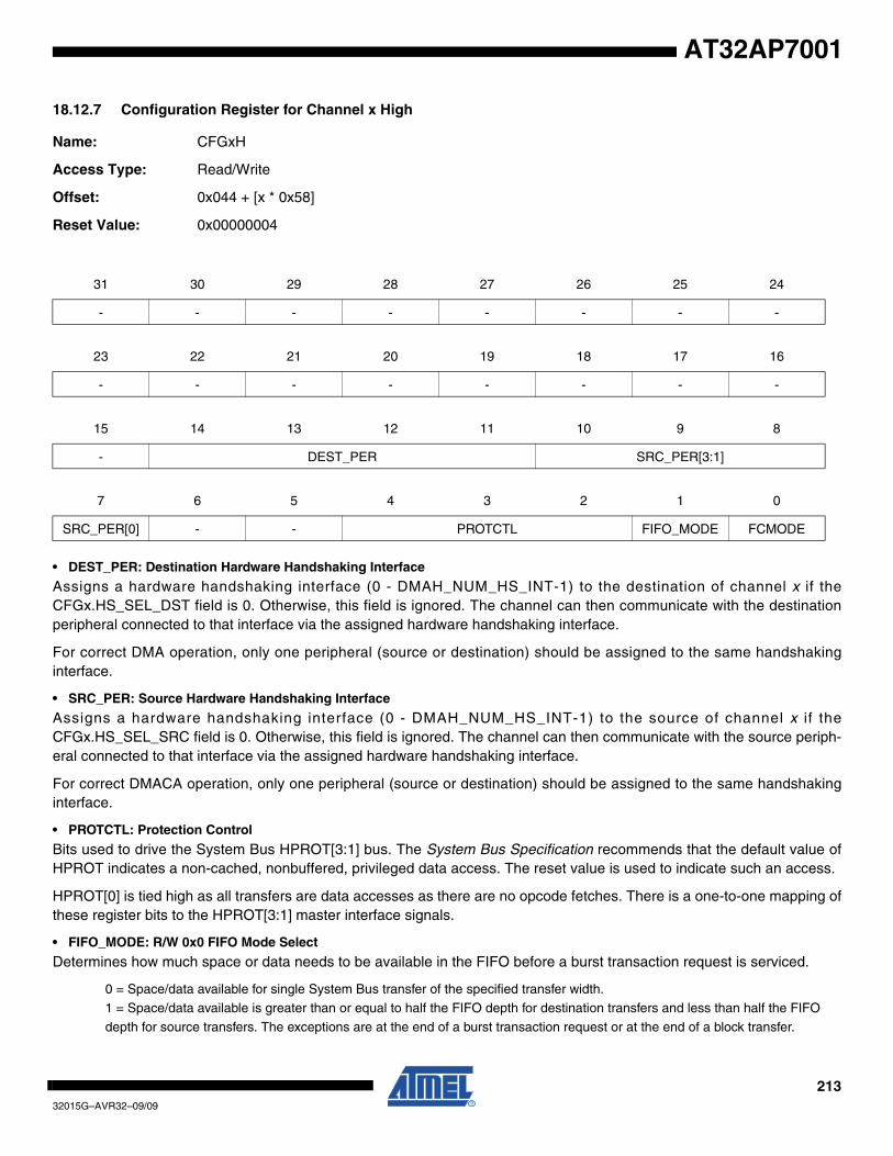
21332015G–AVR32–09/09
AT32AP7001
18.12.7 Configuration Register for Channel x High
Name: CFGxH
Access Type: Read/Write
Offset: 0x044 + [x * 0x58]
Reset Value: 0x00000004
• DEST_PER: Destination Hardware Handshaking Interface
Assigns a hardware handshaking interface (0 - DMAH_NUM_HS_INT-1) to the destination of channel x if theCFGx.HS_SEL_DST field is 0. Otherwise, this field is ignored. The channel can then communicate with the destinationperipheral connected to that interface via the assigned hardware handshaking interface.
For correct DMA operation, only one peripheral (source or destination) should be assigned to the same handshakinginterface.
• SRC_PER: Source Hardware Handshaking Interface
Assigns a hardware handshaking interface (0 - DMAH_NUM_HS_INT-1) to the source of channel x i f theCFGx.HS_SEL_SRC field is 0. Otherwise, this field is ignored. The channel can then communicate with the source periph-eral connected to that interface via the assigned hardware handshaking interface.
For correct DMACA operation, only one peripheral (source or destination) should be assigned to the same handshakinginterface.
• PROTCTL: Protection Control
Bits used to drive the System Bus HPROT[3:1] bus. The System Bus Specification recommends that the default value ofHPROT indicates a non-cached, nonbuffered, privileged data access. The reset value is used to indicate such an access.
HPROT[0] is tied high as all transfers are data accesses as there are no opcode fetches. There is a one-to-one mapping ofthese register bits to the HPROT[3:1] master interface signals.
• FIFO_MODE: R/W 0x0 FIFO Mode Select
Determines how much space or data needs to be available in the FIFO before a burst transaction request is serviced.
0 = Space/data available for single System Bus transfer of the specified transfer width.1 = Space/data available is greater than or equal to half the FIFO depth for destination transfers and less than half the FIFO
depth for source transfers. The exceptions are at the end of a burst transaction request or at the end of a block transfer.
31 30 29 28 27 26 25 24
- - - - - - - -
23 22 21 20 19 18 17 16
- - - - - - - -
15 14 13 12 11 10 9 8
- DEST_PER SRC_PER[3:1]
7 6 5 4 3 2 1 0
SRC_PER[0] - - PROTCTL FIFO_MODE FCMODE

21432015G–AVR32–09/09
AT32AP7001
• FCMODE: Flow Control Mode
Determines when source transaction requests are serviced when the Destination Peripheral is the flow controller.
0 = Source transaction requests are serviced when they occur. Data pre-fetching is enabled.
1 = Source transaction requests are not serviced until a destination transaction request occurs. In this mode the amount of data transferred from the source is limited such that it is guaranteed to be transferred to the destination prior to block termination by
the destination. Data pre-fetching is disabled.
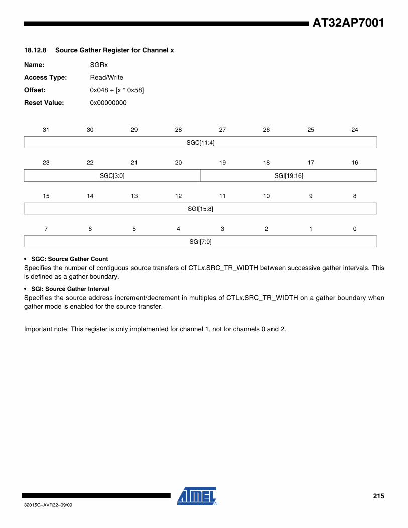
21532015G–AVR32–09/09
AT32AP7001
18.12.8 Source Gather Register for Channel x
Name: SGRx
Access Type: Read/Write
Offset: 0x048 + [x * 0x58]
Reset Value: 0x00000000
• SGC: Source Gather Count
Specifies the number of contiguous source transfers of CTLx.SRC_TR_WIDTH between successive gather intervals. Thisis defined as a gather boundary.
• SGI: Source Gather Interval
Specifies the source address increment/decrement in multiples of CTLx.SRC_TR_WIDTH on a gather boundary whengather mode is enabled for the source transfer.
Important note: This register is only implemented for channel 1, not for channels 0 and 2.
31 30 29 28 27 26 25 24
SGC[11:4]
23 22 21 20 19 18 17 16
SGC[3:0] SGI[19:16]
15 14 13 12 11 10 9 8
SGI[15:8]
7 6 5 4 3 2 1 0
SGI[7:0]
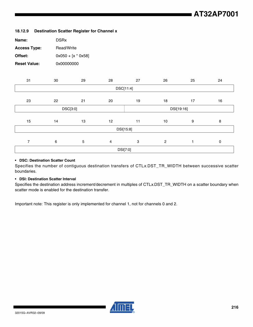
21632015G–AVR32–09/09
AT32AP7001
18.12.9 Destination Scatter Register for Channel x
Name: DSRx
Access Type: Read/Write
Offset: 0x050 + [x * 0x58]
Reset Value: 0x00000000
• DSC: Destination Scatter Count
Specifies the number of contiguous destination transfers of CTLx.DST_TR_WIDTH between successive scatterboundaries.
• DSI: Destination Scatter Interval
Specifies the destination address increment/decrement in multiples of CTLx.DST_TR_WIDTH on a scatter boundary whenscatter mode is enabled for the destination transfer.
Important note: This register is only implemented for channel 1, not for channels 0 and 2.
31 30 29 28 27 26 25 24
DSC[11:4]
23 22 21 20 19 18 17 16
DSC[3:0] DSI[19:16]
15 14 13 12 11 10 9 8
DSI[15:8]
7 6 5 4 3 2 1 0
DSI[7:0]

21732015G–AVR32–09/09
AT32AP7001
18.12.10 Interrupt Registers
The following sections describe the registers pertaining to interrupts, their status, and how to clear them. For each channel,there are five types of interrupt sources:
• IntTfr: DMA Transfer Complete Interrupt
This interrupt is generated on DMA transfer completion to the destination peripheral.
• IntBlock: Block Transfer Complete Interrupt
This interrupt is generated on DMA block transfer completion to the destination peripheral.
• IntSrcTran: Source Transaction Complete Interrupt
This interrupt is generated after completion of the last System Bus transfer of the requested single/burst transaction fromthe handshaking interface on the source side.
If the source for a channel is memory, then that channel never generates a IntSrcTran interrupt and hence the correspond-ing bit in this field is not set.
• IntDstTran: Destination Transaction Complete Interrupt
This interrupt is generated after completion of the last System Bus transfer of the requested single/burst transaction fromthe handshaking interface on the destination side.
If the destination for a channel is memory, then that channel never generates the IntDstTran interrupt and hence the corre-sponding bit in this field is not set.
• IntErr: Error Interrupt
This interrupt is generated when an ERROR response is received from an HSB slave on the HRESP bus during a DMAtransfer. In addition, the DMA transfer is cancelled and the channel is disabled.
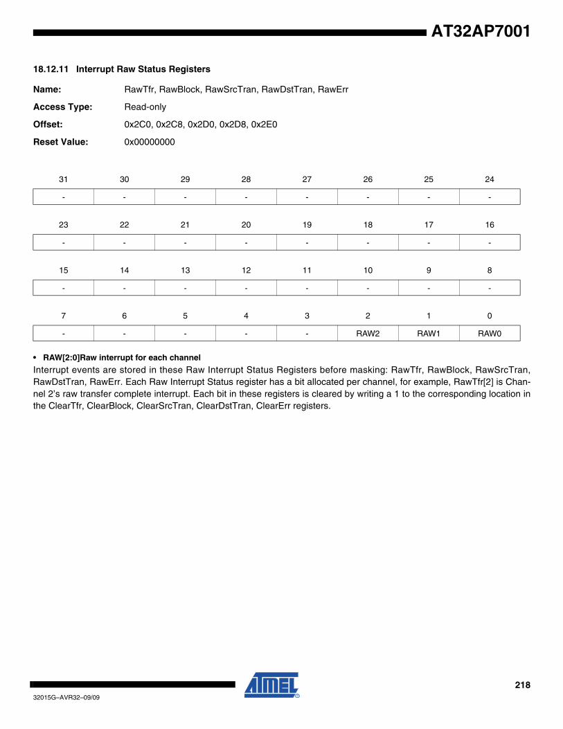
21832015G–AVR32–09/09
AT32AP7001
18.12.11 Interrupt Raw Status Registers
Name: RawTfr, RawBlock, RawSrcTran, RawDstTran, RawErr
Access Type: Read-only
Offset: 0x2C0, 0x2C8, 0x2D0, 0x2D8, 0x2E0
Reset Value: 0x00000000
• RAW[2:0]Raw interrupt for each channel
Interrupt events are stored in these Raw Interrupt Status Registers before masking: RawTfr, RawBlock, RawSrcTran,RawDstTran, RawErr. Each Raw Interrupt Status register has a bit allocated per channel, for example, RawTfr[2] is Chan-nel 2’s raw transfer complete interrupt. Each bit in these registers is cleared by writing a 1 to the corresponding location inthe ClearTfr, ClearBlock, ClearSrcTran, ClearDstTran, ClearErr registers.
31 30 29 28 27 26 25 24
- - - - - - - -
23 22 21 20 19 18 17 16
- - - - - - - -
15 14 13 12 11 10 9 8
- - - - - - - -
7 6 5 4 3 2 1 0
- - - - - RAW2 RAW1 RAW0
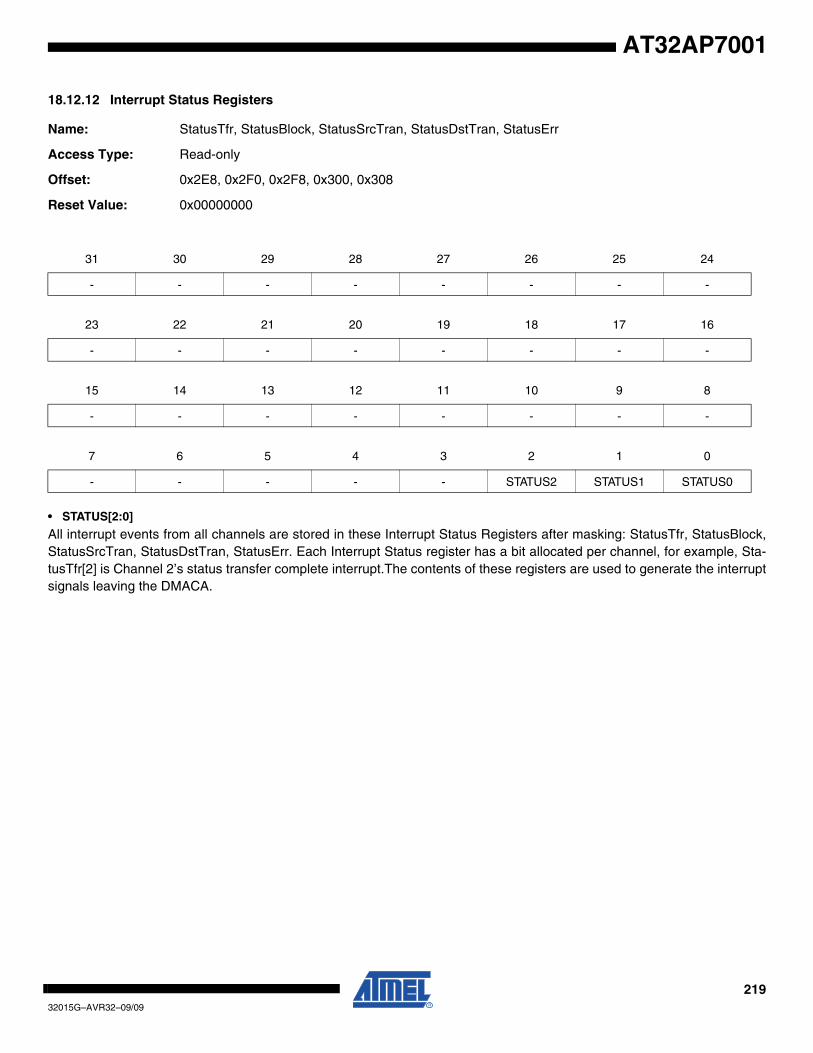
21932015G–AVR32–09/09
AT32AP7001
18.12.12 Interrupt Status Registers
Name: StatusTfr, StatusBlock, StatusSrcTran, StatusDstTran, StatusErr
Access Type: Read-only
Offset: 0x2E8, 0x2F0, 0x2F8, 0x300, 0x308
Reset Value: 0x00000000
• STATUS[2:0]
All interrupt events from all channels are stored in these Interrupt Status Registers after masking: StatusTfr, StatusBlock,StatusSrcTran, StatusDstTran, StatusErr. Each Interrupt Status register has a bit allocated per channel, for example, Sta-tusTfr[2] is Channel 2’s status transfer complete interrupt.The contents of these registers are used to generate the interruptsignals leaving the DMACA.
31 30 29 28 27 26 25 24
- - - - - - - -
23 22 21 20 19 18 17 16
- - - - - - - -
15 14 13 12 11 10 9 8
- - - - - - - -
7 6 5 4 3 2 1 0
- - - - - STATUS2 STATUS1 STATUS0

22032015G–AVR32–09/09
AT32AP7001
18.12.13 Interrupt Mask Registers
Name: MaskTfr, MaskBlock, MaskSrcTran, MaskDstTran, MaskErr
Access Type: Read/Write
Offset: 0x310, 0x318, 0x320, 0x328, 0x330
Reset Value: 0x00000000
The contents of the Raw Status Registers are masked with the contents of the Mask Registers: MaskTfr, MaskBlock, Mask-SrcTran, MaskDstTran, MaskErr. Each Interrupt Mask register has a bit allocated per channel, for example, MaskTfr[2] isthe mask bit for Channel 2’s transfer complete interrupt.
A channel’s INT_MASK bit is only written if the corresponding mask write enable bit in the INT_MASK_WE field is assertedon the same System Bus write transfer. This allows software to set a mask bit without performing a read-modified writeoperation.
For example, writing hex 01x1 to the MaskTfr register writes a 1 into MaskTfr[0], while MaskTfr[7:1] remains unchanged.Writing hex 00xx leaves MaskTfr[7:0] unchanged.
Writing a 1 to any bit in these registers unmasks the corresponding interrupt, thus allowing the DMACA to set the appropri-ate bit in the Status Registers.
• INT_M_WE[10:8]: Interrupt Mask Write Enable0 = Write disabled1 = Write enabled
• INT_MASK[2:0]: Interrupt Mask0= Masked
1 = Unmasked
31 30 29 28 27 26 25 24
- - - - - - - -
23 22 21 20 19 18 17 16
- - - - - - - -
15 14 13 12 11 10 9 8
- - - - - INT_M_WE2 INT_M_WE1 INT_M_WE0
7 6 5 4 3 2 1 0
- - - - - INT_MASK2 INT_MASK1 INT_MASK0
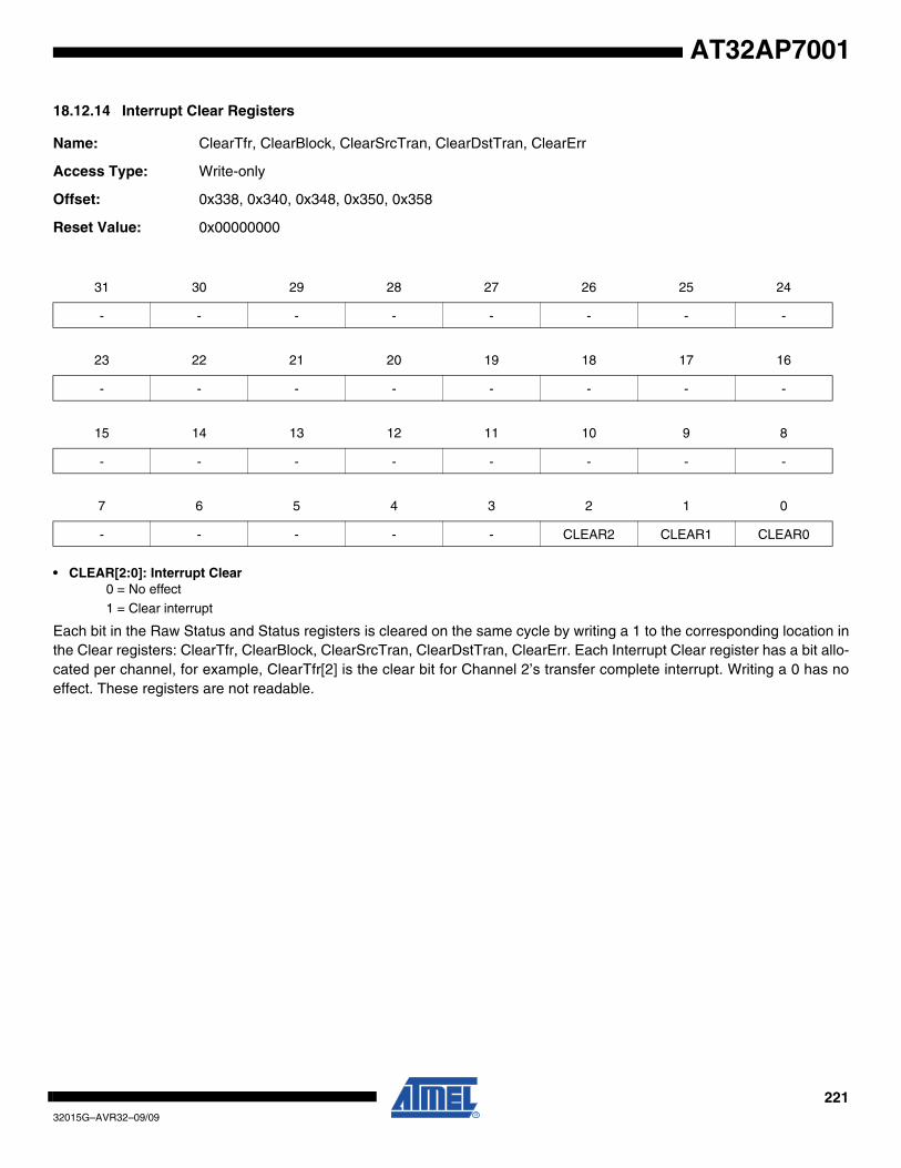
22132015G–AVR32–09/09
AT32AP7001
18.12.14 Interrupt Clear Registers
Name: ClearTfr, ClearBlock, ClearSrcTran, ClearDstTran, ClearErr
Access Type: Write-only
Offset: 0x338, 0x340, 0x348, 0x350, 0x358
Reset Value: 0x00000000
• CLEAR[2:0]: Interrupt Clear0 = No effect
1 = Clear interrupt
Each bit in the Raw Status and Status registers is cleared on the same cycle by writing a 1 to the corresponding location inthe Clear registers: ClearTfr, ClearBlock, ClearSrcTran, ClearDstTran, ClearErr. Each Interrupt Clear register has a bit allo-cated per channel, for example, ClearTfr[2] is the clear bit for Channel 2’s transfer complete interrupt. Writing a 0 has noeffect. These registers are not readable.
31 30 29 28 27 26 25 24
- - - - - - - -
23 22 21 20 19 18 17 16
- - - - - - - -
15 14 13 12 11 10 9 8
- - - - - - - -
7 6 5 4 3 2 1 0
- - - - - CLEAR2 CLEAR1 CLEAR0
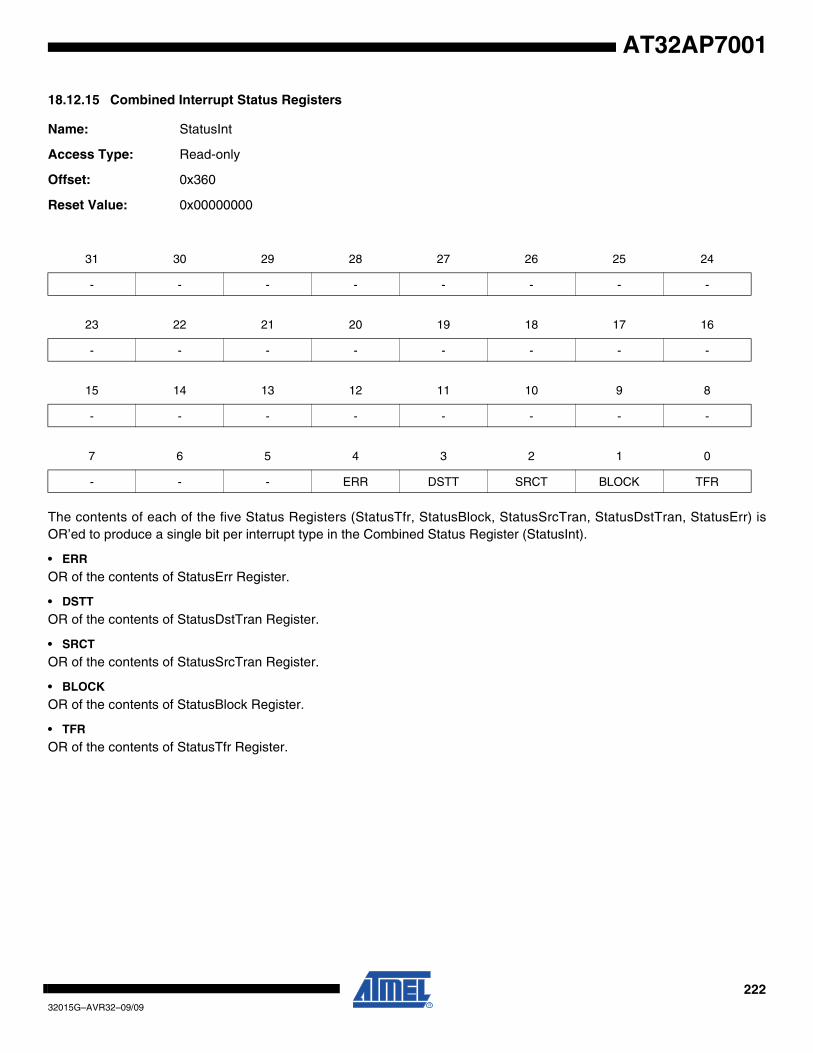
22232015G–AVR32–09/09
AT32AP7001
18.12.15 Combined Interrupt Status Registers
Name: StatusInt
Access Type: Read-only
Offset: 0x360
Reset Value: 0x00000000
The contents of each of the five Status Registers (StatusTfr, StatusBlock, StatusSrcTran, StatusDstTran, StatusErr) isOR’ed to produce a single bit per interrupt type in the Combined Status Register (StatusInt).
• ERR
OR of the contents of StatusErr Register.
• DSTT
OR of the contents of StatusDstTran Register.
• SRCT
OR of the contents of StatusSrcTran Register.
• BLOCK
OR of the contents of StatusBlock Register.
• TFR
OR of the contents of StatusTfr Register.
31 30 29 28 27 26 25 24
- - - - - - - -
23 22 21 20 19 18 17 16
- - - - - - - -
15 14 13 12 11 10 9 8
- - - - - - - -
7 6 5 4 3 2 1 0
- - - ERR DSTT SRCT BLOCK TFR
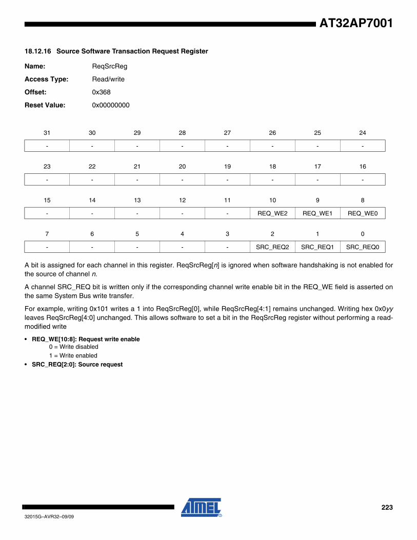
22332015G–AVR32–09/09
AT32AP7001
18.12.16 Source Software Transaction Request Register
Name: ReqSrcReg
Access Type: Read/write
Offset: 0x368
Reset Value: 0x00000000
A bit is assigned for each channel in this register. ReqSrcReg[n] is ignored when software handshaking is not enabled forthe source of channel n.
A channel SRC_REQ bit is written only if the corresponding channel write enable bit in the REQ_WE field is asserted onthe same System Bus write transfer.
For example, writing 0x101 writes a 1 into ReqSrcReg[0], while ReqSrcReg[4:1] remains unchanged. Writing hex 0x0yyleaves ReqSrcReg[4:0] unchanged. This allows software to set a bit in the ReqSrcReg register without performing a read-modified write
• REQ_WE[10:8]: Request write enable0 = Write disabled1 = Write enabled
• SRC_REQ[2:0]: Source request
31 30 29 28 27 26 25 24
- - - - - - - -
23 22 21 20 19 18 17 16
- - - - - - - -
15 14 13 12 11 10 9 8
- - - - - REQ_WE2 REQ_WE1 REQ_WE0
7 6 5 4 3 2 1 0
- - - - - SRC_REQ2 SRC_REQ1 SRC_REQ0
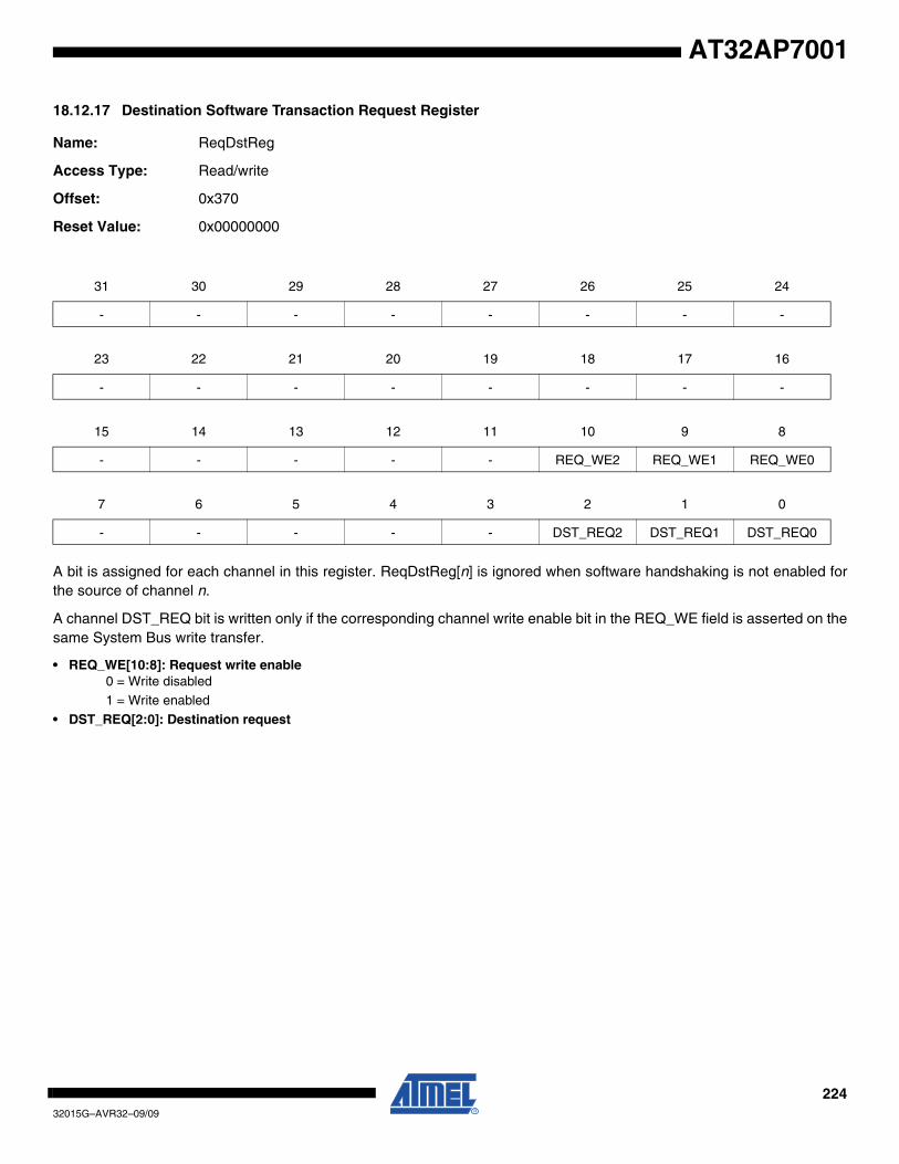
22432015G–AVR32–09/09
AT32AP7001
18.12.17 Destination Software Transaction Request Register
Name: ReqDstReg
Access Type: Read/write
Offset: 0x370
Reset Value: 0x00000000
A bit is assigned for each channel in this register. ReqDstReg[n] is ignored when software handshaking is not enabled forthe source of channel n.
A channel DST_REQ bit is written only if the corresponding channel write enable bit in the REQ_WE field is asserted on thesame System Bus write transfer.
• REQ_WE[10:8]: Request write enable0 = Write disabled1 = Write enabled
• DST_REQ[2:0]: Destination request
31 30 29 28 27 26 25 24
- - - - - - - -
23 22 21 20 19 18 17 16
- - - - - - - -
15 14 13 12 11 10 9 8
- - - - - REQ_WE2 REQ_WE1 REQ_WE0
7 6 5 4 3 2 1 0
- - - - - DST_REQ2 DST_REQ1 DST_REQ0

22532015G–AVR32–09/09
AT32AP7001
18.12.18 Single Source Transaction Request Register
Name: SglReqSrcReg
Access Type: Read/write
Offset: 0x378
Reset Value: 0x00000000
A bit is assigned for each channel in this register. SglReqSrcReg[n] is ignored when software handshaking is not enabledfor the source of channel n.
A channel S_SG_REQ bit is written only if the corresponding channel write enable bit in the REQ_WE field is asserted onthe same System Bus write transfer.
• REQ_WE[10:8]: Request write enable0 = Write disabled1 = Write enabled
• S_SG_REQ[2:0]: Source single request
31 30 29 28 27 26 25 24
- - - - - - - -
23 22 21 20 19 18 17 16
- - - - - - - -
15 14 13 12 11 10 9 8
- - - - - REQ_WE2 REQ_WE1 REQ_WE0
7 6 5 4 3 2 1 0
- - - - - S_SG_REQ2 S_SG_REQ1 S_SG_REQ0
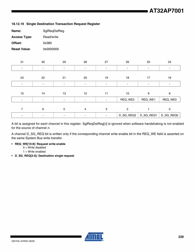
22632015G–AVR32–09/09
AT32AP7001
18.12.19 Single Destination Transaction Request Register
Name: SglReqDstReg
Access Type: Read/write
Offset: 0x380
Reset Value: 0x0000000
A bit is assigned for each channel in this register. SglReqDstReg[n] is ignored when software handshaking is not enabledfor the source of channel n.
A channel D_SG_REQ bit is written only if the corresponding channel write enable bit in the REQ_WE field is asserted onthe same System Bus write transfer.
• REQ_WE[10:8]: Request write enable0 = Write disabled1 = Write enabled
• D_SG_REQ[2:0]: Destination single request
31 30 29 28 27 26 25 24
- - - - - - - -
23 22 21 20 19 18 17 16
- - - - - - - -
15 14 13 12 11 10 9 8
- - - - - REQ_WE2 REQ_WE1 REQ_WE0
7 6 5 4 3 2 1 0
- - - - - D_SG_REQ2 D_SG_REQ1 D_SG_REQ0

22732015G–AVR32–09/09
AT32AP7001
18.12.20 Last Source Transaction Request Register
Name: LstSrcReg
Access Type: Read/write
Offset: 0x388
Reset Value: 0x0000000
A bit is assigned for each channel in this register. LstSrcReg[n] is ignored when software handshaking is not enabled forthe source of channel n.
A channel LSTSRC bit is written only if the corresponding channel write enable bit in the LSTSRC_WE field is asserted onthe same System Bus write transfer.
• LSTSRC_WE[10:8]: Source Last Transaction request write enable0 = Write disabled
1 = Write enabled• LSTSRC[2:0]: Source Last Transaction request
31 30 29 28 27 26 25 24
- - - - - - - -
23 22 21 20 19 18 17 16
- - - - - - - -
15 14 13 12 11 10 9 8
- - - - - LSTSRC_WE2
LSTSRC_WE1
LSTSRC_WE0
7 6 5 4 3 2 1 0
- - - - - LSTSRC2 LSTSRC1 LSTSRC0
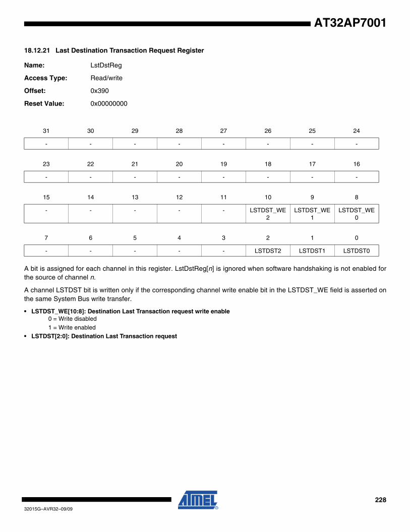
22832015G–AVR32–09/09
AT32AP7001
18.12.21 Last Destination Transaction Request Register
Name: LstDstReg
Access Type: Read/write
Offset: 0x390
Reset Value: 0x00000000
A bit is assigned for each channel in this register. LstDstReg[n] is ignored when software handshaking is not enabled forthe source of channel n.
A channel LSTDST bit is written only if the corresponding channel write enable bit in the LSTDST_WE field is asserted onthe same System Bus write transfer.
• LSTDST_WE[10:8]: Destination Last Transaction request write enable0 = Write disabled
1 = Write enabled• LSTDST[2:0]: Destination Last Transaction request
31 30 29 28 27 26 25 24
- - - - - - - -
23 22 21 20 19 18 17 16
- - - - - - - -
15 14 13 12 11 10 9 8
- - - - - LSTDST_WE2
LSTDST_WE1
LSTDST_WE0
7 6 5 4 3 2 1 0
- - - - - LSTDST2 LSTDST1 LSTDST0
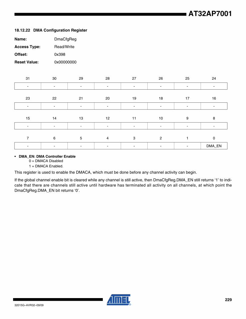
22932015G–AVR32–09/09
AT32AP7001
18.12.22 DMA Configuration Register
Name: DmaCfgReg
Access Type: Read/Write
Offset: 0x398
Reset Value: 0x00000000
• DMA_EN: DMA Controller Enable0 = DMACA Disabled
1 = DMACA Enabled.
This register is used to enable the DMACA, which must be done before any channel activity can begin.
If the global channel enable bit is cleared while any channel is still active, then DmaCfgReg.DMA_EN still returns ‘1’ to indi-cate that there are channels still active until hardware has terminated all activity on all channels, at which point theDmaCfgReg.DMA_EN bit returns ‘0’.
31 30 29 28 27 26 25 24
- - - - - - - -
23 22 21 20 19 18 17 16
- - - - - - - -
15 14 13 12 11 10 9 8
- - - - - - - -
7 6 5 4 3 2 1 0
- - - - - - - DMA_EN
23032015G–AVR32–09/09
AT32AP7001
18.12.23 DMA Channel Enable Register
Name: ChEnReg
Access Type: Read/Write
Offset: 0x3A0
Reset Value: 0x00000000
• CH_EN_WE[10:8]: Channel Enable Write Enable
The channel enable bit, CH_EN, is only written if the corresponding channel write enable bit, CH_EN_WE, is asserted onthe same System Bus write transfer.
For example, writing 0x101 writes a 1 into ChEnReg[0], while ChEnReg[7:1] remains unchanged.
• CH_EN[2:0] 0 = Disable the Channel
1 = Enable the Channel
Enables/Disables the channel. Setting this bit enables a channel, clearing this bit disables the channel.
The ChEnReg.CH_EN bit is automatically cleared by hardware to disable the channel after the last System Bus transfer ofthe DMA transfer to the destination has completed.Software can therefore poll this bit to determine when a DMA transferhas completed.
31 30 29 28 27 26 25 24
- - - - - - - -
23 22 21 20 19 18 17 16
- - - - - - - -
15 14 13 12 11 10 9 8
- - - - - CH_EN_WE2
CH_EN_WE1
CH_EN_WE0
7 6 5 4 3 2 1 0
- - - - - CH_EN2 CH_EN1 CH_EN0
23132015G–AVR32–09/09
AT32AP7001
18.12.24 DMACA Component Id Register Low
Name: DmaCompIdRegL
Access Type: Read-only
Offset: 0x3F8
Reset Value: 0x44571110
• DMA_COMP_TYPE
DesignWare component type number = 0x44571110.
This assigned unique hex value is constant and is derived from the two ASCII letters “DW” followed by a 32-bit unsignednumber
31 30 29 28 27 26 25 24
DMA_COMP_TYPE[31:24]
23 22 21 20 19 18 17 16
DMA_COMP_TYPE[23:16]
15 14 13 12 11 10 9 8
DMA_COMP_TYPE[15:8]
7 6 5 4 3 2 1 0
DMA_COMP_TYPE[7:0]
23232015G–AVR32–09/09
AT32AP7001
18.12.25 DMACA Component Id Register High
Name: DmaCompIdRegH
Access Type: Read-only
Offset: 0x3FC
Reset Value: 0x3230362A
• DMA_COMP_VERSION: Version of the component
31 30 29 28 27 26 25 24
DMA_COMP_VERSION[31:24]
23 22 21 20 19 18 17 16
DMA_COMP_VERSION[23:16]
15 14 13 12 11 10 9 8
DMA_COMP_VERSION[15:8]
7 6 5 4 3 2 1 0
DMA_COMP_VERSION[7:0]
23332015G–AVR32–09/09
AT32AP7001
19. Peripheral DMA Controller (PDC)
Rev: 1.0.0.1
19.1 Features
• Generates Transfers to/from Peripherals such as USART, SSC and SPI• Supports Up to 20 Channels (Product Dependent)• One Master Clock Cycle Needed for a Transfer from Memory to Peripheral• Two Master Clock Cycles Needed for a Transfer from Peripheral to Memory
19.2 Description
The Peripheral DMA Controller (PDC) transfers data between on-chip serial peripherals such asthe UART, USART, SSC, SPI, and the on- and off-chip memories. Using the Peripheral DMAController avoids processor intervention and removes the processor interrupt-handling over-head. This significantly reduces the number of clock cycles required for a data transfer and, as aresult, improves the performance of the microcontroller and makes it more power efficient.
The PDC channels are implemented in pairs, each pair being dedicated to a particular periph-eral. One channel in the pair is dedicated to the receiving channel and one to the transmittingchannel of each UART, USART, SSC and SPI.
The user interface of a PDC channel is integrated in the memory space of each peripheral. Itcontains:
• A 32-bit memory pointer register
• A 16-bit transfer count register
• A 32-bit register for next memory pointer
• A 16-bit register for next transfer count
The peripheral triggers PDC transfers using transmit and receive signals. When the pro-grammed data is transferred, an end of transfer interrupt is generated by the correspondingperipheral.

23432015G–AVR32–09/09
AT32AP7001
19.3 Block Diagram
Figure 19-1. Block Diagram
Control
PDC Channel 0
PDC Channel 1
THR
RHR
ControlStatus & Control
Peripheral Peripheral DMA Controller
MemoryController
23532015G–AVR32–09/09
AT32AP7001
19.4 Product Dependencies
19.4.1 Power Management
The PDC clock is generated by the Power Manager. The PDC also depends on the HSB-HSBbridge clock. Before using the PDC, the programmer must ensure that the PDC clock and HSB-HSB bridge clock are enabled in the Power Manager.
To prevent bus errors the PDC operation must be terminated before entering sleep mode
19.4.2 Interrupt
The PDC has an interrupt line for each channel connected to the Interrupt Controller via the cor-responding peripheral. Handling the PDC interrupt requires programming the interrupt controllerbefore configuring the PDC.
19.4.3 Peripherals
Before using each PDC channel the corresponding peripheral has to be configured correctly.
19.5 Functional Description
19.5.1 Configuration
The PDC channels user interface enables the user to configure and control the data transfers foreach channel. The user interface of a PDC channel is integrated into the user interface of theperipheral (offset 0x100), which it is related to.
Per peripheral, it contains four 32-bit Pointer Registers (RPR, RNPR, TPR, and TNPR) and four16-bit Counter Registers (RCR, RNCR, TCR, and TNCR).
The size of the buffer (number of transfers) is configured in an internal 16-bit transfer counterregister, and it is possible, at any moment, to read the number of transfers left for each channel.
The memory base address is configured in a 32-bit memory pointer by defining the location ofthe first address to access in the memory. It is possible, at any moment, to read the location inmemory of the next transfer and the number of remaining transfers. The PDC has dedicated sta-tus registers which indicate if the transfer is enabled or disabled for each channel. The status foreach channel is located in the peripheral status register. Transfers can be enabled and/or dis-abled by setting TXTEN/TXTDIS and RXTEN/RXTDIS in PDC Transfer Control Register. Thesecontrol bits enable reading the pointer and counter registers safely without any risk of theirchanging between both reads.
The PDC sends status flags to the peripheral visible in its status-register (ENDRX, ENDTX,RXBUFF, and TXBUFE).
ENDRX flag is set when the PERIPH_RCR register reaches zero.
RXBUFF flag is set when both PERIPH_RCR and PERIPH_RNCR reach zero.
ENDTX flag is set when the PERIPH_TCR register reaches zero.
TXBUFE flag is set when both PERIPH_TCR and PERIPH_TNCR reach zero.
These status flags are described in the peripheral status register.
23632015G–AVR32–09/09
AT32AP7001
19.5.2 Memory Pointers
Each peripheral is connected to the PDC by a receiver data channel and a transmitter datachannel. Each channel has an internal 32-bit memory pointer. Each memory pointer points to alocation anywhere in the memory space (on-chip memory or external bus interface memory).
Depending on the type of transfer (byte, half-word or word), the memory pointer is incrementedby 1, 2 or 4, respectively for peripheral transfers. The size of the transfer is setup up in theperipheral’s control register and automatically sensed by the PDC. The size is always roundedup to wither byte, half-word or word.
If a memory pointer is reprogrammed while the PDC is in operation, the transfer address ischanged, and the PDC performs transfers using the new address.
19.5.3 Transfer Counters
There is one internal 16-bit transfer counter for each channel used to count the size of the blockalready transferred by its associated channel. These counters are decremented after each datatransfer. When the counter reaches zero, the transfer is complete and the PDC stops transfer-ring data.
If the Next Counter Register is equal to zero, the PDC disables the trigger while activating therelated peripheral end flag.
If the counter is reprogrammed while the PDC is operating, the number of transfers is updatedand the PDC counts transfers from the new value.
Programming the Next Counter/Pointer registers chains the buffers. The counters are decre-mented after each data transfer as stated above, but when the transfer counter reaches zero,the values of the Next Counter/Pointer are loaded into the Counter/Pointer registers in order tore-enable the triggers.
For each channel, two status bits indicate the end of the current buffer (ENDRX, ENTX) and theend of both current and next buffer (RXBUFF, TXBUFE). These bits are directly mapped to theperipheral status register and can trigger an interrupt request to the Interrupt Controller.
The peripheral end flag is automatically cleared when one of the counter-registers (Counter orNext Counter Register) is written.
Note: When the Next Counter Register is loaded into the Counter Register, it is set to zero.
19.5.4 Data Transfers
The peripheral triggers PDC transfers using transmit (TXRDY) and receive (RXRDY) signals.
When the peripheral receives an external character, it sends a Receive Ready signal to the PDCwhich then requests access to the system bus. When access is granted, the PDC starts a readof the peripheral Receive Holding Register (RHR) and then triggers a write in the memory.
After each transfer, the relevant PDC memory pointer is incremented and the number of trans-fers left is decremented. When the memory block size is reached, a signal is sent to theperipheral and the transfer stops.
The same procedure is followed, in reverse, for transmit transfers.
23732015G–AVR32–09/09
AT32AP7001
19.5.5 Priority of PDC Transfer Requests
The Peripheral DMA Controller handles transfer requests from the channel according to priori-ties fixed for each product.These priorities are defined in the product datasheet.
If simultaneous requests of the same type (receiver or transmitter) occur on identical peripher-als, the priority is determined by the numbering of the peripherals.
If transfer requests are not simultaneous, they are treated in the order they occurred. Requestsfrom the receivers are handled first and then followed by transmitter requests.
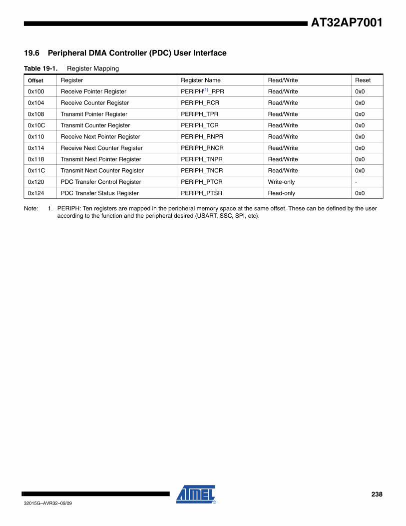
23832015G–AVR32–09/09
AT32AP7001
19.6 Peripheral DMA Controller (PDC) User Interface
Note: 1. PERIPH: Ten registers are mapped in the peripheral memory space at the same offset. These can be defined by the user according to the function and the peripheral desired (USART, SSC, SPI, etc).
Table 19-1. Register Mapping
Offset Register Register Name Read/Write Reset
0x100 Receive Pointer Register PERIPH(1)_RPR Read/Write 0x0
0x104 Receive Counter Register PERIPH_RCR Read/Write 0x0
0x108 Transmit Pointer Register PERIPH_TPR Read/Write 0x0
0x10C Transmit Counter Register PERIPH_TCR Read/Write 0x0
0x110 Receive Next Pointer Register PERIPH_RNPR Read/Write 0x0
0x114 Receive Next Counter Register PERIPH_RNCR Read/Write 0x0
0x118 Transmit Next Pointer Register PERIPH_TNPR Read/Write 0x0
0x11C Transmit Next Counter Register PERIPH_TNCR Read/Write 0x0
0x120 PDC Transfer Control Register PERIPH_PTCR Write-only -
0x124 PDC Transfer Status Register PERIPH_PTSR Read-only 0x0
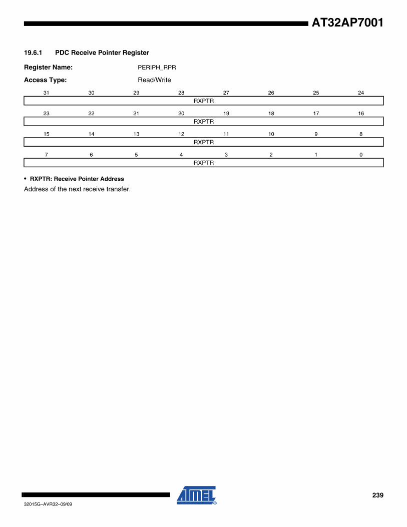
23932015G–AVR32–09/09
AT32AP7001
19.6.1 PDC Receive Pointer Register
Register Name: PERIPH_RPR
Access Type: Read/Write
• RXPTR: Receive Pointer Address
Address of the next receive transfer.
31 30 29 28 27 26 25 24
RXPTR
23 22 21 20 19 18 17 16
RXPTR
15 14 13 12 11 10 9 8
RXPTR
7 6 5 4 3 2 1 0
RXPTR
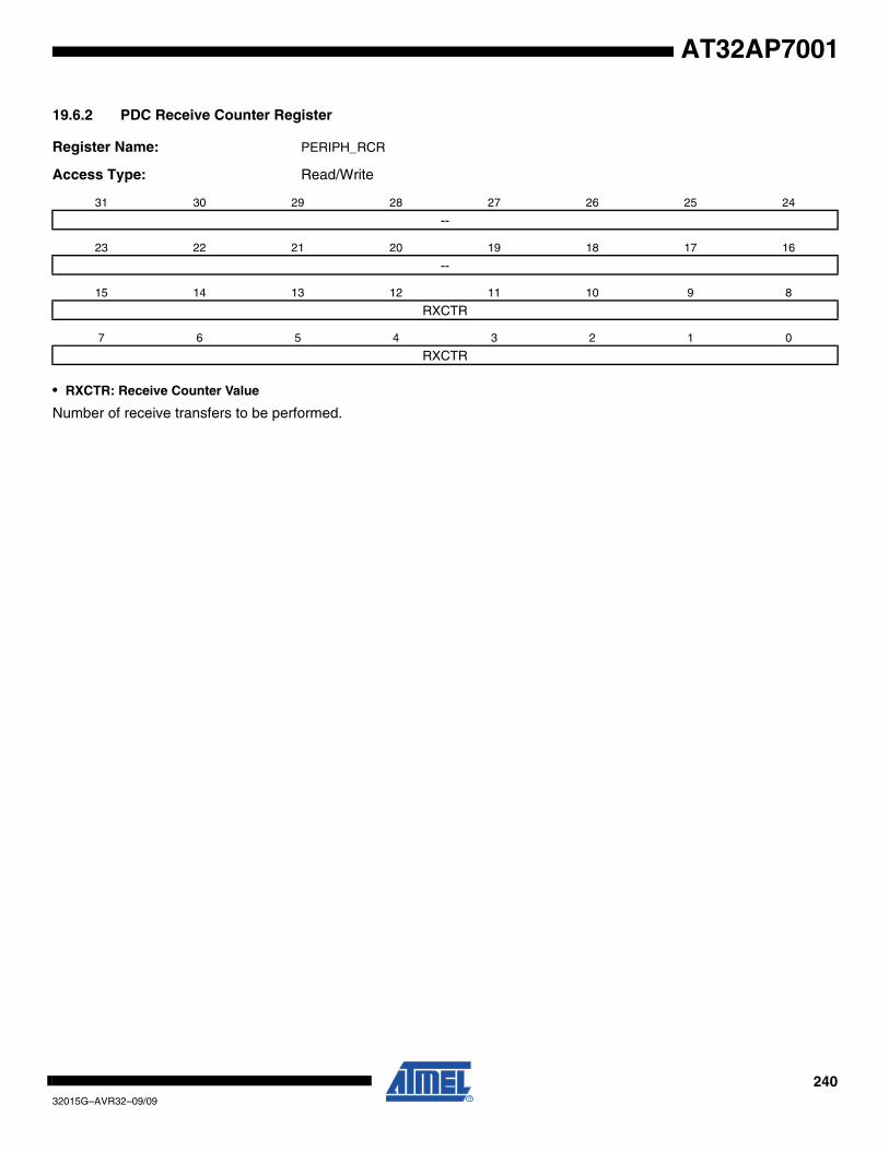
24032015G–AVR32–09/09
AT32AP7001
19.6.2 PDC Receive Counter Register
Register Name: PERIPH_RCR
Access Type: Read/Write
• RXCTR: Receive Counter Value
Number of receive transfers to be performed.
31 30 29 28 27 26 25 24
--
23 22 21 20 19 18 17 16
--
15 14 13 12 11 10 9 8
RXCTR
7 6 5 4 3 2 1 0
RXCTR
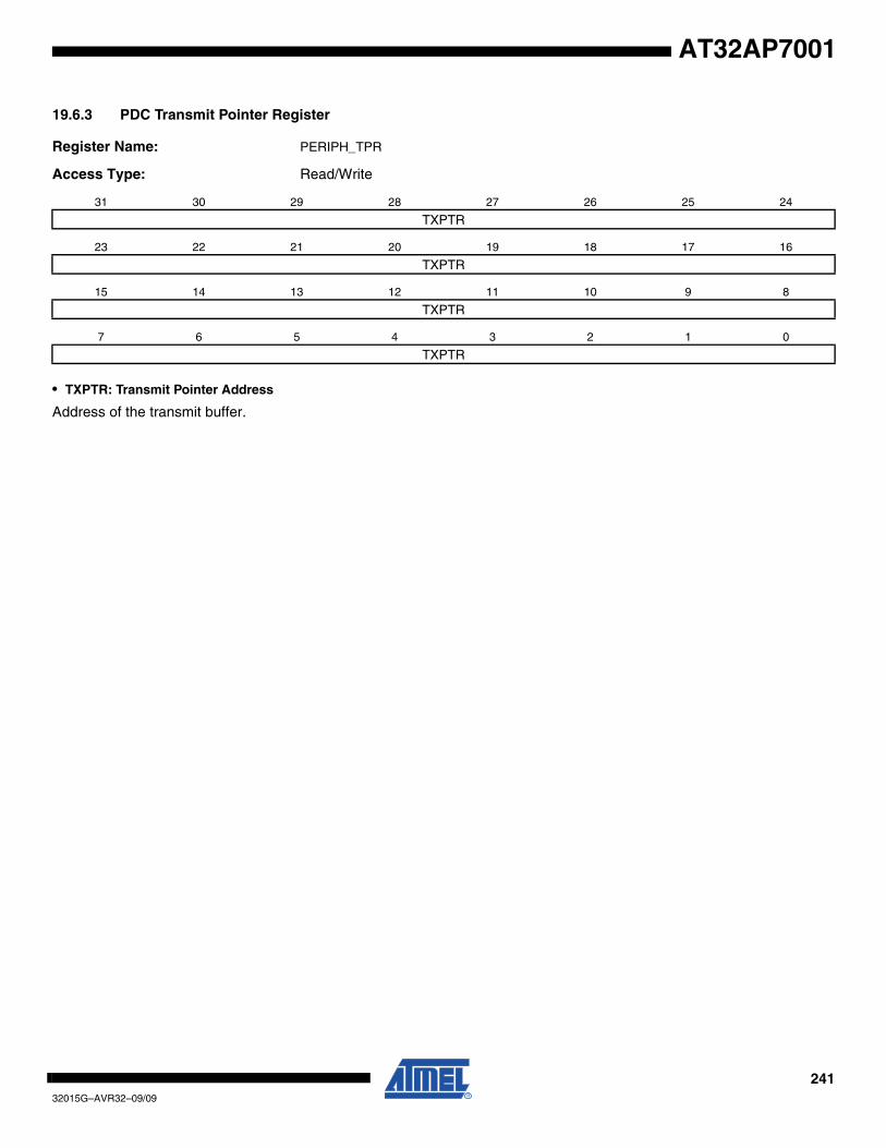
24132015G–AVR32–09/09
AT32AP7001
19.6.3 PDC Transmit Pointer Register
Register Name: PERIPH_TPR
Access Type: Read/Write
• TXPTR: Transmit Pointer Address
Address of the transmit buffer.
31 30 29 28 27 26 25 24
TXPTR
23 22 21 20 19 18 17 16
TXPTR
15 14 13 12 11 10 9 8
TXPTR
7 6 5 4 3 2 1 0
TXPTR

24232015G–AVR32–09/09
AT32AP7001
19.6.4 PDC Transmit Counter Register
Register Name: PERIPH_TCR
Access Type: Read/Write
• TXCTR: Transmit Counter Value
TXCTR is the size of the transmit transfer to be performed. At zero, the peripheral data transfer is stopped.
31 30 29 28 27 26 25 24
--
23 22 21 20 19 18 17 16
--
15 14 13 12 11 10 9 8
TXCTR
7 6 5 4 3 2 1 0
TXCTR
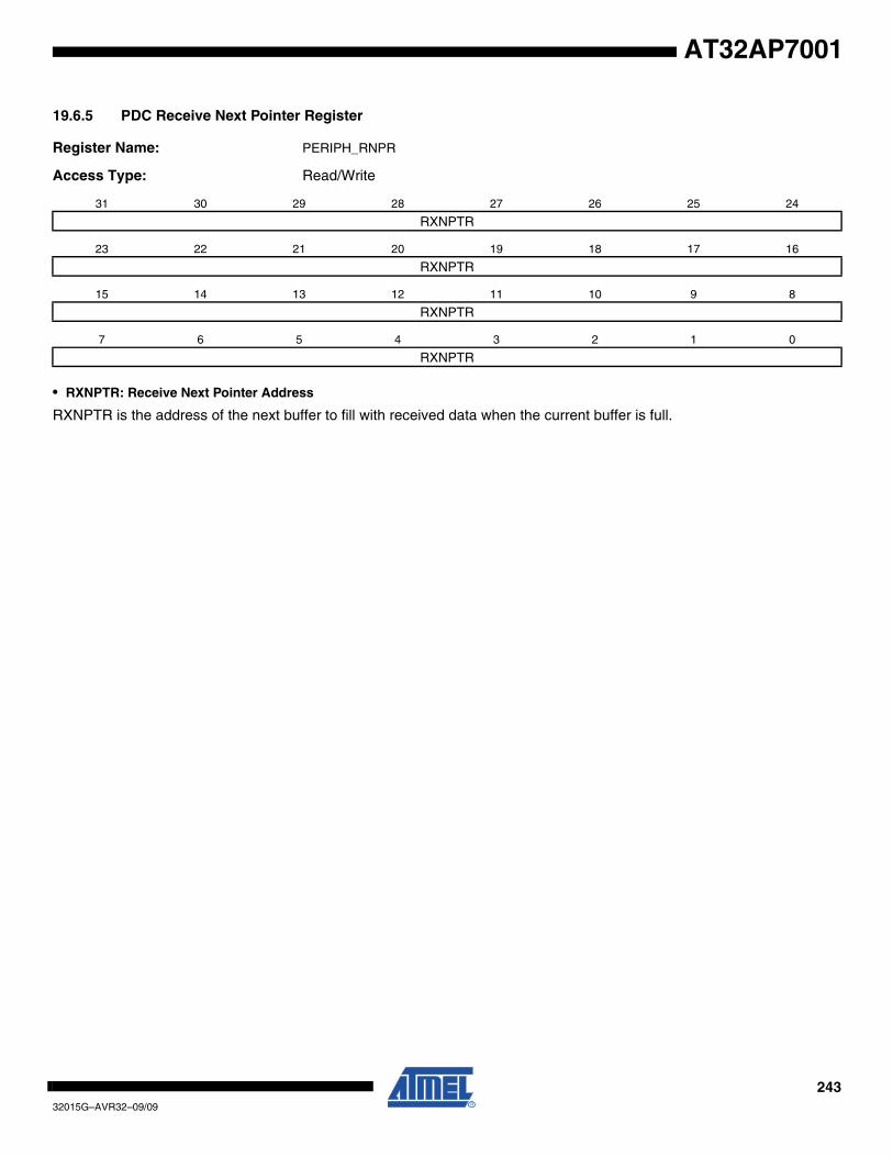
24332015G–AVR32–09/09
AT32AP7001
19.6.5 PDC Receive Next Pointer Register
Register Name: PERIPH_RNPR
Access Type: Read/Write
• RXNPTR: Receive Next Pointer Address
RXNPTR is the address of the next buffer to fill with received data when the current buffer is full.
31 30 29 28 27 26 25 24
RXNPTR
23 22 21 20 19 18 17 16
RXNPTR
15 14 13 12 11 10 9 8
RXNPTR
7 6 5 4 3 2 1 0
RXNPTR
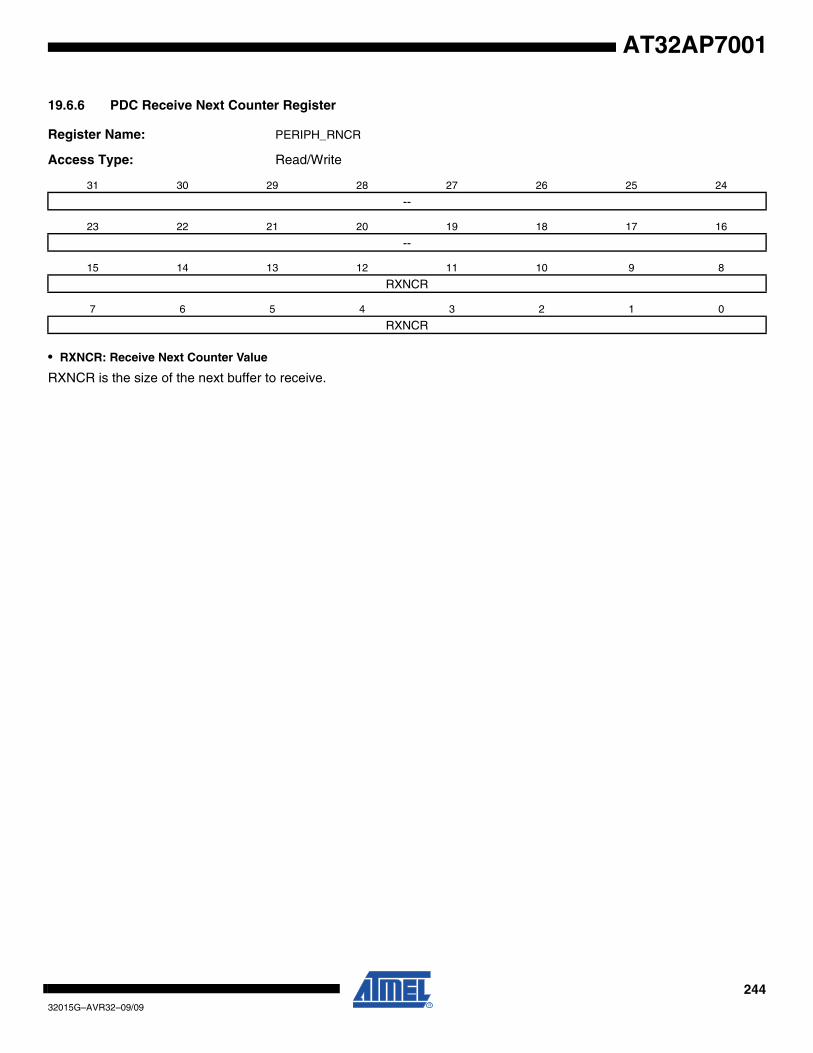
24432015G–AVR32–09/09
AT32AP7001
19.6.6 PDC Receive Next Counter Register
Register Name: PERIPH_RNCR
Access Type: Read/Write
• RXNCR: Receive Next Counter Value
RXNCR is the size of the next buffer to receive.
31 30 29 28 27 26 25 24
--
23 22 21 20 19 18 17 16
--
15 14 13 12 11 10 9 8
RXNCR
7 6 5 4 3 2 1 0
RXNCR

24532015G–AVR32–09/09
AT32AP7001
19.6.7 PDC Transmit Next Pointer Register
Register Name: PERIPH_TNPR
Access Type: Read/Write
• TXNPTR: Transmit Next Pointer Address
TXNPTR is the address of the next buffer to transmit when the current buffer is empty.
31 30 29 28 27 26 25 24
TXNPTR
23 22 21 20 19 18 17 16
TXNPTR
15 14 13 12 11 10 9 8
TXNPTR
7 6 5 4 3 2 1 0
TXNPTR
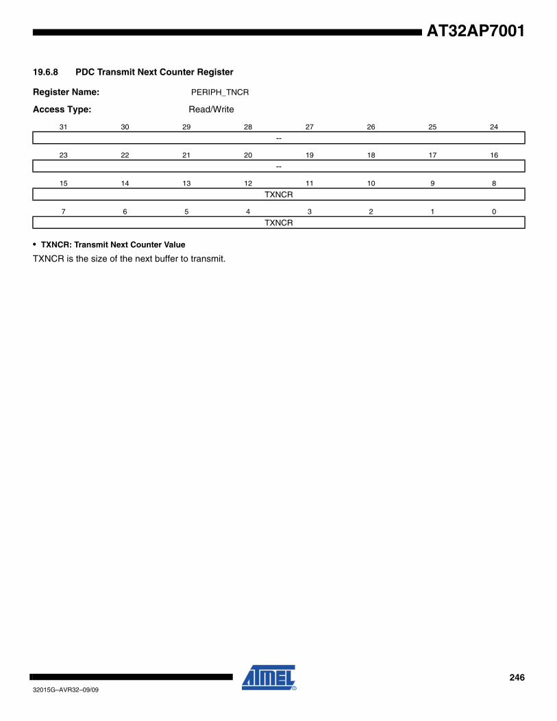
24632015G–AVR32–09/09
AT32AP7001
19.6.8 PDC Transmit Next Counter Register
Register Name: PERIPH_TNCR
Access Type: Read/Write
• TXNCR: Transmit Next Counter Value
TXNCR is the size of the next buffer to transmit.
31 30 29 28 27 26 25 24
--
23 22 21 20 19 18 17 16
--
15 14 13 12 11 10 9 8
TXNCR
7 6 5 4 3 2 1 0
TXNCR
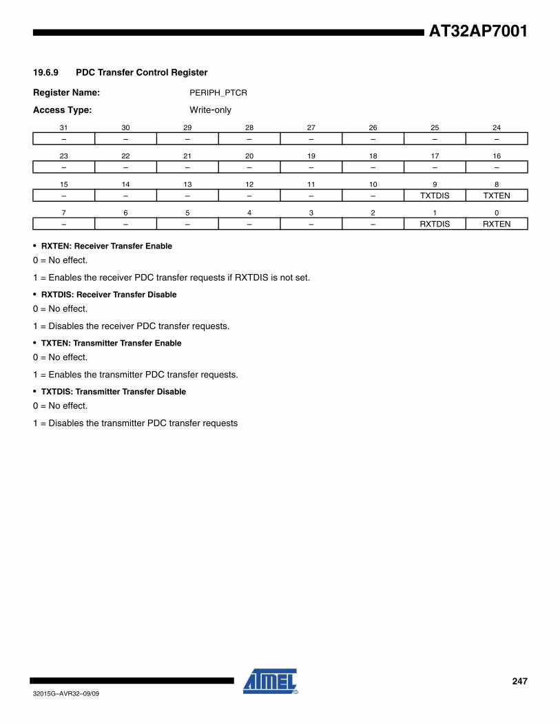
24732015G–AVR32–09/09
AT32AP7001
19.6.9 PDC Transfer Control Register
Register Name: PERIPH_PTCR
Access Type: Write-only
• RXTEN: Receiver Transfer Enable
0 = No effect.
1 = Enables the receiver PDC transfer requests if RXTDIS is not set.
• RXTDIS: Receiver Transfer Disable
0 = No effect.
1 = Disables the receiver PDC transfer requests.
• TXTEN: Transmitter Transfer Enable
0 = No effect.
1 = Enables the transmitter PDC transfer requests.
• TXTDIS: Transmitter Transfer Disable
0 = No effect.
1 = Disables the transmitter PDC transfer requests
31 30 29 28 27 26 25 24
– – – – – – – –
23 22 21 20 19 18 17 16
– – – – – – – –
15 14 13 12 11 10 9 8
– – – – – – TXTDIS TXTEN
7 6 5 4 3 2 1 0
– – – – – – RXTDIS RXTEN
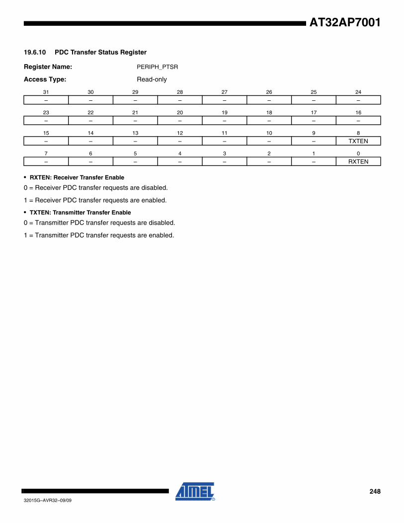
24832015G–AVR32–09/09
AT32AP7001
19.6.10 PDC Transfer Status Register
Register Name: PERIPH_PTSR
Access Type: Read-only
• RXTEN: Receiver Transfer Enable
0 = Receiver PDC transfer requests are disabled.
1 = Receiver PDC transfer requests are enabled.
• TXTEN: Transmitter Transfer Enable
0 = Transmitter PDC transfer requests are disabled.
1 = Transmitter PDC transfer requests are enabled.
31 30 29 28 27 26 25 24
– – – – – – – –
23 22 21 20 19 18 17 16
– – – – – – – –
15 14 13 12 11 10 9 8
– – – – – – – TXTEN
7 6 5 4 3 2 1 0
– – – – – – – RXTEN

24932015G–AVR32–09/09
AT32AP7001
20. Parallel Input/Output Controller (PIO)
Rev: 2.0.2.3
20.1 Features• Up to 32 Programmable I/O Lines• Fully Programmable through Set/Clear Registers • Multiplexing of Two Peripheral Functions per I/O Line• For each I/O Line (Whether Assigned to a Peripheral or Used as General Purpose I/O)
– Input Change Interrupt – Glitch Filter– Programmable Pull Up on Each I/O Line– Pin Data Status Register, Supplies Visibility of the Level on the Pin at Any Time
• Synchronous Output, Provides Set and Clear of Several I/O lines in a Single Write
20.2 DescriptionThe Parallel Input/Output Controller (PIO) manages up to 32 fully programmable input/outputlines. Each I/O line may be dedicated as a general-purpose I/O or be assigned to a function ofan embedded peripheral. This assures effective optimization of the pins of a product.
Each I/O line is associated with a bit number in all of the 32-bit registers of the 32-bit wide UserInterface.
Each I/O line of the PIO Controller features:
•An input change interrupt enabling level change detection on any I/O line.
•A glitch filter providing rejection of pulses lower than one-half of clock cycle.
•Control of the the pull-up of the I/O line.
•Input visibility and output control.
The PIO Controller also features a synchronous output providing up to 32 bits of data output in asingle write operation.
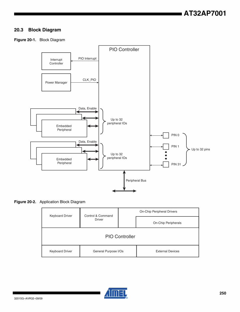
25032015G–AVR32–09/09
AT32AP7001
20.3 Block Diagram
Figure 20-1. Block Diagram
Figure 20-2. Application Block Diagram
Embedded Peripheral
Embedded Peripheral
PIO Interrupt
PIO Controller
Up to 32 pins
Power Manager
Up to 32 peripheral IOs
Up to 32 peripheral IOs
CLK_PIO
Peripheral Bus
InterruptController
Data, Enable
PIN 31
PIN 1
PIN 0
Data, Enable
On-Chip Peripherals
PIO Controller
On-Chip Peripheral DriversControl & Command
DriverKeyboard Driver
Keyboard Driver General Purpose I/Os External Devices
25132015G–AVR32–09/09
AT32AP7001
20.4 Product Dependencies
20.4.1 Pin MultiplexingEach pin is configurable, according to product definition as either a general-purpose I/O lineonly, or as an I/O line multiplexed with one or two peripheral I/Os. As the multiplexing is hard-ware-defined and thus product-dependent, the hardware designer and programmer mustcarefully determine the configuration of the PIO controllers required by their application. Whenan I/O line is general-purpose only, i.e. not multiplexed with any peripheral I/O, programming ofthe PIO Controller regarding the assignment to a peripheral has no effect and only the PIO Con-troller can control how the pin is driven by the product.
20.4.2 External Interrupt LinesThe external interrupt request signals are most generally multiplexed through the PIO Control-lers. However, it is not necessary to assign the I/O line to the interrupt function as the PIOController has no effect on inputs and the external interrupt lines are used only as inputs.
20.4.3 Power ManagementThe PIO clock (CLK_PIO) is generated by the Power Manager. Before accessing the PIO, theprogrammer must ensure that CLK_PIO is enabled in the Power Manager. Note that CLK_PIOmust be enabled when using the Input Change interrupt.
In the PIO description, CLK_PIO is the clock of the peripheral bus to which the PIO isconnected.
20.4.4 Interrupt GenerationThe PIO interrupt line is connected to the Interrupt Controller. Using the PIO interrupt requiresthe Interrupt Controller to be programmed first.
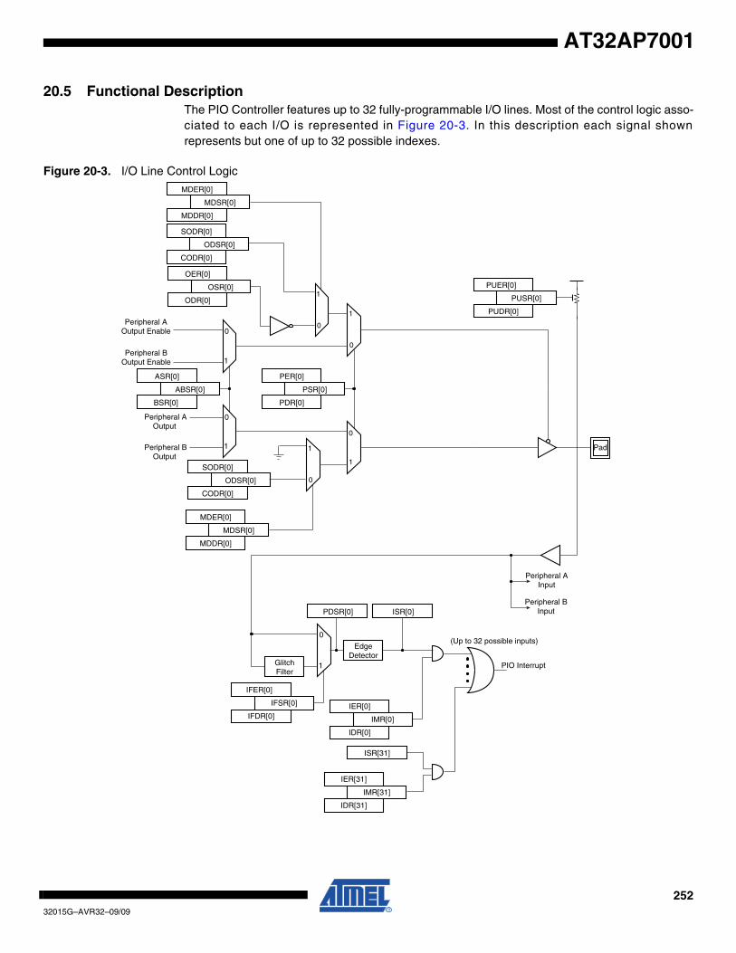
25232015G–AVR32–09/09
AT32AP7001
20.5 Functional DescriptionThe PIO Controller features up to 32 fully-programmable I/O lines. Most of the control logic asso-ciated to each I/O is represented in Figure 20-3. In this description each signal shownrepresents but one of up to 32 possible indexes.
Figure 20-3. I/O Line Control Logic
1
0
1
0
1
0
1
0
GlitchFilter
Peripheral B Input
Peripheral A Input
1
0
IFDR[0]
IFSR[0]
IFER[0]
EdgeDetector
PDSR[0] ISR[0]
IDR[0]
IMR[0]
IER[0]
PIO Interrupt
(Up to 32 possible inputs)
ISR[31]
IDR[31]
IMR[31]
IER[31]
Pad
PUDR[0]
PUSR[0]
PUER[0]
CODR[0]
ODSR[0]
SODR[0]
PDR[0]
PSR[0]
PER[0]
1
0
1
0
BSR[0]
ABSR[0]
ASR[0]
Peripheral BOutput Enable
Peripheral AOutput Enable
Peripheral BOutput
Peripheral AOutput
ODR[0]
OSR[0]
OER[0]
MDDR[0]
MDSR[0]
MDER[0]
CODR[0]
ODSR[0]
SODR[0]
MDDR[0]
MDSR[0]
MDER[0]
25332015G–AVR32–09/09
AT32AP7001
20.5.1 Pull-up Resistor ControlEach I/O line is designed with an embedded pull-up resistor. The pull-up resistor can be enabledor disabled by writing respectively PUER (Pull-up Enable Register) and PUDR (Pull-up DisableResistor). Writing in these registers results in setting or clearing the corresponding bit in PUSR(Pull-up Status Register). Reading a 1 in PUSR means the pull-up is disabled and reading a 0means the pull-up is enabled.
Control of the pull-up resistor is possible regardless of the configuration of the I/O line.
After reset, all of the pull-ups are enabled, i.e. PUSR resets at the value 0x0.
20.5.2 I/O Line or Peripheral Function Selection When a pin is multiplexed with one or two peripheral functions, the selection is controlled withthe registers PER (PIO Enable Register) and PDR (PIO Disable Register). The register PSR(PIO Status Register) is the result of the set and clear registers and indicates whether the pin iscontrolled by the corresponding peripheral or by the PIO Controller. A value of 0 indicates thatthe pin is controlled by the corresponding on-chip peripheral selected in the ABSR (AB SelectStatus Register). A value of 1 indicates the pin is controlled by the PIO controller.
If a pin is used as a general purpose I/O line (not multiplexed with an on-chip peripheral), PERand PDR have no effect and PSR returns 1 for the corresponding bit.
After reset, most generally, the I/O lines are controlled by the PIO controller, i.e. PSR resets at1. However, in some events, it is important that PIO lines are controlled by the peripheral (as inthe case of memory chip select lines that must be driven inactive after reset or for address linesthat must be driven low for booting out of an external memory). Thus, the reset value of PSR isdefined at the product level, depending on the multiplexing of the device.
20.5.3 Peripheral A or B SelectionThe PIO Controller provides multiplexing of up to two peripheral functions on a single pin. Theselection is performed by writing ASR (A Select Register) and BSR (Select B Register). ABSR(AB Select Status Register) indicates which peripheral line is currently selected. For each pin,the corresponding bit at level 0 means peripheral A is selected whereas the corresponding bit atlevel 1 indicates that peripheral B is selected.
Note that multiplexing of peripheral lines A and B only affects the output line. The peripheralinput lines are always connected to the pin input.
After reset, ABSR is 0, thus indicating that all the PIO lines are configured on peripheral A. How-ever, peripheral A generally does not drive the pin as the PIO Controller resets in I/O line mode.
Writing in ASR and BSR manages ABSR regardless of the configuration of the pin. However,assignment of a pin to a peripheral function requires a write in the corresponding peripheralselection register (ASR or BSR) in addition to a write in PDR.
20.5.4 Output ControlWhen the I/0 line is assigned to a peripheral function, i.e. the corresponding bit in PSR is at 0,the drive of the I/O line is controlled by the peripheral. Peripheral A or B, depending on the valuein ABSR, determines whether the pin is driven or not.
When the I/O line is controlled by the PIO controller, the pin can be configured to be driven. Thisis done by writing OER (Output Enable Register) and ODR (Output Disable Register). Theresults of these write operations are detected in OSR (Output Status Register). When a bit in this

25432015G–AVR32–09/09
AT32AP7001
register is at 0, the corresponding I/O line is used as an input only. When the bit is at 1, the cor-responding I/O line is driven by the PIO controller.
The level driven on an I/O line can be determined by writing in SODR (Set Output Data Register)and CODR (Clear Output Data Register). These write operations respectively set and clearODSR (Output Data Status Register), which represents the data driven on the I/O lines. Writingin OER and ODR manages OSR whether the pin is configured to be controlled by the PIO con-troller or assigned to a peripheral function. This enables configuration of the I/O line prior tosetting it to be managed by the PIO Controller.
Similarly, writing in SODR and CODR effects ODSR. This is important as it defines the first leveldriven on the I/O line.
20.5.5 Multi-drive capabilityThe PIO is able to configure each pin as open drain to support external drivers on the same pin.This is done by writing MDER (Multi-Drive Enable Register) and MDDR (Multi-Drive DisableRegister). The result of these write operations are detected in MDSR (multui-Drive Status Regis-ter). The multi-drive mode is only available when the PIO is controlling the pin, i.e. PSR is set.
When using multi-drive the PIO will tri-state the pin when ODSR is set and drive the pin lowwhen ODSR is cleared. writing to OER or ODR will have no effect.
20.5.6 Synchronous Data OutputControlling all parallel busses using several PIOs requires two successive write operations in theSODR and CODR registers. This may lead to unexpected transient values. The PIO controlleroffers a direct control of PIO outputs by single write access to ODSR (Output Data Status Regis-ter). Only bits unmasked by OWSR (Output Write Status Register) are written. The mask bits inthe OWSR are set by writing to OWER (Output Write Enable Register) and cleared by writing toOWDR (Output Write Disable Register).
After reset, the synchronous data output is disabled on all the I/O lines as OWSR resets at 0x0.
20.5.7 Output Line TimingsFigure 20-4 shows how the outputs are driven either by writing SODR or CODR, or by directlywriting ODSR. This last case is valid only if the corresponding bit in OWSR is set. Figure 20-4also shows when the feedback in PDSR is available.
Figure 20-4. Output Line Timings
2 cycles
Peripheral Bus Access
2 cycles
Peripheral Bus Access
CLK_PIO
Write SODRWrite ODSR at 1
ODSR
PDSR
Write CODRWrite ODSR at 0

25532015G–AVR32–09/09
AT32AP7001
20.5.8 InputsThe level on each I/O line can be read through PDSR (Pin Data Status Register). This registerindicates the level of the I/O lines regardless of their configuration, whether uniquely as an inputor driven by the PIO controller or driven by a peripheral.
Reading the I/O line levels requires the clock of the PIO controller to be enabled, otherwisePDSR reads the levels present on the I/O line at the time the clock was disabled.
20.5.9 Input Glitch FilteringOptional input glitch filters are independently programmable on each I/O line. When the glitch fil-ter is enabled, a glitch with a duration of less than 1/2 CLK_PIO cycle is automatically rejected,while a pulse with a duration of 1 CLK_PIO cycle or more is accepted. For pulse durationsbetween 1/2 CLK_PIO cycle and 1 CLK_PIO cycle the pulse may or may not be taken intoaccount, depending on the precise timing of its occurrence. Thus for a pulse to be visible it mustexceed 1 CLK_PIO cycle, whereas for a glitch to be reliably filtered out, its duration must notexceed 1/2 CLK_PIO cycle. The filter introduces one CLK_PIO cycle latency if the pin levelchange occurs before a rising edge. However, this latency does not appear if the pin levelchange occurs before a falling edge. This is illustrated in Figure 20-5.
The glitch filters are controlled by the register set; IFER (Input Filter Enable Register), IFDR(Input Filter Disable Register) and IFSR (Input Filter Status Register). Writing IFER and IFDRrespectively sets and clears bits in IFSR. This last register enables the glitch filter on the I/Olines.
When the glitch filter is enabled, it does not modify the behavior of the inputs on the peripherals.It acts only on the value read in PDSR and on the input change interrupt detection. The glitch fil-ters require that the PIO Controller clock is enabled.
Figure 20-5. Input Glitch Filter Timing
20.5.10 Input Change InterruptThe PIO Controller can be programmed to generate an interrupt when it detects an input changeon an I/O line. The Input Change Interrupt is controlled by writing IER (Interrupt Enable Register)and IDR (Interrupt Disable Register), which respectively enable and disable the input changeinterrupt by setting and clearing the corresponding bit in IMR (Interrupt Mask Register). As Inputchange detection is possible only by comparing two successive samplings of the input of the I/Oline, the PIO Controller clock must be enabled. The Input Change Interrupt is available, regard-less of the configuration of the I/O line, i.e. configured as an input only, controlled by the PIOController or assigned to a peripheral function.
CLK_PIO
Pin Level
PDSRif IFSR = 0
PDSRif IFSR = 1
1 cycle 1 cycle 1 cycle
up to 1.5 cycles
2 cycles
up to 2.5 cycles up to 2 cycles
1 cycle
1 cycle
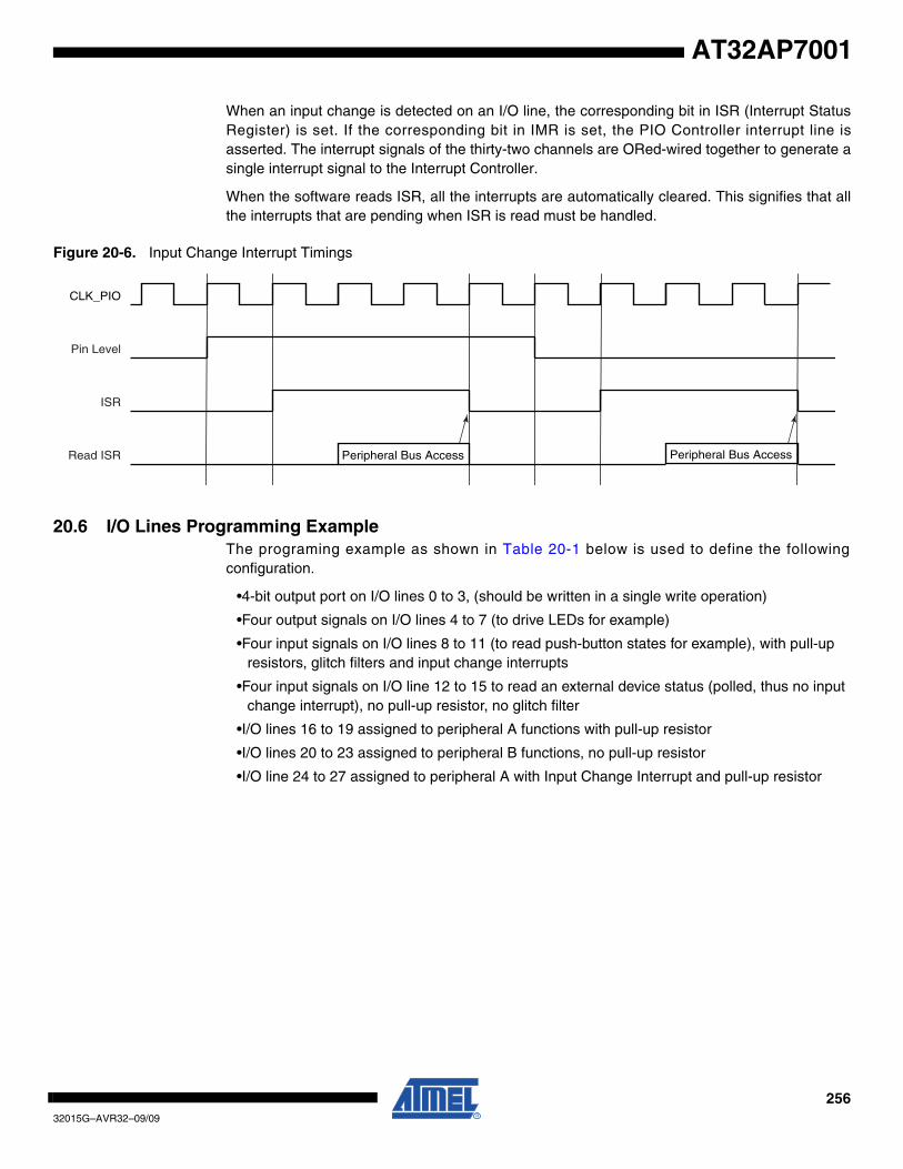
25632015G–AVR32–09/09
AT32AP7001
When an input change is detected on an I/O line, the corresponding bit in ISR (Interrupt StatusRegister) is set. If the corresponding bit in IMR is set, the PIO Controller interrupt line isasserted. The interrupt signals of the thirty-two channels are ORed-wired together to generate asingle interrupt signal to the Interrupt Controller.
When the software reads ISR, all the interrupts are automatically cleared. This signifies that allthe interrupts that are pending when ISR is read must be handled.
Figure 20-6. Input Change Interrupt Timings
20.6 I/O Lines Programming ExampleThe programing example as shown in Table 20-1 below is used to define the followingconfiguration.
•4-bit output port on I/O lines 0 to 3, (should be written in a single write operation)
•Four output signals on I/O lines 4 to 7 (to drive LEDs for example)
•Four input signals on I/O lines 8 to 11 (to read push-button states for example), with pull-up resistors, glitch filters and input change interrupts
•Four input signals on I/O line 12 to 15 to read an external device status (polled, thus no input change interrupt), no pull-up resistor, no glitch filter
•I/O lines 16 to 19 assigned to peripheral A functions with pull-up resistor
•I/O lines 20 to 23 assigned to peripheral B functions, no pull-up resistor
•I/O line 24 to 27 assigned to peripheral A with Input Change Interrupt and pull-up resistor
CLK_PIO
Pin Level
Read ISR Peripheral Bus Access
ISR
Peripheral Bus Access

25732015G–AVR32–09/09
AT32AP7001
Table 20-1. Programming Example
Register Value to be Written
PER 0x0000 FFFF
PDR 0x0FFF 0000
OER 0x0000 00FF
ODR 0x0FFF FF00
IFER 0x0000 0F00
IFDR 0x0FFF F0FF
SODR 0x0000 0000
CODR 0x0FFF FFFF
IER 0x0F00 0F00
IDR 0x00FF F0FF
PUDR 0x00F0 00F0
PUER 0x0F0F FF0F
ASR 0x0F0F 0000
BSR 0x00F0 0000
OWER 0x0000 000F
OWDR 0x0FFF FFF0
25832015G–AVR32–09/09
AT32AP7001
20.7 User InterfaceEach I/O line controlled by the PIO Controller is associated with a bit in each of the PIO Control-ler User Interface registers. Each register is 32 bits wide. If a parallel I/O line is not defined,writing to the corresponding bits has no effect. Undefined bits read zero. If the I/O line is not mul-tiplexed with any peripheral, the I/O line is controlled by the PIO Controller and PSR returns 1systematically.
Table 20-2. Register Mapping
Offset Register Name Access Reset Value
0x0000 PIO Enable Register PER Write-only –
0x0004 PIO Disable Register PDR Write-only –
0x0008 PIO Status Register PSR Read-only (1)
0x000C Reserved
0x0010 Output Enable Register OER Write-only –
0x0014 Output Disable Register ODR Write-only –
0x0018 Output Status Register OSR Read-only 0x0000 0000
0x001C Reserved
0x0020 Glitch Input Filter Enable Register IFER Write-only –
0x0024 Glitch Input Filter Disable Register IFDR Write-only –
0x0028 Glitch Input Filter Status Register IFSR Read-only 0x0000 0000
0x002C Reserved
0x0030 Set Output Data Register SODR Write-only –
0x0034 Clear Output Data Register CODR Write-only –
0x0038 Output Data Status Register ODSRRead-only
or
Read/Write(2)
0x0000 0000
0x003C Pin Data Status Register(3) PDSR Read-only
0x0040 Interrupt Enable Register IER Write-only –
0x0044 Interrupt Disable Register IDR Write-only –
0x0048 Interrupt Mask Register IMR Read-only 0x0000 0000
0x004C Interrupt Status Register(4) ISR Read-only 0x0000 0000
0x0050 Multi-driver Enable Register MDER Write-only
0x0054 Multi-driver Disable Register MDDR Write-only
0x0058 Multi-driver Status Register MDSR Read-only
0x005C Reserved
0x0060 Pull-up Disable Register PUDR Write-only –
0x0064 Pull-up Enable Register PUER Write-only –
0x0068 Pad Pull-up Status Register PUSR Read-only 0x0000 0000
25932015G–AVR32–09/09
AT32AP7001
Notes: 1. Reset value of PSR depends on the product implementation.2. ODSR is Read-only or Read/Write depending on OWSR I/O lines.3. Reset value of PDSR depends on the level of the I/O lines. 4. ISR is reset at 0x0. However, the first read of the register may read a different value as input changes may have occurred.5. Only this set of registers clears the status by writing 1 in the first register and sets the status by writing 1 in the second
register.
0x006C Reserved
0x0070 Peripheral A Select Register(5) ASR Write-only –
0x0074 Peripheral B Select Register(5) BSR Write-only –
0x0078 AB Status Register(5) ABSR Read-only 0x0000 0000
0x007C to0x009C
Reserved
0x00A0 Output Write Enable OWER Write-only –
0x00A4 Output Write Disable OWDR Write-only –
0x00A8 Output Write Status Register OWSR Read-only 0x0000 0000
0x00AC- 0x00FC Reserved
Table 20-2. Register Mapping (Continued)
Offset Register Name Access Reset Value
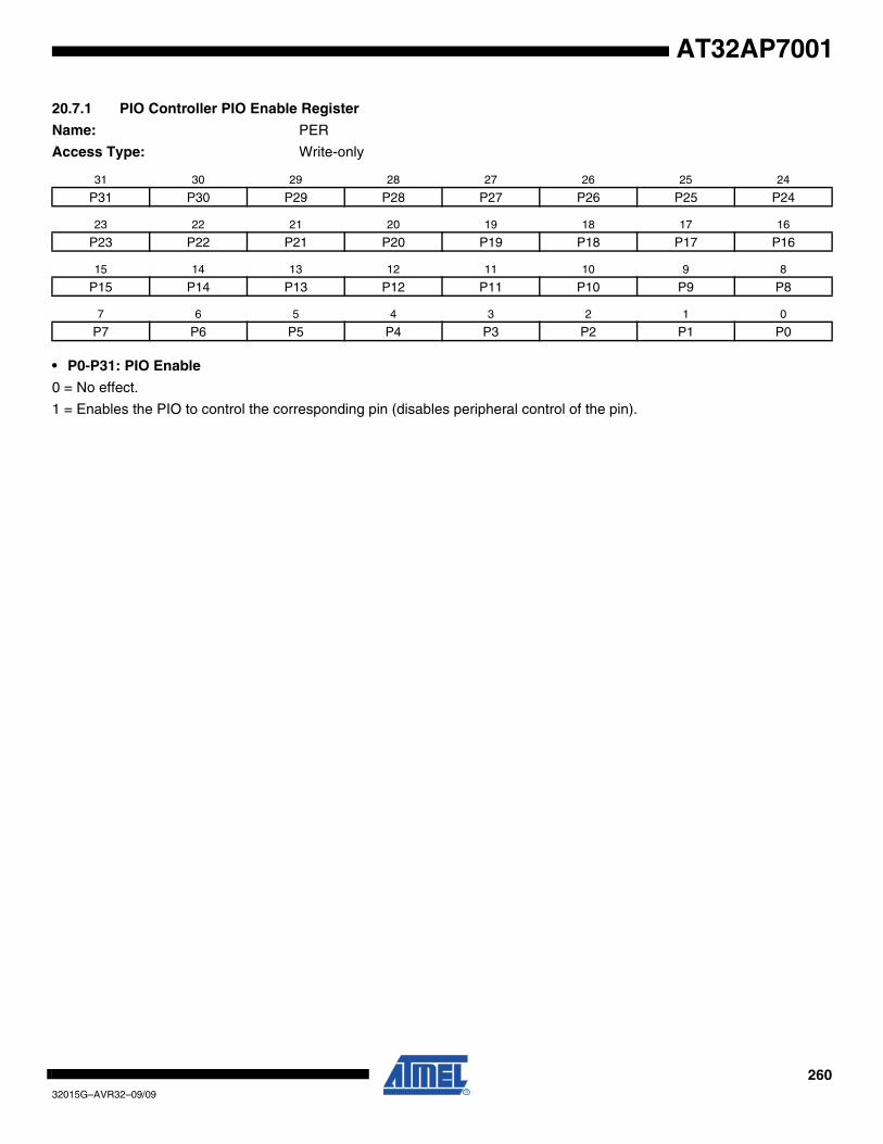
26032015G–AVR32–09/09
AT32AP7001
20.7.1 PIO Controller PIO Enable Register
Name: PER
Access Type: Write-only
• P0-P31: PIO Enable
0 = No effect.
1 = Enables the PIO to control the corresponding pin (disables peripheral control of the pin).
31 30 29 28 27 26 25 24
P31 P30 P29 P28 P27 P26 P25 P24
23 22 21 20 19 18 17 16
P23 P22 P21 P20 P19 P18 P17 P16
15 14 13 12 11 10 9 8
P15 P14 P13 P12 P11 P10 P9 P8
7 6 5 4 3 2 1 0
P7 P6 P5 P4 P3 P2 P1 P0
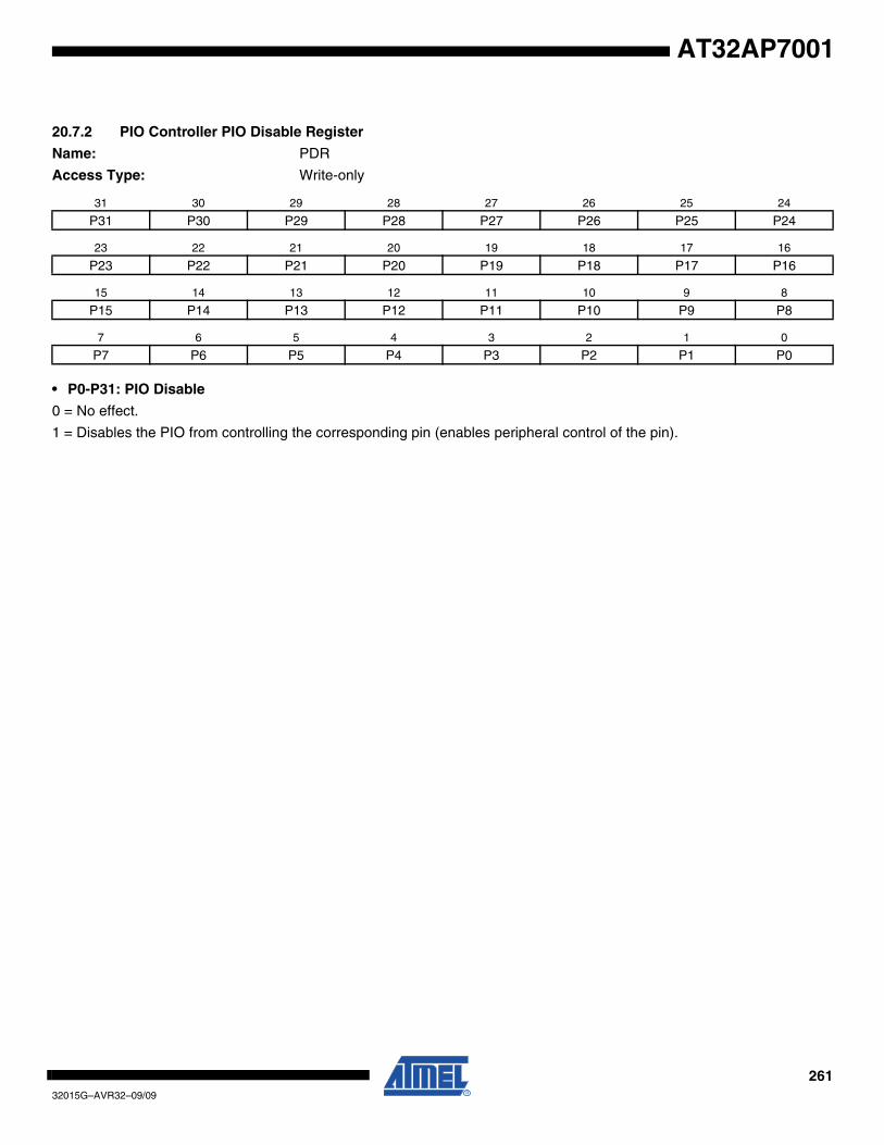
26132015G–AVR32–09/09
AT32AP7001
20.7.2 PIO Controller PIO Disable Register
Name: PDR
Access Type: Write-only
• P0-P31: PIO Disable
0 = No effect.
1 = Disables the PIO from controlling the corresponding pin (enables peripheral control of the pin).
31 30 29 28 27 26 25 24
P31 P30 P29 P28 P27 P26 P25 P24
23 22 21 20 19 18 17 16
P23 P22 P21 P20 P19 P18 P17 P16
15 14 13 12 11 10 9 8
P15 P14 P13 P12 P11 P10 P9 P8
7 6 5 4 3 2 1 0
P7 P6 P5 P4 P3 P2 P1 P0
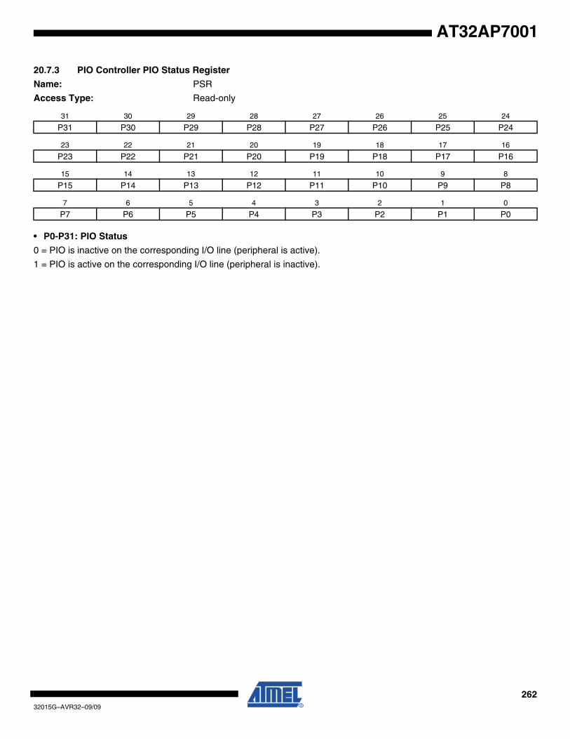
26232015G–AVR32–09/09
AT32AP7001
20.7.3 PIO Controller PIO Status Register
Name: PSR
Access Type: Read-only
• P0-P31: PIO Status
0 = PIO is inactive on the corresponding I/O line (peripheral is active).
1 = PIO is active on the corresponding I/O line (peripheral is inactive).
31 30 29 28 27 26 25 24
P31 P30 P29 P28 P27 P26 P25 P24
23 22 21 20 19 18 17 16
P23 P22 P21 P20 P19 P18 P17 P16
15 14 13 12 11 10 9 8
P15 P14 P13 P12 P11 P10 P9 P8
7 6 5 4 3 2 1 0
P7 P6 P5 P4 P3 P2 P1 P0
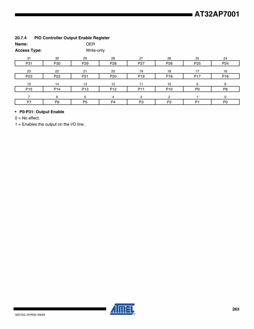
26332015G–AVR32–09/09
AT32AP7001
20.7.4 PIO Controller Output Enable Register
Name: OER
Access Type: Write-only
• P0-P31: Output Enable
0 = No effect.
1 = Enables the output on the I/O line.
31 30 29 28 27 26 25 24
P31 P30 P29 P28 P27 P26 P25 P24
23 22 21 20 19 18 17 16
P23 P22 P21 P20 P19 P18 P17 P16
15 14 13 12 11 10 9 8
P15 P14 P13 P12 P11 P10 P9 P8
7 6 5 4 3 2 1 0
P7 P6 P5 P4 P3 P2 P1 P0
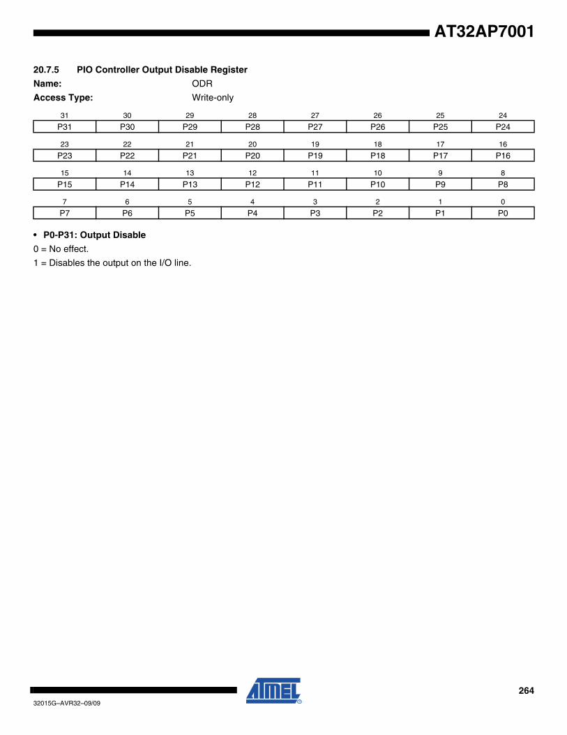
26432015G–AVR32–09/09
AT32AP7001
20.7.5 PIO Controller Output Disable Register
Name: ODR
Access Type: Write-only
• P0-P31: Output Disable
0 = No effect.
1 = Disables the output on the I/O line.
31 30 29 28 27 26 25 24
P31 P30 P29 P28 P27 P26 P25 P24
23 22 21 20 19 18 17 16
P23 P22 P21 P20 P19 P18 P17 P16
15 14 13 12 11 10 9 8
P15 P14 P13 P12 P11 P10 P9 P8
7 6 5 4 3 2 1 0
P7 P6 P5 P4 P3 P2 P1 P0

26532015G–AVR32–09/09
AT32AP7001
20.7.6 PIO Controller Output Status Register
Name: OSR
Access Type: Read-only
• P0-P31: Output Status
0 = The I/O line is a pure input.
1 = The I/O line is enabled in output.
31 30 29 28 27 26 25 24
P31 P30 P29 P28 P27 P26 P25 P24
23 22 21 20 19 18 17 16
P23 P22 P21 P20 P19 P18 P17 P16
15 14 13 12 11 10 9 8
P15 P14 P13 P12 P11 P10 P9 P8
7 6 5 4 3 2 1 0
P7 P6 P5 P4 P3 P2 P1 P0
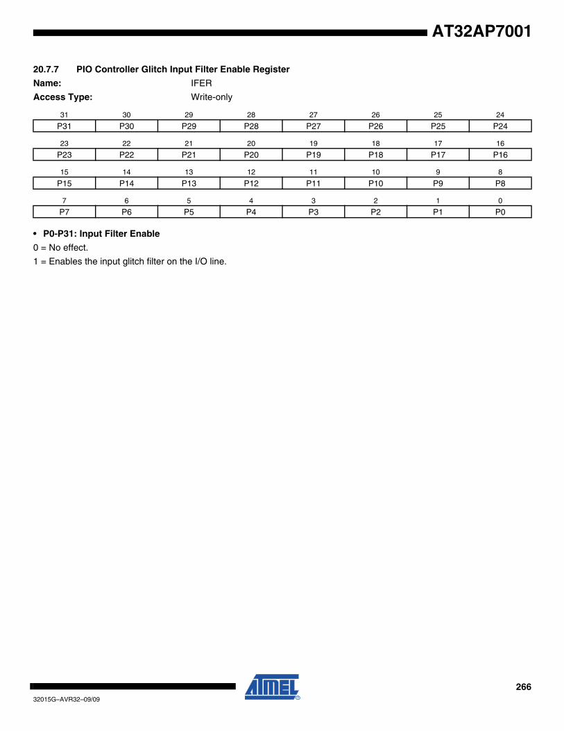
26632015G–AVR32–09/09
AT32AP7001
20.7.7 PIO Controller Glitch Input Filter Enable Register
Name: IFER
Access Type: Write-only
• P0-P31: Input Filter Enable
0 = No effect.
1 = Enables the input glitch filter on the I/O line.
31 30 29 28 27 26 25 24
P31 P30 P29 P28 P27 P26 P25 P24
23 22 21 20 19 18 17 16
P23 P22 P21 P20 P19 P18 P17 P16
15 14 13 12 11 10 9 8
P15 P14 P13 P12 P11 P10 P9 P8
7 6 5 4 3 2 1 0
P7 P6 P5 P4 P3 P2 P1 P0
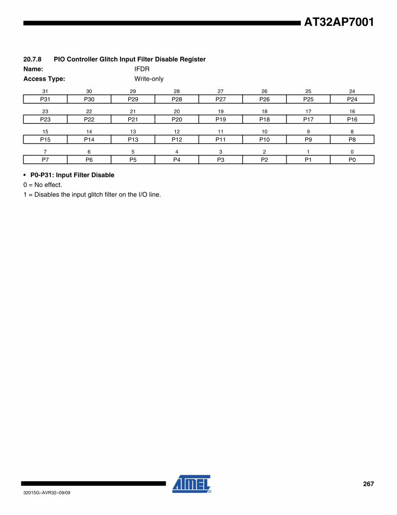
26732015G–AVR32–09/09
AT32AP7001
20.7.8 PIO Controller Glitch Input Filter Disable Register
Name: IFDR
Access Type: Write-only
• P0-P31: Input Filter Disable
0 = No effect.
1 = Disables the input glitch filter on the I/O line.
31 30 29 28 27 26 25 24
P31 P30 P29 P28 P27 P26 P25 P24
23 22 21 20 19 18 17 16
P23 P22 P21 P20 P19 P18 P17 P16
15 14 13 12 11 10 9 8
P15 P14 P13 P12 P11 P10 P9 P8
7 6 5 4 3 2 1 0
P7 P6 P5 P4 P3 P2 P1 P0
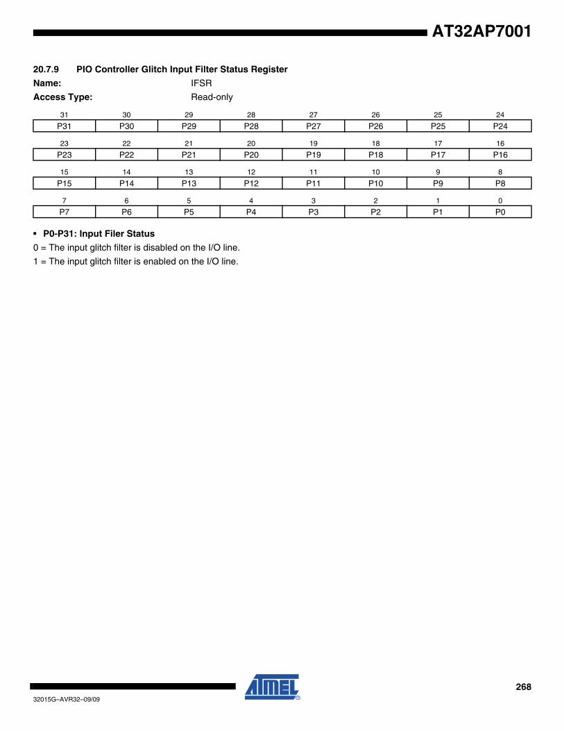
26832015G–AVR32–09/09
AT32AP7001
20.7.9 PIO Controller Glitch Input Filter Status Register
Name: IFSR
Access Type: Read-only
• P0-P31: Input Filer Status
0 = The input glitch filter is disabled on the I/O line.
1 = The input glitch filter is enabled on the I/O line.
31 30 29 28 27 26 25 24
P31 P30 P29 P28 P27 P26 P25 P24
23 22 21 20 19 18 17 16
P23 P22 P21 P20 P19 P18 P17 P16
15 14 13 12 11 10 9 8
P15 P14 P13 P12 P11 P10 P9 P8
7 6 5 4 3 2 1 0
P7 P6 P5 P4 P3 P2 P1 P0
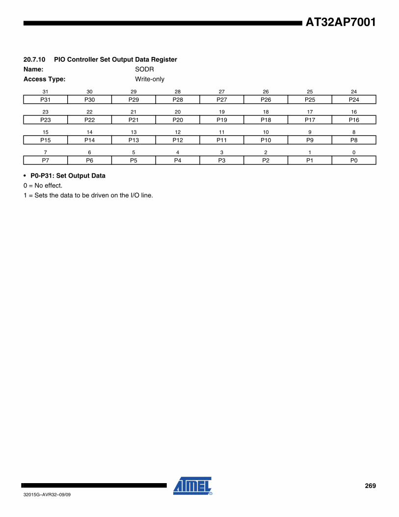
26932015G–AVR32–09/09
AT32AP7001
20.7.10 PIO Controller Set Output Data Register
Name: SODR
Access Type: Write-only
• P0-P31: Set Output Data
0 = No effect.
1 = Sets the data to be driven on the I/O line.
31 30 29 28 27 26 25 24
P31 P30 P29 P28 P27 P26 P25 P24
23 22 21 20 19 18 17 16
P23 P22 P21 P20 P19 P18 P17 P16
15 14 13 12 11 10 9 8
P15 P14 P13 P12 P11 P10 P9 P8
7 6 5 4 3 2 1 0
P7 P6 P5 P4 P3 P2 P1 P0
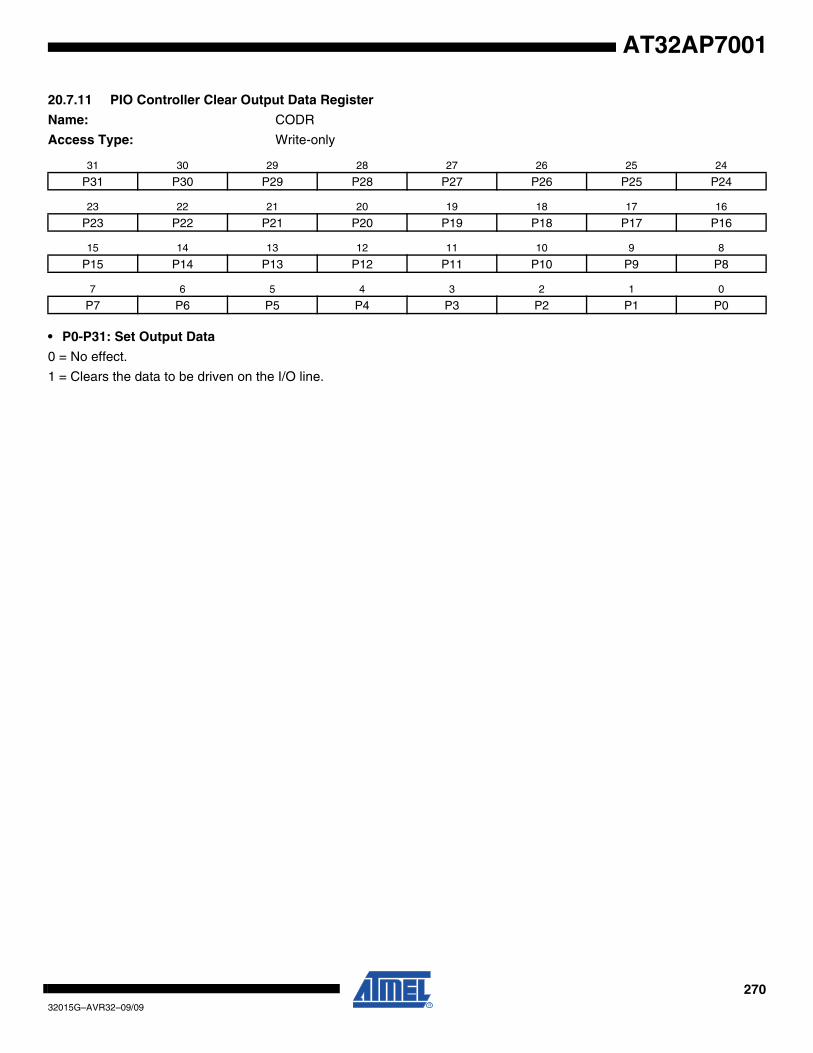
27032015G–AVR32–09/09
AT32AP7001
20.7.11 PIO Controller Clear Output Data Register
Name: CODR
Access Type: Write-only
• P0-P31: Set Output Data
0 = No effect.
1 = Clears the data to be driven on the I/O line.
31 30 29 28 27 26 25 24
P31 P30 P29 P28 P27 P26 P25 P24
23 22 21 20 19 18 17 16
P23 P22 P21 P20 P19 P18 P17 P16
15 14 13 12 11 10 9 8
P15 P14 P13 P12 P11 P10 P9 P8
7 6 5 4 3 2 1 0
P7 P6 P5 P4 P3 P2 P1 P0
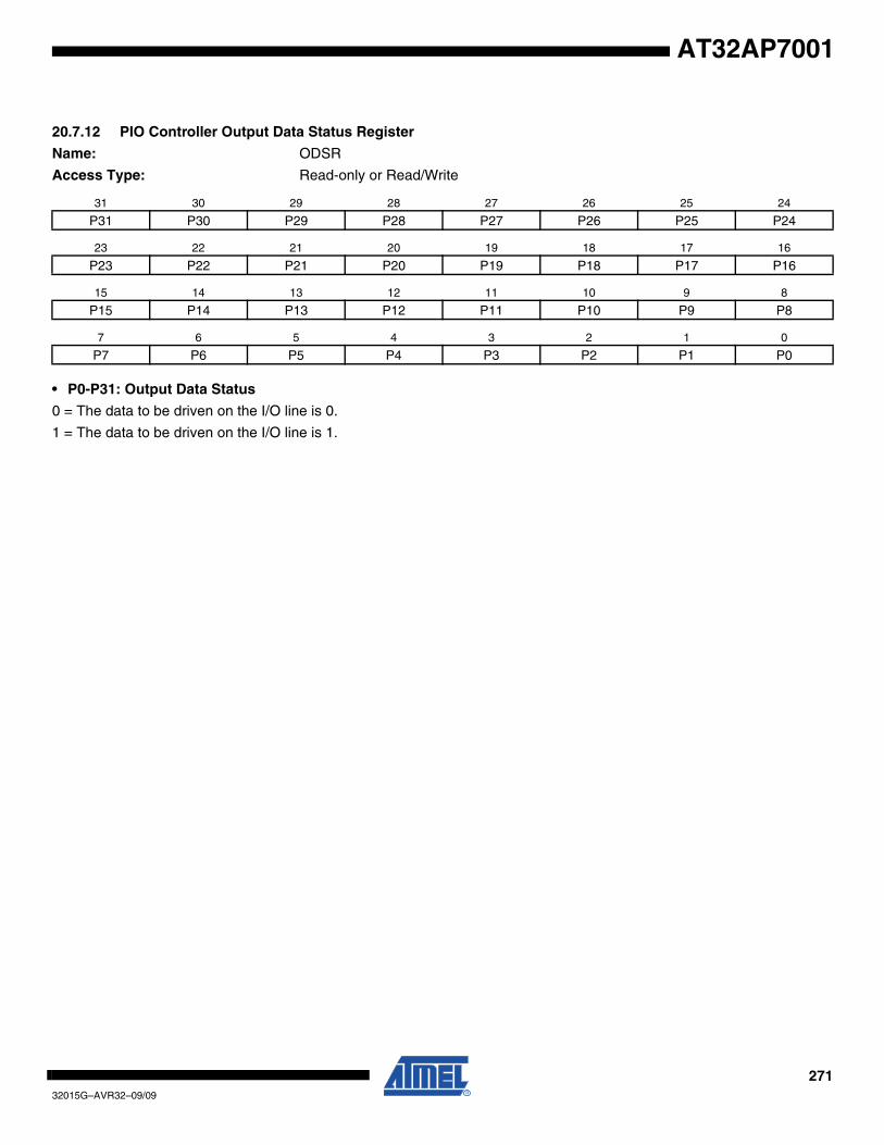
27132015G–AVR32–09/09
AT32AP7001
20.7.12 PIO Controller Output Data Status Register
Name: ODSR
Access Type: Read-only or Read/Write
• P0-P31: Output Data Status
0 = The data to be driven on the I/O line is 0.
1 = The data to be driven on the I/O line is 1.
31 30 29 28 27 26 25 24
P31 P30 P29 P28 P27 P26 P25 P24
23 22 21 20 19 18 17 16
P23 P22 P21 P20 P19 P18 P17 P16
15 14 13 12 11 10 9 8
P15 P14 P13 P12 P11 P10 P9 P8
7 6 5 4 3 2 1 0
P7 P6 P5 P4 P3 P2 P1 P0

27232015G–AVR32–09/09
AT32AP7001
20.7.13 PIO Controller Pin Data Status Register
Name: PDSR
Access Type: Read-only
• P0-P31: Output Data Status
0 = The I/O line is at level 0.
1 = The I/O line is at level 1.
31 30 29 28 27 26 25 24
P31 P30 P29 P28 P27 P26 P25 P24
23 22 21 20 19 18 17 16
P23 P22 P21 P20 P19 P18 P17 P16
15 14 13 12 11 10 9 8
P15 P14 P13 P12 P11 P10 P9 P8
7 6 5 4 3 2 1 0
P7 P6 P5 P4 P3 P2 P1 P0
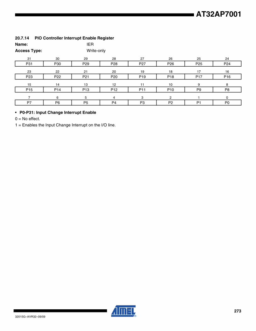
27332015G–AVR32–09/09
AT32AP7001
20.7.14 PIO Controller Interrupt Enable Register
Name: IER
Access Type: Write-only
• P0-P31: Input Change Interrupt Enable
0 = No effect.
1 = Enables the Input Change Interrupt on the I/O line.
31 30 29 28 27 26 25 24
P31 P30 P29 P28 P27 P26 P25 P24
23 22 21 20 19 18 17 16
P23 P22 P21 P20 P19 P18 P17 P16
15 14 13 12 11 10 9 8
P15 P14 P13 P12 P11 P10 P9 P8
7 6 5 4 3 2 1 0
P7 P6 P5 P4 P3 P2 P1 P0
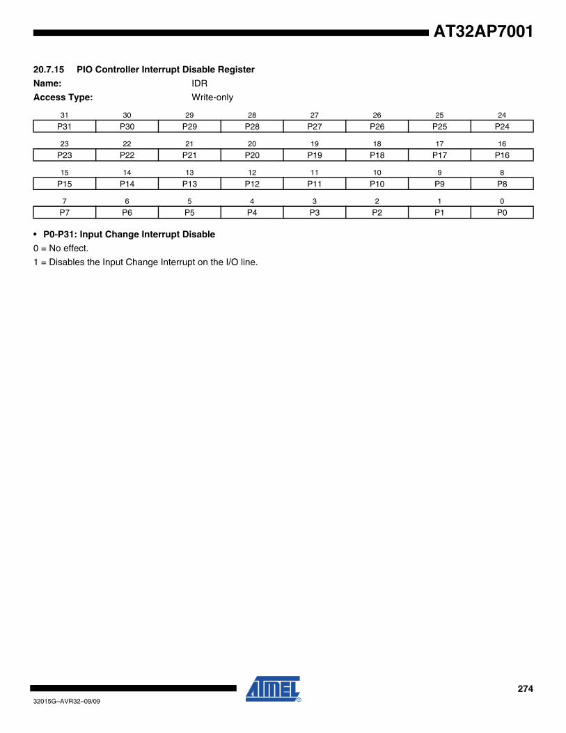
27432015G–AVR32–09/09
AT32AP7001
20.7.15 PIO Controller Interrupt Disable Register
Name: IDR
Access Type: Write-only
• P0-P31: Input Change Interrupt Disable
0 = No effect.
1 = Disables the Input Change Interrupt on the I/O line.
31 30 29 28 27 26 25 24
P31 P30 P29 P28 P27 P26 P25 P24
23 22 21 20 19 18 17 16
P23 P22 P21 P20 P19 P18 P17 P16
15 14 13 12 11 10 9 8
P15 P14 P13 P12 P11 P10 P9 P8
7 6 5 4 3 2 1 0
P7 P6 P5 P4 P3 P2 P1 P0

27532015G–AVR32–09/09
AT32AP7001
20.7.16 PIO Controller Interrupt Mask Register
Name: IMR
Access Type: Read-only
• P0-P31: Input Change Interrupt Mask
0 = Input Change Interrupt is disabled on the I/O line.
1 = Input Change Interrupt is enabled on the I/O line.
31 30 29 28 27 26 25 24
P31 P30 P29 P28 P27 P26 P25 P24
23 22 21 20 19 18 17 16
P23 P22 P21 P20 P19 P18 P17 P16
15 14 13 12 11 10 9 8
P15 P14 P13 P12 P11 P10 P9 P8
7 6 5 4 3 2 1 0
P7 P6 P5 P4 P3 P2 P1 P0
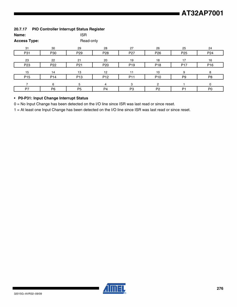
27632015G–AVR32–09/09
AT32AP7001
20.7.17 PIO Controller Interrupt Status Register
Name: ISR
Access Type: Read-only
• P0-P31: Input Change Interrupt Status
0 = No Input Change has been detected on the I/O line since ISR was last read or since reset.
1 = At least one Input Change has been detected on the I/O line since ISR was last read or since reset.
31 30 29 28 27 26 25 24
P31 P30 P29 P28 P27 P26 P25 P24
23 22 21 20 19 18 17 16
P23 P22 P21 P20 P19 P18 P17 P16
15 14 13 12 11 10 9 8
P15 P14 P13 P12 P11 P10 P9 P8
7 6 5 4 3 2 1 0
P7 P6 P5 P4 P3 P2 P1 P0
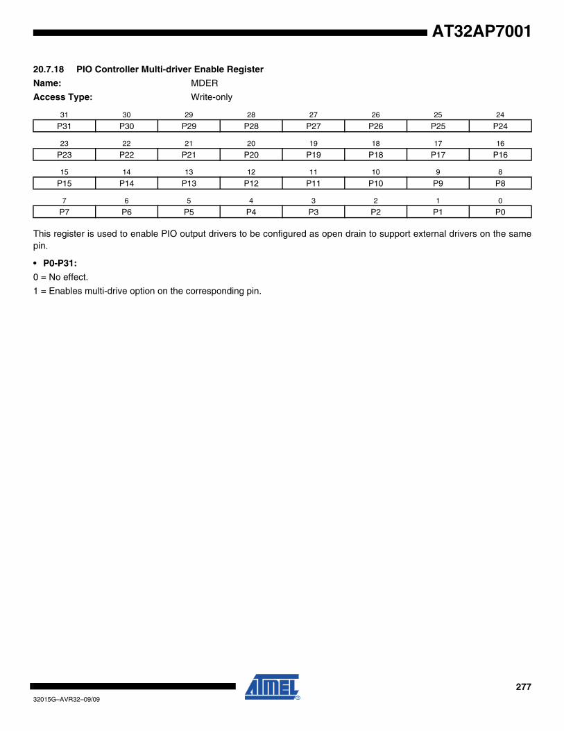
27732015G–AVR32–09/09
AT32AP7001
20.7.18 PIO Controller Multi-driver Enable Register
Name: MDER
Access Type: Write-only
This register is used to enable PIO output drivers to be configured as open drain to support external drivers on the samepin.
• P0-P31:
0 = No effect.
1 = Enables multi-drive option on the corresponding pin.
31 30 29 28 27 26 25 24
P31 P30 P29 P28 P27 P26 P25 P24
23 22 21 20 19 18 17 16
P23 P22 P21 P20 P19 P18 P17 P16
15 14 13 12 11 10 9 8
P15 P14 P13 P12 P11 P10 P9 P8
7 6 5 4 3 2 1 0
P7 P6 P5 P4 P3 P2 P1 P0

27832015G–AVR32–09/09
AT32AP7001
20.7.19 PIO Controller Multi-driver Disable Register
Name: MDDR
Access Type: Write-only
This register is used to diasble the open drain configuration of the output buffer.
• P0-P31:
0 = No effect.
1 = Disables multi-drive option on the corresponding pin.
31 30 29 28 27 26 25 24
P31 P30 P29 P28 P27 P26 P25 P24
23 22 21 20 19 18 17 16
P23 P22 P21 P20 P19 P18 P17 P16
15 14 13 12 11 10 9 8
P15 P14 P13 P12 P11 P10 P9 P8
7 6 5 4 3 2 1 0
P7 P6 P5 P4 P3 P2 P1 P0
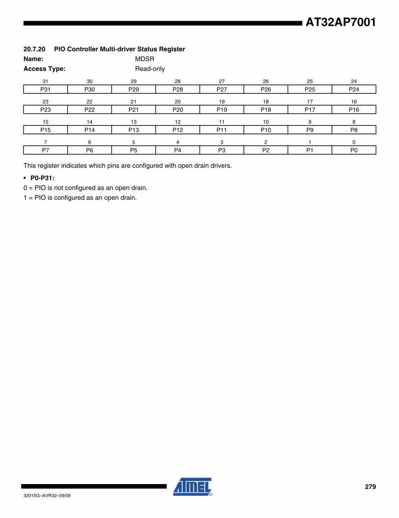
27932015G–AVR32–09/09
AT32AP7001
20.7.20 PIO Controller Multi-driver Status Register
Name: MDSR
Access Type: Read-only
This register indicates which pins are configured with open drain drivers.
• P0-P31:
0 = PIO is not configured as an open drain.
1 = PIO is configured as an open drain.
31 30 29 28 27 26 25 24
P31 P30 P29 P28 P27 P26 P25 P24
23 22 21 20 19 18 17 16
P23 P22 P21 P20 P19 P18 P17 P16
15 14 13 12 11 10 9 8
P15 P14 P13 P12 P11 P10 P9 P8
7 6 5 4 3 2 1 0
P7 P6 P5 P4 P3 P2 P1 P0
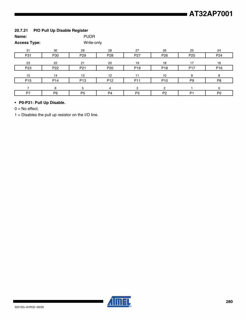
28032015G–AVR32–09/09
AT32AP7001
20.7.21 PIO Pull Up Disable Register
Name: PUDR
Access Type: Write-only
• P0-P31: Pull Up Disable.
0 = No effect.
1 = Disables the pull up resistor on the I/O line.
31 30 29 28 27 26 25 24
P31 P30 P29 P28 P27 P26 P25 P24
23 22 21 20 19 18 17 16
P23 P22 P21 P20 P19 P18 P17 P16
15 14 13 12 11 10 9 8
P15 P14 P13 P12 P11 P10 P9 P8
7 6 5 4 3 2 1 0
P7 P6 P5 P4 P3 P2 P1 P0
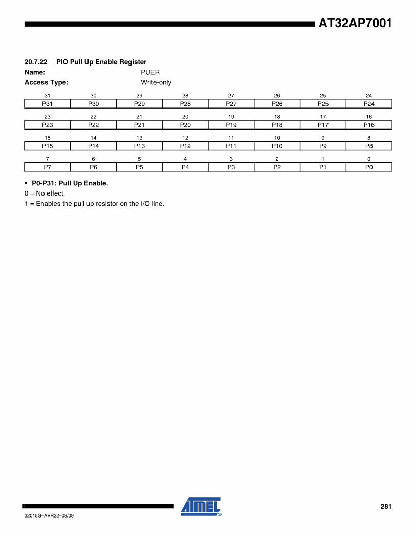
28132015G–AVR32–09/09
AT32AP7001
20.7.22 PIO Pull Up Enable Register
Name: PUER
Access Type: Write-only
• P0-P31: Pull Up Enable.
0 = No effect.
1 = Enables the pull up resistor on the I/O line.
31 30 29 28 27 26 25 24
P31 P30 P29 P28 P27 P26 P25 P24
23 22 21 20 19 18 17 16
P23 P22 P21 P20 P19 P18 P17 P16
15 14 13 12 11 10 9 8
P15 P14 P13 P12 P11 P10 P9 P8
7 6 5 4 3 2 1 0
P7 P6 P5 P4 P3 P2 P1 P0
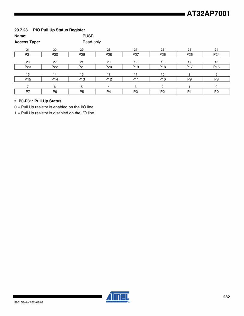
28232015G–AVR32–09/09
AT32AP7001
20.7.23 PIO Pull Up Status Register
Name: PUSR
Access Type: Read-only
• P0-P31: Pull Up Status.
0 = Pull Up resistor is enabled on the I/O line.
1 = Pull Up resistor is disabled on the I/O line.
31 30 29 28 27 26 25 24
P31 P30 P29 P28 P27 P26 P25 P24
23 22 21 20 19 18 17 16
P23 P22 P21 P20 P19 P18 P17 P16
15 14 13 12 11 10 9 8
P15 P14 P13 P12 P11 P10 P9 P8
7 6 5 4 3 2 1 0
P7 P6 P5 P4 P3 P2 P1 P0
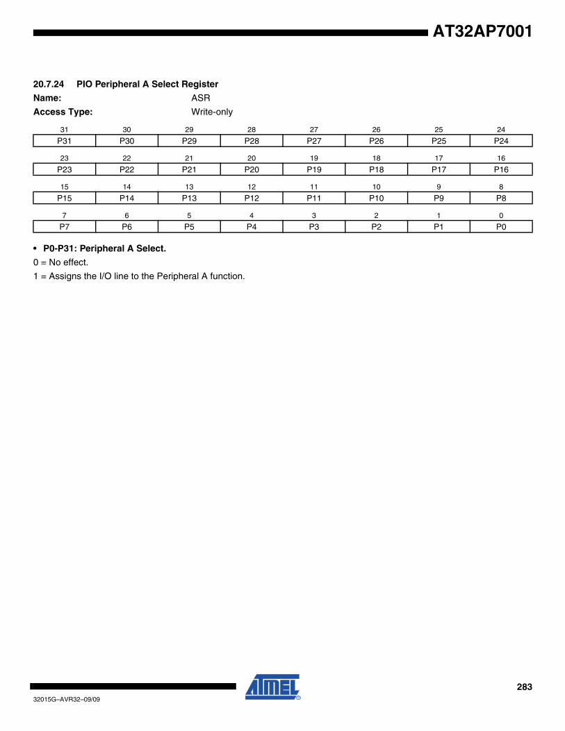
28332015G–AVR32–09/09
AT32AP7001
20.7.24 PIO Peripheral A Select Register
Name: ASR
Access Type: Write-only
• P0-P31: Peripheral A Select.
0 = No effect.
1 = Assigns the I/O line to the Peripheral A function.
31 30 29 28 27 26 25 24
P31 P30 P29 P28 P27 P26 P25 P24
23 22 21 20 19 18 17 16
P23 P22 P21 P20 P19 P18 P17 P16
15 14 13 12 11 10 9 8
P15 P14 P13 P12 P11 P10 P9 P8
7 6 5 4 3 2 1 0
P7 P6 P5 P4 P3 P2 P1 P0
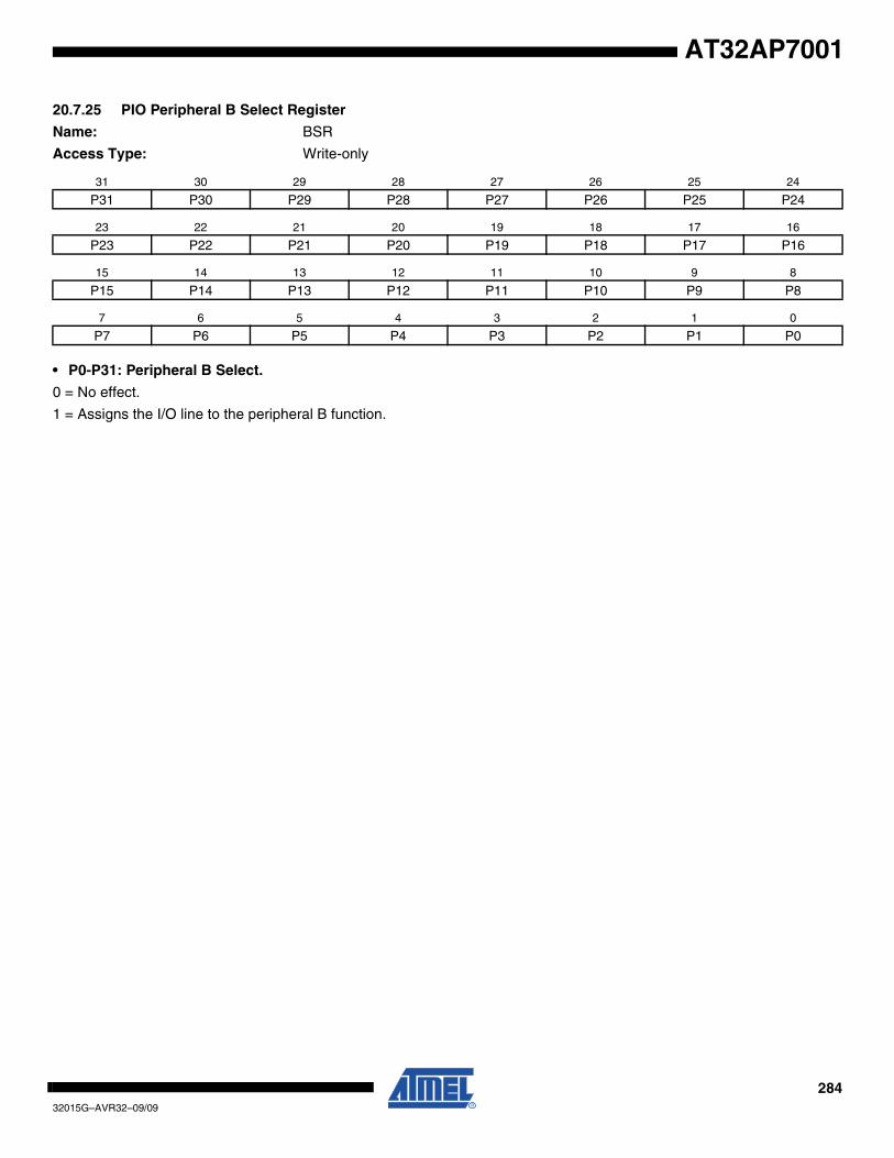
28432015G–AVR32–09/09
AT32AP7001
20.7.25 PIO Peripheral B Select Register
Name: BSR
Access Type: Write-only
• P0-P31: Peripheral B Select.
0 = No effect.
1 = Assigns the I/O line to the peripheral B function.
31 30 29 28 27 26 25 24
P31 P30 P29 P28 P27 P26 P25 P24
23 22 21 20 19 18 17 16
P23 P22 P21 P20 P19 P18 P17 P16
15 14 13 12 11 10 9 8
P15 P14 P13 P12 P11 P10 P9 P8
7 6 5 4 3 2 1 0
P7 P6 P5 P4 P3 P2 P1 P0

28532015G–AVR32–09/09
AT32AP7001
20.7.26 PIO Peripheral A B Status Register
Name: ABSR
Access Type: Read-only
• P0-P31: Peripheral A B Status.
0 = The I/O line is assigned to the Peripheral A.
1 = The I/O line is assigned to the Peripheral B.
31 30 29 28 27 26 25 24
P31 P30 P29 P28 P27 P26 P25 P24
23 22 21 20 19 18 17 16
P23 P22 P21 P20 P19 P18 P17 P16
15 14 13 12 11 10 9 8
P15 P14 P13 P12 P11 P10 P9 P8
7 6 5 4 3 2 1 0
P7 P6 P5 P4 P3 P2 P1 P0

28632015G–AVR32–09/09
AT32AP7001
20.7.27 PIO Output Write Enable Register
Name: OWER
Access Type: Write-only
• P0-P31: Output Write Enable.
0 = No effect.
1 = Enables writing ODSR for the I/O line.
31 30 29 28 27 26 25 24
P31 P30 P29 P28 P27 P26 P25 P24
23 22 21 20 19 18 17 16
P23 P22 P21 P20 P19 P18 P17 P16
15 14 13 12 11 10 9 8
P15 P14 P13 P12 P11 P10 P9 P8
7 6 5 4 3 2 1 0
P7 P6 P5 P4 P3 P2 P1 P0

28732015G–AVR32–09/09
AT32AP7001
20.7.28 PIO Output Write Disable Register
Name: OWDR
Access Type: Write-only
• P0-P31: Output Write Disable.
0 = No effect.
1 = Disables writing ODSR for the I/O line.
31 30 29 28 27 26 25 24
P31 P30 P29 P28 P27 P26 P25 P24
23 22 21 20 19 18 17 16
P23 P22 P21 P20 P19 P18 P17 P16
15 14 13 12 11 10 9 8
P15 P14 P13 P12 P11 P10 P9 P8
7 6 5 4 3 2 1 0
P7 P6 P5 P4 P3 P2 P1 P0

28832015G–AVR32–09/09
AT32AP7001
20.7.29 PIO Output Write Status Register
Name: OWSR
Access Type: Read-only
• P0-P31: Output Write Status.
0 = Writing ODSR does not affect the I/O line.
1 = Writing ODSR affects the I/O line.
31 30 29 28 27 26 25 24
P31 P30 P29 P28 P27 P26 P25 P24
23 22 21 20 19 18 17 16
P23 P22 P21 P20 P19 P18 P17 P16
15 14 13 12 11 10 9 8
P15 P14 P13 P12 P11 P10 P9 P8
7 6 5 4 3 2 1 0
P7 P6 P5 P4 P3 P2 P1 P0
28932015G–AVR32–09/09
AT32AP7001
21. Serial Peripheral Interface (SPI)
Rev: 1.7.1.3
21.1 Features
• Supports Communication with Serial External Devices– Four Chip Selects with External Decoder Support Allow Communication with Up to 15
Peripherals– Serial Memories, such as DataFlash and 3-wire EEPROMs– Serial Peripherals, such as ADCs, DACs, CAN Controllers and Sensors– External Co-processors
• Master or Slave Serial Peripheral Bus Interface– 8- to 16-bit Programmable Data Length Per Chip Select – Programmable Phase and Polarity Per Chip Select– Programmable Transfer Delays Between Consecutive Transfers and Between Clock and Data
Per Chip Select– Programmable Delay Between Consecutive Transfers– Selectable Mode Fault Detection
• Connection to PDC Channel Capabilities Optimizes Data Transfers– One Channel for the Receiver, One Channel for the Transmitter– Next Buffer Support
21.2 Description
The Serial Peripheral Interface (SPI) circuit is a synchronous serial data link that provides com-munication with external devices in Master or Slave Mode. It also enables communicationbetween processors if an external processor is connected to the system.
The Serial Peripheral Interface is essentially a shift register that serially transmits data bits toother SPIs. During a data transfer, one SPI system acts as the “master”' which controls the dataflow, while the other devices act as “slaves'' which have data shifted into and out by the master.Different CPUs can take turn being masters (Multiple Master Protocol opposite to Single MasterProtocol where one CPU is always the master while all of the others are always slaves) and onemaster may simultaneously shift data into multiple slaves. However, only one slave may drive itsoutput to write data back to the master at any given time.
A slave device is selected when the master asserts its NSS signal. If multiple slave devicesexist, the master generates a separate slave select signal for each slave (NPCS).
The SPI system consists of two data lines and two control lines:
• Master Out Slave In (MOSI): This data line supplies the output data from the master shifted into the input(s) of the slave(s).
• Master In Slave Out (MISO): This data line supplies the output data from a slave to the input of the master. There may be no more than one slave transmitting data during any particular transfer.
• Serial Clock (SPCK): This control line is driven by the master and regulates the flow of the data bits. The master may transmit data at a variety of baud rates; the SPCK line cycles once for each bit that is transmitted.
• Slave Select (NSS): This control line allows slaves to be turned on and off by hardware.
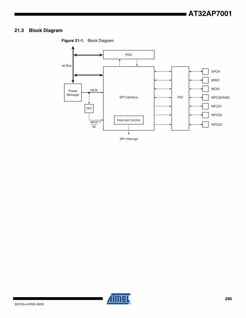
29032015G–AVR32–09/09
AT32AP7001
21.3 Block Diagram
Figure 21-1. Block Diagram
SPI Interface
Interrupt Control
PIO
PDC
PowerManager
MCK
SPI Interrupt
SPCK
MISO
MOSI
NPCS0/NSS
NPCS1
NPCS2
DIV
NPCS3
ral Bus
MCK32
(1)
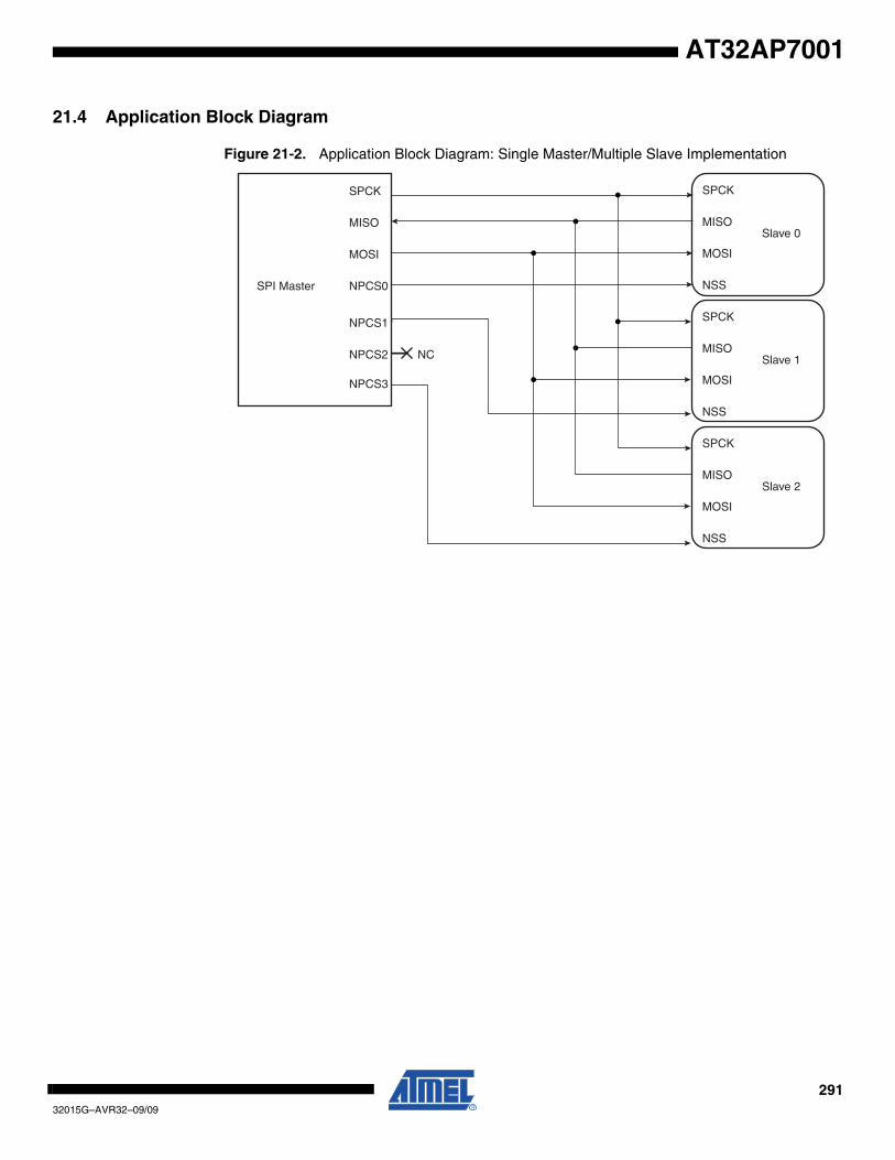
29132015G–AVR32–09/09
AT32AP7001
21.4 Application Block Diagram
Figure 21-2. Application Block Diagram: Single Master/Multiple Slave Implementation
SPI Master
SPCK
MISO
MOSI
NPCS0
NPCS1
NPCS2
SPCK
MISO
MOSI
NSS
Slave 0
SPCK
MISO
MOSI
NSS
Slave 1
SPCK
MISO
MOSI
NSS
Slave 2
NC
NPCS3

29232015G–AVR32–09/09
AT32AP7001
21.5 Signal Description
Table 21-1. Signal Description
Pin Name Pin Description
Type
Master Slave
MISO Master In Slave Out Input Output
MOSI Master Out Slave In Output Input
SPCK Serial Clock Output Input
NPCS1-NPCS3 Peripheral Chip Selects Output Unused
NPCS0/NSS Peripheral Chip Select/Slave Select Output Input
29332015G–AVR32–09/09
AT32AP7001
21.6 Product Dependencies
21.6.1 I/O Lines
The pins used for interfacing the compliant external devices may be multiplexed with PIO lines.The programmer must first program the PIO controllers to assign the SPI pins to their peripheralfunctions. To use the local loopback function the SPI pins must be controlled by the SPI.
21.6.2 Power Management
The SPI clock is generated by the Power Manager. Before using the SPI, the programmer mustensure that the SPI clock is enabled in the Power Manager.
In the SPI description, Master Clock (MCK) is the clock of the peripheral bus to which the SPI isconnected.
21.6.3 Interrupt
The SPI interface has an interrupt line connected to the Interrupt Controller. Handling the SPIinterrupt requires programming the interrupt controller before configuring the SPI.

29432015G–AVR32–09/09
AT32AP7001
21.7 Functional Description
21.7.1 Modes of Operation
The SPI operates in Master Mode or in Slave Mode.
Operation in Master Mode is programmed by writing at 1 the MSTR bit in the Mode Register.The pins NPCS0 to NPCS3 are all configured as outputs, the SPCK pin is driven, the MISO lineis wired on the receiver input and the MOSI line driven as an output by the transmitter.
If the MSTR bit is written at 0, the SPI operates in Slave Mode. The MISO line is driven by thetransmitter output, the MOSI line is wired on the receiver input, the SPCK pin is driven by thetransmitter to synchronize the receiver. The NPCS0 pin becomes an input, and is used as aSlave Select signal (NSS). The pins NPCS1 to NPCS3 are not driven and can be used for otherpurposes.
The data transfers are identically programmable for both modes of operations. The baud rategenerator is activated only in Master Mode.
21.7.2 Data Transfer
Four combinations of polarity and phase are available for data transfers. The clock polarity isprogrammed with the CPOL bit in the Chip Select Register. The clock phase is programmed withthe NCPHA bit. These two parameters determine the edges of the clock signal on which data isdriven and sampled. Each of the two parameters has two possible states, resulting in four possi-ble combinations that are incompatible with one another. Thus, a master/slave pair must use thesame parameter pair values to communicate. If multiple slaves are used and fixed in differentconfigurations, the master must reconfigure itself each time it needs to communicate with a dif-ferent slave.
Table 21-2 shows the four modes and corresponding parameter settings.
Figure 21-3 and Figure 21-4 show examples of data transfers.
Table 21-2. SPI Bus Protocol Mode
SPI Mode CPOL NCPHA
0 0 1
1 0 0
2 1 1
3 1 0
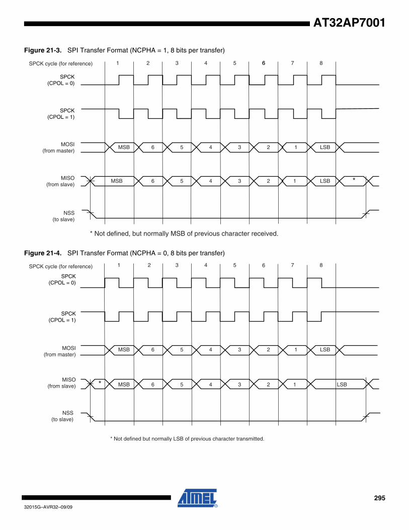
29532015G–AVR32–09/09
AT32AP7001
Figure 21-3. SPI Transfer Format (NCPHA = 1, 8 bits per transfer)
Figure 21-4. SPI Transfer Format (NCPHA = 0, 8 bits per transfer)
6
*
SPCK(CPOL = 0)
SPCK(CPOL = 1)
MOSI(from master)
MISO(from slave)
NSS(to slave)
SPCK cycle (for reference)
MSB
MSB
LSB
LSB
6
6
5
5
4
4
3
3
2
2
1
1
* Not defined, but normally MSB of previous character received.
1 2 3 4 5 7 86
*
SPCK(CPOL = 0)
SPCK(CPOL = 1)
1 2 3 4 5 7
MOSI(from master)
MISO(from slave)
NSS(to slave)
SPCK cycle (for reference) 8
MSB
MSB
LSB
LSB
6
6
5
5
4
4
3
3
1
1
* Not defined but normally LSB of previous character transmitted.
2
2
6
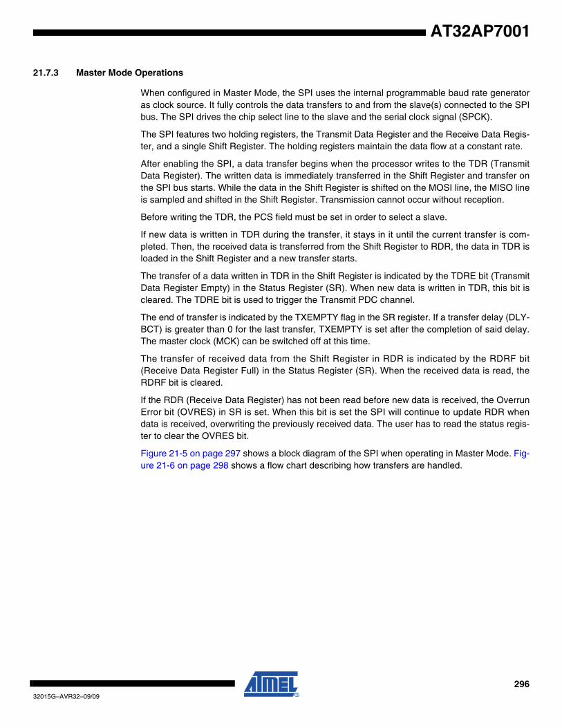
29632015G–AVR32–09/09
AT32AP7001
21.7.3 Master Mode Operations
When configured in Master Mode, the SPI uses the internal programmable baud rate generatoras clock source. It fully controls the data transfers to and from the slave(s) connected to the SPIbus. The SPI drives the chip select line to the slave and the serial clock signal (SPCK).
The SPI features two holding registers, the Transmit Data Register and the Receive Data Regis-ter, and a single Shift Register. The holding registers maintain the data flow at a constant rate.
After enabling the SPI, a data transfer begins when the processor writes to the TDR (TransmitData Register). The written data is immediately transferred in the Shift Register and transfer onthe SPI bus starts. While the data in the Shift Register is shifted on the MOSI line, the MISO lineis sampled and shifted in the Shift Register. Transmission cannot occur without reception.
Before writing the TDR, the PCS field must be set in order to select a slave.
If new data is written in TDR during the transfer, it stays in it until the current transfer is com-pleted. Then, the received data is transferred from the Shift Register to RDR, the data in TDR isloaded in the Shift Register and a new transfer starts.
The transfer of a data written in TDR in the Shift Register is indicated by the TDRE bit (TransmitData Register Empty) in the Status Register (SR). When new data is written in TDR, this bit iscleared. The TDRE bit is used to trigger the Transmit PDC channel.
The end of transfer is indicated by the TXEMPTY flag in the SR register. If a transfer delay (DLY-BCT) is greater than 0 for the last transfer, TXEMPTY is set after the completion of said delay.The master clock (MCK) can be switched off at this time.
The transfer of received data from the Shift Register in RDR is indicated by the RDRF bit(Receive Data Register Full) in the Status Register (SR). When the received data is read, theRDRF bit is cleared.
If the RDR (Receive Data Register) has not been read before new data is received, the OverrunError bit (OVRES) in SR is set. When this bit is set the SPI will continue to update RDR whendata is received, overwriting the previously received data. The user has to read the status regis-ter to clear the OVRES bit.
Figure 21-5 on page 297 shows a block diagram of the SPI when operating in Master Mode. Fig-ure 21-6 on page 298 shows a flow chart describing how transfers are handled.
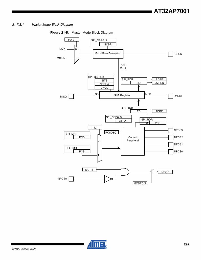
29732015G–AVR32–09/09
AT32AP7001
21.7.3.1 Master Mode Block Diagram
Figure 21-5. Master Mode Block Diagram
Shift Register
SPCK
MOSILSB MSB
MISO
SPI_RDRRD
SPI Clock
TDRESPI_TDR
TD
RDRFOVRES
SPI_CSR0..3
CPOLNCPHA
BITS
0
1
FDIV
MCK
MCK/N
Baud Rate Generator
SPI_CSR0..3
SCBR
NPCS3
NPCS0
NPCS2
NPCS1
NPCS0
0
1
PS
SPI_MRPCS
SPI_TDRPCS
MODF
CurrentPeripheral
SPI_RDRPCS
SPI_CSR0..3CSAAT
PCSDEC
MODFDIS
MSTR
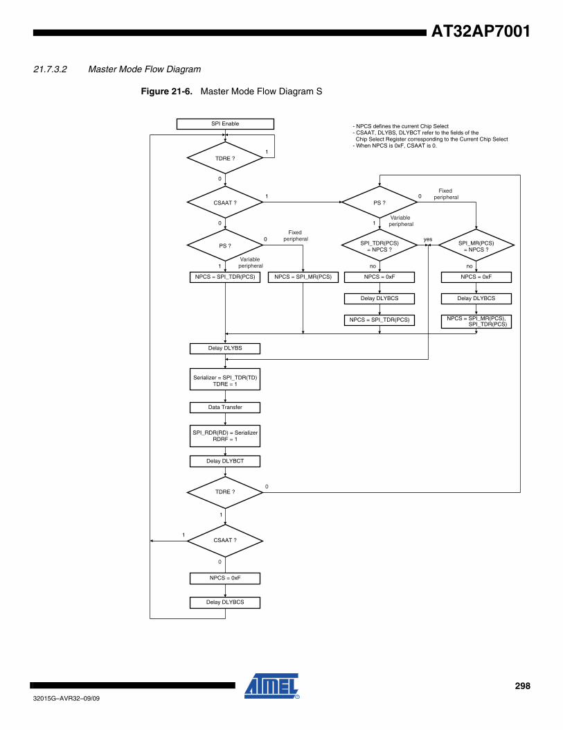
29832015G–AVR32–09/09
AT32AP7001
21.7.3.2 Master Mode Flow Diagram
Figure 21-6. Master Mode Flow Diagram S
SPI Enable
CSAAT ?
PS ?
1
0
0
1
1
NPCS = SPI_TDR(PCS) NPCS = SPI_MR(PCS)
Delay DLYBS
Serializer = SPI_TDR(TD)TDRE = 1
Data Transfer
SPI_RDR(RD) = SerializerRDRF = 1
TDRE ?
NPCS = 0xF
Delay DLYBCS
Fixed peripheral
Variable peripheral
Delay DLYBCT
0
1CSAAT ?
0
TDRE ?1
0
PS ?0
1
SPI_TDR(PCS)= NPCS ?
no
yesSPI_MR(PCS)
= NPCS ?
no
NPCS = 0xF
Delay DLYBCS
NPCS = SPI_TDR(PCS)
NPCS = 0xF
Delay DLYBCS
NPCS = SPI_MR(PCS), SPI_TDR(PCS)
Fixed peripheral
Variable peripheral
- NPCS defines the current Chip Select- CSAAT, DLYBS, DLYBCT refer to the fields of the Chip Select Register corresponding to the Current Chip Select- When NPCS is 0xF, CSAAT is 0.
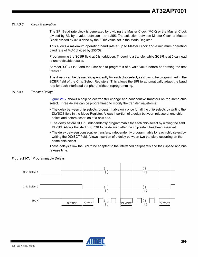
29932015G–AVR32–09/09
AT32AP7001
21.7.3.3 Clock Generation
The SPI Baud rate clock is generated by dividing the Master Clock (MCK) or the Master Clockdivided by 32, by a value between 1 and 255. The selection between Master Clock or MasterClock divided by 32 is done by the FDIV value set in the Mode Register
This allows a maximum operating baud rate at up to Master Clock and a minimum operatingbaud rate of MCK divided by 255*32.
Programming the SCBR field at 0 is forbidden. Triggering a transfer while SCBR is at 0 can leadto unpredictable results.
At reset, SCBR is 0 and the user has to program it at a valid value before performing the firsttransfer.
The divisor can be defined independently for each chip select, as it has to be programmed in theSCBR field of the Chip Select Registers. This allows the SPI to automatically adapt the baudrate for each interfaced peripheral without reprogramming.
21.7.3.4 Transfer Delays
Figure 21-7 shows a chip select transfer change and consecutive transfers on the same chipselect. Three delays can be programmed to modify the transfer waveforms:
• The delay between chip selects, programmable only once for all the chip selects by writing the DLYBCS field in the Mode Register. Allows insertion of a delay between release of one chip select and before assertion of a new one.
• The delay before SPCK, independently programmable for each chip select by writing the field DLYBS. Allows the start of SPCK to be delayed after the chip select has been asserted.
• The delay between consecutive transfers, independently programmable for each chip select by writing the DLYBCT field. Allows insertion of a delay between two transfers occurring on the same chip select
These delays allow the SPI to be adapted to the interfaced peripherals and their speed and busrelease time.
Figure 21-7. Programmable Delays
DLYBCS DLYBS DLYBCT DLYBCT
Chip Select 1
Chip Select 2
SPCK
30032015G–AVR32–09/09
AT32AP7001
21.7.3.5 Peripheral Selection
The serial peripherals are selected through the assertion of the NPCS0 to NPCS3 signals. Bydefault, all the NPCS signals are high before and after each transfer.
The peripheral selection can be performed in two different ways:
• Fixed Peripheral Select: SPI exchanges data with only one peripheral
• Variable Peripheral Select: Data can be exchanged with more than one peripheral
Fixed Peripheral Select is activated by writing the PS bit to zero in MR (Mode Register). In thiscase, the current peripheral is defined by the PCS field in MR and the PCS field in TDR have noeffect.
Variable Peripheral Select is activated by setting PS bit to one. The PCS field in TDR is used toselect the current peripheral. This means that the peripheral selection can be defined for eachnew data.
The Fixed Peripheral Selection allows buffer transfers with a single peripheral. Using the PDC isan optimal means, as the size of the data transfer between the memory and the SPI is either 8bits or 16 bits. However, changing the peripheral selection requires the Mode Register to bereprogrammed.
The Variable Peripheral Selection allows buffer transfers with multiple peripherals without repro-gramming the Mode Register. Data written in TDR is 32 bits wide and defines the real data to betransmitted and the peripheral it is destined to. Using the PDC in this mode requires 32-bit widebuffers, with the data in the LSBs and the PCS and LASTXFER fields in the MSBs, however theSPI still controls the number of bits (8 to16) to be transferred through MISO and MOSI lines withthe chip select configuration registers. This is not the optimal means in term of memory size forthe buffers, but it provides a very effective means to exchange data with several peripheralswithout any intervention of the processor.
21.7.3.6 Peripheral Chip Select Decoding
The user can program the SPI to operate with up to 15 peripherals by decoding the four ChipSelect lines, NPCS0 to NPCS3 with an external logic. This can be enabled by writing the PCS-DEC bit at 1 in the Mode Register (MR).
When operating without decoding, the SPI makes sure that in any case only one chip select lineis activated, i.e. driven low at a time. If two bits are defined low in a PCS field, only the lowestnumbered chip select is driven low.
When operating with decoding, the SPI directly outputs the value defined by the PCS field ofeither the Mode Register or the Transmit Data Register (depending on PS).
As the SPI sets a default value of 0xF on the chip select lines (i.e. all chip select lines at 1) whennot processing any transfer, only 15 peripherals can be decoded.
The SPI has only four Chip Select Registers, not 15. As a result, when decoding is activated,each chip select defines the characteristics of up to four peripherals. As an example, CRS0defines the characteristics of the externally decoded peripherals 0 to 3, corresponding to thePCS values 0x0 to 0x3. Thus, the user has to make sure to connect compatible peripherals onthe decoded chip select lines 0 to 3, 4 to 7, 8 to 11 and 12 to 14.
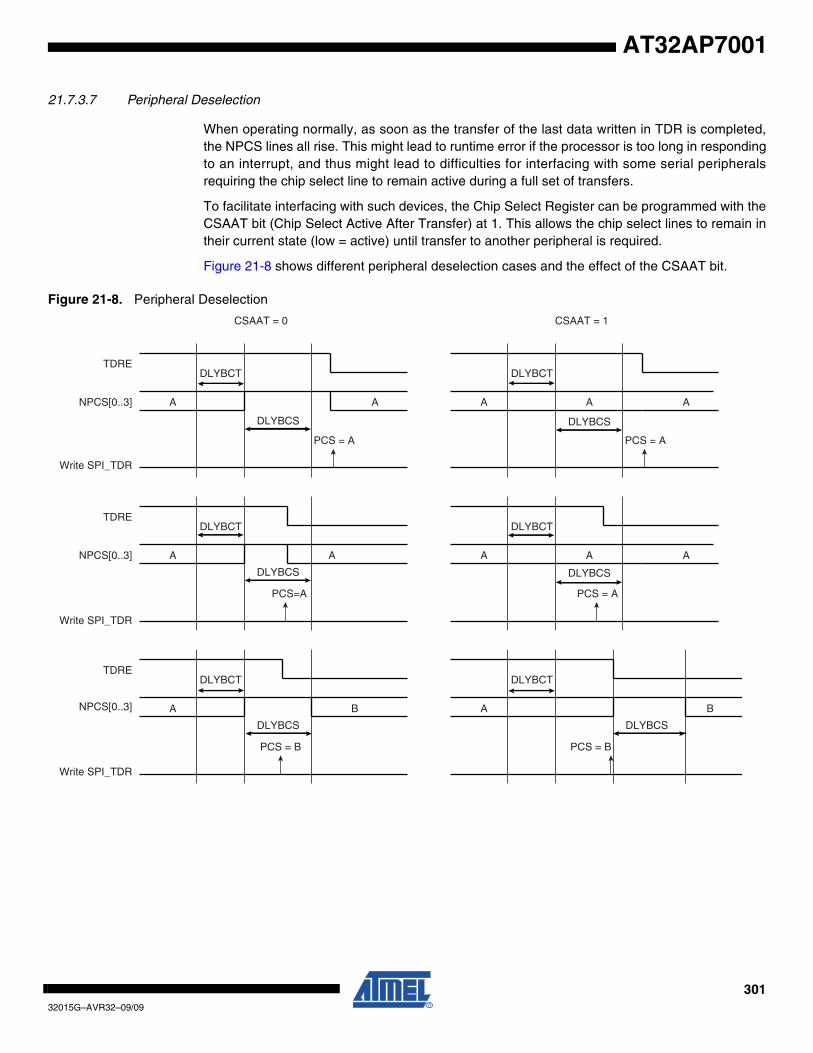
30132015G–AVR32–09/09
AT32AP7001
21.7.3.7 Peripheral Deselection
When operating normally, as soon as the transfer of the last data written in TDR is completed,the NPCS lines all rise. This might lead to runtime error if the processor is too long in respondingto an interrupt, and thus might lead to difficulties for interfacing with some serial peripheralsrequiring the chip select line to remain active during a full set of transfers.
To facilitate interfacing with such devices, the Chip Select Register can be programmed with theCSAAT bit (Chip Select Active After Transfer) at 1. This allows the chip select lines to remain intheir current state (low = active) until transfer to another peripheral is required.
Figure 21-8 shows different peripheral deselection cases and the effect of the CSAAT bit.
Figure 21-8. Peripheral Deselection
A
NPCS[0..3]
Write SPI_TDR
TDRE
NPCS[0..3]
Write SPI_TDR
TDRE
NPCS[0..3]
Write SPI_TDR
TDRE
DLYBCS
PCS = A
DLYBCS
DLYBCT
A
PCS = B
B
DLYBCS
PCS = A
DLYBCS
DLYBCT
A
PCS = B
B
DLYBCS
DLYBCT
PCS=A
A
DLYBCS
DLYBCT
A
PCS = A
AA
DLYBCT
A A
CSAAT = 0
DLYBCT
A A
CSAAT = 1
A
30232015G–AVR32–09/09
AT32AP7001
21.7.3.8 Mode Fault Detection
A mode fault is detected when the SPI is programmed in Master Mode and a low level is drivenby an external master on the NPCS0/NSS signal. NPCS0, MOSI, MISO and SPCK must be con-figured in open-drain through the PIO controller, so that external pull up resistors are needed toguarantee high level.
When a mode fault is detected, the MODF bit in the SR is set until the SR is read and the SPI isautomatically disabled until re-enabled by writing the SPIEN bit in the CR (Control Register) at 1.
By default, the Mode Fault detection circuitry is enabled. The user can disable Mode Faultdetection by setting the MODFDIS bit in the SPI Mode Register (MR).
21.7.4 SPI Slave Mode
When operating in Slave Mode, the SPI processes data bits on the clock provided on the SPIclock pin (SPCK).
The SPI waits for NSS to go active before receiving the serial clock from an external master.When NSS falls, the clock is validated on the serializer, which processes the number of bitsdefined by the BITS field of the Chip Select Register 0 (CSR0). These bits are processed follow-ing a phase and a polarity defined respectively by the NCPHA and CPOL bits of the CSR0. Notethat BITS, CPOL and NCPHA of the other Chip Select Registers have no effect when the SPI isprogrammed in Slave Mode.
The bits are shifted out on the MISO line and sampled on the MOSI line.
When all the bits are processed, the received data is transferred in the Receive Data Registerand the RDRF bit rises. If RDRF is already high when the data is transferred, the Overrun bitrises and the data transfer to RDR is aborted.
When a transfer starts, the data shifted out is the data present in the Shift Register. If no datahas been written in the Transmit Data Register (TDR), the last data received is transferred. If nodata has been received since the last reset, all bits are transmitted low, as the Shift Registerresets at 0.
When a first data is written in TDR, it is transferred immediately in the Shift Register and theTDRE bit rises. If new data is written, it remains in TDR until a transfer occurs, i.e. NSS falls andthere is a valid clock on the SPCK pin. When the transfer occurs, the last data written in TDR istransferred in the Shift Register and the TDRE bit rises. This enables frequent updates of criticalvariables with single transfers.
Then, a new data is loaded in the Shift Register from the Transmit Data Register. In case nocharacter is ready to be transmitted, i.e. no character has been written in TDR since the last loadfrom TDR to the Shift Register, the Shift Register is not modified and the last received characteris retransmitted.
Figure 21-9 shows a block diagram of the SPI when operating in Slave Mode.
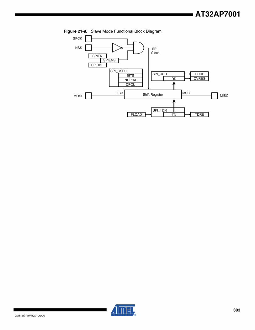
30332015G–AVR32–09/09
AT32AP7001
Figure 21-9. Slave Mode Functional Block Diagram
Shift Register
SPCK
SPIENS
LSB MSB
NSS
MOSI
SPI_RDRRD
SPI Clock
TDRESPI_TDR
TD
RDRFOVRES
SPI_CSR0
CPOLNCPHA
BITS
FLOAD
SPIEN
SPIDIS
MISO
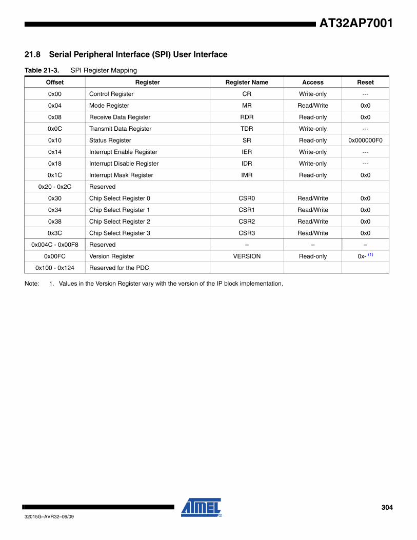
30432015G–AVR32–09/09
AT32AP7001
21.8 Serial Peripheral Interface (SPI) User Interface
Note: 1. Values in the Version Register vary with the version of the IP block implementation.
Table 21-3. SPI Register Mapping
Offset Register Register Name Access Reset
0x00 Control Register CR Write-only ---
0x04 Mode Register MR Read/Write 0x0
0x08 Receive Data Register RDR Read-only 0x0
0x0C Transmit Data Register TDR Write-only ---
0x10 Status Register SR Read-only 0x000000F0
0x14 Interrupt Enable Register IER Write-only ---
0x18 Interrupt Disable Register IDR Write-only ---
0x1C Interrupt Mask Register IMR Read-only 0x0
0x20 - 0x2C Reserved
0x30 Chip Select Register 0 CSR0 Read/Write 0x0
0x34 Chip Select Register 1 CSR1 Read/Write 0x0
0x38 Chip Select Register 2 CSR2 Read/Write 0x0
0x3C Chip Select Register 3 CSR3 Read/Write 0x0
0x004C - 0x00F8 Reserved – – –
0x00FC Version Register VERSION Read-only 0x- (1)
0x100 - 0x124 Reserved for the PDC
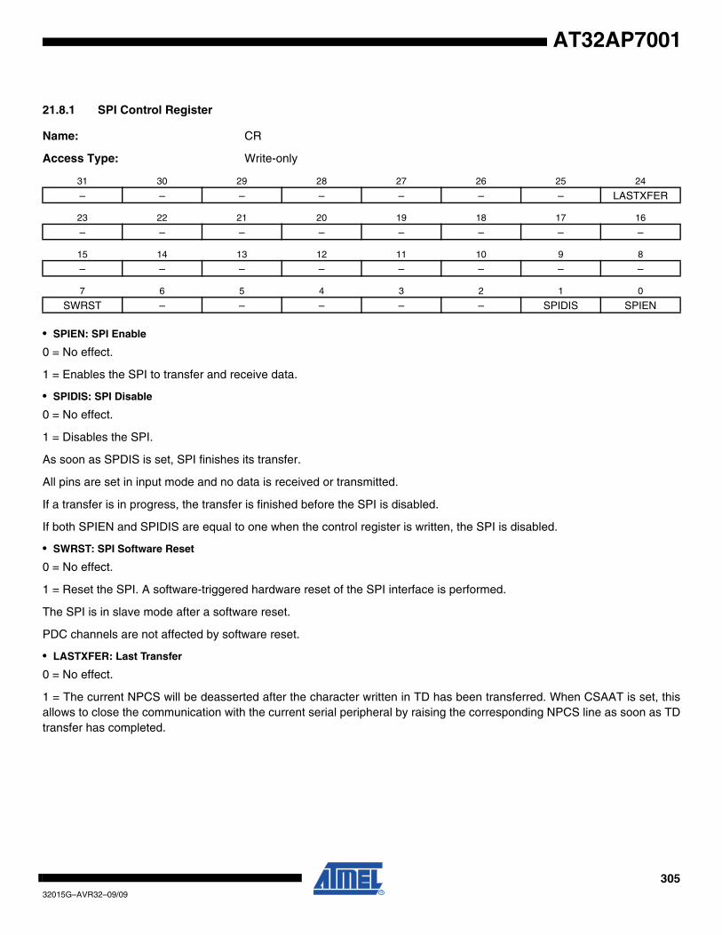
30532015G–AVR32–09/09
AT32AP7001
21.8.1 SPI Control Register
Name: CR
Access Type: Write-only
• SPIEN: SPI Enable
0 = No effect.
1 = Enables the SPI to transfer and receive data.
• SPIDIS: SPI Disable
0 = No effect.
1 = Disables the SPI.
As soon as SPDIS is set, SPI finishes its transfer.
All pins are set in input mode and no data is received or transmitted.
If a transfer is in progress, the transfer is finished before the SPI is disabled.
If both SPIEN and SPIDIS are equal to one when the control register is written, the SPI is disabled.
• SWRST: SPI Software Reset
0 = No effect.
1 = Reset the SPI. A software-triggered hardware reset of the SPI interface is performed.
The SPI is in slave mode after a software reset.
PDC channels are not affected by software reset.
• LASTXFER: Last Transfer
0 = No effect.
1 = The current NPCS will be deasserted after the character written in TD has been transferred. When CSAAT is set, thisallows to close the communication with the current serial peripheral by raising the corresponding NPCS line as soon as TDtransfer has completed.
31 30 29 28 27 26 25 24
– – – – – – – LASTXFER
23 22 21 20 19 18 17 16
– – – – – – – –
15 14 13 12 11 10 9 8
– – – – – – – –
7 6 5 4 3 2 1 0
SWRST – – – – – SPIDIS SPIEN
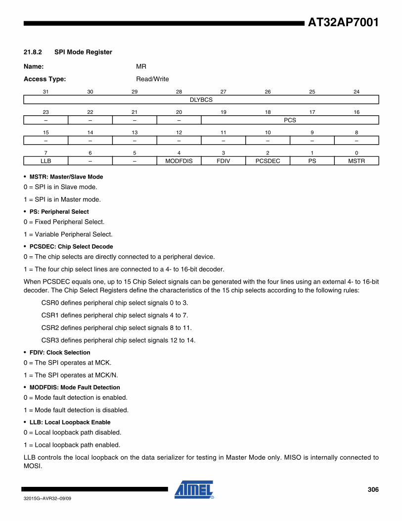
30632015G–AVR32–09/09
AT32AP7001
21.8.2 SPI Mode Register
Name: MR
Access Type: Read/Write
• MSTR: Master/Slave Mode
0 = SPI is in Slave mode.
1 = SPI is in Master mode.
• PS: Peripheral Select
0 = Fixed Peripheral Select.
1 = Variable Peripheral Select.
• PCSDEC: Chip Select Decode
0 = The chip selects are directly connected to a peripheral device.
1 = The four chip select lines are connected to a 4- to 16-bit decoder.
When PCSDEC equals one, up to 15 Chip Select signals can be generated with the four lines using an external 4- to 16-bitdecoder. The Chip Select Registers define the characteristics of the 15 chip selects according to the following rules:
CSR0 defines peripheral chip select signals 0 to 3.
CSR1 defines peripheral chip select signals 4 to 7.
CSR2 defines peripheral chip select signals 8 to 11.
CSR3 defines peripheral chip select signals 12 to 14.
• FDIV: Clock Selection
0 = The SPI operates at MCK.
1 = The SPI operates at MCK/N.
• MODFDIS: Mode Fault Detection
0 = Mode fault detection is enabled.
1 = Mode fault detection is disabled.
• LLB: Local Loopback Enable
0 = Local loopback path disabled.
1 = Local loopback path enabled.
LLB controls the local loopback on the data serializer for testing in Master Mode only. MISO is internally connected toMOSI.
31 30 29 28 27 26 25 24
DLYBCS
23 22 21 20 19 18 17 16
– – – – PCS
15 14 13 12 11 10 9 8
– – – – – – – –
7 6 5 4 3 2 1 0
LLB – – MODFDIS FDIV PCSDEC PS MSTR
30732015G–AVR32–09/09
AT32AP7001
• PCS: Peripheral Chip Select
This field is only used if Fixed Peripheral Select is active (PS = 0).
If PCSDEC = 0:
PCS = xxx0 NPCS[3:0] = 1110
PCS = xx01 NPCS[3:0] = 1101
PCS = x011 NPCS[3:0] = 1011
PCS = 0111 NPCS[3:0] = 0111
PCS = 1111 forbidden (no peripheral is selected)
(x = don’t care)
If PCSDEC = 1:
NPCS[3:0] output signals = PCS.
• DLYBCS: Delay Between Chip Selects
This field defines the delay from NPCS inactive to the activation of another NPCS. The DLYBCS time guarantees non-over-lapping chip selects and solves bus contentions in case of peripherals having long data float times.
If DLYBCS is less than or equal to six, six MCK periods (or 6*N MCK periods if FDIV is set) will be inserted by default.
Otherwise, the following equation determines the delay:
If FDIV is 0:
If FDIV is 1:
Delay Between Chip Selects DLYBCSMCK
-----------------------=
Delay Between Chip Selects DLYBCS N×MCK
---------------------------------=

30832015G–AVR32–09/09
AT32AP7001
21.8.3 SPI Receive Data Register
Name: RDR
Access Type: Read-only
• RD: Receive Data
Data received by the SPI Interface is stored in this register right-justified. Unused bits read zero.
• PCS: Peripheral Chip Select
In Master Mode only, these bits indicate the value on the NPCS pins at the end of a transfer. Otherwise, these bits readzero.
31 30 29 28 27 26 25 24
– – – – – – – –
23 22 21 20 19 18 17 16
– – – – PCS
15 14 13 12 11 10 9 8
RD
7 6 5 4 3 2 1 0
RD
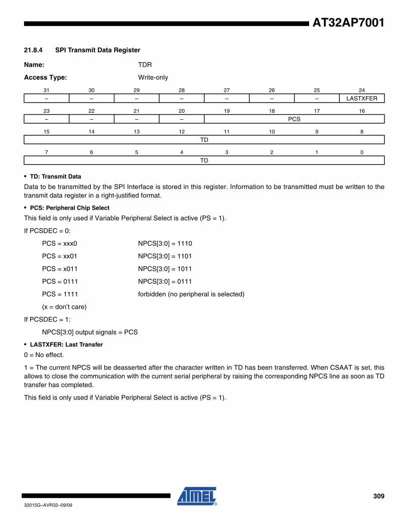
30932015G–AVR32–09/09
AT32AP7001
21.8.4 SPI Transmit Data Register
Name: TDR
Access Type: Write-only
• TD: Transmit Data
Data to be transmitted by the SPI Interface is stored in this register. Information to be transmitted must be written to thetransmit data register in a right-justified format.
• PCS: Peripheral Chip Select
This field is only used if Variable Peripheral Select is active (PS = 1).
If PCSDEC = 0:
PCS = xxx0 NPCS[3:0] = 1110
PCS = xx01 NPCS[3:0] = 1101
PCS = x011 NPCS[3:0] = 1011
PCS = 0111 NPCS[3:0] = 0111
PCS = 1111 forbidden (no peripheral is selected)
(x = don’t care)
If PCSDEC = 1:
NPCS[3:0] output signals = PCS
• LASTXFER: Last Transfer
0 = No effect.
1 = The current NPCS will be deasserted after the character written in TD has been transferred. When CSAAT is set, thisallows to close the communication with the current serial peripheral by raising the corresponding NPCS line as soon as TDtransfer has completed.
This field is only used if Variable Peripheral Select is active (PS = 1).
31 30 29 28 27 26 25 24
– – – – – – – LASTXFER
23 22 21 20 19 18 17 16
– – – – PCS
15 14 13 12 11 10 9 8
TD
7 6 5 4 3 2 1 0
TD

31032015G–AVR32–09/09
AT32AP7001
21.8.5 SPI Status Register
Name: SR
Access Type: Read-only
• RDRF: Receive Data Register Full
0 = No data has been received since the last read of RDR
1 = Data has been received and the received data has been transferred from the serializer to RDR since the last read ofRDR.
• TDRE: Transmit Data Register Empty
0 = Data has been written to TDR and not yet transferred to the serializer.
1 = The last data written in the Transmit Data Register has been transferred to the serializer.
TDRE equals zero when the SPI is disabled or at reset. The SPI enable command sets this bit to one.
• MODF: Mode Fault Error
0 = No Mode Fault has been detected since the last read of SR.
1 = A Mode Fault occurred since the last read of the SR.
• OVRES: Overrun Error Status
0 = No overrun has been detected since the last read of SR.
1 = An overrun has occurred since the last read of SR.
An overrun occurs when RDR is loaded at least twice from the serializer since the last read of the RDR.
• ENDRX: End of RX buffer
0 = The Receive Counter Register has not reached 0 since the last write in RCR or RNCR.
1 = The Receive Counter Register has reached 0 since the last write in RCR or RNCR.
• ENDTX: End of TX buffer
0 = The Transmit Counter Register has not reached 0 since the last write in TCR or TNCR.
1 = The Transmit Counter Register has reached 0 since the last write in TCR or TNCR.
• RXBUFF: RX Buffer Full
0 = RCR or RNCR has a value other than 0.
1 = Both RCR and RNCR has a value of 0.
• TXBUFE: TX Buffer Empty
0 = TCR or TNCR has a value other than 0.
31 30 29 28 27 26 25 24
– – – – – – – –
23 22 21 20 19 18 17 16
– – – – – – – SPIENS
15 14 13 12 11 10 9 8
– – – – – – TXEMPTY NSSR
7 6 5 4 3 2 1 0
TXBUFE RXBUFF ENDTX ENDRX OVRES MODF TDRE RDRF
31132015G–AVR32–09/09
AT32AP7001
1 = Both TCR and TNCR has a value of 0.
• NSSR: NSS Rising
0 = No rising edge detected on NSS pin since last read.
1 = A rising edge occurred on NSS pin since last read.
• TXEMPTY: Transmission Registers Empty
0 = As soon as data is written in TDR.
1 = TDR and internal shifter are empty. If a transfer delay has been defined, TXEMPTY is set after the completion of suchdelay.
• SPIENS: SPI Enable Status
0 = SPI is disabled.
1 = SPI is enabled.

31232015G–AVR32–09/09
AT32AP7001
21.8.6 SPI Interrupt Enable Register
Name: IER
Access Type: Write-only
• RDRF: Receive Data Register Full Interrupt Enable
• TDRE: SPI Transmit Data Register Empty Interrupt Enable
• MODF: Mode Fault Error Interrupt Enable
• OVRES: Overrun Error Interrupt Enable• ENDRX: End of Receive Buffer Interrupt Enable• ENDTX: End of Transmit Buffer Interrupt Enable• RXBUFF: Receive Buffer Full Interrupt Enable• TXBUFE: Transmit Buffer Empty Interrupt Enable• TXEMPTY: Transmission Registers Empty Enable• NSSR: NSS Rising Interrupt Enable
0 = No effect.
1 = Enables the corresponding interrupt.
31 30 29 28 27 26 25 24
– – – – – – – –
23 22 21 20 19 18 17 16
– – – – – – – –
15 14 13 12 11 10 9 8
– – – – – – TXEMPTY NSSR
7 6 5 4 3 2 1 0
TXBUFE RXBUFF ENDTX ENDRX OVRES MODF TDRE RDRF
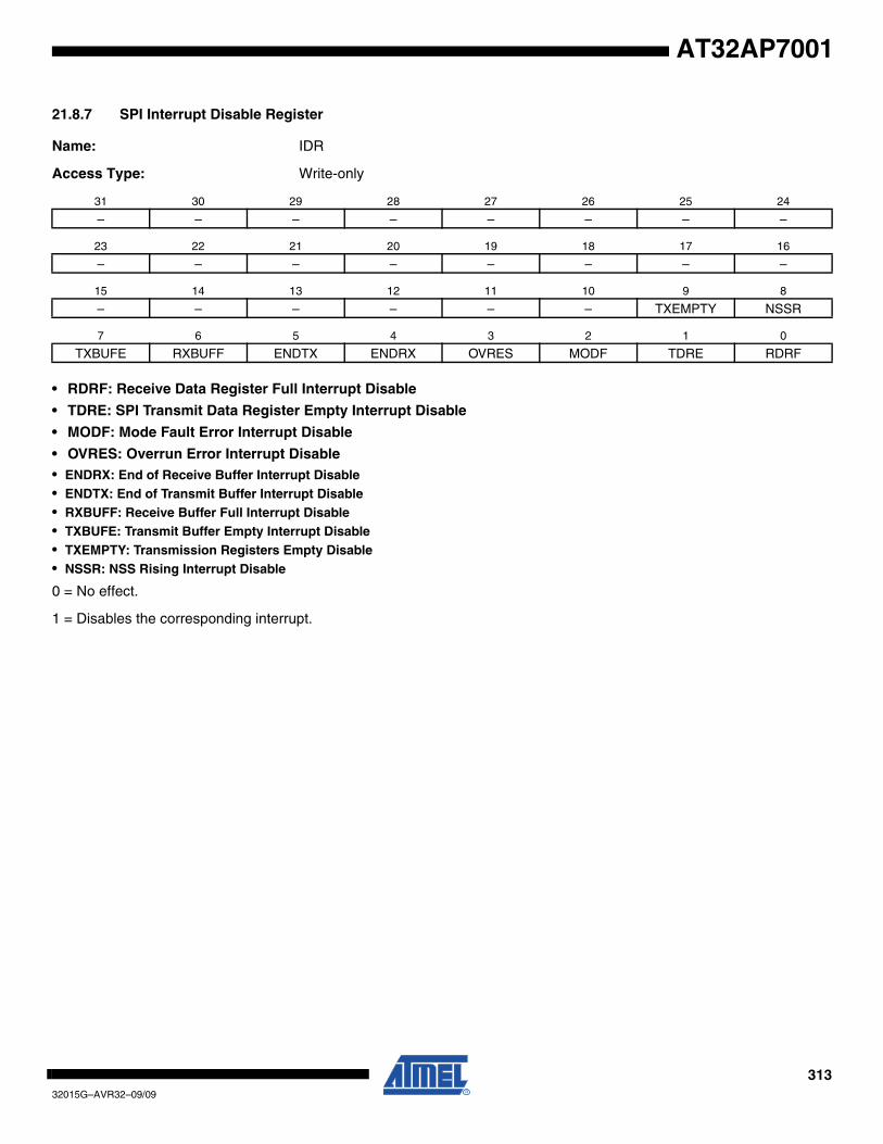
31332015G–AVR32–09/09
AT32AP7001
21.8.7 SPI Interrupt Disable Register
Name: IDR
Access Type: Write-only
• RDRF: Receive Data Register Full Interrupt Disable
• TDRE: SPI Transmit Data Register Empty Interrupt Disable
• MODF: Mode Fault Error Interrupt Disable
• OVRES: Overrun Error Interrupt Disable• ENDRX: End of Receive Buffer Interrupt Disable• ENDTX: End of Transmit Buffer Interrupt Disable• RXBUFF: Receive Buffer Full Interrupt Disable• TXBUFE: Transmit Buffer Empty Interrupt Disable• TXEMPTY: Transmission Registers Empty Disable• NSSR: NSS Rising Interrupt Disable
0 = No effect.
1 = Disables the corresponding interrupt.
31 30 29 28 27 26 25 24
– – – – – – – –
23 22 21 20 19 18 17 16
– – – – – – – –
15 14 13 12 11 10 9 8
– – – – – – TXEMPTY NSSR
7 6 5 4 3 2 1 0
TXBUFE RXBUFF ENDTX ENDRX OVRES MODF TDRE RDRF
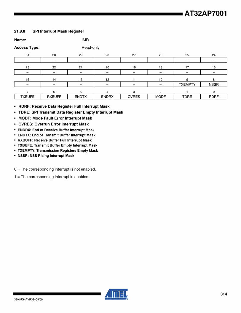
31432015G–AVR32–09/09
AT32AP7001
21.8.8 SPI Interrupt Mask Register
Name: IMR
Access Type: Read-only
• RDRF: Receive Data Register Full Interrupt Mask
• TDRE: SPI Transmit Data Register Empty Interrupt Mask
• MODF: Mode Fault Error Interrupt Mask
• OVRES: Overrun Error Interrupt Mask• ENDRX: End of Receive Buffer Interrupt Mask• ENDTX: End of Transmit Buffer Interrupt Mask• RXBUFF: Receive Buffer Full Interrupt Mask• TXBUFE: Transmit Buffer Empty Interrupt Mask• TXEMPTY: Transmission Registers Empty Mask• NSSR: NSS Rising Interrupt Mask
0 = The corresponding interrupt is not enabled.
1 = The corresponding interrupt is enabled.
31 30 29 28 27 26 25 24
– – – – – – – –
23 22 21 20 19 18 17 16
– – – – – – – –
15 14 13 12 11 10 9 8
– – – – – – TXEMPTY NSSR
7 6 5 4 3 2 1 0
TXBUFE RXBUFF ENDTX ENDRX OVRES MODF TDRE RDRF
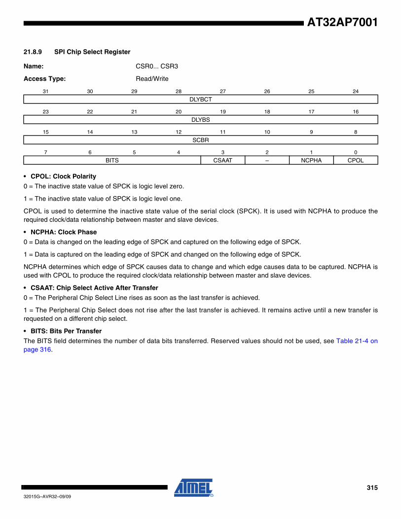
31532015G–AVR32–09/09
AT32AP7001
21.8.9 SPI Chip Select Register
Name: CSR0... CSR3
Access Type: Read/Write
• CPOL: Clock Polarity
0 = The inactive state value of SPCK is logic level zero.
1 = The inactive state value of SPCK is logic level one.
CPOL is used to determine the inactive state value of the serial clock (SPCK). It is used with NCPHA to produce therequired clock/data relationship between master and slave devices.
• NCPHA: Clock Phase
0 = Data is changed on the leading edge of SPCK and captured on the following edge of SPCK.
1 = Data is captured on the leading edge of SPCK and changed on the following edge of SPCK.
NCPHA determines which edge of SPCK causes data to change and which edge causes data to be captured. NCPHA isused with CPOL to produce the required clock/data relationship between master and slave devices.
• CSAAT: Chip Select Active After Transfer
0 = The Peripheral Chip Select Line rises as soon as the last transfer is achieved.
1 = The Peripheral Chip Select does not rise after the last transfer is achieved. It remains active until a new transfer isrequested on a different chip select.
• BITS: Bits Per Transfer
The BITS field determines the number of data bits transferred. Reserved values should not be used, see Table 21-4 onpage 316.
31 30 29 28 27 26 25 24
DLYBCT
23 22 21 20 19 18 17 16
DLYBS
15 14 13 12 11 10 9 8
SCBR
7 6 5 4 3 2 1 0
BITS CSAAT – NCPHA CPOL
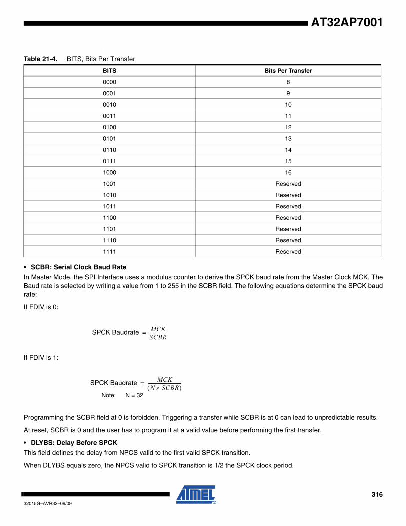
31632015G–AVR32–09/09
AT32AP7001
.
• SCBR: Serial Clock Baud Rate
In Master Mode, the SPI Interface uses a modulus counter to derive the SPCK baud rate from the Master Clock MCK. TheBaud rate is selected by writing a value from 1 to 255 in the SCBR field. The following equations determine the SPCK baudrate:
If FDIV is 0:
If FDIV is 1:
Note: N = 32
Programming the SCBR field at 0 is forbidden. Triggering a transfer while SCBR is at 0 can lead to unpredictable results.
At reset, SCBR is 0 and the user has to program it at a valid value before performing the first transfer.
• DLYBS: Delay Before SPCK
This field defines the delay from NPCS valid to the first valid SPCK transition.
When DLYBS equals zero, the NPCS valid to SPCK transition is 1/2 the SPCK clock period.
Table 21-4. BITS, Bits Per Transfer
BITS Bits Per Transfer
0000 8
0001 9
0010 10
0011 11
0100 12
0101 13
0110 14
0111 15
1000 16
1001 Reserved
1010 Reserved
1011 Reserved
1100 Reserved
1101 Reserved
1110 Reserved
1111 Reserved
SPCK Baudrate MCKSCBR---------------=
SPCK Baudrate MCKN SCBR×( )
------------------------------=
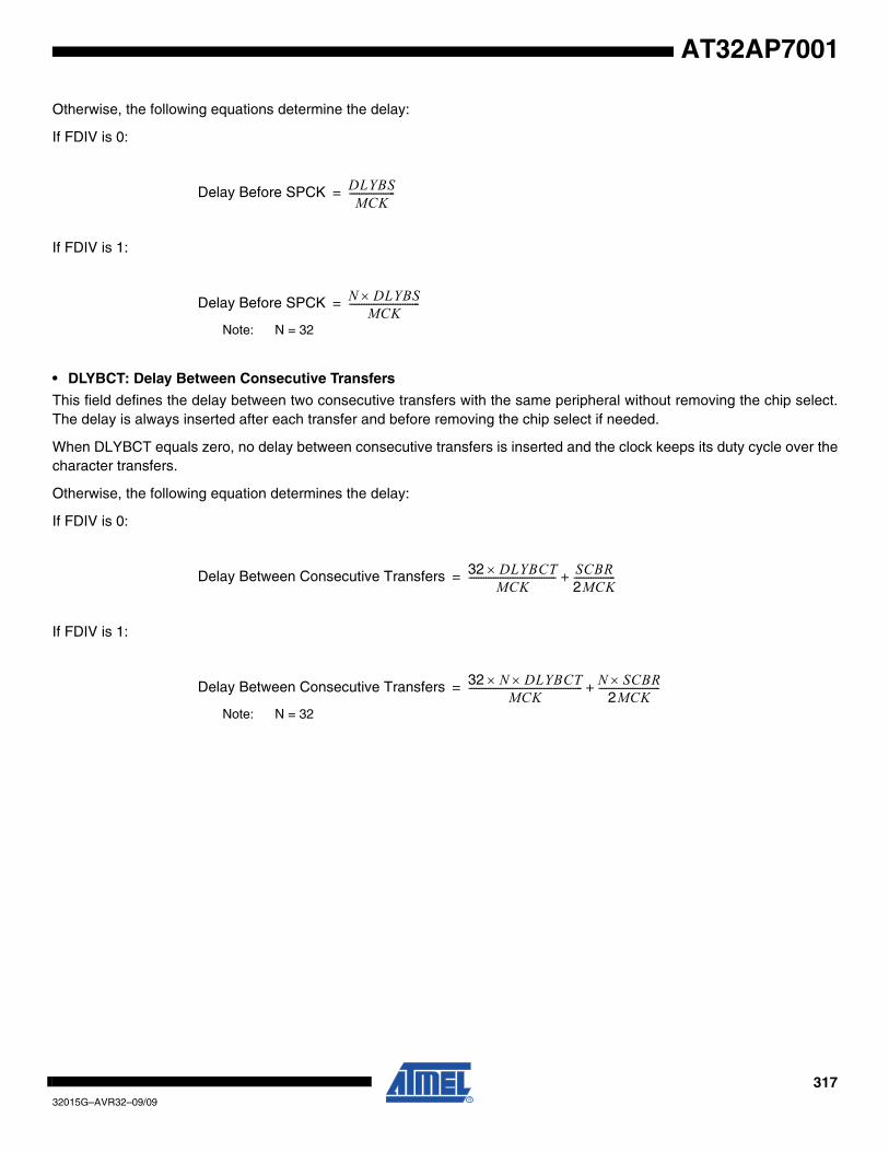
31732015G–AVR32–09/09
AT32AP7001
Otherwise, the following equations determine the delay:
If FDIV is 0:
If FDIV is 1:
Note: N = 32
• DLYBCT: Delay Between Consecutive Transfers
This field defines the delay between two consecutive transfers with the same peripheral without removing the chip select.The delay is always inserted after each transfer and before removing the chip select if needed.
When DLYBCT equals zero, no delay between consecutive transfers is inserted and the clock keeps its duty cycle over thecharacter transfers.
Otherwise, the following equation determines the delay:
If FDIV is 0:
If FDIV is 1:
Note: N = 32
Delay Before SPCK DLYBSMCK
-------------------=
Delay Before SPCK N DLYBS×MCK
-----------------------------=
Delay Between Consecutive Transfers 32 DLYBCT×MCK
------------------------------------ SCBR2MCK-----------------+=
Delay Between Consecutive Transfers 32 N× DLYBCT×MCK
----------------------------------------------- N SCBR×2MCK
-------------------------+=
31832015G–AVR32–09/09
AT32AP7001
22. Two-wire Interface (TWI)
Rev: 1.8.0.1
22.1 Features• Compatible with Philips’ I2C protocol• One, Two or Three Bytes for Slave Address• Sequential Read/Write Operations
22.2 DescriptionThe Two-wire Interface (TWI) interconnects components on a unique two-wire bus, made up ofone clock line and one data line with speeds of up to 400 Kbits per second, based on a byte-ori-ented transfer format. It can be used with any Atmel two-wire bus Serial EEPROM. The TWI isprogrammable as a master with sequential or single-byte access. A configurable baud rate gen-erator permits the output data rate to be adapted to a wide range of core clock frequencies.
22.3 Block Diagram
Figure 22-1. Block Diagram
22.4 Application Block Diagram
Figure 22-2. Application Block Diagram
Peripheral Bus Bridge
Power Manager
MCK
Two-wireInterface
PIO
InterruptController
TWIInterrupt
TWCK
TWD
Host withTWI
Interface
TWD
TWCK
AT24LC16U1
AT24LC16U2
Slave 1 Slave 2
R R
VDD

31932015G–AVR32–09/09
AT32AP7001
22.4.1 I/O Lines Description
22.5 Product Dependencies
22.5.1 I/O LinesBoth TWD and TWCK are bi-directional lines, connected to a positive supply voltage via a cur-rent source or pull-up resistor (see Figure 1-2 on page 1). When the bus is free, both lines arehigh. The output stages of devices connected to the bus must have an open-drain or open-col-lector to perform the wired-AND function.
TWD and TWCK pins may be multiplexed with PIO lines. To enable the TWI, the programmermust program the PIO controller to dedicate TWD and TWCK as peripheral lines.
22.5.2 Power ManagementThe TWI clock is generated by the power manager. Before using the TWI, the programmer mustensure that the TWI clock is enabled in the power manager.
In the TWI description, Master Clock (MCK) is the clock of the peripheral bus to which the TWI isconnected.
22.5.3 InterruptThe TWI interface has an interrupt line connected to the interrupt controller. In order to handleinterrupts, the interrupt controller must be programmed before configuring the TWI.
Table 22-1. I/O Lines Description
Pin Name Pin Description Type
TWD Two-wire Serial Data Input/Output
TWCK Two-wire Serial Clock Input/Output
32032015G–AVR32–09/09
AT32AP7001
22.6 Functional Description
22.6.1 Transfer formatThe data put on the TWD line must be 8 bits long. Data is transferred MSB first; each byte mustbe followed by an acknowledgement. The number of bytes per transfer is unlimited (see Figure22-4 on page 320).
Each transfer begins with a START condition and terminates with a STOP condition (see Figure22-3 on page 320).
•A high-to-low transition on the TWD line while TWCK is high defines the START condition.
•A low-to-high transition on the TWD line while TWCK is high defines a STOP condition.
Figure 22-3. START and STOP Conditions
Figure 22-4. Transfer Format
22.6.2 Modes of OperationThe TWI has two modes of operation:
•Master transmitter mode
•Master receiver mode
The TWI Control Register (CR) allows configuration of the interface in Master Mode. In thismode, it generates the clock according to the value programmed in the Clock Waveform Gener-ator Register (CWGR). This register defines the TWCK signal completely, enabling the interfaceto be adapted to a wide range of clocks.
22.6.3 Transmitting DataAfter the master initiates a Start condition, it sends a 7-bit slave address, configured in the Mas-ter Mode register (DADR in MMR), to notify the slave device. The bit following the slave addressindicates the transfer direction (write or read). If this bit is 0, it indicates a write operation (trans-mit operation). If the bit is 1, it indicates a request for data read (receive operation).
The TWI transfers require the slave to acknowledge each received byte. During the acknowl-edge clock pulse, the master releases the data line (HIGH), enabling the slave to pull it down inorder to generate the acknowledge. The master polls the data line during this clock pulse andsets the NAK bit in the status register if the slave does not acknowledge the byte. As with the
TWD
TWCK
Start Stop
TWD
TWCK
Start Address R/W Ack Data Ack Data Ack Stop
32132015G–AVR32–09/09
AT32AP7001
other status bits, an interrupt can be generated if enabled in the interrupt enable register (IER).After writing in the transmit-holding register (THR), setting the START bit in the control registerstarts the transmission. The data is shifted in the internal shifter and when an acknowledge isdetected, the TXRDY bit is set until a new write in the THR (see Figure 22-6 below). The mastergenerates a stop condition to end the transfer.
The read sequence begins by setting the START bit. When the RXRDY bit is set in the statusregister, a character has been received in the receive-holding register (RHR). The RXRDY bit isreset when reading the RHR.
The TWI interface performs various transfer formats (7-bit slave address, 10-bit slave address).The three internal address bytes are configurable through the Master Mode register (MMR). Ifthe slave device supports only a 7-bit address, IADRSZ must be set to 0. For a slave addresshigher than 7 bits, the user must configure the address size (IADRSZ) and set the other slaveaddress bits in the internal address register (IADR).
Figure 22-5. Master Write with One, Two or Three Bytes Internal Address and One Data Byte
Figure 22-6. Master Write with One Byte Internal Address and Multiple Data Bytes
Figure 22-7. Master Read with One, Two or Three Bytes Internal Address and One Data Byte
S DADR W A IADR(23:16) A IADR(15:8) A IADR(7:0) A DATA A P
S DADR W A IADR(15:8) A IADR(7:0) A PDATA A
A IADR(7:0) A PDATA AS DADR W
TWD
Three bytes internal address
Two bytes internal address
One byte internal address
TWD
TWD
A IADR(7:0) A DATA AS DADR W DATA A PDATA A
TXCOMP
TXRDY
Write THR
Write THR Write THR Write THR
TWD
S DADR W A IADR(23:16) A IADR(15:8) A IADR(7:0) A
S DADR W A IADR(15:8) A IADR(7:0) A
A IADR(7:0) AS DADR W
DATA N P
S DADR R A
S DADR R A DATA N P
S DADR R A DATA N P
TWD
TWD
TWD
Three bytes internal address
Two bytes internal address
One byte internal address

32232015G–AVR32–09/09
AT32AP7001
Figure 22-8. Master Read with One Byte Internal Address and Multiple Data Bytes
•S = Start
•P = Stop
•W = Write
•R = Read
•A = Acknowledge
•N = Not Acknowledge
•DADR= Device Address
•IADR = Internal Address
Figure 22-9 below shows a byte write to an Atmel AT24LC512 EEPROM. This demonstrates theuse of internal addresses to access the device.
Figure 22-9. Internal Address Usage
A IADR(7:0) AS DADR W S DADR R A DATA A DATA N P
TXCOMP
Write START Bit
RXRDY
Write STOP Bit
Read RHR Read RHR
TWD
START
MSB
DeviceAddress
0
LSB
R/
W
ACK
MSB
WRITE
ACK
ACK
LSB
ACK
FIRSTWORD ADDRESS
SECONDWORD ADDRESS DATA
STOP

32332015G–AVR32–09/09
AT32AP7001
22.6.4 Read/Write FlowchartsThe following flowcharts shown in Figure 22-10 on page 323 and in Figure 22-11 on page 324give examples for read and write operations in Master Mode. A polling or interrupt method canbe used to check the status bits. The interrupt method requires that the interrupt enable register(IER) be configured first.
Figure 22-10. TWI Write in Master Mode
Set TWI clock: CWGR = clock
Set the control register:- Master enable CR = MSEN
Set the Master Mode register:- Device slave address- Internal address size- Transfer direction bit
Write ==> bit MREAD = 0
Internal address size = 0?
Load transmit registerTHR = Data to send
Read status register
TXRDY = 0?
Data to send?
Read status register
TXCOMP = 0?
END
START
Set theinternal addressIADR = address
Yes
THR = data to send
Yes
Yes
Yes
32432015G–AVR32–09/09
AT32AP7001
Figure 22-11. TWI Read in Master Mode
Set TWI clock:CWGR = clock
Set the control register:- Master enable
CR = MSEN
Set the Master Mode register:- Device slave address- Internal address size- Transfer direction bit
Read ==> bit MREAD = 0
Internal address size = 0?
Start the transferCR = START
Stop the transferCR = STOP
Read status register
RXRDY = 0?
Data to read?
Read status register
TXCOMP = 0?
END
START
Set the internal addressIADR = address
Yes
Yes
Yes
Yes
Read RHR
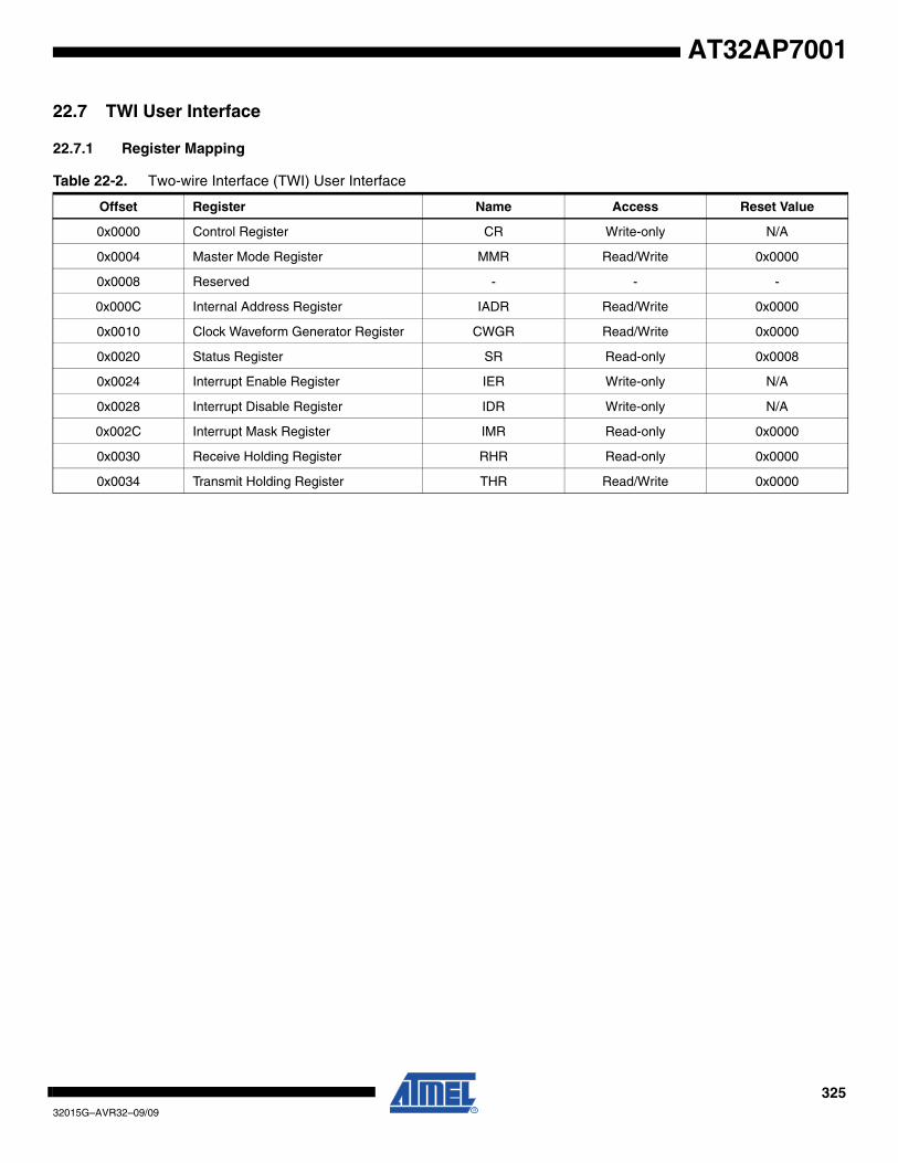
32532015G–AVR32–09/09
AT32AP7001
22.7 TWI User Interface
22.7.1 Register Mapping
Table 22-2. Two-wire Interface (TWI) User Interface
Offset Register Name Access Reset Value
0x0000 Control Register CR Write-only N/A
0x0004 Master Mode Register MMR Read/Write 0x0000
0x0008 Reserved - - -
0x000C Internal Address Register IADR Read/Write 0x0000
0x0010 Clock Waveform Generator Register CWGR Read/Write 0x0000
0x0020 Status Register SR Read-only 0x0008
0x0024 Interrupt Enable Register IER Write-only N/A
0x0028 Interrupt Disable Register IDR Write-only N/A
0x002C Interrupt Mask Register IMR Read-only 0x0000
0x0030 Receive Holding Register RHR Read-only 0x0000
0x0034 Transmit Holding Register THR Read/Write 0x0000
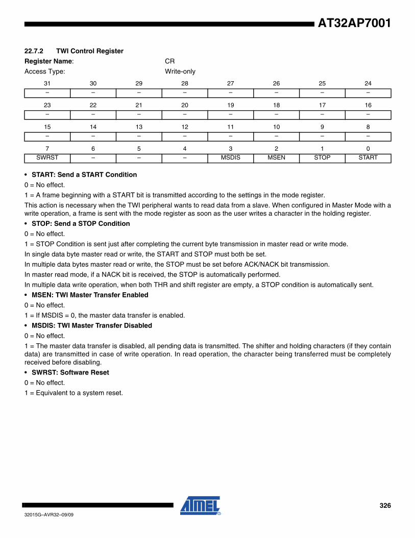
32632015G–AVR32–09/09
AT32AP7001
22.7.2 TWI Control Register
Register Name: CR
Access Type: Write-only
• START: Send a START Condition
0 = No effect.
1 = A frame beginning with a START bit is transmitted according to the settings in the mode register.
This action is necessary when the TWI peripheral wants to read data from a slave. When configured in Master Mode with awrite operation, a frame is sent with the mode register as soon as the user writes a character in the holding register.
• STOP: Send a STOP Condition
0 = No effect.
1 = STOP Condition is sent just after completing the current byte transmission in master read or write mode.
In single data byte master read or write, the START and STOP must both be set.
In multiple data bytes master read or write, the STOP must be set before ACK/NACK bit transmission.
In master read mode, if a NACK bit is received, the STOP is automatically performed.
In multiple data write operation, when both THR and shift register are empty, a STOP condition is automatically sent.
• MSEN: TWI Master Transfer Enabled
0 = No effect.
1 = If MSDIS = 0, the master data transfer is enabled.
• MSDIS: TWI Master Transfer Disabled
0 = No effect.
1 = The master data transfer is disabled, all pending data is transmitted. The shifter and holding characters (if they containdata) are transmitted in case of write operation. In read operation, the character being transferred must be completelyreceived before disabling.
• SWRST: Software Reset
0 = No effect.
1 = Equivalent to a system reset.
31 30 29 28 27 26 25 24– – – – – – – –
23 22 21 20 19 18 17 16
– – – – – – – –
15 14 13 12 11 10 9 8– – – – – – – –
7 6 5 4 3 2 1 0
SWRST – – – MSDIS MSEN STOP START
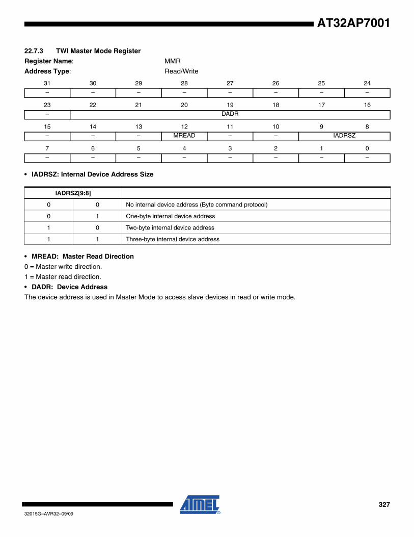
32732015G–AVR32–09/09
AT32AP7001
22.7.3 TWI Master Mode Register
Register Name: MMR
Address Type: Read/Write
• IADRSZ: Internal Device Address Size
• MREAD: Master Read Direction
0 = Master write direction.
1 = Master read direction.
• DADR: Device Address
The device address is used in Master Mode to access slave devices in read or write mode.
31 30 29 28 27 26 25 24– – – – – – – –
23 22 21 20 19 18 17 16
– DADR
15 14 13 12 11 10 9 8– – – MREAD – – IADRSZ
7 6 5 4 3 2 1 0
– – – – – – – –
IADRSZ[9:8]
0 0 No internal device address (Byte command protocol)
0 1 One-byte internal device address
1 0 Two-byte internal device address
1 1 Three-byte internal device address

32832015G–AVR32–09/09
AT32AP7001
22.7.4 TWI Internal Address Register
Register Name: IADR
Access Type: Read/Write
• IADR: Internal Address
0, 1, 2 or 3 bytes depending on IADRSZ.
– Low significant byte address in 10-bit mode addresses.
31 30 29 28 27 26 25 24– – – – – – – –
23 22 21 20 19 18 17 16
IADR
15 14 13 12 11 10 9 8IADR
7 6 5 4 3 2 1 0
IADR
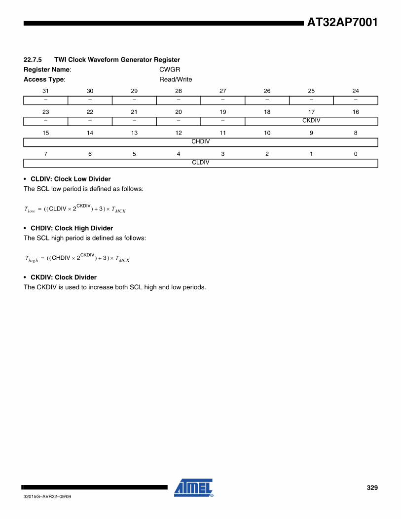
32932015G–AVR32–09/09
AT32AP7001
22.7.5 TWI Clock Waveform Generator Register
Register Name: CWGR
Access Type: Read/Write
• CLDIV: Clock Low Divider
The SCL low period is defined as follows:
• CHDIV: Clock High Divider
The SCL high period is defined as follows:
• CKDIV: Clock Divider
The CKDIV is used to increase both SCL high and low periods.
31 30 29 28 27 26 25 24
– – – – – – – –
23 22 21 20 19 18 17 16
– – – – – CKDIV
15 14 13 12 11 10 9 8
CHDIV
7 6 5 4 3 2 1 0CLDIV
Tlow CLDIV( 2CKDIV×( ) 3 )+ TMCK×=
Thigh CHDIV( 2CKDIV×( ) 3 )+ TMCK×=
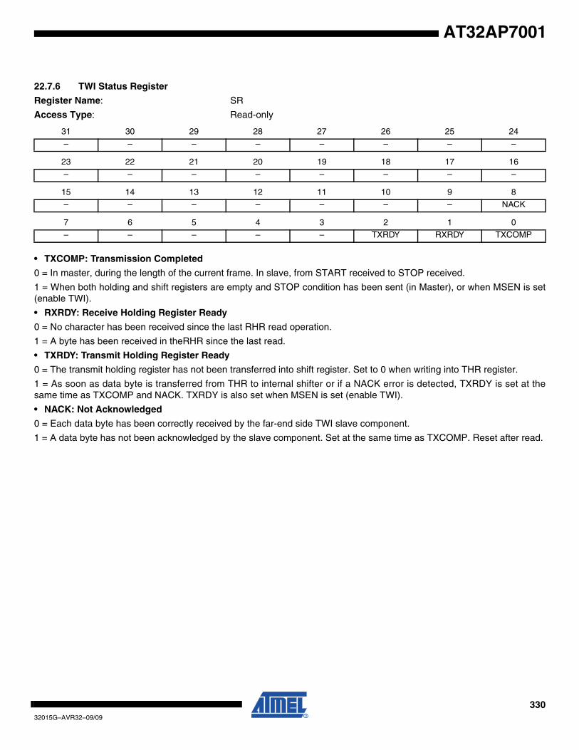
33032015G–AVR32–09/09
AT32AP7001
22.7.6 TWI Status Register
Register Name: SR
Access Type: Read-only
• TXCOMP: Transmission Completed
0 = In master, during the length of the current frame. In slave, from START received to STOP received.
1 = When both holding and shift registers are empty and STOP condition has been sent (in Master), or when MSEN is set(enable TWI).
• RXRDY: Receive Holding Register Ready
0 = No character has been received since the last RHR read operation.
1 = A byte has been received in theRHR since the last read.
• TXRDY: Transmit Holding Register Ready
0 = The transmit holding register has not been transferred into shift register. Set to 0 when writing into THR register.
1 = As soon as data byte is transferred from THR to internal shifter or if a NACK error is detected, TXRDY is set at thesame time as TXCOMP and NACK. TXRDY is also set when MSEN is set (enable TWI).
• NACK: Not Acknowledged
0 = Each data byte has been correctly received by the far-end side TWI slave component.
1 = A data byte has not been acknowledged by the slave component. Set at the same time as TXCOMP. Reset after read.
31 30 29 28 27 26 25 24
– – – – – – – –
23 22 21 20 19 18 17 16
– – – – – – – –
15 14 13 12 11 10 9 8
– – – – – – – NACK
7 6 5 4 3 2 1 0– – – – – TXRDY RXRDY TXCOMP
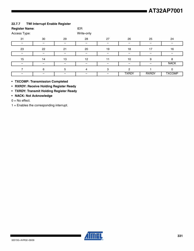
33132015G–AVR32–09/09
AT32AP7001
22.7.7 TWI Interrupt Enable Register
Register Name: IER
Access Type: Write-only
• TXCOMP: Transmission Completed
• RXRDY: Receive Holding Register Ready
• TXRDY: Transmit Holding Register Ready
• NACK: Not Acknowledge
0 = No effect.
1 = Enables the corresponding interrupt.
31 30 29 28 27 26 25 24– – – – – – – –
23 22 21 20 19 18 17 16
– – – – – – – –
15 14 13 12 11 10 9 8– – – – – – – NACK
7 6 5 4 3 2 1 0
– – – – – TXRDY RXRDY TXCOMP
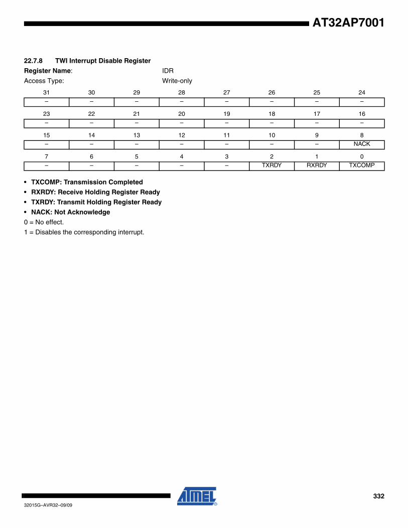
33232015G–AVR32–09/09
AT32AP7001
22.7.8 TWI Interrupt Disable Register
Register Name: IDR
Access Type: Write-only
• TXCOMP: Transmission Completed
• RXRDY: Receive Holding Register Ready
• TXRDY: Transmit Holding Register Ready
• NACK: Not Acknowledge
0 = No effect.
1 = Disables the corresponding interrupt.
31 30 29 28 27 26 25 24
– – – – – – – –
23 22 21 20 19 18 17 16
– – – – – – – –
15 14 13 12 11 10 9 8
– – – – – – – NACK
7 6 5 4 3 2 1 0– – – – – TXRDY RXRDY TXCOMP
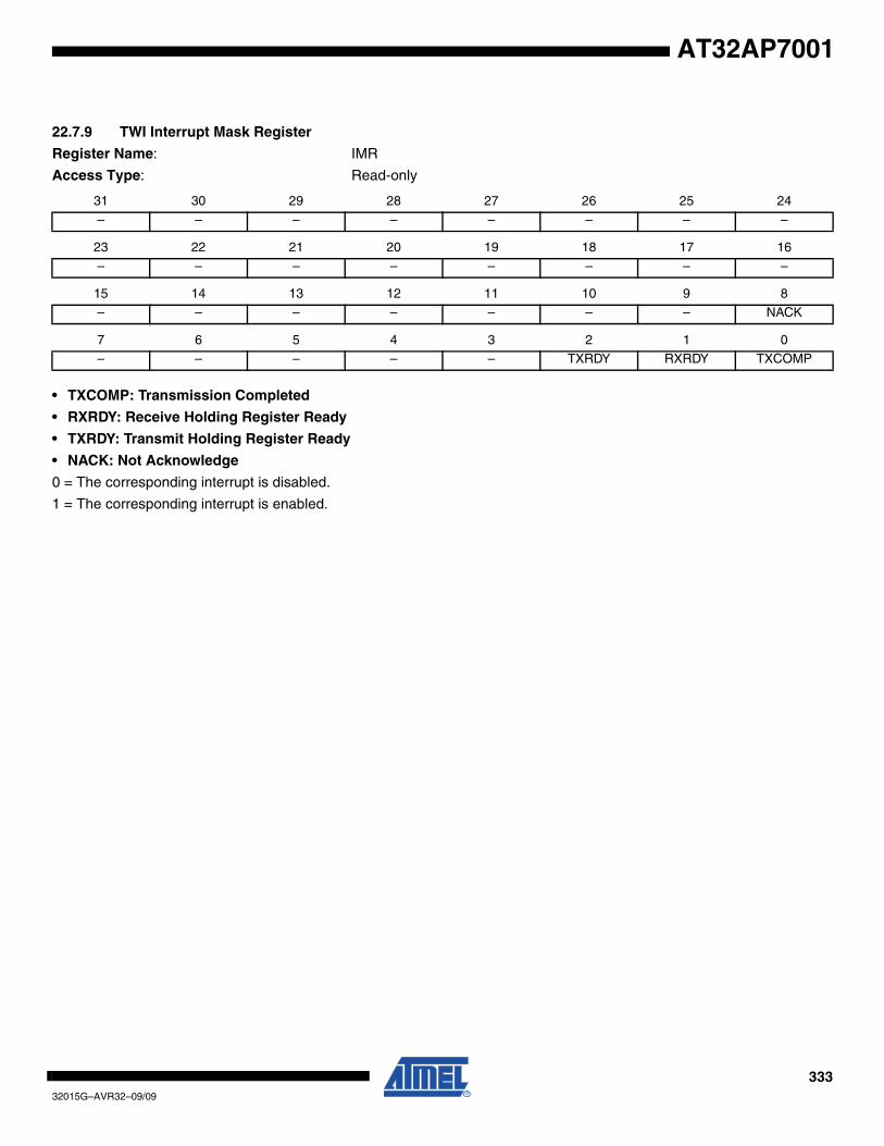
33332015G–AVR32–09/09
AT32AP7001
22.7.9 TWI Interrupt Mask Register
Register Name: IMR
Access Type: Read-only
• TXCOMP: Transmission Completed
• RXRDY: Receive Holding Register Ready
• TXRDY: Transmit Holding Register Ready
• NACK: Not Acknowledge
0 = The corresponding interrupt is disabled.
1 = The corresponding interrupt is enabled.
31 30 29 28 27 26 25 24
– – – – – – – –
23 22 21 20 19 18 17 16
– – – – – – – –
15 14 13 12 11 10 9 8
– – – – – – – NACK
7 6 5 4 3 2 1 0– – – – – TXRDY RXRDY TXCOMP
33432015G–AVR32–09/09
AT32AP7001
22.7.10 TWI Receive Holding Register
Register Name: RHR
Access Type: Read-only
• RXDATA: Master or Slave Receive Holding Data
31 30 29 28 27 26 25 24
– – – – – – – –
23 22 21 20 19 18 17 16
– – – – – – – –
15 14 13 12 11 10 9 8
– – – – – – – –
7 6 5 4 3 2 1 0RXDATA
33532015G–AVR32–09/09
AT32AP7001
22.7.11 TWI Transmit Holding Register
Register Name: THR
Access Type: Read/Write
• TXDATA: Master or Slave Transmit Holding Data
31 30 29 28 27 26 25 24
– – – – – – – –
23 22 21 20 19 18 17 16
– – – – – – – –
15 14 13 12 11 10 9 8
– – – – – – – –
7 6 5 4 3 2 1 0TXDATA
33632015G–AVR32–09/09
AT32AP7001
23. PS/2 Module (PSIF)
Rev: 1.0.0.2
23.1 Features
• PS/2 Host• Receive and transmit capability• Parity generation and error detection• Overrun error detection
23.2 Description
The PS/2 module provides host functionality allowing the MCU to interface PS/2 devices such askeyboard and mice. The module is capable of both host-to-device and device-to-hostcommunication.
23.3 Product Dependencies
23.3.1 I/O Lines
The PS/2 may be multiplexed with PIO lines. The programmer must first program the PIO con-troller to give control of the pins to the PS/2 module.
23.3.2 Power Management
The clock for the PS/2 module is generated by the power manager. The programmer mustensure that the PS/2 clock is enabled in the power manager before using the PS/2 module.
23.3.3 Interrupt
The PS/2 module has an interrupt line connected to the interrupt controller. Handling the PS/2interrupt requires programming the interrupt controller before configuring the PS/2 module.
23.4 The PS/2 Protocol
The PS/2 protocol is a bidirectional synchronous serial communication protocol. It connects asingle master - referred to as the ‘host’ - to a single slave - referred to as the ‘device’. Communi-cation is done through two lines called ‘data’ and ‘clock’. Both of these must be open-drain oropen-collector with a pullup resistor to perform a wired-AND function. When the bus is idle, bothlines are high.
The device always generates the clock signal, but the host may pull the clock low to inhibit trans-fers. The clock frequency is in the range 10-16.7 kHz. Both the host and the slave may initiate atransfer, but the host has ultimate control of the bus.
Data are transmitted one byte at a time in a frame consisting of 11-12 bits. The transfer format isdescribed in detail below.
23.4.1 Device to host communication
The device can only initiate a transfer when the bus is idle. If the host at any time pulls the clocklow, the device must stop transferring data and prepare to receive data from the host.
The device transmits data using a 11-bit frame. The device writes a bit on the data line when theclock is high, and the host reads the bit when the clock is low.
The format of the frame is:
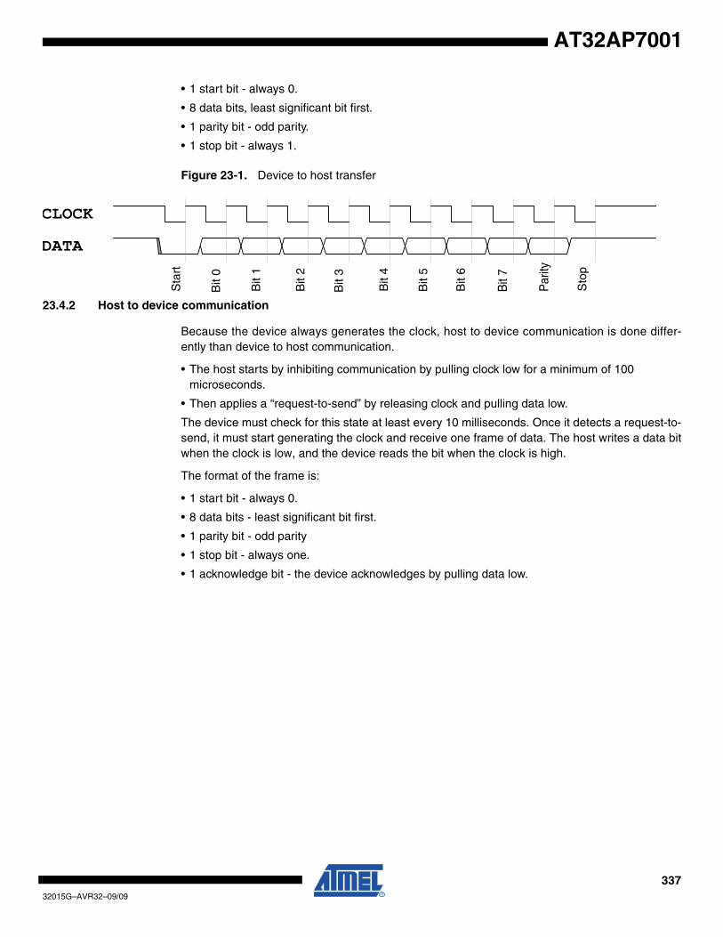
33732015G–AVR32–09/09
AT32AP7001
• 1 start bit - always 0.
• 8 data bits, least significant bit first.
• 1 parity bit - odd parity.
• 1 stop bit - always 1.
Figure 23-1. Device to host transfer
23.4.2 Host to device communication
Because the device always generates the clock, host to device communication is done differ-ently than device to host communication.
• The host starts by inhibiting communication by pulling clock low for a minimum of 100 microseconds.
• Then applies a “request-to-send” by releasing clock and pulling data low.
The device must check for this state at least every 10 milliseconds. Once it detects a request-to-send, it must start generating the clock and receive one frame of data. The host writes a data bitwhen the clock is low, and the device reads the bit when the clock is high.
The format of the frame is:
• 1 start bit - always 0.
• 8 data bits - least significant bit first.
• 1 parity bit - odd parity
• 1 stop bit - always one.
• 1 acknowledge bit - the device acknowledges by pulling data low.
Sta
rt
Bit
0
Bit
1
Bit
2
Bit
3
Bit
4
Bit
5
Bit
7
Sto
p
Bit
6
CLOCK
DATA
Par
ity
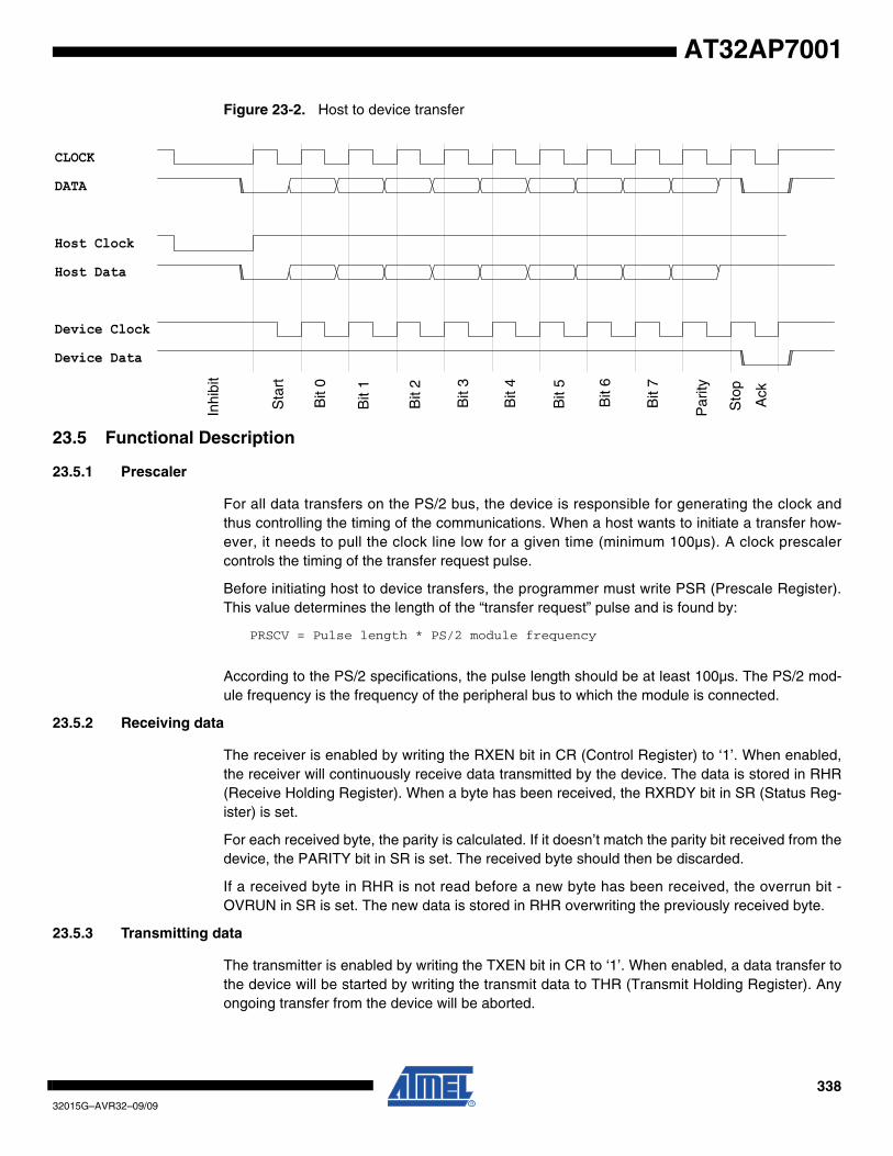
33832015G–AVR32–09/09
AT32AP7001
Figure 23-2. Host to device transfer
23.5 Functional Description
23.5.1 Prescaler
For all data transfers on the PS/2 bus, the device is responsible for generating the clock andthus controlling the timing of the communications. When a host wants to initiate a transfer how-ever, it needs to pull the clock line low for a given time (minimum 100µs). A clock prescalercontrols the timing of the transfer request pulse.
Before initiating host to device transfers, the programmer must write PSR (Prescale Register).This value determines the length of the “transfer request” pulse and is found by:
PRSCV = Pulse length * PS/2 module frequency
According to the PS/2 specifications, the pulse length should be at least 100µs. The PS/2 mod-ule frequency is the frequency of the peripheral bus to which the module is connected.
23.5.2 Receiving data
The receiver is enabled by writing the RXEN bit in CR (Control Register) to ‘1’. When enabled,the receiver will continuously receive data transmitted by the device. The data is stored in RHR(Receive Holding Register). When a byte has been received, the RXRDY bit in SR (Status Reg-ister) is set.
For each received byte, the parity is calculated. If it doesn’t match the parity bit received from thedevice, the PARITY bit in SR is set. The received byte should then be discarded.
If a received byte in RHR is not read before a new byte has been received, the overrun bit -OVRUN in SR is set. The new data is stored in RHR overwriting the previously received byte.
23.5.3 Transmitting data
The transmitter is enabled by writing the TXEN bit in CR to ‘1’. When enabled, a data transfer tothe device will be started by writing the transmit data to THR (Transmit Holding Register). Anyongoing transfer from the device will be aborted.
Sta
rt
Bit
0
Bit
1
Bit
2
Bit
3
Bit
4
Bit
5
Sto
p
Bit
6
Inhi
bit
Ack
CLOCK
DATA
Host Clock
Host Data
Device Clock
Device Data
Bit
7
Par
ity
33932015G–AVR32–09/09
AT32AP7001
When the data written to THR has been transmitted to the device, the TXRDY bit in SR will beset and a new value can be loaded into THR.
At the end of the transfer, the device should acknowledge the transfer by pulling the data linelow for one cycle. If an acknowledge is not detected, the NACK bit in SR will be set.
If the device fails to acknowledge the frame, the NACK bit in SR will be set. The software isresponsible for any retries.
All transfers from host to device are started by the host pulling the clock line low for at least100µs. The programmer must ensure that the prescaler is programmed to generate correctpulse length.
23.5.4 Interrupts
The PS/2 module can be configured to signal an interrupt when one of the bits in SR is set. Theinterrupt is enabled by writing to IER (Interrupt Enable Register) and disabled by writing to IDR(Interrupt Disable Register). The current setting of an interrupt line can be seen by reading IMR(Interrupt Mask Register).
23.6 User Interface
Offset Register Register Name Access Reset
0x000 PS/2 Control Register 0 CR0 Write-only -
0x004 PS/2 Receive Holding Register 0 RHR0 Read-only 0x0
0x008 PS/2 Transmit Holding Register 0 THR0 Write-only -
0x00C RESERVED - - -
0x010 PS/2 Status Register 0 SR0 Read-only 0x0
0x014 PS/2 Interrupt Enable Register 0 IER0 Write-only -
0x018 PS/2 Interrupt Disable Register 0 IDR0 Write-only -
0x01C PS/2 Interrupt Mask Register 0 IMR0 Read-only 0x0
0x020 RESERVED - - -
0x024 PS/2 Prescale Register 0 PSR0 Read/Write 0x0
0x100 PS/2 Control Register 1 CR1 Write-only -
0x104 PS/2 Receive Holding Register 1 RHR1 Read-only 0x0
0x108 PS/2 Transmit Holding Register 1 THR1 Write-only -
0x10C RESERVED - - -
0x110 PS/2 Status Register 1 SR1 Read-only 0x0
0x114 PS/2 Interrupt Enable Register 1 IER1 Write-only -
0x118 PS/2 Interrupt Disable Register 1 IDR1 Write-only -
0x11C PS/2 Interrupt Mask Register 1 IMR1 Read-only 0x0
0x120 RESERVED - - -
0x124 PS/2 Prescale Register 1 PSR1 Read/Write 0x0
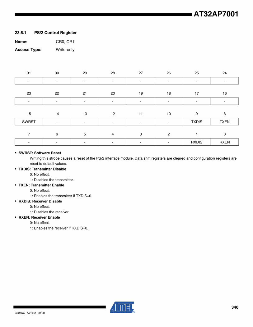
34032015G–AVR32–09/09
AT32AP7001
23.6.1 PS/2 Control Register
Name: CR0, CR1
Access Type: Write-only
• SWRST: Software ResetWriting this strobe causes a reset of the PS/2 interface module. Data shift registers are cleared and configuration registers are
reset to default values.
• TXDIS: Transmitter Disable0: No effect.
1: Disables the transmitter.
• TXEN: Transmitter Enable0: No effect.
1: Enables the transmitter if TXDIS=0.
• RXDIS: Receiver Disable0: No effect.
1: Disables the receiver.
• RXEN: Receiver Enable0: No effect.
1: Enables the receiver if RXDIS=0.
31 30 29 28 27 26 25 24
- - - - - - - -
23 22 21 20 19 18 17 16
- - - - - - - -
15 14 13 12 11 10 9 8
SWRST - - - - - TXDIS TXEN
7 6 5 4 3 2 1 0
- - - - - - RXDIS RXEN

34132015G–AVR32–09/09
AT32AP7001
23.6.2 PS/2 Receive Holding Register
Name: RHR0, RHR1
Access Type: Read-only
• RXDATA: Receive DataData received from the device.
31 30 29 28 27 26 25 24
- - - - - - - -
23 22 21 20 19 18 17 16
- - - - - - - -
15 14 13 12 11 10 9 8
- - - - - - - -
7 6 5 4 3 2 1 0
RXDATA
34232015G–AVR32–09/09
AT32AP7001
23.6.3 PS/2 Transmit Holding Register
Name: THR0, THR1
Access Type: Write-only
• TXDATA: Transmit DataData to be transmitted to the device.
31 30 29 28 27 26 25 24
- - - - - - - -
23 22 21 20 19 18 17 16
- - - - - - - -
15 14 13 12 11 10 9 8
- - - - - - - -
7 6 5 4 3 2 1 0
TXDATA
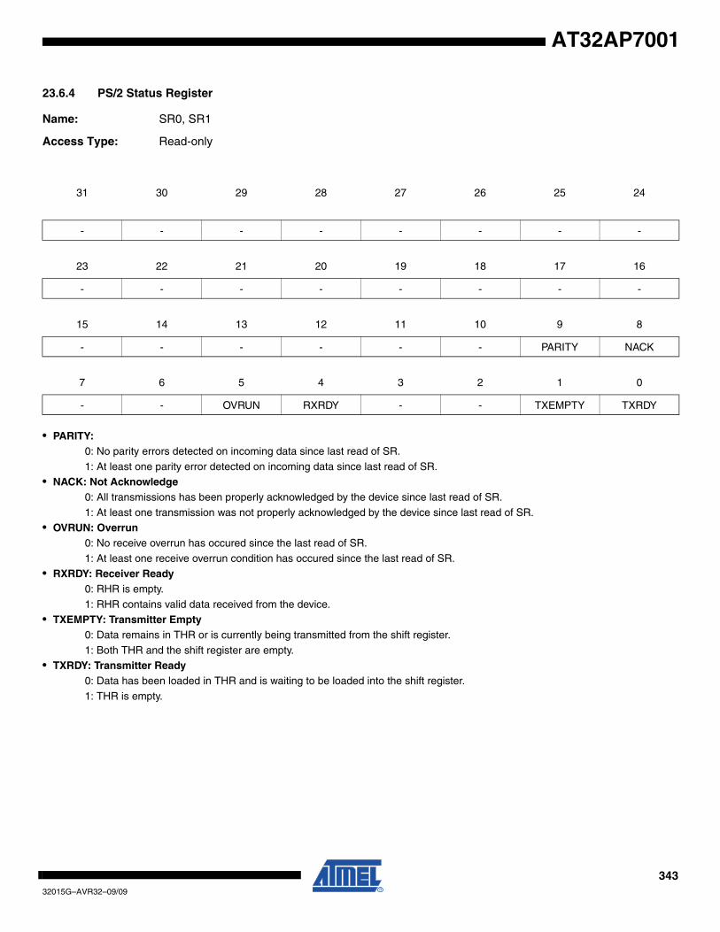
34332015G–AVR32–09/09
AT32AP7001
23.6.4 PS/2 Status Register
Name: SR0, SR1
Access Type: Read-only
• PARITY: 0: No parity errors detected on incoming data since last read of SR.
1: At least one parity error detected on incoming data since last read of SR.
• NACK: Not Acknowledge0: All transmissions has been properly acknowledged by the device since last read of SR.
1: At least one transmission was not properly acknowledged by the device since last read of SR.
• OVRUN: Overrun0: No receive overrun has occured since the last read of SR.
1: At least one receive overrun condition has occured since the last read of SR.
• RXRDY: Receiver Ready0: RHR is empty.
1: RHR contains valid data received from the device.
• TXEMPTY: Transmitter Empty0: Data remains in THR or is currently being transmitted from the shift register.
1: Both THR and the shift register are empty.
• TXRDY: Transmitter Ready0: Data has been loaded in THR and is waiting to be loaded into the shift register.
1: THR is empty.
31 30 29 28 27 26 25 24
- - - - - - - -
23 22 21 20 19 18 17 16
- - - - - - - -
15 14 13 12 11 10 9 8
- - - - - - PARITY NACK
7 6 5 4 3 2 1 0
- - OVRUN RXRDY - - TXEMPTY TXRDY
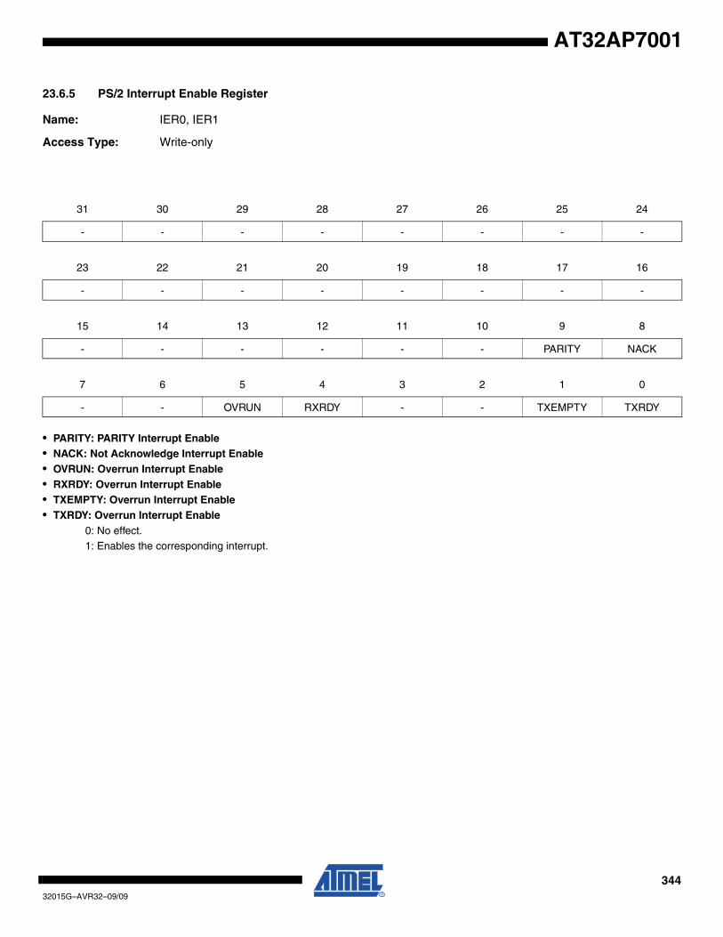
34432015G–AVR32–09/09
AT32AP7001
23.6.5 PS/2 Interrupt Enable Register
Name: IER0, IER1
Access Type: Write-only
• PARITY: PARITY Interrupt Enable• NACK: Not Acknowledge Interrupt Enable• OVRUN: Overrun Interrupt Enable• RXRDY: Overrun Interrupt Enable• TXEMPTY: Overrun Interrupt Enable• TXRDY: Overrun Interrupt Enable
0: No effect.1: Enables the corresponding interrupt.
31 30 29 28 27 26 25 24
- - - - - - - -
23 22 21 20 19 18 17 16
- - - - - - - -
15 14 13 12 11 10 9 8
- - - - - - PARITY NACK
7 6 5 4 3 2 1 0
- - OVRUN RXRDY - - TXEMPTY TXRDY
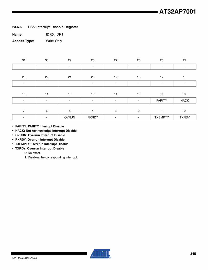
34532015G–AVR32–09/09
AT32AP7001
‘
23.6.6 PS/2 Interrupt Disable Register
Name: IDR0, IDR1
Access Type: Write-Only
• PARITY: PARITY Interrupt Disable• NACK: Not Acknowledge Interrupt Disable• OVRUN: Overrun Interrupt Disable• RXRDY: Overrun Interrupt Disable• TXEMPTY: Overrun Interrupt Disable• TXRDY: Overrun Interrupt Disable
0: No effect.1: Disables the corresponding interrupt.
31 30 29 28 27 26 25 24
- - - - - - - -
23 22 21 20 19 18 17 16
- - - - - - - -
15 14 13 12 11 10 9 8
- - - - - - PARITY NACK
7 6 5 4 3 2 1 0
- - OVRUN RXRDY - - TXEMPTY TXRDY
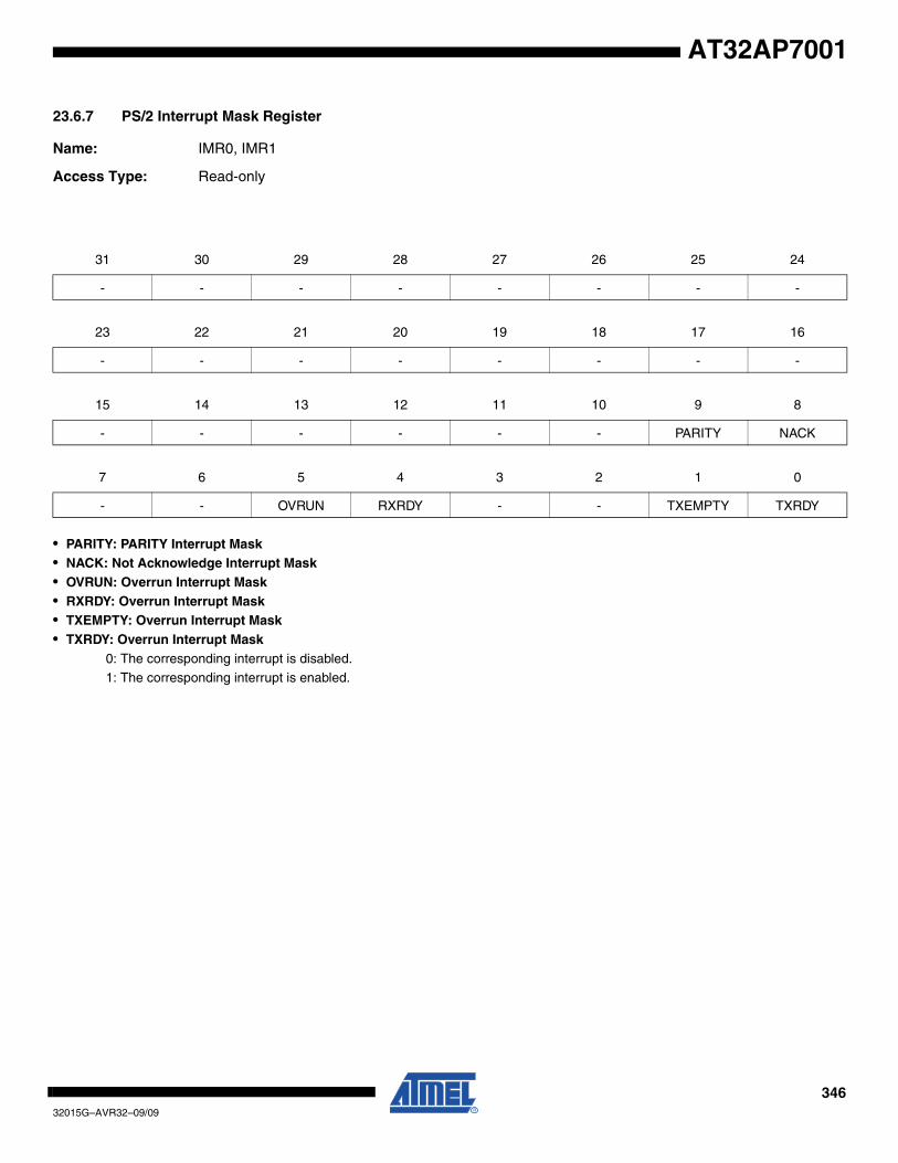
34632015G–AVR32–09/09
AT32AP7001
23.6.7 PS/2 Interrupt Mask Register
Name: IMR0, IMR1
Access Type: Read-only
• PARITY: PARITY Interrupt Mask• NACK: Not Acknowledge Interrupt Mask• OVRUN: Overrun Interrupt Mask• RXRDY: Overrun Interrupt Mask• TXEMPTY: Overrun Interrupt Mask• TXRDY: Overrun Interrupt Mask
0: The corresponding interrupt is disabled.1: The corresponding interrupt is enabled.
31 30 29 28 27 26 25 24
- - - - - - - -
23 22 21 20 19 18 17 16
- - - - - - - -
15 14 13 12 11 10 9 8
- - - - - - PARITY NACK
7 6 5 4 3 2 1 0
- - OVRUN RXRDY - - TXEMPTY TXRDY
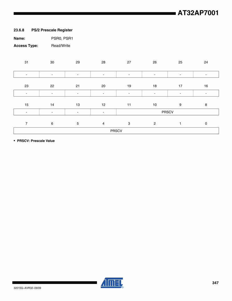
34732015G–AVR32–09/09
AT32AP7001
23.6.8 PS/2 Prescale Register
Name: PSR0, PSR1
Access Type: Read/Write
• PRSCV: Prescale Value
31 30 29 28 27 26 25 24
- - - - - - - -
23 22 21 20 19 18 17 16
- - - - - - - -
15 14 13 12 11 10 9 8
- - - - PRSCV
7 6 5 4 3 2 1 0
PRSCV
34832015G–AVR32–09/09
AT32AP7001
24. Synchronous Serial Controller (SSC)
Rev: 2.0.0.2
24.1 Features• Provides Serial Synchronous Communication Links Used in Audio and Telecom Applications • Contains an Independent Receiver and Transmitter and a Common Clock Divider• Interfaced with Two PDCA Channels (DMA Access) to Reduce Processor Overhead• Offers a Configurable Frame Sync and Data Length• Receiver and Transmitter Can be Programmed to Start Automatically or on Detection of Different
Events on the Frame Sync Signal• Receiver and Transmitter Include a Data Signal, a Clock Signal and a Frame Synchronization
Signal
24.2 OverviewThe Atmel Synchronous Serial Controller (SSC) provides a synchronous communication linkwith external devices. It supports many serial synchronous communication protocols generallyused in audio and telecom applications such as I2S, Short Frame Sync, Long Frame Sync, etc.
The SSC contains an independent receiver and transmitter and a common clock divider. Thereceiver and the transmitter each interface with three signals: the TX_DATA/RX_DATA signalfo r da ta , the TX_CLOCK/RX_CLOCK s igna l fo r the c lock and theTX_FRAME_SYNC/RX_FRAME_SYNC signal for the Frame Sync. The transfers can be pro-grammed to start automatically or on different events detected on the Frame Sync signal.
The SSC’s high-level of programmability and its two dedicated PDCA channels of up to 32 bitspermit a continuous high bit rate data transfer without processor intervention.
Featuring connection to two PDCA channels, the SSC permits interfacing with low processoroverhead to the following:
•CODEC’s in master or slave mode
•DAC through dedicated serial interface, particularly I2S
•Magnetic card reader
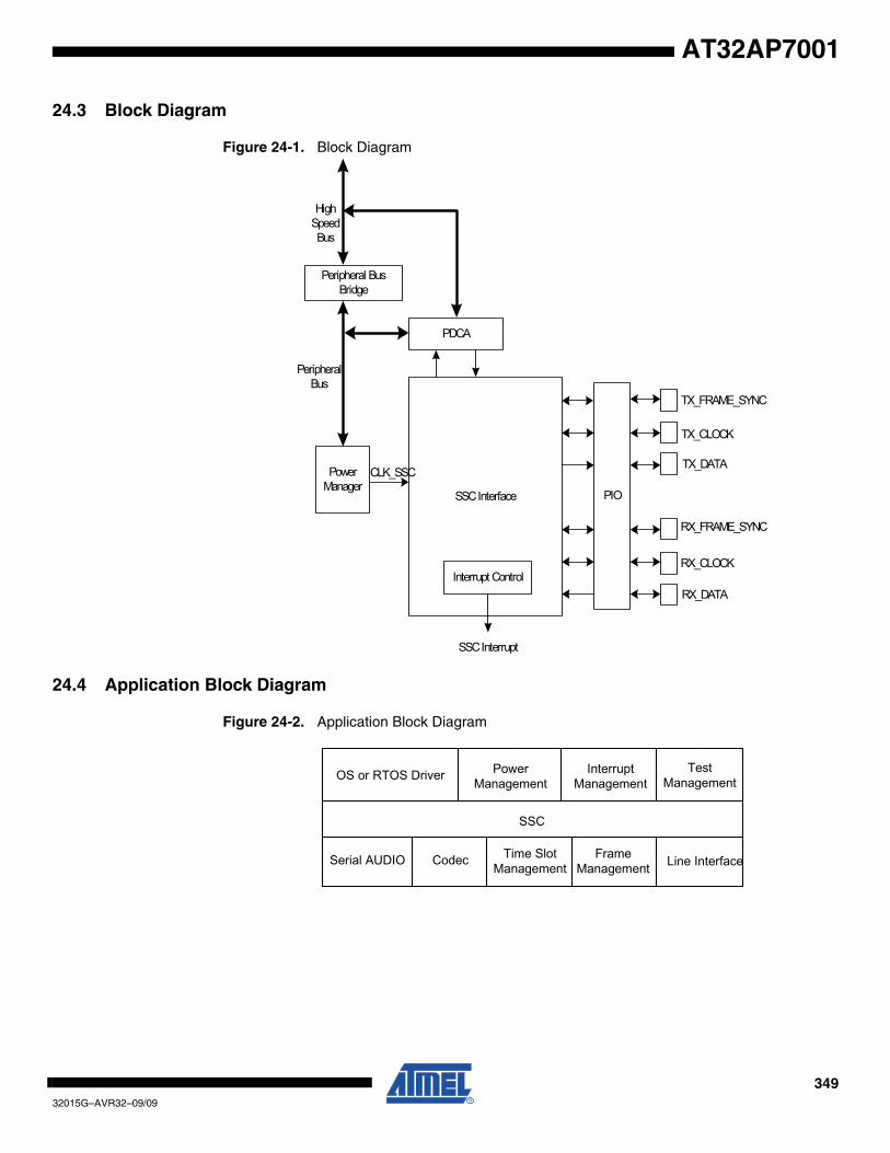
34932015G–AVR32–09/09
AT32AP7001
24.3 Block Diagram
Figure 24-1. Block Diagram
24.4 Application Block Diagram
Figure 24-2. Application Block Diagram
SSC Interface
PDCA
Peripheral BusBridge
HighSpeedBus
PeripheralBus
PowerManager
CLK_SSC
PIO
Interrupt Control
SSC Interrupt
TX_FRAME_SYNC
RX_FRAME_SYNC
TX_CLOCK
RX_CLOCK
RX_DATA
TX_DATA
TestManagement
Line Interface
InterruptManagement
FrameManagement
Time SlotManagement
SSC
PowerManagement
CodecSerial AUDIO
OS or RTOS Driver
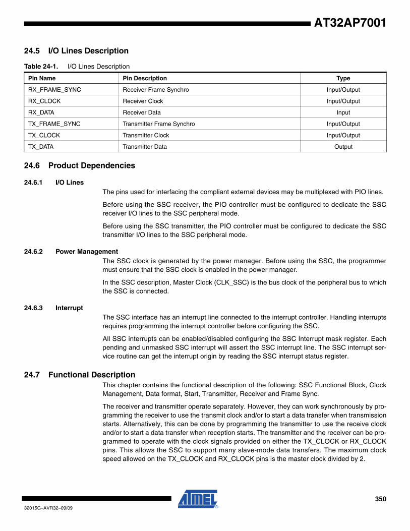
35032015G–AVR32–09/09
AT32AP7001
24.5 I/O Lines Description
24.6 Product Dependencies
24.6.1 I/O LinesThe pins used for interfacing the compliant external devices may be multiplexed with PIO lines.
Before using the SSC receiver, the PIO controller must be configured to dedicate the SSCreceiver I/O lines to the SSC peripheral mode.
Before using the SSC transmitter, the PIO controller must be configured to dedicate the SSCtransmitter I/O lines to the SSC peripheral mode.
24.6.2 Power ManagementThe SSC clock is generated by the power manager. Before using the SSC, the programmermust ensure that the SSC clock is enabled in the power manager.
In the SSC description, Master Clock (CLK_SSC) is the bus clock of the peripheral bus to whichthe SSC is connected.
24.6.3 InterruptThe SSC interface has an interrupt line connected to the interrupt controller. Handling interruptsrequires programming the interrupt controller before configuring the SSC.
All SSC interrupts can be enabled/disabled configuring the SSC Interrupt mask register. Eachpending and unmasked SSC interrupt will assert the SSC interrupt line. The SSC interrupt ser-vice routine can get the interrupt origin by reading the SSC interrupt status register.
24.7 Functional DescriptionThis chapter contains the functional description of the following: SSC Functional Block, ClockManagement, Data format, Start, Transmitter, Receiver and Frame Sync.
The receiver and transmitter operate separately. However, they can work synchronously by pro-gramming the receiver to use the transmit clock and/or to start a data transfer when transmissionstarts. Alternatively, this can be done by programming the transmitter to use the receive clockand/or to start a data transfer when reception starts. The transmitter and the receiver can be pro-grammed to operate with the clock signals provided on either the TX_CLOCK or RX_CLOCKpins. This allows the SSC to support many slave-mode data transfers. The maximum clockspeed allowed on the TX_CLOCK and RX_CLOCK pins is the master clock divided by 2.
Table 24-1. I/O Lines Description
Pin Name Pin Description Type
RX_FRAME_SYNC Receiver Frame Synchro Input/Output
RX_CLOCK Receiver Clock Input/Output
RX_DATA Receiver Data Input
TX_FRAME_SYNC Transmitter Frame Synchro Input/Output
TX_CLOCK Transmitter Clock Input/Output
TX_DATA Transmitter Data Output
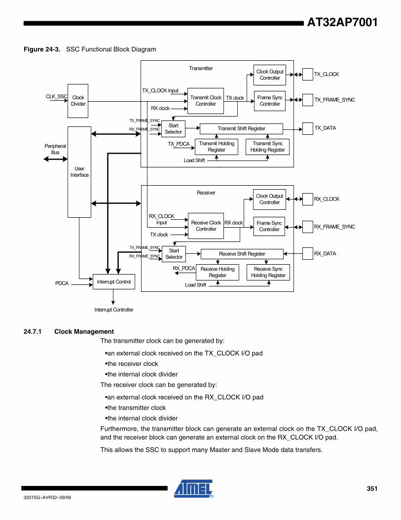
35132015G–AVR32–09/09
AT32AP7001
Figure 24-3. SSC Functional Block Diagram
24.7.1 Clock ManagementThe transmitter clock can be generated by:
•an external clock received on the TX_CLOCK I/O pad
•the receiver clock
•the internal clock divider
The receiver clock can be generated by:
•an external clock received on the RX_CLOCK I/O pad
•the transmitter clock
•the internal clock divider
Furthermore, the transmitter block can generate an external clock on the TX_CLOCK I/O pad,and the receiver block can generate an external clock on the RX_CLOCK I/O pad.
This allows the SSC to support many Master and Slave Mode data transfers.
ClockDivider
UserInterface
PeripheralBus
CLK_SSC
Interrupt Control
Start Selector Receive Shift Register
Receive Holding Register
Receive SyncHolding Register
PDCA
Interrupt Controller
RX_FRAME_SYNC
RX_DATA
RX_CLOCK
Frame SyncController
Clock OutputController
Receive ClockController
Transmit HoldingRegister
Transmit Sync Holding Register
Transmit Shift Register
Frame SyncController
Clock OutputController
Transmit Clock Controller
Start Selector
TX_FRAME_SYNC
RX_FRAME_SYNC
TX_CLOCK Input
Transmitter
TX_PDCA
Load Shift
RX clock
TX clock
TX_CLOCK
TX_FRAME_SYNC
TX_DATA
Receiver
RX clockRX_CLOCK
Input
TX clock
TX_FRAME_SYNC
RX_FRAME_SYNC
RX_PDCA
Load Shift
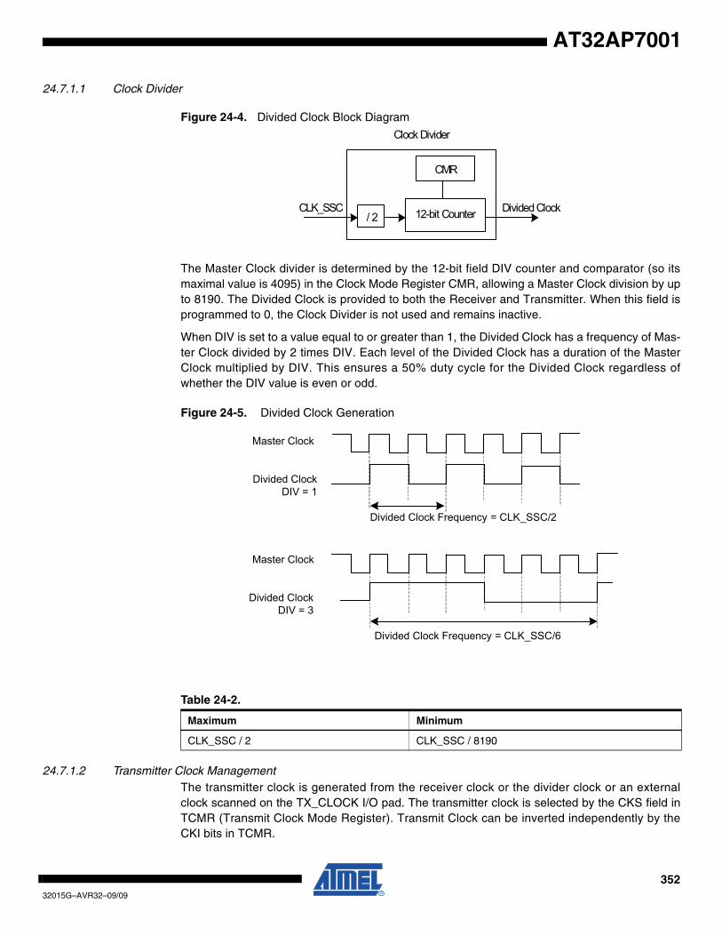
35232015G–AVR32–09/09
AT32AP7001
24.7.1.1 Clock Divider
Figure 24-4. Divided Clock Block Diagram
The Master Clock divider is determined by the 12-bit field DIV counter and comparator (so itsmaximal value is 4095) in the Clock Mode Register CMR, allowing a Master Clock division by upto 8190. The Divided Clock is provided to both the Receiver and Transmitter. When this field isprogrammed to 0, the Clock Divider is not used and remains inactive.
When DIV is set to a value equal to or greater than 1, the Divided Clock has a frequency of Mas-ter Clock divided by 2 times DIV. Each level of the Divided Clock has a duration of the MasterClock multiplied by DIV. This ensures a 50% duty cycle for the Divided Clock regardless ofwhether the DIV value is even or odd.
Figure 24-5. Divided Clock Generation
24.7.1.2 Transmitter Clock ManagementThe transmitter clock is generated from the receiver clock or the divider clock or an externalclock scanned on the TX_CLOCK I/O pad. The transmitter clock is selected by the CKS field inTCMR (Transmit Clock Mode Register). Transmit Clock can be inverted independently by theCKI bits in TCMR.
Table 24-2.
Maximum Minimum
CLK_SSC / 2 CLK_SSC / 8190
CMR
/ 2CLK_SSC Divided Clock12-bit Counter
Clock Divider
Master Clock
Divided ClockDIV = 1
Master Clock
Divided ClockDIV = 3
Divided Clock Frequency = CLK_SSC/2
Divided Clock Frequency = CLK_SSC/6

35332015G–AVR32–09/09
AT32AP7001
The transmitter can also drive the TX_CLOCK I/O pad continuously or be limited to the actualdata transfer. The clock output is configured by the TCMR register. The Transmit Clock Inver-sion (CKI) bits have no effect on the clock outputs. Programming the TCMR register to selectTX_CLOCK pin (CKS field) and at the same time Continuous Transmit Clock (CKO field) mightlead to unpredictable results.
Figure 24-6. Transmitter Clock Management
24.7.1.3 Receiver Clock ManagementThe receiver clock is generated from the transmitter clock or the divider clock or an externalclock scanned on the RX_CLOCK I/O pad. The Receive Clock is selected by the CKS field inRCMR (Receive Clock Mode Register). Receive Clocks can be inverted independently by theCKI bits in RCMR.
The receiver can also drive the RX_CLOCK I/O pad continuously or be limited to the actual datatransfer. The clock output is configured by the RCMR register. The Receive Clock Inversion(CKI) bits have no effect on the clock outputs. Programming the RCMR register to selectRX_CLOCK pin (CKS field) and at the same time Continuous Receive Clock (CKO field) canlead to unpredictable results.
TX_CLOCK(pin)
ReceiverClock
DividerClock
CKO Data Transfer
Tri-stateController
INVMUX
CKS
MUX
Tri-stateController
CKI CKG
TransmitterClock
ClockOutput
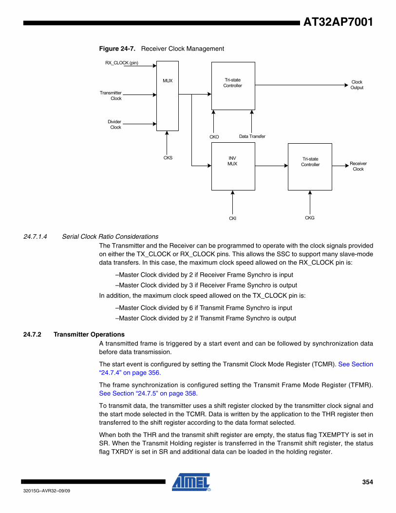
35432015G–AVR32–09/09
AT32AP7001
Figure 24-7. Receiver Clock Management
24.7.1.4 Serial Clock Ratio ConsiderationsThe Transmitter and the Receiver can be programmed to operate with the clock signals providedon either the TX_CLOCK or RX_CLOCK pins. This allows the SSC to support many slave-modedata transfers. In this case, the maximum clock speed allowed on the RX_CLOCK pin is:
–Master Clock divided by 2 if Receiver Frame Synchro is input
–Master Clock divided by 3 if Receiver Frame Synchro is output
In addition, the maximum clock speed allowed on the TX_CLOCK pin is:
–Master Clock divided by 6 if Transmit Frame Synchro is input
–Master Clock divided by 2 if Transmit Frame Synchro is output
24.7.2 Transmitter OperationsA transmitted frame is triggered by a start event and can be followed by synchronization databefore data transmission.
The start event is configured by setting the Transmit Clock Mode Register (TCMR). See Section“24.7.4” on page 356.
The frame synchronization is configured setting the Transmit Frame Mode Register (TFMR).See Section “24.7.5” on page 358.
To transmit data, the transmitter uses a shift register clocked by the transmitter clock signal andthe start mode selected in the TCMR. Data is written by the application to the THR register thentransferred to the shift register according to the data format selected.
When both the THR and the transmit shift register are empty, the status flag TXEMPTY is set inSR. When the Transmit Holding register is transferred in the Transmit shift register, the statusflag TXRDY is set in SR and additional data can be loaded in the holding register.
DividerClock
RX_CLOCK (pin)
TransmitterClock
MUX Tri-stateController
CKO Data Transfer
INVMUX
CKI
Tri-stateController
CKG
ReceiverClock
ClockOutput
CKS

35532015G–AVR32–09/09
AT32AP7001
Figure 24-8. Transmitter Block Diagram
24.7.3 Receiver OperationsA received frame is triggered by a start event and can be followed by synchronization databefore data transmission.
The start event is configured setting the Receive Clock Mode Register (RCMR). See Section“24.7.4” on page 356.
The frame synchronization is configured setting the Receive Frame Mode Register (RFMR). SeeSection “24.7.5” on page 358.
The receiver uses a shift register clocked by the receiver clock signal and the start modeselected in the RCMR. The data is transferred from the shift register depending on the data for-mat selected.
When the receiver shift register is full, the SSC transfers this data in the holding register, the sta-tus flag RXRDY is set in SR and the data can be read in the receiver holding register. If anothertransfer occurs before read of the RHR register, the status flag OVERUN is set in SR and thereceiver shift register is transferred in the RHR register.
TFMR.DATDEF
TFMR.MSBF 0
1
Transmit Shift Register
0 1
THR TSHR TFMR.FSLEN
TCMR.STTDLYTFMR.FSDENTFMR.DATNB
CR.TXEN
CR.TXDIS
SR.TXEN
TX_DATA
TFMR.DATLEN
TCMR.STTDLYTFMR.FSDEN
StartSelector
RX_FRAME_SYNCTX_FRAME_SYNC
Transmitter Clock
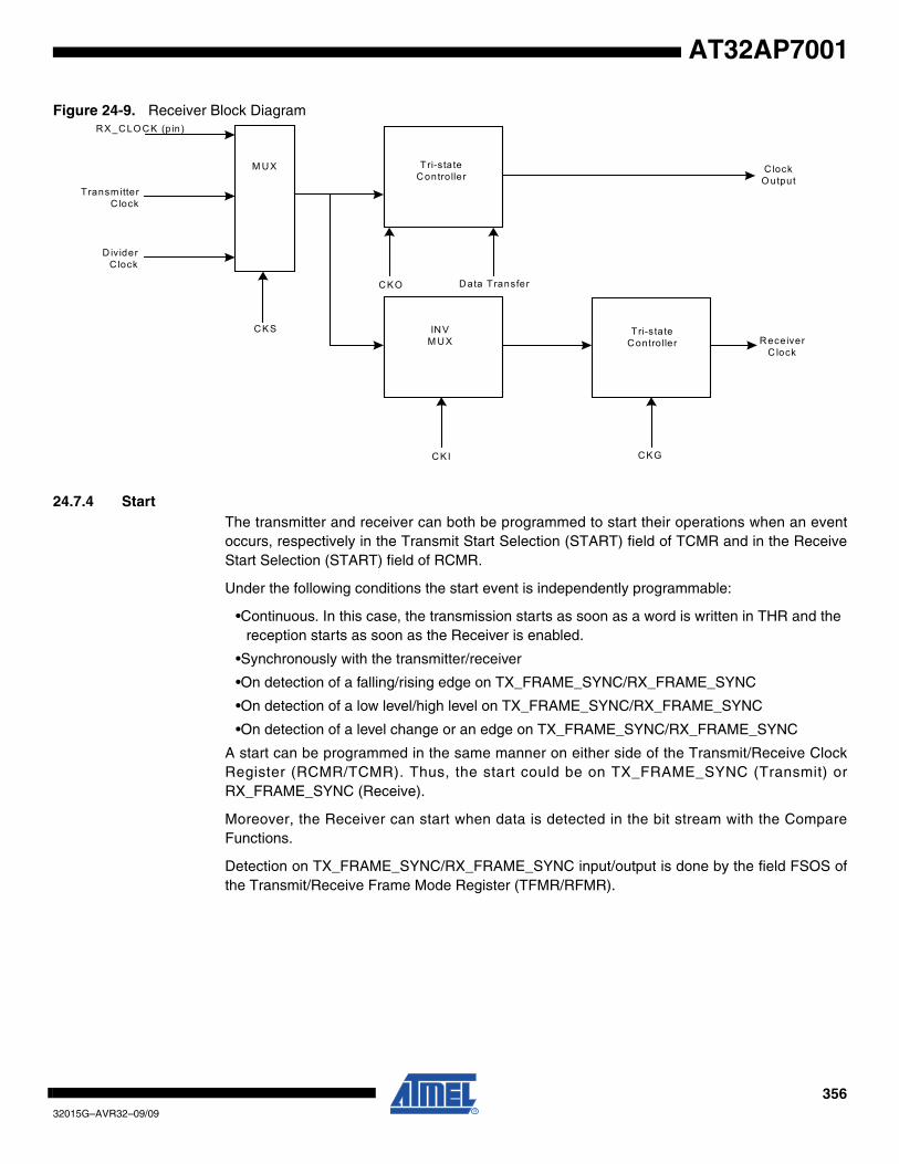
35632015G–AVR32–09/09
AT32AP7001
Figure 24-9. Receiver Block Diagram
24.7.4 StartThe transmitter and receiver can both be programmed to start their operations when an eventoccurs, respectively in the Transmit Start Selection (START) field of TCMR and in the ReceiveStart Selection (START) field of RCMR.
Under the following conditions the start event is independently programmable:
•Continuous. In this case, the transmission starts as soon as a word is written in THR and the reception starts as soon as the Receiver is enabled.
•Synchronously with the transmitter/receiver
•On detection of a falling/rising edge on TX_FRAME_SYNC/RX_FRAME_SYNC
•On detection of a low level/high level on TX_FRAME_SYNC/RX_FRAME_SYNC
•On detection of a level change or an edge on TX_FRAME_SYNC/RX_FRAME_SYNC
A start can be programmed in the same manner on either side of the Transmit/Receive ClockRegister (RCMR/TCMR). Thus, the start could be on TX_FRAME_SYNC (Transmit) orRX_FRAME_SYNC (Receive).
Moreover, the Receiver can start when data is detected in the bit stream with the CompareFunctions.
Detection on TX_FRAME_SYNC/RX_FRAME_SYNC input/output is done by the field FSOS ofthe Transmit/Receive Frame Mode Register (TFMR/RFMR).
DividerC lock
RX _CLO CK (pin)
Transm itterC lock
M UX Tri-stateContro ller
CKO Data Transfer
INVM UX
CKI
Tri-stateContro ller
CKG
ReceiverC lock
C lockO utput
CKS

35732015G–AVR32–09/09
AT32AP7001
Figure 24-10. Transmit Start Mode
Figure 24-11. Receive Pulse/Edge Start Modes
X B0 B1
B1B0
B0 B1
B1B0
B0 B1 B0 B1
B0 B1B1B0
X
X
X
X
XTX_DATA (Output)Start= Any Edge on TX_FRAME_SYNC
TX_DATA (Output)Start= Level Change on TX_FRAME_SYNC
TX_DATA (Output)Start= Rising Edge on TX_FRAME_SYNC
TX_DATA (Output)Start= Falling Edge on TX_FRAME_SYNC
TX_DATA (Output)Start= High Level on TX_FRAME_SYNC
TX_DATA (Output)Start= Low Level on TX_FRAME_SYNC
TX_FRAME_SYNC (Input)
TX_CLOCK (Input)
STTDLY
STTDLY
STTDLY
STTDLY
STTDLY
STTDLY
RX_CLOCK
RX_FRAME_SYNC (Input)
RX_DATA (Input)Start = High Level on RX_FRAME_SYNC
RX_DATA (Input)Start = Falling Edge on RX_FRAME_SYNC
RX_DATA (Input)Start = Rising Edge on RX_FRAME_SYNC
RX_DATA (Input)Start = Level Change on RX_FRAME_SYNC
RX_DATA (Input)Start = Any Edge on RX_FRAME_SYNC
RX_DATA (Input)Start = Low Level on RX_FRAME_SYNC
X
X
X
X
X
X B0
B0
B0
B0
B0
B0
B0
B1 B1
B1
B1
B1
B1
B1
STTDLY
STTDLY
STTDLY
STTDLY
STTDLY
STTDLY
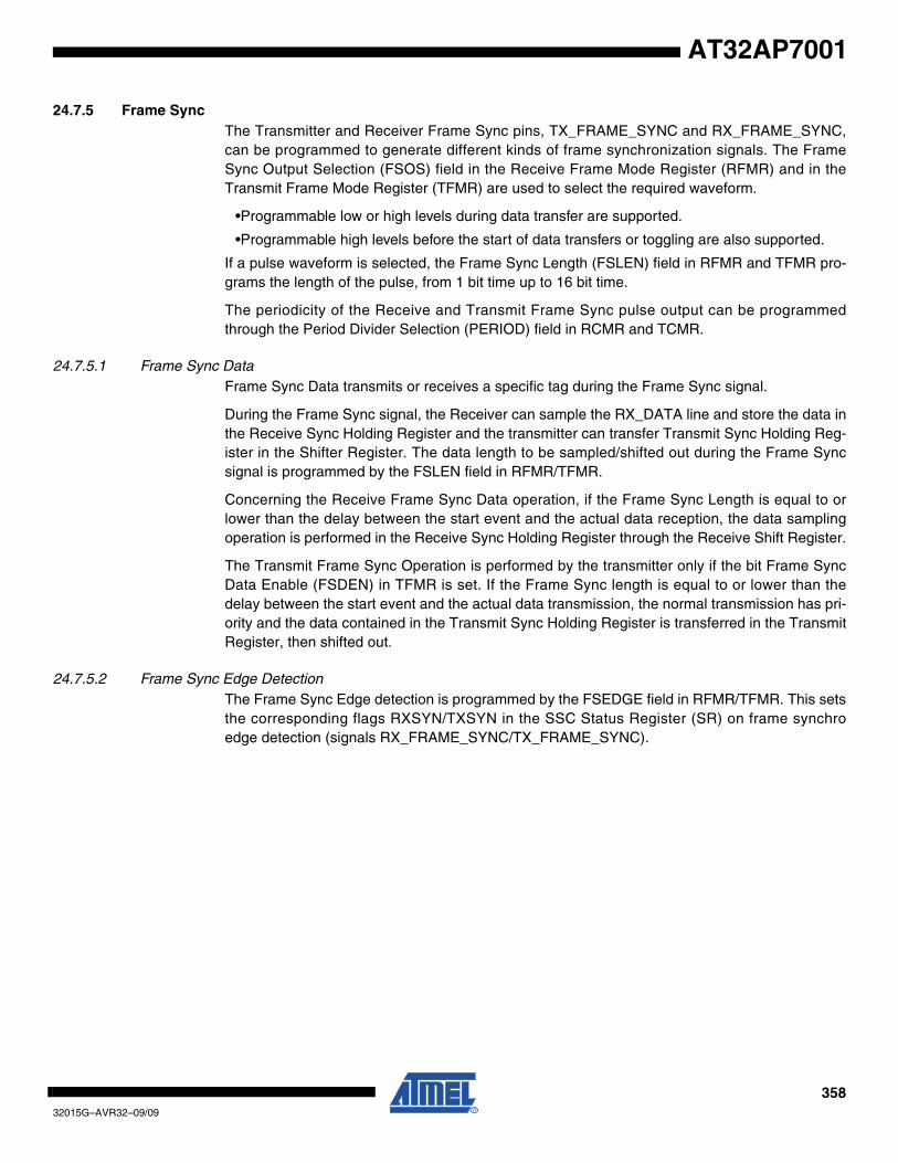
35832015G–AVR32–09/09
AT32AP7001
24.7.5 Frame SyncThe Transmitter and Receiver Frame Sync pins, TX_FRAME_SYNC and RX_FRAME_SYNC,can be programmed to generate different kinds of frame synchronization signals. The FrameSync Output Selection (FSOS) field in the Receive Frame Mode Register (RFMR) and in theTransmit Frame Mode Register (TFMR) are used to select the required waveform.
•Programmable low or high levels during data transfer are supported.
•Programmable high levels before the start of data transfers or toggling are also supported.
If a pulse waveform is selected, the Frame Sync Length (FSLEN) field in RFMR and TFMR pro-grams the length of the pulse, from 1 bit time up to 16 bit time.
The periodicity of the Receive and Transmit Frame Sync pulse output can be programmedthrough the Period Divider Selection (PERIOD) field in RCMR and TCMR.
24.7.5.1 Frame Sync DataFrame Sync Data transmits or receives a specific tag during the Frame Sync signal.
During the Frame Sync signal, the Receiver can sample the RX_DATA line and store the data inthe Receive Sync Holding Register and the transmitter can transfer Transmit Sync Holding Reg-ister in the Shifter Register. The data length to be sampled/shifted out during the Frame Syncsignal is programmed by the FSLEN field in RFMR/TFMR.
Concerning the Receive Frame Sync Data operation, if the Frame Sync Length is equal to orlower than the delay between the start event and the actual data reception, the data samplingoperation is performed in the Receive Sync Holding Register through the Receive Shift Register.
The Transmit Frame Sync Operation is performed by the transmitter only if the bit Frame SyncData Enable (FSDEN) in TFMR is set. If the Frame Sync length is equal to or lower than thedelay between the start event and the actual data transmission, the normal transmission has pri-ority and the data contained in the Transmit Sync Holding Register is transferred in the TransmitRegister, then shifted out.
24.7.5.2 Frame Sync Edge DetectionThe Frame Sync Edge detection is programmed by the FSEDGE field in RFMR/TFMR. This setsthe corresponding flags RXSYN/TXSYN in the SSC Status Register (SR) on frame synchroedge detection (signals RX_FRAME_SYNC/TX_FRAME_SYNC).
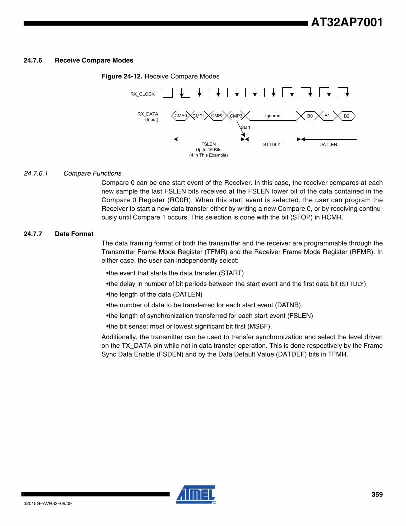
35932015G–AVR32–09/09
AT32AP7001
24.7.6 Receive Compare Modes
Figure 24-12. Receive Compare Modes
24.7.6.1 Compare FunctionsCompare 0 can be one start event of the Receiver. In this case, the receiver compares at eachnew sample the last FSLEN bits received at the FSLEN lower bit of the data contained in theCompare 0 Register (RC0R). When this start event is selected, the user can program theReceiver to start a new data transfer either by writing a new Compare 0, or by receiving continu-ously until Compare 1 occurs. This selection is done with the bit (STOP) in RCMR.
24.7.7 Data FormatThe data framing format of both the transmitter and the receiver are programmable through theTransmitter Frame Mode Register (TFMR) and the Receiver Frame Mode Register (RFMR). Ineither case, the user can independently select:
•the event that starts the data transfer (START)
•the delay in number of bit periods between the start event and the first data bit (STTDLY)
•the length of the data (DATLEN)
•the number of data to be transferred for each start event (DATNB).
•the length of synchronization transferred for each start event (FSLEN)
•the bit sense: most or lowest significant bit first (MSBF).
Additionally, the transmitter can be used to transfer synchronization and select the level drivenon the TX_DATA pin while not in data transfer operation. This is done respectively by the FrameSync Data Enable (FSDEN) and by the Data Default Value (DATDEF) bits in TFMR.
RX_DATA(Input)
RX_CLOCK
CMP0 CMP1 CMP2 CMP3
Start
FSLENUp to 16 Bits
(4 in This Example)
STTDLY
Ignored
DATLEN
B2B0 B1
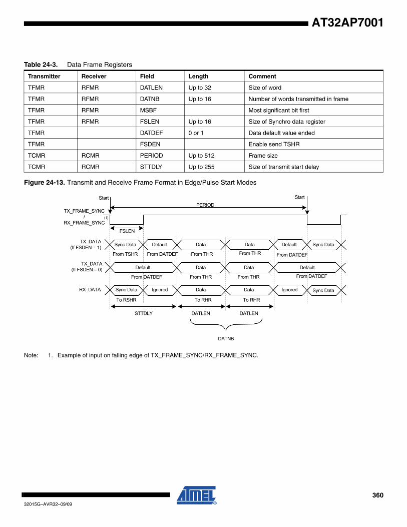
36032015G–AVR32–09/09
AT32AP7001
Figure 24-13. Transmit and Receive Frame Format in Edge/Pulse Start Modes
Note: 1. Example of input on falling edge of TX_FRAME_SYNC/RX_FRAME_SYNC.
Table 24-3. Data Frame Registers
Transmitter Receiver Field Length Comment
TFMR RFMR DATLEN Up to 32 Size of word
TFMR RFMR DATNB Up to 16 Number of words transmitted in frame
TFMR RFMR MSBF Most significant bit first
TFMR RFMR FSLEN Up to 16 Size of Synchro data register
TFMR DATDEF 0 or 1 Data default value ended
TFMR FSDEN Enable send TSHR
TCMR RCMR PERIOD Up to 512 Frame size
TCMR RCMR STTDLY Up to 255 Size of transmit start delay
DATNB
DATLEN
Data
DataData
Data
Data Data Default
Default
Sync Data
Sync DataIgnored
From DATDEF
Start
From DATDEF
DATLEN
To RHRTo RHR
From THR
From THRFrom THR
From THR
From DATDEF
From DATDEF
Ignored
Default
Default
Sync Data
To RSHR
From TSHR
FSLEN
Start
TX_FRAME_SYNC/
RX_FRAME_SYNC
TX_DATA(If FSDEN = 1)
TX_DATA(If FSDEN = 0)
RX_DATA
STTDLY
Sync Data
PERIOD
(1)
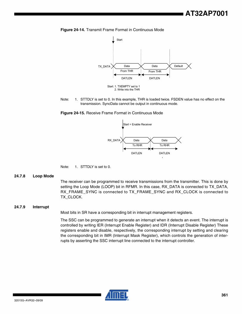
36132015G–AVR32–09/09
AT32AP7001
Figure 24-14. Transmit Frame Format in Continuous Mode
Note: 1. STTDLY is set to 0. In this example, THR is loaded twice. FSDEN value has no effect on the transmission. SyncData cannot be output in continuous mode.
Figure 24-15. Receive Frame Format in Continuous Mode
Note: 1. STTDLY is set to 0.
24.7.8 Loop ModeThe receiver can be programmed to receive transmissions from the transmitter. This is done bysetting the Loop Mode (LOOP) bit in RFMR. In this case, RX_DATA is connected to TX_DATA,RX_FRAME_SYNC is connected to TX_FRAME_SYNC and RX_CLOCK is connected toTX_CLOCK.
24.7.9 InterruptMost bits in SR have a corresponding bit in interrupt management registers.
The SSC can be programmed to generate an interrupt when it detects an event. The interrupt iscontrolled by writing IER (Interrupt Enable Register) and IDR (Interrupt Disable Register) Theseregisters enable and disable, respectively, the corresponding interrupt by setting and clearingthe corresponding bit in IMR (Interrupt Mask Register), which controls the generation of inter-rupts by asserting the SSC interrupt line connected to the interrupt controller.
Start
Data Data
DATLEN
From THR
DATLEN
TX_DATA
Start: 1. TXEMPTY set to 12. Write into the THR
From THR
Default
Data Data
To RHRTo RHR
DATLENDATLEN
RX_DATA
Start = Enable Receiver
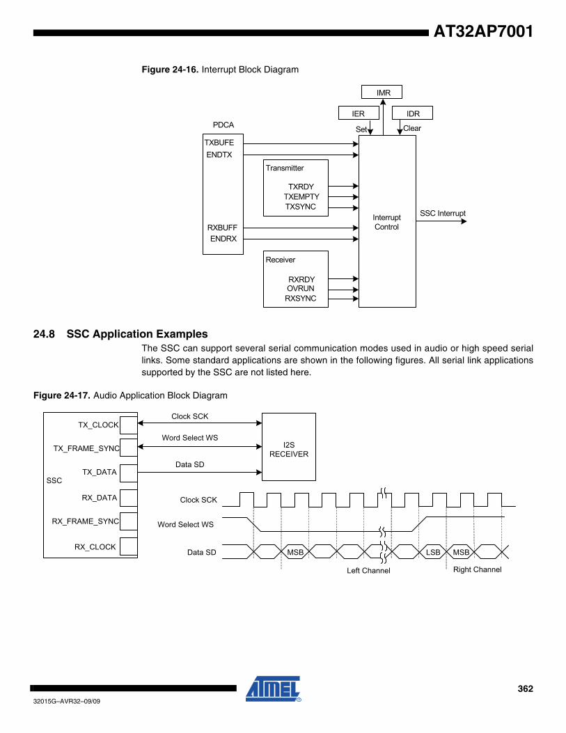
36232015G–AVR32–09/09
AT32AP7001
Figure 24-16. Interrupt Block Diagram
24.8 SSC Application ExamplesThe SSC can support several serial communication modes used in audio or high speed seriallinks. Some standard applications are shown in the following figures. All serial link applicationssupported by the SSC are not listed here.
Figure 24-17. Audio Application Block Diagram
IMR
IER IDR
ClearSet
Interrupt Control
SSC Interrupt
TXRDYTXEMPTYTXSYNC
Transmitter
ENDTXTXBUFE
PDCA
RXBUFFENDRX
Receiver
RXRDYOVRUNRXSYNC
Clock SCK
Word Select WS
Data SD MSB
Left Channel
LSB MSB
Right Channel
Data SD
Word Select WS
Clock SCK
SSC
TX_CLOCK
TX_FRAME_SYNC
TX_DATA
RX_DATA
RX_FRAME_SYNC
RX_CLOCK
I2SRECEIVER
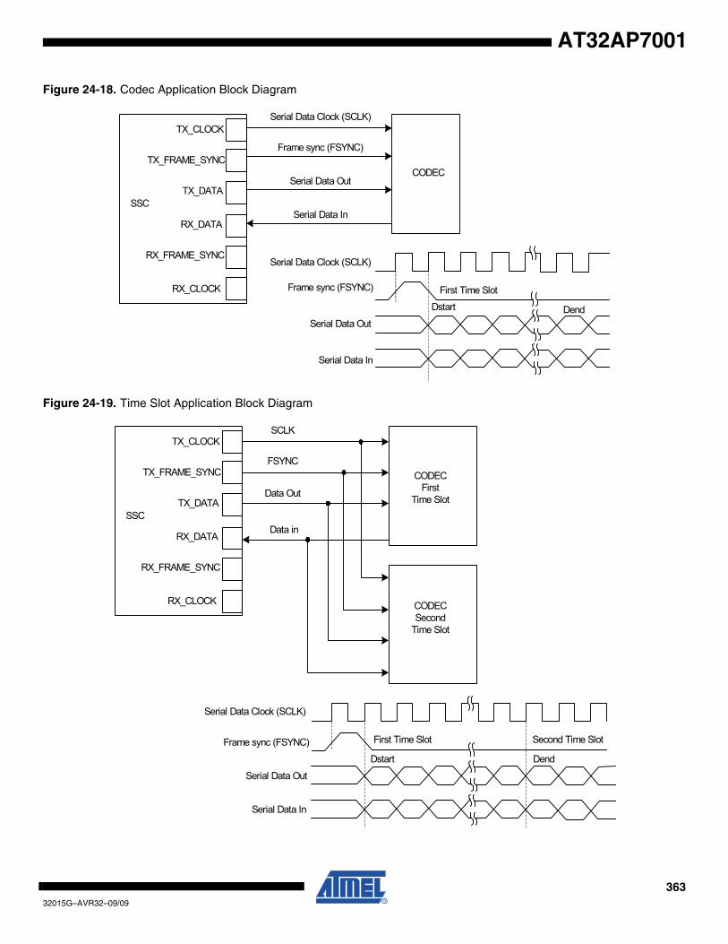
36332015G–AVR32–09/09
AT32AP7001
Figure 24-18. Codec Application Block Diagram
Figure 24-19. Time Slot Application Block Diagram
SSC
Serial Data Clock (SCLK)
Frame sync (FSYNC)
Serial Data Out
Serial Data In
Serial Data Clock (SCLK)
Frame sync (FSYNC)
Serial Data Out
Serial Data In
Dstart Dend
First Time Slot
CODEC
TX_CLOCK
TX_FRAME_SYNC
TX_DATA
RX_DATA
RX_FRAME_SYNC
RX_CLOCK
CODECFirst
Time Slot
CODECSecond
Time Slot
Data in
Data Out
FSYNC
SCLK
Serial Data Clock (SCLK)
Frame sync (FSYNC)
Serial Data Out
Serial Data In
Dstart
First Time Slot Second Time Slot
Dend
SSC
TX_CLOCK
TX_FRAME_SYNC
TX_DATA
RX_DATA
RX_FRAME_SYNC
RX_CLOCK
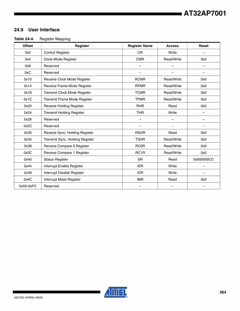
36432015G–AVR32–09/09
AT32AP7001
24.9 User Interface
Table 24-4. Register Mapping
Offset Register Register Name Access Reset
0x0 Control Register CR Write –
0x4 Clock Mode Register CMR Read/Write 0x0
0x8 Reserved – – –
0xC Reserved – – –
0x10 Receive Clock Mode Register RCMR Read/Write 0x0
0x14 Receive Frame Mode Register RFMR Read/Write 0x0
0x18 Transmit Clock Mode Register TCMR Read/Write 0x0
0x1C Transmit Frame Mode Register TFMR Read/Write 0x0
0x20 Receive Holding Register RHR Read 0x0
0x24 Transmit Holding Register THR Write –
0x28 Reserved – – –
0x2C Reserved – – –
0x30 Receive Sync. Holding Register RSHR Read 0x0
0x34 Transmit Sync. Holding Register TSHR Read/Write 0x0
0x38 Receive Compare 0 Register RC0R Read/Write 0x0
0x3C Receive Compare 1 Register RC1R Read/Write 0x0
0x40 Status Register SR Read 0x000000CC
0x44 Interrupt Enable Register IER Write –
0x48 Interrupt Disable Register IDR Write –
0x4C Interrupt Mask Register IMR Read 0x0
0x50-0xFC Reserved – – –
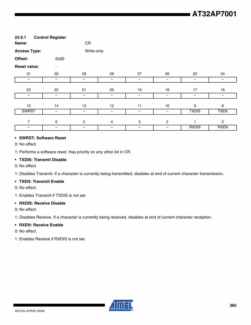
36532015G–AVR32–09/09
AT32AP7001
24.9.1 Control RegisterName: CR
Access Type: Write-only
Offset: 0x00
Reset value: -
• SWRST: Software Reset
0: No effect.
1: Performs a software reset. Has priority on any other bit in CR.
• TXDIS: Transmit Disable
0: No effect.
1: Disables Transmit. If a character is currently being transmitted, disables at end of current character transmission.
• TXEN: Transmit Enable
0: No effect.
1: Enables Transmit if TXDIS is not set.
• RXDIS: Receive Disable
0: No effect.
1: Disables Receive. If a character is currently being received, disables at end of current character reception.
• RXEN: Receive Enable
0: No effect.
1: Enables Receive if RXDIS is not set.
31 30 29 28 27 26 25 24
– – – – – – – –
23 22 21 20 19 18 17 16
– – – – – – – –
15 14 13 12 11 10 9 8
SWRST – – – – – TXDIS TXEN
7 6 5 4 3 2 1 0
– – – – – – RXDIS RXEN

36632015G–AVR32–09/09
AT32AP7001
24.9.2 Clock Mode RegisterName: CMR
Access Type: Read/Write
Offset: 0x04
Reset value: 0x00000000
• DIV: Clock Divider
0: The Clock Divider is not active.
Any Other Value: The Divided Clock equals the Master Clock divided by 2 times DIV. The maximum bit rate is CLK_SSC/2.The minimum bit rate is CLK_SSC/2 x 4095 = CLK_SSC/8190.
31 30 29 28 27 26 25 24
– – – – – – – –
23 22 21 20 19 18 17 16
– – – – – – – –
15 14 13 12 11 10 9 8
– – – – DIV
7 6 5 4 3 2 1 0
DIV
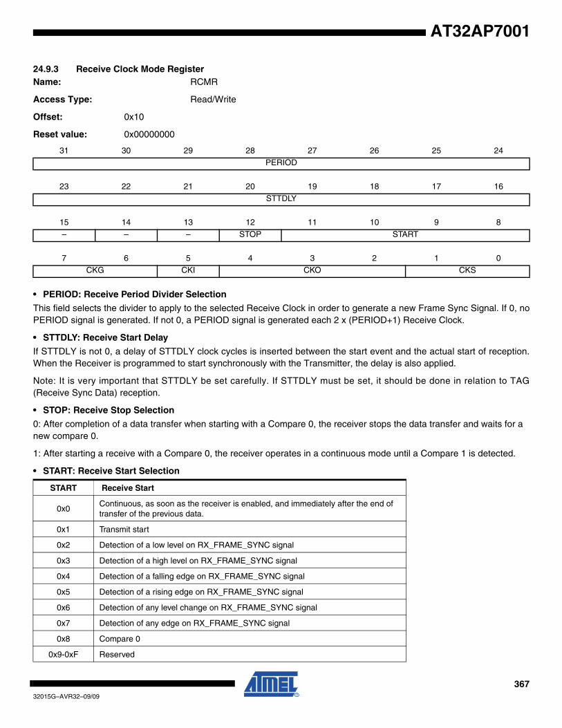
36732015G–AVR32–09/09
AT32AP7001
24.9.3 Receive Clock Mode RegisterName: RCMR
Access Type: Read/Write
Offset: 0x10
Reset value: 0x00000000
• PERIOD: Receive Period Divider Selection
This field selects the divider to apply to the selected Receive Clock in order to generate a new Frame Sync Signal. If 0, noPERIOD signal is generated. If not 0, a PERIOD signal is generated each 2 x (PERIOD+1) Receive Clock.
• STTDLY: Receive Start Delay
If STTDLY is not 0, a delay of STTDLY clock cycles is inserted between the start event and the actual start of reception.When the Receiver is programmed to start synchronously with the Transmitter, the delay is also applied.
Note: It is very important that STTDLY be set carefully. If STTDLY must be set, it should be done in relation to TAG(Receive Sync Data) reception.
• STOP: Receive Stop Selection
0: After completion of a data transfer when starting with a Compare 0, the receiver stops the data transfer and waits for anew compare 0.
1: After starting a receive with a Compare 0, the receiver operates in a continuous mode until a Compare 1 is detected.
• START: Receive Start Selection
31 30 29 28 27 26 25 24
PERIOD
23 22 21 20 19 18 17 16
STTDLY
15 14 13 12 11 10 9 8
– – – STOP START
7 6 5 4 3 2 1 0
CKG CKI CKO CKS
START Receive Start
0x0Continuous, as soon as the receiver is enabled, and immediately after the end of transfer of the previous data.
0x1 Transmit start
0x2 Detection of a low level on RX_FRAME_SYNC signal
0x3 Detection of a high level on RX_FRAME_SYNC signal
0x4 Detection of a falling edge on RX_FRAME_SYNC signal
0x5 Detection of a rising edge on RX_FRAME_SYNC signal
0x6 Detection of any level change on RX_FRAME_SYNC signal
0x7 Detection of any edge on RX_FRAME_SYNC signal
0x8 Compare 0
0x9-0xF Reserved
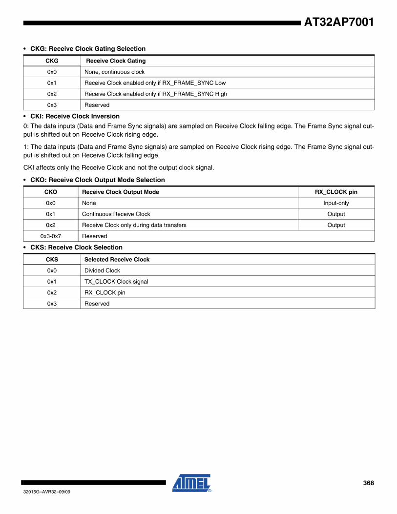
36832015G–AVR32–09/09
AT32AP7001
• CKG: Receive Clock Gating Selection
• CKI: Receive Clock Inversion
0: The data inputs (Data and Frame Sync signals) are sampled on Receive Clock falling edge. The Frame Sync signal out-put is shifted out on Receive Clock rising edge.
1: The data inputs (Data and Frame Sync signals) are sampled on Receive Clock rising edge. The Frame Sync signal out-put is shifted out on Receive Clock falling edge.
CKI affects only the Receive Clock and not the output clock signal.
• CKO: Receive Clock Output Mode Selection
• CKS: Receive Clock Selection
CKG Receive Clock Gating
0x0 None, continuous clock
0x1 Receive Clock enabled only if RX_FRAME_SYNC Low
0x2 Receive Clock enabled only if RX_FRAME_SYNC High
0x3 Reserved
CKO Receive Clock Output Mode RX_CLOCK pin
0x0 None Input-only
0x1 Continuous Receive Clock Output
0x2 Receive Clock only during data transfers Output
0x3-0x7 Reserved
CKS Selected Receive Clock
0x0 Divided Clock
0x1 TX_CLOCK Clock signal
0x2 RX_CLOCK pin
0x3 Reserved

36932015G–AVR32–09/09
AT32AP7001
24.9.4 Receive Frame Mode RegisterName: RFMR
Access Type: Read/Write
Offset: 0x14
Reset value: 0x00000000
• FSLENHI: Receive Frame Sync Length High part
The four MSB of the FSLEN bitfield.
• FSEDGE: Frame Sync Edge Detection
Determines which edge on Frame Sync will generate the interrupt RXSYN in the SSC Status Register.
• FSOS: Receive Frame Sync Output Selection
• FSLEN: Receive Frame Sync Length
This field defines the length of the Receive Frame Sync Signal and the number of bits sampled and stored in the ReceiveSync Data Register. When this mode is selected by the START field in the Receive Clock Mode Register, it also deter-mines the length of the sampled data to be compared to the Compare 0 or Compare 1 register. Note: The four mostsignificant bits fo this bitfield are in the FSLENHI bitfield.
Pulse length is equal to ({FSLENHI,FSLEN} + 1) Receive Clock periods. Thus, if {FSLENHI,FSLEN} is 0, the ReceiveFrame Sync signal is generated during one Receive Clock period.
• DATNB: Data Number per Frame
31 30 29 28 27 26 25 24
FSLENHI – – – FSEDGE
23 22 21 20 19 18 17 16
– FSOS FSLEN
15 14 13 12 11 10 9 8
– – – – DATNB
7 6 5 4 3 2 1 0
MSBF – LOOP DATLEN
FSEDGE Frame Sync Edge Detection
0x0 Positive Edge Detection
0x1 Negative Edge Detection
FSOS Selected Receive Frame Sync Signal RX_FRAME_SYNC Pin
0x0 None Input-only
0x1 Negative Pulse Output
0x2 Positive Pulse Output
0x3 Driven Low during data transfer Output
0x4 Driven High during data transfer Output
0x5 Toggling at each start of data transfer Output
0x6-0x7 Reserved Undefined
37032015G–AVR32–09/09
AT32AP7001
This field defines the number of data words to be received after each transfer start, which is equal to (DATNB + 1).
• MSBF: Most Significant Bit First
0: The lowest significant bit of the data register is sampled first in the bit stream.
1: The most significant bit of the data register is sampled first in the bit stream.
• LOOP: Loop Mode
0: Normal operating mode.
1: RX_DATA is driven by TX_DATA, RX_FRAME_SYNC is driven by TX_FRAME_SYNC and TX_CLOCK drivesRX_CLOCK.
• DATLEN: Data Length
0: Forbidden value (1-bit data length not supported). Any other value: The bit stream contains DATLEN + 1 data bits. Moreover, it defines the transfer size performed by thePDCA assigned to the Receiver. If DATLEN is lower or equal to 7, data transfers are in bytes. If DATLEN is between 8 and15 (included), half-words are transferred, and for any other value, 32-bit words are transferred.
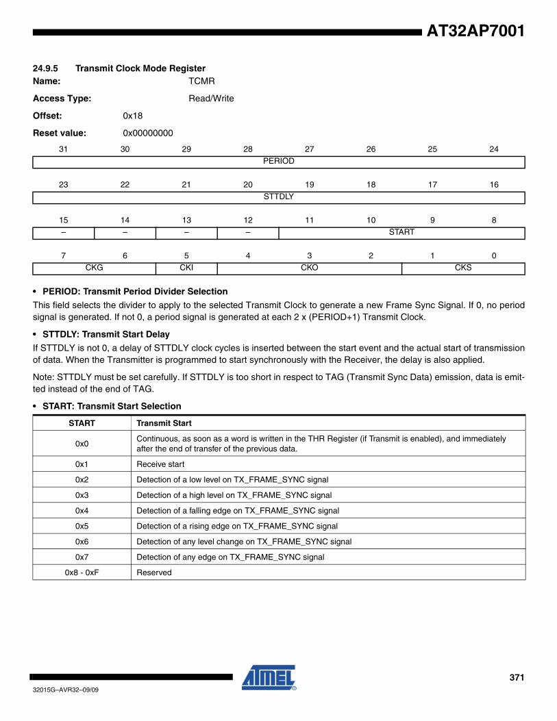
37132015G–AVR32–09/09
AT32AP7001
24.9.5 Transmit Clock Mode RegisterName: TCMR
Access Type: Read/Write
Offset: 0x18
Reset value: 0x00000000
• PERIOD: Transmit Period Divider Selection
This field selects the divider to apply to the selected Transmit Clock to generate a new Frame Sync Signal. If 0, no periodsignal is generated. If not 0, a period signal is generated at each 2 x (PERIOD+1) Transmit Clock.
• STTDLY: Transmit Start Delay
If STTDLY is not 0, a delay of STTDLY clock cycles is inserted between the start event and the actual start of transmissionof data. When the Transmitter is programmed to start synchronously with the Receiver, the delay is also applied.
Note: STTDLY must be set carefully. If STTDLY is too short in respect to TAG (Transmit Sync Data) emission, data is emit-ted instead of the end of TAG.
• START: Transmit Start Selection
31 30 29 28 27 26 25 24
PERIOD
23 22 21 20 19 18 17 16
STTDLY
15 14 13 12 11 10 9 8
– – – – START
7 6 5 4 3 2 1 0
CKG CKI CKO CKS
START Transmit Start
0x0Continuous, as soon as a word is written in the THR Register (if Transmit is enabled), and immediately after the end of transfer of the previous data.
0x1 Receive start
0x2 Detection of a low level on TX_FRAME_SYNC signal
0x3 Detection of a high level on TX_FRAME_SYNC signal
0x4 Detection of a falling edge on TX_FRAME_SYNC signal
0x5 Detection of a rising edge on TX_FRAME_SYNC signal
0x6 Detection of any level change on TX_FRAME_SYNC signal
0x7 Detection of any edge on TX_FRAME_SYNC signal
0x8 - 0xF Reserved

37232015G–AVR32–09/09
AT32AP7001
• CKG: Transmit Clock Gating Selection
• CKI: Transmit Clock Inversion
0: The data outputs (Data and Frame Sync signals) are shifted out on Transmit Clock falling edge. The Frame sync signalinput is sampled on Transmit clock rising edge.
1: The data outputs (Data and Frame Sync signals) are shifted out on Transmit Clock rising edge. The Frame sync signalinput is sampled on Transmit clock falling edge.
CKI affects only the Transmit Clock and not the output clock signal.
• CKO: Transmit Clock Output Mode Selection
• CKS: Transmit Clock Selection
CKG Transmit Clock Gating
0x0 None, continuous clock
0x1 Transmit Clock enabled only if TX_FRAME_SYNC Low
0x2 Transmit Clock enabled only if TX_FRAME_SYNC High
0x3 Reserved
CKO Transmit Clock Output Mode TX_CLOCK pin
0x0 None Input-only
0x1 Continuous Transmit Clock Output
0x2 Transmit Clock only during data transfers Output
0x3-0x7 Reserved
CKS Selected Transmit Clock
0x0 Divided Clock
0x1 RX_CLOCK Clock signal
0x2 TX_CLOCK Pin
0x3 Reserved
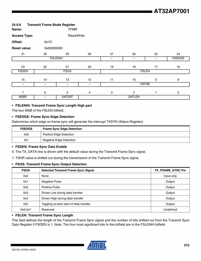
37332015G–AVR32–09/09
AT32AP7001
24.9.6 Transmit Frame Mode RegisterName: TFMR
Access Type: Read/Write
Offset: 0x1C
Reset value: 0x00000000
• FSLENHI: Transmit Frame Sync Length High part
The four MSB of the FSLEN bitfield.
• FSEDGE: Frame Sync Edge Detection
Determines which edge on frame sync will generate the interrupt TXSYN (Status Register).
• FSDEN: Frame Sync Data Enable
0: The TX_DATA line is driven with the default value during the Transmit Frame Sync signal.
1: TSHR value is shifted out during the transmission of the Transmit Frame Sync signal.
• FSOS: Transmit Frame Sync Output Selection
• FSLEN: Transmit Frame Sync Length
This field defines the length of the Transmit Frame Sync signal and the number of bits shifted out from the Transmit SyncData Register if FSDEN is 1. Note: The four most significant bits fo this bitfield are in the FSLENHI bitfield.
31 30 29 28 27 26 25 24
FSLENHI – – – FSEDGE
23 22 21 20 19 18 17 16
FSDEN FSOS FSLEN
15 14 13 12 11 10 9 8
– – – – DATNB
7 6 5 4 3 2 1 0
MSBF – DATDEF DATLEN
FSEDGE Frame Sync Edge Detection
0x0 Positive Edge Detection
0x1 Negative Edge Detection
FSOS Selected Transmit Frame Sync Signal TX_FRAME_SYNC Pin
0x0 None Input-only
0x1 Negative Pulse Output
0x2 Positive Pulse Output
0x3 Driven Low during data transfer Output
0x4 Driven High during data transfer Output
0x5 Toggling at each start of data transfer Output
0x6-0x7 Reserved Undefined
37432015G–AVR32–09/09
AT32AP7001
Pulse length is equal to ({FSLENHI,FSLEN} + 1) Transmit Clock periods, i.e., the pulse length can range from 1 to 16Transmit Clock periods. If {FSLENHI,FSLEN} is 0, the Transmit Frame Sync signal is generated during one Transmit Clockperiod.
• DATNB: Data Number per frame
This field defines the number of data words to be transferred after each transfer start, which is equal to (DATNB +1).
• MSBF: Most Significant Bit First
0: The lowest significant bit of the data register is shifted out first in the bit stream.
1: The most significant bit of the data register is shifted out first in the bit stream.
• DATDEF: Data Default Value
This bit defines the level driven on the TX_DATA pin while out of transmission. Note that if the pin is defined as multi-driveby the PIO Controller, the pin is enabled only if the SCC TX_DATA output is 1.
• DATLEN: Data Length
0: Forbidden value (1-bit data length not supported).
Any other value: The bit stream contains DATLEN + 1 data bits. Moreover, it defines the transfer size performed by thePDCA assigned to the Transmit. If DATLEN is lower or equal to 7, data transfers are bytes, if DATLEN is between 8 and 15(included), half-words are transferred, and for any other value, 32-bit words are transferred.
37532015G–AVR32–09/09
AT32AP7001
24.9.7 SSC Receive Holding RegisterName: RHR
Access Type: Read-only
Offset: 0x20
Reset value: 0x00000000
• RDAT: Receive Data
Right aligned regardless of the number of data bits defined by DATLEN in RFMR.
31 30 29 28 27 26 25 24
RDAT
23 22 21 20 19 18 17 16
RDAT
15 14 13 12 11 10 9 8
RDAT
7 6 5 4 3 2 1 0
RDAT
37632015G–AVR32–09/09
AT32AP7001
24.9.8 Transmit Holding RegisterName: THR
Access Type: Write-only
Offset: 0x24
Reset value: -
• TDAT: Transmit Data
Right aligned regardless of the number of data bits defined by DATLEN in TFMR.
31 30 29 28 27 26 25 24
TDAT
23 22 21 20 19 18 17 16
TDAT
15 14 13 12 11 10 9 8
TDAT
7 6 5 4 3 2 1 0
TDAT
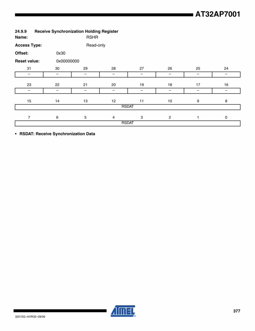
37732015G–AVR32–09/09
AT32AP7001
24.9.9 Receive Synchronization Holding RegisterName: RSHR
Access Type: Read-only
Offset: 0x30
Reset value: 0x00000000
• RSDAT: Receive Synchronization Data
31 30 29 28 27 26 25 24
– – – – – – – –
23 22 21 20 19 18 17 16
– – – – – – – –
15 14 13 12 11 10 9 8
RSDAT
7 6 5 4 3 2 1 0
RSDAT
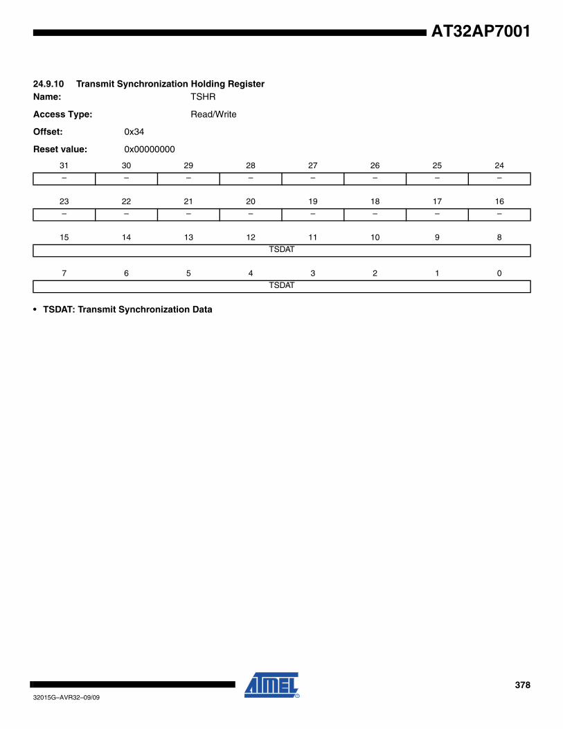
37832015G–AVR32–09/09
AT32AP7001
24.9.10 Transmit Synchronization Holding RegisterName: TSHR
Access Type: Read/Write
Offset: 0x34
Reset value: 0x00000000
• TSDAT: Transmit Synchronization Data
31 30 29 28 27 26 25 24
– – – – – – – –
23 22 21 20 19 18 17 16
– – – – – – – –
15 14 13 12 11 10 9 8
TSDAT
7 6 5 4 3 2 1 0
TSDAT
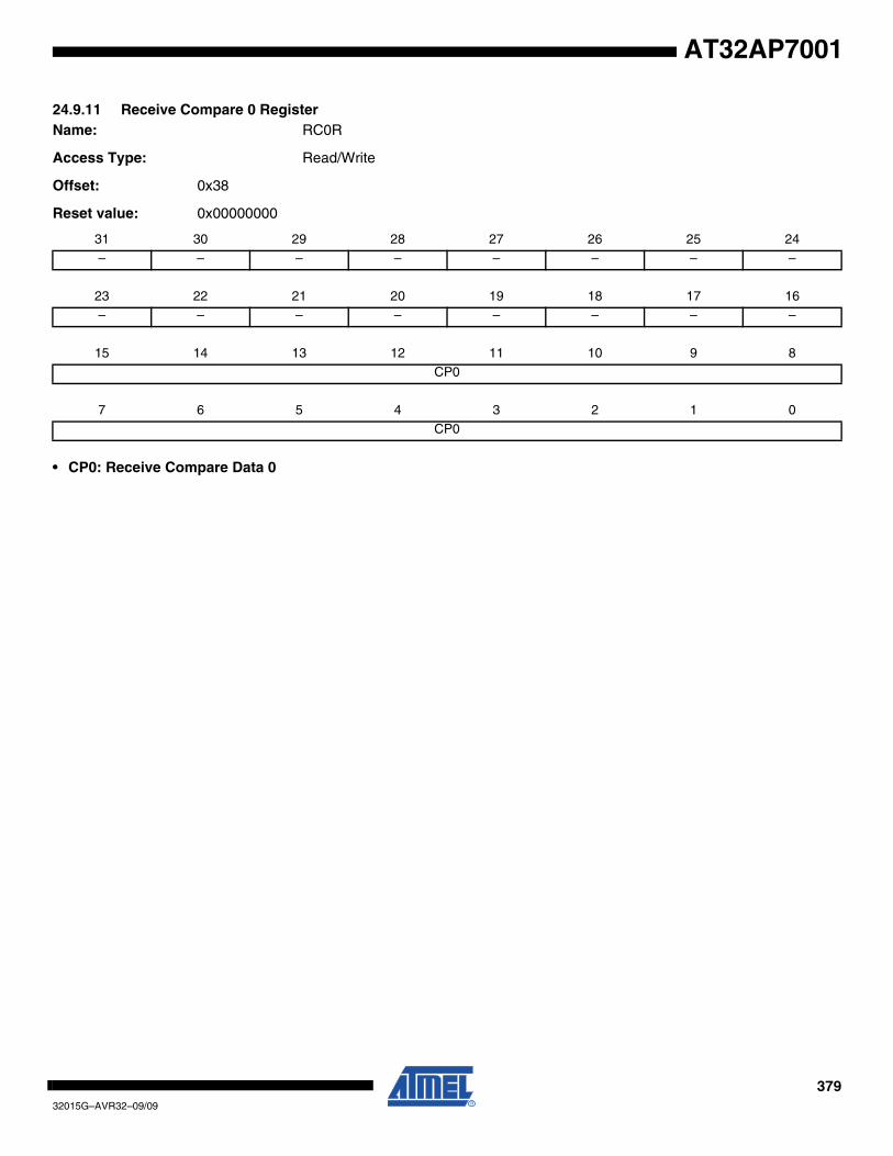
37932015G–AVR32–09/09
AT32AP7001
24.9.11 Receive Compare 0 RegisterName: RC0R
Access Type: Read/Write
Offset: 0x38
Reset value: 0x00000000
• CP0: Receive Compare Data 0
31 30 29 28 27 26 25 24
– – – – – – – –
23 22 21 20 19 18 17 16
– – – – – – – –
15 14 13 12 11 10 9 8
CP0
7 6 5 4 3 2 1 0
CP0

38032015G–AVR32–09/09
AT32AP7001
24.9.12 Receive Compare 1 RegisterName: RC1R
Access Type: Read/Write
Offset: 0x3C
Reset value: 0x00000000
• CP1: Receive Compare Data 1
31 30 29 28 27 26 25 24
– – – – – – – –
23 22 21 20 19 18 17 16
– – – – – – – –
15 14 13 12 11 10 9 8
CP1
7 6 5 4 3 2 1 0
CP1
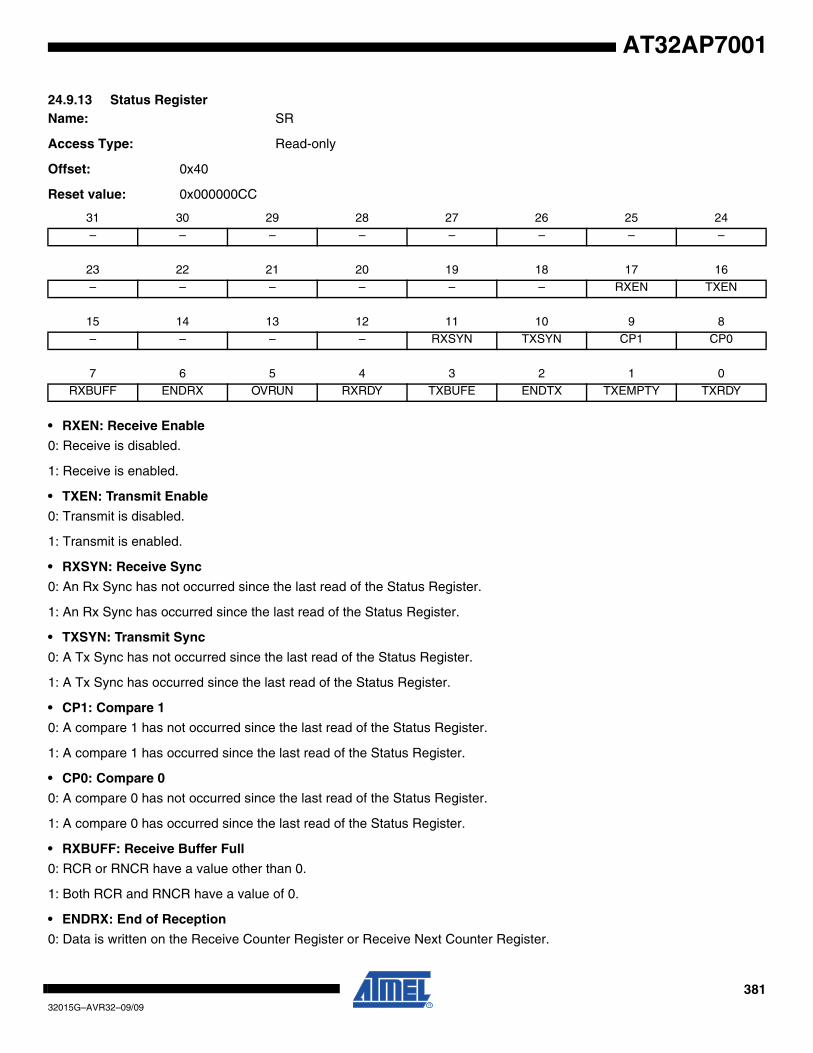
38132015G–AVR32–09/09
AT32AP7001
24.9.13 Status RegisterName: SR
Access Type: Read-only
Offset: 0x40
Reset value: 0x000000CC
• RXEN: Receive Enable
0: Receive is disabled.
1: Receive is enabled.
• TXEN: Transmit Enable
0: Transmit is disabled.
1: Transmit is enabled.
• RXSYN: Receive Sync
0: An Rx Sync has not occurred since the last read of the Status Register.
1: An Rx Sync has occurred since the last read of the Status Register.
• TXSYN: Transmit Sync
0: A Tx Sync has not occurred since the last read of the Status Register.
1: A Tx Sync has occurred since the last read of the Status Register.
• CP1: Compare 1
0: A compare 1 has not occurred since the last read of the Status Register.
1: A compare 1 has occurred since the last read of the Status Register.
• CP0: Compare 0
0: A compare 0 has not occurred since the last read of the Status Register.
1: A compare 0 has occurred since the last read of the Status Register.
• RXBUFF: Receive Buffer Full
0: RCR or RNCR have a value other than 0.
1: Both RCR and RNCR have a value of 0.
• ENDRX: End of Reception
0: Data is written on the Receive Counter Register or Receive Next Counter Register.
31 30 29 28 27 26 25 24
– – – – – – – –
23 22 21 20 19 18 17 16
– – – – – – RXEN TXEN
15 14 13 12 11 10 9 8
– – – – RXSYN TXSYN CP1 CP0
7 6 5 4 3 2 1 0
RXBUFF ENDRX OVRUN RXRDY TXBUFE ENDTX TXEMPTY TXRDY
38232015G–AVR32–09/09
AT32AP7001
1: End of PDCA transfer when Receive Counter Register has arrived at zero.
• OVRUN: Receive Overrun
0: No data has been loaded in RHR while previous data has not been read since the last read of the Status Register.
1: Data has been loaded in RHR while previous data has not yet been read since the last read of the Status Register.
• RXRDY: Receive Ready
0: RHR is empty.
1: Data has been received and loaded in RHR.
• TXBUFE: Transmit Buffer Empty
0: TCR or TNCR have a value other than 0.
1: Both TCR and TNCR have a value of 0.
• ENDTX: End of Transmission
0: The register TCR has not reached 0 since the last write in TCR or TNCR.
1: The register TCR has reached 0 since the last write in TCR or TNCR.
• TXEMPTY: Transmit Empty
0: Data remains in THR or is currently transmitted from TSR.
1: Last data written in THR has been loaded in TSR and last data loaded in TSR has been transmitted.
• TXRDY: Transmit Ready
0: Data has been loaded in THR and is waiting to be loaded in the Transmit Shift Register (TSR).
1: THR is empty.
38332015G–AVR32–09/09
AT32AP7001
24.9.14 Interrupt Enable RegisterName: IER
Access Type: Write-only
Offset: 0x44
Reset value: -
• RXSYN: Rx Sync Interrupt Enable
0: No effect.
1: Enables the Rx Sync Interrupt.
• TXSYN: Tx Sync Interrupt Enable
0: No effect.
1: Enables the Tx Sync Interrupt.
• CP1: Compare 1 Interrupt Enable
0: No effect.
1: Enables the Compare 1 Interrupt.
• CP0: Compare 0 Interrupt Enable
0: No effect.
1: Enables the Compare 0 Interrupt.
• RXBUFF: Receive Buffer Full Interrupt Enable
0: No effect.
1: Enables the Receive Buffer Full Interrupt.
• ENDRX: End of Reception Interrupt Enable
0: No effect.
1: Enables the End of Reception Interrupt.
• OVRUN: Receive Overrun Interrupt Enable
0: No effect.
1: Enables the Receive Overrun Interrupt.
• RXRDY: Receive Ready Interrupt Enable
0: No effect.
31 30 29 28 27 26 25 24
– – – – – – – –
23 22 21 20 19 18 17 16
– – – – – – – –
15 14 13 12 11 10 9 8
– – – – RXSYN TXSYN CP1 CP0
7 6 5 4 3 2 1 0
RXBUFF ENDRX OVRUN RXRDY TXBUFE ENDTX TXEMPTY TXRDY

38432015G–AVR32–09/09
AT32AP7001
1: Enables the Receive Ready Interrupt.
• TXBUFE: Transmit Buffer Empty Interrupt Enable
0: No effect.
1: Enables the Transmit Buffer Empty Interrupt
• ENDTX: End of Transmission Interrupt Enable
0: No effect.
1: Enables the End of Transmission Interrupt.
• TXEMPTY: Transmit Empty Interrupt Enable
0: No effect.
1: Enables the Transmit Empty Interrupt.
• TXRDY: Transmit Ready Interrupt Enable
0: No effect.
1: Enables the Transmit Ready Interrupt.

38532015G–AVR32–09/09
AT32AP7001
24.9.15 Interrupt Disable RegisterName: IDR
Access Type: Write-only
Offset: 0x48
Reset value: -
• RXSYN: Rx Sync Interrupt Enable
0: No effect.
1: Disables the Rx Sync Interrupt.
• TXSYN: Tx Sync Interrupt Enable
0: No effect.
1: Disables the Tx Sync Interrupt.
• CP1: Compare 1 Interrupt Disable
0: No effect.
1: Disables the Compare 1 Interrupt.
• CP0: Compare 0 Interrupt Disable
0: No effect.
1: Disables the Compare 0 Interrupt.
• RXBUFF: Receive Buffer Full Interrupt Disable
0: No effect.
1: Disables the Receive Buffer Full Interrupt.
• ENDRX: End of Reception Interrupt Disable
0: No effect.
1: Disables the End of Reception Interrupt.
• OVRUN: Receive Overrun Interrupt Disable
0: No effect.
1: Disables the Receive Overrun Interrupt.
• RXRDY: Receive Ready Interrupt Disable
0: No effect.
31 30 29 28 27 26 25 24
– – – – – – – –
23 22 21 20 19 18 17 16
– – – – – – – –
15 14 13 12 11 10 9 8
– – – – RXSYN TXSYN CP1 CP0
7 6 5 4 3 2 1 0
RXBUFF ENDRX OVRUN RXRDY TXBUFE ENDTX TXEMPTY TXRDY

38632015G–AVR32–09/09
AT32AP7001
1: Disables the Receive Ready Interrupt.
• TXBUFE: Transmit Buffer Empty Interrupt Disable
0: No effect.
1: Disables the Transmit Buffer Empty Interrupt.
• ENDTX: End of Transmission Interrupt Disable
0: No effect.
1: Disables the End of Transmission Interrupt.
• TXEMPTY: Transmit Empty Interrupt Disable
0: No effect.
1: Disables the Transmit Empty Interrupt.
• TXRDY: Transmit Ready Interrupt Disable
0: No effect.
1: Disables the Transmit Ready Interrupt.
38732015G–AVR32–09/09
AT32AP7001
24.9.16 Interrupt Mask RegisterName: IMR
Access Type: Read-only
Offset: 0x4C
Reset value: 0x00000000
• RXSYN: Rx Sync Interrupt Mask
0: The Rx Sync Interrupt is disabled.
1: The Rx Sync Interrupt is enabled.
• TXSYN: Tx Sync Interrupt Mask
0: The Tx Sync Interrupt is disabled.
1: The Tx Sync Interrupt is enabled.
• CP1: Compare 1 Interrupt Mask
0: The Compare 1 Interrupt is disabled.
1: The Compare 1 Interrupt is enabled.
• CP0: Compare 0 Interrupt Mask
0: The Compare 0 Interrupt is disabled.
1: The Compare 0 Interrupt is enabled.
• RXBUFF: Receive Buffer Full Interrupt Mask
0: The Receive Buffer Full Interrupt is disabled.
1: The Receive Buffer Full Interrupt is enabled.
• ENDRX: End of Reception Interrupt Mask
0: The End of Reception Interrupt is disabled.
1: The End of Reception Interrupt is enabled.
• OVRUN: Receive Overrun Interrupt Mask
0: The Receive Overrun Interrupt is disabled.
1: The Receive Overrun Interrupt is enabled.
• RXRDY: Receive Ready Interrupt Mask
0: The Receive Ready Interrupt is disabled.
31 30 29 28 27 26 25 24
– – – – – – – –
23 22 21 20 19 18 17 16
– – – – – – – –
15 14 13 12 11 10 9 8
– – – – RXSYN TXSYN CP1 CP0
7 6 5 4 3 2 1 0
RXBUFF ENDRX OVRUN RXRDY TXBUFE ENDTX TXEMPTY TXRDY
38832015G–AVR32–09/09
AT32AP7001
25. Universal Synchronous/Asynchronous Receiver/Transmitter (USART)
Rev: 3.0.2.3
25.1 Features
• Programmable Baud Rate Generator• 5- to 9-bit Full-duplex Synchronous or Asynchronous Serial Communications
– 1, 1.5 or 2 Stop Bits in Asynchronous Mode or 1 or 2 Stop Bits in Synchronous Mode– Parity Generation and Error Detection– Framing Error Detection, Overrun Error Detection– MSB- or LSB-first– Optional Break Generation and Detection– By 8 or by 16 Over-sampling Receiver Frequency– Optional Hardware Handshaking RTS-CTS– Receiver Time-out and Transmitter Timeguard– Optional Multidrop Mode with Address Generation and Detection
• RS485 with Driver Control Signal• ISO7816, T = 0 or T = 1 Protocols for Interfacing with Smart Cards
– NACK Handling, Error Counter with Repetition and Iteration Limit• IrDA Modulation and Demodulation
– Communication at up to 115.2 Kbps• Test Modes
– Remote Loopback, Local Loopback, Automatic Echo• Supports Connection of Two Peripheral DMA Controller Channels (PDC)• Offers Buffer Transfer without Processor Intervention
25.2 Overview
The Universal Synchronous Asynchronous Receiver Transceiver (USART) provides one fullduplex universal synchronous asynchronous serial link. Data frame format is widely programma-ble (data length, parity, number of stop bits) to support a maximum of standards. The receiverimplements parity error, framing error and overrun error detection. The receiver time-out enableshandling variable-length frames and the transmitter timeguard facilitates communications withslow remote devices. Multidrop communications are also supported through address bit han-dling in reception and transmission.
The USART features three test modes: remote loopback, local loopback and automatic echo.
The USART supports specific operating modes providing interfaces on RS485 buses, withISO7816 T = 0 or T = 1 smart card slots and infrared transceivers. The hardware handshakingfeature enables an out-of-band flow control by automatic management of the pins RTS andCTS.
The USART supports the connection to the Peripheral DMA Controller, which enables datatransfers to the transmitter and from the receiver. The PDC provides chained buffer manage-ment without any intervention of the processor.
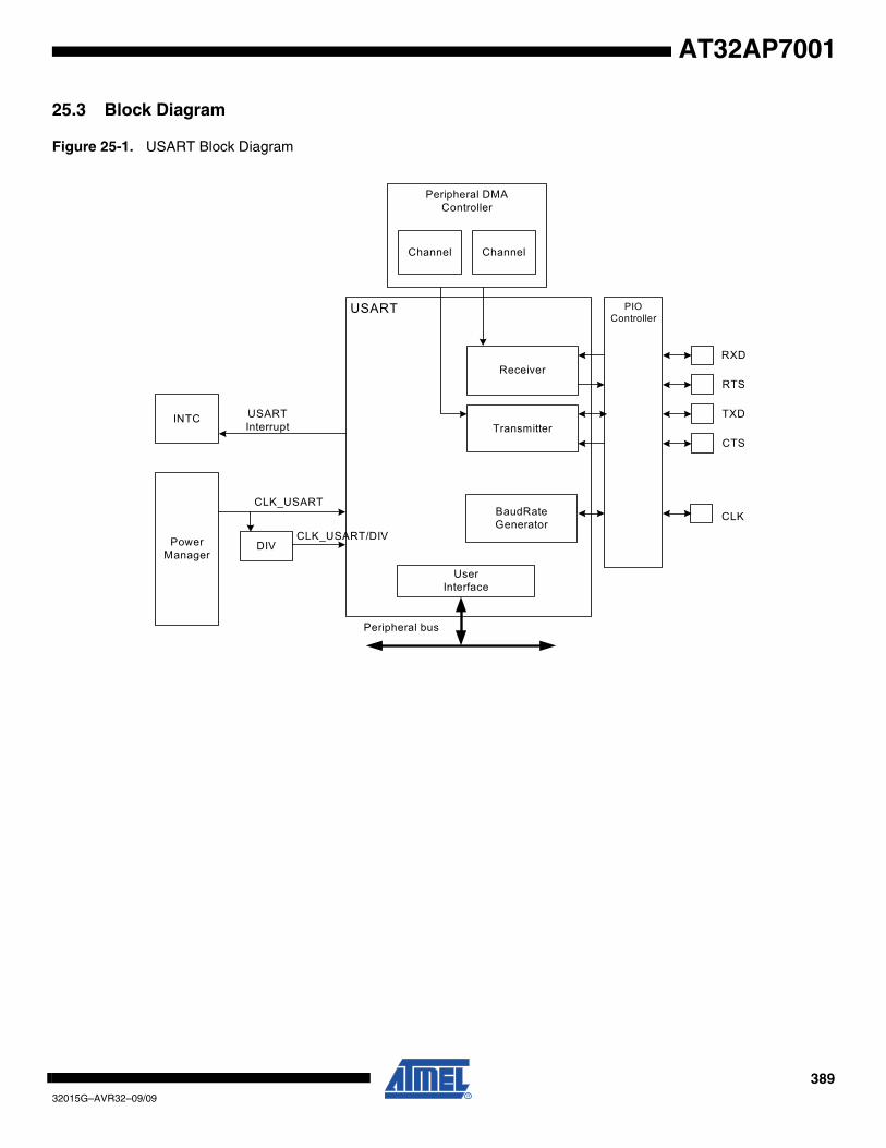
38932015G–AVR32–09/09
AT32AP7001
25.3 Block Diagram
Figure 25-1. USART Block Diagram
Peripheral DMAController
Channel Channel
INTC
PowerManager
DIV
Receiver
Transmitter
UserInterface
PIOController
RXD
RTS
TXD
CTS
CLKBaudRateGenerator
USARTInterrupt
CLK_USART
CLK_USART/DIV
USART
Peripheral bus
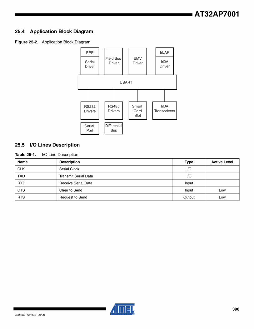
39032015G–AVR32–09/09
AT32AP7001
25.4 Application Block Diagram
Figure 25-2. Application Block Diagram
25.5 I/O Lines Description
Table 25-1. I/O Line Description
Name Description Type Active Level
CLK Serial Clock I/O
TXD Transmit Serial Data I/O
RXD Receive Serial Data Input
CTS Clear to Send Input Low
RTS Request to Send Output Low
Smart CardSlot
USART
RS485Drivers
DifferentialBus
IrDATransceivers
Field Bus Driver
EMVDriver IrDA
Driver
IrLAP
RS232Drivers
Serial Port
SerialDriver
PPP
39132015G–AVR32–09/09
AT32AP7001
25.6 Product Dependencies
25.6.1 I/O Lines
The pins used for interfacing the USART may be multiplexed with the PIO lines. The program-mer must first program the PIO controller to assign the desired USART pins to their peripheralfunction. If I/O lines of the USART are not used by the application, they can be used for otherpurposes by the PIO Controller.
To prevent the TXD line from falling when the USART is disabled, the use of an internal pull upis mandatory.
25.6.2 Power Manager (PM)
The USART is not continuously clocked. The programmer must ensure that the USART clock isenabled in the Power Manager (PM) before using the USART. However, if the application doesnot require USART operations, the USART clock can be stopped when not needed and berestarted later. In this case, the USART will resume its operations where it left off. USART clock(CLK_USART) in the USART description is the clock for the peripheral bus to which the USARTis connected.
25.6.3 Interrupt
The USART interrupt line is connected on one of the internal sources of the Interrupt Controller.Using the USART interrupt requires the interrupt controller to be programmed first.
39232015G–AVR32–09/09
AT32AP7001
25.7 Functional Description
The USART is capable of managing several types of serial synchronous or asynchronouscommunications.
It supports the following communication modes:
•5- to 9-bit full-duplex asynchronous serial communication
–MSB- or LSB-first
–1, 1.5 or 2 stop bits
–Parity even, odd, marked, space or none
–By 8 or by 16 over-sampling receiver frequency
–Optional hardware handshaking
–Optional break management
–Optional multidrop serial communication
•High-speed 5- to 9-bit full-duplex synchronous serial communication
–MSB- or LSB-first
–1 or 2 stop bits
–Parity even, odd, marked, space or none
–By 8 or by 16 over-sampling frequency
–Optional hardware handshaking
–Optional break management
–Optional multidrop serial communication
•RS485 with driver control signal
•ISO7816, T0 or T1 protocols for interfacing with smart cards
–NACK handling, error counter with repetition and iteration limit
•InfraRed IrDA Modulation and Demodulation
•Test modes
–Remote loopback, local loopback, automatic echo
25.7.1 Baud Rate Generator
The Baud Rate Generator provides the bit period clock named the Baud Rate Clock to both thereceiver and the transmitter.
The Baud Rate Generator clock source can be selected by setting the USCLKS field in the ModeRegister (MR) between:
•the CLK_USART
•a division of the CLK_USART, the divider being product dependent, but generally set to 8
•the external clock, available on the CLK pin
The Baud Rate Generator is based upon a 16-bit divider, which is programmed with the CD fieldof the Baud Rate Generator Register (BRGR). If CD is programmed at 0, the Baud Rate Gener-ator does not generate any clock. If CD is programmed at 1, the divider is bypassed andbecomes inactive.
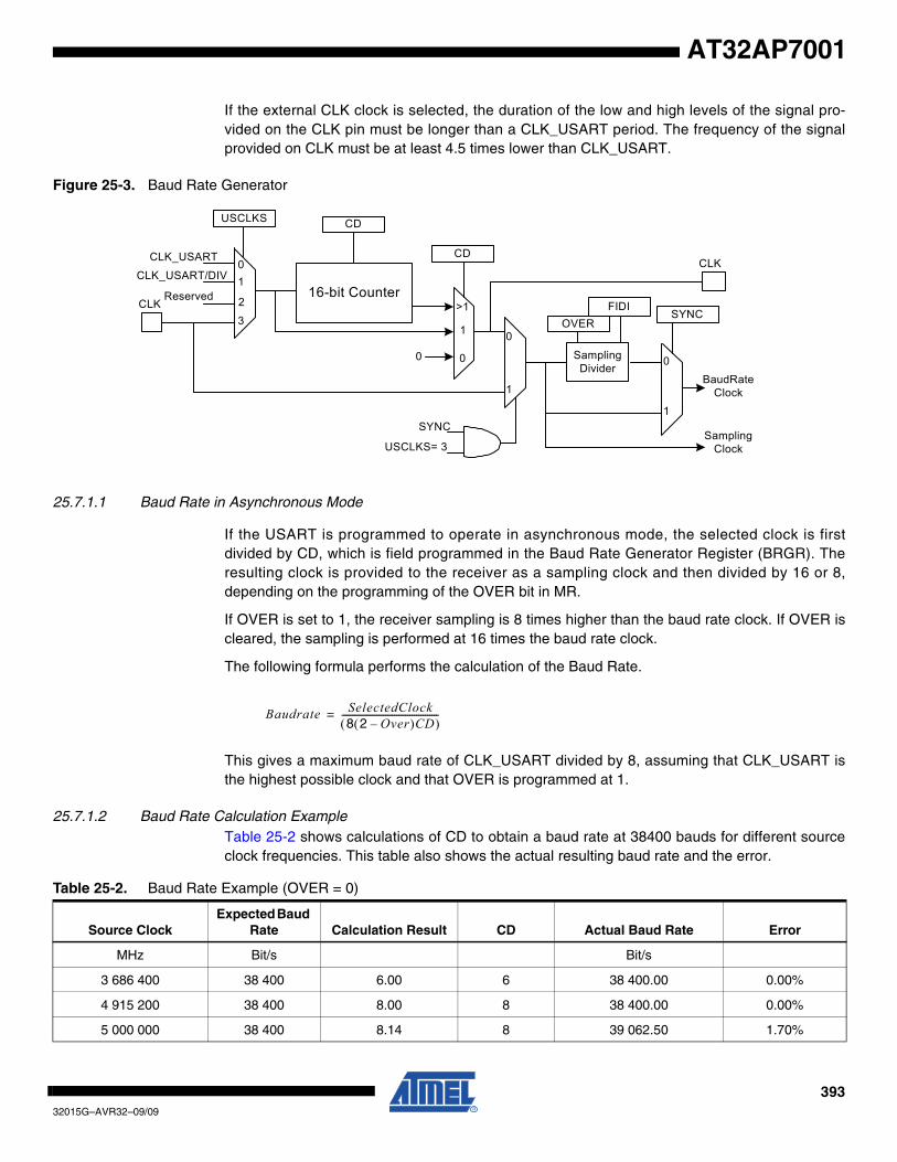
39332015G–AVR32–09/09
AT32AP7001
If the external CLK clock is selected, the duration of the low and high levels of the signal pro-vided on the CLK pin must be longer than a CLK_USART period. The frequency of the signalprovided on CLK must be at least 4.5 times lower than CLK_USART.
Figure 25-3. Baud Rate Generator
25.7.1.1 Baud Rate in Asynchronous Mode
If the USART is programmed to operate in asynchronous mode, the selected clock is firstdivided by CD, which is field programmed in the Baud Rate Generator Register (BRGR). Theresulting clock is provided to the receiver as a sampling clock and then divided by 16 or 8,depending on the programming of the OVER bit in MR.
If OVER is set to 1, the receiver sampling is 8 times higher than the baud rate clock. If OVER iscleared, the sampling is performed at 16 times the baud rate clock.
The following formula performs the calculation of the Baud Rate.
This gives a maximum baud rate of CLK_USART divided by 8, assuming that CLK_USART isthe highest possible clock and that OVER is programmed at 1.
25.7.1.2 Baud Rate Calculation ExampleTable 25-2 shows calculations of CD to obtain a baud rate at 38400 bauds for different sourceclock frequencies. This table also shows the actual resulting baud rate and the error.
16-bit Counter
CDUSCLKS
CDCLK_USART
CLK_USART/DIV
ReservedCLK
SYNC
SYNC
USCLKS= 3
FIDIOVER
SamplingDivider
BaudRateClock
SamplingClock
1
00
CLK01
2
3>1
1
1
0
0
Baudrate SelectedClock8 2 Over–( )CD( )
--------------------------------------------=
Table 25-2. Baud Rate Example (OVER = 0)
Source ClockExpected Baud
Rate Calculation Result CD Actual Baud Rate Error
MHz Bit/s Bit/s
3 686 400 38 400 6.00 6 38 400.00 0.00%
4 915 200 38 400 8.00 8 38 400.00 0.00%
5 000 000 38 400 8.14 8 39 062.50 1.70%
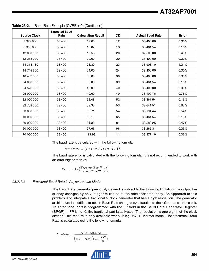
39432015G–AVR32–09/09
AT32AP7001
The baud rate is calculated with the following formula:
The baud rate error is calculated with the following formula. It is not recommended to work withan error higher than 5%.
25.7.1.3 Fractional Baud Rate in Asynchronous Mode
The Baud Rate generator previously defined is subject to the following limitation: the output fre-quency changes by only integer multiples of the reference frequency. An approach to thisproblem is to integrate a fractional N clock generator that has a high resolution. The generatorarchitecture is modified to obtain Baud Rate changes by a fraction of the reference source clock.This fractional part is programmed with the FP field in the Baud Rate Generator Register(BRGR). If FP is not 0, the fractional part is activated. The resolution is one eighth of the clockdivider. This feature is only available when using USART normal mode. The fractional BaudRate is calculated using the following formula:
7 372 800 38 400 12.00 12 38 400.00 0.00%
8 000 000 38 400 13.02 13 38 461.54 0.16%
12 000 000 38 400 19.53 20 37 500.00 2.40%
12 288 000 38 400 20.00 20 38 400.00 0.00%
14 318 180 38 400 23.30 23 38 908.10 1.31%
14 745 600 38 400 24.00 24 38 400.00 0.00%
18 432 000 38 400 30.00 30 38 400.00 0.00%
24 000 000 38 400 39.06 39 38 461.54 0.16%
24 576 000 38 400 40.00 40 38 400.00 0.00%
25 000 000 38 400 40.69 40 38 109.76 0.76%
32 000 000 38 400 52.08 52 38 461.54 0.16%
32 768 000 38 400 53.33 53 38 641.51 0.63%
33 000 000 38 400 53.71 54 38 194.44 0.54%
40 000 000 38 400 65.10 65 38 461.54 0.16%
50 000 000 38 400 81.38 81 38 580.25 0.47%
60 000 000 38 400 97.66 98 38 265.31 0.35%
70 000 000 38 400 113.93 114 38 377.19 0.06%
Table 25-2. Baud Rate Example (OVER = 0) (Continued)
Source ClockExpected Baud
Rate Calculation Result CD Actual Baud Rate Error
BaudRate CLKUSART( ) CD 16×⁄=
Error 1 ExpectedBaudRateActualBaudRate
---------------------------------------------------⎝ ⎠⎛ ⎞–=
Baudrate SelectedClock
8 2 Over–( ) CD FP8
-------+⎝ ⎠⎛ ⎞
⎝ ⎠⎛ ⎞-----------------------------------------------------------------=
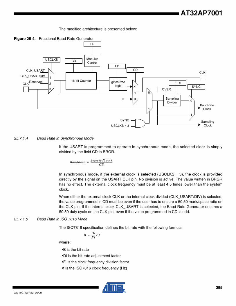
39532015G–AVR32–09/09
AT32AP7001
The modified architecture is presented below:
Figure 25-4. Fractional Baud Rate Generator
25.7.1.4 Baud Rate in Synchronous Mode
If the USART is programmed to operate in synchronous mode, the selected clock is simplydivided by the field CD in BRGR.
In synchronous mode, if the external clock is selected (USCLKS = 3), the clock is provideddirectly by the signal on the USART CLK pin. No division is active. The value written in BRGRhas no effect. The external clock frequency must be at least 4.5 times lower than the systemclock.
When either the external clock CLK or the internal clock divided (CLK_USART/DIV) is selected,the value programmed in CD must be even if the user has to ensure a 50:50 mark/space ratio onthe CLK pin. If the internal clock CLK_USART is selected, the Baud Rate Generator ensures a50:50 duty cycle on the CLK pin, even if the value programmed in CD is odd.
25.7.1.5 Baud Rate in ISO 7816 Mode
The ISO7816 specification defines the bit rate with the following formula:
where:
•B is the bit rate
•Di is the bit-rate adjustment factor
•Fi is the clock frequency division factor
•f is the ISO7816 clock frequency (Hz)
USCLKS CDModulusControl
FP
FPCD
glitch-freelogic
16-bit Counter
OVER
FIDISYNC
SamplingDivider
CLK_USART
CLK_USART/DIV
ReservedCLK
CLK
BaudRateClock
SamplingClock
SYNC
USCLKS = 3
>1
1
2
30
0
1
0
1
1
0
0
BaudRate SelectedClockCD
--------------------------------------=
B DiFi------ f×=
39632015G–AVR32–09/09
AT32AP7001
Di is a binary value encoded on a 4-bit field, named DI, as represented in Table 25-3.
Fi is a binary value encoded on a 4-bit field, named FI, as represented in Table 25-4.
Table 25-5 shows the resulting Fi/Di Ratio, which is the ratio between the ISO7816 clock and thebaud rate clock.
If the USART is configured in ISO7816 Mode, the clock selected by the USCLKS field in theMode Register (MR) is first divided by the value programmed in the field CD in the Baud RateGenerator Register (BRGR). The resulting clock can be provided to the CLK pin to feed thesmart card clock inputs. This means that the CLKO bit can be set in MR.
This clock is then divided by the value programmed in the FI_DI_RATIO field in the FI_DI_Ratioregister (FIDI). This is performed by the Sampling Divider, which performs a division by up to2047 in ISO7816 Mode. The non-integer values of the Fi/Di Ratio are not supported and the usermust program the FI_DI_RATIO field to a value as close as possible to the expected value.
The FI_DI_RATIO field resets to the value 0x174 (372 in decimal) and is the most commondivider between the ISO7816 clock and the bit rate (Fi = 372, Di = 1).
Figure 25-5 shows the relation between the Elementary Time Unit, corresponding to a bit time,and the ISO 7816 clock.
Table 25-3. Binary and Decimal Values for Di
DI field 0001 0010 0011 0100 0101 0110 1000 1001
Di (decimal) 1 2 4 8 16 32 12 20
Table 25-4. Binary and Decimal Values for Fi
FI field 0000 0001 0010 0011 0100 0101 0110 1001 1010 1011 1100 1101
Fi (decimal 372 372 558 744 1116 1488 1860 512 768 1024 1536 2048
Table 25-5. Possible Values for the Fi/Di Ratio
Fi/Di 372 558 774 1116 1488 1806 512 768 1024 1536 2048
1 372 558 744 1116 1488 1860 512 768 1024 1536 2048
2 186 279 372 558 744 930 256 384 512 768 1024
4 93 139.5 186 279 372 465 128 192 256 384 512
8 46.5 69.75 93 139.5 186 232.5 64 96 128 192 256
16 23.25 34.87 46.5 69.75 93 116.2 32 48 64 96 128
32 11.62 17.43 23.25 34.87 46.5 58.13 16 24 32 48 64
12 31 46.5 62 93 124 155 42.66 64 85.33 128 170.6
20 18.6 27.9 37.2 55.8 74.4 93 25.6 38.4 51.2 76.8 102.4
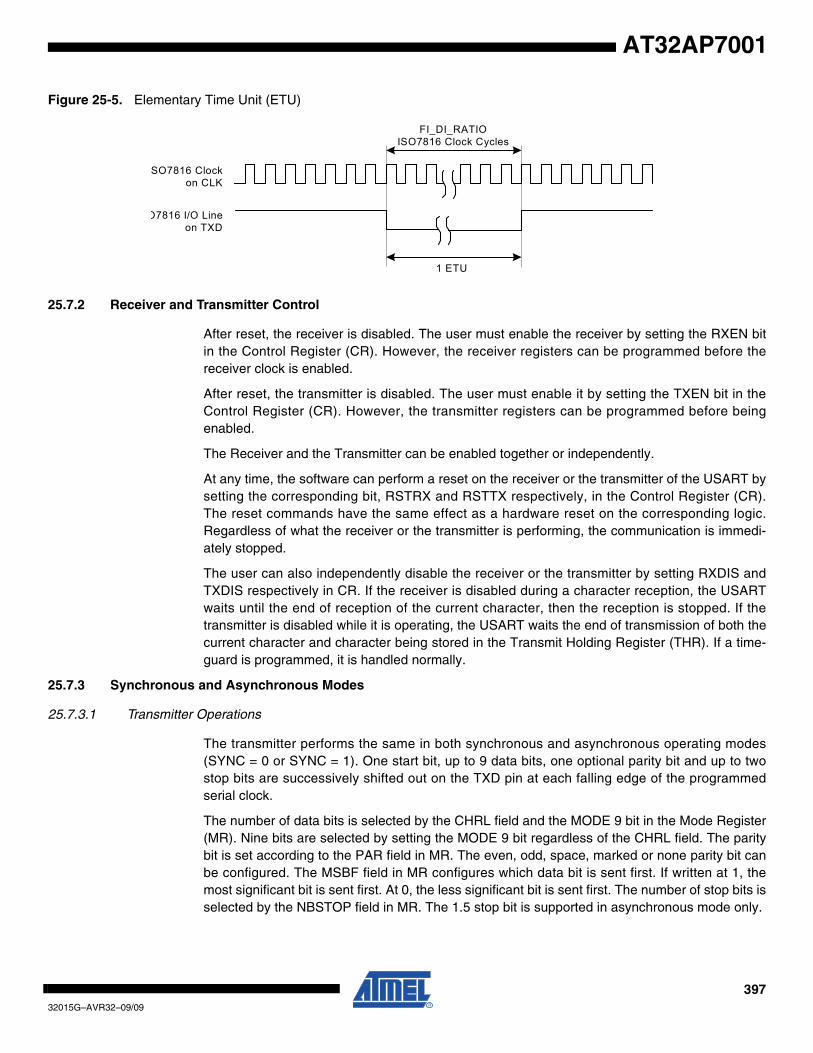
39732015G–AVR32–09/09
AT32AP7001
Figure 25-5. Elementary Time Unit (ETU)
25.7.2 Receiver and Transmitter Control
After reset, the receiver is disabled. The user must enable the receiver by setting the RXEN bitin the Control Register (CR). However, the receiver registers can be programmed before thereceiver clock is enabled.
After reset, the transmitter is disabled. The user must enable it by setting the TXEN bit in theControl Register (CR). However, the transmitter registers can be programmed before beingenabled.
The Receiver and the Transmitter can be enabled together or independently.
At any time, the software can perform a reset on the receiver or the transmitter of the USART bysetting the corresponding bit, RSTRX and RSTTX respectively, in the Control Register (CR).The reset commands have the same effect as a hardware reset on the corresponding logic.Regardless of what the receiver or the transmitter is performing, the communication is immedi-ately stopped.
The user can also independently disable the receiver or the transmitter by setting RXDIS andTXDIS respectively in CR. If the receiver is disabled during a character reception, the USARTwaits until the end of reception of the current character, then the reception is stopped. If thetransmitter is disabled while it is operating, the USART waits the end of transmission of both thecurrent character and character being stored in the Transmit Holding Register (THR). If a time-guard is programmed, it is handled normally.
25.7.3 Synchronous and Asynchronous Modes
25.7.3.1 Transmitter Operations
The transmitter performs the same in both synchronous and asynchronous operating modes(SYNC = 0 or SYNC = 1). One start bit, up to 9 data bits, one optional parity bit and up to twostop bits are successively shifted out on the TXD pin at each falling edge of the programmedserial clock.
The number of data bits is selected by the CHRL field and the MODE 9 bit in the Mode Register(MR). Nine bits are selected by setting the MODE 9 bit regardless of the CHRL field. The paritybit is set according to the PAR field in MR. The even, odd, space, marked or none parity bit canbe configured. The MSBF field in MR configures which data bit is sent first. If written at 1, themost significant bit is sent first. At 0, the less significant bit is sent first. The number of stop bits isselected by the NBSTOP field in MR. The 1.5 stop bit is supported in asynchronous mode only.
1 ETU
FI_DI_RATIOISO7816 Clock Cycles
SO7816 Clock on CLK
O7816 I/O Line on TXD
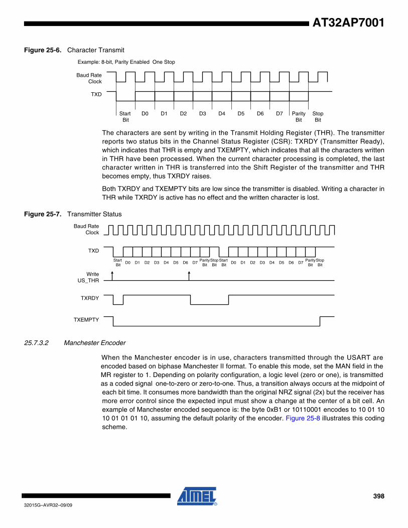
39832015G–AVR32–09/09
AT32AP7001
Figure 25-6. Character Transmit
The characters are sent by writing in the Transmit Holding Register (THR). The transmitterreports two status bits in the Channel Status Register (CSR): TXRDY (Transmitter Ready),which indicates that THR is empty and TXEMPTY, which indicates that all the characters writtenin THR have been processed. When the current character processing is completed, the lastcharacter written in THR is transferred into the Shift Register of the transmitter and THRbecomes empty, thus TXRDY raises.
Both TXRDY and TXEMPTY bits are low since the transmitter is disabled. Writing a character inTHR while TXRDY is active has no effect and the written character is lost.
Figure 25-7. Transmitter Status
25.7.3.2 Manchester Encoder
When the Manchester encoder is in use, characters transmitted through the USART areencoded based on biphase Manchester II format. To enable this mode, set the MAN field in theMR register to 1. Depending on polarity configuration, a logic level (zero or one), is transmittedas a coded signal one-to-zero or zero-to-one. Thus, a transition always occurs at the midpoint ofeach bit time. It consumes more bandwidth than the original NRZ signal (2x) but the receiver hasmore error control since the expected input must show a change at the center of a bit cell. Anexample of Manchester encoded sequence is: the byte 0xB1 or 10110001 encodes to 10 01 1010 01 01 01 10, assuming the default polarity of the encoder. Figure 25-8 illustrates this codingscheme.
D0 D1 D2 D3 D4 D5 D6 D7
TXD
Start Bit
ParityBit
StopBit
Example: 8-bit, Parity Enabled One Stop
Baud Rate Clock
D0 D1 D2 D3 D4 D5 D6 D7
TXD
Start Bit
ParityBit
StopBit
Baud Rate Clock
Start Bit
WriteUS_THR
D0 D1 D2 D3 D4 D5 D6 D7Parity
BitStopBit
TXRDY
TXEMPTY
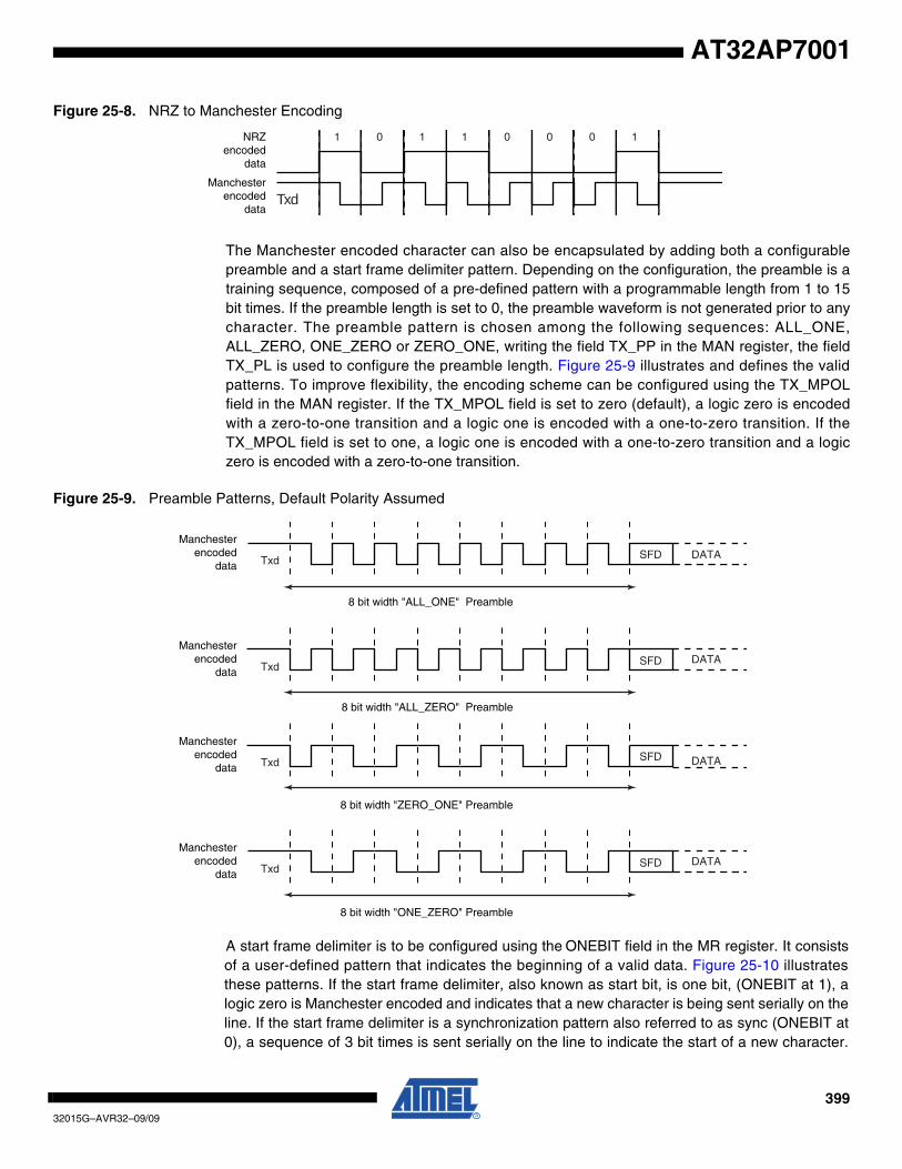
39932015G–AVR32–09/09
AT32AP7001
Figure 25-8. NRZ to Manchester Encoding
The Manchester encoded character can also be encapsulated by adding both a configurablepreamble and a start frame delimiter pattern. Depending on the configuration, the preamble is atraining sequence, composed of a pre-defined pattern with a programmable length from 1 to 15bit times. If the preamble length is set to 0, the preamble waveform is not generated prior to anycharacter. The preamble pattern is chosen among the following sequences: ALL_ONE,ALL_ZERO, ONE_ZERO or ZERO_ONE, writing the field TX_PP in the MAN register, the fieldTX_PL is used to configure the preamble length. Figure 25-9 illustrates and defines the validpatterns. To improve flexibility, the encoding scheme can be configured using the TX_MPOLfield in the MAN register. If the TX_MPOL field is set to zero (default), a logic zero is encodedwith a zero-to-one transition and a logic one is encoded with a one-to-zero transition. If theTX_MPOL field is set to one, a logic one is encoded with a one-to-zero transition and a logiczero is encoded with a zero-to-one transition.
Figure 25-9. Preamble Patterns, Default Polarity Assumed
A start frame delimiter is to be configured using the ONEBIT field in the MR register. It consistsof a user-defined pattern that indicates the beginning of a valid data. Figure 25-10 illustratesthese patterns. If the start frame delimiter, also known as start bit, is one bit, (ONEBIT at 1), alogic zero is Manchester encoded and indicates that a new character is being sent serially on theline. If the start frame delimiter is a synchronization pattern also referred to as sync (ONEBIT at0), a sequence of 3 bit times is sent serially on the line to indicate the start of a new character.
NRZencoded
data
Manchesterencoded
data
1 0 1 1 0 0 0 1
Txd
Manchesterencoded
data Txd SFD DATA
8 bit width "ALL_ONE" Preamble
Manchesterencoded
data Txd SFD DATA
8 bit width "ALL_ZERO" Preamble
Manchesterencoded
data Txd SFD DATA
8 bit width "ZERO_ONE" Preamble
Manchesterencoded
data Txd SFD DATA
8 bit width "ONE_ZERO" Preamble
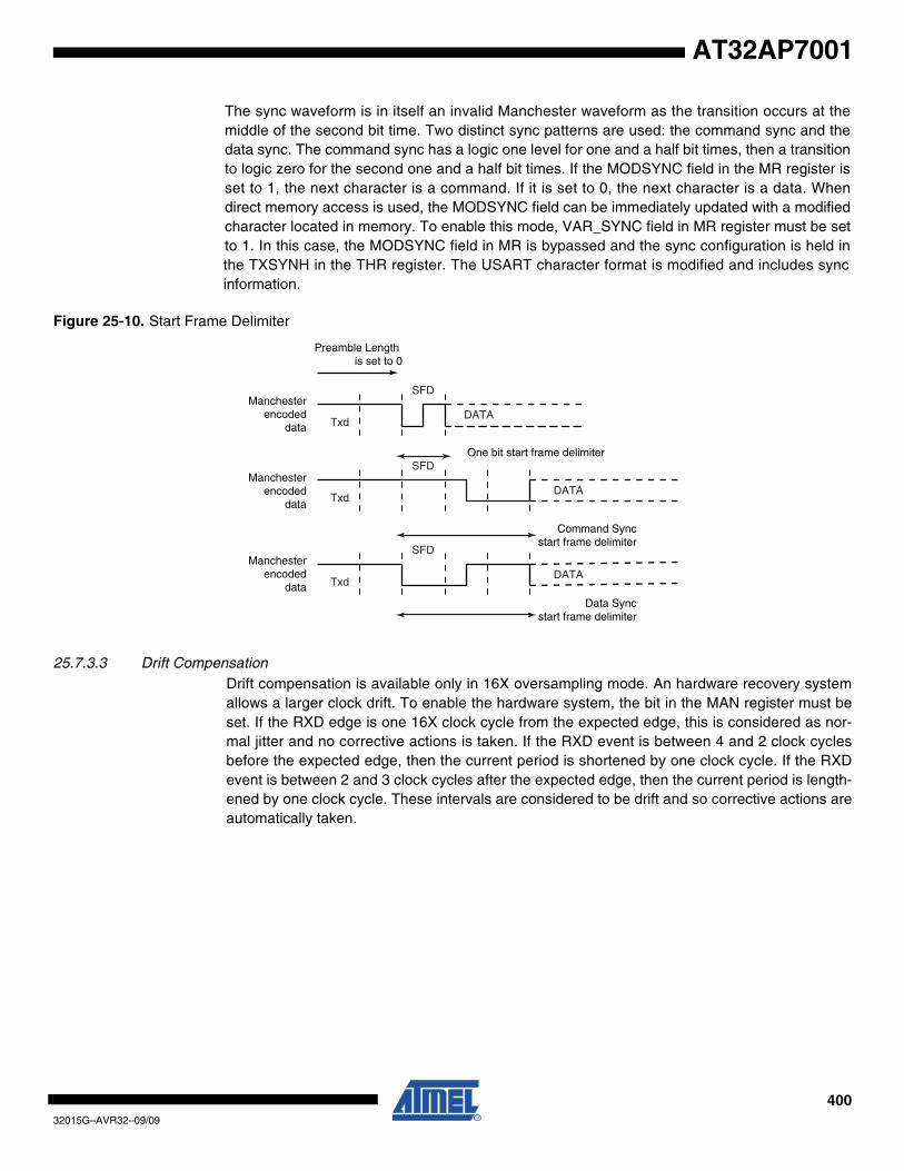
40032015G–AVR32–09/09
AT32AP7001
The sync waveform is in itself an invalid Manchester waveform as the transition occurs at themiddle of the second bit time. Two distinct sync patterns are used: the command sync and thedata sync. The command sync has a logic one level for one and a half bit times, then a transitionto logic zero for the second one and a half bit times. If the MODSYNC field in the MR register isset to 1, the next character is a command. If it is set to 0, the next character is a data. Whendirect memory access is used, the MODSYNC field can be immediately updated with a modifiedcharacter located in memory. To enable this mode, VAR_SYNC field in MR register must be setto 1. In this case, the MODSYNC field in MR is bypassed and the sync configuration is held inthe TXSYNH in the THR register. The USART character format is modified and includes syncinformation.
Figure 25-10. Start Frame Delimiter
25.7.3.3 Drift CompensationDrift compensation is available only in 16X oversampling mode. An hardware recovery systemallows a larger clock drift. To enable the hardware system, the bit in the MAN register must beset. If the RXD edge is one 16X clock cycle from the expected edge, this is considered as nor-mal jitter and no corrective actions is taken. If the RXD event is between 4 and 2 clock cyclesbefore the expected edge, then the current period is shortened by one clock cycle. If the RXDevent is between 2 and 3 clock cycles after the expected edge, then the current period is length-ened by one clock cycle. These intervals are considered to be drift and so corrective actions areautomatically taken.
Manchesterencoded
data Txd
SFD
DATA
One bit start frame delimiter
Preamble Length is set to 0
Manchesterencoded
dataTxd
SFD
DATA
Command Syncstart frame delimiter
Manchesterencoded
data Txd
SFD
DATA
Data Syncstart frame delimiter

40132015G–AVR32–09/09
AT32AP7001
Figure 25-11. Bit Resynchronization
25.7.3.4 Asynchronous Receiver
If the USART is programmed in asynchronous operating mode (SYNC = 0), the receiver over-samples the RXD input line. The oversampling is either 16 or 8 times the Baud Rate clock,depending on the OVER bit in the Mode Register (MR).
The receiver samples the RXD line. If the line is sampled during one half of a bit time at 0, a startbit is detected and data, parity and stop bits are successively sampled on the bit rate clock.
If the oversampling is 16, (OVER at 0), a start is detected at the eighth sample at 0. Then, databits, parity bit and stop bit are sampled on each 16 sampling clock cycle. If the oversampling is 8(OVER at 1), a start bit is detected at the fourth sample at 0. Then, data bits, parity bit and stopbit are sampled on each 8 sampling clock cycle.
The number of data bits, first bit sent and parity mode are selected by the same fields and bitsas the transmitter, i.e. respectively CHRL, MODE9, MSBF and PAR. The number of stop bitshas no effect on the receiver as it considers only one stop bit, regardless of the field NBSTOP,so that resynchronization between the receiver and the transmitter can occur. Moreover, assoon as the stop bit is sampled, the receiver starts looking for a new start bit so that resynchroni-zation can also be accomplished when the transmitter is operating with one stop bit.
Figure 25-12 and Figure 25-13 illustrate start detection and character reception when USARToperates in asynchronous mode.
RXD
Oversampling 16x Clock
Sampling point
Expected edge
ToleranceSynchro.Jump
SyncJumpSynchro.
Error
Synchro.Error
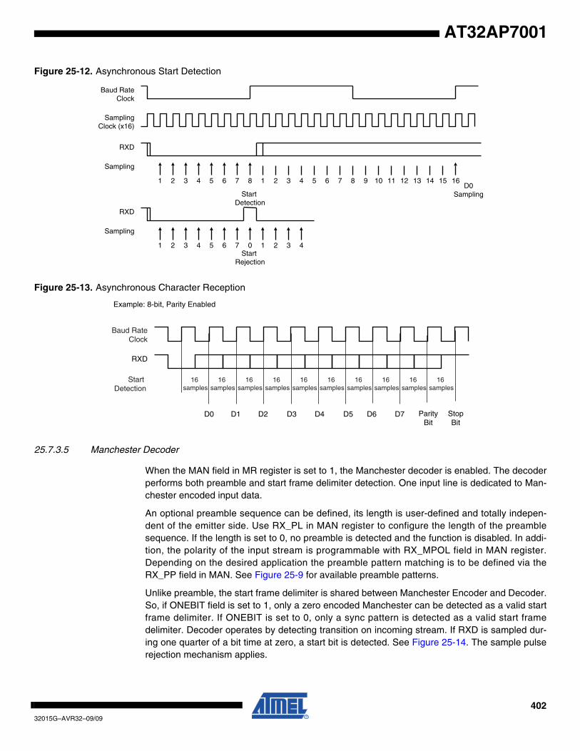
40232015G–AVR32–09/09
AT32AP7001
Figure 25-12. Asynchronous Start Detection
Figure 25-13. Asynchronous Character Reception
25.7.3.5 Manchester Decoder
When the MAN field in MR register is set to 1, the Manchester decoder is enabled. The decoderperforms both preamble and start frame delimiter detection. One input line is dedicated to Man-chester encoded input data.
An optional preamble sequence can be defined, its length is user-defined and totally indepen-dent of the emitter side. Use RX_PL in MAN register to configure the length of the preamblesequence. If the length is set to 0, no preamble is detected and the function is disabled. In addi-tion, the polarity of the input stream is programmable with RX_MPOL field in MAN register.Depending on the desired application the preamble pattern matching is to be defined via theRX_PP field in MAN. See Figure 25-9 for available preamble patterns.
Unlike preamble, the start frame delimiter is shared between Manchester Encoder and Decoder.So, if ONEBIT field is set to 1, only a zero encoded Manchester can be detected as a valid startframe delimiter. If ONEBIT is set to 0, only a sync pattern is detected as a valid start framedelimiter. Decoder operates by detecting transition on incoming stream. If RXD is sampled dur-ing one quarter of a bit time at zero, a start bit is detected. See Figure 25-14. The sample pulserejection mechanism applies.
SamplingClock (x16)
RXD
Start Detection
Sampling
Baud RateClock
RXD
Start Rejection
Sampling
1 2 3 4 5 6 7 8
1 2 3 4 5 6 7 0 1 2 3 4
1 2 3 4 5 6 7 8 9 10 11 12 13 14 15 16D0
Sampling
D0 D1 D2 D3 D4 D5 D6 D7
RXD
ParityBit
StopBit
Example: 8-bit, Parity Enabled
Baud RateClock
Start Detection
16 samples
16 samples
16 samples
16 samples
16 samples
16 samples
16 samples
16 samples
16 samples
16 samples
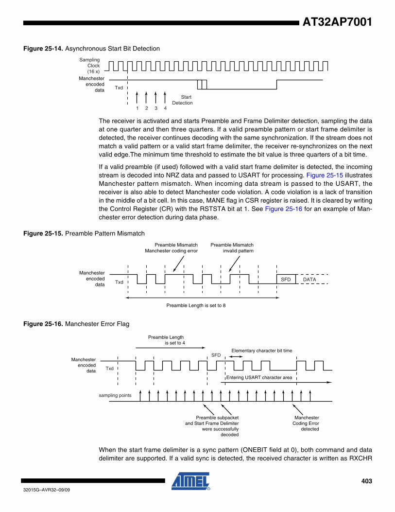
40332015G–AVR32–09/09
AT32AP7001
Figure 25-14. Asynchronous Start Bit Detection
The receiver is activated and starts Preamble and Frame Delimiter detection, sampling the dataat one quarter and then three quarters. If a valid preamble pattern or start frame delimiter isdetected, the receiver continues decoding with the same synchronization. If the stream does notmatch a valid pattern or a valid start frame delimiter, the receiver re-synchronizes on the nextvalid edge.The minimum time threshold to estimate the bit value is three quarters of a bit time.
If a valid preamble (if used) followed with a valid start frame delimiter is detected, the incomingstream is decoded into NRZ data and passed to USART for processing. Figure 25-15 illustratesManchester pattern mismatch. When incoming data stream is passed to the USART, thereceiver is also able to detect Manchester code violation. A code violation is a lack of transitionin the middle of a bit cell. In this case, MANE flag in CSR register is raised. It is cleared by writingthe Control Register (CR) with the RSTSTA bit at 1. See Figure 25-16 for an example of Man-chester error detection during data phase.
Figure 25-15. Preamble Pattern Mismatch
Figure 25-16. Manchester Error Flag
When the start frame delimiter is a sync pattern (ONEBIT field at 0), both command and datadelimiter are supported. If a valid sync is detected, the received character is written as RXCHR
Manchesterencoded
data Txd
1 2 3 4
SamplingClock(16 x)
Start Detection
Manchesterencoded
data Txd SFD DATA
Preamble Length is set to 8
Preamble Mismatchinvalid pattern
Preamble MismatchManchester coding error
Manchesterencoded
data Txd
SFD
Preamble Length is set to 4
Elementary character bit time
ManchesterCoding Error
detected
sampling points
Preamble subpacketand Start Frame Delimiter
were successfullydecoded
Entering USART character area
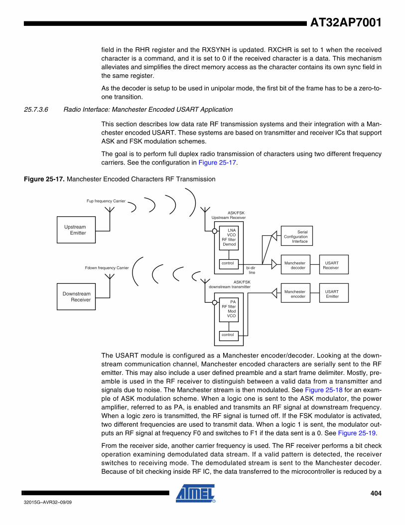
40432015G–AVR32–09/09
AT32AP7001
field in the RHR register and the RXSYNH is updated. RXCHR is set to 1 when the receivedcharacter is a command, and it is set to 0 if the received character is a data. This mechanismalleviates and simplifies the direct memory access as the character contains its own sync field inthe same register.
As the decoder is setup to be used in unipolar mode, the first bit of the frame has to be a zero-to-one transition.
25.7.3.6 Radio Interface: Manchester Encoded USART Application
This section describes low data rate RF transmission systems and their integration with a Man-chester encoded USART. These systems are based on transmitter and receiver ICs that supportASK and FSK modulation schemes.
The goal is to perform full duplex radio transmission of characters using two different frequencycarriers. See the configuration in Figure 25-17.
Figure 25-17. Manchester Encoded Characters RF Transmission
The USART module is configured as a Manchester encoder/decoder. Looking at the down-stream communication channel, Manchester encoded characters are serially sent to the RFemitter. This may also include a user defined preamble and a start frame delimiter. Mostly, pre-amble is used in the RF receiver to distinguish between a valid data from a transmitter andsignals due to noise. The Manchester stream is then modulated. See Figure 25-18 for an exam-ple of ASK modulation scheme. When a logic one is sent to the ASK modulator, the poweramplifier, referred to as PA, is enabled and transmits an RF signal at downstream frequency.When a logic zero is transmitted, the RF signal is turned off. If the FSK modulator is activated,two different frequencies are used to transmit data. When a logic 1 is sent, the modulator out-puts an RF signal at frequency F0 and switches to F1 if the data sent is a 0. See Figure 25-19.
From the receiver side, another carrier frequency is used. The RF receiver performs a bit checkoperation examining demodulated data stream. If a valid pattern is detected, the receiverswitches to receiving mode. The demodulated stream is sent to the Manchester decoder.Because of bit checking inside RF IC, the data transferred to the microcontroller is reduced by a
LNAVCO
RF filterDemod
controlbi-dir
line
PARF filter
ModVCO
control
Manchesterdecoder
Manchesterencoder
USARTReceiver
USARTEmitter
ASK/FSK Upstream Receiver
ASK/FSKdownstream transmitter
UpstreamEmitter
DownstreamReceiver
SerialConfiguration
Interface
Fup frequency Carrier
Fdown frequency Carrier
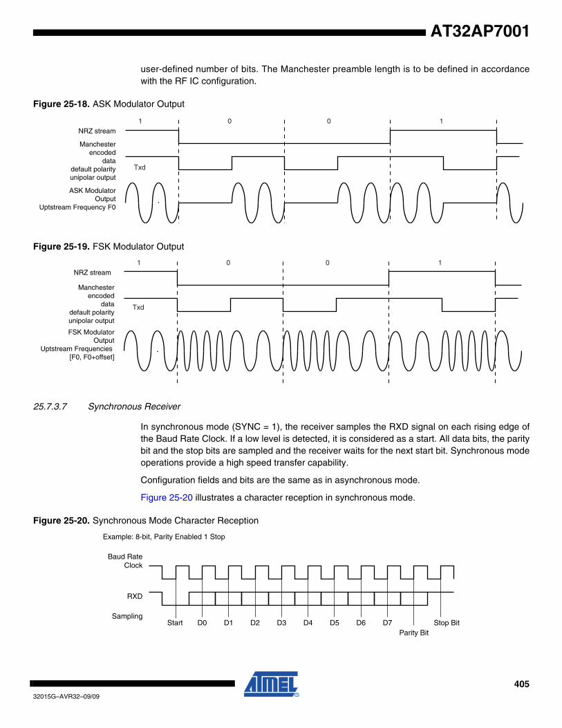
40532015G–AVR32–09/09
AT32AP7001
user-defined number of bits. The Manchester preamble length is to be defined in accordancewith the RF IC configuration.
Figure 25-18. ASK Modulator Output
Figure 25-19. FSK Modulator Output
25.7.3.7 Synchronous Receiver
In synchronous mode (SYNC = 1), the receiver samples the RXD signal on each rising edge ofthe Baud Rate Clock. If a low level is detected, it is considered as a start. All data bits, the paritybit and the stop bits are sampled and the receiver waits for the next start bit. Synchronous modeoperations provide a high speed transfer capability.
Configuration fields and bits are the same as in asynchronous mode.
Figure 25-20 illustrates a character reception in synchronous mode.
Figure 25-20. Synchronous Mode Character Reception
Manchesterencoded
datadefault polarityunipolar output
Txd
ASK ModulatorOutput
Uptstream Frequency F0
NRZ stream1 0 0 1
Manchesterencoded
datadefault polarityunipolar output
Txd
FSK ModulatorOutput
Uptstream Frequencies [F0, F0+offset]
NRZ stream1 0 0 1
D0 D1 D2 D3 D4 D5 D6 D7
RXD
Start Sampling
Parity BitStop Bit
Example: 8-bit, Parity Enabled 1 Stop
Baud RateClock
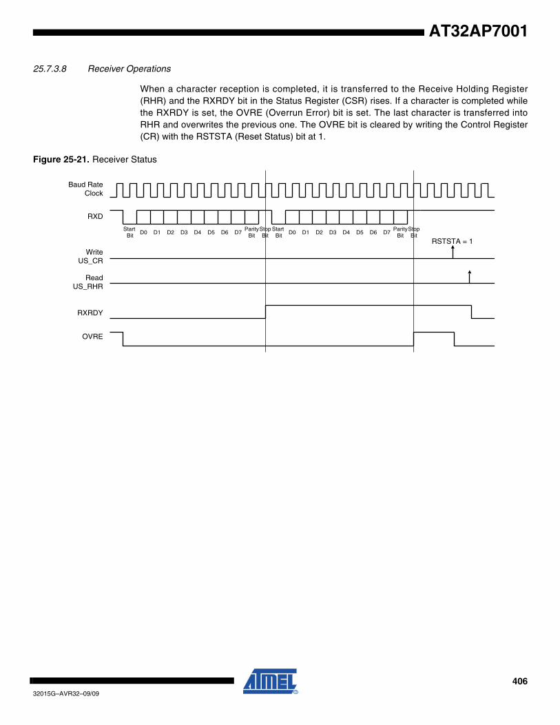
40632015G–AVR32–09/09
AT32AP7001
25.7.3.8 Receiver Operations
When a character reception is completed, it is transferred to the Receive Holding Register(RHR) and the RXRDY bit in the Status Register (CSR) rises. If a character is completed whilethe RXRDY is set, the OVRE (Overrun Error) bit is set. The last character is transferred intoRHR and overwrites the previous one. The OVRE bit is cleared by writing the Control Register(CR) with the RSTSTA (Reset Status) bit at 1.
Figure 25-21. Receiver Status
D0 D1 D2 D3 D4 D5 D6 D7
RXD
Start Bit
ParityBit
StopBit
Baud Rate Clock
WriteUS_CR
RXRDY
OVRE
D0 D1 D2 D3 D4 D5 D6 D7Start
BitParity
BitStopBit
RSTSTA = 1
ReadUS_RHR

40732015G–AVR32–09/09
AT32AP7001
25.7.3.9 Parity
The USART supports five parity modes selected by programming the PAR field in the ModeRegister (MR). The PAR field also enables the Multidrop mode, see ”Multidrop Mode” on page408. Even and odd parity bit generation and error detection are supported.
If even parity is selected, the parity generator of the transmitter drives the parity bit at 0 if a num-ber of 1s in the character data bit is even, and at 1 if the number of 1s is odd. Accordingly, thereceiver parity checker counts the number of received 1s and reports a parity error if the sam-pled parity bit does not correspond. If odd parity is selected, the parity generator of thetransmitter drives the parity bit at 1 if a number of 1s in the character data bit is even, and at 0 ifthe number of 1s is odd. Accordingly, the receiver parity checker counts the number of received1s and reports a parity error if the sampled parity bit does not correspond. If the mark parity isused, the parity generator of the transmitter drives the parity bit at 1 for all characters. Thereceiver parity checker reports an error if the parity bit is sampled at 0. If the space parity isused, the parity generator of the transmitter drives the parity bit at 0 for all characters. Thereceiver parity checker reports an error if the parity bit is sampled at 1. If parity is disabled, thetransmitter does not generate any parity bit and the receiver does not report any parity error.
Table 25-6 shows an example of the parity bit for the character 0x41 (character ASCII “A”)depending on the configuration of the USART. Because there are two bits at 1, 1 bit is addedwhen a parity is odd, or 0 is added when a parity is even.
When the receiver detects a parity error, it sets the PARE (Parity Error) bit in the Channel StatusRegister (CSR). The PARE bit can be cleared by writing the Control Register (CR) with the RST-STA bit at 1. Figure 25-22 illustrates the parity bit status setting and clearing.
Table 25-6. Parity Bit Examples
Character Hexa Binary Parity Bit Parity Mode
A 0x41 0100 0001 1 Odd
A 0x41 0100 0001 0 Even
A 0x41 0100 0001 1 Mark
A 0x41 0100 0001 0 Space
A 0x41 0100 0001 None None

40832015G–AVR32–09/09
AT32AP7001
Figure 25-22. Parity Error
25.7.3.10 Multidrop Mode
If the PAR field in the Mode Register (MR) is programmed to the value 0x6 or 0x07, the USARTruns in Multidrop Mode. This mode differentiates the data characters and the address charac-ters. Data is transmitted with the parity bit at 0 and addresses are transmitted with the parity bitat 1.
If the USART is configured in multidrop mode, the receiver sets the PARE parity error bit whenthe parity bit is high and the transmitter is able to send a character with the parity bit high whenthe Control Register is written with the SENDA bit at 1.
To handle parity error, the PARE bit is cleared when the Control Register is written with the bitRSTSTA at 1.
The transmitter sends an address byte (parity bit set) when SENDA is written to CR. In this case,the next byte written to THR is transmitted as an address. Any character written in THR withouthaving written the command SENDA is transmitted normally with the parity at 0.
25.7.3.11 Transmitter Timeguard
The timeguard feature enables the USART interface with slow remote devices.
The timeguard function enables the transmitter to insert an idle state on the TXD line betweentwo characters. This idle state actually acts as a long stop bit.
The duration of the idle state is programmed in the TG field of the Transmitter Timeguard Regis-ter (TTGR). When this field is programmed at zero no timeguard is generated. Otherwise, thetransmitter holds a high level on TXD after each transmitted byte during the number of bit peri-ods programmed in TG in addition to the number of stop bits.
As illustrated in Figure 25-23, the behavior of TXRDY and TXEMPTY status bits is modified bythe programming of a timeguard. TXRDY rises only when the start bit of the next character issent, and thus remains at 0 during the timeguard transmission if a character has been written inTHR. TXEMPTY remains low until the timeguard transmission is completed as the timeguard ispart of the current character being transmitted.
D0 D1 D2 D3 D4 D5 D6 D7
RXD
Start Bit
BadParity
Bit
StopBit
Baud Rate Clock
WriteUS_CR
PARE
RXRDY
RSTSTA = 1
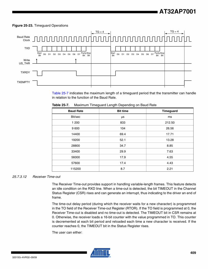
40932015G–AVR32–09/09
AT32AP7001
Figure 25-23. Timeguard Operations
Table 25-7 indicates the maximum length of a timeguard period that the transmitter can handlein relation to the function of the Baud Rate.
25.7.3.12 Receiver Time-out
The Receiver Time-out provides support in handling variable-length frames. This feature detectsan idle condition on the RXD line. When a time-out is detected, the bit TIMEOUT in the ChannelStatus Register (CSR) rises and can generate an interrupt, thus indicating to the driver an end offrame.
The time-out delay period (during which the receiver waits for a new character) is programmedin the TO field of the Receiver Time-out Register (RTOR). If the TO field is programmed at 0, theReceiver Time-out is disabled and no time-out is detected. The TIMEOUT bit in CSR remains at0. Otherwise, the receiver loads a 16-bit counter with the value programmed in TO. This counteris decremented at each bit period and reloaded each time a new character is received. If thecounter reaches 0, the TIMEOUT bit in the Status Register rises.
The user can either:
D0 D1 D2 D3 D4 D5 D6 D7
TXD
Start Bit
ParityBit
StopBit
Baud Rate Clock
Start Bit
TG = 4
WriteUS_THR
D0 D1 D2 D3 D4 D5 D6 D7Parity
BitStopBit
TXRDY
TXEMPTY
TG = 4
Table 25-7. Maximum Timeguard Length Depending on Baud Rate
Baud Rate Bit time Timeguard
Bit/sec µs ms
1 200 833 212.50
9 600 104 26.56
14400 69.4 17.71
19200 52.1 13.28
28800 34.7 8.85
33400 29.9 7.63
56000 17.9 4.55
57600 17.4 4.43
115200 8.7 2.21

41032015G–AVR32–09/09
AT32AP7001
•Obtain an interrupt when a time-out is detected after having received at least one character. This is performed by writing the Control Register (CR) with the STTTO (Start Time-out) bit at 1.
•Obtain a periodic interrupt while no character is received. This is performed by writing CR with the RETTO (Reload and Start Time-out) bit at 1.
If STTTO is performed, the counter clock is stopped until a first character is received. The idlestate on RXD before the start of the frame does not provide a time-out. This prevents having toobtain a periodic interrupt and enables a wait of the end of frame when the idle state on RXD isdetected.
If RETTO is performed, the counter starts counting down immediately from the value TO. Thisenables generation of a periodic interrupt so that a user time-out can be handled, for examplewhen no key is pressed on a keyboard.
Figure 25-24 shows the block diagram of the Receiver Time-out feature.
Figure 25-24. Receiver Time-out Block Diagram
Table 25-8 gives the maximum time-out period for some standard baud rates.
16-bit Time-out Counter
0
TO
TIMEOUT
Baud Rate Clock
=
CharacterReceived
RETTO
Load
Clock
16-bit Value
STTTO
D Q1
Clear
Table 25-8. Maximum Time-out Period
Baud Rate Bit Time Time-out
bit/sec µs ms
600 1 667 109 225
1 200 833 54 613
2 400 417 27 306
4 800 208 13 653
9 600 104 6 827
14400 69 4 551
19200 52 3 413
28800 35 2 276
33400 30 1 962
56000 18 1 170
57600 17 1 138
200000 5 328
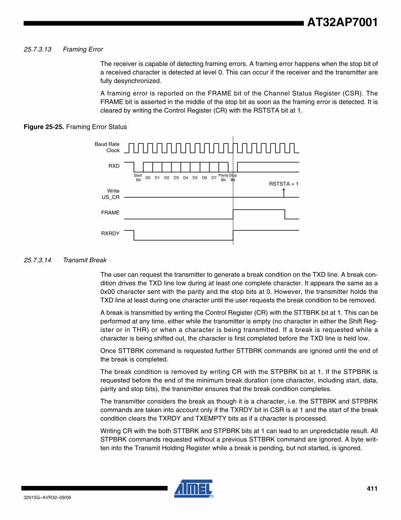
41132015G–AVR32–09/09
AT32AP7001
25.7.3.13 Framing Error
The receiver is capable of detecting framing errors. A framing error happens when the stop bit ofa received character is detected at level 0. This can occur if the receiver and the transmitter arefully desynchronized.
A framing error is reported on the FRAME bit of the Channel Status Register (CSR). TheFRAME bit is asserted in the middle of the stop bit as soon as the framing error is detected. It iscleared by writing the Control Register (CR) with the RSTSTA bit at 1.
Figure 25-25. Framing Error Status
25.7.3.14 Transmit Break
The user can request the transmitter to generate a break condition on the TXD line. A break con-dition drives the TXD line low during at least one complete character. It appears the same as a0x00 character sent with the parity and the stop bits at 0. However, the transmitter holds theTXD line at least during one character until the user requests the break condition to be removed.
A break is transmitted by writing the Control Register (CR) with the STTBRK bit at 1. This can beperformed at any time, either while the transmitter is empty (no character in either the Shift Reg-ister or in THR) or when a character is being transmitted. If a break is requested while acharacter is being shifted out, the character is first completed before the TXD line is held low.
Once STTBRK command is requested further STTBRK commands are ignored until the end ofthe break is completed.
The break condition is removed by writing CR with the STPBRK bit at 1. If the STPBRK isrequested before the end of the minimum break duration (one character, including start, data,parity and stop bits), the transmitter ensures that the break condition completes.
The transmitter considers the break as though it is a character, i.e. the STTBRK and STPBRKcommands are taken into account only if the TXRDY bit in CSR is at 1 and the start of the breakcondition clears the TXRDY and TXEMPTY bits as if a character is processed.
Writing CR with the both STTBRK and STPBRK bits at 1 can lead to an unpredictable result. AllSTPBRK commands requested without a previous STTBRK command are ignored. A byte writ-ten into the Transmit Holding Register while a break is pending, but not started, is ignored.
D0 D1 D2 D3 D4 D5 D6 D7
RXD
Start Bit
ParityBit
StopBit
Baud Rate Clock
WriteUS_CR
FRAME
RXRDY
RSTSTA = 1
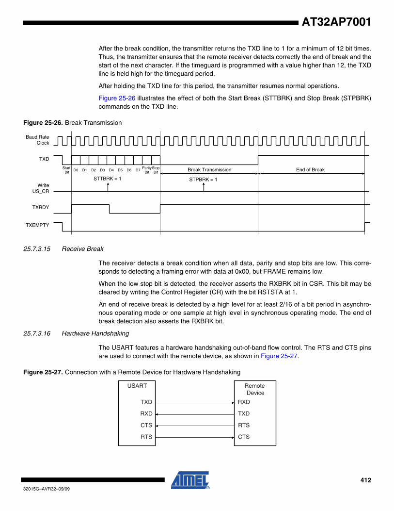
41232015G–AVR32–09/09
AT32AP7001
After the break condition, the transmitter returns the TXD line to 1 for a minimum of 12 bit times.Thus, the transmitter ensures that the remote receiver detects correctly the end of break and thestart of the next character. If the timeguard is programmed with a value higher than 12, the TXDline is held high for the timeguard period.
After holding the TXD line for this period, the transmitter resumes normal operations.
Figure 25-26 illustrates the effect of both the Start Break (STTBRK) and Stop Break (STPBRK)commands on the TXD line.
Figure 25-26. Break Transmission
25.7.3.15 Receive Break
The receiver detects a break condition when all data, parity and stop bits are low. This corre-sponds to detecting a framing error with data at 0x00, but FRAME remains low.
When the low stop bit is detected, the receiver asserts the RXBRK bit in CSR. This bit may becleared by writing the Control Register (CR) with the bit RSTSTA at 1.
An end of receive break is detected by a high level for at least 2/16 of a bit period in asynchro-nous operating mode or one sample at high level in synchronous operating mode. The end ofbreak detection also asserts the RXBRK bit.
25.7.3.16 Hardware Handshaking
The USART features a hardware handshaking out-of-band flow control. The RTS and CTS pinsare used to connect with the remote device, as shown in Figure 25-27.
Figure 25-27. Connection with a Remote Device for Hardware Handshaking
D0 D1 D2 D3 D4 D5 D6 D7
TXD
Start Bit
ParityBit
StopBit
Baud Rate Clock
WriteUS_CR
TXRDY
TXEMPTY
STPBRK = 1STTBRK = 1
Break Transmission End of Break
USART
TXD
CTS
Remote Device
RXD
TXDRXD
RTS
RTS
CTS
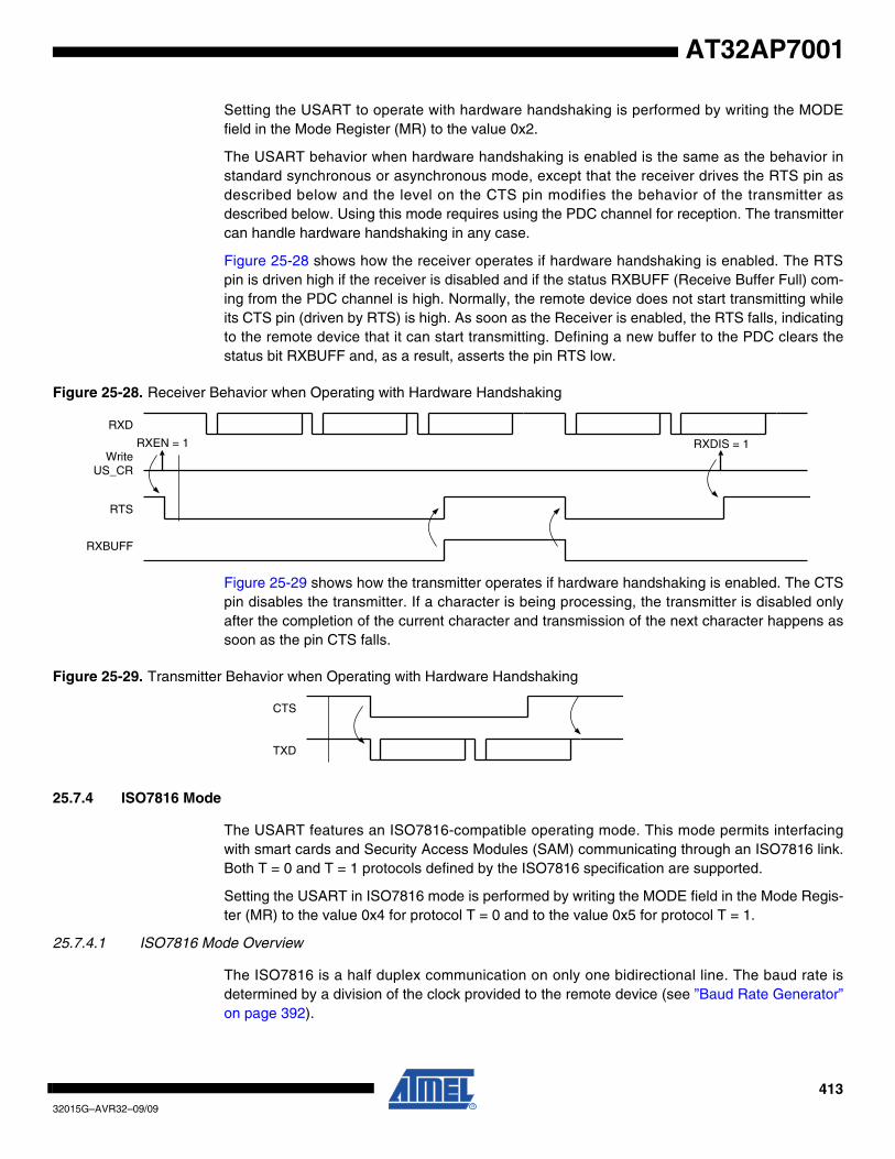
41332015G–AVR32–09/09
AT32AP7001
Setting the USART to operate with hardware handshaking is performed by writing the MODEfield in the Mode Register (MR) to the value 0x2.
The USART behavior when hardware handshaking is enabled is the same as the behavior instandard synchronous or asynchronous mode, except that the receiver drives the RTS pin asdescribed below and the level on the CTS pin modifies the behavior of the transmitter asdescribed below. Using this mode requires using the PDC channel for reception. The transmittercan handle hardware handshaking in any case.
Figure 25-28 shows how the receiver operates if hardware handshaking is enabled. The RTSpin is driven high if the receiver is disabled and if the status RXBUFF (Receive Buffer Full) com-ing from the PDC channel is high. Normally, the remote device does not start transmitting whileits CTS pin (driven by RTS) is high. As soon as the Receiver is enabled, the RTS falls, indicatingto the remote device that it can start transmitting. Defining a new buffer to the PDC clears thestatus bit RXBUFF and, as a result, asserts the pin RTS low.
Figure 25-28. Receiver Behavior when Operating with Hardware Handshaking
Figure 25-29 shows how the transmitter operates if hardware handshaking is enabled. The CTSpin disables the transmitter. If a character is being processing, the transmitter is disabled onlyafter the completion of the current character and transmission of the next character happens assoon as the pin CTS falls.
Figure 25-29. Transmitter Behavior when Operating with Hardware Handshaking
25.7.4 ISO7816 Mode
The USART features an ISO7816-compatible operating mode. This mode permits interfacingwith smart cards and Security Access Modules (SAM) communicating through an ISO7816 link.Both T = 0 and T = 1 protocols defined by the ISO7816 specification are supported.
Setting the USART in ISO7816 mode is performed by writing the MODE field in the Mode Regis-ter (MR) to the value 0x4 for protocol T = 0 and to the value 0x5 for protocol T = 1.
25.7.4.1 ISO7816 Mode Overview
The ISO7816 is a half duplex communication on only one bidirectional line. The baud rate isdetermined by a division of the clock provided to the remote device (see ”Baud Rate Generator”on page 392).
RTS
RXBUFF
WriteUS_CR
RXEN = 1
RXD
RXDIS = 1
CTS
TXD
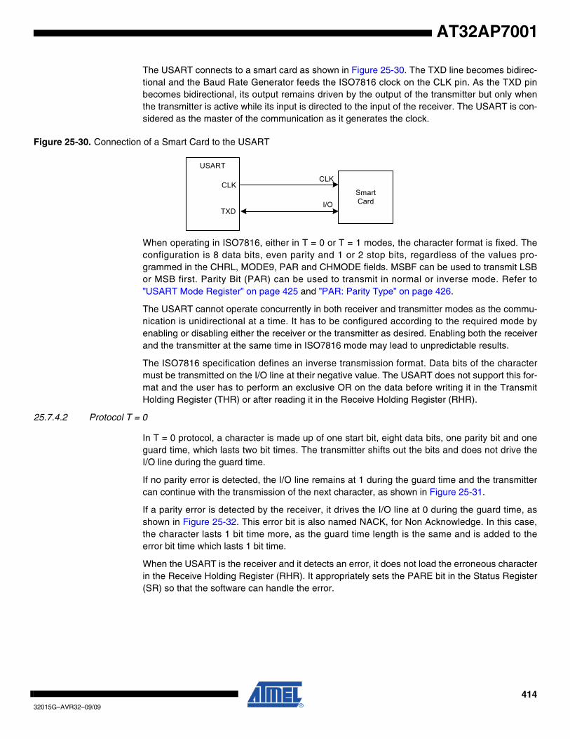
41432015G–AVR32–09/09
AT32AP7001
The USART connects to a smart card as shown in Figure 25-30. The TXD line becomes bidirec-tional and the Baud Rate Generator feeds the ISO7816 clock on the CLK pin. As the TXD pinbecomes bidirectional, its output remains driven by the output of the transmitter but only whenthe transmitter is active while its input is directed to the input of the receiver. The USART is con-sidered as the master of the communication as it generates the clock.
Figure 25-30. Connection of a Smart Card to the USART
When operating in ISO7816, either in T = 0 or T = 1 modes, the character format is fixed. Theconfiguration is 8 data bits, even parity and 1 or 2 stop bits, regardless of the values pro-grammed in the CHRL, MODE9, PAR and CHMODE fields. MSBF can be used to transmit LSBor MSB first. Parity Bit (PAR) can be used to transmit in normal or inverse mode. Refer to”USART Mode Register” on page 425 and ”PAR: Parity Type” on page 426.
The USART cannot operate concurrently in both receiver and transmitter modes as the commu-nication is unidirectional at a time. It has to be configured according to the required mode byenabling or disabling either the receiver or the transmitter as desired. Enabling both the receiverand the transmitter at the same time in ISO7816 mode may lead to unpredictable results.
The ISO7816 specification defines an inverse transmission format. Data bits of the charactermust be transmitted on the I/O line at their negative value. The USART does not support this for-mat and the user has to perform an exclusive OR on the data before writing it in the TransmitHolding Register (THR) or after reading it in the Receive Holding Register (RHR).
25.7.4.2 Protocol T = 0
In T = 0 protocol, a character is made up of one start bit, eight data bits, one parity bit and oneguard time, which lasts two bit times. The transmitter shifts out the bits and does not drive theI/O line during the guard time.
If no parity error is detected, the I/O line remains at 1 during the guard time and the transmittercan continue with the transmission of the next character, as shown in Figure 25-31.
If a parity error is detected by the receiver, it drives the I/O line at 0 during the guard time, asshown in Figure 25-32. This error bit is also named NACK, for Non Acknowledge. In this case,the character lasts 1 bit time more, as the guard time length is the same and is added to theerror bit time which lasts 1 bit time.
When the USART is the receiver and it detects an error, it does not load the erroneous characterin the Receive Holding Register (RHR). It appropriately sets the PARE bit in the Status Register(SR) so that the software can handle the error.
CLK
TXD
USART
CLK
I/OSmartCard

41532015G–AVR32–09/09
AT32AP7001
Figure 25-31. T = 0 Protocol without Parity Error
Figure 25-32. T = 0 Protocol with Parity Error
25.7.4.3 Receive Error CounterThe USART receiver also records the total number of errors. This can be read in the Number ofError (NER) register. The NB_ERRORS field can record up to 255 errors. Reading NER auto-matically clears the NB_ERRORS field.
25.7.4.4 Receive NACK InhibitThe USART can also be configured to inhibit an error. This can be achieved by setting theINACK bit in the Mode Register (MR). If INACK is at 1, no error signal is driven on the I/O lineeven if a parity bit is detected, but the INACK bit is set in the Status Register (SR). The INACKbit can be cleared by writing the Control Register (CR) with the RSTNACK bit at 1.
Moreover, if INACK is set, the erroneous received character is stored in the Receive HoldingRegister, as if no error occurred. However, the RXRDY bit does not raise.
25.7.4.5 Transmit Character RepetitionWhen the USART is transmitting a character and gets a NACK, it can automatically repeat thecharacter before moving on to the next one. Repetit ion is enabled by writ ing theMAX_ITERATION field in the Mode Register (MR) at a value higher than 0. Each character canbe transmitted up to eight times; the first transmission plus seven repetitions.
If MAX_ITERATION does not equal zero, the USART repeats the character as many times asthe value loaded in MAX_ITERATION.
When the USART repetition number reaches MAX_ITERATION, the ITERATION bit is set in theChannel Status Register (CSR). If the repetition of the character is acknowledged by thereceiver, the repetitions are stopped and the iteration counter is cleared.
The ITERATION bit in CSR can be cleared by writing the Control Register with the RSIT bit at 1.
25.7.4.6 Disable Successive Receive NACKThe receiver can limit the number of successive NACKs sent back to the remote transmitter.This is programmed by setting the bit DSNACK in the Mode Register (MR). The maximum num-ber of NACK transmitted is programmed in the MAX_ITERATION field. As soon as
D0 D1 D2 D3 D4 D5 D6 D7
RXD
ParityBit
Baud RateClock
Start Bit
GuardTime 1
Next Start
Bit
GuardTime 2
D0 D1 D2 D3 D4 D5 D6 D7
I/O
ParityBit
Baud RateClock
StartBit
GuardTime 1
Start Bit
GuardTime 2
D0 D1
Error
Repetition
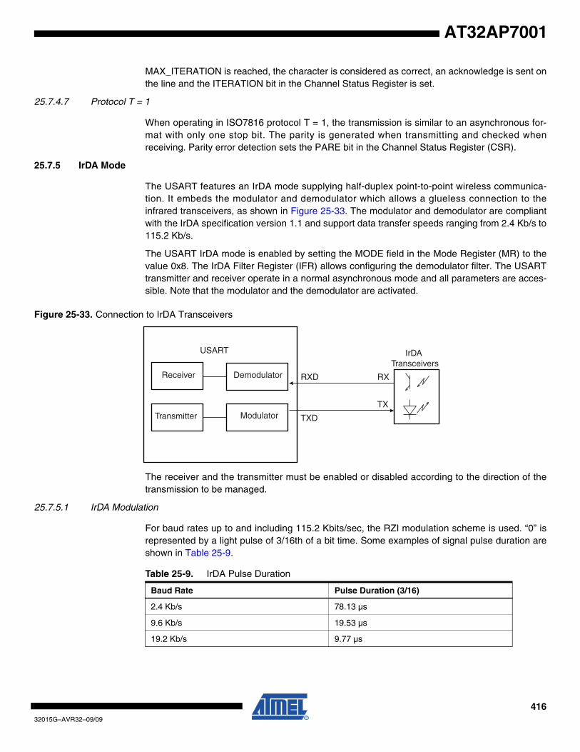
41632015G–AVR32–09/09
AT32AP7001
MAX_ITERATION is reached, the character is considered as correct, an acknowledge is sent onthe line and the ITERATION bit in the Channel Status Register is set.
25.7.4.7 Protocol T = 1
When operating in ISO7816 protocol T = 1, the transmission is similar to an asynchronous for-mat with only one stop bit. The parity is generated when transmitting and checked whenreceiving. Parity error detection sets the PARE bit in the Channel Status Register (CSR).
25.7.5 IrDA Mode
The USART features an IrDA mode supplying half-duplex point-to-point wireless communica-tion. It embeds the modulator and demodulator which allows a glueless connection to theinfrared transceivers, as shown in Figure 25-33. The modulator and demodulator are compliantwith the IrDA specification version 1.1 and support data transfer speeds ranging from 2.4 Kb/s to115.2 Kb/s.
The USART IrDA mode is enabled by setting the MODE field in the Mode Register (MR) to thevalue 0x8. The IrDA Filter Register (IFR) allows configuring the demodulator filter. The USARTtransmitter and receiver operate in a normal asynchronous mode and all parameters are acces-sible. Note that the modulator and the demodulator are activated.
Figure 25-33. Connection to IrDA Transceivers
The receiver and the transmitter must be enabled or disabled according to the direction of thetransmission to be managed.
25.7.5.1 IrDA Modulation
For baud rates up to and including 115.2 Kbits/sec, the RZI modulation scheme is used. “0” isrepresented by a light pulse of 3/16th of a bit time. Some examples of signal pulse duration areshown in Table 25-9.
IrDA Transceivers
RXD RX
TXD
TX
USART
Demodulator
Modulator
Receiver
Transmitter
Table 25-9. IrDA Pulse Duration
Baud Rate Pulse Duration (3/16)
2.4 Kb/s 78.13 µs
9.6 Kb/s 19.53 µs
19.2 Kb/s 9.77 µs
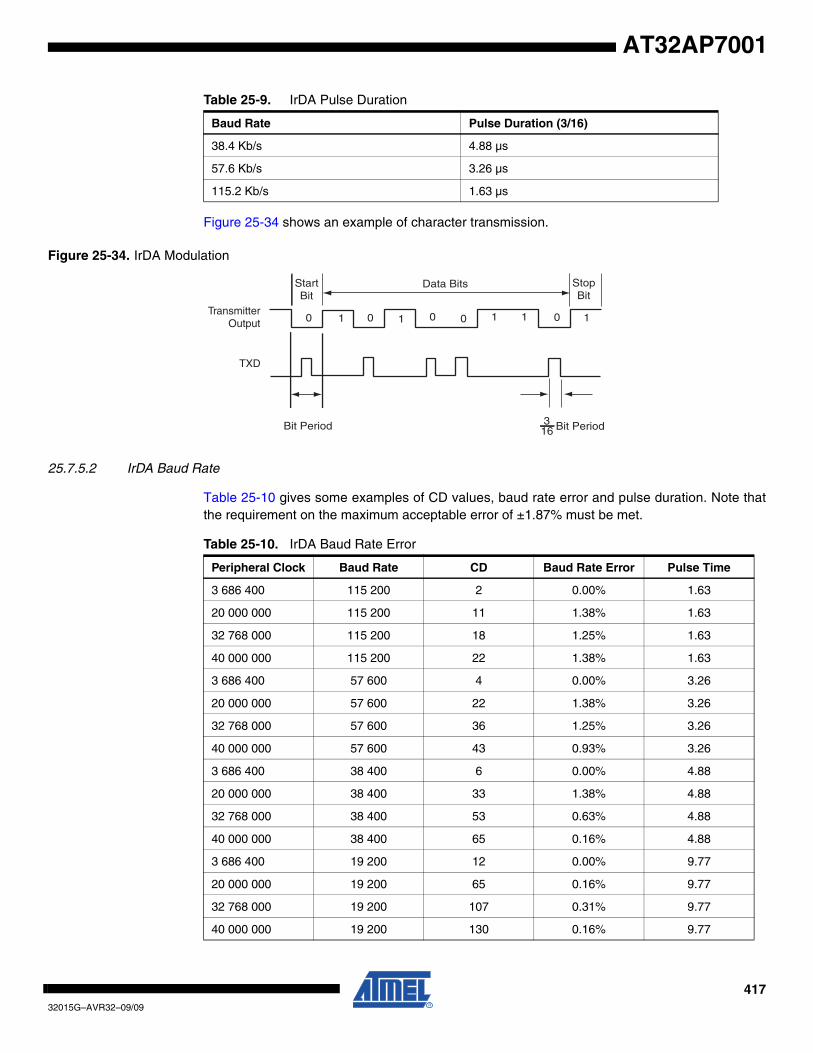
41732015G–AVR32–09/09
AT32AP7001
Figure 25-34 shows an example of character transmission.
Figure 25-34. IrDA Modulation
25.7.5.2 IrDA Baud Rate
Table 25-10 gives some examples of CD values, baud rate error and pulse duration. Note thatthe requirement on the maximum acceptable error of ±1.87% must be met.
38.4 Kb/s 4.88 µs
57.6 Kb/s 3.26 µs
115.2 Kb/s 1.63 µs
Table 25-9. IrDA Pulse Duration
Baud Rate Pulse Duration (3/16)
Bit Period Bit Period316
StartBit
Data Bits StopBit
0 00 0 01 11 11Transmitter
Output
TXD
Table 25-10. IrDA Baud Rate Error
Peripheral Clock Baud Rate CD Baud Rate Error Pulse Time
3 686 400 115 200 2 0.00% 1.63
20 000 000 115 200 11 1.38% 1.63
32 768 000 115 200 18 1.25% 1.63
40 000 000 115 200 22 1.38% 1.63
3 686 400 57 600 4 0.00% 3.26
20 000 000 57 600 22 1.38% 3.26
32 768 000 57 600 36 1.25% 3.26
40 000 000 57 600 43 0.93% 3.26
3 686 400 38 400 6 0.00% 4.88
20 000 000 38 400 33 1.38% 4.88
32 768 000 38 400 53 0.63% 4.88
40 000 000 38 400 65 0.16% 4.88
3 686 400 19 200 12 0.00% 9.77
20 000 000 19 200 65 0.16% 9.77
32 768 000 19 200 107 0.31% 9.77
40 000 000 19 200 130 0.16% 9.77
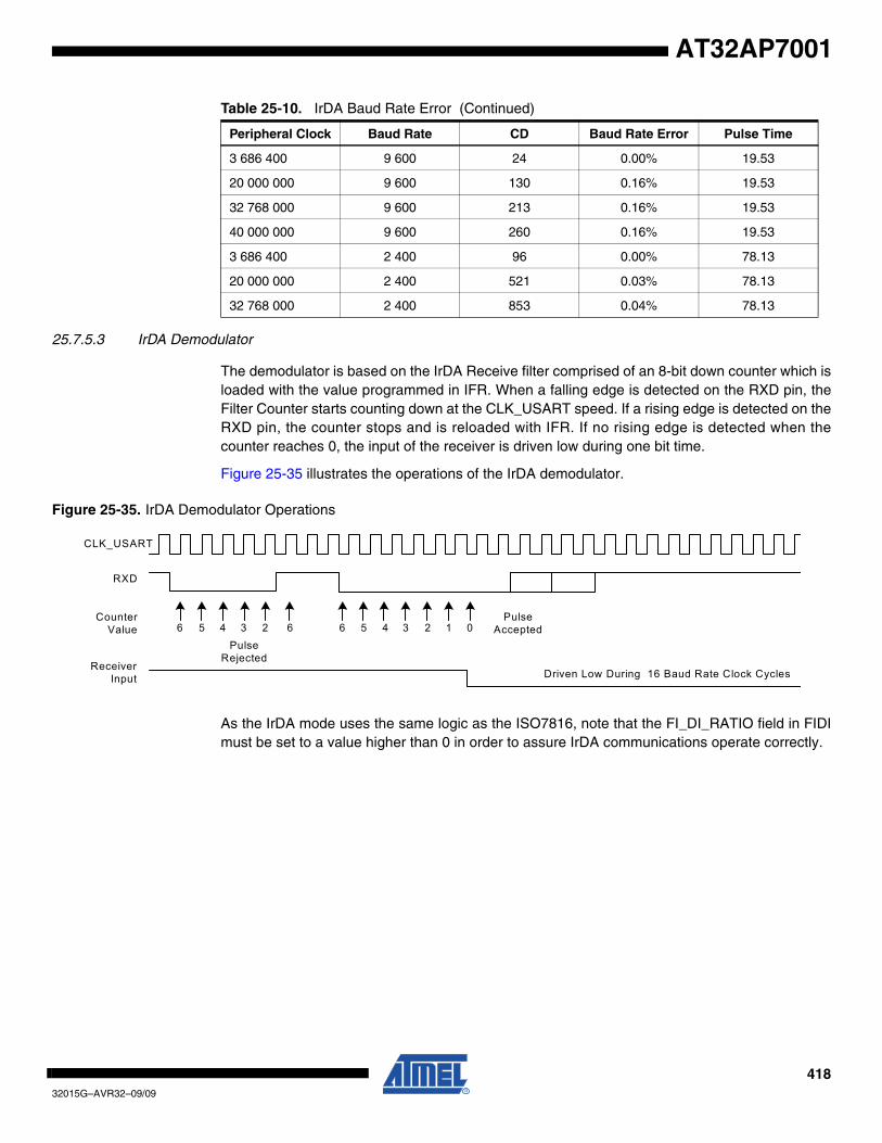
41832015G–AVR32–09/09
AT32AP7001
25.7.5.3 IrDA Demodulator
The demodulator is based on the IrDA Receive filter comprised of an 8-bit down counter which isloaded with the value programmed in IFR. When a falling edge is detected on the RXD pin, theFilter Counter starts counting down at the CLK_USART speed. If a rising edge is detected on theRXD pin, the counter stops and is reloaded with IFR. If no rising edge is detected when thecounter reaches 0, the input of the receiver is driven low during one bit time.
Figure 25-35 illustrates the operations of the IrDA demodulator.
Figure 25-35. IrDA Demodulator Operations
As the IrDA mode uses the same logic as the ISO7816, note that the FI_DI_RATIO field in FIDImust be set to a value higher than 0 in order to assure IrDA communications operate correctly.
3 686 400 9 600 24 0.00% 19.53
20 000 000 9 600 130 0.16% 19.53
32 768 000 9 600 213 0.16% 19.53
40 000 000 9 600 260 0.16% 19.53
3 686 400 2 400 96 0.00% 78.13
20 000 000 2 400 521 0.03% 78.13
32 768 000 2 400 853 0.04% 78.13
Table 25-10. IrDA Baud Rate Error (Continued)
Peripheral Clock Baud Rate CD Baud Rate Error Pulse Time
CLK_USART
RXD
Counter Value
ReceiverInput
6 5 4 63Pulse
Rejected
2 6 45 3 2 1 0Pulse
Accepted
Driven Low During 16 Baud Rate Clock Cycles
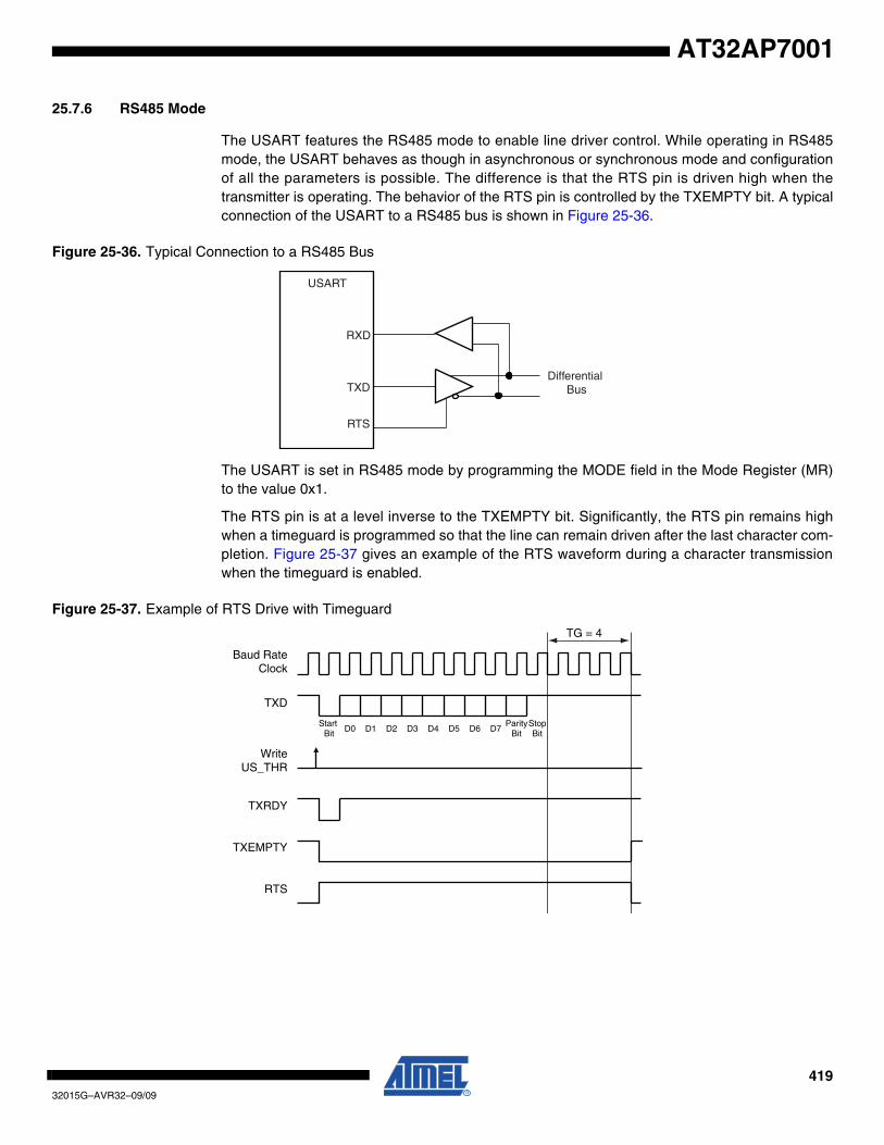
41932015G–AVR32–09/09
AT32AP7001
25.7.6 RS485 Mode
The USART features the RS485 mode to enable line driver control. While operating in RS485mode, the USART behaves as though in asynchronous or synchronous mode and configurationof all the parameters is possible. The difference is that the RTS pin is driven high when thetransmitter is operating. The behavior of the RTS pin is controlled by the TXEMPTY bit. A typicalconnection of the USART to a RS485 bus is shown in Figure 25-36.
Figure 25-36. Typical Connection to a RS485 Bus
The USART is set in RS485 mode by programming the MODE field in the Mode Register (MR)to the value 0x1.
The RTS pin is at a level inverse to the TXEMPTY bit. Significantly, the RTS pin remains highwhen a timeguard is programmed so that the line can remain driven after the last character com-pletion. Figure 25-37 gives an example of the RTS waveform during a character transmissionwhen the timeguard is enabled.
Figure 25-37. Example of RTS Drive with Timeguard
USART
RTS
TXD
RXD
Differential Bus
D0 D1 D2 D3 D4 D5 D6 D7
TXD
Start Bit
ParityBit
StopBit
Baud Rate Clock
TG = 4
WriteUS_THR
TXRDY
TXEMPTY
RTS

42032015G–AVR32–09/09
AT32AP7001
25.7.7 Test Modes
The USART can be programmed to operate in three different test modes. The internal loopbackcapability allows on-board diagnostics. In the loopback mode the USART interface pins are dis-connected or not and reconfigured for loopback internally or externally.
25.7.7.1 Normal Mode
Normal mode connects the RXD pin on the receiver input and the transmitter output on the TXDpin.
Figure 25-38. Normal Mode Configuration
25.7.7.2 Automatic Echo Mode
Automatic echo mode allows bit-by-bit retransmission. When a bit is received on the RXD pin, itis sent to the TXD pin, as shown in Figure 25-39. Programming the transmitter has no effect onthe TXD pin. The RXD pin is still connected to the receiver input, thus the receiver remainsactive.
Figure 25-39. Automatic Echo Mode Configuration
25.7.7.3 Local Loopback Mode
Local loopback mode connects the output of the transmitter directly to the input of the receiver,as shown in Figure 25-40. The TXD and RXD pins are not used. The RXD pin has no effect onthe receiver and the TXD pin is continuously driven high, as in idle state.
Figure 25-40. Local Loopback Mode Configuration
Receiver
Transmitter
RXD
TXD
Receiver
Transmitter
RXD
TXD
Receiver
Transmitter
RXD
TXD1
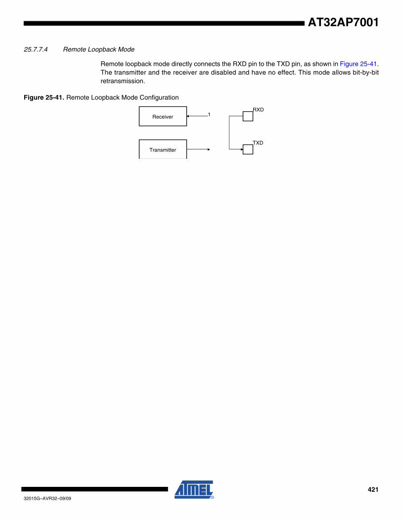
42132015G–AVR32–09/09
AT32AP7001
25.7.7.4 Remote Loopback Mode
Remote loopback mode directly connects the RXD pin to the TXD pin, as shown in Figure 25-41.The transmitter and the receiver are disabled and have no effect. This mode allows bit-by-bitretransmission.
Figure 25-41. Remote Loopback Mode Configuration
Receiver
Transmitter
RXD
TXD
1
42232015G–AVR32–09/09
AT32AP7001
25.8 USART User Interface
Note: 1. Values in the Version Register vary with the version of the IP block implementation.
Table 25-11. USART Memory Map
Offset Register Name Access Reset State
0x0000 Control Register CR Write-only –
0x0004 Mode Register MR Read/Write –
0x0008 Interrupt Enable Register IER Write-only –
0x000C Interrupt Disable Register IDR Write-only –
0x0010 Interrupt Mask Register IMR Read-only 0x0
0x0014 Channel Status Register CSR Read-only –
0x0018 Receiver Holding Register RHR Read-only 0x0
0x001C Transmitter Holding Register THR Write-only –
0x0020 Baud Rate Generator Register BRGR Read/Write 0x0
0x0024 Receiver Time-out Register RTOR Read/Write 0x0
0x0028 Transmitter Timeguard Register TTGR Read/Write 0x0
0x2C - 0x3C Reserved – – –
0x0040 FI DI Ratio Register FIDI Read/Write 0x174
0x0044 Number of Errors Register NER Read-only –
0x0048 Reserved - – –
0x004C IrDA Filter Register IFR Read/Write 0x0
0x0050 Manchester Encoder Decoder Register MAN Read/Write 0x30011004
0x5C - 0xF8 Reserved – – –
0xFC Version Register US_VERSION Read-only 0x–(1)
0x100 - 0x128 Reserved for PDC Registers – – –
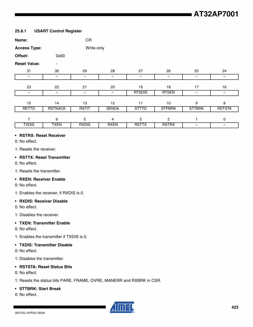
42332015G–AVR32–09/09
AT32AP7001
25.8.1 USART Control Register
Name: CR
Access Type: Write-only
Offset: 0x00
Reset Value: -
• RSTRX: Reset Receiver0: No effect.
1: Resets the receiver.
• RSTTX: Reset Transmitter0: No effect.
1: Resets the transmitter.
• RXEN: Receiver Enable0: No effect.
1: Enables the receiver, if RXDIS is 0.
• RXDIS: Receiver Disable0: No effect.
1: Disables the receiver.
• TXEN: Transmitter Enable0: No effect.
1: Enables the transmitter if TXDIS is 0.
• TXDIS: Transmitter Disable0: No effect.
1: Disables the transmitter.
• RSTSTA: Reset Status Bits0: No effect.
1: Resets the status bits PARE, FRAME, OVRE, MANERR and RXBRK in CSR.
• STTBRK: Start Break0: No effect.
31 30 29 28 27 26 25 24– – – – – – – –
23 22 21 20 19 18 17 16– – – – RTSDIS RTSEN – –
15 14 13 12 11 10 9 8RETTO RSTNACK RSTIT SENDA STTTO STPBRK STTBRK RSTSTA
7 6 5 4 3 2 1 0TXDIS TXEN RXDIS RXEN RSTTX RSTRX – –
42432015G–AVR32–09/09
AT32AP7001
1: Starts transmission of a break after the characters present in THR and the Transmit Shift Register have been transmit-ted. No effect if a break is already being transmitted.
• STPBRK: Stop Break0: No effect.
1: Stops transmission of the break after a minimum of one character length and transmits a high level during 12-bit periods.No effect if no break is being transmitted.
• STTTO: Start Time-out0: No effect
1: Starts waiting for a character before clocking the time-out counter.
• SENDA: Send Address0: No effect.
1: In Multidrop Mode only, the next character written to the THR is sent with the address bit set.
• RSTIT: Reset Iterations0: No effect.
1: Resets ITERATION in CSR. No effect if the ISO7816 is not enabled.
• RSTNACK: Reset Non Acknowledge0: No effect
1: Resets NACK in CSR.
• RETTO: Rearm Time-out0: No effect
1: Restart Time-out
• RTSEN: Request to Send Enable0: No effect.
1: Drives the pin RTS to 0.
• RTSDIS: Request to Send Disable0: No effect.
1: Drives the pin RTS to 1.

42532015G–AVR32–09/09
AT32AP7001
25.8.2 USART Mode Register
Name: MR
Access Type: Read/Write
• MODE
• USCLKS: Clock Selection
• CHRL: Character Length.
31 30 29 28 27 26 25 24
ONEBIT MODSYNC MAN FILTER – MAX_ITERATION
23 22 21 20 19 18 17 16
– VAR_SYNC DSNACK INACK OVER CLKO MODE9 MSBF
15 14 13 12 11 10 9 8
CHMODE NBSTOP PAR SYNC
7 6 5 4 3 2 1 0
CHRL USCLKS MODE
MODE Mode of the USART
0 0 0 0 Normal
0 0 0 1 RS485
0 0 1 0 Hardware Handshaking
0 0 1 1 Reserved
0 1 0 0 IS07816 Protocol: T = 0
0 1 0 1 Reserved
0 1 1 0 IS07816 Protocol: T = 1
0 1 1 1 Reserved
1 0 0 0 IrDA
1 1 x x Reserved
USCLKS Selected Clock
0 0 CLK_USART
0 1 CLK_USART / DIV
1 0 Reserved
1 1 CLK
CHRL Character Length
0 0 5 bits
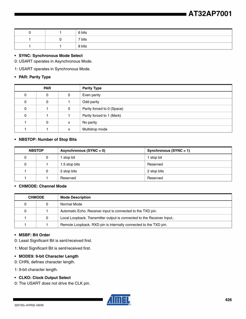
42632015G–AVR32–09/09
AT32AP7001
• SYNC: Synchronous Mode Select0: USART operates in Asynchronous Mode.
1: USART operates in Synchronous Mode.
• PAR: Parity Type
• NBSTOP: Number of Stop Bits
• CHMODE: Channel Mode
• MSBF: Bit Order0: Least Significant Bit is sent/received first.
1: Most Significant Bit is sent/received first.
• MODE9: 9-bit Character Length0: CHRL defines character length.
1: 9-bit character length.
• CLKO: Clock Output Select0: The USART does not drive the CLK pin.
0 1 6 bits
1 0 7 bits
1 1 8 bits
PAR Parity Type
0 0 0 Even parity
0 0 1 Odd parity
0 1 0 Parity forced to 0 (Space)
0 1 1 Parity forced to 1 (Mark)
1 0 x No parity
1 1 x Multidrop mode
NBSTOP Asynchronous (SYNC = 0) Synchronous (SYNC = 1)
0 0 1 stop bit 1 stop bit
0 1 1.5 stop bits Reserved
1 0 2 stop bits 2 stop bits
1 1 Reserved Reserved
CHMODE Mode Description
0 0 Normal Mode
0 1 Automatic Echo. Receiver input is connected to the TXD pin.
1 0 Local Loopback. Transmitter output is connected to the Receiver Input..
1 1 Remote Loopback. RXD pin is internally connected to the TXD pin.
42732015G–AVR32–09/09
AT32AP7001
1: The USART drives the CLK pin if USCLKS does not select the external clock CLK.
• OVER: Oversampling Mode0: 16x Oversampling.
1: 8x Oversampling.
• INACK: Inhibit Non Acknowledge0: The NACK is generated.
1: The NACK is not generated.
• DSNACK: Disable Successive NACK0: NACK is sent on the ISO line as soon as a parity error occurs in the received character (unless INACK is set).
1: Successive parity errors are counted up to the value specified in the MAX_ITERATION field. These parity errors gener-ate a NACK on the ISO line. As soon as this value is reached, no additional NACK is sent on the ISO line. The flagITERATION is asserted.
• VAR_SYNC: Variable synchronization of command/data sync Start Frame Delimiter0: User defined configuration of command or data sync field depending on SYNC value.
1: The sync field is updated when a character is written into THR register.
• MAX_ITERATIONDefines the maximum number of iterations in mode ISO7816, protocol T= 0.
• FILTER: Infrared Receive Line Filter0: The USART does not filter the receive line.
1: The USART filters the receive line using a three-sample filter (1/16-bit clock) (2 over 3 majority).
• MAN: Manchester Encoder/Decoder Enable0: Manchester Encoder/Decoder are disabled.
1: Manchester Encoder/Decoder are enabled.
• MODSYNC: Manchester Synchronization mode0:The Manchester Start bit is a 0 to 1 transition
1: The Manchester Start bit is a 1 to 0 transition.
• ONEBIT: Start Frame Delimiter selector0: Start Frame delimiter is COMMAND or DATA SYNC.
1: Start Frame delimiter is One Bit.

42832015G–AVR32–09/09
AT32AP7001
25.8.3 USART Interrupt Enable Register
Name: IER
Access Type: Write-only
• RXRDY: RXRDY Interrupt Enable
• TXRDY: TXRDY Interrupt Enable
• RXBRK: Receiver Break Interrupt Enable
• ENDRX: End of Receive Transfer Interrupt Enable
• ENDTX: End of Transmit Interrupt Enable
• OVRE: Overrun Error Interrupt Enable
• FRAME: Framing Error Interrupt Enable
• PARE: Parity Error Interrupt Enable
• TIMEOUT: Time-out Interrupt Enable
• TXEMPTY: TXEMPTY Interrupt Enable
• ITERATION: Iteration Interrupt Enable
• TXBUFE: Buffer Empty Interrupt Enable
• RXBUFF: Buffer Full Interrupt Enable
• NACK: Non Acknowledge Interrupt Enable
• CTSIC: Clear to Send Input Change Interrupt Enable
• MANE: Manchester Error Interrupt Enable0: No effect.
1: Enables the corresponding interrupt.
31 30 29 28 27 26 25 24
– – – – – – – –
23 22 21 20 19 18 17 16
– – – MANE CTSIC – – –
15 14 13 12 11 10 9 8
– – NACK RXBUFF TXBUFE ITERATION TXEMPTY TIMEOUT
7 6 5 4 3 2 1 0
PARE FRAME OVRE ENDTX ENDRX RXBRK TXRDY RXRDY
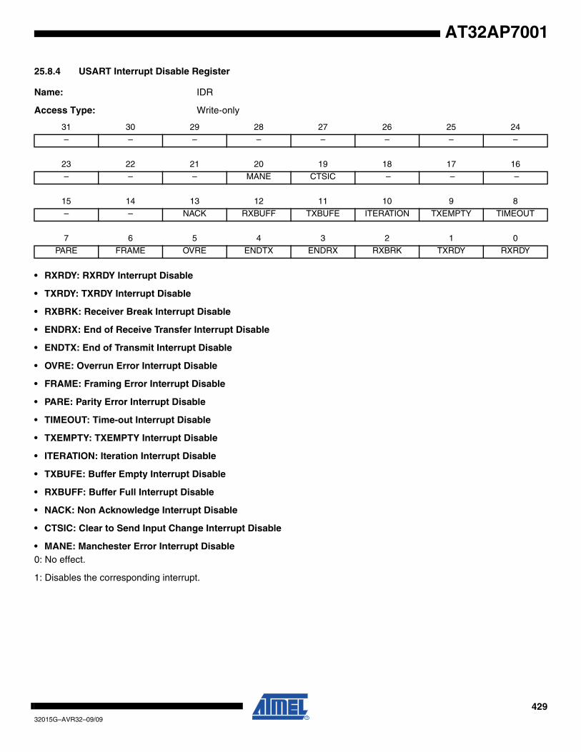
42932015G–AVR32–09/09
AT32AP7001
25.8.4 USART Interrupt Disable Register
Name: IDR
Access Type: Write-only
• RXRDY: RXRDY Interrupt Disable
• TXRDY: TXRDY Interrupt Disable
• RXBRK: Receiver Break Interrupt Disable
• ENDRX: End of Receive Transfer Interrupt Disable
• ENDTX: End of Transmit Interrupt Disable
• OVRE: Overrun Error Interrupt Disable
• FRAME: Framing Error Interrupt Disable
• PARE: Parity Error Interrupt Disable
• TIMEOUT: Time-out Interrupt Disable
• TXEMPTY: TXEMPTY Interrupt Disable
• ITERATION: Iteration Interrupt Disable
• TXBUFE: Buffer Empty Interrupt Disable
• RXBUFF: Buffer Full Interrupt Disable
• NACK: Non Acknowledge Interrupt Disable
• CTSIC: Clear to Send Input Change Interrupt Disable
• MANE: Manchester Error Interrupt Disable0: No effect.
1: Disables the corresponding interrupt.
31 30 29 28 27 26 25 24
– – – – – – – –
23 22 21 20 19 18 17 16
– – – MANE CTSIC – – –
15 14 13 12 11 10 9 8
– – NACK RXBUFF TXBUFE ITERATION TXEMPTY TIMEOUT
7 6 5 4 3 2 1 0
PARE FRAME OVRE ENDTX ENDRX RXBRK TXRDY RXRDY
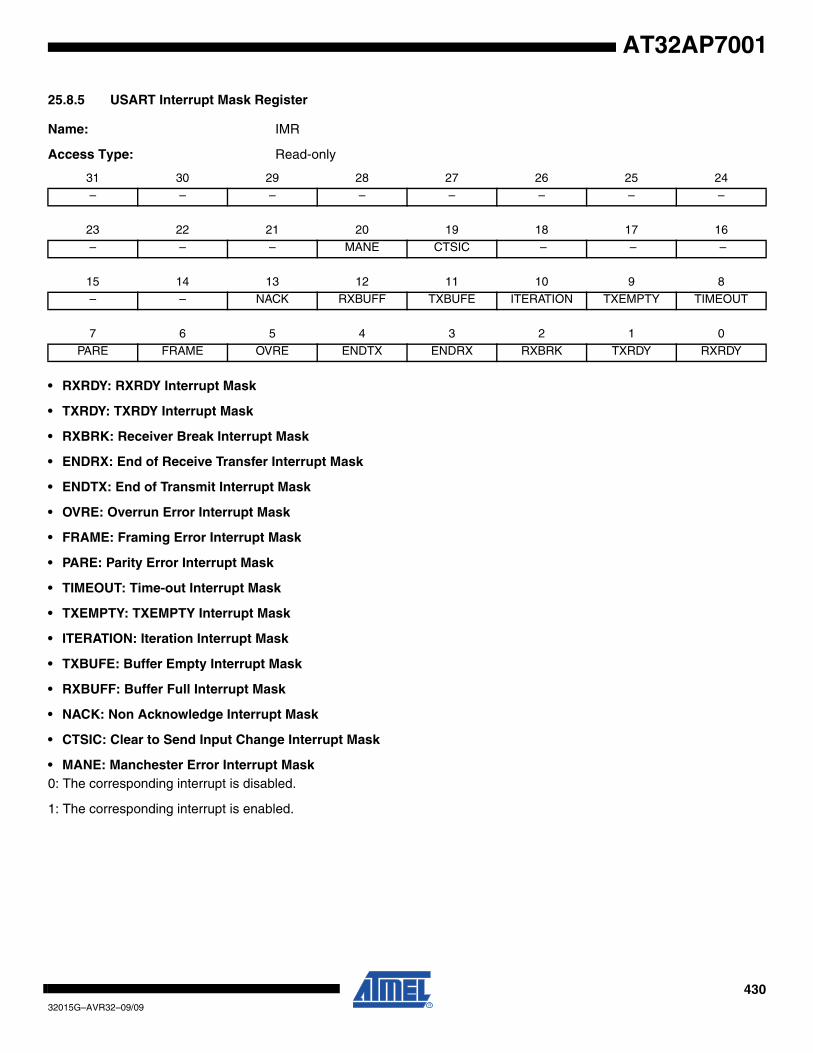
43032015G–AVR32–09/09
AT32AP7001
25.8.5 USART Interrupt Mask Register
Name: IMR
Access Type: Read-only
• RXRDY: RXRDY Interrupt Mask
• TXRDY: TXRDY Interrupt Mask
• RXBRK: Receiver Break Interrupt Mask
• ENDRX: End of Receive Transfer Interrupt Mask
• ENDTX: End of Transmit Interrupt Mask
• OVRE: Overrun Error Interrupt Mask
• FRAME: Framing Error Interrupt Mask
• PARE: Parity Error Interrupt Mask
• TIMEOUT: Time-out Interrupt Mask
• TXEMPTY: TXEMPTY Interrupt Mask
• ITERATION: Iteration Interrupt Mask
• TXBUFE: Buffer Empty Interrupt Mask
• RXBUFF: Buffer Full Interrupt Mask
• NACK: Non Acknowledge Interrupt Mask
• CTSIC: Clear to Send Input Change Interrupt Mask
• MANE: Manchester Error Interrupt Mask0: The corresponding interrupt is disabled.
1: The corresponding interrupt is enabled.
31 30 29 28 27 26 25 24
– – – – – – – –
23 22 21 20 19 18 17 16
– – – MANE CTSIC – – –
15 14 13 12 11 10 9 8
– – NACK RXBUFF TXBUFE ITERATION TXEMPTY TIMEOUT
7 6 5 4 3 2 1 0
PARE FRAME OVRE ENDTX ENDRX RXBRK TXRDY RXRDY
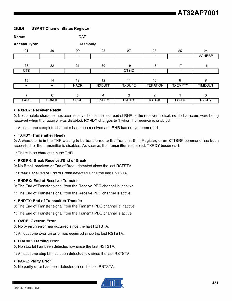
43132015G–AVR32–09/09
AT32AP7001
25.8.6 USART Channel Status Register
Name: CSR
Access Type: Read-only
• RXRDY: Receiver Ready0: No complete character has been received since the last read of RHR or the receiver is disabled. If characters were beingreceived when the receiver was disabled, RXRDY changes to 1 when the receiver is enabled.
1: At least one complete character has been received and RHR has not yet been read.
• TXRDY: Transmitter Ready0: A character is in the THR waiting to be transferred to the Transmit Shift Register, or an STTBRK command has beenrequested, or the transmitter is disabled. As soon as the transmitter is enabled, TXRDY becomes 1.
1: There is no character in the THR.
• RXBRK: Break Received/End of Break0: No Break received or End of Break detected since the last RSTSTA.
1: Break Received or End of Break detected since the last RSTSTA.
• ENDRX: End of Receiver Transfer0: The End of Transfer signal from the Receive PDC channel is inactive.
1: The End of Transfer signal from the Receive PDC channel is active.
• ENDTX: End of Transmitter Transfer0: The End of Transfer signal from the Transmit PDC channel is inactive.
1: The End of Transfer signal from the Transmit PDC channel is active.
• OVRE: Overrun Error0: No overrun error has occurred since the last RSTSTA.
1: At least one overrun error has occurred since the last RSTSTA.
• FRAME: Framing Error0: No stop bit has been detected low since the last RSTSTA.
1: At least one stop bit has been detected low since the last RSTSTA.
• PARE: Parity Error0: No parity error has been detected since the last RSTSTA.
31 30 29 28 27 26 25 24
– – – – – – – MANERR
23 22 21 20 19 18 17 16
CTS – – – CTSIC – – –
15 14 13 12 11 10 9 8
– – NACK RXBUFF TXBUFE ITERATION TXEMPTY TIMEOUT
7 6 5 4 3 2 1 0
PARE FRAME OVRE ENDTX ENDRX RXBRK TXRDY RXRDY

43232015G–AVR32–09/09
AT32AP7001
1: At least one parity error has been detected since the last RSTSTA.
• TIMEOUT: Receiver Time-out0: There has not been a time-out since the last Start Time-out command or the Time-out Register is 0.
1: There has been a time-out since the last Start Time-out command.
• TXEMPTY: Transmitter Empty0: There are characters in either THR or the Transmit Shift Register, or the transmitter is disabled.
TXEMPTY == 1 means that the transmit shift register is empty and that there is no data in THR.
• ITERATION: Max number of Repetitions Reached0: Maximum number of repetitions has not been reached since the last RSIT.
1: Maximum number of repetitions has been reached since the last RSIT.
• TXBUFE: Transmission Buffer Empty0: The signal Buffer Empty from the Transmit PDC channel is inactive.
1: The signal Buffer Empty from the Transmit PDC channel is active.
• RXBUFF: Reception Buffer Full0: The signal Buffer Full from the Receive PDC channel is inactive.
1: The signal Buffer Full from the Receive PDC channel is active.
• NACK: Non Acknowledge0: No Non Acknowledge has not been detected since the last RSTNACK.
1: At least one Non Acknowledge has been detected since the last RSTNACK.
• CTSIC: Clear to Send Input Change Flag0: No input change has been detected on the CTS pin since the last read of CSR.
1: At least one input change has been detected on the CTS pin since the last read of CSR.
• CTS: Image of CTS Input0: CTS is at 0.
1: CTS is at 1.
• MANERR: Manchester Error0: No Manchester error has been detected since the last RSTSTA.
1: At least one Manchester error has been detected since the last RSTSTA.

43332015G–AVR32–09/09
AT32AP7001
25.8.7 USART Receive Holding Register
Name: RHR
Access Type: Read-only
• RXCHR: Received CharacterLast character received if RXRDY is set.
• RXSYNH: Received Sync0: Last Character received is a Data.
1: Last Character received is a Command.
31 30 29 28 27 26 25 24
– – – – – – – –
23 22 21 20 19 18 17 16
– – – – – – – –
15 14 13 12 11 10 9 8
RXSYNH – – – – – – RXCHR
7 6 5 4 3 2 1 0
RXCHR
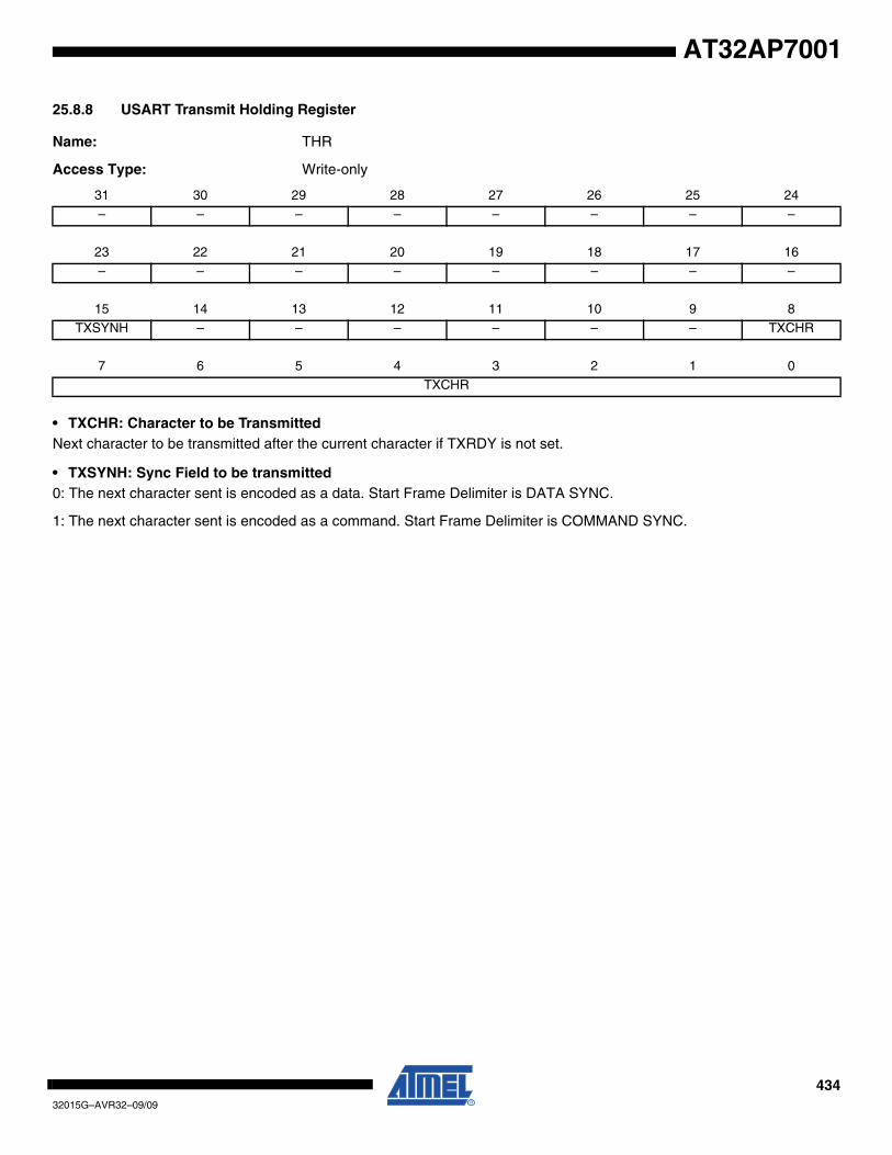
43432015G–AVR32–09/09
AT32AP7001
25.8.8 USART Transmit Holding Register
Name: THR
Access Type: Write-only
• TXCHR: Character to be TransmittedNext character to be transmitted after the current character if TXRDY is not set.
• TXSYNH: Sync Field to be transmitted0: The next character sent is encoded as a data. Start Frame Delimiter is DATA SYNC.
1: The next character sent is encoded as a command. Start Frame Delimiter is COMMAND SYNC.
31 30 29 28 27 26 25 24
– – – – – – – –
23 22 21 20 19 18 17 16
– – – – – – – –
15 14 13 12 11 10 9 8
TXSYNH – – – – – – TXCHR
7 6 5 4 3 2 1 0
TXCHR
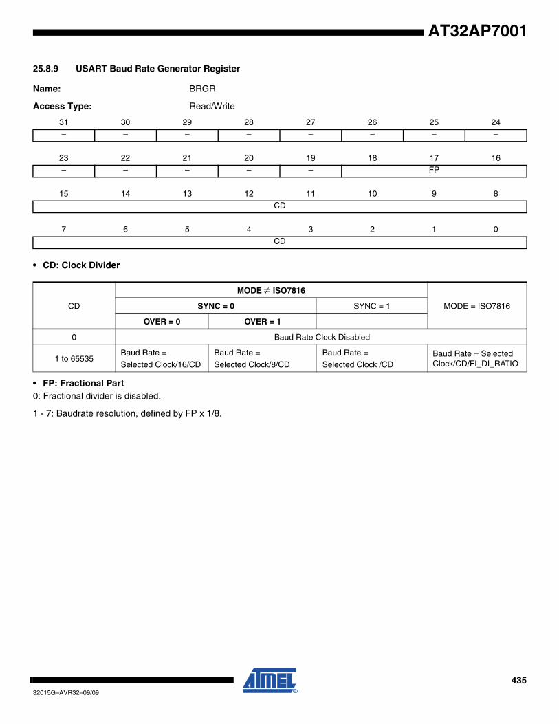
43532015G–AVR32–09/09
AT32AP7001
25.8.9 USART Baud Rate Generator Register
Name: BRGR
Access Type: Read/Write
• CD: Clock Divider
• FP: Fractional Part0: Fractional divider is disabled.
1 - 7: Baudrate resolution, defined by FP x 1/8.
31 30 29 28 27 26 25 24
– – – – – – – –
23 22 21 20 19 18 17 16
– – – – – FP
15 14 13 12 11 10 9 8
CD
7 6 5 4 3 2 1 0
CD
CD
MODE ≠ ISO7816
MODE = ISO7816SYNC = 0 SYNC = 1
OVER = 0 OVER = 1
0 Baud Rate Clock Disabled
1 to 65535Baud Rate =
Selected Clock/16/CD
Baud Rate =
Selected Clock/8/CD
Baud Rate =
Selected Clock /CDBaud Rate = Selected Clock/CD/FI_DI_RATIO
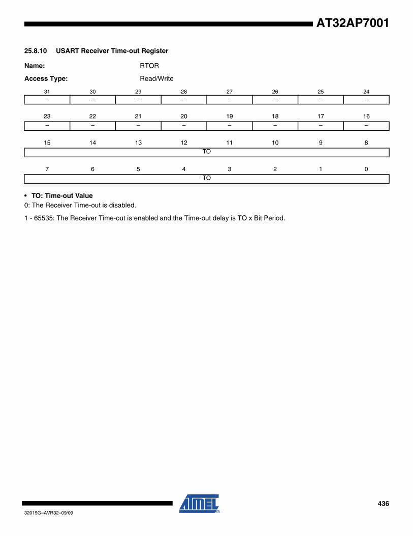
43632015G–AVR32–09/09
AT32AP7001
25.8.10 USART Receiver Time-out Register
Name: RTOR
Access Type: Read/Write
• TO: Time-out Value0: The Receiver Time-out is disabled.
1 - 65535: The Receiver Time-out is enabled and the Time-out delay is TO x Bit Period.
31 30 29 28 27 26 25 24– – – – – – – –
23 22 21 20 19 18 17 16– – – – – – – –
15 14 13 12 11 10 9 8TO
7 6 5 4 3 2 1 0TO
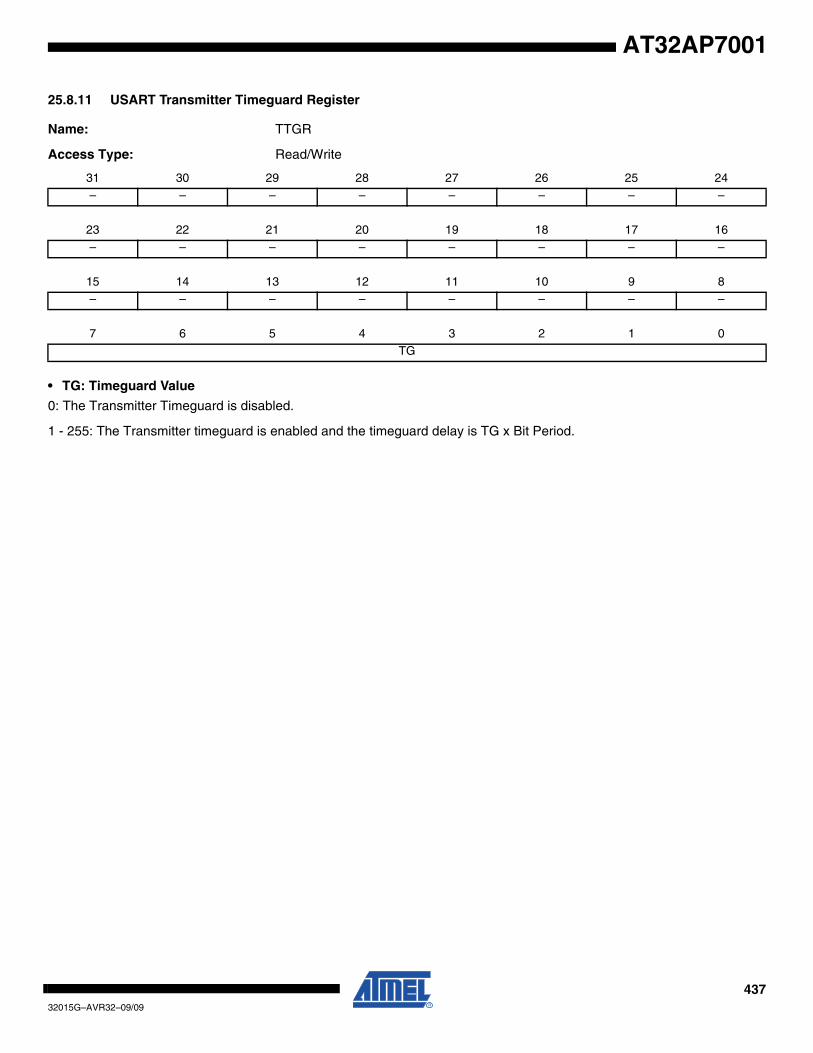
43732015G–AVR32–09/09
AT32AP7001
25.8.11 USART Transmitter Timeguard Register
Name: TTGR
Access Type: Read/Write
• TG: Timeguard Value
0: The Transmitter Timeguard is disabled.
1 - 255: The Transmitter timeguard is enabled and the timeguard delay is TG x Bit Period.
31 30 29 28 27 26 25 24
– – – – – – – –
23 22 21 20 19 18 17 16
– – – – – – – –
15 14 13 12 11 10 9 8
– – – – – – – –
7 6 5 4 3 2 1 0
TG
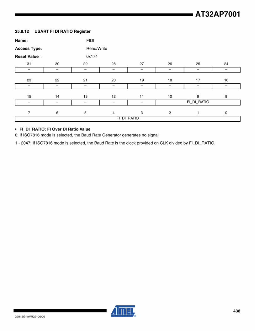
43832015G–AVR32–09/09
AT32AP7001
25.8.12 USART FI DI RATIO Register
Name: FIDI
Access Type: Read/Write
Reset Value : 0x174
• FI_DI_RATIO: FI Over DI Ratio Value0: If ISO7816 mode is selected, the Baud Rate Generator generates no signal.
1 - 2047: If ISO7816 mode is selected, the Baud Rate is the clock provided on CLK divided by FI_DI_RATIO.
31 30 29 28 27 26 25 24
– – – – – – – –
23 22 21 20 19 18 17 16
– – – – – – – –
15 14 13 12 11 10 9 8
– – – – – FI_DI_RATIO
7 6 5 4 3 2 1 0
FI_DI_RATIO
43932015G–AVR32–09/09
AT32AP7001
25.8.13 USART Number of Errors Register
Name: NER
Access Type: Read-only
• NB_ERRORS: Number of ErrorsTotal number of errors that occurred during an ISO7816 transfer. This register automatically clears when read.
31 30 29 28 27 26 25 24
– – – – – – – –
23 22 21 20 19 18 17 16
– – – – – – – –
15 14 13 12 11 10 9 8
– – – – – – – –
7 6 5 4 3 2 1 0
NB_ERRORS
44032015G–AVR32–09/09
AT32AP7001
25.8.14 USART Manchester Configuration Register
Name: MAN
Access Type: Read/Write
• TX_PL: Transmitter Preamble Length0: The Transmitter Preamble pattern generation is disabled
1 - 15: The Preamble Length is TX_PL x Bit Period
• TX_PP: Transmitter Preamble Pattern
• TX_MPOL: Transmitter Manchester Polarity0: Logic Zero is coded as a zero-to-one transition, Logic One is coded as a one-to-zero transition.
1: Logic Zero is coded as a one-to-zero transition, Logic One is coded as a zero-to-one transition.
• RX_PL: Receiver Preamble Length0: The receiver preamble pattern detection is disabled
1 - 15: The detected preamble length is RX_PL x Bit Period
• RX_PP: Receiver Preamble Pattern detected
• RX_MPOL: Receiver Manchester Polarity0: Logic Zero is coded as a zero-to-one transition, Logic One is coded as a one-to-zero transition.
31 30 29 28 27 26 25 24
– DRIFT – RX_MPOL – – RX_PP
23 22 21 20 19 18 17 16
– – – – RX_PL
15 14 13 12 11 10 9 8
– – – TX_MPOL – – TX_PP
7 6 5 4 3 2 1 0
– – – – TX_PL
TX_PP Preamble Pattern default polarity assumed (TX_MPOL field not set)
0 0 ALL_ONE
0 1 ALL_ZERO
1 0 ZERO_ONE
1 1 ONE_ZERO
RX_PP Preamble Pattern default polarity assumed (RX_MPOL field not set)
0 0 ALL_ONE
0 1 ALL_ZERO
1 0 ZERO_ONE
1 1 ONE_ZERO

44132015G–AVR32–09/09
AT32AP7001
1: Logic Zero is coded as a one-to-zero transition, Logic One is coded as a zero-to-one transition.
• DRIFT: Drift compensation0: The USART can not recover from an important clock drift
1: The USART can recover from clock drift. The 16X clock mode must be enabled.
44232015G–AVR32–09/09
AT32AP7001
25.8.15 USART IrDA FILTER Register
Name: IFR
Access Type: Read/Write
• IRDA_FILTER: IrDA FilterSets the filter of the IrDA demodulator.
25.9 USART Version RegisterName: US_VERSION
Access Type: Read-only
• VERSIONReserved. Value subject to change. No functionality associated. This is the Atmel internal version of the macrocell.
• MFNReserved. Value subject to change. No functionality associated.
31 30 29 28 27 26 25 24
– – – – – – – –
23 22 21 20 19 18 17 16
– – – – – – – –
15 14 13 12 11 10 9 8
– – – – – – – –
7 6 5 4 3 2 1 0
IRDA_FILTER
31 30 29 28 27 26 25 24
– – – – – – – –
23 22 21 20 19 18 17 16
– – – – – MFN
15 14 13 12 11 10 9 8
– – – – VERSION
7 6 5 4 3 2 1 0
VERSION
44332015G–AVR32–09/09
AT32AP7001
26. AC97 Controller (AC97C)
Rev: 2.1.0.0
26.1 Features• Compliant with AC97 2.2 Component Specification• 2 independent communication channels
– Codec Channel, dedicated to the AC97 Analog Front End Control and Status Monitoring– 2 channels associated with DMA Controller interface for Isochronous Audio Streaming
Transfer• Variable Sampling Rate AC97 Codec Interface Support• One Primary Codec Support• Independent input and Output Slot to Channel Assignment, Several Slots Can Be Assigned to the
Same Channel. • Channels Support Mono/Stereo/Multichannel Samples of 10, 16, 18 and 20 Bits.
26.2 DescriptionThe AC97 Controller is the hardware implementation of the AC97 digital controller (DC’97) com-pliant with AC97 Component Specification 2.2. The AC97 Controller communicates with anaudio codec (AC97) or a modem codec (MC’97) via the AC-link digital serial interface. All digitalaudio, modem and handset data streams, as well as control (command/status) informations aretransferred in accordance to the AC-link protocol.
The AC97 Controller features a DMA Controller interface for audio streaming transfers. It alsosupports variable sampling rate and four Pulse Code Modulation (PCM) sample resolutions of10, 16, 18 and 20 bits.
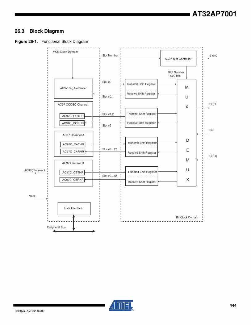
44432015G–AVR32–09/09
AT32AP7001
26.3 Block Diagram
Figure 26-1. Functional Block Diagram
AC97 Channel A
AC97C_CATHR
AC97C_CARHRSlot #3...12
AC97 CODEC Channel
AC97C_COTHR
AC97C_CORHRSlot #2
Slot #1,2
AC97 Channel B
AC97C_CBTHR
AC97C_CBRHRSlot #3...12
AC97 Tag ControllerTransmit Shift Register
Receive Shift Register
Receive Shift Register
Receive Shift Register
Receive Shift Register
Transmit Shift Register
Transmit Shift Register
Transmit Shift Register
Slot #0
Slot #0,1
AC97 Slot Controller
Slot Number16/20 bits
Slot Number
SDI
SCLK
SDO
SYNC
User Interface
MCK Clock Domain
Bit Clock Domain
AC97C Interrupt
MCK
Peripheral Bus
M
U
X
D
E
M
U
X
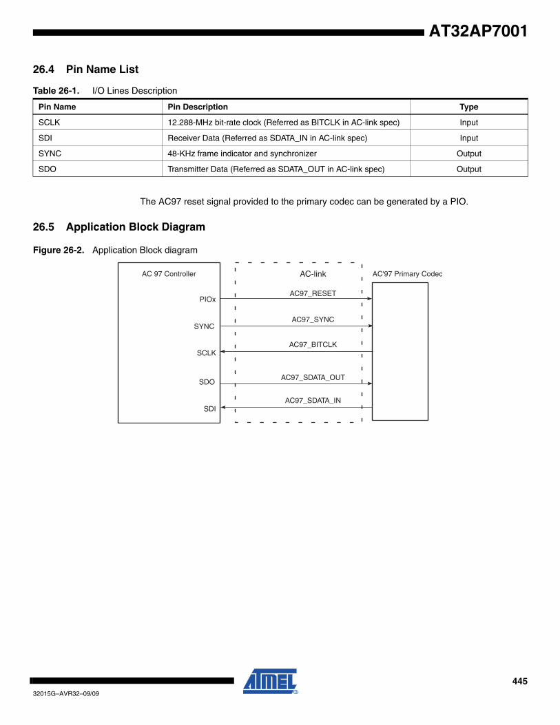
44532015G–AVR32–09/09
AT32AP7001
26.4 Pin Name List
The AC97 reset signal provided to the primary codec can be generated by a PIO.
26.5 Application Block Diagram
Figure 26-2. Application Block diagram
Table 26-1. I/O Lines Description
Pin Name Pin Description Type
SCLK 12.288-MHz bit-rate clock (Referred as BITCLK in AC-link spec) Input
SDI Receiver Data (Referred as SDATA_IN in AC-link spec) Input
SYNC 48-KHz frame indicator and synchronizer Output
SDO Transmitter Data (Referred as SDATA_OUT in AC-link spec) Output
AC 97 Controller
SDO
SDI
PIOx
AC'97 Primary Codec
SYNC
SCLK
AC97_RESET
AC97_SYNC
AC97_SDATA_OUT
AC97_BITCLK
AC-link
AC97_SDATA_IN

44632015G–AVR32–09/09
AT32AP7001
26.6 Product Dependencies
26.6.1 I/O LinesThe pins used for interfacing the compliant external devices may be multiplexed with PIO lines.
Before using the AC97 Controller receiver, the PIO controller must be configured in order for theAC97C receiver I/O lines to be in AC97 Controller peripheral mode.
Before using the AC97 Controller transmitter, the PIO controller must be configured in order forthe AC97C transmitter I/O lines to be in AC97 Controller peripheral mode.
26.6.2 Power ManagementThe AC97 clock is generated by the power manager. Before using the AC97, the programmermust ensure that the AC’97 clock is enabled in the power manager.
In the AC97 description, Master Clock (MCK) is the clock of the peripheral bus to which theAC97 is connected. It is important that that the MCK clock frequency is higher than the SCLK(Bit Clock) clock frequancy as signals that cross the two clock domains are re-synchronized.
26.6.3 InterruptThe AC97 interface has an interrupt line connected to the interrupt controller. In order to handleinterrupts, the interrupt controller must be programmed before configuring the AC97.
All AC97 Controller interrupts can be enabled/disabled by writing to the AC97 Controller Inter-rupt Enable/Disable Registers. Each pending and unmasked AC97 Controller interrupt willassert the interrupt line. The AC97 Controller interrupt service routine can get the interruptsource in two steps:
•Reading and ANDing AC97 Controller Interrupt Mask Register (IMR) and AC97 Controller Status Register (SR).
•Reading AC97 Controller Channel x Status Register (CxSR).)
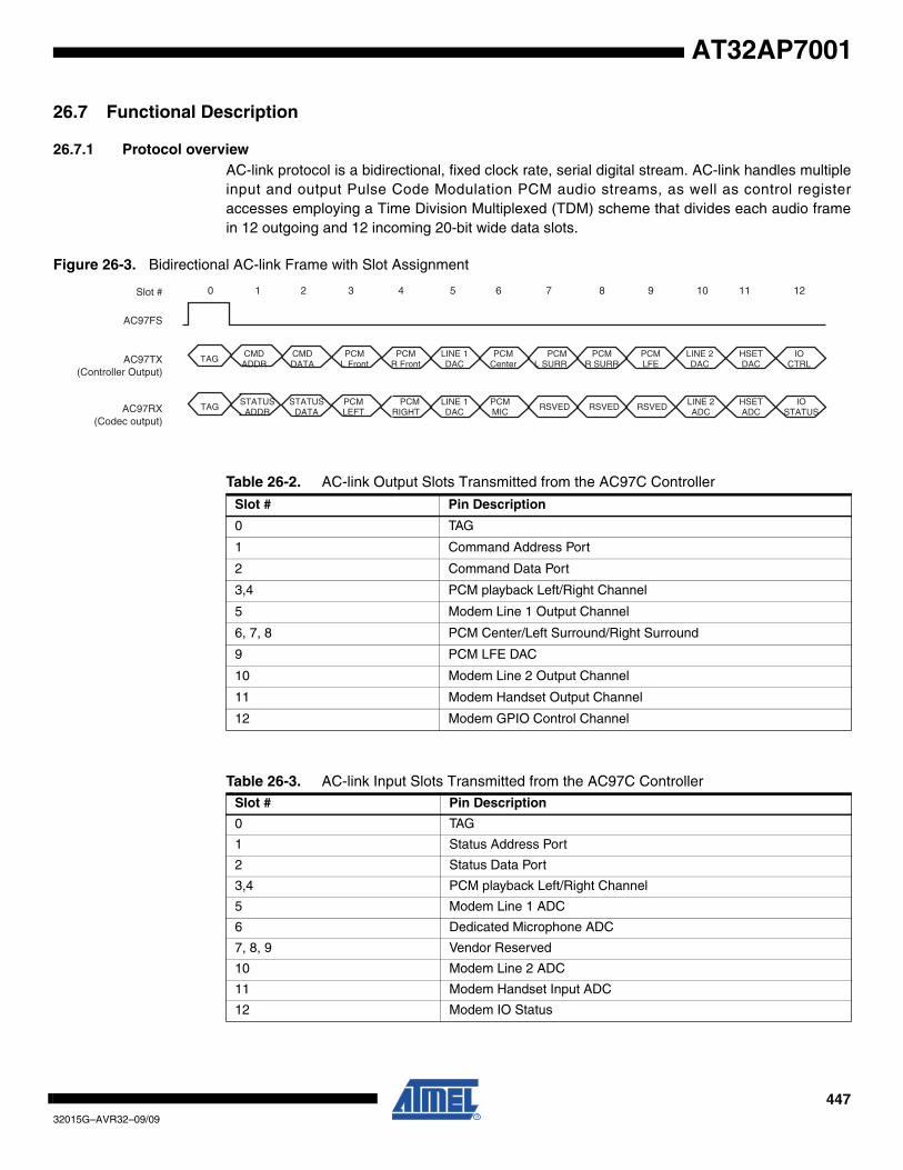
44732015G–AVR32–09/09
AT32AP7001
26.7 Functional Description
26.7.1 Protocol overviewAC-link protocol is a bidirectional, fixed clock rate, serial digital stream. AC-link handles multipleinput and output Pulse Code Modulation PCM audio streams, as well as control registeraccesses employing a Time Division Multiplexed (TDM) scheme that divides each audio framein 12 outgoing and 12 incoming 20-bit wide data slots.
Figure 26-3. Bidirectional AC-link Frame with Slot Assignment
Slot #
AC97FS
TAGCMD
ADDRCMDDATA
0
AC97TX(Controller Output)
AC97RX(Codec output)
PCML Front
PCMR Front
LINE 1DAC
PCMCenter
PCMR SURR
PCMLFE
LINE 2DAC
HSETDAC
IOCTRL
TAGSTATUS
ADDRSTATUS
DATAPCMLEFT
LINE 1DAC
PCMMIC
RSVED RSVED RSVEDLINE 2ADC
HSETADC
IOSTATUS
1 2 3 4 5 6 7 8 9 10 11 12
PCML SURR
PCMRIGHT
Table 26-2. AC-link Output Slots Transmitted from the AC97C Controller
Slot # Pin Description
0 TAG
1 Command Address Port
2 Command Data Port
3,4 PCM playback Left/Right Channel
5 Modem Line 1 Output Channel
6, 7, 8 PCM Center/Left Surround/Right Surround
9 PCM LFE DAC
10 Modem Line 2 Output Channel
11 Modem Handset Output Channel
12 Modem GPIO Control Channel
Table 26-3. AC-link Input Slots Transmitted from the AC97C ControllerSlot # Pin Description
0 TAG
1 Status Address Port
2 Status Data Port
3,4 PCM playback Left/Right Channel
5 Modem Line 1 ADC
6 Dedicated Microphone ADC
7, 8, 9 Vendor Reserved
10 Modem Line 2 ADC
11 Modem Handset Input ADC
12 Modem IO Status

44832015G–AVR32–09/09
AT32AP7001
26.7.2 Slot Description
26.7.2.1 Tag SlotThe tag slot, or slot 0, is a 16-bit wide slot that always goes at the beginning of an outgoing orincoming frame. Within tag slot, the first bit is a global bit that flags the entire frame validity. Thenext 12 bit positions sampled by the AC97 Controller indicate which of the corresponding 12time slots contain valid data. The slot’s last two bits (combined) called Codec ID, are used to dis-tinguish primary and secondary codec.
The 16-bit wide tag slot of the output frame is automatically generated by the AC97 Controlleraccording to the transmit request of each channel and to the SLOTREQ from the previous inputframe, sent by the AC97 Codec, in Variable Sample Rate mode.
26.7.2.2 Codec Slot 1The command/status slot is a 20-bit wide slot used to control features, and monitors status forAC97 Codec functions.
The control interface architecture supports up to sixty-four 16-bit wide read/write registers. Onlythe even registers are currently defined and addressed.
Slot 1’s bitmap is the following:
•Bit 19 is for read/write command, 1= read, 0 = write.
•Bits [18:12] are for control register index.
•Bits [11:0] are reserved.
26.7.2.3 Codec Slot 2Slot 2 is a 20-bit wide slot used to carry 16-bit wide AC97 Codec control register data. If the cur-rent command port operation is a read, the entire slot time is stuffed with zeros. Its bitmap is thefollowing:
•Bits [19:4] are the control register data
•Bits [3:0] are reserved and stuffed with zeros.
26.7.2.4 Data Slots [3:12]Slots [3:12] are 20-bit wide data slots, they usually carry audio PCM or/and modem I/O data.
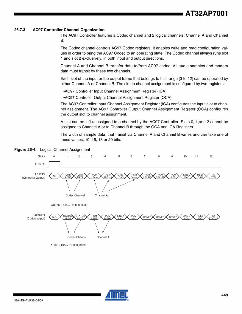
44932015G–AVR32–09/09
AT32AP7001
26.7.3 AC97 Controller Channel OrganizationThe AC97 Controller features a Codec channel and 2 logical channels; Channel A and ChannelB.
The Codec channel controls AC97 Codec registers, it enables write and read configuration val-ues in order to bring the AC97 Codec to an operating state. The Codec channel always runs slot1 and slot 2 exclusively, in both input and output directions.
Channel A and Channel B transfer data to/from AC97 codec. All audio samples and modemdata must transit by these two channels.
Each slot of the input or the output frame that belongs to this range [3 to 12] can be operated byeither Channel A or Channel B. The slot to channel assignment is configured by two registers:
•AC97 Controller Input Channel Assignment Register (ICA)
•AC97 Controller Output Channel Assignment Register (OCA)
The AC97 Controller Input Channel Assignment Register (ICA) configures the input slot to chan-nel assignment. The AC97 Controller Output Channel Assignment Register (OCA) configuresthe output slot to channel assignment.
A slot can be left unassigned to a channel by the AC97 Controller. Slots 0, 1,and 2 cannot beassigned to Channel A or to Channel B through the OCA and ICA Registers.
The width of sample data, that transit via Channel A and Channel B varies and can take one ofthese values; 10, 16, 18 or 20 bits.
Figure 26-4. Logical Channel Assignment
Slot #
AC97FS
TAG CMDDATA
0
AC97TX(Controller Output)
AC97RX(Codec output)
PCML Front
PCMR Front
LINE 1DAC
PCMCenter
PCML SURR
PCMR SURR
PCMLFE
LINE 2DAC
HSETDAC
IOCTRL
TAG STATUSADDR
STATUSDATA
PCMLEFT
PCMRIGHT
LINE 1DAC
PCMMIC RSVED RSVED RSVED LINE 2
ADCHSETADC
IOSTATUS
1 2 3 4 5 6 7 8 9 10 11 12
Codec Channel Channel A
Codec Channel Channel A
AC97C_OCA = 0x0000_0209
AC97C_ICA = 0x0000_0009
CMDADDR
45032015G–AVR32–09/09
AT32AP7001
26.7.3.1 AC97 Controller SetupThe following operations must be performed in order to bring the AC97 Controller into an operat-ing state:
1. Enable the AC97 Controller clock in the power manager.
2. Turn on AC97 function by enabling the ENA bit in AC97 Controller Mode Register (MR).
3. Configure the input channel assignment by controlling the AC97 Controller Input Assign-ment Register (ICA).
4. Configure the output channel assignment by controlling the AC97 Controller Input Assignment Register (OCA).
5. Configure sample width for Channel A and Channel B by writing the SIZE bit field in AC97C Channel A Mode Register (CAMR) and AC97C Channel B Mode Register (CBMR). The application can write 10, 16, 18,or 20-bit wide PCM samples through the AC97 interface and they will be transferred into 20-bit wide slots.
6. Configure data Endianness for Channel A and Channel B by writing CEM bit field in CAMR and CBMR registers. Data on the AC-link are shifted MSB first. The application can write little- or big-endian data to the AC97 Controller interface.
7. Configure the PIO controller to drive the RESET signal of the external Codec. The RESET signal must fulfill external AC97 Codec timing requirements.
8. Enable Channel A and/or Channel B by writing CEN bit field in CAMR and CBMR registers.
26.7.3.2 Transmit OperationThe application must perform the following steps in order to send data via a channel to the AC97Codec:
•Check if previous data has been sent by polling TXRDY flag in the AC97C Channel x Status Register (CxSR). x being one of the 2 channels.
•Write data to the AC97 Controller Channel x Transmit Holding Register (CxTHR).
Once data has been transferred to the Channel x Shift Register, the TXRDY flag is automaticallyset by the AC97 Controller which allows the application to start a new write action. The applica-tion can also wait for an interrupt notice associated with TXRDY in order to send data. Theinterrupt remains active until TXRDY flag is cleared..
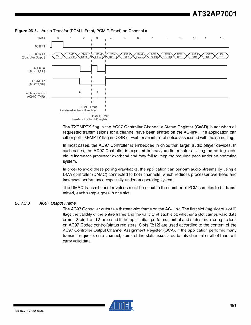
45132015G–AVR32–09/09
AT32AP7001
Figure 26-5. Audio Transfer (PCM L Front, PCM R Front) on Channel x
The TXEMPTY flag in the AC97 Controller Channel x Status Register (CxSR) is set when allrequested transmissions for a channel have been shifted on the AC-link. The application caneither poll TXEMPTY flag in CxSR or wait for an interrupt notice associated with the same flag.
In most cases, the AC97 Controller is embedded in chips that target audio player devices. Insuch cases, the AC97 Controller is exposed to heavy audio transfers. Using the polling tech-nique increases processor overhead and may fail to keep the required pace under an operatingsystem.
In order to avoid these polling drawbacks, the application can perform audio streams by using aDMA controller (DMAC) connected to both channels, which reduces processor overhead andincreases performance especially under an operating system.
The DMAC transmit counter values must be equal to the number of PCM samples to be trans-mitted, each sample goes in one slot.
26.7.3.3 AC97 Output FrameThe AC97 Controller outputs a thirteen-slot frame on the AC-Link. The first slot (tag slot or slot 0)flags the validity of the entire frame and the validity of each slot; whether a slot carries valid dataor not. Slots 1 and 2 are used if the application performs control and status monitoring actionson AC97 Codec control/status registers. Slots [3:12] are used according to the content of theAC97 Controller Output Channel Assignment Register (OCA). If the application performs manytransmit requests on a channel, some of the slots associated to this channel or all of them willcarry valid data.
Slot #
AC97FS
TAGCMDADDR
CMDDATA
0
AC97TX(Controller Output)
PCML Front
PCMR Front
LINE 1DAC
PCMCenter
PCML SURR
PCMR SURR
PCMLFE
LINE 2DAC
HSETDAC
IOCTRL
1 2 3 4 5 6 7 8 9 10 11 12
TXRDYCx(AC97C_SR)
Write access toAC97C_THRx
PCM L Fronttransfered to the shift register
PCM R Fronttransfered to the shift register
TXEMPTY(AC97C_SR)

45232015G–AVR32–09/09
AT32AP7001
26.7.3.4 Receive OperationThe AC97 Controller can also receive data from AC97 Codec. Data is received in the channel’sshift register and then transferred to the AC97 Controller Channel x Read Holding Register. Toread the newly received data, the application must perform the following steps:
•Poll RXRDY flag in AC97 Controller Channel x Status Register (CxSR). x being one of the 2 channels.
•Read data from AC97 Controller Channel x Read Holding Register.
The application can also wait for an interrupt notice in order to read data from CxRHR. The inter-rupt remains active until RXRDY is cleared by reading CxSR.
The RXRDY flag in CxSR is set automatically when data is received in the Channel x shift regis-ter. Data is then shifted to CxRHR.
Figure 26-6. Audio Transfer (PCM L Front, PCM R Front) on Channel x
If the previously received data has not been read by the application, the new data overwrites thedata already waiting in CxRHR, therefore the OVRUN flag in CxSR is raised. The applicationcan either poll the OVRUN flag in CxSR or wait for an interrupt notice. The interrupt remainsactive until the OVRUN flag in CxSR is set.
The AC97 Controller can also be used in sound recording devices in association with an AC97Codec. The AC97 Controller may also be exposed to heavy PCM transfers.
The application can use the DMAC connected to both channels in order to reduce processoroverhead and increase performance especially under an operating system.
The DMAC receive counter values must be equal to the number of PCM samples to be received.When more than one timeslot is assigned to a channel using DMA, the different timeslot sam-ples will be interleaved.
26.7.3.5 AC97 Input FrameThe AC97 Controller receives a thirteen slot frame on the AC-Link sent by the AC97 Codec. Thefirst slot (tag slot or slot 0) flags the validity of the entire frame and the validity of each slot;whether a slot carries valid data or not. Slots 1 and 2 are used if the application requires statusinformations from AC97 Codec. Slots [3:12] are used according to AC97 Controller OutputChannel Assignment Register (ICA) content. The AC97 Controller will not receive any data fromany slot if ICA is not assigned to a channel in input.
Slot #
AC97FS
0 1 2 3 4 5 6 7 8 9 10 11 12
RXRDYCx(AC97C_SR)
Read access toAC97C_RHRx
AC97RX(Codec output)
TAGSTATUSADDR
STATUSDATA
PCMLEFT
PCMRIGHT
LINE 1DAC
PCMMIC
RSVED RSVED RSVEDLINE 2ADC
HSETADC
IOSTATUS
45332015G–AVR32–09/09
AT32AP7001
26.7.3.6 Configuring and Using InterruptsInstead of polling flags in AC97 Controller Global Status Register (SR) and in AC97 ControllerChannel x Status Register (CxSR), the application can wait for an interrupt notice. The followingsteps show how to configure and use interrupts correctly:
•Set the interruptible flag in AC97 Controller Channel x Mode Register (CxMR).
•Set the interruptible event and channel event in AC97 Controller Interrupt Enable Register (IER).
The interrupt handler must read both AC97 Controller Global Status Register (SR) and AC97Controller Interrupt Mask Register (IMR) and AND them to get the real interrupt source. Further-more, to get which event was activated, the interrupt handler has to read AC97 ControllerChannel x Status Register (CxSR), x being the channel whose event triggers the interrupt.
The application can disable event interrupts by writing in AC97 Controller Interrupt Disable Reg-ister (IDR). The AC97 Controller Interrupt Mask Register (IMR) shows which event can triggeran interrupt and which one cannot.
26.7.3.7 EndiannessEndianness can be managed automatically for each channel, except for the Codec channel, bywriting to Channel Endianness Mode (CEM) in CxMR. This enables transferring data on AC-linkin Little Endian format without any additional operation.
26.7.3.8 To Transmit a Word Stored in Little Endian Format on AC-linkWord to be written in AC97 Controller Channel x Transmit Holding Register (CxTHR) (as it isstored in memory or microprocessor register).
Word stored in Channel x Transmit Holding Register (AC97C_CxTHR) (data to transmit).
Data transmitted on appropriate slot: data[19:0] = {Byte1[3:0], Byte2[7:0], Byte3[7:0]}.
26.7.3.9 To Transmit A Halfword Stored in Little Endian Format on AC-linkHalfword to be written in AC97 Controller Channel x Transmit Holding Register (CxTHR).
Halfword stored in AC97 Controller Channel x Transmit Holding Register (CxTHR) (data totransmit).
Data emitted on related slot: data[19:0] = {Byte1[7:0], Byte0[7:0], 0x0}.
31 24 23 16 15 8 7 0
Byte3[7:0] Byte2[7:0] Byte1[7:0] Byte0[7:0]
31 24 23 20 19 16 15 8 7 0
– – Byte1[3:0] Byte2[7:0] Byte3[7:0]
31 24 23 16 15 8 7 0
– – Byte0[7:0] Byte1[7:0]
31 24 23 16 15 8 7 0
– – Byte1[7:0] Byte0[7:0]
45432015G–AVR32–09/09
AT32AP7001
26.7.3.10 To Transmit a10-bit Sample Stored in Little Endian Format on AC-linkHalfword to be written in AC97 Controller Channel x Transmit Holding Register (CxTHR).
Halfword stored in AC97 Controller Channel x Transmit Holding Register (CxTHR) (data totransmit).
Data emitted on related slot: data[19:0] = {Byte1[1:0], Byte0[7:0], 0x000}.
26.7.3.11 To Receive Word transfersData received on appropriate slot: data[19:0] = {Byte2[3:0], Byte1[7:0], Byte0[7:0]}.
Word stored in AC97 Controller Channel x Receive Holding Register (CxRHR) (Received Data).
Data is read from AC97 Controller Channel x Receive Holding Register (CxRHR) when Channelx data size is greater than 16 bits and when little endian mode is enabled (data written tomemory).
26.7.3.12 To Receive Halfword TransfersData received on appropriate slot: data[19:0] = {Byte1[7:0], Byte0[7:0], 0x0 }.
Halfword stored in AC97 Controller Channel x Receive Holding Register (CxRHR) (ReceivedData).
Data is read from AC97 Controller Channel x Receive Holding Register (CxRHR) when data sizeis equal to 16 bits and when little endian mode is enabled.
26.7.3.13 To Receive 10-bit SamplesData received on appropriate slot: data[19:0] = {Byte1[1:0], Byte0[7:0], 0x000}. Halfword storedin AC97 Controller Channel x Receive Holding Register (CxRHR) (Received Data)
31 24 23 16 15 8 7 0
– – Byte0[7:0] {0x00, Byte1[1:0]}
31 24 23 16 15 10 9 8 7 0
– – –Byte1 [1:0]
Byte0[7:0]
31 24 23 20 19 16 15 8 7 0
– – Byte2[3:0] Byte1[7:0] Byte0[7:0]
31 24 23 16 15 8 7 0
Byte0[7:0] Byte1[7:0] {0x0, Byte2[3:0]} 0x00
31 24 23 16 15 8 7 0
– – Byte1[7:0] Byte0[7:0]
31 24 23 16 15 8 7 0– – Byte0[7:0] Byte1[7:0]
31 24 23 16 15 10 9 8 7 0
– – –Byte1 [1:0]
Byte0[7:0]
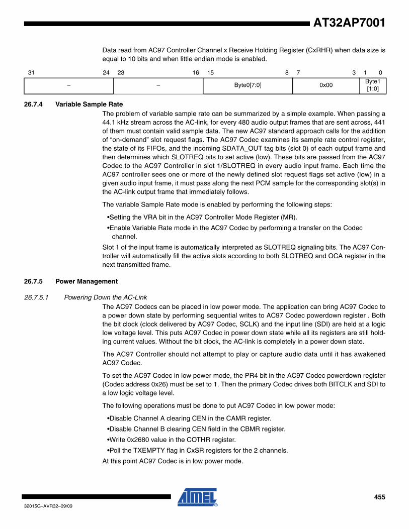
45532015G–AVR32–09/09
AT32AP7001
Data read from AC97 Controller Channel x Receive Holding Register (CxRHR) when data size isequal to 10 bits and when little endian mode is enabled.
26.7.4 Variable Sample RateThe problem of variable sample rate can be summarized by a simple example. When passing a44.1 kHz stream across the AC-link, for every 480 audio output frames that are sent across, 441of them must contain valid sample data. The new AC97 standard approach calls for the additionof “on-demand” slot request flags. The AC97 Codec examines its sample rate control register,the state of its FIFOs, and the incoming SDATA_OUT tag bits (slot 0) of each output frame andthen determines which SLOTREQ bits to set active (low). These bits are passed from the AC97Codec to the AC97 Controller in slot 1/SLOTREQ in every audio input frame. Each time theAC97 controller sees one or more of the newly defined slot request flags set active (low) in agiven audio input frame, it must pass along the next PCM sample for the corresponding slot(s) inthe AC-link output frame that immediately follows.
The variable Sample Rate mode is enabled by performing the following steps:
•Setting the VRA bit in the AC97 Controller Mode Register (MR).
•Enable Variable Rate mode in the AC97 Codec by performing a transfer on the Codec channel.
Slot 1 of the input frame is automatically interpreted as SLOTREQ signaling bits. The AC97 Con-troller will automatically fill the active slots according to both SLOTREQ and OCA register in thenext transmitted frame.
26.7.5 Power Management
26.7.5.1 Powering Down the AC-LinkThe AC97 Codecs can be placed in low power mode. The application can bring AC97 Codec toa power down state by performing sequential writes to AC97 Codec powerdown register . Boththe bit clock (clock delivered by AC97 Codec, SCLK) and the input line (SDI) are held at a logiclow voltage level. This puts AC97 Codec in power down state while all its registers are still hold-ing current values. Without the bit clock, the AC-link is completely in a power down state.
The AC97 Controller should not attempt to play or capture audio data until it has awakenedAC97 Codec.
To set the AC97 Codec in low power mode, the PR4 bit in the AC97 Codec powerdown register(Codec address 0x26) must be set to 1. Then the primary Codec drives both BITCLK and SDI toa low logic voltage level.
The following operations must be done to put AC97 Codec in low power mode:
•Disable Channel A clearing CEN in the CAMR register.
•Disable Channel B clearing CEN field in the CBMR register.
•Write 0x2680 value in the COTHR register.
•Poll the TXEMPTY flag in CxSR registers for the 2 channels.
At this point AC97 Codec is in low power mode.
31 24 23 16 15 8 7 3 1 0
– – Byte0[7:0] 0x00Byte1 [1:0]
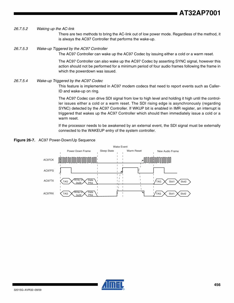
45632015G–AVR32–09/09
AT32AP7001
26.7.5.2 Waking up the AC-linkThere are two methods to bring the AC-link out of low power mode. Regardless of the method, itis always the AC97 Controller that performs the wake-up.
26.7.5.3 Wake-up Tiggered by the AC97 ControllerThe AC97 Controller can wake up the AC97 Codec by issuing either a cold or a warm reset.
The AC97 Controller can also wake up the AC97 Codec by asserting SYNC signal, however thisaction should not be performed for a minimum period of four audio frames following the frame inwhich the powerdown was issued.
26.7.5.4 Wake-up Triggered by the AC97 CodecThis feature is implemented in AC97 modem codecs that need to report events such as Caller-ID and wake-up on ring.
The AC97 Codec can drive SDI signal from low to high level and holding it high until the control-ler issues either a cold or a warm reset. The SDI rising edge is asynchronously (regardingSYNC) detected by the AC97 Controller. If WKUP bit is enabled in IMR register, an interrupt istriggered that wakes up the AC97 Controller which should then immediately issue a cold or awarm reset.
If the processor needs to be awakened by an external event, the SDI signal must be externallyconnected to the WAKEUP entry of the system controller.
Figure 26-7. AC97 Power-Down/Up Sequence
AC97CK
AC97FS
TAGWrite to 0x26
DataPR4
Power Down Frame Sleep State
TAGWrite to 0x26
DataPR4
Wake Event
Warm Reset New Audio Frame
TAG Slot1 Slot2
AC97TX
AC97RX
TAG Slot1 Slot2
45732015G–AVR32–09/09
AT32AP7001
26.7.5.5 AC97 Codec ResetThere are three ways to reset an AC97 Codec.
26.7.5.6 Cold AC97 ResetA cold reset is generated by asserting the RESET signal low for the minimum specified time(depending on the AC97 Codec) and then by de-asserting RESET high. BITCLK and SYNC isreactivated and all AC97 Codec registers are set to their default power-on values. Transfers onAC-link can resume.
The RESET signal will be controlled via a PIO line. This is how an application should perform acold reset:
•Clear and set ENA flag in the MR register to reset the AC97 Controller
•Clear PIO line output controlling the AC97 RESET signal
•Wait for the minimum specified time
•Set PIO line output controlling the AC97 RESET signal
BITCLK, the clock provided by AC97 Codec, is detected by the controller.
26.7.5.7 Warm AC97 ResetA warm reset reactivates the AC-link without altering AC97 Codec registers. A warm reset is sig-naled by driving AC97FX signal high for a minimum of 1us in the absence of BITCLK. In theabsence of BITCLK, AC97FX is treated as an asynchronous (regarding AC97FX) input used tosignal a warm reset to AC97 Codec.
This is the right way to perform a warm reset:
•Set WRST in the MR register.
•Wait for at least 1us
•Clear WRST in the MR register.
The application can check that operations have resumed by checking SOF flag in the SR regis-ter or wait for an interrupt notice if SOF is enabled in IMR.
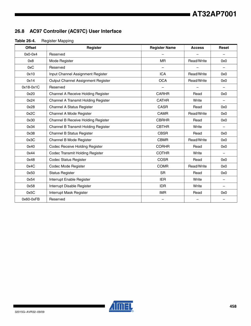
45832015G–AVR32–09/09
AT32AP7001
26.8 AC97 Controller (AC97C) User Interface
Table 26-4. Register Mapping
Offset Register Register Name Access Reset
0x0-0x4 Reserved – – –
0x8 Mode Register MR Read/Write 0x0
0xC Reserved – – –
0x10 Input Channel Assignment Register ICA Read/Write 0x0
0x14 Output Channel Assignment Register OCA Read/Write 0x0
0x18-0x1C Reserved – – –
0x20 Channel A Receive Holding Register CARHR Read 0x0
0x24 Channel A Transmit Holding Register CATHR Write –
0x28 Channel A Status Register CASR Read 0x0
0x2C Channel A Mode Register CAMR Read/Write 0x0
0x30 Channel B Receive Holding Register CBRHR Read 0x0
0x34 Channel B Transmit Holding Register CBTHR Write –
0x38 Channel B Status Register CBSR Read 0x0
0x3C Channel B Mode Register CBMR Read/Write 0x0
0x40 Codec Receive Holding Register CORHR Read 0x0
0x44 Codec Transmit Holding Register COTHR Write –
0x48 Codec Status Register COSR Read 0x0
0x4C Codec Mode Register COMR Read/Write 0x0
0x50 Status Register SR Read 0x0
0x54 Interrupt Enable Register IER Write –
0x58 Interrupt Disable Register IDR Write –
0x5C Interrupt Mask Register IMR Read 0x0
0x60-0xFB Reserved – – –
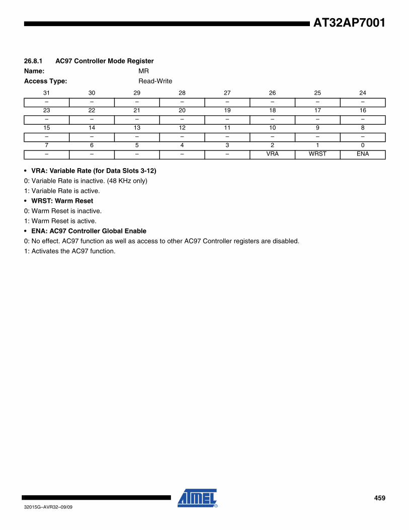
45932015G–AVR32–09/09
AT32AP7001
26.8.1 AC97 Controller Mode Register
Name: MR
Access Type: Read-Write
• VRA: Variable Rate (for Data Slots 3-12)
0: Variable Rate is inactive. (48 KHz only)
1: Variable Rate is active.
• WRST: Warm Reset
0: Warm Reset is inactive.
1: Warm Reset is active.
• ENA: AC97 Controller Global Enable
0: No effect. AC97 function as well as access to other AC97 Controller registers are disabled.
1: Activates the AC97 function.
31 30 29 28 27 26 25 24
– – – – – – – –
23 22 21 20 19 18 17 16
– – – – – – – –15 14 13 12 11 10 9 8
– – – – – – – –
7 6 5 4 3 2 1 0– – – – – VRA WRST ENA
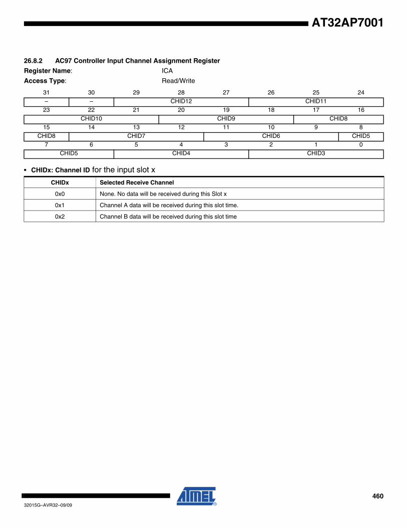
46032015G–AVR32–09/09
AT32AP7001
26.8.2 AC97 Controller Input Channel Assignment Register
Register Name: ICA
Access Type: Read/Write
• CHIDx: Channel ID for the input slot x
31 30 29 28 27 26 25 24
– – CHID12 CHID11
23 22 21 20 19 18 17 16
CHID10 CHID9 CHID815 14 13 12 11 10 9 8
CHID8 CHID7 CHID6 CHID5
7 6 5 4 3 2 1 0CHID5 CHID4 CHID3
CHIDx Selected Receive Channel
0x0 None. No data will be received during this Slot x
0x1 Channel A data will be received during this slot time.
0x2 Channel B data will be received during this slot time

46132015G–AVR32–09/09
AT32AP7001
26.8.3 AC97 Controller Output Channel Assignment Register
Register Name: OCA
Access Type: Read/Write
• CHIDx: Channel ID for the output slot x
31 30 29 28 27 26 25 24
– – CHID12 CHID11
23 22 21 20 19 18 17 16
CHID10 CHID9 CHID815 14 13 12 11 10 9 8
CHID8 CHID7 CHID6 CHID5
7 6 5 4 3 2 1 0CHID5 CHID4 CHID3
CHIDx Selected Transmit Channel
0x0 None. No data will be transmitted during this Slot x
0x1 Channel A data will be transferred during this slot time.
0x2 Channel B data will be transferred during this slot time
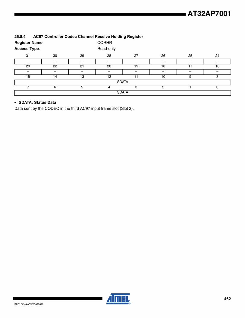
46232015G–AVR32–09/09
AT32AP7001
26.8.4 AC97 Controller Codec Channel Receive Holding Register
Register Name: CORHR
Access Type: Read-only
• SDATA: Status Data
Data sent by the CODEC in the third AC97 input frame slot (Slot 2).
31 30 29 28 27 26 25 24
– – – – – – – –
23 22 21 20 19 18 17 16
– – – – – – – –15 14 13 12 11 10 9 8
SDATA
7 6 5 4 3 2 1 0SDATA
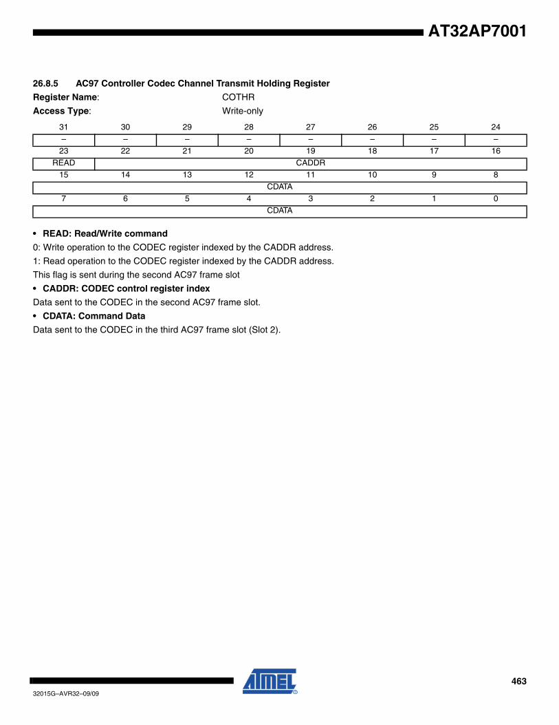
46332015G–AVR32–09/09
AT32AP7001
26.8.5 AC97 Controller Codec Channel Transmit Holding Register
Register Name: COTHR
Access Type: Write-only
• READ: Read/Write command
0: Write operation to the CODEC register indexed by the CADDR address.
1: Read operation to the CODEC register indexed by the CADDR address.
This flag is sent during the second AC97 frame slot
• CADDR: CODEC control register index
Data sent to the CODEC in the second AC97 frame slot.
• CDATA: Command Data
Data sent to the CODEC in the third AC97 frame slot (Slot 2).
31 30 29 28 27 26 25 24
– – – – – – – –
23 22 21 20 19 18 17 16
READ CADDR15 14 13 12 11 10 9 8
CDATA
7 6 5 4 3 2 1 0CDATA
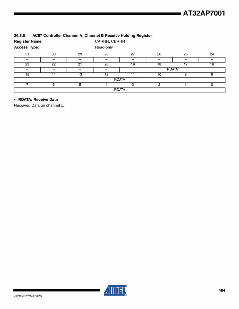
46432015G–AVR32–09/09
AT32AP7001
26.8.6 AC97 Controller Channel A, Channel B Receive Holding Register
Register Name: CARHR, CBRHR
Access Type: Read-only
• RDATA: Receive Data
Received Data on channel x.
31 30 29 28 27 26 25 24
– – – – – – – –
23 22 21 20 19 18 17 16
– – – – RDATA15 14 13 12 11 10 9 8
RDATA
7 6 5 4 3 2 1 0RDATA
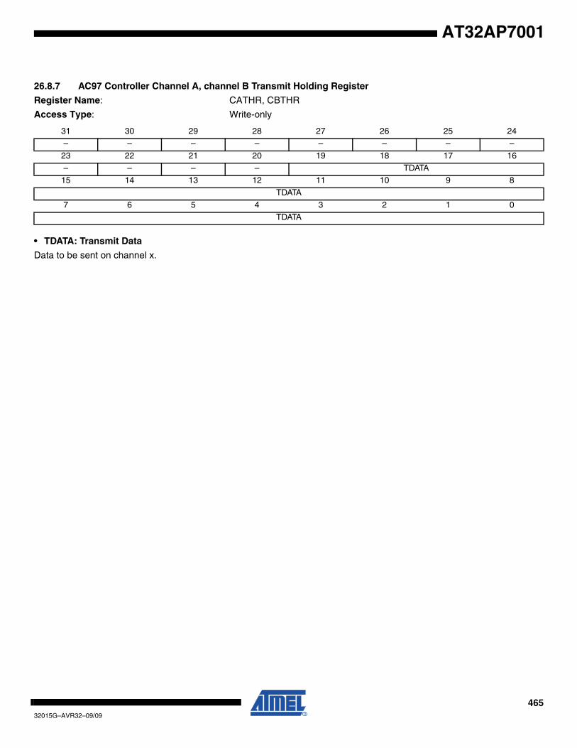
46532015G–AVR32–09/09
AT32AP7001
26.8.7 AC97 Controller Channel A, channel B Transmit Holding Register
Register Name: CATHR, CBTHR
Access Type: Write-only
• TDATA: Transmit Data
Data to be sent on channel x.
31 30 29 28 27 26 25 24
– – – – – – – –
23 22 21 20 19 18 17 16
– – – – TDATA15 14 13 12 11 10 9 8
TDATA
7 6 5 4 3 2 1 0TDATA
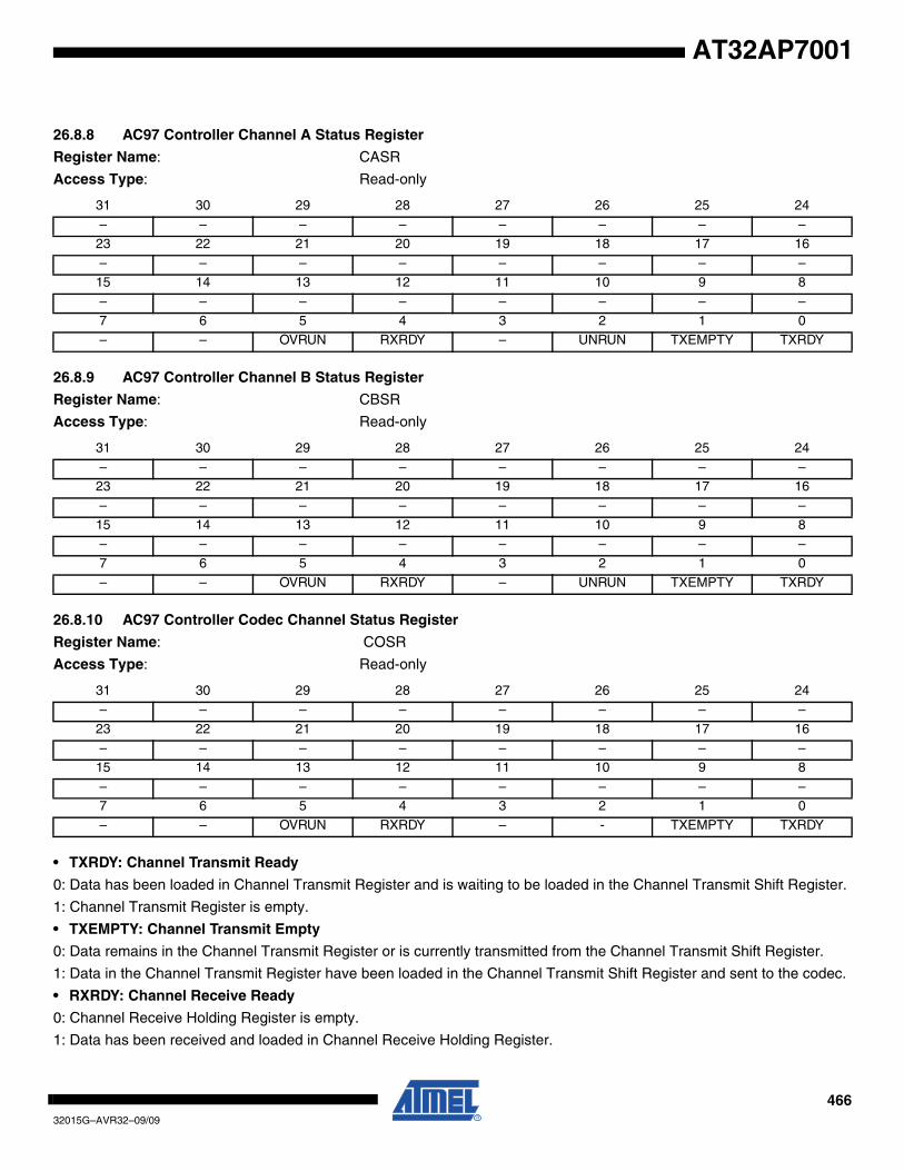
46632015G–AVR32–09/09
AT32AP7001
26.8.8 AC97 Controller Channel A Status Register
Register Name: CASR
Access Type: Read-only
26.8.9 AC97 Controller Channel B Status Register
Register Name: CBSR
Access Type: Read-only
26.8.10 AC97 Controller Codec Channel Status Register
Register Name: COSR
Access Type: Read-only
• TXRDY: Channel Transmit Ready
0: Data has been loaded in Channel Transmit Register and is waiting to be loaded in the Channel Transmit Shift Register.
1: Channel Transmit Register is empty.
• TXEMPTY: Channel Transmit Empty
0: Data remains in the Channel Transmit Register or is currently transmitted from the Channel Transmit Shift Register.
1: Data in the Channel Transmit Register have been loaded in the Channel Transmit Shift Register and sent to the codec.
• RXRDY: Channel Receive Ready
0: Channel Receive Holding Register is empty.
1: Data has been received and loaded in Channel Receive Holding Register.
31 30 29 28 27 26 25 24
– – – – – – – –
23 22 21 20 19 18 17 16
– – – – – – – –15 14 13 12 11 10 9 8
– – – – – – – –
7 6 5 4 3 2 1 0– – OVRUN RXRDY – UNRUN TXEMPTY TXRDY
31 30 29 28 27 26 25 24
– – – – – – – –23 22 21 20 19 18 17 16
– – – – – – – –
15 14 13 12 11 10 9 8– – – – – – – –
7 6 5 4 3 2 1 0
– – OVRUN RXRDY – UNRUN TXEMPTY TXRDY
31 30 29 28 27 26 25 24
– – – – – – – –
23 22 21 20 19 18 17 16– – – – – – – –
15 14 13 12 11 10 9 8
– – – – – – – –7 6 5 4 3 2 1 0
– – OVRUN RXRDY – - TXEMPTY TXRDY

46732015G–AVR32–09/09
AT32AP7001
• OVRUN: Receive Overrun
Automatically cleared by a processor read operation.
0: No data has been loaded in the Channel Receive Holding Register while previous data has not been read since the lastread of the Status Register.
1: Data has been loaded in the Channel Receive Holding Register while previous data has not yet been read since the lastread of the Status Register.

46832015G–AVR32–09/09
AT32AP7001
26.8.11 AC97 Controller Channel A Mode Register
Register Name: CAMR
Access Type: Read/Write
• DMAEN: DMA Enable
0: Disable DMA transfers for this channel.
1: Enable DMA transfers for this channel using DMAC.
• CEM: Channel A Endian Mode
0: Transferring Data through Channel A is straight forward (Big Endian).
1: Transferring Data through Channel A from/to a memory is performed with from/to Little Endian format translation.
• SIZE: Channel A Data Size
SIZE Encoding
Note: Each time slot in the data phase is 20 bit long. For example, if a 16-bit sample stream is being played to an AC 97 DAC, the first 16 bit positions are presented to the DAC MSB-justified. They are followed by the next four bit positions that the AC97 Controller fills with zeroes. This process ensures that the least significant bits do not introduce any DC biasing, regardless of the imple-mented DAC’s resolution (16-, 18-, or 20-bit).
• CEN: Channel A Enable
0: Data transfer is disabled on Channel A.
1: Data transfer is enabled on Channel A.
31 30 29 28 27 26 25 24
– – – – – – – –
23 22 21 20 19 18 17 16
– DMAEN CEN – – CEM SIZE15 14 13 12 11 10 9 8
– – – – – – – –
7 6 5 4 3 2 1 0– – OVRUN RXRDY – UNRUN TXEMPTY TXRDY
SIZE Selected Channel
0x0 20 bits
0x1 18bits
0x2 16 bits
0x3 10 bits
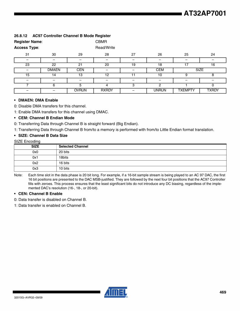
46932015G–AVR32–09/09
AT32AP7001
26.8.12 AC97 Controller Channel B Mode Register
Register Name: CBMR
Access Type: Read/Write
• DMAEN: DMA Enable
0: Disable DMA transfers for this channel.
1: Enable DMA transfers for this channel using DMAC.
• CEM: Channel B Endian Mode
0: Transferring Data through Channel B is straight forward (Big Endian).
1: Transferring Data through Channel B from/to a memory is performed with from/to Little Endian format translation.
• SIZE: Channel B Data Size
SIZE Encoding
Note: Each time slot in the data phase is 20 bit long. For example, if a 16-bit sample stream is being played to an AC 97 DAC, the first 16 bit positions are presented to the DAC MSB-justified. They are followed by the next four bit positions that the AC97 Controller fills with zeroes. This process ensures that the least significant bits do not introduce any DC biasing, regardless of the imple-mented DAC’s resolution (16-, 18-, or 20-bit).
• CEN: Channel B Enable
0: Data transfer is disabled on Channel B.
1: Data transfer is enabled on Channel B.
31 30 29 28 27 26 25 24
– – – – – – – –
23 22 21 20 19 18 17 16
– DMAEN CEN – – CEM SIZE15 14 13 12 11 10 9 8
– – – – – – – –
7 6 5 4 3 2 1 0– – OVRUN RXRDY – UNRUN TXEMPTY TXRDY
SIZE Selected Channel
0x0 20 bits
0x1 18bits
0x2 16 bits
0x3 10 bits
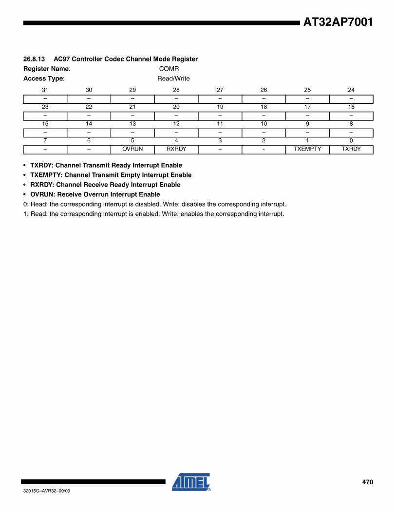
47032015G–AVR32–09/09
AT32AP7001
26.8.13 AC97 Controller Codec Channel Mode Register
Register Name: COMR
Access Type: Read/Write
• TXRDY: Channel Transmit Ready Interrupt Enable
• TXEMPTY: Channel Transmit Empty Interrupt Enable
• RXRDY: Channel Receive Ready Interrupt Enable
• OVRUN: Receive Overrun Interrupt Enable
0: Read: the corresponding interrupt is disabled. Write: disables the corresponding interrupt.
1: Read: the corresponding interrupt is enabled. Write: enables the corresponding interrupt.
31 30 29 28 27 26 25 24
– – – – – – – –
23 22 21 20 19 18 17 16
– – – – – – – –15 14 13 12 11 10 9 8
– – – – – – – –
7 6 5 4 3 2 1 0– – OVRUN RXRDY – - TXEMPTY TXRDY
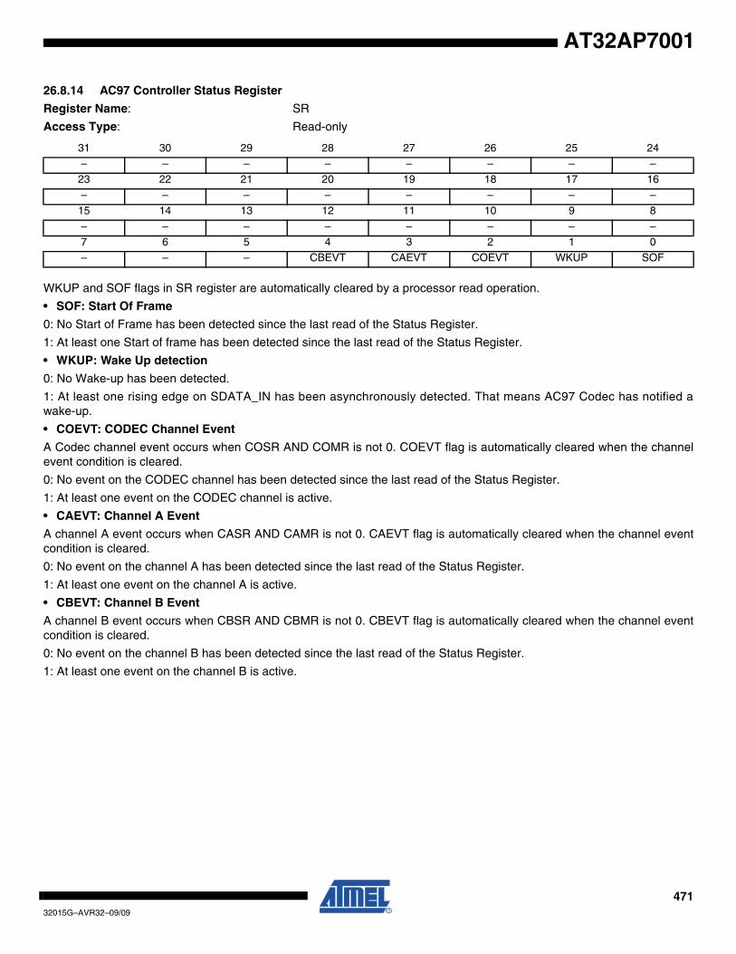
47132015G–AVR32–09/09
AT32AP7001
26.8.14 AC97 Controller Status Register
Register Name: SR
Access Type: Read-only
WKUP and SOF flags in SR register are automatically cleared by a processor read operation.
• SOF: Start Of Frame
0: No Start of Frame has been detected since the last read of the Status Register.
1: At least one Start of frame has been detected since the last read of the Status Register.
• WKUP: Wake Up detection
0: No Wake-up has been detected.
1: At least one rising edge on SDATA_IN has been asynchronously detected. That means AC97 Codec has notified awake-up.
• COEVT: CODEC Channel Event
A Codec channel event occurs when COSR AND COMR is not 0. COEVT flag is automatically cleared when the channelevent condition is cleared.
0: No event on the CODEC channel has been detected since the last read of the Status Register.
1: At least one event on the CODEC channel is active.
• CAEVT: Channel A Event
A channel A event occurs when CASR AND CAMR is not 0. CAEVT flag is automatically cleared when the channel eventcondition is cleared.
0: No event on the channel A has been detected since the last read of the Status Register.
1: At least one event on the channel A is active.
• CBEVT: Channel B Event
A channel B event occurs when CBSR AND CBMR is not 0. CBEVT flag is automatically cleared when the channel eventcondition is cleared.
0: No event on the channel B has been detected since the last read of the Status Register.
1: At least one event on the channel B is active.
31 30 29 28 27 26 25 24– – – – – – – –
23 22 21 20 19 18 17 16
– – – – – – – –
15 14 13 12 11 10 9 8– – – – – – – –
7 6 5 4 3 2 1 0
– – – CBEVT CAEVT COEVT WKUP SOF
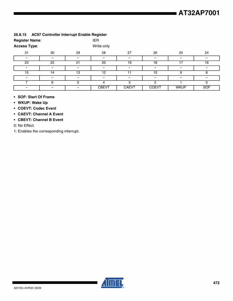
47232015G–AVR32–09/09
AT32AP7001
26.8.15 AC97 Controller Interrupt Enable Register
Register Name: IER
Access Type: Write-only
• SOF: Start Of Frame
• WKUP: Wake Up
• COEVT: Codec Event
• CAEVT: Channel A Event
• CBEVT: Channel B Event
0: No Effect.
1: Enables the corresponding interrupt.
31 30 29 28 27 26 25 24
– – – – – – – –
23 22 21 20 19 18 17 16
– – – – – – – –15 14 13 12 11 10 9 8
– – – – – – – –
7 6 5 4 3 2 1 0– – – CBEVT CAEVT COEVT WKUP SOF

47332015G–AVR32–09/09
AT32AP7001
26.8.16 AC97 Controller Interrupt Disable Register
Register Name: IDR
Access Type: Write-only
• SOF: Start Of Frame
• WKUP: Wake Up
• COEVT: Codec Event
• CAEVT: Channel A Event
• CBEVT: Channel B Event
0: No Effect.
1: Disables the corresponding interrupt.
31 30 29 28 27 26 25 24
– – – – – – – –
23 22 21 20 19 18 17 16
– – – – – – – –15 14 13 12 11 10 9 8
– – – – – – – –
7 6 5 4 3 2 1 0– – – CBEVT CAEVT COEVT WKUP SOF
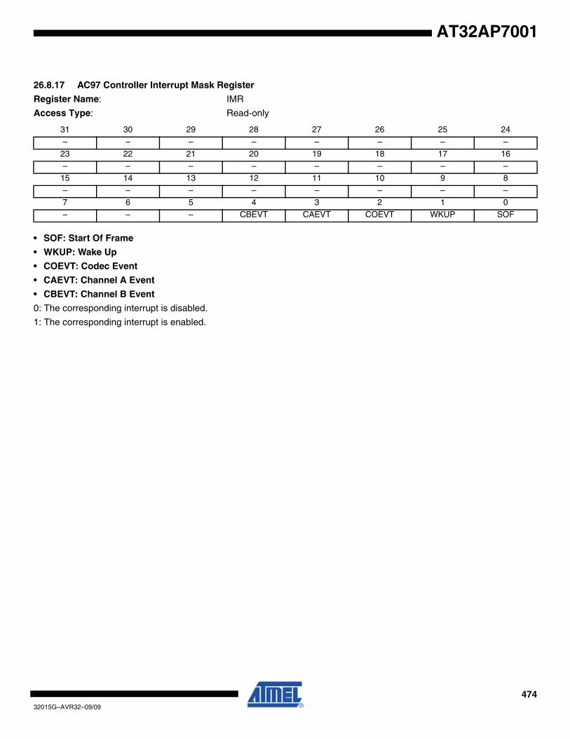
47432015G–AVR32–09/09
AT32AP7001
26.8.17 AC97 Controller Interrupt Mask Register
Register Name: IMR
Access Type: Read-only
• SOF: Start Of Frame
• WKUP: Wake Up
• COEVT: Codec Event
• CAEVT: Channel A Event
• CBEVT: Channel B Event
0: The corresponding interrupt is disabled.
1: The corresponding interrupt is enabled.
31 30 29 28 27 26 25 24
– – – – – – – –
23 22 21 20 19 18 17 16
– – – – – – – –15 14 13 12 11 10 9 8
– – – – – – – –
7 6 5 4 3 2 1 0– – – CBEVT CAEVT COEVT WKUP SOF
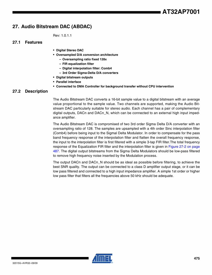
47532015G–AVR32–09/09
AT32AP7001
27. Audio Bitstream DAC (ABDAC)
Rev: 1.0.1.1
27.1 Features
• Digital Stereo DAC• Oversampled D/A conversion architecture
– Oversampling ratio fixed 128x– FIR equalization filter– Digital interpolation filter: Comb4 – 3rd Order Sigma-Delta D/A converters
• Digital bitstream outputs• Parallel interface• Connected to DMA Controller for background transfer without CPU intervention
27.2 Description
The Audio Bitstream DAC converts a 16-bit sample value to a digital bitstream with an averagevalue proportional to the sample value. Two channels are supported, making the Audio Bit-stream DAC particularly suitable for stereo audio. Each channel has a pair of complementarydigital outputs, DACn and DACn_N, which can be connected to an external high input imped-ance amplifier.
The Audio Bitstream DAC is compromised of two 3rd order Sigma Delta D/A converter with anoversampling ratio of 128. The samples are upsampled with a 4th order Sinc interpolation filter(Comb4) before being input to the Sigmal Delta Modulator. In order to compensate for the passband frequency response of the interpolation filter and flatten the overall frequency response,the input to the interpolation filter is first filtered with a simple 3-tap FIR filter.The total frequencyresponse of the Equalization FIR filter and the interpolation filter is given in Figure 27-2 on page487. The digital output bitstreams from the Sigma Delta Modulators should be low-pass filteredto remove high frequency noise inserted by the Modulation process.
The output DACn and DACn_N should be as ideal as possible before filtering, to achieve thebest SNR quality. The output can be connected to a class D amplifier output stage, or it can below pass filtered and connected to a high input impedance amplifier. A simple 1st order or higherlow pass filter that filters all the frequencies above 50 kHz should be adequate.
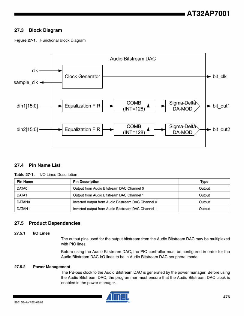
47632015G–AVR32–09/09
AT32AP7001
27.3 Block Diagram
Figure 27-1. Functional Block Diagram
27.4 Pin Name List
27.5 Product Dependencies
27.5.1 I/O LinesThe output pins used for the output bitstream from the Audio Bitstream DAC may be multiplexedwith PIO lines.
Before using the Audio Bitstream DAC, the PIO controller must be configured in order for theAudio Bitstream DAC I/O lines to be in Audio Bitstream DAC peripheral mode.
27.5.2 Power ManagementThe PB-bus clock to the Audio Bitstream DAC is generated by the power manager. Before usingthe Audio Bitstream DAC, the programmer must ensure that the Audio Bitstream DAC clock isenabled in the power manager.
Table 27-1. I/O Lines Description
Pin Name Pin Description Type
DATA0 Output from Audio Bitstream DAC Channel 0 Output
DATA1 Output from Audio Bitstream DAC Channel 1 Output
DATAN0 Inverted output from Audio Bitstream DAC Channel 0 Output
DATAN1 Inverted output from Audio Bitstream DAC Channel 1 Output
Clock Generator
Equalization FIR COMB (INT=128)
Sigma-DeltaDA-MOD
Equalization FIR COMB (INT=128)
Sigma-DeltaDA-MOD
bit_clk
bit_out1
bit_out2
clk
sample_clk
din1[15:0]
din2[15:0]
Audio Bitstream DAC
47732015G–AVR32–09/09
AT32AP7001
27.5.3 Clock Management
The Audio Bitstream DAC needs a separate clock for the D/A conversion operation. This clockshould be set up in the generic clock register in the power manager. The frequency of this clockmust be 256 times the frequency of the desired samplerate (fs). For fs=48kHz this means that theclock must have a frequency of 12.288MHz.
27.5.4 Interrupts
The Audio Bitstream DAC interface has an interrupt line connected to the interrupt controller. Inorder to handle interrupts, the interrupt controller must be programmed before configuring theAudio Bitstream DAC.
All Audio Bitstream DAC interrupts can be enabled/disabled by writing to the Audio BitstreamDAC Interrupt Enable/Disable Registers. Each pending and unmasked Audio Bitstream DACinterrupt will assert the interrupt line. The Audio Bitstream DAC interrupt service routine can getthe interrupt source by reading the Interrupt Status Register.
27.5.5 DMA
The Audio Bitstream DAC is connected to the DMA controller. The DMA controller can be pro-grammed to automatically transfer samples to the Audio Bitstream DAC Sample Data Register(SDR) when the Audio Bitstream DAC is ready for new samples. This enables the Audio Bit-stream DAC to operate without any CPU intervention such as polling the Interrupt StatusRegister (ISR) or using interrupts. See the DMA controller documentation for details on how tosetup DMA transfers.
27.6 Functional Description
In order to use the Audio Bitstream DAC the product dependencies given in Section 27.5 onpage 476 must be resolved. Particular attention should be given to the configuration of clocksand I/O lines in order to ensure correct operation of the Audio Bitstream DAC.
The Audio Bitstream DAC is enabled by writing the ENABLE bit in the Audio Bitstream DACControl Register (CR). The two 16-bit sample values for channel 0 and 1 can then be written tothe least and most significant halfword of the Sample Data Register (SDR), respectively. TheTX_READY bit in the Interrupt Status Register (ISR) will be set whenever the DAC is ready toreceive a new sample. A new sample value should be written to SDR before 256 DAC clockcycles, or an underrun will occur, as indicated by the UNDERRUN status flags in ISR. ISR iscleared when read, or when writing one to the corresponding bits in the Interrupt Clear Register(ICR).
For interrupt-based operation, the relevant interrupts must be enabled by writing one to the cor-responding bits in the Interrupt Enable Register (IER). Interrupts can be disabled by the InterruptDisable Register (IDR), and active interrupts are indicated in the read-only Interrupt Mask Regis-ter (IMR).
The Audio Bitstream DAC can also be configured for peripheral DMA access, in which case onlythe enable bit in the control register needs to be set in the Audio Bitstream DAC module.
27.6.1 Equalization Filter
The equalization filter is a simple 3-tap FIR filter. The purpose of this filter is to compensate forthe pass band frequency response of the sinc interpolation filter. The equalization filter makesthe pass band response more flat and moves the -3dB corner a little higher.
47832015G–AVR32–09/09
AT32AP7001
27.6.2 Interpolation filter
The interpolation filter interpolates from fs to 128fs. This filter is a 4th order Cascaded Integrator-Comb filter, and the basic building blocks of this filter is a comb part and an integrator part.
27.6.3 Sigma Delta Modulator
This part is a 3rd order Sigma Delta Modulator consisting of three differentiators (delta blocks),three integrators (sigma blocks) and a one bit quantizer. The purpose of the integrators is toshape the noise, so that the noise is reduces in the band of interest and increased at the higherfrequencies, where it can be filtered.
27.6.4 Data Format
Input data is on two’s complement format.
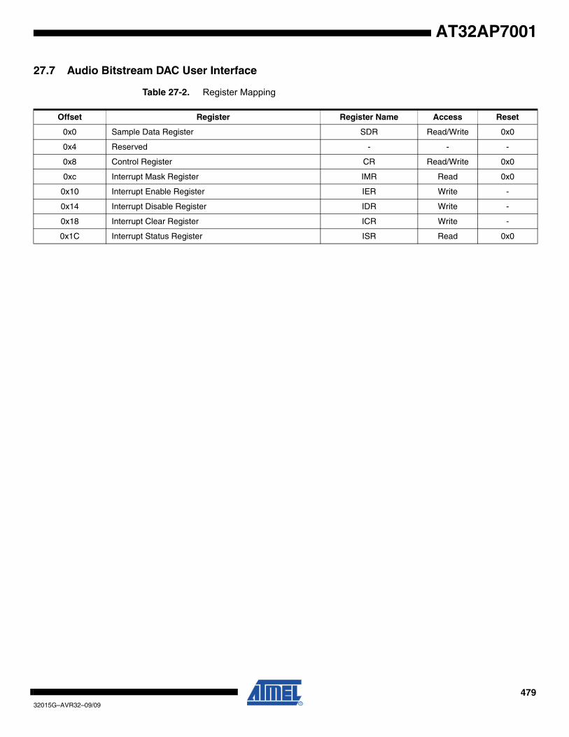
47932015G–AVR32–09/09
AT32AP7001
27.7 Audio Bitstream DAC User Interface
Table 27-2. Register Mapping
Offset Register Register Name Access Reset
0x0 Sample Data Register SDR Read/Write 0x0
0x4 Reserved - - -
0x8 Control Register CR Read/Write 0x0
0xc Interrupt Mask Register IMR Read 0x0
0x10 Interrupt Enable Register IER Write -
0x14 Interrupt Disable Register IDR Write -
0x18 Interrupt Clear Register ICR Write -
0x1C Interrupt Status Register ISR Read 0x0
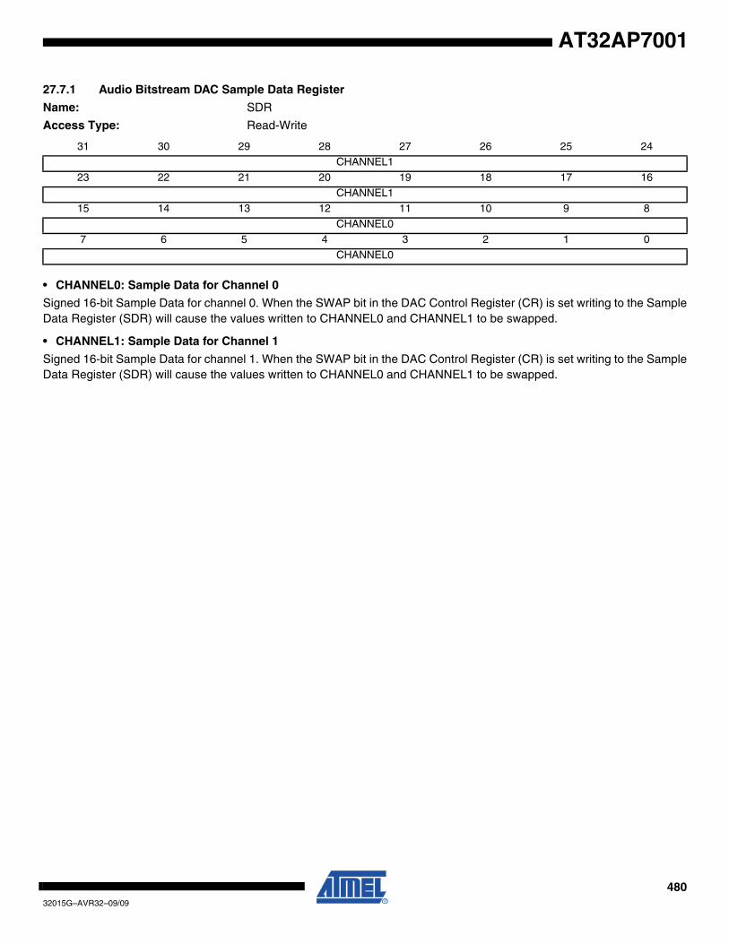
48032015G–AVR32–09/09
AT32AP7001
27.7.1 Audio Bitstream DAC Sample Data Register
Name: SDR
Access Type: Read-Write
• CHANNEL0: Sample Data for Channel 0
Signed 16-bit Sample Data for channel 0. When the SWAP bit in the DAC Control Register (CR) is set writing to the SampleData Register (SDR) will cause the values written to CHANNEL0 and CHANNEL1 to be swapped.
• CHANNEL1: Sample Data for Channel 1
Signed 16-bit Sample Data for channel 1. When the SWAP bit in the DAC Control Register (CR) is set writing to the SampleData Register (SDR) will cause the values written to CHANNEL0 and CHANNEL1 to be swapped.
31 30 29 28 27 26 25 24CHANNEL1
23 22 21 20 19 18 17 16
CHANNEL1
15 14 13 12 11 10 9 8CHANNEL0
7 6 5 4 3 2 1 0
CHANNEL0
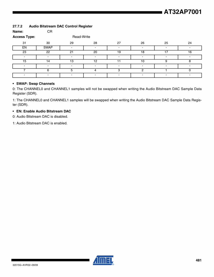
48132015G–AVR32–09/09
AT32AP7001
27.7.2 Audio Bitstream DAC Control Register
Name: CR
Access Type: Read-Write
• SWAP: Swap Channels
0: The CHANNEL0 and CHANNEL1 samples will not be swapped when writing the Audio Bitstream DAC Sample DataRegister (SDR).
1: The CHANNEL0 and CHANNEL1 samples will be swapped when writing the Audio Bitstream DAC Sample Data Regis-ter (SDR).
• EN: Enable Audio Bitstream DAC
0: Audio Bitstream DAC is disabled.
1: Audio Bitstream DAC is enabled.
31 30 29 28 27 26 25 24EN SWAP - - - - - -
23 22 21 20 19 18 17 16
- - - - - - - -
15 14 13 12 11 10 9 8- - - - - - - -
7 6 5 4 3 2 1 0
- - - - - - - -
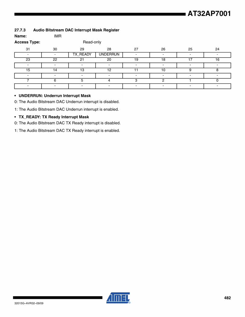
48232015G–AVR32–09/09
AT32AP7001
27.7.3 Audio Bitstream DAC Interrupt Mask Register
Name: IMR
Access Type: Read-only
• UNDERRUN: Underrun Interrupt Mask
0: The Audio Bitstream DAC Underrun interrupt is disabled.
1: The Audio Bitstream DAC Underrun interrupt is enabled.
• TX_READY: TX Ready Interrupt Mask
0: The Audio Bitstream DAC TX Ready interrupt is disabled.
1: The Audio Bitstream DAC TX Ready interrupt is enabled.
31 30 29 28 27 26 25 24- - TX_READY UNDERRUN - - - -
23 22 21 20 19 18 17 16
- - - - - - - -
15 14 13 12 11 10 9 8- - - - - - - -
7 6 5 4 3 2 1 0
- - - - - - - -

48332015G–AVR32–09/09
AT32AP7001
27.7.4 Audio Bitstream DAC Interrupt Enable Register
Name: IER
Access Type: Write-only
• UNDERRUN: Underrun Interrupt Enable
0: No effect.
1: Enables the Audio Bitstream DAC Underrun interrupt.
• TX_READY: TX Ready Interrupt Enable
0: No effect.
1: Enables the Audio Bitstream DAC TX Ready interrupt.
31 30 29 28 27 26 25 24- - TX_READY UNDERRUN - - - -
23 22 21 20 19 18 17 16
- - - - - - - -
15 14 13 12 11 10 9 8- - - - - - - -
7 6 5 4 3 2 1 0
- - - - - - - -
48432015G–AVR32–09/09
AT32AP7001
27.7.5 Audio Bitstream DAC Interrupt Disable Register
Name: IDR
Access Type: Write-only
• UNDERRUN: Underrun Interrupt Disable
0: No effect.
1: Disable the Audio Bitstream DAC Underrun interrupt.
• TX_READY: TX Ready Interrupt Disable
0: No effect.
1: Disable the Audio Bitstream DAC TX Ready interrupt.
31 30 29 28 27 26 25 24- - TX_READY UNDERRUN - - - -
23 22 21 20 19 18 17 16
- - - - - - - -
15 14 13 12 11 10 9 8- - - - - - - -
7 6 5 4 3 2 1 0
- - - - - - - -
48532015G–AVR32–09/09
AT32AP7001
27.7.6 Audio Bitstream DAC Interrupt Clear Register
Name: ICR
Access Type: Write-only
• UNDERRUN: Underrun Interrupt Clear
0: No effect.
1: Clear the Audio Bitstream DAC Underrun interrupt.
• TX_READY: TX Ready Interrupt Clear
0: No effect.
1: Clear the Audio Bitstream DAC TX Ready interrupt.
31 30 29 28 27 26 25 24- - TX_READY UNDERRUN - - - -
23 22 21 20 19 18 17 16
- - - - - - - -
15 14 13 12 11 10 9 8- - - - - - - -
7 6 5 4 3 2 1 0
- - - - - - - -

48632015G–AVR32–09/09
AT32AP7001
27.7.7 Audio Bitstream DAC Interrupt Status Register
Name: ISR
Access Type: Read-only
• UNDERRUN: Underrun Interrupt Status
0: No Audio Bitstream DAC Underrun has occured since the last time ISR was read or since reset.
1: At least one Audio Bitstream DAC Underrun has occured since the last time ISR was read or since reset.
• TX_READY: TX Ready Interrupt Status
0: No Audio Bitstream DAC TX Ready has occuredt since the last time ISR was read.
1: At least one Audio Bitstream DAC TX Ready has occuredt since the last time ISR was read.
31 30 29 28 27 26 25 24- - TX_READY UNDERRUN - - - -
23 22 21 20 19 18 17 16
- - - - - - - -
15 14 13 12 11 10 9 8- - - - - - - -
7 6 5 4 3 2 1 0
- - - - - - - -
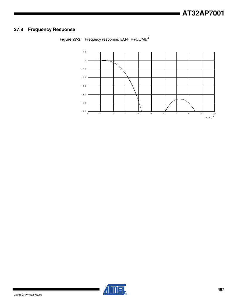
48732015G–AVR32–09/09
AT32AP7001
27.8 Frequency Response
Figure 27-2. Frequecy response, EQ-FIR+COMB4
0 1 2 3 4 5 6 7 8 9 1 0
x 1 04
- 6 0
- 5 0
- 4 0
- 3 0
- 2 0
- 1 0
0
1 0
48832015G–AVR32–09/09
AT32AP7001
28. Static Memory Controller (SMC)
Rev. 1.0.0.3
28.1 Features
• 6 chip selects available• 64-Mbytes address space per chip select• 8-, 16- or 32-bit data bus• Word, halfword, byte transfers• Byte write or byte select lines• Programmable setup, pulse and hold time for read signals per chip select• Programmable setup, pulse and hold time for write signals per chip select• Programmable data float time per chip select• Compliant with LCD module• External wait request• Automatic switch to slow clock mode• Asynchronous read in page mode supported: page size ranges from 4 to 32 bytes
28.2 Overview
The Static Memory Controller (SMC) generates the signals that control the access to the exter-nal memory devices or peripheral devices. It has 6 chip selects and a 26-bit address bus. The32-bit data bus can be configured to interface with 8-, or16-, or 32-bit external devices. Separateread and write control signals allow for direct memory and peripheral interfacing. Read and writesignal waveforms are fully parametrizable.
The SMC can manage wait requests from external devices to extend the current access. TheSMC is provided with an automatic slow clock mode. In slow clock mode, it switches from user-programmed waveforms to slow-rate specific waveforms on read and write signals. The SMCsupports asynchronous burst read in page mode access for page size up to 32 bytes.
48932015G–AVR32–09/09
AT32AP7001
28.3 Block Diagram
Figure 28-1. SMC Block Diagram
28.4 I/O Lines Description
SMCChip SelectBus
Matrix
PowerManager
CLK_SMC
SMC
NCS[5:0]
NRD
NWE0
ADDR[0]
NWE1
ADDR[1]
NWE3
ADDR[25:2]
DATA[31:0]
NWAIT
User Interface
Peripheral Bus
NCS[5:0]
NRD
NWR0/NWE
A0/NBS0
NWR1/NBS1
A1/NWR2/NBS2
NWR3/NBS3
A[25:2]
D[31:0]
NWAIT
EBIMux Logic
I/OController
Table 28-1. I/O Lines Description
Pin Name Pin Description Type Active Level
NCS[5:0] Chip Select Lines Output Low
NRD Read Signal Output Low
NWR0/NWE Write 0/Write Enable Signal Output Low
A0/NBS0 Address Bit 0/Byte 0 Select Signal Output Low
NWR1/NBS1 Write 1/Byte 1 Select Signal Output Low
A1/NWR2/NBS2 Address Bit 1/Write 2/Byte 2 Select Signal Output Low
NWR3/NBS3 Write 3/Byte 3 Select Signal Output Low
A[25:2] Address Bus Output
D[31:0] Data Bus Input/Output
NWAIT External Wait Signal Input Low
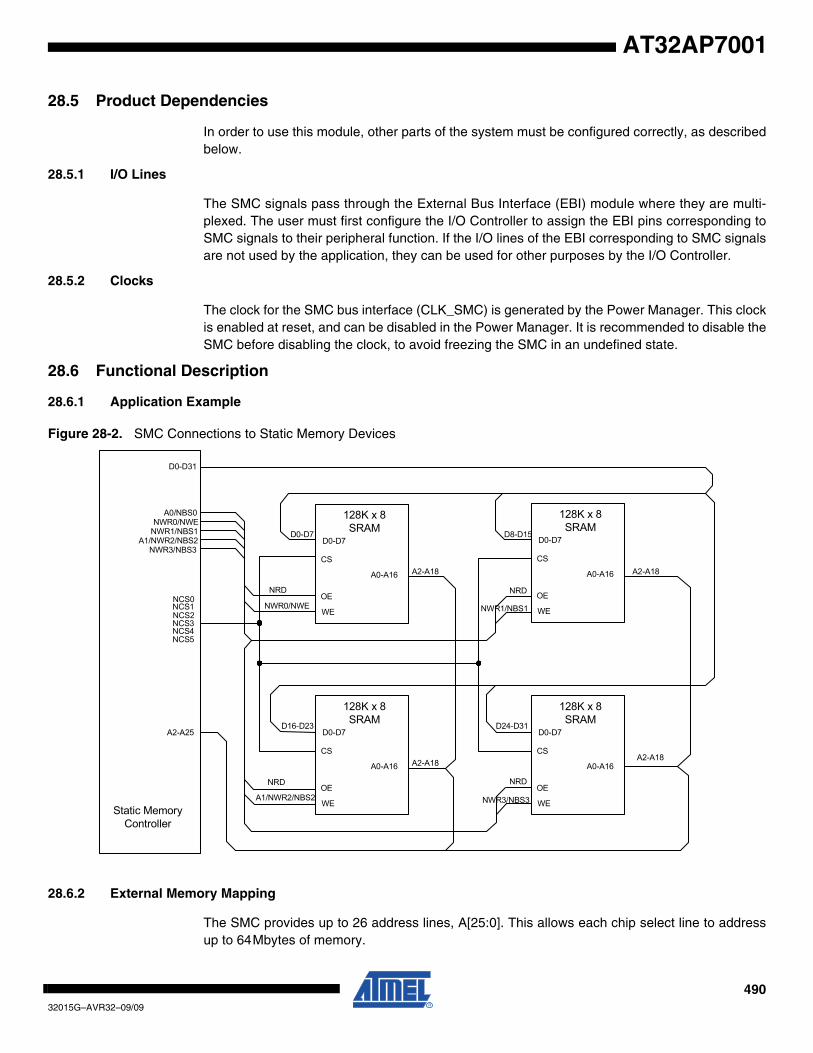
49032015G–AVR32–09/09
AT32AP7001
28.5 Product Dependencies
In order to use this module, other parts of the system must be configured correctly, as describedbelow.
28.5.1 I/O Lines
The SMC signals pass through the External Bus Interface (EBI) module where they are multi-plexed. The user must first configure the I/O Controller to assign the EBI pins corresponding toSMC signals to their peripheral function. If the I/O lines of the EBI corresponding to SMC signalsare not used by the application, they can be used for other purposes by the I/O Controller.
28.5.2 Clocks
The clock for the SMC bus interface (CLK_SMC) is generated by the Power Manager. This clockis enabled at reset, and can be disabled in the Power Manager. It is recommended to disable theSMC before disabling the clock, to avoid freezing the SMC in an undefined state.
28.6 Functional Description
28.6.1 Application Example
Figure 28-2. SMC Connections to Static Memory Devices
28.6.2 External Memory Mapping
The SMC provides up to 26 address lines, A[25:0]. This allows each chip select line to addressup to 64Mbytes of memory.
128K x 8SRAM
D0-D7
CS
OE
WE
A0-A16
128K x 8SRAM
D0-D7
CS
OE
WE
A0-A16
128K x 8SRAM
D0-D7
CS
OE
WE
A0-A16
128K x 8SRAM
D0-D7
CS
OE
WE
A0-A16
D0-D31
NWR1/NBS1
A0/NBS0NWR0/NWE
A1/NWR2/NBS2NWR3/NBS3
NCS0
NCS2NCS1
NCS3
NCS5NCS4
NRD
NRD NRD
NRD
A2-A25
Static MemoryController
A1/NWR2/NBS2
NWR0/NWE NWR1/NBS1
NWR3/NBS3
D8-D15D0-D7
D16-D23 D24-D31
A2-A18A2-A18
A2-A18A2-A18
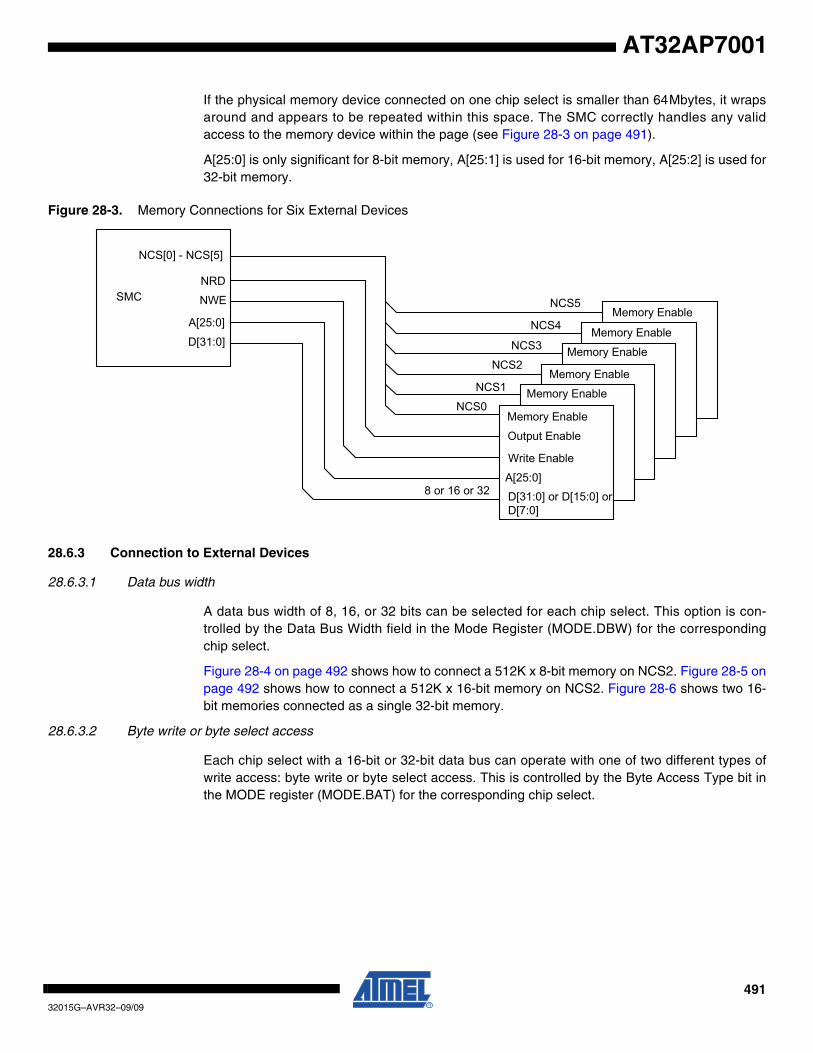
49132015G–AVR32–09/09
AT32AP7001
If the physical memory device connected on one chip select is smaller than 64Mbytes, it wrapsaround and appears to be repeated within this space. The SMC correctly handles any validaccess to the memory device within the page (see Figure 28-3 on page 491).
A[25:0] is only significant for 8-bit memory, A[25:1] is used for 16-bit memory, A[25:2] is used for32-bit memory.
Figure 28-3. Memory Connections for Six External Devices
28.6.3 Connection to External Devices
28.6.3.1 Data bus width
A data bus width of 8, 16, or 32 bits can be selected for each chip select. This option is con-trolled by the Data Bus Width field in the Mode Register (MODE.DBW) for the correspondingchip select.
Figure 28-4 on page 492 shows how to connect a 512K x 8-bit memory on NCS2. Figure 28-5 onpage 492 shows how to connect a 512K x 16-bit memory on NCS2. Figure 28-6 shows two 16-bit memories connected as a single 32-bit memory.
28.6.3.2 Byte write or byte select access
Each chip select with a 16-bit or 32-bit data bus can operate with one of two different types ofwrite access: byte write or byte select access. This is controlled by the Byte Access Type bit inthe MODE register (MODE.BAT) for the corresponding chip select.
NCS[0] - NCS[5]
NRD
NWE
A[25:0]
D[31:0]
SMC NCS5
NCS4
NCS3
NCS2
NCS1
NCS0
8 or 16 or 32
Memory Enable
Memory Enable
Memory Enable
Memory Enable
Memory Enable
Memory Enable
Output Enable
Write Enable
A[25:0]D[31:0] or D[15:0] or D[7:0]
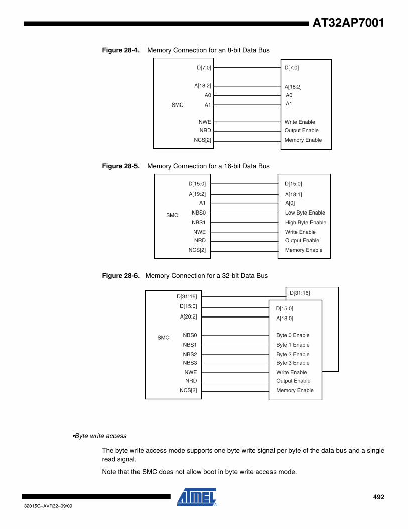
49232015G–AVR32–09/09
AT32AP7001
Figure 28-4. Memory Connection for an 8-bit Data Bus
Figure 28-5. Memory Connection for a 16-bit Data Bus
Figure 28-6. Memory Connection for a 32-bit Data Bus
•Byte write access
The byte write access mode supports one byte write signal per byte of the data bus and a singleread signal.
Note that the SMC does not allow boot in byte write access mode.
SMC
A0
NWE
NRD
NCS[2]
A0
Write Enable
Output Enable
Memory Enable
D[7:0] D[7:0]
A[18:2]A[18:2]
A1 A1
SMC NBS0
NWE
NRD
NCS[2]
Low Byte Enable
Write Enable
Output Enable
Memory Enable
NBS1 High Byte Enable
D[15:0] D[15:0]
A[19:2] A[18:1]
A[0]A1
D[31:16]
SMC NBS0
NWE
NRD
NCS[2]
NBS1
D[15:0]
A[20:2]
D[31:16]
NBS2
NBS3
Byte 0 Enable
Write Enable
Output Enable
Memory Enable
Byte 1 Enable
D[15:0]
A[18:0]
Byte 2 Enable
Byte 3 Enable

49332015G–AVR32–09/09
AT32AP7001
• For 16-bit devices: the SMC provides NWR0 and NWR1 write signals for respectively byte0 (lower byte) and byte1 (upper byte) of a 16-bit bus. One single read signal (NRD) is provided.
The byte write access mode is used to connect two 8-bit devices as a 16-bit memory.
• For 32-bit devices: NWR0, NWR1, NWR2 and NWR3, are the write signals of byte0 (lower byte), byte1, byte2, and byte 3 (upper byte) respectively. One single read signal (NRD) is provided. The byte write access is used to connect four 8-bit devices as a 32-bit memory.
The byte write option is illustrated on Figure 28-7 on page 493.
•Byte select access
In this mode, read/write operations can be enabled/disabled at a byte level. One byte select lineper byte of the data bus is provided. One NRD and one NWE signal control read and write.
• For 16-bit devices: the SMC provides NBS0 and NBS1 selection signals for respectively byte0 (lower byte) and byte1 (upper byte) of a 16-bit bus. The byte select access is used to connect one 16-bit device.
• For 32-bit devices: NBS0, NBS1, NBS2 and NBS3, are the selection signals of byte0 (lower byte), byte1, byte2, and byte 3 (upper byte) respectively. The byte select access is used to connect two 16-bit devices.
Figure 28-8 on page 494 shows how to connect two 16-bit devices on a 32-bit data bus in byteselect access mode, on NCS3.
Figure 28-7. Connection of two 8-bit Devices on a 16-bit Bus: Byte Write Option
•Signal multiplexing
Depending on the MODE.BAT bit, only the write signals or the byte select signals are used. Tosave I/Os at the external bus interface, control signals at the SMC interface are multiplexed.
SMC A1
NWR0
NRD
NCS[3]
Write Enable
Read Enable
Memory Enable
NWR1
Write Enable
Read Enable
Memory Enable
D[7:0] D[7:0]
D[15:8]
D[15:8]
A[24:2]
A[23:1]
A[23:1]
A[0]
A[0]
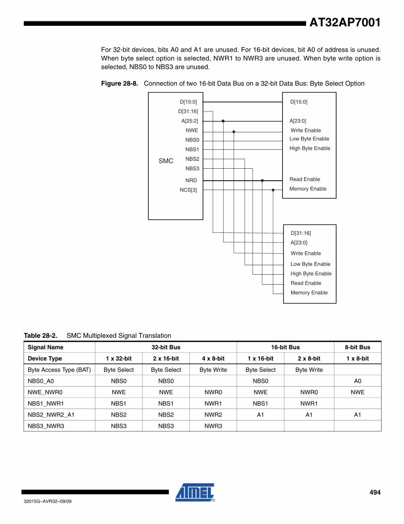
49432015G–AVR32–09/09
AT32AP7001
For 32-bit devices, bits A0 and A1 are unused. For 16-bit devices, bit A0 of address is unused.When byte select option is selected, NWR1 to NWR3 are unused. When byte write option isselected, NBS0 to NBS3 are unused.
Figure 28-8. Connection of two 16-bit Data Bus on a 32-bit Data Bus: Byte Select Option
SMC
NWE
NRD
NCS[3]
Write Enable
Read Enable
Memory Enable
NBS0
D[15:0] D[15:0]
D[31:16]
A[25:2] A[23:0]
Write Enable
Read Enable
Memory Enable
D[31:16]
A[23:0]
Low Byte Enable
High Byte Enable
Low Byte Enable
High Byte EnableNBS1
NBS2
NBS3
Table 28-2. SMC Multiplexed Signal Translation
Signal Name 32-bit Bus 16-bit Bus 8-bit Bus
Device Type 1 x 32-bit 2 x 16-bit 4 x 8-bit 1 x 16-bit 2 x 8-bit 1 x 8-bit
Byte Access Type (BAT) Byte Select Byte Select Byte Write Byte Select Byte Write
NBS0_A0 NBS0 NBS0 NBS0 A0
NWE_NWR0 NWE NWE NWR0 NWE NWR0 NWE
NBS1_NWR1 NBS1 NBS1 NWR1 NBS1 NWR1
NBS2_NWR2_A1 NBS2 NBS2 NWR2 A1 A1 A1
NBS3_NWR3 NBS3 NBS3 NWR3
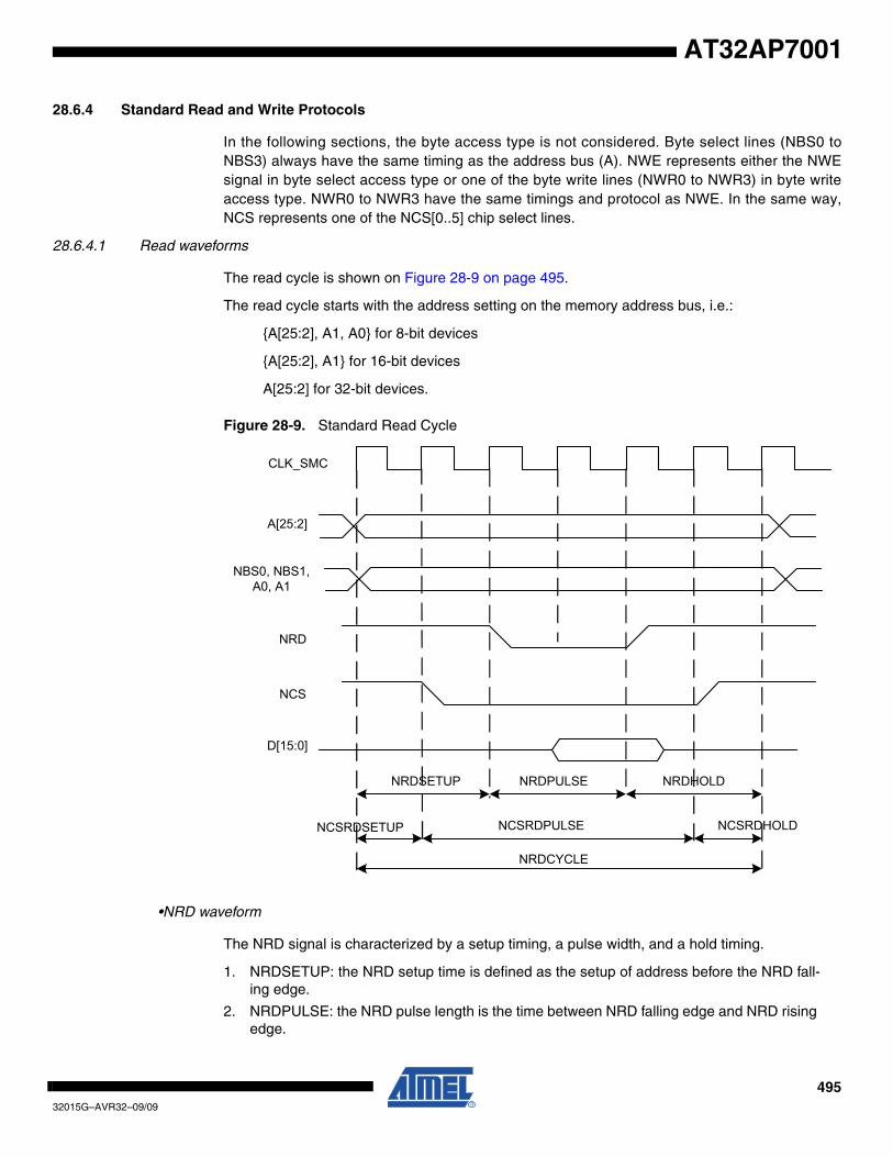
49532015G–AVR32–09/09
AT32AP7001
28.6.4 Standard Read and Write Protocols
In the following sections, the byte access type is not considered. Byte select lines (NBS0 toNBS3) always have the same timing as the address bus (A). NWE represents either the NWEsignal in byte select access type or one of the byte write lines (NWR0 to NWR3) in byte writeaccess type. NWR0 to NWR3 have the same timings and protocol as NWE. In the same way,NCS represents one of the NCS[0..5] chip select lines.
28.6.4.1 Read waveforms
The read cycle is shown on Figure 28-9 on page 495.
The read cycle starts with the address setting on the memory address bus, i.e.:
{A[25:2], A1, A0} for 8-bit devices
{A[25:2], A1} for 16-bit devices
A[25:2] for 32-bit devices.
Figure 28-9. Standard Read Cycle
•NRD waveform
The NRD signal is characterized by a setup timing, a pulse width, and a hold timing.
1. NRDSETUP: the NRD setup time is defined as the setup of address before the NRD fall-ing edge.
2. NRDPULSE: the NRD pulse length is the time between NRD falling edge and NRD rising edge.
A[25:2]
CLK_SMC
NBS0, NBS1, A0, A1
NRD
NCS
D[15:0]
NCSRDSETUP
NRDSETUP NRDPULSE
NCSRDPULSE
NRDCYCLE
NRDHOLD
NCSRDHOLD

49632015G–AVR32–09/09
AT32AP7001
3. NRDHOLD: the NRD hold time is defined as the hold time of address after the NRD ris-ing edge.
•NCS waveform
Similarly, the NCS signal can be divided into a setup time, pulse length and hold time.
1. NCSRDSETUP: the NCS setup time is defined as the setup time of address before the NCS falling edge.
2. NCSRDPULSE: the NCS pulse length is the time between NCS falling edge and NCS rising edge.
3. NCSRDHOLD: the NCS hold time is defined as the hold time of address after the NCS rising edge.
•Read cycle
The NRDCYCLE time is defined as the total duration of the read cycle, i.e., from the time whereaddress is set on the address bus to the point where address may change. The total read cycletime is equal to:
Similarly,
All NRD and NCS timings are defined separately for each chip select as an integer number ofCLK_SMC cycles. To ensure that the NRD and NCS timings are coherent, the user must definethe total read cycle instead of the hold timing. NRDCYCLE implicitly defines the NRD hold timeand NCS hold time as:
And,
•Null delay setup and hold
If null setup and hold parameters are programmed for NRD and/or NCS, NRD and NCS remainactive continuously in case of consecutive read cycles in the same memory (see Figure 28-10on page 497).
NRDCYCLE NRDSETUP NRDPULSE NRDHOLD+ +=
NRDCYCLE NCSRDSETUP NCSRDPULSE NCSRDHOLD+ +=
NRDHOLD NRDCYCLE NRDSETUP– NRDPULSE–=
NCSRDHOLD NRDCYCLE NCSRDSETUP– NCSRDPULSE–=
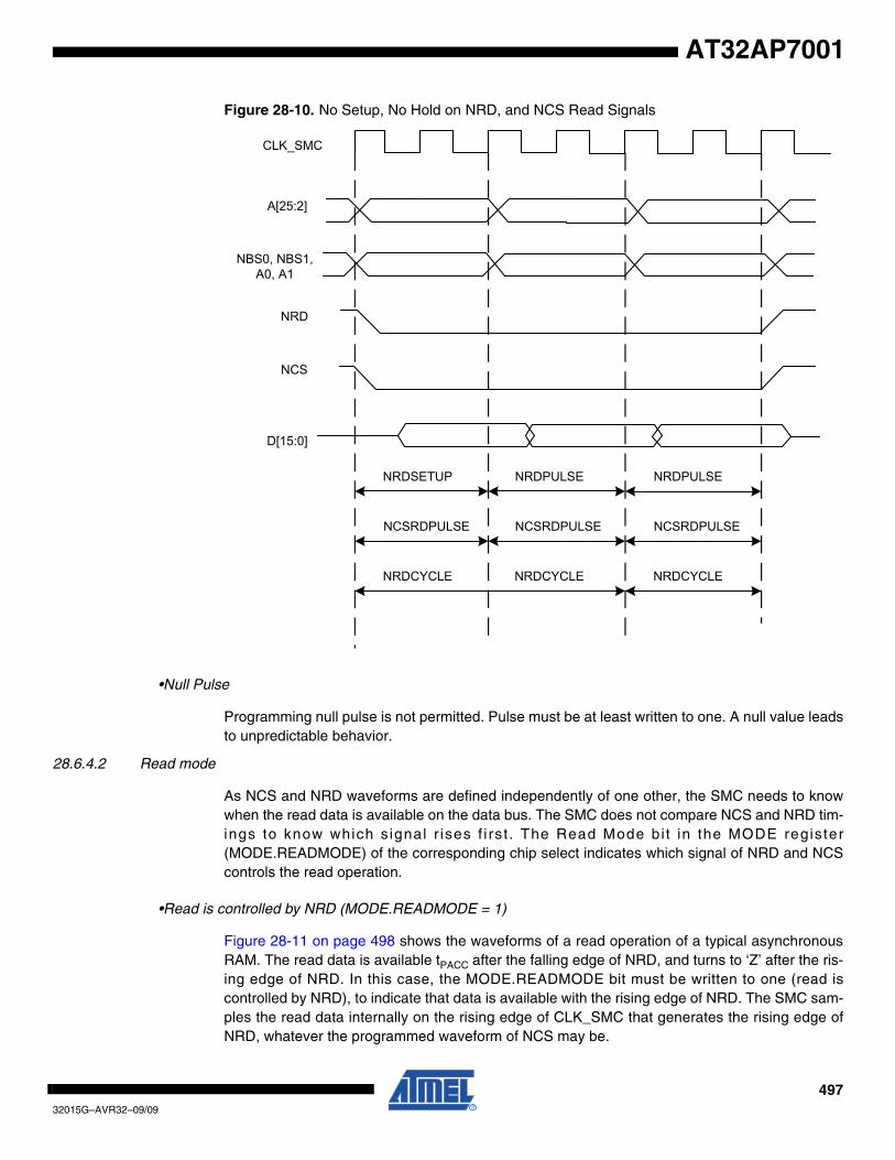
49732015G–AVR32–09/09
AT32AP7001
Figure 28-10. No Setup, No Hold on NRD, and NCS Read Signals
•Null Pulse
Programming null pulse is not permitted. Pulse must be at least written to one. A null value leadsto unpredictable behavior.
28.6.4.2 Read mode
As NCS and NRD waveforms are defined independently of one other, the SMC needs to knowwhen the read data is available on the data bus. The SMC does not compare NCS and NRD tim-ings to know which s ignal r ises f i rs t . The Read Mode bi t in the MODE register(MODE.READMODE) of the corresponding chip select indicates which signal of NRD and NCScontrols the read operation.
•Read is controlled by NRD (MODE.READMODE = 1)
Figure 28-11 on page 498 shows the waveforms of a read operation of a typical asynchronousRAM. The read data is available tPACC after the falling edge of NRD, and turns to ‘Z’ after the ris-ing edge of NRD. In this case, the MODE.READMODE bit must be written to one (read iscontrolled by NRD), to indicate that data is available with the rising edge of NRD. The SMC sam-ples the read data internally on the rising edge of CLK_SMC that generates the rising edge ofNRD, whatever the programmed waveform of NCS may be.
CLK_SMC
A[25:2]
NBS0, NBS1, A0, A1
NRD
NCS
D[15:0]
NRDSETUP NRDPULSE
NCSRDPULSE
NRDCYCLE NRDCYCLE
NCSRDPULSE NCSRDPULSE
NRDPULSE
NRDCYCLE
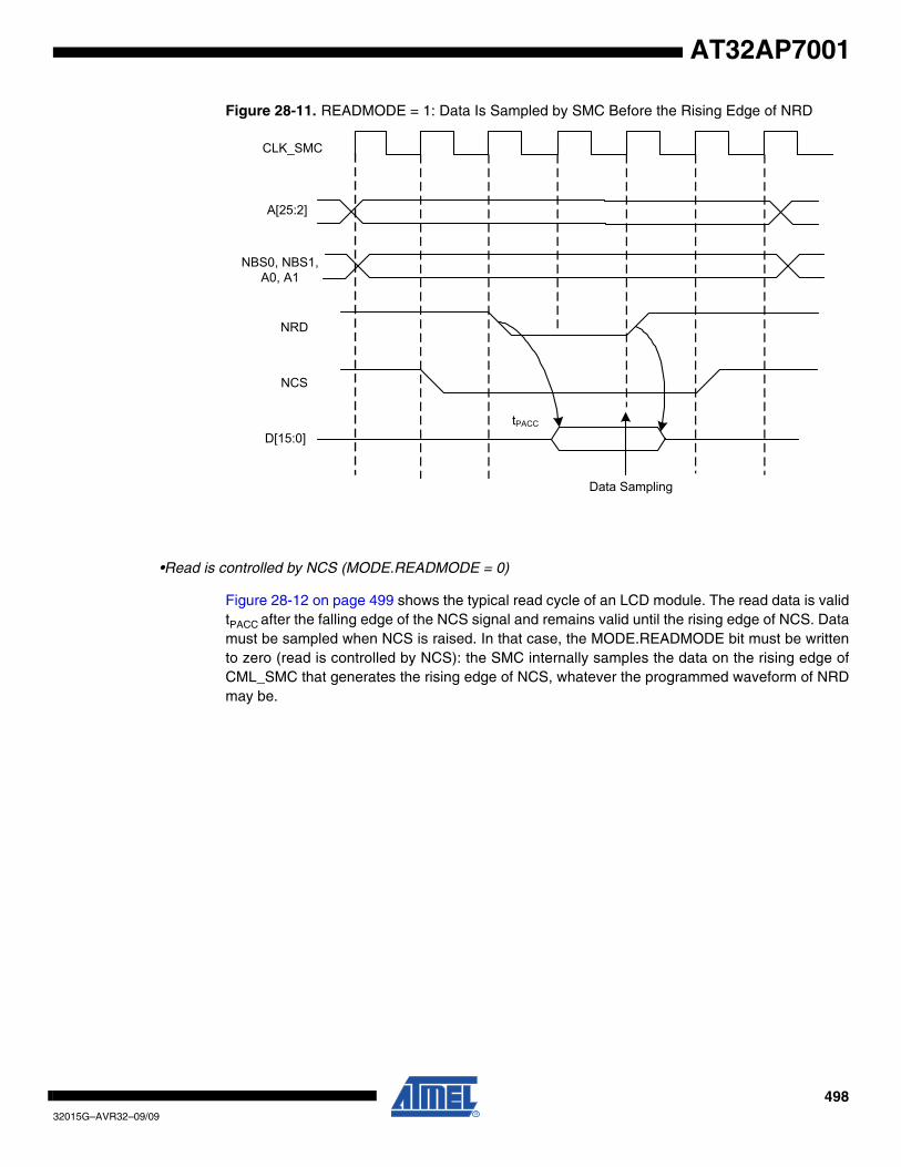
49832015G–AVR32–09/09
AT32AP7001
Figure 28-11. READMODE = 1: Data Is Sampled by SMC Before the Rising Edge of NRD
•Read is controlled by NCS (MODE.READMODE = 0)
Figure 28-12 on page 499 shows the typical read cycle of an LCD module. The read data is validtPACC after the falling edge of the NCS signal and remains valid until the rising edge of NCS. Datamust be sampled when NCS is raised. In that case, the MODE.READMODE bit must be writtento zero (read is controlled by NCS): the SMC internally samples the data on the rising edge ofCML_SMC that generates the rising edge of NCS, whatever the programmed waveform of NRDmay be.
CLK_SMC
A[25:2]
NBS0, NBS1, A0, A1
NRD
NCS
D[15:0]tPACC
Data Sampling
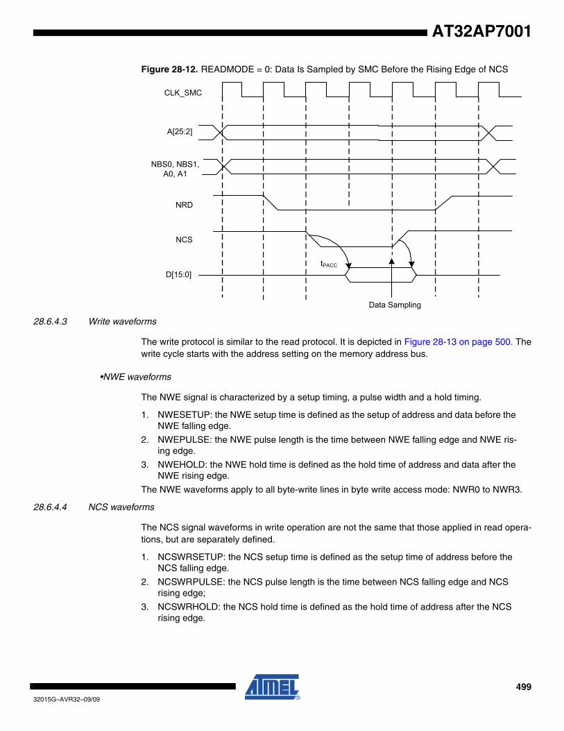
49932015G–AVR32–09/09
AT32AP7001
Figure 28-12. READMODE = 0: Data Is Sampled by SMC Before the Rising Edge of NCS
28.6.4.3 Write waveforms
The write protocol is similar to the read protocol. It is depicted in Figure 28-13 on page 500. Thewrite cycle starts with the address setting on the memory address bus.
•NWE waveforms
The NWE signal is characterized by a setup timing, a pulse width and a hold timing.
1. NWESETUP: the NWE setup time is defined as the setup of address and data before the NWE falling edge.
2. NWEPULSE: the NWE pulse length is the time between NWE falling edge and NWE ris-ing edge.
3. NWEHOLD: the NWE hold time is defined as the hold time of address and data after the NWE rising edge.
The NWE waveforms apply to all byte-write lines in byte write access mode: NWR0 to NWR3.
28.6.4.4 NCS waveforms
The NCS signal waveforms in write operation are not the same that those applied in read opera-tions, but are separately defined.
1. NCSWRSETUP: the NCS setup time is defined as the setup time of address before the NCS falling edge.
2. NCSWRPULSE: the NCS pulse length is the time between NCS falling edge and NCS rising edge;
3. NCSWRHOLD: the NCS hold time is defined as the hold time of address after the NCS rising edge.
CLK_SMC
A[25:2]
NBS0, NBS1, A0, A1
NRD
NCS
D[15:0]tPACC
Data Sampling
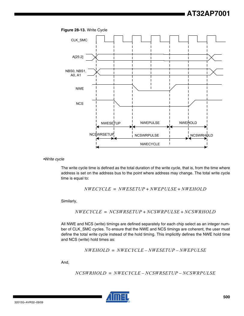
50032015G–AVR32–09/09
AT32AP7001
Figure 28-13. Write Cycle
•Write cycle
The write cycle time is defined as the total duration of the write cycle, that is, from the time whereaddress is set on the address bus to the point where address may change. The total write cycletime is equal to:
Similarly,
All NWE and NCS (write) timings are defined separately for each chip select as an integer num-ber of CLK_SMC cycles. To ensure that the NWE and NCS timings are coherent, the user mustdefine the total write cycle instead of the hold timing. This implicitly defines the NWE hold timeand NCS (write) hold times as:
And,
CLK_SMC
A[25:2]
NBS0, NBS1, A0, A1
NWE
NCS
NWESETUP NWEPULSE
NCSWRPULSENCSWRSETUP
NWECYCLE
NWEHOLD
NCSWRHOLD
NWECYCLE NWESETUP NWEPULSE NWEHOLD+ +=
NWECYCLE NCSWRSETUP NCSWRPULSE NCSWRHOLD+ +=
NWEHOLD NWECYCLE NWESETUP– NWEPULSE–=
NCSWRHOLD NWECYCLE NCSWRSETUP– NCSWRPULSE–=
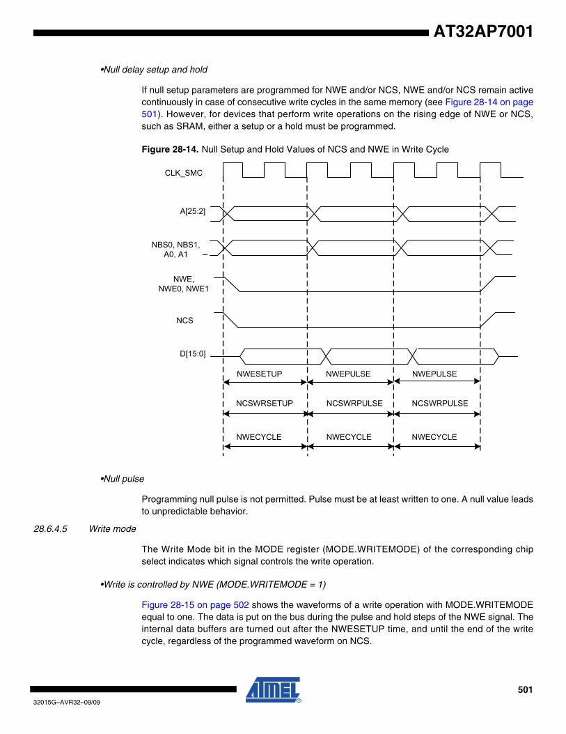
50132015G–AVR32–09/09
AT32AP7001
•Null delay setup and hold
If null setup parameters are programmed for NWE and/or NCS, NWE and/or NCS remain activecontinuously in case of consecutive write cycles in the same memory (see Figure 28-14 on page501). However, for devices that perform write operations on the rising edge of NWE or NCS,such as SRAM, either a setup or a hold must be programmed.
Figure 28-14. Null Setup and Hold Values of NCS and NWE in Write Cycle
•Null pulse
Programming null pulse is not permitted. Pulse must be at least written to one. A null value leadsto unpredictable behavior.
28.6.4.5 Write mode
The Write Mode bit in the MODE register (MODE.WRITEMODE) of the corresponding chipselect indicates which signal controls the write operation.
•Write is controlled by NWE (MODE.WRITEMODE = 1)
Figure 28-15 on page 502 shows the waveforms of a write operation with MODE.WRITEMODEequal to one. The data is put on the bus during the pulse and hold steps of the NWE signal. Theinternal data buffers are turned out after the NWESETUP time, and until the end of the writecycle, regardless of the programmed waveform on NCS.
CLK_SMC
A[25:2]
NBS0, NBS1, A0, A1
NWE,NWE0, NWE1
NCS
NWESETUP NWEPULSE
NCSWRPULSENCSWRSETUP
NWECYCLE
D[15:0]
NWECYCLE
NWEPULSE
NCSWRPULSE
NWECYCLE
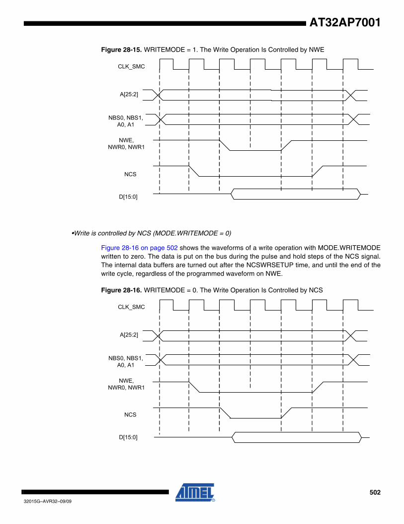
50232015G–AVR32–09/09
AT32AP7001
Figure 28-15. WRITEMODE = 1. The Write Operation Is Controlled by NWE
•Write is controlled by NCS (MODE.WRITEMODE = 0)
Figure 28-16 on page 502 shows the waveforms of a write operation with MODE.WRITEMODEwritten to zero. The data is put on the bus during the pulse and hold steps of the NCS signal.The internal data buffers are turned out after the NCSWRSETUP time, and until the end of thewrite cycle, regardless of the programmed waveform on NWE.
Figure 28-16. WRITEMODE = 0. The Write Operation Is Controlled by NCS
CLK_SMC
A[25:2]
NBS0, NBS1, A0, A1
NWE,NWR0, NWR1
NCS
D[15:0]
CLK_SMC
A[25:2]
NBS0, NBS1, A0, A1
NWE,NWR0, NWR1
NCS
D[15:0]
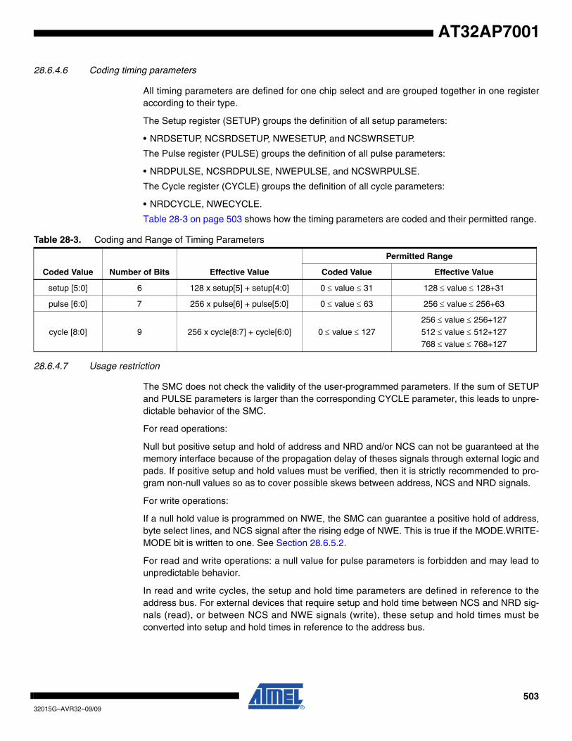
50332015G–AVR32–09/09
AT32AP7001
28.6.4.6 Coding timing parameters
All timing parameters are defined for one chip select and are grouped together in one registeraccording to their type.
The Setup register (SETUP) groups the definition of all setup parameters:
• NRDSETUP, NCSRDSETUP, NWESETUP, and NCSWRSETUP.
The Pulse register (PULSE) groups the definition of all pulse parameters:
• NRDPULSE, NCSRDPULSE, NWEPULSE, and NCSWRPULSE.
The Cycle register (CYCLE) groups the definition of all cycle parameters:
• NRDCYCLE, NWECYCLE.
Table 28-3 on page 503 shows how the timing parameters are coded and their permitted range.
28.6.4.7 Usage restriction
The SMC does not check the validity of the user-programmed parameters. If the sum of SETUPand PULSE parameters is larger than the corresponding CYCLE parameter, this leads to unpre-dictable behavior of the SMC.
For read operations:
Null but positive setup and hold of address and NRD and/or NCS can not be guaranteed at thememory interface because of the propagation delay of theses signals through external logic andpads. If positive setup and hold values must be verified, then it is strictly recommended to pro-gram non-null values so as to cover possible skews between address, NCS and NRD signals.
For write operations:
If a null hold value is programmed on NWE, the SMC can guarantee a positive hold of address,byte select lines, and NCS signal after the rising edge of NWE. This is true if the MODE.WRITE-MODE bit is written to one. See Section 28.6.5.2.
For read and write operations: a null value for pulse parameters is forbidden and may lead tounpredictable behavior.
In read and write cycles, the setup and hold time parameters are defined in reference to theaddress bus. For external devices that require setup and hold time between NCS and NRD sig-nals (read), or between NCS and NWE signals (write), these setup and hold times must beconverted into setup and hold times in reference to the address bus.
Table 28-3. Coding and Range of Timing Parameters
Coded Value Number of Bits Effective Value
Permitted Range
Coded Value Effective Value
setup [5:0] 6 128 x setup[5] + setup[4:0] 0 ≤ value ≤ 31 128 ≤ value ≤ 128+31
pulse [6:0] 7 256 x pulse[6] + pulse[5:0] 0 ≤ value ≤ 63 256 ≤ value ≤ 256+63
cycle [8:0] 9 256 x cycle[8:7] + cycle[6:0] 0 ≤ value ≤ 127
256 ≤ value ≤ 256+127
512 ≤ value ≤ 512+127768 ≤ value ≤ 768+127
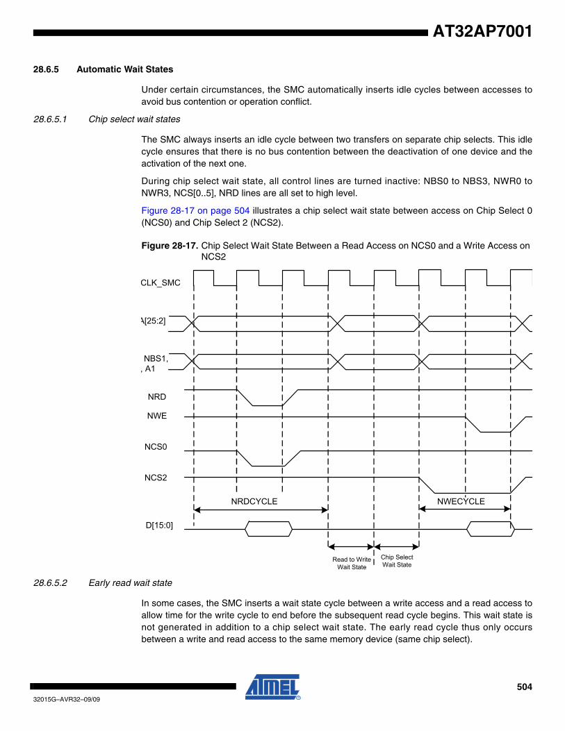
50432015G–AVR32–09/09
AT32AP7001
28.6.5 Automatic Wait States
Under certain circumstances, the SMC automatically inserts idle cycles between accesses toavoid bus contention or operation conflict.
28.6.5.1 Chip select wait states
The SMC always inserts an idle cycle between two transfers on separate chip selects. This idlecycle ensures that there is no bus contention between the deactivation of one device and theactivation of the next one.
During chip select wait state, all control lines are turned inactive: NBS0 to NBS3, NWR0 toNWR3, NCS[0..5], NRD lines are all set to high level.
Figure 28-17 on page 504 illustrates a chip select wait state between access on Chip Select 0(NCS0) and Chip Select 2 (NCS2).
Figure 28-17. Chip Select Wait State Between a Read Access on NCS0 and a Write Access on NCS2
28.6.5.2 Early read wait state
In some cases, the SMC inserts a wait state cycle between a write access and a read access toallow time for the write cycle to end before the subsequent read cycle begins. This wait state isnot generated in addition to a chip select wait state. The early read cycle thus only occursbetween a write and read access to the same memory device (same chip select).
CLK_SMC
A[25:2]
NBS1, , A1
NRD
NWE
NCS0
NCS2
D[15:0]
NRDCYCLE
Read to WriteWait State
Chip SelectWait State
NWECYCLE
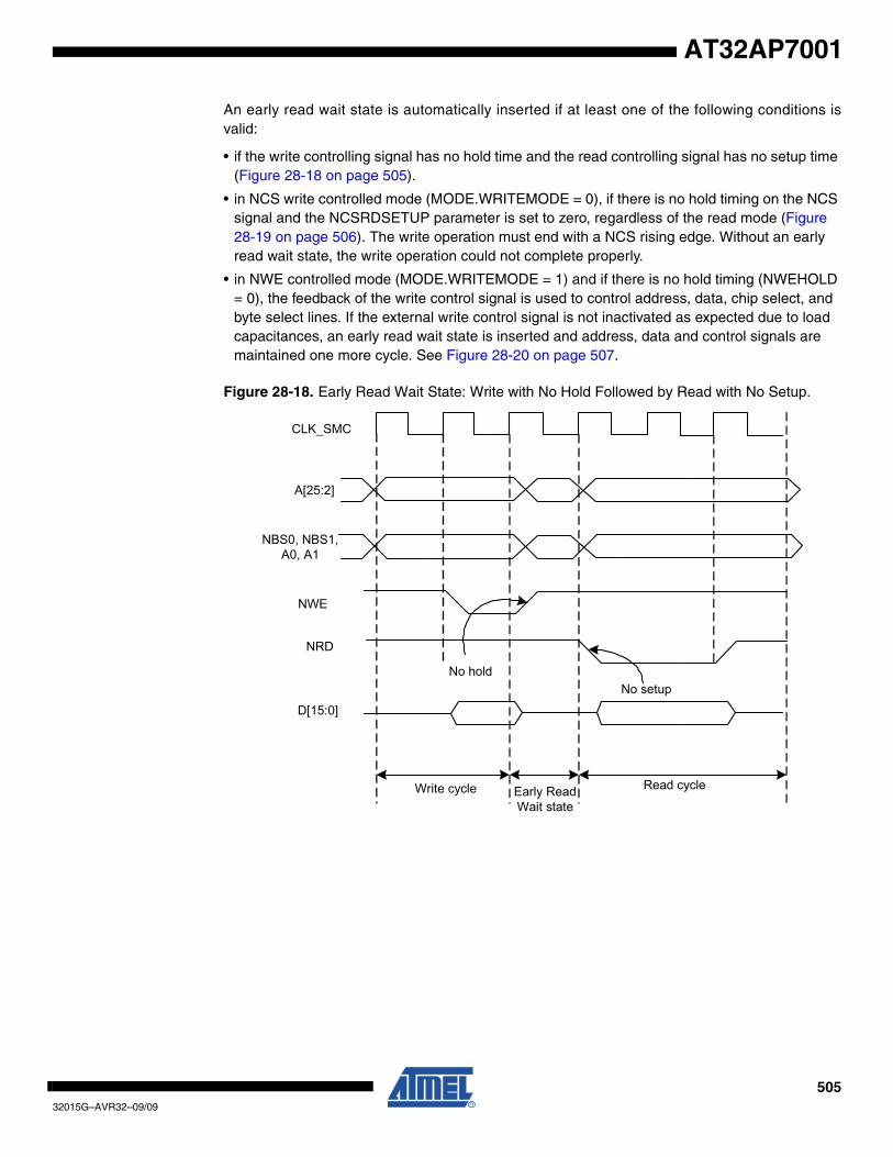
50532015G–AVR32–09/09
AT32AP7001
An early read wait state is automatically inserted if at least one of the following conditions isvalid:
• if the write controlling signal has no hold time and the read controlling signal has no setup time (Figure 28-18 on page 505).
• in NCS write controlled mode (MODE.WRITEMODE = 0), if there is no hold timing on the NCS signal and the NCSRDSETUP parameter is set to zero, regardless of the read mode (Figure 28-19 on page 506). The write operation must end with a NCS rising edge. Without an early read wait state, the write operation could not complete properly.
• in NWE controlled mode (MODE.WRITEMODE = 1) and if there is no hold timing (NWEHOLD = 0), the feedback of the write control signal is used to control address, data, chip select, and byte select lines. If the external write control signal is not inactivated as expected due to load capacitances, an early read wait state is inserted and address, data and control signals are maintained one more cycle. See Figure 28-20 on page 507.
Figure 28-18. Early Read Wait State: Write with No Hold Followed by Read with No Setup.
CLK_SMC
A[25:2]
NBS0, NBS1, A0, A1
NWE
NRD
D[15:0]
No holdNo setup
Read cycleEarly ReadWait state
Write cycle
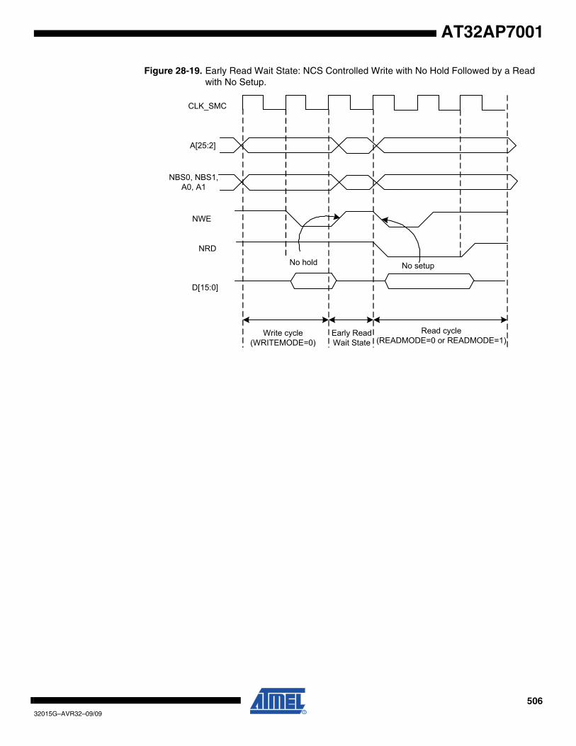
50632015G–AVR32–09/09
AT32AP7001
Figure 28-19. Early Read Wait State: NCS Controlled Write with No Hold Followed by a Read with No Setup.
CLK_SMC
A[25:2]
NBS0, NBS1, A0, A1
NWE
NRD
D[15:0]
No hold No setup
Read cycle(READMODE=0 or READMODE=1)
Early ReadWait State
Write cycle(WRITEMODE=0)
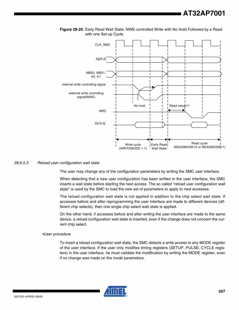
50732015G–AVR32–09/09
AT32AP7001
Figure 28-20. Early Read Wait State: NWE-controlled Write with No Hold Followed by a Read with one Set-up Cycle.
28.6.5.3 Reload user configuration wait state
The user may change any of the configuration parameters by writing the SMC user interface.
When detecting that a new user configuration has been written in the user interface, the SMCinserts a wait state before starting the next access. The so called “reload user configuration waitstate” is used by the SMC to load the new set of parameters to apply to next accesses.
The reload configuration wait state is not applied in addition to the chip select wait state. Ifaccesses before and after reprogramming the user interface are made to different devices (dif-ferent chip selects), then one single chip select wait state is applied.
On the other hand, if accesses before and after writing the user interface are made to the samedevice, a reload configuration wait state is inserted, even if the change does not concern the cur-rent chip select.
•User procedure
To insert a reload configuration wait state, the SMC detects a write access to any MODE registerof the user interface. If the user only modifies timing registers (SETUP, PULSE, CYCLE regis-ters) in the user interface, he must validate the modification by writing the MODE register, evenif no change was made on the mode parameters.
CLK_SMC
A[25:2]
NBS0, NBS1, A0, A1
Internal write controlling signal
external write controlling signal(NWE)
NRD
D[15:0]
No hold Read setup=1
Write cycle(WRITEMODE = 1)
Early ReadWait State
Read cycle(READMODE=0 or READMODE=1)
50832015G–AVR32–09/09
AT32AP7001
•Slow clock mode transition
A reload configuration wait state is also inserted when the slow clock mode is entered or exited,after the end of the current transfer (see Section 28.6.8).
28.6.5.4 Read to write wait state
Due to an internal mechanism, a wait cycle is always inserted between consecutive read andwrite SMC accesses.
This wait cycle is referred to as a read to write wait state in this document.
This wait cycle is applied in addition to chip select and reload user configuration wait stateswhen they are to be inserted. See Figure 28-17 on page 504.
28.6.6 Data Float Wait States
Some memory devices are slow to release the external bus. For such devices, it is necessary toadd wait states (data float wait states) after a read access:
• before starting a read access to a different external memory.
• before starting a write access to the same device or to a different external one.
The Data Float Output Time (tDF) for each external memory device is programmed in the DataFloat Time field of the MODE register (MODE.TDFCYCLES) for the corresponding chip select.The value of MODE.TDFCYCLES indicates the number of data float wait cycles (between 0 and15) before the external device releases the bus, and represents the time allowed for the dataoutput to go to high impedance after the memory is disabled.
Data float wait states do not delay internal memory accesses. Hence, a single access to anexternal memory with long tDF will not slow down the execution of a program from internalmemory.
The data float wait states management depends on the MODE.READMODE bit and the TDFOptimization bit of the MODE register (MODE.TDFMODE) for the corresponding chip select.
28.6.6.1 Read mode
Writing a one to the MODE.READMODE bit indicates to the SMC that the NRD signal is respon-sible for turning off the tri-state buffers of the external memory device. The data float period thenbegins after the rising edge of the NRD signal and lasts MODE.TDFCYCLES cycles of theCLK_SMC clock.
When the read operation is controlled by the NCS signal (MODE.READMODE = 0), theMODE.TDFCYCLES field gives the number of CLK_SMC cycles during which the data busremains busy after the rising edge of NCS.
Figure 28-21 on page 509 illustrates the data float period in NRD-controlled mode(MODE.READMODE =1), assuming a data float period of two cycles (MODE.TDFCYCLES = 2).Figure 28-22 on page 509 shows the read operation when controlled by NCS (MODE.READ-MODE = 0) and the MODE.TDFCYCLES field equals to three.
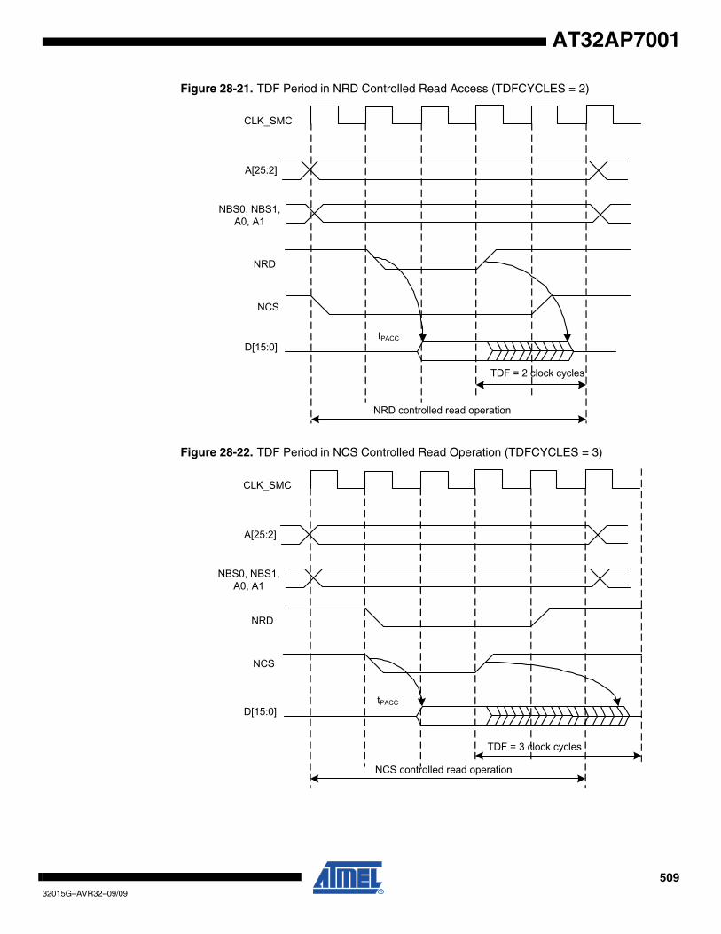
50932015G–AVR32–09/09
AT32AP7001
Figure 28-21. TDF Period in NRD Controlled Read Access (TDFCYCLES = 2)
Figure 28-22. TDF Period in NCS Controlled Read Operation (TDFCYCLES = 3)
CLK_SMC
A[25:2]
NBS0, NBS1, A0, A1
NRD
NCS
D[15:0]tPACC
NRD controlled read operation
TDF = 2 clock cycles
CLK_SMC
A[25:2]
NBS0, NBS1, A0, A1
NRD
NCS
D[15:0]tPACC
NCS controlled read operation
TDF = 3 clock cycles
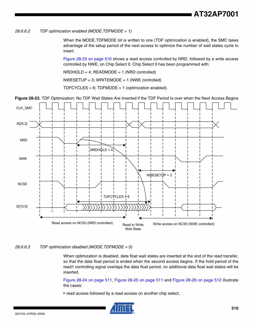
51032015G–AVR32–09/09
AT32AP7001
28.6.6.2 TDF optimization enabled (MODE.TDFMODE = 1)
When the MODE.TDFMODE bit is written to one (TDF optimization is enabled), the SMC takesadvantage of the setup period of the next access to optimize the number of wait states cycle toinsert.
Figure 28-23 on page 510 shows a read access controlled by NRD, followed by a write accesscontrolled by NWE, on Chip Select 0. Chip Select 0 has been programmed with:
NRDHOLD = 4; READMODE = 1 (NRD controlled)
NWESETUP = 3; WRITEMODE = 1 (NWE controlled)
TDFCYCLES = 6; TDFMODE = 1 (optimization enabled).
Figure 28-23. TDF Optimization: No TDF Wait States Are Inserted if the TDF Period Is over when the Next Access Begins
28.6.6.3 TDF optimization disabled (MODE.TDFMODE = 0)
When optimization is disabled, data float wait states are inserted at the end of the read transfer,so that the data float period is ended when the second access begins. If the hold period of theread1 controlling signal overlaps the data float period, no additional data float wait states will beinserted.
Figure 28-24 on page 511, Figure 28-25 on page 511 and Figure 28-26 on page 512 illustratethe cases:
• read access followed by a read access on another chip select.
CLK_SMC
A[25:2]
NRD
NWE
NCS0
D[15:0]
Read access on NCS0 (NRD controlled) Read to WriteWait State
Write access on NCS0 (NWE controlled)
TDFCYCLES = 6
NWESETUP = 3
NRDHOLD = 4
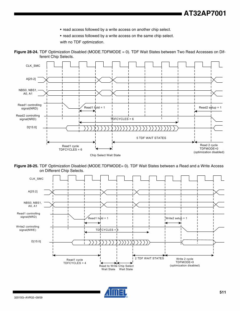
51132015G–AVR32–09/09
AT32AP7001
• read access followed by a write access on another chip select.
• read access followed by a write access on the same chip select.
with no TDF optimization.
Figure 28-24. TDF Optimization Disabled (MODE.TDFMODE = 0). TDF Wait States between Two Read Accesses on Dif-ferent Chip Selects.
Figure 28-25. TDF Optimization Disabled (MODE.TDFMODE= 0). TDF Wait States between a Read and a Write Access on Different Chip Selects.
CLK_SMC
A[25:2]
NBS0, NBS1, A0, A1
Read1 controlling signal(NRD)
Read2 controlling signal(NRD)
D[15:0]
Read1 hold = 1
Read1 cycleTDFCYCLES = 6
Chip Select Wait State
5 TDF WAIT STATES
TDFCYCLES = 6
Read2 setup = 1
Read 2 cycleTDFMODE=0
(optimization disabled)
CLK_SMC
A[25:2]
NBS0, NBS1, A0, A1
Read1 controlling signal(NRD)
Write2 controlling signal(NWE)
D[15:0]
Read1 cycleTDFCYCLES = 4
Chip Select Wait State
Read1 hold = 1
TDFCYCLES = 4
Read to WriteWait State
2 TDF WAIT STATES
Write2 setup = 1
Write 2 cycleTDFMODE=0
(optimization disabled)
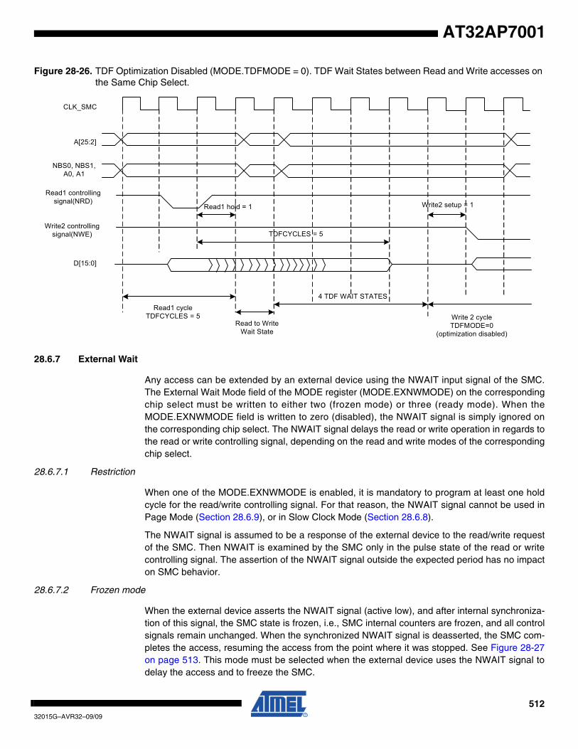
51232015G–AVR32–09/09
AT32AP7001
Figure 28-26. TDF Optimization Disabled (MODE.TDFMODE = 0). TDF Wait States between Read and Write accesses on the Same Chip Select.
28.6.7 External Wait
Any access can be extended by an external device using the NWAIT input signal of the SMC.The External Wait Mode field of the MODE register (MODE.EXNWMODE) on the correspondingchip select must be written to either two (frozen mode) or three (ready mode). When theMODE.EXNWMODE field is written to zero (disabled), the NWAIT signal is simply ignored onthe corresponding chip select. The NWAIT signal delays the read or write operation in regards tothe read or write controlling signal, depending on the read and write modes of the correspondingchip select.
28.6.7.1 Restriction
When one of the MODE.EXNWMODE is enabled, it is mandatory to program at least one holdcycle for the read/write controlling signal. For that reason, the NWAIT signal cannot be used inPage Mode (Section 28.6.9), or in Slow Clock Mode (Section 28.6.8).
The NWAIT signal is assumed to be a response of the external device to the read/write requestof the SMC. Then NWAIT is examined by the SMC only in the pulse state of the read or writecontrolling signal. The assertion of the NWAIT signal outside the expected period has no impacton SMC behavior.
28.6.7.2 Frozen mode
When the external device asserts the NWAIT signal (active low), and after internal synchroniza-tion of this signal, the SMC state is frozen, i.e., SMC internal counters are frozen, and all controlsignals remain unchanged. When the synchronized NWAIT signal is deasserted, the SMC com-pletes the access, resuming the access from the point where it was stopped. See Figure 28-27on page 513. This mode must be selected when the external device uses the NWAIT signal todelay the access and to freeze the SMC.
CLK_SMC
A[25:2]
NBS0, NBS1, A0, A1
Read1 controlling signal(NRD)
Write2 controlling signal(NWE)
D[15:0]
Read1 hold = 1
TDFCYCLES = 5
Read1 cycleTDFCYCLES = 5
Read to WriteWait State
4 TDF WAIT STATES
Write2 setup = 1
Write 2 cycleTDFMODE=0
(optimization disabled)
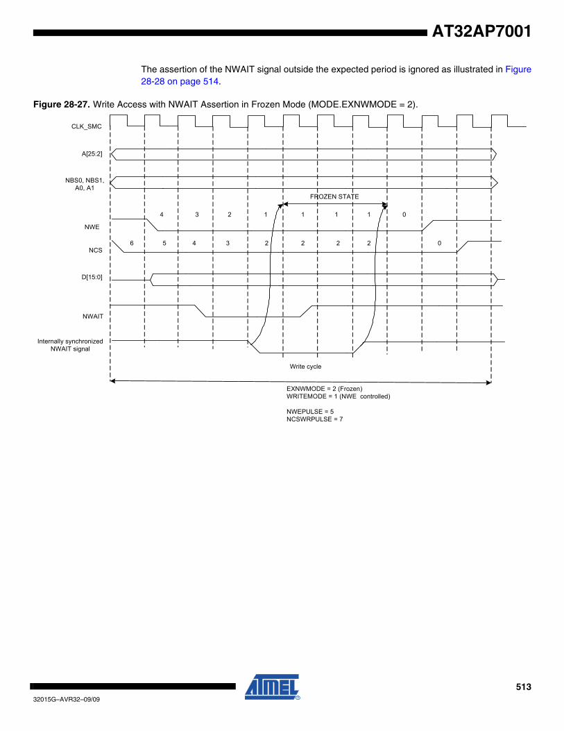
51332015G–AVR32–09/09
AT32AP7001
The assertion of the NWAIT signal outside the expected period is ignored as illustrated in Figure28-28 on page 514.
Figure 28-27. Write Access with NWAIT Assertion in Frozen Mode (MODE.EXNWMODE = 2).
CLK_SMC
A[25:2]
NBS0, NBS1, A0, A1
NWE
NCS
D[15:0]
6 5 4
4
3
3
2
2 1 1
2
1
2 2
1
0
0
FROZEN STATE
NWAIT
Internally synchronized NWAIT signal
Write cycle
EXNWMODE = 2 (Frozen)WRITEMODE = 1 (NWE controlled)
NWEPULSE = 5NCSWRPULSE = 7
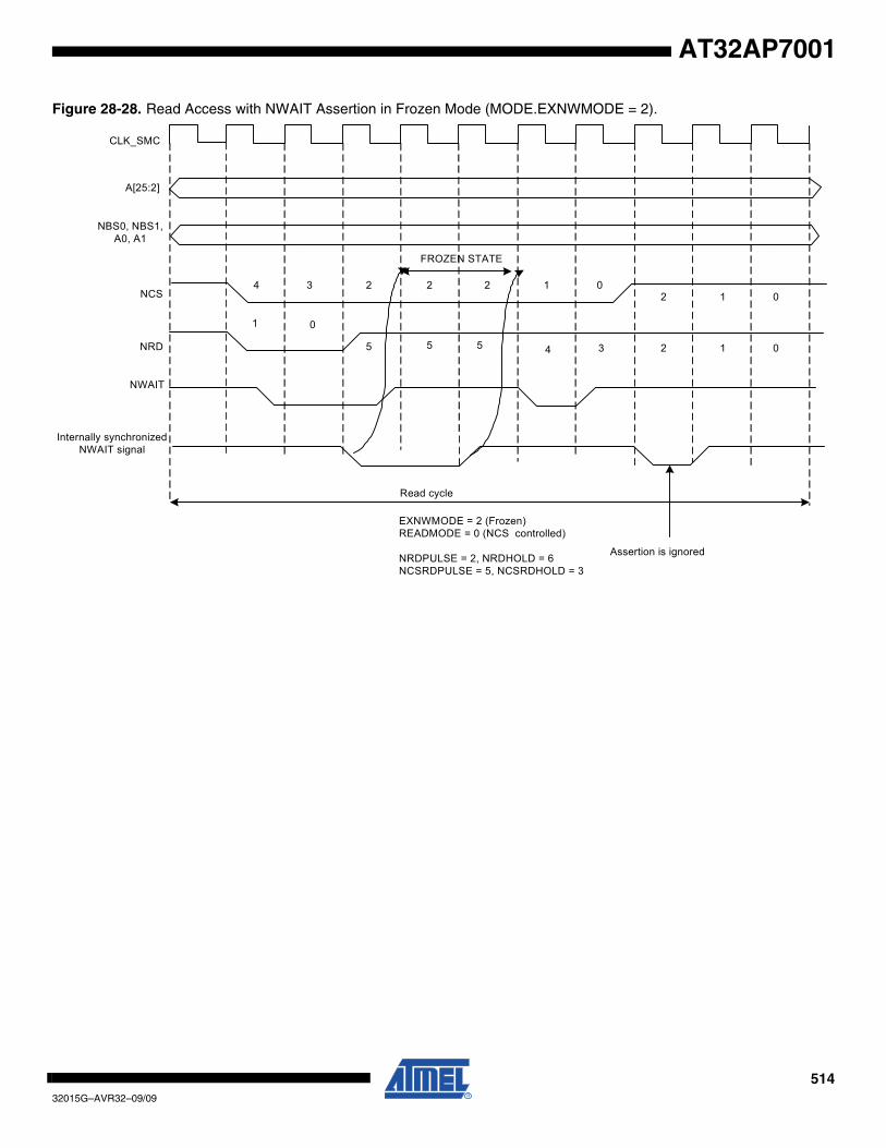
51432015G–AVR32–09/09
AT32AP7001
Figure 28-28. Read Access with NWAIT Assertion in Frozen Mode (MODE.EXNWMODE = 2).
CLK_SMC
A[25:2]
NBS0, NBS1, A0, A1
NCS
NRD
NWAIT
Internally synchronized NWAIT signal
EXNWMODE = 2 (Frozen)READMODE = 0 (NCS controlled)
NRDPULSE = 2, NRDHOLD = 6NCSRDPULSE = 5, NCSRDHOLD = 3
Read cycle
Assertion is ignored
4 3 2 1 02 2
1 0
5 5 5 4 3
2
2 1
1 0
0
FROZEN STATE
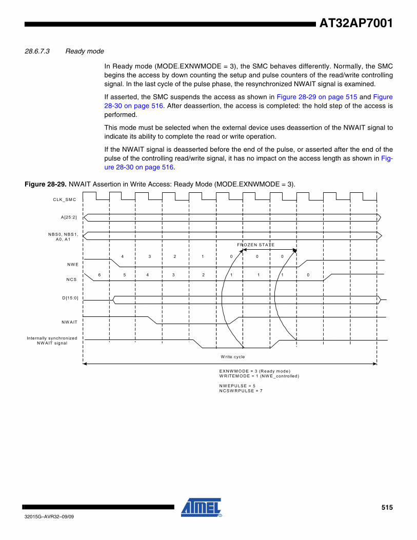
51532015G–AVR32–09/09
AT32AP7001
28.6.7.3 Ready mode
In Ready mode (MODE.EXNWMODE = 3), the SMC behaves differently. Normally, the SMCbegins the access by down counting the setup and pulse counters of the read/write controllingsignal. In the last cycle of the pulse phase, the resynchronized NWAIT signal is examined.
If asserted, the SMC suspends the access as shown in Figure 28-29 on page 515 and Figure28-30 on page 516. After deassertion, the access is completed: the hold step of the access isperformed.
This mode must be selected when the external device uses deassertion of the NWAIT signal toindicate its ability to complete the read or write operation.
If the NWAIT signal is deasserted before the end of the pulse, or asserted after the end of thepulse of the controlling read/write signal, it has no impact on the access length as shown in Fig-ure 28-30 on page 516.
Figure 28-29. NWAIT Assertion in Write Access: Ready Mode (MODE.EXNWMODE = 3).
C LK_SM C
A [25:2]
N BS 0, N BS 1, A 0, A1
N W E
N C S
D [15 :0 ]
6 5 4
4
3
3
2
2 1 0
1
0
1 1
0
FR O ZE N STA TE
N W A IT
Interna lly synchronized N W AIT s ignal
W rite cyc le
EXN W M O D E = 3 (R eady m ode)W R ITEM O D E = 1 (N W E_contro lled)
N W EPU LSE = 5N C SW R PU LSE = 7
0

51632015G–AVR32–09/09
AT32AP7001
Figure 28-30. NWAIT Assertion in Read Access: Ready Mode (EXNWMODE = 3).
CLK_SMC
A[25:2]
NBS0, NBS1, A0, A1
NCS
NRD6
6
5
5
4
4 3 2
3
1
2 1
0
NWAIT
Internally synchronized NWAIT signal
Read cycle
EXNWMODE = 3 (Ready mode)READMODE = 0 (NCS_controlled)
NRDPULSE = 7NCSRDPULSE = 7
1
0
0
Assertion is ignored Assertion is ignored
Wait STATE
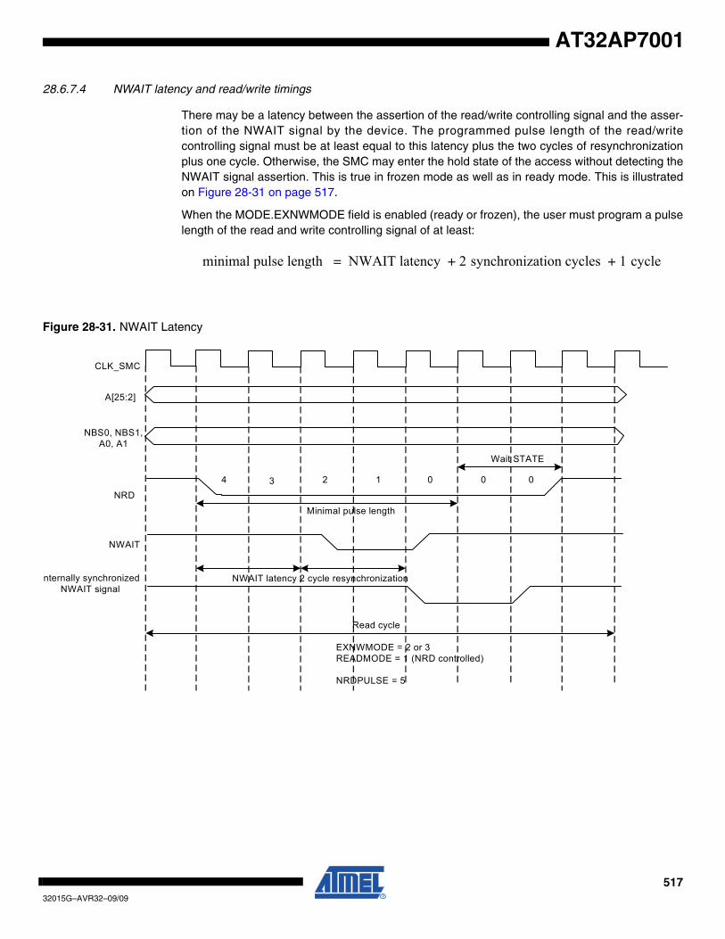
51732015G–AVR32–09/09
AT32AP7001
28.6.7.4 NWAIT latency and read/write timings
There may be a latency between the assertion of the read/write controlling signal and the asser-tion of the NWAIT signal by the device. The programmed pulse length of the read/writecontrolling signal must be at least equal to this latency plus the two cycles of resynchronizationplus one cycle. Otherwise, the SMC may enter the hold state of the access without detecting theNWAIT signal assertion. This is true in frozen mode as well as in ready mode. This is illustratedon Figure 28-31 on page 517.
When the MODE.EXNWMODE field is enabled (ready or frozen), the user must program a pulselength of the read and write controlling signal of at least:
Figure 28-31. NWAIT Latency
minimal pulse length NWAIT latency 2 synchronization cycles 1 cycle+ +=
Wait STATE
01234
CLK_SMC
A[25:2]
NBS0, NBS1, A0, A1
NRD
NWAIT
nternally synchronized NWAIT signal
Minimal pulse length
00
NWAIT latency 2 cycle resynchronization
Read cycle
EXNWMODE = 2 or 3READMODE = 1 (NRD controlled)
NRDPULSE = 5
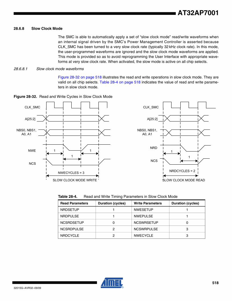
51832015G–AVR32–09/09
AT32AP7001
28.6.8 Slow Clock Mode
The SMC is able to automatically apply a set of “slow clock mode” read/write waveforms whenan internal signal driven by the SMC’s Power Management Controller is asserted becauseCLK_SMC has been turned to a very slow clock rate (typically 32 kHz clock rate). In this mode,the user-programmed waveforms are ignored and the slow clock mode waveforms are applied.This mode is provided so as to avoid reprogramming the User Interface with appropriate wave-forms at very slow clock rate. When activated, the slow mode is active on all chip selects.
28.6.8.1 Slow clock mode waveforms
Figure 28-32 on page 518 illustrates the read and write operations in slow clock mode. They arevalid on all chip selects. Table 28-4 on page 518 indicates the value of read and write parame-ters in slow clock mode.
Figure 28-32. Read and Write Cycles in Slow Clock Mode
CLK_SMC
A[25:2]
NBS0, NBS1, A0, A1
NCS
NWE
NWECYCLES = 3
SLOW CLOCK MODE WRITE
1
1
1
CLK_SMC
A[25:2]
NBS0, NBS1, A0, A1
NCS
NRD
SLOW CLOCK MODE READ
NRDCYCLES = 2
1
1
Table 28-4. Read and Write Timing Parameters in Slow Clock Mode
Read Parameters Duration (cycles) Write Parameters Duration (cycles)
NRDSETUP 1 NWESETUP 1
NRDPULSE 1 NWEPULSE 1
NCSRDSETUP 0 NCSWRSETUP 0
NCSRDPULSE 2 NCSWRPULSE 3
NRDCYCLE 2 NWECYCLE 3
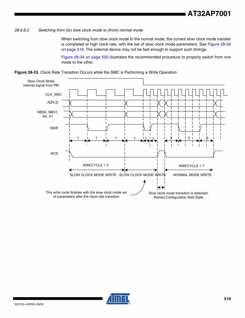
51932015G–AVR32–09/09
AT32AP7001
28.6.8.2 Switching from (to) slow clock mode to (from) normal mode
When switching from slow clock mode to the normal mode, the current slow clock mode transferis completed at high clock rate, with the set of slow clock mode parameters. See Figure 28-33on page 519. The external device may not be fast enough to support such timings.
Figure 28-34 on page 520 illustrates the recommended procedure to properly switch from onemode to the other.
Figure 28-33. Clock Rate Transition Occurs while the SMC is Performing a Write Operation
CLK_SMC
A[25:2]
NBS0, NBS1, A0, A1
NCS
NWE
Slow Clock ModeInternal signal from PM
This write cycle finishes with the slow clock mode setof parameters after the clock rate transition
NWECYCLE = 3
SLOW CLOCK MODE WRITE SLOW CLOCK MODE WRITE
1 1 1 1 1 1 2 3 2
NWECYCLE = 7
NORMAL MODE WRITE
Slow clock mode transition is detected:Reload Configuration Wait State

52032015G–AVR32–09/09
AT32AP7001
Figure 28-34. Recommended Procedure to Switch from Slow Clock Mode to Normal Mode or from Normal Mode to Slow Clock Mode
28.6.9 Asynchronous Page Mode
The SMC supports asynchronous burst reads in page mode, providing that the Page ModeEnabled bit is written to one in the MODE register (MODE.PMEN). The page size must be con-figured in the Page Size field in the MODE register (MODE.PS) to 4, 8, 16, or 32 bytes.
The page defines a set of consecutive bytes into memory. A 4-byte page (resp. 8-, 16-, 32-bytepage) is always aligned to 4-byte boundaries (resp. 8-, 16-, 32-byte boundaries) of memory. TheMSB of data address defines the address of the page in memory, the LSB of address define theaddress of the data in the page as detailed in Table 28-5 on page 520.
With page mode memory devices, the first access to one page (tpa) takes longer than the subse-quent accesses to the page (tsa) as shown in Figure 28-35 on page 521. When in page mode,the SMC enables the user to define different read timings for the first access within one page,and next accesses within the page.
Notes: 1. A denotes the address bus of the memory device2. For 16-bit devices, the bit 0 of address is ignored. For 32-bit devices, bits [1:0] are ignored.
28.6.9.1 Protocol and timings in page mode
Figure 28-35 on page 521 shows the NRD and NCS timings in page mode access.
CLK_SMC
Slow Clock ModeInternal signal from PM
A[25:2]
NBS0, NBS1, A0, A1
NWE
NCS
1 1
SLOW CLOCK MODE WRITE
2 3 2
IDLE STATE
Reload ConfigurationWait State
NORMAL MODE WRITE
1
Table 28-5. Page Address and Data Address within a Page
Page Size Page Address(1) Data Address in the Page(2)
4 bytes A[25:2] A[1:0]
8 bytes A[25:3] A[2:0]
16 bytes A[25:4] A[3:0]
32 bytes A[25:5] A[4:0]
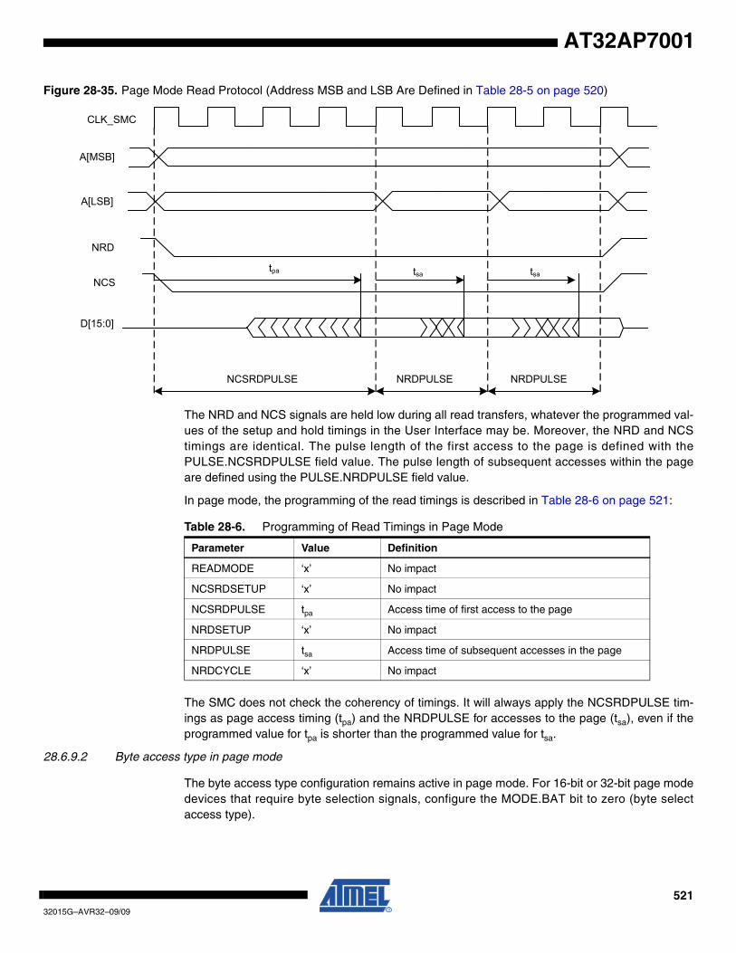
52132015G–AVR32–09/09
AT32AP7001
Figure 28-35. Page Mode Read Protocol (Address MSB and LSB Are Defined in Table 28-5 on page 520)
The NRD and NCS signals are held low during all read transfers, whatever the programmed val-ues of the setup and hold timings in the User Interface may be. Moreover, the NRD and NCStimings are identical. The pulse length of the first access to the page is defined with thePULSE.NCSRDPULSE field value. The pulse length of subsequent accesses within the pageare defined using the PULSE.NRDPULSE field value.
In page mode, the programming of the read timings is described in Table 28-6 on page 521:
The SMC does not check the coherency of timings. It will always apply the NCSRDPULSE tim-ings as page access timing (tpa) and the NRDPULSE for accesses to the page (tsa), even if theprogrammed value for tpa is shorter than the programmed value for tsa.
28.6.9.2 Byte access type in page mode
The byte access type configuration remains active in page mode. For 16-bit or 32-bit page modedevices that require byte selection signals, configure the MODE.BAT bit to zero (byte selectaccess type).
CLK_SMC
A[MSB]
A[LSB]
NCS
NRD
D[15:0]
tpa
NCSRDPULSE
tsa
NRDPULSE NRDPULSE
tsa
Table 28-6. Programming of Read Timings in Page Mode
Parameter Value Definition
READMODE ‘x’ No impact
NCSRDSETUP ‘x’ No impact
NCSRDPULSE tpa Access time of first access to the page
NRDSETUP ‘x’ No impact
NRDPULSE tsa Access time of subsequent accesses in the page
NRDCYCLE ‘x’ No impact

52232015G–AVR32–09/09
AT32AP7001
28.6.9.3 Page mode restriction
The page mode is not compatible with the use of the NWAIT signal. Using the page mode andthe NWAIT signal may lead to unpredictable behavior.
28.6.9.4 Sequential and non-sequential accesses
If the chip select and the MSB of addresses as defined in Table 28-5 on page 520 are identical,then the current access lies in the same page as the previous one, and no page break occurs.
Using this information, all data within the same page, sequential or not sequential, are accessedwith a minimum access time (tsa). Figure 28-36 on page 522 illustrates access to an 8-bit mem-ory device in page mode, with 8-byte pages. Access to D1 causes a page access with a longaccess time (tpa). Accesses to D3 and D7, though they are not sequential accesses, only requirea short access time (tsa).
If the MSB of addresses are different, the SMC performs the access of a new page. In the sameway, if the chip select is different from the previous access, a page break occurs. If two sequen-tial accesses are made to the page mode memory, but separated by an other internal or externalperipheral access, a page break occurs on the second access because the chip select of thedevice was deasserted between both accesses.
Figure 28-36. Access to Non-sequential Data within the Same Page
CLK_SMC
A[25:3]
A[2], A1, A0
NCS
NRD
D[7:0]
A1
Page address
A3 A7
D1 D3 D7
NCSRDPULSE NRDPULSE NRDPULSE
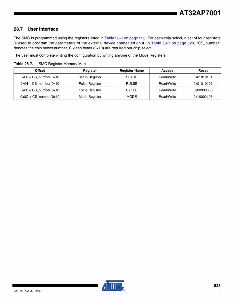
52332015G–AVR32–09/09
AT32AP7001
28.7 User Interface
The SMC is programmed using the registers listed in Table 28-7 on page 523. For each chip select, a set of four registersis used to program the parameters of the external device connected on it. In Table 28-7 on page 523, “CS_number”denotes the chip select number. Sixteen bytes (0x10) are required per chip select.
The user must complete writing the configuration by writing anyone of the Mode Registers.
Table 28-7. SMC Register Memory Map
Offset Register Register Name Access Reset
0x00 + CS_number*0x10 Setup Register SETUP Read/Write 0x01010101
0x04 + CS_number*0x10 Pulse Register PULSE Read/Write 0x01010101
0x08 + CS_number*0x10 Cycle Register CYCLE Read/Write 0x00030003
0x0C + CS_number*0x10 Mode Register MODE Read/Write 0x10002103
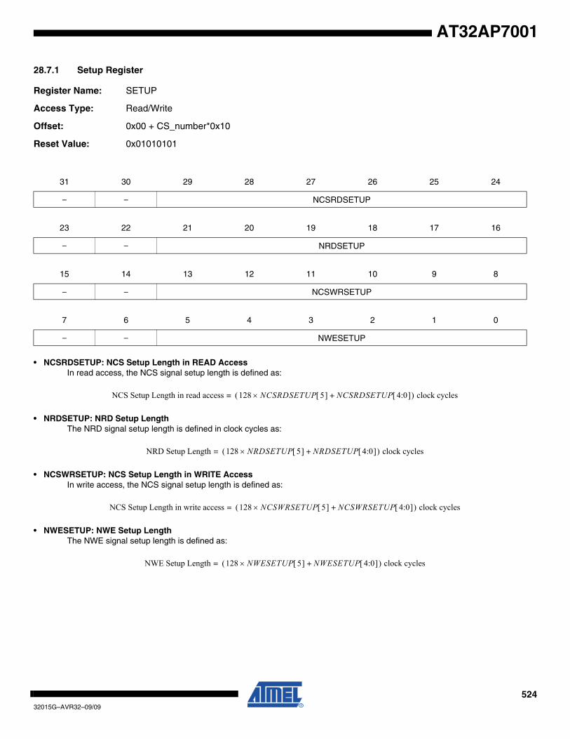
52432015G–AVR32–09/09
AT32AP7001
28.7.1 Setup Register
Register Name: SETUP
Access Type: Read/Write
Offset: 0x00 + CS_number*0x10
Reset Value: 0x01010101
• NCSRDSETUP: NCS Setup Length in READ AccessIn read access, the NCS signal setup length is defined as:
• NRDSETUP: NRD Setup LengthThe NRD signal setup length is defined in clock cycles as:
• NCSWRSETUP: NCS Setup Length in WRITE AccessIn write access, the NCS signal setup length is defined as:
• NWESETUP: NWE Setup LengthThe NWE signal setup length is defined as:
31 30 29 28 27 26 25 24
– – NCSRDSETUP
23 22 21 20 19 18 17 16
– – NRDSETUP
15 14 13 12 11 10 9 8
– – NCSWRSETUP
7 6 5 4 3 2 1 0
– – NWESETUP
NCS Setup Length in read access 128 NCSRDSETUP 5[ ] NCSRDSETUP 4:0[ ]+×( ) clock cycles=
NRD Setup Length 128 NRDSETUP 5[ ] NRDSETUP 4:0[ ]+×( ) clock cycles=
NCS Setup Length in write access 128 NCSWRSETUP 5[ ] NCSWRSETUP 4:0[ ]+×( ) clock cycles=
NWE Setup Length 128 NWESETUP 5[ ] NWESETUP 4:0[ ]+×( ) clock cycles=
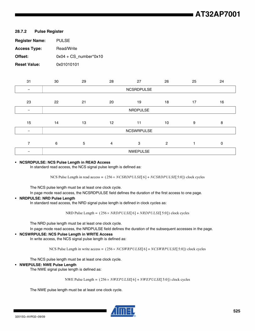
52532015G–AVR32–09/09
AT32AP7001
28.7.2 Pulse Register
Register Name: PULSE
Access Type: Read/Write
Offset: 0x04 + CS_number*0x10
Reset Value: 0x01010101
• NCSRDPULSE: NCS Pulse Length in READ AccessIn standard read access, the NCS signal pulse length is defined as:
The NCS pulse length must be at least one clock cycle.In page mode read access, the NCSRDPULSE field defines the duration of the first access to one page.
• NRDPULSE: NRD Pulse LengthIn standard read access, the NRD signal pulse length is defined in clock cycles as:
The NRD pulse length must be at least one clock cycle.
In page mode read access, the NRDPULSE field defines the duration of the subsequent accesses in the page.• NCSWRPULSE: NCS Pulse Length in WRITE Access
In write access, the NCS signal pulse length is defined as:
The NCS pulse length must be at least one clock cycle.
• NWEPULSE: NWE Pulse LengthThe NWE signal pulse length is defined as:
The NWE pulse length must be at least one clock cycle.
31 30 29 28 27 26 25 24
– NCSRDPULSE
23 22 21 20 19 18 17 16
– NRDPULSE
15 14 13 12 11 10 9 8
– NCSWRPULSE
7 6 5 4 3 2 1 0
– NWEPULSE
NCS Pulse Length in read access 256 NCSRDPULSE 6[ ] NCSRDPULSE 5:0[ ]+×( ) clock cycles=
NRD Pulse Length 256 NRDPULSE 6[ ] NRDPULSE 5:0[ ]+×( ) clock cycles=
NCS Pulse Length in write access 256 NCSWRPULSE 6[ ] NCSWRPULSE 5:0[ ]+×( ) clock cycles=
NWE Pulse Length 256 NWEPULSE 6[ ] NWEPULSE 5:0[ ]+×( ) clock cycles=
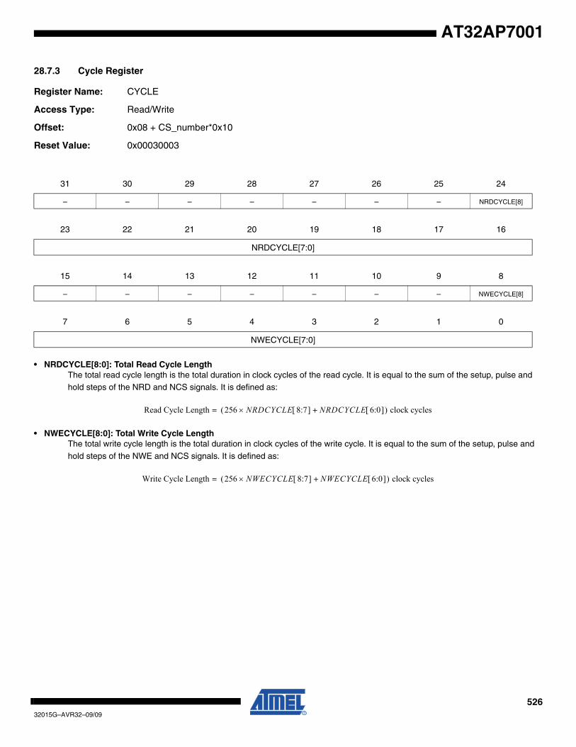
52632015G–AVR32–09/09
AT32AP7001
28.7.3 Cycle Register
Register Name: CYCLE
Access Type: Read/Write
Offset: 0x08 + CS_number*0x10
Reset Value: 0x00030003
• NRDCYCLE[8:0]: Total Read Cycle LengthThe total read cycle length is the total duration in clock cycles of the read cycle. It is equal to the sum of the setup, pulse and hold steps of the NRD and NCS signals. It is defined as:
• NWECYCLE[8:0]: Total Write Cycle LengthThe total write cycle length is the total duration in clock cycles of the write cycle. It is equal to the sum of the setup, pulse and
hold steps of the NWE and NCS signals. It is defined as:
31 30 29 28 27 26 25 24
– – – – – – – NRDCYCLE[8]
23 22 21 20 19 18 17 16
NRDCYCLE[7:0]
15 14 13 12 11 10 9 8
– – – – – – – NWECYCLE[8]
7 6 5 4 3 2 1 0
NWECYCLE[7:0]
Read Cycle Length 256 NRDCYCLE 8:7[ ] NRDCYCLE 6:0[ ]+×( ) clock cycles=
Write Cycle Length 256 NWECYCLE 8:7[ ] NWECYCLE 6:0[ ]+×( ) clock cycles=
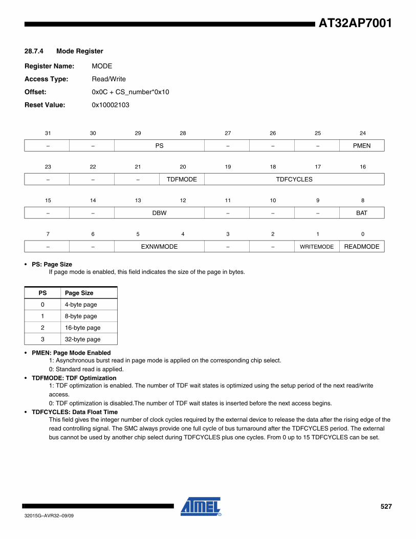
52732015G–AVR32–09/09
AT32AP7001
28.7.4 Mode Register
Register Name: MODE
Access Type: Read/Write
Offset: 0x0C + CS_number*0x10
Reset Value: 0x10002103
• PS: Page SizeIf page mode is enabled, this field indicates the size of the page in bytes.
• PMEN: Page Mode Enabled1: Asynchronous burst read in page mode is applied on the corresponding chip select.0: Standard read is applied.
• TDFMODE: TDF Optimization1: TDF optimization is enabled. The number of TDF wait states is optimized using the setup period of the next read/write
access.
0: TDF optimization is disabled.The number of TDF wait states is inserted before the next access begins.• TDFCYCLES: Data Float Time
This field gives the integer number of clock cycles required by the external device to release the data after the rising edge of the read controlling signal. The SMC always provide one full cycle of bus turnaround after the TDFCYCLES period. The external
bus cannot be used by another chip select during TDFCYCLES plus one cycles. From 0 up to 15 TDFCYCLES can be set.
31 30 29 28 27 26 25 24
– – PS – – – PMEN
23 22 21 20 19 18 17 16
– – – TDFMODE TDFCYCLES
15 14 13 12 11 10 9 8
– – DBW – – – BAT
7 6 5 4 3 2 1 0
– – EXNWMODE – – WRITEMODE READMODE
PS Page Size
0 4-byte page
1 8-byte page
2 16-byte page
3 32-byte page
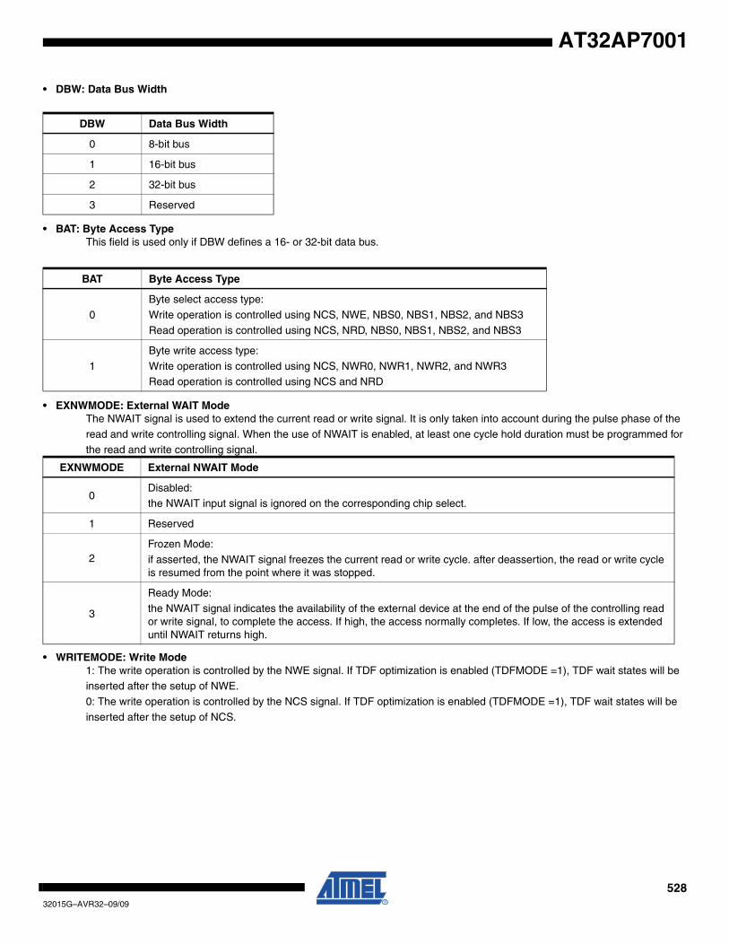
52832015G–AVR32–09/09
AT32AP7001
• DBW: Data Bus Width
• BAT: Byte Access TypeThis field is used only if DBW defines a 16- or 32-bit data bus.
• EXNWMODE: External WAIT ModeThe NWAIT signal is used to extend the current read or write signal. It is only taken into account during the pulse phase of the
read and write controlling signal. When the use of NWAIT is enabled, at least one cycle hold duration must be programmed for the read and write controlling signal.
• WRITEMODE: Write Mode1: The write operation is controlled by the NWE signal. If TDF optimization is enabled (TDFMODE =1), TDF wait states will be inserted after the setup of NWE.
0: The write operation is controlled by the NCS signal. If TDF optimization is enabled (TDFMODE =1), TDF wait states will be
inserted after the setup of NCS.
DBW Data Bus Width
0 8-bit bus
1 16-bit bus
2 32-bit bus
3 Reserved
BAT Byte Access Type
0
Byte select access type:
Write operation is controlled using NCS, NWE, NBS0, NBS1, NBS2, and NBS3
Read operation is controlled using NCS, NRD, NBS0, NBS1, NBS2, and NBS3
1
Byte write access type:
Write operation is controlled using NCS, NWR0, NWR1, NWR2, and NWR3Read operation is controlled using NCS and NRD
EXNWMODE External NWAIT Mode
0Disabled:the NWAIT input signal is ignored on the corresponding chip select.
1 Reserved
2Frozen Mode:
if asserted, the NWAIT signal freezes the current read or write cycle. after deassertion, the read or write cycle is resumed from the point where it was stopped.
3
Ready Mode:
the NWAIT signal indicates the availability of the external device at the end of the pulse of the controlling read or write signal, to complete the access. If high, the access normally completes. If low, the access is extended until NWAIT returns high.
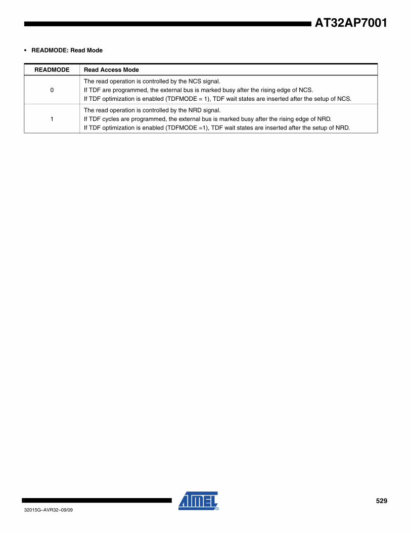
52932015G–AVR32–09/09
AT32AP7001
• READMODE: Read Mode
READMODE Read Access Mode
0
The read operation is controlled by the NCS signal.
If TDF are programmed, the external bus is marked busy after the rising edge of NCS.
If TDF optimization is enabled (TDFMODE = 1), TDF wait states are inserted after the setup of NCS.
1
The read operation is controlled by the NRD signal.
If TDF cycles are programmed, the external bus is marked busy after the rising edge of NRD.
If TDF optimization is enabled (TDFMODE =1), TDF wait states are inserted after the setup of NRD.

53032015G–AVR32–09/09
AT32AP7001
29. SDRAM Controller (SDRAMC)
Rev: 2.0.0.3
29.1 Features
• 256-Mbytes address space• Numerous configurations supported
– 2K, 4K, 8K row address memory parts – SDRAM with two or four internal banks– SDRAM with 16- or 32-bit data path
• Programming facilities– Word, halfword, byte access– Automatic page break when memory boundary has been reached– Multibank ping-pong access– Timing parameters specified by software– Automatic refresh operation, refresh rate is programmable– Automatic update of DS, TCR and PASR parameters (mobile SDRAM devices)
• Energy-saving capabilities– Self-refresh, power-down, and deep power-down modes supported– Supports mobile SDRAM devices
• Error detection– Refresh error interrupt
• SDRAM power-up initialization by software• CAS latency of one, two, and three supported• Auto Precharge command not used
29.2 Overview
The SDRAM Controller (SDRAMC) extends the memory capabilities of a chip by providing theinterface to an external 16-bit or 32-bit SDRAM device. The page size supports ranges from2048 to 8192 and the number of columns from 256 to 2048. It supports byte (8-bit), halfword (16-bit) and word (32-bit) accesses.
The SDRAMC supports a read or write burst length of one location. It keeps track of the activerow in each bank, thus maximizing SDRAM performance, e.g., the application may be placed inone bank and data in the other banks. So as to optimize performance, it is advisable to avoidaccessing different rows in the same bank.
The SDRAMC supports a CAS latency of one, two, or three and optimizes the read accessdepending on the frequency.
The different modes available (self refresh, power-down, and deep power-down modes) mini-mize power consumption on the SDRAM device.
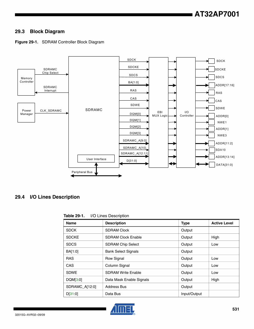
53132015G–AVR32–09/09
AT32AP7001
29.3 Block Diagram
Figure 29-1. SDRAM Controller Block Diagram
29.4 I/O Lines Description
MemoryController
PowerManager
CLK_SDRAMC
SDRAMC Chip Select
SDRAMC Interrupt
SDRAMC
User Interface
Peripheral Bus
I/OController
SDCS
SDCK
SDCKE
BA[1:0]
RAS
CAS
SDWE
DQM[0]
SDRAMC_A[9:0]
D[31:0]
EBIMUX Logic
DATA[31:0]
SDCK
SDCKE
SDCS
RAS
CAS
ADDR[17:16]
SDWE
ADDR[0]DQM[1]
NWE1DQM[2]
ADDR[1]DQM[3]
NWE3
ADDR[11:2]SDRAMC_A[10]
SDA10SDRAMC_A[12:11]
ADDR[13:14]
Table 29-1. I/O Lines Description
Name Description Type Active Level
SDCK SDRAM Clock Output
SDCKE SDRAM Clock Enable Output High
SDCS SDRAM Chip Select Output Low
BA[1:0] Bank Select Signals Output
RAS Row Signal Output Low
CAS Column Signal Output Low
SDWE SDRAM Write Enable Output Low
DQM[3:0] Data Mask Enable Signals Output High
SDRAMC_A[12:0] Address Bus Output
D[31:0] Data Bus Input/Output
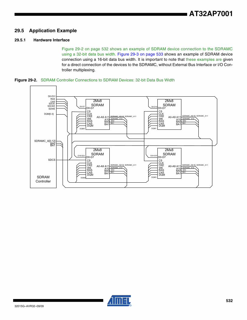
53232015G–AVR32–09/09
AT32AP7001
29.5 Application Example
29.5.1 Hardware Interface
Figure 29-2 on page 532 shows an example of SDRAM device connection to the SDRAMCusing a 32-bit data bus width. Figure 29-3 on page 533 shows an example of SDRAM deviceconnection using a 16-bit data bus width. It is important to note that these examples are givenfor a direct connection of the devices to the SDRAMC, without External Bus Interface or I/O Con-troller multiplexing.
Figure 29-2. SDRAM Controller Connections to SDRAM Devices: 32-bit Data Bus Width
SDRAMC_A[0-9], SDRAMC_A11
2Mx8SDRAM
D0-D7CS
DQM
CLKCKEWERASCAS
A0-A9 A11
BA0A10
BA1
SDRAMC_A10BA0BA1
2Mx8SDRAM
D0-D7CS
DQM
CLKCKEWERASCAS
A0-A9 A11
BA0A10
BA1
SDRAMC_A10BA0BA1
2Mx8SDRAM
D0-D7CS
DQM
CLKCKEWERASCAS
A0-A9 A11
BA0A10
BA1
SDRAMC_A10BA0BA1
2Mx8SDRAM
D0-D7CS
DQM
CLKCKEWERASCAS
A0-A9 A11
BA0A10
BA1
SDRAMC_A10BA0BA1
SDRAMC_A[0-9], SDRAMC_A11
SDRAMC_A[0-9], SDRAMC_A11SDRAMC_A[0-9], SDRAMC_A11
D8-D15
DQM1DQM0
D0-D7
DQM2
D16-D23
DQM3
D24-D31
SDRAMController
SDCS
BA1BA0
SDRAMC_A[0-12]
DQM[0-3]
SDWESDCKESDCK
CASRAS
D0-D31
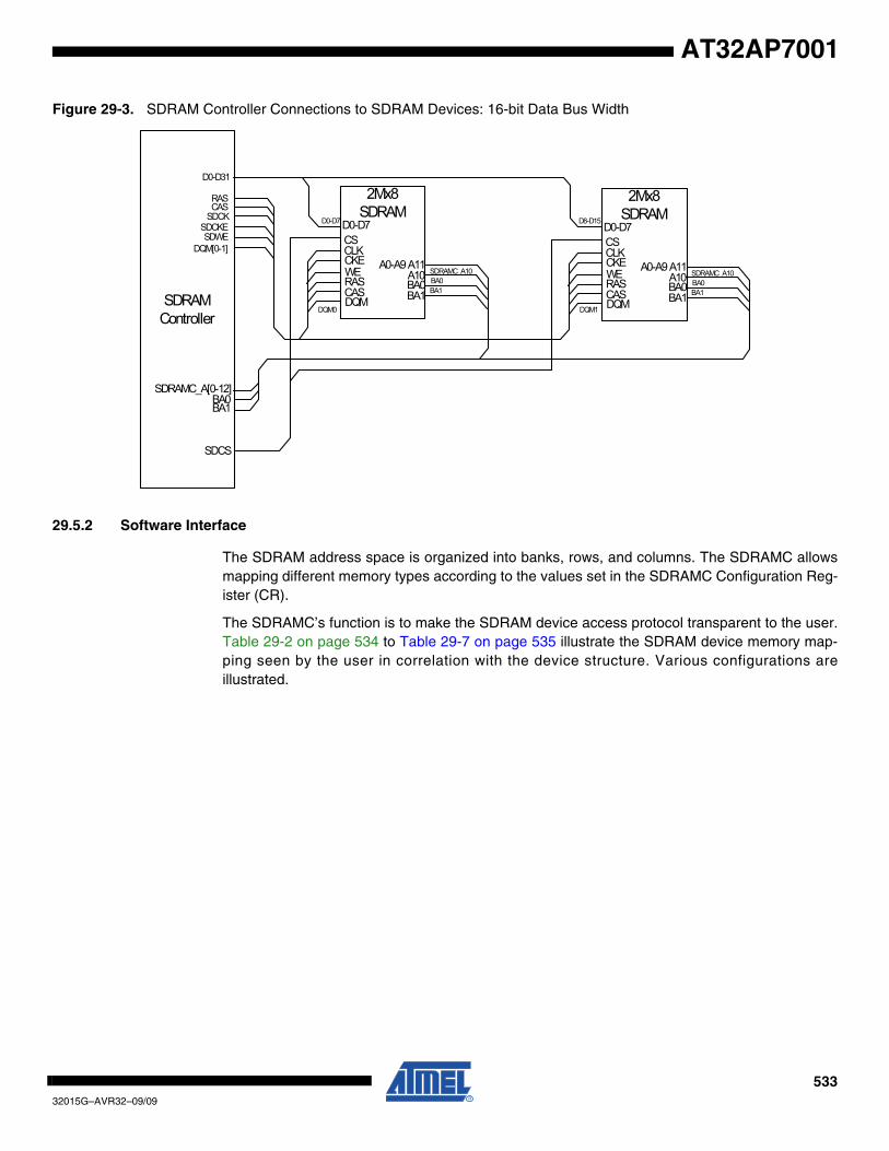
53332015G–AVR32–09/09
AT32AP7001
Figure 29-3. SDRAM Controller Connections to SDRAM Devices: 16-bit Data Bus Width
29.5.2 Software Interface
The SDRAM address space is organized into banks, rows, and columns. The SDRAMC allowsmapping different memory types according to the values set in the SDRAMC Configuration Reg-ister (CR).
The SDRAMC’s function is to make the SDRAM device access protocol transparent to the user.Table 29-2 on page 534 to Table 29-7 on page 535 illustrate the SDRAM device memory map-ping seen by the user in correlation with the device structure. Various configurations areillustrated.
2Mx8SDRAM
D0-D7CS
DQM
CLKCKEWERASCAS
A0-A9 A11
BA0A10
BA1
SDRAMC_A10BA0BA1
2Mx8SDRAM
D0-D7CS
DQM
CLKCKEWERASCAS
A0-A9 A11
BA0A10
BA1
SDRAMC_A10BA0BA1
SDCS
BA1BA0
SDRAMC_A[0-12]
SDRAMController
DQM[0-1]SDWE
SDCKESDCKCASRAS
D0-D31
DQM0
D0-D7 D8-D15
DQM1
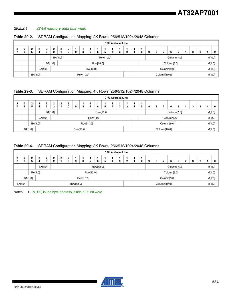
53432015G–AVR32–09/09
AT32AP7001
29.5.2.1 32-bit memory data bus width
Notes: 1. M[1:0] is the byte address inside a 32-bit word.
Table 29-2. SDRAM Configuration Mapping: 2K Rows, 256/512/1024/2048 Columns
CPU Address Line
27
26
25
24
23
22
21
20
19
18
17
16
15
14
13
12
11
10 9 8 7 6 5 4 3 2 1 0
BA[1:0] Row[10:0] Column[7:0] M[1:0]
BA[1:0] Row[10:0] Column[8:0] M[1:0]
BA[1:0] Row[10:0] Column[9:0] M[1:0]
BA[1:0] Row[10:0] Column[10:0] M[1:0]
Table 29-3. SDRAM Configuration Mapping: 4K Rows, 256/512/1024/2048 Columns
CPU Address Line
27
26
25
24
23
22
21
20
19
18
17
16
15
14
13
12
11
10 9 8 7 6 5 4 3 2 1 0
BA[1:0] Row[11:0] Column[7:0] M[1:0]
BA[1:0] Row[11:0] Column[8:0] M[1:0]
BA[1:0] Row[11:0] Column[9:0] M[1:0]
BA[1:0] Row[11:0] Column[10:0] M[1:0]
Table 29-4. SDRAM Configuration Mapping: 8K Rows, 256/512/1024/2048 Columns
CPU Address Line
27
26
25
24
23
22
21
20
19
18
17
16
15
14
13
12
11
10 9 8 7 6 5 4 3 2 1 0
BA[1:0] Row[12:0] Column[7:0] M[1:0]
BA[1:0] Row[12:0] Column[8:0] M[1:0]
BA[1:0] Row[12:0] Column[9:0] M[1:0]
BA[1:0] Row[12:0] Column[10:0] M[1:0]
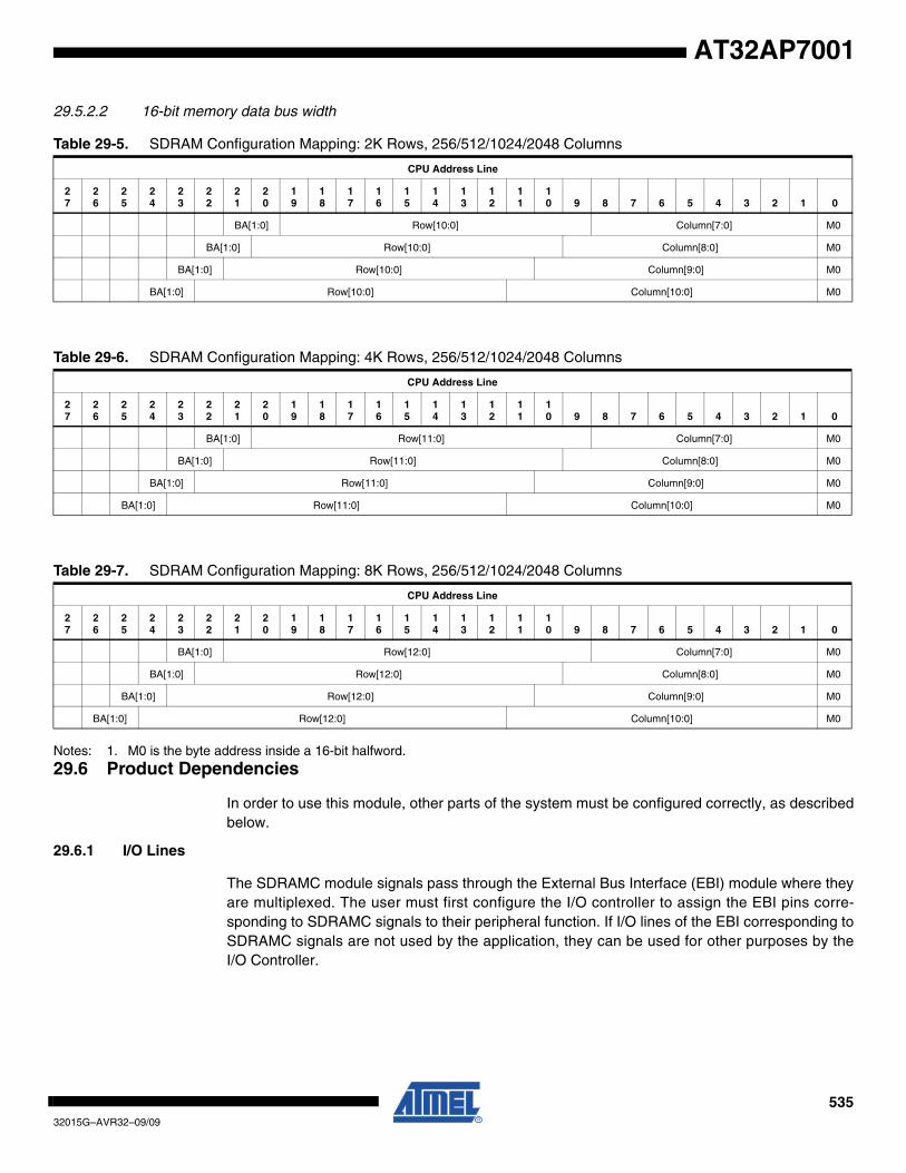
53532015G–AVR32–09/09
AT32AP7001
29.5.2.2 16-bit memory data bus width
Notes: 1. M0 is the byte address inside a 16-bit halfword.
29.6 Product Dependencies
In order to use this module, other parts of the system must be configured correctly, as describedbelow.
29.6.1 I/O Lines
The SDRAMC module signals pass through the External Bus Interface (EBI) module where theyare multiplexed. The user must first configure the I/O controller to assign the EBI pins corre-sponding to SDRAMC signals to their peripheral function. If I/O lines of the EBI corresponding toSDRAMC signals are not used by the application, they can be used for other purposes by theI/O Controller.
Table 29-5. SDRAM Configuration Mapping: 2K Rows, 256/512/1024/2048 Columns
CPU Address Line
27
26
25
24
23
22
21
20
19
18
17
16
15
14
13
12
11
10 9 8 7 6 5 4 3 2 1 0
BA[1:0] Row[10:0] Column[7:0] M0
BA[1:0] Row[10:0] Column[8:0] M0
BA[1:0] Row[10:0] Column[9:0] M0
BA[1:0] Row[10:0] Column[10:0] M0
Table 29-6. SDRAM Configuration Mapping: 4K Rows, 256/512/1024/2048 Columns
CPU Address Line
27
26
25
24
23
22
21
20
19
18
17
16
15
14
13
12
11
10 9 8 7 6 5 4 3 2 1 0
BA[1:0] Row[11:0] Column[7:0] M0
BA[1:0] Row[11:0] Column[8:0] M0
BA[1:0] Row[11:0] Column[9:0] M0
BA[1:0] Row[11:0] Column[10:0] M0
Table 29-7. SDRAM Configuration Mapping: 8K Rows, 256/512/1024/2048 Columns
CPU Address Line
27
26
25
24
23
22
21
20
19
18
17
16
15
14
13
12
11
10 9 8 7 6 5 4 3 2 1 0
BA[1:0] Row[12:0] Column[7:0] M0
BA[1:0] Row[12:0] Column[8:0] M0
BA[1:0] Row[12:0] Column[9:0] M0
BA[1:0] Row[12:0] Column[10:0] M0
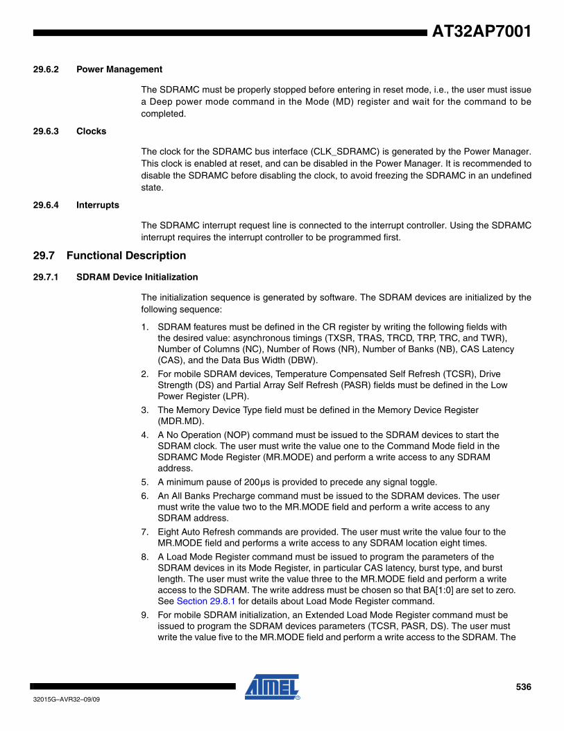
53632015G–AVR32–09/09
AT32AP7001
29.6.2 Power Management
The SDRAMC must be properly stopped before entering in reset mode, i.e., the user must issuea Deep power mode command in the Mode (MD) register and wait for the command to becompleted.
29.6.3 Clocks
The clock for the SDRAMC bus interface (CLK_SDRAMC) is generated by the Power Manager.This clock is enabled at reset, and can be disabled in the Power Manager. It is recommended todisable the SDRAMC before disabling the clock, to avoid freezing the SDRAMC in an undefinedstate.
29.6.4 Interrupts
The SDRAMC interrupt request line is connected to the interrupt controller. Using the SDRAMCinterrupt requires the interrupt controller to be programmed first.
29.7 Functional Description
29.7.1 SDRAM Device Initialization
The initialization sequence is generated by software. The SDRAM devices are initialized by thefollowing sequence:
1. SDRAM features must be defined in the CR register by writing the following fields with the desired value: asynchronous timings (TXSR, TRAS, TRCD, TRP, TRC, and TWR), Number of Columns (NC), Number of Rows (NR), Number of Banks (NB), CAS Latency (CAS), and the Data Bus Width (DBW).
2. For mobile SDRAM devices, Temperature Compensated Self Refresh (TCSR), Drive Strength (DS) and Partial Array Self Refresh (PASR) fields must be defined in the Low Power Register (LPR).
3. The Memory Device Type field must be defined in the Memory Device Register (MDR.MD).
4. A No Operation (NOP) command must be issued to the SDRAM devices to start the SDRAM clock. The user must write the value one to the Command Mode field in the SDRAMC Mode Register (MR.MODE) and perform a write access to any SDRAM address.
5. A minimum pause of 200µs is provided to precede any signal toggle.
6. An All Banks Precharge command must be issued to the SDRAM devices. The user must write the value two to the MR.MODE field and perform a write access to any SDRAM address.
7. Eight Auto Refresh commands are provided. The user must write the value four to the MR.MODE field and performs a write access to any SDRAM location eight times.
8. A Load Mode Register command must be issued to program the parameters of the SDRAM devices in its Mode Register, in particular CAS latency, burst type, and burst length. The user must write the value three to the MR.MODE field and perform a write access to the SDRAM. The write address must be chosen so that BA[1:0] are set to zero. See Section 29.8.1 for details about Load Mode Register command.
9. For mobile SDRAM initialization, an Extended Load Mode Register command must be issued to program the SDRAM devices parameters (TCSR, PASR, DS). The user must write the value five to the MR.MODE field and perform a write access to the SDRAM. The
53732015G–AVR32–09/09
AT32AP7001
write address must be chosen so that BA[1] or BA[0] are equal to one. See Section 29.8.1 for details about Extended Load Mode Register command.
10. The user must go into Normal Mode, writing the value 0 to the MR.MODE field and per-forming a write access at any location in the SDRAM.
11. Write the refresh rate into the Refresh Timer Count field in the Refresh Timer Register (TR.COUNT). The refresh rate is the delay between two successive refresh cycles. The SDRAM device requires a refresh every 15.625µs or 7.81µs. With a 100MHz frequency, the TR register must be written with the value 1562 (15.625 µs x 100 MHz) or 781 (7.81 µs x 100 MHz).
After initialization, the SDRAM devices are fully functional.
Figure 29-4. SDRAM Device Initialization Sequence
29.7.2 SDRAM Controller Write Cycle
The SDRAMC allows burst access or single access. In both cases, the SDRAMC keeps track ofthe active row in each bank, thus maximizing performance. To initiate a burst access, theSDRAMC uses the transfer type signal provided by the master requesting the access. If the nextaccess is a sequential write access, writing to the SDRAM device is carried out. If the nextaccess is a write-sequential access, but the current access is to a boundary page, or if the nextaccess is in another row, then the SDRAMC generates a precharge command, activates thenew row and initiates a write command. To comply with SDRAM timing parameters, additionalclock cycles are inserted between precharge and active (tRP) commands and between activeand write (tRCD) commands. For definition of these timing parameters, refer to the Section29.8.3. This is described in Figure 29-5 on page 538.
SDCKE
SDCK
SDRAMC_A[9:0]
A10
SDRAMC_A[12:11]
SDCS
RAS
CAS
SDWE
DQM
Inputs Stable for200 usec
Valid CommandPrecharge All Banks 1st Auto Refresh 8th Auto Refresh LMR Command
tMRDtRCtRP
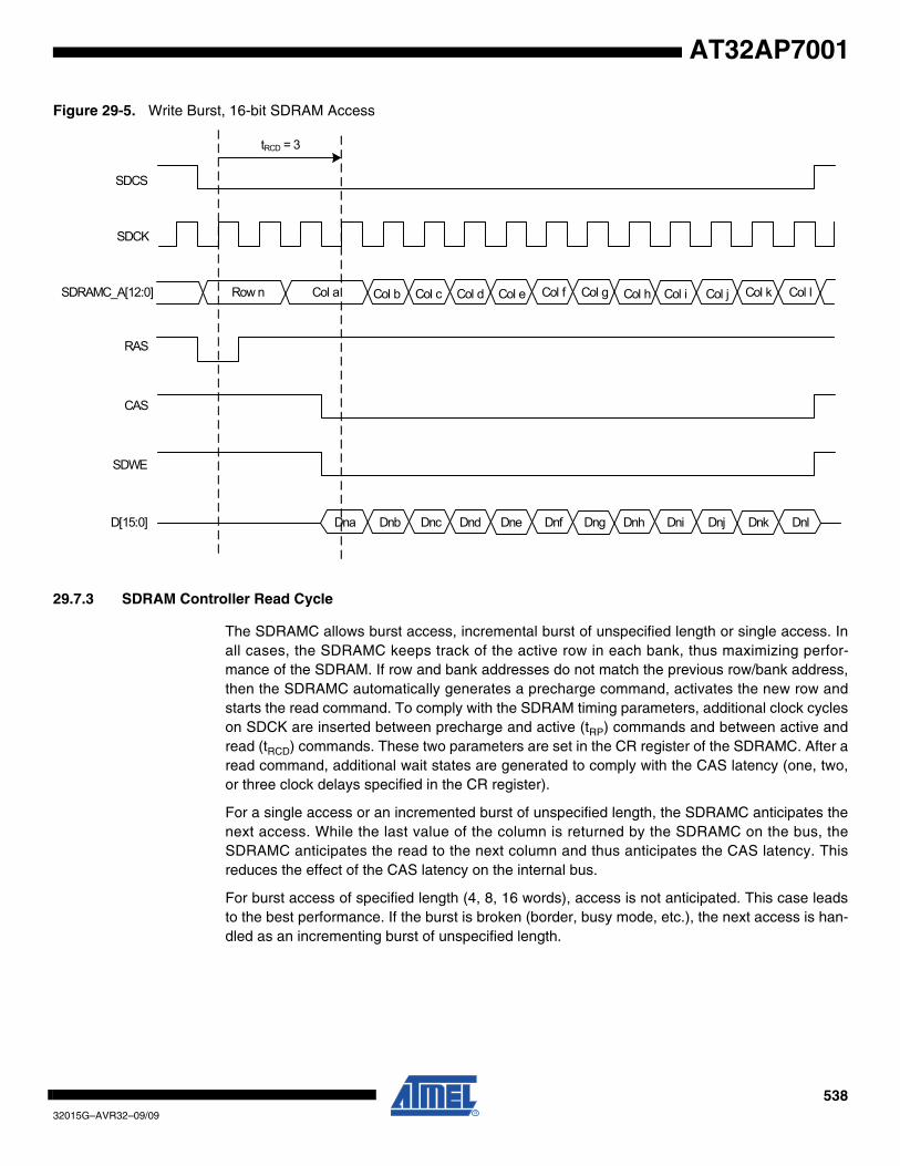
53832015G–AVR32–09/09
AT32AP7001
Figure 29-5. Write Burst, 16-bit SDRAM Access
29.7.3 SDRAM Controller Read Cycle
The SDRAMC allows burst access, incremental burst of unspecified length or single access. Inall cases, the SDRAMC keeps track of the active row in each bank, thus maximizing perfor-mance of the SDRAM. If row and bank addresses do not match the previous row/bank address,then the SDRAMC automatically generates a precharge command, activates the new row andstarts the read command. To comply with the SDRAM timing parameters, additional clock cycleson SDCK are inserted between precharge and active (tRP) commands and between active andread (tRCD) commands. These two parameters are set in the CR register of the SDRAMC. After aread command, additional wait states are generated to comply with the CAS latency (one, two,or three clock delays specified in the CR register).
For a single access or an incremented burst of unspecified length, the SDRAMC anticipates thenext access. While the last value of the column is returned by the SDRAMC on the bus, theSDRAMC anticipates the read to the next column and thus anticipates the CAS latency. Thisreduces the effect of the CAS latency on the internal bus.
For burst access of specified length (4, 8, 16 words), access is not anticipated. This case leadsto the best performance. If the burst is broken (border, busy mode, etc.), the next access is han-dled as an incrementing burst of unspecified length.
SDCS
tRCD = 3
SDCK
SDRAMC_A[12:0]
RAS
CAS
SDWE
D[15:0] Dna Dnb Dnc Dnd Dne Dnf Dng Dnh Dni Dnj Dnk Dnl
Row n Col b Col c Col d Col e Col f Col g Col h Col i Col k Col lCol jCol a
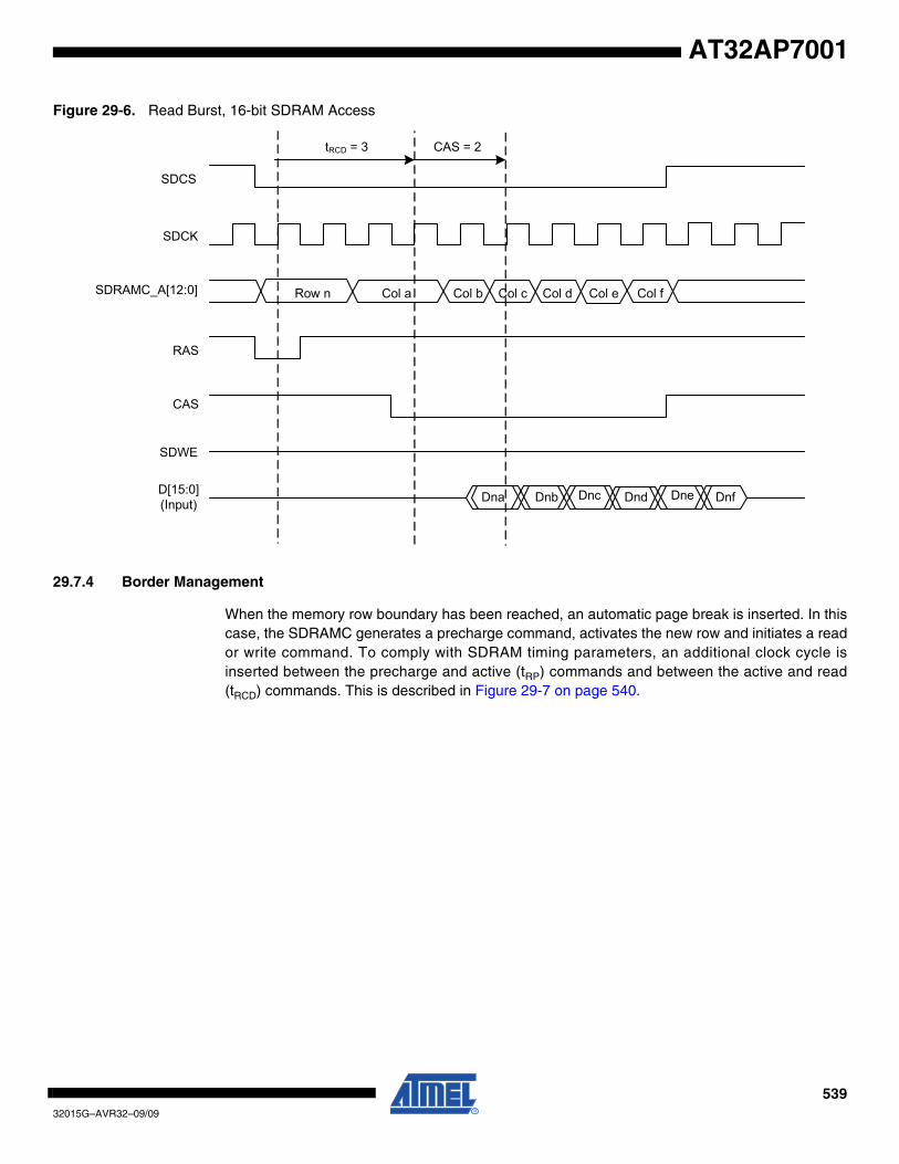
53932015G–AVR32–09/09
AT32AP7001
Figure 29-6. Read Burst, 16-bit SDRAM Access
29.7.4 Border Management
When the memory row boundary has been reached, an automatic page break is inserted. In thiscase, the SDRAMC generates a precharge command, activates the new row and initiates a reador write command. To comply with SDRAM timing parameters, an additional clock cycle isinserted between the precharge and active (tRP) commands and between the active and read(tRCD) commands. This is described in Figure 29-7 on page 540.
SDCS
D[15:0](Input)
SDCK
SDRAMC_A[12:0]
RAS
CAS
SDWE
Dna Dnb Dnc Dnd Dne Dnf
Col a Col b Col c Col d Col e Col fRow n
CAS = 2tRCD = 3
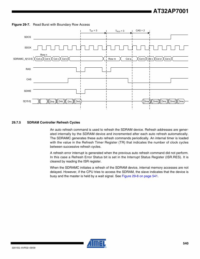
54032015G–AVR32–09/09
AT32AP7001
Figure 29-7. Read Burst with Boundary Row Access
29.7.5 SDRAM Controller Refresh Cycles
An auto refresh command is used to refresh the SDRAM device. Refresh addresses are gener-ated internally by the SDRAM device and incremented after each auto refresh automatically.The SDRAMC generates these auto refresh commands periodically. An internal timer is loadedwith the value in the Refresh Timer Register (TR) that indicates the number of clock cyclesbetween successive refresh cycles.
A refresh error interrupt is generated when the previous auto refresh command did not perform.In this case a Refresh Error Status bit is set in the Interrupt Status Register (ISR.RES). It iscleared by reading the ISR register.
When the SDRAMC initiates a refresh of the SDRAM device, internal memory accesses are notdelayed. However, if the CPU tries to access the SDRAM, the slave indicates that the device isbusy and the master is held by a wait signal. See Figure 29-8 on page 541.
SDCS
SDCK
SDRAMC_A[12:0]
CAS
RAS
SDWE
D[15:0] Dna Dnb Dnc Dnd Dma Dmb Dmc DmeDmd
Row m Col a Col b Col c Col d Col e
Row n
Col a Col b Col c Col d
CAS = 2TRCD = 3TRP = 3
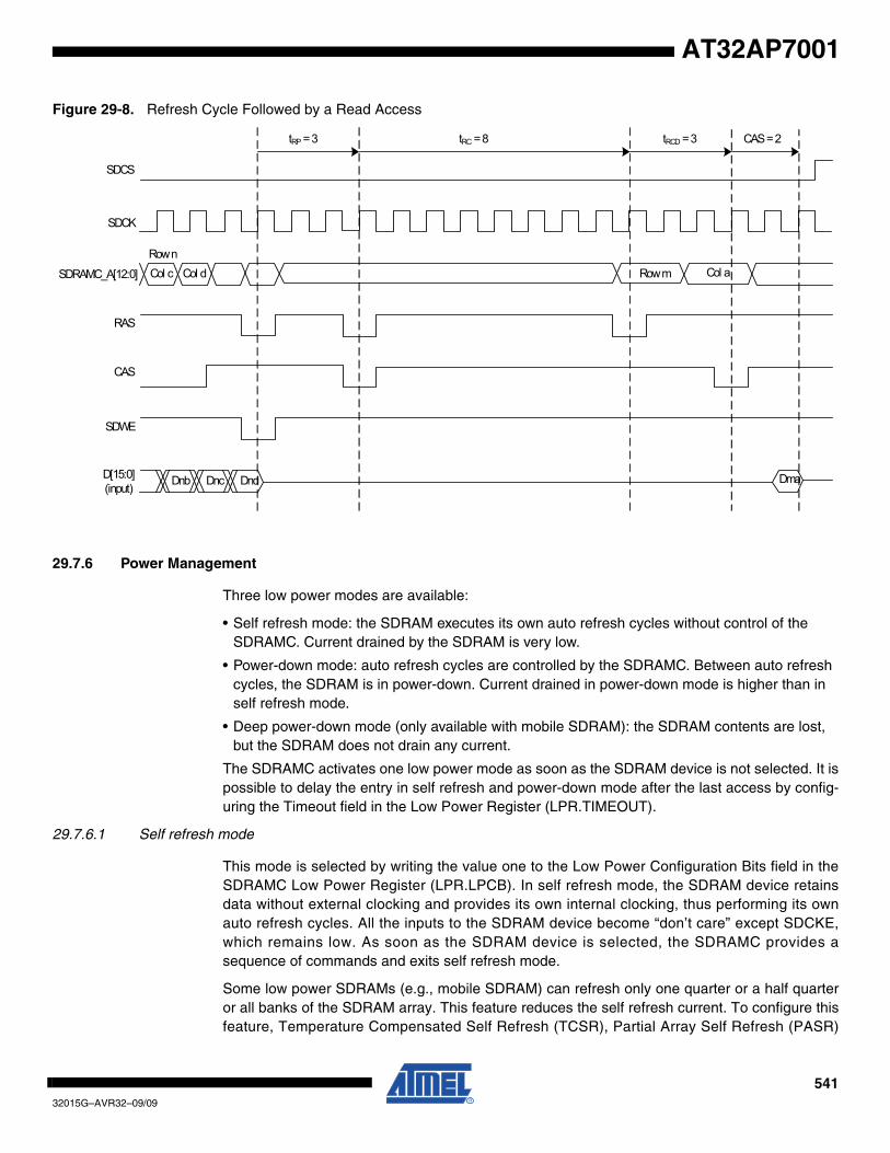
54132015G–AVR32–09/09
AT32AP7001
Figure 29-8. Refresh Cycle Followed by a Read Access
29.7.6 Power Management
Three low power modes are available:
• Self refresh mode: the SDRAM executes its own auto refresh cycles without control of the SDRAMC. Current drained by the SDRAM is very low.
• Power-down mode: auto refresh cycles are controlled by the SDRAMC. Between auto refresh cycles, the SDRAM is in power-down. Current drained in power-down mode is higher than in self refresh mode.
• Deep power-down mode (only available with mobile SDRAM): the SDRAM contents are lost, but the SDRAM does not drain any current.
The SDRAMC activates one low power mode as soon as the SDRAM device is not selected. It ispossible to delay the entry in self refresh and power-down mode after the last access by config-uring the Timeout field in the Low Power Register (LPR.TIMEOUT).
29.7.6.1 Self refresh mode
This mode is selected by writing the value one to the Low Power Configuration Bits field in theSDRAMC Low Power Register (LPR.LPCB). In self refresh mode, the SDRAM device retainsdata without external clocking and provides its own internal clocking, thus performing its ownauto refresh cycles. All the inputs to the SDRAM device become “don’t care” except SDCKE,which remains low. As soon as the SDRAM device is selected, the SDRAMC provides asequence of commands and exits self refresh mode.
Some low power SDRAMs (e.g., mobile SDRAM) can refresh only one quarter or a half quarteror all banks of the SDRAM array. This feature reduces the self refresh current. To configure thisfeature, Temperature Compensated Self Refresh (TCSR), Partial Array Self Refresh (PASR)
SDCS
SDCK
SDRAMC_A[12:0]
Row nCol c Col d
RAS
CAS
SDWE
D[15:0](input) Dnb Dnc Dnd Dma
Col aRow m
CAS = 2tRCD = 3tRC = 8tRP = 3
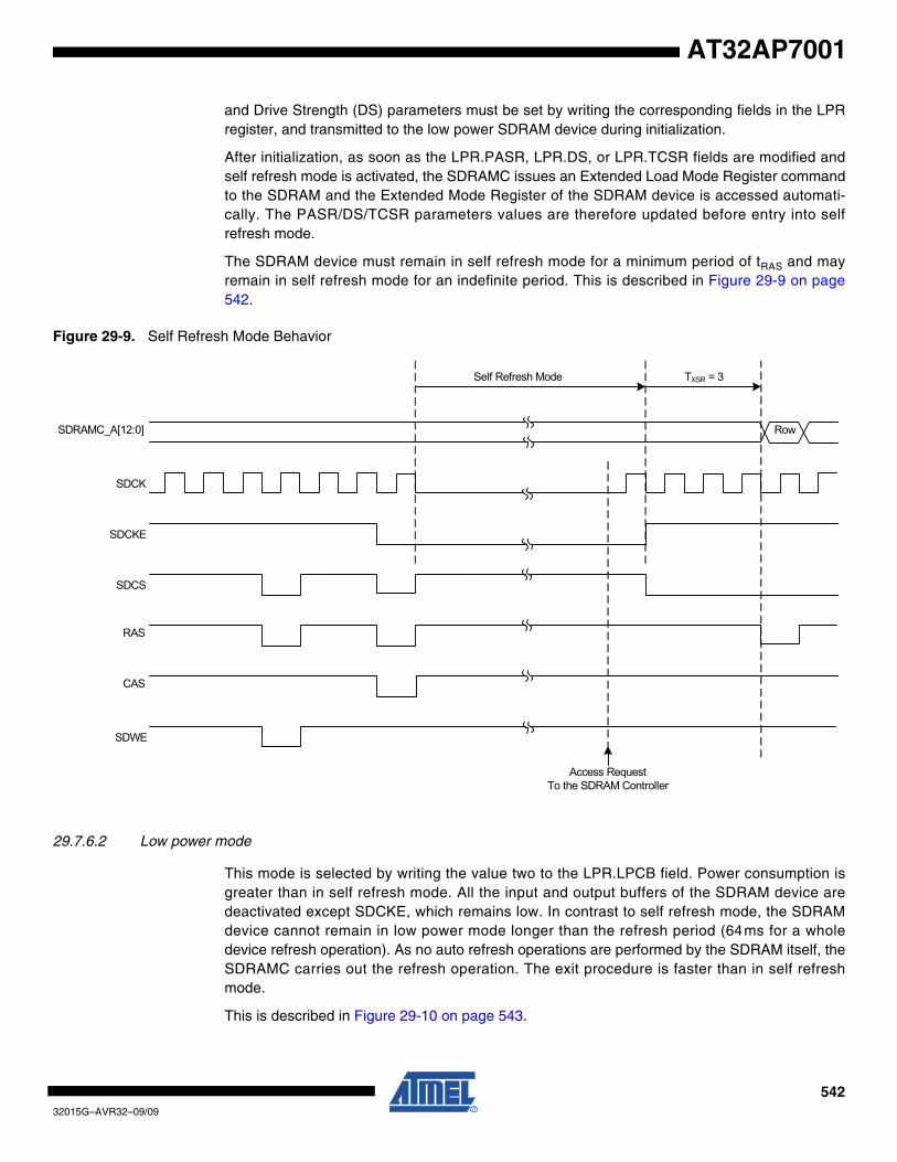
54232015G–AVR32–09/09
AT32AP7001
and Drive Strength (DS) parameters must be set by writing the corresponding fields in the LPRregister, and transmitted to the low power SDRAM device during initialization.
After initialization, as soon as the LPR.PASR, LPR.DS, or LPR.TCSR fields are modified andself refresh mode is activated, the SDRAMC issues an Extended Load Mode Register commandto the SDRAM and the Extended Mode Register of the SDRAM device is accessed automati-cally. The PASR/DS/TCSR parameters values are therefore updated before entry into selfrefresh mode.
The SDRAM device must remain in self refresh mode for a minimum period of tRAS and mayremain in self refresh mode for an indefinite period. This is described in Figure 29-9 on page542.
Figure 29-9. Self Refresh Mode Behavior
29.7.6.2 Low power mode
This mode is selected by writing the value two to the LPR.LPCB field. Power consumption isgreater than in self refresh mode. All the input and output buffers of the SDRAM device aredeactivated except SDCKE, which remains low. In contrast to self refresh mode, the SDRAMdevice cannot remain in low power mode longer than the refresh period (64ms for a wholedevice refresh operation). As no auto refresh operations are performed by the SDRAM itself, theSDRAMC carries out the refresh operation. The exit procedure is faster than in self refreshmode.
This is described in Figure 29-10 on page 543.
SDRAMC_A[12:0]
SDCK
SDCKE
SDCS
RAS
CAS
Access RequestTo the SDRAM Controller
Self Refresh Mode
Row
TXSR = 3
SDWE
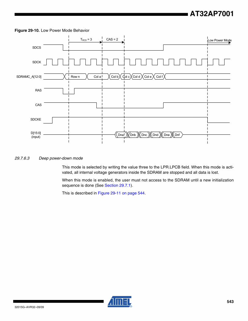
54332015G–AVR32–09/09
AT32AP7001
Figure 29-10. Low Power Mode Behavior
29.7.6.3 Deep power-down mode
This mode is selected by writing the value three to the LPR.LPCB field. When this mode is acti-vated, all internal voltage generators inside the SDRAM are stopped and all data is lost.
When this mode is enabled, the user must not access to the SDRAM until a new initializationsequence is done (See Section 29.7.1).
This is described in Figure 29-11 on page 544.
Low Power ModeCAS = 2TRCD = 3
SDCS
SDCK
SDRAMC_A[12:0]
RAS
CAS
SDCKE
D[15:0](input) Dna Dnb Dnc Dnd Dne Dnf
Col fCol eCol dCol cCol bCol aRow n
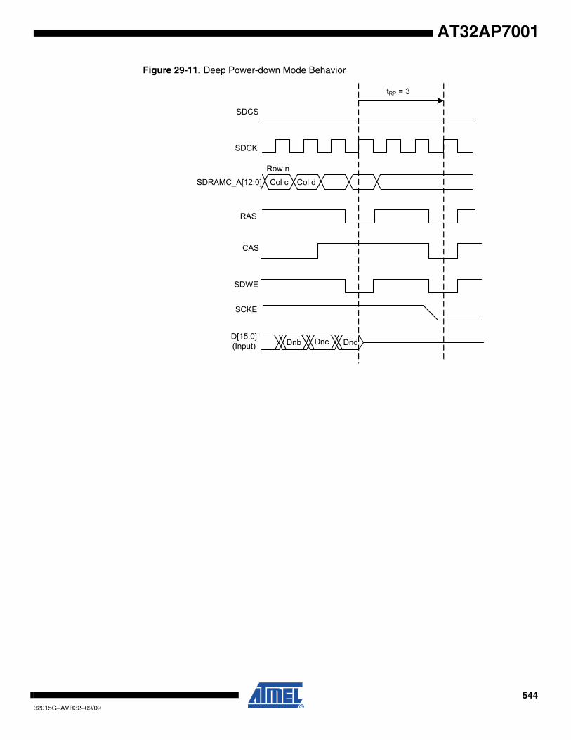
54432015G–AVR32–09/09
AT32AP7001
Figure 29-11. Deep Power-down Mode Behavior
SDCS
SDCK
SDRAMC_A[12:0]
RAS
CAS
SDWE
SCKE
D[15:0](Input) Dnb Dnc Dnd
Col dCol c
Row n
tRP = 3
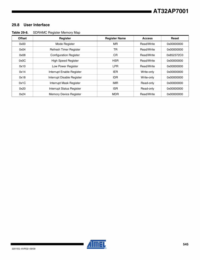
54532015G–AVR32–09/09
AT32AP7001
29.8 User Interface
Table 29-8. SDRAMC Register Memory Map
Offset Register Register Name Access Reset
0x00 Mode Register MR Read/Write 0x00000000
0x04 Refresh Timer Register TR Read/Write 0x00000000
0x08 Configuration Register CR Read/Write 0x852372C0
0x0C High Speed Register HSR Read/Write 0x00000000
0x10 Low Power Register LPR Read/Write 0x00000000
0x14 Interrupt Enable Register IER Write-only 0x00000000
0x18 Interrupt Disable Register IDR Write-only 0x00000000
0x1C Interrupt Mask Register IMR Read-only 0x00000000
0x20 Interrupt Status Register ISR Read-only 0x00000000
0x24 Memory Device Register MDR Read/Write 0x00000000
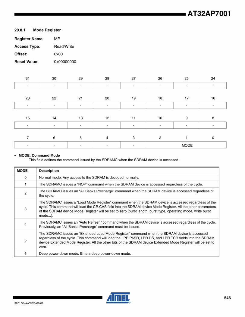
54632015G–AVR32–09/09
AT32AP7001
29.8.1 Mode Register
Register Name: MR
Access Type: Read/Write
Offset: 0x00
Reset Value: 0x00000000
• MODE: Command ModeThis field defines the command issued by the SDRAMC when the SDRAM device is accessed.
31 30 29 28 27 26 25 24
- - - - - - - -
23 22 21 20 19 18 17 16
- - - - - - - -
15 14 13 12 11 10 9 8
- - - - - - - -
7 6 5 4 3 2 1 0
- - - - - MODE
MODE Description
0 Normal mode. Any access to the SDRAM is decoded normally.
1 The SDRAMC issues a “NOP” command when the SDRAM device is accessed regardless of the cycle.
2The SDRAMC issues an “All Banks Precharge” command when the SDRAM device is accessed regardless of the cycle.
3
The SDRAMC issues a “Load Mode Register” command when the SDRAM device is accessed regardless of the cycle. This command will load the CR.CAS field into the SDRAM device Mode Register. All the other parameters of the SDRAM device Mode Register will be set to zero (burst length, burst type, operating mode, write burst mode...).
4The SDRAMC issues an “Auto Refresh” command when the SDRAM device is accessed regardless of the cycle. Previously, an “All Banks Precharge” command must be issued.
5
The SDRAMC issues an “Extended Load Mode Register” command when the SDRAM device is accessed regardless of the cycle. This command will load the LPR.PASR, LPR.DS, and LPR.TCR fields into the SDRAM device Extended Mode Register. All the other bits of the SDRAM device Extended Mode Register will be set to zero.
6 Deep power-down mode. Enters deep power-down mode.
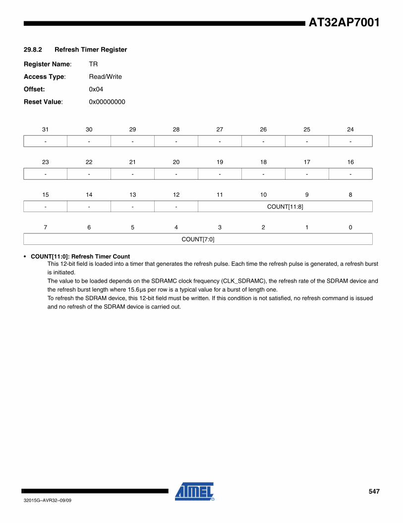
54732015G–AVR32–09/09
AT32AP7001
29.8.2 Refresh Timer Register
Register Name: TR
Access Type: Read/Write
Offset: 0x04
Reset Value: 0x00000000
• COUNT[11:0]: Refresh Timer CountThis 12-bit field is loaded into a timer that generates the refresh pulse. Each time the refresh pulse is generated, a refresh burst
is initiated. The value to be loaded depends on the SDRAMC clock frequency (CLK_SDRAMC), the refresh rate of the SDRAM device and
the refresh burst length where 15.6µs per row is a typical value for a burst of length one.
To refresh the SDRAM device, this 12-bit field must be written. If this condition is not satisfied, no refresh command is issued and no refresh of the SDRAM device is carried out.
31 30 29 28 27 26 25 24
- - - - - - - -
23 22 21 20 19 18 17 16
- - - - - - - -
15 14 13 12 11 10 9 8
- - - - COUNT[11:8]
7 6 5 4 3 2 1 0
COUNT[7:0]
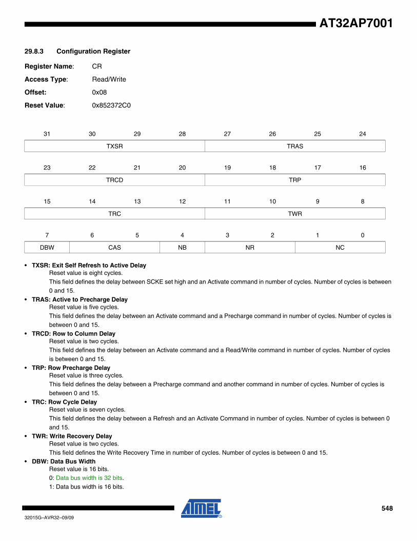
54832015G–AVR32–09/09
AT32AP7001
29.8.3 Configuration Register
Register Name: CR
Access Type: Read/Write
Offset: 0x08
Reset Value: 0x852372C0
• TXSR: Exit Self Refresh to Active DelayReset value is eight cycles.
This field defines the delay between SCKE set high and an Activate command in number of cycles. Number of cycles is between 0 and 15.
• TRAS: Active to Precharge DelayReset value is five cycles.
This field defines the delay between an Activate command and a Precharge command in number of cycles. Number of cycles is
between 0 and 15.• TRCD: Row to Column Delay
Reset value is two cycles.This field defines the delay between an Activate command and a Read/Write command in number of cycles. Number of cycles
is between 0 and 15.
• TRP: Row Precharge DelayReset value is three cycles.
This field defines the delay between a Precharge command and another command in number of cycles. Number of cycles is between 0 and 15.
• TRC: Row Cycle DelayReset value is seven cycles.
This field defines the delay between a Refresh and an Activate Command in number of cycles. Number of cycles is between 0
and 15.• TWR: Write Recovery Delay
Reset value is two cycles.
This field defines the Write Recovery Time in number of cycles. Number of cycles is between 0 and 15.• DBW: Data Bus Width
Reset value is 16 bits.0: Data bus width is 32 bits.
1: Data bus width is 16 bits.
31 30 29 28 27 26 25 24
TXSR TRAS
23 22 21 20 19 18 17 16
TRCD TRP
15 14 13 12 11 10 9 8
TRC TWR
7 6 5 4 3 2 1 0
DBW CAS NB NR NC
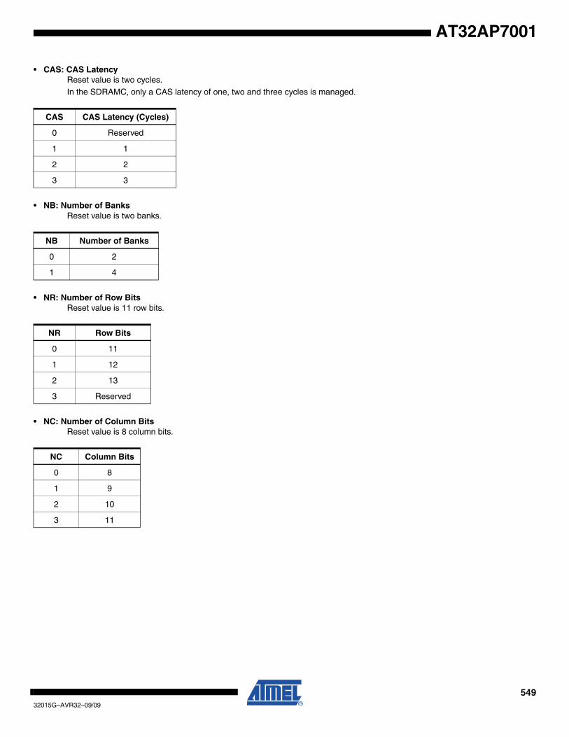
54932015G–AVR32–09/09
AT32AP7001
• CAS: CAS LatencyReset value is two cycles.
In the SDRAMC, only a CAS latency of one, two and three cycles is managed.
• NB: Number of BanksReset value is two banks.
• NR: Number of Row BitsReset value is 11 row bits.
• NC: Number of Column BitsReset value is 8 column bits.
CAS CAS Latency (Cycles)
0 Reserved
1 1
2 2
3 3
NB Number of Banks
0 2
1 4
NR Row Bits
0 11
1 12
2 13
3 Reserved
NC Column Bits
0 8
1 9
2 10
3 11

55032015G–AVR32–09/09
AT32AP7001
29.8.4 High Speed Register
Register Name: HSR
Access Type: Read/Write
Offset: 0x0C
Reset Value: 0x00000000
• DA: Decode Cycle EnableA decode cycle can be added on the addresses as soon as a non-sequential access is performed on the HSB bus.The addition of the decode cycle allows the SDRAMC to gain time to access the SDRAM memory.
1: Decode cycle is enabled.
0: Decode cycle is disabled.
31 30 29 28 27 26 25 24
- - - - - - - -
23 22 21 20 19 18 17 16
- - - - - - - -
15 14 13 12 11 10 9 8
- - - - - - - -
7 6 5 4 3 2 1 0
- - - - - - - DA

55132015G–AVR32–09/09
AT32AP7001
29.8.5 Low Power Register
Register Name: LPR
Access Type: Read/Write
Offset: 0x10
Reset Value: 0x00000000
• TIMEOUT: Time to Define when Low Power Mode Is Enabled
• DS: Drive Strength (only for low power SDRAM)This field is transmitted to the SDRAM during initialization to select the SDRAM strength of data output. This parameter must be set according to the SDRAM device specification.
After initialization, as soon as this field is modified and self refresh mode is activated, the Extended Mode Register of the
SDRAM device is accessed automatically and its DS parameter value is updated before entry in self refresh mode.• TCSR: Temperature Compensated Self Refresh (only for low power SDRAM)
This field is transmitted to the SDRAM during initialization to set the refresh interval during self refresh mode depending on the temperature of the low power SDRAM. This parameter must be set according to the SDRAM device specification.
After initialization, as soon as this field is modified and self refresh mode is activated, the Extended Mode Register of the
SDRAM device is accessed automatically and its TCSR parameter value is updated before entry in self refresh mode.• PASR: Partial Array Self Refresh (only for low power SDRAM)
This field is transmitted to the SDRAM during initialization to specify whether only one quarter, one half or all banks of the
SDRAM array are enabled. Disabled banks are not refreshed in self refresh mode. This parameter must be set according to the SDRAM device specification.
After initialization, as soon as this field is modified and self refresh mode is activated, the Extended Mode Register of the
SDRAM device is accessed automatically and its PASR parameter value is updated before entry in self refresh mode.
31 30 29 28 27 26 25 24
- - - - - - - -
23 22 21 20 19 18 17 16
- - - - - - - -
15 14 13 12 11 10 9 8
- - TIMEOUT DS TCSR
7 6 5 4 3 2 1 0
- PASR - - LPCB
TIMEOUT Time to Define when Low Power Mode Is Enabled
0 The SDRAMC activates the SDRAM low power mode immediately after the end of the last transfer.
1 The SDRAMC activates the SDRAM low power mode 64 clock cycles after the end of the last transfer.
2 The SDRAMC activates the SDRAM low power mode 128 clock cycles after the end of the last transfer.
3 Reserved.
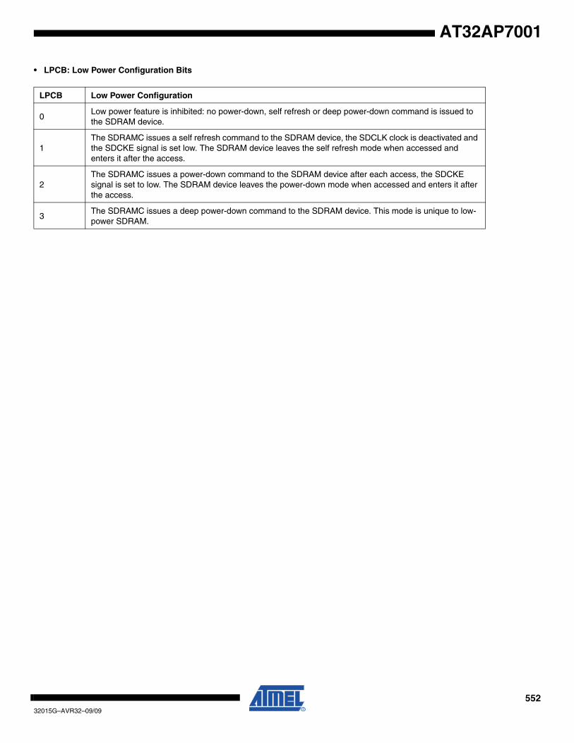
55232015G–AVR32–09/09
AT32AP7001
• LPCB: Low Power Configuration Bits
LPCB Low Power Configuration
0Low power feature is inhibited: no power-down, self refresh or deep power-down command is issued to the SDRAM device.
1The SDRAMC issues a self refresh command to the SDRAM device, the SDCLK clock is deactivated and the SDCKE signal is set low. The SDRAM device leaves the self refresh mode when accessed and enters it after the access.
2The SDRAMC issues a power-down command to the SDRAM device after each access, the SDCKE signal is set to low. The SDRAM device leaves the power-down mode when accessed and enters it after the access.
3The SDRAMC issues a deep power-down command to the SDRAM device. This mode is unique to low-power SDRAM.

55332015G–AVR32–09/09
AT32AP7001
29.8.6 Interrupt Enable Register
Register Name: IER
Access Type: Write-only
Offset: 0x14
Reset Value: 0x00000000
Writing a zero to a bit in this register has no effect.
Writing a one to a bit in this register will set the corresponding bit in IMR.
31 30 29 28 27 26 25 24
- - - - - - - -
23 22 21 20 19 18 17 16
- - - - - - - -
15 14 13 12 11 10 9 8
- - - - - - - -
7 6 5 4 3 2 1 0
- - - - - - - RES

55432015G–AVR32–09/09
AT32AP7001
29.8.7 Interrupt Disable Register
Register Name: IDR
Access Type: Write-only
Offset: 0x18
Reset Value: 0x00000000
Writing a zero to a bit in this register has no effect.
Writing a one to a bit in this register will clear the corresponding bit in IMR.
31 30 29 28 27 26 25 24
- - - - - - - -
23 22 21 20 19 18 17 16
- - - - - - - -
15 14 13 12 11 10 9 8
- - - - - - - -
7 6 5 4 3 2 1 0
- - - - - - - RES
55532015G–AVR32–09/09
AT32AP7001
29.8.8 Interrupt Mask Register
Register Name: IMR
Access Type: Read-only
Offset: 0x1C
Reset Value: 0x00000000
0: The corresponding interrupt is disabled.
1: The corresponding interrupt is enabled.
A bit in this register is cleared when the corresponding bit in IDR is written to one.A bit in this register is set when the corresponding bit in IER is written to one.
31 30 29 28 27 26 25 24
- - - - - - - -
23 22 21 20 19 18 17 16
- - - - - - - -
15 14 13 12 11 10 9 8
- - - - - - - -
7 6 5 4 3 2 1 0
- - - - - - - RES
55632015G–AVR32–09/09
AT32AP7001
29.8.9 Interrupt Status Register
Register Name: ISR
Access Type: Read-only
Offset: 0x20
Reset Value: 0x00000000
• RES: Refresh Error StatusThis bit is set when a refresh error is detected.This bit is cleared when the register is read.
31 30 29 28 27 26 25 24
- - - - - - - -
23 22 21 20 19 18 17 16
- - - - - - - -
15 14 13 12 11 10 9 8
- - - - - - - -
7 6 5 4 3 2 1 0
- - - - - - - RES
55732015G–AVR32–09/09
AT32AP7001
29.8.10 Memory Device Register
Register Name: MDR
Access Type: Read/Write
Offset: 0x24
Reset Value: 0x00000000
• MD: Memory Device Type
31 30 29 28 27 26 25 24
- - - - - - - -
23 22 21 20 19 18 17 16
- - - - - - - -
15 14 13 12 11 10 9 8
- - - - - - - -
7 6 5 4 3 2 1 0
- - - - - - MD
MD Device Type
0 SDRAM
1 Low power SDRAM
Other Reserved
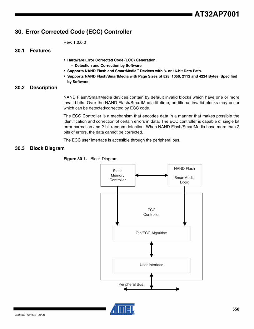
55832015G–AVR32–09/09
AT32AP7001
30. Error Corrected Code (ECC) Controller
Rev: 1.0.0.0
30.1 Features
• Hardware Error Corrected Code (ECC) Generation– Detection and Correction by Software
• Supports NAND Flash and SmartMedia™ Devices with 8- or 16-bit Data Path.• Supports NAND Flash/SmartMedia with Page Sizes of 528, 1056, 2112 and 4224 Bytes, Specified
by Software
30.2 Description
NAND Flash/SmartMedia devices contain by default invalid blocks which have one or moreinvalid bits. Over the NAND Flash/SmartMedia lifetime, additional invalid blocks may occurwhich can be detected/corrected by ECC code.
The ECC Controller is a mechanism that encodes data in a manner that makes possible theidentification and correction of certain errors in data. The ECC controller is capable of single biterror correction and 2-bit random detection. When NAND Flash/SmartMedia have more than 2bits of errors, the data cannot be corrected.
The ECC user interface is accesible through the peripheral bus.
30.3 Block Diagram
Figure 30-1. Block Diagram
User Interface
Ctrl/ECC Algorithm
StaticMemory
Controller
Peripheral Bus
NAND Flash
SmartMediaLogic
ECCController
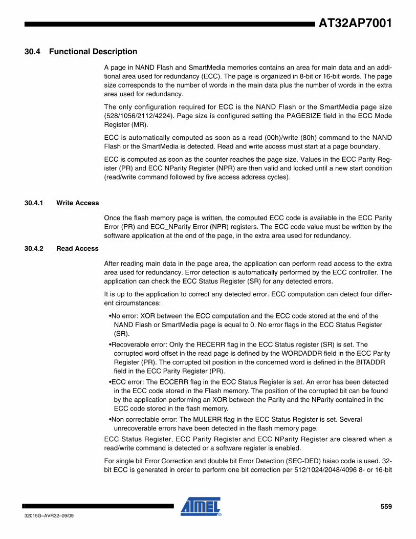
55932015G–AVR32–09/09
AT32AP7001
30.4 Functional Description
A page in NAND Flash and SmartMedia memories contains an area for main data and an addi-tional area used for redundancy (ECC). The page is organized in 8-bit or 16-bit words. The pagesize corresponds to the number of words in the main data plus the number of words in the extraarea used for redundancy.
The only configuration required for ECC is the NAND Flash or the SmartMedia page size(528/1056/2112/4224). Page size is configured setting the PAGESIZE field in the ECC ModeRegister (MR).
ECC is automatically computed as soon as a read (00h)/write (80h) command to the NANDFlash or the SmartMedia is detected. Read and write access must start at a page boundary.
ECC is computed as soon as the counter reaches the page size. Values in the ECC Parity Reg-ister (PR) and ECC NParity Register (NPR) are then valid and locked until a new start condition(read/write command followed by five access address cycles).
30.4.1 Write Access
Once the flash memory page is written, the computed ECC code is available in the ECC ParityError (PR) and ECC_NParity Error (NPR) registers. The ECC code value must be written by thesoftware application at the end of the page, in the extra area used for redundancy.
30.4.2 Read Access
After reading main data in the page area, the application can perform read access to the extraarea used for redundancy. Error detection is automatically performed by the ECC controller. Theapplication can check the ECC Status Register (SR) for any detected errors.
It is up to the application to correct any detected error. ECC computation can detect four differ-ent circumstances:
•No error: XOR between the ECC computation and the ECC code stored at the end of the NAND Flash or SmartMedia page is equal to 0. No error flags in the ECC Status Register (SR).
•Recoverable error: Only the RECERR flag in the ECC Status register (SR) is set. The corrupted word offset in the read page is defined by the WORDADDR field in the ECC Parity Register (PR). The corrupted bit position in the concerned word is defined in the BITADDR field in the ECC Parity Register (PR).
•ECC error: The ECCERR flag in the ECC Status Register is set. An error has been detected in the ECC code stored in the Flash memory. The position of the corrupted bit can be found by the application performing an XOR between the Parity and the NParity contained in the ECC code stored in the flash memory.
•Non correctable error: The MULERR flag in the ECC Status Register is set. Several unrecoverable errors have been detected in the flash memory page.
ECC Status Register, ECC Parity Register and ECC NParity Register are cleared when aread/write command is detected or a software register is enabled.
For single bit Error Correction and double bit Error Detection (SEC-DED) hsiao code is used. 32-bit ECC is generated in order to perform one bit correction per 512/1024/2048/4096 8- or 16-bit
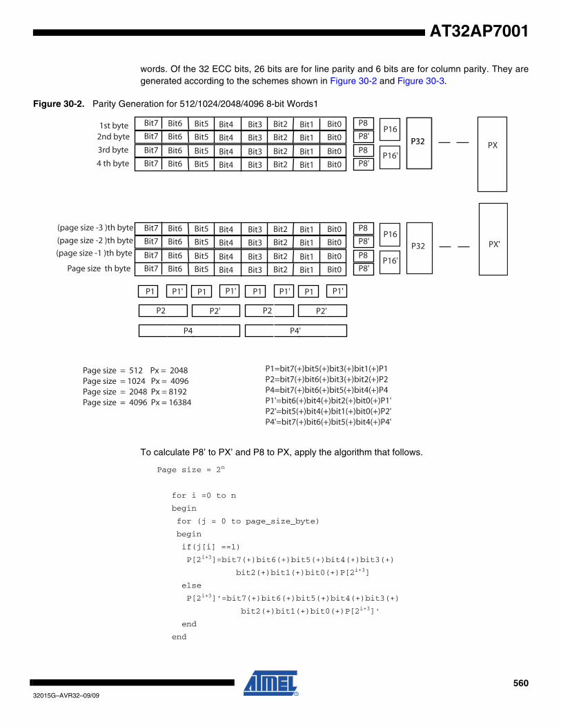
56032015G–AVR32–09/09
AT32AP7001
words. Of the 32 ECC bits, 26 bits are for line parity and 6 bits are for column parity. They aregenerated according to the schemes shown in Figure 30-2 and Figure 30-3.
Figure 30-2. Parity Generation for 512/1024/2048/4096 8-bit Words1
To calculate P8’ to PX’ and P8 to PX, apply the algorithm that follows.
Page size = 2n
for i =0 to n
begin
for (j = 0 to page_size_byte)
begin
if(j[i] ==1)
P[2i+3]=bit7(+)bit6(+)bit5(+)bit4(+)bit3(+)
bit2(+)bit1(+)bit0(+)P[2i+3]
else
P[2i+3]’=bit7(+)bit6(+)bit5(+)bit4(+)bit3(+)
bit2(+)bit1(+)bit0(+)P[2i+3]'
end
end
Bit7 Bit6 Bit5 Bit4 Bit3 Bit2 Bit1 Bit0
Bit7 Bit6 Bit5 Bit4 Bit3 Bit2 Bit1 Bit0
P8
P8'
Bit7 Bit6 Bit5 Bit4 Bit3 Bit2 Bit1 Bit0
Bit7 Bit6 Bit5 Bit4 Bit3 Bit2 Bit1 Bit0
P8
P8'
P16
P16'
Bit7 Bit6 Bit5 Bit4 Bit3 Bit2 Bit1 Bit0
Bit7 Bit6 Bit5 Bit4 Bit3 Bit2 Bit1 Bit0
P8
P8'
Bit7 Bit6 Bit5 Bit4 Bit3 Bit2 Bit1 Bit0
Bit7 Bit6 Bit5 Bit4 Bit3 Bit2 Bit1 Bit0
P8
P8'
P16
P16'
P32
P32
1st byte
P322nd byte
3rd byte
4 th byte
Page size th byte
(page size -1 )th byte
PX
PX'
Page size = 512 Px = 2048 Page size = 1024 Px = 4096Page size = 2048 Px = 8192Page size = 4096 Px = 16384
(page size -2 )th byte
(page size -3 )th byte
P1 P1' P1'P1 P1 P1' P1'P1
P2 P2' P2 P2'
P4 P4'
P1=bit7(+)bit5(+)bit3(+)bit1(+)P1 P2=bit7(+)bit6(+)bit3(+)bit2(+)P2 P4=bit7(+)bit6(+)bit5(+)bit4(+)P4P1'=bit6(+)bit4(+)bit2(+)bit0(+)P1'P2'=bit5(+)bit4(+)bit1(+)bit0(+)P2'P4'=bit7(+)bit6(+)bit5(+)bit4(+)P4'

56132015G–AVR32–09/09
AT32AP7001
Figure 30-3. Parity Generation for 512/1024/2048/4096 16-bit Words
1st w
ord
2nd
wor
d
3rd
wor
d
4th
wor
d
(Pag
e si
ze -3
)th
wor
d
(Pag
e si
ze -2
)th
wor
d
(Pag
e si
ze -1
)th
wor
d
Page
siz
e th
wor
d(+
)(+
)

56232015G–AVR32–09/09
AT32AP7001
To calculate P8’ to PX’ and P8 to PX, apply the algorithm that follows.
Page size = 2n
for i =0 to n
begin
for (j = 0 to page_size_word)
begin
if(j[i] ==1)
P[2i+3]= bit15(+)bit14(+)bit13(+)bit12(+)
bit11(+)bit10(+)bit9(+)bit8(+)
bit7(+)bit6(+)bit5(+)bit4(+)bit3(+)
bit2(+)bit1(+)bit0(+)P[2n+3]
else
P[2i+3]’=bit15(+)bit14(+)bit13(+)bit12(+)
bit11(+)bit10(+)bit9(+)bit8(+)
bit7(+)bit6(+)bit5(+)bit4(+)bit3(+)
bit2(+)bit1(+)bit0(+)P[2i+3]'
end
end
56332015G–AVR32–09/09
AT32AP7001
30.5 ECC User Interface
Table 30-1. ECC Register Mapping
Offset Register Register Name Access Reset
0x00 ECC Control Register CR Write-only 0x0
0x04 ECC Mode Register MR Read/Write 0x0
0x8 ECC Status Register SR Read-only 0x0
0x0C ECC Parity Register PR Read-only 0x0
0x10 ECC NParity Register NPR Read-only 0x0
0x14-0xF8 Reserved – – –
0x14 - 0xFC Reserved – – –

56432015G–AVR32–09/09
AT32AP7001
30.5.1 ECC Control Register
Name: CR
Access Type: Write-only
• RST: RESET Parity
Provides reset to current ECC by software.
0: No effect
1: Reset sECC Parity and ECC NParity register
31 30 29 28 27 26 25 24
– – – – – – – –
23 22 21 20 19 18 17 16
– – – – – – – –15 14 13 12 11 10 9 8
– – – – – – – –
7 6 5 4 3 2 1 0– – – – – – – RST
56532015G–AVR32–09/09
AT32AP7001
30.5.2 ECC Mode Register
Register Name: MR
Access Type: Read/Write
• PAGESIZE: Page Size
This field defines the page size of the NAND Flash device.
A word has a value of 8 bits or 16 bits, depending on the NAND Flash or Smartmedia memory organization.
31 30 29 28 27 26 25 24
– – – – – – – –
23 22 21 20 19 18 17 16– – – – – – – –
15 14 13 12 11 10 9 8
– – – – – – – –7 6 5 4 3 2 1 0
– – – – – – PAGESIZE
Page Size Description
00 528 words
01 1056 words
10 2112 words
11 4224 words
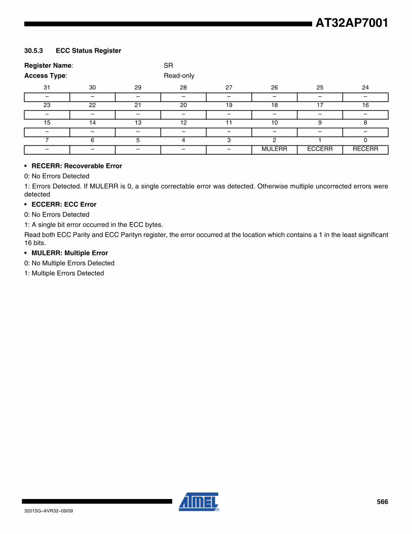
56632015G–AVR32–09/09
AT32AP7001
30.5.3 ECC Status Register
Register Name: SR
Access Type: Read-only
• RECERR: Recoverable Error
0: No Errors Detected
1: Errors Detected. If MULERR is 0, a single correctable error was detected. Otherwise multiple uncorrected errors weredetected
• ECCERR: ECC Error
0: No Errors Detected
1: A single bit error occurred in the ECC bytes.
Read both ECC Parity and ECC Parityn register, the error occurred at the location which contains a 1 in the least significant16 bits.
• MULERR: Multiple Error
0: No Multiple Errors Detected
1: Multiple Errors Detected
31 30 29 28 27 26 25 24
– – – – – – – –
23 22 21 20 19 18 17 16
– – – – – – – –15 14 13 12 11 10 9 8
– – – – – – – –
7 6 5 4 3 2 1 0– – – – – MULERR ECCERR RECERR
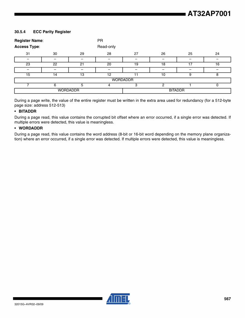
56732015G–AVR32–09/09
AT32AP7001
30.5.4 ECC Parity Register
Register Name: PR
Access Type: Read-only
During a page write, the value of the entire register must be written in the extra area used for redundancy (for a 512-bytepage size: address 512-513)
• BITADDR
During a page read, this value contains the corrupted bit offset where an error occurred, if a single error was detected. Ifmultiple errors were detected, this value is meaningless.
• WORDADDR
During a page read, this value contains the word address (8-bit or 16-bit word depending on the memory plane organiza-tion) where an error occurred, if a single error was detected. If multiple errors were detected, this value is meaningless.
31 30 29 28 27 26 25 24
– – – – – – – –
23 22 21 20 19 18 17 16– – – – – – – –
15 14 13 12 11 10 9 8
WORDADDR7 6 5 4 3 2 1 0
WORDADDR BITADDR
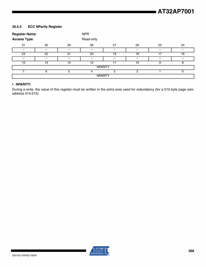
56832015G–AVR32–09/09
AT32AP7001
30.5.5 ECC NParity Register
Register Name: NPR
Access Type: Read-only
• NPARITY:
During a write, the value of this register must be written in the extra area used for redundancy (for a 512-byte page size:address 514-515)
31 30 29 28 27 26 25 24
– – – – – – – –
23 22 21 20 19 18 17 16– – – – – – – –
15 14 13 12 11 10 9 8
NPARITY7 6 5 4 3 2 1 0
NPARITY
56932015G–AVR32–09/09
AT32AP7001
31. MultiMedia Card Interface (MCI)
Rev: 2.0.0.3
31.1 Features
• Compatible with MultiMedia Card Specification Version 2.2• Compatible with SD Memory Card Specification Version 1.0• Compatible with MultiMedia Card Specification Version 3.31• Compatible with SDIO Specification Version 1.1• Cards Clock Rate Up to Master Clock Divided by 2• Embedded Power Management to Slow Down Clock Rate When Not Used• Supports 2 Slots
– Each Slot for either a MultiMediaCard Bus (Up to 30 Cards) or an SD Memory Card• Support for Stream, Block and Multi-block Data Read and Write• Supports Connection to DMA Controller
– Minimizes Processor Intervention for Large Buffer Transfers
31.2 Overview
The MCI includes a command register, response registers, data registers, timeout counters anderror detection logic that automatically handle the transmission of commands and, whenrequired, the reception of the associated responses and data with a limited processor overhead.
The MCI supports stream, block and multi-block data read and write, and is compatible with aDMA Controller, minimizing processor intervention for large buffer transfers.
The MCI operates at a rate of up to Master Clock divided by 2 and supports the interfacing of 2Slots . Each slot may be used to interface with a MultiMedia Card bus (up to 30 Cards) or with aSD Memory Card. Only one slot can be selected at a time (slots are multiplexed). A bit field inthe SD Card Register performs this selection.
The SD Memory Card communication is based on a 9-pin interface (clock, command, four dataand three power lines) and the MultiMediaCard on a 7-pin interface (clock, command, one data,three power lines and one reserved for future use).
The SD Memory Card interface also supports MultiMedia Card operations. The main differencesbetween SD and MultiMedia Cards are the initialization process and the bus topology.
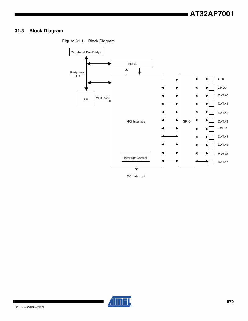
57032015G–AVR32–09/09
AT32AP7001
31.3 Block Diagram
Figure 31-1. Block Diagram
CLK
GPIOMCI Interface
Interrupt Control
MCI Interrupt
CLK_MCIPM
PeripheralBus
PDCA
Peripheral Bus Bridge
DATA0
DATA1
DATA2
DATA3
DATA4
DATA5
DATA6
DATA7
CMD0
CMD1
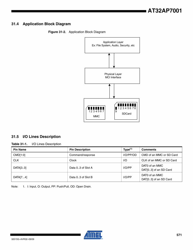
57132015G–AVR32–09/09
AT32AP7001
31.4 Application Block Diagram
Figure 31-2. Application Block Diagram
31.5 I/O Lines Description
Note: 1. I: Input, O: Output, PP: Push/Pull, OD: Open Drain.
1 2 3 4 5 6
MMC
71
92 3 4 5 76 8
SDCard
Physical Layer MCI Interface
Application LayerEx: File System, Audio, Security, etc
Table 31-1. I/O Lines Description
Pin Name Pin Description Type(1) Comments
CMD[1:0] Command/response I/O/PP/OD CMD of an MMC or SD Card
CLK Clock I/O CLK of an MMC or SD Card
DATA[3..0] Data 0..3 of Slot A I/O/PPDAT0 of an MMC
DAT[0..3] of an SD Card
DATA[7...4] Data 0..3 of Slot B I/O/PPDAT0 of an MMC
DAT[0..3] of an SD Card

57232015G–AVR32–09/09
AT32AP7001
31.6 Product Dependencies
31.6.1 GPIO
The pins used for interfacing the MultiMedia Cards or SD Cards may be multiplexed with GPIOlines. The programmer must first program the GPIO controller to assign the peripheral functionsto MCI pins.
31.6.2 Power Manager
The MCI may receive a clock from the Power Manager (PM), so the programmer must first con-figure the PM to enable the MCI clock(CLK_MCI).
31.6.3 Interrupt Controller
The MCI interface has an interrupt line connected to the Interrupt Controller (INTC).
Handling the MCI interrupt requires programming the INTC before configuring the MCI.
31.7 Functional Description
31.7.1 Bus Topology
Figure 31-3. MultiMedia Memory Card Bus Topology
The MultiMedia Card communication is based on a 7-pin serial bus interface. It has three com-munication lines and four supply lines.
Note: 1. I: Input, O: Output, PP: Push/Pull, OD: Open Drain.
Table 31-2. Bus Topology
Pin Number Name Type(1) Description
MCI Pin Name(Slot x)
1 RSV NC Not connected
2 CMD I/O/PP/OD Command/response CMDx
3 VSS1 S Supply voltage ground VSS
4 VDD S Supply voltage VDD
5 CLK I/O Clock CLK
6 VSS2 S Supply voltage ground VSS
7 DAT[0] I/O/PP Data 0 DATAx0
1 2 3 4 5 6 7
MMC
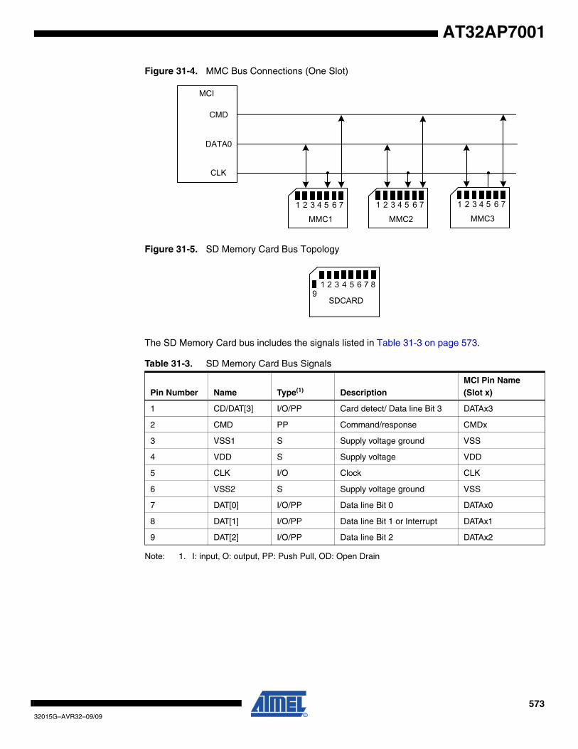
57332015G–AVR32–09/09
AT32AP7001
Figure 31-4. MMC Bus Connections (One Slot)
Figure 31-5. SD Memory Card Bus Topology
The SD Memory Card bus includes the signals listed in Table 31-3 on page 573.
Note: 1. I: input, O: output, PP: Push Pull, OD: Open Drain
Table 31-3. SD Memory Card Bus Signals
Pin Number Name Type(1) DescriptionMCI Pin Name(Slot x)
1 CD/DAT[3] I/O/PP Card detect/ Data line Bit 3 DATAx3
2 CMD PP Command/response CMDx
3 VSS1 S Supply voltage ground VSS
4 VDD S Supply voltage VDD
5 CLK I/O Clock CLK
6 VSS2 S Supply voltage ground VSS
7 DAT[0] I/O/PP Data line Bit 0 DATAx0
8 DAT[1] I/O/PP Data line Bit 1 or Interrupt DATAx1
9 DAT[2] I/O/PP Data line Bit 2 DATAx2
21 3 4 5 6 7
MMC1
21 3 4 5 6 7
MMC2
21 3 4 5 6 7
MMC3
CLK
DATA0
CMD
MCI
1 2 43 5 6 7 89
SDCARD
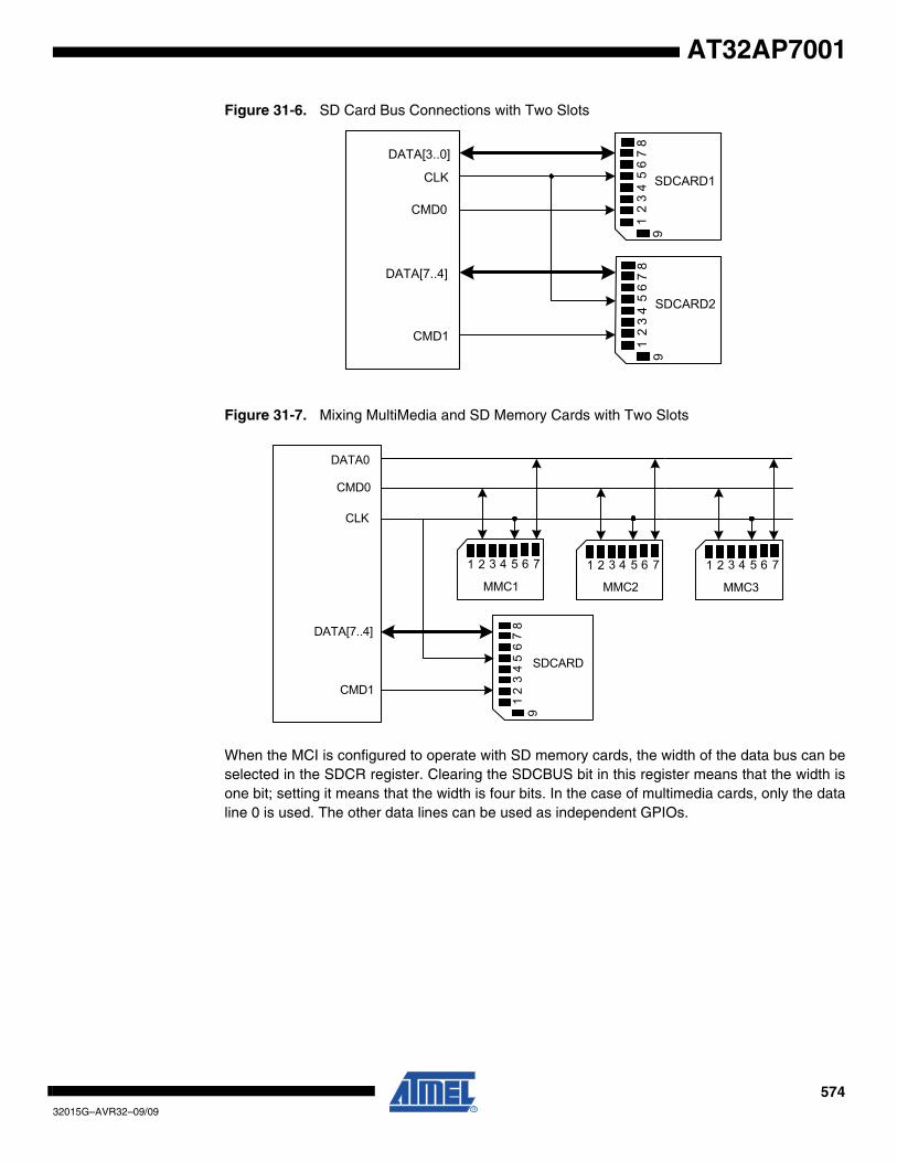
57432015G–AVR32–09/09
AT32AP7001
Figure 31-6. SD Card Bus Connections with Two Slots
Figure 31-7. Mixing MultiMedia and SD Memory Cards with Two Slots
When the MCI is configured to operate with SD memory cards, the width of the data bus can beselected in the SDCR register. Clearing the SDCBUS bit in this register means that the width isone bit; setting it means that the width is four bits. In the case of multimedia cards, only the dataline 0 is used. The other data lines can be used as independent GPIOs.
52
36
14
78
9
SDCARD1
52
36
14
78
9
SDCARD2
DATA[7..4]
CMD0
CLK
DATA[3..0]
CMD1
1 2 3 4 5 6 7
MMC1
1 2 3 4 5 6 7
MMC2
1 2 3 4 5 6 7
MMC3
49
23
15
67
8
SDCARD
DATA0
CMD0
CLK
DATA[7..4]
CMD1
57532015G–AVR32–09/09
AT32AP7001
31.7.2 MultiMedia Card Operations
After a power-on reset, the cards are initialized by a special message-based MultiMedia Cardbus protocol. Each message is represented by one of the following tokens:
• Command: A command is a token that starts an operation. A command is sent from the host either to a single card (addressed command) or to all connected cards (broadcast command). A command is transferred serially on the CMD line.
• Response: A response is a token which is sent from an addressed card or (synchronously) from all connected cards to the host as an answer to a previously received command. A response is transferred serially on the CMD line.
• Data: Data can be transferred from the card to the host or vice versa. Data is transferred via the data line.
Card addressing is implemented using a session address assigned during the initializationphase by the bus controller to all currently connected cards. Their unique CID number identifiesindividual cards.
The structure of commands, responses and data blocks is described in the MultiMedia-CardSystem Specification. See also Table 31-4 on page 576.
MultiMediaCard bus data transfers are composed of these tokens.
There are different types of operations. Addressed operations always contain a command and aresponse token. In addition, some operations have a data token; the others transfer their infor-mation directly within the command or response structure. In this case, no data token is presentin an operation. The bits on the DAT and the CMD lines are transferred synchronous to the MCIClock.
Two types of data transfer commands are defined:
• Sequential commands: These commands initiate a continuous data stream. They are terminated only when a stop command follows on the CMD line. This mode reduces the command overhead to an absolute minimum.
• Block-oriented commands: These commands send a data block succeeded by CRC bits.
Both read and write operations allow either single or multiple block transmission. A multipleblock transmission is terminated when a stop command follows on the CMD line similarly to thesequential read or when a multiple block transmission has a predefined block count (See ”DataTransfer Operation” on page 577.).
The MCI provides a set of registers to perform the entire range of MultiMedia Card operations.
31.7.2.1 Command - Response Operation
After reset, the MCI is disabled and becomes valid after setting the MCIEN bit in the ControlRegister(CR).
The two bits RDPROOF and WRPROOF in the Mode Register (MR) allow stopping the MCIClock during read or write access if the internal FIFO is full. This will guarantee data integrity, notbandwidth.
The command and the response of the card are clocked out with the rising edge of the MCIClock.
All the timings for MultiMedia Card are defined in the MultiMediaCard System Specification.
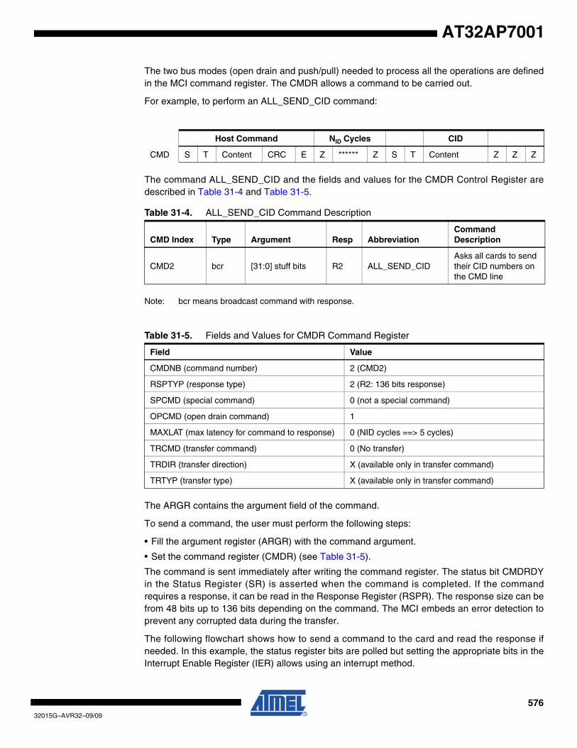
57632015G–AVR32–09/09
AT32AP7001
The two bus modes (open drain and push/pull) needed to process all the operations are definedin the MCI command register. The CMDR allows a command to be carried out.
For example, to perform an ALL_SEND_CID command:
The command ALL_SEND_CID and the fields and values for the CMDR Control Register aredescribed in Table 31-4 and Table 31-5.
Note: bcr means broadcast command with response.
The ARGR contains the argument field of the command.
To send a command, the user must perform the following steps:
• Fill the argument register (ARGR) with the command argument.
• Set the command register (CMDR) (see Table 31-5).
The command is sent immediately after writing the command register. The status bit CMDRDYin the Status Register (SR) is asserted when the command is completed. If the commandrequires a response, it can be read in the Response Register (RSPR). The response size can befrom 48 bits up to 136 bits depending on the command. The MCI embeds an error detection toprevent any corrupted data during the transfer.
The following flowchart shows how to send a command to the card and read the response ifneeded. In this example, the status register bits are polled but setting the appropriate bits in theInterrupt Enable Register (IER) allows using an interrupt method.
Host Command NID Cycles CID
CMD S T Content CRC E Z ****** Z S T Content Z Z Z
Table 31-4. ALL_SEND_CID Command Description
CMD Index Type Argument Resp AbbreviationCommand Description
CMD2 bcr [31:0] stuff bits R2 ALL_SEND_CIDAsks all cards to send their CID numbers on the CMD line
Table 31-5. Fields and Values for CMDR Command Register
Field Value
CMDNB (command number) 2 (CMD2)
RSPTYP (response type) 2 (R2: 136 bits response)
SPCMD (special command) 0 (not a special command)
OPCMD (open drain command) 1
MAXLAT (max latency for command to response) 0 (NID cycles ==> 5 cycles)
TRCMD (transfer command) 0 (No transfer)
TRDIR (transfer direction) X (available only in transfer command)
TRTYP (transfer type) X (available only in transfer command)
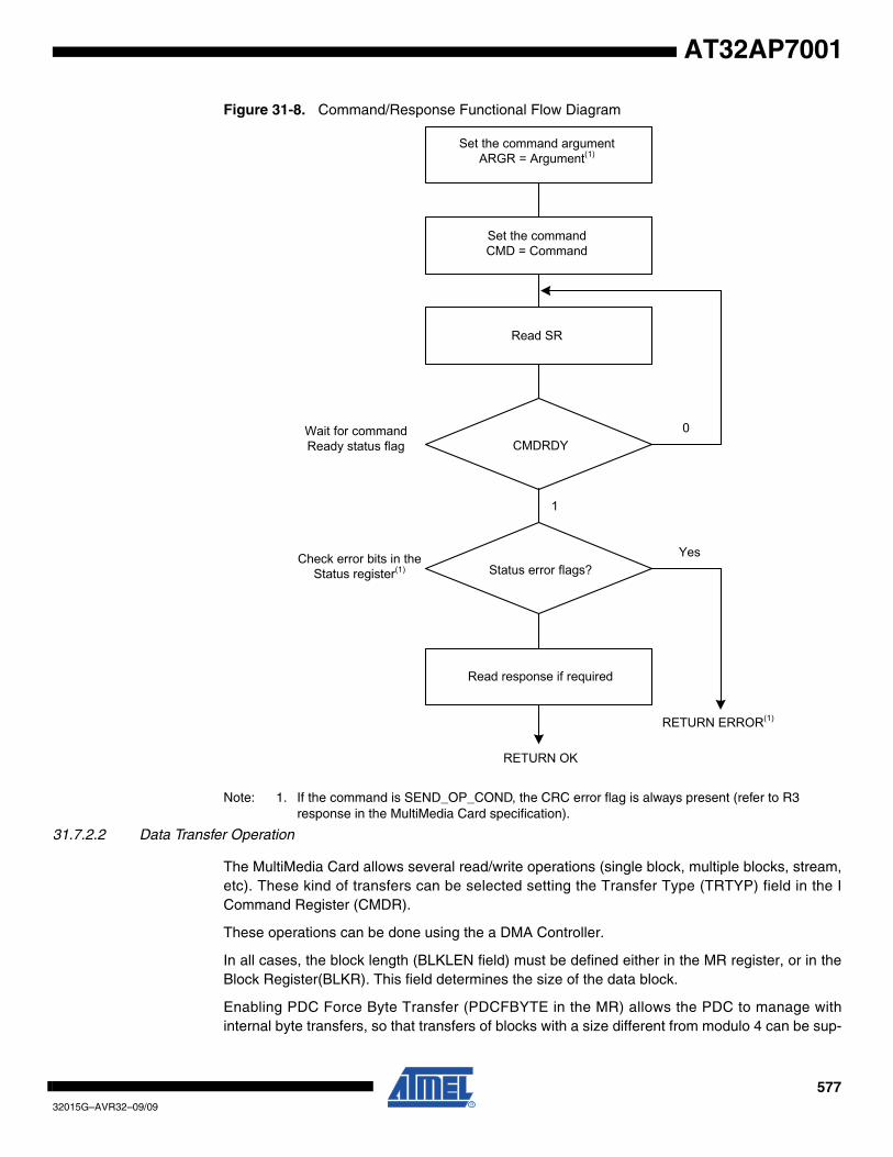
57732015G–AVR32–09/09
AT32AP7001
Figure 31-8. Command/Response Functional Flow Diagram
Note: 1. If the command is SEND_OP_COND, the CRC error flag is always present (refer to R3 response in the MultiMedia Card specification).
31.7.2.2 Data Transfer Operation
The MultiMedia Card allows several read/write operations (single block, multiple blocks, stream,etc). These kind of transfers can be selected setting the Transfer Type (TRTYP) field in the ICommand Register (CMDR).
These operations can be done using the a DMA Controller.
In all cases, the block length (BLKLEN field) must be defined either in the MR register, or in theBlock Register(BLKR). This field determines the size of the data block.
Enabling PDC Force Byte Transfer (PDCFBYTE in the MR) allows the PDC to manage withinternal byte transfers, so that transfers of blocks with a size different from modulo 4 can be sup-
Set the command argumentARGR = Argument(1)
Set the commandCMD = Command
Read SR
0
Yes
1
CMDRDYWait for commandReady status flag
Check error bits in theStatus register(1) Status error flags?
RETURN OK
RETURN ERROR(1)
Read response if required
57832015G–AVR32–09/09
AT32AP7001
ported. When PDC Force Byte Transfer is disabled, the PDC type of transfers are in words,otherwise the type of transfers are in bytes.
Consequent to MMC Specification 3.1, two types of multiple block read (or write) transactionsare defined (the host can use either one at any time):
•Open-ended/Infinite Multiple block read (or write):
The number of blocks for the read (or write) multiple block operation is not defined. The cardwill continuously transfer (or program) data blocks until a stop transmission command isreceived.
•Multiple block read (or write) with pre-defined block count (since version 3.1 and higher):
The card will transfer (or program) the requested number of data blocks and terminate thetransaction. The stop command is not required at the end of this type of multiple block read(or write), unless terminated with an error. In order to start a multiple block read (or write) withpre-defined block count, the host must correctly program the Block Register (BLKR). Other-wise the card will start an open-ended multiple block read. The BCNT field of the BlockRegister defines the number of blocks to transfer (from 1 to 65535 blocks). Programming thevalue 0 in the BCNT field corresponds to an infinite block transfer.
31.7.2.3 Read Operation
The following flowchart shows how to read a single block with or without use of DMA facilities. Inthis example, a polling method is used to wait for the end of read. Similarly, the user can config-ure the IER regsiter to trigger an interrupt at the end of read.
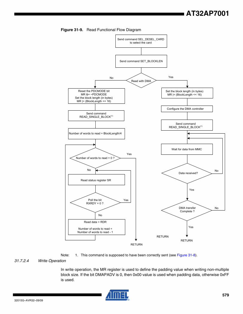
57932015G–AVR32–09/09
AT32AP7001
Figure 31-9. Read Functional Flow Diagram
Note: 1. This command is supposed to have been correctly sent (see Figure 31-8).
31.7.2.4 Write Operation
In write operation, the MR register is used to define the padding value when writing non-multipleblock size. If the bit DMAPADV is 0, then 0x00 value is used when padding data, otherwise 0xFFis used.
Send command SEL_DESEL_CARDto select the card
Send command SET_BLOCKLEN
Read with DMANo Yes
Reset the PDCMODE bitMR &= ~PDCMODE
Set the block length (in bytes)MR |= (BlockLength << 16)
Send commandREAD_SINGLE_BLOCK(1)
Number of words to read = BlockLength/4
Set the block length (in bytes)MR |= (BlockLength << 16)
Configure the DMA controller
Send commandREAD_SINGLE_BLOCK(1)
Data received?
Wait for data from MMC
Number of words to read = 0 ?
No
Yes
No
Yes
No
No
Yes
Yes
Read status register SR
RETURN
RETURNRETURN
Read data = RDR
Number of words to read = Number of words to read - 1
DMA transfer Complete ?
Poll the bit RXRDY = 0 ?

58032015G–AVR32–09/09
AT32AP7001
The following flowchart shows how to write a single block with or without use of DMA facilities.Polling or interrupt method can be used to wait for the end of write according to the contents ofthe Interrupt Mask Register (IMR).
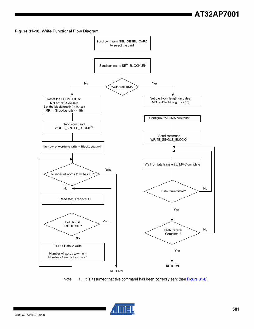
58132015G–AVR32–09/09
AT32AP7001
Figure 31-10. Write Functional Flow Diagram
Note: 1. It is assumed that this command has been correctly sent (see Figure 31-8).
Send command SEL_DESEL_CARDto select the card
Send command SET_BLOCKLEN
NoWrite with DMA
Yes
Reset the PDCMODE bitMR &= ~PDCMODE
Set the block length (in bytes)MR |= (BlockLength << 16)
Send commandWRITE_SINGLE_BLOCK(1)
Number of words to write = BlockLength/4
Number of words to write = 0 ?Yes
No
Read status register SR
YesPoll the bit TXRDY = 0 ?
No
TDR = Data to write
Number of words to write = Number of words to write - 1
RETURN
RETURN
DMA transfer Complete ?
Yes
Yes
Data transmitted?
No
No
Wait for data transfert to MMC complete
Send commandWRITE_SINGLE_BLOCK(1)
Configure the DMA controller
Set the block length (in bytes)MR |= (BlockLength << 16)
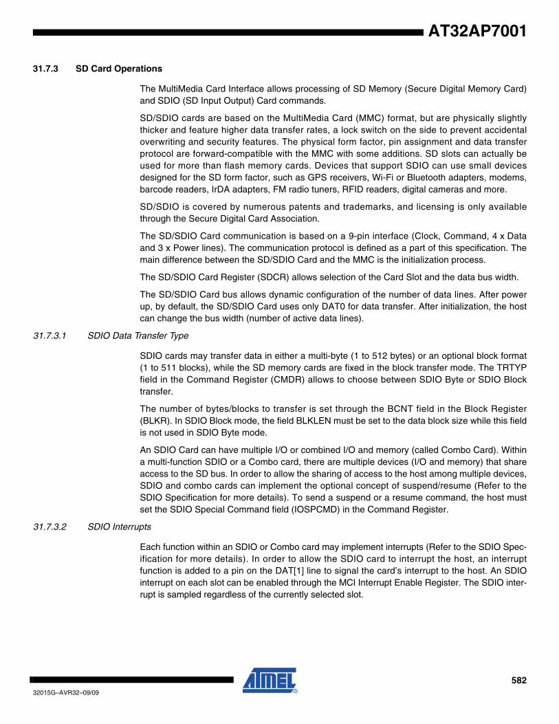
58232015G–AVR32–09/09
AT32AP7001
31.7.3 SD Card Operations
The MultiMedia Card Interface allows processing of SD Memory (Secure Digital Memory Card)and SDIO (SD Input Output) Card commands.
SD/SDIO cards are based on the MultiMedia Card (MMC) format, but are physically slightlythicker and feature higher data transfer rates, a lock switch on the side to prevent accidentaloverwriting and security features. The physical form factor, pin assignment and data transferprotocol are forward-compatible with the MMC with some additions. SD slots can actually beused for more than flash memory cards. Devices that support SDIO can use small devicesdesigned for the SD form factor, such as GPS receivers, Wi-Fi or Bluetooth adapters, modems,barcode readers, IrDA adapters, FM radio tuners, RFID readers, digital cameras and more.
SD/SDIO is covered by numerous patents and trademarks, and licensing is only availablethrough the Secure Digital Card Association.
The SD/SDIO Card communication is based on a 9-pin interface (Clock, Command, 4 x Dataand 3 x Power lines). The communication protocol is defined as a part of this specification. Themain difference between the SD/SDIO Card and the MMC is the initialization process.
The SD/SDIO Card Register (SDCR) allows selection of the Card Slot and the data bus width.
The SD/SDIO Card bus allows dynamic configuration of the number of data lines. After powerup, by default, the SD/SDIO Card uses only DAT0 for data transfer. After initialization, the hostcan change the bus width (number of active data lines).
31.7.3.1 SDIO Data Transfer Type
SDIO cards may transfer data in either a multi-byte (1 to 512 bytes) or an optional block format(1 to 511 blocks), while the SD memory cards are fixed in the block transfer mode. The TRTYPfield in the Command Register (CMDR) allows to choose between SDIO Byte or SDIO Blocktransfer.
The number of bytes/blocks to transfer is set through the BCNT field in the Block Register(BLKR). In SDIO Block mode, the field BLKLEN must be set to the data block size while this fieldis not used in SDIO Byte mode.
An SDIO Card can have multiple I/O or combined I/O and memory (called Combo Card). Withina multi-function SDIO or a Combo card, there are multiple devices (I/O and memory) that shareaccess to the SD bus. In order to allow the sharing of access to the host among multiple devices,SDIO and combo cards can implement the optional concept of suspend/resume (Refer to theSDIO Specification for more details). To send a suspend or a resume command, the host mustset the SDIO Special Command field (IOSPCMD) in the Command Register.
31.7.3.2 SDIO Interrupts
Each function within an SDIO or Combo card may implement interrupts (Refer to the SDIO Spec-ification for more details). In order to allow the SDIO card to interrupt the host, an interruptfunction is added to a pin on the DAT[1] line to signal the card’s interrupt to the host. An SDIOinterrupt on each slot can be enabled through the MCI Interrupt Enable Register. The SDIO inter-rupt is sampled regardless of the currently selected slot.

58332015G–AVR32–09/09
AT32AP7001
31.8 User Interface
Note: 1. The response register can be read by N accesses at the same RSPR or at consecutive addresses (0x20 to 0x2C). N depends on the size of the response.
Table 31-6. Register Mapping
Offset Register Register Name Read/Write Reset
0x00 Control Register CR Write –
0x04 Mode Register MR Read/write 0x0
0x08 Data Timeout Register DTOR Read/write 0x0
0x0C SD/SDIO Card Register SDCR Read/write 0x0
0x10 Argument Register ARGR Read/write 0x0
0x14 Command Register CMDR Write –
0x18 Block Register BLKR Read/write –
0x1C Reserved – – –
0x20 Response Register(1) RSPR Read 0x0
0x24 Response Register(1) RSPR Read 0x0
0x28 Response Register(1) RSPR Read 0x0
0x2C Response Register(1) RSPR Read 0x0
0x30 Receive Data Register RDR Read 0x0
0x34 Transmit Data Register TDR Write –
0x38 - 0x3C Reserved – – –
0x40 Status Register SR Read 0x25
0x44 Interrupt Enable Register IER Write –
0x48 Interrupt Disable Register IDR Write –
0x4C Interrupt Mask Register IMR Read 0x0
0x50-0xF8 Reserved – – –
0xFC Version Register VERSION Read-only –
0x50-0xFC Reserved – – –
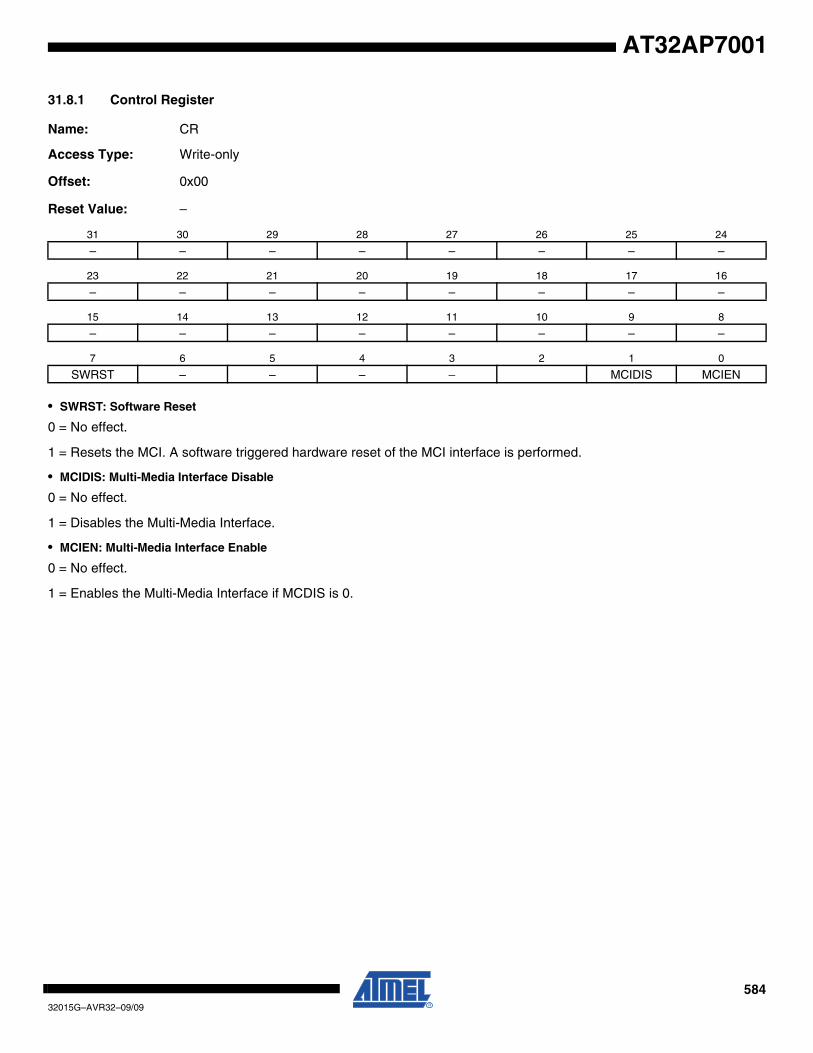
58432015G–AVR32–09/09
AT32AP7001
31.8.1 Control Register
Name: CR
Access Type: Write-only
Offset: 0x00
Reset Value: –
• SWRST: Software Reset
0 = No effect.
1 = Resets the MCI. A software triggered hardware reset of the MCI interface is performed.
• MCIDIS: Multi-Media Interface Disable
0 = No effect.
1 = Disables the Multi-Media Interface.
• MCIEN: Multi-Media Interface Enable
0 = No effect.
1 = Enables the Multi-Media Interface if MCDIS is 0.
31 30 29 28 27 26 25 24
– – – – – – – –
23 22 21 20 19 18 17 16
– – – – – – – –
15 14 13 12 11 10 9 8
– – – – – – – –
7 6 5 4 3 2 1 0
SWRST – – – – MCIDIS MCIEN

58532015G–AVR32–09/09
AT32AP7001
31.8.2 Mode Register
Name: MR
Access Type: Read/write
Offset: 0x04
Reset Value: 0x00000000
• BLKLEN: Data Block Length
This field determines the size of the data block.
This field is also accessible in the MCI Block Register (BLKR).
Bits 16 and 17 must be written to 0 if PDCFBYTE is disabled.
Note: In SDIO Byte mode, BLKLEN field is not used.
• DMAPADV: DMA Padding Value
0 = 0x00 value is used when padding data in write transfer.
1 = 0xFF value is used when padding data in write transfer.
• PDCFBYTE: PDC Force Byte TransferEnabling PDC Force Byte Transfer allows the PDC to manage with internal byte transfers, so that transfer of blocks with asize different from modulo 4 can be supported. This applies to both PDC and non-PDC transfers.
Warning: BLKLEN value depends on PDCFBYTE.
0 = Disables PDC Force Byte Transfer. PDC type of transfer are in words.
1 = Enables PDC Force Byte Transfer. PDC type of transfer are in bytes.
• WRPROOF Write Proof EnableEnabling Write Proof allows to stop the MCI Clock during write access if the internal FIFO is full. This will guarantee dataintegrity, not bandwidth.
0 = Disables Write Proof.
1 = Enables Write Proof.
• RDPROOF Read Proof EnableEnabling Read Proof allows to stop the MCI Clock during read access if the internal FIFO is full. This will guarantee dataintegrity, not bandwidth.
0 = Disables Read Proof.
1 = Enables Read Proof.
31 30 29 28 27 26 25 24
BLKLEN
23 22 21 20 19 18 17 16
BLKLEN
15 14 13 12 11 10 9 8
- DMAPADV PDCFBYTE WRPROOF RDPROOF
7 6 5 4 3 2 1 0
CLKDIV

58632015G–AVR32–09/09
AT32AP7001
• CLKDIV: Clock Divider
Multimedia Card Interface clock (MCCK) is Master Clock (CLK_MCI) divided by (2*(CLKDIV+1)).
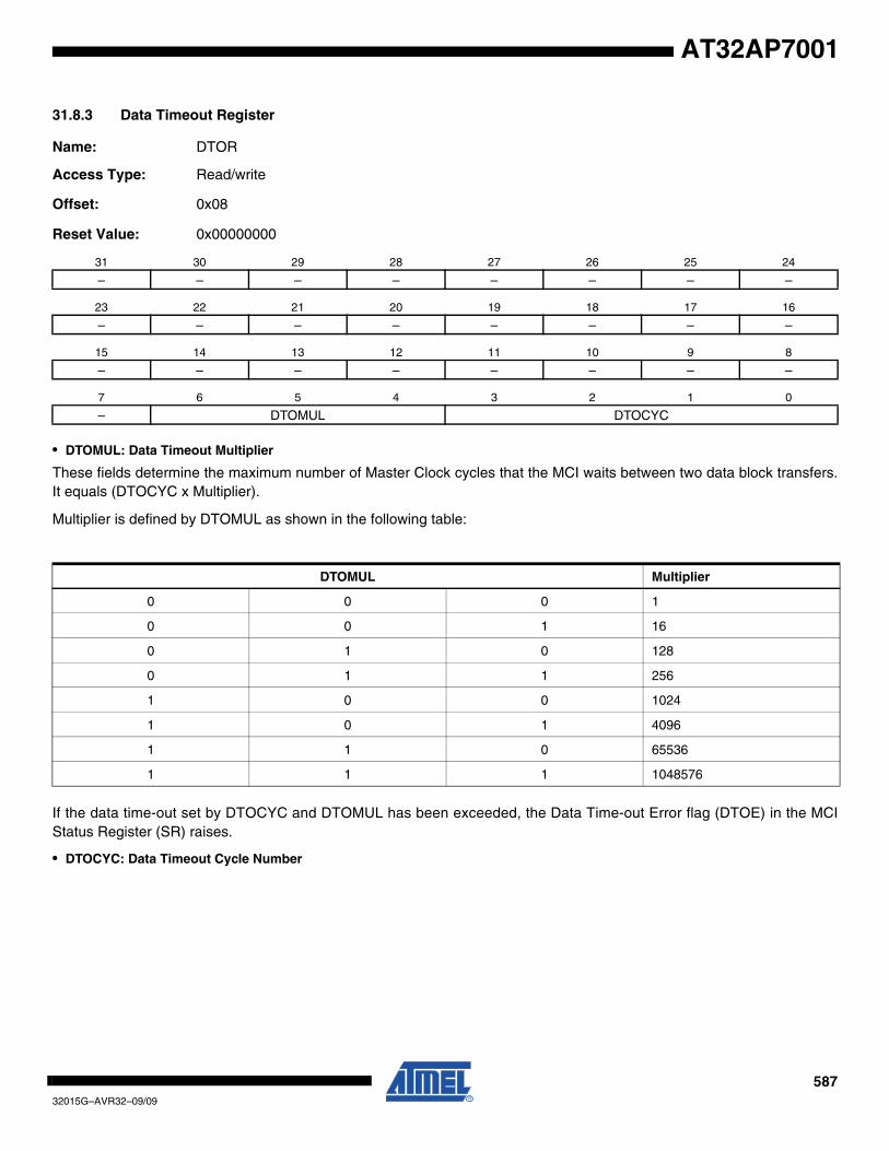
58732015G–AVR32–09/09
AT32AP7001
31.8.3 Data Timeout Register
Name: DTOR
Access Type: Read/write
Offset: 0x08
Reset Value: 0x00000000
• DTOMUL: Data Timeout Multiplier
These fields determine the maximum number of Master Clock cycles that the MCI waits between two data block transfers.It equals (DTOCYC x Multiplier).
Multiplier is defined by DTOMUL as shown in the following table:
If the data time-out set by DTOCYC and DTOMUL has been exceeded, the Data Time-out Error flag (DTOE) in the MCIStatus Register (SR) raises.
• DTOCYC: Data Timeout Cycle Number
31 30 29 28 27 26 25 24
– – – – – – – –
23 22 21 20 19 18 17 16
– – – – – – – –
15 14 13 12 11 10 9 8
– – – – – – – –
7 6 5 4 3 2 1 0
– DTOMUL DTOCYC
DTOMUL Multiplier
0 0 0 1
0 0 1 16
0 1 0 128
0 1 1 256
1 0 0 1024
1 0 1 4096
1 1 0 65536
1 1 1 1048576
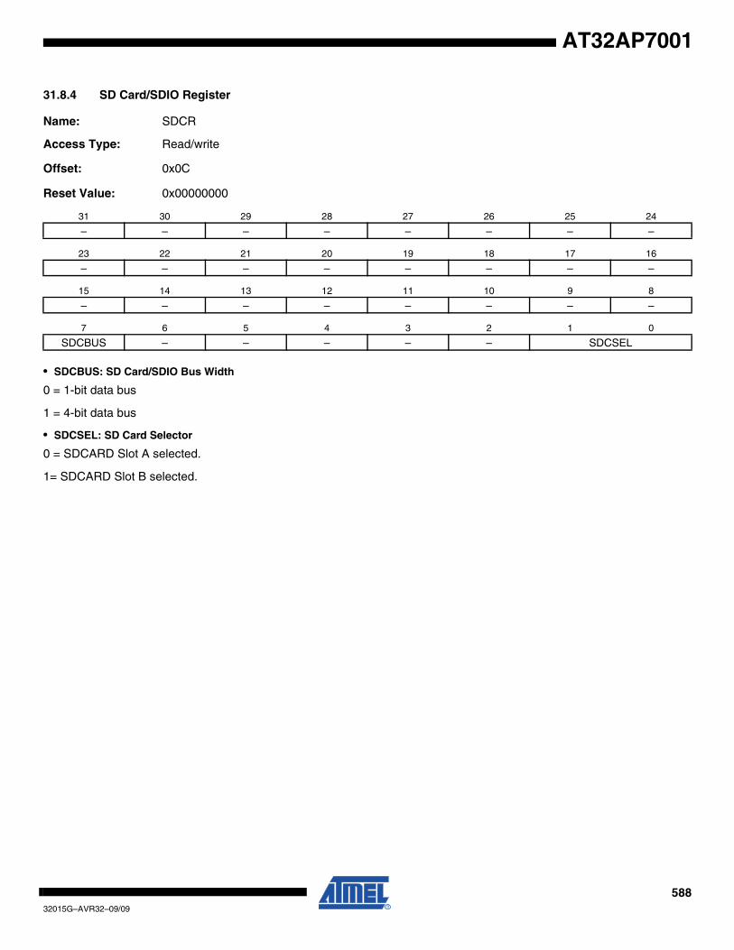
58832015G–AVR32–09/09
AT32AP7001
31.8.4 SD Card/SDIO Register
Name: SDCR
Access Type: Read/write
Offset: 0x0C
Reset Value: 0x00000000
• SDCBUS: SD Card/SDIO Bus Width
0 = 1-bit data bus
1 = 4-bit data bus
• SDCSEL: SD Card Selector
0 = SDCARD Slot A selected.
1= SDCARD Slot B selected.
31 30 29 28 27 26 25 24
– – – – – – – –
23 22 21 20 19 18 17 16
– – – – – – – –
15 14 13 12 11 10 9 8
– – – – – – – –
7 6 5 4 3 2 1 0
SDCBUS – – – – – SDCSEL
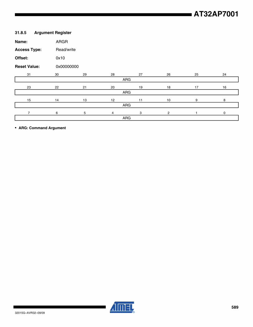
58932015G–AVR32–09/09
AT32AP7001
31.8.5 Argument Register
Name: ARGR
Access Type: Read/write
Offset: 0x10
Reset Value: 0x00000000
• ARG: Command Argument
31 30 29 28 27 26 25 24
ARG
23 22 21 20 19 18 17 16
ARG
15 14 13 12 11 10 9 8
ARG
7 6 5 4 3 2 1 0
ARG
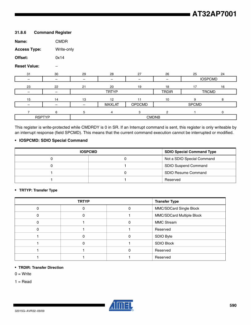
59032015G–AVR32–09/09
AT32AP7001
31.8.6 Command Register
Name: CMDR
Access Type: Write-only
Offset: 0x14
Reset Value: –
This register is write-protected while CMDRDY is 0 in SR. If an Interrupt command is sent, this register is only writeable byan interrupt response (field SPCMD). This means that the current command execution cannot be interrupted or modified.
• IOSPCMD: SDIO Special Command
• TRTYP: Transfer Type
• TRDIR: Transfer Direction
0 = Write
1 = Read
31 30 29 28 27 26 25 24
– – – – – – IOSPCMD
23 22 21 20 19 18 17 16
– – TRTYP TRDIR TRCMD
15 14 13 12 11 10 9 8
– – – MAXLAT OPDCMD SPCMD
7 6 5 4 3 2 1 0
RSPTYP CMDNB
IOSPCMD SDIO Special Command Type
0 0 Not a SDIO Special Command
0 1 SDIO Suspend Command
1 0 SDIO Resume Command
1 1 Reserved
TRTYP Transfer Type
0 0 0 MMC/SDCard Single Block
0 0 1 MMC/SDCard Multiple Block
0 1 0 MMC Stream
0 1 1 Reserved
1 0 0 SDIO Byte
1 0 1 SDIO Block
1 1 0 Reserved
1 1 1 Reserved
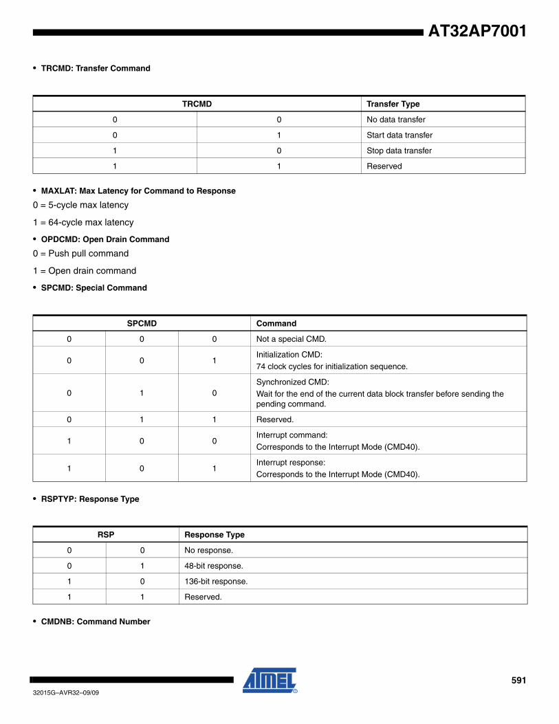
59132015G–AVR32–09/09
AT32AP7001
• TRCMD: Transfer Command
• MAXLAT: Max Latency for Command to Response
0 = 5-cycle max latency
1 = 64-cycle max latency
• OPDCMD: Open Drain Command
0 = Push pull command
1 = Open drain command
• SPCMD: Special Command
• RSPTYP: Response Type
• CMDNB: Command Number
TRCMD Transfer Type
0 0 No data transfer
0 1 Start data transfer
1 0 Stop data transfer
1 1 Reserved
SPCMD Command
0 0 0 Not a special CMD.
0 0 1Initialization CMD:74 clock cycles for initialization sequence.
0 1 0Synchronized CMD:Wait for the end of the current data block transfer before sending the pending command.
0 1 1 Reserved.
1 0 0Interrupt command:
Corresponds to the Interrupt Mode (CMD40).
1 0 1Interrupt response:
Corresponds to the Interrupt Mode (CMD40).
RSP Response Type
0 0 No response.
0 1 48-bit response.
1 0 136-bit response.
1 1 Reserved.

59232015G–AVR32–09/09
AT32AP7001
31.8.7 Block Register
Name: BLKR
Access Type: Read/write
Offset: 0x00
Reset Value: –
• BLKLEN: Data Block LengthThis field determines the size of the data block.
This field is also accessible in the MCI Mode Register (MR).
Bits 16 and 17 must be set to 0 if PDCFBYTE is disabled.
Note: In SDIO Byte mode, BLKLEN field is not used.
• BCNT: MMC/SDIO Block Count - SDIO Byte CountThis field determines the number of data byte(s) or block(s) to transfer.
The transfer data type and the authorized values for BCNT field are determined by the TRTYP field in the MCI CommandRegister (CMDR):
Warning: In SDIO Byte and Block modes, writing to the 7 last bits of BCNT field, is forbidden and may lead to unpredict-able results.
31 30 29 28 27 26 25 24
BLKLEN
23 22 21 20 19 18 17 16
BLKLEN
15 14 13 12 11 10 9 8
BCNT
7 6 5 4 3 2 1 0
BCNT
TRTYP Type of Transfer BCNT Authorized Values
0 0 1 MMC/SDCard Multiple BlockFrom 1 to MCI_MAXNUM_BLK: Value 0 corresponds to an infinite block transfer.
1 0 0 SDIO ByteFrom 1 to 512 bytes: Value 0 corresponds to a 512-byte transfer.
Values from 0x200 to 0xFFFF are forbidden.
1 0 1 SDIO BlockFrom 1 to 511 blocks: Value 0 corresponds to an infinite block transfer.
Values from 0x200 to 0xFFFF are forbidden.
Other values - Reserved.
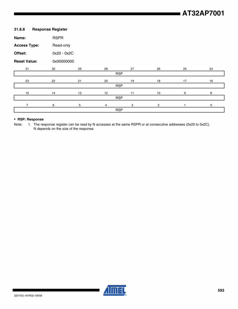
59332015G–AVR32–09/09
AT32AP7001
31.8.8 Response Register
Name: RSPR
Access Type: Read-only
Offset: 0x20 - 0x2C
Reset Value: 0x00000000
• RSP: ResponseNote: 1. The response register can be read by N accesses at the same RSPR or at consecutive addresses (0x20 to 0x2C).
N depends on the size of the response.
31 30 29 28 27 26 25 24
RSP
23 22 21 20 19 18 17 16
RSP
15 14 13 12 11 10 9 8
RSP
7 6 5 4 3 2 1 0
RSP
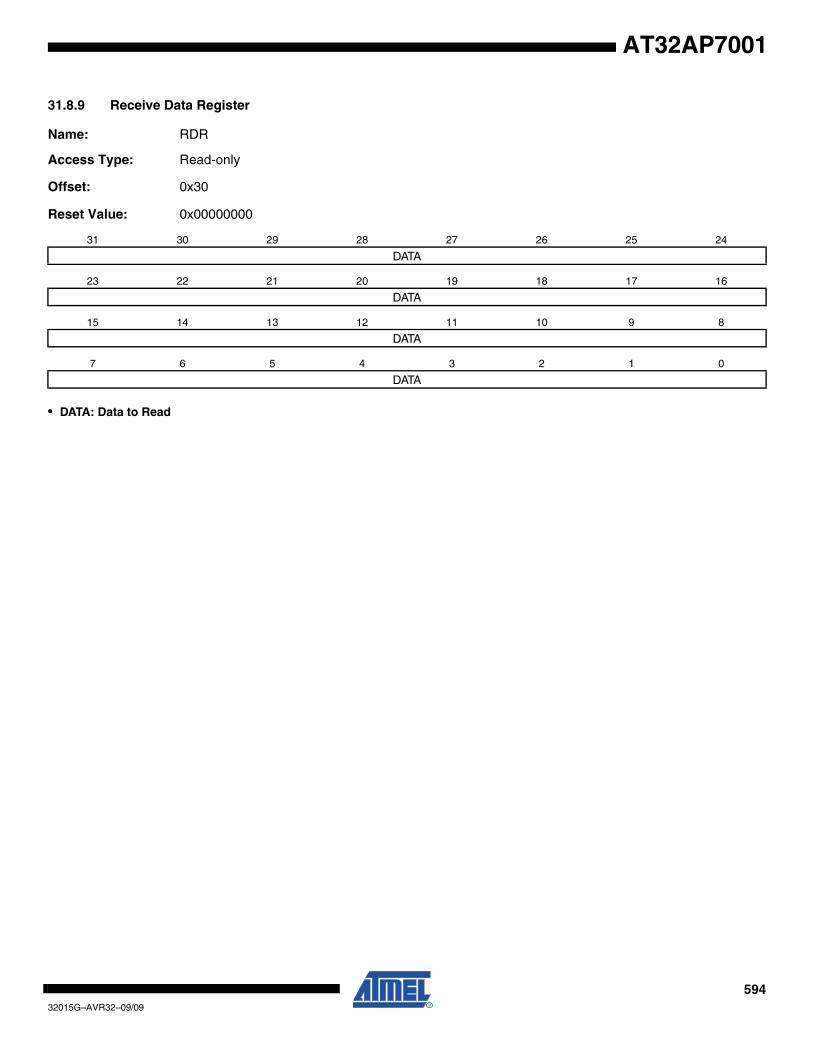
59432015G–AVR32–09/09
AT32AP7001
31.8.9 Receive Data Register
Name: RDR
Access Type: Read-only
Offset: 0x30
Reset Value: 0x00000000
• DATA: Data to Read
31 30 29 28 27 26 25 24
DATA
23 22 21 20 19 18 17 16
DATA
15 14 13 12 11 10 9 8
DATA
7 6 5 4 3 2 1 0
DATA
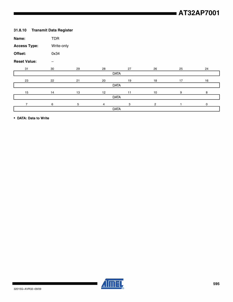
59532015G–AVR32–09/09
AT32AP7001
31.8.10 Transmit Data Register
Name: TDR
Access Type: Write-only
Offset: 0x34
Reset Value: –
• DATA: Data to Write
31 30 29 28 27 26 25 24
DATA
23 22 21 20 19 18 17 16
DATA
15 14 13 12 11 10 9 8
DATA
7 6 5 4 3 2 1 0
DATA
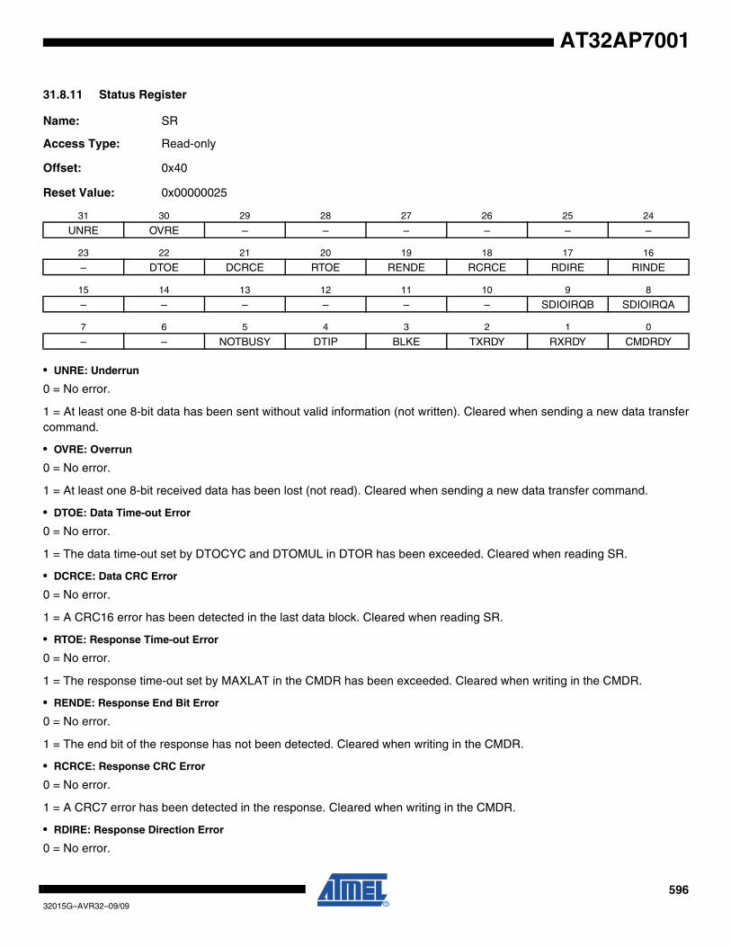
59632015G–AVR32–09/09
AT32AP7001
31.8.11 Status Register
Name: SR
Access Type: Read-only
Offset: 0x40
Reset Value: 0x00000025
• UNRE: Underrun
0 = No error.
1 = At least one 8-bit data has been sent without valid information (not written). Cleared when sending a new data transfercommand.
• OVRE: Overrun
0 = No error.
1 = At least one 8-bit received data has been lost (not read). Cleared when sending a new data transfer command.
• DTOE: Data Time-out Error
0 = No error.
1 = The data time-out set by DTOCYC and DTOMUL in DTOR has been exceeded. Cleared when reading SR.
• DCRCE: Data CRC Error
0 = No error.
1 = A CRC16 error has been detected in the last data block. Cleared when reading SR.
• RTOE: Response Time-out Error
0 = No error.
1 = The response time-out set by MAXLAT in the CMDR has been exceeded. Cleared when writing in the CMDR.
• RENDE: Response End Bit Error
0 = No error.
1 = The end bit of the response has not been detected. Cleared when writing in the CMDR.
• RCRCE: Response CRC Error
0 = No error.
1 = A CRC7 error has been detected in the response. Cleared when writing in the CMDR.
• RDIRE: Response Direction Error
0 = No error.
31 30 29 28 27 26 25 24
UNRE OVRE – – – – – –
23 22 21 20 19 18 17 16
– DTOE DCRCE RTOE RENDE RCRCE RDIRE RINDE
15 14 13 12 11 10 9 8
– – – – – – SDIOIRQB SDIOIRQA
7 6 5 4 3 2 1 0
– – NOTBUSY DTIP BLKE TXRDY RXRDY CMDRDY
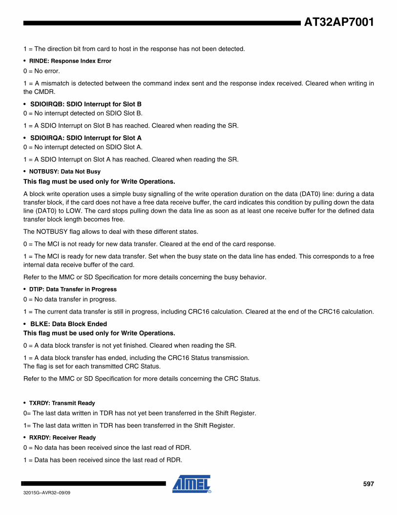
59732015G–AVR32–09/09
AT32AP7001
1 = The direction bit from card to host in the response has not been detected.
• RINDE: Response Index Error
0 = No error.
1 = A mismatch is detected between the command index sent and the response index received. Cleared when writing inthe CMDR.
• SDIOIRQB: SDIO Interrupt for Slot B0 = No interrupt detected on SDIO Slot B.
1 = A SDIO Interrupt on Slot B has reached. Cleared when reading the SR.
• SDIOIRQA: SDIO Interrupt for Slot A0 = No interrupt detected on SDIO Slot A.
1 = A SDIO Interrupt on Slot A has reached. Cleared when reading the SR.
• NOTBUSY: Data Not Busy
This flag must be used only for Write Operations.
A block write operation uses a simple busy signalling of the write operation duration on the data (DAT0) line: during a datatransfer block, if the card does not have a free data receive buffer, the card indicates this condition by pulling down the dataline (DAT0) to LOW. The card stops pulling down the data line as soon as at least one receive buffer for the defined datatransfer block length becomes free.
The NOTBUSY flag allows to deal with these different states.
0 = The MCI is not ready for new data transfer. Cleared at the end of the card response.
1 = The MCI is ready for new data transfer. Set when the busy state on the data line has ended. This corresponds to a freeinternal data receive buffer of the card.
Refer to the MMC or SD Specification for more details concerning the busy behavior.
• DTIP: Data Transfer in Progress
0 = No data transfer in progress.
1 = The current data transfer is still in progress, including CRC16 calculation. Cleared at the end of the CRC16 calculation.
• BLKE: Data Block EndedThis flag must be used only for Write Operations.
0 = A data block transfer is not yet finished. Cleared when reading the SR.
1 = A data block transfer has ended, including the CRC16 Status transmission.The flag is set for each transmitted CRC Status.
Refer to the MMC or SD Specification for more details concerning the CRC Status.
• TXRDY: Transmit Ready
0= The last data written in TDR has not yet been transferred in the Shift Register.
1= The last data written in TDR has been transferred in the Shift Register.
• RXRDY: Receiver Ready
0 = No data has been received since the last read of RDR.
1 = Data has been received since the last read of RDR.

59832015G–AVR32–09/09
AT32AP7001
• CMDRDY: Command Ready
0 = A command is in progress.
1 = The last command has been sent. Cleared when writing in the CMDR.
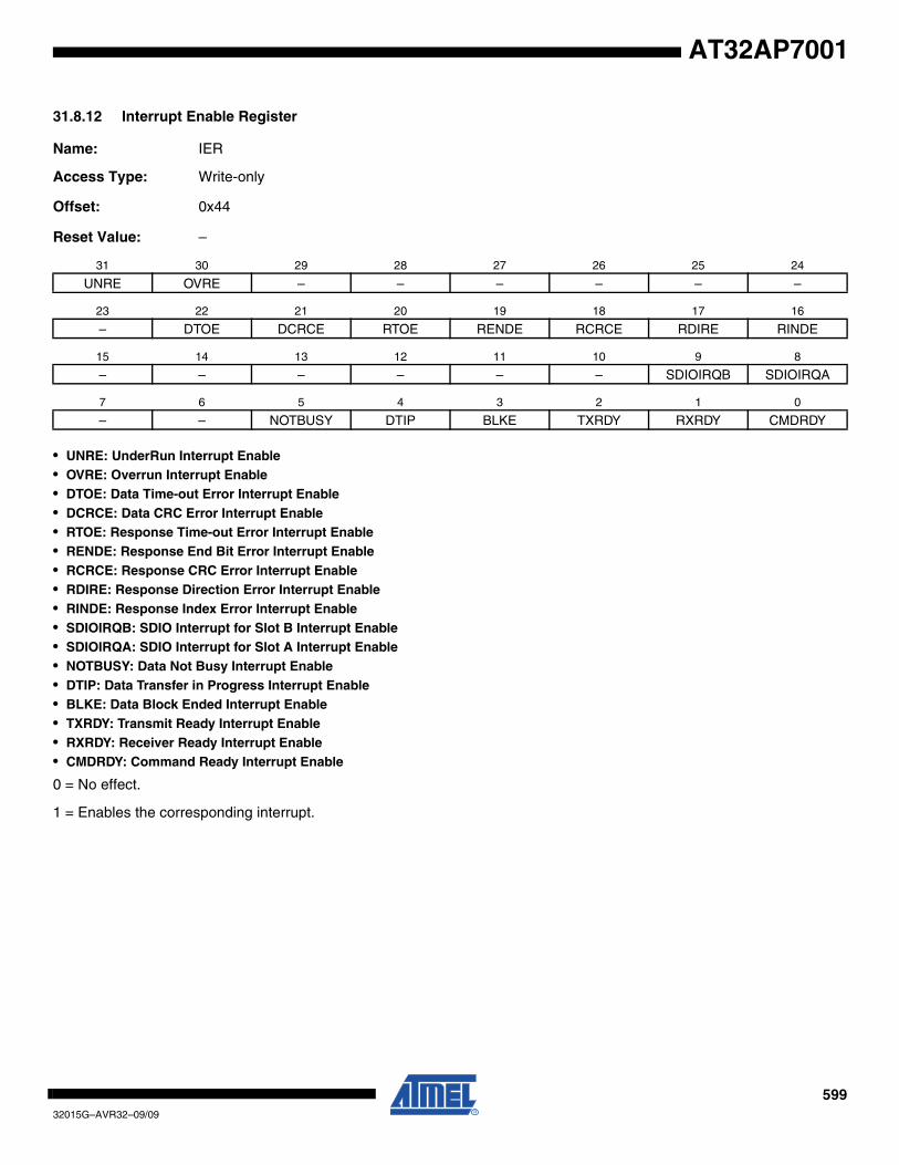
59932015G–AVR32–09/09
AT32AP7001
31.8.12 Interrupt Enable Register
Name: IER
Access Type: Write-only
Offset: 0x44
Reset Value: –
• UNRE: UnderRun Interrupt Enable• OVRE: Overrun Interrupt Enable• DTOE: Data Time-out Error Interrupt Enable• DCRCE: Data CRC Error Interrupt Enable• RTOE: Response Time-out Error Interrupt Enable• RENDE: Response End Bit Error Interrupt Enable• RCRCE: Response CRC Error Interrupt Enable• RDIRE: Response Direction Error Interrupt Enable• RINDE: Response Index Error Interrupt Enable• SDIOIRQB: SDIO Interrupt for Slot B Interrupt Enable• SDIOIRQA: SDIO Interrupt for Slot A Interrupt Enable• NOTBUSY: Data Not Busy Interrupt Enable• DTIP: Data Transfer in Progress Interrupt Enable• BLKE: Data Block Ended Interrupt Enable• TXRDY: Transmit Ready Interrupt Enable• RXRDY: Receiver Ready Interrupt Enable• CMDRDY: Command Ready Interrupt Enable
0 = No effect.
1 = Enables the corresponding interrupt.
31 30 29 28 27 26 25 24
UNRE OVRE – – – – – –
23 22 21 20 19 18 17 16
– DTOE DCRCE RTOE RENDE RCRCE RDIRE RINDE
15 14 13 12 11 10 9 8
– – – – – – SDIOIRQB SDIOIRQA
7 6 5 4 3 2 1 0
– – NOTBUSY DTIP BLKE TXRDY RXRDY CMDRDY

60032015G–AVR32–09/09
AT32AP7001
31.8.13 Interrupt Disable Register
Name: IDR
Access Type: Write-only
Offset: 0x48
Reset Value: –
• UNRE: UnderRun Interrupt Disable• OVRE: Overrun Interrupt Disable• DTOE: Data Time-out Error Interrupt Disable• DCRCE: Data CRC Error Interrupt Disable• RTOE: Response Time-out Error Interrupt Disable• RENDE: Response End Bit Error Interrupt Disable• RCRCE: Response CRC Error Interrupt Disable• RDIRE: Response Direction Error Interrupt Disable• RINDE: Response Index Error Interrupt Disable• SDIOIRQB: SDIO Interrupt for Slot B Interrupt Enable• SDIOIRQA: SDIO Interrupt for Slot A Interrupt Enable• NOTBUSY: Data Not Busy Interrupt Disable• DTIP: Data Transfer in Progress Interrupt Disable• BLKE: Data Block Ended Interrupt Disable• TXRDY: Transmit Ready Interrupt Disable• RXRDY: Receiver Ready Interrupt Disable• CMDRDY: Command Ready Interrupt Disable
0 = No effect.
1 = Disables the corresponding interrupt.
31 30 29 28 27 26 25 24
UNRE OVRE – – – – – –
23 22 21 20 19 18 17 16
– DTOE DCRCE RTOE RENDE RCRCE RDIRE RINDE
15 14 13 12 11 10 9 8
– – – – – – SDIOIRQB SDIOIRQA
7 6 5 4 3 2 1 0
– – NOTBUSY DTIP BLKE TXRDY RXRDY CMDRDY
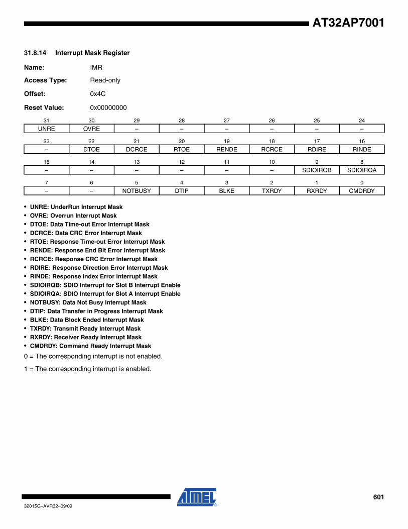
60132015G–AVR32–09/09
AT32AP7001
31.8.14 Interrupt Mask Register
Name: IMR
Access Type: Read-only
Offset: 0x4C
Reset Value: 0x00000000
• UNRE: UnderRun Interrupt Mask• OVRE: Overrun Interrupt Mask• DTOE: Data Time-out Error Interrupt Mask• DCRCE: Data CRC Error Interrupt Mask• RTOE: Response Time-out Error Interrupt Mask• RENDE: Response End Bit Error Interrupt Mask• RCRCE: Response CRC Error Interrupt Mask• RDIRE: Response Direction Error Interrupt Mask• RINDE: Response Index Error Interrupt Mask• SDIOIRQB: SDIO Interrupt for Slot B Interrupt Enable• SDIOIRQA: SDIO Interrupt for Slot A Interrupt Enable• NOTBUSY: Data Not Busy Interrupt Mask• DTIP: Data Transfer in Progress Interrupt Mask• BLKE: Data Block Ended Interrupt Mask• TXRDY: Transmit Ready Interrupt Mask• RXRDY: Receiver Ready Interrupt Mask• CMDRDY: Command Ready Interrupt Mask
0 = The corresponding interrupt is not enabled.
1 = The corresponding interrupt is enabled.
31 30 29 28 27 26 25 24
UNRE OVRE – – – – – –
23 22 21 20 19 18 17 16
– DTOE DCRCE RTOE RENDE RCRCE RDIRE RINDE
15 14 13 12 11 10 9 8
– – – – – – SDIOIRQB SDIOIRQA
7 6 5 4 3 2 1 0
– – NOTBUSY DTIP BLKE TXRDY RXRDY CMDRDY
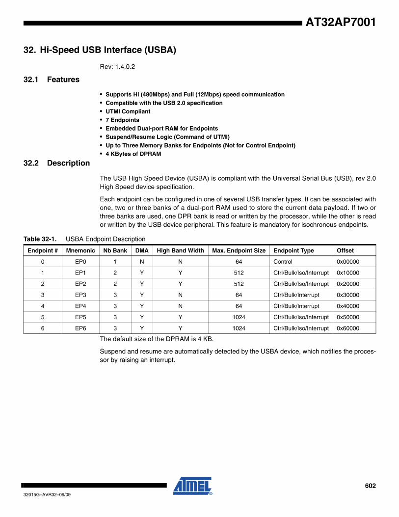
60232015G–AVR32–09/09
AT32AP7001
32. Hi-Speed USB Interface (USBA)
Rev: 1.4.0.2
32.1 Features
• Supports Hi (480Mbps) and Full (12Mbps) speed communication• Compatible with the USB 2.0 specification• UTMI Compliant• 7 Endpoints• Embedded Dual-port RAM for Endpoints• Suspend/Resume Logic (Command of UTMI)• Up to Three Memory Banks for Endpoints (Not for Control Endpoint)• 4 KBytes of DPRAM
32.2 Description
The USB High Speed Device (USBA) is compliant with the Universal Serial Bus (USB), rev 2.0High Speed device specification.
Each endpoint can be configured in one of several USB transfer types. It can be associated withone, two or three banks of a dual-port RAM used to store the current data payload. If two orthree banks are used, one DPR bank is read or written by the processor, while the other is reador written by the USB device peripheral. This feature is mandatory for isochronous endpoints.
The default size of the DPRAM is 4 KB.
Suspend and resume are automatically detected by the USBA device, which notifies the proces-sor by raising an interrupt.
Table 32-1. USBA Endpoint Description
Endpoint # Mnemonic Nb Bank DMA High Band Width Max. Endpoint Size Endpoint Type Offset
0 EP0 1 N N 64 Control 0x00000
1 EP1 2 Y Y 512 Ctrl/Bulk/Iso/Interrupt 0x10000
2 EP2 2 Y Y 512 Ctrl/Bulk/Iso/Interrupt 0x20000
3 EP3 3 Y N 64 Ctrl/Bulk/Interrupt 0x30000
4 EP4 3 Y N 64 Ctrl/Bulk/Interrupt 0x40000
5 EP5 3 Y Y 1024 Ctrl/Bulk/Iso/Interrupt 0x50000
6 EP6 3 Y Y 1024 Ctrl/Bulk/Iso/Interrupt 0x60000
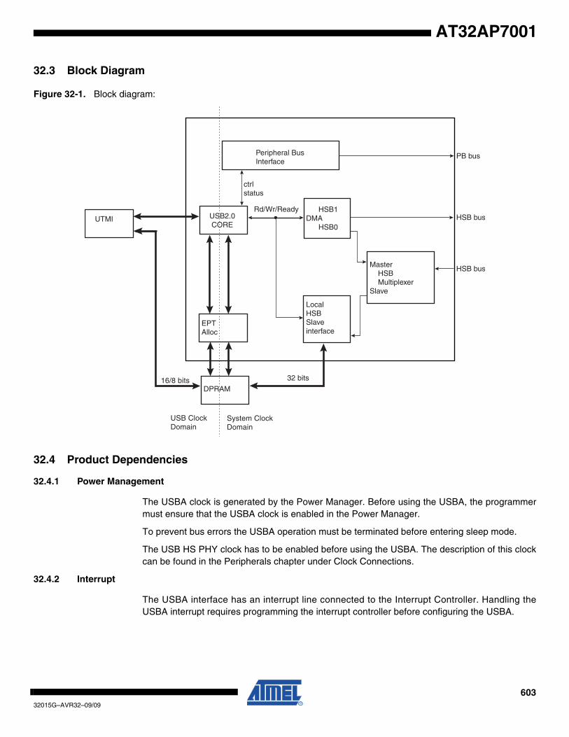
60332015G–AVR32–09/09
AT32AP7001
32.3 Block Diagram
Figure 32-1. Block diagram:
32.4 Product Dependencies
32.4.1 Power Management
The USBA clock is generated by the Power Manager. Before using the USBA, the programmermust ensure that the USBA clock is enabled in the Power Manager.
To prevent bus errors the USBA operation must be terminated before entering sleep mode.
The USB HS PHY clock has to be enabled before using the USBA. The description of this clockcan be found in the Peripherals chapter under Clock Connections.
32.4.2 Interrupt
The USBA interface has an interrupt line connected to the Interrupt Controller. Handling theUSBA interrupt requires programming the interrupt controller before configuring the USBA.
32 bits
System ClockDomain
USB ClockDomain
ctrlstatus
Rd/Wr/Ready
Peripheral BusInterface
USB2.0CORE
EPTAlloc
HSB1DMA HSB0
LocalHSBSlave interface
Master HSB MultiplexerSlave
DPRAM
UTMI
16/8 bits
PB bus
HSB bus
HSB bus
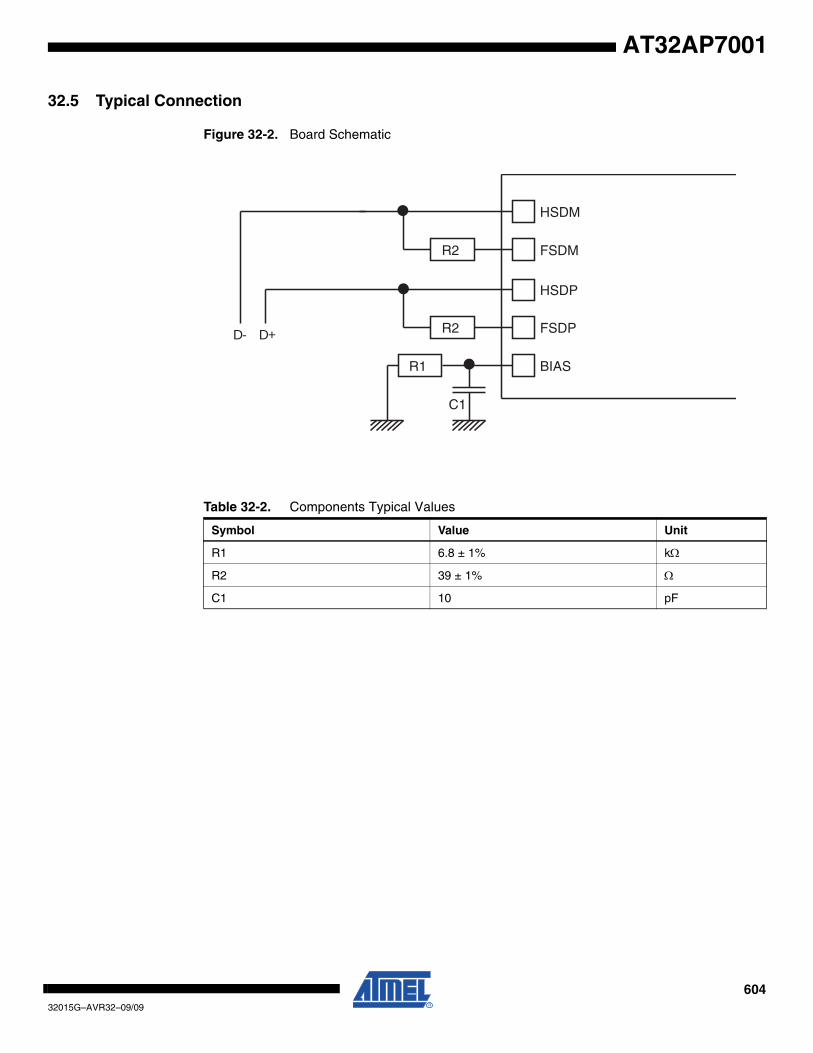
60432015G–AVR32–09/09
AT32AP7001
32.5 Typical Connection
Figure 32-2. Board Schematic
Table 32-2. Components Typical Values
Symbol Value Unit
R1 6.8 ± 1% kΩ
R2 39 ± 1% Ω
C1 10 pF
HSDP
HSDM
FSDM
FSDP
BIAS
R2
R2
R1
C1
D- D+
60532015G–AVR32–09/09
AT32AP7001
32.6 USB V2.0 High Speed Device Introduction
The USB V2.0 High Speed Device provides communication services to/from host whenattached. Each device is offered with a collection of communication flows (pipes) associated witheach endpoint. Software on the host communicates with a USB Device through a set of commu-nication flows.
32.6.1 USB V2.0 High Speed Transfer Types
A communication flow is carried over one of four transfer types defined by the USB device.
A device provides several logical communication pipes with the host. To each logical pipe isassociated an endpoint. Transfer through a pipe belongs to one of the four transfer types:
• Control Transfers: Used to configure a device at attach time and can be used for other device-specific purposes, including control of other pipes on the device.
• Bulk Data Transfers: Generated or consumed in relatively large burst quantities and have wide dynamic latitude in transmission constraints.
• Interrupt Data Transfers: Used for timely but reliable delivery of data, for example, characters or coordinates with human-perceptible echo or feedback response characteristics.
• Isochronous Data Transfers: Occupy a prenegotiated amount of USB bandwidth with a prenegotiated delivery latency. (Also called streaming real time transfers.)
As indicated below, transfers are sequential events carried out on the USB bus.
Endpoints must be configured according to the transfer type they handle.
Table 32-3. USB Communication Flow
Transfer Direction Bandwidth Endpoint Size Error Detection Retrying
Control Bidirectional Not guaranteed 8,16,32,64 Yes Automatic
Isochronous Unidirectional Guaranteed 8-1024 Yes No
Interrupt Unidirectional Not guaranteed 8-1024 Yes Yes
Bulk Unidirectional Not guaranteed 8-512 Yes Yes
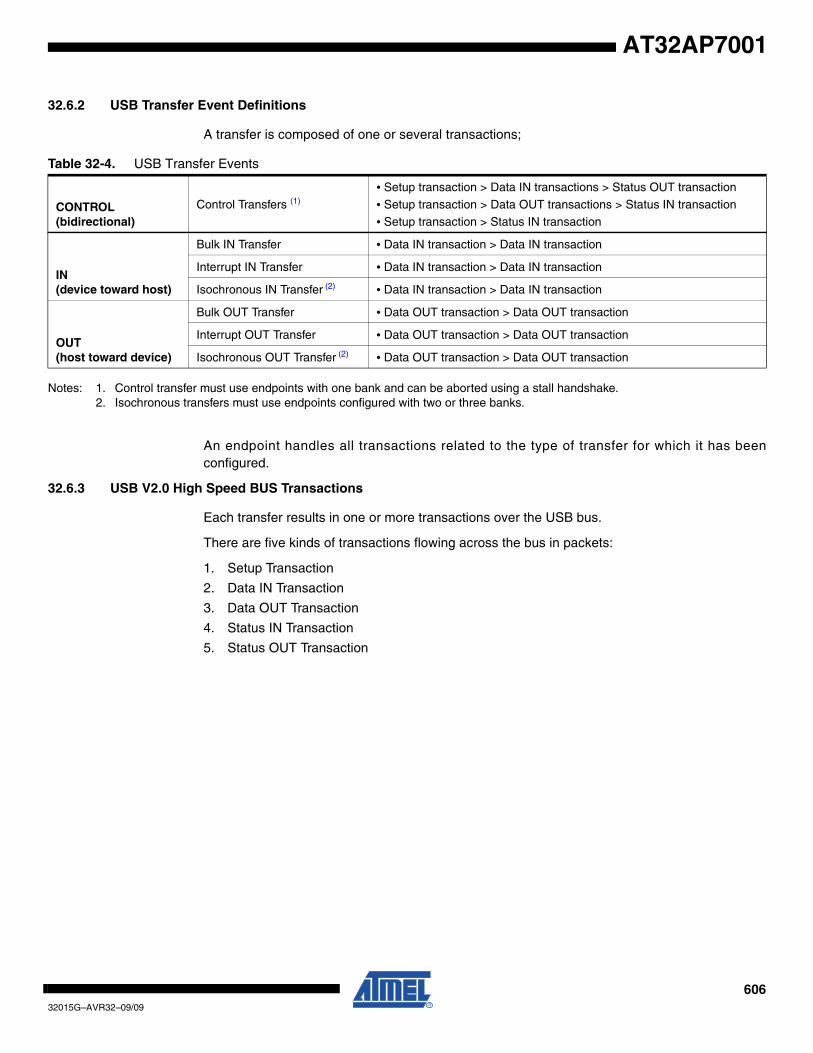
60632015G–AVR32–09/09
AT32AP7001
32.6.2 USB Transfer Event Definitions
A transfer is composed of one or several transactions;
Notes: 1. Control transfer must use endpoints with one bank and can be aborted using a stall handshake. 2. Isochronous transfers must use endpoints configured with two or three banks.
An endpoint handles all transactions related to the type of transfer for which it has beenconfigured.
32.6.3 USB V2.0 High Speed BUS Transactions
Each transfer results in one or more transactions over the USB bus.
There are five kinds of transactions flowing across the bus in packets:
1. Setup Transaction
2. Data IN Transaction
3. Data OUT Transaction
4. Status IN Transaction
5. Status OUT Transaction
Table 32-4. USB Transfer Events
CONTROL(bidirectional)
Control Transfers (1)
• Setup transaction > Data IN transactions > Status OUT transaction
• Setup transaction > Data OUT transactions > Status IN transaction• Setup transaction > Status IN transaction
IN(device toward host)
Bulk IN Transfer • Data IN transaction > Data IN transaction
Interrupt IN Transfer • Data IN transaction > Data IN transaction
Isochronous IN Transfer (2) • Data IN transaction > Data IN transaction
OUT(host toward device)
Bulk OUT Transfer • Data OUT transaction > Data OUT transaction
Interrupt OUT Transfer • Data OUT transaction > Data OUT transaction
Isochronous OUT Transfer (2) • Data OUT transaction > Data OUT transaction
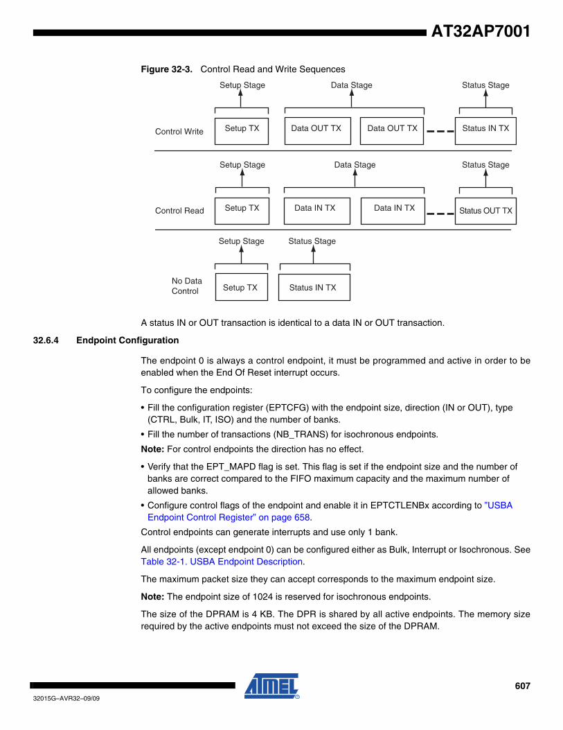
60732015G–AVR32–09/09
AT32AP7001
Figure 32-3. Control Read and Write Sequences
A status IN or OUT transaction is identical to a data IN or OUT transaction.
32.6.4 Endpoint Configuration
The endpoint 0 is always a control endpoint, it must be programmed and active in order to beenabled when the End Of Reset interrupt occurs.
To configure the endpoints:
• Fill the configuration register (EPTCFG) with the endpoint size, direction (IN or OUT), type (CTRL, Bulk, IT, ISO) and the number of banks.
• Fill the number of transactions (NB_TRANS) for isochronous endpoints.
Note: For control endpoints the direction has no effect.
• Verify that the EPT_MAPD flag is set. This flag is set if the endpoint size and the number of banks are correct compared to the FIFO maximum capacity and the maximum number of allowed banks.
• Configure control flags of the endpoint and enable it in EPTCTLENBx according to ”USBA Endpoint Control Register” on page 658.
Control endpoints can generate interrupts and use only 1 bank.
All endpoints (except endpoint 0) can be configured either as Bulk, Interrupt or Isochronous. SeeTable 32-1. USBA Endpoint Description.
The maximum packet size they can accept corresponds to the maximum endpoint size.
Note: The endpoint size of 1024 is reserved for isochronous endpoints.
The size of the DPRAM is 4 KB. The DPR is shared by all active endpoints. The memory sizerequired by the active endpoints must not exceed the size of the DPRAM.
Control Write Setup TX Data OUT TX Data OUT TX
Data Stage
Control Read
Setup Stage
Setup Stage
Setup TX
Setup TXNo DataControl
Data IN TX Data IN TX
Status Stage
Status Stage
Status IN TX
Status OUT TX
Status IN TX
Data Stage
Setup Stage Status Stage
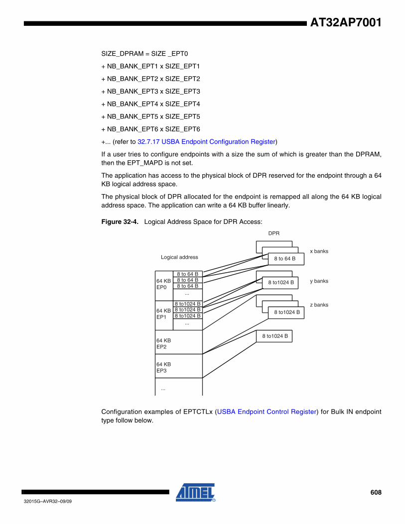
60832015G–AVR32–09/09
AT32AP7001
SIZE_DPRAM = SIZE _EPT0
+ NB_BANK_EPT1 x SIZE_EPT1
+ NB_BANK_EPT2 x SIZE_EPT2
+ NB_BANK_EPT3 x SIZE_EPT3
+ NB_BANK_EPT4 x SIZE_EPT4
+ NB_BANK_EPT5 x SIZE_EPT5
+ NB_BANK_EPT6 x SIZE_EPT6
+... (refer to 32.7.17 USBA Endpoint Configuration Register)
If a user tries to configure endpoints with a size the sum of which is greater than the DPRAM,then the EPT_MAPD is not set.
The application has access to the physical block of DPR reserved for the endpoint through a 64KB logical address space.
The physical block of DPR allocated for the endpoint is remapped all along the 64 KB logicaladdress space. The application can write a 64 KB buffer linearly.
Figure 32-4. Logical Address Space for DPR Access:
Configuration examples of EPTCTLx (USBA Endpoint Control Register) for Bulk IN endpointtype follow below.
64 KBEP0
64 KBEP1
64 KBEP2
DPR
Logical address 8 to 64 B
8 to1024 B
8 to1024 B
8 to1024 B
64 KBEP3
...
8 to 64 B8 to 64 B8 to 64 B
...
...
x banks
y banks
z banks8 to1024 B8 to1024 B8 to1024 B
60932015G–AVR32–09/09
AT32AP7001
• With DMA
– AUTO_VALID: Automatically validate the packet and switch to the next bank.
– EPT_ENABL: Enable endpoint.
• Without DMA:
– TX_BK_RDY: An interrupt is generated after each transmission.
– EPT_ENABL: Enable endpoint.
Configuration examples of Bulk OUT endpoint type follow below.
• With DMA
– AUTO_VALID: Automatically validate the packet and switch to the next bank.
– EPT_ENABL: Enable endpoint.
• Without DMA
– RX_BK_RDY: An interrupt is sent after a new packet has been stored in the endpoint FIFO.
– EPT_ENABL: Enable endpoint.
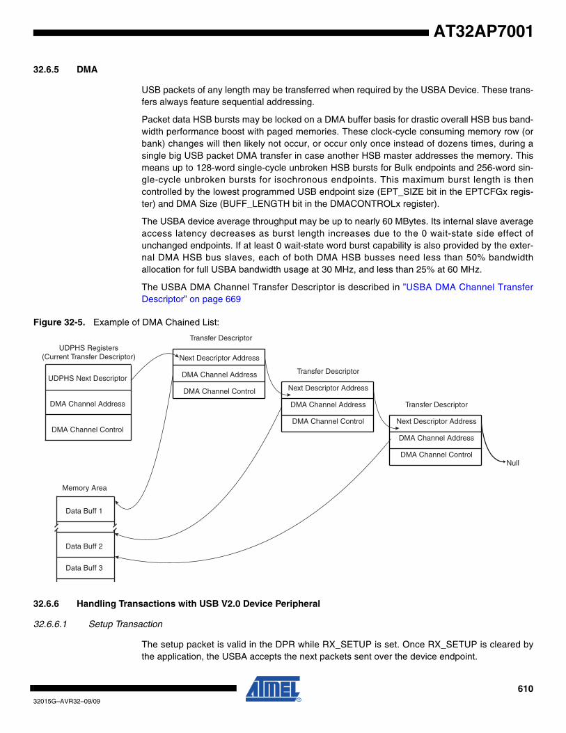
61032015G–AVR32–09/09
AT32AP7001
32.6.5 DMA
USB packets of any length may be transferred when required by the USBA Device. These trans-fers always feature sequential addressing.
Packet data HSB bursts may be locked on a DMA buffer basis for drastic overall HSB bus band-width performance boost with paged memories. These clock-cycle consuming memory row (orbank) changes will then likely not occur, or occur only once instead of dozens times, during asingle big USB packet DMA transfer in case another HSB master addresses the memory. Thismeans up to 128-word single-cycle unbroken HSB bursts for Bulk endpoints and 256-word sin-gle-cycle unbroken bursts for isochronous endpoints. This maximum burst length is thencontrolled by the lowest programmed USB endpoint size (EPT_SIZE bit in the EPTCFGx regis-ter) and DMA Size (BUFF_LENGTH bit in the DMACONTROLx register).
The USBA device average throughput may be up to nearly 60 MBytes. Its internal slave averageaccess latency decreases as burst length increases due to the 0 wait-state side effect ofunchanged endpoints. If at least 0 wait-state word burst capability is also provided by the exter-nal DMA HSB bus slaves, each of both DMA HSB busses need less than 50% bandwidthallocation for full USBA bandwidth usage at 30 MHz, and less than 25% at 60 MHz.
The USBA DMA Channel Transfer Descriptor is described in ”USBA DMA Channel TransferDescriptor” on page 669
Figure 32-5. Example of DMA Chained List:
32.6.6 Handling Transactions with USB V2.0 Device Peripheral
32.6.6.1 Setup Transaction
The setup packet is valid in the DPR while RX_SETUP is set. Once RX_SETUP is cleared bythe application, the USBA accepts the next packets sent over the device endpoint.
Data Buff 1
Data Buff 2
Data Buff 3
Memory Area
Transfer Descriptor
Next Descriptor Address
DMA Channel Address
DMA Channel Control
Transfer Descriptor
Next Descriptor Address
DMA Channel Address
DMA Channel Control
Transfer Descriptor
Next Descriptor Address
DMA Channel Address
DMA Channel Control
UDPHS Registers(Current Transfer Descriptor)
UDPHS Next Descriptor
DMA Channel Address
DMA Channel Control
Null
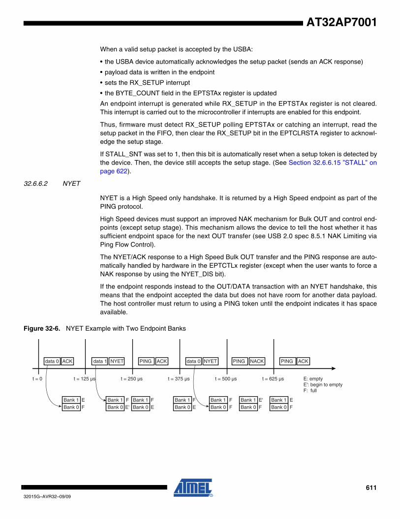
61132015G–AVR32–09/09
AT32AP7001
When a valid setup packet is accepted by the USBA:
• the USBA device automatically acknowledges the setup packet (sends an ACK response)
• payload data is written in the endpoint
• sets the RX_SETUP interrupt
• the BYTE_COUNT field in the EPTSTAx register is updated
An endpoint interrupt is generated while RX_SETUP in the EPTSTAx register is not cleared.This interrupt is carried out to the microcontroller if interrupts are enabled for this endpoint.
Thus, firmware must detect RX_SETUP polling EPTSTAx or catching an interrupt, read thesetup packet in the FIFO, then clear the RX_SETUP bit in the EPTCLRSTA register to acknowl-edge the setup stage.
If STALL_SNT was set to 1, then this bit is automatically reset when a setup token is detected bythe device. Then, the device still accepts the setup stage. (See Section 32.6.6.15 ”STALL” onpage 622).
32.6.6.2 NYET
NYET is a High Speed only handshake. It is returned by a High Speed endpoint as part of thePING protocol.
High Speed devices must support an improved NAK mechanism for Bulk OUT and control end-points (except setup stage). This mechanism allows the device to tell the host whether it hassufficient endpoint space for the next OUT transfer (see USB 2.0 spec 8.5.1 NAK Limiting viaPing Flow Control).
The NYET/ACK response to a High Speed Bulk OUT transfer and the PING response are auto-matically handled by hardware in the EPTCTLx register (except when the user wants to force aNAK response by using the NYET_DIS bit).
If the endpoint responds instead to the OUT/DATA transaction with an NYET handshake, thismeans that the endpoint accepted the data but does not have room for another data payload.The host controller must return to using a PING token until the endpoint indicates it has spaceavailable.
Figure 32-6. NYET Example with Two Endpoint Banks
t = 0 t = 125 µs t = 250 µs t = 375 µs t = 500 µs t = 625 µs
data 0 ACK data 1 NYET PING ACK data 0 NYET PING NACK PING ACK
Bank 1
Bank 0 Bank 0
Bank 1
Bank 0
Bank 1
Bank 0
Bank 1
Bank 0
Bank 1
Bank 0
Bank 1
Bank 0
Bank 1E
F
F
E
F
E'
F
E
F
F
E'
F
E
F
E: emptyE': begin to emptyF: full
61232015G–AVR32–09/09
AT32AP7001
32.6.6.3 Data IN
32.6.6.4 Bulk IN or Interrupt IN
Data IN packets are sent by the device during the data or the status stage of a control transfer orduring an (interrupt/bulk/isochronous) IN transfer. Data buffers are sent packet by packet underthe control of the application or under the control of the DMA channel.
There are three ways for an application to transfer a buffer in several packets over the USB:
• packet by packet (see 32.6.6.5 below)
• 64 KB (see 32.6.6.5 below)
• DMA (see 32.6.6.6 below)
32.6.6.5 Bulk IN or Interrupt IN: Sending a Packet Under Application Control (Device to Host)
The application can write one or several banks.
A simple algorithm can be used by the application to send packets regardless of the number ofbanks associated to the endpoint.
Algorithm Description for Each Packet:
• The application waits for TX_PK_RDY flag to be cleared in the EPTSTAx register before it can perform a write access to the DPR.
• The application writes one USB packet of data in the DPR through the 64 KB endpoint logical memory window.
• The application sets TX_PK_RDY flag in the EPTSETSTAx register.
The application is notified that it is possible to write a new packet to the DPR by theTX_PK_RDY interrupt. This interrupt can be enabled or masked by setting the TX_PK_RDY bitin the EPTCTLENB/EPTCTLDIS register.
Algorithm Description to Fill Several Packets:
Using the previous algorithm, the application is interrupted for each packet. It is possible toreduce the application overhead by writing linearly several banks at the same time. TheAUTO_VALID bit in the EPTCTLx must be set by writing the AUTO_VALID bit in theEPTCTLENBx register.
The auto-valid-bank mechanism allows the transfer of data (IN and OUT) without the interven-tion of the CPU. This means that bank validation (set TX_PK_RDY or clear the RX_BK_RDY bit)is done by hardware.
• The application checks the BUSY_BANK_STA field in the EPTSTAx register. The application must wait that at least one bank is free.
• The application writes a number of bytes inferior to the number of free DPR banks for the endpoint. Each time the application writes the last byte of a bank, the TX_PK_RDY signal is automatically set by the USBA.
• If the last packet is incomplete (i.e., the last byte of the bank has not been written) the application must set the TX_PK_RDY bit in the EPTSETSTAx register.
The application is notified that all banks are free, so that it is possible to write another burst ofpackets by the BUSY_BANK interrupt. This interrupt can be enabled or masked by setting theBUSY_BANK flag in the EPTCTLENB and EPTCTLDIS registers.
61332015G–AVR32–09/09
AT32AP7001
This algorithm must not be used for isochronous transfer. In this case, the ping-pong mechanismdoes not operate.
A Zero Length Packet can be sent by setting just the TX_PKTRDY flag in the EPTSETSTAxregister.
32.6.6.6 Bulk IN or Interrupt IN: Sending a Buffer Using DMA (Device to Host)
The USBA integrates a DMA host controller. This DMA controller can be used to transfer a buf-fer from the memory to the DPR or from the DPR to the processor memory under the USBAcontrol. The DMA can be used for all transfer types except control transfer.
Example DMA configuration:
1. Program DMAADDRESSx with the address of the buffer that should be transfer.
2. Enable the interrupt of the DMA in IEN
3. Program DMACONTROLx:
– Size of buffer to send: size of the buffer to be sent to the host.
– END_B_EN: The endpoint can validate the packet (according to the values programmed in the AUTO_VALID and SHRT_PCKT fields of EPTCTLx.) (See ”USBA Endpoint Control Register” on page 658 and Figure 32-11. Autovalid with DMA)
– END_BUFFIT: generate an interrupt when the BUFF_COUNT in DMASTATUSx reaches 0.
– CHANN_ENB: Run and stop at end of buffer
The auto-valid-bank mechanism allows the transfer of data (IN & OUT) without the interventionof the CPU. This means that bank validation (set TX_PK_RDY or clear the RX_BK_RDY bit) isdone by hardware.
A transfer descriptor can be used. Instead of programming the register directly, a descriptorshould be programmed and the address of this descriptor is then given to DMANXTDSC to beprocessed after setting the LDNXT_DSC field (Load Next Descriptor Now) in DMACONTROLxregister.
The structure that defines this transfer descriptor must be aligned.
Each buffer to be transferred must be described by a DMA Transfer descriptor (see ”USBA DMAChannel Transfer Descriptor” on page 669). Transfer descriptors are chained. Before executingtransfer of the buffer, the USBA may fetch a new transfer descriptor from the memory addresspointed by the DMANXTDSCx register. Once the transfer is complete, the transfer status isupdated in the DMASTATUSx register.
To chain a new transfer descriptor with the current DMA transfer, the DMA channel must bestopped. To do so, INTDIS_DMA and TX_BK_RDY may be set in the EPTCTLENBx register. Itis also possible for the application to wait for the completion of all transfers. In this case theLDNXT_DSC field in the last transfer descriptor DMACONTROLx register must be set to 0 andCHANN_ENB set to 1.
Then the application can chain a new transfer descriptor.
The INTDIS_DMA can be used to stop the current DMA transfer if an enabled interrupt is trig-gered. This can be used to stop DMA transfers in case of errors.
The application can be notified at the end of any buffer transfer (ENB_BUFFIT bit in the DMA-CONTROLx register).
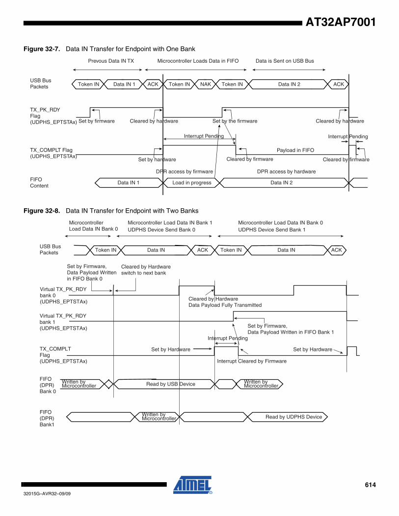
61432015G–AVR32–09/09
AT32AP7001
Figure 32-7. Data IN Transfer for Endpoint with One Bank
Figure 32-8. Data IN Transfer for Endpoint with Two Banks
USB Bus Packets
FIFOContent
TX_COMPLT Flag(UDPHS_EPTSTAx)
TX_PK_RDY Flag(UDPHS_EPTSTAx)
Prevous Data IN TX Microcontroller Loads Data in FIFO Data is Sent on USB Bus
Interrupt Pending
Set by firmware Cleared by hardware Set by the firmware Cleared by hardware
Interrupt Pending
Cleared by firmware
DPR access by firmware DPR access by hardware
Cleared by firmware
Payload in FIFO
Set by hardware
Data IN 2Token IN NAKACKData IN 1Token IN Token IN ACK
Data IN 1 Load in progress Data IN 2
Read by USB Device
Read by UDPHS Device
FIFO(DPR)Bank 0
TX_COMPLTFlag(UDPHS_EPTSTAx) Interrupt Cleared by Firmware
Virtual TX_PK_RDYbank 1(UDPHS_EPTSTAx)
ACK Token IN ACK
Set by Firmware,Data Payload Written in FIFO Bank 1
Cleared by HardwareData Payload Fully Transmitted
Token INUSB BusPackets
Set by HardwareSet by Hardware
Set by Firmware,Data Payload Writtenin FIFO Bank 0
Written by FIFO (DPR) Bank1
Microcontroller
Written by Microcontroller
Written by Microcontroller
Microcontroller Load Data IN Bank 0
Microcontroller Load Data IN Bank 1UDPHS Device Send Bank 0
Microcontroller Load Data IN Bank 0UDPHS Device Send Bank 1
Interrupt Pending
Data INData IN
Cleared by Hardwareswitch to next bank
Virtual TX_PK_RDYbank 0(UDPHS_EPTSTAx)
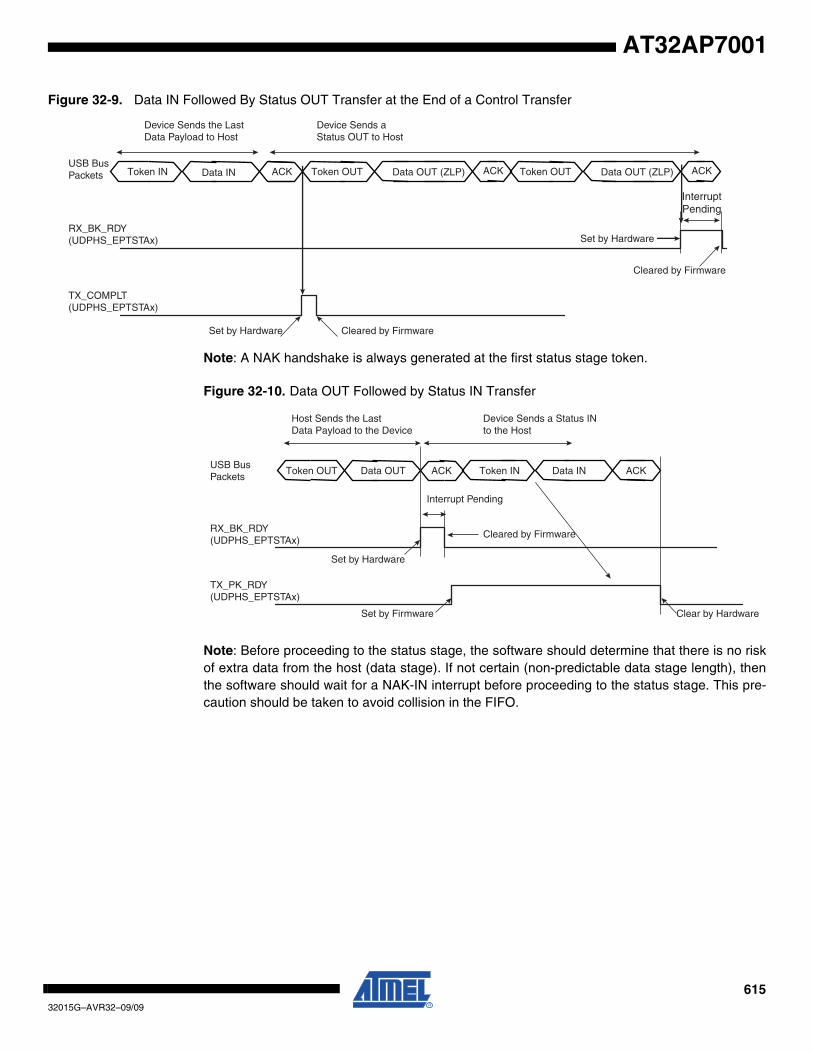
61532015G–AVR32–09/09
AT32AP7001
Figure 32-9. Data IN Followed By Status OUT Transfer at the End of a Control Transfer
Note: A NAK handshake is always generated at the first status stage token.
Figure 32-10. Data OUT Followed by Status IN Transfer
Note: Before proceeding to the status stage, the software should determine that there is no riskof extra data from the host (data stage). If not certain (non-predictable data stage length), thenthe software should wait for a NAK-IN interrupt before proceeding to the status stage. This pre-caution should be taken to avoid collision in the FIFO.
Token OUTData INToken IN ACKACK Data OUT (ZLP)
RX_BK_RDY(UDPHS_EPTSTAx)
TX_COMPLT(UDPHS_EPTSTAx)
Set by Hardware
Set by Hardware
USB BusPackets
Cleared by Firmware
Cleared by Firmware
Device Sends a Status OUT to Host
Device Sends the LastData Payload to Host
InterruptPending
Token OUT ACKData OUT (ZLP)
Token INACKData OUTToken OUT ACKData INUSB BusPackets
RX_BK_RDY(UDPHS_EPTSTAx)
Cleared by Firmware
Set by Hardware
Clear by Hardware
TX_PK_RDY(UDPHS_EPTSTAx)
Set by Firmware
Host Sends the LastData Payload to the Device
Device Sends a Status INto the Host
Interrupt Pending
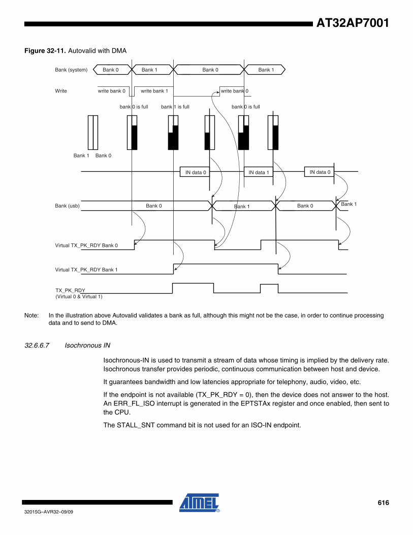
61632015G–AVR32–09/09
AT32AP7001
Figure 32-11. Autovalid with DMA
Note: In the illustration above Autovalid validates a bank as full, although this might not be the case, in order to continue processing data and to send to DMA.
32.6.6.7 Isochronous IN
Isochronous-IN is used to transmit a stream of data whose timing is implied by the delivery rate.Isochronous transfer provides periodic, continuous communication between host and device.
It guarantees bandwidth and low latencies appropriate for telephony, audio, video, etc.
If the endpoint is not available (TX_PK_RDY = 0), then the device does not answer to the host.An ERR_FL_ISO interrupt is generated in the EPTSTAx register and once enabled, then sent tothe CPU.
The STALL_SNT command bit is not used for an ISO-IN endpoint.
Bank 0 Bank 1 Bank 0Bank (usb)
Write write bank 0 write bank 1 write bank 0
Bank 0Bank (system) Bank 1 Bank 0 Bank 1
Virtual TX_PK_RDY Bank 0
Virtual TX_PK_RDY Bank 1
TX_PK_RDY(Virtual 0 & Virtual 1)
bank 0 is full bank 1 is full bank 0 is full
IN data 0 IN data 1 IN data 0
Bank 1
Bank 1 Bank 0
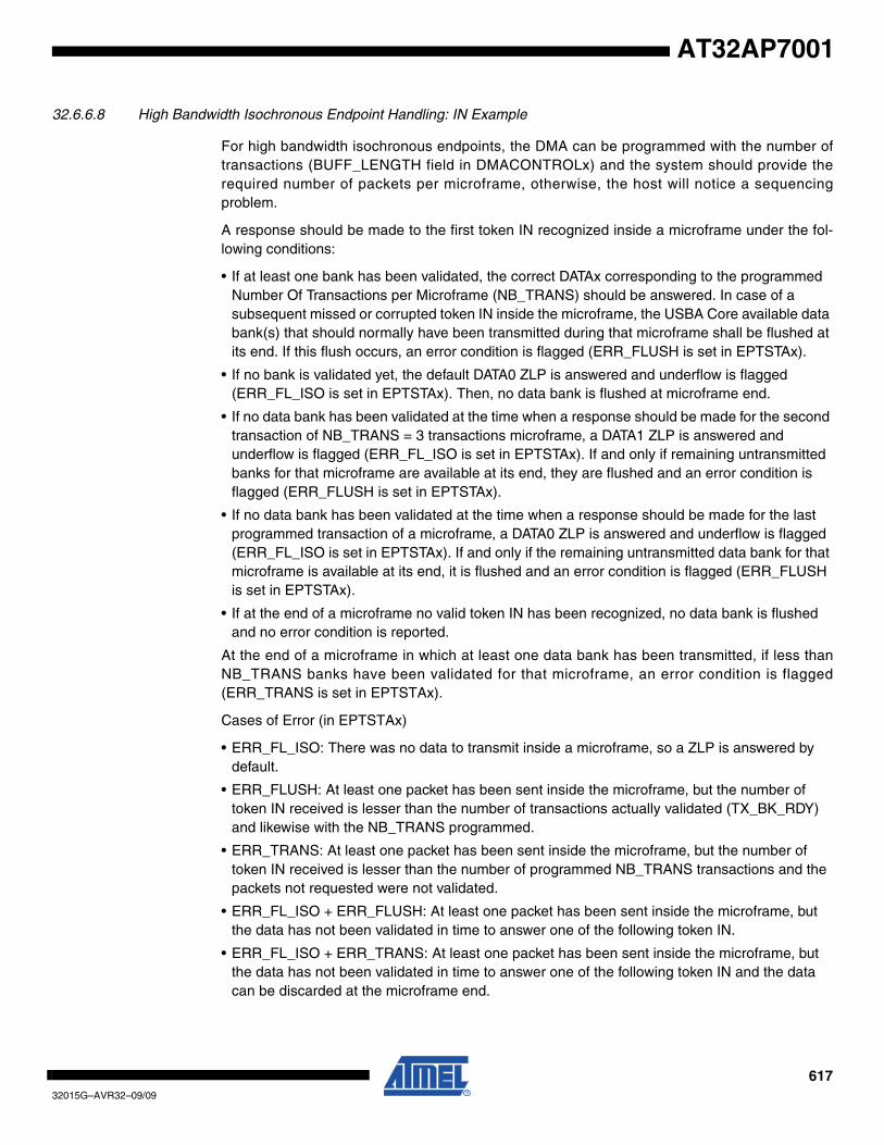
61732015G–AVR32–09/09
AT32AP7001
32.6.6.8 High Bandwidth Isochronous Endpoint Handling: IN Example
For high bandwidth isochronous endpoints, the DMA can be programmed with the number oftransactions (BUFF_LENGTH field in DMACONTROLx) and the system should provide therequired number of packets per microframe, otherwise, the host will notice a sequencingproblem.
A response should be made to the first token IN recognized inside a microframe under the fol-lowing conditions:
• If at least one bank has been validated, the correct DATAx corresponding to the programmed Number Of Transactions per Microframe (NB_TRANS) should be answered. In case of a subsequent missed or corrupted token IN inside the microframe, the USBA Core available data bank(s) that should normally have been transmitted during that microframe shall be flushed at its end. If this flush occurs, an error condition is flagged (ERR_FLUSH is set in EPTSTAx).
• If no bank is validated yet, the default DATA0 ZLP is answered and underflow is flagged (ERR_FL_ISO is set in EPTSTAx). Then, no data bank is flushed at microframe end.
• If no data bank has been validated at the time when a response should be made for the second transaction of NB_TRANS = 3 transactions microframe, a DATA1 ZLP is answered and underflow is flagged (ERR_FL_ISO is set in EPTSTAx). If and only if remaining untransmitted banks for that microframe are available at its end, they are flushed and an error condition is flagged (ERR_FLUSH is set in EPTSTAx).
• If no data bank has been validated at the time when a response should be made for the last programmed transaction of a microframe, a DATA0 ZLP is answered and underflow is flagged (ERR_FL_ISO is set in EPTSTAx). If and only if the remaining untransmitted data bank for that microframe is available at its end, it is flushed and an error condition is flagged (ERR_FLUSH is set in EPTSTAx).
• If at the end of a microframe no valid token IN has been recognized, no data bank is flushed and no error condition is reported.
At the end of a microframe in which at least one data bank has been transmitted, if less thanNB_TRANS banks have been validated for that microframe, an error condition is flagged(ERR_TRANS is set in EPTSTAx).
Cases of Error (in EPTSTAx)
• ERR_FL_ISO: There was no data to transmit inside a microframe, so a ZLP is answered by default.
• ERR_FLUSH: At least one packet has been sent inside the microframe, but the number of token IN received is lesser than the number of transactions actually validated (TX_BK_RDY) and likewise with the NB_TRANS programmed.
• ERR_TRANS: At least one packet has been sent inside the microframe, but the number of token IN received is lesser than the number of programmed NB_TRANS transactions and the packets not requested were not validated.
• ERR_FL_ISO + ERR_FLUSH: At least one packet has been sent inside the microframe, but the data has not been validated in time to answer one of the following token IN.
• ERR_FL_ISO + ERR_TRANS: At least one packet has been sent inside the microframe, but the data has not been validated in time to answer one of the following token IN and the data can be discarded at the microframe end.
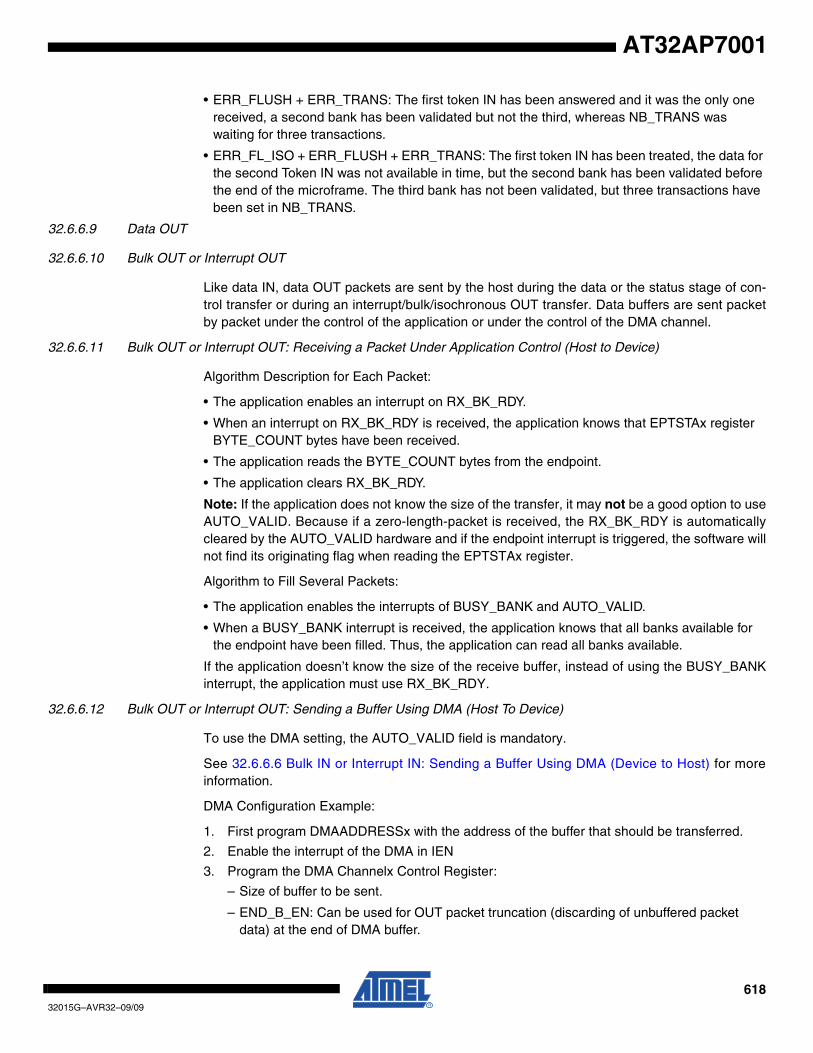
61832015G–AVR32–09/09
AT32AP7001
• ERR_FLUSH + ERR_TRANS: The first token IN has been answered and it was the only one received, a second bank has been validated but not the third, whereas NB_TRANS was waiting for three transactions.
• ERR_FL_ISO + ERR_FLUSH + ERR_TRANS: The first token IN has been treated, the data for the second Token IN was not available in time, but the second bank has been validated before the end of the microframe. The third bank has not been validated, but three transactions have been set in NB_TRANS.
32.6.6.9 Data OUT
32.6.6.10 Bulk OUT or Interrupt OUT
Like data IN, data OUT packets are sent by the host during the data or the status stage of con-trol transfer or during an interrupt/bulk/isochronous OUT transfer. Data buffers are sent packetby packet under the control of the application or under the control of the DMA channel.
32.6.6.11 Bulk OUT or Interrupt OUT: Receiving a Packet Under Application Control (Host to Device)
Algorithm Description for Each Packet:
• The application enables an interrupt on RX_BK_RDY.
• When an interrupt on RX_BK_RDY is received, the application knows that EPTSTAx register BYTE_COUNT bytes have been received.
• The application reads the BYTE_COUNT bytes from the endpoint.
• The application clears RX_BK_RDY.
Note: If the application does not know the size of the transfer, it may not be a good option to useAUTO_VALID. Because if a zero-length-packet is received, the RX_BK_RDY is automaticallycleared by the AUTO_VALID hardware and if the endpoint interrupt is triggered, the software willnot find its originating flag when reading the EPTSTAx register.
Algorithm to Fill Several Packets:
• The application enables the interrupts of BUSY_BANK and AUTO_VALID.
• When a BUSY_BANK interrupt is received, the application knows that all banks available for the endpoint have been filled. Thus, the application can read all banks available.
If the application doesn’t know the size of the receive buffer, instead of using the BUSY_BANKinterrupt, the application must use RX_BK_RDY.
32.6.6.12 Bulk OUT or Interrupt OUT: Sending a Buffer Using DMA (Host To Device)
To use the DMA setting, the AUTO_VALID field is mandatory.
See 32.6.6.6 Bulk IN or Interrupt IN: Sending a Buffer Using DMA (Device to Host) for moreinformation.
DMA Configuration Example:
1. First program DMAADDRESSx with the address of the buffer that should be transferred.
2. Enable the interrupt of the DMA in IEN
3. Program the DMA Channelx Control Register:
– Size of buffer to be sent.
– END_B_EN: Can be used for OUT packet truncation (discarding of unbuffered packet data) at the end of DMA buffer.
61932015G–AVR32–09/09
AT32AP7001
– END_BUFFIT: Generate an interrupt when BUFF_COUNT in the DMASTATUSx register reaches 0.
– END_TR_EN: End of transfer enable, the USBA device can put an end to the current DMA transfer, in case of a short packet.
– END_TR_IT: End of transfer interrupt enable, an interrupt is sent after the last USB packet has been transferred by the DMA, if the USB transfer ended with a short packet. (Beneficial when the receive size is unknown.)
– CHANN_ENB: Run and stop at end of buffer.
For OUT transfer, the bank will be automatically cleared by hardware when the application hasread all the bytes in the bank (the bank is empty).
Note: When a zero-length-packet is received, RX_BK_RDY bit in EPTSTAx is cleared automat-ically by AUTO_VALID, and the application knows of the end of buffer by the presence of theEND_TR_IT.
Note: If the host sends a zero-length packet, and the endpoint is free, then the device sends anACK. No data is written in the endpoint, the RX_BY_RDY interrupt is generated, and theBYTE_COUNT field in EPTSTAx is null.
Figure 32-12. Data OUT Transfer for Endpoint with One Bank
ACKToken OUTNAKToken OUTACKToken OUT Data OUT 1USB BusPackets
RX_BK_RDY
Set by Hardware Cleared by Firmware,Data Payload Written in FIFO
FIFO (DPR)Content
Written by UDPHS Device Microcontroller Read
Data OUT 1 Data OUT 1 Data OUT 2
Host Resends the Next Data PayloadMicrocontroller Transfers Data
Host Sends Data Payload
Data OUT 2 Data OUT 2
Host Sends the Next Data Payload
Written by UDPHS Device
(UDPHS_EPTSTAx)
Interrupt Pending
62032015G–AVR32–09/09
AT32AP7001
Figure 32-13. Data OUT Transfer for an Endpoint with Two Banks
32.6.6.13 High Bandwidth Isochronous Endpoint OUT
Figure 32-14. Bank Management, Example of Three Transactions per Microframe
USB 2.0 supports individual High Speed isochronous endpoints that require data rates up to 192Mb/s (24 MB/s): 3x1024 data bytes per microframe.
To support such a rate, two or three banks may be used to buffer the three consecutive datapackets. The microcontroller (or the DMA) should be able to empty the banks very rapidly (atleast 24 MB/s on average).
NB_TRANS field in EPTCFGx register = Number Of Transactions per Microframe.
If NB_TRANS > 1 then it is High Bandwidth.
Token OUT ACK Data OUT 3Token OUTData OUT 2Token OUTData OUT 1
Data OUT 1
Data OUT 2 Data OUT 2
ACK
Cleared by Firmware
USB BusPackets
Virtual RX_BK_RDYBank 0
Virtual RX_BK_RDYBank 1
Set by HardwareData Payload writtenin FIFO endpoint bank 1
FIFO (DPR) Bank 0
Bank 1
Write by UDPHS Device Write in progress
Read by Microcontroller
Read by Microcontroller
Set by Hardware,Data payload writtenin FIFO endpoint bank 0
Host sends first data payload Microcontroller reads Data 1 in bank 0, Host sends second data payload
Microcontroller reads Data 2 in bank 1, Host sends third data payload
Cleared by Firmware
Write by Hardware
FIFO (DPR)
(UDPHS_EPTSTAx)
Interrupt pending
Interrupt pending
RX_BK_RDY = (virtual bank 0 | virtual bank 1)
Data OUT 1 Data OUT 3
MDATA0 MDATA0 MDATA1 DATA2DATA2MDATA1
t = 0 t = 52.5 µs(40% of 125 µs)RX_BK_RDY
t = 125 µsRX_BK_RDY
USB line
Read Bank 3Read Bank 2Read Bank 1 Read Bank 1
USB busTransactions
Microcontroller FIFO (DPR) Access

62132015G–AVR32–09/09
AT32AP7001
Example:
• If NB_TRANS = 3, the sequence should be either
– MData0
– MData0/Data1
– MData0/Data1/Data2
• If NB_TRANS = 2, the sequence should be either
– MData0
– MData0/Data1
• If NB_TRANS = 1, the sequence should be
– Data0
32.6.6.14 Isochronous Endpoint Handling: OUT Example
The user can ascertain the bank status (free or busy), and the toggle sequencing of the datapacket for each bank with the EPTSTAx register in the three bit fields as follows:
• TOGGLESQ_STA: PID of the data stored in the current bank
• CURRENT_BANK: Number of the bank currently being accessed by the microcontroller.
• BUSY_BANK_STA: Number of busy bank
This is particularly useful in case of a missing data packet.
If the inter-packet delay between the OUT token and the Data is greater than the USB standard,then the ISO-OUT transaction is ignored. (Payload data is not written, no interrupt is generatedto the CPU.)
If there is a data CRC (Cyclic Redundancy Check) error, the payload is, none the less, written inthe endpoint. The ERR_CRISO flag is set in EPTSTAx register.
If the endpoint is already full, the packet is not written in the DPRAM. The ERR_FL_ISO flag isset in EPTSTAx.
If the payload data is greater than the maximum size of the endpoint, then the ERR_OVFLW flagis set. It is the task of the CPU to manage this error. The data packet is written in the endpoint(except the extra data).
If the host sends a Zero Length Packet, and the endpoint is free, no data is written in the end-point, the RX_BK_RDY flag is set, and the BYTE_COUNT field in EPTSTAx register is null.
The FRCESTALL command bit is unused for an isochonous endpoint.
Otherwise, payload data is written in the endpoint, the RX_BK_RDY interrupt is generated andthe BYTE_COUNT in EPTSTAx register is updated.
62232015G–AVR32–09/09
AT32AP7001
32.6.6.15 STALL
STALL is returned by a function in response to an IN token or after the data phase of an OUT orin response to a PING transaction. STALL indicates that a function is unable to transmit orreceive data, or that a control pipe request is not supported.
• OUT
To stall an endpoint, set the FRCESTALL bit in EPTSETSTAx register and after theSTALL_SNT flag has been set, set the TOGGLE_SEG bit in the EPTCLRSTAx register.
• IN
Set the FRCESTALL bit in EPTSETSTAx register.
Figure 32-15. Stall Handshake Data OUT Transfer
Figure 32-16. Stall Handshake Data IN Transfer
Token OUT Stall PID Data OUTUSB BusPackets
Cleared by Firmware
Set by FirmwareFRCESTALL
STALL_SNTSet by Hardware
Interrupt PendingCleared by Firmware
Token IN Stall PIDUSB BusPackets
Cleared by FirmwareSet by Firmware
FRCESTALL
STALL_SNT
Set by Hardware Cleared by Firmware
Interrupt Pending

62332015G–AVR32–09/09
AT32AP7001
32.6.7 Speed Identification
The high speed reset is managed by the hardware.
At the connection, the host makes a reset which could be a classic reset (full speed) or a highspeed reset.
At the end of the reset process (full or high), the ENDRESET interrupt is generated.
Then the CPU should read the SPEED bit in INTSTAx to ascertain the speed mode of thedevice.
32.6.8 USB V2.0 High Speed Global Interrupt
Interrupts are defined in Section 32.7.3 ”USBA Interrupt Enable Register” (IEN) and in Section32.7.4 ”USBA Interrupt Status Register” (INTSTA).
32.6.9 Endpoint Interrupts
Interrupts are enabled in IEN (see Section 32.7.3 ”USBA Interrupt Enable Register”) and individ-ually masked in EPTCTLENBx (see Section 32.7.18 ”USBA Endpoint Control Enable Register”).
Table 32-5. Endpoint Interrupt Source Masks
SHRT_PCKT Short Packet Interrupt
BUSY_BANK Busy Bank Interrupt
NAK_OUT NAKOUT Interrupt
NAK_IN/ERR_FLUSH NAKIN/Error Flush Interrupt
STALL_SNT/ERR_CRISO/ERR_NB_TRA Stall Sent/CRC error/Number of Transaction Error Interrupt
RX_SETUP/ERR_FL_ISO Received SETUP/Error Flow Interrupt
TX_PK_RD /ERR_TRANS TX Packet Read/Transaction Error Interrupt
TX_COMPLT Transmitted IN Data Complete Interrupt
RX_BK_RDY Received OUT Data Interrupt
ERR_OVFLW Overflow Error Interrupt
MDATA_RX MDATA Interrupt
DATAX_RX DATAx Interrupt
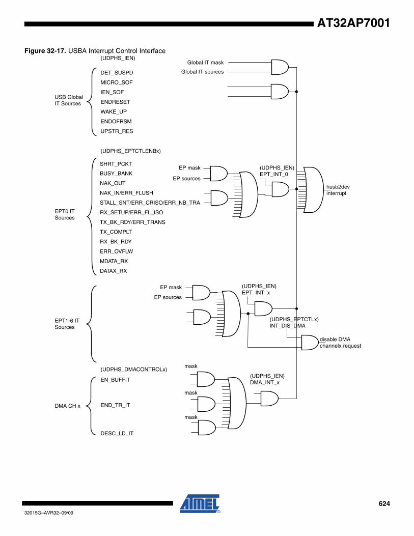
62432015G–AVR32–09/09
AT32AP7001
Figure 32-17. USBA Interrupt Control Interface
DET_SUSPD
MICRO_SOF
IEN_SOF
ENDRESET
WAKE_UP
ENDOFRSM
UPSTR_RES
USB GlobalIT Sources
EPT0 ITSources
BUSY_BANK
NAK_OUT
(UDPHS_EPTCTLENBx)
NAK_IN/ERR_FLUSH
STALL_SNT/ERR_CRISO/ERR_NB_TRA
RX_SETUP/ERR_FL_ISO
TX_BK_RDY/ERR_TRANS
TX_COMPLT
RX_BK_RDY
ERR_OVFLW
MDATA_RX
DATAX_RX
(UDPHS_IEN)
EPT1-6 ITSources
Global IT mask
Global IT sources
EP mask
EP sources
(UDPHS_IEN)EPT_INT_0
EP mask
EP sources
(UDPHS_IEN)EPT_INT_x
(UDPHS_EPTCTLx)INT_DIS_DMA
DMA CH x
(UDPHS_DMACONTROLx)
EN_BUFFIT
END_TR_IT
DESC_LD_IT
mask
mask
mask
(UDPHS_IEN)DMA_INT_x
SHRT_PCKT
husb2devinterrupt
disable DMAchannelx request

62532015G–AVR32–09/09
AT32AP7001
32.6.10 Power Modes
32.6.10.1 Controlling Device States
A USB device has several possible states. Refer to Chapter 9 (USB Device Framework) of theUniversal Serial Bus Specification, Rev 2.0.
Figure 32-18. USBADevice State Diagram
Movement from one state to another depends on the USB bus state or on standard requestssent through control transactions via the default endpoint (endpoint 0).
After a period of bus inactivity, the USB device enters Suspend Mode. Accepting Sus-pend/Resume requests from the USB host is mandatory. Constraints in Suspend Mode are verystrict for bus-powered applications; devices may not consume more than 500 µA on the USBbus.
While in Suspend Mode, the host may wake up a device by sending a resume signal (bus activ-ity) or a USB device may send a wake-up request to the host, e.g., waking up a PC by moving aUSB mouse.
Attached
Suspended
Suspended
Suspended
Suspended
Hub Resetor
Deconfigured
HubConfigured
Bus Inactive
Bus Activity
Bus Inactive
Bus Activity
Bus Inactive
Bus Activity
Bus Inactive
Bus Activity
Reset
Reset
AddressAssigned
DeviceDeconfigured
DeviceConfigured
Powered
Default
Address
Configured
PowerInterruption
62632015G–AVR32–09/09
AT32AP7001
The wake-up feature is not mandatory for all devices and must be negotiated with the host.
32.6.10.2 From Powered State to Default State (Reset)
After its connection to a USB host, the USB device waits for an end-of-bus reset. The unmaskedflag ENDRESET is set in the IEN register and an interrupt is triggered.
Once the ENDRESET interrupt has been triggered, the device enters Default State. In this state,the USBA software must:
• Enable the default endpoint, setting the EPT_ENABL flag in the EPTCTLENB[0] register and, optionally, enabling the interrupt for endpoint 0 by writing 1 in EPT_INT_0 of the IEN register. The enumeration then begins by a control transfer.
• Configure the Interrupt Mask Register which has been reset by the USB reset detection
• Enable the transceiver.
In this state, the EN_USBA bit in CTRL register must be enabled.
32.6.10.3 From Default State to Address State (Address Assigned)
After a Set Address standard device request, the USB host peripheral enters the address state.
Warning: before the device enters address state, it must achieve the Status IN transaction ofthe control transfer, i.e., the USBA device sets its new address once the TX_COMPLT flag in theEPTCTL[0] register has been received and cleared.
To move to address state, the driver software sets the DEV_ADDR field and the FADDR_ENflag in the CTRL register.
32.6.10.4 From Address State to Configured State (Device Configured)
Once a valid Set Configuration standard request has been received and acknowledged, thedevice enables endpoints corresponding to the current configuration. This is done by setting theBK_NUMBER, EPT_TYPE, EPT_DIR and EPT_SIZE fields in the EPTCFGx registers andenabling them by setting the EPT_ENABL flag in the EPTCTLENBx registers, and, optionally,enabling corresponding interrupts in the IEN register.
32.6.10.5 Entering Suspend State (Bus Activity)
When a Suspend (no bus activity on the USB bus) is detected, the DET_SUSPD signal in theINTSTA register is set. This triggers an interrupt if the corresponding bit is set in the IEN register.This flag is cleared by writing to the CLRINT register. Then the device enters Suspend Mode.
In this state bus powered devices must drain less than 500 µA from the 5V VBUS. As an exam-ple, the microcontroller switches to slow clock, disables the PLL and main oscillator, and goesinto Idle Mode. It may also switch off other devices on the board.
The USBAUSBA device peripheral clocks can be switched off. Resume event is asynchronouslydetected.
32.6.10.6 Receiving a Host Resume
In Suspend mode, a resume event on the USB bus line is detected asynchronously, transceiverand clocks disabled (however the pull-up should not be removed).
62732015G–AVR32–09/09
AT32AP7001
Once the resume is detected on the bus, the signal WAKE_UP in the INTSTA is set. It may gen-erate an interrupt if the corresponding bit in the IEN register is set. This interrupt may be used towake-up the core, enable PLL and main oscillators and configure clocks.
32.6.10.7 Sending an External Resume
In Suspend State it is possible to wake-up the host by sending an external resume.
The device waits at least 5 ms after being entered in Suspend State before sending an externalresume.
The device must force a K state from 1 to 15 ms to resume the host.
32.6.11 Test Mode
A device must support the TEST_MODE feature when in the Default, Address or Configured
High Speed device states.
TEST_MODE can be:
• Test_J
• Test_K
• Test_Packet
• Test_SEO_NAK
(See Section 32.7.11 ”USBA Test Register” on page 644 for definitions of each test mode.)
const char test_packet_buffer[] = {
// JKJKJKJK * 9
0x00,0x00,0x00,0x00,0x00,0x00,0x00,0x00,0x00,
// JJKKJJKK * 8
0xAA,0xAA,0xAA,0xAA,0xAA,0xAA,0xAA,0xAA,
// JJKKJJKK * 8
0xEE,0xEE,0xEE,0xEE,0xEE,0xEE,0xEE,0xEE,
// JJJJJJJKKKKKKK * 8
0xFE,0xFF,0xFF,0xFF,0xFF,0xFF,0xFF,0xFF,0xFF,0xFF,0xFF,0xFF,
// JJJJJJJK * 8
0x7F,0xBF,0xDF,0xEF,0xF7,0xFB,0xFD,
// {JKKKKKKK * 10}, JK
0xFC,0x7E,0xBF,0xDF,0xEF,0xF7,0xFB,0xFD,0x7E
};

62832015G–AVR32–09/09
AT32AP7001
32.7 USB High Speed Device (USBA) User Interface
Table 32-6. Register Mapping
Offset Register Name Access Reset
0x00 USBA Control Register CTRL Read/Write 0x0000_0200
0x04 USBA Frame Number Register FNUM Read 0x0000_0000
0x08 - 0x0C Reserved – – –
0x10 USBA Interrupt Enable Register IEN Read/Write 0x0000_0010
0x14 USBA Interrupt Status Register INTSTA Read 0x0000_0000
0x18 USBA Clear Interrupt Register CLRINT Write –
0x1C USBA Endpoints Reset Register EPTRST Write –
0x20 - 0xCC Reserved – – –
0xD0 USBA Test SOF Counter Register TSTSOFCNT Read/Write 0x0000_0000
0xD4 USBA Test A Counter Register TSTCNTA Read/Write 0x0000_0000
0xD8 USBA Test B Counter Register TSTCNTB Read/Write 0x0000_0000
0xDC USBA Test Mode Register TSTMODEREG Read/Write 0x0000_0000
0xE0 USBA Test Register TST Read/Write 0x0000_0000
0xE4 - 0xE8 Reserved – – –
0xEC USBA PADDRSIZE Register IPPADDRSIZE Read 0x0000_4000
0xF0 USBA Name1 Register IPNAME1 Read 0x4855_5342
0xF4 USBA Name2 Register IPNAME2 Read 0x3244_4556
0xF8 USBA Features Register IPFEATURES Read
0xFC USBA IP Version Register IPVERSION Read
0x100 USBA Endpoint Configuration Register EPTCFGx Read/Write 0x0000_0000
0x104 USBA Endpoint Control Enable Register EPTCTLENBx Write –
0x108 USBA Endpoint Control Disable Register EPTCTLDISx Write –
0x10C USBA Endpoint Control Register EPTCTLx Read 0x0000_0000(1)
0x110 Reserved – – –
0x114 USBA Endpoint Set Status Register EPTSETSTAx Write –
0x118 USBA Endpoint Clear Status Register EPTCLRSTAx Write –
0x11C USBA Endpoint Status Register EPTSTA Read 0x0000_0040
0x120 - 0x1FC Endpoints 1 to 7
0x200 - 0x2FC Endpoints 8 to 15
0x200 - 0x30C Reserved – – –
0x300 - 0x30C Reserved – – –
0x310 USBA DMA Next Descriptor Address Register DMANXTDSCx Read/Write 0x0000_0000
0x314 USBA DMA Channelx Address Register DMAADDRESSx Read/Write 0x0000_0000

62932015G–AVR32–09/09
AT32AP7001
Note: 1. The reset value for EPTCTL0 is 0x0000_0001
0x318 USBA DMA Channelx Control Register DMACONTROLx Read/Write 0x0000_0000
0x31C USBA DMA Channelx Status Register DMASTATUSx Read/Write 0x0000_0000
0x320 - 0x37C DMA Channel 2 to 7
Table 32-6. Register Mapping (Continued)
Offset Register Name Access Reset
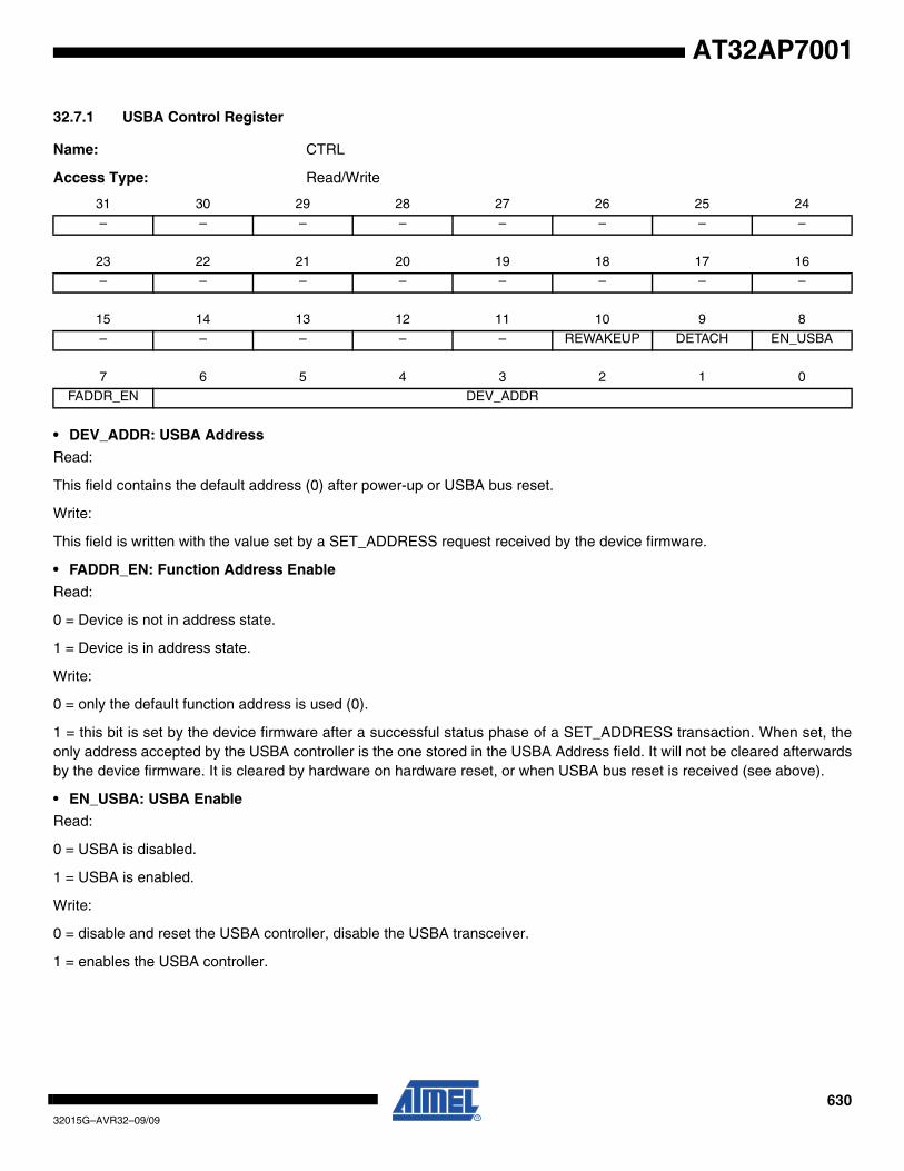
63032015G–AVR32–09/09
AT32AP7001
32.7.1 USBA Control Register
Name: CTRL
Access Type: Read/Write
• DEV_ADDR: USBA Address
Read:
This field contains the default address (0) after power-up or USBA bus reset.
Write:
This field is written with the value set by a SET_ADDRESS request received by the device firmware.
• FADDR_EN: Function Address Enable
Read:
0 = Device is not in address state.
1 = Device is in address state.
Write:
0 = only the default function address is used (0).
1 = this bit is set by the device firmware after a successful status phase of a SET_ADDRESS transaction. When set, theonly address accepted by the USBA controller is the one stored in the USBA Address field. It will not be cleared afterwardsby the device firmware. It is cleared by hardware on hardware reset, or when USBA bus reset is received (see above).
• EN_USBA: USBA Enable
Read:
0 = USBA is disabled.
1 = USBA is enabled.
Write:
0 = disable and reset the USBA controller, disable the USBA transceiver.
1 = enables the USBA controller.
31 30 29 28 27 26 25 24
– – – – – – – –
23 22 21 20 19 18 17 16
– – – – – – – –
15 14 13 12 11 10 9 8
– – – – – REWAKEUP DETACH EN_USBA
7 6 5 4 3 2 1 0
FADDR_EN DEV_ADDR
63132015G–AVR32–09/09
AT32AP7001
• DETACH: Detach Command
Read:
0 = USBA is attached.
1 = USBA is detached, UTMI transceiver is suspended.
Write:
0 = pull up the DP line (attach command).
1 = simulate a detach on the USBA line and force the UTMI transceiver into suspend state (Suspend M = 0).
• REWAKEUP: Send Remote Wake Up
Read:
0 = Remote Wake Up is disabled.
1 = Remote Wake Up is enabled.
Write:
0 = no effect.
1 = force an external interrupt on the USBA controller for Remote Wake UP purposes.
An Upstream Resume is sent only after the USBA bus has been in SUSPEND state for at least 5 ms.
This bit is automatically cleared by hardware at the end of the Upstream Resume.
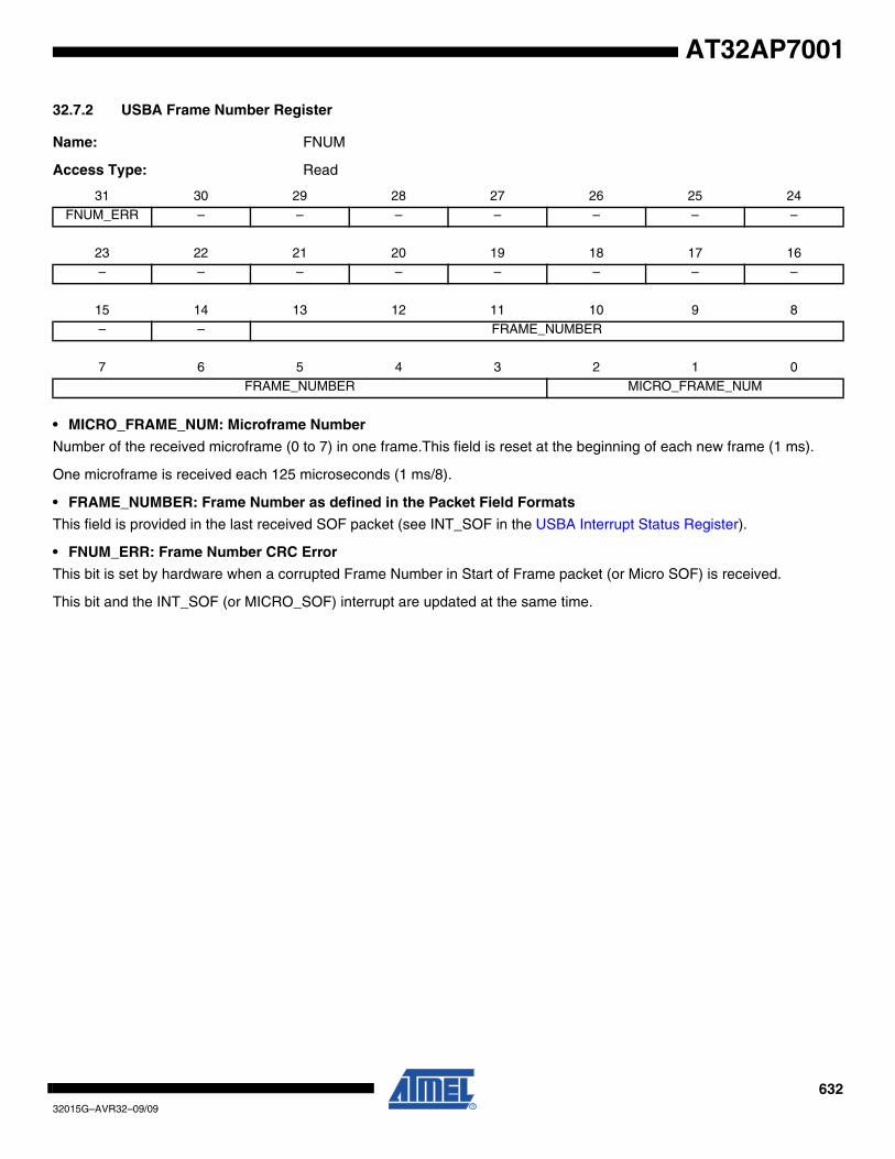
63232015G–AVR32–09/09
AT32AP7001
32.7.2 USBA Frame Number Register
Name: FNUM
Access Type: Read
• MICRO_FRAME_NUM: Microframe Number
Number of the received microframe (0 to 7) in one frame.This field is reset at the beginning of each new frame (1 ms).
One microframe is received each 125 microseconds (1 ms/8).
• FRAME_NUMBER: Frame Number as defined in the Packet Field Formats
This field is provided in the last received SOF packet (see INT_SOF in the USBA Interrupt Status Register).
• FNUM_ERR: Frame Number CRC Error
This bit is set by hardware when a corrupted Frame Number in Start of Frame packet (or Micro SOF) is received.
This bit and the INT_SOF (or MICRO_SOF) interrupt are updated at the same time.
31 30 29 28 27 26 25 24
FNUM_ERR – – – – – – –
23 22 21 20 19 18 17 16
– – – – – – – –
15 14 13 12 11 10 9 8
– – FRAME_NUMBER
7 6 5 4 3 2 1 0
FRAME_NUMBER MICRO_FRAME_NUM
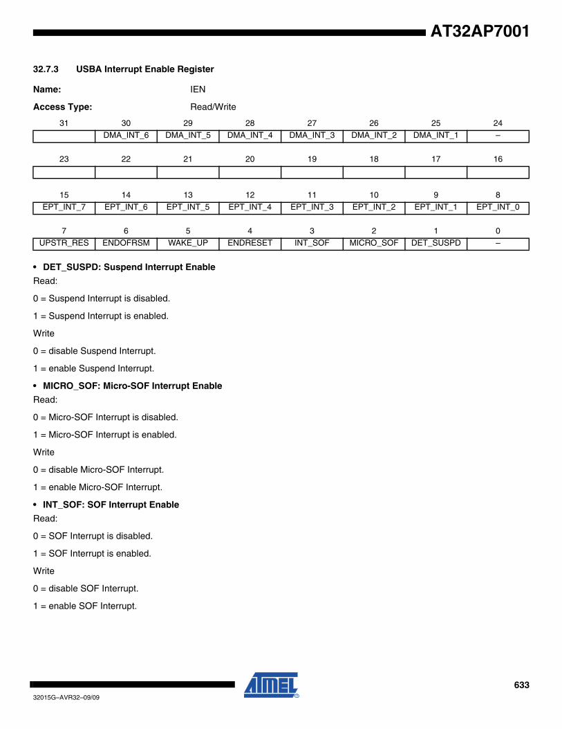
63332015G–AVR32–09/09
AT32AP7001
32.7.3 USBA Interrupt Enable Register
Name: IEN
Access Type: Read/Write
• DET_SUSPD: Suspend Interrupt Enable
Read:
0 = Suspend Interrupt is disabled.
1 = Suspend Interrupt is enabled.
Write
0 = disable Suspend Interrupt.
1 = enable Suspend Interrupt.
• MICRO_SOF: Micro-SOF Interrupt Enable
Read:
0 = Micro-SOF Interrupt is disabled.
1 = Micro-SOF Interrupt is enabled.
Write
0 = disable Micro-SOF Interrupt.
1 = enable Micro-SOF Interrupt.
• INT_SOF: SOF Interrupt Enable
Read:
0 = SOF Interrupt is disabled.
1 = SOF Interrupt is enabled.
Write
0 = disable SOF Interrupt.
1 = enable SOF Interrupt.
31 30 29 28 27 26 25 24
DMA_INT_6 DMA_INT_5 DMA_INT_4 DMA_INT_3 DMA_INT_2 DMA_INT_1 –
23 22 21 20 19 18 17 16
15 14 13 12 11 10 9 8
EPT_INT_7 EPT_INT_6 EPT_INT_5 EPT_INT_4 EPT_INT_3 EPT_INT_2 EPT_INT_1 EPT_INT_0
7 6 5 4 3 2 1 0
UPSTR_RES ENDOFRSM WAKE_UP ENDRESET INT_SOF MICRO_SOF DET_SUSPD –
63432015G–AVR32–09/09
AT32AP7001
• ENDRESET: End Of Reset Interrupt Enable
Read:
0 = End Of Reset Interrupt is disabled.
1 = End Of Reset Interrupt is enabled.
Write
0 = disable End Of Reset Interrupt.
1 = enable End Of Reset Interrupt.
• WAKE_UP: Wake Up CPU Interrupt Enable
Read:
0 = Wake Up CPU Interrupt is disabled.
1 = Wake Up CPU Interrupt is enabled.
Write
0 = disable Wake Up CPU Interrupt.
1 = enable Wake Up CPU Interrupt.
• ENDOFRSM: End Of Resume Interrupt Enable
Read:
0 = Resume Interrupt is disabled.
1 = Resume Interrupt is enabled.
Write
0 = disable Resume Interrupt.
1 = enable Resume Interrupt.
• UPSTR_RES: Upstream Resume Interrupt Enable
Read:
0 = Upstream Resume Interrupt is disabled.
1 = Upstream Resume Interrupt is enabled.
Write
0 = disable Upstream Resume Interrupt.
1 = enable Upstream Resume Interrupt.
• EPT_INT_x: Endpointx Interrupt Enable
Read:
0 = the interrupts for this endpoint are disabled.
1 = the interrupts for this endpoint are enabled.
Write
0 = disable the interrupts for this endpoint.
1 = enable the interrupts for this endpoint.
63532015G–AVR32–09/09
AT32AP7001
• DMA_INT_x: DMA Channelx Interrupt Enable
Read:
0 = the interrupts for this channel are disabled.
1 = the interrupts for this channel are enabled.
Write
0 = disable the interrupts for this channel.
1 = enable the interrupts for this channel.
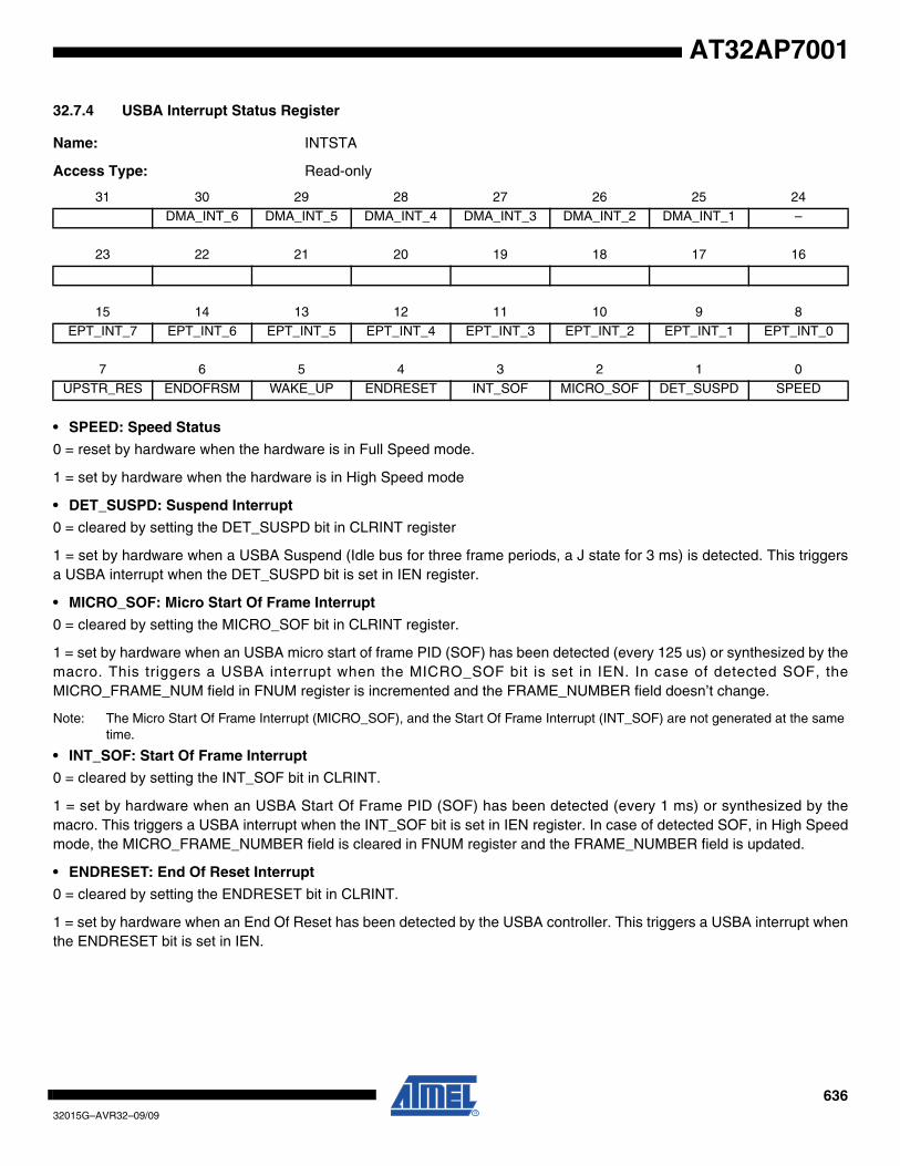
63632015G–AVR32–09/09
AT32AP7001
32.7.4 USBA Interrupt Status Register
Name: INTSTA
Access Type: Read-only
• SPEED: Speed Status
0 = reset by hardware when the hardware is in Full Speed mode.
1 = set by hardware when the hardware is in High Speed mode
• DET_SUSPD: Suspend Interrupt
0 = cleared by setting the DET_SUSPD bit in CLRINT register
1 = set by hardware when a USBA Suspend (Idle bus for three frame periods, a J state for 3 ms) is detected. This triggersa USBA interrupt when the DET_SUSPD bit is set in IEN register.
• MICRO_SOF: Micro Start Of Frame Interrupt
0 = cleared by setting the MICRO_SOF bit in CLRINT register.
1 = set by hardware when an USBA micro start of frame PID (SOF) has been detected (every 125 us) or synthesized by themacro. This triggers a USBA interrupt when the MICRO_SOF bit is set in IEN. In case of detected SOF, theMICRO_FRAME_NUM field in FNUM register is incremented and the FRAME_NUMBER field doesn’t change.
Note: The Micro Start Of Frame Interrupt (MICRO_SOF), and the Start Of Frame Interrupt (INT_SOF) are not generated at the same time.
• INT_SOF: Start Of Frame Interrupt
0 = cleared by setting the INT_SOF bit in CLRINT.
1 = set by hardware when an USBA Start Of Frame PID (SOF) has been detected (every 1 ms) or synthesized by themacro. This triggers a USBA interrupt when the INT_SOF bit is set in IEN register. In case of detected SOF, in High Speedmode, the MICRO_FRAME_NUMBER field is cleared in FNUM register and the FRAME_NUMBER field is updated.
• ENDRESET: End Of Reset Interrupt
0 = cleared by setting the ENDRESET bit in CLRINT.
1 = set by hardware when an End Of Reset has been detected by the USBA controller. This triggers a USBA interrupt whenthe ENDRESET bit is set in IEN.
31 30 29 28 27 26 25 24
DMA_INT_6 DMA_INT_5 DMA_INT_4 DMA_INT_3 DMA_INT_2 DMA_INT_1 –
23 22 21 20 19 18 17 16
15 14 13 12 11 10 9 8
EPT_INT_7 EPT_INT_6 EPT_INT_5 EPT_INT_4 EPT_INT_3 EPT_INT_2 EPT_INT_1 EPT_INT_0
7 6 5 4 3 2 1 0
UPSTR_RES ENDOFRSM WAKE_UP ENDRESET INT_SOF MICRO_SOF DET_SUSPD SPEED
63732015G–AVR32–09/09
AT32AP7001
• WAKE_UP: Wake Up CPU Interrupt
0 = cleared by setting the WAKE_UP bit in CLRINT.
1 = set by hardware when the USBA controller is in SUSPEND state and is re-activated by a filtered non-idle signal fromthe USBA line (not by an upstream resume). This triggers a USBA interrupt when the WAKE_UP bit is set in IEN register.When receiving this interrupt, the user has to enable the device controller clock prior to operation.
Note: this interrupt is generated even if the device controller clock is disabled.
• ENDOFRSM: End Of Resume Interrupt
0 = cleared by setting the ENDOFRSM bit in CLRINT.
1 = set by hardware when the USBA controller detects a good end of resume signal initiated by the host. This triggers aUSBA interrupt when the ENDOFRSM bit is set in IEN.
• UPSTR_RES: Upstream Resume Interrupt
0 = cleared by setting the UPSTR_RES bit in CLRINT.
1 = set by hardware when the USBA controller is sending a resume signal called “upstream resume”. This triggers a USBAinterrupt when the UPSTR_RES bit is set in IEN.
• EPT_INT_x: Endpointx Interrupt
0 = reset when the EPTSTAx interrupt source is cleared.
1 = set by hardware when an interrupt is triggered by the EPTSTAx register and this endpoint interrupt is enabled by theEPT_INT_x bit in IEN.
• DMA_INT_x: DMA Channelx Interrupt
0 = reset when the DMASTATUSx interrupt source is cleared.
1 = set by hardware when an interrupt is triggered by the DMA Channelx and this endpoint interrupt is enabled by theDMA_INT_x bit in IEN.
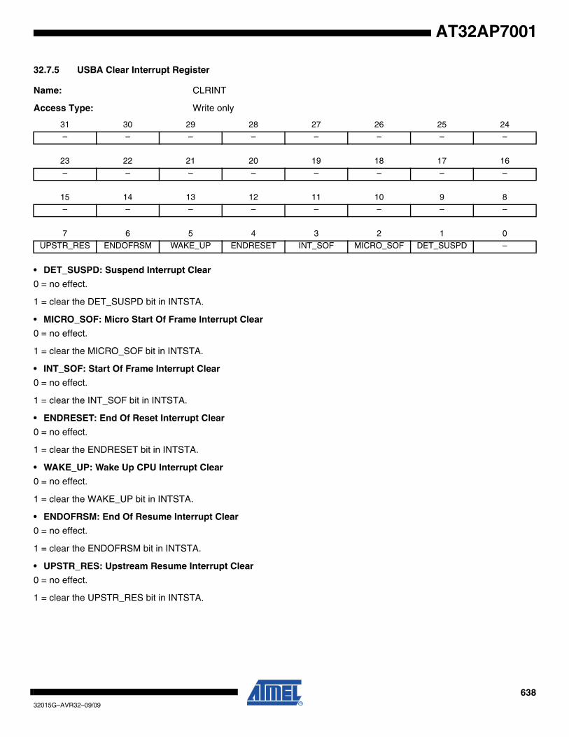
63832015G–AVR32–09/09
AT32AP7001
32.7.5 USBA Clear Interrupt Register
Name: CLRINT
Access Type: Write only
• DET_SUSPD: Suspend Interrupt Clear
0 = no effect.
1 = clear the DET_SUSPD bit in INTSTA.
• MICRO_SOF: Micro Start Of Frame Interrupt Clear
0 = no effect.
1 = clear the MICRO_SOF bit in INTSTA.
• INT_SOF: Start Of Frame Interrupt Clear
0 = no effect.
1 = clear the INT_SOF bit in INTSTA.
• ENDRESET: End Of Reset Interrupt Clear
0 = no effect.
1 = clear the ENDRESET bit in INTSTA.
• WAKE_UP: Wake Up CPU Interrupt Clear
0 = no effect.
1 = clear the WAKE_UP bit in INTSTA.
• ENDOFRSM: End Of Resume Interrupt Clear
0 = no effect.
1 = clear the ENDOFRSM bit in INTSTA.
• UPSTR_RES: Upstream Resume Interrupt Clear
0 = no effect.
1 = clear the UPSTR_RES bit in INTSTA.
31 30 29 28 27 26 25 24
– – – – – – – –
23 22 21 20 19 18 17 16
– – – – – – – –
15 14 13 12 11 10 9 8
– – – – – – – –
7 6 5 4 3 2 1 0
UPSTR_RES ENDOFRSM WAKE_UP ENDRESET INT_SOF MICRO_SOF DET_SUSPD –
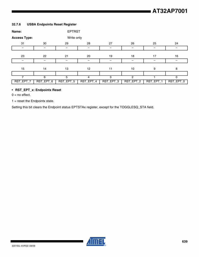
63932015G–AVR32–09/09
AT32AP7001
32.7.6 USBA Endpoints Reset Register
Name: EPTRST
Access Type: Write only
• RST_EPT_x: Endpointx Reset
0 = no effect.
1 = reset the Endpointx state.
Setting this bit clears the Endpoint status EPTSTAx register, except for the TOGGLESQ_STA field.
31 30 29 28 27 26 25 24
– – – – – – – –
23 22 21 20 19 18 17 16
– – – – – – – –
15 14 13 12 11 10 9 8
7 6 5 4 3 2 1 0RST_EPT_7 RST_EPT_6 RST_EPT_5 RST_EPT_4 RST_EPT_3 RST_EPT_2 RST_EPT_1 RST_EPT_0
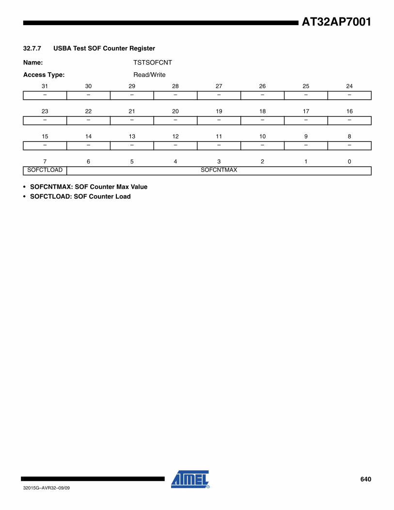
64032015G–AVR32–09/09
AT32AP7001
32.7.7 USBA Test SOF Counter Register
Name: TSTSOFCNT
Access Type: Read/Write
• SOFCNTMAX: SOF Counter Max Value
• SOFCTLOAD: SOF Counter Load
31 30 29 28 27 26 25 24
– – – – – – – –
23 22 21 20 19 18 17 16
– – – – – – – –
15 14 13 12 11 10 9 8
– – – – – – – –
7 6 5 4 3 2 1 0
SOFCTLOAD SOFCNTMAX

64132015G–AVR32–09/09
AT32AP7001
32.7.8 USBA Test A Counter Register
Name: TSTCNTA
Access Type: Read/Write
• CNTALOAD: A Counter Load
• CNTAMAX: A Counter Max Value
31 30 29 28 27 26 25 24
– – – – – – – –
23 22 21 20 19 18 17 16
– – – – – – – –
15 14 13 12 11 10 9 8
CNTALOAD CNTAMAX
7 6 5 4 3 2 1 0
CNTAMAX
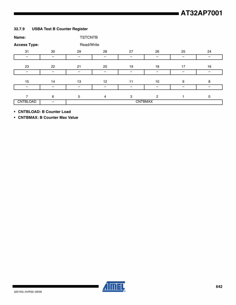
64232015G–AVR32–09/09
AT32AP7001
32.7.9 USBA Test B Counter Register
Name: TSTCNTB
Access Type: Read/Write
• CNTBLOAD: B Counter Load
• CNTBMAX: B Counter Max Value
31 30 29 28 27 26 25 24
– – – – – – – –
23 22 21 20 19 18 17 16
– – – – – – – –
15 14 13 12 11 10 9 8
– – – – – – – –
7 6 5 4 3 2 1 0
CNTBLOAD – CNTBMAX
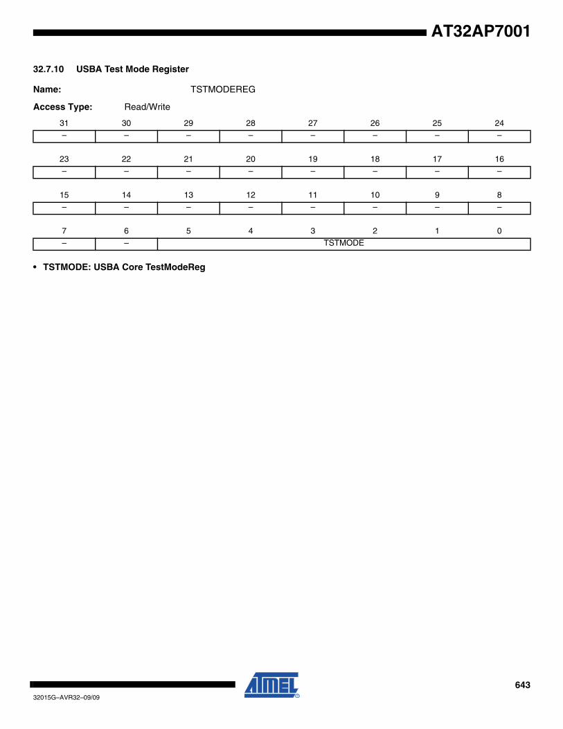
64332015G–AVR32–09/09
AT32AP7001
32.7.10 USBA Test Mode Register
Name: TSTMODEREG
Access Type: Read/Write
• TSTMODE: USBA Core TestModeReg
31 30 29 28 27 26 25 24
– – – – – – – –
23 22 21 20 19 18 17 16
– – – – – – – –
15 14 13 12 11 10 9 8
– – – – – – – –
7 6 5 4 3 2 1 0
– – TSTMODE
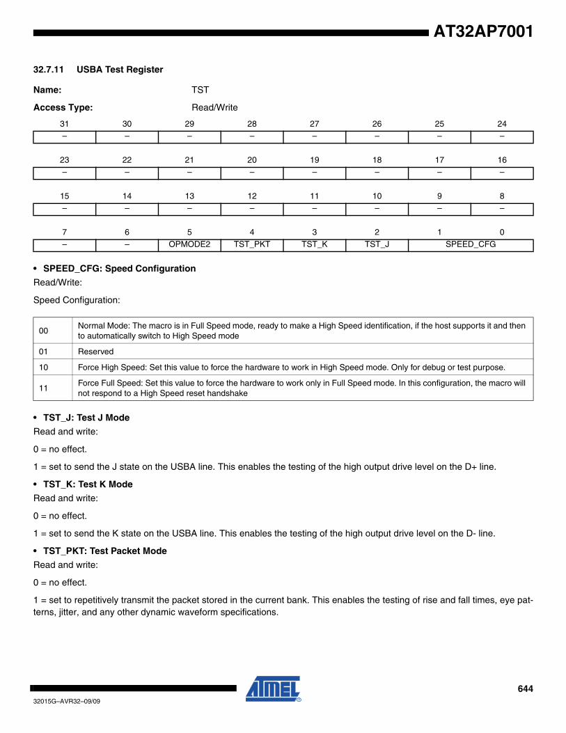
64432015G–AVR32–09/09
AT32AP7001
32.7.11 USBA Test Register
Name: TST
Access Type: Read/Write
• SPEED_CFG: Speed Configuration
Read/Write:
Speed Configuration:
• TST_J: Test J Mode
Read and write:
0 = no effect.
1 = set to send the J state on the USBA line. This enables the testing of the high output drive level on the D+ line.
• TST_K: Test K Mode
Read and write:
0 = no effect.
1 = set to send the K state on the USBA line. This enables the testing of the high output drive level on the D- line.
• TST_PKT: Test Packet Mode
Read and write:
0 = no effect.
1 = set to repetitively transmit the packet stored in the current bank. This enables the testing of rise and fall times, eye pat-terns, jitter, and any other dynamic waveform specifications.
31 30 29 28 27 26 25 24
– – – – – – – –
23 22 21 20 19 18 17 16
– – – – – – – –
15 14 13 12 11 10 9 8
– – – – – – – –
7 6 5 4 3 2 1 0
– – OPMODE2 TST_PKT TST_K TST_J SPEED_CFG
00Normal Mode: The macro is in Full Speed mode, ready to make a High Speed identification, if the host supports it and then to automatically switch to High Speed mode
01 Reserved
10 Force High Speed: Set this value to force the hardware to work in High Speed mode. Only for debug or test purpose.
11Force Full Speed: Set this value to force the hardware to work only in Full Speed mode. In this configuration, the macro will not respond to a High Speed reset handshake

64532015G–AVR32–09/09
AT32AP7001
• OPMODE2: OpMode2
Read and write:
0 = no effect.
1 = set to force the OpMode signal (UTMI interface) to “10”, to disable the bit-stuffing and the NRZI encoding.
Note: For the Test mode, Test_SE0_NAK (see Universal Serial Bus Specification, Revision 2.0: 7.1.20, Test Mode Sup-port). Force the device in High Speed mode, and configure a bulk-type endpoint. Do not fill this endpoint for sending NAK tothe host.
Upon command, a port’s transceiver must enter the High Speed receive mode and remain in that mode until the exit actionis taken. This enables the testing of output impedance, low level output voltage and loading characteristics. In addition,while in this mode, upstream facing ports (and only upstream facing ports) must respond to any IN token packet with a NAKhandshake (only if the packet CRC is determined to be correct) within the normal allowed device response time. Thisenables testing of the device squelch level circuitry and, additionally, provides a general purpose stimulus/response test forbasic functional testing.
64632015G–AVR32–09/09
AT32AP7001
32.7.12 USBA PADDRSIZE Register
Name: IPPADDRSIZE
Access Type: Read-only
• IP_PADDRSIZE
2^PADDR_SIZE
PB address bus aperture of the USBA
31 30 29 28 27 26 25 24
IP_PADDRSIZE
23 22 21 20 19 18 17 16
IP_PADDRSIZE
15 14 13 12 11 10 9 8
IP_PADDRSIZE
7 6 5 4 3 2 1 0
IP_PADDRSIZE
64732015G–AVR32–09/09
AT32AP7001
32.7.13 USBA Name1 Register
Name: IPNAME1
Access Type: Read-only
• IP_NAME1
ASCII string “HUSB”
31 30 29 28 27 26 25 24
IP_NAME1
23 22 21 20 19 18 17 16
IP_NAME1
15 14 13 12 11 10 9 8
IP_NAME1
7 6 5 4 3 2 1 0
IP_NAME1
64832015G–AVR32–09/09
AT32AP7001
32.7.14 USBA Name2 Register
Name: IPNAME2
Access Type: Read-only
• IP_NAME2
ASCII string “2DEV”
31 30 29 28 27 26 25 24
IP_NAME2
23 22 21 20 19 18 17 16
IP_NAME2
15 14 13 12 11 10 9 8
IP_NAME2
7 6 5 4 3 2 1 0
IP_NAME2
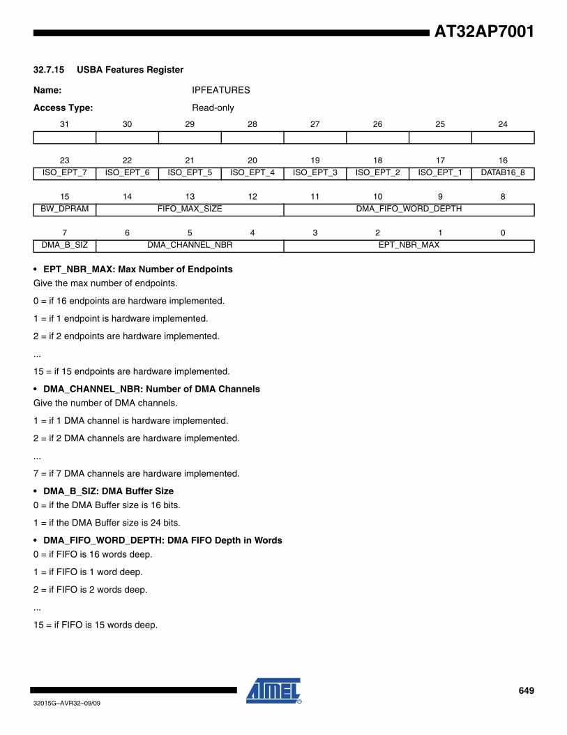
64932015G–AVR32–09/09
AT32AP7001
32.7.15 USBA Features Register
Name: IPFEATURES
Access Type: Read-only
• EPT_NBR_MAX: Max Number of Endpoints
Give the max number of endpoints.
0 = if 16 endpoints are hardware implemented.
1 = if 1 endpoint is hardware implemented.
2 = if 2 endpoints are hardware implemented.
...
15 = if 15 endpoints are hardware implemented.
• DMA_CHANNEL_NBR: Number of DMA Channels
Give the number of DMA channels.
1 = if 1 DMA channel is hardware implemented.
2 = if 2 DMA channels are hardware implemented.
...
7 = if 7 DMA channels are hardware implemented.
• DMA_B_SIZ: DMA Buffer Size
0 = if the DMA Buffer size is 16 bits.
1 = if the DMA Buffer size is 24 bits.
• DMA_FIFO_WORD_DEPTH: DMA FIFO Depth in Words
0 = if FIFO is 16 words deep.
1 = if FIFO is 1 word deep.
2 = if FIFO is 2 words deep.
...
15 = if FIFO is 15 words deep.
31 30 29 28 27 26 25 24
23 22 21 20 19 18 17 16
ISO_EPT_7 ISO_EPT_6 ISO_EPT_5 ISO_EPT_4 ISO_EPT_3 ISO_EPT_2 ISO_EPT_1 DATAB16_8
15 14 13 12 11 10 9 8
BW_DPRAM FIFO_MAX_SIZE DMA_FIFO_WORD_DEPTH
7 6 5 4 3 2 1 0
DMA_B_SIZ DMA_CHANNEL_NBR EPT_NBR_MAX
65032015G–AVR32–09/09
AT32AP7001
• FIFO_MAX_SIZE: DPRAM Size
0 = if DPRAM is 128 bytes deep.
1 = if DPRAM is 256 bytes deep.
2 = if DPRAM is 512 bytes deep.
3 = if DPRAM is 1024 bytes deep.
4 = if DPRAM is 2048 bytes deep.
5 = if DPRAM is 4096 bytes deep.
6 = if DPRAM is 8192 bytes deep.
7 = if DPRAM is 16384 bytes deep.
• BW_DPRAM: DPRAM Byte Write Capability
0 = if DPRAM Write Data Shadow logic is implemented.
1 = if DPRAM is byte write capable.
• DATAB16_8: UTMI DataBus16_8
0 = if the UTMI uses an 8-bit parallel data interface (60 MHz, unidirectional).
1 = if the UTMI uses a 16-bit parallel data interface (30 MHz, bidirectional).
• ISO_EPT_x: Endpointx High Bandwidth Isochronous Capability
0 = if the endpoint does not have isochronous High Bandwidth Capability.
1 = if the endpoint has isochronous High Bandwidth Capability.
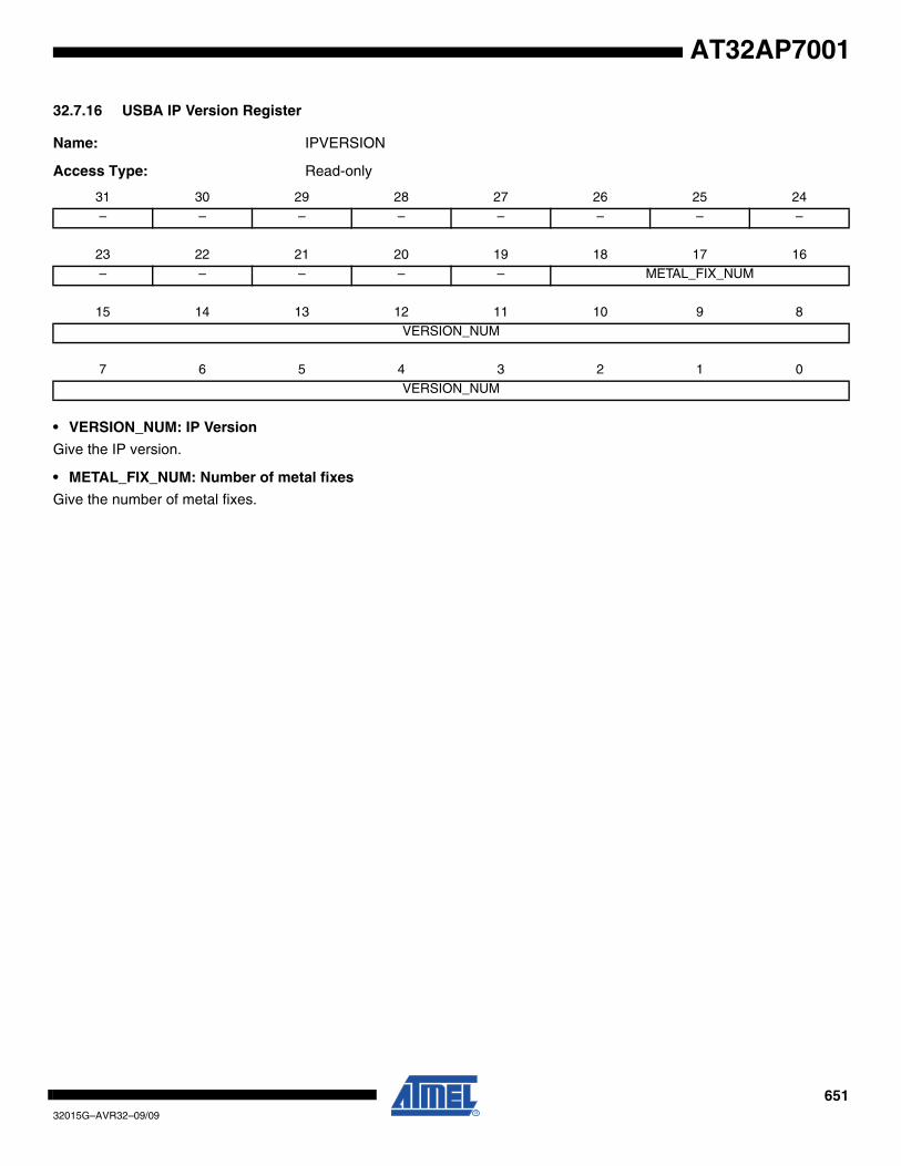
65132015G–AVR32–09/09
AT32AP7001
32.7.16 USBA IP Version Register
Name: IPVERSION
Access Type: Read-only
• VERSION_NUM: IP Version
Give the IP version.
• METAL_FIX_NUM: Number of metal fixes
Give the number of metal fixes.
31 30 29 28 27 26 25 24
– – – – – – – –
23 22 21 20 19 18 17 16
– – – – – METAL_FIX_NUM
15 14 13 12 11 10 9 8
VERSION_NUM
7 6 5 4 3 2 1 0
VERSION_NUM
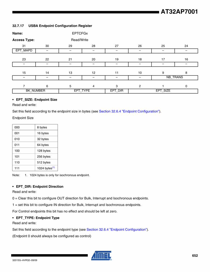
65232015G–AVR32–09/09
AT32AP7001
32.7.17 USBA Endpoint Configuration Register
Name: EPTCFGx
Access Type: Read/Write
• EPT_SIZE: Endpoint Size
Read and write:
Set this field according to the endpoint size in bytes (see Section 32.6.4 ”Endpoint Configuration”).
Endpoint Size
Note: 1. 1024 bytes is only for isochronous endpoint.
• EPT_DIR: Endpoint Direction
Read and write:
0 = Clear this bit to configure OUT direction for Bulk, Interrupt and Isochronous endpoints.
1 = set this bit to configure IN direction for Bulk, Interrupt and Isochronous endpoints.
For Control endpoints this bit has no effect and should be left at zero.
• EPT_TYPE: Endpoint Type
Read and write:
Set this field according to the endpoint type (see Section 32.6.4 ”Endpoint Configuration”).
(Endpoint 0 should always be configured as control)
31 30 29 28 27 26 25 24
EPT_MAPD – – – – – – –
23 22 21 20 19 18 17 16
– – – – – – – –
15 14 13 12 11 10 9 8
– – – – – – NB_TRANS
7 6 5 4 3 2 1 0
BK_NUMBER EPT_TYPE EPT_DIR EPT_SIZE
000 8 bytes
001 16 bytes
010 32 bytes
011 64 bytes
100 128 bytes
101 256 bytes
110 512 bytes
111 1024 bytes(1)
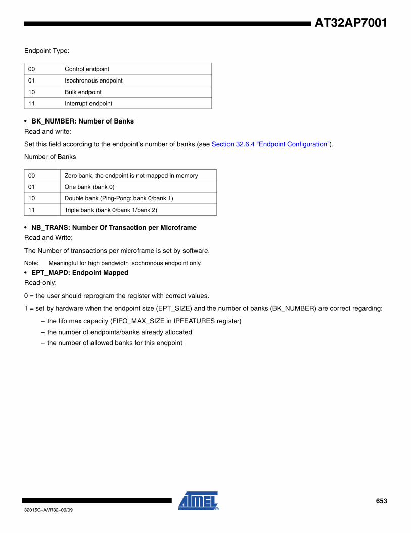
65332015G–AVR32–09/09
AT32AP7001
Endpoint Type:
• BK_NUMBER: Number of Banks
Read and write:
Set this field according to the endpoint’s number of banks (see Section 32.6.4 ”Endpoint Configuration”).
Number of Banks
• NB_TRANS: Number Of Transaction per Microframe
Read and Write:
The Number of transactions per microframe is set by software.
Note: Meaningful for high bandwidth isochronous endpoint only.
• EPT_MAPD: Endpoint Mapped
Read-only:
0 = the user should reprogram the register with correct values.
1 = set by hardware when the endpoint size (EPT_SIZE) and the number of banks (BK_NUMBER) are correct regarding:
– the fifo max capacity (FIFO_MAX_SIZE in IPFEATURES register)
– the number of endpoints/banks already allocated
– the number of allowed banks for this endpoint
00 Control endpoint
01 Isochronous endpoint
10 Bulk endpoint
11 Interrupt endpoint
00 Zero bank, the endpoint is not mapped in memory
01 One bank (bank 0)
10 Double bank (Ping-Pong: bank 0/bank 1)
11 Triple bank (bank 0/bank 1/bank 2)
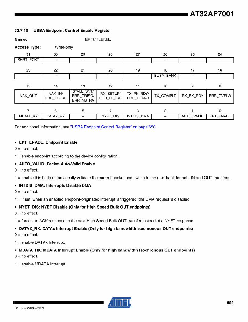
65432015G–AVR32–09/09
AT32AP7001
32.7.18 USBA Endpoint Control Enable Register
Name: EPTCTLENBx
Access Type: Write-only
For additional Information, see ”USBA Endpoint Control Register” on page 658.
• EPT_ENABL: Endpoint Enable
0 = no effect.
1 = enable endpoint according to the device configuration.
• AUTO_VALID: Packet Auto-Valid Enable
0 = no effect.
1 = enable this bit to automatically validate the current packet and switch to the next bank for both IN and OUT transfers.
• INTDIS_DMA: Interrupts Disable DMA
0 = no effect.
1 = If set, when an enabled endpoint-originated interrupt is triggered, the DMA request is disabled.
• NYET_DIS: NYET Disable (Only for High Speed Bulk OUT endpoints)
0 = no effect.
1 = forces an ACK response to the next High Speed Bulk OUT transfer instead of a NYET response.
• DATAX_RX: DATAx Interrupt Enable (Only for high bandwidth Isochronous OUT endpoints)
0 = no effect.
1 = enable DATAx Interrupt.
• MDATA_RX: MDATA Interrupt Enable (Only for high bandwidth Isochronous OUT endpoints)
0 = no effect.
1 = enable MDATA Interrupt.
31 30 29 28 27 26 25 24
SHRT_PCKT – – – – – – –
23 22 21 20 19 18 17 16
– – – – – BUSY_BANK – –
15 14 13 12 11 10 9 8
NAK_OUTNAK_IN/
ERR_FLUSH
STALL_SNT/ ERR_CRISO/ ERR_NBTRA
RX_SETUP/ ERR_FL_ISO
TX_PK_RDY/ ERR_TRANS
TX_COMPLT RX_BK_RDY ERR_OVFLW
7 6 5 4 3 2 1 0
MDATA_RX DATAX_RX – NYET_DIS INTDIS_DMA – AUTO_VALID EPT_ENABL

65532015G–AVR32–09/09
AT32AP7001
• ERR_OVFLW: Overflow Error Interrupt Enable
0 = no effect.
1 = enable Overflow Error Interrupt.
• RX_BK_RDY: Received OUT Data Interrupt Enable
0 = no effect.
1 = enable Received OUT Data Interrupt.
• TX_COMPLT: Transmitted IN Data Complete Interrupt Enable
0 = no effect.
1 = enable Transmitted IN Data Complete Interrupt.
• TX_PK_RDY/ERR_TRANS: TX Packet Ready/Transaction Error Interrupt Enable
0 = no effect.
1 = enable TX Packet Ready/Transaction Error Interrupt.
• RX_SETUP/ERR_FL_ISO: Received SETUP/Error Flow Interrupt Enable
0 = no effect.
1 = enable RX_SETUP/Error Flow ISO Interrupt.
• STALL_SNT/ERR_CRISO/ERR_NBTRA: Stall Sent /ISO CRC Error/Number of Transaction Error Interrupt Enable
0 = no effect.
1 = enable Stall Sent/Error CRC ISO/Error Number of Transaction Interrupt.
• NAK_IN/ERR_FLUSH: NAKIN/Bank Flush Error Interrupt Enable
0 = no effect.
1 = enable NAKIN/Bank Flush Error Interrupt.
• NAK_OUT: NAKOUT Interrupt Enable
0 = no effect.
1 = enable NAKOUT Interrupt.
• BUSY_BANK: Busy Bank Interrupt Enable
0 = no effect.
1 = enable Busy Bank Interrupt.
• SHRT_PCKT: Short Packet Send/Short Packet Interrupt Enable
For OUT endpoints:
0 = no effect.
1 = enable Short Packet Interrupt.
For IN endpoints:
Guarantees short packet at end of DMA Transfer if the DMACONTROLx register END_B_EN and EPTCTLx registerAUTOVALID bits are also set.
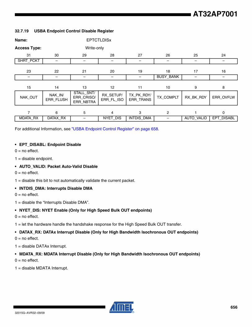
65632015G–AVR32–09/09
AT32AP7001
32.7.19 USBA Endpoint Control Disable Register
Name: EPTCTLDISx
Access Type: Write-only
For additional Information, see ”USBA Endpoint Control Register” on page 658.
• EPT_DISABL: Endpoint Disable
0 = no effect.
1 = disable endpoint.
• AUTO_VALID: Packet Auto-Valid Disable
0 = no effect.
1 = disable this bit to not automatically validate the current packet.
• INTDIS_DMA: Interrupts Disable DMA
0 = no effect.
1 = disable the “Interrupts Disable DMA”.
• NYET_DIS: NYET Enable (Only for High Speed Bulk OUT endpoints)
0 = no effect.
1 = let the hardware handle the handshake response for the High Speed Bulk OUT transfer.
• DATAX_RX: DATAx Interrupt Disable (Only for High Bandwidth Isochronous OUT endpoints)
0 = no effect.
1 = disable DATAx Interrupt.
• MDATA_RX: MDATA Interrupt Disable (Only for High Bandwidth Isochronous OUT endpoints)
0 = no effect.
1 = disable MDATA Interrupt.
31 30 29 28 27 26 25 24
SHRT_PCKT – – – – – – –
23 22 21 20 19 18 17 16
– – – – – BUSY_BANK – –
15 14 13 12 11 10 9 8
NAK_OUTNAK_IN/
ERR_FLUSH
STALL_SNT/ ERR_CRISO/ ERR_NBTRA
RX_SETUP/ ERR_FL_ISO
TX_PK_RDY/ ERR_TRANS
TX_COMPLT RX_BK_RDY ERR_OVFLW
7 6 5 4 3 2 1 0
MDATA_RX DATAX_RX – NYET_DIS INTDIS_DMA – AUTO_VALID EPT_DISABL
65732015G–AVR32–09/09
AT32AP7001
• ERR_OVFLW: Overflow Error Interrupt Disable
0 = no effect.
1 = disable Overflow Error Interrupt.
• RX_BK_RDY: Received OUT Data Interrupt Disable
0 = no effect.
1 = disable Received OUT Data Interrupt.
• TX_COMPLT: Transmitted IN Data Complete Interrupt Disable
0 = no effect.
1 = disable Transmitted IN Data Complete Interrupt.
• TX_PK_RDY/ERR_TRANS: TX Packet Ready/Transaction Error Interrupt Disable
0 = no effect.
1 = disable TX Packet Ready/Transaction Error Interrupt.
• RX_SETUP/ERR_FL_ISO: Received SETUP/Error Flow Interrupt Disable
0 = no effect.
1 = disable RX_SETUP/Error Flow ISO Interrupt.
• STALL_SNT/ERR_CRISO/ERR_NBTRA: Stall Sent/ISO CRC Error/Number of Transaction Error Interrupt Disable
0 = no effect.
1 = disable Stall Sent/Error CRC ISO/Error Number of Transaction Interrupt.
• NAK_IN/ERR_FLUSH: NAKIN/bank flush error Interrupt Disable
0 = no effect.
1 = disable NAKIN/ Bank Flush Error Interrupt.
• NAK_OUT: NAKOUT Interrupt Disable
0 = no effect.
1 = disable NAKOUT Interrupt.
• BUSY_BANK: Busy Bank Interrupt Disable
0 = no effect.
1 = disable Busy Bank Interrupt.
• SHRT_PCKT: Short Packet Interrupt Disable
For OUT endpoints:
0 = no effect.
1 = disable Short Packet Interrupt.
For IN endpoints:
Never automatically add a zero length packet at end of DMA transfer.
.
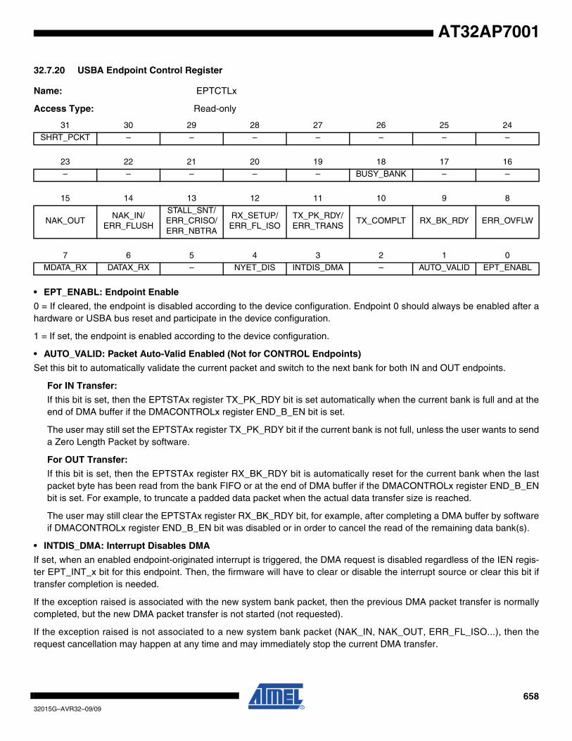
65832015G–AVR32–09/09
AT32AP7001
32.7.20 USBA Endpoint Control Register
Name: EPTCTLx
Access Type: Read-only
• EPT_ENABL: Endpoint Enable
0 = If cleared, the endpoint is disabled according to the device configuration. Endpoint 0 should always be enabled after ahardware or USBA bus reset and participate in the device configuration.
1 = If set, the endpoint is enabled according to the device configuration.
• AUTO_VALID: Packet Auto-Valid Enabled (Not for CONTROL Endpoints)
Set this bit to automatically validate the current packet and switch to the next bank for both IN and OUT endpoints.
For IN Transfer:
If this bit is set, then the EPTSTAx register TX_PK_RDY bit is set automatically when the current bank is full and at theend of DMA buffer if the DMACONTROLx register END_B_EN bit is set.
The user may still set the EPTSTAx register TX_PK_RDY bit if the current bank is not full, unless the user wants to senda Zero Length Packet by software.
For OUT Transfer:
If this bit is set, then the EPTSTAx register RX_BK_RDY bit is automatically reset for the current bank when the lastpacket byte has been read from the bank FIFO or at the end of DMA buffer if the DMACONTROLx register END_B_ENbit is set. For example, to truncate a padded data packet when the actual data transfer size is reached.
The user may still clear the EPTSTAx register RX_BK_RDY bit, for example, after completing a DMA buffer by softwareif DMACONTROLx register END_B_EN bit was disabled or in order to cancel the read of the remaining data bank(s).
• INTDIS_DMA: Interrupt Disables DMA
If set, when an enabled endpoint-originated interrupt is triggered, the DMA request is disabled regardless of the IEN regis-ter EPT_INT_x bit for this endpoint. Then, the firmware will have to clear or disable the interrupt source or clear this bit iftransfer completion is needed.
If the exception raised is associated with the new system bank packet, then the previous DMA packet transfer is normallycompleted, but the new DMA packet transfer is not started (not requested).
If the exception raised is not associated to a new system bank packet (NAK_IN, NAK_OUT, ERR_FL_ISO...), then therequest cancellation may happen at any time and may immediately stop the current DMA transfer.
31 30 29 28 27 26 25 24
SHRT_PCKT – – – – – – –
23 22 21 20 19 18 17 16
– – – – – BUSY_BANK – –
15 14 13 12 11 10 9 8
NAK_OUTNAK_IN/
ERR_FLUSH
STALL_SNT/ ERR_CRISO/ ERR_NBTRA
RX_SETUP/ ERR_FL_ISO
TX_PK_RDY/ ERR_TRANS
TX_COMPLT RX_BK_RDY ERR_OVFLW
7 6 5 4 3 2 1 0
MDATA_RX DATAX_RX – NYET_DIS INTDIS_DMA – AUTO_VALID EPT_ENABL
65932015G–AVR32–09/09
AT32AP7001
This may be used, for example, to identify or prevent an erroneous packet to be transferred into a buffer or to complete aDMA buffer by software after reception of a short packet, or to perform buffer truncation on ERR_FL_ISO interrupt foradaptive rate.
• NYET_DIS: NYET Disable (Only for High Speed Bulk OUT endpoints)
0 = If clear, this bit lets the hardware handle the handshake response for the High Speed Bulk OUT transfer.
1 = If set, this bit forces an ACK response to the next High Speed Bulk OUT transfer instead of a NYET response.
Note: According to the Universal Serial Bus Specification, Rev 2.0 (8.5.1.1 NAK Responses to OUT/DATA During PING Protocol), a NAK response to an HS Bulk OUT transfer is expected to be an unusual occurrence.
• DATAX_RX: DATAx Interrupt Enabled (Only for High Bandwidth Isochronous OUT endpoints)
0 = no effect.
1 = send an interrupt when a DATA2, DATA1 or DATA0 packet has been received meaning the whole microframe datapayload has been received.
• MDATA_RX: MDATA Interrupt Enabled (Only for High Bandwidth Isochronous OUT endpoints)
0 = no effect.
1 = send an interrupt when an MDATA packet has been received and so at least one packet of the microframe data pay-load has been received.
• ERR_OVFLW: Overflow Error Interrupt Enabled
0 = Overflow Error Interrupt is masked.
1 = Overflow Error Interrupt is enabled.
• RX_BK_RDY: Received OUT Data Interrupt Enabled
0 = Received OUT Data Interrupt is masked.
1 = Received OUT Data Interrupt is enabled.
• TX_COMPLT: Transmitted IN Data Complete Interrupt Enabled
0 = Transmitted IN Data Complete Interrupt is masked.
1 = Transmitted IN Data Complete Interrupt is enabled.
• TX_PK_RDY/ERR_TRANS: TX Packet Ready/Transaction Error Interrupt Enabled
0 = TX Packet Ready/Transaction Error Interrupt is masked.
1 = TX Packet Ready/Transaction Error Interrupt is enabled.
Caution: Interrupt source is active as long as the corresponding EPTSTAx register TX_PK_RDY flag remains low. Ifthere are no more banks available for transmitting after the software has set EPTSTAx/TX_PK_RDY for the last trans-mit packet, then the interrupt source remains inactive until the first bank becomes free again to transmit atEPTSTAx/TX_PK_RDY hardware clear.
• RX_SETUP/ERR_FL_ISO: Received SETUP/Error Flow Interrupt Enabled
0 = Received SETUP/Error Flow Interrupt is masked.
1 = Received SETUP/Error Flow Interrupt is enabled.
66032015G–AVR32–09/09
AT32AP7001
• STALL_SNT/ERR_CRISO/ERR_NBTRA: Stall Sent/ISO CRC Error/Number of Transaction Error Interrupt Enabled
0 = Stall Sent/ISO CRC error/number of Transaction Error Interrupt is masked.
1 = Stall Sent /ISO CRC error/number of Transaction Error Interrupt is enabled.
• NAK_IN/ERR_FLUSH: NAKIN/Bank Flush Error Interrupt Enabled
0 = NAKIN Interrupt is masked.
1 = NAKIN/Bank Flush Error Interrupt is enabled.
• NAK_OUT: NAKOUT Interrupt Enabled
0 = NAKOUT Interrupt is masked.
1 = NAKOUT Interrupt is enabled.
• BUSY_BANK: Busy Bank Interrupt Enabled
0 = BUSY_BANK Interrupt is masked.
1 = BUSY_BANK Interrupt is enabled.
For OUT endpoints: an interrupt is sent when all banks are busy.
For IN endpoints: an interrupt is sent when all banks are free.
• SHRT_PCKT: Short Packet Interrupt Enabled
For OUT endpoints: send an Interrupt when a Short Packet has been received.
0 = Short Packet Interrupt is masked.
1 = Short Packet Interrupt is enabled.
For IN endpoints: a Short Packet transmission is guaranteed upon end of the DMA Transfer, thus signaling a BULK orINTERRUPT end of transfer or an end of isochronous (micro-)frame data, but only if the DMACONTROLx registerEND_B_EN and EPTCTLx register AUTO_VALID bits are also set.
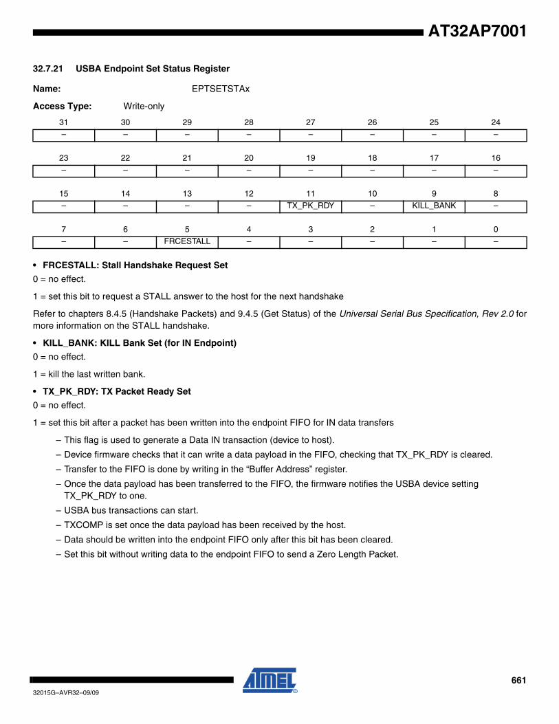
66132015G–AVR32–09/09
AT32AP7001
32.7.21 USBA Endpoint Set Status Register
Name: EPTSETSTAx
Access Type: Write-only
• FRCESTALL: Stall Handshake Request Set
0 = no effect.
1 = set this bit to request a STALL answer to the host for the next handshake
Refer to chapters 8.4.5 (Handshake Packets) and 9.4.5 (Get Status) of the Universal Serial Bus Specification, Rev 2.0 formore information on the STALL handshake.
• KILL_BANK: KILL Bank Set (for IN Endpoint)
0 = no effect.
1 = kill the last written bank.
• TX_PK_RDY: TX Packet Ready Set
0 = no effect.
1 = set this bit after a packet has been written into the endpoint FIFO for IN data transfers
– This flag is used to generate a Data IN transaction (device to host).
– Device firmware checks that it can write a data payload in the FIFO, checking that TX_PK_RDY is cleared.
– Transfer to the FIFO is done by writing in the “Buffer Address” register.
– Once the data payload has been transferred to the FIFO, the firmware notifies the USBA device setting TX_PK_RDY to one.
– USBA bus transactions can start.
– TXCOMP is set once the data payload has been received by the host.
– Data should be written into the endpoint FIFO only after this bit has been cleared.
– Set this bit without writing data to the endpoint FIFO to send a Zero Length Packet.
31 30 29 28 27 26 25 24
– – – – – – – –
23 22 21 20 19 18 17 16
– – – – – – – –
15 14 13 12 11 10 9 8
– – – – TX_PK_RDY – KILL_BANK –
7 6 5 4 3 2 1 0
– – FRCESTALL – – – – –
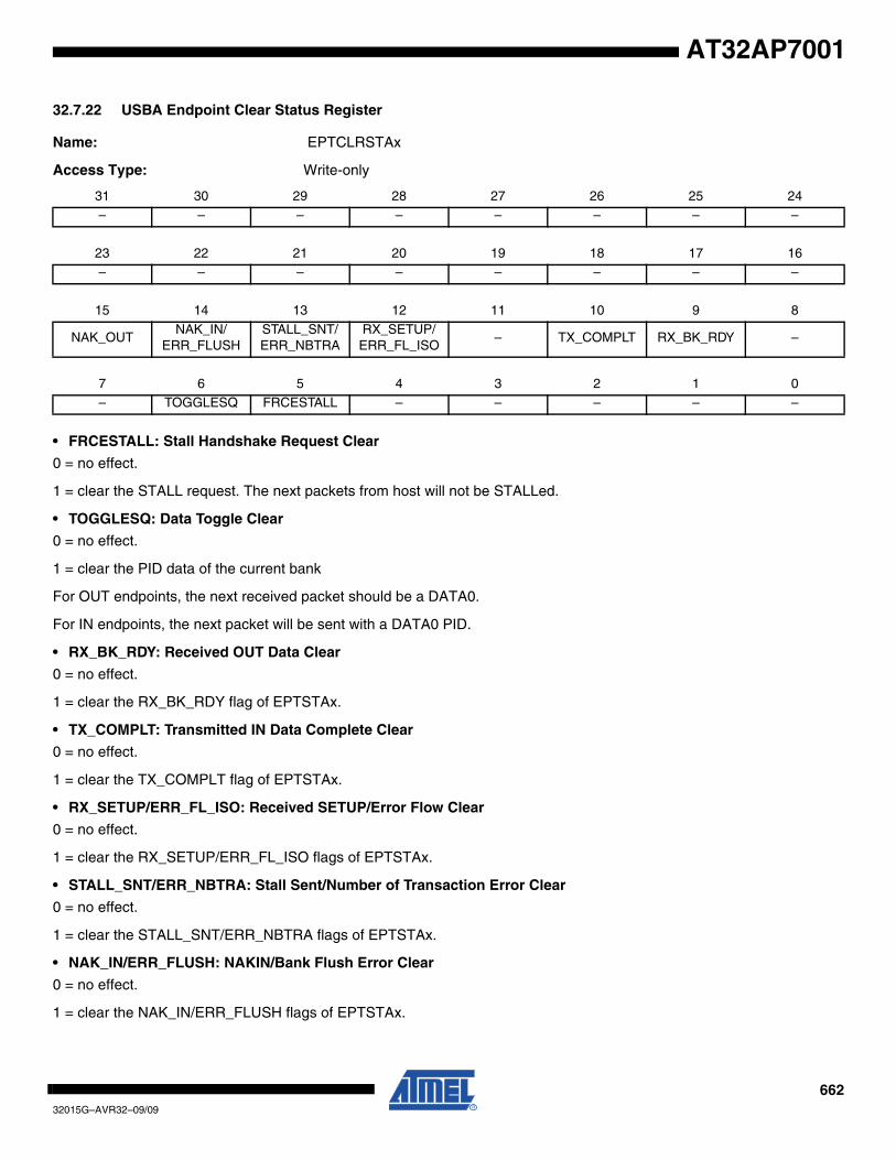
66232015G–AVR32–09/09
AT32AP7001
32.7.22 USBA Endpoint Clear Status Register
Name: EPTCLRSTAx
Access Type: Write-only
• FRCESTALL: Stall Handshake Request Clear
0 = no effect.
1 = clear the STALL request. The next packets from host will not be STALLed.
• TOGGLESQ: Data Toggle Clear
0 = no effect.
1 = clear the PID data of the current bank
For OUT endpoints, the next received packet should be a DATA0.
For IN endpoints, the next packet will be sent with a DATA0 PID.
• RX_BK_RDY: Received OUT Data Clear
0 = no effect.
1 = clear the RX_BK_RDY flag of EPTSTAx.
• TX_COMPLT: Transmitted IN Data Complete Clear
0 = no effect.
1 = clear the TX_COMPLT flag of EPTSTAx.
• RX_SETUP/ERR_FL_ISO: Received SETUP/Error Flow Clear
0 = no effect.
1 = clear the RX_SETUP/ERR_FL_ISO flags of EPTSTAx.
• STALL_SNT/ERR_NBTRA: Stall Sent/Number of Transaction Error Clear
0 = no effect.
1 = clear the STALL_SNT/ERR_NBTRA flags of EPTSTAx.
• NAK_IN/ERR_FLUSH: NAKIN/Bank Flush Error Clear
0 = no effect.
1 = clear the NAK_IN/ERR_FLUSH flags of EPTSTAx.
31 30 29 28 27 26 25 24
– – – – – – – –
23 22 21 20 19 18 17 16
– – – – – – – –
15 14 13 12 11 10 9 8
NAK_OUTNAK_IN/
ERR_FLUSHSTALL_SNT/ ERR_NBTRA
RX_SETUP/ ERR_FL_ISO
– TX_COMPLT RX_BK_RDY –
7 6 5 4 3 2 1 0– TOGGLESQ FRCESTALL – – – – –

66332015G–AVR32–09/09
AT32AP7001
• NAK_OUT: NAKOUT Clear
0 = no effect.
1 = clear the NAK_OUT flag of EPTSTAx.
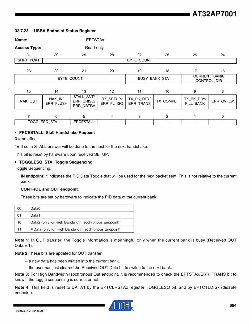
66432015G–AVR32–09/09
AT32AP7001
32.7.23 USBA Endpoint Status Register
Name: EPTSTAx
Access Type: Read-only
• FRCESTALL: Stall Handshake Request
0 = no effect.
1= If set a STALL answer will be done to the host for the next handshake.
This bit is reset by hardware upon received SETUP.
• TOGGLESQ_STA: Toggle Sequencing
Toggle Sequencing:
IN endpoint: it indicates the PID Data Toggle that will be used for the next packet sent. This is not relative to the currentbank.
CONTROL and OUT endpoint:
These bits are set by hardware to indicate the PID data of the current bank:
Note 1: In OUT transfer, the Toggle information is meaningful only when the current bank is busy (Received OUTData = 1).
Note 2:These bits are updated for OUT transfer:
– a new data has been written into the current bank.
– the user has just cleared the Received OUT Data bit to switch to the next bank.
Note 3: For High Bandwidth Isochronous Out endpoint, it is recommended to check the EPTSTAx/ERR_TRANS bit toknow if the toggle sequencing is correct or not.
Note 4: This field is reset to DATA1 by the EPTCLRSTAx register TOGGLESQ bit, and by EPTCTLDISx (disableendpoint).
31 30 29 28 27 26 25 24
SHRT_PCKT BYTE_COUNT
23 22 21 20 19 18 17 16
BYTE_COUNT BUSY_BANK_STACURRENT_BANK/
CONTROL_DIR
15 14 13 12 11 10 9 8
NAK_OUTNAK_IN/
ERR_FLUSH
STALL_SNT/ ERR_CRISO/ ERR_NBTRA
RX_SETUP/ ERR_FL_ISO
TX_PK_RDY/ ERR_TRANS
TX_COMPLTRX_BK_RDY/ KILL_BANK
ERR_OVFLW
7 6 5 4 3 2 1 0
TOGGLESQ_STA FRCESTALL – – – – –
00 Data0
01 Data1
10 Data2 (only for High Bandwidth Isochronous Endpoint)
11 MData (only for High Bandwidth Isochronous Endpoint)
66532015G–AVR32–09/09
AT32AP7001
• ERR_OVFLW: Overflow Error
This bit is set by hardware when a new too-long packet is received.
Example: If the user programs an endpoint 64 bytes wide and the host sends 128 bytes in an OUT transfer, then the Over-flow Error bit is set.
This bit is updated at the same time as the BYTE_COUNT field.
This bit is reset by EPTRST register RST_EPT_x (reset endpoint) and by EPTCTLDISx (disable endpoint).
• RX_BK_RDY/KILL_BANK: Received OUT Data/KILL Bank
Received OUT Data: (For OUT endpoint or Control endpoint)
This bit is set by hardware after a new packet has been stored in the endpoint FIFO.
This bit is cleared by the device firmware after reading the OUT data from the endpoint.
For multi-bank endpoints, this bit may remain active even when cleared by the device firmware, this if an other packet hasbeen received meanwhile.
Hardware assertion of this bit may generate an interrupt if enabled by the EPTCTLx register RX_BK_RDY bit.
This bit is reset by EPTRST register RST_EPT_x (reset endpoint) and by EPTCTLDISx (disable endpoint).
KILL Bank: (For IN endpoint)
– the bank is really cleared or the bank is sent, BUSY_BANK_STA is decremented.
– the bank is not cleared but sent on the IN transfer, TX_COMPLT
– the bank is not cleared because it was empty. The user should wait that this bit is cleared before trying to clear another packet.
Note: “Kill a packet” may be refused if at the same time, an IN token is coming and the current packet is sent on the USBAline. In this case, the TX_COMPLT bit is set. Take notice however, that if at least two banks are ready to be sent, there isno problem to kill a packet even if an IN token is coming. In fact, in that case, the current bank is sent (IN transfer) and thelast bank is killed.
• TX_COMPLT: Transmitted IN Data Complete
This bit is set by hardware after an IN packet has been transmitted for isochronous endpoints and after it has beenaccepted (ACK’ed) by the host for Control, Bulk and Interrupt endpoints.
This bit is reset by EPTRST register RST_EPT_x (reset endpoint), and by EPTCTLDISx (disable endpoint).
• TX_PK_RDY/ERR_TRANS: TX Packet Ready/Transaction Error
TX Packet Ready:
This bit is cleared by hardware, as soon as the packet has been sent for isochronous endpoints, or after the host hasacknowledged the packet for Control, Bulk and Interrupt endpoints.
For Multi-bank endpoints, this bit may remain clear even after software is set if another bank is available to transmit.
Hardware clear of this bit may generate an interrupt if enabled by the EPTCTLx register TX_PK_RDY bit.
This bit is reset by EPTRST register RST_EPT_x (reset endpoint), and by EPTCTLDISx (disable endpoint).
Transaction Error: (For high bandwidth isochronous OUT endpoints) (Read-Only)
This bit is set by hardware when a transaction error occurs inside one microframe.
If one toggle sequencing problem occurs among the n-transactions (n = 1, 2 or 3) inside a microframe, then this bit is stillset as long as the current bank contains one “bad” n-transaction. (see ”CURRENT_BANK/CONTROL_DIR: Current
66632015G–AVR32–09/09
AT32AP7001
Bank/Control Direction” on page 667) As soon as the current bank is relative to a new “good” n-transactions, then this bit isreset.
Note1: A transaction error occurs when the toggle sequencing does not respect the Universal Serial Bus Specification, Rev2.0 (5.9.2 High Bandwidth Isochronous endpoints) (Bad PID, missing data....)
Note2: When a transaction error occurs, the user may empty all the “bad” transactions by clearing the Received OUT Dataflag (RX_BK_RDY).
If this bit is reset, then the user should consider that a new n-transaction is coming.
This bit is reset by EPTRST register RST_EPT_x (reset endpoint), and by EPTCTLDISx (disable endpoint).
• RX_SETUP/ERR_FL_ISO: Received SETUP/Error Flow
Received SETUP: (for Control endpoint only)
This bit is set by hardware when a valid SETUP packet has been received from the host.
It is cleared by the device firmware after reading the SETUP data from the endpoint FIFO.
This bit is reset by EPTRST register RST_EPT_x (reset endpoint), and by EPTCTLDISx (disable endpoint).
Error Flow: (for isochronous endpoint only)
This bit is set by hardware when a transaction error occurs.
– Isochronous IN transaction is missed, the micro has no time to fill the endpoint (underflow).
– Isochronous OUT data is dropped because the bank is busy (overflow).
This bit is reset by EPTRST register RST_EPT_x (reset endpoint) and by EPTCTLDISx (disable endpoint).
• STALL_SNT/ERR_CRISO/ERR_NBTRA: Stall Sent/CRC ISO Error/Number of Transaction Error
STALL_SNT: (for Control, Bulk and Interrupt endpoints)
This bit is set by hardware after a STALL handshake has been sent as requested by the EPTSTAx register FRCESTALLbit.
This bit is reset by EPTRST register RST_EPT_x (reset endpoint) and by EPTCTLDISx (disable endpoint).
ERR_CRISO: (for Isochronous OUT endpoints) (Read-only)
This bit is set by hardware if the last received data is corrupted (CRC error on data).
This bit is updated by hardware when new data is received (Received OUT Data bit).
ERR_NBTRA: (for High Bandwidth Isochronous IN endpoints)
This bit is set at the end of a microframe in which at least one data bank has been transmitted, if less than the number oftransactions per micro-frame banks (EPTCFGx register NB_TRANS) have been validated for transmission inside thismicroframe.
This bit is reset by EPTRST register RST_EPT_x (reset endpoint) and by EPTCTLDISx (disable endpoint).
• NAK_IN/ERR_FLUSH: NAK IN/Bank Flush Error
NAK_IN:
This bit is set by hardware when a NAK handshake has been sent in response to an IN request from the Host.
This bit is cleared by software.
ERR_FLUSH: (for High Bandwidth Isochronous IN endpoints)
This bit is set when flushing unsent banks at the end of a microframe.
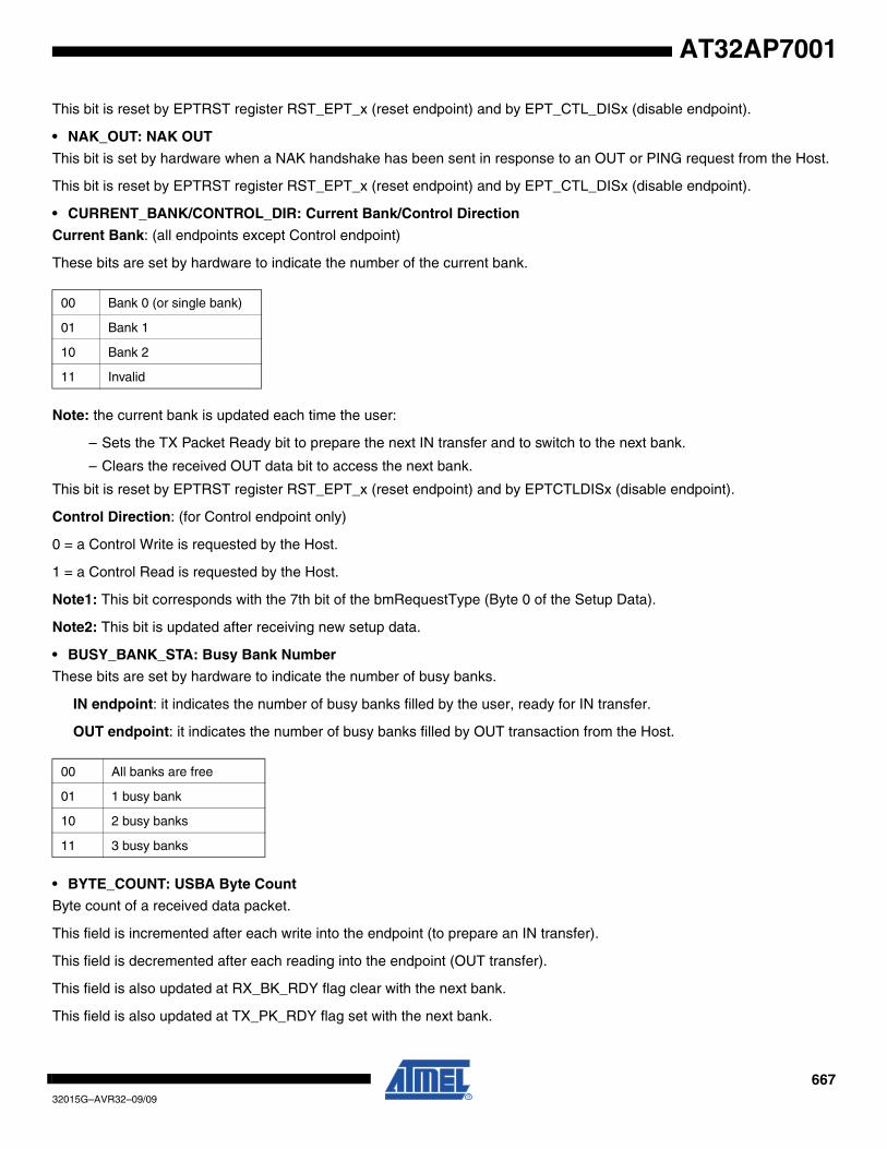
66732015G–AVR32–09/09
AT32AP7001
This bit is reset by EPTRST register RST_EPT_x (reset endpoint) and by EPT_CTL_DISx (disable endpoint).
• NAK_OUT: NAK OUT
This bit is set by hardware when a NAK handshake has been sent in response to an OUT or PING request from the Host.
This bit is reset by EPTRST register RST_EPT_x (reset endpoint) and by EPT_CTL_DISx (disable endpoint).
• CURRENT_BANK/CONTROL_DIR: Current Bank/Control Direction
Current Bank: (all endpoints except Control endpoint)
These bits are set by hardware to indicate the number of the current bank.
Note: the current bank is updated each time the user:
– Sets the TX Packet Ready bit to prepare the next IN transfer and to switch to the next bank.
– Clears the received OUT data bit to access the next bank.
This bit is reset by EPTRST register RST_EPT_x (reset endpoint) and by EPTCTLDISx (disable endpoint).
Control Direction: (for Control endpoint only)
0 = a Control Write is requested by the Host.
1 = a Control Read is requested by the Host.
Note1: This bit corresponds with the 7th bit of the bmRequestType (Byte 0 of the Setup Data).
Note2: This bit is updated after receiving new setup data.
• BUSY_BANK_STA: Busy Bank Number
These bits are set by hardware to indicate the number of busy banks.
IN endpoint: it indicates the number of busy banks filled by the user, ready for IN transfer.
OUT endpoint: it indicates the number of busy banks filled by OUT transaction from the Host.
• BYTE_COUNT: USBA Byte Count
Byte count of a received data packet.
This field is incremented after each write into the endpoint (to prepare an IN transfer).
This field is decremented after each reading into the endpoint (OUT transfer).
This field is also updated at RX_BK_RDY flag clear with the next bank.
This field is also updated at TX_PK_RDY flag set with the next bank.
00 Bank 0 (or single bank)
01 Bank 1
10 Bank 2
11 Invalid
00 All banks are free
01 1 busy bank
10 2 busy banks
11 3 busy banks

66832015G–AVR32–09/09
AT32AP7001
This field is reset by RST_EPT_x of EPTRST register.
• SHRT_PCKT: Short Packet
An OUT Short Packet is detected when the receive byte count is less than the configured EPTCFGx register EPT_Size.
This bit is updated at the same time as the BYTE_COUNT field.
This bit is reset by EPTRST register RST_EPT_x (reset endpoint) and by EPTCTLDISx (disable endpoint).
66932015G–AVR32–09/09
AT32AP7001
32.7.24 USBA DMA Channel Transfer Descriptor
The DMA channel transfer descriptor is loaded from the memory.
Be careful with the alignment of this buffer.
The structure of the DMA channel transfer descriptor is defined by three parameters as described below:
Offset 0:
The address must be aligned: 0xXXXX0
Next Descriptor Address Register: DMANXTDSCx
Offset 4:
The address must be aligned: 0xXXXX4
DMA Channelx Address Register: DMAADDRESSx
Offset 8:
The address must be aligned: 0xXXXX8
DMA Channelx Control Register: DMACONTROLx
To use the DMA channel transfer descriptor, fill the structures with the correct value (as described in the following pages).
Then write directly in DMANXTDSCx the address of the descriptor to be used first.
Then write 1 in the LDNXT_DSC bit of DMACONTROLx (load next channel transfer descriptor). The descriptor is automat-ically loaded upon Endpointx request for packet transfer.
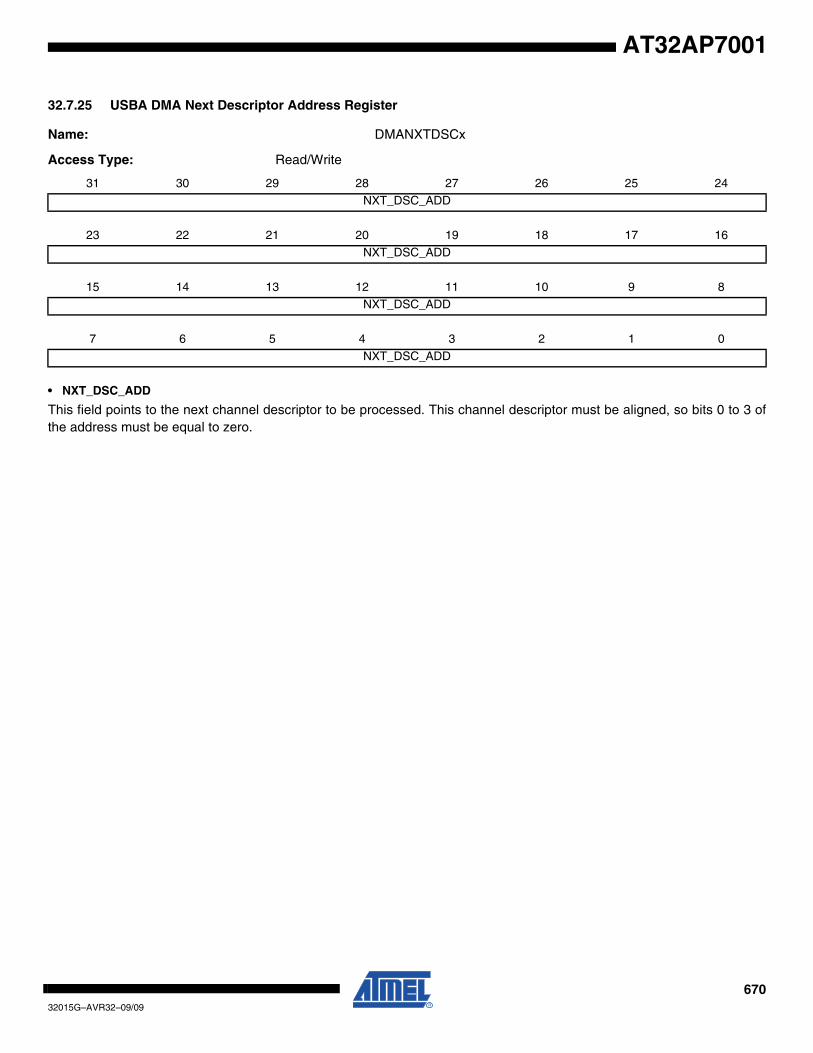
67032015G–AVR32–09/09
AT32AP7001
32.7.25 USBA DMA Next Descriptor Address Register
Name: DMANXTDSCx
Access Type: Read/Write
• NXT_DSC_ADD
This field points to the next channel descriptor to be processed. This channel descriptor must be aligned, so bits 0 to 3 ofthe address must be equal to zero.
31 30 29 28 27 26 25 24
NXT_DSC_ADD
23 22 21 20 19 18 17 16
NXT_DSC_ADD
15 14 13 12 11 10 9 8
NXT_DSC_ADD
7 6 5 4 3 2 1 0
NXT_DSC_ADD
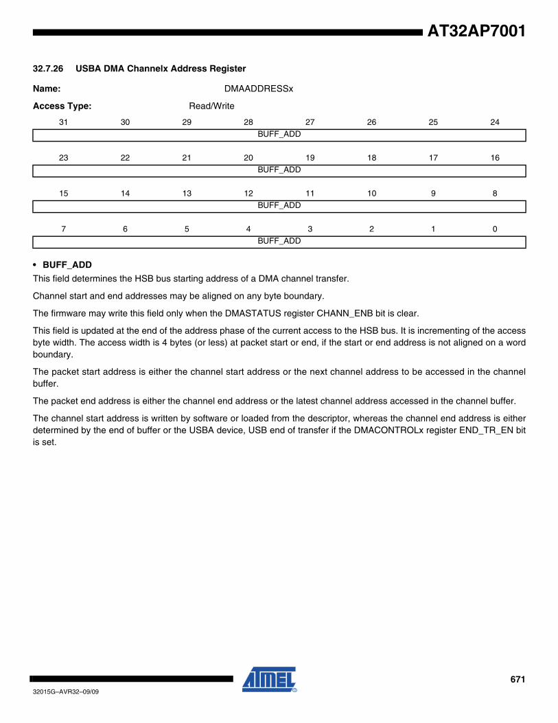
67132015G–AVR32–09/09
AT32AP7001
32.7.26 USBA DMA Channelx Address Register
Name: DMAADDRESSx
Access Type: Read/Write
• BUFF_ADD
This field determines the HSB bus starting address of a DMA channel transfer.
Channel start and end addresses may be aligned on any byte boundary.
The firmware may write this field only when the DMASTATUS register CHANN_ENB bit is clear.
This field is updated at the end of the address phase of the current access to the HSB bus. It is incrementing of the accessbyte width. The access width is 4 bytes (or less) at packet start or end, if the start or end address is not aligned on a wordboundary.
The packet start address is either the channel start address or the next channel address to be accessed in the channelbuffer.
The packet end address is either the channel end address or the latest channel address accessed in the channel buffer.
The channel start address is written by software or loaded from the descriptor, whereas the channel end address is eitherdetermined by the end of buffer or the USBA device, USB end of transfer if the DMACONTROLx register END_TR_EN bitis set.
31 30 29 28 27 26 25 24
BUFF_ADD
23 22 21 20 19 18 17 16
BUFF_ADD
15 14 13 12 11 10 9 8
BUFF_ADD
7 6 5 4 3 2 1 0
BUFF_ADD
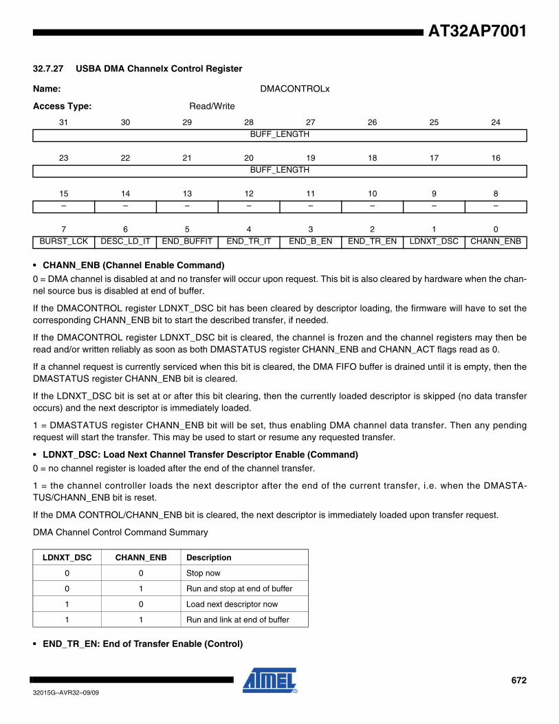
67232015G–AVR32–09/09
AT32AP7001
32.7.27 USBA DMA Channelx Control Register
Name: DMACONTROLx
Access Type: Read/Write
• CHANN_ENB (Channel Enable Command)
0 = DMA channel is disabled at and no transfer will occur upon request. This bit is also cleared by hardware when the chan-nel source bus is disabled at end of buffer.
If the DMACONTROL register LDNXT_DSC bit has been cleared by descriptor loading, the firmware will have to set thecorresponding CHANN_ENB bit to start the described transfer, if needed.
If the DMACONTROL register LDNXT_DSC bit is cleared, the channel is frozen and the channel registers may then beread and/or written reliably as soon as both DMASTATUS register CHANN_ENB and CHANN_ACT flags read as 0.
If a channel request is currently serviced when this bit is cleared, the DMA FIFO buffer is drained until it is empty, then theDMASTATUS register CHANN_ENB bit is cleared.
If the LDNXT_DSC bit is set at or after this bit clearing, then the currently loaded descriptor is skipped (no data transferoccurs) and the next descriptor is immediately loaded.
1 = DMASTATUS register CHANN_ENB bit will be set, thus enabling DMA channel data transfer. Then any pendingrequest will start the transfer. This may be used to start or resume any requested transfer.
• LDNXT_DSC: Load Next Channel Transfer Descriptor Enable (Command)
0 = no channel register is loaded after the end of the channel transfer.
1 = the channel controller loads the next descriptor after the end of the current transfer, i.e. when the DMASTA-TUS/CHANN_ENB bit is reset.
If the DMA CONTROL/CHANN_ENB bit is cleared, the next descriptor is immediately loaded upon transfer request.
DMA Channel Control Command Summary
• END_TR_EN: End of Transfer Enable (Control)
31 30 29 28 27 26 25 24
BUFF_LENGTH
23 22 21 20 19 18 17 16
BUFF_LENGTH
15 14 13 12 11 10 9 8
– – – – – – – –
7 6 5 4 3 2 1 0
BURST_LCK DESC_LD_IT END_BUFFIT END_TR_IT END_B_EN END_TR_EN LDNXT_DSC CHANN_ENB
LDNXT_DSC CHANN_ENB Description
0 0 Stop now
0 1 Run and stop at end of buffer
1 0 Load next descriptor now
1 1 Run and link at end of buffer
67332015G–AVR32–09/09
AT32AP7001
Used for OUT transfers only.
0 = USB end of transfer is ignored.
1 = USBA device can put an end to the current buffer transfer.
When set, a BULK or INTERRUPT short packet or the last packet of an ISOCHRONOUS (micro) frame (DATAX) will closethe current buffer and the DMASTATUSx register END_TR_ST flag will be raised.
This is intended for USBA non-prenegotiated end of transfer (BULK or INTERRUPT) or ISOCHRONOUS microframe databuffer closure.
• END_B_EN: End of Buffer Enable (Control)
0 = DMA Buffer End has no impact on USB packet transfer.
1 = endpoint can validate the packet (according to the values programmed in the EPTCTLx register AUTO_VALID andSHRT_PCKT fields) at DMA Buffer End, i.e. when the DMASTATUS register BUFF_COUNT reaches 0.
This is mainly for short packet IN validation initiated by the DMA reaching end of buffer, but could be used for OUT packettruncation (discarding of unwanted packet data) at the end of DMA buffer.
• END_TR_IT: End of Transfer Interrupt Enable
0 = USBA device initiated buffer transfer completion will not trigger any interrupt at STATUSx/END_TR_ST rising.
1 = an interrupt is sent after the buffer transfer is complete, if the USBA device has ended the buffer transfer.
Use when the receive size is unknown.
• END_BUFFIT: End of Buffer Interrupt Enable
0 = DMA_STATUSx/END_BF_ST rising will not trigger any interrupt.
1 = an interrupt is generated when the DMASTATUSx register BUFF_COUNT reaches zero.
• DESC_LD_IT: Descriptor Loaded Interrupt Enable
0 = DMASTATUSx/DESC_LDST rising will not trigger any interrupt.
1 = an interrupt is generated when a descriptor has been loaded from the bus.
• BURST_LCK: Burst Lock Enable
0 = the DMA never locks bus access.
1 = USB packets HSB data bursts are locked for maximum optimization of the bus bandwidth usage and maximization offly-by HSB burst duration.
• BUFF_LENGTH: Buffer Byte Length (Write-only)
This field determines the number of bytes to be transferred until end of buffer. The maximum channel transfer size (64 KB)is reached when this field is 0 (default value). If the transfer size is unknown, this field should be set to 0, but the transferend may occur earlier under USBA device control.
When this field is written, The DMASTATUSx register BUFF_COUNT field is updated with the write value.
Note: Bits [31:2] are only writable when issuing a channel Control Command other than “Stop Now”.
Note: For reliability it is highly recommended to wait for both DMASTATUSx register CHAN_ACT and CHAN_ENB flags are at 0, thus ensuring the channel has been stopped before issuing a command other than “Stop Now”.
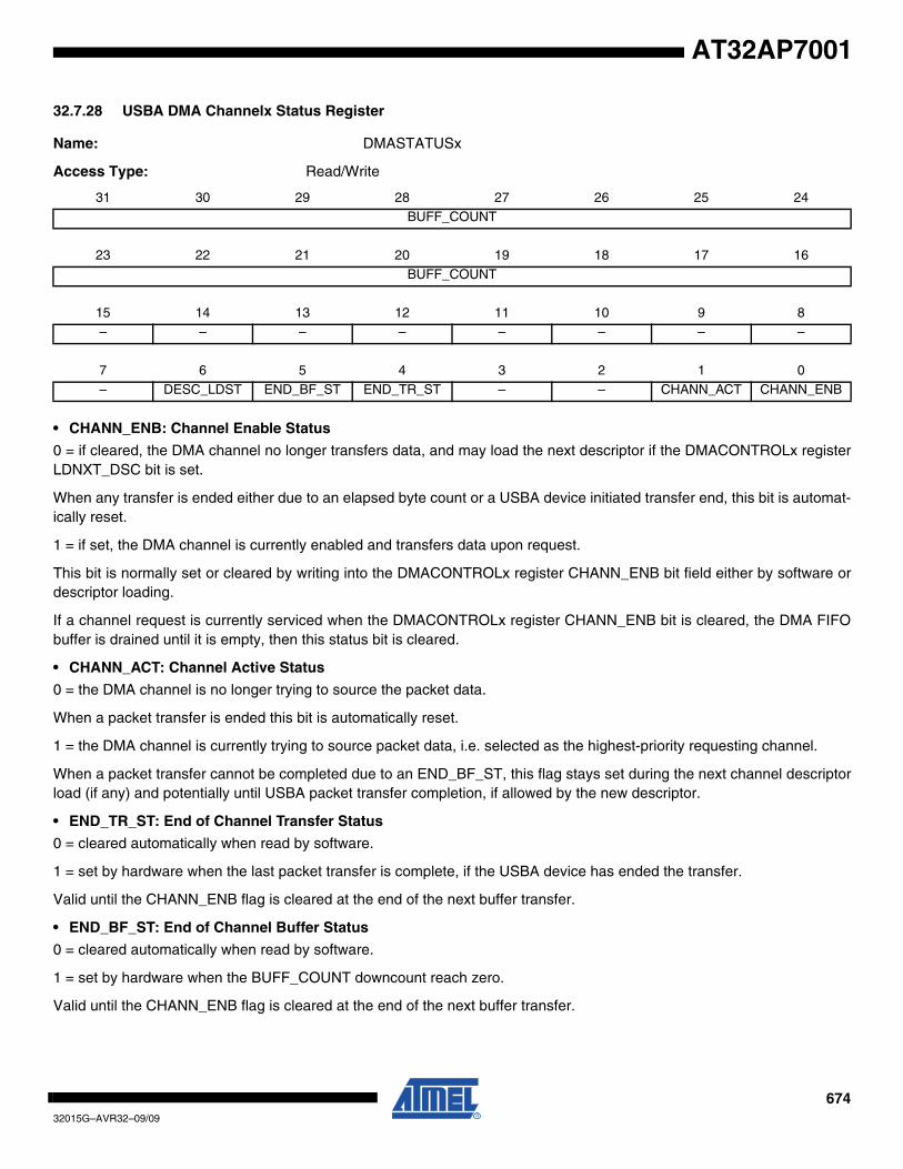
67432015G–AVR32–09/09
AT32AP7001
32.7.28 USBA DMA Channelx Status Register
Name: DMASTATUSx
Access Type: Read/Write
• CHANN_ENB: Channel Enable Status
0 = if cleared, the DMA channel no longer transfers data, and may load the next descriptor if the DMACONTROLx registerLDNXT_DSC bit is set.
When any transfer is ended either due to an elapsed byte count or a USBA device initiated transfer end, this bit is automat-ically reset.
1 = if set, the DMA channel is currently enabled and transfers data upon request.
This bit is normally set or cleared by writing into the DMACONTROLx register CHANN_ENB bit field either by software ordescriptor loading.
If a channel request is currently serviced when the DMACONTROLx register CHANN_ENB bit is cleared, the DMA FIFObuffer is drained until it is empty, then this status bit is cleared.
• CHANN_ACT: Channel Active Status
0 = the DMA channel is no longer trying to source the packet data.
When a packet transfer is ended this bit is automatically reset.
1 = the DMA channel is currently trying to source packet data, i.e. selected as the highest-priority requesting channel.
When a packet transfer cannot be completed due to an END_BF_ST, this flag stays set during the next channel descriptorload (if any) and potentially until USBA packet transfer completion, if allowed by the new descriptor.
• END_TR_ST: End of Channel Transfer Status
0 = cleared automatically when read by software.
1 = set by hardware when the last packet transfer is complete, if the USBA device has ended the transfer.
Valid until the CHANN_ENB flag is cleared at the end of the next buffer transfer.
• END_BF_ST: End of Channel Buffer Status
0 = cleared automatically when read by software.
1 = set by hardware when the BUFF_COUNT downcount reach zero.
Valid until the CHANN_ENB flag is cleared at the end of the next buffer transfer.
31 30 29 28 27 26 25 24
BUFF_COUNT
23 22 21 20 19 18 17 16
BUFF_COUNT
15 14 13 12 11 10 9 8
– – – – – – – –
7 6 5 4 3 2 1 0
– DESC_LDST END_BF_ST END_TR_ST – – CHANN_ACT CHANN_ENB
67532015G–AVR32–09/09
AT32AP7001
• DESC_LDST: Descriptor Loaded Status
0 = cleared automatically when read by software.
1 = set by hardware when a descriptor has been loaded from the system bus.
Valid until the CHANN_ENB flag is cleared at the end of the next buffer transfer.
• BUFF_COUNT: Buffer Byte Count
This field determines the current number of bytes still to be transferred for this buffer.
This field is decremented from the HSB source bus access byte width at the end of this bus address phase.
The access byte width is 4 by default, or less, at DMA start or end, if the start or end address is not aligned on a wordboundary.
At the end of buffer, the DMA accesses the USBA device only for the number of bytes needed to complete it.
This field value is reliable (stable) only if the channel has been stopped or frozen (EPTCTLx register NT_DIS_DMA bit isused to disable the channel request) and the channel is no longer active CHANN_ACT flag is 0.
Note: For OUT endpoints, if the receive buffer byte length (BUFF_LENGTH) has been defaulted to zero because the USB transfer length is unknown, the actual buffer byte length received will be 0x10000-BUFF_COUNT.
67632015G–AVR32–09/09
AT32AP7001
33. Timer/Counter (TC)
Rev: 2.0.0.1
33.1 Features
• Three 16-bit Timer Counter channels• A wide range of functions including:
– Frequency measurement– Event counting– Interval measurement– Pulse generation– Delay timing– Pulse width modulation– Up/down capabilities
• Each channel is user-configurable and contains:– Three external clock inputs– Five internal clock inputs– Two multi-purpose input/output signals
• Internal interrupt signal• Two global registers that act on all three TC channels• Peripheral event input on all A lines in capture mode
33.2 Overview
The Timer Counter (TC) includes three identical 16-bit Timer Counter channels.
Each channel can be independently programmed to perform a wide range of functions includingfrequency measurement, event counting, interval measurement, pulse generation, delay timing,and pulse width modulation.
Each channel has three external clock inputs, five internal clock inputs, and two multi-purposeinput/output signals which can be configured by the user. Each channel drives an internal inter-rupt signal which can be programmed to generate processor interrupts.
The TC block has two global registers which act upon all three TC channels.
The Block Control Register (BCR) allows the three channels to be started simultaneously withthe same instruction.
The Block Mode Register (BMR) defines the external clock inputs for each channel, allowingthem to be chained.

67732015G–AVR32–09/09
AT32AP7001
33.3 Block Diagram
Figure 33-1. TC Block Diagram
33.4 I/O Lines Description
33.5 Product Dependencies
In order to use this module, other parts of the system must be configured correctly, as describedbelow.
33.5.1 I/O Lines
The pins used for interfacing the compliant external devices may be multiplexed with I/O lines.The user must first program the I/O Controller to assign the TC pins to their peripheral functions.
I/OController
TC2XC2S
INT0
INT1
INT2
TIOA0
TIOA1
TIOA2
TIOB0
TIOB1
TIOB2
XC2
TCLK0
TCLK1
TCLK2
TCLK0
TCLK1
TCLK2
TCLK0
TCLK1
TCLK2
TIOA1
TIOA2
TIOA0
TIOA2
TIOA1
InterruptController
CLK0CLK1CLK2
A0B0
A1B1
A2B2
Timer Count er
TIOB
TIOA
TIOB
SYNC
TIMER_CLOCK1
TIOA
SYNC
SYNC
TIOA
TIOB
TIMER_CLOCK2
TIMER_CLOCK3
TIMER_CLOCK4
TIMER_CLOCK5
XC1
XC0
XC0
XC2
XC1
XC0
XC1
XC2
Timer/CounterChannel 2
Timer/CounterChannel 1
Timer/CounterChannel 0
TC1XC1S
TC0XC0S
TIOA0
Table 33-1. I/O Lines Description
Pin Name Description Type
CLK0-CLK2 External Clock Input Input
A0-A2 I/O Line A Input/Output
B0-B2 I/O Line B Input/Output
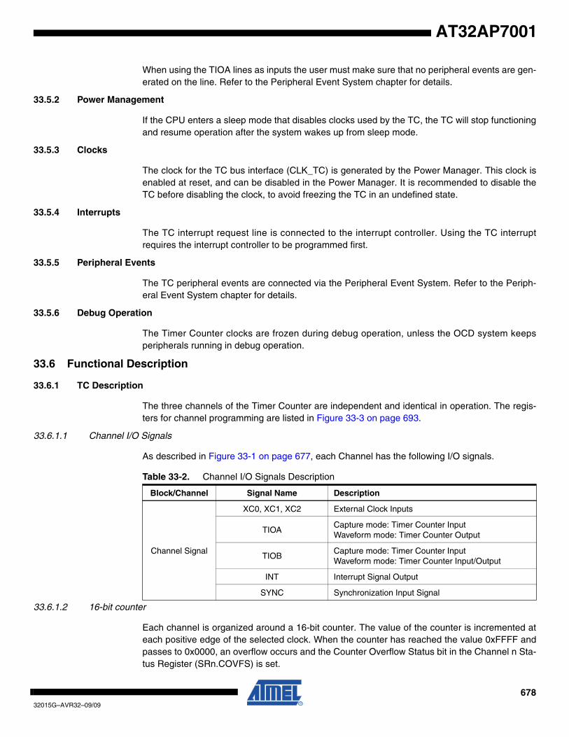
67832015G–AVR32–09/09
AT32AP7001
When using the TIOA lines as inputs the user must make sure that no peripheral events are gen-erated on the line. Refer to the Peripheral Event System chapter for details.
33.5.2 Power Management
If the CPU enters a sleep mode that disables clocks used by the TC, the TC will stop functioningand resume operation after the system wakes up from sleep mode.
33.5.3 Clocks
The clock for the TC bus interface (CLK_TC) is generated by the Power Manager. This clock isenabled at reset, and can be disabled in the Power Manager. It is recommended to disable theTC before disabling the clock, to avoid freezing the TC in an undefined state.
33.5.4 Interrupts
The TC interrupt request line is connected to the interrupt controller. Using the TC interruptrequires the interrupt controller to be programmed first.
33.5.5 Peripheral Events
The TC peripheral events are connected via the Peripheral Event System. Refer to the Periph-eral Event System chapter for details.
33.5.6 Debug Operation
The Timer Counter clocks are frozen during debug operation, unless the OCD system keepsperipherals running in debug operation.
33.6 Functional Description
33.6.1 TC Description
The three channels of the Timer Counter are independent and identical in operation. The regis-ters for channel programming are listed in Figure 33-3 on page 693.
33.6.1.1 Channel I/O Signals
As described in Figure 33-1 on page 677, each Channel has the following I/O signals.
33.6.1.2 16-bit counter
Each channel is organized around a 16-bit counter. The value of the counter is incremented ateach positive edge of the selected clock. When the counter has reached the value 0xFFFF andpasses to 0x0000, an overflow occurs and the Counter Overflow Status bit in the Channel n Sta-tus Register (SRn.COVFS) is set.
Table 33-2. Channel I/O Signals Description
Block/Channel Signal Name Description
Channel Signal
XC0, XC1, XC2 External Clock Inputs
TIOACapture mode: Timer Counter InputWaveform mode: Timer Counter Output
TIOBCapture mode: Timer Counter InputWaveform mode: Timer Counter Input/Output
INT Interrupt Signal Output
SYNC Synchronization Input Signal
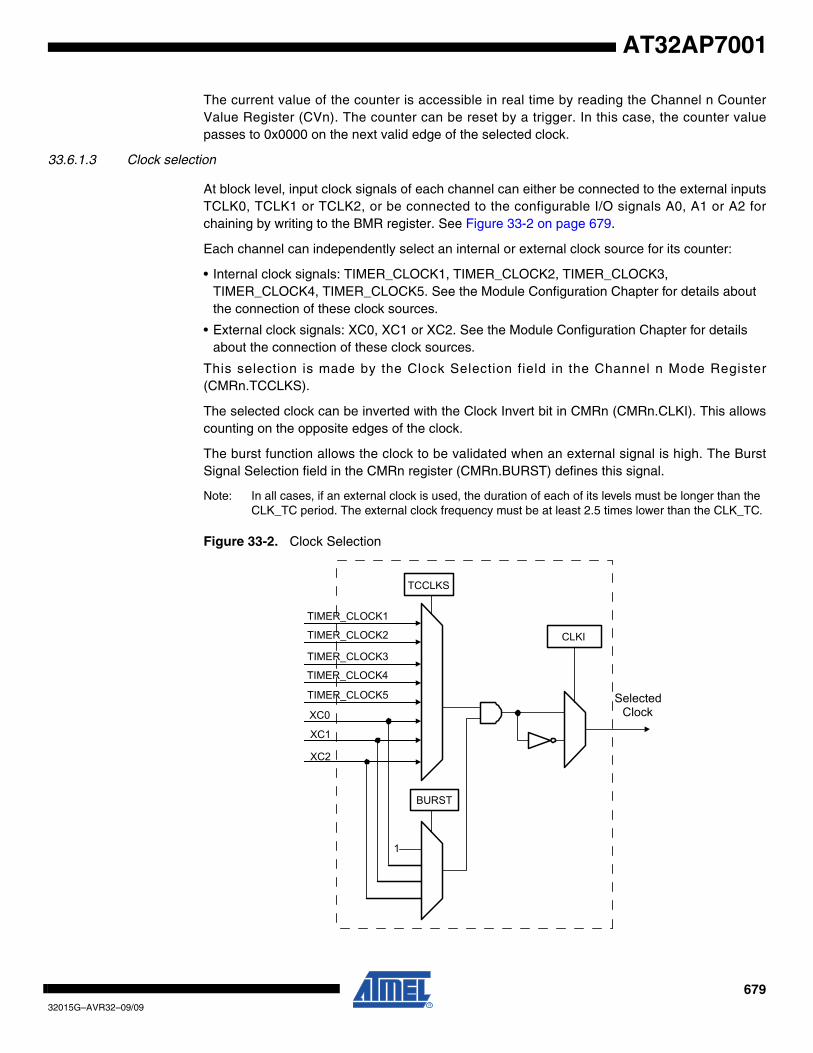
67932015G–AVR32–09/09
AT32AP7001
The current value of the counter is accessible in real time by reading the Channel n CounterValue Register (CVn). The counter can be reset by a trigger. In this case, the counter valuepasses to 0x0000 on the next valid edge of the selected clock.
33.6.1.3 Clock selection
At block level, input clock signals of each channel can either be connected to the external inputsTCLK0, TCLK1 or TCLK2, or be connected to the configurable I/O signals A0, A1 or A2 forchaining by writing to the BMR register. See Figure 33-2 on page 679.
Each channel can independently select an internal or external clock source for its counter:
• Internal clock signals: TIMER_CLOCK1, TIMER_CLOCK2, TIMER_CLOCK3, TIMER_CLOCK4, TIMER_CLOCK5. See the Module Configuration Chapter for details about the connection of these clock sources.
• External clock signals: XC0, XC1 or XC2. See the Module Configuration Chapter for details about the connection of these clock sources.
This selection is made by the Clock Selection field in the Channel n Mode Register(CMRn.TCCLKS).
The selected clock can be inverted with the Clock Invert bit in CMRn (CMRn.CLKI). This allowscounting on the opposite edges of the clock.
The burst function allows the clock to be validated when an external signal is high. The BurstSignal Selection field in the CMRn register (CMRn.BURST) defines this signal.
Note: In all cases, if an external clock is used, the duration of each of its levels must be longer than the CLK_TC period. The external clock frequency must be at least 2.5 times lower than the CLK_TC.
Figure 33-2. Clock Selection
TIMER_CLOCK5
XC2
TCCLKS
CLKI
BURST
1
SelectedClock
XC1
XC0
TIMER_CLOCK4
TIMER_CLOCK3
TIMER_CLOCK2
TIMER_CLOCK1
68032015G–AVR32–09/09
AT32AP7001
33.6.1.4 Clock control
The clock of each counter can be controlled in two different ways: it can be enabled/disabledand started/stopped. See Figure 33-3 on page 680.
• The clock can be enabled or disabled by the user by writing to the Counter Clock Enable/Disable Command bits in the Channel n Clock Control Register (CCRn.CLKEN and CCRn.CLKDIS). In Capture mode it can be disabled by an RB load event if the Counter Clock Disable with RB Loading bit in CMRn is written to one (CMRn.LDBDIS). In Waveform mode, it can be disabled by an RC Compare event if the Counter Clock Disable with RC Compare bit in CMRn is written to one (CMRn.CPCDIS). When disabled, the start or the stop actions have no effect: only a CLKEN command in CCRn can re-enable the clock. When the clock is enabled, the Clock Enabling Status bit is set in SRn (SRn.CLKSTA).
• The clock can also be started or stopped: a trigger (software, synchro, external or compare) always starts the clock. In Capture mode the clock can be stopped by an RB load event if the Counter Clock Stopped with RB Loading bit in CMRn is written to one (CMRn.LDBSTOP). In Waveform mode it can be stopped by an RC compare event if the Counter Clock Stopped with RC Compare bit in CMRn is written to one (CMRn.CPCSTOP). The start and the stop commands have effect only if the clock is enabled.
Figure 33-3. Clock Control
33.6.1.5 TC operating modes
Each channel can independently operate in two different modes:
• Capture mode provides measurement on signals.
• Waveform mode provides wave generation.
The TC operating mode selection is done by writing to the Wave bit in the CCRn register(CCRn.WAVE).
In Capture mode, TIOA and TIOB are configured as inputs.
Q SR
S
R
Q
CLKSTA CLKEN CLKDIS
StopEvent
DisableCounter
Clock
SelectedClock Trigger
Event
68132015G–AVR32–09/09
AT32AP7001
In Waveform mode, TIOA is always configured to be an output and TIOB is an output if it is notselected to be the external trigger.
33.6.1.6 Trigger
A trigger resets the counter and starts the counter clock. Three types of triggers are common toboth modes, and a fourth external trigger is available to each mode.
The following triggers are common to both modes:
• Software Trigger: each channel has a software trigger, available by writing a one to the Software Trigger Command bit in CCRn (CCRn.SWTRG).
• SYNC: each channel has a synchronization signal SYNC. When asserted, this signal has the same effect as a software trigger. The SYNC signals of all channels are asserted simultaneously by writing a one to the Synchro Command bit in the BCR register (BCR.SYNC).
• Compare RC Trigger: RC is implemented in each channel and can provide a trigger when the counter value matches the RC value if the RC Compare Trigger Enable bit in CMRn (CMRn.CPCTRG) is written to one.
The channel can also be configured to have an external trigger. In Capture mode, the externaltrigger signal can be selected between TIOA and TIOB. In Waveform mode, an external eventcan be programmed to be one of the following signals: TIOB, XC0, XC1, or XC2. This externalevent can then be programmed to perform a trigger by writing a one to the External Event Trig-ger Enable bit in CMRn (CMRn.ENETRG).
If an external trigger is used, the duration of the pulses must be longer than the CLK_TC periodin order to be detected.
Regardless of the trigger used, it will be taken into account at the following active edge of theselected clock. This means that the counter value can be read differently from zero just after atrigger, especially when a low frequency signal is selected as the clock.
33.6.1.7 Peripheral events on TIOA inputs
The TIOA input lines are ored internally with peripheral events from the Peripheral Event Sys-tem. To capture using events the user must ensure that the corresponding pin functions for theTIOA line are disabled. When capturing on the external TIOA pin the user must ensure that noperipheral events are generated on this pin.
33.6.2 Capture Operating Mode
This mode is entered by writing a zero to the CMRn.WAVE bit.
Capture mode allows the TC channel to perform measurements such as pulse timing, fre-quency, period, duty cycle and phase on TIOA and TIOB signals which are considered asinputs.
Figure 33-4 on page 683 shows the configuration of the TC channel when programmed in Cap-ture mode.
33.6.2.1 Capture registers A and B
Registers A and B (RA and RB) are used as capture registers. This means that they can beloaded with the counter value when a programmable event occurs on the signal TIOA.
68232015G–AVR32–09/09
AT32AP7001
The RA Loading Selection field in CMRn (CMRn.LDRA) defines the TIOA edge for the loading ofthe RA register, and the RB Loading Selection field in CMRn (CMRn.LDRB) defines the TIOAedge for the loading of the RB register.
RA is loaded only if it has not been loaded since the last trigger or if RB has been loaded sincethe last loading of RA.
RB is loaded only if RA has been loaded since the last trigger or the last loading of RB.
Loading RA or RB before the read of the last value loaded sets the Load Overrun Status bit inSRn (SRn.LOVRS). In this case, the old value is overwritten.
33.6.2.2 Trigger conditions
In addition to the SYNC signal, the software trigger and the RC compare trigger, an external trig-ger can be defined.
The TIOA or TIOB External Trigger Selection bit in CMRn (CMRn.ABETRG) selects TIOA orTIOB input signal as an external trigger. The External Trigger Edge Selection bit in CMRn(CMRn.ETREDG) defines the edge (rising, falling or both) detected to generate an external trig-ger. If CMRn.ETRGEDG is zero (none), the external trigger is disabled.
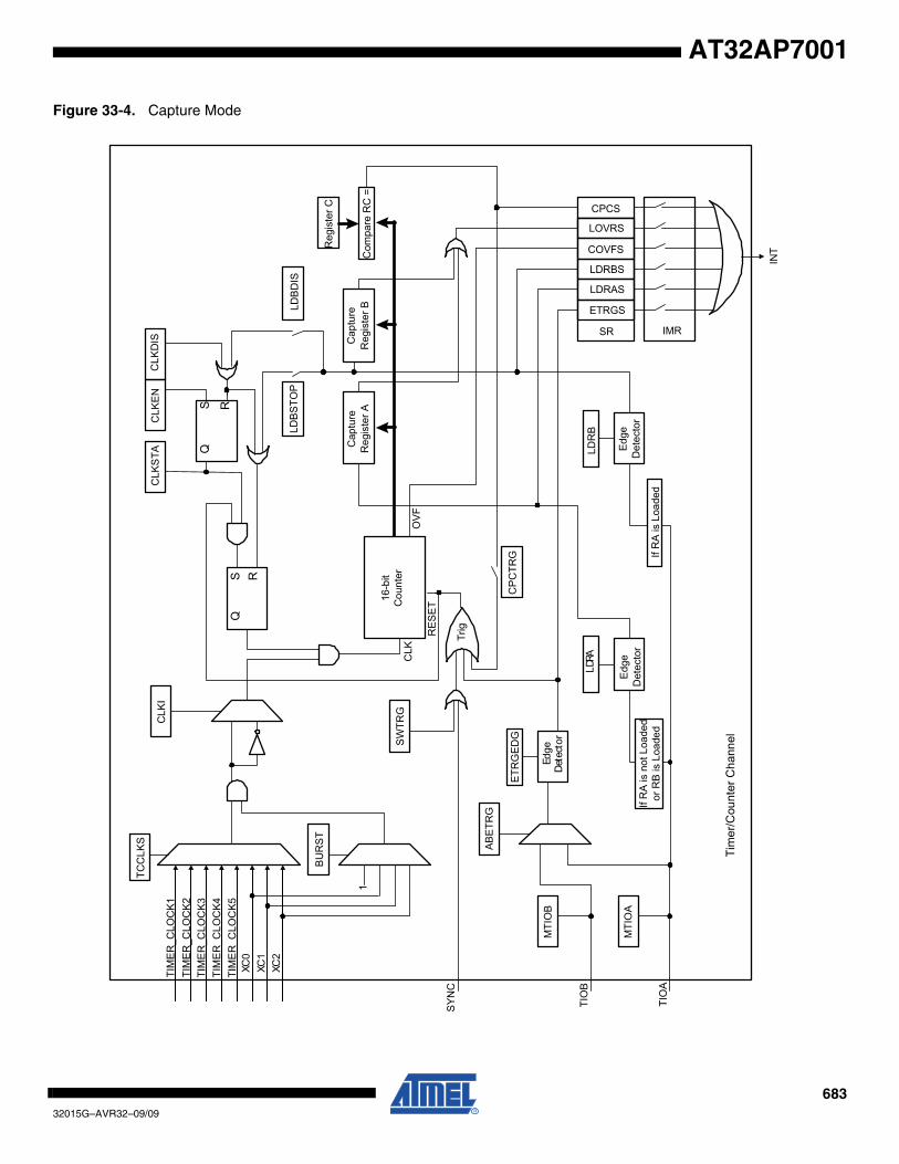
68332015G–AVR32–09/09
AT32AP7001
Figure 33-4. Capture Mode
TIM
ER_C
LOC
K1
XC0
XC1
XC2
TCC
LKS
CLK
I
QS R
S R
Q
CLK
STA
CLK
ENC
LKD
IS
BU
RST
TIO
B
Cap
ture
Reg
iste
r AC
ompa
re R
C =
16-b
itC
ount
er
ABET
RG
SW
TRG
ETR
GE
DG
CP
CTR
G
IMR
Trig
LDRBS
LDRAS
ETRGS
SR
LOVRS
COVFS
SYN
C
1
MTI
OB
TIO
A
MTI
OA
LDRA
LDB
STO
P
If R
A is
not
Loa
ded
or R
B is
Loa
ded
If R
A is
Loa
ded
LDB
DIS
CPCS
INT
Edge
Dete
ctor
LDR
B
CLK
OV
FR
ESET
Tim
er/C
ount
er C
hann
el
Edg
eD
etec
tor
Edg
eD
etec
tor
Cap
ture
Reg
iste
r B
Reg
iste
r C
TIM
ER_C
LOC
K2TI
ME
R_C
LOC
K3TI
ME
R_C
LOC
K4TI
ME
R_C
LOC
K5
68432015G–AVR32–09/09
AT32AP7001
33.6.3 Waveform Operating Mode
Waveform operating mode is entered by writing a one to the CMRn.WAVE bit.
In Waveform operating mode the TC channel generates one or two PWM signals with the samefrequency and independently programmable duty cycles, or generates different types of one-shot or repetitive pulses.
In this mode, TIOA is configured as an output and TIOB is defined as an output if it is not usedas an external event.
Figure 33-5 on page 685 shows the configuration of the TC channel when programmed inWaveform operating mode.
33.6.3.1 Waveform selection
Depending on the Waveform Selection field in CMRn (CMRn.WAVSEL), the behavior of CVnvaries.
With any selection, RA, RB and RC can all be used as compare registers.
RA Compare is used to control the TIOA output, RB Compare is used to control the TIOB output(if correctly configured) and RC Compare is used to control TIOA and/or TIOB outputs.
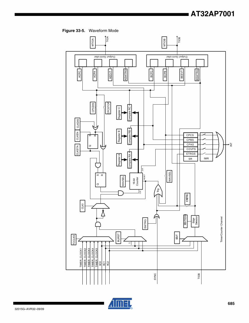
68532015G–AVR32–09/09
AT32AP7001
Figure 33-5. Waveform Mode
TCC
LKS
CLK
I
QS R
S R
Q
CLK
STA
CLK
EN
CLK
DIS
CP
CD
IS
BUR
ST
TIO
B
Reg
iste
r A
Com
pare
RC
=
CPC
STO
P
16-b
itC
ount
er
EEVT
EEV
TED
G
SYN
C
SWTR
G
ENE
TRG
WA
VSE
L
IMRTr
ig
AC
PC
ACP
A
AEE
VT
ASW
TRG
BCP
C
BC
PB
BE
EVT
BSW
TRG
TIO
A
MTI
OA
TIO
B
MTI
OB
CPAS
COVFS
ETRGS
SR
CPCS
CPBSC
LKO
VF
RE
SET
OutputController OutputController
INT
1
Edge
Dete
ctor
Tim
er/C
ount
er C
hann
el
TIM
ER
_CLO
CK1
XC0
XC1
XC2
WAV
SEL
Reg
iste
r BR
egis
ter C
Com
pare
RB
=C
ompa
re R
A =
TIM
ER
_CLO
CK2
TIM
ER_C
LOC
K3
TIM
ER_C
LOC
K4
TIM
ER_C
LOC
K5
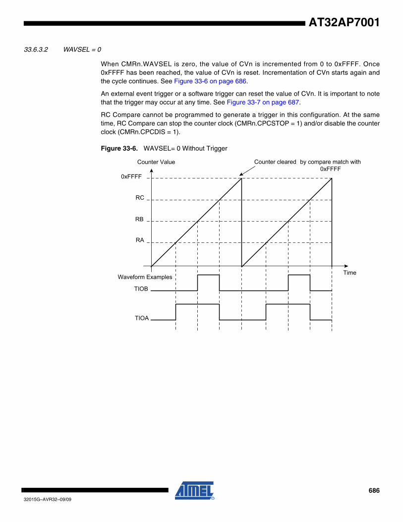
68632015G–AVR32–09/09
AT32AP7001
33.6.3.2 WAVSEL = 0
When CMRn.WAVSEL is zero, the value of CVn is incremented from 0 to 0xFFFF. Once0xFFFF has been reached, the value of CVn is reset. Incrementation of CVn starts again andthe cycle continues. See Figure 33-6 on page 686.
An external event trigger or a software trigger can reset the value of CVn. It is important to notethat the trigger may occur at any time. See Figure 33-7 on page 687.
RC Compare cannot be programmed to generate a trigger in this configuration. At the sametime, RC Compare can stop the counter clock (CMRn.CPCSTOP = 1) and/or disable the counterclock (CMRn.CPCDIS = 1).
Figure 33-6. WAVSEL= 0 Without Trigger
Time
Counter Value
RC
RB
RA
TIOB
TIOA
Counter cleared by compare match with 0xFFFF
0xFFFF
Waveform Examples

68732015G–AVR32–09/09
AT32AP7001
Figure 33-7. WAVSEL= 0 With Trigger
33.6.3.3 WAVSEL = 2
When CMRn.WAVSEL is two, the value of CVn is incremented from zero to the value of RC,then automatically reset on a RC Compare. Once the value of CVn has been reset, it is thenincremented and so on. See Figure 33-8 on page 688.
It is important to note that CVn can be reset at any time by an external event or a software trig-ger if both are programmed correctly. See Figure 33-9 on page 688.
In addition, RC Compare can stop the counter clock (CMRn.CPCSTOP) and/or disable thecounter clock (CMRn.CPCDIS = 1).
Time
Counter Value
RC
RB
RA
TIOB
TIOA
Counter cleared by compare match with 0xFFFF
0xFFFF
Waveform Examples
Counter cleared by trigger
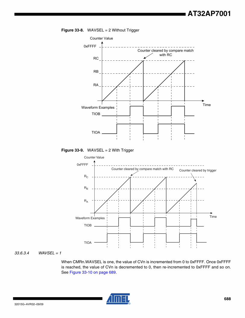
68832015G–AVR32–09/09
AT32AP7001
Figure 33-8. WAVSEL = 2 Without Trigger
Figure 33-9. WAVSEL = 2 With Trigger
33.6.3.4 WAVSEL = 1
When CMRn.WAVSEL is one, the value of CVn is incremented from 0 to 0xFFFF. Once 0xFFFFis reached, the value of CVn is decremented to 0, then re-incremented to 0xFFFF and so on.See Figure 33-10 on page 689.
Time
Counter Value
RC
RB
RA
TIOB
TIOA
Counter cleared by compare match with RC
0xFFFF
Waveform Examples
Time
Counter Value
RC
RB
RA
TIOB
TIOA
Counter cleared by compare match with RC0xFFFF
Waveform Examples
Counter cleared by trigger
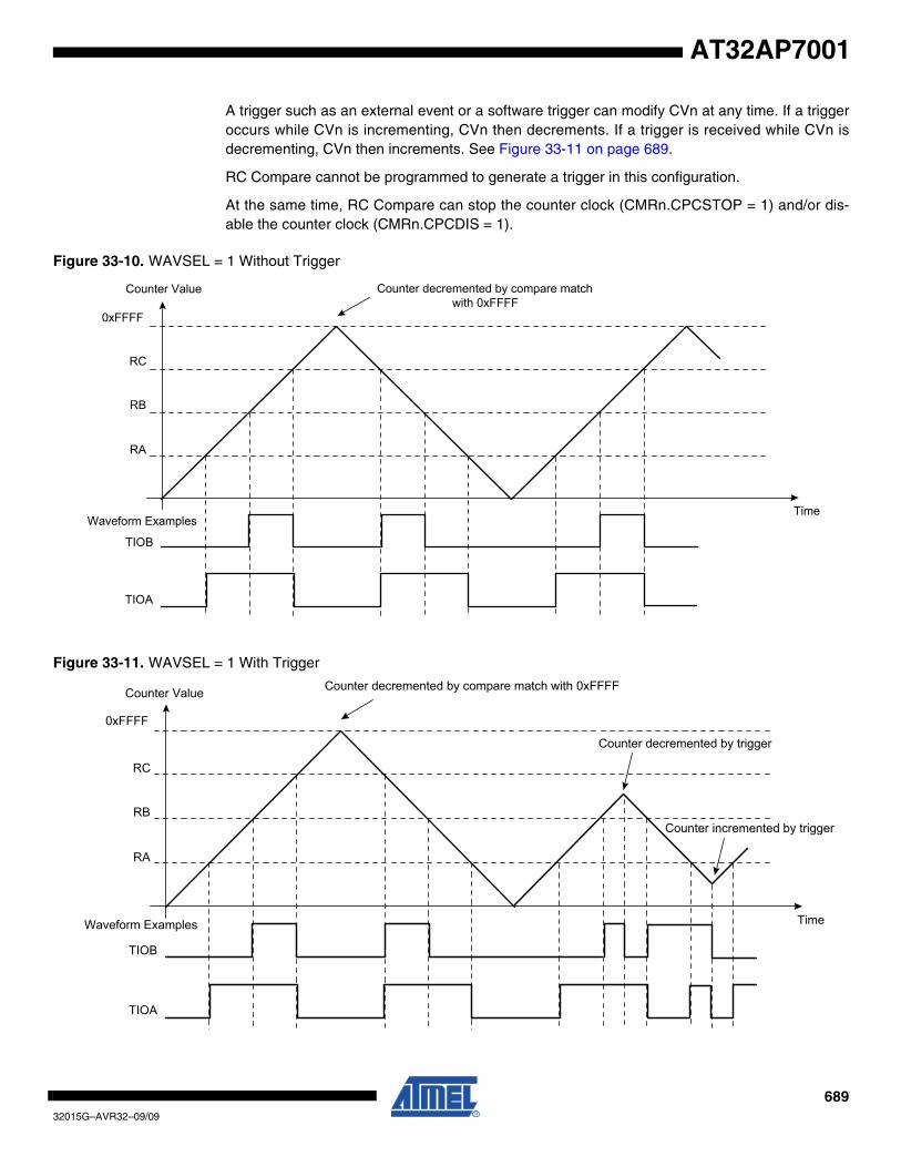
68932015G–AVR32–09/09
AT32AP7001
A trigger such as an external event or a software trigger can modify CVn at any time. If a triggeroccurs while CVn is incrementing, CVn then decrements. If a trigger is received while CVn isdecrementing, CVn then increments. See Figure 33-11 on page 689.
RC Compare cannot be programmed to generate a trigger in this configuration.
At the same time, RC Compare can stop the counter clock (CMRn.CPCSTOP = 1) and/or dis-able the counter clock (CMRn.CPCDIS = 1).
Figure 33-10. WAVSEL = 1 Without Trigger
Figure 33-11. WAVSEL = 1 With Trigger
Time
Counter Value
RC
RB
RA
TIOB
TIOA
Counter decremented by compare match with 0xFFFF
0xFFFF
Waveform Examples
Time
Counter Value
TIOB
TIOA
Counter decremented by compare match with 0xFFFF
0xFFFF
Waveform Examples
Counter decremented by trigger
RC
RB
RA
Counter incremented by trigger
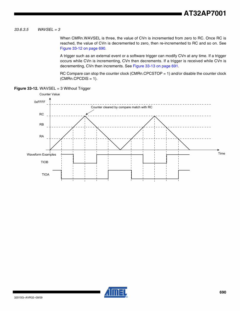
69032015G–AVR32–09/09
AT32AP7001
33.6.3.5 WAVSEL = 3
When CMRn.WAVSEL is three, the value of CVn is incremented from zero to RC. Once RC isreached, the value of CVn is decremented to zero, then re-incremented to RC and so on. SeeFigure 33-12 on page 690.
A trigger such as an external event or a software trigger can modify CVn at any time. If a triggeroccurs while CVn is incrementing, CVn then decrements. If a trigger is received while CVn isdecrementing, CVn then increments. See Figure 33-13 on page 691.
RC Compare can stop the counter clock (CMRn.CPCSTOP = 1) and/or disable the counter clock(CMRn.CPCDIS = 1).
Figure 33-12. WAVSEL = 3 Without Trigger
Time
Counter Value
RC
RB
RA
TIOB
TIOA
Counter cleared by compare match with RC0xFFFF
Waveform Examples

69132015G–AVR32–09/09
AT32AP7001
Figure 33-13. WAVSEL = 3 With Trigger
33.6.3.6 External event/trigger conditions
An external event can be programmed to be detected on one of the clock sources (XC0, XC1,XC2) or TIOB. The external event selected can then be used as a trigger.
The External Event Selection field in CMRn (CMRn.EEVT) selects the external trigger. TheExternal Event Edge Selection field in CMRn (CMRn.EEVTEDG) defines the trigger edge foreach of the possible external triggers (rising, falling or both). If CMRn.EEVTEDG is written tozero, no external event is defined.
If TIOB is defined as an external event signal (CMRn.EEVT = 0), TIOB is no longer used as anoutput and the compare register B is not used to generate waveforms and subsequently noIRQs. In this case the TC channel can only generate a waveform on TIOA.
When an external event is defined, it can be used as a trigger by writing a one to theCMRn.ENETRG bit.
As in Capture mode, the SYNC signal and the software trigger are also available as triggers. RCCompare can also be used as a trigger depending on the CMRn.WAVSEL field.
33.6.3.7 Output controller
The output controller defines the output level changes on TIOA and TIOB following an event.TIOB control is used only if TIOB is defined as output (not as an external event).
The following events control TIOA and TIOB:
• software trigger
• external event
• RC compare
RA compare controls TIOA and RB compare controls TIOB. Each of these events can be pro-grammed to set, clear or toggle the output as defined in the following fields in CMRn:
Time
Counter Value
TIOB
TIOA
Counter decremented by compare match with RC
0xFFFF
Waveform Examples
RC
RB
RA
Counter decremented by trigger
Counter incremented by trigger

69232015G–AVR32–09/09
AT32AP7001
• RC Compare Effect on TIOB (CMRn.BCPC)
• RB Compare Effect on TIOB (CMRn.BCPB)
• RC Compare Effect on TIOA (CMRn.ACPC)
• RA Compare Effect on TIOA (CMRn.ACPA)
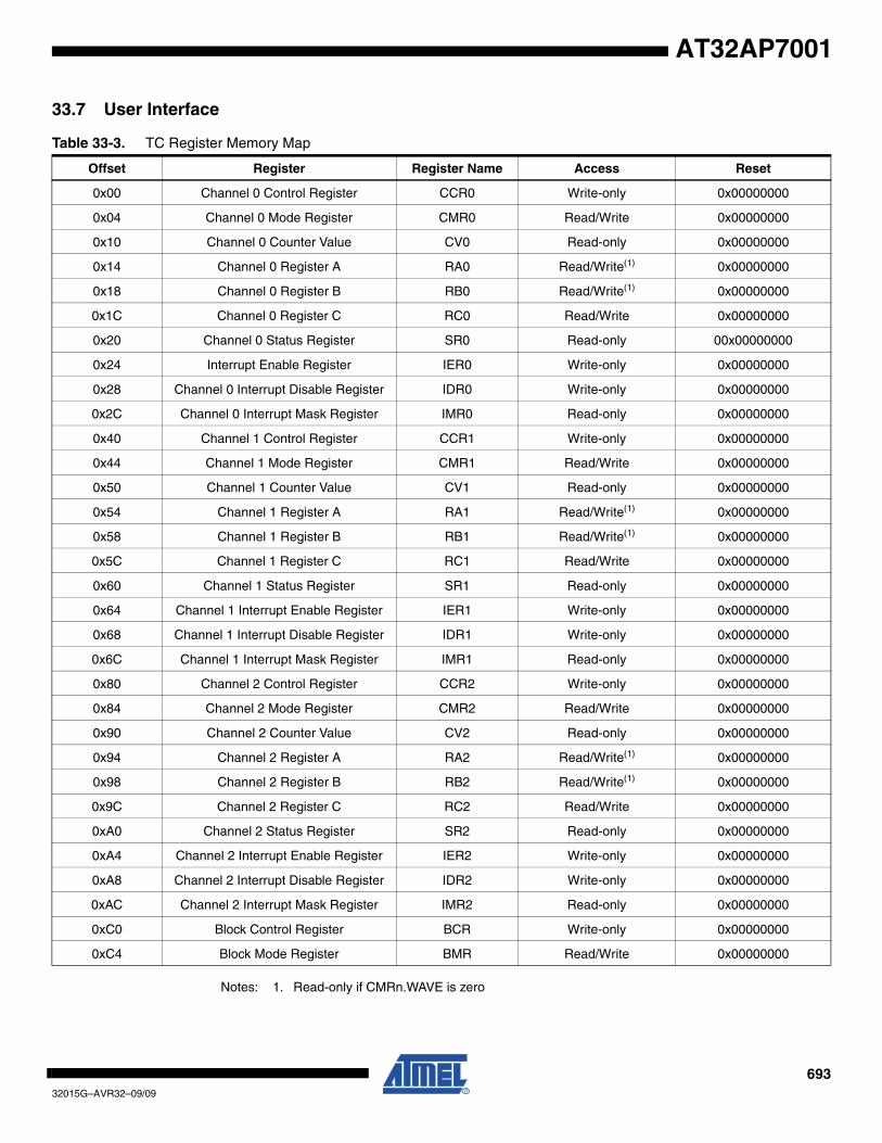
69332015G–AVR32–09/09
AT32AP7001
33.7 User Interface
Notes: 1. Read-only if CMRn.WAVE is zero
Table 33-3. TC Register Memory Map
Offset Register Register Name Access Reset
0x00 Channel 0 Control Register CCR0 Write-only 0x00000000
0x04 Channel 0 Mode Register CMR0 Read/Write 0x00000000
0x10 Channel 0 Counter Value CV0 Read-only 0x00000000
0x14 Channel 0 Register A RA0 Read/Write(1) 0x00000000
0x18 Channel 0 Register B RB0 Read/Write(1) 0x00000000
0x1C Channel 0 Register C RC0 Read/Write 0x00000000
0x20 Channel 0 Status Register SR0 Read-only 00x00000000
0x24 Interrupt Enable Register IER0 Write-only 0x00000000
0x28 Channel 0 Interrupt Disable Register IDR0 Write-only 0x00000000
0x2C Channel 0 Interrupt Mask Register IMR0 Read-only 0x00000000
0x40 Channel 1 Control Register CCR1 Write-only 0x00000000
0x44 Channel 1 Mode Register CMR1 Read/Write 0x00000000
0x50 Channel 1 Counter Value CV1 Read-only 0x00000000
0x54 Channel 1 Register A RA1 Read/Write(1) 0x00000000
0x58 Channel 1 Register B RB1 Read/Write(1) 0x00000000
0x5C Channel 1 Register C RC1 Read/Write 0x00000000
0x60 Channel 1 Status Register SR1 Read-only 0x00000000
0x64 Channel 1 Interrupt Enable Register IER1 Write-only 0x00000000
0x68 Channel 1 Interrupt Disable Register IDR1 Write-only 0x00000000
0x6C Channel 1 Interrupt Mask Register IMR1 Read-only 0x00000000
0x80 Channel 2 Control Register CCR2 Write-only 0x00000000
0x84 Channel 2 Mode Register CMR2 Read/Write 0x00000000
0x90 Channel 2 Counter Value CV2 Read-only 0x00000000
0x94 Channel 2 Register A RA2 Read/Write(1) 0x00000000
0x98 Channel 2 Register B RB2 Read/Write(1) 0x00000000
0x9C Channel 2 Register C RC2 Read/Write 0x00000000
0xA0 Channel 2 Status Register SR2 Read-only 0x00000000
0xA4 Channel 2 Interrupt Enable Register IER2 Write-only 0x00000000
0xA8 Channel 2 Interrupt Disable Register IDR2 Write-only 0x00000000
0xAC Channel 2 Interrupt Mask Register IMR2 Read-only 0x00000000
0xC0 Block Control Register BCR Write-only 0x00000000
0xC4 Block Mode Register BMR Read/Write 0x00000000
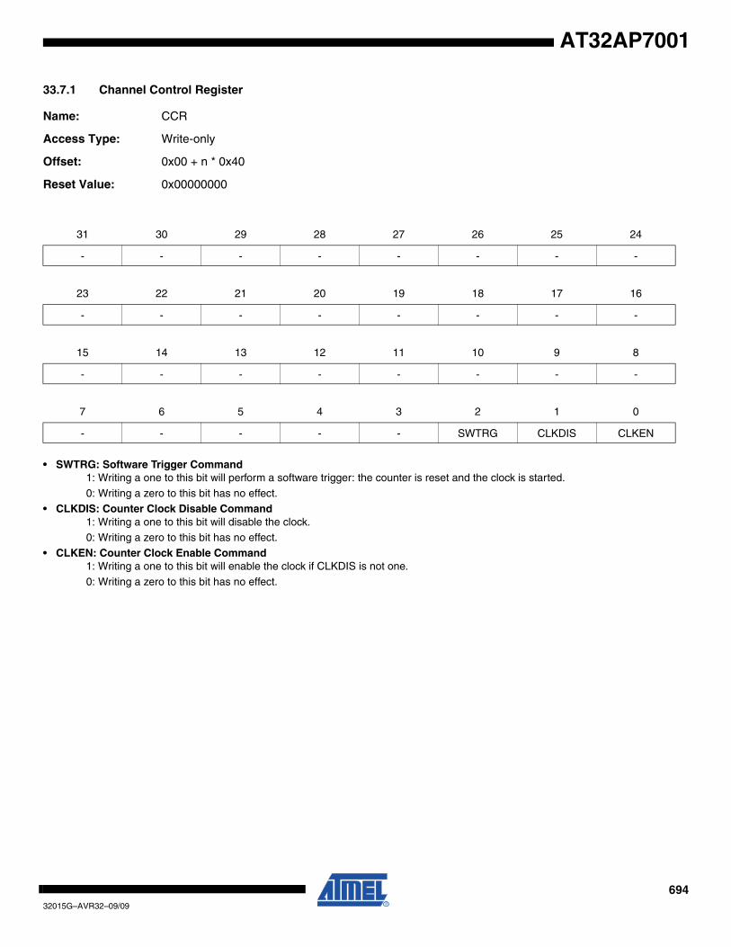
69432015G–AVR32–09/09
AT32AP7001
33.7.1 Channel Control Register
Name: CCR
Access Type: Write-only
Offset: 0x00 + n * 0x40
Reset Value: 0x00000000
• SWTRG: Software Trigger Command1: Writing a one to this bit will perform a software trigger: the counter is reset and the clock is started.
0: Writing a zero to this bit has no effect.• CLKDIS: Counter Clock Disable Command
1: Writing a one to this bit will disable the clock.0: Writing a zero to this bit has no effect.
• CLKEN: Counter Clock Enable Command1: Writing a one to this bit will enable the clock if CLKDIS is not one.
0: Writing a zero to this bit has no effect.
31 30 29 28 27 26 25 24
- - - - - - - -
23 22 21 20 19 18 17 16
- - - - - - - -
15 14 13 12 11 10 9 8
- - - - - - - -
7 6 5 4 3 2 1 0
- - - - - SWTRG CLKDIS CLKEN
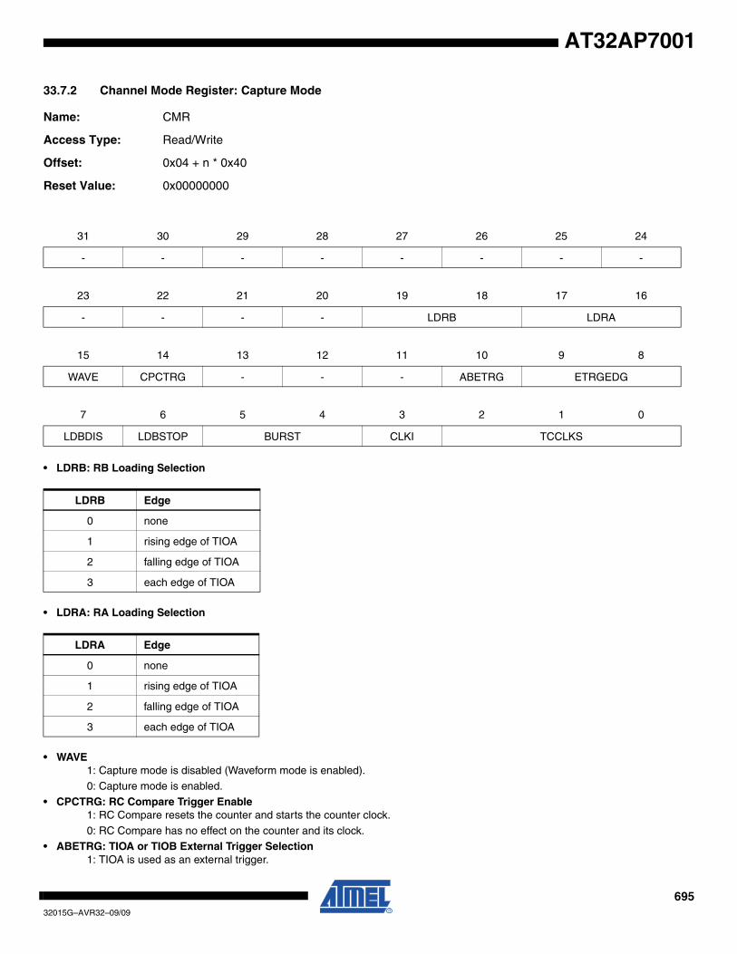
69532015G–AVR32–09/09
AT32AP7001
33.7.2 Channel Mode Register: Capture Mode
Name: CMR
Access Type: Read/Write
Offset: 0x04 + n * 0x40
Reset Value: 0x00000000
• LDRB: RB Loading Selection
• LDRA: RA Loading Selection
• WAVE1: Capture mode is disabled (Waveform mode is enabled).
0: Capture mode is enabled.
• CPCTRG: RC Compare Trigger Enable1: RC Compare resets the counter and starts the counter clock.
0: RC Compare has no effect on the counter and its clock.• ABETRG: TIOA or TIOB External Trigger Selection
1: TIOA is used as an external trigger.
31 30 29 28 27 26 25 24
- - - - - - - -
23 22 21 20 19 18 17 16
- - - - LDRB LDRA
15 14 13 12 11 10 9 8
WAVE CPCTRG - - - ABETRG ETRGEDG
7 6 5 4 3 2 1 0
LDBDIS LDBSTOP BURST CLKI TCCLKS
LDRB Edge
0 none
1 rising edge of TIOA
2 falling edge of TIOA
3 each edge of TIOA
LDRA Edge
0 none
1 rising edge of TIOA
2 falling edge of TIOA
3 each edge of TIOA
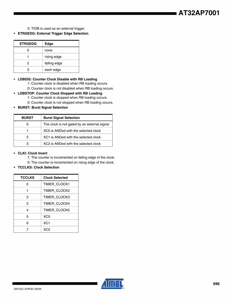
69632015G–AVR32–09/09
AT32AP7001
0: TIOB is used as an external trigger.• ETRGEDG: External Trigger Edge Selection
• LDBDIS: Counter Clock Disable with RB Loading1: Counter clock is disabled when RB loading occurs.
0: Counter clock is not disabled when RB loading occurs.• LDBSTOP: Counter Clock Stopped with RB Loading
1: Counter clock is stopped when RB loading occurs.0: Counter clock is not stopped when RB loading occurs.
• BURST: Burst Signal Selection
• CLKI: Clock Invert1: The counter is incremented on falling edge of the clock.
0: The counter is incremented on rising edge of the clock.
• TCCLKS: Clock Selection
ETRGEDG Edge
0 none
1 rising edge
2 falling edge
3 each edge
BURST Burst Signal Selection
0 The clock is not gated by an external signal
1 XC0 is ANDed with the selected clock
2 XC1 is ANDed with the selected clock
3 XC2 is ANDed with the selected clock
TCCLKS Clock Selected
0 TIMER_CLOCK1
1 TIMER_CLOCK2
2 TIMER_CLOCK3
3 TIMER_CLOCK4
4 TIMER_CLOCK5
5 XC0
6 XC1
7 XC2

69732015G–AVR32–09/09
AT32AP7001
33.7.3 Channel Mode Register: Waveform Mode
Name: CMR
Access Type: Read/Write
Offset: 0x04 + n * 0x40
Reset Value: 0x00000000
• BSWTRG: Software Trigger Effect on TIOB
• BEEVT: External Event Effect on TIOB
31 30 29 28 27 26 25 24
BSWTRG BEEVT BCPC BCPB
23 22 21 20 19 18 17 16
ASWTRG AEEVT ACPC ACPA
15 14 13 12 11 10 9 8
WAVE WAVSEL ENETRG EEVT EEVTEDG
7 6 5 4 3 2 1 0
CPCDIS CPCSTOP BURST CLKI TCCLKS
BSWTRG Effect
0 none
1 set
2 clear
3 toggle
BEEVT Effect
0 none
1 set
2 clear
3 toggle

69832015G–AVR32–09/09
AT32AP7001
• BCPC: RC Compare Effect on TIOB
• BCPB: RB Compare Effect on TIOB
• ASWTRG: Software Trigger Effect on TIOA
• AEEVT: External Event Effect on TIOA
• ACPC: RC Compare Effect on TIOA
BCPC Effect
0 none
1 set
2 clear
3 toggle
BCPB Effect
0 none
1 set
2 clear
3 toggle
ASWTRG Effect
0 none
1 set
2 clear
3 toggle
AEEVT Effect
0 none
1 set
2 clear
3 toggle
ACPC Effect
0 none
1 set
2 clear
3 toggle

69932015G–AVR32–09/09
AT32AP7001
• ACPA: RA Compare Effect on TIOA
• WAVE1: Waveform mode is enabled.
0: Waveform mode is disabled (Capture mode is enabled).
• WAVSEL: Waveform Selection
• ENETRG: External Event Trigger Enable1: The external event resets the counter and starts the counter clock.
0: The external event has no effect on the counter and its clock. In this case, the selected external event only controls the TIOA output.
• EEVT: External Event Selection
Note: 1. If TIOB is chosen as the external event signal, it is configured as an input and no longer generates waveforms and subse-quently no IRQs.
• EEVTEDG: External Event Edge Selection
• CPCDIS: Counter Clock Disable with RC Compare1: Counter clock is disabled when counter reaches RC.
0: Counter clock is not disabled when counter reaches RC.• CPCSTOP: Counter Clock Stopped with RC Compare
1: Counter clock is stopped when counter reaches RC.
ACPA Effect
0 none
1 set
2 clear
3 toggle
WAVSEL Effect
0 UP mode without automatic trigger on RC Compare
1 UPDOWN mode without automatic trigger on RC Compare
2 UP mode with automatic trigger on RC Compare
3 UPDOWN mode with automatic trigger on RC Compare
EEVT Signal selected as external event TIOB Direction
0 TIOB input(1)
1 XC0 output
2 XC1 output
3 XC2 output
EEVTEDG Edge
0 none
1 rising edge
2 falling edge
3 each edge
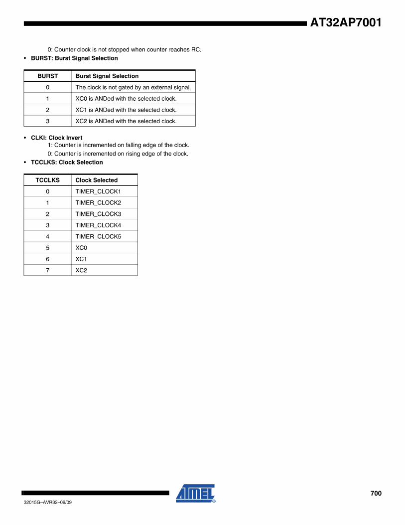
70032015G–AVR32–09/09
AT32AP7001
0: Counter clock is not stopped when counter reaches RC.• BURST: Burst Signal Selection
• CLKI: Clock Invert 1: Counter is incremented on falling edge of the clock.
0: Counter is incremented on rising edge of the clock.• TCCLKS: Clock Selection
BURST Burst Signal Selection
0 The clock is not gated by an external signal.
1 XC0 is ANDed with the selected clock.
2 XC1 is ANDed with the selected clock.
3 XC2 is ANDed with the selected clock.
TCCLKS Clock Selected
0 TIMER_CLOCK1
1 TIMER_CLOCK2
2 TIMER_CLOCK3
3 TIMER_CLOCK4
4 TIMER_CLOCK5
5 XC0
6 XC1
7 XC2
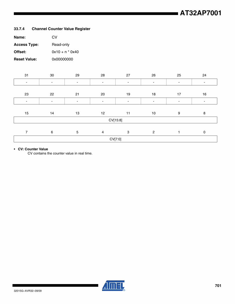
70132015G–AVR32–09/09
AT32AP7001
33.7.4 Channel Counter Value Register
Name: CV
Access Type: Read-only
Offset: 0x10 + n * 0x40
Reset Value: 0x00000000
• CV: Counter ValueCV contains the counter value in real time.
31 30 29 28 27 26 25 24
- - - - - - - -
23 22 21 20 19 18 17 16
- - - - - - - -
15 14 13 12 11 10 9 8
CV[15:8]
7 6 5 4 3 2 1 0
CV[7:0]

70232015G–AVR32–09/09
AT32AP7001
33.7.5 Channel Register A
Name: RA
Access Type: Read-only if CMRn.WAVE = 0, Read/Write if CMRn.WAVE = 1
Offset: 0x14 + n * 0X40
Reset Value: 0x00000000
• RA: Register ARA contains the Register A value in real time.
31 30 29 28 27 26 25 24
- - - - - - - -
23 22 21 20 19 18 17 16
- - - - - - - -
15 14 13 12 11 10 9 8
RA[15:8]
7 6 5 4 3 2 1 0
RA[7:0]
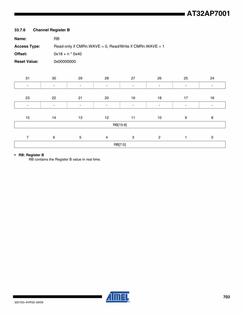
70332015G–AVR32–09/09
AT32AP7001
33.7.6 Channel Register B
Name: RB
Access Type: Read-only if CMRn.WAVE = 0, Read/Write if CMRn.WAVE = 1
Offset: 0x18 + n * 0x40
Reset Value: 0x00000000
• RB: Register BRB contains the Register B value in real time.
31 30 29 28 27 26 25 24
- - - - - - - -
23 22 21 20 19 18 17 16
- - - - - - - -
15 14 13 12 11 10 9 8
RB[15:8]
7 6 5 4 3 2 1 0
RB[7:0]
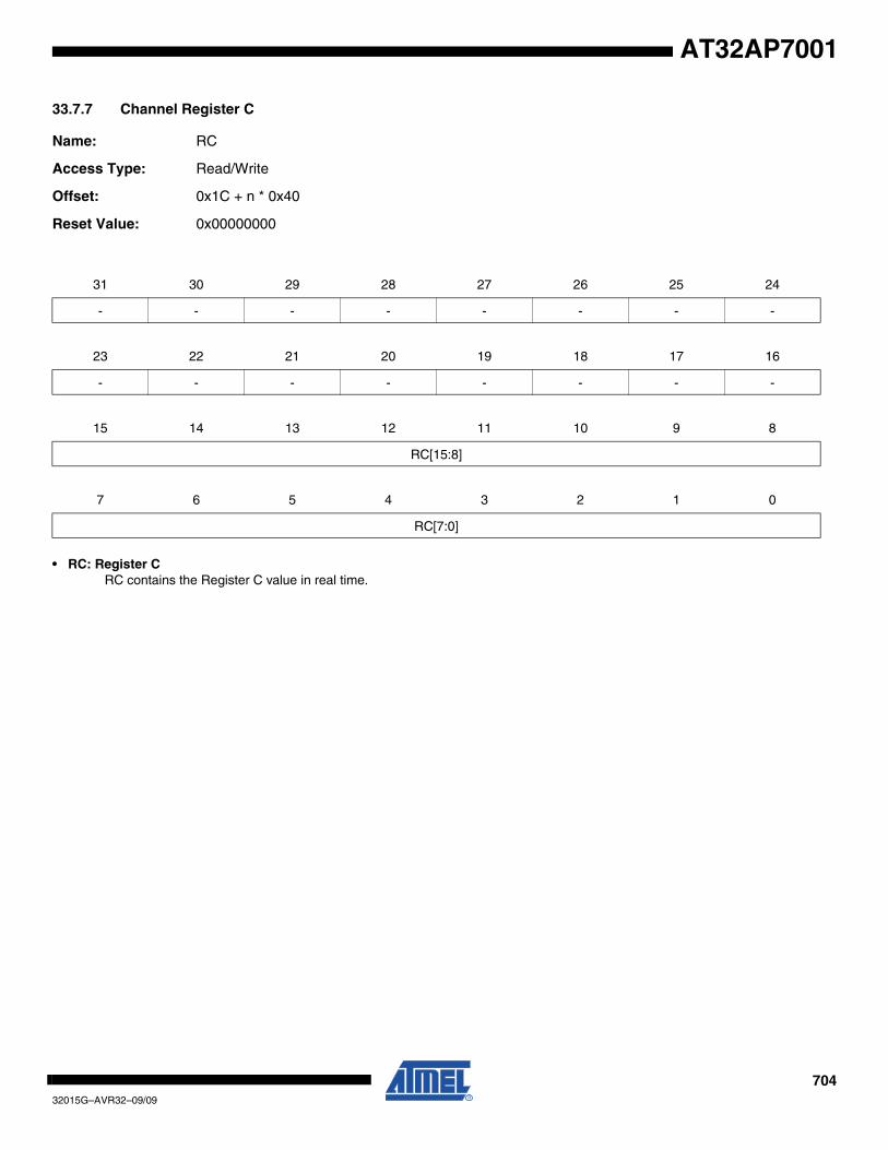
70432015G–AVR32–09/09
AT32AP7001
33.7.7 Channel Register C
Name: RC
Access Type: Read/Write
Offset: 0x1C + n * 0x40
Reset Value: 0x00000000
• RC: Register CRC contains the Register C value in real time.
31 30 29 28 27 26 25 24
- - - - - - - -
23 22 21 20 19 18 17 16
- - - - - - - -
15 14 13 12 11 10 9 8
RC[15:8]
7 6 5 4 3 2 1 0
RC[7:0]
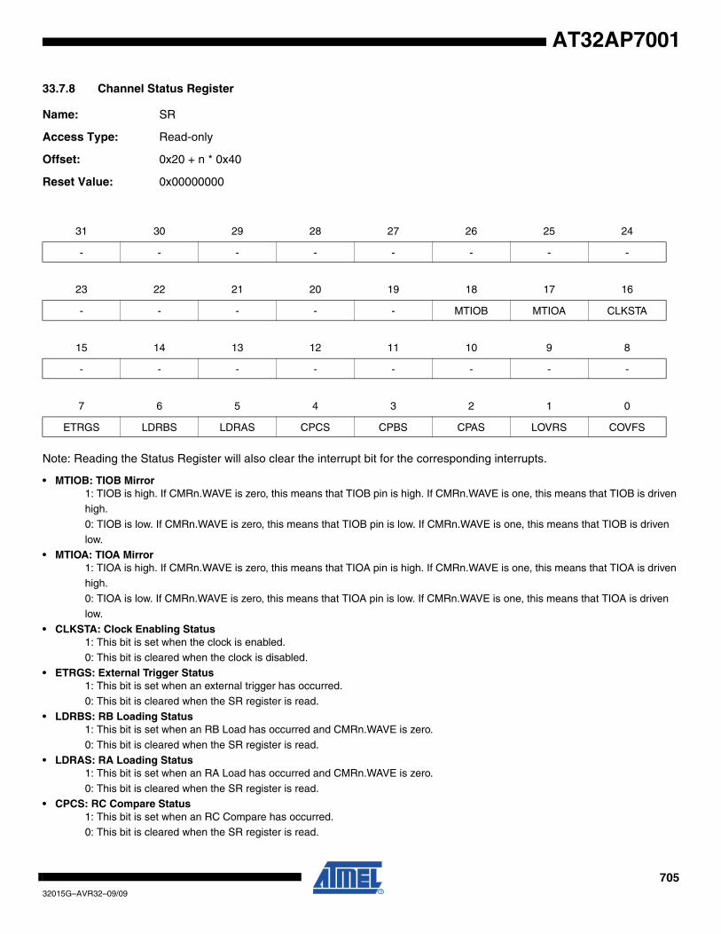
70532015G–AVR32–09/09
AT32AP7001
33.7.8 Channel Status Register
Name: SR
Access Type: Read-only
Offset: 0x20 + n * 0x40
Reset Value: 0x00000000
Note: Reading the Status Register will also clear the interrupt bit for the corresponding interrupts.
• MTIOB: TIOB Mirror1: TIOB is high. If CMRn.WAVE is zero, this means that TIOB pin is high. If CMRn.WAVE is one, this means that TIOB is driven high.
0: TIOB is low. If CMRn.WAVE is zero, this means that TIOB pin is low. If CMRn.WAVE is one, this means that TIOB is driven
low.• MTIOA: TIOA Mirror
1: TIOA is high. If CMRn.WAVE is zero, this means that TIOA pin is high. If CMRn.WAVE is one, this means that TIOA is driven high.
0: TIOA is low. If CMRn.WAVE is zero, this means that TIOA pin is low. If CMRn.WAVE is one, this means that TIOA is driven
low.• CLKSTA: Clock Enabling Status
1: This bit is set when the clock is enabled.0: This bit is cleared when the clock is disabled.
• ETRGS: External Trigger Status1: This bit is set when an external trigger has occurred.
0: This bit is cleared when the SR register is read.
• LDRBS: RB Loading Status1: This bit is set when an RB Load has occurred and CMRn.WAVE is zero.
0: This bit is cleared when the SR register is read.
• LDRAS: RA Loading Status1: This bit is set when an RA Load has occurred and CMRn.WAVE is zero.
0: This bit is cleared when the SR register is read.• CPCS: RC Compare Status
1: This bit is set when an RC Compare has occurred.0: This bit is cleared when the SR register is read.
31 30 29 28 27 26 25 24
- - - - - - - -
23 22 21 20 19 18 17 16
- - - - - MTIOB MTIOA CLKSTA
15 14 13 12 11 10 9 8
- - - - - - - -
7 6 5 4 3 2 1 0
ETRGS LDRBS LDRAS CPCS CPBS CPAS LOVRS COVFS
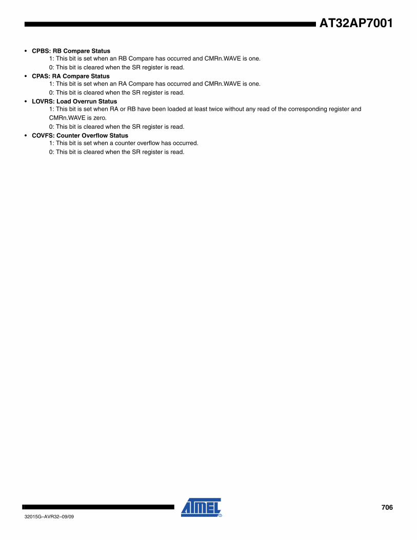
70632015G–AVR32–09/09
AT32AP7001
• CPBS: RB Compare Status1: This bit is set when an RB Compare has occurred and CMRn.WAVE is one.
0: This bit is cleared when the SR register is read.• CPAS: RA Compare Status
1: This bit is set when an RA Compare has occurred and CMRn.WAVE is one.0: This bit is cleared when the SR register is read.
• LOVRS: Load Overrun Status1: This bit is set when RA or RB have been loaded at least twice without any read of the corresponding register and CMRn.WAVE is zero.
0: This bit is cleared when the SR register is read.
• COVFS: Counter Overflow Status1: This bit is set when a counter overflow has occurred.
0: This bit is cleared when the SR register is read.
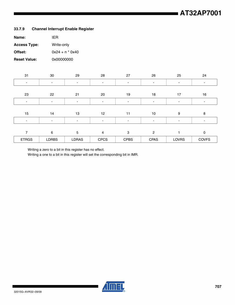
70732015G–AVR32–09/09
AT32AP7001
33.7.9 Channel Interrupt Enable Register
Name: IER
Access Type: Write-only
Offset: 0x24 + n * 0x40
Reset Value: 0x00000000
Writing a zero to a bit in this register has no effect.Writing a one to a bit in this register will set the corresponding bit in IMR.
31 30 29 28 27 26 25 24
- - - - - - - -
23 22 21 20 19 18 17 16
- - - - - - - -
15 14 13 12 11 10 9 8
- - - - - - - -
7 6 5 4 3 2 1 0
ETRGS LDRBS LDRAS CPCS CPBS CPAS LOVRS COVFS

70832015G–AVR32–09/09
AT32AP7001
33.7.10 Channel Interrupt Disable Register
Name: IDR
Access Type: Write-only
Offset: 0x28 + n * 0x40
Reset Value: 0x00000000
Writing a zero to a bit in this register has no effect.Writing a one to a bit in this register will clear the corresponding bit in IMR.
31 30 29 28 27 26 25 24
- - - - - - - -
23 22 21 20 19 18 17 16
- - - - - - - -
15 14 13 12 11 10 9 8
- - - - - - - -
7 6 5 4 3 2 1 0
ETRGS LDRBS LDRAS CPCS CPBS CPAS LOVRS COVFS
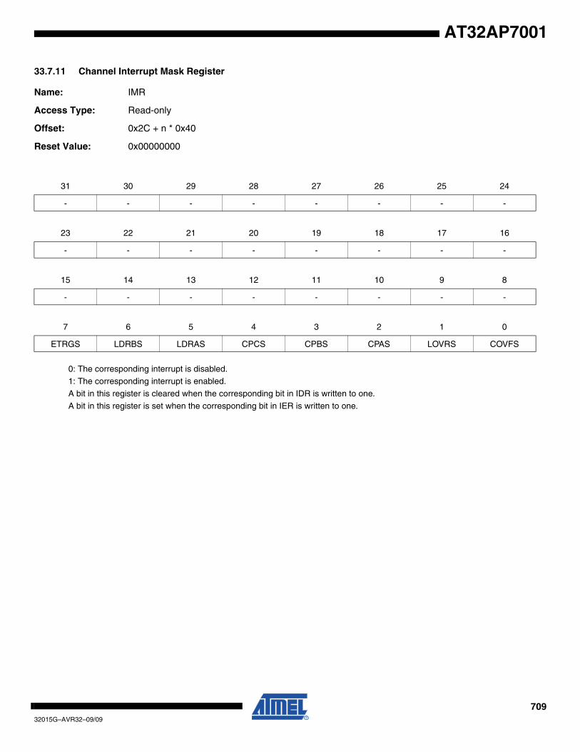
70932015G–AVR32–09/09
AT32AP7001
33.7.11 Channel Interrupt Mask Register
Name: IMR
Access Type: Read-only
Offset: 0x2C + n * 0x40
Reset Value: 0x00000000
0: The corresponding interrupt is disabled.1: The corresponding interrupt is enabled.
A bit in this register is cleared when the corresponding bit in IDR is written to one.
A bit in this register is set when the corresponding bit in IER is written to one.
31 30 29 28 27 26 25 24
- - - - - - - -
23 22 21 20 19 18 17 16
- - - - - - - -
15 14 13 12 11 10 9 8
- - - - - - - -
7 6 5 4 3 2 1 0
ETRGS LDRBS LDRAS CPCS CPBS CPAS LOVRS COVFS
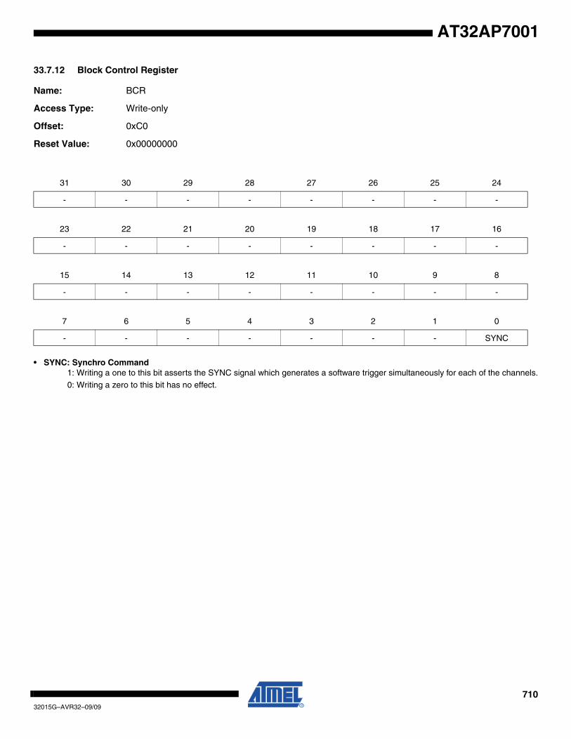
71032015G–AVR32–09/09
AT32AP7001
33.7.12 Block Control Register
Name: BCR
Access Type: Write-only
Offset: 0xC0
Reset Value: 0x00000000
• SYNC: Synchro Command1: Writing a one to this bit asserts the SYNC signal which generates a software trigger simultaneously for each of the channels.
0: Writing a zero to this bit has no effect.
31 30 29 28 27 26 25 24
- - - - - - - -
23 22 21 20 19 18 17 16
- - - - - - - -
15 14 13 12 11 10 9 8
- - - - - - - -
7 6 5 4 3 2 1 0
- - - - - - - SYNC
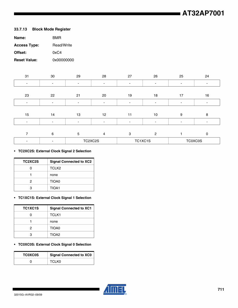
71132015G–AVR32–09/09
AT32AP7001
33.7.13 Block Mode Register
Name: BMR
Access Type: Read/Write
Offset: 0xC4
Reset Value: 0x00000000
• TC2XC2S: External Clock Signal 2 Selection
• TC1XC1S: External Clock Signal 1 Selection
• TC0XC0S: External Clock Signal 0 Selection
31 30 29 28 27 26 25 24
- - - - - - - -
23 22 21 20 19 18 17 16
- - - - - - - -
15 14 13 12 11 10 9 8
- - - - - - - -
7 6 5 4 3 2 1 0
- - TC2XC2S TC1XC1S TC0XC0S
TC2XC2S Signal Connected to XC2
0 TCLK2
1 none
2 TIOA0
3 TIOA1
TC1XC1S Signal Connected to XC1
0 TCLK1
1 none
2 TIOA0
3 TIOA2
TC0XC0S Signal Connected to XC0
0 TCLK0

71232015G–AVR32–09/09
AT32AP7001
1 none
2 TIOA1
3 TIOA2
71332015G–AVR32–09/09
AT32AP7001
34. Pulse Width Modulation Controller (PWM)
Rev: 1.2.0.2
34.1 Features
• 4 Channels• One 20-bit Counter Per Channel• Common Clock Generator Providing Thirteen Different Clocks
– A Modulo n Counter Providing Eleven Clocks– Two Independent Linear Dividers Working on Modulo n Counter Outputs
• Independent Channels– Independent Enable Disable Command for Each Channel– Independent Clock Selection for Each Channel– Independent Period and Duty Cycle for Each Channel– Double Buffering of Period or Duty Cycle for Each Channel– Programmable Selection of The Output Waveform Polarity for Each Channel– Programmable Center or Left Aligned Output Waveform for Each Channel
34.2 Description
The PWM macrocell controls several channels independently. Each channel controls onesquare output waveform. Characteristics of the output waveform such as period, duty-cycle andpolarity are configurable through the user interface. Each channel selects and uses one of theclocks provided by the clock generator. The clock generator provides several clocks resultingfrom the division of the PWM macrocell master clock.
All PWM macrocell accesses are made through registers mapped on the peripheral bus.
Channels can be synchronized, to generate non overlapped waveforms. All channels integrate adouble buffering system in order to prevent an unexpected output waveform while modifying theperiod or the duty-cycle.
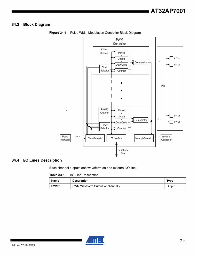
71432015G–AVR32–09/09
AT32AP7001
34.3 Block Diagram
Figure 34-1. Pulse Width Modulation Controller Block Diagram
34.4 I/O Lines Description
Each channel outputs one waveform on one external I/O line.
PWMController
PeripheralBus
PWMx
PWMx
PWMx
Channel
Update
Duty Cycle
Counter
PWM0Channel
PIO
Interrupt Controller
PowerManager
MCKClock Generator PB Interface Interrupt Generator
ClockSelector
Period
Comparator
Update
Duty Cycle
CounterClock
Selector
Period
Comparator
PWM0
PWM0
Table 34-1. I/O Line Description
Name Description Type
PWMx PWM Waveform Output for channel x Output
71532015G–AVR32–09/09
AT32AP7001
34.5 Product Dependencies
34.5.1 I/O Lines
The pins used for interfacing the PWM may be multiplexed with PIO lines. The programmer mustfirst program the PIO controller to assign the desired PWM pins to their peripheral function. If I/Olines of the PWM are not used by the application, they can be used for other purposes by thePIO controller.
Not all PWM outputs may be enabled. If an application requires only four channels, then onlyfour PIO lines will be assigned to PWM outputs.
34.5.2 Debug operation
The PWM clock is running during debug operation.
34.5.3 Power Management
The PWM clock is generated by the Power Manager. Before using the PWM, the programmermust ensure that the PWM clock is enabled in the Power Manager. However, if the applicationdoes not require PWM operations, the PWM clock can be stopped when not needed and berestarted later. In this case, the PWM will resume its operations where it left off.
In the PWM description, Master Clock (MCK) is the clock of the peripheral bus to which thePWM is connected.
34.5.4 Interrupt Sources
The PWM interrupt line is connected to the interrupt controller. Using the PWM interrupt requiresthe interrupt controller to be programmed first.

71632015G–AVR32–09/09
AT32AP7001
34.6 Functional Description
The PWM macrocell is primarily composed of a clock generator module and 4 channels.
– Clocked by the system clock, MCK, the clock generator module provides 13 clocks.
– Each channel can independently choose one of the clock generator outputs.
– Each channel generates an output waveform with attributes that can be defined independently for each channel through the user interface registers.
34.6.1 PWM Clock Generator
Figure 34-2. Functional View of the Clock Generator Block Diagram
Caution: Before using the PWM macrocell, the programmer must ensure that the PWM clock inthe Power Manager is enabled.
The PWM macrocell master clock, MCK, is divided in the clock generator module to provide dif-ferent clocks available for all channels. Each channel can independently select one of thedivided clocks.
modulo n counterMCK
MCK/2MCK/4
MCK/16MCK/32MCK/64
MCK/8
Divider A clkA
DIVA
PWM_MR
MCK
MCK/128MCK/256MCK/512MCK/1024
PREA
Divider B clkB
DIVB
PWM_MR
PREB
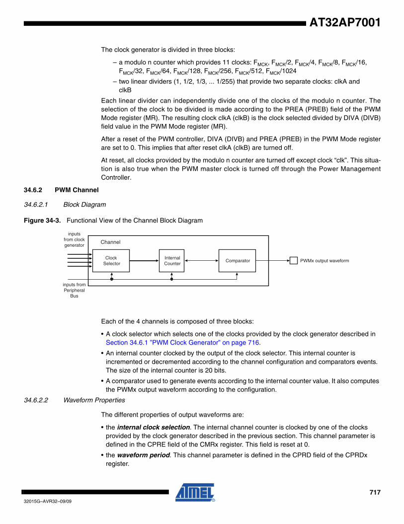
71732015G–AVR32–09/09
AT32AP7001
The clock generator is divided in three blocks:
– a modulo n counter which provides 11 clocks: FMCK, FMCK/2, FMCK/4, FMCK/8, FMCK/16, FMCK/32, FMCK/64, FMCK/128, FMCK/256, FMCK/512, FMCK/1024
– two linear dividers (1, 1/2, 1/3, ... 1/255) that provide two separate clocks: clkA and clkB
Each linear divider can independently divide one of the clocks of the modulo n counter. Theselection of the clock to be divided is made according to the PREA (PREB) field of the PWMMode register (MR). The resulting clock clkA (clkB) is the clock selected divided by DIVA (DIVB)field value in the PWM Mode register (MR).
After a reset of the PWM controller, DIVA (DIVB) and PREA (PREB) in the PWM Mode registerare set to 0. This implies that after reset clkA (clkB) are turned off.
At reset, all clocks provided by the modulo n counter are turned off except clock “clk”. This situa-tion is also true when the PWM master clock is turned off through the Power ManagementController.
34.6.2 PWM Channel
34.6.2.1 Block Diagram
Figure 34-3. Functional View of the Channel Block Diagram
Each of the 4 channels is composed of three blocks:
• A clock selector which selects one of the clocks provided by the clock generator described in Section 34.6.1 ”PWM Clock Generator” on page 716.
• An internal counter clocked by the output of the clock selector. This internal counter is incremented or decremented according to the channel configuration and comparators events. The size of the internal counter is 20 bits.
• A comparator used to generate events according to the internal counter value. It also computes the PWMx output waveform according to the configuration.
34.6.2.2 Waveform Properties
The different properties of output waveforms are:
• the internal clock selection. The internal channel counter is clocked by one of the clocks provided by the clock generator described in the previous section. This channel parameter is defined in the CPRE field of the CMRx register. This field is reset at 0.
• the waveform period. This channel parameter is defined in the CPRD field of the CPRDx register.
Comparator PWMx output waveformInternalCounter
Clock Selector
inputs from clock generator
inputs from Peripheral
Bus
Channel
71832015G–AVR32–09/09
AT32AP7001
- If the waveform is left aligned, then the output waveform period depends on the counter source clock and can be calculated:By using the Master Clock (MCK) divided by an X given prescaler value(with X being 1, 2, 4, 8, 16, 32, 64, 128, 256, 512, or 1024), the resulting period formula will be:
By using a Master Clock divided by one of both DIVA or DIVB divider, the formula becomes, respectively:
or
If the waveform is center aligned then the output waveform period depends on the counter source clock and can be calculated:By using the Master Clock (MCK) divided by an X given prescaler value(with X being 1, 2, 4, 8, 16, 32, 64, 128, 256, 512, or 1024). The resulting period formula will be:
By using a Master Clock divided by one of both DIVA or DIVB divider, the formula becomes, respectively:
or
• the waveform duty cycle. This channel parameter is defined in the CDTY field of the CDTYx register. If the waveform is left aligned then:
If the waveform is center aligned, then:
• the waveform polarity. At the beginning of the period, the signal can be at high or low level. This property is defined in the CPOL field of the CMRx register. By default the signal starts by a low level.
• the waveform alignment. The output waveform can be left or center aligned. Center aligned waveforms can be used to generate non overlapped waveforms. This property is defined in the CALG field of the CMRx register. The default mode is left aligned.
X CPRD×( )MCK
-------------------------------
CRPD DIVA×( )MCK
------------------------------------------ CRPD DIVAB×( )MCK
----------------------------------------------
2 X CPRD××( )MCK
-----------------------------------------
2 CPRD DIVA××( )MCK
---------------------------------------------------- 2 CPRD× DIVB×( )MCK
----------------------------------------------------
duty cycle period 1 fchannel_x_clock CDTY×⁄–( )period
--------------------------------------------------------------------------------------------------------=
duty cycle period 2⁄( ) 1 fchannel_x_clock CDTY×⁄–( ) )period 2⁄( )
-----------------------------------------------------------------------------------------------------------------------=
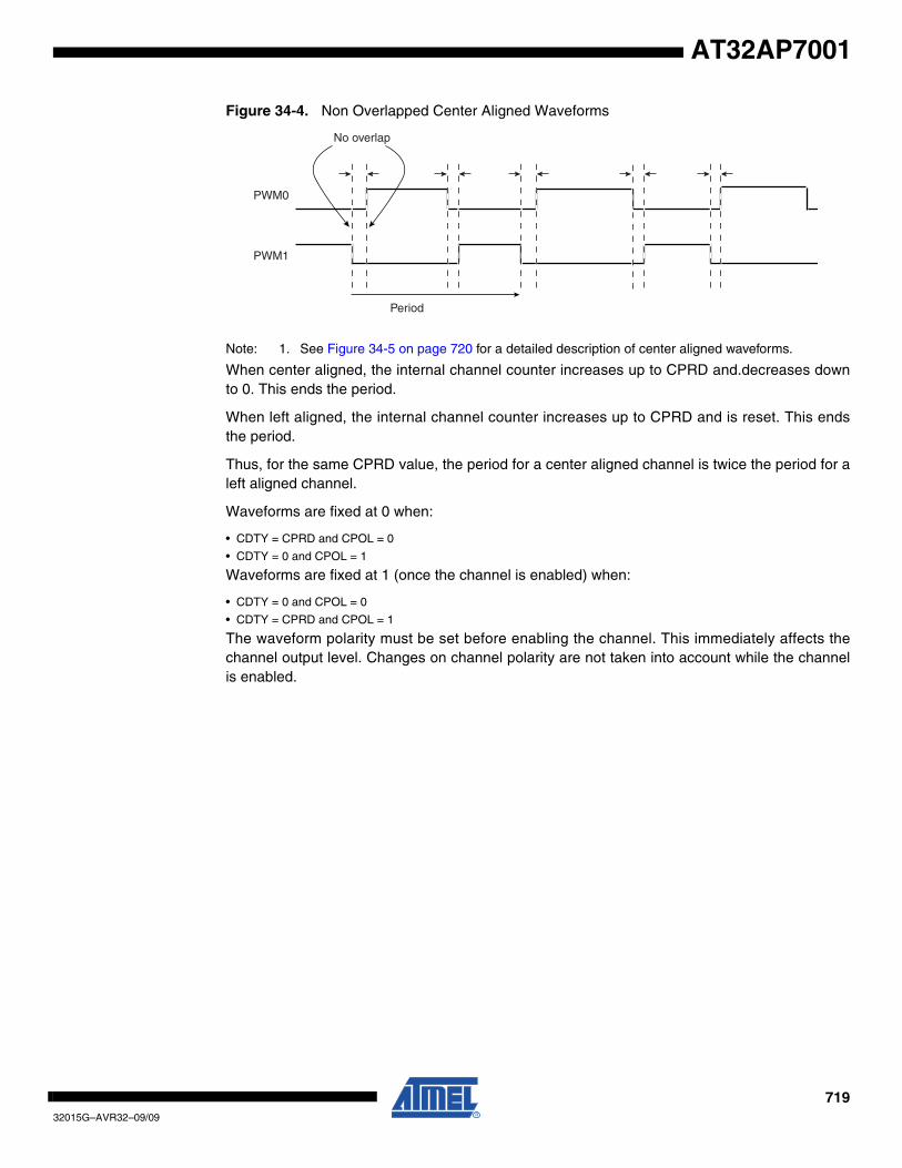
71932015G–AVR32–09/09
AT32AP7001
Figure 34-4. Non Overlapped Center Aligned Waveforms
Note: 1. See Figure 34-5 on page 720 for a detailed description of center aligned waveforms.
When center aligned, the internal channel counter increases up to CPRD and.decreases downto 0. This ends the period.
When left aligned, the internal channel counter increases up to CPRD and is reset. This endsthe period.
Thus, for the same CPRD value, the period for a center aligned channel is twice the period for aleft aligned channel.
Waveforms are fixed at 0 when:
• CDTY = CPRD and CPOL = 0
• CDTY = 0 and CPOL = 1
Waveforms are fixed at 1 (once the channel is enabled) when:
• CDTY = 0 and CPOL = 0
• CDTY = CPRD and CPOL = 1
The waveform polarity must be set before enabling the channel. This immediately affects thechannel output level. Changes on channel polarity are not taken into account while the channelis enabled.
PWM0
PWM1
Period
No overlap
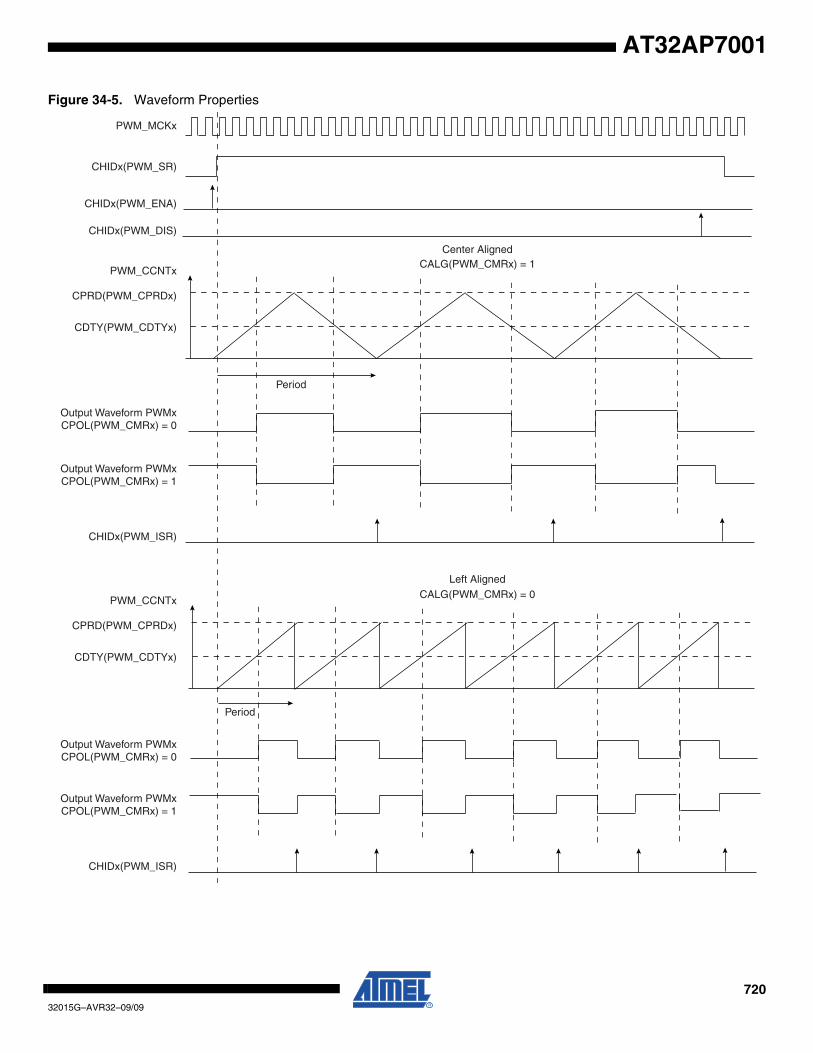
72032015G–AVR32–09/09
AT32AP7001
Figure 34-5. Waveform Properties
PWM_MCKx
CHIDx(PWM_SR)
Center Aligned
CPRD(PWM_CPRDx)
CDTY(PWM_CDTYx)
PWM_CCNTx
Output Waveform PWMxCPOL(PWM_CMRx) = 0
Output Waveform PWMxCPOL(PWM_CMRx) = 1
CHIDx(PWM_ISR)
Left Aligned
CPRD(PWM_CPRDx)
CDTY(PWM_CDTYx)
PWM_CCNTx
Output Waveform PWMxCPOL(PWM_CMRx) = 0
Output Waveform PWMxCPOL(PWM_CMRx) = 1
CHIDx(PWM_ISR)
CALG(PWM_CMRx) = 0
CALG(PWM_CMRx) = 1
Period
Period
CHIDx(PWM_ENA)
CHIDx(PWM_DIS)
72132015G–AVR32–09/09
AT32AP7001
34.6.3 PWM Controller Operations
34.6.3.1 Initialization
Before enabling the output channel, this channel must have been configured by the softwareapplication:
• Configuration of the clock generator if DIVA and DIVB are required
• Selection of the clock for each channel (CPRE field in the CMRx register)
• Configuration of the waveform alignment for each channel (CALG field in the CMRx register)
• Configuration of the period for each channel (CPRD in the CPRDx register). Writing in CPRDx Register is possible while the channel is disabled. After validation of the channel, the user must use CUPDx Register to update CPRDx as explained below.
• Configuration of the duty cycle for each channel (CDTY in the CDTYx register). Writing in CDTYx Register is possible while the channel is disabled. After validation of the channel, the user must use CUPDx Register to update CDTYx as explained below.
• Configuration of the output waveform polarity for each channel (CPOL in the CMRx register)
• Enable Interrupts (Writing CHIDx in the IER register)
• Enable the PWM channel (Writing CHIDx in the ENA register)
It is possible to synchronize different channels by enabling them at the same time by means ofwriting simultaneously several CHIDx bits in the ENA register.
In such a situation, all channels may have the same clock selector configuration and the sameperiod specified.
34.6.3.2 Source Clock Selection Criteria
The large number of source clocks can make selection difficult. The relationship between thevalue in the Period Register (CPRDx) and the Duty Cycle Register (CDTYx) can help the user inchoosing. The event number written in the Period Register gives the PWM accuracy. The DutyCycle quantum cannot be lower than 1/CPRDx value. The higher the value of CPRDx, thegreater the PWM accuracy.
For example, if the user sets 15 (in decimal) in CPRDx, the user is able to set a value between 1up to 14 in CDTYx Register. The resulting duty cycle quantum cannot be lower than 1/15 of thePWM period.
34.6.3.3 Changing the Duty Cycle or the Period
It is possible to modulate the output waveform duty cycle or period.
To prevent unexpected output waveform, the user must use the update register (PWM_CUPDx)to change waveform parameters while the channel is still enabled. The user can write a newperiod value or duty cycle value in the update register (CUPDx). This register holds the newvalue until the end of the current cycle and updates the value for the next cycle. Depending onthe CPD field in the CMRx register, CUPDx either updates CPRDx or CDTYx. Note that even ifthe update register is used, the period must not be smaller than the duty cycle.

72232015G–AVR32–09/09
AT32AP7001
Figure 34-6. Synchronized Period or Duty Cycle Update
To prevent overwriting the CUPDx by software, the user can use status events in order to syn-chronize his software. Two methods are possible. In both, the user must enable the dedicatedinterrupt in IER at PWM Controller level.
The first method (polling method) consists of reading the relevant status bit in ISR Registeraccording to the enabled channel(s). See Figure 34-7.
The second method uses an Interrupt Service Routine associated with the PWM channel.
Note: Reading the ISR register automatically clears CHIDx flags.
Figure 34-7. Polling Method
Note: Polarity and alignment can be modified only when the channel is disabled.
PWM_CUPDx Value
PWM_CPRDx PWM_CDTYx
End of Cycle
PWM_CMRx. CPD
User's Writing
1 0
Writing in PWM_CUPDxThe last write has been taken into account
CHIDx = 1
Writing in CPD fieldUpdate of the Period or Duty Cycle
PWM_ISR ReadAcknowledgement and clear previous register state
YES

72332015G–AVR32–09/09
AT32AP7001
34.6.3.4 Interrupts
Depending on the interrupt mask in the IMR register, an interrupt is generated at the end of thecorresponding channel period. The interrupt remains active until a read operation in the ISR reg-ister occurs.
A channel interrupt is enabled by setting the corresponding bit in the IER register. A channelinterrupt is disabled by setting the corresponding bit in the IDR register.

72432015G–AVR32–09/09
AT32AP7001
34.7 Pulse Width Modulation (PWM) Controller User Interface
34.7.1 Register Mapping
Table 34-2. PWM Controller Registers
Offset Register Name AccessPeripheral
Reset Value
0x00 PWM Mode Register MR Read/Write 0
0x04 PWM Enable Register ENA Write-only -
0x08 PWM Disable Register DIS Write-only -
0x0C PWM Status Register SR Read-only 0
0x10 PWM Interrupt Enable Register IER Write-only -
0x14 PWM Interrupt Disable Register IDR Write-only -
0x18 PWM Interrupt Mask Register IMR Read-only 0
0x1C PWM Interrupt Status Register ISR Read-only 0
0x4C - 0xF8 Reserved – – –
0x4C - 0xFC Reserved – – –
0x100 - 0x1FC Reserved
0x200 Channel 0 Mode Register CMR0 Read/Write 0x0
0x204 Channel 0 Duty Cycle Register CDTY0 Read/Write 0x0
0x208 Channel 0 Period Register CPRD0 Read/Write 0x0
0x20C Channel 0 Counter Register CCNT0 Read-only 0x0
0x210 Channel 0 Update Register CUPD0 Write-only -
... Reserved
0x220 Channel 1 Mode Register CMR1 Read/Write 0x0
0x224 Channel 1 Duty Cycle Register CDTY1 Read/Write 0x0
0x228 Channel 1 Period Register CPRD1 Read/Write 0x0
0x22C Channel 1 Counter Register CCNT1 Read-only 0x0
0x230 Channel 1 Update Register CUPD1 Write-only -
... ... ... ... ...
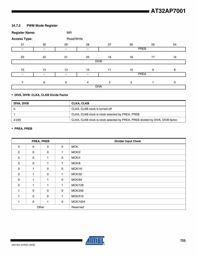
72532015G–AVR32–09/09
AT32AP7001
34.7.2 PWM Mode Register
Register Name: MR
Access Type: Read/Write
• DIVA, DIVB: CLKA, CLKB Divide Factor
• PREA, PREB
31 30 29 28 27 26 25 24
– – – – PREB
23 22 21 20 19 18 17 16
DIVB
15 14 13 12 11 10 9 8
– – – – PREA
7 6 5 4 3 2 1 0
DIVA
DIVA, DIVB CLKA, CLKB
0 CLKA, CLKB clock is turned off
1 CLKA, CLKB clock is clock selected by PREA, PREB
2-255 CLKA, CLKB clock is clock selected by PREA, PREB divided by DIVA, DIVB factor.
PREA, PREB Divider Input Clock
0 0 0 0 MCK.
0 0 0 1 MCK/2
0 0 1 0 MCK/4
0 0 1 1 MCK/8
0 1 0 0 MCK/16
0 1 0 1 MCK/32
0 1 1 0 MCK/64
0 1 1 1 MCK/128
1 0 0 0 MCK/256
1 0 0 1 MCK/512
1 0 1 0 MCK/1024
Other Reserved
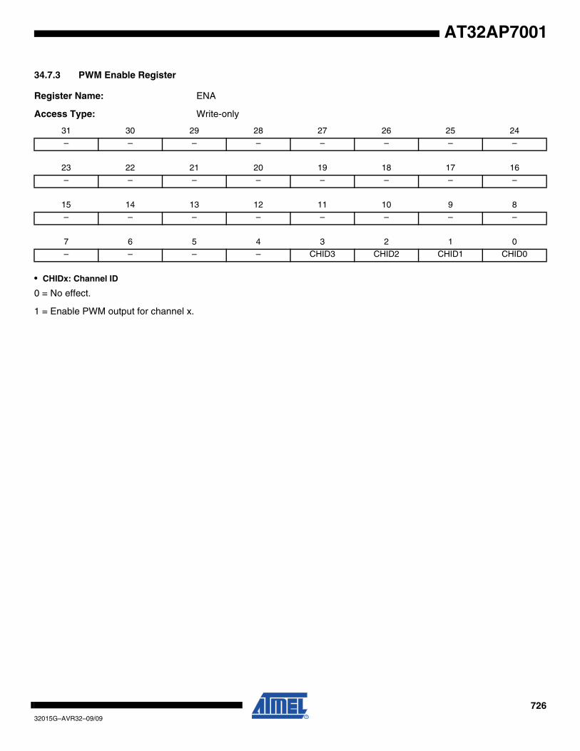
72632015G–AVR32–09/09
AT32AP7001
34.7.3 PWM Enable Register
Register Name: ENA
Access Type: Write-only
• CHIDx: Channel ID
0 = No effect.
1 = Enable PWM output for channel x.
31 30 29 28 27 26 25 24
– – – – – – – –
23 22 21 20 19 18 17 16
– – – – – – – –
15 14 13 12 11 10 9 8
– – – – – – – –
7 6 5 4 3 2 1 0
– – – – CHID3 CHID2 CHID1 CHID0

72732015G–AVR32–09/09
AT32AP7001
34.7.4 PWM Disable Register
Register Name: DIS
Access Type: Write-only
• CHIDx: Channel ID
0 = No effect.
1 = Disable PWM output for channel x.
31 30 29 28 27 26 25 24
– – – – – – – –
23 22 21 20 19 18 17 16
– – – – – – – –
15 14 13 12 11 10 9 8
– – – – – – – –
7 6 5 4 3 2 1 0
– – – – CHID3 CHID2 CHID1 CHID0

72832015G–AVR32–09/09
AT32AP7001
34.7.5 PWM Status Register
Register Name: SR
Access Type: Read-only
• CHIDx: Channel ID
0 = PWM output for channel x is disabled.
1 = PWM output for channel x is enabled.
31 30 29 28 27 26 25 24
– – – – – – – –
23 22 21 20 19 18 17 16
– – – – – – – –
15 14 13 12 11 10 9 8
– – – – – – – –
7 6 5 4 3 2 1 0
– – – – CHID3 CHID2 CHID1 CHID0
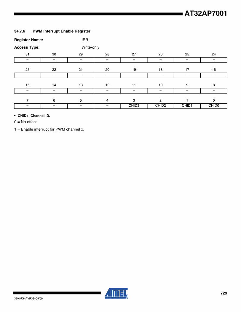
72932015G–AVR32–09/09
AT32AP7001
34.7.6 PWM Interrupt Enable Register
Register Name: IER
Access Type: Write-only
• CHIDx: Channel ID.
0 = No effect.
1 = Enable interrupt for PWM channel x.
31 30 29 28 27 26 25 24
– – – – – – – –
23 22 21 20 19 18 17 16
– – – – – – – –
15 14 13 12 11 10 9 8
– – – – – – – –
7 6 5 4 3 2 1 0
– – – – CHID3 CHID2 CHID1 CHID0

73032015G–AVR32–09/09
AT32AP7001
34.7.7 PWM Interrupt Disable Register
Register Name: IDR
Access Type: Write-only
• CHIDx: Channel ID.
0 = No effect.
1 = Disable interrupt for PWM channel x.
31 30 29 28 27 26 25 24
– – – – – – – –
23 22 21 20 19 18 17 16
– – – – – – – –
15 14 13 12 11 10 9 8
– – – – – – – –
7 6 5 4 3 2 1 0
– – – – CHID3 CHID2 CHID1 CHID0
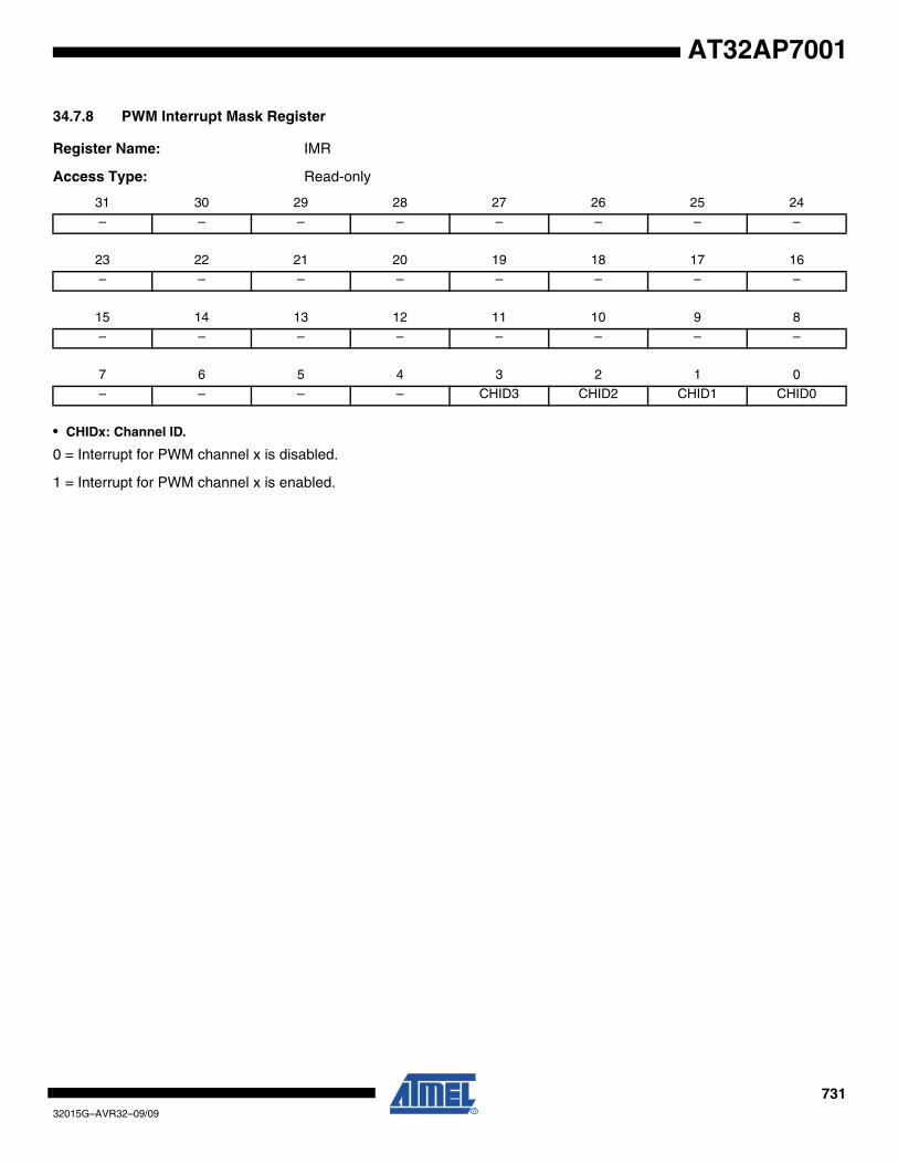
73132015G–AVR32–09/09
AT32AP7001
34.7.8 PWM Interrupt Mask Register
Register Name: IMR
Access Type: Read-only
• CHIDx: Channel ID.
0 = Interrupt for PWM channel x is disabled.
1 = Interrupt for PWM channel x is enabled.
31 30 29 28 27 26 25 24
– – – – – – – –
23 22 21 20 19 18 17 16
– – – – – – – –
15 14 13 12 11 10 9 8
– – – – – – – –
7 6 5 4 3 2 1 0
– – – – CHID3 CHID2 CHID1 CHID0
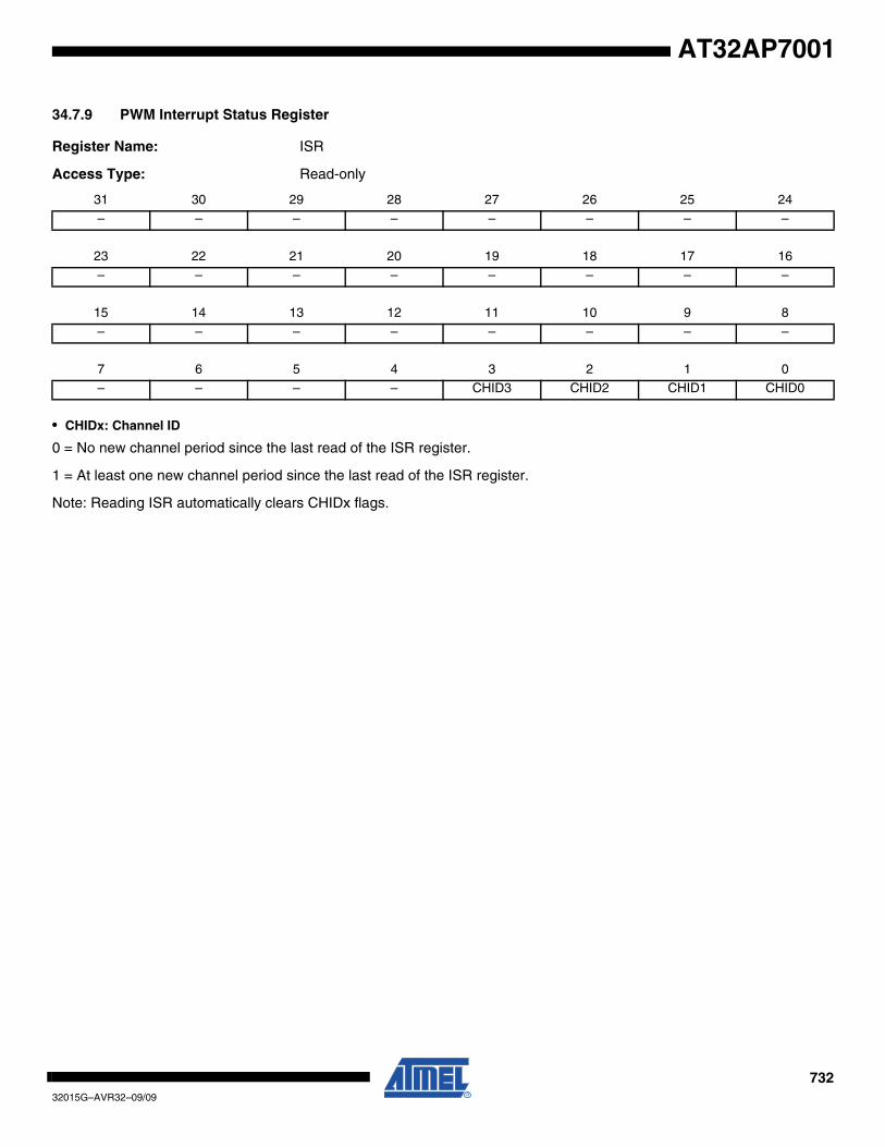
73232015G–AVR32–09/09
AT32AP7001
34.7.9 PWM Interrupt Status Register
Register Name: ISR
Access Type: Read-only
• CHIDx: Channel ID
0 = No new channel period since the last read of the ISR register.
1 = At least one new channel period since the last read of the ISR register.
Note: Reading ISR automatically clears CHIDx flags.
31 30 29 28 27 26 25 24
– – – – – – – –
23 22 21 20 19 18 17 16
– – – – – – – –
15 14 13 12 11 10 9 8
– – – – – – – –
7 6 5 4 3 2 1 0
– – – – CHID3 CHID2 CHID1 CHID0
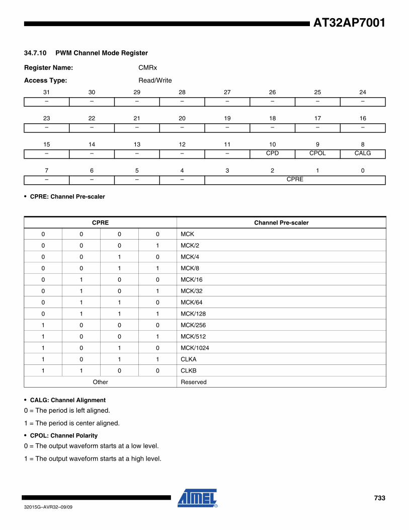
73332015G–AVR32–09/09
AT32AP7001
34.7.10 PWM Channel Mode Register
Register Name: CMRx
Access Type: Read/Write
• CPRE: Channel Pre-scaler
• CALG: Channel Alignment
0 = The period is left aligned.
1 = The period is center aligned.
• CPOL: Channel Polarity
0 = The output waveform starts at a low level.
1 = The output waveform starts at a high level.
31 30 29 28 27 26 25 24
– – – – – – – –
23 22 21 20 19 18 17 16
– – – – – – – –
15 14 13 12 11 10 9 8
– – – – – CPD CPOL CALG
7 6 5 4 3 2 1 0
– – – – CPRE
CPRE Channel Pre-scaler
0 0 0 0 MCK
0 0 0 1 MCK/2
0 0 1 0 MCK/4
0 0 1 1 MCK/8
0 1 0 0 MCK/16
0 1 0 1 MCK/32
0 1 1 0 MCK/64
0 1 1 1 MCK/128
1 0 0 0 MCK/256
1 0 0 1 MCK/512
1 0 1 0 MCK/1024
1 0 1 1 CLKA
1 1 0 0 CLKB
Other Reserved

73432015G–AVR32–09/09
AT32AP7001
• CPD: Channel Update Period
0 = Writing to the CUPDx will modify the duty cycle at the next period start event.
1 = Writing to the CUPDx will modify the period at the next period start event.
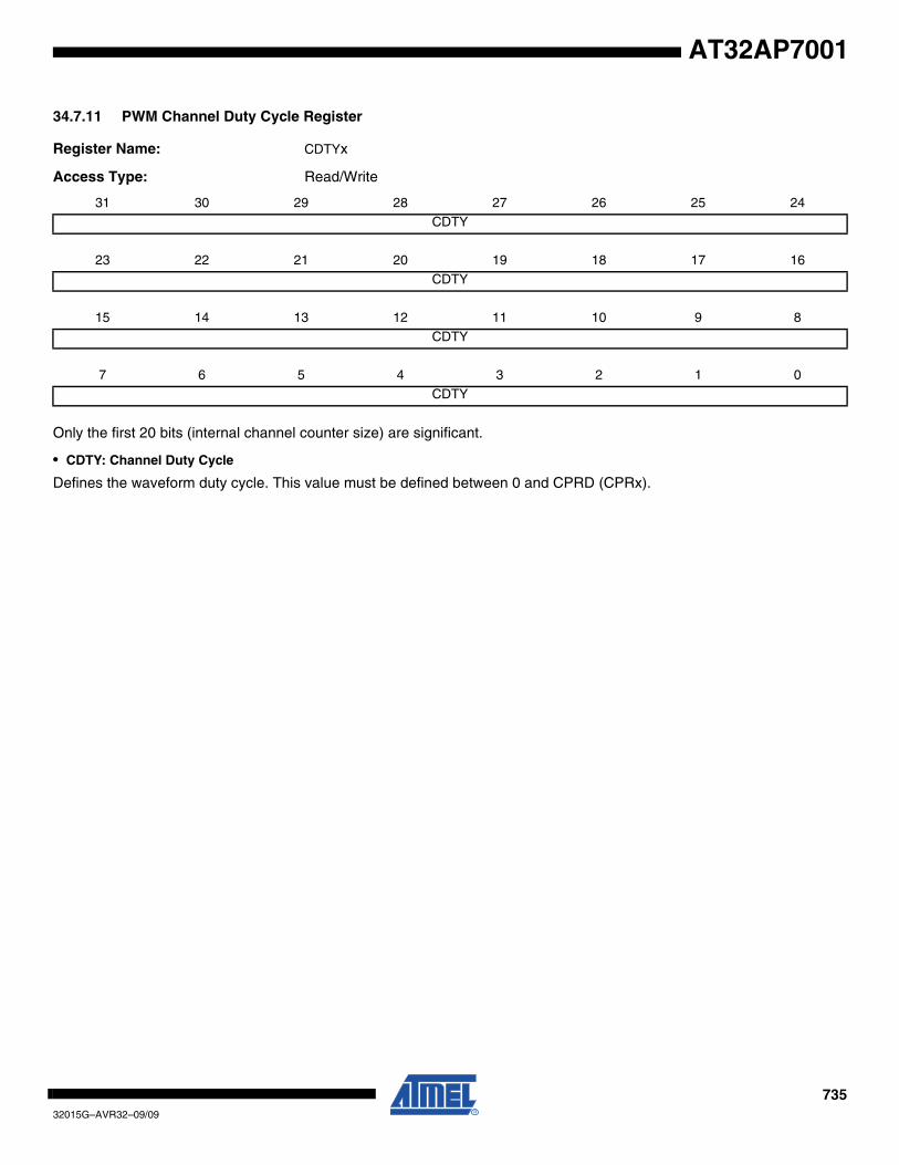
73532015G–AVR32–09/09
AT32AP7001
34.7.11 PWM Channel Duty Cycle Register
Register Name: CDTYx
Access Type: Read/Write
Only the first 20 bits (internal channel counter size) are significant.
• CDTY: Channel Duty Cycle
Defines the waveform duty cycle. This value must be defined between 0 and CPRD (CPRx).
31 30 29 28 27 26 25 24
CDTY
23 22 21 20 19 18 17 16
CDTY
15 14 13 12 11 10 9 8
CDTY
7 6 5 4 3 2 1 0
CDTY
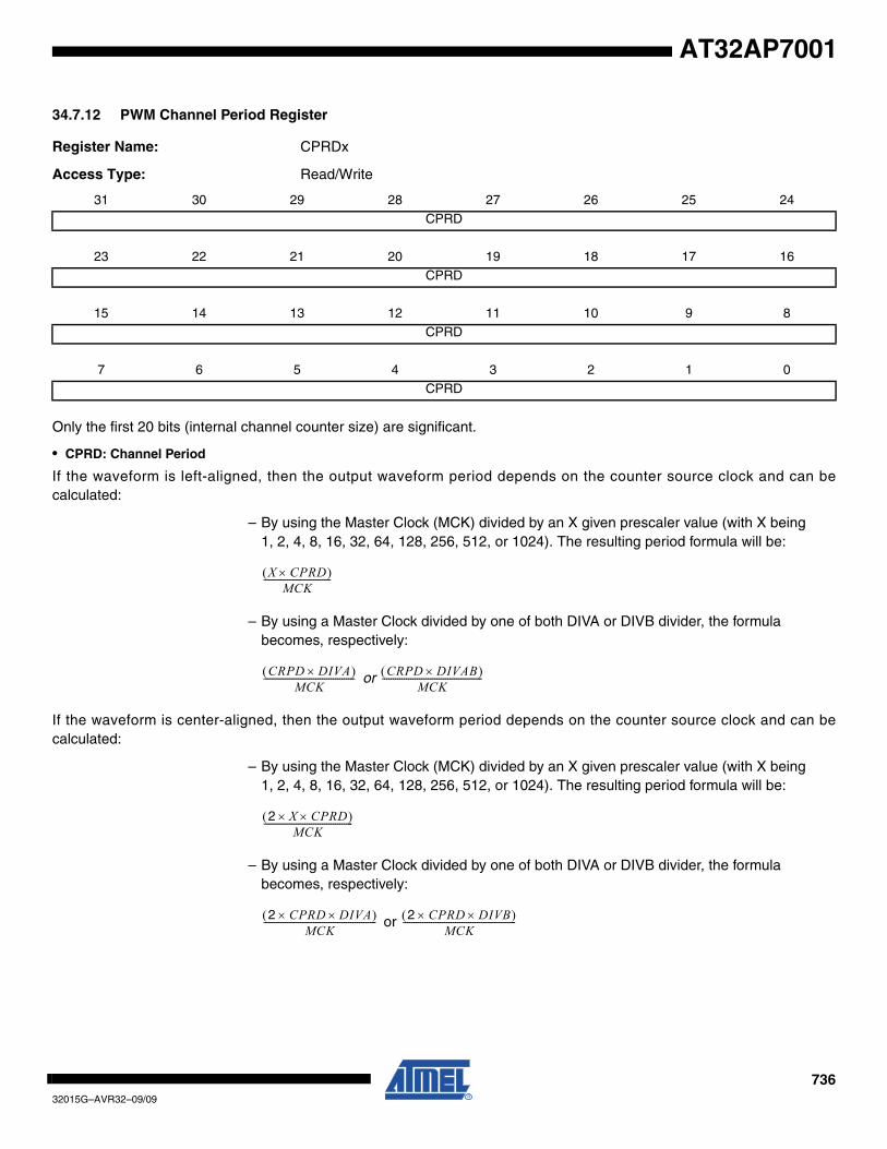
73632015G–AVR32–09/09
AT32AP7001
34.7.12 PWM Channel Period Register
Register Name: CPRDx
Access Type: Read/Write
Only the first 20 bits (internal channel counter size) are significant.
• CPRD: Channel Period
If the waveform is left-aligned, then the output waveform period depends on the counter source clock and can becalculated:
– By using the Master Clock (MCK) divided by an X given prescaler value (with X being 1, 2, 4, 8, 16, 32, 64, 128, 256, 512, or 1024). The resulting period formula will be:
– By using a Master Clock divided by one of both DIVA or DIVB divider, the formula becomes, respectively:
or
If the waveform is center-aligned, then the output waveform period depends on the counter source clock and can becalculated:
– By using the Master Clock (MCK) divided by an X given prescaler value (with X being 1, 2, 4, 8, 16, 32, 64, 128, 256, 512, or 1024). The resulting period formula will be:
– By using a Master Clock divided by one of both DIVA or DIVB divider, the formula becomes, respectively:
or
31 30 29 28 27 26 25 24
CPRD
23 22 21 20 19 18 17 16
CPRD
15 14 13 12 11 10 9 8
CPRD
7 6 5 4 3 2 1 0
CPRD
X CPRD×( )MCK
-------------------------------
CRPD DIVA×( )MCK
------------------------------------------ CRPD DIVAB×( )MCK
----------------------------------------------
2 X CPRD××( )MCK
-----------------------------------------
2 CPRD DIVA××( )MCK
---------------------------------------------------- 2 CPRD× DIVB×( )MCK
----------------------------------------------------
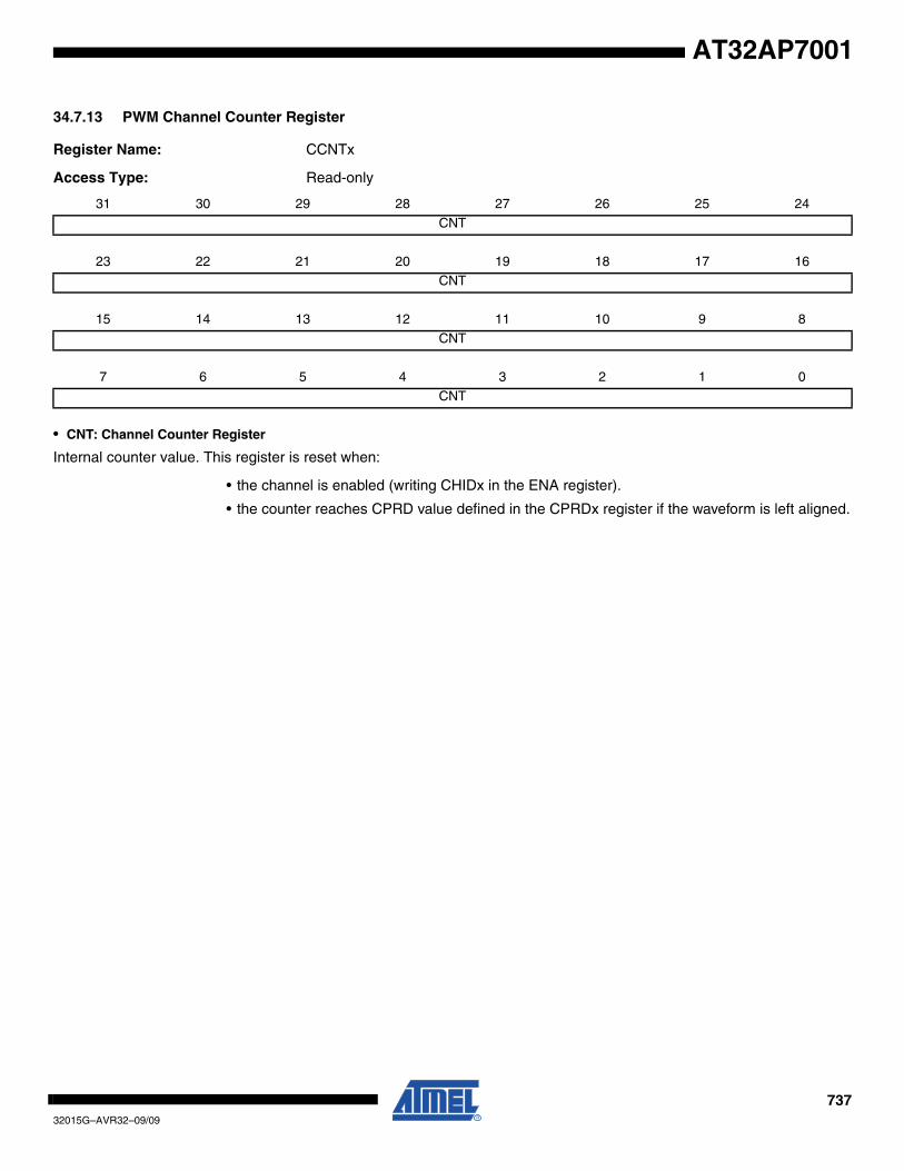
73732015G–AVR32–09/09
AT32AP7001
34.7.13 PWM Channel Counter Register
Register Name: CCNTx
Access Type: Read-only
• CNT: Channel Counter Register
Internal counter value. This register is reset when:
• the channel is enabled (writing CHIDx in the ENA register).
• the counter reaches CPRD value defined in the CPRDx register if the waveform is left aligned.
31 30 29 28 27 26 25 24
CNT
23 22 21 20 19 18 17 16
CNT
15 14 13 12 11 10 9 8
CNT
7 6 5 4 3 2 1 0
CNT

73832015G–AVR32–09/09
AT32AP7001
34.7.14 PWM Channel Update Register
Register Name: CUPDx
Access Type: Write-only
This register acts as a double buffer for the period or the duty cycle. This prevents an unexpected waveform when modify-ing the waveform period or duty-cycle.
Only the first 20 bits (internal channel counter size) are significant.
31 30 29 28 27 26 25 24
CUPD
23 22 21 20 19 18 17 16
CUPD
15 14 13 12 11 10 9 8
CUPD
7 6 5 4 3 2 1 0
CUPD
CPD (CMRx Register)
0The duty-cycle (CDTY in the CDTYx register) is updated with the CUPD value at the beginning of the next period.
1The period (CPRD in the CPRDx register) is updated with the CUPD value at the beginning of the next period.

73932015G–AVR32–09/09
AT32AP7001
35. Image Sensor Interface (ISI)
Rev: 0.0.5.2
35.1 Features• ITU-R BT. 601/656 8-bit Mode External Interface Support• Supports up to 12-bit Grayscale CMOS Sensors• Support for ITU-R BT.656-4 SAV and EAV Synchronization• Vertical and Horizontal Resolutions up to 2048 x 2048• Preview Path up to 640*480• 128 Bytes FIFO on Codec Path• 128 Bytes FIFO on Preview Path• Support for Packed Data Formatting for YCbCr 4:2:2 Formats• Preview Scaler to Generate Smaller Size image• Programmable Frame Capture Rate• VGA, QVGA, CIF, QCIF supported for LCD Preview• Custom Formats with Horizontal and Vertical Preview Size as Multiples of 16 Also Supported for
LCD Preview
35.2 OverviewThe Image Sensor Interface (ISI) connects a CMOS-type image sensor to the processor andprovides image capture in various formats. It does data conversion, if necessary, before the stor-age in memory through DMA.
The ISI supports color CMOS image sensor and grayscale image sensors with a reduced set offunctionalities.
This module outputs the data in RGB format (LCD compatible) and has scaling capabilities tomake it compliant to the LCD display resolution (See Table 35-3 on page 742).
Several input formats such as preprocessed RGB or YCbCr are supported through the data businterface.
It supports two modes of synchronization:
1. The hardware with VSYNC and HSYNC signals
2. The International Telecommunication Union Recommendation ITU-R BT.656-4 Start-of-Active-Video (SAV) and End-of-Active-Video (EAV) synchronization sequence.
Using EAV/SAV for synchronization reduces the pin count (VSYNC, HSYNC not used). Thepolarity of the synchronization pulse is programmable to comply with the sensor signals.
Table 35-1. I/O Description
Signal Dir Description
VSYNC IN Vertical Synchronization
HSYNC IN Horizontal Synchronization
DATA[11..0] IN Sensor Pixel Data
MCK OUT Master Clock Provided to the Image Sensor
PCK IN Pixel Clock Provided by the Image Sensor

74032015G–AVR32–09/09
AT32AP7001
Figure 35-1. ISI Connection Example
35.3 Block Diagram
Figure 35-2. Image Sensor Interface Block Diagram
35.4 Product Dependencies
35.4.1 I/O Lines
The pins used for interfacing the compliant external devices may be multiplexed with PIO lines.The programmer must first program the PIO controllers to assign the ISI pins to their peripheralfunctions.
35.4.2 Power Management
The ISI clock is generated by the Power Manager. Before using the ISI, the programmer mustensure that the ISIclock is enabled in the Power Manager.
In the ISI description, Master Clock (MCK) is the clock of the peripheral bus to which the ISI isconnected.
Image Sensor Image Sensor Interface
data[11..0] ISI_DATA[11..0]
CLK ISI_MCK
PCLK ISI_PCK
VSYNC
HSYNC
ISI_VSYNC
ISI_HSYNC
Timing SignalsInterface
CCIR-656Embedded TimingDecoder(SAV/EAV)
Pixel SamplingModule
Clipping + ColorConversion
YCC to RGB
2-D ImageScaler
PixelFormatter
Rx DirectDisplayFIFO Core
VideoArbiter
CameraHSB
MasterInterface
PBInterfaceCamera
InterruptController
ConfigRegisters
Clipping + ColorConversion
RGB to YCC
Rx DirectCapture
FIFO
ScatterMode
SupportPacked
Formatter
Frame Rate
YCbCr 4:2:2
8:8:8 5:6:5RGB
CMOSsensorPixel inputup to 12 bit
Hsync/LenVsync/Fen
CMOSsensorpixel clockinput
Pixel Clock Domain
HSBClock Domain
PBClock DomainFrom
Rx buffers
CameraInterrupt Request Line
codec_on
HS
B b
usP
B b
us
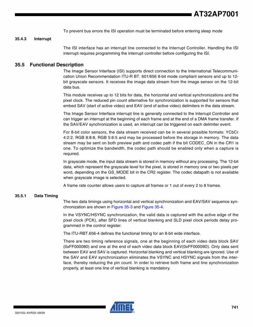
74132015G–AVR32–09/09
AT32AP7001
To prevent bus errors the ISI operation must be terminated before entering sleep mode
35.4.3 Interrupt
The ISI interface has an interrupt line connected to the Interrupt Controller. Handling the ISIinterrupt requires programming the interrupt controller before configuring the ISI.
35.5 Functional DescriptionThe Image Sensor Interface (ISI) supports direct connection to the International Telecommuni-cation Union Recommendation ITU-R BT. 601/656 8-bit mode compliant sensors and up to 12-bit grayscale sensors. It receives the image data stream from the image sensor on the 12-bitdata bus.
This module receives up to 12 bits for data, the horizontal and vertical synchronizations and thepixel clock. The reduced pin count alternative for synchronization is supported for sensors thatembed SAV (start of active video) and EAV (end of active video) delimiters in the data stream.
The Image Sensor Interface interrupt line is generally connected to the Interrupt Controller andcan trigger an interrupt at the beginning of each frame and at the end of a DMA frame transfer. Ifthe SAV/EAV synchronization is used, an interrupt can be triggered on each delimiter event.
For 8-bit color sensors, the data stream received can be in several possible formats: YCbCr4:2:2, RGB 8:8:8, RGB 5:6:5 and may be processed before the storage in memory. The datastream may be sent on both preview path and codec path if the bit CODEC_ON in the CR1 isone. To optimize the bandwidth, the codec path should be enabled only when a capture isrequired.
In grayscale mode, the input data stream is stored in memory without any processing. The 12-bitdata, which represent the grayscale level for the pixel, is stored in memory one or two pixels perword, depending on the GS_MODE bit in the CR2 register. The codec datapath is not availablewhen grayscale image is selected.
A frame rate counter allows users to capture all frames or 1 out of every 2 to 8 frames.
35.5.1 Data TimingThe two data timings using horizontal and vertical synchronization and EAV/SAV sequence syn-chronization are shown in Figure 35-3 and Figure 35-4.
In the VSYNC/HSYNC synchronization, the valid data is captured with the active edge of thepixel clock (PCK), after SFD lines of vertical blanking and SLD pixel clock periods delay pro-grammed in the control register.
The ITU-RBT.656-4 defines the functional timing for an 8-bit wide interface.
There are two timing reference signals, one at the beginning of each video data block SAV(0xFF000080) and one at the end of each video data block EAV(0xFF00009D). Only data sentbetween EAV and SAV is captured. Horizontal blanking and vertical blanking are ignored. Use ofthe SAV and EAV synchronization eliminates the VSYNC and HSYNC signals from the inter-face, thereby reducing the pin count. In order to retrieve both frame and line synchronizationproperly, at least one line of vertical blanking is mandatory.
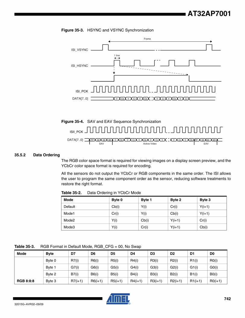
74232015G–AVR32–09/09
AT32AP7001
Figure 35-3. HSYNC and VSYNC Synchronization
Figure 35-4. SAV and EAV Sequence Synchronization
35.5.2 Data OrderingThe RGB color space format is required for viewing images on a display screen preview, and theYCbCr color space format is required for encoding.
All the sensors do not output the YCbCr or RGB components in the same order. The ISI allowsthe user to program the same component order as the sensor, reducing software treatments torestore the right format.
ISI_VSYNC
ISI_HSYNC
ISI_PCK
Frame
1 line
Y Cb Y Cr Y Cb Y Cr Y Cb Y CrDATA[7..0]
ISII_PCK
Cr Y Cb Y Cr Y Y Cr Y Cb FF 00DATA[7..0] FF 00 00 80 Y Cb Y 00 9D
SAV EAVActive Video
Table 35-2. Data Ordering in YCbCr Mode
Mode Byte 0 Byte 1 Byte 2 Byte 3
Default Cb(i) Y(i) Cr(i) Y(i+1)
Mode1 Cr(i) Y(i) Cb(i) Y(i+1)
Mode2 Y(i) Cb(i) Y(i+1) Cr(i)
Mode3 Y(i) Cr(i) Y(i+1) Cb(i)
Table 35-3. RGB Format in Default Mode, RGB_CFG = 00, No Swap
Mode Byte D7 D6 D5 D4 D3 D2 D1 D0
RGB 8:8:8
Byte 0 R7(i) R6(i) R5(i) R4(i) R3(i) R2(i) R1(i) R0(i)
Byte 1 G7(i) G6(i) G5(i) G4(i) G3(i) G2(i) G1(i) G0(i)
Byte 2 B7(i) B6(i) B5(i) B4(i) B3(i) B2(i) B1(i) B0(i)
Byte 3 R7(i+1) R6(i+1) R5(i+1) R4(i+1) R3(i+1) R2(i+1) R1(i+1) R0(i+1)
74332015G–AVR32–09/09
AT32AP7001
The RGB 5:6:5 input format is processed to be displayed as RGB 5:5:5 format.
35.5.3 ClocksThe sensor master clock (MCK) can be generated either by the power manager through a pro-grammable clock output or by an external oscillator connected to the sensor.
None of the sensors embeds a power management controller, so providing the clock by thepower manager is a simple and efficient way to control power consumption of the system.
Care must be taken when programming the system clock. The ISI has two clock domains, thesystem bus clock and the pixel clock provided by sensor. The two clock domains are not syn-chronized, but the system clock must be faster than pixel clock.
RGB 5:6:5
Byte 0 R4(i) R3(i) R2(i) R1(i) R0(i) G5(i) G4(i) G3(i)
Byte 1 G2(i) G1(i) G0(i) B4(i) B3(i) B2(i) B1(i) B0(i)
Byte 2 R4(i+1) R3(i+1) R2(i+1) R1(i+1) R0(i+1) G5(i+1) G4(i+1) G3(i+1)
Byte 3 G2(i+1) G1(i+1) G0(i+1) B4(i+1) B3i+1) B2(i+1) B1(i+1) B0(i+1)
Table 35-3. RGB Format in Default Mode, RGB_CFG = 00, No Swap
Table 35-4. RGB Format, RGB_CFG = 10 (Mode 2), No Swap
Mode Byte D7 D6 D5 D4 D3 D2 D1 D0
RGB 5:6:5
Byte 0 G2(i) G1(i) G0(i) R4(i) R3(i) R2(i) R1(i) R0(i)
Byte 1 B4(i) B3(i) B2(i) B1(i) B0(i) G5(i) G4(i) G3(i)
Byte 2 G2(i+1) G1(i+1) G0(i+1) R4(i+1) R3(i+1) R2(i+1) R1(i+1) R0(i+1)
Byte 3 B4(i+1) B3(i+1) B2(i+1) B1(i+1) B0(i+1) G5(i+1) G4(i+1) G3(i+1)
Table 35-5. RGB Format in Default Mode, RGB_CFG = 00, Swap Activated
Mode Byte D7 D6 D5 D4 D3 D2 D1 D0
RGB 8:8:8
Byte 0 R0(i) R1(i) R2(i) R3(i) R4(i) R5(i) R6(i) R7(i)
Byte 1 G0(i) G1(i) G2(i) G3(i) G4(i) G5(i) G6(i) G7(i)
Byte 2 B0(i) B1(i) B2(i) B3(i) B4(i) B5(i) B6(i) B7(i)
Byte 3 R0(i+1) R1(i+1) R2(i+1) R3(i+1) R4(i+1) R5(i+1) R6(i+1) R7(i+1)
RGB 5:6:5
Byte 0 G3(i) G4(i) G5(i) R0(i) R1(i) R2(i) R3(i) R4(i)
Byte 1 B0(i) B1(i) B2(i) B3(i) B4(i) G0(i) G1(i) G2(i)
Byte 2 G3(i+1) G4(i+1) G5(i+1) R0(i+1) R1(i+1) R2(i+1) R3(i+1) R4(i+1)
Byte 3 B0(i+1) B1(i+1) B2(i+1) B3(i+1) B4(i+1) G0(i+1) G1(i+1) G2(i+1)
74432015G–AVR32–09/09
AT32AP7001
35.5.4 Preview Path
35.5.4.1 Scaling, Decimation (Subsampling)This module resizes captured 8-bit color sensor images to fit the LCD display format. The resizemodule performs only downscaling. The same ratio is applied for both horizontal and verticalresize, then a fractional decimation algorithm is applied.
The decimation factor is a multiple of 1/16 and values 0 to 15 are forbidden.
Example:
Input 1280*1024 Output=640*480
Hratio = 1280/640 =2
Vratio = 1024/480 =2.1333
The decimation factor is 2 so 32/16.
Table 35-6. Decimation Factor
Dec value 0->15 16 17 18 19 ... 124 125 126 127
Dec Factor X 1 1.063 1.125 1.188 ... 7.750 7.813 7.875 7.938
Table 35-7. Decimation and Scaler Offset Values
INPUT
OUTPUT352*288 640*480 800*600 1280*1024 1600*1200 2048*1536
VGA
640*480F NA 16 20 32 40 51
QVGA
320*240F 16 32 40 64 80 102
CIF
352*288F 16 26 33 56 66 85
QCIF
176*144F 16 53 66 113 133 170

74532015G–AVR32–09/09
AT32AP7001
Figure 35-5. Resize Examples
35.5.4.2 Color Space ConversionThis module converts YCrCb or YUV pixels to RGB color space. Clipping is performed to ensurethat the samples value do not exceed the allowable range. The conversion matrix is definedbelow:
Example of programmable value to convert YCrCb to RGB:
An example of programmable value to convert from YUV to RGB:
1280
1024 480
640
32/16 decimation
1280
1024 288
352
56/16 decimation
RGB
C0 0 C1
C0 C2– C3–
C0 C4 0
Y Yoff–
Cb Cboff–
Cr Croff–
×=
R 1.164 Y 16–( )⋅ 1.596 Cr 128–( )⋅+=
G 1.164 Y 16–( ) 0.813 Cr 128–( )⋅– 0.392 Cb 128–( )⋅–⋅=
B 1.164 Y 16–( )⋅ 2.107 Cb 128–( )⋅+=⎩⎪⎨⎪⎧
R Y 1.596 V⋅+=
G Y 0.394 U⋅– 0.436 V⋅–=
B Y 2.032 U⋅+=⎩⎪⎨⎪⎧
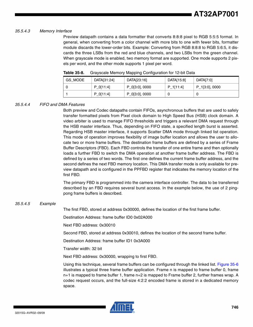
74632015G–AVR32–09/09
AT32AP7001
35.5.4.3 Memory InterfacePreview datapath contains a data formatter that converts 8:8:8 pixel to RGB 5:5:5 format. Ingeneral, when converting from a color channel with more bits to one with fewer bits, formattermodule discards the lower-order bits. Example: Converting from RGB 8:8:8 to RGB 5:6:5, it dis-cards the three LSBs from the red and blue channels, and two LSBs from the green channel.When grayscale mode is enabled, two memory format are supported. One mode supports 2 pix-els per word, and the other mode supports 1 pixel per word.
35.5.4.4 FIFO and DMA FeaturesBoth preview and Codec datapaths contain FIFOs, asynchronous buffers that are used to safelytransfer formatted pixels from Pixel clock domain to High Speed Bus (HSB) clock domain. Avideo arbiter is used to manage FIFO thresholds and triggers a relevant DMA request throughthe HSB master interface. Thus, depending on FIFO state, a specified length burst is asserted.Regarding HSB master interface, it supports Scatter DMA mode through linked list operation.This mode of operation improves flexibility of image buffer location and allows the user to allo-cate two or more frame buffers. The destination frame buffers are defined by a series of FrameBuffer Descriptors (FBD). Each FBD controls the transfer of one entire frame and then optionallyloads a further FBD to switch the DMA operation at another frame buffer address. The FBD isdefined by a series of two words. The first one defines the current frame buffer address, and thesecond defines the next FBD memory location. This DMA transfer mode is only available for pre-view datapath and is configured in the PPFBD register that indicates the memory location of thefirst FBD.
The primary FBD is programmed into the camera interface controller. The data to be transferreddescribed by an FBD requires several burst access. In the example below, the use of 2 ping-pong frame buffers is described.
35.5.4.5 ExampleThe first FBD, stored at address 0x30000, defines the location of the first frame buffer.
Destination Address: frame buffer ID0 0x02A000
Next FBD address: 0x30010
Second FBD, stored at address 0x30010, defines the location of the second frame buffer.
Destination Address: frame buffer ID1 0x3A000
Transfer width: 32 bit
Next FBD address: 0x30000, wrapping to first FBD.
Using this technique, several frame buffers can be configured through the linked list. Figure 35-6illustrates a typical three frame buffer application. Frame n is mapped to frame buffer 0, framen+1 is mapped to frame buffer 1, frame n+2 is mapped to Frame buffer 2, further frames wrap. Acodec request occurs, and the full-size 4:2:2 encoded frame is stored in a dedicated memoryspace.
Table 35-8. Grayscale Memory Mapping Configuration for 12-bit Data
GS_MODE DATA[31:24] DATA[23:16] DATA[15:8] DATA[7:0]
0 P_0[11:4] P_0[3:0], 0000 P_1[11:4] P_1[3:0], 0000
1 P_0[11:4] P_0[3:0], 0000 0 0

74732015G–AVR32–09/09
AT32AP7001
Figure 35-6. Three Frame Buffers Application and Memory Mapping
35.5.5 Codec Path
35.5.5.1 Color Space ConversionDepending on user selection, this module can be bypassed so that input YCrCb stream isdirectly connected to the format converter module. If the RGB input stream is selected, this mod-ule converts RGB to YCrCb color space with the formulas given below:
An example of coefficients are given below:
frame n frame n+1 frame n+2frame n-1 frame n+3 frame n+4
Frame Buffer 0
Frame Buffer 1
Frame Buffer 3
4:2:2 ImageFull ROI
ISI config Space
Codec RequestCodec Done
LCD
Memory Space
YCrCb
C0 C1 C2
C3 C– 4 C– 5
C– 6 C– 7 C8
RGB
×
YoffCroffCboff
+=
Y 0.257 R⋅ 0.504 G 0.098 B 16+⋅+⋅+=
Cr 0.439 R⋅ 0.368 G⋅– 0.071 B 128+⋅–=
Cb 0.148 R⋅– 0.291 G 0.439 B 128+⋅+⋅–=⎩⎪⎨⎪⎧

74832015G–AVR32–09/09
AT32AP7001
35.5.5.2 Memory InterfaceDedicated FIFO are used to support packed memory mapping. YCrCb pixel components aresent in a single 32-bit word in a contiguous space (packed). Data is stored in the order of naturalscan lines. Planar mode is not supported.
35.5.5.3 DMA FeaturesUnlike preview datapath, codec datapath DMA mode does not support linked list operation. Onlythe CODEC_DMA_ADDR register is used to configure the frame buffer base address.
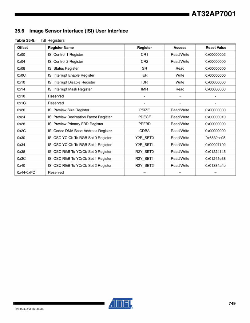
74932015G–AVR32–09/09
AT32AP7001
35.6 Image Sensor Interface (ISI) User Interface
Table 35-9. ISI Registers
Offset Register Name Register Access Reset Value
0x00 ISI Control 1 Register CR1 Read/Write 0x00000002
0x04 ISI Control 2 Register CR2 Read/Write 0x00000000
0x08 ISI Status Register SR Read 0x00000000
0x0C ISI Interrupt Enable Register IER Write 0x00000000
0x10 ISI Interrupt Disable Register IDR Write 0x00000000
0x14 ISI Interrupt Mask Register IMR Read 0x00000000
0x18 Reserved - - -
0x1C Reserved - - -
0x20 ISI Preview Size Register PSIZE Read/Write 0x00000000
0x24 ISI Preview Decimation Factor Register PDECF Read/Write 0x00000010
0x28 ISI Preview Primary FBD Register PPFBD Read/Write 0x00000000
0x2C ISI Codec DMA Base Address Register CDBA Read/Write 0x00000000
0x30 ISI CSC YCrCb To RGB Set 0 Register Y2R_SET0 Read/Write 0x6832cc95
0x34 ISI CSC YCrCb To RGB Set 1 Register Y2R_SET1 Read/Write 0x00007102
0x38 ISI CSC RGB To YCrCb Set 0 Register R2Y_SET0 Read/Write 0x01324145
0x3C ISI CSC RGB To YCrCb Set 1 Register R2Y_SET1 Read/Write 0x01245e38
0x40 ISI CSC RGB To YCrCb Set 2 Register R2Y_SET2 Read/Write 0x01384a4b
0x44-0xFC Reserved – – –
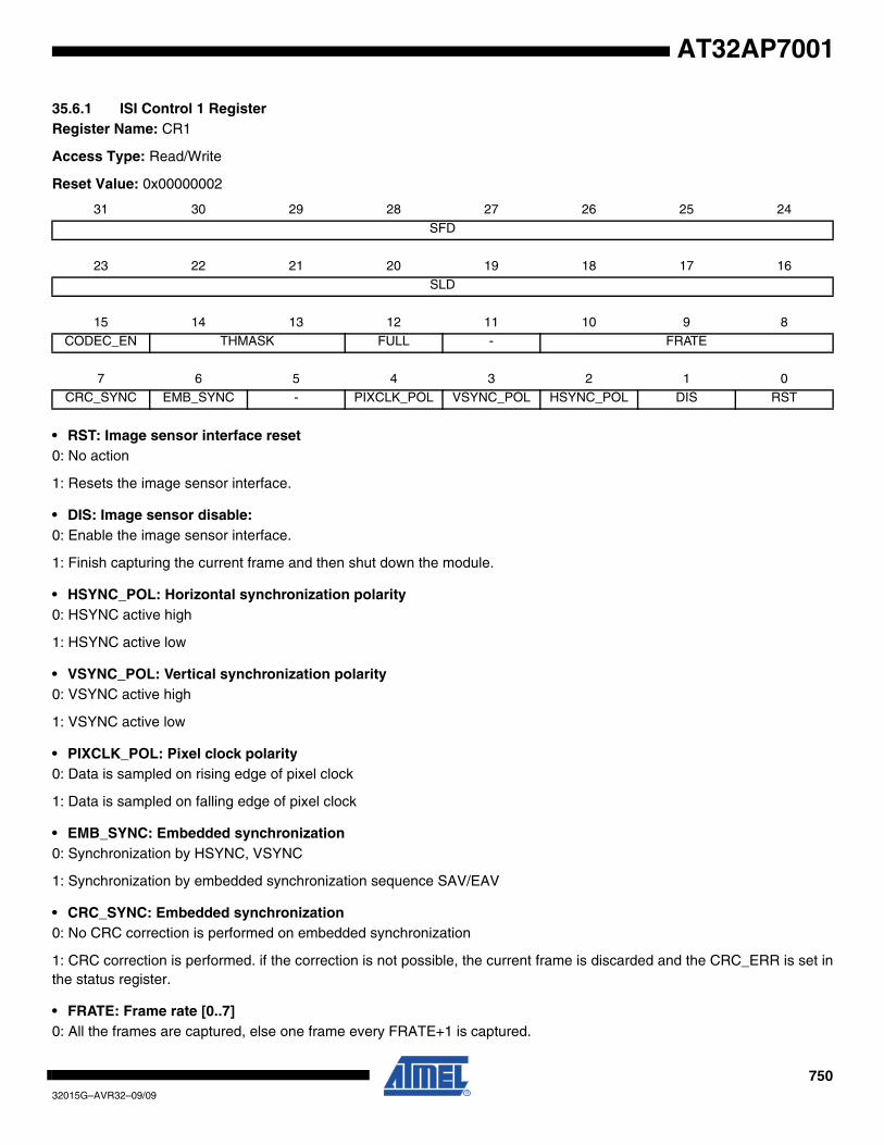
75032015G–AVR32–09/09
AT32AP7001
35.6.1 ISI Control 1 RegisterRegister Name: CR1
Access Type: Read/Write
Reset Value: 0x00000002
• RST: Image sensor interface reset0: No action
1: Resets the image sensor interface.
• DIS: Image sensor disable:0: Enable the image sensor interface.
1: Finish capturing the current frame and then shut down the module.
• HSYNC_POL: Horizontal synchronization polarity0: HSYNC active high
1: HSYNC active low
• VSYNC_POL: Vertical synchronization polarity0: VSYNC active high
1: VSYNC active low
• PIXCLK_POL: Pixel clock polarity0: Data is sampled on rising edge of pixel clock
1: Data is sampled on falling edge of pixel clock
• EMB_SYNC: Embedded synchronization0: Synchronization by HSYNC, VSYNC
1: Synchronization by embedded synchronization sequence SAV/EAV
• CRC_SYNC: Embedded synchronization0: No CRC correction is performed on embedded synchronization
1: CRC correction is performed. if the correction is not possible, the current frame is discarded and the CRC_ERR is set inthe status register.
• FRATE: Frame rate [0..7]0: All the frames are captured, else one frame every FRATE+1 is captured.
31 30 29 28 27 26 25 24
SFD
23 22 21 20 19 18 17 16SLD
15 14 13 12 11 10 9 8CODEC_EN THMASK FULL - FRATE
7 6 5 4 3 2 1 0CRC_SYNC EMB_SYNC - PIXCLK_POL VSYNC_POL HSYNC_POL DIS RST
75132015G–AVR32–09/09
AT32AP7001
• FULL: Full mode is allowed0: Codec and preview datapaths are not working simultaneously
1: Both codec and preview datapaths are working simultaneously
• THMASK: Threshold mask0: 4, 8 and 16 HSB bursts are allowed
1: 8 and 16 HSB bursts are allowed
2: Only 16 HSB bursts are allowed
• CODEC_EN: Enable the codec path enable bitThis bit always read as zero
0: The codec path is disabled
1: The codec path is enabled and the next frame is captured
• SLD: Start of Line DelaySLD pixel clock periods to wait before the beginning of a line.
• SFD: Start of Frame DelaySFD lines are skipped at the beginning of the frame.
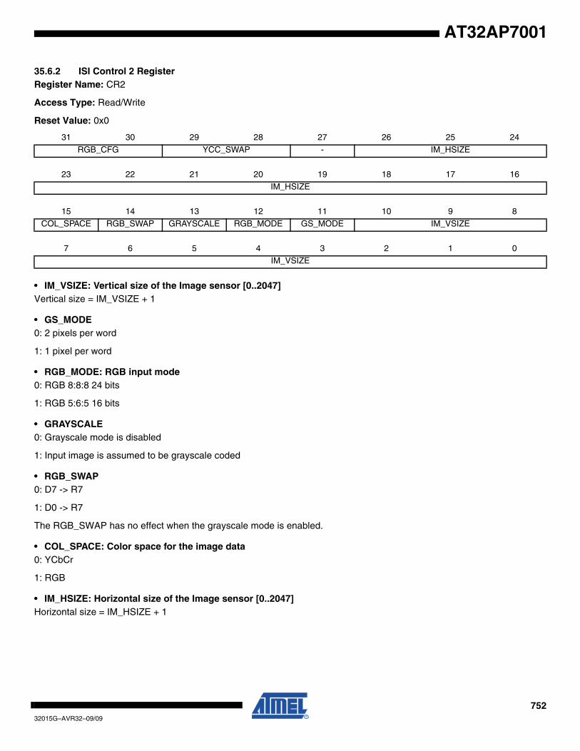
75232015G–AVR32–09/09
AT32AP7001
35.6.2 ISI Control 2 RegisterRegister Name: CR2
Access Type: Read/Write
Reset Value: 0x0
• IM_VSIZE: Vertical size of the Image sensor [0..2047]Vertical size = IM_VSIZE + 1
• GS_MODE0: 2 pixels per word
1: 1 pixel per word
• RGB_MODE: RGB input mode0: RGB 8:8:8 24 bits
1: RGB 5:6:5 16 bits
• GRAYSCALE0: Grayscale mode is disabled
1: Input image is assumed to be grayscale coded
• RGB_SWAP0: D7 -> R7
1: D0 -> R7
The RGB_SWAP has no effect when the grayscale mode is enabled.
• COL_SPACE: Color space for the image data0: YCbCr
1: RGB
• IM_HSIZE: Horizontal size of the Image sensor [0..2047]Horizontal size = IM_HSIZE + 1
31 30 29 28 27 26 25 24
RGB_CFG YCC_SWAP - IM_HSIZE
23 22 21 20 19 18 17 16IM_HSIZE
15 14 13 12 11 10 9 8COL_SPACE RGB_SWAP GRAYSCALE RGB_MODE GS_MODE IM_VSIZE
7 6 5 4 3 2 1 0IM_VSIZE
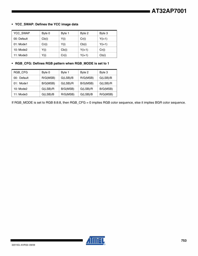
75332015G–AVR32–09/09
AT32AP7001
• YCC_SWAP: Defines the YCC image data
• RGB_CFG: Defines RGB pattern when RGB_MODE is set to 1
If RGB_MODE is set to RGB 8:8:8, then RGB_CFG = 0 implies RGB color sequence, else it implies BGR color sequence.
YCC_SWAP Byte 0 Byte 1 Byte 2 Byte 3
00: Default Cb(i) Y(i) Cr(i) Y(i+1)
01: Mode1 Cr(i) Y(i) Cb(i) Y(i+1)
10: Mode2 Y(i) Cb(i) Y(i+1) Cr(i)
11: Mode3 Y(i) Cr(i) Y(i+1) Cb(i)
RGB_CFG Byte 0 Byte 1 Byte 2 Byte 3
00: Default R/G(MSB) G(LSB)/B R/G(MSB) G(LSB)/B
01: Mode1 B/G(MSB) G(LSB)/R B/G(MSB) G(LSB)/R
10: Mode2 G(LSB)/R B/G(MSB) G(LSB)/R B/G(MSB)
11: Mode3 G(LSB)/B R/G(MSB) G(LSB)/B R/G(MSB)
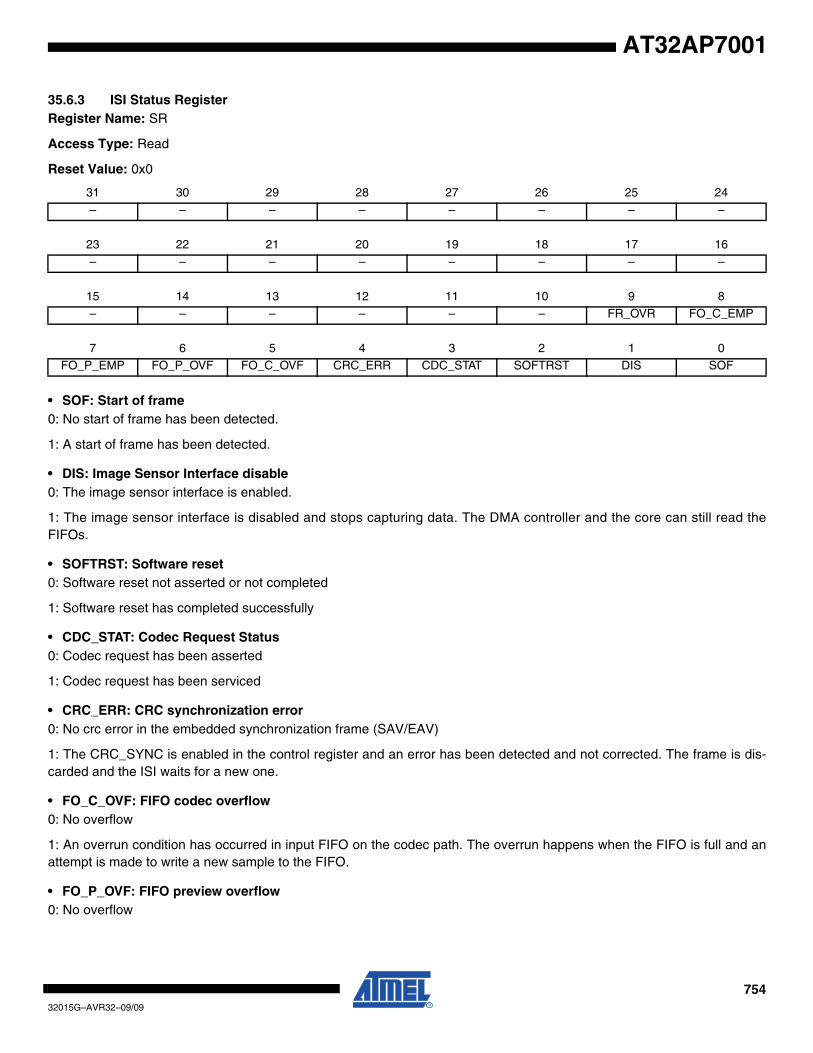
75432015G–AVR32–09/09
AT32AP7001
35.6.3 ISI Status RegisterRegister Name: SR
Access Type: Read
Reset Value: 0x0
• SOF: Start of frame0: No start of frame has been detected.
1: A start of frame has been detected.
• DIS: Image Sensor Interface disable0: The image sensor interface is enabled.
1: The image sensor interface is disabled and stops capturing data. The DMA controller and the core can still read theFIFOs.
• SOFTRST: Software reset0: Software reset not asserted or not completed
1: Software reset has completed successfully
• CDC_STAT: Codec Request Status0: Codec request has been asserted
1: Codec request has been serviced
• CRC_ERR: CRC synchronization error0: No crc error in the embedded synchronization frame (SAV/EAV)
1: The CRC_SYNC is enabled in the control register and an error has been detected and not corrected. The frame is dis-carded and the ISI waits for a new one.
• FO_C_OVF: FIFO codec overflow0: No overflow
1: An overrun condition has occurred in input FIFO on the codec path. The overrun happens when the FIFO is full and anattempt is made to write a new sample to the FIFO.
• FO_P_OVF: FIFO preview overflow0: No overflow
31 30 29 28 27 26 25 24
– – – – – – – –
23 22 21 20 19 18 17 16– – – – – – – –
15 14 13 12 11 10 9 8– – – – – – FR_OVR FO_C_EMP
7 6 5 4 3 2 1 0FO_P_EMP FO_P_OVF FO_C_OVF CRC_ERR CDC_STAT SOFTRST DIS SOF

75532015G–AVR32–09/09
AT32AP7001
1: An overrun condition has occurred in input FIFO on the preview path. The overrun happens when the FIFO is full and anattempt is made to write a new sample to the FIFO.
• FO_P_EMP0:The DMA has not finished transferring all the contents of the preview FIFO.
1:The DMA has finished transferring all the contents of the preview FIFO.
• FO_C_EMP0: The DMA has not finished transferring all the contents of the codec FIFO.
1: The DMA has finished transferring all the contents of the codec FIFO.
• FR_OVR: Frame overrun0: No frame overrun.
1: Frame overrun, the current frame is being skipped because a vsync signal has been detected while flushing FIFOs.
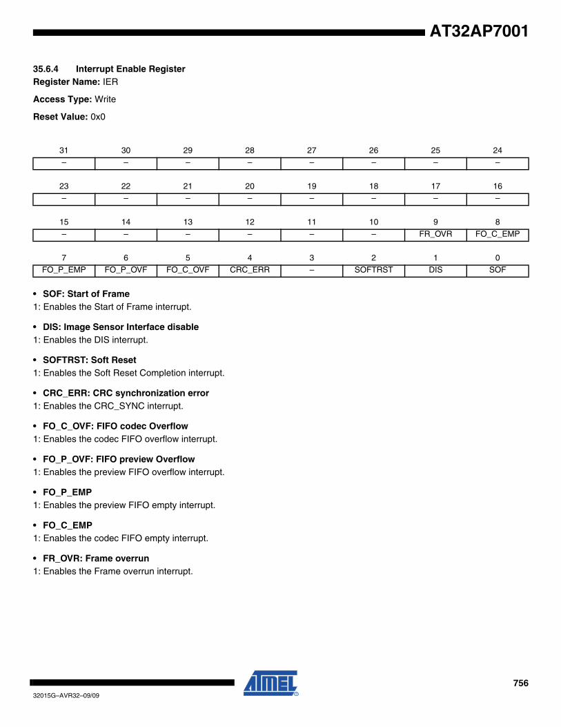
75632015G–AVR32–09/09
AT32AP7001
35.6.4 Interrupt Enable RegisterRegister Name: IER
Access Type: Write
Reset Value: 0x0
• SOF: Start of Frame1: Enables the Start of Frame interrupt.
• DIS: Image Sensor Interface disable1: Enables the DIS interrupt.
• SOFTRST: Soft Reset1: Enables the Soft Reset Completion interrupt.
• CRC_ERR: CRC synchronization error1: Enables the CRC_SYNC interrupt.
• FO_C_OVF: FIFO codec Overflow1: Enables the codec FIFO overflow interrupt.
• FO_P_OVF: FIFO preview Overflow1: Enables the preview FIFO overflow interrupt.
• FO_P_EMP1: Enables the preview FIFO empty interrupt.
• FO_C_EMP1: Enables the codec FIFO empty interrupt.
• FR_OVR: Frame overrun1: Enables the Frame overrun interrupt.
31 30 29 28 27 26 25 24
– – – – – – – –
23 22 21 20 19 18 17 16
– – – – – – – –
15 14 13 12 11 10 9 8
– – – – – – FR_OVR FO_C_EMP
7 6 5 4 3 2 1 0
FO_P_EMP FO_P_OVF FO_C_OVF CRC_ERR – SOFTRST DIS SOF

75732015G–AVR32–09/09
AT32AP7001
35.6.5 ISI Interrupt Disable RegisterRegister Name: IDR
Access Type: Write
Reset Value: 0x0
• SOF: Start of Frame1: Disables the Start of Frame interrupt.
• DIS: Image Sensor Interface disable1: Disables the DIS interrupt.
• SOFTRST1: Disables the soft reset completion interrupt.
• CRC_ERR: CRC synchronization error1: Disables the CRC_SYNC interrupt.
• FO_C_OVF: FIFO codec overflow1: Disables the codec FIFO overflow interrupt.
• FO_P_OVF: FIFO preview overflow1: Disables the preview FIFO overflow interrupt.
• FO_P_EMP1: Disables the preview FIFO empty interrupt.
• FO_C_EMP1: Disables the codec FIFO empty interrupt.
• FR_OVR: Frame overrun1: Disables frame overrun interrupt.
31 30 29 28 27 26 25 24
– – – – – – – –
23 22 21 20 19 18 17 16– – – – – – – –
15 14 13 12 11 10 9 8– – – – – – FR_OVR FO_C_EMP
7 6 5 4 3 2 1 0FO_P_EMP FO_P_OVF FO_C_OVF CRC_ERR – SOFTRST DIS SOF
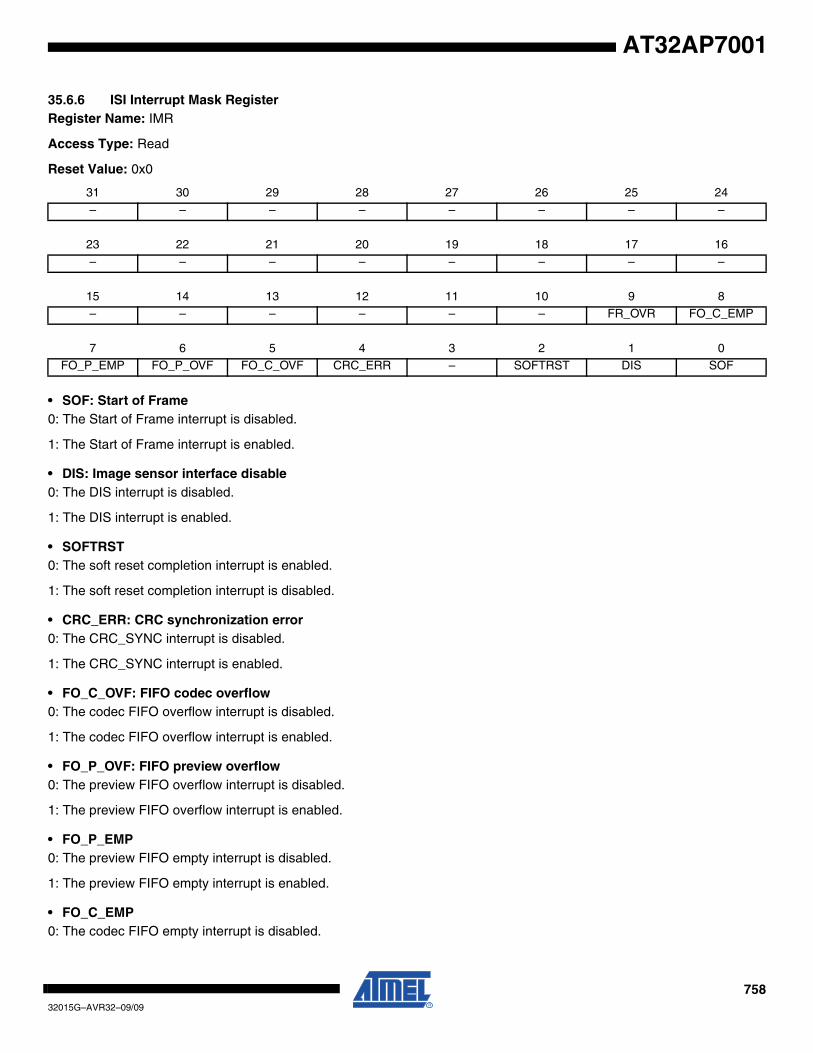
75832015G–AVR32–09/09
AT32AP7001
35.6.6 ISI Interrupt Mask RegisterRegister Name: IMR
Access Type: Read
Reset Value: 0x0
• SOF: Start of Frame0: The Start of Frame interrupt is disabled.
1: The Start of Frame interrupt is enabled.
• DIS: Image sensor interface disable0: The DIS interrupt is disabled.
1: The DIS interrupt is enabled.
• SOFTRST0: The soft reset completion interrupt is enabled.
1: The soft reset completion interrupt is disabled.
• CRC_ERR: CRC synchronization error0: The CRC_SYNC interrupt is disabled.
1: The CRC_SYNC interrupt is enabled.
• FO_C_OVF: FIFO codec overflow0: The codec FIFO overflow interrupt is disabled.
1: The codec FIFO overflow interrupt is enabled.
• FO_P_OVF: FIFO preview overflow0: The preview FIFO overflow interrupt is disabled.
1: The preview FIFO overflow interrupt is enabled.
• FO_P_EMP0: The preview FIFO empty interrupt is disabled.
1: The preview FIFO empty interrupt is enabled.
• FO_C_EMP0: The codec FIFO empty interrupt is disabled.
31 30 29 28 27 26 25 24
– – – – – – – –
23 22 21 20 19 18 17 16– – – – – – – –
15 14 13 12 11 10 9 8– – – – – – FR_OVR FO_C_EMP
7 6 5 4 3 2 1 0FO_P_EMP FO_P_OVF FO_C_OVF CRC_ERR – SOFTRST DIS SOF

75932015G–AVR32–09/09
AT32AP7001
1: The codec FIFO empty interrupt is enabled.
• FR_OVR: Frame Overrun
0: The frame overrun interrupt is disabled.
1: The frame overrun interrupt is enabled.
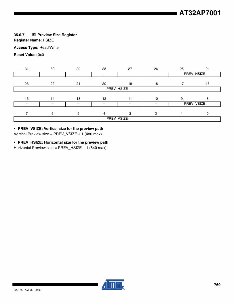
76032015G–AVR32–09/09
AT32AP7001
35.6.7 ISI Preview Size RegisterRegister Name: PSIZE
Access Type: Read/Write
Reset Value: 0x0
• PREV_VSIZE: Vertical size for the preview pathVertical Preview size = PREV_VSIZE + 1 (480 max)
• PREV_HSIZE: Horizontal size for the preview pathHorizontal Preview size = PREV_HSIZE + 1 (640 max)
31 30 29 28 27 26 25 24
– – – – – – PREV_HSIZE
23 22 21 20 19 18 17 16
PREV_HSIZE
15 14 13 12 11 10 9 8
– – – – – – PREV_VSIZE
7 6 5 4 3 2 1 0
PREV_VSIZE
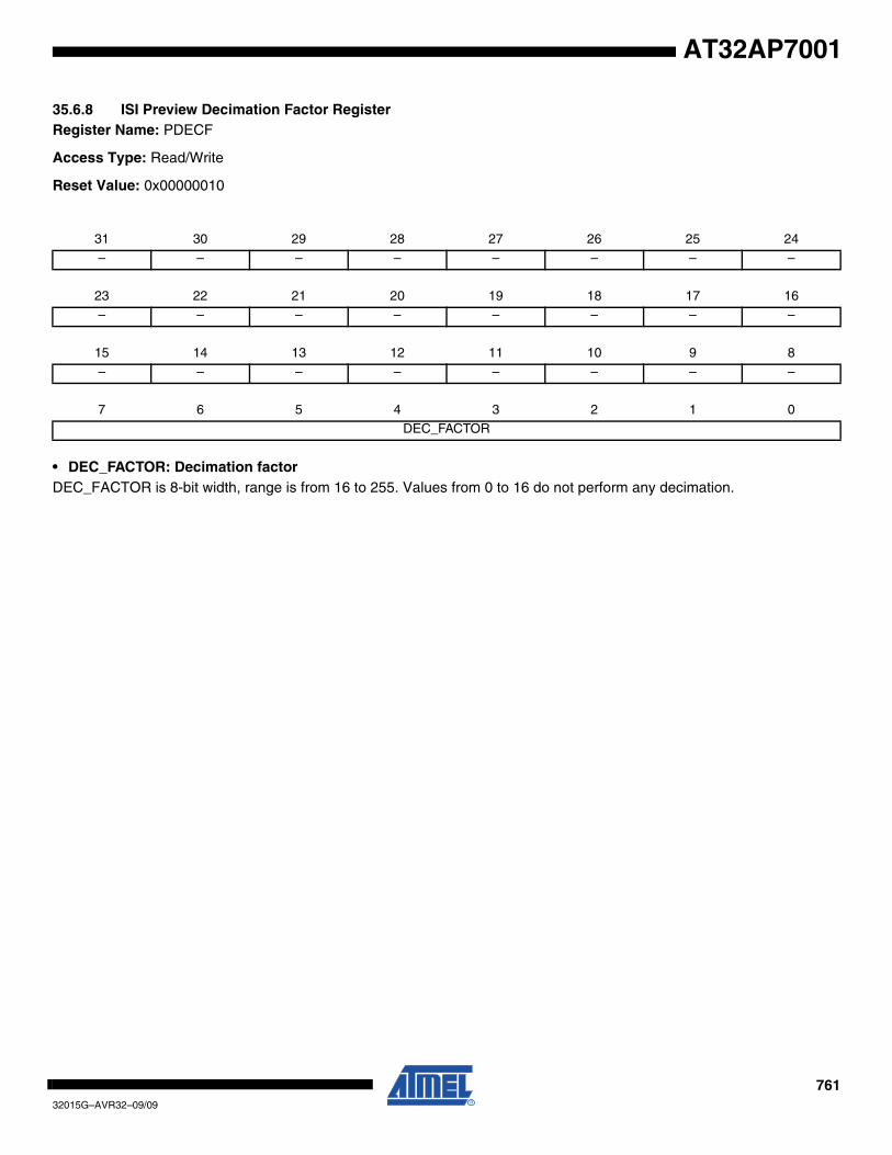
76132015G–AVR32–09/09
AT32AP7001
35.6.8 ISI Preview Decimation Factor RegisterRegister Name: PDECF
Access Type: Read/Write
Reset Value: 0x00000010
• DEC_FACTOR: Decimation factorDEC_FACTOR is 8-bit width, range is from 16 to 255. Values from 0 to 16 do not perform any decimation.
31 30 29 28 27 26 25 24
– – – – – – – –
23 22 21 20 19 18 17 16
– – – – – – – –
15 14 13 12 11 10 9 8
– – – – – – – –
7 6 5 4 3 2 1 0
DEC_FACTOR
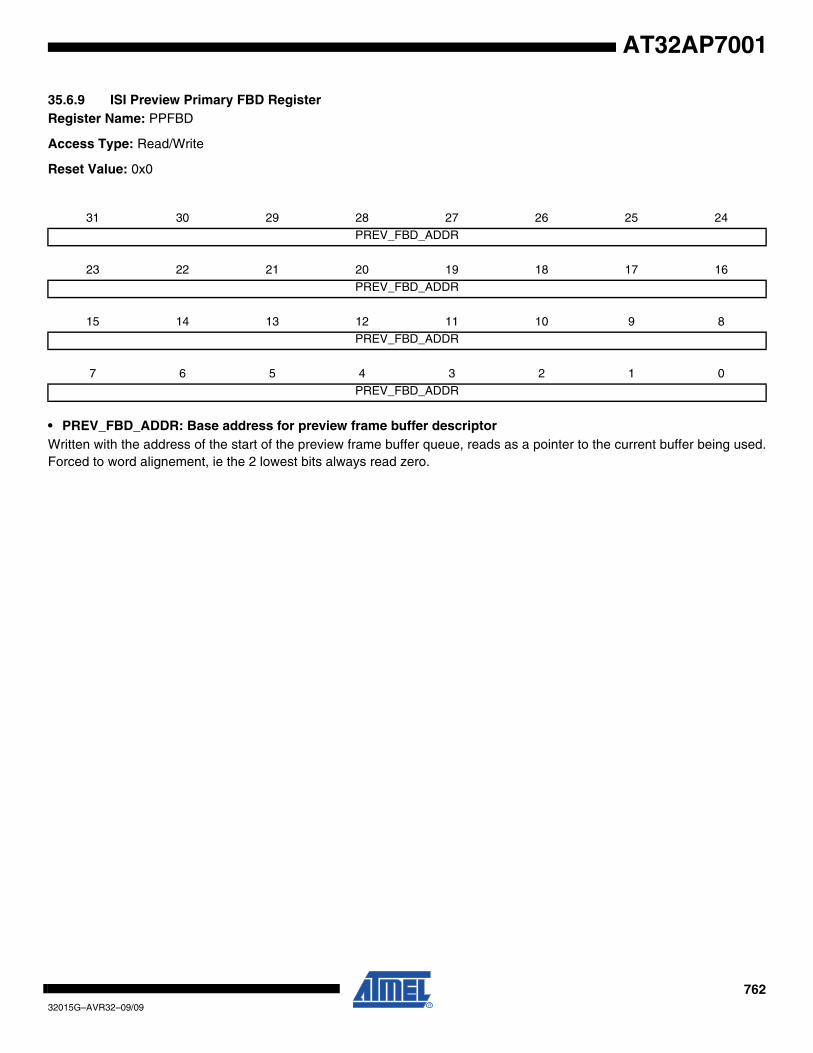
76232015G–AVR32–09/09
AT32AP7001
35.6.9 ISI Preview Primary FBD RegisterRegister Name: PPFBD
Access Type: Read/Write
Reset Value: 0x0
• PREV_FBD_ADDR: Base address for preview frame buffer descriptorWritten with the address of the start of the preview frame buffer queue, reads as a pointer to the current buffer being used.Forced to word alignement, ie the 2 lowest bits always read zero.
31 30 29 28 27 26 25 24
PREV_FBD_ADDR
23 22 21 20 19 18 17 16
PREV_FBD_ADDR
15 14 13 12 11 10 9 8
PREV_FBD_ADDR
7 6 5 4 3 2 1 0
PREV_FBD_ADDR

76332015G–AVR32–09/09
AT32AP7001
35.6.10 ISI Codec DMA Base Address RegisterRegister Name: CDBA
Access Type: Read/Write
Reset Value: 0x0
• CODEC_DMA_ADDR: Base address for codec DMAThis register contains codec datapath start address of buffer location. Forced to word alignement, ie the 2 lowest bitsalways read zero.
31 30 29 28 27 26 25 24
CODEC_DMA_ADDR
23 22 21 20 19 18 17 16
CODEC_DMA_ADDR
15 14 13 12 11 10 9 8
CODEC_DMA_ADDR
7 6 5 4 3 2 1 0
CODEC_DMA_ADDR

76432015G–AVR32–09/09
AT32AP7001
35.6.11 ISI Color Space Conversion YCrCb to RGB Set 0 RegisterRegister Name: Y2R_SET0
Access Type: Read/Write
Reset Value: 0x6832cc95
• C3 : Color Space Conversion Matrix Coefficient C3C3 element, default step is 1/128, ranges from 0 to 255/128
• C2 : Color Space Conversion Matrix Coefficient C2C2 element, default step is 1/128, ranges from 0 to 255/128
• C1 : Color Space Conversion Matrix Coefficient C1C1 element, default step is 1/128, ranges from 0 to 255/128
• C0 : Color Space Conversion Matrix Coefficient C0C0 element, default step is 1/128, ranges from 0 to 255/128
31 30 29 28 27 26 25 24
C3
23 22 21 20 19 18 17 16
C2
15 14 13 12 11 10 9 8
C1
7 6 5 4 3 2 1 0
C0
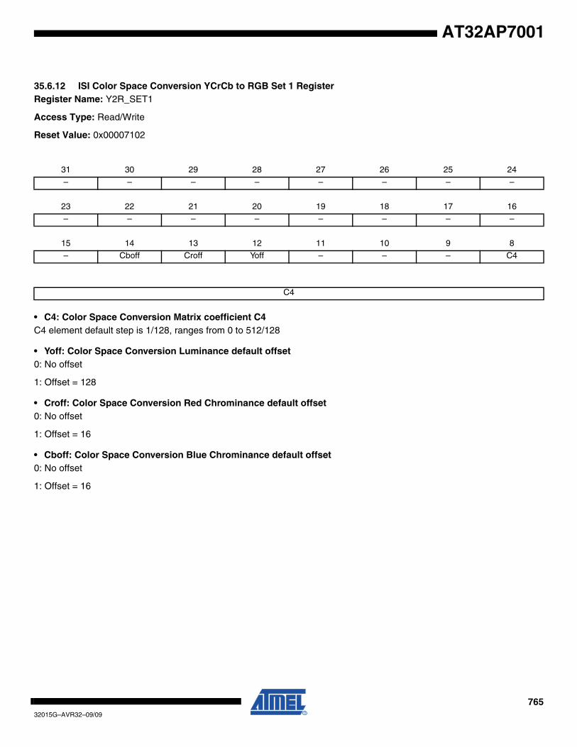
76532015G–AVR32–09/09
AT32AP7001
35.6.12 ISI Color Space Conversion YCrCb to RGB Set 1 RegisterRegister Name: Y2R_SET1
Access Type: Read/Write
Reset Value: 0x00007102
• C4: Color Space Conversion Matrix coefficient C4C4 element default step is 1/128, ranges from 0 to 512/128
• Yoff: Color Space Conversion Luminance default offset0: No offset
1: Offset = 128
• Croff: Color Space Conversion Red Chrominance default offset0: No offset
1: Offset = 16
• Cboff: Color Space Conversion Blue Chrominance default offset0: No offset
1: Offset = 16
31 30 29 28 27 26 25 24
– – – – – – – –
23 22 21 20 19 18 17 16
– – – – – – – –
15 14 13 12 11 10 9 8
– Cboff Croff Yoff – – – C4
C4

76632015G–AVR32–09/09
AT32AP7001
35.6.13 ISI Color Space Conversion RGB to YCrCb Set 0 RegisterRegister Name: R2Y_SET0
Access Type: Read/Write
Reset Value: 0x01324145
• C0: Color Space Conversion Matrix coefficient C0C0 element default step is 1/256, from 0 to 127/256
• C1: Color Space Conversion Matrix coefficient C1C1 element default step is 1/128, from 0 to 127/128
• C2: Color Space Conversion Matrix coefficient C2C2 element default step is 1/512, from 0 to 127/512
• Roff: Color Space Conversion Red component offset0: No offset
1: Offset = 16
31 30 29 28 27 26 25 24
– – – – – – – Roff
23 22 21 20 19 18 17 16
- C2
15 14 13 12 11 10 9 8
- C1
7 6 5 4 3 2 1 0
- C0

76732015G–AVR32–09/09
AT32AP7001
35.6.14 ISI Color Space Conversion RGB to YCrCb Set 1 RegisterRegister Name: R2Y_SET1
Access Type: Read/Write
Reset Value: 0x01245e38
• C3: Color Space Conversion Matrix coefficient C3C0 element default step is 1/128, ranges from 0 to 127/128
• C4: Color Space Conversion Matrix coefficient C4C1 element default step is 1/256, ranges from 0 to 127/256
• C5: Color Space Conversion Matrix coefficient C5C1 element default step is 1/512, ranges from 0 to 127/512
• Goff: Color Space Conversion Green component offset0: No offset
1: Offset = 128
31 30 29 28 27 26 25 24
– – – – – – – Goff
23 22 21 20 19 18 17 16
- C5
15 14 13 12 11 10 9 8
- C4
7 6 5 4 3 2 1 0
- C3
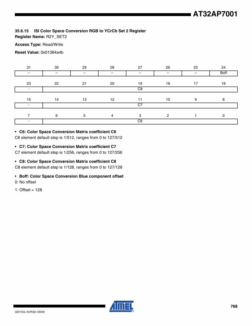
76832015G–AVR32–09/09
AT32AP7001
35.6.15 ISI Color Space Conversion RGB to YCrCb Set 2 RegisterRegister Name: R2Y_SET2
Access Type: Read/Write
Reset Value: 0x01384a4b
• C6: Color Space Conversion Matrix coefficient C6C6 element default step is 1/512, ranges from 0 to 127/512
• C7: Color Space Conversion Matrix coefficient C7C7 element default step is 1/256, ranges from 0 to 127/256
• C8: Color Space Conversion Matrix coefficient C8C8 element default step is 1/128, ranges from 0 to 127/128
• Boff: Color Space Conversion Blue component offset0: No offset
1: Offset = 128
31 30 29 28 27 26 25 24
– – – – – – – Boff
23 22 21 20 19 18 17 16
- C8
15 14 13 12 11 10 9 8
- C7
7 6 5 4 3 2 1 0
- C6
76932015G–AVR32–09/09
AT32AP7001
36. On-Chip Debug
Rev: 1.0.0.0
36.1 Features
• Debug interface in compliance with IEEE-ISTO 5001-2003 (Nexus 2.0) Class 3• JTAG access to all on-chip debug functions• Advanced Program, Data, Ownership, and Watchpoint trace supported• NanoTrace JTAG-based trace access• Auxiliary port for high-speed trace information• Hardware support for 6 Program and 2 Data breakpoints• Unlimited number of software breakpoints supported• Automatic CRC check of memory regions• Advanced Program, Data, Ownership, and Watchpoint trace supported
36.2 Overview
Debugging on the AT32AP7001 is facilitated by a powerful On-Chip Debug (OCD) system. Theuser accesses this through an external debug tool which connects to the JTAG port and the Aux-iliary (AUX) port. The AUX port is primarily used for trace functions, and a JTAG-baseddebugger is sufficient for basic debugging.
The debug system is based on the Nexus 2.0 standard, class 3, which includes:
• Basic run-time control
• Program breakpoints
• Data breakpoints
• Program trace
• Ownership trace
• Data trace
• Run-time direct memory access
In addition to the mandatory Nexus debug features, the AT32AP7001 implements several usefulOCD features, such as:
• Debug Communication Channel between CPU and JTAG
• Run-time PC monitoring
• CRC checking
• NanoTrace
• Software Quality Assurance (SQA) support
The OCD features are controlled by OCD registers, which can be accessed by JTAG when theNEXUS_ACCESS JTAG instruction is loaded. The CPU can also access OCD registers directlyusing mtdr/mfdr instructions in any privileged mode. The OCD registers are implemented basedon the recommendations in the Nexus 2.0 standard, and are detailed in the AVR32AP TechnicalReference Manual.
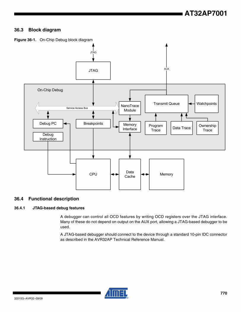
77032015G–AVR32–09/09
AT32AP7001
36.3 Block diagram
Figure 36-1. On-Chip Debug block diagram
36.4 Functional description
36.4.1 JTAG-based debug features
A debugger can control all OCD features by writing OCD registers over the JTAG interface.Many of these do not depend on output on the AUX port, allowing a JTAG-based debugger to beused.
A JTAG-based debugger should connect to the device through a standard 10-pin IDC connectoras described in the AVR32AP Technical Reference Manual.
On-Chip Debug
JTAG
Debug PC
Debug Instruction
CPU
Breakpoints Program Trace Data Trace Ownership
Trace
WatchpointsTransmit Queue
AUX
JTAG
Memory
NanoTraceModule
Service Access Bus
Memory Interface
Data Cache

77132015G–AVR32–09/09
AT32AP7001
Figure 36-2. JTAG-based debugger
36.4.1.1 Debug Communication Channel
The Debug Communication Channel (DCC) consists of a pair OCD registers with associatedhandshake logic, accessible to both CPU and JTAG. The registers can be used to exchangedata between the CPU and the JTAG master, both runtime as well as in debug mode.
36.4.1.2 Breakpoints
One of the most fundamental debug features is the ability to halt the CPU, to examine registersand the state of the system. This is accomplished by breakpoints, of which many types areavailable:
• Unconditional breakpoints are set by writing OCD registers by JTAG, halting the CPU immediately.
• Program breakpoints halt the CPU when a specific address in the program is executed.
• Data breakpoints halt the CPU when a specific memory address is read or written, allowing variables to be watched.
• Software breakpoints halt the CPU when the breakpoint instruction is executed.
When a breakpoint triggers, the CPU enters debug mode, and the D bit in the status register isset. This is a privileged mode with dedicated return address and return status registers. All privi-leged instructions are permitted. Debug mode can be entered as either OCD Mode, runninginstructions from JTAG, or Monitor Mode, running instructions from program memory.
AVR32
JTAG-baseddebug tool
PC
JTAG
10-pin IDC
77232015G–AVR32–09/09
AT32AP7001
36.4.1.3 OCD Mode
When a breakpoint triggers, the CPU enters OCD mode, and instructions are fetched from theDebug Instruction OCD register. Each time this register is written by JTAG, the instruction isexecuted, allowing the JTAG to execute CPU instructions directly. The JTAG master can e.g.read out the register file by issuing mtdr instructions to the CPU, writing each register to theDebug Communication Channel OCD registers.
36.4.1.4 Monitor Mode
Since the OCD registers are directly accessible by the CPU, it is possible to build a software-based debugger that runs on the CPU itself. Setting the Monitor Mode bit in the DevelopmentControl register causes the CPU to enter Monitor Mode instead of OCD mode when a breakpointtriggers. Monitor Mode is similar to OCD mode, except that instructions are fetched from thedebug exception vector in regular program memory, instead of issued by JTAG.
36.4.1.5 Program Counter monitoring
Normally, the CPU would need to be halted for a JTAG-based debugger to examine the currentPC value. However, the AT32AP7001 also proves a Debug Program Counter OCD register,where the debugger can continuously read the current PC without affecting the CPU. This allowsthe debugger to generate a simple statistic of the time spent in various areas of the code, easingcode optimization.
36.4.1.6 Cyclic Redundancy Check (CRC)
The MIU can be used to automatically calculate the CRC of a block of data in memory. The OCDwill then read out each word in the specified memory block and report the CRC32-value in anOCD register.
36.4.1.7 NanoTrace
The MIU additionally supports NanoTrace. This is an AVR32-specific feature, in which trace datais output to memory instead of the AUX port. This allows the trace data to be extracted by JTAGMEMORY_ACCESS, enabling trace features for JTAG-based debuggers. The user must writeOCD registers to configure the address and size of the memory block to be used for NanoTrace.The NanoTrace buffer can be anywhere in the physical address range, including internal andexternal RAM, through an EBI, if present. This area may not be used by the application runningon the CPU.
36.4.2 AUX-based debug features
Utilizing the Auxiliary (AUX) port gives access to a wide range of advanced debug features. Ofprime importance are the trace features, which allow an external debugger to receive continuousinformation on the program execution in the CPU. Additionally, Event In and Event Out pinsallow external events to be correlated with the program flow.
The AUX port contains a number of pins, as shown in Table 36-1 on page 773. These are multi-plexed with PIO lines, and must explicitly be enabled by writing OCD registers before the debugsession starts. The AUX port is mapped to two different locations, selectable by OCD Registers,minimizing the chance that the AUX port will need to be shared with an application.
Debug tools utilizing the AUX port should connect to the device through a Nexus-compliant Mic-tor-38 connector, as described in the AVR32AP Technical Reference manual. This connector
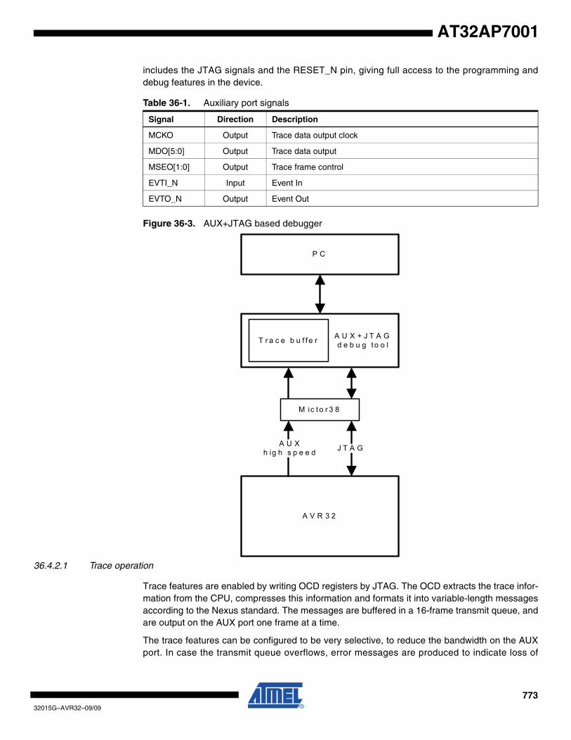
77332015G–AVR32–09/09
AT32AP7001
includes the JTAG signals and the RESET_N pin, giving full access to the programming anddebug features in the device.
Figure 36-3. AUX+JTAG based debugger
36.4.2.1 Trace operation
Trace features are enabled by writing OCD registers by JTAG. The OCD extracts the trace infor-mation from the CPU, compresses this information and formats it into variable-length messagesaccording to the Nexus standard. The messages are buffered in a 16-frame transmit queue, andare output on the AUX port one frame at a time.
The trace features can be configured to be very selective, to reduce the bandwidth on the AUXport. In case the transmit queue overflows, error messages are produced to indicate loss of
Table 36-1. Auxiliary port signals
Signal Direction Description
MCKO Output Trace data output clock
MDO[5:0] Output Trace data output
MSEO[1:0] Output Trace frame control
EVTI_N Input Event In
EVTO_N Output Event Out
A V R 3 2
A U X + J T A Gd e b u g to o l
J T A GA U Xh ig h s p e e d
M ic t o r 3 8
T r a c e b u f f e r
P C
77432015G–AVR32–09/09
AT32AP7001
data. The transmit queue module can optionally be configured to halt the CPU when an overflowoccurs, to prevent the loss of messages, at the expense of longer run-time for the program.
36.4.2.2 Program Trace
Program trace allows the debugger to continuously monitor the program execution in the CPU.Program trace messages are generated for every branch in the program, and contains com-pressed information, which allows the debugger to correlate the message with the source codeto identify the branch instruction and target address.
36.4.2.3 Data Trace
Data trace outputs a message every time a specific location is read or written. The messagecontains information about the type (read/write) and size of the access, as well as the addressand data of the accessed location. The AT32AP7001 contains two data trace channels, each ofwhich are controlled by a pair of OCD registers which determine the range of addresses (or sin-gle address) which should produce data trace messages.
36.4.2.4 Ownership Trace
Program and data trace operate on virtual addresses. In cases where an operating system runsseveral processes in overlapping virtual memory segments, the Ownership Trace feature can beused to identify the process switch. When the O/S activates a process, it will write the process IDnumber to an OCD register, which produces an Ownership Trace Message, allowing the debug-ger to switch context for the subsequent program and data trace messages. As the use of thisfeature depends on the software running on the CPU, it can also be used to extract other typesof information from the system.
36.4.2.5 Watchpoint messages
The breakpoint modules normally used to generate program and data breakpoints can also beused to generate Watchpoint messages, allowing a debugger to monitor program and dataevents without halting the CPU. Watchpoints can be enabled independently of breakpoints, so abreakpoint module can optionally halt the CPU when the trigger condition occurs. Data tracemodules can also be configured to produce watchpoint messages instead of regular data tracemessages.
36.4.2.6 Event In and Event Out pins
The AUX port also contains an Event In pin (EVTI_N) and an Event Out pin (EVTO_N). EVTI_Ncan be used to trigger a breakpoint when an external event occurs. It can also be used to triggerspecific program and data trace synchronization messages, allowing an external event to becorrelated to the program flow.
When the CPU enters debug mode, a Debug Status message is transmitted on the trace port.All trace messages can be timestamped when they are received by the debug tool. However,due to the latency of the transmit queue buffering, the timestamp will not be 100% accurate. Toimprove this, EVTO_N can toggle every time a message is inserted into the transmit queue,allowing trace messages to be timestamped precisely. EVTO_N can also toggle when a break-point module triggers, or when the CPU enters debug mode, for any reason. This can be used tomeasure precisely when the respective internal event occurs.

77532015G–AVR32–09/09
AT32AP7001
36.4.2.7 Software Quality Analysis (SQA)
Software Quality Analysis (SQA) deals with two important issues regarding embedded softwaredevelopment. Code coverage involves identifying untested parts of the embedded code, toimprove test procedures and thus the quality of the released software. Performance analysisallows the developer to precisely quantify the time spent in various parts of the code, allowingbottlenecks to be identified and optimized.
Program trace must be used to accomplish these tasks without instrumenting (altering) the codeto be examined. However, traditional program trace cannot reconstruct the current PC valuewithout correlating the trace information with the source code, which cannot be done on-the-fly.This limits program trace to a relatively short time segment, determined by the size of the tracebuffer in the debug tool.
The OCD system in AT32AP7001 extends program trace with SQA capabilities, allowing thedebug tool to reconstruct the PC value on-the-fly. Code coverage and performance analysis canthus be reported for an unlimited execution sequence.

77632015G–AVR32–09/09
AT32AP7001
37. JTAG and Boundary Scan
Rev.: 1.0.0.0
37.1 Features
• IEEE1149.1 compliant JTAG Interface• Boundary-Scan Chain for board-level testing• Direct memory access and programming capabilities through JTAG interface• On-Chip Debug access in compliance with IEEE-ISTO 5001-2003 (Nexus 2.0)
37.2 Overview
Figure 37-1 on page 777 shows how the JTAG is connected in an AVR32 device. The TAP Con-troller is a state machine controlled by the TCK and TMS signals. The TAP Controller selectseither the JTAG Instruction Register or one of several Data Registers as the scan chain (shiftregister) between the TDI-input and TDO-output. The Instruction Register holds JTAG instruc-tions controlling the behavior of a Data Register.
The Device Identification Register, Bypass Register, and the Boundary-Scan Chain are the DataRegisters used for board-level testing. The Reset Register can be used to keep the device resetduring test or programming.
The Service Access Bus (SAB) interface contains address and data registers for the ServiceAccess Bus, which gives access to on-chip debug, programming, and other functions in thedevice. The SAB offers several modes of access to the address and data registers, as dis-cussed in ”Service Access Bus” on page 780.
”JTAG Instruction Summary” on page 782 lists the supported JTAG instructions, with referencesto the description in this document.
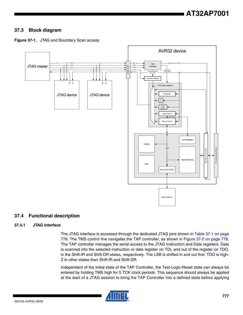
77732015G–AVR32–09/09
AT32AP7001
37.3 Block diagram
Figure 37-1. JTAG and Boundary Scan access
37.4 Functional description
37.4.1 JTAG interface
The JTAG interface is accessed through the dedicated JTAG pins shown in Table 37-1 on page778. The TMS control line navigates the TAP controller, as shown in Figure 37-2 on page 778.The TAP controller manages the serial access to the JTAG Instruction and Data registers. Datais scanned into the selected instruction or data register on TDI, and out of the register on TDO,in the Shift-IR and Shift-DR states, respectively. The LSB is shifted in and out first. TDO is high-Z in other states than Shift-IR and Shift-DR.
Independent of the initial state of the TAP Controller, the Test-Logic-Reset state can always beentered by holding TMS high for 5 TCK clock periods. This sequence should always be appliedat the start of a JTAG session to bring the TAP Controller into a defined state before applying
AVR32 device
JTAG data registers
TAPController
TCK
TMS
TDI
TDO
Instruction Register
ID Register
By-pass
Reset Register
Memory Access
Bou
ndar
y S
can
Cha
in
CPU
Internal Memory
Caches
OCD Registers
External Bus Interface
Pin
s an
d an
alog
blo
cks
Instruction RegisterScan enable
Data registerscan enable
Nexus Access
JTA
G T
AP
TRST_N Boundary scan enable
JTAG deviceJTAG device
JTAG masterTRST_N
TCK
TMS
TDI
TDO
TDI
TDO
External Memory
HSB
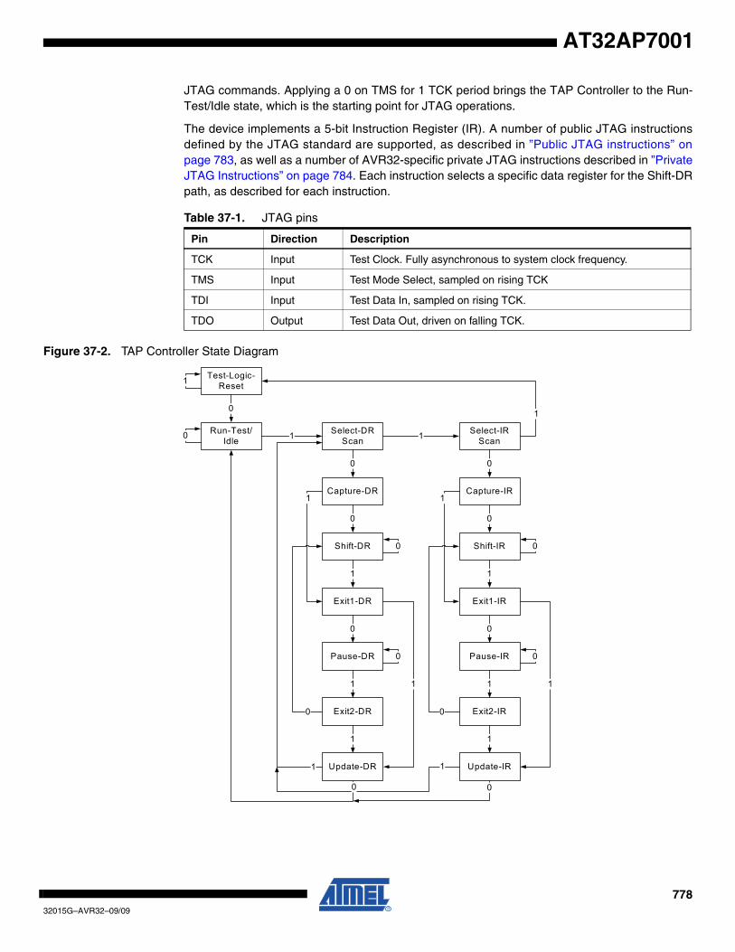
77832015G–AVR32–09/09
AT32AP7001
JTAG commands. Applying a 0 on TMS for 1 TCK period brings the TAP Controller to the Run-Test/Idle state, which is the starting point for JTAG operations.
The device implements a 5-bit Instruction Register (IR). A number of public JTAG instructionsdefined by the JTAG standard are supported, as described in ”Public JTAG instructions” onpage 783, as well as a number of AVR32-specific private JTAG instructions described in ”PrivateJTAG Instructions” on page 784. Each instruction selects a specific data register for the Shift-DRpath, as described for each instruction.
Figure 37-2. TAP Controller State Diagram
Table 37-1. JTAG pins
Pin Direction Description
TCK Input Test Clock. Fully asynchronous to system clock frequency.
TMS Input Test Mode Select, sampled on rising TCK
TDI Input Test Data In, sampled on rising TCK.
TDO Output Test Data Out, driven on falling TCK.
Test-Logic-Reset
Run-Test/Idle
Select-DR Scan
Select-IR Scan
Capture-DR Capture-IR
Shift-DR Shift-IR
Exit1-DR Exit1-IR
Pause-DR Pause-IR
Exit2-DR Exit2-IR
Update-DR Update-IR
0
1 1
1
0
0
1
0
1
1
0
0
1
0
1
1
1
0
1 1
0 0
11
0
1
0
0 0
0
0
1

77932015G–AVR32–09/09
AT32AP7001
37.4.2 Typical sequence
Assuming Run-Test/Idle is the present state, a typical scenario for using the JTAG interface is:
37.4.2.1 Scanning in JTAG instruction
At the TMS input, apply the sequence 1, 1, 0, 0 at the rising edges of TCK to enter the ShiftInstruction Register - Shift-IR state. While in this state, shift the 5 bits of the JTAG instructionsinto the JTAG instruction register from the TDI input at the rising edge of TCK. The TMS inputmust be held low during input of the 4 LSBs in order to remain in the Shift-IR state. The JTAGInstruction selects a particular Data Register as path between TDI and TDO and controls the cir-cuitry surrounding the selected Data Register.
Apply the TMS sequence 1, 1, 0 to re-enter the Run-Test/Idle state. The instruction is latchedonto the parallel output from the shift register path in the Update-IR state. The Exit-IR, Pause-IR,and Exit2-IR states are only used for navigating the state machine.
Figure 37-3. Scanning in JTAG instruction
37.4.2.2 Scanning in/out data
At the TMS input, apply the sequence 1, 0, 0 at the rising edges of TCK to enter the Shift DataRegister - Shift-DR state. While in this state, upload the selected Data Register (selected by thepresent JTAG instruction in the JTAG Instruction Register) from the TDI input at the rising edgeof TCK. In order to remain in the Shift-DR state, the TMS input must be held low. While the DataRegister is shifted in from the TDI pin, the parallel inputs to the Data Register captured in theCapture-DR state is shifted out on the TDO pin.
Apply the TMS sequence 1, 1, 0 to re-enter the Run-Test/Idle state. If the selected Data Registerhas a latched parallel-output, the latching takes place in the Update-DR state. The Exit-DR,Pause-DR, and Exit2-DR states are only used for navigating the state machine.
As shown in the state diagram, the Run-Test/Idle state need not be entered between selectingJTAG instruction and using Data Registers.
37.4.3 Boundary-Scan
The Boundary-Scan chain has the capability of driving and observing the logic levels on the dig-ital I/O pins, as well as the boundary between digital and analog logic for analog circuitry havingoff-chip connections. At system level, all ICs having JTAG capabilities are connected serially bythe TDI/TDO signals to form a long shift register. An external controller sets up the devices todrive values at their output pins, and observe the input values received from other devices. Thecontroller compares the received data with the expected result. In this way, Boundary-Scan pro-vides a mechanism for testing interconnections and integrity of components on Printed CircuitsBoards by using the 4 TAP signals only.
TCK
TAP State TLR RTI SelDR SelIR CapIR ShIR Ex1IR UpdIR RTI
TMS
TDI Instruction
TDO ImplDefined
78032015G–AVR32–09/09
AT32AP7001
The four IEEE 1149.1 defined mandatory JTAG instructions IDCODE, BYPASS, SAMPLE/PRE-LOAD, and EXTEST can be used for testing the Printed Circuit Board. Initial scanning of thedata register path will show the ID-code of the device, since IDCODE is the default JTAGinstruction. It may be desirable to have the AVR32 device in reset during test mode. If not reset,inputs to the device may be determined by the scan operations, and the internal software maybe in an undetermined state when exiting the test mode. Entering reset, the outputs of any PortPin will instantly enter the high impedance state, making the HIGHZ instruction redundant. Ifneeded, the BYPASS instruction can be issued to make the shortest possible scan chainthrough the device. The device can be set in the reset state either by pulling the externalRESETn pin low, or issuing the AVR_RESET instruction with appropriate setting of the ResetData Register.
The EXTEST instruction is used for sampling external pins and loading output pins with data.The data from the output latch will be driven out on the pins as soon as the EXTEST instructionis loaded into the JTAG IR-register. Therefore, the SAMPLE/PRELOAD should also be used forsetting initial values to the scan ring, to avoid damaging the board when issuing the EXTESTinstruction for the first time. SAMPLE/PRELOAD can also be used for taking a snapshot of theexternal pins during normal operation of the part.
When using the JTAG interface for Boundary-Scan, the JTAG TCK clock is independent of theinternal chip clock, which is not required to run.
NOTE: For pins connected to 5V lines care should be taken to not drive the pins to a logic oneusing boundary scan, as this will create a current flowing from the 3,3V driver to the 5V pullup onthe line. Optionally a series resistor can be added between the line and the pin to reduce thecurrent.
37.4.4 Service Access Bus
The AVR32 architecture offers a common interface for access to On-Chip Debug, programming,and test functions. These are mapped on a common bus called the Service Access Bus (SAB),which is linked to the JTAG port through a bus master module, which also handles synchroniza-tion between the JTAG and SAB clocks.
When accessing the SAB through the TAP there are no limitations on TCK frequency comparedto chip frequency, although there must be an active system clock in order for the SAB accessesto complete. If the system clock is switched off in sleep mode, activity on the TCK pin will restartthe system clock automatically, without waking the device from sleep. JTAG masters may opti-mize the transfer rate by adjusting the TCK frequency in relation to the system clock. This ratiocan be measured with the SYNC instruction.
The Service Access Bus uses 36 address bits to address memory or registers in any of theslaves on the bus. The bus supports accesses of words (32 bits). All accesses must be alignedto the size of the access, i.e. word accesses must have the two lowest address bits cleared.
A number of private instructions are used to access SAB resources. Each of these are describedin detail in ”Private JTAG Instructions” on page 784. The MEMORY_WORD_ACCESS instruc-tion allows a read or write a word to any 36-bit address on the bus. NEXUS_ACCESS instructionis a Nexus-compliant shorthand instruction for accessing the 32-bit OCD registers in the 7-bitaddress space reserved for these. These instructions require two passes through the Shift-DRTAP state: one for the address and control information, and one for data.

78132015G–AVR32–09/09
AT32AP7001
To increase the transfer rate, consecutive memory accesses can be accomplished by theMEMORY_BLOCK_ACCESS instruction, which only requires a single pass through Shift-DR fordata transfer only. The address is automatically increment the address.
The access time to SAB resources depends on the type of resource being accessed. It is possi-ble to read external memory through the EBI, in which case the latency may be very long. It ispossible to abort an ongoing SAB access by the CANCEL_ACCESS instruction, to avoid hang-ing the bus due to an extremely slow slave.
37.4.4.1 Busy reporting
As the time taken to perform an access may vary depending on system activity and current chipfrequency, all the SAB access JTAG instructions can return a busy indicator. This indicateswhether a delay needs to be inserted, or an operation needs to be repeated in order to be suc-cessful. If a new access is requested while the SAB is busy, the request is ignored.
The SAB becomes busy when:
• Entering Update-DR in the address phase of any read operation, e.g. after scanning in a NEXUS_ACCESS address with the read bit set.
• Entering Update-DR in the data phase of any write operation, e.g. after scanning in data for a NEXUS_ACCESS write.
• Entering Update-DR during a MEMORY_BLOCK_ACCESS.
• Entering Update-DR after scanning in a counter value for SYNC.
• Entering Update-IR after scanning in a MEMORY_BLOCK_ACCESS if the previous access was a read and data was scanned after scanning the address.
The SAB becomes ready again when:
• A read or write operation completes.
• A SYNC countdown completed.
• A operation is cancelled by the CANCEL_ACCESS instruction.
What to do if the busy bit is set:
• During Shift-IR: The new instruction is selected, but the previous operation has not yet completed and will continue (unless the new instruction is CANCEL_ACCESS). You may continue shifting the same instruction until the busy bit clears, or start shifting data. If shifting data, you must be prepared that the data shift may also report busy.
• During Shift-DR of an address: The new address is ignored. The SAB stays in address mode, so no data must be shifted. Repeat the address until the busy bit clears.
• During Shift-DR of read data: The read data are invalid. The SAB stays in data mode. Repeat scanning until the busy bit clears.
• During Shift-DR of write data: The write data are ignored. The SAB stays in data mode. Repeat scanning until the busy bit clears.
37.4.4.2 Error reporting
The Service access port may not be able to complete all accesses as requested. This may bebecause the address is invalid, the addressed area is read-only or cannot handle byte/halfwordaccesses, or because the chip is set in a protected mode where only limited accesses areallowed.
The error bit is updated when an access completes, and is cleared when a new access starts.
78232015G–AVR32–09/09
AT32AP7001
What to do if the error bit is set:
• During Shift-IR: The new instruction is selected. The last operation performed using the old instruction did not complete successfully.
• During Shift-DR of an address: The previous operation failed. The new address is accepted. If the read bit is set, a read operation is started.
• During Shift-DR of read data: The read operation failed, and the read data are invalid.
• During Shift-DR of write data: The previous write operation failed. The new data are accepted and a write operation started. This should only occur during block writes or stream writes. No error can occur between scanning a write address and the following write data.
• While polling with CANCEL_ACCESS: The previous access was cancelled. It may or may not have actually completed.
37.4.5 Memory programming
The High-Speed Bus (HSB) in the device is mapped as a slave on the SAB. This enables allHSB-mapped memories to be read or written through the SAB using JTAG instructions, asdescribed in ”Service Access Bus” on page 780.
Internal SRAM can always be directly accessed. External static memory or SDRAM can beaccessed if the EBI has been correctly configured to access this memory. It is also possible toaccess the configuration registers for these modules to set up the correct configuration. Simi-larly, external parallel flash can be programmed by accessing the registers for the flash devicethrough the EBI.
Memory can be written while the CPU is executing, which can be utilized for debug purposes.When downloading a new program, the AVR_RESET instruction should be used to freeze theCPU, to prevent partially downloaded code from being executed.
37.5 JTAG Instruction Summary
The implemented JTAG instructions in the AVR32 are shown in the table below.
Table 37-2. JTAG Instruction Summary
Instruction OPCODE Instruction Description Page
0x01 IDCODE Select the 32-bit Device Identification register as data register. 783
0x02 SAMPLE_PRELOADTake a snapshot of external pin values without affecting system operation.
783
0x03 EXTESTSelect boundary scan chain as data register for testing circuitry external to the device.
783
0x04 INTEST Select boundary scan chain for internal testing of the device. 783
0x06 CLAMPBypass device through Bypass register, while driving outputs from boundary scan register.
784
0x0C AVR_RESET Apply or remove a static reset to the device 789
0x10 NEXUS_ACCESSSelect the SAB Address and Data registers as data register for the TAP. The registers are accessed in Nexus mode.
785
0x11 MEMORY_WORD_ACCESSSelect the SAB Address and Data registers as data register for the TAP.
786
78332015G–AVR32–09/09
AT32AP7001
37.6 Public JTAG instructions
37.6.1 IDCODE
This instruction selects the 32 bit Device Identification register as Data Register. The DeviceIdentification register consists of a version number, a device number and the manufacturer codechosen by JEDEC. This is the default instruction after power-up.
The active states are:
• Capture-DR: The static IDCODE value is latched into the shift register.
• Shift-DR: The IDCODE scan chain is shifted by the TCK input.
37.6.2 SAMPLE_PRELOAD
JTAG instruction for taking a snap-shot of the input/output pins without affecting the systemoperation, and pre-loading the scan chain without updating the DR-latch. The Boundary-ScanChain is selected as Data Register.
The active states are:
• Capture-DR: Data on the external pins are sampled into the Boundary-Scan Chain.
• Shift-DR: The Boundary-Scan Chain is shifted by the TCK input.
EXTEST
JTAG instruction for selecting the Boundary-Scan Chain as Data Register for testing circuitryexternal to the AVR32 package. The contents of the latched outputs of the Boundary-Scan chainis driven out as soon as the JTAG IR-register is loaded with the EXTEST instruction.
The active states are:
• Capture-DR: Data on the external pins is sampled into the Boundary-Scan Chain.
• Shift-DR: The Internal Scan Chain is shifted by the TCK input.
• Update-DR: Data from the scan chain is applied to output pins.
37.6.3 INTEST
This instruction selects the Boundary-Scan Chain as Data Register for testing internal logic inthe device. The logic inputs are determined by the Boundary-Scan Chain, and the logic outputsare captured by the Boundary-Scan chain. The device output pins are driven from the Boundary-Scan Chain.
0x12 MEMORY_BLOCK_ACCESSSelect the SAB Data register as data register for the TAP. The address is auto-incremented.
787
0x13 CANCEL_ACCESS Cancel an ongoing Nexus or Memory access. 788
0x17 SYNC Synchronization counter 788
0x1F BYPASS Bypass this device through the bypass register. 784
Others N/A Acts as BYPASS
Table 37-2. JTAG Instruction Summary
Instruction OPCODE Instruction Description Page
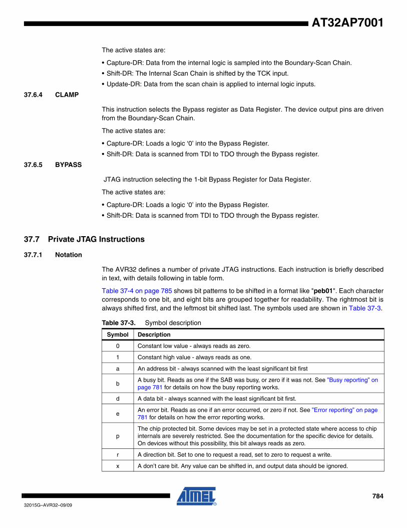
78432015G–AVR32–09/09
AT32AP7001
The active states are:
• Capture-DR: Data from the internal logic is sampled into the Boundary-Scan Chain.
• Shift-DR: The Internal Scan Chain is shifted by the TCK input.
• Update-DR: Data from the scan chain is applied to internal logic inputs.
37.6.4 CLAMP
This instruction selects the Bypass register as Data Register. The device output pins are drivenfrom the Boundary-Scan Chain.
The active states are:
• Capture-DR: Loads a logic ‘0’ into the Bypass Register.
• Shift-DR: Data is scanned from TDI to TDO through the Bypass register.
37.6.5 BYPASS
JTAG instruction selecting the 1-bit Bypass Register for Data Register.
The active states are:
• Capture-DR: Loads a logic ‘0’ into the Bypass Register.
• Shift-DR: Data is scanned from TDI to TDO through the Bypass register.
37.7 Private JTAG Instructions
37.7.1 Notation
The AVR32 defines a number of private JTAG instructions. Each instruction is briefly describedin text, with details following in table form.
Table 37-4 on page 785 shows bit patterns to be shifted in a format like "peb01". Each charactercorresponds to one bit, and eight bits are grouped together for readability. The rightmost bit isalways shifted first, and the leftmost bit shifted last. The symbols used are shown in Table 37-3.
Table 37-3. Symbol description
Symbol Description
0 Constant low value - always reads as zero.
1 Constant high value - always reads as one.
a An address bit - always scanned with the least significant bit first
bA busy bit. Reads as one if the SAB was busy, or zero if it was not. See ”Busy reporting” on page 781 for details on how the busy reporting works.
d A data bit - always scanned with the least significant bit first.
eAn error bit. Reads as one if an error occurred, or zero if not. See ”Error reporting” on page 781 for details on how the error reporting works.
pThe chip protected bit. Some devices may be set in a protected state where access to chip internals are severely restricted. See the documentation for the specific device for details. On devices without this possibility, this bit always reads as zero.
r A direction bit. Set to one to request a read, set to zero to request a write.
x A don’t care bit. Any value can be shifted in, and output data should be ignored.

78532015G–AVR32–09/09
AT32AP7001
In many cases, it is not required to shift all bits through the data register. Bit patterns are shownusing the full width of the shift register, but the suggested or required bits are emphasized usingbold text. I.e. given the pattern "aaaaaaar xxxxxxxx xxxxxxxx xxxxxxxx xx", the shift register is34 bits, but the test or debug unit may choose to shift only 8 bits "aaaaaaar".
The following describes how to interpret the fields in the instruction description tables:
37.7.2 NEXUS_ACCESS
This instruction allows Nexus-compliant access to on-chip debug registers through the SAB.OCD registers are addressed by their register index, as listed in the AVR32 Technical ReferenceManual. The 7-bit register index and a read/write control bit, and the 32-bit data is accessedthrough the JTAG port.
The data register is alternately interpreted by the SAB as an address register and a data regis-ter. The SAB starts in address mode after the NEXUS_ACCESS instruction is selected, andtoggles between address and data mode each time a data scan completes with the busy bitcleared.
NOTE: The polarity of the direction bit is inverse of the Nexus standard.
Starting in Run-Test/Idle, OCD registers are accessed in the following way:
1. Select the DR Scan path
2. Scan in the 7-bit address for the OCD register and a direction bit (1=read, 0=write).
3. Go to Update-DR and re-enter Select-DR Scan
4. For a read operation, scan out the contents of the addressed register. For a write opera-tion, scan in the new contents of the register.
5. Return to Run-Test/Idle
Table 37-4. Instruction description
Instruction Description
IR input value
Shows the bit pattern to shift into IR in the Shift-IR state in order to select this instruction. The pattern is show both in binary and in hexadecimal form for convenience.
Example: 10000 (0x10)
IR output valueShows the bit pattern shifted out of IR in the Shift-IR state when this instruction is active.Example: peb01
DR SizeShows the number of bits in the data register chain when this instruction is active.Example: 34 bits
DR input value
Shows which bit pattern to shift into the data register in the Shift-DR state when this instruction is active. Multiple such lines may exist, e.g. to distinguish between reads and writes.
Example: aaaaaaar xxxxxxxx xxxxxxxx xxxxxxxx xx
DR output value
Shows the bit pattern shifted out of the data register in the Shift-DR state when this instruction is active. Multiple such lines may exist, e.g. to distinguish between reads and writes.
Example: xx xxxxxxxx xxxxxxxx xxxxxxxx xxxxxxeb
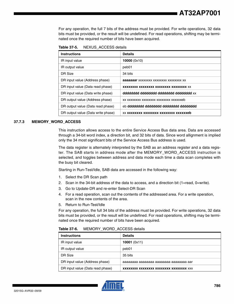
78632015G–AVR32–09/09
AT32AP7001
For any operation, the full 7 bits of the address must be provided. For write operations, 32 databits must be provided, or the result will be undefined. For read operations, shifting may be termi-nated once the required number of bits have been acquired.
37.7.3 MEMORY_WORD_ACCESS
This instruction allows access to the entire Service Access Bus data area. Data are accessedthrough a 34-bit word index, a direction bit, and 32 bits of data. Since word allignment is impliedonly the 34 most significant bits of the Service Access Bus address is used.
The data register is alternately interpreted by the SAB as an address register and a data regis-ter. The SAB starts in address mode after the MEMORY_WORD_ACCESS instruction isselected, and toggles between address and data mode each time a data scan completes withthe busy bit cleared.
Starting in Run-Test/Idle, SAB data are accessed in the following way:
1. Select the DR Scan path
2. Scan in the 34-bit address of the data to access, and a direction bit (1=read, 0=write).
3. Go to Update-DR and re-enter Select-DR Scan
4. For a read operation, scan out the contents of the addressed area. For a write operation, scan in the new contents of the area.
5. Return to Run-Test/Idle
For any operation, the full 34 bits of the address must be provided. For write operations, 32 databits must be provided, or the result will be undefined. For read operations, shifting may be termi-nated once the required number of bits have been acquired.
Table 37-5. NEXUS_ACCESS details
Instructions Details
IR input value 10000 (0x10)
IR output value peb01
DR Size 34 bits
DR input value (Address phase) aaaaaaar xxxxxxxx xxxxxxxx xxxxxxxx xx
DR input value (Data read phase) xxxxxxxx xxxxxxxx xxxxxxxx xxxxxxxx xx
DR input value (Data write phase) dddddddd dddddddd dddddddd dddddddd xx
DR output value (Address phase) xx xxxxxxxx xxxxxxxx xxxxxxxx xxxxxxeb
DR output value (Data read phase) eb dddddddd dddddddd dddddddd dddddddd
DR output value (Data write phase) xx xxxxxxxx xxxxxxxx xxxxxxxx xxxxxxeb
Table 37-6. MEMORY_WORD_ACCESS details
Instructions Details
IR input value 10001 (0x11)
IR output value peb01
DR Size 35 bits
DR input value (Address phase) aaaaaaaa aaaaaaaa aaaaaaaa aaaaaaaa aar
DR input value (Data read phase) xxxxxxxx xxxxxxxx xxxxxxxx xxxxxxxx xxx

78732015G–AVR32–09/09
AT32AP7001
37.7.4 MEMORY_BLOCK_ACCESS
This instruction allows access to the entire SAB data area. Up to 32 bits of data are accessed ata time, while the address is sequentially incremented from the previously used address.
In this mode, the SAB address, and access direction is not provided with each access. Instead,the previous address is auto-incremented and the previous operation repeated. The addressmust be set up in advance with MEMORY_WORD_ACCESS. It is allowed, but not required, toshift data after shifting the address.
This instruction is primarily intended to speed up large quantities of sequential word accesses..
The following sequence should be used:
1. Use the MEMORY_WORD_ACCESS to read or write the first location.
2. Apply MEMORY_BLOCK_ACCESS in the IR Scan path.
3. Select the DR Scan path. The address will now have incremented by 4 (corresponding to the next word location).
4. For a read operation, scan out the contents of the next addressed location. For a write operation, scan in the new contents of the next addressed location.
5. Go to Update-DR
6. If the block access is not complete, return to Select-DR Scan and repeat the access.
7. If the block access is complete, return to Run-Test/Idle
For write operations, 32 data bits must be provided, or the result will be undefined. For readoperations, shifting may be terminated once the required number of bits have been acquired.
The overhead using block word access is 4 cycles per 32 bits of data, resulting in an 88% trans-fer efficiency, or 2.1 MBytes per second with a 20 MHz TCK frequency.
DR input value (Data write phase) dddddddd dddddddd dddddddd dddddddd xxx
DR output value (Address phase) xxx xxxxxxxx xxxxxxxx xxxxxxxx xxxxxxxx
DR output value (Data read phase) xeb dddddddd dddddddd dddddddd dddddddd
DR output value (Data write phase) xxx xxxxxxxx xxxxxxxx xxxxxxxx xxxxxxeb
Table 37-6. MEMORY_WORD_ACCESS details (Continued)
Instructions Details
Table 37-7. MEMORY_BLOCK_ACCESS details
Instructions Details
IR input value 10010 (0x12)
IR output value peb01
DR Size 34 bits
DR input value (Data read phase) xxxxxxxx xxxxxxxx xxxxxxxx xxxxxxxx xx
DR input value (Data write phase) dddddddd dddddddd dddddddd dddddddd xx
DR output value (Data read phase) eb dddddddd dddddddd dddddddd dddddddd
DR output value (Data write phase) xx xxxxxxxx xxxxxxxx xxxxxxxx xxxxxxeb
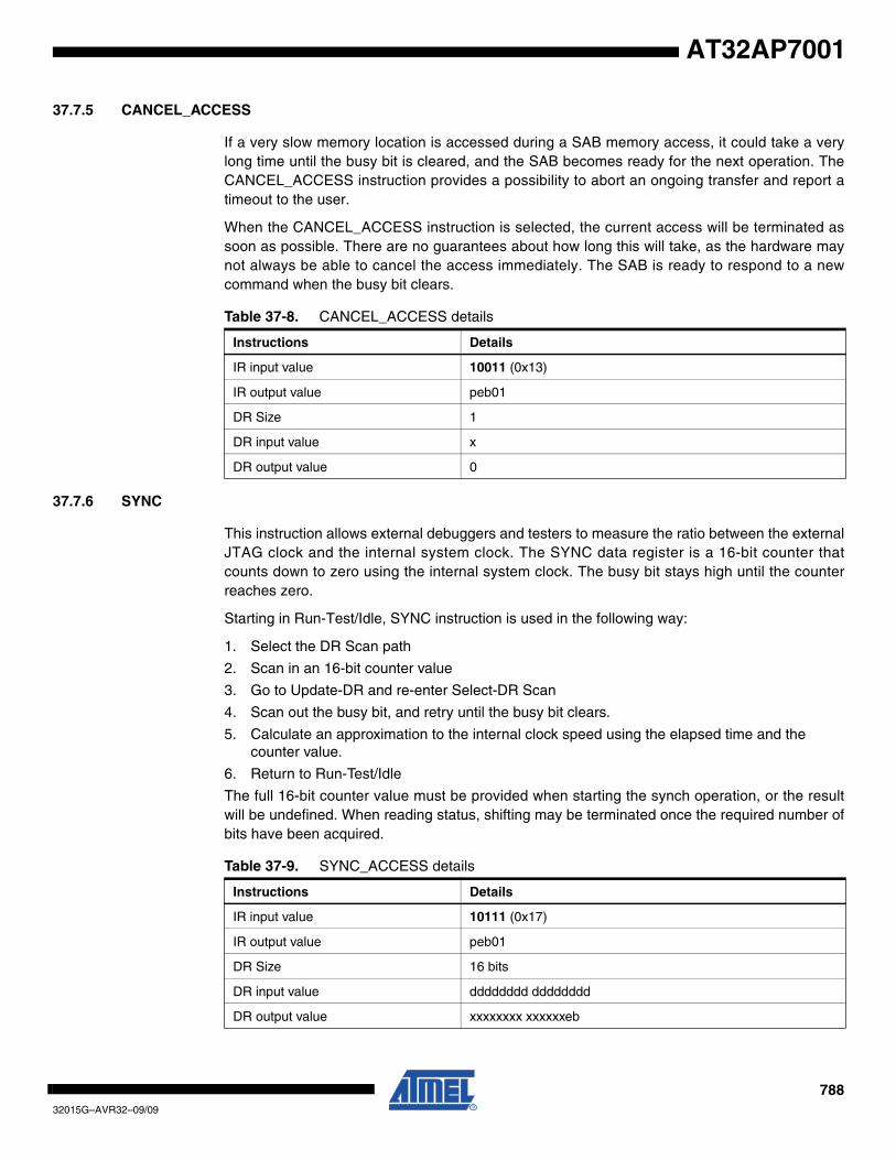
78832015G–AVR32–09/09
AT32AP7001
37.7.5 CANCEL_ACCESS
If a very slow memory location is accessed during a SAB memory access, it could take a verylong time until the busy bit is cleared, and the SAB becomes ready for the next operation. TheCANCEL_ACCESS instruction provides a possibility to abort an ongoing transfer and report atimeout to the user.
When the CANCEL_ACCESS instruction is selected, the current access will be terminated assoon as possible. There are no guarantees about how long this will take, as the hardware maynot always be able to cancel the access immediately. The SAB is ready to respond to a newcommand when the busy bit clears.
37.7.6 SYNC
This instruction allows external debuggers and testers to measure the ratio between the externalJTAG clock and the internal system clock. The SYNC data register is a 16-bit counter thatcounts down to zero using the internal system clock. The busy bit stays high until the counterreaches zero.
Starting in Run-Test/Idle, SYNC instruction is used in the following way:
1. Select the DR Scan path
2. Scan in an 16-bit counter value
3. Go to Update-DR and re-enter Select-DR Scan
4. Scan out the busy bit, and retry until the busy bit clears.
5. Calculate an approximation to the internal clock speed using the elapsed time and the counter value.
6. Return to Run-Test/Idle
The full 16-bit counter value must be provided when starting the synch operation, or the resultwill be undefined. When reading status, shifting may be terminated once the required number ofbits have been acquired.
Table 37-8. CANCEL_ACCESS details
Instructions Details
IR input value 10011 (0x13)
IR output value peb01
DR Size 1
DR input value x
DR output value 0
Table 37-9. SYNC_ACCESS details
Instructions Details
IR input value 10111 (0x17)
IR output value peb01
DR Size 16 bits
DR input value dddddddd dddddddd
DR output value xxxxxxxx xxxxxxeb
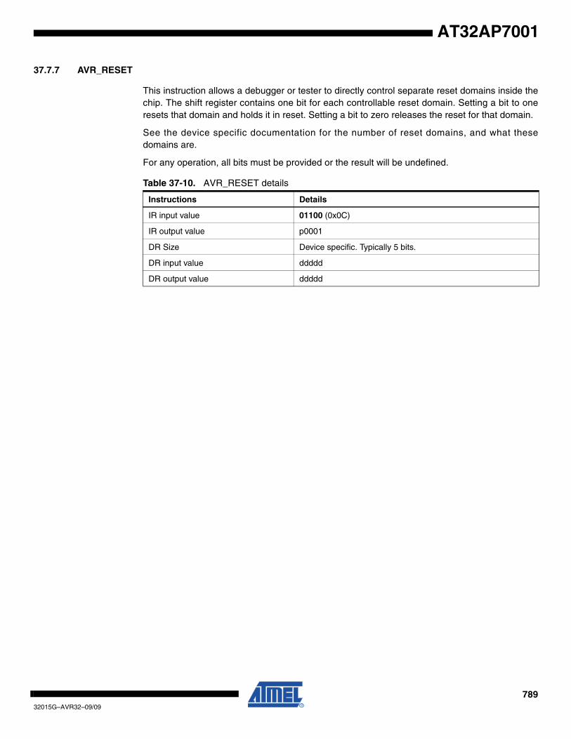
78932015G–AVR32–09/09
AT32AP7001
37.7.7 AVR_RESET
This instruction allows a debugger or tester to directly control separate reset domains inside thechip. The shift register contains one bit for each controllable reset domain. Setting a bit to oneresets that domain and holds it in reset. Setting a bit to zero releases the reset for that domain.
See the device specific documentation for the number of reset domains, and what thesedomains are.
For any operation, all bits must be provided or the result will be undefined.
Table 37-10. AVR_RESET details
Instructions Details
IR input value 01100 (0x0C)
IR output value p0001
DR Size Device specific. Typically 5 bits.
DR input value ddddd
DR output value ddddd
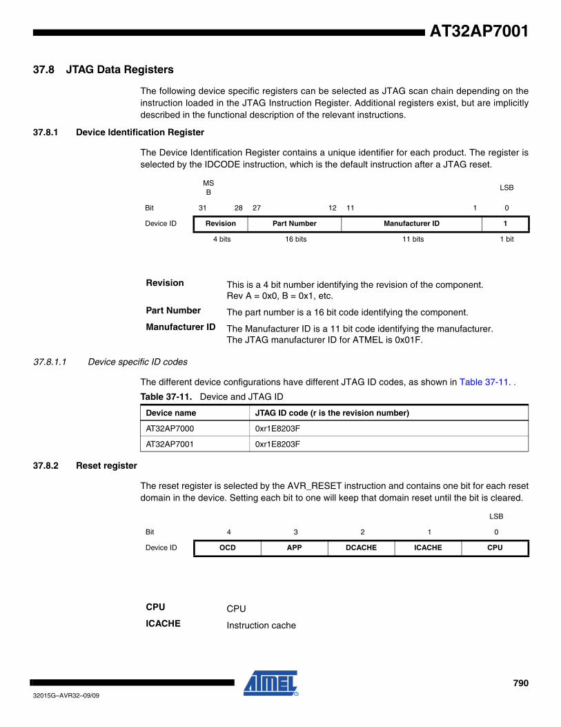
79032015G–AVR32–09/09
AT32AP7001
37.8 JTAG Data Registers
The following device specific registers can be selected as JTAG scan chain depending on theinstruction loaded in the JTAG Instruction Register. Additional registers exist, but are implicitlydescribed in the functional description of the relevant instructions.
37.8.1 Device Identification Register
The Device Identification Register contains a unique identifier for each product. The register isselected by the IDCODE instruction, which is the default instruction after a JTAG reset.
37.8.1.1 Device specific ID codes
The different device configurations have different JTAG ID codes, as shown in Table 37-11. .
37.8.2 Reset register
The reset register is selected by the AVR_RESET instruction and contains one bit for each resetdomain in the device. Setting each bit to one will keep that domain reset until the bit is cleared.
MSB
LSB
Bit 31 28 27 12 11 1 0
Device ID Revision Part Number Manufacturer ID 1
4 bits 16 bits 11 bits 1 bit
Revision This is a 4 bit number identifying the revision of the component.Rev A = 0x0, B = 0x1, etc.
Part Number The part number is a 16 bit code identifying the component.
Manufacturer ID The Manufacturer ID is a 11 bit code identifying the manufacturer.The JTAG manufacturer ID for ATMEL is 0x01F.
Table 37-11. Device and JTAG ID
Device name JTAG ID code (r is the revision number)
AT32AP7000 0xr1E8203F
AT32AP7001 0xr1E8203F
LSB
Bit 4 3 2 1 0
Device ID OCD APP DCACHE ICACHE CPU
CPU CPU
ICACHE Instruction cache
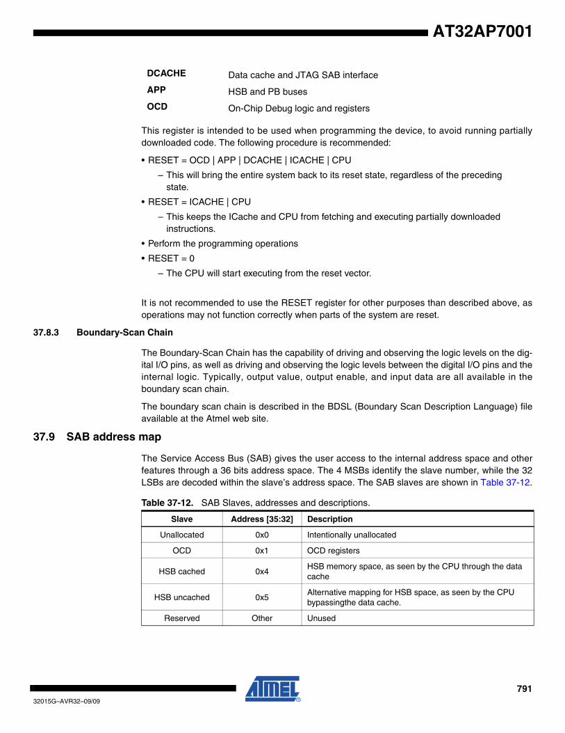
79132015G–AVR32–09/09
AT32AP7001
This register is intended to be used when programming the device, to avoid running partiallydownloaded code. The following procedure is recommended:
• RESET = OCD | APP | DCACHE | ICACHE | CPU
– This will bring the entire system back to its reset state, regardless of the preceding state.
• RESET = ICACHE | CPU
– This keeps the ICache and CPU from fetching and executing partially downloaded instructions.
• Perform the programming operations
• RESET = 0
– The CPU will start executing from the reset vector.
It is not recommended to use the RESET register for other purposes than described above, asoperations may not function correctly when parts of the system are reset.
37.8.3 Boundary-Scan Chain
The Boundary-Scan Chain has the capability of driving and observing the logic levels on the dig-ital I/O pins, as well as driving and observing the logic levels between the digital I/O pins and theinternal logic. Typically, output value, output enable, and input data are all available in theboundary scan chain.
The boundary scan chain is described in the BDSL (Boundary Scan Description Language) fileavailable at the Atmel web site.
37.9 SAB address map
The Service Access Bus (SAB) gives the user access to the internal address space and otherfeatures through a 36 bits address space. The 4 MSBs identify the slave number, while the 32LSBs are decoded within the slave’s address space. The SAB slaves are shown in Table 37-12.
DCACHE Data cache and JTAG SAB interface
APP HSB and PB buses
OCD On-Chip Debug logic and registers
Table 37-12. SAB Slaves, addresses and descriptions.
Slave Address [35:32] Description
Unallocated 0x0 Intentionally unallocated
OCD 0x1 OCD registers
HSB cached 0x4HSB memory space, as seen by the CPU through the data cache
HSB uncached 0x5Alternative mapping for HSB space, as seen by the CPU bypassingthe data cache.
Reserved Other Unused
79232015G–AVR32–09/09
AT32AP7001
38. Boot Sequence
This chapter summarizes the boot sequence of the AT32AP7001. The behaviour after power-upis controlled by the Power Manager.
38.1 Starting of clocks
After power-up, the device will be held in a reset state by the Power-On Reset (POR) circuitryuntil the voltage has reached the power-on reset rising threshold value (see Electrical Character-istics for details). This ensures that all critical parts of the device are properly reset.
Once the power-on reset is complete, the device will use the XIN0 pin as clock source. XIN0 canbe connected either to an external clock, or a crystal. The OSCEN_N pin is connected either toVDD or GND to inform the Power Manager on how the XIN0 pin is connected. If XIN0 receives asignal from a crystal, dedicated circuitry in the Power Manager keeps the part in a reset stateuntil the oscillator connected to XIN0 has settled. If XIN0 receives an external clock, no such set-tling delay is applied.
On system start-up, the PLLs are disabled. All clocks to all modules are running. No clocks havea divided frequency, all parts of the system recieves a clock with the same frequency as theXIN0 clock.
Note that the power-on reset will release reset at a lower voltage threshold than the minimumspecified operating voltage. If the voltage is not guaranteed to be stable by the time the devicestarts executing, an external brown-out reset circuit should be used.
38.2 Fetching of initial instructions
After reset has been released, the AVR32AP CPU starts fetching instructions from the resetaddress, which is 0xA000_0000. This address lies in the P2 segment, which is non-translated,non-cacheable, and permanently mapped to the physical address range 0x0000_0000 to0x2000_0000. This means that the instruction being fetched from virtual address 0xA000_0000is being fetched from physical address 0x0000_0000. Physical address 0x0000_0000 ismapped to EBI SRAM CS0. This is the external memory the device boots from.
The code read from the SRAM CS0 memory is free to configure the system to use for examplethe PLLs, to divide the frequency of the clock routed to some of the peripherals, and to gate theclocks to unused peripherals.
79332015G–AVR32–09/09
AT32AP7001
39. Mechanical Characteristics
39.1 AVR32AP7001
39.1.1 Thermal Considerations
39.1.1.1 Thermal Data
Table 38-1 summarizes the thermal resistance data depending on the package.
39.1.1.2 Junction Temperature
The average chip-junction temperature, TJ, in °C can be obtained from the following:
1.
2.
where:
•θJA = package thermal resistance, Junction-to-ambient (°C/W), provided in Table 38-4 on page 769.
•θJC = package thermal resistance, Junction-to-case thermal resistance (°C/W), provided in Table 38-4 on page 769.
•θHEAT SINK = cooling device thermal resistance (°C/W), provided in the device datasheet.
•PD = device power consumption (W) estimated from data provided in the Power consumption section, in the next chapter.
•TA = ambient temperature (°C).
From the first equation, the user can derive the estimated lifetime of the chip and decide if acooling device is necessary or not. If a cooling device is to be fitted on the chip, the secondequation should be used to compute the resulting average chip-junction temperature TJ in °C.
Table 39-1. Thermal Resistance Data
Symbol Parameter Condition Package Typ Unit
θJA Junction-to-ambient thermal resistance Still Air QFP208 38°C/W
θJC Junction-to-case thermal resistance QFP208 6.8
TJ TA PD θJA×( )+=
TJ TA P( D θ( HEATSINK× θJC ) )+ +=
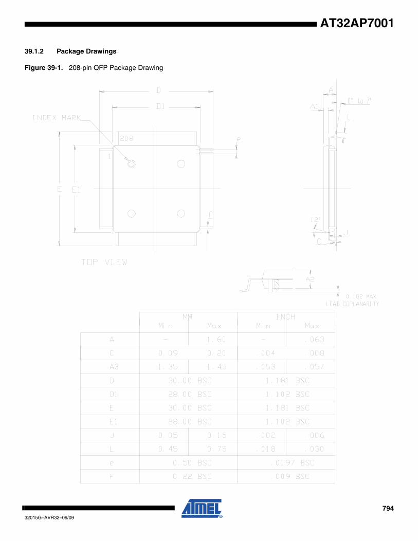
79432015G–AVR32–09/09
AT32AP7001
39.1.2 Package Drawings
Figure 39-1. 208-pin QFP Package Drawing
79532015G–AVR32–09/09
AT32AP7001
39.1.3 Soldering Profile
Table 38-6 gives the recommended soldering profile from J-STD-20.
Note: It is recommended to apply a soldering temperature higher than 250°C. A maximum of three reflow passes is allowed per component.
Table 39-2. Soldering Information
Pin Land 0.29 x 1.35 mm
Table 39-3. Device and 208-QFP Package Maximum Weight
2850 mg
Table 39-4. 208-QFP Package Characteristics
Moisture Sensitivity Level 3
Table 39-5. Package Reference
JEDEC Drawing Reference MS-029
JESD97 Classification e3
Table 39-6. Soldering Profile
Profile Feature Green Package
Average Ramp-up Rate (217°C to Peak) 3°C/sec
Preheat Temperature 175°C ±25°C 60 - 180 sec
Temperature Maintained Above 217°C 60 - 150 sec
Time within 5°C of Actual Peak Temperature 20 - 40 sec
Peak Temperature Range 260 + 0°C
Ramp-down Rate 6°C/sec max
Time 25°C to Peak Temperature 8 minuts max
79632015G–AVR32–09/09
AT32AP7001
40. Electrical Characteristics
40.1 Absolute Maximum Ratings
40.2 DC CharacteristicsThe following characteristics are applicable to the operating temperature range: TA = -40°C to 85°C, unless otherwise spec-ified and are certified for a junction temperature up to TJ = 100°C.
Table 40-1. Absolute Maximum Ratings*
Operating Temperature (Industrial)............ -40°C to +85°C *NOTICE: Stresses beyond those listed under “Absolute Maximum Ratings” may cause permanent damage to the device. This is a stress rating only and functional operation of the device at these or other conditions beyond those indicated in the operational sections of this specification is not implied. Exposure to absolute maximum rating conditions for extended periods may affect device reli-ability.
Storage Temperature ............................... -60°C to +150°C
Voltage on Input Pinswith Respect to Ground-0.3V to VDDIO + 0.3V (+3.9V max)
Maximum Operating Voltage(VDDCORE, VDDOSC, VDDPLL and VDDUSB) ..... 1.95V
Maximum Operating Voltage(VDDIO ) ..................................................................... 3.6V
Total DC Output Current on all I/O lines ................ 350 mA
Table 40-2. DC Characteristics
Symbol Parameter Conditions Min Typ Max Units
VVDDCORE DC Supply Core 1.65 1.95 V
VVDDBU DC Supply Backup 1.65 1.95
VVDDOSC DC Supply Oscillator 1.65 1.95 V
VVDDPLL DC Supply PLL 1.65 1.95 V
VVDDUSB DC Supply USB 1.65 1.95 V
VVDDIODC Supply Peripheral I/Os
3.0 3.6 V
VIL Input Low-level Voltage -0.3 +0.8 V
VIH Input High-level Voltage 2.0 VVDDIO+0.3 V
VOL Output Low-level VoltageIOL = 8 mA
0.4 VIOL, TDO= 2 mA
VOH Output High-level VoltageIOH = 8 mA
VVDDIO-0.4 VIOH, TDO = 2 mA
IILInput Leakage Current, Pin Low
Pullup resistors disabled 1 µA
IIHInput Leakage Current, Pin High
Pullup resistors disabled 1 µA
RPULLUPPIOPull-up Resistance on PIO pins
190 kΩ
79732015G–AVR32–09/09
AT32AP7001
Note: 1. Includes the TCK, TMS, TDI, OSCEN_N, TRST_N, RESET_N, EVTI_N, and WAKE_N pins.
40.3 Power Consumption•Typical power consumption of PLLs, Slow Clock and Main Oscillator.
•Power consumption of power supply in Active mode.
•Power consumption by peripheral: calculated as the difference in current measurement after having enabled then disabled the corresponding clock.
40.3.1 Power Consumption versus ModesThe values in Table 40-3 and Table 40-4 on page 798 are measured values of power consump-tion with operating conditions as follows:
•VVDDIO = 3.3V
•VVDDCORE = VVDDUSB= VVDDPLL= VVDDOSC = 1.8V
•TA = 25°C
•There is no consumption on the I/Os of the device
Figure 40-1. Measures Schematics
RPULLUPCTRLPull-up Resistance on Control and JTAG pins(1) 13 kΩ
IO Output Current 8mA
IO, TDO Output Current, TDO pin 2
ISC Static Current
On VVDDCORE = 1.8V,
CPU = 0 HzTA =25°C 300
µAAll inputs driven; RESET_N=1
TA =85°C 5000
Table 40-2. DC Characteristics (Continued)
VDDCORE
VDDUSB
VDDPLL
VDDOSC
AMP
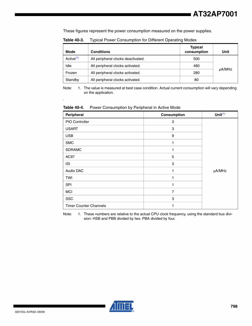
79832015G–AVR32–09/09
AT32AP7001
These figures represent the power consumption measured on the power supplies.
Note: 1. The value is measured at best case condition. Actual current consumption will vary depending on the application.
.
Note: 1. These numbers are relative to the actual CPU clock frequency, using the standard bus divi-sion: HSB and PBB divided by two. PBA divided by four.
Table 40-3. Typical Power Consumption for Different Operating Modes
Mode ConditionsTypical
consumption Unit
Active(1) All peripheral clocks deactivated. 500
µA/MHzIdle All peripheral clocks activated. 480
Frozen All peripheral clocks activated. 280
Standby All peripheral clocks activated. 80
Table 40-4. Power Consumption by Peripheral in Active Mode
Peripheral Consumption Unit(1)
PIO Controller 3
µA/MHz
USART 3
USB 9
SMC 1
SDRAMC 1
AC97 5
ISI 3
Audio DAC 1
TWI 1
SPI 1
MCI 7
SSC 3
Timer Counter Channels 1
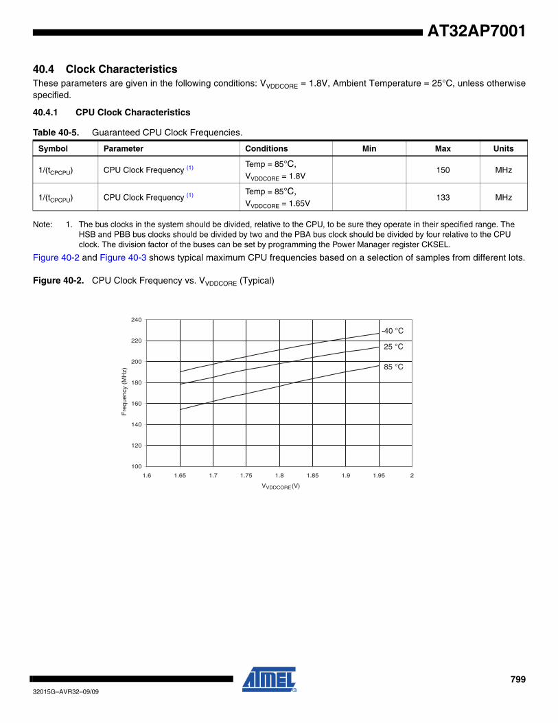
79932015G–AVR32–09/09
AT32AP7001
40.4 Clock CharacteristicsThese parameters are given in the following conditions: VVDDCORE = 1.8V, Ambient Temperature = 25°C, unless otherwisespecified.
40.4.1 CPU Clock Characteristics
Note: 1. The bus clocks in the system should be divided, relative to the CPU, to be sure they operate in their specified range. The HSB and PBB bus clocks should be divided by two and the PBA bus clock should be divided by four relative to the CPU clock. The division factor of the buses can be set by programming the Power Manager register CKSEL.
Figure 40-2 and Figure 40-3 shows typical maximum CPU frequencies based on a selection of samples from different lots.
Figure 40-2. CPU Clock Frequency vs. VVDDCORE (Typical)
Table 40-5. Guaranteed CPU Clock Frequencies.
Symbol Parameter Conditions Min Max Units
1/(tCPCPU) CPU Clock Frequency (1) Temp = 85°C,VVDDCORE = 1.8V
150 MHz
1/(tCPCPU) CPU Clock Frequency (1) Temp = 85°C,VVDDCORE = 1.65V
133 MHz
85 °C
25 °C
-40 °C
100
120
140
160
180
200
220
240
1.6 1.65 1.7 1.75 1.8 1.85 1.9 1.95 2
VVDDCORE (V)
Fre
quen
cy (
MH
z)
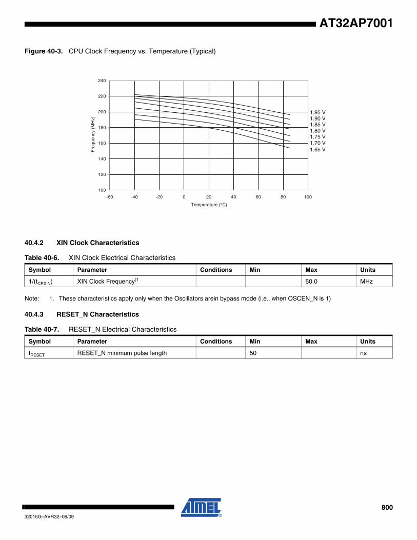
80032015G–AVR32–09/09
AT32AP7001
Figure 40-3. CPU Clock Frequency vs. Temperature (Typical)
40.4.2 XIN Clock Characteristics
Note: 1. These characteristics apply only when the Oscillators arein bypass mode (i.e., when OSCEN_N is 1)
40.4.3 RESET_N Characteristics
1.95 V1.90 V1.85 V1.80 V1.75 V1.70 V1.65 V
100
120
140
160
180
200
220
240
-60 -40 -20 0 20 40 60 80 100
Temperature (°C)
Fre
quen
cy (
MH
z)
Table 40-6. XIN Clock Electrical Characteristics
Symbol Parameter Conditions Min Max Units
1/(tCPXIN) XIN Clock Frequency(1 50.0 MHz
Table 40-7. RESET_N Electrical Characteristics
Symbol Parameter Conditions Min Max Units
tRESET RESET_N minimum pulse length 50 ns
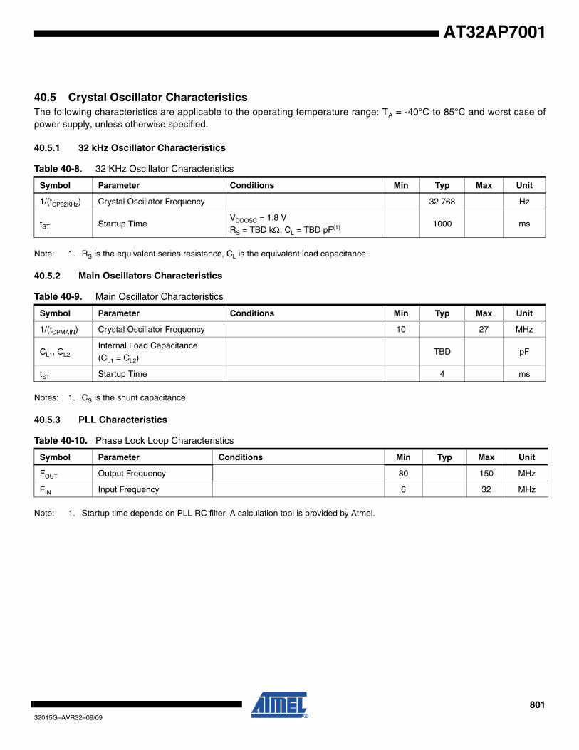
80132015G–AVR32–09/09
AT32AP7001
40.5 Crystal Oscillator CharacteristicsThe following characteristics are applicable to the operating temperature range: TA = -40°C to 85°C and worst case ofpower supply, unless otherwise specified.
40.5.1 32 kHz Oscillator Characteristics
Note: 1. RS is the equivalent series resistance, CL is the equivalent load capacitance.
40.5.2 Main Oscillators Characteristics
Notes: 1. CS is the shunt capacitance
40.5.3 PLL Characteristics
Note: 1. Startup time depends on PLL RC filter. A calculation tool is provided by Atmel.
Table 40-8. 32 KHz Oscillator Characteristics
Symbol Parameter Conditions Min Typ Max Unit
1/(tCP32KHz) Crystal Oscillator Frequency 32 768 Hz
tST Startup TimeVDDOSC = 1.8 V
RS = TBD kΩ, CL = TBD pF(1) 1000 ms
Table 40-9. Main Oscillator Characteristics
Symbol Parameter Conditions Min Typ Max Unit
1/(tCPMAIN) Crystal Oscillator Frequency 10 27 MHz
CL1, CL2Internal Load Capacitance
(CL1 = CL2)TBD pF
tST Startup Time 4 ms
Table 40-10. Phase Lock Loop Characteristics
Symbol Parameter Conditions Min Typ Max Unit
FOUT Output Frequency 80 150 MHz
FIN Input Frequency 6 32 MHz
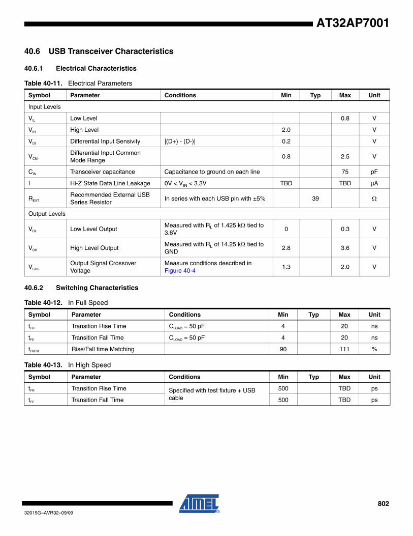
80232015G–AVR32–09/09
AT32AP7001
40.6 USB Transceiver Characteristics
40.6.1 Electrical Characteristics
40.6.2 Switching Characteristics
Table 40-11. Electrical Parameters
Symbol Parameter Conditions Min Typ Max Unit
Input Levels
VIL Low Level 0.8 V
VIH High Level 2.0 V
VDI Differential Input Sensivity |(D+) - (D-)| 0.2 V
VCM
Differential Input Common Mode Range
0.8 2.5 V
CIN Transceiver capacitance Capacitance to ground on each line 75 pF
I Hi-Z State Data Line Leakage 0V < VIN < 3.3V TBD TBD µA
REXT
Recommended External USB Series Resistor
In series with each USB pin with ±5% 39 Ω
Output Levels
VOL Low Level OutputMeasured with RL of 1.425 kΩ tied to 3.6V
0 0.3 V
VOH High Level OutputMeasured with RL of 14.25 kΩ tied to GND
2.8 3.6 V
VCRS
Output Signal Crossover Voltage
Measure conditions described in Figure 40-4
1.3 2.0 V
Table 40-12. In Full Speed
Symbol Parameter Conditions Min Typ Max Unit
tFR Transition Rise Time CLOAD = 50 pF 4 20 ns
tFE Transition Fall Time CLOAD = 50 pF 4 20 ns
tFRFM Rise/Fall time Matching 90 111 %
Table 40-13. In High Speed
Symbol Parameter Conditions Min Typ Max Unit
tFR Transition Rise Time Specified with test fixture + USB cable
500 TBD ps
tFE Transition Fall Time 500 TBD ps
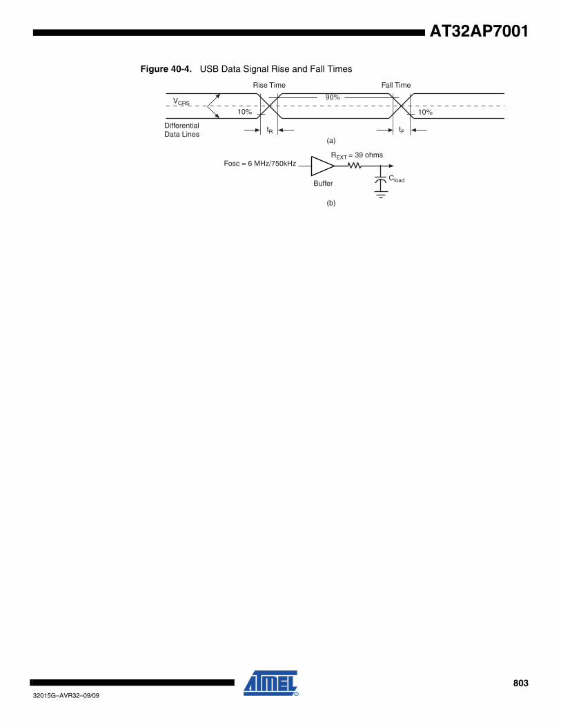
80332015G–AVR32–09/09
AT32AP7001
Figure 40-4. USB Data Signal Rise and Fall Times
10% 10%
90%VCRS
tR tFDifferentialData Lines
Rise Time Fall Time
Fosc = 6 MHz/750kHzREXT = 39 ohms
CloadBuffer
(b)
(a)
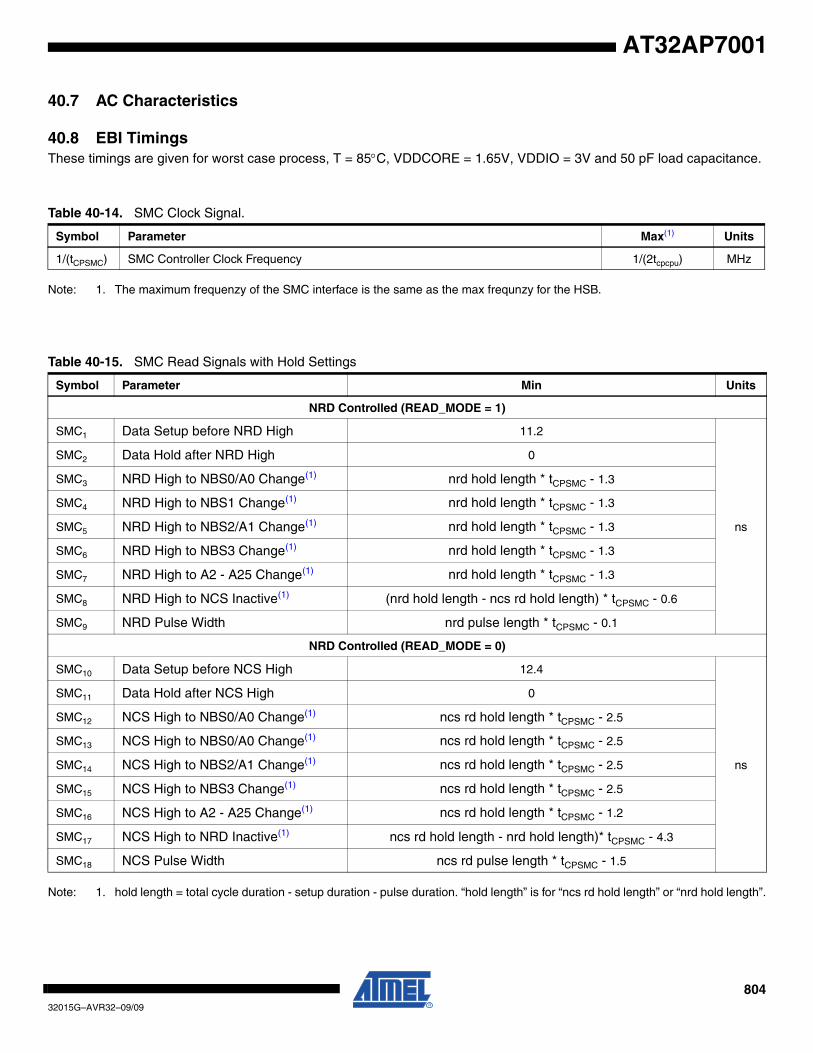
80432015G–AVR32–09/09
AT32AP7001
40.7 AC Characteristics
40.8 EBI TimingsThese timings are given for worst case process, T = 85°C, VDDCORE = 1.65V, VDDIO = 3V and 50 pF load capacitance.
Note: 1. The maximum frequenzy of the SMC interface is the same as the max frequnzy for the HSB.
Note: 1. hold length = total cycle duration - setup duration - pulse duration. “hold length” is for “ncs rd hold length” or “nrd hold length”.
Table 40-14. SMC Clock Signal.
Symbol Parameter Max(1) Units
1/(tCPSMC) SMC Controller Clock Frequency 1/(2tcpcpu) MHz
Table 40-15. SMC Read Signals with Hold Settings
Symbol Parameter Min Units
NRD Controlled (READ_MODE = 1)
SMC1 Data Setup before NRD High 11.2
ns
SMC2 Data Hold after NRD High 0
SMC3 NRD High to NBS0/A0 Change(1) nrd hold length * tCPSMC - 1.3
SMC4 NRD High to NBS1 Change(1) nrd hold length * tCPSMC - 1.3
SMC5 NRD High to NBS2/A1 Change(1) nrd hold length * tCPSMC - 1.3
SMC6 NRD High to NBS3 Change(1) nrd hold length * tCPSMC - 1.3
SMC7 NRD High to A2 - A25 Change(1) nrd hold length * tCPSMC - 1.3
SMC8 NRD High to NCS Inactive(1) (nrd hold length - ncs rd hold length) * tCPSMC - 0.6
SMC9 NRD Pulse Width nrd pulse length * tCPSMC - 0.1
NRD Controlled (READ_MODE = 0)
SMC10 Data Setup before NCS High 12.4
ns
SMC11 Data Hold after NCS High 0
SMC12 NCS High to NBS0/A0 Change(1) ncs rd hold length * tCPSMC - 2.5
SMC13 NCS High to NBS0/A0 Change(1) ncs rd hold length * tCPSMC - 2.5
SMC14 NCS High to NBS2/A1 Change(1) ncs rd hold length * tCPSMC - 2.5
SMC15 NCS High to NBS3 Change(1) ncs rd hold length * tCPSMC - 2.5
SMC16 NCS High to A2 - A25 Change(1) ncs rd hold length * tCPSMC - 1.2
SMC17 NCS High to NRD Inactive(1) ncs rd hold length - nrd hold length)* tCPSMC - 4.3
SMC18 NCS Pulse Width ncs rd pulse length * tCPSMC - 1.5
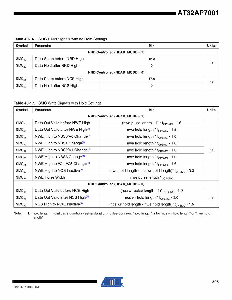
80532015G–AVR32–09/09
AT32AP7001
Note: 1. hold length = total cycle duration - setup duration - pulse duration. “hold length” is for “ncs wr hold length” or “nwe hold length"
Table 40-16. SMC Read Signals with no Hold Settings
Symbol Parameter Min Units
NRD Controlled (READ_MODE = 1)
SMC19 Data Setup before NRD High 15.8ns
SMC20 Data Hold after NRD High 0
NRD Controlled (READ_MODE = 0)
SMC21 Data Setup before NCS High 17.0ns
SMC22 Data Hold after NCS High 0
Table 40-17. SMC Write Signals with Hold Settings
Symbol Parameter Min Units
NRD Controlled (READ_MODE = 1)
SMC23 Data Out Valid before NWE High (nwe pulse length - 1) * tCPSMC - 1.6
ns
SMC24 Data Out Valid after NWE High(1) nwe hold length * tCPSMC - 1.5
SMC25 NWE High to NBS0/A0 Change(1) nwe hold length * tCPSMC - 1.0
SMC26 NWE High to NBS1 Change(1) nwe hold length * tCPSMC - 1.0
SMC29 NWE High to NBS2/A1 Change(1) nwe hold length * tCPSMC - 1.0
SMC30 NWE High to NBS3 Change(1) nwe hold length * tCPSMC - 1.0
SMC31 NWE High to A2 - A25 Change(1) nwe hold length * tCPSMC - 1.6
SMC32 NWE High to NCS Inactive(1) (nwe hold length - ncs wr hold length)* tCPSMC - 0.3
SMC33 NWE Pulse Width nwe pulse length * tCPSMC
NRD Controlled (READ_MODE = 0)
SMC34 Data Out Valid before NCS High (ncs wr pulse length - 1)* tCPSMC - 1.9
nsSMC35 Data Out Valid after NCS High(1) ncs wr hold length * tCPSMC - 3.0
SMC36 NCS High to NWE Inactive(1) (ncs wr hold length - nwe hold length)* tCPSMC - 1.5
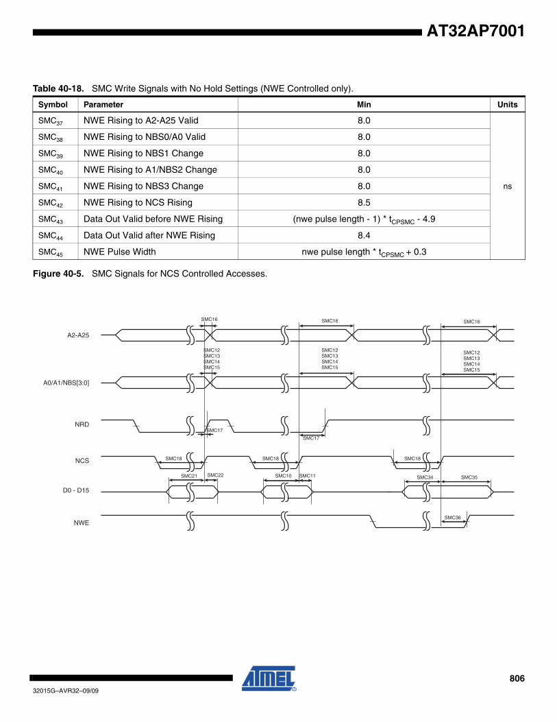
80632015G–AVR32–09/09
AT32AP7001
Figure 40-5. SMC Signals for NCS Controlled Accesses.
Table 40-18. SMC Write Signals with No Hold Settings (NWE Controlled only).
Symbol Parameter Min Units
SMC37 NWE Rising to A2-A25 Valid 8.0
ns
SMC38 NWE Rising to NBS0/A0 Valid 8.0
SMC39 NWE Rising to NBS1 Change 8.0
SMC40 NWE Rising to A1/NBS2 Change 8.0
SMC41 NWE Rising to NBS3 Change 8.0
SMC42 NWE Rising to NCS Rising 8.5
SMC43 Data Out Valid before NWE Rising (nwe pulse length - 1) * tCPSMC - 4.9
SMC44 Data Out Valid after NWE Rising 8.4
SMC45 NWE Pulse Width nwe pulse length * tCPSMC + 0.3
NRD
NCS
D0 - D15
NWE
A2-A25
A0/A1/NBS[3:0]
SMC34 SMC35SMC10 SMC11
SMC16
SMC15
SMC22SMC21
SMC17
SMC18
SMC14SMC13SMC12
SMC18
SMC17
SMC16
SMC15SMC14SMC13SMC12
SMC18
SMC36
SMC16
SMC15SMC14SMC13SMC12
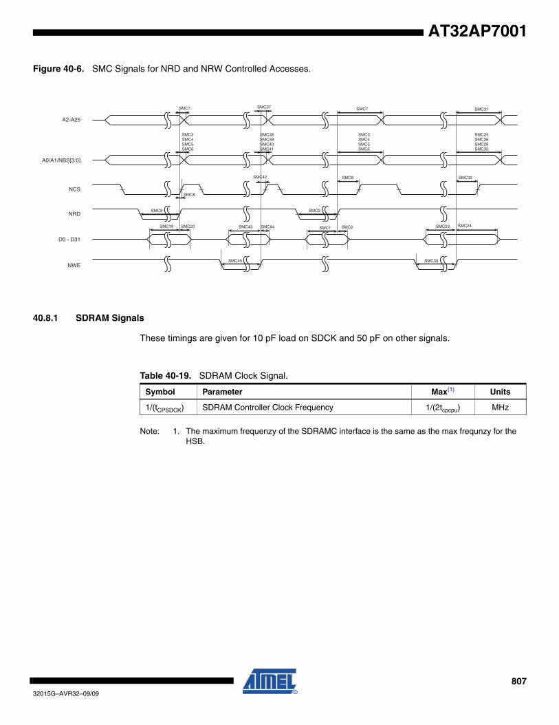
80732015G–AVR32–09/09
AT32AP7001
Figure 40-6. SMC Signals for NRD and NRW Controlled Accesses.
40.8.1 SDRAM Signals
These timings are given for 10 pF load on SDCK and 50 pF on other signals.
Note: 1. The maximum frequenzy of the SDRAMC interface is the same as the max frequnzy for the HSB.
NRD
NCS
D0 - D31
NWE
A2-A25
A0/A1/NBS[3:0]
SMC7
SMC19 SMC20 SMC43
SMC37
SMC42 SMC8
SMC1 SMC2 SMC23 SMC24
SMC32
SMC7
SMC8
SMC6SMC5SMC4SMC3
SMC9
SMC41SMC40SMC39SMC38
SMC45
SMC9
SMC6SMC5SMC4SMC3
SMC33
SMC30SMC29SMC26SMC25
SMC31
SMC44
Table 40-19. SDRAM Clock Signal.
Symbol Parameter Max(1) Units
1/(tCPSDCK) SDRAM Controller Clock Frequency 1/(2tcpcpu) MHz
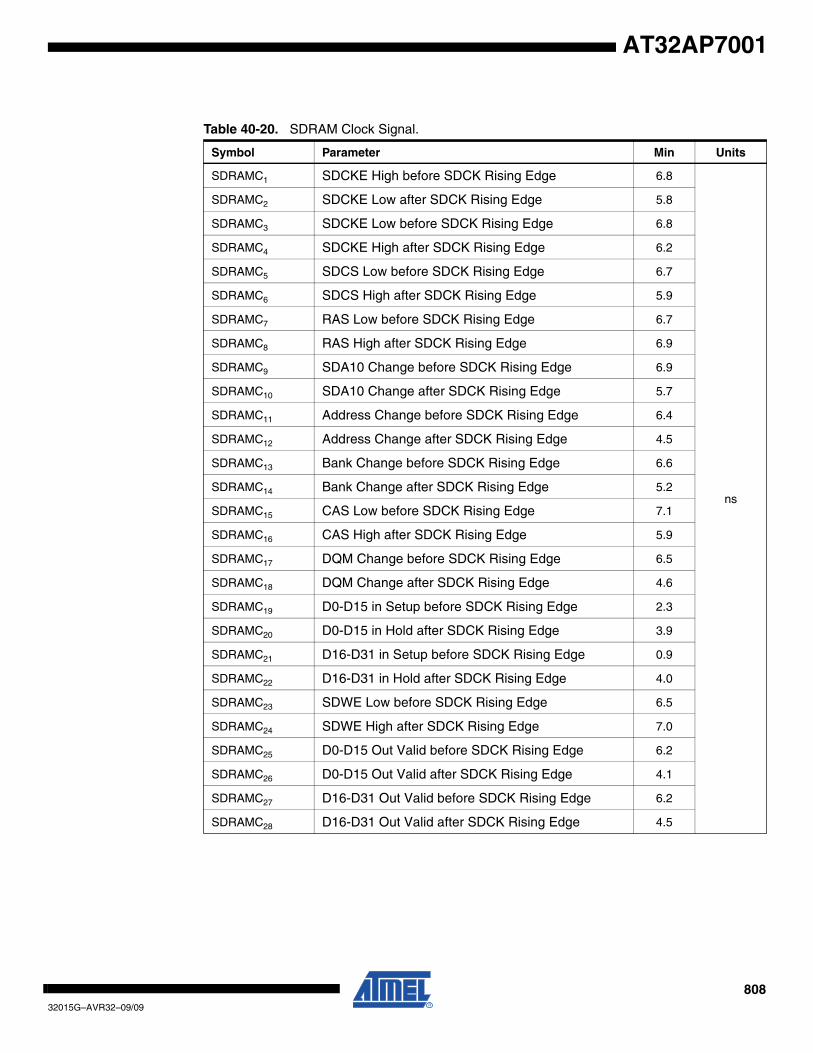
80832015G–AVR32–09/09
AT32AP7001
Table 40-20. SDRAM Clock Signal.
Symbol Parameter Min Units
SDRAMC1 SDCKE High before SDCK Rising Edge 6.8
ns
SDRAMC2 SDCKE Low after SDCK Rising Edge 5.8
SDRAMC3 SDCKE Low before SDCK Rising Edge 6.8
SDRAMC4 SDCKE High after SDCK Rising Edge 6.2
SDRAMC5 SDCS Low before SDCK Rising Edge 6.7
SDRAMC6 SDCS High after SDCK Rising Edge 5.9
SDRAMC7 RAS Low before SDCK Rising Edge 6.7
SDRAMC8 RAS High after SDCK Rising Edge 6.9
SDRAMC9 SDA10 Change before SDCK Rising Edge 6.9
SDRAMC10 SDA10 Change after SDCK Rising Edge 5.7
SDRAMC11 Address Change before SDCK Rising Edge 6.4
SDRAMC12 Address Change after SDCK Rising Edge 4.5
SDRAMC13 Bank Change before SDCK Rising Edge 6.6
SDRAMC14 Bank Change after SDCK Rising Edge 5.2
SDRAMC15 CAS Low before SDCK Rising Edge 7.1
SDRAMC16 CAS High after SDCK Rising Edge 5.9
SDRAMC17 DQM Change before SDCK Rising Edge 6.5
SDRAMC18 DQM Change after SDCK Rising Edge 4.6
SDRAMC19 D0-D15 in Setup before SDCK Rising Edge 2.3
SDRAMC20 D0-D15 in Hold after SDCK Rising Edge 3.9
SDRAMC21 D16-D31 in Setup before SDCK Rising Edge 0.9
SDRAMC22 D16-D31 in Hold after SDCK Rising Edge 4.0
SDRAMC23 SDWE Low before SDCK Rising Edge 6.5
SDRAMC24 SDWE High after SDCK Rising Edge 7.0
SDRAMC25 D0-D15 Out Valid before SDCK Rising Edge 6.2
SDRAMC26 D0-D15 Out Valid after SDCK Rising Edge 4.1
SDRAMC27 D16-D31 Out Valid before SDCK Rising Edge 6.2
SDRAMC28 D16-D31 Out Valid after SDCK Rising Edge 4.5
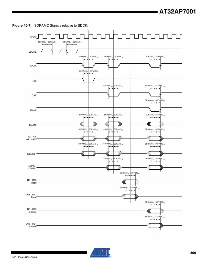
80932015G–AVR32–09/09
AT32AP7001
Figure 40-7. SDRAMC Signals relative to SDCK.
RAS
A0 - A9,A11 - A13
D0 - D15Read
SDCK
SDA10
D0 - D15to Write
SDRAMC1
SDCKE
SDRAMC2 SDRAMC3 SDRAMC4
SDCS
SDRAMC5 SDRAMC6 SDRAMC5 SDRAMC6 SDRAMC5 SDRAMC6
SDRAMC7 SDRAMC8
CAS
SDRAMC15 SDRAMC16 SDRAMC15 SDRAMC16
SDWE
SDRAMC23 SDRAMC24
SDRAMC9 SDRAMC10SDRAMC9 SDRAMC10SDRAMC9 SDRAMC10
SDRAMC11 SDRAMC12 SDRAMC11 SDRAMC12SDRAMC11 SDRAMC12
BA0/BA1
SDRAMC13 SDRAMC14 SDRAMC13 SDRAMC14 SDRAMC13 SDRAMC14
SDRAMC17 SDRAMC18SDRAMC17 SDRAMC18
DQM0 -DQM3
SDRAMC19 SDRAMC20
D16 - D31Read
SDRAMC21 SDRAMC22
SDRAMC25 SDRAMC26
D16 - D31to Write
SDRAMC27 SDRAMC28

81032015G–AVR32–09/09
AT32AP7001
41. Ordering Information
Table 41-1. Ordering Information
Ordering Code Package Package Type PackingTemperature
Operating Range
AT32AP7001-ALUT QFP208 Green Tray Industrial (-40°C to 85°C)
81132015G–AVR32–09/09
AT32AP7001
42. Errata
42.1 Rev. C
1. SPI FDIV option does not workSelecting clock signal using FDIV = 1 does not work as specified.
Fix/WorkaroundDo not set FDIV = 1.
2. SPI Chip Select 0 BITS field overrides other Chip SelectsThe BITS field for Chip Select 0 overrides BITS fields for other Chip selects.
Fix/WorkaroundUpdate Chip Select 0 BITS field to the relevant settings before transmitting with Chip Selectsother than 0.
3. SPI LASTXFER may be overwrittenWhen Peripheral Select (PS) = 0, the LASTXFER-bit in the Transmit Data Register (TDR)should be internally discared. This fails and may cause problems during DMA transfers.Transmitting data using the PDC when PS=0, the size of the transferred data is 8- or 16-bits.The upper 16 bits of the TDR will be written to a random value. If Chip Select Active AfterTransfer (CSAAT) = 1, the behavior of the Chip Select will be unpredictable.
Fix/Workaround- Do not use CSAAT = 1 if PS = 0
- Use GPIO to control Chip Select lines
- Select PS=1 and store data for PCS and LASTXFER for each data in transmit buffer.
4. SPI LASTXFER overrides Chip SelectThe LASTXFER bit overrides Chip Select input when PS = 0 and CSAAT is used.
Fix/Workaround- Do not use the CSAAT
- Use GPIO as Chip Select input
- Select PS = 1. Transfer 32-bit with correct LASTXFER settings.
5. MMC data write operation with less than 12 bytes is impossible.MCI data write operation with less than 12 bytes is impossible. The Data Write operationwith a number of bytes less than 12 leaves the internal MCI FIFO in an inconsistent state.Subsequent reads and writes will not function properly.
Fix/WorkaroundAlways transfer 12 or more bytes at a time. If less than 12 bytes are transferred, the onlyrecovery mechanism is to perform a software reset of the MCI.
6. MMC SDIO interrupt only works for slot AIf 1-bit data bus width and on other slots than slot A, the SDIO interrupt can not be cap-tured.
81232015G–AVR32–09/09
AT32AP7001
Fix/WorkaroundUse slot A.
7. PSIF TXEN/RXEN may disable the transmitter/receiverWriting a '0' to RXEN will disable the receiver. Writing '0' to TXEN will disable the transmitter.
Fix/WorkaroundWhen accessing the PS/2 Control Register always write '1' to RXEN to keep the receiverenabled, and write '1' to TXEN to keep the transmitter enabled.
8. PSIF TXRDY interrupt corrupts transfersWhen writing to the Transmit Holding Register (THR), the data will be transferred to the datashift register immediately, regardless of the state of the data shift register. If a transfer isongoing, it will be interrupted and a new transfer will be started with the new data written toTHR.
Fix/WorkaroundUse the TXEMPTY-interrupt instead of the TXRDY-interrupt to update the THR. Thisensures that a transfer is completed.
9. PWMcounter restarts at 0x0001The PWM counter restarts at 0x0001 and not 0x0000 as specified. Because of this the firstPWM period has one more clock cycle.
Fix/Workaround- The first period is 0x0000, 0x0001, ..., period
- Consecutive periods are 0x0001, 0x0002, ..., period
10. PWM channel interrupt enabling triggers an interruptWhen enabling a PWM channel that is configured with center aligned period (CALG=1), aninterrupt is signalled.
Fix/WorkaroundWhen using center aligned mode, enable the channel and read the status before channelinterrupt is enabled.
11. PWM update period to a 0 value does not workIt is impossible to update a period equal to 0 by the using the PWM update register(PWM_CUPD).
Fix/WorkaroundDo not update the PWM_CUPD register with a value equal to 0.
12. PWM channel status may be wrong if disabled before a period has elapsedBefore a PWM period has elapsed, the read channel status may be wrong. The CHIDx-bitfor a PWM channel in the PWM Enable Register will read '1' for one full PWM period even ifthe channel was disabled before the period elapsed. It will then read '0' as expected.
Fix/WorkaroundReading the PWM channel status of a disabled channel is only correct after a PWM period
13. TWI transfer error without ACK
81332015G–AVR32–09/09
AT32AP7001
If the TWI does not receive an ACK from a slave during the address+R/W phase, no bits inthe status register will be set to indicate this. Hence, the transfer will never complete.
Fix/WorkaroundTo prevent errors due to missing ACK, the software should use a timeout mechanism to ter-minate the transfer if this happens.
14. SSC can not transmit or receive dataThe SSC can not transmit or receive data when CKS = CKDIV and CKO = none in TCMR orRCMR respectively.
Fix/WorkaroundSet CKO to a value that is not "None" and enable the PIO with output driver disabled on theTK/RK pin.
15. USART - RXBREAK flag is not correctly handledThe FRAME_ERROR is set instead of the RXBREAK when the break character is locatedjust after the STOP BIT(S) in ASYNCHRONOUS mode.
Fix/WorkaroundThe transmitting UART must set timeguard greater than 0.
16. USART - Manchester encoding/decoding is not working.Manchester encoding/decoding is not working.
Fix/WorkaroundDo not use manchester encoding.
17. SPI - Disabling SPI has no effect on TDRE flag.Disabling SPI has no effect on TDRE whereas the write data command is filtered when SPIis disabled. This means that as soon as the SPI is disabled it becomes impossible to resetthe TDRE flag by writing in the SPI_TDR. So if the SPI is disabled during a PDC transfer, thePDC will continue to write data in the SPI_TDR (as TDRE keeps High) till its buffer is empty,and all data written after the disable command is lost.
Fix/WorkaroundDisable PDC, 2 NOP (minimum), Disable SPI. When you want to continue the transfer:Enable SPI, Enable PDC.
18. SPI disable does not work in SLAVE mode.SPI disable does not work in SLAVE mode.
Fix/WorkaroundRead the last received data, then perform a Software Reset.
19. SCC - First Data transmitted after reset is not DATDEF.In the first frame transmitted, the first transmitted data that follows the frame synchro is 0,not DATDEF. This happens when:
1. PDC is disabled
2. Reset the SSC
81432015G–AVR32–09/09
AT32AP7001
3. Configure the SSC with a transmit START condition different from CONTINUOUS(START = 0)
4. DATDEF = 1
5. Enable the SSC in transmission.
This trouble only appears after a reset and it is only the first frame is affected.
Fix/WorkaroundUse the PDC to fill the THR after the enable of the SSC and before the start of the frame.
20. MCI - False data timeout error DTOE may occur.If a small block (5 bytes) is read through the READ_SINGLE_BLOCK command (CMD17),the flag NOTBUSY will be set and a false data timeout error DTOE occurs.
Fix/WorkaroundNone.
21. SDRAM - Self-refresh modeIf Entry in Self-refresh mode is followed by SDRAM access and auto-refresh event, TRC tim-ing is not checked for AUTO_REFRESH sequence.
Fix/WorkaroundSet the value of TRAS field in user interface with TRC+1.
22. SPI - No TX UNDERRUN flag availableThere is no TX UNDERRUN flag available, therefore in slave mode there is no way to beinformed of a character lost in transmission.
Fix/WorkaroundPDC/PDCA transfers: None.
Manual transfers (no PDC and TX slave only): Read the RHR every time the THR is written.The OVRS flag of the status register will track any UNDERRUN on the TX side.
23. HMATRIX - Fixed priority arbitration does not workFixed priority arbitration does not work.
Fix/WorkaroundUse Round-robin arbitration instead.
24. OSC32 is not available for RTC, WDT, TIMERs and USARTs at startupRight after startup the osc32 clock to internal modules is not valid. The osc32 clock will bevalid for use approximately 128 osc32 cycles after the the first instruction is executed. Thishas consequences if you are planning to use the RTC, WDT, going into sleep mode andUSARTs with SCK and TCs with TIMER_CLOCK0.
Fix/WorkaroundBefore executing any code the user should enable the RTC with the smallest prescaler andpoll that the RTC is counting before doing anything in your program. Another way to ensurethat the osc32 is valid is to use interrupts with TOP=1.
Example:
//reset the counter register
81532015G–AVR32–09/09
AT32AP7001
AVR32_RTC.val = 0x0;
//enable the RTC with the smallest prescaler
AVR32_RTC.ctrl = 0x1;
//wait until the value increases
while(AVR32_RTC.val == 0);
25. SPI can generate a false RXREADY signal in SLAVE modeIn slave mode the SPI can generate a false rxready signal during enabling of the SPI or dur-ing the first transfer.
Fix/Workaround1. Set slave mode, set required CPOL/CPHA
2. Enable SPI
3. Set the polarity CPOL of the line in the opposite value of the required one
4. Set the polarity CPOL to the required one.
5. Read the RXHOLDING register
Transfers can now begin and RXREADY will now behave as expected.
26. EBI address lines 23, 24, and 25 are pulled up when booting upAfter reset the EBI address lines 23, 24 and 25 are tristated with pullups. Booting from aflash larger than 8 MB using these lines will fail, as the flash will be accessed with theseaddress bits set.
Fix/WorkaroundAdd external pulldown resistors (5 kΩ) on these lines if booting from a flash larger than 8 MBusing these address lines.
27. SSC - Additional delay on TD outputA delay from 2 to 3 system clock cycles is added to TD output when:
TCMR.START = Receive Start,
TCMR.STTDLY = more than ZERO,
RCMR.START = Start on falling edge / Start on Rising edge / Start on any edge
RFMR.FSOS = None (input)
Fix/WorkaroundNone.
28. SSC - TF output is not correctTF output is not correct (at least emitted one serial clock cycle later than expected) when:
TFMR.FSOS = Driven Low during data transfer/ Driven High during data transfer
TCMR.START = Receive start
RFMR.FSOS = None (Input)
RCMR.START = any on RF (edge/level)
Fix/WorkaroundNone.
29. USART - TXD signal is floating in Modem and Hardware Handshaking mode
81632015G–AVR32–09/09
AT32AP7001
The TXD signal is floating in Modem and Hardware Handshaking mode, but should bepulled up.
Fix/WorkaroundEnable pullup on this line in the PIO.
30. PWM - Impossible to update a period equal to 0 by using the CUPD registerIt is impossible to UPDATE a period equal to 0 by the using of the UPDATE register(CUPD).
Fix/WorkaroundTo update a period equal to 0, write directly to the CPRD register.
31. WDT Clear is blocked after WDT ResetA watchdog timer event will, after reset, block writes to the WDT_CLEAR register, prevent-ing the program to clear the next Watchdog Timer Reset.
Fix/WorkaroundIf the RTC is not used a write to AVR32_RTC.ctrl.pclr = 1, instead of writing toAVR32_WDT.clr, will reset the prescaler and thus prevent the watchdog event from happen-ing. This will render the RTC useless, but prevents WDT reset because the RTC and WDTshare the same prescaler. Another sideeffect of this is that the watchdog timeout period willbe half the expected timeout period.
If the RTC is used one can disable the Watchdog Timer (WDT) after a WDT reset hasoccured. This will prevent the WDT resetting the system. To make the WDT functional againa hard reset (power on reset or RESET_N) must be applied. If you still want to use the WDTafter a WDT reset a smal l code can be inserted at the startup checking theAVR32_PM.rcause register for WDT reset and use a GPIO pin to reset the system. Thismethod requires that one of the GPIO pins are available and connected externally to theRESET_N pin. After the GPIO pin has pulled down the reset line the GPIO will be reset andleave the pin tristated with pullup.
32. USART - The DCD Signal is active high from the USART, but should be active lowThe DCD signal is active high from the USART, but should be active low.
Fix/WorkaroundAn inverter should be added on this line on the PCB.
33. MCI Transmit Data Register (TDR) FIFO corruptionIf the number of bytes to be transmitted by the MCI is not a multiple of 4, the Transmit DataRegister (TDR) First In First Out data buffer control logic will become corrupted when trans-mit data is written to the TDR as 32-bit values.
Fix/WorkaroundConfigure the MCI Mode Register (MR) to accept 8-bit data input by writing a 1 to bit 13(FBYTE), and transfer each byte of the transmit data to TDR by right aligning the usefulvalue. This allows the number of bytes transferred into the TDR to match the number set upin the BCNT field of the MCI Block Register (BLKR).
34. Unreliable branch foldingIn certain situations, branch folding does not work as expected.
81732015G–AVR32–09/09
AT32AP7001
Fix/WorkaroundWrite 0 to CPUCR.FE before executing any branch instructions after reset.
35. USB PLL jitter may cause packet loss during USB hi-speed transmissionThe USB Hi-speed PLL accuracy is not sufficient for Isochronous USB hi-speed transmis-sion and may cause packet loss. The observed bit-loss is typically < 125 ppm.
Fix/WorkaroundDo not use isochronous mode if absolute data accuracy is critical.
42.2 Rev. B
Not sampled.
42.3 Rev. A
Not sampled.
81832015G–AVR32–09/09
AT32AP7001
43. Datasheet Revision History
Please note that the referring page numbers in this section are referred to this document. Thereferring revision in this section are referring to the document revision.
43.1 Rev. G 09/09
43.2 Rev. F 09/09
43.3 Rev. E 01/08
43.4 Rev. D 09/07
1. Updated ”Errata” on page 811.
1. Updated ”Errata” on page 811.
1. Updated Pin 208 from GND to VDDIO in ”Package and Pinout” on page 9.
1. PIO Controller C Multiplexing table updated in ”Peripherals” on page 73“.
2. Added section ”USBA” on page 78 in Clock Connections in ”Peripherals” on page 73.
3. USBA feature list updated in ”Peripherals” on page 73.
4. Renamed clk_slow to clk_osc32 in Table 9-4 on page 80.
5 Updated organisation of User Interface in ”HSB Bus Matrix (HMATRIX)” on page 139.
6. Updated special bus granting mechanism in ”HSB Bus Matrix (HMATRIX)” on page 139.
7. Added product dependencies in ”DMA Controller (DMACA)” on page 169.
8. Added product dependencies in ”Peripheral DMA Controller (PDC)” on page 233.
9. Added description of multi-drive in ”Parallel Input/Output Controller (PIO)” on page 249.
10.Added MDER/MDDR/MDSR to pin logic diagram in ”Parallel Input/Output Controller (PIO)” on page 249.
11. SPI pins must be enabled to use local loopback.
12. Updated description of the OVRES bit in ”SPI Status Register” on page 310.
13. Updated bit description of TXEMPTY in the ”USART Channel Status Register” on page 431.
14.Number of chip select lines updatedin figures and tables, changed from 8 to 6 in ”Static Memory Controller (SMC)” on page 488.
15.Made the MDR register Read/Write instead of Read in ”SDRAM Controller (SDRAMC)” on page 530.
16. Removed the PWSEN and PWSDIS bits from the ”Control Register” on page 584.
17. Added PDCFBYTE and removed the PWSDIV bits from the ”Mode Register” on page 585.
18.Added note about reading the Status Register clears the interrupt flag in ”Timer/Counter (TC)” on page 676.
81932015G–AVR32–09/09
AT32AP7001
43.5 Rev. C 07/07
43.6 Rev. B 04/07
43.7 Rev. A 02/07
19. Added debug operation to product dependencies in ”Timer/Counter (TC)” on page 676.
20.Added debug operation to product dependencies in ”Pulse Width Modulation Controller (PWM)” on page 713.
21. Updated ”PLL Characteristics” on page 933.
22. Updated ”Errata” on page 811.
1. Updated ”Part Description” on page 2.
2. PC Signals removed in ”Signals Description” on page 5
3. USB Signals updated in ”Signals Description” on page 5.
4. The PX0 - PX53 Signals added in ”Signals Description” on page 5.
5. SDCS signals removed from PIO Controller Multiplexing tables in ”Peripherals” on page 79.
6. LCD and MAC references removed form tables in ”Memories” on page 77.
7. LCD and MAC controller references removed in ”Peripheral overview” on page 94.
8.SDCS1 signal removed from figures and tables, and SDCS0 renamed to SDCS in ”External Bus Interface (EBI)” on page 152.
9.SmartMedia renamed to NAND Flash in some description to avoid confusion in ”External Bus Interface (EBI)” on page 152.
10. Updated Application block diagram in Figure 1-2 on page 1.
11. LCD removed from feature list in ”Serial Peripheral Interface (SPI)” on page 297.
12. Updated the reset state of the SMC Mode register in Table 27-9 on page 523.
13. Updated ”Mechanical Characteristics” on page 927.
14. Updated pad parameters in ”DC Characteristics” on page 796.
15.Updated ”Power Consumption by Peripheral in Active Mode” on page 798, LCD and MACB excluded.
16. Updated pad parameters in ”Clock Characteristics” on page 799.
17. Updated ”USB Transceiver Characteristics” on page 802.
18. Updated ”EBI Timings” on page 939.
1. Updated ”Features” on page 1.
2. Updated tables in ”Signals Description” on page 4.
3.Updated Table 9-2 on page 77, Table 9-9 on page 82, and Table 9-10 on page 83 in the ”Peripherals” on page 75.
4. Updated module names and abbreviations through the datasheet.
1. Initial revision.
82032015G–AVR32–09/09
AT32AP7001
Table of Contents
Features ..................................................................................................... 1
1 Part Description ....................................................................................... 2
2 Signals Description ................................................................................. 3
3 Power Considerations ............................................................................. 8
3.1Power Supplies .........................................................................................................8
3.2Power Supply Connections .......................................................................................8
4 Package and Pinout ................................................................................. 9
4.1AVR32AP7001 ..........................................................................................................9
5 Blockdiagram ......................................................................................... 11
6 I/O Line Considerations ......................................................................... 15
6.1JTAG pins ................................................................................................................15
6.2WAKE_N pin ...........................................................................................................15
6.3RESET_N pin ..........................................................................................................15
6.4EVTI_N pin ..............................................................................................................15
6.5TWI pins ..................................................................................................................15
6.6PIO pins ...................................................................................................................15
7 AVR32 AP CPU ....................................................................................... 16
7.1AVR32 Architecture .................................................................................................16
7.2The AVR32 AP CPU ...............................................................................................16
7.3Programming Model ................................................................................................22
8 Pixel Coprocessor (PICO) ..................................................................... 25
8.1Features ..................................................................................................................25
8.2Description ..............................................................................................................25
8.3Block Diagram .........................................................................................................26
8.4Vector Multiplication Unit (VMU) ..............................................................................27
8.5Input Pixel Selector .................................................................................................27
8.6Output Pixel Inserter ................................................................................................29
8.7User Interface ..........................................................................................................31
8.8PICO Instructions ....................................................................................................49
8.9Data Hazards ..........................................................................................................70
9 Memories ................................................................................................ 71

82132015G–AVR32–09/09
AT32AP7001
9.1Embedded Memories ..............................................................................................71
9.2Physical Memory Map .............................................................................................71
10 Peripherals ............................................................................................. 73
10.1Peripheral address map ........................................................................................73
10.2Interrupt Request Signal Map ................................................................................75
10.3DMACA Handshake Interface Map .......................................................................76
10.4Clock Connections ................................................................................................77
10.5External Interrupt Pin Mapping ..............................................................................78
10.6Nexus OCD AUX port connections .......................................................................78
10.7Peripheral Multiplexing on IO lines ........................................................................79
10.8Peripheral overview ...............................................................................................86
11 Power Manager (PM) .............................................................................. 91
11.1Features ................................................................................................................91
11.2Description ............................................................................................................91
11.3Block Diagram .......................................................................................................92
11.4Product Dependencies ..........................................................................................93
11.5Functional Description ...........................................................................................93
11.6User Interface ......................................................................................................106
12 Real Time Counter (RTC) .................................................................... 115
12.1Features ..............................................................................................................115
12.2Description ..........................................................................................................115
12.3Block Diagram .....................................................................................................115
12.4Product Dependencies ........................................................................................115
12.5Functional Description .........................................................................................116
12.6User Interface ......................................................................................................117
13 Watchdog Timer (WDT) ....................................................................... 122
13.1Features ..............................................................................................................122
13.2Description ..........................................................................................................122
13.3Block Diagram .....................................................................................................122
13.4Product Dependencies ........................................................................................122
13.5Functional Description .........................................................................................123
13.6User Interface ......................................................................................................124
14 Interrupt Controller (INTC) .................................................................. 126
14.1Features ..............................................................................................................126
82232015G–AVR32–09/09
AT32AP7001
14.2Overview .............................................................................................................126
14.3Block Diagram .....................................................................................................126
14.4Product Dependencies ........................................................................................127
14.5Functional Description .........................................................................................127
14.6User Interface ......................................................................................................129
15 External Interrupt Controller (EIC) ..................................................... 133
15.1Features ..............................................................................................................133
15.2Description ..........................................................................................................133
15.3Block Diagram .....................................................................................................133
15.4Product Dependencies ........................................................................................133
15.5Functional Description .........................................................................................134
15.6User Interface ......................................................................................................135
16 HSB Bus Matrix (HMATRIX) ................................................................ 139
16.1Features .............................................................................................................139
16.2Overview .............................................................................................................139
16.3Product Dependencies ........................................................................................139
16.4Functional Description .........................................................................................139
16.5User Interface ......................................................................................................143
17 External Bus Interface (EBI) ................................................................ 152
17.1Features ..............................................................................................................152
17.2Description ..........................................................................................................152
17.3Block Diagram .....................................................................................................153
17.4I/O Lines Description ...........................................................................................155
17.5Application Example ............................................................................................157
17.6Product Dependencies ........................................................................................161
17.7Functional Description .........................................................................................161
18 DMA Controller (DMACA) .................................................................... 169
18.1Features ..............................................................................................................169
18.2Overview .............................................................................................................169
18.3Block Diagram .....................................................................................................170
18.4Product Dependencies ........................................................................................170
18.5Functional Description .........................................................................................171
18.6Arbitration for HSB Master Interface ...................................................................176
18.7Memory Peripherals ............................................................................................176
18.8Handshaking Interface ........................................................................................176

82332015G–AVR32–09/09
AT32AP7001
18.9DMACA Transfer Types ......................................................................................178
18.10Programming a Channel ...................................................................................182
18.11Disabling a Channel Prior to Transfer Completion ............................................199
18.12User Interface ....................................................................................................201
19 Peripheral DMA Controller (PDC) ....................................................... 233
19.1Features ..............................................................................................................233
19.2Description ..........................................................................................................233
19.3Block Diagram .....................................................................................................234
19.4Product Dependencies ........................................................................................235
19.5Functional Description .........................................................................................235
19.6Peripheral DMA Controller (PDC) User Interface ...............................................238
20 Parallel Input/Output Controller (PIO) ................................................ 249
20.1Features ..............................................................................................................249
20.2Description ..........................................................................................................249
20.3Block Diagram .....................................................................................................250
20.4Product Dependencies ........................................................................................251
20.5Functional Description .........................................................................................252
20.6I/O Lines Programming Example ........................................................................256
20.7User Interface ......................................................................................................258
21 Serial Peripheral Interface (SPI) ......................................................... 289
21.1Features ..............................................................................................................289
21.2Description ..........................................................................................................289
21.3Block Diagram .....................................................................................................290
21.4Application Block Diagram ..................................................................................291
21.5Signal Description ...............................................................................................292
21.6Product Dependencies ........................................................................................293
21.7Functional Description .........................................................................................294
21.8Serial Peripheral Interface (SPI) User Interface ..................................................304
22 Two-wire Interface (TWI) ..................................................................... 318
22.1Features .............................................................................................................318
22.2Description ..........................................................................................................318
22.3Block Diagram .....................................................................................................318
22.4Application Block Diagram ..................................................................................318
22.5Product Dependencies ........................................................................................319
22.6Functional Description .........................................................................................320
82432015G–AVR32–09/09
AT32AP7001
22.7TWI User Interface ..............................................................................................325
23 PS/2 Module (PSIF) .............................................................................. 336
23.1Features ..............................................................................................................336
23.2Description ..........................................................................................................336
23.3Product Dependencies ........................................................................................336
23.4The PS/2 Protocol ...............................................................................................336
23.5Functional Description .........................................................................................338
23.6User Interface ......................................................................................................339
24 Synchronous Serial Controller (SSC) ................................................ 348
24.1Features .............................................................................................................348
24.2Overview .............................................................................................................348
24.3Block Diagram .....................................................................................................349
24.4Application Block Diagram ..................................................................................349
24.5I/O Lines Description ...........................................................................................350
24.6Product Dependencies ........................................................................................350
24.7Functional Description .........................................................................................350
24.8SSC Application Examples ..................................................................................362
24.9User Interface ......................................................................................................364
25 Universal Synchronous/Asynchronous Receiver/Transmitter (USART) 388
25.1Features ..............................................................................................................388
25.2Overview .............................................................................................................388
25.3Block Diagram .....................................................................................................389
25.4Application Block Diagram ..................................................................................390
25.5I/O Lines Description ..........................................................................................390
25.6Product Dependencies ........................................................................................391
25.7Functional Description .........................................................................................392
25.8USART User Interface ........................................................................................422
25.9USART Version Register .....................................................................................442
26 AC97 Controller (AC97C) .................................................................... 443
26.1Features .............................................................................................................443
26.2Description ..........................................................................................................443
26.3Block Diagram .....................................................................................................444
26.4Pin Name List ......................................................................................................445
26.5Application Block Diagram ..................................................................................445
82532015G–AVR32–09/09
AT32AP7001
26.6Product Dependencies ........................................................................................446
26.7Functional Description .........................................................................................447
26.8AC97 Controller (AC97C) User Interface ............................................................458
27 Audio Bitstream DAC (ABDAC) .......................................................... 475
27.1Features ..............................................................................................................475
27.2Description ..........................................................................................................475
27.3Block Diagram .....................................................................................................476
27.4Pin Name List ......................................................................................................476
27.5Product Dependencies ........................................................................................476
27.6Functional Description .........................................................................................477
27.7Audio Bitstream DAC User Interface ...................................................................479
27.8Frequency Response ..........................................................................................487
28 Static Memory Controller (SMC) ......................................................... 488
28.1Features .............................................................................................................488
28.2Overview .............................................................................................................488
28.3Block Diagram .....................................................................................................489
28.4I/O Lines Description ...........................................................................................489
28.5Product Dependencies ........................................................................................490
28.6Functional Description .........................................................................................490
28.7User Interface ......................................................................................................523
29 SDRAM Controller (SDRAMC) ............................................................ 530
29.1Features ..............................................................................................................530
29.2Overview .............................................................................................................530
29.3Block Diagram .....................................................................................................531
29.4I/O Lines Description ...........................................................................................531
29.5Application Example ............................................................................................532
29.6Product Dependencies ........................................................................................535
29.7Functional Description .........................................................................................536
29.8User Interface ......................................................................................................545
30 Error Corrected Code (ECC) Controller ............................................. 558
30.1Features .............................................................................................................558
30.2Description ..........................................................................................................558
30.3Block Diagram .....................................................................................................558
30.4Functional Description .........................................................................................559
30.5ECC User Interface .............................................................................................563
82632015G–AVR32–09/09
AT32AP7001
31 MultiMedia Card Interface (MCI) ......................................................... 569
31.1Features ..............................................................................................................569
31.2Overview .............................................................................................................569
31.3Block Diagram .....................................................................................................570
31.4Application Block Diagram ..................................................................................571
31.5I/O Lines Description ...........................................................................................571
31.6Product Dependencies ........................................................................................572
31.7Functional Description .........................................................................................572
31.8User Interface ......................................................................................................583
32 Hi-Speed USB Interface (USBA) ......................................................... 602
32.1Features ..............................................................................................................602
32.2Description ..........................................................................................................602
32.3Block Diagram .....................................................................................................603
32.4Product Dependencies ........................................................................................603
32.5Typical Connection ..............................................................................................604
32.6USB V2.0 High Speed Device Introduction .........................................................605
32.7USB High Speed Device (USBA) User Interface .................................................628
33 Timer/Counter (TC) .............................................................................. 676
33.1Features ..............................................................................................................676
33.2Overview .............................................................................................................676
33.3Block Diagram .....................................................................................................677
33.4I/O Lines Description ...........................................................................................677
33.5Product Dependencies ........................................................................................677
33.6Functional Description .........................................................................................678
33.7User Interface ......................................................................................................693
34 Pulse Width Modulation Controller (PWM) ........................................ 713
34.1Features ..............................................................................................................713
34.2Description ..........................................................................................................713
34.3Block Diagram .....................................................................................................714
34.4I/O Lines Description ...........................................................................................714
34.5Product Dependencies ........................................................................................715
34.6Functional Description .........................................................................................716
34.7Pulse Width Modulation (PWM) Controller User Interface ..................................724
35 Image Sensor Interface (ISI) ................................................................ 739
35.1Features ..............................................................................................................739

82732015G–AVR32–09/09
AT32AP7001
35.2Overview .............................................................................................................739
35.3Block Diagram .....................................................................................................740
35.4Product Dependencies ........................................................................................740
35.5Functional Description .........................................................................................741
35.6Image Sensor Interface (ISI) User Interface ........................................................749
36 On-Chip Debug ..................................................................................... 769
36.1Features ..............................................................................................................769
36.2Overview .............................................................................................................769
36.3Block diagram ......................................................................................................770
36.4Functional description .........................................................................................770
37 JTAG and Boundary Scan ................................................................... 776
37.1Features ..............................................................................................................776
37.2Overview .............................................................................................................776
37.3Block diagram ......................................................................................................777
37.4Functional description .........................................................................................777
37.5JTAG Instruction Summary .................................................................................782
37.6Public JTAG instructions .....................................................................................783
37.7Private JTAG Instructions ....................................................................................784
37.8JTAG Data Registers ..........................................................................................790
37.9SAB address map ...............................................................................................791
38 Boot Sequence ..................................................................................... 792
38.1Starting of clocks .................................................................................................792
38.2Fetching of initial instructions ..............................................................................792
39 Mechanical Characteristics ................................................................. 793
39.1AVR32AP7001 ....................................................................................................793
40 Electrical Characteristics .................................................................... 796
40.1Absolute Maximum Ratings .................................................................................796
40.2DC Characteristics ..............................................................................................796
40.3Power Consumption ............................................................................................797
40.4Clock Characteristics ...........................................................................................799
40.5Crystal Oscillator Characteristics .........................................................................801
40.6USB Transceiver Characteristics .........................................................................802
40.7AC Characteristics ...............................................................................................804
40.8EBI Timings .........................................................................................................804
82832015G–AVR32–09/09
AT32AP7001
41 Ordering Information ........................................................................... 810
42 Errata ..................................................................................................... 811
42.1Rev. C .................................................................................................................811
42.2Rev. B ..................................................................................................................817
42.3Rev. A ..................................................................................................................817
43 Datasheet Revision History ................................................................ 818
43.1Rev. G 09/09 .......................................................................................................818
43.2Rev. F 09/09 ........................................................................................................818
43.3Rev. E 01/08 ........................................................................................................818
43.4Rev. D 09/07 .......................................................................................................818
43.5Rev. C 07/07 .......................................................................................................819
43.6Rev. B 04/07 ........................................................................................................819
43.7Rev. A 02/07 ........................................................................................................819
Table of Contents.................................................................................. 820
32015G–AVR32–09/09
Headquarters International
Atmel Corporation2325 Orchard ParkwaySan Jose, CA 95131USATel: 1(408) 441-0311Fax: 1(408) 487-2600
Atmel AsiaUnit 1-5 & 16, 19/FBEA Tower, Millennium City 5418 Kwun Tong RoadKwun Tong, KowloonHong KongTel: (852) 2245-6100Fax: (852) 2722-1369
Atmel EuropeLe Krebs8, Rue Jean-Pierre TimbaudBP 30978054 Saint-Quentin-en-Yvelines CedexFranceTel: (33) 1-30-60-70-00 Fax: (33) 1-30-60-71-11
Atmel Japan9F, Tonetsu Shinkawa Bldg.1-24-8 ShinkawaChuo-ku, Tokyo 104-0033JapanTel: (81) 3-3523-3551Fax: (81) 3-3523-7581
Product Contact
Web Sitewww.atmel.com
Technical [email protected]
Sales Contactwww.atmel.com/contacts
Literature Requestswww.atmel.com/literature
Disclaimer: The information in this document is provided in connection with Atmel products. No license, express or implied, by estoppel or otherwise, to anyintellectual property right is granted by this document or in connection with the sale of Atmel products. EXCEPT AS SET FORTH IN ATMEL’S TERMS AND CONDI-TIONS OF SALE LOCATED ON ATMEL’S WEB SITE, ATMEL ASSUMES NO LIABILITY WHATSOEVER AND DISCLAIMS ANY EXPRESS, IMPLIED OR STATUTORYWARRANTY RELATING TO ITS PRODUCTS INCLUDING, BUT NOT LIMITED TO, THE IMPLIED WARRANTY OF MERCHANTABILITY, FITNESS FOR A PARTICULARPURPOSE, OR NON-INFRINGEMENT. IN NO EVENT SHALL ATMEL BE LIABLE FOR ANY DIRECT, INDIRECT, CONSEQUENTIAL, PUNITIVE, SPECIAL OR INCIDEN-TAL DAMAGES (INCLUDING, WITHOUT LIMITATION, DAMAGES FOR LOSS OF PROFITS, BUSINESS INTERRUPTION, OR LOSS OF INFORMATION) ARISING OUT OFTHE USE OR INABILITY TO USE THIS DOCUMENT, EVEN IF ATMEL HAS BEEN ADVISED OF THE POSSIBILITY OF SUCH DAMAGES. Atmel makes norepresentations or warranties with respect to the accuracy or completeness of the contents of this document and reserves the right to make changes to specificationsand product descriptions at any time without notice. Atmel does not make any commitment to update the information contained herein. Unless specifically providedotherwise, Atmel products are not suitable for, and shall not be used in, automotive applications. Atmel’s products are not intended, authorized, or warranted for useas components in applications intended to support or sustain life.
© 2009 Atmel Corporation. All rights reserved. Atmel®, Atmel logo and combinations thereof, AVR®, AVR® logo and others are registered trade-marks or trademarks of Atmel Corporation or its subsidiaries. Other terms and product names may be trademarks of others.